dsPIC33AK64MC102 - Microcontroller Microchip - Free user manual and instructions
Find the device manual for free dsPIC33AK64MC102 Microchip in PDF.

User questions about dsPIC33AK64MC102 Microchip
0 question about this device. Answer the ones you know or ask your own.
Ask a new question about this device
Download the instructions for your Microcontroller in PDF format for free! Find your manual dsPIC33AK64MC102 - Microchip and take your electronic device back in hand. On this page are published all the documents necessary for the use of your device. dsPIC33AK64MC102 by Microchip.
USER MANUAL dsPIC33AK64MC102 Microchip
This document details the instruction set for the dsPIC33A family of Digital Signal Controllers and is intended to guide development in the native assembly language for dsPIC devices for optimization and direct control over instruction execution. Assembly code can be used to simplify and accelerate time sensitive applications including embedded control loops and data processing. Information about these devices and products, with corresponding technical documentation, is available on the Microchip web site (www.microchip.com).
Manual Objective
This manual is a software developer's reference for the dsPIC33A device families. It describes the instruction set in detail and also provides general information to assist the development of software for the dsPIC33A device families.
This manual does not include detailed information about the core, peripherals, system integration or device-specific information. The user should refer to the specific device family reference manual for information about the core, peripherals and system integration. For device-specific information, the user should refer to the specific device data sheets. The information that can be found in the data sheets includes:
• Device memory map
• Device pinout and packaging details
• Device electrical specifications
• List of peripherals included on the device
Code examples are given throughout this manual. These examples are valid for any device in the dsPIC33A families.
Development Support
Microchip offers a wide range of development tools that allow users to efficiently develop and debug application code. Microchip's development tools can be broken down into four categories:
- Code Generation
- Hardware/Software Debug
- Device Programmer
• Product Evaluation Boards
Information about the latest tools, product briefs and user guides can be obtained from the Microchip web site (www.microchip.com) or from your local Microchip Sales Office.
Microchip offers other reference tools to speed up the development cycle. These include:
- Application Notes
- Reference Designs
- Microchip Web Site
- Local Sales Offices with Field Application Support
• Corporate Support Line
The Microchip web site also lists other sites that may be useful references.
Style and Symbol Conventions
Throughout this document, certain style and font format conventions are used. Table 1 provides a description of the conventions used in this document.
Table 1. Document Conventions
| Symbol or Term Description | |
| set To force a bit/register to a value of logic '1'. | |
| clear To force a bit/register to a value of logic '0'. | |
| Reset | 1. To force a register/bit to its default state.2. A condition in which the device places itself after a device Reset occurs. Some bits will be forced to '0' (such as Interrupt Enable bits), while others will be forced to '1' (such as the I/O Data Direction bits). |
| 0xnnnn Designates the number 'nnnn' in the hexadecimal number system. These conventions are used in the code examples. For example, 0x013F or 0xA800. | |
| :(colon) Used to specify a range or the concatenation of registers/bits/pins.One example is ACCAU:ACCAH:ACCAL, which is the concatenation of three registers to form the 72-bit Accumulator. Concatenation order (left-right) usually specifies a positional relationship (MSb to LSb, higher to lower). | |
| [ ] Specifies bit locations in a particular register.One example is SR[7:5] (or IPL[2:0]), which specifies the register and associated bits or bit locations. | |
| LSb, MSb | Indicates the Least Significant or Most Significant bit in a field. |
| LSB, MSB Indicates the Least/Most Significant Byte in a field of bits. | |
| Isw, msw Indicates the least/most significant word in a field of bits | |
| Courier New Font | Used for code examples, binary numbers and for instruction mnemonics in the text. |
| Times New Roman Font, Italic | Used for equations and variables. |
| Times New Roman Font, Bold Italic | Used in explanatory text for items called out from a figure, equation or example. |
| Note: | A note presents information that we want to re-emphasize, either to help you avoid a common pitfall or make you aware of operating differences between some device family members. A note can be in a box, or when used in a table or figure, it is located at the bottom of the table or figure. |
Instruction Set Symbols
The summary tables in 2. Instruction Set Overview and 2.3. Instruction Set Summary Tables, and the instruction descriptions in 4. Instruction Descriptions utilize the symbols shown in Table 2.
Table 2. Symbols Used in Instruction Summary Tables and Descriptions
| Symbol(1) | Description |
| { } | Optional field or operation |
| [text] | The location addressed by text |
| (text) | The contents of text |
| #text | The literal defined by text |
| {label:} | Optional label name |
| [n:m] | Register bit field |
| .l | 32-bit Long Word mode selection |
| .b | 8-bit Byte mode selection |
| .sl | 24-bit (literal) Word mode selection |
| .v | Destination data value select (MAXABW, MINABW and FLIMW) |
| .w | 16-bit Word mode selection (default) |
| AMB | Accumulator write back destination address register |
| bit3 | 3-bit bit selection field (used in byte addressed instructions) (0:7) |
| bit4 | 4-bit bit selection field (used in word addressed instructions) (0:15) |
| C, N, OV, Z | ALU status bits: Carry, Digit Carry, Negative, Overflow, Zero |
| d File register destination (W0, none) | |
| Expr | Absolute address, label or expression (resolved by the linker) |
| f | File register address (0x0000:0xFFFF) or (0x00000:0xFFFF) (addressable space varies depending upon instruction class) |
| Fd(2) | One of 32 FPU destination data registers (F0:F31) (Register Direct) |
| Fs(2) | One of 32 FPU source data registers (F0:F31) (Register Direct) |
| FSR, FSRH, FCR,FEAR 1(2) | FPU special (control & status) coprocessor registers (Register Direct) |
| label | Translates to a literal representing the location of the label name |
| lit1 | 1-bit unsigned literal (0:1) |
| lit3 | 3-bit unsigned literal (0:7) |
| lit5 | 5-bit unsigned literal (0:31) |
| lit6 | 6-bit unsigned literal (0:63) |
| lit8 | 8-bit unsigned literal (0:255) |
| lit16 | 16-bit unsigned literal (0:65535) |
| lit24 | 24-bit unsigned literal (0:1677215; LSB must be 0 if an address) |
| lit32 | 32-bit unsigned literal (0:4294967295) |
| none | Field does not require an entry and may be blank |
| OA, OB, SA, SB | DSC status bits: ACCA Overflow, ACCB Overflow, ACCA Saturate, ACCB Saturate |
| PC | Program Counter |
| Rdo | Destination Working register |
| Rnd | Instruction rounding mode [E, Z, P, N] |
| Rso | Source Working register |
| Slit6 | Signed 6-bit literal (-32:31) |
| Slit7 | Signed 7-bit literal (-64:63) |
| Slit8 | Signed 8-bit literal (-128:127) |
| Slit20 | Signed 20-bit literal (-524288:524287) |
| SR | Status Register |
| text1 ∈ {text2, {text3,...} | text1 must be in the set of text2, text3, ... |
| v Selects MULxxx operand data types | |
| Wp | Base Working register |
| Wd | Destination Working register |
| Wm | One of 16 Working registers (W0:W15) |
| Wn | Both source and destination Working register (W0:W15) |
| Wnd | One of 16 destination Working registers |
| Wns | One of 16 source Working registers |
| Wm * Wm | Multiplicand and Multiplier Working register for Square instructions |
| Wm * Wn | Multiplicand and Multiplier W register for DSP instructions |
| Ws | Source Working register |
| Wx | X data space fetch address register for DSP instructions |
| Wy | Y data space fetch address register for DSP instructions |
Notes:
-
The range of each symbol is instruction-dependent. Refer to 4. Instruction Descriptions for the specific instruction range.
-
Only applicable when the FPU coprocessor is present.
Table of Contents
Introduction....1
Manual Objective....1
Development Support....2
Style and Symbol Conventions....2
Instruction Set Symbols....3
- dsPIC33A Core Architecture Overview....7
1.1. Features Specific to the dsPIC33A Core....7
1.2. Floating Point Unit (FPU) Overview....8
1.3. Programmer's Model....11
1.4. Working Register Array....13
1.5. Software Stack Frame Pointer.... 13
1.6. Software Stack Pointer.... 13
1.7. Stack Pointer Limit Register (SPLIM)....13
1.8. Accumulator A and Accumulator B....13
1.9. Program Counter.... 13
1.10. RCOUNT Register....13
1.11. STATUS Register....13
1.12. Core Control Register.... 15
1.13. Shadow Registers....15
1.14. CPU STATUS Register.... 16
1.15. Core Control Register.... 19
- Instruction Set Overview.... 21
2.1. Multicycle Instructions.... 21
2.2. Multiword Instructions....21
2.3. Instruction Set Summary Tables.... 22
- Instruction Set Details....33
3.1. Data Addressing Modes....33
3.2. Data Addressing Mode Tree....40
3.3. Program Addressing Modes....40
3.4. Instruction Stalls.... 41
3.5. Byte Operations....42
3.6. Word Move Operations....44
3.7. Using 16-Bit Literal Operands....47
3.8. Bit Field Insert/Extract Instructions.... 47
3.9. Software Stack Pointer and Frame Pointer....48
3.10. Conditional Branch Instructions....52
3.11.Z Status Bit....54
3.12. DSP Data Formats....54
3.13. Accumulator Usage....56
3.14. Accumulator Access....57
3.15. DSP MAC Instructions....58
3.16. DSP Accumulator Instructions....59
3.17. Scaling Data with the FBCL Instruction....60
3.18. Data Range Limit Instructions....61
3.19. Normalizing the Accumulator with the NORM Instruction....62
- Instruction Descriptions....63
4.1. Instruction Symbols....63
4.2. Instruction Encoding Field Descriptors Introduction....63
4.3. Instruction Description Example....67
4.4. Instruction Descriptions (A to BZ)....68
4.5. Instruction Descriptions (C to DTB).... 108
4.6. Instruction Descriptions (E to MULUU).... 124
4.7. Instruction Descriptions (N to XORWF)....191
4.8. FPU Instruction Encoding and Opcode Field Description 232
4.9. Floating Point Instruction Description.... 233
- Built-In Functions.... 250
5.1. Introduction....250
5.2. Built-In Functions List....251
- Reference......269
6.1. Instruction Bit Map....269
6.2. Instruction Set Summary Table....269
6.3. REVISION HISTORY....288
Microchip Information....289
The Microchip Website....289
Product Change Notification Service....289
Customer Support....289
Microchip Devices Code Protection Feature....289
Legal Notice....289
Trademarks....290
Quality Management System....291
Worldwide Sales and Service....292
1. dsPIC33A Core Architecture Overview
This section provides an overview of the features and capabilities of the dsPIC33A family of devices.
1.1 Features Specific to the dsPIC33A Core
The core of the dsPIC33A devices is a 32-bit (data) modified Harvard architecture with an enhanced instruction set. The core has a 32-bit instruction word with an 8-bit opcode field. The Program Counter (PC) is 24-bits wide and addresses up to 4M x 24 bits of user program memory space. An instruction prefetch mechanism is used to help maintain throughput and provides predictable execution. The majority of instructions execute in a single cycle.
1.1.1 Registers
The dsPIC33A devices have sixteen 32-bit Working registers. Each of the Working registers can act as a data, address or offset register. The 16th Working register (W15) operates as a Software Stack Pointer (SSP) for interrupts and calls.
1.1.2 Instruction Set
The instruction set is almost identical for the 16-bit MCU and DSC architectures. The instruction set includes many addressing modes and was designed for optimum C compiler efficiency.
1.1.3 Addressing Modes
The core supports Inherent (no operand), Relative, Literal, Memory Direct, Register Direct, Register Indirect and Register Offset Addressing modes. Each instruction is associated with a predefined addressing mode group, depending upon its functional requirements. As many as seven addressing modes are supported for each instruction.
For most instructions, the CPU is capable of executing a data (or program data) memory read, a Working register (data) read, a data memory write and a program (instruction) memory read per instruction cycle. As a result, 3-operand instructions can be supported, allowing A + B = C operations to be executed in a single cycle.
1.1.4 Arithmetic and Logic Unit
A high-speed, 33-bit by 33-bit multiplier is included to significantly enhance the core's arithmetic capability and throughput. The multiplier supports signed and unsigned, as well as 32-bit by 32-bit, or 16-bit by 16-bit integer multiplication. All multiply instructions execute in a single cycle.
The 16-bit Arithmetic Logic Unit (ALU) is enhanced with integer divide assist hardware that supports an iterative non-restoring divide algorithm. It operates in conjunction with the REPEAT instruction looping mechanism and a selection of iterative divide instructions to support 32-bit (or 16-bit) divided by 16-bit integer signed and unsigned division.
1.1.5 Exception Processing
The dsPIC33A devices have a vectored exception scheme with support for up to eight sources of non-maskable traps and up to 502 interrupt sources. Each interrupt source can be assigned to one of seven priority levels.
1.1.6 MCU Multiplications With 64-Bit Result
32x32-bit MUL instructions include an option to store the product in a single 32-bit Working register rather than a pair of registers. This feature helps free up a register for other purposes in cases where the numbers being multiplied are small in magnitude and therefore expected to provide a 16-bit result. See the individual MUL instruction descriptions in 4. Instruction Descriptions for more details.
1.1.7 DSP Context Switch Support
DSP Overflow and Saturation Status bits are writable. This allows the state of the DSP engine to be efficiently saved and restored while switching between DSP tasks. See 1.11.3. DSP ALU Status Bits for more details on DSP Status bits. There are also seven additional sets of DSP Accumulators A and B for fast context switching; each set is inherently assigned to a respective IPL.
1.1.8 DSP Instruction Class
The DSP class of instructions are seamlessly integrated into the architecture and execute from a single execution unit.
1.1.9 Data Space Addressing
The data space is split into two blocks, referred to as X and Y data memory. Each memory block has its own independent Address Generation Unit (AGU). The MCU class of instructions operates solely through the X memory AGU, which accesses the entire memory map as one linear data space. The DSP dual source class of instructions operates through the X and Y AGUs, which splits the data address space into two parts. The X and Y data space boundary is arbitrary and device-specific.
1.1.10 Modulo and Bit-Reversed Addressing
Overhead-free circular buffers (Modulo Addressing) are supported in both X and Y address spaces. The Modulo Addressing removes the software boundary checking overhead for DSP algorithms. Furthermore, the X AGU Circular Addressing can be used with any of the MCU class of instructions. The X AGU also supports Bit-Reversed Addressing to greatly simplify input or output data reordering for radix-2 FFT algorithms.
1.1.11 DSP Engine
The DSP engine features a high-speed 33-bit by 33-bit multiplier, a 72-bit ALU, two 72-bit saturating accumulators and a 72-bit bidirectional barrel shifter. The barrel shifter is capable of shifting a 72-bit value up to 32 bits right or up to 32 bits left in a single cycle. The DSP instructions operate seamlessly with all other instructions and have been designed for optimal real-time performance. The MAC instruction and other associated instructions can concurrently fetch two data operands from memory while multiplying two Working registers. This requires that the data space be split for these instructions and linear for all others. This is achieved in a transparent and flexible manner through dedicating certain Working registers to each address space.
1.2 Floating Point Unit (FPU) Overview
The IEEE standard for floating-point arithmetic (IEEE 754-2008) specifies the floating-point data formats as shown in Figure 1-1, which are comprised of a Sign bit, an exponent value and a (fractional) mantissa value. The dsPIC Floating-Point Unit (FPU) supports both single precision (32-bit, SP) and double precision (64-bit, DP) operations for most instructions.
To avoid the need for another Sign bit in the exponent, the IEEE floating-point format exponent is biased by 127 (SP) or 1023 (DP). Consequently, for any datum, the required IEEE exponent value = datum exponent + bias. In addition, the '1' to the left of the Most Significant bit (MSb) of the mantissa is implied for all numbers except subnormal numbers and is consequently referred to as the leading bit convention "hidden bit." The mantissa is therefore a fractional value with an implied integer value of [1].
Figure 1-1. IEEE Floating-Point Data Formats and Single Precision Example
Single Precision Floating-Point

text_image
23 22 S 8-bit exponent 23-bit mantissa biased exponent 0 = +127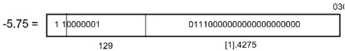
text_image
-5.75 = 1 10000001 129 011100000000000000000000 [1].4275 030Double Precision Floating-Point
| 52 51 | 06 | ||
| S 1 | 1-bit exponent | 52-bit mantissa | |
| biased exponent 0 = +1023 | |||
$$ (- 1) ^ {S} \times [ 1 ]. m _ {\text { base2 }} \times 2 ^ {(e - b i a s)} $$
where:
- 'S' indicates the sign of the number (same values as a signed integer value)
- 'e' represents the exponent value
- 'm' represents the fractional mantissa value
- 'bias' is 127 (SP) or 1023 (DP)
For example, -5.75 = -(1.4275 × 2^2) . In IEEE SP format this would be represented as:
$$ (- 1) ^ {1} \times [ 1 ]. 4 2 7 5 \times 2 ^ {(1 2 9 - 1 2 7)} $$
or (as shown in Figure 1-1):
$$ S = 1, \text { exponent } = 1 2 9 _ {1 0}, \text { mantissa } = [ 1 ]. 4 2 7 5 _ {1 0} $$
or: 0xC0B8 0000
1.2.1 Floating-Point Unit Registers
The dsPIC Floating-Point Unit (FPU) provides a large set of Working registers (F-regs):
- 32 x 32-bit (Single Precision, F0 ... F31) or
- 16 x 64-bit (Double Precision, F0, F2 ... F28, F30) or
- A mix of the two sizes aligned as shown in Figure 1-2.
In addition to the F-regs, status (FSR) and control (FCR) registers are also supported as shown in Figure 1-2:
- FSR (FPU Status Register, 32-bit): Holds the status of retired floating-point instructions:
- FSR[6:0]: Instruction "most-recent" exception status
- FSR[14:8]: Instruction "sticky" exception status
- FSR[19:16]: CPS/CPQ instruction status
- FSR[28:24]: FTST instruction status
• FCR (FPU Control Register, 16-bit):
- FCR[6:0]: Exception mask control
- FCR[9:8]: Rounding mode control
- FCR[10]: Subnormal result "Flush to Zero" (FTZ) control
- FCR[11]: Subnormal operand "Subnormals are Zeros" (SAZ) control
- • FEAR: (FPU Exception Address Capture Register, 24-bit):
- Holds the address of the first instruction encountered that causes an exception. All subsequent instructions in the FPU pipeline that subsequently retire will not affect the FEAR, even if they too generate exceptions.
Figure 1-2. FPU Programmer's Model

text_image
63 31 0 DP F0 SP F1 F2 DP F3 F4 DP F5 F6 DP F6 F7 F8 DP F9 F8 DP F10 F11 F10 DP F12 F13 F12 DP F14 F15 F14 DP F16 F16 DP F17 F18 DP F18 DP F20 F20 DP F21 F22 DP F22 DP F23 F24 DP F24 DP F25 F26 DP F26 DP F27 F28 DP F28 DP F29 F30 DP F30 SP F31 FP Working Registers FP Round Control (FCR[11:8]) FTZSAZ RND[1:0] Exception Masks (FCR[6:0]) SUBOM INF FN FZ FINAN FCR[15:0] FINALMDIVOMOVFMUDFMINXM FTST Status (FSR[28:24]) SUB INF FN FZ FINAN FCPS/FCPQ Status (FSR[19:16]) UNEQLTGT Sticky Exception Status (FSR[14:8]) SUBOS HUGIS UDFSINXBVFS DIVOS INVALS Most-Recent Exception Status (FSR[6:0]) SUBO INVALIDV00VFUDFINXHUGI 23 01 FP EXCEPTION ADDRESS CAPTURE REGISTER EACE FEAR[23:0]Note: Only a single register context shown.
1.3 Programmer's Model
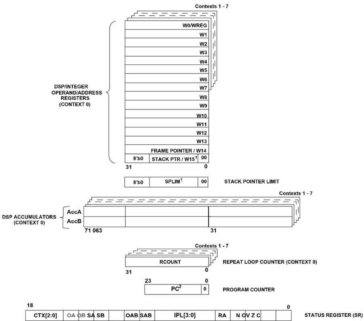
Figure 1-3 shows the programmer's model diagrams for the dsPIC33A family of devices.
Figure 1-3. dsPIC33A Programmer's Model
text_image
DSP/INTEGER OPERAND/ADDRESS REGISTERS (CONTEXT 0) Contexts 1 - 7 W0/WREG W1 W2 W3 W4 W5 W6 W7 W8 W9 W10 W11 W12 W13 FRAME POINTER / W14 8'b0 STACK PTR / W15¹ 00 31 0 8'b0 SPLIM¹ 00 STACK POINTER LIMIT Contexts 1 - 7 DSP ACCUMULATORS (CONTEXT 0) AccA AccB 71 063 31 Contexts 1 - 7 REPEAT LOOP COUNTER (CONTEXT 0) RCOUNT 23 0 PROGRAM COUNTER PC² 0 18 0 CTX[2:0] OA OB SA SB OAB SAB IPL[3:0] RA N OV Z C STATUS REGISTER (SR)Notes:
- W15[1:0] and SPLIM[1:0] always = 0b00.
- PC[0] always = 0b0.
Table 1-1. Programmer's Model Register Descriptions
| Register Description | |
| CORCON CPU Core Configuration register | |
| PC 24-Bit Program Counter | |
| RCOUNT REPEAT Loop Counter register | |
| SPLIM | Stack Pointer Limit Value register |
| SR | ALU and DSP Engine STATUS Register |
| W0-W15 | Working register array |
| ACCA, ACCB | 72-Bit DSP Accumulators |
1.4 Working Register Array
The 16 Working (W) registers can function as data, address or offset registers. The function of a W register is determined by the instruction that accesses it.
Byte instructions, which target the Working register array, only affect the Least Significant Byte (LSB) of the target register.
1.5 Software Stack Frame Pointer
A frame is a user-defined section of memory in the stack, used by a function to allocate memory for local variables. W14 has been assigned for use as a Stack Frame Pointer with the link (LNK) and unlink (ULNK) instructions. However, if a Stack Frame Pointer and the LNK and ULNK instructions are not used, W14 can be used by any instruction in the same manner as all other W registers. See 3.9.2. Software Stack Frame Pointer for detailed information about the Frame Pointer.
1.6 Software Stack Pointer
W15 serves as a dedicated Software Stack Pointer and will be automatically modified by function calls, exception processing and returns. However, W15 can be referenced by any instruction in the same manner as all other W registers. This simplifies reading, writing and manipulating the Stack Pointer. Refer to 3.9.1. Software Stack Pointer for detailed information about the Stack Pointer.
1.7 Stack Pointer Limit Register (SPLIM)
The SPLIM is a 32-bit register associated with the Stack Pointer. It is used to prevent the Stack Pointer from overflowing and accessing memory beyond the user allocated region of stack memory. Refer to 3.9.3. Stack Pointer Overflow for detailed information about the SPLIM.
1.8 Accumulator A and Accumulator B
Accumulator A (ACCA) and Accumulator B (ACCB) are 72-bit wide registers utilized by DSP instructions to perform mathematical and shifting operations.
Accumulator A and Accumulator B can also be used as destination registers in MCU MUL.xx instructions. This helps reduce the execution time of extended precision arithmetic operations.
Refer to Figure 3-13 for details on using ACCA and ACCB.
1.9 Program Counter
The Program Counter (PC) is 24 bits wide. Instructions are addressed in the 4M x 24-bit user program memory space by PC[22:1], where PC[0] is always set to '0' to maintain instruction word alignment and provide compatibility with Data Space Addressing. This means that during normal instruction execution, the PC increments by two.
1.10 RCOUNT Register
The 32-bit RCOUNT register contains the loop counter for the REPEAT instruction. When a REPEAT instruction is executed, RCOUNT is loaded with the repeat count of the instruction, either "lit20" for the "REPEAT #lit20" instruction, "lit5" for the "REPEAT #lit5" instruction or Wn register for the "REPEAT Wn" instruction. The REPEAT loop will be executed RCOUNT + 1 time.
Note: If a REPEAT loop is executing and gets interrupted, RCOUNT may be cleared by the Interrupt Service Routine (ISR) to break out of the REPEAT loop when the foreground code is re-entered.
1.11 STATUS Register
The 32-bit STATUS Register maintains status information for the instructions which have been executed most recently. Operation Status bits exist for MCU operations, loop operations and DSP operations. Additionally, the STATUS Register contains the CPU Interrupt Priority Level bits, IPL[2:0], which are used as a context identifier and for interrupt processing. See 1.14. SR for more detailed information.
1.11.1 MCU ALU Status Bits
The MCU operation Status bits are either affected or used by the majority of instructions in the instruction set. Most of the logic, math, rotate/shift and bit instructions modify the MCU Status bits after execution, and the conditional branch instructions use the state of individual Status bits to determine the flow of program execution. All conditional branch instructions are listed in 3.10. Conditional Branch Instructions.
The Carry (C), Zero (Z), Overflow (OV) and Negative (N) bits show the immediate status of the MCU ALU by indicating whether an operation has resulted in a Carry, Zero, Overflow or Negative result. When a subtract operation is performed, the C flag is used as a Borrow flag.
The Z Status bit is useful for extended precision arithmetic. The Z Status bit functions like a normal Z flag for all instructions except those that use a carry or borrow input (ADDC, CPB, SUBB and SUBBR). See 3.11. Z Status Bit for more detailed information.
Notes:
- All MCU bits are shadowed during execution of the PUSH.S instruction and they are restored on execution of the POP.S instruction.
- All MCU bits are stacked during exception processing (see 3.9.1. Software Stack Pointer).
1.11.2 REPEAT Loop Active (RA) Status Bit
The REPEAT Loop Active bit (RA) is used to indicate when looping is active. The RA flag indicates that a REPEAT instruction is being executed, and it is only affected by the REPEAT instructions. The RA flag is set to '1' when the instruction being repeated begins execution, and it is cleared when the instruction being repeated completes execution for the last time.
Since the RA flag is also read-only, it may not be directly cleared. However, if a REPEAT or its target instruction is interrupted, the Interrupt Service Routine may clear the RA flag, which resides on the stack. This action will disable looping once program execution returns from the Interrupt Service Routine because the restored RA will be '0'.
1.11.3 DSP ALU Status Bits
The high byte of the STATUS Register is used by the DSP class of instructions and it is modified when data passes through one of the adders. It provides status information about overflow and saturation for both accumulators. The Saturate A, Saturate B, Overflow A and Overflow B (SA, SB, OA, OB) bits provide individual accumulator status, while the Saturate AB and Overflow AB (SAB, OAB) bits provide combined accumulator status. The SAB and OAB bits provide an efficient method for the software developer to check the register for saturation or overflow.
The OA and OB bits are used to indicate when an operation has generated an overflow into the Guard bits (bits 63 through 71) of the respective accumulator. This condition can only occur when the processor is in Super Saturation mode or if saturation is disabled. It indicates that the operation has generated a number which cannot be represented with the lower 62 bits of the accumulator.
The SA and SB bits are used to indicate when an operation has generated an overflow out of the MSb of the respective accumulator. The SA and SB bits are active, regardless of the Saturation mode (Disabled, Normal or Super) and may be considered "sticky." Namely, once the SA or SB bit is set to '1', it can only be cleared manually by software, regardless of subsequent DSP operations. When it is required, the BCLR instruction can be used to clear the SA or SB bit.
In addition, the SA and SB bits can be set by software, enabling efficient context state switching.
For convenience, the OA and OB bits are logically ORed together to form the OAB flag, and the SA and SB bits are logically ORed to form the SAB flag. These cumulative Status bits provide efficient overflow and saturation checking when an algorithm is implemented. Instead of interrogating the OA and OB bits independently for arithmetic overflows, a single check of OAB can be performed. Likewise, when checking for saturation, SAB may be examined instead of checking both the SA and SB bits. Note that clearing the SAB flag will clear both the SA and SB bits.
1.11.4 Interrupt Priority Level Status Bits
The three Interrupt Priority Level (IPL) bits of the SRL (SR[7:5]) and the IPL3 bit (SR[8]) set the CPU's IPL, which is used for exception processing. Exceptions consist of interrupts and hardware traps. Interrupts have a user-defined priority level between 0 and 7, while traps have a fixed priority level between 8 and 15. The fourth Interrupt Priority Level bit, IPL3, is a special IPL bit that may only be read or cleared by the user. This bit is only set when a hardware trap is activated, and it is cleared after the trap is serviced.
The CPU's IPL identifies the lowest level exception which may interrupt the processor. The interrupt level of a pending exception must always be greater than the CPU's IPL for the CPU to process the exception. This means that if the IPL is 0, all exceptions at Priority Level 1 and above may interrupt the processor. If the IPL is 7, only hardware traps may interrupt the processor.
When an exception is serviced, the IPL is automatically set to the priority level of the exception being serviced, which will disable all exceptions of equal and lower priority. However, since the IPL field is read/write, one may modify the lower three bits of the IPL in an Interrupt Service Routine to control which exceptions may preempt the exception processing. Since the SRL is stacked during exception processing, the original IPL is always restored after the exception is serviced. If required, one may also prevent exceptions from nesting by setting the NSTDIS bit (INTCON1[15]).
1.12 Core Control Register
The Core Control register (CORCON) is used to set the configuration of the CPU.
In addition to setting CPU modes, the following features are available through the CORCON register:
- Sets the ACCA and ACCB saturation enable
- Sets the Data Space Write Saturation mode
- Sets the Accumulator Saturation and Rounding modes
- Sets the Multiplier mode for DSP operations
1.13 Shadow Registers
A shadow register is used as a temporary holding register and can transfer its contents to or from the associated host register when instructed. Some of the registers in the programmer's model have a shadow register, which is utilized during the execution of a POP.S or PUSH.S instruction. Shadow register usage is shown in Table 1-2.
Table 1-2. Automatic Shadow Register Usage
| Location | DO POP.S/PUSH.S | |
| STATUS Register - DC, N, OV, Z and C bits — Yes | ||
| W0-W3 — Yes |
Note: All shadow registers are one register deep and not directly accessible. Additional shadowing may be performed in software using the software stack.
1.14 CPU STATUS Register
Name: SR
Notes:
-
This bit may be read or cleared (not set). Clearing this bit will clear SA and SB irrespective of the value simultaneously written to SA and/or SB.
-
IPL[2:0] become read only bits if NSTDIS(INTCON1[15])=1 (nesting disabled).
Legend: C = Clearable bit
| Bit 31 30 29 28 27 26 25 24 | |||||||
| Access Reset | |||||||
| Bit 23 22 21 20 19 18 17 16 | ||||||
| VF | CTX[2:0] | |||||
| Access | R | R | R | |||
| Reset | 0 | 0 | 0 | |||
| Bit 15 14 13 12 11 10 | 9 | 8 | ||||||
| OA | OB | SA | SB | OAB | SAB | IPL3 | ||
| Access | R/W | R/W | R/W | R/W | R | R/C | R/C | |
| Reset | 0 | 0 | 0 | 0 | 0 | 0 | 0 | |
| Bit | 7 | 6 | 5 | 4 | 3 | 2 | 1 | 0 |
| IPL[2:0] | RA | N | OV | Z | C | |||
| Access | R/W | R/W | R/W | R | R/W | R/W | R/W | R/W |
| Reset | 0 | 0 | 0 | 0 | 0 | 0 | 0 | 0 |
Bit 23 - VF Vector (Fetch) Fail Status
| Value | Description |
| 1 | Indicates to the bus error handler that the source of the bus error is a vector fetch. The vector data read will be substituted with the contents of the Vector Fail Address (VFA) SFR. |
| 0 | Indicates to the bus error handler that the source of the bus error is not a vector fetch. |
Bits 18:16 - CTX[2:0] Current (W register) Context Identifier Identifies which W register context is currently in use by the CPU
| Value | Description |
| 111 | Context 7 is currently in use |
| 110 | Context 6 is currently in use |
| 101 | Context 5 is currently in use |
| 100 | Context 4 is currently in use |
| 011 | Context 3 is currently in use |
| 010 | Context 2 is currently in use |
| 001 | Context 1 is currently in use |
| 000 | Context 0 is currently in use |
Bit 15 - OA Accumulator A Fractional Overflow Status
| Value | Description |
| 1 | Accumulator A fractional overflow has occurred (its contents can no longer be represented as a 1.31 fractional value) |
| 0 | Accumulator A not overflowed |
Bit 14 - OB Accumulator B Fractional Overflow Status
| Value Description | |
| 1 | Accumulator A fractional overflow has occurred (its contents can no longer be represented as a 1.31 fractional value) |
| 0 | Accumulator A not overflowed |
Bit 13 - SA Accumulator A Saturation/Sign Overflow 'Sticky' Status
| Value Description | |
| 1 | Accumulator A is saturated or has been saturated at some time, or has overflowed into bit 71 (if saturation is disabled) |
| 0 | Accumulator A is not saturated or has not overflowed into bit 71 (if saturation is disabled) |
Bit 12 - SB Accumulator B Saturation/Sign Overflow 'Sticky' Status
| Value Description | |
| 1 | Accumulator B is saturated or has been saturated at some time, or has overflowed into bit 71 (if saturation is disabled) |
| 0 | Accumulator B is not saturated or has not overflowed into bit 71 (if saturation is disabled) |
Bit 11 - OAB OA || OB Combined Accumulator Fractional Overflow Status
| Value Description | |
| 1 | Accumulators A or B fractional overflow has occurred (one or both of their contents can no longer be represented as a 1.31 fractional value) |
| 0 | Neither Accumulators A nor B have overflowed |
Bit 10 - SAB SA || SB Combined Accumulator 'Sticky' Status ^(1)
| Value Description | |
| 1 | Accumulators A or B are saturated or have been saturated at some time, or have overflowed into bit 71 (if saturation is disabled) |
| 0 | Neither Accumulator A nor B are saturated or have overflowed into bit 71 (if saturation is disabled) |
Bit 8 - IPL3 MSb (Most Significant bit) of CPU Priority Level Nibble
| Value Description | |
| 1 | CPU Priority ≥ 8 (trap exception underway) |
| 0 | CPU Priority < 8 (no trap exception underway) |
Bits 7:5 - IPL[2:0] CPU Interrupt Priority Level Status bits ^(2)
| Value | Description |
| 111 | All interrupts disabled |
| 110 | Level 7 interrupts enabled |
| 101 | Level 6 and 7 interrupts enabled |
| 100 | Level 5 through 7 interrupts enabled |
| 011 | Level 4 through 7 interrupts enabled |
| 010 | Level 3 through 7 interrupts enabled |
| 001 | Level 2 through 7 interrupts enabled |
| 000 | Level 1 through 7 interrupts enabled |
Bit 4 - RA REPEAT Loop Active
| Value Description | |
| 1 | REPEAT loop in progress |
| 0 | REPEAT loop not in progress |
Bit 3 - N MCU ALU Negative bit
| Value Description | |
| 1 | Result was negative |
| 0 | Result was non-negative (zero or positive) |
Bit 2 - OV MCU ALU Overflow bit
This bit is used for signed arithmetic (2's complement). It indicates an overflow of the magnitude that causes the Sign bit to change state.
| Value Description | |
| 1 | Overflow occurred for signed arithmetic (in this arithmetic operation) |
| 0 | No overflow occurred |
Bit 1 - Z MCU ALU 'Sticky' Zero bit
| Value Description | |
| 1 | An operation which effects the Z bit has set it at some time in the past |
| 0 | The most recent operation which effects the Z bit has cleared it (i.e., a non-zero result) |
Bit 0 - C MCU ALU Carry/Borrow bit
| Value Description | |
| 1 | A carry-out from the MSb of the result occurred |
| 0 | No carry-out from the MSb of the result occurred |
1.15 Core Control Register
Name: CORCON
Note:
- This bit has no effect if US = 1 (unsigned mode).
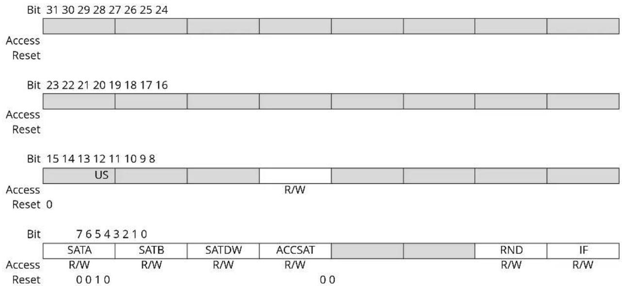
text_image
Bit 31 30 29 28 27 26 25 24 Access Reset Bit 23 22 21 20 19 18 17 16 Access Reset Bit 15 14 13 12 11 10 9 8 US R/W Access Reset 0 Bit 7 6 5 4 3 2 1 0 SATA SATB SATDW ACCSAT RND IF Access R/W R/W R/W R/W R/W Reset 0 0 1 0 0 0Bit 12 - US DSP Multiply Unsigned/Signed Control bits
| Value | Description |
| 1 | DSP Engine Unsigned mode enabled |
| 0 | DSP Engine Signed mode enabled |
Bit 7 - SATA ACCA Saturation Enable bit ^(1)
| Value | Description |
| 1 | Accumulator A saturation is enabled |
| 0 | Accumulator A saturation is disabled |
Bit 6 - SATB ACCB Saturation Enable bit ^(1)
| Value | Description |
| 1 | Accumulator B saturation is enabled |
| 0 | Accumulator B saturation is disabled |
Bit 5 - SATDW Data Space Write from DSP Engine Saturation Enable bit
| Value | Description |
| 1 | Data Space write saturation is enabled |
| 0 | Data Space write saturation is disabled |
Bit 4 - ACCSAT Accumulator Saturation Mode Select bit
| Value | Description |
| 1 | 9.31 saturation (super saturation) |
| 0 | 1.31 saturation (normal saturation) |
Bit 1 - RND Rounding Mode Select bit
| Value | Description |
| 1 | Biased (conventional) rounding is enabled |
Value Description
| 0 | Unbiased (convergent) rounding is enabled |
Bit 0 - IF Integer or Fractional Multiplier Mode Select bit
Value Description
| 1 | Integer mode is enabled for DSP multiply |
| 0 | Fractional mode is enabled for DSP multiply |
2. Instruction Set Overview
The dsPIC33A instruction set provides a broad suite of instructions that support traditional microcontroller applications and a class of instructions that support math-intensive applications. Since almost all of the functionality of the 16-bit MCU and DSC instruction set has been maintained, this hybrid instruction set allows an easy 32-bit migration path for users already familiar with the PIC microcontroller.
Instructions can be grouped into the functional categories shown in Table 2-1. Table 2 defines the symbols used in the instruction summary tables. Table 2-1 through Table 2-12 define the syntax, description, storage and execution requirements for each instruction. Storage requirements are represented in 32-bit instruction words and execution requirements are represented in instruction cycles.
Table 2-1. Instruction Groups
| Functional Group Summary Table | |
| Move Instructions Table 2-2 | |
| Math Instructions Table 2-3 | |
| Logic Instructions Table 2-4 | |
| Rotate/Shift Instructions Table 2-5 | |
| Bit Instructions Table 2-6 | |
| Compare/Skip and Compare/Branch Instructions Table 2-7 | |
| Program Flow Instructions Table 2-8 | |
| Shadow/Stack Instructions Table 2-9 | |
| Control Instructions Table 2-10 | |
| DSP Instructions Table 2-11 | |
| FPU Instructions Table 2-12 |
Most instructions have several different addressing modes and execution flows, which require different instruction variants. For instance, there are up to seven unique ADD instructions and each instruction variant has its own instruction encoding. Instruction format descriptions and specific instruction operations are provided in Instruction Descriptions. Additionally, a composite alphabetized instruction set table is provided in 6. Reference.
2.1 Multicycle Instructions
As shown in the instruction summary tables, most instructions execute in a single cycle with the following exceptions:
- Instructions, MOV.D, POP.D and PUSH.D, require two cycles to execute.
- Instructions, DIV.S, DIV.U and DIVF, are single-cycle instructions, which should be executed consecutive times as the target of a REPEAT instruction.
- Instructions that change the Program Counter require two cycles to execute. Instructions such as CALL also require two cycles to execute.
- RETFIE, RETLW and RETURN are a special case of an instruction that changes the Program Counter. These execute in three cycles, unless an exception is pending, and then they execute in two cycles.
2.2 Multiword Instructions
As defined by Table 2-2 through Table 2-12, almost all instructions consume one instruction word (32 bits), with the exception of the CALL and GOTO instructions, which are program flow instructions listed in Table 2-8. These instructions require two words of memory because their opcodes embed large literal operands.
2.3 Instruction Set Summary Tables
Table 2-2. Move Instructions
| Assembled Syntax Description Words Cycles | |||
| EXCH Wns,Wnd | Swap Wns with Wnd 1 2 | ||
| MOV Rso,Rdo | Move Ws to Wd 0.5/1 1 | ||
| MOV.l lit32,Wnd | Move 32-bit unsigned literal to Wnd 2 2 | ||
| MOV.sl lit24,Wnd | Move 24-bit unsigned literal to Wnd; 0 extend to 32-bits | 1 | 1 |
| MOV.w lit16,Wnd | Move 16-bit unsigned literal to Wnd; 0 extend to 32-bits | 1 | 1 |
| MOV.bz lit8,Wnd | Move 8-bit unsigned literal to Wnd; 0 extend to 32-bits | 1 | 1 |
| MOV.l [W15-lit7], Wnd[W14+slit7], Wnd | Move from system stack with literal offset to Wnd using SP or FP | 0.5 1 | |
| MOV.l Wns, [W15-lit7]Wns, [W14+slit7] | Move from Wns to system stack with literal off-set using SP or FP | 0.5 1 | |
| MOV.l f,Wnd | Move f to Wnd (Word or Long Word)(f < ~1MB) | 1 | 1 |
| MOV.w f,Wnd | Move f to Wnd (Word or Long Word)(f > ~1MB) | 2 | 2 |
| MOV.b f,Wnd | Move f to Wnd (Byte) 1 1 | ||
| MOV.l Wns,f | Move Wns to f (Word or Long Word)(f < ~1MB) | 1 | 1 |
| MOV.w Wns,f | Move Wns to f (Word or Long Word)(f > ~1MB) | 2 | 2 |
| MOV.b Wns,f | Move Wns to f (Byte) 1 1 | ||
| MOV [Wns+Slit12],Wnd | Move [Wns+Slit12] to Wnd 1 1 | ||
| MOV Wns, [Wnd+Slit12] | Move Wns to [Wnd+Slit12] 1 1 | ||
| MOVIF.l CC, Wb, Wns, Wd | If SR.Z=1Move W1 to [W15++]Else Move W2 to [W15++] | 1 | 1 |
| MOVIF.w CC, Wb, Wns, Wd | If SR.Z=1Move W1 to [W15++]Else Move W2 to [W15++] | 1 | 1 |
| MOVIF.bz CC, Wb, Wns, Wd | If SR.Z=1Move W1 to [W15++]Else Move W2 to [W15++] | 1 | 1 |
| MOVIF.b CC, Wb, Wns, Wd | If SR.Z=1Move W1 to [W15++]Else Move W2 to [W15++] | 1 | 1 |
| MOVR.l | Move Ws to Wd with destination Bit Reversed | ||
| MOVR.w | Move Ws to Wd with destination Bit Reversed | 1 | 1 |
| MOVS.l slit16, Wd | Move signed extended 16-bit literal to Wd | 1 | 1 |
| MOVS.w slit16, Wd | Move 16-bit literal to Wd; sign extend to 32-bits if register direct mode. | 1 | 1 |
| MOVS.b slit8, Wnd | Move 8-bit literal to Wd; no extension. | 1 1 | |
| SWAP Wn | Wn = Word or byte swap Wn | 1 1 | |
| TST f | Test f 1 1 | ||
| TST f, Wind | Test f and move f to Wind 1 1 |
Table 2-3. Math Instructions
| Assembled Syntax Description Words Cycles | |||
| ADD f,Wn | f = f + Wn 1 1 | ||
| ADD f,Wn,Wn | Wn = f + Wn 1 1 | ||
| ADD.1 lit5,Wn | Wn = Wn + lit5 0.5 1 | ||
| ADD lit16,Wn | Wn = Wn + lit16 1 1 | ||
| ADD Wb,Ws,Wd | Wd = Wb + Ws 0.5/1 1 | ||
| ADD Wb,lit7,Wd | Wd = Wb + lit7(literal zero-extended) | 1 1 | |
| ADDC f,Wn | f = f + Wn + (C) 1 1 | ||
| ADDC f,Wn,Wn | Wn = f + Wn + (C) | 1 1 | |
| ADDC lit16,Wn | Wn = Wn + lit16 + (C) | 1 1 | |
| ADDC Wb,Ws,Wd | Wd = Wb + Ws + (C) | 0.5/1 | 1 |
| ADDC Wb,lit7,Wd | Wd = Wb + lit7 + (C)(literal zero-extended) | 1 1 | |
| DEC f | f = f -1 | 1 1 | |
| DEC f,Wd | W5 = f -1 | 1 1 | |
| DEC Ws,Wd | Wd = Ws - 1 | 1 1 | |
| DEC2 f | f = f -2 | 1 1 | |
| DEC2 f,Wd | W5 = f -2 | 1 1 | |
| DEC2 Ws,Wd | Wd = Ws - 2 | 1 1 | |
| DIVF Wm/Wn | Interruptible Signed 16/16 or 32/16 Fractional Divide | 1 | 1 |
| DIVFL Wm/Wn | Interruptible Signed 32/32 Fractional Divide | 1 | 1 |
| DIVS.w Wm/Wn | Interruptible Signed 16/16-bit Integer Divide | 1 | 1 |
| DIVS.1 Wm/Wn | Interruptible Signed 32/16-bit Integer Divide | 1 | 1 |
| DIVSL Wm/Wn | Interruptible Signed 32/32 Integer Divide | 1 1 | |
| DIVU.w Wm/Wn | Interruptible Unsigned 16/16-bit Integer Divide | 1 | 1 |
| DIVU.1 Wm/Wn | Interruptible Unsigned 32/16-bit Integer Divide | 1 | 1 |
| DIVUL Wm/Wn | Interruptible Unsigned 32/32 Integer Divide | 1 | 1 |
| FLIM Wb, Ws | Force Data (Upper and Lower) Range Limit without Limit Excess Result | 1 | 1 |
| FLIM Wb, Ws, Wd | Force Data (Upper and Lower) Range Limit with Limit Excess Flag (Wd=-1) | 1 | 2 |
| FLIM.V Wb, Ws, Wd | Force Data (Upper and Lower) Range Limit with Limit Excess Result | 1 | 2 |
| INC f | f = f + 1 | 1 1 | |
| INC f,Wd | W5 = f + 1 | 1 1 | |
| INC Ws,Wd | Wd = Ws + 1 | 1 1 | |
| INC2 f | f = f + 2 | 1 1 | |
| INC2 f,Wd | W5 = f + 2 | 1 1 | |
| INC2 Ws,Wd | Wd = Ws +2 1 1 | ||
| MULSS Wb,Ws,Wnd | {Wd}=signed(Wb) * signed(WS) 0.5/1 1 | ||
| MULSU Wb,Ws,Wnd | {Wd}=signed(Wb) * unsigned(WS) 0.5/1 1 | ||
| MULUS Wb,Ws,Wnd | {Wd}=unsigned(Wb) * signed(WS) 0.5/1 1 | ||
| MULUU Wb,Ws,Wnd | {Wd}=unsigned(Wb) * unsigned(WS) 0.5/1 1 | ||
| MULSU Wb,lit8,Wnd | {Wd}=signed(Wb) * unsigned(lit8) 1 1 | ||
| MULUU Wb,lit8,Wnd | {Wd}=unsigned(Wb) * unsigned(lit8) 1 1 | ||
| MULSS Wb,slit8,Wnd | {Wd}=signed(Wb) * signed(slit8) 1 1 | ||
| MULUS Wb,slit8,Wnd | {Wd}=unsigned(Wb) * signed(slit8) 1 1 | ||
| MUL f, Wn | W2 = f * Wn 1 1 | ||
| SE Rso,Wnd | Wd = sign-extended Ws 0.5/1 1 | ||
| SUB f,Wn | f = f - Wn 1 1 | ||
| SUB f,Wn,Wn | Wn = f - Wn 1 1 | ||
| SUB.1 lit5,Wn | Wn = Wn - lit5 0.5 1 | ||
| SUB lit16,Wn | Wn = Wn - lit16 | 1 1 | |
| SUB Wb,Ws,Wd | Wd = Wb - Ws 0.5/1 1 | ||
| SUB Ws,lit7,Wd | Wd = Ws - lit7 (literal zero-extended) | 1 1 | |
| SUBB f,Wn | f = f - Wn - (C) | 1 1 | |
| SUBB f,Wn,Wn | Wn = f - Wn - (C) | 1 1 | |
| SUBB lit16,Wn | Wn = Wn - lit16 - (C) | 1 1 | |
| SUBB Wb,Ws,Wd | Wd = Wb - Ws - (C) | 0.5/1 1 | |
| SUBB Ws,lit7,Wd | Wd = Ws - lit7 - (literal zero-extended) | 1 1 | |
| SUBR f,Wn | f = Wn - f 1 1 | ||
| SUBR f,Wn,Wn | Wn = Wn - f 1 1 | ||
| SUBR Wb,Ws,Wd | Wd = Ws - Wb 0.5/1 1 | ||
| SUBR Ws,lit7,Wd | Wd = lit7 - Ws (literal zero-extended) | 0.5/1 1 | |
| SUBBR f,Wn | f = Wn - f - (C) | 1 1 | |
| SUBBR f,Wn,Wn | Wn = Wn -f - (C) | 1 1 | |
| SUBBR Wb,Ws,Wd | Wd = Ws - Wb - (C) | 0.5/1 1 | |
| SUBBR Ws,lit7,Wd | Wd = lit7 - Ws - (C) (literal zero-extended) | 1 1 | |
| ZE Rso,Wnd | Wd = Zero-extend Ws | 0.5/1 1 |
Table 2-4. Logic Instructions
| Assembled Syntax | Description | Words Cycles |
| AND f,Wn | f = f.AND. Wn | 1 1 |
| AND f,Wn,Wn | W0 = f.AND. Wn | 1 1 |
| AND lit16,Wn | Wn = Wn.AND. lit16 | 1 1 |
| AND Wb,Ws,Wd | Wd = Wb.AND. Ws | 0.5/1 1 |
| AND Wb,lit7,Wd | Wd = Wb.AND. Lit7 (literal zero-extended) | 1 1 |
| AND1 Wb,lit7,Wd | Wd = Wb.AND. Lit7 (literal zero-extended) | 1 1 |
| CLR f | f = 0x0000 | 1 1 |
| CLR Wd | Wd = 0x0000 | 1 1 |
| COM f | f = f | 1 1 |
| COM f,Wd | Wd = f | 1 1 |
| COM Ws,Wd | Wd = Ws | 0.5/1 1 |
......continued
| Assembled Syntax Description Words Cycles | |||
| IOR f,Wn | f = f.IOR. Wn 1 1 | ||
| IOR f,Wn,Wn | Wn = f.IOR. Wn 1 1 | ||
| IOR lit16,Wn | Wn = Wn .IOR. lit16 1 1 | ||
| IOR Wb,Ws,Wd | Wd = Wb .IOR. Ws 0.5/1 1 | ||
| IOR Wb,lit7,Wd | Wd = Wb .IOR. lit7 1 1 | ||
| NEG f | f = f+ 1 1 1 | ||
| NEG f,Wd | Wd = f+ 1 1 1 | ||
| NEG Ws,Wd | Wd = Ws- + 1 0.5/1 1 | ||
| SETM f | f = 0xFFFF 1 1 | ||
| SETM Wd | Wd = 0xFFFF 1 1 | ||
| XOR f,Wn | f = f.XOR. Wn | 1 1 | |
| XOR f,Wn,Wn | Wn = f.XOR. Wn | 1 1 | |
| XOR lit16,Wn | Wn = Wn .XOR. lit16 | 1 1 | |
| XOR Wb,Ws,Wd | Wd = Wb .XOR. Ws | 0.5/1 1 | |
| XOR Wb,lit7,Wd | Wd = Wb .XOR. Llt7 (literal zero-extended) | 1 1 |
Table 2-5. Rotate/Shift Instructions
| Assembled Syntax | Description | Words | Cycles |
| ASR f | f = Arithmetic Right Shift f by 1 | 1 | 1 |
| ASR f,Wn | Wn = Arithmetic Right Shift f by 1 | 1 | 1 |
| ASR Ws,Wd | Wd = Arithmetic Right Shift Ws by 1 | 0.5/1 | 1 |
| ASR Ws,Wb,Wd | Wnd = Arithmetic Right Shift Ws by Wb | 0.5/1 | 1 |
| ASR Ws,lit5,Wd | Wnd = Arithmetic Right Shift Ws by lit5 | 0.5/1 | 1 |
| ASRM Ws, lit5, Wnd | Wnd = Arithmetic Right Shift Ws by lit5, then logically OR with next lsw | 1 | 2 |
| ASRM Ws, Wb, Wnd | Wnd = Arithmetic Right Shift Ws by Wb, then logically OR with next lsw | 1 | 2 |
| LSR f | f = Logical Right Shift f by 1 | 1 | 1 |
| LSR f,Wd | Wd = Logical Right Shift f by 1 | 1 | 1 |
| LSR Ws,Wd | Wd = Logical Right Shift Ws by 1 | 0.5/1 | 1 |
| LSR Ws,Wb,Wd | Wnd = Logical Right Shift Ws by Wns | 0.5/1 | 1 |
| LSR Ws,lit5,Wd | Wnd = Logical Right Shift Ws by lit5 | 0.5/1 | 1 |
| LSRM Ws, lit5, Wnd | Wnd = Logical Right Shift Ws by lit5, then logically OR with next lsw | 1 | 2 |
| LSRM Ws, Wb, Wnd | Wnd = Logical Right Shift Ws by Wb, then logically OR with next lsw | 1 | 2 |
| RLC f | f = Rotate Left through Carry f | 1 | 1 |
| RLC f,Wd | Wd = Rotate Left through Carry f | 1 | 1 |
| RLC Ws,Wd | Wd = Rotate Left through Carry Ws | 0.5/1 | 1 |
| RLNC f | f = Rotate Left (No Carry) f | 1 | 1 |
| RLNC f,Wd | Wd = Rotate Left (No Carry) f | 1 | 1 |
| RLNC Ws,Wd | Wd = Rotate Left (No Carry) Ws | 0.5/1 | 1 |
| RRC f | f = Rotate Right through Carry f | 1 | 1 |
| RRC f,Wd | Wd = Rotate Right through Carry f | 1 | 1 |
| RRC Ws,Wd | Wd = Rotate Right through Carry Ws | 0.5/1 | 1 |
| RRNC f | f = Rotate Right (No Carry) f | 1 | 1 |
| RRNC f,WdAssembled Syntax Description Words Cycles | Wd = Rotate Right (No Carry) f | 1 | 1 |
| RRNC Ws,Wd | Wd = Rotate Right (No Carry) Ws 0.5/1 1 | ||
| SL f | f = Left Shift f by 1 1 1 | ||
| SL f,Wd | Wd = Left Shift f by 1 1 1 | ||
| SL Ws,Wd | Wd = Left Shift Ws by 1 0.5/1 1 | ||
| SL Ws,Wb,Wnd | Wnd = Left Shift Wb by Wns 0.5/1 1 | ||
| SL Ws,lit5,Wnd | Wnd = Left Shift Ws by lit5 0.5/1 1 | ||
| SLM Ws, lit5, Wnd | Wnd = Left Shift Wb by lit5, then logically OR with next msw | 1 | 2 |
| SLM Ws, Wb, Wnd | Wnd = Left Shift Wb by Wb, then logically OR with next msw | 1 | 2 |
Table 2-6. Bit Instructions
| Assembled Syntax Description Words Cycles | |||
| BCLR.b f,bit3 | Bit Clear f 1 1 | ||
| BCLR Ws,bit4 | Bit Clear Ws | 0.5/1 | 1 |
| BFEXT bit4,wid5,Ws,Wb | Bit Field Extract from Ws to Wb | 1 | 1 |
| BFEXT bit4,wid5,f,Wb | Bit Field Extract from f to Wb | 2 | 2 |
| BFINS bit4,wid5,Wb,Ws | Bit Field Insert from Wb into Ws | 1 | 1 |
| BFINS bit4,wid5,Wb,f | Bit Field Insert from Wb Into f | 2 | 2 |
| BFINS bit4,wid5,lit8,Ws | Bit Field Insert lit8 into Ws | 2 | 2 |
| BSET.b f,bit3 | Bit Set f | 1 | 1 |
| BSET Ws,bit4 | Bit Set Ws | 0.5/1 | 1 |
| BSW.C Ws,Wb | Write C or Z bit to Ws1 | 1 | 1 |
| BSW.Z Ws,Wb | Write C or Z bit to Ws0.5/11 | 0.5/1 | 1 |
| BTG.b f,bit3 | Bit Toggle f | 1 | 1 |
| BTG Ws,bit4 | Bit Toggle Ws | 0.5/1 | 1 |
| BTST.b f,bit3 | Bit Test f | 1 | 1 |
| BTST.C Ws,bit4 | Bit Test Ws to C | 0.5/1 | 1 |
| BTST.Z Ws,bit4 | Bit Test Ws to Z | 1 | 1 |
| BTST.C Ws,Wb | Bit Test Wsto C | 0.5/1 | 1 |
| BTST.Z Ws,Wb | Bit Test Wsto Z | 1 | 1 |
| BTSTS.b f,bit3 | Bit Test then Set f | 1 | 1 |
| BTSTS.C Ws,bit4 | Bit Test Ws to C then Set | 0.5/1 | 1 |
| BTSTS.Z Ws,bit4 | Bit Test Ws to Z then Set | 1 | 1 |
| FBCL Ws,Wnd | Find Bit Change from Left (MSb) Side | 1 | 1 |
| FF1L Ws,Wnd | Find First One from Left (MSb) Side | 1 | 1 |
| FF1R Ws,Wnd | Find First One from Right (LSb) Side | 1 | 1 |
Table 2-7. Compare/Skip and Compare/Branch Instructions
| Assembled Syntax | Description | Words | Cycles |
| CP f, Ws | Compare f with Ws | 1 | 1 |
| CP Ws, lit13 | Compare Ws with lit13 (literal zero-extended) | 1 | 1 |
| CP Wb, lit16 | Compare Wb with lit16 (literal zero-extended) | 1 | 1 |
| CP Wb, Ws | Compare Wb with Ws 0.5/1 1 | ||
| CP0 f | Compare f with 0x0000 | 1 | 1 |
| Assembled Syntax Description Words Cycles | |||
| CP0 Ws | Compare Ws with 0x0000 (substitute CPLS Ws,#0) | 1 | 1 |
| CPB f,Ws | Compare f with Ws, with borrow 1 1 | ||
| CP Wb,lit13 | Compare Wb with lit13, with borrow (literal zero-extended) | 1 | 1 |
| CP Wb,lit16 | Compare Wb with lit16, with borrow (literal zero-extended) | 1 | 1 |
| CPB Wb,Ws | Compare Borrow Wb with Ws 0.5/1 1 | ||
| DTB Wn,Label | Decrement Wn, then branch if not zero 1 1(2/3) | ||
Table 2-8. Program Flow Instructions
| Assembled Syntax Description | Words Cycles | ||
| BRA Label | Branch Unconditionally 1 1 | ||
| BRA Wn | Computed Branch 1 2 | ||
| BRA C,Label | Branch if Carry | 1 1(2/3) | |
| BRA GE,Label | Branch if greater than or equal | 1 1(2/3) | |
| BRA GEU,Label | Branch if unsigned greater than or equal | 1 1(2/3) | |
| BRA GT,Label | Branch if greater than | 1 1(2/3) | |
| BRA GTU,Label | Branch if unsigned greater than | 1 1(2/3) | |
| BRA LE,Label | Branch if less than or equal | 1 1(2/3) | |
| BRA LEU,Label | Branch if unsigned less than or equal | 1 1(2/3) | |
| BRA LT,Label | Branch if less than | 1 1(2/3) | |
| BRA LTU,Label | Branch if unsigned less than | 1 1(2/3) | |
| BRA N,Label | Branch if Negative 1 1(2/3) | ||
| BRA NC,Label | Branch if Not Carry | 1 1(2/3) | |
| BRA NN,Label | Branch if Not Negative | 1 1(2/3) | |
| BRA NOV,Label | Branch if Not Overflow | 1 1(2/3) | |
| BRA NZ,Label | Branch if Not Zero 1 1(2/3) | ||
| BRA Z,Label | Branch if Zero | 1 1(2/3) | |
| BREAK | Stop user code execution | 0.5/1 | 1 |
| CALL Label | Call subroutine (label > ~ 16MB) | 1 1 | |
| (label < ~ 16MB) | 2 2 | ||
| CALL Wns | Call indirect subroutine at address [W11] | 1 2 | |
| GOTO Label | Goto address (address < ~ 16MB) | 1 1 | |
| (address > ~ 16MB) | 2 2 | ||
| GOTO Wn | Go to indirect address at [W11] | 1 2 | |
| RCALL Label | Relative Call | 1 1 | |
| RCALL Wns | Computed Call | 1 2 | |
| REPEAT lit15 | Repeat Next Instruction lit15+1 times | 1 1 | |
| REPEAT lit5 | Repeat Next Instruction lit5+1 times | 0.5 | 1 |
| REPEAT Wn | Repeat Next Instruction (Wn)+1 times | 1 1 | |
| RETFIE | Return from interrupt enable | 0.5 | 4 |
| RETLW lit16,Wn | Return from Subroutine with literal in Wn | 1 3 | |
| RETURN | Return from Subroutine | 0.5 | 3 |
Table 2-9. Shadow/Stack/Context Instructions
| Assembled Syntax Description | Words Cycles | ||
| BOOTSWP | Swap Active and Inactive address space | 0.5 2 | |
| CTXTSWP lit3 | Swap to CPU register context #2 | 0.5 2 | |
| CTXTSWP Wn | Swap to CPU register context defined in Wn[2:0] | 1 | 2 |
| LNK lit16 | Link frame pointer 1 1 | ||
| LNK lit7 | Link frame pointer (literal < 128) | 0.5 1 | |
| POP f | Pop f from top of stack (TOS) 1 | 1 | |
| POP { [--Ws],} Wnd | Pop Wnd Register from system stack. | 0.5 1 | |
| POP Fd | Pop Fd Register from system stack. | 0.5 1 | |
| PUSH f | Push f to top of stack (TOS) 1 1 | ||
| PUSH Wns, { [Wd++]} | Push Wns Register to system stack | 0.5 1 | |
| PUSH Fs | Push Fs Register to system stack | 0.5 1 | |
| ULNK | Unlink frame pointer 0.5 1 |
Table 2-10. Control Instructions
| Assembled Syntax Description | Words Cycles | ||
| CLRWDT | Clear Watchdog Timer 0.5 1 | ||
| DISICTL lit3 (,Wd) | Disable interrupts at IPL <= lit3 Optionally save prior IPL threshold to Wd | 1 | 1 |
| DISICTL Wns (,Wd) | Disable Interrupts at IPL <= Wns[2:0] Optionally save prior IPL threshold to Wd | 1 | 1 |
| NEOP | None executable NOP (16-bit instruction pad) | 0.5 0 | |
| NOP | No Operation 1 1 | ||
| NOPR | No Operation 1 1 | ||
| PWRSAV mode | Go into standby mode 0.5 2 | ||
| RESET | Software device RESET 1 1 |
Table 2-11. DSP Instructions
| Assembled Syntax Description | Words Cycles | ||
| ADD A | Add Accumulators 0.5 1 | ||
| ADD Rso,Slit6, A | 16-bit Signed Add to Accumulator | 1 | 1 |
| BRA OA,Label | Branch if accumulator A overflow | 1 1(2/3) | |
| BRA OB,Label | Branch if accumulator B overflow | 1 1(2/3) | |
| BRA OV,Label | Branch if Overflow 1 1(2/3) | ||
| BRA SA,Label | Branch if accumulator A saturated | 1 1(2/3) | |
| BRA SB,Label | Branch if accumulator B saturated | 1 1(2/3) | |
| CLR A | Clear Accumulator 0.5 1 | ||
| ED Wxp * Wyp, A, AWB | Euclidean Distance 1 2 | ||
| EDAC Wxp * Wyp, A, AWB | Euclidean Distance Accumulate | 1 | 2 |
| LAC Rso, Slit6, A | Load Accumulator (16/32-bit), literal shift | 1 | 1 |
| LLAC.1 Rso Slit6, A | Load Lower (LS-word of) Accumulator (32-bit), literal shift | 1 | 1 |
| LUAC.1 Rso, Slit6, A | Load Upper (LS-byte) of Accumulator (32-bit), literal shift | 1 | 1 |
| MAC Wxp * Wyp, A, AWB | Multiply and Accumulate 1 1 | ||
| MAX Wb, Ws | Force Data Maximum Range Limit | 1 | 1 |
| MAX A | Force Data Maximum Range Limit | 0.5 1 | |
| MAX.V A, Rdo | Force Data Maximum Range Limit with Result | 1 | 2 |
| MIN Wb, Ws | Force Data Minimum Range Limit | 1 | 1 |
| MIN A | Force Data Minimum Range Limit | 0.5 1 | |
| MIN.V A, Rdo | Force Data Minimum Range Limit with Result | 1 | 2 |
| MULISS Wb, Ws, A | Integer: Acc(A or B) = signed(Wb) * signed(Ws) | 1 | 1 |
| MULFSS Wb, Ws, A | Fractional: Acc(A or B) = signed(Wb) * signed(Ws) | 1 | 1 |
| MULISU Wb, Ws, A | Integer: Acc(A or B) = signed(Wb) * unsigned(Ws) | 1 | 1 |
| MULFSU Wb, Ws, A | Fractional: Acc(A or B) = signed(Wb) * unsigned(Ws) | 1 | 1 |
| MULIUS Wb, Ws, A | Integer: Acc(A or B) = unsigned(Wb) * signed(Ws) | 1 | 1 |
| MULFUS Wb, Ws, A | Fractional: Acc(A or B) = unsigned(Wb) * signed(Ws) | 1 | 1 |
| MULIUU Wb, Ws, A | Integer: Acc(A or B) = unsigned(Wb) * unsigned(Ws) | 1 | 1 |
| MULFUU Wb, Ws, A | Fractional: Acc(A or B) = unsigned(Wb) * unsigned(Ws) | 1 | 1 |
| MULISS Wb, slit8, A | Integer: Acc(A or B) = signed(Wb) * signed(slit8) | 1 | 1 |
| MULFSS Wb, slit8, A | Integer: Acc(A or B) = signed(Wb) * signed(slit8) | 1 | 1 |
| MULISU Wb, lit8, A | Integer: Acc(A or B) = signed(Wb) * unsigned(lit8) | 1 | 1 |
| MULFSU Wb, lit8, A | Integer: Acc(A or B) = signed(Wb) * unsigned(lit8) | 1 | 1 |
| MULIUS Wb, slit8, A | Integer: Acc(A or B) = signed(Wb) * signed(slit8) | 1 | 1 |
| MULFUS Wb, slit8, A | Integer: Acc(A or B) = signed(Wb) * signed(slit8) | 1 | 1 |
| MULIUW Wb,lit8,A | Integer: Acc(A or B) = signed(Wb) * unsigned(lit8) | 1 | 1 |
| MULFUW Wb,lit8,A | Integer: Acc(A or B) = signed(Wb) * unsigned(lit8) | 1 | 1 |
| MPYWxp * Wyp, A, AWB | Multiply Wm by Wn to Accumulator | 1 | 1 |
| MPYN Wxp * Wyp, A, AWB | -(Multiply Wm by Wn) to Accumulator | 1 | 1 |
| MSC Wxp * Wyp, A, AWB | Multiply and Subtract from Accumulator | 1 | 1 |
| NEG A | Negate Accumulator 0.5 1 | ||
| NORM A, Rdo | Normalize Accumulator 1 1 | ||
| SAC A,Slit6,Rdo | Store Accumulator (16/32-bit) 1 | 1 | |
| SACR A,Slit6,Rdo | Store Rounded Accumulator (16/32-bit), literal shift | 1 | 1 |
| SACRW A,Ws,Rdo | Store Rounded Accumulator (16/32-bit), Wb shift | 1 | 1 |
| SLAC.1 A,Slit6,Rdo | Store Lower (LS-Word of) Accumulator (32-bit), literal shift | 1 | 1 |
| SUAC.1 A,Slit6,Rdo | Store sign extended Upper (MS-Byte of) Accumulator (32-bit), literal shift | 1 | 1 |
| SFTAC A,Wn | Arithmetic Shift by (Wn) Accumulator | 1 | 1 |
| SFTAC A,Slit7 | Arithmetic Shift by Slit7 Accumulator | 1 | 1 |
| SQR Wxp, A, AWB | Square to Accumulator 1 1 | ||
| SQRAC Wxp, A, AWB | Square and Accumulate 1 1 | ||
| SQRN Wxp, A, AWB | Negated Square to Accumulator | 1 | 1 |
| SQRSC Wxp, A, AWB | Square and Subtract from Accumulator | 1 | 1 |
| SUB A | Subtract Accumulators 0.5 1 | ||
| SUB Rso,Slit6, A | 16-bit Signed Subtract from Accumulator | 1 | 1 |
Table 2-12. FPU Instructions
| Assembled Syntax Description | Words Cycles | ||
| ABS Fs, Fd | Absolute value of Fs 1 1 | ||
| ADD Fb, Fs, Fd | Fd = Fb + Fs 1 2 | ||
| AND lit16, FSR | FSR = FSR AND lit16 1 1 | ||
| AND lit16, FCR | FCR = FCR AND lit16 | 1 1 | |
| AND lit16, FEAR | FEAR = FEAR AND lit16 | 1 1 | |
| COS Fs , Fd | Fd = COS(Fs) | 1 4 | |
| CPQ Fb, Fs | Compare Fb with Fs, Quiet Signaling | 1 | 1 |
| CPS Fb, Fs | Compare Fb with Fs, Signaling | 1 1 | |
| DI2F Fs, Fd | Convert Double Word (64-bit) Integer to Floating-Point, Fs (integer) -->Fd (float) | 1 | 2 |
| DIV Fb, Fs, Fd | Signed Floating-Point Divide, Fd = Fb/Fs | 1 11/32 | |
| FBRA EQ, Label | Floating Point Branch if Equal 1 | 1(2/3) | |
| FBRA NE, Label | Floating Point Branch if Not Equal | 1 1(2/3) | |
| FBRA GT, Label | Floating Point Branch if Greater Than | 1 1(2/3) | |
| FBRA GE, Label | Floating Point Branch if Greater Than or Equal | 1 1(2/3) | |
| FBRA LT, Label | Floating Point Branch if Less Than | 1 1(2/3) | |
| FBRA LE, Label | Floating Point Branch if Less Than or Equal | 1 1(2/3) | |
| FBRA CR, Label | Floating Point Branch if Ordered | 1 1(2/3) | |
| FBRA UNE, Label | Floating Point Branch if Unordered or Not Equal | 1 1(2/3) | |
| FBRA UEQ, Label | Floating Point Branch if Unordered or Equal | 1 1(2/3) | |
| FBRA ULE, Label | Floating Point Branch if Unordered or Less Than or Equal | 1 1(2/3) | |
| FBRA ULT, Label | Floating Point Branch if Unordered or Less Than | 1 1(2/3) | |
| FBRA UGE, Label | Floating Point Branch if Unordered or Greater Than or Equal | 1 1(2/3) | |
| FBRA UGT, Label | Floating Point Branch if Unordered or Greater Than | 1 1(2/3) | |
| FBRA UN, Label | Floating Point Branch if Unordered | 1 1(2/3) | |
| FLIM Fb, Fs, Fd | Force Signed Data Limit, If Fd > Fs Then Fd = Fs If Fd < Fb then Fd = Fb | 1 | 1 |
| F2DI Fs, Fd | Convert Floating-Point Fs to Double Word (64-bit) Integer,Fs (float)->Fd (integer) | 1 1/2 | |
| F2LI Fs, Fd | Convert Floating-Point Fs to Long Word (32-bit) Integer,Fs (float)->Fd (integer) | 1 1/2 | |
| IOR lit16, FSR | Inclusive OR FSR, FSR = FSR .IOR. lit16 | 1 | 1 |
| IOR lit16, FCR | Inclusive OR FCR, FCR = FCR .IOR. Lit16 | 1 | 1 |
| IOR lit16, FEAR | Inclusive OR FEAR, FEAR = FEAR .IOR. Lit16 | 1 | 1 |
| LI2F Fs, Fd | Convert Long Word (32-bit) Integer to Floating-Point,Fs (integer)->Fd (float) | 1 | 1 |
| MAC Fb, Fs, Fd | Floating-Point Signed Multiply and Accumulate,Fd = Fd +(Fb * Fs) | 1 3/4 | |
| Assembled Syntax Description Words Cycles | |||
| MAX Fb, Fs, Fd | Select the Signed Maximum of Fb and Fs {IEEE 754-2019 maximum(x,y)}, if Fs >= Fb then Fd = Fs Else Fd= Fb | 1 | 1 |
| MAXNM Fb, Fs, Fd | Select the Signed Maximum of Fb and Fs {IEEE 754-2019 maximumNumber(x,y)}, if Fs >= Fb then Fd = Fs Else Fd= Fb | 1 | 1 |
| MIN Fb, Fs, Fd | Select the Signed Minimum of Fb and Fs {IEEE 754-2019 minimum(x,y)}, if Fs =< Fb then Fd = Fs Else Fd= Fb | 1 | 1 |
| MINNM Fb, Fs, Fd | Select the Signed Minimum of Fb and Fs [minimumNumber(}], if Fs =< Fb then Fd = Fs Else Fd= Fb | 1 | 1 |
| MOV.1 Fs, Rdo | Move coprocessor register to Wd | 0.5/1 1 | |
| MOV.1 Rso, Fd | Move Ws to coprocessor register | 0.5/1 1 | |
| MOV.1 lit32,Fd | Move 32-bit unsigned literal to coprocessor register | 2 | 2 |
| MOV Fs,[Wnd+Slit12] | Move Fs to [Wnd+Slit12] 1 1 | ||
| MOV [Wns+Slit12],Fd | Move [Wns+Slit12] to Fd 1 1 | ||
| MOV Fs, Fd | Move Fs to Fd 1 1 | ||
| MOV index, Fd | Fd = Constant table (index) Fd 1 1 | ||
| MUL Fb, Fs, Fd | Fd = Fb * Fs 1 3 | ||
| NEG Fs, Fd | Fd = -Fs 1 1 | ||
| SIN Fs, Fd | Fd = SIN(Fs) 1 4 | ||
| SQRT Fs, Fd | Fd = √Fs 1 10/13 | ||
| SUB Fb, Fs, Fd | Fd= Fb- Fs 1 2 | ||
| TST Fs | Test Fs 1 1 | ||
3. Instruction Set Details
3.1 Data Addressing Modes
The dsPIC33A devices support three native addressing modes for accessing data memory, along with several forms of Immediate Addressing. Data accesses may be performed using File Register Addressing, Register Direct or Indirect Addressing, and Immediate Addressing, allowing a fixed value to be used by the instruction.
File Register Addressing provides the ability to operate on data stored up to 64 KB (if a WREG operand is required), and the MOV instruction provides access to all 1 MB of data space. Register Direct Addressing is used to access the 16 memory-mapped Working registers, W0:W15. Register Indirect Addressing is used to efficiently operate on data stored in the entire 1MB data space, using the contents of the Working registers as an Effective Address (EA). Immediate Addressing does not access data memory but provides the ability to use a constant value as an instruction operand. The address range of each mode is summarized in Table 3-1.
Table 3-1. dsPIC33A Addressing Modes
| Addressing Mode Address Range | |
| File Register 0x0000-0xFFFF | (1) |
| Register Direct 0x0000-0x001F (Working register array, W0:W15) | |
| Register Indirect 0x0000-0xFFFF | |
| Immediate N/A (constant value) | |
| The address range for the File Register MOV is 0x0000-0xFFFE. | |
3.1.1 File Register Addressing
File Register Addressing is used by instructions that use a predetermined data address as an operand for the instruction. The majority of instructions that support File Register Addressing provide access up to 64 KB (if a WREG operand is required). However, the MOV instruction provides access to all 1 MB of memory using File Register Addressing. This allows the loading of the data from any location in data memory to any Working register and storing the contents of any Working register to any location in data memory. It should be noted that File Register Addressing supports byte, extended byte, word and long word data sizes. Examples of File Register Addressing are shown in Example 3-1.
Most instructions which support File Register Addressing perform an operation on the specified file register and the default Working register, WREG. If only one operand is supplied in the instruction, WREG is an implied operand and the operation results are stored back to the file register. In these cases, the instruction is effectively a Read-Modify-Write instruction. However, when both the file register and the WREG register are specified in the instruction, the operation results are stored in the WREG register and the contents of the file register are unchanged. Sample instructions that show the interaction between the file register and the WREG register are shown in Example 3-2.
Note: Instructions which support File Register Addressing use 'f' as an operand in the instruction summary tables of 2. Instruction Set Overview
Example 3-1. File Register Addressing
DEC 0x0000100 ; decrement data stored at 0x00001000
Before Instruction:
Data Memory 0x00001000 = 0x55555555
After Instruction:
Data Memory 0x00001000 = 0x55555554
MOV 0x000027FE, W0 ; move data stored at 0x000027FE to W0
Before Instruction:
WO = 0x55555555
Data Memory 0x000027FE = 0x12345678
After Instruction:
WO = 0x12345678
Data Memory 0x000027FE = 0x12345678
Example 3-2. File Register Addressing and WREG
AND 0x00001000 ; AND 0x00001000 with WREG, store to 0x00001000
Before Instruction:
WO (WREG) = 0x0000332C
Data Memory 0x00001000 = 0x55555555
After Instruction:
WO (WREG) = 0x0000332C
Data Memory 0x00001000 = 0x00001104
AND 0x00001000, WREG ; AND 0x00001000 with WREG, store to WREG
Before Instruction:
W0 (WREG) = 0x0000332C
Data Memory 0x00001000 = 0x55555555
After Instruction:
WO (WREG) = 0x00001104
Data Memory 0x00001000 = 0x55555555
3.1.2 Register Direct Addressing
Register Direct Addressing is used to access the contents of the 16 Working registers (W0:W15). The Register Direct Addressing mode is fully orthogonal, which allows any Working register to be specified for any instruction that uses Register Direct Addressing, and it supports byte, word, and long word accesses. Instructions which employ Register Direct Addressing use the contents of the specified Working register as data to execute the instruction; therefore, this addressing mode is useful only when data already resides in the Working register core. Sample instructions which utilize Register Direct Addressing are shown in Example 3-3.
Another feature of Register Direct Addressing is that it provides the ability for dynamic flow control. Since variants of the REPEAT instruction support Register Direct Addressing, flexible looping constructs may be generated using these instructions.
Note: Instructions that must use Register Direct Addressing use the symbols Wb, Wn, Wns and Wnd in the summary tables of 2. Instruction Set Overview. Commonly, Register Direct Addressing may also be used when Register Indirect Addressing may be used. Instructions that use Register Indirect Addressing use the symbols Wd and Ws in the summary tables of 2. Instruction Set Overview.
Example 3-3. Register Direct Addressing
EXCH W2, W3 ; Exchange W2 and W3
Before Instruction:
W2 = 0x00003499
W3 = 0x0000003D
After Instruction:
W2 = 0x0000003D
W3 = 0x00003499
IOR #0x44, W0 ; Inclusive-OR 0x44 and W0
Before Instruction:
W0 = 0x12349C2E
After Instruction:
W0 = 0x12349C6E
SL W6, W7, W8 ; Shift left W6 by W7, and store to W8
Before Instruction:
W6 = 0x0000000C
W7 = 0x00000008
W8 = 0x12345678
After Instruction:
W6 = 0x0000000C
W7 = 0x00000008
W8 = 0x00000C00
3.1.3 Register Indirect Addressing
Register Indirect Addressing is used to access any location in data memory by treating the contents of a Working register as an Effective Address (EA) to data memory. Essentially, the contents of the Working register become a pointer to the location in data memory that is to be accessed by the instruction.
This addressing mode is powerful because it also allows one to modify the contents of the Working register, either before or after the data access is made, by incrementing or decrementing the EA. By modifying the EA in the same cycle that an operation is being performed, Register Indirect Addressing allows for the efficient processing of data that is stored sequentially in memory. The modes of Indirect Addressing supported by dsPIC33A devices are shown in Table 3-2.
Table 3-2. Indirect Addressing Modes
| Indirect Mode Syntax Function (Byte Instruction) | Function (Word Instruction) | Description | ||
| No Modification | [Wn] EA | = [Wn] EA = [Wn] | The contents of Wn form the EA. | |
| Pre-Increment | [++Wn] | EA = [Wn + = 1] | EA = [Wn + = 2] | Wn is pre-incremented to form the EA. |
| Pre-Decrement | [--Wn] | EA = [Wn - = 1] | EA = [Wn - = 2] | Wn is pre-decremented to form the EA. |
| Post-Increment | [Wn++] | EA = [Wn] + = 1 | EA = [Wn] + = 2 | The contents of Wn form the EA, then Wn is post-incremented. |
| Post-Decrement | [Wn--] | EA = [Wn] - = 1 | EA = [Wn] - = 2 | The contents of Wn form the EA, then Wn is post-decremented. |
| Register Offset | [Wn+Wb] | EA = [Wn + Wb] | EA = [Wn + Wb] | The sum of Wn and Wb forms the EA. Wn and Wb are not modified. |
Table 3-2 shows that four addressing modes modify the EA used in the instruction, and this allows the following updates to be made to the Working register: post-increment, post-decrement, pre-increment and pre-decrement.
Table 3-2 also shows that the Register Offset mode addresses data which is offset from a base EA stored in a Working register. This mode uses the contents of a second Working register to form the EA by adding the two specified Working registers. Note that neither of the Working registers used to form the EA is modified. Example 3-4 shows how Register Offset Indirect Addressing may be used to access data memory.
Note: The MOV with offset instructions provides a literal addressing offset ability to be used with Indirect Addressing. In these instructions, the EA is formed by adding the contents of a Working register to a signed literal. Example 3-5 shows how these instructions may be used to move data to and from the Working register array.
Example 3-4. Indirect Addressing with Effective Address Update
MOV.B [W0++], [W13--] ; byte move [W0] to [W13]; post-inc W0, post-dec W13
Before Instruction:
w0 = 0x2300
w13 = 0x2708
Data Memory 0x2300 = 0x7783
Data Memory 0x2708 = 0x904E
After Instruction:
W0 = 0x2301
W13 = 0x2707
Data Memory 0x2300 = 0x7783
Data Memory 0x2708 = 0x9083

ADD    W1, [--W5],[++W8]    ; pre-dec W5, pre-inc W8
; add W1 to [W5], store in [W8]
Before Instruction:
W1 = 0x0800
W5 = 0x2200
W8 = 0x2400
Data Memory 0x21FE = 0x7783
Data Memory 0x2402 = 0xAACC
After Instruction:
W1 = 0x0800
W5 = 0x21FE
W8 = 0x2402
Data Memory 0x21FE = 0x7783
Data Memory 0x2402 = 0x7F83
Example 3-5. Indirect Addressing with Register Offset
MOV.B [W0+W1], [W7++] ; byte move ; [W0+W1] to W7, post-inc W7
Before Instruction:
W0 = 0x2300
W1 = 0x01FE
W7 = 0x1000
Data Memory 0x24FE = 0x7783
Data Memory 0x1000 = 0x11DC
After Instruction:
W0 = 0x2300
W1 = 0x01FE
W7 = 0x1001
Data Memory 0x24FE = 0x7783
Data Memory 0x1000 = 0x1183
LAC [W0+W8], A ; load ACCA with [W0+W8] ; (sign-extend and zero-backfill)
Before Instruction:
W0 = 0x2344
W8 = 0x0008
ACCA = 0x00 7877 9321
Data Memory 0x234C = 0xE290
After Instruction:
W0 = 0x2344
W8 = 0x0008
ACCA = 0xFF E290 0000
Data Memory 0x234C = 0xE290
Example 3-6. Move with Literal Offset Instructions
MOV [W0+0x20], W1 ; move [W0+0x20] to W1
Before Instruction:
W0 = 0x1200
W1 = 0x01FE
Data Memory 0x1220 = 0xFD27
After Instruction:
W0 = 0x1200
W1 = 0xFD27
Data Memory 0x1220 = 0xFD27

MOV W4, [W8-0x300] ; move W4 to [W8-0x300]

Before Instruction:

W4 = 0x3411
W8 = 0x2944
Data Memory 0x2644 = 0xCB98

After Instruction:

W4 = 0x3411
W8 = 0x2944
Data Memory 0x2644 = 0x3411
3.1.3.1 Register Indirect Addressing and the Instruction Set
The addressing modes presented in Table 4-2 demonstrate the Indirect Addressing mode capability of the dsPIC33A devices. Due to operation encoding and functional considerations, not every instruction which supports Indirect Addressing supports all modes shown in Table 4-2. The majority of instructions which use Indirect Addressing support the No Modify, Pre-Increment, Pre-Decrement, Post-Increment and Post-Decrement Addressing modes. The MOV instructions and several accumulator-based DSP instructions are also capable of using the Register Offset Addressing mode.
Note: Instructions that use Register Indirect Addressing use the operand symbols Wd and Ws in the summary tables of 2. Instruction Set Overview.
3.1.3.2 DSP MAC Indirect Addressing Modes
A special class of Indirect Addressing modes is utilized by the DSP MAC instructions. As is described later in 3.15. DSP MAC Instructions, the DSP MAC class of instructions is capable of performing two fetches from memory using Effective Addressing. Since DSP algorithms frequently demand a broader range of address updates, the addressing modes offered by the DSP MAC instructions provide greater range in the size of the Effective Address update which may be made. Table 3-3 shows that both X and Y prefetches support Post-Increment and Post-Decrement Addressing modes with updates of two, four and six bytes. Since DSP instructions only execute in Word mode, no provisions are made for odd-sized EA updates.
Table 3-3. DSP MAC Indirect Addressing Modes
| Addressing Mode X Memory Y Memory | ||
| Indirect with No Modification EA = [Wx] EA = [Wy] | ||
| Indirect with Post-Increment by two EA = [Wx] + = 2 EA = [Wy] + = 2 | ||
| Indirect with Post-Increment by four EA = [Wx] + = 4 EA = [Wy] + = 4 | ||
| Indirect with Post-Increment by six EA = [Wx] + = 6 EA = [Wy] + = 6 | ||
| Indirect with Post-Decrement by two EA = [Wx] - = 2 EA = [Wy] - = 2 | ||
| Indirect with Post-Decrement by four EA = [Wx] - = 4 EA = [Wy] - = 4 | ||
| Indirect with Post-Decrement by six EA = [Wx] - = 6 EA = [Wy] - = 6 | ||
| Indirect with Register Offset | EA = [W9 + W12] | EA = [W11 + W12] |
3.1.3.3 Modulo and Bit-Reversed Addressing Modes
The dsPIC33A architecture provides support for two special Register Indirect Addressing modes that are commonly used to implement DSP algorithms. Modulo (or circular) Addressing provides an
automated means to support circular data buffers in X and/or Y memory. Modulo buffers remove the need for software to perform address boundary checks, which can improve the performance of certain algorithms. Similarly, Bit-Reversed Addressing allows one to access the elements of a buffer in a nonlinear fashion. This addressing mode simplifies data re-ordering for radix-2 FFT algorithms and provides a significant reduction in FFT processing time.
Both of these addressing modes are powerful features of the dsPIC33A architectures, which can be exploited by any instruction that uses Indirect Addressing.
3.1.4 Immediate Addressing
In Immediate Addressing, the instruction encoding contains a predefined constant operand that is used by the instruction. This addressing mode may be used independently, but it is more frequently combined with the File Register, Direct and Indirect Addressing modes. The size of the immediate operand which may be used varies with the instruction type. Constants of size 1-bit (#lit1), 4-bit (#bit4, #lit4 and #Slit4), 5-bit (#lit5), 6-bit (#Slit6), 8-bit (#lit8), 10-bit (#lit10 and #Slit10), 14-bit (#lit14) and 16-bit (#lit16) may be used. Constants may be signed or unsigned, and the symbols #Slit4, #Slit6 and #Slit10 designate a signed constant. All other immediate constants are unsigned. Table 3-4 shows the usage of each immediate operand in the instruction set.
Table 3-4. Immediate Operands in the Instruction Set
Operand Instruction Usage
#lit1 PWRSAV
#lit3 CTXTSWP
#bit4 BCLR, BSET, BTG, BTST, BTST.C, BTST.Z, BTSTS, BTSTS.C, BTSTS.Z
#lit4 ASR, LSR, SL
#Slit4 ADD, LAC, SAC, SAC.R
#wid4 BFEXT,BFINS
#lit5 ADD, ADDC, AND, CP, CPB, IOR, MUL.SU, MUL.UU, SUB, SUBB, SUBBR, SUBR, XOR
#Slit7 SFTAC
#lit8 MOV.B, CP, CPB
#lit10 ADD, ADDC, AND, CP, CPB, IOR, RETLW, SUB, SUBB, XOR
#Slit10 MOV
#lit14 DISI, LNK, REPEAT
#lit15 REPEAT
#lit16 MOV
The syntax for Immediate Addressing requires that the number sign (#) must immediately precede the constant operand value. The “#” symbol indicates to the assembler that the quantity is a constant. If an out-of-range constant is used with an instruction, the assembler will generate an error. Several examples of Immediate Addressing are shown in Example 3-7.
Example 3-7. Immediate Addressing
PWRSAV #1 ; Enter IDLE mode
ADD.B #0x10, W0 ; Add 0x10 to W0 (byte mode)
Before Instruction:
W0 = 0x12A9
After Instruction:
W0 = 0x12B9
XOR W0, #1, [W1++] ; Exclusive-OR W0 and 0x1
; Store the result to [W1]
; Post-increment W1
Before Instruction:
W0 = 0xFFFF
W1 = 0x0890
Data Memory 0x0890 = 0x0032
After Instruction:
W0 = 0xFFFF
W1 = 0x0892
Data Memory 0x0890 = 0xFFFF
3.2 Data Addressing Mode Tree
The Data Addressing modes of the dsPIC33A family are summarized in Figure 3-1.
Figure 3-1. Data Addressing Mode Tree
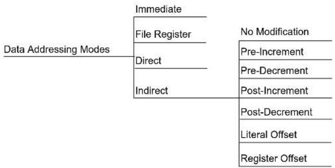
flowchart
graph TD
    A["Data Addressing Modes"] --> B["Immediate"]
    A --> C["File Register"]
    A --> D["Direct"]
    A --> E["Indirect"]
    F["No Modification"] --> G["Pre-Increment"]
    F --> H["Pre-Decrement"]
    F --> I["Post-Increment"]
    F --> J["Post-Decrement"]
    F --> K["Literal Offset"]
    F --> L["Register Offset"]
3.3 Program Addressing Modes
The dsPIC33A devices have a 24-bit Program Counter (PC). The PC addresses the 24-bit wide program memory to fetch instructions for execution and it may be loaded in several ways. Instructions are either 16-bit, 32-bit or 64-bit entities; therefore, the PC is incremented by 2, 4 or 8 during sequential 16-bit, 32-bit or 64-bit instruction execution, respectively.
Several methods may be used to modify the PC in a non-sequential manner and both absolute and relative changes may be made to the PC. The change to the PC may be from an immediate value encoded in the instruction or a dynamic value contained in a Working register. For exception handling, the PC is loaded with the address of the exception handler, which is stored in the Interrupt Vector Table (IVT). When required, the software stack is used to return scope to the foreground process from where the change in program flow occurred.
Table 3-5 summarizes the instructions which modify the PC. When performing function calls, it is recommended that RCALL be used instead of CALL, since RCALL only consumes one word of program memory.
Table 3-5. Methods of Modifying Program Flow
| Condition/Instruction PC Modification Software Stack Usage | ||
| Sequential Execution PC = PC + 2 None | ||
| BRA Expr(1)(Branch Unconditionally) | PC = PC + 2 * Slit16 None | |
| BRA Condition, Expr(1)(Branch Conditionally) | PC = PC + 2 (condition false)PC = PC + 2 * Slit16 (condition true) | None |
| Condition/Instruction PC Modification Software Stack Usage | ||
| CALL Expr(1)(Call Subroutine) | PC = lit23 PC + 4 is PUSHed on the stack | (2) |
| CALL Wn(Call Subroutine Indirect) | PC = Wn PC + 2 is PUSHed on the stack | (2) |
| CALL.L Wn(Call Indirect Subroutine Long) | PC = {Wn+1:Wn} PC + 2 is PUSHed on the stack | (2) |
| GOTO Expr(1)(Unconditional Jump) | PC = lit23 None | |
| GOTO Wn(Unconditional Indirect Jump) | PC = Wn None | |
| GOTO.L Wn(Unconditional Indirect Long Jump) | PC = {Wn+1:Wn} None | |
| RCALL Expr(1)(Relative Call) | PC = PC + 2 * Slit16 PC + 2 is PUSHed on the stack | (2) |
| RCALL Wn(Computed Relative Call) | PC = PC + 2 * Wn PC + 2 is PUSHed on the stack | (2) |
| Exception Handling PC = Address of the exception handler(read from vector table) | PC + 2 is PUSHed on the stack(3) | |
| PC = Target REPEAT instruction(REPEAT Looping) | PC not modified (if REPEAT active) None | |
| Notes:For BRA, CALL and GOTO, the Expr may be a label, absolute address or expression, which is resolved by the linker to a 16-bit or 23-bit value (Slit16 or lit23). When representing an address offset value, Expr can also be indicated by using a “.” and a sign, “+” or “-”. For example, the expression, “.+2”, means an address offset of +2 (i.e., the next instruction address relative to the current position of the Program Counter). See Instruction Descriptions for details. | ||
| 2. After CALL or RCALL is executed, RETURN or RETLW will POP the Top-of-Stack (TOS) back into the PC. | ||
| 3. After an exception is processed, RETFIE will POP the Top-of-Stack (TOS) back into the PC. | ||
3.4 Instruction Stalls
In order to maximize the data space EA calculation and operand fetch time, the X data space read and write accesses are partially pipelined. A consequence of this pipelining is that address register data dependencies may arise between successive read and write operations using common registers.
'Read-After-Write' (RAW) dependencies occur across instruction boundaries and are detected by the hardware. An example of a RAW dependency would be a write operation that modifies W5, followed by a read operation that uses W5 as an Address Pointer. The contents of W5 will not be valid for the read operation until the earlier write completes. This problem is resolved by stalling the instruction execution for one instruction cycle, which allows the write to complete before the next read is started.
3.4.1 RAW Dependency Detection
During the instruction predecode, the core determines if any address register dependency is imminent across an instruction boundary. The stall detection logic compares the W register (if any) used for the destination EA of the instruction currently being executed with the W register to be used by the source EA (if any) of the prefetched instruction. When a match between the destination and source registers is identified, a set of rules is applied to decide whether or not to stall the instruction by one cycle. Table 3-6 lists various RAW conditions that cause an instruction execution stall.
Table 3-6. Raw Dependency Rules (Detection By Hardware)
| Destination Addressing Mode Using Wn | Source Addressing Mode Using Wn | Stall Required? Examples (2)(Wn = W2) |
| Direct Direct No Stall | ADD.W W0, W1, W2MOV.W W2, W3 | |
| Indirect Direct No Stall | ADD.W W0, W1, [W2]MOV.W W2, W3 | |
| Indirect Indirect No Stall | ADD.W W0, W1, [W2]MOV.W [W2], W3 | |
| Indirect Indirect with Pre/Post-Modification No Stall | ADD.W W0, W1, [W2]MOV.W [W2++, W3 | |
| Indirect with Pre/Post-Modification Direct No Stall | ADD.W W0, W1, [W2++]MOV.W W2, W3 | |
| Direct Indirect Stall | (1) | ADD.W W0, W1, W2MOV.W [W2], W3 |
| Direct Indirect with Pre/Post-Modification Stall | (1) | ADD.W W0, W1, W2MOV.W [W2++, W3 |
| Indirect Indirect Stall | (1) | ADD.W W0, W1, [W2](2)MOV.W [W2], W3(2) |
| Indirect Indirect with Pre/Post-Modification Stall | (1) | ADD.W W0, W1, [W2](2)MOV.W [W2++, W3(2) |
| Indirect with Pre/Post-Modification Indirect Stall | (1) | ADD.W W0, W1, [W2++]MOV.W [W2], W3 |
| Indirect with Pre/Post-Modification | Indirect with Pre/Post-Modification Stall(1) | ADD.W W0, W1, [W2++]MOV.W [W2++, W3 |
| When stalls are detected, one cycle is added to the instruction execution time. For these examples, the contents of W2 = the mapped address of W2 (0x0004). | ||
Note: When Register Indirect with Offset Addressing is used to specify the destination for an instruction, and Ws is the same register as Wd, the old value of Ws is used for Wd (i.e., the address offset is ignored).
3.4.2 Instruction Stalls and Exceptions
In order to maintain deterministic operation, instruction stalls are allowed to happen, even if they occur immediately prior to exception processing.
3.4.3 Instruction Stalls and Instructions that Change Program Flow
CALL and RCALL write to the stack using W15; therefore, they may be subject to an instruction stall if the source read of the subsequent instruction uses W15.
GOTO, RETFIE and RETURN instructions are never subject to an instruction stall because they do not perform write operations to the Working registers.
3.4.4 Instruction Stalls and REPEAT Loops
Instructions operating in a REPEAT loop are subject to instruction stalls, just like any other instruction. Stalls may occur on loop entry, loop exit and also during loop processing.
3.5 Byte Operations
Since the data memory is byte-addressable, most of the base instructions may operate in either Byte mode or Word mode. When these instructions operate in Byte mode, the following rules apply:
- All direct Working register references use the Least Significant Byte (LSB) of the 32-bit Working register and leave the Most Significant Byte (MSB) unchanged
- All indirect Working register references use the data byte specified by the 32-bit address stored in the Working register
- All file register references use the data byte specified by the byte address
- The STATUS Register (SR) is updated to reflect the result of the byte operation
It should be noted that data addresses are always represented as byte addresses. Additionally, the native data format is little-endian, which means that words are stored with the LSB at the lower address and the MSB at the adjacent, higher address (as shown in Figure 3-2). Example 3-8 shows sample byte move operations and Example 3-9 shows sample byte math operations.
Note: Instructions that operate in Byte mode must use the ".b" or ".B" instruction extension to specify a byte instruction. For example, the following two instructions are valid forms of a byte clear operation:
CLR.b W0
CLR.B W0
Example 3-8. Sample Byte Move Operations
MOV.B #0x30, W0 ; move the literal byte 0x30 to W0
Before Instruction:
W0 = 0x5555
After Instruction:
W0 = 0x5530
MOV.B 0x1000, WO ; move the byte at 0x1000 to WO
Before Instruction:
W0 = 0x5555
Data Memory 0x1000 = 0x1234
After Instruction:
WO = 0x5534
Data Memory 0x1000 = 0x1234
MOV.B W0, 0x1001 ; byte move W0 to address 0x1001
Before Instruction:
W0 = 0x1234
Data Memory 0x1000 = 0x5555
After Instruction:
W0 = 0x1234
Data Memory 0x1000 = 0x3455
MOV.B W0, [W1++] ; byte move W0 to [W1], then post-inc W1
Before Instruction:
W0 = 0x1234
W1 = 0x1001
Data Memory 0x1000 = 0x5555
After Instruction:
W0 = 0x1234
W1 = 0x1002
Data Memory 0x1000 = 0x3455
Example 3-9. Sample Byte Math Operations
CLR.B [W6--] ; byte clear [W6], then post-dec W6
Before Instruction:
W6 = 0x1001
Data Memory 0x1000 = 0x5555
After Instruction:
w6 = 0x1000
Data Memory 0x1000 = 0x0055
SUB.B W0, #0x10, W1 ; byte subtract literal 0x10 from W0; and store to W1
Before Instruction:
W0 = 0x1234
W1 = 0xFFFF
After Instruction:
w0 = 0x1234
w1 = 0xFF24
ADD.B W0, W1, [W2++] ; byte add W0 and W1, store to [W2]; and post-inc W2
Before Instruction:
w0 = 0x1234
w1 = 0x5678
w2 = 0x1000
Data Memory 0x1000 = 0x5555
After Instruction:
W0 = 0x1234
W1 = 0x5678
W2 = 0x1001
Data Memory 0x1000 = 0x55AC
3.6 Word Move Operations
Even though the data space is byte-addressable, all move operations made in Word mode must be word-aligned. This means that for all source and destination operands, the Least Significant Address bit must be '0'. If a word move is made to or from an odd address, an address error exception is generated. Likewise, all double words must be word-aligned. Figure 3-2 shows how bytes and words may be aligned in data memory. Example 3-10 contains several legal word move operations.
When an exception is generated due to a misaligned access, the exception is taken after the instruction executes. If the illegal access occurs from a data read, the operation will be allowed
to complete, but the Least Significant bit (LSb) of the source address will be cleared to force word alignment. If the illegal access occurs during a data write, the write will be inhibited. Example 3-11 contains several illegal word move operations.
Figure 3-2. Data Alignment in Memory

bar_stacked
| Category | b0 | b1 | b3b2 | b5b4 | b7b6 | b8 | |---|---|---|---|---|---|---| | 0x1001 | 0x1000 | 0x1002 | 0x1004 | 0x1006 | 0x1008 | 0x100A | | 0x1003 | 0x1002 | 0x1004 | 0x1004 | 0x1004 | 0x1004 | 0x1004 | | 0x1005 | 0x1004 | 0x1004 | 0x1004 | 0x1004 | 0x1004 | 0x1004 | | 0x1007 | 0x1006 | 0x1004 | 0x1004 | 0x1004 | 0x1004 | 0x1004 | | 0x1009 | 0x1008 | 0x1004 | 0x1004 | 0x1004 | 0x1004 | 0x1004 | | 0x100B | 0x100A | 0x1004 | 0x1004 | 0x1004 | 0x1004 | 0x1004 |Legend:
b0 - byte stored at 0x1000
b1 - byte stored at 0x1003
b3:b2 – word stored at 0x1005:1004 (b2 is LSB)
b7:b4 - double word stored at 0x1009:0x1006 (b4 is LSB)
b8 - byte stored at 0x100A
Note: Instructions that operate in Word mode are not required to use an instruction extension. However, they may be specified with an optional ".w" or ".W" extension, if desired. For example, the following instructions are valid forms of a word clear operation:
CLR W0
CLR.w W0
CLR.W W0
Example 3-10. Legal Word Move Operations
MOV #0x30, W0 ; move the literal word 0x30 to W0
Before Instruction:
W0 = 0x5555
After Instruction:
W0 = 0x0030
MOV 0x1000, WO ; move the word at 0x1000 to WO
Before Instruction:
WO = 0x5555
Data Memory 0x1000 = 0x1234
After Instruction:
w0 = 0x1234
Data Memory 0x1000 = 0x1234
MOV [W0], [W1++] ; word move [W0] to [W1], ; then post-inc W1
Before Instruction:
W0 = 0x1234
W1 = 0x1000
Data Memory 0x1000 = 0x5555
Data Memory 0x1234 = 0xAAAA
After Instruction:
W0 = 0x1234
W1 = 0x1002
Data Memory 0x1000 = 0xAAAA
Data Memory 0x1234 = 0xAAAA
Example 3-11. Illegal Word Move Operations
MOV 0x1001, w0 ; move the word at 0x1001 to w0
Before Instruction:
w0 = 0x5555
Data Memory 0x1000 = 0x1234
Data Memory 0x1002 = 0x5678
After Instruction:
W0 = 0x1234
Data Memory 0x1000 = 0x1234
Data Memory 0x1002 = 0x5678
ADDRESS ERROR TRAP GENERATED
(source address is misaligned, so MOV is performed)
MOV WO, 0x1001 ; move WO to the word at 0x1001
Before Instruction:
W0 = 0x1234
Data Memory 0x1000 = 0x5555
Data Memory 0x1002 = 0x6666
After Instruction:
WO = 0x1234
Data Memory 0x1000 = 0x5555
Data Memory 0x1002 = 0x6666
ADDRESS ERROR TRAP GENERATED
(destination address is misaligned, so MOV is not performed)
MOV [W0], [W1++] ; word move [W0] to [W1], ; then post-inc W1
Before Instruction:
W0 = 0x1235
W1 = 0x1000
Data Memory 0x1000 = 0x1234
Data Memory 0x1234 = 0xAAAA
Data Memory 0x1236 = 0xBBBB
After Instruction:
W0 = 0x1235
W1 = 0x1002
Data Memory 0x1000 = 0xAAAA
Data Memory 0x1234 = 0xAAAA
Data Memory 0x1236 = 0xBBBB
ADDRESS ERROR TRAP GENERATED
(source address is misaligned, so MOV is performed)
3.7 Using 16-Bit Literal Operands
Several instructions that support Byte and Word mode have 16-bit operands. For byte instructions, a 16-bit literal is too large to use. Therefore, when 16-bit literals are used in Byte mode, the range of the operand must be reduced to eight bits or the assembler will generate an error. Table 3-7 shows that the range of a 16-bit literal is 0:1023 in Word mode and 0:255 in Byte mode.
Instructions that employ 16-bit literals in Byte and Word mode are ADD, ADDC, AND, IOR, RETLW, SUB, SUBB and XOR. Example 3-12 shows how positive and negative literals are used in Byte mode for the ADD instruction.
Table 3-7. 16-Bit Literal Coding
| Literal Value Word Mode | kk kkkk kkkk | Byte Modekkkk kkkk | ||||||
| 0 | 0000 | 0000 | 0000 | 0000 | 0000 | 0000 | ||
| 1 | 0000 | 0000 | 0000 | 0001 | 0000 | 0001 | ||
| 2 | 0000 | 0000 | 0000 | 0010 | 0000 | 0010 | ||
| 127 | 0000 | 0000 | 0111 | 1111 | 0111 | 1111 | ||
| 128 | 0000 | 0000 | 1000 | 0000 | 1000 | 0000 | ||
| 255 | 0000 | 0000 | 1111 | 1111 | 1111 | 1111 | ||
| 256 | 0000 | 0001 | 0000 | 0000 | N/A | |||
| 512 | 0000 | 0010 | 0000 | 0000 | N/A | |||
| 1023 | 0000 | 0011 | 1111 | 1111 | N/A | |||
| 65535 | 1111 | 1111 | 1111 | 1111 | N/A | |||
Note: Using a literal value greater than 127 in Byte mode is functionally identical to using the equivalent negative two's complement value, since the MSb of the byte is set. When operating in Byte mode, the assembler will accept either a positive or negative literal value (i.e., #-10).
Example 3-12. Using 16-Bit Literals for Byte Operands
ADD.B #0x80, W0 ; add 128 (or -128) to W0
ADD.B #0x380, W0 ; ERROR... Illegal syntax for byte mode
ADD.B #0xFF, W0 ; add 255 (or -1) to W0
ADD.B #0x3FF, W0 ; ERROR... Illegal syntax for byte mode
ADD.B #0xF, W0 ; add 15 to W0
ADD.B #0x7F, W0 ; add 127 to W0
ADD.B #0x100, W0 ; ERROR... Illegal syntax for byte mode
3.8 Bit Field Insert/Extract Instructions
dsPIC33A provides a set of instructions that operate on bit fields within a target word.
3.8.1 BFEXT
This instruction can extract multiple bits from a W register or data memory location into a destination W register.
3.8.2 BFINS
This instruction can insert multiple bits from a source W register or an 8-bit literal value into a W register or data memory location.
In both instructions, the location and width of the bit field within the target word are defined as literal values within the instruction.
3.9 Software Stack Pointer and Frame Pointer
3.9.1 Software Stack Pointer
The dsPIC33A devices feature a software stack which facilitates function calls and exception handling. W15 is the default Stack Pointer (SP) and after any Reset, it is initialized to 0x4000. This ensures that the SP will point to valid RAM and permits stack availability for exceptions, which may occur before the SP is set by the user software. The user may reprogram the SP during initialization to any location within data space.
The SP always points to the first available free word (Top-of-Stack) and fills the software stack, working from lower addresses towards higher addresses. It pre-decrements for a stack POP (read) and post-increments for a stack PUSH (write).
The software stack is manipulated using the PUSH and POP instructions. The PUSH and POP instructions are the equivalent of a MOV instruction with W15 used as the destination pointer. For example, the contents of W0 can be PUSHed onto the Top-of-Stack (TOS) by:
PUSH WO
This syntax is equivalent to:
MOV W0, [W15++]
The contents of the TOS can be returned to W0 by:
POP W0
This syntax is equivalent to:
MOV [--W15], W0
During any CALL instruction, the PC is PUSHed onto the stack, such that when the subroutine completes execution, program flow may resume from the correct location. When the PC is PUSHed onto the stack, PC[15:0] are PUSHed onto the first available stack word, then PC[22:16] are PUSHed. When PC[22:16] are PUSHed, the Most Significant seven bits of the PC are zero-extended before the PUSH is made, as shown in Figure 3-3. During exception processing, the Most Significant seven bits of the PC are concatenated with the lower byte of the STATUS Register (SRL) and IPL[3] (CORCON[3]). This allows the primary STATUS Register contents and CPU Interrupt Priority Level to be automatically preserved during interrupts.
Note: In order to protect against misaligned stack accesses, W15[0] is always clear.
Figure 3-3. Stack Operation for CALL Instruction
text_image
0x0000 15 0 Stack Grows Towards Higher Address PC<15:0> 0x0PC[22:16] Top-of-Stack W15 (before CALL) W15 (after CALL) 0xFFFE3.9.1.1 Stack Pointer Example
Figure 3-4 through Figure 3-7 show how the software stack is modified for the code snippet shown in Example 3-13. Figure 3-4 shows the software stack before the first PUSH has executed. Note that the SP has the initialized value of 0x4000. Furthermore, the example loads 0x5A5A and 0x3636 to W0 and W1, respectively. The stack is PUSHed for the first time in Figure 3-5 and the value contained in W0 is copied to TOS. W15 is automatically updated to point to the next available stack location and the new TOS is 0x4002. In Figure 3-6, the contents of W1 are PUSHed onto the stack and the new TOS becomes 0x4004. In Figure 3-7, the stack is POPped, which copies the last PUSHed value (W1) to W3. The SP is decremented during the POP operation and at the end of the example, the final TOS is 0x4002.
Figure 3-4. Stack Pointer Before the First PUSH

text_image
0x0000 0x4000 [TOS] W15 (SP) 0xFFFE W0 = 0x5A5A W1 = 0x3636 W15 = 0x0800Figure 3-5. Stack Pointer After "PUSH W0" Instruction

text_image
0x0000 0x4000 5A5A 0x4002 [TOS] W15 (SP) 0xFFFE W0 = 0x5A5A W1 = 0x3636 W15 = 0x0802Figure 3-6. Stack Pointer After "PUSH W1" Instruction

text_image
0x0000 0x4000 5A5A 0x4002 3636 0x4004 [TOS] W15 (SP) 0xFFFE W0 = 0x5A5A W1 = 0x3636 W15 = 0x0804Figure 3-7. Stack Pointer After "POP W3" Instruction
text_image
0x0000 0x4000 5A5A 0x4002 [TOS] 0x4004 W15 (SP) 0xFFFE W0 = 0x5A5A W1 = 0x3636 W3 = 0x3636 W15 = 0x0802Example 3-13. Stack Pointer Usage
MOV #0x5A5A, W0 ; Load W0 with 0x5A5A
MOV #0x3636, W1 ; Load W1 with 0x3636
PUSH w0 ; Push W0 to TOS
PUSH w1 ; Push W1 to TOS
POP W3 ; Pop TOS to W3
3.9.2 Software Stack Frame Pointer
A stack frame is a user-defined section of memory residing in the software stack. It is used to allocate memory for temporary variables, which a function uses, and one stack frame may be created for each function. W14 is the default Stack Frame Pointer (FP) and it is initialized to 0x0000 on any Reset. If the Stack Frame Pointer is not used, W14 may be used like any other Working register.
The Link (LNK) and Unlink (ULNK) instructions provide stack frame functionality. The LNK instruction is used to create a stack frame. It is used during a call sequence to adjust the SP, such that the stack may be used to store temporary variables utilized by the called function. After the function completes execution, the ULNK instruction is used to remove the stack frame created by the LNK instruction. The LNK and ULNK instructions must always be used together to avoid stack overflow.
3.9.2.1 Stack Frame Pointer Example
Figure 3-8 through Figure 3-10 show how a stack frame is created and removed for the code snippet shown in Example 3-14. This example demonstrates how a stack frame operates and is not indicative of the code generated by the compiler. Figure 3-8 shows the stack condition at the beginning of the example, before any registers are pushed to the stack. Here, W15 points to the first free stack location (TOS) and W14 points to a portion of stack memory allocated for the routine that is currently executing.
Before calling the function, "COMPUTE", the parameters of the function (W0, W1 and W2) are PUSHed on the stack. After the "CALL COMPUTE" instruction is executed, the PC changes to the address of "COMPUTE" and the return address of the function, "TASKA", is placed on the stack (Figure 3-9). Function "COMPUTE" then uses the "LNK #4" instruction to PUSH the calling routine's Frame Pointer value onto the stack and the new Frame Pointer will be set to point to the current Stack Pointer. Then, the literal 4 is added to the Stack Pointer address in W15, which reserves memory for two words of temporary data (Figure 3-10).
Inside the function, "COMPUTE", the FP is used to access the function parameters and temporary (local) variables. [W14 + n] will access the temporary variables used by the routine and [W14 - n] is used to access the parameters. At the end of the function, the ULNK instruction is used to copy the Frame Pointer address to the Stack Pointer and then POP the calling subroutine's Frame Pointer back to the W14 register. The ULNK instruction returns the stack back to the state shown in Figure 3-9.
A RETURN instruction will return to the code that called the subroutine. The calling code is responsible for removing the parameters from the stack. The RETURN and POP instructions restore the stack to the state shown in Figure 3-8.
Figure 3-8. Stack at the Beginning of Frame Pointer Usage Example
text_image
0x0000 0x4000 Frame of TASKA [TOS] W14 (FP) W15 (SP) 0xFFFEFigure 3-9. Stack After "CALL COMPUTE" Executes
text_image
0x0000 0x4000 Frame of TASKA Parameter 1 Parameter 2 Parameter 3 PC[15:0] 0:PC[22:16] [TOS] W14 (FP) W15 (SP) 0xFFFEFigure 3-10. Stack After "LNK #4" Executes
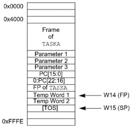
text_image
0x0000 0x4000 Frame of TASKA Parameter 1 Parameter 2 Parameter 3 PC[15:0] 0:PC[22:16] FP of TASKA Temp Word 1 Temp Word 2 [TOS] W14 (FP) W15 (SP) 0xFFFEExample 3-14. Frame Pointer Usage
TASKA:
...
PUSH    W0    ; Push parameter 1
PUSH    W1    ; Push parameter 2
PUSH    W2    ; Push parameter 3
CALL    COMPUTE    ; Call COMPUTE function
POP    W2    ; Pop parameter 3
POP    W1    ; Pop parameter 2
POP    W0    ; Pop parameter 1
...
COMPUTE:
LNK #4    ; Stack FP, allocate 4 bytes for local variables
...
ULNK    ; Free allocated memory, restore original FP
RETURN    ; Return to TASKA
3.9.3 Stack Pointer Overflow
There is a Stack Limit register (SPLIM) associated with the Stack Pointer that is reset to 0x00000000. SPLIM is a 32-bit register, but SPLIM[1:0] is fixed to '00', because all stack operations must be long word-aligned. To match the Stack Pointer, the device address space is limited to 24-bits, so the upper 8-bits of SPLIM are always all 0.
The stack overflow check will not be enabled until a word write to SPLIM occurs, after which time it can only be disabled by a device Reset. All Effective Addresses generated using W15 as a source or destination are compared against the value in SPLIM. Should the Effective Address be greater than the contents of SPLIM, then a stack error trap is generated.
If stack overflow checking has been enabled, a stack error trap will also occur if the W15 Effective Address calculation wraps over the end of data space (0x00FFFFFF).
3.9.4 Stack Pointer Underflow
The stack is initialized to 0x4000 during Reset. A stack error trap will be initiated should the Stack Pointer address ever be less than 0x4000.
3.10 Conditional Branch Instructions
Conditional branch instructions are used to direct program flow based on the contents of the STATUS Register. These instructions are generally used in conjunction with a compare class instruction, but they may be employed effectively after any operation that modifies the STATUS Register.
The compare instructions, CP, CP0 and CPB, perform a subtract operation (minuend - subtrahend), but do not actually store the result of the subtraction. Instead, compare instructions just update the flags in the STATUS Register, such that an ensuing conditional branch instruction may change program flow by testing the contents of the updated STATUS Register. If the result of the STATUS Register test is true, the branch is taken. If the result of the STATUS Register test is false, the branch is not taken.
The supported conditional branch instructions are shown in Table 3-8. This table identifies the condition in the STATUS Register that must be true for the branch to be taken. In some cases, just a single bit is tested (as in BRA C), while in other cases, a complex logic operation is performed (as in BRA GT). Both signed and unsigned conditional tests are supported, and support is provided for DSP algorithms with the OA, OB, SA and SB condition mnemonics.
Table 3-8. Conditional Branch Instructions
| Condition Mnemonic^(1) | Description Status Test | |
| C Carry (not Borrow) C | ||
| GE Signed Greater Than or Equal (N&&OV) || (N&&OV) | — — | |
| GEU ^(2) | Unsigned Greater Than or Equal C | |
| GT Signed Greater Than (Z&&N&&OV) || (Z&&N&&OV) | — — — | |
| GTU Unsigned Greater Than C&&Z | — | |
| LE Signed Less Than or Equal Z || (N&&OV) || (N&&OV) | — — | |
| LEU Unsigned Less Than or Equal C || Z | — | |
| LT Signed Less Than (N&&OV) || (N&&OV) | — — | |
| LTU ^(3) | Unsigned Less Than | C |
| N Negative | N | |
| NC | Not Carry (Borrow) | C |
| NN | Not Negative N | |
| NOV | Not Overflow | OV |
| NZ | Not Zero | Z |
| OA | Accumulator A Overflow | OA |
| OB | Accumulator B Overflow | OB |
| OV | Overflow | OV |
| SA | Accumulator A Saturate | SA |
| SB | Accumulator B Saturate | SB |
| Z | Zero | Z |
| Notes:1. Instructions are of the form: BRA mnemonic, Expr.2. GEU is identical to C and will reverse assemble to BRA NC, Expr.3. LTU is identical to NC and will reverse assemble to BRA NC, Expr. | ||
Note: The "Compare and Skip" instructions (CPBEQ, CPBGT, CPBLT, CPBNE, CPSEQ, CPSGT, CPSLT and CPSNE) do not modify the STATUS Register.
3.10.1 Floating Point Branch Instruction
Subsequent to floating point CPS/CPQ instructions setting one of the FSR ordering relations status bits, a subsequent floating point conditional branch (FBRA) instruction will (indirectly) examine these status bits, applying them to a logical predicate that represents the required condition. A list of the supported floating point branches and corresponding predicates is shown in Table 3-9.
Table 3-9. FPU Conditional Branch Instruction
| Condition Mnemonic(1) | Description Status test | |
| EQ Equal FSR.EQ | ||
| UNE Unordered or Not Equal (FSR.GT || FSR.LT || FSR.UN) | ||
| NE Not Equal (FSR.GT || FSR.LT) | ||
| UEQ Unordered or Equal (FSR.EQ || FSR.UN) | ||
| GT Greater Than FSR.GT | ||
| ULE Unordered or Less Than or Equal (FSR.LT || FSR.EQ || FSR.UN) | ||
| GE Greater Than or Equal (FSR.GT || FSR.EQ) | ||
| ULT Unordered or Less Than (FSR.LT || FSR.UN) | ||
| LT Less Than | FSR.LT | |
| UGE Unordered or Greater Than or Equal | (FSR.GT || FSR.EQ || FSR.UN) | |
| LE Less Than or Equal | (FSR.LT || FSR.EQ) | |
| UGT Unordered or Greater Than | (FSR.GT || FSR.UN) | |
| OR | Ordered | (FSR.GT || FSR.LT || FSR.EQ) |
| UN | Unordered | FSR.UN |
Note:
- Instructions are of the form: FBRA mnemonic, Expr.
3.11 Z Status Bit
The Z Status bit is a special Zero Status bit that is useful for extended precision arithmetic. The Z bit functions like a normal Z flag for all instructions, except those that use the Carry/Borrow input (ADDC, CPB, SUBB and SUBBR). For the ADDC, CPB, SUBB and SUBBR instructions, the Z bit can only be cleared and never set. If the result of one of these instructions is non-zero, the Z bit will be cleared and will remain cleared, regardless of the result of subsequent ADDC, CPB, SUBB or SUBBR operations. This allows the Z bit to be used for performing a simple zero check on the result of a series of extended precision operations.
A sequence of instructions working on multiprecision data (starting with an instruction with no Carry/Borrow input) will automatically logically AND the successive results of the zero test. All results must be zero for the Z flag to remain set at the end of the sequence of operations. If the result of the ADDC, CPB, SUBB or SUBBR instruction is non-zero, the Z bit will be cleared and remain cleared for all subsequent ADDC, CPB, SUBB or SUBBR instructions.
3.12 DSP Data Formats
3.12.1 Integer and Fractional Data
The DSP engine supports both integer and fractional data types. Integer data is inherently represented as a signed two's complement value, where the MSb is defined as a Sign bit. Generally speaking, the range of an N-bit two's complement integer is -2^N-1 to 2^N-1-1 . For a 16-bit integer, the data range is -32768 (0x8000) to 32767 (0x7FFF), including '0'. For a 32-bit integer, the data range is -2,147,483,648 (0x8000 0000) to 2,147,483,647 (0x7FFF FFFF).
Fractional data is represented as a two's complement number, where the MSb is defined as a Sign bit and the radix point is implied to lie just after the Sign bit. This format is commonly referred to as 1.15 (or Q15) format, where 1 is the number of bits used to represent the integer portion of the number and 15 is the number of bits used to represent the fractional portion. The range of an N-bit two's complement fraction with this implied radix point is -1.0 to (1 - 2^1 - N) . For a 16-bit fraction, the 1.15 data range is -1.0 (0x8000) to 0.999969482 (0x7FFF), including 0.0 and it has a precision of 3.05176 × 10^-5 . In Normal Saturation mode, the 32-bit accumulators use a 1.31 format, which enhances the precision to 4.6566 × 10^-10 . In Fractional mode, the 32x32-bit dsPIC multiplier generates a Q1.63 product which has a precision of 1.08420 × 10^-19 .
The dynamic range of the accumulators can be expanded by using the eight bits of the Upper Accumulator register (ACCxU) as Guard bits. Guard bits are used if the value stored in the accumulator overflows beyond the 62 ^nd bit and they are useful for implementing DSP algorithms. This mode is enabled when the ACCSAT bit (CORCON[4]) is set to '1' and it expands the accumulators to 72 bits. The Guard bits are also used when the accumulator saturation is disabled. The accumulators then support an integer range of -271 (0x80 0000 0000 0000 0000) to 271-1 (0x7F FFFF FFFF FFFF FFFF). In Fractional mode, the Guard bits of the accumulator do not modify the location of the radix point and the 72-bit accumulators use a 9.71 fractional format. Note that all fractional operation results are stored in the 72-bit accumulator, justified with a 1.71 radix point. As in Integer mode, the Guard bits merely increase the dynamic range of the accumulator. 9.71 fractions have a range of -256.0 (0x80 0000 0000 0000 0000) to 256.0 -1.08420x10⁻¹⁹ (0x7F FFFF FFFF FFFF FFFF).
Table 3-10 identifies the range and precision of integers and fractions on 16-bit, 32-bit and 72-bit registers.
With the exception of DSP multiplies, the ALU operates identically on integer and fractional data. Namely, an addition of two integers will yield the same result (binary number) as the addition of two fractional numbers. The only difference is how the result is interpreted by the user. However, multiplies performed by DSP operations are different. In these instructions, data format selection is made by the IF bit (CORCON[0]) and it must be set accordingly ('0' for Fractional mode, '1' for Integer mode). This is required because of the implied radix point used by fractional numbers. In Integer mode, multiplying two 16-bit integers produces a 32-bit integer result. However, multiplying two 1.15 values generates a 2.30 result. Since the dsPIC33A devices use a 1.31 format for the accumulators, a DSP multiply in Fractional mode also includes a left shift of one bit to keep the radix point properly aligned. This feature reduces the resolution of the DSP multiplier to 2^-30 , but has no other effect on the computation (e.g., 0.5 × 0.5 = 0.25 ).
Table 3-10. dsPIC33A Data Ranges
| Register Size Integer | Range Fraction Range | Fraction Resolution | |
| 16-bit -32768 to 32767 | -1.0 to (1.0 – 2) | ^-15 3.052 x 10 | -5 |
| 32-bit -2,147,483,648 to 2,147,483,647 | -1.0 to (1.0 – 2^-31 ) 4.657 x 10 | ^-10 | |
| 70-bit -2 | ^71 to 2^71 | -256.0 to 256.0 -1.08420x 10^-19 | 4.657 × 10^-10 |
3.12.2 Integer and Fractional Data Representation
Both integer and fractional data treat the MSb as a Sign bit, and the binary exponent decreases by one as the bit position advances toward the LSb. The binary exponent for an N-bit integer starts at (N-1) for the MSb and ends at '0' for the LSb. For an N-bit fraction, the binary exponent starts at '0' for the MSb and ends at (1-N) for the LSb (as shown in Figure 3-11 for a positive value and in Figure 3-12 for a negative value).
Conversion between integer and fractional representations can be performed using simple division and multiplication. To go from an N-bit integer to a fraction, divide the integer value by 2^N-1 . Similarly, to convert an N-bit fraction to an integer, multiply the fractional value by 2^N-1 .
Figure 3-11. Different Representations of 0x4001
Integer:

text_image
010 00000 00000 001 -2^15 2^14 2^13 2^12 .... 2^0$$ 0 \times 4 0 0 1 = 2 ^ {1 4} + 2 ^ {0} = 1 6 3 8 4 + 1 = 1 6 3 8 5 $$
1.15 Fractional:

text_image
-2⁰ . 2¹ 2² 2³ . . . . . Implied Radix Point 0x4001 = 2⁻¹ + 2⁻¹⁵ = 0.5 + .000030518 = 0.500030518Figure 3-12. Different Representations of 0xC002
Integer:
| 1 | 1 | 0 | 0 | 0 | 0 | 0 | 0 | 0 | 0 | 0 | 0 | 0 | 1 | 0 |
| -2^15 | 2^14 | 2^13 | 2^12 | ...... | 2^0 |
$$ 0 \mathrm{xC} 0 0 2 = - 2 ^ {1 5} + 2 ^ {1 4} + 2 ^ {1} = - 3 2 7 6 8 + 1 6 3 8 4 + 2 = - 1 6 3 8 2 $$
1.15 Fractional:
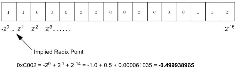
text_image
-2^0 . 2^1 2^2 2^3 ...... Implied Radix Point 0xC002 = -2^0 + 2^-1 + 2^-14 = -1.0 + 0.5 + 0.000061035 = -0.4999389653.13 Accumulator Usage
Accumulators A and B are utilized by DSP instructions to perform mathematical and shifting operations. Since the accumulators are 72-bits wide and the X and Y data paths are only 32 bits, the method to load and store the accumulators must be understood.
Item A in Figure 3-13 shows that each 72-bit accumulator (ACCA and ACCB) consists of an 8-bit upper register (ACCxU), a 32-bit high register (ACCxH) and a 32-bit low register (ACCxL). To address the bus alignment requirement and provide the ability for 1.31 math, ACCxH is used as a destination register for loading the accumulator (with the LAC instruction) and also as a source register for storing the accumulator (with the SAC.R instruction). This is represented by Item B in Figure 3-13, where the upper and lower portions of the accumulator are shaded. In reality, during accumulator
loads, ACCxL is zero backfilled and ACCxU is sign-extended to represent the sign of the value loaded in ACCxH.
Note: dsPIC33A devices provide double-word LAC.D and SAC.D instructions that allow both ACCxH and ACCxL to be loaded or stored in a single instruction.
When normal (63-bit) saturation is enabled, DSP operations (such as ADD, MAC, MSC, etc.) solely utilize ACCxH:ACCxL (item C in Figure 3-13) and ACCxU is only used to maintain the sign of the value stored in ACCxH:ACCxL. For instance, when an MPY instruction is executed, the result is stored in ACCxH:ACCxL, and the sign of the result is extended through ACCxU.
When super saturation is enabled, or when saturation is disabled, all registers of the accumulator may be used (item D in Figure 3-13), and the results of DSP operations are stored in ACCxU:ACCxH:ACCxL. The benefit of ACCxU is that it increases the dynamic range of the accumulator, as described in 3.12.1. Integer and Fractional Data. Refer to Table 3-10 to see the range of values which may be stored in the accumulator when in Normal and Super Saturation modes.
Figure 3-13. Accumulator Alignment and Usage
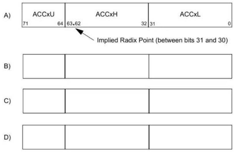
text_image
A) ACCxU 71 64 63.62 32 31 0 Implied Radix Point (between bits 31 and 30) B) C) D)A) 72-bit accumulator consists of ACCxU:ACCxH:ACCxL
B) Load and store operations
C) Operations in Normal Saturation mode
D) Operations in Super Saturation mode or with saturation disabled
3.14 Accumulator Access
Accumulator can be accessed with File Register or Indirect Addressing, using any instruction which supports such addressing. However, it is recommended that the DSP instructions, LAC, SAC and SAC.R, be used to load and store the accumulators, since they provide sign-extension, shifting and rounding capabilities. LAC, SAC and SAC.R instruction details are provided in Instruction Descriptions.
Notes:
- For convenience, ACCAU and ACCBU are sign-extended to 32 bits. This provides the flexibility to access these registers using either Byte or Word mode (when File Register or Indirect Addressing is used).
- The OA, OB, SA or SB bit cannot be set by writing overflowed values to the memory-mapped accumulators using MOV instructions, as these Status bits are only affected by DSP operations.
- dsPIC33A devices provide double-word LAC.D and SAC.D instructions that allow both ACCxH and ACCxL to be loaded or stored in a single instruction.
3.15 DSP MAC Instructions
The DSP Multiply and Accumulate (MAC) operations are a special suite of instructions that provide the most efficient use of the dsPIC33A architectures. The DSP MAC instructions, shown in Table 3-11, utilize both the X and Y data paths of the CPU core.
MAC instructions are also capable of performing an operation with one accumulator, while storing out the rounded contents of the alternate accumulator. This feature is called Accumulator Write-Back (WB) and it provides flexibility for the software developer. For instance, the Accumulator WB may be used to run two algorithms concurrently or efficiently process complex numbers, among other things.
Table 3-11. DSP MAC Instructions
| Instruction Description | |
| ED | Euclidean Distance (No Accumulate) |
| EDAC | Euclidean Distance |
| MAC | Multiply and Accumulate |
| SQRAC | Square and Accumulate |
| MPY | Multiply to Accumulator |
| MPY.N | Negative Multiply to Accumulator |
| MSC | Multiply and Subtract from Accumulator |
| SQRSC | Square and Subtract from Accumulator |
| SQR | Square to Accumulator |
| SQRN | Negated Square to Accumulator |
3.15.1 MAC Operations
The mathematical operations performed by the MAC class of DSP instructions center around multiplying or squaring the contents of two Working registers and either adding, subtracting or storing the result to either Accumulator A or Accumulator B. This is the operation of the MAC, MPY, MPY.N, MSC, SQR, SQRAC, SQRSC and SQRN instructions.
For the ED and EDAC instructions, the same multiplicand operand must be specified by the instruction because this is the definition of the Euclidean Distance operation.
3.15.2 MAC Write-Back
The Write-Back ability of the MAC class of DSP instructions facilitates efficient processing of algorithms. This feature allows one mathematical operation to be performed with one accumulator and the rounded contents of the other accumulator to be stored in the same cycle.
The following addressing modes are supported:
- W0, W1, W2, W3, W13 or W14 register direct: the rounded contents of the non-target accumulator are written into the destination register as a 1.15 (Word mode) or 1.31 (Long Word mode) fraction. As is the case for any register direct word write, the value written is zero extended to 32-bits prior to being written into the destination WREG.
- [W13++] or [W15++] register indirect with post increment: the rounded contents of the non-target accumulator are written into the address pointed to by W13 or W15 as a 1.15 (Word mode) or 1.31 (Long Word mode) fraction. The destination EA W-reg is then incremented by two (for a word write) or four (for a long word write).
3.15.3 MAC Syntax
The syntax of the MAC class of instructions can have several formats, which depend on the instruction type and the operation it is performing with respect to prefetches and Accumulator Write-Back. All MAC class instructions must specify a target accumulator along with two multiplicands, as shown in Example 3-15.
If an Accumulator Write-Back is used in the instruction, it is specified last. By definition, the accumulator not used in the mathematical operation is stored, so the Write-Back accumulator is not specified in the instruction. Legal forms of Accumulator Write-Back (WB) are shown in Example 3-16.
Example 3-15. Base MAC Syntax
; MAC with no prefetch
MAC W4,W5, A

; MAC with no prefetch
MAC W7,W7, B

Multiply W7*W7, Accumulate to ACCB
Example 3-16. MAC Accumulator WB Syntax

flowchart
graph TD
    A["CLR A, W13"] --> B["0-ACCA"]
    B --> C["ACCB-W13"]
    D["MAC W4,W5, A"] --> E["[W13"] += 2]
    E --> F["ACCA=ACCA+W4*W5"]
    F --> G["ACCB-[W13"] += 2]
3.16 DSP Accumulator Instructions
The DSP accumulator instructions provide the ability to add, negate, shift, load and store the contents of either 72-bit accumulator. In addition, the ADD and SUB instructions allow the two accumulators to be added or subtracted from each other. DSP accumulator instructions are shown in Table 3-12 and instruction details are provided in Instruction Descriptions.
Table 3-12. DSP Accumulator Instructions
| Instruction Description Accumulator WB? | ||
| ADD | Add Accumulators No | |
| ......continued | ||
| Instruction Description | Accumulator WB? | |
| ADD | 16-Bit Signed Accumulator Add No | |
| LAC | Load Accumulator No | |
| LAC.D | Load Accumulator Double Word No | |
| NEG | Negate Accumulator No | |
| SAC | Store Accumulator No | |
| SAC.D | Store Accumulator Double Word No | |
| SAC.R | Store Rounded Accumulator No | |
| SFTAC | Arithmetic Shift Accumulator by Literal No | |
| SFTAC | Arithmetic Shift Accumulator by (Wn) No | |
| SUB | Subtract Accumulators No | |
3.17 Scaling Data with the FBCL Instruction
To minimize quantization errors that are associated with data processing using DSP instructions, it is important to utilize the complete numerical result of the operations. This may require scaling data up to avoid underflow (i.e., when processing data from a 12-bit ADC) or scaling data down to avoid overflow (i.e., when sending data to a 10-bit DAC). The scaling, which must be performed to minimize quantization error, depends on the dynamic range of the input data which is operated on and the required dynamic range of the output data. At times, these conditions may be known beforehand and fixed scaling may be employed. In other cases, scaling conditions may not be fixed or known and then dynamic scaling must be used to process data.
The FBCL instruction (Find First Bit Change Left) can efficiently be used to perform dynamic scaling, because it determines the exponent of a value. A fixed point or integer value's exponent represents the amount that the value may be shifted before overflowing. This information is valuable because it may be used to bring the data value to "full scale", meaning that its numeric representation utilizes all the bits of the register it is stored in.
The FBCL instruction determines the exponent of a word by detecting the first bit change, starting from the value's Sign bit and working towards the LSB. Since the dsPIC DSC device's barrel shifter uses negative values to specify a left shift, the FBCL instruction returns the negated exponent of a value. If the value is being scaled up, this allows the ensuing shift to be performed immediately with the value returned by FBCL. Additionally, since the FBCL instruction only operates on signed quantities, FBCL produces results in the range of -15:0 for word operation and -31:0 for long word operation. When the FBCL instruction returns 0, it indicates that the value is already at full scale. When the instruction returns -31, it indicates that the value cannot be scaled (as is the case with 0x0 and 0xFFFFFFF). Table 3-13 shows word data with various dynamic ranges, their exponents and the value after scaling the data to maximize the dynamic range. Example 3-17 shows how the FBCL instruction may be used for block processing.
Table 3-13. Scaling Examples
| Word Value Exponent | Full-Scale Value | (Word Value << Exponent) |
| 0x0001 | 14 | 0x4000 |
| 0x0002 | 13 | 0x4000 |
| 0x0004 | 12 | 0x4000 |
| 0x0100 | 6 | 0x4000 |
| 0x01FF | 6 | 0x7FC0 |
| 0x0806 | 3 | 0x4030 |
| 0x2007 | 1 | 0x400E |
| 0x4800 | 0 | 0x4800 |
| ......continued | ||
| Word Value Exponent Full-Scale Value | (Word Value << Exponent) | |
| 0x7000 0 0x7000 | ||
| 0x8000 0 0x8000 | ||
| 0x900A 0 0x900A | ||
| 0xE001 2 0x8004 | ||
| 0xFF07 7 0x8380 | ||
Note: For the word values, 0x0000 and 0xFFFF, the FBCL instruction returns -15.
As a practical example, assume that block processing is performed on a sequence of data with very low dynamic range stored in 1.15 fractional format. To minimize quantization errors, the data may be scaled up to prevent any quantization loss that may occur as it is processed. The FBCL instruction can be executed on the sample with the largest magnitude to determine the optimal scaling value for processing the data. Note that scaling the data up is performed by left shifting the data. This is demonstrated with the code snippet below.
Example 3-17. Scaling with FBCL
; assume W0 contains the largest absolute value of the data block
; assume W4 points to the beginning of the data block
; assume the block of data contains BLOCK_SIZE words
; determine the exponent to use for scaling
FBCL    W0, W2    ; store exponent in W2
; scale the entire data block before processing
DO    #(BLOCK_SIZE-1), SCALE
LAC    [W4], A    ; move the next data sample to ACCA
SFTAC    A, W2    ; shift ACCA by W2 bits
SCALE:
SAC    A, [W4++]    ; store scaled input (overwrite original)
; now process the data
; (processing block goes here)
3.18 Data Range Limit Instructions
The dsPIC33A family provides special instructions that automatically limit the data in a W register or an accumulator to lie within a user-specified numerical range. These include the FLIM, MAX, MIN and MINZ instructions.
3.18.1 FLIM/FLIM.V
The FLIM instruction simultaneously compares a maximum and a minimum data limit value with the specified W register (or data pointed to by the W register) and clamps the target data to the user-specified limit if the limit is exceeded. SR Status bits are set accordingly for subsequent signed branching. In the FLIM.V instruction, an additional W register is specified, in which the limit test result (known as "limit excess") value is loaded.
3.18.2 MAX/MAX.V
The MAX instruction compares a maximum data limit value (stored in a W register or the other accumulator) with the target accumulator and clamps the target accumulator to the user-specified limit if this upper limit is exceeded. SR Status bits are set accordingly for subsequent signed branching. In the MAX.V instruction, an additional W register (or W register in Indirect Addressing mode) is specified in which the limit excess value is loaded.
3.18.3 MIN/MIN.V/MINZ
The MIN instruction compares a minimum data limit value (stored in a W register or the other accumulator) with the target accumulator and clamps the target accumulator to the user-specified
limit if the data is smaller than this minimum limit. SR Status bits are set accordingly for subsequent signed branching. In the MIN.V instruction, an additional W register (or W register in Indirect Addressing mode) is specified, in which the limit excess value is loaded. The MINZ instruction is simply a conditional version of the MIN instruction, which is executed only when Z = 1.
3.19 Normalizing the Accumulator with the NORM Instruction
The NORM instruction automatically normalizes the target accumulator to obtain the largest fractional value possible without overflow. The target accumulator must contain signed fractional data for the instruction result to be valid. It will shift the target accumulator right or left by as many bits as required to normalize the data, keeping the sign consistent. The shift value is stored in a destination address. The N Status bit reflects the direction of the accumulator shift.
If the accumulator cannot be normalized, the accumulator contents will not be affected.
4. Instruction Descriptions
4.1 Instruction Symbols
All the symbols used in Instruction Descriptions are listed in Table 2.
4.2 Instruction Encoding Field Descriptors Introduction
All instruction encoding field descriptors used in Instruction Descriptions are shown in Table 4-2 through Table 4-10.
Table 4-1. Instruction Encoding Field Descriptors
| Field Description | |
| A | Accumulator Selection bit: 0 = ACCA; 1 = ACCB |
| aaa | Accumulator Write Back mode (see Table 4-9) |
| B | Byte Mode Selection bit: 0 = word operation; 1 = byte operation |
| bbb | 3-bit bit position select: 000 = LSB; 111 = MSB |
| bbbb | 5-bit bit position select: 00000 = LSB; 11111 = MSB |
| cccc Bit field instructions LSb value | |
| D | Destination Address bit: 0 = result stored in W0; 1 = result stored in file register |
| dddd | Wd destination register select: 0000 = W0; 1111 = W15 |
| dddd | Coprocessor destination register select (Fd for FPU where 00000 = F0; 11111 = F31) |
| E | MULxx Result size: 0 = 32-bit in Wnd; 1 = 64-bit in (Wnd+1, Wnd) |
| F | Selects between W15 (F = 0) and W14 (F = 1) registers |
| (ffff) ffff ffff ffff ffff | 16-bit or 20-bit register file address (addressable space varies depending upon instruction class) |
| G | Bit test destination: 0 = Z flag bit; 1 = C flag bit |
| I | MULAxx Multiply mode: 0 = Fractional; 1 = Integer |
| IIIii | X data fetch operation |
| JJJjj | Y data fetch operation |
| k | 1-bit literal field, constant data |
| kkk | 3-bit literal field, constant data |
| k kkkk | 5-bit literal field, constant data |
| kk kkkk | 6-bit literal field, constant data |
| kkkk kkkk | 8-bit literal field, constant data |
| kkkk kkkk kkkk kkkk | 16-bit literal field, constant data |
| kkkk kkkk kkkk kkkk kkkk kkkk | 32-bit literal field, constant data |
| L | Long (32-bit) Mode Selection bit: 0 = word or byte operation; 1 = long operation |
| mmmm | Bit field instructions MSb value |
| nnnn nnnn nnnn nnnn nnnn n | 21-bit signed instruction word offset field for relative branch/call instructions |
| nnnn nnnn nnnn nn00 nnnn nnnn | 24-bit program address for goto/call instructions |
| ppp | Addressing mode for Ws source register (see Table 4-2) |
| qqq | Addressing mode for Wd destination register (see Table 4-3) |
| R | Selects between FPU coprocessor special registers or F-regs |
| rrr | Condition select for conditional move (MOVIF) instruction |
| ......continued | |
| Field Description | |
| S | Opcode size select (16-bit: S = 0; 32-bit: S = 1) |
| ssss | Ws source or Wn source/destination register select: 0000 = W0; 1111 = W15 |
| sssss | Coprocessor source register select (Fs for FPU where 00000 = F0; 11111 = F31) |
| T | Selects between Ws (T = 0) and SR (T = 1) target registers |
| U | Unused (don't care) Instruction bit. Assembler to assign '0' |
| V | FLIMW: Selects result format for Wnd (refer to instruction description) MULxx: Selects between unsigned Ws (V = 0) and signed Ws (V = 1). |
| W | Destination write control: 0 = Wd write not required; 1 = Wd write required |
| www | Source Wb base register select: 0000 = W0; 1111 = W15 |
| zz | Coprocessor select |
Table 4-2. Addressing Modes for Ws Source Register
| ppp | Addressing Mode Source Operand | |
| 000 | Register Direct Wns | |
| 001 | Indirect [Ws] | |
| 010 | Indirect with Post-Decrement [Ws--] | |
| 011 | Indirect with Post-Increment [Ws++] | |
| 100 | Indirect with Pre-Decrement [--Ws] | |
| 101 | Indirect with Pre-Increment (++Ws] | |
| 110 | Status Register Direct SR (Source) | |
| 111 | Indirect with Register Offset [Ws+Wb] |
Table 4-3. Addressing Modes for Wd Destination Register
| qqq | Addressing Mode Destination Operand | |
| 000 | Register Direct Wnd | |
| 001 | Indirect [Wd] | |
| 010 | Indirect with Post-Decrement [Wd--] | |
| 011 | Indirect with Post-Increment | [Wd++] |
| 100 | Indirect with Pre-Decrement | [--Wd] |
| 101 | Indirect with Pre-Increment | [++Wd] |
| 110 | Status Register (SR) Direct | SR (Destination) |
| 111 | Indirect with Register Offset | [Wd+Wb] |
Table 4-4. Destination Addressing Modes for MCU Multiplications
| dddd | Destination |
| 0000 | W1:W0 |
| 0001 | W0 |
| 0010 | W3:W2 |
| 0011 | W2 |
| 0100 | W5:W4 |
| 0101 | W4 |
| 0110 | W7:W6 |
| 0111 | W6 |
| 1000 | W9:W8 |
| 1001 | W8 |
| 1010 | W11:W10 |
| ......continued | |
| dddd | Destination |
| 1011 | W10 |
| 1100 | W13:W12 |
| 1101 | W12 |
| 1110 | ACCA[39:0] |
| 1111 | ACCB[39:0] |
Table 4-5. Offset Addressing Modes for Ws Source Register (with Register Offset)
| ggg | Addressing Mode Source Operand | |
| 000 | Register Direct Ws | |
| 001 | Indirect [Ws] | |
| 010 | Indirect with Post-Decrement [Ws--] | |
| 011 | Indirect with Post-Increment [Ws++] | |
| 100 | Indirect with Pre-Decrement [--Ws] | |
| 101 | Indirect with Pre-Increment (++Ws] | |
| 11x | Indirect with Register Offset [Ws+Wb] |
Table 4-6. Offset Addressing Modes for Wd Destination Register (with Register Offset)
| hhh | Addressing Mode Source Operand | |
| 000 | Register Direct Wd | |
| 001 | Indirect [Wd] | |
| 010 | Indirect with Post-Decrement [Wd--] | |
| 011 | Indirect with Post-Increment [Wd++] | |
| 100 | Indirect with Pre-Decrement [--Wd] | |
| 101 | Indirect with Pre-Increment (++Wd] | |
| 11x | Indirect with Register Offset [Wd+Wb] |
Table 4-7. MAC or MPY Source Operands – Same Working Register
| mm | Multiplicands |
| 00 | W4 * W4 |
| 01 | W5 * W5 |
| 10 | W6 * W6 |
| 11 | W7 * W7 |
Table 4-8. MAC or MPY Source Operands – Different Working Register
| mm | Multiplicands |
| 000 | W4 * W5 |
| 001 | W4 * W6 |
| 010 | W4 * W7 |
| 011 | Invalid |
| 100 | W5 * W6 |
| 101 | W5 * W7 |
| 110 | W6 * W7 |
| 111 | Invalid |
Table 4-9. MAC Accumulator Write-Back Selection
| aaa Write-Back Selection | |
| 000 | W0 = Other Accumulator |
| 001 | W1 = Other Accumulator |
| 010 | W2 = Other Accumulator |
| 011 | W3 = Other Accumulator |
| 100 | W13 = Other Accumulator (Direct Addressing) |
| 101 | [W13++] = Other Accumulator (Indirect Addressing with Post-Increment) |
| 110 | [W15++] = Other Accumulator |
| 111 | No Accumulator Write Back |
Table 4-10. Accumulator Selection
| A | Target Accumulator |
| 0 | Accumulator A |
| 1 | Accumulator B |
4.3 Instruction Description Example
The example description below is for the fictitious instruction, FOO. The following example instruction was created to demonstrate how the table fields (syntax, operands, operation, etc.) are used to describe the instructions presented in Instruction Descriptions.
FOO
| FOO The Header field summarizes what the instruction does | |
| Syntax: | The Syntax field consists of an optional label, the instruction mnemonic, any optional extensions which exist for the instruction and the operands for the instruction. Most instructions support more than one operand variant to support the various addressing modes. In these circumstances, all possible instruction operands are listed beneath each other and are enclosed in braces. |
| Operands: | The Operands field describes the set of values that each of the operands may take. Operands may be accumulator registers, file registers, literal constants (signed or unsigned) or Working registers. |
| Operation: The Operation field summarizes the operation performed by the instruction. | |
| Status Affected: | The Status Affected field describes which bits of the STATUS Register are affected by the instruction. Status bits are listed by bit position in descending order. |
| Encoding: | The Encoding field shows how the instruction is bit encoded. Individual bit fields are explained in the Description field and complete encoding details are provided in Table 5.2. |
| Description: | The Description field describes in detail the operation performed by the instruction. A key for the encoding bits is also provided. |
| Words: The Words field contains the number of program words that are used to store the instruction in memory. | |
| Cycles: | The Cycles field contains the number of instruction cycles that are required to execute the instruction. |
| Examples: | The Examples field contains examples that demonstrate how the instruction operates. “Before” and “After” register snapshots are provided, which allow the user to clearly understand what operation the instruction performs. |
4.4 Instruction Descriptions (A to BZ)
ADD Add Wb and Ws
Syntax: {label:} ADD.b Wb, Ws, Wd
ADD.bz [Ws], [Wd]
ADD{.w} [Ws++], [Wd++]
ADD.1 [Ws--], [Wd--]
[++Ws], [++Wd]
[--Ws], [--Wd]
Operands: Wb ∈ [W0 ... W15]; Ws ∈ [W0 ... W15]; Wd ∈ [W0 ... W15]
Operation: (Wb) + (Ws) → Wd
Status Affected: C, N, OV, Z
Encoding: \$110 000L dddd ssss pppq qqww wwUU BU00
Description: Add the contents of the source register Ws and the contents of the base register Wb and place the result in the destination register Wd.
The 'S' bit selects instruction size.
The 'L' and 'B' bits select operation data width.
The 's' bits select the source register.
The 'd' bits select the destination register.
The 'p' bits select the source addressing mode.
The 'q' bits select the destination addressing mode.
I-Words: 1 or 0.5
Cycles: 1
ADD Add ACCA to ACCB
Syntax: {label:} ADD A
B
Operands: none
Operation: ACCA + ACCB → ACC(A or B)
Status Affected: OA, SA or OB, SB
Encoding: 0111 001A UUUU 1000
Description: Add ACCA to ACCB and write results to selected accumulator.
The 'A' bits specify the destination accumulator.
I-Words: 0.5
Cycles: 1
ADD Signed Add to Accumulator
Syntax: {label:} ADD{.w} Ws, {Slit6, } A
ADD.1 [Ws], B
[Ws++]
[Ws--]
[--Ws],
[++Ws],
[Ws+Wb],
Operands: Ws ∈ [W0 ... W15]; Wb ∈ [W0 ... W15]; Slit6 ∈ [-32 ... +31]
Operation: (ACC) + Shift Slit6 (Sign-extend(Ws)) → ACC
Status Affected: OA, SA or OB, SB
Encoding: 1100 00AL www ssss pppU UUkk kkkk 1011
Description: The operand contained at the effective address is assumed to be Q1.15 or Q1.31 fractional data for word and long data operations respectively. The operand is read, then automatically sign-extended and zero-backfilled to create a value the same size as the accumulator.
The value is then optionally (arithmetically) shifted before being added to the target accumulator.
The 'L' bit selects word or long word operation.
The 'A' bit specifies the destination accumulator.
The 's' bits specify the source register Ws.
The 'p' bits select the source addressing mode.
The 'w' bits specify the offset register Wb.
The 'k' bits encode the optional operand Slit6 which determines the amount of the accumulator preshift; if the operand Slit6 is absent, the literal bit field is set to all 0's.
Note:
-
Positive values of operand Slit6 represent arithmetic shift right.
Negative values of operand Slit6 represent shift left. -
This instruction operates in Long or Word mode only.
I-Words: 1
Cycles: 1
ADDC Add Wb and Ws with Carry
| Syntax: {label:} ADDC.b Wb, | Ws, | Wd | ||
| ADDC.bz | [Ws], | [Wd] | ||
| ADDC{.w} | [Ws++], | [Wd++] | ||
| ADDC.I | [Ws--], | [Wd--] | ||
| [++Ws], | [++Wd] | |||
.continued
ADDC Add Wb and Ws with Carry
[--Ws], [--Wd]
Operands: Wb ∈ [W0 ... W15]; Ws ∈ [W0 ... W15]; Wd ∈ [W0 ... W15]
Operation: (Wb) + (Ws) + (C) → Wd
Status Affected: C, N, OV, Z
Encoding: S110 001L dddd ssss pppq qqww wwUU BU00
Description: Add the contents of the source register Ws and the contents of the base register Wb and the
Carry bit and place the result in the destination register Wd.
The Z bit is "sticky" (can only be cleared).
The 'S' bit selects instruction size.
The 'L' and 'B' bits select operation data width.
The 's' bits select the source register.
The 'w' bits select the base register.
The 'd' bits select the destination register.
The 'p' bits select the source addressing mode.
The 'q' bits select the destination addressing mode.
I-Words: 1 or 0.5
Cycles: 1
ADDC Add Ws and Short Literal with Carry
Syntax: {label:} ADDC.b Ws, lit7, Wd
| ADDC.bz [Ws], | [Wd] |
| ADDC.{w} [Ws++], | [Wd++] |
| ADDC.I [Ws--], | [Wd--] |
| [++Ws], | [++Wd] |
| [--Ws], | [--Wd] |
Operands: Ws ∈ [W0 ... W15]; lit7 ∈ [0 ... 127]; Wd ∈ [W0 ... W15]
Operation: (Ws) + lit7 + (C) → Wd
Note: The literal is zero-extended to the selected data size of the operation
Status Affected: C, N, OV, Z
Encoding: 1110 001L dddd ssss pppq qqkk kkkk Bk10
Description: Add the contents of the source register Ws, the zero-extended unsigned literal operand and the
Carry bit; place the result in the destination register Wd.
The Z bit is "sticky" (can only be cleared).
The 'L' and 'B' bits select operation data width.
The 'k' bits provide the signed literal operand.
The 's' bits select the source register.
The 'd' bits select the destination register.
The 'p' bits select the source addressing mode.
The 'q' bits select the destination addressing mode.
Note: Word (.w) and Zero-Extended Byte mode (.bz) mode with a register direct destination will 0 extend the result to 32-bits.
I-Words: 1
Cycles: 1
ADDC Add Literal to Wn with Carry
| Syntax: {label:} ADDC.b lit16, | Wn |
| ADDC.bz | |
| ADDC{.w} |
.continued
ADDC Add Literal to Wn with Carry
ADDC.I
Operands: lit16 ∈ [0 ... 65535]; Wn ∈ [W0 ... W15]
Operation: (Wn) + lit16 + (C) → Wn
Note: The literal is zero-extended to the selected data size of the operation
Status Affected: C, N, OV, Z
Encoding: 1100 001L ssss kkkk kkkk kkkk B010
Description: Add the zero-extended literal operand to the contents of the Working register Wn and the
Carry bit and place the result in the Working register Wn.
The Z bit is "sticky" (can only be cleared).
The 'L' and 'B' bits select operation data width.
The 's' bits select the Working register.
The 'k' bits specify the signed literal operand.
I-Words: 1
Cycles: 1
ADDC Add f and Carry bit and Wn
Syntax: {label:} ADDC.b f, Wn {,WREG}
ADDC.bz
ADDC{.w}
ADDC.I
Operands: f [0 64KB] ; Wn [W0 W15]
Operation: (f) + (Wn) + (C)→ destination designated by D
Status Affected: C, N, OV, Z
Encoding: 1110 001L ssss ffff ffff ffff ffff BD01
Description: Add the contents of the Working register and the Carry Flag and the contents of the file register and place the result in the destination designated by D. If the optional Wn destination is specified, D=0 and store result in Wn; otherwise, D=1 and store result in the file register. The Z bit is "sticky" (can only be cleared).
The 'L' and 'B' bits select operation data width.
The 'D' bit selects the destination.
The 'f' bits select the address of the file register.
The 's' bits select the Working register.
I-Words: 1
Cycles: 1
ADD
Add Short Literal to Wn
Syntax: {label:} ADD.I lit5, Wn
Operands: lit5 ∈ [0 ... 31]; Wn ∈ [W0 ... W15]
Operation: (Wn) + lit5 → Wn
Note: The literal is zero-extended to the selected data size of the operation
Status Affected: C, N, OV, Z
Encoding: 0111 010k kkkk ssss
.continued
ADD Add Short Literal to Wn
Description: Add the zero-extended literal operand to the contents of the Working register Wn and place the result in the Working register Wn. If literal >31 and/or word or byte operation is required, assemble as ADDLW instruction. The 's' bits select the Working register. The 'k' bits specify the signed literal operand.
I-Words: 0.5
Cycles: 1
ADD Add Ws and Short Literal
Syntax: {label:} ADD.b Ws, lit7, Wd
ADD.bz [Ws], [Wd]
ADD.{w}[Ws++], [Wd++]
ADD.1 [Ws--], [Wd--]
[++Ws], [++Wd]
[--Ws], [--Wd]
Operands: Ws ∈ [W0 ... W15]; lit7 ∈ [0 ... 127]; Wd ∈ [W0 ... W15]
Operation: (Ws) + lit7 → Wd
Note: The literal is zero-extended to the selected data size of the operation
Status Affected: C, N, OV, Z
Encoding: 1110 000L dddd ssss pppq qqkk kkkk Bk10
Description: Add the contents of the source register Ws and the zero-extended unsigned literal operand and place the result in the destination register Wd.
The 'L' and 'B' bits select operation data width.
The 'k' bits provide the literal operand.
The 's' bits select the source register.
The 'd' bits select the destination register.
The 'p' bits select the source addressing mode.
The 'q' bits select the destination addressing mode.
I-Words: 1
Cycles: 1
ADD Add Literal to Wn
Syntax: {label:} ADD.b lit16, Wn
ADD.bz
ADD{.w}
ADD.1
Operands: lit16 ∈ [0 ... 65535]; Wn ∈ [W0 ... W15]
Operation: (Wn) + lit16 → Wn
Note: The literal is zero-extended to the selected data size of the operation
Status Affected: C, N, OV, Z
Encoding: 1100 000L ssss kkkk kkkk kkkk kkkk BU10
Description: Add the zero-extended literal operand to the contents of the Working register Wn and place the result in the Working register Wn.
The 'L' and 'B' bits select operation data width.
The 's' bits select the Working register.
The 'k' bits specify the signed literal operand.
I-Words: 1
Cycles: 1
ADD Add f and Wn
Syntax: {label:} ADD.b f Wn {,WREG}
ADD.bz
ADD{.w}
ADD.I
Operands: f [0 64KB] ; Wn [W0 W15]
Operation: (f) + (Wn) → destination designated by D
Status Affected: C, N, OV, Z
Encoding:
1110 000L ssss ffff ffff ffff ffff BD01
Description:
Add the contents of the Working register and the contents of the file register and place the result in the destination designated by D. If the optional Wn is specified, D = 0 and store result in Wn; otherwise, D = 1 and store result in the file register.
The 'L' and 'B' bits select operation data width.
The 'D' bit selects the destination.
The 'f' bits select the address of the file register.
The 's' bits select the Working register.
I-Words: 1
Cycles: 1
AND
AND Wb and Ws
Syntax: {label:} AND.b Wb,
Ws, Wd
| AND.bz | [Ws], | [Wd] |
| AND{.w} | [Ws++], | [Wd++] |
| AND.I | [Ws--], [Wd--] | |
AND.I
[Ws--], [Wd--]
[++Ws], [++Wd]
[--Ws], [--Wd]
SR SR
Operands:
Wb ∈ [W0 ... W14]; Ws ∈ [W0 ... W15]; Wd ∈ [W0 ... W15]
Operation: (Wb).AND.(Ws) → Wd
Status Affected: N, Z
Encoding:
S110 100L dddd ssss pppq qqww wwUU BU00
Description: Compute the AND of the contents of the source register Ws and the contents of the base
register Wb and place the result in the destination register Wd.
The 'S' bit selects instruction size.
The 'L' and 'B' bits select operation data width.
The 's' bits select the source register.
The 'w' bits select the base register.
The 'd' bits select the destination register.
The 'p' bits select the source addressing mode.
The 'q' bits select the destination addressing mode.
See and for modifier addressing information.
Notes:
- When the SR is selected, SR data write will take priority over any SR update resulting from the AND operation.
- .bz data size/mode is disallowed when writing to the SR.
I-Words: 1 or 0.5
Cycles: 1
AND AND Ws and 0's Extended Short Literal
| Syntax: {label:} AND.b Ws, lit7, Wd | |
| AND.bz [Ws], [Wd]AND{.w} [Ws++, [Wd++]AND.I [Ws--], [Wd--][++Ws], [++Wd][--Ws], [--Wd]SR SR | |
| Operands: | Ws ∈ [W0 ... W15]; lit7 ∈ [0 ... 127]; Wd ∈ [W0 ... W15] |
| Operation: (Ws).AND.lit7 | 3→ Wd |
| Status Affected: N, Z (see note 1) | |
| Encoding: | 1110 100L dddd ssss pppq qqkk kkkk Bk10 |
| Description: | Compute the AND of the contents of the source register Ws and the zero-extended literal operand and place the result in the destination register Wd.The ‘L’ and ‘B’ bits select operation data width.The ‘k’ bits provide the unsigned literal operand.The ‘s’ bits select the source register.The ‘d’ bits select the destination register.The ‘p’ bits select the source addressing mode.The ‘q’ bits select the destination addressing mode.Notes:When the SR is selected, SR data write will take priority over any SR update resulting from the AND operation.bz data size/mode is disallowed when writing to the SR.The literal is zero-extended to the selected data size of the operation. |
| I-Words: | 1 |
| Cycles: | 1 |
| AND1 | AND Ws and 1's Extended Short Literal | |||||||
| Syntax: {label:} AND1.b | Ws, lit7, Wd | |||||||
| AND1.bz [Ws], AND1{.w} [Ws++], AND1.I | [Wd][Wd++] | |||||||
| [Ws--], [Wd--] | ||||||||
| [++Ws], [++Wd] | ||||||||
| [--Ws], [--Wd] | ||||||||
| SR SR | ||||||||
| Operands: | Ws ∈ [W0 ... W15]; lit7 ∈ [0 ... 127]; Wd ∈ [W0 ... W15] | |||||||
| Operation: (Ws).AND.lit7 | ^3 → Wd | |||||||
| Status Affected: N, Z (see note 1) | ||||||||
| Encoding: | 1110 | 110L | dddd | ssss | pppq | qqkk | kkkk | Bk10 |
.continued
AND1 AND Ws and 1's Extended Short Literal
Description: Compute the AND of the contents of the source register Ws and the ones-extended literal operand and place the result in the destination register Wd.
The 'L' and 'B' bits select operation data width.
The 'k' bits provide the unsigned literal operand.
The 's' bits select the source register.
The 'd' bits select the destination register.
The 'p' bits select the source addressing mode.
The 'q' bits select the destination addressing mode.
Notes:
- When the SR is selected, SR data write will take priority over any SR update resulting from the AND operation.
- .bz data size/mode is disallowed when writing to the SR.
- The literal is ones-extended to the selected data size of the operation.
I-Words: 1
Cycles: 1
AND AND Literal and Wn
Syntax: {label:} AND.b lit16, Wn
AND.bz SR
AND{.w}
AND.I
Operands: lit16 ∈ [0 ... 65536]; Wn ∈ [W0 ... W15]; Status Register (SR)
Operation: (Wn).AND. lit16 ^3 → Wn or (SR).AND. lit16 → SR
Status Affected: N, Z (see note 1)
Encoding: 1100 100L ssss kkkk kkkk kkkk kkkk BT10
Description: Compute the AND of the literal operand and the contents of the Working register Wn or SR and place the result in the Working register Wn or SR.
The 'L' and 'B' bits select operation data width.
The 's' bits select the Working register.
The 'k' bits specify the unsigned literal operand.
The 'T' bit selects between Ws (T = 0) and SR (T = 1) target registers.
Notes:
- When the SR is selected, SR data write will take priority over any SR update resulting from the AND operation.
- .bz data size/mode is disallowed when writing to the SR.
- The literal is zero-extended to 32-bits for long word operations.
I-Words: 1
Cycles: 1
AND And f and Wn
Syntax: {label:} AND.b f ,Wn {,WREG}
AND.bz
AND{.w}
AND.I
Operands: f [0 64KB] ; Wn [W0 W14]
Operation: (f).AND.(Wn) → destination designated by D
Status Affected: N, Z
.continued
AND And f and Wn
| Encoding: | 1110 100L ssss ffff ffff ffff ffff BD01 |
| Description: | Compute the AND of the contents of the Working register and the contents of the file register and place the result in the destination designated by D. If the optional Wn is specified, D=0 and store result in Wn; otherwise, D=1 and store result in the file register.The ‘L’ and ‘B’ bits select operation data width.The ‘D’ bit selects the destination.The ‘f’ bits select the address of the file register.The ‘s’ bits select the Working register. |
I-Words: 1
Cycles: 1
ASR Arithmetic Shift Right by 1
| Syntax: {label:} ASR.b Ws, Wd | |
| ASR.bz [Ws], [Wd] | |
| ASR{.w} [Ws++, [Wd++] | |
| ASR.I [Ws--], [Wd--] | |
| [++Ws], [++Wd] | |
| [--Ws], [--Wd] | |
| Operands: | Ws ∈ [W0 ... W15]; Wd ∈ [W0 ... W15] |
| Operation: | For long word operation:(Ws[31]) → Wd[31], (Ws[31:1]) → Wd[30:0], (Ws[0]) → C |
| For word operation:(Ws[15]) → Wd[15], (Ws[15:1]) → Wd[14:0], (Ws[0]) → C | |
| For byte operation:(Ws[7]) → Wd[7], (Ws[7:1]) → Wd[6:0], (Ws[0]) → C | |
| Status Affected: | C, N,Z |
| Encoding: | S010 100L dddd ssss pppq qqUU UUUU B000 |
| Description: Arithmetic shift right the contents of the source register by one bit, placing the result in thedestination register Wd. | |
| Destination register direct Extended Byte or Word mode will zero-extend the result to 32-bits,then write to Wd. | |
| The 'S' bit selects instruction size. | |
| The 'L' and 'B' bits select operation data width. | |
| The 's' bits select the source register. | |
| The 'w' bits select the base register. | |
| The 'd' bits select the destination register. | |
| The 'p' bits select the source addressing mode. | |
| The 'q' bits select the destination addressing mode. | |
I-Words: 1 or 0.5
Cycles: 1
ASR Arithmetic Shift Right f
| Syntax: {label:} ASR.b f | {,Wnd} {,WREG} |
| ASR.bz | |
| ASR{.w} | |
| ASR.l | |
| Operands: | f ∈ [0 ... 64KB]; Wnd ∈ [W0 ... W14] |
.continued
ASR Arithmetic Shift Right f
Operation: For long word operation:
(f[31]) → Dest[31], (f[31]) → Dest[30],
(f[30:1]) → Dest[29:0], (f[0]) → C
For word operation:
(f[15]) → Dest[15], (f[15]) → Dest[14]
(f[14:1]) → Dest[13:0], (f[0]) → C
For byte operation:
(f[7]) → Dest[7:1], (f[7]) → Dest[6],
(f[6:1]) → Dest[5:0], (f[0]) → C
Status Affected: C, N, Z
Encoding:
1010 000L dddd ffff ffff ffff ffff BD01
Description:
Shift the contents of the file register f one bit to the right through the carry flag, and place the result in the destination designated by D. If the optional Wnd is specified, D=0 and store result in Wnd; otherwise, D=1 and store result in the file register.
The 'L' and 'B' bits select operation data width.
The 'D' bit selects the destination.
The 'f' bits select the address of the file register.
The 'd' bits select the Working register.
I-Words: 1
Cycles: 1
ASR Arithmetic Shift Right by Short Literal
Syntax: {label:} ASR{.w} Ws, lit5, Wd
ASR.I [Ws], [Wd]
[Ws++], [Wd++]
[Ws--], [Wd--]
[++Ws], [++Wd]
[--Ws], [--Wd]
Operands:
Ws ∈ [W0 ... W15]; lit5 ∈ [0...31]; Wd ∈ [W0 ... W15]
Operation: llt5[4:0]→ Shift_Val
For long word operation:
Ws[31] → Right shift input (arithmetic shift)
Ws[31:0], 32'b0 → Shift_In[63:0]
Arithmetic shift right Shift_In[63:0] by Shift_Val → Shift_Out[63:0]
Shift_Out[63:32] → Wd
For word operation:
Ws[15] → Right shift input (arithmetic shift)
{16{Ws[15]}}, Ws[15:0],32'b0 → Shift_In[63:0]
Arithmetic shift right Shift_In[63:0] by Shift_Val → Shift_Out[63:0]
Shift_Out[47:32] → Wd[15:0]
Status Affected: N,Z
Encoding:
S010 000k kkkk dddd pppq qqss ssUU LU00
.continued
ASR Arithmetic Shift Right by Short Literal
Description: Arithmetic shift right the contents of the source register Ws by lit5 bits (up to 31 positions), placing the result in the destination Wd.
This instruction will generate the correct result for a word operation with any shift value in lit5. If lit5 > 15 and Ws[15] = 0, then Wd[15:0]=0x0000.
If lit5 > 15 and Ws[15] = 1, then Wd[15:0]=0xFFFF.
Register Direct Word mode will zero-extend the result to 32-bits, then write to Wd.
The 'S' bit selects instruction size.
The 'L' bit selects word or long word operation.
The 's' bits select the source register.
The 'd' bits select the destination register.
The 'p' bits select the source addressing mode.
The 'q' bits select the destination addressing mode.
The 'k' bits provide the literal operand.
Note:
- This instruction only operates in Word or Long Word mode.
I-Words: 1 or 0.5
Cycles: 1
ASRM Arithmetic Shift Right Multi-Precision by Short Literal
Syntax: {label:} ASRM{.l} Ws, lit5, Wnd
[Ws],
[Ws++],
[Ws--],
[++Ws],
[--Ws],
Operands: Ws ∈ [W0 ... W15]; lit5 ∈ [0...31]; Wnd ∈ [W1 ... W14]
Operation: lit5[4:0]→ Shift_Val
Ws[31] → Right shift input (arithmetic shift)
Ws[31:0], 32'b0 → Shift_In[63:0]
Arithmetic shift right Shift_In[63:0] by Shift_Val → Shift_Out[63:0]
Shift_Out[63:32] → Wnd
Shift_Out[31:0] | Wnd-1 → Wnd-1
Status Affected: N,Z
Encoding: 1110 000k kkkk dddd pppU UUss ssUU 0011
Description: Arithmetic shift right the contents of the source register Ws by lit5 bits (up to 31 positions),
placing the result in the destination register Wnd. The register containing the next least significant data word will already contain an intermediate shift result. Bitwise OR this value with the data shifted out of Ws in order to create the final shift result, then update the corresponding destination register.
The Z bit is "sticky" (can only be cleared).
The 's' bits select the source register.
The 'd' bits select the destination register.
The 'p' bits select the source addressing mode.
The 'k' bits provide the literal operand.
Note:
- This instruction only operates in Long Word mode.
I-Words: 1
Cycles: 2
ASRM Arithmetic Shift Right Multi-Precision by Wb
Syntax: {label:} ASRM{.l} Ws, Wb, Wnd
[Ws],
[Ws++],
[Ws--],
[++Ws],
[--Ws],
Operands: Ws ∈ [W0 ... W15]; Wb ∈ [W0 ...W15]; Wnd ∈ [W1 ... W14]
Operation: Wb[15:0]→ Shift_Val
Ws[31] → Right shift input (arithmetic shift)
Ws[31:0], 32'b0 → Shift_In[63:0]
Arithmetic shift right Shift_In[63:0] by Shift_Val → Shift_Out[63:0]
Shift_Out[63:32] → Wnd
Shift_Out[31:0] | Wnd-1 → Wnd-1
Status Affected: N,Z
Encoding: 1110 001U ssss dddd pppU UUww wwUU 0011
Description: Arithmetic shift right the contents of the source register Ws by Wb bits, placing the result in the destination register Wnd. The register containing the next least significant data word will already contain an intermediate shift result. Bitwise OR this value with the data shifted out of Ws in order to create the final shift result, then update the corresponding destination register or memory address.
The arithmetic right shift may be by any amount between 0 and 32 bits. Should the shift value held in Wb[15:0] exceed 2'd32, the shift value will saturate to 2'd32 for consistency. Any data held in Wb[31:16] will have no effect.
The Z bit is "sticky" (can only be cleared).
The 'w' bits select the base (shift count) register.
The 's' bits select the source register.
The 'd' bits select the destination register.
The 'p' bits select the source addressing mode.
Note: This instruction only operates in Long Word mode.
I-Words: 1
Cycles: 2
ASR Arithmetic Shift Right by Wb
Syntax: {label:} ASR.b Ws, Wb, Wd
ASR.bz [Ws], [Wd]
ASR{.w} [Ws++], [Wd++]
ASR.I [Ws--], [Wd--]
[+Ws], [+Wd]
[--Ws], [--Wd]
Operands: Ws ∈ [W0 ... W15]; Wb ∈ [W0 ...W15]; Wd ∈ [W0 ... W15
.continued
ASR Arithmetic Shift Right by Wb
Operation: Wb[15:0]→ Shift_Val
For long word operation:
Ws[31] → Right shift input (arithmetic shift)
Ws[31:0], 32'b0 → Shift_In[63:0]
Arithmetic shift right Shift_In[63:0] by Shift_Val → Shift_Out[63:0]
Shift_Out[63:32] → Wd
For word operation:
Ws[15] → Right shift input (arithmetic shift)
{16{Ws[15]}}, Ws[15:0],32'b0 → Shift_In[63:0]
Arithmetic shift right Shift_In[63:0] by Shift_Val → Shift_Out[63:0]
Shift_Out[47:32] → Wd[15:0]
For byte operation:
Ws<7> → Right shift input (arithmetic shift)
{24{Ws<7>}}, Ws[7:0],32'b0 → Shift_In[63:0]
Arithmetic shift right Shift_In[63:0] by Shift_Val → Shift_Out[63:0]
Shift_Out[39:32] → Wd[7:0]
Status Affected: N,Z Encoding: 1010 100L www dddd pppq qqss ssUU B100 Description: Arithmetic shift right the contents of the source register by Wb bits, placing the result in the destination register Wd. This instruction will generate the correct result for any shift value in Wb[15:0]: • For a byte operation shift value > 7: If Ws[7] = 0 then Wd[7:0]=0x00 else Wd[7:0]=0xFF • For a word operation shift value > 15: If Ws[15] = 0 then Wd[15:0]=0x0000 else Wd[15:0]=0xFFFF • For a Long Word operation shift value > 31: If Ws[31] = 0 then Wd[31:0]=0x00000000 else Wd[31:0]=0xFFFFFFFF Any data held in Wb[31:16] will have no effect. Destination register direct Extended Byte or Word mode will zero-extend the result to 32-bits, then write to Wd. The 'L' and 'B' bits select operation data width. The 's' bits select the source register. The 'w' bits select the base (shift count) register. The 'd' bits select the destination register. The 'p' bits select the source addressing mode. The 'q' bits select the destination addressing mode.
I-Words: 1
Cycles: 1
BRA C Branch if Carry / Unsigned Greater Than or Equal
Syntax: {label:} BRA C, Label
{label:} BRA GEU,
Operands: Label is resolved by the linker to a signed word offset
Operation: Condition = C
If (condition) then {
If slit20 = 1 then skip next (16-bit) instruction
Else If (slit20 = 2 && next_op[31] = 1) then skip next (32-bit) instruction
Else (PC+4) + 2*slit20 → PC
}
Else no branch
.continued
BRA C Branch if Carry / Unsigned Greater Than or Equal
Status Affected: None
Encoding:
1010 101U nnnn nnnn nnnn nnnn 0010
Description: If the branch condition is met, then the instruction will either skip the next 16-bit or 32-bit
instruction, or branch to any size of instruction with a forward or backward range of up to 1MB. If the 2's complement byte offset value '2*slit20' (the PC offset) equals two, the conditional branch will execute as a conditional skip of one 16-bit instruction. This instruction will be speculatively executed as not skipped until such time that the branch decision can be determined.
If the 2's complement byte offset value '2*slit20' (the PC offset) equals four, and the instruction after the branch is a 32-bit opcode (see note), the conditional branch will execute as a conditional skip of that 32-bit instruction. This instruction will be speculatively executed as not skipped until such time that the branch decision can be determined.
If requirements for a conditional skip are not met, the 2's complement byte offset value '2*slit20' is added to the PC to create a new PS word address. Since the PC will have incremented to fetch the next instruction, the new address will be (PC+4) + 2*slit20.
Branch prediction is based on the direction of the branch. If the branch is backwards (negative), it will be predicted as taken. If the branch is forwards (positive), it will be predicted as not taken. The two instructions that follow the branch will then be speculatively executed in the predicted path until such time that the actual branch decision can be assessed. A correctly predicted branch will continue instruction execution in the same path unabated. An incorrectly predicted branch will abort the speculatively executed instructions and start execution from the correct path.
The 'n' bits are a signed literal that specifies the number of PS words offset from (PC+4).
Note: Should the byte offset equal fourF and instruction after the branch is a 16-bit opcode, a branch will occur (over the next two 16-bit ops) if the condition is met.
I-Words: 1
Cycles: 1 (2 or 3)
Note: The taken branch target instruction fetch is not executed if an exception is pending, making effective instruction execution time one cycle.
BCLR Bit Clear in Ws
Syntax: {label:} BCLR.b Ws, bit5
BCLR{.w} [Ws],
BCLR.I [Ws++],
[Ws--],
[++Ws],
[--Ws],
SR
Operands: Ws ∈ [W0 ... W15];
Byte: bit5 ∈ [0 ... 7];
Word: bit5 ∈ [0 ... 15];
Long word: bit5 ∈ [0 ... 31]
Operation: 0 → Ws
Status Affected: None (see Note 1)
Encoding:
s100
000b
bbb
SSSS
pppU
UUUU
UUUU
LB00
.continued
BCLR Bit Clear in Ws
Description: Bit 'bit5' in register Ws is cleared.
The 'S' bit selects instruction size.
The 'L' and 'B' bits select operation data width.
The 'b' bits define value or bit5 of the bit position to be cleared (bit5[4:0] for the 16-bit opcode).
The 's' bits select the source/destination register.
The 'p' bits select the source addressing mode.
Note:
- When targeting the SR, a bit within the SR will be cleared as a result of the instruction operation.
I-Words: 1 or 0.5
Cycles: 1
BCLR Bit Clear f
Syntax: {label:} BCLR.b f, bit3
Operands: bit3 ∈ [0 ... 7]; f ∈ [0 ... 1MB]
Operation: 0 → f[bit3]
Status Affected: None
Encoding: 1100 000b ffff ffff ffff ffff ffff bb01
Description: Bit 'bit3' in file register f is cleared. The 'w' bits select value bit3 of the bit position to be cleared. The 'f' bits select the address of the file register.
Notes:
- This instruction operates in Byte mode only.
- The .b extension must be included with the opcode.
I-Words: 1
Cycles: 1
| BFEXT | Bit Field Extract from Ws into Wb | |||||||
| Syntax: | {label:} | BFEXT{.w} bit5, BFEXT.I | wid6, | Ws, [Ws], [Ws++], [Ws--], [++Ws], [--Ws], SR | Wb | |||
| Operands: | Word: bit5 ∈ [0 .. 15]; wid6 ∈ [0 .. 16]Long: bit5 ∈ [0 .. 31]; wid6 ∈ [0 .. 32]Ws ∈ [W0 ... W15]; Wb ∈ [W0 ... W14] | |||||||
| Operation: | See text | |||||||
| Status Affected: | None | |||||||
| Encoding: | 1111 | 100m | mmmm | ssss | pppc | ccww | wwcc | L111 |
.continued
BFEXT Bit Field Extract from Ws into Wb
| Description: | A bit field is extracted (copied) from (Ws), and written into Wb. The bit field data loaded into Wb starts at Wb[0], and all MSbs within Wb that are beyond the defined bit field width will be cleared. The bit location within Ws of the LSb of the bit field to be extracted is defined by operand bit5. The width of the bit field is defined by operand wid6 and may be between zero and up to 16-bits (word operation) or 32-bits (long word operation).Word mode will zero-extend the result to 32-bits prior to the write to Wb.The ‘L’ bit selects word or long word operation.The ‘w’ bits select the bit field destination register.The ‘s’ bits select the data source register.The ‘p’ bits select the source addressing mode.The ‘cccc’ bits define the bit field LSb position within the target word.The ‘mmmmm’ bits define the bit field MSb position within the target word. |
Note:
- Literal wid6 = 0 is a legal value for both long and word sized operations.
I-Words: 1
Cycles: 1
BFEXT Bit Field Extract from f into Wb
| Syntax: {label:} BFEXT{.w} bit5, wid6, f, WbBFEXT.I |
| Operands: bit5 ∈ [0 .. 31]; wid6 ∈ [0 .. 32]Wb ∈ [W0 ... W14]; f ∈ [0 ... 1MB] |
Operation: See text
Status Affected: None
Encoding:
| 1st word | 1100 | 110U | FFFF | FFFF | FFFF | FFFF | FFFF | 1001 |
| 2nd word | 1100 | 110L | UUUm | mmmm | UUUc | ccww | wwcc | 1101 |
| Description: | A bit field is extracted (copied) from the file register address and written into Wb. The bit field data loaded into Wb starts at Wb[0], and all MSbs within Wb that are beyond the defined bit field width will be cleared.The bit location within the file register of the LSb of the bit field to be extracted is defined by operand bit5. The width of the bit field is defined by operand wid6 and may be between 0 and up to 16-bits (word operation) or 32-bits (long word operation).Word mode will zero-extended the result to 32-bits and then write to Wb.The ‘L’ bit selects word or long word operation.The ‘w’ bits select the bit field destination register.The ‘f’ bits select the address of the source file register.The ‘cccc’ bits define the bit field LSb position within the target word.The ‘mmmmm’ bits define the bit field MSb position within the target word. |
Notes:
-
Literal wid6 = 0 is a legal value for both long and word sized operations.
-
Accessible file address space is 1MB. LSb of 'f' bits is 1'b0 for word operation. LS 2-bits of 'f' bits is 2'b00 for long word operation.
I-Words: 2
Cycles: 2
| BFINS | Bit Field Insert from Wb into Ws | |
| Syntax: {label:} BFINS{.w} bit5, | wid6, Wb, | Ws |
| BFINS.I | [Ws] | |
.continued
BFINS Bit Field Insert from Wb into Ws
| [Ws++] | |
| [Ws--] | |
| [++Ws] | |
| [--Ws] | |
| SR |
Operands: Word: bit5 ∈ [0 .. 15]; wid6 ∈ [0 .. 16]
Long: bit5 ∈ [0 .. 31]; wid6 ∈ [0 .. 32]
Wb ∈ [W0 ... W14]; Ws ∈ [W0 ... W15]
Operation: See text
Status Affected: None
| Encoding: | 1111 100m mmmm ssss pppc ccww wwcc L011 |
| Description: | A bit field is read from (Wb) and inserted (copied) into Ws. The bit field data sourced from Wb starts at Wb[0]. All MSbs within Wb that are beyond the defined bit field width are ignored and may be set to any value.The inserted bit field will overwrite the bits already in Ws or SR (i.e., the instruction does not shift any existing bits to accommodate the new bit field).The bit location within Ws of the LSb of the bit field to be inserted is defined by operand bit5. The width of the bit field is defined by operand wid6 and may be between zero and up to 16-bits (word operation) or 32-bits (long word operation).Word mode will zero-extend a Ws register direct result write to 32-bits.The ‘L’ bit selects word or long word operation.The ‘w’ bits select the bit field source register.The ‘s’ bits select the data source/destination register.The ‘p’ bits select the source addressing mode.The ‘cccc’ bits define the bit field LSb position within the target word.The ‘mmmmm’ bits define the bit field MSb position within the target word. |
Note:
- Literal wid6 = 0 is a legal value for both long and word sized operations.
I-Words: 1
Cycles: 1
BFINS Bit Field Insert from Wb into f
| Syntax: | {label:} | BFINS{.w} bit5, | wid6, | Wb, | f |
| BFINS.I |
Operands: Word: bit5 ∈ [0 .. 15]; wid6 ∈ [0 .. 16]
Long: bit5 ∈ [0 .. 31]; wid6 ∈ [0 .. 32]
Wb ∈ [W0 ... W14]; f ∈ [0 ... 1MB]
Operation: See text
Status Affected: None
| Encoding: | ||||||
| 1st word | 1100 | 110U | ffff | ffff | ffff | ffff 0001 |
| 2nd word | 1100 | 110L | UUUm | UUUc | ccww | wwcc 0101 |
.continued
BFINS Bit Field Insert from Wb into f
Description:
A bit field is read from (Wb) and inserted (copied) into the file register address. The bit field data sourced from Wb starts at Wb[0]. All MSbs within Wb that are beyond the defined bit field width are ignored and may be set to any value.
The inserted bit field will overwrite the bits already in the file register (i.e., the instruction does not shift any existing bits to accommodate the new bit field).
The bit location within the file register of the LSb of the bit field to be inserted is defined by operand bit5. The width of the bit field is defined by operand wid6 and may be between zero and up to 16-bits (word operation) or 32-bits (long word operation).
The 'w' bits select the bit field source register.
The 'f' bits select the source/destination file register.
The 'ccccc' bits define the bit field LSb position within the target word.
The 'mmmmm' bits define the bit field MSb position within the target word.
Notes:
- Literal wid6 = 0 is a legal value for both long and word sized operations.
- Accessible file address space is 1MB. LSb of 'f' bits is 1'b0 for word operation. LS 2-bits of 'f' bits is 2'b00 for long word operation.
I-Words: 2
Cycles: 2
BFINS Bit Field Insert Literal into Ws
Syntax: {label:} BFINS{.w} bit5, wid6, lit16, Ws
BFINS.I [Ws]
[Ws++]
[Ws--]
[++Ws]
[--Ws]
Operands: bit5 ∈ [0 .. 31]; wid6 ∈ [0 .. 32]
lit16 ∈ [0 .. 65536]; Ws ∈ [W0 ... W15]
Operation:
See text
Status Affected:
None
Encoding:
1st word
1100
101U
UUUU
kkkk
kkkk
kkkk
kkkk
U001
2nd word
1100
101m
mum
3335
pppc
ccUU
UUcc
L101
Description:
A bit field literal value is inserted (copied) into Ws. The bit field data sourced from the literal starts at the LSb of the literal. All MSbs within the literal value that are beyond the defined bit field width are ignored and may be set to any value.
The inserted bit field will overwrite the bits already in Ws (i.e., the instruction does not shift any existing bits to accommodate the new bit field).
The bit location within Ws of the LSb of the bit field to be inserted is defined by operand bit5. The width of the bit field is defined by operand wid6 and may be between zero and up to 16-bits (word operation) or 32-bits (long word operation).
Word mode will zero-extend a Ws register direct result write to 32-bits.
The 'L' bit selects word or long word operation.
The 'k' bits contain the bit field source value.
The 's' bits select the source/destination register.
The 'p' bits select the source addressing mode.
The 'ccccc' bits define the bit field LSb position within the target word.
The 'mmmmm' bits define the bit field MSb position within the target word.
Note:
- Literal wid6 = 0 is a legal value for both long and word sized operations.
.continued
BFINS Bit Field Insert Literal into Ws
I-Words: 2
Cycles: 2
BRA GE Branch if Signed Greater Than or Equal
Syntax: {label:} BRA GE, Label
Operands: Label is resolved by the linker to a signed word offset (slit20)
Operation: Condition = (N&&OV) | (!N&&!OV)
If (condition) then {
If slit20 = 1 then skip next (16-bit) instruction
Else if (slit20 = 2 && next_op[31] = 1) then skip next (32-bit) instruction
Else (PC+4) + 2*slit20 → PC
}
Else no branch
Status Affected: None
Encoding:
1010
100U
nnnn
nnnn
nnnn
nnnn
nnnn
0110
Description:
If the branch condition is met, then the instruction will either skip the next 16-bit or 32-bit instruction, or it will branch to any size of instruction with a forward or backward range of 1MB. If the 2's complement byte offset value '2*slit20' (the PC offset) equals two, the conditional branch will execute as a conditional skip of one 16-bit instruction. This instruction will be speculatively executed as not skipped until such time that the branch decision can be determined.
If the 2's complement byte offset value '2*slit20' (the PC offset) equals four and the instruction after the branch is a 32-bit opcode (see note), the conditional branch will execute as a conditional skip of that 32-bit instruction. This instruction will be speculatively executed as not skipped until such time that the branch decision can be determined.
If requirements for a conditional skip are not met, the 2's complement byte offset value '2*slit20' is added to the PC to create a new PS word address. Since the PC will have incremented to fetch the next instruction, the new address will be (PC + 4) + 2*slit20 .
Branch prediction is based on the direction of the branch. If the branch is backwards (negative), it will be predicted as taken. If the branch is forwards (positive), it will be predicted as not taken. The two instructions that follow the branch will then be speculatively executed in the predicted path until such time that the actual branch decision can be assessed. A correctly predicted branch will continue instruction execution in the same path unabated. An incorrectly predicted branch will abort the speculatively executed instructions and start execution from the correct path.
The 'n' bits are a signed literal that specifies the number of PS words offset from (PC+4).
Note: Should the byte offset equal four and instruction after the branch is a 16-bit opcode, a branch will occur (over the next two 16-bit ops) if the condition is met.
I-Words: 1
Cycles: 1 (2 or 3)
The taken branch target instruction fetch is not executed if an exception is pending, making effective instruction execution time one cycle.
BRA GT Branch if Signed Greater Than
Syntax: {label:} BRA GT,
Label
Operands: Label is resolved by the linker to a signed word offset (slit20)
Operation: Condition = (!Z&&N&&OV) | (!Z&&!N&&!OV);
If (condition) then {
If slit20 = 1 then skip next (16-bit) instruction
Else if (slit20 = 2 && next_op[31] = 1) then skip next (32-bit) instruction
Else (PC+4) + 2*slit20 → PC
}
Else no branch
.continued
BRA GT Branch if Signed Greater Than
Status Affected: None
Encoding:
1010 100U nnnn nnnn nnnn nnnn 0010
Description: If the branch condition is met, then the instruction will either skip the next 16-bit or 32-bit
instruction, or it will branch to any size of instruction with a forward or backward range of 1MB. If the 2's complement byte offset value '2*slit20' (the PC offset) equals two, the conditional branch will execute as a conditional skip of one 16-bit instruction. This instruction will be speculatively executed as not skipped until such time that the branch decision can be determined.
If the 2's complement byte offset value '2*slit20' (the PC offset) equals four and the instruction after the branch is a 32-bit opcode (see note), the conditional branch will execute as a conditional skip of that 32-bit instruction. This instruction will be speculatively executed as not skipped until such time that the branch decision can be determined.
If requirements for a conditional skip are not met, the 2's complement byte offset value '2*slit20' is added to the PC to create a new PS word address. Since the PC will have incremented to fetch the next instruction, the new address will be (PC+4) + 2*slit20.
Branch prediction is based on the direction of the branch. If the branch is backwards (negative), it will be predicted as taken. If the branch is forwards (positive), it will be predicted as not taken. The two instructions that follow the branch will then be speculatively executed in the predicted path until such time that the actual branch decision can be assessed. A correctly predicted branch will continue instruction execution in the same path unabated. An incorrectly predicted branch will abort the speculatively executed instructions and start execution from the correct path.
The 'n' bits are a signed literal that specifies the number of PS words offset from (PC+4).
Note: Should the byte offset equal four and instruction after the branch is a 16-bit opcode, a branch will occur (over the next two 16-bit ops) if the condition is met.
I-Words: 1
Cycles: 1 (2 or 3)
Note: The taken branch target instruction fetch is not executed if an exception is pending, making effective instruction execution time one cycle.
BRA GTU Branch if Unsigned Greater Than
| Syntax: {label:} BRA | GTU, Label |
| Operands: | Label is resolved by the linker to a signed word offset (slit20) |
| Operation: | Condition = (C&&!Z);If (condition) then {If slit20 = 1 then skip next (16-bit) instructionElse if (slit20 = 2 && next_op[31] = 1) then skip next (32-bit) instructionElse (PC+4) + 2*slit20 → PC}Else no branch |
| Status Affected: None | |
| Encoding: | 1010 111U nnnn nnnn nnnn nnnn 0110 |
.continued
BRA GTU Branch if Unsigned Greater Than
Description: If the branch condition is met, then the instruction will either skip the next 16-bit or 32-bit
instruction, or it will branch to any size of instruction with a forward or backward range of 1MB. If the 2's complement byte offset value '2*slit20' (the PC offset) equals two, the conditional branch will execute as a conditional skip of one 16-bit instruction. This instruction will be speculatively executed as not skipped until such time that the branch decision can be determined.
If the 2's complement byte offset value '2*slit20' (the PC offset) equals four, and the instruction after the branch is a 32-bit opcode (see note), the conditional branch will execute as a conditional skip of that 32-bit instruction. This instruction will be speculatively executed as not skipped until such time that the branch decision can be determined.
If requirements for a conditional skip are not met, the 2's complement byte offset value '2*slit20' is added to the PC, to create a new PS word address. Since the PC will have incremented to fetch the next instruction, the new address will be (PC+4) + 2*slit20.
Branch prediction is based on the direction of the branch. If the branch is backwards (negative), it will be predicted as taken. If the branch is forwards (positive), it will be predicted as not taken. The two instructions that follow the branch will then be speculatively executed in the predicted path until such time that the actual branch decision can be assessed. A correctly predicted branch will continue instruction execution in the same path unabated. An incorrectly predicted branch will abort the speculatively executed instructions and start execution from the correct path.
The 'n' bits are a signed literal that specifies the number of PS words offset from (PC+4).
Note: Should the byte offset equal four and instruction after the branch is a 16-bit opcode, a branch will occur (over the next two 16-bit ops) if the condition is met.
I-Words: 1
Cycles: 1 (2 or 3)
Note: The taken branch target instruction fetch is not executed if an exception is pending, making effective instruction execution time one cycle.
BRA LE Branch if Signed Less Than or Equal
Syntax: {label:} BRA LE, Label
Operands: Label is resolved by the linker to a signed word offset (slit20)
Operation: Condition = Z | | (N&&!OV) | | (!N&&OV);
    If (condition) then {
    If slit20 = 1 then skip next (16-bit) instruction
    Else if (slit20 = 2 && next_op[31] = 1) then skip next (32-bit) instruction
    Else (PC+4) + 2 * slit20 → PC
    }
    Else no branch
Status Affected: None
Encoding: 1010 100U nnnn nnnn nnnn nnnn 1110
.continued
BRA LE Branch if Signed Less Than or Equal
Description: If the branch condition is met, then the instruction will either skip the next 16-bit or 32-bit
instruction, or it will branch to any size of instruction with a forward or backward range of 1MB. If the 2's complement byte offset value '2*slit20' (the PC offset) equals two, the conditional branch will execute as a conditional skip of one 16-bit instruction. This instruction will be speculatively executed as not skipped until such time that the branch decision can be determined.
If the 2's complement byte offset value '2*slit20' (the PC offset) equals four, and the instruction after the branch is a 32-bit opcode (see note), the conditional branch will execute as a conditional skip of that 32-bit instruction. This instruction will be speculatively executed as not skipped until such time that the branch decision can be determined.
If requirements for a conditional skip are not met, the 2's complement byte offset value '2*slit20' is added to the PC to create a new PS word address. Since the PC will have incremented to fetch the next instruction, the new address will be (PC+4) + 2*slit20.
Branch prediction is based on the direction of the branch. If the branch is backwards (negative), it will be predicted as taken. If the branch is forwards (positive), it will be predicted as not taken. The two instructions that follow the branch will then be speculatively executed in the predicted path until such time that the actual branch decision can be assessed. A correctly predicted branch will continue instruction execution in the same path unabated. An incorrectly predicted branch will abort the speculatively executed instructions and start execution from the correct path.
The 'n' bits are a signed literal that specifies the number of PS words offset from (PC+4).
Note: Should the byte offset equal four and instruction after the branch is a 16-bit opcode, a branch will occur (over the next two 16-bit ops) if the condition is met.
I-Words: 1
Cycles: 1 (2 or 3)
Note: The taken branch target instruction fetch is not executed if an exception is pending, making effective instruction execution time one cycle.
BRA LEU Branch if Unsigned Less Than or Equal
Syntax: {label:} BRA LEU, Label
Operands: Label is resolved by the linker to a signed word offset (slit20)
Operation: Condition = !C | | Z;
    If (condition) then {
    If slit20 = 1 then skip next (16-bit) instruction
    Else if (slit20 = 2 && next_op[31] = 1) then skip next (32-bit) instruction
    Else (PC+4) + 2*slit20 → PC
    }
    Else no branch
Status Affected: None
Encoding:
1010 111U nnnn
nnnn
nnnn
nnnn
nnnn
0010
.continued
BRA LEU Branch if Unsigned Less Than or Equal
Description: If the branch condition is met, then the instruction will either skip the next 16-bit or 32-bit
instruction, or it will branch to any size of instruction with a forward or backward range of 1MB. If the 2's complement byte offset value '2*slit20' (the PC offset) equals two, the conditional branch will execute as a conditional skip of one 16-bit instruction. This instruction will be speculatively executed as not skipped until such time that the branch decision can be determined.
If the 2's complement byte offset value '2*slit20' (the PC offset) equals four, and the instruction after the branch is a 32-bit opcode (see note), the conditional branch will execute as a conditional skip of that 32-bit instruction. This instruction will be speculatively executed as not skipped until such time that the branch decision can be determined.
If requirements for a conditional skip are not met, the 2's complement byte offset value '2*slit20' is added to the PC to create a new PS word address. Since the PC will have incremented to fetch the next instruction, the new address will be (PC+4) + 2*slit20.
Branch prediction is based on the direction of the branch. If the branch is backwards (negative), it will be predicted as taken. If the branch is forwards (positive), it will be predicted as not taken. The two instructions that follow the branch will then be speculatively executed in the predicted path until such time that the actual branch decision can be assessed. A correctly predicted branch will continue instruction execution in the same path unabated. An incorrectly predicted branch will abort the speculatively executed instructions and start execution from the correct path.
The 'n' bits are a signed literal that specifies the number of PS words offset from (PC+4).
Note: Should the byte offset equal four and instruction after the branch is a 16-bit opcode, a branch will occur (over the next two 16-bit ops) if the condition is met.
I-Words: 1
Cycles: 1 (2 or 3)
Note: The taken branch target instruction fetch is not executed if an exception is pending, making effective instruction execution time one cycle.
BRA LT Branch if Signed Less Than
Syntax: {label:} BRA LT, Label
Operands: Label is resolved by the linker to a signed word offset (slit20)
Operation: Condition = (N&&!OV) | |(!N&&OV);
    If (condition) then {
    If slit20 = 1 then skip next (16-bit) instruction
    Else if (slit20 = 2 && next_op[31] = 1) then skip next (32-bit) instruction
    Else (PC+4) + 2*slit20 → PC
    }
    Else no branch
Status Affected: None
Encoding: 1010 100U nnnn nnnn nnnn nnnn nnnn 1010
.continued
BRA LT Branch if Signed Less Than
Description: If the branch condition is met, then the instruction will either skip the next 16-bit or 32-bit
instruction, or it will branch to any size of instruction with a forward or backward range of 1MB. If the 2's complement byte offset value '2*slit20' (the PC offset) equals two, the conditional branch will execute as a conditional skip of one 16-bit instruction. This instruction will be speculatively executed as not skipped until such time that the branch decision can be determined.
If the 2's complement byte offset value '2*slit20' (the PC offset) equals four, and the instruction after the branch is a 32-bit opcode (see note), the conditional branch will execute as a conditional skip of that 32-bit instruction. This instruction will be speculatively executed as not skipped until such time that the branch decision can be determined.
If requirements for a conditional skip are not met, the 2's complement byte offset value '2*slit20' is added to the PC to create a new PS word address. Since the PC will have incremented to fetch the next instruction, the new address will be (PC+4) + 2*slit20.
Branch prediction is based on the direction of the branch. If the branch is backwards (negative), it will be predicted as taken. If the branch is forwards (positive), it will be predicted as not taken. The two instructions that follow the branch will then be speculatively executed in the predicted path until such time that the actual branch decision can be assessed. A correctly predicted branch will continue instruction execution in the same path unabated. An incorrectly predicted branch will abort the speculatively executed instructions and start execution from the correct path.
The 'n' bits are a signed literal that specifies the number of PS words offset from (PC+4).
Note: Should the byte offset equal four and instruction after the branch is a 16-bit opcode, a branch will occur (over the next two 16-bit ops) if the condition is met.
I-Words: 1
Cycles: 1 (2 or 3)
Note: The taken branch target instruction fetch is not executed if an exception is pending, making effective instruction execution time one cycle.
BRA NC/LTU Branch if Not Carry / Unsigned Less Than
Syntax: {label:} BRA NC, Label
{label:} BRA LTU,
Operands: Label is resolved by the linker to a signed word offset (slit20)
Operation: Condition = !C
If (condition) then {
If slit20 = 1 then skip next (16-bit) instruction
Else If (slit20 = 2 && next_op[31] = 1) then skip next (32-bit) instruction
Else (PC+4) + 2*slit20 → PC
}
Else no branch
Status Affected: None
Encoding: 1010 101U nnnn nnnn nnnn nnnn 0110
.continued
BRA NC/LTU Branch if Not Carry / Unsigned Less Than
Description: If the branch condition is met, then the instruction will either skip the next 16-bit or 32-bit
instruction, or branch to any size of instruction with a forward or backward range of 1MB.
If the 2's complement byte offset value '2*slit20' (the PC offset) equals two, the conditional branch will execute as a conditional skip of one 16-bit instruction. This instruction will be speculatively executed as not skipped until such time that the branch decision can be determined.
If the 2's complement byte offset value '2*slit20' (the PC offset) equals four and the instruction after the branch is a 32-bit opcode (see note), the conditional branch will execute as a conditional skip of that 32-bit instruction. This instruction will be speculatively executed as not skipped until such time that the branch decision can be determined.
If requirements for a conditional skip are not met, the 2's complement byte offset value '2*slit20' is added to the PC to create a new PS word address. Since the PC will have incremented to fetch the next instruction, the new address will be (PC+4) + 2*slit20.
Branch prediction is based on the direction of the branch. If the branch is backwards (negative), it will be predicted as taken. If the branch is forwards (positive), it will be predicted as not taken. The two instructions that follow the branch will then be speculatively executed in the predicted path until such time that the actual branch decision can be assessed. A correctly predicted branch will continue instruction execution in the same path unabated. An incorrectly predicted branch will abort the speculatively executed instructions and start execution from the correct path.
The 'n' bits are a signed literal that specifies the number of PS words offset from (PC+4).
Note: Should the byte offset equal four and instruction after the branch is a 16-bit opcode, a branch will occur (over the next two 16-bit ops) if the condition is met.
I-Words: 1
Cycles: 1 (2 or 3)
Note: The taken branch target instruction fetch is not executed if an exception is pending, making effective instruction execution time one cycle.
BRA NN Branch if Not Negative
Syntax: {label:} BRA NN, Label
Operands: Label is resolved by the linker to a signed word offset (slit20)
Operation: Condition = !N
If (condition) then {
    If slit20 = 1 then skip next (16-bit) instruction
    Else if (slit20 = 2 && next_op[31] = 1) then skip next (32-bit) instruction
    Else (PC+4) + 2 * slit20 → PC
}
Else no branch
Status Affected: None
Encoding:
1010 011U nnnn nnnn nnnn nnnn 0110
.continued
BRA NN Branch if Not Negative
Description: If the branch condition is met, then the instruction will either skip the next 16-bit or 32-bit
instruction, or it will branch to any size of instruction with a forward or backward range of 1MB. If the 2's complement byte offset value '2*slit20' (the PC offset) equals two, the conditional branch will execute as a conditional skip of one 16-bit instruction. This instruction will be speculatively executed as not skipped until such time that the branch decision can be determined.
If the 2's complement byte offset value '2*slit20' (the PC offset) equals four, and the instruction after the branch is a 32-bit opcode (see note), the conditional branch will execute as a conditional skip of that 32-bit instruction. This instruction will be speculatively executed as not skipped until such time that the branch decision can be determined.
If requirements for a conditional skip are not met, the 2's complement byte offset value '2*slit20' is added to the PC to create a new PS word address. Since the PC will have incremented to fetch the next instruction, the new address will be (PC+4) + 2*slit20.
Branch prediction is based on the direction of the branch. If the branch is backwards (negative), it will be predicted as taken. If the branch is forwards (positive), it will be predicted as not taken. The two instructions that follow the branch will then be speculatively executed in the predicted path until such time that the actual branch decision can be assessed. A correctly predicted branch will continue instruction execution in the same path unabated. An incorrectly predicted branch will abort the speculatively executed instructions and start execution from the correct path.
The 'n' bits are a signed literal that specifies the number of PS words offset from (PC+4).
Note: Should the byte offset equal four and instruction after the branch is a 16-bit opcode, a branch will occur (over the next two 16-bit ops) if the condition is met.
I-Words: 1
Cycles: 1 (2 or 3)
Note: The taken branch target instruction fetch is not executed if an exception is pending, making effective instruction execution time one cycle.
BRA OV Branch if Not Overflow
Syntax: {label:} BRA NOV, Label
Operands: Label is resolved by the linker to a signed word offset (slit20)
Operation: Condition = !OV
If (condition) then {
    If slit20 = 1 then skip next (16-bit) instruction
    Else if (slit20 = 2 && next_op[31] = 1) then skip next (32-bit) instruction
    Else (PC+4) + 2 * slit20 → PC
}
Else no branch
Status Affected: None
Encoding:
1010 101U nnnn nnnn nnnn nnnn 1110
.continued
BRA OV Branch if Not Overflow
Description: If the branch condition is met, then the instruction will either skip the next 16-bit or 32-bit
instruction, or it will branch to any size of instruction with a forward or backward range of 1MB. If the 2's complement byte offset value '2*slit20' (the PC offset) equals two, the conditional branch will execute as a conditional skip of one 16-bit instruction. This instruction will be speculatively executed as not skipped until such time that the branch decision can be determined.
If the 2's complement byte offset value '2*slit20' (the PC offset) equals four and the instruction after the branch is a 32-bit opcode (see note), the conditional branch will execute as a conditional skip of that 32-bit instruction. This instruction will be speculatively executed as not skipped until such time that the branch decision can be determined.
If requirements for a conditional skip are not met, the 2's complement byte offset value '2*slit20' is added to the PC to create a new PS word address. Since the PC will have incremented to fetch the next instruction, the new address will be (PC+4) + 2*slit20.
Branch prediction is based on the direction of the branch. If the branch is backwards (negative), it will be predicted as taken. If the branch is forwards (positive), it will be predicted as not taken. The two instructions that follow the branch will then be speculatively executed in the predicted path until such time that the actual branch decision can be assessed. A correctly predicted branch will continue instruction execution in the same path unabated. An incorrectly predicted branch will abort the speculatively executed instructions and start execution from the correct path.
The 'n' bits are a signed literal that specifies the number of PS words offset from (PC+4).
Note: Should the byte offset equal four and instruction after the branch is a 16-bit opcode, a branch will occur (over the next two 16-bit ops) if the condition is met.
I-Words: 1
Cycles: 1 (2 or 3)
Note: The taken branch target instruction fetch is not executed if an exception is pending, making effective instruction execution time one cycle.
BRA NZ Branch if Not Zero
Syntax: {label:} BRA NZ, Label
Operands: Label is resolved by the linker to a signed word offset (slit20)
Operation: Condition = !Z
If (condition) then {
    If slit20 = 1 then skip next (16-bit) instruction
    Else if (slit20 = 2 && next_op[31] = 1) then skip next (32-bit) instruction
    Else (PC+4) + 2 * slit20 → PC
}
Else no branch
Status Affected: None
Encoding:
1010 011U nnnn nnnn nnnn nnnn 1110
.continued
BRA NZ Branch if Not Zero
Description: If the branch condition is met, then the instruction will either skip the next 16-bit or 32-bit
instruction, or it will branch to any size of instruction with a forward or backward range of 1MB. If the 2's complement byte offset value '2*slit20' (the PC offset) equals two, the conditional branch will execute as a conditional skip of one 16-bit instruction. This instruction will be speculatively executed as not skipped until such time that the branch decision can be determined.
If the 2's complement byte offset value '2*slit20' (the PC offset) equals four, and the instruction after the branch is a 32-bit opcode (see note), the conditional branch will execute as a conditional skip of that 32-bit instruction. This instruction will be speculatively executed as not skipped until such time that the branch decision can be determined.
If requirements for a conditional skip are not met, the 2's complement byte offset value '2*slit20' is added to the PC to create a new PS word address. Since the PC will have incremented to fetch the next instruction, the new address will be (PC+4) + 2*slit20.
Branch prediction is based on the direction of the branch. If the branch is backwards (negative), it will be predicted as taken. If the branch is forwards (positive), it will be predicted as not taken. The two instructions that follow the branch will then be speculatively executed in the predicted path until such time that the actual branch decision can be assessed. A correctly predicted branch will continue instruction execution in the same path unabated. An incorrectly predicted branch will abort the speculatively executed instructions and start execution from the correct path.
The 'n' bits are a signed literal that specifies the number of PS words offset from (PC+4).
Note: Should the byte offset equal four and instruction after the branch is a 16-bit opcode, a branch will occur (over the next two 16-bit ops) if the condition is met.
I-Words: 1
Cycles: 1 (2 or 3)
Note: The taken branch target instruction fetch is not executed if an exception is pending, making effective instruction execution time one cycle.
BRA OA Branch if Overflow Accumulator A
Syntax: {label:} BRA OA, Label
Operands: Label is resolved by the linker to a signed word offset (slit20)
Operation: Condition = OA
If (condition) then {
    If slit20 = 1 then skip next (16-bit) instruction
    Else if (slit20 = 2 && next_op[31] = 1) then skip next (32-bit) instruction
    Else (PC+4) + 2 * slit20 → PC
}
Else no branch
Status Affected: None
Encoding:
1010 110U nnnn nnnn nnnn nnnn 0010
.continued
BRA OA Branch if Overflow Accumulator A
Description: If the branch condition is met, then the instruction will either skip the next 16-bit or 32-bit
instruction, or it will branch to any size of instruction with a forward or backward range of 1MB. If the 2's complement byte offset value '2*slit20' (the PC offset) equals two, the conditional branch will execute as a conditional skip of one 16-bit instruction. This instruction will be speculatively executed as not skipped until such time that the branch decision can be determined.
If the 2's complement byte offset value '2*slit20' (the PC offset) equals four and the instruction after the branch is a 32-bit opcode (see note), the conditional branch will execute as a conditional skip of that 32-bit instruction. This instruction will be speculatively executed as not skipped until such time that the branch decision can be determined.
If requirements for a conditional skip are not met, the 2's complement byte offset value '2*slit20' is added to the PC to create a new PS word address. Since the PC will have incremented to fetch the next instruction, the new address will be (PC+4) + 2*slit20.
Branch prediction is based on the direction of the branch. If the branch is backwards (negative), it will be predicted as taken. If the branch is forwards (positive), it will be predicted as not taken. The two instructions that follow the branch will then be speculatively executed in the predicted path until such time that the actual branch decision can be assessed. A correctly predicted branch will continue instruction execution in the same path unabated. An incorrectly predicted branch will abort the speculatively executed instructions and start execution from the correct path.
The 'n' bits are a signed literal that specifies the number of PS words offset from (PC+4).
Note: Should the byte offset equal four and instruction after the branch is a 16-bit opcode, a branch will occur (over the next two 16-bit ops) if the condition is met.
I-Words: 1
Cycles: 1 (2 or 3)
Note: The taken branch target instruction fetch is not executed if an exception is pending, making effective instruction execution time one cycle.
BRA OB Branch if Overflow Accumulator B
Syntax: {label:} BRA OB, Label
Operands: Label is resolved by the linker to a signed word offset (slit20)
Operation: Condition = OB
If (condition) then {
    If slit20 = 1 then skip next (16-bit) instruction
    Else if (slit20 = 2 && next_op[31] = 1) then skip next (32-bit) instruction
    Else (PC+4) + 2 * slit20 → PC
}
Else no branch
Status Affected: None
Encoding:
1010 110U nnnn nnnn nnnn nnnn nnnn 0110
.continued
BRA OB Branch if Overflow Accumulator B
Description: If the branch condition is met, then the instruction will either skip the next 16-bit or 32-bit
instruction, or it will branch to any size of instruction with a forward or backward range of 1MB. If the 2's complement byte offset value '2*slit20' (the PC offset) equals two, the conditional branch will execute as a conditional skip of one 16-bit instruction. This instruction will be speculatively executed as not skipped until such time that the branch decision can be determined.
If the 2's complement byte offset value '2*slit20' (the PC offset) equals four and the instruction after the branch is a 32-bit opcode (see note), the conditional branch will execute as a conditional skip of that 32-bit instruction. This instruction will be speculatively executed as not skipped until such time that the branch decision can be determined.
If requirements for a conditional skip are not met, the 2's complement byte offset value '2*slit20' is added to the PC to create a new PS word address. Since the PC will have incremented to fetch the next instruction, the new address will be (PC+4) + 2*slit20.
Branch prediction is based on the direction of the branch. If the branch is backwards (negative), it will be predicted as taken. If the branch is forwards (positive), it will be predicted as not taken. The two instructions that follow the branch will then be speculatively executed in the predicted path until such time that the actual branch decision can be assessed. A correctly predicted branch will continue instruction execution in the same path unabated. An incorrectly predicted branch will abort the speculatively executed instructions and start execution from the correct path.
The 'n' bits are a signed literal that specifies the number of PS words offset from (PC+4).
Note: Should the byte offset equal four and instruction after the branch is a 16-bit opcode, a branch will occur (over the next two 16-bit ops) if the condition is met.
I-Words: 1
Cycles: 1 (2 or 3)
Note: The taken branch target instruction fetch is not executed if an exception is pending, making effective instruction execution time one cycle.
BOOTSWP Swap Active and Inactive Flash Address Space
Syntax: {label:} BOOTSWP Ws
Operands: Ws ∈ [W0 ... W14]
Operation: IF (cfg_bootstrap_disable = 0)
IF Ws valid (see text)
1 * Z
IF (sec_dual_boot_active = 1)
NVMCON.P2ACTIV * NVMCON.P2ACTIV
1 * NVMCON.SOFTSWAP
ELSE no panel swap
ELSE 0 * Z (and no panel swap)
ELSE execute as 2 cycle NOP (and no panel swap)
Status Affected: Z (when BOOTSWP enabled)
Encoding:
1111
101U
UUUU
3333
UUUU
UUUU
UUU1
0011
.continued
BOOTSWP Swap Active and Inactive Flash Address Space
| Description: | If the BOOTSWP instruction is enabled (cfg_bootswap_disable = 0), it will confirm that Ws contains a valid Boot Sequence (BTSEQ) value (see note 1) before signaling the NVM Controller to execute a panel swap.If Ws is valid and the device is operating in Dual Boot mode (sec_dual_boot_active = 1), the following will occur:Toggle the state of the NVMCON.P2ACTIV Status bit which will swap the Active and Inactive Flash address spaces within the PS address map.Set NVMCON.SOFTSWAP and Z = 1, indicating a successful panel swap. If Ws is valid but the device is not operating in Dual Boot mode, the Z-bit will still be set to 1'b1, but no panel swap will occur. If Ws is invalid, BOOTSWP will set Z = 0 (irrespective of whether the device is operating in Dual Boot mode or not), and no panel swap will occur. If the BOOTSWP instruction is not enabled, it will execute as a two cycle NOP instruction (the Z-bit will be unaffected and no panel swap will occur). The 's' bits specify the source register Ws.Note:It is required that the Inactive panel BTSEQ value be loaded into Ws prior to the execution of BOOTSWP. |
I-Words: 1
Cycles: 2 + additional cycle(s) for PS memory instruction fetch from target space if Flash address space swap is successful.
BRA OV Branch if Overflow
Syntax: {label:} BRA OV, Label
Operands: Label is resolved by the linker to a signed word offset (slit20)
Operation: Condition = OV
If (condition) then {
    If slit20 = 1 then skip next (16-bit) instruction
    Else if (slit20 = 2 && next_op[31] = 1) then skip next (32-bit) instruction
    Else (PC+4) + 2 * slit20 → PC
}
Else no branch
Status Affected: None
Encoding: 1010 101U nnnn nnnn nnnn nnnn 1010
Description: If the branch condition is met, then the instruction will either skip the next 16-bit or 32-bit
instruction, or it will branch to any size of instruction with a forward or backward range of 1MB. If the 2's complement byte offset value '2*slit20' (the PC offset) equals two, the conditional branch will execute as a conditional skip of one 16-bit instruction. This instruction will be speculatively executed as not skipped until such time that the branch decision can be determined.
If the 2's complement byte offset value '2*slit20' (the PC offset) equals four and the instruction after the branch is a 32-bit opcode (see note), the conditional branch will execute as a conditional skip of that 32-bit instruction. This instruction will be speculatively executed as not skipped until such time that the branch decision can be determined.
If requirements for a conditional skip are not met, the 2's complement byte offset value '2*slit20' is added to the PC to create a new PS word address. Since the PC will have incremented to fetch the next instruction, the new address will be (PC + 4) + 2*slit20 .
Branch prediction is based on the direction of the branch. If the branch is backwards (negative), it will be predicted as taken. If the branch is forwards (positive), it will be predicted as not taken. The two instructions that follow the branch will then be speculatively executed in the predicted path until such time that the actual branch decision can be assessed. A correctly predicted branch will continue instruction execution in the same path unabated. An incorrectly predicted branch will abort the speculatively executed instructions and start execution from the correct path.
The 'n' bits are a signed literal that specifies the number of PS words offset from (PC+4).
Note: Should the byte offset equal four and instruction after the branch is a 16-bit opcode, a branch will occur (over the next two 16-bit ops) if the condition is met.
I-Words: 1
.continued
BRA OV Branch if Overflow
Cycles: 1 (2 or 3)
Note: The taken branch target instruction fetch is not executed if an exception is pending, making effective instruction execution time one cycle.
BRA Branch Unconditionally
Syntax: {label:} BRA Label
Operands: Label is resolved by the linker to a signed word offset (slit20)
Operation: (PC+4) + 2*slit20 → PC
Status Affected: None
Encoding: 1010 1110 nnnn nnnn nnnn nnnn nnnn 1010
Description: The program will branch unconditionally with a forward or backward range of 1MB. The 2's complement byte offset value '2*slit20' (the PC offset) is added to the PC. Since the PC will have incremented to fetch the next instruction, the new address will be (PC+4) + 2*slit20 . The 'n' bits are a signed literal that specifies the number of PS words to branch from (PC+4) .
I-Words: 1
Cycles: 1
BRA Computed Branch
Syntax: {label:} BRA Wns
Operands: Wns ∈ [W0 ... W14]
Operation: (PC + 4) + 2^*Wns[19:0] PC, NOP Instruction Register.
Status Affected: None
Encoding: 1101 0110 UUUU ssss UUUU UUUU UUUU 0010
Description: Computed branch with a forward or backward branch address range of 1MB. The signed value in Wns[19:0] represents the PS (16-bit) word offset from the current PC. This value is multiplied by two to create a byte address that is then added to the contents of the PC to form the target address. Therefore, Wn must contain a signed value that specifies the number of PS words to offset from (PC + 4) for the branch.
The 's' bits select the source register.
Note: If Wns[31:19] is not all 0's or all 1's, an address error trap will be initiated.
I-Words: 1
Cycles: 2
Note: The branch target instruction fetch is not executed if an exception is pending, making effective instruction execution time one cycle.
BREAK Break
Syntax: {label:} BREAK
Operands: none
Operation: Application (User) Mode:
Execute as NOP
Debugger Mode:
Mission Mode: Stop user code execution.
Debug Mode: Execute as NOP
Status Affected: None
.continued
BREAK Break
Encoding:
S111 001U UUUU 0010 UUUU UUUU UUUU UUUU
Description: BREAK will only execute as such when the device is operating in Mission mode. If encountered in any other mode, it will be executed as an NOP.
BREAK will stop user code execution and switch from Mission into Debug mode where it will execute the resident Debug Executive (DE). The User PC is not modified by this instruction. All exceptions (including traps) are blocked while executing BREAK and while in Debug mode.
In order to avoid possible hazards between Debug and Mission mode code, BREAK will execute two FNOPs prior to starting Debug mode execution. The total instruction cycle count includes these FNOPs.
The 'S' bit selects instruction size.
Note: 16-bit encoding (bold).
I-Words: 1 or 0.5
Cycles: 3
BRA SA Branch if ACCA Saturation
| Syntax: {label:} BRA | SA, Label |
| Operands: | Label is resolved by the linker to a signed word offset (slit20) |
| Operation: | Condition = SAIf (condition) then {If slit20 = 1 then skip next (16-bit) instructionElse if (slit20 = 2 && next_op[31] = 1) then skip next (32-bit) instructionElse (PC+4) + 2*slit20 → PC}Else no branch |
| Status Affected: | None |
| Encoding: | 1010 110U nnnn nnnn nnnn nnnn 1010 |
| Description: If the branch condition is met, then the instruction will either skip the next 16-bit or 32-bit instruction, or it will branch to any size of instruction with a forward or backward range of 1MB.If the 2's complement byte offset value '2*slit20' (the PC offset) equals two, the conditional branch will execute as a conditional skip of one 16-bit instruction. This instruction will be speculatively executed as not skipped until such time that the branch decision can be determined.If the 2's complement byte offset value '2*slit20' (the PC offset) equals four and the instruction after the branch is a 32-bit opcode (see note), the conditional branch will execute as a conditional skip of that 32-bit instruction. This instruction will be speculatively executed as not skipped until such time that the branch decision can be determined.If requirements for a conditional skip are not met, the 2's complement byte offset value '2*slit20' is added to the PC to create a new PS word address. Since the PC will have incremented to fetch the next instruction, the new address will be (PC+4) + 2*slit20.Branch prediction is based on the direction of the branch. If the branch is backwards (negative), it will be predicted as taken. If the branch is forwards (positive), it will be predicted as not taken. The two instructions that follow the branch will then be speculatively executed in the predicted path until such time that the actual branch decision can be assessed. A correctly predicted branch will continue instruction execution in the same path unabated. An incorrectly predicted branch will abort the speculatively executed instructions and start execution from the correct path.The 'n' bits are a signed literal that specifies the number of PS words offset from (PC+4).Note:Should the byte offset equal four and instruction after the branch is a 16-bit opcode, a branch will occur (over the next two 16-bit ops) if the condition is met. | |
| I-Words: 1 | |
| Cycles: 1 (2 or 3) | Note:The branch target instruction fetch is not executed if an exception is pending, making effective instruction execution time one cycle. |
BRA SB Branch if ACCB Saturation
Syntax: {label:} BRA SB, Label
Operands: Label is resolved by the linker to a signed word offset (slit20)
Operation: Condition = SB
If (condition) then {
If slit20 = 1 then skip next (16-bit) instruction
Else if (slit20 = 2 && next_op[31] = 1) then skip next (32-bit) instruction
Else (PC+4) + 2*slit20 → PC }
Else no branch
Status Affected: None
Encoding: 1010 110U nnnn nnnn nnnn nnnn 1110
Description: If the branch condition is met, then the instruction will either skip the next 16-bit or 32-bit instruction, or it will branch to any size of instruction with a forward or backward range of 1MB. If the 2's complement byte offset value '2*slit20' (the PC offset) equals two, the conditional branch will execute as a conditional skip of one 16-bit instruction. This instruction will be speculatively executed as not skipped until such time that the branch decision can be determined.
If the 2's complement byte offset value '2*slit20' (the PC offset) equals four and the instruction after the branch is a 32-bit opcode (see note), the conditional branch will execute as a conditional skip of that 32-bit instruction. This instruction will be speculatively executed as not skipped until such time that the branch decision can be determined.
If requirements for a conditional skip are not met, the 2's complement byte offset value '2*slit20' is added to the PC to create a new PS word address. Since the PC will have incremented to fetch the next instruction, the new address will be (PC + 4) + 2*slit20 .
Branch prediction is based on the direction of the branch. If the branch is backwards (negative), it will be predicted as taken. If the branch is forwards (positive), it will be predicted as not taken. The two instructions that follow the branch will then be speculatively executed in the predicted path until such time that the actual branch decision can be assessed. A correctly predicted branch will continue instruction execution in the same path unabated. An incorrectly predicted branch will abort the speculatively executed instructions and start execution from the correct path.
The 'n' bits are a signed literal that specifies the number of PS words offset from (PC+4).
Note: Should the byte offset equal four and instruction after the branch is a 16-bit opcode, a branch will occur (over the next two 16-bit ops) if the condition is met.
I-Words: 1
Cycles: 1 (2 or 3)
Note: The branch target instruction fetch is not executed if an exception is pending, making effective instruction execution time one cycle.
BSET Bit Set in Ws
Syntax: {label:} BSET.b Ws, bit5
BSET{.w} [Ws],
BSET.1 [Ws++],
[Ws--],
[++Ws],
[--Ws],
SR
Operands: Ws ∈ [W0 ... W15];
Byte: bit5 ∈ [0 ... 7];
Word: bit5 ∈ [0 ... 15];
Long word: bit5 ∈ [0 ... 31]
Operation: 1 → Ws
Status Affected: None (see note 2)
Encoding: S100 001b bbbb ssss pppU UUUU UUUU LB00
.continued
BSET Bit Set in Ws
Description: Bit 'bit5' in register Ws is set.
The 'S' bit selects instruction size.
The 'L' and 'B' bits select operation data width.
The 'b' bits define value or bit5 of the bit position to be cleared (bit5[4:0] for the 16-bit opcode).
The 's' bits select the source/destination register.
The 'p' bits select the source addressing mode.
See for modifier addressing information.
Note:
- When targeting the SR, a bit within the SR will be set as a result of the instruction operation.
I-Words: 1 or 0.5
Cycles: 1
BSET Bit Set f
Syntax: {label:} BSET.b f, bit3
Operands: bit3 ∈ [0 ... 7]; f ∈ [0 ... 1MB]
Operation: 1 → f
Status Affected: None
Encoding: 1100 001b ffff ffff ffff ffff ffff bb01
Description: Bit 'bit3' in file register f is set.
The 'w' bits select value bit3 of the bit position to be set.
The 'f' bits select the address of the file register.
Notes:
- This instruction operates in Byte mode only.
- The .b extension must be included with the opcode.
- Accessible file address space is 1MB.
I-Words: 1
Cycles: 1
| BSW | Bit Write in Ws | |||||||
| Syntax: {label:} BSW.bC | Ws, | Wb | ||||||
| BSW.bZ | [Ws], | |||||||
| BSW.{w}C [++Ws], | ||||||||
| BSW.{w}Z [--Ws], | ||||||||
| BSW.IC | [Ws++], | |||||||
| BSW.IZ | [Ws--], | |||||||
| Operands: Wb ∈ [W0 ... W14]; Ws ∈ [W0 ... W15] | ||||||||
| Operation: If ".Z" option, then Z → Ws<(Wb)> | ||||||||
| If ".C" option, then C → Ws<(Wb)> | ||||||||
| Status Affected: None | ||||||||
| Encoding: | $100 | 101L | www | ssss | ppPU | UUUU | UUUG | BU00 |
.continued
BSW Bit Write in Ws
Description:
The bit number defined in Wb is written in Ws with the value of the C or Z bit. For byte, word and long word operations, the target bit number is defined by Wb[2:0], Wb[3:0] and Wb[4:0], respectively. Any bit within Wb, beyond those bits required to select the target bit, will be ignored and may be set to any value.
The 'S' bit selects instruction size.
The 'L' and 'B' bits select operation data width.
The 'w' bits select the bit select register.
The 'G' bit selects the Z or C flag bit as source (G = 0 selects Z flag).
The 's' bits select the source register.
The 'p' bits select the source addressing mode.
I-Words: 1 or 0.5
Cycles: 1
BTG Bit Toggle in Ws
Syntax: {label:} BTG.b Ws, bit5
BTG{.w} [Ws],
BTG.I [Ws++],
[Ws--],
[++Ws],
[--Ws],
SR
Operands: Ws ∈ [W0 ... W15];
Byte: bit5 ∈ [0 ... 7];
Word: bit5 ∈ [0 ... 15];
Long word: bit5 ∈ [0 ... 31]
Operation: (Ws)[bit5] → Ws[bit5]
Status Affected: None (see note 2)
Encoding: S100 010b bbbb ssss pppU UUUU UUUU LB00
Description: Bit 'bit5' in register Ws is toggled.
The 'S' bit selects instruction size.
The 'L' and 'B' bits select operation data width.
The 'b' bits define value or bit5 of the bit position to be cleared (bit5[4:0] for the 16-bit opcode)
The 's' bits select the source/destination register.
The 'p' bits select the source addressing mode.
Note:
- When targeting the SR, a bit within the SR will be toggled as a result of the instruction operation.
I-Words: 1 or 0.5
Cycles: 1
BTG Bit Toggle f
Syntax: {label:} BTG.b f, bit3
Operands: bit3 ∈ [0 ... 7]; f ∈ [0 ... 1MB]
Operation: (f)[bit3] → (f)[bit3]
| Status Affected: | None | |||||||
| Encoding: | 1100 | 010b | ffff | ffff | ffff | ffff | ffff | bb01 |
.continued
BTG Bit Toggle f
Description: Bit 'bit3' in file register f is toggled.
The 'w' bits select value bit3 of the bit position to be cleared.
The 'f' bits select the address of the file register.
Notes:
- This instruction operates in Byte mode only.
- The .b extension must be included with the opcode.
- Accessible file address space is 1MB.
I-Words: 1
Cycles: 1
BTST Bit Test in Ws
Syntax: {label:} BTST.bC Ws, bit5
BTST.bZ [Ws],
BTST.{w}C [Ws++],
BTST.{w}Z [Ws--],
BTST.IC [++Ws],
BTST.IZ [--Ws],
Operands: Ws ∈ [W0 ... W15];
Byte: bit5 ∈ [0 ... 7];
Word: bit5 ∈ [0 ... 15];
Long word: bit5 ∈ [0 ... 31]
Operation: If ".Z" option, (Ws)[bit5] → Z
If ".C" option, (Ws)[bit5] → C
Status Affected: C or Z
Encoding: S100 011b bbbb ssss pppU UUUU UUG LB00
Description: Bit 'bit5' in register Ws is tested. The Zero Flag contains the inversion of the bit or the Carry Flag contains the bit.
The 'S' bit selects instruction size.
The 'L' and 'B' bits select operation data width.
The 'G' bit selects the Z or C flag bit as source (G = 0 selects Z flag).
The 'b' bits define value or bit5 of the bit position to be cleared (bit5[4:0] for the 16-bit opcode).
The 's' bits select the source/destination register.
The 'p' bits select the source addressing mode.
I-Words: 1 or 0.5
Cycles: 1
BTST Bit Test f
Syntax: {label:} BTST.b f, bit3
Operands: bit3 ∈ [0 ... 7]; f ∈ [0 ... 1MB]
Operation: (f)[bit3] → Z
Status Affected: Z
Encoding: 1100 011b ffff ffff ffff ffff ffff bb01
.continued
BTST Bit Test f
| Description: | Bit 'bit3' in file register f is tested, the Zero Flag bit is set if it is zero and cleared otherwise. The file register contents are unchanged.The 'b' bits select value bit3 of the bit position to be cleared.The 'f' bits select the address of the file register. |
Notes:
- This instruction operates in Byte mode only.
- The .b extension must be included with the opcode.
- Accessible file address space is 1MB.
I-Words: 1
Cycles: 1
BTST Bit Test/Set in Ws
Syntax: {label:} BTST.bC Ws, bit5
BTST.bZ [Ws],
BTST.{w}C [Ws++],
BTST..{w}Z [Ws--],
BTST.IC [++Ws],
BTST..IZ [--Ws],
Operands: Ws ∈ [W0 ... W15];
Byte: bit5 ∈ [0 ... 7];
Word: bit5 ∈ [0 ... 15];
Long word: bit5 ∈ [0 ... 31]
| Operation: | if ".Z" option, first (Ws)[bit5] → Z, then 1 → Ws[bit5] |
| if ".C" option, first (Ws)[bit5] → C, then 1 → Ws[bit5] |
Status Affected: C or Z
| Encoding: | S100 | 100b | bbbb | ssss | pppU | UUUU | UUUG | LB00 |
Description: Bit 'bit5' in register Ws is tested and then set.
For the ".Z" option, the Z Flag is set to the complement of the 'bit5' value prior to being set, and the C Flag is not modified. For the ".C" option, the C Flag is set to the 'bit5' value prior to being set, and the Z Flag is not modified.
The 'S' bit selects instruction size.
The 'L' and 'B' bits select operation data width.
The 'G' bit selects the Z or C Flag bit as source (G = 0 selects Z Flag).
The 'b' bits define value or bit5 of the bit position to be cleared.
The 's' bits select the source/destination register.
The 'p' bits select the source addressing mode.
I-Words: 1 or 0.5
Cycles: 1
BTSTS Bit Test/Set f
Syntax: {label:} BTSTS.b f, bit3
Operands: bit3 ∈ [0 ... 7]; f ∈ [0 ... 1MB]
Operation: First (f)[bit3] → Z, then 1 → (f)[bit3]
Status Affected: Z
| Encoding: | 1100 | 100b | ffff | ffff | ffff | ffff | ffff | bb01 |
.continued
BTSTS Bit Test/Set f
| Description: | Bit 'bit3' in file register f is tested and then set. The Z Flag is set to the complement of the 'bit3' value prior to being set.The 'w' bits select value bit3 of the bit position to be test/set.The 'f' bits select the address of the file register. |
Notes:
- This instruction operates in Byte mode only.
- The .b extension must be included with the opcode.
- Accessible file address space is 1MB.
I-Words: 1
Cycles: 1
BTST Bit Test in Ws
Syntax: {label:} BTST.bC Ws, Wb
BTST.bZ [Ws], BTST.{w}C [Ws++] BTST.{w}Z [Ws--], BTST.IC [++Ws], BTST.IZ [--Ws],
Operands: Wb ∈ [W0 ... W14]; Ws ∈ [W0 ... W15]
Operation: if ".Z" option, (Ws)<(Wb)> → Z if ".C" option, (Ws)<(Wb)> → C
Status Affected: C or Z
Encoding: S100 110L www ssss pppU UUUU UUG BU00
Description: The bit number defined in Wb is tested in source register Ws. For byte, word and long word operations, the target bit number is defined by Wb[2:0], Wb[3:0] and Wb[4:0], respectively. Any bit within Wb, beyond those bits required to select the target bit, will be ignored and may be set to any value.
For the ".Z" option, the Z Flag is set to the complement of the bit value tested, and the C Flag is not modified. For the ".C" option, the C Flag is set to the bit value tested, and the Z Flag is not modified. Wb[31:5] are ignored and may be set to any value.
The 'S' bit selects instruction size.
The 'L' and 'B' bits select operation data width.
The 'w' bits select the bit select register.
The 'G' bit selects the Z or C Flag bit as source (G = 0 selects Z Flag).
The 's' bits select the source register.
The 'p' bits select the source addressing mode.
I-Words: 1 or 0.5
Cycles: 1
BRA Z
Branch if Zero
Syntax: {label:} BRA Z,
Label
Operands:
Label is resolved by the linker to a signed word offset (slit20)
.continued
BRA Z Branch if Zero
Operation: Condition = Z
If (condition) then {
    If slit20 = 1 then skip next (16-bit) instruction
    Else if (slit20 = 2 && next_op[31] = 1) then skip next (32-bit) instruction
    Else (PC+4) + 2*slit20 → PC
}
Else no branch
Status Affected: None
Encoding: 1010 011U nnnn nnnn nnnn nnnn 1010
Description: If the branch condition is met, then the instruction will either skip the next 16-bit or 32-bit
instruction, or it will branch to any size of instruction with a forward or backward range of 1MB. If the 2's complement byte offset value '2*slit20' (the PC offset) equals two, the conditional branch will execute as a conditional skip of one 16-bit instruction. This instruction will be speculatively executed as not skipped until such time that the branch decision can be determined.
If the 2's complement byte offset value '2*slit20' (the PC offset) equals four and the instruction after the branch is a 32-bit opcode (see note), the conditional branch will execute as a conditional skip of that 32-bit instruction. This instruction will be speculatively executed as not skipped until such time that the branch decision can be determined.
If requirements for a conditional skip are not met, the 2's complement byte offset value '2*slit20' is added to the PC to create a new PS word address. Since the PC will have incremented to fetch the next instruction, the new address will be (PC + 4) + 2*slit20 .
Branch prediction is based on the direction of the branch. If the branch is backwards (negative), it will be predicted as taken. If the branch is forwards (positive), it will be predicted as not taken. The two instructions that follow the branch will then be speculatively executed in the predicted path until such time that the actual branch decision can be assessed. A correctly predicted branch will continue instruction execution in the same path unabated. An incorrectly predicted branch will abort the speculatively executed instructions and start execution from the correct path.
The 'n' bits are a signed literal that specifies the number of PS words offset from (PC+4).
Note: Should the byte offset equal four and instruction after the branch is a 16-bit opcode, a branch will occur (over the next two 16-bit ops) if the condition is met.
I-Words: 1
Cycles: 1 (2 or 3)
Note: The branch target instruction fetch is not executed if an exception is pending, making effective instruction execution time one cycle.
4.5 Instruction Descriptions (C to DTB)
CALL Call Subroutine
Syntax: {label:} CALL lit24
Operands: lit24 ∈ [0 ... 16MB]
Operation: (PC) + 4 → PC,
(8'b0, PC[23:2]) → TOS[31:2]; 2'b00 → TOS[1:0],
(W15) + 4 → W15,
lit24 → PC[23:0];
NOP → Instruction Register
Status Affected: None
Encoding:
1101 111n nppn nppn nppn nppn nn10
Description:
Subroutine call to any address within all of executable memory address space. A call to either a 32-bit or 16-bit instruction is permitted.
The long word aligned return address (PC+4) is pushed onto the system stack. The 24-bit value 'lit24' is then loaded into the PC (the opcode does not store the LSb which is always 1'b0).
The 'n' bits form the target address.
Note: The (byte) PC address is always either word or long word aligned. The opcode does not store the LSb because it is always 1'b0.
I-Words: 1
Cycles: 1
CALL Call Subroutine Extended
Syntax: {label:} CALL lit32
Operands: lit32 ∈ [16MB
^1 ... 4GB]
Operation: (PC) + 4 → PC,
PC[31:2]) → TOS[31:2]; 2'b00 → TOS[1:0],
(W15) + 4 → W15,
lit32 → PC[31:0];
NOP → Instruction Register
Status Affected: None
Encoding:
1st word 1111 010U nnnn nnnn nnnn nnn0 0011
2nd word 1111 010U UUUU Unnn nnnU UUnn nnnn 0111
Description: Subroutine call to any address within all of executable memory address space. A call to either a 32-bit or 16-bit instruction is permitted.
The long word aligned return address (PC+4) is pushed onto the system stack. The 32-bit value 'lit32' is then loaded into the PC.
The 'n' bits form the target address.
PC[31:0] = Word1[18:13], Word2[9:4], Word1[23:4]
Note: The (byte) PC address is always either word or long word aligned such that the LSb is always 1'b0.
I-Words: 2
Cycles: 2
CALL Call Indirect Subroutine
Syntax: {label:} CALL Wns
.continued
CALL Call Indirect Subroutine
Operands: Wns ∈ [W0...W14]
Operation: (PC) + 2 → PC,
(8'b0, PC[23:2]) → TOS[31:2]; 2'b00 → TOS[1:0],
(W15)+4 → W15,
NOP → Instruction Register.
Status Affected: None
Encoding: 1101 0110 UUUU ssss UUUU UUUU UUUU 1110
Description: Indirect subroutine call of any instruction address (16-bit or 32-bit) within program memory using a computed call PS (word) address.
The long word aligned return address (PC+4) is pushed onto the system stack. The 24-bit value (Wns[23:0]) is then loaded into the PC[23:0]. Wns must therefore contain a PS byte address.
The value of Wns[0] is ignored, and PC[0] is always set to 1'b0.
The 's' bits specify the source register.
Note:
- If Wns[31:24] !=8'h00, an address error trap will be initiated.
I-Words: 1
Cycles: 2
Note: The call target instruction fetch is not executed if an exception is pending, making effective instruction execution time one cycle.
| CLR | Clear Accumulator | |
| Syntax: {label} | CLR | A |
| B | ||
Operands: None
Operation: 0 ACC(A or B)
Status Affected: OA,SA or OB,SB
Encoding: 0111 001A UUUU 1100
Description: Clear the specified accumulator (A or B). The 'A' bit selects the accumulator to clear.
I-Words: 0.5
Cycles: 1
| CLR | Clear f | |
| Syntax: | {label:} | CLR.b f |
| CLR{.w} | ||
| CLR.l |
Operands: f ∈ [0 ... 1MB]
Operation: 0x00000000 → file register for long operation 0x0000 → file register for word operation 0x00 → file register for byte operation
Status Affected: None
Encoding: 1010 011L ffff ffff ffff ffff ffff B101
.continued
CLR Clear f
Description: Clear the file register.
The 'L' and 'B' bits select operation data width.
The 'f' bits select the address of the file register.
Notes:
- Same flow as any other file operation with D-bit (opcode[2]) set to 1.
- Accessible file address space is 1MB.
I-Words: 1
Cycles: 1
CLRWDT Clear Watchdog Timer
Syntax: {label:} CLRWDT
Operands: None
Operation: 0 → WDT Reg
Status Affected: None
Encoding: 0111 001U UUUU 0101
Description: Clear the WatchDog Timer register.
I-Words: 0.5
Cycles: 1
| COM | Complement Ws | |||||||
| Syntax: {label:} COM.b | Ws, | Wd | ||||||
| COM.bz | [Ws], [Wd] | |||||||
| COM{.w} | [Ws++], | [Wd++] | ||||||
| COM.I | [Ws--], | [Wd--] | ||||||
| [++Ws], | [++Wd] | |||||||
| [--Ws], | [--Wd] | |||||||
| Operands: | Ws ∈ [W0 ... W15]; Wd ∈ [W0 ... W15] | |||||||
| Operation: (Ws) → Wd | ||||||||
| Status Affected: Z, N | ||||||||
| Encoding: | S111 | 100L | dddd | ssss | pppq | qqUU | UUUU | BU00 |
| Description: Compute the 1's complement of the contents of the source register Ws and place the result in the destination register Wd.The 'S' bit selects instruction size.The 'L' and 'B' bits select operation data width.The 's' bits select the source register.The 'd' bits select the destination register.The 'p' bits select the source addressing mode.The 'q' bits select the destination addressing mode. | ||||||||
I-Words: 1 or 0.5
Cycles: 1
| COM | Complement f | ||
| Syntax: {label:} COM.b | f | {,Wnd} | {,WREG} |
| COM.bz | |||
| COM{:w} | |||
| COM.I | |||
.continued
COM Complement f
Operands: f ∈ [0 ... 64KB]; Wnd ∈ [W0 ... W14]
Operation: (f) → destination designated by D
Status Affected: Z, N
Encoding: 1101 100L dddd ffff ffff ffff ffff BD01
Description: Compute the 1's complement of the contents of the file register and place the result in the destination designated by D. If the optional Wnd is specified, D=0 and store result in Wnd; otherwise, D=1 and store result in the file register. The 'L' and 'B' bits select operation data width. The 'D' bit selects the destination. The 'f' bits select the address of the file register. The 'd' bits select the Working register.
I-Words: 1
Cycles: 1
| CP | Compare Wb with Ws, Set Status Flags | |||
| Syntax: | {label:} | CP.b | Wb, | Ws |
| CP{.w} | [Ws] | |||
| CP.I | [Ws++] | |||
| [Ws--] | ||||
| [++Ws] | ||||
| [--Ws] | ||||
Operands: Wb ∈ [W0 ... W15]; Ws ∈ [W0 ... W15]
Operation: (Wb) - (Ws)
Status Affected: C, N, OV, Z
Encoding: S011 110L www ssss pppU UUUU UUUU BU00
Description: Compute (Wb) - (Ws), then set flags but do not store result. Equivalent to SUB instruction (without a destination result write). The 'S' bit selects instruction size. The 'L' and 'B' bits select operation data width. The 'w' bits select the Wb source register. The 's' bits select the Ws source register. The 'p' bits select the source addressing mode.
I-Words: 1 or 0.5
Cycles: 1
| CPB | Compare Wb with Ws with Borrow, Set Status Flags | ||
| Syntax: | {label:} | CPB.b Wb, | Ws |
| CPB{.w} | [Ws] | ||
| CPB.I | [Ws++] | ||
| [Ws--] | |||
| [++Ws] | |||
| [--Ws] | |||
| Operands: | Wb ∈ [W0 ... W15]; Ws ∈ [W0 ... W15] | ||
| Operation: | (Wb) - (Ws) - (C) | ||
| Status Affected: C, N, OV, Z | |||
| Encoding: | S011 111L www ssss pppU UUUU UUUU BU00 | ||
.continued
CPB Compare Wb with Ws with Borrow, Set Status Flags
| Description: | Compute (Wb) - (Ws) - (C), then set flags but do not store result. Equivalent to SUBB instruction without a destination result write.The Z bit is “sticky” (can only be cleared).The ‘S’ bit selects instruction size.The ‘L’ and ‘B’ bits select operation data width.The ‘w’ bits select the Wb source register.The ‘s’ bits select the Ws source register.The ‘p’ bits select the source addressing mode. |
I-Words: 1 or 0.5
Cycles: 1
CPB Compare Ws with lit13 with Borrow, Set Status Flags
| Syntax: {label:} CPB.b Ws, lit13 | |
| CPB{.w} [Ws], | |
| CPB.I [Ws++], | |
| [Ws--], | |
| [++Ws], | |
| [--Ws], | |
| Operands: Ws ∈ [W0 ... W15]; | |
| lit13 ∈ [0 ... 8191] (32-bit opcode); lit4 ∈ [0 ... 15] (16-bit opcode) ^1 | |
| Operation: (Ws) - lit13 - (C) | |
| or | |
| (Ws) - lit4 - (C) ^1 | |
| Note: The literal is zero-extended to the selected data size of the operation | |
| Status Affected: | C, N, OV, Z |
| Encoding: | S011 101L kkkk ssss pppk kkkk kkkk BU00 |
| Description: | Zero-extend literal then compute (Ws) - literal - (C). Set flags but do not store result.The Z bit is sticky (can only be cleared).The ‘L’ and ‘B’ bits select operation data width.The ‘p’ bits select the source addressing mode.The ‘s’ bits select the source register.The ‘k’ bits provide the literal operand.lit13[12:0] = Opcode[12:4], Opcode[23:20]lit4[3:0] = Opcode[23:20] |
| I-Words: | 1 or 0.5 |
| Cycles: | 1 |
CP
Compare Ws with lit13, Set Status Flags
| Syntax: {label:} CP.b | Ws, lit13 | |
| CP{.w} | [Ws], | |
| CP.I | [Ws++], | |
| [Ws--], | ||
| [++Ws], | ||
| [--Ws], | ||
| Operands: Ws ∈ [W0 ... W15]; | ||
| lit13 ∈ [0 ... 8191] (32-bit opcode); lit4 ∈ [0 ... 15] (16-bit opcode)1 | ||
.continued
CP Compare Ws with lit13, Set Status Flags
Operation: (Ws) - lit13 (32-bit opcode)
or
(Ws) - lit4 (16-bit opcode) ^1
Note: The literal is zero-extended to the selected data size of the operation
Status Affected: C, N, OV, Z
Encoding: S011 100L kkkk ssss pppk kkkk kkkk BU00
Description: Zero-extend literal as necessary, then compute (Ws) - literal. Set flags but do not store result.
The Z bit is sticky (can only be cleared).
The 'L' and 'B' bits select operation data width.
The 'p' bits select the source addressing mode.
The 's' bits select the source register.
The 'k' bits provide the literal operand.
lit13[12:0] = Opcode[12:4], Opcode[23:20]
lit4[3:0] = Opcode[23:20]
I-Words: 1 or 0.5
Cycles: 1
CPB Compare Wb with lit16 with Borrow, Set Status Flags
Syntax: {label:} CPB.b Wb, lit16
CPB{.w}
CPB.I
Operands: Wb ∈ [W0 ... W15]; lit16 ∈ [0 ... 65535]
Operation: (Wb) - lit16 - (C)
Status Affected: C, N, OV, Z
Encoding: 1100 011L www kkkk kkkk kkkk kkkk B110
Description: Compute (Wb) - lit16 - (C), set flags but do not store result.
The Z bit is "sticky" (can only be cleared).
The 'L' and 'B' bits select operation data width.
The 'w' bits select the source register.
The 'k' bits provide the literal operand.
I-Words: 1
Cycles: 1
CP Compare f with Ws, Set Status Flags
Syntax: {label:} CP.b f, Ws
CP{.w}
CP.I
Operands: f [0 ...64KB]; Ws [W0 ... W15]
Operation: (f) - (Ws)
Status Affected: C, N, OV, Z
Encoding: 1010 101L ssss ffff ffff ffff ffff BU01
Description: Compute (f) - (Ws), set flags but do not store result. Equivalent to SUBWF instruction with a stack sink destination ([W15]).
The 'L' and 'B' bits select operation data width.
The 'f' bits select the address of the file register.
The 's' bits select the Working register.
I-Words: 1
.continued
CP Compare f with Ws, Set Status Flags
Cycles: 1
CP0 Compare f with Zero, Set Status Flags
Syntax: {label:} CP0.b f
CPO{.w}
CP0.1
Operands: f [0 1MB]
Operation: Long: (f) - 0x0000000
Word: (f) - 0x0000
Byte: (f) - 0x00
Status Affected: C, N, OV, Z
Encoding: 1010 100L ffff ffff ffff ffff ffff BU01
Description: Compute (f) minus zero value for selected data size, set flags but do not store result. The C bit is always set, and OV is always cleared by this operation.
The 'L' and 'B' bits select operation data width.
The 'f' bits select the address of the file register.
Accessible file address space is 1 MB.
I-Words: 1
Cycles: 1
CPB Compare f with Ws with Borrow, Set Status Flags
Syntax: {label:} CPB.b f, Ws
CPB{.w}
CPB.I
Operands: f [0 64KB] ; Ws [W0 W15]
Operation: (f) - (Ws) - (C)
Status Affected: C, N, OV, Z
Encoding: 1010 110L ssss ffff ffff ffff ffff BU01
Description: Compute (f) - (Ws) - (C), set flags but do not store result. Equivalent to
SUBBWF instruction with a stack sink destination write ([W15]).
The Z bit is "sticky" (can only be cleared).
The 'L' and 'B' bits select operation data width.
The 'f' bits select the address of the file register.
The 's' bits select the Working register.
I-Words: 1
Cycles: 1
CP Compare Wb with lit16, Set Status Flags
Syntax: {label:} CP.b Wb, lit16
CP{.w}
CP.I
Operands: Wb ∈ [W0 ... W15]; lit16 ∈ [0 ... 65535]
Operation: (Wb) - lit16
Status Affected: C, N, OV, Z
Encoding: 1100 010L www kkkk kkkk kkkk kkkk B110
.continued
CP Compare Wb with lit16, Set Status Flags
Description: Compute (Wb) - lit16, set flags but do not store result. The 'L' and 'B' bits select operation data width. The 'w' bits select the source register. The 'k' bits provide the literal operand.
I-Words: 1
Cycles: 1
CTXTSWP CPU Register Context Swap Literal
Syntax: {label:} CTXTSWP lit3
Operands: lit3 ∈ [0 ... 7]
Operation: Switch CPU register context to context defined by lit3 lit3 → SR.CTX[2:0]
Status Affected: None
Encoding: 0111 001U Ukkk 0110
Description: This instruction will force a CPU register context switch from the current context to the target context defined by value lit3. If supported, coprocessor contexts will also be switched accordingly. A context switch will update the Current Context Identifier (SR.CTX[2:0]) to reflect the new active CPU register context. The 'k' bits select the target register context.
I-Words: 0.5
Cycles: 2
CTXTSWP CPU Register Context Swap Ws
Syntax: {label:} CTXTSWP Wns
Operands: Wns ∈ [W0 ... W14]
Operation: Switch CPU register context to context defined in Wns[2:0] Wns[2:0] → SR.CTX[2:0]
Status Affected: None
Encoding: 1101 100U UUUU ssss UUUU UUUU UUUU U110
Description: This instruction will force a CPU register context switch (W0 through W7) from the current context to the target context defined by the contents of Wns[2:0]. Supported register contexts in any instantiated coprocessors will also be switched. A context switch will update the Current Context (SR.CTX[2:0]) to reflect the new active CPU register context. The 's' bits select the source register.
Note:
- The contents of Wns[31:3] are ignored.
I-Words: 1
Cycles: 2
| DEC | Decrement f | ||
| Syntax: {label:} DEC.b | f | {,Wnd} | {,WREG} |
| DEC.bz | |||
| DEC{.w} | |||
| DEC.l | |||
.continued
DEC Decrement f
Operands: f [0 64KB] ; Wnd [W0 W14]
Operation: (f) - 1 → destination designated by D
Status Affected: C, N, OV, Z
Encoding: 1101 011L dddd ffff ffff ffff ffff BD01
Description: Subtract one from the contents of the file register and place the result in the destination designated by D. If the optional Wnd is specified, D=0 and store result in Wnd; otherwise, D=1 and store result in the file register.
The 'L' and 'B' bits select operation data width.
The 'D' bit selects the destination.
The 'f' bits select the address of the file register.
The 'd' bits select the Working register.
I-Words: 1
Cycles: 1
| DEC2 | Decrement f by 2 | ||||
| Syntax: | {label:} | DEC2.b | f | {,Wnd} | {,WREG} |
| DEC2.bz | |||||
| DEC2{.w} | |||||
| DEC2.l | |||||
Operands: f [0 64KB] ; Wnd [W0 W14]
Operation: (f) - 2 → destination designated by D
Status Affected: C, N, OV, Z
Encoding: 1101 111L dddd ffff ffff ffff ffff BD01
Description: Subtract two from the contents of the file register and place the result in the destination designated by D. If the optional Wnd is specified, D=0 and store result in Wnd; otherwise, D=1 and store result in the file register.
The 'L' and 'B' bits select operation data width.
The 'D' bit selects the destination.
The 'f' bits select the address of the file register.
The 'd' bits select the Working register.
I-Words: 1
Cycles: 1
| DISICTL | Disable Interrupts Control Literal | |||
| Syntax: | {label:} | DISICTL | lit3 | {,Wd} |
| {,[Wd]} | ||||
| {,[Wd++]} | ||||
| {,[Wd--]} | ||||
| {,[++Wd]} | ||||
| {,-[--Wd]} | ||||
Operands: lit3 ∈ [0 ... 7]; Wd ∈ [W0 ... W15]
Operation: Disable interrupts at or below IPL threshold (IPLT[2:0]) defined by lit3
Setting lit3 = 0 will enable all interrupt levels up to and including those at SR.IPL[2:0].
If Wd declared, zero extended prior IPLT[2:0] → Wd[31:0]
Status Affected: None
Encoding: 1101 110U dddd UUUU UUUq qqUU Ukkk OW10
.continued
DISICTL Disable Interrupts Control Literal
Description:
This instruction disables interrupts at or below the IPL threshold (IPLT[2:0]) defined by lit3, effective starting from the subsequent instruction. Traps cannot be inhibited by this instruction.
The current DISICTL 3-bit IPLT is memory mapped (DISIPL.IPLT[2:0]) and can be read by the user at any time. A write to DISIPL will have no effect.
In addition, the IPLT established prior to DISICTL execution may be optionally written to destination Wd if a destination is declared (W = 1). The prior IPLT[2:0] is zero extended to 32-bits prior to being written. If a destination operand is not declared, nothing will be written (W = 0). This facilitates nesting of DISICTL and/or DISICTLW instructions.
The 'W' bit determines if a destination write is required.
The 'k' bits are an unsigned literal that specifies the DISICTL IPL threshold.
The 'd' bits select the destination register.
The 'q' bits select the destination addressing mode.
Note: SR.IPL[2:0] is not modified by this instruction.
I-Words: 1
Cycles: 1
DISICTL Disable Interrupts Control Wns
Syntax: {label:} DISICTL Wns {,Wd}
{,[Wd]}
{,[Wd++]}
{,[Wd--]}
{,[++Wd]}
{,[--Wd]}
Operands: Wns ∈ [W0 ... W14]; Wd ∈ [W0 ... W15]
Operation: Disable interrupts at or below IPL threshold (IPLT[2:0]) defined by Wns[2:0]
Wns[2:0] = 0 will enable all interrupt levels
If Wd declared, zero extended prior IPLT[2:0] → Wd[31:0]
Status Affected: None
Encoding:
1101
110U
dddd
§§§§
UUUq
qqUU
UUUU
1W10
Description:
This instruction disables interrupts at or below the IPL threshold (IPLT[2:0]) defined by the LS 3-bits of source Wns (remaining MSbs of Wns are ignored), effective starting from the subsequent instruction. Traps cannot be inhibited by this instruction.
The current DISICTLW 3-bit IPLT is memory mapped (DISIIPL.IPLT[2:0]) and can be read by the user at any time. A write to DISIIPL will have no effect.
In addition, the IPLT established prior to DISICTL execution may be optionally written to destination Wd if a destination is declared (W = 1). The prior IPLT[2:0] is zero extended to 32-bits prior to being written. If a destination operand is not declared, nothing will be written (W = 0). This facilitates nesting of DISICTL(W) instructions.
This instruction can be used (optionally in conjunction with DISICTLR) to control the impact of system interrupts.
The 'W' bit determines if a destination write is required.
The 's' bits select the source register.
The 'd' bits select the destination register.
The 'q' bits select the destination addressing mode.
Note: SR.IPL[2:0] is not modified by this instruction.
I-Words: 1
Cycles: 1
DIVF
Signed Fractional 16/16 and 32/16 Divide
Syntax: {label:} DIVF.w
Wm
Wn
.continued
DIVF Signed Fractional 16/16 and 32/16 Divide
DIVF.I
Operands: Wn ∈ [W0 ... W14]; Wm ∈ [W0 ... W13]
Operation: DIVF.w (16/16): Wm[15:0] = Dividend, Wn[15:0] = Divisor:
Wm << 16; 16'b0 → Wm[15:0];
Wm / Wn → 16'b0, Wm[15:0];
Remainder → 16'b0, W(m+1)[15:0]
DIVF.I (32/16); Wm[31:0] = Dividend, Wn[15:0] = Divisor:
Wm / Wn → 16'b0, Wm[15:0];
Remainder → 16'b0, W(m+1)[15:0]
Status Affected: C, N, OV, Z
Encoding: 1110 100L www ssss UUUU UUUU UUUU 1011
Description: Iterative, signed fractional 32-bit (or 16-bit) by 16-bit divide to a 16-bit quotient and a 16-bit
remainder, both of which are zero-extended prior to being written to Wm and W(m+1), respectively. The sign of the remainder will be the same as that of the dividend. The 16-bit by 16-bit divide scales the dividend to become a 32-bit fractional value prior to executing the divide.
This instruction must be executed six times to generate the correct quotient and remainder. This may only be achieved by executing a REPEAT with an iteration count of five (i.e. 5+1 iterations in all) and the DIVF.x instruction as its target. The REPEAT loop may be interrupted at any iteration boundary.
C is modified as per the divide algorithm.
Z is set if the remainder is clear. Z is cleared otherwise.
N is set if the remainder is negative. N is cleared otherwise.
OV is set if the divide will result in an overflow. The quotient and remainder will be deterministic but meaningless.
The 'w' bits select the source (dividend) register.
The 's' bits select the source (divisor) register.
Notes:
-
The divisor is tested for zero during the first iteration. An attempt to divide by zero will initiate an arithmetic error trap during the first cycle of DIVF.x execution.
-
Wn cannot share the same W-reg with Wm or W(m+1).
I-Words: 1
Cycles: 6
DIVFL Signed Fractional 32/32 Divide
Syntax: {label:} DIVFL Wm Wn
Operands: Wn ∈ [W0 ... W14]; Wm ∈ [W0 ... W13]
Operation: 32/32; Wm = Dividend, Wn = Divisor:
Wm / Wn → Wm[31:0]; Remainder → W(m+1)[31:0]
Status Affected: C, N, OV, Z
Encoding: 1110 101U www ssss UUUU UUUU UUUU 1011
.continued
DIVFL Signed Fractional 32/32 Divide
Description: Iterative, signed fractional 32-bit by 32-bit divide to a 32-bit quotient and a 32-bit remainder. The sign of the remainder will be the same as that of the dividend.
This instruction must be executed ten times to generate the correct quotient and remainder. This may only be achieved by executing a REPEAT with an iteration count of nine (i.e. 9+1 iterations in all) and the DIVFL instruction as its target. The REPEAT loop may be interrupted at any iteration boundary.
C is modified as per the divide algorithm.
Z is set if the remainder is clear. Z is cleared otherwise.
N is set if the remainder is negative. N is cleared otherwise.
OV is set if the divide will result in an overflow. The quotient and remainder will be deterministic but meaningless.
The 'w' bits select the source (dividend) register.
The 's' bits select the source (divisor) register.
Notes:
-
The divisor is tested for zero during the first iteration. An attempt to divide by zero will initiate an arithmetic error trap during the first cycle of DIVFL execution.
-
Wn cannot share the same W-reg with Wm or W(m+1).
I-Words: 1
Cycles: 10
DIVS Signed Integer 16/16 and 32/16 Divide
Syntax: {label:} DIVS.w Wm, Wn
DIVS.I
Operands: Wn ∈ [W0 ... W14], Wm ∈ [W0 ... W13]
Operation: DIVS.w (16/16): Wm[15:0] = Dividend, Wn[15:0] = Divisor:
{16{Wm[15]}}, Wm[15:0] → Wm[31:0];
Wm / Wn → 16'b0, Wm[15:0];
Remainder → 16'b0, W(m+1)[15:0]
DIVS.I (32/16); Wm[31:0] = Dividend, Wn[15:0] = Divisor:
Wm / Wn → 16'b0, Wm[15:0];
Remainder → 16'b0, W(m+1)[15:0]
Status Affected: C, N, OV, Z
Encoding:
1110
100L
WWW
ssss
UUUU
UUUU
UUUU
0011
.continued
DIVS Signed Integer 16/16 and 32/16 Divide
Description: Iterative, signed integer 32-bit (or 16-bit) by 16-bit divide to a 16-bit quotient and a 16-bit remainder,
both of which are zero-extended to 32-bits prior to being written to Wm and W(m+1), respectively. The sign of the remainder will be the same as that of the dividend. The 16-bit by 16-bit divide sign-extends the dividend prior to executing the divide.
This instruction must be executed six times to generate the correct quotient and remainder. This may only be achieved by executing a REPEAT with an iteration count of five (i.e. 5+1 iterations in all) and the DIVS instruction as its target. The REPEAT loop may be interrupted at any iteration boundary.
C is modified as per the divide algorithm.
Z is set if the remainder is clear.
Z is cleared otherwise.
N is set if the remainder is negative.
N is cleared otherwise.
OV is set if the divide will result in an overflow.
OV is cleared otherwise. The quotient and remainder will be deterministic but meaningless.
The 'L' bit selects 32-bit or 16-bit dividend size.
The 'w' bits select the source (dividend) register.
The 's' bits select the source (divisor) register.
Notes:
- The divisor is tested for zero during the first iteration. An attempt to divide by zero will initiate an arithmetic error trap during the first cycle of DIVS.x
- Wn cannot share the same W-reg with Wm or W(m+1).
I-Words: 1
Cycles: 6
DIVSL Signed Integer 32/32 Divide
Syntax: {label:} DIVSL Wm, Wn
Operands: Wn ∈ [W0 ... W14], Wm ∈ [W0 ... W13]
Operation: 32/32; Wm = Dividend, Wn = Divisor:
Wm / Wn → Wm; Remainder → W(m+1)
Status Affected: C, N, OV, Z
Encoding: 1110 101U www ssss UUUU UUUU UUUU 0011
.continued
DIVSL Signed Integer 32/32 Divide
Description: Iterative, signed integer 32-bit by 32-bit divide to a 32-bit quotient and a 32-bit remainder. The sign of the remainder will be the same as that of the dividend.
This instruction must be executed ten times to generate the correct quotient and remainder. This may only be achieved by executing a REPEAT with an iteration count of nine (i.e. 9+1 iterations in all) and the DIVSL instruction as its target. The REPEAT loop may be interrupted at any iteration boundary.
C is modified as per the divide algorithm.
Z is set if the remainder is clear. Z is cleared otherwise.
N is set if the remainder is negative. N is cleared otherwise.
OV is set if the divide will result in an overflow. OV is cleared otherwise. The quotient and remainder will be deterministic but meaningless.
The 'w' bits select the source (dividend) register.
The 's' bits select the source (divisor) register.
Notes:
- The divisor is tested for zero during the first iteration. An attempt to divide by zero will initiate an arithmetic error trap during the first cycle of DIVSL.
- Wn cannot share the same W-reg with Wm or W(m+1).
I-Words: 1
Cycles: 10
DIVU Unsigned Integer 16/16 and 32/16 Divide
Syntax: {label:} DIVU.w Wm, Wn
DIVU.I
Operands: Wn ∈ [W0 ... W14], Wm ∈ [W0 ... W13]
Operation: DIVU.w (16/16); Wm[15:0] = Dividend, Wn[15:0] = Divisor:
16'b0 → Wm[31:16];
Wm / Wn → 16'b0, Wm[15:0]; Remainder → 16'b0, W(m+1)[15:0]
DIVU.I (32/16); Wm[31:0] = Dividend, Wn[15:0] = Divisor:
Wm / Wn → 16'b0, Wm[15:0]; Remainder → 16'b0, W(m+1)[15:0]
Status Affected: C, N, OV, Z
Encoding:
1110
100L
WWW
3333
UUUU
UUUU
UUUU
0111
.continued
DIVU Unsigned Integer 16/16 and 32/16 Divide
Description: Iterative, unsigned integer 32-bit (or 16-bit) by 16-bit divide to a 16-bit quotient and a 16-bit
remainder, both of which are zero-extended to 32-bits prior to being written to Wm and W(m+1), respectively. The 16-bit by 16-bit divide also zero extends the dividend prior to executing the divide. This instruction must be executed six times to generate the correct quotient and remainder. This may only be achieved by executing a REPEAT with an iteration count of five (i.e. 5+1 iterations in all) and the DIVU instruction as its target. The REPEAT loop may be interrupted at any iteration boundary.
C is modified as per the divide algorithm.
Z is set if the remainder is clear. Z is cleared otherwise.
N is always cleared.
OV (DIVU.w) is always cleared because an overflow is not possible.
OV (DIVU.I) is set if the divide will result in an overflow.
OV is cleared otherwise.
The 'L' bit selects 32-bit or 16-bit dividend size.
The 'w' bits select the source (dividend) register.
The 's' bits select the source (divisor) register.
Notes:
- The divisor is tested for zero during the first iteration. An attempt to divide by zero will initiate an arithmetic error trap during the first cycle of DIVU.x
- Wn cannot share the same W-reg with Wm or W(m+1).
I-Words: 1
Cycles: 6
DIVUL Unsigned Integer 32/32 Divide
Syntax: {label:} DIVUL Wm, Wn
Operands: Wn ∈ [W0 ... W14], Wm ∈ [W0 ... W13]
Operation: 32/32; Wm = Dividend, Wn = Divisor:
Wm / Wn → Wm; Remainder → W(m+1)
Status Affected: C, N, OV, Z
Encoding: 1110 101U www ssss UUUU UUUU UUUU 0111
Description: Iterative, unsigned integer 32-bit by 32-bit divide to a 32-bit quotient and a 32-bit remainder.
This instruction must be executed ten times to generate the correct quotient and remainder. This may only be achieved by executing a REPEAT with an iteration count of nine (i.e. 9+1 iterations in all) and the DIVUL instruction as its target. The REPEAT loop may be interrupted at any iteration boundary.
C is modified as per the divide algorithm.
Z is set if the remainder is clear.
Z is cleared otherwise.
N is always cleared.
OV is always cleared because an overflow is not possible.
The 'w' bits select the source (dividend) register.
The 's' bits select the source (divisor) register.
Notes:
-
The divisor is tested for zero during the first iteration. An attempt to divide by zero will initiate an arithmetic error trap during the first cycle of DIVUL.
-
Wn cannot share the same W-reg with Wm or W(m+1).
.continued
DIVUL Unsigned Integer 32/32 Divide
I-Words: 1
Cycles: 10
DTB Decrement, Test and Branch
Syntax: {label:} DTB Wn, Label
Operands: Wn ∈ [W0 ... W14];
Label is resolved by the linker to a signed word offset (slit16)
Operation: Wn = Wn - 1;
If (Wn != 0 [see text]) then {
If slit16 = 1 then skip next (16-bit) instruction
Else if (slit16 = 2 && next_op[31] = 1) then skip next (32-bit) instruction
Else (PC+4) + 2*slit16 → PC
}
Else No branch
Status Affected: None
Encoding:
1011
100U
SSSS
nnnn
nnnn
nnnn
nnnn
UU01
Description:
Decrement Wn[31:0] and write result back to Wn (see note 2). Test Wn[31:0] after decrement and branch to target address if Wn[31:0] != 0. Do not branch when Wn[31:0] = 0.
When utilized as a code block loop counter where DTB is located at the end of the loop, DTB will iterate the loop (i.e., branch) Wn times and will exit the loop with Wn = 0x0000_0000 (see note 2).
If the branch condition is met, then the instruction will either skip the next 16-bit or 32-bit instruction, or it will branch to any size of instruction with a forward or backward range of 64KB.
If the 2's complement byte offset value '2*slit16' (the PC offset) equals two, the conditional branch will execute as a conditional skip of one 16-bit instruction. This instruction will be speculatively executed as not skipped until such time that the branch decision can be determined.
If the 2's complement byte offset value '2*slit16' (the PC offset) equals four and the instruction after the branch is a 32-bit opcode (see note), the conditional branch will execute as a conditional skip of that 32-bit instruction. This instruction will be speculatively executed as not skipped until such time that the branch decision can be determined.
If requirements for a conditional skip are not met, the 2's complement byte offset value '2*slit16' is added to the PC to create a new PS word address. Since the PC will have incremented to fetch the next instruction, the new address will be (PC+4) + 2*slit16.
Branch prediction is based on the direction of the branch. If the branch is backwards (negative), it will be predicted as taken. If the branch is forwards (positive), it will be predicted as not taken. The two instructions that follow the branch will then be speculatively executed in the predicted path until such time that the actual branch decision can be assessed. A correctly predicted branch will continue instruction execution in the same path unabated. An incorrectly predicted branch will abort the speculatively executed instructions and start execution from the correct path.
The 'n' bits are a signed literal that specifies the number of PS words offset from (PC+4).
Notes:
- Should the byte offset equal four and instruction after the branch is a 16-bit opcode, a branch will occur (over the next two 16-bit ops) if the condition is met.
- Execution of DTB when Wn = 0 will result in a loop count of 2^31 .
I-Words: 1
Cycles: 1 (2 or 3)
Note: The taken branch target instruction fetch is not executed if an exception is pending, making effective instruction execution time one cycle.
4.6 Instruction Descriptions (E to MULUU)
ED Subtract and Square to Accumulator
(Partial Euclidean Distance)
Syntax: {label} ED{.w} Wx, Wy, A {AWB}
ED.I [Wx], [Wy], B
[Wx]+=kx, [Wy]+=ky,
[Wx]-=kx,[Wy]=ky,
[Wx+=kx], [Wy+=ky],
[Wx-=kx], [Wy-=ky],
[Wx+W12], [Wy+W12],
Operands: Wx ∈ {W0 ... W14}; Wy ∈ {W0 ... W14}
Word mode: kx ∈ {-8, -6, -4, -2, 2, 4, 6, 8};
ky ∈ {-8, -6, -4, -2, 2, 4, 6, 8};
Long Word mode: kx ∈ {-16, -12, -8, -4, 4, 8, 12, 16};
ky ∈ {-16, -12, -8, -4, 4, 8, 12, 16};
AWB {W0, W1, W2, W3, W13, [W13++], [W15++]4}
Operation: ((Wx) - (Wy)) ^2 → ACC(A or B);
(ACC(B or A)) rounded → AWB
When Indirect Pre/Post Modified Addressing:
(Wx)+kx Wx or (Wx)-kx Wx;
(Wy)+ky→Wy or (Wy)-ky→Wy;
Status Affected: OA,SA or OB,SB
Encoding: 1101 10AL www ssss IIIi iJJJ jjaa a011
Description: Instruction to compute (A-B)^2 functions. Signed or unsigned (defined by CORCON.US) subtract then square of data concurrently read from Wx and Wy or fetched from X and Y address space (see note 3). The result is sign-extended or zero-extended to 72-bits then written to the specified accumulator. Fractional results are also scaled prior to the accumulator update to align the operand and accumulator (msw) fractional points.
When indirect addressing is selected for either or both X and Y address space, the Wx and Wy registers provide the corresponding indirect addresses. The address modifier values are kx and ky, respectively, and represent the number of data bytes by which to modify the effective address.
The optional AWB specifies the direct or indirect (see note 4) store of the (32-bit) rounded fractional contents of the accumulator not targeted by the ED operation. Rounding mode is defined by CORCON.RND. Write data width is determined by selected instruction data size (see note 5). AWB is not intended for use when the DSP engine is operating in Integer mode.
Data read may be 16-bit or 32-bit values. All indirect address modification is scaled accordingly.
The 'L' bit selects word or long word operation.
The 'A' bit selects the accumulator for the result.
The 'l' bits select the Operation.X-Space Addressing mode.
The 'l' bits select the kx modification value.
The 'J' bits select the Operation.Y-Space Addressing mode.
The 'j' bits select the ky modification value.
The 's' bits select the Wx register
The 'w' bits select the Wy register.
The 'a' bits select the accumulator write-back destination and addressing mode.
Notes:
- Operates in Fractional or Integer Data mode as defined by CORCON.IF.
- Operands are always regarded as signed or unsigned based on the state of CORCON.US.
- Use of the same W-reg for both indirect source (X or Y) and AWB indirect destination is not permitted if the source is a pre- or post-modified effective address.
- Stack must remain long word aligned. Consequently, [W15++] AWB is only permitted for use with long word MAC-class instructions.
.continued
ED Subtract and Square to Accumulator
(Partial Euclidean Distance)
I-Words: 1
Cycles: 2
EDAC Subtract, Square and Accumulate (Euclidean Distance)
Syntax: {label} EDAC{.w} Wx, Wy, A {,AWB}
EDAC.I [Wx], [Wy], B
[Wx]+=kx,[Wy]+=ky,
[Wx]-=kx, [Wy]-=ky,
[Wx+=kx], [Wy+=ky],
[Wx-=kx], [Wy-=ky],
[Wx+W12], [Wy+W12],
Operands: Wx ∈ {W0 ... W14}; Wy ∈ {W0 ... W14}
Word mode: kx ∈ {-8, -6, -4, -2, 2, 4, 6, 8};
ky ∈ {-8, -6, -4, -2, 2, 4, 6, 8};
Long Word mode: kx ∈ {-16, -12, -8, -4, 4, 8, 12, 16};
ky ∈ {-16, -12, -8, -4, 4, 8, 12, 16};
AWB ∈ {W0, W1, W2, W3, W13, [W13++], [W15++]⁴}
Operation: ACC(A or B) + ((Wx) - (Wy))
^2 → ACC(A or B);
(ACC(B or A)) rounded → AWB
When Indirect Pre/Post Modification Addressing:
(Wx)+kx→Wx or (Wx)-kx→Wx;
(Wy)+ky→Wy or (Wy)-ky→Wy;
Status Affected: OA,SA or OB,SB
Encoding:
1101
10AL
WWW
SSSS
IIIi
iJJJ
jjaa
a111
.continued
EDAC Subtract, Square and Accumulate (Euclidean Distance)
Description: Instruction to compute (A-B)
^2 functions. Signed or unsigned (defined by CORCON.US) subtract then
square of data read from Wx and Wy or concurrently fetched from the X and Y address space. The result is sign-extended or zero-extended to 72-bits and then added to the specified accumulator. Fractional or integer operation (defined by CORCON.IF) will determine if the result is scaled or not prior to the accumulator update. Fractional operation will scale the result to align the operand and accumulator (msw) fractional points (see note 3). Integer operation will align the LSb of the result with the LSb of the accumulator.
When indirect addressing is selected for either or both X and Y address space, the Wx and Wy registers provide the corresponding indirect addresses. The address modifier values are kx and ky, respectively, and represent the number of data words by which to modify the effective address.
The optional AWB specifies the direct or indirect (see note 4) store of the (32-bit) rounded fractional contents of the accumulator not targeted by the EDAC operation. Rounding mode is defined by CORCON.RND. Write data width is determined by selected instruction data size (see note 5). AWB is not intended for use when the DSP engine is operating in Integer mode.
Data read may be 16-bit or 32-bit values. All indirect address modification is scaled accordingly.
The 'L' bit selects word or long word operation.
The 'A' bit selects the accumulator for the result.
The 'l' bits select the Operation.X-Space Addressing mode.
The "i" bits select the kx modification value.
The 'J' bits select the Operation.Y-Space Addressing mode.
The 'j' bits select the ky modification value.
The 's' bits select the Wx register.
The 'w' bits select the Wy register.
The 'a' bits select the accumulator write-back destination and addressing mode.
Notes:
- Operates in Fractional or Integer Data mode as defined by CORCON.IF.
- Operands are always regarded as signed or unsigned based on the state of CORCON.US.
- The LS portion of ACCx is unaffected when operating in Fractional mode with word sized data. Lower significance data that may be present from prior (32-bit data) operations is therefore preserved. Users not requiring this should clear ACCx during initialization.
- Use of the same W-reg for both indirect source (X or Y) and AWB indirect destination is not permitted if the source is a pre- or post-modified effective address.
- Stack must remain long word aligned. Consequently, [W15++] AWB is only permitted for use with long word MAC-class instructions.
I-Words: 1
Cycles: 2
EXCH Exchange Ws and Wd
Syntax: {label:} EXCH Wns, Wnd
Operands: Wns ∈ [W0 ... W15]; Wnd ∈ [W0 ... W15]
Operation: (Wns) ↔ (Wnd)
Status Affected: None
Encoding:
1000
001U
dddd
3333
UUUU
UUUU
UUUU
0100
.continued
EXCH Exchange Ws and Wd
Description: This instruction exchanges the contents of two Working registers and is a two cycle operation. In cycle one, Wnd is read and moved to Wns. In cycle two, Wns is read and moved to Wnd.
The 's' bits select the Wns register.
The 'd' bits select the Wnd register.
es:
- Opcode shared with MOV (32-bit variant) using sub-opcode.
- Long word operation is assumed.
- Although operand order has no effect on final outcome, it could influence the detection of hazards because operands are read in different cycles.
I-Words: 1
Cycles: 2
FBCL Find First Bit Change from Left
Syntax: {label:} FBCL{.w} Ws, Wnd
FBCL.1 [Ws],
[Ws++]
[Ws--],
[++Ws],
[--Ws],
Operands: Ws ∈ [W0 ... W15]; Wnd ∈ [W0 ... W14]
Operation: See description
Status Affected: C
Encoding:
1110
011L
dddd
SSSS
pppU
UUUU
UUUU
1011
Description:
Finds the first occurrence of a one (for a positive signed value) or zero (for a negative signed value) starting from the next MSb after the Sign bit working towards the LSb of the word operand. The bit number is sign-extended to 32-bits and is written to the destination register.
The next MSb after the Sign bit is assigned number zero. For a word operation, the LSb number is assigned -14 and a result of -15 (C=1) indicates that the bit was not found. For a long word operation, the LSb number is assigned -30 and a result of -31 (C=1) indicates that the bit was not found.
C is cleared for all non-zero results.
The 'L' bit selects word or long word operation.
The 's' bits select the source register.
The 'd' bits select the destination register.
The 'p' bits select the source addressing mode.
See and for modifier addressing information.
Note: This instruction only operates in Word and Long Word mode.
I-Words: 1
Cycles: 1
FBRA EQ
Coprocessor Branch 0
(CPO FPU Branch if Equal)
Syntax: {label:} FBRA
EQ,
Expr
Operands:
Label is resolved by the linker to a signed word offset (slit20)
.continued
FBRA EQ Coprocessor Branch 0
(CPO FPU Branch if Equal)
Operation: Condition = FSR.EQ;
If (condition) then {
    If slit20 = 1 then skip next (16-bit) instruction
    Else if (slit20 = 2 && next_op[31] = 1) then skip next (32-bit) instruction
    Else (PC+4) + 2*slit20 → PC
}
Else no branch
Status Affected: None
Encoding:
1011 0000 nnnn nnnn nnnn nnnn nnnn zz10
Description: If the branch condition is met, then the instruction will either skip the next 16-bit or 32-bit
instruction, or it will branch to any size of instruction with a forward or backward range of 1MB.
If the 2's complement byte offset value '2*slit20' (the PC offset) equals two, the conditional branch will execute as a conditional skip of one 16-bit instruction. This instruction will be speculatively executed as not skipped until such time that the branch decision can be determined.
If the 2's complement byte offset value '2*slit20' (the PC offset) equals four and the instruction after the branch is a 32-bit opcode (see note), the conditional branch will execute as a conditional skip of that 32-bit instruction. This instruction will be speculatively executed as not skipped until such time that the branch decision can be determined.
If requirements for a conditional skip are not met, the 2's complement byte offset value '2*slit20' is added to the PC to create a new PS word address. Since the PC will have incremented to fetch the next instruction, the new address will be (PC+4) + 2*slit20.
Branch prediction is based on the direction of the branch. If the branch is backwards (negative), it will be predicted as taken. If the branch is forwards (positive), it will be predicted as not taken. The two instructions that follow the branch will then be speculatively executed in the predicted path until such time that the actual branch decision can be assessed. A correctly predicted branch will continue instruction execution in the same path unabated. An incorrectly predicted branch will abort the speculatively executed instructions and start execution from the correct path.
The 'n' bits are a signed literal that specifies the number of PS words offset from (PC+4).
The 'z' bits select the target coprocessor.
Notes:
- Coprocessor select bit field zz = 2'b00 for floating-point coprocessor.
- Should the byte offset equal four and instruction after the branch is a 16-bit opcode, a branch will occur (over the next two 16-bit ops) if the condition is met.
- Branch conditions are evaluated within the coprocessor.
I-Words: 1
Cycles: 1 (2 or 3)
FBRA GE Coprocessor Branch 6
(CPO FPU Branch if Greater Than or Equal)
Syntax:
{label:}
FBRA GE,
Expr
Operands:
Expr is resolved by the linker to a signed word offset (slit20)
Operation: Condition = (FSR.GT || FSR.EQ);
If (condition) then {
If slit20 = 1 then skip next (16-bit) instruction
Else If (slit20 = 2 && next_op[31] = 1) then skip next (32-bit) instruction
Else (PC+4) + 2*slit20 → PC
}
Else no branch
Status Affected: None
Encoding:
1011 0110 nnnn nnnn nnnn nnnn nnnn zz10
.continued
FBRA GE Coprocessor Branch 6
(CPO FPU Branch if Greater Than or Equal)
Description: If the branch condition is met, then the instruction will either skip the next 16-bit or 32-bit
instruction, or it will branch to any size of instruction with a forward or backward range of 1MB. If the 2's complement byte offset value '2*slit20' (the PC offset) equals two, the conditional branch will execute as a conditional skip of one 16-bit instruction. This instruction will be speculatively executed as not skipped until such time that the branch decision can be determined.
If the 2's complement byte offset value '2*slit20' (the PC offset) equals four and the instruction after the branch is a 32-bit opcode (see note), the conditional branch will execute as a conditional skip of that 32-bit instruction. This instruction will be speculatively executed as not skipped until such time that the branch decision can be determined.
If requirements for a conditional skip are not met, the 2's complement byte offset value '2*slit20' is added to the PC to create a new PS word address. Since the PC will have incremented to fetch the next instruction, the new address will be (PC + 4) + 2*slit20 .
Branch prediction is based on the direction of the branch. If the branch is backwards (negative), it will be predicted as taken. If the branch is forwards (positive), it will be predicted as not taken. The two instructions that follow the branch will then be speculatively executed in the predicted path until such time that the actual branch decision can be assessed. A correctly predicted branch will continue instruction execution in the same path unabated. An incorrectly predicted branch will abort the speculatively executed instructions and start execution from the correct path.
The 'n' bits are a signed literal that specifies the number of PS words offset from (PC+4).
The 'z' bits select the target coprocessor.
Notes:
- Coprocessor select bit field zz = 2'b00 for floating-point coprocessor macro.
- Should the byte offset equal four and instruction after the branch is a 16-bit opcode, a branch will occur (over the next two 16-bit ops) if the condition is met.
- Branch conditions are evaluated within the coprocessor.
I-Words: 1
Cycles: 1 (2 or 3)
FBRA GT Coprocessor Branch 4
(CPO FPU Branch if Greater Than)
Syntax: {label:} FBRA GT, Expr
Operands: Expr is resolved by the linker to a signed word offset (slit20)
Operation: Condition = FSR.GT;
If (condition) then {
If slit20 = 1 then skip next (16-bit) instruction
Else if (slit20 = 2 && next_op[31] = 1) then skip next (32-bit) instruction
Else (PC+4) + 2*slit20 → PC
}
Else no branch
Status Affected: None
Encoding:
1011 0100 nnnn nnnn nnnn nnnn nnnn zz10
.continued
FBRA GT Coprocessor Branch 4
(CP0 FPU Branch if Greater Than)
Description: If the branch condition is met, then the instruction will either skip the next 16-bit or 32-bit
instruction, or it will branch to any size of instruction with a forward or backward range of 1MB. If the 2's complement byte offset value '2*slit20' (the PC offset) equals two, the conditional branch will execute as a conditional skip of one 16-bit instruction. This instruction will be speculatively executed as not skipped until such time that the branch decision can be determined.
If the 2's complement byte offset value '2*slit20' (the PC offset) equals four and the instruction after the branch is a 32-bit opcode (see note), the conditional branch will execute as a conditional skip of that 32-bit instruction. This instruction will be speculatively executed as not skipped until such time that the branch decision can be determined.
If requirements for a conditional skip are not met, the 2's complement byte offset value '2*slit20' is added to the PC to create a new PS word address. Since the PC will have incremented to fetch the next instruction, the new address will be (PC+4) + 2*slit20.
Branch prediction is based on the direction of the branch. If the branch is backwards (negative), it will be predicted as taken. If the branch is forwards (positive), it will be predicted as not taken. The two instructions that follow the branch will then be speculatively executed in the predicted path until such time that the actual branch decision can be assessed. A correctly predicted branch will continue instruction execution in the same path unabated. An incorrectly predicted branch will abort the speculatively executed instructions and start execution from the correct path.
The 'n' bits are a signed literal that specifies the number of PS words offset from (PC+4).
The 'z' bits select the target coprocessor.
Notes:
- Coprocessor select bit field zz = 2'b00 for floating-point coprocessor macro.
- Should the byte offset equal four and instruction after the branch is a 16-bit opcode, a branch will occur (over the next two 16-bit ops) if the condition is met.
- Branch conditions are evaluated within the coprocessor.
I-Words: 1
Cycles: 1 (2 or 3)
FBRA LE Coprocessor Branch 10
(CP0 FPU Branch if Less Than or Equal)
Syntax: {label:} FBRA LE, Expr
Operands: Expr is resolved by the linker to a signed word offset (slit20)
Operation: Condition = (FSR.LT || FSR.EQ);
    If (condition) then {
    If slit20 = 1 then skip next (16-bit) instruction
    Else if (slit20 = 2 && next_op[31] = 1) then skip next (32-bit) instruction
    Else (PC+4) + 2*slit20 → PC
    }
    Else no branch
Status Affected: None
Encoding:
1011
1010
nnnn
nnnn
nnnn
nnnn
nnnn
zz10
.continued
FBRA LE Coprocessor Branch 10
(CPO FPU Branch if Less Than or Equal)
Description: If the branch condition is met, then the instruction will either skip the next 16-bit or 32-bit
instruction, or it will branch to any size of instruction with a forward or backward range of 1MB. If the 2's complement byte offset value '2*slit20' (the PC offset) equals two, the conditional branch will execute as a conditional skip of one 16-bit instruction. This instruction will be speculatively executed as not skipped until such time that the branch decision can be determined.
If the 2's complement byte offset value '2*slit20' (the PC offset) equals four and the instruction after the branch is a 32-bit opcode (see note), the conditional branch will execute as a conditional skip of that 32-bit instruction. This instruction will be speculatively executed as not skipped until such time that the branch decision can be determined.
If requirements for a conditional skip are not met, the 2's complement byte offset value '2*slit20' is added to the PC to create a new PS word address. Since the PC will have incremented to fetch the next instruction, the new address will be (PC + 4) + 2*slit20 .
Branch prediction is based on the direction of the branch. If the branch is backwards (negative), it will be predicted as taken. If the branch is forwards (positive), it will be predicted as not taken. The two instructions that follow the branch will then be speculatively executed in the predicted path until such time that the actual branch decision can be assessed. A correctly predicted branch will continue instruction execution in the same path unabated. An incorrectly predicted branch will abort the speculatively executed instructions and start execution from the correct path.
The 'n' bits are a signed literal that specifies the number of PS words offset from (PC+4).
The 'z' bits select the target coprocessor.
Notes:
- Coprocessor select bit field zz = 2'b00 for floating-point coprocessor macro.
- Should the byte offset equal four and instruction after the branch is a 16-bit opcode, a branch will occur (over the next two 16-bit ops) if the condition is met.
- Branch conditions are evaluated within the coprocessor.
I-Words: 1
Cycles: 1 (2 or 3)
FBRA LT Coprocessor Branch 8
(CP0 FPU Branch if Less Than)
Syntax: {label:} FBRA LT, Expr
Operands: Expr is resolved by the linker to a signed word offset (slit20)
Operation: Condition = FSR.LT;
If (condition) then {
    If slit20 = 1 then skip next (16-bit) instruction
    Else if (slit20 = 2 && next_op[31] = 1) then skip next (32-bit) instruction
    Else (PC+4) + 2*slit20 → PC
}
Else no branch
Status Affected: None
Encoding:
1011 1000 nnnn nnnn nnnn nnnn nnnn zz10
.continued
FBRA LT Coprocessor Branch 8
(CPO FPU Branch if Less Than)
Description: If the branch condition is met, then the instruction will either skip the next 16-bit or 32-bit
instruction, or it will branch to any size of instruction with a forward or backward range of 1MB. If the 2's complement byte offset value '2*slit20' (the PC offset) equals two, the conditional branch will execute as a conditional skip of one 16-bit instruction. This instruction will be speculatively executed as not skipped until such time that the branch decision can be determined.
If the 2's complement byte offset value '2*slit20' (the PC offset) equals four and the instruction after the branch is a 32-bit opcode (see note), the conditional branch will execute as a conditional skip of that 32-bit instruction. This instruction will be speculatively executed as not skipped until such time that the branch decision can be determined.
If requirements for a conditional skip are not met, the 2's complement byte offset value '2*slit20' is added to the PC to create a new PS word address. Since the PC will have incremented to fetch the next instruction, the new address will be (PC+4) + 2*slit20.
Branch prediction is based on the direction of the branch. If the branch is backwards (negative), it will be predicted as taken. If the branch is forwards (positive), it will be predicted as not taken. The two instructions that follow the branch will then be speculatively executed in the predicted path until such time that the actual branch decision can be assessed. A correctly predicted branch will continue instruction execution in the same path unabated. An incorrectly predicted branch will abort the speculatively executed instructions and start execution from the correct path.
The 'n' bits are a signed literal that specifies the number of PS words offset from (PC+4).
The 'z' bits select the target coprocessor.
Notes:
- Coprocessor select bit field zz = 2'b00 for floating-point coprocessor macro.
- Should the byte offset equal four and instruction after the branch is a 16-bit opcode, a branch will occur (over the next two 16-bit ops) if the condition is met.
- Branch conditions are evaluated within the coprocessor.
I-Words: 1
Cycles: 1 (2 or 3)
FBRA NE Coprocessor Branch 2
(CPO FPU Branch if Not Equal)
Syntax: {label:} FBRA NE, Expr
Operands: Expr is resolved by the linker to a signed word offset (slit20)
Operation: Condition = (FSR.GT || FSR.LT);
    If (condition) then {
    If slit20 = 1 then skip next (16-bit) instruction
    Else if (slit20 = 2 && next_op[31] = 1) then skip next (32-bit) instruction
    Else (PC+4) + 2 * slit20 → PC
    }
    Else no branch
Status Affected: None
Encoding:
1011
0010
nnnn
nnnn
nnnn
nnnn
nnnn
zz10
.continued
FBRA NE Coprocessor Branch 2
(CP0 FPU Branch if Not Equal)
Description: If the branch condition is met, then the instruction will either skip the next 16-bit or 32-bit
instruction, or it will branch to any size of instruction with a forward or backward range of 1MB. If the 2's complement byte offset value '2*slit20' (the PC offset) equals two, the conditional branch will execute as a conditional skip of one 16-bit instruction. This instruction will be speculatively executed as not skipped until such time that the branch decision can be determined.
If the 2's complement byte offset value '2*slit20' (the PC offset) equals four and the instruction after the branch is a 32-bit opcode (see note), the conditional branch will execute as a conditional skip of that 32-bit instruction. This instruction will be speculatively executed as not skipped until such time that the branch decision can be determined.
If requirements for a conditional skip are not met, the 2's complement byte offset value '2*slit20' is added to the PC to create a new PS word address. Since the PC will have incremented to fetch the next instruction, the new address will be (PC+4) + 2*slit20.
Branch prediction is based on the direction of the branch. If the branch is backwards (negative), it will be predicted as taken. If the branch is forwards (positive), it will be predicted as not taken. The two instructions that follow the branch will then be speculatively executed in the predicted path until such time that the actual branch decision can be assessed. A correctly predicted branch will continue instruction execution in the same path unabated. An incorrectly predicted branch will abort the speculatively executed instructions and start execution from the correct path.
The 'n' bits are a signed literal that specifies the number of PS words offset from (PC+4).
The 'z' bits select the target coprocessor.
Notes:
- Coprocessor select bit field zz = 2'b00 for floating-point coprocessor macro.
- Should the byte offset equal four and instruction after the branch is a 16-bit opcode, a branch will occur (over the next two 16-bit ops) if the condition is met.
- Branch conditions are evaluated within the coprocessor.
I-Words: 1
Cycles: 1 (2 or 3)
FBRA OR Coprocessor Branch 12
(CP0 FPU Branch if Ordered)
Syntax: {label:} FBRA OR, Expr
Operands: Expr is resolved by the linker to a signed word offset (slit20)
Operation: Condition = (FSR.GT || FSR.LT || FSR.EQ)
    If (condition) then {
    If slit20 = 1 then skip next (16-bit) instruction
    Else if (slit20 = 2 && next_op[31] = 1) then skip next (32-bit) instruction
    Else (PC+4) + 2*slit20 → PC
    }
    Else no branch
Status Affected: None
Encoding:
1011
1100
nnnn
nnnn
nnnn
nnnn
nnnn
zz10
.continued
FBRA OR Coprocessor Branch 12
(CPO FPU Branch if Ordered)
Description: If the branch condition is met, then the instruction will either skip the next 16-bit or 32-bit
instruction, or it will branch to any size of instruction with a forward or backward range of 1MB. If the 2's complement byte offset value '2*slit20' (the PC offset) equals two, the conditional branch will execute as a conditional skip of one 16-bit instruction. This instruction will be speculatively executed as not skipped until such time that the branch decision can be determined.
If the 2's complement byte offset value '2*slit20' (the PC offset) equals four and the instruction after the branch is a 32-bit opcode (see note), the conditional branch will execute as a conditional skip of that 32-bit instruction. This instruction will be speculatively executed as not skipped until such time that the branch decision can be determined.
If requirements for a conditional skip are not met, the 2's complement byte offset value '2*slit20' is added to the PC to create a new PS word address. Since the PC will have incremented to fetch the next instruction, the new address will be (PC+4) + 2*slit20.
Branch prediction is based on the direction of the branch. If the branch is backwards (negative), it will be predicted as taken. If the branch is forwards (positive), it will be predicted as not taken. The two instructions that follow the branch will then be speculatively executed in the predicted path until such time that the actual branch decision can be assessed. A correctly predicted branch will continue instruction execution in the same path unabated. An incorrectly predicted branch will abort the speculatively executed instructions and start execution from the correct path.
The 'n' bits are a signed literal that specifies the number of PS words offset from (PC+4).
The 'z' bits select the target coprocessor.
Notes:
- Coprocessor select bit field zz = 2'b00 for floating-point coprocessor macro.
- Should the byte offset equal four and instruction after the branch is a 16-bit opcode, a branch will occur (over the next two 16-bit ops) if the condition is met.
- Branch conditions are evaluated within the coprocessor.
I-Words: 1
Cycles: 1 (2 or 3)
FBRA UGE Coprocessor Branch 9
(CP0 FPU Branch if Unordered or Greater Than or Equal)
Syntax: {label:} FBRA UGE, Expr
Operands: Expr is resolved by the linker to a signed word offset (slit20)
Operation: Condition = (FSR.GT || FSR.EQ || FSR.UN);
    If (condition) then {
    If slit20 = 1 then skip next (16-bit) instruction
    Else if (slit20 = 2 && next_op[31] = 1) then skip next (32-bit) instruction
    Else (PC+4) + 2*slit20 → PC
    }
    Else no branch
Status Affected: None
Encoding:
1011
1001
nnnn
nnnn
nnnn
nnnn
nnnn
zz10
.continued
FBRA UGE Coprocessor Branch 9
(CPO FPU Branch if Unordered or Greater Than or Equal)
Description: If the branch condition is met, then the instruction will either skip the next 16-bit or 32-bit
instruction, or it will branch to any size of instruction with a forward or backward range of 1MB. If the 2's complement byte offset value '2*slit20' (the PC offset) equals two, the conditional branch will execute as a conditional skip of one 16-bit instruction. This instruction will be speculatively executed as not skipped until such time that the branch decision can be determined.
If the 2's complement byte offset value '2*slit20' (the PC offset) equals four and the instruction after the branch is a 32-bit opcode (see note), the conditional branch will execute as a conditional skip of that 32-bit instruction. This instruction will be speculatively executed as not skipped until such time that the branch decision can be determined.
If requirements for a conditional skip are not met, the 2's complement byte offset value '2*slit20' is added to the PC to create a new PS word address. Since the PC will have incremented to fetch the next instruction, the new address will be (PC+4) + 2*slit20.
Branch prediction is based on the direction of the branch. If the branch is backwards (negative), it will be predicted as taken. If the branch is forwards (positive), it will be predicted as not taken. The two instructions that follow the branch will then be speculatively executed in the predicted path until such time that the actual branch decision can be assessed. A correctly predicted branch will continue instruction execution in the same path unabated. An incorrectly predicted branch will abort the speculatively executed instructions and start execution from the correct path.
The 'n' bits are a signed literal that specifies the number of PS words offset from (PC+4).
The 'z' bits select the target coprocessor.
Notes:
- Coprocessor select bit field zz = 2'b00 for floating-point coprocessor macro.
- Should the byte offset equal four and instruction after the branch is a 16-bit opcode, a branch will occur (over the next two 16-bit ops) if the condition is met.
- Branch conditions are evaluated within the coprocessor.
I-Words: 1
Cycles: 1 (2 or 3)
FBRA UGT Coprocessor Branch 11
(CP0 FPU Branch if Unordered or Greater Than)
Syntax: {label:} FBRA UGT, Expr
Operands: Expr is resolved by the linker to a signed word offset (slit20)
Operation: Condition = (FSR.GT || FSR.UN);
    If (condition) then {
    If slit20 = 1 then skip next (16-bit) instruction
    Else if (slit20 = 2 && next_op[31] = 1) then skip next (32-bit) instruction
    Else (PC+4) + 2*slit20 → PC
    }
    Else no branch
Status Affected: None
Encoding:
1011 1011 nnnn nnnn nnnn nnnn nnnn zz10
.continued
FBRA UGT Coprocessor Branch 11
(CPO FPU Branch if Unordered or Greater Than)
Description: If the branch condition is met, then the instruction will either skip the next 16-bit or 32-bit
instruction, or it will branch to any size of instruction with a forward or backward range of 1MB. If the 2's complement byte offset value '2*slit20' (the PC offset) equals two, the conditional branch will execute as a conditional skip of one 16-bit instruction. This instruction will be speculatively executed as not skipped until such time that the branch decision can be determined.
If the 2's complement byte offset value '2*slit20' (the PC offset) equals four and the instruction after the branch is a 32-bit opcode (see note), the conditional branch will execute as a conditional skip of that 32-bit instruction. This instruction will be speculatively executed as not skipped until such time that the branch decision can be determined.
If requirements for a conditional skip are not met, the 2's complement byte offset value '2*slit20' is added to the PC to create a new PS word address. Since the PC will have incremented to fetch the next instruction, the new address will be (PC+4) + 2*slit20.
Branch prediction is based on the direction of the branch. If the branch is backwards (negative), it will be predicted as taken. If the branch is forwards (positive), it will be predicted as not taken. The two instructions that follow the branch will then be speculatively executed in the predicted path until such time that the actual branch decision can be assessed. A correctly predicted branch will continue instruction execution in the same path unabated. An incorrectly predicted branch will abort the speculatively executed instructions and start execution from the correct path.
The 'n' bits are a signed literal that specifies the number of PS words offset from (PC+4).
The 'z' bits select the target coprocessor.
Notes:
- Coprocessor select bit field zz = 2'b00 for floating-point coprocessor macro.
- Should the byte offset equal four and instruction after the branch is a 16-bit opcode, a branch will occur (over the next two 16-bit ops) if the condition is met.
- Branch conditions are evaluated within the coprocessor.
I-Words: 1
Cycles: 1 (2 or 3)
FBRA UEQ Coprocessor Branch 3
(CPO FPU Branch if Unordered or Equal)
Syntax: {label:} FBRA UEQ, Expr
Operands: Expr is resolved by the linker to a signed word offset (slit20)
Operation: Condition = (FSR.EQ | | FSR.UN);
If (condition) then {
If slit20 = 1 then skip next (16-bit) instruction
Else if (slit20 = 2 && next_op[31] = 1) then skip next (32-bit) instruction
Else (PC+4) + 2*slit20 → PC
}
Else no branch
Status Affected: None
Encoding:
1011
0011
nnnn
nnnn
nnnn
nnnn
nnnn
zz10
.continued
FBRA UEQ Coprocessor Branch 3
(CPO FPU Branch if Unordered or Equal)
Description: If the branch condition is met, then the instruction will either skip the next 16-bit or 32-bit
instruction, or it will branch to any size of instruction with a forward or backward range of 1MB. If the 2's complement byte offset value '2*slit20' (the PC offset) equals two, the conditional branch will execute as a conditional skip of one 16-bit instruction. This instruction will be speculatively executed as not skipped until such time that the branch decision can be determined.
If the 2's complement byte offset value '2*slit20' (the PC offset) equals four and the instruction after the branch is a 32-bit opcode (see note), the conditional branch will execute as a conditional skip of that 32-bit instruction. This instruction will be speculatively executed as not skipped until such time that the branch decision can be determined.
If requirements for a conditional skip are not met, the 2's complement byte offset value '2*slit20' is added to the PC to create a new PS word address. Since the PC will have incremented to fetch the next instruction, the new address will be (PC+4) + 2*slit20.
Branch prediction is based on the direction of the branch. If the branch is backwards (negative), it will be predicted as taken. If the branch is forwards (positive), it will be predicted as not taken. The two instructions that follow the branch will then be speculatively executed in the predicted path until such time that the actual branch decision can be assessed. A correctly predicted branch will continue instruction execution in the same path unabated. An incorrectly predicted branch will abort the speculatively executed instructions and start execution from the correct path.
The 'n' bits are a signed literal that specifies the number of PS words offset from (PC+4).
The 'z' bits select the target coprocessor.
Notes:
- Coprocessor select bit field zz = 2'b00 for floating-point coprocessor macro.
- Should the byte offset equal four and instruction after the branch is a 16-bit opcode, a branch will occur (over the next two 16-bit ops) if the condition is met.
- Branch conditions are evaluated within the coprocessor.
I-Words: 1
Cycles: 1 (2 or 3)
FBRA ULE Coprocessor Branch 5
(CPO FPU Branch if Unordered or Less Than or Equal)
Syntax: {label:} FBRA ULE, Expr
Operands: Expr is resolved by the linker to a signed word offset (slit20)
Operation: Condition = (FSR.LT || FSR.EQ || FSR.UN);
    If (condition) then {
    If slit20 = 1 then skip next (16-bit) instruction
    Else if (slit20 = 2 && next_op[31] = 1) then skip next (32-bit) instruction
    Else (PC+4) + 2*slit20 → PC
    }
    Else no branch
Status Affected: None
Encoding:
1011
0101
nnnn
nnnn
nnnn
nnnn
nnnn
zz10
.continued
FBRA ULE Coprocessor Branch 5
(CPO FPU Branch if Unordered or Less Than or Equal)
Description: If the branch condition is met, then the instruction will either skip the next 16-bit or 32-bit
instruction, or it will branch to any size of instruction with a forward or backward range of 1MB. If the 2's complement byte offset value '2*slit20' (the PC offset) equals two, the conditional branch will execute as a conditional skip of one 16-bit instruction. This instruction will be speculatively executed as not skipped until such time that the branch decision can be determined.
If the 2's complement byte offset value '2*slit20' (the PC offset) equals four and the instruction after the branch is a 32-bit opcode (see note), the conditional branch will execute as a conditional skip of that 32-bit instruction. This instruction will be speculatively executed as not skipped until such time that the branch decision can be determined.
If requirements for a conditional skip are not met, the 2's complement byte offset value '2*slit20' is added to the PC to create a new PS word address. Since the PC will have incremented to fetch the next instruction, the new address will be (PC+4) + 2*slit20.
Branch prediction is based on the direction of the branch. If the branch is backwards (negative), it will be predicted as taken. If the branch is forwards (positive), it will be predicted as not taken. The two instructions that follow the branch will then be speculatively executed in the predicted path until such time that the actual branch decision can be assessed. A correctly predicted branch will continue instruction execution in the same path unabated. An incorrectly predicted branch will abort the speculatively executed instructions and start execution from the correct path.
The 'n' bits are a signed literal that specifies the number of PS words offset from (PC+4).
The 'z' bits select the target coprocessor.
Notes:
- Coprocessor select bit field zz = 2'b00 for floating-point coprocessor macro.
- Should the byte offset equal four and instruction after the branch is a 16-bit opcode, a branch will occur (over the next two 16-bit ops) if the condition is met.
- Branch conditions are evaluated within the coprocessor.
I-Words: 1
Cycles: 1 (2 or 3)
FBRA ULT Coprocessor Branch 7
(CP0 FPU Branch if Unordered or Less Than)
Syntax: {label:} FBRA ULT, Expr
Operands: Expr is resolved by the linker to a signed word offset (slit20)
Operation: Condition = (FSR.LT | | FSR.UN);
If (condition) then {
If slit20 = 1 then skip next (16-bit) instruction
Else if (slit20 = 2 && next_op[31] = 1) then skip next (32-bit) instruction
Else (PC+4) + 2*slit20 → PC
}
Else no branch
Status Affected: None
Encoding:
1011
0111
nnnn
nnnn
nnnn
nnnn
nnnn
zz10
.continued
FBRA ULT Coprocessor Branch 7
(CP0 FPU Branch if Unordered or Less Than)
Description: If the branch condition is met, then the instruction will either skip the next 16-bit or 32-bit
instruction, or it will branch to any size of instruction with a forward or backward range of 1MB. If the 2's complement byte offset value '2*slit20' (the PC offset) equals two, the conditional branch will execute as a conditional skip of one 16-bit instruction. This instruction will be speculatively executed as not skipped until such time that the branch decision can be determined.
If the 2's complement byte offset value '2*slit20' (the PC offset) equals four and the instruction after the branch is a 32-bit opcode (see note), the conditional branch will execute as a conditional skip of that 32-bit instruction. This instruction will be speculatively executed as not skipped until such time that the branch decision can be determined.
If requirements for a conditional skip are not met, the 2's complement byte offset value '2*slit20' is added to the PC to create a new PS word address. Since the PC will have incremented to fetch the next instruction, the new address will be (PC+4) + 2*slit20.
Branch prediction is based on the direction of the branch. If the branch is backwards (negative), it will be predicted as taken. If the branch is forwards (positive), it will be predicted as not taken. The two instructions that follow the branch will then be speculatively executed in the predicted path until such time that the actual branch decision can be assessed. A correctly predicted branch will continue instruction execution in the same path unabated. An incorrectly predicted branch will abort the speculatively executed instructions and start execution from the correct path.
The 'n' bits are a signed literal that specifies the number of PS words offset from (PC+4).
The 'z' bits select the target coprocessor.
Notes:
- Coprocessor select bit field zz = 2'b00 for floating-point coprocessor macro.
- Should the byte offset equal four and instruction after the branch is a 16-bit opcode, a branch will occur (over the next two 16-bit ops) if the condition is met.
- Branch conditions are evaluated within the coprocessor.
for details.
I-Words: 1
Cycles: 1 (2 or 3)
FBRA UN Coprocessor Branch 13
(CPO FPU Branch if Unordered)
Syntax: {label:} FBRA UN, Expr
Operands: Expr is resolved by the linker to a signed word offset (slit20)
Operation: Condition = FSR.UN;
If (condition) then {
    If slit20 = 1 then skip next (16-bit) instruction
    Else if (slit20 = 2 && next_op[31] = 1) then skip next (32-bit) instruction
    Else (PC+4) + 2 * slit20 → PC
}
Else no branch
Status Affected: None
Encoding:
1011
1101
nnnn
nnnn
nnnn
nnnn
nnnn
zz10
.continued
FBRA UN Coprocessor Branch 13
(CPO FPU Branch if Unordered)
Description: If the branch condition is met, then the instruction will either skip the next 16-bit or 32-bit
instruction, or it will branch to any size of instruction with a forward or backward range of 1MB. If the 2's complement byte offset value '2*slit20' (the PC offset) equals two, the conditional branch will execute as a conditional skip of one 16-bit instruction. This instruction will be speculatively executed as not skipped until such time that the branch decision can be determined.
If the 2's complement byte offset value '2*slit20' (the PC offset) equals four and the instruction after the branch is a 32-bit opcode (see note), the conditional branch will execute as a conditional skip of that 32-bit instruction. This instruction will be speculatively executed as not skipped until such time that the branch decision can be determined.
If requirements for a conditional skip are not met, the 2's complement byte offset value '2*slit20' is added to the PC to create a new PS word address. Since the PC will have incremented to fetch the next instruction, the new address will be (PC+4) + 2*slit20.
Branch prediction is based on the direction of the branch. If the branch is backwards (negative), it will be predicted as taken. If the branch is forwards (positive), it will be predicted as not taken. The two instructions that follow the branch will then be speculatively executed in the predicted path until such time that the actual branch decision can be assessed. A correctly predicted branch will continue instruction execution in the same path unabated. An incorrectly predicted branch will abort the speculatively executed instructions and start execution from the correct path.
The 'n' bits are a signed literal that specifies the number of PS words offset from (PC+4).
The 'z' bits select the target coprocessor.
Notes:
- Coprocessor select bit field zz = 2'b00 for floating-point coprocessor macro.
- Should the byte offset equal four and instruction after the branch is a 16-bit opcode, a branch will occur (over the next two 16-bit ops) if the condition is met.
- Branch conditions are evaluated within the coprocessor.
I-Words: 1
Cycles: 1 (2 or 3)
FBRA UNE Coprocessor Branch 1
(CP0 FPU Branch if Unordered or Not Equal)
Syntax: {label:} FBRA UNE, Expr
Operands: Label is resolved by the linker to a signed word offset (slit20)
Operation: Condition = (FSR.GT || FSR.LT || FSR.UN);
    If (condition) then {
    If slit20 = 1 then skip next (16-bit) instruction
    Else if (slit20 = 2 && next_op[31] = 1) then skip next (32-bit) instruction
    Else (PC+4) + 2*slit20 → PC
    }
    Else no branch
Status Affected: None
Encoding:
1011
0001
nnnn
nnnn
nnnn
nnnn
nnnn
zz10
.continued
FBRA UNE Coprocessor Branch 1
(CP0 FPU Branch if Unordered or Not Equal)
Description: If the branch condition is met, then the instruction will either skip the next 16-bit or 32-bit
instruction, or it will branch to any size of instruction with a forward or backward range of 1MB. If the 2's complement byte offset value '2*slit20' (the PC offset) equals two, the conditional branch will execute as a conditional skip of one 16-bit instruction. This instruction will be speculatively executed as not skipped until such time that the branch decision can be determined.
If the 2's complement byte offset value '2*slit20' (the PC offset) equals four and the instruction after the branch is a 32-bit opcode (see note), the conditional branch will execute as a conditional skip of that 32-bit instruction. This instruction will be speculatively executed as not skipped until such time that the branch decision can be determined.
If requirements for a conditional skip are not met, the 2's complement byte offset value '2*slit20' is added to the PC to create a new PS word address. Since the PC will have incremented to fetch the next instruction, the new address will be (PC+4) + 2*slit20.
Branch prediction is based on the direction of the branch. If the branch is backwards (negative), it will be predicted as taken. If the branch is forwards (positive), it will be predicted as not taken. The two instructions that follow the branch will then be speculatively executed in the predicted path until such time that the actual branch decision can be assessed. A correctly predicted branch will continue instruction execution in the same path unabated. An incorrectly predicted branch will abort the speculatively executed instructions and start execution from the correct path.
The 'n' bits are a signed literal that specifies the number of PS words offset from (PC+4).
The 'z' bits select the target coprocessor.
Notes:
- Coprocessor select bit field zz = 2'b00 for floating-point coprocessor macro.
- Should the byte offset equal four and instruction after the branch is a 16-bit opcode, a branch will occur (over the next two 16-bit ops) if the condition is met.
- Branch conditions are evaluated within the coprocessor.
I-Words: 1
Cycles: 1 (2 or 3)
FF1L Find First One from Left
Syntax: {label:} FF1L{.w} Ws, Wnd
FF1L.I [Ws],
[Ws++]
[Ws--],
[++Ws],
[--Ws],
Operands: Ws ∈ [W0 ... W15]; Wnd ∈ [W0 ... W14]
Operation: See description
Status Affected: C
Encoding:
1110 011L dddd ssss pppU UUUU UUUU 0011
Description:
Finds the first occurrence of a one starting from the MSb working towards the LSb of the word operand. The bit number result is zero-extended to 32-bits and is written to the destination register. The MSb is assigned number one. For a word operation, the LSb number is assigned 16, and a result of zero (C=1) indicates that the bit was not found. For a long word operation, the LSb number is assigned 32 and a result of zero (C=1) indicates that the bit was not found.
C is cleared for all non-zero results.
The 'L' bit selects word or long word operation.
The 's' bits select the source register.
The 'd' bits select the destination register.
The 'p' bits select the source addressing mode.
Note: This instruction only operates in word and long word mode.
I-Words: 1
.continued
FF1L Find First One from Left
Cycles: 1
FF1R Find First One from Right
Syntax: {label:} FF1R{.w} Ws, Wnd
FF1R.I [Ws],
[Ws++]
[Ws--],
[++Ws],
[--Ws],
Operands: Ws ∈ [W0 ... W15]; Wnd ∈ [W0 ... W14]
Operation: See description
Status Affected: C
Encoding:
1110 011L dddd ssss pppU
UUUU
UUUU
0111
Description:
Finds the first occurrence of a one starting from the LSb working towards the MSb of the word operand. The bit number result is zero-extended to 32-bits and is written to the destination register. The LSb is assigned number one. For a word operation, the MSb number is assigned 16, and a result of zero (C=1) indicates that the bit was not found. For a long word operation, the MSb number is assigned 32 and a result of zero (C=1) indicates that the bit was not found.
C is cleared for all non-zero results.
The 'L' bit selects word or long word operation.
The 's' bits select the source register.
The 'd' bits select the destination register.
The 'p' bits select the source addressing mode.
Note: This instruction only operates in word and long word mode.
I-Words: 1
Cycles: 1
FLIM
Force (Signed) Data Range Limit
| Syntax: | {label:} | FLIM{.w} | Wb, | Ws, | ||||
| FLIM.I | [Ws], | |||||||
| [Ws++], | ||||||||
| [Ws--], | ||||||||
| [++Ws], | ||||||||
| [--Ws], | ||||||||
| Operands: | Ws ∈ [W0 ... W14]; Wb ∈ [W0 ... W13]; | |||||||
| Operation: | IF (Ws) > (Wb) THEN { (Wb) → (Ws); 0→Z; 0→N; 0→OV} ELSE IF (Ws) < (Wb+1) THEN { (Wb+1) → Ws; 0→Z; 1→N; 0→OV} ELSE { (Ws) → Ws ^4 ; 1→Z; 0→N; 0→OV} | |||||||
| Status Affected: | N, Z, OV | |||||||
| Encoding: | 1110 | 010L | UUUU | ssss | pppU | UUww | wwUU | 0011 |
.continued
FLIM Force (Signed) Data Range Limit
Description: Simultaneously compare any size of signed data value in Ws to a maximum signed limit value held in Wb and a minimum signed limit value held in Wb + 1 .
For long word data size, if Ws[31:0] is greater than Wb[31:0], set Ws[31:0] to the limit value held in Wb[31:0]. For word data sizes, if Ws[15:0] is greater than Wb[15:0], set Ws[15:0] to the limit value held in Wb[15:0] (Ws[31:16] is ignored). The Z, N and OV status bits are updated such that a subsequent BGT instruction will take a branch.
For long word data size, if Ws[31:0] is less than Wb+1[31:0], set Ws[31:0] to the limit value held in Wb+1[31:0]. For word data sizes, if Ws[15:0] is less than Wb+1[15:0], set Ws[15:0] to the limit value held in Wb+1[15:0] (Ws[31:16] is ignored). The Z, N and OV status bits are updated such that a subsequent BLT instruction will take a branch.
If Ws[31:0] is less than or equal to the maximum limit value in Wb[31:0], and greater than or equal to the minimum limit value in Wb+1[31:0] (for long word sized data), or Ws[15:0] is less than or equal to the maximum limit value in Wb[15:0] and greater than or equal to the minimum limit value in Wb+1[15:0] (for word sized data), neither data limit is applied such that the contents of Ws will not change (for the given data size). The Z status bit is set such that a subsequent BZ instruction will take a branch (OV and N status are both cleared).
For word sized register direct operations, Ws is always 0 extended to 32-bits (even if neither of the data limits are applied) ^4 .
Note that the instruction always executes the maximum compare first. Should Ws be less than the maximum, it will then execute the minimum compare, and if Ws is found to be not less than the minimum, Ws will remain unchanged.
Furthermore, should the (maximum) limit value Wb be inadvertently set to less than or equal to the (minimum) limit value Wb+1, the same compare sequence will still be executed. This condition is not detected.
The OV status bit is always cleared by this instruction.
The 's' bits select the source (data value) register.
The 'w' bits select the base (data limit) register.
The 'p' bits select the source addressing mode.
Notes:
- Although the instruction assumes signed values for all operands, both upper and lower limit values may be of the same sign.
- The status bits are set based upon the data compare result.
- Word data FLIM{.w} writes to Ws are zero extended to 32-bits.
- Zero extension to 32-bits is consistent with any register direct word write. However, the potential for a RAW hazard from the Ws write therefore always exists, even if the limit is not exceeded.
I-Words: 1
Cycles: 1
FLIM Force (Signed) Data Range Limit with Limit Excess Result
Syntax: {label:} FLIM{.w}{v} Wb, Ws, Wd
FLIM.l{v} [Ws], [Wd]
[Ws++, [Wd++]
[Ws--], [Wd--]
[++Ws], [++Wd]
[--Ws], [--Wd]
Operands: Ws ∈ [W0 ... W14]; Wb ∈ [W0 ... W13]; Wnd ∈ [W0 ... W14]
.continued
FLIM Force (Signed) Data Range Limit with Limit Excess Result
Operation: IF (Ws) > (Wb) THEN (
IF FLIM.v THEN (Ws) - (Wb) → Wnd
ELSE +1 → Wnd;
(Wb) → (Ws);
0 → Z; 0 → N; 0 → OV;
)
ELSE IF (Ws) < (Wb+1) THEN (
IF FLIM.v THEN (Ws) - (Wb+1) → Wnd
ELSE -1 → Wnd;
(Wb+1) → Ws;
0 → Z; 1 → N; 0 → OV;
)
ELSE (
0 → Wnd;
(Ws) → Ws ^4 ;
1 → Z; 0 → N; 0 → OV;
)
Status Affected: N, Z, OV
Encoding: 1110 010L dddd ssss pppq qqww wwUV 0111
.continued
FLIM Force (Signed) Data Range Limit with Limit Excess Result
Description: Simultaneously compare any size of signed data value in Ws to a maximum signed limit value held in Wb and a minimum signed limit value held in Wb+1. Write a limit excess value into Wnd.
For long word data size, if Ws[31:0] is greater than Wb[31:0], set Ws[31:0] to the limit value held in Wb[31:0]. For word data sizes, if Ws[15:0] is greater than Wb[15:0], set Ws[15:0] to the limit value held in Wb[15:0] (Ws[31:16] is ignored).
In all cases, write the (signed) value by which the limit is exceeded to Wnd[31:0] (FLIM.v, where opcode bit field V = 1) or set Wnd to +1 (FLIM, where opcode bit field V = 0). Whenever Ws is greater than Wb, Wnd will always be a positive value. The Z, N and OV status bits are updated such that a subsequent BGT instruction will take a branch.
For long word data size, if Ws[31:0] is less than Wb+1[31:0], set Ws[31:0] to the limit value held in Wb+1[31:0]. For word data sizes, if Ws[15:0] is less than Wb+1[15:0], set Ws[15:0] to the limit value held in Wb+1[15:0] (Ws[31:16] is ignored). In all cases, write the (signed) value by which the limit is exceeded to Wnd[31:0] (FLIM.v, where opcode bit field V = 1) or set Wnd to +1 (FLIM, where opcode bit field V = 0). Whenever Ws is less than Wb+1, Wnd will always be a negative value. The Z, N and OV status bits are updated such that a subsequent BLT instruction will take a branch.
If Ws[31:0] is less than or equal to the maximum limit value in Wb[31:0] and greater than or equal to the minimum limit value in Wb+1[31:0] (for long word sized data), or Ws[15:0] is less than or equal to the maximum limit value in Wb[15:0] and greater than or equal to the minimum limit value in Wb+1[15:0] (for word sized data), neither data limit is applied such that contents of Ws will not change (for the given data size). The Z status bit is set such that a subsequent BZ instruction will take a branch (OV and N status are both cleared).
For word sized register direct operations, Ws is always zero extended to 32-bits (even if neither of the data limits are applied) ^4 .
Note that the instruction always executes the maximum compare first. Should Ws be less than the maximum, it will then execute the minimum compare, and if Ws is found to be not less than the minimum, Ws will remain unchanged.
Furthermore, should the (maximum) limit value Wb be inadvertently set to less than or equal to the (minimum) limit value Wb+1, the same compare sequence will still be executed. This condition is not detected.
The OV status bit is always cleared by this instruction.
The 's' bits select the source (data value) register.
The 'w' bits select the base (data limit) register.
The 'd' bits select the destination (limit test result) register.
The 'p' bits select the source addressing mode.
The 'q' bits select the destination addressing mode.
The 'V' bit selects the result format for Wnd.
See for modifier addressing information.
Notes:
- Although the instruction assumes signed values for all operands, both upper and lower limit values may be of the same sign.
- The status bits are set based upon the value loaded into Wnd.
- Word data FLIM{.w} writes to Ws (and FLIM{.w}v writes to Wnd) are zero extended to 32-bits.
- Zero extension to 32-bits is consistent with any register direct word write. However, the potential for a RAW hazard from the Ws write therefore always exists, even if the limit is not exceeded.
- Ws and Wd cannot be the same register.
I-Words: 1
Cycles: 2
GOTO Unconditional Jump
Syntax: {label:} GOTO lit24
Operands: lit24 ∈ [0 ... 16MB]
Operation: lit24 → PC[23:0], NOP → Instruction Register.
.continued
GOTO Unconditional Jump
Status Affected: None
Encoding:
1101 101n nnnn nnnn nnnn nnnn nn10
Description: Unconditional jump to any address within (for latency) one cycle's memory space. The 24-bit value
'lit24' is loaded into the PC. A jump to either a 32-bit or 16-bit instruction is permitted.
The 'n' bits form the target address.
Note: The (byte) PC address is always either word or long word aligned. The opcode does not store the LSb because it is always 1'b0.
I-Words: 1
Cycles: 1
GOTO Unconditional Jump Extended
Syntax: {label:} CALL lit32
Operands: lit32 ∈ [16MB¹ ... 4GB]
Operation: lit32 → PC[31:0];
NOP → Instruction Register
Status Affected: None
Encoding:
1st word 1111 010U nnnn nnnn nnnn nnnn 0 1011
2nd word 1111 010U UUUU Unnn nnnU UUnn nnnn 1111
Description: Unconditional jump to any address within (for latency) one cycle's memory space. The 32-bit value
'lit32' is loaded into the PC. A jump to either a 32-bit or 16-bit instruction is permitted.
The 'n' bits form the target address.
PC[31:0] = Word1[18:13], Word2[9:4], Word1[23:4]
Note: The (byte) PC address is always either word or long word aligned such that the LSb is always 1'b0.
I-Words: 2
Cycles: 2
GOTO Unconditional Indirect Jump
Syntax: {label:} GOTO Wns
Operands: Wns ∈ [W0 ... W14]
Operation: (Wns) → PC[23:0]; NOP → Instruction Register.
Status Affected: None
Encoding: 1101 011U UUUU ssss UUUU UUUU UUUU 1010
Description: Unconditional indirect jump to any address within executable memory address space.
The Wns[23:0] is loaded into PC[23:0]. Wns must therefore contain a PS byte address.
The value of Wns[0] is ignored and PC[0] is always set to 1'b0.
GOTO is a two-cycle instruction.
The 's' bits select the source register.
If Wns[31:24] !=8'h00, an address error trap will be initiated.
I-Words: 1
Cycles: 2
Note: The goto target instruction fetch is not executed if an exception is pending, making effective instruction execution time one cycle.
INC Increment f
Syntax: {label:} INC.b f {,Wnd} {,WREG}
INC.bz
INC{.w}
INC.I
Operands: f [0 64KB] ; Wnd [W0 W14]
Operation: (f) + 1 → destination designated by D
Status Affected: C, N, OV, Z
Encoding: 1101 010L dddd ffff ffff ffff ffff BD01
Description: Add one to the contents of the file register and place the result in the destination designated by D. If the optional Wnd is specified, D=0 and store result in Wnd; otherwise, D=1 and store result in the file register.
The 'L' and 'B' bits select operation data width.
The 'D' bit selects the destination.
The 'f' bits select the address of the file register.
The 'd bits select the Working register.
I-Words: 1
Cycles: 1
INC2
Increment f by 2
Syntax: {label:} INC2.b f {,Wnd} {,WREG}
INC2.bz
INC2{.w}
INC2.1
Operands: f [0 64KB] ; Wnd [W0 W14]
Operation: (f) + 2 → destination designated by D
Status Affected: C, N, OV, Z
Encoding: 1101 110L dddd ffff ffff ffff ffff BD01
Description: Add two to the contents of the file register and place the result in the destination designated by D. If the optional Wnd is specified, D=0 and store result in Wnd; otherwise, D=1 and store result in the file register.
The 'L' and 'B' bits select operation data width.
The 'D' bit selects the destination.
The 'f' bits select the address of the file register.
The 'd' bits select the Working register.
I-Words: 1
Cycles: 1
IOR
Inclusive OR Wb and Ws
Syntax: {label:} IOR.b Wb, Ws, Wd
IOR.bz [Ws], [Wd]
IOR{.w} [Ws++], [Wd++]
IOR.I [Ws--], [Wd--]
[++Ws], [++Wd]
[--Ws], [--Wd]
SR SR
Operands: Wb ∈ [W0 ... W14]; Ws ∈ [W0 ... W15]; Wd ∈ [W0 ... W15]
Operation: (Wb).IOR.(Ws) → Wd
.continued
IOR Inclusive OR Wb and Ws
Status Affected: N, Z
Encoding: s110 101L dddd ssss pppq qqww wwUU BU00
Description: Compute the Inclusive OR of the contents of the source register Ws and the contents of the base register Wb and place the result in the destination register Wd.
The 'S' bit selects instruction size.
The 'L' and 'B' bits select operation data width.
The 's' bits select the source register.
The 'w' bits select the base register.
The 'd' bits select the destination register.
The 'p' bits select the source addressing mode.
The 'q' bits select the destination addressing mode.
Notes:
-
When the SR is selected, SR data write will take priority over any SR update resulting from the IOR operation.
-
.bz data size/mode is disallowed when writing to the SR.
I-Words: 1 or 0.5
Cycles: 1
IOR Inclusive OR Wb and Short Literal
Syntax: {label:} IOR.b Ws, lit7, Wd
| IOR.bz | [Ws], | [Wd] | ||||||
| IOR{.w} | [Ws++], | [Wd++] | ||||||
| IOR.I | [Ws--], | [Wd--] | ||||||
| [++Ws], | [++Wd] | |||||||
| [--Ws], | [--Wd] | |||||||
| SR | SR | |||||||
| Operands: | Ws ∈ [W0 ... W15]; lit7 ∈ [0 ... 127]; Wd ∈ [W0 ... W15] | |||||||
| Operation: | (Ws).IOR.lit7 → WdNote: The literal is zero-extended to the selected data size of the operation | |||||||
| Status Affected: N, Z | ||||||||
| Encoding: | 1110 | 101L | dddd | ssss | pppq | qqkk | kkkk | Bk10 |
| Description: | Compute the Inclusive OR of the contents of the source register Ws and the zero-extended literal operand and place the result in the destination register Wd.The 'L' and 'B' bits select operation data width.The 'k' bits provide the literal operand (MSb in op[2]).The 's' bits select the source register.The 'd' bits select the destination register.The 'p' bits select the source addressing mode.The 'q' bits select the destination addressing mode.See and for modifier addressing information.Notes:1. When the SR is selected, SR data write will take priority over any SR update resulting from the AND operation.2. .bz data size/mode is disallowed when writing to the SR. | |||||||
| I-Words: | 1 | |||||||
| Cycles: | 1 | |||||||
IOR Inclusive OR Literal and Wn
Syntax: {label:} IOR.b lit16, Wn
.continued
IOR Inclusive OR Literal and Wn
IOR.bz SR
IOR{.w}
IOR.I
Operands: lit16 ∈ [0 ... 65535]; Wn ∈ [W0 ... W14]; Status Register (SR)
Operation: (Wn) .IOR. lit16 ^3 → Wn or (SR) .IOR. lit16 → SR
Status Affected: N, Z
Encoding: 1100 101L ssss kkkk kkkk kkkk kkkk BT10
Description: Compute the Inclusive OR of the literal operand and the contents of the Working register Wn or SR and place the result in the Working register Wn or SR.
The 'L' and 'B' bits select operation data width.
The 's' bits select the Working register.
The 'k' bits specify the literal operand.
The 'T' bit selects between Ws (T = 0) and SR (T = 1) target registers.
Notes:
- When the SR is selected, SR data write will take priority over any SR update resulting from the AND operation.
- .bz data size/mode is disallowed when writing to the SR.
- The literal is zero-extended to 32-bits for long word operations.
I-Words: 1
Cycles: 1
IOR Inclusive OR f and Wn
| Syntax: | {label:} | IOR.b | f | ,Wn | {WREG} |
| IOR.bz | |||||
| IOR{.w} | |||||
| IOR.I |
Operands: f [0 64KB] ; Wn [W0 W14]
Operation: (f).IOR.(Wn) → destination designated by D
Status Affected: N, Z
Encoding: 1110 101L ssss ffff ffff ffff ffff BD01
Description: Compute the Inclusive OR of the contents of the Working register and the contents of the file register and place the result in the destination designated by D. If the optional Wn is specified, D = 0 and store result in Wn; otherwise, D = 1 and store result in the file register.
The 'L' and 'B' bits select operation data width.
The 'D' bit selects the destination.
The 'f' bits select the address of the file register.
The 's' bits select the Working register.
I-Words: 1
Cycles: 1
LAC Load Accumulator
Syntax: {label:} LAC{.w} Ws, {Slit6,} A
LAC.I [Ws], B
[Ws++]
[Ws--]
[--Ws],
[++Ws],
.continued
LAC Load Accumulator
[Ws+Wb],
Operands: Ws ∈ [W0 ... W15]; Wb ∈ [W0 ... W15]; Slit6 ∈ [-32 ... +31]
Operation: For Word operation;
8{Ws[15]}, Ws[15:0], 48'h000000000000 → ACC[71:0]
Shift _Slit6 (ACC) ACC
For Long Word operation:
8{Ws[31]}, Ws[31:0], 32'h00000000 → ACC[71:0]
Shift _Slit6 (ACC) → ACC
Status Affected: OA, SA or OB, SB
Encoding: 1100 00AL www ssss pppU UUkk kkkk 0011
Description: Read the contents of the effective address. Place the data read into the target accumulator, then optionally shift the entire accumulator. For a word operation (LAC{w}), the value contained at the effective address is assumed to be Q1.15 signed fractional data and is written into ACCx[63:48]. ACCx[47:0] is set to all 0's, and ACCx[63:0] is automatically sign-extended (through bit 71). The accumulator is then arithmetically shifted by the value held in slit6.
For a long word operation (LAC.I), the value contained at the effective address is assumed to be Q1.31 signed fractional data and is written into ACCx[63:32]. ACCx[31:0] is set to all 0's, and ACCx[63:0] is automatically sign-extended (through bit 71). The accumulator is then arithmetically shifted by the value held in slit6.
The 'L' bit selects word or long word operation.
The 'A' bits specify the destination accumulator.
The 's' bits specify the source register Wns.
The 'p' bits select the source addressing mode.
The 'w' bits specify the offset register Wb.
The 'k' bits encode the optional operand Slit6 which determines the amount of the accumulator shift; if the operand Slit6 is absent, the literal bit field is set to all 0's.
Note: Positive values of operand Slit6 represent arithmetic shift right. Negative values of operand Slit6 represent shift left.
I-Words: 1
Cycles: 1
| LLAC | Load Lower Accumulator | ||||
| Syntax: | {label:} | LLAC.I | Ws, [Ws], [Ws++] [Ws--] [--Ws], (++Ws], [Ws+Wb], | {Slit6,} | A B |
Operands: Ws ∈ [W0 ... W15]; Wb ∈ [W0 ... W15]; Slit6 ∈ [-32 ... +31]
Operation: Ws[31:0] → ACC[31:0] Shift _Slit6 (ACC) → ACC
Status Affected: OA, SA or OB, SB
Encoding: 1100 00A1 www ssss pppU UUkk kkkk 0111
.continued
LLAC Load Lower Accumulator
| Description: | Read the contents of the effective address. Place the data read into the lower 32-bits of the target accumulator (ACCx[31:0]), then optionally arithmetically shift the entire accumulator.The ‘A’ bits specify the destination accumulator.The ‘s’ bits specify the source register Wns.The ‘p’ bits select the source addressing mode.The ‘w’ bits specify the offset register Wb.The ‘k’ bits encode the optional operand Slit6 which determines the amount of the accumulator shift; if the operand Slit6 is absent, the literal bit field is set to all 0’s.Note:Positive values of operand Slit6 represent arithmetic shift right. Negative values of operand Slit6 represent shift left. |
I-Words: 1
Cycles: 1
LNK Allocate Stack Frame
Syntax: {label:} LNK lit16
Operands: lit16 ∈ [0 ... 65535]
Operation: (W14) → (TOS)
(W15) + 4 → W15
(W15) → W14;
(W15) + lit16 → W15
Status Affected: None
Encoding: 1101 010U UUUU kkkk kkkk kkkk kkkk 1010
Description: This instruction allocates a stack frame of size lit16 bytes (though always long word aligned) and adjusts the Stack Pointer and Frame Pointer.
The 'k' bits specify the size of the stack frame in bytes.
Note:
- This instruction operates with long word aligned operands only. The LS 2-bits of the literal encoding are therefore always set to 2'b00.
I-Words: 1
Cycles: 1
LNK Allocate Stack Frame (short)
Syntax: {label:} LNK lit7
Operands: lit7 ∈ [0 ... 127]
Operation: (W14) → (TOS)
(W15) + 4 → W15
(W15) → W14;
(W15) + lit5, 2'b00 → W15
Status Affected: None
Encoding: 0111 001k kkkk 1110
Description: This instruction allocates a stack frame of size lit7 bytes and adjusts the Stack Pointer and Frame Pointer.
The 'k' bits specify the size of the stack frame (in long words).
Note:
- This instruction operates with long word aligned operands only. The LS 2-bits of the frame size are therefore assumed to be always set to 2'b00 (i.e., such that only 5-bits of the literal need be encoded within the opcode).
.continued
LNK Allocate Stack Frame (short)
I-Words: 0.5
Cycles: 1
LSR Logical Shift Right by 1
Syntax: {label:} LSR.b Ws, Wd
$$ \text { LSR.bz } [ \text { Ws } ], [ \text { Wd } ] $$
$$ \operatorname{LSR} {. w } [ W s + + ], [ W d + + ] $$
$$ \text { LSR.I } [ \text { Ws-- } ], [ \text { Wd-- } ] $$
$$ [ + + \mathrm{Ws} ], [ + + \mathrm{Wd} ] $$
$$ [ - - W s ], [ - - W d ] $$
Operands: Ws ∈ [W0 ... W15]; Wd ∈ [W0 ... W15]
Operation: For long word operation:
$$ 0 \to \operatorname{Wd} [ 3 1 ], (\operatorname{Ws} [ 3 1: 1 ]) \to \operatorname{Wd} [ 3 0: 0 ], (\operatorname{Ws} [ 0 ]) \to C $$
$$ \text { For word operation: } $$
$$ 0 \rightarrow \mathrm{Wd} [ 1 5 ], (\mathrm{Ws} [ 1 5: 1 ]) \rightarrow \mathrm{Wd} [ 1 4: 0 ], (\mathrm{Ws} [ 0 ]) \rightarrow C $$
$$ \text { For byte operation: } $$
$$ 0 \rightarrow \operatorname{Wd} [ 7 ], (\operatorname{Ws} [ 7: 1 ]) \rightarrow \operatorname{Wd} [ 6: 0 ], (\operatorname{Ws} [ 0 ]) \rightarrow C $$
0 C
Status Affected: C,N,Z
Encoding: S010 101L dddd ssss pppq qqUU UUUU B000
Description: Logical shift right the contents of the source register Ws by one bit, placing the result in the destination register Wd.
Destination register direct Extended Byte or Word mode will zero-extend the result to 32-bits, then write to Wd.
The 'S' bit selects instruction size.
The 'L' and 'B' bits select operation data width.
The 's' bits select the source register.
The 'd' bits select the destination register.
The 'p' bits select the source addressing mode.
The 'q' bits select the destination addressing mode.
Note:
- The N flag can only be set if the MSb of Ws = 1 with a shift value of zero.
I-Words: 1 or 0.5
Cycles: 1
LSR Logical Shift Right f
Syntax: {label:} LSR.b f {,Wnd} {,WREG}
LSR.bz
LSR{.w}
LSR.I
Operands: f ∈ [0 ....64KB]; Wnd ∈ [W0 ... W14]
.continued
LSR Logical Shift Right f
Operation: For byte operation:
0 Dest[7:1], (f[7:1]) Dest[6:0], (f[0]) C
For word operation:
0 Dest[15], (f[15:1]) Dest[14:0], (f[0]) C
For long word operation:
0 Dest[31], (f[31:1]) Dest[30:0], (f[0]) C
Status Affected: C, N, Z
Encoding: 1010 001L dddd ffff ffff ffff ffff BD01
Description: Shift the contents of the file register f one bit to the right and place the result in the destination designated by D. If the optional Wnd is specified, D=0 and store result in Wnd; otherwise, D=1 and store result in the file register. The carry flag bit is set if the LSB of the file register is '1'. The N flag is always cleared.
The 'L' and 'B' bits select operation data width.
The 'D' bit selects the destination.
The 'f' bits select the address of the file register.
The 'd' bits select the Working register.
I-Words: 1
Cycles: 1
LSR Logical Shift Right by Short Literal
| Syntax: | {label:} | LSR{.w} | Ws, | lit5, | Wd |
| LSR.I | [Ws], | [Wd] | |||
| [Ws++], | [Wd++] | ||||
| [Ws--], | [Wd--] | ||||
| [++Ws], | [--Wd] | ||||
| [--Ws], | [++Wd] |
Operands: Ws ∈ [W0 ... W15]; lit5 ∈ [0...32]; Wd ∈ [W0 ... W14]
Operation: lit5[4:0]→ Shift_Val
1'b0 → Right shift input (logical shift)
For long word operation:
Ws[31:0], 32'b0 → Shift_In[63:0]
Logical shift right Shift_In[63:0] by Shift_Val → Shift_Out[63:0]
Shift_Out[63:32] → Wd
For word operation:
16'b0,Ws[15:0],32'b0 → Shift_In[63:0]
Logical shift right Shift_In[63:0] by Shift_Val → Shift_Out[63:0]
Shift_Out[47:32] → Wd[15:0]
Status Affected: N,Z
Encoding: S010 001k kkkk dddd pppq qss ssUU L000
.continued
LSR Logical Shift Right by Short Literal
Description: Logical shift right the contents of the source register Ws by lit5 bits (up to 31 positions), placing the result in the destination Wd.
The N flag is always cleared unless the shift value is zero (see note 1).
This instruction will generate the correct result for any shift value in lit5 (a word operation shift value > 15, Wd[15:0]=0x0000).
Register Direct Word mode will zero-extend the result to 32-bits, then write to Wd.
The 'S' bit selects instruction size.
The 'L' bit selects word or long word operation.
The 's' bits select the source register.
The 'd' bits select the destination register.
The 'p' bits select the source addressing mode.
The 'q' bits select the destination addressing mode.
The 'k' bits provide the literal operand.
Notes:
- The N flag can only be set if the MSb of Ws = 1 with a shift value of zero.
- This instruction only operates in Word or Long Word mode.
I-Words: 1 or 0.5
Cycles: 1
LSR Logical Shift Right by Wb
Syntax: {label:} LSR.b Ws, Wb, Wd
LSR.bz [Ws], [Wd]
LSR{.w} [Ws++], [Wd++]
LSR.I [Ws--], [Wd--]
[++Ws], [++Wd]
[--Ws], [--Wd]
Operands: Ws ∈ [W0 ... W15]; Wb ∈ [W0 ...W15]; Wd ∈ [W0 ... W15]
Operation: Wb[15:0]→ Shift_Val
For long word operation:
Ws[31:0], 32'b0 → Shift_In[63:0]
Logical shift right Shift_In[63:0] by Shift_Val → Shift_Out[63:0]
Shift_Out[63:32] → Wd
For word operation:
16'b0,Ws[15:0],32'b0 → Shift_In[63:0]
Logical shift right Shift_In[63:0] by Shift_Val → Shift_Out[63:0]
Shift_Out[47:32] → Wd[15:0]
For byte operation:
24'b0,Ws[7:0],32'b0 → Shift_In[63:0]
Logical shift right Shift_In[63:0] by Shift_Val → Shift_Out[63:0]
Shift_Out[39:32] → Wd[7:0]
Status Affected: N,Z
Encoding:
1010 101L www dddd pppq qqss ssUU B100
.continued
LSR Logical Shift Right by Wb
Description: Logical shift right the contents of the source register Ws by Wb bits, placing the result in the destination register Wd.
When used in isolation, this instruction will generate the correct result for any shift value in Wb[15:0]:
- For a byte operation shift value > 7, Wd[7:0]=0x00
- For a word operation shift value >15 , Wd[15:0]=0x0000
- For a long word operation shift value >31 , Wd=0x00000000
When used in conjunction with ASRMW and/or LSRMW instructions for multi-precision multi-bit shift operations, this instruction will not generate a correct result for any shift value greater than 32.
Any data held in Wb[31:16] will have no effect.
The N flag is always cleared unless the shift value is 0 (see note 1).
Destination register direct Extended Byte or Word mode will zero-extend the result to 32-bits, then write to Wd.
The 'L' and 'B' bits select operation data width.
The 's' bits select the source register.
The 'w' bits select the base (shift count) register.
The 'd' bits select the destination register.
The 'p' bits select the source addressing mode.
The 'q' bits select the destination addressing mode.
Note:
- The N flag can only be set if the MSb of Ws = 1 with a shift value of zero.
I-Words: 1
Cycles: 1
LSRM Logical Shift Right Multi-Precision by Short Literal
Syntax: {label:} LSRM{.l} Ws, lit5, Wnd
[Ws],
[Ws++]
[Ws--],
[++Ws],
[--Ws],
Operands: Ws ∈ [W0 ... W15]; lit5 ∈ [0...31]; Wnd ∈ [W1 ... W14]
Operation: lit5[4:0]→ Shift_Val
0 → Right shift input (logical shift)
Ws[31:0], 32'b0 → Shift_In[63:0]
Logical shift right Shift_In[63:0] by Shift_Val → Shift_Out[63:0]
Shift_Out[63:32] → Wnd
Shift_Out[31:0] | Wnd-1 → Wnd-1
Status Affected: N,Z
Encoding:
1110
000k
kkkk
ddd
pppU
UUss
ssUU
0111
.continued
LSRM Logical Shift Right Multi-Precision by Short Literal
Description: Logical shift right the contents of the source register Ws by lit5 bits (up to 31 positions), placing the result in the destination register Wnd. The register containing the next least significant data word will already contain an intermediate shift result. Bitwise OR this value with the data shifted out of Ws in order to create the final shift result, then update the corresponding destination register. The Z bit is "sticky" (can only be cleared). The 's' bits select the source register. The 'd' bits select the destination register. The 'p' bits select the source addressing mode. The 'k' bits provide the literal operand.
Notes:
- The N flag can only be set if the MSb of Ws = 1 with a shift value of zero.
- This instruction operates in Long Word mode only.
I-Words: 1
Cycles: 2
LSRM Logical Shift Right Multi-Precision by Wb
Syntax: {label:} LSRM{.l} Ws, Wb, Wnd
[Ws],
[Ws++]
[Ws--],
[++Ws],
[--Ws],
Operands: Ws ∈ [W0 ... W15]; Wb ∈ [W0 ...W15]; Wnd ∈ [W1 ... W14]
Operation: Wb[15:0]→ Shift_Val
0 → Right shift input (logical shift)
Ws[31:0], 32'b0 → Shift_In[63:0]
Logical shift right Shift_In[63:0] by Shift_Val → Shift_Out[63:0]
Shift_Out[63:32] → Wnd
Shift_Out[31:0] | Wnd-1 → Wnd-1
Status Affected: N,Z
Encoding:
1110
001U
ssss
ddd
pppU
UUWW
wwUU
0111
Description: Logical shift right the contents of the source register Ws by Wb bits, placing the result in the destination register Wnd. The register containing the next least significant data word will already contain an intermediate shift result. Bitwise OR this value with the data shifted out of Ws in order to create the final shift result, then update the corresponding destination register. The right shift may be by any amount between zero and 32 bits. Should the shift value held in Wb[15:0] exceed 2'd32, the shift value will saturate to 2'd32 for consistency. Any data held in Wb[31:16] will have no effect. The Z bit is "sticky" (can only be cleared). The 'w' bits select the base (shift count) register. The 's' bits select the source register. The 'd' bits select the destination register. The 'p' bits select the source addressing mode. Note: This instruction operates in Long Word mode only.
I-Words: 1
Cycles: 2
LUAC
Load Upper Accumulator
Syntax: {label:} LUAC.I Ws, {Slit6, }
A
[Ws],
B
.continued
LUAC Load Upper Accumulator
| [Ws++] | |
| [Ws--] | |
| [--Ws], | |
| [++Ws], | |
| [Ws+Wb], | |
| Operands: | Ws ∈ [W0 ... W15]; Wb ∈ [W0 ... W15]; Slit6 ∈ [-32 ... +31] |
| Operation: Ws[7:0] → ACC[71:64]ShiftSlit6(ACC) → ACC | |
| Status Affected: OA, SA or OB, SB | |
| Encoding: | 1100 11A1 www ssss pppU UUkk kkkk 1011 |
| Description: | Read the contents of the effective address. Place the LSb of the data read into the upper 8-bits of the target accumulator (ACCx[71:64]), then optionally arithmetically shift the entire accumulator.The 'A' bits specify the destination accumulator.The 's' bits specify the source register Wns.The 'p' bits select the source addressing mode.The 'w' bits specify the offset register Wb.The 'k' bits encode the optional operand Slit6 which determines the amount of the accumulator shift; if the operand Slit6 is absent, the literal bit field is set to all 0's.Note:Positive values of operand Slit6 represent arithmetic shift right. Negative values of operand Slit6 represent shift left. |
I-Words: 1
Cycles: 1
| MAC | Multiply and Accumulate | |||||||
| Syntax: {label:} | MAC{.w} | Wx | , Wy, | A | {,AWB} | |||
| MAC.I | [Wx] | ,[Wy], B | ||||||
| [Wx]+=kx | ,[Wy]+=ky, | |||||||
| [Wx-=kx | ,[Wy-=ky, | |||||||
| [Wx+=kx] | ,[Wy+=ky], | |||||||
| [Wx-=kx] | ,[Wy-=ky], | |||||||
| [Wx+W12] | ,[Wy+W12], | |||||||
| Operands: | Wx ∈ {W0 ... W14}; Wy ∈ {W0 ... W14}Word mode: kx ∈ {-8, -6, -4, -2, 2, 4, 6, 8};ky ∈ {-8, -6, -4, -2, 2, 4, 6, 8};Long Word mode: kx ∈ {-16, -12, -8, -4, 4, 8, 12, 16};ky ∈ {-16, -12, -8, -4, 4, 8, 12, 16};AWB ∈ {W0, W1, W2, W3, W13, [W13++], [W15++] ^3 } | |||||||
| Operation: | (ACC(A or B)) + ((Wx) * (Wy)) → ACC(A or B);(ACC(B or A)) rounded → AWBWhen Indirect Pre/Post Modified Addressing:(Wx)+kx→Wx or (Wx)-kx→Wx;(Wy)+ky→Wy or (Wy)-ky→Wy; | |||||||
| Status Affected: | OA,SA or OB,SB | |||||||
| Encoding: | 1101 | 00AL | www | ssss | IIIi | iJJJ | jjaa | a011 |
.continued
MAC Multiply and Accumulate
Description:
Signed/unsigned (defined by CORCON.US) multiply of data read from Wx and Wy or concurrently fetched from the X and Y address space. The result is sign-extended (when at least one operand is considered signed) or zero-extended (when both operands are unsigned) to 72-bits and added to the specified accumulator. Fractional or integer operation (defined by CORCON.IF) will determine if the result is scaled or not prior to the accumulator update. Fractional operation will scale the result to align the operand and accumulator (msw) fractional points (see note 3). Integer operation will align the LSb of the result with the LSb of the accumulator.
When indirect addressing is selected for either or both the X and Y address space, Wx and Wy registers provide the corresponding indirect addresses. The address modifier values are kx and ky, respectively, and represent the number of data bytes by which to modify the effective address.
The optional AWB specifies the direct or indirect (see note 4) store of the (32-bit) rounded fractional contents of the accumulator not targeted by the MAC operation. Rounding mode is defined by CORCON.RND. Write data width is determined by selected instruction data size. AWB is not intended for use when the DSP engine is operating in Integer mode.
Data read may be 16-bit or 32-bit values. All indirect address modification is scaled accordingly.
The 'L' bit selects word or long word operation.
The 'A' bit selects the accumulator for the result.
The 'l' bits select the Operation.X-Space Addressing mode.
The "i" bits select the kx modification value.
The 'J' bits select the Operation.Y-Space Addressing mode.
The 'j' bits select the ky modification value.
The 's' bits select the Wx register
The 'w' bits select the Wy register.
The 'a' bits select the accumulator write-back destination and addressing mode.
Notes:
- Operates in Fractional or Integer Data mode as defined by CORCON.IF.
- MAC register direct where Wx = Wy is equivalent to SQRAC Wx, ACCx
- The LS portion of ACCx is unaffected when operating in Fractional mode with word sized data. Lower significance data that may be present from prior (32-bit data) operations is therefore preserved. Users not requiring this should clear ACCx during initialization.
- Use of the same W-reg for both indirect source (X or Y) and AWB indirect destination is not permitted if the source is a pre- or post-modified effective address.
- Stack must remain long word aligned. Consequently, [W15++] AWB is only permitted for use with long word MAC-class instructions.
I-Words: 1
Cycles: 1
MAX Force (Signed) Maximum Data Range Limit
Syntax: {label:} MAX{.w} Wb, Ws
MAX.1 [Ws]
[Ws++]
[Ws--]
[++Ws]
[--Ws]
Operands: Ws ∈ [W0 ... W15]; Wb ∈ [W0 ... W14]
.continued
MAX Force (Signed) Maximum Data Range Limit
Operation: IF (Ws) > (Wb) THEN {
(Wb) → (Ws);
0 → Z; 0 → N; 0 → OV
}
ELSE {
1 → Z; 0 → N; 0 → OV
}
Status Affected: N, Z, OV
Encoding: 1110 010L UUUU ssss pppU UUww wwUU 1111
Description: Compare any size of signed data value in Ws to a maximum signed limit value held in Wb. For long word data size, if Ws[31:0] is greater than Wb[31:0], set Ws[31:0] to the limit value held in Wb[31:0]. For word data sizes, if Ws[15:0] is greater than Wb[15:0], set Ws[15:0] to the limit value held in Wb[15:0] (Ws[31:16] is ignored). The Z, N and OV status bits are set such that a subsequent BGT instruction will take a branch. If Ws[31:0] is less than or equal to the maximum limit value in Wb[31:0] (for long word data size), or if Ws[15:0] is less than or equal to the maximum limit value in Wb[15:0] (word data size), the data limit is not applied such that contents of Ws will not change (for the given data size). The Z, N and OV status bits are set such that a subsequent BZ or BLE instruction will take a branch. The OV status bit is always cleared by this instruction. The 's' bits select the source (data value) register. The 'w' bits select the base (data limit) register. The 'p' bits select the source addressing mode.
Note: 1. The status bits are set based upon the data compare result.
I-Words: 1
Cycles: 1
MAX Accumulator Force Maximum Data Range Limit
Syntax: {label:} MAX A
B
Operands: None
Operation: IF (MAX A) THEN (
IF ACCA - ACCB > 0 THEN (
ACCB → ACCA;
0→ Z; 0→ N; 0→ OV;
)
ELSE (
1→ Z; 0→ N; 0→ OV;
)
)
IF (MAX B) THEN (
IF ACCB - ACCA > 0 THEN (
ACCA → ACCB;
0→ Z; 0→ N; 0→ OV;
)
ELSE (
1→ Z; 0→ N; 0→ OV;
)
)
Status Affected: N, OV, Z
Encoding: 0111 001A UUUU 1101
.continued
MAX Accumulator Force Maximum Data Range Limit
Description:
Clamp the target accumulator (defined in the instruction) to the maximum limit value previously loaded into the other accumulator.
The compare examines the full 72-bit value of the target accumulator and will therefore clamp an overflowed accumulator (variable saturation).
If the target accumulator is greater than the limit accumulator, load the target accumulator with the contents of the limit accumulator. The Z and N status bits are set such that a subsequent BGT instruction will take a branch.
If the target accumulator is not greater than the limit accumulator, the target accumulator is unaffected. The Z status bit is set such that a subsequent BZ instruction will take a branch.
The OV status bit is always cleared by this instruction.
The 'A' bit specifies the destination accumulator.
Note:
- OA and SA or OB and SB status bits are not modified by this instruction.
Execute SFTAC
I-Words: 0.5
Cycles: 1
MAX Accumulator Force Maximum Data Range Limit with Limit Excess Result
Syntax: {label:} MAX{.w}{.v} A, Wd
MAX.1{v} B, [Wd]
[Wd++]
[Wd--]
[++Wd]
[--Wd]
[Wd+Wb]
Operands: Wd ∈ [W0 ... W15] (see note 4); Wb ∈ [W0 ... W15]
Operation: IF (MAX A) THEN (
IF ACCA - ACCB > 0 THEN (
+1 → Wd OR ACCA - ACCB → Wd (see text);
ACCB → ACCA;
0 Z; 0 N; 0 OV;
)
ELSE (
0 → Wd;
1 Z; 0 N; 0 OV;
}
)
IF (MAX B) THEN (
IF ACCB - ACCA > 0 THEN (
+1 → Wd OR ACCB - ACCA → Wd (see text);
ACCA → ACCB;
0→Z; 0→N; 0→OV;
)
ELSE (
0→Wd;
1 Z; 0 N; 0 OV;
)
)
Status Affected: N, OV, Z
.continued
MAX Accumulator Force Maximum Data Range Limit
with Limit Excess Result
Encoding:
1100 10AL www dddd UUUq qqUU UUUV 1011
Description:
Clamp the target accumulator (defined in the instruction) to the maximum limit value previously loaded into the other accumulator.
The compare examines the full 72-bit value of the target accumulator and will therefore clamp an overflowed accumulator (variable saturation).
If the target accumulator is greater than the limit accumulator, load the target accumulator with the contents of the limit accumulator. For MAX (instruction bit field V = 0, default when not declared), set Wd to +1. For MAX.v (instruction bit field V = 1), write the (signed) value by which the limit is exceeded to Wd:
- Word operation: Consider only bits [47:32] of the compare result and write to Wd (destination is also word-sized, see note 3). If the limit is exceeded by a value greater than that which can be represented by a signed 16-bit number, saturate the Wd write to the maximum 16-bit positive value (i.e., set Wd[15:0] to 0x7FFF).
- Long word operation: Consider only bits [31:0] of the compare result and write to Wd. If the limit is exceeded by a value greater than that which can be represented by a signed 32-bit number, saturate the Wd write to the maximum positive value (i.e., set Wd to 0x7FFFFFFF).
The Z and N status bits are set such that a subsequent BGT instruction will take a branch if the limit is exceeded.
If the target accumulator is not greater than the limit accumulator, the target accumulator is unaffected, and Wd is cleared. The Z status bit is set such that a subsequent BZ instruction will take a branch.
The OV status bit is always cleared by this instruction.
The 'L' bit selects word or long word operation.
The 'A' bit specifies the destination accumulator.
The 'd' bits select the destination register.
The 'q' bits select the destination addressing mode.
The 'w' bits define the offset Wb.
The 'V' bit defines the presence and result format for Wd.
Notes:
- OA and SA or OB and SB status bits are not modified by this instruction.
Execute SFTAC
, 0 after MAXAB operation to update DSP status to reflect contents of ACCx. - In keeping with all word sized register direct writes, Wd[15:0] will always be zero extended to 32-bits.
- Register direct destination W15 not permitted.
I-Words: 1
Cycles: 2
MIN Force (Signed) Minimum Data Range Limit
| Syntax: {label:} | MIN{.w} | Wb, | Ws | |
| MIN.l | [Ws] | |||
| [Ws++] | ||||
| [Ws--] | ||||
| [++Ws] | ||||
| [--Ws] |
Operands: Ws ∈ [W0 ... W15]; Wb ∈ [W0 ... W14]
.continued
MIN Force (Signed) Minimum Data Range Limit
Operation: IF (Ws) < (Wb) THEN {
(Wb) → (Ws);
0 → Z; 1 → N; 0 → OV
}
ELSE {
1 → Z; 0 → N; 0 → OV
}
Status Affected: N, Z, OV
Encoding: 1110 010L UUUU ssss pppU UUww wwUU 1011
Description: Compare a word or long word signed data value in Ws to a minimum signed limit value held in Wb. For long word data size, if Ws[31:0] is less than Wb[31:0], set Ws[31:0] to the limit value held in Wb[31:0]. For word data sizes, if Ws[15:0] is less than Wb[15:0], set Ws[15:0] to the limit value held in Wb[15:0] (Ws[31:16] is ignored). The Z, N and OV status bits are set such that a subsequent BLT instruction will take a branch. If Ws[31:0] is greater than or equal to the minimum limit value in Wb[31:0] (for long word data size), or if Ws[15:0] is greater than or equal to the minimum limit value in Wb[15:0] (word data size), the data limit is not applied such that contents of Ws will not change (for the given data size). The Z, N and OV status bits are set such that a subsequent BZ or BGE instruction will take a branch. For word sized register direct operations, Ws is always zero extended to 32-bits (even if greater than or equal to the limit value in Wb) ^2 . The OV status bit is always cleared by this instruction. The 's' bits select the source (data value) register. The 'w' bits select the base (data limit) register. The 'p' bits select the source addressing mode.
Note: 1. The status bits are set based upon the data compare result.
I-Words: 1
Cycles: 1
MIN Accumulator Force Minimum Data Range Limit (unconditional execution)
Syntax: {label:} MIN A
B
Operands: None
Operation: IF (MIN A) THEN (
IF ACCA - ACCB < 0 THEN (
ACCB → ACCA;
0 → Z; 1 → N; 0 → OV;
)
ELSE (
1 → Z; 0 → N; 0 → OV;
)
IF (MIN B) THEN (
IF ACCB - ACCA < 0 THEN (
ACCA → ACCB;
0 → Z; 1 → N; 0 → OV;
)
ELSE (
1 → Z; 0 → N; 0 → OV;
)
)
.continued
MIN Accumulator Force Minimum Data Range Limit (unconditional execution)
Status Affected: N, OV, Z
Encoding: 0111 001A UUUU 1011
| Description: | Clamp the target accumulator (defined in the instruction) to the minimum limit value previously loaded into the other accumulator.The compare examines the full 72-bit value of the target accumulator and will therefore clamp an overflowed accumulator (variable saturation).If the target accumulator is less than the limit accumulator, load the target accumulator with the contents of the limit accumulator. The Z and N status bits are set such that a subsequent BLT instruction will take a branch.If the target accumulator is not less than the limit accumulator, the target accumulator is unaffected. The Z status bit is set (Z = 1) such that a subsequent BLT instruction will take a branch.The OV status bit is always cleared by this instruction.The 'A' bit specifies the destination accumulator. |
Note:
- OA and SA or OB and SB status bits are not modified by this instruction. Execute SFTAC
, 0 after MAXAB execution to update DSP status to reflect contents of ACCx.
I-Words: 0.5
Cycles: 1
MIN Accumulator Force Minimum Data Range Limit
with Limit Excess Result (unconditional execution)
Syntax: {label:} MIN{.w}{.v} A, Wd
MIN.l{v} B, [Wd]
[Wd++]
[Wd--]
[++Wd]
[--Wd]
[Wd+Wb]
Operands: Wd ∈ [W0 ... W15] (see note 4); Wb ∈ [W0 ... W15]
Operation: IF (MIN A) THEN (
    IF ACCA - ACCB < 0 THEN (
    -1 → Wd OR ACCA - ACCB → Wd (see text);
    ACCB → ACCA;
    0 → Z; 1 → N; 0 → OV;
    )
    ELSE (
    0 → Wd;
    1 → Z; 0 → N; 0 → OV;
    )
    IF (MIN B) THEN (
    IF ACCB - ACCA < 0 THEN (
    -1 → Wd OR ACCB - ACCA → Wd (see text);
    ACCA → ACCB;
    0 → Z; 1 → N; 0 → OV;
    )
    ELSE (
    0 → Wd;
    1 → Z; 0 → N; 0 → OV;
    )
    )
Status Affected: N, OV, Z
.continued
MIN Accumulator Force Minimum Data Range Limit
with Limit Excess Result (unconditional execution)
Encoding:
1100 10AL www dddd UUUq qqUU UUUV 0011
Description:
Clamp the target accumulator (defined in the instruction) to the minimum limit value previously loaded into the other accumulator.
The compare examines the full 72-bit value of the target accumulator and will therefore clamp an overflowed accumulator (variable saturation).
If the target accumulator is less than the limit accumulator, load the target accumulator with the contents of the limit accumulator. For MIN (instruction bit field V = 0, default when not declared), set Wd to -1. For MIN.v (instruction bit field V = 1), write the (signed) value by which the limit is exceeded to Wd:
- Word operation: consider only bits [47:32] of the compare result and write to Wd (destination is also word sized, see note 3). If the limit is exceeded by a value greater than that which can be represented by a signed 16-bit number, saturate the Wd write to the maximum 16-bit negative value (i.e., set Wd[15:0] to 0x8000).
- Long word operation: consider only bits [31:0] of the compare result and write to Wd. If the limit is exceeded by a value greater than that which can be represented by a signed 32-bit number, saturate the Wd write to the maximum negative value (i.e., set Wd to 0x80000000).
The Z and N status bits are set such that a subsequent BLT instruction will take a branch if the limit is exceeded.
If the target accumulator is not less than the limit accumulator, the target accumulator is unaffected, and Wd is cleared. The Z status bit is set such that a subsequent BZ instruction will take a branch.
The OV status bit is always cleared by this instruction.
The 'L' bit selects word or long word operation.
The 'A' bit specifies the destination accumulator.
The 'd' bits select the destination register.
The 'q' bits select the destination addressing mode.
The 'w' bits define the offset Wb.
The 'V' bit defines the result format for Wd.
Notes:
- OA and SA or OB and SB status bits are not modified by this instruction. Execute SFTAC
, 0 after MINABW execution to update DSP status to reflect contents of ACCx. - In keeping with all word-sized register direct writes, Wd[15:0] will always be zero extended to 32-bits (irrespective of the sign of the result).
- Register direct destination W15 not permitted.
I-Words: 1
Cycles: 2
MOV Move Coprocessor Register to Wns with Signed Literal Offset
Syntax: {label:}
MOV.I
Fs, [Wnd+Slit14]
Operands:
Wnd ∈ [W0 ... W15]
Fs ∈ [F0 ... F31]
Operation:
Wns → [Wnd+Slit14]
Status Affected:
None
Encoding:
1000 011s ssss dddd kkkk kkkk kkkk zz01
.continued
MOV Move Coprocessor Register to Wns with Signed Literal Offset
| Description: | Moves contents of the destination register to the source effective address. Syntax shown is for the floating-point coprocessor F-regs. The contents of Wnd are not modified by this operation.The instruction encoding includes space for a 12-bit literal which is scaled accordingly for long word data moves in order to generate the corresponding byte offset value.The 'z' bits select the target coprocessor.The 's' bits select the source register.The 'd' bits select the floating-point destination register.Note:1. This instruction operates in Long Word mode only. |
I-Words: 1
Cycles: 1
MOV Move f to Wnd (Word or Long)
| Syntax: {label:} MOV{.w} f, Wnd | ||||||||
| MOV.I | ||||||||
| Operands: f ∈ [0 ... 1MB]; Wnd ∈ [W0 ... W15] | ||||||||
| Operation: (f) → Wnd | ||||||||
| Status Affected: None | ||||||||
| Encoding: | 1001 | 00dd | ffff | ffff | ffff | ffff | ffffL | dd01 |
| Description: | Moves the contents of any file register to the specified W register. The file address is a word address. Word data will be zero-extended to 32-bits prior to destination write.The 'L' bit selects word or long word operation.The 'f' bits select the address of the file register.The 'd' bits select the destination register.Notes:1. Accessible file address space is 1MB.2. The file address is always either word or long word aligned. The opcode does not store the LSb because it is always 1'b0. | |||||||
| I-Words: 1 | ||||||||
| Cycles: 1 | ||||||||
MOV Move f to Wnd (Byte)
| Syntax: {label:} MOV.bz f, Wnd | ||||||||
| Operands: f ∈ [0 ... 1MB]; Wnd ∈ [W0 ... W14] | ||||||||
| Operation: (f) → Wnd | ||||||||
| Status Affected: None | ||||||||
| Encoding: | 1001 | 10dd | ffff | ffff | ffff | ffff | ffff | dd01 |
| Description: | Moves contents of any file register to the specified W register. The file address is a byte address. The byte data will be zero-extended to 32-bits prior to destination write.The 'f' bits select the address of the file register.The 'd' bits select the destination register. | |||||||
| I-Words: 1 | ||||||||
| Cycles: 1 | ||||||||
MOV Move f (extended) to Wd
Syntax: {label:} MOV.I f, Wd
.continued
MOV Move f (extended) to Wd
| MOV{.w} [Wd] | |
| MOV{.bz} [Wd++] | |
| MOV{.b} [Wd--] | |
| [++Wd] | |
| [--Wd] | |
| Operands: f ∈ [1MB | ^1 ... 4GB]; Wd ∈ [W0 ... W15] |
| Operation: (f) → Wd | |
| Status Affected: None | |
| Encoding: | |
| 1st word | 1111 000U ffff ffff ffff ffff ffff U011 |
| 2nd word | 1111 000L dddd Ufff fffq qqff ffff B111 |
| Description: | Moves contents of any file register to Wd. The file address is a byte address.The ‘d’ bits select the Working register.The ‘q’ bits select the destination addressing mode.The ‘f’ bits select the address of the file register:file[31:0] = Word1[18:13], Word2[9:4], Word1[23:4] |
| I-Words: | 2 |
| Cycles: | 2 |
| Notes: | |
| 1. Assembler to use LDW if file address less than 2^20 . | |
| 2. Remains two cycles even when skipped after a Bcc op. |
| Syntax: | {label:} MOV.b Wns f |
| Operands: f ∈ [0 ... 1MB]; Wns ∈ [W0 ... W15] | |
| Operation: Wns → (f) | |
| Status Affected: None | |
| Encoding: | 1001 l1ss ffff ffff ffff ffff ffff ss01 |
| Description: | Moves contents of the specified W register to any file register. The file address is a byte address.The 'f' bits select the address of the file register.The 's bits select the source register. |
| I-Words: | 1 |
| Cycles: | 1 |
MOV Move Wns to f (Word/Long)
| Syntax: | {label:} | MOV{.w} | Wns | f |
| MOV.I | ||||
| Operands: f ∈ [0 ... 1MB]; Wns ∈ [W0 ... W15] | ||||
| Operation: Wns → (f) | ||||
| Status Affected: None | ||||
| Encoding: | 1001 01ss ffff ffff ffff ffff ffffL ss01 | |||
.continued
MOV Move Wns to f (Word/Long)
| Description: | Moves contents of the specified W register to any file register. The file address is a word address.The ‘L’ bit selects word or long word operation.The ‘f’ bits select the address of the file register.The ‘s bits select the source register.Note:The file address is always either word or long word aligned. The opcode does not store the LSb because it is always 1'b0. |
I-Words: 1
Cycles: 1
MOV Move Ws to f (extended)
| Syntax: {label;} MOV.I Ws, f | ||||||||
| MOV{.w} [Ws], | ||||||||
| MOV{.b} [Ws++], | ||||||||
| [Ws--], | ||||||||
| [++Ws], | ||||||||
| [--Ws], | ||||||||
| Operands: f ∈ [1MB 1 ... 4GB]; Ws ∈ [W0 ... W15] | ||||||||
| Operation: Ws → (f) | ||||||||
| Status Affected: None | ||||||||
| Encoding: | ||||||||
| 1st word | 1111 | 001U | ffff | ffff | ffff | ffff | ffff | U011 |
| 2nd word | 1111 | 001L | ssss | Ufff | pppf | ffff | ffff | B111 |
| Description: | Moves contents of Ws to any file register. The file address is a byte address.The 's' bits select the Working register.The 'p' bits select the source addressing mode.The 'f' bits select the address of the file register:file[31:0] = Word1[18:13], Word2[9:4], Word1[23:4] | |||||||
I-Words: 2
Cycles: 2
MOV Move Wns with Signed Literal Offset to Wnd
| Syntax: {label:} MOV.b [Wns+Slit12], Wnd | ||||||||
| MOV.bz [Wns+Slit12], Wnd | ||||||||
| MOV{.w} [Wns+Slit13], Wnd | ||||||||
| MOV.I [Wns+Slit14], Wnd | ||||||||
| Operands: Wns ∈ [W0 ... W15] | ||||||||
| Wind ∈ [W0 ... W15] | ||||||||
| Operation: [Wns+Slit12/13/14] → Wnd | ||||||||
| Status Affected: None | ||||||||
| Encoding: 1111 110L dddd ssss kkkk kkkk kkkk B011 | ||||||||
.continued
MOV Move Wns with Signed Literal Offset to Wnd
| Description: | Moves contents of the source effective address to a specified W register. The contents of Wns are not modified by this operation.The instruction encoding includes space for a 12-bit literal which is scaled accordingly for byte, word and long word data moves in order to generate the corresponding byte offset value.The ‘L’ and ‘B’ bits select operation data width.The ‘d’ bits select the destination register.The ‘s’ bits select the source register.The ‘k’ bits specify the literal operand. |
I-Words: 1
Cycles: 1
MOV Move Wns with Signed Literal Offset to Coprocessor Register
Syntax: {label:} MOV.I [Wns+Slit14], Fd
Operands: Wns ∈ [W0 ... W15]
$$ \mathrm{Fd} \in [ \mathrm{F0} \dots \mathrm{F31} ] $$
Operation: [Wns+Slit14] → Fd
Status Affected: None
Encoding: 1000 010d dddd ssss kkkk kkkk kkkk zz01
Description: Moves contents of the source effective address into the destination register. Syntax shown is for the floating-point coprocessor F-regs. The contents of Wns are not modified by this operation.
The instruction encoding includes space for a 12-bit literal which is scaled accordingly for long word data moves in order to generate the corresponding byte offset value.
The 'z' bits select the target coprocessor.
The 's' bits select the source register.
The 'd' bits select the floating-point destination register.
Notes:
- This instruction only supported when a coprocessor is instantiated.
- This instruction operates in Long Word mode only.
I-Words: 1
Cycles: 1
MOV Move Wns to Wnd with Signed Literal Offset
Syntax: {label:} MOV.b Wns, [Wnd+Slit12]
MOV{.w} Wns, [Wnd+Slit13]
MOV.I Wns, [Wnd+Slit14]
Operands: Wnd ∈ [W0 ... W15]
Wns ∈ [W0 ... W15]
Operation: Wns → [Wnd+Slit12/13/14]
Status Affected: None
Encoding: 1111 110L dddd ssss kkkk kkkk kkkk B111
.continued
MOV Move Wns to Wnd with Signed Literal Offset
| Description: | Moves contents of a specified W register to the destination effective address. The contents of Wnd are not modified by this operation.The instruction encoding includes space for a 12-bit literal which is scaled accordingly for byte, word and long word data moves in order to generate the corresponding byte offset value.The 'L' and 'B' bits select operation data width.The 'd' bits select the destination register.The 's' bits select the source register.The 'k' bits specify the literal operand. |
I-Words: 1
Cycles: 1
MOV Move Ws to Wd
Syntax: {label:} MOV.b Ws, Wd
MOV.bz [Ws], [Wd]
MOV{.w} [Ws++] [Wd++]
MOV.I [Ws--] [Wd--]
    [--Ws],    [--Wd]
    (++Ws],    (++Wd]
    [Ws+Wb], [Wd+Wb]
    SR    SR
Operands: Ws ∈ [W0 ... W15]; Wd ∈ [W0 ... W15]; Wb ∈ [W0 ... W14] (see Note 6)
Operation: (EAs) → (EAd)
Status Affected: None (see note 3)
Encoding: S000 001L dddd ssss pppq qqww wwUU B000
Description: Move the contents of the source register into the destination register.
The 'S' bit selects instruction size.
The 'L' and 'B' bits select operation data width.
The 's' bits select the source register.
The 'd' bits select the destination register.
The 'p' bits select the source addressing mode.
The 'q' bits select the destination addressing mode.
The 'w' bits define the offset Wb.
Notes:
- When targeting the SR, the SR will be modified as a result of the instruction operation.
- .bz data size/mode is disallowed when writing to the SR.
- If register offset addressing is used for both source and destinations addressing modes, Wb cannot be set to W15.
I-Words: 1 or 0.5
Cycles: 1
MOV Move Coprocessor Register to Wd
Syntax: {label:} MOV.I Fs, Wd
| FSR, | [Wd] |
| FSRH, | [Wd++] |
| FCR, | [Wd--] |
| FEAR, | [--Wd] |
| [++Wd] | |
| [Wd+W |
.continued
MOV Move Coprocessor Register to Wd
Operands: Fs ∈ [F0 ... F31]; Wd ∈ [W0 ... W15]; Wb ∈ [W0 ... W14] (see Note 2)
Operation: (Fs or FSR or FSRH or FCR or FEAR) → (EAd)
Status Affected: None
Encoding: S000 011s ssss dddd UUUq qqww wwRU zz00
Description: Move the contents of the source coprocessor data, status or control register into the destination register. Syntax shown is for the floating-point coprocessor registers.
The 'S' bit selects instruction size.
The 'z' bits select the target coprocessor.
The 's' bits select the coprocessor source register.
The 'd' bits select the destination register.
The 'q' bits select the destination addressing mode.
The 'w' bits define the offset Wb.
The 'R' bit selects between the F-regs and FPU special registers.
Notes:
-
This instruction operates in Long Word mode only.
-
Stack Pointer (W15) limit checks are only performed for Wd = W15. Consequently, setting Wb = W15 is not permitted.
I-Words: 1 or 0.5
Cycles: 1
MOV Move Literal to Wnd
| Syntax: | {label:} | MOV.bz | lit8 | Wnd |
| MOV{.w} | lit16 | |||
| MOV.sl | lit24 |
Operands: lit8 ∈ [0 ... 255]; lit16 ∈ [0 ... 65535]; lit24 ∈ [0 ... 16MB]; Wnd ∈ [W0 ... W15]
Operation: 8'h00, lit24 → Wnd
Status Affected: None
Encoding: 10dd ddkk kkkk kkkk kkkk kkkk kkkk kkll
Description: The literal 'k' is zero-extended to 32-bits then loaded into the Wnd register.
The 'd' bits select the Working register.
The 'k' bits specify the value of the 8-bit, 16-bit or 24-bit literal. The 8-bit and 16-bit literals are zero extended by the assembler to generate the 24-bit value for the opcode.
I-Words: 1
Cycles: 1
MOV Move Long Literal to Coprocessor Register
| Syntax: | {label:} | MOV.I | lit32, | Fd |
| FSR | ||||
| FCR |
Operands: lit32 ∈ [0 ... 4GB]; Fd ∈ [F0 ... F31]
Operation: lit32 → (Fd or FSR or FCR)
Status Affected: None
Encoding:
1st word 1000 001z kkkk kkkk kkkk kkkk z001
2nd word 1000 001d dddd Ukkk kkkU UUkk kkkk R101
.continued
MOV Move Long Literal to Coprocessor Register
Description: The literal 'k' is loaded into the coprocessor destination data register. Syntax shown is for the floating-point coprocessor register.
The 'd' bits select the coprocessor destination register.
The 'z' bits select the target coprocessor.
zz[1:0] = Word1[24], Word1[3]
The 'R' bit selects between the F-regs and FPU special registers.
The 'k' bits specify the value of the 32-bit literal:
lit32[31:0] = Word1[18:13], Word2[9:4], Word1[23:4]
I-Words: 2
Cycles: 2
MOV Move Long Literal to Wd
Syntax: {label:} MOV.I lit32, Wd
[Wd]
[Wd++]
[Wd--]
[++Wd]
[--Wd]
Operands: lit32 ∈ [0 ... 4GB]; Wd ∈ [W0 ... W15]
Operation: lit32 → Wd
Status Affected: None
Encoding:
| 1st word | 1000 | 000U | kkkk | kkkk | kkkk | kkkk | kkkk | U001 |
| 2nd word | 1000 | 000U | dddd | Ukkk | kkkg | qqkk | kkkk | U101 |
Description: The literal 'k' is loaded into the Wd register.
The 'd' bits select the Working register.
The 'q' bits select the destination addressing mode.
The 'k' bits specify the value of the 32-bit literal:
lit32[31:0] = Word2[18:13], Word2[9:4], Word1[23:4]
I-Words: 2
Cycles: 2
MOV Move Short Literal to Wnd
Syntax: {label:} MOV.I lit5, Wnd
Operands: lit5 ∈ [0 ... 31]; Wnd ∈ [W0 ... W14]
Operation: 27'h0000000, lit5 → Wnd
Status Affected: None
Encoding: 0001 000k kkkk dddd
Description: The literal 'k' is zero-extended to 32-bits then loaded into the Wnd register.
The 'd' bits select the Working register.
The 'k' bits specify the value of the 5-bit literal.
I-Words: 0.5
Cycles: 1
MOV Move Ws to Wd with Bit-Reversed Addressing
Syntax: {label:} MOVR{.w} Ws, [Wd++]
.continued
MOV Move Ws to Wd with Bit-Reversed Addressing
MOVR.I [Ws], [++Wd]
[Ws++]
[++Ws],
Operands: Ws ∈ [W0 ... W14]; Wd ∈ [W0 ... W14]
Operation: (EAs) → (EAd) with Bit-Reversed Addressing
Status Affected: None
Encoding: 1000 001L dddd ssss pppq qqUU UUUU 1100
Description: Move the contents of the source address to the destination address using Bit-Reversed Addressing to generate the destination EA. The destination Bit-Reversed Addressing modifier is sourced from XBREV.XB[14:0].
The 'L' bit selects operation data width.
The 's' bits select the source register.
The 'd' bits select the destination register.
The 'p' bits select the source addressing mode.
The 'q' bits select the destination addressing mode.
Note:
- Ws = Wd only permitted when Source Addressing mode is register indirect without modification ([Ws]).
I-Words: 1
Cycles: 1
MOV Move from Stack with Literal Offset to Wnd
| Syntax: | {label:} | MOV.I | [W15-lit7], Wnd |
| [W14+slit7], Wnd |
Operands: Wnd ∈ [W0 ... W14];
lit7 ∈ [4, 8 .... 124, 128] (see note 2)
slit7 ∈ [-64, -60 .... +56, +60]
Operation: ([W15 - lit7]) → Wnd or ([W14 + slit7]) → Wnd
Status Affected: None
Encoding: 0000 11Fk kkkk dddd
Description: Move the contents of the system stack to the destination register using the SP (W15) or FP (W14) as source address with a (byte) offset. The stack source effective address is defined as [W15 - lit7] or [W14 + slit7], but is aligned to a 32-bit boundary (i.e., long word data moves only). The offset used by the CPU is a signed value generated from the 5-bit literal stored within the opcode. The effective address is long word aligned such that the LS 2-bits of the address are always 2'b00.
- When W15 is the source address register, the offset is always negative so the sign bit is implied (i.e., not stored within the opcode) as 1'b1. The assembler will generate the 2's complement of lit7, truncate it, and drop the sign bit to create the 5-bit opcode literal value. An offset of zero cannot be supported.
- When W14 is the source address register, the offset may be positive or negative, so the sign bit is stored within the 5-bit literal. The assembler will truncate Slit7 to create the 5-bit opcode literal value.
The 'd' bits select the destination register.
The 'F' bit selects between W15 (F = 0) and W14 (F = 1).
The 'k' bits define a 5-bit signed literal.
Note:
- This instruction operates in Long Word mode only.
I-Words: 0.5
Cycles: 1
MOV Move Ws to Coprocessor Register
| Syntax: {label:} MOV.I Ws, Fd | |
| [Ws], FSR | |
| [Ws++] FCR | |
| [Ws--] FEAR | |
| [--Ws], | |
| [++Ws], | |
| [Ws+Wb], | |
| Operands: | Fd ∈ [F0 ... F31]; Ws ∈ [W0 ... W15]; Wb ∈ [W0 ... W14] (see Note 2) |
| Operation: (EAs) → Fd, FSR, FCR or FEAR | |
| Status Affected: None | |
| Encoding: | 8000 010d dddd ssss pppU UUww wwRU zz00 |
| Description: | Move the contents of the source register into the coprocessor destination data, status or control register. Syntax shown is for the floating-point coprocessor registers.The 'S' bit selects instruction size.The 'z' bits select the target coprocessor.The 's' bits select the source register.The 'd' bits select the coprocessor destination register.The 'p' bits select the source addressing mode.The 'w' bits define the offset Wb.The 'R' bit selects between the F-regs and FPU special registers.Notes:This instruction operates in Long Word mode only.Stack Pointer (W15) limit checks are only performed for Wd = W15. Consequently, setting Wb = W15 is not permitted. |
| I-Words: | 1 or 0.5 |
| Cycles: | 1 |
MOV Move Wns to Stack with Literal Offset
| Syntax: {label:} MOV.I Wns, [W15 - lit7] | |
| [W14 + slit7] | |
| Operands: Wns ∈ [W0 ... W14]; | |
| lit8 ∈ [4, 8 .... 124, 128] (see note 2) | |
| slit7 ∈ [-64, -60 .... +56, +60] | |
| Operation: Wns → ([W15 - lit7]) or Wns → ([W14 + slit7]) | |
| Status Affected: None | |
| Encoding: | 0000 10Fk kkkk ssss |
.continued
MOV Move Wns to Stack with Literal Offset
Description: Move the contents of the system stack to the destination register using the SP (W15) or FP (W14) as destination address with a (byte) offset. The stack destination effective address is defined as [W15 - lit7] or [W14 + slit7], but is aligned to a 32-bit boundary (i.e., long word data moves only). The offset used by the CPU is a signed value generated from the 5-bit literal stored within the opcode. The effective address is long word aligned such that the LS 2-bits of the address are always 2'b00.
- When W15 is the destination address register, the offset is always negative so the sign bit is implied (i.e., not stored within the opcode) as 1'b1. The assembler will generate the 2's complement of lit7, truncate it, and drop the sign bit to create the 5-bit opcode literal value. An offset of zero cannot be supported.
- When W14 is the destination address register, the offset may be positive or negative, so the sign bit is stored within the 5-bit literal. The assembler will truncate Slit7 to create the 5-bit opcode literal value.
The 's' bits select the source register.
The 'F' bit selects between W15 (F = 0) and W14 (F = 1).
The 'k' bits specify the literal operand.
Note:
- This instruction operates in Long Word mode only.
I-Words: 0.5
Cycles: 1
MOVIF Conditionally Move Wb or Wns to Wd
Syntax: {label:} MOVIF.b CC, Wb, Wns, Wd
MOVIF.bz [Wd]
MOVIF{.w} [Wd++]
MOVIF.I
[Wd--]
[--Wd]
[++Wd]
Operands: Wb ∈ [W0 ... W15]; Wns ∈ [W0 ... W15]; Wd ∈ [W0 ... W15] CC ∈ Z, N, C, OV, GT, LT, GTU
Operation: If CC = true then Wb → (EAd)
Else
Wns → (EAd)
Status Affected: None
Encoding: 1111
011L
dddd
3355
rrrq
qqww
wwUU
B011
Description: Test the specified condition. If true, move the contents of the Wb source register into the destination, else move the contents of the Wns source register into the destination. The 'L' and 'B' bits select operation data width.
The 'w' bits select the (condition true) Wb source register.
The 's' bits select the (condition false) Ws source register.
The 'd' bits select the destination register.
The 'q' bits select the destination addressing mode.
The 'r' bits select the move condition.
I-Words: 1
Cycles: 1
MOVS
Move Signed Literal to Wd
Syntax: {label:} MOVS.b
slit16,
Wd
MOVS{.w}
[Wd]
.continued
MOVS Move Signed Literal to Wd
MOVS.1 [Wd++]
[Wd--]
[++Wd]
[--Wd]
SR
Operands: slit16 ∈ [-32768 ... 32767]; Wd ∈ [W0 ... W15]
Operation: Byte: slit16[7:0] → (EAd[7:0])
Word: slit16[15:0] → (EAd[15:0])
Long or Word Register Direct: {16{slit16[15]}}, slit16[15:0] → (EAd[31:0])
Status Affected: None (see note 4)
Encoding: 1000 lkkk dddd kkkk kkkq qqkk kkkk LB01
Description: Write a signed literal value to the destination.
MOVS.b will move the LS 8-bits of the literal to the destination. For Register Direct Addressing, the remaining bits of the register will be unaffected.
MOVS.w will move the 16-bit literal to the destination (see Note 1). For Register Direct Addressing, the value will be sign-extended to 32-bits.
MOVS.I will sign extend the literal to 32-bits prior to moving the value to the destination.
The 'L' and 'B' bits select operation data width.
The 'd' bits select the Working register.
The 'q' bits select the destination addressing mode.
The 'k' bits specify the value of the literal. For .b mode, the 8-bit literal value is zero extended by the assembler to generate the 16-bit value for the opcode.
Notes:
- For byte sized data, the literal can be considered to be a signed or unsigned value because only an 8-bit value is written. The declared slit16 literal value must be between 0x0000 and 0x00FF.
- For word size data using any Indirect Addressing mode, the literal can be considered to be a signed or unsigned value because only a 16-bit value is written.
- Long Word and Word Register Direct Addressing modes are equivalent operations because both sign-extend the literal to 32-bits.
- When targeting the SR, the SR will be modified as a result of the instruction operation.
I-Words: 1
Cycles: 1
MPY Multiply to Accumulator
| Syntax: {label:} | MPY{.w} | Wx | , Wy, | A | {,AWB} |
| MPY.I [Wx] | , [Wy], B | ||||
| [Wx]+=kx | , [Wy]+=ky, | ||||
| [Wx-=kx | , [Wy-=ky, | ||||
| [Wx+=kx] | , [Wy+=ky], | ||||
| [Wx-=kx] | , [Wy-=ky], | ||||
| [Wx+W12] | , [Wy+W12], | ||||
Operands: Wx ∈ {W0 ... W14}; Wy ∈ {W0 ... W14}
Word mode: kx ∈ {-8, -6, -4, -2, 2, 4, 6, 8};
ky ∈ {-8, -6, -4, -2, 2, 4, 6, 8};
Long Word mode: kx ∈ {-16, -12, -8, -4, 4, 8, 12, 16};
ky ∈ {-16, -12, -8, -4, 4, 8, 12, 16};
AWB ∈ {W0, W1, W2, W3, W13, [W13++, [W15++] ^3 }
.continued
MPY Multiply to Accumulator
| Operation: ((Wx) * (Wy)) → ACC(A or B); |
| (ACC(B or A)) rounded → AWB |
| When Indirect Pre/Post Modification Addressing: |
| (Wx)+kx→Wx or (Wx)-kx→Wx; |
| (Wy)+ky→Wy or (Wy)-ky→Wy; |
Status Affected: OA,SA or OB,SB
Encoding: 1101 01AL www ssss IIIi iJJJ jjaa a011
Description: Signed/unsigned (defined by CORCON.US) multiply of data read from Wx and Wy or concurrently fetched from the X and Y address space. The result is sign-extended (when at least one operand is considered signed) or zero-extended (when both operands are unsigned) to 72-bits then written to the specified accumulator. Fractional results are also scaled prior to the accumulator update to align the operand and accumulator (msw) fractional points.
When indirect addressing is selected for either or both the X and Y address space, Wx and Wy registers provide the corresponding indirect addresses. The address modifier values are kx and ky, respectively, and represent the number of data bytes by which to modify the effective address.
The optional AWB specifies the direct or indirect (see note 2) store of the (32-bit) rounded fractional contents of the accumulator not targeted by the MPY operation. Rounding mode is defined by CORCON.RND. Write data width is determined by selected instruction data size (see note 3). AWB is not intended for use when the DSP engine is operating in Integer mode.
Data read may be 16-bit or 32-bit values. All indirect address modification is scaled accordingly.
The 'L' bit selects word or long word operation.
The 'A' bit selects the accumulator for the result.
The 'l' bits select the Operation.X-Space Addressing mode.
The 'l' bits select the kx modification value.
The 'J' bits select the Operation.Y-Space Addressing mode.
The 'j' bits select the ky modification value.
The 's' bits select the Wx register
The 'w' bits select the Wy register.
The 'a' bits select the accumulator write-back destination and addressing mode.
Notes:
- Operates in Fractional or Integer Data mode as defined by CORCON.IF.
- Use of the same W-reg for both indirect source (X or Y) and AWB indirect destination is not permitted if the source is a pre- or post-modified effective address.
- Stack must remain long word aligned. Consequently, [W15++] AWB is only permitted for use with long word MAC-class instructions.
I-Words: 1
Cycles: 1
MPYN Negated Multiply to Accumulator
| Syntax: {label:} | MPYN{.w} Wx | , Wy, | A | {,AWB} | |
| MPYN.I | [Wx] | , [Wy], | B | ||
| [Wx]+=kx | , [Wy]+=ky, | ||||
| [Wx-=kx | , [Wy-=ky, | ||||
| [Wx+=kx] | , [Wy+=ky], | ||||
| [Wx-=kx] | , [Wy-=ky], | ||||
| [Wx+W12] | , [Wy+W12], | ||||
.continued
MPYN Negated Multiply to Accumulator
Operands: Wx ∈ {W0 ... W14}; Wy ∈ {W0 ... W14}
Word mode: kx ∈ {-8, -6, -4, -2, 2, 4, 6, 8};
ky ∈ {-8, -6, -4, -2, 2, 4, 6, 8};
Long Word mode: kx ∈ {-16, -12, -8, -4, 4, 8, 12, 16};
ky ∈ {-16, -12, -8, -4, 4, 8, 12, 16};
AWB ∈ {W0, W1, W2, W3, W13, [W13++, [W15++]²}
Operation: - ((Wx) * (Wy)) → ACC(A or B);
(ACC(B or A)) rounded → AWB
When Indirect Pre/Post Modification Addressing:
(Wx) + kx Wx or (Wx) - kx Wx ;
(Wy)+ky→Wy or (Wy)-ky→Wy;
Status Affected: OA,SA or OB,SB
Encoding: 1101 01AL www ssss IIIi iJJJ jjaa a111
Description: Signed/unsigned (defined by CORCON.US) multiply of data read from Wx and Wy or concurrently fetched from the X and Y address space. The result is sign-extended (when at least one operand is considered signed) or zero-extended (when both operands are unsigned) to 72-bits, negated and then written to the specified accumulator. Fractional results are also scaled prior to the accumulator update to align the operand and accumulator (msw) fractional points.
When indirect addressing is selected for either or both the X and Y address space, Wx and Wy registers provide the corresponding indirect addresses. The address modifier values are kx and ky, respectively, and represent the number of data bytes by which to modify the effective address.
The optional AWB specifies the direct or indirect store of the (32-bit) rounded fractional contents of the accumulator not targeted by the MPYN operation. Rounding mode is defined by CORCON.RND. Write data width is determined by selected instruction data size (see note 3). AWB is not intended for use when the DSP engine is operating in Integer mode.
Data read may be 16-bit or 32-bit values. All indirect address modification is scaled accordingly.
The 'L' bit selects word or long word operation.
The 'A' bit selects the accumulator for the result.
The 'I' bits select the Operation.X-Space Addressing mode.
The "i" bits select the kx modification value.
The 'J' bits select the Operation.Y-Space Addressing mode.
The 'j' bits select the ky modification value.
The 's' bits select the Wx register
The 'w' bits select the Wy register.
The 'a' bits select the accumulator write-back destination and addressing mode.
Notes:
- Operates in Fractional or Integer Data mode as defined by CORCON.IF.
- Use of the same W-reg for both indirect source (X or Y) and AWB indirect destination is not permitted if the source is a pre- or post-modified effective address.
- Stack must remain long word aligned. Consequently, [W15++] AWB is only permitted for use with long word MAC-class instructions.
I-Words: 1
Cycles: 1
MSC Multiply and Subtract from Accumulator
| Syntax: {label:} | MSC{.w} | Wx | , Wy, | A | {,AWB} |
| MSC.I | [Wx] | , [Wy], | B | ||
| [Wx]+=kx | , [Wy]+=ky, | ||||
| [Wx-=kx | , [Wy-=ky, | ||||
| [Wx+=kx] | , [Wy+=ky], | ||||
| [Wx-=kx] | , [Wy-=ky], |
.continued
MSC Multiply and Subtract from Accumulator
[Wx+W12], [Wy+W12],
Operands: Wx ∈ {W0 ... W14}; Wy ∈ {W0 ... W14}
Word mode: kx ∈ {-8, -6, -4, -2, 2, 4, 6, 8};
ky ∈ {-8, -6, -4, -2, 2, 4, 6, 8};
Long Word mode: kx ∈ {-16, -12, -8, -4, 4, 8, 12, 16};
ky ∈ {-16, -12, -8, -4, 4, 8, 12, 16};
AWB ∈ {W0, W1, W2, W3, W13, [W13++, [W15++]³}
Operation: (ACC(A or B)) - ((Wx) * (Wy)) → ACC(A or B);
(ACC(B or A)) rounded → AWB
When Indirect Pre/Post Modified Addressing:
(Wx)+kx→Wx or (Wx)-kx→Wx;
(Wy)+ky→Wy or (Wy)-ky→Wy;
Status Affected: OA,SA or OB,SB
Encoding: 1101 00AL www ssss IIIi iJJJ jjaa all1
Description: Signed/unsigned (defined by CORCON.US) multiply of data read from Wx and Wy or concurrently fetched from the X and Y address space. The result is sign-extended (when at least one operand is considered signed) or zero-extended (when both operands are unsigned) to 72-bits, and then subtracted from the specified accumulator. Fractional or integer operation (defined by CORCON.IF) will determine if the result is scaled or not prior to the accumulator update. Fractional operation will scale the result to align the operand and accumulator (msw) fractional points. Integer operation will align the LSb of the result with the LSb of the accumulator.
For word sized operand operations, ACCx[31:0] (Integer mode) or ACCx[32:0] (Fractional mode) is preserved (see note 2).
When indirect addressing is selected for either or both the X and Y address space, Wx and Wy registers provide the corresponding indirect addresses. The address modifier values are kx and ky, respectively, and represent the number of data bytes by which to modify the effective address.
The optional AWB specifies the direct or indirect store of the (32-bit) rounded fractional contents of the accumulator not targeted by the MSC operation. Rounding mode is defined by CORCON.RND. Write data width is determined by selected instruction data size (see note 4). AWB is not intended for use when the DSP engine is operating in Integer mode.
Data read may be 16-bit or 32-bit values. All indirect address modification is scaled accordingly.
The 'L' bit selects word or long word operation.
The 'A' bit selects the accumulator for the result.
The 'l' bits select the Operation.X-Space Addressing mode.
The 'i' bits select the kx modification value.
The 'J' bits select the Operation.Y-Space Addressing mode.
The 'j' bits select the ky modification value.
The 's' bits select the Wx register
The 'w' bits select the Wy register.
The 'a' bits select the accumulator write-back destination and addressing mode.
Notes:
- Operates in Fractional or Integer Data mode as defined by CORCON.IF.
- The LS portion of ACCx is unaffected when operating in Fractional mode with word sized data. Lower significance data that may be present from prior (32-bit data) operations is therefore preserved. Users not requiring this should clear ACCx during initialization.
- Use of the same W-reg for both indirect source (X or Y) and AWB indirect destination is not permitted if the source is a pre- or post-modified effective address.
- Stack must remain long word aligned. Consequently, [W15++] AWB is only permitted for use with long word MAC-class instructions.
I-Words: 1
Cycles: 1
MUL Multiply f by Wn
Syntax: {label:} MUL.b f, Wns
MUL{.w}
MUL.I
Operands: f [0 64KB] ; Wn [W0 W14]
Operation: If Byte mode:
(Wn)[7:0] * (f)[7:0] → 16'b0, W2[15:0].
If Word mode:
(Wn)[15:0] * (f)[15:0] → W2
If Long Word mode:
(Wn) * (f) → W2
Status Affected: None
Encoding: 1011 101L ssss ffff ffff ffff ffff BU01
Description: Unsigned integer multiply of Wn and the file register, then write the result to the default destination register W2.
For long word operations, the LS 32-bits of the 64-bit result is written to W2.
The 'L' and 'B' bits select operation data width.
The 'f' bits select the address of the file register.
I-Words: 1
Cycles: 1
MULISS/MULFSS
Signed-Signed Multiply to Accumulator
Syntax: {label:} MULISS.w Wb,
Ws, A
MULFSS.w
[Ws],
B
MULISS.I
[Ws++]
MULFSS.I
[Ws--],
[++Ws],
[--Ws],
Operands: Wb ∈ [W0 ... W14]; Ws ∈ [W0 ... W15]
Operation: Signed (Wb) * signed (Ws) → ACC(A or B)[63:0]
8{ACC(A or B)[63]} → ACC(A or B)[71:64]
Status Affected: None
Encoding: 1111 100L www ssss pppA UUUU UUUU I010
Description: Performs word or long word integer (MULISS) or fractional (MULFSS) multiply of the signed contents
of Wb and Ws. The source operands are interpreted as a two's-complement signed values.
For MULISS.l, the 64-bit result will be sign-extended and written to ACCx[71:0].
For MULFSS.I, the 64-bit result will be sign-extended, shifted left by one (to align the result and accumulator fractional points), and written to ACCx[71:0]. ACCx[0] will always be cleared.
For MULISS.w, the 32-bit result will be sign-extended and written to ACCx[71:32]. ACCx[31:0] will hold the multiply result.
For MULFSS.w, the 32-bit result will be sign-extended, shifted left by 33 bits (to align the result and accumulator fractional points), and written to ACCx[71:33]. ACCx[32:0] will always be cleared.
The 'L bit selects word or long word operation.
The 'l' bit selects between integer and fractional operation.
The 'A' bit selects the destination accumulator.
The 's' bits select the source register.
The 'w' bits select the base register.
The 'p' bits select the source addressing mode.
Note: The state of the Multiplier Mode bit (CORCON.US) has no effect upon the operation of this instruction.
.continued
MULISS/MULFSS Signed-Signed Multiply to Accumulator
I-Words: 1
Cycles: 1
MULISU/MULFSU Signed-Unsigned Multiply to Accumulator
Syntax: {label:} MULISU.w Wb, Ws, A
MULFSU.w [Ws], B
MULISU.I [Ws++,]
MULFSU.I [Ws--],
[++Ws],
[--Ws],
Operands: Wb ∈ [W0 ... W14]; Ws ∈ [W0 ... W15]
Operation: signed (Wb) * unsigned (Ws) → ACC(A or B)[63:0]
8{ACC(A or B)[63]} → ACC(A or B)[71:64]
Status Affected: None
Encoding: 1111 101L www ssss pppA UUUU UUUU I110
Description: Performs a word or long word integer (MULISU) or fractional (MULFSU) multiply of the signed contents of Wb and unsigned contents of Ws. Wb is interpreted as a two's-complement signed value. For MULISU.I, the 64-bit result will be sign-extended and written to ACCx[71:0].
For MULFSU.I, the 64-bit result will be sign-extended, shifted left by one (to align the result and accumulator fractional points), and written to ACCx[71:0]. ACCx[0] will always be cleared.
For MULISU.w, the 32-bit result will be sign-extended and written to ACCx[71:32]. ACCx[31:0] will hold the multiply result.
For MULFSU.w, the 32-bit result will be sign-extended, shifted left by 33 bits (to align the result and accumulator fractional points), and written to ACCx[71:33]. ACCx[32:0] will always be cleared.
The 'L bit selects word or long word operation.
The 'l' bit selects between integer and fractional operation.
The 'A' bit selects the destination accumulator.
The 's' bits select the source register.
The 'w' bits select the base register.
The 'p' bits select the source addressing mode.
Notes:
- The state of the Multiplier Mode bit (CORCON.US) has no effect upon the operation of this instruction.
- An unsigned fractional operand includes one integer bit (i.e., can be up to 1.999...). Consequently, the mixed sign fractional result includes one integer bit (i.e., can be up to 1.999...). Results equal to, or in excess of, the range +/-1.0 may require normalization before subsequent use.
I-Words: 1
Cycles: 1
MULISU/MULIUU Signed/Unsigned - Unsigned Literal Multiply to Accumulator
Syntax: {label:} MULISU.w Ws, lit8, A
MULIUU.w [Ws], B
MULISU.I [Ws++],
MULIUU.I [Ws--],
[++Ws],
[--Ws],
Operands: Ws ∈ [W0 ... W15]; lit8 ∈ [0 ... 255]
.continued
MULISU/MULIUU Signed/Unsigned - Unsigned Literal Multiply to Accumulator
Operation: MULISU: signed (Ws) * unsigned lit8 → ACC(A or B)[63:0]
8{ACC(A or B)[63]} → ACC(A or B)[71:64]
MULIUU: unsigned (Ws) * unsigned lit8 → ACC(A or B)[63:0]
8'b00 → ACC(A or B)[71:64]
Note: The literal is zero-extended to the selected data size of the operation
Status Affected: None
Encoding: 1111 111L UUUU ssss pppA kkkk kkkk 1V10
Description: Performs a word or long word integer multiply of the signed (MULISU) or unsigned (MULIUU)
contents of Ws and unsigned lit8. The 'V' bit is set to 1'b1 to select a signed Ws value and set to
1'b0 to select an unsigned Ws value.
For MULISU.I, the 64-bit result will be sign-extended and written to ACCx[71:0].
For MULIUU.I, the 64-bit result will be zero-extended and written to ACCx[71:0].
For MULISU.w, the 32-bit result will be sign-extended and written to ACCx[71:32]. ACCx[31:0] will hold the multiply result.
For MULIUU.w, the 32-bit result will be zero-extended and written to ACCx[71:32]. ACCx[31:0] will hold the multiply result.
The 'L bit selects word or long word operation.
The 'V' bit selects between a signed or unsigned Ws value.
The 'A' bit selects the destination accumulator.
The 's' bits select the source register.
The 'p' bits select the source addressing mode.
The 'k' bits determine the 8-bit literal value.
Notes:
-
The state of the Multiplier Mode bit (CORCON.US) has no effect upon the operation of this instruction.
-
Fractional mode is not supported for these instructions.
I-Words: 1
Cycles: 1
MULIUU/MULFUU Unsigned-Unsigned Multiply to Accumulator
| Syntax: | {label:} | MULIUU.w Wb, | Ws, | A |
| MULFUU.w | [Ws], | B | ||
| MULIUU.I | [Ws++], | |||
| MULFUU.I | [Ws--], | |||
| [++Ws], | ||||
| [--Ws], |
Operands: Wb ∈ [W0 ... W14]; Ws ∈ [W0 ... W15]
Operation: unsigned (Wb) * unsigned (Ws) → ACC(A or B)[63:0]
8'h00 → ACC(A or B)[71:64]
Status Affected: None
Encoding: 1111 101L www ssss pppA UUUU UUUU I010
.continued
MULIUU/MULFUU Unsigned-Unsigned Multiply to Accumulator
Description: Performs a word or long word integer (MULIUU) or fractional (MULFUU) multiply of the unsigned contents of Wb and unsigned contents of Ws (see Note 2).
For MULIUU.I, the 64-bit result will be zero-extended and written to ACCx[71:0].
For MULFUU.I, the 64-bit result will be zero-extended, shifted left by one (to align the result and accumulator fractional points), and written to ACCx[71:0]. ACCx[0] will always be cleared.
For MULIUU.w, the 32-bit result will be zero-extended and written to ACCx[71:32]. ACCx[31:0] will hold the multiply result.
For MULFUU.w, the 32-bit result will be zero-extended, shifted left by 33 bits (to align the result and accumulator fractional points) and written to ACCx[71:33]. ACCx[32:0] will always be cleared.
The 'L bit selects word or long word operation.
The 'I' bit selects between integer and fractional operation.
The 'A' bit selects the destination accumulator.
The 's' bits select the source register.
The 'w' bits select the base register.
The 'p' bits select the source addressing mode.
Notes:
-
The state of the Multiplier Mode bit (CORCON.US) has no effect upon the operation of this instruction.
-
An unsigned fractional operand includes one integer bit (i.e., can be up to 1.999...). Consequently, the unsigned fractional result includes two integer bits (i.e., can be up to 3.999...). Results greater than or equal to 1.0 may require normalization before subsequent use.
I-Words: 1
Cycles: 1
MULIUS/MULFUS Unsigned-Signed Multiply to Accumulator
Syntax: {label:} MULIUS.w Wb, Ws, A
MULFUS.w [Ws], B
MULIUS.I [Ws++],
MULFUS.I [Ws--],
[++Ws],
[--Ws],
Operands: Wb ∈ [W0 ... W14]; Ws ∈ [W0 ... W15]
Operation: unsigned (Wb) * signed (Ws) → ACC(A or B)[63:0]
8{ACC(A or B)[63]} → ACC(A or B)[71:64]
Status Affected: None
Encoding: 1111 100L www ssss pppA UUUU UUUU I110
.continued
MULIUS/MULFUS Unsigned-Signed Multiply to Accumulator
Description: Performs a word or long word integer (MULIUS) or fractional (MULFUS) multiply of the unsigned contents of Wb and signed contents of Ws (see Note 2).
For MULIUS.I, the 64-bit result will be sign-extended and written to ACCx[71:0].
For MULFUS.I, the 64-bit result will be sign-extended, shifted left by one (to align the result and accumulator fractional points), and written to ACCx[71:0]. ACCx[0] will always be cleared.
For MULIUS.w, the 32-bit result will be sign-extended and written to ACCx[71:32]. ACCx[31:0] will hold the multiply result.
For MULFUS.w, the 32-bit result will be sign-extended, shifted left by 33 bits (to align the result and accumulator fractional points), and written to ACCx[71:33]. ACCx[32:0] will always be cleared.
The 'L bit selects word or long word operation.
The 'I' bit selects between integer and fractional operation.
The 'A' bit selects the destination accumulator.
The 's' bits select the source register.
The 'w' bits select the base register.
The 'p' bits select the source addressing mode.
Notes:
- The state of the Multiplier Mode bit (CORCON.US) has no effect upon the operation of this instruction.
- An unsigned fractional operand includes one integer bit (i.e., can be up to 1.999...). Consequently, the mixed sign fractional result includes one integer bit (i.e., can be up to 1.999...). Results equal to, or in excess of, the range +/-1.0 may require normalization before subsequent use.
I-Words: 1
Cycles: 1
MULISS/MULIUS Signed/Unsigned-Signed Literal Multiply to Accumulator
Syntax: {label:} MULISS.w Ws, slit8, A
MULIUS.w [Ws], B
MULISS.I [Ws++],
MULIUS.I [Ws--],
[++Ws],
[--Ws],
Operands: Ws ∈ [W0 ... W15]; slit8 ∈ [-128 ... 127]
Operation: MULxUS : unsigned (Ws) * signed slit8 → ACC(A or B)[63:0]
MULxSS : signed (Ws) * signed slit8 → ACC(A or B)[63:0]
8{ACC(A or B)[63]} → ACC(A or B)[71:64]
Note: The literal is sign-extended to the selected data size of the operation
Status Affected: None
Encoding: 1111 110L UUUU ssss pppA kkkk kkkk 1V10
.continued
MULISS/MULIUS Signed/Unsigned-Signed Literal Multiply to Accumulator
| Description: Performs a word or long word integer multiply of the signed (MULISS) or unsigned (MULIUS) contents of Ws and signed slit8. The 'V' bit is set to 1'b1 to select a signed Ws value and set to 1'b0 to select an unsigned Ws value.For MULISS.l, the 64-bit result will be sign-extended and written to ACCx[71:0].For MULIUS.l, the 64-bit result will be sign-extended and written to ACCx[71:0].For MULISS.w, the 32-bit result will be sign-extended and written to ACCx[71:32]. ACCx[31:0] will hold the multiply result.For MULIUS.w, the 32-bit result will be sign-extended and written to ACCx[71:32]. ACCx[31:0] will hold the multiply result.The 'L bit selects word or long word operation.The 'V' bit selects between a signed or unsigned Ws value.The 'A' bit selects the destination accumulator.The 's' bits select the source register.The 'p' bits select the source addressing mode.The 'k' bits determine the 8-bit literal value. |
Notes:
- The state of the Multiplier Mode bit (CORCON.US) has no effect upon the operation of this instruction.
- Fractional mode is not supported for these instructions.
I-Words: 1
Cycles: 1
MULSS/MULUS Signed/Unsigned-Signed Literal Integer Multiply
Syntax: {label:} MULSS.d Ws, slit8, Wnd
MULSS.I [Ws],
MULSS.w [Ws++],
MULUS.d [Ws--],
MULUS.I [++Ws],
MULUS.w [--Ws],
Operands: Ws ∈ [W0 ... W15]; slit8 ∈ [-128 ... 127]; Wnd ∈ [W0 ... W14]
Operation: MULSS.d : signed (Ws) * signed slit8 → {Wnd+1[31:0], Wnd[31:0]}
MULSS.I : signed (Ws) * signed slit8 → {Wnd[31:0]}
MULSS.w : signed (Ws[15:0]) * signed slit8 → {Wnd[31:0]}
MULUS.d : unsigned (Ws) * signed slit8 → {Wnd+1[31:0], Wnd[31:0]}
MULUS.I : unsigned (Ws) * signed slit8 → {Wnd[31:0]}
MULUS.w : unsigned (Ws[15:0]) * signed slit8 → {Wnd[31:0]}
Note: The literal is sign-extended to the selected data size of the operation
Status Affected: None
Encoding: 1111
010L
dddd
S335
ppp^E
kkkk
kkkk
0v10
.continued
MULSS/MULUS Signed/Unsigned-Signed Literal Integer Multiply
Description: Performs a 32-bit x 32-bit or a 16-bit x 16-bit integer multiply of the signed or unsigned contents of
Ws and sign-extended slit8. The 'V' bit is set to 1'b1 to select a signed Ws value and set to 1'b0 to select an unsigned Ws value.
For MULSS.d and MULUS.d (L = 1, E = 1), a 32-bit x 32-bit multiply of Ws and sign-extended slit8 is executed. The MS 32-bits of the 64-bit result will be written to Wnd+1, and the LS 32-bits of the result will be written to Wnd.
For MULSS.I and MULUS.I (L = 1, E = 0), a 32-bit x 32-bit multiply of Ws and sign-extended slit8 is executed. The LS 32-bits of the 64-bit result will be written to Wnd.
For MULSS.w and MULUS.w (L = 0, E = 0), a 16-bit x 16-bit multiply of the lsw of Ws and sign-extended slit8 is executed. The result will be 32-bits and is written to Wnd.
The 'L' bit selects the operand date size.
The 'V' bit selects between a signed or unsigned Ws value.
The 'E' bit selects between a 32-bit and 64-bit result write.
The 's' bits select the source register.
The 'd' bits select the destination register.
The 'p' bits select the source addressing mode.
The 'k' bits determine the 8-bit literal value.
Notes:
-
The state of the Multiplier Mode bit (CORCON.US) has no effect upon the operation of this instruction.
-
For 32-bit result writes, user is responsible to ensure that the result does not overflow into the sign bit, Wnd[31].
I-Words: 1
Cycles: 1
MULSS Signed-Signed Integer Multiply
Syntax: {label:} MULSS.d Wb, Ws, Wnd
MULSS.I [Ws],
MULSS.w [Ws++,]
[Ws--],
[++Ws],
[--Ws],
Operands: Wb ∈ [W0 ... W15]; Ws ∈ [W0 ... W15]; Wnd ∈ [W0 ... W14]
Operation: MULSS.d : signed (Wb) * signed (Ws) → {Wnd+1[31:0], Wnd[31:0]}
MULSS.I : signed (Wb) * signed (Ws) → {Wnd[31:0]}
MULSS.w : signed (Wb[15:0]) * signed (Ws[15:0]) → {Wnd[31:0]}
Status Affected: None
Encoding: S001 010L dddd ssss pppE UUww wwUU 0000
.continued
MULSS Signed-Signed Integer Multiply
Description: Performs a 16-bit x 16-bit or 32-bit x 32-bit integer multiply of the signed contents of Wb and Ws.
For MULSS.d (L=1, E=1), a 32-bit x 32-bit multiply of Wb and Ws is executed. The MS 32-bits of the 64-bit result will be written to Wnd+1, and the LS 32-bits of the result will be written to Wnd.
For MULSS.I (L=1, E=0), a 32-bit x 32-bit multiply of Wb and Ws is executed. The LS 32-bits of the 64-bit result will be written to Wnd.
For MULSS.w (L=0, E=0), a 16-bit x 16-bit multiply of the lsw of Wb and the lsw of Ws is executed. The result will be 32-bits and is written to Wnd.
Both source operands are interpreted as two's-complement integer signed values.
The 'S' bit selects instruction size.
The 'L' bit selects the operand data size.
The 'E' bit selects between a 32-bit and 64-bit result write.
The 's' bits select the source register.
The 'w' bits select the base register.
The 'd' bits select the destination register.
The 'p' bits select the source addressing mode.
Notes:
-
The state of the Multiplier Mode bit (CORCON.US) has no effect upon the operation of this instruction.
-
For 32-bit result writes, user is responsible to ensure that the result does not overflow into the sign bit, Wnd[31].
I-Words: 1 or 0.5
Cycles: 1
MULSU Signed-Unsigned Integer Multiply
Syntax: {label:} MULSU.d Wb, Ws, Wnd
MULSU.I [Ws],
MULSU.w [Ws++],
[Ws--],
[++Ws],
[--Ws],
Operands: Wb ∈ [W0 ... W15]; Ws ∈ [W0 ... W15]; Wnd ∈ [W0 ... W14]
Operation: MULSU.d : signed (Wb) * unsigned (Ws) → {Wnd+1[31:0], Wnd[31:0]}
MULSU.I : signed (Wb) * unsigned (Ws) → {Wnd[31:0]}
MULSU.w : signed (Wb[15:0]) * unsigned (Ws[15:0]) → {Wnd[31:0]}
Status Affected: None
Encoding: 1001 011L dddd ssss pppE UUww wwUU 0100
.continued
MULSU Signed-Unsigned Integer Multiply
Description: Performs a 16-bit x 16-bit or 32-bit x 32-bit integer multiply of the signed contents of Wb and unsigned contents of Ws. Wb is interpreted as a two's-complement signed value. For MULSU.d (L = 1, E = 1), a 32-bit x 32-bit multiply of Wb and Ws is executed. The MS 32-bits of the 64-bit result will be written to Wnd+1, and the LS 32-bits of the result will be written to Wnd.
For MULSU.I (L=1, E = 0), a 32-bit x 32-bit multiply of Wb and Ws is executed. The LS 32-bits of the result will be written to Wnd.
For MULSU.w (L=0, E = 0), a 16-bit x 16-bit multiply of the lsw of Wb and the lsw of Ws is executed. The result will be 32-bits and is written to Wnd.
The 'L' bit selects the operand date size.
The 'E' bit selects between a 32-bit and 64-bit result write.
The 's' bits select the source register.
The 'w' bits select the base register.
The 'd' bits select the destination register.
The 'p' bits select the source addressing mode.
Notes:
- The state of the Multiplier Mode bit (CORCON.US in CORCON) has no effect upon the operation of this instruction.
- For 32-bit result writes, user is responsible to ensure that the result does not overflow into the sign bit, Wnd[31].
I-Words: 1
Cycles: 1
MULSU/MULUU Signed/Unsigned-Unsigned Short Literal Integer Multiply
Syntax: {label:} MULSU.d Ws, lit8, Wnd
MULSU.I [Ws],
MULSU.w [Ws++],
MULUU.d [Ws--],
MULUU.I [++Ws],
MULUU.w [--Ws],
Operands: Ws ∈ [W0 ... W15]; lit8 ∈ [0...255]; Wnd ∈ [W0 ... W14]
Operation: MULSU.d : signed (Ws) * unsigned lit8 → {Wnd+1[31:0], Wnd[31:0]}
MULSU.I : signed (Ws) * unsigned lit8 → {Wnd[31:0]}
MULSU.w : signed (Ws[15:0]) * unsigned lit8 → {Wnd[31:0]}
MULUU.d : unsigned (Ws) * unsigned lit8 → {Wnd+1[31:0], Wnd[31:0]}
MULUU.I : unsigned (Ws) * unsigned lit8 → {Wnd[31:0]}
MULUU.w : unsigned (Ws[15:0]) * unsigned lit8 → {Wnd[31:0]}
Note: The literal is zero-extended to the selected data size of the operation
Status Affected: None
Encoding: 1111 011L dddd ssss pppE kkkk kkkk 0V10
.continued
MULSU/MULUU Signed/Unsigned-Unsigned Short Literal Integer Multiply
Description: Performs a 16-bit x 16-bit or 32-bit x 32-bit integer multiply of the signed or unsigned contents of
Ws and unsigned lit8. The 'V' bit is set to 1'b1 to select a signed Ws value and set to 1'b0 to select an unsigned Ws value.
For MULSU.d and MULUU.d (L = 1, E = 1), a 32-bit x 32-bit multiply of Ws and zero-extended lit8 is executed. The MS 32-bits of the 64-bit result will be written to Wnd+1, and the LS 32-bits of the result will be written to Wnd.
For MULSU.I and MULUU.I (L = 1, E = 0), a 32-bit x 32-bit multiply of Ws and zero-extended lit8 is executed. The LS 32-bits of the 64-bit result will be written to Wnd.
For MULSU.w and MULUU.w (L = 0, E = 0), a 16-bit x 16-bit multiply of the lsw of Ws and zero-extended lit8 is executed. The result will be 32-bits and is written to Wnd.
The 'L' bit selects the operand date size.
The 'V' bit selects between a signed or unsigned Ws value.
The 'E' bit selects between a 32-bit and 64-bit result write.
The 's' bits select the source register.
The 'd' bits select the destination register.
The 'p' bits select the source addressing mode.
The 'k' bits determine the 8-bit literal value.
Notes:
-
The state of the Multiplier Mode bit (CORCON.US) has no effect upon the operation of this instruction.
-
For signed 32-bit result writes, user is responsible to ensure that the result does not overflow into the sign bit, Wnd[31].
I-Words: 1
Cycles: 1
MULUS Unsigned-Signed Integer Multiply
Syntax: {label:} MULUS.d Wb, Ws, Wnd
MULUS.I [Ws],
MULUS.w [Ws++],
[Ws--],
[++Ws],
[--Ws],
Operands: Wb ∈ [W0 ... W15]; Ws ∈ [W0 ... W15]; Wnd ∈ [W0 ... W14]
Operation: MULUS.d : unsigned (Wb) * signed (Ws) → {Wnd+1[31:0], Wnd[31:0]}
MULUS.I : unsigned (Wb) * signed (Ws) → {Wnd[31:0]}
MULUS.w : unsigned (Wb[15:0]) * signed (Ws[15:0]) → {Wnd[31:0]}
Status Affected: None
Encoding: 1001 010L dddd ssss pppE UUww wwUU 0100
.continued
MULUS Unsigned-Signed Integer Multiply
Description: Performs a 16-bit x 16-bit or 32-bit x 32-bit integer multiply of the unsigned contents of Wb and signed contents of Ws. Ws is interpreted as a two's-complement signed value.
For MULUS.d (L = 1, E = 1), a 32-bit x 32-bit multiply of Wb and Ws is executed. The MS 32-bits of the 64-bit result will be written to Wnd+1, and the LS 32-bits of the result will be written to Wnd.
For MULUS.I (L=1, E = 0), a 32-bit x 32-bit multiply of Wb and Ws is executed. The LS 32-bits of the result will be written to Wnd.
For MULUS.w (L=0, E = 0), a 16-bit x 16-bit multiply of the lsw of Wb and the lsw of Ws is executed. The result will be 32-bits and is written to Wnd.
The 'L' bit selects the operand date size.
The 'E' bit selects between a 32-bit and 64-bit result write.
The 's' bits select the source register.
The 'w' bits select the base register.
The 'd' bits select the destination register.
The 'p' bits select the source addressing mode.
Notes:
- The state of the Multiplier Mode bit (CORCON.US) has no effect upon the operation of this instruction.
- For 32-bit result writes, user is responsible to ensure that the result does not overflow into the sign bit, Wnd[31].
I-Words: 1
Cycles: 1
MULUU Unsigned-Unsigned Integer Multiply
Syntax: {label:} MULUU.d Wb, Ws, Wnd
MULUU.I [Ws],
MULUU.w [Ws++],
[Ws--],
[++Ws],
[--Ws],
Operands: Wb ∈ [W0 ... W15]; Ws ∈ [W0 ... W15]; Wnd ∈ [W0 ... W14]
Operation: MULUU.d : unsigned (Wb) * unsigned (Ws) → {Wnd+1[31:0], Wnd[31:0]}
MULUU.I : unsigned (Wb) * unsigned (Ws) → {Wnd[31:0]}
MULUU.w : unsigned (Wb[15:0]) * unsigned (Ws[15:0]) → {Wnd[31:0]}
Status Affected: None
Encoding: S001 011L dddd ssss pppE UUww wwUU 0000
.continued
MULUU Unsigned-Unsigned Integer Multiply
Description: Performs a 16-bit x 16-bit or 32-bit x 32-bit integer multiply of the unsigned contents of Wb and Ws.
For MULUU.d (L = 1, E = 1), a 32-bit x 32-bit multiply of Wb and Ws is executed. The MS 32-bits of the 64-bit result will be written to Wnd+1, and the LS 32-bits of the result will be written to Wnd.
For MULUU.I (L=1, E=0), a 32-bit x 32-bit multiply of Wb and Ws is executed. The LS 32-bits of the result will be written to Wnd.
For MULUU.w (L=0, E = 0), a 16-bit x 16-bit multiply of the lsw of Wb and the lsw of Ws is executed. The result will be 32-bits and is written to Wnd.
The 'S' bit selects instruction size.
The 'L' bit selects the operand date size.
The 'E' bit selects between a 32-bit and 64-bit result write.
The 's' bits select the source register.
The 'w' bits select the base register.
The 'd' bits select the destination register.
The 'p' bits select the source addressing mode.
Note:
- The state of the Multiplier Mode bit (CORCON.US) has no effect upon the operation of this instruction.
I-Words: 1 or 0.5
Cycles: 1
4.7 Instruction Descriptions (N to XORWF)
NEG Negate Accumulators
Syntax: {label:} NEG A
B
Operands: None
Operation: if (NEGAB A) then -ACCA → ACCA if (NEGAB B) then -ACCB → ACCB
Status Affected: OA, SA or OB, SB
Encoding: 0111 001A UUUU 1010
Description: Compute the 2's complement of the contents of the specified accumulator and place the result back into the specified accumulator. The 'A' bit specifies the selected accumulator. OA and SA are affected if AccA is selected. OB and SB are affected if AccB is selected.
I-Words: 0.5
Cycles: 1
NEG Negate f
| Syntax: {label:} NEG.b | f | {,Wnd} | {,WREG} |
| NEG.bz | |||
| NEG{.w} | |||
| NEG.l |
Operands: f [0 64KB] ; Wnd [W0 W14]
Operation: (f) + 1 → destination designated by D
Status Affected: C, N, OV, Z
Encoding: 1101 101L dddd ffff ffff ffff ffff BD01
Description: Compute the 2's complement of the contents of the file register and place the result in the destination designated by D. If the optional Wnd is specified, D=0 and store result in Wnd; otherwise, D=1 and store result in the file register. The 'L' and 'B' bits select operation data width. The 'D' bit selects the destination. The 'f' bits select the address of the file register. The 'd' bits select the Working register.
I-Words: 1
Cycles: 1
NEOP
None Executable No Operation
Syntax: {label:} NEOP
Operands: None
Operation: No Operation
Status Affected: None
Encoding: 0000 0000 UUUU UUUU
Description: No Operation is performed. This instruction will also consume no execution time. It can be regarded as a means to pad a 16-bit instruction (to use a 32-bit word) when the instruction cannot be paired with another 16-bit instruction (to maintain alignment).
I-Words: 0.5
Cycles: 0
NOP No Operation
Syntax: {label:} NOP
Operands: None
Operation: No Operation
Status Affected: None
Encoding: 0000 0001 UUUU UUUU
Description: No Operation is performed.
I-Words: 1
Cycles: 1
NOPR No Operation (32-bit)
Syntax: {label:} NOPR
Operands: None
Operation: No Operation
Status Affected: None
Encoding: 1111 1110 UUUU UUUU UUUU UUUU UUUU UUUU UU11
Description: No Operation is performed.
I-Words: 1
Cycles: 1
NORM Normalize Accumulator
| Syntax: {label:} NORM{.w} A, | Wd | ||
| NORM.I | B, | [Wd] | |
| [Wd++] | |||
| [Wd--] | |||
| [++Wd] | |||
| [--Wd] | |||
| [Wd+Wb] | |||
Operands: Wd ∈ [W0 ... W15], Wb ∈ [W0 ... W15]
Operation: refer to text
Status Affected: OA or OB, N, Z
Encoding: 1100 10AL www dddd UUUq qqUU UUUU 1111
.continued
NORM Normalize Accumulator
Description:
Normalize the contents of the target accumulator. If the accumulator contains an overflowed value, the contents of the accumulator are shifted right by the minimum number of bits required to remove the overflow. If the accumulator does not contain an overflowed value, the contents of the accumulator are shifted left by the minimum number of bits required to produce the largest fractional data value without an overflow.
If it is not possible to normalize the target accumulator (i.e., it is already normalized, or it is all 0's or all 1's) Wd is cleared and the Z bit is set (and the N bit is cleared). The target accumulator is unaffected.
If it is possible to normalize the target accumulator, the exponent (shift value) required to normalize the target accumulator is written into Wd. A positive result indicates that a right shift of the accumulator was required for normalization. A negative result indicates that a left shift of the accumulator was required for normalization. The N bit is set to reflect the sign of the result and the Z bit is cleared.
The 'L' bit selects word or long word Wd destination.
The 'A' bit specifies the destination accumulator.
The 'd' bits select the destination register.
The 'q' bits select the destination addressing mode.
The 'w' bits define the offset Wb.
Note:
1.
OA or OB status bits are set based on the content of the target accumulator. Consequently, because NORM removes any overflow, OA or OB will always be cleared.
SA/SB are 'sticky' so will remain set if set prior to execution of the NORM, but they can never be affected by this instruction.
I-Words: 1
Cycles: 1
POP Pop Top of Return Stack
Syntax: {label;} POP f
Operands: f [0 1MB]
Operation: (W15) - 4 → W15;
(TOS) → (f,2'b00)
Status Affected: None
Encoding:
1011
1101
f f f f
ffff
ffff
f f f f
f f f f
UU01
Description:
The Stack Pointer (W15) is pre-decremented and Top-of-Stack (TOS) value is pulled off the stack and written to the file register.
The 'f' bits select the address of the file register.
Notes:
- This instruction operates in Long Word mode only. The LS 2-bits of the file address will therefore always be 2'b00.
- Accessible file address space is 1MB.
I-Words: 1
Cycles: 1
POP Pop FPU Coprocessor Register
Syntax: {label:} POP.I Fd
FSR
FCR
FEAR
.continued
POP Pop FPU Coprocessor Register
Operands: Fd ∈ [F0 ... F31]
Operation: (W15)-4 → W15
(TOS) → (Fd or FSR or FCR or FEAR)
Status Affected: None
Encoding: 0010 111d dddd zzRU
Description: Move the top of system stack to the coprocessor destination register. Use of the system Stack
Pointer ( [--W15] ) is implied. Syntax shown is for the floating-point coprocessor registers.
The 'd' bits select the floating point destination register.
The 'z' bits select the target coprocessor.
The 'R' bit selects between the F-regs and FPU special registers.
Notes:
-
This instruction operates in Long Word mode only.
-
FSRH not supported as it would clear exception status in FSR[15:0].
Words: 1
Cycles: 1
POP Pop Working (W) Register
Syntax: {label:} POP.I Wnd
MOV.I [--Ws], Wnd
MOV{.w}
Operands: Ws ∈ [W0 ... W15] ^1,2 ; Wnd ∈ [W0 ... W15]
Operation: POP.I 1,2: (W15) - 4 → W15; (TOS) → Wnd
MOV. I^2 : (Ws) - 4 → Ws; (EAs) → Wnd
MOV.w ^1 : (Ws) - 2 → Ws; (EAs) → Wnd
Status Affected: None
Encoding: 0001 110L dddd ssss
Description: Move the top of a LIFO stack data structure (or data memory) to the destination Working register,
Wnd. Use of the system Stack Pointer ([--W15]) is implied for POP.I.
The 'L' bit selects operation data width.
The 's' bits select the Working Source register.
The 'd' bits select the Working Destination register.
I-Words: 0.5
Cycles: 1
PUSH Push Top of Return Stack (TOS)
Syntax: {label:} PUSH f
Operands: f [0 1MB]
Operation: (f) → (TOS);
(W15)+4 → W15
Status Affected: None
Encoding: 1011 1111 ffff ffff ffff ffff ffff UU01
.continued
PUSH Push Top of Return Stack (TOS)
| Description: | The file register contents are written to the Top of Stack (TOS) location. The Stack Pointer (W15) is then incremented.The ‘f’ bits select the address of the file register.Notes:This instruction operates in Long Word mode only. The LS 2-bits of the file address will therefore always be 2'b00.Accessible file address space is 1MB. |
| I-Words: 1 | |
| Cycles: 1 |
PUSH Push FPU Coprocessor Register
| Syntax: {label:} PUSH.I Fs | |
| FSR | |
| FSRH | |
| FCR | |
| FEAR | |
| Operands: Fs ∈ [F0 ... F31] | |
| Operation: (Fs or FSR or FSRH or FCR or FEAR) → (TOS)(W15)+4 → W15 | |
| Status Affected: None | |
| Encoding: | 0010 011s ssss zzRU |
| Description: | Move the contents of the source floating point register to the top of system stack. Use of the system Stack Pointer ([W15++]) is implied. Syntax shown is for the floating-point coprocessor registers.When FSRH is selected, long word value {FSR[31:16], 16'b0} will be pushed onto the stack. FSR[31:16] comprises of FCPS/FCPQ and FTST instruction status only.The 's' bits select the floating point source register.The 'z' bits select the target coprocessor.The 'R' bit selects between the F-regs and FPU special registers.Note:1. This instruction operates in Long Word mode only. |
| Words: | 0.5 |
| Cycles: 1 | |
PUSH Push Working (W) Register
| Syntax: {label:} PUSH.I Wns | |
| MOV.I Wns, [Wd++] | |
| MOV{.w} | |
| Operands: | Wns ∈ [W0 ... W15]; Wd ∈ [W0 ... W15] 1,2 |
| Operation: PUSH.I | 1,2: Wns → (TOS); (W15)+4 → W15 |
| MOV.l2: Wns → (EAd); (Wd)+4 → Wd | |
| MOV.w1: Wns → (EAd); (Wd)+2 → Wd | |
| Status Affected: None | |
| Encoding: | 0001 lllL dddd ssss |
| Description: Move the contents of the source Working register, Wns, to the top of a LIFO stack data structure (or data memory). Use of the system Stack Pointer ([W15++) is implied for PUSH.I. The 'L' bit selects operation data width. The 's' bits select the Working Source register. The 'd' bits select the Working Destination register. | |
.continued
PUSH Push Working (W) Register
I-Words: 0.5
Cycles: 1
PWRSAV Enter Power Saving Mode
Syntax: {label:} PWRSAV lit1
Operands: lit1 ∈ [0 ... 1]
Operation: 0 → WDT
1 → WDTO
0 → SLEEP
0 → IDLE
Enter either IDLE or SLEEP mode
Status Affected: SLEEP, IDLE
Encoding: 0111 001U UUuk 0111
Description: If lit1 = 0, device is placed in SLEEP mode.
If lit1 = 1, device is placed in IDLE mode.
The WDT is reset. The SLEEP and IDLE status bits (located within the RCON register) are cleared. If SLEEP mode is selected, the device is shut down. The oscillator source is stopped. If IDLE is selected, the CPU is shut down, but the peripherals continue to operate.
The processor will exit from SLEEP or IDLE mode through an interrupt or a Reset or a Watchdog Time-Out.
If exiting from IDLE mode, the clock source is reapplied to CPU. If exiting from SLEEP mode, the clock source is restarted.
If waking from SLEEP mode: 1 → SLEEP (in RCON register)
If waking from IDLE mode: 1 → IDLE (in RCON register)
If awakened by a WDT timeout: 1 → WDTO
The 'k' bit select the Power Saving mode.
I-Words: 0.5
Cycles: 2
RCALL Relative Call
Syntax: {label:} RCALL Label
Operands: Label is resolved by the linker to a signed word offset (slit20)
Operation: (PC) + 4 → PC,
(8'b0, PC[23:2]) → TOS[31:2]; 2'b00 → TOS[1:0],
(W15) + 4 → W15,
PC+ 2*sllt20 → PC;
NOP → Instruction Register
Status Affected: None
Encoding: 1101 010U nnnn nnnn nnnn nnnn 0010
Description: Subroutine call with a forward or backward branch address range of 1MB to either a 32-bit or 16-bit instruction.
The long word aligned return address (PC+4) is pushed onto the system stack. The 2's complement byte offset value '2*slit20' (the PC offset) is added to the PC. Since the PC will have incremented to fetch the next instruction, the new address will be (PC+4) + 2*slit20.
The 'n' bits are a signed literal that specifies the number of PS words to branch from (PC+4).
I-Words: 1
.continued
RCALL Relative Call
Cycles: 1
RCALL Computed Call
Syntax: {label:} RCALL Wns
Operands: Wns ∈ [W0 ... W15]
Operation: (PC) + 4 → PC,
(8'b0, PC[23:0]) → TOS[31:0],
(W15) + 4 → W15,
(PC) + 2*Wns[19:0] → PC;
NOP → Instruction Register
Status Affected: None
Encoding: 1101 011U UUUU ssss UUUU UUUU UUUU 0110
Description: Computed subroutine call with a forward or backward branch address range of 1MB to any size of instruction.
The long word aligned return address (PC+4) is pushed onto the system stack. The signed value in Wns[19:0] represents the PS (16-bit) word offset from the current PC. This value is multiplied by 2 to create a byte address which is then added to the contents of the PC to form the target address. Wn must therefore contain a signed value that specifies the number of PS words to offset from (PC+4) for the call.
RCALLW is a two-cycle instruction.
The 's' bits specify the source register.
Note: If Wns[31:19] is not all 0's or all 1's, an address error trap will be initiated.
I-Words: 1
Cycles: 2
Note: The call target instruction fetch is not executed if an exception is pending, making effective instruction execution time one cycle.
REPEAT Repeat next instruction, literal count
Syntax: {label:} REPEAT lit20
Operands: lit20 ∈ [0 ... 1048575]
Operation: (12'h000, lit20) → RCOUNT[31:0] (Loop Count Register)
(PC) + 4 → PC
1 → RA (Enable Code Looping)
Status Affected: RA (if lit20 > 0)
Encoding: 1101 0100 kkkk kkkk kkkk kkkk 0110
.continued
REPEAT Repeat next instruction, literal count
Description: The instruction immediately following the REPEAT instruction is executed (lit20+1) times.
The repeated instruction is held in the instruction register for all iterations and so is fetched only once (during the REPEAT instruction, as would be expected). The last iteration of the repeated instruction fetches the next instruction.
The repeat count is decremented during each iteration. When it equals zero (during the penultimate loop), PC increment and instruction fetch is re-enabled (RA=0) allowing the final iteration to fetch the next instruction and normal execution continues.
The repeated instruction can be interrupted before any iteration by any interrupt. Note that the user must save and restore RCOUNT to support nested repeats (e.g., from within the interrupt service routine).
The 'k' bits are an unsigned literal that specifies the loop count.
Note:
- If lit20 = 0, RA is not set and the subsequent instruction executes as normal (equivalent to a loop count of one).
I-Words: 1
Cycles: 1
REPEAT Repeat next instruction, short literal count
Syntax: {label:} REPEAT lit5
Operands: lit5 ∈ [0 ... 31]
Operation: (27'h000000, lit5) → RCOUNT[31:0] (Loop Count Register)
(PC) + 2 → PC
1 → RA (Enable Code Looping)
Status Affected: RA (if lit5 > 0)
Encoding: 0111 001k kkkk 1111
Description: The instruction immediately following the REPEAT instruction is executed (lit5+1) times. If lit5 > 31, assemble as REPEAT instruction.
The repeated instruction is held in the instruction register for all iterations and so is fetched only once (during the REPEAT instruction, as would be expected). The last iteration of the repeated instruction fetches the next instruction.
The repeat count is decremented during each iteration. When it equals zero (during the penultimate loop), PC increment and instruction fetch is re-enabled (RA=0) allowing the final iteration to fetch the next instruction and normal execution continues.
The repeated instruction can be interrupted before any iteration by any interrupt. Note that the user must save and restore RCOUNT to support nested repeats (e.g., from within the interrupt service routine).
The 'k' bits are an unsigned literal that specifies the loop count.
Note: If lit5 = 0, RA is not set and the subsequent instruction executes as normal (equivalent to a loop count of one)
I-Words: 0.5
Cycles: 1
REPEAT Repeat next instruction, variable count
Syntax: {label:} REPEAT Wn
Operands: Wn ∈ [W0 ... W15]
Operation: (Wn[31:0]) → RCOUNT[31:0] (Loop Count Register)
(PC) + 2 PC
1 → RA (Enable Code Looping)
.continued
REPEAT Repeat next instruction, variable count
Status Affected: RA (if (Wn) > 0)
Encoding: 1101 100U UUUU ssss UUUU UUUU UUUU U010
Description: The instruction immediately following the REPEAT instruction is executed (Wn)+1 times. The
repeated instruction is held in the instruction register for all iterations and so is fetched only once (during the REPEAT instruction, as would be expected). The last iteration of the repeated instruction fetches the next instruction.
The repeat count is decremented during each iteration. When it equals zero (during the penultimate loop), PC increment and instruction fetch is re-enabled (RA=0) allowing the final iteration to fetch the next instruction and normal execution continues.
The repeated instruction can be interrupted before any iteration by any interrupt. Note that the user must save and restore RCOUNT to support nested repeats (e.g., from within the interrupt service routine).
The 's' bits specify the Wn register that contains the loop count
Note: If Wn = 0, RA is not set and the subsequent instruction executes as normal (equivalent to a loop count of one).
I-Words: 1
Cycles: 1
RESET Reset
Syntax: {label:} RESET
Operands: None
Operation: Force all registers and flag bits that are affected by an MCLR Reset to their Reset condition.
Status Affected: None
Encoding: 1111 101U UUUU UUUU UUUU UUUU UUUU 0011
Description: This instruction provides a means to execute a software Reset.
I-Words: 1
Cycles: 1
RETFIE
Return from Interrupt
Syntax: {label:} RETFIE
Operands: None
Operation: (W15) - 4 → W15
TOS[23:1] → (PC[23:1]),
(W15) - 4 → W15
TOS[15:0] → (SR[31:0]),
1'b0 → PC[0]
NOP → Instruction Register
Status Affected: OA, OB, SA, SB, (OAB), (SAB), IPL[3:0], RA, N, OV, Z, C
Encoding: 0111 001U UUUU 0000
Description: Return from interrupt service routine to either a 32-bit or 16-bit instruction.
The stack is popped and the Top of Stack (TOS) is loaded into PC[23:1] (PC[0] is always clear). The stack is popped again and the Top of Stack (TOS) is loaded into the SR.
In addition, this instruction will also manage hardware context switching (IPL-based).
Note:
- OAB and SAB will reflect the returned state of OA/OB and SA/SB respectively.
I-Words: 0.5
.continued
RETFIE Return from Interrupt
Cycles: 4
Note:
- Return PC instruction fetch is not executed if an exception is pending, making effective instruction execution time (for latency) one cycle.
RETLW Return with Literal in Wd
Syntax: {label:} RETLW.b lit16, Wnd
RETLW.bz
RETLW{.w}
RETLW.I
Operands: Wnd ∈ [W0 ... W14]; lit16 ∈ [0 ... 65535]
Operation: (W15) - 4 → W15
TOS[23:1] → (PC[23:1]),
1'b0 → PC[0]
Byte mode: lit16[7:0] → Wnd[7:0]
Extended Byte mode: 24'b0, lit16[7:0] → Wnd
Word or Long Word mode: 16'b0, lit16 → Wnd
NOP → Instruction Register
Status Affected: None
Encoding:
1100
110L
dddd
kkkk
kkkk
kkkk
kkkk
BU10
Description:
Return with a literal value in Wnd.
When operating in Long Word, Word or Extended Byte mode, the literal is zero-extended to 32-bits before being written into Wnd.
When operating in Byte mode, the literal is loaded into the LSb of Wnd, leaving the MSb of Wnd unchanged.
The 'L' and 'B' bits select operation data width.
The 'd' bits select the destination register.
The 'k' bits define the literal.
Notes:
- W15 is excluded from being a valid destination for the return literal value.
- Word and Long Word operating modes are equivalent.
- Return PC instruction fetch is not executed if an exception is pending, making effective instruction execution time (for latency) one cycle.
I-Words: 1
Cycles: 3 (refer to note 3)
RETURN
Return
Syntax: {label:} RETURN
Operands: None
Operation: (W15) - 4 → W15
TOS[23:1] → (PC[23:1])
1'b0 → PC[0]
NOP → Instruction Register
Status Affected: None
Encoding:
0111 001U UUUU 0001
Description:
Return from subroutine to either a 32-bit or 16-bit instruction.
The stack is popped and the Top-of-Stack (TOS) is loaded into PC[23:0]. PC[0] is always clear.
.continued
RETURN Return
I-Words: 0.5
Cycles: 3
Note:
- Return PC instruction fetch is not executed if an exception is pending, making effective instruction execution time (for latency) 1 cycle.
RLC Rotate Left Ws through Carry
Syntax: {label:} RLC.b Ws, Wd
RLC.bz [Ws], [Wd]
RLC{.w} [Ws++], [Wd++]
RLC.1 [Ws--], [Wd--]
[++Ws], [++Wd]
[--Ws], [--Wd]
Operands: Ws ∈ [W0 ... W15]; Wd ∈ [W0 ... W15]
Operation: For Byte operation:
(C) → Wd[0], (Ws[6:0]) → Wd[7:1], (Ws<7>) → C
For Word operation:
(C) → Wd[0], (Ws[14:0]) → Wd[15:1], (Ws[15]) → C
For Long Word operation:
(C) → Wd[0], (Ws[30:0]) → Wd[31:1], (Ws[31]) → C
Status Affected: C, N, Z
Encoding: S011 000L dddd ssss pppq qqUU UUUU BU00
Description: Rotate the contents of the source register Ws one bit to the left through the carry flag and place the result in the destination register Wd.
In all cases, N and Z are set based on an evaluation of the result using the data size of the operation.
The 'S' bit selects instruction size.
The 'L' and 'B' bits select operation data width.
The 's' bits select the source register.
The 'd' bits select the destination register.
The 'p' bits select the source addressing mode.
The 'q' bits select the destination addressing mode.
I-Words: 1 or 0.5
Cycles: 1
RLC Rotate Left f through Carry
Syntax: {label:} RLC.b f {,Wnd} {,WREG}
RLC.bz
RLC{.w}
RLC.1
Operands: f [0 64KB]; Wnd [W0 W14]
Operation: For Byte operation:
(C) → Dest[0], (f[6:0]) → Dest[7:1], (f<7>) → C
For Word operation:
(C) → Dest[0], (f[14:0]) → Dest[15:1], (f[15]) → C
For Long Word operation:
(C) → Dest[0], (f[30:0]) → Dest[31:1], (f[31]) → C
Status Affected: C, N, Z
.continued
RLC Rotate Left f through Carry
| Encoding: | 1011 000L dddd ffff ffff ffff ffff BD01 |
| Description: | Rotate the contents of the file register f one bit to the left through the carry flag and place the result in the destination designated by D. If the optional Wnd is specified, D=0 and store result in Wnd; otherwise, D=1 and store result in the file register.The ‘L’ and ‘B’ bits select operation data width.The ‘D’ bit selects the destination.The ‘f’ bits select the address of the file register.The ‘d’ bits select the Working register. |
I-Words: 1
Cycles: 1
RLNC Rotate Left Ws (No Carry)
| Syntax: {label:} RLNC.b | Ws, | Wd | ||
| RLNC.bz [Ws], [Wd] | ||||
| RLNC{.w} | [Ws++], | [Wd++] | ||
| RLNC.I | [Ws--], | [Wd--] | ||
| [++Ws], | [++Wd] | |||
| [--Ws], | [--Wd] | |||
Operands: Ws ∈ [W0 ... W15]; Wd ∈ [W0 ... W15]
Operation: For Byte operation: (Ws[6:0]) → Wd[7:1], (Ws<7>) → Wd[0]
For Word operation: (Ws[14:0]) → Wd[15:1], (Ws[15]) → Wd[0] For Long Word operation: (Ws[30:0]) → Wd[31:1], (Ws[31]) → Wd[0]
Status Affected: N, Z
Encoding: S011 001L dddd ssss pppq qqUU UUUU BU00
Description: Rotate the contents of the source register Ws one bit to the left and place the result in the destination register Wd. The Carry Flag bit is not affected. The 'S' bit selects instruction size.
The 'L' and 'B' bits select operation data width.
The 's' bits select the source register.
The 'd' bits select the destination register.
The 'p' bits select the source addressing mode.
The 'q' bits select the destination addressing mode.
I-Words: 1 or 0.5
Cycles: 1
RLNC Rotate Left f (No Carry)
| Syntax: | {label:} | RLNC.b | f | {,Wnd} | {,WREG} |
| RLNC.bz | |||||
| RLNC{.w} | |||||
| RLNC.I |
Operands: f [0 64KB] ; Wnd [W0 W14]
.continued
RLNC Rotate Left f (No Carry)
Operation: For Byte operation:
(f[6:0]) → Dest[7:1], (f<7>) → Dest[0]
For Word operation:
(f[14:0]) → Dest[15:1], (f[15]) → Dest[0]
For Long Word operation:
(f[30:0]) → Dest[31:1], (f[31]) → Dest[0]
Status Affected: N, Z
Encoding: 1011 001L dddd ffff ffff ffff ffff BD01
Description: Rotate the contents of the file register f one bit to the left and place the result in the destination designated by D. If the optional Wnd is specified, D=0 and store result in Wnd; otherwise, D=1 and store result in the file register. The Carry Flag bit is not affected.
The 'L' and 'B' bits select operation data width.
The 'D' bit selects the destination.
The 'f' bits select the address of the file register.
The 'd' bits select the Working register.
I-Words: 1
Cycles: 1
RRC Rotate Right Ws through Carry
| Syntax: | {label:} | RRC.b | Ws, | Wd |
| RRC.bz | [Ws], [Wd] | |||
| RRC{.w} | [Ws++], | [Wd++] | ||
| RRC.I [Ws--], | [Wd--] | |||
| [++Ws], | [++Wd] | |||
| [--Ws], | [--Wd] |
Operands: Ws ∈ [W0 ... W15]; Wd ∈ [W0 ... W15]
Operation: For Byte operation:
(C) → Wd<7>, (Ws[7:1]) → Wd[6:0], (Ws[0]) → C
For Word operation:
(C) → Wd[15], (Ws[15:1]) → Wd[14:0], (Ws[0]) → C
For Long Word operation:
(C) → Wd[31], (Ws[31:1]) → Wd[30:0], (Ws[0]) → C
Status Affected: C, N, Z
Encoding: S011 010L dddd ssss pppq qqUU UUUU BU00
Description: Rotate the contents of the source register Ws one bit to the right through the carry flag and place the result in the destination register Wd.
The 'S' bit selects instruction size.
The 'L' and 'B' bits select operation data width.
The 's' bits select the source register.
The 'd' bits select the destination register.
The 'p' bits select the source addressing mode.
The 'q' bits select the destination addressing mode.
I-Words: 1 or 0.5
Cycles: 1
RRC Rotate Right f through Carry
| Syntax: | {label:} | RRC.b | f | {,Wnd} | {,WREG} |
| RRC.bz | |||||
| RRC{.w} |
.continued
RRC Rotate Right f through Carry
RRC.I
Operands: f [0 64KB] ; Wnd [W0 W14]
Operation: For Byte operation:
(C) → Dest[7], (f[7:1]) → Dest[6:0], (f[0]) → C
For Word operation:
(C) → Dest[15], (f[15:1]) → Dest[14:0], (f[0]) → C
For Long Word operation:
(C) → Dest[31], (f[31:1]) → Dest[30:0], (f[0]) → C
Status Affected: C, N, Z
Encoding:
1011 010L dddd ffff ffff ffff ffff BD01
Description:
Rotate the contents of the file register f one bit to the left through the carry flag and place the result in the destination designated by D. If the optional Wnd is specified, D=0 and store result in Wnd; otherwise, D=1 and store result in the file register.
The 'L' and 'B' bits select operation data width.
The 'D' bit selects the destination.
The 'f' bits select the address of the file register.
The 'd' bits select the Working register.
I-Words: 1
Cycles: 1
RRNC Rotate Right Ws (No Carry)
| Syntax: | {label:} | RRNC.b | Ws, | Wd |
| RRNC.bz | [Ws], [Wd] | |||
| RRNC{.w} | [Ws++], | [Wd++] | ||
| RRNC.I | [Ws--], | [Wd--] | ||
| [++Ws], | [++Wd] | |||
| [--Ws], | [--Wd] |
Operands: Ws ∈ [W0 ... W15]; Wd ∈ [W0 ... W15]
Operation: For Byte operation:
(Ws[7:1]) Wd[6:0], (Ws[0]) Wd<7>
For Word operation:
(Ws[15:1]) Wd[14:0], (Ws[0]) Wd[15]
For Long Word operation:
(Ws[31:1]) Wd[30:0], (Ws[0]) Wd[31]
Status Affected: N, Z
Encoding: S011 011L dddd ssss pppq qqUU UUUU BU00
Description: Rotate the contents of the source register Ws one bit to the right and place the result in the destination register Wd. The Carry Flag bit is not affected.
The 'S' bit selects instruction size.
The 'L' and 'B' bits select operation data width.
The 's' bits select the source register.
The 'd' bits select the destination register.
The 'p' bits select the source addressing mode.
The 'q' bits select the destination addressing mode.
I-Words: 1 or 0.5
Cycles: 1
RRNC Rotate Right f (No Carry)
| Syntax: {label:} RRNC.b f {,Wnd} {,WREG} | |
| RRNC.bz | |
| RRNC{.w} | |
| RRNC.I | |
| Operands: f ∈ [0 ... 64KB]; Wnd ∈ [W0 ... W14] | |
| Operation: For Byte operation: | |
| (f[7:1]) → Dest[6:0], (f[0]) → Dest[7] | |
| For Word operation: | |
| (f[15:1]) → Dest[14:0], (f[0]) → Dest[15] | |
| For Long Word operation: | |
| (f[31:1]) → Dest[30:0], (f[0]) → Dest[31] | |
| Status Affected: N, Z | |
| Encoding: | 1011 011L dddd ffff ffff ffff ffff BDO1 |
| Description: | Rotate the contents of the file register f one bit to the right, and place the result in the destination designated by D. If the optional Wnd is specified, D=0 and store result in Wnd; otherwise, D=1 and store result in the file register. The Carry Flag bit is not affected.The ‘L’ and ‘B’ bits select operation data width.The ‘D’ bit selects the destination.The ‘f’ bits select the address of the file register.The ‘s’ bits select the Working register. |
| I-Words: | 1 |
| Cycles: | 1 |
| SAC | Store Accumulator | ||||
| Syntax: | {label:} | SAC{w} | A, | {Slit6,} | Wd |
| SAC.I | B, | [Wd] | |||
| [Wd++] | |||||
| [Wd--] | |||||
| [--Wd] | |||||
| [++Wd] | |||||
| [Wd+Wb] | |||||
| Operands: | Slit6 ∈ [-32 ... +31]; Wd ∈ [W0 ... W15] (see note 4); Wb ∈ [W0 ... W15] | ||||
| Operation: For Long Word operation: | |||||
| ACC[63:32]) → Wd[31:0] | |||||
| For Word operation: | |||||
| ShiftSlit6(ACC) | |||||
| (ACC[63:48]) → Wd[15:0] (see note 3) | |||||
| Status Affected: None | |||||
| Encoding: | 1100 01AL www dddd UUQ qqkk kkkk 0011 | ||||
.continued
SAC Store Accumulator
Description: Read then optionally shift accumulator value, then store the truncated result to the destination
effective address. Any shift will apply only to data read from the accumulator, so will not modify the accumulator contents. The shift value is sourced from a signed literal value.
After the shift, a word operation (SAC{.w}) assumes that the value is a Q1.15 signed fraction.
Accordingly, the post-shift result [63:48] is then written to the effective address.
After the shift, a long word operation (SAC.I) assumes that the value is a Q1.31 signed fraction.
Accordingly, the post-shift result [63:32] is then written to the effective address.
The 'L' bit selects word or long word operation.
The 'A' bit specifies the source accumulator.
The 'd' bits specify the destination register Wd.
The 'q' bits select the destination addressing mode.
The 'w' bits specify the offset register Wb.
The 'k' bits encode the optional operand Slit6 which determines the amount of the accumulator shift. If operand Slit6 is absent, set literal to all 0's.
Notes:
- Positive values of operand Slit6 represent arithmetic shift right. Negative values of operand Slit6 represent shift left.
- When the destination is register direct (W-reg), the result is either zero extended (CORCON.US = 1) or sign extended (CORCON.US = 0) to 32-bits.
- Register direct destination W15 not permitted.
I-Words: 1
Cycles: 1
SE Sign Extend Ws
Syntax: {label:} SE.b Ws, Wnd
SE.w [Ws],
[Ws++],
[Ws--],
[++Ws],
[--Ws],
[Ws+Wb],
Operands: Ws ∈ [W0 ... W15]; Wb ∈ [W0 ... W15]; Wnd ∈ [W0 ... W14]
Operation: If Byte Mode:
{24{Ws[7]}}, Ws[7:0] → Wnd[31:0]
If Word Mode:
{16{Ws[15]}}, Ws[15:0] → Wnd[31:0]
Status Affected: C,N,Z
Encoding: S111 110B dddd ssss pppU UUww wwUU UU00
Description: Sign-extend an 8-bit or 16-bit signed value in Ws to a 32-bit signed value, then write the result back
to Wnd.
C is set to the complement of N.
The 'S' bit selects instruction size.
The 'B' bit selects byte or word operation.
The 's' bits select the source register.
The 'd' bits select the destination register.
The 'p' bits select the source addressing mode.
The 'w' bits define the offset Wb.
Notes:
- This operation always writes a long word.
- Unlike all other Word mode instructions, word data does not always zero extend.
.continued
SE Sign Extend Ws
I-Words: 1 or 0.5
Cycles: 1
SETM Set f
Syntax: {label:} SETM.b f
SETM{.w}
SETM.I
Operands: f [0 1MB]
Operation: 0xFFFFFFF → file register for long operation
0xFFFF → file register for word operation
0xFF → file register for byte operation
Status Affected: None
Encoding:
1010 111L ffff ffff ffff
£fff £fff
B101
Description:
Set the file register.
The 'L' and 'B' bits select operation data width.
The 'f' bits select the address of the file register.
Note:
- Accessible file address space is 1MB.
I-Words: 1
Cycles: 1
| SFTAC | Arithmetic Shift Accumulator | ||||
| Syntax: {label:} SFTAC{.w} A, | Ws | ||||
| SFTAC.I | B, | [Ws] | |||
| [Ws++] | |||||
| [Ws--] | |||||
| [++Ws] | |||||
| [--Ws] | |||||
| [Ws+Wb] | |||||
| Operands: Ws ∈ [W0 ... W15]; Wb ∈ [W0 ... W15] | |||||
| Operation: Shift (Ws)(ACC) | |||||
| Status Affected: OA, SA or OB, SB | |||||
| Encoding: | 1100 11AL www ssss pppU | UUUU | UUUU | 0011 | |
| Description: | Arithmetic shift of accumulator.The shift value is sourced from the word or long word signed contents of Ws[5:0]. If Ws is positive or zero, the shift will be a right shift of between 1 and 31 bits maximum (or no shift if Ws is 0). If Ws is negative, the shift will be a left shift of between 1 and 32 bits maximum.If Ws is out of range (i.e., when Ws[15:5] for word, or Ws[31:5] for long word are not equal to all 1's or all 0's), a math error trap will be requested during execution. The instruction will continue to execute but the result will not be written to the destination accumulator, and the SR will not be modified.The 'L' bit selects word or long word Ws (shift count).The 'A' bit selects the accumulator for the result.The 's' bits select the Ws register.The 'p' bits select the source addressing mode.The 'w' bits define the offset Wb. | ||||
| I-Words: 1 | |||||
| Cycles: 1 | |||||
SFTAC Arithmetic Shift Accumulator
Syntax: {label:} SFTAC A, Slit6
B,
Operands: Slit6 ∈ [-32 ... 31]
Operation: Shift _k (ACC)
Status Affected: OA, SA or OB, SB
Encoding: 1100 11AU UUUU UUUU UUUU UUkk kkkk 0111
Description: Arithmetic shift of accumulator.
The Slit6 is used as the shift amount. If Slit6 is positive or zero, the shift will be a right shift of between 0 and 31 bits maximum. If Slit6 is negative, the shift will be a left shift of between 1 and 32 bits maximum.
The 'A' bit selects the accumulator for the result.
The 'k' bits determine the number of bits to be shifted.
I-Words: 1
Cycles: 1
SL Shift Left by 1
Syntax: {label:} SL.b Ws, Wd
SL.bz [Ws], [Wd]
SL{.w} [Ws++], [Wd++]
SL.I [Ws--], [Wd--]
[++Ws], [++Wd]
[--Ws], [--Wd]
Operands: Ws ∈ [W0 ... W15]; Wd ∈ [W0 ... W15]
Operation: For long word operation:
(Ws[31]) C,(Ws[30:0]) Wd[31:1],0 Wd[0]
For word operation:
(Ws[15]) C,(Ws[14:0]) Wd[15:1],0 Wd[0]
For byte operation:
(Ws[7]) C,(Ws[6:0]) Wd[7:1],0 Wd[0]
Status Affected: C,N,Z
Encoding: S010 110L dddd ssss pppq qqUU UUUU B000
Description: Shift left the contents of the source register Ws by 1 bit, placing the result in the destination register Wd.
Destination register direct Extended Byte or Word mode will zero-extend the result to 32-bits, then write to Wd.
The 'S' bit selects instruction size.
The 'L' and 'B' bits select operation data width.
The 's' bits select the source register.
The 'd' bits select the destination register.
The 'p' bits select the source addressing mode.
The 'q' bits select the destination addressing mode.
I-Words: 1 or 0.5
Cycles: 1
SL Shift Left f
Syntax: {label:} SL.b f {,Wnd} {,WREG}
SL.bz
SL{.w}
.continued
SL Shift Left f
SL.I
Operands: f ∈ [0 ... 64KB]; Wnd ∈ [W0 ... W14]
Operation: For byte operation:
(f<7>) → (C), (f[6:0]) → Dest[7:1], 0 → Dest[0]
For word operation:
(f[15]) → (C), (f[14:0]) → Dest[15:1], 0 → Dest[0]
For long word operation:
(f[31]) → (C), (f[30:0]) → Dest[31:1], 0 → Dest[0]
Status Affected: C, N, Z
Encoding: 1010 010L dddd ffff ffff ffff ffff BD01
Description: Shift the contents of the file register f one bit to the left with a '0' fill. The carry flag is set if the MSB of f is '1'. Place the result in the destination designated by D. If the optional Wnd is specified, D = 0 and store result in Wnd; otherwise, D = 1 and store result in the file register.
The 'L' and 'B' bits select operation data width.
The 'D' bit selects the destination.
The 'f' bits select the address of the file register.
The 'd' bits select the Working register.
I-Words: 1
Cycles: 1
SL Shift Left by Short Literal
| Syntax: | {label:} | SL{.w} | Ws, | lit5, | Wd |
| SL.I | [Ws], | [Wd] | |||
| [Ws++], | [Wd++] | ||||
| [Ws--], | [Wd--] | ||||
| [++Ws], | [--Wd] | ||||
| [--Ws], | [++Wd] |
Operands: Ws ∈ [W0 ... W14]; lit5 ∈ [0...31]; Wd ∈ [W0 ... W14]
Operation: lit5[4:0]→ Shift_Val
1'b0 → Left shift input
For long word operation:
32'b0,Ws[31:0] → Shift_In[63:0]
Shift left Shift_In[63:0] by Shift_Val → Shift_Out[63:0]
Shift_Out[31:0] → Wnd
For word operation:
48'b0, Ws[15:0], → Shift_ln[63:0]
Shift left Shift_In[63:0] by Shift_Val → Shift_Out[63:0]
Shift_Out[15:0] → Wnd[15:0]
Status Affected: N,Z
Encoding: s010 010k kkkk dddd pppq qqss ssUU LU00
.continued
SL Shift Left by Short Literal
Description: Shift left the contents of the source register Ws by lit5 bits (up to 31 positions), placing the result in the destination Wd.
This instruction will generate the correct result for any shift value in lit5 (a word operation shift value > 15, Wnd[15:0]=0x0000).
When used in conjunction with the SLMK instruction for multi-precision multi-bit shift operations, this instruction will not generate a correct result for any shift value greater than 32.
Register Direct Word mode will zero-extend the result to 32-bits, then write to Wd.
The 'S' bit selects instruction size.
The 'L' bit selects word or long word operation.
The 's' bits select the source register.
The 'd' bits select the destination register.
The 'p' bits select the source addressing mode.
The 'q' bits select the destination addressing mode.
The 'k' bits provide the literal operand.
Note:
- This instruction only operates in Word or Long Word mode.
I-Words: 1 or 0.5
Cycles: 1
SL Shift Left by Wb
Syntax: {label:} SL.b Ws, Wb, Wd
SL.bz [Ws], [Wd]
SL{.w} [Ws++], [Wd++]
SL.I [Ws--], [Wd--]
[++Ws], [++Wd]
[--Ws], [--Wd]
Operands: Ws ∈ [W0 ... W15]; Wb ∈ [W0 ...W15]; Wd ∈ [W0 ... W15]
Operation: Wb[15:0]→ Shift_Val
For long word operation:
32'b0, Ws[31:0] → Shift_In[63:0]
Shift left Shift_In[63:0] by Shift_Val → Shift_Out[63:0]
Shift_Out[31:0] → Wd
For word operation:
48'b0, Ws[15:0] → Shift_In[63:0]
Shift left Shift_In[63:0] by Shift_Val → Shift_Out[63:0]
Shift_Out[15:0] → Wd
For byte operation:
56'b0, Ws[7:0] → Shift_In[63:0]
Shift left Shift_In[63:0] by Shift_Val → Shift_Out[63:0]
Shift_Out[7:0] → Wd
Status Affected: N,Z
Encoding: 1010 110L www dddd pppq qqss ssUU B100
.continued
SL Shift Left by Wb
Description: Shift left the contents of the source register Ws by Wb bits, placing the result in the destination register Wd.
When used in isolation, this instruction will generate the correct result for any shift value in Wb[15:0]:
- For a byte operation shift value > 7, Wd[7:0]=0x00
- For a word operation shift value >15 , Wd[15:0]=0x0000
- For a long word operation shift value >31 , Wd=0x00000000
When used in conjunction with the SLMW instruction for multi-precision multi-bit shift operations, this instruction will not generate a correct result for any shift value greater than 32.
Any data held in Wb[31:16] will have no effect.
Destination register direct Extended Byte or Word mode will zero-extend the result to 32-bits, then write to Wd.
The 'L' and 'B' bits select operation data width.
The 's' bits select the source register.
The 'w' bits select the base (shift count) register.
The 'd' bits select the destination register.
The 'p' bits select the source addressing mode.
The 'q' bits select the destination addressing mode.
I-Words: 1
Cycles: 1
SLAC Store Lower Accumulator
Syntax: {label:} SLAC{.l} A, {Slit6, } Wd
B, [Wd]
[Wd++]
[Wd--]
[--Wd]
[++Wd]
[Wd+Wb]
Operands: Slit6 ∈ [-32 ... +31]; Wd ∈ [W0 ... W15] (see note 2); Wb ∈ [W0 ... W15]
Operation: ShiftSlit6(ACC)
(ACC[31:0]) → Wd[31:0]
Status Affected: None
Encoding: 1100 01A1 www dddd UUUq qqkk kkkk 0111
Description: Read then optionally shift accumulator value, then store post-shift ACC[31:0] to the destination effective address. Any shift will apply only to data read from the accumulator so will not modify the accumulator contents. The shift value is sourced from a signed literal value.
The 'A' bit specifies the source accumulator.
The 'd' bits specify the destination register Wd.
The 'q' bits select the destination addressing mode.
The 'w' bits specify the offset register Wb.
The 'k' bits encode the optional operand Slit6 which determines the amount of the accumulator shift. If operand Slit6 is absent, set literal to all 0's.
Notes:
- Positive values of operand Slit6 represent arithmetic shift right. Negative values of operand Slit6 represent shift left.
- Register direct destination W15 not permitted.
I-Words: 1
.continued
SLAC Store Lower Accumulator
Cycles: 1
SLM Shift Left Multi-Precision by Short Literal
Syntax: {label:} SLM{.I} Ws, lit5, Wnd
[Ws],
[Ws++]
[Ws--],
[++Ws],
[--Ws],
Operands: Ws ∈ [W0 ... W15]; lit5 ∈ [0...31]; Wnd ∈ [W0 ... W13]
Operation: lit5[4:0]→ Shift_Val
0 → Left shift input
32'b0,Ws[31:0] → Shift_In[63:0]
Shift left Shift_In[63:0] by Shift_Val → Shift_Out[63:0]
Shift_Out[31:0] → Wnd
Shift_Out[63:32] | Wnd+1 → Wnd+1
Status Affected: Z
Encoding: 1110 000k kkkk dddd pppU UUss ssUU 1011
Description: Shift left the contents of the source register Ws by lit5 bits (up to 31 positions), placing the result in the destination register Wnd. The register containing the next most significant data word will already contain an intermediate shift result. Bitwise OR this value with the data shifted out of Ws in order to create the final shift result, then update the corresponding destination register.
This instruction is intended to be used in conjunction with the SLK instruction to support multi-precision multi-bit shift operations.
The Z bit is "sticky" (can only be cleared).
The 's' bits select the source register.
The 'd' bits select the destination register.
The 'p' bits select the source addressing mode.
The 'k' bits provide the literal operand.
Note: This instruction operates in Long Word mode only.
I-Words: 1
Cycles: 2
SLM Shift Left Multi-Precision by Wb
Syntax: {label:} SLM{.l} Ws, Wb, Wnd
[Ws],
[Ws++]
[Ws--],
[++Ws],
[--Ws],
Operands: Ws ∈ [W0 ... W15]; Wb ∈ [W0 ...W15]; Wnd ∈ [W0 ... W13]
Operation: Wb[15:0]→ Shift_Val
0 → Left shift input
32'b0,Ws[31:0] → Shift_In[63:0]
Shift left Shift_In[63:0] by Shift_Val → Shift_Out[63:0]
Shift_Out[31:0] → Wnd
Shift_Out[63:32] | Wnd+1 → Wnd+1
Status Affected: Z
.continued
SLM Shift Left Multi-Precision by Wb
Encoding:
1110 001U ssss dddd pppU UUww wwUU 1011
Description: Shift left the contents of the source register Ws by Wb bits, placing the result in the destination
register Wnd. The register containing the next most significant data word will already contain an intermediate shift result. Bitwise OR this value with the data shifted out of Ws in order to create the final shift result, then update the corresponding destination register.
The left shift may be by any amount between 0 and 32 bits. Should the shift value held in Wb[15:0] exceed 2'd32, the shift value will saturate to 2'd32 for consistency. Any data held in Wb[31:16] will have no effect.
This instruction is intended to be used in conjunction with the SLW instruction to support multi-precision multi-bit shift operations.
The Z bit is "sticky" (can only be cleared).
The 'w' bits select the base (shift count) register.
The 's' bits select the source register.
The 'd' bits select the destination register.
The 'p' bits select the source addressing mode.
Note: This instruction operates in Long Word mode only.
I-Words: 1
Cycles: 2
SQR Square to Accumulator
| Syntax: {label} SQR{.w} Wx, | A | {,AWB} | ||||||
| SQR.I | [Wx], | B | ||||||
| [Wx]+=kx, | ||||||||
| [Wx]:=kx, | ||||||||
| [Wx+=kx], | ||||||||
| [Wx-=kx], | ||||||||
| [Wx+W12], | ||||||||
| Operands: | Wx ∈ {W0 ... W15};Word mode: kx ∈ {-8, -6, -4, -2, 2, 4, 6, 8};Long Word mode: kx ∈ {-16, -12, -8, -4, 4, 8, 12, 16};AWB ∈ {W0, W1, W2, W3, W13, [W13++], [W15++]5} | |||||||
| Operation: | (Wx)2→ACC(A or B); (ACC(B or A)) rounded → AWBWhen Indirect Pre/Post Modification Addressing:(Wx)+kx→Wx or (Wx)-kx→Wx; | |||||||
| Status Affected: | OA,SA or OB,SB | |||||||
| Encoding: | 1101 | 01AL | www | ssss | IIIi | i110 | UUaa | a011 |
.continued
SQR Square to Accumulator
Description: Instruction to compute (A)
^2 functions. Signed or unsigned (defined by CORCON.US) square of data
read from Wx or fetched from the X address space. Note that, because only one operand is required, DS is not split into the X and Y address space for concurrent read access, so X-space in this instruction represents all of available DS (which will include Y-space).
The result is sign-extended or zero-extended to 72-bits then written to the specified accumulator. Fractional results are also scaled prior to the accumulator update to align the operand and accumulator (msw) fractional points.
When Indirect Pre/Post Modified Addressing is selected, the address modifier value is kx, and represents the number of data bytes by which to modify the effective address.
The optional AWB specifies the direct or indirect store of the (32-bit) rounded fractional contents of the accumulator not targeted by the SQR operation. Rounding mode is defined by CORCON.RND. Write data width is determined by selected instruction data size (see note 4). AWB is not intended for use when the DSP engine is operating in Integer mode.
Data read may be 16-bit or 32-bit values. All indirect address modification is scaled accordingly.
The 'L' bit selects word or long word operation.
The 'A' bit selects the accumulator for the result.
The 'I' bits select the Operation.Addressing mode.
The 'i' bits select the kx modification value.
The 's' bits select Wx, data register or X-space source address register.
The 'w' bits are to be a copy of the 's' bits.
The 'a' bits select the accumulator write-back destination and addressing mode.
Notes:
- Operates in Fractional or Integer Data mode as defined by CORCON.IF.
- Operands are always regarded as signed or unsigned based on the state of CORCON.US.
- Use of the same W-reg for both indirect source and AWB indirect destination is not permitted if the source is a pre- or post-modified effective address.
- Stack must remain long word aligned. Consequently, [W15++] AWB is only permitted for use with long word MAC-class instructions.
I-Words: 1
Cycles: 1
SQRAC Square and Accumulate
Syntax: {label} SQRAC{.w} Wx, A {,AWB}
SQRAC.I [Wx], B
[Wx]+=kx,
[Wx]=kx,
[Wx+=kx],
[Wx-=kx],
[Wx+W12],
Operands: Wx ∈ {W0 ... W15};
Word mode: kx ∈ {-8, -6, -4, -2, 2, 4, 6, 8};
Long Word mode: kx ∈ {-16, -12, -8, -4, 4, 8, 12, 16};
AWB {W0, W1, W2, W3, W13, [W13++], [W15++] ^5 }
Operation: ACC(A or B) + (Wx)
^2 → ACC(A or B);
(ACC(B or A)) rounded → AWB
When Indirect Pre/Post Modification Addressing:
(Wx)+kx→Wx or (Wx)-kx→Wx;
Status Affected: OA,SA or OB,SB
Encoding: 1101
00AL
WWW
SSSS
IIIi
i110
UUaa
a011
.continued
SQRAC Square and Accumulate
Description: Instruction to compute Accumulator + (A)
^2 functions. Signed or unsigned (defined by CORCON.US)
square of data read from Wx or fetched from the X address space. Note that, because only one operand is required, DS is not split into X and Y address space for concurrent read access, so X-space in this instruction represents all of the available DS (which will include Y-space).
The result is sign-extended or zero-extended to 72-bits then added to the specified accumulator. Fractional or integer operation (defined by CORCON.IF) will determine if the result is scaled or not prior to the accumulator update. Fractional operation will scale the result to align the operand and accumulator (msw) fractional points (see note 3). Integer operation will align the LSb of the result with the LSb of the accumulator.
When indirect pre/post modified addressing is selected, the address modifier value is kx and represents the number of data bytes by which to modify the effective address.
The optional AWB specifies the direct or indirect (see note 4) store of the (32-bit) rounded fractional contents of the accumulator not targeted by the SQRAC operation. Rounding mode is defined by CORCON.RND. Write data width is determined by selected instruction data size. AWB is not intended for use when the DSP engine is operating in Integer mode.
Data read may be 16-bit or 32-bit values. All indirect address modification is scaled accordingly.
The 'L' bit selects word or long word operation.
The 'A' bit selects the accumulator for the result.
The 'I' bits select the Operation.Addressing mode.
The 'i' bits select the kx modification value.
The 's' bits select Wx, data register or X-space source address register.
The 'w' bits are to be a copy of the 's' bits.
The 'a' bits select the accumulator write-back destination and addressing mode.
Notes:
-
Operates in Fractional or Integer Data mode as defined by CORCON.IF.
-
Operands are always regarded as signed or unsigned based on the state of CORCON.US.
-
The LS portion of ACCx is unaffected when operating in Fractional mode with word sized data. Lower significance data that may be present from prior (32-bit data) operations is therefore preserved. Users not requiring this should clear ACCx during initialization.
-
Use of the same W-reg for both indirect source and AWB indirect destination is not permitted if the source is a pre- or post-modified effective address.
-
Stack must remain long word aligned. Consequently, [W15++] AWB is only permitted for use with long word MAC-class instructions.
I-Words: 1
Cycles: 1
SQRN Negated Square to Accumulator
Syntax: {label} SQRN{.w} Wx, A {,AWB}
SQRN.I [Wx], B
[Wx]+=kx,
[Wx]-=kx,
[Wx+=kx],
[Wx-=kx],
[Wx+W12],
Operands: Wx ∈ {W0 ... W15};
Word mode: kx ∈ {-8, -6, -4, -2, 2, 4, 6, 8};
Long Word mode: kx ∈ {-16, -12, -8, -4, 4, 8, 12, 16};
AWB ∈ {W0, W1, W2, W3, W13, [W13++], [W15++]⁵}
.continued
SQRN Negated Square to Accumulator
| Operation: -(Wx) | ^2 → ACC(A or B);(ACC(B or A)) rounded → AWBWhen Indirect Pre/Post Modification Addressing:(Wx)+kx→Wx or (Wx)-kx→Wx; |
Status Affected: OA,SA or OB,SB
Encoding: 1101 01AL www ssss IIIi i110 UUaa all1
Description: Instruction to compute -(A) ^2 functions. Signed or unsigned (defined by CORCON.US) square of data read from Wx or fetched from the X address space. Note that, because only one operand is required, DS is not split into X and Y address space for concurrent read access, so X-space in this instruction represents all of the available DS (which will include Y-space). The result is sign-extended or zero-extended to 72-bits, negated and then written to the specified accumulator. Fractional results are also scaled prior to the accumulator update to align the operand and accumulator (msw) fractional points. For word sized operand operations, when Indirect Pre/Post Modified Addressing is selected, the address modifier value is kx and represents the number of data bytes by which to modify the effective address.
to compute -(A) ^2 functions. Signed or unsigned (defined by CORCON.US) square of data read from Wx or fetched from the X address space. Note that, because only one operand is required, DS is not split into X and Y address space for concurrent read access, so X-space in this instruction represents all of the available DS (which will include Y-space).
The result is sign-extended or zero-extended to 72-bits, negated and then written to the specified accumulator. Fractional results are also scaled prior to the accumulator update to align the operand and accumulator (msw) fractional points. For word sized operand operations, when Indirect Pre/Post Modified Addressing is selected, the address modifier value is kx and represents the number of data bytes by which to modify the effective address.
The optional AWB specifies the direct or indirect (see note 3) store of the (32-bit) rounded fractional contents of the accumulator not targeted by the SQRN operation. Rounding mode is defined by CORCON.RND. Write data width is determined by selected instruction data size (see note 4). AWB is not intended for use when the DSP engine is operating in Integer mode.
Data read may be 16-bit or 32-bit values. All indirect address modification is scaled accordingly.
The 'L' bit selects word or long word operation.
The 'A' bit selects the accumulator for the result.
The 'I' bits select the Operation.Addressing mode.
The "i" bits select the kx modification value.
The 's' bits select Wx, data register or X-space source address register.
The 'w' bits are to be a copy of the 's' bits.
The 'a' bits select the accumulator write-back destination and addressing mode.
Notes:
- Operates in Fractional or Integer Data mode as defined by CORCON.IF.
- Use of the same W-reg for both indirect source and AWB indirect destination is not permitted if the source is a pre- or post-modified effective address.
- Use of the same W-reg for both indirect source and AWB indirect destination is not permitted if the source is a pre- or post-modified effective address.
- Stack must remain long word aligned. Consequently, [W15++] AWB is only permitted for use with long word MAC-class instructions.
I-Words: 1
Cycles: 1
SQRSC Square and Subtract from Accumulator
| Syntax: {label} | SQRSC{.w} Wx, | A | {,AWB} |
| SQRSC.I [Wx], | B | ||
| [Wx]+=kx, | |||
| [Wx]:=kx, | |||
| [Wx+=kx], | |||
| [Wx-=kx], | |||
| [Wx+W12], |
| Operands: | Wx ∈ {W0 ... W15}; |
| Word mode: kx ∈ {-8, -6, -4, -2, 2, 4, 6, 8}; | |
| Long Word mode: kx ∈ {-16, -12, -8, -4, 4, 8, 12, 16}; | |
| AWB ∈ {W0, W1, W2, W3, W13, [W13++], [W15++]5} |
.continued
SQRSC Square and Subtract from Accumulator
Operation: ACC(A or B) - (Wx)
^2 → ACC(A or B);
(ACC(B or A)) rounded → AWB
When Indirect Pre/Post Modification Addressing:
(Wx)+kx→Wx or (Wx)-kx→Wx;
Status Affected: OA,SA or OB,SB
Encoding:
1101 00AL www ssss IIIi i110 UUaa all1
Description: Instruction to compute Accumulator - (A)
^2 functions. Signed or unsigned (defined by CORCON.US)
square of data read from Wx or fetched from the X address space. Note that, because only one operand is required, DS is not split into X and Y address space for concurrent read access, so X-space in this instruction represents all of the available DS (which will include Y-space).
The result is sign-extended or zero-extended to 72-bits then subtracted from the specified accumulator. Fractional or integer operation (defined by CORCON.IF) will determine if the result is scaled or not prior to the accumulator update. Fractional operation will scale the result to align the operand and accumulator (msw) fractional points (see note 4). Integer operation will align the LSb of the result with the LSb of the accumulator.
When Indirect Pre/Post Modified Addressing is selected, the address modifier value is kx and represents the number of data bytes by which to modify the effective address.
The optional AWB specifies the direct or indirect (see note 4) store of the (32-bit) rounded fractional contents of the accumulator not targeted by the SQRSC operation. Rounding mode is defined by CORCON.RND. Write data width is determined by selected instruction data size. AWB is not intended for use when the DSP engine is operating in Integer mode.
Data read may be 16-bit or 32-bit values. All indirect address modification is scaled accordingly.
The 'L' bit selects word or long word operation.
The 'A' bit selects the accumulator for the result.
The 'I' bits select the Operation.Addressing mode.
The "l" bits select the kx modification value.
The 's' bits select Wx, data register or X-space source address register.
The 'w' bits are to be a copy of the 's' bits.
The 'a' bits select the accumulator write-back destination and addressing mode.
Notes:
- Operates in Fractional or Integer Data mode as defined by CORCON.IF.
- Operands are always regarded as signed or unsigned based on the state of CORCON.US.
- Use of the same W-reg for both indirect source and AWB indirect destination is not permitted if the source is a pre- or post-modified effective address.
- The LS portion of ACCx is unaffected when operating in Fractional mode with word sized data. Lower significance data that may be present from prior (32-bit data) operations is therefore preserved. Users not requiring this should clear ACCx during initialization.
- Stack must remain long word aligned. Consequently, [W15++] AWB is only permitted for use with long word MAC-class instructions.
I-Words: 1
Cycles: 1
SACR Store Rounded Accumulator, Literal Shift
| Syntax: | {label:} | SACR{.w} A, | {Slit6,} | Wd | |
| SACR.I | B, | [Wd] | |||
| [Wd++] | |||||
| [Wd--] | |||||
| [--Wd] | |||||
| [++Wd] | |||||
| [Wd+Wb] | |||||
Operands: Slit6 ∈ [-32 ... +31]; Wd ∈ [W0 ... W15]; Wb ∈ [W0 ... W15];
.continued
SACR Store Rounded Accumulator, Literal Shift
Operation: For long word operation:
Long Word mode: Post-shift(Round{ACC[63:32]}) → Wd[31:0]
For word operation:
Word mode: Post-shift(Round{ACC[63:48]}) → Wd[15:0] ^1
Status Affected: None
Encoding:
1100 01AL www dddd UUUq qqkk kkkk 1011
Description: Read and optionally arithmetically shift the contents of the accumulator, then store rounded result
to the destination effective address. The rounding mode used is defined by the CORCON.RND bit.
This instruction does not modify the contents of the target accumulator.
The shift value is sourced from a signed 6-bit literal. If the literal is positive or zero, the shift will be a right shift of between 0 and 31 bits maximum. If the literal is negative, the shift will be a left shift of between 1 and 32 bits maximum. If the literal is not declared, a value of 0 is assigned to it in the opcode, and no shift occurs.
After the shift, a word operation (SACR.w) assumes that the value is a Q1.15 signed fraction.
Accordingly, a round into shift result bit 48 is executed and shift result [63:48] is then written to the effective address. Value is zero extended when the destination is a W-reg.
After the shift, a long word operation (SACR.l) assumes that the value is a Q1.31 signed fraction.
Accordingly, a round into shift result bit 32 is executed and shift result [63:32] is then written to the effective address.
The 'L' bit selects word or long word operation.
The 'A' bit specifies the source accumulator.
The 'd' bits specify the destination register Wd.
The 'q' bits select the destination addressing mode.
The 'w' bits specify the offset register Wb.
The 'k' bits encode the optional operand Slit6 which determines the amount of the accumulator shift. If operand Slit6 is absent, set literal to all 0's.
Notes:
-
When the destination is register direct (W-reg), the result is either zero extended (CORCON.US = 1) or sign extended (CORCON.US = 0) to 32 bits.
-
Register direct destination W15 not permitted.
I-Words: 1
Cycles: 1
SACR Store Rounded Accumulator after Shift
| Syntax: | {label:} | SACR{.w} A, | Ws, | Wd | |
| SACR.I | B, | [Wd] | |||
| [Wd++] | |||||
| [Wd--] | |||||
| [--Wd] | |||||
| [++Wd] | |||||
| [Wd+Wb] | |||||
Operands: Ws ∈ [W0 ... W15]; Wd ∈ [W0 ... W15] (see note 2); Wb ∈ [W0 ... W15];
Operation: For long word operation:
Long Word mode: Post-shift(Round{ACC[63:32]}) → Wd[31:0]
For word operation:
Word mode: Post-shift(Round{ACC[63:48]}) → Wd[15:0]¹
Status Affected: None
Encoding:
1100 10AL www dddd UUUq qqss ssUU 0111
.continued
SACR Store Rounded Accumulator after Shift
Description: Read and arithmetically shift the contents of the accumulator, then store rounded result to the
destination effective address. The rounding mode used is defined by the CORCON.RND bit. This instruction does not modify the contents of the target accumulator (or SR).
The shift value is sourced from the signed contents of Ws[5:0]. If Ws is positive, the shift will be a right shift of between 1 and 31 bits maximum (or no shift if Ws is 0). If Ws is negative, the shift will be a left shift of between 1 and 32 bits maximum.
If Ws is out of range (i.e., Ws[31:5] not equal to all 1's or all 0's), a math error trap will be requested during execution. The instruction will continue to execute based on the value held in Ws[5:0].
After the shift, a word operation (SACR.w) assumes that the value is a Q1.15 signed fraction. Accordingly, a round into shift result bit 48 is executed and shift result [63:48] is then written to the effective address.
After the shift, a long word operation (SACR.l) assumes that the value is a Q1.31 signed fraction. Accordingly, a round into shift result bit 32 is executed and shift result [63:32] is then written to the effective address.
The 'L' bit selects word or long word operation.
The 'A' bit specifies the source accumulator.
The 'd' bits specify the destination register Wd.
The 's' bits specify the shift value source register Ws.
The 'q' bits select the destination addressing mode.
The 'w' bits specify the offset register Wb.
See for modifier addressing information.
Notes:
-
When the destination is register direct (W-reg), the result is either zero extended (CORCON.US = 1) or sign extended (CORCON.US = 0) to 32-bits.
-
Register direct destination W15 not permitted.
I-Words: 1
Cycles: 1
SUAC Store Upper Accumulator
Syntax: {label:} SUAC{.l} A, {Slit6, } Wd
B, [Wd]
[Wd++]
[Wd--]
[--Wd]
[++Wd]
[Wd+Wb]
Operands: Slit6 ∈ [-32 ... +31]; Wd ∈ [W0 ... W15] (see note 2); Wb ∈ [W0 ... W15]
Operation: Shift _Slit6 (ACC)
(24{ACC[71]}, ACC[71:64]) → Wd[31:0]
Status Affected: None
Encoding: 1100
WWW
ddd
UUUq
qqkk
kkkk
1111
.continued
SUAC Store Upper Accumulator
Description: Read then optionally shift accumulator value, then store the post-shifted upper byte (ACC[71:64]) to the destination effective address. Any shift will apply only to data read from the accumulator so will therefore not modify the accumulator contents. The shift value is sourced from a signed literal value. When the destination is register direct (W-reg), the byte result is either zero extended (CORCON.US = 1) or sign extended (CORCON.US = 0) to 32 bits prior to the write. The 'A' bit specifies the source accumulator. The 'd' bits specify the destination register Wd. The 'q' bits select the destination addressing mode. The 'w' bits specify the offset register Wb. The 'k' bits encode the optional operand Slit6 which determines the amount of the accumulator shift. If operand Slit6 is absent, set literal to all 0's.
Notes:
- Positive values of operand Slit6 represent arithmetic shift right. Negative values of operand Slit6 represent shift left.
- Register direct destination W15 not permitted.
I-Words: 1
Cycles: 1
SUB Subtract Ws from Wb
| Syntax: {label:} SUB.b Wb, Ws, Wd | ||||||||
| SUB.bz [Ws], [Wd] | ||||||||
| SUB{.w} | [Ws++,] | [Wd++] | ||||||
| SUB.I | [Ws--], | [Wd--] | ||||||
| [++Ws], | [++Wd] | |||||||
| [--Ws], | [--Wd] | |||||||
| Operands: | Wb ∈ [W0 ... W15]; Ws ∈ [W0 ... W15]; Wd ∈ [W0 ... W15] | |||||||
| Operation: | (Wb) - (Ws) → Wd | |||||||
| Status Affected: | C, N, OV, Z | |||||||
| Encoding: | S110 | 010L | dddd | ssss | pppq | qqww | wwUU | BU00 |
Description: Subtract the contents of the source register Ws from the contents of the base register Wb and place the result in the destination register Wd.
The 'S' bit selects instruction size.
The 'L' and 'B' bits select operation data width.
The 's' bits select the source register.
The 'w' bits select the base register.
The 'd' bits select the destination register.
The 'p' bits select the source addressing mode.
The 'q' bits select the destination addressing mode.
I-Words: 1 or 0.5
Cycles: 1
SUB Subtract Accumulators
| Syntax: {label:} SUB | A | B |
| Operands: | none | |
| Operation: | if (SUBAB A) then ACCA - ACCB → ACCA if (SUBAB B) then ACCB - ACCA → ACCB | |
.continued
SUB Subtract Accumulators
Status Affected: OA, SA or OB, SB
Encoding: 0111 001A UUUU 1001
Description: Subtract accumulators and write results to selected accumulator.
The 'A' bit specifies the destination accumulator.
I-Words: 0.5
Cycles: 1
SUB Signed Subtract from Accumulator
Syntax: {label:} SUB{.w} Ws, {Slit6, } A
SUB.I [Ws], B
[Ws++]
[Ws--]
[--Ws],
[++Ws],
[Ws+Wb],
Operands: Ws ∈ [W0 ... W15]; Wb ∈ [W0 ... W15]; Slit6 ∈ [-32 ... +31]
Operation: (ACC) - Shift _Slit6 (Sign-extend(Ws)) → ACC
Status Affected: OA, SA or OB, SB
Encoding: 1100 00AL www ssss pppU UUkk kkkk 1111
Description: The operand contained at the effective address is assumed to be Q1.15 or Q1.31 fractional data for word and long data operations, respectively. The operand is read, then automatically sign-extended and zero-backfilled to create a value the same size as the accumulator. The value is then optionally (arithmetically) shifted before being subtracted from the target accumulator.
The 'L' bit selects word or long word operation.
The 'A' bit specifies the destination accumulator.
The 's' bits specify the source register Ws.
The 'p' bits select the source addressing mode.
The 'w' bits specify the offset register Wb.
The 'k' bits encode the optional operand Slit6 which determines the amount of the accumulator preshift; if the operand Slit6 is absent, the literal bit field is set to all 0's.
Notes:
-
Positive values of operand Slit6 represent arithmetic shift right. Negative values of operand Slit6 represent shift left.
-
This instruction operates in Long or Word mode only.
I-Words: 1
Cycles: 1
SUBB Subtract Ws from Wb with Borrow
| Syntax: | {label:} | SUBB.b | Wb, | Ws, | Wd |
| SUBB.bz | [Ws], | [Wd] | |||
| SUBB{.w} | [Ws++], | [Wd++] | |||
| SUBB.l | [Ws--], | [Wd--] | |||
| [++Ws], | [++Wd] | ||||
| [--Ws], | [--Wd] |
Operands: Wb ∈ [W0 ... W15]; Ws ∈ [W0 ... W15]; Wd ∈ [W0 ... W15]
Operation: (Wb) - (Ws) - (C) → Wd
Status Affected: C, N, OV, Z
.continued
SUBB Subtract Ws from Wb with Borrow
| Encoding: | S110 011L dddd ssss pppq qqww wwUU BU00 |
| Description: | Subtract the contents of the source register Ws and the Carry flag from the contents of the base register Wb and place the result in the destination register Wd.The Z bit is "sticky" (can only be cleared).The 'S' bit selects instruction size .The 'L' and 'B' bits select operation data width.The 's' bits select the source register.The 'w' bits select the base register.The 'd' bits select the destination register.The 'p' bits select the source addressing mode.The 'q' bits select the destination addressing mode. |
I-Words: 1 or 0.5
Cycles: 1
SUBB Subtract Short Literal from Ws with Borrow
| Syntax: {label:} SUBB.b Ws, | lit7, | Wd | |
| SUBB.bz [Ws], | [Wd] | ||
| SUBB{.w} | [Ws++], | [Wd++] | |
| SUBB.l | [Ws--], | [Wd--] | |
| [++Ws], | [++Wd] | ||
| [--Ws], | [--Wd] | ||
Operands: Ws ∈ [W0 ... W15]; lit7 ∈ [0 ... 127]; Wd ∈ [W0 ... W15]
Operation: (Ws) - lit7 - (C) → Wd
Note: The literal is zero-extended to the selected data size of the operation
Status Affected: C, N, OV, Z
Encoding: 1110 011L dddd ssss pppq qqkk kkkk Bk10
Description: Subtract the zero-extended unsigned literal operand and the Carry bit from the contents of the source register Ws, and place the result in the destination register Wd.
The Z bit is "sticky" (can only be cleared).
The 'L' and 'B' bits select operation data width.
The 'k' bits provide the literal operand (MSb in op[2]).
The 's' bits select the source register.
The 'd' bits select the destination register.
The 'p' bits select the source addressing mode.
The 'q' bits select the destination addressing mode.
I-Words: 1
Cycles: 1
SUBB Subtract Literal from Wn with Borrow
| Syntax: {label:} SUBB.b lit16, | Wn |
| SUBB.bz | |
| SUBB{.w} | |
| SUBB.l |
Operands: lit16 ∈ [0 ... 65535]; Wn ∈ [W0 ... W15]
Operation: (Wn) - lit16 - (C) → Wn
Note: The literal is zero-extended to the selected data size of the operation
Status Affected: C, N, OV, Z
.continued
SUBB Subtract Literal from Wn with Borrow
| Encoding: | 1100 011L ssss kkkk kkkk kkkk B010 |
| Description: Subtract the zero-extended literal operand and the Carry bit from the contents of the Working register Wn, and place the result in the Working register Wn.In Byte mode, only the LSb of Wn is written. In Word mode, the word result is zero-extended to 32-bits and written to Wn.The Z bit is "sticky" (can only be cleared).The 'L' and 'B' bits select operation data width.The 's' bits select the Working register.The 'k' bits specify the literal operand. | |
I-Words: 1
Cycles: 1
SUBBR Subtract f and Carry bit from Wn
| Syntax: {label:} SUBBR.b f ,Wn | {,WREG} |
| SUBBR.bz | |
| SUBBR{.w} | |
| SUBBR.I | |
| Operands: | f ∈ [0 ... 64KB]; Wn ∈ [W0 ... W15] |
| Operation: | (Wn) - (f) - (C) → destination designated by D |
| Status Affected: | C, N, OV, Z |
| Encoding: | 1110 011L ssss ffff ffff ffff ffff BD01 |
| Description: | Subtract the contents of the file register and the Carry bit from the contents of the Working register and place the result in the destination designated by D. If the optional Wn is specified, D=0 and store result in Wn; otherwise, D=1 and store result in the file register.The Z bit is “sticky” (can only be cleared).The ‘L’ and ‘B’ bits select operation data width.The ‘D’ bit selects the destination.The ‘f’ bits select the address of the file register.The ‘s’ bits select the Working register. |
| I-Words: | 1 |
| Cycles: | 1 |
SUBBR Subtract Wb from Ws with Borrow
| Syntax: | {label:} | SUBBR.b | Wb, | Ws, | Wd |
| SUBBR.bz | [Ws], | [Wd] | |||
| SUBBR{.w} [Ws++], | [Wd++] | ||||
| SUBBR.I | [Ws--], | [Wd--] | |||
| [++Ws], | [++Wd] | ||||
| [--Ws], | [--Wd] | ||||
| Operands: | Wb ∈ [W0 ... W15]; Ws ∈ [W0 ... W15]; Wd ∈ [W0 ... W15] | ||||
| Operation: | (Ws) - (Wb) - (C) → Wd | ||||
| Status Affected: | C, N, OV, Z | ||||
| Encoding: | S110 111L dddd ssss pppq qqww wwUU BU00 | ||||
.continued
SUBBR Subtract Wb from Ws with Borrow
| Description: | Subtract the contents of the base register Wb and the Carry flag from the contents of the source register Ws, and place the result in the destination register Wd.The Z bit is “sticky” (can only be cleared).The ‘S’ bit selects instruction size.The ‘L’ and ‘B’ bits select operation data width.The ‘s’ bits select the source register.The ‘w’ bits select the base register.The ‘d’ bits select the destination register.The ‘p’ bits select the source addressing mode.The ‘q’ bits select the destination addressing mode. |
I-Words: 1 or 0.5
Cycles: 1
SUBBR Subtract Ws from Short Literal with Borrow
| Syntax: {label:} SUBBR.b Ws, lit7 Wd | ||||||||
| SUBBR.bz [Ws], [Wd] | ||||||||
| SUBBR{.w} [Ws++], [Wd++] | ||||||||
| SUBBR.I [Ws--], [Wd--] | ||||||||
| [++Ws], [++Wd] | ||||||||
| [--Ws], [--Wd] | ||||||||
| Operands: | Ws ∈ [W0 ... W15]; lit7 ∈ [0 ... 127; Wd ∈ [W0 ... W15]Note: The literal is zero-extended to the selected data size of the operation | |||||||
| Operation: | lit7 - (Ws) - (C) → Wd | |||||||
| Status Affected: | C, N, OV, Z | |||||||
| Encoding: | 1110 | 111L | dddd | sss | pppq | qqkk | kkkk | Bk10 |
| Description: | Subtract the contents of the source register Ws and the Carry flag from the zero-extended unsigned literal, and place the result in the destination register Wd.The Z bit is “sticky” (can only be cleared).The ‘L’ and ‘B’ bits select operation data width.The ‘k’ bits provide the literal operand (MSb in op[2]).The ‘s’ bits select the source register.The ‘d’ bits select the destination register.The ‘p’ bits select the source addressing mode.The ‘q’ bits select the destination addressing mode. | |||||||
I-Words: 1
Cycles: 1
| SUBB | Subtract Wn and Carry bit from f | |||||||
| Syntax: | {label:} | SUBB.b | f | ,Wn | {,WREG} | |||
| SUBB.bz | ||||||||
| SUBB{.w} | ||||||||
| SUBB.l | ||||||||
| Operands: | f ∈ [0 ... 64KB]; Wn ∈ [W0 ... W15] | |||||||
| Operation: | (f) - (Wn) - (C) → destination designated by D | |||||||
| Status Affected: | C, N, OV, Z | |||||||
| Encoding: | 1110 | 111L | sss | ffff | ffff | ffff | ffff | BD01 |
.continued
SUBB Subtract Wn and Carry bit from f
| Description: | Subtract the contents of the Working register and the Carry bit from the contents of the file register, and place the result in the destination designated by D. If the optional Wn is specified, D=0 and store result in Wn; otherwise, D=1 and store result in the file register.The Z bit is “sticky” (can only be cleared).The ‘L’ and ‘B’ bits select operation data width.The ‘D’ bit selects the destination.The ‘f’ bits select the address of the file register.The ‘s’ bits select the Working register. |
I-Words: 1
Cycles: 1
SUB Subtract f from Wn
| Syntax: {label:} SUBR.b f ,Wn {,WREG} | ||||||||
| SUBR.bz | ||||||||
| SUBR{.w} | ||||||||
| SUBR.I | ||||||||
| Operands: f ∈ [0 ... 64KB]; Wn ∈ [W0 ... W15] | ||||||||
| Operation: (Wn) - (f) → destination designated by D | ||||||||
| Status Affected: C, N, OV, Z | ||||||||
| Encoding: | 1110 | 010L | ssss | ffff | ffff | ffff | ffff | BD01 |
| Description: | Subtract the contents of the file register from the contents of the Working register, and place the result in the destination designated by D. If the optional Wn is specified, D=0 and store result in Wn; otherwise, D=1 and store result in the file register.The 'L' and 'B' bits select operation data width.The 'D' bit selects the destination.The 'f' bits select the address of the file register.The 's' bits select the Working register. | |||||||
| I-Words: 1 | ||||||||
| Cycles: 1 | ||||||||
| SUB | Subtract Short Literal from Wn | |||
| Syntax: {label:} | SUB.I | lit5, | Wn | |
| Operands: | lit5 ∈ [0 ... 31]; Wn ∈ [W0 ... W15] | |||
| Operation: | (Wn) - lit5 → Wn | |||
| Status Affected: | C, N, OV, Z | |||
| Encoding: | 0111 | 011k | kkkk | ssss |
| Description: | Subtract the zero-extended literal operand from the contents of the Working register and place the result in the Working register Wn. If literal >31 and/or word or byte operation is required, assemble as SUBLW instruction.The ‘s’ bits select the Working register.The ‘k’ bits specify the literal operand. | |||
| I-Words: | 0.5 | |||
| Cycles: | 1 | |||
| SUB | Subtract Short Literal from Ws | ||
| Syntax: {label:} | SUB.b Ws, | lit7, Wd | |
| SUB.bz [Ws], | [Wd] | ||
| SUB{.w} [Ws++], | [Wd++] | ||
.continued
SUB Subtract Short Literal from Ws
SUB.I [Ws--], [Wd--]
[++Ws], [++Wd]
[--Ws], [--Wd]
Operands: Ws ∈ [W0 ... W15]; lit7 ∈ [0 ... 127]; Wd ∈ [W0 ... W15]
Operation: (Ws) - lit7 → Wd
Note: The literal is zero-extended to the selected data size of the operation
Status Affected: C, N, OV, Z
Encoding: 1110 010L dddd ssss pppq qqkk kkkk Bk10
Description: Subtract the zero-extended unsigned literal operand from the contents of the source register Ws, and place the result in the destination register Wd.
The 'L' and 'B' bits select operation data width.
The 'k' bits provide the literal operand (MSb in op[2]).
The 's' bits select the source register.
The 'd' bits select the destination register.
The 'p' bits select the source addressing mode.
The 'q' bits select the destination addressing mode.
I-Words: 1
Cycles: 1
SUB Subtract Literal from Wn
| Syntax: | {label:} | SUB.b | lit16, | Wn |
| SUB.bz | ||||
| SUB{.w} | ||||
| SUB.l |
Operands: lit16 ∈ [0 ... 65535]; Wn ∈ [W0 ... W15]
Operation: (Wn) - lit16 → Wn
Status Affected: C, N, OV, Z
Encoding: 1100 010L ssss kkkk kkkk kkkk B010
Description: Subtract the zero-extended literal operand from the contents of the Working register, and place the result in the Working register Wn. If literal <=31 and long operation is required, assemble as SUBLN Instruction.
The 'L' and 'B' bits select operation data width.
The 's' bits select the Working register.
The 'k' bits specify the literal operand.
I-Words: 1
Cycles: 1
SUBR Subtract Wb from Ws
| Syntax: | {label:} | SUBR.b | Wb, | Ws, | Wd |
| SUBR.bz | [Ws], | [ Wd] | |||
| SUBR{.w} | [Ws++], | [ Wd++] | |||
| SUBR.I | [Ws--], | [ Wd--] | |||
| [++Ws], | [++Wd] | ||||
| [--Ws], | [--Wd] |
Operands: Wb ∈ [W0 ... W15]; Ws ∈ [W0 ... W15]; Wd ∈ [W0 ... W15]
Operation: (Ws) - (Wb) → Wd
Status Affected: C, N, OV, Z
.continued
SUBR Subtract Wb from Ws
Encoding:
S110 110L dddd ssss pppq qqww wwUU BU00
Description: Subtract the contents of the base register Wb from the contents of the source register Ws, and place the result in the destination register Wd.
The 'S' bit selects instruction size.
The 'L' and 'B' bits select operation data width.
The 's' bits select the source register.
The 'w' bits select the base register.
The 'd' bits select the destination register.
The 'p' bits select the source addressing mode.
The 'q' bits select the destination addressing mode.
I-Words: 1 or 0.5
Cycles: 1
SUBR Subtract Ws from Short Literal
| Syntax: {label:} SUBR.b Ws, | lit7, Wd | |
| SUBR.bz [Ws], | [Wd] | |
| SUBR{.w} [Ws++], | [Wd++] | |
| SUBR.I [Ws--], | [Wd--] | |
| [++Ws], | ||
| [--Ws], |
Operands: Ws ∈ [W0 ... W15]; Wd ∈ [W0 ... W15]; lit7 ∈ [1 ... 63] (see note when lit7 = 0)
Operation: lit7 - (Ws) → Wd Note: The literal is zero-extended to the selected data size of the operation
Status Affected: C, N, OV, Z
Encoding: S111 101L dddd ssss pppq qqkk kkkk Bk00
Description: Subtract the contents of the source register Ws from the zero-extended unsigned literal, and place the result in the destination register Wd.
The 'S' bit selects instruction size.
The 'L' and 'B' bits select operation data width.
The 'k' bits provide the literal operand (MSb in op[2]).
The 's' bits select the source register.
The 'd' bits select the destination register.
The 'p' bits select the source addressing mode.
The 'q' bits select the destination addressing mode.
I-Words: 1 or 0.5
Cycles: 1
| SUB | Subtract Wn from f | |||||||
| Syntax: | {label:} | SUB.b | f | Wn | {WREG} | |||
| SUB.bz | ||||||||
| SUB{.w} | ||||||||
| SUB.l | ||||||||
| Operands: | f ∈ [0 ... 64KB]; Wn ∈ [W0 ... W15] | |||||||
| Operation: | (f) - (Wn) → destination designated by D | |||||||
| Status Affected: | C, N, OV, Z | |||||||
| Encoding: | 1110 | 110L | ssss | ffff | ffff | ffff | ffff | BD01 |
.continued
SUB Subtract Wn from f
| Description: | Subtract the contents of the Working register from the contents of the file register, and place the result in the destination designated by D. If the optional Wn is specified, D=0 and store the result in Wn; otherwise, D=1 and store the result in the file register.The ‘L’ and ‘B’ bits select operation data width.The ‘D’ bit selects the destination.The ‘f’ bits select the address of the file register.The ‘s’ bits select the Working register. |
I-Words: 1
Cycles: 1
SWAP Word, Byte or Nibble Swap Wn
Syntax: {label:} SWAP.b Wn
SWAP.bz
SWAP{.w}
SWAP.I
Operands: Wn ∈ [W0 ... W15]
Operation: Byte mode: Wn[7:4] ↔ Wn[3:0]
Extended Byte mode: Wn[7:4] ↔ Wn[3:0]; 24'h000000 → Wn[31:8]
Word mode: Wn[15:8] ↔ Wn[7:0]
Long Word mode: Wn[31:24] ↔ Wn[7:0]; Wn[23:16] ↔ Wn[15:8]
Status Affected: None
Encoding: 1111 011L UUUU ssss UUUU UUUU UUUU B111
Description: If in Long Word mode, swap bytes in both the msw and lsw of Wn register.
If in Word mode, swap bytes in the lsw of Wn register. Wn[31:16] is cleared.
If in Extended Byte mode, swap nibbles in the LSb of Wn register. Wn[31:8] is cleared.
If in Byte mode, swap nibbles in the LSb of Wn register. Wn[31:8] is unaffected.
The 'L' and 'B' bits select operation data width.
The 's' bits select the Working register.
Long word byte swap is intended for data endian conversion.
I-Words: 1
Cycles: 1
TSTF Test f and (optionally) Move to Wd
| Syntax: | {label:} | TST.b | f | {,Wnd} | {,WREG} |
| TST.bz | |||||
| TST{.w} | |||||
| TST.l |
Operands: f [0 64KB]; Wnd [W0 W14];
Operation: (f) → destination designated by D
Status Affected: Z, N
Encoding: 1101 001L dddd ffff ffff ffff ffff BD01
Description: Read and test the contents of the file register. If the optional Wnd is specified, D=0 and also store the data read in Wnd. Otherwise, D=1 and the only effect is to modify the status flags (i.e., test file register), and no write occurs.
The 'L' and 'B' bits select operation data width.
The 'D' bit selects if a data write occurs.
The 'f' bits select the address of the file register.
.continued
TSTF Test f and (optionally) Move to Wd
I-Words: 1
Cycles: 1
ULNK De-allocate Stack Frame
Syntax: {label:} ULNK
Operands: None
Operation: W14 → W15
(W15) - 4 → W15 [Implementation: (W14) - 4 → W15]
(TOS) → W14
Status Affected: None
Encoding: 0111 001U UUUU 0011
Description: This instruction de-allocates a stack frame and adjusts the Stack Pointer and Frame Pointer.
Note:
- This instruction operates with long word aligned operands only.
I-Words: 0.5
Cycles: 1
| XOR | Exclusive or Wb and Ws | |||
| Syntax: {label:} XOR.b | Wb, | Ws, | Wd | |
| XOR.bz | [Ws], [Wd] | |||
| XOR{.w} | [Ws++], [Wd++] | |||
| XOR.I | [Ws--], [Wd--] | |||
| [++Ws], [++Wd] | ||||
| [--Ws], [--Wd] | ||||
| SR SR | ||||
Operands: Wb ∈ [W0 ... W15]; Ws ∈ [W0 ... W15]; Wd ∈ [W0 ... W15]
Operation: (Wb).XOR.(Ws) → Wd
Status Affected: N, Z
Encoding: S111 000L dddd ssss pppq qqww wwUU BU00
Description: Compute exclusive OR of the contents of the source register Ws and the contents of the base
register Wb, and place the result in the destination register Wd.
The 'S' bit selects instruction size.
The 'L' and 'B' bits select operation data width.
The 's' bits select the source register.
The 'w' bits select the base register.
The 'd' bits select the destination register.
The 'p' bits select the source addressing mode.
The 'q' bits select the destination addressing mode.
Notes:
- When the SR is selected, SR data write will take priority over any SR update resulting from the XOR operation.
- .bz data size/mode is disallowed when writing to the SR.
I-Words: 1 or 0.5
Cycles: 1
XOR Exclusive Or Ws and Short Literal
| Syntax: {label:} XOR.b Ws, lit7, Wd | |
| XOR.bz [Ws], [Wd] | |
| XOR{.w} [Ws++, [Wd++] | |
| XOR.l [Ws--], [Wd--] | |
| [++Ws], [++Wd] | |
| [--Ws], [--Wd] | |
| SR SR | |
| Operands: | Ws ∈ [W0 ... W15]; lit7 ∈ [0 ... 127]; Wd ∈ [W0 ... W15] |
| Operation: | (Ws).XOR.lit7 → WdNote:The literal is zero-extended to the selected data size of the operation |
| Status Affected: | N, Z |
| Encoding: | 1111 000L dddd ssss pppq qqkk kkkk Bk10 |
| Description: | Compute the exclusive OR of the contents of the source register Ws and the zero-extended literal operand, and place the result in the destination register Wd.The ‘L’ and ‘B’ bits select operation data width.The ‘k’ bits provide the literal operand (MSb in op[2]).The ‘s’ bits select the source register.The ‘d’ bits select the destination register.The ‘p’ bits select the source addressing mode.The ‘q’ bits select the destination addressing mode.Notes:When the SR is selected, SR data write will take priority over any SR update resulting from the XOR operation.bz data size/mode is disallowed when writing to the SR. |
| I-Words: | 1 |
| Cycles: | 1 |
XOR Exclusive Or Literal and Wn
| Syntax: {label:} XOR.b lit16, Wn | |
| XOR.bz SR | |
| XOR{.w} | |
| XOR.l | |
| Operands: | lit16 ∈ [0 ... 65535]; Wn ∈ [W0 ... W15]; Status Register (SR) |
| Operation: | (Wn) .XOR. lit16 → Wn or (SR) .XOR. lit16 → SR |
| Status Affected: | N, Z |
| Encoding: | 1101 000L ssss kkkk kkkk kkkk kkkk BT10 |
| Description: | Compute the exclusive OR of the zero-extended literal operand and the contents of the Working register Wn or SR, and place the result in the Working register Wn or SR.The ‘L’ and ‘B’ bits select operation data width.The ‘s’ bits select the Working register.The ‘k’ bits specify the literal operand.The ‘T’ bit selects between Ws (T = 0) and SR (T = 1) target registers.Notes:When the SR is selected, SR data write will take priority over any SR update resulting from the XOR operation.bz data size/mode is disallowed when writing to the SR. |
| I-Words: | 1 |
| Cycles: | 1 |
XOR Exclusive Or f and Wn
Syntax: {label:} XOR.b f ,Wn {,WREG}
XOR.bz
XOR{.w}
XOR.I
Operands: f [0 64KB] ; Wn [W0 W15]
Operation: (f).XOR.(Wn) → destination designated by D
Status Affected: N, Z
| Encoding: | 1111 000L ssss ffff ffff ffff ffff BD01 |
| Description: | Compute the XOR of the contents of the Working register and the contents of the file register, and place the result in the destination designated by D: If the optional Wn is specified, D=0 and store the result in Wn; otherwise, D=1 and store the result in the file register.The ‘L’ and ‘B’ bits select operation data width.The ‘D’ bit selects the destination.The ‘f’ bits select the address of the file register.The ‘s’ bits select the Working register. |
| I-Words: | 1 |
| Cycles: | 1 |
ZE Zero Extend Ws
Syntax: {label:} ZE.bz Ws, Wnd
ZE.w [Ws],
    [Ws++],
    [Ws--],
    (++Ws),
    [--Ws],
    [Ws+Wb]
Operands: Ws ∈ [W0 ... W15]; Wb ∈ [W0 ... W15]; Wnd ∈ [W0 ... W14]
Operation: If Byte mode:
Ws[7:0] → Wd[7:0];
0 → Wnd[31:8];
If Word mode:
Ws[15:0] → Wd[15:0];
0 → Wnd[31:16];
Status Affected: C, N, Z
| Encoding: | S111 111B dddd ssss pppU UUww wwUU UU00 |
| Description: | Zero-extend an 8-bit or 16-bit signed value in Ws to a 32-bit value, then write the result back to Wnd.N is always cleared. C is always set.The ‘S’ bit selects instruction size.The ‘B’ bit selects byte or word operation.The ‘s’ bits select the source register.The ‘d’ bits select the destination register.The ‘p’ bits select the source addressing mode.The ‘w’ bits define the offset Wb. |
Note:
- This operation always writes a long word.
I-Words: 1 or 0.5
Cycles: 1
4.8 FPU Instruction Encoding and Opcode Field Description
Table 4-11. Symbols Used in FPU Instruction Encoding Field Description
| Field Description | |
| lit16 16-bit unsigned literal 1 {0...65535} | |
| index Literal address index into 32 entry SP and DP constant tables | |
| .s 32-bit Single Precision selection | |
| .d 64-bit Double Precision selection | |
| Fd One of 32 destination floating-point registers 1 {F0..F31} (Register Direct) | |
| Fb One of 32 source floating-point registers 1 {F0..F31} (Register Direct) | |
| Fs One of 32 source floating-point registers 1 {F0..F31} (Register Direct) | |
| SUB, INF, FN, FZ, FNANGT, LT, EQ, UNSUBO, HUGI, INX, UDF, OVF,DIVO, INVALID | FPU status bits (FSR)Note:Flags for exceptions that cannot be signaled by an instruction are always cleared by that instruction (sticky flags are unaffected) |
Table 4-12. FPU Instruction Opcode Field Descriptions
| Field Description | |
| P Selects Single Precision (P=0) or Double Precision (P=1) | operation |
| R Selects between FPU coprocessor special registers (R=1) or U Unused (don't care) instruction bit. Assembler to assign '0' | F-regs (R=0) |
| ddddd R=0: FPU coprocessor Fd destination register select: | 00000=F0; 11111=F31R=1: FPU coprocessor special register select |
| eee FPU rounding mode selection | |
| kkkk kkkk kkkk kkkk 16-bit literal field, constant data | |
sssss R=0: FPU coprocessor Fs source register select: 00000=F0;
11111=F31
R=1: FPU coprocessor special register select
4.9 Floating Point Instruction Description
ABS Absolute value of Fs
Syntax: {label:} ABS.s Fs, Fd
ABS.d
Operands (.s): Fs ∈ [F0 ... F31]; Fd ∈ [F0 ... F31]
Operands (.d): Fs ∈ [F0, F2 ... F30]; Fd ∈ [F0, F2 ... F30]
Operation: ABS Fs → Fd
Status Affected: SUBO
Exceptions Possible: SUBO
Encoding: 1000 100P zzdd ddds ssss UUUU UUUU 0010
Description: Clear the sign of the contents of the source register Fs, and place the result in the destination
register Fd.
The 'P' bit selects single (.s) or double precision (.d) operation.
The 'z' bits select the target coprocessor.
The 's' bits select the source register.
The 'a' bits select the destination register.
I-Words: 1
SP Execute Cycles: 1
DP Execute Cycles: 1
Repetition Rate: 1
Note: This instruction only affects the sign bit and will not quit an sNaN input operand.
ADD Add Fb and Fs
| Syntax: {label:} ADD.s Fb, | Fs, Fd |
| ADD.d | |
| Operands (.s): | Fs ∈ [F0 ... F31]; Fb ∈ [F0 ... F31]; Fd ∈ [F0 ... F31] |
| Operands (.d): | Fs ∈ [F0, F2 ... F30]; Fb ∈ [F0, F2 ... F30]; Fd ∈ [F0, F2 ... F30] |
| Operation: Fb + Fs → Fd | |
| Status Affected: SUBO, INX, UDF, OVF, INVALID (see Note 1) | |
| Exceptions Possible: SUBO, INX, UDF, OVF, INVALID | |
| Encoding: | 1000 000P zzdd ddds ssss www wUUU 0010 |
| Description: Add the contents of the source register Fb and the contents of the register Fs, then place the result in the destination register Fd. | |
Notes:
- If not already set, corresponding sticky exception status will also be set.
- Coprocessor select bit field zz = 2'b00 for floating-point coprocessor macro.
I-Words: 1
SP Execute Cycles: 2
DP Execute Cycles: 2
Repetition Rate: 1
AND AND Floating-Point Control/Status Register and Literal
Syntax: {label:} AND lit16, FSR
FCR
FEAR
Operand lit16 ∈ [0 ... 65535]
Operation: (FP special register[15:0]).AND.lit16 → FP special register[15:0]
Status Affected: None (other than as a result of the instruction AND operation)
Exceptions Possible: None
Encoding: 1001 0000 zzss kkkk kkkk kkkk kkkk 0010
Description: Compute the AND of the lsw contents of the selected floating-point coprocessor special register and the literal operand, and write the result back into the lsw of the selected register. The 'z' bits select the target coprocessor.
The 's' bits select the floating-point coprocessor source register.
The 'k' bits specify the 16-bit literal operand.
Notes:
- Coprocessor select bit field zz = 2'b00 for floating-point coprocessor macro.
- The effect of this instruction is solely to clear bits within the target register. No FPU interrupts can result from its execution.
- FEAR destination includes the EACE control/status bit.
I-Words: 1
Execute Cycles: 1
Repetition Rate: 1
COS Evaluate the Cosine of Fs
| Syntax: | {label:} COS.s Fs, Fd |
| Operands (.s): | Fs ∈ [F0 ... F31]; Fd ∈ [F0 ... F31] |
| Operation: | cos(Fs) → Fd |
| Status Affected: | SUBO, INX, UDF, INVALID (see Note 1) |
| Exceptions Possible: | SUBO, INX, UDF, INVALID |
| Encoding: | 1000 110P zzdd ddds ssss UUUU UUUU 0110 |
| Description: | Calculate the cosine of the contents of the source register Fs(where Fs = [2πk + θ rads]), and place the result in the destination register Fd.The 'z' bits select the target coprocessor.The 's' bits select the source registerThe 'd' bits select the destination register. |
Notes:
-
If not already set, corresponding sticky exception status will also be set.
-
This operation is only supported using single precision floating-point.
-
Coprocessor select bit field zz = 2'b00 for floating-point coprocessor macro.
I-Words: 1
SP Execute Cycles: 4
Repetition Rate: 1
CPQ Compare Fb with Fs, Quiet Signaling
| Syntax: {label:} CPQ.s | Fb, Fs |
| CPQ.d | |
| Operands (.s): | Fs ∈ [F0 ... F31]; Fb ∈ [F0 ... F31] |
| Operands (.d): | Fs ∈ [F0, F2 ... F30]; Fb ∈ [F0, F2 ... F30] |
.continued
CPQ Compare Fb with Fs, Quiet Signaling
Operation: Fb - Fs (with IEEE signaling predicates)
Status Affected: LT, GT, EQ, UN, SUBO, INVALID (see Note 1)
Exceptions Possible: SUBO, INVALID
Encoding: 1000 101P zzUU UUUs ssss www wUUU 1010
Description: Compare of the contents of the source registers Fb and Fs (Fb - Fs) then set flags, but do not store the result. An Invalid signaling exception will only be generated if either source operand is a sNaN. A qNaN source operand will not result in a signaling exception.
If any source operand is a sNaN or qNaN, then set FSR.UN = 1.
The LT, GT and EQ status bits are set depending on the result.
The 'P' bit selects single (32-bit) or double precision (64-bit) operation.
The 'z' bits select the target coprocessor.
The 's' bits select the source register.
The 'w' bits select the base register.
Notes:
- If not already set, corresponding sticky exception status will also be set.
- Coprocessor select bit field zz = 2'b00 for floating-point coprocessor macro.
- This instruction considers -0 and +0 as equivalent.
I-Words: 1
SP Execute Cycles: 1
DP Execute Cycles: 1
Repetition Rate: 1
CPS Compare Fb with Fs, Signaling
Syntax: {label:} CPS.s Fb, Fs
CPS.d
Operands (.s): Fs ∈ [F0 ... F31]; Fb ∈ [F0 ... F31]
Operands (.d): Fs ∈ [F0, F2 ... F30]; Fb ∈ [F0, F2 ... F30]
Operation: Fb - Fs (with IEEE signaling predicates)
Status Affected: LT, GT, EQ, UN, SUBO, INVALID (see Note 1)
Exceptions Possible: SUBO, INVALID
Encoding: 1000 101P zzUU UUUs ssss www wUUU 1110
Description: Compare of the contents of the source registers Fb and Fs (Fb - Fs) then set flags, but do not store the result. If either source operand is a sNaN or a qNaN, an Invalid signaling exception will be generated.
If any source operand is a sNaN or qNaN, then set FSR.UN = 1.
The LT, GT and EQ status bits are set depending on the result.
The 'P' bit selects single (32-bit) or double precision (64-bit) operation.
The 'z' bits select the target coprocessor.
The 's' bits select the source register.
The 'w' bits select the base register.
Notes:
- If not already set, corresponding sticky exception status will also be set.
- Coprocessor select bit field zz = 2'b00 for floating-point coprocessor macro.
- This instruction consider -0 and +0 as equivalent.
I-Words: 1
SP Execute Cycles: 1
DP Execute Cycles: 1
Repetition Rate: 1
DI2F Convert Double Word (64-bit) Integer to Floating-Point
| Syntax: {label:} DI2F.s{rnd} Fs, Fd | |
| DI2F.d{rnd} | |
| Operands (.s): | Fs ∈ [F0, F2 ... F30]; Fd ∈ [F0 ... F31]; rnd ∈ [e, z, p, n] |
| Operands (.d): | Fs ∈ [F0, F2 ... F30]; Fd ∈ [F0, F2 ... F30]; rnd ∈ [e, z, p, n] |
| Operation: Fs (integer) → Fd (float) | |
| Status Affected: INX | 1 |
| Exceptions Possible: INX | |
| Encoding: | 1000 111P zzdd ddds ssss UUUU Ueee 1110 |
| Description: | Convert the 64-bit integer contents of the source register Fs to floating-point, round, then place the result in the destination register Fd. If rounding mode {rnd} is not specified, it will default to that defined by FCR.RND[1:0]. If the integer cannot be represented exactly as a floating point value, the Inexact signaling exception will be generated.The 'P' bit selects single (.s) or double precision (.d) operation.The 'e' bits define the rounding mode applied.The 'z' bits select the target coprocessor.The 's' bits select the source register.The 'd' bits select the destination register.Notes:1. If not already set, corresponding sticky exception status will also be set.2. Coprocessor select bit field zz = 2'b00 for floating-point coprocessor macro. |
| I-Words: 1 | |
| SP Execute Cycles: | 2 |
| DP Execute Cycles: | 2 |
| Repetition Rate: | 1 |
| DIV | Signed Floating-Point Divide | |||||||
| Syntax: | {label:} | DIV.s | Fb | Fs, | Fd | |||
| DIV.d | ||||||||
| Operands (.s): | Fs ∈ [F0 ... F31]; Fb ∈ [F0 ... F31]; Fd ∈ [F0 ... F31] | |||||||
| Operands (.d): | Fs ∈ [F0, F2 ... F30]; Fb ∈ [F0, F2 ... F30]; Fd ∈ [F0, F2 ... F30] | |||||||
| Operation: | Fb ÷ Fs → Fd | |||||||
| Status Affected: | SUBO, INX, UDF, OVF, DIV0, INVALID (see Note 1) | |||||||
| Exceptions Possible: | SUBO, INX, UDF, OVF, DIV0, INVALID | |||||||
| Encoding: | 1000 | 010P | zzdd | ddds | ssss | www | wUUU | 1010 |
| Description: | Divide the contents of the source register Fb with the contents of the source register Fs, then place the result in the destination register Fd.Result of ( /0 ) is correctly signed infinity. Whereas, ((0/0) or ( / )) will result in distinguished qNaN and signal an FPU INVALID exception.The ‘P’ bit selects single (.s) or double precision (.d) operation.The ‘z’ bits select the target coprocessor.The ‘s’ bits select the source register.The ‘w’ bits select the base register.The ‘d’ bits select the destination register.Notes:1. If not already set, corresponding sticky exception status will also be set.2. An attempt to divide by zero may or may not signal DIV0 depending upon operands.3. Coprocessor select bit field zz = 2'b00 for floating-point coprocessor macro. | |||||||
| I-Words: | 1 | |||||||
| SP Execute Cycles: 11 | ||||||||
.continued
DIV Signed Floating-Point Divide
DP Execute Cycles: 32
Repetition Rate: TBD
FLIM Force Signed Data Limit
Syntax: {label:} FLIM.s Fb, Fs, Fd
FLIM.d
Operands (.s): Fs ∈ [F0 ... F31]; Fb ∈ [F0 ... F31]; Fd ∈ [F0 ... F31]
Operands (.d): Fs ∈ [F0, F2 ... F30]; Fb ∈ [F0, F2 ... F30]; Fd ∈ [F0, F2 ... F30]
Operation: IF (Fd) > (Fs) THEN (Fs) → (Fd);
IF (Fd) < (Fb) THEN (Fb) → (Fd);
Status Affected: SUBO, INVALID (see Note 1)
Exceptions Possible: SUBO, INVALID
Encoding: 1001 001P zzdd ddds ssss www wUUU 0010
Description: Simultaneously compare a signed floating-point value in Fd to a maximum signed floating-point value held in Fs and a minimum signed floating-point value held in Fb.
If Fd is greater than Fs, set Fd to the limit value held in Fs.
If Fd is less than Fb, set Fd to the limit value held in Fb.
If Fd is less than or equal to the maximum limit value in Fs, and greater than or equal to the minimum limit value in Fb, Fd is not modified (i.e., data is within range and limits are not applied). See note 2.
If any of the operands (limit values or value to be tested) are an sNaN or a qNaN, the instruction will return a qNaN as the result. In addition, if any of the operands are an sNaN, the INVALID status will be set.
Should the (maximum) limit value Fs be inadvertently set to less than (minimum) limit value Fb, the instruction will return the distinguished qNaN as the result and set the INVALID status.
This is a signed comparison operation. The limits may both be of the same sign.
The 'P' bit selects single (32-bit) or double precision (64-bit) operation.
The 'z' bits select the target coprocessor.
The 's' bits select the source register.
The 'w' bits select the base register.
The 'd' bits select the destination register.
If not already set, corresponding sticky exception status will also be set.
Coprocessor select bit field zz = 2'b00 for floating-point coprocessor macro.
I-Words: 1
SP Execute Cycles: 1
DP Execute Cycles: 1
Repetition Rate: 1
F2DI Convert Floating-Point Fs to Double Word (64-bit) Integer
| Syntax: | {label:} F2DI.s{rnd} Fs, FdF2DI.d{rnd} | |||||||
| Operands (.s): | Fs ∈ [F0 ... F31]; Fd ∈ [F0, F2 ... F30]; rnd ∈ [e, z, p, n] | |||||||
| Operands (.d): | Fs ∈ [F0, F2 ... F30]; Fd ∈ [F0, F2 ... F30]; rnd ∈ [e, z, p, n] | |||||||
| Operation: | Fs (float) → Fd (integer) | |||||||
| Status Affected: | SUBO, HUGI, INX, INVALID (see Note 1) | |||||||
| Exceptions Possible: SUBO, HUGI, INX, INVALID | ||||||||
| Encoding: | 1000 | 111P | zzdd | ddds | ssss | UUUU | Ueee | 0110 |
.continued
F2DI Convert Floating-Point Fs to Double Word (64-bit) Integer
Description:
Convert the floating-point contents of the source register Fs to a rounded 64-bit integer, then place the result in the destination register Fd. If rounding mode {rnd} is not specified, it will default to that defined by FCR.RND[1:0].
If the source register contains ± NaN or ± , the INVALID exception will be signaled and the result will be the integer indefinite value of 0x8000_0000_0000_0000 (maximum negative integer).
If the source register contains a finite floating point number, but the result rounds to a number greater than 2^63-1 or less than -2^63 , the HUGI and INVALID exceptions will be signaled and the default result will be the integer indefinite value of 0x7FFF_FFFF_FFFF_FFFF or 0x8000_0000_0000_0000, respectively.
If the source register contains a subnormal value, the result will always be zero and the INX exception will be signaled.
The 'P' bit selects single (.s) or double precision (.d) operation.
The 'e' bits define the rounding mode applied.
The 'z' bits select the target coprocessor.
The 's' bits select the source register.
The 'd' bits select the destination register.
Notes:
- If not already set, corresponding sticky exception status will also be set.
- Coprocessor select bit field zz = 2'b00 for floating-point coprocessor macro.
I-Words: 1
SP Execute Cycles: 1 (subject to change)
DP Execute Cycles: 2 (subject to change)
Repetition Rate: 1
F2LI Convert Floating-Point Fs to Long Word (32-bit) Integer
Syntax: {label:} F2LI.s{rnd} Fs, Fd
F2LI.d{rnd}
Operands (.s): Fs ∈ [F0 ... F31]; Fd ∈ [F0 ... F31]; rnd ∈ [e, z, p, n]
Operands (.d): Fs ∈ [F0, F2 ... F30]; Fd ∈ [F0 ... F31]; rnd ∈ [e, z, p, n]
Operation: Fs (float) → Fd (integer)
Status Affected: SUBO, HUGI, INX, INVALID (see Note 1)
Exceptions Possible: SUBO, HUGI, INX, INVALID
Encoding: 1000 111P zzdd ddds ssss UUUU Ueee 0010
.continued
F2LI Convert Floating-Point Fs to Long Word (32-bit) Integer
Description:
Convert the floating-point contents of the source register Fs to a rounded 32-bit integer, then place the result in the destination register Fd. If rounding mode {rnd} is not specified, it will default to that defined by FCR.RND[1:0].
If the source register contains ± NaN or ± , the INVALID exception will be signaled and the result will be the integer indefinite value of 0x8000_0000 (maximum negative integer).
If the source register contains a finite floating-point number but the result rounds to a number greater than 2^31 - 1 or less than -2^31 , the HUGI and INVALID exceptions will be signaled and the default result will be the integer indefinite value of 0x7FFF_FFFF or 0x8000_0000, respectively.
If the source register contains a subnormal value, the result will always be zero and the INX exception will be signaled.
The 'P' bit selects single (.s) or double precision (.d) operation.
The 'e' bits define the rounding mode applied.
The 'z' bits select the target coprocessor.
The 's' bits select the source register.
The 'd' bits select the destination register.
Notes:
- If not already set, corresponding sticky exception status will also be set.
- Coprocessor select bit field zz = 2'b00 for floating-point coprocessor macro.
I-Words: 1
SP Execute Cycles: 1
DP Execute Cycles: 2
Repetition Rate: 1
IOR Inclusive OR Floating-Point Control/Status Register and Literal
Syntax: {label:} IOR lit16, FSR
FCR
FEAR
Operand lit16 ∈ [0 ... 65535]
Operation: (FP special register[15:0]).IOR.lit16 → FP special register[15:0]
Status Affected: None (other than as a result of the instruction OR operation)
Exceptions Possible: None
Encoding: 1001 000U zzss kkkk kkkk kkkk kkkk 0110
Description: Compute the inclusive OR of the contents of the lsw of the selected floating-point coprocessor register and the literal operand, and write the result back into the lsw of the selected register. The 'z' bits select the target coprocessor.
The 's' bits select the floating-point coprocessor source register.
The 'k' bits specify the 16-bit literal operand.
Notes:
- Coprocessor select bit field zz = 2'b00 for floating-point coprocessor macro.
- The effect of this instruction is solely to set bits within the target register. No FPU interrupts can result from its execution.
- FEAR destination includes the EACE control/status bit.
I-Words: 1
Execute Cycles: 1
Repetition Rate: 1
LI2F Convert Long Word (32-bit) Integer to Floating-Point
Syntax: {label:} LI2F.s{rnd} Fs,
Fd
LI2F.d{rnd}
.continued
LI2F Convert Long Word (32-bit) Integer to Floating-Point
| Operands (.s): | Fs ∈ [F0 ... F31]; Fd ∈ [F0 ... F31]; rnd ∈ [e, z, p, n] |
| Operands (.d): | Fs ∈ [F0 ... F31]; Fd ∈ [F0, F2 ... F30]; rnd ∈ [e, z, p, n] ^3 |
| Operation: Fs (integer) → Fd (float) | |
| Status Affected: INX | 1,3 |
| Exceptions Possible: INX | |
| Encoding: | 1000 111P zzdd ddds ssss UUUU Ueee 1010 |
| Description: | Convert the 32-bit integer contents of the source register Fs to floating-point, round, and then place the result in the destination register Fd. If rounding mode {rnd} is not specified, it will default to that defined by FCR.RND[1:0]. If the integer cannot be represented exactly as a floating-point value, the Inexact signaling exception will be generated (see note 3).The 'P' bit selects single (.s) or double precision (.d) operation.The 'e' bits define the rounding mode applied.The 'z' bits select the target coprocessor.The 's' bits select the source register.The 'd' bits select the destination register.Notes:1. If not already set, corresponding sticky exception status will also be set.2. Coprocessor select bit field zz = 2'b00 for floating-point coprocessor macro.3. Long integer to Double Precision float (LI2F.d) conversion are always exact, so Inexact (INX) status will never be set. Similarly, rounding modes will have no effect on LI2F.d result. |
I-Words: 1
SP Execute Cycles: 1
DP Execute Cycles: 1
Repetition Rate: 1
MAC Floating-Point Signed Multiply and Accumulate
| Syntax: | {label:} MAC.s Fb, Fs, FdMAC.d |
| Operands (.s): | Fs ∈ [F0 ... F31]; Fb ∈ [F0 ... F31]; Fd ∈ [F0 ... F31] |
| Operands (.d): | Fs ∈ [F0, F2 ... F30]; Fb ∈ [F0, F2 ... F30]; Fd ∈ [F0, F2 ... F30] |
| Operation: | (Fd) + ((Fb) * (Fs)) → Fd; |
| Status Affected: | SUBO, INX, UDF, OVF, INVALID (see Note 1) |
| Exceptions Possible: | SUBO, INX, UDF, OVF, INVALID |
| Encoding: | 1000 010P zzdd ddds ssss www wUUU 0010 |
| Description: | Multiply the signed contents of the source register Fb with the signed contents of the source register Fs, then add the product to Fd.The 'P' bit selects single (.s) or double precision (.d) operation.The 'z' bits select the target coprocessor.The 's' bits select the source register.The 'w' bits select the base register.The 'd' bits select the destination register.Notes:1. If not already set, corresponding sticky exception status will also be set.2. Coprocessor select bit field zz = 2'b00 for floating-point coprocessor macro. |
| I-Words: | 1 |
| SP Execute Cycles: 3 | |
| DP Execute Cycles: | 4 |
| Repetition Rate: | 1 |
MAX Select the Signed Maximum of Fb and Fs
{IEEE 754-2019 maximum(x,y)}
Syntax: {label:} MAX.s Fb, Fs, Fd
MAX.d
Operands (.s): Fs ∈ [F0 ... F31]; Fb ∈ [F0 ... F31]; Fd ∈ [F0 ... F31]
Operands (.d): Fs ∈ [F0, F2 ... F30]; Fb ∈ [F0, F2 ... F30]; Fd ∈ [F0, F2 ... F30]
Operation: IF (Fs) >= (Fb) THEN (Fs) → (Fd);
ELSE (Fb) → (Fd)
Status Affected: SUBO, INVALID (see Note 1)
Exceptions Possible: SUBO, INVALID
Encoding: 1000 001P zzdd ddds ssss www wUUU 0010
Description: Find the signed maximum of two floating-point values held in Fb and Fs. This instruction is compliant with the IEEE 754-2019 maximum() operation.
Compare the contents of the source registers Fb and Fs, then place the maximum of the two values in the destination register Fd. This is a signed comparison operation (see note 3). If Fb = Fs (and of the same sign), Fd is loaded with the contents of Fs.
When one (or both) of the input operands is a NaN, the instructions will return a qNaN.
The 'P' bit selects single (32-bit) or double precision (64-bit) operation.
The 'z' bits select the target coprocessor.
The 's' bits select the source register.
The 'w' bits select the base register.
The 'd' bits select the destination register.
Notes:
- If not already set, corresponding sticky exception status will also be set.
- Coprocessor select bit field zz = 2'b00 for floating-point coprocessor macro.
- Operand value of -0 compares to less than +0.
I-Words: 1
SP Execute Cycles: 1
DP Execute Cycles: 1
Repetition Rate: 1
MAXNM
Select the Signed Maximum of Fb and Fs
{IEEE 754-2019 maximumNumber(x,y)}
Syntax: {label:} MAXNM.s Fb, Fs, Fd
MAXNM.d
Operands (.s): Fs ∈ [F0 ... F31]; Fb ∈ [F0 ... F31]; Fd ∈ [F0 ... F31]
Operands (.d): Fs ∈ [F0, F2 ... F30]; Fb ∈ [F0, F2 ... F30]; Fd ∈ [F0, F2 ... F30]
Operation: IF (Fs) >= (Fb) THEN (Fs) → (Fd);
ELSE (Fb) → (Fd)
Status Affected: SUBO, INVALID (see Note 1)
Exceptions Possible: SUBO, INVALID
Encoding: 1000 001P zzdd ddds ssss www wUUU 0110
.continued
MAXNM Select the Signed Maximum of Fb and Fs
{IEEE 754-2019 maximumNumber(x,y)}
Description:
Find the signed maximum of two floating-point values held in Fb and Fs. This instruction is compliant with the IEEE 754-2019 maximumNumber() operation.
Compare the contents of the source registers Fb and Fs, then place the maximum of the two values in the destination register Fd. If Fb = Fs, Fd is loaded with the contents of Fs. This is a signed comparison operation (see note 3). If Fb = Fs (and of the same sign), Fd is loaded with the contents of Fs.
When one of the input operands is a NaN and the other input is a floating-point number (that is not a NaN), the instructions will return the floating-point number.
If both input operands are a NaN, the instructions will return a qNaN.
The 'P' bit selects single (32-bit) or double precision (64-bit) operation.
The 'z' bits select the target coprocessor.
The 's' bits select the source register.
The 'w' bits select the base register.
The 'd' bits select the destination register.
Notes:
- If not already set, corresponding sticky exception status will also be set.
- Coprocessor select bit field zz = 2'b00 for floating-point coprocessor macro.
- Operand value of -0 compares to less than +0.
I-Words: 1
SP Execute Cycles: 1
DP Execute Cycles: 1
Repetition Rate: 1
MIN Select the Signed Minimum of Fb and Fs
{IEEE 754-2019 minmum(x,y)}
Syntax: {label:} MIN.s Fb, Fs, Fd
MIN.d
Operands (.s): Fs ∈ [F0 ... F31]; Fb ∈ [F0 ... F31]; Fd ∈ [F0 ... F31]
Operands (.d): Fs ∈ [F0, F2 ... F30]; Fb ∈ [F0, F2 ... F30]; Fd ∈ [F0, F2 ... F30]
Operation: IF (Fs) <= (Fb) THEN (Fs) → (Fd);
ELSE (Fb) → (Fd)
Status Affected: SUBO, INVALID (see note 1)
Exceptions Possible: SUBO, INVALID
Encoding: 1000 001P zzdd ddds ssss www wUUU 1010
.continued
MIN Select the Signed Minimum of Fb and Fs
{IEEE 754-2019 minmum(x,y)}
Description:
Find the signed minimum of two floating-point values held in Fb and Fs. This instruction is compliant with the IEEE 754-2019 minimum() operation.
Compare the contents of the source registers Fb and Fs, then place the minimum of the two values in the destination register Fd. This is a signed comparison operation (see note 3). If Fb = Fs (and of the same sign), Fd is loaded with the contents of Fs.
When one (or both) of the input operands is a NaN, the instructions will return a qNaN.
The 'P' bit selects single (32-bit) or double precision (64-bit) operation.
The 'z' bits select the target coprocessor.
The 's' bits select the source register.
The 'w' bits select the base register.
The 'd' bits select the destination register.
Notes:
- If not already set, corresponding sticky exception status will also be set.
- Coprocessor select bit field zz = 2'b00 for floating-point coprocessor macro.
- Operand value of -0 compares to less than +0.
I-Words: 1
SP Execute Cycles: 1
DP Execute Cycles: 1
Repetition Rate: 1
MINNM Select the Signed Minimum of Fb and Fs [minmumNumber()]
Syntax: {label:} MINNM.s Fb, Fs, Fd
MINNM.d
Operands (.s):
Fs ∈ [F0 ... F31]; Fb ∈ [F0 ... F31]; Fd ∈ [F0 ... F31]
Operands (.d):
Fs ∈ [F0, F2 ... F30]; Fb ∈ [F0, F2 ... F30]; Fd ∈ [F0, F2 ... F30]
Operation:
IF (Fs) <= (Fb) THEN (Fs) → (Fd);
ELSE THEN (Fb) → (Fd)
Status Affected:
SUBO, INVALID (see Note 1)
Exceptions Possible:
SUBO, INVALID
Encoding:
1000
001P
zzdd
ddds
SSSS
WWW
wUUU
1110
Description:
Find the signed minimum of two floating-point values held in Fb and Fs. This instruction is compliant with the IEEE 754-2019 minimumNumber() operation.
Compare the contents of the source registers Fb and Fs, then place the minimum of the two values in the destination register Fd. If Fb = Fs, Fd is loaded with the contents of Fs. This is a signed comparison operation (see note 3). If Fb = Fs (and of the same sign), Fd is loaded with the contents of Fs.
When one of the input operands is a NaN and the other input is a floating-point number (that is not a NaN), the instructions will return the floating-point number.
If both input operands are a NaN, the instructions will return a qNaN.
The 'P' bit selects single (32-bit) or double precision (64-bit) operation.
The 'z' bits select the target coprocessor.
The 's' bits select the source register.
The 'w' bits select the base register.
The 'd' bits select the destination register.
Notes:
- If not already set, the corresponding sticky exception status will also be set.
- Coprocessor select bit field zz = 2'b00 for floating-point coprocessor macro.
- Operand value of -0 compares to less than +0.
.continued
MINNM Select the Signed Minimum of Fb and Fs [minmumNumber()]
I-Words: 1
SP Execute Cycles: 1
DP Execute Cycles: 1
Repetition Rate: 1
MOV Move Fs to Fd
Syntax: {label:} MOV.s Fs, Fd
MOV.d
Operands (.s): Fs ∈ [F0 ... F31]; Fd ∈ [F0 ... F31]
Operands (.d): Fs ∈ [F0, F2 ... F30]; Fd ∈ [F0, F2 ... F30]
Operation: Fs → Fd
Status Affected: None
Exceptions Possible: None
Encoding: 1000 011P zzdd ddds ssss UUUU UUUU 0010
Description: Move (copy) the contents of the source register Fs to the destination register Fd.
The 'P' bit selects single (.s) or double precision (.d) operation.
The 'z' bits select the target coprocessor.
The 's' bits select the source register.
The 'd' bits select the destination register.
Note: Coprocessor select bit field zz = 2'b00 for floating-point coprocessor macro.
I-Words: 1
SP Execute Cycles: 1
DP Execute Cycles: 1
Repetition Rate: 1
MOVC Move Constant Value to Fd
| Syntax: | {label:} | MOVC.s index, | Fd | |||||
| MOVC.d | ||||||||
| Operands (.s): | Fd ∈ [F0 ... F31]; index ∈ [0 ... 31] | |||||||
| Operands (.d): | Fd ∈ [F0, F2 ... F30]; index ∈ [0 ... 31] | |||||||
| Operation: | Constant table (index) → Fd | |||||||
| Status Affected: | None | |||||||
| Exceptions Possible: | None | |||||||
| Encoding: | 1000 | 011P | zzdd | dddU | UUUU | UUUk | kkkk | 0110 |
| Description: | Move the constant value specified by the 5-bit index into the Fd register, as defined in the tables below.The 'P' bit selects single (.s) or double precision (.d) operation.The 'z' bits select the target coprocessor.The 'd' bits select the destination register.The 'k' bits select the index.Note: Coprocessor select bit field zz = 2'b00 for floating-point coprocessor macro. | |||||||
| I-Words: | 1 | |||||||
| SP Execute Cycles: | 1 | |||||||
| DP Execute Cycles: | 1 | |||||||
| Repetition Rate: | 1 | |||||||
| Single Precision: | ||||||||
| Index | Data | Description | ||||||
.continued
MOVC Move Constant Value to Fd
| 31 32'H7FFF_FFFF QNAN - RANGE ENDS |
| 30 32'H7FC0_0000 QNAN - RANGE STARTS |
| 29 32'H7FBF_FFFF SNAN - RANGE ENDS |
| 28 32'H7F80_0001 SNAN - RANGE STARTS |
| 27 32'H7F80_0000 +INF |
| 26 32'H7F7F_FFFF +MAX MAG NORMAL |
| 25 32'H0080_0000 +MIN MAG NORMAL |
| 24 32'H007F_FFFF +MAX MAG SUB-NORMAL |
| 23 32'H0000_0001 +MIN MAG SUB-NORMAL |
| 22 32'H0000_0000 +0.0 |
| 21 32'H8000_0000 -0.0 |
| 20 32'H8000_0001 -MIN MAG SUB-NORMAL |
| 19 32'H807F_FFFF -MAX MAG SUB-NORMAL |
| 18 32'H8080_0000 -MIN MAG NORMAL |
| 17 32'HFF7F_FFFF -MAX MAG NORMAL |
| 16 32'HFF80_0000 -INF |
| 15 32'HFF80_0001 SNAN - RANGE STARTS |
| 14 32'HFFBF_FFFF SNAN - RANGE ENDS |
| 13 32'HFFC0_0000 QNAN - RANGE STARTS |
| 12 32'HFFFF_FFFF QNAN - RANGE ENDS |
| 11 32'H3F35_04F3 1/√ 2 =0.70710... |
| 10 32'H3FB5_04F3 √2 = 1.41421... |
| 9 32'H4054_9A78 LOG2(10) = 3.321 |
| 8 32'H3F31_7218 LN(2) = 0.6931471 ... |
| 7 32'H402D_F854 E = 2.71828... |
| 6 32'H3F49_0FDB Π/4 = 0.785398... |
| 5 32'H3FC9_0FDB Π/2 = 1.5707... |
| 4 32'H4049_0FDB Π = 3.14159... |
| 3 32'H40C9_0FDB 2Π = 6.283185... |
| 2 32'H4000_0000 2.0 |
| 1 32'H3F80_0000 1.0 |
| 0 32'H4120_0000 10.0 |
Double Precision:
| Index | Data | Description |
| 31 | 64'H7FFF_FFFF_FFFF_FFFF | QNAN - RANGE ENDS |
| 30 | 64'H7FF8_0000_0000_0000 | QNAN RANGE STARTS |
| 29 | 64'H7FF7_FFFF_FFFF_FFFF | SNAN RANGE ENDS |
| 28 | 64'H7FF0_0000_0000_0001 | SNAN RANGE STARTS |
| 27 | 64'H7FF0_0000_0000_0000 | +INF |
| 26 | 64'H7FEF_FFFF_FFFF_FFFF | +MAX MAG NORMAL |
| 25 | 64'H0010_0000_0000_0000 | +MIN MAG NORMAL |
| 24 | 64'H000F_FFFF_FFFF_FFFF | +MAX MAG SUB-NORMAL |
| 23 | 64'H0000_0000_0000_0001 | +MIN MAG SUB-NORMAL |
| 22 | 64'H0000_0000_0000_0000 | +0.0 |
| 21 | 64'H8000_0000_0000_0000 | -0.0 |
| 20 | 64'H8000_0000_0000_0001 | -MIN MAG SUB-NORMAL |
| 19 | 64'H800F_FFFF_FFFF_FFFF | -MAX MAG SUB-NORMAL |
.continued
MOVC Move Constant Value to Fd
| 18 64'H8010_0000_0000_0000 -MIN MAG NORMAL |
| 17 64'HFFEF_FFFF_FFFF_FFFF -MAX MAG NORMAL |
| 16 64'HFFF0_0000_0000_0000 -INF |
| 15 64'HFFF0_0000_0000_0001 SNAN RANGE STARTS |
| 14 64'HFFF7_FFFF_FFFF_FFFF SNAN RANGE ENDS |
| 13 64'HFFF8_0000_0000_0000 QNAN RANGE STARTS |
| 12 64'HFFFF_FFFF_FFFF_FFFF QNAN RANGE ENDS |
| 11 64'H3FE6_A09E_667F_3BCD 1/ 2 =0.7071... |
| 10 64'H3FF6_A09E_667F_3BCD 2 =1.41421.. |
| 9 64'H400A_934F_0979_A371 LOG2(10)= 3.321 |
| 8 64'H3FE6_2E42_FEFA_39EF LN(2)=0.69314 |
| 7 64'H4005_BF0A_8B14_5769 E = 2.71828... |
| 6 64'H3FE9_21FB_5444_2D18 π/4= 0.7853... |
| 5 64'H3FF9_21FB_5444_2D18 π/2 = 1.5707.. |
| 4 64'H4009_21FB_5444_2D18 π = 3.14159... |
| 3 64'H4019_21FB_5444_2D18 2π = 6.28... |
| 2 64'H4000_0000_0000_0000 2.0 |
| 1 64'H3FF0_0000_0000_0000 1.0 |
| 0 64'H4024_0000_0000_0000 10.0 |
MUL Floating-Point Signed Multiply
| Syntax: | {label:} MUL.s Fb, Fs, FdMUL.d |
| Operands (.s): | Fs ∈ [F0 ... F31]; Fb ∈ [F0 ... F31]; Fd ∈ [F0 ... F31] |
| Operands (.d): | Fs ∈ [F0, F2 ... F30]; Fb ∈ [F0, F2 ... F30]; Fd ∈ [F0, F2 ... F30] |
| Operation: | (Fb) * (Fs) → Fd; |
| Status Affected: SUBO, INX, UDF, OVF, INVALID (see Note 1) | |
| Exceptions Possible: | SUBO, INX, UDF, OVF, INVALID |
| Encoding: | 1000 010P zzdd ddds assss www wUUU 0110 |
| Description: | Multiply the signed contents of the source register Fb with the signed contents of the source register Fs, then write the product to Fd.(0 *∞) or (∞ * 0) will result in distinguished qNaN and signal an INVALID exception.The 'P' bit selects single (.s) or double precision (.d) operation.The 'z' bits select the target coprocessor.The 's' bits select the source register.The 'w' bits select the base register.The 'd' bits select the destination register.Notes:If not already set, the corresponding sticky exception status will also be set.Coprocessor select bit field zz = 2'b00 for floating-point coprocessor macro. |
| I-Words: | 1 |
| SP Execute Cycles: | 3 |
| DP Execute Cycles: | 3 |
| Repetition Rate: | 1 |
NEG
Syntax:
Negate Fs
{label:}
NEG.s
Fs, Fd
.continued
NEG Negate Fs
NEG.d
Operands (.s): Fs ∈ [F0 ... F31]; Fd ∈ [F0 ... F31]
Operands (.d): Fs ∈ [F0, F2 ... F30]; Fd ∈ [F0, F2 ... F30]
Operation: -Fs → Fd
Status Affected: SUBO 1
Exceptions Possible: SUBO
Encoding: 1000 100P zzdd ddds ssss UUUU UUUU 0110
Description: Negate the sign of the contents of the source register Fs and place the result in the destination register Fd.
The 'P' bit selects single (.s) or double precision (.d) operation.
The 'z' bits select the target coprocessor.
The 's' bits select the source register.
The 'd' bits select the destination register.
Notes:
- If not already set, the corresponding sticky exception status will also be set.
- Coprocessor select bit field zz = 2'b00 for floating-point coprocessor macro.
I-Words: 1
SP Execute Cycles: 1
DP Execute Cycles: 1
Repetition Rate: 1
Note: This instruction only affects the sign bit and will not quit an sNaN input operand.
SIN Evaluate the Sine of Fs
| Syntax: | {label:} SIN.s Fs, Fd |
| Operands (.s): | Fs ∈ [F0 ... F31]; Fd ∈ [F0 ... F31] |
| Operation: | Sin(Fs) → Fd |
| Status Affected: | SUBO, INX, UDF, INVALID (see Note 1) |
| Exceptions Possible: | SUBO, INX, UDF, INVALID |
| Encoding: | 1000 110P zzdd ddds ssss UUUU UUUU 0010 |
Description: Calculate the sine of contents of the source register Fs
(where F_s = [2 k + rads] ), and place the result in the destination register F_d .
The 'z' bits select the target coprocessor.
The 's' bits select the source register
The 'd' bits select the destination register.
Notes:
- If not already set, the corresponding sticky exception status will also be set.
- This operation is only supported using single precision floating-point.
- Coprocessor select bit field zz = 2'b00 for floating-point coprocessor macro.
I-Words: 1
SP Execute Cycles: 4
Repetition Rate: 1
SQRT Square Root Fs, result in Fd
| Syntax: | {label:} | SQRT.s | Fs, | Fd |
| SQRT.d |
Operands (.s): Fs ∈ [F0 ... F31]; Fd ∈ [F0 ... F31]
.continued
SQRT Square Root Fs, result in Fd
Operands (.d): Fs ∈ [F0, F2 ... F30]; Fd ∈ [F0, F2 ... F30]
Operation: √Fs → Fd
Status Affected: SUBO, INX, INVALID (see Note 1)
Exceptions Possible: SUBO, INX, INVALID
Encoding: 1000 100P zzdd ddds ssss UUUU UUUU 1010
Description: Take the square root of contents of the source register Fs, and place the result in the destination register Fd.
If Fs < 0, destination will be written with distinguished qNaN and signal an FPU INVALID exception.
The 'P' bit selects single (.s) or double precision (.d) operation.
The 'z' bits select the target coprocessor.
The 's' bits select the source register.
The 'd' bits select the destination register.
Notes:
- If not already set, the corresponding sticky exception status will also be set.
- Coprocessor select bit field zz = 2'b00 for floating-point coprocessor macro.
I-Words: 1
SP Execute Cycles: 10
DP Execute Cycles: 13
Repetition Rate: TBD
SUB Subtract Fs from Fb
| Syntax: | {label:} SUB.s Fb, Fs, FdSUB.d |
| Operands (.s): | Fs ∈ [F0 ... F31]; Fb ∈ [F0 ... F31]; Fd ∈ [F0 ... F31] |
| Operands (.d): | Fs ∈ [F0, F2 ... F30]; Fb ∈ [F0, F2 ... F30]; Fd ∈ [F0, F2 ... F30] |
| Operation: | Fb - Fs → Fd |
| Status Affected: | SUBO, INX, UDF, OVF, INVALID (see Note 1) |
| Exceptions Possible: | SUBO, INX, UDF, OVF, INVALID |
| Encoding: | 1000 000P zzdd ddds ssss www wUUU 0110 |
| Description: | Subtract the contents of the source register Fs from the contents of the base register Fb, then place the result in the destination register Fd.(∞ -∞) will result in distinguished qNaN and signal an FPU INVALID exception.The ‘P’ bit selects single (.s) or double precision (.d) operation.The ‘z’ bits select the target coprocessor.The ‘s’ bits select the source register.The ‘w’ bits select the base register.The ‘d’ bits select the destination register.Notes:1. If not already set, the corresponding sticky exception status will also be set.2. Coprocessor select bit field zz = 2'b00 for floating-point coprocessor macro. |
| I-Words: | 1 |
| SP Execute Cycles: | 2 |
| DP Execute Cycles: | 2 |
| Repetition Rate: | 1 |
TST Test Fs
| Syntax: {label:} | TST.s | Fs | TST.d |
.continued
TST Test Fs
Operands (.s): Fs ∈ [F0 ... F31]
Operands (.d): Fs ∈ [F0, F2 ... F30]
Operation: If Fs is +/-Subnormal FSR.SUB = 1 else FSR.SUB = 0
If Fs is +/- Infinity FSR.INF = 1 else FSR.INF = 0
If Fs is Negative FSR.FN = 1 else FSR.FN = 0
If Fs is +/- Zero FSR.FZ = 1 else FSR.FZ = 0
If Fs is qNaN or sNaN FSR.FNAN = 1 else FSR.FNAN = 0
Status Affected: SUB, INF, FN, FZ, FNAN
Exceptions Possible: None
Encoding: 1001 010P zzUU UUUs ssss UUUU UUUU 0010
Description: Inspect the contents of Fs and set the FSR status accordingly.
The 'P' bit selects single (.s) or double precision (.d) operation.
The 'z' bits select the target coprocessor.
The 's' bits select the source register.
Note: Coprocessor select bit field zz = 2'b00 for floating-point coprocessor macro.
I-Words: 1
SP Execute Cycles: 1
DP Execute Cycles: 1
Repetition Rate: 1
5. Built-In Functions
5.1 Introduction
Built-in functions give the C programmer access to assembler operators or machine instructions that are currently only accessible using in-line assembly but are sufficiently useful that they are applicable to a broad range of applications. Built-in functions are coded in C source files syntactically like function calls, but they are compiled to assembly code that directly implements the function and does not involve function calls or library routines.
There are a number of reasons why providing built-in functions is preferable to requiring programmers to use in-line assembly. They include the following:
- Providing built-in functions for specific purposes simplifies coding.
- Certain optimizations are disabled when in-line assembly is used. This is not the case for built-in functions.
- For machine instructions that use dedicated registers, coding in-line assembly while avoiding register allocation errors can require considerable care. The built-in functions make this process simpler as you do not need to be concerned with the particular register requirements for each individual machine instruction.
The built-in functions are listed below followed by their individual detailed descriptions.
- _builtin_addab
- _builtin_add
- _builtin_btg
- _builtin_clr
- _builtin_divf
- _builtin_divmodsd
- _builtin_divmodud
- _builtin_divsd
- _builtin_divud
- _builtin_dmaoffset
- _builtin_ed
- _builtin_edac
- _builtin_fbcl
- _builtin_lac
- _builtin_mac
- _builtin_modsd
- _builtin_modud
- _builtin_mpy
- _builtin_mpyn
- _builtin_msc
- _builtin_mulss
- _builtin_mulsu
- _builtin_mulus
-
_builtin_muluu
-
_builtin_nop
- _builtin_readsfr
- __builtin_return_address
- _builtin_sac
- _builtin_sacr
- _builtin_sftac
- _builtin_subab
This section describes only the built-in functions related to the CPU operations. The compiler provides additional built-in functions for operations, such as writing to Flash program memory and changing the oscillator settings. Refer to the "MPLAB" C Compiler for PIC24 MCUs and dsPIC* DSCs User's Guide" (DS51284) for a complete list of compiler built-in functions.
5.2 Built-In Functions List
This section describes the programmer interface to the compiler built-in functions. Since the functions are "built-in", there are no header files associated with them. Similarly, there are no command-line switches associated with the built-in functions; they are always available. The built-in function names are chosen such that they belong to the compiler's namespace (they all have the prefix: _builtin_), so they will not conflict with function or variable names in the programmer's namespace.
_builtin_addab
Description:
Adds Accumulators A and B with the result written back to the specified accumulator. For example:
register int result asm("A");
register int B asm("A");
result = _builtin_addab(result, B);
will generate:
add A
Prototype:
int builtin addab(int Accum a, int Accum b);
Argument:
Accum_a First accumulator to add.
Accum_b Second accumulator to add.
Return Value:
Returns the addition result to an accumulator.
Assembler Operator/Machine Instruction:
add
Error Messages:
An error message appears if the result is not an Accumulator register.
\_builtin\_add
Description:
Adds value to the accumulator specified by result with a shift specified by literal shift. For example:
register int result asm("A");
int value;
result = _builtin_add(result, value, 0);
If value is held in w0, the following will be generated:
add w0, #0, A
Prototype:
int builtin add(int Accum, int value, const int shift);
Argument:
Accum Accumulator to add.
value Integer number to add to accumulator value.
shift Amount to shift resultant accumulator value.
Return Value:
Returns the shifted addition result to an accumulator.
Assembler Operator/Machine Instruction:
add
Error Messages:
An error message appears if:
• The result is not an Accumulator register
- Argument 0 is not an accumulator
• The shift value is not a literal within range
\_builtin\_btg
Description:
This function will generate a btg machine instruction. Some examples include:
int i;    /* near by default */
int l    _attribute_((far));
struct foo {
    int bit1:1;
} barbits;
int    bar;
void some_bittoggles() {
    register int j asm("w9");
    int k;
    k = i;
    _builtin_btg(&i,1);
    _builtin_btg(&j,3);
    _builtin_btg(&k,4);
    _builtin_btg(&l,11);
    return j+k;
}
Note that taking the address of a variable in a register will produce a warning by the compiler and cause the register to be saved onto the stack (so that its address may be taken); this form is not recommended. This caution only applies to variables explicitly placed in registers by the programmer.
Prototype:
void _builtin_btg(unsigned int *, unsigned int 0xn);
Argument:
* A pointer to the data item for which a bit should be toggled.
0xn A literal value in the range of 0 to 15.
......continued
\_builtin\_btg
Return Value:
Returns a btg machine instruction.
Assembler Operator/Machine Instruction:
btg
Error Messages:
An error message appears if the parameter values are not within range.
\_builtin\_clr
Description:
Clears the specified accumulator. For example:
register int result asm("A");
result = _builtin_clr();
will generate:
clr A
Prototype:
int _builtin_clr(void);
Argument:
None.
Return Value:
Returns the cleared value result to an accumulator.
Assembler Operator/Machine Instruction:
clr
Error Messages:
An error message appears if the result is not an Accumulator register.
\_builtin\_divf
Description:
Computes the quotient: num / den. A math error exception occurs if den is zero. Function arguments are unsigned, as is the function result.
Prototype:
unsigned int _builtin_divf(unsigned int num, unsigned int den);
Argument:
num Numerator.
den Denominator.
Return Value:
Returns the unsigned integer value of the quotient: num / den.
Assembler Operator/Machine Instruction:
div.f
builtin\_divmodsd
Description:
Issues the 16-bit architecture's native signed divide support. Notably, if the quotient does not fit into a 16-bit result, the results (including remainder) are unexpected. This form of the built-in function will capture both the quotient and remainder.
......continued
builtin\_divmodsd
Prototype:
signed int builtin_divmodsd(
signed long dividend, signed int divisor,
signed int *remainder);
Argument:
dividend Number to be divided.
divisor Number to divide by.
remainder Pointer to remainder.
Return Value:
Quotient and remainder.
Assembler Operator/Machine Instruction:
divmodsd
Error Messages:
None.
\_builtin\_divmodud
Description:
Issues the 16-bit architecture's native unsigned divide support. Notably, if the quotient does not fit into a 16-bit result, the results (including remainder) are unexpected. This form of the built-in function will capture both the quotient and remainder.
Prototype:
unsigned int _builtin_divmodud(
unsigned long dividend, unsigned int divisor,
unsigned int *remainder);
Argument:
dividend Number to be divided.
divisor Number to divide by.
remainder Pointer to remainder.
Return Value:
Quotient and remainder.
Assembler Operator/Machine Instruction:
divmodud
Error Messages:
None.
\_builtin\_divsd
Description:
Computes the quotient: num / den. A math error exception occurs if den is zero. Function arguments are signed, as is the function result. The command-line option, -Wconversions, can be used to detect unexpected sign conversions.
Prototype:
int _builtin_divsd(const long num, const int den);
Argument:
num Numerator.
den Denominator.
Return Value:
Returns the signed integer value of the quotient: num / den.
Assembler Operator/Machine Instruction:
div.sd
builtin divud
Description:
Computes the quotient: num / den. A math error exception occurs if den is zero. Function arguments are unsigned, as is the function result. The command-line option, -Wconversions, can be used to detect unexpected sign conversions.
Prototype:
unsigned int _builtin_divud(const unsigned long num, const unsigned int den);
Argument:
num Numerator.
den Denominator.
Return Value:
Returns the unsigned integer value of the quotient: num / den.
Assembler Operator/Machine Instruction:
div.ud
\_builtin dmaoffset
Description:
Obtains the offset of a symbol within DMA memory.
For example:
unsigned int result;
char buffer[256] _attribute((space(dma)));
result = _builtin_dmaoffset(&buffer);
May generate:
mov #dmaoffset(buffer), w0
Prototype:
unsigned int _builtin dmaoffset(const void *p);
Argument:
*p Pointer to DMA address value.
Return Value:
Returns the offset to a variable located in DMA memory.
Assembler Operator/Machine Instruction:
dmaoffset
Error Messages:
An error message appears if the parameter is not the address of a global symbol.
builtin ed
Description:
Squares sqr, returning it as the result. Also prefetches data for future square operation by computing **xptr-**yptr and storing the result in *distance.
xiner and yiner may be the literal values: -6, -4, -2, 0, 2, 4, 6 or an integer value.
For example:
register int result asm("A");
int *xmemory, *ymemory;
int distance;
result = _builtin_ed(distance,
    &xmemory, 2,
    &ymemory, 2,
    &distance);
May generate:
ed w4*w4, A, [w8] += 2, [W10] += 2, w4
Prototype:
int _builtin_ed(int sqr, int **xptr, int xincr, int **yptr, int yincr, int *distance);
Argument:
sqr Integer squared value.
xptr Integer Pointer to pointer to X prefetch.
xincr Integer increment value of X prefetch.
yptr Integer Pointer to pointer to Y prefetch.
yincr Integer increment value of Y prefetch.
distance Integer Pointer to distance.
The arguments, xptr and yptr, must point to the arrays located in the X data memory and Y data memory, respectively.
Return Value:
Returns the squared result to an accumulator.
Assembler Operator/Machine Instruction:
ed
Error Messages:
An error message appears if:
• The result is not an Accumulator register
- xptr is null
- yptr is null
- distance is null
builtin edac
Description:
Squares sqr and sums with the nominated Accumulator register, returning it as the result. Also prefetches data for future square operation by computing **xptr-**yptr and storing the result in *distance.
xiner and yiner may be the literal values: -6, -4, -2, 0, 2, 4, 6 or an integer value.
For example:
register int result asm("A");
int *xmemory, *ymemory;
int distance;
result = _builtin_ed(result, distance,
    &xmemory, 2,
    &ymemory, 2,
    &distance);
May generate:
edac w4*w4, A, [w8]+=2, [W10]+=2, w4
Prototype:
int _builtin_edac(int Accum, int sqr,
int **xptr, int xincr, int **yptr, int yincr,
int *distance);
Argument:
Accum Accumulator to sum.
sqr Integer squared value.
xptr Integer Pointer to pointer to X prefetch.
xincr Integer increment value of X prefetch.
yptr Integer Pointer to pointer to Y prefetch.
yincr Integer increment value of Y prefetch.
distance Integer Pointer to distance.
The arguments, xptr and yptr, must point to the arrays located in the X data memory and Y data memory, respectively.
Return Value:
Returns the squared result to specified accumulator.
Assembler Operator/Machine Instruction:
edac
Error Messages:
An error message appears if:
• The result is not an Accumulator register
- Accum is not an Accumulator register
- xptr is null
- yptr is null
- distance is null
builtin fbcl
Description:
Finds the first bit change from left in value. This is useful for dynamic scaling of fixed-point data. For example:
int result, value;
result = _builtin_fbcl(value);
May generate:
fbcl w4, w5
......continued
builtin\_fbcl
Prototype:
int _builtin_fbcl(int value);
Argument:
value Integer number of first bit change.
Return Value:
Returns the shifted addition result to an accumulator.
Assembler Operator/Machine Instruction:
fbc1
Error Messages:
An error message appears if the result is not an Accumulator register.
\_builtin\_lac
Description:
Shifts value by shift (a literal between -8 and 7) and returns the value to be stored into the Accumulator register. For example:
register int result asm("A");
int value;
result = _builtin_lac(value, 3);
May generate:
lac w4, #3, A
Prototype:
int _builtin_lac(int value, int shift);
Argument:
value Integer number to be shifted.
shift Literal amount to shift.
Return Value:
Returns the shifted addition result to an accumulator.
Assembler Operator/Machine Instruction:
lac
Error Messages:
An error message appears if:
• The result is not an Accumulator register
• The shift value is not a literal within range
\_builtin\_mac
Description:
Computes a × b and sums with the accumulator; it also prefetches data ready for a future MAC operation.
xptr may be null to signify no X prefetch to be performed; in which case, the values of xincr and xval are ignored but required.
yptr may be null to signify no Y prefetch to be performed; in which case, the values of yincr and yval are ignored but required.
xval and yval nominate the address of a C variable where the prefetched value will be stored.
xincr and yincr may be the literal values: -6, -4, -2, 0, 2, 4, 6 or an integer value.
If AWB is non-null, the other accumulator will be written back into the referenced variable.
For example:
register int result asm("A");
register int B asm("B");
int *xmemory;
int *ymemory;
int xVal, yVal;
result = _builtin_mac(result, xVal, yVal,
    &xmemory, &xVal, 2,
    &ymemory, &yVal, 2, 0, B);
May generate:
mac w4*w5, A, [w8]+=2, w4, [w10]+=2, w5
Prototype:
int _builtin_mac(int Accum, int a, int b,
int **xptr, Int *xval, int xincr,
int **yptr, int *yval, int yincr, int *AWB,
int AWB_accum);
Argument:
Accum Accumulator to sum.
a Integer multiplicand.
b Integer multiplier.
xptr Integer Pointer to pointer to X prefetch.
xval Integer Pointer to value of X prefetch.
xincr Integer increment value of X prefetch.
yptr Integer Pointer to pointer to Y prefetch.
yval Integer Pointer to value of Y prefetch.
yincr Integer increment value of Y prefetch.
AWB Accumulator Write-Back location.
AWB_accum Accumulator to Write-Back.
The arguments, xptr and yptr, must point to the arrays located in the X data memory and Y data memory, respectively.
Return Value:
Returns the cleared value result to an accumulator.
Assembler Operator/Machine Instruction:
mac
Error Messages:
An error message appears if:
• The result is not an Accumulator register
• Accum is not an Accumulator register
- xval is a null value but xptr is not null
- yval is a null value but yptr is not null
- AWB_accum is not an Accumulator register and AWB is not null
builtin modsd
Description:
Issues the 16-bit architecture's native signed divide support. Notably, if the quotient does not fit into a 16-bit result, the results (including remainder) are unexpected. This form of the built-in function will capture only the remainder.
Prototype:
signed int builtin modsd(signed long dividend, signed int divisor);
Argument:
dividend Number to be divided. divisor Number to divide by.
Return Value:
Remainder.
Assembler Operator/Machine Instruction:
modsd
Error Messages:
None.
builtin modud
Description:
Issues the 16-bit architecture's native unsigned divide support. Notably, if the quotient does not fit into a 16-bit result, the results (including remainder) are unexpected. This form of the built-in function will capture only the remainder.
Prototype:
unsigned int builtin modud(unsigned long dividend, unsigned int divisor);
Argument:
dividend Number to be divided. divisor Number to divide by.
Return Value:
Remainder.
Assembler Operator/Machine Instruction:
modud
Error Messages:
None.
\_builtin\_mpy
Description:
Computes a × b ; also, prefetches data ready for a future MAC operation.
xptr may be null to signify no X prefetch to be performed; in which case, the values of xincr and xval are ignored but required.
yptr may be null to signify no Y prefetch to be performed; in which case, the values of yincr and yval are ignored but required.
xval and yval nominate the address of a C variable where the prefetched value will be stored.
xincr and yincr may be the literal values: -6, -4, -2, 0, 2, 4, 6 or an integer value.
For example:
register int result asm("A");
int *xmemory;
int *ymemory;
int xVal, yVal;
result = _builtin_mpy(xVal, yVal, &xmemory, &xVal, 2, &ymemory, &yVal, 2);
May generate:
mac w4*w5, A, [w8]+=2, w4, [w10]+=2, w5
Prototype:
int builtin mpy(int a, int b,
int **xptr, int *xval, int xincr,
int **yptr, int *yval, int yincr);
Argument:
a Integer multiplicand.
b Integer multiplier.
xptr Integer Pointer to pointer to X prefetch.
xval Integer Pointer to value of X prefetch.
xincr Integer increment value of X prefetch.
yptr Integer Pointer to pointer to Y prefetch.
yval Integer Pointer to value of Y prefetch.
yincr Integer increment value of Y prefetch.
AWB Integer Pointer to accumulator selection.
The arguments xptr and yptr must point to the arrays located in the X data memory and the Y data memory, respectively.
Return Value:
Returns the cleared value result to an accumulator.
Assembler Operator/Machine Instruction:
mpy
Error Messages:
An error message appears if:
• The result is not an Accumulator register
- xval is a null value but xptr is not null
- yval is a null value but yptr is not null
\_builtin\_mpyn
Description:
Computes -a x b; also, prefetches data ready for a future MAC operation.
xptr may be null to signify no X prefetch to be performed; in which case, the values of xincr and xval are ignored but required.
yptr may be null to signify no Y prefetch to be performed; in which case, the values of yincr and yval are ignored but required.
xval and yval nominate the address of a C variable where the prefetched value will be stored.
xincr and yincr may be the literal values: -6, -4, -2, 0, 2, 4, 6 or an integer value.
For example:
register int result asm("A");
int *xmemory;
int *ymemory;
int xVal, yVal;
result = _builtin_mpy(xVal, yVal, &xmemory, &xVal, 2, &ymemory, &yVal, 2);
May generate:
mac w4*w5, A, [w8]+=2, w4, [w10]+=2, w5
Prototype:
int builtin mpyn(int a, int b,
int **xptr, int *xval, int xincr,
int **yptr, int *yval, int yincr);
Argument:
a Integer multiplicand.
b Integer multiplier.
xptr Integer Pointer to pointer to X prefetch.
xval Integer Pointer to value of X prefetch.
xincr Integer increment value of X prefetch.
yptr Integer Pointer to pointer to Y prefetch.
yval Integer Pointer to value of Y prefetch.
yincr Integer increment value of Y prefetch.
AWB Integer Pointer to accumulator selection.
The arguments xptr and yptr must point to the arrays located in the X data memory and the Y data memory, respectively.
Return Value:
Returns the cleared value result to an accumulator.
Assembler Operator/Machine Instruction:
mpyn
Error Messages:
An error message appears if:
• The result is not an Accumulator register
- xval is a null value but xptr is not null
- yval is a null value but yptr is not null
builtin msc
Description:
Computes a × b and subtracts from accumulator; also, prefetches data ready for a future MAC operation.
xptr may be null to signify no X prefetch to be performed; in which case, the values of xincr and xval are ignored but required.
yptr may be null to signify no Y prefetch to be performed; in which case, the values of yincr and yval are ignored but required.
xval and yval nominate the address of a C variable where the prefetched value will be stored.
xincr and yincr may be the literal values: -6, -4, -2, 0, 2, 4, 6 or an integer value.
If AWB is non-null, the other accumulator will be written back into the referenced variable.
For example:
register int result asm("A");
int *xmemory;
int *ymemory;
int xVal, yVal;
result = _builtin_msc(result, xVal, yVal,
    &xmemory, &xVal, 2,
    &ymemory, &yVal, 2, 0, 0);
May generate:
msc w4*w5, A, [w8]+=2, w4, [w10]+=2, w5
Prototype:
int builtin mec(int Accum, int a, int b,
int **xptr, int *xval, int xincr,
int **yptr, int *yval, int yincr, int *AWB,
int AWB_accum);
Argument:
Accum Accumulator to sum.
a Integer multiplicand.
b Integer multiplier.
xptr Integer Pointer to pointer to X prefetch.
xval Integer Pointer to value of X prefetch.
xincr Integer increment value of X prefetch.
yptr Integer Pointer to pointer to Y prefetch.
yval Integer Pointer to value of Y prefetch.
yincr Integer increment value of Y prefetch.
AWB Accumulator Write-Back location.
AWB_accum Accumulator to Write-Back.
The arguments xptr and yptr must point to the arrays located in the X data memory and the Y data memory, respectively.
Return Value:
Returns the cleared value result to an accumulator.
Assembler Operator/Machine Instruction:
msc
Error Messages:
An error message appears if:
• The result is not an Accumulator register
- Accum is not an Accumulator register
- xval is a null value but xptr is not null
- yval is a null value but yptr is not null
- AWB_accum is not an Accumulator register and AWB is not null
builtin mulss
Description:
Computes the product p0 × p1 . Function arguments are signed integers and the function result is a signed long integer. The command-line option, -Wconversions, can be used to detect unexpected sign conversions.
Prototype:
signed long _builtin_mulss(const signed int p0, const signed int p1);
Argument:
p0 Multiplicand.
p1 Multiplier.
Return Value:
Returns the signed long integer value of the product p0 × p1 .
Assembler Operator/Machine Instruction:
mul.ss
\_builtin\_mulsu
Description:
Computes the product p0 × p1 . Function arguments are integers with mixed signs and the function result is a signed long integer. The command-line option, -wconversions, can be used to detect unexpected sign conversions. This function supports the full range of addressing modes of the instruction, including Immediate mode for operand p1 .
Prototype:
signed long _builtin_mulsu(const signed int p0, const unsigned int pl);
Argument:
p0 Multiplicand.
p1 Multiplier.
Return Value:
Returns the signed long integer value of the product p0 × p1 .
Assembler Operator/Machine Instruction:
mul.su
\_builtin\_mulus
Description:
Computes the product p0 × p1 . Function arguments are integers with mixed signs and the function result is a signed long integer. The command-line option, -Wconversions, can be used to detect unexpected sign conversions. This function supports the full range of addressing modes of the instruction.
Prototype:
signed long _builtin_mulus(const unsigned int p0, const signed int pl);
Argument:
p0 Multiplicand.
p1 Multiplier.
Return Value:
Returns the signed long integer value of the product p0 × p1 .
Assembler Operator/Machine Instruction:
mul.us
builtin muluu
Description:
Computes the product p0 × p1 . Function arguments are unsigned integers and the function result is an unsigned long integer. The command-line option, -Wconversions, can be used to detect unexpected sign conversions. This function supports the full range of addressing modes of the instruction, including Immediate mode for operand p1 .
Prototype:
unsigned long _builtin_muluu(const unsigned int p0, const unsigned int p1);
Argument:
p0 Multiplicand.
p1 Multiplier.
Return Value:
Returns the signed long integer value of the product p0 × p1 .
Assembler Operator/Machine Instruction:
mul.uu
\_builtin\_nop
Description:
Generates a NOP instruction.
Prototype:
void builtin nop(void);
Argument:
None.
Return Value:
Returns a no operation (NOP).
Assembler Operator/Machine Instruction:
NOP
\_builtin\_readsfr
Description:
Reads the SFR.
Prototype:
unsigned int _builtin_readsfr(const void *p);
Argument:
p Object address.
Return Value:
Returns the SFR.
Assembler Operator/Machine Instruction:
readsfr
\_builtin\_return\_address
Description:
Returns the return address of the current function or of one of its callers. For the level argument, a value of zero yields the return address of the current function, a value of one yields the return address of the caller of the current function, and so forth. When level exceeds the current stack depth, zero will be returned. This function should only be used with a non-zero argument for debugging purposes.
......continued
\_builtin\_return\_address
Prototype:
int _builtin_return_address (const int level);
Argument:
level Number of frames to scan up the call stack.
Return Value:
Returns the return address of the current function or of one of its callers.
Assembler Operator/Machine Instruction:
return address
\_builtin\_sac
Description:
Shifts value by shift (a literal between -8 and 7) and returns the value.
For example:
register int value asm("A");
int result;
result = _builtin_sac(value, 3);
May generate:
sac A, #3, w0
Prototype:
int_builtin_sac(int value, int shift);
Argument:
value Integer number to be shifted.
shift Literal amount to shift.
Return Value:
Returns the shifted result to an accumulator.
Assembler Operator/Machine Instruction:
sac
Error Messages:
An error message appears if:
• The result is not an Accumulator register
• The shift value is not a literal within range
\_builtin\_sacr
Description:
Shifts value by shift (a literal between -8 and 7) and returns the value, which is rounded using the Rounding mode determined by the RND (CORCON<1>) control bit.
For example:
register int value asm("A");
int result;
result = _builtin_sac(value, 3);
May generate:
sac.r A, #3, w0
......continued
\_builtin\_sacr
Prototype:
int _builtin_sacr(int value, int shift);
Argument:
value Integer number to be shifted.
shift Literal amount to shift.
Return Value:
Returns the shifted result to the CORCON register.
Assembler Operator/Machine Instruction:
sacr
Error Messages:
An error message appears if:
• The result is not an Accumulator register
• The shift value is not a literal within range
\_builtin\_sftac
Description:
Shifts accumulator by shift. The valid shift range is -16 to 16.
For example:
register int result asm("A");
int i;
result = _builtin_sftac(result, i);
May generate:
sftac A, w0
Prototype:
int _builtin_sftac(int Accum, int shift);
Argument:
Accum Accumulator to shift.
shift Amount to shift.
Return Value:
Returns the shifted result to an accumulator.
Assembler Operator/Machine Instruction:
sftac
Error Messages:
An error message appears if:
• The result is not an Accumulator register
- Accum is not an Accumulator register
• The shift value is not a literal within range
\_builtin\_subab
Description:
Subtracts accumulators A and B with the result written back to the specified accumulator. For example:
register int result asm("A");
register int B asm("B");
result = _builtin_subab(result, B);
Will generate:
sub A
Prototype:
int _builtin_subab(int Accum_a, int Accum_b);
Argument:
Accum_a Accumulator from which to subtract.
Accum_b Accumulator to subtract.
Return Value:
Returns the subtraction result to an accumulator.
Assembler Operator/Machine Instruction:
sub
Error Messages:
An error message appears if the result is not an Accumulator register.
6. Reference
6.1 Instruction Bit Map
Instruction encoding for the 16-bit MCU and DSC family devices is summarized in Figure 6-1. This table contains the encoding for the MSB of each instruction. The first column in the table represents bits[23:20] of the opcode and the first row of the table represents bits 19:16 of the opcode. The first byte of the opcode is formed by taking the first column bit value and appending the first row bit value. For instance, the MSB of the PUSH instruction (last row, ninth column) is encoded with '11111000b' (0xF8).
Note: The complete opcode for each instruction may be determined by the instruction descriptions in 4. Instruction Descriptions.
Figure 6-1. Instruction Encoding
| Co. Set | C | 1 | 2 | 3 | 4 | 5 | 6 | 7 | 8 | 9 | 10 | 11 | 12 | 13 | 14 | 15 | |||
| Row Rof | Cascade Size | Cascade Extension | Uproot LS bits, NS bits | 0000 000H 0010 0011 | 0100 0101 B 10 0111 1000 | 1001 1010 1011 1100 1101 | |||||||||||||
| a | ASKR LSRK SLK 16/32 bit | 01 | 02 | MOV MOV (16-bit only) | MOV MOV (W→W) | GP Co-processor Move Ops (16-bit) | MOV MOV(SW→W→W) | MOV MOV(SW→W→W) | MOV N HS | MULSS MULUS | MULU MULSU | PORV (18-bit only) | PUSHW (16-bit only) | ||||||
| MOV MOV(RW→W) | MOV MOV(RW→W) | MOV MOV(RW→W) | MOV MOV(RW→W) | ||||||||||||||||
| b 01 | PUSH PUSHOR | AR ASRV | LR LSRW | SL SW | POP POPOR | RUC BLNC REC RBOC | CPLS CPELS CP | CPB | |||||||||||
| c | 10 | BOLR BSET BTG | BTST BTSTS | BSW BTSTW | |||||||||||||||
| c | 11 | ADD | ADD | BIF | SUB | AND | DR | SUB | SUBB | NOR | TNCWS | ADDUN IHS | SULUN IHS | COM | SUBALS | SF | ZF | ||
| e | 32-bit ADDLW | 01 | 02 | MOV NOVLL | GP Co-processor Move Ops (32-bit) | MOV b.w./J literal MOV | MOV.W/LDIN w/l | MOV.W/JSTIN w/l | MOV.bz LOW/W | MOV.bz STIN/W | |||||||||
| MOV NOVLL | MOV NOVLL | MOV NOVLL | MOV NOVLL | ||||||||||||||||
| f | 01 | ADF | LSP | BF | OIF | OFIO | CPF | OFIB | SFF | BLF | RUNCF | RICE | RIMEF | DT | MLWF | POF | PUSHF | ||
| g 10 | BTGF BSETF BTSTSIF BFTNSL | D'INGF BFIXTF | TSFF (formerly MOV) | INCF | DRCF COHF NRGF INCF | OPD DRCF2 | |||||||||||||
| h | 11 | ADDWT | ADDWT | SUBW | SUBW | NOWF | IDWT | SUBWT | SUBWT | XOMT | |||||||||
| i | 10 | 03 | Reserved for Co-processor Ops | ||||||||||||||||
| ADD FBB | PMAX PMAX FBB PMX PMX | PMAC PMUL FBB | PMOX PMOVC | PAM FOG FSGKT | POP POP | FSN FOS | ITLL ITOD FLI2F FOD | IAND FOR | FILMN FTST | Reserved | Reserved | Reserved | Reserved | Reserved | |||||
| j | 01 | LOA IDB USA RGB | BST BEE ELT B E | IC BNC UDV BNV | UN BIN EZ BN7 | B.R.I SUT BRA | |||||||||||||
| CBRAO CBRAI | CBRA2 CBRA3 | CBRA4 CBRA5 | CBRA6 CBRA7 | CBRA8 CBRA9 | CBRA10 CBRA11 | CBRA14 CBRA15 | |||||||||||||
| FRARA0 FERA UML | FRGA NE FERA UCL | FRGA CT FERA ULL | FRSA CF FERA ULT | FRSA LT FERA USL | FRBA LF FERA UST | FRBA OR FIBA UN | Reserved | ||||||||||||
| k 10 | ADDXLY | SUBLV QFW (formerly CDSL) | SUBLW CFWLW (formerly CDSL) | ANOLOW JORLW RETLY | XORLW | RCAI RLPCAT UK | IRNA ROALD AGONI CALW | REPAIV CTSTMPN | GSTO H24 | DISTCL DISTCT W | CALL H24 | ||||||||
| l | 11 | ADDLS | ADDCLS | SUBLS SUBBS | ANOLES JOKLS | ANOIS1 | SUBBRLS | XORLS | LOSLV VPS.LV | MULES LTR | MUULS IUR | MULASS/US Mull Ace | MULAVUSI MILL Ace | MULASLS KIR | MLAVLS IR | ||||
| m | 11 | 02 | NOVL saw/w/s literal | ||||||||||||||||
| n | 03 | ||||||||||||||||||
| o | 10 | LAC LLAC ADDAC SURAC | GAC SUAC STAIC SUAC | WINAOW CRACK MAXARU, NORMACN | SFTAC SFTACK LHC | MACRXGRAC MSCRXRSC | MPYV/SQR MPYW/SQWA | SDAC RD | |||||||||||
| p | 11 | ASRMK LSRK ELKK | ASRMW LSRW SMAY | REM FLWM PKS PKS | FILL FTA PEL | DWS DNV DNF | OWSL ONVUL DVFIL | LOWE STYLE | GOTUC CALIF | ROVIF SWAP | DCINS REFXT | RESET ROOTSWAP | MOV LUNLO STWLO | NXR (32-bit) | |||||
6.2 Instruction Set Summary Table
The complete 16-bit MCU and DSC device instruction set is summarized in Table 6-1. This table contains an alphabetized listing of the instruction set. It includes instruction assembly syntax, description, size (in 24-bit words), execution time (in instruction cycles), affected Status bits and the page number in which the detailed description can be found. Table 6-2 identifies the symbols that are used in the Instruction Set Summary Table.
Table 6-1. Instruction Set Summary Table
| Assembly Syntax Mnemonic, Operands | Description Word | S | Cycles | OA OB SA SB | (1) | OAB SAB (1) | DC N | OV Z C | |||||||
| ADD | f {WREG} | Destination = f + WREG | 1 | 1 | — | — | — | — | — | — | |||||
| ADD | #lit10,Wn | Wn = lit10 + Wn | 1 | 1 | — | — | — | — | — | — | |||||
| ADD | Wb,#lit5,Wd | Wd = Wb + lit5 | 1 | 1 | — | — | — | — | — | — | |||||
| ADD | Wb,Ws,Wd | Wd = Wb + Ws | 1 | 1 | — | — | — | — | — | — | |||||
| ADD | Acc | Add Accumulators | 1 | 1 | — | — | — | — | — | ||||||
| ADD | Ws,#Slit4,Acc | 16-Bit Signed Add to Accumulator | 1 | 1 | — | — | — | — | — | ||||||
| ADDC | f {WREG} | Destination = f + WREG + (C) | 1 | 1 | — | — | — | — | — | — | |||||
| ADDC | #lit10,Wn | Wn = lit10 + Wn + (C) | 1 | 1 | — | — | — | — | — | — | |||||
| ADDC | Wb,#lit5,Wd | Wd = Wb + lit5 + (C) | 1 | 1 | — | — | — | — | — | — | |||||
| ADDC | Wb,Ws,Wd | Wd = Wb + Ws + (C) | 1 | 1 | — | — | — | — | — | — | |||||
| AND | f {WREG} | Destination = f .AND. WREG | 1 | 1 | — | — | — | — | — | — | — | — | — | ||
| AND | #lit10,Wn | Wn = lit10 .AND. Wn | 1 | 1 | — | — | — | — | — | — | — | — | — | ||
| AND | Wb,#lit5,Wd | Wd = Wb .AND. lit5 | 1 | 1 | — | — | — | — | — | — | — | — | — | ||
| AND | Wb,Ws,Wd | Wd = Wb .AND. Ws | 1 | 1 | — | — | — | — | — | — | — | — | — | ||
| ASR | f {WREG} | Destination = Arithmetic Right Shift f, LSb → C | 1 | 1 | — | — | — | — | — | — | — | — | |||
| ASR | Ws,Wd | Wd = Arithmetic Right Shift Ws, LSb → C | 1 | 1 | — | — | — | — | — | — | — | — | |||
| ASR | Wb,#lit4,Wnd | Wnd = Arithmetic Right Shift Wb by lit4, LSb → C | 1 | 1 | — | — | — | — | — | — | — | — | — | ||
| ASR | Wb,Wns,Wnd | Wnd = Arithmetic Right Shift Wb by Wns, LSb → C | 1 | 1 | — | — | — | — | — | — | — | — | — | ||
| BCLR | f,#bit4 | Bit Clear f | 1 | 1 | — | — | — | — | — | — | — | — | — | — | — |
| BCLR | Ws,#bit4 | Bit Clear Ws | 1 | 1 | — | — | — | — | — | — | — | — | — | — | — |
| BFEXT | #bit4,#wid5,Ws,Wb | Bit Field Extract from Ws to Wb | 2 | 2 | — | — | — | — | — | — | — | — | — | — | — |
| BFEXT | #bit4,#wid5,f,Wb | Bit Field Extract from f to Wb | 2 | 2 | — | — | — | — | — | — | — | — | — | — | — |
| BFINS | #bit4,#wid5,Wb,Ws | Bit Field Insert from Wb into Ws | 2 | 2 | — | — | — | — | — | — | — | — | — | — | — |
| BFINS | #bit4,#wid5,Wb,f | Bit Field Insert from Wb into f | 2 | 2 | — | — | — | — | — | — | — | — | — | — | — |
| BFINS | #bit4,#wid5,#lit8,Ws | Bit Field Insert from #lit8 into Ws | 2 | 2 | — | — | — | — | — | — | — | — | — | — | — |
Legend: ♂ set or cleared; ∪ may be cleared, but never set; ♂ may be set, but never cleared; '1' always set; '0' always cleared; — unchanged
Note:
1. SA, SB and SAB are only modified if the corresponding saturation is enabled, otherwise unchanged.
| ......continued | ||||||||||||||
| Assembly Syntax Mnemonic, Operands | Description Word | S | Cycles | OA OB SA SB | (1) | OAB SAB (1) | DC N OV Z C | |||||||
| BOOTSWP Swap Active and Inactive Program Flash Spaces | 1 | 2 | — | — | — | — | — | — | — | — | — | |||
| BRA | Expr | Branch Unconditionally | 1 | 2 | — | — | — | — | — | — | — | — | — | — |
| BRA | Wn | Computed Branch | 1 | 2 | — | — | — | — | — | — | — | — | — | — |
| BRA | Wn | Computed Branch | 1 | 2 | — | — | — | — | — | — | — | — | — | — |
| BRA C | Expr | Branch if Carry | 1 | 1 (2) | — | — | — | — | — | — | — | — | — | — |
| BRA GE | Expr | Branch if Signed Greater Than or Equal | 1 | 1 (2) | — | — | — | — | — | — | — | — | — | — |
| BRA GEU | Expr | Branch if Unsigned Greater Than or Equal | 1 | 1 (2) | — | — | — | — | — | — | — | — | — | — |
| BRA GT | Expr | Branch if Signed Greater Than | 1 | 1 (2) | — | — | — | — | — | — | — | — | — | — |
| BRA GTU | Expr | Branch if Unsigned Greater Than | 1 | 1 (2) | — | — | — | — | — | — | — | — | — | — |
| BRA LE | Expr | Branch if Signed Less Than or Equal | 1 | 1 (2) | — | — | — | — | — | — | — | — | — | — |
| BRA LEU | Expr | Branch if Unsigned Less Than or Equal | 1 | 1 (2) | — | — | — | — | — | — | — | — | — | — |
| BRA LT | Expr | Branch if Signed Less Than | 1 | 1 (2) | — | — | — | — | — | — | — | — | — | — |
| BRA LTU | Expr | Branch if Unsigned Less Than | 1 | 1 (2) | — | — | — | — | — | — | — | — | — | — |
| BRA N | Expr | Branch if Negative | 1 | 1 (2) | — | — | — | — | — | — | — | — | — | — |
| BRA NC | Expr | Branch if Not Carry | 1 | 1 (2) | — | — | — | — | — | — | — | — | — | — |
| BRA NN | Expr | Branch if Not Negative | 1 | 1 (2) | — | — | — | — | — | — | — | — | — | — |
| BRA NOV | Expr | Branch if Not Overflow | 1 | 1 (2) | — | — | — | — | — | — | — | — | — | — |
| BRA NZ | Expr | Branch if Not Zero | 1 | 1 (2) | — | — | — | — | — | — | — | — | — | — |
| BRA OA | Expr | Branch if Accumulator A Overflow | 1 | 1 (2) | — | — | — | — | — | — | — | — | — | — |
| BRA OB | Expr | Branch if Accumulator B Overflow | 1 | 1 (2) | — | — | — | — | — | — | — | — | — | — |
| BRA OV | Expr | Branch if Overflow | 1 | 1 (2) | — | — | — | — | — | — | — | — | — | — |
| BRA SA | Expr | Branch if Accumulator A Saturation | 1 | 1 (2) | — | — | — | — | — | — | — | — | — | — |
| BRA SB | Expr | Branch if Accumulator B Saturation | 1 | 1 (2) | — | — | — | — | — | — | — | — | — | — |
| BRA Z | Expr | Branch if Zero | 1 | 1 (2) | — | — | — | — | — | — | — | — | — | — |
Legend: ↑ set or cleared; ↓ may be cleared, but never set; ↑ may be set, but never cleared; '1' always set; '0' always cleared; — unchanged
Note:
1. SA, SB and SAB are only modified if the corresponding saturation is enabled, otherwise unchanged.
Legend: set or cleared; may be cleared, but never set; may be set, but never cleared; '1' always set; '0' always cleared; — unchanged
Note:
1. SA, SB and SAB are only modified if the corresponding saturation is enabled, otherwise unchanged.
Legend: set or cleared; may be cleared, but never set; may be set, but never cleared; '1' always set; '0' always cleared; — unchanged
Note:
1. SA, SB and SAB are only modified if the corresponding saturation is enabled, otherwise unchanged.
| ......continued | |||||||||||||||
| Assembly Syntax Mnemonic, Operands | Description Word | S | Cycles | OA OB SA SB | (1) | OAB SAB (1) | DC N OV Z C | ||||||||
| CPSLT Wb,Wn Signed Compare (Wb with Wn), Skip if < | 1 | 1(2 or 3) | |||||||||||||
| CPSLT Wb,Wn Signed Compare (Wb with Wn), Skip if < | 1 | 1(2 or 3) | |||||||||||||
| CPSNE Wb,Wn | Signed Compare (Wb with Wn), Skip if ≠ | 1 | 1(2 or 3) | ||||||||||||
| CPSNE Wb,Wn | Signed Compare (Wb with Wn), Skip if ≠ | 1 | 1(2 or 3) | ||||||||||||
| CTXTSW P | #lit3 | CPU Register Context Swap Literal | 1 | 2 | |||||||||||
| CTXTSW P | Wn | CPU Register Context Swap Wn | 1 | 2 | |||||||||||
| DAW.B | Wn | Wn = Decimal Adjust Wn | 1 | 1 | |||||||||||
| DEC | f {WREG} | Destination = f - 1 | 1 | 1 | |||||||||||
| DEC | Ws,Wd | Wd = Ws - 1 | 1 | 1 | |||||||||||
| DEC2 | f {WREG} | Destination = f - 2 | 1 | 1 | |||||||||||
| DEC2 | Ws,Wd | Wd = Ws - 2 | 1 | 1 | |||||||||||
| DISI | #lit14 | Disable Interrupts for lit14 Instruction Cycles | 1 | 1 | |||||||||||
| DIV.S | Wm,Wn | Signed 16/16-Bit Integer Divide | 1 | 18 | |||||||||||
| DIV.U | Wm,Wn | Unsigned 16/16-Bit Integer Divide | 1 | 18 | |||||||||||
| DIVF | Wm,Wn | Signed 16/16-Bit Fractional Divide | 1 | 18 | |||||||||||
| DIVF2 | Wm,Wn | Signed 16/16-Bit Fractional Divide (W1:WO preserved) | 1 | 6 | |||||||||||
| DIV2.S | Wm, Wn | Signed 16/16-Bit Integer Divide (W1:WO preserved) | 1 | 6 | |||||||||||
| DIV2.U | Wm,Wn | Unsigned 16/16-Bit Integer Divide (W1:WO preserved) | 1 | 6 | |||||||||||
| DO | #lit14,Expr | Do Code to PC + Expr, (lit14 + 1) Times | 2 | 2 | |||||||||||
Legend: ↑ set or cleared; ↓ may be cleared, but never set; ↑ may be set, but never cleared; '1' always set; '0' always cleared; — unchanged
Note:
1. SA, SB and SAB are only modified if the corresponding saturation is enabled, otherwise unchanged.
| ......continued | ||||||||||||||
| Assembly Syntax Mnemonic, Operands | Description Word | s | Cycles | OA OB SA SB | (1) | OAB SAB (1) | DC N OV Z C | |||||||
| DO | #lit15,Expr | Do Code to PC + Expr, (lit15 + 1) Times | 2 | 2 | — | — | — | — | — | — | — | — | — | — |
| DO | Wn,Expr | Do Code to PC + Expr, (Wn + 1) Times | 2 | 2 | — | — | — | — | — | — | — | — | — | — |
| DO | Wn,Expr | Do Code to PC + Expr, (Wn + 1) Times | 2 | 2 | — | — | — | — | — | — | — | — | — | — |
| ED | Wm*Wm,Acc,[Wx],[Wy],Wxd | Euclidean Distance (no accumulate) | 1 | 1 | ↑ | ↑ | ↑ | — | — | — | — | |||
| EDAC | Wm*Wm,Acc,[Wx],[Wy],Wxd | Euclidean Distance | 1 | 1 | ↑ | ↑ | ↑ | — | — | — | — | |||
| EXCH | Wns,Wnd | Swap Wns and Wnd | 1 | 1 | — | — | — | — | — | — | — | — | — | — |
| FBCL | Ws,Wnd | Find First Blt Change from Left (MSb) Side | 1 | 1 | — | — | — | — | — | — | — | — | — | |
| FF1L | Ws,Wnd | Find First One from Left (MSb) Side | 1 | 1 | — | — | — | — | — | — | — | — | — | |
| FF1R | Ws,Wnd | Find First One from Right (LSb) Side | 1 | 1 | — | — | — | — | — | — | — | — | — | |
| FLIM | Wb,Ws | Force (signed) Data Range Limit | 1 | 1 | — | — | — | — | — | — | — | — | ||
| FLIM.V | Wb,Ws,Wnd | Force (signed) Data Range Limit with Limit Excess Result | 1 | 1 | — | — | — | — | — | — | — | — | ||
| GOTO | Expr | Unconditional Jump | 2 | 2 | — | — | — | — | — | — | — | — | — | — |
| GOTO | Wn | Unconditional Indirect Jump | 1 | 2 | — | — | — | — | — | — | — | — | — | — |
| GOTO | Wn | Unconditional Indirect Jump | 1 | 2 | — | — | — | — | — | — | — | — | — | — |
| GOTO.L | Wn | Unconditional Indirect Jump Long | 1 | 4 | — | — | — | — | — | — | — | — | — | — |
| INC | f {,WREG} | Destination = f + 1 | 1 | 1 | — | — | — | — | — | — | ||||
| INC | Ws,Wd | Wd = Ws + 1 | 1 | 1 | — | — | — | — | — | — | ||||
| INC2 | f {,WREG} | Destination = f + 2 | 1 | 1 | — | — | — | — | — | — | ||||
| INC2 | Ws,Wd | Wd = Ws + 2 | 1 | 1 | — | — | — | — | — | — | ||||
| IOR | f {,WREG} | Destination = f .IOR. WREG | 1 | 1 | — | — | — | — | — | — | — | — | ||
| IOR | #lit10,Wn | Wn = lit10 .IOR. Wn | 1 | 1 | — | — | — | — | — | — | — | — | ||
| IOR | Wb,#lit5,Wd | Wd = Wb .IOR. lit5 | 1 | 1 | — | — | — | — | — | — | — | — | ||
| IOR | Wb,Ws,Wd | Wd = Wb .IOR. Ws | 1 | 1 | — | — | — | — | — | — | — | — | ||
| LAC | Ws,{#Slit4},Acc | Load Accumulator | 1 | 1 | ↑ | ↑ | ↑ | — | — | — | — | |||
| LAC.D | Ws,{,#Slit4},Acc | Load Accumulator Double Word | 1 | 2 | ↑ | ↑ | ↑ | — | — | — | — | |||
| LDSLV [Wns],[Wnd++,],#llt2 | Move Single Instruction Word from Master to Slave PRAM | 1 | 2 | — | — | — | — | — | — | — | — | — | — | |
| LNK | #lit14 | Link Frame Pointer | 1 | 1 | — | — | — | — | — | — | — | — | — | — |
Legend: set or cleared; may be cleared, but never set; may be set, but never cleared; '1' always set; '0' always cleared; — unchanged
Note:
1. SA, SB and SAB are only modified if the corresponding saturation is enabled, otherwise unchanged.
| ......continued | ||||||||||||||
| Assembly Syntax Mnemonic, Operands | Description Word | S | Cycles | OA OB SA SB | (1) | OAB SAB (1) | DC N | OV Z C | ||||||
| LNK | #lit14 | Link Frame Pointer | 1 | 1 | — | — | — | — | — | — | — | — | — | — |
| LSR | f {WREG} | Destination = Logical Right Shift f, MSb → C | 1 | 1 | — | — | — | — | — | — | — | 0 | — | 0 |
| LSR | Ws,Wd | Wd = Logical Right Shift Ws, MSb → C | 1 | 1 | — | — | — | — | — | — | — | 0 | — | 0 |
| LSR | Wb,#lit4,Wnd | Wnd = Logical Right Shift Wb by lit4, MSb → C | 1 | 1 | — | — | — | — | — | — | — | 0 | — | 0 |
| LSR | Wb,Wns,Wnd | Wnd = Logical Right Shift Wb by Wns, MSb → C | 1 | 1 | — | — | — | — | — | — | — | 0 | — | 0 |
| MAC Wm*Wn,Acc,[Wx],Wxd,[Wy], Wyd,AWB | Multiply and Accumulate | 1 | 1 | 0 | 0 | ↑ | ↑ | 0 | ↑ | — | — | — | — | |
| MAC Wm*Wm,Acc,[Wx],Wxd, [Wy],Wyd | Square and Accumulate | 1 | 1 | 0 | 0 | ↑ | ↑ | 0 | ↑ | — | — | — | — | |
| MAX Acc | Force Accumulator Maximum Data Range Limit | 1 | 1 | — | — | — | — | — | — | 0 | 0 | 0 | 0 | |
| MAX.V Acc,Wd | Force Accumulator Maximum Data Range Limit and Store Limit Excess Result | 1 | 1 | — | — | — | — | — | — | 0 | 0 | 0 | 0 | |
| MIN Acc | Force Accumulator Minimum Data Range Limit | 1 | 1 | — | — | — | — | — | — | 0 | 0 | 0 | 0 | |
| MIN.V | Acc,Wd | Force Accumulator Minimum Data Range Limit and Store Limit Excess Result | 1 | 1 | — | — | — | — | — | — | 0 | 0 | 0 | 0 |
| MINZ | Acc | Conditionally Force Accumulator Minimum Data Range Limit if Z Flag is Set | 1 | 1 | — | — | — | — | — | — | 0 | 0 | 0 | 0 |
| MINZ.V | Acc,Wd | Conditionally Force Accumulator Minimum Data Range Limit and Store Limit Excess Result if Z Flag is Set | 1 | 1 | — | — | — | — | — | — | 0 | 0 | 0 | 0 |
| MOV | f {WREG} | Move f to Destination | 1 | 1 | — | — | — | — | — | — | — | 0 | — | 0 |
| MOV | WREG,f | Move WREG to f | 1 | 1 | — | — | — | — | — | — | — | — | — | — |
| MOV | f,Wnd | Move f to Wind | 1 | 1 | — | — | — | — | — | — | — | — | — | — |
| MOV | Wns,f | Move Wns to f | 1 | 1 | — | — | — | — | — | — | — | — | — | — |
| MOV.B | #lit8,Wnd | Move 8-Bit Unsigned Literal to Wind | 1 | 1 | — | — | — | — | — | — | — | — | — | — |
| MOV | #lit16,Wnd | Move 16-Bit Literal to Wind | 1 | 1 | — | — | — | — | — | — | — | — | — | — |
| MOV | [Ws+Slit10],Wnd | Move [Ws + Slit10] to Wind | 1 | 1 | — | — | — | — | — | — | — | — | — | — |
Legend: ↑ set or cleared; ↓ may be cleared, but never set; ↑ may be set, but never cleared; '1' always set; '0' always cleared; — unchanged
Note:
1. SA, SB and SAB are only modified if the corresponding saturation is enabled, otherwise unchanged.
| ......continued | ||||||||||||||
| Assembly Syntax Mnemonic, Operands | Description Word | S | Cycles | OA OB SA SB | (1) | OAB SAB (1) | DC N | OV Z C | ||||||
| MOV | Wns,[Wd+Slit10] | Move Wns to [Wd + Slit10] | 1 | 1 | — | — | — | — | — | — | — | — | — | — |
| MOV | Ws,Wd | Move Ws to Wd | 1 | 1 | — | — | — | — | — | — | — | — | — | — |
| MOV.D | Wns,Wnd | Move Double Wns:Wns + 1 to Wnd | 1 | 2 | — | — | — | — | — | — | — | — | — | — |
| MOVPAG | #lit10,DSRPAG | Move 10-Bit Literal to DSRPAG | 1 | 1 | — | — | — | — | — | — | — | — | — | — |
| MOVPAG | Wn,DSRPAG | Move Wn to DSRPAG | 1 | 1 | — | — | — | — | — | — | — | — | — | — |
| MOVSA C | Acc,[Wx],Wxd,[Wy],Wyd,AWB Move [Wx] to Wxd and [Wy] to Wyd | 1 | 1 | — | — | — | — | — | — | — | — | — | — | |
| MPY | Wm*Wn,Acc,[Wx],Wxd,[Wy],Wyd | Multiply Wm by Wn to Accumulator | 1 | 1 | — | — | — | — | ||||||
| MPY | Wm*Wm,Acc,[Wx],Wxd,[Wy],Wyd | Square to Accumulator | 1 | 1 | — | — | — | — | ||||||
| MPY.N | Wm*Wn,Acc,[Wx],Wxd,[Wy],Wyd | -(Multiply Wn by Wm) to Accumulator | 1 | 1 | — | — | — | — | — | — | — | |||
| MSC Wm*Wn,Acc,[Wx],Wxd,[Wy],Wyd,AWB | Multiply and Subtract from Accumulator | 1 | 1 | — | — | — | — | |||||||
| MUL | f | W3:W2 = f * WREG | 1 | 1 | — | — | — | — | — | — | — | — | — | — |
| MUL.SS | Wb,Ws,Wnd | {Wnd + 1,Wnd} = Signed(Wb) * Signed(WS) | 1 | 1 | — | — | — | — | — | — | — | — | — | — |
| MUL.SS | Wb,Ws,Acc | Accumulator = Signed(Wb) * Signed(WS) | 1 | 1 | — | — | — | — | — | — | — | — | — | — |
| MUL.SU | Wb,#lit5,Wnd | {Wnd + 1,Wnd} = Signed(Wb) * Unsigned(llt5) | 1 | 1 | — | — | — | — | — | — | — | — | — | — |
| MUL.SU | Wb,Ws,Wnd | {Wnd + 1,Wnd} = Signed(Wb) * Unsigned(WS) | 1 | 1 | — | — | — | — | — | — | — | — | — | — |
| MUL.SU | Wb,Ws,Acc | Accumulator = Signed(Wb) * Unsigned(WS) | 1 | 1 | — | — | — | — | — | — | — | — | — | — |
| MUL.SU | Wb,#lit5,Acc | Accumulator = Signed(Wb) * Unsigned(llt5) | 1 | 1 | — | — | — | — | — | — | — | — | — | — |
| MUL.US | Wb,Ws,Wnd | {Wnd + 1,Wnd} = Unsigned(Wb) * Signed(WS) | 1 | 1 | — | — | — | — | — | — | — | — | — | — |
| MUL.US | Wb,Ws,Acc | Accumulator = Unsigned(Wb) * Signed(WS) | 1 | 1 | — | — | — | — | — | — | — | — | — | — |
| MUL.UU | Wb,#lit5,Wnd | {Wnd + 1,Wnd} = Unsigned(Wb) * Unsigned(llt5) | 1 | 1 | — | — | — | — | — | — | — | — | — | — |
| MUL.UU | Wb,Ws,Wnd | {Wnd + 1,Wnd} = Unsigned(Wb) * Unsigned(WS) | 1 | 1 | — | — | — | — | — | — | — | — | — | — |
| MUL.UU | Wb,Ws,Acc | Accumulator = Unsigned(Wb) * Unsigned(WS) | 1 | 1 | — | — | — | — | — | — | — | — | — | — |
Legend: set or cleared; may be cleared, but never set; may be set, but never cleared; '1' always set; '0' always cleared; — unchanged
Note:
1. SA, SB and SAB are only modified if the corresponding saturation is enabled, otherwise unchanged.
| ......continued | ||||||||||||||
| Assembly Syntax Mnemonic, Operands | Description Word | S | Cycles | OA OB SA SB | (1) | OAB SAB (1) | DC N | OV Z C | ||||||
| MUL.UU | Wb,#lit5,Acc Accumulator = Unsigned(Wb) * Unsigned(lit5) | 1 | 1 | — | — | — | — | — | — | — | — | — | — | — |
| MULW.S S | Wb,Ws,Wnd | Wnd = Signed(Wb) * Signed(Ws) | 1 | 1 | — | — | — | — | — | — | — | — | — | — |
| MULW.S U | Wb,Ws,Wnd | Wnd = Signed(Wb) * Unsigned(Ws) | 1 | 1 | — | — | — | — | — | — | — | — | — | — |
| MULW.S U | Wb,#lit5,Wnd | Wnd = Signed(Wb) * Unsigned(lit5) | 1 | 1 | — | — | — | — | — | — | — | — | — | — |
| MULW. US | Wb,Ws,Wnd | Wnd = Unsigned(Wb) * Signed(Ws) | 1 | 1 | — | — | — | — | — | — | — | — | — | — |
| MULW. UU | Wb,Ws,Wnd | Wnd = Unsigned(Wb) * Unsigned(Ws) | 1 | 1 | — | — | — | — | — | — | — | — | — | — |
| MULW. UU | Wb,#lit5,Wnd | Wnd = Unsigned(Wb) * Unsigned(lit5) | 1 | 1 | — | — | — | — | — | — | — | — | — | — |
| NEG | f {,WREG} | Destination = f + 1 | 1 | 1 | — | — | — | — | — | — | ||||
| NEG | Ws,Wd | Wd = Ws + 1 | 1 | 1 | — | — | — | — | — | — | ||||
| NEG | Acc | Negate Accumulator | 1 | 1 | — | — | — | — | ||||||
| NOP | No Operation | 1 | 1 | — | — | — | — | — | — | — | — | — | — | |
| NOPR | No Operation | 1 | 1 | — | — | — | — | — | — | — | — | — | — | |
| NORM | Acc,Wd | Normalize Accumulator | 1 | 1 | 0 | 0 | — | — | — | — | — | |||
| POP | f | POP TOS to f | 1 | 1 | — | — | — | — | — | — | — | — | — | — |
| POP | Wd | POP TOS to Wd | 1 | 1 | — | — | — | — | — | — | — | — | — | — |
| POP.D | Wnd | POP Double from TOS to Wnd:Wnd + 1 | 1 | 2 | — | — | — | — | — | — | — | — | — | — |
| POPS | POP Shadow Registers | 1 | 1 | — | — | — | — | — | — | |||||
| PUSH | f | PUSH f to TOS | 1 | 1 | — | — | — | — | — | — | — | — | — | — |
| PUSH | Ws | PUSH Ws to TOS | 1 | 1 | — | — | — | — | — | — | — | — | — | — |
| PUSH.D | Wns | PUSH Double Wns:Wns + 1 to TOS | 1 | 2 | — | — | — | — | — | — | — | — | — | — |
| PUSH.S | PUSH Shadow Registers | 1 | 1 | — | — | — | — | — | — | — | — | — | — | |
| PWRSAV | #lit1 | Enter Power-Saving Mode | 1 | 1 | — | — | — | — | — | — | — | — | — | — |
| RCALL | Expr | Relative Call | 1 | 2 | — | — | — | — | — | — | — | — | — | — |
Legend: ↑ set or cleared; ↓ may be cleared, but never set; ↑ may be set, but never cleared; '1' always set; '0' always cleared; — unchanged
Note:
1. SA, SB and SAB are only modified if the corresponding saturation is enabled, otherwise unchanged.
| ......continued | |||||||||||||||
| Assembly Syntax Mnemonic, Operands | Description Word | S | Cycles | OA OB SA SB | (1) | OAB SAB (1) | DC N OV Z C | ||||||||
| RCALL | Expr | Relative Call | 1 | 2 | — | — | — | — | — | — | — | — | — | — | — |
| RCALL | Wn | Computed Relative Call | 1 | 2 | — | — | — | — | — | — | — | — | — | — | — |
| RCALL | Wn | Computed Relative Call | 1 | 2 | — | — | — | — | — | — | — | — | — | — | — |
| REPEAT | #lit14 | Repeat Next Instruction (lit14 + 1) Times | 1 | 1 | — | — | — | — | — | — | — | — | — | — | — |
| REPEAT | #lit15 | Repeat Next Instruction (lit15 + 1) Times | 1 | 1 | — | — | — | — | — | — | — | — | — | — | — |
| REPEAT | Wn | Repeat Next Instruction (Wn + 1) Times | 1 | 1 | — | — | — | — | — | — | — | — | — | — | — |
| REPEAT | Wn | Repeat Next Instruction (Wn + 1) Times | 1 | 1 | — | — | — | — | — | — | — | — | — | — | — |
| RESET | Software Device Reset | 1 | 1 | — | — | — | — | — | — | — | — | — | — | — | |
| RETFIE | Return from Interrupt Enable | 1 | 3 (2) | — | — | — | — | — | — | — | |||||
| RETFIE | Return from Interrupt Enable | 1 | 3 (2) | — | — | — | — | — | — | — | |||||
| RETLW | #lit10,Wn | Return with lit10 in Wn | 1 | 3 (2) | — | — | — | — | — | — | — | — | — | — | — |
| RETLW | #lit10,Wn | Return with lit10 in Wn | 1 | 3 (2) | — | — | — | — | — | — | — | — | — | — | — |
| RETURN | Return from Subroutine | 1 | 3 (2) | — | — | — | — | — | — | — | — | — | — | — | |
| RETURN | Return from Subroutine | 1 | 3 (2) | — | — | — | — | — | — | — | — | — | — | — | |
| RLC | f {,WREG} | Destination = Rotate Left through Carry f | 1 | 1 | — | — | — | — | — | — | — | — | |||
| RLC | Ws,Wd | Wd = Rotate Left through Carry Ws | 1 | 1 | — | — | — | — | — | — | — | — | |||
| RLNC | f {,WREG} | Destination = Rotate Left (no Carry) f | 1 | 1 | — | — | — | — | — | — | — | — | — | ||
| RLNC | Ws,Wd | Wd = Rotate Left (no Carry) Ws | 1 | 1 | — | — | — | — | — | — | — | — | — | ||
| RRC | f {,WREG} | Destination = Rotate Right through Carry f | 1 | 1 | — | — | — | — | — | — | — | — | |||
| RRC | Ws,Wd | Wd = Rotate Right through Carry Ws | 1 | 1 | — | — | — | — | — | — | — | — | |||
| RRNC | f {,WREG} | Destination = Rotate Right (no Carry) f | 1 | 1 | — | — | — | — | — | — | — | — | — | ||
| RRNC | Ws,Wd | Wd = Rotate Right (no Carry) Ws | 1 | 1 | — | — | — | — | — | — | — | — | — | ||
| SAC | Acc,#Slit4,Wd | Store Accumulator | 1 | 1 | — | — | — | — | — | — | — | — | — | — | — |
| SAC.D | Acc,#Slit4,Wnd | Store Accumulator Double Word | 1 | 1 | — | — | — | — | — | — | — | — | — | — | — |
| SAC.R | Acc,#Slit4,Wd | Store Rounded Accumulator | 1 | 1 | — | — | — | — | — | — | — | — | — | — | — |
| SE | Ws,Wnd | Wd = Sign-Extended Ws | 1 | 1 | — | — | — | — | — | — | — | — | |||
| SETM | f | f = 0xFFFF | 1 | 1 | — | — | — | — | — | — | — | — | — | — | — |
| SETM | Wd | Wd = 0xFFFF | 1 | 1 | — | — | — | — | — | — | — | — | — | — | — |
Legend: ↑ set or cleared; ↓ may be cleared, but never set; ↑ may be set, but never cleared; '1' always set; '0' always cleared; — unchanged
Note:
1. SA, SB and SAB are only modified if the corresponding saturation is enabled, otherwise unchanged.
| ......continued | |||||||||||||||
| Assembly Syntax Mnemonic, Operands | Description Word | s | Cycles | OA OB SA SB | (1) | OAB SAB (1) | DC N OV Z C | ||||||||
| SFTAC | Acc,#Slit6 | Arithmetic Shift Accumulator by Slit6 | 1 | 1 | ↑ | ↑ | ↑ | — | — | — | — | — | |||
| SFTAC | Acc,Wb | Arithmetic Shift Accumulator by (Wb) | 1 | 1 | ↑ | ↑ | ↑ | — | — | — | — | — | |||
| SL | f {,WREG} | Destination = Arithmetic Left Shift f | 1 | 1 | — | — | — | — | — | — | — | — | |||
| SL | Ws,Wd | Wd = Arithmetic Left Shift Ws | 1 | 1 | — | — | — | — | — | — | — | — | |||
| SL | Wb,#llit4,Wnd | Wnd = Left Shift Wb by lit4 | 1 | 1 | — | — | — | — | — | — | — | — | — | ||
| SL | Wb,Wns,Wnd | Wnd = Left Shift Wb by Wns | 1 | 1 | — | — | — | — | — | — | — | — | — | ||
| SUB | f {,WREG} | Destination = f - WREG | 1 | 1 | — | — | — | — | — | — | |||||
| SUB | #llit10,Wn | Wn = Wn - lit10 | 1 | 1 | — | — | — | — | — | — | |||||
| SUB | Wb,#llit5,Wd | Wd = Wb - lit5 | 1 | 1 | — | — | — | — | — | — | |||||
| SUB | Wb,Ws,Wd | Wd = Wb - Ws | 1 | 1 | — | — | — | — | — | — | |||||
| SUB | Acc | Subtract Accumulators | 1 | 1 | ↑ | ↑ | ↑ | — | — | — | — | — | |||
| SUBB | f {,WREG} | Destination = f - WREG - (C) | 1 | 1 | — | — | — | — | — | — | |||||
| SUBB | #llit10,Wn | Wn = Wn - lit10 - (C) | 1 | 1 | — | — | — | — | — | — | |||||
| SUBB | Wb,#llit5,Wd | Wd = Wb - lit5 - (C) | 1 | 1 | — | — | — | — | — | — | |||||
| SUBB | Wb,Ws,Wd | Wd = Wb - Ws - (C) | 1 | 1 | — | — | — | — | — | — | |||||
| SUBBR | f {,WREG} | Destination = WREG - f - (C) | 1 | 1 | — | — | — | — | — | — | |||||
| SUBBR | Wb,#llit5,Wd | Wd = llt5 - Wb - (C) | 1 | 1 | — | — | — | — | — | — | |||||
| SUBBR | Wb,Ws,Wd | Wd = Ws - Wb - (C) | 1 | 1 | — | — | — | — | — | — | |||||
| SUBR | f {,WREG} | Destination = WREG - f | 1 | 1 | — | — | — | — | — | — | |||||
| SUBR | Wb,#llit5,Wd | Wd = llt5 - Wb | 1 | 1 | — | — | — | — | — | — | |||||
| SUBR | Wb,Ws,Wd | Wd = Ws - Wb | 1 | 1 | — | — | — | — | — | — | |||||
| SWAP | Wn | Wn = Byte or Nibble Swap Wn | 1 | 1 | — | — | — | — | — | — | — | — | — | — | — |
| TBLRDH | [Ws],Wd | Read High Program Word to Wd | 1 | 2 | — | — | — | — | — | — | — | — | — | — | — |
| TBLRDL | [Ws],Wd | Read Low Program Word to Wd | 1 | 2 | — | — | — | — | — | — | — | — | — | — | — |
| TBLWT H | Ws,[Wd] | Write Ws to High Program Word | 1 | 2 | — | — | — | — | — | — | — | — | — | — | — |
| TBLWTL | Ws,[Wd] | Write Ws to Low Program Word | 1 | 2 | — | — | — | — | — | — | — | — | — | — | — |
| ULNK | Deallocate Stack Frame | 1 | 1 | — | — | — | — | — | — | — | — | — | — | — | |
Legend: set or cleared; may be cleared, but never set; may be set, but never cleared; '1' always set; '0' always cleared; — unchanged
Note:
1. SA, SB and SAB are only modified if the corresponding saturation is enabled, otherwise unchanged.
| ......continued | ||||||||||||||
| Assembly Syntax Mnemonic, Operands | Description Word | S | Cycles | OA OB SA SB | (1) | OAB SAB (1) | DC N | OV Z C | ||||||
| ULNK | Deallocate Stack Frame | 1 | 1 | — | — | — | — | — | — | — | — | — | — | |
| VFSLV | Wns,Wnd,#lit2 | Verify Slave Processor Program RAM | 1 | 1 | — | — | — | — | — | — | — | — | — | — |
| XOR | f {,WREG} | Destination = f .XOR. WREG | 1 | 1 | — | — | — | — | — | — | — | — | ||
| XOR | #lit10,Wn | Wn = lit10 .XOR. Wn | 1 | 1 | — | — | — | — | — | — | — | — | ||
| XOR | Wb,#lit5,Wd | Wd = Wb .XOR. lit5 | 1 | 1 | — | — | — | — | — | — | — | — | ||
| XOR | Wb,Ws,Wd | Wd = Wb .XOR. Ws | 1 | 1 | — | — | — | — | — | — | — | — | ||
| ZE | Ws,Wnd | Wnd = Zero-Extended Ws | 1 | 1 | — | — | — | — | — | — | — | 0 | — | $ |
Legend: set or cleared; may be cleared, but never set; may be set, but never cleared; '1' always set; '0' always cleared; — unchanged
Note:
1. SA, SB and SAB are only modified if the corresponding saturation is enabled, otherwise unchanged.
Table 6-2. dsPIC33A CPU Instruction Status Flag Operations
BIT OPERATIONS - W Registers
Compare and Limit OPERATIONS - W Registers
| CP C,N,OV,Z | —— | —— | —— | ||||||||||
| CPB | C,N,OV,Z | —— | —— | —— | |||||||||
| MAX | N,OV,Z | —00 | —— | —— | —— | ||||||||
| MIN | N,OV,Z | — | 0 | — | — | — | — | — | |||||
Compare OPERATIONS - Byte Literals (literal 0...255)
| CPLW C,N,OV,Z | — — — — — | |||||||||||
| CPBLW | C,N,OV,Z | — — — — — |
Compare OPERATIONS - File Registers
| CPF0 C,N,OV,Z 1 ⇧ ⇧ — — — — — | |||||||||||
| CPF | C,N,OV,Z ⇧ ⇧ ⇧ ⇧ — — — — — | ||||||||||
| CPFB C,N,OV,Z ⇧ ⇧ ⇧ ⇧ — — — — — | |||||||||||
Branch Operations
Revision A (October 2023)
This is the initial release of this document.
Microchip Information
The Microchip Website
Microchip provides online support via our website at www.microchip.com/. This website is used to make files and information easily available to customers. Some of the content available includes:
- Product Support – Data sheets and errata, application notes and sample programs, design resources, user's guides and hardware support documents, latest software releases and archived software
- General Technical Support – Frequently Asked Questions (FAQs), technical support requests, online discussion groups, Microchip design partner program member listing
- Business of Microchip – Product selector and ordering guides, latest Microchip press releases, listing of seminars and events, listings of Microchip sales offices, distributors and factory representatives
Product Change Notification Service
Microchip's product change notification service helps keep customers current on Microchip products. Subscribers will receive email notification whenever there are changes, updates, revisions or errata related to a specified product family or development tool of interest.
To register, go to www.microchip.com/pcn and follow the registration instructions.
Customer Support
Users of Microchip products can receive assistance through several channels:
• Distributor or Representative
- Local Sales Office
- Embedded Solutions Engineer (ESE)
- Technical Support
Customers should contact their distributor, representative or ESE for support. Local sales offices are also available to help customers. A listing of sales offices and locations is included in this document.
Technical support is available through the website at: www.microchip.com/support
Microchip Devices Code Protection Feature
Note the following details of the code protection feature on Microchip products:
- Microchip products meet the specifications contained in their particular Microchip Data Sheet.
- Microchip believes that its family of products is secure when used in the intended manner, within operating specifications, and under normal conditions.
- Microchip values and aggressively protects its intellectual property rights. Attempts to breach the code protection features of Microchip product is strictly prohibited and may violate the Digital Millennium Copyright Act.
- Neither Microchip nor any other semiconductor manufacturer can guarantee the security of its code. Code protection does not mean that we are guaranteeing the product is "unbreakable". Code protection is constantly evolving. Microchip is committed to continuously improving the code protection features of our products.
Legal Notice
This publication and the information herein may be used only with Microchip products, including to design, test, and integrate Microchip products with your application. Use of this information in any other manner violates these terms. Information regarding device applications is provided only for your convenience and may be superseded by updates. It is your responsibility to ensure
that your application meets with your specifications. Contact your local Microchip sales office for additional support or, obtain additional support at www.microchip.com/en-us/support/design-help/client-support-services.
THIS INFORMATION IS PROVIDED BY MICROCHIP "AS IS". MICROCHIP MAKES NO REPRESENTATIONS OR WARRANTIES OF ANY KIND WHETHER EXPRESS OR IMPLIED, WRITTEN OR ORAL, STATUTORY OR OTHERWISE, RELATED TO THE INFORMATION INCLUDING BUT NOT LIMITED TO ANY IMPLIED WARRANTIES OF NON-INFRINGEMENT, MERCHANTABILITY, AND FITNESS FOR A PARTICULAR PURPOSE, OR WARRANTIES RELATED TO ITS CONDITION, QUALITY, OR PERFORMANCE.
IN NO EVENT WILL MICROCHIP BE LIABLE FOR ANY INDIRECT, SPECIAL, PUNITIVE, INCIDENTAL, OR CONSEQUENTIAL LOSS, DAMAGE, COST, OR EXPENSE OF ANY KIND WHATSOEVER RELATED TO THE INFORMATION OR ITS USE, HOWEVER CAUSED, EVEN IF MICROCHIP HAS BEEN ADVISED OF THE POSSIBILITY OR THE DAMAGES ARE FORESEEABLE. TO THE FULLEST EXTENT ALLOWED BY LAW, MICROCHIP'S TOTAL LIABILITY ON ALL CLAIMS IN ANY WAY RELATED TO THE INFORMATION OR ITS USE WILL NOT EXCEED THE AMOUNT OF FEES, IF ANY, THAT YOU HAVE PAID DIRECTLY TO MICROCHIP FOR THE INFORMATION.
Use of Microchip devices in life support and/or safety applications is entirely at the buyer's risk, and the buyer agrees to defend, indemnify and hold harmless Microchip from any and all damages, claims, suits, or expenses resulting from such use. No licenses are conveyed, implicitly or otherwise, under any Microchip intellectual property rights unless otherwise stated.
Trademarks
The Microchip name and logo, the Microchip logo, Adaptec, AVR, AVR logo, AVR Freaks, BesTime, BitCloud, CryptoMemory, CryptoRF, dsPIC, flexPWR, HELDO, IGLOO, JukeBlox, KeeLoq, Kleer, LANCheck, LinkMD, maXStylus, maXTouch, MediaLB, megaAVR, Microsemi, Microsemi logo, MOST, MOST logo, MPLAB, OptoLyzer, PIC, picoPower, PICSTART, PIC32 logo, PolarFire, Prochip Designer, QTouch, SAM-BA, SenGenuity, SpyNIC, SST, SST Logo, SuperFlash, Symmetricom, SyncServer, Tachyon, TimeSource, tinyAVR, UNI/O, Vectron, and XMEGA are registered trademarks of Microchip Technology Incorporated in the U.S.A. and other countries.
AgileSwitch, ClockWorks, The Embedded Control Solutions Company, EtherSynch, Flashtec, HyperSpeed Control, HyperLight Load, Libero, motorBench, mTouch, Powermite 3, Precision Edge, ProASIC, ProASIC Plus, ProASIC Plus logo, Quiet-Wire, SmartFusion, SyncWorld, TimeCesium, TimeHub, TimePictra, TimeProvider, and ZL are registered trademarks of Microchip Technology Incorporated in the U.S.A.
Adjacent Key Suppression, AKS, Analog-for-the-Digital Age, Any Capacitor, AnyIn, AnyOut, Augmented Switching, BlueSky, BodyCom, Clockstudio, CodeGuard, CryptoAuthentication, CryptoAutomotive, CryptoCompanion, CryptoController, dsPICDEM, dsPICDEM.net, Dynamic Average Matching, DAM, ECAN, Espresso T1S, EtherGREEN, EyeOpen, GridTime, IdealBridge, IGAT, In-Circuit Serial Programming, ICSP, INICnet, Intelligent Paralleling, IntelliMOS, Inter-Chip Connectivity, JitterBlocker, Knob-on-Display, MarginLink, maxCrypto, maxView, memBrain, Mindi, MiWi, MPASM, MPF, MPLAB Certified logo, MPLIB, MPLINK, mSiC, MultiTRAK, NetDetach, Omniscient Code Generation, PICDEM, PICDEM.net, PICkit, PICtail, Power MOS IV, Power MOS 7, PowerSmart, PureSilicon, QMatrix, REAL ICE, Ripple Blocker, RTAX, RTG4, SAM-ICE, Serial Quad I/O, simpleMAP, SimpliPHY, SmartBuffer, SmartHLS, SMART-I.S., storClad, SQI, SuperSwitcher, SuperSwitcher II, Switchtec, SynchroPHY, Total Endurance, Trusted Time, TSHARC, Turing, USBCheck, VariSense, VectorBlox, VeriPHY, ViewSpan, WiperLock, XpressConnect, and ZENA are trademarks of Microchip Technology Incorporated in the U.S.A. and other countries.
SQTP is a service mark of Microchip Technology Incorporated in the U.S.A.
The Adaptec logo, Frequency on Demand, Silicon Storage Technology, and Symmcom are registered trademarks of Microchip Technology Inc. in other countries.
GestIC is a registered trademark of Microchip Technology Germany II GmbH & Co. KG, a subsidiary of Microchip Technology Inc., in other countries.
All other trademarks mentioned herein are property of their respective companies.
© 2023, Microchip Technology Incorporated and its subsidiaries. All Rights Reserved.
ISBN: 978-1-6683-3136-1
Quality Management System
For information regarding Microchip's Quality Management Systems, please visit www.microchip.com/quality.
AMERICAS ASIA/PACIFIC ASIA/PACIFIC EUROPE
| Corporate Office | Australia - Sydney | India - Bangalore | Austria - Wels |
| 2355 West Chandler Blvd. | Tel: 61-2-9868-6733 | Tel: 91-80-3090-4444 | Tel: 43-7242-2244-39 |
| Chandler, AZ 85224-6199 | China - Beijing | India - New Delhi | Fax: 43-7242-2244-393 |
| Tel: 480-792-7200 | Tel: 86-10-8569-7000 | Tel: 91-11-4160-8631 | Denmark - Copenhagen |
| Fax: 480-792-7277 | China - Chengdu | India - Pune | Tel: 45-4485-5910 |
| Technical Support: | Tel: 86-28-8665-5511 | Tel: 91-20-4121-0141 | Fax: 45-4485-2829 |
| www.microchip.com/support | China - Chongqing | Japan - Osaka | Finland - Espoo |
| Web Address: | Tel: 86-23-8980-9588 | Tel: 81-6-6152-7160 | Tel: 358-9-4520-820 |
| www.microchip.com | China - Dongguan | Japan - Tokyo | France - Paris |
| Atlanta | Tel: 86-769-8702-9880 | Tel: 81-3-6880-3770 | Tel: 33-1-69-53-63-20 |
| Duluth, GA | China - Guangzhou | Korea - Daegu | Fax: 33-1-69-30-90-79 |
| Tel: 678-957-9614 | Tel: 86-20-8755-8029 | Tel: 82-53-744-4301 | Germany - Garching |
| Fax: 678-957-1455 | China - Hangzhou | Korea - Seoul | Tel: 49-8931-9700 |
| Austin, TX | Tel: 86-571-8792-8115 | Tel: 82-2-554-7200 | Germany - Haan |
| Tel: 512-257-3370 | China - Hong Kong SAR | Malaysia - Kuala Lumpur | Tel: 49-2129-3766400 |
| Boston | Tel: 852-2943-5100 | Tel: 60-3-7651-7906 | Germany - Heilbronn |
| Westborough, MA | China - Nanjing | Malaysia - Penang | Tel: 49-7131-72400 |
| Tel: 774-760-0087 | Tel: 86-25-8473-2460 | Tel: 60-4-227-8870 | Germany - Karlsruhe |
| Fax: 774-760-0088 | China - Qingdao | Philippines - Manila | Tel: 49-721-625370 |
| Chicago | Tel: 86-532-8502-7355 | Tel: 63-2-634-9065 | Germany - Munich |
| Itasca, IL | China - Shanghai | Singapore | Tel: 49-89-627-144-0 |
| Tel: 630-285-0071 | Tel: 86-21-3326-8000 | Tel: 65-6334-8870 | Fax: 49-89-627-144-44 |
| Fax: 630-285-0075 | China - Shenyang | Taiwan - Hsin Chu | Germany - Rosenheim |
| Dallas | Tel: 86-24-2334-2829 | Tel: 886-3-577-8366 | Tel: 49-8031-354-560 |
| Addison, TX | China - Shenzhen | Taiwan - Kaohsiung | Israel - Ra'anana |
| Tel: 972-818-7423 | Tel: 86-755-8864-2200 | Tel: 886-7-213-7830 | Tel: 972-9-744-7705 |
| Fax: 972-818-2924 | China - Suzhou | Taiwan - Taipei | Italy - Milan |
| Detroit | Tel: 86-186-6233-1526 | Tel: 886-2-2508-8600 | Tel: 39-0331-742611 |
| Novi, MI | China - Wuhan | Thailand - Bangkok | Fax: 39-0331-466781 |
| Tel: 248-848-4000 | Tel: 86-27-5980-5300 | Tel: 66-2-694-1351 | Italy - Padova |
| Houston, TX | China - Xian | Vietnam - Ho Chi Minh | Tel: 39-049-7625286 |
| Tel: 281-894-5983 | Tel: 86-29-8833-7252 | Tel: 84-28-5448-2100 | Netherlands - Drunen |
| Indianapolis | China - Xiamen | Tel: 31-416-690399 | |
| Noblesville, IN | Tel: 86-592-2388138 | Fax: 31-416-690340 | |
| Tel: 317-773-8323 | China - Zhuhai | Norway - Trondheim | |
| Fax: 317-773-5453 | Tel: 86-756-3210040 | Tel: 47-72884388 | |
| Tel: 317-536-2380 | Poland - Warsaw | ||
| Los Angeles | Tel: 48-22-3325737 | ||
| Mission Viejo, CA | Romania - Bucharest | ||
| Tel: 949-462-9523 | Tel: 40-21-407-87-50 | ||
| Fax: 949-462-9608 | Spain - Madrid | ||
| Tel: 951-273-7800 | Tel: 34-91-708-08-90 | ||
| Raleigh, NC | Fax: 34-91-708-08-91 | ||
| Tel: 919-844-7510 | Sweden - Gothenberg | ||
| New York, NY | Tel: 46-31-704-60-40 | ||
| Tel: 631-435-6000 | Sweden - Stockholm | ||
| San Jose, CA | Tel: 46-8-5090-4654 | ||
| Tel: 408-735-9110 | UK - Wokingham | ||
| Tel: 408-436-4270 | Tel: 44-118-921-5800 | ||
| Canada - Toronto | Fax: 44-118-921-5820 | ||
| Tel: 905-695-1980 | |||
| Fax: 905-695-2078 |