MCP6562A - Electronic component Microchip - Free user manual and instructions
Find the device manual for free MCP6562A Microchip in PDF.

User questions about MCP6562A Microchip
0 question about this device. Answer the ones you know or ask your own.
Ask a new question about this device
Download the instructions for your Electronic component in PDF format for free! Find your manual MCP6562A - Microchip and take your electronic device back in hand. On this page are published all the documents necessary for the use of your device. MCP6562A by Microchip.
USER MANUAL MCP6562A Microchip
Note the following details of the code protection feature on Microchip products:
• Microchip products meet the specifications contained in their particular Microchip Data Sheet.
- Microchip believes that its family of products is secure when used in the intended manner, within operating specifications, and under normal conditions.
- Microchip values and aggressively protects its intellectual property rights. Attempts to breach the code protection features of Microchip product is strictly prohibited and may violate the Digital Millennium Copyright Act.
- Neither Microchip nor any other semiconductor manufacturer can guarantee the security of its code. Code protection does not mean that we are guaranteeing the product is "unbreakable" Code protection is constantly evolving. Microchip is committed to continuously improving the code protection features of our products.
This publication and the information herein may be used only with Microchip products, including to design, test, and integrate Microchip products with your application. Use of this information in any other manner violates these terms. Information regarding device applications is provided only for your convenience and may be superseded by updates. It is your responsibility to ensure that your application meets with your specifications. Contact your local Microchip sales office for additional support or, obtain additional support at https://www.microchip.com/en-us/support/design-help/client-support-services.
THIS INFORMATION IS PROVIDED BY MICROCHIP "AS IS". MICROCHIP MAKES NO REPRESENTATIONS OR WARRANTIES OF ANY KIND WHETHER EXPRESS OR IMPLIED, WRITTEN OR ORAL, STATUTORY OR OTHERWISE, RELATED TO THE INFORMATION INCLUDING BUT NOT LIMITED TO ANY IMPLIED WARRANTIES OF NON-INFRINGEMENT, MERCHANTABILITY, AND FITNESS FOR A PARTICULAR PURPOSE, OR WARRANTIES RELATED TO ITS CONDITION, QUALITY, OR PERFORMANCE.
IN NO EVENT WILL MICROCHIP BE LIABLE FOR ANY INDIRECT, SPECIAL, PUNITIVE, INCIDENTAL, OR CONSEQUENTIAL LOSS, DAMAGE, COST, OR EXPENSE OF ANY KIND WHATSOEVER RELATED TO THE INFORMATION OR ITS USE, HOWEVER CAUSED, EVEN IF MICROCHIP HAS BEEN ADVISED OF THE POSSIBILITY OR THE DAMAGES ARE FORESEEABLE. TO THE FULLEST EXTENT ALLOWED BY LAW, MICROCHIP'S TOTAL LIABILITY ON ALL CLAIMS IN ANY WAY RELATED TO THE INFORMATION OR ITS USE WILL NOT EXCEED THE AMOUNT OF FEES, IF ANY, THAT YOU HAVE PAID DIRECTLY TO MICROCHIP FOR THE INFORMATION.
Use of Microchip devices in life support and/or safety applications is entirely at the buyer's risk, and the buyer agrees to defend, indemnify and hold harmless Microchip from any and all damages, claims, suits, or expenses resulting from such use. No licenses are conveyed, implicitly or otherwise, under any Microchip intellectual property rights unless otherwise stated.
Trademarks
The Microchip name and logo, the Microchip logo, Adaptec, AVR, AVR logo, AVR Freaks, BesTime, BitCloud, CryptoMemory, CryptoRF, dsPIC, flexPWR, HELDO, IGLOO, JukeBlox, KeeLoq, Kleer, LANCheck, LinkMD, maXStylus, maXTouch, MediaLB, megaAVR, Microsemi, Microsemi logo, MOST, MOST logo, MPLAB, OptoLyzer, PIC, picoPower, PICSTART, PIC32 logo, PolarFire, Prochip Designer, QTouch, SAM-BA, SenGenuity, SpyNIC, SST, SST Logo, SuperFlash, Symmetricom, SyncServer, Tachyon, TimeSource, tinyAVR, UNI/O, Vectron, and XMEGA are registered trademarks of Microchip Technology Incorporated in the U.S.A. and other countries.
AgileSwitch, ClockWorks, The Embedded Control Solutions Company, EtherSynch, Flashtec, Hyper Speed Control, HyperLight Load, Libero, motorBench, mTouch, Powermite 3, Precision Edge, ProASIC, ProASIC Plus, ProASIC Plus logo, Quiet-Wire, SmartFusion, SyncWorld, TimeCesium, TimeHub, TimePictra, TimeProvider, and ZL are registered trademarks of Microchip Technology Incorporated in the U.S.A.
Adjacent Key Suppression, AKS, Analog-for-the-Digital Age, Any Capacitor, AnyIn, AnyOut, Augmented Switching, BlueSky, BodyCom, Clockstudio, CodeGuard, CryptoAuthentication, CryptoAutomotive, CryptoCompanion, CryptoController, dsPICDEM, dsPICDEM.net, Dynamic Average Matching, DAM, ECAN, Espresso T1S, EtherGREEN, EyeOpen, GridTime, IdealBridge, IGAT, In-Circuit Serial Programming, ICSP, INICnet, Intelligent Paralleling, IntelliMOS, Inter-Chip Connectivity, JitterBlocker, Knob-on-Display, MarginLink, maxCrypto, maxView, memBrain, Mindi, MiWi, MPASM, MPF, MPLAB Certified logo, MPLIB, MPLINK, mSiC, MultiTRAK, NetDetach, Omniscient Code Generation, PICDEM, PICDEM.net, PICkit, PICtail, Power MOS IV, Power MOS 7, PowerSmart, PureSilicon, QMatrix, REAL ICE, Ripple Blocker, RTAX, RTG4, SAM-ICE, Serial Quad I/O, simpleMAP, SimpliPHY, SmartBuffer, SmartHLS, SMART-I.S., storClad, SQI, SuperSwitcher, SuperSwitcher II, Switchtec, SynchroPHY, Total Endurance, Trusted Time, TSHARC, Turing, USBCheck, VariSense, VectorBlox, VeriPHY, ViewSpan, WiperLock, XpressConnect, and ZENA are trademarks of Microchip Technology Incorporated in the U.S.A. and other countries.
SQTP is a service mark of Microchip Technology Incorporated in the U.S.A.
The Adaptec logo, Frequency on Demand, Silicon Storage Technology, and Symmcom are registered trademarks of Microchip Technology Inc. in other countries.
GestIC is a registered trademark of Microchip Technology Germany II GmbH & Co. KG, a subsidiary of Microchip Technology Inc., in other countries.
All other trademarks mentioned herein are property of their respective companies. © 2021-2024, Microchip Technology Incorporated and its subsidiaries.
All Rights Reserved.
ISBN: 978-1-6683-4031-8
For information regarding Microchip's Quality Management Systems, please visit www.microchip.com/quality.
Table of Contents
Preface 5
Introduction....5
Intended Use 5
Document Layout 6
Term Definitions 6
Recommended Reading....7
Customer Support 7
Document Revision History 7
Chapter 1. Introduction ...... 9
1.1 Product Features .... 10
1.2 Functional Description ...... 10
Chapter 2. PHY Daughter Board .... 11
Chapter 3. Board Details
3.1 Electrical Characteristics ...... 13
3.2 Connectors 13
3.2.1 CN1 and CN2 – Audio Sockets 13
3.2.2 J1 - USB Connector 13
3.2.3 J2-J5 - LAN PHY Daughter Board Connector 14
3.2.4 J26 - I²C/SPI Connector 14
3.2.5 J27 - Debug Header Connector 15
3.2.6 J28 – Audio Interface A Connector 16
3.2.7 J29 – Audio Interface B Connector 17
3.2.8 J30 - I2C/SPI Port Header 18
3.3 Jumpers 19
3.3.1 J10 – Power Management Option 19
3.3.2 J11- Select Configuration from Configuration Database 19
3.3.3 J12 - SCL Connector 19
3.3.4 J13 – SDA Connector 19
3.3.5 J14 – Select SPI 20
3.3.6 J15 – Connect AVB Endpoint PLLIN/RK 20
3.3.7 J16 - Connect AVB Endpoint SRA Audio Interface A 20
3.3.8 J17 – Connect Microphone Clock to the AVB Endpoint 20
3.3.9 J18 – Connect Audio Codec Clock to the AVB Endpoint 20
3.3.10 J19 – Connect Audio Codec DAC to the AVB Endpoint 21
3.3.11 J20 – Connect Audio Codec LRCLK to the AVB Endpoint 21
3.3.12 J21 – Connect AVB Endpoint RF with AVB Endpoint EVIN ...... 21
3.3.13 J22 – Erase Flash Memory of AVB Endpoint 21
3.3.14 J23 – Enable External Power for Analog Microphone 21
3.4 Buttons 22
3.5 LEDs 22
Chapter 4. Configuration Options
4.1 Talker/Listener with On-Board Codec 24
4.2 Talker/Listener with External Codec/DSP 25
4.3 Talker/Listener with External PCM Source and On-Board Codec as Sink ... 26
4.4 Talker/Listener with External PCM Sink and On-Board Codec as Source ... 27
4.5 1PPS Method for Clock Accuracy Measurement ...... 28
Chapter 5. Assembly Plan and Mechanical Dimensions
5.1 Top View and Mechanical Dimensions 29
5.2 Bottom View and Mechanical Dimensions 30
Appendix A. AVB Endpoint Connection Options ....31
Appendix B. Four Microphone Add-On Board 33
B.1 Board Details 35
B.1.1 Electrical Characteristics ......35
B.1.2 Connectors ....35
B.2 Assembly Plan and Mechanical Dimensions 36
B.2.1 Top View and Mechanical Dimensions ......36
B.2.2 Bottom View ....36
Appendix C. I²C Service Add-On Board 37
C.1 Board Details 39
C.1.1 Electrical Characteristics ......39
C.1.2 Connectors ....39
C.1.3 Port Expander 40
C.1.4 Sensors ....40
C.2 Assembly Plan and Mechanical Dimensions 41
C.2.1 Top View and Mechanical Dimensions ....41
C.2.2 Bottom View 42
List of Figures 43
List of Tables 45
Worldwide Sales and Service 46
Preface
NOTICE TO CUSTOMERS
All documentation becomes dated, and this manual is no exception. Microchip tools and documentation are constantly evolving to meet customer needs, so some actual dialogs and/or tool descriptions may differ from those in this document. Please refer to our web site (www.microchip.com) to obtain the latest documentation available.
Documents are identified with a "DS" number. This number is located on the bottom of each page, in front of the page number. The numbering convention for the DS number is "DSXXXXXA", where "XXXXX" is the document number and "A" is the revision level of the document.
INTRODUCTION
This chapter contains general information that will be useful to know before using the EVB-LAN9360. Topics discussed in this chapter include:
- Intended Use
- Document Layout
- Term Definitions
• Recommended Reading - Customer Support
• Document Revision History
INTENDED USE
This Microchip product is intended to be used for developing or testing AVB Audio Endpoint cases of application by persons with experience in developing multimedia devices.
Note: The operation of this Microchip product is only admitted with original Microchip devices.
Do not interfere with the product's original state. Otherwise user safety, faultless operation and electromagnetic compatibility are not ensured.
To avoid electric shocks and short circuits use this device only in an appropriate environment.
This open device may exceed the limits of electromagnetic interference.
Electromagnetic compatibility can be only achieved if the equipment is built into an appropriate housing.
DOCUMENT LAYOUT
This user's guide describes how to use the EVB-LAN9360. The document is organized as follows:
- Chapter 1, Introduction – This chapter introduces the EVB-LAN9360, lists the board features and shows the functional block diagram.
- Chapter 2, PHY Daughter Board – This chapter gives an overview of LAN PHY daughter boards.
- Chapter 3, Board Details – This chapter lists the electrical characteristics of the board. Furthermore, it describes the board components including connectors, jumpers, LEDs and buttons.
- Chapter 4, Configuration Options – This chapter lists some configuration options applicable with the board.
- Chapter 5, Assembly Plan and Mechanical Dimensions – This chapter shows the top- and bottom view of the board and the mechanical dimensions.
- Appendix A, AVB Endpoint Connection Options – This chapter shows a block diagram of the board including the jumpers that are required for board configuration.
- Appendix B, Four Microphone Add-On Board – This chapter gives an overview of the Four Microphone Add-On Board, explains how it is attached to the EVB-LAN9360 and describes configuration options.
- Appendix C, I²C Service Add-On Board – This chapter gives an overview of the I²C Service Add-On Board, explains how it is attached to the EVB-LAN9360 and describes configuration options.
- List of Figures
- List of Tables
TERM DEFINITIONS
This user's guide uses the following term definitions:
| Term Description | |
| AVB Audio Video Bridging | |
| AVTP Audio Video | Transport Protocol |
| gPTP Generalized | Precision Time Protocol |
| LED Light Emitting | Diode |
| MEMS Micro-Electro-Mechanical Systems | |
| NC Not Connected | |
| PDM Pulse-Density | Modulation |
| PPS Pulse per second | |
| RTP Real Time Protocol | |
| USB | Universal Serial Bus |
RECOMMENDED READING
This user's guide describes how to use the EVB-LAN9360. Other useful documents ^1 are listed below.
[1] LAN8770 Data Sheet, Microchip
[2] LAN9360 Data Sheet, Microchip
CUSTOMER SUPPORT
Users of Microchip products can receive assistance through several channels:
• Distributor or Representative
- Local Sales Office
• Field Application Engineer (FAE)
- Technical Support
Customers should contact their distributor, representative or field application engineer (FAE) for support. Local sales offices are also available to help customers. A listing of sales offices and locations is included in the back of this document.
Technical support is available through the web site at:
http://www.microchip.com/support.
DOCUMENT REVISION HISTORY
Revision C (April 2024)
• Section 3.2.5, J27 – Debug Header Connector: Added
- Section 3.3.2, J11– Select Configuration from Configuration Database: Updated jumper description
• Chapter 4, Configuration Options
- Common jumper settings, Table 4-1: Added "J17" ("Open": on-board PDM microphone is not supported); deleted "J15" (no longer a common jumper setting); changed "J12" and "J13" from "1-2" to "2-3"; changed "J21" from "Open" to "1-2"
- Media clock generation: Reworked section
- Section 4.1, Talker/Listener with On-Board Codec: Reworked description, updated Table4-2 and Figure 4-1
- Section 4.2, Talker/Listener with External Codec/DSP: Reworked description, updated Table 4-3 and Figure 4-2
• Section 4.3, Talker/Listener with External PCM Source and On-Board Codec as Sink: Reworked description, updated Table 4-3 and Figure 4-3
• Section 4.4, Talker/Listener with External PCM Sink and On-Board Codec as Source: Added
• Section 4.5, 1PPS Method for Clock Accuracy Measurement: Updated Figure 4-5
- Appendix C, I²C Service Add-On Board: Added
Revision B (April 2023)
- General: From firmware V2.0.0 and newer the on-board MEMS microphone and the direct connection of a PDM microphone are no longer supported. For an external microphone use case (external PCM source) refer to Appendix B, Four Microphone Add-On Board.
• Chapter 2, PHY Daughter Board: Added EVB-LAN8670 RMII (EV06P90A) PHY daughter board - Section 4.5, 1PPS Method for Clock Accuracy Measurement: 1PPS signal is now provided at J22/Pin1 (formerly J9).
- Appendix B, Four Microphone Add-On Board: Added
Revision A (May 2021)
- Initial release of this document.
Chapter 1. Introduction
The EVB-LAN9360 is used to simulate an AVB Ethernet Endpoint that can be operated either as a Listener or a Talker. For that, the board provides a variety of functionalities that allow to prototype different types of Ethernet devices, such as a:
- remote amplifier,
- remote microphone or
- remote microphone array.
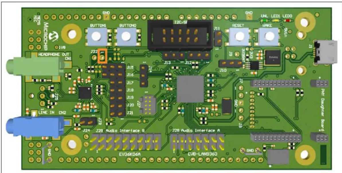
An image of the board (with an exchangeable LAN PHY daughter board) is shown in Figure 1-1.
FIGURE 1-1: EVB-LAN9360

text_image
Exchangeable LAN PHY Daughter Board J1 J2 J3 J4 J5 J6 J7 J8 J9 J10 J11 J12 J13 J14 J15 J16 J17 J18 J19 J20 J21 J22 J23 J24 J25 J26 Audio Interface A EVB-LN930C ELG6X06A J3U3 3VUSB RESET MIL LIDI LEDD LNG SND BUTTON0 BUTTON1 BUTTON1 J22 J23 Audio Interface B MICROCHIP MEMS REC 1106 HEADHONE OUT CN1 LINE IN CN2 BND1.1 PRODUCT FEATURES
- Supports the following standards (and protocols):
- IEEE Std 802.1AS™-2011 generalized Precision Time Protocol (gPTP) slave: time synchronization over the network
- IEEE Std 1722™-2016 (AVTP), Talker and Listener
- Microphone
- Support for a four Micro-Electro-Mechanical Systems (MEMS) microphones application use case
- Support for external analog microphone
• Supports a sample application for LAN9360 remote services
• Audio codec providing:
- One analog stereo input
- One analog stereo output
1.2 FUNCTIONAL DESCRIPTION
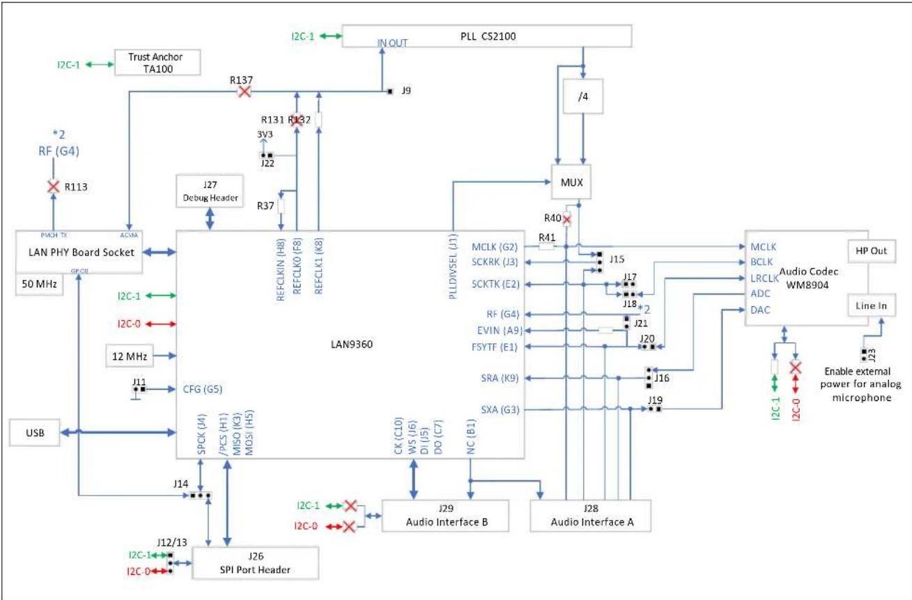
Figure 1-2 shows a simplified block diagram of the EVB-LAN9360.
FIGURE 1-2: BLOCK DIAGRAM

flowchart
graph TD
    A["Trust Anchor ATTA100"] --> B["LAN9360"]
    C["Debug Connector"] --> B
    D["IN"] --> B
    E["PLL OUT"] --> B
    F["LAN PHY Daughter Board Socket"] --> B
    G["USB Port"] --> B
    H["12 MHz"] --> B
    I["IC/SPI Port Header"] --> B
    J["Audio Interface B"] --> B
    K["Audio Interface A"] --> B
    L["HP OUT Audio Codec WM8904 Line IN"] --> M["Jumpers to Configure Stand-Alone Operation or the Use of External Components"]
    B --> M
The EVB-LAN9360, assembled with one stereo audio codec, can be used stand-alone to directly test or implement several configuration options (e.g., the board operates as a Talker and uses the Line In of the on-board codec).
Apart from the stand-alone use case, the board can be easily extended with customer components via on-board expansion connectors that allow external devices to be connected.
If the board should be run in stand-alone operation or if it uses external components can be configured by jumpers (simplified depicted in Figure 1-2; configuration details can be found in Figure A-1.
In addition, the EVB-LAN9360 supports an four MEMS microphones application use case that can be simulated via an external board. Details are described in Appendix B, Four Microphone Add-On Board.
The LAN9360 I²C Service can be used to remotely control local I²C peripherals via the I²C Service Add-On Board. For details see Appendix C, I²C Service Add-On Board.
Chapter 2. PHY Daughter Board
As shown in Figure 1-1, the EVB-LAN9360 is designed in a way that allows to easily exchange the Ethernet transceiver (PHY) and connector. For this purpose Microchip Technology Inc. provides LAN PHY daughter boards:
- For 100BASE-TX applications the LAN PHY daughter board uses a KSZ8041 ^1 ; for details refer to https://www.microchip.com/Developmenttools/ProductDetails/AC320004-5
- For 100BASE-T1 applications the LAN PHY daughter board uses a LAN8770 [1]; for details refer to https://www.microchip.com/Developmenttools/ProductDetails/EV48S68A
- For 10BASE-T1S applications the LAN PHY daughter board uses a LAN8670; for details refer to https://www.microchip.com/en-us/development-tool/EV06P90A
LAN PHY daughter boards must be connected to the EVB-LAN9360 by use of J2-J5, see Section 5.1.
Note: Connecting or changing LAN PHY daughter boards is only permitted when the device is detached from power. Hot plug is not supported and could damage the hardware.
Note: Repeated plugging and unplugging of LAN PHY daughter boards should be avoided due to the sensitivity of the connectors.
Figure 2-1 shows some examples of available LAN PHY daughter boards.
FIGURE 2-1: LAN PHY DAUGHTER BOARD EXAMPLES
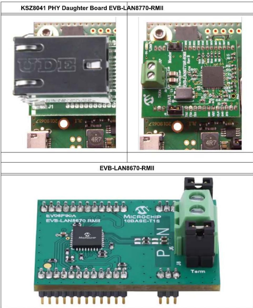
text_image
KSZ8041 PHY Daughter Board EVB-LAN8770-RMII EVB-LAN8670-RMII EV08P90A EV8-LAN8670 RMII MICROCHIP 10BASE-T1S TermChapter 3. Board Details
3.1 ELECTRICAL CHARACTERISTICS
| Parameter Min. Typ. Max. Unit | ||||
| Board Current Consumption at — Board Operating Voltage 4.5 5 | 300 mA5.5 | V | ||
3.2 CONNECTORS
3.2.1 CN1 and CN2 – Audio Sockets
These connectors are located on the top side of the board, see Section 5.1.
CN1 is used as Headphone Out connector.
CN2 is used as Line In connector.
| Designator | Socket Type |
| CN1 | SJ-3524-SMT-TR-GR, standard jack, stereo, 3.5 mm, green, from CUI Inc. |
| CN2 | SJ-3524-SMT-TR-BE, standard jack, stereo, 3.5 mm, blue, from CUI Inc. |
| Suitable counter-piece: SP-3501, stereo plug, 3.5 mm male, from CUI Inc. | |
3.2.2 J1 - USB Connector
This connector is located on the top side of the board, see Section 5.1.
| Designator | Socket Type |
| J1 Standard type | micro B |
| Suitable counter-piece: USB cable type A male/type micro B | |
Table 3-1 shows the pin assignment of J1.
TABLE 3-1: USB CONNECTOR – PIN ASSIGNMENT
| Pin | Description |
| 1 | VBUS |
| 2 | D- |
| 3 | D+ |
| 4 | NC |
| 5, 6, 7, 8, 9 | GND |
3.2.3 J2-J5 – LAN PHY Daughter Board Connector
These connectors are located on the top side of the board, see Section 5.1. J2-J5 are used to attach a LAN PHY daughter board onto the EVB-LAN9360.
3.2.4 J26 - I²C/SPI Connector
This connector is located on the top side of the board, see Section 5.1.
| Designator Socket Type | |
| J26 612 010 235 | 121, 2x5 TH Header Shrouded 2.54 mm Pitch, from Würth Elektronik |
| Suitable counter-piece: WR-BHD | |
Table3-2 shows the pin assignment of J26.
TABLE 3-2: I²C/SPI CONNECTOR – PIN ASSIGNMENT
| Pin Description | |||
| 1 | B | - | S |
| 2, 10 GND | |||
| 3 | B | - | S |
| 4, 6 3.3V | |||
| 5 | M | I | S |
| 7 SPI-CLK | |||
| 8 | M | O | S |
| 9 | / | P | C |
3.2.5 J27 - Debug Header Connector
This connector is located on the top side of the board, see Section 5.1.
| Designator Socket Type | |
| J27 FTSH-105-01 | -F-D-K, from Samtec |
| Suitable counter-pieces: FFSD-05-01-NFFSD-05-D-06.00-01-N | |
Table 3-3 shows the pin assignment of J27.
TABLE 3-3: DEBUG HEADER CONNECTOR – PIN ASSIGNMENT
| Pin Description | ||
| 1 | 3 | . 3 |
| 2 | S | W D |
| 3, 5, 9 GND | ||
| 4 | S | W C |
| 6 | SWO | |
| 7, 8 NC | ||
| 10 LAN9360-nRST | ||
3.2.6 J28 - Audio Interface A Connector
This connector is located on the top side of the board, see Section 5.1.
J28 is used as serial synchronous controller interface. It serves as board extension for connecting external devices.
| Designator Socket Type | |
| J28 TSW-107-07-G-D, 2.54 mm Pitch, from Samtec | |
| Suitable counter-piece: SSW-107-01-G-D |
Table 3-4 shows the pin assignment of J28.
TABLE 3-4: AUDIO INTERFACE A CONNECTOR – PIN ASSIGNMENT
| Pin Description | ||
| 1, 3, 5, 7, 9, 11, 13 GND | ||
| 2 | 3 | . 3 |
| 4 CLKEN | ||
| 6 A-MCLK | ||
| 8 | S | C K |
| 10 FSYA | ||
| 12 SRA | ||
| 14 SXA | ||
3.2.7 J29 – Audio Interface B Connector
This connector is located on the top side of the board, see Section 5.1.
J29 is used as I^2S interface. It serves as board extension for connecting external devices.
| Designator Socket Type | |
| J29 TSW-109-07-G-D, 2.54 mm Pitch, from Samtec | |
| Suitable counter-piece: SSW-109-07-G-D |
Table3-5 shows the pin assignment of J29.
TABLE 3-5: AUDIO INTERFACE B CONNECTOR – PIN ASSIGNMENT
| Pin Description | ||
| 1, 3, 5, 7, 9, 11, 13, 15, 17 | GND | |
| 2 | 3 | 3 |
| 4 CLKEN | ||
| 6 A-MCLK | ||
| 8 | S | C K |
| 10 FSYB | ||
| 12 SRB | ||
| 14 SXB | ||
| 16 ext-SCL | ||
| 18 ext-SDA | ||
3.2.8 J30 - I2C/SPI Port Header
This port header can be accessed from the top and from the bottom side of the board. The location of the port header is visualized in Figure 5-2.
| Designator Socket Type | |
| J30 TSW-110-23-F-S, 2.54 mm Pitch, from Samtec | |
| Suitable counter-piece: SSW-110-23-F-S |
Table 3-6 shows the pin assignment of J30.
TABLE 3-6: I²C/SPI PORT HEADER – PIN ASSIGNMENT
| Pin Description | |
| 1 XP-SCL | |
| 2 XP-SDA | |
| 3 | NC |
| 4 | GND |
| 5 XP-SCK | |
| 6 XP-MISO | |
| 7 XP-MOSI | |
| 8 XP-SS | |
| 9 XP-FC | |
| 10 XP-Int0a | |
3.3 JUMPERS
All jumpers are located on the top side of the board, see Section 5.1.
3.3.1 J10 – Power Management Option
If closed (1-2), this jumper connects to LAN-INH, using the LAN PHY daughter board power management.
If closed (2-3), the board is always powered.
| Designator Socket Type | |
| J10 TSW-103-2 | 3-F-S, 2.54 mm TH SQ Header, from Samtec |
| Suitable counter-piece: Jumper 2.54 mm | |
3.3.2 J11- Select Configuration from Configuration Database
If open, the primary configuration is selected at start-up.
If closed (1-2), the secondary configuration is selected at start-up. For details refer to the LAN9360 Data Sheet [1], section 4.3.1.
| Designator Socket Type |
| J11 TSW-102-23-F-S, 2.54 mm TH SQ Header, from Samtec |
| Suitable counter-piece: Jumper 2.54 mm |
| Note: | The EVB-LAN9360 is delivered with two configuration options stored in the Configuration Database, as described in the LAN9360 Data Sheet [1], section 4.1.With the primary configuration the LAN9360 acts as a gPTP slave.With the secondary configuration the LAN9360 acts as a gPTP grandmaster.Configurations may be changed assisted by the MPLAB ^ Network Creator. |
3.3.3 J12 - SCL Connector
If closed (1-2), this jumper connects SCL1 to J26, Pin1.
If closed (2-3), this jumper connects SCL0 to J26, Pin1.
| Designator Socket Type |
| J12 TSW-103-23-F-S, 2.54 mm TH SQ Header, from Samtec |
| Suitable counter-piece: Jumper 2.54 mm |
3.3.4 J13 - SDA Connector
If closed (1-2), this jumper connects SDA1 to J26, Pin3.
If closed (2-3), this jumper connects SDA0 to J26, Pin3.
| Designator Socket Type |
| J13 TSW-103-23-F-S, 2.54 mm TH SQ Header, from Samtec |
| Suitable counter-piece: Jumper 2.54 mm |
3.3.5 J14 - Select SPI
If closed (1-2), this jumper setting is for test purposes only and must not be used. If closed (2-3), this jumper connects the SPI SPCK signal to the SPI Port Header.
| Designator Socket Type |
| J14 TSW-103-23-F-S, 2.54 mm TH SQ Header, from Samtec |
| Suitable counter-piece: Jumper 2.54 mm |
3.3.6 J15 - Connect AVB Endpoint PLLIN/RK
If closed (1-2), this jumper connects the AVB Endpoint PLLIN/RK to the PLL divider output.
If closed (2-3), this jumper connects the AVB Endpoint PLLIN/RK to Audio Interface A, Pin8.
| Designator Socket Type | |
| J15 TSW-103-2 | 3-F-S, 2.54 mm TH SQ Header, from Samtec |
| Suitable counter-piece: Jumper 2.54 mm | |
3.3.7 J16 - Connect AVB Endpoint SRA Audio Interface A
If closed (1-2), this jumper connects the AVB Endpoint SRA Audio Interface A to the microphone.
If closed (2-3), this jumper connects the AVB Endpoint SRA Audio Interface A to the audio codec.
| Designator Socket Type |
| J16 TSW-103-23-F-S, 2.54 mm TH SQ Header, from Samtec |
| Suitable counter-piece: Jumper 2.54 mm |
3.3.8 J17 - Connect Microphone Clock to the AVB Endpoint
If closed (1-2), this jumper connects the microphone clock CLK to the AVB Endpoint.
| Designator Socket Type |
| J17 TSW-102-23-F-S, 2.54 mm TH SQ Header, from Samtec |
| Suitable counter-piece: Jumper 2.54 mm |
3.3.9 J18 - Connect Audio Codec Clock to the AVB Endpoint
If closed (1-2), this jumper connects the audio codec clock BCKL to the AVB Endpoint.
| Designator Socket Type | |
| J18 TSW-102-23-F-S, 2.54 mm TH SQ Header, from Samtec | |
| Suitable counter-piece: Jumper 2.54 mm |
3.3.10 J19 – Connect Audio Codec DAC to the AVB Endpoint
If closed (1-2), this jumper connects the audio codec DAC to the AVB Endpoint.
| Designator Socket Type |
| J19 TSW-102-23-F-S, 2.54 mm TH SQ Header, from Samtec |
| Suitable counter-piece: Jumper 2.54 mm |
3.3.11 J20 - Connect Audio Codec LRCLK to the AVB Endpoint
If closed (1-2), this jumper connects the audio codec LRCLK to the AVB Endpoint.
| Designator Socket Type | |
| J20 TSW-102-2 | 3-F-S, 2.54 mm TH SQ Header, from Samtec |
| Suitable counter-piece: Jumper 2.54 mm | |
3.3.12 J21 – Connect AVB Endpoint RF with AVB Endpoint EVIN
If closed (1-2), this jumper connects the AVB Endpoint RF signal with the AVB Endpoint EVIN signal.
| Designator Socket Type |
| J21 TSW-102-23-F-S, 2.54 mm TH SQ Header, from Samtec |
| Suitable counter-piece: Jumper 2.54 mm |
3.3.13 J22 – Erase Flash Memory of AVB Endpoint
If closed, this jumper is used to erase the flash memory of the AVB Endpoint.
| Designator Socket Type |
| J22 TSW-102-23-F-S, 2.54 mm TH SQ Header, from Samtec |
| Suitable counter-piece: Jumper 2.54 mm |
3.3.14 J23 – Enable External Power for Analog Microphone
If closed, this jumper is used to enable external power for an analog microphone.
| Designator Socket Type |
| J23 TSW-102-23-F-S, 2.54 mm TH SQ Header, from Samtec |
| Suitable counter-piece: Jumper 2.54 mm |
3.4 BUTTONS
All buttons are located on the top side of the board, see Section 5.1.
| Designator Description | |
| Button0 (SW1) Reserved for future use. | |
| Button1 (SW2) | |
| Reset (SW3) Reset components on the development board, especially the LAN9360 | |
| Wake (SW4) Wake up PHY daughter board (WakeIN signal) | |
3.5 LEDS
LEDs 0-2 are mounted on the top side of the board (see Section 5.1); LED 120 is mounted on the bottom side (see Section 5.2).
The table below gives an overview of the LEDs and the states they signal.
| Designator State | Description | |
| LED0 (LD1) Off Reser | ved for future use | |
| On (red) | ||
| LED1 (LD2) Off | ||
| On (yellow) | ||
| UNL (LD3) Off Media | Clock unlock indicator | |
| On (green) Media | Clock lock indicator | |
| LED120 (LD120) Off P | PLL lock indicator | |
| On (red) PLL unlock indicator, depends on firmware | ||
Chapter 4. Configuration Options
This chapter lists several configuration options that can be set up with the EVB-LAN9360. The EVB-LAN9360 can be configured as either Talker or Listener, or both. Possible configuration options are as follows:
• Talker/Listener with On-Board Codec
• Talker/Listener with External Codec/DSP
- Talker/Listener with External PCM Source and On-Board Codec as Sink
- Talker/Listener with External PCM Sink and On-Board Codec as Source
• 1PPS Method for Clock Accuracy Measurement
Common jumper settings
For all configuration options, the following jumper settings are common:
TABLE 4-1: COMMON JUMPER SETTINGS
| Jumper Setting | |
| J10 2-3 | |
| J12 2-3 | |
| J13 | |
| J14 2-3 | |
| J17 Open | |
| J21 1-2 |
Deviating jumper settings are described in the respective configuration sections, see the following pages.
Codec
The on-board codec is configured by the LAN9360 via I²C.
Note: The configuration of an external codec is not included in the LAN9360's functionality.
Media clock generation
If an external source or sink (codec, DSP) is used, the media clock can either be provided externally or is generated on-board.
4.1 TALKER/LISTENER WITH ON-BOARD CODEC
In this configuration the on-board codec is used as PCM source and sink.
The media clock may be recovered from the network with the PLL or generated onboard (selected by LAN9360 configuration options Clock Source and property Clock-Mode).
Table 4-2 gives an overview of the jumper settings for this configuration.
TABLE 4-2: TALKER/LISTENER WITH ON-BOARD CODEC – JUMPER SETTINGS
| Jumper Setting | |
| J15 1-2-3: Clock Mode: | FSYOut2-3: Clock Mode: FSYIn1-2: Clock Mode: Master (factory default) |
| J16 2-3 | |
| J18 1-2 | |
| J19 | |
| J20 |
Figure 4-1 depicts the jumper settings on the EVB-LAN9360.
FIGURE 4-1: TALKER/LISTENER WITH ON-BOARD CODEC – JUMPER SETTINGS
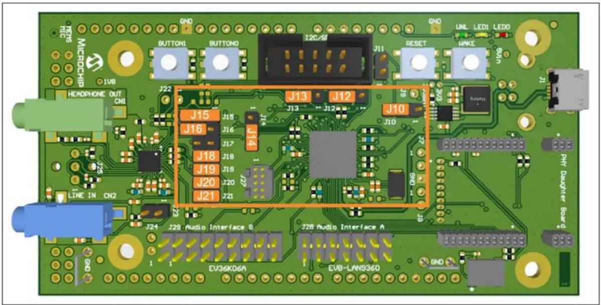
text_image
GND GND RUNL LEDI LEDO REPS MICROCHIP JVB HEADPHONE OUT CNI J22 J13 J12 J15 J14 J16 J15 J17 J16 J18 J17 J19 J18 J20 J19 J21 J20 J22 J21 J13 J12 J10 J9 J10 J17 J20 J21 J24 J28 Audio Interface B J28 Audio Interface A EV36K06A EV8-LAN936D END PHY Daughter Board ENDThe audio source (stereo) for the AVB Talker is the blue jack connector (Line In).
Note: Close J23 (1-2) to feed power to an analog microphone if needed. Otherwise J23 should be open.
The AVB Listener plays the received audio signal (stereo) through the green jack connector (Headphone Out).
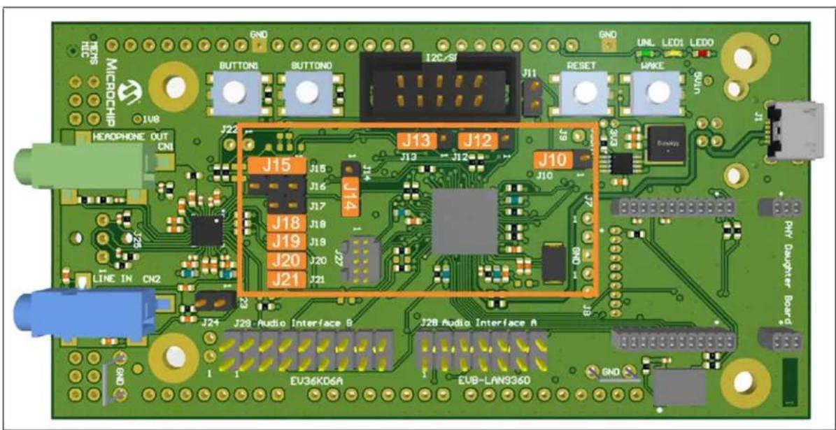
4.2 TALKER/LISTENER WITH EXTERNAL CODEC/DSP
In this configuration the LAN9360 acts as Talker or Listener or both.
An external codec or DSP is connected to the Audio Interface A Connector (J28, see Section 3.2.6) as PCM source and sink.
The media clock may be recovered from the network with the PLL or generated by the external device (selected by LAN9360 configuration options Clock Source and property ClockMode).
Note: It is not possible to use the on-board codec simultaneously.
Table 4-3 gives an overview of the jumper settings for this configuration.
TABLE 4-3: TALKER/LISTENER WITH EXTERNAL CODEC/DSP – JUMPER SETTINGS
| Jumper Setting | |
| J15 1-2-3: Clock Mode: | FSYOut2-3: Clock Mode: FSYIn1-2: Clock Mode: Master (factory default) |
| J16 Open | |
| J18 | |
| J19 | |
| J20 |
Figure 4-2 depicts the jumper settings on the EVB-LAN9360.
FIGURE 4-2: TALKER/LISTENER WITH EXTERNAL CODEC/DSP - JUMPER SETTINGS

text_image
MICROCHIP J15 J14 J21 J29 Audio Interface B J28 Audio Interface A EU36KD6A EVB-LAN9360 J13 J12 J13 J12 J10 J17 J18 J19 J20 J21 J22 J23 J24 LINE IN CN2 JND RUNS UNI LEDI LEDO MAKE BAN PHY Daughter BoardThe audio source for the AVB Talker and the audio sink for the AVB Listener is provided at Audio Interface A.
4.3 TALKER/LISTENER WITH EXTERNAL PCM SOURCE AND ON-BOARD CODEC AS SINK
In this configuration the LAN9360 acts as Talker and Listener. For a Talker only or a Listener only, the configurations as described in Section 4.1 or Section 4.2 should be used.
An external codec/DSP is connected to Audio Interface A (J28, see Section 3.2.6) as PCM source. The on-board codec is used as PCM sink.
The media clock may be recovered from the network with the PLL or generated onboard (selected by LAN9360 configuration option Clock Source).
Table 4-4 gives an overview of the jumper settings for this configuration.
TABLE 4-4: TALKER/LISTENER WITH EXTERNAL PCM SOURCE AND ON-BOARD CODEC AS SINK - JUMPER SETTINGS
| Jumper Setting | |
| J15 1-2-3: Clock Mode: | FSYOut2-3: Clock Mode: FSYIn (not possible)1-2: Clock Mode: Master (factory default) |
| J16 Open | |
| J18 1-2 | |
| J19 | |
| J20 |
Figure 4-3 depicts the jumper settings on the EVB-LAN9360.
FIGURE 4-3: TALKER/LISTENER WITH EXTERNAL PCM SOURCE AND ON-BOARD CODEC AS SINK – JUMPER SETTINGS
text_image
J15 J14 J13 J12 J10 J18 J19 J20 J21 J24 J28 Audio Interface B J2B Audio Interface A EV36KD6A EVB-LAN9360 GND TETS MICROCHIP 1V8 HEADPHONE OUT CN1 LINE IN CN2 RESET UNL LEDI LEDO WIKU Dunahy Pit Daughter BoardThe audio source for the AVB Talker is provided at Audio Interface A.
The AVB Listener plays the received audio signal (stereo) through the green jack connector (Headphone Out).
4.4 TALKER/LISTENER WITH EXTERNAL PCM SINK AND ON-BOARD CODEC AS SOURCE
In this configuration the LAN9360 acts as Talker and Listener. For a Talker only or a Listener only, the configurations as described in Section 4.1 or Section 4.2 should be used.
An external codec/DSP is connected to Audio Interface A (J28, see Section 3.2.6) as PCM sink. The on-board codec is used as PCM source.
The media clock may be recovered from the network with the PLL or generated onboard (selected by LAN9360 configuration option Clock Source).
Table 4-5 gives an overview of the jumper settings for this configuration.
TABLE 4-5: TALKER/LISTENER WITH EXTERNAL PCM SINK AND ON-BOARD CODEC AS SOURCE - JUMPER SETTINGS
| Jumper Setting | |
| J15 1-2-3: Clock Mode: | FSYOut2-3: Clock Mode: FSYIn (not possible)1-2: Clock Mode: Master (factory default) |
| J16 2-3 | |
| J18 1-2 | |
| J19 Open | |
| J20 1-2 |
Figure 4-4 depicts the jumper settings on the EVB-LAN9360.
FIGURE 4-4: TALKER/LISTENER WITH EXTERNAL PCM SINK AND ON-BOARD CODEC AS SOURCE - JUMPER SETTINGS
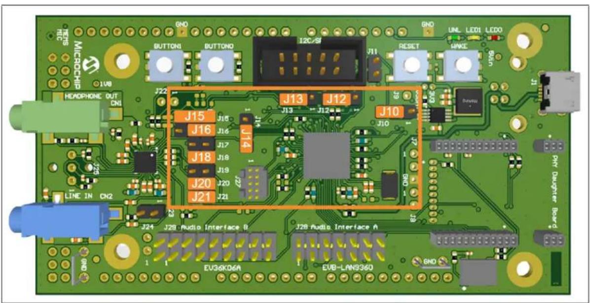
text_image
TETS MICROCHIP 1V8 HEADPHONE OUT CN1 LINE IN CN2 J22 J15 J16 J14 J17 J18 J19 J20 J21 J13 J12 J13 J12 J10 J10 J28 Audio Interface B J28 Audio Interface A EV36KD6A EVB-LAN936D GND UNL LEDI LEDO RESET MAKE Dundlow DHT Daughter BoardThe audio sink for the AVB Listener is provided at Audio Interface A.
The AVB Talker receives the audio signal (stereo) through the blue jack connector (Line In).
4.5 1PPS METHOD FOR CLOCK ACCURACY MEASUREMENT
In this configuration the LAN9360 does not process audio data, neither as a Talker nor as a Listener—hence, jumper settings are not required.
A one-pulse-per-second (1PPS) signal is provided at J22/Pin1 to measure the accuracy of the synchronization to the gPTP clock. The device may operate as gPTP master or gPTP slave. Reception of a media clock is not required and has no influence on the 1PPS signal.
Figure 4-5 indicates the location of J22/Pin1 on the LAN9360 Development Board.
FIGURE 4-5: 1PPS METHOD FOR CLOCK ACCURACY MEASUREMENT - J22/PIN1
text_image
GND TITLE MICROCHIP J18 HEADPHONE OUT CN1 J22 J16 J16 J17 J18 J19 J20 J21 J23 J24 J28 Audio Interface B EV36K06A J28 Audio Interface A EVB-LAN9360 GND RESET UNL LEDI LEDO MPKE Cable J10 J29 J27 J13 J12 J14 J15 J16 J17 J18 J19 J20 J21 LINE IN CN2 PMT Daughter BoardTo evaluate the 1PPS signal, an oscilloscope can be connected to J22/Pin1.
It is of advantage to compare the 1PPS signals with multiple devices (gPTP master with several gPTP slaves).
Chapter 5. Assembly Plan and Mechanical Dimensions
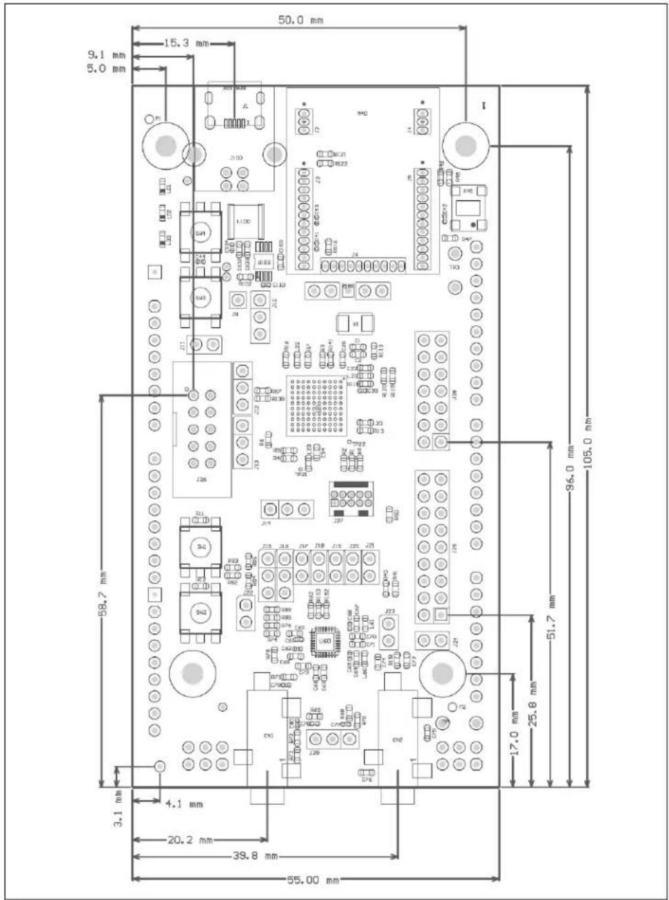
5.1 TOP VIEW AND MECHANICAL DIMENSIONS
FIGURE 5-1: ASSEMBLY PLAN – TOP VIEW AND MECHANICAL DIMENSIONS
text_image
50.0 mm 15.3 mm 9.1 mm 5.0 mm I 96.0 mm 105.0 mm 58.7 mm 3.1 mm 4.1 mm 20.2 mm 39.8 mm 55.00 mm 50.0 mm 11.00 12.00 13.00 14.00 15.00 16.00 17.00 18.00 19.00 20.00 21.00 22.00 23.00 24.00 25.00 26.00 27.00 28.00 29.00 30.00 31.00 32.00 33.00 34.00 35.00 36.00 37.00 38.00 39.00 40.00 41.00 42.00 43.00 44.00 45.00 46.00 47.00 48.00 49.00 50.05.2 BOTTOM VIEW AND MECHANICAL DIMENSIONS
FIGURE 5-2: ASSEMBLY PLAN – BOTTOM VIEW AND MECHANICAL DIMENSIONS

text_image
58.0 mm 36.5 mm 13.6 mm 3.4 mm 104-11396-R LRC11 31.4 mm 54.2 mm 3.3 mm 10.9 mm 3.4 mm 8.5 mm 46.5 mm 51.6 mmAppendix A. AVB Endpoint Connection Options
Figure A-1 shows a simple block diagram of the EVB-LAN9360 including the AVB End-point connection options configurable by jumpers.
Note: Pin1 of each jumper is indicated by a square.
For a description of the jumpers refer to Section 3.3.
FIGURE A-1: AVB ENDPOINT CONNECTION OPTIONS
flowchart
graph TD
    A["J26 SPI Port Header"] --> B["SPCK (J4)"]
    A --> C["PCS (H1)"]
    A --> D["MISO (K3)"]
    A --> E["MOSI (H5)"]
    A --> F["J12/13"]
    A --> G["I2C-1"]
    A --> H["I2C-0"]
    A --> I["J14"]
    J["USB"] --> K["CFG (G5)"]
    K --> L["LAN PHY Board Socket"]
    L --> M["50 MHz"]
    M --> N["PACH TX"]
    N --> O["R113"]
    O --> P["RF (G4)"]
    P --> Q["R137"]
    Q --> R["R131 R132"]
    R --> S["J27 Debug Header"]
    S --> T["J27"]
    T --> U["REFCLKIN (H8)"]
    T --> V["REFCLK0 (F8)"]
    T --> W["REFCLK1 (K8)"]
    X["I2C-1"] --> Y["Trust Anchor TA100"]
    Z["I2C-1"] --> AA["IN OUT"]
    AB["I2C-1"] --> AC["J9"]
    AD["I2C-0"] --> AE["ACMA"]
    AF["I2C-0"] --> AG["I2C-1"]
    AH["I2C-0"] --> AI["PLL CS2100"]
    AJ["PLL CS2100"] --> AK["/4"]
    AL["PLL CS2100"] --> AM["MUX"]
    AM --> AN["R40"]
    AN --> AO["MCLK (G2)"]
    AN --> AP["SCKRK (J3)"]
    AN --> AQ["SCKTK (E2)"]
    AN --> AR["PLL DIVSEL (J1)"]
    AN --> AS["MCLK (G2)"]
    AN --> AT["J15"]
    AN --> AU["J17"]
    AN --> AV["J18*2"]
    AN --> AW["J21"]
    AN --> AX["J20"]
    AN --> AY["J16"]
    AN --> AZ["J19"]
    AN --> BA["Audio Codec WM8904"]
    BB["Audio Codec WM8904"] --> BC["MCLK"]
    BB --> BD["BCLK"]
    BB --> BE["LRCLK"]
    BB --> BF["ADC"]
    BB --> BG["DAC"]
    BH["Audio Codec WM8904"] --> BI["MCLK"]
    BH --> BJ["BCLK"]
    BH --> BK["LRCLK"]
    BH --> BL["ADC"]
    BH --> BM["DAC"]
    BN["Audio Codec WM8904"] --> BO["MCLK"]
    BN --> BP["BCLK"]
    BN --> BQ["LRCLK"]
    BN --> BR["ADC"]
    BN --> BS["DAC"]
    BN --> BT["MCLK"]
    BN --> BU["BCLK"]
    BN --> BV["LRCLK"]
    BN --> BW["DAC"]
    BX["Audio Codec WM8904"] --> BY["MCLK"]
    BX --> BZ["BCLK"]
    BX --> CA["LRCLK"]
    BX --> CB["ADC"]
    BX --> CC["DAC"]
    BX --> CD["MCLK"]
    BX --> CE["BCLK"]
    BX --> CF["LRCLK"]
    BX --> CG["DAC"]
    CX["Audio Codec WM8904"] --> CY["MCLK"]
    CX --> CZ["BCLK"]
    CX --> DA["LRCLK"]
    CX --> DB["ADC"]
    CX --> DC["DAC"]
    CX --> DY["MCLK"]
    CX --> DE["BCLK"]
    CX --> DF["LRCLK"]
    CX --> DG["DAC"]
    DY --> DY
    DZ["Audio Codec WM8904"] --> DA
    DZ --> DZ
    DZ --> DZ
    DZ --> DZ
    DZ --> DZ
Appendix B. Four Microphone Add-On Board
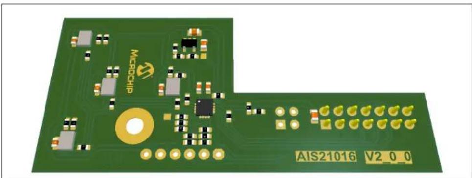
This chapter describes a use case with four digital MEMS microphones that are available on an external circuit board, the so-called Four Microphone Add-On Board (AIS21016).
The Four Microphone Add-On Board in combination with the EVB-LAN9360 can be used to produce an AVB Stream containing up to four audio channels, each captured from one of the four microphones.
Typical areas of application are:
• Mono microphone (one channel)
• Stereo microphone (two channels)
- Microphone array (three or four channels), e.g., to realize beamforming applications
A picture of the Four Microphone Add-On Board is shown in Figure B-1.
FIGURE B-1: FOUR MICROPHONE ADD-ON BOARD
natural_image
Green printed circuit board with various electronic components and a gold circular connector (no readable text or symbols)To setup the application use case, J1 of the Four Microphone Add-On Board needs to be attached to J28, which is the Audio Interface A Connector of the EVB-LAN9360. Figure B-2 depicts this connection.
FIGURE B-2: FOUR-MICROPHONE APPLICATION USE CASE
natural_image
Green printed circuit board with various electronic components and connectors (no readable text or symbols)For configuration options set the jumpers as described Section 4.3.
Note: In the MPLAB Network Creator, this Add-On module requires the Audio Port Frame Sync Format set to "HighDelayed".
B.1 BOARD DETAILS
B.1.1 Electrical Characteristics
| Parameter Min. Typ. Max. Unit | ||||
| Board Current Consumption at — 18 — mA Board Operating Voltage | — | 3.3 | — | V |
B.1.2 Connectors
B.1.2.1 J1 - FOUR MICROPHONE ADD-ON BOARD CONNECTOR
This connector is located on the bottom side of the board, see Section B.2.2.
J1 is used as serial synchronous controller interface for the connection with the EVB-LAN9360 (J28).
| Designator | Socket Type |
| J1 | SSW-107-01-G-D, 2.54 mm Pitch, from Samtec |
| Suitable counter-piece: TSW-107-07-G-D | |
Table B-1 shows the pin assignment of J1.
TABLE B-1: FOUR MICROPHONE ADD-ON BOARD CONNECTOR – PIN ASSIGNMENT
| Pin | Description |
| 1, 3, 5, 7, 9, 11, 13 | GND |
| 2 | 3.3V |
| 4, 6, 14 | NC |
| 8 | BCLK |
| 10 | FSY |
| 12 | SD0 |
B.2 ASSEMBLY PLAN AND MECHANICAL DIMENSIONS
B.2.1 Top View and Mechanical Dimensions
FIGURE B-3: ASSEMBLY PLAN – TOP VIEW AND MECHANICAL DIMENSIONS
text_image
35.0 mm 32.0 mm 71.0 mm 15.0 mmB.2.2 Bottom View
FIGURE B-4: ASSEMBLY PLAN - BOTTOM VIEW

This chapter provides an explanation on the practical utilization of the LAN9360 I²C Service to remotely control local I²C peripherals by using the so-called I²C Service Add-On Board (AIS23008).
The I²C Service Add-On Board in combination with the EVB-LAN9360 can be used to test and validate the usage of the LAN9360 I²C Service either through the sample code library provided by Microchip or through the customer's own implementation.
The following peripherals are available on the I²C Service Add-On Board:
- Weather sensor
- Ambient light sensor
• GPIO expander with four LEDs (outputs) and four DIP switches (inputs)
A picture of the I²C Service Add-On Board is shown in Figure C-1.
FIGURE C-1: I²C SERVICE ADD-ON BOARD

text_image
J3 GND J4 AUX AMB. LIGHT WEATHER U300 U200 CH: 01 12 23 D100 D101 D102 D103 SW100 AIS23008 V01_01_00To set up the application use case, J12 and J13 on the EVB-LAN9360 must be set to 2-3, to provide I²C-0 at J26, see Figure A-1.
J1 of the I²C Service Add-On Board needs to be attached to J26, which is the I²C/SPI Connector of the EVB-LAN9360. J2 of the I²C Service Add-On Board needs to be attached to J29, which is the Audio Interface B Connector of the EVB-LAN9360.
Figure C-2 depicts this connection.
FIGURE C-2: I²C SERVICE ADD-ON BOARD APPLICATION USE CASE
text_image
AMB-LIGHT WEATHER U300 CH O 100 N 0101 0102 0103 U200 U100 SH100 AIS23008 U01_01_00 J3 SND INT J4 SDP GND J4 AUX 21.3 21.5 21.0 21.5 21.0 EV36X06A R1 EVB-LAN9360 EV36X06A/20112 4.50 Interlace A EVB-LAN9360 new Computer BoardC.1 BOARD DETAILS
C.1.1 Electrical Characteristics
| Parameter Min. Typ. Max. Unit | ||||
| Board Current Consumption at — — 15 mA Board Operating Voltage | 2.5 | 3.3 | 3.6 V | |
C.1.2 Connectors
C.1.2.1 J1 - I²C CONNECTION TO EVB-LAN9360
This connector is located on the bottom side of the board, see Section C.2.2.
J1 is used as I²C interface connector.
| Designator | Socket Type |
| J1 | SSW-105-01-F-D, 2.54 mm Pitch, from Samtec |
| Suitable counter-piece: TSW-109-07-G-D, 2.54 mm Pitch, from SamtecTSW-105-07-G-D, 2.54 mm Pitch, from Samtec | |
Table C-1 shows the pin assignment of J1.
TABLE C-1: I²C SERVICE ADD-ON BOARD CONNECTOR J1 – PIN ASSIGNMENT
| Pin | Description |
| 1 | SCL |
| 2, 10 | GND |
| 3 | SDA |
| 4, 5, 6, 7, 8, 9 NC |
C.1.2.2 J2 - 3V3 CONNECTION TO EVB-LAN9360
This connector is located on the bottom side of the board, see Section C.2.2.
J2 is used to power the I²C Service Add-On Board.
| Designator | Socket Type |
| J2 | SSW-105-01-F-D, 2.54 mm Pitch, from Samtec |
| Suitable counter-piece: TSW-109-07-G-D, 2.54 mm Pitch, from SamtecTSW-105-07-G-D, 2.54 mm Pitch, from Samtec | |
Table C-2 shows the pin assignment of J2.
TABLE C-2: I²C SERVICE ADD-ON BOARD CONNECTOR J2 – PIN ASSIGNMENT
| Pin | Description |
| 1, 3, 5, 7, 9 | GND |
| 2 | 3.3V |
| 4, 6, 8, 10 | NC |
C.1.3 Port Expander
The port expander exposes eight channels; four of them are connected to LEDs and the remaining four channels are connected to a DIP switch (SW100). The 7-bit I²C client address is used to exchange I²C commands over the port expander.
| Designator Description | |
| U100 Port expander | I2C client address: 0x20Type: MCP23008https://www.microchip.com/en-us/product/MCP23008 |
LEDs and the DIP switch are mounted on the top side of the board, see Section C.2.1.
| Port Expander Channel Description | |
| 0 LED D100 | |
| 1 LED D101 | |
| 2 LED D102 | |
| 3 LED D103 | |
| 4 DIP switch slider 1 | |
| 5 DIP switch slider 2 | |
| 6 DIP switch slider 3 | |
| 7 DIP switch slider 4 | |
C.1.4 Sensors
All sensors are located on the top side of the board, see Section C.2.1.
| Designator Description | |
| U200 Weather sensor (temperature, humidity, athmospheric pressure)I2C client address: 0x76Type: Bosch® BME280https://www.bosch-sensortec.com/products/environmental-sensors/humidity-sensors-bme280/ | |
| U300 Ambient light | I2C client address: 0x29Type: Vishay® VEML6031X00https://www.vishay.com/en/product/80007/ |
C.2 ASSEMBLY PLAN AND MECHANICAL DIMENSIONS
C.2.1 Top View and Mechanical Dimensions
FIGURE C-3: ASSEMBLY PLAN – TOP VIEW AND MECHANICAL DIMENSIONS
text_image
63.3mm 53.6mm 44.8mm 25.3mm J4 J3 mO 55.0mm 51.1mm 46.0mm 8.5mm U100 10.0mm 40.0mm 44.6mm 17.0mm 30.9mm 37.5mmC.2.2 Bottom View
FIGURE C-4: ASSEMBLY PLAN - BOTTOM VIEW

text_image
H3 J2 J6L 20230708 J1 AIS23008 V01_01_00 M4List of Figures
Figure 1-1: EVB-LAN9360 9
Figure 1-2: Block Diagram 10
Figure 2-1: LAN PHY Daughter Board Examples 12
Figure 4-1: Talker/Listener with On-Board Codec – Jumper Settings 24
Figure 4-2: Talker/Listener with External Codec/DSP – Jumper Settings 25
Figure 4-3: Talker/Listener with External PCM Source and On-Board Codec as Sink – Jumper Settings 26
Figure 4-4: Talker/Listener with External PCM Sink and On-Board Codec as Source – Jumper Settings 27
Figure 4-5: 1PPS Method for Clock Accuracy Measurement – J22/Pin1 28
Figure 5-1: Assembly Plan – Top View and Mechanical Dimensions 29
Figure 5-2: Assembly Plan – Bottom View and Mechanical Dimensions 30
Figure A-1: AVB Endpoint Connection Options 32
Figure B-1: Four Microphone Add-On Board 33
Figure B-2: Four-Microphone Application Use Case 34
Figure B-3: Assembly Plan – Top View and Mechanical Dimensions 36
Figure B-4: Assembly Plan – Bottom View 36
Figure C-1: I²C Service Add-On Board 37
Figure C-2: I²C Service Add-On Board Application Use Case 38
Figure C-3: Assembly Plan – Top View and Mechanical Dimensions 41
Figure C-4: Assembly Plan – Bottom View 42
NOTES:
List of Tables
Table 3-1: USB Connector – Pin Assignment .... 13
Table 3-2: I²C/SPI Connector – Pin Assignment .... 14
Table 3-3: Debug Header Connector – Pin Assignment .... 15
Table 3-4: Audio Interface A Connector – Pin Assignment .... 16
Table 3-5: Audio Interface B Connector – Pin Assignment .... 17
Table 3-6: I²C/SPI Port Header – Pin Assignment .... 18
Table 4-1: Common Jumper Settings ...... 23
Table 4-2: Talker/Listener with On-Board Codec – Jumper Settings 24
Table 4-3: Talker/Listener with External Codec/DSP – Jumper Settings ...... 25
Table 4-4: Talker/Listener with External PCM Source and On-Board Codec as Sink – Jumper Settings ...... 26
Table 4-5: Talker/Listener with External PCM Sink and On-Board Codec as Source – Jumper Settings ...... 27
Table B-1: Four Microphone Add-On Board Connector – Pin Assignment 35
Table C-1: I²C Service Add-On Board Connector J1 – Pin Assignment 39
Table C-2: I²C Service Add-On Board Connector J2 – Pin Assignment 39
Worldwide Sales and Service
AMERICAS
Corporate Office
2355 West Chandler Blvd.
Chandler, AZ 85224-6199
Tel: 480-792-7200
Fax: 480-792-7277
Technical Support:
http://www.microchip.com/
support
Web Address:
www.microchip.com
Atlanta
Duluth, GA
Tel: 678-957-9614
Fax: 678-957-1455
Austin, TX
Tel: 512-257-3370
Boston
Westborough, MA
Tel: 774-760-0087
Fax: 774-760-0088
Chicago
Itasca, IL
Tel: 630-285-0071
Fax: 630-285-0075
Dallas
Addison, TX
Tel: 972-818-7423
Fax: 972-818-2924
Detroit
Novi, MI
Tel: 248-848-4000
Houston, TX
Tel: 281-894-5983
Indianapolis
Noblesville, IN
Tel: 317-773-8323
Fax: 317-773-5453
Tel: 317-536-2380
Los Angeles
Mission Viejo, CA
Tel: 949-462-9523
Fax: 949-462-9608
Tel: 951-273-7800
Raleigh, NC
Tel: 919-844-7510
New York, NY
Tel: 631-435-6000
San Jose, CA
Tel: 408-735-9110
Tel: 408-436-4270
Canada - Toronto
Tel: 905-695-1980
Fax: 905-695-2078
ASIA/PACIFIC
Australia - Sydney
Tel: 61-2-9868-6733
China - Beijing
Tel: 86-10-8569-7000
China - Chengdu
Tel: 86-28-8665-5511
China - Chongqing
Tel: 86-23-8980-9588
China - Dongguan
Tel: 86-769-8702-9880
China - Guangzhou
Tel: 86-20-8755-8029
China - Hangzhou
Tel: 86-571-8792-8115
China - Hong Kong SAR
Tel: 852-2943-5100
China - Nanjing
Tel: 86-25-8473-2460
China - Qingdao
Tel: 86-532-8502-7355
China - Shanghai
Tel: 86-21-3326-8000
China - Shenyang
Tel: 86-24-2334-2829
China - Shenzhen
Tel: 86-755-8864-2200
China - Suzhou
Tel: 86-186-6233-1526
China - Wuhan
Tel: 86-27-5980-5300
China - Xian
Tel: 86-29-8833-7252
China - Xiamen
Tel: 86-592-2388138
China - Zhuhai
Tel: 86-756-3210040
ASIA/PACIFIC
India - Bangalore
Tel: 91-80-3090-4444
India - New Delhi
Tel: 91-11-4160-8631
India - Pune
Tel: 91-20-4121-0141
Japan - Osaka
Tel: 81-6-6152-7160
Japan - Tokyo
Tel: 81-3-6880-3770
Korea - Daegu
Tel: 82-53-744-4301
Korea - Seoul
Tel: 82-2-554-7200
Malaysia - Kuala Lumpur
Tel: 60-3-7651-7906
Malaysia - Penang
Tel: 60-4-227-8870
Philippines - Manila
Tel: 63-2-634-9065
Singapore
Tel: 65-6334-8870
Taiwan - Hsin Chu
Tel: 886-3-577-8366
Taiwan - Kaohsiung
Tel: 886-7-213-7830
Taiwan - Taipei
Tel: 886-2-2508-8600
Thailand - Bangkok
Tel: 66-2-694-1351
Tel: 43-7242-2244-39
Fax: 43-7242-2244-393
Denmark - Copenhagen
Tel: 45-4485-5910
Fax: 45-4485-2829
Finland - Espoo
Tel: 358-9-4520-820
France - Paris
Tel: 33-1-69-53-63-20
Fax: 33-1-69-30-90-79
Germany - Garching
Tel: 49-8931-9700
Germany - Haan
Tel: 49-2129-3766400
Germany - Heilbronn
Tel: 49-7131-72400
Germany - Karlsruhe
Tel: 49-721-625370
Germany - Munich
Tel: 49-89-627-144-0
Fax: 49-89-627-144-44
Germany - Rosenheim
Tel: 49-8031-354-560
Israel - Hod Hasharon
Tel: 972-9-775-5100
Italy - Milan
Tel: 39-0331-742611
Fax: 39-0331-466781
Italy - Padova
Tel: 39-049-7625286
Netherlands - Drunen
Tel: 31-416-690399
Fax: 31-416-690340
Norway - Trondheim
Tel: 47-7288-4388
Poland - Warsaw
Tel: 48-22-3325737
Romania - Bucharest
Tel: 40-21-407-87-50
Spain - Madrid
Tel: 34-91-708-08-90
Fax: 34-91-708-08-91
Sweden - Gothenberg
Tel: 46-31-704-60-40
Sweden - Stockholm
Tel: 46-8-5090-4654
UK - Wokingham
Tel: 44-118-921-5800
Fax: 44-118-921-5820