MPL485 - Electronic component Microchip - Free user manual and instructions
Find the device manual for free MPL485 Microchip in PDF.

User questions about MPL485 Microchip
0 question about this device. Answer the ones you know or ask your own.
Ask a new question about this device
Download the instructions for your Electronic component in PDF format for free! Find your manual MPL485 - Microchip and take your electronic device back in hand. On this page are published all the documents necessary for the use of your device. MPL485 by Microchip.
USER MANUAL MPL485 Microchip
PL360 Host Controller
Introduction
The PL360 is a multi-protocol modem for the Power Line Communication (PLC) device, implementing a very flexible architecture and allowing the implementation of standard and customized PLC solutions. It has been conceived to be bundled with an external Microchip MCU, which downloads the corresponding PLC firmware and controls the operation of the PL360 device.
The purpose of the PL360 Host Controller is to provide the external microcontroller a way to control the PL360 device and offer upper layers an easy way to get access to PLC communication.
As an example of the PLC system, the figure below shows the system architecture for G3 protocol based on a PL360 device being controlled by a SAM4C MCU.
Figure 1. G3 System Architecture

flowchart
graph TD
    A["USER APPLICATION"] --> B["IPv6 STACK"]
    B --> C["G3-PLC Stack"]
    C --> D["Adaptation Layer (IETF RFC 4944)"]
    C --> E["MAC Layer (IEEE 802.15.4)"]
    C --> F["PAL Layer (ITU-T G.9903)"]
    C --> G["Host Controller"]
    H["Platform"] --> I["PHY + PLC Transceiver"]
    I --> J["PL360"]
    K["Embedded USI"] --> L["app_if"]
    K --> M["adp_if"]
    K --> N["mac_if"]
    K --> O["phy_if"]
    K --> P["sniffer_if"]
    Q["Interrupt"] --> R["Carrier Detect"]
    S["SPI"] --> T["PLC"]
    U["PLC"] --> V["SAM4C"]
The aim of this document is to clarify and detail the user interface of the PL360 Host Controller.
Features
- Compliant with PRIME 1.3 Physical Layer
- Compliant with PRIME 1.4 Physical Layer
- Compliant with G3 Physical Layer
- SPI Interface
- Secure Boot Option
Table of Contents
Introduction....1
Features....2
- PL360 Host Controller Architecture....5
1.1. PL360 Host Controller File Structure....5
1.2. Application Interface (API)....6
1.3. PLC Stack Wrapper....6
1.4. Add-ons....7
1.5. Bootloader....7
1.6. Hardware Abstraction Layer (HAL)....7
1.7. Sleep Mode....7
1.8. Debug Mode....8
- PL360 System Architecture....9
2.1. Block Diagram....9
2.2. Bootloader....9
2.3. PL360 Memory....9
2.4. PL360 Drivers....10
2.5. PHY PLC Service....10
2.6. PHY Host Application....11
-
Brief about ASF....12
-
Initialization Example.... 13
4.1. Init Controller Descriptor....13
4.2. Set Controller Callbacks....13
4.3. Enable Controller....13
4.4. PLC Event Handling....14
4.5. Code Example....14
- Configuration....16
5.1. Configure Application.... 16
5.2. Configure Secure Mode.... 16
- Host Interface Management....17
6.1. Message Transmission....17
6.2. Message Reception....17
- SPI Protocol....18
7.1. Boot Command Format....18
7.2. Boot Response Format.... 18
7.3. Firmware Command Format.... 19
7.4. Firmware Response Format....19
7.5. Firmware Data Memory Regions....20
7.6. Message Flow for Basic Transactions....21
- Example Applications....32
8.1. PHY Examples....32
- Supported Platforms.... 34
9.1. Supported MCU Families....34
9.2. Supported Transceivers....34
9.3. Supported Boards.... 34
- Abbreviations.... 35
- References....36
- PL360 Host Controller API....37
12.1. Common PHY API....37
12.2. G3 PHY API....41
12.3. PRIME PHY SAP 63
- Appendix B: ZC Offset Configuration....83
- Revision History....84
14.1. Rev A - 03/2018....84
14.2. Rev B - 10/2018....84
14.3. Rev C - 04/2019....84
14.4. Rev D - 07/2019....85
14.5. Rev E - 08/2020....85
The Microchip Website....86
Product Change Notification Service....86
Customer Support....86
Microchip Devices Code Protection Feature....86
Legal Notice....87
Trademarks....87
Quality Management System....88
Worldwide Sales and Service....89
1. PL360 Host Controller Architecture
The PL360 Host Controller is a C source code component which provides the host MCU application access to the API of the Power Line Communications PHY layer running in the PL360 device. Figure 1-1 shows the architecture of the software which runs on the host MCU. The components of the PL360 Host Controller are described in the following subsections.
Figure 1-1. PL360 Host Controller Architecture

flowchart
graph TD
    A["HOST MCU"] --> B["PLC Application"]
    C["PL360 Host Controller"] --> D["PLC Application Interface API"]
    C --> E["Bootloader PLC Stack Wrapper Add-ons"]
    C --> F["Hardware Abstraction Layer"]
1.1 PL360 Host Controller File Structure
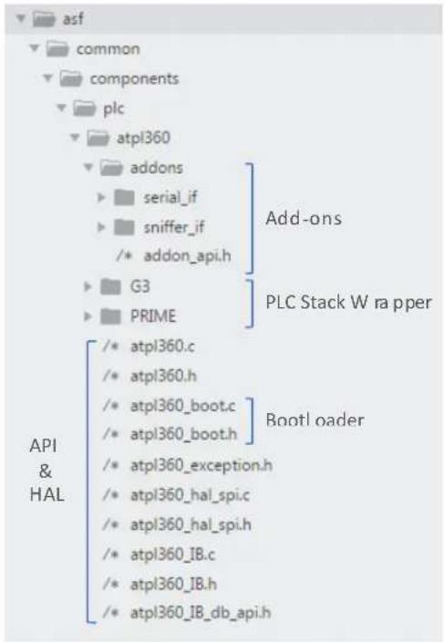
The PL360 Host Controller is provided as a component of Microchip ASF (Advanced Software Framework). The image below shows the location of the main files of the PL360 Host Controller Software. Different blocks provide different features. The next subsections describe the purpose of each block.
Figure 1-2. PL360 Host Controller File Structure
text_image
asf common components plc atpl360 addons serial_if sniffer_if /* addon_api.h G3 PRIME Add-ons PLC Stack W r apper API & HAL /* atpl360.c /* atpl360.h /* atpl360_boot.c /* atpl360_boot.h /* atpl360_exception.h /* atpl360_hal_spi.c /* atpl360_hal_spi.h /* atpl360_IB.c /* atpl360_I8.h /* atpl360_IB_db_api.h1.2 Application Interface (API)
This module provides an interface to the application for all PLC operations.
This API includes the following services:
- Set a custom hardware interface.
- Manage the bootloader process of the PL360 device.
- Manage the external configuration of the PL360 device.
- Enable / Disable PLC interface.
- Enable / Disable Secure mode.
- Enable / Disable add-on module (only for PHY firmwares).
- Enable / Disable Sleep mode.
- Enable / Disable Debug mode in run time. Manage extraction of data me memory from PL360.
This interface is defined in file atpl360.h and some of these services are configured in file conf_atpl360.h (see 5.1 Configure Application).
1.3 PLC Stack Wrapper
This module provides an interface compliant with the specific PLC communication stack, G3 or PRIME. It includes all declarations and definitions relative to the specific communication stack.
The main function of this module is to parse/serialize frames between SPI protocol and API functions in order to manage information from/to upper layers. It also provides a configuration function to set some hardware-specific parameters during the initialization process.
For further details, please refer to atpl360_comm.h header file.
1.4 Add-ons
This module is responsible for providing compatibility with Microchip PLC tools. Its main function is to pack/unpack frames so that they can be used by each PLC tool.
There are two add-ons available per PLC communication stack: one to connect with the Microchip PLC Sniffer PC tool, and another one to connect with the Microchip PLC PHY Tester PC tool.
1.5 Bootloader
The PL360 device is RAM-based, so it is required to transfer the binary code to the device after each reset. The main purpose of this module is to manage the binary download process.
During the bootloading process, the integrity of the SPI communication between the PL360 Host Controller and the PL360 device is checked in each SPI transaction. If the SPI header does not match the expected value, the PL360 Host Controller resets the PL360 device and the bootloader restarts the download of the binary code to the device again. The PL360 Host Controller tries this download process up to three times and reports a critical failure to upper layers after the last unsuccessful download process.
There are two modes of operation for the bootloader: Normal mode or Secure mode.
In Secure mode, the downloaded binary must be encrypted.
The following points should be taken into account in order to enable the Secure Boot mode:
- Define ATPL360 SEC BOOT MODE in conf_atpl360.h file
- It is mandatory to include specific metadata in the binary file before downloading it to the PL360 device, such as number of blocks to decipher, init vector and signature. A Microchip Python ^ script is provided in PLC PHY Workspace as an example of how to include this metadata information in the binary file
For further information about Secure mode, please refer to the PL360 Security Features document.
1.6 Hardware Abstraction Layer (HAL)
The Hardware Abstraction Layer provides full hardware compatibility with the host device.
There are four hardware peripherals that depend on customer platform/implementation:
- Access to SPI peripheral
- Access to interrupt system
- Access to delay system
- Access to carrier detect line
For further details, please refer to section 4. Initialization Example.
1.7 Sleep Mode
In the Sleep mode of the PL360, the core of the device and the peripherals are reset reducing power consumption. In this mode, RAM memory is still alive and the content of the memory is maintained, so program reloading is not required when the PL360 returns to normal operating mode and wake-up time is reduced considerably.
The mean power consumption of the PL360 device in Sleep mode is 0.7mA / 2.3 mW.
The wake-up time is optimized and reduced to 4ms. Please note that the wake-up time only takes into account the time for powering up the hardware and the initialization of the PL360 firmware. If any parameter (such as coupling parameters) is required to be configured, the time of configuration of the PL360 must be added.
In order to handle Sleep mode from the host, the NRST and TST pins of the PL360 device must be connected to the host controller.
There are 2 different ways to manage Sleep mode:
- Use standard API functions. Please refer to 12.1 Common PHY API.
- Use PIB objects specification. Please refer to 12.2.5 PIB Objects Specification and Access (G3) or 12.3.4 PIB Objects Specification and Access (PRIME)
1.8 Debug Mode
In the Debug mode of the PL360, the core of the device and the peripherals are reset. In this mode, RAM memory is still alive and the content of the memory is maintained, but the PL360 is set in Bootloader mode. The bootloader commands are used to access the memory contents.
Reloading of the program is not necessary to return to the PL360 normal operating mode.
Some requirements are mandatory to handle this mode:
- The NRST pin of the PL360 device must be connected to a host device.
- The PL360 Control fuses must be configured to allow read operations. For further information, please refer to the PL360 datasheet.
There are two different ways to manage Debug mode:
- Using standard API functions. Please refer to 12.1 Common PHY API.
- Using PIB objects specification. Please refer to 12.2.5 PIB Objects Specification and Access (G3) or 12.3.4 PIB Objects Specification and Access (PRIME)
Please contact Microchip Support for further information.
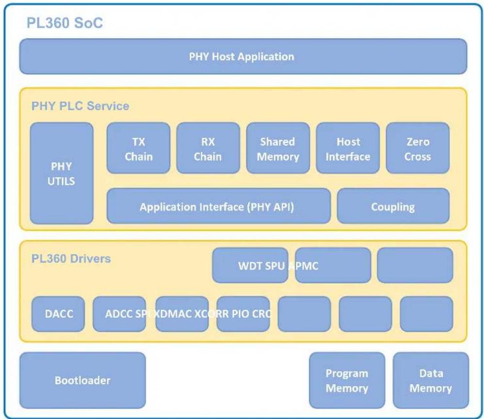
2. PL360 System Architecture
2.1 Block Diagram
Figure 2-1 shows the PL360 system architecture of the embedded firmware. The PL360 device has an embedded Cortex® M7 CPU running the PLC firmware. This firmware can either implement the G3 or the PRIME Physical layer, depending on what has been loaded by the PL360 Host Controller. The components of the system are described in the following subsections.
Figure 2-1. PL360 Embedded Firmware Architecture
flowchart
graph TD
    A["PHY Host Application"] --> B["PHY PLC Service"]
    B --> C["PHY UTILS"]
    B --> D["TX Chain"]
    B --> E["RX Chain"]
    B --> F["Shared Memory"]
    B --> G["Host Interface"]
    B --> H["Zero Cross"]
    B --> I["Application Interface (PHY API)"]
    I --> J["Coupling"]
    K["PL360 Drivers"] --> L["WDT SPU APMC"]
    L --> M["DACC"]
    L --> N["ADCC SPI XDMAC XCORR PIO CRC"]
    N --> O["Bootloader"]
    O --> P["Program Memory"]
    O --> Q["Data Memory"]
2.2 Bootloader
The bootloader is an Internal Peripheral (IP) designed to load the program from an external master into the instruction memory of the Cortex M7. This IP can access the instruction memory, data memory and peripheral registers.
For further information, please refer to the PL360 datasheet.
2.3 PL360 Memory
There are two memory configurations controlled via MEM_CONFIG bit. In the firmware loading process, the appropriate memory configuration is established by the PL360 Host Controller according to the firmware requisites.
| MEM_CONFIG Program memory Data memory | ||
| 0 128 KBytes 64 KBytes | ||
| 1 96 KBytes 96 KBytes | ||
The PL360 Host Controller code provided by Microchip sets MEM_CONFIG to 1 by default.
For further information, please refer to the PL360 datasheet.
2.4 PL360 Drivers
Each driver is responsible for managing a hardware peripheral:
• WDT: Watchdog system
• SPU: Signal Processing Unit
- APMC: Advanced Power Management Controller
• DACC: Digital to Analog Converter Controller
- ADCC: Analog to Digital Converter Controller
• SPI: Serial Peripheral Interface
• XDMAC: DMA Controller
- XCORR: Correlator
• PIO: Parallel Input/Output Controller
• CRC: Cyclic Redundancy Check
2.5 PHY PLC Service
There are several blocks in the PHY PLC service:
- Application Interface: The API provides a set of functions to access the physical medium and different parameters relative to each communication stack
- Host Interface: This block is in charge of managing the communication with the PL360 Host Controller through SPI. It is responsible for parsing/serializing the SPI data, managing PLC data regions and providing control on PLC Interruption PIO
- Coupling: This block contains the hardware configuration associated to the reference design provided by Microchip. If a customer needs to change this configuration to adapt it to its own design, Microchip provides a specific tool called the PHY Calibration Tool which helps customers calculate the best values for all coupling parameters. For further details, please refer to the PL360 Physical Calibration document
- TX Chain: The TX chain is responsible for handling messages from upper layers (passed through the API) to the physical output. This block controls all drivers relative to transmission and adapts signal parameters in order to use functionalities of the transmission chain PHY Utils block: convolutional encoder, scrambler, interleaver, modulator, IFFT and interpolator. In addition, it handles the result of the transmission in order to report it to upper layers through the API
- RX Chain: The RX chain is responsible for handling messages from the physical input to upper layers (passed through the API). This block checks if the PLC signal is present on the PLC medium, synchronizes with this PLC signal and drives the signal through functionalities of the reception chain in the PHY Utils block: decimator, FFT, demodulator, deinterleaver, descrambler and Viterbi block. In addition, it builds the complete message and reports it to upper layers through the API
- Shared Memory: This block defines the structure of the data memory to avoid collisions between TX and RX chains
- Zero Cross: The Zero Cross is responsible for calculating the last Zero Cross value and providing it to the PLC communication stack in use. For further information, please refer to 13. Appendix B: ZC Offset Configuration
- PHY Utils: This block contains several functionalities used by the TX/RX chains
2.6 PHY Host Application
The PHY Host Application is responsible for running the main application of the PL360 device. It is in charge of initializing the hardware and clock systems, checking the watchdog timer and managing the PL360 PLC service described in the previous chapter.
3. Brief about ASF
The Advanced Software Framework (ASF) is a MCU software library providing a large collection of embedded software for Microchip Flash MCUs: megaAVR, AVR XMEGA, AVR UC3 and SAM devices.
For details on ASF, please refer to the Advanced Software Framework documentation:
- Advanced Software Framework - Website
• [PDF] Atmel AVR4029: Atmel Software Framework - Getting Started
• [PDF] Atmel AVR4030: Atmel Software Framework - Reference Manual
4. Initialization Example
This chapter aims to explain the different steps required during the initialization phase of the system. After powering up the PL360 device, a set of initialization sequences must be executed in the correct order for the proper operation of the PL360 device.
The steps are the following:
- Init controller descriptor
- Set controller callbacks
- Enable controller
- PL360 event handling

Failure to complete any of the these initialization steps will result in failure in the PL360 Host Controller startup.
4.1 Init Controller Descriptor
The PL360 Host Controller is initialized by calling the atp1360_init function in the API. The PL360 Host Controller initialization routine performs the following actions:
- Disable PLC interrupt and component
- Register wrapper for Hardware Abstraction Layer (for further information, please refer to 12.1.1 Initialization Function)
- Reset the PL360 device using corresponding host MCU control GPIOs
- Configure a GPIO as an interrupt source from the PL360 device
- Initialize the SPI driver
- Register an internal event handler for the external PLC interrupt
- If an add-on is required, initialize specific add-on (configured previously). See chapter 5.1 Configure Application
- Return a descriptor to the PL360 Host Controller. This descriptor will be used to manage the PLC communication
4.2 Set Controller Callbacks
After initializing the PL360 Host Controller, it is important to set callbacks to manage PL360 events.
The PL360 Host Controller reports PLC events using callback functions.
The following callback functions are defined:
• Data indication: Used to report a new incoming message
- Data confirm: Used to report the result of the last transmitted message
- Add-on event: Used to report that a new add-on message is ready to be sent to the PLC application
- Exception event: Used to report if an exception occurs, such as a reset of the PL360 device
- Sleep mode event: Used to report that Sleep mode has been disabled
- Debug mode event: Used to report that Debug mode has been disabled
4.3 Enable Controller
The PL360 Host Controller is enabled by calling the atpl360_enable function in the API. This PL360 Host Controller routine performs the following actions:
- Disable/enable PLC interrupt and component
- Transfer the PL360 firmware to the PL360 device and validate. In case of failure, report a critical error in host communication with the PL360 device through exception callback
4.4 PLC Event Handling
Once the controller callbacks have been set up, the PL360 Host Controller component must be enabled. Then, the host MCU application is required to call the PL360 Host Controller API periodically to handle events from PL360 embedded firmware.
The PL360 Host Controller API allows the host MCU application to interact with the PL360 embedded firmware. To facilitate interaction, the PL360 Host Controller implements the host interface protocol described in section 6. Host Interface Management. This protocol defines how to serialize and how to handle API requests and response callbacks over the SPI bus interface.
Some PL360 Host Controller APIs are synchronous function calls, whose return indicates that the requested action is completed. However, most API functions are asynchronous. This means that when the application calls an API to request a service, the call is non-blocking and returns immediately, usually before the requested action is completed. When the requested action is completed, a notification is provided in the form of a host interface protocol message from the PL360 embedded firmware to the PL360 Host Controller, which, in turn, delivers it to the application via callback functions. Asynchronous operation is essential when the requested service, such as a PLC message transmission, may take significant time to complete. In general, the PL360 embedded firmware uses asynchronous events to notify the host driver of status changes or pending data.
The PL360 device interrupts the host MCU when one or more events are pending in the PL360 embedded firmware. The host MCU application processes received data and events when the PL360 Host Controller calls the corresponding event callback function(s). In order to receive event callbacks, the host MCU application is required to periodically call the atpl360 handle events function in the API.
When host MCU application calls atpl360_handle_events, the PL360 Host Controller checks for pending unhandled interrupts from the PL360 device. If no interrupt is pending, it returns immediately. If an interrupt is pending, atpl360_handle_events function dispatches the PLC event data to the respective registered callback. If the corresponding callback is not registered, the PLC event is discarded.
It is recommended to call this function either:
- From the main loop or from a dedicated task in the host MCU application; or,
- At least once when the host MCU application receives an interrupt from the PL360 embedded firmware
WARNING
The Host driver function atpl360_handle_events is non re-entrant. In the operating system configuration, it is required to protect the PL360 Host Controller from re-entrance.
4.5 Code Example
The code example below shows the initialization flow as described in previous sections.
/**
 * \brief Handler to receive add-on data from ATPL360.
 */
static void _handler_serial_atpl360_event(uint8_t *px_serial_data, uint16_t us_len)
{
    /* customer application */
}

/**
 * \brief Handler to receive add-on data from ATPL360.
 */
static void _handler_sleep_mode_resume_event(void)
{
    /* customer application : restore PL360 custom configuration */
}
/**
 * \brief Main code entry point.
 */
int main( void )
{
    atp1360_dev_callbacks_t x_atp1360_cbs;
    atp1360_hal_wrapper_t x_atp1360_hal_wp;
    uint8_t uc_ret;

    /* ASF function to setup clocking. */
    sysclk_init();

    /* ASF library function to setup for the evaluation kit being used. */
    board_init();

    /* Init ATPL360 */
    x_atp1360_hal_wp.plc_init = hal_plc_init;
    x_atp1360_hal_wp.plc_reset = hal_plc_reset;
    x_atp1360_hal_wp.plc_set_handler = hal_plc_set_handler;
    x_atp1360_hal_wp.plc_send_boot_cmd = hal_plc_send_boot_cmd;
    x_atp1360_hal_wp.plc_write_read_cmd = hal_plc_send_wrrd_cmd;
    x_atp1360_hal_wp.plc_enable_int = hal_plc_enable_interrupt;
    x_atp1360_hal_wp.plc_delay = hal_plc_delay;
    atp1360_init(&sx_atp1360_desc, &x_atp1360_hal_wp);

    /* Callback configuration. Set NULL as Not used */
    x_atp1360_cbs.data_confirm = NULL;
    x_atp1360_cbs.data_indication = NULL;
    x_atp1360_cbs.exception_event = NULL;
    x_atp1360_cbs.addons_event = handler_serial_atp1360_event;
    x_atp1360_cbs.sleep_mode_cb = handler_sleep_mode_resume_event;
    x_atp1360_cbs.debug_mode_cb = NULL;
    sx_atp1360_desc.set_callbacks(&x_atp1360_cbs);

    /* Enable ATPL360 */
    uc_ret = atp1360_enable(ATPL360_BINARY_ADDRESS, ATPL360_BINARY_LEN);
    if (uc_ret == ATPL360_ERROR) {
    printf("\r\nmain: atp1360_enable call error!(%d)\r\n", uc_ret);
    while (1) {
    }
    }

    while (1) {
    /* Check ATPL360 pending events */
    atp1360_handle_events();
    }
}
5. Configuration
The PL360 firmware has a set of configurable parameters that control its behavior. There is a set of configuration APIs provided to the host MCU application to configure these parameters. The configuration APIs are categorized according to their functionality: application, coupling parameters and secure mode.
Any parameter left unset by the host MCU application will use the default value assigned during the initialization of the PL360 firmware.

Info: All configuration parameters described in this chapter can be found in conf_atpl360.h file.
5.1 Configure Application
The following parameters can be modified in the conf_atp1360.h file to alter the behavior of the device.
- ATPL360_ADDONS_ENABLE: Use add-on capabilities
- Serial Interface: provides handling of messages to communicate with the Microchip PLC PHY Tester PC tool and PLC Python scripts
- Sniffer Interface: provides handling of messages to communicate with the Microchip PLC Sniffer PC tool

Info: These add-on modules are included in the PLC PHY workspace provided by Microchip. This workspace contains the projects to use with the Microchip PLC tools commented previously.
- ATPL360_WB: Only in case of G3 communication stack, the frequency band can be selected depending on customer requirements. G3 CENELEC-A, CENELEC-B, FCC and ARIB bands are available. Take into account that this configuration requires the use of different firmware binary files in the PL360 device. For further information, please refer to 12.2.1 Bandplan Selection.
5.2 Configure Secure Mode
For information about configuration of the Secure mode, please consult the PL360 Security Features document.
6. Host Interface Management
The PL360 Host Controller services are divided in two categories: synchronous and asynchronous services. Please refer to section 4.4 PLC Event Handling.
Most of the services implemented by the PL360 Host Controller are asynchronous.
The synchronous service is only used in the get_config function in order to get specific internal parameters relative to the communication stack.
When a function from the API is called, a sequence of actions is activated to format the request and to arrange to transfer it to the PL360 device through the SPI protocol.
When an asynchronous event occurs, the PL360 Host Controller handles the PLC interrupt, checks the events reported by the PL360 device and extracts the information relative to the notified event.
The associated callback will be invoked in the next call to atp1360_handle_events function.
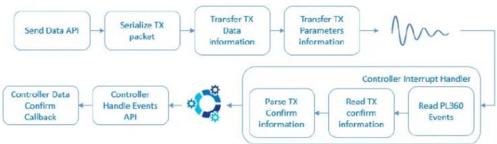
6.1 Message Transmission
The following figure shows the steps involved in the transmission of a message from the PL360 Host Controller to the PL360 device.
Figure 6-1. Sequence of Message Transmission
flowchart
graph TD
    A["Send Data API"] --> B["Serialize TX packet"]
    B --> C["Transfer TX Data information"]
    C --> D["Transfer TX Parameters information"]
    D --> E["Controller Interrupt Handler"]
    E --> F["Read PL360 Events"]
    F --> G["Read TX confirm information"]
    G --> H["Parse TX Confirm information"]
    H --> I["Controller Handle Events API"]
    I --> J["Controller Data Confirm Callback"]
    J --> A
6.2 Message Reception
The following figure shows the steps involved in the reception of a message from the PL360 device to the PL360 Host Controller.
Figure 6-2. Sequence of Message Reception

flowchart
graph LR
    A["Controller Data Indication Callback"] --> B["Controller Handle Events API"]
    B --> C((+))
    C --> D["Controller Interrupt Handler"]
    D --> E["Read PL360 Events"]
    D --> F["Read RX Data information"]
    D --> G["Parse RX Data information"]
    D --> H["Controller Interrupt Handler"]
    H --> I["Read RX Parameters information"]
    H --> J["Parse RX Parameters information"]
    H --> K["Controller Interrupt Handler"]
    K --> L["Read PL360 Events"]
    style A fill:#f9f,stroke:#333
    style B fill:#ccf,stroke:#333
    style C fill:#cfc,stroke:#333
    style D fill:#fcc,stroke:#333
    style E fill:#cff,stroke:#333
    style F fill:#ffc,stroke:#333
    style G fill:#ffc,stroke:#333
    style H fill:#ffc,stroke:#333
    style I fill:#cfc,stroke:#333
    style J fill:#cfc,stroke:#333
    style K fill:#cfc,stroke:#333
    style L fill:#fcc,stroke:#333
7. SPI Protocol
The main interface of the PL360 device is the SPI port. The PL360 device employs a proprietary protocol to allow the exchange of formatted data with the PL360 Host Controller. The PL360 SPI protocol uses raw bytes exchanged on the SPI bus to form high-level structures like requests and callbacks.
The PL360 SPI protocol consists of two layers:
- Layer 1: bootloader commands to transfer the firmware and configure the PL360 device
- Layer 2: firmware commands to allow the host MCU application to exchange high-level messages (e.g. PLC data transmission or PLC data reception) with the PL360 embedded firmware
The PL360 SPI Protocol is implemented as a command-response transaction and assumes that one part is the master (PL360 Host Controller) and the other one is the slave (PL360 embedded firmware).
The format of Command, Response and Data frames is described in the following subsections. The following points apply:
- There is a response for each command
- Transmitted/received data is divided into packets with variable size
- For a write transaction (slave is receiving data packets), the slave sends a response for each data packet
- For a read transaction (master is receiving data packets), the master does not send any response
- Boot commands require 8-bit transactions. Firmware commands require 16-bit transactions.
7.1 Boot Command Format
The following frame format is used for boot commands, where the PL360 device supports an address of four bytes.
Figure 7-1. Boot Command Fields

text_image
4 bytes 2 bytes Payload size ADDRESS BOOT COMMAND PAYLOAD 634 bytes maxThe address field contains any physical address of the PL360 device.
For further information regarding the boot command and payload fields, please see the PL360 datasheet.
7.2 Boot Response Format
The following frame format is used for boot responses.

text_image
2 bytes | 2 bytes | Payload size | HEADER | FLAGS | PAYLOAD | 634 bytes maxThe header field is formed by the first 15 bits and it contains the boot signature data (0b010101100011010). This data is fixed by the PL360 device and it is used to identify the status of the PL360 device.
The flags field contains information about the reset type of the last reset event:
- USER_RST: User reset
• CM7_RST: Cortex reset
• WDG_RST: Watchdog reset
Table 7-1. Boot Signature Data
| 31 30 29 28 27 26 25 24 | ||||||
| 0 1 0 1 0 1 1 0 | ||||||
| 23 22 21 20 19 18 17 16 | ||||||
| 0 0 1 1 0 1 0 USER_RST | ||||||
| 15 14 13 12 11 10 9 8 | ||||||
| CM7_RST WDG_RST ---- | ||||||
| 7 6 5 4 3 2 1 0 | ||||||
| ---- | ||||||
7.3 Firmware Command Format
The following frame format is used for firmware commands, where the PL360 device supports an address of two bytes.
Figure 7-2. Firmware Command Fields

text_image
CMD: 1bit 2 bytes | 2 bytes | Payload size ADDRESS LENGTH PAYLOAD 634 bytes maxThe address field contains the identification number of the region to access data. These region numbers are described in section 7.5 Firmware Data Memory Regions.
The CMD field (1 bit), which is the most significant bit of the length field, contains the SPI command:
- Read command: 0
- Write command: 1
The length field (15 bits) contains the number of 16-bit blocks to read.
The payload field depends on the region number to access and on the communication stack in use, G3 or PRIME. For further information, please refer to atpl360_comm.h file.
7.4 Firmware Response Format
The following frame format is used for firmware responses.
Figure 7-3. Firmware Response Fields

text_image
2 bytes Payload size HEADER PAYLOAD 634 bytes maxThe header field contains the firmware signature data (0x1122). This field is fixed by the PL360 embedded firmware and is used to check if this firmware runs properly.

Info: Due to the 16-bit configuration used in this SPI firmware transaction, the firmware signature is stored in memory as 0x2211.
The payload field depends on the PLC communication stack in use (G3 or PRIME). For further information, please refer to atpl360_comm.h file.
7.5 Firmware Data Memory Regions
This section shows the data memory regions defined in the PL360 device depending on which PLC communication stack is used.
The only difference between PRIME and G3 communication stacks regarding data memory regions is the number of transmission messages that can be simultaneously queued. In case of G3, only one message can be queued. In case of PRIME, two transmission messages can be queued simultaneously. This is possible because there are two transmission buffers defined in the PRIME PL360 embedded firmware, TX0 and TX1.

In both cases, G3 and PRIME, upper layers are responsible for managing multiple TX times in order to avoid collisions between them.
7.5.1 G3 Memory Regions
The following table defines memory regions to use with the G3 communication stack:
Table 7-2. G3 Memory Regions Table
| Region Name Value Comments | |
| ATPL360_STATUS_INFO_ID 0 | Information relative to the system timer and system events occurrences in the PL360 firmware |
| ATPL360_TX_PARAM_ID 1 | Information relative to parameters of the last transmission |
| ATPL360_TX_DATA_ID 2 | Information relative to data of the last transmission |
| ATPL360_TX_CFM_ID 3 | Information relative to the confirmation of the last transmission |
| ATPL360_RX_PARAM_ID 4 | Information relative to parameters of the last received message |
| ATPL360_RX_DATA_ID 5 | Information relative to data of the last received message |
| ATPL360_REG_INFO_ID 6 | Information relative to internal registers or PIB's |
7.5.2 PRIME Memory Regions
The following table defines memory regions to use with the PRIME communication stack:
Table 7-3. PRIME Memory Regions Table
| Region Name Value Comments | |
| ATPL360_STATUS_INFO_ID 0 Information relative to the system timer and system events occurrences in the PL360 firmware | |
| ATPL360_TX0_PARAM_ID 1 Information relative to parameters of the last transmission (buffer 0) | |
| ATPL360_TX0_DATA_ID 2 Information relative to data of the last transmission (buffer 0) | |
| ATPL360_TX0_CFM_ID 3 Information relative to the confirmation of the last transmission (buffer 0) | |
| ATPL360_TX1_PARAM_ID 4 Information relative to parameters of the last transmission (buffer 1) | |
| ATPL360_TX1_DATA_ID 5 Information relative to data of the last transmission (buffer 1) | |
| ATPL360_TX1_CFM_ID 6 Information relative to the confirmation of the last transmission (buffer 1) | |
| ATPL360_RX_PARAM_ID 7 Information relative to parameters of the last received message | |
| ATPL360_RX_DATA_ID 8 Information relative to data of the last received message | |
| ATPL360_REG_INFO_ID 9 Information relative to internal registers or PIB's | |
7.6 Message Flow for Basic Transactions
This section shows the essential message exchanges and timings.
Related constants affecting below parameters:
/* ! FLAG MASKs for set G3 events */
#define ATPL360_TX_CFM_FLAG_MASK 0x0001
#define ATPL360_RX_DATA_IND_FLAG_MASK 0x0002
#define ATPL360_CD_FLAG_MASK 0x0004
#define ATPL360_REG_RSP_MASK 0x0008
#define ATPL360_RX_QPAR_IND_FLAG_MASK 0x0010

/* ! G3 Event Info MASKs */
#define ATPL360_EV_DAT_LEN_MASK 0x0000FFFF
#define ATPL360_EV_REG_LEN_MASK 0xFFFF0000
#define ATPL360_GET_EV_DAT_LEN_INFO(x) ((uint32_t)x & ATPL360_EV_DAT_LEN_MASK)
#define ATPL360_GET_EV_REG_LEN_INFO(x) (((uint32_t)x & ATPL360_EV_REG_LEN_MASK) >> 16)

/* ! FLAG MASKs for set PRIME events */
#define ATPL360_TX0_CFM_FLAG_MASK 0x0001
#define ATPL360_TX1_CFM_FLAG_MASK 0x0002
#define ATPL360_RX_DATA_IND_FLAG_MASK 0x0004
#define ATPL360_CD_FLAG_MASK 0x0008
#define ATPL360_REG_RSP_MASK 0x0010
#define ATPL360_RX_QPAR_IND_FLAG_MASK 0x0020

/* ! PRIME Event Info MASKs */
#define ATPL360_EV_DAT_LEN_MASK 0x0000FFFF
#define ATPL360_EV_REG_LEN_MASK 0xFFFF0000
#define ATPL360_GET_EV_DAT_LEN_INFO(x) ((uint32_t)x & ATPL360_EV_DAT_LEN_MASK)
#define ATPL360_GET_EV_REG_LEN_INFO(x) (((uint32_t)x & ATPL360_EV_REG LEN_MASK) >> 16)
7.6.1 G3: Send Message
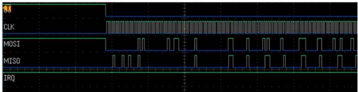
In a message transmission, there are 2 SPI blocks. The first one is relative to the transmission of G3 parameters of the message, the second one is relative to the data part of the same message.
Figure 7-4. G3 Send Message SPI Sequence

text_image
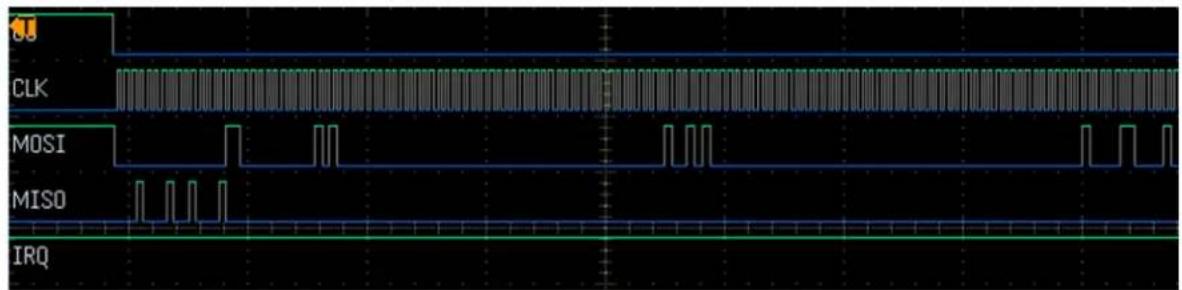
CLK MOSI MISO IRQ7.6.1.1 G3: Send Parameters
Figure 7-5. G3 Send Parameters SPI Array
text_image
CLK MOSI MISO IRQIn a transmission of parameters, the following can be seen:
- Master (MOSI):
- Send ID memory region(16 bits): 0x0001 (ATPL360_TX_PARAM_ID)
- Send SPI command (1 bit): 1 (write command)
- Send SPI params length (15 bits) (in blocks of 16-bits): 0x14 (40 bytes)
- Send configuration parameters of G3 transmission (40 bytes) [example in CEN-A band]
- Slave (MISO): PL360 device responds with the Firmware Header (0x1122)
- IRQ is not used in this request operation
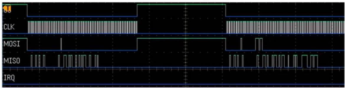
7.6.1.2 G3: Send Data
Figure 7-6. G3 Send Data SPI Array
text_image
CLK MOSI MISO IRQIn a transmission of data, the following can be seen:
- Master (MOSI):
- Send ID memory region(16 bits): 0x0002 (ATPL360_TX_DATA_ID)
- Send SPI command (1 bit): 1 (write command)
-
Send SPI data length (15 bits) (in blocks of 16-bits): 0x04 (8 bytes)
– Send data of G3 transmission (8 bytes) -
Slave (MISO): PL360 device responds with the Firmware Header (0x1122)
- IRQ is not used in this request operation
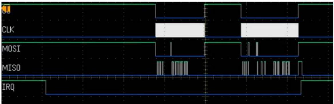
7.6.2 G3: Read TX confirm Information
When message transmission is complete, the PL360 device reports the status of the last transmission. For that purpose, IRQ is used to notify the PL360 Host Controller that an event has occurred.
Figure 7-7. G3 Read TX Confirm SPI Sequence
text_image
CLK MOSI MISO IRQIn the figure above, the following can be seen:
- IRQ is used to notify of PL360 events
- First SPI transaction corresponds to the retrieval of event information from the PL360 device
• Second SPI transaction corresponds to the retrieval of confirmation data from the PL360 device (if needed)
7.6.2.1 Get Events Information
Figure 7-8. G3 Get Events Information SPI Array

text_image
CLK MOSI MISO IRQIn the retrieval of event information, the following can be seen:
- Master (MOSI):
- Send ID memory region(16 bits): 0x0000 (ATPL360_STATUS_INFO_ID)
- Send SPI command (1 bit): 0 (read command)
- Send SPI data length (15 bits) (in blocks of 16 bits): 0x04 (8 bytes)
- Slave (MISO):
- Send Firmware Header (16 bits): 0x1122
- Send Firmware Events (16 bits): 0x0001 (ATPL360_TX_CFM_FLAG_MASK)
- Send Firmware Timer reference (32 bits)
- Send Firmware Events Information (32 bits). Only valid in case of data indication (ATPL360_RX_DATA_IND_FLAG_MASK) or register response (ATPL360_REG_RSP_MASK) events. It is used to report the length of the data to be read
7.6.2.2 Get Confirmation Data
Figure 7-9. G3 Get Confirmation Data SPI Array

text_image
CLK MOSI MISO IRQIf there is a pending ATPL360_TX_CFM_FLAG_MASK event, it is needed to read information relative to the TX confirmation event:
- Master (MOSI):
- Send ID memory region(16 bits): 0x0003 (ATPL360_TX_CFM_ID)
- Send SPI command (1 bit): 0 (read command)
- Send SPI data length (15 bits) (in blocks of 16-bits): 0x05 (10 bytes)
- Slave (MISO):
- Send Firmware Header (16 bits): 0x1122
- Send Firmware Events (16 bits): 0x0001 (ATPL360_TX_CFM_FLAG_MASK)
– Send Firmware TX confirmation data:
• RMS calc value (32 bits)
• Transmission Time (32 bits)
• Transmission Result (8 bits)
If there are no pending events to attend, the nterrupt line is disabled.
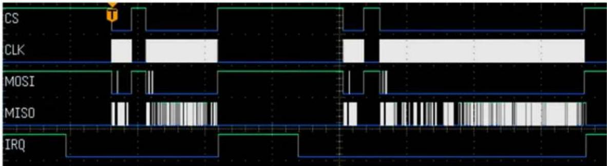
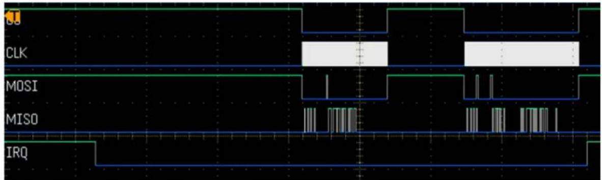
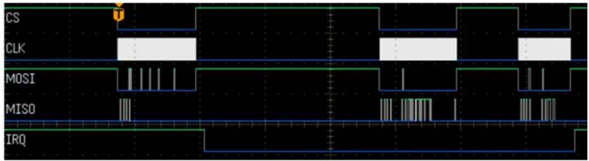
7.6.3 G3: Receive Message
Figure 7-10. G3 Receive Message SPI Sequence
text_image
CS CLK MOSI MISO IRQMessage reception is composed of four SPI transactions in two interruption blocks:
- IRQ 1: Get data part of the message (two transactions):
- Get Events Information
- Get Data
- IRQ 2: Get parameters part of the message (two transactions):
- Get Events Information
- Get Parameters
7.6.3.1 Get Events Information and Data
Figure 7-11. G3 Get Events Information and Data SPI Arrays
text_image
CS CLK MOSI MISO IRQIf IRQ occurs (enabled in low), it is first needed to read events reported by the PL360 device.
- Master (MOSI):
- Send ID memory region(16 bits): 0x0000 (ATPL360_STATUS_INFO_ID)
- Send SPI command (1 bit): 0 (read command)
- Send SPI data length (15 bits) (in blocks of 16-bits): 0x04 (8 bytes)
- Slave (MISO):
- Send Firmware Header (16 bits): 0x1122
- Send Firmware Events (16 bits): 0x0002 (ATPL360_RX_DATA_IND_FLAG_MASK)
– Send Firmware Timer reference (32 bits)
– Send Firmware Events Information (32 bits)
- First 16 bits: Not valid
- Second 16 bits: Length of the data to be read in next transaction (D_LEN)
The next transaction gets the data part of the message:
- Master (MOSI):
- Send ID memory region(16 bits): 0x0005 (ATPL360_RX_DATA_ID)
- Send SPI command (1 bit): 0 (read command)
- Send SPI data length (15 bits) (in blocks of 16-bits): Use (D_LEN/2) obtained in previous transaction
- Slave (MISO):
- Send Firmware Header (16 bits): 0x1122
- Send Firmware Events (16 bits): 0x0002 (ATPL360_RX_DATA_IND_FLAG_MASK)
- Send Firmware RX data (variable)
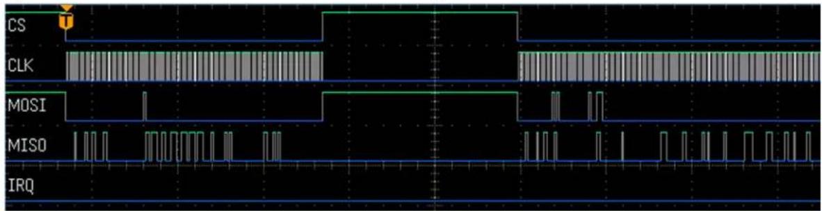
7.6.3.2 Get Events Information and Parameters
Figure 7-12. G3 Get Events Information and Parameters SPI Arrays
text_image
CLK MOSI MISO IRQIf IRQ occurs (enabled in low), first it is needed to read events reported by the PL360 device.
- Master (MOSI):
- Send ID memory region(16 bits): 0x0000 (ATPL360_STATUS_INFO_ID)
- Send SPI command (1 bit): 0 (read command)
- Send SPI data length (15 bits) (in blocks of 16-bits): 0x04 (8 bytes)
- Slave (MISO):
– Send Firmware Header (16 bits): 0x1122
- Send Firmware Events (16 bits): 0x0010 (ATPL360_RX_QPAR_IND_FLAG_MASK)
– Send Firmware Timer reference (32 bits)
– Send Firmware Events Information (32 bits): Not valid
The next transaction gets the parameters part of the message:
- Master (MOSI):
- Send ID memory region(16 bits): 0x0004 (ATPL360_RX_PARAM_ID)
- Send SPI command (1 bit): 0 (read command)
– Send SPI data length (15 bits) (in blocks of 16-bits): Variable length depending on G3 band
- Slave (MISO):
– Send Firmware Header (16 bits): 0x1122
- Send Firmware Events (16 bits): 0x0010 (ATPL360 RX QPAR IND FLAG MASK)
- Send Firmware RX parameters. See rx_msg_t structure in atpl360_comm.h file
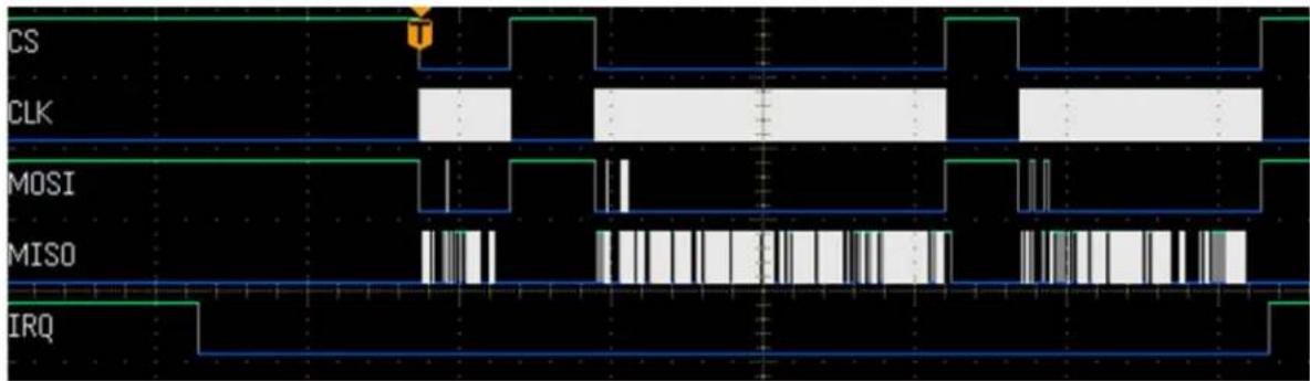
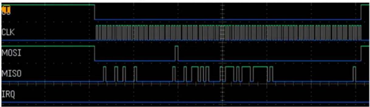
7.6.4 PRIME: Send Message (Buffer 0)
In a message transmission, there is only one SPI transaction that includes both parameters and data.
Figure 7-13. PRIME Send Message SPI Array

text_image
CS CLK MOSI MISO IRQIn the figure above, the following can be seen:
- Master (MOSI):
- Send ID memory region(16 bits): 0x0001 (ATPL360_TXO_PARAM_ID)
- Send SPI command (1 bit): 1 (write command)
- Send SPI params length (15 bits) (in blocks of 16-bits): (param length + data length) / 2, where param length is 12 bytes
- Send configuration parameters of PRIME transmission (12 bytes)
– Send data part of message (variable)
- Slave (MISO): PL360 responds with Firmware Header (0x1122)
IRQ is not used in this request operation.
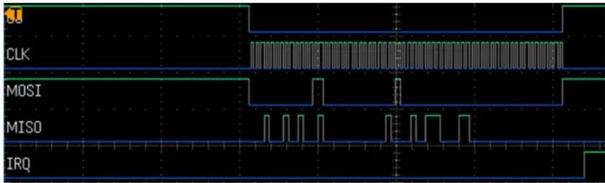
7.6.5 PRIME: Read TX confirm Information (Buffer 0)
When message transmission is complete, the PL360 device reports the status of the last transmission. For that purpose, IRQ is used to notify the PL360 Host Controller that an event has occurred.
Figure 7-14. PRIME TX Confirm Information SPI Sequence
text_image
CB CLK MOSI MISO IRQIn the figure above, the following can be seen:
- IRQ is used to notify of PL360 events
- First SPI transaction corresponds to the retrieval of event information from the PL360 device
• Second SPI transaction corresponds to the retrieval of confirmation data from the PL360 device (if needed)
7.6.5.1 Get Events Information (Buffer 0)
Figure 7-15. PRIME Events Information SPI Array

line
| Signal | Time | |--------|------| | CC | 0 | | CLK | 0 | | MOSI | 0 | | MISO | 0 | | IRQ | 0 |It is similar to the flow described in section 7.6.2.1 Get Events Information, but changing the firmware descriptors for the ones applicable to the PRIME PL360 firmware.
7.6.5.2 Get Confirmation Data (Buffer 0)
Figure 7-16. PRIME Confirmation Data SPI Array

text_image
CLK MOSI MISO IRQIt is similar to the flow described in section 7.6.2.2 Get Confirmation Data, but changing the firmware descriptors for the ones applicable to the PRIME PL360 firmware.
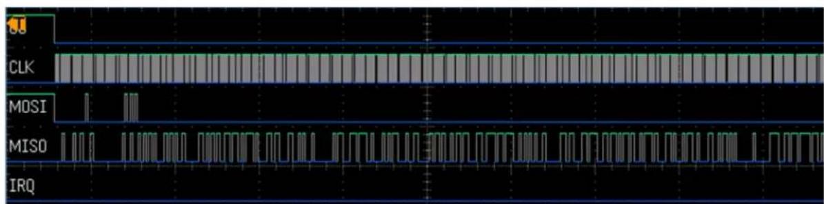
7.6.6 PRIME: Receive Message
Figure 7-17. PRIME Receive Message SPI Sequence
text_image
CS CLK MOSI MISO IRQIt is similar to the flow described in section 7.6.3 G3: Receive Message, but changing the firmware descriptors for the ones applicable to the PRIME PL360 firmware.
In this case, two events are read simultaneously, ATPL360_RX_DATA_IND_FLAG_MASK and ATPL360_RX_QPAR_IND_FLAG_MASK, so there are two consecutive SPI transactions in order to get data and parameters information from the PL360 device.
7.6.6.1 Get Events Information
Figure 7-18. PRIME Get Events SPI Array

line
| Signal | Time (ms) | |--------|-----------| | CS | 0 | | CLK | 0 | | MOSI | 0 | | MISO | 0 | | IRQ | 0 |It is similar to the flow described in section 7.6.3.1 Get Events Information and Data, but changing the firmware descriptors for the ones applicable to the PRIME PL360 firmware.
7.6.6.2 Get Data Information
Figure 7-19. PRIME Get Data SPI Array
text_image
CLK MOSI MISO IRQIt is similar to the flow described in section 7.6.3.1 Get Events Information and Data, but changing the firmware descriptors for the ones applicable to the PRIME PL360 firmware.
7.6.6.3 Get Parameters Information
Figure 7-20. PRIME Get Parameters SPI Array

text_image
CLK MOSI MISO IRQIt is similar to the flow described in section 7.6.3.2 Get Events Information and Parameters, but changing the firmware descriptors for the ones applicable to the PRIME PL360 firmware.
7.6.7 Read Register Information
It is possible to get internal information from the PL360 device.
Figure 7-21. Read Register Information SPI Sequence
text_image
CS CLK MOSI MISO IRQIn the figure above, three SPI transactions can be seen:
- Request register information
- Get events information
- Get register value
7.6.7.1 Request Register Information
Figure 7-22. Request Register Information Array

text_image
CS CLK MOSI MISO IRQ- Master (MOSI):
- Send ID memory region(16 bits): 0x0006 (ATPL360_REG_INFO_ID) [example with G3]
- Send SPI command (1 bit): 1 (write command)
- Send SPI params length (15 bits) (in blocks of 16-bits): 0x0004 (8 bytes)
- Send register identification (4 bytes). See section 12.2.5 PIB Objects Specification and Access (G3) or 12.3.4 PIB Objects Specification and Access (PRIME)
- Send length of the register to read (2 bytes)
- Slave (MISO): PL360 device responds with firmware header (0x1122)
7.6.7.2 Get Events Information
Figure 7-23. Get Events Information Array
line
| Signal | Time Segment 1 | Time Segment 2 | Time Segment 3 | Time Segment 4 | |--------|----------------|----------------|----------------|----------------| | CLK | High | Low | Low | Low | | MOSI | Low | Low | Low | Low | | MISO | Low | Low | Low | Low | | IRQ | Low | Low | Low | Low |- Master (MOSI):
- Send ID memory region(16 bits): 0x0000 (ATPL360_STATUS_INFO_ID)
- Send SPI command (1 bit): 0 (read command)
- Send SPI data length (15 bits) (in blocks of 16 bits): 0x04 (8 bytes)
- Slave (MISO):
- Send Firmware Header (16 bits): 0x1122
- Send Firmware Events (16 bits): 0x0008 (ATPL360_REG_RSP_MASK)
– Send Firmware Timer reference (32 bits)
– Send Firmware Events Information (32 bits)
- First 16 bits: Length of the register value to read in next transaction. (D_REG)
• Second 16 bits: Not valid
7.6.7.3 Get Register Value
Figure 7-24. Get Register Value SPI Array
text_image
CLK MOSI MISO IRQ- Master (MOSI):
- Send ID memory region(16 bits): 0x0006 (ATPL360_REG_INFO_ID)
- Send SPI command (1 bit): 0 (read command)
- Send SPI data length (15 bits) (in blocks of 16 bits): Variable length depending on register to read (D_REG)
- Slave (MISO):
- Send Firmware Header (16 bits): 0x1122
- Send Firmware Events (16 bits): 0x008 (ATPL360_REG_RSP_MASK)
- Send Firmware register value. See section 12.2.5 PIB Objects Specification and Access (G3) or 12.3.4 PIB Objects Specification and Access (PRIME)
8. Example Applications

Please note that all the provided application examples have been configured to work on Microchip evaluation boards. When using other hardware, the firmware project must define a Board Support Package (BSP) customized for that hardware.
Along with the PLC communication stacks, specific application examples are provided in order to show how to integrate the PL360 Host Controller.
In addition, PHY examples using only the PL360 Host Controller are provided in order to evaluate some low level parameters and to be used together with a Microchip PLC tool for demonstration purposes.
In case of a G3 stack, applications are provided for CENELEC A, CENELEC B and FCC bands (project folders with suffixes “_cen_a”, “_cen_b” and “_fcc” in each example). Setting the appropriate band in each project is made by means of conf_atpl360.h file, as explained in section 5.1 Configure Application.
In case of a PRIME stack, applications are provided for CENELEC A and FCC bands (the same project folder is used in both bands depending on PRIME configured channel. See 12.3.4.30 ATPL360_REG_CHANNEL_CFG (0x4016)).
8.1 PHY Examples
8.1.1 PHY Tester
The PHY Tester is an application example that demonstrates the complete performance of the Microchip PLC PHY layer. This example requires a board and a PC tool. In addition, the Microchip PLC PHY Tester PC tool (available in the Microchip website) has to be installed on the user's host PC to interface with the boards.
The Microchip PLC PHY Tester PC tool configures the devices and performs communication tests.
This example uses the serial interface configured through UART0 at 230400bps.
8.1.2 PHY Sniffer
The PHY Sniffer is an application example to monitor data traffic in the PLC network and then send it via serial communications to a PC tool and the Microchip PLC Sniffer PC tool (available in the Microchip website), which has to be installed in the user's host PC to interface with the board. This example requires only one board and (obviously) a PLC network to be monitored.
This example uses the serial interface configured through UART0 at 230400bps.
8.1.3 TX Console
Due to PC timing, the Microchip PLC PHY Tester PC tool may present limitations in those applications or tests that require a very short time interval between consecutive frame transmissions.
The PHY TX Console is an application example that demonstrates the complete performance of the Microchip PLC PHY Layer avoiding the limitations of timing in the PC host. This way, users can perform more specific PHY tests (e.g., short time interval between consecutive frames).
This application offers an interface to the user by means of a command console. In this console, users can configure several transmission parameters such as modulation, frame data length and time interval between frames. In the console it is also possible to test transmission/reception processes.
This example uses the serial interface configured through UART0 at 921600bps.
8.1.4 PHY Getting Started
This example is intended to show the minimal application to be developed over the PL360 PHY layer (G3 or PRIME).
Two modes of operation can be configured: CONF_APP_TX_MODE or CONF_APP_RX_MODE. The former will start sending PHY frames without user intervention, while the latter will wait for frame receptions from the PHY layer. Both modes print messages on a Serial Console to inform the user about frames transmitted and received, respectively.
Thus, depending on G3 or PRIME PHY layer, the following configuration is allowed:
• G3 (conf_project.h file):
- CONF APP MODE: CONF APP TX MODE or CONF APP RX MODE
- TX_DELAY_US (phy_getting_started.c): Time delay between transmitted frames in microseconds
- PRIME (conf_app_example.h file):
- CONF APP MODE: CONF APP TX MODE or CONF APP RX MODE
- CONF_PRIME_CHANNEL: PRIME channel for transmission and reception (see 12.3.4.30 ATPL360_REG_CHANNEL_CFG (0x4016))
- CONF_TX_DELAY_US: Time delay between transmitted frames in microseconds
9. Supported Platforms
This chapter describes which hardware platforms are currently supported with the PL360 Host Controller source code. Usually, a platform usually is comprised of three major components:
• An MCU
- A transceiver chip
- A specific board or even several boards that contain the MCU or the transceiver chip
9.1 Supported MCU Families
Currently the supported families are SAM4C, SAME70 and SAMG55 platforms.
The dedicated code for each device of the family can be found in the corresponding sub-directories of the FW package.
9.2 Supported Transceivers
Currently the supported transceivers are PL360.
9.3 Supported Boards
The boards currently supported are:
- PL360MB
- PL360G55CB
- PL360G55CF
- PL360BN
- SAME70 Xplained board connected to PL360MB board through Xplained Port
10. Abbreviations
AGC Automatic Gain Control
API Application Programming Interface
APP Application
ASF Advanced Software Framework
BER Bit Error Rate
CINR Carrier to Interference + Noise Ratio
DT Delimiter Type
EK Evaluation Kit
EVM Error Vector Magnitude
FCH Frame Control Header
FFT Fast Fourier Transform
FW Firmware
GPIO General Purpose Input/Output
HAL Hardware Abstraction Layer
IP Internal Peripheral
IFFT Inverse Fast Fourier Transform
IRQ Interrupt Request
LQI Link Quality Indicator
MCU Microcontroller Unit
MISO Master Input Salve Output
MOSI Master Output Salve Input
PAL Platform Abstraction Layer
PDU Protocol Data Unit
PGA Programmable-Gain Amplifier
PHY Physical Layer
PIB PLC Information Base
PLC Power Line Communication
SPI Serial Peripheral Interface
RD Read
RRC Root Raised Cosine
RS Reed Solomon
RSSI Received Signal Strength Indication
RX Reception
SNR Signal to Noise Ratio
TX Transmission
WR Write
11. References
- Microchip Smart Energy
- Microchip Power Line Communications
- Microchip Design Support
• G3-PLC Alliance - PRIME Alliance
• PL360-EK User Guide, 2018
• PL360G55CB-EK, 2019
• PL360G55CF-EK, 2019
• PL360 Datasheet, 2019
• PL360 Physical Calibration, 2019
• PL360 Security Features, 2018
• Advanced Software Framework - Atmel Studio
- Documents for supported families and boards
12. PL360 Host Controller API
This chapter describes all the data structures and functions which are part of the PL360 Host Controller component.
12.1 Common PHY API
12.1.1 Initialization Function
The PL360 Host Controller must always be initialized when the system starts the execution. The following function initializes the hardware parameters and configures the controller descriptor:
void atpl360_init(atpl360_descriptor_t *const descr, atpl360_hal_wrapper_t *px_hal_wrapper);
Parameters:
descr Pointer to component descriptor
px_hal_wrapper Pointer to HAL wrapper structure
This function performs the following actions:
- Sets the handlers for the PLC interruption
- Initializes the PLC SPI service
- And, if necessary, initializes add-on interfaces
The component descriptor offers the customer a set of functions to get access to the PL360 device. It is defined as a structure of function pointers as follows:
typedef struct atpl360_descriptor {
    pf_set_callbacks_t set_callbacks;
    pf_send_data_t send_data;
    pf_mng_get_cfg_t get_config;
    pf_mng_set_cfg_t set_config;
    pf_addons_event_t send_addons_cmd;
} atpl360_descriptor_t;
where:
- set_callbacks function is used to set upper layers' functions to be executed when a PL360 Host Controller event has been reported. For further information, please refer to the 12.1.2 Setting Callbacks chapter
- send_data function provides a mechanism to send a PLC message through the PL360 device. For further G3 information, please refer to the G3 12.2.2 PHY-DATA.request chapter. For further PRIME information, please refer to the PRIME 12.3.1 PHY-DATA.request chapter
- get_config function provides a read access method to get PL360 internal data. For further information, please refer to the 12.1.11.2 Get Configuration chapter
- set_config function provides a write access method to set PL360 internal data. For further information, please refer to the 12.1.11.1 Set Configuration chapter
- send_addons_cmd function provides a mechanism to connect PLC Microchip tools to the PL360 device. All information received from these tools should be redirected to this function in order to pass the information to the PL360 Host Controller
Function pointers are defined as follows:
typedef void (*pf_set_callbacks_t)(atpl360_dev_callbacks_t *dev_cb);
typedef uint8_t (*pf_send_data_t)(tx_msg_t *px_msg);
typedef bool (*pf_mng_get_cfg_t)(uint16_t us_param_id, void *px_value, uint8_t uc_len, bool b_sync);
typedef bool (*pf_mng_set_cfg_t)(uint16_t us_param_id, void *px_value, uint16_t us_len);
typedef void (*pf_addons_event_t)(uint8_t *px_msg, uint16_t us_len);
The PL360 Host Controller also needs to have access to hardware peripherals. A HAL wrapper structure is used to separate this hardware and software dependency.
typedef struct atpl360_hal_wrapper {
    pf_plc_init_t plc_init;
    pf_plc_reset_t plc_reset;
    pf_plc_set_handler_t plc_set_handler;
    pf_plc_bootloader_cmd_t plc_send_boot_cmd;
    pf_plc_write_read_cmd_t plc_write_read_cmd;
    pf_plc_enable_int_t plc_enable_int;
    pf_plc_delay_t plc_delay;
} atpl360_hal_wrapper_t;
In ASF, Microchip provides a set of example functions to get hardware access. It depends on the communication stack in use.
• G3: Refer to pplc_if.c/.h files. They are located in asf.sam.services.plc.pplc_if.atpl360 path
- PRIME. Refer to hal_plc.c/.h files. They are located in asf.thirdparty.prime_ng.hal path
12.1.2 Setting Callbacks
The user can set their own callbacks using the following function pointer defined in the PL360 Host Controller descriptor:
typedef void (*pf_set_callbacks_t)(atpl360_dev_callbacks_t *dev_cb);
Parameters:
atpl360_dev_callbacks_t Pointer to callbacks struct
The structure used as the input of the pf_set_callbacks_t function contains the pointers to the functions to be executed for the different PL360 Host Controller events:
typedef struct atpl360_dev_callbacks {
    pf_data_confirm_t data_confirm;
    pf_data_indication_t data_indication;
    pf_addons_event_t addons_event;
    pf_exception_event_t exception_event;
    pf_handle_cb_t sleep_mode_cb;
    pf_handle_cb_t debug_mode_cb;
} atpl360_dev_callbacks_t;
where:
- data confirm function is used to notify of the result of the last message transmission
- data_indication function is used to notify of the reception of a new message
- addons_event function is used to notify that there is a new message to be sent to a PLC Microchip Tool
- exception_event function is used to notify of any exception which occurs in the communication with the PL360 device
- sleep_mode_cb function is used to notify when Sleep mode has been disabled. It's strongly recommended to use this callback function to restore any additional configuration to PL360 device from user application.
- debug_mode_cb function is used to notify when Debug mode has been disabled. It's strongly recommended to use this callback function to restore any additional configuration to PL360 device from user application.
Exception values are defined as follows:
typedef enum {
    ATPL360_EXCEPTION_UNEXPECTED_SPI_STATUS = 0, /* SPI has detected an unexpected status */
    ATPL360_EXCEPTION_SPI_CRITICAL_ERROR, /* SPI critical error. */
    ATPL360_EXCEPTION_RESET, /* Reset device */
} atpl360_exception_t;

Tip: SPI critical error means that the PL360 firmware cannot be loaded into the PL360 device. A possible reason for this would be that the SPI is not working properly.
12.1.3 Enable Function
Once the host descriptor has been initialized and the application callbacks have been set, the PL360 Host Controller must be enabled using the following function:
atpl360_res_t atpl360_enable(uint32_t ul_binary_address, uint32_t ul_binary_len);
Parameters:
ul_binary_address Memory address where the PL360 firmware binary file is located
ul_binary_len Size of the PL360 firmware binary file
This function performs the following actions:
- Disable PLC interrupt
- Transfer firmware binary file to the PL360 device
- Check firmware integrity
- Enable PLC interrupt
12.1.4 Disable Function
The PL360 Host Controller provides a mechanism to disable the notification of PL360 Host Controller events to the application in order to avoid interrupting the normal flow of the customer application. This mechanism implies that the PLC activity is stopped in the PL360 device.
void atp1360_disable(void);
12.1.5 Event Handler Function
This function provides a mechanism to notify the PL360 Host Controller events to the customer application using the previously configured callbacks.
The following function must be called every program cycle or at least once when the host MCU application receives an interrupt from the PL360 embedded firmware:
void atpl360_handle_events(void);
First, this function checks all PLC events:
• PHY parameters and configuration
• End of transmission of PLC message
• End of reception of PLC message
- Exceptions
And then, it triggers the corresponding PL360 Host Controller callbacks.
12.1.6 Set Sleep Mode Function
This function provides a mechanism to control the Sleep mode capability in order to minimize the power consumption of the PL360 device.
void atpl360_set_sleep(bool sleep);
Parameters:
sleep True to enable Sleep mode, False to disable.
Please note that while being in Sleep mode, the core and peripherals of PL360 are reset; therefore, all the other PLC capabilities are not available.
12.1.7 Get Sleep Mode Function
This function provides a mechanism to query the status of the Sleep mode.
bool atpl360_get_sleep(void);
This function returns True if Sleep mode is enabled, False when it is disabled.
12.1.8 Set Debug Mode Function
This function provides a mechanism to enable or disable the Debug mode capability in order to access to the internal memory of PL360 device.
void atpl360_set_debug(bool debug);
Parameters:
debug True to enable Debug mode, False to disable.
Please note that when in Debug mode, the core and peripherals of PL360 are reset; therefore, all the other PLC capabilities are not available.
12.1.9 Get Debug Mode Function
This function provides a mechanism to query the status of the Debug mode.
bool atp1360_get_debug(void);
This function returns True if Debug mode is enabled, False when it is disabled.
12.1.10 Read Debug Function
Once Debug mode has been enabled, the internal memory of PL360 device can be read by the host controller using the following function:
uint16_t atpl360_debug_read(uint32_t ul_address, uint8_t *puc_data, uint16_t us_len);
Parameters:
ul_address Address of the internal memory of PL360 to read
*puc_data Pointer of data buffer to write with debug data
us_len Length of the debug data to read
Please note that the maximum length to get debug data per transaction is limited to 512 bytes.
For further information about the memory map of the PL360 binary file in use, please contact Microchip Smart Energy Support team.
12.1.11 Management Primitives
12.1.11.1 Set Configuration
This is done by means of a specific function provided by the controller descriptor:
typedef bool (*pf_mng_set_cfg_t)(uint16_t us_param_id, void *px_value, uint8_t uc_len);
Parameters:
us_param_id
PIB ID (see 12.3.4 PIB Objects Specification and Access (PRIME) and 12.2.5 PIB Objects Specification and Access (G3))
*px_value Pointer to parameter value to set
uc_len Length of parameter
The function returns 0 if the result is invalid, otherwise returns 1.
12.1.11.2 Get Configuration
This is done by means of a specific function provided by the controller descriptor:
typedef bool (*pf_mng_get_cfg_t)(uint16_t us_param_id, void *px_value, uint8_t uc_len, bool b_sync);
Parameters:
us_param_id
PIB ID (see 12.3.4 PIB Objects Specification and Access (PRIME) and 12.2.5 PIB Objects Specification and Access (G3))
*px_value Pointer to parameter value to get
uc_len Length of parameter
b_sync Set synchronous (True) or asynchronous mode (False)
The function returns 0 if the result is invalid, otherwise returns 1.
12.2 G3 PHY API
12.2.1 Bandplan Selection
At compilation time, the G3-PLC bandplan must be defined (i.e.: CENELEC A, CENELEC B, FCC or ARIB) according to user needs.
In general_defs.h there are four constant options for configuring the bandplan:
/* ! CENELEC A Band Plan (35 - 91 kHz) */
#define ATPL360_WB_CENELEC_A
/* ! FCC Band Plan (154 - 488 kHz) */
#define ATPL360_WB_FCC
/* ! ARIB Band Plan (154 - 404 kHz) */
#define ATPL360_WB_ARIB
/* ! CENELEC-B Band Plan (98 - 122 kHz) */
#define ATPL360_WB_CENELEC_B
The constant ATPL360_WB has to be set, in file conf_atpl360.h, to the value of one of the constant options of general_defs.h so that the PHY layer is correctly configured.
12.2.2 PHY-DATA.request
This function sends a frame using the PHY layer. This is done by means of a specific function provided by the controller descriptor:
typedef uint8_t (*pf_send_data_t) (tx_msg_t *px_msg);
The input parameter structure is the following:
typedef struct tx_msg {
    uint8_t *puc_data_buf;
    uint32_t ul_tx_time;
    uint16_t us_data_len;
    uint8_t puc_preemphasis[NUM_SUBBANDS_MAX];
    uint8_t puc_tone_map[TONE_MAP_SIZE_MAX];
    uint8_t uc_tx_mode;
    uint8_t uc_tx_power;
    enum mod_types uc_mod_type;
    enum mod_schemes uc_mod_scheme;
    uint8_t uc_pdc;
    uint8_t uc_2_rs_blocks;
enum delimiter_types uc_delimiter_type;
} tx_msg_t;
Fields of the structure:
*puc_data_buf Pointer to data buffer
ul_tx_time Instant when transmission has to start referred to 1μs PHY counter (absolute or relative value, depending on uc_tx_mode)
us_data_len Length of the data buffer in bytes
puc_preemphasis Preemphasis for transmission. Same as uc_tx_power but for each subband (Related constants explained below)
puc_tone_map Tone map to use in transmission (Related constants explained below)
uc_tx_mode Transmission mode (forced, delayed, ...) (Related constants explained below)
uc_tx_power Power to transmit [0 = Full gain, 1 = (Full gain - 3dB), 2 = (Full gain - 6dB) and so on]. Maximum value is 15 (Full gain - 45dBs). Value 0xFF is a special case used to apply zero-gain (transmit all zeros)
uc_mod_type Modulation type (Related constants explained below)
uc_mod_scheme Modulation scheme (Related constants explained below)
uc_pdc Phase detector counter. Not used; calculated and filled internally by PHY layer
uc_2_rs_blocks Flag to indicate whether 2 Reed-Solomon blocks have to be used (only used in FCC bandplan)
uc_delimiter_type DT field to be used in header (Related constants explained below)
Related constants affecting above parameters:
/* ! \name TX Mode Bit Mask */
/* ! TX Mode: Forced transmission */
#define TX_MODE_FORCED (1 << 0)
/* ! TX Mode: Absolute transmission */
#define TX_MODE_ABSOLUTE (0 << 1)
/* ! TX Mode: Delayed transmission */
#define TX_MODE_RELATIVE (1 << 1)
/* ! TX Mode: SYNCP Continuous transmission */
#define TX_MODE_SYNCP_CONTINUOUS (1 << 2)
/* ! TX Mode: Symbols Continuous transmission */
#define TX_MODE_SYMBOLS_CONTINUOUS (1 << 3)
/* ! TX Mode: Cancel transmission */
#define TX_MODE_CANCEL (1 << 4)

/* Modulation types */
enum mod_types {
    MOD_TYPE_BPSK = 0,
    MOD_TYPE_QPSK = 1,
    MOD_TYPE_8PSK = 2,
    MOD_TYPE_QAM = 3,
    MOD_TYPE_BPSK_ROBO = 4
};

/* Modulation schemes */
enum mod_schemes {
    MOD_SCHEME_DIFFERENTIAL = 0,
    MOD_SCHEME_COHERENT = 1
};

/* Frame Delimiter Types */
enum delimiter_types {
    DT_SOF_NO_RESP = 0, /* Data frame requiring ACK */
    DT_SOF_RESP = 1, /* Data frame Not requiring ACK */
    DT_ACK = 2, /* Positive ACK */
    DT_NACK = 3 /* Negative ACK */
};
/* ! Subbands for Cenelec-A bandplan */
#define NUM_SUBBANDS_CENELEC_A 6
/* ! Subbands for FCC bandplan */
#define NUM_SUBBANDS_FCC 24
/* ! Subbands for ARIB bandplan */
#define NUM_SUBBANDS_ARIB 18
/* ! Subbands for Cenelec-B bandplan */
#define NUM_SUBBANDS_CENELEC_B 4

/* ! Tone Map size for Cenelec bandplan */
#define TONE_MAP_SIZE_CENELEC 1
/* ! Tone Map size for FCC and ARIB bandplans */
#define TONE_MAP_SIZE_FCC_ARIB 3

/* ! Maximum number of tone map */
#define TONE_MAP_SIZE_MAX TONE_MAP_SIZE_FCC_ARIB
/* ! Maximum number of subbands */
#define NUM_SUBBANDS_MAX NUM_SUBBANDS_FCC
The function returns one of the following transmission result values:
/* TX Result values */
enum tx_result_values {
    TX_RESULT_PROCESS = 0,    /* Already in process */
    TX_RESULT_INV_LENGTH = 2,    /* Invalid length error */
    TX_RESULT_NO_TX = 255,    /* No transmission ongoing */
};
12.2.3 PHY-DATA.confirm
This data confirm callback executes the function set by the upper layer at the initialization of the PL360 Host Controller (see 12.1.2 Setting Callbacks). It is called when a transmission request has been processed. The format of the function is:
typedef void (*pf_data_confirm_t)(tx_cfm_t *px_msg_cfm);
The result is reported in the following structure:
typedef struct tx_cfm {
    uint32_t ul_rms_calc;
    uint32_t ul_tx_time;
    enum tx_result_values uc_tx_result;
} tx_cfm_t;
Fields of the structure:
ul_rms_calc RMS_CALC value after transmission. Allows estimation of Tx power injected ul_tx_time Instant when frame transmission ended, referred to 1μs PHY counter uc_tx_result Tx result (Related constants explained below)
Possible values of the field "uc_tx_result":
/* TX Result_values */
enum tx_result_values {
    TX_RESULT_SUCCESS = 1, /* End successfully */
    TX_RESULT_INV_LENGTH = 2, /* Invalid length error */
    TX_RESULT_BUSY_CH = 3, /* Busy channel error */
    TX_RESULT_BUSY_TX = 4, /* Busy in transmission error */
    TX_RESULT_BUSY_RX = 5, /* Busy in reception error */
    TX_RESULT_INV_SCHEME = 6, /* Invalid modulation scheme error */
    TX_RESULT_TIMEOUT = 7, /* Timeout error */
    TX_RESULT_INV_TONEMAP = 8, /* Invalid tone map error */
    TX_RESULT_INV_MODTYPE = 9, /* Invalid modulation type error */
    TX_RESULT_INV_DT = 10, /* Invalid delimiter type */
    TX_RESULT_NO_TX = 255, /* No transmission ongoing */
};
12.2.4 PHY-DATA.indication
This data indication callback executes the function set by the upper layer at the initialization of the PL360 Host Controller (see 12.1.2 Setting Callbacks). It is called when a frame has been received. The format of the function is:
typedef void (*pf_data_indication_t)(rx_msg_t *px_msg);
The information is reported in the following structure:
typedef struct rx_msg {
    uint32_t ul_rx_time;
    uint32_t ul_frame_duration;
    uint16_t us_rssi;
    uint16_t us_data_len;
    uint8_t uc_zct_diff;
    uint8_t uc_rs_corrected_errors;
    enum mod_types uc_mod_type;
    enum mod_schemes uc_mod_scheme;
    uint32_t ul_agc_factor;
    uint16_t us_agc_fine;
    int16_t ss_agc_offset_meas;
    uint8_t uc_agc_active;
    uint8_t uc_agc_pga_value;
    int16_t ss_snr_fch;
    int16_t ss_snr_pay;
    uint16_t us_payload_corrupted_carriers;
    uint16_t us_payload_noised_symbols;
    uint8_t uc_payload_snr_worst_carrier;
    uint8_t uc_payload_snr_worst_symbol;
    uint8_t uc_payload_snr_impulsive;
    uint8_t uc_payload_snr_band;
    uint8_t uc_payload_snr_background;
    uint8_t uc_lqi;
    enum delimiter_types uc_delimiter_type;
    uint8_t uc_crc_ok;
    uint8_t puc_tone_map[TONE_MAP_SIZE_MAX];
    uint8_t puc_carrier_snr[PROTOCOL_CARRIERS_MAX];
    uint8_t *puc_data_buf;
} rx_msg_t;
Fields of the structure:
ul_rx_time Instant when frame was received (end of frame), referred to 1μs PHY counter
ul_frame_duration Frame duration in μs (Preamble + FCH + Payload)
us_rssi Reception RSSI in dBμV
us_data_len Length of received frame in bytes
uc_zct_diff Phase difference with transmitting node
uc_rs_corrected_errors Errors corrected by Reed-Solomon
uc_mod_type Modulation type of the received frame (Related constants defined in section 12.2.2 PHY-DATA.request)
uc_mod_scheme Modulation scheme of the received frame (Related constants defined in section 12.2.2 PHY-DATA.request)
ul_agc_factor Global amplifying factor of the main branch (21 bits)
us_agc_fine Factor that multiplies the digital input signal (13 bits)
ss_agc_offset_meas DC offset after the ADC that will be removed in case the DC Blocker is enabled (10 bits)
uc_agc_active Flag to indicate if AGC is active
uc_agc_pga_value Gain value applied to the PGA (3 bits)
ss_snr_fch SNR of the header in quarters of dBs
ss_snr_pay SNR of the payload in quarters of dBs
us_payload_corrupted_carriers Number of corrupted carriers in payload due to narrow/broad-band noise
us_payload_noised_symbols Number of corrupted symbols in payload due to impulsive noise
uc_payload_snr_worst_carrier SNR for the worst carrier of the payload in quarters of dBs
uc_payload_snr_worst_symbol SNR for the worst symbol of the payload in quarters of dBs
uc_payload_snr_impulsive SNR of corrupted symbols in payload due to impulsive noise in quarters of dBs
uc_payload_snr_band SNR of corrupted carriers in payload due to narrow/broad-band noise in quarters of dBs
uc_payload_snr_background SNR without taking into account corrupted carriers and symbols in quarters of dBs
uc_lqi Link Quality Indicator. SNR in quarters of dBs with offset of 10 dB (value 0 means -10 dB)
uc_delimiter_type DT field coming in header. Related constants defined in section 12.2.2 PHY-DATA.request
uc_crc_ok CRC verification result (1: OK; 0: BAD; 0xFE: unexpected error; 0xFF: CRC capability disabled). See 12.2.5.39 ATPL360_REG_CRC_TX_RX_CAPABILITY (0x401C)
puc_tone_map Tone Map in received frame (Related constants defined in section 12.2.2 PHY-DATA.request)
puc_carrier_snr SNR for each carrier in dBs with offset of 10dB (value 0 means -10dB) (Related constants explained below)
puc_data_buf Pointer to data buffer containing received frame. The received frame includes padding (if needed). CRC is included if the CRC capability in the PL360 is disabled (see 12.2.5.39 ATPL360_REG_CRC_TX_RX_CAPABILITY (0x401C))
Related constants affecting above parameters:
/* ! Carriers for Cenelec-A bandplan */
#define NUM_CARRIERS_CENELEC_A 36
/* ! Carriers for FCC bandplan */
#define NUM_CARRIERS_FCC 72
/* ! Carriers for ARIB bandplan */
#define NUM_CARRIERS_ARIB 54
/* ! Carriers for Cenelec-B bandplan */
#define NUM_CARRIERS_CENELEC_B 16
/* ! Maximum number of protocol carriers */
#define PROTOCOL_CARRIERS_MAX NUM_CARRIERS_FCC
12.2.5 PIB Objects Specification and Access (G3)
The default endianness of all PIBs is little endian, otherwise it is explicitly stated.
12.2.5.1 ATPL360\_HOST\_DESCRIPTION\_ID (0x0100)
PL360 Host Controller description.
Access: Read-only.
Value Range: 10 bytes.
Default Value: "SAM4CMS16C" (for SAM4CMS16_0 core) or "SAM4C16C" (for SAM4C16_0 core).
12.2.5.2 ATPL360\_HOST\_MODEL\_ID (0x010A)
Model identification number of the PL360 Host Controller.
Access: Read-only.
Value Range: 2 bytes.
Default Value: 0x0002.
12.2.5.3 ATPL360\_HOST\_PHY\_ID (0x010C)
Physical identification number of the PL360 Host Controller. It is composed of ATPL360_HOST_VERSION_ID (0x0112) + ATPL360_HOST_BAND_ID (0x0116).
Access: Read-only.
Value Range: 4 bytes.
Default Value: 0x36010201 for CENELEC A band. 0x36010202 for FCC band. 0x36010203 for ARIB band.
0x36010204 for CENELEC B band.
12.2.5.4 ATPL360\_HOST\_PRODUCT\_ID (0x0110)
Product identification number of the PL360 Host Controller.
Access: Read-only.
Value Range: 2 bytes.
Default Value: 0x3601.
12.2.5.5 ATPL360\_HOST\_VERSION\_ID (0x0112)
Version number of the PL360 Host Controller.
Access: Read-only.
Value Range: 4 bytes.
Default Value: 0x36010200.
12.2.5.6 ATPL360\_HOST\_BAND\_ID (0x0116)
Workband identification number of the PL360 Host Controller.
Access: Read-only.
Default Value: 1: CENELEC A, 2: FCC, 3: ARIB, 4: CENELEC B.
12.2.5.7 ATPL360\_TIME\_REF (0x0200)
Time reference in microseconds from the last reset of the PL360 device.
Access: Read-only.
Value Range: 4 bytes.
Default Value: Not applicable.
12.2.5.8 ATPL360\_SLEEP\_MODE\_ID
Enable/Disable the Sleep mode of the PL360 device. This is useful to minimize the power consumption in conditions of prolonged inactivity.
Access: Read-write.
Value Range: 1 byte [0: Disabled, 1: Enabled].
Default value: 0.
12.2.5.9 ATPL360\_DEBUG\_SET\_ID
Enable/Disable the Debug mode of the PL360 device. This is useful to get debug data from the PL360 device. For further information, please contact Microchip Smart Energy Support team.
Access: Read-write.
Value Range: 7 bytes
- byte 0: Enable/Disable. Write 1 to enable Debug mode, 0 to disable Debug mode. In case of disabling Debug mode, address and length values are not taken into account.
- bytes 1-4: Address of the data to read from PL360 internal memory.
- bytes 5-6: Length of the data to read. It is internally limited to 255 bytes.
Default value: Enable/Disable: 0, Address: 0, Length: 0.
12.2.5.10 ATPL360\_DEBUG\_READ\_ID
Read debug data from PL360 device.
Access: Read only.
Value Range: 255 bytes.
Default value: 0.
12.2.5.11 ATPL360\_REG\_PRODID (0x4000)
Product Identifier of firmware embedded in PL360 device.
Access: Read-only.
Value Range: 8 bytes.
Default Value: "ATPL360".
12.2.5.12 ATPL360\_REG\_MODEL (0x4001)
Model Identifier of firmware embedded in PL360 device.
Access: Read-only.
Value Range: 2 bytes.
Default Value: 0x3601.
12.2.5.13 ATPL360\_REG\_VERSION\_STR (0x4002)
Version number of PL360 embedded firmware in string format. The format is "AA.BB.CC.DD", where:
• AA: Corresponds to device model ("36")
- BB: Corresponds to G3 band ["01": CEN A, "02": FCC, "03": ARIB, "04": CEN B]
• CC: Major version number
• DD: Minor version number
Access: Read-only.
Value Range: 11 bytes.
Example Value: "36.01.04.15".
12.2.5.14 ATPL360\_REG\_VERSION\_NUM (0x4003)
Version number of PL360 embedded firmware in hexadecimal format. The format is 0xAABBCCDD, where:
• AA: Corresponds to device model (0x36)
- BB: Corresponds to G3 band [0x01: CEN A, 0x02: FCC, 0x03: ARIB, 0x04: CEN B]
• CC: Major version number
• DD: Minor version number
Access: Read-only.
Value Range: 4 bytes.
Example Value: 0x36010415.
12.2.5.15 ATPL360\_REG\_TONE\_MASK (0x4004)
Tone mask for static notching.
Access: Read-write.
Value Range: Depends on the number of carriers which are specified in the G3 band (one byte per carrier).
Default Value: 0.
12.2.5.16 ATPL360\_REG\_TONE\_MAP\_RSP\_DATA (0x4005)
Tone Map response data is the best modulation and Tone Map combination to maximize baud rate and minimize frame error rate. It is calculated by the selection algorithm, based on the signal quality of the last received message. See 12.2.5.72 ATPL360_REG_TONE_MAP_RSP_ENABLED_MODS (0x403E) to enable/disable the different modulations for the selection algorithm.
The format is defined by the structure shown below (fields and related constants are explained in 12.2.2 PHY-DATA.request):
typedef struct tm_rsp_data {
    enum mod_types uc_mod_type;
    enum mod_schemes uc_mod_scheme;
    uint8_t puc_tone_map[TONE_MAP_SIZE_MAX];
} tm_rsp_data_t;
Access: Read-only.
Value Range: 5 bytes.
Default Value: BPSK Robust modulation type (0x04), differential modulation scheme (0x00) and full tone map (0x3F0000 in CENELEC-A; 0x0F0000 in CENELEC-B; 0xFFFFF in FCC; 0xFFFFF03 in ARIB).
12.2.5.17 ATPL360\_REG\_TX\_TOTAL (0x4006)
Number of successfully transmitted PDUs.
Access: Read-write.
Value Range: 4 bytes.
Default Value: 0.
12.2.5.18 ATPL360\_REG\_TX\_TOTAL\_BYTES (0x4007)
Number of bytes in successfully transmitted PDUs.
Access: Read-write.
Value Range: 4 bytes.
Default Value: 0.
12.2.5.19 ATPL360\_REG\_TX\_TOTAL\_ERRORS (0x4008)
Number of unsuccessfully transmitted PDUs.
Access: Read-write.
Value Range: 4 bytes.
Default Value: 0.
12.2.5.20 ATPL360\_REG\_TX\_BAD\_BUSY\_TX (0x4009)
Number of times when the PL360 device received new data to transmit (send_data) and there is already data in the TX chain.
Access: Read-write.
Value Range: 4 bytes.
Default Value: 0.
12.2.5.21 ATPL360\_REG\_TX\_BAD\_BUSY\_CHANNEL (0x400A)
Number of times when the PL360 device received new data to transmit (send_data) and the PLC channel is busy.
Access: Read-write.
Value Range: 4 bytes.
Default Value: 0.
12.2.5.22 ATPL360\_REG\_TX\_BAD\_LEN (0x400B)
Number of times when the PL360 device received new data to transmit (send_data) and the specified length in transmission parameters is invalid.
Access: Read-write.
Value Range: 4 bytes.
Default Value: 0.
12.2.5.23 ATPL360\_REG\_TX\_BAD\_FORMAT (0x400C)
Number of times when the PL360 device received new data to transmit (send_data) and the transmission parameters are not valid.
Access: Read-write.
Value Range: 4 bytes.
Default Value: 0.
12.2.5.24 ATPL360\_REG\_TX\_TIMEOUT (0x400D)
Number of times when the PL360 device received new data to transmit (send_data) and it cannot transmit data in the specified time provided by the transmission parameters.
Access: Read-write.
Value Range: 4 bytes.
Default Value: 0.
12.2.5.25 ATPL360\_REG\_RX\_TOTAL (0x400E)
Number of successfully received PDUs.
Access: Read-write.
Value Range: 4 bytes.
Default Value: 0.
12.2.5.26 ATPL360\_REG\_RX\_TOTAL\_BYTES (0x400F)
Number of bytes in successfully received PDUs.
Access: Read-write.
Value Range: 4 bytes.
Default Value: 0.
12.2.5.27 ATPL360\_REG\_RX\_RS\_ERRORS (0x4010)
Number of corrected errors by RS block in received PDUs.
Access: Read-write.
Value Range: 4 bytes.
Default Value: 0.
12.2.5.28 ATPL360\_REG\_RX\_EXCEPTIONS (0x4011)
Number of time-out errors in received PDUs.
Access: Read-write.
Value Range: 4 bytes.
Default Value: 0.
12.2.5.29 ATPL360\_REG\_RX\_BAD\_LEN (0x4012)
Number of errors in FCH length in received PDUs.
Access: Read-write.
Value Range: 4 bytes.
Default Value: 0.
12.2.5.30 ATPL360\_REG\_RX\_BAD\_CRC\_FCH (0x4013)
Number of errors in FCH CRC in received PDUs.
Access: Read-write.
Value Range: 4 bytes.
Default Value: 0.
12.2.5.31 ATPL360\_REG\_RX\_FALSE\_POSITIVE (0x4014)
Number of errors in PDU synchronization phase.
Access: Read-write.
Value Range: 4 bytes.
Default Value: 0.
12.2.5.32 ATPL360\_REG\_RX\_BAD\_FORMAT (0x4015)
Number of errors in modulation type field included in FCH of received PDUs.
Access: Read-write.
Value Range: 4 bytes.
Default Value: 0.
12.2.5.33 ATPL360\_REG\_ENABLE\_AUTO\_NOISE\_CAPTURE (0x4016)
Flag to indicate if automatic noise analyzer is enabled in the reception chain. If Auto-mode is enabled, notch filter parameters (12.2.5.36 ATPL360_REG_RRC_NOTCH_ACTIVE (0x4019), 12.2.5.37
ATPL360_REG_RRC_NOTCH_INDEX (0x401A)) cannot be modified by the user.
See 12.2.5.34 ATPL360_REG_TIME_BETWEEN_NOISE_CAPTURES (0x4017), 12.2.5.62
ATPL360_REG_RRC_NOTCH_THR_ON (0x4034), 12.2.5.63 ATPL360_REG_RRC_NOTCH_THR_OFF (0x4035)
to configure parameters related to the Auto-mode.
Access: Read-write.
Value Range: 1 byte [0: Disabled (Manual-mode), 1: Enabled (Auto-mode)].
Default Value: 1.
12.2.5.34 ATPL360\_REG\_TIME\_BETWEEN\_NOISE\_CAPTURES (0x4017)
Time in milliseconds between noise captures.
Access: Read-write.
Value Range: 4 bytes.
Default Value: 1000 (1 second).

It is recommended to keep the default value of this parameter. If reduced, the power consumption could increase. Default value is optimum for power consumption and performance of noise detection.
12.2.5.35 ATPL360\_REG\_DELAY\_NOISE\_CAPTURE\_AFTER\_RX (0x4018)
Time in microseconds to start a new noise capture after PDU reception/transmission.
Access: Read-write.
Value Range: 4 bytes.
Default Value: 3000 (3 milliseconds).

It is recommended to keep the default value of this parameter. If reduced, there could be unexpected results.
12.2.5.36 ATPL360\_REG\_RRC\_NOTCH\_ACTIVE (0x4019)
Number of notched frequencies with RRC notch filter. For CENELEC-A, FCC and ARIB bands, up to 5 notched frequencies are allowed. For CENELEC-B band, only one notched frequency is allowed.
Access: Depends on 12.2.5.33 ATPL360_REG_ENABLE_AUTO_NOISE_CAPTURE (0x4016) value:
• 1 (Automatic noise analyzer enabled): Read-only
- 0 (Automatic noise analyzer disabled): Read-write
Value Range: 1 byte [In CENELEC-A, FCC and ARIB bands, 0-5; In CENELEC-B, 0-1].
Default Value: 0 (No notched frequencies).
12.2.5.37 ATPL360\_REG\_RRC\_NOTCH\_INDEX (0x401A)
Array of RRC notch filter index values in format unsigned Q7.8. The 7 integer bits indicate the carrier index (0 -127) for which the notch filter is applied. The 8 decimal bits allow to apply the notch filter to a frequency which is between two consecutive carriers.
To convert the notch index to frequency (in Hz), the following formula is applied:
F = INDEX * F_s / 65536 , where F_s is the sampling rate in Hz:
• CENELEC-A, CENELEC-B bands: F s = 400000 Hz
• FCC, ARIB bands: Fs = 1200000 Hz
For example:
• CENELEC-A, INDEX = 8192 (0x2000): F = 8192 * 400000 / 65536 = 50000 Hz
- FCC, INDEX = 20544 (0x5040): F = 20544 * 1200000 / 65536 = 376172 Hz
Access: Depends on 12.2.5.33 ATPL360_REG_ENABLE_AUTO_NOISE_CAPTURE (0x4016) value:
• 1 (Auto-mode): Read-only
• 0 (Manual-mode): Read-write
Value Range: 10 bytes (CENELEC-A, FCC, ARIB bands) or 2 bytes (CENELEC-B band). Each group of 2 bytes corresponds to one notched frequency (Integer part: 0 - 127, Decimal part: 0-255). Number of valid values depends on 12.2.5.36 ATPL360_REG_RRC_NOTCH_ACTIVE (0x4019).
Default Value: 0.
12.2.5.38 ATPL360\_REG\_NOISE\_PEAK\_POWER (0x401B)
Noise peak power. Power of the carrier with more noise power in dBuV. The value is updated only if Auto-mode is enabled (see 12.2.5.33 ATPL360_REG_ENABLE_AUTO_NOISE_CAPTURE (0x4016)) or noise capture is triggered through 12.2.5.47 ATPL360_REG_RRC_NOTCH_AUTODETECT (0x4024).
Access: Read-only.
Value Range: 2 bytes.
Default Value: Not applicable.
12.2.5.39 ATPL360\_REG\_CRC\_TX\_RX\_CAPABILITY (0x401C)
CRC computation capability. If it is enabled, 16-bit CRC is computed in transmitted and received PDUs. The CRC format is the same that uses the G3-PLC stack, which is described in the IEEE 802.15.4 standard.
In transmission, when it is enabled, padding and CRC are added to the data automatically. In order to ensure that all OFDM symbols are filled with data, a zero-padding is inserted after data payload (if it is needed). The padding guarantees that the last 16 bits in reception correspond to the 16-bit CRC. The 16-bit CRC is added after the padding.
In reception, when it is enabled, CRC is computed over the received PDU and it is compared to the last 16 bits of the data (corresponding to the CRC of the message) to check the integrity of the message. These two bytes are not included in the data buffer containing the received frame reported in 12.2.4 PHY-DATA.indication. The field uc_crc_ok in 12.2.4 PHY-DATA.indication shows whether the CRC is correct or not.
Microchip G3-PLC stack implementation does not use this functionality, since CRC is computed in MAC layer instead of PHY layer. The aim of this PIB is to make it easier for customers to build applications over PHY layer.
Access: Read-write.
Value Range: 1 byte [0: Disabled, 1: Enabled].
Default Value: 0.
12.2.5.40 ATPL360\_REG\_RX\_BAD\_CRC\_PAY (0x401D)
Number of errors in payload CRC in received PDUs. It is only updated if CRC capability is enabled (see 12.2.5.39 ATPL360_REG_CRC_TX_RX_CAPABILITY (0x401C)).
Access: Read-write.
Value Range: 4 bytes.
Default Value: 0.
12.2.5.41 ATPL360\_REG\_CFG\_AUTODETECT\_IMPEDANCE (0x401E)
Auto-Detect Impedance Mode. Transmission Automatic Gain Control (Tx AGC) and Automatic Transmission Mode Control (ATMC) can be enabled/disabled. There are 3 available modes:
- OFF [0]: Tx AGC disabled. ATMC disabled.
• ON [1]: Tx AGC enabled. ATMC enabled. - AGC [2]: Tx AGC enabled. ATMC disabled.
Access: Read-write.
Value Range: 1 byte [0: OFF, 1: ON, 2: AGC].
Default Value: 1.
12.2.5.42 ATPL360\_REG\_CFG\_IMPEDANCE (0x401F)
Transmission Mode (HIGH, LOW, VERY_LOW). It is automatically updated if ATMC is enabled (see 12.2.5.41 ATPL360_REG_CFG_AUTODETECT_IMPEDANCE (0x401E)).
Access: Read-write.
Value Range: 1 byte [0: HIGH, 1: LOW, 2: VERY_LOW].
Default Value: 0.
12.2.5.43 ATPL360\_REG\_ZC\_PERIOD (0x4020)
Estimated last Zero Cross period in microseconds.
Access: Read-only.
Value Range: 4 bytes.
Default Value: Not applicable.
12.2.5.44 ATPL360\_REG\_FCH\_SYMBOLS (0x4021)
Number of symbols in Frame Control Header. Depends on the G3 band in use and Tone Mask (see 12.2.5.15 ATPL360_REG_TONE_MASK (0x4004)).
Access: Read-only.
Value Range: 1 byte [13-78 (CENELEC-A); 12-144 (FCC); 16-144 (ARIB); 30-78 (CENELEC-B)].
12.2.5.45 ATPL360\_REG\_PAY\_SYMBOLS\_TX (0x4022)
Number of payload symbols in last transmitted message.
Access: Read-only.
Value Range: 2 bytes [1-252 (CENELEC-A, CENELEC-B); 1-511 (FCC, ARIB)].
Default Value: Not applicable.
12.2.5.46 ATPL360\_REG\_PAY\_SYMBOLS\_RX (0x4023)
Number of payload symbols in last received message.
Access: Read-only.
Value Range: 2 bytes [1-252 (CENELEC-A, CENELEC-B); 1-511 (FCC, ARIB)].
Default Value: Not applicable.
12.2.5.47 ATPL360\_REG\_RRC\_NOTCH\_AUTODETECT (0x4024)
Trigger to start noise analysis. If noise analyzer Manual-mode is enabled (see 12.2.5.33)
ATPL360_REG_ENABLE_AUTO_NOISE_CAPTURE (0x4016)), noise capture can be triggered through this PIB by writing 1. Writing 0 has no effect. If noise analyzer Auto-mode is enabled, writing any value has no effect.
Access: Write-only.
Value Range: 1 byte. [0: No effect, 1: Trigger (Manual-mode)]
Default Value: 0.
12.2.5.48 ATPL360\_REG\_MAX\_RMS\_TABLE\_HI (0x4025)
Target value of RMS_CALC in HIGH Tx Mode (see 12.2.5.42 ATPL360_REG_CFG_IMPEDANCE (0x401F)).
RMS_CALC will tend to this value by automatically adjusting the gain after every transmission (see 12.2.5.64)
ATPL360_REG_CURRENT_GAIN (0x4036)). These parameters are only used if Tx AGC is enabled (see 12.2.5.41 ATPL360_REG_CFG_AUTODETECT_IMPEDANCE (0x401E)).
Access: Read-write.
Value Range: 32 bytes (see Table 12-1).
Default Value: See Table 12-2.
Table 12-1. Structure of ATPL360_REG_MAX_RMS_TABLE_HI
| Byte 0-3 Byte 4-7 Byte 8-11 | Byte 12-15 Byte 16-19 Byte 20-24 Byte 25-27 Byte 28-31 | ||
| RMS_HI_0 RMS_HI_1 RMS_HI_2 RMS_HI_3 | RMS_HI_4 RMS_HI_5 RMS_HI_6 RMS_HI_7 |
where:
- RMS_HI_x: Target value of RMS_CALC in mode of transmission HIGH for the attenuation level x (attenuation levels in 3dB steps)
Table 12-2. Default values of ATPL360_REG_MAX_RMS_TABLE_HI
| G3 BAND RMS_HI_0 RMS_HI_1 RMS_HI_2 RMS_HI_3 RMS_HI_4 RMS_HI_5 RMS_HI_6 RMS_HI_7 | ||||||||
| CEN-A 1991 1381 976 695 495 351 250 179 | ||||||||
| FCC | 1355 960 | 681 485 345 246 177 129 | ||||||
| ARIB | 872 | 618 | 438 | 311 | 221 | 158 | 113 | 83 |
| CEN-B | 1133 | 793 559 | 396 280 199 143 108 | |||||
12.2.5.49 ATPL360\_REG\_MAX\_RMS\_TABLE\_VLO (0x4026)
Target value of RMS_CALC in VERY_LOW Tx Mode (see 12.2.5.42 ATPL360_REG_CFG_IMPEDANCE (0x401F)).
RMS_CALC will tend to this value by automatically adjusting the gain after every transmission (see 12.2.5.64 ATPL360_REG_CURRENT_GAIN (0x4036)). These parameters are only used if Tx AGC is enabled (see 12.2.5.41 ATPL360_REG_CFG_AUTODETECT_IMPEDANCE (0x401E)).
Access: Read-write.
Value Range: 32 bytes (see Table 12-3).
Default Value: See Table 12-4.
Table 12-3. Structure of ATPL360_REG_MAX_RMS_TABLE_VLO
| Byte 0-3 | Byte 4-7 | Byte 8-11 | Byte 12-15 | Byte 16-19 | Byte 20-24 | Byte 25-27 | Byte 28-31 |
| RMS_VLO_0 | RMS_VLO_1 | RMS_VLO_2 | RMS_VLO_3 | RMS_VLO_4 | RMS_VLO_5 | RMS_VLO_6 | RMS_VLO_7 |
where:
- RMS_HI_x: Target value of RMS_CALC in mode of transmission VERY_LOW for the attenuation level x (attenuation levels in 3dB steps)
Table 12-4. Default values of ATPL360_REG_MAX_RMS_TABLE_VLO
| G3 BAND RMS_VLO_0 RMS_VLO_1 RMS_VLO_2 RMS_VLO_3 RMS_VLO_4 RMS_VLO_5 RMS_VLO_6 RMS_VLO_7 | ||||||||
| CEN-A 6356 | 4706 | 3317 | 2308 | 1602 | 1112 | 778 | 546 | |
| FCC 5656 | 4174 | 2877 | 1987 | 1413 | 1020 | 736 | 532 | |
| ARIB 3383 | 2463 | 1689 | 1168 | 832 | 603 | 438 | 316 | |
| CEN-B 2871 | 2120 | 1498 | 1054 | 740 | 519 | 366 | 259 | |
12.2.5.50 ATPL360\_REG\_THRESHOLDS\_TABLE\_HI (0x4027)
Table of thresholds to automatically update Tx Mode (see 12.2.5.42 ATPL360_REG_CFG_IMPEDANCE (0x401F)) from HIGH mode. These parameters are only used if ATMC is enabled (see 12.2.5.41 ATPL360_REG_CFG_AUTODETECT_IMPEDANCE (0x401E)).
Corrected RMS_CALC (see 12.2.5.61 ATPL360_REG_CORRECTED_RMS_CALC (0x4033)) is compared with these thresholds after every transmission to select Tx Mode for next transmission. The decision is taken following the steps shown below:
- If corrected RMS_CALC is below TH_HI_VLO_x, Tx Mode will be updated to VERY_LOW mode
- Else if corrected RMS_CALC is below TH_HI_LO_x, Tx Mode will be updated to LOW mode
- Else Tx Mode will remain in HIGH mode
where:
- TH_HI_VLO_x: Threshold to change from HIGH to VERY_LOW mode for Tx attenuation level x (3 dB steps)
- TH_HI_LO_x: Threshold to change from HIGH to LOW mode for Tx attenuation level x (3 dB steps)
Access: Read-write.
Value Range: 64 bytes (see Table 12-5).
Default Value: See Table 12-6.
Table 12-5. Structure of ATPL360_REG_THRESHOLDS_TABLE_HI
| Byte 0-3 | Byte 4-7 | Byte 8-11 | Byte 12-15 | Byte 16-19 | Byte 20-24 | Byte 25-27 | Byte 28-31 |
| TH_HI_LO_0 | TH_HI_LO_1 | TH_HI_LO_2 | TH_HI_LO_3 | TH_HI_LO_4 | TH_HI_LO_5 | TH_HI_LO_6 | TH_HI_LO_7 |
| Byte 32-35 | Byte 36-39 | Byte 40-43 | Byte 44-47 | Byte 48-51 | Byte 52-55 | Byte 56-59 | Byte 60-63 |
| TH_HI_VLO_0 | TH_HI_VLO_1 | TH_HI_VLO_2 | TH_HI_VLO_3 | TH_HI_VLO_4 | TH_HI_VLO_5 | TH_HI_VLO_6 | TH_HI_VLO_7 |
Table 12-6. Default values of ATPL360_REG_THRESHOLDS_TABLE_HI
| G3 BAND | TH_HI_LO_0 | TH_HI_LO_1 | TH_HI_LO_2 | TH_HI_LO_3 | TH_HI_LO_4 | TH_HI_LO_5 | TH_HI_LO_6 | TH_HI_LO_7 |
| CEN-A | 0 | 0 | 0 | 0 | 0 | 0 | 0 | 0 |
| FCC | 0 | 0 | 0 | 0 | 0 | 0 | 0 | 0 |
| ARIB | 0 | 0 | 0 | 0 | 0 | 0 | 0 | 0 |
| CEN-B | 0 | 0 | 0 | 0 | 0 | 0 | 0 | 0 |
| G3 BAND | TH_HI_VLO_0 | TH_HI_VLO_1 | TH_HI_VLO_2 | TH_HI_VLO_3 | TH_HI_VLO_4 | TH_HI_VLO_5 | TH_HI_VLO_6 | TH_HI_VLO_7 |
| CEN-A | 1685 | 1173 | 828 | 589 | 419 | 298 | 212 | 151 |
| FCC | 1147 | 811 | 576 | 409 | 291 | 208 | 150 | 109 |
| ARIB | 744 | 527 | 374 | 266 | 188 | 134 | 96 | 67 |
| CEN-B | 950 | 667 | 471 | 334 | 238 | 169 | 122 | 90 |
12.2.5.51 ATPL360\_REG\_THRESHOLDS\_TABLE\_LO (0x4028)
Table of thresholds to automatically update Tx Mode (see 12.2.5.42 ATPL360_REG_CFG_IMPEDANCE (0x401F)) from LOW mode. These parameters are only used if ATMC is enabled (see 12.2.5.41 ATPL360_REG_CFG_AUTODETECT_IMPEDANCE (0x401E)).
Corrected RMS_CALC (see 12.2.5.61 ATPL360_REG_CORRECTED_RMS_CALC (0x4033)) is compared with these thresholds after every transmission to select Tx Mode for next transmission. The decision is taken following the steps shown below:
- If corrected RMS_CALC is below TH_LO_VLO_x, Tx Mode will be updated to VERY_LOW mode
- Else if corrected RMS_CALC is above TH_LO_HI_x, Tx Mode will be updated to HIGH mode
- Else Tx Mode will remain in LOW mode
where:
- TH_LO_VLO_x: Threshold to change from LOW to VERY_LOW mode for Tx attenuation level x (3 dB steps)
- TH_LO_HI_x: Threshold to change from LOW to HIGH mode for Tx attenuation level x (3 dB steps)
Access: Read-write.
Value Range: 64 bytes (see Table 12-7).
Default Value: See Table 12-8.
Table 12-7. Structure of ATPL360_REG_THRESHOLDS_TABLE_LO
| Byte 0-3 Byte 4-7 Byte 8-11 Byte 12-15 Byte 16-19 Byte 20-24 Byte 25-27 Byte 28-31 | ||||
| TH_LO_HI_0 TH_LO_HI_1 TH_LO_HI_2 TH_LO_HI_3 TH_LO_HI_4 TH_LO_HI_5 TH_LO_HI_6 TH_LO_HI_7 | ||||
| Byte 32-35 Byte 36-39 Byte 40-43 Byte 44-47 Byte 48-51 Byte 52-55 Byte 56-59 Byte 60-63 | ||||
| TH_LO_VLO_0 TH_LO_VLO_1 TH_LO_VLO_2 TH_LO_VLO_3 TH_LO_VLO_4 TH_LO_VLO_5 TH_LO_VLO_6 TH_LO_VLO_7 |
Table 12-8. Default values of ATPL360_REG_THRESHOLDS_TABLE_LO
| G3 BAND TH_LO_HI_0 TH_LO_HI_1 TH_LO_HI_2 TH_LO_HI_3 TH_LO_HI_4 TH_LO_HI_5 TH_LO_HI_6 TH_LO_HI_7 | ||||
| CEN-A 0 0 0 0 0 0 0 | ||||
| FCC 0 0 0 0 0 0 0 | ||||
| ARIB 0 0 0 0 0 0 0 | ||||
| CEN-B 0 0 0 0 0 0 0 |
| G3 BAND | TH_LO_VLO_0 | TH_LO_VLO_1 | TH_LO_VLO_2 | TH_LO_VLO_3 | TH_LO_VLO_4 | TH_LO_VLO_5 | TH_LO_VLO_6 | TH_LO_VLO_7 |
| CEN-A 0 0 0 0 0 0 0 0 | ||||||||
| FCC | 0 0 0 0 0 0 0 0 | |||||||
| ARIB | 0 0 0 0 0 0 0 0 | |||||||
| CEN-B 0 0 0 0 0 0 0 0 |
12.2.5.52 ATPL360\_REG\_THRESHOLDS\_TABLE\_VLO (0x4029)
Table of thresholds to automatically update Tx Mode (see 12.2.5.42 ATPL360_REG_CFG_IMPEDANCE (0x401F)) from VERY_LOW mode. These parameters are only used if ATMC is enabled (see 12.2.5.41 ATPL360_REG_CFG_AUTODETECT_IMPEDANCE (0x401E)).
Corrected RMS_CALC (see 12.2.5.61 ATPL360_REG_CORRECTED_RMS_CALC (0x4033)) is compared with these thresholds after every transmission to select Tx Mode for next transmission. The decision is taken following the steps shown below:
- If corrected RMS_CALC is below TH_VLO_VLO_x, Tx Mode will remain in VERY_LOW mode
- Else if corrected RMS_CALC is above TH_VLO_HI_x, Tx Mode will be updated to HIGH mode
- Else Tx Mode will be updated to LOW mode
where:
- TH_VLO_VLO_x: Threshold to remain Tx mode in VERY_LOW mode for Tx attenuation level x (3 dB steps)
- TH_VLO_HI_x: Threshold to change from VERY_LOW to HIGH mode for Tx attenuation level x (3 dB steps)
Access: Read-write.
Value Range: 64 bytes (see Table 12-9).
Default Value: See Table 12-10.
Table 12-9. Structure of ATPL360_REG_THRESHOLDS_TABLE_VLO
| Byte 0-3 Byte 4-7 | Byte 8-11 Byte 12-15 Byte 16-19 Byte 20-24 Byte 25-27 | Byte 28-31 | ||||
| TH_VLO_HI_0 TH_VLO | TH_VLO_HI_1 TH_VLO_HI_2 TH_VLO_HI_3 TH_VLO_HI_4 TH_VLO_HI_5 TH_VLO_HI_6 TH_VLO_HI_7 | |||||
| Byte 32-35 Byte 36 | 39 Byte 40-43 Byte 44-47 Byte 48-51 Byte 52-55 Byte 56-59 Byte 60-63 | |||||
| TH_VLO_VLO_0 TH_VLO | VLO_1 TH_VLO_VLO_2 TH_VLO_VLO_3 TH_VLO_VLO_4 TH_VLO_VLO_5 TH_VLO_VLO_6 TH_VLO_VLO_7 |
Table 12-10. Default values of ATPL360_REG_THRESHOLDS_TABLE_VLO
| G3 BAND TH_VLO_HI_0 TH_VLO_HI_1 TH_VLO_HI_2 TH_VLO_HI_3 TH_VLO_HI_4 TH_VLO_HI_5 TH_VLO_HI_6 TH_VLO_HI_7 | |||||
| CEN-A 0 0 0 0 0 0 0 | |||||
| FCC 0 0 0 0 0 0 0 | |||||
| ARIB 0 0 0 0 0 0 0 | |||||
| CEN-B 0 0 0 0 0 0 0 |
| G3 BAND | TH_VLO_VLO_0 | TH_VLO_VLO_1 | TH_VLO_VLO_2 | TH_VLO_VLO_3 | TH_VLO_VLO_4 | TH_VLO_VLO_5 | TH_VLO_VLO_6 | TH_VLO_VLO_7 |
| CEN-A | 8968 | 6370 | 4456 | 3119 | 2171 | 1512 | 1061 | 752 |
| FCC | 8153 | 5718 | 4007 | 2871 | 2080 | 1506 | 1083 | 778 |
| ARIB | 4914 | 3462 | 2458 | 1777 | 1288 | 931 | 669 | 465 |
| CEN-B | 3878 | 2749 | 1935 | 1362 | 965 | 666 | 493 | 353 |
12.2.5.53 ATPL360\_REG\_PREDIST\_COEF\_TABLE\_HI (0x402A)
Equalization Coefficients table in HIGH Tx mode. There is one coefficient for each carrier in the used band. The format of each coefficient is uQ0.16 (2 bytes). PL360 firmware compensates the total gain internally, so modifying the gain is not needed (see 12.2.5.56 ATPL360_REG_GAIN_TABLE_HI (0x402D)) when equalization is modified.
Access: Read-write.
Value Range: 72 bytes (CENELEC-A), 32 bytes (CENELEC-B), 144 bytes (FCC) or 108 bytes (ARIB).
Default Value:
CENELEC-A
{0x670A, 0x660F, 0x676A, 0x6A6B, 0x6F3F, 0x7440, 0x74ED, 0x7792, 0x762D, 0x7530, 0x7938, 0x7C0A, 0x7C2A, 0x7B0E, 0x7AF2, 0x784B, 0x7899, 0x76F9, 0x76D6, 0x769F, 0x775D, 0x70C0, 0x6EB9, 0x6F18, 0x6F1E, 0x6FA2, 0x6862, 0x67C9, 0x68F9, 0x68A5, 0x6CA3, 0x7153, 0x7533, 0x750B, 0x7B59, 0x7FFF}
FCC
{0x7FFF, 0x7FFF, 0x7FFF, 0x7FFF, 0x7FFF, 0x7FFF, 0x7FFF, 0x7FFF, 0x7FFF, 0x7FFF, 0x7FFF, 0x7FFF, 0x7FFF, 0x7FFF, 0x7FFF, 0x7FFF, 0x7FFF, 0x7FEE, 0x7FFF, 0x7FFF, 0x7FFF, 0x7FFF, 0x7FFF, 0x7FFF, 0x7FFF, 0x7FFF, 0x7FFF, 0x7FFF, 0x7FFF, 0x7FFF, 0x7FFF, 0x7FFF, 0x7FFF, 0x7FFF, 0.
ARIB
{0x7FFF, 0x7FFF, 0x7FFF, 0x7FFF, 0x7FFF, 0x7FFF, 0x7FFF, 0x7FFF, 0x7FFF, 0x7FFF, 0x7FFF, 0x7FFF, 0x7FFF, 0x7FFF, 0x7FFF, 0x7FFF, 0x7FFF, 0x7F, 0x7FFF, 0x7FFF, 0x7FFF, 0x7FFF, 0x7FFF, 0x7FFF, 0x7FFF, 0x7FFF, 0x7FFF, 0x7FFF, 0x7FFF, 0x7FFF}
CENELEC-B
0×7FFF, 0×7FFF, 0×7FFF, 0×7FFF, 0×7FFF, 0×7FFF, 0×7FFF, 0×7FFF, 0×7FFF, 0×7FFF, 0×7FFF, 0×7FFF, 0×7FFF, 0×7FFF
12.2.5.54 ATPL360\_REG\_PREDIST\_COEF\_TABLE\_LO (0x402B)
Equalization Coefficients table in LOW Tx mode. There is one coefficient for each carrier in the used band. The format of each coefficient is uQ0.16 (2 bytes). PL360 firmware compensates the total gain internally, so modifying the gain it is not needed (see 12.2.5.57 ATPL360_REG_GAIN_TABLE_LO (0x402E)) when equalization is modified.
Access: Read-write.
Value Range: 72 bytes (CENELEC-A), 32 bytes (CENELEC-B), 144 bytes (FCC) or 108 bytes (ARIB).
Default Value:
CENELEC-A
{0x7FFF, 0x7DB1, 0x7CE6, 0x7B36, 0x772F, 0x7472, 0x70AA, 0x6BC2, 0x682D, 0x6618, 0x6384, 0x6210, 0x61D7, 0x6244, 0x6269, 0x63A8, 0x6528, 0x65CC, 0x67F6, 0x693B, 0x6B13, 0x6C29, 0x6D43, 0x6E26, 0x6D70, 0x6C94, 0x6BB5, 0x6AC9, 0x6A5F, 0x6B65, 0x6B8C, 0x6A62, 0x6CEC, 0x6D5A, 0x6F9D, 0x6FD3}
FCC
{0x7FFF, 0x7FFF, 0x7FFF, 0x7FFF, 0x7FFF, 0x7FFF, 0x7FFF, 0x7FFF, 0x7FFF, 0x7FFF, 0x7FFF, 0x7FFF, 0x7FFF, 0x7FFF, 0x7FFF, 0x7FFF, 0x7FFF, 0x7FEE, 0x7FFF, 0x7FFF, 0x7FFF, 0x7FFF, 0x7FFF, 0x7FFF, 0x7FFF, 0x7FFF, 0x7FFF, 0x7FFF, 0x7FFF, 0x7FFF, 0x7FFF, 0x7FFF, 0x7FFF, 0x7FFF, 0.
ARIB
{0x7FFF, 0x7FFF, 0x7FFF, 0x7FFF, 0x7FFF, 0x7FFF, 0x7FFF, 0x7FFF, 0x7FFF, 0x7FFF, 0x7FFF, 0x7FFF, 0x7FFF, 0x7FFF, 0x7FFF, 0x7FFF, 0x7FFF, 0x7F, 0x7FFF, 0x7FFF, 0x7FFF, 0x7FFF, 0x7FFF, 0x7FFF, 0x7FFF, 0x7FFF, 0x7FFF, 0x7FFF, 0x7FFF}
CENELEC-B
(0x7FFF, 0x7FFF, 0x7FFF, 0x7FFF, 0x7FFF, 0x7FFF, 0x7FFF, 0x7FFF, 0x7FFF, 0x7FFF, 0x7FFF, 0x7FFF, 0x7FFF)
12.2.5.55 ATPL360\_REG\_PREDIST\_COEF\_TABLE\_VLO (0x402C)
Equalization Coefficients table in VERY_LOW Tx mode. There is one coefficient for each carrier in the used band. The format of each coefficient is uQ0.16 (2 bytes). PL360 firmware compensates the total gain internally, so modifying the gain is not needed (see 12.2.5.58 ATPL360_REG_GAIN_TABLE_VLO (0x402F)) when equalization is modified.
Access: Read-write.
Value Range: 72 bytes (CENELEC-A), 32 bytes (CENELEC-B), 144 bytes (FCC) or 108 bytes (ARIB).
Default Value:
CENELEC-A
{0x7FFF, 0x7DB1, 0x7CE6, 0x7B36, 0x772F, 0x7472, 0x70AA, 0x6BC2, 0x682D, 0x6618, 0x6384, 0x6210, 0x61D7, 0x6244, 0x6269, 0x63A8, 0x6528, 0x65CC, 0x67F6, 0x693B, 0x6B13, 0x6C29, 0x6D43, 0x6E26, 0x6D70, 0x6C94, 0x6BB5, 0x6AC9, 0x6A5F, 0x6B65, 0x6B8C, 0x6A62, 0x6CEC, 0x6D5A, 0x6F9D, 0x6FD3}
FCC
{0x7FFF, 0x7FFF, 0x7FFF, 0x7FFF, 0x7FFF, 0x7FFF, 0x7FFF, 0x7FFF, 0x7FFF, 0x7FFF, 0x7FFF, 0x7FFF, 0x7FFF, 0x7FFF, 0x7FFF, 0x7FFF, 0x7FFF, 0x7F, 0x7FFF, 0x7FFF, 0x7FFF, 0x7FFF, 0x7FFF, 0x7FFF, 0x7FFF, 0x7FFF, 0x7FFF, 0x7FFF, 0x7FFF, 0x7FFF, 0x7FFF, 0x7FFF, 0x7FFF, 0x7FFF, 0.
0x7FFF, 0x7FFF, 0x7FFF, 0x7FFF, 0x7FFF, 0x7FFF, 0x7FFF, 0x7FFF, 0x7FFF, 0x7FFF, 0x7FFF, 0x7FFF, 0x7FFF, 0x7FFF, 0x7FFF, 0x7FFF, 0x7FFF, 0x7F
ARIB
{0x7FFF, 0x7FFF, 0x7FFF, 0x7FFF, 0x7FFF, 0x7FFF, 0x7FFF, 0x7FFF, 0x7FFF, 0x7FFF, 0x7FFF, 0x7FFF, 0x7FFF, 0x7FFF, 0x7FFF, 0x7FFF, 0x7FFF, 0x7FEE, 0x7FFF, 0x7FFF, 0x7FFF, 0x7FFF, 0x7FFF, 0x7FFF, 0x7FFF, 0x7FFF, 0x7FFF, 0x7FFF, 0x7FFF, 0x7FFF, 0x7FFF, 0x7FFF, 0x7FFF}
CENELEC-B
(0x7FFF, 0x7FFF, 0x7FFF, 0x7FFF, 0x7FFF, 0x7FFF, 0x7FFF, 0x7FFF, 0x7FFF, 0x7FFF, 0x7FFF, 0x7FFF, 0x7FFF, 0x7FFF)
12.2.5.56 ATPL360\_REG\_GAIN\_TABLE\_HI (0x402D)
Table of gain values for HIGH Tx Mode.
Access: Read-write.
Value Range: 6 bytes (see Table 12-11).
Default Value: See Table 12-12.
Table 12-11. Structure of ATPL360_REG_GAIN_TABLE_HI
| Byte 0-1 Byte 2-3 Byte 4-5 | |
| GAIN_HI_INI GAIN_HI_MIN GAIN_HI_MAX |
where:
- GAIN_HI_INI: Initial gain value in HIGH Tx Mode. The minimum value is GAIN_HI_MIN.
- GAIN_HI_MIN: Minimum gain value in HIGH Tx Mode. The minimum value is 1.
- GAIN_HI_MAX: Maximum gain value in HIGH Tx Mode. The minimum value is GAIN_HI_INI.
GAIN_HI_MIN and GAIN_HI_MAX are only used if Tx AGC is enabled (see 12.2.5.41
ATPL360_REG_CFG_AUTODETECT_IMPEDANCE (0x401E)).
Table 12-12. Default values of ATPL360_REG_GAIN_TABLE_HI
| G3 BAND GAIN_HI_INI GAIN_HI_MIN GAIN_HI_MAX | ||
| CENELEC-A 142 70 336 | ||
| FCC 109 50 256 | ||
| ARIB 120 60 281 | ||
| CENELEC-B 248 119 496 | ||
12.2.5.57 ATPL360\_REG\_GAIN\_TABLE\_LO (0x402E)
Gain value in LOW Tx Mode.
Access: Read-write.
Value Range: 2 bytes. The minimum value is 1.
Default Value: CENELEC-A: 474; FCC: 364; ARIB: 403; CENELEC-B: 701.
12.2.5.58 ATPL360\_REG\_GAIN\_TABLE\_VLO (0x402F)
Table of gain values for VERY_LOW Tx Mode.
Access: Read-write.
Value Range: 6 bytes (see Table 12-13).
Default Value: See Table 12-14.
Table 12-13. Structure of ATPL360_REG_GAIN_TABLE_VLO
| Byte 0-1 Byte 2-3 Byte 4-5 | |
| GAIN_VLO_INI GAIN_VLO_MIN GAIN_VLO_MAX |
where:
- GAIN_VLO_INI: Initial gain value in VERY_LOW Tx Mode. The minimum value is GAIN_VLO_MIN.
- GAIN_VLO_MIN: Minimum gain value in VERY_LOW Tx Mode. The minimum value is 1.
- GAIN_VLO_MAX: Maximum gain value in VERY_LOW Tx Mode. The minimum value is GAIN_VLO_INI.
GAIN_VLO_MIN and GAIN_VLO_MAX are only used if Tx AGC is enabled (see 12.2.5.41
ATPL360_REG_CFG_AUTODETECT_IMPEDANCE (0x401E)).
Table 12-14. Default values of ATPL360_REG_GAIN_TABLE_VLO
| G3 BAND GAIN_VLO_INI GAIN_VLO_MIN GAIN_VLO_MAX | ||
| CENELEC-A 474 230 597 | ||
| FCC 364 180 408 | ||
| ARIB 403 200 451 | ||
| CENELEC-B 701 350 883 | ||
12.2.5.59 ATPL360\_REG\_DACC\_TABLE\_CFG (0x4030)
Configuration values of DACC peripheral according to hardware configuration.
Access: Read-write.
Value Range: 68 bytes.
Default Value:
CENELEC-A:
{0x00000000, 0x00002120, 0x0000073F, 0x00003F3F, 0x00000333, 0x00000000, 0x610800FF, 0x14141414, 0x00002020, 0x00000044, 0x0FD2004, 0x00000355, 0x0F000000, 0x001020F0, 0x00000355, 0x0F000000, 0x001020FF}
FCC, ARIB:
{0x00000000, 0x10102120, 0x033F073F, 0x3F3F3F3F, 0x00000FFF, 0x00000000, 0x2A3000FF, 0x1B1B1B1B, 0x10101010, 0x00001111, 0x04380006, 0x000003AA, 0xF0000000, 0x001020F0, 0x0000355, 0xFF000000, 0x001020FF}
CENELEC-B:
{0x00000000, 0x00002120, 0x0000073F, 0x00003F3F, 0x00000333, 0x00000000, 0x58CA00FF, 0x19191919, 0x00002020, 0x0000044, 0x0FD20004, 0x00000355, 0x0F000000, 0x001020P0, 0x00000355, 0x0F000000, 0x001020FF}
12.2.5.60 ATPL360\_REG\_NUM\_TX\_LEVELS (0x4032)
Number of Tx attenuation levels (3 dB steps) for normal transmission behavior. When "uc_tx_power" field (see 12.2.2 PHY-DATA.request) is higher than or equal to the number of Tx attenuation levels, Tx Mode is internally forced by the PL360 device to LOW mode. Maximum value is 8 levels.
Access: Read-write.
Value Range: 1 byte [0-8].
Default Value: 8.
12.2.5.61 ATPL360\_REG\_CORRECTED\_RMS\_CALC (0x4033)
RMS_CALC value obtained in the last transmitted message, compensated with gain applied by Tx AGC algorithm (see 12.2.5.64 ATPL360_REG_CURRENT_GAIN (0x4036)). This is the value which is actually compared with
thresholds (12.2.5.52 ATPL360_REG_THRESHOLDS_TABLE_VLO (0x4029), 12.2.5.50 ATPL360_REG_THRESHOLDS_TABLE_HI (0x4027)) to automatically update Tx Mode.
Access: Read-only.
Value Range: 4 bytes.
Default Value: Not applicable.
12.2.5.62 ATPL360\_REG\_RRC\_NOTCH\_THR\_ON (0x4034)
Activation threshold for narrow band noise (in quarters of dBμV, uQ14.2).
Access: Read-write.
Value Range: 2 bytes.
Default Value: CENELEC-A: 270 (67.5 dBμV); CENELEC-B: 281 (70.25 dBμV); FCC: 258 (64.5 dBμV); ARIB: 270 (67.5 dBμV).
12.2.5.63 ATPL360\_REG\_RRC\_NOTCH\_THR\_OFF (0x4035)
Deactivation threshold for narrow band noise (in dBμV quarters, uQ14.2).
Access: Read-write.
Value Range: 2 bytes.
Default Value: CENELEC-A: 254 (63.5 dBμV); CENELEC-B: 265 (66.25 dBμV); FCC: 242 (60.5 dBμV); ARIB: 254 (63.5 dBμV).
12.2.5.64 ATPL360\_REG\_CURRENT\_GAIN (0x4036)
Transmission Gain which will be used in the next transmitted message. It can vary after every transmission if Tx AGC is enabled (see 12.2.5.41 ATPL360_REG_CFG_AUTODETECT_IMPEDANCE (0x401E)). Maximum and minimum Gain values can be set in 12.2.5.56 ATPL360_REG_GAIN_TABLE_HI (0x402D) and 12.2.5.58 ATPL360_REG_GAIN_TABLE_VLO (0x402F).
Access: Read-only.
Value Range: 2 bytes.
Default Value: Not Applicable.
12.2.5.65 ATPL360\_REG\_ZC\_CONF\_INV (0x4037)
Inverted output of Zero-Crossing Detector.
Access: Read-write.
Value Range: 1 byte [0: Normal mode, 1: Inverted mode].
Default Value: 1.
12.2.5.66 ATPL360\_REG\_ZC\_CONF\_FREQ (0x4038)
Initial frequency in Hz for Zero-Crossing Detector.
Access: Read-write.
Time Delay in microseconds of external Zero-Crossing Detection circuit.
Access: Read-write.
Value Range: 2 bytes.
Default Value: 176.
12.2.5.68 ATPL360\_REG\_NOISE\_PER\_CARRIER (0x403A)
Estimation of noise (in dBμV) in each carrier belonging to the corresponding band. It is measured every time a noise capture is executed (see 12.2.5.33 ATPL360_REG_ENABLE_AUTO_NOISE_CAPTURE (0x4016), 12.2.5.34
ATPL360_REG_TIME_BETWEEN_NOISE_CAPTURES (0x4017), 12.2.5.47 ATPL360_REG_RRC_NOTCH_AUTODETECT (0x4024)).
This information is used internally for narrow band noise detection and notch filter activation.
The value is updated only if Auto-mode is enabled (12.2.5.33 ATPL360_REG_ENABLE_AUTO_NOISE_CAPTURE (0x4016)) or noise capture is triggered through 12.2.5.47 ATPL360_REG_RRC_NOTCH_AUTODETECT (0x4024).
Access: Read only.
Value Range: 1 byte per carrier.
Default Value: Not applicable.
12.2.5.69 ATPL360\_REG\_SYNC\_XCORR\_THRESHOLD (0x403B)
Correlation threshold for synchronization (preamble detection). The format is uQ0.16. It represents percentage with respect to the maximum ideal value of correlation (computed internally in PL360).
Access: Read-write.
Value Range: 2 bytes.
Default value: 0x7400 (45.3%).

It is recommended to keep the default value of this parameter in order to maintain expected reception performance.
12.2.5.70 ATPL360\_REG\_SYNC\_XCORR\_PEAK\_VALUE (0x403C)
Correlation value in last received PDU. The format is the same described in 12.2.5.69 ATPL360_REG_SYNC_XCORR_THRESHOLD (0x403B).
Access: Read-only.
Value Range: 2 bytes.
Default value: Not applicable.
12.2.5.71 ATPL360\_REG\_SYNC\_SYNCM\_THRESHOLD (0x403D)
Threshold for SYNCM detection (once preamble is detected with correlation).
Access: Read-write.
Value Range: 2 bytes.
Default value: 15299.

It is recommended to keep the default value of this parameter in order to maintain expected reception performance.
12.2.5.72 ATPL360\_REG\_TONE\_MAP\_RSP\_ENABLED\_MODS (0x403E)
Bitmask to enable/disable the available modulations for the algorithm to select modulation and Tone Map (see 12.2.5.16 ATPL360_REG_TONE_MAP_RSP_DATA (0x4005)). Each bit corresponds to a combination of modulation type and modulation scheme (see Table 12-15). The modulation is enabled if the corresponding bit is 1.
Table 12-15. ATPL360_REG_TONE_MAP_RSP_ENABLED_MODS Bit-field
| Bit 7 (MSB) | Bit 6 Bit 5 Bit 4 | Bit 3 Bit 2 Bit 1 | Bit 0 (LSB) | ||||
| 8PSK_D | 8PSK_C | QPSK_D | QPSK_C | BPSK_D | BPSK_C | ROBO_D | ROBO_C |
Access: Read-write.
Value Range: 1 byte (1-255).
Default value: CENELEC-A, CENELEC-B, FCC: 0xFF (All modulations enabled); ARIB: 0x2A (Coherent Modulation Scheme and 8PSK Modulation Type not supported).
12.2.5.73 ATPL360\_REG\_PPM\_CALIB\_ON (0x403F)
Enable the oscillator clock signal to go out through TXRX1 pad. This is useful to measure clock frequency deviation.
Access: Read-write.
Value Range: 1 byte [0: Disabled, 1: Enabled].
Default value: 0.
12.2.5.74 ATPL360\_REG\_SFO\_ESTIMATION\_LAST\_RX (0x4040)
Estimation of clock frequency deviation on last received PDU. The estimated deviation is the difference between transmitter and receiver devices. The format is sQ0.31 (signed). The unit is 0.001 ppm. To convert to ppm, the read value has to be divided by 1000.
Access: Read-only.
Value Range: 4 bytes.
Default value: Not Applicable.
12.2.5.75 ATPL360\_REG\_PDC\_LAST\_RX (0x4041)
PDC value (field in G3 Frame Control Header) corresponding to last received PDU.
Access: Read-only.
The format is defined by the structure shown below (fields and related constants are explained in 12.2.2 PHY-DATA.request):
typedef struct max_psdu_len_params {
    enum mod_types uc_mod_type;
    enum mod_schemes uc_mod_scheme;
    uint8_t uc_2_rs_blocks;
    uint8_t puc_tone_map[TONE_MAP_SIZE_MAX];
} max_psdu_len_params_t;
Access: Read-write.
Value Range: 6 bytes.
Default value: BPSK Robust modulation type (0x04), differential modulation scheme (0x00), 1 Reed Solomon block (0x00) and full tone map (0x3F0000, in CENELEC-A; 0x0F0000, in CENELEC-B; 0xFFFFF, in FCC; 0xFFFFF03, in ARIB).
12.2.5.77 ATPL360\_REG\_MAX\_PSDU\_LEN (0x4043)
Maximum PDU length allowed by PHY layer depending on Modulation type, Modulation scheme, Tone map and number of Reed-Solomon blocks (see 12.2.5.76 ATPL360_REG_MAX_PSDU_LEN_PARAMS (0x4042) to configure these parameters). If CRC capability is enabled (see 12.2.5.39 ATPL360_REG_CRC_TX_RX_CAPABILITY (0x401C)), the final result does not include the 2 bytes of the 16-bit CRC computed by the PL360.
Access: Read-only.
Value Range: 2 bytes (CENELEC-A, CENELEC-B: 0-239; FCC: 0-494; ARIB: 0-247).
Default value: 133 (CENELEC-A); 54 (CENELEC-B); 247 (FCC, ARIB).
12.2.5.78 ATPL360\_REG\_RESET\_STATS (0x4044)
Writing any value (1 - 255) causes all PHY statistics (ATPL360_REG_TX_TOTAL, ATPL360_REG_RX_TOTAL, etc.) to be reset to 0.
Access: Write-only.
This function sends a frame using the PHY layer. This is done by means of a specific function provided by the controller descriptor:
typedef uint8_t (*pf_send_data_t) (tx_msg_t *px_msg);
The input parameter structure is the following:
typedef struct tx_msg {
    uint32_t ul_tx_time;
    uint16_t us_data_len;
    uint8_t uc_att_level;
    enum mod_schemes uc_scheme;
    uint8_t uc_disable_rx;
    enum mode_types uc_mod_type;
    uint8_t uc_tx_mode;
    enum buffer_id uc_buffer_id;
    uint8_t uc_rsvd;
    uint8_t *puc_data_buf;
} tx_msg_t;
Fields of the structure:
ul_tx_time Instant when transmission has to start referred to 1μs PHY counter (absolute or relative value, depending on uc_tx_mode)
us_data_len Length of the data buffer in bytes
uc_att_level Attenuation level in dBs with which the message must be transmitted. Maximum attenuation is 21 dB. Value 0xFF is a special case used to apply zero-gain (transmit all zeros)
uc_scheme Modulation scheme (Related constants explained below)
uc_disable_rx Disable carrier detect monitor in order to force transmission
uc_mod_type PRIME mode type (Related constants explained below)
uc_tx_mode Transmission mode (Related constants explained below)
uc_buffer_id Identifier of the buffer used for transmitting (Related constants explained below)
uc_rsvd Reserved field for future use
*puc_data_buf Pointer to data buffer
Related constants affecting above parameters:
/* ! \name TX Mode Bit Mask */
/* ! TX Mode: Absolute transmission */
#define TX_MODE_ABSOLUTE (0 << 0)
/* ! TX Mode: Delayed transmission */
#define TX_MODE_RELATIVE (1 << 0)
/* ! TX Mode: Cancel transmission */
#define TX_MODE_CANCEL (1 << 1)
/* ! TX Mode: Preamble Continuous transmission */
#define TX_MODE_PREAMBLE_CONTINUOUS (1 << 2)
/* ! TX Mode: Symbols Continuous transmission */
#define TX_MODE_SYMBOLS_CONTINUOUS (1 << 3)
/* ! \name PRIME Mode types */
enum mode_types {
    MODE_TYPE_A = 0,
    MODE_TYPE_B = 2,
    MODE_TYPE_BC = 3,
};

/* ! \name PRIME Buffer ID */
enum buffer_id {
    TX_BUFFER_0 = 0,
    TX_BUFFER_1 = 1,
};

/* ! \name Modulation schemes */
enum mod_schemes {
    MOD_SCHEME_DBPSK = 0,
    MOD_SCHEME_DQPSK = 1,
    MOD_SCHEME_D8PSK = 2,
    MOD_SCHEME_DBPSK_C = 4,
    MOD_SCHEME_DQPSK_C = 5,
    MOD_SCHEME_D8PSK_C = 6,
    MOD_SCHEME_R_DBPSK = 12,
    MOD_SCHEME_R_DQPSK = 13,
};
The function returns one of the following transmission result values.
/* TX Result values */
enum tx_result_values {
    TX_RESULT_PROCESS = 0,    /* Already in process */
    TX_RESULT_INV_LENGTH = 2,    /* Invalid length error */
    TX_RESULT_NO_TX = 255,    /* No transmission ongoing */
};
12.3.2 PHY-DATA.confirm
This data confirm callback executes the function set by the upper layer at the initialization of the PL360 Host
Controller (see 12.1.2 Setting Callbacks). It is called when a transmission request has been processed. The format of the function is:
typedef void (*pf_data_confirm_t)(tx_cfm_t *px_msg_cfm);
The result is reported in the following structure:
typedef struct tx_cfm {
    uint32_t ul_tx_time;
    uint32_t ul_rms_calc;
    enum mode_types uc_mod_type;
    enum tx_result_values uc_tx_result;
    enum buffer_id uc_buffer_id;
} tx_cfm_t;
Fields of the structure:
ul_tx_time Instant when frame transmission started, referred to 1μs PHY counter
ul_rms_calc RMS_CALC value after transmission. Allows to estimate Tx power injected
uc_mod_type PRIME mode type (Related constants explained in 12.3.1 PHY-DATA.request)
uc_tx_result Tx result (Related constants explained below)
uc_buffer_id Identifier of the buffer used for transmission (Related constants explained in 12.3.1 PHY-DATA.request)
Possible values of the field "uc_tx_result":
/* TX Result values */
enum tx_result_values {
    TX_RESULT_SUCCESS = 1,    /* End successfully */
TX_RESULT_INV_LENGTH = 2,    /* Invalid length error */
TX_RESULT_BUSY_CH = 3,    /* Busy channel error */
TX_RESULT_BUSY_TX = 4,    /* Busy in transmission error */
TX_RESULT_INV_SCHEME = 6,    /* Invalid modulation scheme error */
TX_RESULT_TIMEOUT = 7,    /* Timeout error */
TX_RESULT_INV_BUFFER = 8,    /* Invalid buffer identifier error */
TX_RESULT_INV_MODE = 9,    /* Invalid PRIME Mode error */
TX_RESULT_CANCELLED = 11,    /* Transmission result: Transmission cancelled */
TX_RESULT_NO_TX = 255,    /* No transmission ongoing */
12.3.3 PHY-DATA.indication
This data indication callback executes the function set by the upper layer at the initialization of the PL360 Host Controller (see 12.1.2 Setting Callbacks). It is called when a frame has been received. The format of the function is:
typedef void (*pf_data_indication_t)(rx_msg_t *px_msg);
The information is reported in the following structure:
typedef struct rx_msg {
    uint32_t ul_evm_header_acum;
    uint32_t ul_evm_payload_acum;
    uint32_t ul_rx_time;
    uint16_t us_evm_header;
    uint16_t us_evm_payload;
    uint16_t us_data_len;
    enum mod_schemes uc_scheme;
    enum mode_types uc_mod_type;
    enum header_types uc_header_type;
    uint8_t uc_rssi_avg;
    uint8_t uc_cinr_avg;
    uint8_t uc_cinr_min;
    uint8_t uc_ber_soft;
    uint8_t uc_ber_soft_max;
    uint8_t uc_nar_bnd_percent;
    uint8_t uc_imp_percent;
    uint8_t *puc_data_buf;
} rx_msg_t;
Fields of the structure:
ul_evm_header_acum Accumulated EVM for header
ul_evm_payload_acum Accumulated EVM for payload
ul_rx_time Instant when frame was received (start of frame), referred to 1μs PHY counter
us_evm_header EVM for header
us_evm_payload EVM for payload
us_data_len Length of the received data
uc_scheme Modulation scheme of the received message (Related constants explained in 12.3.1 PHY-DATA.request)
uc_mod_type PRIME mode type of the last received message (Related constants explained in 12.3.1 PHY-DATA.request)
uc_header_type Header Type of the last received message (Related constants explained below)
uc_rssi_avg Reception RSSI in dBμV
uc_cinr_avg Average CINR
uc_cinr_min Minimum CINR
uc_ber_soft Average Soft BER
uc_ber_soft_max Maximum Soft BER
uc_nar_bnd_percent Percentage of carriers affected by narrow band noise, multiplied by 512
uc_imp_percent Percentage of symbols affected by impulsive noise, multiplied by 256
puc_data_buf Pointer to data buffer containing received frame
Related constants affecting above parameters:
/* ! \name Header types */
enum header_types {
    PHY_HT_GENERIC = 0,
    PHY_HT_PROMOTION = 1,
    PHY_HT_BEACON = 2,
};
12.3.4 PIB Objects Specification and Access (PRIME)
The default endianness of all PIB's is little endian, otherwise it is explicitly stated.
12.3.4.1 ATPL360\_HOST\_DESCRIPTION\_ID (0x0100)
PL360 Host Controller description.
Access: Read-only.
Value Range: 10 bytes.
Default Value: "SAM4CMS16C" (for SAM4CMS16_0 core) or "SAM4C16C" (for SAM4C16_0 core).
12.3.4.2 ATPL360\_HOST\_MODEL\_ID (0x010A)
Model identification number of the PL360 Host Controller.
Access: Read-only.
Value Range: 2 bytes.
Default Value: 0x0002.
12.3.4.3 ATPL360\_HOST\_PRODUCT\_ID (0x0110)
Product identification number of the PL360 Host Controller.
Access: Read-only.
Value Range: 2 bytes.
Default Value: 0x3600.
12.3.4.4 ATPL360\_HOST\_VERSION\_ID (0x0112)
Version number of the PL360 Host Controller.
Access: Read-only.
Value Range: 4 bytes.
Default Value: 0x36000200.
12.3.4.5 ATPL360\_TIME\_REF (0x0200)
Time reference in microseconds from the last reset of the PL360 device.
Access: Read-only.
Value Range: 4 bytes.
Default Value: Not applicable.
12.3.4.6 ATPL360\_SLEEP\_MODE\_ID
Enable/Disable the Sleep mode of the PL360 device. This is useful to minimize the power consumption in conditions of prolonged inactivity.
Access: Read-write.
Value Range: 1 byte [0: Disabled, 1: Enabled].
Default value: 0.
12.3.4.7 ATPL360\_DEBUG\_SET\_ID
Enable/Disable the Debug mode of the PL360 device. This is useful to get debug data from the PL360 device. For further information, please contact Microchip Smart Energy Support team.
Access: Read-write.
Value Range: 7 bytes
- byte 0: Enable/Disable. Write 1 to enable Debug mode, 0 to disable Debug mode. In case of disabling Debug mode, address and length values are not taken into account.
- bytes 1-4: Address of the data to read from PL360 internal memory.
- bytes 5-6: Length of the data to read. It is internally limited to 255 bytes.
Default value: Enable/Disable: 0, Address: 0, Length: 0.
12.3.4.8 ATPL360\_DEBUG\_READ\_ID
Read debug data from PL360 device.
Access: Read only.
Value Range: 255 bytes.
Default value: 0.
12.3.4.9 ATPL360\_REG\_PRODID (0x4000)
Product Identifier of firmware embedded in PL360 device.
Access: Read-only.
Value Range: 8 bytes.
Default Value: "ATPL360".
12.3.4.10 ATPL360\_REG\_MODEL (0x4001)
Model Identifier of firmware embedded in PL360 device.
Access: Read-only.
Value Range: 2 bytes.
Default Value: 0x3601.
12.3.4.11 ATPL360\_REG\_VERSION\_STR (0x4002)
Version number of embedded firmware in string format. The format is "AA.BB.CC.DD", where:
• AA: Corresponds to device model ("36")
- BB: Corresponds to PRIME band ["05": Single Channel 1 - 8, "06": Double and Single Channel 1 - 8]
• CC: Major version number
• DD: Minor version number
Access: Read-only.
Value Range: 11 bytes.
Example Value: "36.05.02.00".
12.3.4.12 ATPL360\_REG\_VERSION\_NUM (0x4003)
Version number of embedded firmware in hexadecimal format. The format is 0xAABBCCDD, where:
• AA: Corresponds to device model (0x36)
- BB: Corresponds to PRIME band [0x05: Single Channel, 0x06: Double and Single Channel]
• CC: Major version number
• DD: Minor version number
Access: Read-only.
Value Range: 4 bytes.
Example Value: 0x36050411.
12.3.4.13 ATPL360\_REG\_CFG\_AUTODETECT\_IMPEDANCE (0x4004)
Auto-Detect Impedance Mode. Transmission Automatic Gain Control (Tx AGC) and Automatic Transmission Mode Control (ATMC) can be enabled/disabled. There are 3 available modes:
- OFF [0]: Tx AGC disabled. ATMC disabled.
• ON [1]: Tx AGC enabled. ATMC enabled. - AGC [2]: Tx AGC enabled. ATMC disabled.
Access: Read-write.
Value Range: 1 byte [0: OFF, 1: ON, 2: AGC].
Default Value: 1.
12.3.4.14 ATPL360\_REG\_CFG\_IMPEDANCE (0x4005)
Transmission Mode (HIGH, LOW, VERY_LOW). It is automatically updated if ATMC is enabled (see 12.3.4.13 ATPL360_REG_CFG_AUTODETECT_IMPEDANCE (0x4004)).
Access: Read-write.
Value Range: 1 byte [0: HIGH, 1: LOW, 2: VERY_LOW].
Default Value: 0.
12.3.4.15 ATPL360\_REG\_ZC\_TIME (0x4006)
Last Zero Cross time in microseconds.
Access: Read-only.
Value Range: 4 bytes.
Default Value: Not applicable.
12.3.4.16 ATPL360\_REG\_RX\_PAY\_SYMBOLS (0x4007)
Number of payload symbols in last received message.
Access: Read-only.
Value Range: 2 bytes.
Default Value: Not applicable.
12.3.4.17 ATPL360\_REG\_TX\_PAY\_SYMBOLS (0x4008)
Number of payload symbols in last transmitted message.
Access: Read-only.
Value Range: 2 bytes.
Default Value: Not applicable.
12.3.4.18 ATPL360\_REG\_MAX\_RMS\_TABLE\_HI (0x400A)
Target RMS_CALC in HIGH Tx Mode (see 12.3.4.14 ATPL360_REG_CFG_IMPEDANCE (0x4005)). RMS_CALC will tend to this value by automatically adjusting the gain after every transmission (see 12.3.4.33 ATPL360_REG_CURRENT_GAIN (0x4019)). These parameters are only used if Tx AGC is enabled (see 12.3.4.13 ATPL360_REG_CFG_AUTODETECT_IMPEDANCE (0x4004)).
Access: Read-write.
Value Range: 32 bytes (see Table 12-16).
Default Value: See Table 12-17 (only applies to PRIME channel 1).
Table 12-16. MAX_RMS Table HIGH
| Byte 0-3 Byte 4-7 Byte 8-11 Byte 12-15 | Byte 16-19 Byte 20-24 Byte 25-27 Byte 28-31 | |
| RMS_HI_0 RMS_HI_1 RMS_HI_2 RMS_HI_3 RMS_HI_4 RMS_HI_5 RMS_HI_6 RMS_HI_7 |
where:
- RMS_HI_x: Target RMS_CALC in HIGH mode for Tx attenuation level x (1 dB steps)
Table 12-17. MAX_RMS Table HIGH Default Values
| RMS_HI_0 | RMS_HI_1 | RMS_HI_2 | RMS_HI_3 | RMS_HI_4 | RMS_HI_5 | RMS_HI_6 | RMS_HI_7 | |
| 1725 | 1522 | 1349 | 1202 | 1071 | 957 | 855 | 764 |
12.3.4.19 ATPL360\_REG\_MAX\_RMS\_TABLE\_VLO (0x400B)
Target RMS_CALC in VERY_LOW Tx Mode (see 12.3.4.14 ATPL360_REG_CFG_IMPEDANCE (0x4005)). RMS_CALC will tend to this value by automatically adjusting the gain after every transmission (see 12.3.4.33 ATPL360_REG_CURRENT_GAIN (0x4019)). These parameters are only used if Tx AGC is enabled (see 12.3.4.13 ATPL360_REG_CFG_AUTODETECT_IMPEDANCE (0x4004)).
Access: Read-write.
Value Range: 32 bytes (see Table 12-18).
Default Value: See Table 12-19 (only applies to PRIME channel 1).
Table 12-18. MAX_RMS Table VERY_LOW
| Byte 0-3 | Byte 4-7 Byte 8-11 Byte 12-15 | Byte 16-19 Byte 20-24 Byte 25-27 | Byte 28-31 | ||||
| RMS_VLO_0 | RMS_VLO_1 | RMS_VLO_2 | RMS_VLO_3 | RMS_VLO_4 | RMS_VLO_5 | RMS_VLO_6 | RMS_VLO_7 |
where:
- RMS_VLO_x: Target RMS_CALC in VERY_LOW mode for Tx attenuation level x (1 dB steps)
Table 12-19. MAX_RMS Table VERY_LOW Default Values
| RMS_VLO_0 | RMS_VLO_1 | RMS_VLO_2 | RMS_VLO_3 | RMS_VLO_4 | RMS_VLO_5 | RMS_VLO_6 | RMS_VLO_7 |
| 4874 | 4427 | 3986 | 3555 | 3157 | 2795 | 2470 | 2184 |
12.3.4.20 ATPL360\_REG\_THRESHOLDS\_TABLE\_HI (0x400C)
Thresholds table to automatically update Tx Mode (see 12.3.4.14 ATPL360_REG_CFG_IMPEDANCE (0x4005)) from HIGH mode. These parameters are only used if ATMC is enabled (see 12.3.4.13 ATPL360_REG_CFG_AUTODETECT_IMPEDANCE (0x4004)).
Corrected RMS_CALC (see 12.3.4.32 ATPL360_REG_CORRECTED_RMS_CALC (0x4018)) is compared with these thresholds after every transmission to decide Tx Mode for next transmission. The decision is taken following the steps shown below:
- If corrected RMS_CALC is below TH_HI_VLO_x, Tx Mode will be updated to VERY_LOW mode
- Else if corrected RMS_CALC is below TH_HI_LO_x, Tx Mode will be updated to LOW mode
- Else Tx Mode will remain in HIGH mode
where:
- TH_HI_VLO_x: Threshold to change from HIGH to VERY_LOW mode for Tx attenuation level x (1 dB steps)
- TH_HI_LO_x: Threshold to change from HIGH to LOW mode for Tx attenuation level x (1 dB steps)
Access: Read-write.
Value Range: 64 bytes (see Table 12-20).
Default Value: See Table 12-21 (only applies to PRIME channel 1).
Table 12-20. Thresholds Table HIGH
| Byte 0-3 Byte | 4-7 Byte 8-11 Byte | 12-15 Byte 16-19 Byte | 20-24 Byte 25-27 | Byte 28-31 | |||
| TH_HI_LO_0 TH | HI_LO_1 TH_HI_LO | 2 TH_HI_LO_3 TH | HI_LO_4 TH_HI_LO | 5 TH_HI_LO_6 TH | HI_LO_7 | ||
| Byte 32-35 Byte | 36-39 Byte 40-43 | Byte 44-47 Byte 48-51 | Byte 52-55 Byte 56-59 | Byte 60-63 | |||
| TH_HI_VLO_0 TH | HI_VLO_1 TH_HI | VLO_2 TH_HI_VLO | 3 TH_HI_VLO_4 TH | HI_VLO_5 TH_HI_VLO_6 TH_HI_VLO_7 |
Table 12-21. Thresholds Table HIGH Default Values
| TH_HI_LO_0 TH | HI_LO_1 TH | HI_LO_2 TH | HI_LO_3 TH | HI_LO_4 TH | HI_LO_5 TH | HI_LO_6 TH | HI_LO_7 | ||
| 0 0 0 0 0 0 | 0 0 | ||||||||
| TH_HI_VLO_0 TH | HI_VLO_1 TH | HI_VLO_2 TH | HI_VLO_3 | TH | HI_VLO_4 TH | HI_VLO_5 TH | HI_VLO_6 TH | HI_VLO_7 | |
| 1467 1292 1 | 145 1019 | 910 811 | 725 648 | ||||||
12.3.4.21 ATPL360\_REG\_THRESHOLDS\_TABLE\_LO (0x400D)
Thresholds table to automatically update Tx Mode (see 12.3.4.14 ATPL360_REG_CFG_IMPEDANCE (0x4005)) from LOW mode. These parameters are only used if ATMC is enabled (see 12.3.4.13 ATPL360_REG_CFG_AUTODETECT_IMPEDANCE (0x4004)).
Corrected RMS_CALC (see 12.3.4.32 ATPL360_REG_CORRECTED_RMS_CALC (0x4018)) is compared with these thresholds after every transmission to decide Tx Mode for next transmission. The decision is taken following the steps shown below:
- If corrected RMS_CALC is below TH_LO_VLO_x, Tx Mode will be updated to VERY_LOW mode
- Else if corrected RMS_CALC is above TH_LO_HI_x, Tx Mode will be updated to HIGH mode
- Else Tx Mode will remain in LOW mode
where:
- TH_LO_VLO_x: Threshold to change from LOW to VERY_LOW mode for Tx attenuation level x (1 dB steps)
- TH_LO_HI_x: Threshold to change from LOW to HIGH mode for Tx attenuation level x (1 dB steps)
Access: Read-write.
Value Range: 64 bytes (see Table 12-22).
Default Value: See Table 12-23 (only applies to PRIME channel 1).
Table 12-22. Thresholds Table LOW
| Byte 0-3 | Byte 4-7 Byte | 8-11 Byte 12-15 Byte | 16-19 Byte 20-24 | Byte 25-27 Byte 28-31 | |||
| TH_LO_HI_0 | TH_LO_HI_1 | TH_LO_HI_2 | TH_LO_HI_3 | TH_LO_HI_4 | TH_LO_HI_5 | TH_LO_HI_6 | TH_LO_HI_7 |
| Byte 32-35 Byte | 36-39 Byte 40-43 | Byte 44-47 Byte 48-51 | Byte 52-55 Byte 56-59 Byte 60-63 | ||||
| TH_LO_VLO_0 | TH_LO_VLO_1 | TH_LO_VLO_2 | TH_LO_VLO_3 | TH_LO_VLO_4 | TH_LO_VLO_5 | TH_LO_VLO_6 | TH_LO_VLO_7 |
Table 12-23. Thresholds Table LOW Default Values
| TH_LO_HI_0 | TH_LO_HI_1 TH_LO_HI_2 TH_LO_HI_3 TH_LO_HI_4 TH_LO_HI_5 TH_LO_HI_6 TH_LO_HI_7 | ||
| 0 0 0 0 0 0 0 0 | |||
| TH_LO_VLO_0 | TH_LO_VLO_1 | TH_LO_VLO_2 | TH_LO_VLO_3 |
| 0 0 0 0 0 0 0 0 |
12.3.4.22 ATPL360\_REG\_THRESHOLDS\_TABLE\_VLO (0x400E)
Thresholds table to automatically update Tx Mode (see 12.3.4.14 ATPL360_REG_CFG_IMPEDANCE (0x4005)) from VERY_LOW mode. These parameters are only used if ATMC is enabled (see 12.3.4.13 ATPL360_REG_CFG_AUTODETECT_IMPEDANCE (0x4004)).
Corrected RMS_CALC (see 12.3.4.32 ATPL360_REG_CORRECTED_RMS_CALC (0x4018)) is compared with these thresholds after every transmission to decide Tx Mode for next transmission. The decision is taken following the steps shown below:
- If corrected RMS_CALC is below TH_VLO_VLO_x, Tx Mode will remain in VERY_LOW mode
- Else if corrected RMS_CALC is above TH_VLO_HI_x, Tx Mode will be updated to HIGH mode
- Else Tx Mode will be updated to LOW mode
where:
- TH_VLO_VLO_x: Threshold to remain Tx mode in VERY_LOW mode for Tx attenuation level x (1 dB steps)
- TH_VLO_HI_x: Threshold to change from VERY_LOW to HIGH mode for Tx attenuation level x (1 dB steps)
Access: Read-write.
Value Range: 64 bytes (see Table 12-24).
Default Value: See Table 12-25 (only applies to PRIME channel 1).
Table 12-24. Thresholds Table VERY_LOW
| Byte 0-3 Byte 4-7 Byte 8-11 Byte 12-15 | Byte 16-19 Byte 20-24 | Byte 25-27 Byte 28-31 | ||||
| TH_VLO_HI_0 TH_VLO_HI_1 TH_VLO_HI_2 | TH_VLO_HI_3 TH_VLO_HI_4 TH_VLO_HI_5 | TH_VLO_HI_6 TH_VLO_HI_7 | ||||
| Byte 32-35 Byte 36-39 Byte 40-43 Byte 44-47 Byte 48-51 Byte 52-55 Byte 56-59 Byte 60-63 | ||||||
| TH_VLO_VLO_0 TH_VLO_VLO_1 TH_VLO_VLO_2 | TH_VLO_VLO_3 TH_VLO_VLO_4 TH_VLO_VLO_5 | TH_VLO_VLO_6 TH_VLO_VLO_7 | ||||
Table 12-25. Thresholds Table VERY_LOW Default Values
| TH_VLO_HI_0 TH | VLO_HI_1 TH_VLO_HI | 2 TH_VLO_HI_3 TH_VLO_HI_4 TH_VLO_HI_5 | TH_VLO_HI_6 TH_VLO_HI_7 | ||
| 0 0 0 0 0 0 0 | 0 | ||||
| TH_VLO_VLO_0 TH | VLO_VLO_1 TH_VLO | VLO_2 TH_VLO_VLO_3 | TH_VLO_VLO_4 TH_VLO_VLO_5 TH_VLO_VLO_6 TH_VLO_VLO_7 | ||
| 8479 7515 6665 | 5874 5192 4576 4030 | 3557 | |||
12.3.4.23 ATPL360\_REG\_PREDIST\_COEF\_TABLE\_HI (0x400F)
Equalization Coefficients table in HIGH Tx mode. There is one coefficient for each carrier in the used band. The format of each coefficient is uQ0.16 (2 bytes). PL360 firmware compensates the total gain internally, so modifying the gain is not needed (see 12.3.4.26 ATPL360_REG_GAIN_TABLE_HI (0x4012)) when equalization is modified.
Access: Read-write.
Value Range: 194 bytes.
Default Value: (Only applies to PRIME channel 1)
| {0x756E, 0x7396, 0x730A, 0x72EB, 0x72B2, 0x7433, 0x755E, 0x75D7, 0x769E, 0x76A4, 0x77C3, 0x7851, 0x7864, 0x78A0, 0x78BA, 0x7918, 0x79B6, 0x79E9, 0x7ACC, 0x7B06, 0x7B30, 0x7B27, 0x7C1E, 0x7B96, 0x7A76, 0x7B12, 0x7AFD, 0x7C40, 0x7C5E, 0x7B48, 0x7B8A, 0x7C64, 0x7C42, 0x7BCD, 0x7AFD, 0x7A5F, 0x7A03, 0x7A9D, 0x7A1A, 0x7A4A, 0x79FC, 0x7984, 0x7A0D, 0x79CC, 0x792E, 0x780D, 0x7676, 0x75E4, 0x747A, 0x7251, 0x707E, 0x6E96, 0x6E30, 0x6D44, 0x6DBD, 0x6C9A, 0x6C3C, 0x6CF8, 0x6CA4, 0x6CDF, 0x6C59, 0x6B2C, 0x6CB9, 0x6C1F, 0x6B6D, 0x6BF5, 0x6AF0, 0x6A55, 0x6955, 0x674F, 0x6841, 0x685D, 0x670F, 0x6904, 0x6967, 0x6B01, 0x6C31, 0x6C2A, 0x6D82, 0x6F58, 0x6B62, 0x6F18, 0x6BE7, 0x7069, 0x717B, 0x7120, 0x7170, 0x72FB, 0x7491, 0x75B3, 0x75A2, 0x7664, 0x784A, 0x7A52, 0x7B51, 0x7D5A, 0x7FFF} |
12.3.4.24 ATPL360\_REG\_PREDIST\_COEF\_TABLE\_LO (0x4010)
Equalization Coefficients table in LOW Tx mode. There is one coefficient for each carrier in the used band. The format of each coefficient is uQ0.16 (2 bytes). PL360 firmware compensates the total gain internally, so modifying the gain is not needed (see 12.3.4.27 ATPL360_REG_GAIN_TABLE_LO (0x4013)) when equalization is modified.
Access: Read-write.
Value Range: 194 bytes.
Default Value: (Only applies to PRIME channel 1)
| {0x7FFF, 0x7F2B, 0x7E38, 0x7CD3, 0x7B38, 0x7972, 0x77D6, 0x7654, 0x74AE, 0x7288, 0x70C0, 0x6E9A, 0x6D24, 0x6B80, 0x6A2F, 0x6852, 0x674E, 0x65DA, 0x652E, 0x637E, 0x6292, 0x6142, 0x60CC, 0x5FF8, 0x5F6D, 0x5EC2, 0x5E6F, 0x5E55, 0x5E43, 0x5E02, 0x5E5B, 0x5EB3, 0x5F4A, 0x5FD7, 0x604C, 0x60FC, 0x61F3, 0x6297, 0x63A9, 0x643D, 0x654A, 0x6634, 0x675C, 0x6824, 0x6910, 0x69A4, 0x6A73, 0x6B6F, 0x6C15, 0x6CCD, 0x6D64, 0x6E4B, 0x6ED3, 0x6F44, 0x6F85, 0x70A1, 0x70AF, 0x71B2, 0x7149, 0x71F3, 0x7203, 0x7279, 0x71FB, 0x72B4, 0x7281, 0x72A4, 0x7262, 0x72BD, 0x7295, 0x72CC, 0x729E, 0x7288, 0x7244, 0x7279, 0x726C, 0x7230, 0x71B9, 0x70D8, 0x7045, 0x7052, 0x6F8D, 0x6F3D, 0x6BB0, 0x6E6A, 0x6E76, 0x6E1C, 0x6D7A, 0x6D84, 0x6D50, 0x6D45, 0x6CF2, 0x6CA9, 0x6C92, 0x6CBA, 0x6C69, 0x6C27, 0x6C02} |
12.3.4.25 ATPL360\_REG\_PREDIST\_COEF\_TABLE\_VLO (0x4011)
Equalization Coefficients table in VERY_LOW Tx mode. There is one coefficient for each carrier in the used band. The format of each coefficient is uQ0.16 (2 bytes). PL360 firmware compensates the total gain internally, so modifying the gain is not needed (see 12.3.4.28 ATPL360_REG_GAIN_TABLE_VLO (0x4014)) when equalization is modified.
Access: Read-write.
Value Range: 194 bytes.
Default Value: (Only applies to PRIME channel 1)
| {0x7FFF, 0x7F2B, 0x7E38, 0x7CD3, 0x7B38, 0x7972, 0x77D6, 0x7654, 0x74AE, 0x7288, 0x70C0, 0x6E9A, 0x6D24, 0x6B80, 0x6A2F, 0x6B52, 0x674E, 0x65DA, 0x652E, 0x637E, 0x6292, 0x6142, 0x60CC, 0x5FF8, 0x5F6D, 0x5EC2, 0x5E6F, 0x5E55, 0x5E43, 0x5E02, 0x5E5B, 0x5EB3, 0x5F4A, 0x5FD7, 0x604C, 0x60FC, 0x61F3, 0x6297, 0x63A9, 0x643D, 0x654A, 0x6634, 0x675C, 0x6824, 0x6910, 0x69A4, 0x6A73, 0x6B6F, 0x6C15, 0x6CCD, 0x6D64, 0x6E4B, 0x6ED3, 0x6F44, 0x6F85, 0x70A1, 0x70AF, 0x71B2, 0x7149, 0x71F3, 0x7203, 0x7279, 0x71FB, 0x72B4, 0x7281, 0x72A4, 0x7262, 0x72BD, 0x7295, 0x72CC, 0x729E, 0x7288, 0x7244, 0x7279, 0x726C, 0x7230, 0x71B9, 0x70D8, 0x7045, 0x7052, 0x6F8D, 0x6F3D, 0x6BB0, 0x6E6A, 0x6E76, 0x6E1C, 0x6D7A, 0x6D84, 0x6D50, 0x6D45, 0x6CF2, 0x6CA9, 0x6C92, 0x6CBA, 0x6C69, 0x6C27, 0x6C02} |
12.3.4.26 ATPL360\_REG\_GAIN\_TABLE\_HI (0x4012)
Gain values table for HIGH Tx Mode.
Access: Read-write.
Value Range: 6 bytes (see Table 12-26).
Default Value: See Table 12-27 (only applies to PRIME channel 1).
Table 12-26. Gain Table HIGH
| Byte 0-1 Byte 2-3 Byte 4-5 | |
| GAIN_HI_INI GAIN_HI_MIN GAIN_HI_MAX |
where:
- GAIN_HI_INI: Initial gain value in HIGH Tx Mode
- GAIN_HI_MIN: Minimum gain value in HIGH Tx Mode
- GAIN_HI_MAX: Maximum gain value in HIGH Tx Mode
GAIN_HI_MIN and GAIN_HI_MAX are only used if Tx AGC is enabled (see 12.3.4.13)
ATPL360_REG_CFG_AUTODETECT_IMPEDANCE (0x4004)).
Table 12-27. Gain Table HIGH Default Values
| GAIN_HI_INI GAIN_HI_MIN GAIN_HI_MAX | |
| 81 40 128 |
12.3.4.27 ATPL360\_REG\_GAIN\_TABLE\_LO (0x4013)
Gain values table for LOW Tx Mode.
Access: Read-write.
Value Range: 2 bytes. Only GAIN_LO_INI (Initial gain value in LOW Tx Mode).
Default Value: 256 (only applies to PRIME channel 1).
12.3.4.28 ATPL360\_REG\_GAIN\_TABLE\_VLO (0x4014)
Gain values table for VERY_LOW Tx Mode.
Access: Read-write.
Value Range: 6 bytes (see Table 12-28).
Default Value: See Table 12-29 (only applies to PRIME channel 1).
Table 12-28. Gain Table VERY_LOW
| Byte 0-1 Byte 2-3 Byte 4-5 | |
| GAIN_VLO_INI GAIN_VLO_MIN GAIN_VLO_MAX |
where:
- GAIN_VLO_INI: Initial gain value in VERY_LOW Tx Mode
- GAIN_VLO_MIN: Minimum gain value in VERY_LOW Tx Mode
- GAIN_VLO_MAX: Maximum gain value in VERY_LOW Tx Mode
GAIN_VLO_MIN and GAIN_VLO_MAX are only used if Tx AGC is enabled (see 12.3.4.13 ATPL360_REG_CFG_AUTODETECT_IMPEDANCE (0x4004)).
Table 12-29. Gain Table VERY_LOW Default Values
| GAIN_VLO_INI GAIN_VLO_MIN GAIN_VLO_MAX | ||
| 256 128 281 | ||
12.3.4.29 ATPL360\_REG\_DACC\_TABLE\_CFG (0x4015)
Configuration values of DACC peripheral according to hardware configuration.
Access: Read-write.
Value Range: 68 bytes.
Default Value: (Only applies to PRIME channel 1)
{0x00000000, 0x00002120, 0x0000073F, 0x00003F3F, 0x00000333, 0x00000000, 0x546000FF, 0x1A1A1A1A, 0x00002020, 0x00000044, 0x0FD20005, 0x00000355, 0x0F000000, 0x001020F0, 0x00000355, 0x0F000000, 0x001020FF}
12.3.4.30 ATPL360\_REG\_CHANNEL\_CFG (0x4016)
PRIME channel used for transmission and reception in the PL360 device.
Access: Read-write.
Value Range: 1 byte (1-8).
Default Value: 1.

Important: If the channel is modified, the coupling parameters must be modified, too (default coupling parameters correspond to channel 1).
12.3.4.31 ATPL360\_REG\_NUM\_TX\_LEVELS (0x4017)
Number of Tx attenuation levels (1 dB steps) for normal transmission behavior. For higher Tx attenuation levels, Tx Mode is internally forced by the PL360 device to LOW mode. Maximum value is 8 levels.
Access: Read-write.
Value Range: 1 byte [0-8].
Default Value: 8.
12.3.4.32 ATPL360\_REG\_CORRECTED\_RMS\_CALC (0x4018)
RMS_CALC value obtained in the last transmitted message, compensated with gain applied by Tx AGC algorithm (see 12.3.4.33 ATPL360_REG_CURRENT_GAIN (0x4019)). This is the value which is actually compared with thresholds (12.3.4.22 ATPL360_REG_THRESHOLDS_TABLE_VLO (0x400E), 12.3.4.20 ATPL360_REG_THRESHOLDS_TABLE_HI (0x400C)) to automatically update Tx Mode.
Access: Read-only.
Value Range: 4 bytes.
Default Value: Not applicable.
12.3.4.33 ATPL360\_REG\_CURRENT\_GAIN (0x4019)
Transmission Gain which will be used in the next transmitted message. It can vary after every transmission if Tx AGC is enabled (see 12.3.4.13 ATPL360_REG_CFG_AUTODETECT_IMPEDANCE (0x4004)). Maximum and minimum Gain values can be set in 12.3.4.26 ATPL360_REG_GAIN_TABLE_HI (0x4012) and 12.3.4.28 ATPL360_REG_GAIN_TABLE_VLO (0x4014).
Access: Read-only.
Value Range: 2 bytes.
Default Value: Not Applicable.
12.3.4.34 ATPL360\_REG\_ZC\_CONF\_INV (0x401A)
Inverted output of Zero-Crossing Detector.
Access: Read-write.
Value Range: 1 byte [0: Normal mode, 1: Inverted mode].
Default Value: 1.
12.3.4.35 ATPL360\_REG\_ZC\_CONF\_FREQ (0x401B)
Initial frequency in Hz for Zero-Crossing Detector.
Access: Read-write.
Time delay in microseconds of external Zero-Crossing Detection circuit.
Access: Read-write.
Value Range: 2 bytes.
Default Value: 176.
12.3.4.37 ATPL360\_REG\_SIGNAL\_CAPTURE\_START (0x401D)
Trigger to start signal capture process.
Access: Write only.
Value range: 9 bytes (see Table 12-30).
Table 12-30. Signal Capture Start Parameters
- Mode: Set according to the following table:
Table 12-31. Capture Mode Bit-field
| bit 7 bit 6 | bit 5 bit 4 bit | 3 bit 2 bit 1 bit 0 | ||||
| - Time Mode Band Mode Signal Mode Channel | ||||||
– Time Mode: 0: Start time in absolute mode, 1: Start time in relative mode. In any case, time is always relative to PL360 internal timer reference
- Band Mode:
- 0: Channel mode. Low Pass Equivalent signal @62.5 KHz. Each sample is composed of 6 bytes (2 bytes real part, 2 bytes imaginary part and 2 bytes AGC value)
- 1: Band mode. @1 MHz. AGC is fixed. Each sample is composed of 1 byte (only real part), using μ-law compression algorithm
- Signal Mode [Only valid if Band Mode = 1]. Select the signal level range (AGC fixed):
- 0: Low level signals up to +/- 100 mV amplitude
• 1: High level signals up to +/- 13 V amplitude
- Channel [Only valid if Band Mode = 0]: Select channel to capture from 1 to 8
- Start Time: Start time in microseconds referenced to PL360 internal timer
- Duration: Duration time in microseconds. Maximum duration depends on the selected Band Mode. In case of channel mode, maximum duration is fixed to 97008 microseconds. In case of band mode, maximum duration is fixed to 36378 microseconds
12.3.4.38 ATPL360\_REG\_SIGNAL\_CAPTURE\_STATUS (0x401E)
Get the status of signal capture process.
Access: Read only.
Value range: 3 bytes (see Table 12-32).
Table 12-32. Signal Capture Status Parameters
- Num_frags: Number of fragments of 129 bytes to complete all capture data
- Capture Status: The status of the last capture process. [0: Capture Idle, 1: Capture Running, 2: Capture Ready]
12.3.4.39 ATPL360\_REG\_SIGNAL\_CAPTURE\_FRAGMENT (0x401F)
Signal fragment index to read. It must be set before reading 12.3.4.40 ATPL360_REG_SIGNAL_CAPTURE_DATA (0x4020).
Access: Read-write.
Value Range: 2 bytes.
Default Value: 0.
12.3.4.40 ATPL360\_REG\_SIGNAL\_CAPTURE\_DATA (0x4020)
Signal capture data buffer. Fragment of captured signal is selected through 12.3.4.39 ATPL360_REG_SIGNAL_CAPTURE_FRAGMENT (0x401F).
Access: Read only.
Value Range: 129 bytes.
Default Value: Not applicable.
12.3.4.41 ATPL360\_REG\_ENABLE\_AUTO\_NOISE\_CAPTURE (0x4021)
Flag to indicate if automatic noise analyzer is enabled in the reception chain. If Auto-mode is enabled, notch filter parameters (12.3.4.44 ATPL360_REG_RRC_NOTCH_ACTIVE (0x4024), 12.3.4.45 ATPL360_REG_RRC_NOTCH_INDEX (0x4025)) cannot be modified by the user.
See 12.3.4.42 ATPL360_REG_TIME_BETWEEN_NOISE_CAPTURES (0x4022), 12.3.4.48
ATPL360_REG_RRC_NOTCH_THR_ON (0x4028), 12.3.4.49 ATPL360_REG_RRC_NOTCH_THR_OFF (0x4029)
to configure parameters related to the Auto-mode.
Access: Read-write.
Value Range: 1 byte [0: Disabled (Manual-mode), 1: Enabled (Auto-mode)].
Default Value: 1.
12.3.4.42 ATPL360\_REG\_TIME\_BETWEEN\_NOISE\_CAPTURES (0x4022)
Time in milliseconds between noise captures.
Access: Read-write.
Value Range: 4 bytes.
Default Value: 1000 (1 second).

It is recommended to keep the default value of this parameter. If reduced, the power consumption could increase. Default value is optimum for power consumption and performance of noise detection.
12.3.4.43 ATPL360\_REG\_DELAY\_NOISE\_CAPTURE\_AFTER\_RX (0x4023)
Time in microseconds to start a new noise capture after PDU reception/transmission.
Access: Read-write.
Value Range: 4 bytes.
Default Value: 3000 (3 milliseconds).

It is recommended to keep the default value of this parameter. If reduced, there could be unexpected results.
12.3.4.44 ATPL360\_REG\_RRC\_NOTCH\_ACTIVE (0x4024)
Number of notched frequencies with RRC notch filter. Up to five notched frequencies are allowed.
Access: Depends on 12.3.4.41 ATPL360_REG_ENABLE_AUTO_NOISE_CAPTURE (0x4021) value:
• 1 (Auto-mode): Read-only
• 0 (Manual-mode): Read-write
Value Range: 1 byte [0: OFF, 1-5: ON].
Default Value: 0.
12.3.4.45 ATPL360\_REG\_RRC\_NOTCH\_INDEX (0x4025)
Array of RRC notch filter index values in format unsigned Q9.7. The 9 integer bits indicate the carrier index for which the notch filter is applied. The 7 decimal bits allow to apply the notch filter to a frequency which is between two consecutive carriers.
To convert the notch index to frequency (in Hz), the following formula is applied:
F = F' + 65429.6875 + (Ch - 1) * 54687.5 , where Ch is the PRIME channel used (1-8, see 12.3.4.30
ATPL360_REG_CHANNEL_CFG (0x4016)) and F':
- If INDEX < 32768 : F' = INDEX * k
- If INDEX ≥ 32768 : F' = (INDEX-65536) * k
where k = 1000000 / (2048 * 128) = 3.814697265625 Hz
For example:
- Channel 1, INDEX = 64768 (0xFD00): F = (64768 - 65536) * k + 65429.6875 = 62500 Hz
- Channel 4, INDEX = 16 (0x0010): F = 16 * k + 65429.6875 + 3 * 54687.5 = 229553 Hz
Access: Depends on 12.3.4.41 ATPL360_REG_ENABLE_AUTO_NOISE_CAPTURE (0x4021) value:
• 1 (Auto-mode): Read-only
• 0 (Manual-mode): Read-write
Value Range: 10 bytes. Each group of two bytes corresponds to one notched frequency (Integer part: 0 - 511, Decimal part: 0-127). Number of valid values depends on 12.3.4.44 ATPL360_REG_RRC_NOTCH_ACTIVE (0x4024).
Default Value: 0.
12.3.4.46 ATPL360\_REG\_NOISE\_PEAK\_POWER (0x4026)
Noise peak power. Power of the carrier with more noise power in dBuV. The value is updated only if Auto-mode is enabled (see 12.3.4.41 ATPL360_REG_ENABLE_AUTO_NOISE_CAPTURE (0x4021)) or noise capture is triggered through 12.3.4.47 ATPL360_REG_RRC_NOTCH_AUTODETECT (0x4027).
Access: Read-only.
Value Range: 2 bytes.
Default Value: Not applicable.
12.3.4.47 ATPL360\_REG\_RRC\_NOTCH\_AUTODETECT (0x4027)
Trigger to start noise analysis. If noise analyzer Manual-mode is enabled (see 12.3.4.41)
ATPL360_REG_ENABLE_AUTO_NOISE_CAPTURE (0x4021)), noise capture can be triggered through this PIB by writing 1. Writing 0 has no effect. If noise analyzer Auto-mode is enabled, writing any value has no effect.
Access: Write-only.
Value Range: 1 byte. [0: No effect, 1: Trigger].
Default Value: 0.
12.3.4.48 ATPL360\_REG\_RRC\_NOTCH\_THR\_ON (0x4028)
Activation threshold for narrow band noise (in dBμV quarters, uQ14.2). For each PRIME channel, there is a specific value. The value (for both read and write) depends on 12.3.4.30 ATPL360_REG_CHANNEL_CFG (0x4016).
Access: Read-write.
Value Range: 2 bytes.
Default Value:
• Channel 1: 283 (70.75 dBμV)
• Channel 2: 260 (65.00 dBμV)
• Channel 3: 241 (60.25 dBμV)
• Channel 4: 230 (57.50 dBμV)
• Channel 5: 222 (55.50 dBμV)
• Channel 6: 213 (53.25 dBμV)
• Channel 7: 210 (52.50 dBμV)
• Channel 8: 200 (50.00 dBμV)
12.3.4.49 ATPL360\_REG\_RRC\_NOTCH\_THR\_OFF (0x4029)
Deactivation threshold for narrow band noise (in dBμV quarters, uQ14.2). For each PRIME channel, there is a specific value. The value (for both read and write) depends on 12.3.4.30 ATPL360_REG_CHANNEL_CFG (0x4016).
Access: Read-write.
Value Range: 2 bytes.
Default Value:
• Channel 1: 267 (66.75 dBμV)
• Channel 2: 244 (61.00 dBμV)
• Channel 3: 241 (56.25 dBμV)
• Channel 4: 225 (53.50 dBμV)
• Channel 5: 206 (51.50 dBμV)
• Channel 6: 197 (49.25 dBμV)
• Channel 7: 194 (48.50 dBμV)
• Channel 8: 184 (46.00 dBμV)
12.3.4.50 ATPL360\_REG\_TX\_TOTAL (0x402A)
Number of successfully transmitted PDUs.
Access: Read-write.
Value Range: 4 bytes.
Default Value: 0.
12.3.4.51 ATPL360\_REG\_TX\_TOTAL\_BYTES (0x402B)
Number of bytes in successfully transmitted PDUs.
Access: Read-write.
Value Range: 4 bytes.
Default Value: 0.
12.3.4.52 ATPL360\_REG\_TX\_TOTAL\_ERRORS (0x402C)
Number of unsuccessfully transmitted PDUs.
Access: Read-write.
Value Range: 4 bytes.
Default Value: 0.
12.3.4.53 ATPL360\_REG\_TX\_BAD\_BUSY\_TX (0x402D)
Number of times when the PL360 device received new data to transmit (send_data) and there is already data in the TX chain.
Access: Read-write.
Value Range: 4 bytes.
Default Value: 0.
12.3.4.54 ATPL360\_REG\_TX\_BAD\_BUSY\_CHANNEL (0x402E)
Number of times when the PL360 device received new data to transmit (send_data) and the PLC channel is busy.
Access: Read-write.
Value Range: 4 bytes.
Default Value: 0.
12.3.4.55 ATPL360\_REG\_TX\_BAD\_LEN (0x402F)
Number of times when the PL360 device received new data to transmit (send_data) and the specified length in transmission parameters is invalid.
Access: Read-write.
Value Range: 4 bytes.
Default Value: 0.
12.3.4.56 ATPL360\_REG\_TX\_BAD\_FORMAT (0x4030)
Number of times when the PL360 device received new data to transmit (send_data) and the transmission parameters are not valid.
Access: Read-write.
Value Range: 4 bytes.
Default Value: 0.
12.3.4.57 ATPL360\_REG\_TX\_TIMEOUT (0x4031)
Number of times when the PL360 device received new data to transmit (send_data) and it cannot transmit data in the specified time provided by the transmission parameters.
Access: Read-write.
Value Range: 4 bytes.
Default Value: 0.
12.3.4.58 ATPL360\_REG\_RX\_TOTAL (0x4032)
Number of successfully received PDUs.
Access: Read-write.
Value Range: 4 bytes.
Default Value: 0.
12.3.4.59 ATPL360\_REG\_RX\_TOTAL\_BYTES (0x4033)
Number of bytes in successfully received PDUs.
Access: Read-write.
Value Range: 4 bytes.
Default Value: 0.
12.3.4.60 ATPL360\_REG\_RX\_EXCEPTIONS (0x4034)
Number of time-out errors in received PDUs.
Access: Read-write.
Value Range: 4 bytes.
Default Value: 0.
12.3.4.61 ATPL360\_REG\_RX\_BAD\_LEN (0x4035)
Number of errors in FCH length in received PDUs.
Access: Read-write.
Value Range: 4 bytes.
Default Value: 0.
12.3.4.62 ATPL360\_REG\_RX\_BAD\_CRC\_FCH (0x4036)
Number of errors in FCH CRC in received PDUs.
Access: Read-write.
Value Range: 4 bytes.
Default Value: 0.
12.3.4.63 ATPL360\_REG\_RX\_FALSE\_POSITIVE (0x4037)
Number of errors in PDU synchronization phase.
Access: Read-write.
Value Range: 4 bytes.
Default Value: 0.
12.3.4.64 ATPL360\_REG\_RX\_BAD\_FORMAT (0x4038)
Number of errors in modulation type field included in FCH of received PDUs.
Access: Read-write.
Value Range: 4 bytes.
Default Value: 0.
12.3.4.65 ATPL360\_REG\_NOISE\_PER\_CARRIER (0x4039)
Estimation of noise (in dBμV) in each carrier belonging to the corresponding band. It is measured every time a noise capture is executed (see 12.3.4.41 ATPL360_REG_ENABLE_AUTO_NOISE_CAPTURE (0x4021), 12.3.4.42 ATPL360_REG_TIME_BETWEEN_NOISE_CAPTURES (0x4022), 12.3.4.47 ATPL360_REG_RRC_NOTCH_AUTODETECT (0x4027)).
This information is used internally for narrow band noise detection and notch filter activation.
The value is updated only if Auto-mode is enabled (12.3.4.41 ATPL360_REG_ENABLE_AUTO_NOISE_CAPTURE (0x4021)) or noise capture is triggered through 12.3.4.47 ATPL360_REG_RRC_NOTCH_AUTODETECT (0x4027).
Access: Read only.
Value Range: 1 byte per carrier.
Default Value: Not applicable.
12.3.4.66 ATPL360\_REG\_PPM\_CALIB\_ON (0x403A)
Enable the oscillator clock signal to go out through TXRX1 pad. This is useful to measure clock frequency deviation.
Access: Read-write.
Value Range: 1 byte [0: Disabled, 1: Enabled].
Default value: 0.
12.3.4.67 ATPL360\_REG\_ZC\_PERIOD (0x403B)
Estimated last Zero Cross period in microseconds.
Access: Read-only.
Value Range: 4 bytes.
Default Value: Not applicable.
12.3.4.68 ATPL360\_REG\_SYNC\_XCORR\_THRESHOLD (0x403C)
Correlation thresholds for synchronization (preamble detection). The format of each threshold is uQ0.16. It represents percentage with respect to the maximum ideal value of correlation (computed internally in PL360).
Access: Read-write.
Value Range: 12 bytes (see Table 12-33).
Default value: See Table 12-34.
Table 12-33. Synchronization Thresholds Table
| Byte 0-1 | Byte 2-3 Byte 4-5 Byte 6-7 Byte 8-9 Byte 10-11 | ||
| SYNC_TH_A SYNC_TH_B SYNC_2_3_TH_A SYNC_2_3_TH_B SYNC_1_2_TH_A SYNC_1_2_TH_B |
where:
- SYNC_TH_A: Threshold for detection of complete TYPE_A preamble. Used for frame synchronization.
- SYNC_TH_B: Threshold for detection of complete TYPE_B preamble. Used for frame synchronization.
- SYNC_TH_2_3_A: Threshold for detection of 2/3 TYPE_A preamble. Used to lock AGC.
- SYNC_TH_2_3_B: Threshold for detection of 2/3 TYPE_B preamble. Used to lock AGC.
- SYNC_TH_1_2_A: Threshold for detection of 1/2 TYPE_A preamble. Used to activate carrier detect.
- SYNC_TH_1_2_B: Threshold for detection of 1/2 TYPE_B preamble. Used to activate carrier detect.
Table 12-34. Synchronization Thresholds Table Default Values
| SYNC_TH_A | SYNC_TH_B SYNC_2_3_TH_A SYNC_2_3_TH_B SYNC_1_2_TH_A SYNC_1_2_TH_B | |
| 11272 10748 12124 11534 16908 16122 |

It is recommended to keep the default value of this parameter in order to maintain expected reception performance.
12.3.4.69 ATPL360\_REG\_NUM\_CHANNELS (0x403D)
Number of PRIME channels (consecutive) used for transmission and reception in the PL360 device.
Access: Read-write.
Value Range: 1 byte [1-2].
Default Value: 1.

Important: If the number of channels is modified, the coupling parameters must be modified, too (default coupling parameters correspond to channel 1).
12.3.4.70 ATPL360\_REG\_MAX\_NUM\_CHANNELS (0x403E)
Maximum number of PRIME channels (consecutive) that can be used for transmission and reception in the PL360 device, depending on the PL360 PRIME binary used (see 12.3.4.12 ATPL360_REG_VERSION_NUM (0x4003)).
Access: Read-only.
Value Range: 1 byte [1 (Single Channel); 2 (Double Channel)).
Default Value: 1.
12.3.4.71 ATPL360\_REG\_PREDIST\_COEF\_TABLE\_HI\_2 (0x403F)
Equivalent to 12.3.4.23 ATPL360_REG_PREDIST_COEF_TABLE_HI (0x400F), but for the second channel if double channel is used.
Access: Read-write.
Value Range: 194 bytes.
Default Value:
{0x7FFF, 0x7FFF, 0x7FFF, 0x7FFF, 0x7FFF, 0x7FFF, 0x7FFF, 0x7FFF, 0x7FFF, 0x7FFF, 0x7FFF, 0x7FFF, 0x7FFF, 0x7FFF, 0x7FFF, 0x7FFF, 0x7FFF, 0x7F, 0x7FFF, 0x7FFF, 0x7FFF, 0x7FFF, 0x7FFF, 0x7FFF, 0x7FFF, 0x7FFF, 0x7FFF, 0x7FFF, 0x7FFF, 0x7FFF, 0x7FFF, 0x7FFF, 0x7FFF, 0x7FFF, 0.
12.3.4.72 ATPL360\_REG\_PREDIST\_COEF\_TABLE\_LO\_2 (0x4040)
Equivalent to 12.3.4.24 ATPL360_REG_PREDIST_COEF_TABLE_LO (0x4010), but for the second channel if double channel is used.
Access: Read-write.
Value Range: 194 bytes.
Default Value:
{0x7FFF, 0x7FFF, 0x7FFF, 0x7FFF, 0x7FFF, 0x7FFF, 0x7FFF, 0x7FFF, 0x7FFF, 0x7FFF, 0x7FFF, 0x7FFF, 0x7FFF, 0x7FFF, 0x7FFF, 0x7FFF, 0x7FFF, 0x7FEE, 0x7FFF, 0x7FFF, 0x7FFF, 0x7FFF, 0x7FFF, 0x7FFF, 0x7FFF, 0x7FFF, 0x7FFF, 0x7FFF, 0x7FFF, 0x7FFF, 0x7FFF, 0x7FFF, 0x7FFF, 0x7FFF, 0.
12.3.4.73 ATPL360\_REG\_PREDIST\_COEF\_TABLE\_VLO\_2 (0x4041)
Equivalent to 12.3.4.25 ATPL360_REG_PREDIST_COEF_TABLE_VLO (0x4011), but for the second channel if double channel is used.
Access: Read-write.
Value Range: 194 bytes.
Default Value:
{0x7FFF, 0x7FFF, 0x7FFF, 0x7FFF, 0x7FFF, 0x7FFF, 0x7FFF, 0x7FFF, 0x7FFF, 0x7FFF, 0x7FFF, 0x7FFF, 0x7FFF, 0x7FFF, 0x7FFF, 0x7FFF, 0x7FFF, 0x7FEE, 0x7FFF, 0x7FFF, 0x7FFF, 0x7FFF, 0x7FFF, 0x7FFF, 0x7FFF, 0x7FFF, 0x7FFF, 0x7FFF, 0x7FFF, 0x7FFF, 0x7FFF, 0x7FFF, 0x7FFF, 0x7FFF, 0.
12.3.4.74 ATPL360\_REG\_NOISE\_PER\_CARRIER\_2 (0x4042)
Equivalent to 12.3.4.65 ATPL360_REG_NOISE_PER_CARRIER (0x4039), but for the second channel if double channel is used.
Access: Read only.
Value Range: 1 byte per carrier.
Default Value: Not applicable.
12.3.4.75 ATPL360\_REG\_RESET\_STATS (0x4044)
Writing any value (1 - 255) causes all PHY statistics (ATPL360_REG_TX_TOTAL, ATPL360_REG_RX_TOTAL, etc.) to be reset to 0.
Access: Write-only.
The PHY layer calculates the electrical phase difference between transmitter and receiver for a given frame. To do so, both devices have to be able to read the Zero Cross time of the mains.
The PL360 device has a dedicated input pin to be connected to a signal which provides such mains zero cross.
Due to design reasons, the signal entering the PL360 device may not be fully synchronized with the real mains zero cross. To handle this, a PIB is available (ATPL360_REG_ZC_CONF_DELAY) to set the delay, in s, between mains zero cross and the signal provided to the PL360 device. The delay has to be measured between the highest point of the mains signal and the middle of the positive pulse provided to the PL360 device (see Figure 13-1). Default value of this parameter is 176 s.
Other PIBs for Zero Cross are:
- ATPL360_REG_ZC_CONF_INV: It indicates if the pulse is positive (value 0), as in Figure 13-1, or negative (value 1). The default value is 1
- ATPL360_REG_ZC_CONF_FREQ: It is the expected frequency of the mains signal, in Hz. The system is able to adapt itself to a different frequency of the mains signal, but the closer the configured parameter is to the actual frequency, the faster the adaptation will be. The default value is 50 Hz
Figure 13-1. ZC_Delay calculation
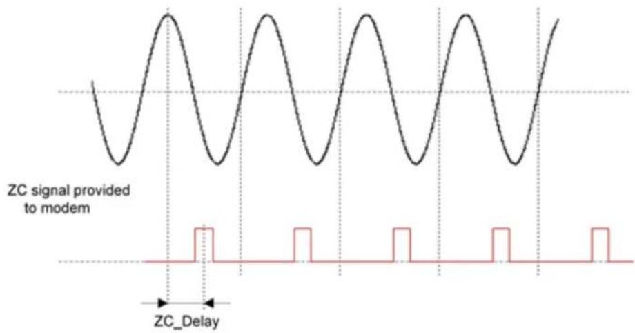
line
| Time Segment | Signal Amplitude | | ------------ | ---------------- | | 0 | High | | 1 | Low | | 2 | High | | 3 | Low | | 4 | High | | 5 | Low | | 6 | High | | 7 | Low | | 8 | High | | 9 | Low | | 10 | High | | 11 | Low | | 12 | High | | 13 | Low | | 14 | High | | 15 | Low | | 16 | High | | 17 | Low | | 18 | High | | 19 | Low | | 20 | High | | 21 | Low | | 22 | High | | 23 | Low | | 24 | High | | 25 | Low | | 26 | High | | 27 | Low | | 28 | High | | 29 | Low | | 30 | High | | 31 | Low | | 32 | High | | 33 | Low | | 34 | High | | 35 | Low | | 36 | High | | 37 | Low | | 38 | High | | 39 | Low | | 40 | High | | 41 | Low | | 42 | High | | 43 | Low | | 44 | High | | 45 | Low | | 46 | High | | 47 | Low | | 48 | High | | 49 | Low | | 50 | High | | 51 | Low | | 52 | High | | 53 | Low | | 54 | High | | 55 | Low | | 56 | High | | 57 | Low | | 58 | High | | 59 | Low | | 60 | High | | 61 | Low | | 62 | High | | 63 | Low | | 64 | High | | 65 | Low | | 66 | High | | 67 | Low | | 68 | High | | 69 | Low | | 70 | High | | 71 | Low | | 72 | High | | 73 | Low | | 74 | High | | 75 | Low | | 76 | High | | 77 | Low | | 78 | High | | 79 | Low | | 80 | High | | 81 | Low | | 82 | High | | 83 | Low | | 84 | High | | 85 | Low | | 86 | High | | 87 | Low | | 88 | High | | 89 | Low | | 90 | High | | 91 | Low | | 92 | High | | 93 | Low | | 94 | High | | 95 | Low | | 96 | High | | 97 | Low | | 98 | High | | 99 | Low | | 100 | High |14. Revision History
14.1 Rev A - 03/2018
| Document Initial document release. |
14.2 Rev B - 10/2018
| 12.2.5 PIB Objects Specification and Access (G3) | Updated sections 12.2.5.16, 12.2.5.33, 12.2.5.34, 12.2.5.35, 12.2.5.36, 12.2.5.37, 12.2.5.38, 12.2.5.47, 12.2.5.62, 12.2.5.63, 12.2.5.68.Added sections 12.2.5.69, 12.2.5.70, 12.2.5.71, 12.2.5.72, 12.2.5.73, 12.2.5.74. |
| 12.3.4 PIB Objects Specification and Access (PRIME) | Updated sections 12.3.4.41, 12.3.4.42, 12.3.4.43, 12.3.4.44, 12.3.4.45, 12.3.4.46, 12.3.4.47, 12.3.4.48, 12.3.4.49, 12.3.4.65.Added section 12.3.4.66. |
14.3 Rev C - 04/2019
| Document Minor typographical updates throughout. | |
| 1. PL360 Host Controller Architecture Updated section 1.5 | |
| 5. Configuration Deleted section Configure Coupling ParametersUpdated sections 5.1, 5.2 | |
| 8.1 PHY Examples Added section 8.1.4 | |
| 9. Supported Platforms | Updated sections 9.1, 9.3, Platform Porting |
| 11. References Updated references | |
| 12.2 G3 PHY API Updated section 12.2.1 | |
| 12.2.5 PIB Objects Specification and Access (G3) | Updated sections 12.2.5.33, 12.2.5.36, 12.2.5.38, 12.2.5.41, 12.2.5.42, 12.2.5.43, 12.2.5.44, 12.2.5.45, 12.2.5.46, 12.2.5.47, 12.2.5.48, 12.2.5.49, 12.2.5.50, 12.2.5.51, 12.2.5.52, 12.2.5.53, 12.2.5.54, 12.2.5.55, 12.2.5.56, 12.2.5.57, 12.2.5.58, 12.2.5.59, 12.2.5.60, 12.2.5.61, 12.2.5.62, 12.2.5.63, 12.2.5.64, 12.2.5.65, 12.2.5.73Added section 12.2.5.75 |
| 12.3 PRIME PHY SAP | Updated sections 12.3.3, 12.3.4.13, 12.3.4.14, 12.3.4.18, 12.3.4.19, 12.3.4.20, 12.3.4.21, 12.3.4.22, 12.3.4.23, 12.3.4.24, 12.3.4.25, 12.3.4.26, 12.3.4.27, 12.3.4.28, 12.3.4.29, 12.3.4.30, 12.3.4.31, 12.3.4.32, 12.3.4.33, 12.3.4.34, 12.3.4.37, 12.3.4.38, 12.3.4.39, 12.3.4.40, 12.3.4.41, 12.3.4.44, 12.3.4.45, 12.3.4.46, 12.3.4.47, 12.3.4.48, 12.3.4.49, 12.3.4.66Added sections 12.3.4.67, 12.3.4.68 |
14.4 Rev D - 07/2019
| 12.2 G3 PHY API | Updated sections 12.2.2, 12.2.3, 12.2.4 |
| 12.2.5 PIB Objects Specification and Access (G3) | Updated sections 12.2.5.16, 12.2.5.36, 12.2.5.37, 12.2.5.48, 12.2.5.49, 12.2.5.50, 12.2.5.51, 12.2.5.52, 12.2.5.53, 12.2.5.54, 12.2.5.55, 12.2.5.56, 12.2.5.57, 12.2.5.58, 12.2.5.59, 12.2.5.72Added sections 12.2.5.39, 12.2.5.40, 12.2.5.76, 12.2.5.77 |
| 12.3 PRIME PHY SAP | Updated sections 12.3.1, 12.3.2, 12.3.3 |
| 12.3.4 PIB Objects Specification and Access (PRIME) | Updated sections 12.3.4.18, 12.3.4.19, 12.3.4.20, 12.3.4.21, 12.3.4.22, 12.3.4.26, 12.3.4.27, 12.3.4.28, 12.3.4.31 |
14.5 Rev E - 08/2020
| 1. PL360 Host Controller Architecture New sections 1.7, 1.8 | |
| 4. Initialization Example Updated sections 4.2, 4.5 | |
| 12.1 Common PHY API Updated sections 12.1.2 | New sections 12.1.6, 12.1.7, 12.1.8, 12.1.9, 12.1.10 |
| 12.2.5 PIB Objects Specification and Access (G3) | Updated sections 12.2.5.13, 12.2.5.14New sections 12.2.5.8, 12.2.5.9, 12.2.5.10, 12.2.5.78 |
| 12.3.4 PIB Objects Specification and Access (PRIME) | Updated sections 12.3.4.11, 12.3.4.12New sections 12.2.5.8, 12.2.5.9, 12.2.5.10, 12.3.4.69, 12.3.4.70, 12.3.4.71, 12.3.4.72, 12.3.4.73, 12.3.4.74, 12.3.4.75 |
The Microchip Website
Microchip provides online support via our website at www.microchip.com/. This website is used to make files and information easily available to customers. Some of the content available includes:
- Product Support – Data sheets and errata, application notes and sample programs, design resources, user's guides and hardware support documents, latest software releases and archived software
- General Technical Support – Frequently Asked Questions (FAQs), technical support requests, online discussion groups, Microchip design partner program member listing
- Business of Microchip – Product selector and ordering guides, latest Microchip press releases, listing of seminars and events, listings of Microchip sales offices, distributors and factory representatives
Product Change Notification Service
Microchip's product change notification service helps keep customers current on Microchip products. Subscribers will receive email notification whenever there are changes, updates, revisions or errata related to a specified product family or development tool of interest.
To register, go to www.microchip.com/pcn and follow the registration instructions.
Customer Support
Users of Microchip products can receive assistance through several channels:
• Distributor or Representative
- Local Sales Office
• Embedded Solutions Engineer (ESE)
- Technical Support
Customers should contact their distributor, representative or ESE for support. Local sales offices are also available to help customers. A listing of sales offices and locations is included in this document.
Technical support is available through the website at: www.microchip.com/support
Microchip Devices Code Protection Feature
Note the following details of the code protection feature on Microchip devices:
- Microchip products meet the specifications contained in their particular Microchip Data Sheet.
- Microchip believes that its family of products is secure when used in the intended manner and under normal conditions.
- There are dishonest and possibly illegal methods being used in attempts to breach the code protection features of the Microchip devices. We believe that these methods require using the Microchip products in a manner outside the operating specifications contained in Microchip's Data Sheets. Attempts to breach these code protection features, most likely, cannot be accomplished without violating Microchip's intellectual property rights.
- Microchip is willing to work with any customer who is concerned about the integrity of its code.
- Neither Microchip nor any other semiconductor manufacturer can guarantee the security of its code. Code protection does not mean that we are guaranteeing the product is “unbreakable.” Code protection is constantly evolving. We at Microchip are committed to continuously improving the code protection features of our products. Attempts to break Microchip’s code protection feature may be a violation of the Digital Millennium Copyright Act. If such acts allow unauthorized access to your software or other copyrighted work, you may have a right to sue for relief under that Act.
Legal Notice
Information contained in this publication is provided for the sole purpose of designing with and using Microchip products. Information regarding device applications and the like is provided only for your convenience and may be superseded by updates. It is your responsibility to ensure that your application meets with your specifications.
THIS INFORMATION IS PROVIDED BY MICROCHIP "AS IS". MICROCHIP MAKES NO REPRESENTATIONS OR WARRANTIES OF ANY KIND WHETHER EXPRESS OR IMPLIED, WRITTEN OR ORAL, STATUTORY OR OTHERWISE, RELATED TO THE INFORMATION INCLUDING BUT NOT LIMITED TO ANY IMPLIED WARRANTIES OF NON-INFRINGEMENT, MERCHANTABILITY, AND FITNESS FOR A PARTICULAR PURPOSE OR WARRANTIES RELATED TO ITS CONDITION, QUALITY, OR PERFORMANCE.
IN NO EVENT WILL MICROCHIP BE LIABLE FOR ANY INDIRECT, SPECIAL, PUNITIVE, INCIDENTAL OR CONSEQUENTIAL LOSS, DAMAGE, COST OR EXPENSE OF ANY KIND WHATSOEVER RELATED TO THE INFORMATION OR ITS USE, HOWEVER CAUSED, EVEN IF MICROCHIP HAS BEEN ADVISED OF THE POSSIBILITY OR THE DAMAGES ARE FORESEEABLE. TO THE FULLEST EXTENT ALLOWED BY LAW, MICROCHIP'S TOTAL LIABILITY ON ALL CLAIMS IN ANY WAY RELATED TO THE INFORMATION OR ITS USE WILL NOT EXCEED THE AMOUNT OF FEES, IF ANY, THAT YOU HAVE PAID DIRECTLY TO MICROCHIP FOR THE INFORMATION. Use of Microchip devices in life support and/or safety applications is entirely at the buyer's risk, and the buyer agrees to defend, indemnify and hold harmless Microchip from any and all damages, claims, suits, or expenses resulting from such use. No licenses are conveyed, implicitly or otherwise, under any Microchip intellectual property rights unless otherwise stated.
Trademarks
The Microchip name and logo, the Microchip logo, Adaptec, AnyRate, AVR, AVR logo, AVR Freaks, BesTime, BitCloud, chipKIT, chipKIT logo, CryptoMemory, CryptoRF, dsPIC, FlashFlex, flexPWR, HELDO, IGLOO, JukeBlox, KeeLoq, Kleer, LANCheck, LinkMD, maXStylus, maXTouch, MediaLB, megaAVR, Microsemi, Microsemi logo, MOST, MOST logo, MPLAB, OptoLyzer, PackeTime, PIC, picoPower, PICSTART, PIC32 logo, PolarFire, Prochip Designer, QTouch, SAM-BA, SenGenuity, SpyNIC, SST, SST Logo, SuperFlash, Symmetricom, SyncServer, Tachyon, TempTrackr, TimeSource, tinyAVR, UNI/O, Vectron, and XMEGA are registered trademarks of Microchip Technology Incorporated in the U.S.A. and other countries.
APT, ClockWorks, The Embedded Control Solutions Company, EtherSynch, FlashTec, Hyper Speed Control, HyperLight Load, IntelliMOS, Libero, motorBench, mTouch, Powermite 3, Precision Edge, ProASIC, ProASIC Plus, ProASIC Plus logo, Quiet-Wire, SmartFusion, SyncWorld, Temux, TimeCesium, TimeHub, TimePictra, TimeProvider, Vite, WinPath, and ZL are registered trademarks of Microchip Technology Incorporated in the U.S.A.
Adjacent Key Suppression, AKS, Analog-for-the-Digital Age, Any Capacitor, AnyIn, AnyOut, BlueSky, BodyCom, CodeGuard, CryptoAuthentication, CryptoAutomotive, CryptoCompanion, CryptoController, dsPICDEM, dsPICDEM.net, Dynamic Average Matching, DAM, ECAN, EtherGREEN, In-Circuit Serial Programming, ICSP, INICnet, Inter-Chip Connectivity, JitterBlocker, KleerNet, KleerNet logo, memBrain, Mindi, MiWi, MPASM, MPF, MPLAB Certified logo, MPLIB, MPLINK, MultiTRAK, NetDetach, Omniscient Code Generation, PICDEM, PICDEM.net, PICkit, PICtail, PowerSmart, PureSilicon, QMatrix, REAL ICE, Ripple Blocker, SAM-ICE, Serial Quad I/O, SMART-I.S., SQI, SuperSwitcher, SuperSwitcher II, Total Endurance, TSHARC, USBCheck, VariSense, ViewSpan, WiperLock, Wireless DNA, and ZENA are trademarks of Microchip Technology Incorporated in the U.S.A. and other countries.
SQTP is a service mark of Microchip Technology Incorporated in the U.S.A.
The Adaptec logo, Frequency on Demand, Silicon Storage Technology, and Symmcom are registered trademarks of Microchip Technology Inc. in other countries.
GestIC is a registered trademark of Microchip Technology Germany II GmbH & Co. KG, a subsidiary of Microchip Technology Inc., in other countries.
All other trademarks mentioned herein are property of their respective companies.
© 2020, Microchip Technology Incorporated, Printed in the U.S.A., All Rights Reserved.
ISBN: 978-1-5224-6748-9
Quality Management System
For information regarding Microchip's Quality Management Systems, please visit www.microchip.com/quality.
Worldwide Sales and Service
AMERICAS ASIA/PACIFIC ASIA/PACIFIC EUROPE
| Corporate Office | Australia - Sydney | India - Bangalore | Austria - Wels |
| 2355 West Chandler Blvd. | Tel: 61-2-9868-6733 | Tel: 91-80-3090-4444 | Tel: 43-7242-2244-39 |
| Chandler, AZ 85224-6199 | China - Beijing | India - New Delhi | Fax: 43-7242-2244-393 |
| Tel: 480-792-7200 | Tel: 86-10-8569-7000 | Tel: 91-11-4160-8631 | Denmark - Copenhagen |
| Fax: 480-792-7277 | China - Chengdu | India - Pune | Tel: 45-4485-5910 |
| Technical Support: | Tel: 86-28-8665-5511 | Tel: 91-20-4121-0141 | Fax: 45-4485-2829 |
| www.microchip.com/support | China - Chongqing | Japan - Osaka | Finland - Espoo |
| Web Address: | Tel: 86-23-8980-9588 | Tel: 81-6-6152-7160 | Tel: 358-9-4520-820 |
| www.microchip.com | China - Dongguan | Japan - Tokyo | France - Paris |
| Atlanta | Tel: 86-769-8702-9880 | Tel: 81-3-6880-3770 | Tel: 33-1-69-53-63-20 |
| Duluth, GA | China - Guangzhou | Korea - Daegu | Fax: 33-1-69-30-90-79 |
| Tel: 678-957-9614 | Tel: 86-20-8755-8029 | Tel: 82-53-744-4301 | Germany - Garching |
| Fax: 678-957-1455 | China - Hangzhou | Korea - Seoul | Tel: 49-8931-9700 |
| Austin, TX | Tel: 86-571-8792-8115 | Tel: 82-2-554-7200 | Germany - Haan |
| Tel: 512-257-3370 | China - Hong Kong SAR | Malaysia - Kuala Lumpur | Tel: 49-2129-3766400 |
| Boston | Tel: 852-2943-5100 | Tel: 60-3-7651-7906 | Germany - Heilbronn |
| Westborough, MA | China - Nanjing | Malaysia - Penang | Tel: 49-7131-72400 |
| Tel: 774-760-0087 | Tel: 86-25-8473-2460 | Tel: 60-4-227-8870 | Germany - Karlsruhe |
| Fax: 774-760-0088 | China - Qingdao | Philippines - Manila | Tel: 49-721-625370 |
| Chicago | Tel: 86-532-8502-7355 | Tel: 63-2-634-9065 | Germany - Munich |
| Itasca, IL | China - Shanghai | Singapore | Tel: 49-89-627-144-0 |
| Tel: 630-285-0071 | Tel: 86-21-3326-8000 | Tel: 65-6334-8870 | Fax: 49-89-627-144-44 |
| Fax: 630-285-0075 | China - Shenyang | Taiwan - Hsin Chu | Germany - Rosenheim |
| Dallas | Tel: 86-24-2334-2829 | Tel: 886-3-577-8366 | Tel: 49-8031-354-560 |
| Addison, TX | China - Shenzhen | Taiwan - Kaohsiung | Israel - Ra'anana |
| Tel: 972-818-7423 | Tel: 86-755-8864-2200 | Tel: 886-7-213-7830 | Tel: 972-9-744-7705 |
| Fax: 972-818-2924 | China - Suzhou | Taiwan - Taipei | Italy - Milan |
| Detroit | Tel: 86-186-6233-1526 | Tel: 886-2-2508-8600 | Tel: 39-0331-742611 |
| Novi, MI | China - Wuhan | Thailand - Bangkok | Fax: 39-0331-466781 |
| Tel: 248-848-4000 | Tel: 86-27-5980-5300 | Tel: 66-2-694-1351 | Italy - Padova |
| Houston, TX | China - Xian | Vietnam - Ho Chi Minh | Tel: 39-049-7625286 |
| Tel: 281-894-5983 | Tel: 86-29-8833-7252 | Tel: 84-28-5448-2100 | Netherlands - Drunen |
| Indianapolis | China - Xiamen | Tel: 31-416-690399 | |
| Noblesville, IN | Tel: 86-592-2388138 | Fax: 31-416-690340 | |
| Tel: 317-773-8323 | China - Zhuhai | Norway - Trondheim | |
| Fax: 317-773-5453 | Tel: 86-756-3210040 | Tel: 47-72884388 | |
| Tel: 317-536-2380 | Poland - Warsaw | ||
| Los Angeles | Tel: 48-22-3325737 | ||
| Mission Viejo, CA | Romania - Bucharest | ||
| Tel: 949-462-9523 | Tel: 40-21-407-87-50 | ||
| Fax: 949-462-9608 | Spain - Madrid | ||
| Tel: 951-273-7800 | Tel: 34-91-708-08-90 | ||
| Raleigh, NC | Fax: 34-91-708-08-91 | ||
| Tel: 919-844-7510 | Sweden - Gothenberg | ||
| New York, NY | Tel: 46-31-704-60-40 | ||
| Tel: 631-435-6000 | Sweden - Stockholm | ||
| San Jose, CA | Tel: 46-8-5090-4654 | ||
| Tel: 408-735-9110 | UK - Wokingham | ||
| Tel: 408-436-4270 | Tel: 44-118-921-5800 | ||
| Canada - Toronto | Fax: 44-118-921-5820 | ||
| Tel: 905-695-1980 | |||
| Fax: 905-695-2078 |