DSC2130 - Unspecified Microchip - Free user manual and instructions
Find the device manual for free DSC2130 Microchip in PDF.

User questions about DSC2130 Microchip
0 question about this device. Answer the ones you know or ask your own.
Ask a new question about this device
Download the instructions for your Unspecified in PDF format for free! Find your manual DSC2130 - Microchip and take your electronic device back in hand. On this page are published all the documents necessary for the use of your device. DSC2130 by Microchip.
USER MANUAL DSC2130 Microchip
Programming User's Guide
Note the following details of the code protection feature on Microchip devices:
• Microchip products meet the specification contained in their particular Microchip Data Sheet.
- Microchip believes that its family of products is one of the most secure families of its kind on the market today, when used in the intended manner and under normal conditions.
- There are dishonest and possibly illegal methods used to breach the code protection feature. All of these methods, to our knowledge, require using the Microchip products in a manner outside the operating specifications contained in Microchip's Data Sheets. Most likely, the person doing so is engaged in theft of intellectual property.
• Microchip is willing to work with the customer who is concerned about the integrity of their code.
- Neither Microchip nor any other semiconductor manufacturer can guarantee the security of their code. Code protection does not mean that we are guaranteeing the product as "unbreakable."
Code protection is constantly evolving. We at Microchip are committed to continuously improving the code protection features of our products. Attempts to break Microchip's code protection feature may be a violation of the Digital Millennium Copyright Act. If such acts allow unauthorized access to your software or other copyrighted work, you may have a right to sue for relief under that Act.
Information contained in this publication regarding device applications and the like is provided only for your convenience and may be superseded by updates. It is your responsibility to ensure that your application meets with your specifications. MICROCHIP MAKES NO REPRESENTATIONS OR WARRANTIES OF ANY KIND WHETHER EXPRESS OR IMPLIED, WRITTEN OR ORAL, STATUTORY OR OTHERWISE, RELATED TO THE INFORMATION, INCLUDING BUT NOT LIMITED TO ITS CONDITION, QUALITY, PERFORMANCE, MERCHANTABILITY OR FITNESS FOR PURPOSE. Microchip disclaims all liability arising from this information and its use. Use of Microchip devices in life support and/or safety applications is entirely at the buyer's risk, and the buyer agrees to defend, indemnify and hold harmless Microchip from any and all damages, claims, suits, or expenses resulting from such use. No licenses are conveyed, implicitly or otherwise, under any Microchip intellectual property rights unless otherwise stated.
Microchip received ISO/TS-16949:2009 certification for its worldwide headquarters, design and wafer fabrication facilities in Chandler and Tempe, Arizona; Gresham, Oregon and design centers in California and India. The Company's quality system processes and procedures are for its PIC® MCUs and dsPIC® DSCs, KEELOQ® code hopping devices, Serial EEPROMs, microperipherals, nonvolatile memory and analog products. In addition, Microchip's quality system for the design and manufacture of development systems is ISO 9001:2000 certified.
QUALITY MANAGEMENT SYSTEM CERTIFIED BY DNV = ISO/TS 16949=
Trademarks
The Microchip name and logo, the Microchip logo, AnyRate, AVR, AVR logo, AVR Freaks, BeaconThings, BitCloud, CryptoMemory, CryptoRF, dsPIC, FlashFlex, flexPWR, Heldo, JukeBlox, KEELOQ, KEELOQ logo, Kleer, LANCheck, LINK MD, maXStylus, maXTouch, MediaLB, megaAVR, MOST, MOST logo, MPLAB, OptoLyzer, PIC, picoPower, PICSTART, PIC32 logo, Prochip Designer, QTouch, RightTouch, SAM-BA, SpyNIC, SST, SST Logo, SuperFlash, tinyAVR, UNI/O, and XMEGA are registered trademarks of Microchip Technology Incorporated in the U.S.A. and other countries.
ClockWorks, The Embedded Control Solutions Company, EtherSynch, Hyper Speed Control, HyperLight Load, IntelliMOS, mTouch, Precision Edge, and Quiet-Wire are registered trademarks of Microchip Technology Incorporated in the U.S.A.
Adjacent Key Suppression, AKS, Analog-for-the-Digital Age, Any Capacitor, AnyIn, AnyOut, BodyCom, chipKIT, chipKIT logo,
CodeGuard, CryptoAuthentication, CryptoCompanion, CryptoController, dsPICDEM, dsPICDEM.net, Dynamic Average Matching, DAM, ECAN, EtherGREEN, In-Circuit Serial Programming, ICSP, Inter-Chip Connectivity, JitterBlocker, KleerNet, KleerNet logo, Mindi, MiWi, motorBench, MPASM, MPF, MPLAB Certified logo, MPLIB, MPLINK, MultiTRAK, NetDetach, Omniscient Code Generation, PICDEM, PICDEM.net, PICkit, PICtail, PureSilicon, QMatrix, RightTouch logo, REAL ICE, Ripple Blocker, SAM-ICE, Serial Quad I/O, SMART-I.S., SQI, SuperSwitcher, SuperSwitcher II, Total Endurance, TSHARC, USBCheck, VariSense, ViewSpan, WiperLock, Wireless DNA, and ZENA are trademarks of Microchip Technology Incorporated in the U.S.A. and other countries.
SQTP is a service mark of Microchip Technology Incorporated in the U.S.A.
Silicon Storage Technology is a registered trademark of Microchip Technology Inc. in other countries.
GestIC is a registered trademark of Microchip Technology Germany II GmbH & Co. KG, a subsidiary of Microchip Technology Inc., in other countries.
All other trademarks mentioned herein are property of their respective companies.
© 2018, Microchip Technology Incorporated, All Rights Reserved. ISBN: 978-1-5224-2887-9
Table of Contents
Preface ....5
Introduction 5
Document Layout 5
Conventions Used in this Guide 6
The Microchip Website 7
Customer Support 7
Document Revision History 7
Chapter 1. Product Overview ......9
Device Architecture 9
Default Conditions 9
Chapter 2. Programming Features ......11
Programming Clock Frequencies 11
Calculation of N,F & M for Single-Output Oscillator (DSC21X0 & DSC22X0) 11
Calculation of N,F & M for Single-Output Oscillator (DSC21X0 & DSC22X0) 13
Programming CMOS Output Drive Strength & Output Control Modes.... 15
Hibernate (Low Current) Mode.... 15
I²C Bus Control Interface 15
SPI Bus Control Interface.... 17
Worldwide Sales and Service 29
NOTES:
Preface
NOTICE TO CUSTOMERS
All documentation becomes dated, and this manual is no exception. Microchip tools and documentation are constantly evolving to meet customer needs, so some actual dialogs and/or tool descriptions may differ from those in this document. Please refer to our web site (www.microchip.com) to obtain the latest documentation available.
Documents are identified with a "DS" number. This number is located on the bottom of each page, in front of the page number. The numbering convention for the DS number is "DSXXXXXXXXA", where "XXXXXXX" is the document number and "A" is the revision level of the document.
For the most up-to-date information on development tools, see the MPLAB ^® IDE online help. Select the Help menu, and then Topics to open a list of available online help files.
INTRODUCTION
This chapter contains general information that will be useful to know before using the DSC22XX/DSC21XX Programming Guide. Items discussed in this chapter include:
- Document Layout
• Conventions Used in this Guide
• The Microchip Website - Customer Support
• Document Revision History
DOCUMENT LAYOUT
This document describes how to use the DSC22XX/DSC21XX Programming Guide to program a MEMS oscillator device. The manual layout is as follows:
- Chapter 1. “Product Overview” – Provides important information about the DSC22XX/DSC21XX Programming Guide.
- Chapter 2. “Programming Features” – Provides information about using the DSC22XX/DSC21XX Programming Guide.
CONVENTIONS USED IN THIS GUIDE
This manual uses the following documentation conventions:
DOCUMENTATION CONVENTIONS
| Description Represents Examples | ||
| Arial font: | ||
| Italic characters Referenced books | MPLAB | ^ IDE User's Guide |
| Emphasized text ...is the only compiler... | ||
| Initial caps A window the Output | window | |
| A dialog the Settings dialog | ||
| A menu selection select Enable Programmer | ||
| Quotes A field name in a window or dialog | "Save project before build" | |
| Underlined, italic text with right angle bracket | A menu path File>Save | —— |
| Bold characters A dialog button | Click OK | |
| A tab | Click the Power tab | |
| N'Rnnnn | A number in verilog format, where N is the total number of digits, R is the radix and n is a digit. | 4'b0010, 2'hF1 |
| Text in angle brackets <> | A key on the keyboard | Press,, |
| Courier New font: | ||
| Plain Courier New | Sample source code | #define START |
| Filenames | autoexec.bat | |
| File paths | c:\mccl8\h | |
| Keywords | _asm, _endasm, static | |
| Command-line options | -0pa+, -0pa- | |
| Bit values | 0, 1 | |
| Constants | 0xFF, 'A' | |
| Italic Courier New | A variable argument | file.o, where file can be any valid filename |
| Square brackets [] | Optional arguments | mccl8 [options] file [options] |
| Curly brackets and pipe character: { | } | Choice of mutually exclusive arguments; an OR selection | errorlevel {0|1} |
| Ellipses... | Replaces repeated text | var_name [, var_name...] |
| Represents code supplied by user | void main (void) { ... } | |
THE MICROCHIP WEBSITE
Microchip provides on-line support via our web site at www.microchip.com. This website is used as a means to make files and information easily available to customers. Accessible by using your favorite Internet browser, the website contains the following information:
- Product Support – Data sheets and errata, application notes and sample programs, design resources, user's guides and hardware support documents, latest software releases and archived software
- General Technical Support – Frequently Asked Questions (FAQs), technical support requests, on-line discussion groups, Microchip consultant program member listing
- Business of Microchip – Product selector and ordering guides, latest Microchip press releases, listing of seminars and events, listings of Microchip sales offices, distributors and factory representatives
CUSTOMER SUPPORT
Users of Microchip products can receive assistance through several channels:
• Distributor or Representative
- Local Sales Office
• Field Application Engineer (FAE)
- Technical Support
Customers should contact their distributor, representative or field application engineer (FAE) for support. Local sales offices are also available to help customers. A listing of sales offices and locations is included in the back of this document.
Technical support is available through the web site at: http://support.microchip.com.
DOCUMENT REVISION HISTORY
Revision A (April 2018)
- Converted Micrel version of the DSC22XX/DSC21XX Programming Guide to Microchip User Guide DS50002739A.
NOTES:
Chapter 1. Product Overview
1.1 DEVICE ARCHITECTURE
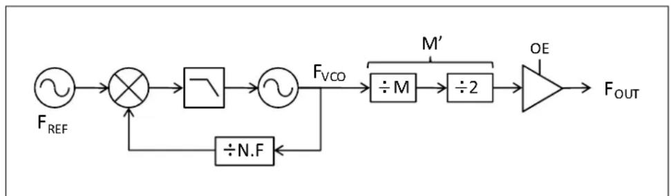
The DSC21XX & DSC22XX families of low jitter, configurable single and dual output oscillators consist of a MEMS resonator and a high performance PLL IC, programmable via I ^2 C/SPI interface. This document will explain how to program the output frequencies as well as the CMOS outputs drive strength.
The basic block diagram of the dual and single output oscillators including the integrated PLL and clock distribution path are shown in Figure 1-1 and Figure 1-2. These oscillators are equipped with a high performance fractional-N PLL that locks an integrated high frequency VCO to the internal MEMS oscillator. The output of the VCO is then divided down through independent even integer dividers, with divide values ranging from 4 to 254, to generate the desired output clock frequencies. Each clock output is buffered by a low-noise output driver, available in CMOS, LVPECL, LVDS, and HCSL formats.
Block Diagrams of Single and Dual Output DSC20XX Oscillators
flowchart
graph LR
    A["F_REF"] --> B["×"]
    B --> C["÷"]
    C --> D["×"]
    D --> E["F_VCO"]
    E --> F["÷M"]
    F --> G["÷2"]
    G --> H["OE"]
    H --> I["F_OUT"]
    J["÷N.F"] --> B
    K["M'"] --> F
FIGURE 1-1: Single Output Oscillator.

flowchart
graph LR
    A["F_REF"] --> B["×"]
    B --> C["÷"]
    C --> D["÷"]
    D --> E["F_VCO"]
    E --> F["÷M1"]
    F --> G["÷2"]
    G --> H["O1E"]
    H --> I["F_OUT1"]
    D --> J["÷N.F"]
    J --> K["M2'"]
    K --> L["÷M2"]
    L --> M["÷2"]
    M --> N["O2E"]
    N --> O["F_OUT2"]
FIGURE 1-2: Dual Output Oscillator.
1.2 DEFAULT CONDITIONS
Upon power-up, the initial output frequency configuration is controlled by an internal preprogrammed memory (OTP). This memory stores all coefficients required by the PLL for two independent default frequencies for a single output oscillator, or two fre-
quency combinations for a dual output version. The control pin (FS) selects which default frequency is the initial setting. After power-up, a new output frequency configuration can be programmed using I ^2 C/SPI interface.
The CMOS output drive strength, which is programmable using 3 control bits, is set by default to maximum strength or the value of 111. After power-up, a new CMOS drive-strength setting can be programmed using I ^2 C/SPI interface.
Chapter 2. Programming Features
2.1 PROGRAMMING CLOCK FREQUENCIES
This section describes the PLL variables and registers used to configure the oscillator to produce the desired output frequencies.
As shown in Figure 1-1 and Figure 1-2, several parameters need to be programmed to determine the internal VCO and the output clock frequencies. The PLL consists of a feedback divider with a fractional value described as N.F, where N (7-bit value) and F (17-bit value) are the integer and fractional portions of the divider value, respectively. The PLL is then followed by M divider (8-bit value) integer divider and a final divide-by-2 stage to ensure 50% output clock duty cycle. The combination of these two dividers creates an even integer M' divider block with divider value range of 4 to 254. It must be noted that M must have a minimum value of 2. To summarize, the output frequency is specified by three programmable values, N, F & M.
2.1.1 Calculation of N,F & M for Single-Output Oscillator (DSC21X0 & DSC22X0)
To optimize performance of the PLL, it is desirable to program the internal PLL to the lowest possible valid VCO frequency that can generate the desired output clock frequency. The minimum valid VCO frequency for the device is 1135 MHz while the optimum VCO frequency range is from 1175 to 1700 MHz. Below is an example illustrating how to calculate the required N, F & M values.
Example:
Desired Clock Frequency: F_OUT = 25 MHz
Lowest Optimum VCO Frequency: F_VCO = F_OUT × M' = 25 × 48 = 1200 MHz
$$ \mathrm{M} = \mathrm{M} ^ {\prime} \div 2 = 2 4 $$
Once the VCO frequency is determined, the N.F value can be easily calculated by dividing the VCO frequency by the input reference frequency from the MEMS oscillator, which is calibrated in the fabrication process to 18 MHz.
$$ N. F = F _ {V C O} \div F _ {R E F} = 1 2 0 0 \mathrm{MHz} \div 1 8 \mathrm{MHz} = 6 6. 6 6 6 6 6 7 $$
$$ N = 6 6, F = 0. 6 6 6 6 6 7 $$
Since F is described using a 17-bit register, we need to calculate it as the numerator value that will create our desired fraction with (2^7 - 1) in the denominator. This number will then need to be rounded to the nearest integer value.
$$ F [ 1 6: 0 ] = 0. 6 6 6 6 6 7 \times (2 ^ {1 7} - 1) = 8 7 3 8 0. 7 1 \rightarrow F [ 1 6: 0 ] = 8 7 3 8 1 (\text { rounded }) $$
The final step before programming the values into the appropriate registers is to convert M, N, and F to the appropriate binary or hexadecimal values.
$$ M [ 7: 0 ] = 2 4 _ {\text { dec }} = 0 0 0 1 1 0 0 0 \text { bin } = 1 8 _ {\text { hex }} $$
$$ N [ 6: 0 ] = 6 6 _ {\text { dec }} = 1 0 0 0 0 1 0 1 \text { bin } = 8 5 _ {\text { hex }} $$
$$ F [ 1 6: 0 ] = 8 7 3 8 1 _ {\text { dec }} = 1 0 1 0 1 0 1 0 1 0 1 0 1 0 1 0 1 \text { bin } = 1 5 5 5 5 _ {\text { hex }} $$
We now load the resulting values into the appropriate registers to program the DSC21X0 or DSC22X0 to the desired output clock frequency. Table 2-1 describes the register map for the variables described above.
TABLE 2-1: REGISTER MAP FOR THE SINGLE-OUTPUT DSC2XXX OSCILLATOR
| Register | 7 6 5 4 3 2 | 1 0 | ||||||
| 0x13 | F[7] | F[6] | F[5] | F[4] | F[3] | F[2] | F[1] | F[0] |
| 0x14 | F[15] | F[14] | F[13] | F[12] | F[11] | F[10] | F[9] | F[8] |
| 0x15 | N[6] | N[5] | N[4] | N[3] | N[2] | N[1] | N[0] | N[16] |
| 0x16 | M1[7] | M1[6] | M1[5] | M1[4] | M1[3] | M1[2] | M1[1] | M1[0] |
Note: In reference to Register 0x13: Register 0x13 holds the least eight significant bits of the 17-bit F value. This register, though, is not accessible through the I²C and no writes should be made to it. While some frequency granularity is lost in programming only the upper 8 bits of F, frequency steps of about 13 ppm can be achieved, sufficiently fine for most applications.
Commonly used clock frequencies:
Table 2-2 provides a list of commonly used output clock frequencies, corresponding PLL variables, and register parameters that need to be programmed into the oscillator via I²C/SPI interface.
TABLE 2-2: COMMON CLOCK FREQUENCIES AND CORRESPONDING PARAMETERS
| Freq (MHz) | M | N | F | FVCO (MHz) | Registers (address & value in HEX) | |||
| 0x13 | 0x14 | 0x15 | 0x16 | |||||
| 19.2 | 31 | 66 | 0.133333 | 1190.4000 | 44 | 44 | 84 | 1F |
| 24 | 25 | 66 | 0.666667 | 1200.0000 | 55 | 55 | 85 | 19 |
| 25 | 24 | 66 | 0.666667 | 1200.0000 | 55 | 55 | 85 | 18 |
| 33.3333 | 18 | 66 | 0.666666 | 1200.0000 | 55 | 55 | 85 | 12 |
| 40 | 15 | 66 | 0.666667 | 1200.0000 | 55 | 55 | 85 | 15 |
| 48 | 13 | 69 | 0.333333 | 1248.0000 | AA | AA | 8A | 0D |
| 50 | 12 | 66 | 0.666667 | 1200.0000 | 55 | 55 | 85 | 0C |
| 54 | 11 | 66 | 0 | 1188.0000 | 00 | 00 | 84 | 0B |
| 62.5 | 10 | 69 | 0.444444 | 1250.0000 | 8E | E3 | 8A | 0A |
| 66.6666 | 9 | 66 | 0.666666 | 1200.0000 | 55 | 55 | 85 | 09 |
| 74.25 | 8 | 66 | 0 | 1188.0000 | 00 | 00 | 84 | 08 |
| 75 | 8 | 66 | 0.666667 | 1200.0000 | 55 | 55 | 85 | 08 |
| 77.76 | 8 | 69 | 0.12 | 1244.1600 | 71 | 3D | 8A | 08 |
| 100 | 6 | 66 | 0.666667 | 1200.0000 | 55 | 55 | 85 | 06 |
| 106.25 | 6 | 70 | 0.833333 | 1275.0000 | AA | AA | 8D | 06 |
| 125 | 5 | 69 | 0.444444 | 1250.0000 | 8E | E3 | 8A | 05 |
| 133.333 | 5 | 74 | 0.074074 | 1333.3333 | ED | 25 | 94 | 05 |
| 148.5 | 4 | 66 | 0 | 1188.0000 | 00 | 00 | 84 | 04 |
| 150 | 4 | 66 | 0.666667 | 1200.0000 | 55 | 55 | 85 | 04 |
| 155.52 | 4 | 69 | 0.12 | 1244.1600 | 71 | 3D | 8A | 04 |
| 156.25 | 4 | 69 | 0.444444 | 1250.0000 | 8E | E3 | 8A | 04 |
| 200 | 3 | 66 | 0.666667 | 1200.0000 | 55 | 55 | 85 | 03 |
| 212.5 | 3 | 70 | 0.833333 | 1275.0000 | AA | AA | 8D | 03 |
| 400 | 2 | 88 | 0.888889 | 1600.0000 | 1C | C7 | B1 | 02 |
2.1.2 Calculation of N,F & M for Dual-Output Oscillator (DSC21XX & DSC22XX)
Calculation of the PLL parameters (N, F & M) for the dual output oscillator devices is very similar to that described in the previous section. However, the oscillator will now need to simultaneously generate two output clock frequencies from a single VCO frequency. This constraint alters the computation of the common VCO frequency. We need a valid VCO frequency that when divided by two independent even integer values, each ranging from 4 to 254, will generate both desired output clock frequencies. This analysis is best performed with an iterative approach using a spreadsheet.
Example:
Desired Clock Frequency 1: F_OUT1 = 125 MHz
Desired Clock Frequency 2: F_OUT2 = 25 MHz
Lowest Common VCO Frequency (from spreadsheet): F_VCO = 1250 MHz
Once the VCO frequency is determined, all other parameters can be easily calculated as shown in previous section.
Example:
$$ \mathrm{M} 1 ^ {\prime} = \mathrm{F} _ {\mathrm{VCO}} \div \mathrm{F} _ {\mathrm{OUT} 1} = 1 2 5 0 \mathrm{MHz} \div 1 2 5 \mathrm{MHz} = 1 0 $$
$$ M 1 = M 1 ^ {\prime} \div 2 = 5 $$
And
$$ \mathrm{M} 2 ^ {\prime} = \mathrm{F} _ {\mathrm{VCO}} \div \mathrm{F} _ {\mathrm{OUT2}} = 1 2 5 0 \mathrm{MHz} \div 2 5 \mathrm{MHz} = 5 0 $$
$$ \mathrm{M} 2 = \mathrm{M} 2 ^ {\prime} \div 2 = 2 5 $$
$$ N. F = F _ {V C O} \div F R E F = 1 2 5 0 \mathrm{MHz} \div 1 8 \mathrm{MHz} = 6 9. 4 4 4 4 4 4 $$
$$ N = 6 9, F = 0. 4 4 4 4 4 4 $$
Since F is described using a 17-bit register, we need to calculate it as the numerator value that will create our desired fraction with (2^17 - 1) as the denominator. This number will then need to be rounded to the nearest integer value.
$$ F [ 1 6: 0 ] = 0. 4 4 4 4 4 4 \times (2 1 7 - 1) = 5 8 2 5 3. 7 1 \rightarrow F [ 1 6: 0 ] = 5 8 2 5 4 (\text { rounded }) $$
The final step before programming the values into the appropriate registers is to convert the M, N, and F to the appropriate binary or hexadecimal values.
$$ \mathrm{M} 1 [ 7: 0 ] = 5 _ {\text { dec }} = 0 0 0 0 0 1 0 1 _ {\text { bin }} = 0 5 _ {\text { hex }} $$
$$ \mathrm{M} 2 [ 7: 0 ] = 2 5 _ {\text {dec}} = 0 0 0 1 1 0 0 1 _ {\text {bin}} = 1 9 _ {\text {hex}} $$
$$ N [ 6: 0 ] = 6 9 _ {\text { dec }} = 1 0 0 0 1 0 1 0 _ {\text { bin }} = 8 A _ {\text { hex }} $$
$$ F [ 1 6: 0 ] = 5 8 2 5 4 _ {\text { dec }} = 0 1 1 1 0 0 0 1 1 1 0 0 0 1 1 1 0 _ {\text { bin }} = 0 E 3 8 E _ {\text { hex }} $$
We now load the resulting values into the appropriate registers to program the DSC21XX or DSC22XX to our desired output clock frequencies. Table 2-3 describes the register map for the variable described above.
TABLE 2-3: REGISTER MAP FOR THE DUAL-OUTPUT DSC21XX & DSC22XX OSCILLATORS
| R | e | g | i | s | t | e | r | 7 | 6 |
| 0x13 | F[7] | F[6] | F[5] | F[4] | F[3] | F[2] | F[1] | F[0] | |
| 0x14 | F[15] | F[14] | F[13] | F[12] | F[11] | F[10] | F[9] | F[8] | |
| 0x15 | N[6] | N[5] | N[4] | N[3] | N[2] | N[1] | N[0] | N[16] | |
| 0x16 | M1[7] | M1[6] | M1[5] | M1[4] | M1[3] | M1[2] | M1[1] | M1[0] | |
| 0x17 | M2[7] | M2[6] | M2[5] | M2[4] | M2[3] | M2[2] | M2[1] | M2[0] |
Note: In reference to Register 0x13: Register 0x13 holds the least eight significant bits of the 17-bit F value. This register, though, is not accessible through the I²C and no writes should be made to it. While some frequency granularity is lost in programming only the upper 8 bits of F, frequency steps of about 13 ppm can be achieved, sufficiently fine for most applications.
Commonly used clock frequencies:
Table 4 provides a list of commonly used output clock frequency combinations, corresponding PLL variables, and register values that need to be programmed into the oscillator via I ^2 C/SPI interface.
Contact factory for frequency pairs not included in the table below.
TABLE 2-4: COMMON CLOCK FREQUENCY PAIRS AND CORRESPONDING PARAMETERS
| Freq1 (MHz) | Freq2 (MHz) | M1 | M2 N | F | FVCO (MHz) | Registers (address & value in HEX) | |||||
| 0x13 | 0x14 0x1 | 5 0x16 | 0x17 | ||||||||
| 27 | 24 | 24 | 27 | 72 | 0 | 1296.0000 | 00 | 00 | 90 | 18 | 1B |
| 27 | 25 | 25 | 27 | 75 | 0 | 1350.0000 | 00 | 00 | 96 | 19 | 1B |
| 33.3333 | 25 | 18 | 24 | 66 | 0.66666 | 1199.0000 | 54 | 55 | 85 | 12 | 18 |
| 40 | 25 | 15 | 24 | 66 | 0.66667 | 1200.0000 | 55 | 55 | 85 | 0F | 18 |
| 50 | 25 | 12 | 24 | 66 | 0.66667 | 1200.0000 | 55 | 55 | 85 | 0C | 18 |
| 75 | 25 | 8 | 24 | 66 | 0.66667 | 1200.0000 | 55 | 55 | 85 | 08 | 18 |
| 100 | 25 | 6 | 24 | 66 | 0.66667 | 1200.0000 | 55 | 55 | 85 | 06 | 18 |
| 106.25 | 25 | 8 | 34 | 94 | 0.44444 | 1700.0000 | 8E | E3 | BC | 08 | 22 |
| 125 | 25 | 5 | 25 | 69 | 0.44444 | 1250.0000 | 8E | E3 | 8A | 05 | 19 |
| 150 | 25 | 4 | 24 | 66 | 0.66667 | 1200.0000 | 55 | 55 | 85 | 04 | 18 |
| 156.25 | 25 | 4 | 25 | 69 | 0.44444 | 1250.0000 | 8E | E3 | 8A | 04 | 19 |
| 212.5 | 25 | 4 | 34 | 94 | 0.44444 | 1700.0000 | 8E | E3 | BC | 04 | 22 |
| 40 | 33.3333 | 20 | 24 | 88 | 0.88889 | 1600.0000 | 1C | C7 | B1 | 14 | 18 |
| 48 | 40 | 15 | 18 | 80 | 0 | 1440.0000 | 00 | 00 | A0 | 0F | 12 |
| 100 | 75 | 6 | 8 | 66 | 0.66667 | 1200.0000 | 55 | 55 | 85 | 06 | 08 |
| 50 | 106.25 | 17 | 8 | 94 | 0.44444 | 1700.0000 | 8E | E3 | BC | 11 | 08 |
| 50 | 125 | 15 | 6 | 83 | 0.33333 | 1500.0000 | AA | AA | A6 | 0F | 06 |
| 148.5 | 74.25 | 5 | 10 | 82 | 0.5 | 1485.0000 | 00 | 00 | A5 | 05 | 0A |
| 156.25 | 125 | 4 | 5 | 69 | 0.44444 | 1250.0000 | 8E | E3 | 8A | 04 | 05 |
2.1.3 Executing a Frequency WRITE for (DSC21XX & DSC22XX)
When executing a frequency WRITE to the DSC21XX & DSC22XX devices it is required to place the device in Hibernate by setting (0x10h<5>), execute the frequency WRITE to addresses x13-x17h, then bring the device out of Hibernate by clearing (0x10h<5>). Refer to section 5 for details of entering/exiting Hibernate mode. Allow a 100 μs delay after applying the Hibernate signal before taking the subsequent Read / Write activity with the device.
The DSC21xx/22xx devices come with pre-stored frequencies selectable by the FSEL pin (pin 14). Frequency-bank 0 registers, selected when FSEL = 0, can be overwritten via I²C/SPI (addresses 0x13 - 0x17). Frequency-bank 1, selected when FSEL = 1, contains fixed frequency information and cannot be modified via I²C/SPI.
FSEL pin (pin 14) can be overwritten by resetting all the eight bits of register 0x12. Resetting register 0x12 makes the device select frequency-bank 0 and therefore allows the I²C/SPI interface to change the output frequency.
2.2 PROGRAMMING CMOS OUTPUT DRIVE STRENGTH & OUTPUT CONTROL MODES
As described earlier, drive strength for CMOS output drivers can be optimized via I^2C/SPI interface to help reduce EMI and improve performance. Each CMOS output driver has 8 drive strength settings (3 bits) and can also be independently enabled (logic high) or disabled (logic low) by writing into the corresponding bit, O1E for output 1 and O2E for output 2. An enabled output passes the generated output while a disabled output is in its tri-state condition (high impedance).
Please note that oscillator has to be already enabled via ENABLE pin prior to any serial programming. Please refer to the data sheet of the specific DSC21XX device for the typical rise/fall times for the different output strength settings.
Table 2-5 describes the output control register map. Register bits [7:4] are only applicable to dual output oscillators and can be ignored when programming a single-output oscillator.
TABLE 2-5: REGISTER MAP FOR CMOS OUTPUT DRIVE CONTROL
| Register 7 6 5 4 3 2 1 | 0 | |||||||
| 0x11 | O2S[2] | O2S[1] | O2S[0] | O2E | O1S[2] | O1S[1] | O1S[0] | O1E |
2.3 HIBERNATE (LOW CURRENT) MODE
Using serial programming, the DSC21XX or DSC22XX devices can be put into a low current mode to save power. By programming the Hibernate bit (0x10<5>) to a high, the device will enter the low current mode. During Hibernate, all outputs are in the tri-state condition and the PLL and oscillator circuitry are powered down. Less than 100 A are consumed. Writing a 0 into the Hibernate bit (0x10<5>) will return the device to normal operation.
When writing to register-bit 0x10<5>, care must be taken to not modify the other bits in the register. This can be achieved by masking the other bits with their existing value when writing the hibernate command. The register should be initially read, then rewritten with bit<5> changed to the desired hibernate state while keeping other bits as is.
2.4 I ^2 C BUS CONTROL INTERFACE
The DSC21XX can be configured as a read/write slave device that conforms to Phillips I ^2 C bus specifications except a “general call”. The DSC21XX employs a three pin I ^2 C bus configuration. A Chip Select (Cs_bar) enables I ^2 C communications with DSC21XX. The I ^2 C bus transmits data and clock with SDA and SCL. SDA and SCL are open-drain, that is the device can only drive these lines low or leave them to float. The bus is controlled by a master device that generates the serial clock SCL, controls bus access and generates the START and STOP conditions while the DSC21XX works as a slave. When Cs_bar is low, the accessed device will respond to SDA and SCL. When Cs_bar is high, the accessed device will not respond to I2C signals. The I ^2 C slave interface follows the Philips Fast Mode (400 kHz) format.
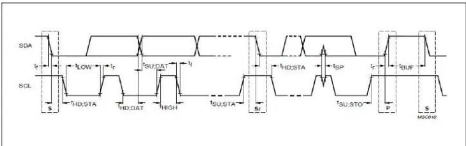
The DSC21XX uses standard I2C data structures and timing sequences. Because the DSC21XX employs a three pin configuration where Cs_bar controls access to the device, any 7 bit slave address can be used in the read or write commands with the exception of all bits equal 0. Figure 2-1 displays the I²C timing diagram and specification.
text_image
SDA t_f sCL s t_HD;STA t_HD;DAT t_HIGH t_SU;STA s_f t_HD;STA t_SP t_P tBUF t_SU;STO P S MSC010FIGURE 2-1: I ^2 C Timing Diagram.
TABLE 2-6: I ^2 C TIMING SPECIFICATION
| Parameter Symbol Min Max Unit | ||||
| SCL t | SCL | — | 3 | . |
| SET-UP Start t | SU_STA | 160 ns | ||
| Hold Time Start t | HD_STA | 160 ns | ||
| Low period SCK | tLOW | 160 ns | ||
| High period SCK t | HIGH | 160 ns | ||
| Data Set-Up Time | tSU_DAT | 10 | ns | |
| Data Hold Time | tHD_DAT | 0 | 70 | ns |
| Rise Time: SCL | tCL | 10 | 40 | ns |
| Fall Time: SCL | tCL | 10 | 40 | ns |
| Rise Time: SDA | tDA | 10 | 80 | ns |
| Fall Time: SDA | tDA | 10 | 80 | ns |
| Set-Up Stop | tSU_STO | 160 | — | ns |
The I ^2 C data format to perform read and write is as follows:

text_image
Master Controls SDA Line Slave Controls SDA Line Write to One Register in a Device Device (Slave) Address (7 bits) Register Address N (8 bits) Data Byte to Register N (8 bits) START R/W = 0 ACK ACK ACK STOPFIGURE 2-2: I ^2 C Write To a (Slave) Register.
text_image
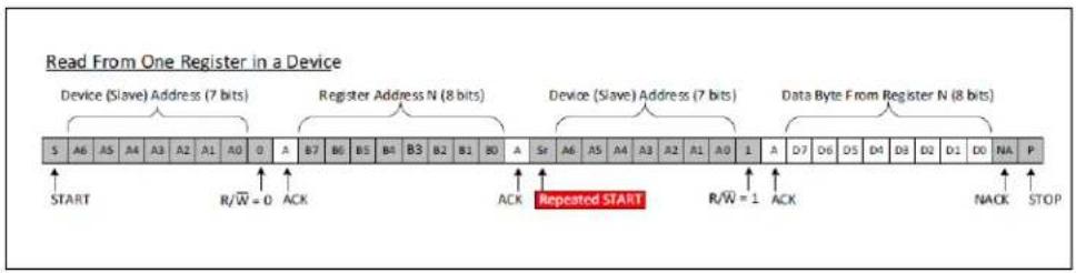
Read From One Register in a Device Device (Slave) Address (7 bits) Register Address N (8 bits) Device (Slave) Address (7 bits) Data Byte From Register N (8 bits) START R/W = 0 ACK Repeated START R/W = 1 ACK NACK STOPFIGURE 2-3: I ^2 C Read From a (Slave) Register.
TABLE 2-7: COMMANDS TO CHANGE OUTPUT FREQUENCY
| # Command Note/Comment | ||
| 1 Set CS_low Very first command to issue | that will set CS_low | |
| 2 | Write 0x0 into register 0x12 | Reset register 0x12 to 0 in order to select frequency bank 0 |
| 3 Write N value to register 0x15 7 bits only, | bits7:1 | |
| 4 Write F value into register 0x14 and bit0 of register 0x15 | MSB of F value goes to bit0 of register 0x15Next 8 bits go to register 0x14Least 8 bits (7:0) are automatically truncated | |
| 5 Write M1 value into register 0x16 — | ||
| 6 Write M2 value into register 0x17 — | ||
| 7 Repeat 3-6 for each desired output frequency | — | |
2.5 SPI BUS CONTROL INTERFACE
The DSC22XX can be used as a read/write slave device that conforms to SPI bus link protocol. The DSC22XX employs the standard four pin SPI bus configuration. The SS (Chip Select) signal (Active Low) enables communications with DSC22XX. The bus transmits full duplex synchronous data over the MOSI (Master Out Slave In) and MISO (Master In Slave Out) pins. Data is clocked by SCLK. MISO can be tri-stated (high impedance) to permit multiple devices to share the bus.
The DSC22XX uses standard SPI data structures and timing sequences. SPI commands should be preceded by 4 idle/setup cycles with the SS pin held high. This should be followed by asserting SS (taking it low) and transmitting data on the MOSI pin MSB first. The first data consists of a 7-bit register address appended with a read/write selection bit in the LSB position (1=Read, 0=Write).
Figure 2-4 displays the SPI timing diagram and specification.

text_image
Clock Edge 0 1 tCH 2 3 tCL 4 5 6 7 CLK CS tCSHD tCH tCSWH DIN D0 D1 D2 D3 D4 D5 D6 D7 tDO DOUT D0 D1 D2 D3 D4 D5 D6 D7 (prev) (prev) (prev) (prev) (prev) (prev) (prev) (prev)FIGURE 2-4: SPI Timing Diagram.
TABLE 2-8: SPI TIMING SPECIFICATION
| Parameter Symbol | Min Max Unit | |||
| SCLK t | SCL | — | 2 | 0 |
| Low Period SCLK t | LOW | 25 — ns | ||
| High Period SCLK | t_HIGH | 25 — ns | ||
| DIN Set-Up Time | t_DS | 10 — ns | ||
| DIN Hold Time | t_DH | 0 | — | ns |
| SCLK Fall to DOUT Valid | t_DO | — | 2 | 2 |
| SCLK High to CS High Hold | t_CSH1 | 22 — ns | ||
| SCLK High to CS Low Hold | t_CSH0 | 0 | — | ns |
| CS Low to SCLK High Setup | t_CSS0 | 10 — ns | ||
| CS High to SCLK High Setup | t_CSS0 | 5 | — | ns |
| CS Pulse Width High | t_CSS1 | 10 — ns |
Figure 2-5 and Figure 2-6 displays example SPI communications.
text_image
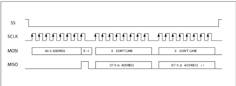
SS SCLK MOSI A6-0 ADDRESS R=1 X - DON'T CARE X - DON'T CARE MISO D7-0 @ ADDRESS D7-0 @ ADDRESS +1FIGURE 2-5: Example SPI Read Operation.
text_image
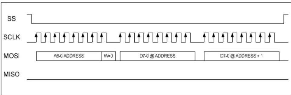
SS SCLK MOSI A6-0 ADDRESS W=0 D7-0 @ ADDRESS D7-0 @ ADDRESS + 1 MISOFIGURE 2-6: Example SPI Write Operation.
Worldwide Sales and Service
AMERICAS
Corporate Office
2355 West Chandler Blvd.
Chandler, AZ 85224-6199
Tel: 480-792-7200
Fax: 480-792-7277
Technical Support:
http://www.microchip.com/
support
Web Address:
www.microchip.com
Atlanta
Duluth, GA
Tel: 678-957-9614
Fax: 678-957-1455
Austin, TX
Tel: 512-257-3370
Boston
Westborough, MA
Tel: 774-760-0087
Fax: 774-760-0088
Chicago
Itasca, IL
Tel: 630-285-0071
Fax: 630-285-0075
Dallas
Addison, TX
Tel: 972-818-7423
Fax: 972-818-2924
Detroit
Novi, MI
Tel: 248-848-4000
Houston, TX
Tel: 281-894-5983
Indianapolis
Noblesville, IN
Tel: 317-773-8323
Fax: 317-773-5453
Tel: 317-536-2380
Los Angeles
Mission Viejo, CA
Tel: 949-462-9523
Fax: 949-462-9608
Tel: 951-273-7800
Raleigh, NC
Tel: 919-844-7510
New York, NY
Tel: 631-435-6000
San Jose, CA
Tel: 408-735-9110
Tel: 408-436-4270
Canada - Toronto
Tel: 905-695-1980
Fax: 905-695-2078
ASIA/PACIFIC
Australia - Sydney
Tel: 61-2-9868-6733
China - Beijing
Tel: 86-10-8569-7000
China - Chengdu
Tel: 86-28-8665-5511
China - Chongqing
Tel: 86-23-8980-9588
China - Dongguan
Tel: 86-769-8702-9880
China - Guangzhou
Tel: 86-20-8755-8029
China - Hangzhou
Tel: 86-571-8792-8115
China - Hong Kong SAR
Tel: 852-2943-5100
China - Nanjing
Tel: 86-25-8473-2460
China - Qingdao
Tel: 86-532-8502-7355
China - Shanghai
Tel: 86-21-3326-8000
China - Shenyang
Tel: 86-24-2334-2829
China - Shenzhen
Tel: 86-755-8864-2200
China - Suzhou
Tel: 86-186-6233-1526
China - Wuhan
Tel: 86-27-5980-5300
China - Xian
Tel: 86-29-8833-7252
China - Xiamen
Tel: 86-592-2388138
China - Zhuhai
Tel: 86-756-3210040
ASIA/PACIFIC
India - Bangalore
Tel: 91-80-3090-4444
India - New Delhi
Tel: 91-11-4160-8631
India - Pune
Tel: 91-20-4121-0141
Japan - Osaka
Tel: 81-6-6152-7160
Japan - Tokyo
Tel: 81-3-6880-3770
Korea - Daegu
Tel: 82-53-744-4301
Korea - Seoul
Tel: 82-2-554-7200
Malaysia - Kuala Lumpur
Tel: 60-3-7651-7906
Malaysia - Penang
Tel: 60-4-227-8870
Philippines - Manila
Tel: 63-2-634-9065
Singapore
Tel: 65-6334-8870
Taiwan - Hsin Chu
Tel: 886-3-577-8366
Taiwan - Kaohsiung
Tel: 886-7-213-7830
Taiwan - Taipei
Tel: 886-2-2508-8600
Thailand - Bangkok
Tel: 66-2-694-1351
Tel: 43-7242-2244-39
Fax: 43-7242-2244-393
Denmark - Copenhagen
Tel: 45-4450-2828
Fax: 45-4485-2829
Finland - Espoo
Tel: 358-9-4520-820
France - Paris
Tel: 33-1-69-53-63-20
Fax: 33-1-69-30-90-79
Germany - Garching
Tel: 49-8931-9700
Germany - Haan
Tel: 49-2129-3766400
Germany - Heilbronn
Tel: 49-7131-67-3636
Germany - Karlsruhe
Tel: 49-721-625370
Germany - Munich
Tel: 49-89-627-144-0
Fax: 49-89-627-144-44
Germany - Rosenheim
Tel: 49-8031-354-560
Israel - Ra'anana
Tel: 972-9-744-7705
Italy - Milan
Tel: 39-0331-742611
Fax: 39-0331-466781
Italy - Padova
Tel: 39-049-7625286
Netherlands - Drunen
Tel: 31-416-690399
Fax: 31-416-690340
Norway - Trondheim
Tel: 47-7289-7561
Poland - Warsaw
Tel: 48-22-3325737
Romania - Bucharest
Tel: 40-21-407-87-50
Spain - Madrid
Tel: 34-91-708-08-90
Fax: 34-91-708-08-91
Sweden - Gothenberg
Tel: 46-31-704-60-40
Sweden - Stockholm
Tel: 46-8-5090-4654
UK - Wokingham
Tel: 44-118-921-5800
Fax: 44-118-921-5820