ATmega48PB - Microcontroller Microchip - Free user manual and instructions
Find the device manual for free ATmega48PB Microchip in PDF.

User questions about ATmega48PB Microchip
0 question about this device. Answer the ones you know or ask your own.
Ask a new question about this device
Download the instructions for your Microcontroller in PDF format for free! Find your manual ATmega48PB - Microchip and take your electronic device back in hand. On this page are published all the documents necessary for the use of your device. ATmega48PB by Microchip.
USER MANUAL ATmega48PB Microchip
AVR® Instruction Set Manual
Introduction
This manual gives an overview and explanation of every instruction available for 8-bit AVR ^® devices. Each instruction has its own section containing functional description, it's opcode, and syntax, the end state of the status register, and cycle times.
The manual also contains an explanation of the different addressing modes used by AVR devices and an appendix listing all modern AVR devices and what instruction it has available.
Table of Contents
Introduction....1
-
Instruction Set Nomenclature....6
-
CPU Registers Located in the I/O Space....8
2.1. RAMPX, RAMPY, and RAMPZ....8
2.2. RAMPD....8
2.3. EIND....8
- The Program and Data Addressing Modes....9
3.1. Register Direct, Single Register Rd....9
3.2. Register Direct - Two Registers, Rd and Rr....9
3.3. I/O Direct....10
3.4. Data Direct.... 10
3.5. Data Indirect....11
3.6. Data Indirect with Pre-decrement....11
3.7. Data Indirect with Post-increment.... 12
3.8. Data Indirect with Displacement....12
3.9. Program Memory Constant Addressing using the LPM, ELPM, and SPM Instructions.... 13
3.10. Program Memory with Post-increment using the LPM Z+ and ELPM Z+ Instruction.... 13
3.11. Store Program Memory Post-increment....14
3.12. Direct Program Addressing, JMP and CALL....14
3.13. Indirect Program Addressing, IJMP and ICALL....15
3.14. Extended Indirect Program Addressing, EIJMP and EICALL....15
3.15. Relative Program Addressing, RJMP and RCALL.... 16
- Conditional Branch Summary...... 17
- Instruction Set Summary......18
- Instruction Description....24
6.1. ADC – Add with Carry....24
6.2. ADD – Add without Carry.... 25
6.3. ADIW – Add Immediate to Word....26
6.4. AND – Logical AND....27
6.5. ANDI – Logical AND with Immediate....28
6.6. ASR – Arithmetic Shift Right.... 29
6.7. BCLR – Bit Clear in SREG....30
6.8. BLD – Bit Load from the T Bit in SREG to a Bit in Register.... 31
6.9. BRBC – Branch if Bit in SREG is Cleared....32
6.10. BRBS – Branch if Bit in SREG is Set....33
6.11. BRCC – Branch if Carry Cleared....34
6.12. BRCS – Branch if Carry Set....35
6.13. BREAK-Break 36
6.14. BREQ - Branch if Equal....36
6.15. BRGE – Branch if Greater or Equal (Signed)....37
6.16. BRHC – Branch if Half Carry Flag is Cleared....38
6.17. BRHS – Branch if Half Carry Flag is Set....39
6.18. BRID – Branch if Global Interrupt is Disabled....40
6.19. BRIE – Branch if Global Interrupt is Enabled....41
6.20. BRLO - Branch if Lower (Unsigned)....42
6.21. BRLT – Branch if Less Than (Signed)......43
6.22. BRMI – Branch if Minus....44
6.23. BRNE - Branch if Not Equal 45
6.24. BRPL – Branch if Plus....46
6.25. BRSH – Branch if Same or Higher (Unsigned)...... 47
6.26. BRTC - Branch if the T Bit is Cleared....48
6.27. BRTS - Branch if the T Bit is Set....49
6.28. BRVC - Branch if Overflow Cleared.... 50
6.29. BRVS – Branch if Overflow Set....51
6.30. BSET-Bit Set in SREG 52
6.31. BST - Bit Store from Bit in Register to T Bit in SREG....53
6.32. CALL – Long Call to a Subroutine....54
6.33. CBI – Clear Bit in I/O Register....55
6.34. CBR – Clear Bits in Register....56
6.35. CLC – Clear Carry Flag....57
6.36. CLH – Clear Half Carry Flag.... 57
6.37. CLI – Clear Global Interrupt Enable Bit....58
6.38. CLN - Clear Negative Flag.... 59
6.39. CLR - Clear Register....60
6.40. CLS – Clear Sign Flag....61
6.41. CLT - Clear T Bit....62
6.42. CLV - Clear Overflow Flag....62
6.43. CLZ – Clear Zero Flag....63
6.44.COM-One's Complement 64
6.45. CP- Compare....65
6.46. CPC - Compare with Carry....66
6.47. CPI – Compare with Immediate.... 67
6.48. CPSE - Compare Skip if Equal....68
6.49. DEC - Decrement....69
6.50. DES – Data Encryption Standard....71
6.51. EICALL – Extended Indirect Call to Subroutine....72
6.52. EIJMP - Extended Indirect Jump....73
6.53. ELPM – Extended Load Program Memory....73
6.54. EOR – Exclusive OR....75
6.55. FMUL - Fractional Multiply Unsigned.... 76
6.56. FMULS - Fractional Multiply Signed....77
6.57. FMULSU - Fractional Multiply Signed with Unsigned....79
6.58. ICALL – Indirect Call to Subroutine....80
6.59. IJMP – Indirect Jump....81
6.60. IN - Load an I/O Location to Register 82
6.61. INC – Increment....83
6.62. JMP – Jump....84
6.63. LAC – Load and Clear....85
6.64. LAS – Load and Set 86
6.65. LAT – Load and Toggle....86
6.66. LD - Load Indirect from Data Space to Register using X....87
6.67. LD (LDD) – Load Indirect from Data Space to Register using Y.... 89
6.68. LD (LDD) – Load Indirect From Data Space to Register using Z.... 90
6.69. LDI – Load Immediate....92
6.70. LDS – Load Direct from Data Space....93
6.71. LDS (AVRrc) – Load Direct from Data Space.... 94
6.72. LPM – Load Program Memory....95
6.73. LSL - Logical Shift Left.... 96
6.74. LSR – Logical Shift Right.... 97
6.75.MOV-CopyRegister 98
6.76. MOVW - Copy Register Word....99
6.77. MUL - Multiply Unsigned.... 100
6.78. MULS – Multiply Signed....101
6.79. MULSU - Multiply Signed with Unsigned....102
6.80. NEG - Two's Complement.... 103
6.81. NOP - No Operation.... 104
6.82. OR - Logical OR.... 105
6.83. ORI - Logical OR with Immediate....106
6.84. OUT – Store Register to I/O Location.... 107
6.85. POP – Pop Register from Stack....108
6.86. PUSH – Push Register on Stack....109
6.87. RCALL - Relative Call to Subroutine.... 110
6.88. RET – Return from Subroutine.... 111
6.89. RETI – Return from Interrupt.... 112
6.90. RJMP - Relative Jump.... 113
6.91. ROL – Rotate Left trough Carry....114
6.92. ROR - Rotate Right through Carry....115
6.93. SBC – Subtract with Carry....116
6.94. SBCI – Subtract Immediate with Carry SBI – Set Bit in I/O Register.... 117
6.95. SBI – Set Bit in I/O Register.... 118
6.96. SBIC - Skip if Bit in I/O Register is Cleared.... 119
6.97. SBIS - Skip if Bit in I/O Register is Set.... 120
6.98. SBIW – Subtract Immediate from Word.... 121
6.99. SBR – Set Bits in Register.... 122
6.100. SBRC - Skip if Bit in Register is Cleared....123
6.101. SBRS - Skip if Bit in Register is Set.... 124
6.102. SEC – Set Carry Flag....125
6.103. SEH – Set Half Carry Flag.... 126
6.104. SEI – Set Global Interrupt Enable Bit....127
6.105. SEN – Set Negative Flag.... 128
6.106. SER - Set all Bits in Register....128
6.107. SES - Set Sign Flag.... 129
6.108. SET – Set T Bit.... 130
6.109. SEV – Set Overflow Flag.... 131
6.110. SEZ – Set Zero Flag....132
6.111. SLEEP....132
6.112. SPM (AVRe) – Store Program Memory....133
6.113. SPM (AVRxm, AVRxt) – Store Program Memory....135
6.114. ST – Store Indirect From Register to Data Space using Index X.... 136
6.115. ST (STD) – Store Indirect From Register to Data Space using Index Y.... 138
6.116. ST (STD) – Store Indirect From Register to Data Space using Index Z....140
6.117. STS – Store Direct to Data Space....141
6.118. STS (AVRrc) – Store Direct to Data Space.... 142
6.119. SUB – Subtract Without Carry....143
6.120. SUBI – Subtract Immediate....144
6.121. SWAP – Swap Nibbles....145
6.122. TST - Test for Zero or Minus.... 146
6.123.WDR-Watchdog Reset 147
6.124. XCH – Exchange....148
7. Appendix A Device Core Overview....149
7.1. Core Descriptions....149
7.2. Device Tables....150
8. Revision History.... 161
8.1. Rev. DS40002198B - 02/2021....161
8.2. Rev. DS40002198A - 05/2020....161
8.3. Rev.0856L - 11/2016.... 161
8.4. Rev.0856K - 04/2016....161
8.5. Rev.0856J - 07/2014.... 161
8.6. Rev.0856I - 07/2010.... 161
8.7. Rev.0856H - 04/2009....162
8.8. Rev.0856G - 07/2008....162
8.9. Rev.0856F - 05/2008....162
The Microchip Website....163
Product Change Notification Service....163
Customer Support....163
Microchip Devices Code Protection Feature....163
Legal Notice....164
Trademarks....164
Quality Management System.... 165
Worldwide Sales and Service....166
1. Instruction Set Nomenclature
Status Register (SREG)
SREG Status Register
C Carry Flag
Z Zero Flag
N Negative Flag
V Two's Complement Overflow Flag
S Sign Flag
H Half Carry Flag
T Transfer Bit
I Global Interrupt Enable Bit
Registers and Operands
Rd: Destination (and source) register in the Register File
Rr: Source register in the Register File
R: Result after instruction is executed
K: Constant data
k: Constant address
b: Bit position (0..7) in the Register File or I/O Register
s: Bit position (0..7) in the Status Register
X,Y,Z: Indirect Address Register (X=R27:R26, Y=R29:R28, and Z=R31:R30 or X=RAMPX:R27:R26, Y=RAMPY:R29:R28, and Z=RAMPZ:R31:R30 if the memory is larger than 64 KB)
A: I/O memory address
q: Displacement for direct addressing
UU Unsigned × Unsigned operands
SS Signed × Signed operands
SU Signed × Unsigned operands
Memory Space Identifiers
DS() Represents a pointer to address in data space
PS() Represents a pointer to address in program space
I/O(A) I/O space address A
I/O(A,b) Bit position b of the byte in I/O space address A
Rd(n) Bit n in register Rd
Operator
✗ Arithmetic multiplication
- Arithmetic addition
- Arithmetic subtraction
^ Logical AND
v Logical OR
⊕ Logical XORShift right
<< Shift left
== Comparison
← Assignment
↔ Swap
Logical complement of x (NOT x)
Stack
STACK Stack for return address and pushed registers
SP The Stack Pointer
Flags
Flag affected by instruction
0 Flag cleared by instruction
1 Flag set by instruction
- Flag not affected by instruction
2. CPU Registers Located in the I/O Space
2.1 RAMPX, RAMPY, and RAMPZ
Registers concatenated with the X-, Y-, and Z-registers enabling indirect addressing of the whole data space on MCUs with more than 64 KB data space, and constant data fetch on MCUs with more than 64 KB program space.
2.2 RAMPD
Register concatenated with the Z-register enabling direct addressing of the whole data space on MCUs with more than 64 KB data space.
2.3 EIND
Register concatenated with the Z-register enabling indirect jump and call to the whole program space on MCUs with more than 64K words (128 KB) program space.
3. The Program and Data Addressing Modes
The AVR ^® Enhanced RISC microcontroller supports powerful and efficient addressing modes for access to the program memory (Flash) and Data memory (SRAM, Register file, I/O Memory, and Extended I/O Memory). This section describes the various addressing modes supported by the AVR architecture. In the following figures, OP means the operation code part of the instruction word. To simplify, not all figures show the exact location of the addressing bits. To generalize, the abstract terms RAMEND and FLASHEND have been used to represent the highest location in data and program space, respectively.
Note: Not all addressing modes are present in all devices. Refer to the device specific instruction summary.
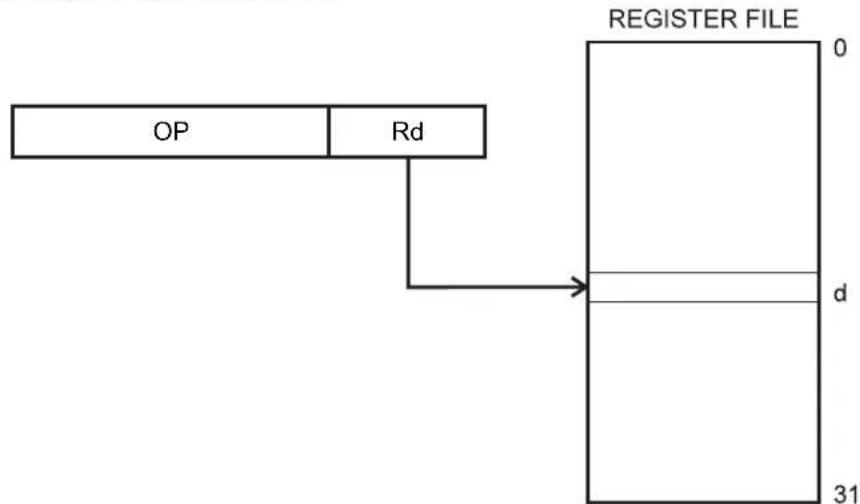
3.1 Register Direct, Single Register Rd
Figure 3-1. Direct Single Register Addressing
flowchart
graph TD
    A["OP"] --> B["Rd"]
    B --> C["REGISTER FILE"]
    C --> D["d"]
    C --> E["31"]
The operand is contained in the destination register (Rd).
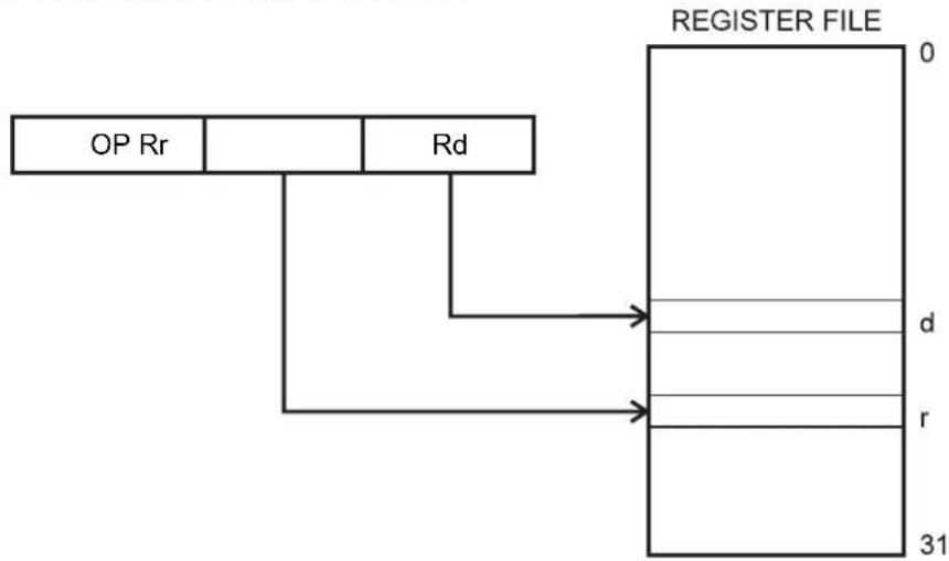
3.2 Register Direct - Two Registers, Rd and Rr
Figure 3-2. Direct Register Addressing, Two Registers
flowchart
graph TD
    A["OP Rr"] --> B["Rd"]
    B --> C["REGISTER FILE"]
    C --> D["d"]
    C --> E["r"]
    C --> F["31"]
Operands are contained in the sources register (Rr) and destination register (Rd). The result is stored in the destination register (Rd).
3.3 I/O Direct
Figure 3-3. I/O Direct Addressing

flowchart
graph TD
    A["OP"] --> B["Rr/Rd A"]
    B --> C["I/O MEMORY"]
    C --> D["63"]
Operand address A is contained in the instruction word. Rr/Rd specify the destination or source register.
Note: Some AVR microcontrollers have more peripheral units than can be supported within the 64 locations reserved in the opcode for I/O direct addressing. The extended I/O memory from address 64 and higher can only be reached by data addressing, not I/O addressing.
3.4 Data Direct
Figure 3-4. Direct Data Addressing

flowchart
graph TD
    A["OP"] --> B["Data Address"]
    C["Rr/Rd"] --> B
    B --> D["Data Space 0x0000"]
A 16-bit Data Address is contained in the 16 LSBs of a two-word instruction. Rd/Rr specify the destination or source register. The LDS instruction uses the RAMPD register to access memory above 64 KB.
3.5 Data Indirect
Figure 3-5. Data Indirect Addressing

flowchart
graph TD
    A["X, Y OR Z - POINTER"] --> B["Data Space"]
    B --> C["0x0000"]
The operand address is the contents of the X-, Y-, or the Z-pointer. In AVR devices without SRAM, Data Indirect Addressing is called Register Indirect Addressing.
3.6 Data Indirect with Pre-decrement
Figure 3-6. Data Indirect Addressing with Pre-decrement

flowchart
graph TD
    A["X, Y OR Z - POINTER"] --> B["+"]
    C["-1"] --> B
    B --> D["Data Space 0x0000"]
    D --> E["Feedback to +"]
The X,- Y-, or the Z-pointer is decremented before the operation. The operand address is the decremented contents of the X-, Y-, or the Z-pointer.
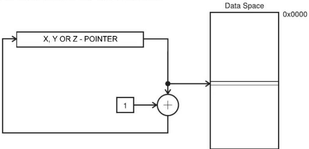
3.7 Data Indirect with Post-increment
Figure 3-7. Data Indirect Addressing with Post-increment
flowchart
graph TD
    A["X, Y OR Z - POINTER"] --> B["+"]
    C["1"] --> B
    B --> D["Data Space 0x0000"]
    D --> E["Output"]
The X-, Y-, or the Z-pointer is incremented after the operation. The operand address is the content of the X-, Y-, or the Z-pointer before incrementing.
3.8 Data Indirect with Displacement
Figure 3-8. Data Indirect with Displacement

flowchart
graph TD
    A["Y OR Z - POINTER"] --> C["+"]
    B["OP"] --> C
    D["Rr/Rd"] --> C
    E["q"] --> C
    C --> F["Data Space 0x0000"]
The operand address is the result of the q displacement contained in the instruction word added to the Y- or Z-pointer. Rd/Rr specify the destination or source register.
3.9 Program Memory Constant Addressing using the LPM, ELPM, and SPM Instructions
Figure 3-9. Program Memory Constant Addressing

flowchart
graph TD
    A["Z - POINTER"] --> B["LSb"]
    B --> C["PROGRAM MEMORY"]
    C --> D["0x0000"]
    C --> E["FLASHEND"]
Constant byte address is specified by the Z-pointer contents. The 15 MSbs select word address. For LPM, the LSb selects low byte if cleared (LSb == 0) or high byte if set (LSb == 1). For SPM, the LSb should be cleared. If ELPM is used, the RAMPZ Register is used to extend the Z-register.
3.10 Program Memory with Post-increment using the LPM Z+ and ELPM Z+ Instruction
Figure 3-10. Program Memory Addressing with Post-increment

flowchart
graph TD
    A["Z- POINTER"] -->|LSb| B["Program Memory"]
    C["1"] --> D["+"]
    D --> B
    B --> E["0x0000"]
    B --> F["FLASHEND"]
Constant byte address is specified by the Z-pointer contents. The 15 MSbs select word address. The LSb selects low byte if cleared (LSb == 0) or high byte if set (LSb == 1). If ELPM Z+ is used, the RAMPZ Register is used to extend the Z-register.
3.11 Store Program Memory Post-increment
Figure 3-11. Store Program Memory

flowchart
graph TD
    A["Z - POINTER"] --> B["+"]
    C["2"] --> B
    B --> D["PROGRAM MEMORY"]
    D --> E["0x0000"]
    D --> F["FLASHEND"]
The Z-pointer is incremented by 2 after the operation. Constant byte address is specified by the Z-pointer contents before incrementing. The 15 MSbs select word address and the LSb should be left cleared.
3.12 Direct Program Addressing, JMP and CALL
Figure 3-12. Direct Program Memory Addressing

flowchart
graph TD
    A["OP"] --> B["k"]
    B --> C["PC"]
    D["0x0000"] --> E["Flashend"]
    F["PROGRAM MEMORY"] --> G["0x0000"]
Program execution continues at the address immediate in the instruction word.
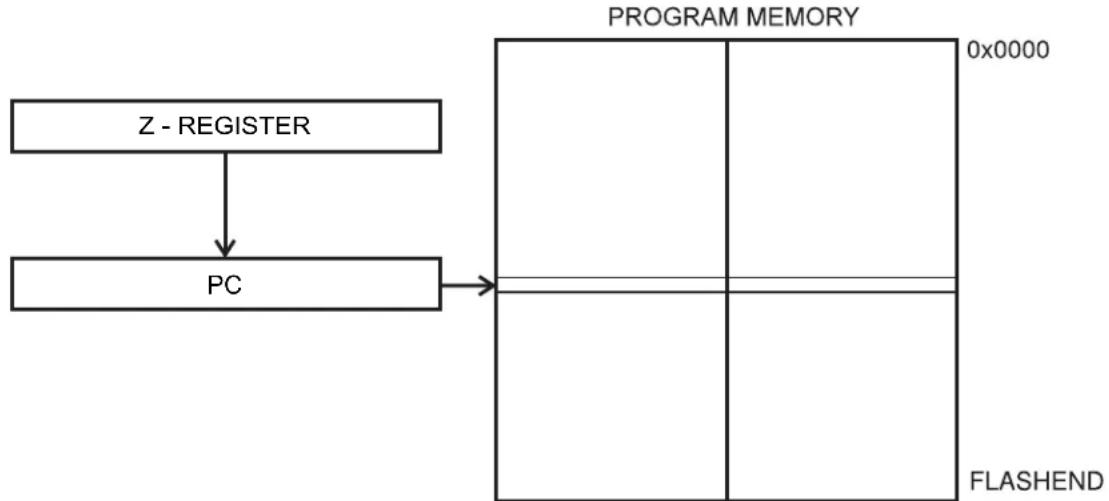
3.13 Indirect Program Addressing, IJMP and ICALL
Figure 3-13. Indirect Program Memory Addressing
flowchart
graph TD
    A["Z - REGISTER"] --> B["PC"]
    B --> C["PROGRAM MEMORY 0x0000"]
    C --> D["FLASHEND"]
Program execution continues at the address contained by the Z-register (i.e., the PC is loaded with the contents of the Z-register).
3.14 Extended Indirect Program Addressing, EIJMP and EICALL
Figure 3-14. Extended Indirect Program Memory Addressing
flowchart
graph TD
    A["EIND"] --> C["PC"]
    B["Z - REGISTER"] --> C["PC"]
    C --> D["PROGRAM MEMORY"]
    D --> E["0x0000"]
    D --> F["FLASHEND"]
Program execution continues at the address contained by the Z-register and the EIND-register (i.e., the PC is loaded with the contents of the EIND and Z-register).
3.15 Relative Program Addressing, RJMP and RCALL
Figure 3-15. Relative Program Memory Addressing
flowchart
graph TD
    A["PC"] --> C["+"]
    B["OP k"] --> C
    C --> D["0x0000 FLASHEND"]
    E["1"] --> C
    F["PROGRAM MEMORY"] --> D
Program execution continues at the address PC + k + 1. The relative address k is from -2048 to 2047.
- Conditional Branch Summary
| One Form Complement Form Comment | ||||||
| Mnemonic | Common Test | Status Register Mnemonic | Common Test | Status Register | ||
| BRGE | Rd ≥ Rr | S == 0 BRLT | Rd < Rr | S == 1 Signed | ||
| BRSH C == 0 BRLO C == 1 Unsigned | ||||||
| BRNE Rd ≠ Rr Z == 0 BREQ Rd == Rr Z == 1 Unsigned/Signed | ||||||
| BRBC | - | SREG(s) == 0 BRBS | - | SREG(s) == 1 - | ||
| BRCC C == 0 | BRCS C == 1 Simple | |||||
| BRPL | N == 0 | BRMI | N == 1 Simple | |||
| BRVC V == 0 | BRVS | V == 1 | Simple | |||
Note: The Status Register status is a result of the preceding instruction, for further information see instruction description. If the preceding instruction is CP, CPI, SUB, or SUBI, the branch will occur according to column 'Common Test'.
5. Instruction Set Summary
Several updates of the AVR CPU during its lifetime has resulted in different flavors of the instruction set, especially for the timing of the instructions. Machine code level of compatibility is intact for all CPU versions with very few exceptions related to the Reduced Core (AVRrc), though not all instructions are included in the instruction set for all devices. The table below contains the major versions of the AVR 8-bit CPUs. In addition to the different versions, there are differences depending on the size of the device memory map. Typically these differences are handled by a C/EC++ compiler, but users that are porting code should be aware that the code execution can vary slightly in the number of clock cycles.
Table 5-1. Versions of AVR® 8-bit CPU
| Name Description | |
| AVR Original instruction set from 1995 | |
| AVRe AVR instruction set extended with the Move Word (MOVW) instruction, and the Load Program Memory (LPM) instruction has been enhanced. Same timing as AVR. | |
| AVRe+ AVRe instruction set extended with the Multiply (xMULxx) instructions, and if applicable with the extended range instructions EICALL, EIJMP and ELPM. Same timing as AVR and AVRe. Thus, tables listing number of clock cycles do not distinguish between AVRe and AVRe+, and use AVRe to represent both. | |
| AVRxm AVRe+ instruction set extended with the Read Modify Write (RMW) and Data Encryption Standard (DES) instructions. SPM extended to include SPM Z+2. Significantly different timing compared to AVR, AVRe, AVRe+. | |
| AVRxt A combination of AVRe+ and AVRxm. Available instructions are the same as AVRe+, but the timing has been improved compared to AVR, AVRe, AVRe+ and AVRxm. | |
| AVRrc AVRrc has only 16 registers in its register file (R31-R16), and the instruction set is reduced. The timing is significantly different compared to the AVR, AVRe, AVRe+, AVRxm and AVRxt. Refer to the instruction set summary for further details. | |
Table 5-2. Arithmetic and Logic Instructions
| Mnemonic | Operands | Description Operation Flags | #Clocks AVRe | #Clocks AVRxm | #Clocks AVRxt | #Clocks AVRrc | |||||
| ADD | Rd, Rr | Add without Carry | Rd | ← | Rd + Rr | Z,C,N,V,S,H | 1 | 1 | 1 | 1 | |
| ADC | Rd, Rr | Add with Carry | Rd | ← | Rd + Rr + C | Z,C,N,V,S,H | 1 | 1 | 1 | 1 | |
| ADIW | Rd, K | Add Immediate to Word | R[d + 1]:Rd | ← | R[d + 1]:Rd + K | Z,C,N,V,S | 2 | 2 | 2 | N/A | |
| SUB | Rd, Rr | Subtract without Carry | Rd | ← | Rd - Rr | Z,C,N,V,S,H | 1 | 1 | 1 | 1 | |
| SUBI | Rd, K | Subtract Immediate | Rd | ← | Rd - K | Z,C,N,V,S,H | 1 | 1 | 1 | 1 | |
| SBC | Rd, Rr | Subtract with Carry | Rd | ← | Rd - Rr - C | Z,C,N,V,S,H | 1 | 1 | 1 | 1 | |
| SBCI | Rd, K | Subtract Immediate with Carry | Rd | ← | Rd - K - C | Z,C,N,V,S,H | 1 | 1 | 1 | 1 | |
| SBIW | Rd, K | Subtract Immediate from Word | R[d + 1]:Rd | ← | R[d + 1]:Rd - K | Z,C,N,V,S | 2 | 2 | 2 | N/A | |
| AND | Rd, Rr | Logical AND | Rd | ← | Rd ∧ Rr | Z,N,V,S | 1 | 1 | 1 | 1 | |
| ANDI | Rd, K | Logical AND with Immediate | Rd | ← | Rd ∧ K | Z,N,V,S | 1 | 1 | 1 | 1 | |
| OR | Rd, Rr | Logical OR | Rd | ← | Rd v Rr | Z,N,V,S | 1 | 1 | 1 | 1 | |
| ORI | Rd, K | Logical OR with Immediate | Rd | ← | Rd v K | Z,N,V,S | 1 | 1 | 1 | 1 | |
| EOR | Rd, Rr | Exclusive OR | Rd | ← | Rd ⊕ Rr | Z,N,V,S | 1 | 1 | 1 | 1 | |
| ......continued | ||||||||||
| Mnemonic Operands Description Operation Flags | #Clocks AVRe | #Clocks AVRxm | #Clocks AVRxt | #Clocks AVRrc | ||||||
| COM Rd One's Complement Rd ← 0xFF - Rd Z,C,N,V,S 1 1 1 1 | ||||||||||
| NEG Rd Two's Complement Rd ← 0x00 - Rd Z,C,N,V,S,H 1 1 1 1 | ||||||||||
| SBR | Rd,K | Set Bit(s) in Register | Rd | ← | Rd v K | Z,N,V,S | 1 | 1 | 1 | 1 |
| CBR | Rd,K | Clear Bit(s) in Register | Rd | ← | Rd ∧ (0xFFh - K) | Z,N,V,S | 1 | 1 | 1 | 1 |
| INC | Rd | Increment | Rd | ← | Rd + 1 | Z,N,V,S | 1 | 1 | 1 | 1 |
| DEC | Rd | Decrement | Rd | ← | Rd - 1 | Z,N,V,S | 1 | 1 | 1 | 1 |
| TST | Rd | Test for Zero or Minus | Rd | ← | Rd ∧ Rd | Z,N,V,S | 1 | 1 | 1 | 1 |
| CLR | Rd | Clear Register | Rd | ← | Rd ⊕ Rd | Z,N,V,S | 1 | 1 | 1 | 1 |
| SER | Rd | Set Register | Rd | ← | 0xFF | None | 1 | 1 | 1 | 1 |
| MUL | Rd,Rr | Multiply Unsigned | R1:R0 | ← | Rd x Rr (UU) | Z,C | 2 | 2 | 2 | N/A |
| MULS | Rd,Rr | Multiply Signed | R1:R0 | ← | Rd x Rr (SS) | Z,C | 2 | 2 | 2 | N/A |
| MULSU | Rd,Rr | Multiply Signed with Unsigned | R1:R0 ← Rd x Rr (SU) | Z,C | 2 2 2 N/A | |||||
| FMUL | Rd,Rr | Fractional Multiply Unsigned | R1:R0 ← Rd x Rr<<1 (UU) | Z,C | 2 2 2 N/A | |||||
| FMULS | Rd,Rr | Fractional Multiply Signed | R1:R0 | ← | Rd x Rr<<1 (SS) | Z,C | 2 | 2 | 2 | N/A |
| FMULSU | Rd,Rr | Fractional Multiply Signed with Unsigned | R1:R0 ← Rd x Rr<<1 (SU) | Z,C | 2 2 2 N/A | |||||
| DES K | Data Encryption if (H == 0), R15:R0 ← Encrypt(R15:R0, K)if (H == 1), R15:R0 ← Decrypt(R15:R0, K) | N/A | 1 / 2 | N/A | N/A | |||||
Table 5-3. Change of Flow Instructions
| Mnemonic | Operands | Description | Operation | Flags | #Clocks AVRe | #Clocks AVRxm | #Clocks AVRxt | #Clocks AVRrc | ||
| RJMP | k | Relative Jump | PC | ← | PC + k + 1 | None | 2 | 2 | 2 | 2 |
| IJMP | Indirect Jump to (Z) | PC(15:0) | ← | Z | None | 2 | 2 | 2 | 2 | |
| PC(21:16) | ← | 0 | ||||||||
| EIJMP | Extended Indirect Jump to (Z) | PC(15:0) | ← | Z | None | 2 | 2 | 2 | N/A | |
| PC(21:16) | ← | EIND | ||||||||
| JMP | k | Jump | PC | ← | k | None | 3 | 3 | 3 | N/A |
| RCALL | k | Relative Call Subroutine | PC | ← | PC + k + 1 | None | 3/4^(1) | 2/3^(1) | 2/3 | 3 |
| ICALL | Indirect Call to (Z) | PC(15:0) | ← | Z | None | 3/4^(1) | 2/3^(1) | 2/3 | 3 | |
| PC(21:16) | ← | 0 | ||||||||
| EICALL | Extended Indirect Call to (Z) | PC(15:0) | ← | Z | None | 4^(1) | 3^(1) | 3 | N/A | |
| PC(21:16) | ← | EIND | ||||||||
| CALL | k | Call Subroutine | PC | ← | k | None | 4/5^(1) | 3/4^(1) | 3/4 | N/A |
| RET | Subroutine Return | PC | ← | STACK | None | 4/5^(1) | 4/5^(1) | 4/5 | 6 | |
| RETI | Interrupt Return | PC | ← | STACK | I | 4/5^(1) | 4/5^(1) | 4/5 | 6 | |
| CPSE | Rd,Rr | Compare, skip if Equal | if (Rd == Rr) PC | ← | PC + 2 or 3 | None | 1/2/3 | 1/2/3 | 1/2/3 | 1/2 |
| CP | Rd,Rr | Compare | Rd - Rr | Z,C,N,V,S,H | 1 | 1 | 1 | 1 | ||
| CPC | Rd,Rr | Compare with Carry | Rd - Rr - C | Z,C,N,V,S,H | 1 | 1 | 1 | 1 | ||
| ......continued | |||||||||
| Mnemonic Operands Description Operation Flags | #Clocks AVRe | #Clocks AVRxm | #Clocks AVRxt | ||||||
| CPI Rd,K Compare with Immediate Rd - K Z,C,N,V,S,H 1 1 1 1 | |||||||||
| SBRC | Rr, b | Skip if Bit in Register Cleared | if (Rr(b) == 0) PC | ← | PC + 2 or 3 | None | 1/2/3 | 1/2/3 | 1/2/3 |
| SBRS | Rr, b | Skip if Bit in Register Set | if (Rr(b) == 1) PC | ← | PC + 2 or 3 | None | 1/2/3 | 1/2/3 | 1/2/3 |
| SBIC | A, b | Skip if Bit in I/O Register Cleared | if (I/O(A,b) == 0) PC | ← | PC + 2 or 3 | None | 1/2/3 | 2/3/4 | 1/2/3 |
| SBIS | A, b | Skip if Bit in I/O Register Set | If (I/O(A,b) == 1) PC | ← | PC + 2 or 3 | None | 1/2/3 | 2/3/4 | 1/2/3 |
| BRBS | s, k | Branch if Status Flag Set | if (SREG(s) == 1) then PC | ← | PC + k + 1 | None | 1/2 | 1/2 | 1/2 |
| BRBC s, k | Branch if Status Flag Cleared | if (SREG(s) == 0) then PC | ← | PC + k + 1 | None | 1/2 | 1/2 | 1/2 | 1/2 |
| BREQ | k | Branch if Equal | if (Z == 1) then PC | ← | PC + k + 1 | None | 1/2 | 1/2 | 1/2 |
| BRNE | k | Branch if Not Equal | if (Z == 0) then PC | ← | PC + k + 1 | None | 1/2 | 1/2 | 1/2 |
| BRCS | k | Branch if Carry Set | if (C == 1) then PC | ← | PC + k + 1 | None | 1/2 | 1/2 | 1/2 |
| BRCC | k | Branch if Carry Cleared | if (C == 0) then PC | ← | PC + k + 1 | None | 1/2 | 1/2 | 1/2 |
| BRSH | k | Branch if Same or Higher | if (C == 0) then PC | ← | PC + k + 1 | None | 1/2 | 1/2 | 1/2 |
| BRLO | k | Branch if Lower | if (C == 1) then PC | ← | PC + k + 1 | None | 1/2 | 1/2 | 1/2 |
| BRMI | k | Branch if Minus | if (N == 1) then PC | ← | PC + k + 1 | None | 1/2 | 1/2 | 1/2 |
| BRPL | k | Branch if Plus | if (N == 0) then PC | ← | PC + k + 1 | None | 1/2 | 1/2 | 1/2 |
| BRGE | k | Branch if Greater or Equal, Signed | if (S == 0) then PC | ← | PC + k + 1 | None | 1/2 | 1/2 | 1/2 |
| BRLT | k | Branch if Less Than, Signed | if (S == 1) then PC | ← | PC + k + 1 | None | 1/2 | 1/2 | 1/2 |
| BRHS | k | Branch if Half Carry Flag Set | if (H == 1) then PC | ← | PC + k + 1 | None | 1/2 | 1/2 | 1/2 |
| BRHC | k | Branch if Half Carry Flag Cleared | if (H == 0) then PC | ← | PC + k + 1 | None | 1/2 | 1/2 | 1/2 |
| BRTS | k | Branch if T Bit Set | if (T == 1) then PC | ← | PC + k + 1 | None | 1/2 | 1/2 | 1/2 |
| BRTC | k | Branch if T Bit Cleared | if (T == 0) then PC | ← | PC + k + 1 | None | 1/2 | 1/2 | 1/2 |
| BRVS | k | Branch if Overflow Flag is Set | if (V == 1) then PC | ← | PC + k + 1 | None | 1/2 | 1/2 | 1/2 |
| BRVC k | Branch if Overflow Flag is Cleared | if (V == 0) then PC | ← | PC + k + 1 | None | 1/2 | 1/2 | 1/2 | 1/2 |
| BRIE | k | Branch if Interrupt Enabled | if (I == 1) then PC | ← | PC + k + 1 | None | 1/2 | 1/2 | 1/2 |
| BRID | k | Branch if Interrupt Disabled | if (I == 0) then PC | ← | PC + k + 1 | None | 1/2 | 1/2 | 1/2 |
Table 5-4. Data Transfer Instructions
| Mnemonic | Operands Description Operation Flags | #Clocks AVRe | #Clocks AVRxm | #Clocks AVRxt | #Clocks AVRrc | |||||
| MOV | Rd, Rr | Copy Register | Rd | ← | Rr | None | 1 | 1 | 1 | 1 |
| MOVW | Rd, Rr | Copy Register Pair | R[d + 1]:Rd | ← | R[r + 1]:Rr | None | 1 | 1 | 1 | N/A |
| LDI | Rd, K | Load Immediate | Rd | ← | K | None | 1 | 1 | 1 | 1 |
| LDS | Rd, k | Load Direct from Data Space | Rd | ← | DS(k) | None | 2(1) | 3(1)(3) | 3(2) | 2 |
| LD | Rd, X | Load Indirect | Rd | ← | DS(X) | None | 2(1) | 2(1)(3) | 2(2) | 1/2 |
| LD Rd, X+ | Load Indirect and Post-Increment | Rd | ← | DS(X) | None | 2(1) | 2(1)(3) | 2(2) | 2/3 | |
| X | ← | X + 1 | ||||||||
| LD Rd, -X | Load Indirect and Pre-Decrement | X | ← | X - 1 | None | 2(1) | 3(1)(3) | 2(2) | 2/3 | |
| Rd | ← | DS(X) | ||||||||
| Mnemonic Operands Description Operation Flags | #Clocks AVRe | #Clocks AVRxm | #Clocks AVRxt | #Clocks AVRrc | ||||||
| LD Rd, Y Load Indirect Rd ← DS(Y) None 2 | (1) | 2(1)(3) | 2(2) | 1/2 | ||||||
| LD Rd, Y+ Load Indirect and Post-Increment Rd | ← | DS(Y) | None 2 | (1) | 2(1)(3) | 2(2) | 2/3 | |||
| Y | ← | Y + 1 | ||||||||
| LD Rd, -Y Load Indirect and Pre-Decrement Y | ← | Y - 1 | None 2 | (1) | 3(1)(3) | 2(2) | 2/3 | |||
| Rd | ← | DS(Y) | ||||||||
| LDD Rd, Y+q | Load Indirect with Displacement Rd ← DS(Y + q) | None 2 | (1) | 3(1)(3) | 2(2) | N/A | ||||
| LD Rd, Z | Load Indirect Rd ← DS(Z) | None 2 | (1) | 2(1)(3) | 2(2) | 1/2 | ||||
| LD Rd, Z+ | Load Indirect and Post-Increment Rd | ← | DS(Z) | None 2 | (1) | 2(1)(3) | 2(2) | 2/3 | ||
| Z | ← | Z+1 | ||||||||
| LD Rd, -Z | Load Indirect and Pre-Decrement | Z | ← | Z - 1 | None 2 | (1) | 3(1)(3) | 2(2) | 2/3 | |
| Rd | ← | DS(Z) | ||||||||
| LDD Rd, Z+q | Load Indirect with Displacement Rd ← DS(Z + q) | None 2 | (1) | 3(1)(3) | 2(2) | N/A | ||||
| STS | k, Rr | Store Direct to Data Space | DS(k) | ← | Rd | None | 2(1) | 2(1) | 2(2) | |
| ST | X, Rr | Store Indirect | DS(X) | ← | Rr | None | 2(1) | 1(1) | 1(2) | |
| ST X+, Rr Store Indirect and Post-Increment | DS(X) | ← | Rr | None 2 | (1) | 1(1) | 1(2) | |||
| X | ← | X + 1 | ||||||||
| ST -X, Rr | Store Indirect and Pre-Decrement | X | ← | X - 1 | None 2 | (1) | 2(1) | 1(2) | 2 | |
| DS(X) | ← | Rr | ||||||||
| ST | Y, Rr | Store Indirect | DS(Y) | ← | Rr | None | 2(1) | 1(1) | 1(2) | |
| ST Y+, Rr Store Indirect and Post-Increment | DS(Y) | ← | Rr | None 2 | (1) | 1(1) | 1(2) | |||
| Y | ← | Y + 1 | ||||||||
| ST -Y, Rr Store Indirect and Pre-Decrement | Y | ← | Y - 1 | None 2 | (1) | 2(1) | 1(2) | |||
| DS(Y) | ← | Rr | ||||||||
| STD | Y+q, Rr | Store Indirect with Displacement | DS(Y + q) | ← | Rr | None | 2(1) | 2(1) | 1(2) | |
| ST | Z, Rr | Store Indirect | DS(Z) | ← | Rr | None | 2(1) | 1(1) | 1(2) | |
| ST Z+, Rr Store Indirect and Post-Increment | DS(Z) | ← | Rr | None 2 | (1) | 1(1) | 1(2) | |||
| Z | ← | Z + 1 | ||||||||
| ST -Z, Rr | Store Indirect and Pre-Decrement | Z | ← | Z - 1 | None 2 | (1) | 2(1) | 1(2) | ||
| DS(Z) | ← | Rr | ||||||||
| STD Z+q,Rr Store Indirect with Displacement | DS(Z + q) ← Rr | None 2 | (1) | 2(1) | 1(2) | |||||
| LPM | Load Program Memory | R0 | ← | PS(Z) | None | 3 | 3 | 3 | ||
| LPM | Rd, Z | Load Program Memory | Rd | ← | PS(Z) | None | 3 | 3 | 3 | |
| LPM | Rd, Z+ | Load Program Memory and Post-Increment | Rd | ← | PS(Z) | None | 3 3 3 | N/A | ||
| Z | ← | Z + 1 | ||||||||
| ELPM | Extended Load Program Memory | R0 | ← | PS(RAMPZ:Z) | None | 3 | 3 | 3 | ||
| ELPM | Rd, Z | Extended Load Program Memory | Rd | ← | PS(RAMPZ:Z) | None | 3 | 3 | 3 | |
| ELPM | Rd, Z+ | Extended Load Program Memory and Post-Increment | Rd (RAMPZ:Z) | ← | PS(RAMPZ:Z) (RAMPZ:Z) + 1 | None | 3 | 3 3 | N/A | |
| SPM | Store Program Memory | PS(RAMPZ:Z) | ← | R1:R0 | None | -(4) | -(4) | -(4) | ||
| SPM | Z+ | Store Program Memory and Post-Increment by 2 | PS(RAMPZ:Z) Z | ← ← | R1:R0 Z + 2 | None | N/A - | (4) | -(4) | |
| ......continued | ||||||||||
| Mnemonic Operands Description Operation Flags | #Clocks AVRe | #Clocks AVRxm | #Clocks AVRxt | #Clocks AVRrc | ||||||
| IN Rd, A In From I/O Location Rd ← I/O(A) None 1 1 1 1 | ||||||||||
| OUT A, Rr Out To I/O Location I/O(A) ← Rr None 1 1 1 1 | ||||||||||
| PUSH | Rr | Push Register on Stack | STACK | ← | Rr | None | 2 | 1^(1) | 1 | 1 |
| POP | Rd | Pop Register from Stack | Rd | ← | STACK | None | 2 | 2^(1) | 2 | 3 |
| XCH | Z, Rd | Exchange | DS(Z) | ↔ | Rd | None | N/A | 2 | N/A | N/A |
| LAS | Z, Rd | Load and Set | DS(Z) | ← | Rd v DS(Z) | None | N/A | 2 | N/A | N/A |
| Rd | ← | DS(Z) | ||||||||
| LAC | Z, Rd | Load and Clear | DS(Z) | ← | (0xFF - Rd) ∧ DS(Z) | None | N/A | 2 | N/A | N/A |
| Rd | ← | DS(Z) | ||||||||
| LAT | Z, Rd | Load and Toggle | DS(Z) | ← | Rd ⊕ DS(Z) | None | N/A | 2 | N/A | N/A |
| Rd | ← | DS(Z) | ||||||||
Table 5-5. Bit and Bit-Test Instructions
| Mnemonic | Operands Description Operation Flags | #Clocks AVRe | #Clocks AVRxm | #Clocks AVRxt | #Clocks AVRrc | |||||
| LSL | Rd Logical Shift Left | C | ← | Rd(7) | Z,C,N,V,H | 1 1 1 1 | ||||
| Rd(n+1) | ← | Rd(n), n=6...0 | ||||||||
| Rd(0) | ← | 0 | ||||||||
| LSR | Rd Logical Shift Right | C | ← | Rd(0) | Z,C,N,V | 1 1 1 1 | ||||
| Rd(n) | ← | Rd(n+1), n=0...6 | ||||||||
| Rd(7) | ← | 0 | ||||||||
| ROL | Rd Rotate Left Through Carry | temp | ← | C | Z,C,N,V,H | 1 1 1 1 | ||||
| C | ← | Rd(7) | ||||||||
| Rd(n+1) | ← | Rd(n), n=6...0 | ||||||||
| Rd(0) | ← | temp | ||||||||
| ROR | Rd Rotate Right Through Carry | temp | ← | C | Z,C,N,V | 1 1 1 1 | ||||
| C | ← | Rd(0) | ||||||||
| Rd(n) | ← | Rd(n+1), n=0...6 | ||||||||
| Rd(7) | ← | temp | ||||||||
| ASR | Rd Arithmetic Shift Right | C | ← | Rd(0) | Z,C,N,V | 1 1 1 1 | ||||
| Rd(n) | ← | Rd(n+1), n=0..6 | ||||||||
| Rd(7) | ← | Rd(7) | ||||||||
| SWAP | Rd Swap Nibbles | Rd(3..0) ↔ Rd(7..4) None 1 1 1 1 | ||||||||
| SBI | A, b | Set Bit in I/O Register | I/O(A, b) | ← | 1 | None | 2 | 1 | 1 | 1 |
| CBI | A, b | Clear Bit in I/O Register | I/O(A, b) | ← | 0 | None | 2 | 1 | 1 | 1 |
| BST | Rr, b | Bit Store from Register to T | T | ← | Rr(b) | T | 1 | 1 | 1 | 1 |
| BLD | Rd, b | Bit load from T to Register | Rd(b) | ← | T | None | 1 | 1 | 1 | 1 |
| BSET | s | Flag Set | SREG(s) | ← | 1 | SREG(s) | 1 | 1 | 1 | 1 |
| BCLR | s | Flag Clear | SREG(s) | ← | 0 | SREG(s) | 1 | 1 | 1 | 1 |
| SEC | Set Carry | C | ← | 1 | C | 1 | 1 | 1 | 1 | |
| CLC | Clear Carry | C | ← | 0 | C | 1 | 1 | 1 | 1 | |
| SEN | Set Negative Flag | N | ← | 1 | N | 1 | 1 | 1 | 1 | |
| ......continued | |||||||||
| Mnemonic Operands Description Operation Flags | #Clocks AVRe | #Clocks AVRxm | #Clocks AVRxt | #Clocks AVRrc | |||||
| CLN Clear Negative Flag N ← 0 N 1 1 1 1 | |||||||||
| SEZ Set Zero Flag Z ← 1 Z 1 1 1 1 | |||||||||
| CLZ Clear Zero Flag Z ← 0 Z 1 1 1 1 | |||||||||
| SEI | Global Interrupt Enable | I ← 1 | I | 1 | 1 | 1 | 1 | ||
| CLI | Global Interrupt Disable | I ← 0 | I | 1 | 1 | 1 | 1 | ||
| SES Set Sign Bit | S ← 1 S | 1 1 1 1 | |||||||
| CLS Clear Sign Bit | S ← 0 S | 1 1 1 1 | |||||||
| SEV Set Two's Complement Overflow | V ← 1 V | 1 1 1 1 | |||||||
| CLV Clear Two's Complement Overflow | V ← 0 V | 1 1 1 1 | |||||||
| SET Set T in SREG | T ← 1 T 1 1 1 1 | ||||||||
| CLT | Clear T in SREG | T ← 0 T 1 1 1 1 | |||||||
| SEH | Set Half Carry Flag in SREG | H ← 1 H 1 1 1 1 | |||||||
| CLH Clear Half Carry Flag in SREG | H ← 0 H 1 1 1 1 | ||||||||
Table 5-6. MCU Control Instructions
| Mnemonic | Operands | Description | Operation | Flags | #Clocks AVRe | #Clocks AVRxm | #Clocks AVRxt | #Clocks AVRrc |
| BREAK | Break | See the debug interface description | None | 1 | 1 | 1 | 1 | |
| NOP | No Operation | None | 1 | 1 | 1 | 1 | ||
| SLEEP | Sleep | See the power management and sleep description | None | 1 | 1 | 1 | 1 | |
| WDR | Watchdog Reset | See the Watchdog Controller description | None | 1 | 1 | 1 | 1 |
Notes:
- Cycle times for data memory access assume internal RAM access and are not valid for accessing external RAM.
- Cycle time for data memory access assumes internal RAM access, and are not valid for access to NVM. A minimum of one extra cycle must be added when accessing NVM. The additional time varies dependent on the NVM module implementation. See the NVMCTRL section in the specific devices data sheet for more information.
- If the LD instruction is accessing I/O Registers, one cycle can be deducted.
- Varies with the programming time of the device.
6. Instruction Description
6.1 ADC - Add with Carry
6.1.1 Description
Adds two registers and the contents of the C flag and places the result in the destination register Rd.
Operation:
(i) Rd ← Rd + Rr + C
Syntax: Operands: Program Counter:
(i) ADC Rd, Rr 0 ≤ d ≤ 31, 0 ≤ r ≤ 31 PC ← PC + 1
16-bit Opcode:
| 0001 11rd dddd rrrr |
6.1.2 Status Register (SREG) and Boolean Formula
H Rd3 ∧ Rr3 ∨ Rr3 ∧ R3 ∨ R3 ∧ Rd3
Set if there was a carry from bit 3; cleared otherwise.
S N ⊕ V, for signed tests.
V Rd7 ∧ Rr7 ∧ R7 ∨ Rd7 ∧ Rr7 ∧ R7
Set if two's complement overflow resulted from the operation; cleared otherwise.
N R7
Set if MSB of the result is set; cleared otherwise.
Z R7 ∧ R6 ∧ R5 ∧ R4 ∧ R3 ∧ R2 ∧ R1 ∧ R0
Set if the result is 0x00; cleared otherwise.
C Rd7 ∧ Rr7 ∨ Rr7 ∧ R7 ∨ R7 ∧ Rd7
Set if there was a carry from the MSB of the result; cleared otherwise.
R (Result) equals Rd after the operation.
Example:
| ; Add R1:R0 to R3:R2 | ||
| add | r2,r0 | ; Add low byte |
| adc | r3,r1 | ; Add with carry high byte |
Words
1 (2 bytes)
Table 6-1. Cycles
| Name Cycles | |
| AVRe 1 | |
| AVRxm 1 | |
| AVRxt 1 | |
| AVRrc 1 |
6.2 ADD – Add without Carry
6.2.1 Description
Adds two registers without the C flag and places the result in the destination register Rd.
Operation:
(i) (i) Rd ← Rd + Rr
Syntax: Operands: Program Counter:
(i) ADD Rd, Rr 0 ≤ d ≤ 31, 0 ≤ r ≤ 31 PC ← PC + 1
16-bit Opcode:
| 0000 11rd dddd rrrr |
6.2.2 Status Register (SREG) and Boolean Formula
H Rd3 ∧ Rr3 ∨ Rr3 ∧ R3 ∨ R3 ∧ Rd3
Set if there was a carry from bit 3; cleared otherwise.
S N ⊕ V, for signed tests.
V Rd7 ∧ Rr7 ∧ R7 ∨ Rd7 ∧ Rr7 ∧ R7
Set if two's complement overflow resulted from the operation; cleared otherwise.
N R7
Set if MSB of the result is set; cleared otherwise.
Set if the result is 0x00; cleared otherwise.
C Rd7 ∧ Rr7 ∨ Rr7 ∧ R7 ∨ R7 ∧ Rd7
Set if there was a carry from the MSB of the result; cleared otherwise.
R (Result) equals Rd after the operation.
Example:
add r1,r2 ; Add r2 to r1 (r1=r1+r2)
add r28,r28 ; Add r28 to itself (r28=r28+r28)
Words 1 (2 bytes)
Table 6-2. Cycles
| Name Cycles | |
| AVRe 1 | |
| AVRxm 1 | |
| AVRxt 1 | |
| AVRrc 1 |
6.3 ADIW - Add Immediate to Word
6.3.1 Description
Adds an immediate value (0-63) to a register pair and places the result in the register pair. This instruction operates on the upper four register pairs and is well suited for operations on the Pointer Registers.
This instruction is not available on all devices. Refer to Appendix A.
Operation:
(i) R[d+1]:Rd ← R[d+1]:Rd + K
Syntax: Operands: Program Counter:
(i) ADIW Rd, K d ∈ {24, 26, 28, 30}, 0 ≤ K ≤ 63 PC ← PC + 1
16-bit Opcode:
| 1001 0110 KKdd | KKKK |
6.3.2 Status Register (SREG) and Boolean Formula
S N ⊕ V, for signed tests.
V Rdh7 ∧ R15
Set if two's complement overflow resulted from the operation; cleared otherwise.
N R15
Set if MSB of the result is set; cleared otherwise.
Z R15 ∧ R14 ∧ R13 ∧ R12 ∧ R11 ∧ R10 ∧ R9 ∧ R8 ∧ R7 ∧ R6 ∧ R5 ∧ R4 ∧ R3 ∧ R2 ∧ R1 ∧ R0
Set if the result is 0x0000; cleared otherwise.
C R15 ∧ Rdh7
Set if there was a carry from the MSB of the result; cleared otherwise.
R (Result) equals R[d+1]:Rd after the operation.
Example:
adiw r24,1 ; Add 1 to r25:r24
adiw ZL,63 ; Add 63 to the Z-pointer(r31:r30)
Words 1 (2 bytes)
Table 6-3. Cycles
| Name Cycles | |
| AVRe 2 | |
| AVRxm 2 | |
| AVRxt 2 | |
| AVRrc N/A |
6.4 AND - Logical AND
6.4.1 Description
Performs the logical AND between the contents of register Rd and register Rr, and places the result in the destination register Rd.
Operation:
(i) Rd ← Rd ∧ Rr
Syntax: Operands: Program Counter:
(i) AND Rd, Rr 0 ≤ d ≤ 31, 0 ≤ r ≤ 31 PC ← PC + 1
16-bit Opcode:
| 0010 00rd dddd rrrr |
6.4.2 Status Register (SREG) and Boolean Formula
| I | T | H | S | V | N | Z | C |
| - | - | - | 0 | - |
S N ⊕ V, for signed tests.
v 0
Cleared.
N R7
Set if MSB of the result is set; cleared otherwise.
Z R7 ∧ R6 ∧ R5 ∧ R4 ∧ R3 ∧ R2 ∧ R1 ∧ R0
Set if the result is 0x00; cleared otherwise.
R (Result) equals Rd after the operation.
Example:
and r2,r3 ; Bitwise and r2 and r3, result in r2
ldi r16,1 ; Set bitmask 0000 0001 in r16
and r2,r16 ; Isolate bit 0 in r2
Words 1 (2 bytes)
Table 6-4. Cycles
| Name Cycles | |
| AVRe 1 | |
| AVRxm 1 | |
| AVRxt 1 | |
| AVRrc 1 |
6.5 ANDI – Logical AND with Immediate
6.5.1 Description
Performs the logical AND between the contents of register Rd and a constant, and places the result in the destination register Rd.
Operation:
(i) Rd ← Rd ∧ K
Syntax: Operands: Program Counter:
(i) ANDI Rd, K 16 ≤ d ≤ 31, 0 ≤ K ≤ 255 PC ← PC + 1
16-bit Opcode:
| 0111 KKKK dddd | KKKK |
6.5.2 Status Register (SREG) and Boolean Formula
| I | T | H | S | V | N | Z | C |
| - | - | - | 0 | - |
S N ⊕ V, for signed tests.
v 0
Cleared.
N R7
Set if MSB of the result is set; cleared otherwise.
Z R7 ∧ R6 ∧ R5 ∧ R4 ∧ R3 ∧ R2 ∧ R1 ∧ R0
Set if the result is 0x00; cleared otherwise.
R (Result) equals Rd after the operation.
Example:
andi r17,0x0F ; Clear upper nibble of r17
andi r18,0x10 ; Isolate bit 4 in r18
andi r19,0xAA ; Clear odd bits of r19
Words 1 (2 bytes)
Table 6-5. Cycles
| Name Cycles | |
| AVRe 1 | |
| AVRxm 1 | |
| AVRxt 1 | |
| AVRrc 1 |
6.6 ASR – Arithmetic Shift Right
6.6.1 Description
Shifts all bits in Rd one place to the right. Bit 7 is held constant. Bit 0 is loaded into the C flag of the SREG. This operation effectively divides a signed value by two without changing its sign. The Carry flag can be used to round the result.
flowchart
graph TD
    A["b7"] --> B["b0"]
    B --> C["C"]
    D["(i)"] --> A
    D --> E["Operation:"]
Syntax: Operands: Program Counter:
(i) ASR Rd 0 ≤ d ≤ 31 PC ← PC + 1
16-bit Opcode:
| 1001 010d dddd 0101 |
6.6.2 Status Register (SREG) and Boolean Formula
S N ⊕ V, for signed tests.
V N ⊕ C, for N and C after the shift.
N R7. Set if MSB of the result is set; cleared otherwise.
Z R7 ∧ R6 ∧ R5 ∧ R4 ∧ R3 ∧ R2 ∧ R1 ∧ R0
Set if the result is 0x00; cleared otherwise.
C Rd0
Set if, before the shift, the LSB of Rd was set; cleared otherwise.
R (Result) equals Rd after the operation.
Example:
ldi r16,0x10 ; Load decimal 16 into r16
asr r16 ; r16=r16 / 2
ldi r17,0xFC ; Load -4 in r17
asr r17 ; r17=r17/2
Words 1 (2 bytes)
Table 6-6. Cycles
| Name Cycles | |
| AVRe 1 | |
| AVRxm 1 | |
| AVRxt 1 | |
| AVRrc 1 |
6.7 BCLR - Bit Clear in SREG
6.7.1 Description
Clears a single flag in SREG.
Operation:
(i) SREG(s) ← 0
Syntax: Operands: Program Counter:
(i) BCLR s 0 ≤ s ≤ 7 PC ← PC + 1
16-bit Opcode:
| 1001 0100 1sss 1000 |
6.7.2 Status Register (SREG) and Boolean Formula
If (s == 7) then I ← 0, else unchanged.
T If (s == 6) then T ← 0, else unchanged.
H If (s == 5) then H ← 0, else unchanged.
S If (s == 4) then S ← 0, else unchanged.
V If (s == 3) then V ← 0, else unchanged.
N If (s == 2) then N ← 0, else unchanged.
Z If (s == 1) then Z ← 0, else unchanged.
C If (s == 0) then C ← 0, else unchanged.
Example:
bclr 0 ; Clear Carry flag
bclr 7 ; Disable interrupts
Words 1 (2 bytes)
Table 6-7. Cycles
| Name Cycles | |
| AVRe 1 | |
| AVRxm 1 | |
| AVRxt 1 | |
| AVRrc 1 |
6.8 BLD - Bit Load from the T Bit in SREG to a Bit in Register
6.8.1 Description
Copies the T bit in the SREG (Status Register) to bit b in register Rd.
Operation:
(i) Rd(b) ← T
Syntax: Operands: Program Counter:
(i) BLD Rd, b 0 ≤ d ≤ 31, 0 ≤ b ≤ 7 PC ← PC + 1
16 bit Opcode:
| 1111 100d dddd 0bbb |
6.8.2 Status Register (SREG) and Boolean Formula
| I | T | H | S | V | N | Z | C |
| - | - | - | - | - | - | - | - |
Example:
; Copy bit
bst r1,2 ; Store bit 2 of r1 in T bit
bld r0,4 ; Load T bit into bit 4 of r0
Words 1 (2 bytes)
Table 6-8. Cycles
| Name Cycles | |
| AVRe 1 | |
| AVRxm 1 | |
| AVRxt 1 |
......continued
Name Cycles
AVRrc 1
6.9 BRBC - Branch if Bit in SREG is Cleared
6.9.1 Description
Conditional relative branch. Tests a single bit in SREG and branches relatively to the PC if the bit is cleared. This instruction branches relatively to the PC in either direction (PC - 63 ≤ destination ≤ PC + 64). Parameter k is the offset from the PC and is represented in two's complement form.
Operation:
(i) If SREG(s) == 0 then PC ← PC + k + 1, else PC ← PC + 1
Syntax: Operands: Program Counter:
(i) BRBC s,k 0 ≤ s ≤ 7, -64 ≤ k ≤ +63 PC ← PC + k + 1
PC ← PC + 1, if the condition is false
16-bit Opcode:
| 1111 01kk kkkk ksss |
6.9.2 Status Register (SREG) and Boolean Formula
i) If the condition is false.
ii) If the condition is true.
6.10 BRBS - Branch if Bit in SREG is Set
6.10.1 Description
Conditional relative branch. Tests a single bit in SREG and branches relatively to the PC if the bit is set. This instruction branches relatively to the PC in either direction (PC - 63 ≤ destination ≤ PC + 64). Parameter k is the offset from the PC and is represented in two's complement form.
Operation:
(i) If SREG(s) == 1 then PC ← PC + k + 1, else PC ← PC + 1
Syntax: Operands: Program Counter:
(i) BRBS s,k 0 ≤ s ≤ 7, -64 ≤ k ≤ +63 PC ← PC + k + 1
PC ← PC + 1, if the condition is false
16-bit Opcode:
| 1111 00kk kkkk ksss |
6.10.2 Status Register (SREG) and Boolean Formula
| ITHSVNZC | ||||||
| ---- |
Example:
bst r0,3 ; Load T bit with bit 3 of r0
brbs 6,bitset ; Branch T bit was set
...
bitset: nop ; Branch destination (do nothing)
Words 1 (2 bytes)
Table 6-10. Cycles
| Name | Cycles | |
| i | ii | |
| AVRe | 1 | 2 |
| AVRxm | 1 | 2 |
| AVRxt | 1 | 2 |
| AVRrc | 1 | 2 |
i) If the condition is false.
ii) If the condition is true.
6.11 BRCC – Branch if Carry Cleared
6.11.1 Description
Conditional relative branch. Tests the Carry (C) flag and branches relatively to the PC if C is cleared. This instruction branches relatively to the PC in either direction (PC - 63 ≤ destination ≤ PC + 64). Parameter k is the offset from the PC and is represented in two's complement form. (Equivalent to instruction BRBC 0,k.)
Operation:
(i) If C == 0 then PC ← PC + k + 1, else PC ← PC + 1
Syntax: Operands: Program Counter:
(i) BRCC k -64 ≤ k ≤ +63 PC ← PC + k + 1
PC ← PC + 1, if the condition is false
16-bit Opcode:
| 1111 01kk kkkk k000 |
6.11.2 Status Register (SREG) and Boolean Formula
| ITHSVNZC | ||||||
| ---- |
Example:
add r22,r23 ; Add r23 to r22
brcc nocarry ; Branch if carry cleared
...
nocarry: nop ; Branch destination (do nothing)
Words 1 (2 bytes)
Table 6-11. Cycles
| Name | Cycles | |
| i | ii | |
| AVRe | 1 | 2 |
| AVRxm | 1 | 2 |
| AVRxt | 1 | 2 |
| AVRrc | 1 | 2 |
i) If the condition is false.
ii) If the condition is true.
6.12 BRCS – Branch if Carry Set
6.12.1 Description
Conditional relative branch. Tests the Carry (C) flag and branches relatively to the PC if C is set. This instruction branches relatively to the PC in either direction (PC - 63 ≤ destination ≤ PC + 64). Parameter k is the offset from the PC and is represented in two's complement form. (Equivalent to instruction BRBS 0,k.)
Operation:
(i) If C == 1 then PC ← PC + k + 1, else PC ← PC + 1
Syntax: Operands: Program Counter:
(i) BRCS k -64 ≤ k ≤ +63 PC ← PC + k + 1
PC ← PC + 1, if the condition is false
16-bit Opcode:
| 1111 00kk kkkk k000 |
6.12.2 Status Register (SREG) and Boolean Formula
| ITHSVNZC | ||||||
| ---- |
Example:
cpi r26,0x56 ; Compare r26 with 0x56
brcs carry ; Branch if carry set
...
carry: nop ; Branch destination (do nothing)
Words 1 (2 bytes)
Table 6-12. Cycles
| Name | Cycles | |
| i | ii | |
| AVRe | 1 | 2 |
| AVRxm | 1 | 2 |
| AVRxt | 1 | 2 |
| AVRrc | 1 | 2 |
i) If the condition is false.
ii) If the condition is true.
6.13 BREAK - Break
6.13.1 Description
The BREAK instruction is used by the On-chip Debug system and not used by the application software. When the BREAK instruction is executed, the AVR CPU is set in the Stopped state. This gives the On-chip Debugger access to internal resources.
If the device is locked, or the on-chip debug system is not enabled, the CPU will treat the BREAK instruction as a NOP and will not enter the Stopped state.
This instruction is not available on all devices. Refer to Appendix A.
Operation:
(i) On-chip Debug system breakpoint instruction.
Syntax: Operands: Program Counter:
(i) BREAK None PC ← PC + 1
16-bit Opcode:
| 1001 0101 1001 1000 |
6.13.2 Status Register (SREG) and Boolean Formula
| ITHSVNZC | ||||||
| ---- |
Words 1 (2 bytes)
Table 6-13. Cycles
| Name Cycles | |
| AVRe 1 | |
| AVRxm | 1 |
| AVRxt | 1 |
| AVRrc | 1 |
6.14 BREQ – Branch if Equal
6.14.1 Description
Conditional relative branch. Tests the Zero (Z) flag and branches relatively to the PC if Z is set. If the instruction is executed immediately after any of the instructions CP, CPI, SUB, or SUBI, the branch will occur only if the unsigned or signed binary number represented in Rd was equal to the unsigned or signed binary number represented in Rr. This instruction branches relatively to the PC in either direction (PC - 63 ≤ destination ≤ PC + 64). Parameter k is the offset from the PC and is represented in two's complement form. (Equivalent to instruction BRBS 1,k.)
Operation:
(i) If Rd == Rr (Z == 1) then PC ← PC + k + 1, else PC ← PC + 1
Syntax: Operands: Program Counter:
(i) BREQ k -64 ≤ k ≤ +63 PC ← PC + k + 1
PC ← PC + 1, if the condition is false
16-bit Opcode:
| 1111 00kk kkkk k001 |
6.14.2 Status Register (SREG) and Boolean Formula
| ITHSVNZC | ||||||
| ---- |
Example:
cp r1,r0 ; Compare registers r1 and r0
breq equal ; Branch if registers equal
...
equal: nop ; Branch destination (do nothing)
Words 1 (2 bytes)
Table 6-14. Cycles
| Name Cycles | ||
| i | ii | |
| AVRe 1 2 | ||
| AVRxm | 1 2 | |
| AVRxt | 1 2 | |
| AVRrc | 1 2 | |
i) If the condition is false.
ii) If the condition is true.
6.15 BRGE – Branch if Greater or Equal (Signed)
6.15.1 Description
Conditional relative branch. Tests the Sign (S) flag and branches relatively to the PC if S is cleared. If the instruction is executed immediately after any of the instructions CP, CPI, SUB, or SUBI, the branch will occur only if the signed binary number represented in Rd was greater than or equal to the signed binary number represented in Rr. This instruction branches relatively to the PC in either direction (PC - 63 ≤ destination ≤ PC + 64). Parameter k is the offset from the PC and is represented in two's complement form. (Equivalent to instruction BRBC 4,k.)
Operation:
(i) If Rd ≥ Rr (S == 0) then PC ← PC + k + 1, else PC ← PC + 1
Syntax:
Operands:
Program Counter:
(i) BRGE k -64 ≤ k ≤ +63 PC ← PC + k + 1
PC ← PC + 1, if the condition is false
16-bit Opcode:
| 1111 01kk kkkk k100 |
6.15.2 Status Register (SREG) and Boolean Formula
| ITHSVNZC | ||||||
| ---- |
Example:
cp r11,r12 ; Compare registers r11 and r12
brge greateq ; Branch if r11 ≥ r12 (signed)
...
greateq: nop ; Branch destination (do nothing)
Words 1 (2 bytes)
Table 6-15. Cycles
| Name Cycles | ||
| i | ii | |
| AVRe 1 2 | ||
| AVRxm | 1 2 | |
| AVRxt | 1 2 | |
| AVRrc | 1 2 | |
i) If the condition is false.
ii) If the condition is true.
6.16 BRHC – Branch if Half Carry Flag is Cleared
6.16.1 Description
Conditional relative branch. Tests the Half Carry (H) flag and branches relatively to the PC if H is cleared. This instruction branches relatively to the PC in either direction (PC - 63 ≤ destination ≤ PC + 64). Parameter k is the offset from the PC and is represented in two's complement form. (Equivalent to instruction BRBC 5,k.)
Operation:
(i) If H == 0 then PC ← PC + k + 1, else PC ← PC + 1
Syntax:
Operands:
Program Counter:
(i) BRHC k -64 ≤ k ≤ +63 PC ← PC + k + 1
PC ← PC + 1, if the condition is false
16-bit Opcode:
| 1111 01kk kkkk k101 |
6.16.2 Status Register (SREG) and Boolean Formula
| ITHSVNZC | ||||||
| ---- |
Example:
brhc hclear ; Branch if Half Carry flag cleared
...
hclear: nop ; Branch destination (do nothing)
Words 1 (2 bytes)
Table 6-16. Cycles
| Name Cycles | ||
| i | ii | |
| AVRe 1 2 | ||
| AVRxm 1 2 | ||
| AVRxt 1 2 | ||
| AVRrc 1 2 | ||
i) If the condition is false.
ii) If the condition is true.
6.17 BRHS – Branch if Half Carry Flag is Set
6.17.1 Description
Conditional relative branch. Tests the Half Carry (H) flag and branches relatively to the PC if H is set. This instruction branches relatively to the PC in either direction (PC - 63 ≤ destination ≤ PC + 64). Parameter k is the offset from the PC and is represented in two's complement form. (Equivalent to instruction BRBS 5,k.)
Operation:
(i) If H == 1 then PC ← PC + k + 1, else PC ← PC + 1
Syntax: Operands:
Program Counter:
(i) BRHS k -64 ≤ k ≤ +63
PC ← PC + k + 1
PC ← PC + 1, if the condition is false
16-bit Opcode:
| 1111 00kk kkkk k101 |
6.17.2 Status Register (SREG) and Boolean Formula
| ITHSVNZC | ||||||
| ---- |
Example:
brhs hset ; Branch if Half Carry flag set
...
hset: nop ; Branch destination (do nothing)
Words 1 (2 bytes)
Table 6-17. Cycles
| Name Cycles | ||
| i | ii | |
| AVRe 1 2 | ||
| AVRxm 1 2 | ||
| AVRxt 1 2 | ||
| AVRrc 1 2 | ||
i) If the condition is false.
ii) If the condition is true.
6.18 BRID – Branch if Global Interrupt is Disabled
6.18.1 Description
Conditional relative branch. Tests the Global Interrupt Enable (I) bit and branches relatively to the PC if I is cleared. This instruction branches relatively to the PC in either direction (PC - 63 ≤ destination ≤ PC + 64). Parameter k is the offset from the PC and is represented in two's complement form. (Equivalent to instruction BRBC 7,k.)
Operation:
(i) If I == 0 then PC ← PC + k + 1, else PC ← PC + 1
Syntax: Operands:
Program Counter:
(i) BRID k -64 ≤ k ≤ +63
PC ← PC + k + 1
PC ← PC + 1, if the condition is false
16-bit Opcode:
| 1111 | 01kk | kkkk | k111 |
6.18.2 Status Register (SREG) and Boolean Formula
| ITHSVNZC | ||||||
| ---- |
Example:
brid intdis ; Branch if interrupt disabled
...
intdis: nop ; Branch destination (do nothing)
Words 1 (2 bytes)
Table 6-18. Cycles
| Name Cycles | ||
| i | ii | |
| AVRe 1 2 | ||
| AVRxm 1 2 | ||
| AVRxt 1 2 | ||
| AVRrc 1 2 | ||
i) If the condition is false.
ii) If the condition is true.
6.19 BRIE – Branch if Global Interrupt is Enabled
6.19.1 Description
Conditional relative branch. Tests the Global Interrupt Enable (I) bit and branches relatively to the PC if I is set. This instruction branches relatively to the PC in either direction (PC - 63 ≤ destination ≤ PC + 64). Parameter k is the offset from the PC and is represented in two's complement form. (Equivalent to instruction BRBS 7,k.)
Operation:
(i) If I == 1 then PC ← PC + k + 1, else PC ← PC + 1
Syntax: Operands: Program Counter:
(i) BRIE k -64 ≤ k ≤ +63
PC ← PC + k + 1
PC ← PC + 1, if the condition is false
16-bit Opcode:
| 1111 | 00kk | kkkk | k111 |
6.19.2 Status Register (SREG) and Boolean Formula
| I | T | H | S | V | N | Z | C |
| - | - | - | - | - | - | - | - |
Example:
brie inten ; Branch if interrupt enabled
...
inten: nop ; Branch destination (do nothing)
Words 1 (2 bytes)
Table 6-19. Cycles
| Name Cycles | ||
| i | ii | |
| AVRe 1 2 | ||
| AVRxm 1 2 | ||
| AVRxt 1 2 | ||
| AVRrc 1 2 | ||
i) If the condition is false.
ii) If the condition is true.
6.20 BRLO – Branch if Lower (Unsigned)
6.20.1 Description
Conditional relative branch. Tests the Carry (C) flag and branches relatively to the PC if C is set. If the instruction is executed immediately after any of the instructions CP, CPI, SUB, or SUBI, the branch will occur only if the unsigned binary number represented in Rd was smaller than the unsigned binary number represented in Rr. This instruction branches relatively to the PC in either direction (PC - 63 ≤ destination ≤ PC + 64). Parameter k is the offset from the PC and is represented in two's complement form. (Equivalent to instruction BRBS 0,k.)
Operation:
(i) If Rd < Rr (C == 1) then PC ← PC + k + 1, else PC ← PC + 1
Syntax: Operands: Program Counter:
(i) BRLO k -64 ≤ k ≤ +63
$$ \mathrm{PC} \leftarrow \mathrm{PC} + k + 1 $$
PC ← PC + 1, if the condition is false
16-bit Opcode:
| 1111 | 00kk | kkkk | k000 |
6.20.2 Status Register (SREG) and Boolean Formula
| I | T | H | S | V | N | Z | C |
| - | - | - | - | - | - | - | - |
Example:
eor r19,r19 ; Clear r19
loop: inc r19 ; Increase r19
...
cpi r19,0x10 ; Compare r19 with 0x10
brlo loop ; Branch if r19 < 0x10 (unsigned)
nop ; Exit from loop (do nothing)
Words 1 (2 bytes)
Table 6-20. Cycles
| Name Cycles | ||
| i | ii | |
| AVRe 1 2 | ||
| AVRxm 1 2 | ||
| AVRxt 1 2 | ||
| AVRrc 1 2 | ||
i) If the condition is false.
ii) If the condition is true.
6.21 BRLT – Branch if Less Than (Signed)
6.21.1 Description
Conditional relative branch. Tests the Sign (S) flag and branches relatively to the PC if S is set. If the instruction is executed immediately after any of the instructions CP, CPI, SUB, or SUBI, the branch will occur only if the signed binary number represented in Rd was less than the signed binary number represented in Rr. This instruction branches relatively to the PC in either direction (PC - 63 ≤ destination ≤ PC + 64). Parameter k is the offset from the PC and is represented in two's complement form. (Equivalent to instruction BRBS 4,k.)
Operation:
(i) If Rd < Rr (S == 1) then PC ← PC + k + 1, else PC ← PC + 1
Syntax: Operands: Program Counter:
(i) BRLT k -64 ≤ k ≤ +63 PC ← PC + k + 1
PC ← PC + 1, if the condition is false
16-bit Opcode:
| 1111 | 00kk | kkkk | k100 |
6.21.2 Status Register (SREG) and Boolean Formula
| I | T | H | S | V | N | Z | C |
| - | - | - | - | - | - | - | - |
Example:
cp r16,r1 ; Compare r16 to r1
brlt less ; Branch if r16 < r1 (signed)
...
less: nop ; Branch destination (do nothing)
Words
1 (2 bytes)
Table 6-21. Cycles
| Name Cycles | ||
| i | ii | |
| AVRe 1 2 | ||
| AVRxm 1 2 | ||
| AVRxt 1 2 | ||
| AVRrc 1 2 | ||
i) If the condition is false.
ii) If the condition is true.
6.22 BRMI – Branch if Minus
6.22.1 Description
Conditional relative branch. Tests the Negative (N) flag and branches relatively to the PC if N is set. This instruction branches relatively to the PC in either direction (PC - 63 ≤ destination ≤ PC + 64). Parameter k is the offset from the PC and is represented in two's complement form. (Equivalent to instruction BRBS 2,k.)
Operation:
(i) If N == 1 then PC ← PC + k + 1, else PC ← PC + 1
Syntax: Operands: Program Counter:
(i) BRMI k -64 ≤ k ≤ +63 PC ← PC + k + 1
PC ← PC + 1, if the condition is false
16-bit Opcode:
| 1111 | 00kk | kkkk | k010 |
6.22.2 Status Register (SREG) and Boolean Formula
| I | T | H | S | V | N | Z | C |
| - | - | - | - | - | - | - | - |
Example:
| subi r18,4 | ; Subtract 4 from r18 |
| brmi negative | ; Branch if result negative |
| ... | |
| negative: nop | ; Branch destination (do nothing) |
Words
1 (2 bytes)
Table 6-22. Cycles
| Name Cycles | ||
| i | ii | |
| AVRe 1 2 | ||
| AVRxm 1 2 | ||
| AVRxt 1 2 | ||
| AVRrc 1 2 | ||
i) If the condition is false.
ii) If the condition is true.
6.23 BRNE – Branch if Not Equal
6.23.1 Description
Conditional relative branch. Tests the Zero (Z) flag and branches relatively to the PC if Z is cleared. If the instruction is executed immediately after any of the instructions CP, CPI, SUB, or SUBI, the branch will occur only if the unsigned or signed binary number represented in Rd was not equal to the unsigned or signed binary number represented in Rr. This instruction branches relatively to the PC in either direction (PC - 63 ≤ destination ≤ PC + 64). Parameter k is the offset from the PC and is represented in two's complement form. (Equivalent to instruction BRBC 1,k.)
Operation:
(i) If Rd ≠ Rr (Z == 0) then PC ← PC + k + 1, else PC ← PC + 1
Syntax: Operands: Program Counter:
(i) BRNE k -64 ≤ k ≤ +63
$$ \mathrm{PC} \leftarrow \mathrm{PC} + k + 1 $$
PC ← PC + 1, if the condition is false
16-bit Opcode:
| 1111 | 01kk | kkkk | k001 |
6.23.2 Status Register (SREG) and Boolean Formula
| I | T | H | S | V | N | Z | C |
| - | - | - | - | - | - | - | - |
Example:
eor r27,r27 ; Clear r27
loop: inc r27 ; Increase r27
...
cpi r27,5 ; Compare r27 to 5
brne loop ; Branch if r27<>5
nop ; Loop exit (do nothing)
Words
1 (2 bytes)
Table 6-23. Cycles
| Name Cycles | ||
| i | ii | |
| AVRe 1 2 | ||
| AVRxm 1 2 | ||
| AVRxt 1 2 | ||
| AVRrc 1 2 | ||
i) If the condition is false.
ii) If the condition is true.
6.24 BRPL – Branch if Plus
6.24.1 Description
Conditional relative branch. Tests the Negative (N) flag and branches relatively to the PC if N is cleared. This instruction branches relatively to the PC in either direction (PC - 63 ≤ destination ≤ PC + 64). Parameter k is the offset from the PC and is represented in two's complement form. (Equivalent to instruction BRBC 2,k.)
Operation:
(i) If N == 0 then PC ← PC + k + 1, else PC ← PC + 1
Syntax: Operands: Program Counter:
(i) BRPL k -64 ≤ k ≤ +63 PC ← PC + k + 1
PC ← PC + 1, if the condition is false
16-bit Opcode:
| 1111 | 01kk | kkkk | k010 |
6.24.2 Status Register (SREG) and Boolean Formula
| I | T | H | S | V | N | Z | C |
| - | - | - | - | - | - | - | - |
Example:
| subi | r26,0x50 | ; Subtract 0x50 from r26 |
| brpl | positive | ; Branch if r26 positive |
| ... | ||
| positive: nop | ; Branch destination (do nothing) |
Words
1 (2 bytes)
Table 6-24. Cycles
| Name Cycles | ||
| i | ii | |
| AVRe 1 2 | ||
| AVRxm 1 2 | ||
| AVRxt 1 2 | ||
| AVRrc 1 2 | ||
i) If the condition is false.
ii) If the condition is true.
6.25 BRSH – Branch if Same or Higher (Unsigned)
6.25.1 Description
Conditional relative branch. Tests the Carry (C) flag and branches relatively to the PC if C is cleared. If the instruction is executed immediately after execution of any of the instructions CP, CPI, SUB, or SUBI, the branch will occur only if the unsigned binary number represented in Rd was greater than or equal to the unsigned binary number represented in Rr. This instruction branches relatively to the PC in either direction (PC - 63 ≤ destination ≤ PC + 64). Parameter k is the offset from the PC and is represented in two's complement form. (Equivalent to instruction BRBC 0,k.)
Operation:
(i) If Rd ≥Rr (C == 0) then PC ← PC + k + 1, else PC ← PC + 1
Syntax: Operands: Program Counter:
(i) BRSH k -64 ≤ k ≤ +63
$$ \mathrm{PC} \leftarrow \mathrm{PC} + k + 1 $$
$$ \begin{array}{l} \text {PC} \leftarrow \text {PC} + 1, \text {if the condition is} \ \text {false} \end{array} $$
16-bit Opcode:
| 1111 | 01kk | kkkk | k000 |
6.25.2 Status Register (SREG) and Boolean Formula
| I | T | H | S | V | N | Z | C |
| - | - | - | - | - | - | - | - |
Example:
subi r19,4 ; Subtract 4 from r19
brsh highsm ; Branch if r19 >= 4 (unsigned)
...
highsm: nop ; Branch destination (do nothing)
Words
1 (2 bytes)
Table 6-25. Cycles
| Name Cycles | ||
| i | ii | |
| AVRe 1 2 | ||
| AVRxm 1 2 | ||
| AVRxt 1 2 | ||
| AVRrc 1 2 | ||
i) If the condition is false.
ii) If the condition is true.
6.26 BRTC - Branch if the T Bit is Cleared
6.26.1 Description
Conditional relative branch. Tests the T bit and branches relatively to the PC if T is cleared. This instruction branches relatively to the PC in either direction (PC - 63 ≤ destination ≤ PC + 64). Parameter k is the offset from the PC and is represented in two's complement form. (Equivalent to instruction BRBC 6,k.)
Operation:
(i) If T == 0 then PC ← PC + k + 1, else PC ← PC + 1
Syntax: Operands: Program Counter:
(i) BRTC k -64 ≤ k ≤ +63 PC ← PC + k + 1
PC ← PC + 1, if the condition is false
16-bit Opcode:
| 1111 | 01kk | kkkk | k110 |
6.26.2 Status Register (SREG) and Boolean Formula
| I | T | H | S | V | N | Z | C |
| - | - | - | - | - | - | - | - |
Example:
| bst | r3,5 | ; Store bit 5 of r3 in T bit |
| brtc | tclear | ; Branch if this bit was cleared |
| ... | ||
| tclear: | nop | ; Branch destination (do nothing) |
Words
1 (2 bytes)
Table 6-26. Cycles
| Name Cycles | ||
| i | ii | |
| AVRe 1 2 | ||
| AVRxm 1 2 | ||
| AVRxt 1 2 | ||
| AVRrc 1 2 | ||
i) If the condition is false.
ii) If the condition is true.
6.27 BRTS - Branch if the T Bit is Set
6.27.1 Description
Conditional relative branch. Tests the T bit and branches relatively to the PC if T is set. This instruction branches relatively to the PC in either direction (PC - 63 ≤ destination ≤ PC + 64). Parameter k is the offset from the PC and is represented in two's complement form. (Equivalent to instruction BRBS 6,k.)
Operation:
(i) If T == 1 then PC ← PC + k + 1, else PC ← PC + 1
Syntax: Operands: Program Counter:
(i) BRTS k -64 ≤ k ≤ +63 PC ← PC + k + 1
PC ← PC + 1, if the condition is false
16-bit Opcode:
| 1111 | 00kk | kkkk | k110 |
6.27.2 Status Register (SREG) and Boolean Formula
| I | T | H | S | V | N | Z | C |
| - | - | - | - | - | - | - | - |
Example:
| bst | r3,5 | ; Store bit 5 of r3 in T bit |
| brts | tset | ; Branch if this bit was set |
| ... | ||
| tset: nop | ; Branch destination (do nothing) |
Words
1 (2 bytes)
Table 6-27. Cycles
| Name Cycles | ||
| i | ii | |
| AVRe 1 2 | ||
| AVRxm 1 2 | ||
| AVRxt 1 2 | ||
| AVRrc 1 2 | ||
i) If the condition is false.
ii) If the condition is true.
6.28 BRVC – Branch if Overflow Cleared
6.28.1 Description
Conditional relative branch. Tests the Overflow (V) flag and branches relatively to the PC if V is cleared. This instruction branches relatively to the PC in either direction (PC - 63 ≤ destination ≤ PC + 64). Parameter k is the offset from the PC and is represented in two's complement form. (Equivalent to instruction BRBC 3,k.)
Operation:
(i) If V == 0 then PC ← PC + k + 1, else PC ← PC + 1
Syntax: Operands: Program Counter:
(i) BRVC k -64 ≤ k ≤ +63 PC ← PC + k + 1
PC ← PC + 1, if the condition is false
16-bit Opcode:
| 1111 | 01kk | kkkk | k011 |
6.28.2 Status Register (SREG) and Boolean Formula
| I | T | H | S | V | N | Z | C |
| - | - | - | - | - | - | - | - |
Example:
| add | r3,r4 | ; Add r4 to r3 |
| brvc | noover | ; Branch if no overflow |
| ... | ||
| noover: | nop | ; Branch destination (do nothing) |
Words
1 (2 bytes)
i) If the condition is false.
ii) If the condition is true.
Table 6-28. Cycles
| Name Cycles | ||
| i | ii | |
| AVRe 1 2 | ||
| AVRxm 1 2 | ||
| AVRxt 1 2 | ||
| AVRrc 1 2 | ||
6.29 BRVS - Branch if Overflow Set
6.29.1 Description
Conditional relative branch. Tests the Overflow (V) flag and branches relatively to the PC if V is set. This instruction branches relatively to the PC in either direction (PC - 63 ≤ destination ≤ PC + 64). Parameter k is the offset from the PC and is represented in two's complement form. (Equivalent to instruction BRBS 3,k.)
Operation:
(i) If V == 1 then PC ← PC + k + 1, else PC ← PC + 1
Syntax: Operands: Program Counter:
(i) BRVS k -64 ≤ k ≤ +63 PC ← PC + k + 1
PC ← PC + 1, if the condition is false
16-bit Opcode:
| 1111 | 00kk | kkkk | k011 |
6.29.2 Status Register (SREG) and Boolean Formula
| I | T | H | S | V | N | Z | C |
| - | - | - | - | - | - | - | - |
Example:
add r3,r4 ; Add r4 to r3
brvs overfl ; Branch if overflow
...
overfl: nop ; Branch destination (do nothing)
Words
1 (2 bytes)
Table 6-29. Cycles
| Name Cycles | ||
| i | ii | |
| AVRe 1 2 | ||
| AVRxm 1 2 | ||
| ......continued | ||
| Name Cycles | ||
| i | ii | |
| AVRxt 1 2 | ||
| AVRrc 1 2 | ||
i) If the condition is false.
ii) If the condition is true.
6.30 BSET - Bit Set in SREG
6.30.1 Description
Sets a single flag or bit in SREG.
Operation:
(i) SREG(s) ← 1
Syntax: Operands: Program Counter:
(i) BSET s 0 ≤ s ≤ 7 PC ← PC + 1
16-bit Opcode:
| 1001 0100 0sss 1000 |
6.30.2 Status Register (SREG) and Boolean Formula
If (s == 7) then I ← 1, else unchanged.
T If (s == 6) then T ← 1, else unchanged.
H If (s == 5) then H ← 1, else unchanged.
S If (s == 4) then S ← 1, else unchanged.
V If (s == 3) then V ← 1, else unchanged.
N If (s == 2) then N ← 1, else unchanged.
Z If (s == 1) then Z ← 1, else unchanged.
C If (s == 0) then C ← 1, else unchanged.
Example:
bset 6 ; Set T bit
bset 7 ; Enable interrupt
Words
1 (2 bytes)
Table 6-30. Cycles
| Name Cycles | |
| AVRe 1 | |
| AVRxm 1 | |
| AVRxt 1 | |
| AVRrc 1 |
6.31 BST - Bit Store from Bit in Register to T Bit in SREG
6.31.1 Description
Stores bit b from Rd to the T bit in SREG (Status Register).
Operation:
(i) T ← Rd(b)
Syntax: Operands: Program Counter:
(i) BST Rd, b 0 ≤ d ≤ 31, 0 ≤ b ≤ 7 PC ← PC + 1
16-bit Opcode:
| 1111 101d dddd 0bbb |
6.31.2 Status Register (SREG) and Boolean Formula
| I | T | H | S | V | N | Z | C |
| - | - | - | - | - | - | - |
T '0' if bit b in Rd is cleared. Set to '1' otherwise.
Example:
| ; Copy bit | |
| bst r1,2 | ; Store bit 2 of r1 in T bit |
| bld r0,4 | ; Load T into bit 4 of r0 |
Words
1 (2 bytes)
Table 6-31. Cycles
| Name Cycles | |
| AVRe 1 | |
| AVRxm 1 | |
| AVRxt 1 | |
| AVRrc 1 |
6.32 CALL – Long Call to a Subroutine
6.32.1 Description
Calls to a subroutine within the entire program memory. The return address (to the instruction after the CALL) will be stored on the Stack. (See also RCALL.) The Stack Pointer uses a post-decrement scheme during CALL.
This instruction is not available on all devices. Refer to Appendix A.
Operation:
(i) PC ← k Devices with 16-bit PC, 128 KB program memory maximum.
(ii) PC ← k Devices with 22-bit PC, 8 MB program memory maximum.
Syntax: Operands: Program Counter: Stack:
(i) CALL k 0 ≤ k < 64K PC ← k STACK ← PC + 2
SP ← SP-2, (2 bytes, 16 bits)
(ii) CALL k 0 ≤ k < 4M PC ← k STACK ← PC + 2
SP ← SP-3 (3 bytes, 22 bits)
32-bit Opcode:
| 1001 010k kkkk 111k | |||
| kkkk kkkk kkkk kkkk |
6.32.2 Status Register (SREG) and Boolean Formula
| ITHSV | NZC | ||||||
| - | - | - | - | - | - | - | - |
Example:
mov r16,r0 ; Copy r0 to r16
call check ; Call subroutine
nop ; Continue (do nothing)
...
check:
cpi r16,0x42 ; Check if r16 has a special value
breq error ; Branch if equal
ret ; Return from subroutine
...
error:
rjmp error ; Infinite loop
Words
2 (4 bytes)
Table 6-32. Cycles
| Name | Cycles | |
| 16-bit PC | 22-bit PC | |
| AVRe | 4^(1) | 5^(1) |
| AVRxm | 3^(1) | 4^(1) |
| ......continued | ||
| Name Cycles | ||
| 16-bit PC 22-bit PC | ||
| AVRxt 3 4 | ||
| AVRrc N/A N/A | ||
Note:
- Cycle times for data memory access assume internal RAM access and are not valid for accessing external RAM.
6.33 CBI - Clear Bit in I/O Register
6.33.1 Description
Clears a specified bit in an I/O Register. This instruction operates on the lower 32 I/O Registers – addresses 0-31.
Operation:
(i) I/O(A,b) ← 0
Syntax: Operands: Program Counter:
(i) CBI A, b 0 ≤ A ≤ 31, 0 ≤ b ≤ 7 PC ← PC + 1
16-bit Opcode:
| 1001 1000 AAAA | Abbb |
6.33.2 Status Register (SREG) and Boolean Formula
| I | T | H | S | V | N | Z | C |
| - | - | - | - | - | - | - | - |
Example:
cbi 0x12,7 ; Clear bit 7 at address 0x12
Words
1 (2 bytes)
Table 6-33. Cycles
| Name | Cycles |
| AVRe | 2 |
| AVRxm | 1 |
| AVRxt | 1 |
| AVRrc | 1 |
6.34 CBR - Clear Bits in Register
6.34.1 Description
Clears the specified bits in register Rd. Performs the logical AND between the contents of register Rd and the complement of the constant mask K. The result will be placed in register Rd. (Equivalent to ANDI Rd,(0xFF - K).)
Operation:
(i) Rd ← Rd ∧ (0xFF - K)
Syntax: Operands: Program Counter:
(i) CBR Rd, K 16 ≤ d ≤ 31, 0 ≤ K ≤ 255 PC ← PC + 1
16-bit Opcode: (see ANDI with K complemented)
6.34.2 Status Register (SREG) and Boolean Formula
| ITHSVNZC | ||||||
| --- ⇔ 0 ⇔ ⇔ - |
S N ⊕ V, for signed tests.
v0
Cleared.
N R7
Set if MSB of the result is set; cleared otherwise.
Z 7 6 5 4 3 2 1 0
Set if the result is 0x00; cleared otherwise.
R (Result) equals Rd after the operation.
Example:
cbr r16,0xF0 ; Clear upper nibble of r16
cbr r18,1 ; Clear bit 0 in r18
Words
1 (2 bytes)
Table 6-34. Cycles
| Name | Cycles |
| AVRe | 1 |
| AVRxm | 1 |
| AVRxt | 1 |
| AVRrc | 1 |
6.35 CLC – Clear Carry Flag
6.35.1 Description
Clears the Carry (C) flag in SREG (Status Register). (Equivalent to instruction BCLR 0.)
Operation:
(i) C ← 0
Syntax: Operands: Program Counter:
(i) CLC None PC ← PC + 1
16-bit Opcode:
| 1001 0100 1000 1000 |
6.35.2 Status Register (SREG) and Boolean Formula
| ITHSVNZC | ||||||
| ----0 |
C0
Carry flag cleared.
Example:
add r0,r0 ; Add r0 to itself
clc ; Clear Carry flag
Words 1 (2 bytes)
Table 6-35. Cycles
| Name Cycles | |
| AVRe | 1 |
| AVRxm | 1 |
| AVRxt | 1 |
| AVRrc | 1 |
6.36 CLH – Clear Half Carry Flag
6.36.1 Description
Clears the Half Carry (H) flag in SREG (Status Register). (Equivalent to instruction BCLR 5.)
Operation:
(i) H 0
Syntax: Operands: Program Counter:
(i) CLH None PC ← PC + 1
16-bit Opcode:
| 1001 0100 1101 1000 |
6.36.2 Status Register (SREG) and Boolean Formula
| ITHSVNZC | ||||||
| --0---- |
H0
Half Carry flag cleared.
Example:
clh ; Clear the Half Carry flag
Words 1 (2 bytes)
Table 6-36. Cycles
| Name Cycles | |
| AVRe 1 | |
| AVRxm 1 | |
| AVRxt | 1 |
| AVRrc | 1 |
6.37 CLI – Clear Global Interrupt Enable Bit
6.37.1 Description
Clears the Global Interrupt Enable (I) bit in SREG (Status Register). The interrupts will be immediately disabled. No interrupt will be executed after the CLI instruction, even if it occurs simultaneously with the CLI instruction. (Equivalent to instruction BCLR 7.)
Operation:
(i) 1 0
Syntax:
Operands:
Program Counter:
(i) CLI
None PC ← PC + 1
16-bit Opcode:
| 1001 0100 1111 | 1000 |
6.37.2 Status Register (SREG) and Boolean Formula
| ITHSVNZC | ||||||
| 0---- |
10
Global Interrupt Enable bit cleared.
Example:
in temp, SREG ; Store SREG value (temp must be defined by user)
cli ; Disable interrupts during timed sequence
sbi EECR, EEMWE ; Start EEPROM write
sbi EECR, EEWE
out SREG, temp ; Restore SREG value (I-flag)
Words 1 (2 bytes)
Table 6-37. Cycles
| Name Cycles | |
| AVRe 1 | |
| AVRxm 1 | |
| AVRxt 1 | |
| AVRrc 1 |
6.38 CLN – Clear Negative Flag
6.38.1 Description
Clears the Negative (N) flag in SREG (Status Register). (Equivalent to instruction BCLR 2.)
Operation:
(i) N 0
Syntax: Operands: Program Counter:
(i) CLN None PC ← PC + 1
16-bit Opcode:
| 1001 0100 1010 1000 |
6.38.2 Status Register (SREG) and Boolean Formula
| I | T | H | S | V | N | Z | C |
| - | - | - | - | - | 0 | - | - |
N 0
Negative flag cleared.
Example:
add r2,r3 ; Add r3 to r2
cln ; Clear Negative flag
Words 1 (2 bytes)
Table 6-38. Cycles
| Name Cycles | |
| AVRe 1 | |
| AVRxm 1 | |
| AVRxt 1 | |
| AVRrc 1 |
6.39 CLR - Clear Register
6.39.1 Description
Clears a register. This instruction performs an Exclusive OR between a register and itself. This will clear all bits in the register. (Equivalent to instruction EOR Rd,Rd.)
Operation:
(i) Rd ← Rd ⊕ Rd
Syntax: Operands: Program Counter:
(i) CLR Rd 0 ≤ d ≤ 31 PC ← PC + 1
16-bit Opcode: (see EOR Rd,Rd)
| 0010 01dd dddd dddd |
6.39.2 Status Register (SREG) and Boolean Formula
| ITHSV | NZC | ||||||
| - | - | - | 0 | 0 | 0 | 1 | - |
| S | 0 |
| Cleared. | |
| V | 0 |
| Cleared. | |
| N | 0 |
| Cleared. | |
| Z | 1 |
| Set. |
R (Result) equals Rd after the operation.
Example:
clr r18 ; clear r18
loop: inc r18 ; increase r18
...
cpi r18,0x50 ; Compare r18 to 0x50
brne loop
Words 1 (2 bytes)
Table 6-39. Cycles
| Name Cycles | |
| AVRe 1 | |
| AVRxm 1 | |
| AVRxt 1 | |
| AVRrc 1 |
6.40 CLS - Clear Sign Flag
6.40.1 Description
Clears the Sign (S) flag in SREG (Status Register). (Equivalent to instruction BCLR 4.)
Operation:
(i) S 0
Syntax: Operands: Program Counter:
(i) CLS None PC ← PC + 1
16-bit Opcode:
| 1001 0100 1100 1000 |
6.40.2 Status Register (SREG) and Boolean Formula
| I | T | H | S | V | N | Z | C |
| - | - | - | 0 | - | - | - | - |
s 0
Sign flag cleared.
Example:
add r2,r3 ; Add r3 to r2
cls ; Clear Sign flag
Words 1 (2 bytes)
Table 6-40. Cycles
| Name Cycles | |
| AVRe 1 | |
| AVRxm 1 | |
| AVRxt 1 | |
| AVRrc 1 |
6.41 CLT - Clear T Bit
6.41.1 Description
Clears the T bit in SREG (Status Register). (Equivalent to instruction BCLR 6.)
Operation:
(i) T 0
Syntax: Operands: Program Counter:
(i) CLT None PC ← PC + 1
16-bit Opcode:
| 1001 0100 1110 1000 |
6.41.2 Status Register (SREG) and Boolean Formula
| ITHSVNZC | ||||||
| -0---- |
T0
T bit cleared.
Example:
clt ; Clear T bit
Words
1 (2 bytes)
Table 6-41. Cycles
| Name | Cycles |
| AVRe | 1 |
| AVRxm | 1 |
| AVRxt | 1 |
| AVRrc | 1 |
6.42 CLV - Clear Overflow Flag
6.42.1 Description
Clears the Overflow (V) flag in SREG (Status Register). (Equivalent to instruction BCLR 3.)
Operation:
(i) V ← 0
Syntax: Operands: Program Counter:
(i) CLV
None PC ← PC + 1
16-bit Opcode:
| 1001 0100 1011 1000 |
6.42.2 Status Register (SREG) and Boolean Formula
| ITHSVNZC | ||||||
| ----0---- |
v0
Overflow flag cleared.
Example:
add r2,r3 ; Add r3 to r2
clv ; Clear Overflow flag
Words 1 (2 bytes)
Table 6-42. Cycles
| Name Cycles | |
| AVRe 1 | |
| AVRxm 1 | |
| AVRxt 1 | |
| AVRrc 1 |
6.43 CLZ - Clear Zero Flag
6.43.1 Description
Clears the Zero (Z) flag in SREG (Status Register). (Equivalent to instruction BCLR 1.)
Operation:
(i) Z 0
Syntax: Operands:
Program Counter:
(i) CLZ
None
PC ← PC + 1
16-bit Opcode:
| 1001 0100 1001 1000 |
6.43.2 Status Register (SREG) and Boolean Formula
| ITHSVNZC | ||||||
| ----0- |
z 0
Zero flag cleared.
Example:
add r2,r3 ; Add r3 to r2
clz ; Clear zero
Words 1 (2 bytes)
Table 6-43. Cycles
| Name Cycles | |
| AVRe 1 | |
| AVRxm 1 | |
| AVRxt 1 | |
| AVRrc 1 |
6.44 COM – One's Complement
6.44.1 Description
This instruction performs a One's Complement of register Rd.
Operation:
(i) Rd ← 0xFF - Rd
Syntax: Operands: Program Counter:
(i) COM Rd 0 ≤ d ≤ 31 PC ← PC + 1
16-bit Opcode:
| 1001 010d dddd 0000 |
6.44.2 Status Register (SREG) and Boolean Formula
| I | T | H | S | V | N | Z | C |
| - | - | - | ⇔ | 0 | ⇔ | ⇔ | 1 |
S N ⊕ V, for signed tests.
v 0
Cleared.
N R7
Set if MSB of the result is set; cleared otherwise.
Z R7 ∧ R6 ∧ R5 ∧ R4 ∧ R3 ∧ R2 ∧ R1 ∧ R0
Set if the result is 0x00; cleared otherwise.
C 1
Set.
R (Result) equals Rd after the operation.
Example:
com r4 ; Take one's complement of r4
breq zero ; Branch if zero
...
zero: nop ; Branch destination (do nothing)
Words 1 (2 bytes)
Table 6-44. Cycles
| Name Cycles | |
| AVRe 1 | |
| AVRxm 1 | |
| AVRxt 1 | |
| AVRrc 1 |
6.45 CP - Compare
6.45.1 Description
This instruction performs a compare between two registers Rd and Rr. None of the registers are changed. All conditional branches can be used after this instruction.
Operation:
(i) Rd - Rr
Syntax: Operands: Program Counter:
(i) CP Rd, Rr 0 ≤ d ≤ 31, 0 ≤ r ≤ 31 PC ← PC + 1
16-bit Opcode:
| 0001 01rd dddd rrrr |
6.45.2 Status Register (SREG) and Boolean Formula
H Rd3 ∧ Rr3 ∨ Rr3 ∧ R3 ∨ R3 ∧ Rd3
Set if there was a borrow from bit 3; cleared otherwise.
S N ⊕ V, for signed tests.
V Rd7 ∧ Rr7 ∧ R7 ∨ Rd7 ∧ Rr7 ∧ R7
Set if two's complement overflow resulted from the operation; cleared otherwise.
N R7
Set if MSB of the result is set; cleared otherwise.
Z R7 ∧ R6 ∧ R5 ∧ R4 ∧ R3 ∧ R2 ∧ R1 ∧ R0
Set if the result is 0x00; cleared otherwise.
C 7 Rr7 Rr7 R7 R7 7
Set if the absolute value of the contents of Rr is larger than the absolute value of Rd; cleared otherwise.
R (Result) after the operation.
Example:
cp r4,r19 ; Compare r4 with r19
brne noteq ; Branch if r4 <> r19
...
noteq:
nop ; Branch destination (do nothing)
Words 1 (2 bytes)
Table 6-45. Cycles
| Name Cycles | |
| AVRe 1 | |
| AVRxm 1 | |
| AVRxt 1 | |
| AVRrc 1 |
6.46 CPC - Compare with Carry
6.46.1 Description
This instruction performs a compare between two registers Rd and Rr and also takes into account the previous carry. None of the registers are changed. All conditional branches can be used after this instruction.
Operation:
(i) Rd - Rr - C
Syntax: Operands: Program Counter:
(i) CPC Rd, Rr 0 ≤ d ≤ 31, 0 ≤ r ≤ 31 PC ← PC + 1
16-bit Opcode:
| 0000 | 01rd | dddd | rrrr |
6.46.2 Status Register (SREG) and Boolean Formula
Set if there was a borrow from bit 3; cleared otherwise.
S N ⊕ V, for signed tests.
V Rd7 ∧ Rr7 ∧ R7 ∨ Rd7 ∧ Rr7 ∧ R7
Set if two's complement overflow resulted from the operation; cleared otherwise.
N R7
Set if MSB of the result is set; cleared otherwise.
Z R7 ∧ R6 ∧ R5 ∧ R4 ∧ R3 ∧ R2 ∧ R1 ∧ R0 ∧ Z
The previous value remains unchanged when the result is zero; cleared otherwise.
C 7 ∧ Rr7 ∨ Rr7 ∧ R7 ∨ R7 ∧ 7
Set if the absolute value of the contents of Rr plus previous carry is larger than the absolute value of Rd; cleared otherwise.
R (Result) after the operation.
Example:
; Compare r3:r2 with r1:r0
cp r2,r0 ; Compare low byte
cpc r3,r1 ; Compare high byte
brne noteq ; Branch if not equal
...
noteq:
nop ; Branch destination (do nothing)
Words 1 (2 bytes)
Table 6-46. Cycles
| Name Cycles | |
| AVRe 1 | |
| AVRxm 1 | |
| AVRxt 1 | |
| AVRrc 1 |
6.47 CPI – Compare with Immediate
6.47.1 Description
This instruction performs a compare between register Rd and a constant. The register is not changed. All conditional branches can be used after this instruction.
Operation:
(i) Rd - K
Syntax: Operands: Program Counter:
(i) CPI Rd, K 16 ≤ d ≤ 31, 0 ≤ K ≤ 255 PC ← PC + 1
16-bit Opcode:
0011 KKKK dddd KKKK
6.47.2 Status Register (SREG) and Boolean Formula
H Rd3 ∧ K3 ∨ K3 ∧ R3 ∨ R3 ∧ Rd3
Set if there was a borrow from bit 3; cleared otherwise.
S N ⊕ V, for signed tests.
V Rd7 ∧ K7 ∧ R7 ∨ Rd7 ∧ K7 ∧ R7
Set if two's complement overflow resulted from the operation; cleared otherwise.
N R7
Set if MSB of the result is set; cleared otherwise.
Set if the result is 0x00; cleared otherwise.
C Rd7 ∧ K7 ∨ K7 ∧ R7 ∨ R7 ∧ Rd7
Set if the absolute value of K is larger than the absolute value of Rd; cleared otherwise.
R (Result) after the operation.
Example:
cpi r19,3 ; Compare r19 with 3
brne error ; Branch if r19<>3
...
error:
nop ; Branch destination (do nothing)
Words 1 (2 bytes)
Table 6-47. Cycles
| Name Cycles | |
| AVRe | 1 |
| AVRxm | 1 |
| AVRxt | 1 |
| AVRrc | 1 |
6.48 CPSE – Compare Skip if Equal
6.48.1 Description
This instruction performs a compare between two registers Rd and Rr and skips the next instruction if Rd == Rr.
Operation:
(i) If Rd == Rr then PC ← PC + 2 (or 3) else PC ← PC + 1
Syntax: Operands: Program Counter:
(i) CPSE Rd, Rr 0 ≤ d ≤ 31, 0 ≤ r ≤ 31 PC ← PC + 1, Condition false - no
skip
PC ← PC + 2, Skip a one word instruction
PC ← PC + 3, Skip a two word instruction
16-bit Opcode:
0001 00rd dddd rrrr
6.48.2 Status Register (SREG) and Boolean Formula
| ITHSVNZC | ||||||
| ---- |
Example:
inc r4 ; Increase r4
cpse r4,r0 ; Compare r4 to r0
neg r4 ; Only executed if r4<>r0
nop ; Continue (do nothing)
Words 1 (2 bytes)
Table 6-48. Cycles
| Name Cycles | |||
| i ii | iii | ||
| AVRe | 1 | 2 | 3 |
| AVRxm | 1 | 2 | 3 |
| AVRxt | 1 | 2 | 3 |
| AVRrc | 1 | 2 | N/A |
i) If the condition is false (no skip).
ii) If the condition is true (skip is executed) and the instruction skipped is one word.
iii) If the condition is true (skip is executed) and the instruction skipped is two words.
6.49 DEC - Decrement
6.49.1 Description
Subtracts one -1- from the contents of register Rd and places the result in the destination register Rd.
The C flag in SREG is not affected by the operation, thus allowing the DEC instruction to be used on a loop counter in multiple-precision computations.
When operating on unsigned values, only BREQ and BRNE branches can be expected to perform consistently. When operating on two's complement values, all signed branches are available.
Operation:
(i) Rd ← Rd - 1
Syntax: Operands: Program Counter:
(i) DEC Rd 0 ≤ d ≤ 31 PC ← PC + 1
16-bit Opcode:
| 1001 010d dddd 1010 |
6.49.2 Status Register and Boolean Formula
| ITHSVNZC | ||||||
| --- ⇔ ⇔ ⇔ ⇔ - |
S N ⊕ V, for signed tests.
V R7 ∧ R6 ∧ R5 ∧ R4 ∧ R3 ∧ R2 ∧ R1 ∧ R0
Set if two's complement overflow resulted from the operation; cleared otherwise. Two's complement overflow occurs only if Rd was 0x80 before the operation.
N R7
Set if MSB of the result is set; cleared otherwise.
Z R7 ∧ R6 ∧ R5 ∧ R4 ∧ R3 ∧ R2 ∧ R1 ∧ R0
Set if the result is 0x00; cleared otherwise.
R (Result) equals Rd after the operation.
Example:
ldi r17,0x10 ; Load constant in r17
loop:
add r1,r2 ; Add r2 to r1
dec r17 ; Decrement r17
brne loop ; Branch if r17<>0
nop ; Continue (do nothing)
Words
1 (2 bytes)
Table 6-49. Cycles
| Name | Cycles |
| AVRe | 1 |
| AVRxm | 1 |
| AVRxt | 1 |
| AVRrc | 1 |
6.50 DES – Data Encryption Standard
6.50.1 Description
The module is an instruction set extension to the AVR CPU, performing DES iterations. The 64-bit data block (plaintext or ciphertext) is placed in the CPU Register File, registers R0-R7, where the LSB of data is placed in the LSB of R0 and the MSB of data is placed in the MSB of R7. The full 64-bit key (including parity bits) is placed in registers R8-R15, organized in the Register File with the LSB of the key in the LSB of R8 and the MSB of the key in the MSB of R15. Executing one DES instruction performs one round in the DES algorithm. Sixteen rounds must be executed in increasing order to form the correct DES ciphertext or plaintext. Intermediate results are stored in the Register File (R0-R15) after each DES instruction. The instruction's operand (K) determines which round is executed, and the Half Carry (H) flag determines whether encryption or decryption is performed.
The DES algorithm is described in “Specifications for the Data Encryption Standard” (Federal Information Processing Standards Publication 46). Intermediate results in this implementation differ from the standard because the initial permutation and the inverse initial permutation are performed in each iteration. This does not affect the result in the final ciphertext or plaintext but reduces the execution time.
Operation:
(i) If H == 0 then Encrypt round (R7-R0, R15-R8, K)
If H == 1 then Decrypt round (R7-R0, R15-R8, K)
Syntax: Operands: Program Counter:
(i) DES K 0x00≤K≤0x0F PC ← PC + 1
16-bit Opcode:
| 1001 0100 KKKK 1011 |
Example:
| Name Cycles | |
| AVRe N/A | |
| AVRxm 1 / 2 | |
| AVRxt N/A | |
| AVRrc N/A |
Note: If the DES instruction is succeeding a non-DES instruction, it requires two cycles otherwise one.
6.51 EICALL – Extended Indirect Call to Subroutine
6.51.1 Description
Indirect call of a subroutine pointed to by the Z (16-bit) Pointer Register in the Register File and the EIND Register in the I/O space. This instruction allows for indirect calls to the entire 4M (words) program memory space. See also ICALL. The Stack Pointer uses a post-decrement scheme during EICALL.
This instruction is not available on all devices. Refer to Appendix A.
Operation:
(i) PC(15:0) ← Z(15:0)
PC(21:16) ← EIND
Syntax: Operands: Program Counter: Stack:
(i) EICALL None See Operation STACK ← PC + 1
SP ← SP - 3 (3 bytes, 22 bits)
16-bit Opcode:
| 1001 0101 0001 1001 |
6.51.2 Status Register (SREG) and Boolean Formula
| ITHSVNZC | ||||||
| ---- |
Example:
| ldi r16,0x05 ; Set up EIND and Z-pointer |
| out EIND,r16 |
| ldi r30,0x00 |
| ldi r31,0x10 |
| eicall ; Call to 0x051000 |
Words 1 (2 bytes)
Table 6-51. Cycles
| Name | Cycles |
| AVRe | 4^(2) |
| AVRxm | 3^(2) |
| AVRxt | 3 |
| AVRrc | N/A |
Notes:
- The instruction is only implemented on devices with 22-bit PC
- Cycle times for data memory access assume internal RAM access and are not valid for accessing external RAM.
6.52 EIJMP - Extended Indirect Jump
6.52.1 Description
Indirect jump to the address pointed to by the Z (16-bit) Pointer Register in the Register File and the EIND Register in the I/O space. This instruction allows for indirect jumps to the entire 4M (words) program memory space. See also IJMP.
This instruction is not available on all devices. Refer to Appendix A.
Operation:
(i) PC(15:0) ← Z(15:0)
PC(21:16) ← EIND
Syntax: Operands: Program Counter: Stack:
(i) EIJMP None See Operation Not Affected
16-bit Opcode:
| 1001 0100 0001 1001 |
6.52.2 Status Register (SREG) and Boolean Formula
| ITHSVNZC | ||||||
| ---- |
Example:
| ldi | r16,0x05 | ; Set up EIND and Z-pointer |
| out | EIND,r16 | |
| ldi | r30,0x00 | |
| ldi | r31,0x10 | |
| eijmp | ; Jump to 0x051000 |
Words 1 (2 bytes)
Table 6-52. Cycles
| Name | Cycles |
| AVRe | 2 |
| AVRxm | 2 |
| AVRxt | 2 |
| AVRrc | N/A |
6.53 ELPM - Extended Load Program Memory
6.53.1 Description
Loads one byte pointed to by the Z-register and the RAMPZ Register in the I/O space, and places this byte in the destination register Rd. This instruction features a 100% space-effective constant initialization or constant data fetch. The program memory is organized in 16-bit words while the Z-pointer is a byte address. Thus, the least significant bit of the Z-pointer selects either low byte ( Z_LSB == 0 ) or high byte ( Z_LSB == 1 ). This instruction can address the
entire program memory space. The Z-Pointer Register can either be left unchanged by the operation, or it can be incremented. The incrementation applies to the entire 24-bit concatenation of the RAMPZ and Z-Pointer Registers.
Devices with self-programming capability can use the ELPM instruction to read the Fuse and Lock bit value. Refer to the device documentation for a detailed description.
This instruction is not available on all devices. Refer to Appendix A.
The result of these combinations is undefined:
ELPM r30, Z+
ELPM r31, Z+
Operation: Comment:
(i) R0 ← PS(RAMPZ:Z) RAMPZ:Z: Unchanged, R0
implied destination register
(ii) Rd ← PS(RAMPZ:Z) RAMPZ:Z: Unchanged
(iii) Rd ← PS(RAMPZ:Z) (RAMPZ:Z) ← (RAMPZ:Z)
+ 1 RAMPZ:Z: Post incremented
Syntax: Operands: Program Counter:
(i) ELPM None, R0 implied PC ← PC + 1
(ii) ELPM Rd, Z 0 ≤ d ≤ 31 PC ← PC + 1
(iii) ELPM Rd, Z+ 0 ≤ d ≤ 31 PC ← PC + 1
16 bit Opcode:
| (i) 1001 0101 1101 1000 | |||
| (ii) | 1001 000d dddd 0110 | ||
| (iii) | 1001 000d dddd 0111 |
6.53.2 Status Register (SREG) and Boolean Formula
| I | T | H | S | V | N | Z | C |
| - | - | - | - | - | - | - | - |
Example:
ldi ZL, byte3(Table_1 << 1) ; Initialize Z-pointer
out RAMPZ, ZL
ldi ZH, byte2(Table_1 << 1)
ldi ZL, byte1(Table_1 << 1)
elpm r16, Z+ ; Load constant from Program
; memory pointed to by RAMPZ:Z (Z is r31:r30)
...
Table_1:
dw 0x3738 ; 0x38 is addressed when Z_LSB == 0
; 0x37 is addressed when Z_LSB == 1
...
Words
1 (2 bytes)
Table 6-53. Cycles
| Name Cycles | |
| AVRe 3 | |
| AVRxm 3 | |
| AVRxt 3 | |
| AVRrc N/A |
6.54 EOR – Exclusive OR
6.54.1 Description
Performs the logical EOR between the contents of register Rd and register Rr and places the result in the destination register Rd.
Operation:
(i) Rd ← Rd ⊕ Rr
Syntax: Operands: Program Counter:
(i) EOR Rd, Rr 0 ≤ d ≤ 31, 0 ≤ r ≤ 31 PC ← PC + 1
16-bit Opcode:
| 0010 01rd dddd rrrr |
6.54.2 Status Register (SREG) and Boolean Formula
| I | T | H | S | V | N | Z | C |
| - | - | - | 0 | - |
S N ⊕ V, for signed tests.
v 0
Cleared.
N R7
Set if MSB of the result is set; cleared otherwise.
Z R7 ∧ R6 ∧ R5 ∧ R4 ∧ R3 ∧ R2 ∧ R1 ∧ R0
Set if the result is 0x00; cleared otherwise.
R (Result) equals Rd after the operation.
Example:
| eor | r4,r4 | ; Clear r4 |
| eor | r0,r22 | ; Bitwise exclusive or between r0 and r22 |
Words
1 (2 bytes)
Table 6-54. Cycles
| Name Cycles | |
| AVRe 1 | |
| AVRxm 1 | |
| AVRxt 1 | |
| AVRrc 1 |
6.55 FMUL - Fractional Multiply Unsigned
6.55.1 Description
This instruction performs 8-bit × 8-bit → 16-bit unsigned multiplication and shifts the result one bit left.
Rd Rr R1 R0
| Multiplicand | × | Multiplier | → | Product High Product Low |
8 8 16
Let (N.Q) denote a fractional number with N binary digits left of the radix point, and Q binary digits right of the radix point. A multiplication between two numbers in the formats (N1.Q1) and (N2.Q2) results in the format ((N1+N2). (Q1+Q2)). For signal processing applications, the format (1.7) is widely used for the inputs, resulting in a (2.14) format for the product. A left shift is required for the high byte of the product to be in the same format as the inputs. The FMUL instruction incorporates the shift operation in the same number of cycles as MUL.
The (1.7) format is most commonly used with signed numbers, while FMUL performs an unsigned multiplication. This instruction is, therefore, most useful for calculating one of the partial products when performing a signed multiplication with 16-bit inputs in the (1.15) format, yielding a result in the (1.31) format.
Note: The result of the FMUL operation may suffer from a 2's complement overflow if interpreted as a number in the (1.15) format. The MSB of the multiplication before shifting must be taken into account and is found in the carry bit. See the following example.
The multiplicand Rd and the multiplier Rr are two registers containing unsigned fractional numbers where the implicit radix point lies between bit 6 and bit 7. The 16-bit unsigned fractional product with the implicit radix point between bit 14 and bit 15 is placed in R1 (high byte) and R0 (low byte).
This instruction is not available on all devices. Refer to Appendix A.
Operation:
(i) R1:R0 ← Rd × Rr (unsigned (1.15) ← unsigned (1.7) × unsigned (1.7))
| Syntax: | Operands: | Program Counter: |
| (i) FMUL Rd,Rr | 16 ≤ d ≤ 23, 16 ≤ r ≤ 23 | PC ← PC + 1 |
(i) PC ← PC + 1
16-bit Opcode:
| 0000 | 0011 | 0ddd | 1rrr |
6.55.2 Status Register (SREG) and Boolean Formula
| I | T | H | S | V | N | Z | C |
| - | - | - | - | - | - |
C R16
Set if bit 15 of the result before the left shift is set; cleared otherwise.
Z R15 ∧ R14 ∧ R13 ∧ R12 ∧ R11 ∧ R10 ∧ R9 ∧ R8 ∧ R7 ∧ R6 ∧ R5 ∧ R4 ∧ R3 ∧ R2 ∧ R1 ∧ R0
Set if the result is 0x0000; cleared otherwise.
R (Result) equals R1,R0 after the operation.
Example:
;**********************************************************************
;* DESCRIPTION
;* Signed fractional multiply of two 16-bit numbers with 32-bit result.
;* USAGE
;* r19:r18:r17:r16 = ( r23:r22 * r21:r20 ) << 1
;**********************************************************************
fmuls16x16_32:
    clr    r2
    fmuls    r23, r21    ; ((signed)ah * (signed)bh) << 1
    movw    r18, r0
    fmul    r22, r20    ; (al * bl) << 1
    adc    r18, r2
    movw    r16, r0
    fmulsu   r23, r20    ; ((signed)ah * bl) << 1
    sbc    r19, r2
    add    r17, r0
    adc    r18, r1
    adc    r19, r2
    fmulsu   r21, r22    ; ((signed)bh * al) << 1
    sbc    r19, r2
    add    r17, r0
    adc    r18, r1
    adc    r19, r2
    ret
Words 1 (2 bytes)
Table 6-55. Cycles
| Name Cycles | |
| AVRe 2 | |
| AVRxm 2 | |
| AVRxt 2 | |
| AVRrc N/A |
6.56 FMULS - Fractional Multiply Signed
6.56.1 Description
This instruction performs 8-bit × 8-bit → 16-bit signed multiplication and shifts the result one bit left.
Rd Rr R1 R0

flowchart
graph LR
    A["Multiplicand"] -->|×| B["Multiplier"]
    B --> C["Product High Product Low"]
    D["88"] --> E["16"]
Let (N.Q) denote a fractional number with N binary digits left of the radix point, and Q binary digits right of the radix point. A multiplication between two numbers in the formats (N1.Q1) and (N2.Q2) results in the format ((N1+N2). (Q1+Q2)). For signal processing applications, the format (1.7) is widely used for the inputs, resulting in a (2.14)
format for the product. A left shift is required for the high byte of the product to be in the same format as the inputs. The FMULS instruction incorporates the shift operation in the same number of cycles as MULS.
The multiplicand Rd and the multiplier Rr are two registers containing signed fractional numbers where the implicit radix point lies between bit 6 and bit 7. The 16-bit signed fractional product with the implicit radix point between bit 14 and bit 15 is placed in R1 (high byte) and R0 (low byte).
Note: That when multiplying 0x80 (-1) with 0x80 (-1), the result of the shift operation is 0x8000 (-1). The shift operation thus gives a two's complement overflow. This must be checked and handled by software.
This instruction is not available on all devices. Refer to Appendix A.
Operation:
(i) R1:R0 ← Rd × Rr (signed (1.15) ← signed (1.7) × signed (1.7))
Syntax: Operands: Program Counter:
(i) FMULS Rd, Rr 16 ≤ d ≤ 23, 16 ≤ r ≤ 23 PC ← PC + 1
16-bit Opcode:
| 0000 0011 1ddd 0rrr |
6.56.2 Status Register (SREG) and Boolean Formula
| ITHSVNZC | ||||||
| ---- ⇔ ⇔ |
C R16
Set if bit 15 of the result before the left shift is set; cleared otherwise.
Z R15 ∧ R14 ∧ R13 ∧ R12 ∧ R11 ∧ R10 ∧ R9 ∧ R8 ∧ R7 ∧ R6 ∧ R5 ∧ R4 ∧ R3 ∧ R2 ∧ R1 ∧ R0
Set if the result is 0x0000; cleared otherwise.
R (Result) equals R1,R0 after the operation.
Example:
fmuls r23,r22 ; Multiply signed r23 and r22 in (1.7) format, ; result in (1.15) format
movw r22,r0 ; Copy result back in r23:r22
Words
1 (2 bytes)
Table 6-56. Cycles
| Name | Cycles |
| AVRe | 2 |
| AVRxm | 2 |
| AVRxt | 2 |
| AVRrc | N/A |
6.57 FMULSU - Fractional Multiply Signed with Unsigned
6.57.1 Description
This instruction performs 8-bit × 8-bit → 16-bit signed multiplication and shifts the result one bit left.
Rd Rr R1 R0
Multiplicand
×
Multiplier
→
Product High Product Low
8 8 16
Let (N.Q) denote a fractional number with N binary digits left of the radix point, and Q binary digits right of the radix point. A multiplication between two numbers in the formats (N1.Q1) and (N2.Q2) results in the format ((N1+N2). (Q1+Q2)). For signal processing applications, the format (1.7) is widely used for the inputs, resulting in a (2.14) format for the product. A left shift is required for the high byte of the product to be in the same format as the inputs. The FMULSU instruction incorporates the shift operation in the same number of cycles as MULSU.
The (1.7) format is most commonly used with signed numbers, while FMULSU performs a multiplication with one unsigned and one signed input. This instruction is, therefore, most useful for calculating two of the partial products when performing a signed multiplication with 16-bit inputs in the (1.15) format, yielding a result in the (1.31) format.
Note: The result of the FMULSU operation may suffer from a 2's complement overflow if interpreted as a number in the (1.15) format. The MSB of the multiplication before shifting must be taken into account and is found in the carry bit. See the following example.
The multiplicand Rd and the multiplier Rr are two registers containing fractional numbers where the implicit radix point lies between bit 6 and bit 7. The multiplicand Rd is a signed fractional number, and the multiplier Rr is an unsigned fractional number. The 16-bit signed fractional product with the implicit radix point between bit 14 and bit 15 is placed in R1 (high byte) and R0 (low byte).
This instruction is not available on all devices. Refer to Appendix A.
Operation:
(i) R1:R0 ← Rd × Rr (signed (1.15) ← signed (1.7) × unsigned (1.7))
Syntax: Operands: Program Counter:
(i) FMULSU Rd, Rr 16 ≤ d ≤ 23, 16 ≤ r ≤ 23 PC ← PC + 1
16-bit Opcode:
0000 0011 1ddd 1rrr
6.57.2 Status Register (SREG) and Boolean Formula
| I | T | H | S | V | N | Z | C |
| - | - | - | - | - | - |
C R16
Set if bit 15 of the result before the left shift is set; cleared otherwise.
Z R15 ∧ R14 ∧ R13 ∧ R12 ∧ R11 ∧ R10 ∧ R9 ∧ R8 ∧ R7 ∧ R6 ∧ R5 ∧ R4 ∧ R3 ∧ R2 ∧ R1 ∧ R0
Set if the result is 0×0000; cleared otherwise.
R (Result) equals R1,R0 after the operation.
Example:
;**********************************************************************
;* DESCRIPTION
;* Signed fractional multiply of two 16-bit numbers with 32-bit result.
;* USAGE
;* r19:r18:r17:r16 = ( r23:r22 * r21:r20 ) << 1
;**********************************************************************
fmuls16x16_32:
    clr    r2
    fmuls    r23, r21    ; ((signed)ah * (signed)bh) << 1
    movw    r18, r0
    fmul    r22, r20    ; (al * bl) << 1
    adc    r18, r2
    movw    r16, r0
    fmulsu    r23, r20    ; ((signed)ah * bl) << 1
    sbc    r19, r2
    add    r17, r0
    adc    r18, r1
    adc    r19, r2
    fmulsu    r21, r22    ; ((signed)bh * al) << 1
    sbc    r19, r2
    add    r17, r0
    adc    r18, r1
    adc    r19, r2
    ret
Words 1 (2 bytes)
Table 6-57. Cycles
| Name Cycles | |
| AVRe 2 | |
| AVRxm 2 | |
| AVRxt 2 | |
| AVRrc N/A |
6.58 ICALL – Indirect Call to Subroutine
6.58.1 Description
Indirect call of a subroutine pointed to by the Z (16-bit) Pointer Register in the Register File. The Z-Pointer Register is 16 bits wide and allows a call to a subroutine within the lowest 64K words (128 KB) section in the program memory space. The Stack Pointer uses a post-decrement scheme during ICALL.
This instruction is not available on all devices. Refer to Appendix A.
Operation: Comment:
(i) PC(15:0) ← Z(15:0) Devices with 16-bit PC, 128 KB program memory maximum.
(ii) PC(15:0) ← Z(15:0) Devices with 22-bit PC, 8 MB program memory maximum.
PC(21:16) ← 0
Syntax: Operands: Program Counter: Stack:
(i) ICALL None
See Operation
STACK ← PC + 1
SP ← SP - 2 (2 bytes, 16 bits)
(ii) ICALL None See Operation STACK ← PC + 1
SP ← SP - 3 (3 bytes, 22 bits)
16-bit Opcode:
| 1001 0101 0000 1001 |
6.58.2 Status Register (SREG) and Boolean Formula
| ITHSVNZC | ||||||
| ---- |
Example:
mov r30,r0 ; Set offset to call table
icall ; Call routine pointed to by r31:r30
Words 1 (2 bytes)
Table 6-58. Cycles
| Name Cycles | ||
| 9/16-bit PC 22-bit PC | ||
| AVRe 3 | (1) | 4(1) |
| AVRxm 2 | (1) | 3(1) |
| AVRxt | 2 | 3 |
| AVRrc | 3 | N/A |
Note:
- Cycle times for data memory access assume internal RAM access and are not valid for accessing external RAM.
6.59 IJMP – Indirect Jump
6.59.1 Description
Indirect jump to the address pointed to by the Z (16-bit) Pointer Register in the Register File. The Z-Pointer Register is 16 bits wide and allows jump within the lowest 64K words (128 KB) section of program memory.
This instruction is not available on all devices. Refer to Appendix A.
Operation: Comment:
(i) PC ← Z(15:0) Devices with 16-bit PC, 128 KB program memory maximum.
(ii) PC(15:0) ← Z(15:0) Devices with 22-bit PC, 8 MB program memory maximum.
PC(21:16) ← 0
Syntax: Operands: Program Counter: Stack:
(i), (ii) IJMP None See Operation Not Affected
16-bit Opcode:
| 1001 0100 0000 1001 |
6.59.2 Status Register (SREG) and Boolean Formula
| ITHSVNZC | ||||||
| ---- |
Example:
mov r30,r0 ; Set offset to jump table
ijmp ; Jump to routine pointed to by r31:r30
Words 1 (2 bytes)
Table 6-59. Cycles
| Name Cycles | |
| AVRe 2 | |
| AVRxm 2 | |
| AVRxt 2 | |
| AVRrc 2 |
6.60 IN - Load an I/O Location to Register
6.60.1 Description
Loads data from the I/O space into register Rd in the Register File.
Operation:
(i) Rd ← I/O(A)
Syntax: Operands:
Program Counter:
(i) IN Rd,A
0 ≤ d ≤ 31, 0 ≤ A ≤ 63
PC ← PC + 1
16-bit Opcode:
| 1011 | 0AAd | dddd AAAA |
6.60.2 Status Register (SREG) and Boolean Formula
| ITHSVNZC | ||||||
| ---- |
Example:
in r25,0x16 ; Read Port B
cpi r25,4 ; Compare read value to constant
breq exit ; Branch if r25=4
exit:
nop ; Branch destination (do nothing)
Words 1 (2 bytes)
Table 6-60. Cycles
| Name Cycles | |
| AVRe 1 | |
| AVRxm 1 | |
| AVRxt 1 | |
| AVRrc 1 |
6.61 INC - Increment
6.61.1 Description
Adds one -1- to the contents of register Rd and places the result in the destination register Rd.
The C flag in SREG is not affected by the operation, thus allowing the INC instruction to be used on a loop counter in multiple-precision computations.
When operating on unsigned numbers, only BREQ and BRNE branches can be expected to perform consistently. When operating on two's complement values, all signed branches are available.
Operation:
(i) Rd ← Rd + 1
Syntax: Operands: Program Counter:
(i) INC Rd 0 ≤ d ≤ 31 PC ← PC + 1
16-bit Opcode:
1001 010d dddd 0011
6.61.2 Status Register and Boolean Formula
S N ⊕ V, for signed tests.
V R7 ∧ R6 ∧ R5 ∧ R4 ∧ R3 ∧ R2 ∧ R1 ∧ R0
Set if two's complement overflow resulted from the operation; cleared otherwise. Two's complement overflow occurs only if Rd was 0x7F before the operation.
N R7
Set if MSB of the result is set; cleared otherwise.
Z 7 6 5 4 3 2 1 0
Set if the result is 0x00; cleared otherwise.
R (Result) equals Rd after the operation.
Example:
clr r22 ; clear r22
loop:
inc r22 ; increment r22
...
cpi r22,0x4F ; Compare r22 to 0x4f
brne loop ; Branch if not equal
nop ; Continue (do nothing)
Words 1 (2 bytes)
Table 6-61. Cycles
| Name Cycles | |
| AVRe 1 | |
| AVRxm 1 | |
| AVRxt 1 | |
| AVRrc 1 |
6.62 JMP - Jump
6.62.1 Description
Jump to an address within the entire 4M (words) program memory. See also RJMP.
This instruction is not available on all devices. Refer to Appendix A.
Operation:
(i) PC ← k
Syntax: Operands: Program Counter: Stack:
(i) JMP k 0 ≤ k < 4M PC ← k Unchanged
32-bit Opcode:
| 1001 | 010k | kkkk | 110k |
| kkkk | kkkk | kkkk | kkkk |
6.62.2 Status Register (SREG) and Boolean Formula
| I | T | H | S | V | N | Z | C |
| - | - | - | - | - | - | - | - |
Example:
mov r1,r0 ; Copy r0 to r1
jmp farplc ; Unconditional jump
...
farplc:
nop ; Jump destination (do nothing)
Words 2 (4 bytes)
Table 6-62. Cycles
| Name Cycles | |
| AVRe 3 | |
| AVRxm 3 | |
| AVRxt 3 | |
| AVRrc N/A |
6.63 LAC - Load and Clear
6.63.1 Description
Load one byte indirect from data space to register and stores and clear the bits in data space specified by the register. The instruction can only be used towards internal SRAM.
The data location is pointed to by the Z (16-bit) Pointer Register in the Register File. Memory access is limited to the current data segment of 64 KB. To access another data segment in devices with more than 64 KB data space, the RAMPZ in the register in the I/O area has to be changed.
The Z-Pointer Register is left unchanged by the operation. This instruction is especially suited for clearing status bits stored in SRAM.
Operation:
(i) DS(Z) ← (0xFF - Rd) ∧ DS(Z), Rd ← DS(Z)
Syntax: Operands: Program Counter:
(i) LAC Z,Rd 0 ≤ d ≤ 31 PC ← PC + 1
16-bit Opcode:
| 1001 001r rrrr | 0110 |
6.63.2 Status Register (SREG) and Boolean Formula
| I | T | H | S | V | N | Z | C |
| - | - | - | - | - | - | - | - |
Words
1 (2 bytes)
Table 6-63. Cycles
| Name Cycles | |
| AVRe N/A | |
| AVRxm 2 | |
| AVRxt N/A | |
| AVRrc N/A |
6.64 LAS - Load and Set
6.64.1 Description
Load one byte indirect from data space to register and set bits in the data space specified by the register. The instruction can only be used towards internal SRAM.
The data location is pointed to by the Z (16-bit) Pointer Register in the Register File. Memory access is limited to the current data segment of 64 KB. To access another data segment in devices with more than 64 KB data space, the RAMPZ in the register in the I/O area has to be changed.
The Z-Pointer Register is left unchanged by the operation. This instruction is especially suited for setting status bits stored in SRAM.
Operation:
(i) DS(Z) ← Rd v DS(Z), Rd ← DS(Z)
Syntax: Operands: Program Counter:
(i) LAS Z,Rd 0 ≤ d ≤ 31 PC ← PC + 1
16-bit Opcode:
| 1001 001r rrrr 0101 |
6.64.2 Status Register (SREG) and Boolean Formula
| ITHSVNZC | ||||||
| ---- |
Words
1 (2 bytes)
Table 6-64. Cycles
| Name | Cycles |
| AVRe | N/A |
| AVRxm | 2 |
| AVRxt | N/A |
| AVRrc | N/A |
6.65 LAT - Load and Toggle
6.65.1 Description
Load one byte indirect from data space to register and toggles bits in the data space specified by the register. The instruction can only be used towards SRAM.
The data location is pointed to by the Z (16-bit) Pointer Register in the Register File. Memory access is limited to the current data segment of 64 KB. To access another data segment in devices with more than 64 KB data space, the RAMPZ in the register in the I/O area has to be changed.
The Z-Pointer Register is left unchanged by the operation. This instruction is especially suited for changing status bits stored in SRAM.
Operation:
(i) DS(Z) Rd DS(Z), Rd DS(Z)
Syntax: Operands: Program Counter:
(i) LAT Z,Rd 0 ≤ d ≤ 31 PC ← PC + 1
16-bit Opcode:
1001 001r rrrr 0111
6.65.2 Status Register (SREG) and Boolean Formula
| ITHSVNZC | ||||||
| ---- |
Words 1 (2 bytes)
Table 6-65. Cycles
| Name Cycles | |
| AVRe | N/A |
| AVRxm | 2 |
| AVRxt | N/A |
| AVRrc | N/A |
6.66 LD - Load Indirect from Data Space to Register using X
6.66.1 Description
Loads one byte indirect from the data space to a register. The data space usually consists of the Register File, I/O memory, and SRAM, refer to the device data sheet for a detailed definition of the data space.
The data location is pointed to by the X (16-bit) Pointer Register in the Register File. Memory access is limited to the current data segment of 64 KB. To access another data segment in devices with more than 64 KB data space, the RAMPX in the register in the I/O area has to be changed.
The X-Pointer Register can either be left unchanged by the operation, or it can be post-incremented or pre-decremented. These features are especially suited for accessing arrays, tables, and Stack Pointer usage of the X-Pointer Register. Note that only the low byte of the X-pointer is updated in devices with no more than 256 bytes of data space. For such devices, the high byte of the pointer is not used by this instruction and can be used for other purposes. The RAMPX Register in the I/O area is updated in parts with more than 64 KB data space or more than 64 KB program memory, and the increment/decrement is added to the entire 24-bit address on such devices.
Not all variants of this instruction are available on all devices.
In the Reduced Core AVRc, the LD instruction can be used to achieve the same operation as LPM since the program memory is mapped to the data memory space.
The result of these combinations is undefined:
LD r26, X+
LD r27, X+
LD r26, -X
LD r27, -X
Using the X-pointer:
Operation: Comment:
(i) Rd ← DS(X) X: Unchanged
(ii) Rd ← DS(X) X ← X + 1 X: Post incremented
(iii) X ← X - 1 Rd ← DS(X) X: Pre decremented
Syntax: Operands: Program Counter:
(i) LD Rd, X 0 ≤ d ≤ 31 PC ← PC + 1
(ii) LD Rd, X + 0 ≤ d ≤ 31 PC PC + 1
(iii) LD Rd, -X 0 ≤ d ≤ 31 PC ← PC + 1
16-bit Opcode:
| (i) 1001 000d dddd 1100 | |||
| (ii) | 1001 000d dddd 1101 | ||
| (iii) | 1001 000d dddd 1110 |
6.66.2 Status Register (SREG) and Boolean Formula
| I | T | H | S | V | N | Z | C |
| - | - | - | - | - | - | - | - |
Example:
clr r27 ; Clear X high byte
ldi r26,0x60 ; Set X low byte to 0x60
ld r0,X+ ; Load r0 with data space loc. 0x60(X post inc)
ld r1,X ; Load r1 with data space loc. 0x61
ldi r26,0x63 ; Set X low byte to 0x63
ld r2,X ; Load r2 with data space loc. 0x63
ld r3,-X ; Load r3 with data space loc. 0x62(X pre dec)
Words
1 (2 bytes)
Table 6-66. Cycles
| Name | Cycles | ||
| i | ii | iii | |
| AVRe | 2^(1) | 2^(1) | 2^(1) |
| AVRxm | 2^(1)(3) | 2^(1)(3) | 3^(1)(3) |
| AVRxt | 2^(2) | 2^(2) | 2^(2) |
| AVRrc | 1 / 2 | 2 / 3 | 2 / 3 |
Notes:
- Cycle times for data memory access assume internal RAM access and are not valid for accessing external RAM.
- Cycle time for data memory access assumes internal RAM access, and are not valid for access to NVM. A minimum of one extra cycle must be added when accessing NVM. The additional time varies dependent on the NVM module implementation. See the NVMCTRL section in the specific devices data sheet for more information.
- If the LD instruction is accessing I/O Registers, one cycle can be deducted.
6.67 LD (LDD) - Load Indirect from Data Space to Register using Y
6.67.1 Description
Loads one byte indirect with or without displacement from the data space to a register. The data space usually consists of the Register File, I/O memory and SRAM, refer to the device data sheet for a detailed definition of the data space.
The data location is pointed to by the Y (16-bit) Pointer Register in the Register File. Memory access is limited to the current data segment of 64 KB. To access another data segment in devices with more than 64 KB data space, the RAMPY in the register in the I/O area has to be changed.
The Y-Pointer Register can either be left unchanged by the operation, or it can be post-incremented or pre-decremented. These features are especially suited for accessing arrays, tables, and Stack Pointer usage of the Y-Pointer Register. Note that only the low byte of the Y-pointer is updated in devices with no more than 256 bytes of data space. For such devices, the high byte of the pointer is not used by this instruction and can be used for other purposes. The RAMPY Register in the I/O area is updated in parts with more than 64 KB data space or more than 64 KB program memory, and the increment/decrement/displacement is added to the entire 24-bit address on such devices.
Not all variants of this instruction are available on all devices.
In the Reduced Core AVRc, the LD instruction can be used to achieve the same operation as LPM since the program memory is mapped to the data memory space.
The result of these combinations is undefined:
LD r28, Y+
LD r29, Y+
LD r28, -Y
LD r29, -Y
Using the Y-pointer:
Operation: Comment:
(i) Rd ← DS(Y) Y: Unchanged
(ii) Rd ← DS(Y), Y ← Y + 1 Y: Post incremented
(iii) Y ← Y - 1, Rd ← DS(Y) Y: Pre decremented
(iv) Rd ← DS(Y+q) Y: Unchanged, q: Displacement
Syntax: Operands: Program Counter:
(i) LD Rd, Y 0 ≤ d ≤ 31
(ii) LD Rd, Y+ 0 ≤ d ≤ 31
(iii) LD Rd, -Y 0 ≤ d ≤ 31
PC ← PC + 1
PC ← PC + 1
PC ← PC + 1
(iv) LDD Rd, Y+q 0 ≤ d ≤ 31, 0 ≤ q ≤ 63 PC ← PC + 1
16-bit Opcode:
| (i) 1000 000d dddd 1000 | |||
| (ii) 1001 000d dddd 1001 | |||
| (iii) 1001 000d dddd 1010 | |||
| (iv) 10q0 qq0d dddd 1qqq |
6.67.2 Status Register (SREG) and Boolean Formula
| ITHSVNZC | ||||||
| ---- |
Example:
| clr | r29 | ; Clear Y high byte |
| ldi | r28,0x60 | ; Set Y low byte to 0x60 |
| ld | r0,Y+ | ; Load r0 with data space loc. 0x60(Y post inc) |
| ld | r1,Y | ; Load r1 with data space loc. 0x61 |
| ldi | r28,0x63 | ; Set Y low byte to 0x63 |
| ld | r2,Y | ; Load r2 with data space loc. 0x63 |
| ld | r3,-Y | ; Load r3 with data space loc. 0x62(Y pre dec) |
| ldd | r4,Y+2 | ; Load r4 with data space loc. 0x64 |
Words 1 (2 bytes)
Table 6-67. Cycles
| Name Cycles | ||||
| i | ii | iii | iv | |
| AVRe | 2^(1) | 2^(1) | 2^(1) | 2^(1) |
| AVRxm | 2^(1)(3) | 2^(1)(3) | 3^(1)(3) | 3^(1)(3) |
| AVRxt | 2^(2) | 2^(2) | 2^(2) | 2^(2) |
| AVRrc | 1 / 2 | 2 / 3 | 2 / 3 | N/A |
Notes:
- Cycle times for data memory access assume internal RAM access and are not valid for accessing external RAM.
- Cycle time for data memory access assumes internal RAM access, and are not valid for access to NVM. A minimum of one extra cycle must be added when accessing NVM. The additional time varies dependent on the NVM module implementation. See the NVMCTRL section in the specific devices data sheet for more information.
- If the LD instruction is accessing I/O Registers, one cycle can be deducted.
6.68 LD (LDD) – Load Indirect From Data Space to Register using Z
6.68.1 Description
Loads one byte indirect with or without displacement from the data space to a register. The data space usually consists of the Register File, I/O memory, and SRAM, refer to the device data sheet for a detailed definition of the data space.
The data location is pointed to by the Z (16-bit) Pointer Register in the Register File. Memory access is limited to the current data segment of 64 KB. To access another data segment in devices with more than 64 KB data space, the RAMPZ in the register in the I/O area has to be changed.
The Z-Pointer Register can either be left unchanged by the operation, or it can be post-incremented or pre-decremented. These features are especially suited for Stack Pointer usage of the Z-pointer Register. However, because the Z-Pointer Register can be used for indirect subroutine calls, indirect jumps, and table look-up, it is often more convenient to use the X- or Y-pointer as a dedicated Stack Pointer. Note that only the low byte of the Z-pointer is updated in devices with no more than 256 bytes of data space. For such devices, the high byte of the pointer is not used by this instruction and can be used for other purposes. The RAMPZ Register in the I/O area is updated in parts with more than 64 KB data space or more than 64 KB program memory, and the increment/decrement/displacement is added to the entire 24-bit address on such devices.
Not all variants of this instruction are available on all devices.
In the Reduced Core AVRc, the LD instruction can be used to achieve the same operation as LPM since the program memory is mapped to the data memory space.
For using the Z-pointer for table look-up in program memory, see the LPM and ELPM instructions.
The result of these combinations is undefined:
LD r30, Z+
LD r31, Z+
LD r30, -Z
LD r31, -Z
Using the Z-pointer:
Operation: Comment:
(i) Rd ← DS(Z) Z: Unchanged
(ii) Rd ← DS(Z), Z ← Z + 1 Z: Post incremented
(iii) Z ← Z - 1, Rd ← DS(Z) Z: Pre decremented
(iv) Rd ← DS(Z+q) Z: Unchanged, q: Displacement
Syntax: Operands: Program Counter:
(i) LD Rd, Z 0 ≤ d ≤ 31 PC ← PC + 1
(ii) LD Rd, Z + 0 ≤ d ≤ 31 PC PC + 1
(iii) LD Rd, -Z 0 ≤ d ≤ 31 PC PC + 1
(iv) LDD Rd, Z+q 0 ≤ d ≤ 31 , 0 ≤ q ≤ 63 PC PC + 1
16-bit Opcode:
| (i) | 1000 | 000d | dddd | 0000 |
| (ii) | 1001 | 000d | dddd | 0001 |
| (iii) | 1001 | 000d | dddd | 0010 |
| (iv) | 10q0 | qq0d | dddd | 0qqq |
6.68.2 Status Register (SREG) and Boolean Formula
| I | T | H | S | V | N | Z | C |
| - | - | - | - | - | - | - | - |
Example:
clr r31 ; Clear Z high byte
ldi r30,0x60 ; Set Z low byte to 0x60
ld r0,Z+ ; Load r0 with data space loc. 0x60(Z post inc)
ld r1,Z ; Load r1 with data space loc. 0x61
ldi r30,0x63 ; Set Z low byte to 0x63
ld r2,Z ; Load r2 with data space loc. 0x63
ld r3,-Z ; Load r3 with data space loc. 0x62(Z pre dec)
ldd r4,Z+2 ; Load r4 with data space loc. 0x64
Words 1 (2 bytes)
Table 6-68. Cycles
| Name Cycles | ||||
| i ii iii iv | ||||
| AVRe 2 | (1) | 2^(1) | 2^(1) | 2^(1) |
| AVRxm 2 | ^(1)(3) | 2^(1)(3) | 3^(1)(3) | 3^(1)(3) |
| AVRxt 2 | (2) | 2^(2) | 2^(2) | 2^(2) |
| AVRrc 1 / 2 2 / 3 2 / 3 N/A | ||||
Notes:
- Cycle times for data memory access assume internal RAM access and are not valid for accessing external RAM.
- Cycle time for data memory access assumes internal RAM access, and are not valid for access to NVM.
A minimum of one extra cycle must be added when accessing NVM. The additional time varies dependent on the NVM module implementation. See the NVMCTRL section in the specific devices data sheet for more information. - If the LD instruction is accessing I/O Registers, one cycle can be deducted.
6.69 LDI - Load Immediate
6.69.1 Description
Loads an 8-bit constant directly to register 16 to 31.
Operation:
(i) Rd ← K
Syntax: Operands:
Program Counter:
(i) LDI Rd, K
16 ≤ d ≤ 31, 0 ≤ K ≤ 255
PC ← PC + 1
16-bit Opcode:
| 1110 | KKKK | dddd | KKKK |
6.69.2 Status Register (SREG) and Boolean Formula
| I | T | H | S | V | N | Z | C |
| - | - | - | - | - | - | - | - |
Example:
clr r31 ; Clear Z high byte
ldi r30,0xF0 ; Set Z low byte to 0xF0
lpm ; Load constant from Program
; memory pointed to by Z
Words 1 (2 bytes)
Table 6-69. Cycles
| Name Cycles | |
| AVRe 1 | |
| AVRxm 1 | |
| AVRxt 1 | |
| AVRrc 1 |
6.70 LDS – Load Direct from Data Space
6.70.1 Description
Loads one byte from the data space to a register. The data space usually consists of the Register File, I/O memory, and SRAM, refer to the device data sheet for a detailed definition of the data space.
A 16-bit address must be supplied. Memory access is limited to the current data segment of 64 KB. The LDS instruction uses the RAMPD Register to access memory above 64 KB. To access another data segment in devices with more than 64 KB data space, the RAMPD in the register in the I/O area has to be changed.
This instruction is not available on all devices. Refer to Appendix A.
Operation:
(i) Rd ← DS(k)
Syntax: Operands: Program Counter:
(i) LDS Rd, k 0 ≤ d ≤ 31, 0 ≤ k ≤ 65535 PC ← PC + 2
32-bit Opcode:
| 1001 000d dddd 0000 | |||
| kkkk | kkkk | kkkk | kkkk |
6.70.2 Status Register (SREG) and Boolean Formula
| I | T | H | S | V | N | Z | C |
| - | - | - | - | - | - | - | - |
Example:
lds r2,0xFF00 ; Load r2 with the contents of data space location 0xFF00
add r2,r1 ; add r1 to r2
sts 0xFF00,r2 ; Write back
Words 2 (4 bytes)
Table 6-70. Cycles
| Name Cycles | |
| AVRe 2 | (1) |
| AVRxm 3 | (1)(3) |
| AVRxt 3 | (2) |
| AVRrc N/A |
Notes:
- Cycle times for data memory access assume internal RAM access and are not valid for accessing external RAM.
- Cycle time for data memory access assumes internal RAM access, and are not valid for access to NVM. A minimum of one extra cycle must be added when accessing NVM. The additional time varies dependent on the NVM module implementation. See the NVMCTRL section in the specific devices data sheet for more information.
- If the LD instruction is accessing I/O Registers, one cycle can be deducted.
6.71 LDS (AVRrc) - Load Direct from Data Space
6.71.1 Description
Loads one byte from the data space to a register. The data space usually consists of the Register File, I/O memory, and SRAM, refer to the device data sheet for a detailed definition of the data space.
A 7-bit address must be supplied. The address given in the instruction is coded to a data space address as follows:
ADDR[7:0] ← (INST[8], INST[8], INST[10], INST[9], INST[3], INST[2], INST[1], INST[0])
Memory access is limited to the address range 0x40...0xbf.
This instruction is not available on all devices. Refer to Appendix A.
Operation:
(i) Rd ← (k)
Syntax: Operands: Program Counter:
(i) LDS Rd, k 16 ≤ d ≤ 31, 0 ≤ k ≤ 127 PC ← PC + 1
16-bit Opcode:
| 1010 0kkk | dddd kkkk |
6.71.2 Status Register (SREG) and Boolean Formula
| I | T | H | S | V | N | Z | C |
| - | - | - | - | - | - | - | - |
Example:
| lds | r16,0x00 | ; Load r16 with the contents of data space location 0x00 |
| add | r16,r17 | ; add r17 to r16 |
| sts | 0x00,r16 | ; Write result to the same address it was fetched from |
Words 1 (2 bytes)
Table 6-71. Cycles
| Name Cycles | |
| AVRe N/A | |
| AVRxm N/A | |
| AVRxt N/A | |
| AVRrc 2 |
Note: Registers r0...r15 are remapped to r16...r31.
6.72 LPM – Load Program Memory
6.72.1 Description
Loads one byte pointed to by the Z-register into the destination register Rd. This instruction features a 100% space-effective constant initialization or constant data fetch. The program memory is organized in 16-bit words while the Z-pointer is a byte address. Thus, the least significant bit of the Z-pointer selects either low byte ( Z_LSb == 0 ) or high byte ( Z_LSb == 1 ). This instruction can address the first 64 KB (32K words) of program memory. The Z-Pointer Register can either be left unchanged by the operation, or it can be incremented. The incrementation does not apply to the RAMPZ Register.
Devices with self-programming capability can use the LPM instruction to read the Fuse and Lock bit values. Refer to the device documentation for a detailed description.
The LPM instruction is not available on all devices. Refer to Appendix A.
The result of these combinations is undefined:
LPM r30, Z+
LPM r31, Z+
Operation: Comment:
(i) R0 ← PS(Z) Z: Unchanged, R0 implied
destination register
(ii) Rd ← PS(Z) Z: Unchanged
(iii) Rd ← PS(Z) Z ← Z + 1 Z: Post incremented
Syntax: Operands:
Program Counter:
| (i) LPM | None, R0 implied | PC ← PC + 1 |
| (ii) LPM Rd, Z | 0 ≤ d ≤ 31 | PC ← PC + 1 |
| (iii) LPM Rd, Z+ | 0 ≤ d ≤ 31 | PC ← PC + 1 |
16-bit Opcode:
| (i) | 1001 | 0101 | 1100 | 1000 |
| (ii) | 1001 | 000d | dddd | 0100 |
| (iii) | 1001 | 000d | dddd | 0101 |
6.72.2 Status Register (SREG) and Boolean Formula
| ITHSVNZC | ||||||
| ---- |
Example:
ldi ZH, high(Table_1<<1) ; Initialize Z-pointer
ldi ZL, low(Table_1<<1)
lpm r16, Z ; Load constant from Program
; Memory pointed to by Z (r31:r30)
...
Table_1:
dw 0x5876 ; 0x76 is addresses when Z_LSB == 0
; 0x58 is addresses when Z_LSB == 1
Words 1 (2 bytes)
Table 6-72. Cycles
| Name Cycles | |
| AVRe 3 | |
| AVRxm 3 | |
| AVRxt 3 | |
| AVRrc N/A |
6.73 LSL – Logical Shift Left
6.73.1 Description
Shifts all bits in Rd one place to the left. Bit 0 is cleared. Bit 7 is loaded into the C flag of the SREG. This operation effectively multiplies signed and unsigned values by two.
Operation:
(i)

flowchart
graph LR
    C --> b7
    b7 -.-> b0
    b0 --> 0
Syntax: Operands: Program Counter:
(i) LSL Rd 0 ≤ d ≤ 31
PC ← PC + 1
16-bit Opcode: (see ADD Rd,Rd)
| 0000 | 11dd | dddd | dddd |
6.73.2 Status Register (SREG) and Boolean Formula
S N ⊕ V, for signed tests.
V N C , for N and C after the shift.
N R7
Set if MSB of the result is set; cleared otherwise.
Z 7 6 5 4 3 2 1 0
Set if the result is 0x00; cleared otherwise.
C Rd7
Set if, before the shift, the MSB of Rd was set; cleared otherwise.
R (Result) equals Rd after the operation.
Example:
add r0,r4 ; Add r4 to r0
ls1 r0 ; Multiply r0 by 2
Words 1 (2 bytes)
Table 6-73. Cycles
| Name Cycles | |
| AVRe 1 | |
| AVRxm 1 | |
| AVRxt 1 | |
| AVRrc 1 |
6.74 LSR – Logical Shift Right
6.74.1 Description
Shifts all bits in Rd one place to the right. Bit 7 is cleared. Bit 0 is loaded into the C flag of the SREG. This operation effectively divides an unsigned value by two. The C flag can be used to round the result.
Operation:
(i)

flowchart
graph LR
    A["0"] --> B["b7"]
    B --> C["b0"]
    C --> D["C"]
Syntax: Operands: Program Counter:
(i) LSR Rd 0 ≤ d ≤ 31 PC ← PC + 1
16-bit Opcode:
| 1001 | 010d | dddd | 0110 |
6.74.2 Status Register (SREG) and Boolean Formula
| ITHSVNZC | ||||||
| --- ⇔ ⇔ 0 ⇔ ⇔ |
S N ⊕ V, for signed tests.
V N C , for N and C after the shift.
N0
Z R7 ∧ R6 ∧ R5 ∧ R4 ∧ R3 ∧ R2 ∧ R1 ∧ R0
Set if the result is 0x00; cleared otherwise.
C Rd0
Set if, before the shift, the LSB of Rd was set; cleared otherwise.
R (Result) equals Rd after the operation.
Example:
add r0,r4 ; Add r4 to r0
lsr r0 ; Divide r0 by 2
Words 1 (2 bytes)
Table 6-74. Cycles
| Name Cycles | |
| AVRe 1 | |
| AVRxm 1 | |
| AVRxt 1 | |
| AVRrc 1 |
6.75 MOV - Copy Register
6.75.1 Description
This instruction makes a copy of one register into another. The source register Rr is left unchanged, while the destination register Rd is loaded with a copy of Rr.
Operation:
(i) Rd ← Rr
Syntax:
Operands:
Program Counter:
(i) MOV Rd, Rr
0 ≤ d ≤ 31, 0 ≤ r ≤ 31
PC ← PC + 1
16-bit Opcode:
| 0010 | 11rd | dddd | rrrr |
6.75.2 Status Register (SREG) and Boolean Formula
| ITHSVNZC | ||||||
| ---- |
Example:
mov r16,r0 ; Copy r0 to r16
call check ; Call subroutine
...
check: cpi r16,0x11 ; Compare r16 to 0x11
...
ret ; Return from subroutine
Words 1 (2 bytes)
Table 6-75. Cycles
| Name Cycles | |
| AVRe 1 | |
| AVRxm 1 | |
| AVRxt 1 | |
| AVRrc 1 |
6.76 MOVW - Copy Register Word
6.76.1 Description
This instruction makes a copy of one register pair into another register pair. The source register pair Rr+1:Rr is left unchanged, while the destination register pair Rd+1:Rd is loaded with a copy of Rr + 1:Rr .
This instruction is not available on all devices. Refer to Appendix A.
Operation:
(i) R[d+1]:Rd ← R[r+1]:Rr
Syntax: Operands: Program Counter:
(i) MOVW Rd, Rr
$$ d \in {0, 2, \dots , 3 0 }, r \in {0, 2, \dots , 3 0 } $$
$$ \mathrm{PC} \leftarrow \mathrm{PC} + 1 $$
16-bit Opcode:
| 0000 | 0001 | dddd | rrrr |
6.76.2 Status Register (SREG) and Boolean Formula
| ITHSVNZC | ||||||
| ---- |
Example:
movw r17:16,r1:r0 ; Copy r1:r0 to r17:r16
call check ; Call subroutine
...
check: cpi r16,0x11 ; Compare r16 to 0x11
...
cpi r17,0x32 ; Compare r17 to 0x32
...
ret ; Return from subroutine
Words 1 (2 bytes)
Table 6-76. Cycles
| Name Cycles | |
| AVRe 1 | |
| AVRxm 1 | |
| AVRxt 1 | |
| AVRrc N/A |
6.77 MUL - Multiply Unsigned
6.77.1 Description
This instruction performs 8-bit × 8-bit → 16-bit unsigned multiplication.
Rd Rr R1 R0
| Multiplicand | × | Multiplier | → | Product High Product Low |
8 8 16
The multiplicand Rd and the multiplier Rr are two registers containing unsigned numbers. The 16-bit unsigned product is placed in R1 (high byte) and R0 (low byte). Note that if the multiplicand or the multiplier is selected from R0 or R1, the result will overwrite those after multiplication.
This instruction is not available on all devices. Refer to Appendix A.
Operation:
(i) R1:R0 ← Rd × Rr (unsigned ← unsigned × unsigned)
Syntax:
Operands:
Program Counter:
(i) MUL Rd, Rr
0 ≤ d ≤ 31, 0 ≤ r ≤ 31
PC ← PC + 1
16-bit Opcode:
| 1001 | 11rd | dddd | rrrr |
6.77.2 Status Register (SREG) and Boolean Formula
| I | T | H | S | V | N | Z | C |
| - | - | - | - | - | - |
C R15
Z R15 ∧ R14 ∧ R13 ∧ R12 ∧ R11 ∧ R10 ∧ R9 ∧ R8 ∧ R7 ∧ R6 ∧ R5 ∧ R4 ∧ R3 ∧ R2 ∧ R1 ∧ R0
Set if the result is 0x0000; cleared otherwise.
R (Result) equals R1,R0 after the operation.
Example:
mul r5,r4 ; Multiply unsigned r5 and r4
movw r4,r0 ; Copy result back in r5:r4
Words 1 (2 bytes)
Table 6-77. Cycles
| Name Cycles | |
| AVRe 2 | |
| AVRxm 2 | |
| AVRxt 2 | |
| AVRrc N/A |
6.78 MULS - Multiply Signed
6.78.1 Description
This instruction performs 8-bit × 8-bit → 16-bit signed multiplication.
Rd Rr R1 R0

flowchart
graph LR
    A["Multiplicand"] -->|×| B["Multiplier"]
    B --> C["Product High Product Low"]
    D["8 8 16"] --> B
The multiplicand Rd and the multiplier Rr are two registers containing signed numbers. The 16-bit signed product is placed in R1 (high byte) and R0 (low byte).
This instruction is not available on all devices. Refer to Appendix A.
Operation:
(i) R1:R0 ← Rd × Rr (signed ← signed × signed)
Syntax:
Operands:
Program Counter:
(i) MULS Rd, Rr
16 ≤ d ≤ 31, 16 ≤ r ≤ 31
PC ← PC + 1
16-bit Opcode:
| 0000 | 0010 | dddd | rrrr |
6.78.2 Status Register (SREG) and Boolean Formula
| I | T | H | S | V | N | Z | C |
| - | - | - | - | - | - |
C R15
Z R15 ∧ R14 ∧ R13 ∧ R12 ∧ R11 ∧ R10 ∧ R9 ∧ R8 ∧ R7 ∧ R6 ∧ R5 ∧ R4 ∧ R3 ∧ R2 ∧ R1 ∧ R0
Set if the result is 0x0000; cleared otherwise.
R (Result) equals R1,R0 after the operation.
Example:
muls r21,r20 ; Multiply signed r21 and r20
movw r20,r0 ; Copy result back in r21:r20
Words 1 (2 bytes)
Table 6-78. Cycles
| Name Cycles | |
| AVRe 2 | |
| AVRxm 2 | |
| AVRxt 2 | |
| AVRrc N/A |
6.79 MULSU - Multiply Signed with Unsigned
6.79.1 Description
This instruction performs 8-bit × 8-bit → 16-bit multiplication of a signed and an unsigned number.
Rd Rr R1 R0
Multiplicand Multiplier

Product High Product Low
8 8 16
The multiplicand Rd and the multiplier Rr are two registers. The multiplicand Rd is a signed number, and the multiplier Rr is unsigned. The 16-bit signed product is placed in R1 (high byte) and R0 (low byte).
This instruction is not available on all devices. Refer to Appendix A.
Operation:
(i) R1:R0 ← Rd × Rr (signed ← signed × unsigned)
Syntax:
Operands:
Program Counter:
(i) MULSU Rd, Rr
16 ≤ d ≤ 23, 16 ≤ r ≤ 23
PC ← PC + 1
16-bit Opcode:
| 0000 | 0011 | 0ddd | 0rrr |
6.79.2 Status Register (SREG) and Boolean Formula
| I | T | H | S | V | N | Z | C |
| - | - | - | - | - | - |
C R15
Z R15 ∧ R14 ∧ R13 ∧ R12 ∧ R11 ∧ R10 ∧ R9 ∧ R8 ∧ R7 ∧ R6 ∧ R5 ∧ R4 ∧ R3 ∧ R2 ∧ R1 ∧ R0
Set if the result is 0x0000; cleared otherwise.
R (Result) equals R1,R0 after the operation.
Example:
;**********************************************************************
;* DESCRIPTION
;* Signed multiply of two 16-bit numbers with 32-bit result.
;* USAGE
;* r19:r18:r17:r16 = r23:r22 * r21:r20
;**********************************************************************
muls16x16_32:
    clr    r2
    muls    r23, r21    ; (signed)ah * (signed)bh
    movw    r18, r0
    mul    r22, r20    ; al * bl
    movw    r16, r0
    mulsu    r23, r20    ; (signed)ah * bl
    sbc    r19, r2
    add    r17, r0
    adc    r18, r1
    adc    r19, r2
    mulsu    r21, r22    ; (signed)bh * al
    sbc    r19, r2
    add    r17, r0
    adc    r18, r1
    adc    r19, r2
    ret
Words 1 (2 bytes)
Table 6-79. Cycles
| Name Cycles | |
| AVRe 2 | |
| AVRxm 2 | |
| AVRxt 2 | |
| AVRrc N/A |
6.80 NEG - Two's Complement
6.80.1 Description
Replaces the contents of register Rd with its two's complement; the value 0x80 is left unchanged.
Operation:
(i) Rd ← 0×00 - Rd
Syntax: Operands: Program Counter:
(i) NEG Rd 0 ≤ d ≤ 31 PC ← PC + 1
16-bit Opcode:
| 1001 010d dddd 0001 |
6.80.2 Status Register (SREG) and Boolean Formula
Set if there was a borrow from bit 3; cleared otherwise.
S N ⊕ V, for signed tests.
V R7 ∧ R6 ∧ R5 ∧ R4 ∧ R3 ∧ R2 ∧ R1 ∧ R0
Set if there is a two's complement overflow from the implied subtraction from zero; cleared otherwise. A two's complement overflow will occur only if the contents of the Register after the operation (Result) is 0x80.
N R7
Set if MSB of the result is set; cleared otherwise.
Z R7 ∧ R6 ∧ R5 ∧ R4 ∧ R3 ∧ R2 ∧ R1 ∧ R0
Set if the result is 0x00; cleared otherwise.
Set if there is a borrow in the implied subtraction from zero; cleared otherwise. The C flag will be set in all cases except when the contents of the Register after the operation is 0x00.
R (Result) equals Rd after the operation.
Example:
sub r11,r0 ; Subtract r0 from r11
brpl positive ; Branch if result positive
neg r11 ; Take two's complement of r11
positive:
nop ; Branch destination (do nothing)
Words 1 (2 bytes)
Table 6-80. Cycles
| Name Cycles | |
| AVRe 1 | |
| AVRxm 1 | |
| AVRxt 1 | |
| AVRrc 1 |
6.81 NOP - No Operation
6.81.1 Description
This instruction performs a single cycle No Operation.
Operation:
(i) No
Syntax: Operands: Program Counter:
(i) NOP None
PC ← PC + 1
16-bit Opcode:
0000 0000 0000 0000
6.81.2 Status Register (SREG) and Boolean Formula
| ITHSVNZC | ||||||
| ---- |
Example:
clr r16 ; Clear r16
ser r17 ; Set r17
out 0x18,r16 ; Write zeros to Port B
nop ; Wait (do nothing)
out 0x18,r17 ; Write ones to Port B
Words 1 (2 bytes)
Table 6-81. Cycles
| Name Cycles | |
| AVRe 1 | |
| AVRxm 1 | |
| AVRxt 1 | |
| AVRrc 1 |
6.82 OR - Logical OR
6.82.1 Description
Performs the logical OR between the contents of register Rd and register Rr, and places the result in the destination register Rd.
Operation:
(i) Rd ← Rd v Rr
Syntax: Operands:
Program Counter:
(i) OR Rd, Rr
$$ 0 \leq d \leq 3 1, 0 \leq r \leq 3 1 $$
$$ \mathrm{PC} \leftarrow \mathrm{PC} + 1 $$
16-bit Opcode:
| 0010 10rd | dddd rrrr |
6.82.2 Status Register (SREG) and Boolean Formula
| ITHSVNZC | |||||||
| - | - | - | ⇔ | 0 | ⇔ | ⇔ | - |
S N ⊕ V, for signed tests.
v 0
Cleared.
N R7
Set if MSB of the result is set; cleared otherwise.
Z R7 ∧ R6 ∧ R5 ∧ R4 ∧ R3 ∧ R2 ∧ R1 ∧ R0
Set if the result is 0x00; cleared otherwise.
R (Result) equals Rd after the operation.
Example:
or r15,r16 ; Do bitwise or between registers
bst r15,6 ; Store bit 6 of r15 in T bit
brts ok ; Branch if T bit set
...
ok:
nop ; Branch destination (do nothing)
Words 1 (2 bytes)
Table 6-82. Cycles
| Name Cycles | |
| AVRe 1 | |
| AVRxm 1 | |
| AVRxt 1 | |
| AVRrc 1 |
6.83 ORI - Logical OR with Immediate
6.83.1 Description
Performs the logical OR between the contents of register Rd and a constant, and places the result in the destination register Rd.
Operation:
(i) Rd ← Rd v K
Syntax: Operands: Program Counter:
(i) ORI Rd, K 16 ≤ d ≤ 31, 0 ≤ K ≤ 255 PC ← PC + 1
16-bit Opcode:
| 0110 KKKK | dddd | KKKK |
6.83.2 Status Register (SREG) and Boolean Formula
| I | T | H | S | V | N | Z | C |
| - | - | - | 0 | - |
S N ⊕ V, for signed tests.
v 0
Cleared.
N R7
Set if MSB of the result is set; cleared otherwise.
Z R7 ∧ R6 ∧ R5 ∧ R4 ∧ R3 ∧ R2 ∧ R1 ∧ R0
Set if the result is 0x00; cleared otherwise.
R (Result) equals Rd after the operation.
Example:
ori r16,0xF0 ; Set high nibble of r16
ori r17,1 ; Set bit 0 of r17
Words 1 (2 bytes)
Table 6-83. Cycles
| Name Cycles | |
| AVRe 1 | |
| AVRxm 1 | |
| AVRxt 1 | |
| AVRrc 1 |
6.84 OUT – Store Register to I/O Location
6.84.1 Description
Stores data from register Rr in the Register File to I/O space.
Operation:
(i) I/O(A) ← Rr
Syntax: Operands: Program Counter:
(i) OUT A, Rr 0 ≤ r ≤ 31, 0 ≤ A ≤ 63 PC ← PC + 1
16-bit Opcode:
| 1011 1AAr | rrrr | AAAA |
6.84.2 Status Register (SREG) and Boolean Formula
| I | T | H | S | V | N | Z | C |
| - | - | - | - | - | - | - | - |
Example:
clr r16 ; Clear r16
ser r17 ; Set r17
out 0x18,r16 ; Write zeros to Port B
nop ; Wait (do nothing)
out 0x18,r17 ; Write ones to Port B
Words 1 (2 bytes)
Table 6-84. Cycles
| Name Cycles | |
| AVRe 1 | |
| AVRxm 1 | |
| AVRxt 1 | |
| AVRrc 1 |
6.85 POP – Pop Register from Stack
6.85.1 Description
This instruction loads register Rd with a byte from the STACK. The Stack Pointer is pre-incremented by 1 before the POP.
This instruction is not available on all devices. Refer to Appendix A.
Operation:
(i) Rd ← STACK
Syntax: Operands: Program Counter: Stack:
(i) POP Rd 0 ≤ d ≤ 31 PC ← PC + 1 SP ← SP + 1
16-bit Opcode:
| 1001 | 000d | dddd | 1111 |
6.85.2 Status Register (SREG) and Boolean Formula
| I | T | H | S | V | N | Z | C |
| - | - | - | - | - | - | - | - |
Example:
call routine ; Call subroutine
...
routine:
push r14 ; Save r14 on the Stack
push r13 ; Save r13 on the Stack
...
pop r13 ; Restore r13
pop r14 ; Restore r14
ret ; Return from subroutine
Words 1 (2 bytes)
Table 6-85. Cycles
| Name Cycles | |
| AVRe 2 | |
| AVRxm 2 | (1) |
| AVRxt 2 | |
| AVRrc 3 |
Note:
- Cycle times for data memory access assume internal RAM access and are not valid for accessing external RAM.
6.86 PUSH - Push Register on Stack
6.86.1 Description
This instruction stores the contents of register Rr on the STACK. The Stack Pointer is post-decremented by 1 after the PUSH.
This instruction is not available on all devices. Refer to Appendix A.
Operation:
(i) STACK ← Rr
Syntax: Operands: Program Counter: Stack:
(i) PUSH Rr 0 ≤ r ≤ 31 PC ← PC + 1 SP ← SP - 1
16-bit Opcode:
| 1001 | 001d | dddd | 1111 |
6.86.2 Status Register (SREG) and Boolean Formula
| I | T | H | S | V | N | Z | C |
| - | - | - | - | - | - | - | - |
Example:
call routine ; Call subroutine
...
routine:
push r14 ; Save r14 on the Stack
push r13 ; Save r13 on the Stack
...
pop r13 ; Restore r13
pop r14 ; Restore r14
ret ; Return from subroutine
Words
1 (2 bytes)
Table 6-86. Cycles
| Name Cycles | |
| AVRe 2 | |
| AVRxm 1 | (1) |
| AVRxt 1 | |
| AVRrc 1 |
Note:
- Cycle times for data memory access assume internal RAM access and are not valid for accessing external RAM.
6.87 RCALL – Relative Call to Subroutine
6.87.1 Description
Relative call to an address within PC - 2K + 1 and PC + 2K (words). The return address (the instruction after the RCALL) is stored onto the Stack. See also CALL. For AVR microcontrollers with program memory not exceeding 4K words (8 KB), this instruction can address the entire memory from every address location. The Stack Pointer uses a post-decrement scheme during RCALL.
Operation: Comment:
(i) PC ← PC + k + 1 Devices with 16-bit PC, 128 KB program memory maximum.
(ii) PC ← PC + k + 1 Devices with 22-bit PC, 8 MB program memory maximum.
Syntax: Operands: Program Counter: Stack:
(i) RCALL k -2K ≤ k < 2K PC ← PC + k + 1 STACK ← PC + 1
SP ← SP - 2 (2 bytes, 16 bits)
(ii) RCALL k -2K ≤ k < 2K PC ← PC + k + 1 STACK ← PC + 1
SP ← SP - 3 (3 bytes, 22 bits)
16-bit Opcode:
| 1101 | kkkk | kkkk | kkkk |
6.87.2 Status Register (SREG) and Boolean Formula
| I | T | H | S | V | N | Z | C |
| - | - | - | - | - | - | - | - |
Example:
| rcall routine ; Call subroutine | |
| ... | |
| routine: | |
| push r14 ; Save r14 on the Stack | |
| ... | |
| pop r14 ; Restore r14 | |
| ret ; Return from subroutine |
Words 1 (2 bytes)
Table 6-87. Cycles
| Name Cycles | ||
| 9/16-bit PC 22-bit PC | ||
| AVRe 3 | (1) | 4(1) |
| AVRxm 2 | (1) | 3(1) |
| AVRxt 2 3 | ||
| AVRrc 3 N/A | ||
Note:
- Cycle times for data memory access assume internal RAM access and are not valid for accessing external RAM.
6.88 RET - Return from Subroutine
6.88.1 Description
Returns from the subroutine. The return address is loaded from the STACK. The Stack Pointer uses a pre-increment scheme during RET.
Operation:
Operation: Comment:
(i) PC(15:0) ← STACK Devices with 16-bit PC, 128 KB program memory maximum.
(ii) PC(21:0) ← STACK Devices with 22-bit PC, 8 MB program memory maximum.
| Syntax: | Operands: Program Counter: | Stack: | ||
| (i) | RET | None | See Operation | SP← SP + 2, (2 bytes,16 bits) |
| (ii) | RET | None | See Operation | SP← SP + 3, (3 bytes,22 bits) |
16-bit Opcode:
| 1001 | 0101 | 0000 | 1000 |
6.88.2 Status Register (SREG) and Boolean Formula
| I | T | H | S | V | N | Z | C |
| - | - | - | - | - | - | - | - |
Example:
call routine ; Call subroutine
...
routine:
push r14 ; Save r14 on the Stack
...
pop r14 ; Restore r14
ret ; Return from subroutine
Words 1 (2 bytes)
Table 6-88. Cycles
| Name Cycles | ||
| 9/16-bit PC 22-bit PC | ||
| AVRe 4 | (1) | 5(1) |
| AVRxm 4 | (1) | 5(1) |
| AVRxt 4 5 | ||
| AVRrc 6 N/A | ||
Note:
- Cycle times for data memory access assume internal RAM access and are not valid for accessing external RAM.
6.89 RETI – Return from Interrupt
6.89.1 Description
Returns from the interrupt. The return address is loaded from the STACK, and the Global Interrupt Enable bit is set. Note that the Status Register is not automatically stored when entering an interrupt routine, and it is not restored when returning from an interrupt routine. This must be handled by the application program. The Stack Pointer uses a pre-increment scheme during RETI.
Operation: Comment:
(i) PC(15:0) ← STACK Devices with 16-bit PC, 128 KB program memory maximum.
(ii) PC(21:0) ← STACK Devices with 22-bit PC, 8 MB program memory maximum.
Syntax: Operands: Program Counter: Stack:
(i) RETI None See Operation SP ← SP + 2 (2 bytes, 16
(ii) RETI None See Operation SP ← SP + 3 (3 bytes, 22
16-bit Opcode:
| 1001 | 0101 | 0001 | 1000 |
6.89.2 Status Register (SREG) and Boolean Formula
| I | T | H | S | V | N | Z | C |
| 1 | - | - | - | - | - | - | - |
1
The I flag is set.
Example:
+ + +
extint:
    push r0 ; Save r0 on the Stack
    ...
    pop r0 ; Restore r0
    reti ; Return and enable interrupts
Words 1 (2 bytes)
Table 6-89. Cycles
| Name Cycles | ||
| 9/16-bit PC 22-bit PC | ||
| AVRe 4 | (2) | 5(2) |
| AVRxm 4 | (2) | 5(2) |
| AVRxt 4 5 | ||
| AVRrc 6 N/A | ||
Notes:
-
RETI behaves differently in AVRe, AVRxm, and AVRxt devices. In the AVRse series of devices, the Global Interrupt Enable bit is cleared by hardware once an interrupt occurs, and this bit is set when RETI is executed. In the AVRxm and AVRxt devices, RETI will not modify the Global Interrupt Enable bit in SREG since it is not cleared by hardware while entering ISR. This bit should be modified using SEI and CLI instructions when needed.
-
Cycle times for data memory access assume internal RAM access and are not valid for accessing external RAM.
6.90 RJMP - Relative Jump
6.90.1 Description
Relative jump to an address within PC - 2K +1 and PC + 2K (words). For AVR microcontrollers with pogram memory not exceeding 4K words (8 KB), this instruction can address the entire memory from every address location. See also JMP.
Operation:
(i) PC ← PC + k + 1
Syntax: Operands: Program Counter: Stack:
(i) RJMP k -2K ≤ k < 2K PC ← PC + k + 1 Unchanged
16-bit Opcode:
| 1100 | kkkk | kkkk | kkkk |
6.90.2 Status Register (SREG) and Boolean Formula
| I | T | H | S | V | N | Z | C |
| - | - | - | - | - | - | - | - |
Example:
cpi r16,0x42 ; Compare r16 to 0x42
brne error ; Branch if r16 <> 0x42
rjmp ok ; Unconditional branch
error:
add r16,r17 ; Add r17 to r16
inc r16 ; Increment r16
ok:
nop ; Destination for rjmp (do nothing)
Words 1 (2 bytes)
Table 6-90. Cycles
| Name Cycles | |
| AVRe 2 | |
| AVRxm 2 | |
| AVRxt 2 | |
| AVRrc 2 |
6.91 ROL - Rotate Left trough Carry
6.91.1 Description
Shifts all bits in Rd one place to the left. The C flag is shifted into bit 0 of Rd. Bit 7 is shifted into the C flag. This operation, combined with LSL, effectively multiplies multi-byte signed and unsigned values by two.
Operation:

text_image
C b7 b0 ← ← CSyntax: Operands: Program Counter:
(i) ROL Rd 0 ≤ d ≤ 31 PC ← PC + 1
16-bit Opcode: (see ADC Rd,Rd)
| 0001 11dd dddd dddd |
6.91.2 Status Register (SREG) and Boolean Formula
S N ⊕ V, for signed tests.
V N ⊕ C, for N and C after the shift.
N R7
Set if MSB of the result is set; cleared otherwise.
Z R7 ∧ R6 ∧ R5 ∧ R4 ∧ R3 ∧ R2 ∧ R1 ∧ R0
Set if the result is 0x00; cleared otherwise.
C Rd7
Set if, before the shift, the MSB of Rd was set; cleared otherwise.
R (Result) equals Rd after the operation.
Example:
ls1 r18 ; Multiply r19:r18 by two
rol r19 ; r19:r18 is a signed or unsigned two-byte integer
brcs oneenc ; Branch if carry set
...
oneenc:
nop ; Branch destination (do nothing)
Words 1 (2 bytes)
Table 6-91. Cycles
| Name Cycles | |
| AVRe 1 | |
| AVRxm 1 | |
| AVRxt 1 | |
| AVRrc 1 |
6.92 ROR – Rotate Right through Carry
6.92.1 Description
Shifts all bits in Rd one place to the right. The C flag is shifted into bit 7 of Rd. Bit 0 is shifted into the C flag. This operation, combined with ASR, effectively divides multi-byte signed values by two. Combined with LSR, it effectively divides multi-byte unsigned values by two. The Carry flag can be used to round the result.
Operation:

flowchart
graph LR
    C --> b7
    b7 -.-> b0
    b0 --> C
Syntax: Operands: Program Counter:
(i) ROR Rd 0 ≤ d ≤ 31 PC ← PC + 1
16-bit Opcode:
| 1001 | 010d | dddd | 0111 |
6.92.2 Status Register (SREG) and Boolean Formula
S N ⊕ V, for signed tests.
V N ⊕ C, for N and C after the shift.
N R7
Set if MSB of the result is set; cleared otherwise.
Z 7 6 5 4 3 2 1 0
Set if the result is 0x00; cleared otherwise.
C Rd0
Set if, before the shift, the LSB of Rd was set; cleared otherwise.
R (Result) equals Rd after the operation.
Example:
lsr r19 ; Divide r19:r18 by two
ror r18 ; r19:r18 is an unsigned two-byte integer
brcc zeroenc1 ; Branch if carry cleared
asr r17 ; Divide r17:r16 by two
ror r16 ; r17:r16 is a signed two-byte integer
brcc zeroenc2 ; Branch if carry cleared
...
zeroenc1:
nop ; Branch destination (do nothing)
...
zeroenc1:
nop ; Branch destination (do nothing)
Words 1 (2 bytes)
Table 6-92. Cycles
| Name Cycles | |
| AVRe 1 | |
| AVRxm 1 | |
| AVRxt 1 | |
| AVRrc 1 |
6.93 SBC - Subtract with Carry
6.93.1 Description
Subtracts two registers and subtracts with the C flag, and places the result in the destination register Rd.
Operation:
(i) Rd ← Rd - Rr - C
Syntax: Operands: Program Counter:
(i) SBC Rd, Rr 0 ≤ d ≤ 31, 0 ≤ r ≤ 31 PC ← PC + 1
16-bit Opcode:
| 0000 10rd | dddd rrrr |
6.93.2 Status Register (SREG) and Boolean Formula
H Rd3 ∧ Rr3 ∨ Rr3 ∧ R3 ∨ R3 ∧ Rd3
Set if there was a borrow from bit 3; cleared otherwise.
S N ⊕ V, for signed tests.
V Rd7 ∧ Rr7 ∧ R7 ∨ Rd7 ∧ Rr7 ∧ R7
Set if two's complement overflow resulted from the operation; cleared otherwise.
N R7
Set if MSB of the result is set; cleared otherwise.
Z R7 ∧ R6 ∧ R5 ∧ R4 ∧ R3 ∧ R2 ∧ R1 ∧ R0 ∧ Z
The previous value remains unchanged when the result is zero; cleared otherwise.
C Rd7 ∧ Rr7 ∨ Rr7 ∧ R7 ∨ R7 ∧ Rd7
Set if the absolute value of the contents of Rr plus previous carry is larger than the absolute value of the Rd; cleared otherwise.
R (Result) equals Rd after the operation.
Example:
; Subtract r1:r0 from r3:r2
sub r2,r0 ; Subtract low byte
sbc r3,r1 ; Subtract with carry high byte
Words 1 (2 bytes)
Table 6-93. Cycles
| Name Cycles | |
| AVRe 1 | |
| AVRxm 1 | |
| AVRxt 1 | |
| AVRrc 1 |
6.94 SBCI – Subtract Immediate with Carry SBI – Set Bit in I/O Register
6.94.1 Description
Subtracts a constant from a register and subtracts with the C flag, and places the result in the destination register Rd.
Operation:
(i) Rd ← Rd - K - C
Syntax: Operands:
Program Counter:
(i) SBCI Rd, K 16 ≤ d ≤ 31, 0 ≤ K ≤ 255
PC ← PC + 1
16-bit Opcode:
| 0100 KKKK dddd KKKK |
6.94.2 Status Register (SREG) and Boolean Formula
H Rd3 ∧ K3 ∨ K3 ∧ R3 ∨ R3 ∧ Rd3
Set if there was a borrow from bit 3; cleared otherwise.
S N ⊕ V, for signed tests.
V Rd7 ∧ K7 ∧ R7 ∨ Rd7 ∧ K7 ∧ R7
Set if two's complement overflow resulted from the operation; cleared otherwise.
N R7
Set if MSB of the result is set; cleared otherwise.
Z R7 ∧ R6 ∧ R5 ∧ R4 ∧ R3 ∧ R2 ∧ R1 ∧ R0 ∧ Z
The previous value remains unchanged when the result is zero; cleared otherwise.
C Rd7 ∧ K7 ∨ K7 ∧ R7 ∨ R7 ∧ Rd7
Set if the absolute value of the constant plus previous carry is larger than the absolute value of Rd; cleared otherwise.
R (Result) equals Rd after the operation.
Example:
; Subtract 0x4F23 from r17:r16
subi r16,0x23 ; Subtract low byte
sbci r17,0x4F ; Subtract with carry high byte
Words 1 (2 bytes)
Table 6-94. Cycles
| Name Cycles | |
| AVRe 1 | |
| AVRxm | 1 |
| AVRxt 1 | |
| AVRrc | 1 |
6.95 SBI – Set Bit in I/O Register
6.95.1 Description
Sets a specified bit in an I/O Register. This instruction operates on the lower 32 I/O Registers – addresses 0-31.
Operation:
(i) I/O(A,b) ← 1
Syntax: Operands: Program Counter:
(i) SBI A, b 0 ≤ A ≤ 31, 0 ≤ b ≤ 7 PC ← PC + 1
16-bit Opcode:
1001 1010 AAAA Abb
6.95.2 Status Register (SREG) and Boolean Formula
| ITHSVNZC | ||||||
| ---- |
Example:
sbi 0x1C,0 ; Set bit 0 at address 0x1C
Words 1 (2 bytes)
Table 6-95. Cycles
| Name Cycles | |
| AVRe 2 | |
| AVRxm | 1 |
| AVRxt | 1 |
| AVRrc | 1 |
6.96 SBIC – Skip if Bit in I/O Register is Cleared
6.96.1 Description
This instruction tests a single bit in an I/O Register and skips the next instruction if the bit is cleared. This instruction operates on the lower 32 I/O Registers – addresses 0-31.
Operation:
(i) If I/O(A,b) == 0 then PC ← PC + 2 (or 3) else PC ← PC + 1
Syntax: Operands: Program Counter:
(i) SBIC A,b
0 ≤ A ≤ 31, 0 ≤ b ≤ 7 PC PC + 1, Condition false - no
skip
PC ← PC + 2, Skip a one word instruction
PC ← PC + 3, Skip a two word instruction
16-bit Opcode:
1001 1001 AAAA Abb
6.96.2 Status Register (SREG) and Boolean Formula
| ITHSVNZC | ||||||
| ---- |
Example:
wait:
sbic 0x1C,1 ; Skip next instruction if 0x1C bit 1 is cleared
rjmp wait ; Bit not cleared yet
nop ; Continue (do nothing)
Words 1 (2 bytes)
Table 6-96. Cycles
| Name Cycles | |||
| i ii iii | |||
| AVRe 1 2 3 | |||
| AVRxm 2 3 4 | |||
| AVRxt 1 2 3 | |||
| AVRrc 1 2 N/A | |||
i) If the condition is false (no skip).
ii) If the condition is true (skip is executed) and the instruction skipped is one word.
iii) If the condition is true (skip is executed) and the instruction skipped is two words.
6.97 SBIS – Skip if Bit in I/O Register is Set
6.97.1 Description
This instruction tests a single bit in an I/O Register and skips the next instruction if the bit is set. This instruction operates on the lower 32 I/O Registers – addresses 0-31.
Operation:
(i) If I/O(A,b) == 1 then PC ← PC + 2 (or 3) else PC ← PC + 1
Syntax:
Operands:
Program Counter:
(i) SBIS A,b
0 ≤ A ≤ 31, 0 ≤ b ≤ 7
PC ← PC + 1, Condition false - no skip
PC ← PC + 2, Skip a one word instruction
PC ← PC + 3, Skip a two word instruction
16-bit Opcode:
| 1001 | 1011 | AAAA | Abbb |
6.97.2 Status Register (SREG) and Boolean Formula
| ITHSVNZC | ||||||
| ---- |
Example:
waitset:
sbis 0x10,0 ; Skip next instruction if bit 0 at 0x10 is set
rjmp waitset ; Bit not set
nop ; Continue (do nothing)
Words 1 (2 bytes)
Table 6-97. Cycles
| Name Cycles | |||
| i ii iii | |||
| AVRe 1 2 3 | |||
| AVRxm 2 3 4 | |||
| AVRxt 1 2 3 | |||
| AVRrc 1 2 N/A | |||
i) If the condition is false (no skip).
ii) If the condition is true (skip is executed) and the instruction skipped is one word.
iii) If the condition is true (skip is executed) and the instruction skipped is two words.
6.98 SBIW - Subtract Immediate from Word
6.98.1 Description
Subtracts an immediate value (0-63) from a register pair and places the result in the register pair. This instruction operates on the upper four register pairs and is well suited for operations on the Pointer Registers.
This instruction is not available on all devices. Refer to Appendix A.
Operation:
(i) R[d+1]:Rd ← R[d+1]:Rd - K
Syntax:
Operands:
Program Counter:
(i) SBIW Rd,K
d 24, 26, 28, 30, 0 ≤ K ≤ 63
PC ← PC + 1
16-bit Opcode:
| 1001 | 0111 | KKdd | KKKK |
6.98.2 Status Register (SREG) and Boolean Formula
S N ⊕ V, for signed tests.
V R15 ∧ Rdh7
Set if two's complement overflow resulted from the operation; cleared otherwise.
N R15
Set if MSB of the result is set; cleared otherwise.
Z R15 ∧ R14 ∧ R13 ∧ R12 ∧ R11 ∧ R10 ∧ R9 ∧ R8 ∧ R7 ∧ R6 ∧ R5 ∧ R4 ∧ R3 ∧ R2 ∧ R1 ∧ R0
Set if the result is 0x0000; cleared otherwise.
C R15 ∧ Rdh7
Set if the absolute value of K is larger than the absolute value of Rd; cleared otherwise.
R (Result) equals R[d+1]:Rd after the operation.
Example:
sbiw r24,1 ; Subtract 1 from r25:r24
sbiw YL,63 ; Subtract 63 from the Y-pointer(r29:r28)
Words 1 (2 bytes)
Table 6-98. Cycles
| Name Cycles | |
| AVRe 2 | |
| AVRxm 2 | |
| AVRxt 2 | |
| AVRrc N/A |
6.99 SBR - Set Bits in Register
6.99.1 Description
Sets specified bits in register Rd. Performs the logical ORI between the contents of register Rd and a constant mask K, and places the result in the destination register Rd. (Equivalent to ORI Rd,K.)
Operation:
(i) Rd ← Rd v K
Syntax: Operands: Program Counter:
(i) SBR Rd, K 16 ≤ d ≤ 31, 0 ≤ K ≤ 255 PC ← PC + 1
16-bit Opcode:
| 0110 | KKKK | dddd | KKKK |
6.99.2 Status Register (SREG) and Boolean Formula
| I | T | H | S | V | N | Z | C |
| - | - | - | 0 | - |
S N ⊕ V, for signed tests.
v0
Cleared.
N R7
Set if MSB of the result is set; cleared otherwise.
Z R7 ∧ R6 ∧ R5 ∧ R4 ∧ R3 ∧ R2 ∧ R1 ∧ R0
Set if the result is 0x00; cleared otherwise.
R (Result) equals Rd after the operation.
Example:
sbr r16,3 ; Set bits 0 and 1 in r16
sbr r17,0xF0 ; Set 4 MSB in r17
Words 1 (2 bytes)
Table 6-99. Cycles
| Name Cycles | |
| AVRe 1 | |
| AVRxm 1 | |
| AVRxt 1 | |
| AVRrc 1 |
6.100 SBRC - Skip if Bit in Register is Cleared
6.100.1 Description
This instruction tests a single bit in a register and skips the next instruction if the bit is cleared.
Operation:
Operation:
(i) If Rr(b) == 0 then PC PC + 2 (or 3) else PC PC + 1
Syntax: Operands: Program Counter:
(i) SBRC Rr,b 0 ≤ r ≤ 31, 0 ≤ b ≤ 7 PC ← PC + 1, Condition false - no
skip
PC ← PC + 2, Skip a one word instruction
PC ← PC + 3, Skip a two word instruction
16-bit Opcode:
| 1111 | 110r | rrrr | 0bbb |
6.100.2 Status Register (SREG) and Boolean Formula
| ITHSVNZC | ||||||
| ---- |
Example:
| sub | r0,r1 | ; Subtract r1 from r0 |
| sbrc | r0,7 | ; Skip if bit 7 in r0 cleared |
| sub | r0,r1 | ; Only executed if bit 7 in r0 not cleared |
| nop | ; Continue (do nothing) |
Words 1 (2 bytes)
Table 6-100. Cycles
| Name Cycles | |||
| i ii iii | |||
| AVRe 1 2 3 | |||
| AVRxm 1 2 3 | |||
| AVRxt 1 2 3 | |||
| AVRrc 1 2 N/A | |||
i) If the condition is false (no skip).
ii) If the condition is true (skip is executed) and the instruction skipped is one word.
iii) If the condition is true (skip is executed) and the instruction skipped is two words.
6.101 SBRS – Skip if Bit in Register is Set
6.101.1 Description
This instruction tests a single bit in a register and skips the next instruction if the bit is set.
Operation:
(i) If Rr(b) == 1 then PC PC + 2 (or 3) else PC PC + 1
Syntax:
Operands:
Program Counter:
(i) SBRS Rr,b
0 ≤ r ≤ 31, 0 ≤ b ≤ 7
PC ← PC + 1, Condition false - no skip
PC ← PC + 2, Skip a one word instruction
PC ← PC + 3, Skip a two word instruction
16-bit Opcode:
| 1111 | 111r | rrrr | 0bbb |
6.101.2 Status Register (SREG) and Boolean Formula
| ITHSVNZC | ||||||
| ---- |
Example:
| sub | r0,r1 | ; Subtract r1 from r0 |
| sbrs | r0,7 | ; Skip if bit 7 in r0 set |
| neg | r0 | ; Only executed if bit 7 in r0 not set |
| nop | ; Continue (do nothing) |
Words 1 (2 bytes)
Table 6-101. Cycles
| Name Cycles | |||
| i ii iii | |||
| AVRe 1 2 3 | |||
| AVRxm 1 2 3 | |||
| AVRxt 1 2 3 | |||
| AVRrc 1 2 N/A | |||
i) If the condition is false (no skip).
ii) If the condition is true (skip is executed) and the instruction skipped is one word.
iii) If the condition is true (skip is executed) and the instruction skipped is two words.
6.102 SEC - Set Carry Flag
6.102.1 Description
Sets the Carry (C) flag in SREG (Status Register). (Equivalent to instruction BSET 0.)
Operation:
(i) C ← 1
| Syntax: | Operands: | Program Counter: |
| (i) SEC | None | PC ← PC + 1 |
16-bit Opcode:
| 1001 | 0100 | 0000 | 1000 |
6.102.2 Status Register (SREG) and Boolean Formula
| ITHSVNZC | ||||||
| ----1 |
c 1
Carry flag set.
Example:
sec ; Set Carry flag
adc r0,r1 ; r0=r0+r1+1
Words 1 (2 bytes)
Table 6-102. Cycles
| Name Cycles | |
| AVRe 1 | |
| AVRxm 1 | |
| AVRxt 1 | |
| AVRrc 1 |
6.103 SEH – Set Half Carry Flag
6.103.1 Description
Sets the Half Carry (H) flag in SREG (Status Register). (Equivalent to instruction BSET 5.)
Operation:
(i) H ← 1
Syntax: Operands: Program Counter:
(i) SEH None PC ← PC + 1
16-bit Opcode:
| 1001 0100 0101 1000 |
6.103.2 Status Register (SREG) and Boolean Formula
| I | T | H | S | V | N | Z | C |
| - | - | 1 | - | - | - | - | - |
H 1
Half Carry flag set.
Example:
seh ; Set Half Carry flag
Words 1 (2 bytes)
Table 6-103. Cycles
| Name Cycles | |
| AVRe 1 | |
| ......continued | |
| Name Cycles | |
| AVRxm 1 | |
| AVRxt 1 | |
| AVRrc 1 | |
6.104 SEI - Set Global Interrupt Enable Bit
6.104.1 Description
Sets the Global Interrupt Enable (I) bit in SREG (Status Register). The instruction following SEI will be executed before any pending interrupts.
Operation:
(i) 1
Syntax: Operands: Program Counter:
(i) SEI None PC ← PC + 1
16-bit Opcode:
| 1001 0100 0111 1000 |
6.104.2 Status Register (SREG) and Boolean Formula
| ITHSV | NZC | ||||||
| 1 | - | - | - | - | - | - | - |
1 1
Global Interrupt Enable bit set.
Example:
| sei | ; set global interrupt enable |
| sleep | ; enter sleep, waiting for interrupt |
| ; note: will enter sleep before any pending interrupt(s) |
Words
1 (2 bytes)
Table 6-104. Cycles
| Name Cycles | |
| AVRe | 1 |
| AVRxm 1 | |
| AVRxt 1 | |
| AVRrc 1 |
6.105 SEN - Set Negative Flag
6.105.1 Description
Sets the Negative (N) flag in SREG (Status Register). (Equivalent to instruction BSET 2.)
Operation:
(i) N ← 1
Syntax: Operands: Program Counter:
(i) SEN None PC ← PC + 1
16-bit Opcode:
| 1001 0100 0010 1000 |
6.105.2 Status Register (SREG) and Boolean Formula
| ITHSVNZC | ||||||
| ----1-- |
N 1
Negative flag set.
Example:
add r2,r19 ; Add r19 to r2
sen ; Set Negative flag
Words 1 (2 bytes)
Table 6-105. Cycles
| Name Cycles | |
| AVRe | 1 |
| AVRxm | 1 |
| AVRxt | 1 |
| AVRrc | 1 |
6.106 SER - Set all Bits in Register
6.106.1 Description
Loads 0xFF directly to register Rd. (Equivalent to instruction LDI Rd, 0xFF).
Operation:
(i) Rd ← 0xFF
Syntax: Operands: Program Counter:
(i) SER Rd 16 ≤ d ≤ 31 PC ← PC + 1
16-bit Opcode:
| 1110 1111 dddd 1111 |
6.106.2 Status Register (SREG) and Boolean Formula
| ITHSVNZC | ||||||
| ---- |
Example:
| clr | r16 | ; Clear r16 |
| ser | r17 | ; Set r17 |
| out | 0x18,r16 | ; Write zeros to Port B |
| nop | ; Delay (do nothing) | |
| out | 0x18,r17 | ; Write ones to Port B |
Words 1 (2 bytes)
Table 6-106. Cycles
| Name Cycles | |
| AVRe 1 | |
| AVRxm 1 | |
| AVRxt | 1 |
| AVRrc | 1 |
6.107 SES - Set Sign Flag
6.107.1 Description
Sets the Sign (S) flag in SREG (Status Register). (Equivalent to instruction BSET 4.)
Operation:
(i) S ← 1
Syntax: Operands: Program Counter:
(i) SES None PC ← PC + 1
16-bit Opcode:
| 1001 0100 0100 1000 |
6.107.2 Status Register (SREG) and Boolean Formula
| ITHSVNZC | ||||||
| ---1---- |
s 1
Sign flag set.
Example:
add r2,r19 ; Add r19 to r2
ses ; Set Negative flag
Words 1 (2 bytes)
Table 6-107. Cycles
| Name Cycles | |
| AVRe 1 | |
| AVRxm 1 | |
| AVRxt 1 | |
| AVRrc 1 |
6.108 SET - Set T Bit
6.108.1 Description
Sets the T bit in SREG (Status Register). (Equivalent to instruction BSET 6.)
Operation:
(i) T 1
Syntax: Operands: Program Counter:
(i) SET None PC ← PC + 1
16-bit Opcode:
| 1001 0100 0110 1000 |
6.108.2 Status Register (SREG) and Boolean Formula
| I | T | H | S | V | N | Z | C |
| - | 1 | - | - | - | - | - | - |
T 1 T bit set.
Example:
set ; Set T bit
Words 1 (2 bytes)
Table 6-108. Cycles
| Name Cycles | |
| AVRe 1 | |
| ......continued | |
| Name Cycles | |
| AVRxm 1 | |
| AVRxt 1 | |
| AVRrc 1 | |
6.109 SEV - Set Overflow Flag
6.109.1 Description
Sets the Overflow (V) flag in SREG (Status Register). (Equivalent to instruction BSET 3.)
Operation:
(i) V ← 1
Syntax: Operands: Program Counter:
(i) SEV None PC ← PC + 1
16-bit Opcode:
| 1001 0100 0011 1000 |
6.109.2 Status Register (SREG) and Boolean Formula
| ITHSV | NZC | ||||||
| - | - | - | - | 1 | - | - | - |
V V: 1
Overflow flag set.
Example:
add r2,r19 ; Add r19 to r2
sev ; Set Overflow flag
Words
1 (2 bytes)
Table 6-109. Cycles
| Name Cycles | |
| AVRe | 1 |
| AVRxm 1 | |
| AVRxt 1 | |
| AVRrc 1 |
6.110 SEZ – Set Zero Flag
6.110.1 Description
Sets the Zero (Z) flag in SREG (Status Register). (Equivalent to instruction BSET 1.)
Operation:
(i) Z 1
Syntax: Operands: Program Counter:
(i) SEZ None PC ← PC + 1
16-bit Opcode:
| 1001 0100 0001 1000 |
6.110.2 Status Register (SREG) and Boolean Formula
| ITHSVNZC | ||||||
| ----1- |
Z 1
Zero flag set.
Example:
add r2,r19 ; Add r19 to r2
sez ; Set Zero flag
Words 1 (2 bytes)
Table 6-110. Cycles
| Name Cycles | |
| AVRe | 1 |
| AVRxm | 1 |
| AVRxt | 1 |
| AVRrc | 1 |
6.111 SLEEP
6.111.1 Description
This instruction sets the circuit in sleep mode defined by the MCU Control Register.
Operation:
(i) Refer to the device documentation for a detailed description of SLEEP usage.
Syntax: Operands: Program Counter:
(i) SLEEP None PC ← PC + 1
16-bit Opcode:
| 1001 0101 1000 1000 |
6.111.2 Status Register (SREG) and Boolean Formula
| ITHSVNZC | ||||||
| ---- |
Example:
mov r0,r11 ; Copy r11 to r0
ldi r16,(1<<SE) ; Enable sleep mode
out MCUCR, r16
sleep ; Put MCU in sleep mode
Words 1 (2 bytes)
Table 6-111. Cycles
| Name Cycles | |
| AVRe 1 | |
| AVRxm 1 | |
| AVRxt 1 | |
| AVRrc 1 |
6.112 SPM (AVRe) – Store Program Memory
6.112.1 Description
SPM can be used to erase a page in the program memory, to write a page in the program memory (that is already erased), and to set Boot Loader Lock bits. In some devices, the Program memory can be written one word at a time. In other devices, an entire page can be programmed simultaneously after first filling a temporary page buffer. In all cases, the program memory must be erased one page at a time. When erasing the program memory, the RAMPZ and Z-register are used as page address. When writing the program memory, the RAMPZ and Z-register are used as page or word address, and the R1:R0 register pair is used as data ^(1) . The Flash is word-accessed for code space write operations, so the least significant bit of the RAMPZ register concatenated with the Z register should be set to '0'. When setting the Boot Loader Lock bits, the R1:R0 register pair is used as data. Refer to the device documentation for the detailed description of SPM usage. This instruction can address the entire program memory.
The SPM instruction is not available on all devices. Refer to Appendix A.
Note: 1. R1 determines the instruction high byte, and R0 determines the instruction low byte.
Operation:
| (i) | PS(RAMPZ:Z) ← 0xffff | Erase program memory page |
| (ii) | PS(RAMPZ:Z) ← R1:R0 | Write program memory word |
| (iii) | PS(RAMPZ:Z) ← R1:R0 | Load page buffer |
| (iv) | PS(RAMPZ:Z) ← BUFFER | Write page buffer to program memory |
(v) BLBITS ← R1:R0 Set Boot Loader Lock bits
Syntax: Operands: Program Counter:
(i)-(v) SPM None PC ← PC + 1
16-bit Opcode:
1001 0101 1110 1000
6.112.2 Status Register (SREG) and Boolean Formula
| ITHSVNZC | ||||||
| ---- |
Example:
; This example shows SPM write of one page for devices with page write
; - the routine writes one page of data from RAM to Flash
; the first data location in RAM is pointed to by the Y-pointer
; the first data location in Flash is pointed to by the Z-pointer
; - error handling is not included
; - the routine must be placed inside the boot space
; (at least the do_spm sub routine)
; - registers used: r0, r1, temp1, temp2, looplo, loophi, spmcrval
; (temp1, temp2, looplo, loophi, spmcrval must be defined by the user)
; storing and restoring of registers is not included in the routine
; register usage can be optimized at the expense of code size

equ PAGESIZEB = PAGESIZE*2 ; PAGESIZEB is page size in BYTES, not words
org SMALLBOOTSTART

write_page:
    ; page erase
ldi spmcrval, (1<<PGERS) + (1<<SPMEN)
call do_spm ; transfer data from RAM to Flash page buffer
ldi looplo, low(PAGESIZEB) ; init loop variable
ldi loophi, high(PAGESIZEB) ; not required for PAGESIZEB<=256

wrloop:
    ld r0, Y+
    ld r1, Y+
    ldi spmcrval, (1<<SPMEN)
call do_spm
adiw ZL, 2
sbiw looplo, 2 ; use subi for PAGESIZEB<=256
brne wrloop ; execute page write
subi ZL, low(PAGESIZEB) ; restore pointer
sbci ZH, high(PAGESIZEB) ; not required for PAGESIZEB<=256
ldi spmcrval, (1<<PGWRT) + (1<<SPMEN)
call do_spm ; read back and check, optional
ldi looplo, low(PAGESIZEB) ; init loop variable
ldi loophi, high(PAGESIZEB) ; not required for PAGESIZEB<=256
subi YL, low(PAGESIZEB) ; restore pointer
sbci YH, high(PAGESIZEB)

rdloop:
    lpm r0, Z+
    ld r1, Y+
    cpse r0, r1
jmp error
sbiw looplo, 2 ; use subi for PAGESIZEB<=256
brne rdloop

ret ; return
do_spm:
    in temp2, SREG ; input: spmcrval determines SPM action
    cli ; disable interrupts if enabled, store status

wait:
    in temp1, SPMCR ; check for previous SPM complete
    sbrc temp1, SPMEN
    rjmp wait

    out SPMCR, spmcrval ; SPM timed sequence
    spm

    out SREG, temp2 ; restore SREG (to enable interrupts if originally enabled)

    ret
Words 1 (2 bytes)
Table 6-112. Cycles
| Name Cycles | |
| AVRe - | (1) |
| AVRxm N/A | |
| AVRxt N/A | |
| AVRrc N/A |
Note:
- Varies with the programming time of the device.
6.113 SPM (AVRxm, AVRxt) – Store Program Memory
6.113.1 Description
SPM can be used to erase a page in the program memory and to write a page in the program memory (that is already erased). In some devices, the program memory can be written one word at a time. In other devices, an entire page can be programmed simultaneously after first filling a temporary page buffer. In all cases, the program memory must be erased one page at a time. When erasing the program memory, the RAMPZ and Z-register are used as page address. When writing the program memory, the RAMPZ and Z-register are used as page or word address, and the R1:R0 register pair is used as data ^(1) . The Flash is word-accessed for code space write operations, so the least significant bit of the RAMPZ register concatenated with the Z register should be set to '0'.
Refer to the device documentation for a detailed description of SPM usage. This instruction can address the entire program memory.
The SPM instruction is not available on all devices. Refer to Appendix A.
Note: 1. R1 determines the instruction high byte, and R0 determines the instruction low byte.
Operation:
| (i) PS(RAMPZ:Z) ← 0xffff Erase program memory page | ||
| (ii) PS(RAMPZ:Z) ← R1:R0 Write to program memory word | (1) | |
| (iii) | PS(RAMPZ:Z) ← R1:R0 Load Page Buffer | (2) |
| (iv) | PS(RAMPZ:Z) ← BUFFER | Write Page Buffer to program memory(2) |
| (v) | PS(RAMPZ:Z) ← 0xffff, Z ← Z + 2 | Erase program memory page, Z post incremented |
| (vi) | PS(RAMPZ:Z) ← R1:R0, Z ← Z + 2 | Write to program memory word, Z post incremented(1) |
(vii) PS(RAMPZ:Z) ← R1:R0, Z ← Z + 2 Load Page Buffer, Z post incremented (2)
(viii) PS(RAMPZ:Z) ← BUFFER, Z ← Z + 2 Write Page Buffer to program memory, Z post incremented ^(2)
Syntax: Operands: Program Counter:
(i)-(iv) SPM None PC ← PC + 1
(v)-(viii) SPM Z+ None PC ← PC + 1
Notes:
- Not all devices can write directly to program memory, see device data sheet for detailed description of SPM usage.
- Not all devices have a page buffer, see device data sheet for detailed description of SPM usage.
16-bit Opcode:
| (i)-(iv) 1001 | 0101 1110 | 1000 | ||
| (v)-(viii) | 1001 0101 1111 | 1000 |
6.113.2 Status Register (SREG) and Boolean Formula
| I | T | H | S | V | N | Z | C |
| - | - | - | - | - | - | - | - |
Words 1 (2 bytes)
Table 6-113. Cycles
| Name | Cycles | |
| i-iii | iv-vi | |
| AVRe | N/A | N/A |
| AVRxm | -(1) | -(1) |
| AVRxt | -(1) | -(1) |
| AVRrc | N/A | N/A |
Note:
- Varies with the programming time of the device.
6.114 ST – Store Indirect From Register to Data Space using Index X
6.114.1 Description
Stores one byte indirect from a register to data space. The data space usually consists of the Register File, I/O memory, and SRAM, refer to the device data sheet for a detailed definition of the data space.
The data location is pointed to by the X (16-bit) Pointer Register in the Register File. Memory access is limited to the current data segment of 64 KB. To access another data segment in devices with more than 64 KB data space, the RAMPX in the register in the I/O area has to be changed.
The X-Pointer Register can either be left unchanged by the operation, or it can be post-incremented or pre-decremented. These features are especially suited for accessing arrays, tables, and Stack Pointer usage of the X-Pointer Register. Note that only the low byte of the X-pointer is updated in devices with no more than 256 bytes of data space. For such devices, the high byte of the pointer is not used by this instruction and can be used for other
purposes. The RAMPX Register in the I/O area is updated in parts with more than 64 KB data space or more than 64 KB program memory, and the increment/ decrement is added to the entire 24-bit address on such devices.
Not all variants of this instruction are available on all devices.
The result of these combinations is undefined:
ST X+, r26
ST X+, r27
ST-X, r26
ST-X, r27
Using the X-pointer:
Operation: Comment:
(i) DS(X) ← Rr X: Unchanged
(ii) DS(X) ← Rr, X ← X+1 X: Post incremented
(iii) X ← X - 1, DS(X) ← Rr X: Pre decremented
Syntax: Operands: Program Counter:
(i) ST X, Rr 0 ≤ r ≤ 31 PC ← PC + 1
(ii) ST X+, Rr 0 ≤ r ≤ 31 PC ← PC + 1
(iii) ST -X, Rr 0 ≤ r ≤ 31 PC ← PC + 1
16-bit Opcode:
| (i) 1001 001r | rrrr | 1100 | ||
| (ii) | 1001 001r | rrrr | 1101 | |
| (iii) | 1001 001r | rrrr | 1110 | |
6.114.2 Status Register (SREG) and Boolean Formula
| I | T | H | S | V | N | Z | C |
| - | - | - | - | - | - | - | - |
Example:
| clr | r27 | ; Clear X high byte |
| ldi | r26,0x60 | ; Set X low byte to 0x60 |
| st | X+,r0 | ; Store r0 in data space loc. 0x60(X post inc) |
| st | X,r1 | ; Store r1 in data space loc. 0x61 |
| ldi | r26,0x63 | ; Set X low byte to 0x63 |
| st | X,r2 | ; Store r2 in data space loc. 0x63 |
| st | -X,r3 | ; Store r3 in data space loc. 0x62(X pre dec) |
Words
1 (2 bytes)
Table 6-114. Cycles
| Name | Cycles | ||
| (i) | (ii) | (iii) | |
| AVRe | 2^(1) | 2^(1) | 2^(1) |
| ......continued | |||
| Name Cycles | |||
| (i) (ii) (iii) | |||
| AVRxm 1 | (1) | 1(1) | 2(1) |
| AVRxt 1 | (2) | 1(2) | 1(2) |
| AVRrc 1 1 2 | |||
Notes:
- Cycle times for data memory access assume internal RAM access and are not valid for accessing external RAM.
- Cycle time for data memory access assumes internal RAM access, and are not valid for access to NVM. A minimum of one extra cycle must be added when accessing NVM. The additional time varies dependent on the NVM module implementation. See the NVMCTRL section in the specific devices data sheet for more information.
6.115 ST (STD) – Store Indirect From Register to Data Space using Index Y
6.115.1 Description
Stores one byte indirect with or without displacement from a register to data space. The data space usually consists of the Register File, I/O memory, and SRAM, refer to the device data sheet for a detailed definition of the data space.
The data location is pointed to by the Y (16-bit) Pointer Register in the Register File. Memory access is limited to the current data segment of 64 KB. To access another data segment in devices with more than 64 KB data space, the RAMPY in the register in the I/O area has to be changed.
The Y-Pointer Register can either be left unchanged by the operation, or it can be post-incremented or pre-decremented. These features are especially suited for accessing arrays, tables, and Stack Pointer usage of the Y-Pointer Register. Note that only the low byte of the Y-pointer is updated in devices with no more than 256 bytes of data space. For such devices, the high byte of the pointer is not used by this instruction and can be used for other purposes. The RAMPY Register in the I/O area is updated in parts with more than 64 KB data space or more than 64 KB program memory, and the increment/ decrement/displacement is added to the entire 24-bit address on such devices.
Not all variants of this instruction are available on all devices.
The result of these combinations is undefined:
ST Y+, r28
ST Y+, r29
ST -Y, r28
ST -Y, r29
Using the Y-pointer:
Operation: Comment:
(i) DS(Y) ← Rr Y: Unchanged
(ii) DS(Y) ← Rr, Y ← Y+1
(iii) Y ← Y - 1, DS(Y) ← Rr
(iv) DS(Y+q) ← Rr
Syntax:
Operands:
Y: Post incremented
Y: Pre decremented
Y: Unchanged, q: Displacement
Program Counter:
(i) ST Y, Rr 0 ≤ r ≤ 31 PC ← PC + 1
(ii) ST Y+, Rr 0 ≤ r ≤ 31 PC ← PC + 1
(iii) ST -Y, Rr 0 ≤ r ≤ 31 PC ← PC + 1
(iv) STD Y+q, Rr 0 ≤ r ≤ 31, 0 ≤ q ≤ 63 PC ← PC + 1
16-bit Opcode:
| (i) 1000 001r rrrr 1000 | |||
| (ii) 1001 001r rrrr 1001 | |||
| (iii) 1001 001r rrrr 1010 | |||
| (iv) 10q0 qq1r rrrr 1qqq |
6.115.2 Status Register (SREG) and Boolean Formula
| I | T | H | S | V | N | Z | C |
| - | - | - | - | - | - | - | - |
Example:
| clr | r29 | ; Clear Y high byte |
| ldi | r28,0x60 | ; Set Y low byte to 0x60 |
| st | Y+,r0 | ; Store r0 in data space loc. 0x60(Y post inc) |
| st | Y,r1 | ; Store r1 in data space loc. 0x61 |
| ldi | r28,0x63 | ; Set Y low byte to 0x63 |
| st | Y,r2 | ; Store r2 in data space loc. 0x63 |
| st | -Y,r3 | ; Store r3 in data space loc. 0x62(Y pre dec) |
| std | Y+2,r4 | ; Store r4 in data space loc. 0x64 |
Words
1 (2 bytes)
Table 6-115. Cycles
| Name | Cycles | |||
| (i) | (ii) | (iii) | (iv) | |
| AVRe | 2^(1) | 2^(1) | 2^(1) | 2^(1) |
| AVRxm | 1^(1) | 1^(1) | 2^(1) | 2^(1) |
| AVRxt | 1^(2) | 1^(2) | 1^(2) | 1^(2) |
| AVRrc | 1 | 1 | 2 | N/A |
Notes:
- Cycle times for data memory access assume internal RAM access and are not valid for accessing external RAM.
- Cycle time for data memory access assumes internal RAM access, and are not valid for access to NVM. A minimum of one extra cycle must be added when accessing NVM. The additional time varies dependent on the NVM module implementation. See the NVMCTRL section in the specific devices data sheet for more information.
6.116 ST (STD) – Store Indirect From Register to Data Space using Index Z
6.116.1 Description
Stores one byte indirect with or without displacement from a register to data space. The data space usually consists of the Register File, I/O memory, and SRAM, refer to the device data sheet for a detailed definition of the data space.
The data location is pointed to by the Z (16-bit) Pointer Register in the Register File. Memory access is limited to the current data segment of 64 KB. To access another data segment in devices with more than 64 KB data space, the RAMPZ in the register in the I/O area has to be changed.
The Z-Pointer Register can either be left unchanged by the operation, or it can be post-incremented or pre-decremented. These features are especially suited for Stack Pointer usage of the Z-Pointer Register. However, because the Z-Pointer Register can be used for indirect subroutine calls, indirect jumps, and table look-up, it is often more convenient to use the X- or Y-pointer as a dedicated Stack Pointer. Note that only the low byte of the Z-pointer is updated in devices with no more than 256 bytes of data space. For such devices, the high byte of the pointer is not used by this instruction and can be used for other purposes. The RAMPZ Register in the I/O area is updated in parts with more than 64 KB data space or more than 64 KB program memory, and the increment/decrement/displacement is added to the entire 24-bit address on such devices.
Not all variants of this instruction are available on all devices.
The result of these combinations is undefined:
ST Z+, r30
ST Z+, r31
ST -Z, r30
ST -Z, r31
Using the Z-pointer:
Operation: Comment:
(i) DS(Z) ← Rr Z: Unchanged
(ii) DS(Z) ← Rr, Z ← Z+1 Z: Post incremented
(iii) Z Z - 1 , DS(Z) Rr Z : Pre decremented
(iv) DS(Z+q) ← Rr Z: Unchanged, q:
Displacement
Syntax: Operands: Program Counter:
| (i) ST Z, Rr 0 ≤ r ≤ 31 | PC ← PC + 1 |
| (ii) ST Z+, Rr | 0 ≤ r ≤ 31 |
| (iii) ST -Z, Rr | 0 ≤ r ≤ 31 |
| (iv) STD Z+q, Rr | 0 ≤ r ≤ 31, 0 ≤ q ≤ 63 |
16-bit Opcode :
| (i) | 1000 | 001r | rrrr | 0000 |
| (ii) | 1001 | 001r | rrrr | 0001 |
| (iii) | 1001 | 001r | rrrr | 0010 |
| (iv) | 10q0 | qq1r | rrrr | 0qqq |
6.116.2 Status Register (SREG) and Boolean Formula
| ITHSVNZC | ||||||
| ---- |
Example:
| clr | r31 | ; Clear Z high byte |
| ldi | r30,0x60 | ; Set Z low byte to 0x60 |
| st | Z+,r0 | ; Store r0 in data space loc. 0x60(Z post inc) |
| st | Z,r1 | ; Store r1 in data space loc. 0x61 |
| ldi | r30,0x63 | ; Set Z low byte to 0x63 |
| st | Z,r2 | ; Store r2 in data space loc. 0x63 |
| st | -Z,r3 | ; Store r3 in data space loc. 0x62(Z pre dec) |
| std | Z+2,r4 | ; Store r4 in data space loc. 0x64 |
Words 1 (2 bytes)
Table 6-116. Cycles
| Name Cycles | ||||
| (i) (ii) (iii) (iv) | ||||
| AVRe 2 | (1) | 2^(1) | 2^(1) | 2^(1) |
| AVRxm 1 | (1) | 1^(1) | 2^(1) | 2^(1) |
| AVRxt 1 | (2) | 1^(2) | 1^(2) | 1^(2) |
| AVRrc 1 1 2 N/A | ||||
Notes:
- Cycle times for data memory access assume internal RAM access and are not valid for accessing external RAM.
- Cycle time for data memory access assumes internal RAM access, and are not valid for access to NVM. A minimum of one extra cycle must be added when accessing NVM. The additional time varies dependent on the NVM module implementation. See the NVMCTRL section in the specific devices data sheet for more information.
6.117 STS – Store Direct to Data Space
6.117.1 Description
Stores one byte from a Register to the data space. The data space usually consists of the Register File, I/O memory, and SRAM, refer to the device data sheet for a detailed definition of the data space.
A 16-bit address must be supplied. Memory access is limited to the current data segment of 64 KB. The STS instruction uses the RAMPD Register to access memory above 64 KB. To access another data segment in devices with more than 64 KB data space, the RAMPD in the register in the I/O area has to be changed.
This instruction is not available on all devices. Refer to Appendix A.
Operation:
(i) DS(k) ← Rr
Syntax:
Operands:
Program Counter:
(i) STS k,Rr
0 ≤ r ≤ 31, 0 ≤ k ≤ 65535
PC ← PC + 2
32-bit Opcode:
| 1001 001d dddd 0000 | |||
| kkkk kkkk kkkk kkkk |
6.117.2 Status Register (SREG) and Boolean Formula
| ITHSVNZC | ||||||
| ---- |
Example:
lds r2,0xFF00 ; Load r2 with the contents of data space location 0xFF00
add r2,r1 ; add r1 to r2
sts 0xFF00,r2 ; Write back
Words 2 (4 bytes)
Table 6-117. Cycles
| Name Cycles | |
| AVRe 2 | (1) |
| AVRxm 2 | (1) |
| AVRxt 2 | (2) |
| AVRrc N/A |
Notes:
- Cycle times for data memory access assume internal RAM access and are not valid for accessing external RAM.
- Cycle time for data memory access assumes internal RAM access, and are not valid for access to NVM. A minimum of one extra cycle must be added when accessing NVM. The additional time varies dependent on the NVM module implementation. See the NVMCTRL section in the specific devices data sheet for more information.
6.118 STS (AVRrc) – Store Direct to Data Space
6.118.1 Description
Stores one byte from a Register to the data space. The data space usually consists of the Register File, I/O memory, and SRAM, refer to the device data sheet for a detailed definition of the data space.
A 7-bit address must be supplied. The address given in the instruction is coded to a data space address as follows:
ADDR[7:0] ← (INST[8], INST[8], INST[10], INST[9], INST[3], INST[2], INST[1], INST[0])
Memory access is limited to the address range 0x40...0xbf of the data segment.
This instruction is not available on all devices. Refer to Appendix A.
Operation:
(i) (k) ← Rr
Syntax: Operands: Program Counter:
(i) STS k,Rr 16 ≤ r ≤ 31, 0 ≤ k ≤ 127 PC PC + 1
16-bit Opcode:
| 1010 1kkk dddd kkkk |
6.118.2 Status Register (SREG) and Boolean Formula
| ITHSVNZC | ||||||
| ---- |
Example:
| lds | r16,0x00 | ; Load r16 with the contents of data space location 0x00 |
| add | r16,r17 | ; add r17 to r16 |
| sts | 0x00,r16 | ; Write result to the same address it was fetched from |
Words 1 (2 bytes)
Table 6-118. Cycles
| Name Cycles | |
| AVRe N/A | |
| AVRxm N/A | |
| AVRxt N/A | |
| AVRrc 1 |
Note: Registers r0...r15 are remapped to r16...r31.
6.119 SUB – Subtract Without Carry
6.119.1 Description
Subtracts two registers and places the result in the destination register Rd.
Operation:
(i) Rd ← Rd - Rr
Syntax:
Operands:
Program Counter:
(i) SUB Rd,Rr
$$ 0 \leq d \leq 3 1, 0 \leq r \leq 3 1 $$
$$ \mathrm{PC} \leftarrow \mathrm{PC} + 1 $$
16-bit Opcode:
| 0001 10rd | dddd rrrr |
6.119.2 Status Register and Boolean Formula
Set if there was a borrow from bit 3; cleared otherwise.
S N ⊕ V, for signed tests.
V Rd7 ∧ Rr7 ∧ R7 ∨ Rd7 ∧ Rr7 ∧ R7
Set if two's complement overflow resulted from the operation; cleared otherwise.
N R7
Set if MSB of the result is set; cleared otherwise.
Z R7 ∧ R6 ∧ R5 ∧ R4 ∧ R3 ∧ R2 ∧ R1 ∧ R0
Set if the result is 0x00; cleared otherwise.
C Rd7 ∧ Rr7 ∨ Rr7 ∧ R7 ∨ R7 ∧ Rd7
Set if the absolute value of the contents of Rr is larger than the absolute value of Rd; cleared otherwise.
R (Result) equals Rd after the operation.
Example:
sub r13,r12 ; Subtract r12 from r13
brne noteq ; Branch if r12<>r13
...
noteq:
nop ; Branch destination (do nothing)
Words 1 (2 bytes)
Table 6-119. Cycles
| Name Cycles | |
| AVRe 1 | |
| AVRxm 1 | |
| AVRxt 1 | |
| AVRrc 1 |
6.120 SUBI – Subtract Immediate
6.120.1 Description
Subtracts a register and a constant, and places the result in the destination register Rd. This instruction is working on Register R16 to R31 and is very well suited for operations on the X, Y, and Z-pointers.
Operation:
(i) Rd ← Rd - K
Syntax: Operands: Program Counter:
(i) SUBI Rd,K
16 ≤ d ≤ 31, 0 ≤ K ≤ 255
PC ← PC + 1
16-bit Opcode:
| 0101 | KKKK | dddd | KKKK |
6.120.2 Status Register and Boolean Formula
H Rd3 ∧ K3 ∨ K3 ∧ R3 ∨ R3 ∧ Rd3
Set if there was a borrow from bit 3; cleared otherwise.
S N ⊕ V, for signed tests.
V Rd7 ∧ K7 ∧ R7 ∨ Rd7 ∧ K7 ∧ R7
Set if two's complement overflow resulted from the operation; cleared otherwise.
N R7
Set if MSB of the result is set; cleared otherwise.
Z R7 ∧ R6 ∧ R5 ∧ R4 ∧ R3 ∧ R2 ∧ R1 ∧ R0
Set if the result is 0x00; cleared otherwise.
C Rd7 ∧ K7 ∨ K7 ∧ R7 ∨ R7 ∧ Rd7
Set if the absolute value of K is larger than the absolute value of Rd; cleared otherwise.
R (Result) equals Rd after the operation.
Example:
subi r22,0x11 ; Subtract 0x11 from r22
brne noteq ; Branch if r22<>0x11
...
noteq:
nop ; Branch destination (do nothing)
Words 1 (2 bytes)
Table 6-120. Cycles
| Name Cycles | |
| AVRe 1 | |
| AVRxm 1 | |
| AVRxt 1 | |
| AVRrc 1 |
6.121 SWAP – Swap Nibbles
6.121.1 Description
Swaps high and low nibbles in a register.
Operation:
(i) SWAP Rd 0 ≤ d ≤ 31 PC ← PC + 1
16-bit Opcode:
| 1001 010d dddd 0010 |
6.121.2 Status Register (SREG) and Boolean Formula
| ITHSVNZC | ||||||
| ---- |
R (Result) equals Rd after the operation.
Example:
| inc | r1 | ; Increment r1 |
| swap | r1 | ; Swap high and low nibble of r1 |
| inc | r1 | ; Increment high nibble of r1 |
| swap | r1 | ; Swap back |
Words 1 (2 bytes)
Table 6-121. Cycles
| Name Cycles | |
| AVRe 1 | |
| AVRxm 1 | |
| AVRxt 1 | |
| AVRrc | 1 |
6.122 TST - Test for Zero or Minus
6.122.1 Description
Tests if a register is zero or negative. Performs a logical AND between a register and itself. The register will remain unchanged. (Equivalent to instruction AND Rd,Rd.)
Operation:
(i) Rd ← Rd ∧ Rd
Syntax:
Operands:
Program Counter:
(i) TST Rd
$$ 0 \leq d \leq 3 1 P C \leftarrow P C + 1 $$
16-bit Opcode: (see AND Rd, Rd)
| 0010 00dd dddd dddd |
6.122.2 Status Register (SREG) and Boolean Formula
| ITHSVNZC | |||||||
| - | - | - | 0 | - | |||
S N ⊕ V, for signed tests.
v0
Cleared.
N R7
Set if MSB of the result is set; cleared otherwise.
Z R7 ∧ R6 ∧ R5 ∧ R4 ∧ R3 ∧ R2 ∧ R1 ∧ R0
Set if the result is 0x00; cleared otherwise.
R (Result) equals Rd.
Example:
tst r0 ; Test r0
breq zero ; Branch if r0=0
...
zero:
nop ; Branch destination (do nothing)
Words 1 (2 bytes)
Table 6-122. Cycles
| Name Cycles | |
| AVRe 1 | |
| AVRxm 1 | |
| AVRxt 1 | |
| AVRrc 1 |
6.123 WDR – Watchdog Reset
6.123.1 Description
This instruction resets the Watchdog Timer. This instruction must be executed within a limited time given by the WD prescaler. See the Watchdog Timer hardware specification.
Operation:
(i) WD timer restart.
Syntax: Operands: Program Counter:
(i) WDR None PC ← PC + 1
16-bit Opcode:
| 1001 0101 1010 1000 |
6.123.2 Status Register (SREG) and Boolean Formula
| I | T | H | S | V | N | Z | C |
| - | - | - | - | - | - | - | - |
Example:
wdr ; Reset watchdog timer
Words 1 (2 bytes)
Table 6-123. Cycles
| Name Cycles | |
| AVRe 1 | |
| AVRxm 1 | |
| AVRxt 1 | |
| AVRrc 1 |
6.124 XCH - Exchange
6.124.1 Description
Exchanges one byte indirect between the register and data space.
The data location is pointed to by the Z (16-bit) Pointer Register in the Register File. Memory access is limited to the current data segment of 64 KB. To access another data segment in devices with more than 64 KB data space, the RAMPZ in the register in the I/O area has to be changed.
The Z-Pointer Register is left unchanged by the operation. This instruction is especially suited for writing/reading status bits stored in SRAM.
Operation:
(i) DS(Z) ↔ Rd
Syntax: Operands: Program Counter:
(i) XCH Z, Rd 0 ≤ d ≤ 31 PC ← PC + 1
16-bit Opcode:
| 1001 001r | rrrr 0100 |
6.124.2 Status Register (SREG) and Boolean Formula
| I | T | H | S | V | N | Z | C |
| - | - | - | - | - | - | - | - |
Words 1 (2 bytes)
Table 6-124. Cycles
| Name Cycles | |
| AVRe N/A | |
| AVRxm 2 | |
| AVRxt N/A | |
| AVRrc N/A |
7. Appendix A Device Core Overview
7.1 Core Descriptions
The table list all instructions that vary between the different cores and marks if it is included in the core. If the instruction is not a part of the table, then it is included in all cores.
Table 7-1. Core Description
| Instructions AVR AVRe AVRe+ AVRxm AVRxt AVRrc | |||||
| ADIW x x x x x | |||||
| BREAK x x x x x | |||||
| CALL x x x x | |||||
| DES x | |||||
| EICALL x x x | |||||
| EIJMP x x x | |||||
| ELPM | x x x | ||||
| FMUL | x x x | ||||
| FMULS | x x x | ||||
| FMULSU | x x x | ||||
| JMP | x x x x | ||||
| LAC | x | ||||
| LAS | x | ||||
| LAT | x | ||||
| LDD | x x x x x | ||||
| LPM x x x x x | |||||
| LPM Rd, Z | x x x x | ||||
| LPM Rd, Z+ | x x x x | ||||
| MOVW | x x x x | ||||
| MUL | x x x | ||||
| MULS | x x x | ||||
| MULSU | x x x | ||||
| SBIW | x x x x x | ||||
| SPM | x x x x | ||||
| SPM Z+ | x x | ||||
| STD | x x x x x | ||||
| XCH | x | ||||
7.2 Device Tables
7.2.1 megaAVR ^® Devices
Table 7-2. megaAVR® Devices
| Device Core Missing Instructions | |
| AT90CAN128 AVRe+ EIJMP, EICALL | |
| AT90CAN32 AVRe+ ELPM, EIJMP, EICALL | |
| AT90CAN64 AVRe+ ELPM, EIJMP, EICALL | |
| ATmega1280 AVRe+ EIJMP, EICALL | |
| ATmega1281 AVRe+ EIJMP, EICALL | |
| ATmega1284P AVRe+ EIJMP, EICALL | |
| ATmega1284RFR2 AVRe+ EIJMP, EICALL | |
| ATmega1284 AVRe+ EIJMP, EICALL | |
| ATmega128A AVRe+ EIJMP, EICALL | |
| ATmega128RFA1 AVRe+ EIJMP, EICALL | |
| ATmega128RFR2 AVRe+ EIJMP, EICALL | |
| ATmega128 | AVRe+ EIJMP, EICALL |
| ATmega1608 AVRxt | ELPM, SPM, SPM Z+, EIJMP, EICALL |
| ATmega1609 AVRxt | ELPM, SPM, SPM Z+, EIJMP, EICALL |
| ATmega162 | AVRe+ ELPM, EIJMP, EICALL |
| ATmega164A AVRe+ ELPM, EIJMP, EICALL | |
| ATmega164PA | AVRe+ ELPM, EIJMP, EICALL |
| ATmega164P AVRe+ ELPM, EIJMP, EICALL | |
| ATmega165A AVRe+ ELPM, EIJMP, EICALL | |
| ATmega165PA | AVRe+ ELPM, EIJMP, EICALL |
| ATmega165P AVRe+ ELPM, EIJMP, EICALL | |
| ATmega168A AVRe+ ELPM, EIJMP, EICALL | |
| ATmega168PA | AVRe+ ELPM, EIJMP, EICALL |
| ATmega168PB | AVRe+ ELPM, EIJMP, EICALL |
| ATmega168P AVRe+ ELPM, EIJMP, EICALL | |
| ATmega168 | AVRe+ ELPM, EIJMP, EICALL |
| ATmega169A AVRe+ ELPM, EIJMP, EICALL | |
| ATmega169PA | AVRe+ ELPM, EIJMP, EICALL |
| ATmega169P AVRe+ ELPM, EIJMP, EICALL | |
| ATmega16A AVRe+ ELPM, EIJMP, EICALL | |
| ATmega16HVA AVRe+ ELPM, EIJMP, EICALL | |
| ATmega16HVB AVRe+ ELPM, EIJMP, EICALL | |
| ATmega16HVBrevB AVRe+ ELPM, EIJMP, EICALL | |
| ATmega16M1 AVRe+ ELPM, EIJMP, EICALL | |
| ATmega16U2 AVRe+ ELPM, EIJMP, EICALL | |
| ATmega16U4 AVRe+ ELPM, EIJMP, EICALL | |
| ATmega16 AVRe+ ELPM, EIJMP, EICALL | |
| ATmega2560 AVRe+ | |
| ATmega2561 AVRe+ | |
| ATmega2564RFR2 AVRe+ | |
| ATmega256RFR2 AVRe+ | |
| ATmega3208 AVRxt | ELPM, SPM, SPM Z+, EIJMP, EICALL |
| ATmega3209 AVRxt | ELPM, SPM, SPM Z+, EIJMP, EICALL |
| ATmega324A AVRe+ ELPM, EIJMP, EICALL | |
| ATmega324PA | AVRe+ ELPM, EIJMP, EICALL |
| ATmega324PB | AVRe+ ELPM, EIJMP, EICALL |
| ATmega324P AVRe+ ELPM, EIJMP, EICALL | |
| ATmega3250A | AVRe+ ELPM, EIJMP, EICALL |
| ATmega3250PA | AVRe+ ELPM, EIJMP, EICALL |
| ATmega3250P | AVRe+ ELPM, EIJMP, EICALL |
| ATmega3250 AVRe+ ELPM, EIJMP, EICALL | |
| ATmega325A AVRe+ ELPM, EIJMP, EICALL | |
| ATmega325PA | AVRe+ ELPM, EIJMP, EICALL |
| ATmega325P AVRe+ ELPM, EIJMP, EICALL | |
| ATmega325 | AVRe+ ELPM, EIJMP, EICALL |
| ATmega328PB | AVRe+ ELPM, EIJMP, EICALL |
| ATmega328P AVRe+ ELPM, EIJMP, EICALL | |
| ATmega328 | AVRe+ ELPM, EIJMP, EICALL |
| ATmega3290A | AVRe+ ELPM, EIJMP, EICALL |
| ATmega3290PA AVRe+ ELPM, EIJMP, EICALL | |
| ATmega3290P AVRe+ ELPM, EIJMP, EICALL | |
| ATmega3290 AVRe+ ELPM, EIJMP, EICALL | |
| ATmega329A AVRe+ ELPM, EIJMP, EICALL | |
| ATmega329PA AVRe+ ELPM, EIJMP, EICALL | |
| ATmega329P AVRe+ ELPM, EIJMP, EICALL | |
| ATmega329 AVRe+ ELPM, EIJMP, EICALL | |
| ATmega32A AVRe+ ELPM, EIJMP, EICALL | |
| ATmega32C1 AVRe+ ELPM, EIJMP, EICALL | |
| ATmega32HVB AVRe+ ELPM, EIJMP, EICALL | |
| ATmega32HVBrevB AVRe+ ELPM, EIJMP, EICALL | |
| ATmega32M1 AVRe+ ELPM, EIJMP, EICALL | |
| ATmega32U2 AVRe+ ELPM, EIJMP, EICALL | |
| ATmega32U4 AVRe+ ELPM, EIJMP, EICALL | |
| ATmega32 AVRe+ ELPM, EIJMP, EICALL | |
| ATmega406 AVRe+ ELPM, EIJMP, EICALL | |
| ATmega4808 AVRxt | ELPM, SPM, SPM Z+, EIJMP, EICALL |
| ATmega4809 AVRxt | ELPM, SPM, SPM Z+, EIJMP, EICALL |
| ATmega48A AVRe+ | CALL, JMP, ELPM, EIJMP, EICALL |
| ATmega48PA AVRe+ | CALL, JMP, ELPM, EIJMP, EICALL |
| ATmega48PB AVRe+ | CALL, JMP, ELPM, EIJMP, EICALL |
| ATmega48P AVRe+ | CALL, JMP, ELPM, EIJMP, EICALL |
| ATmega48 AVRe+ | CALL, JMP, ELPM, EIJMP, EICALL |
| ATmega640 AVRe+ ELPM, EIJMP, EICALL | |
| ATmega644A AVRe+ ELPM, EIJMP, EICALL | |
| ATmega644PA AVRe+ ELPM, EIJMP, EICALL | |
| ATmega644P AVRe+ ELPM, EIJMP, EICALL | |
| ATmega644RFR2 | AVRe+ ELPM, EIJMP, EICALL |
| ATmega644 AVRe+ ELPM, EIJMP, EICALL | |
| ATmega6450A AVRe+ ELPM, EIJMP, EICALL | |
| ATmega6450P AVRe+ ELPM, EIJMP, EICALL | |
| ATmega6450 AVRe+ ELPM, EIJMP, EICALL | |
| ATmega645A AVRe+ ELPM, EIJMP, EICALL | |
| ATmega645P AVRe+ ELPM, EIJMP, EICALL | |
| ATmega645 AVRe+ ELPM, EIJMP, EICALL | |
| ATmega6490A AVRe+ ELPM, EIJMP, EICALL | |
| ATmega6490P AVRe+ ELPM, EIJMP, EICALL | |
| ATmega6490 AVRe+ ELPM, EIJMP, EICALL | |
| ATmega649A AVRe+ ELPM, EIJMP, EICALL | |
| ATmega649P AVRe+ ELPM, EIJMP, EICALL | |
| ATmega649 AVRe+ ELPM, EIJMP, EICALL | |
| ATmega64AVRe+ ELPM, EIJMP, EICALL | |
| ATmega64C1 AVRe+ ELPM, EIJMP, EICALL | |
| ATmega64HVE2 AVRe+ ELPM, EIJMP, EICALL | |
| ATmega64M1 AVRe+ ELPM, EIJMP, EICALL | |
| ATmega64RFR2 AVRe+ ELPM, EIJMP, EICALL | |
| ATmega64 AVRe+ ELPM, EIJMP, EICALL | |
| ATmega808 AVRxt CALL, JMP, ELPM, SPM, SPM Z+, EIJMP, EICALL | |
| ATmega809 AVRxt CALL, JMP, ELPM, SPM, SPM Z+, EIJMP, EICALL | |
| ATmega8515 AVRe+ BREAK, CALL, JMP, ELPM, EIJMP, EICALL | |
| ATmega8535 AVRe+ BREAK, CALL, JMP, ELPM, EIJMP, EICALL | |
| ATmega88A AVRe+ CALL, JMP, ELPM, EIJMP, EICALL | |
| ATmega88PA AVRe+ CALL, JMP, ELPM, EIJMP, EICALL | |
| ATmega88PB AVRe+ CALL, JMP, ELPM, EIJMP, EICALL | |
| ATmega88P AVRe+ CALL, JMP, ELPM, EIJMP, EICALL | |
| ATmega88 AVRe+ CALL, JMP, ELPM, EIJMP, EICALL | |
| ATmega8A | AVRe+ BREAK, CALL, JMP, ELPM, EIJMP, EICALL |
| ATmega8HVA AVRe+ CALL, JMP, ELPM, EIJMP, EICALL | |
| ATmega8U2 AVRe+ CALL, JMP, ELPM, EIJMP, EICALL | |
| ATmega8 | AVRe+ BREAK, CALL, JMP, ELPM, EIJMP, EICALL |
| AT90PWM161 | AVRe+ CALL, JMP, ELPM, EIJMP, EICALL |
| AT90PWM1 | AVRe+ CALL, JMP, ELPM, EIJMP, EICALL |
| AT90PWM216 AVRe+ ELPM, EIJMP, EICALL | |
| AT90PWM2B AVRe+ CALL, JMP, ELPM, EIJMP, EICALL | |
| AT90PWM316 AVRe+ ELPM, EIJMP, EICALL | |
| AT90PWM3B AVRe+ CALL, JMP, ELPM, EIJMP, EICALL | |
| AT90PWM81 AVRe+ CALL, JMP, ELPM, EIJMP, EICALL | |
| AT90USB1286 AVRe+ EIJMP, EICALL | |
| AT90USB1287 AVRe+ EIJMP, EICALL | |
| AT90USB162 AVRe+ ELPM, EIJMP, EICALL | |
| AT90USB646 AVRe+ ELPM, EIJMP, EICALL | |
| AT90USB647 AVRe+ ELPM, EIJMP, EICALL | |
| AT90USB82 AVRe+ CALL, JMP, ELPM, EIJMP, EICALL | |
7.2.2 tinyAVR ^® Devices
Table 7-3. tinyAVR ^® Devices
| Device Core Missing Instructions | ||
| ATtiny102 AVRrc | ||
| ATtiny104 AVRrc | ||
| ATtiny10 | AVRrc | BREAK |
| ATtiny11 | AVR | BREAK, LPM, LPM Z+ ADIW, SBIW, IJMP, ICALL, LD X, LD Y, LD -Z, LD Z+, LD |
| ATtiny12 | AVR | BREAK, LPM, LPM Z+ ADIW, SBIW, IJMP, ICALL, LD X, LD Y, LD -Z, LD Z+, LD |
| ATtiny13A | AVRe | CALL, JMP, ELPM |
| ATtiny13 | AVRe | CALL, JMP, ELPM |
| ATtiny15 | AVR | BREAK, LPM, LPM Z+ ADIW, SBIW, IJMP, ICALL, LD X, LD Y, LD -Z, LD Z+, LD |
| ATtiny1604 | AVRxt | ELPM, EIJMP, EICALL, SPM, SPM Z+ |
| ATtiny1606 | AVRxt | ELPM, EIJMP, EICALL, SPM, SPM Z+ |
| ATtiny1607 | AVRxt | ELPM, EIJMP, EICALL, SPM, SPM Z+ |
| ATtiny1614 | AVRxt | ELPM, EIJMP, EICALL, SPM, SPM Z+ |
| ATtiny1616 | AVRxt | ELPM, EIJMP, EICALL, SPM, SPM Z+ |
| ATtiny1617 | AVRxt | ELPM, EIJMP, EICALL, SPM, SPM Z+ |
| ATtiny1624 | AVRxt | ELPM, EIJMP, EICALL, SPM, SPM Z+ |
| ATtiny1626 | AVRxt | ELPM, EIJMP, EICALL, SPM, SPM Z+ |
| ......continued | ||
| Device Core Missing Instructions | ||
| ATtiny1627 AVRxt ELPM, EIJMP, EICALL, SPM, SPM Z+ | ||
| ATtiny1634 AVRe | ||
| ATtiny167 AVRe | ||
| ATtiny202 AVRxt CALL, JMP, ELPM, SPM, SPM Z+, EIJMP, EICALL | ||
| ATtiny204 AVRxt CALL, JMP, ELPM, SPM, SPM Z+, EIJMP, EICALL | ||
| ATtiny20 AVRrc BREAK | ||
| ATtiny212 AVRxt CALL, JMP, ELPM, SPM, SPM Z+, EIJMP, EICALL | ||
| ATtiny214 AVRxt CALL, JMP, ELPM, SPM, SPM Z+, EIJMP, EICALL | ||
| ATtiny2313A AVRe CALL, JMP, ELPM | ||
| ATtiny2313 AVRe CALL, JMP, ELPM | ||
| ATtiny24A AVRe CALL, JMP, ELPM | ||
| ATtiny24 AVRe CALL, JMP, ELPM | ||
| ATtiny25 AVRe CALL, JMP, ELPM | ||
| ATtiny261A | AVRe CALL, JMP, ELPM | |
| ATtiny261 AVRe CALL, JMP, ELPM | ||
| ATtiny26 | AVR | BREAK |
| ATtiny3216 AVRxt ELPM, EIJMP, EICALL, SPM, SPM Z+ | ||
| ATtiny3217 AVRxt ELPM, EIJMP, EICALL, SPM, SPM Z+ | ||
| ATtiny3224 AVRxt ELPM, EIJMP, EICALL, SPM, SPM Z+ | ||
| ATtiny3226 AVRxt ELPM, EIJMP, EICALL, SPM, SPM Z+ | ||
| ATtiny3227 AVRxt ELPM, EIJMP, EICALL, SPM, SPM Z+ | ||
| ATtiny402 AVRxt CALL, JMP, ELPM, SPM, SPM Z+, EIJMP, EICALL | ||
| ATtiny404 AVRxt CALL, JMP, ELPM, SPM, SPM Z+, EIJMP, EICALL | ||
| ATtiny406 AVRxt CALL, JMP, ELPM, SPM, SPM Z+, EIJMP, EICALL | ||
| ATtiny40 AVRrc | ||
| ATtiny412 AVRxt CALL, JMP, ELPM, SPM, SPM Z+, EIJMP, EICALL | ||
| ATtiny414 AVRxt CALL, JMP, ELPM, SPM, SPM Z+, EIJMP, EICALL | ||
| ATtiny416 AVRxt CALL, JMP, ELPM, SPM, SPM Z+, EIJMP, EICALL | ||
| ATtiny417 AVRxt CALL, JMP, ELPM, SPM, SPM Z+, EIJMP, EICALL | ||
| ATtiny424 AVRxt CALL, JMP, ELPM, SPM, SPM Z+, EIJMP, EICALL | ||
| ATtiny426 AVRxt CALL, JMP, ELPM, SPM, SPM Z+, EIJMP, EICALL | ||
| ATtiny427 AVRxt CALL, JMP, ELPM, SPM, SPM Z+, EIJMP, EICALL | ||
| ATtiny4313 AVRe CALL, JMP, ELPM | ||
| ATtiny43U AVRe CALL, JMP, ELPM | ||
| ATtiny441 AVRe CALL, JMP, ELPM | ||
| ATtiny44A AVRe CALL, JMP, ELPM | ||
| ATtiny44 AVRe CALL, JMP, ELPM | ||
| ATtiny45 AVRe CALL, JMP, ELPM | ||
| ATtiny461A AVRe CALL, JMP, ELPM | ||
| ATtiny461 AVRe CALL, JMP, ELPM | ||
| ATtiny48 AVRe CALL, JMP, ELPM | ||
| ATtiny4 AVRc BREAK | ||
| ATtiny5 AVRc BREAK | ||
| ATtiny804 AVRxt CALL, JMP, ELPM, SPM, SPM Z+, EIJMP, EICALL | ||
| ATtiny806 AVRxt CALL, JMP, ELPM, SPM, SPM Z+, EIJMP, EICALL | ||
| ATtiny807 AVRxt CALL, JMP, ELPM, SPM, SPM Z+, EIJMP, EICALL | ||
| ATtiny814 AVRxt CALL, JMP, ELPM, SPM, SPM Z+, EIJMP, EICALL | ||
| ATtiny816 AVRxt CALL, JMP, ELPM, SPM, SPM Z+, EIJMP, EICALL | ||
| ATtiny817 AVRxt CALL, JMP, ELPM, SPM, SPM Z+, EIJMP, EICALL | ||
| ATtiny824 AVRxt CALL, JMP, ELPM, SPM, SPM Z+, EIJMP, EICALL | ||
| ATtiny826 AVRxt CALL, JMP, ELPM, SPM, SPM Z+, EIJMP, EICALL | ||
| ATtiny827 AVRxt CALL, JMP, ELPM, SPM, SPM Z+, EIJMP, EICALL | ||
| ATtiny828 AVRe CALL, JMP, ELPM | ||
| ATtiny841 AVRe CALL, JMP, ELPM | ||
| ATtiny84A AVRe CALL, JMP, ELPM | ||
| ATtiny84 AVRe CALL, JMP, ELPM | ||
| ATtiny85 AVRe CALL, JMP, ELPM | ||
| ATtiny861A AVRe CALL, JMP, ELPM | ||
| ATtiny861 AVRe CALL, JMP, ELPM | ||
| ATtiny87 AVRe CALL, JMP, ELPM | ||
| ATtiny88 AVRe CALL, JMP, ELPM | ||
| ATtiny9 AVRc BREAK | ||
7.2.3 AVR ^® Dx Devices
Table 7-4. AVR® Dx Devices
| Device Core Missing Instructions | |
| AVR128DA28 AVRxt EIJMP, EICALL | |
| AVR128DA32 AVRxt EIJMP, EICALL | |
| AVR128DA48 AVRxt EIJMP, EICALL | |
| AVR128DA64 AVRxt EIJMP, EICALL | |
| AVR32DA28 AVRxt ELPM, EIJMP, EICALL | |
| AVR32DA32 AVRxt ELPM, EIJMP, EICALL | |
| AVR32DA48 AVRxt ELPM, EIJMP, EICALL | |
| AVR64DA28 AVRxt ELPM, EIJMP, EICALL | |
| AVR64DA32 AVRxt ELPM, EIJMP, EICALL | |
| AVR64DA48 AVRxt ELPM, EIJMP, EICALL | |
| AVR64DA64 AVRxt ELPM, EIJMP, EICALL | |
| AVR128DB28 AVRxt EIJMP, EICALL | |
| AVR128DB32 AVRxt EIJMP, EICALL | |
| AVR128DB48 AVRxt EIJMP, EICALL | |
| AVR128DB64 AVRxt EIJMP, EICALL | |
| AVR32DB28 AVRxt ELPM, EIJMP, EICALL | |
| AVR32DB32 AVRxt ELPM, EIJMP, EICALL | |
| AVR32DB48 AVRxt ELPM, EIJMP, EICALL | |
| AVR64DB28 AVRxt ELPM, EIJMP, EICALL | |
| AVR64DB32 AVRxt ELPM, EIJMP, EICALL | |
| AVR64DB48 AVRxt ELPM, EIJMP, EICALL | |
| AVR64DB64 AVRxt ELPM, EIJMP, EICALL | |
| AVR128DD28 AVRxt EIJMP, EICALL | |
| AVR128DD32 AVRxt EIJMP, EICALL | |
| AVR128DD48 AVRxt EIJMP, EICALL | |
| AVR128DD64 AVRxt EIJMP, EICALL | |
| AVR32DD28 AVRxt ELPM, EIJMP, EICALL | |
| AVR32DD32 AVRxt ELPM, EIJMP, EICALL | |
| AVR32DD48 AVRxt ELPM, EIJMP, EICALL | |
| AVR64DD28 AVRxt ELPM, EIJMP, EICALL | |
| AVR64DD32 AVRxt ELPM, EIJMP, EICALL | |
| AVR64DD48 AVRxt ELPM, EIJMP, EICALL | |
| AVR64DD64 AVRxt ELPM, EIJMP, EICALL |
7.2.4 XMEGA ^® Devices
Table 7-5. XMEGA ^® Devices
| Device Core Missing Instructions | ||
| ATxmega128A1 AVRxm | LAC, LAT, LAS, XCH | |
| ATxmega128A1U AVRxm | ||
| ATxmega128A3 AVRxm | LAC, LAT, LAS, XCH | |
| ATxmega128A3U AVRxm | ||
| ATxmega128A4U AVRxm | ||
| ATxmega128B1 AVRxm | ||
| ATxmega128B3 AVRxm | ||
| ATxmega128C3 AVRxm | ||
| ATxmega128D3 AVRxm | LAC, LAT, LAS, XCH | |
| ATxmega128D4 AVRxm | LAC, LAT, LAS, XCH | |
| ATxmega16A4 AVRxm | LAC, LAT, LAS, XCH, ELPM, EIJMP, EICALL | |
| ATxmega16A4U AVRxm | ELPM, EIJMP, EICALL | |
| ATxmega16C4 | AVRxm | ELPM, EIJMP, EICALL |
| ATxmega16D4 | AVRxm LAC, LAT, LAS, XCH, ELPM, EIJMP, EICALL | |
| ATxmega16E5 AVRxm | ELPM, EIJMP, EICALL | |
| ATxmega192A3 AVRxm | LAC, LAT, LAS, XCH | |
| ATxmega192A3U AVRxm | ||
| ATxmega192C3 AVRxm | ||
| ATxmega192D3 AVRxm | LAC, LAT, LAS, XCH | |
| ATxmega256A3B AVRxm | LAC, LAT, LAS, XCH | |
| ATxmega256A3BU | AVRxm | |
| ATxmega256A3 AVRxm | LAC, LAT, LAS, XCH | |
| ATxmega256A3U AVRxm | ||
| Device Core Missing Instructions | |
| ATxmega256C3 AVRxm | |
| ATxmega256D3 AVRxm LAC, LAT, LAS, XCH | |
| ATxmega32C3 AVRxm LAC, LAT, LAS, XCH, ELPM, EIJMP, EICALL | |
| ATxmega32D3 AVRxm LAC, LAT, LAS, XCH, ELPM, EIJMP, EICALL | |
| ATxmega32A4 AVRxm LAC, LAT, LAS, XCH, ELPM, EIJMP, EICALL | |
| ATxmega32A4U AVRxm ELPM, EIJMP, EICALL | |
| ATxmega32C4 AVRxm ELPM, EIJMP, EICALL | |
| ATxmega32D4 AVRxm LAC, LAT, LAS, XCH, ELPM, EIJMP, EICALL | |
| ATxmega32E5 AVRxm ELPM, EIJMP, EICALL | |
| ATxmega384C3 AVRxm | |
| ATxmega384D3 AVRxm LAC, LAT, LAS, XCH | |
| ATxmega64A1 AVRxm LAC, LAT, LAS, XCH, EIJMP, EICALL | |
| ATxmega64A1U AVRxm EIJMP, EICALL | |
| ATxmega64A3 AVRxm LAC, LAT, LAS, XCH, EIJMP, EICALL | |
| ATxmega64A3U AVRxm EIJMP, EICALL | |
| ATxmega64A4U AVRxm EIJMP, EICALL | |
| ATxmega64B1 AVRxm EIJMP, EICALL | |
| ATxmega64B3 AVRxm EIJMP, EICALL | |
| ATxmega64C3 AVRxm EIJMP, EICALL | |
| ATxmega64D3 AVRxm LAC, LAT, LAS, XCH, EIJMP, EICALL | |
| ATxmega64D4 AVRxm LAC, LAT, LAS, XCH, EIJMP, EICALL | |
| ATxmega8E5 AVRxm ELPM, EIJMP, EICALL | |
7.2.5 Automotive Devices
Table 7-6. Automotive Devices
| Device Core | Missing Instructions | |
| ATA5272 | AVRe | CALL, JMP, ELPM |
| ATA5505 | AVRe | |
| ATA5700M322 | AVRe+ | ELPM, EIJMP, EICALL |
| ATA5702M322 | AVRe+ | ELPM, EIJMP, EICALL |
| ATA5781 | AVRe+ | ELPM, EIJMP, EICALL |
| Device Core Missing Instructions | |
| ATA5782 AVRe+ | ELPM, EIJMP, EICALL |
| ATA5783 AVRe+ | ELPM, EIJMP, EICALL |
| ATA5787 AVRe+ | ELPM, EIJMP, EICALL |
| ATA5790N AVRe+ | ELPM, EIJMP, EICALL |
| ATA5790 AVRe+ | ELPM, EIJMP, EICALL |
| ATA5791 AVRe+ | ELPM, EIJMP, EICALL |
| ATA5795 AVRe+ | CALL, JMP, ELPM, EIJMP, EICALL |
| ATA5831 AVRe+ | ELPM, EIJMP, EICALL |
| ATA5832 AVRe+ | ELPM, EIJMP, EICALL |
| ATA5833 AVRe+ | ELPM, EIJMP, EICALL |
| ATA5835 AVRe+ | ELPM, EIJMP, EICALL |
| ATA6285 AVRe+ | CALL, JMP, ELPM, EIJMP, EICALL |
| ATA6286 AVRe+ | CALL, JMP, ELPM, EIJMP, EICALL |
| ATA6612C AVRe+ | CALL, JMP, ELPM, EIJMP, EICALL |
| ATA6613C AVRe+ | ELPM, EIJMP, EICALL |
| ATA6614Q AVRe+ | ELPM, EIJMP, EICALL |
| ATA6616C AVRe | CALL, JMP, ELPM |
| ATA6617C AVRe | |
| ATA664251 AVRe | |
| ATA8210 AVRe+ | ELPM, EIJMP, EICALL |
| ATA8215 AVRe+ | ELPM, EIJMP, EICALL |
| ATA8510 AVRe+ | ELPM, EIJMP, EICALL |
| ATA8515 AVRe+ | ELPM, EIJMP, EICALL |
| ATtiny416auto AVRxt CALL, JMP, ELPM, SPM, SPM Z+, EIJMP, EICALL | |
8. Revision History
The revisions in this section are only correlated with the document revision.
8.1 Rev. DS40002198B - 02/2021
- Editorial change, code examples needed beautification.
- Corrected instructions affecting two registers had a syntax that did not compile as inline in avr-gcc or xc8.
- Defined overline symbol as negation.
- Corrected core overview for AVR ^® DA Family AVRxm to AVRxt.
- Added to core overview AVR ^ DB and AVR ^ DD Families.
- Reintroduced the Conditional Branch Summary table with some simplification.
8.2 Rev. DS40002198A - 05/2020
- Converted to Microchip format and replaced the Atmel document number 0856.
- Complete review of entire document.
- Update to all figures in section 2.
- The section Conditional Branch Summary is removed.
- Cycle times and operation is updated for all instructions.
- Every instruction now has a table listing all cycle times for all variations of the AVR core.
- Addition of Appendix A listing which instructions are valid for the devices.
8.3 Rev.0856L - 11/2016
A complete review of the document.
New document template.
8.4 Rev.0856K - 04/2016
A note has been added to section "RETI – Return from Interrupt".
8.5 Rev.0856J - 07/2014
- Section Conditional Branch Summary has been corrected.
- The first table in section "Description" has been corrected.
- "TBD" in "Example" in section "Description"" has been removed.
- The LAC operation in section "LAC – Load and Clear" has been corrected.
- New template has been added.
8.6 Rev.0856I - 07/2010
- Updated section "Instruction Set Summary" with new instructions: LAC, LAS, LAT, and XCH.
Section "LAC - Load and Clear"
Section "LAS – Load and Set"
Section "LAT – Load and Toggle"
Section "XCH - Exchange"
- Updated number of clock cycles column to include Reduced Core tinyAVR. (ATtiny replaced by Reduced Core tinyAVR).
8.7 Rev.0856H - 04/2009
- Updated section "Instruction Set Summary":
Updated number of clock cycles column to include Reduced Core tinyAVR. - Updated sections for Reduced Core tinyAVR compatibility:
Section "CBI – Clear Bit in I/O Register"
Section "LD – Load Indirect from Data Space to Register using Index X"
Section "LD (LDD) – Load Indirect from Data Space to Register using Index Y"
Section "LD (LDD) – Load Indirect From Data Space to Register using Index Z"
Section "RCALL – Relative Call to Subroutine"
Section "SBI – Set Bit in I/O Register"
Section "ST – Store Indirect From Register to Data Space using Index X"
Section "ST (STD) – Store Indirect From Register to Data Space using Index Y"
Section "ST (STD) – Store Indirect From Register to Data Space using Index Z" - Added sections for Reduced Core tinyAVR compatibility:
Section "LDS (16-bit) – Load Direct from Data Space"
Section "STS (16-bit) – Store Direct to Data Space"
8.8 Rev.0856G - 07/2008
- Inserted "Datasheet Revision History".
- Updated "Cycles XMEGA" for ST, by removing (iv).
- Updated "SPM #2" opcodes.
8.9 Rev.0856F - 05/2008
- This revision is based on the AVR Instruction Set 0856E-AVR-11/05.
Changes done compared to AVR Instruction Set 0856E-AVR-11/05: - Updated "Complete Instruction Set Summary" with DES and SPM #2.
- Updated AVR Instruction Set with XMEGA Clock cycles and Instruction Description.
The Microchip Website
Microchip provides online support via our website at www.microchip.com/. This website is used to make files and information easily available to customers. Some of the content available includes:
- Product Support – Data sheets and errata, application notes and sample programs, design resources, user's guides and hardware support documents, latest software releases and archived software
- General Technical Support – Frequently Asked Questions (FAQs), technical support requests, online discussion groups, Microchip design partner program member listing
- Business of Microchip – Product selector and ordering guides, latest Microchip press releases, listing of seminars and events, listings of Microchip sales offices, distributors and factory representatives
Product Change Notification Service
Microchip's product change notification service helps keep customers current on Microchip products. Subscribers will receive email notification whenever there are changes, updates, revisions or errata related to a specified product family or development tool of interest.
To register, go to www.microchip.com/pcn and follow the registration instructions.
Customer Support
Users of Microchip products can receive assistance through several channels:
• Distributor or Representative
- Local Sales Office
• Embedded Solutions Engineer (ESE)
- Technical Support
Customers should contact their distributor, representative or ESE for support. Local sales offices are also available to help customers. A listing of sales offices and locations is included in this document.
Technical support is available through the website at: www.microchip.com/support
Microchip Devices Code Protection Feature
Note the following details of the code protection feature on Microchip devices:
- Microchip products meet the specifications contained in their particular Microchip Data Sheet.
- Microchip believes that its family of products is secure when used in the intended manner and under normal conditions.
- There are dishonest and possibly illegal methods being used in attempts to breach the code protection features of the Microchip devices. We believe that these methods require using the Microchip products in a manner outside the operating specifications contained in Microchip's Data Sheets. Attempts to breach these code protection features, most likely, cannot be accomplished without violating Microchip's intellectual property rights.
- Microchip is willing to work with any customer who is concerned about the integrity of its code.
- Neither Microchip nor any other semiconductor manufacturer can guarantee the security of its code. Code protection does not mean that we are guaranteeing the product is “unbreakable.” Code protection is constantly evolving. We at Microchip are committed to continuously improving the code protection features of our products. Attempts to break Microchip’s code protection feature may be a violation of the Digital Millennium Copyright Act. If such acts allow unauthorized access to your software or other copyrighted work, you may have a right to sue for relief under that Act.
Legal Notice
Information contained in this publication is provided for the sole purpose of designing with and using Microchip products. Information regarding device applications and the like is provided only for your convenience and may be superseded by updates. It is your responsibility to ensure that your application meets with your specifications.
THIS INFORMATION IS PROVIDED BY MICROCHIP "AS IS". MICROCHIP MAKES NO REPRESENTATIONS OR WARRANTIES OF ANY KIND WHETHER EXPRESS OR IMPLIED, WRITTEN OR ORAL, STATUTORY OR OTHERWISE, RELATED TO THE INFORMATION INCLUDING BUT NOT LIMITED TO ANY IMPLIED WARRANTIES OF NON-INFRINGEMENT, MERCHANTABILITY, AND FITNESS FOR A PARTICULAR PURPOSE OR WARRANTIES RELATED TO ITS CONDITION, QUALITY, OR PERFORMANCE.
IN NO EVENT WILL MICROCHIP BE LIABLE FOR ANY INDIRECT, SPECIAL, PUNITIVE, INCIDENTAL OR CONSEQUENTIAL LOSS, DAMAGE, COST OR EXPENSE OF ANY KIND WHATSOEVER RELATED TO THE INFORMATION OR ITS USE, HOWEVER CAUSED, EVEN IF MICROCHIP HAS BEEN ADVISED OF THE POSSIBILITY OR THE DAMAGES ARE FORESEEABLE. TO THE FULLEST EXTENT ALLOWED BY LAW, MICROCHIP'S TOTAL LIABILITY ON ALL CLAIMS IN ANY WAY RELATED TO THE INFORMATION OR ITS USE WILL NOT EXCEED THE AMOUNT OF FEES, IF ANY, THAT YOU HAVE PAID DIRECTLY TO MICROCHIP FOR THE INFORMATION. Use of Microchip devices in life support and/or safety applications is entirely at the buyer's risk, and the buyer agrees to defend, indemnify and hold harmless Microchip from any and all damages, claims, suits, or expenses resulting from such use. No licenses are conveyed, implicitly or otherwise, under any Microchip intellectual property rights unless otherwise stated.
Trademarks
The Microchip name and logo, the Microchip logo, Adaptec, AnyRate, AVR, AVR logo, AVR Freaks, BesTime, BitCloud, chipKIT, chipKIT logo, CryptoMemory, CryptoRF, dsPIC, FlashFlex, flexPWR, HELDO, IGLOO, JukeBlox, KeeLoq, Kleer, LANCheck, LinkMD, maXStylus, maXTouch, MediaLB, megaAVR, Microsemi, Microsemi logo, MOST, MOST logo, MPLAB, OptoLyzer, PackeTime, PIC, picoPower, PICSTART, PIC32 logo, PolarFire, Prochip Designer, QTouch, SAM-BA, SenGenuity, SpyNIC, SST, SST Logo, SuperFlash, Symmetricom, SyncServer, Tachyon, TimeSource, tinyAVR, UNI/O, Vectron, and XMEGA are registered trademarks of Microchip Technology Incorporated in the U.S.A. and other countries.
AgileSwitch, APT, ClockWorks, The Embedded Control Solutions Company, EtherSynch, FlashTec, Hyper Speed Control, HyperLight Load, IntelliMOS, Libero, motorBench, mTouch, Powermite 3, Precision Edge, ProASIC, ProASIC Plus, ProASIC Plus logo, Quiet-Wire, SmartFusion, SyncWorld, Temux, TimeCesium, TimeHub, TimePictra, TimeProvider, WinPath, and ZL are registered trademarks of Microchip Technology Incorporated in the U.S.A.
Adjacent Key Suppression, AKS, Analog-for-the-Digital Age, Any Capacitor, AnyIn, AnyOut, Augmented Switching, BlueSky, BodyCom, CodeGuard, CryptoAuthentication, CryptoAutomotive, CryptoCompanion, CryptoController, dsPICDEM, dsPICDEM.net, Dynamic Average Matching, DAM, ECAN, Espresso T1S, EtherGREEN, IdealBridge, In-Circuit Serial Programming, ICSP, INICnet, Intelligent Paralleling, Inter-Chip Connectivity, JitterBlocker, maxCrypto, masView, memBrain, Mindi, MiWi, MPASM, MPF, MPLAB Certified logo, MPLIB, MPLINK, MultiTRAK, NetDetach, Omniscient Code Generation, PICDEM, PICDEM.net, PICkit, PICtail, PowerSmart, PureSilicon, QMatrix, REAL ICE, Ripple Blocker, RTAX, RTG4, SAM-ICE, Serial Quad I/O, simpleMAP, SimpliPHY, SmartBuffer, SMART-I.S., storClad, SQI, SuperSwitcher, SuperSwitcher II, Switchtec, SynchroPHY, Total Endurance, TSHARC, USBCheck, VariSense, VectorBlox, VeriPHY, ViewSpan, WiperLock, XpressConnect, and ZENA are trademarks of Microchip Technology Incorporated in the U.S.A. and other countries.
SQTP is a service mark of Microchip Technology Incorporated in the U.S.A.
The Adaptec logo, Frequency on Demand, Silicon Storage Technology, and Symmcom are registered trademarks of Microchip Technology Inc. in other countries.
GestIC is a registered trademark of Microchip Technology Germany II GmbH & Co. KG, a subsidiary of Microchip Technology Inc., in other countries.
All other trademarks mentioned herein are property of their respective companies.
© 2021, Microchip Technology Incorporated, Printed in the U.S.A., All Rights Reserved.
ISBN: 978-1-5224-7650-4
Quality Management System
For information regarding Microchip's Quality Management Systems, please visit www.microchip.com/quality.
Worldwide Sales and Service
AMERICAS ASIA/PACIFIC ASIA/PACIFIC EUROPE
| Corporate Office | Australia - Sydney | India - Bangalore | Austria - Wels |
| 2355 West Chandler Blvd. | Tel: 61-2-9868-6733 | Tel: 91-80-3090-4444 | Tel: 43-7242-2244-39 |
| Chandler, AZ 85224-6199 | China - Beijing | India - New Delhi | Fax: 43-7242-2244-393 |
| Tel: 480-792-7200 | Tel: 86-10-8569-7000 | Tel: 91-11-4160-8631 | Denmark - Copenhagen |
| Fax: 480-792-7277 | China - Chengdu | India - Pune | Tel: 45-4485-5910 |
| Technical Support: | Tel: 86-28-8665-5511 | Tel: 91-20-4121-0141 | Fax: 45-4485-2829 |
| www.microchip.com/support | China - Chongqing | Japan - Osaka | Finland - Espoo |
| Web Address: | Tel: 86-23-8980-9588 | Tel: 81-6-6152-7160 | Tel: 358-9-4520-820 |
| www.microchip.com | China - Dongguan | Japan - Tokyo | France - Paris |
| Atlanta | Tel: 86-769-8702-9880 | Tel: 81-3-6880-3770 | Tel: 33-1-69-53-63-20 |
| Duluth, GA | China - Guangzhou | Korea - Daegu | Fax: 33-1-69-30-90-79 |
| Tel: 678-957-9614 | Tel: 86-20-8755-8029 | Tel: 82-53-744-4301 | Germany - Garching |
| Fax: 678-957-1455 | China - Hangzhou | Korea - Seoul | Tel: 49-8931-9700 |
| Austin, TX | Tel: 86-571-8792-8115 | Tel: 82-2-554-7200 | Germany - Haan |
| Tel: 512-257-3370 | China - Hong Kong SAR | Malaysia - Kuala Lumpur | Tel: 49-2129-3766400 |
| Boston | Tel: 852-2943-5100 | Tel: 60-3-7651-7906 | Germany - Heilbronn |
| Westborough, MA | China - Nanjing | Malaysia - Penang | Tel: 49-7131-72400 |
| Tel: 774-760-0087 | Tel: 86-25-8473-2460 | Tel: 60-4-227-8870 | Germany - Karlsruhe |
| Fax: 774-760-0088 | China - Qingdao | Philippines - Manila | Tel: 49-721-625370 |
| Chicago | Tel: 86-532-8502-7355 | Tel: 63-2-634-9065 | Germany - Munich |
| Itasca, IL | China - Shanghai | Singapore | Tel: 49-89-627-144-0 |
| Tel: 630-285-0071 | Tel: 86-21-3326-8000 | Tel: 65-6334-8870 | Fax: 49-89-627-144-44 |
| Fax: 630-285-0075 | China - Shenyang | Taiwan - Hsin Chu | Germany - Rosenheim |
| Dallas | Tel: 86-24-2334-2829 | Tel: 886-3-577-8366 | Tel: 49-8031-354-560 |
| Addison, TX | China - Shenzhen | Taiwan - Kaohsiung | Israel - Ra'anana |
| Tel: 972-818-7423 | Tel: 86-755-8864-2200 | Tel: 886-7-213-7830 | Tel: 972-9-744-7705 |
| Fax: 972-818-2924 | China - Suzhou | Taiwan - Taipei | Italy - Milan |
| Detroit | Tel: 86-186-6233-1526 | Tel: 886-2-2508-8600 | Tel: 39-0331-742611 |
| Novi, MI | China - Wuhan | Thailand - Bangkok | Fax: 39-0331-466781 |
| Tel: 248-848-4000 | Tel: 86-27-5980-5300 | Tel: 66-2-694-1351 | Italy - Padova |
| Houston, TX | China - Xian | Vietnam - Ho Chi Minh | Tel: 39-049-7625286 |
| Tel: 281-894-5983 | Tel: 86-29-8833-7252 | Tel: 84-28-5448-2100 | Netherlands - Drunen |
| Indianapolis | China - Xiamen | Tel: 31-416-690399 | |
| Noblesville, IN | Tel: 86-592-2388138 | Fax: 31-416-690340 | |
| Tel: 317-773-8323 | China - Zhuhai | Norway - Trondheim | |
| Fax: 317-773-5453 | Tel: 86-756-3210040 | Tel: 47-72884388 | |
| Tel: 317-536-2380 | Poland - Warsaw | ||
| Los Angeles | Tel: 48-22-3325737 | ||
| Mission Viejo, CA | Romania - Bucharest | ||
| Tel: 949-462-9523 | Tel: 40-21-407-87-50 | ||
| Fax: 949-462-9608 | Spain - Madrid | ||
| Tel: 951-273-7800 | Tel: 34-91-708-08-90 | ||
| Raleigh, NC | Fax: 34-91-708-08-91 | ||
| Tel: 919-844-7510 | Sweden - Gothenberg | ||
| New York, NY | Tel: 46-31-704-60-40 | ||
| Tel: 631-435-6000 | Sweden - Stockholm | ||
| San Jose, CA | Tel: 46-8-5090-4654 | ||
| Tel: 408-735-9110 | UK - Wokingham | ||
| Tel: 408-436-4270 | Tel: 44-118-921-5800 | ||
| Canada - Toronto | Fax: 44-118-921-5820 | ||
| Tel: 905-695-1980 | |||
| Fax: 905-695-2078 |