AT91SAM9N12 - Electronic component Microchip - Free user manual and instructions
Find the device manual for free AT91SAM9N12 Microchip in PDF.

User questions about AT91SAM9N12 Microchip
0 question about this device. Answer the ones you know or ask your own.
Ask a new question about this device
Download the instructions for your Electronic component in PDF format for free! Find your manual AT91SAM9N12 - Microchip and take your electronic device back in hand. On this page are published all the documents necessary for the use of your device. AT91SAM9N12 by Microchip.
USER MANUAL AT91SAM9N12 Microchip
2.1 Deliverables 2-1
2.2 Evaluation Board Specifications.... 2-2
2.3 Electrostatic Warning 2-2
Section 3
Power Up....3-1
3.1 Power up the Board 3-1
3.2 Battery 3-1
3.3 Sample Code and Technical Support 3-1
3.4 Recovery Procedure 3-1
Section 4
Evaluation Kit Hardware 4-1
4.1 Board Overview.... 4-1
4.2 Equipment List 4-2
4.2.1 Features List.... 4-2
4.2.2 Interface Connection.... 4-3
4.2.3 Configuration Items.... 4-3
4.3 Function Blocks.... 4-5
4.3.1 Processor.... 4-5
4.3.2 Clock Distribution 4-5
4.3.3 Reset and Wake-up Circuitry.... 4-6
4.3.4 Power Supplies 4-6
4.3.5 Power Rails 4-7
4.3.6 Battery Backup 4-8
4.3.7 Memory 4-9
4.3.8 UART DBGU 4-10
4.3.9 JTAG Interface 4-10
4.3.10 Serial Peripheral Interface (SPI) Controller 4-11
4.3.11 Two Wire Interface (TWI).... 4-11
4.3.12 USB Ports 4-12
4.3.13 1-Wire EEPROM....4-13
4.3.14 ETH on EBI 4-13
4.3.15 Audio 4-14
4.3.16 SD Card 4-15
4.3.17 ZigBee Interface 4-15
4.3.18 Analog Interface 4-16
4.3.19 LED Indicators 4-16
4.3.20 Push Buttons 4-17
4.3.21 Expansion Ports.... 4-18
4.3.22 PIO Usage 4-19
4.4 Connectors 4-23
4.4.1 Power Supply 4-23
4.4.2 JTAG/ICE Connector 4-23
4.4.3 DBGU 4-24
4.4.4 USB MicroB 4-25
4.4.5 USB Type A port 4-25
4.4.6 SD Card MCI 4-26
4.4.7 Ethernet RJ45 Socket.... 4-27
4.4.8 Zigbee Socket J12 4-27
4.4.9 LCD Socket 4-28
4.4.10 IO Expansion Port 4-30
Section 5
EK Schematics 5-1
5.1 SAM9N12-EK Schematics 5-1
5.2 SAM9CN11-EK Schematics.... 5-2
Section 6
Display Module Hardware....6-1
6.1 Board Overview.... 6-1
6.2 Equipment List 6-1
6.3 Function Blocks 6-2
6.3.1 3.3V Regulator....6-2
6.3.2 TFT LCD with Touch Panel 6-2
6.3.3 Back Light 6-3
6.3.4 QTouch 6-4
6.3.5 1-Wire 6-4
Section 7
DM Schematics....7-1
7.1 DM Board Schematics 7-1
Section 8
Revision History......8-1
1-2 SAM9N12/CN11-EK User Guide

8.1 Revision History 8-1
1.1 SAM9N12/CN11 Evaluation Kit
This User Guide introduces the SAM9N12 and SAM9CN11 Evaluation Kits and describes their development and debugging capabilities running on SAM9N12 and SAM9CN11 devices.
The Atmel® SAM9N12/CN11 Evaluation Kit is a fully-featured evaluation platform for the Atmel SAM9N12 and SAM9CN11 microcontrollers. The evaluation kit allows users to extensively evaluate, prototype and create application-specific designs.
SAM9N12/CN11 Evaluation Kit consists of two boards:
■ The Evaluation Kit (EK) board
■ The Display Module (DM) board
1.2 User Guide Content
This guide gives details on how the SAM9N12/CN11-EK has been designed. It is made up of 8 sections:
■ Section 1 Introduction (including references, applicable documents)
■ Section 2 Kit Contents
■ Section 3 Power Up
■ Section 4 Evaluation Kit Hardware
■ Section 5 EK Schematics
■ Section 6 Display Module Hardware
■ Section 7 DM Schematics
■ Section 8 Revision History
1.3 References and Applicable Documents
The documents listed below should be referred for more information on the SAM9CN11-EK.
Table 1-1. References and Applicable Documents
| Title Comment | |
| SAM9N12/CN11 Datasheet | www.atmel.com |
2.1 Deliverables
The Atmel SAM9N12/CN11 Evaluation Kit contains the following items:
■ Board
- One SAM9N12/CN11-EK board
- One SAM9N12/CN11-DM board
■ Power supply
– Universal input AC/DC power supply with US, Europe and UK plug adapters
– One 3V lithium battery type CR1225
■ Cables
- One serial RS232 cable
- One micro A/B-type USB cable
- One RJ45 crossed cable
■ A Welcome letter
Figure 2-1. Unpacked SAM9N12/CN11-EK

text_image
Product packaging and electronic module with visible brand logos and printed text, including a Alimel brand logo.Unpack and inspect the kit carefully. Contact your local Atmel distributor, should you have issues concerning the contents of the kit.
2.2 Evaluation Board Specifications
Table 2-1. SAM9N12/CN11 Evaluation Kit Specifications
| Characteristics Specifications | |
| Clock speed 400 MHz PCK, 133 MHz MCK | |
| Ports Ethernet, USB, RS232, JTAG, Audio, SD card | |
| Board supply voltage | 5V DC from connector,or 5V DC from Micro USB receptacle |
| Temperature- operating- storage | -10°C to + 50°C-40°C to + 85°C |
| Relative humidity 0 to 90% (non condensing) | |
| Dimensions- SAM9N12/CN11-EK- SAM9N12/CN11-DM | 135 mm x 100 mm135 mm x 70 mm |
| RoHS status Compliant | |
2.3 Electrostatic Warning
The SAM9N12/CN11 Evaluation Kit is shipped in a protective anti-static package. The board system must not be subjected to high electrostatic potentials. We strongly recommend using a grounding strap or similar ESD protective device when handling the board in hostile ESD environments (offices with synthetic carpet, for example). Avoid touching the component pins or any other metallic element on the board.
3.1 Power up the Board
Unpack the board, taking care to avoid electrostatic discharge. Unpack the power supply, select the right power plug adapter corresponding to that of your country, and insert it in the power supply.
Connect the power supply DC connector to the board and plug the power supply to an AC power plug. The board LCD should light up and display a graphic demo program. Then, click or touch icons displayed on the screen and enjoy the demo.
3.2 Battery
The SAM9N12/CN11-EK ships with a 3V coin battery.
This battery is not required for the board to start up.
The coin battery is provided for user convenience in case the user would like to exercise the date and time backup function of the SAM9N12/CN11 devices when the board is switched off.
3.3 Sample Code and Technical Support
After boot-up, designers can run sample code or their own application on the development kit. Users can download sample code and get technical support from the Atmel web site: http://www.atmel.com/.
3.4 Recovery Procedure
All boards of Evaluation Kit have passed strict test procedures before shipment. The demo software boots from SPI DataFlash® and stores the binary image in the NAND Flash. If the contents of either of the Flash have been deleted, follow the instructions below to recover it to the state as it was when shipped by Atmel.
Under the web page of SAM9N12/CN11-EK, find the test package of AT91SAM9N12/CN11-EK_test_xx_public.zip (xx is the version number), which is the file for Flash content burning. A step-by-step instruction is available in name of SAM9N12/CN11_EK_Test_Software on how to recover the contents and how to make test for each section of the boards.
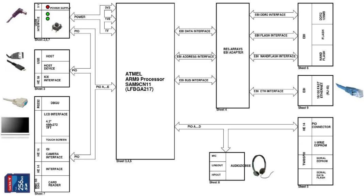
Evaluation Kit Hardware
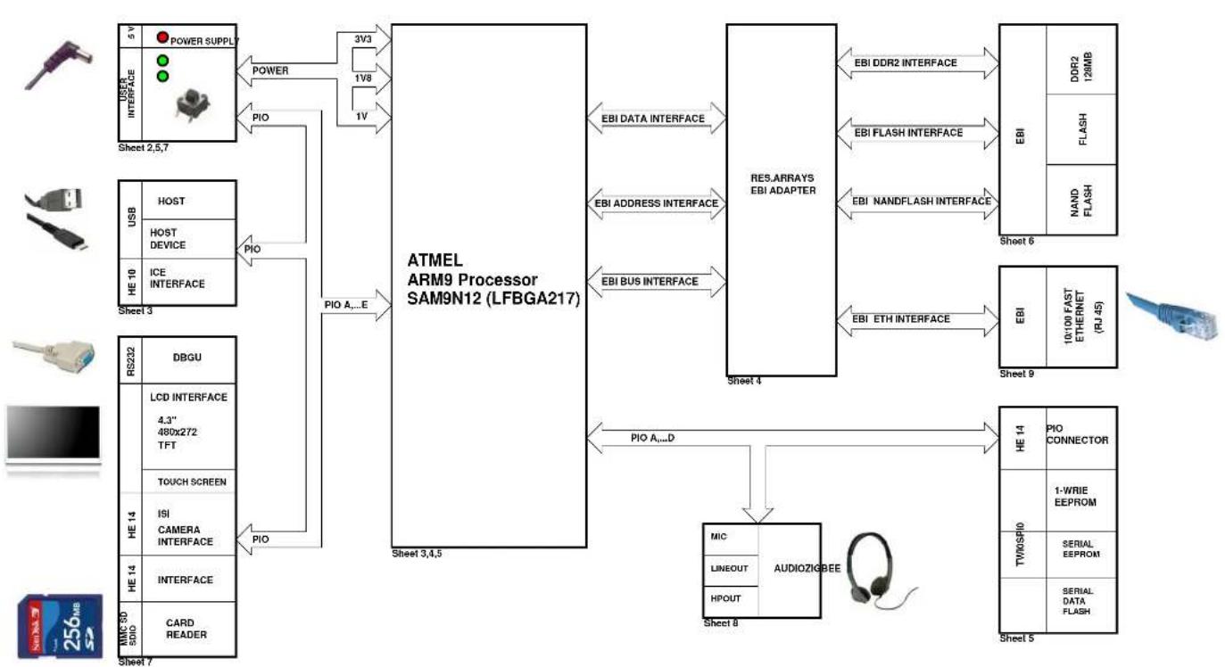
4.1 Board Overview
This section introduces the Atmel SAM9N12/CN11 Evaluation Kit design. It introduces system-level concepts, such as power distribution, memory, and interface assignments.
The SAM9N12/CN11-EK board is built around on the integration of an ARM®926-based microcontroller (BGA 217 package) with on-board SDRAM, NAND-Flash and a set of popular peripherals. It is designed to provide a high performance processor evaluation solution with high flexibility for various kinds of applications.
Figure 4-1. SAM9N12 Board Architecture

flowchart
graph TD
    subgraph AT91SAM9N12_BGA217
        A["USB"] --> B["Host"]
        C["USB"] --> D["Device"]
        E["JTAG"] --> F["UART DBGU"]
        G["DEBUG"] --> H["0000000000000000000000000000000000000000000000000000000000000000000000000000000000000000000000000000"]
        I["LED"] --> J["4 bits interface MMC"]
        K["PIO"] --> L["WOLFSON codec SSC + TWI"]
        M["External Components"] --> N["External Components"]
    end

    subgraph AT91SAM9N12_EK
        O["Nand Flash"] --> P["NAND FLASH 2Gb"]
        Q["DDR2"] --> R["DDR2 or SDRAM 1Gb"]
        S["NOR FLASH 1Gb"] --> T["NOR FLASH 1Gb"]
        U["RJ4S"] --> V["Ethernet MII"]
        W["Serial data flash"] --> X["SPI"]
        Y["4 bits interface MMC"] --> Z["MCIO"]
        AA["Head Phone"] --> AB["Audio output"]
    end

    subgraph AT91SAM9N12_BGA217
        AC["EDI"] --> AD["USB"]
        AE["SPI"] --> AF["DBGU"]
        AG["WOLFSON codec SSC + TWI"] --> AH["PIO"]
    end

    subgraph AT91SAM9N12_BGA217
        AI["External Components"] --> AJ["External Components"]
    end

    subgraph AT91SAM9N12_EK
        AK["USB powered"] --> AL["USB full speed"]
        AM["USB full speed"] --> AN["JTAG"]
        AO["DBGU DB9"] --> AP["LCD HE10"]
        AQ["PIO HE14"] --> AR["AT91SAM9N12-EK"]
    end
Figure 4-2. SAM9CN11 Board Architecture
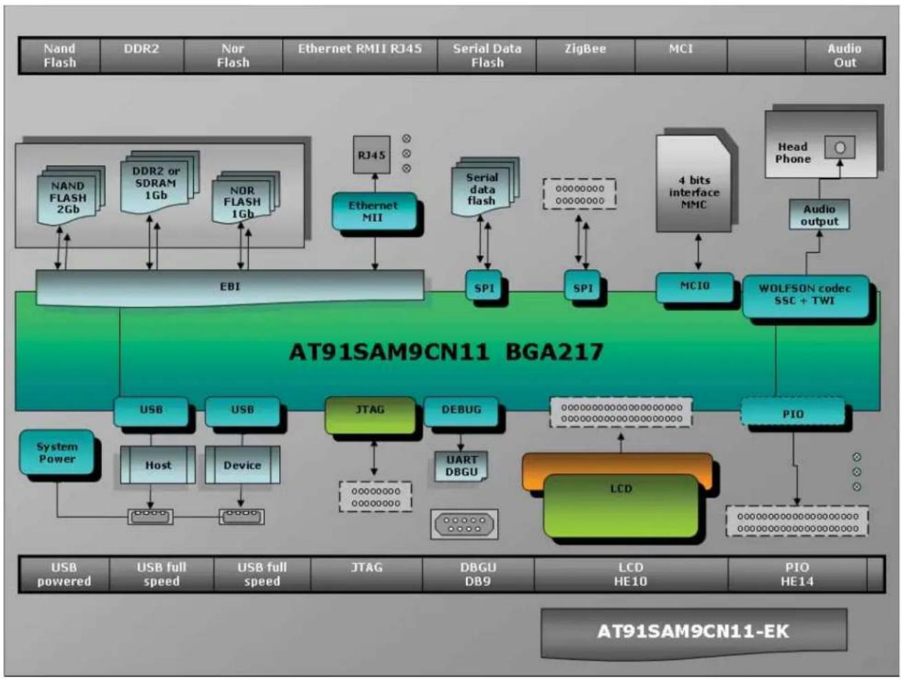
flowchart
graph TD
    A["Nand Flash"] --> B["DDR2"]
    B --> C["Nor Flash"]
    C --> D["Ethernet RMII RJ45"]
    D --> E["Serial Data Flash"]
    E --> F["ZigBee"]
    F --> G["MC1"]
    G --> H["Audio Out"]
    I["NAND FLASH 2Gb"] --> J["DDR2 or SDRAM 1Gb"]
    J --> K["NOR FLASH 1Gb"]
    K --> L["EBI"]
    L --> M["EBI"]
    M --> N["SPI"]
    N --> O["4 bits interface MMC"]
    P["Head Phone"] --> Q["Audio output"]
    Q --> R["WOLFSON codec SSC + TWI"]
    R --> S["PIO"]
    S --> T["LCD"]
    U["System Power"] --> V["USB"]
    V --> W["Host"]
    V --> X["Device"]
    Y["JTAG"] --> Z["UUID"]
    AA["DEBUG"] --> AB["UART DBGU"]
    AC["00000000 00000000"] --> AD["00000000 00000000"]
    AE["00000000 00000000"] --> AF["00000000 00000000"]
    AG["LCD"] --> AH["IEEE Device"]
    AI["PIO"] --> AJ["IEEE Device"]
    AK["AT91SAM9CN11-BGA217"] --> AL["USB powered"]
    AL --> AM["USB full speed"]
    AL --> AN["USB full speed"]
    AL --> AO["JTAG"]
    AL --> AP["DBGU DB9"]
    AL --> AQ["LCD HE10"]
    AL --> AR["PIO HE14"]
    AS["AT91SAM9CN11-EK"] --> AT["IEEE Device"]
4.2 Equipment List
4.2.1 Features List
Here is the list of the EK board components:
■ SAM9N12/CN11 microcontroller BGA
- 16 MHz crystal
- 32.768 kHz crystal
■ Memory
- 1 Gbit DDR2 memory
- 2 Gbits NAND Flash memory with chip selection control switch
- Optional NOR Flash
- 32 Mbits SPI serial DataFlash with chip selection control switch
- 512 Kbits serial EEPROM
- 1 Kbit 1-Wire EEPROM
- SD/MMC interface
■ Communication
– One Ethernet Physical Transceiver Layer with RJ45 connector
- UART DBGU port with level shifter IC
- JTAG/ICE port
- USB Host and Device
- Z i g® B e e
■ Add-on Display Module
- TFT LCD module with touch screen
- Q T o® elements for user QTouch: K1 to K4
■ Audio CODEC with input stereo headphone and microphone
■ On-board power regulation and backup battery
■ Two user LEDs and one power LED
■ System buttons: NRST, WKUP, OE_CS
■ One user button
4.2.2 Interface Connection
The SAM9N12/CN11-EK board includes hardware interfaces such as:
■ DC power supply (J1)
■ Backup battery (Bt1)
■ USB host, type A connector (J2)
■ USB device, micro B connector (J3)
■ One Ethernet 10/100 interface through an ETH controller (J16)
■ DBGU (RX and TX only) connected to a 9-way male RS232 connector (J11)
■ JTAG, 20 pin IDC connector (J4)
■ SD connector (J8)
■ Headphone (J13), line-in (J15), on board mic-phone (mic1)
■ DM board connection for QTouch and TFT LCD display with touch screen and backlight (J9, J10)
■ ZigBee connector (J12)
■ Three IO expansion ports (J5, J6, J7)
■ Test points (various test points are located throughout the board)
4.2.3 Configuration Items
■ Power selection switch (SW1)
■ Push button - NAND/DataFlash OS_CS (PB1)
■ Push button - NRST, board reset (PB2)
■ Push button - Wake-up (PB3)
■ Push button - PB_USER (PB4)
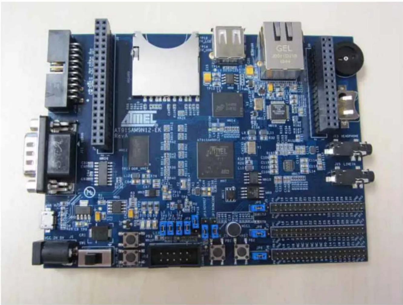
Figure 4-3. SAM9N12-EK Board Layout
natural_image
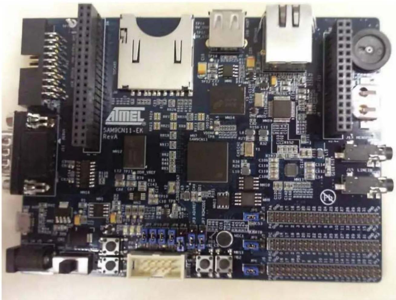
Blue printed circuit board with various electronic components and connectors (no readable text or symbols)Figure 4-4. SAM9CN11-EK Board Layout
natural_image
Close-up of an ATMEL microcontroller board with various electronic components and connectors (no readable text or symbols)4.3 Function Blocks
4.3.1 Processor
The EK board is equipped with a SAM9N12/CN11 device in BGA217 package. The processor runs at a nominal frequency of 400 MHz for the core and 133 MHz for the system bus.
4.3.2 Clock Distribution
The SAM9N12/CN11-EK board includes three clock systems. Two of the clock systems are alternatives for the SAM9N12/CN11 main clock and one clock system is an oscillator used for the Ethernet controller chip.
Table 4-1 lists the main components associated with these clock systems.
Table 4-1. Main Components Associated with the Clock Systems
| QTY Description Component assignment | |
| 1 Crystal for Internal Clock, 16 MHz Y1 | |
| 1 Crystal for RTC Clock, 32.768 kHz Y2 | |
| 1 Crystal for Ethernet Clock, 25 MHz Y3 |
4.3.3 Reset and Wake-up Circuitry
The reset sources for the EK board are:
■ Power-on reset
■ Push-button reset (PB2)
■ JTAG reset from an in-circuit emulator (JTAG interface is equipped on EK board)
To disable any bootable content in NAND Flash or DataFlash, please refer to "Push Buttons".
4.3.4 Power Supplies
The SAM9N12/CN11-EK board evaluation and development platform embeds all the necessary power rails required for the SAM9N12/CN11 processor and peripherals. The SAM9N12/CN11-EK board can be supplied by either a USB connection via J3 or a 5V DC block through input J1 (refer to usb schematic).
A manual power supply selection (SW1) between the USB supply and the 5V power supply is provided to select the main power line.
Figure 4-5. Power Input

Connector J1 is provided for use with a DC adapter. It is a 2.5 mm male power jack. Table 4-2 below lists the DC adapter connector pinouts.
Table 4-2. Power Input Configuration
| PIN INPUT | |
| 1 (Center) Positive | |
| 2 No connection | |
| 3 (Outside) Ground |
4.3.5 Power Rails
The SAM9N12/CN11-EK Board contains three regulated power supplies:
■ 3.3V DC supply
■ 1.8V DC supply
■ 1.0V DC core supply
The outputs of these regulated power supplies are distributed as necessary to the circuits on boards.
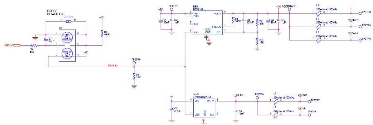
The USB supplies and the 5V input DC block are further regulated to 3.3V. The main 3.3V regulator is based on a RICHTEK RT9018A low dropout regulator providing a fixed output of 3.3V. Its output is used for:
■ VDDIOP0
■ VDDIOP1
■ VDDANA
■ VDDOSC
■ VDDUSB
■ VDDFUSE
When the 3.3V supply is present, power LED D10 is lit.
Test points TP2 to TP5 are used to perform testing.
Figure 4-6. 3. 3V Supply

text_image
+5V TP1 C1 10uF C2 1uF MN1 RT9018A VIN VDD VOUT 6 NC EN GND GND PGOOD ADJ ∞ PWR_EN 5 3 4 6 R1 100K C3 100nF R2 47K C4 10uF C5 1uF R3 15K +3V3 VDDIOP0 L1 220ohm at 100MHz L2 220ohm at 100MHz L3 220ohm at 100MHz VDDIOP1 TP3 TP4 TP5 VDDANAThe 1.8V DC core supply is based on an LDO LP38692MP IC. It is powered by the 5V DC supply. Its output is used for VDDIOM and VDDNF. Test point TP6 is used to perform testing.
Figure 4-7. 1.8V Supply
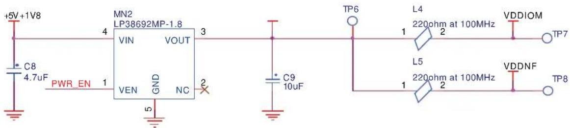
text_image
+5V+1V8 MN2 LP38692MP-1.8 VIN VOUT C8 4.7uF PWR_EN 1 VEN GND NC 2 5 TP6 L4 220ohm at 100MHz VDDIOM TP7 L5 220ohm at 100MHz VDDNF TP8The 1.0V DC core supply is based on an LDO ADP1715AR. It is powered by the output of the 3.3V CC supply. Its output is used for VDDCORE and VDDPLL. Test point TP10 is used to perform testing.
Figure 4-8. 1V Su pply
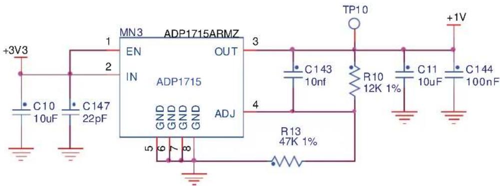
text_image
MN3 ADP1715ARMZ EN OUT 3 +3V3 2 IN ADP1715 G D G D G ADJ 4 C10 10uF C147 22pF 5 6 7 8 R13 47K 1% TP10 C143 10nf R10 12K 1% C11 10uF C144 100nF +1V4.3.6 Battery Backup
VDDBU pin is powered from the 3.3V rail and a backup battery BT1 via a dual Schottky diode D1. Test point TP13 and jumper JP2 are used to perform testing.
Figure 4-9. Backup Battery

text_image
TP13 VDDBU JP2 C16 100nF 3 D1 BAT54C +3V3 2 C18 2.2uF BT1Note: Test points (TPn) are provided for easy access to each of the regulated power lines.
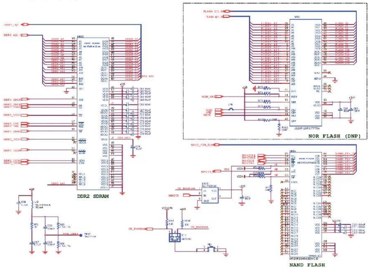
4.3.7 Memory
4.3.7.1 DDR2 SDRAM
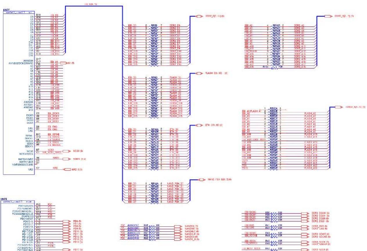
The SAM9N12/CN11 processor uses DDR2 SDRAM as the system memory. The DDR2 interface uses 1.8V power. The DDR2 chips and SAM9N12/CN11 processor are connected directly. The interface is 1.8V provided by an on-board voltage regulator.
VREF, which is half the interface voltage, or 0.9V, is provided by a simple voltage divider of 1.8V.
■ One 1 Gbit DDR2-SDRAM memory (Micron MT47H64M16HR 8Meg*16*8), 16 bits data interface connected to D[0-15].
4.3.7.2 NAND FLASH
The SAM9N12/CN11-EK has native support for NAND Flash memory and implements an 8-bit NAND Flash with 2 Gbits in size.
■ One 2 Gbits NAND Flash (Micro MT29F2G08ABDHC), 16 bits data interface connected to D[0-15].
4.3.7.3 NOR FLASH
The SAM9N12/CN11-EK provides an optional 128 Mbits of Flash memory using a chip-select signal. The Flash memory is used with the 16-bit port size.
■ One reserved position for 128 Mbits NOR Flash (Numonyx JS28F128P30TF75A).
Figure 4-10. External memory
text_image
DDR2_186 DDR2_412.1E DDR2_62 DDR2_63 DDR2_64 DDR2_65 DDR2_66 DDR2_67 DDR2_68 DDR2_69 DDR2_70 DDR2_71 DDR2_72 DDR2_73 DDR2_74 DDR2_75 DDR2_76 DDR2_77 DDR2_78 DDR2_79 DDR2_80 DDR2_81 DDR2_82 DDR2_83 DDR2_84 DDR2_85 DDR2_86 DDR2_87 DDR2_88 DDR2_89 DDR2_90 DDR2_91 DDR2_92 DDR2_93 DDR2_94 DDR2_95 DDR2_96 DDR2_97 DDR2_98 DDR2_99 DDR2_100 DDR2_101 DDR2_102 DDR2_103 DDR2_104 DDR2_105 DDR2_106 DDR2_107 DDR2_108 DDR2_109 DDR2_110 DDR2_111 DDR2_112 DDR2_113 DDR2_114 DDR2_115 DDR2_116 DDR2_117 DDR2_118 DDR2_119 DDR2_120 DDR2_121 DDR2_122 DDR2_123 DDR2_124 DDR2_125 DDR2_126 DDR2_127 DDR2_128 DDR2_129 DDR2_130 DDR2_131 DDR2_132 DDR2_133 DDR2_134 DDR2_135 DDR2_136 DDR2_137 DDR2_138 DDR2_139 DDR2_140 DDR2_141 DDR2_142 DDR2_143 DDR2_144 DDR2_145 DDR2_146 DDR2_147 DDR2_148 DDR2_149 DDR2_150 DDR2_151 DDR2_152 DDR2_153 DDR2_154 DDR2_155 DDR2_156 DDR2_157 DDR2_158 DDR2_159 DDR2_160 DDR2_161 DDR2_162 DDR2_163 DDR2_164 DDR2_165 DDR2_166 DDR2_167 DDR2_168 DDR2_169 DDR2_170 DDR2_171 DDR2_172 DDR2_173 DDR2_174 DDR2_175 DDR2_176 DDR2_177 DDR2_178 DDR2_179 DDR2_180 DDR2_181 DDR2_182 DDR2_183 DDR2_184 DDR2_185 DDR2_186 DDR2_187 DDR2_188 DDR2_189 DDR2_190 DDR2_191 DDR2_192 DDR2_193 DDR2_194 DDR2_195 DDR2_196 DDR2_197 DDR2_198 DDR2_199 DDR2_200 DDR3_SDRAMA 3-state buffer is in serial with NAND flash's CE signal, with PB1 to give a manually disable manner for NAND boot.
4.3.8 UART DBGU
The Universal Asynchronous Receiver Transmitter features a two-pin UART that can be used for communication and trace purposes and offers an ideal medium for in-situ programming solutions.
This two-pin UART (TXD and RXD only) is buffered through an RS232 transceiver MN16 and brought to the DB9 male connector J11.
Figure 4-11. UART

text_image
MN 16 MAX9 232CSE VDD IOP0 16 C90 100nF C92 100nF C93 100nF VCC C1+ 1 C91 100nF V+ 2 6 4 C1- C2+ 5 C94 100nF GND C2- 14 T1N R1OUT T1OUT R1IN T2OUT R2OUT R2IN J11 1 6 2 7 3 8 4 9 5 10 11 PA10 (DTXD) PA9 (DRXD) UART4.3.9 JTAG Interface
The SAM9N12/CN11-EK board includes a JTAG interface port (J4), to provide debug level access to the processor. The JTAG port is a 20-pin male connector. This port provides the required interface for in-circuit emulators such as ARM's Multi-ICE.
Figure 4-12. JTAG
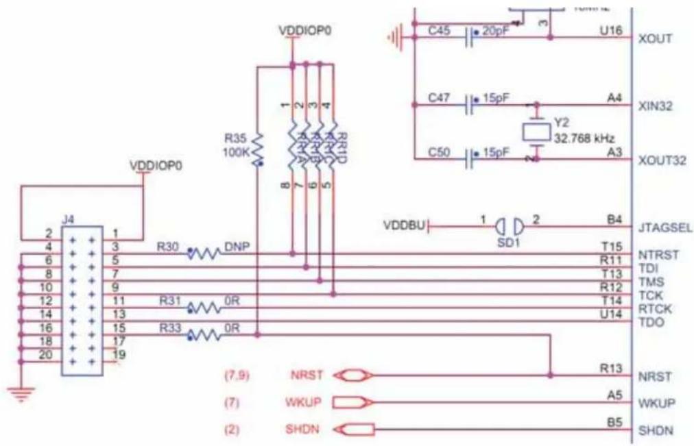
text_image
VDDIOP0 R35 100K 1 2 3 4 8 7 6 5 R30 DNP J4 2 1 4 3 6 5 8 7 10 9 12 11 R31 OR 14 13 16 15 R33 OR 18 17 20 19 (7.9) NRST (7) WKUP (2) SHDN VDDIOP0 C45 20pF U16 C47 15pF A4 Y2 32.768 kHz C50 15pF A3 XOUT XIN32 XOUT32 VDDBU 1 SD1 B4 JTAGSEL T15 NTRST R11 TDI T13 TMS R12 TCK T14 RTCK U14 TDO R13 NRST A5 WKUP B5 SHDN4-10 SAM9N12/CN11-EK User Guide

4.3.10 Serial Peripheral Interface (SPI) Controller
The SAM9N12/CN11 serial processor provides two high-speed Serial Peripheral Interface (SPI) controllers. One port is used to interface with the on-board serial DataFlash.
A 3-state buffer is in serial with DataFlash CS signal, with PB1 to give a manually disable manner for DataFlash boot.
Figure 4-13. SPI DataFlash

text_image
OE_Datal lash PA14 MN8 NL17SZ126 OE VCC IN OUT GND 5 VDDIOP0 C58 100nF PA12 (SPI0 MOSI)R56 OR PA11 (SPI0 MIS0)R57 OR PA13 (SPI0 SPCK)R58 OR (SPI0 NPCS0) 5 2 6 1 VDDIOP0 R55 470K MN9 AT25DF321A SI VCC SO WP SCK HOLD CS GND 8 3 7 4 VDDIOP0 C59 100nF4.3.11 Two Wire Interface (TWI)
The SAM9N12/CN11 processor has two full speed (400 kHz) master/slave I2C serial controllers. The controllers are fully compatible with the industry standard I2C interfaces. On the EK board, TWI0 port is used to interface with serial EEPROM, QTouch device and audio CODEC interface.
SAM9N12/CN11 processor supports TWI EEPROM boot at the device address of 0x50. On board, the EEPROM device address is 0x51. Customer needs to dismount R61 and mount R62 as 10 kohms, if EEPROM boot is needed.
Figure 4-14. EEPROM
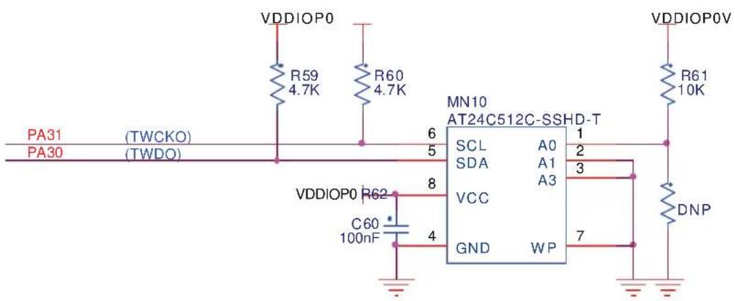
text_image
VDDIOP0 R59 4.7K R60 4.7K VDDIOP0V R61 10K PA31 (TWCKO) TAWDO 6 5 MN10 AT24C512C-SSHD-T SCL A0 1 SDA A1 2 VCC A3 3 VDDIOP0 R62 C60 100nF 4 GND WP 7 DNP4.3.12 USB Ports
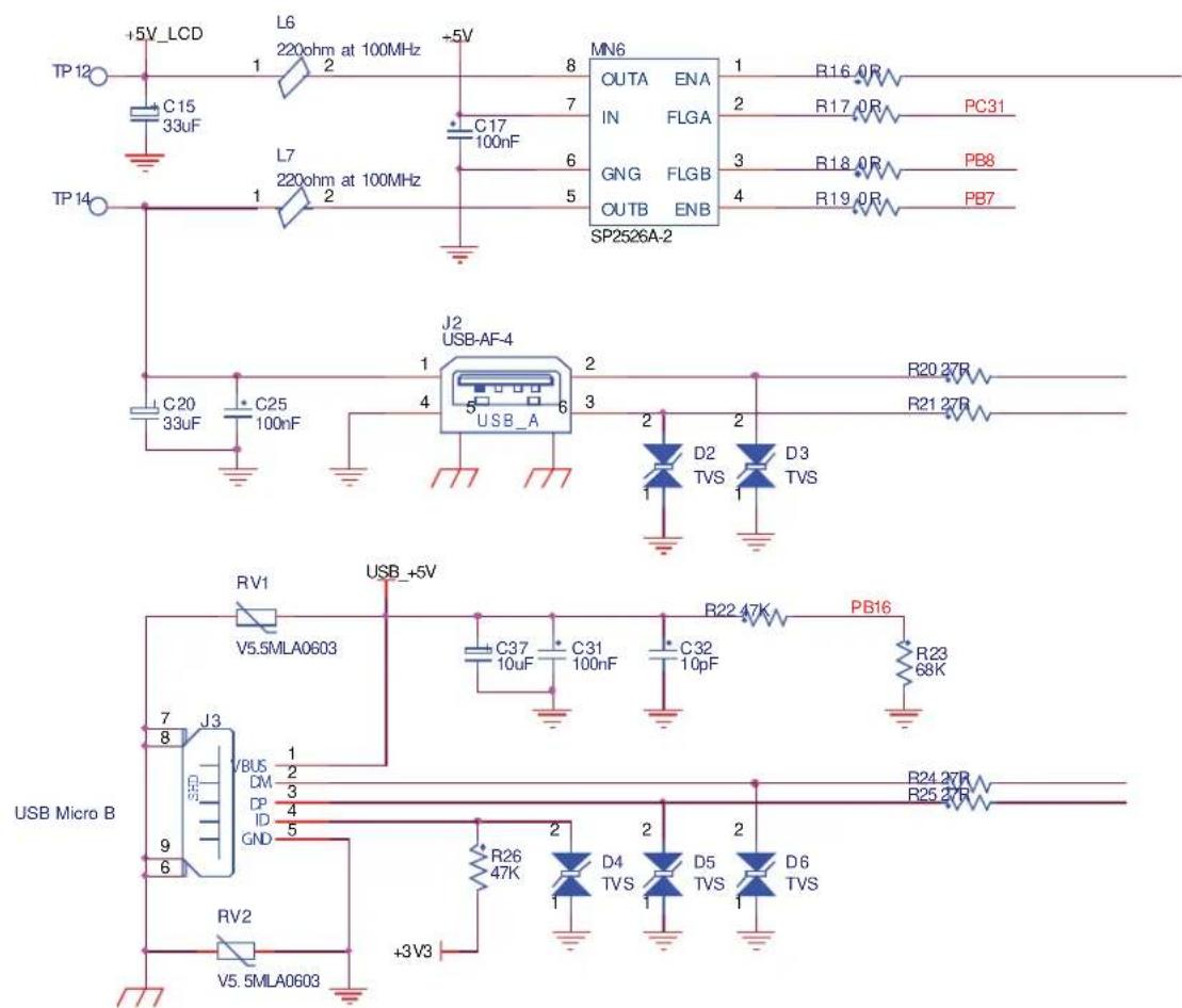
The SAM9N12/CN11-EK features two full speed (OHCI) USB ports:
■ Host full speed, type A USB receptacle, J2
■ Device full speed, micro B USB receptacle, J3
SAM9N12/CN11-EK features USB power function from device port J3. SW1 functions as switch between USB supply and DC input jack J1.
The USB host ports are equipped with 500 mA power switch for bus-powered applications.
Figure 4-15. USB Port
text_image
TP 12 +5V_LCD L6 220ohm at 100MHz -5V MN6 OUTA ENA 1 R16.0R IN FLGA 2 R17.0R PC31 GNG FLGB 3 R18.0R PB8 OUTB ENB 4 R19.0R PB7 SP2526A-2 TP 14 L7 220ohm at 100MHz 1 2 C17 100nF 6 5 J2 USB-AF-4 USB_A 2 3 4 5 6 2 D2 TVS 2 D3 TVS C20 33uF C25 100nF RV1 USB_+5V V5.5MLA0603 C37 C31 R22.47K PB16 10uF 100nF C32 10pF R23 68K USB Micro B 7 J3 8 VBUS 1 DM 2 DP 3 ID 4 GND 5 9 RV2 R24.27R 6 V5.5MLA0603 +3V3 D4 D5 D6 TVS TVS TVS TVS4.3.13 1-Wire EEPROM
The SAM9N12/CN11 Evaluation Kit uses 1-Wire device as "soft label" to store the information such as chip type, manufacture's name, production date, etc.
Figure 4-16. 1-Wire

text_image
VDDIOP0 R64 1.5K PA4 R65.0R 2 MN11 DS2431P+ IO NC1 NC2 GND NC3 GND NC4 1 3 4 5 64.3.14 ETH on EBI
The SAM9N12/CN11 Evaluation Kit uses EBI-based 8-bit EMAC controller KSZ8851 to implement a 10/100 Ethernet access. The board integrates an RJ45 connector with embedded transformer, and two status LEDs.
For more information about the Ethernet controller device, refer to the Micrel KSZ8851 manufacturer's datasheet.
Figure 4-17. Ethernet

text_image
KSZ8 851-16MLL C103 100F C104 100F C105 100F C106 100F C107 100F C108 100F C109 100F C110 100F C111 100F C112 100F C113 100F C114 100F C115 100F C116 100F C117 100F C118 100F C119 100F C120 100F C121 100F C122 100F C123 100F C124 100F C125 100F C126 100F C127 100F C128 100F C129 100F C130 100F C131 100F C132 100F C133 100F C134 100F C135 100F C136 100F C137 100F C138 100F C139 100F C140 100F C141 100F C142 100F C143 100F C144 100F C145 100F C146 100F C147 100F C148 100F C149 100F C150 100F C151 100F C152 100F C153 100F C154 100F C155 100F C156 100F C157 100F C158 100F C159 100F C160 100F C161 100F C162 100F C163 100F C164 100F C165 100F C166 100F C167 100F C168 100F C169 100F C170 100F C171 100F C172 100F C173 100F C174 100F C175 100F C176 100F C177 100F C178 100F C179 100F C180 100F C181 100F C182 100F C183 100F C184 100F C185 100F C186 100F C187 100F C188 100F C189 100F C190 100F C191 100F C192 100F C193 100F C194 100F C195 100F C2A/CCND/CCND/CCND/CCND/CCND/CCND/CCND/CCND/CCND/CCND/CCND/CCND/CCND/CCND/CCND/CCND/CCND/CCND/CCND/CCND/CCND/CCND/CCND/CCND/CCND/CCND/CCND/CCND/CCND/CCND/CCND/CCND/CCND/CCND/ MENIIN VDD DCL DCL DCL DCL DCL DCL DCL DCL DCL DCL DCL DCL DCL DCL DCL DCL DCL DCL DCL DCL DCL DCL DCL DCL DCL DCL DCL DCL DCL DCL DCL DCL DCL DCL DCL DCL DCL DCL DCL DCL DCL DCL DCL DCL DCL DCL DCL DCL DCL DCL DCl DCL DCL DCL DCL DCL DCL DCL DCL DCL DCL DCL DCL DCL DCL DCL DCL DCL DCL DCL DCL DCL DCL DCL DCL DCL DCL DCL DCL DCL DCL DCL DCL DCL DCL DCL DCL DCL DCL DCL DCL DCL DCL DCL DCL DCL DCL DCL DCL DCL DclDLC/DLC/DLC/DLC/DLC/DLC/DLC/DLC/DLC/DLC/DLC/DLC/DLC/DLC/DLC/DLC/DLC/DLC/DLC/DLC/DLC/DLC/DLC/DLC/DLC/DLC/DLC/DLC/DLC/DLC/DLC/DLC/DLC/DLC/DLC/DLC/DLC/DLC/DLC/DLC/DLC/DLC/DLC/DLC/DLC/DLC/DLC/DLC/DLC/DLC/DLC-DLC/DLC/DLC/DLC/DLC/DLC/DLC/DLC/DLC/DLC/DLC/DLC/DLC/DLC/DLC/DLC/DLC/DLC/DLC/DLC/DLC/DLC/DLC/DLC/DLC/DLC/DLC/DLC/DLC/DLC/DLC/DLC/DLC/DLC/DLC/DLC/DLC/DLC/DLC/DLC/DLC/DLC/DLC/DLC/DLC/DLC/DLC/DLC/DLC/DLC/TMENIIN SODI RIO BOSO CDSO CDSO CDSO CDSO CDSO CDSO CDSO CDSO CDSO CDSO CDSO CDSO CDSO CDSO CDSO CDSO CDSO CDSO CDSO CDSO CDSO CDSO CDSO CDSO CDSO CDSO CDSO CDSO CDSO CDSO CDSO CDSO CDSO CDS OENIIN IIOB IIOB IIOB IIOB IIOB IIOB IIOB IIOB IIOB IIOB IIOB IIOB IIOB IIOB IIOB IIOB IIOB IIOB IIOB IIOB IIOB IIOB IIOB IIOB IIOB IIOB IIOB IIOB IIOB IIOB IIOB IIOB IIOB IIOB IIIOB IIIOB IIIOB IIIOB IIIOB IIIOB IIIOB IIIOB IIIOB IIIOB IIIOB IIIOB IIIOB IIIOB IIIOB IIIOB IIIOB IIIOB IIIOB IIIOB IIIOB IIIOB IIIOB IIIOB IIIOB IIIOB IIIOB IIIOB IIIOB IIIOB IIIOB IIIOB IIIOB II IOB II IOB II IOB II IOB II IOB II IOB II IOB II IOB II IOB II IOB II IOB II IOB II IOB II IOB II IOB II IOB II IOB II IOB II IOB II IOB II IOB II IOB II IOB II IOB II IOB II IOB II IOB II IOB II IOB II IOB II IOB II IOB II IOB II IOBCNENIIN IIOBNIIN IIOBNIIN IIOBNIIN IIOBNIIN IIOBNIIN IIOBNIIN IIOBNIIN IIOBNIIN IIOBNIIN IIOBNIIN IIOBNIIN IIOBNIIN IIOBNIIN IIOBNIIN IIOBNIIN IIOBNIIN IIOBNIIN IIOBNIIN IIOBNIIN IIOBNIIN IIOZNENIIN IIOZNENIIN IIOZNENIIN IIOZNENIIN IIOZNENIIN IIOZNENIIN IIOZNENIIN IIOZNENIIN IIOZNENIIN IIOZNENIIN IIOZNENIIN IIOZNENIIN IIOZNENIIN IIOZNENIIN IIOZNENIIN IIOZNENIIN IIOZNENIIN IIOC NENIIN IIOC NENIIN IIOC NENIIN IIOC NENIIN IIOC NENIIN IIOC NENIIN IIOC NENIIN IIOC NENIIN IIOC NENIIN IIOC NENIIN IIOC NENIIN IIOC NENIIN IIOC NENIIN IIOC NENIIN IIOC NENIIN IIOC NENIIN IIOC NENIIN LIDN LN LN LN LN LN LN LN LN LN LN LN LN LN LN LN LN LN LN LN LN LN LN LN LN LN LN LN LN LN LN LN LN LN LN LN LN LN LN LN LN LN LN LN LN LN LN LN LN LN LN LN LN LN LN LN LN LN LN LN LN LN LN LN LN LN LN LN LN LN LN LN LN LN LN LN LN LN LN LN LN LN LN LN LN LN LN LN LN LN LN LN LN LN LN LN LN LN LN LN LN DN DN DN DN DN DN DN DN DN DN DN DN DN DN DN DN DN DN DN DN DN DN DN DN DN DN DN DN DN DN DN DN DN DN DN DN DN DN DN DN DN DN DN DN DN DN DN DN DN DN DN DN DN DN DN DN DN DN DN DN DN DN DN DN DN DN DN DN DN DN DN DN DN DN DN DN DN DN DN DN DN DN DN DN DN DN DN DN DN DN DN DN DN DN DN DN DN DN DN DN CNNENIIN IIOBNNENIIN IIOBNNENIIN IIOBNNENIIN IIOBNNENIIN IIOBNNENIIN IIOBNNENIIN IIOBNNENIIN IIOBNNENIIN IIOBNNENIIN IIOBNNENIIN IIOBNNENIIN IIOBNNENIIN IIOBNNENIIN IIOBNNENIIN IIOBNN ENICN ENICN ENICN ENICN ENICN ENICN ENICN ENICN ENICN ENICN ENICN ENICN ENICN ENICN ENICN ENICN ENICN ENICN ENICN ENICN ENICN ENICN ENICN ENICN ENICN ENICN ENICN ENICN ENICN ENICN ENICN ENICN ENICN ENICM ENICM ENICM ENICM ENICM ENICM ENICM ENICM ENICM ENICM ENICM ENICM ENICM ENICM ENICM ENICM ENICM ENICM ENICM ENICM ENICM ENICM ENICM ENICM ENICM ENICM ENICM ENICM ENICM ENICM ENICM ENICM ENICM ENICM EONJENJENJENJENJENJENJENJENJENJENJENJENJENJENJENJENJENJENJENJENJENJENJENJENJENJENJENJENJENJENJENJENJENJENJENJENJENJENJENJENJENJENJENJENJENJENJENJENJENJENJAN JUN JUN JUN JUN JUN JUN JUN JUN JUN JUN JUN JUN JUN JUN JUN JUN JUN JUN JUN JUN JUN JUN JUN JUN JUN JUN JUN JUN JUN JUN JUN JUN JUN JUN JUN JUN JUN JUN JUN JUN JUN JUN JUN JUN JUN JUN JUN JUN JUN JUN JUNC NGENJENJENJENJENJENJENJENJENJENJENJENJENJENJENJENJENJENJENJENJENJENJENJENJENJENJENJENJENJENJENJAN JUN JUN JUN JUN JUN JUN JUN JUN JUN JUN JUN JUN JUN JUN JUN JUN JUN JUN JUNC NGENJENJAN JUN JUN JUN JUN JUN JUN JUN JUN JUN JUN JUN JUN JUN JUN JUN JUN JUN JUN JUN JUN JUN JUN JUN JUNC NGENJAN jun jun jun jun jun jun jun jun jun jun jun jun jun jun jun jun jun jun jun jun jun jun jun jun jun jun jun jun jun jun jun jun jun jun jun jun jun jun jun jun jun jun jun jun jun jun jun jun jun jun jUnjNN lncn nnnn nnnn nnnn nnnn nnnn nnnn nnnn nnnn nnnn nnnn nnnn nnnn nnnn nnnn nnnn nnnn nnnn nnnn nnnn nnnn nnnn nnnn nnnn nnnn nnnn nnnn nnnn nnnn nnnn nnnn nnnn nnnn nnnn nnnm nnnm nnnm nnnm nnnm nnnm nnnm nnnm nnnm nnnm nnnm nnnm nnnm nnnm nnnm nnnm nnnm nnnm nnnm nnnm nnnm nnnm nnnm nnnm nnnm nnnm nnnm nnnm nnnm nnnm nnnm nnnm nnnm nnnm twn mtn mtn mtn mtn mtn mtn mtn mtn mtn mtn mtn mtn mtn mtn mtn mtn mtn mtn mtn mtn mtn mtn mtn mtn mtn mtn mtn mtn mtn mtn mtn mtn mtn mtn mtn mtn mtn mtn mtn mtn mtn mtn mtn mtn mtn mtn mtn mtn mtn mtn mthn twn mthn twn mthn twn mthn twn mthn twn mthn twn mthn twn mthn twn mthn twn mthn twn mthn twn mthn twn mthn twn mthn twn mthn twn mthn twn mthn twn mthn twn mthn twn mthn twn mthn twt dwt dwt dwt dwt dwt dwt dwt dwt dwt dwt dwt dwt dwt dwt dwt dwt dwt dwt dwt dwt dwt dwt dwt dwt dwt dwt dwt dwt dwt dwt dwt dwt dwt dwt dwt dwt dwt dwt dwt dwt dwt dwt dwt dwt dwt dwt dwt dwt dwt dwt cftdctctctctctctctctctctctctctctctctctctctctctctctctctctctctctctctctctctctctctctctctctctctctctctctctctctctctctctctctctctctctctctctctctctctctctctctctctctctctctctctctctctctctctctctctctctctctctctctctctctctctactcfeetfetfetfetfetfetfetfetfetfetfetfetfetfetfetfetfetfetfetfetfetfetfetfetfetfetfetfetfetfetfetfetfetfetfetfetfetfetfetfetfetfetfetfetfetfetfetfetfetfetfet fet fet fet fet fet fet fet fet fet fet fet fet fet fet fet fet fet fet fet fet fet fet fet fet fet fet fet fet fet fet fet fet fet fet fet fet fet fet fet fet fet fet fet fet fet fet fot fot fot fot fot fot fot fot fot fot fot fot fot fot fot fot fot fot fot fot fot fot fot fot fot fot fot fot fot fot fot fot fot fot fot fot fot fot fot fot fot fot fot fot fot fot fot fot fot fot fow bow bow bow bow bow bow bow bow bow bow bow bow bow bow bow bow bow bow bow bow bow bow bow bow bow bow bow bow bow bow bow bow bow bow bow bow bow bow bow bow bow bow bow bow bow bow bow bow bow bow bcfeetfentfeetfeetfeetfeetfeetfeetfeetfeetfeetfeetfeetfeetfeetfeetfeetfeetfeetfeetfeetfeetfeetfeetfeetfeetfeetfeetfeetfeetfeetfeetfeetfeetfeetfeetfeetfeetfeetfeetfeetfeetfeetfeetfeetfeeftfeeftfeeftfeeftfeeftfeeftfeeftfeeftfeeftfeeftfeeftfeeftfeeftfeeftfeeftfeeftfeeftfeeftfeeftfeeftfeeftfeeftfeeftfeeftfeeftfeeftfeeftfeeftfeeftfeeftfeeftfeeftfeeftfeeftfaenfoenfoenfoenfoenfoenfoenfoenfoenfoenfoenfoenfoenfoenfoenfoenfoenfoenfoenfoenfoenfoenfoenfoenfoenfoenfoenfoenfoenfoenfoenfoenfoenfoenfoenfoenfoenfoenfoenfoenfoenfoenfoenfoenfoenfoenfoenfoenfoenfoenfoen foen foen foen foen foen foen foen foen foen foen foen foen foen foen foen foen foen foen foen foen foen foen foen foen foen foen foen foen foen foen foen foen foen foen foen foen foen foen foen foen foen foen foen foen foen foen foen foen foen foen fea eni fiu eni fiu eni fiu eni fiu eni fiu eni fiu eni fiu eni fiu eni fiu eni fiu eni fiu eni fiu eni fiu eni fiu eni fiu eni fiu eni fiu eni fiu eni fiu eni fiu eni fiu eni fiu eni fiu eni fiu eni fiu eni fi uon eni fiu eni fiu eni fiu eni fiu eni fiu eni fiu eni fiu eni fiu eni fiu eni fiu eni fiu eni fiu eni fiu eni fiu eni fiu eni fiu eni fiu eni fiu eni fiu eni fiu eni fiu eni fiu eni fiu eni fiu eni fiuu an i un an i un an i un an i un an i un an i un an i un an i un an i un an i un an i un an i un an i un an i un an i un an i un an i un an i un an i un an i un an i un an i un an i un an i un an i un an i un an i un an i un an i un an i un an i un an i un an i un an i un An i un an i un an i un an i un An i un An i un An i un An i un An i un An i un An i un An i un An i un An i un An i un An i un An i un An i un An i un An i un An i un An i un An i un An i un An i un An i un An i un An i un An i un An i un An i un An i un An i un An i un An i un An i un An i un An | UDO BON BON BON BON BON BON BON BON BON BON BON BON BON BON BON BON BON BON BON BON BON BON BON BON BON BON BON BON BON BON BON BON BON BON BON BON BON BON BON BON BON BON BON BON BON BON BON BON BON BON B ON BON BON BON BON BON BON BON BON BON BON BON BON BON BON BON BON BON BON BON BON BON BON B ON BN BN BN BN BN BN BN BN BN BN BN BN BN BN BN BN BN BN BN BN BN BN BN BN BN BN BN BN BN BN BN BN BN BN BN BN BN BN BN BN BN BN BN BN BN BN BN BN BN BN BN BN BN BN BN BN BN BN BN BN BN BN BN BN BN BN BN BN BN BN BN BN BN BN BN BN BN BN BN BN BN BN BN BN BN BN BN BN BN BN BN BN BN BN BN BN BN BN BN BN FN IN IN IN IN IN IN IN IN IN IN IN IN IN IN IN IN IN IN IN IN IN IN IN IN IN IN IN IN IN IN IN IN IN IN IN IN IN IN IN IN IN IN IN IN IN IN IN IN IN IN IN IN IN IN IN IN IN IN IN IN IN IN IN IN IN IN IN IN IN IN IN IN IN IN IN IN IN IN IN IN IN IN IN IN IN IN IN IN IN IN IN IN IN IN IN IN IN IN IN IN In In In In In In In In In In In In In In In In In In In In In In In In In In In In In In In In In In In In In In In In In In In In In In In In In In In In In In In In In In In In In In In In In In In In In In In In In In In In In In In In In In In In In In In In In In In In In In In In In In In In Inc Enin Enin Enin Enin Enin Enin Enin Enin Enin Enin Enin Enin Enin Enin Enin Enin Enin Enin Enin Enin Enin Enin Enin Enin Enin Enin Enin Enin Enin Enin Enin Enin Enin Enin Enin Enin Enin Enin Enin Enin Enin Enin Enin Enin Enin Enin Enin Enin Enin Enin En in En in En in En in En in En in En in En in En in En in En in En in En in En in En in En in En in En in En in En in En in En in En in En in En in En in En in En in En in En in En in En in En in En in En in En in En in En in En in En in En in En in En in En in En in En in En in En in En in En in En.4.3.15 Audio
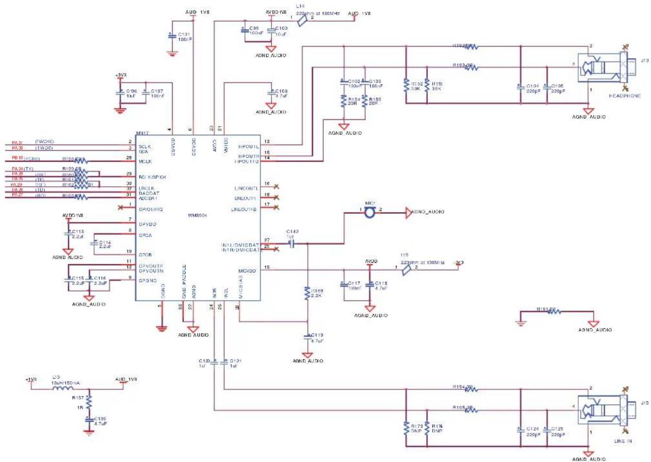
The SAM9N12/CN11-EK includes a WM8904 audio CODEC for digital sound input and output. This interface includes features and audio jacks for:
■ Line In (J13)
■ Headphone output (J15)
■ Microphone on board
The SAM9N12/CN11 programmable clock output PCK0 is used to generate the WM8904 master clock (MCLK).
The bit clock is shared; it can be the SSC Transmitter Clock (TK) or the Receiver Clock (RK). The default setting on SAM9N12/CN11-EK is TK and RK shorted together through R159/R160. Please note that trying different ADC/DAC rates would mean different RK/TK rates; this default setting can be modified.
The 0-ohm resistors R159 to R163 have been implemented to offer a disconnection possibility (freeing these dedicated PIO lines for other custom usages).
Figure 4-18. Audio CODEC
text_image
AUD 1V8 C101 100pF +3V3 C106 1kF C107 100pF +3V3 C109 1kF C110 100pF MN17 SCLK 00A MCLK RCL K2P104 LCLK DAGCAT AUCUK1 GROU/RQ OPVDD OPCA OPCR GVOOUTP OPVOUTIN OPGND C115 2.2uF C116 2.2uF AGND_AUDIO AVDO 1V8 C113 2.2uF C114 2.2uF C115 2.2uF C116 2.2uF +1V8 L5 10uH=150mA R157 1R C106 4.7uF AUD 1V8 AVDO 1V8 C36 100pF C100 10uF ACND_AUDIO L14 220ppm at 100Hz AUD 1V8 C102 100pF C109 100pF ACND_AUDIO R153/20R R155/20R R154/20R R153/20R R152/20R R152/20R R152/20R R152/20R R152/20R R152/20R R152/20R R152/20R R152/20R R152/20R R152/20R R152/AUDIO J13 HEADPHONE AGND_AUDIO HKI 2 ACND_AUDIO NCK 1 2 ACND_AUDIO AVDD 1 2 220ppm at 100Hz C117 100pF C118 4.7uF AGND_AUDIO AGND_AUDIO AGND_AUDIO C119 4.7uF AGND_AUDIO C120 1uF C121 1uF C124/220pF C125/220pF R154/2B R155/2E R156/2B R157/2B R158/2B R159/2B R160/2B R161/2B R162/2B R163/2B R164/2B R165/2B R166/2B R167/2B R168/2B R169/2B R170/2B R171/2B R172/2B R173/2B R174/2B R175/2B R176/2B R177/2B R178/2B R179/2B R180/2B R181/2B R182/2B R183/2B R184/2B R185/2B R186/2B R187/2B R188/2B R189/2B R190/2B R191/2B R192/2B R193/2B R194/2B R195/2B R196/2B R197/2B R198/2B R199/2B R200/2B R201/2B R202/2B R203/2B R204/2B R205/2B R206/2B R207/2B R208/2B R209/2B R210/2B R211/2B R212/2B R213/2B R214/2B R215/2B R216/2B R217/2B R218/2B R219/2B R220/2B R221/2B R222/2B R223/2B R224/2B R225/2B R226/2B R227/2B R228/2B R230/2B R34.3.16 SD Card
The SAM9N12/CN11 has a high-speed Multimedia Card Interface (MCI). It is used as a 4-bit interface connected to an SD card slot.
Figure 4-19. SD Card

text_image
JP10 VDDIOP0 R82 10K R83 10K R84 68K R85 68K R86 68K R87 68K R88 68K PA7 (MCI card detect) 10 11 UP-TOUCH nCD Shell1 WP Shell2 8 7 6 5 4 3 2 1 9 DAT1(RSV) DAT0(DO) VSS2 CLK(SCLK) VDD VSS1 CMD(DI) CD:DAT3(CS) DAT2(RSV) SD CARD SD CARD4.3.17 ZigBee Interface
The EK board has a 10-pin male connector for the Atmel RZ600 ZigBee module. DNP 0-ohm resistors have been implemented in series with the PIO lines that are used elsewhere in the design. Thereby, it enables their individual disconnection, should a conflict occur in user application.
Figure 4-20. ZigBee

text_image
PA5 ZB_RSTN R142.0R 1 PA3 ZB_TRQ1 R144.0R 3 PA8 (SPI1_NPE S46.0R) 5 (SPI1_MISO) R148.0R 7 9 10 J12 2 R143.0R ZB_TRQ0 PA2 4 R145.0R ZB_ST.PTR PA6 6 R147.0R (SPI1_MOSI) PA22 8 (SPI1_SPCK) PA23PA21 L13 220phm at 100MHz +3V3R 1 2 C95 C96 C97 18pF 2.2nF 2.2uFZIGBEE
4.3.18 Analog Interface
The 3.0V voltage reference is based on an LM4040 (Precision Micropower Shunt Voltage Reference). This ADVREF level can be set as 3.0V or 3.3V via the jumper JP3.
Figure 4-21. Analog Reference
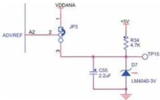
text_image
VDDANA 1 JP3 A2 2 3 +5V R34 4.7K TP15 C55 2.2uF D7 LM4040-3VA 10 kohm potentiometer (VR1) is connected to AD6 port PB17 to implement an easy access to ADC programming and debugging (or to implement an analog user control such as display brightness, volume, etc).
Figure 4-22. Potentiometer

text_image
VDDANA 3 VR1 10K 2 R151 0R (Analog input) PB17 1 C98 10nF4.3.19 LED Indicators
There are three LEDs for general purpose on the SAM9N12/CN11-EK board:
■ D8 blue and D9 green LEDs are user defined and controlled by the GPIO.
■ D10 red LED is a power LED indicating that the 3.3V rail is enabled. It can also be controlled by the GPIO (by default, the GPIO is disabled and an on-board pull-up to 3.3V lights the LED).
Figure 4-23. LED

text_image
PB4 R66 470R D8 Blue PB5 R67 470R D9 Green PD6 R68 100K 1 2 3 Q2 IRLML2502 R69 470R D10 Red VDDANA4.3.20 Push Buttons
SAM9N12/CN11-EK has three mechanical push buttons for system application (PB1 to PB3) and one for free use (PB4).
4.3.20.1 PB1 Output Enable Chip Select
Access to the RomBoot:
- Press simultaneously the PBs OE-CS and NRST
- Release the PB NRST
- Then release PB OE-CS
The program boots to the ROM code whatever the contents of the NAND Flash or serial DataFlash. Please refer to SAM9N12/CN11 datasheet boot strategy for details.
Figure 4-24. PB1
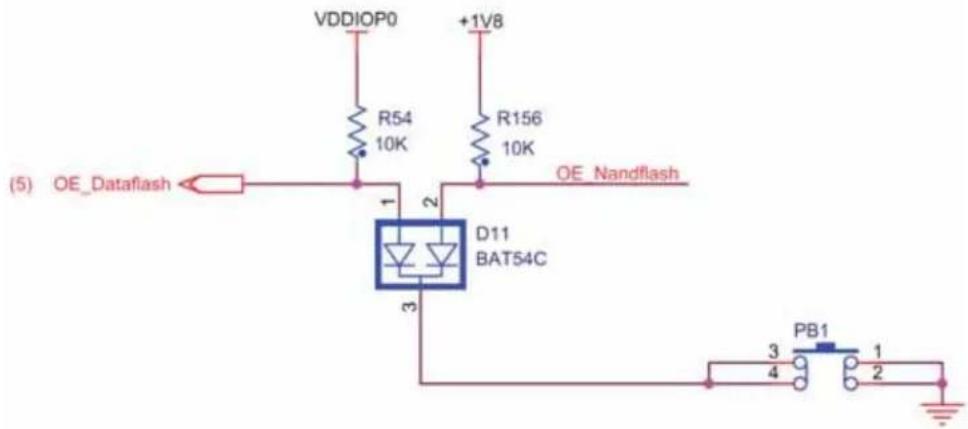
text_image
(5) OE_Dataflash VDDIOP0 R54 10K +1V8 R156 10K OE Nandflash D11 BAT54C 3 PB1 3 4 1 24.3.20.2 PB2 NRST
The NRST pin is bidirectional. It is handled by the on-chip reset controller and can be driven low to provide a reset signal to the external components, or be asserted low externally to reset the microcontroller. It will reset the core and the peripherals except for the backup region.
Figure 4-25. Push Button
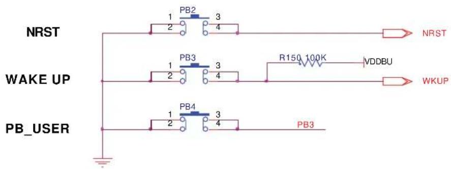
text_image
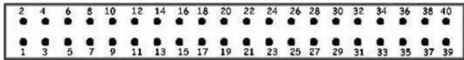
NRST WAKE UP PB_USER 1 PB2 3 2 4 PB3 1 PB3 3 2 4 R150 100K VDDBU PB4 1 PB3 2 4 PB3 NRST WKUP4.3.21 Expansion Ports
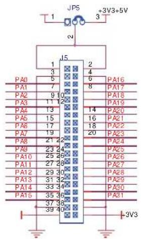
Most of GPIOs are led to expansion ports J5, J6, J7.
LCD and touch screen connector include J9 and J10 to interface DM board.
Figure 4-26. PIO Expansion Ports
text_image
JPS +3V3+5V 1 3 2 4 6 PA16 PA17 PA18 PA19 PA20 PA21 PA22 PA23 PA24 PA25 PA26 PA27 PA28 PA29 PA30 PA31 3V3 15 1 3 5 7 9 10 11 12 13 14 15 16 17 18 19 20 21 22 23 24 25 26 27 28 29 30 31 32 33 34 35 36 37 38 39 40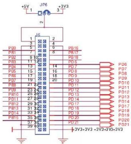
text_image
+5V JP6 +3V3 1 2 3 4 5 6 7 8 9 10 11 12 13 14 15 16 17 18 19 20 21 22 23 24 25 26 27 28 29 30 31 32 33 34 35 36 37 38 39 40 PB0 PB1 PB2 PB3 PB4 PB5 PB6 PB7 PB8 PB9 PB10 PB11 PB12 PB13 PB14 PB15 PB16 PB17 PB18 PD6 PD7 PD8 PD9 PD10 PD11 PD12 PD13 PD14 PD15 PD16 PD17 PD18 PD19 PD20 PD21 +3V3-3V3 -3V3-3V3-3V3
text_image
+5V JP8 +3V3 1 3 2 4 6 8 PC 16 PC 17 PC 18 PC 19 PC 20 PC 21 PC 22 PC 23 PC 24 PC 25 PC 26 PC 27 PC 28 PC 29 PC 30 PC 31 +5V JP8 +3V3 17 1 3 5 7 9 10 11 12 13 14 15 16 17 18 19 20 21 22 23 24 25 26 27 28 29 30 31 32 33 34 35 36 37 38 39 40Figure 4-27. LCD Expansion Ports

text_image
PA2 (ZB_IRQ0) R89 0R PA31 (TWCK0) R91 0R +3V3 J9 1 2 3 4 5 6 7 8 9 10 R90 0R (ZB_IRQ1) PA3 11 12 R92 0R (TWD0) PA30 13 14 R93 22R (LCDDAT15) PC15 15 16 R94 22R (LCDDAT14) PC14 17 18 R95 22R (LCDDAT13) PC13 19 20 R96 22R (LCDDAT12) PC12 21 22 R97 22R (LCDDAT0) PC0 23 24 R98 22R (LCDDAT2) PC2 25 26 R99 22R (LCDDAT4) PC4 27 28 R100 22R (LCDDAT6) PC6 29 30 PC1 (LCDDAT1) R98 22R PC3 (LCDDAT3) R100 22R PC5 (LCDDAT5) R102 22R PC7 (LCDDAT7) R104 22R PC9 (LCDDAT9) R107 22R PC11 (LCDDAT11) R109 22R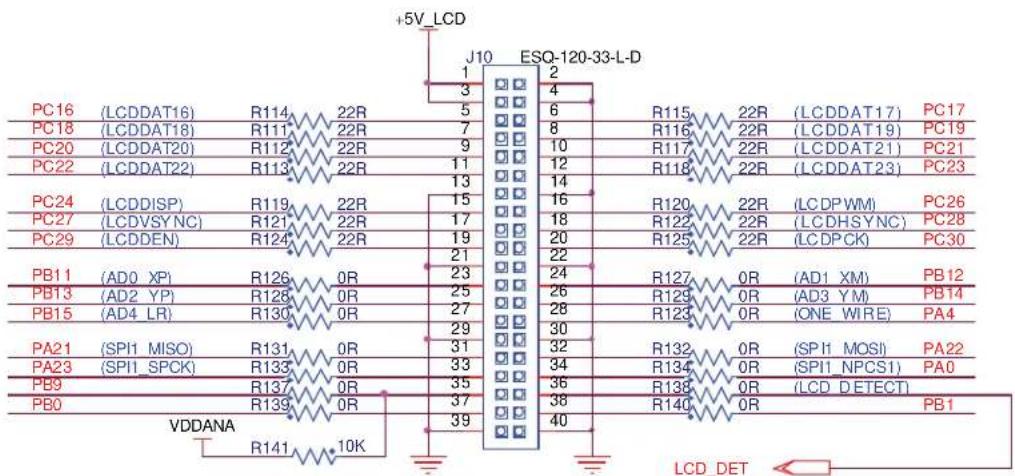
text_image
+5V_LCD J10 ESQ-120-33-L-D PC16 (LCDDAT16) R114 22R 1 2 PC18 (LCDDAT18) R111 22R 7 4 PC20 (LCDDAT20) R112 22R 9 6 PC22 (LCDDAT22) R113 22R 10 8 PC24 (LCDDISP) R119 22R 11 12 PC27 (LCDVSYNC) R121 22R 13 PC29 (LCDDEN) R124 22R 14 PB11 (AD0 XP) R126 0R 15 PB13 (AD2 YP) R128 0R 16 PB15 (AD4 LR) R130 0R 17 PA21 (SPII MISO) R131 0R 18 PA23 (SPII_SPCK) R133 0R 19 PB9 R137 0R 20 PB0 R139 0R 21 VDDANA R141 10K LCD_DET■ PIO A Pin Assignment
Table 4-3. PIO A Pin Assignment and Signal Descriptions
| Signal Alternate Periph A Periph B Periph C | |||||
| PA0 TXD0 SPI1_NPCS1 (LCD connector) | |||||
| PA1 RXD0 SPI0_NPCS2 | |||||
| PA2RTS0ZB_IRQ0 | |||||
| PA3CTS0 | ZB_IRQ1 | ||||
| PA4 SCK0 | One Wire | ||||
| PA5 TXD1 | ZB_RSTN | ||||
| PA6 RXD1 | ZB_SLPTR | ||||
| PA7 TXD2 SPI0_NPCS1 MCI card detect | |||||
| PA8 RXD2 SPI1_NPCS0 ZigBee | |||||
| PA9 DRXD | DBGU | ||||
| PA10 | DTXD | DBGU | |||
| PA11 | SPI0_MISO | MCI_DA4 | Serial DataFlash | ||
| PA12 | SPI0_MOSI | MCI_DA5 | Serial DataFlash | ||
| PA13 | SPI0_SPCK | MCI_DA6 | Serial DataFlash | ||
| PA14 | SPI0_NPCS0 | MCI_DA7 | Serial DataFlash | ||
| PA15 | MCI_DA0 | MCI | |||
| PA16 | MCI_CDA | MCI | |||
| PA17 | MCI_CK | MCI | |||
| PA18 | MCI_DA1 | MCI | |||
| PA19 | MCI_DA2 | MCI | |||
| PA20 | MCI_DA3 | MCI | |||
| PA21 | TIOA0 | SPI1_MISO | ZigBee | ||
| PA22 | TIOA1 | SPI1_MOSI | ZigBee | ||
| PA23 | TIOA2 | SPI1_SPCK | ZigBee | ||
| PA24 | TCLK0 | TK | Audio | ||
| PA25 | TCLK1 | TF | Audio | ||
| PA26 | TCLK2 | TD | Audio | ||
| PA27 | TIOB0 | RD | Audio | ||
| PA28 | TIOB1 | RK | Audio | ||
| PA29 | TIOB2 | RF | Audio | ||
| PA30 | TWD0 | SPI1_NPCS3 | Audio & LCD connector | ||
| PA31 | TWCK0 | SPI1_NPCS2 | Audio & LCD connector | ||
■ PIO B Pin Assignment
Table 4-4. PIO B Pin Assignment and Signal Descriptions
| Signal Alternate Periph A Periph B Periph C | ||||
| PB0 RTS2 (LCD connector) | ||||
| PB1 CTS2 (LCD connector) | ||||
| PB2 SCK2 JUMPER to GND | ||||
| PB3 SPI0_NPCS3 PB_USER1 | ||||
| PB4 USER_LED1 | ||||
| PB5 USER_LED2 | ||||
| PB6 AD7 PWR_LED | ||||
| PB7 AD8 EN5V_HOST | ||||
| PB8 AD9 OVCUR_USB | ||||
| PB9 AD10 PCK1 (LCD connector) | ||||
| PB10 AD11 PCK0 Audio | ||||
| PB11 AD0 | PWM0 | TSC | ||
| PB12 AD1 | PWM1 | TSC | ||
| PB13 AD2 | PWM2 | TSC | ||
| PB14 AD3 | PWM3 | TSC | ||
| PB15 AD4 (TSC) | ||||
| PB16 AD5 VBUS_SENSE | ||||
| PB17 AD6 Analog input | ||||
| PB18 | IRQ | ADTRG | LCDHSYNC (+0R) | |
■ PIO C Pin Assignment
Table 4-5. PIO C Pin Assignment and Signal Descriptions
| Signal Alternate Periph A | Periph B Periph C | ||
| PC0 LCD DAT0 TWD1 LCD | |||
| PC1 LCD DAT1 TWCK1 LCD | |||
| PC2 LCD DAT2 TIOA3 LCD | |||
| PC3 LCD DAT3 TIOB3 LCD | |||
| PC4 LCD DAT4 TCLK3 LCD | |||
| PC5 LCD DAT5 TIOA4 LCD | |||
| PC6 LCD DAT6 TIOB4 LCD | |||
| PC7 LCD DAT7 TCLK4 LCD | |||
| PC8 LCD DAT8 UTXD0 LCD | |||
| PC9 LCD DAT9 URXD0 LCD | |||
| PC10 | LCDDAT10 | PWM0 LCD | |
| PC11 | LCDDAT11 | PWM1 LCD | |
| PC12 | LCDDAT12 | TIOA5 LCD | |
| PC13 | LCDDAT13 | TIOB5 LCD | |
| PC14 | LCDDAT14 | TCLK5 LCD | |
| PC15 | LCDDAT15 | PCK0 LCD | |
| PC16 | LCDDAT16 | UTXD1 LCD | |
| PC17 | LCDDAT17 | URXD1 LCD | |
| PC18 | LCDDAT18 | PWM0 LCD | |
| PC19 | LCDDAT19 | PWM1 LCD | |
| PC20 | LCDDAT20 | PWM2 LCD | |
| PC21 | LCDDAT21 | PWM3 LCD | |
| PC22 | LCDDAT22 | TXD3 | |
| PC23 | LCDDAT23 | RXD3 | |
| PC24 | LCDDISP | RTS3 | |
| PC25 | CTS3 | ||
| PC26 | LCDPWM | SCK3 | |
| PC27 | LCDVSYNC | RTS1 LCD | |
| PC28 | LCDHSYNC | CTS1 LCD | |
| PC29 | LCDDEN | SCK1 LCD | |
| PC30 | LCDPCK | ||
| PC31 | FIQ | PCK1 OVCUR_LCD |
■ PIO D Pin Assignment
Table 4-6. PIO D Pin Assignment and Signal Descriptions
| Signal Alternate Periph | A Periph B Periph | C | ||
| PD0 NANDOE NAND Flash | ||||
| PD1 NANDWE NAND Flash | ||||
| PD2 A21/NANDALE NAND Flash | ||||
| PD3 A22/NANDCLE NAND Flash | ||||
| PD4 NCS3 NAND Flash | ||||
| PD5 NWAIT | ||||
| PD6 D16 NAND Flash | ||||
| PD7 D17 NAND Flash | ||||
| PD8 D18 NAND Flash | ||||
| PD9 D19 NAND Flash | ||||
| PD10 D20 NAND Flash | ||||
| PD11 D21 NAND Flash | ||||
| PD12 D22 NAND Flash | ||||
| PD13 D23 NAND Flash | ||||
| PD14 D24 | ||||
| PD15 D25 A20 | ||||
| PD16 D26 A23 | ||||
| PD17 D27 A24 | ||||
| PD18 D28 A25 | ||||
| PD19 D29 NCS2 | ||||
| PD20 D30 NCS4 | ||||
| PD21 D31 NCS5 ETH INT | ||||
4.4 Connectors
4.4.1 Power Supply
Figure 4-28. Power Supply Connector J1
Table 4-7. Power Supply Connector J1 Signal Descriptions
| Pin Mnemonic Signal description | ||
| 1 Center +5V | ||
| 2 | F | |
| 3 | GND | |
0
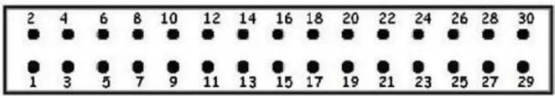
4.4.2 JTAG/ICE Connector
Figure 4-29. JTAG J4

text_image
2 4 6 8 10 12 14 16 18 20 ● ● ● ● ● ● ● ● ● ● ● ● ● ● ● ● ● ● ● ● ● ● ● ● ● 1 3 5 7 9 11 13 15 17 19Table 4-8. JTAG/ICE Connector J4 Signal Descriptions
| Pin Mnemonic Signal Description | ||
| 1 VTref. 3.3V power | This is the target reference voltage. It is used to check if the target has power, to create the logic-level reference for the input comparators, and to control the output logic levels to the target. It is normally fed from VDD on the target board and must not have a series resistor. | |
| 2 Vsupply. 3.3V power | This pin is not connected in SAM-ICE. It is reserved for compatibility with other equipment. Connect to VDD or leave open in target system. | |
| 3 | nTRST TARGET RESET - Active-low output signal that resets the target | JTAG Reset. Output from SAM-ICE to the reset signal on the target JTAG port. Typically connected to nTRST on the target CPU. This pin is normally pulled HIGH on the target to avoid unintentional resets when there is no connection. |
| 4 GND Common ground. | ||
Table 4-8. JTAG/ICE Connector J4 Signal Descriptions
| 5 | TDI TEST DATA INPUT - Serial data output line, sampled on the rising edge of the TCK signal. | JTAG data input of target CPU. It is recommended that this pin is pulled to a defined state on the target board. Typically connected to TDI on target CPU. |
| 6 GND Common ground. | ||
| 7 | TMS TEST MODE SELECT | JTAG mode set input of target CPU. This pin should be pulled up on the target. Typically connected to TMS on target CPU. Output signal that sequences the target's JTAG state machine, sampled on the rising edge of the TCK signal. |
| 8 GND Common ground. | ||
| 9 | TCK TEST CLOCK - Output timing signal, for synchronizing test logic and control register access. | JTAG clock signal to target CPU. It is recommended that this pin is pulled to a defined state on the target board. Typically connected to TCK on target CPU. |
| 10 GND Common ground. | ||
| 11 | RTCK - Input return test clock signal from the target. | Some targets must synchronize the JTAG inputs to internal clocks. To assist in meeting this requirement, a returned and retimed TCK can be used to dynamically control the TCK rate. SAM-ICE supports adaptive clocking which waits for TCK changes to be echoed correctly before making further changes. Connect to RTCK if available, otherwise to GND. |
| 12 GND Common ground. | ||
| 13 | TDO JTAG TEST DATA OUTPUT - Serial data input from the target. | JTAG data output from target CPU. Typically connected to TDO on target CPU. |
| 14 GND Common ground. | ||
| 15 n$RST RESET Active-low reset signal. Target CPU reset signal. | ||
| 16 GND Common ground. | ||
| 17 RFU This pin is not connected in SAM-ICE. | ||
| 18 GND Common ground | ||
| 19 RFU This pin is not connected in SAM-ICE | ||
| 20 GND Common ground | ||
4.4.3 DBGU
Figure 4-30. DBGU Connector J11
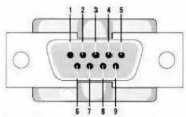
text_image
1 2 3 4 5 6 7 8 9Table 4-9. DBGU Connector J11 Signal Descriptions
| Pin Mnemonic PIO (Via translator) Description | ||
| 1, 4, 6, 9 No connection | ||
| 2 RXD (Received Data) PA9 RS232 serial data output signal | ||
| 3 TXD (Transmitted Data) PA10 RS232 serial data input signal | ||
| 5 GND Common ground | ||
| 7 RTS (Request To Send) | Not used | |
| 8 CTS (Clear To Send) | Not used | |
| Mechanical pins | Shield | |
4.4.4 USB MicroB
Figure 4-31. USB Device Micro B Connector J3
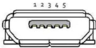
text_image
1 2 3 4 5Micro-B
Table 4-10. USB Device Micro B Connector J3 Signal Descriptions
| Pin Mnemonic | Description | |
| 1 | Vbus | 5V power |
| 2 DM | Data minus | |
| 3 DP | Data plus | |
| 4 ID | On the go identification | |
| 5 GND | Common ground | |
| 6, 7, 8, 9 | Shield | Mechanical pins |
4.4.5 USB Type A port
Figure 4-32. USB Type A Port J2

text_image
1 2 3 4Table 4-11. USB Type A Port J2 Signal Descriptions
| Pin Mnemonic Description | |||||
| 1 | V b | u s 5 V | |||
| 2 DM Data minus | |||||
| 3 DP Data plus | |||||
| 4 GND Common ground | |||||
| 5, 6 Shield Mechanical pins | |||||
p
4.4.6 SD Card MCI
Figure 4-33. SD/MMC Socket J8
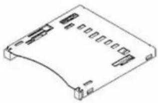
natural_image
Isometric line drawing of a computer monitor base with ventilation slots and mounting feet (no text or symbols)Table 4-12. SD Socket J8 Signal Descriptions
| Pin Function PIO | ||
| 1 | MCI_DA3 | PA20 |
| 2 | MCI_CMD | PA16 |
| 3 | GND | |
| 4 | VDDIOP0 | |
| 5 | MCI_CLK | PA17 |
| 6 | GND | |
| 7 | MCI_DA0 | PA15 |
| 8 | MCI_DA1 | PA18 |
| 9 | MCI_DA2 | PA19 |
| 10 | MCI_CD | PA7 |
| 11 | WP | |
| 12 | GND | |
| 13 | GND | |
4.4.7 Ethernet RJ45 Socket
Figure 4-34. Ethernet RJ45 Socket J16
12345678

RJ-45
Table 4-13. RJ45 Socket J16 Signal Descriptions
| Pin Mnemonic Description | |
| 1 TX+ Differential output plus | |
| 2 TX- Differential output minus | |
| 3 RX+ Differential input plus | |
| 4 Reserved | |
| 5 Reserved | |
| 6 RX- Differential input minus | |
| 7 Reserved | |
| 8 Reserved |
4.4.8 Zigbee Socket J12
Figure 4-35. Zigbee Socket J12

Table 4-14. Zigbee Socket J12 Signal Descriptions
| Function | Signal Name Port | Pin | Pin | Port | Signal Name | Function | |
| Reset | /RST | 1 | 2 | IRQ0 | Interrupt Request | ||
| Interrupt Request | IRQ1 | 3 | 4 | SLP_TR | SLP_TR | ||
| SPI chip select | /CS | 5 | 6 | MOSI | SPI MOSI | ||
| SPI MISO | MISO | 7 | 8 | SCLK | SPI CLK | ||
| Power Supply | GND | GND | 9 | 10 | VCC | VCC | VCC |
Figure 4-36. LCD Socket J9
text_image
2 4 6 8 10 12 14 16 18 20 22 24 26 28 30 ● ● ● ● ● ● ● ● ● ● ● ● ● ● ● ● ● ● ● ● ● ● ● ● ● ● ● ● ● ● ● ● ● 1 3 5 7 9 11 13 15 17 19 21 23 25 27 29Table 4-15. LCD Socket J9 Signal Descriptions
| LCD ISI Pin Num Pin Num ISI LCD | |||||
| 3V3 3V3 1 2 GND GND | |||||
| VDDISI VDDISI 3 4 GND GND | |||||
| ZB_IRQ0 ZB_IRQ0 5 6 | ZB_IRQ1 | ||||
| TWCK0 | TWCK0 7 8 | TWD0 | |||
| GND | GND | 9 | 10 | ISI_MCK | LCDDAT15 |
| GND | GND | 11 | 12 | ISI_VSYNC | LCDDAT13 |
| GND | GND | 13 | 14 | ISI_HSYNC | LCDDAT14 |
| GND | GND | 15 | 16 | ISI_PCK | LCDDAT12 |
| GND | GND | 17 | 18 | ISI_D0 | LCDDAT0 |
| LCDDAT1 | ISI_D1 | 19 | 20 | ISI_D2 | LCDDAT2 |
| LCDDAT3 | ISI_D3 | 21 | 22 | ISI_D4 | LCDDAT4 |
| LCDDAT5 | ISI_D5 | 23 | 24 | ISI_D6 | LCDDAT6 |
| LCDDAT7 | ISI_D7 | 25 | 26 | ISI_D8 | LCDDAT8 |
| LCDDAT9 | ISI_D9 | 27 | 28 | ISI_D10 | LCDDAT10 |
| LCDDAT11 | ISI_D11 | 29 | 30 | GND | GND |
Figure 4-37. LCD Socket J10
text_image
2 4 6 8 10 12 14 16 18 20 22 24 26 28 30 32 34 36 38 40 ● ● ● ● ● ● ● ● ● ● ● ● ● ● ● ● ● ● ● ● ● ● ● ● ● ● ● ● ● ● ● ● ● ● ● ● ● ● ● ● ● ● ● ● ● ● ● 1 3 5 7 9 11 13 15 17 19 21 23 25 27 29 31 33 35 37 39Table 4-16. LCD Socket J10 Signal Descriptions
| LCD Pin Num Pin Num LCD | |||||
| 5V 5V_INTER 1 | 2 GND GND | ||||
| 5V 5V_INTER 3 | 4 GND GND | ||||
| LCDDAT16 5 6 | LCDDAT17 | ||||
| LCDDAT18 7 8 | LCDDAT19 | ||||
| LCDDAT20 9 10 | LCDDAT21 | ||||
| LCDDAT22 | 11 | 12 | LD | DAT23 | |
| GND | GND | 13 | 14 | GND | GND |
| LCDDISP | 15 | 16 | LCD | PWM | |
| LCDCSYNC | 17 | 18 | LCD | HSYNC | |
| LCDDEN | 19 | 20 | LCD | PCK | |
| GND | GND | 21 | 22 | GND | GND |
| AD0_XP | TSC | 23 | 24 | TSC | AD1_XM |
| AD2_YP | TSC | 25 | 26 | TSC | AD3_YM |
| AD4_LR | TSC | 27 | 28 | ONE | WIRE |
| GND | GND | 29 | 30 | GND | GND |
| SPI1_MISO | 31 | 32 | SPI1 | _MOSI | |
| SPI1_SPCK | 33 | 34 | SPI1 | _NPCS1 | |
| EN_PWRLCD | SELCONFIG | 35 | 36 | LCD_DETECT | LCD_DETECT# |
| PD16 | 37 | 38 | PD17 | ||
| GND | GND | 39 | 40 | GND | GND |
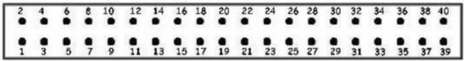
4.4.10 IO Expansion Port
Figure 4-38. IO Expansion Socket J5

text_image
2 4 6 8 10 12 14 16 18 20 22 24 26 28 30 32 34 36 38 40 ● ● ● ● ● ● ● ● ● ● ● ● ● ● ● ● ● ● ● ● ● ● ● ● ● ● ● ● ● ● ● ● ● ● ● ● ● ● ● ● ● ● ● ● ● 1 3 5 7 9 11 13 15 17 19 21 23 25 27 29 31 33 35 37 39Table 4-17. IO Expansion Socket J5 Signal Descriptions
| PIO Power Pin | Num Pin Num Power PIO | ||||
| 3V3, or 5V 1 2 3 | V3, or 5V | ||||
| GND 3 4 GND | |||||
| PA056PA16 | |||||
| PA178PA17 | |||||
| PA2 9 | 10 | PA18 | |||
| PA3 | 11 | 12 | PA19 | ||
| PA4 | 13 | 14 | PA20 | ||
| PA5 | 15 | 16 | PA21 | ||
| PA6 | 17 | 18 | PA22 | ||
| PA7 | 19 | 20 | PA23 | ||
| PA8 | 21 | 22 | PA24 | ||
| PA9 | 23 | 24 | PA25 | ||
| PA10 | 25 | 26 | PA26 | ||
| PA11 | 27 | 28 | PA27 | ||
| PA12 | 29 | 30 | PA28 | ||
| PA13 | 31 | 32 | PA29 | ||
| PA14 | 33 | 34 | PA30 | ||
| PA15 | 35 | 36 | PA31 | ||
| GND | 37 | 38 | GND | ||
| 3V3 | 39 | 40 | 3V3 | ||
Figure 4-39. IO Expansion Socket J6
text_image
2 4 6 8 10 12 14 16 18 20 22 24 26 28 30 32 34 36 38 40 ● ● ● ● ● ● ● ● ● ● ● ● ● ● ● ● ● ● ● ● ● ● ● ● ● ● ● ● ● ● ● ● ● ● ● ● ● ● ● ● ● ● ● ● 1 3 5 7 9 11 13 15 17 19 21 23 25 27 29 31 33 35 37 39Table 4-18. IO Expansion Socket J6 Signal Descriptions
| PIO Power Pin | Num Pin Num Power PIO | ||||
| 3V3, or 5V 1 2 3 | V3, or 5V | ||||
| GND 3 4 GND | |||||
| PB0 5 6 PB16 | |||||
| PB1 7 8 PB17 | |||||
| PB2 9 10 PB18 | |||||
| PB3 11 12 PD6 | |||||
| PB4 13 14 PD7 | |||||
| PB5 15 16 PD8 | |||||
| PB6 17 18 PD9 | |||||
| PB7 19 20 PD10 | |||||
| PB8 21 22 PD11 | |||||
| PB9 23 24 PD12 | |||||
| PB10 | 25 26 PD13 | ||||
| PB11 | 27 28 PD14 | ||||
| PB12 | 29 30 PD17 | ||||
| PB13 | 31 32 PD18 | ||||
| PB14 | 33 34 PD19 | ||||
| PB15 | 35 36 PD20 | ||||
| GND | 37 38 PD21 | ||||
| 3V3 | 39 40 | 3V3 | |||
Figure 4-40. IO Expansion Socket J7
text_image
2 4 6 8 10 12 14 16 18 20 22 24 26 28 30 32 34 36 38 40 ● ● ● ● ● ● ● ● ● ● ● ● ● ● ● ● ● ● ● ● ● ● ● ● ● ● ● ● ● ● ● ● ● ● ● ● ● ● ● ● ● ● ● 1 3 5 7 9 11 13 15 17 19 21 23 25 27 29 31 33 35 37 39Table 4-19. IO Expansion Socket J7 Signal Descriptions
| PIO Power Pin | Num Pin Num Power PIO | ||||
| 3V3, or 5V 1 2 3 | V3, or 5V | ||||
| GND 3 4 GND | |||||
| PC0 5 6 PC16 | |||||
| PC1 7 8 PC17 | |||||
| PC2 9 10 PC18 | |||||
| PC3 | 11 | 12 PC19 | |||
| PC4 | 13 | 14 PC20 | |||
| PC5 | 15 | 16 PC21 | |||
| PC6 | 17 | 18 PC22 | |||
| PC7 | 19 | 20 PC23 | |||
| PC8 | 21 | 22 PC24 | |||
| PC9 | 23 | 24 PC25 | |||
| PC10 | 25 | 26 PC26 | |||
| PC11 | 27 | 28 PC27 | |||
| PC12 | 29 | 30 PC28 | |||
| PC13 | 31 | 32 PC29 | |||
| PC14 | 33 | 34 PC30 | |||
| PC15 | 35 | 36 PC31 | |||
| GND | 37 | 38 | GND | ||
| 3V3 | 39 | 40 | 3V3 | ||
5.1 SAM9N12-EK Schematics
This section contains the following schematics:
■ Top Level
■ Power Supply
■ AT91SAM9N12
■ EBI Interface
■ PIO Interfaces
■ DDR2 NAND Flash
■ Serial Interfaces
■ Audio
ETH
flowchart
graph TD
    subgraph_Panel1["Panel 1"]
        A["USB"] -->|HOST| B["ATMEL ARM9 Processor SAM9N12 (LFBGA217)"]
        C["HD"] -->|ICE INTERFACE| B
        D["USB"] -->|HOST DEVICE| B
        E["HE 10"] -->|ICE INTERFACE| B
        F["RS232"] -->|DBGU| B
        G["HE 14"] -->|TOUCH SCREEN| B
        H["ISI CAMERA INTERFACE"] -->|INTERFACE| B
        I["HE 14"] -->|CARD READER| B
    end

    subgraph_Panel2["Panel 2"]
        J["POWER SUPPL"] --> K["3V3"]
        L["PIO"] --> M["1V"]
        N["PIO A...E"] --> O["PIO"]
    end

    subgraph_Panel3["Panel 3"]
        P["Power"] --> Q["EBI DATA INTERFACE"]
        R["PIO"] --> S["EBI ADDRESS INTERFACE"]
        T["PIO"] --> U["EBI BUS INTERFACE"]
    end

    subgraph_Panel4["Panel 4"]
        V["RES.ARRLAYS EBI ADAPTER"] --> W["EBI DDR2 INTERFACE"]
        X["EBI ADDRESS INTERFACE"] --> Y["EBI NANDFLASH INTERFACE"]
        Z["EBI BUS INTERFACE"] --> AA["EBI ETH INTERFACE"]
    end

    subgraph_Panel5["Panel 5"]
        AB["HE 14"] --> AC["AUDIOZIGBEE"]
        AD["PIO CONNECTOR"] --> AE["TW/OSH0"]
        AF["1-WRIE EEPROM"] --> AG["SERIAL EEPROM"]
        AH["SERIAL DATA FLASH"] --> AI["SERIAL DATA FLASH"]
    end

    J -->|3V3| B
    K -->|3V3| B
    M -->|3V3| B
    N -->|3V3| B
    O -->|3V3| B
    P -->|PIO A...E| B
    Q -->|PIO A...E| B
    S -->|PIO A...E| B
    T -->|PIO A...E| B
    U -->|PIO A...E| B
    V -->|EBI DDR2 INTERFACE| W
    V -->|EBI DDR2 INTERFACE| X
    W -->|EBI DDR2 INTERFACE| Y
    X -->|EBI DDR2 INTERFACE| Z
    Y -->|EBI DDR2 INTERFACE| AA
    Z -->|EBI DDR2 INTERFACE| AB
    AA -->|EBI DDR2 INTERFACE| AC
    AB -->|EBI DDR2 INTERFACE| AD
    AC -->|EBI DDR2 INTERFACE| AE
    AD -->|EBI DDR2 INTERFACE| AF
    AE -->|EBI DDR2 INTERFACE| AG
    AF -->|EBI DDR2 INTERFACE| AH
    AG -->|EBI DDR2 INTERFACE| AI
    AH -->|EBI DDR2 INTERFACE| AJ
    AI -->|EBI DDR2 INTERFACE| AK
    AJ -->|EBI DDR2 INTERFACE| AL
    AK -->|EBI DDR2 INTERFACE| AM
    AL -->|EBI DDR2 INTERFACE| AN
    AM -->|EBI DDR2 INTERFACE| AO
    AN -->|EBI DDR2 INTERFACE| AP

| FICO MIXERS | |||||||||||||
| POA | USAGE | POA | USAGE | POA | USAGE | POA | USAGE | POA | POA | USAGE | POA | POST | POST |
| P01 | POO | PA5 | NO. CO | POI | PS1 | WEI SENSE | POC | LCOOAT10 | PC18 | LCOOAT17 | POU | NANDE | |
| PA1 | POO | NC. CO | PS1 | PS1 | ADC | PS1 | LCOOAT1 | PC17 | LCOOAT17 | PE1 | NANDE | ||
| PA2 | SPB | PA5 | NC. OAI | PS1 | PS1 | ADRG | PC2 | LCOOAT2 | PC18 | LCOOAT18 | PC2 | NANDE/AK1 | |
| PA3 | SPB | PA5 | NC. OAI2 | PS1 | PS1 | ADRG | PC2 | LCOOAT2 | PC18 | LCOOAT19 | PC2 | NANDE/CS2 | |
| PA4 | SPB | PA5 | NC. OAI3 | PS1 | PS1 | ADC | PC4 | LCOOAT14 | PC20 | LCOOAT10 | PC4 | NANDE | |
| PA5 | SPB | PA5 | NC. OAI4 | PS1 | PS1 | ADC | PC5 | LCOOAT15 | PC21 | LCOOAT11 | PC5 | NANAT | |
| PA6 | SPB | PA5 | SPB MISC | PS1 | PS1 | ADC | PC5 | LCOOAT15 | PC22 | LCOOAT12 | PS1 | NANAT | |
| PA7 | SPB | PA5 | SPB MISC | PS1 | PS1 | ADC | PC5 | LCOOAT15 | PC23 | LCOOAT12 | PS1 | NANAT | |
| PA8 | NC/WD/DCI | PA2 | EPI SPCK | PS1 | EPIV 5C | PS7 | LCOOAT1 | PC24 | LCOOAT15 | PC7 | D17 | ||
| PA9 | EPI APOSO | PA2 | TX | PS1 | OVOUR JSS | PC5 | LCOOAT1 | PC25 | LCOOBT | PC6 | D18 | ||
| PA10 | POO | TF | POI | PC10 | LCOOAT1 | PC26 | ENBV LOD | PC10 | D19 | ||||
| PA11 | DX3 | PA5 | TS | PS10 | POII | PC10 | LCOOAT10 | PC26 | LEONVM | PC10 | D20 | ||
| PA12 | SPB MISC | PA5 | RS1 | PS11 | POII | PC11 | LCOOAT11 | PC27 | LEONVM | PC11 | D21 | ||
| PA13 | SPB MISC | PA5 | PK | PS12 | AD1 | PC12 | LCOOAT12 | PC28 | LEONVM | PC12 | D22 | ||
| PA14 | SPB SPCK | PA5 | FSI | PS13 | AD2 | PC13 | LCOOAT15 | PC29 | LEON | PC13 | D23 | ||
| PA15 | SPB APOSO | PA5 | TWO | PS14 | AD3 | PC14 | LCOOAT14 | PC30 | LEON | PC14 | D24 | ||
| PA16 | NCI-DAI | PA5 | TWXO | PS15 | AD4 | PC15 | LCOOAT15 | PC51 | OVCOR LOD | PC15 | A20 | ||
NOTE
"DNP" means the component is not populated by default
| C | NOR NOST | 25-DEC-11 | XXX | XX-XXX-XX | |
| D | SB | 25-SEP-11 | XXX | XX-XXX-XX | |
| A | RNT EDIT | 20-DEC-11 | XX-XXX-XXX-D | ||
| REV. | NORF. | DES. | DATE | VER. | DATE |
| REV. | 1/1 | KX- | H1/9 | ||
| c | 1/9 |
The following table provides the information in English:
text_image
FORCE POWER ON 1 JL1 F1 2 +5V C7 Tref Q1 6 R8 10kX 3 4 +5V PAC-LS R8 10kX TRPTF3 R8 10kX KM1 AC30/SA VOUT NO FU 10kX FGCOO AC1 FU 10kX R3 1kX -50V VCCBOPA2 L1 250nm at 100MHz L2 250nm at 100MHz L3 250nm at 100MHz VDDIP1 TRPTF4 VDDIAA TRPTF6 KM2 LP38802WP 1.8 VOUT VOUT +1.9V-SV VE3 NO +1.9V-SV TRPTF9 L4 250nm at 100MHz L5 250nm at 100MHz L6 250nm at 100MHz TPPTF7 TPPTF8
text_image
REGULATED SV ONLY Ach 2.7mm F1 SP1812 2A DC +5V USB +5V SWI SW-SL/UE-3 -5V CPI 5V C8 30.5F
text_image
2V3 G10 10.8 25pF NC3 ACP:710/620/6 ACP:710 ACP:710 ACP:710 C143 10n1 R-3 12k 1% C144 10nF +19 +19 +19 +19 +19 +19 +19 +19 +19 +19 +19 +19 +19 +19 +19 +19 +19 +19 +19 +19 +19 +19 +19 +19 +19 +15VST = 2.27 x Flug - Dall (wt) / 304
| C NOR RNDT | PP | 5-NCV-11 | XXX | AA-XXX-XX | |
| D NIP | PP | 5-SLPI-11 | XXX | AA-XXX-XX | |
| A. RNF DOT | 60-AUS-11 | 90-XXX-XX | |||
| REV. MODIF. | DEC. | DATE | VER. | DATE | |
| SCALE 1/1 | REV. | HHH-1 | |||
| C | 2g | ||||
PXXX

text_image
TP1 L015 20kV L7 2200mA 100kV TP4 +3V LOB L4 2200mA 100kV L7 2200mA 100kV TP4 C17 100kF C17 100kF C17 100kF C17 100kF C17 100kF C17 100kF C17 100kF C17 100kF C17 100kF C17 100kF C17 100kM U55 OUTA BNA 1 R16 VREF/OR R331 R17 VREF/OR R331 R18 VREF/OR R331 R19 VREF/OR R331 R20 VREF/OR R331 R21 VREF/OR R331 R22 VREF/OR R331 R23 VREF/OR R331 R24 VREF/OR R331 R25 VREF/OR R331 R26 VREF/OR R331 R27 VREF/OR R331 R28 VREF/OR R331 R29 VREF/OR R331 R30 VREF/OR R331 R31 VREF/OR R331 R32 VREF/OR R331 R33 VREF/OR R331 R34 VREF/OR R331 R35 VREF/OR R331 R36 VREF/OR R331 R37 VREF/OR R331 R38 VREF/OR R331 R39 VREF/OR R331 R40 VREF/OR R331 R41 VREF/OR R331 R42 VREF/OR R331 R43 VREF/OR R331 R44 VREF/OR R331 R45 VREF/OR R331 R46 VREF/OR R331 R47 VREF/OR R331 R48 VREF/OR R331 R49 VREF/OR R331 R50 VREF/OR R331 R51 VREF/OR R331 R52 VREF/OR R331 R53 VREF/OR R331 R54 VREF/OR R331 R55 VREF/OR R331 R56 VREF/OR R331 R57 VREF/OR R331 R58 VREF/OR R331 R59 VREF/OR R331 R60 VREF/OR R331 R61 VREF/OR R331 R62 VREF/OR R331 R63 VREF/OR R331 R64 VREF/OR R331 R65 VREF/OR R331 R66 VREF/OR R331 R67 VREF/OR R331 R68 VREF/OR R331 R69 VREF/OR R331 R70 VREF/OR R331 R71 VREF/OR R331 R72 VREF/OR R331 R73 VREF/OR R331 R74 VREF/OR R331 R75 VREF/OR R331 R76 VREF/OR R331 R77 VREF/OR R331 R78 VREF/OR R331 R79 VREF/OR R331 R80 VREF/OR R331 R81 VREF/OR R331 R82 VREF/OR R331 R83 VREF/OR R331 R84 VREF/OR R331 R85 VREF/OR R331 R86 VREF/OR R331 R87 VREF/OR R331 R88 VREF/OR R331 R89 VREF/OR R331 R90 VREF/OR R331 R91 VREF/OR R331 R92 VREF/OR R331 R93 VREF/OR R331 R94 VREF/OR R331 R95 VREF/OR R331 R96 VREF/OR R331 R97 VREF/OR R331 R98 VREF/OR R331 R99 VREF/OR R331 R100 VREF/OR R331XXX
text_image
-5V CD 1 2 3 4 5 6 7 8 9 10 11 12 13 14 15 16 17 18 19 20 21 22 23 24 25 26 27 28 29 30 31 32 33 34 35 36 37 38 39 40 41 42 43 44 45 46 47 48 49 50 51 52 53 54 55 56 57 58 59 60 61 62 63 64 65 66 67 68 69 70 -5V CD 1 M 2 M 3 M 4 M 5 M 6 M 7 M 8 M 9 M 10 M 11 M 12 M 13 M 14 M 15 M 16 M 17 M 18 M 19 M 20 M 21 M 22 M 23 M 24 M 25 M 26 M 27 M 28 M 29 M 30 M 31 M 32 M 33 M 34 M 35 M 36 M 37 M 38 M 39 M 40 M 41 M 42 M 43 M 44 M 45 M 46 M 47 M 48 M 49 M 50 M 51 M 52 M 53 M 54 M 55 M 56 M 57 M 58 M 59 M 60 M 61 M 62 M 63 M 64 M 65 M 66 M 67 M 68 M 69 M 70 M 71 M 72 M 73 M 74 M 75 M 76 M 77 M 78 M 79 M 80 M 81 M 82 M 83 M 84 M 85 M 86 M 87 M 88 M 89 M 90 M 91 M 92 M 93 M 94 M 95 M 96 M 97 M 98 M 99 M 100M A B C D E F G H I J K L N O P Q R S T U V W X Y Z X A X B X C X D X E X F G X G X H X I X J X K X L X A X A X B X C X D X E X F G X G X H X I X J X K X L X A X A X B X C X D X E X F G X G X H X I X J X K X L X A X A X B X C X D X E X F G X G X H X I X J X K X L X A X A X B X C X D X E X F G X G X H XI + - - - - - - - - - - - - - - - - - - - - - - - - - - - - - - - - - - - - - - - - - - - - - - - - - - - - - - - - - - - - - - - - - - - - - - - - - - - - - - - - - - - - CD SETCH
text_image
NRST WAKE UP PB_USER
| ROUSSET | |||||
| SAMB13-64_RWC | G | XOF | RIST | PP | 25-RCP-11 |
| B | = | = | PP | 25-SPPT-11 | |
| A | #RT | EDIT | PP | 20-JUG-11 | |
| REV. | MOOF. | DEC. | DATE | VER. | |
| DATE | |||||
| BGA217 | SXLN = 1/1 | REV. | |||
| LH4 | =3-● | % | |||
5.2 SAM9CN11-EK Schematics
This section contains the following schematics:
■ Block Diagram
■ Power Supply
■ AT91SAM9CN11
■ EBI Interface
■ PIO Interfaces
■ DDR2 NAND Flash
■ Serial Interfaces
■ Audio
ETH
flowchart
graph TD
    subgraph Power Supply
        A["Power Supply"] --> B["ATMEL ARM9 Processor SAM9CN11 (LFBGA217)"]
    end

    subgraph Hardware Components
        C["USB Interface"] --> D["HOST"]
        C --> E["HOST DEVICE"]
        C --> F["ICE INTERFACE"]
        G["USB"] --> H["HOST"]
        G --> I["ICE INTERFACE"]
        J["USB"] --> K["ICE INTERFACE"]
        L["USB"] --> M["ICE INTERFACE"]
        N["USB"] --> O["ICE INTERFACE"]
        P["USB"] --> Q["IC30 SDWG"]
        R["USB"] --> S["IC30 SDWG"]
    end

    subgraph Data Inputs
        T["Power"] --> U["3V3"]
        U --> V["1V8"]
        V --> W["1V"]
        W --> X["PIO"]
        X --> Y["PIO A...E"]
        Y --> Z["Sheet 3,4,5"]

    end

    subgraph EBI Interface
        AA["EBI DATA INTERFACE"] --> AB["RES.ARRLAYS EBI ADAPTER"]
        AC["EBI ADDRESS INTERFACE"] --> AD["RES.ARRLAYS EBI ADAPTER"]
        AE["EBI BUS INTERFACE"] --> AF["RES.ARRLAYS EBI ADAPTER"]
        AG["EBI DDR2 INTERFACE"] --> AH["RES.ARRLAYS EBI ADAPTER"]
        AI["EBI NANDFLASH INTERFACE"] --> AJ["RES.ARRLAYS EBI ADAPTER"]
        AK["EBI ETH INTERFACE"] --> AL["RES.ARRLAYS EBI ADAPTER"]
        AM["EBI DDR2 INTERFACE"] --> AN["RES.ARRLAYS EBI ADAPTER"]
        AO["EBI FLASH INTERFACE"] --> AP["RES.ARRLAYS EBI ADAPTER"]
        AQ["EBI NANDFLASH INTERFACE"] --> AR["RES.ARRLAYS EBI ADAPTER"]
        AS["EBI"] --> AT["EDI"]
        AU["EDI"] --> AV["EDI"]
        AW["EDI"] --> AX["EDI"]
    end

    subgraph Memory Components
        AY["REDACTOR"] --> AZ["AUDIOZIGBEE"]
        BA["Microcontroller"] --> BB["TWOSFIO"]
        BC["I-WRIE EEPROM"] --> BD["SERIAL EEPROM"]
        BE["SERIAL DATA FLASH"] --> BF["SERIAL DATA FLASH"]
    end

    subgraph Data Inputs
        BG["Data Inputs"] --> BH["LCD INTERFACE 4.3" 480x272 TFT"]
        BI["LCD INTERFACE 4.3" 480x272 TFT"] --> BJ["TOUCH SCREEN"]
        BK["DISCIPLS INTERFACE"] --> BL["ISI CAMERA INTERFACE"]
        BM["CARD READER"] --> BN["THE 14"]
    end

    subgraph Data Inputs
        BO["Data Inputs"] --> BP["LOG PROCESS 2.5,7"]
        BP --> BQ["USB Interface"]
        BR["USB Interface"] --> BS["ICE INTERFACE"]
    end

    subgraph Memory Components
        BT["Memory Components"] --> BU["AUDIOZIGBEE"]
        BV["AUDIOZIGBEE"] --> BW["THE 14"]
    end

    subgraph Data Inputs
        BX["AUDIOZIGBEE"] --> BY["TWOSFIO"]
        BZ["AUDIOZIGBEE"] --> CA["SERIAL EEPROM"]
        CB["SERIAL DATA FLASH"] --> CC["SERIAL DATA FLASH"]
    end

    subgraph Data Inputs
        DB["AUDIOZIGBEE"] --> DC["THE 14"]
    end

    subgraph Memory Components
        DD["AUDIOZIGBEE"] --> DP["TWOSFIO"]
        DP --> Q["SERIAL EEPROM"]
        RZ["SERIAL DATA FLASH"] --> BS
    end

    subgraph Data Inputs
        BTA["AUDIOZIGBEE"] --> BY
        BZA["AUDIOZIGBEE"] --> DC
    end

    subgraph Data Inputs
        DBA["AUDIOZIGBEE"] --> DC
    end

    subgraph Memory Components
        DBA --> BA
    end

    subgraph Data Inputs
        DBA --> BZ
    end

    subgraph Memory Components
        DBA --> BZ
    end

    subgraph Data Inputs
        DBA --> BZ
    end

    subgraph Data Inputs
        DBA --> BZ
    end

    subgraph Memory Components
        DBA --> DC
    end

    subgraph Data Inputs
        DBA --> BZ
    end

    subgraph Data Inputs
        DBA --> BZ
    end

    subgraph Memory Components
        DBA --> DC
    end

    subgraph Data Inputs
        DBA --> BZ
    end

    subgraph Memory Components
        DBA --> BZ
    end

    subgraph Data Inputs
        DBA --> BZ
    end

    subgraph Data Inputs
        DBA --> BZ
    end

    subgraph Memory Components
        DBA --> DC
    end

    subgraph Data Inputs
        DBA --> BZ
    end
| PROMS | |||||||||||||
| RCA | USAGE | RCA FOR PROPAGE | USAGE | USAGE USAGE PROBLEM | USAGE | ||||||||
| PG1 | PG0 | PG1 | PG2 | PB0 | - | PB1 | VBR | SENSE | PG2 | LOCDATN | PG15 | LOCDAT18 | PD0 |
| PG1 | ROD | PG16 | NCI ODA | PB1 | PB17 | ADB | PG1 | LOCDAT1 | PG17 | LOCDAT17 | PD1 | ||
| PG1 | ROD | PG17 | NCI OK | PB1 | PB1 | PB17 | ADB | PG1 | LOCDAT1 | PG17 | LOCDAT19 | PD1 | |
| PG2 | ZS RGO | PG18 | NCI D41 | PB2 | ROW CODE | PB18 | ADTRS | PG2 | LOCDAT2 | PG18 | LOCDAT18 | PD2 | |
| PG2 | ZS RGO | PG19 | NCI D42 | PB2 | RED LED | PG2 | LOCDAT3 | PG19 | LOCDAT19 | PD3 | |||
| PG3 | On Wire | PG20 | NCI D43 | PB4 | USER LED | PG4 | LOCDAT4 | PG20 | LOCDAT20 | PD4 | |||
| PG3 | ZS KSTN | PG21 | SP1 M50 | PB6 | USER LED | PG6 | LOCDAT5 | PG31 | LOCDAT21 | PD6 | |||
| PG3 | ZS SLINK | PG22 | SP1 M51 | PB7 | PAR LE | PG7 | LOCDAT6 | PG32 | LOCDAT22 | PD7 | |||
| PG4 | NCI Gold GOGC | PG23 | SP1 SPICK | PB7 | SNY HOST | PG7 | LOCDAT7 | PG33 | LOCDAT23 | PD7 | |||
| PG4 | SPX MPEGD | PG24 | TK | PB8 | CWCH US | PG8 | LEMA12 | PG34 | LEMPRT | PD8 | |||
| PG5 | DEO | PG25 | TF | PB9 | PG9 | LOCDAT9 | PG35 | ENRY LO | PD9 | ||||
| PG5 | LTDQ | PG26 | TU | PB10 | PORT | PG10 | LOCDAT10 | PG36 | LOCMWC | PD10 | |||
| PG5 | SPX MISO | PG27 | ND | PB11 | ADB | PG11 | LEMA11 | PG37 | LODSYNC | PD11 | |||
| PG5 | SPX MISO | PG28 | HK | PB12 | AD1 | PG12 | LOCDAT12 | PG38 | LODSYNC | PD12 | |||
| PG5 | SPX SPICK | PG29 | TH | PB13 | AG2 | PG13 | LOCDAT13 | PG39 | LOCDEN | PD13 | |||
| PG5 | SPX MPEGD | PG30 | TMWD | PB14 | ADC | PG14 | LOCDAT14 | PG40 | LOCPK | PD14 | |||
| PG5 | NCI UBE | PG31 | TMWD | PB15 | ADC | PG15 | LEMA15 | PG31 | DRSR-LED | PD15 | |||
| A | INT=30T | 05-APR12 | 05-APR12P | ||
| REV. | 1/4 | DATE | 2/4 | 2014-08 | |
| SAMBON11-EX | SCALE: 1/1 | REV.A | SHEET: 1/9 | ||
| Block Grayman | ● | ||||

text_image
FORCE POWER ON 1 J1 2 +23 C7 REF 2 6 5 4 3 2 14 -10k SINON IS 3R FVH EN TP8 P8 10k +23 VDD/TP80 L1 200Vdc at 100kHz TP9 L2 200Vdc at 100kHz TP4 L3 200Vdc at 100kHz TP5 L4 250Vdc at 100kHz TP7 L5 250Vdc at 100kHz TP6 L6 250Vdc at 100kHz TP5 MEN ATC-164 VIN VDD VOUT 6 R1 1.0kV G1 1.0kV CC ACU1 1 7 R2 1.0kV CC ACU2 1 7 R3 1.0kV CC ACU3 1 7 R4 1.0kV CC ACU4 1 7 R5 1.0kV CC ACU5 1 7 R6 1.0kV CC ACU6 1 7 R7 1.0kV CC ACU7 1 7 R8 1.0kV CC ACU8 1 7 R9 1.0kV CC ACU9 1 7 R10 1.0kV CC ACU10A 1 7 R11 1.0kV CC ACU11B 1.5 VOUT VIN 2.5 VOUT 3 VOUT 3 VOUT 3 VOUT 3 VOUT 3 VOUT 3 VOUT 3 VOUT 3 VOUT 3 VOUT 3 VOUT 3 VOUT 3 VOUT 3 VOUT 3 VOUT 3 VOUT 3 VOUT 3 VOUT 3 VOUT 3 VOUT 3 VOUT 3 VOUT 3 VOUT 3 VOUT 3 VOUT 3 VOUT 2.5 VOUT 2.5 VOUT 2.5 VOUT 2.5 VOUT 2.5 VOUT 2.5 VOUT 2.5 VOUT 2.5 VOUT 2.5 VOUT 2.5 VOUT 2.5 VOUT 2.5 VOUT 2.5 VOUT 2.5 VOUT 2.5 VOUT 2.5 VOUT 2.5 VOUT 3.5 VOUT 3.5 VOUT 3.5 VOUT 3.5 VOUT 3.5 VOUT 3.5 VOUT 3.5 VOUT 3.5 VOUT 3.5 VOUT 3.5 VOUT 3.5 VOUT 3.5 VOUT 3.5 VOUT 3.5 VOUT 3.5 VOUT 3.5 VOUT 3.5 V OUT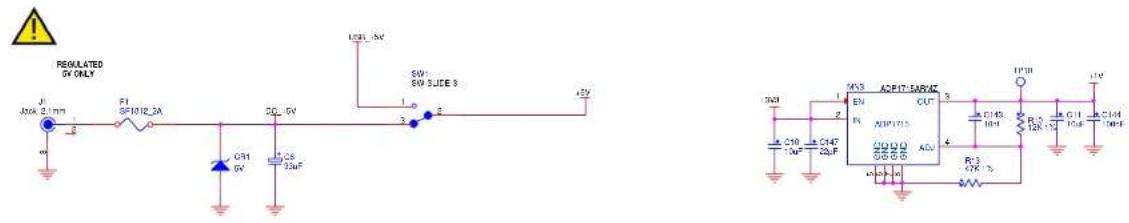
text_image
REGULATED GV ONLY J 3.2kΩ 2.1mm F1 SP1012.2A DC-6V 2.2kΩ GFI 6V 1.2kΩ 1.2kΩ 3.2kΩ 6V 6V SLIDE 9 1.2kΩ 1.2kΩ +2V 1.2kΩ 1.2kΩ 1.2kΩ 1.2kΩ 1.2kΩ 1.2kΩ 1.2kΩ 1.2kΩ 1.2kΩ 1.2kΩ 1.2kΩ 1.2kΩ 1.2kΩ 1.2kΩ 1.2kΩ 1.2kΩ 1.2kΩ 1.4kΩ 1.4kΩ 1.4kΩ 1.4kΩ 1.4kΩ 1.4kΩ 1.4kΩ 1.4kΩ 1.4kΩ 1.4kΩ 1.4kΩ 1.4kΩ 1.4kΩ 1.4kΩ 1.4kΩ 1.4kΩ 1.4kΩ ACP11-SAVE EN ACP11-13A OUT ACP11-13A ADJ ACP11-13A ACP11-13A ACP11-13A ACP11-13A ACP11-13A ACP11-13A ACP11-13A ACP11-13A ACP11-13A ACP11-13A ACP11-13A ACP11-13A2017 - 3.10 v [Ramp. I, Rhetseel, Rhoten]
| A | HBT-HEAT | 05-APR-12 | 05-APR-13 | |
| REV. | DRE | REV. | DRE | |
| SANDER 11-EK | SCALE: 1/1 | REV. | SHEET | |
| POWER SUPPLY | A | 2/9 | ||
text_image
Circuit diagram of a serial dataflash with labeled components and connections, including I/O pins and control signals.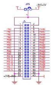
text_image
JFS +V8+5V 1 2 3 4 5 6 6 7 7 8 8 9 9 10 10 11 11 12 12 13 13 14 14 15 15 16 16 17 17 18 18 19 19 20 20 21 21 22 22 23 23 24 23 25 24 26 24 27 25 28 25 29 26 30 26 31 27 32 27 33 27 34 28 35 28 36 28 37 28 38 28 39 28 40 28 41 28 42 28 43 +5V8-5V8
text_image
PB0-16(1)G7A4 PB0H152 PB1LGT2 PB25CK2 PB35PE_PCP8 PB4 PB5 PB6ACV PB7AC8 PB8AC0 PB9AD1PCK0 PB10AD1PCK0 PB11AD2PW00 PB12AD2PW01 PB13AD2PW02 PB14AD2PW03 PB15AD4 PB16AD5 PB17AD6 PB18AD7 PB19AD8 PB20AD9 A WISWOKGK1-DC I4 PB0 I5 PB1 I6 PB2 I7 PB3 I8 PB4 I9 PB5 I10 PB6 I11 PB7 I12 PB8 I13 PB9 I14 PB10 I15 PB11 I16 PB12 I17 PB13 I18 PB14 I19 PB15 I20 PB16 I21 PB17 I22 PB18 I23 PB19 I24 PB20 I25 PB21 I26 PB22 I27 PB23 I28 PB24 I29 PB25 I30 PB26 I31 PB27 I32 PB28 I33 PB29 I34 PB30 I35 PB31 I36 PB32 I37 PB33 I38 PB34 I39 PB35 I40 PB36 I41 PB37 I42 PB38 I43 PB39 I44 PB40 I45 PB41 I46 PB42 I47 PB43 I48 PB44 I49 PB45 I50 PB46 I51 PB47 I52 PB48 I53 PB49 I54 PB50 I55 PB51 I56 PB52 I57 PB53 I58 PB54 I59 PB55 I60 PB56 I61 PB57 I62 PB58 I63 PB59 I64 PB60 I65 PB61 I66 PB62 I67 PB63 I68 PB64 I69 PB65 I70 PB66 I71 PB67 I72 PB68 I73 PB69 I74 PB70 I75 PB71 I76 PB72 I77 PB73 I78 PB74
text_image
VDDIPO VDDIPO VDDIPO R62 4.7k R80 4.7k R61 10k VDDIPO A1 A2 A3 VCC GND GND GND GND GND GND GND GND GND GND GND GND GND GND GND GND GND GND GND GND GND GND GND GND GND GND GND GND GND GND GND GND GND GND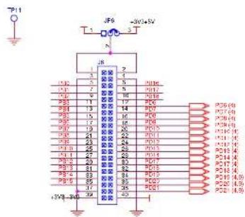
text_image
JF9 3V45V P11 3 V 2 1 0 0 7 6 5 4 3 2 1 0 0 1 0 0 1 0 0 1 0 0 1 0 0 1 0 0 1 0 0 1 0 0 1 0 0 1 0 0 1 0 0 1 0 0 1 0 0 1 0 0 1 0 0 1 0 0 1 0 0 1 1 0 0 1 0 0 1 0 0 1 0 0 1 0 0 1 0 0 1 0 0 1 0 0 1 0 0 1 0 0 1 0 0 1 0 0 1 0 0 1 0 0 1 0 0 1 0 0 1 GND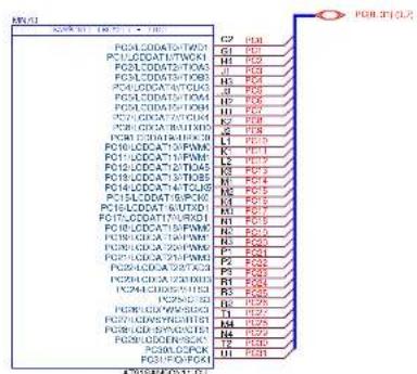
text_image
P01.CODAT47WCKI P01.CODAT47WCKI P01.CODAT47WCKI P01.CODAT47WCKI P01.CODAT47WCKI P01.CODAT47WCKI P01.CODAT47WCKI P01.CODAT47WCKI P01.CODAT47WCKI P01.5CDAT47WCKI P01.5CDAT47WCKI P01.5CDAT47WCKI P01.5CDAT47WCKI P01.5CDAT47WCKI P01.5CDAT47WCKI P01.5CDAT47WCKI P01.5CDAT47WCKI P1.5CDAT47WCKI P1.5CDAT47WCKI P1.5CDAT47WCKI P1.5CDAT47WCKI P1.5CDAT47WCKI P1.5CDAT47WCKI P1.5CDAT47WCKI P1.5CDAT47WCKI P1.5CDDAT47WCKI P1.5CDDAT47WCKI P1.5CDDAT47WCKI P1.5CDDAT47WCKI P1.5CDDAT47WCKI P1.5CDDAT47WCKI P1.5CDDAT47WCKI P1.5CDDAT47WCKI P2.5CDAT47WCKI P2.5CDAT47WCKI P2.5CDAT47WCKI P2.5CDAT47WCKI P2.5CDAT47WCKI P2.5CDAT47WCKI P2.5CDAT47WCKI P2.5CDAT47WCKI P2.5CDAT47RSDI P2.5CDAT47RSDI P2.5CDAT47RSDI P2.5CDAT47RSDI P2.5CDAT47RSDI P2.5CDAT47RSDI P2.5CDAT47RSDI P2.5CDAT47RSDI P2.5CDAT47RSDI P3.5CDAT47RSDI P3.5CDAT47RSDI P3.5CDAT47RSDI P3.5CDAT47RSDI P3.5CDAT47RSDI P3.5CDAT47RSDI P3.5CDAT47RSDI P3.5CDAT47RSDI P3.5CDCAT47RSDI P3.5CDCAT47RSDI P3.5CDCAT47RSDI P3.5CDCAT47RSDI P3.5CDCAT47RSDI P3.5CDCAT47RSDI P3.5CDCAT47RSDI P3.5CDCAT47RSDI P3.5CDCAT47RSCD P3.5CDCAT47RSCD P3.5CDCAT47RSCD P3.5CDCAT47RSCD P3.5CDCAT47RSCD P3.5CDCAT47RSCD P3.5CDCAT47RSCD P3.5CDCAT47RSCD P3.5CDCAT47RSCD P3. P3. P3. P3. P3. P3. P3. P3. P3. P3. P3. P3. P3. P3. P3. P3. P3. P3. A'YBAMAYOY I G'
text_image
VDDOP0 1.5k SN21 252437F+ IC NQ1 NQ2 NQ3 NQ4 NC18 NC28 NC3 DC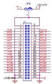
text_image
JPN +3V+5V 1 2 3 n 1 2' 1 3 5 6 7 8 PC18 PC17 PC16 PC15 PC14 PC13 PC12 PC11 PC10 PC9 PC8 PC7 PC6 PC5 PC4 PC3 PC2 PC1 PC0 PC-8 PC-7 PC-6 PC-5 PC-4 PC-3 PC-2 PC-1 PC-0 +3V+5V=5V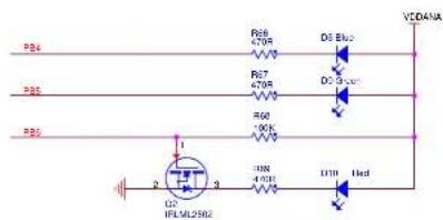
text_image
PB4 PB5 PB6 1 2 3 DCL IFLML2502 R26 470V R27 470V R50 300K INN 410V DE Bus DC Bus UTR Hed VCDATALED
| A | 101-301 | 05-A/01-12 | 05-A/01-12 | ||
| K=1 | K=8 | K=16 | K=4 | ||
| SOMRONI-ER | SOAF 1/1 | REV. | 2H-FET | ||
| PRO_INTERFACES | A | 5/9 | |||

text_image
DDR2_SPM 16A DDR2_APE 16A DDR2_APE 16A DDR2_APE 16A DDR2_APE 16A DDR2_APE 16A DDR2_APE 16A DDR2_APE 16A DDR2_APE 16A DDR2_APE 16A DDR2_APE 16A DDR2_APE 16A DDR2_APE DDR2_APE DDR2_APE DDR2_APE DDR2_APE DDR2_APE DDR2_APE DDR2_APE DDR2_APE DDR2_APE DDR2_APE DDR2_APE DDR2_APE DDR2_APE DDR2_APE DDR2_APE DDR2_APE DDR2_APE DDR2_APE DDR2_APE DDR2_AE DDR2_AE DDR2_AE DDR2_AE DDR2_AE DDR2_AE DDR2_AE DDR2_AE DDR2_AE DDR2_AE DDR2_AE DDR2_AE DDR2_AE DDR2_AE DDR2_AE DDR2_AE DDR2_AE DDR2_AE DDR2_AE DDR2_AE DDR2_AEA DDR2_AEA DDR2_AEA DDR2_AEA DDR2_AEA DDR2_AEA DDR2_AEA DDR2_AEA DDR2_AEA DDR2_AEA DDR2_AEA DDR2_AEA DDR2_AEA DDR2_AEA DDR2_AEA DDR2_AEA DDR2_AEA DDR2_AEA DDR2_AEA DDR2_AEA DDR2_Aea DDR2_Aea DDR2_Aea DDR2_Aea DDR2_Aea DDR2_Aea DDR2_Aea DDR2_Aea DDR2_Aea DDR2_Aea DDR2_Aea DDR2_Aea DDR2_Aea DDR2_Aea DDR2_Aea DDR2_Aea DDR2_Aea DDR2_Aea DDR2_Aea DDR2_Aea DDR2_AEA DDR2_AEA DDR2_AEA DDR2_AEA DDR2_AEA DDR2_AEA DDR2_AEA DDR2_AEA DDR2_AEA DDR2_AEA DDR2_AEA DDR2_AEA DDR2_AEA DDR2_AEA DDR2_AEA DDR2_AEA DDR2_AEA DDR2_AEA DDR2_AEA DDR2_AEEA DDR2_AEEA DDR2_AEEA DDR2_AEEA DDR2_AEEA DDR2_AEEA DDR2_AEEA DDR2_AEEA DDR2_AEEA DDR2_AEEA DDR2_AEEA DDR2_AEEA DDR2_AEEA DDR2_AEEA DDR2_AEEA DDR2_AEEA DDR2_AEEA DDR2_BAA10000000000000000000000000000000000000000000000000000000000000000000000000000000000000000000000000000
text_image
+2kV C54 6.7μF L12 10kN/150mA 150mA R29 H1 C56 1.00 F RMS 1.3K 1% 3D8 VREF TF17 Tux Fund C87 4.7μF C88 1.00 F RS: 1.3K 1%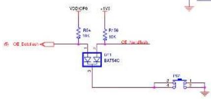
text_image
VDD CF9 +1V5 R04 10K R136 10K OE Doided U13 BAT54C OE 2-w flush 3 4 1V2 1 2
text_image
FLASH [0.19]A FASHI_A1_32B NNS3 I,NSH_A5 22 I,NSH_A6 22 I,NSH_A7 24 I,NSH_A8 23 I,NSH_A9 25 I,NSH_A10 27 I,NSH_A11 28 I,NSH_A12 30 I,NSH_A13 31 I,NSH_A14 32 I,NSH_A15 33 I,NSH_A16 34 I,NSH_A17 35 I,NSH_A18 36 I,NSH_A19 37 I,NSH_A20 38 I,NSH_A21 39 I,NSH_A22 40 I,NSH_A23 41 I,NSH_A24 42 I,NSH_A25 43 I,NSH_A26 44 I,NSH_A27 45 I,NSH_A28 46 I,NSH_A29 47 I,NSH_A30 48 I,NSH_A31 49 I,NSH_A32 50 I,NSH_A33 51 I,NSH_A34 52 I,NSH_A35 53 I,NSH_A36 54 I,NSH_A37 55 I,NSH_A38 56 I,NSH_A39 57 I,NSH_A40 58 I,NSH_A41 59 I,NSH_A42 60 I,NSH_A43 61 I,NSH_A44 62 I,NSH_A45 63 I,NSH_A46 64 I,NSH_A47 65 I,NSH_A48 66 I,NSH_A49 67 I,NSH_A50 68 I,NSH_A51 69 I,NSH_A52 70 I,NSH_A53 71 I,NSH_A54 72 I,NSH_A55 73 I,NSH_A56 74 I,NSH_A57 75 I,NSH_A58 76 I,NSH_A59 77 I,NSH_A60 78 I,NSH_A61 79 I,NSH_A62 80 I,NSH_A63 81 I,NSH_A64 82 I,NSH_A65 83 I,NSH_A66 84 I,NSH_A67 85 I,NSH_A68 86 I,NSH_A69 87 I,NSH_A70 88 I,NSH_A71 89 I,NSH_A72 90 I,NSH_A73 91 I,NSH_A74 92 I,NSH_A75 93 I,NSH_A76 94 I,NSH_A77 95 I,NSH_A78 96 I,NSH_A79 97 I,NSH_A80 98 I,NSH_A81 99 I,NSH_A82 100 +V8 R70 6R 28 C2 K VSS1 VSS2 VSS3 VSS4 VSS5 VSS6 VSS7 VSS8 VSS9 VSS10 VSS11 VSS12 VSS13 VSS14 VSS15 VSS16 VSS17 VSS18 VSS19 VSS20 VSS21 VSS22 VSS23 VSS24 VSS25 VSS26 VSS27 VSS28 VSS29 VSS30 VSS31 VSS32 VSS33 VSS34 VSS35 VSS36 VSS37 VSS38 VSS39 VSS40 VSS41 VSS42 VSS43 VSS44 VSS45 VSS46 VSS47 VSS48 VSS49 VSS50 VSS51 VSS52 VSS53 VSS54 VSS55 VSS56 VSS57 VSS58 VSS59 VSS60 VSS61 VSS62 VSS63 VSS64 VSS65 VSS66 VSS67 VSS68 VSS69 VSS70 VSS71 VSS72 VSS73 VSS74 VSS75 VSS76 VSS77 VSS78 VSS79 VSS80 VSS81 VSS82 VSS83 VSS84 VSS85 VSS86 VSS87 VSS88 VSS89 VSS90 VSS91 VSS92 VSS93 VSS94 VSS95 VSS96 VSS97 VSS98 VSS99 VSS100 -VSP NOS FND PND
text_image
NAND_PSE_037 VDDI R24 R25 R26 RPD1 RPD2 RPD3 RPD4 RPD5 RPD6 RPD7 RPD8 RPD9 RPD10 RPD11 RPD12 RPD13 RPD14 RPD15 RPD16 RPD17 RPD18 RPD19 RPD20 RPD21 RPD22 RPD23 RPD24 RPD25 RPD26 RPD27 RPD28 RPD29 RPD30 RPD31 RPD32 RPD33 RPD34 RPD35 RPD36 RPD37 RPD38 RPD39 RPD40 RPD41 RPD42 RPD43 RPD44 RPD45 RPD46 RPD47 RPD48 RPD49 RPD50 RPD51 RPD52 RPD53 RPD54 RPD55 RPD56 RPD57 RPD58 RPD59 RPD60 RPD61 RPD62 RPD63 RPD64 RPD65 RPD66 RPD67 RPD68 RPD69 RPD70 RPD71 RPD72 RPD73 RPD74 RPD75 RPD76 RPD77 RPD78 RPD79 RPD80 RPD81 RPD82 RPD83 RPD84 RPD85 RPD86 RPD87 RPD88 RPD89 RPD90 RPD91 RPD92 RPD93 RPD94 RPD95 RPD96 RPD97 RPD98 RPD99 RPD100 RPD101 RPD102 RPD103 RPD104 RPD105 RPD106 RPD107 RPD108 RPD109 RPD110 RPD111 RPD112 RPD113 RPD114 RPD115 RPD116 RPD117 RPD118 RPD119 RPD120 RPD121 RPD122 RPD123 RPD124 RPD125 RPD126 RPD127 RPD128 RPD129 RPD130 RPD131 RPD132 RPD133 RPD134 RPD135 RPD136 RPD137 RPD138 RPD139 RPD140 RPD141 RPD142 RPD143 RPD144 RPD145 RPD146 RPD147 RPD148 RPD149 RPD150 RPD151 RPD152 RPD153 RPD154 RPD155 RPD156 RPD157 RPD158 RPD159 RPD160 RPD161 RPD162 RPD163 RPD164 RPD165 RPD166 RPD167 RPD168 RPD169 RPD170 RPD171 RPD172 RPD173 RPD174 RPD175 RPD176 RPD177 RPD178 RPD179 RPD180 RPD181 RPD182 RPD183 RPD184 RPD185 RPD186 RPD187 RPD188 RPD189 RPD190 RPD191 RPD192 RPD193 RPD194 RPD195 RPD196 RPD197 RPD198 RPD199 RPD200| A | 101-31 | PP | 05 APR 12 | PP | 05 APR 12 |
| SAMBON11-SK | 1/1 | 10-8 | 10-1 | 7-9 | 10-1 |
| CORP2 NAND FLASH | 1/1 | REV.A | 6/8 |
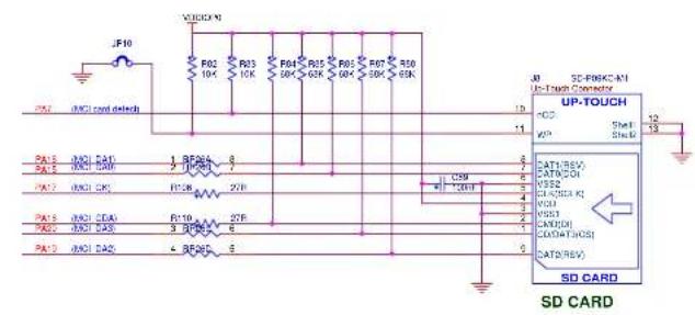
text_image
PI12 13458 PI2 PI3 PI4 PI5 PI6 PI7 PI8 PI9 PI10 PI11 PI12 PI13 PI14 PI15 PI16 PI17 PI18
text_image
PQ8.24 Pin 20 Pin 1 Pin 2 Pin 3 Pin 4 Pin 5 Pin 6 Pin 7 Pin 8 Pin 9 Pin 10 Pin 11 Pin 12 Pin 13 Pin 14 Pin 15 Pin 16 Pin 17 Pin 18 Pin 19 Pin 20 Pin 21 Pin 22 Pin 23 Pin 24 Pin 25 Pin 26 Pin 27 Pin 28 Pin 29 Pin 30 Pin 31| A | D11-31 | PP | 05-APR-12 | PP |
| S### | 11/8 | 12/12 | 24-### | 121-### |
| SCALE | 1/1 | HEV. SHEET | ||
| SERIAL INTERFACES | A 7/9 | |||
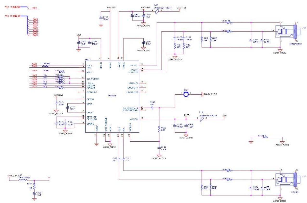
text_image
MAX-198 MAX-318 PAS1 PAS2 PAS3 PAS4 PAS5 PAS6 PAS7 PAS8 PAS9 PAS10 PAS11 PAS12 PAS13 PAS14 PAS15 PAS16 PAS17 PAS18 PAS19 PAS20 PAS21 PAS22 PAS23 PAS24 PAS25 PAS26 PAS27 PAS28 PAS29 PAS30 PAS31 PAS32 PAS33 PAS34 PAS35 PAS36 PAS37 PAS38 PAS39 PAS40 PAS41 PAS42 PAS43 PAS44 PAS45 PAS46 PAS47 PAS48 PAS49 PAS50 PAS51 PAS52 PAS53 PAS54 PAS55 PAS56 PAS57 PAS58 PAS59 PAS60 PAS61 PAS62 PAS63 PAS64 PAS65 PAS66 PAS67 PAS68 PAS69 PAS70 PAS71 PAS72 PAS73 PAS74 PAS75 PAS76 PAS77 PAS78 PAS79 PAS80 PAS81 PAS82 PAS83 PAS84 PAS85 PAS86 PAS87 PAS88 PAS89 PAS90 PAS91 PAS92 PAS93 PAS94 PAS95 PAS96 PAS97 PAS98 PAS99 PAS100 AVDC 198 C101 10kV C102 10kV C103 10kV C104 2.0kV C105 2.0kV C106 2.0kV C107 4.0kV C108 4.0kV C109 4.0kV C110 4.0kV C111 4.0kV C112 4.0kV C113 4.0kV C114 4.0kV C115 4.0kV C116 4.0kV C117 4.0kV C118 4.0kV C119 4.0kV C120 4.0kV C121 4.0kV C122 4.0kV C123 4.0kV C124 4.0kV C125 4.0kV C126 4.0kV C127 4.0kV C128 4.0kV C129 4.0kV C130 4.0kV AVDC 333/334/335/336/337/338/339/340/341/342/343/344/345/346/347/348/349/350/351/352/353/354/355/356/357/358/359/360/361/362/363/364/365/366/367/368/369/370/371/372/373/374/375/376/377/378/379/380/381/382/383/384/385/386/387/388/389/390/391/392/393/394/395/396/397/398/399/400/401/402/403/404/405/406/407/408/409/410/411/412/413/414/415/416/417/418/419/420/421/422/423/424/425/426/427/428/429/430/431/432/433/434/435/436/437/438/439/440/441/442/443/444/445/446/447/448/449/450/451/452/453/454/455/456/457/458/459/460/461/462/463/464/465/466/467/468/469/470/471/472/473/474/475/476/477/478/479/480/481/482/483/484/485/486/487/488/489/490/ AVDC 198A/DVDI/OLED/CNC/AUD/CNC/AUD/CNC/AUD/CNC/AUD/CNC/AUD/CNC/AUD/CNC/AUD/CNC/AUD/CNC/AUD/CNC/AUD/CNC/AUD/CNC/AUD/CNC/AUD/CNC/AUD/CNC/AUD/CNC/AUD/CNC/AUD/CNC/AUD/CNC/AUD/CNC/AUD/CNC/AUD/CNC/AUD/CNC/AUD/CNC/AUD/CNC/AUD/CNC/AUCO/DVDI/OLED/CNC/AUD/CNC/AUD/CNC/AUD/CNC/AUD/CNC/AUD/CNC/AUD/CNC/AUD/CNC/AUD/CNC/AUD/CNC/AUD/CNC/AUD/CNC/AUD/CNC/AUD/CNC/AUD/CNC/AUD/CNC/AUD/CNC/AUD/CNC/AUD/CNC/AUD/CNC/AUD/CNC/AUD/CNC/AUD/CNC/AUD/CNC AUCO/DVDI/OLED/CNC/AUD/CNC/AUD/CNC/AUD/CNC/AUD/CNC/AUD/CNC/AUD/CNC/AUD/CNC/AUD/CNC/AUD/CNC/AUD/CNC/AUD/CNC/AUD/CNC/AUD/CNC/AUD/CNC/AUD/CNC/AUD/CNC/AUD/CNC/AUD/CNC/AUD/CNC/AUD/CNC/AUD/CNC/AUD/CNC/AUD/B/DVDI/OLED/CNC/AUD/CNC/AUD/CNC/AUD/CNC/AUD/CNC/AUD/CNC/AUD/CNC/AUD/CNC/AUD/CNC/AUD/CNC/AUD/CNC/AUD/CNC/AUD/CNC/AUD/CNC/AUD/CNC/AUD/CNC/AUD/CNC/AUD/CNC/AUD/CNC/AUD/CNC/AUD/CNC/AUD/CNC/AUD/CNC/AUD/CNC-AUCO/DVDI/OLED/CNC/AUD/CNC/AUD/CNC/AUD/CNC/AUD/CNC/AUD/CNC/AUD/CNC/AUD/CNC/AUD/CNC/AUD/CNC/AUD/CNC/AUD/CNC/AUD/CNC/AUD/CNC/AUCO/DVDI/OLED/CNC/AUCO/DVDI/OLED/CNC/AUCO/DVDI/OLED/CNC/AUCO/DVDI/OLED/CNC/AUCO/DVDI/OLED/CNC/AUCO/DVDI/OLED/CNC/AUCO/DVDI/OLED/CNC/AUCO/DVDI/OLED/CNC/AUCO/DVDI/OLED/CNC/AUCO/DVDI/OLED/CNC/AUCO/DVDI/O LEDICOSI/OLEDOSI/OLEDOSI/OLEDOSI/OLEDOSI/OLEDOSI/OLEDOSI/OLEDOSI/OLEDOSI/OLEDOSI/OLEDOSI/OLEDOSI/OLEDOSI/OLEDOSI/OLEDOSI/OLEDOSI/OLEDOSI/OLEDOSI/OLEDOSI/OLEDOSI/OLEDOSI/OLEDOSI/OLEDOSI/OLEDOSI/OLEDOSI/OLEDOSI/O LEDICOSI/OLEDOSI/OLEDOSI/OLEDOSI/OLEDOSI/OLEDOSI/OLEDOSI/OLEDOSI/OLEDOSI/OLEDOSI/OLEDOSI/OLEDOSI/OLEDOSI/OLEDOSI/OLEDOSI/OLEDOSI/OLEDOSI/OLEDOSI/OLEDOSI/OLEDOSI/OLEDOSI/OLEDOSI/OLEDOSI/OLEDOSI/O LEDICOSI OLEDOSI OLEDOSI OLEDOSI OLEDOSI OLEDOSI OLEDOSI OLEDOSI OLEDOSI OLEDOSI OLEDOSI OLEDOSI OLEDOSI OLEDOSI OLEDOSI OLEDOSI OLEDOSI OLEDOSI OLEDOSI OLEDOSI OLEDOSI OLEDOSI OLEDOSI OLEDOSI OLEDOSI OLEDOSI O LEDICOSIS OLEDOSIS OLEDOSIS OLEDOSIS OLEDOSIS OLEDOSIS OLEDOSIS OLEDOSIS OLEDOSIS OLEDOSIS OLEDOSIS OLEDOSIS OLEDOSIS OLEDOSIS OLEDOSIS OLEDOSIS OLEDOSIS OLEDOSIS OLEDOSIS OLEDOSIS OLEDOSIS OLEDOSIS OLEDOSIS O LEDICOSIS OLEDOSIS OLEDOSIS OLEDOSIS OLEDOSIS O LEDICOSIS O LEDIOSIS O LEDIOSIS O LEDIOSIS O LEDIOSIS O LEDIOSIS O LEDIOSIS O LEDIOSIS O LEDIOSIS O LEDIOSIS O LEDIOSIS O LEDIOSIS O LEDIOSIS O LEDIOSIS O LEDIOSIS O LEDIOSIS O LEDIOSIS O LEDIOSIS O LEDIOSIS O LEDIOSIS O LEDIOSIS O LEDIOSIS O LEDIOSIS O LEDIOSIS O LEDIOSIS O LEDIOSIS O LEDIO S V D V D V D V D V D V D V D V D V D V D V D V D V D V D V D V D V D V D V D V D V D V D V D V D V D V D V D V D V D V D V D V D V D V D V D V D V D V D V D V D V D V D V D V D V D V D V D V D V D V D VD I N I N I N I N I N I N I N I N I N I N I N I N I N I N I N I N I N I N I N I N I N I N I N I N I N I N I N I N I N I N I N I N I N I N I N I N I N I N I N I N I N I N I N I N I N I N I N I N I N I N IN I N I N I N I N I N I N I N I N I N I N I N I N I N I N I N I N I N I N I N I N I N I N I N I N I N I N I N I N I N I N I N I N I N I N I N I N I N I N I N I N I N I N I N I N I N I N I N I N I N I In U A B C C C C C C C C C C C C C C C C C C C C C C C C C C C C C C C C C C C C C C C C C C C C C C C C C C C C C C C C C C C C C C C C C C C C C C C C C C C C C C C C C C C C C C C C C C C C C C C C C C C C U A B U B U B U B U B U B U B U B U B U B U B U B U B U B U B U B U B U B U B U B U B U B U B U B U B U B U B U B U B U B U B U B U B U B U B U B U B U B U B U B U B U B U B U B U B U B U B U B U B U B U BU A B A A A A A A A A A A A A A A A A A A A A A A A A A A A A A A A A A A A A A A A A A A A A A A A A A A A A A A A A A A A A A A A A A A A A A A A A A A A A A A A A A A A A A A A A A A A A A A A A A A A A | PAST | PAST | PAST | PAST | PAST | PAST | PAST | PAST | PAST | PAST | PAST | PAST | PAST | PAST | PAST | PAST | PAST | PAST | PAST | PAST | PAST | PAST | PAST | PAST | PAST | PAST | PAST | PAST | PAST | PAST | PAST | PAST | PAST | PAST | AVDC 198A/DVDI/O LEDICOSI /LTC 198A/LTC 198A/LTC 198A/LTC 198A/LTC 198A/LTC 198A/LTC 198A/LTC 198A/LTC 198A/LTC 198A/LTC 198A/LTC 198A/LTC 198A/LTC 198A/LTC 198A/LTC| A | 101-31 | 05-A/31-12 | 05-A/31-12 | ||
| X=5 | X=4 | X=3 | |||
| SAMRCN11-EX | ROAF | REV. | SHFET | ||
| AUDIO | 1/1 | A | 8% | ||

text_image
KSZ8851-16MLL +10S -22Vrms at 10CMHz A10S C103 C104 C105 C106 C107 C108 C109 C110 C111 C112 C113 C114 C115 C116 C117 C118 C119 C120 C121 C122 C123 C124 C125 C126 C127 C128 C129 C130 C131 C132 C133 C134 C135 C136 C137 C138 C139 C140 C141 C142 C143 C144 C145 C146 C147 C148 C149 C150 C151 C152 C153 C154 C155 C156 C157 C158 C159 C160 C161 C162 C163 C164 C165 C166 C167 C168 C169 C170 C171 C172 C173 C174 C175 C176 C177 C178 C179 C180 C181 C182 C183 C184 C185 C186 C187 C188 C189 C190 C191 C192 C193 C194 C195 C196 C197 C198 C199 C200 +2V8 +2V6 +2V5 +2V4 +2V3 +2V2/3/4/5/6/7/8/9/10/11/12/13/14/15/16/17/18/19/20/21/22/23/24/25/26/27/28/29/30/31/32/33/34/35/36/37/38/39/40/41/42/43/44/45/46/47/48/49/50/51/52/53/54/55/56/57/58/59/60/61/62/63/64/65/66/67/68/69/70/71/72/73/74/75/76/77/78/79/80/81/82/83/84/85/86/87/88/89/90/91/92/93/94/95/96/97/98/99/9A 0.0 0.0 0.0 0.0 0.0 0.0 0.0 0.0 0.0 0.0 0.0 0.0 0.0 0.0 0.0 0.0 0.0 0.0 0.0 0.0 0.0 0.0 0.0 0.0 0.0 0.3 0.3 0.3 0.3 0.3 0.3 0.3 0.3 0.3 0.3 0.3 0.3 0.3 0.3 0.3 0.3 0.3 0.3 0.3 0.3 0.3 0.3 0.3 0.3 0.3 0.2 0.2 0.2 0.2 0.2 0.2 0.2 0.2 0.2 0.2 0.2 0.2 0.2 0.2 0.2 0.2 0.2 0.2 0.2 0.2 0.2 0.2 0.2 0.2 0.2 0.3 0.3 0.3 0.3 0.3 0.3 0.3 0.3 0.3 0.3 0.3 0.3 0.3 0.3 0.3 0.3 0.3 0.3 0.3 0.3 0.3 0.3 0.3 0.3 0.4 0.4 0.4 0.4 0.4 0.4 0.4 0.4 0.4 0.4 0.4 0.4 0.4 0.4 0.4 0.4 0.4 0.4 0.4 0.4 0.4 0.4 0.4 0.4 0.4 0.5 0.5 0.5 0.5 0.5 0.5 0.5 0.5 0.5 0.5 0.5 0.5 0.5 0.5 0.5| A | 101>31 | 05-AP01-12 | 05-AP01-12 | ||
| X=5 | X=4 | X=3 | X=1+X=8 | ||
| SAMBCN11-EX | SOAL F 1/1 | REV. | SHFET | ||
| ETH | A | % | |||
6.1 Board Overview
SAM9N12/CN11-DM board carries a 4.3" TFT LCD module with touch screen.
The DM board also carries four QTouch pads.
Figure 6-1. DM Board
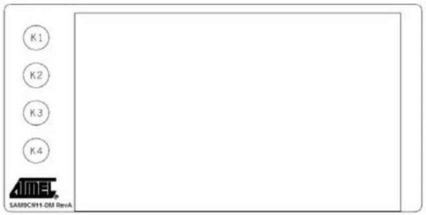
text_image
K1 K2 K3 K4 IMEL SAM9CN11-DM RevA6.2 Equipment List
Here is the list of the DM board components:
■ One 4.3" TFT LCD module
■ LCD Back light driver
■ 3.3V regulator
■ QTouch device
■ 1-Wire device
6.3 Function Blocks
6.3.1 3.3V Regulator
The SAM9N12/CN11-DM board features its own LDO for local power regulation. It accepts DC 5V power from a 500 mA power switch on the EK and outputs a regulated +3.3V to most other circuits on the board.
Figure 6-2. DM Board Power Supply

text_image
5V_INTER MN3 VIN VOUT GND EN BYP SPX3819 500mA capability SELCONFIG C12 10u C13 100n C15 2.2u 3V3_LCD C10 10u C11 100n6.3.2 TFT LCD with Touch Panel
The SAM9N12/CN11-DM board features an LCD controller. The 4.3" 480x272 LCD provides the DM with a low power LCD display feature, back light unit and a touch panel, similar to that used on commercial PDAs.
Graphics and text can be displayed on the dot matrix panel with up to 16 million colors by supplying 24-bit data signals (8 bit x RGB by default). This allows the user to develop graphical user interfaces for a wide variety of end applications.
Warning: Never connect/disconnect the LCD display from the board while the power supply is on. Doing so may damage both units.
Figure 6-3. LCD with Touch Panel
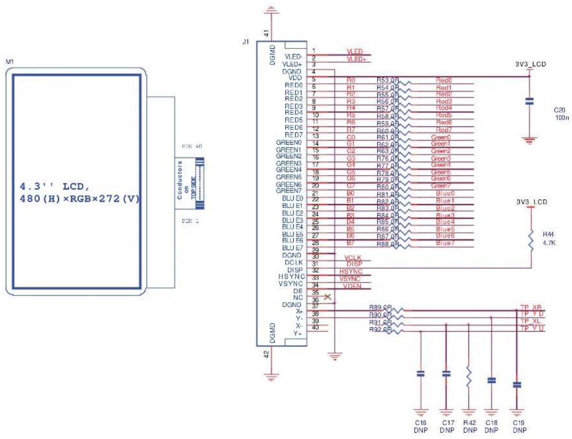
text_image
M1 4.3'' LCD, 480 (H) ×RGB×272 (V) PIN 40 Conductors on TOP SIDE PIN 1 J1 41 DGMD 1 VLED- 2 VLED+ 3 DGND 4 VDD 5 R0 R53.0R Red0 RED1 RED2 RED3 RED4 RED5 RED6 RED7 RED8 RED9 RED10 RED11 RED12 RED13 RED14 RED15 RED16 RED17 RED18 RED19 RED20 RED21 RED22 RED23 RED24 RED25 RED26 RED27 RED28 RED29 RED30 RED31 RED32 RED33 RED34 RED35 RED36 RED37 RED38 RED39 RED40 RED41 R60.0R Red7 Green0 Green1 Green2 Green3 Green4 Green5 Green6 Green7 Blue0 Blue1 Blue2 Blue3 Blue4 Blue5 Blue6 Blue7 GREEN0 GREEN1 GREEN2 GREEN3 GREEN4 GREEN5 GREEN6 GREEN7 BLUE E0 BLUE E1 BLUE E2 BLUE E3 BLUE E4 BLUE E5 BLUE E6 BLUE E7 DCND DCLK DISP HSYNC VSYNC DE NC DGND X+ Y- X- Y+ DGMD 42 VCLK DISP HSYNC VSYNC VDEN R89.0R R90.0R R91.0R R92.0R6.3.3 Back Light
The back light voltage is generated from a CP2122ST boost converter. It is powered directly by the DC 5 V from the EK board. The back light level is controlled by a PWM signal generated from the SAM9N12/CN11 processor.
Figure 6-4. Back Light Control

text_image
5V_INTER L1 22uH 880mA C7 10u 10v 5V/217mA D1 RB160M-60 60V/1A VLED+ C9 2.2u 50v R43 0R MN1 VIN SW OVP GND SHDN# FB CP2123ST-A1 LCDPWM R40 10k 1 2 3 300mV VLED- R41 7.5R 2 x5 LEDs Back Light6.3.4 QTouch
The SAM9N12/CN11-DM board carries a QTouch device piloted through a TWI interface. It manages four capacitive touch buttons directly printed on the PCB.
There are dual footprints for the QTouch device, and SOIC is the default mounted one.
Figure 6-5. QTou ch
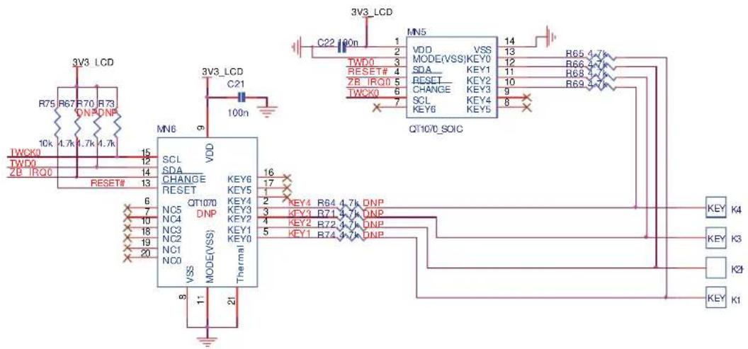
text_image
3V3_LCD R75 R67 R70 R73 DNP DNP 10k 4.7k 4.7k 4.7k TWCK0 TWD0 ZB_IRQ0 RESET# 15 12 14 13 6 7 10 18 19 20 NC5 NC4 NC3 NC2 NC1 NC0 VSS MODE(VSS) THermal SCL SDA CHANGE KEY6 KEY5 KEY4 KEY3 KEY2 KEY1 KEY0 RESET QT1070 DNP 3V3_LCD C21 100n 3V3_LCD MN5 VDD VSS MODE(VSS)KEY0 SDA KEY1 RESET KEY2 CHANGE KEY3 SCL KEY4 KEY5 KEY6 KEY5 QT1070_SOIC C22 100n 1 2 3 4 5 6 7 8 9 10 11 12 13 14 15 16 17 18 19 20 21 22 23 24 25 26 27 28 29 30 31 32 33 34 35 36 37 38 39 40 41 42 43 44 45 46 47 48 49 50 51 52 53 54 55 56 57 58 59 60 61 62 63 64 65 66 67 68 69 70 KEY K4 KEY K3 KEY K2 KEY K16.3.5 1-Wire
The DM board also uses 1-Wire device as “soft label” to store the information such as chip type, manufacture name, production date, etc.
Figure 6-6. 1-Wir e on DM

text_image
3V3_LCD R45 4.7k ONE_WIRE MN2 1 NC1 NC6 8 2 NC2 NC5 7 3 DATA NC4 6 4 GND NC3 5 DS2433S7.1 DM Board Schematics
This section contains the following schematic:
LCD Board
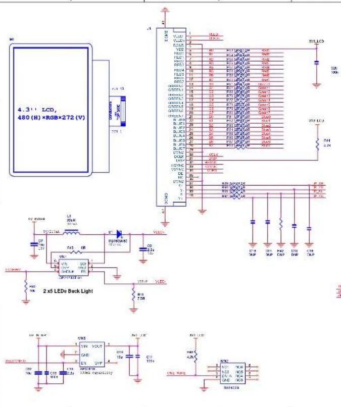
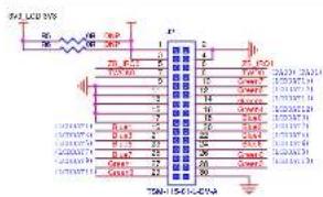
text_image
743 LCD Display Pin 1 Pin 2 Pin 3 Pin 4 Pin 5 Pin 6 Pin 7 Pin 8 Pin 9 Pin 10 Pin 11 Pin 12 Pin 13 Pin 14 Pin 15 Pin 16 Pin 17 Pin 18 Pin 19 Pin 20 Pin 21 Pin 22 Pin 23 Pin 24 Pin 25 Pin 26 Pin 27 Pin 28 Pin 29 Pin 30 Pin 31 Pin 32 Pin 33 Pin 34 Pin 35 Pin 36 Pin 37 Pin 38 Pin 39 Pin 40 Pin 41 Pin 42 Pin 43 Pin 44 Pin 45 Pin 46 Pin 47 Pin 48 Pin 49 Pin 50 Pin 51 Pin 52 Pin 53 Pin 54 Pin 55 Pin 56 Pin 57 Pin 58 Pin 59 Pin 60 Pin 61 Pin 62 Pin 63 Pin 64 Pin 65 Pin 66 Pin 67 Pin 68 Pin 69 Pin 70 Pin 71 Pin 72 Pin 73 Pin 74 Pin 75 Pin 76 Pin 77 Pin 78 Pin 79 Pin 80 Pin 81 Pin 82 Pin 83 Pin 84 Pin 85 Pin 86 Pin 87 Pin 88 Pin 89 Pin 90 Pin 91 Pin 92 Pin 93 Pin 94 Pin 95 Pin 96 Pin 97 Pin 98 Pin 99 Pin100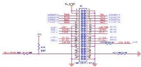
text_image
S10_125 GND00713 GND00714 GND00715 GND00716 GND00717 GND00718 GND00719 GND00720 GND00721 GND00722 GND00723 GND00724 GND00725 GND00726 GND00727 GND00728 GND00729 GND00730 GND00731 GND00732 GND00733 GND00734 GND00735 GND00736 GND00737 GND00738 GND00739 GND00740 GND00741 GND00742 GND00743 GND00744 GND00745 GND00746 GND00747 GND00748 GND00749 GND00750 GND00751 GND00752 GND00753 GND00754 GND00755 GND00756 GND00757 GND00758 GND00759 GND00760 GND00761 GND00762 GND00763 GND00764 GND00765 GND00766 GND00767 GND00768 GND00769 GND00770 GND00771 GND00772 GND00773 GND00774 GND00775 GND00776 GND00777 GND00778 GND00779 GND00780 GND00781 GND00782 GND00783 GND00784 GND00785 GND00786 GND00787 GND00788 GND00789 GND00790 GND00791 GND00792 GND00793 GND00794 GND00795 GND00796 GND00797 GND00798 GND00799 GND1111111111111111111111111111111111111111111111111111111111111111111111111111111111111111111111111111
text_image
300V LED P25 P26 P27 P28 100A 100A 100A 100A 100A 100A 100A 100A 100A 100A 100A 100A 100A 100A 100A 100A 100A 100A 100A 100A 100A 100B 100A 100B 100A 100B 100A 100B 100A 100B 100A 100B 100A 100B 100A 100B 100A 100B 100A 100B 100A 100C 100A 100B 100A 100C 100A 100B 100A 100C 100A 100B 100A 100C 100A 100B 100A 100C 100A 100B 100A 100B 100A 100C 100A 100B 100A 100C 100A 100B 1.22 VDD VDD: VDD VDD: VDD VDD: VDD VDD: VDD VDD: VDD VDD: VDD VDD: VDD VDD: VDD VDD: VDD VDD: VDD VDD: VDD VDD: VDD VDD: VDD VDD: VDD VDD: VDD VDD: VDD VDD: VDD GND TIN BOC VDD: VDD VDD: VDD VDD: VDD VDD: VDD VDD: VDD VDD: VDD VDD: VDD VDD: VDD VDD: VDD VDD: VDD VDD: VDD VDD: VDD VDD: VDD VDD: VDD VDD: VDD VDD: VDD VDD: VDD: VDD: VDD: VDD: VDD: VDD: VDD: VDD: VDD: VDD: VDD: VDD: VDD: VDD: VDD: VDD: VDD: VDD: VDD: VDD: VDD: VDD: VDD: VDD: VDD: VDD: VDD: VDD: VDD: VDD: VDD: VDD: VDD: 555 TIN BOC| A | RBCENT | DATE: 12/12 | DATE: 12/12 | ||
| 0.00 | 0.00 | 0.00 | 0.00 | 0.00 | 0.00 |
| SCALE = 1.14 | SIZE = 1.14 | ||||
| A 1/4 | |||||
8.1 Revision History
Table 8-1.
| Document Comments | Change Request Ref. | |
| 11186A First issue. |
Headquarters International
Atmel Corporation
2325 Orchard Parkway
San Jose, CA 95131
USA
Tel: (+1) (408) 441-0311
Fax: (+1) (408) 487-2600
Atmel Asia Limited
Unit 01-5 & 16, 19F
BEA Tower, Millennium City 5
418 Kwun Tong Road
Kwun Tong, Kowloon
HONG KONG
Tel: (+852) 2245-6100
Fax: (+852) 2722-1369
Atmel Munich GmbH
Business Campus
Parkring 4
D-85748 Garching b. Munich
GERMANY
Tel: (+49) 89-31970-0
Fax: (+49) 89-3194621
Atmel Japan
9F, Tonetsu Shinkawa Bldg.
1-24-8 Shinkawa
Chuo-ku, Tokyo 104-0033
JAPAN
Tel: (81) 3-3523-3551
Fax: (81) 3-3523-7581
Product Contact
Web Site
www.atmel.com
www.atmel.com/AT91SAM
Technical Support
AT91SAM Support
Atmel technical support
Sales Contacts
www.atmel.com/contacts/
Literature Requests
www.atmel.com/literature
Disclaimer: The information in this document is provided in connection with Atmel products. No license, express or implied, by estoppel or otherwise, to any intellectual property right is granted by this document or in connection with the sale of Atmel products. EXCEPT AS SET FORTH IN ATMEL'S TERMS AND CONDITIONS OF SALE LOCATED ON ATMEL'S WEB SITE, ATMEL ASSUMES NO LIABILITY WHATSOEVER AND DISCLAIMS ANY EXPRESS, IMPLIED OR STATUTORY WARRANTY RELATING TO ITS PRODUCTS INCLUDING, BUT NOT LIMITED TO, THE IMPLIED WARRANTY OF MERCHANTABILITY, FITNESS FOR A PARTICULAR PURPOSE, OR NON-INFRINGEMENT. IN NO EVENT SHALL ATMEL BE LIABLE FOR ANY DIRECT, INDIRECT, CONSEQUENTIAL, PUNITIVE, SPECIAL OR INCIDENTAL DAMAGES (INCLUDING, WITHOUT LIMITATION, DAMAGES FOR LOSS OF PROFITS, BUSINESS INTERRUPTION, OR LOSS OF INFORMATION) ARISING OUT OF THE USE OR INABILITY TO USE THIS DOCUMENT, EVEN IF ATMEL HAS BEEN ADVISED OF THE POSSIBILITY OF SUCH DAMAGES. Atmel makes no representations or warranties with respect to the accuracy or completeness of the contents of this document and reserves the right to make changes to specifications and product descriptions at any time without notice. Atmel does not make any commitment to update the information contained herein. Unless specifically provided otherwise, Atmel products are not suitable for, and shall not be used in, automotive applications. Atmel's products are not intended, authorized, or warranted for use as components in applications intended to support or sustain life.

© 2012 Atmel Corporation. All rights reserved. Atmel®, Atmel logo and combinations thereof, QTouch® and others are registered trademarks or trademarks of Atmel Corporation or its subsidiaries. ARM®, ARM®Powered logo, Cortex™ and others are registered trademarks or trademarks of ARM Ltd. Other terms and product names may be trademarks of others.