AT91SAM9M11 - Electronic component Microchip - Free user manual and instructions
Find the device manual for free AT91SAM9M11 Microchip in PDF.

User questions about AT91SAM9M11 Microchip
0 question about this device. Answer the ones you know or ask your own.
Ask a new question about this device
Download the instructions for your Electronic component in PDF format for free! Find your manual AT91SAM9M11 - Microchip and take your electronic device back in hand. On this page are published all the documents necessary for the use of your device. AT91SAM9M11 by Microchip.
USER MANUAL AT91SAM9M11 Microchip
1.1 Scope 1-1
1.2 Applicable Documents 1-2
Section 2
Kit Contents 2-1
2.1 Deliverables 2-1
2.2 Evaluation Board Specifications.... 2-2
2.3 Electrostatic Warning 2-2
Section 3
Power up....3-1
3.1 Power Up the Board.... 3-1
3.2 Battery 3-1
3.3 DevStart 3-1
3.4 Recovery Procedure 3-2
3.5 Sample Code and Technical Support 3-2
Section 4
Board Description 4-1
4.1 Equipment on the Board 4-1
4.1.1 Interfaces 4-1
4.1.2 Board Interface Connection 4-2
4.1.3 Push Button Switches.... 4-2
4.1.4 Display LCD and LEDs 4-3
4.2 Hardware Layout and Configuration 4-3
4.2.1 Processor.... 4-3
4.2.2 Clock Circuitry 4-4
4.2.3 Reset Circuitry 4-4
4.2.4 Memory 4-4
4.2.5 Power Supplies.... 4-7
4.2.6 Debug Interface 4-10
4.2.7 Audio Stereo Interface 4-15
4.2.8 TV-Out Extension 4-17
4.2.9 Software Controlled LEDs 4-18
4.2.10 Serial Peripheral Interface Controller (SPI) 4-19
4.2.11 Two Wire Interface (TWI) 4-19
4.2.12 SD/MMC Interface 4-19
4.2.13 TFT LCD with Touch Panel 4-20
4.2.14 Push Buttons 4-22
4.2.15 Expansion Slot.... 4-22
Section 5
Configuration 5-1
5.1 JTAG/ICE Configuration.... 5-1
5.2 ETHERNET Configuration 5-1
5.3 Jumpers Configuration 5-2
5.4 Miscellaneous Configuration Items 5-3
5.5 PIO Configuration.... 5-3
5.5.1 Peripheral Signals Multiplexing on I/O Lines 5-3
5.5.2 Multiplexing on PIO Controller A (PIOA) 5-3
5.5.3 Multiplexing on PIO Controller B (PIOB).... 5-5
5.5.4 Multiplexing on PIO Controller C (PIOC) 5-6
5.5.5 Multiplexing on PIO Controller D (PIOD) 5-7
5.5.6 Multiplexing on PIO Controller E (PIOE).... 5-8
Section 6
Connectors 6-1
6.1 Power Supply 6-1
6.2 RS232 Connector with RTS/CTS Handshake Support 6-1
6.3 DBGU 6-2
6.4 Ethernet....6-3
6.5 USB Host 6-3
6.6 USB Host/Device 6-4
6.7 JTAG Debugging Connector 6-4
6.8 SD/MMC-MCI0....6-6
6.9 SD/MMC-MCI1 6-7
6.10 AC97 6-8
6.11 Image Sensor - ISI 6-9
6.12 Video....6-10
6.13 Display Devices.... 6-10
6.13.1 TFT LCD 6-10
6.14 LCD Extension 6-11
Section 7
Schematics 7-1
7.1 Schematics.... 7-1
Section 8
Revision History......8-1
8.1 Revision History 8-1
1.1 Scope
This User Guide introduces the AT91SAM9M10(G45) Evaluation Kit and describes its development and debugging capabilities.
Figure 1-1. Board Photo
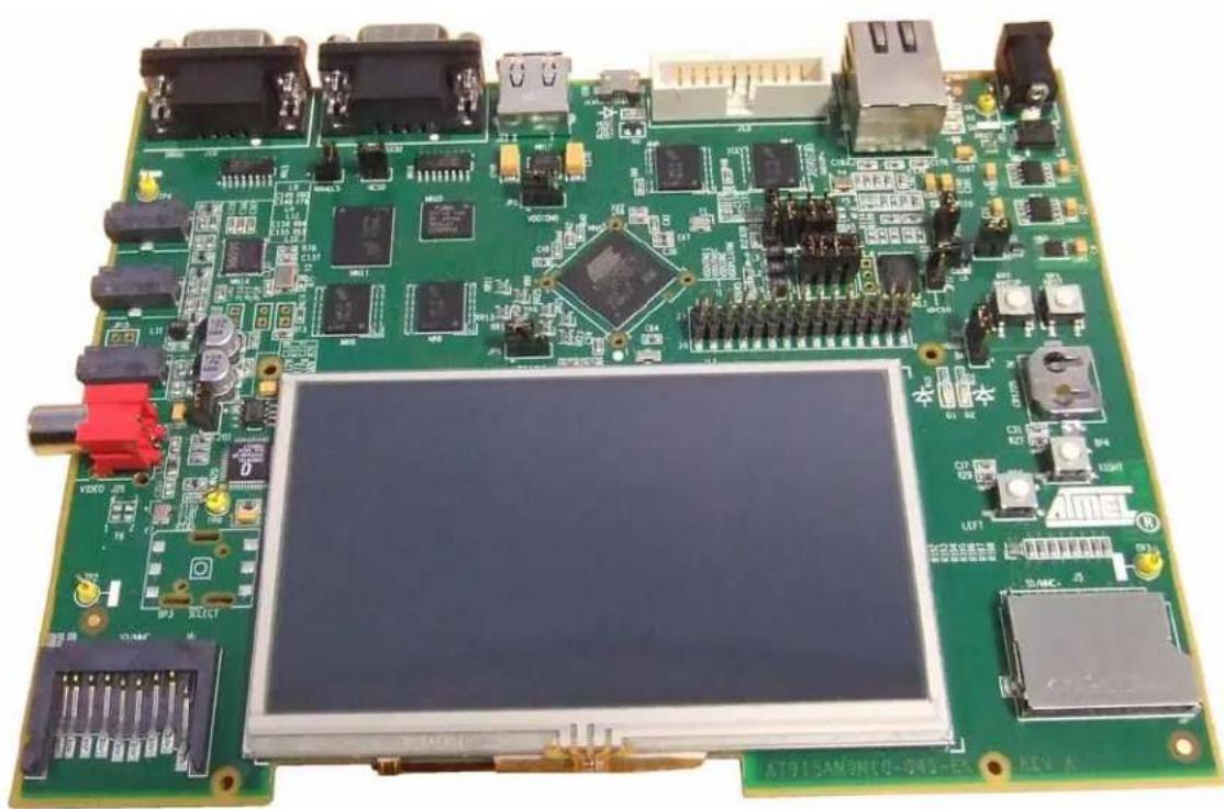
natural_image
Green printed circuit board with various electronic components and a central display (no readable text or symbols)The Atmel® SAM9M10-G45-EK is a fully-featured evaluation platform for the Atmel AT91SAM9M10 or AT91SAM9G45 microcontroller. The kit is equipped with an AT91SAM9M10 chip, which is a superset of the AT91SAM9G45, and therefore allows evaluating that reference as well. The evaluation kit allows users to extensively evaluate, prototype and create application-specific designs.
The SAM9M10-G45-EK includes many hardware peripherals such as:
■ Two high speed USB hosts and one high speed device port
■ An Ethernet 10/100 interface
■ Two high speed multimedia card interfaces
Introduction
■ An LCD TFT display (480*272 RGB) with resistive touch panel
■ A composite video output
■ A camera interface
■ Several communication peripherals such as:
– Universal Synchronous/Asynchronous Receiver Transmitter (USART)
- Two-Wire Interface (TWI)
The external memory block is made of 3 memory types:
DDR2-SDRAM
■ NAND Flash
■ NOR Flash (not populated by default)
1.2 Applicable Documents
Table 1-1. Applicable Documents
| Reference Title Comments | ||
| Atmel Literature n° 6438 SAM9G45 | Preliminary | This document describes the SAM9G45, which is part of the Atmel's Smart ARM® Microcontrollers.It is available fromhttp://www.atmel.com/dyn/resources/prod_documents/doc6438.pdf |
| Atmel Literature n° 6355 SAM9M10 | Preliminary | This document describes the SAM9M10, which is part of the Atmel's Smart ARM® Microcontrollershttp://www.atmel.com/dyn/resources/prod_documents/doc6355.pdf |
2.1 Deliverables
The Atmel SAM9M10-G45-EK toolkit includes:
■ Board
- The SAM9M10-G45-EK board
■ Power supply
- Universal input AC/DC power supply with US, Europe and UK plug adapters
- One 3V Lithium Battery type CR1225
■ Cables
- One micro A/B-type USB cable
- One serial RS232 cable
- One RJ45 crossed cable
■ A Welcome Letter
Figure 2-1. Unpacked SAM9M10-G45-EK
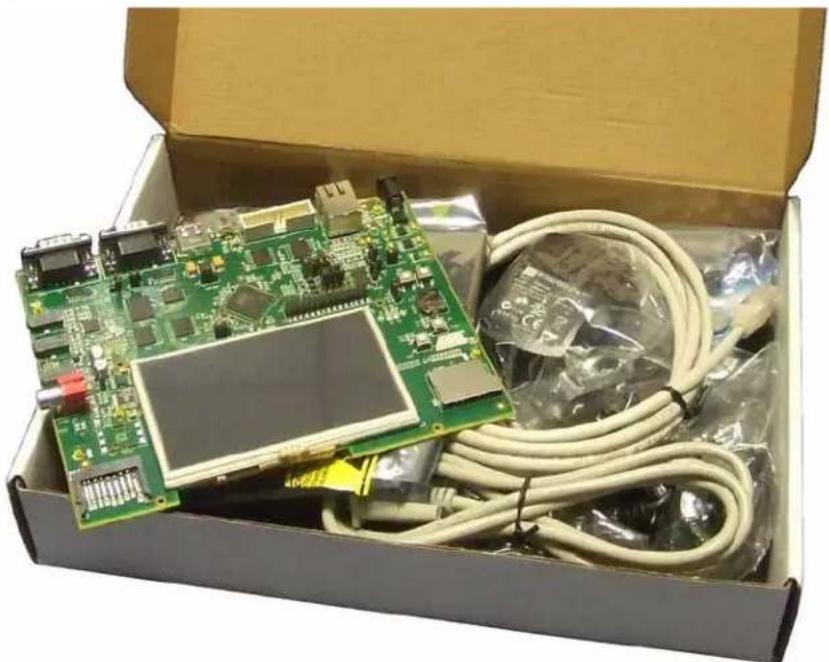
natural_image
Open cardboard box containing a green printed circuit board, coiled with white cables and connectors, no visible text or symbols.Unpack and inspect this kit carefully. Contact your local Atmel distributor, should you have issues concerning the contents of the kit.
2.2 Evaluation Board Specifications
Table 2-1. SAM9M10-G45-EK Specifications
| Characteristics Specifications | |
| Clock speed 400 MHz PCK, 133 MHz MCK | |
| Ports Ethernet, USB, RS232, DBGU, JTAG | |
| Board supply voltage 5 VDC from connector | |
| Temperature- operating- storage | -10^ to +50^ C -40^ to +85^ C |
| Relative humidity 0 to 90% (non condensing) | |
| Dimensions 180 mm x 140 mm | |
| RoHS status Compliant | |
2.3 Electrostatic Warning
The SAM9M10-G45-EK evaluation board is shipped in a protective anti-static package. The board must not be subjected to high electrostatic potentials. We strongly recommend using a grounding strap or similar ESD protective device when handling the board in hostile ESD environments (offices with synthetic carpet, for example...). Avoid touching the component pins or any other metallic element on the board.
3.1 Power Up the Board
Unpack the board taking care to avoid electrostatic discharge. Unpack the power supply, select the right power plug adapter corresponding to that of your country, and insert it in the power supply.
Connect the power supply DC connector to the board and plug the power supply to an AC power plug.
The board LCD should light up and display a welcome page. Then, click or touch icons displayed on the screen and enjoy the demo.
3.2 Battery
The SAM9M10-G45-EK ships with a 3V coin battery.
This battery is not required for the board to start up.
The coin battery is provided for user convenience in case the user would like to exercise the date and time backup function of the SAM9M10 series devices when the board is switched off.
3.3 DevStart
The on-board NAND Flash contains a "SAM9M10-G45-EK DevStart".
It is stored in the "SAM9M10-G45-EK DevStart" folder on the USB Flash disk available when the SAM9M10-G45-EK is connected to a host computer.
Click the file "welcome.html" in this folder to launch SAM9M10-G45-EK DevStart.
SAM9M10-G45-EK DevStart guides you through installation processes of IARTM EWARM, Keil MDK and GNU toolkits. Then, it gives you step-by-step instructions on how to rebuild a single example project and how to program it into the SAM9M10-G45-EK. Optionally, if you have a SAM-ICE™, instructions are also given about how to debug the code.
We recommend that you backup the “SAM9M10-G45-EK DevStart” folder on your computer before launching it.
3.4 Recovery Procedure
The DevStart ends by giving step-by-step instructions on how to recover the SAM9M10-G45-EK to the state as it was when shipped by Atmel.
Follow the instructions if you deleted the contents of the NAND Flash and want to recover from this situation.
3.5 Sample Code and Technical Support
After boot up, you can run some sample code or your own application on the development kit. You can download sample code and get Technical support from http://www.atmel.com/dyn/products/tech_support.asp?Faq=y&family_id=689%20.
4.1 Equipment on the Board
Figure 4-1. Board Architecture

flowchart
graph TD
    A["Main Memory"] --> B["External Memory"]
    B --> C["External Cards"]
    C --> D["Multimedia Cards Interface"]
    D --> E["LCD TFT 480*272"]
    E --> F["Touch Screen"]
    F --> G["Composite video"]
    G --> H["AC97"]
    H --> I["PWM"]
    I --> J["PIO"]
    J --> K["USB"]
    K --> L["DEBUG"]
    L --> M["JTAG/ICE#GU"]

    subgraph AT91SAM9M10
        N["System Controller"] --> O["Image Sensor Interface"]
        O --> P["TWI"]
        P --> Q["ETHERNET 10/100 MAC"]
        Q --> R["USART"]
        R --> S["USB"]
        S --> T["DEBUG"]
    end

    subgraph Media Cards
        U["DDR2 SDRAM"] --> V["External Memory"]
        W["NAND FLASH"] --> V
        X["DDR2 SDRAM"] --> Y["External Memory"]
        Z["NCS1"] --> V
        AA["NCS3"] --> V
        AB["NCS0"] --> V
        AC["Data Flash"] --> AD["MCI1"]
        AE["8 bits interface SD/MMC"] --> AF["MCI1"]
        AG["SPIO"] --> AH["MCIO"]
        AI["4 bits interface SD/MMC"] --> AJ["MCIO"]
        AK["NPC50"] --> AL["External Memory"]
    end

    subgraph LCD TFT
        AM["Micro"] & AN["Line In"] & AO["Line Out"] & AP["Audio"] & AQ["User I/O"] & AR["Joystick & P.B."]
    end

    subgraph Audio
        AS["Codec"] --> AT["AC97"]
        AU["Led"] --> AV["PWM"]
    end

    subgraph User I/O
        AW["User I/O"] --> AX["User I/O"]
    end

    subgraph External Memory
        AY["EBIO"] --> AZ["External Memory"]
        BA["EBI1 / 1.8v"] --> BB["External Memory"]
        BC["External Memory"] --> BD["External Memory"]
        BE["External Memory"] --> BF["External Memory"]
        BG["External Memory"] --> BH["External Memory"]
        BI["External Memory"] --> BJ["External Memory"]
        BK["External Memory"] --> BL["External Memory"]
        BM["External Memory"] --> BN["External Memory"]
        BO["External Memory"] --> BP["External Memory"]
        BQ["External Memory"] --> BR["External Memory"]
        BS["External Memory"] --> BT["External Memory"]
    end

    subgraph System Controller
        BU["System Controller"] --> BV["Internal Controller"]
        BW["System Controller"] --> BX["System Controller"]
        BY["System Controller"] --> BZ["System Controller"]
        BQ["System Controller"] --> CA["System Controller"]
        CB["System Controller"] --> CC["System Controller"]
    end

    subgraph AT91SAM9M10
        DQ["System Controller"] --> DB["System Controller"]
        DC["System Controller"] --> DB["System Controller"]
        DB["System Controller"] --> DCSystem
    end

    subgraph Power / Shdn
        DD["Power / Shdn"] --> DDn
    end

    subgraph Power / Shdn
        DDn0["0000000000000000000"]
        DDn0n["00000000000000000000"]
    end

    subgraph Power / Shdn
        DDn1["Serial Ecprom"] --> DDn1n
        DDn1n --> DDn1n1
        DDn1n1 --> DDn1n1n
        DDn1n1n --> DDn1n1n1
        DDn1n1n1n --> DDn1n1n2
        DDn1n2n --> DDn1n2n1
        DDn1n2n1n --> DDn1n2n2
        DDn1n2n2n --> DDn1n2n3
        DDn1n3n --> DDn1n3n1
        DDn1n3n1n --> DDn1n3n2
        DDn1n3n2n --> DDn1n3n3
    end

    subgraph Power / Shdn
        DDn2["nuon"] --> DDn2n
        DDn2n --> DDn2n1
        DDn2n1 --> DDn2n2
        DDn2n2 --> DDn2n3
        DDn2n3 --> DDn2n4
    end

    subgraph Power / Shdn
        DDn3["nuon"] --> DDn3n
        DDn3n --> DDn3n1
        DDn3n1 --> DDn3n2
        DDn3n2 --> DDn3n3
        DDn3n3 --> DDn3n4
    end

    subgraph Power / Shdn
        DDn4["nuon"] --> DDn4n
        DDn4n --> DDn4n1
        DDn4n1 --> DDn4n2
        DDn4n2 --> DDn4n3
        DDn4n3 --> DDn4n4
    end

    subgraph Power / Shdn
        DDn5["nuon"] --> DDn5n
        DDn5n --> DDn5n1
        DDn5n1 --> DDn5n2
        DDn5n2 --> DDn5n3
    end

    subgraph Power / Shdn
        DDm["nuon"] --> DDm1["nuon"]
        DDm1 --> DDm2["nuon"]
        DDm2 --> DDm3["nuon"]
    end

    subgraph Power / Shdn
        DDm2["nuon"] --> DDm3["nuon"]
    end

    subgraph Power / Shdn
        DDm3["nuon"] --> DDm4["nuon"]
    end

    subgraph Power / Shdn
        DDm4["nuon"] --> DDm5["nuon"]
    end

    subgraph Power / Shdn
        DDm5["nuon"] --> DDm6["nuon"]
    end

    subgraph Power / Shdn
        DDm6["nuon"] --> DDm7["nuon"]
    end

    subgraph Power / Shdn
        DDm7["nuon"] --> DDm8["nuon"]
    end

    subgraph Power / Shdn
        DDm8["nuon"] --> DDm9["nuon"]
    end

    subgraph Power / Shdn
        DDm9["nuon"] --> DDm10["nuon"]
    end

    subgraph Power / Shdn
        DDm10["nuon"] --> DDm11["nuon"]
    end

    subgraph Power / Shdn
        DDm11["nuon"] --> DDm12["nuon"]
    end

    subgraph Power / Shdn
        DDm12["nuon"] --> DDm13["nuon"]
    end

    subgraph Power / Shdn
        DDm13["nuon"] --> DDm14["nuon"]
    end

    subgraph Power / Shdn
        DDm14["nuon"] --> DDm15["nuon"]
    end

    subgraph Power / Shdn
        DDm15["nuon"] --> DDm16["nuon"]
    end

    subgraph Power / Shdn
        DDm16["nuon"] --> DDm17["nuon"]
    end

    subgraph Power / Shdn
        DDm17["nuon"] --> DDm18["nuon"]
    end

    subgraph Power / Shdn
        DDm18["nuon"] --> DDm19["nuon"]
    end

    subgraph Power / Shdn
        DDm19["nuon"] --> DDm20["nuon"]
    end

    subgraph Power / Shdn
        DDm20["nuon"] --> DDm21["nuon"]
    end

    subgraph Power / Shdn
        DDm21["nuon"] --> DDm22["nuon"]
    end

    subgraph Power / Shdn
        DDm22["nuon"] --> DDm23["nuon"]
    end

    subgraph Power / Shdn
        DDm23["nuon"] --> DDm24["nuon"]
    end

    subgraph Power / Shdn
        DDm24["nuon"] --> DDm25["nuon"]
    end

    subgraph Power / Shdn
        DDm25["nuon"] --> DDm26["nuon"]
    end

    subgraph Power / Shdn
        DDm26["nuon"] --> DDm27["nuon"]
    end

    subgraph Power / Shdn
        DDm27["nuon"] --> DDm28["nuon"]
    end

    subgraph Power / Shdn
        DDm28["nuon"] --> DDm29["nuon"]
    end

    subgraph Power / Shdn
        DDm29["nuon"] --> DDm30["nuon"]
    end

    subgraph Power / Shdn
        DDm30["nuon"] --> DDm31["nuon"]
    end

    subgraph Power / Shdn
        DDm31["nuon"] --> DDm32["nuon"]
    end

    subgraph Power / Shdn
        DDm32["nuon"] --> DDm33["nuon"]
    end

    subgraph Power / Shdn
        DDm33["nuon"] --> DDm34["nuon"]
    end

    subgraph Power / Shdn
        DDm34["nuon"] --> DDm35["nuon"]
    end

    subgraph Power / Shdn
        DDm35["nuon"] --> DDm36["nuon"]
    end

    subgraph Power / Shdn
        DDm36["nuon"] --> DDm37["nuon"]
    end

    subgraph Power / Shdn
        DDm37["nuon"] --> DDm38["nuon"]
    end

    subgraph Power / Shdn
        DDm38["nuon"] --> DDm39["nuon"]
    end

    subgraph Power / Shdn
        ND["mus"][ns][ns][ns][ns][ns][ns][ns][ns][ns][ns][ns][ns][ns][ns][ns][ns][ns][ns][ns][ns][ns][ns][ns][ns][ns][ns][ns][ns][ns][ns][ns][ns][ns][ns][ns][ns][ns][ns][ns][ns][ns][ns][ns][ns][ns][ns][ns][ns][ns][ns][ms][ms][ms][ms][ms][ms][ms][ms][ms][ms][ms][ms][ms][ms][ms][ms][ms][ms][ms][ms][ms][ms][ms][ms][ms][ms][ms][ms][ms][ms][ms][ms][ms][ms][ms][ms][ms][ms][ms][ms][ms][ms][ms][ms][ms][ms][ms][ms][ms][ms][mm][mm][mm][mm][mm][mm][mm][mm][mm][mm][mm][mm][mm][mm][mm][mm][mm][mm][mm][mm][mm][mm][mm][mm][mm][mm][mm][mm][mm][mm][mm][mm][mm][mm][mm][mm][mm][mm][mm][mm][mm][mm][mm][mm][mm][mm][mm][mm}[mm["i=0,0"]]{xx}^{x-0}

    end


    subgraph AT91SAM9M10
      AT91SAM9M10
      AT91SAM9M10
      AT91SAM9M10
      AT91SAM9M10
      AT91SAM9M10
      AT91SAM9M10
      AT91SAM9M10
      AT91SAM9M10
      AT91SAM9M10
      AT91SAM9M10
     end

    subgraph AT91SAM9M10
      AT91SAM9M10_AT91SAM9M10_AT91SAM9M10_AT91SAM9M10_AT91SAM9M10_AT91SAM9M10_AT91SAM9M10_AT91SAM9M10_AT91SAM9M10_AT91SAM9M10_AT91SAM9M10_AT91SAM9M10_ATATSM9M10_ATATSM9M10_ATATSM9M10_ATATSM9M10_ATATSM9M10_ATATSM9M10_ATATSM9M10_ATATSM9M10_ATATSM9M10_ATATSM9M10_ATATSM9M10_ATATSM9M10_ATATSM9M1O_ATATSM9M1O_ATATSM9M1O_ATATSM9M1O_ATATSM9M1O_ATATSM9M1O_ATATSM9M1O_ATATSM9M1O_ATATSM9M1O_ATATSM9M1O_ATATSM9M1O_ATATSM9M1O_ATATSM9M1O_ATAT SMN [nnnnnnnnnnnnnnnnnnnnnnnnnnnnnnnnnnnnnnnnnnnnnnnnnnnnnnnnnnnnnnnnnnnnnnnnnnnnnnnnnnnnnnnnnnnnnnnnnnnnnnnnnnnnnnnnnnnnnnnnnnnnnnnnnnnnnnnnnnnnnnnnnnnnnnnnnnnnnnnnnnnnnnnnnnnnnnnnnnnnnnnnnnnnnnnnnnnnnnnnttlllllllllllllllllllllllllllllllllllllllllllllllllllllllllllllllllllllllllllllllllllllllllllllllllllllllllllllllllllll:ccccc;
| VCC 5V | ISI | Ethernet RMII/MII | RS232 | USB HubHigh / Full | USBHub / Device | DBGU | JTAG/ICE | PIO |
4.1.1 Interfaces
The board is equipped with an AT91SAM9M10-CU embedded microprocessor (324-ball TFBGA package) together with the following interfaces or peripherals:
■ DDR2/LPDDR memory interface is connected to 128 MB DDR2-SDRAM memory
■ External Bus Interface (EBI) is connected to three kinds of memory devices (DDR2-SDRAM, NAND Flash and NOR Flash (not populated))
Board Description
■ One TWI serial memory
■ One USB Host/Device multiplexed port interface
■ One USB Host port interface
■ One RS232 serial communication port
■ One DBGU serial communication port
■ One JTAG/ICE debug interface
■ One Ethernet 100-base TX with three status LEDs
■ One AC97 Audio CODEC with headphone line out, line in and mono/stereo microphone inputs
■ One TV interface (composite video output)
■ One 4.3" TFT LCD Module with touch screen and back light
■ One ISI connector (camera interface)
■ One power red LED and two general-purpose green LEDs
■ Two user input push buttons
■ One joystick with 4-direction control and selector
■ One wakeup input push button
■ One reset input push button
■ One SD/SDIO/MMC plus card slot (4/8 bit interface)
■ One SD/SDIO/MMC card slot (4-bit interface)
■ One Lithium Coin Cell Battery Retainer for 12 mm cell size (memory backup usage)
4.1.2 Board Interface Connection
■ Ethernet using RJ45 connector (J15)
■ USB Host, support USB host using a type A connector (J12)
■ USB Host/Device, support USB host/device using a type micro AB connector (J14)
■ UART1 (RX, TX, RTS, CTS) connected to a 9-way male D-type RS232 connector (J11)
■ DBGU (RX and TX only) connected to a 9-way male D-type RS232 connector (J10)
■ JTAG, 20 pin IDC connector (J13)
■ SD/MMCplus connector (J5)
■ SD/MMC connector (J6)
■ Headphone (J7), line-in (J8) and microphone headset (J9)
■ Speaker output (JP15)
■ Image sensor connector (J17)
■ TFT LCD display, with TouchScreen and backligh (J24)
■ Test points; various test points are located throughout the board
■ Main power supply (J2)
4.1.3 Push Button Switches
■ Reset, board reset (BP1)
■ Wake up, push button to bring processor out of low power mode (BP2)
■ Right and left click, user push button switches (BP4 and BP5)
■ Joystick (BP3)
4.1.4 Display LCD and LEDs
■ Display, 480xRGBx272 pixels LCD module display connected to the PIO port E (LCD1)
■ One surface-mounted power red LED, user interface (D3)
■ Two surface-mounted green LEDs, user interface (D1 and D2)
■ Three surface-mounted LEDs indicate Ethernet status (D4, D5, D6)
Figure 4-2. Board Layout Commented
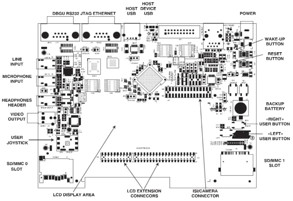
text_image
DBGU RS232 JTAG ETHERNET HOST USB HOST DEVICE USB POWER LINE INPUT MICROPHONE INPUT HEADPHONES HEADER VIDEO OUTPUT USER JOYSTICK SD/MMC 0 SLOT LCD DISPLAY AREA LCD EXTENSION CONNECTORS ISI/CAMERA CONNECTOR WAKE-UP BUTTON RESET BUTTON BACKUP BATTERY «RIGHT» USER BUTTON «LEFT» USER BUTTON SD/MMC 1 SLOTThe major components of the SAM9M10-G45-EK board are shown in Figure 4-1.
4.2 Hardware Layout and Configuration
4.2.1 Processor
The board features the Atmel SAM9M10-CU 324-ball TFBGA package. This chip runs at a nominal frequency of 400 MHz for the core and 133 MHz for the system bus.
For more information, refer to the latest SAM9M10 datasheet available from http://www.atmel.com/
Board Description
4.2.2 Clock Circuitry
The SAM9M10-G45-EK includes six clock sources:
■ Two are alternatives for the SAM9M10 main clock,
■ One crystal and one crystal oscillator are used for the Ethernet MII/RMII chip,
■ One crystal is used for the AC97 codec chip,
■ One crystal or one crystal oscillator is used for the TV encoder.
Table 4-1. Main Components Associated with the Clock Systems
| Quantity Description Component assignment | ||
| 1 Crystal | for Internal Clock, 12 MHz Y1 | |
| 1 Crystal | for RTC Clock, 32.768 kHz Y2 | |
| 1 Oscillator for Ethernet Clock RMII, 50 MHz Y4 | ||
| 1 Crystal | for Ethernet Clock MII, 25 MHz (not populated) Y5 | |
| 1 Crystal | for AC97 Codec Clock, 24.576 MHz | Y3 |
| 1 | Crystal for TV Encoder Clock, 13 MHz, or Oscillator for TV Encoder, 13 MHz (not populated) | Y7Y6 |
4.2.3 Reset Circuitry
The reset sources are:
■ Power on reset
■ Push button reset
■ JTAG reset from an in-circuit emulator interface.
4.2.4 Memory
4.2.4.1 External Memories
The SAM9M10 features a DDR2/LPDDR memory interface and an External Bus Interface (EBI) to permit interfacing to a wide range of external memories and to almost any kind of parallel peripheral.
The SAM9M10-G45-EK board is equipped with DDR2/LPDDR devices featuring 128 MB of DDR2-SDRAM memory (16Meg*8*4).
The External Bus Interface (EBI) is connected to three kinds of memory devices:
■ One Parallel Flash (not populated by default)
■ Two DDR2-SDRAM
■ One NAND Flash (2Gb, 8 bit bus)
The chip selects NCS0, NCS1 and NCS3 are used for NOR Flash, DDR2-SDRAM and NAND Flash memories, respectively. Furthermore, a dedicated jumper can disconnect each of the two NCS0 and NCS3 signals, making them available for other functions.
Figure 4-3. EBI0 - DDR2
Board Description

text_image
DDR2 DDR_C00_159 DDR_A0_158 DDR_A0_157 DDR_A0_156 DDR_A0_155 DDR_A0_154 DDR_A0_153 DDR_A0_152 DDR_A0_151 DDR_A0_150 DDR_A0_149 DDR_A0_148 DDR_A0_147 DDR_A0_146 DDR_A0_145 DDR_A0_144 DDR_A0_143 DDR_A0_142 DDR_A0_141 DDR_A0_140 DDR_A0_139 DDR_A0_138 DDR_A0_137 DDR_A0_136 DDR_A0_135 DDR_A0_134 DDR_A0_133 DDR_A0_132 DDR_A0_131 DDR_A0_130 DDR_A0_129 DDR_A0_128 DDR_A0_127 DDR_A0_126 DDR_A0_125 DDR_A0_124 DDR_A0_123 DDR_A0_122 DDR_A0_121 DDR_A0_120 DDR_A0_119 DDR_A0_118 DDR_A0_117 DDR_A0_116 DDR_A0_115 DDR_A0_114 DDR_A0_113 DDR_A0_112 DDR_A0_111 DDR_A0_110 DDR_A0_109 DDR_A0_108 DDR_A0_107 DDR_A0_106 DDR_A0_105 DDR_A0_104 DDR_A0_103 DDR_A0_102 DDR_A0_101 DDR_A0_100 DDR_A0_99 DDR_A0_98 DDR_A0_97 DDR_A0_96 DDR_A0_95 DDR_A0_94 DDR_A0_93 DDR_A0_92 DDR_A0_91 DDR_A0_90 DDR_A0_89 DDR_A0_88 DDR_A0_87 DDR_A0_86 DDR_A0_85 DDR_A0_84 DDR_A0_83 DDR_A0_82 DDR_A0_81 DDR_A0_80 DDR_A0_79 DDR_A0_78 DDR_A0_77 DDR_A0_76 DDR_A0_75 DDR_A0_74 DDR_A0_73 DDR_A0_72 DDR_A0_71 DDR_A0_70 DDR_A0_69 DDR_A0_68 DDR_A0_67 DDR_A0_66 DDR_A0_65 DDR_A0_64 DDR_A0_63 DDR_A0_62 DDR_A0_61 DDR_A0_60 DDR_A0_59 DDR_A0_58 DDR_A0_57 DDR_A0_56 DDR_A0_55 DDR_A0_54 DDR_A0_53 DDR_A0_52 DDR_A0_51 DDR_A0_50 DDR_A0_49 DDR_A0_48 DDR_A0_47 DDR_A0_46 DDR_A0_45 DDR_A0_44 DDR_A0_43 DDR_A0_42 DDR_A0_41 DDR_A0_40 DDR_A0_39 DDR_A0_38 DDR_A0_37 DDR_A0_36 DDR_A0_35 DDR_A0_34 DDR_A0_33 DDR_A0_32 DDR_A0_31 DDR_A0_30 DDR_A0_29 DDR_A0_28 DDR_A0_27 DDR_A0_26 DDR_A0_25 DDR_A0_24 DDR_A0_23 DDR_A0_22 DDR_A0_21 DDR_A0_20 DDR_A0_19 DDR_A0_18 DDR_A0_17 DDR_A0_16 DDR_A0_15 DDR_A0_14 DDR_A0_13 DDR_A0_12 DDR_A0_11 DDR_A0_10 DDR_A0_9 DDR_A0_8 DDR_A0_7 DDR_A0_6 DDR_A0_5 DDR_A0_4 DDR_A0_3 DDR_A0_2Board Description
Figure 4-4. EBI1 - DDR2 + Flash
text_image
EBI FLASH-01.15 EBI FLASH_A1.20 EBI 08.58.15 EBI 08.48.15 MNS EBI 08.48.15 A1 EB2 288M TKD A2 MRA765490CF 3 A3 A4 A5 A6 A7 A8 A9 A10 A11 A12 A13 RDOS-0M RDOS-NU RDOS-0M RDOS-0M RDOS-0M RDOS-0M RDOS-0M RDOS-0M RDOS-0M RDOS-0M RDOS-0M RDOS-0M RDOS-0M RDOS-0M RDOS-0M RDOS-0M RDOS-0M RDOS-0M RDOS-0M RDOS- RDOS-0M RDOS-0M RDOS-0M RDOS-0M RDOS-0M RDOS-0M RDOS-0M RDOS-0M RDOS-0M RDOS-0M RDOS-0M RDOS-0M RDOS-0M RDOS-0M RDOS-0M RDOS-0M RDOS-100VDCF RDOS-100VDCF RDOS-100VDCF RDOS-100VDCF RDOS-100VDCF RDOS-100VDCF RDOS-100VDCF RDOS-100VDCF RDOS-100VDCF RDOS-100VDCF RDOS-100VDCIF RDOS-100VDCIF RDOS-100VDCIF RDOS-100VDCIF RDOS-100VDCIF RDOS-100VDCIF RDOS-100VDCIF RDOS-100VDCIF RDOS-100VDCIF RDOS-100VDCIF RDOS-100VDCIC RDOS-100VDCIC RDOS-100VDCIC RDOS-100VDCIC RDOS-100VDCIC RDOS-100VDCIC RDOS-100VDCIC RDOS-100VDCIC RDOS-100VDCIC RDOS-100VDCIC RDOS-100VDCID RDOS-100VDCID RDOS-100VDCID RDOS-100VDCID RDOS-100VDCID RDOS-100VDCID RDOS-100VDCID RDOS-100VDCID RDOS-100VDCID RDOS-100VDCID RDOS-100VDCIC RDOS-100VDCIC RDOS-100VDCIC RDOS-100VDCIC RDOS-100VDCIC RDOS-100VDCIC RDOS-100VDCIC RDOS-100VDCIC RDOS-100VDCIC RDOS-100VDCIIC RDOS-100VDCIC RDOS-100VDCIC RDOS-100VDCIC RDOS-100VDCIC RDOS-100VDCIC RDOS-100VDCIC RDOS-100VDCIC RDOS-100VDCIC RDOS-100VDCIC RDOS-100VDAI 288M KQ32 288M KQ32 288M KQ32 288M KQ32 288M KQ32 288M KQ32 288M KQ32 288M KQ32 288M KQ32 288M KQ32 288M KQ32 288M KQ324.2.5 Power Supplies
The SAM9M10 Board contains four regulated power supplies:
■ 3.3 VDC Supply
■ 1.8 VDC Supply
■ 1.0 VDC Core Supply
■ 1.0 VDC Core UTMI Supply, PLL
The outputs of these regulated power supplies ^1 are distributed as necessary to each part of the circuit board.
■ The 3.3 VDC Supply is generated by an adjustable LDO. It accepts VIN 5 VCC power and outputs a regulated +3.3 V to most other circuits on the board.
■ The 1.8 VDC Supply (VDDIOM0, VDDIOM1) is generated by an adjustable LDO. It is powered by VIN 5 VCC power and outputs a regulated +1.8V.
■ The 1.0 VDC Core Supply (VDDCORE) is generated by an adjustable LDO. It is powered by the output of the 3.3 VDC Supply.
■ The 1.0 VDC Core Supply (VDDUTMIC, VDDPLLUTMI and VDDPLLA) is generated by an adjustable LDO RT9186A series. It is powered by the output of the 3.3 VDC Supply.
Note: 1. Corresponding test points (TP1 to TP4, GND) are used with jumpers (JP1.1 to JP7) to permit probing of these voltages.
Board Description
Figure 4-5. Power Supply

text_image
3V3 F10 100k MNS RT3186A VIN VIN PGOOD EN OUT VOUT ADJ GND 8 7 6 5 R14 12k C19 10n C21 10u C22 1u R19 47k C20 4.7u L1 10uH R1 1R C2 4.7u L2 10uH R5 1R C14 4.7u C8 100n JP1,JP1 JP2,JP2 JP3,JP3 JP4,JP4 JP5,JP5 JP6,JP6 JP7,JP7 JP8,JP8 JP9,JP9 JP10,JP10 JP11,JP11 JP12,JP12 JP13,JP13 JP14,JP14 JP15,JP15 JP16,JP16 JP17,JP17 JP18,JP18 JP19,JP19 JP20,JP20 JP21,JP21 JP22,JP22 JP23,JP23 JP24,JP24 JP25,JP25 JP26,JP26 JP27,JP27 JP28,JP28 JP29,JP29 JP30,JP30 J1-1J1-1 2 VDDUTMII VDDANA VDDOSC VDDIOP0 VDDIOP1 VDDIOP2 VDDISI J1-2J1-2 34 VDDUTMIC J1-4J1-4 7 8 VDDPLLUTMI L310μHz-3.5μHzH C15 2.2μ C18 100n L4 10uH R20 1R C20 4.7u C28 100n C29 4.7u IV J1-3J1-3 VDDCORE 5 6 7 8 VDDICORE IV8 JP5,JP5 JP6 JP7,JP7 3 VDDICM0 VDDICM1 VDDBU 3V3 1 C30 100nFigure 4-6. Management Power Block

text_image
REGULATED 5V ONLY J2 DC POWER JACK C4 33u CR1 5V 5V R3 100k MN2 RT9016A PGOOD GND EN ADJ VIN VDD NC C10 1u 8 7 6 5 3V3 C9 10u C11 1u C310n0010n R1 47xR1 47x 3V3 R7 15k C11 1u C12 10u 5V R9 100k PWR_EN Q1 SIT563EDH JP4 SIP2 1 3 C17 2 15p R16 10k R17 10k SHDN 1V8 MN4 RT9016A PGOOD GND EN ADJ VIN VDD NC 8 7 6 5 5 5V R11 100k C24 1u C23 10u C16 10xC16 10n R15 15xF15 15x R18 12k C26 1u C27 10u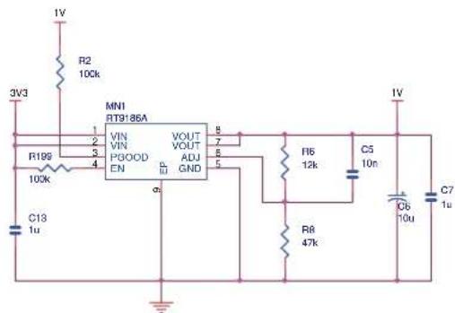
text_image
3V3 R2 10Ck MINI RT9186A VIN VIN PGOOD EN VOUT VOUT ADU GND 1 2 3 4 5 6 7 8 F199 10Ck C13 1u σ1 R6 12k C5 10n R8 47k C6 10u C7 1u 1VBoard Description
4.2.6 Debug Interface
4.2.6.1 JTAG/ICE
Software debug is accessed by a standard 20-pin JTAG connection. This allows connection to a standard USB-to-JTAG in-circuit emulator.
Figure 4-7. JTAG Interface
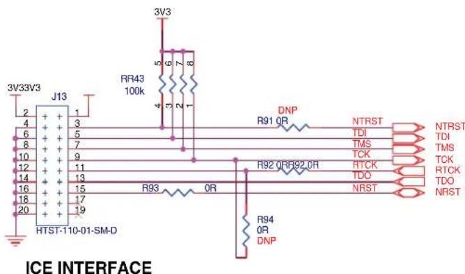
text_image
ICE INTERFACE 3V33V3 J13 RR43 100k 3V3 5 6 7 8 4 3 2 1 R91 OR DNP NTRST TDI TMS TCK RTCK TDO NRST NTRST TDI TMS TCK RTCK TDO NRST HTST-110-01-SM-D R92 ORB92 OR R93 OR R94 OR DNPThis UART is connected to the DB-9 male socket through an RS-232 Transceiver (TXD and RXD only).
Figure 4-8. DBGU Com Port
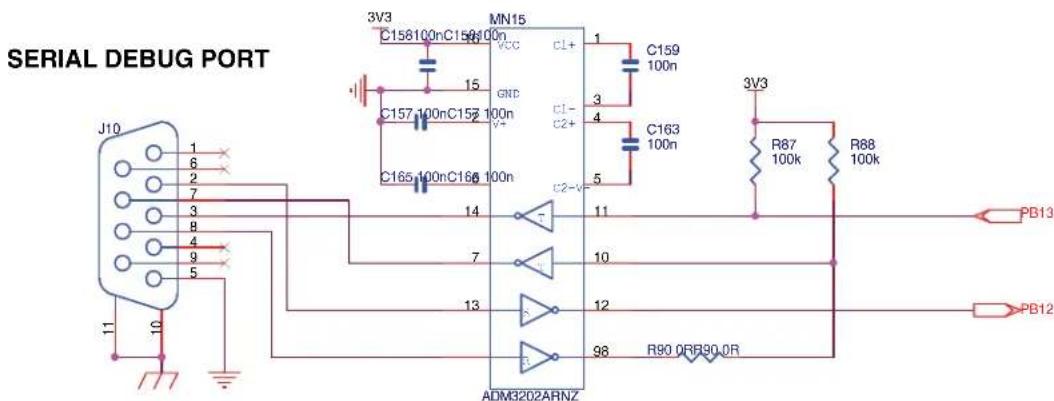
text_image
SERIAL DEBUG PORT J10 1 8 2 7 3 8 4 9 5 11 10 MN15 C156100nC158100n VCC CL+ 1 C159 100n GND 3 C157 100nC157 100n V+ 4 C163 100n C165 100nC166 100n C2-V- 14 - 7 13 12 98 ADM3202ARNZ R90 0RB90.0R 3V3 R87 100k R88 100k PB13 PB124.2.6.3 User Serial Com Port
The USART1 is used as a user serial communication port. This USART1 is buffered with an RS-232 Transceiver (TXD, RXD and handshake CTS/RTS control) and connected to the DB-9 male socket. Software must assign the appropriate PIO pins (PB5 = RXD1, PB4 = TXD1, PD16 = RTS1, PD17 = CTS1) to enable the UART1 function.
Figure 4-9. User Serial Com Port

text_image
RS232 COM PORT SV3 R89 100k R88 100k MN16 C160 100n C164 100n 3 4 5 6 7 8 9 10 11 12 13 14 15 16 3V3 C161 100n C162 100nC162 100n C166 100nC166 100n ADM32C2A-RNZ PD4 PD16 PB5 PD17 J1J11Refer to the SAM9M10 datasheet for more information about the SAM9M10 USARTs.
4.2.6.4 USB Port
The SAM9M10-G45-EK features USB communication ports:
■ Two Host Ports: Full speed OHCI and High speed EHCI
■ One Device Port: High speed.
USB Host Port0 is directly connected to the first UTMI transceiver. The second Host Port (Port1) is multiplexed with the USB Device High speed and connected to the second UTMI port.
■ One USB high/full speed type standard A connector
■ One USB interface Host/Device Micro AB connector
Refer to the SAM9M10 datasheet for detailed programming information.
Board Description
Figure 4-10. USB Port
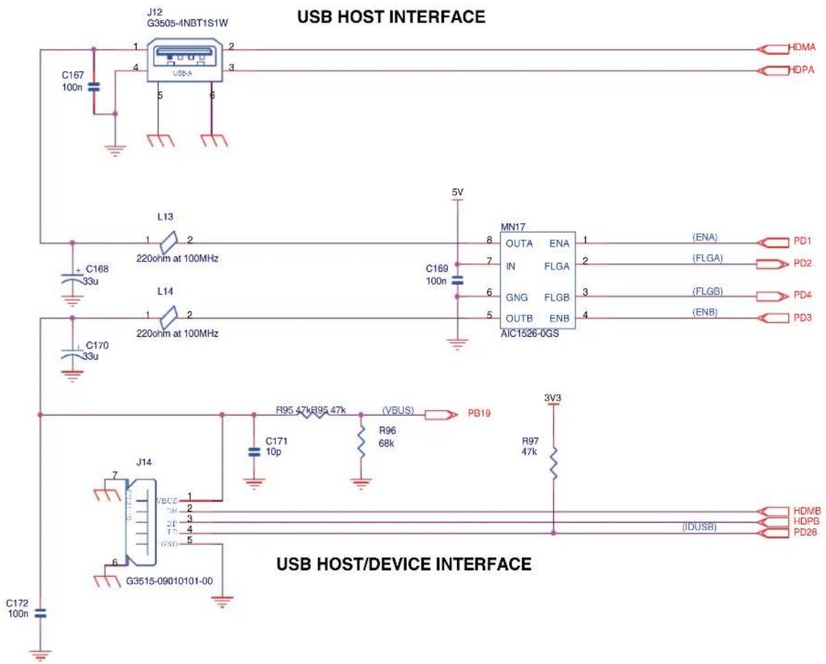
text_image
USB HOST INTERFACE J12 G3505-4NBT1S1W 1 2 3 HDMA C167 100n 4 5 6 USB-A L13 1 2 220ohm at 100MHz C168 33u L14 1 2 220ohm at 100MHz C170 33u 5V MN17 OUTA ENA IN FLGA GNG FLGB OUTB ENB AIC1526-0GS (ENA) PD1 (FLGA) PD2 (FLGB) PD4 (ENB) PD3 USB HOST/DEVICE INTERFACE R95 47kR95 47k (VBUS) PB19 C171 10p R96 68k R97 47k 3V3 J14 7 KBCS 1 DM 2 DE 3 TH 4 GND 5 G3515-09010101-00 (IDUSB) HDMB HDPB PD28 C172 100n4.2.6.5 Ethernet 10/100 (EMAC) Port
The port is compatible with IEEE® Standard 802.3.
The SAM9M10-G45-EK is equipped with a Davicom DM9161AEP 10/100 Mbps Fast Ethernet Physical Layer TX/FX Single Chip Transceiver. It contains the entire physical layer functions of 100BASE-TX as defined by IEEE 802.3u, including the Physical Coding Sublayer (PCS), Physical Medium attachment (PMA), Twisted Pair Physical Medium Dependent Sublayer (TP-PMD), 10BASE-TX Encoder/Decoder (ENC/DEC), and Twisted Pair Media Access Unit (TPMAU).
The Ethernet interface integrates an RJ45 connector with an embedded transformer, and three status LEDs.
The Ethernet interface provides two selectable modes, MII or RMII (Reduced MII), for 100Base-TX or 10Base-TX. The MII and RMII interfaces are capable of both 10Mb/s and 100Mb/s data rates as described in the IEEE 802.3u standard. The signals used by MII and RMII interfaces are described in the table below.
Table 4-2. Pin Mapping for Normal MII and Reduced MII
| Pin Name Normal | MII Mode Reduced MII Mode | |||
| SAM9M10 DM9161 SAM9M10 DM9161 | ||||
| ETX0-ETX1 ETX[0:1] transmit data TXD [0:1] ETX[0:1] TXD [0:1] | ||||
| ETX2-ETX3 ETX[2:3] transmit data TXD [2:3] NC NC | ||||
| ETXEN ETXEN: transmit enable TXEN ETXEN: transmit enable TXEN | ||||
| ETXER ETXER: transmit error TXER/TXD[4] NC NC | ||||
| ETXCK/REFCK | ETXCK: transmit clock | TXCLK | REFCK: reference clock | REF_CLK |
| ERX0-ERX1 | ERX[0:1]: receive data | RXD [0:1] | ERX[0:1]: receive data | RXD [0:1] |
| ERX2-ERX3 | ERX[2:3]: receive data RXD [2:3] | NC NC | ||
| ERXER | ERXER: receive error | RXER/RXD[4]/RPTR/NODE | ERXER: receive error | RPTR/NODE |
| ERXDV | ERXDV: receive valid data | RXDV | ECRSDV: carrier sense / data valid | CRS DV |
| ERXCK | ERXCK: receive clock | RXCLK | NC NC | |
| ECOL | ECOL: collision detect | COL | NC NC | |
| ECRS | ECRS: carrier sense / data valid | CRS (PHYAD[2:4] | NC NC | |
| EMDC | EMDC: management data clock | MDC | EMDC: management data clock | MDC |
| EMDIO | EMDIO: management data input / output | MDIO | EMDIO: management data input / output | MDIO |
| NRST | NRST: microcontroller reset | RESET# XT1(25 MHz) | NRST: microcontroller reset | RESET# XT1(REF_CLK 50MHz) |
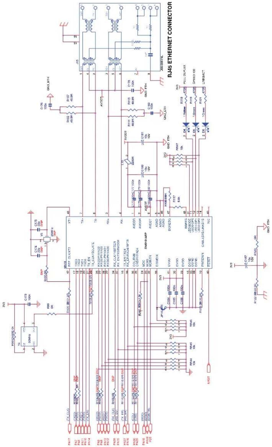
Figure 4-11. Ethernet Port
text_image
RJ45 ETHERNET CONNECTOR RJ45 ETHERNET CONNECTOR 3V3 C175 220 DNP C174 220 DNP C110.0V DNP M018 REF CLKXT2 TX03 TX02 TX01 TX00 TX EN TX_CLM-DCATE RXDSPHYAD2 RXDSPHYAD2 RXDSPHYAD1 RXDSPHYAD0 RXCLKY-0BTSER RX DVTESTMODER TX_EPI-X64 RX_EPI-X64-RPTR CO-PAMII CRS-PHYADS MX616-AFP AVODT AVODR AVODR AVODT AVODR AVODR AVODR AVODR AVODR AVODR AVODR AVODR AVODR AVODR AVODR AVODR AVODR AVODR AVODR AVODR AVODR AVODR AVODR AVODR AVODR AVODR AVODR AVODR AVODR AVODD AVODD AVODD AVODD AVODD AVODD AVODD AVODD AVODD AVODD AVODD AVODD AVODD AVODD AVODD AVODD AVODD AVODD AVODD AVODD AVODD AVODD AVODD AVODD AVODD AVODO AVODO AVODO AVODO AVODO AVODO AVODO AVODO AVODO AVODO AVODO AVODO AVODO AVODO AVODO AVODO AVODO AVODO AVODO AVODO AVODO AVODO AVODO AVODO AVODO AVODU DVDDU DVDDU DVDDU DVDDU DVDDU DVDDU DVDDU DVDDU DVDDU DVDDU DVDDU DVDDU DVDDU DVDDU DVDDU DVDDU DVDDU DVDDU DVDDU DVDDU DVDDU DVDDU DVDDU DVDDU DVDDU DVDOU 10kΩ/Hz/Hz/Hz/Hz/Hz/Hz/Hz/Hz/Hz/Hz/Hz/Hz/Hz/Hz/Hz/Hz/Hz/Hz/Hz/Hz/Hz/Hz/Hz/Hz/Hz/Hz/Hz/Hz/Hz/Hz/Hz/Hz/Hz/Hz/Hz/Hz/Hz/Hz/Hz/Hz/Hz/Hz/Hz/Hz/Hz/Hz/Hz/Hz/Hz/Hz/MHz/Hz/Hz/Hz/Hz/Hz/Hz/Hz/Hz/Hz/Hz/Hz/Hz/Hz/Hz/Hz/Hz/Hz/Hz/Hz/Hz/Hz/Hz/Hz/Hz/Hz/Hz/Hz/Hz/Hz/Hz/Hz/Hz/Hz/Hz/Hz/Hz/Hz/Hz/Hz/Hz/Hz/Hz/Hz/Hz/Hz/Hz/Hz/Hz/Hz/ChFor more information about the Ethernet controller device, refer to the Davicom DM9161 controller manufacturer's datasheet.
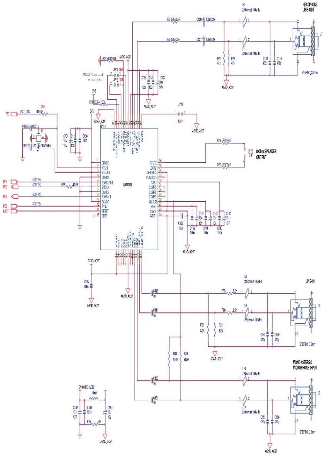
4.2.7 Audio Stereo Interface
The SAM9M10-G45-EK includes a WM9711L AC97 CODEC for digital sound input and output. This interface includes audio jacks for MIC input (J9), line audio input (J8), headphone line output (J7) and a 2-point speaker output connector (JP15).
It is compliant with AC97 Component Specification V2.2.
Figure 4-12. Audio Stereo Interface
text_image
HEADPHONE LINE-OUT 15 220lm at 100kHz C126 - 100kV R70 A357.14F C127 - 100kV R71 47k C128 47k C129 47k C130 47k A5ND_AC3F JPN DNP A5ND_AC3F P13 CRRUUR P14 DIP B Ohm SPEAKER OUTPUT 1MVF1L C133 10Ω C134 1Ω C135 1Ω C136 10Ω C137 2Ω C138 10Ω C139 10Ω C140 10Ω C141 10Ω C142 10Ω C143 10Ω C144 10Ω C145 10Ω C146 10Ω C147 10Ω C148_AC3F A5ND_AC3F C150A357 A5ND_AC3F C151A357 A5ND_AC3F C152A357 A5ND_AC3F C153A357 A5ND_AC3F C154A357 A5ND_AC3F C155A357 A5ND_AC3F C156A357 A5ND_AC3F C157A357 A5ND_AC3F C158A357 A5ND_AC3F C159A357 A5ND_AC3F C160A357 A5ND_AC3F C161A357 A5ND_AC3F C162A357 A5ND_AC3F C163A357 A5ND_AC3F C164A357 A5ND_AC3F C165A357 A5ND_AC3F C166A357 A5ND_AC3F C167A357 A5ND_AC3F C168A357 A5ND_AC3F C169A357 A5ND_AC3F C170A357 A5ND_AC3F C171A357 A5ND_AC3F C172A357 A5ND_AC3F C173A357 A5ND_AC3F C174A357 A5ND_AC3F C175A357 A5ND_AC3F C176A357 A5ND_AC3F C177A357 A5ND_AC3F C178A357 A5ND_AC3F C179A357 A5ND_AC3F C180A357 A5ND_AC3F C181A357 A5ND_AC3F C182A357 A5ND_AC3F C183A357 A5ND_AC3F C184A357 A5ND_AC3F C185A357 A5ND_AC3F C186A357 A5ND_AC3FFor more information about the AC97 codec device, refer to the Wolfson WM9711L controller manufacturer's datasheet.
4.2.8 TV-Out Extension
The Chronel™ CH7024 chip provides an interface between the SAM9M10 LCD Controller and a TV set by converting LCD signals to TV signals.
The CH7024 is a TV encoder device which encodes the video signals and generates synchronization signals for NTSC and PAL standards. Supported TV output formats are NTSC-M, NTSC-J, NTSC-433, PAL-B/D/G/A/I, PAL-M, PAL-N and PAL-60. The CH7024 provides video output support for CVBS or S-video.
Figure 4-13. TV-Out Extension Port

text_image
PE[0..30] PE30 (B7) PE28 (B6) PE28 (B5) PE27 (B4) PE26 (B3) PE25 (B2) PE24 (B1) PE23 (B0) PE22 (G7) PE21 (G6) PE20 (G5) PE19 (G4) PE18 (G3) PE17 (G2) PE16 (G1) PE15 (G0) PE14 (R7) PE13 (R6) PE12 (R5) PE11 (R4) PE10 (R3) PE9 (R2) PE8 (R1) PE7 (R0) PE6 (LCDDEN) PE5 (LCDDOTCK) PE4 (HSYNC) PE3 (VSYNC) PE2 (LCDCC) PE1 (LCDMOD) PE0 (LCDPWR) MN20 CH7024B D0 D1 D2 D3 D4 D5 D6 D7 D8 D9 D10 D11 D12 D13 D14 D15 D16 D17 D18 D19 D20 D21 D22 D23 VDDIO DVDD 38 16 C196 100n C197 100n C198 10u 10V DGND 18 AVDD_PLL 32 C200 100n AGND_PLL 31 AVDD 33 C202 100n AGND 36 AVDD_DAC 25 C203 100n AGND_DAC 29 R1781.2k ISET 30 CVBS 28 Y SPD SPC C/CVBS 27 R181 75R R18375RR18375R C/CVBS 26 P-OUT 37 TP6 COMPOSITE Video Output RCA JACK J2C TV_VSYNC TV_HSYNC TV_XCLK 3V3 R179 4T9 4.7k R180 4.7k PA20 TW DO) 21 TA PN 3V3 DNP 3V3 4 DNP 4 DNP 3V3 4 DNP 3V3 4 DNP 3V3 4 DNP 3V3 4 DNP 3V3 4 DNP 3V3 4 DNP 3V3 4 DNP 3V3 4 DNP 3V3 4 DNP 3V3 4 DNP 3V3 4 DNP 3V3 4 DNP 3V3 4 D-NP 4NPN R184 10k DNP Y6 VSS OUT DNP R186 DNP R185 OR Y7 C207 100n DNP R186 0 1 3 4 5 6 7 8 9 10p C208 10p C209 10p TP6Board Description
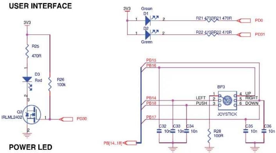
4.2.9 Software Controlled LEDs
Three users LED are provided for general use. The LEDs are connected to PIO port lines, allowing their control through either GPIO or PWM control.
■ LEDs D1 to D3 are software controlled by PIO pins.
■ LEDs D4 to D6 indicate Ethernet traffic and link status. These are automatically managed by on-chip microcontroller hardware. See Section 7.1 "Schematics".
Table 4-3. Discrete LEDs
| LED Description Comment | |
| D1 Green | LED User software controlled |
| D2 Green | LED User software controlled |
| D3 Red | LED User software controlled |
| D4 Yellow | LED Indicates transmission or reception via Ethernet |
| D5 Green | LED Indicates speed 100 |
| D6 Green | LED Is lit when a good link test has been detected |
Figure 4-14. Software Controlled LEDs
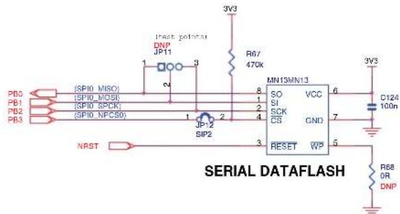
4.2.10 Serial Peripheral Interface Controller (SPI)
The SAM9M10 provides two high-speed Serial Peripheral Interface (SPI) controllers. One port is used to interface with the on-board serial DataFlash ^® .
Figure 4-15. SPI
text_image
PB0 (SP10 MISO) PB1 (SP10 MOSI) PB2 (SP10 SPCK) PB3 (SP10 NPC50) NRST IP-2 SIP2 3V3 DNP JP11 3 6 8 2 4 3 RESET WP MN13MN13 SO VCC SI SCK CND CS 3V3 C124 100n R67 47CK 3V3 R68 OR DNP SERIAL DATAFLASH4.2.11 Two Wire Interface (TWI)
The SAM9M10 has a full speed (400 kHz) master/slave I2C Serial Controller. The controller is fully compatible with the industry standard I2C and SMBus Interfaces. This port is used to interface with the onboard Serial EEPROM, ISI and TV encoder interface.
Figure 4-16. TWI
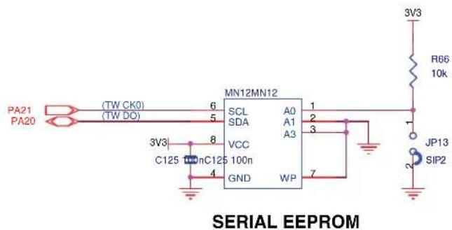
text_image
PA21 PA20 (TW CK0) (TW DO) 6 5 MN12MN12 SCL A0 1 2 3V3 8 VCC A1 3 C125 100nC125 100n GND WP 7 3V3 R66 10k JP13 SIP2 SERIAL EEPROM4.2.12 SD/MMC Interface
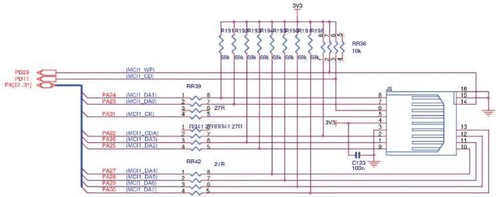
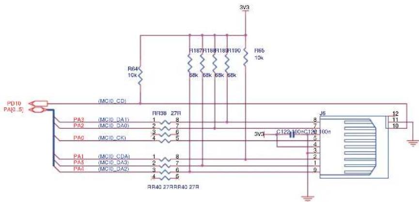
The SAM9M10-G45-EK has two high-speed 8-bit multimedia interfaces MMC/MMCPlus v4.1. The first interface is used as an 8-bit interface (MCI1), connected to a CE-ATA connector footprint and an 8-bit SD/MMC card slot. The second interface is used as a 4-bit interface (MCI0), connected to a 4-bit SD/MMC card slot.
The users must provide their own compatible cards for use with these connectors.
Please note that the power is connected to VCC, which is 3.3 volts.
Board Description
Figure 4-17. SD/MMC0
text_image
PD29 PD11 PA[22..31] (MCI1_WP) (MCI1_CD) PA24 (MCI1_DA1) 1 8 PA23 (MCI1_DA0) 2 7 PA31 (MCI1_CK) 3 6 27R PA22 (MCI1_CDA) 1 RR41 5RR41 27R PA25 (MCI1_DA3) 2 7 PA25 (MCI1_DA2) 3 6 PA27 (MCI1_DA4) 1 8 PA28 (MCI1_DA5) 2 7 PA29 (MCI1_DA6) 3 6 PA30 (MCI1_DA7) 4 5 RR39 RR42 27R RR36 10k J5 8 7 6 5 4 3 2 1 9 C123 100n 3V3SD/MMCPlus CARD INTERFACE - MCI1
Figure 4-18. SD/MMC1
text_image
PD10 PA[0..5] (RCIO_CD) PA3 (MCIO_DA1) 1 8 PA2 (MCIO_DA0) 2 7 PA0 (MCIO_CK) 3 6 PA1 (MCIO_CDA) 4 5 PA5 (MCIO_DA3) 1 8 PA4 (MCIO_DA2) 2 7 RF38 27R 58K 58K 58K 58K F167 F188 F189 F190 H65 10k 3V3 J6 C122 100n C122 100n 3V3 J6 12 11 10 RR40 27RR40 27RSD/MMC CARD INTERFACE - MCI0
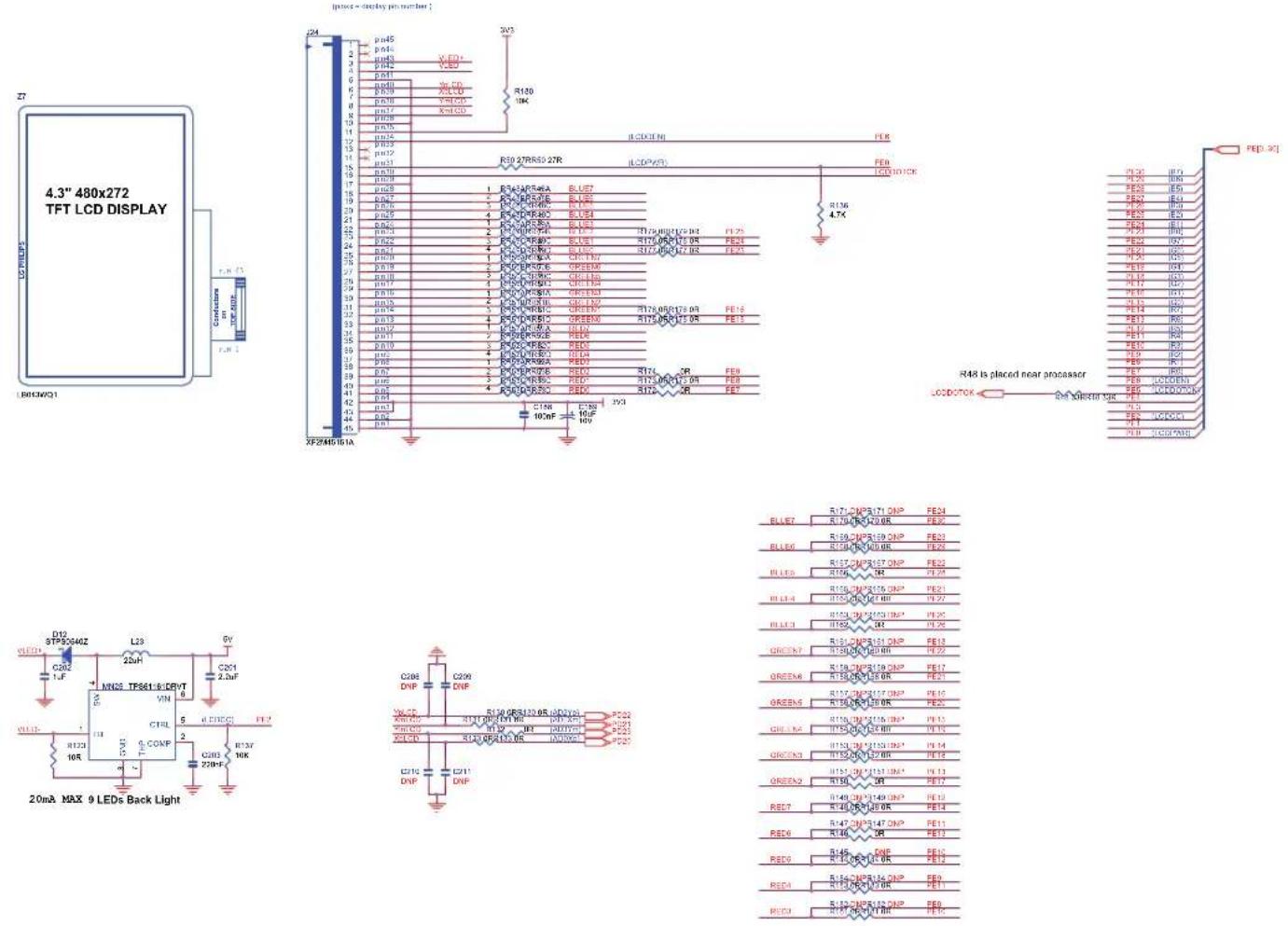
4.2.13 TFT LCD with Touch Panel
The SAM9M10 features an LCD controller. A 4.3" 480x272 Portrait Mode LCD provides the SAM9M10-G45-EK with a low power LCD display, back light unit and a touch panel, similar to that used on commercial PDAs.
The TFT LCD component is a truly model number TFT1N4633.
Graphics and text can be displayed on the dot matrix panel with up to 16 million colors by supplying 24-bit data signals (8bitxRGB by default) or 16-bit data signals (5+6+5bitxRGB in option). This allows the user to develop graphical user interfaces for a wide variety of end applications.
Warning: never connect/disconnect the LCD display from the board while the power supply is on. Doing so may damage both units and is not covered by warranty.
The back light voltage is generated from a CP2122ST boost converter. It is powered directly by the VIN 5 VCC power (the control for the back light voltages is separated from the main board voltages due to the specific voltage requirements of the LCD panel).
Figure 4-19. TFT LCD
| R17 | CNP517 | ONP | PE24 | |
| BLUE7 | R170 | CNP517 | ONP | PE25 |
| R169 | CNP516 | ONP | PE23 | |
| BLUE6 | R158 | CNP516 | ONP | PE25 |
| R157 | CNP517 | ONP | PE22 | |
| BLUE5 | R156 | OR | OR | PE24 |
| R156 | CNP516 | ONP | PE21 | |
| BLUE4 | R155 | OR | OR | PE22 |
| R153 | OR | OR | PE25 | |
| BLUE3 | R152 | OR | OR | PE26 |
| R152 | OR | OR | PE26 | |
| GREEN7 | R151 | CNP516 | ONP | PE13 |
| R150 | OR | OR | PE22 | |
| R150 | CNP516 | ONP | PE17 | |
| GREEN6 | R148 | OR | OR | PE21 |
| R148 | OR | OR | PE21 | |
| GREEN5 | R157 | CNP517 | ONP | PE10 |
| R156 | OR | OR | PE25 | |
| R155 | OR | OR | PE15 | |
| GREEN4 | R155 | OR | OR | PE15 |
| R153 | OR | OR | PE14 | |
| GREEN3 | R152 | OR | OR | PE18 |
| R152 | OR | OR | PE18 | |
| GREEN2 | R151 | OR | OR | PE17 |
| R150 | OR | OR | PE17 | |
| RED7 | R149 | OR | OR | PE13 |
| R148 | OR | OR | PE14 | |
| RED6 | R147 | CNP517 | ONP | PE11 |
| R146 | OR | OR | PE13 | |
| RED5 | R145 | OR | OR | PE10 |
| R144 | OR | OR | PE12 | |
| RED4 | R143 | OR | OR | PE9 |
| R143 | OR | OR | PE11 | |
| RED3 | R142 | OR | OR | PE9 |
| R141 | OR | OR | PE10 |
Board Description
4.2.14 Push Buttons
The SAM9M10-G45-EK is equipped with two system push buttons, two user push buttons and one joystick. The push buttons consist of momentary push button switches mounted directly to the board. When any switch is depressed, a low (zero) appears at the associated input pin.
■ System push buttons:
- Reset, perform system reset
– Wakeup, perform system wake up
■ User push button:
- Right click
- Left click
■ Joystick:
– One touch, 5-way switching,
– Normally open momentary contacts,
- Push down to select in any position.
Figure 4-20. Push Buttons
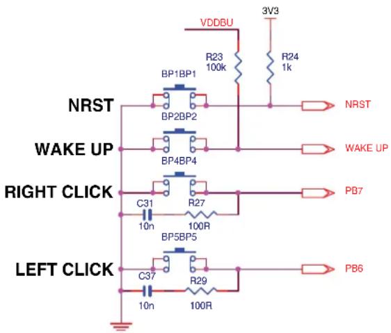
text_image
VDDBU 3V3 R23 100k R24 1k BP1BP1 BP2BP2 NRST WAKE UP BP4BP4 WAKE UP RIGHT CLICK C31 10n R27 100R PB7 LEFT CLICK C37 10n R29 100R PB64.2.15 Expansion Slot
■ GPIO1 & GPIO2, LCD signals (PIO E) are routed to the connectors extension J23
■ All I/Os of the SAM9M10 Image Sensor Interface are routed to connectors J17
■ Touch screen signals and analog I/O are connected to J18
This allows the developer to extend the features of the board by adding external hardware components or boards.
Figure 4-21. Expansion Slot

text_image
CONNECTOR EXTENSION FOR LARGE LCD J23 DNP PE8 1 2 PE7 PE10 34 PE9 PE12 5 6 PE11 PE14 7 8 PE13 PE16 9 10 PE15 PE18 11 12 PE17 PE20 13 14 PE19 PE22 15 16 PE21 PE24 17 18 PE22 PE26 19 20 PE23 PE28 21 22 PE25 PE30 23 24 PE27 LCDHSYNC 25.26 LCDDDYCK 27.26 PD14 30 3V3 33 35.36 37.38 39.40 HDR 2x20 SMT J18 1 2 (AD0Xp) A(O)Xm A(O)Ym (A(O)Yp) 7.8 9 10 R175 CR DNP HD R 2x10 SMT DNP 3V3 3V3 LCDHSYNC LCDDDYCK PD16 PD20 PD22 PD24 PD26 PD18 PV pv3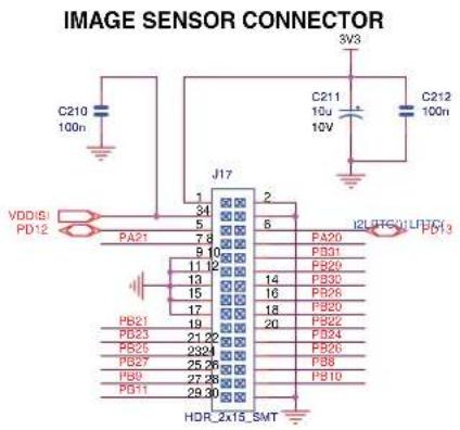
text_image
IMAGE SENSOR CONNECTOR VDD/S PD12 PA21 J17 34 5 7.8 5 10 11 12 13 15 17 19 21 22 23 24 25 26 27 28 29 30 HOR 2x15 SMT 3V3 C210 100n C211 10u 10V C212 100n 12LTCU1 LFC1 P0135.1 JTAG/ICE Configuration
Table 5-1. JTAG/ICE Configuration
| Designation | Default Setting Feature | |
| R91 Not populated Disables the ICE NTRST input | ||
| R92 Soldered Enables the ICE RTCK return. R94 must be opened | ||
| R93 Soldered Enables the ICE NRST input | ||
| R94 Not populated Disables TCK <-> RTCK local loop | ||
5.2 ETHERNET Configuration
RMII is the factory default mode.
To evaluate the MII mode, the user has to unsolder R99 and solder R100, R103 to R105, R108 to R110, R112, R114, C174, C175, Y5.
5.3 Jumpers Configuration
Two types of jumpers are used on the SAM9M10-G45-EK board:
■ 2-pin jumpers with two possible settings:
– Fitted: the circuit is closed
- Not fitted: the circuit is open
■ 3-pin jumpers with two possible positions, for which settings are presented in the following tables.
Table 5-2. Jumpers Configuration
| Designation | Default Setting Feature | ||||
| J1 (combined jumper array) | Closed | J1-1 | 1-2 | ||
| Closed | J1-2 | 3-4 | |||
| Closed | J1-3 | 5-6 | |||
| Closed J1-4 | 7-8 VDDPLLUTMI 1V | ||||
| JP1 1-2 JP1 | 1-2 VDDIOP0 3V3 | ||||
| 2-3 External power to VDDIOP0 3V3 nominal | |||||
| JP2 1-2 JP2 | 1-2 VDDIOP1 3V3 | ||||
| 2-3 External power to VDDIOP1 3V3 nominal | |||||
| JP3 1-2 JP3 | 1-2 VDDIOP2 3V3 | ||||
| 2-3 External power to VDDIOP2 3V3 nominal | |||||
| JP4 Opened | Forces power on.To use the software shutdown control, JP4 must be opened.3V battery backup must be present and JP7 jumper set in position 1-2 | ||||
| JP5 1-2 JP5 | 1-2 VDDIOM0 | 1V8 | |||
| 2-3 External power to VDDIOM0 | 1V8 nominal | ||||
| JP6 1-2 JP6 | 1-2 VDDIOM1 | 1V8 | |||
| 2-3 External power to VDDIOM1 | 1V8 nominal | ||||
| JP7 1-2 JP7 | 1-2 VDDBU | Lithium 3V Battery | |||
| 2-3 VDDBU | 3.3V from regulator | ||||
| JP8 Opened | BMS Enables Boot on the internal ROM; closed selects the boot from the external device connected to NCS0 | ||||
| JP9 | Closed | Enables chip select access, Boot on the NCS0 (MN10 Flash) | |||
| JP10 | Closed | Enables chip select access, Boot on the NCS3 (MN11 NAND Flash) | |||
| JP11 | Test point | JP11.1: SO | JP11.2: SI | JP11.3: SCK | |
| JP12 | Closed | Enables chip select access, Boot on the SPIO_NPCS0 (Serial DataFlash MN13) | |||
| JP13 | Opened | Set address A0 low (MN12 Serial EEPROM), enable Boot access. | |||
| JP14 | JP14.1 = Line_Out | JP14.3 = AGND | |||
| JP15 | Used to connect a Loudspeaker | ||||
| JP16 | Closed | DISMDIX (MN18) | |||
| JP17-JP18 | Test points | Give access to the four GPIOs of WM9711L | |||
5.4 Miscellaneous Configuration Items
N.P = not populated
P = populated
Table 5-3. Miscellaneous Configuration
| Designation | Default Setting Feature | |
| R34 N.P JTAGSEL | ||
| R35 P Connect TSADVREF to VDDANA (may be used for specific filtering) | ||
| R36 P Connect GNDANA to GND (may be used for specific filtering) | ||
| R38 P Force TST pin to GND (chip is set in non-test mode = normal operation mode) | ||
| R63 N.P | Write protect NAND Flash (mount a 0-ohm resistor to write-protect the NAND Flash device) | |
| R68 N.P | Write protect serial DataFlash (mount a 0-ohm resistor to write-protect the serial Flash device) | |
| R75 N.P External clock Audio AC97 (mount a 0-ohm resistor to connect it) | ||
| R91,R92 R93,R94 | ICE interface reset and clocking schemes (see Section 5.1 "JTAG/ICE Configuration") | |
| R100, R103 to R105, R108 to R110, R112, R114, C174, C175, Y5 | Ethernet interface, MII mode (see Section 5.2 "ETHERNET Configuration") | |
| Y6, R184, R186 | N.P External 13 MHz oscillator (option) for the on-board video composite encoder | |
| TP1 GND | Test point | |
| TP2 GND | Test point | |
| TP3 GND | Test point | |
| TP4 GND | Test point | |
5.5 PIO Configuration
5.5.1 Peripheral Signals Multiplexing on I/O Lines
The AT91SAM9M10 product features 5 PIO controllers, PIOA, PIOB, PIOC, PIOD and PIOE, which multiplex the I/O lines of the peripheral set. Each PIO Controller controls up to 32 lines. Each line can be assigned to one of two peripheral functions, A or B. The multiplexing tables in the following paragraphs define how the I/O lines of peripherals A and B are multiplexed on the PIO Controllers.
5.5.2 Multiplexing on PIO Controller A (PIOA)
"R.Select" = connection selectable via an on-board resistor (default not populated)
Table 5-4. PIO Multiplexing Port A
| I/O Peripheral A Peripheral B Function and Comments Power | ||||||
| PA0 MCI0_CK TCLK3 M | MCI0 Clock VDDIOP0 | |||||
| PA1 MCI0_CDA TIOA3 | MMCI0 Command VDDIOP0 | |||||
| PA2 MCI0_DA0 TIOB3 | MMCI0 Data0 VDDIOP0 | |||||
| PA3 MCI0_DA1 TCKL4 | MMCI0 Data1 VDDIOP0 | |||||
| PA4 MCI0_DA2 | TIOA4 MMCI0 Data2 VDDIOP0 | |||||
| PA5 MCI0_DA3 TIOB4 | MMCI0 Data3 VDDIOP0 | |||||
| PA6 | MCI0_DA4 | ETX2 | Ethernet MII | VDDIOP0 | ||
| PA7 | MCI0_DA5 | ETX3 | Ethernet MII | VDDIOP0 | ||
| PA8 | MCI0_DA6 | ERX2 | Ethernet MII | VDDIOP0 | ||
| PA9 | MCI0_DA7 | ERX3 | Ethernet MII | VDDIOP0 | ||
| PA10 | ETX0 | Ethernet RMII Transmit data 0 | VDDIOP0 | |||
| PA11 | ETX1 | Ethernet RMII Transmit data 1 | VDDIOP0 | |||
| PA12 | ERX0 | Ethernet RMII Receive data 0 | VDDIOP0 | |||
| PA13 | ERX1 | Ethernet RMII Receive data 1 | VDDIOP0 | |||
| PA14 | ETXEN | Ethernet RMII Transmit enable | VDDIOP0 | |||
| PA15 | ERXDV | Ethernet RMII Receive data valid | VDDIOP0 | |||
| PA16 | ERXER | Ethernet RMII Receive Error | VDDIOP0 | |||
| PA17 | ETXCK | Ethernet RMII Transmit Clock | VDDIOP0 | |||
| PA18 | EMDC | Ethernet RMII Manag.Data Clock | VDDIOP0 | |||
| PA19 | EMDIO | Ethernet RMII Manag.Data In/Out | VDDIOP0 | |||
| PA20 | TWD0 | Two Wire Interface Data | VDDIOP0 | |||
| PA21 | TWCK0 | Two Wire Interface Clock | VDDIOP0 | |||
| PA22 | MCI1_CDA SCK3 | MMCI1 Command VDDIOP0 | ||||
| PA23 | MCI1_DA0 | RTS3 | MMCI1 Data0 | VDDIOP0 | ||
| PA24 | MCI1_DA1 | CTS3 | MMCI1 Data1 | VDDIOP0 | ||
| PA25 | MCI1_DA2 PWM3 | MMCI1 Data2 VDDIOP0 | ||||
| PA26 | MCI1_DA3 | TIOB2 MMCI1 Data3 VDDIOP0 | ||||
| PA27 | MCI1_DA4 | ETXER | R.Select | MMCI1 Data4 | Ethernet MII | VDDIOP0 |
| PA28 | MCI1_DA5 | ERXCK | R.Select | MMCI1 Data5 | Ethernet MII | VDDIOP0 |
| PA29 | MCI1_DA6 | ECRS | R.Select | MMCI1 Data6 | Ethernet MII | VDDIOP0 |
| PA30 | MCI1_DA7 | ECOL | R.Select | MMCI1 Data7 | Ethernet MII | VDDIOP0 |
| PA31 | MCI1_CK | PCK0 | MMCI1_clock | VDDIOP0 | ||
5.5.3 Multiplexing on PIO Controller B (PIOB)
Table 5-5. PIO Multiplexing Port B
| I/O Peripheral A Peripheral B Function and Comments Power | |||||
| PB0 | SPI0_MISO | SPI | Slave | ||
| PB1 SPI0_MOSI SPI Slave In Serial Data Flash VDDIOP0 | |||||
| PB2 SPI0_SPCK SPI Serial Clock Serial DataFlash VDDIOP0 | |||||
| PB3 SPI0_NPCS0 | SPI Chip Select Serial DataFlash VDDIOP0 | ||||
| PB4 | TXD1 | USART1 | Transmit | ||
| PB5 RXD1 | USART1 Receive Data | VDDIOP0 | |||
| PB6 | TXD2 | User Push Button Right click | VDDIOP0 | ||
| PB7 | RXD2 | User Push Button Left click | VDDIOP0 | ||
| PB8 | TXD3 | ISI_D8 | Image Sensor Data 8 | VDDIOP2 | |
| PB9 | RXD3 | ISI_D9 | Image Sensor Data 9 | VDDIOP2 | |
| PB10 | TWD1 | ISI_D10 | Image Sensor Data 10 | VDDIOP2 | |
| PB11 | TWCK1 | ISI_D11 | Image Sensor Data 11 | VDDIOP2 | |
| PB12 | DRXD | DBGU Receive Data | VDDIOP0 | ||
| PB13 | DTXD | DBGU Transmit Data | VDDIOP0 | ||
| PB14 | SPI1_MISO | Joystick Left | VDDIOP0 | ||
| PB15 | SPI1_MOSI | CTS0 | Joystick Right | VDDIOP0 | |
| PB16 | SPI1_SPCK | SCK0 | Joystick Up | VDDIOP0 | |
| PB17 | SPI1_NPCS0 | RTS0 | Joystick Down | VDDIOP0 | |
| PB18 | RXD0 | SPI0_NPCS1 | Joystick Push | VDDIOP0 | |
| PB19 | TXD0 | SPI0_NPCS2 | UsbVbus | VDDIOP0 | |
| PB20 | ISI_D0 | Image Sensor Data 0 | VDDIOP2 | ||
| PB21 | ISI_D1 | Image Sensor Data 1 | VDDIOP2 | ||
| PB22 | ISI_D2 | Image Sensor Data 2 | VDDIOP2 | ||
| PB23 | ISI_D3 | Image Sensor Data 3 | VDDIOP2 | ||
| PB24 | ISI_D4 | Image Sensor Data 4 | VDDIOP2 | ||
| PB25 | ISI_D5 | Image Sensor Data 5 | VDDIOP2 | ||
| PB26 | ISI_D6 | Image Sensor Data 6 | VDDIOP2 | ||
| PB27 | ISI_D7 | Image Sensor Data 7 | VDDIOP2 | ||
| PB28 | ISI_PCK | Image Sensor Data Clock | VDDIOP2 | ||
| PB29 | ISI_VSYNC | Image Sensor Vertical Synchro | VDDIOP2 | ||
| PB30 | ISI_HSYNC | Image Sensor Horizontal Synchro | VDDIOP2 | ||
| PB31 | ISI_MCK | PCK1 | Image Sensor Reference Clock | VDDIOP2 | |
5.5.4 Multiplexing on PIO Controller C (PIOC)
Table 5-6. PIO Multiplexing Port C
| I/O Peripheral A Peripheral B Function and Comments Power | |||||
| PC0 | DQM2 | ||||
| PC1 | DQM3 | ||||
| PC2 A19 Add19 NAND Flash VDDIOM1 | |||||
| PC3 A20 Add20 NAND Flash VDDIOM1 | |||||
| PC4 | A21/NA | NDALE | ALE NAND Flash VDI | ||
| PC5 A22/NANDCLE | CLE NAND Flash VDDIOM1 | ||||
| PC6 | A23 | ||||
| PC7 | A24 | ||||
| PC8 | CFCE1 | Ready/Busy NAND Flash | VDDIOM1 | ||
| PC9 | CFCE2 RTS2 | ||||
| PC10 | NCS4/CFCS0 TCLK2 | ||||
| PC11 | NCS5/CFCS1 CTS2 | ||||
| PC12 | A25/CFRNW | ||||
| PC13 | NCS2 | ||||
| PC14 | NCS3/NANDCS | Chip select NAND Flash | VDDIOM1 | ||
| PC15 | NWAIT | ||||
| PC16 | D16 | ||||
| PC17 | D17 | ||||
| PC18 | D18 | ||||
| PC19 | D19 | ||||
| PC20 | D20 | ||||
| PC21 | D21 | ||||
| PC22 | D22 | ||||
| PC23 | D23 | ||||
| PC24 | D24 | ||||
| PC25 | D25 | ||||
| PC26 | D26 | ||||
| PC27 | D27 | ||||
| PC28 | D28 | ||||
| PC29 D29 | VDDIOM1 | ||||
| PC30 D30 | VDDIOM1 | ||||
| PC31 D31 | VDDIOM1 | ||||
5.5.5 Multiplexing on PIO Controller D (PIOD)
Table 5-7. PIO Multiplexing Port D
| I/O Peripheral A Peripheral B Function and Comments Power | |||||
| PD0 | TK0 | PWM3 | Command | LED2 VDDIOP0 | |
| PD1 TF0 | Output ENA USB Host VDDIOP0 | ||||
| PD2 TD0 | Input FLGA USB Host | VDDIOP0 | |||
| PD3 | RD0 | Output | ENB USB Host | VDDIOP0 | |
| PD4 | RK0 | Input FLGB USB Host | VDDIOP0 | ||
| PD5 | RF0 | Int. Ethernet 10/100 MDINTR | VDDIOP0 | ||
| PD6 | AC97RX | AC97 Receive Signal | VDDIOP0 | ||
| PD7 | AC97TX | TIOA5 | AC97 Transmit Signal | VDDIOP0 | |
| PD8 | AC97FS | TIOB5 | AC97 Frame Sync Signal | VDDIOP0 | |
| PD9 | AC97CK | TCLK5 | AC97 Clock Signal | VDDIOP0 | |
| PD10 | TD1 | Card Detect MMCI0 MCI0_CD | VDDIOP0 | ||
| PD11 | RD1 | Card Detect MMCI1 MCI1_CD | VDDIOP0 | ||
| PD12 | TK1 | PCK0 | CTRL1 Image Sensor Interface | VDDIOP0 | |
| PD13 | RK1 | CTRL2 Image Sensor Interface | VDDIOP0 | ||
| PD14 | TF1 | GPIO1 Large LCD (connector) | VDDIOP0 | ||
| PD15 | RF1 | GPIO2 Large LCD (connector) | VDDIOP0 | ||
| PD16 | RTS1 | USART1 Request to Send | VDDIOP0 | ||
| PD17 | CTS1 | USART1 Clear To Send | VDDIOP0 | ||
| PD18 | SPI1_NPCS2 | IRQ | VDDIOP0 | ||
| PD19 | SPI1_NPCS3 | FIQ | VDDIOP0 | ||
| PD20 | TIOA0 | TSAD0 | Touch screen X_Right | VDDANA | |
| PD21 | TIOA1 | TSAD1 | Touch screen X_Left | VDDANA | |
| PD22 | TIOA2 | TSAD2 | Touch screen Y_Up | VDDANA | |
| PD23 | TCLK0 | TSAD3 | Touch screen Y_Down | VDDANA | |
| PD24 | SPI0_NPCS1 | PWM0 | GPAD4 | General purpose A/D4 | VDDANA |
| PD25 | SPI0_NPCS2 | PWM1 | GPAD5 | General purpose A/D5 | VDDANA |
| PD26 | PCK0 | PWM2 | GPAD6 | General purpose A/D6 | VDDIOP0 |
| PD27 | PCK1 | SPI0_NPCS3 | GPAD7 | General purpose A/D7 | VDDIOP0 |
| PD28 | TSADTRG | SPI1_NPCS1 | USB Plug-ID IDUSB | VDDIOP0 | |
| PD29 | TCLK1 | SCK1 | MCI1_WP | VDDIOP0 | |
| PD30 | TIOB0 | SCK2 | Command Power Led | VDDIOP0 | |
| PD31 | TIOB1 | PWM1 | Command LED1 VDDIOP0 | ||
5.5.6 Multiplexing on PIO Controller E (PIOE)
Table 5-8. PIO Multiplexing Port E
| I/O Peripheral A Peripheral B Function and Comments Power | |||||
| PE0 LCD PWR PCK0 LCD Panel Pow.Enab.Ctrl VDDIOP1 | |||||
| PE1 LCD MOD LCD Modulation Signal VDDIOP1 | |||||
| PE2 LCDCC LCD Contrast Control VDDIOP1 | |||||
| PE3 LCDVSYNC LCD Vertical Synch. | VDDIOP1 | ||||
| PE4 | LCDHSYNC | LCD Horizontal Synch. | VDDIOP1 | ||
| PE5 | LCDDOTCK | LCD Dot Clock | VDDIOP1 | ||
| PE6 LCDDEN | LCD Data Enable | VDDIOP1 | |||
| PE7 LCDD0 | LCDD2 | LCD-Red0 | VDDIOP1 | ||
| PE8 LCDD1 | LCDD3 | LCD-Red1 | VDDIOP1 | ||
| PE9 LCDD2 | LCDD4 | LCD-Red2 | VDDIOP1 | ||
| PE10 | LCDD3 | LCDD5 | LCD-Red3 | VDDIOP1 | |
| PE11 | LCDD4 | LCDD6 | LCD-Red4 | VDDIOP1 | |
| PE12 | LCDD5 | LCDD7 | LCD-Red5 | VDDIOP1 | |
| PE13 | LCDD6 | LCDD10 | LCD-Red6 | VDDIOP1 | |
| PE14 | LCDD7 | LCDD11 | LCD-Red7 | VDDIOP1 | |
| PE15 | LCDD8 | LCDD12 | LCD-Green0 | VDDIOP1 | |
| PE16 | LCDD9 | LCDD13 | LCD-Green1 | VDDIOP1 | |
| PE17 | LCDD10 | LCDD14 | LCD-Green2 | VDDIOP1 | |
| PE18 | LCDD11 | LCDD15 | LCD-Green3 | VDDIOP1 | |
| PE19 | LCDD12 | LCDD18 | LCD-Green4 | VDDIOP1 | |
| PE20 | LCDD13 | LCDD19 | LCD-Green5 | VDDIOP1 | |
| PE21 | LCDD14 | LCDD20 | LCD-Green6 | VDDIOP1 | |
| PE22 | LCDD15 | LCDD21 | LCD-Green7 | VDDIOP1 | |
| PE23 | LCDD16 | LCDD22 | LCD-Blue0 | VDDIOP1 | |
| PE24 | LCDD17 | LCDD23 | LCD-Blue1 | VDDIOP1 | |
| PE25 | LCDD18 | LCD-Blue2 | VDDIOP1 | ||
| PE26 | LCDD19 | LCD-Blue3 | VDDIOP1 | ||
| PE27 | LCDD20 | LCD-Blue4 | VDDIOP1 | ||
| PE28 | LCDD21 | LCD-Blue5 | VDDIOP1 | ||
| PE29 | LCDD22 | LCD-Blue6 | VDDIOP1 | ||
| PE30 | LCDD23 | LCD-Blue7 | VDDIOP1 | ||
| PE31 | PWM2 | PCK1 | AC97 External Clock | VDDIOP1 | |
6.1 Power Supply
The SAM9M10-G45-EK evaluation board can be powered from a DC 5V power supply via the external power supply jack (J2) shown in Figure 6-1. The positive pole must be on J2 center pin.
Figure 6-1. Power Supply Connector J2
Table 6-1. Power Supply Connector J2 Signal Description
| Pin Mnemonic Signal description | ||
| 1 Center | +5 VCC | |
| 2 | Gnd | |
6.2 RS232 Connector with RTS/CTS Handshake Support
Connector J11 is the COM1 connector.
Figure 6-2. RS232 COM1 Connector J11

Table 6-2. Serial COM1 Connector J11 Signal Descriptions
| Pin Mnemonic Signal description | ||
| 1, 4, 6, 9 NC | NO CONNECTION | |
| 2 TXD TRANSMITTED DATA RS232 serial data output signal | ||
| 3 RXD RECEIVED DATA RS232 serial data input signal | ||
| 5 GND GROUND | ||
| 7 RTS READY TO SEND Active-positive | RS232 input signal | |
| 8 CTS CLEAR TO SEND Active-positive | RS232 output signal | |
6.3 DBGU
Connector J10 is the DBGU connector.
Figure 6-3. RS232 DBGU Connector J10
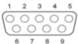
Table 6-3. RS232 DBGU Connector J10 Signal Descriptions
| Pin Mnemonic | Signal description | |
| 1, 4, 6, 7, 8, 9 | NC | NO CONNECTION |
| 2 | TXD TRANSMITTED DATA | RS232 serial data output signal |
| 3 | RXD RECEIVED DATA | RS232 serial data input signal |
| 5 | GND | GROUND |
6.4 Ethernet
Connector J15 is the RJ-45 Ethernet Connector.
Figure 6-4. Ethernet RJ45 Connector J15
12345678

natural_image
Simple gray electrical connector icon with four slots (no text or symbols)Table 6-4. Ethernet RJ45 Connector J15 Signal Descriptions
| Pin Mnemonic Pin Mnemonic | |||
| 1 TxData+ DIFFERENTIAL OUTPUT PLUS 2 Txdata- | DIFFERENTIAL OUTPUT MINUS | ||
| 3 RxData+ DIFFERENTIAL INPUT PLUS 4 Shield | |||
| 5 Shield 6 RxData- DIFFERENTIAL INPUT MINUS | |||
| 7 | S h i e l d | 8 | S h i e l d |
6.5 USB Host
Connector J12 is the USB Host connector.
Figure 6-5. USB Host type A connector J12
text_image
1 2 3 4Table 6-5. USB Host Type A Connector J12 Signal Descriptions
| Pin | Mnemonic | Signal description |
| 1 | Vbus | 5v power |
| 2 | DM | Data minus |
| 3 | DP | Data plus |
| 4 | Gnd | Ground |
| 5 | Shield | Shield |
6.6 USB Host/Device
Connector J14 is the USB Host/Device connector.
Figure 6-6. USB Host/Device Micro AB connector J14
text_image
1 2 3 4 5Table 6-6. USB Host/Device MicroAB Connector J14 Signal Descriptions
| Pin Mne | monic Signal description | ||
| 1 Vbus | 5v power | ||
| 2 | DM | Data | mir |
| 3 DP D | data plus | ||
| 4 ID On the Go Identification | |||
| 5 Gnd Ground | |||
6.7 JTAG Debugging Connector
Connector J13 is the JTAG/ICE connector.
A SAM-ICE connector is a 20-way Insulation Displacement Connector (IDC) keyed box header (2.54 mm male) that mates with IDC sockets mounted on a ribbon cable.
Figure 6-7. JTAG/ICE Connector J13

| Pin Mnemonic Description | ||
| 1 VTref. | 3.3V power | This is the target reference voltage. It is used to check if the target has power, to create the logic-level reference for the input comparators, and to control the output logic levels to the target. It is normally fed from VDD on the target board and must not have a series resistor. |
| 2 Vsupply. | 3.3V power | This pin is not connected in SAM-ICE. It is reserved for compatibility with other equipment. Connect to VDD or leave open in target system. |
| 3 | nTRST TARGET RESET - Active-low output signal that resets the target | JTAG Reset. Output from SAM-ICE to the Reset signal on the target JTAG port. Typically connected to nTRST on the target CPU. This pin is normally pulled HIGH on the target to avoid unintentional resets when there is no connection. |
| 4 GND | Common ground | |
| 5 | TDI TEST DATA INPUT - Serial data output line, sampled on the rising edge of the TCK signal. | JTAG data input of target CPU. It is recommended that this pin is pulled to a defined state on the target board. Typically connected to TDI on target CPU. |
| 6 GND | Common ground | |
| 7 TMS | TEST MODE SELECT | JTAG mode set input of target CPU. This pin should be pulled up on the target. Typically connected to TMS on target CPU. Output signal that sequences the target's JTAG state machine, sampled on the rising edge of the TCK signal. |
| 8 | GND | Common |
| 9 | TCK TEST CLOCK - Output timing signal, for synchronizing test logic and control register access. | JTAG clock signal to target CPU. It is recommended that this pin is pulled to a defined state on the target board. Typically connected to TCK on target CPU. |
| 10 GND | Common ground | |
| 11 | RTCK - Input Return test clock signal from the target. | Some targets must synchronize the JTAG inputs to internal clocks. To assist in meeting this requirement, a returned and retimed TCK can be used to dynamically control the TCK rate. SAM-ICE supports adaptive clocking which waits for TCK changes to be echoed correctly before making further changes. Connect to RTCK if available, otherwise to GND |
| 12 GND | Common ground | |
| 13 | TDO JTAG TEST DATA OUTPUT - Serial data input from the target. | JTAG data output from target CPU. Typically connected to TDO on target CPU. |
| 14 GND | Common ground | |
| 15 nSR | ST RESET Active-low reset signal. Target CPU reset signal | |
| 16 GND | Common ground | |
| 17 RFU | This pin is not connected in SAM-ICE. | |
| 18 GND | Common ground | |
| 19 RFU | This pin is not connected in SAM-ICE | |
| 20 GND | Common ground | |
6.8 SD/MMC-MCI0
Connector J6 is the SD/MMC connector.
Figure 6-8. SD/MMC0 Connector J6
text_image
Technical schematic diagram of a mechanical assembly with numbered components and dashed lines indicating connections or paths.Table 6-8. SD/MMC0 Connector J6 Signal Descriptions
| Pin Mnemonic Pin Mnemonic | |||
| 1 | R S | V | / D |
| 3 GND | 4 VCC | ||
| 5 | C | L | K |
| 7DAT08 | DAT1 | ||
| 9 | DAT2 | 10 Card Detect | |
| 11 | GND | 12 | |
A T 3 2 C D G N D
6.9 SD/MMC-MCI1
Connector J5 is the SD/MMC connector.
Figure 6-9. SD/MMC1 Connector J5

text_image
SD-WP #8 A#7 #13 CD #12 A#5 #9 A#1 #10 A#2 #11 A#3 A#4 A = (MMCplus&MMCmobile & RS-MMC & MMC & SD)Table 6-9. SD/MMC1 Connector J5 Signal Descriptions
| Pin Mnemonic Pin Mnemonic | |||
| 1 | R S | V | / D |
| 3 GND | 4 VCC | ||
| 5 | C | L | K |
| 7 | D | AT0 | 8 |
| 9 | DAT2 | 10 | DAT3 |
| 11 | DAT4 | 12 | DAT5 |
| 13 | DAT6 | 14 | DAT7 |
A T 3 2 C M
AT1
6.10 AC97
■ Connector J7 is the Headphone connector.
■ Connector J8 is the Line In connector.
■ Connector J9 is the Microphone Input.
■ Connector JP15 is the Speaker Output connector
Figure 6-10. Audio Connector J7, J8, J9
text_image
Technical diagram showing exploded and assembled views of a device with numbered componentsTable 6-10. J7, J8, J9 Signal Description
| Pin Mnemonic | |
| 1 | S |
| 2 | S |
| 3 | Gnd |
i g n a l i g n a l
Table 6-11. Speaker JP15 Signal Descriptions
| Pin Mnemonic | |
| 1 Speaker bridge output A | |
| 2 Speaker bridge output B |
6.11 Image Sensor - ISI
Connector J17 is the ISI connector.
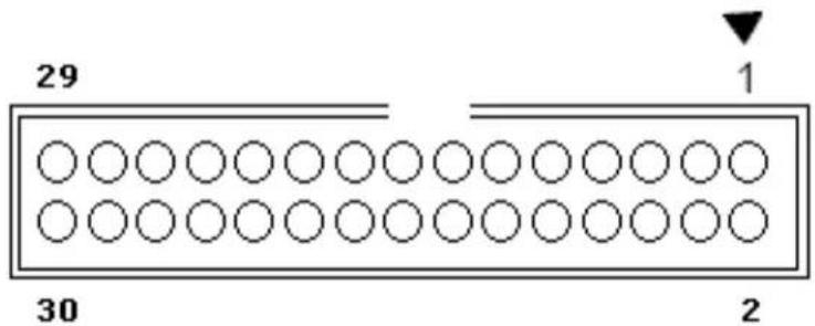
Figure 6-11. ISI Connector J17
text_image
29 1 30 2Table 6-12. ISI Connector J17 Signal Descriptions
| Pin Mnemonic Pin Mnemonic | |||
| 1 VCC | 3v3 2 Gnd | ||
| 3 VCC | 3v3 4 Gnd | ||
| 5 | C | t | r l |
| 7 | S | C | L 8 |
| 9 | G | n | d 1 |
| 11 | Gnd | 12 | ISI_VSYNC |
| 13 | Gnd | 14 | ISI_HSYNC |
| 15 | Gnd | 16 | ISI_PCK |
| 17 | Gnd | 18 | ISI_Data0 |
| 19 | ISI_Data1 | 20 | ISI_Data2 |
| 21 | ISI_Data3 | 22 | ISI_Data4 |
| 23 | ISI_Data5 | 24 | ISI_Data6 |
| 25 | ISI_Data7 | 26 | ISI_Data8 |
| 27 | ISI_Data9 | 28 | ISI_Data10 |
| 29 | ISI_Data11 | 30 | Gnd |
| 1 | 6 | C | t | r |
| S | D | A | ||
| 0 | I | S | I | _ |
6.12 Video
Connector J20 is the Video connector
Figure 6-12. Video Connector J20

Table 6-13. Video Connector J20 Signal Description
| Pin Mnemonic Signal description | |
| 1 Center | Composite video signal output |
6.13 Display Devices
6.13.1 TFT LCD
Connector J24 is the TFT-LCD connector.
Figure 6-13. TFT LCD Connector J24
natural_image
Technical line drawing of a mechanical component with no visible text or symbolsTable 6-14. TFT LCD Connector J24 Signal Descriptions
| Pin Mnemonic Pin Mnemonic | |||
| 1 VLED- | 2 VLED+ | ||
| 3 GND 4 | VDD 3V3 | ||
| 5 | R0 | 6 | R1 |
| 7 | R2 | 8 | R3 |
| 9 | R4 | 10 | R5 |
Table 6-14. TFT LCD Connector J24 Signal Descriptions
| Pin | Mnemonic | Pin | Mnemonic |
| 11 R6 12 | R7 | ||
| 13 G0 14 | G1 | ||
| 15 G2 16 | G3 | ||
| 17 G4 18 | G5 | ||
| 19 G6 20 | G7 | ||
| 21 B0 14 | B1 | ||
| 23 B2 16 | B3 | ||
| 25 B4 18 | B5 | ||
| 27 B6 20 | B7 | ||
| 29 GND 30 | DCLK | ||
| 31 DISPON 32 | HSYNC | ||
| 33 VSYNC 34 | LCDEN | ||
| 35 NO CONNECT 36 | GND | ||
| 37 X2 38 | Y1 | ||
| 39 X1 40 | Y2 |
6.14 LCD Extension
Connectors J23 and J18 are for an optional LCD extension (not populated).
Table 6-15. Connector J23 Signal Description for an LCD Extension
| Pin | Mnemonic | Pin | Mnemonic | ||
| 1 | PE8 | RED Data Signal | 2 | PE7 | RED Data Signal (LSB) |
| 3 | PE10 | RED Data Signal | 4 | PE9 | RED Data Signal |
| 5 | PE12 | RED Data Signal | 6 | PE11 | RED Data Signal |
| 7 | PE14 | RED Data Signal (MSB) | 8 | PE13 | RED Data Signal |
| 9 | PE16 | GREEN Data Signal | 10 | PE15 | GREEN Data Signal (LSB |
| 11 | PE18 | GREEN Data Signal | 12 | PE17 | GREEN Data Signal |
| 13 | PE20 | GREEN Data Signal | 14 | PE19 | GREEN Data Signal |
| 15 | PE22 | GREEN Data Signal (MSB) | 16 | PE21 | GREEN Data Signal |
| 17 | PE24 | BLUE Data Signal | 18 | PE23 | BLUE Data Signal (LSB) |
| 19 | PE26 | BLUE Data Signal | 20 | PE25 | BLUE Data Signal |
| 21 | PE28 | BLUE Data Signal | 22 | PE27 | BLUE Data Signal |
| 23 | PE30 | BLUE Data Signal (MSB) | 24 | PE29 | BLUE Data Signal |
| 25 | PE4 | LCDHSYNC | 26 | PE3 | LCDVSYNC |
| 27 | PE5 | LCDDOTCK | 28 | GND | (0V) |
| 29 | GND | (0V) | 30 | NC |
Table 6-15. Connector J23 Signal Description for an LCD Extension
| Pin | Mnemonic | Pin | Mnemonic | ||
| 31 PE6 | LCDDEN 32 | PE2 LCDCC | |||
| 33 PE0 | DISPON 34 | PE1 LCDMOD | |||
| 35 PD14 | GPIO1 36 | PD15 GPIO2 | |||
| 37 GND | (0V) 38 GND | (0V) | |||
| 39 | VCC | +3V3 power source | 40 | NC |
Table 6-16. Connector J18 Signal Description for an LCD Extension
| Pin | Mnemonic | Pin | Mnemonic | ||
| 1 | XM | AD1XM | 2 | XP | AD0XP |
| 3 | YM | AD3YM | 4 | YP | AD2YP |
| 5 | GND | (0V) | 6 | GND | (0V) |
| 7 | PD25 | PD25 | 8 PD24 | PD24 | |
| 9 | PD27 | PD27 | 10 | PD26 | PD26 |
| 11 PD19 | PD19 | 12 | PD18 | PD18 | |
| 13 | GND | (0V) | 14 GND | (0V) | |
| 15 | GND | (0V) | 16 | +5V | |
| 17 | GND | (0V) | 18 GND | (0V) | |
| 19 | VCC | +3V3 power source | 20 | VCC | +3V3 power source |
7.1 Schematics
This section contains the following schematics:
■ Top Level view, block architecture of the design
■ Power Supply
■ SAM Processor
■ Bus impedance adaptor
■ Main memory
■ EBI memory
■ MCI & TWI
■ Audio AC97
■ Serial interfaces
- Ethernet
LCD
■ Video interfaces and LCD extension

flowchart
graph TD
    subgraph Power Supply
        A["5V POWER SUPPLY"] -->|PI0| B["ATMEL ARM9 Processor SAM9M10 (LFBGA324)"]
    end

    subgraph I/O Interface
        C["RS232 DBGU COM1"] -->|PIO| B
        D["USB HOST"] -->|PIO| B
        E["14 HOST DEVICE"] -->|PIO| B
        F["ICE INTERFACE"] -->|PIO| B
        G["10-100 FAST ETHERNET"] -->|PIO| B
    end

    subgraph Card Reader
        H["CARD READER"] --> I["AUDIO"]
        I --> J["MICOUT IN"]
        J --> K["Sheet 8"]
        L["RAMS SDO"] --> I
    end

    subgraph Memory Card
        M["FLASHN/DDR2 128MB FLASH"] --> N["RES.ARRAYS EBIO_EBI1 ADAPTER"]
        O["FLASH"] --> N
        P["FLASH"] --> N
    end

    A -->|POWER| B
    C -->|PIO A...E| B
    D -->|PIO A...E| B
    E -->|PIO A...E| B
    F -->|PIO A...E| B
    G -->|PIO A...E| B
    H -->|PIO A...E| I
    I --> J
    J --> K
    K --> L
text_image
E80_CNE5 E80_CL93 E80_NCK16 E80_BACK E80_BACK E80_WST E80_CS16 E80_RACK E80_DACK E80_DACK E80_DOS14 R40 27F R42 27F R44 27F 1 R110 5 1 RSMA 3 3 R110 5 2 RSMA 7 3 R210 5 1 RSMA 3 1 RSMA 7 R46 27F R48 27F DOR_CKE [I] DOR_CUL [I] DOR_CLUX [I] DOR_BAG [I] DOR_BAY [I] DOR_WE [I] DOR_OB [I] DOR_AIB [I] DOR_CAS [I] DOR_DOK [I] DOR_DOU [I] DOR_DOU [I]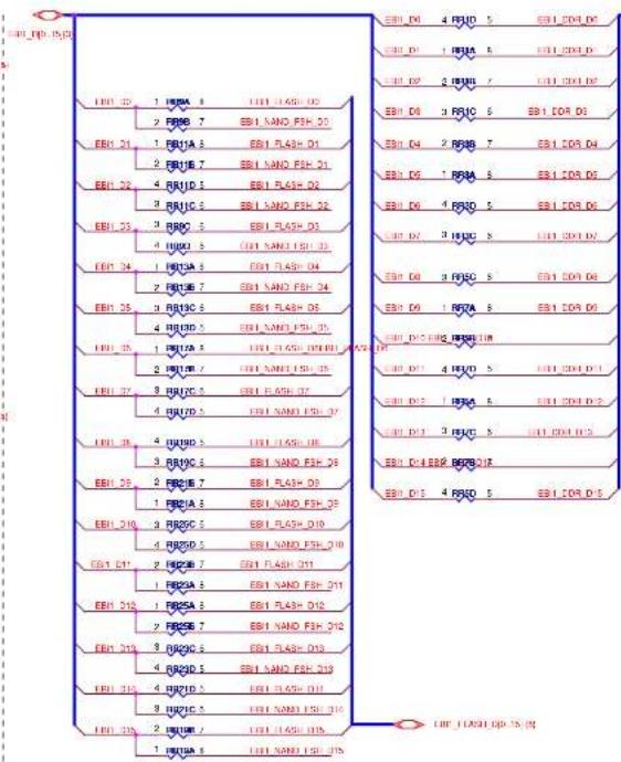
text_image
EBI 20 1 EBITA 8 EBI FLASH-03 2 EBIT 7 EBI NAND FSH-03 EBI 21 1 EBITA 8 EBI FLASH-01 2 EBIT 7 EBI NAND FSH-01 4 EBITD 5 EBI FLASH-02 3 EBITC 5 EBI NAND FSH-02 4 EBIT 5 EBI FLASH-03 EBI 23 1 EBITA 8 EBI FLASH-04 2 EBIT 7 EBI NAND FSH-04 3 EBITC 5 EBI FLASH-05 4 EBITD 5 EBI NAND FSH-05 EBI 25 1 EBITA 8 EBI FLASH-06 2 EBIT 7 EBI NAND FSH-06 3 EBITC 5 EBI FLASH-07 4 EBITD 5 EBI NAND FSH-07 EBI 26 4 EBITD 5 EBI FLASH-08 3 EBITC 5 EBI NAND FSH-09 4 EBITD 7 EBI FLASH-09 1 EBITA 8 EBI NAND FSH-09 2 EBITC 5 EBI FLASH-010 3 EBITD 5 EBI NAND FSH-011 4 EBITD 7 EBI FLASH-012 1 EBITA 8 EBI NAND FSH-013 2 EBITC 5 EBI NAND FSH-014 3 EBITD 5 EBI NAND FSH-015 4 EBITD 7 EBI NAND FSH-016 EBI 26 1 EBITA 8 EBI NAND FSH-017 2 EBITC 5 EBI NAND FSH-018 3 EBITD 5 EBI NAND FSH-019 4 EBITD 7 EBI NAND FSH-020 EBI 27 1 EBITA 8 EBI NAND FSH-021 2 EBITC 5 EBI NAND FSH-022 3 EBITD 5 EBI NAND FSH-023 4 EBITD 7 EBI NAND FSH-024 EBI 28 1 EBITA 8 EBI NAND FSH-025 2 EBITC 5 EBI NAND FSH-026 3 EBITD 5 EBI NAND FSH-027 4 EBITD 7 EBI NAND FSH-028 EBI 29 1 EBITA 8 EBI NAND FSH-029 2 EBITC 5 EBI NAND FSH-030 3 EBITD 5 EBI NAND FSH-031 4 EBITD 7 EBI NAND FSH-032 EBI 30 1 EBITA 8 EBI NAND FSH-033 2 EBITC 5 EBI NAND FSH-034 3 EBITD 5 EBI NAND FSH-035 4 EBITD 7 EBI NAND FSH-036 EBI 31 1 EBITA 8 EBI NAND FSH-037 2 EBITC 5 EBI NAND FSH-038 3 EBITD 5 EBI NAND FSH-039 4 EBITD 7 EBI NAND FSH-040 EBI 32 1 EBITA 8 EBI NAND FSH-041 2 EBITC 5 EBI NAND FSH-042 3 EBITD 5 EBI NAND FSH-043 4 EBITD 7 EBI NAND FSH-044 EBI 33 1 EBITA 8 EBI NAND FSH-045 2 EBITC 5 EBI NAND FSH-046 3 EBITD 5 EBI NAND FSH-047 4 EBITD 7 EBI NAND FSH-048 EBI 34 1 EBITA 8 EBI NAND FSH-049 2 EBITC 5 EBI NAND FSH-050 3 EBITD 5 EBI NAND FSH-051 4 EBITD 7 EBI NAND FSH-052 EBI 35 1 EBITA 8 EBI NAND FSH-053 2 EBITC 5 EBI NAND FSH-054 3 EBITD 5 EBI NAND FSH-055 4 EBITD 7 EBI NAND FSH-056 EBI 36 1 EBITA 8 EBI NAND FSH-057 2 EBITC 5 EBI NAND FSH-058 3 EBITD 5 EBI NAND FSH-059 4 EBITD 7 EBI NAND FSH-060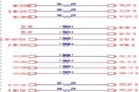
text_image
EB1 SCORE EB1 SCORE EB1_SOC0 EB1_A16 EB1_A17 EB1_NOB-8COS EB1_SCVE EB1_NOB3 EB1_CARS EB1_DCM3 EB1_DQS CB_EBI CB_EBI CB_EBI CB_EBI CB_EBI CB_EBI CB_EBI CB_EBI CB_EBI CB_EBI CB_EBI CB_EBI CB_EBI CB_EBI CB_EBI CB_EBI CB_EBI CB_EBI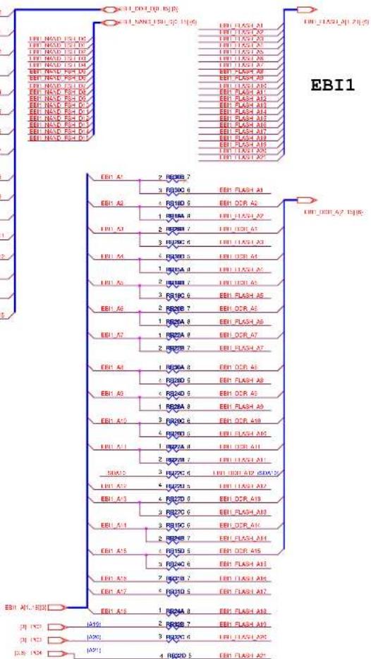
text_image
EBI1 EBI1_D01_D01_01(0) EBI1_D01_D01_01(0) EBI1_D01_D01_01(0) EBI1_D01_D01_01(0) EBI1_D01_D01_01(0) EBI1_D01_D01_01(0) EBI1_D01_D01_01(0) EBI1_D01_D01 01(0) EBI1_D01_D01_01(0) EBI1_D01_D01_01(0) EBI1_D01_D01_01(0) EBI1_D01_D01_01(0) EBI1_D01_D01_01(0) EBI1_D01_D01_01(0) EBI1_D25D7 EBI1_D25D7 EBI1_D25D7 EBI1_D25D7 EBI1_D25D7 EBI1_D25D7 EBI1_D25D7 EBI1_D25D7 EBI1_D25D7 EBI1_D25D7 EBI1_D25D7 EBI1_D25D7 EBI_A2 EBI_A2 EBI_A2 EBI_A2 EBI_A2 EBI_A2 EBI_A2 EBI_A2 EBI_A2 EBI_A2 EBI_A2 EBI_A2 EBI_A2 EBI_A2 EBI_A2 EBI_A2 EBI_A2 EBI_A2 EBI_A2 EBI_A2 EBI_A2 EBiA3 EBiA3 EBiA3 EBiA3 EBiA3 EBiA3 EBiA3 EBiA3 EBiA3 EBiA3 EBiA3 EBiA3 EBiA3 EBiA3 EBiA3 EBiA3 EBiA3 EBiA3 EBiA3 EBiA3 EBiA4 EBiA4 EBiA4 EBiA4 EBiA4 EBiA4 EBiA4 EBiA4 EBiA4 EBiA4 EBiA4 EBiA4 EBiA4 EBiA4 EBiA4 EBiA4 EBiA4 EBiA4 EBiA4 EBiA4 EBiA6 EBiA6 EBiA6 EBiA6 EBiA6 EBiA6 EBiA6 EBiA6 EBiA6 EBiA6 EBiA6 EBiA6 EBiA6 EBiA6 EBiA6 EBiA6 EBiA6 EBiA6 EBiA6 EBiA6 EBiA7 EBiA7 EBiA7 EBiA7 EBiA7 EBiA7 EBiA7 EBiA7 EBiA7 EBiA7 EBiA7 EBiA7 EBiA7 EBiA7 EBiA7 EBiA7 EBiA7 EBiA7 EBI-A2_01(D)# EBI-A2_01(D)# EBI-A2_01(D)# EBI-A2_01(D)# EBI-A2_01(D)# EBI-A2_01(D)# EBI-A2_01(D)# EBI-A2_01(D)# EBI-A2_01(D)# EBI-A2_01(D)# EBI-A2_01(D)## EBI-A2_01(D)# EBI-A2_01(D)# EBI-A2_01(D)# EBI-A2_01(D)# EBI-A2_01(D)# EBI-A2_01(D)# EBI-A2_01(D)# EBI-A2_01(D)# EBI-A2_01(D)# EBI-A2_01(D)##- EBI-A2_01(D)# EBI-A2_01(D)# EBI-A2_01(D)# EBI-A2_01(D)# EBI-A2_01(D)# EBI-A2_01(D)# EBI-A2_01(D)# EBI-A2_01(D)# EBI-A2_01(D)# EBI-A2_01(D)### EBI-A2_01(D)# EBI-A2_01(D)# EBI-A2_01(D)# EBI-A2_01(D)# EBI-A2_01(D)# EBI-A2_01(D)# EBI-A2_01(D)# EBI-A2_01(D)# EBI-A2_01(D)# EBI-A2_01(D)u- EBI-A2_01(D)u- EBI-A2_01(D)u- EBI-A2_01(D)u- EBI-A2_01(D)u- EBI-A2_01(D)u- EBI-A2_01(D)u- EBI-A2_01(D)u- EBI-A2_01(D)u- EBI-A2_01(D)u- FIBIA_ FIBIA_ FIBIA_ FIBIA_ FIBIA_ FIBIA_ FIBIA_ FIBIA_ FIBIA_ FIBIA_ FIBIA_ FIBIA_ FIBIA_ FIBIA_ FIBIA_ FIBIA_ FIBIA_ FIBIA_ FIBIA_ FIBIA_ FIBIA_ FIBIA_ FIBIA_ FIBIA_ FIBIA_ FIBIA_\N3B_ FIBIA_ FIBIA_ FIBIA_ FIBIA_ FIBIA_ FIBIA_ FIBIA_ FIBIA_ FIBIA_ FIBIA_ FIBIA_ FIBIA_ FIBIA_ FIBIA_ FIBIA_ FIBIA_ FIBIA_ FIBIA_ FIBIA_ FIBIA_ FIBIA_ FIBIA_ FIBIA_ FIBIA_ FIBEA_ FIBEA_ FIBEA_ FIBEA_ FIBEA_ FIBEA_ FIBEA_ FIBEA_ FIBEA_ FIBEA_ FIBEA_ FIBEA_ FIBEA_ FIBEA_ FIBEA_ FIBEA_ FIBEA_ FIBEA_ FIBEA_ FIBEA_ FIBEA_ FIBEA_ FIBEA_ FIBEA_ FIBEA_ FIBea_ Fibea_ Fibea_ Fibea_ Fibea_ Fibea_ Fibea_ Fibea_ Fibea_ Fibea_ Fibea_ Fibea_ Fibea_ Fibea_ Fibea_ Fibea_ Fibea_ Fibea_ Fibea_ Fibea_ Fibea_ Fibea_ Fibea_ Fibea_ Fibea_ Fibea_ Fifea_ Fifea_ Fifea_ Fifea_ Fifea_ Fifea_ Fifea_ Fifea_ Fifea_ Fifea_ Fifea_ Fifea_ Fifea_ Fifea_ Fifea_ Fifea_ Fifea_ Fifea_ Fifea_ Fifea_ Fifea_ Fifea_ Fifea_ Fifea_ Fifea_ Fibea_ Fibea_ Fibea_ Fibea_ Fibea_ Fibea_ Fibea_ Fibea_ Fibea_ Fibea_ Fibea_ Fibea_ Fibea_ Fibea_ Fibea_ Fibea_ Fibea_ Fibea_ Fibea_ Fibea_ Fibea_ Fibea_ Fibea_ Fibea_ Fobea_ Fobea_ Fobea_ Fobea_ Fobea_ Fobea_ Fobea_ Fobea_ Fobea_ Fobea_ Fobea_ Fobea_ Fobea_ Fobea_ Fobea_ Fobea_ Fobea_ Fobea_ Fobea_ Fobea_ Fobea_ Fobea_ Fobea_ Fobea_ Fobea_ Fofea_\N3B_\N3B_\N3B_\N3B_\N3B_\N3B_\N3B_\N3B_\N3B_\N3B_\N3B_\N3B_\N3B_\N3B_\N3B_\N3B_\N3B_\N3B_\N3B_\N3B_\N3B_\N3B_\N3B_\N3B_\N3B_\N3C_\N3C_\N3C_\N3C_\N3C_\N3C_\N3C_\N3C_\N3C_\N3C_\N3C_\N3C_\N3C_\N3C_\N3C_\N3C_\N3C_\N3C_\N3C_\N3C_\N3C_\N3C_\N3C_\N3C_\N3C_\N3M_\N3M_\N3M_\N3M_\N3M_\N3M_\N3M_\N3M_\N3M_\N3M_\N3M_\N3M_\N3M_\N3M_\N3M_\N3M_\N3M_\N3M_\N3M_\N3M_\N3M_\N3M_\N3M_\N3M_\N3M_\N3U_\nHfia\(_{X}\)_Hfia\(_{X}\)_Hfia\(_{X}\)_Hfia\(_{X}\)_Hfia\(_{X}\)_Hfia\(_{X}\)_Hfia\(_{X}\)_Hfia\(_{X}\)_Hfia\(_{X}\)_Hfia\(_{X}\)_Hfia\(_{X}\)_Hfia\(_{X}\)_ Hfia\(_{X}\)_Hfia\(_{X}\)_Hfia\(_{X}\)_Hfia\(_{X}\)_Hfia\(_{X}\)_Hfia\(_{X}\)_Hfia\(_{X}\)_Hfia\(_{X}\)_Hfia\(_{X}\)_Hfia\(_{X}\)_Hfia\(_{X}\)_Hfla\(_{X}\)_Hfla\(_{X}\)_Hfla\(_{X}\)_Hfla\(_{X}\)_Hfla\(_{X}\)_Hfla\(_{X}\)_Hfla\(_{X}\)_Hfla\(_{X}\)_Hfla\(_{X}\)_Hfla\(_{X}\)_Hfla\(_{X}\)_Hfla\nHfla\(_{X}\)_Hfla\(_{X}\)_Hfla\(_{X}\)_Hfla\(_{X}\)_Hfla\(_{X}\)_Hfla\(_{X}\)_Hfla\(_{X}\)_Hfla\(_{X}\)_Hfla\(_{X}\)_Hfla\(_{X}\)_Hfla\(_{X}\)_Tlglb\(_{X}\)_Tlglb\(_{X}\)_Tlglb\(_{X}\)_Tlglb\(_{X}\)_Tlglb\(_{X}\)_Tlglb\(_{X}\)_Tlglb\(_{X}\)_Tlglb\(_{X}\)_Tlglb\(_{X}\)_Tlglb\(_{X}\)_Tlglc\(_{X}\)_Tlglc\(_{X}\)_Tlglc\(_{X}\)_Tlglc\(_{X}\)_Tlglc\(_{X}\)_Tlglc\(_{X}\)_Tlglc\(_{X}\)_Tlglc\(_{X}\)_Tlglc\(_{X}\)_Tlglc\(_{X}\)_Tlgld\(_{X}\)_Tlgld\(_{X}\)_Tlgld\(_{X}\)_Tlgld\(_{X}\)_Tlgld\(_{X}\)_Tlgld\(_{X}\)_Tlgld\(_{X}\)_Tlgld\(_{X}\)_Tlgld\(_{X}\)_Tlgld\(_{X}\)_Tlglg\(_{x}\)_Tlglg\(_{x}\)_Tlglg\(_{x}\)_Tlglg\(_{x}\)_Tlglg\(_{x}\)_Tlglg\(_{x}\)_Tlglg\(_{x}\)_Tlglg\(_{x}\)
text_image
ATMEL ROUSET AT91SAM0M10 G45 EK RES ARRAYS EER0_E81 A2 A PP CWOL 16-FEC-10 PF 11-FEB-10 RFE MODEL TYPE DATE VFR DATE SCALE 1/1 A2 SHEET A2 4/12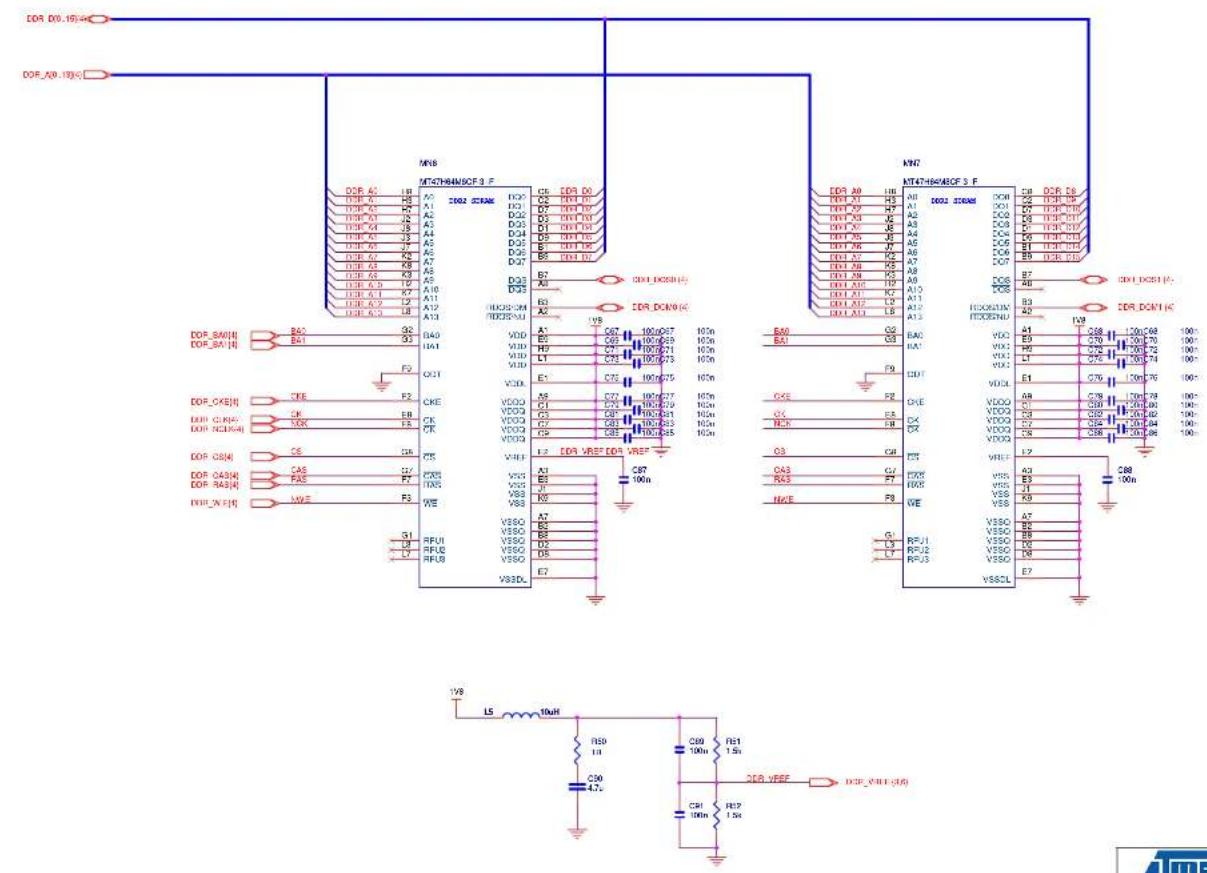
text_image
DDR_D0.15V DDR_A0.19V MNS MT47H4N16CF 3 F DDR_DC5H(1) DDR_DC5H(2) DDR_DC5H(3) DDR_DC5H(4) DDR_DC5H(5) DDR_DC5H(6) DDR_DC5H(7) DDR_DC5H(8) DDR_DC5H(9) DDR_DC5H(10) DDR_DC5H(11) DDR_DC5H(12) DDR_DC5H(13) DDR_DC5H(14) DDR_DC5H(15) DDR_DC5H(16) DDR_DC5H(17) DDR_DC5H(18) DDR_DC5H(19) DDR_DC5H(20) DDR_DC5H(21) DDR_DC5H(22) DDR_DC5H(23) DDR_DC5H(24) DDR_DC5H(25) DDR_DC5H(26) DDR_DC5H(27) DDR_DC5H(28) DDR_DC5H(29) DDR_DC5H(30) DDR_DC5H(31) DDR_DC5H(32) DDR_DC5H(33) DDR_DC5H(34) DDR_DC5H(35) DDR_DC5H(36) DDR_DC5H(37) DDR_DC5H(38) DDR_DC5H(39) DDR_DC5H(40) DDR_DC5H(41) DDR_DC5H(42) DDR_DC5H(43) DDR_DC5H(44) DDR_DC5H(45) DDR_DC5H(46) DDR_DC5H(47) DDR_DC5H(48) DDR_DC5H(49) DDR_DC5H(50) DDR_DC5H(51) DDR_DC5H(52) DDR_DC5H(53) DDR_DC5H(54) DDR_DC5H(55) DDR_DC5H(56) DDR_DC5H(57) DDR_DC5H(58) DDR_DC5H(59) DDR_DC5H(60) DDR_DC5H(61) DDR_DC5H(62) DDR_DC5H(63) DDR_DC5H(64) DDR_DC5H(65) DDR_DC5H(66) DDR_DC5H(67) DDR_DC5H(68) DDR_DC5H(69) DDR_DC5H(70) DDR_DC5H(71) DDR_DC5H(72) DDR_DC5H(73) DDR_DC5H(74) DDR_DC5H(75) DDR_DC5H(76) DDR_DC5H(77) DDR_DC5H(78) DDR_DC5H(79) DDR_DC5H(80) DDR_DC5H(81) DDR_DC5H(82) DDR_DC5H(83) DDR_DC5H(84) DDR_DC5H(85) DDR_DC5H(86) DDR_DC5H(87) DDR_DC5H(88) DDR_DC5H(89) DDR_DC5H(90) DDR_DC5H(91) DDR_DC5H(92) DDR_DC5H(93) DDR_DC5H(94) DDR_DC5H(95) DDR_DC5H(96) DDR_DC5H(97) DDR_DC5H(98) DDR_DC5H(99) DDR_DC5H(D0)- IDR_D0.1(V-)| A2 | PP | 19-04-15 | |||
| A1 | 16-FBC-10 | 11-FEB-10 | |||
| REV./SAMSAP. | VER. | DATE | VER. | ||
| SCALE: 1/1 | REV.A2 | SHEET5/12 | |||
| E= | |||||
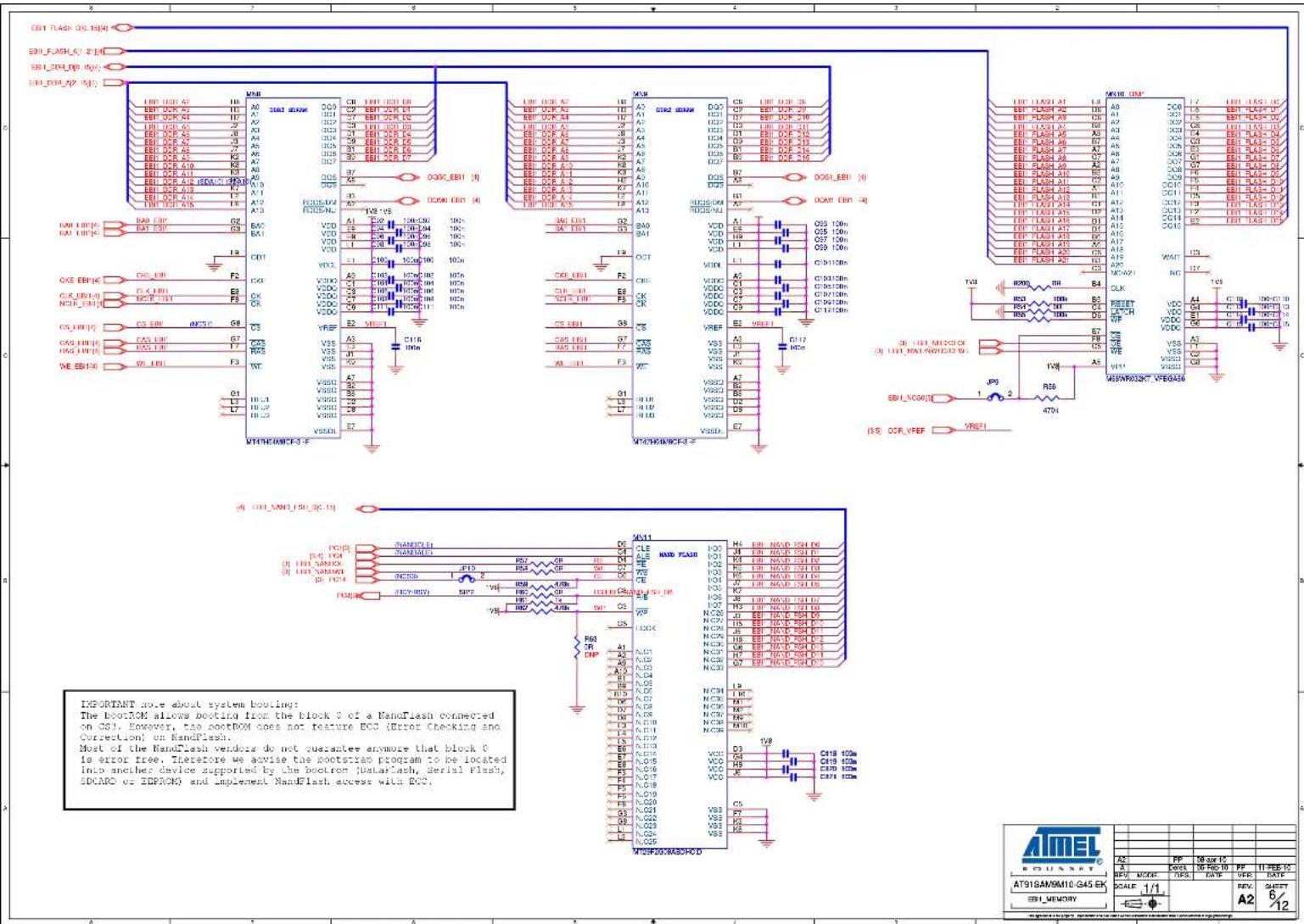
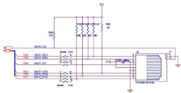
text_image
R64 12k R18 R19 R15 R100 R65 12k DC DC0 CO1 F43 DC01 DA1 F42 DC01 DA0 F40 DC01 G0 FA1 DC01 CO4 F45 DC01 DA5 F43 DC01 D5 R105 2/11 1 8 2 7 3 6 4 5 5 4 6 3 7 2 8 1 9 0 10 0 11 0 12 0 13 0 14 0 15 0 16 0 17 0 3V C129 80mA FP5NR SP24HSD/MMC CARD INTERFACE - MCI0
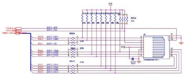
text_image
R19 R10 R15 R10 R10 R10 R10 6K 6K M4 6K 6K E6 6K E6 RL RP36 10k AC-22 AC-22 AC-22 AC-22 AC-22 AC-22 AC-22 AC-22 AC-22 AC-22 AC-22 AC-22 AC-22 AC-22 AC-22 AC-22 AC-22 AC-22 AC-22 AC-22 AC-21 AC-21 AC-21 AC-21 AC-21 AC-21 AC-21 AC-21 AC-21 AC-21 AC-21 AC-21 AC-21 AC-21 AC-21 AC-21 AC-21 AC-21 AC-21 AC-21 AC-20 AC-20 AC-20 AC-20 AC-20 AC-20 AC-20 AC-20 AC-20 AC-20 AC-20 AC-19 AC-19 AC-19 AC-19 AC-19 AC-19 AC-19 AC-19 AC-19 AC-19 AC-18 AC-18 AC-18 AC-18 AC-18 AC-18 AC-18 AC-18 AC-18 AC-18 AC-17 AC-17 AC-17 AC-17 AC-17 AC-17 AC-17 AC-17 AC-17 AC-16 AC-16 AC-16 AC-16 AC-16 AC-16 AC-16 AC-16 AC-16 AC-15 AC-15 AC-15 AC-15 AC-15 AC-15 AC-15 AC-15 AC-15 AC-14 AC-14 AC-14 AC-14 AC-14 AC-14 AC-14 AC-14 AC-13 AC-13 AC-13 AC-13 AC-13 AC-13 AC-13 AC-13 AC-13 AC-13 AC-13 AC-13 AC-13 AC-13 AC-13 AC-13 AUC 0.0000000000000000000000000000000000000000000000000000000000000000000000000000000000000000000000000000SD/MMCPlus CARD INTERFACE - MCI1
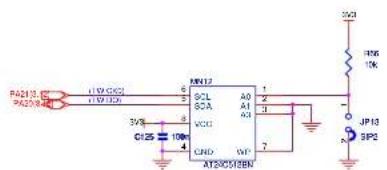
text_image
R4213 PA259 110V CCK2 110V 10A 3V8 C125 10A 6 6CL SCA VCC CND AT280518N A0 A1 A2 1 2 3 4 5 6 7 8 9 10 11 12 13 JP13 SP2 30Ω 45Ω 10K 1kΩSERIAL EEPROM

text_image
2nd pin 1 TNP JP1 30Ω 857 470A NFE3 SC Si SCK GSM VOC GSM PDS 1 2 3 4 5 6 7 8 9 10 11 12 13 14 15 16 17 18 19 20 21 22 23 24 25 26 27 28 29 30 31 32 33 34 35 36 37 38 39 40 41 42 43 44 45 46 47 48 49 50 51 52 53 54 55 56 57 58 59 60 61 62 63 64 65 66 67 68 69 70 71 72 73 74 75 76 77 78 79 80 81 82 83 84 85 86 87 88 89 90 91 92 93 94 95 96 97 98 99 100| A2 | PP | 10-axr 12 | |||
| A | 16-Fec 10 | 11-FEB-100 | |||
| RPU/AMMHF | NFR. | DATE | VFR. | ||
| AT91SAM9M10 G45 EK | SCALE 1/1 | REV. | SHEET | ||
| MOB & TWI | A2 | 7/12 | |||
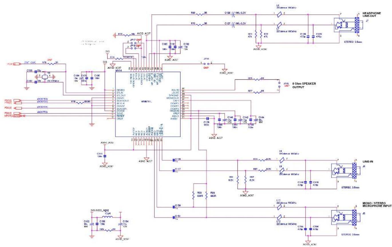
text_image
HEADPHONE LINE-OUT 17 STEREO 3.5mm R70 OR C187 100/-6.3V 1 2 2 2 16 220cm at 100kHz R71 4K R72 4K C198 47p C199 49p JP17 DHP JP18 DHP C182 100m C183 10V ACND_AOS7 JP14 DHP AGND_AOS7 R75 DR C185 100m C186 10V C187 100/-6.3V R76 DR C188 100m C189 10V C190 10V C191 10V C192 10V C193 10V C194 10V C195 10V C196 10V C197 10V C198 10V C199 10V C200 10V C201 10V C202 10V C203 10V C204 10V C205 10V C206 10V C207 10V C208 10V C209 10V C210 10V C211 10V C212 10V C213 10V C214 10V C215 10V C216 10V C217 10V C218 10V C219 10V C220 10V C221 10V C222 10V C223 10V C224 10V C225 10V C226 10V C227 AOSOLED ICs (LPG) AVOCOTX (LPG) AVOCOTG (LPG) AVOCOTH (LPG) AVOCOTI (LPG) AVOCOTJ (LPG) AVOCOTK (LPG) AVOCOTL (LPG) AVOCOTM (LPG) AVOCOTN (LPG) AVOCOTU (LPG) AVOCOTV (LPG) AVOCOTW (LPG) AVOCOTX (LPG) AVOCOTG (LPG) AVOCOTH (LPG) AVOCOTI (LPG) AVOCOTM (LPG) AVOCOTU (LPG) AVOCOTV (LPG) AVOCOTW (LPG) AVOCOTX (LPG) AVOCOTG (LPG) AVOCOTH (LPG) AVOCOTI (LPG) AVOCOTM (LPG) AVOCOTU (LPG) AVOCOTV (LPG) AVOCOTW (LPG) AVOCOTX (LPG) AOSOLED ICs (LPG) AVOCOTX (LPG) AVOCOTG (LPG) AVOCOTH (LPG) AVOCOTI (LPG) AVOCOTM (LPG) AVOCOTU (LPG) AVOCOTV (LPG) AVOCOTW (LPG) AVOCOTX (LPG) AVOCOTG (LPG) AVOCOTH (LPG) AVOCOTI (LPG) AVOCOTM (LPG) AVOCOTU (LPG) AVOCOTV (LPG) AVOCOTW (LPG) AVOCOTX (LPG) AVOCOTG (LPG) AVOCOTH (LPG) AVOCOTI (LPG) AVOCOTX (LPG) AVOCOTG (LPG) AVOCOTH (LPG) AVOCOTI (LPG) AVOCOTM (LPG) AVOCOTU (LPG) AVOCOTV (LPG) AVOCOTW (LPG) AVOCOTX (LPG) AVOCOTG (LPG) AVOCOTH (LPG) AVOCOTI (LPG)| 10-AP-187A2 | ||||
| A | 02-Feb-15 | 11-FEB-16 | ||
| REV. | DAMOND.F. | DES. | DATE | VER. |
| SCALE: 1/1 | REV. SHEET A2 8/12 | |||
SERIAL DEBUG PORT

text_image
L DEBUG PORT J10 6 2 8 5 3 1 5 14 7 13 8 ACM/DC/DATN2 ACM/DC/DATN2 SC9 T162 100n 14 C167 100n 2 T160 100n 5 AN15 VCC C3+ VCC C468 100n VCC C463 100n VCC C467 100n R87 100k R88 100k P87-1回 P8-2回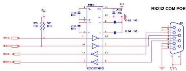
text_image
RS232 COM PORT R50 100k R85 100k C160 100n C164 100n MN15 1 2 3 4 5 6 7 8 9 10 11 12 13 14 15 16 17 18 19 20 21 22 23 24 25 26 27 28 29 30 31 32 33 34 35 36 37 38 39 40 41 42 43 44 45 46 47 48 49 50 51 52 53 54 55 56 57 58 59 60 61 62 63 64 65 66 67 68 69 70 71 72 73 74 75 76 77 78 79 80 81 82 83 84 85 86 87 88 89 90 91 92 93 94 95 96 97 98 99 100
text_image
USB HOST INTERFACE USB HOST/DEVICE INTERFACE J12 G3055-PU811 51W C167 100Ω U8A 1 2 3 4 5 6 7 8 9 10 11 12 13 14 15 16 17 18 19 20 21 22 23 24 25 26 27 28 29 30 31 32 33 34 35 36 37 38 39 40 41 42 43 44 45 46 47 48 49 50 51 52 53 54 55 56 57 58 59 60 61 62 63 64 65 66 67 68 69 70 71 72 73 74 75 76 77 78 79 80 81 82 83 84 85 86 87 88 89 90 91 92 93 94 95 96 97 98 99 100
text_image
3/8 345 J13 R943 10kV 323 R97 DNP R97 R97 ICP IC IC IC IC IC IC IC IC IC IC IC IC IC IC IC IC IC IC IC IC IC IC IC IC IC IC IC IC IC IC IC IC IC IC IC IC IC IC IC IC IC IC IC IC IC IC IC IC IC IC ICP-201 ICP-202 ICP-203 ICP-204 ICP-205 ICP-206 ICP-207 ICP-208 ICP-209 ICP-210 ICP-211 ICP-212 ICP-213 ICP-214 ICP-215 ICP-216 ICP-217 ICP-218 ICP-219 ICP-220 ICP-221 ICP-222 ICP-223 ICP-224 ICP-225 ICP-226 ICP-227 ICP-228 ICP-229 ICP-230 ICP-231 ICP-232 ICP-233 ICP-234 ICP-235 ICP-236 ICP-237 ICP-238 ICP-239 ICP-240 ICP-241 ICP-242 ICP-243 ICP-244 ICP-245 ICP-246 ICP-247 ICP-248 ICP-249 ICP-250 ICP-251 ICP-252 ICP-253 ICP-254 ICP-255 ICP-256 ICP-257 ICP-258 ICP-259 ICP-260 ICP-261 ICP-262 ICP-263 ICP-264 ICP-265 ICP-266 ICP-267 ICP-268 ICP-269 ICP-270 ICP-271 ICP-272 ICP-273 ICP-274 ICP-275 ICP-276 ICP-277 ICP-278 ICP-279 ICP-280| 10-APR-10P/AD | ||||
| A | 02-Feb-10 | 11-FEB-10E | ||
| REV. | DRAWN/E | DES. | DATE | VER. |
| SCALE: 1/1 | REV. SHEET A2 9/12 | |||

text_image
RJ45 ETHERNET CONNECTOR R122 0A R123 3R C178 10Ω C179 10Ω C174 20Ω C175 20Ω C176 10Ω C177 40Ω C178 10Ω C179 40Ω C180 40Ω C181 40Ω C182 40Ω C183 40Ω C184 40Ω C185 40Ω C186 40Ω C187 40Ω C188 40Ω C189 40Ω C190 40Ω C191 40Ω C192 40Ω C193 40Ω C194 40Ω C195 40Ω C196 40Ω C197 40Ω C198 40Ω C199 40Ω C200 40Ω C201 40Ω C202 40Ω C203 40Ω C204 40Ω C205 40Ω C206 40Ω C207 40Ω C208 40Ω C209 40Ω C210 40Ω C211 40Ω C212 40Ω C213 40Ω C214 40Ω C215 40Ω C216 40Ω C217 40Ω C218 40Ω C219 40Ω C220 40Ω C221 40Ω C222 40Ω C223 40Ω C224 40Ω C225 40Ω C226 40Ω C227 40Ω C228 40Ω C229 40Ω C230 40Ω C231 40Ω C232 40Ω C233 40Ω C234 40Ω C235 40Ω C236 40Ω C237 40Ω| 10-APR-10P/20 | ||||
| A | 02-FEB-15 | 11-FEB-16 | ||
| AT918SAM9M10-C45-EK | REV. | DAMND.F. | DES. | DATE: |
| SCALE | 1/1 | REV. | ||
| PMI MII ETHERNET | A2 10/12 | |||

| A2 | PP | 19-04-15 | ||
| A1 | 16-FBC-10 | 11-FEB-10 | ||
| REV. | DATE | VER. | ||
| SCALE 1/1 | REV. | SHEET 11/12 | ||
| E=Φ | A2 | |||
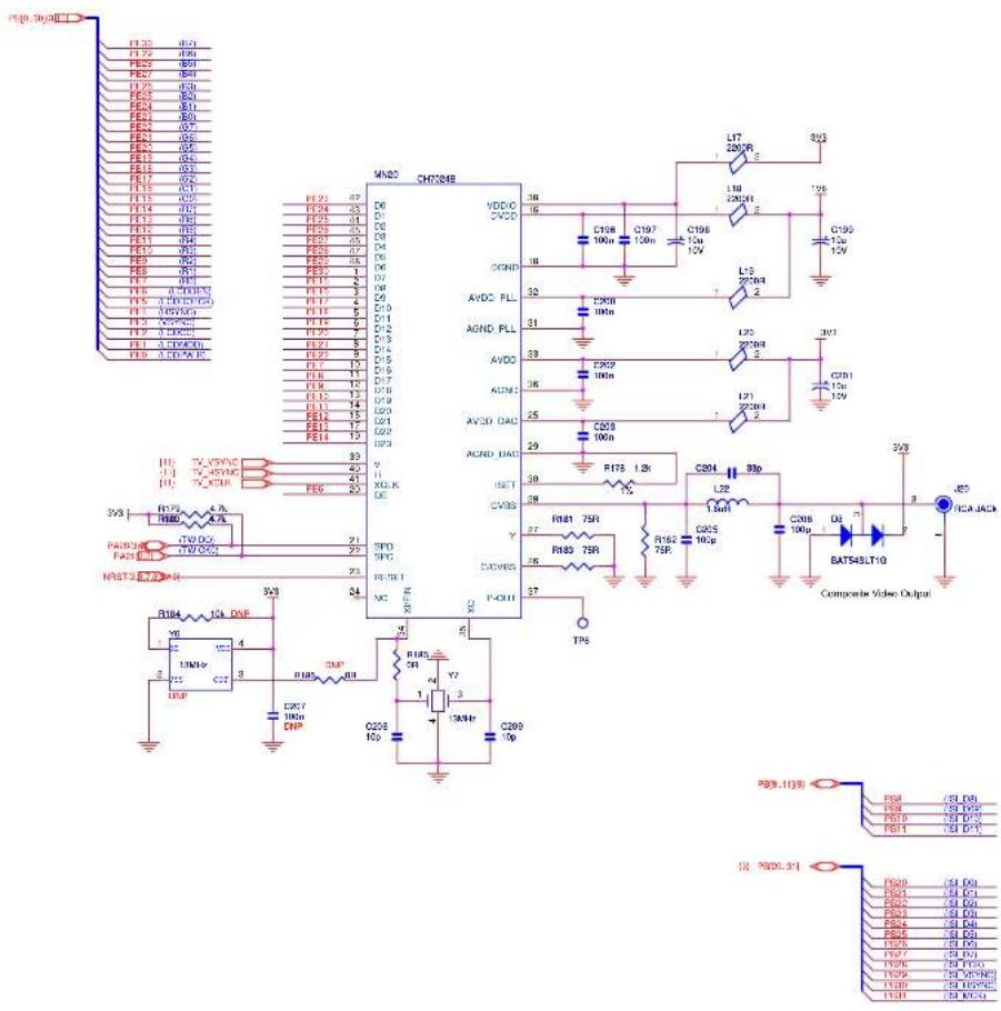
text_image
P01.36V P02.1 P03.1 P04.1 P05.1 P06.1 P07.1 P08.1 P09.1 P10.1 P11.1 P12.1 P13.1 P14.1 P15.1 P16.1 P17.1 P18.1 P19.1 P20.1 P21.1 P22.1 P23.1 P24.1 P25.1 P26.1 P27.1 P28.1 P29.1 P30.1 P31.1 P32.1 P33.1 P34.1 P35.1 P36.1 P37.1 P38.1 P39.1 P40.1 P41.1 P42.1 P43.1 P44.1 P45.1 P46.1 P47.1 P48.1 P49.1 P50.1 P51.1 P52.1 P53.1 P54.1 P55.1 P56.1 P57.1 P58.1 P59.1 P60.1 P61.1 P62.1 P63.1 P64.1 P65.1 P66.1 P67.1 P68.1 P69.1 P70.1 P71.1 P72.1 P73.1 P74.1 P75.1 P76.1 P77.1 P78.1 P79.1 P80.1 P81.1 P82.1 P83.1 P84.1 P85.1 P86.1 P87.1 P88.1 P89.1 P90.1 P91.1 P92.1 P93.1 P94.1 P95.1 P96.1 P97.1 P98.1 P99.1 P100.1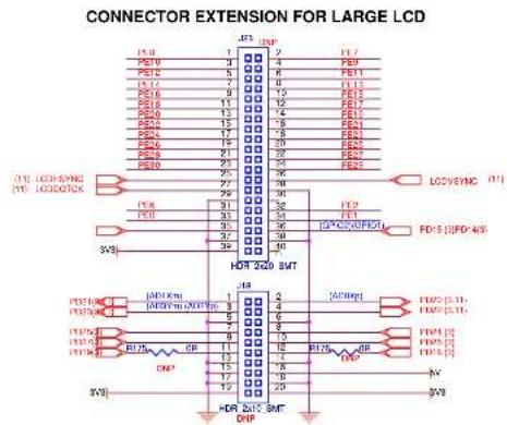
text_image
CONNECTOR EXTENSION FOR LARGE LCD I/O 1 P3 2 I2P 3 I1.2 4 I0.7 5 I9.3 6 I8.1 7 I7.2 8 I6.3 9 I5.4 10 I4.5 11 I3.6 12 I2.7 13 I1.8 14 I0.9 15 I0.1 16 I9.2 17 I8.3 18 I7.4 19 I6.5 20 I5.6 21 I4.7 22 I3.8 23 I2.9 24 I1.9 25 I0.8 26 I9.1 27 I8.2 28 I7.3 29 I5.4 30 I4.5 31 I3.6 32 I2.7 33 I1.8 34 I0.9 35 I9.0 36 I8.1 37 I7.2 38 I5.3 39 I4.4 40 I3.5 41 I2.6 42 I1.7 43 I0.8 44 I9.1 45 I8.2 46 I7.3 47 I5.4 48 I4.5 49 I3.6 50 I2.7 51 I1.8 52 I0.9 53 I9.0 54 I8.1 55 I7.2 56 I5.3 57 I4.4 58 I3.5 59 I2.6 60 I1.7 61 I0.8 62 I9.0 63 I8.1 64 I7.2 65 I5.3 66 I4.4 67 I3.5 68 I2.6 69 I1.7 70 I0.8 71 I9.0 72 I8.1 73 I7.2 74 I5.3 75 I4.4 76 I3.5 77 I2.6 78 I1.7 79 I0.8 80 I9.0 81 I8.1 82 I7.2 83 I5.3 84 I4.4 85 I3.5 86 I2.6 87 I1.7 88 I0.8 89 I9.0 90 I8.1 91 I7.2 92 I5.3 93 I4.4 94 I3.5 95 I2.6 96 I1.7 97 I0.8 98 I9.0 99 I8.1 100 I7.2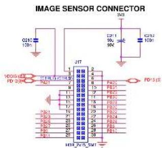
text_image
IMAGE SENSOR CONNECTOR Q24C 100V Q211 10V Q212 100V Q213 10V JIT WDOS/HD FD 5.5V 7A1 1 2 3 4 5 6 7 8 9 10 11 12 13 14 15 16 17 18 19 20 21 22 23 24 25 26 27 28 29 30 31 32 33 34 35 36 37 38 39 40 41 42 43 44 45 46 47 48 49 50 51 52 53 54 55 56 57 58 59 60 61 62 63 64 65 66 67 68 69 70 71 72 73 74 75 76 77 78 79 80 81 82 83 84 85 86 87 88 89 90 91 92 93 94 95 96 97 98 99 100| A2 | PP | 08-pp-10 | |||
| A | Ockk | 05 Feb 10 | PP | 11 FEB 10 | |
| P=V | MOEK | D=X | D=Y | V=H | D=J |
| SCAN = 1/1 | REV. | 3=FFT | |||
| A2 | 12/12 | ||||
8.1 Revision History
Table 8-1.
| Document Comments | Change Request Ref. | |
| 6495B | Main edits:- Most Figures updated- Hyperlinks to PDFs updated- 'Serial Synchronous Controller (SSC)' removed- 'JTAG' added- 'RJ45 crossed cable' added- Dimensions updated- Most configuration tables (with LEDs, pins and connectors) updated- 'LG/Philips' reference removed | 6990 |
| New Figure 4-4," EBI1 - DDR2 + Flash" and new Schematics in Section 7.1 "Schematics" | 7169 | |
| 6495A First issue. | ||
Headquarters International
| Atmel Corporation2325 Orchard ParkwaySan Jose, CA 95131USATel: 1(408) 441-0311Fax: 1(408) 487-2600 | Atmel AsiaUnit 1-5 & 16, 19/FBEA Tower, Millennium City 5418 Kwun Tong RoadKwun Tong, KowloonHong KongTel: (852) 2245-6100Fax: (852) 2722-1369 | Atmel EuropeLe Krebs8, Rue Jean-Pierre TimbaudBP 30978054 Saint-Quentin-en-Yvelines CedexFranceTel: (33) 1-30-60-70-00Fax: (33) 1-30-60-71-11 | Atmel Japan9F, Tonetsu Shinkawa Bldg.1-24-8 ShinkawaChuo-ku, Tokyo 104-0033JapanTel: (81) 3-3523-3551Fax: (81) 3-3523-7581 |
Product Contact
| Web Site | Technical Support | Sales Contact |
| www.atmel.com | AT91SAM Support | www.atmel.com/contacts |
| Atmel technical support |
Literature Requests
www.atmel.com/literature
Disclaimer: The information in this document is provided in connection with Atmel products. No license, express or implied, by estoppel or otherwise, to any intellectual property right is granted by this document or in connection with the sale of Atmel products. EXCEPT AS SET FORTH IN ATMEL'S TERMS AND CONDITIONS OF SALE LOCATED ON ATMEL'S WEB SITE, ATMEL ASSUMES NO LIABILITY WHATSOEVER AND DISCLAIMS ANY EXPRESS, IMPLIED OR STATUTORY WARRANTY RELATING TO ITS PRODUCTS INCLUDING, BUT NOT LIMITED TO, THE IMPLIED WARRANTY OF MERCHANTABILITY, FITNESS FOR A PARTICULAR PURPOSE, OR NON-INFRINGEMENT. IN NO EVENT SHALL ATMEL BE LIABLE FOR ANY DIRECT, INDIRECT, CONSEQUENTIAL, PUNITIVE, SPECIAL OR INCIDENTAL DAMAGES (INCLUDING, WITHOUT LIMITATION, DAMAGES FOR LOSS OF PROFITS, BUSINESS INTERRUPTION, OR LOSS OF INFORMATION) ARISING OUT OF THE USE OR INABILITY TO USE THIS DOCUMENT, EVEN IF ATMEL HAS BEEN ADVISED OF THE POSSIBILITY OF SUCH DAMAGES. Atmel makes no representations or warranties with respect to the accuracy or completeness of the contents of this document and reserves the right to make changes to specifications and product descriptions at any time without notice. Atmel does not make any commitment to update the information contained herein. Unless specifically provided otherwise, Atmel products are not suitable for, and shall not be used in, automotive applications. Atmel's products are not intended, authorized, or warranted for use as components in applications intended to support or sustain life.
© 2010 Atmel Corporation. All rights reserved. Atmel ^® , Atmel logo and combinations thereof, DataFlash ^® , and others are registered trademarks, SAM-ICE ^™ and others are trademarks of Atmel Corporation or its subsidiaries. Other terms and product names may be trademarks of others.