AT91SAM7S32 - Carte d'évaluation Microchip - Free user manual and instructions
Find the device manual for free AT91SAM7S32 Microchip in PDF.

User questions about AT91SAM7S32 Microchip
0 question about this device. Answer the ones you know or ask your own.
Ask a new question about this device
Download the instructions for your Carte d'évaluation in PDF format for free! Find your manual AT91SAM7S32 - Microchip and take your electronic device back in hand. On this page are published all the documents necessary for the use of your device. AT91SAM7S32 by Microchip.
USER MANUAL AT91SAM7S32 Microchip
AT91SAM7S-EK Evaluation Board
User Guide
Table of Contents
Section 1
Overview....1-1
1.1 Scope....1-1
1.2 Deliverables ...... 1-1
1.3 AT91SAM7S-EK Evaluation Board....1-1
Section 2
Setting Up the AT91SAM7S-EK Board....2-1
2.1 Electrostatic Warning .....2-1
2.2 Requirements....2-1
2.3 Powering Up the Board....2-1
2.4 Getting Started....2-1
2.5 AT91SAM7S-EK Block Diagram....2-2
Section 3
Board Description 3-1
3.1 AT91SAM7S256 Microcontroller....3-1
3.2 AT91SAM7S256 Block Diagram....3-3
3.3 Memory 3-3
3.4 Clock Circuitry....3-3
3.5 Reset Circuitry....3-4
3.6 Power Supply Circuitry....3-4
3.7 Remote Communication....3-4
3.8 Analog Interface....3-4
3.9 User Interface 3-4
3.10 Debug Interface 3-4
3.11 Expansion Connector....3-4
3.12 Wrapping User Area....3-4
Section 4
Configuration Straps 4-1
4.1 Configuration Strap ....4-1
Section 5
Schematics 5-1
5.1 Schematics ....5-1
Section 6
Revision History....6-1
6.1 Revision History ......6-1
Table of Contents
ii AT91SAM7S-EK Evaluation Board User Guide

Section 1
Overview
| 1.1 Scope | The AT91SAM7S-EK evaluation board enables the evaluation of and code development for applications running on an AT91SAM7Sxx device.This document describes the evaluation board fitted with an AT91SAM7S256.This guide focuses on the AT91SAM7S-EK board as an evaluation platform for the AT91SAM7S family. |
| 1.2 Deliverables | |
| 1.2.1 Standard VersionAT91SAM7S-EKVAR | The AT91SAM7S-EK package contains the following items:■An AT91SAM7S-EK board■One A/B-type USB cable■One DVD-ROM containing summary and full datasheets, datasheets with electrical and mechanical characteristics, application notes and getting started documents for all development boards and AT91 microcontrollers. An AT91 software package with C and assembly listings is also provided. This allows the user to begin evaluating the AT91 ARM® Thumb® 32-bit microcontroller quickly. |
| 1.3 AT91SAM7S-EKEvaluation Board | The board is generally equipped with an AT91SAM7S256 (64-pin PQFP package) together with the following:■USB device port interface■Two serial communication ports■JTAG/ICE debug interface■Four buffered analog inputs■Four general-purpose LEDs and pushbuttons■Expansion connector■Prototyping area |
AT91SAM7S-EK Evaluation Board User Guide 1-1
Note: The user can also evaluate the AT91SAM7S32 with this board. A 48-pin TQFP footprint has been provided for this purpose. To do so, the user must unsolder the AT91SAM7S256 microcontroller (IC4) and fit the AT91SAM7S32 on the 48-pin TQFP footprint (IC5).
Setting Up the AT91SAM7S-EK Board
| 2.1 Electrostatic Warning | The AT91SAM7S-EK evaluation board is shipped in protective anti-static packaging.The board must not be subjected to high electrostatic potentials. A grounding strap or similar protective device should be worn when handling the board. Avoid touching the component pins or any other metallic element. | |
| 2.2 | Requirements | In order to set up the AT91SAM7S-EK evaluation board, the following items are needed:■The AT91SAM7S-EK evaluation board itself.■Optional DC power supply capable of supplying 7V to 12V at 0.5 A.Note:The AT91SAM7S-EK is not delivered with the JTAG/ICE interface required to start evaluating the device. |
| 2.3 Powering Up the Board | AT91SAM7S-EK is self-powered by the USB port. If the USB port is not used, the card can be supplied by an external DC power supply via the 2.1 mm socket (J1). The polarity of the power supply is not critical.The regulator allows the input voltage range to be from 7V to 12V. | |
| 2.4 | Getting Started | The AT91SAM7S-EK evaluation board is delivered with a DVD-ROM containing all necessary information and step-by-step procedures for working with the most common development toolchains. Please refer to this DVD-ROM, or to the AT91 web site, http://www.atmel.com/products/AT91/, for the most up-to-date information on getting started with the AT91SAM7S-EK. |
AT91SAM7S-EK Evaluation Board User Guide 2-1
2.5 AT91SAM7S-EK Block Diagram
Figure 2-1. Block Diagram for AT91SAM7S-EK Board
flowchart
graph TD
    A["Analog Inputs"] -->|4| B["VDDCORE"]
    C["RS232 Driver"] -->|UART DBGU| D["AT91SAM7S256"]
    E["RS232 Driver"] -->|UART DBGU| D
    B -->|1.8V| F["VDDOUT"]
    D -->|3.3V| G["Oscillator, PLL"]
    D --> H["NRST Pushbutton"]
    D --> I["Power Supply"]
    D --> J["USB Device"]
    D --> K["ICE Debug Port"]
    D --> L["Extension Connector"]
    D --> M["User Grid"]
    N["Input"] --> O["Power Supply"]
    O --> P["USB Device"]
    Q["7 - 14V DC"] --> R["Power Supply"]
    S["User Grid"] --> T["User Grid"]
3.1 AT91SAM7S256 Microcontroller
- Incorporates the ARM7TDMI ^ ARM ^ Thumb ^ Processor
– High-performance 32-bit RISC Architecture
– High-density 16-bit Instruction Set
– Leader in MIPS/Watt
- EmbeddedICE™ In-circuit Emulation, Debug Communication Channel Support
• 256 Kbytes of Internal High-speed Flash, Organized in 1024 Pages of 256 Bytes
– Single Cycle Access at Up to 30 MHz in Worst Case Conditions, Prefetch Buffer Optimizing Thumb Instruction Execution at Maximum Speed
– Page Programming Time: 4 ms, Including Page Auto-erase, Full Erase Time: 10 ms
- 10,000 Write Cycles, 10-year Data Retention Capability, Sector Lock Capabilities, Flash Security Bit
– Fast Flash Programming Interface for High Volume Production
- 64 Kbytes of Internal High-speed SRAM, Single-cycle Access at Maximum Speed
• Memory Controller (MC)
- Embedded Flash Controller, Abort Status and Misalignment Detection
- Reset Controller (RSTC)
– Based on Power-on Reset and Low-power Factory-calibrated Brown-out Detector
– Provides External Reset Signal Shaping and Reset Source Status
- Clock Generator (CKGR)
– Low-power RC Oscillator, 3 to 20 MHz On-chip Oscillator and one PLL
• Power Management Controller (PMC)
- Software Power Optimization Capabilities, Including Slow Clock Mode (Down to 500 Hz) and Idle Mode
– Three Programmable External Clock Signals
- Advanced Interrupt Controller (AIC)
- Individually Maskable, Eight-level Priority, Vectored Interrupt Sources
- Two External Interrupt Sources and One Fast Interrupt Source, Spurious Interrupt Protected
- Debug Unit (DBGU)
– 2-wire UART and Support for Debug Communication Channel interrupt, Programmable ICE Access Prevention
• Periodic Interval Timer (PIT)
- 20-bit Programmable Counter plus 12-bit Interval Counter
• Windowed Watchdog (WDT)
- 12-bit key-protected Programmable Counter
– Provides Reset or Interrupt Signals to the System
– Counter May Be Stopped While the Processor is in Debug State or in Idle Mode
• Real-time Timer (RTT)
- 32-bit Free-running Counter with Alarm
– Runs Off the Internal RC Oscillator
- One Parallel Input/Output Controller (PIOA)
- Thirty-Two Programmable I/O Lines Multiplexed with up to Two Peripheral I/Os
– Input Change Interrupt Capability on Each I/O Line - Individually Programmable Open-drain, Pull-up resistor and Synchronous Output
- Eleven Peripheral Data Controller (PDC) Channels
• One USB 2.0 Full Speed (12 Mbits per second) Device Port
- On-chip Transceiver, 328-byte Configurable Integrated FIFOs
- One Synchronous Serial Controller (SSC)
– Independent Clock and Frame Sync Signals for Each Receiver and Transmitter
- I²S Analog Interface Support, Time Division Multiplex Support
– High-speed Continuous Data Stream Capabilities with 32-bit Data Transfer
- Two Universal Synchronous/Asynchronous Receiver Transmitters (USART)
- Individual Baud Rate Generator, IrDA ^ Infrared Modulation/Demodulation
– Support for ISO7816 T0/T1 Smart Card, Hardware Handshaking, RS485 Support
– Manchester Encoder/Decoder
– Full Modem Line Support on USART1
• One Master/Slave Serial Peripheral Interface (SPI)
- 8- to 16-bit Programmable Data Length, Four External Peripheral Chip Selects
• One Three-channel 16-bit Timer/Counter (TC)
– Three External Clock Inputs, Two Multi-purpose I/O Pins per Channel
- Double PWM Generation, Capture/Waveform Mode, Up/Down Capability
• One Four-channel 16-bit PWM Controller (PWMC)
• One Two-wire Interface (TWI)
– Master Mode Support Only, All Two-wire Atmel EEPROMs Supported
- One 8-channel 10-bit Analog-to-Digital Converter, Four Channels Multiplexed with Digital I/Os
- IEEE ^ 1149.1 JTAG Boundary Scan on All Digital Pins
- 5V-tolerant I/Os, including Four High-current Drive I/O lines, Up to 16 mA Each
-
Power Supplies
-
Embedded 1.8V Regulator, Drawing up to 100mA for the Core and External Components
- 1.8V or 3.3V VDDIO I/O Lines Power Supply, Independent 3.3V VDDFLASH Flash Power Supply
- 1.8V VDDCORE Core Power Supply with Brown-out Detector
- 3.3V VDDANA Analog Voltage Supply
• Fully Static Operation: Up to 55 MHz at 1.65V and 85°C Worst Case Conditions
• Available in a 64-lead TQFP Package
3.2 AT91SAM7S256 Block Diagram
Figure 3-1. AT91SAM7S256 Block Diagram

flowchart
graph TD
    A["JTAG SCAN"] --> B["ICE"]
    C["TDI"] --> B
    D["TDO"] --> B
    E["TMS"] --> B
    F["TCK"] --> B
    G["JTAGSEL"] --> B
    H["TST"] --> I["System Controller"]
    I --> J["AIC"]
    I --> K["PMC"]
    I --> L["PLL"]
    I --> M["OSC"]
    I --> N["OSC"]
    I --> O["OSC"]
    P["PIQ"] --> Q["AIC"]
    R["IRQO-IRQ1"] --> S["PLL"]
    T["PCK0-PCK2"] --> U["OSC"]
    V["POLLRC"] --> W["OSC"]
    X["XIN"] --> Y["OSC"]
    Z["XOUT"] --> AA["OSC"]
    AB["VDDCORE"] --> AC["BOD"]
    AD["VDDCORE"] --> AE["POR"]
    AF["NRST"] --> AG["Reset Controller"]
    AH["VDDANA"] --> AI["ADC"]
    AJ["APB"] --> AK["Peripheral Data Controller 11 Channels"]
    AL["Memory Controller"] --> AM["Embedded Flash Controller"]
    AL --> AN["Address Decoder"]
    AL --> AO["Abort Status"]
    AL --> AP["Misalignment Detection"]
    AQ["SRAM 64 Kbytes"] --> AR["Flash 256 Kbytes"]
    AS["Flash 256 Kbytes"] --> AT["Peripheral Bridge"]
    AU["Peripheral Bridge"] --> AV["Peripheral Data Controller 11 Channels"]
    AW["APB"] --> AX["FIFO USB Device"]
    AX --> AY["Timer Counter"]
    AX --> AZ["PWMC"]
    AX --> BA["SSC"]
    AX --> BB["PDC"]
    AX --> BC["PDC"]
    AX --> BD["PDC"]
    AX --> BE["PDC"]
    AX --> BF["PDC"]
    AX --> BG["PDC"]
    AX --> BH["PDC"]
    AX --> BI["PDC"]
    AX --> BJ["PDC"]
    AX --> BK["PDC"]
    AL --> BL["Fast Flash Programming Interface"]
    BL --> BM["PGMRDY PGMVALID PGMNOE PGMCK PGMCM0 PGMCM3 PGMDD-PGMD15 PGMNCMD PGMEN0-PGMEN1"]
    BN["PDMRDY"] --> BO["PGMNVALID PGMNOE PGMCK PGMCM0 PGMCM3 PGMDD-PGMD15 PGMNCMD PGMEN0-PGMEN1"]
    BP["PDMNVALID"] --> BQ["PGMVALID PGMNOE PGMCK PGMCK PGMCM0 PGMCM3 PGMDD-PGMD15 PGMNCMD PGMEN0-PGMEN1"]
    BQ["PDMUSD"] --> CC["PWM0 PWM1 PWM2 PWM3 TF TCF TCF TCF TCF TCF TCF TCF TCF TCF TCF TCF TCF TCF TCF TCF TCF TCF TCF TCF TCF TCF TCF TCF TCF TCF TCF TCF TCF TCF TCF TCF TCF TCF TCF TCF TCF TCF TCF TCF TCF TCF TCF TCF TCF TCF TCF TCF TCF TCF TCF TCE"]
    DD["PWM0"] --> DP[PWM0 PWM1 PWM2 PWM3 TF TCF TCF TCF TCF TCF TCF TCF TCF TCF TCF TCF TCF TCF TCF TCF TCF TCF TCF TCF TCF TCF TCF TCF TCF TCF TCF TCF TCF TCF TCF TCF TCF TCF TCF TCF TCF TCF TCF TCF TCF TCF TCF TCF
3.3 Memory ■256 Kbytes of internal high-speed Flash
■64 Kbytes of internal high-speed SRAM
3.4 Clock Circuitry
■ 18.432 MHz standard crystal for the embedded oscillator
| 3.5 | Reset Circuitry | ■ Internal bi-directional reset controller with brown out detector■External reset pushbutton |
| 3.6 | Power Supply Circuitry | ■USB powered. The dynamic power consumption on VDDCORE is less than 50 mA at full speed when running out of the Flash. The total current drawn by all the I/O lines cannot exceed 200 mA.■External power can be applied via the 2.1 mm connector to the regulator in either polarity because of the diode-rectifying circuit (CR3 to CR6). The minimum voltage required is 7V. The board has a voltage regulator providing +3.3V. The regulator allows the input voltage to be from 7V to 14V (REG1).■The two power supplies are separated from each other by the diodes CR1 and CR2.■On-chip embedded VDDCORE 1.8V regulator |
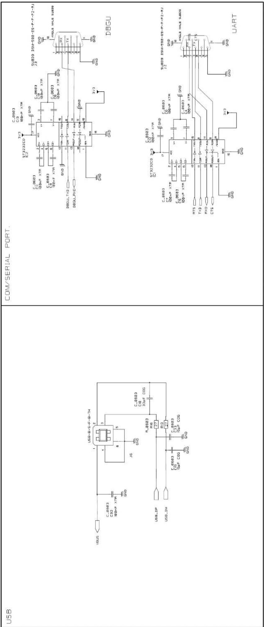
| 3.7 | Remote Communication | ■Two serial interface via RS-232 DB9 male sockets– DBGU COM Port– UART COM Port with RTS/CTS handshake control possibility (USART 0)■USB V2.0 full-speed compliant, 12 Mbits per second (UDP) |
| 3.8 | Analog Interface | ■ Four analog inputs (0V to 3.3V) via J7, J8, J9, J10 footprints |
| 3.9 | User Interface | ■ Four pushbuttons via general PIO lines■Four LEDs via high current PIO lines |
| 3.10 | Debug Interface | ■ 20-pin JTAG/ICE interface connector■DBGU COM port |
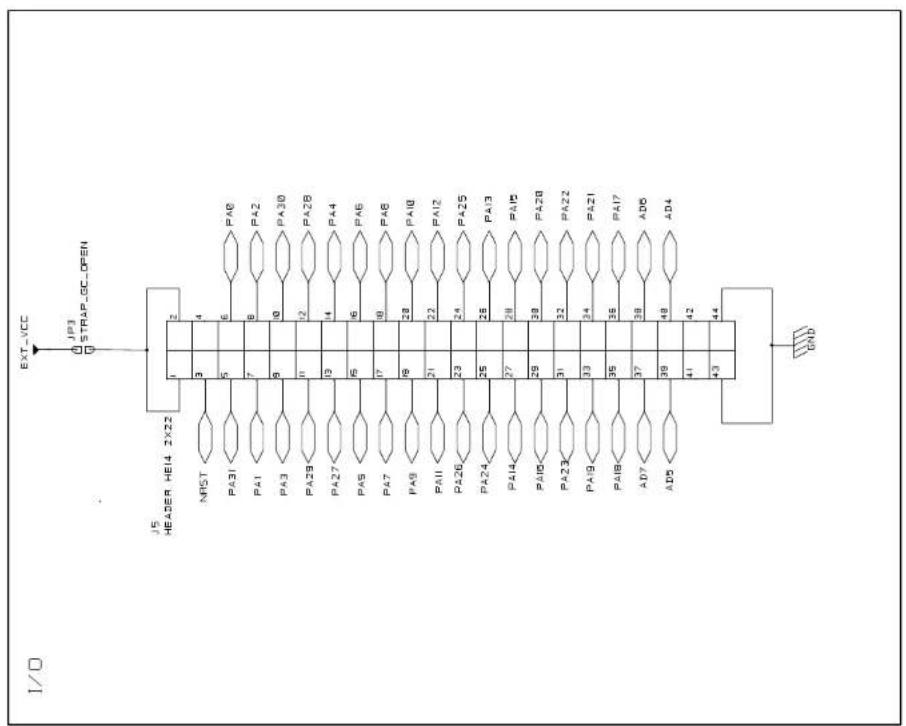
| 3.11 | Expansion Connector | One expansion connector (J5) gives access to all the microcontroller's signals.All I/Os of the AT91SAM7S256 are routed to this connector. This allows the developer to check the integrity of the components and to extend the features of the board by adding external hardware components or boards. |
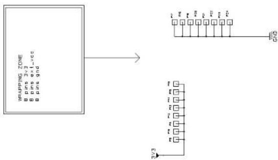
| 3.12 | Wrapping User Area | This allows the developer to fit additional components for prototyping use. |
3-4 AT91SAM7S-EK Evaluation Board User Guide

Configuration Straps
4.1 Configuration Strap
Table 4-1 gives details on configuration straps on the AT91SAM7S-EK evaluation board and their default settings.
Table 4-1. Configuration Straps
| Designation | Default Setting Feature |
| JP1 Closed | Enables the use of the remote DP pull-up (USB) |
| JP2 Closed | Enables the use of the VBUS detect (USB) |
| JP3 Opened | Disable external VCC on the expansion connector J5 (pin 1, 2) |
| JP4 Closed | The System Reset signal (NRST) is connected to the ICE/JTAG socket (J4, pin 15). |
| JP5 Opened | Do not use: Factory test mode |
| JP6 Closed | Enables the use of the CTS signal (UART) |
| JP7 Closed | Enables the use of the TXD signal (UART) |
| JP8 Closed | Enables the use of the RTS signal (UART) |
| JP9 Closed | Enables the use of the RXD signal (UART) |
| JP10 Closed | |
| JP11 Closed | Enables the use of the RXD signal (DBGU) |
| JP12 Closed | Enables the use of the TXD signal (DBGU) |
| JP13^(1) | Closed VDDFLASH Jumper |
| JP14^(1) | Closed VDDIO Jumper |
| JP15 Closed | Enables the use of the User LED (DS1) |
| JP16 Closed | Enables the use of the User LED (DS2) |
| JP17 Closed | Enables the use of the User LED (DS3) |
| JP18 Closed | Enables the use of the User LED (DS4) |
| JP19 Opened | Select ICE mode or JTAG mode (Closed) |
| JP20^(1) | Closed ADVREFP Jumper |
| JP21^(1) | Closed VDDPLL Jumper |
Table 4-1. Configuration Straps
| Designation | Default Setting Feature | |
| JP22^(1) | Closed VDDIN Jumper | |
| JP23^(1) | Closed VDDCORE Jumper | |
| JP24 Closed | Enables the use of the EXT_AD0 (Analog Input 0) | |
| JP25 Closed | Enables the use of the EXT_AD1 (Analog Input 1) | |
| JP26 Closed | Enables the use of the EXT_AD4 (Analog Input 4) | |
| JP27 Closed | Enables the use of the EXT_AD5 (Analog Input 5) | |
| JP28 Opened | Erases all internal Flash memory when the board is powered. To do so, the user must close J28 for at least 10 ms. | |
| TP1 N.A GND Test point | ||
| TP3 N.A GND Test point | ||
| TP5 N.A GND Test point | ||
| TP6 N.A GND Test point |
Note: 1. These jumpers are dedicated to power consumption measurement use. The user has to open the jumper and insert an anmeter.
If these jumpers are not populated (previous revisions of the kit), the related straps are wired on board. In this case and in order to use the power consumption measurement feature, the user has to open the strap by cutting it before soldering a jumper and inserting an anmeter.
5.1 Schematics This section contains the following schematics:
■Board Layout And Silkscreen Printing - Top View
■64-pin SAM7 Microcontroller (dual footprint)
■48-pin SAM7 Microcontroller
■Power Supply
■ICE/EXT Connectors
■Device Interface
■PIO
■User PAD Grid
text_image
POWER SUPPLY ICE / JTAG GND NRST TST VDDRPLASHVDD30 ERASE JTAGSEL USB / POWER SUPPLY GND PA19 PA20 PA16 PA14 RESET UART IPA 18.13 IPA 4.5.10 IPA 8.6.7.51 IPAG.1,2,31 AT915AM7S-EK EXT_VCC to J6 3.3V 300mA DBGU Xvcc HST GND N.L. 1 2 3 4 5 6 7 8 9 10 11 12 13 14 15 16 17 18 19 20 21 22 23 24 25 26 27 28 29 30 31 32 33 34 35 36 37 38 39 40 41 42 43 44 45 46 47 48 49 50 51 52 53 54 55 56 57 58 59 60 61 62 63 64 65 66 67 68 69 70 71 72 73 74 75 76 77 78 79 80 81 82 83 84 85 86 87 88 89 90 91 92 93 94 95 96 97 98 99 100 FREE GRID (DEFAULT N.C.) Rev.A3| A3 | 4 AUG 04 | |
| A2 | 9 JUNE04 | |
| A | 15APR04 | Initial version |
text_image
POWER DECOUPLING C.0603 C26 I00nF xTR +0 PE rP GH10 C.0603 C26 I00nF xTR C28 C30 C29 I00nF x7R GH10 VDCORE C.0603 C29 I00nF x7R VDCPLL C25 G10 C22 G10 C.0603 C21 C21 C21 G10 C.0603 C21 I00nF x7RAT915 AN75-EX
| ATMEL | Title. | Ind. Date | Des. |
| 2T95A7S-EI | +4 | 10:05 | |
| 2T95A7S-EF | +3 | 8+0004 | |
| 2T95A7S-EK | +2 | 10:001 | |
| 2T95A7S-EH | +1 | 10:-1004 | |
| ATG15AM7S-EK | |||
| Scale. | Page | ||
| 1:1 | 1 | ||
text_image
T1/CD 4-1437565-8 gp5 1 2 3 4 GPIO T1/PST JUWERP-2PTS JP5 P-1(-21) P-31 JUWERP-2PTS JP9 T00 JTAGSEL T05 TOI VDDCORE EPL-SE USB-DI USB-DP VDDOIO VDDPLASH GPIO OUT VBR/GRICK PLLPC VDDPLL C14 8pF COG C25 10pF COG GPIO C24 1.51 C23 10nF GPIO C20 303 C24 1.51 C23 10nF GPIO C20 303 C24 1.51 C23 10nF GPIO C20 303 C24 1.51 C23 10nF GPIO C20 303 C24 1.51 C23 1.51 C20 303 C24 1.51 C23 1.51 C20 303 C24 1.51 C23 1.51 C20 303 C24 1.51 C23 1.51 C20 303 C24 1.51 C23-1.51 C20-303 C24-1.51 C23-1.51 C20-303 C24-1.51 C23-1.51 C20-303 C24-1.51 C23-1.51 C20-303 C24-1.51 C23-1.51 C20-303
text_image
PAG PA1 PA2 PA3 TST NRST PA4 PA5 PAG TDI GND VDDIO 38 35 34 33 32 31 30 29 28 27 26 25 TDO PA0/PGMEN0 PA1/PGMEN1 GND VDDIO PA2/PGMEN2 PA3/PGMEN3 TST NRST PA4/PGMEN4 PA5/PGMEN5 TDI JTAGSEL TMS TCK VDDCORE VDDFASH ERASE VDDFLASH GND VDDCORE XOUT XOUT XIN/PQNICK PLLRC VDDPLL ADVREVP AD4 AD5 AD6 AD7 VDDN VDDOUT PA7/PGM1/AD0 PA8/PGM2/AD1 PA9/PGM3/AD2 PA10/PGM4 VDDCORE ADVREVP AD4 AD5 AD6 AD7 VDDN VDDOUT PA11/PGM3 PA12/PGM4 VDDCORE AT9ISAM7S32 ATMEL Title. AT9ISAM7S-EK AT9ISAM7S-EK AT9ISAM7S-EK AT9ISAM7S-EKAT915AM75-EK
| ATMEL | Title. | Ind. | Date | Des. | |
| AT8ISAM7S-EK | A2 | 04AC004 | CJN | ||
| AT91SAM7S-EK | AT9ISAM7S-EK | A2 | 17MA104 | CJN | |
| AT9ISAM7S-EK | A | 05AYFCL04 | CJN | ||
| 48-PIN SAM7 | Scale. | Page | |||
| 1:1 | 2 | ||||
| ANALOG INPUTSBARRETTE 3PTS 2.54MMADVREVPLOC_A08STRAP_GC_CLOSEDLM6154BCMJP24PA17J7GNDLOC_A01LM6154BCMJP25PA18J8GNDLOC_A02LM6154BCMJP26AD4J9GNDLOC_A03ADVREVPLOC_A04LM6154BCMJP27ADSJ10GNDC_0503C36I00nF X7R11GND | USER PUSH-BUTTONSTYCQ 4-1437565-9PA18BP11203GNDPA20BP27203GNDPA15BP3203GNDPA14BP41203GND | USER LEDS & CRYPTO MEMORYSTRAP_GC_CLOSEDHSME-C17RPL_06833V3PA0JP16DS11B0PA1JP162D521B0PA2JP172C531B0PA2JP182D541B0PA3JP182D541B0 |
| PIO STRAPSSTRAP_GC_CLOSEDPASJP6RXDPA6JP7TXDPA7JP8RTSPA8JP6CTSPPASJP11DEGU_RXDPA10JP12DEGU_TXDPA13JP2VBUS_DETPA16JP1USB_DP_FUP | STRAP_GC_CLOSEDC_0603C17I00nF X7RGNDAT885C25616CIC3SDAPVCAT885C25616CSCLND4GND |
AT915AM75-EK
| ATMEL | Title. | Ind. | Date | Des. | |
| AT91SAM7S-EK | A2 | 04/08/04 | CJN | ||
| AT91SAM7S-EK | A2 | 17/08/04 | CJN | ||
| AT91SAM7S-EK | A | 18/08/04 | CJN | ||
| PIO | Scale. | Page | |||
| 1:1 | 6 | ||||
AT915AM75-EK
| ATMEL | Title. | Ind. | Date | Des. | |
| AT81SAM75-EK | A2 | 04AC004 | CJN | ||
| AT91SAM75-EK | AT81SAM75-EK | A2 | 07MA104 | CJN | |
| AT91SAM75-EK | A | 08AYPE04 | CJN | ||
| DEVICEINTERFACE | Scale. | Page | |||
| 1:1 | 5 | ||||
text_image
I/O EXT_VCC JP3 STRAP_SC_OPEN J5 HEADER_HE14 2X22 NIST 3 4 PA31 5 6 PA8 PA1 7 8 PA2 PA3 9 10 PA30 PA29 11 12 PA28 PA27 13 14 PA4 PA5 15 16 PA6 PA7 17 18 PA8 PA9 18 28 PA10 PA11 21 22 PA12 PA26 23 24 PA25 PA24 25 26 PA13 PA14 27 28 PA15 PA16 29 30 PA28 PA23 31 32 PA22 PA19 33 34 PA21 PA18 35 36 PA17 AD7 37 38 AD6 AD5 39 40 AD4 41 42 43 44 GND
text_image
ICE/J TAG INTERFACE. ANGLE HE10_2X10 J4 GND 3V3 STRAP_SC_CLOSED JP4 NRST CKD R17 10K R_0003 3V3 TDO TCK TM5 TDI R12 R11 R10 R9 R4 47K 3V3AT915AM75-EK
| ATMEL | Title. | Ind. | Date | Des. | |
| AT91SAM7S-EK | A3 | 04/08/04 | CJN | ||
| AT91SAM7S-EK | A2 | 07/08/04 | CJN | ||
| AT91SAM7S-EK | A | 05/08/04 | CJN | ||
| ICE/EXT. CONNECTORS. | Scale. | Page | |||
| 1:1 | 4 | ||||

text_image
EXT-SUPPLY INPUT + USB PULLUP CONTROL. 3V3 R_0603 R2 108K S12301ADS-TI TR1 C_0603 C2 10nF X7R GND R_0603 R14 15K USB_DP VBUS_DET R_0603 R2 108K R_0603 R1 10K GND S12302ADS-TI TR2 D GND USB_DP_PUP VBUS I8B0030 CR2 I8B0030 CR6 I8B0030 CR1 I8B030 CR3 I8B030 CR5 I8B030 CR4 I8B030 CR2 I8B030 CF6 I8B030 CF1 KF33BDT REG1 KF33 BDT VIN VOUT GND C_0603 C3 100nF X7R C_1286 CI 2.2uF X7R GND EXT-VCC INPUT SUPPLY 7-14 V TYCO 440107-1 J1 1 2 GND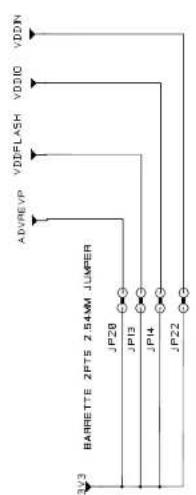
text_image
3V3 BARRETTE 2PTS 2.54MM JUMPER JP20 JP13 JP14 JP22 ADVREVP VDDFLASH VDDIO VDDIN
text_image
VDDOUT BARRETTE 2PTS 2.54MM JUMPER JP23 JP21 VDDCORE VDDPLLAT915AM75-EK
| ATMEL | Title. | Ind. | Date | Des. | |
| AT91SAM7S-EK | A2 | 04AC084 | CJN | ||
| AT91SAM7S-EK | A2 | 17MA084 | CJN | ||
| AT91SAM7S-EK | A | 19A1FRE04 | CJN | ||
| POWERSUPPLY | Scale. | Page | |||
| 1:1 | 3 | ||||
BRIDGE CNS TEST POINT TPI TP3 TPS TP6 GND GND GND GND

text_image
SUPPLY DISTRIBUTION 3V3 BARRETTE 2PTS 2.54MM JUMPER JP20 JP13 JP14 JP22 VDDOUT BARRETTE 2PTS 2.54MM JUMPER JP23 JP21 VDDCORE VDSPLL GROUND TEST POINTS BRIDGE CNS TEST POINT TPI TP3 TP5 TP6 GND GND GND GND AT915AM7S-EK ATMEL Title. Ind. Date Des. AT915AM7S-EK A2 B4ACU04 CJN AT915AM7S-EK A2 B7MA04 CJN AT915AM7S-EK A B9AVF04 CJN POWER SUPPLY Scale. Page 1:1 3 AT915AM7S-EKAT915AM75-EK
| ATMEL | Title. | Ind. | Date | Des. | |
| AT91SAM7S-EK | AT91SAM7S-EK | A2 | 04AD084 | CJN | |
| AT91SAM7S-EK | A2 | 17MA104 | CJN | ||
| AT91SAM7S-EK | A | 05AVPE04 | CJN | ||
| USER PAD GRID | Scale. | Page | |||
| 1:1 | 7 | ||||
flowchart
graph TD
    A["3V3"] --> B["Grid 1"]
    A --> C["Grid 2"]
    A --> D["Grid 3"]
    A --> E["Grid 4"]
    A --> F["Grid 5"]
    A --> G["Grid 6"]
    A --> H["Grid 7"]
    A --> I["Grid 8"]
    A --> J["Grid 9"]
    A --> K["Grid 10"]
    A --> L["GND"]
    M["WRAPPING ZONE\nB pins 3v3\nB pins ex1_vcc\nB pins gnd"] --> N["GND"]
| Document Comments | Change Request Ref. |
| 6112A First issue. | |
| 6112B New schematics. 1457 | |
| 6112C Corrected features for JP26 and JP27 in Table 4-1, "Configuration Straps". Corrected device label in 64-pin SAM7 schematic. | 38492734 |
Revision History
6-2 AT91SAM7S-EK Evaluation Board User Guide

Atmel Corporation Atmel Operations
2325 Orchard Parkway
San Jose, CA 95131, USA
Tel: 1(408) 441-0311
Fax: 1(408) 487-2600
Regional Headquarters
Europe
Atmel Sarl
77 Mody Road Tsimshatsui
East Kowloon
Hong Kong
Tel: (852) 2721-9778
Fax: (852) 2722-1369
Japan
9F, Tonetsu Shinkawa Bldg.
1-24-8 Shinkawa
Chuo-ku, Tokyo 104-0033
Japan
Tel: (81) 3-3523-3551
Fax: (81) 3-3523-7581
Memory
2325 Orchard Parkway
San Jose, CA 95131, USA
Tel: 1(408) 441-0311
Fax: 1(408) 436-4314
Microcontrollers
2325 Orchard Parkway
San Jose, CA 95131, USA
Tel: 1(408) 441-0311
Fax: 1(408) 436-4314
La Chantrerie
BP 70602
44306 Nantes Cedex 3, France
Tel: (33) 2-40-18-18-18
Fax: (33) 2-40-18-19-60
ASIC/ASSP/Smart Cards
Zone Industrielle
13106 Rousset Cedex, France
Tel: (33) 4-42-53-60-00
Fax: (33) 4-42-53-60-01
1150 East Cheyenne Mtn. Blvd.
Colorado Springs, CO 80906, USA
Tel: 1(719) 576-3300
Fax: 1(719) 540-1759
Scottish Enterprise Technology Park
Maxwell Building
East Kilbride G75 0QR, Scotland
Tel: (44) 1355-803-000
Fax: (44) 1355-242-743
RF/Automotive
Theresienstrasse 2
Postfach 3535
74025 Heilbronn, Germany
Tel: (49) 71-31-67-0
Fax: (49) 71-31-67-2340
1150 East Cheyenne Mtn. Blvd.
Colorado Springs, CO 80906, USA
Tel: 1(719) 576-3300
Fax: 1(719) 540-1759
Biometrics
Avenue de Rochepleine
BP 123
38521 Saint-Egreve Cedex, France
Tel: (33) 4-76-58-47-50
Fax: (33) 4-76-58-47-60

Literature Requests
www.atmel.com/literature
Disclaimer: The information in this document is provided in connection with Atmel products. No license, express or implied, by estoppel or otherwise, to any intellectual property right is granted by this document or in connection with the sale of Atmel products. EXCEPT AS SET FORTH IN ATMEL'S TERMS AND CONDITIONS OF SALE LOCATED ON ATMEL'S WEB SITE, ATMEL ASSUMES NO LIABILITY WHATSOEVER AND DISCLAIMS ANY EXPRESS, IMPLIED OR STATUTORY WARRANTY RELATING TO ITS PRODUCTS INCLUDING, BUT NOT LIMITED TO, THE IMPLIED WARRANTY OF MERCHANTABILITY, FITNESS FOR A PARTICULAR PURPOSE, OR NON-INFRINGEMENT. IN NO EVENT SHALL ATMEL BE LIABLE FOR ANY DIRECT, INDIRECT, CONSEQUENTIAL, PUNITIVE, SPECIAL OR INCIDENTAL DAMAGES (INCLUDING, WITHOUT LIMITATION, DAMAGES FOR LOSS OF PROFITS, BUSINESS INTERRUPTION, OR LOSS OF INFORMATION) ARISING OUT OF THE USE OR INABILITY TO USE THIS DOCUMENT, EVEN IF ATMEL HAS BEEN ADVISED OF THE POSSIBILITY OF SUCH DAMAGES. Atmel makes no representations or warranties with respect to the accuracy or completeness of the contents of this document and reserves the right to make changes to specifications and product descriptions at any time without notice. Atmel does not make any commitment to update the information contained herein. Unless specifically provided otherwise, Atmel products are not suitable for, and shall not be used in, automotive applications. Atmel's products are not intended, authorized, or warranted for use as components in applications intended to support or sustain life.
© 2007 Atmel Corporation. All rights reserved. Atmel ^® , logo and combinations thereof, Everywhere You Are ^® and others are registered trademarks or trademarks of Atmel Corporation or its subsidiaries. ARM ^® , Thumb ^® and ARM Powered ^® are the registered trademarks or trademarks of ARM Ltd. Other terms and product names may be trademarks of others.

Printed on recycled paper.
6112C-ATARM-01-Feb-07