PIC16F13124 - Electronic component Microchip - Free user manual and instructions
Find the device manual for free PIC16F13124 Microchip in PDF.

User questions about PIC16F13124 Microchip
0 question about this device. Answer the ones you know or ask your own.
Ask a new question about this device
Download the instructions for your Electronic component in PDF format for free! Find your manual PIC16F13124 - Microchip and take your electronic device back in hand. On this page are published all the documents necessary for the use of your device. PIC16F13124 by Microchip.
USER MANUAL PIC16F13124 Microchip
The PIC16F13145 family of microcontrollers introduce a new peripheral, the Configurable Logic Block (CLB).
The CLB peripheral, comprised of 32 Basic Logic Elements (BLE), allows the users to incorporate hardware-based custom logic into their applications. Each logic element's Look-up Table (LUT) based design offers vast customization options, and the CPU-independent operation improves the response time and power consumption.
The user must configure elements as matrix multiplexers, LUTs, and flip-flops to achieve a given logic function, which is similar to the Configurable Logic Cell (CLC) on PIC ^ MCUs or the Configurable Custom Logic (CCL) on the AVR ^ MCUs. However, the matrix is much larger and is interconnected to a higher degree - which enables users to make more complex logic functions. To help users focus on the intended functionality of their logic design without having to understand the inner workings of the peripheral, Microchip provides a GUI (CLB Synthesizer) used for Configurable Logic Block configuration.
Tool Versions: MCC-Integrated and Stand-Alone-Online
The available configuration tool has two versions: One integrated into MCC Melody and one online, stand-alone version.
CLB Synthesizer - MCC Melody: The version of the tool integrated into MPLAB® Code Configurator (MCC) Melody allows one to create a logic design from scratch or to import a logic design from the online version of the tool. It enables the user to develop a complete application using the CLB in MCC Melody and offers a high level of integration with other peripherals also configured using MCC Melody.
CLB Synthesizer - Online: The tool's online version allows one to create a logic design, synthesize it, and download it as a file (bitstream). In addition to the bitstream, a template source code is provided for configuring the CLB, but integrating it into the embedded project is left up to the user.
The logic configuration experience is common to both versions of the tool, so the tool's online version can be used to start a logic design using the CLB before moving to MCC Melody for further development.
Table of Contents
CLB Synthesizer....1
Tool Versions: MCC-Integrated and Stand-Alone-Online ....1
-
Getting Started....4
-
Drawing a Schematic....5
2.1. Components in CLB Synthesizer....5
2.2. Drawing a Basic Schematic.... 11
-
Status of the Synthesis Process....13
-
Tips and Tricks....14
4.1. How to Make use of Limited Display Resources.... 14
4.2. Tidying up a Design.... 15
- Interacting with Peripherals and the CPU....17
5.1. Interacting with Peripherals.... 17
5.2. Interacting with the CPU....18
-
Storing and Retrieving Logic Designs....20
-
Using Hierarchical Modules......21
7.1. Using Verilog to Describe a Logic Design....22
- Libraries and Modules....24
8.1. The Built-In PIC16F131 Device Library....24
8.2. Using the Hardware Counter 24
8.3. Using Modules from the Microchip Library....25
8.4. Using Modules from a Custom Library.... 25
8.5. Creating a Library with Modules....26
- Advanced Topics....30
9.1. Clocking the Configurable Logic Block....30
9.2. Preferences....30
9.3. Making Use of the Output ZIP....31
9.4. Description of Output Files....31
9.5. Synthesis and Place-and-Route Process.... 32
-
Known Issues and Change Log....34
-
Revision History....35
Microchip Information.... 36
The Microchip Website....36
Product Change Notification Service.... 36
Customer Support....36
Microchip Devices Code Protection Feature....36
Legal Notice....36
Trademarks....37
Quality Management System....38
Worldwide Sales and Service....39
1. Getting Started
Use Cases to hit the ground running with the CLB.
The CLB Synthesizer start page provides:
- A way to start a new design, load a previous design, or continue with the current design
- Quick-start examples for users to browse and see how the tool works
- Documentation links
CLB Synthesizer
Start
Blank design
Load...
Continue last project
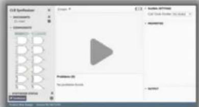
text_image
CUB Synthesis • Instruments • D:\Users\* • Components • Components (1) • Complexity (2) • Complexity (3) • Complexity (4) • Complexity (5) • Complexity (6) • Complexity (7) • Complexity (8) • Complexity (9) • Complexity (10) • Complexity (11) • Complexity (12) • Complexity (13) • Complexity (14) • Complexity (15) • Complexity (16) • Complexity (17) • Complexity (18) • Complexity (19) • Complexity (20) • Complexity (21) • Complexity (22) • Complexity (23) • Complexity (24) • Complexity (25) • Complexity (26) • Complexity (27) • Complexity (28) • Complexity (29) • Complexity (30) • Complexity (31) • Complexity (32) • Complexity (33) • Complexity (34) • Complexity (35) • Complexity (36) • Complexity (37) • Complexity (38) • Complexity (39) • Complexity (40) • Complexity (41) • Complexity (42) • Complexity (43) • Complexity (44) • Complexity (45) • Complexity (46) • Complexity (47) • Complexity (48) • Complexity (49) • Complexity (50)Quick-start examples
Example 1: inverting a signal
Example 2: software driven multiplexer
Example 3: clock divider to a timer
Example 4: PSK encoders
Documentation
CLB Synthesizer User Guide
PIC16F13145 Family Product Brief
2. Drawing a Schematic
Getting started with logic design.
This section contains an introduction to the components in CLB Synthesizer and getting started with a logic design.
2.1 Components in CLB Synthesizer
Following are the components available in CLB Synthesizer.
2.1.1 Ports
Port components represent the interface between a hierarchical layer and the layer above and are strictly input or output.

text_image
An input port is an input to the CLB: unconfigured An output port is an output from the CLB: unconfiguredThere are two main categories of ports:
• I/O ports (Global)
- Off-sheet ports (hierarchical)
Global Input Ports
Global I/O ports represent the interface to other peripherals on the MCU. To place an input port, drag and drop the input port symbol onto the canvas and select the I/O option in the Properties panel.

text_image
PROPERTIES I/O Port Off-Sheet Port Input Ports Filter search CLBIN0PPS CLBIN1PPS CLBIN2PPS CLBIN3PPS FOSC HFINTOSCThe selection box specifies to which signal the input is mapped.
Note: Selecting a signal to be used as an input does not configure the actual source of that signal. Make sure to configure the peripheral or clock source to produce the signal.
Input ports from other peripherals have one of four synchronizer options selected in the Input Synchronizer options box. For more information, see 5.1.1. Input Synchronizers.
Input ports from the CPU do not have synchronizer options. For more information, see 5.2.1. Using CLBSWIN.
Usually, the global ports are used only at the top level (main), but there are cases in which it makes sense to use global input ports on sub-sheets. It is also possible to use the same input signal with an alternative synchronizer option - in which case a second input port symbol must be used, and the alternative synchronizer option applied to that input.
Global output ports
To place an output port, drag and drop the output port symbol onto the canvas and select the I/O option in the Properties panel.

text_image
PROPERTIES I/O Port Off-Sheet Port Output Ports Filter search PPS_OUT0 PPS_OUT1 PPS_OUT2 PPS_OUT3 PPS_OUT4 PPS_OUT5The selection box specifies to which signal the output is mapped.
Note: Selecting a signal to be used as an output does not configure the actual destination of that signal. Make sure to configure the peripheral to use the signal as its input.
For more information on output signals, see 5.1.2. CLB Outputs to other Peripherals.
Off-Sheet I/O Ports
Off-sheet ports represent the interface from the module defined on that particular sheet to the sheets in which the module is used. To place an off-sheet port, drag and drop the input or output symbol onto the canvas, select the Off-Sheet Port option in the Properties panel, and give the signal an appropriate name.
Note: Verilog keywords and other reserved words cannot be used as sheet or signal names.
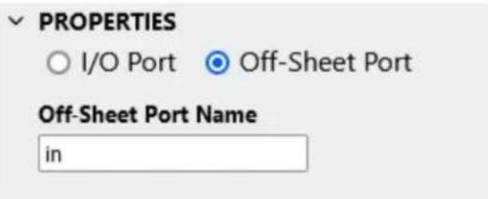
text_image
PROPERTIES ○ I/O Port ● Off-Sheet Port Off-Sheet Port Name inFor more information on hierarchical design, see 7. Using Hierarchical Modules.
2.1.2 Logic Gates
The building blocks of a configurable logic design.
The CLB Synthesizer provides a palette of common logic gates in the left hand panel.
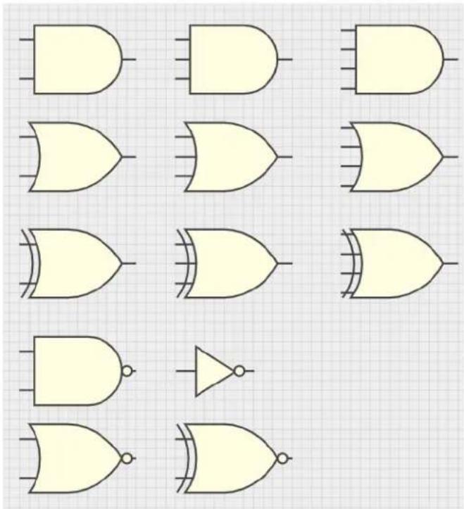
text_image
Diagram showing various logic gate symbols including NAND, OR, and NOT gates with corresponding labels.To use a logic gate, drag and drop the symbol from the palette onto the canvas and connect it as required.
Note: Input and output ports of logic gates must not be left unconnected.
2.1.3 Flip-Flops
Building blocks for synchronous logic designs.
The CLB Synthesizer provides four basic flop-flops to use in synchronous designs.
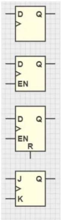
text_image
D Q EN D Q EN R J Q KNotes:
• The CLB architecture has only one type of flip-flop, identical to its BLEs.
- It is not possible to provide an input clock to any flip-flops. For more information, refer to 9.1. Clocking the Configurable Logic Block.
2.1.4 Multiplexers
Switching between signals.
The CLB Synthesizer provides two multiplexers (muxes) for use in logic designs - one with a single-bit select input and one with a two-bit select input.
text_image
3 2 1 0 S0 S1 1 0Note: The CLB architecture does not contain actual MUXes - these are implemented in the CLB by LUTs.
2.1.5 Look-up Tables
Manually configured logic functions.
The CLB Synthesizer provides a four-bit LUT implementation.
text_image
A B C D LUT Q 2482To use the LUT, drag and drop the LUT symbol onto the canvas and set the output (Q) states in the properties panel according to the required logic function.
PROPERTIES
| DCBA | Q |
| 0000 | 0 |
| 0001 | 1 |
| 0010 | 0 |
| 0011 | 0 |
| 0100 | 0 |
| 0101 | 0 |
| 0110 | 0 |
| 0111 | 1 |
| 1000 | 0 |
| 1001 | 0 |
| 1010 | 1 |
| 1011 | 0 |
| 1100 | 0 |
| 1101 | 1 |
| 1110 | 0 |
| 1111 | 0 |
Note: Although the CLB architecture consists of four input LUTs, it is no guarantee that a manually entered LUT will be implemented entirely in one BLE LUT in the same way it was drawn. The synthesis process will always produce the logic equivalent to this LUT, which may be simplified or distributed over several actual BLEs.
2.1.6 Constants
A source of a fixed signal.
The CLB Synthesizer provides several ways to give a fixed signal to an input:
- Individual constant output bits can be connected to inputs
- Multi-signal constants
text_image
0:1 1:0 2:1 3:0 0x5- Configure the number of bits and their values in the properties panel
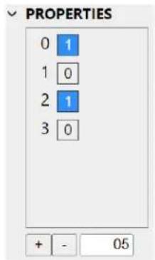
text_image
0 1 1 0 2 1 3 0 + - 05- A Zero port can also be used to provide a constant by using an input MUX position
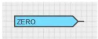
text_image
ZERONote: Although constants can be useful in many cases, they can also be a source of problems. The input logic is optimized into a logical equivalent during the synthesis process. When using constants, this has a major impact. The "zero port" is an exception since it is treated as any other input signal with an unknown value. For more information, see 9.5. Synthesis and Place-and-Route Process.
2.1.7 Net Labels
Using the same signal in many places in a design.
A netlabel component dispenses a signal to be used in several places in a logic design, which can increase the readability of a schematic by reducing the number of crossing lines.
For example, then inverted CLBIN1PPS signal is used immediately (connection not shown) and routed to a netlabel SWITCH.

text_image
CLBIN1PPS SWITCHThe SWITCH signal can then be used elsewhere in the design as a source.
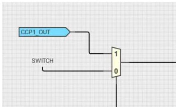
flowchart
graph TD
    A["CCP1_OUT"] --> B["1"]
    C["SWITCH"] --> B
    B --> D["Output"]
2.2 Drawing a Basic Schematic
How to get started with a logic design.
The CLB Synthesizer GUI simplifies the process of creating a logic design.
Step 1: Add and configure logic input sources
- Drag-and-drop an input port from the left side panel onto the canvas

- Select the input port and configure its source properties in the right-hand panel

text_image
PROPERTIES I/O Port Off-Sheet Port Input Ports Filter search CLBIN0PPS CLBIN1PPS CLBIN2PPS CLBIN3PPS FOSC HFINTOSC- Repeat as needed
Step 2: Add and configure logic outputs
- Drag and drop an output port from the left side panel onto the canvas

- Select the output port and configure its destination properties in the right-hand panel

text_image
PROPERTIES I/O Port Off-Sheet Port Output Ports Filter search PPS_OUT0 PPS_OUT1 PPS_OUT2 PPS_OUT3 PPS_OUT4 PPS_OUT5- Repeat as needed
Step 3: Add logic content
- Drag and drop logic gates, flip-flops, multiplexers, LUTs and constants from the palette on the left side panel onto the canvas
text_image
CLBIN2PPS PPS_OUT1- Connect them up by dragging connections from outputs to inputs, or vice versa
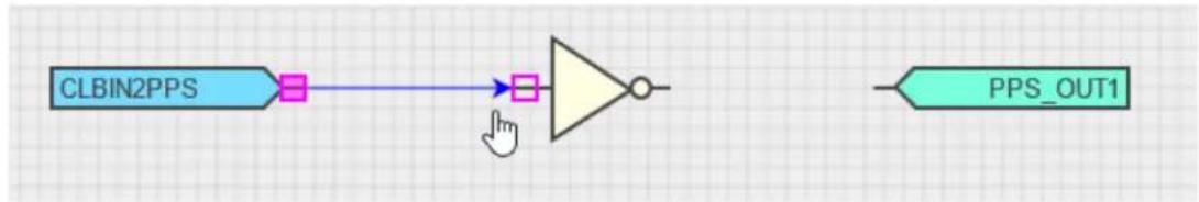
flowchart
graph LR
    A["CLBIN2PPS"] --> B["Square"]
    B --> C["Square"]
    C --> D["Inverter"]
    D --> E["Circle"]
    F["PPS_OUT1"] --> G["Square"]
    G --> H["Arrow to C"]
    style A fill:#FFD700,stroke:#333
    style F fill:#FF6347,stroke:#333
- Add comments for future understanding
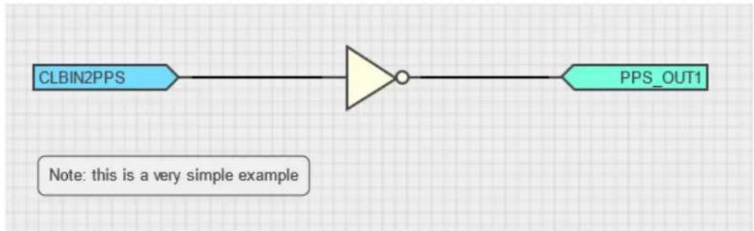
flowchart
graph LR
    A["CLBIN2PPS"] --> B((NOT gate))
    B --> C["PPS_OUT1"]
Step 4: Synthesize
- Click the Synthesize button, and the logic design is converted into a bitstream using a Microchip online service
3. Status of the Synthesis Process
Understanding the synthesis status indicator
A synthesis process converts a logic design into bitstream form which can be loaded into the CLB. This is triggered by clicking the Synthesize button.
The outcome of the synthesis process is indicated by the status indicator and the resource view.
Successful Synthesis
A green indicator will show when the synthesis succeeds and the resource view is updated.
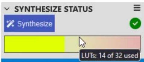
text_image
SYNTHESIZE STATUS Synthesize LUTs: 14 of 32 usedThe resource view indicates how much of the CLBs resources have been used, and hovering the mouse over it gives additional information.
Failed Synthesis
A red indicator will show when synthesis has failed.

text_image
SYNTHESIZE STATUS SynthesizeThe nature of the failure can be determined by:
- Checking the problems/notifications panels for warnings about unconnected pins
- Downloading the ZIP and checking the backend log output. This must also be included when consulting Microchip support channels.

Tip: Selecting the entry in the Problems panel highlights the component or port that is causing the problem.
Resource Usage Debugging
Resource allocation when using the CLB Synthesizer is done by the place and route algorithm in the backend synthesis process. Determining the reason for failure can be complicated, since there are some resources which are locked to individual BLE outputs or a range of BLE outputs. Therefore, a small logic design cannot be synthesized if these resources are in conflict (technically this is a failure to complete place-and-route). In cases where synthesis fails, these actions can be taken to try to alleviate the conflict and reach a solution:
- Try to use alternative outputs (eg: change IRQ0 to IRQ1)
- Try to remove some logic functionality
- Check that there are no unused modules included in the documents
- Check that there are no logic functions with pre-determined outputs (eg: a constant zero as an input to an AND gate)
When contacting Microchip support, include the ZIP file which was returned from the failing synthesis process.
4. Tips and Tricks
Productivity tips and tricks for the CLB Synthesizer.
4.1 How to Make use of Limited Display Resources
Tips for using small displays.
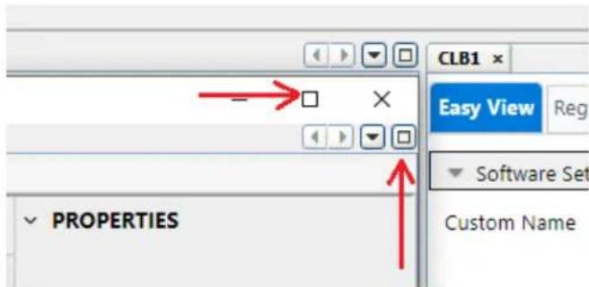
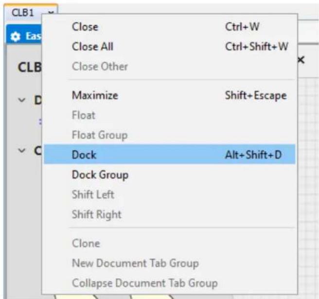
When using the CLB Synthesizer inside MCC the amount of display real-estate available for logic drawings becomes constrained. It is possible to float the logic editor view to mitigate this.
Right click on the CLB1 tab and select Float from the menu.
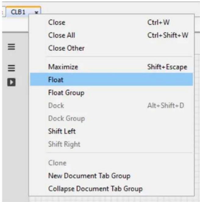
text_image
CLB1 Close Ctrl+W Close All Ctrl+Shift+W Close Other Maximize Shift+Escape Float Float Group Dock Alt+Shift+D Dock Group Shift Left Shift Right Clone New Document Tab Group Collapse Document Tab GroupThe CLB1 tab can then be moved onto an additional display or maximized on the current display by clicking one of the maximize buttons at the top of the window.
text_image
CLB1 Easy View Reg ▼ Software Set Custom Name PROPERTIESTo restore the layout right-click on the CLB1 tab and select Dock from the menu.

CLB1 - Editor
text_image
CLB1 Close Ctrl+W Close All Ctrl+Shift+W Close Other Maximize Shift+Escape Float Float Group Dock Alt+Shift+D Dock Group Shift Left Shift Right Clone New Document Tab Group Collapse Document Tab GroupIt is also possible to toggle the side and lower panels on and off using the control on the upper right side of the editor window:

- The left control toggles on and off the component palette to the left of the editor window
- The middle control toggles on and off the problems panel at the bottom of the editor window
- The right control toggles on and off the properties panel to the right of the editor window
4.2 Tidying up a Design
Making a logic design orderly and readable.
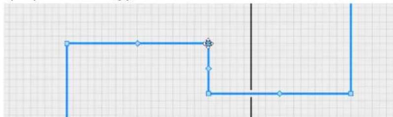
Making connections between components on the canvas is a simple process of connecting a source to a sink. The signal drawn on the schematic usually follows the shortest route by default, but can be manually edited to make a schematic design more readable. This process may require some practice and follows these main concepts:
- Selecting a signal will show what nodes are available for altering the path it takes. Elbow nodes are shown as squares and are used to move the node itself, while and mid-point nodes are diamond-shaped, and are used to split a line into additional segments.

natural_image
Pure geometric line diagram with no text, numbers, or symbols- Hovering over a elbow node indicates which axes are available for altering the location of that node. Dragging this node in one of the indicated directions will move the location of that node.

natural_image
Pure geometric lines forming an angle on grid paper (no text or symbols)• Hovering over a mid-point always shows that is can be moved (split) in any direction
natural_image
Pure decorative symbol with a central cross-like motif and horizontal blue line on grid background (no text or symbols)- Dragging a mid-point node splits the section into two segments and moves the location of the split-point accordingly
natural_image
Pure geometric line diagram with no text, numbers, or symbols on grid paper (no text or symbols)- Split segments can be joined by manually aligning the two segments by dragging the elbow node - dragging the mid-point will create an additional split
The following methods can also be used to create a more orderly schematic design:
- Modules: by extracting functional parts of a design into separate documents, a logic design can be divided into several hierarchical layers. This not only makes the top-level (main) schematic more tidy and readable, but allows the modules to be used multiple times in the same design without duplication. For more information, see 7. Using Hierarchical Modules.
- Net labels: if the same signal needs to be used on opposite sides of a schematic a net label can be used instead of drawing a wire across the schematic. For more information, see 2.1.7. Net Labels.
- Input ports can be duplicated in cases where the same input signal is required in multiple places. This may help to reduce congestion of signals, but may reduce maintainability.
Note: It is possible to use the same input more than once with a different input synchronizer setting on each instance.
- Rotate and flip: all components can be rotated and flipped so that they can be aligned to suit the signals they are connected to. Right-click a component or port on the canvas and select the function from the context menu, or select the item and use shortcut keys 'R' (rotate), 'X' (horizontal flip) or 'Y' (vertical flip).
- Comments: adding comments to a schematic improves readability and can be used to add context to the design itself.
5. Interacting with Peripherals and the CPU
How to make connections between the CLB, CPU and other peripheral modules.
5.1 Interacting with Peripherals
Interaction with other peripherals is done by using the input ports from other peripherals and output ports to other peripherals in a logic design. Consult the device datasheet for information on how these signals are used by the corresponding peripheral.
5.1.1 Input Synchronizers
Making use synchronizers on input signals
The CLB peripheral includes 16 input sources, which connects the CLB to external signals, in addition to the 32 CLBSWIN signals for interacting with the CPU. The 16 input sources include modifiers which can be used to condition the incoming signal before it enters the BLE matrix.
Input synchronizer options are selected on the right side properties panel below the input port source selection box.
Input Synchronizer options
Synchronized input (default)
Direct input
Positive edge detector
Negative edge detector
The available input synchronizer options are shown in the following table:
Table 5-1. Input Synchronizer Options
| Option Description | |
| Synchronized input The input signal will be synchronized to the CLB clock. This is the default, and the safest option when unsure. | |
| Direct input Synchronization is bypassed, and the input signal is connected directly to the BLE input.This must be used with caution as it can cause metastability in sequential logic designs. | |
| Positive edge detector A rising edge on the input signal will generate a pulse synchronized to the CLB clock | |
| Negative edge detector A falling edge on the input signal will generate a pulse synchronized to the CLB clock | |
Notes:
- The CLBSWIN signals cannot pass through the input synchronizers
- The input synchronizer is selected in hardware with three configuration bits, but not all eight possible permutations are made available in the CLB Synthesizer
5.1.2 CLB Outputs to other Peripherals
How to route signals from the CLB to other peripheral modules
The CLB BLE outputs can be connected to various other peripherals. This is a two-stage process:
Step 1: Configure an output from the CLB
In the CLB Synthesizer GUI, configure an output port by selecting the peripheral signal to route to in the port properties panel.

flowchart
graph LR
    A["CLBIN0PPS"] --> B["NOT"]
    B --> C["CLB_TMR1_GATE"]
    style B fill:#f9f,stroke:#333
    style C fill:#ccf,stroke:#333
Synthesize the logic design.
Step 2: Configure the peripheral to accept the signal from the CLB
The peripheral to which the CLB is connecting must be configured to accept the CLB input signal. This is Peripheral-dependent, consult the datasheet for more information.
The peripheral input selector usually specified a range of BLEs which can be used as inputs from the CLB. It is not up to the user to specify this - the place and route algorithm must hit one of these BLEs to satisfy the criteria to use the peripheral. The actual BLE which was realized during synthesis receives the synthesis output.
MCC Users
MCC will automatically unpack the output from the synthesis process and notify the user on how to configure the peripherals being connected to. Check the Notifications window after synthesis.
Web/Bare-Metal Users
Users of the web version need to download the ZIP output from the synthesis process and examine (or use directly) the contents of clb1_output_mappings.h file, which provides values for use in the peripheral configuration register.
5.2 Interacting with the CPU
Interaction between the CPU (running code) and the CLB using the CLBSWIN register.
5.2.1 Using CLBSWIN
How to use CLBSWIN from the MCU
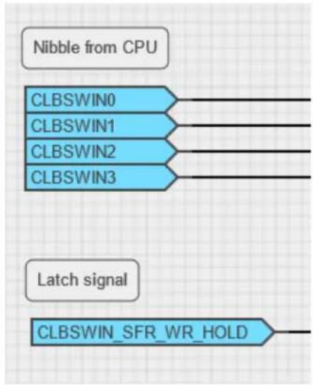
The CLB Software Input register (CLBSWIN) enables the MCU to communicate directly with the logic design in the CLB. So for example, this can be used to load a 'value' into the CLB at run time.
To make use of the CLBSWIN register within a logic design, simply use the individual CLBSWINn bits as input ports.
If a logic design needs to trigger an action when a new value is written to CLBSWIN, then the CLBSWIN_SFR_WR_HOLD input signal can be used. This signal is asserted when the CPU writes a new value to CLBSWIN and that value have been latched into the CLB.
CLB Synthesizer
Interacting with Peripherals and the
CPU
flowchart
graph TD
    A["Nibble from CPU"] --> B["CLBSWIN0"]
    A --> C["CLBSWIN1"]
    A --> D["CLBSWIN2"]
    A --> E["CLBSWIN3"]
    F["Latch signal"] --> G["CLBSWIN_SFR_WR_HOLD"]
Notes:
- The CLBSWIN register cannot be used via the input synchronizers
- The CLBSWIN_SFR_WR_HOLD signal is asserted only when the lower eight bits of CLBSWIN are written (CLBSWINL), so the byte must be written after writing the upper bytes in CLBSWIN
6. Storing and Retrieving Logic Designs
The circuit drawings and verilog content of your logic design can be saved to a file in json format
text_image
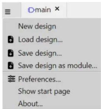
D main × New design Load design... Save design... Save design as module... Preferences... Show start page About...Load and save functionality is accessed from the left panel, in the main drawer-menu.
The entire content of a logic design can be stored to disk for later use by clicking the Save design button. When using the web version, this is a file download from the browser, and the file will be stored in the default download location for that browser. When using MCC, this file can be stored in a custom location.
To continue working with a previously saved logic design, the Load design button will open a file browser where the stored file can be selected and loaded.
The file extension is .clb, and its content is a json string including all content in the design.
7. Using Hierarchical Modules
Complex logic designs can increase their readability, and be reused by placing logic functions in modules, and then using that module elsewhere in the design.
Modules are defined as schematics or Verilog descriptions, which are managed in the documents section of the left panel.
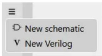
text_image
≡ D New schematic V New VerilogStep 1. Create a new module
• In the documents drawer-menu, select New schematic or New Verilog
- Give the module a suitable name
The module is added to the document list, and a new tab appears for its definition.
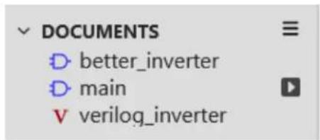
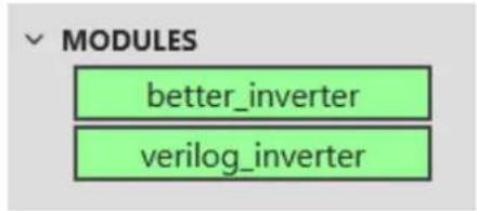
text_image
DOCUMENTS D better_inverter D main V verilog_inverterThe icon indicates which of the documents is the top-level document in the hierarchy.
Step 2a. Schematic module
- Draw the required logic for the module
- Add input and output ports accordingly using the Off-Sheet Port in the properties pane and giving them suitable names for the function of the module

text_image
PROPERTIES I/O Port Off-Sheet Port Off-Sheet Port Name in
flowchart
graph LR
    A["in"] --> B((△))
    B --> C["O"]
    C --> D["out"]
Step 2b. Verilog module
- Describe the module in Verilog
• The Verilog module must have the same name as the document
• Take care to define the module inputs and outputs
V verilog_inverter ✗
1 module verilog_inverter (in, out);
2    input in;
3    output out;
4    logic net2;
5    not U1 (net2, in);
6    assign out = net2;
7 endmodule
8
Step 3. Use the module
- When the module is complete and has no problems, switching back to the main/top-level document will update the modules list on the left side-bar
- Drag the new module onto the canvas
- Connect it up and use it
text_image
MODULES better_inverter verilog_inverter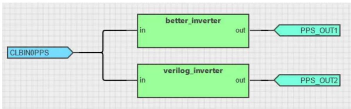
flowchart
graph TD
    A["CLBIN0PPS"] --> B["better_inverter"]
    A --> C["verilog_inverter"]
    B --> D["PPS_OUT1"]
    C --> E["PPS_OUT2"]

Tip: You can double-click a module to descend into its contents.
7.1 Using Verilog to Describe a Logic Design
Advanced users can make use of Verilog to describe their logic rather than drawing a logic circuit.
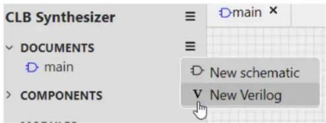
Step 1. Create a new Verilog document
- Click on the 'New Verilog' with 'V' symbol
- Name it as you like
text_image
CLB Synthesizer DOCUMENTS main COMPONENTS ≡ ≡ D main × D New schematic V New VerilogStep 2. Add your Verilog module
- Delete the long line with random numbers and letters (used for internal debugging)
- Give your module the same name as the document (step 1)
- Define inputs and outputs at the module level
- Add the 'code'
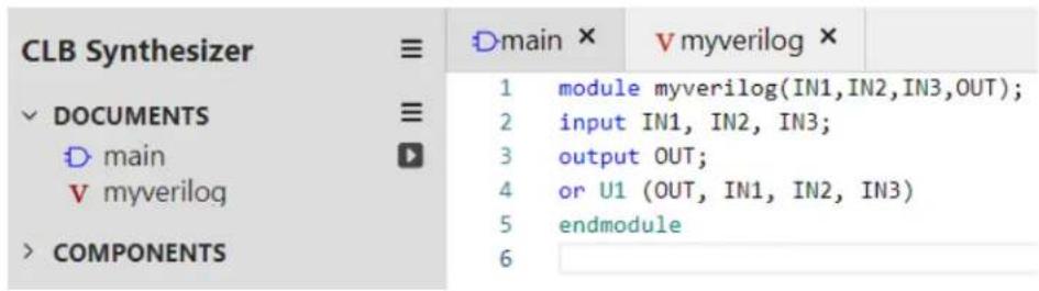
text_image
CLB Synthesizer DOCUMENTS main myverilog COMPONENTS D main × V myverilog × module myverilog(IN1,IN2,IN3,OUT); input IN1, IN2, IN3; output OUT; or U1 (OUT, IN1, IN2, IN3) endmoduleStep 3. Click on the main document tab, and select the Design side bar on the left
- Your Verilog module will appear under "modules"
- Drag it in and connect it up as any other logic symbol

flowchart
graph LR
    A["CLBIN0PPS"] --> B["myverilog"]
    C["IN1"] --> B
    D["IN2"] --> B
    E["IN3"] --> B
    B --> F["OUT"]
8. Libraries and Modules
Making a library of modules that can be easily re-used.
The CLB Synthesizer supports hierarchical designs which includes sub-sheets as either schematics or verilog. It is also possible to store these sub-sheets in a way that they can be reused in multiple designs or projects. A single functional item, which may itself be implemented across multiple sheets, is referred to as a module, and a collection of modules is referred to as a library.
8.1 The Built-In PIC16F131 Device Library
The hardware counter in the CLB is accessed by using a counter module in the built-in PIC16F131 Device Library.
Working with the built-in counter module is no different to working with a custom module from a custom library.
8.2 Using the Hardware Counter
How to work with the built-in hardware counter.
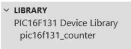
The CLB peripheral contains a dedicated 3-bit hardware counter. This is a convenient building block to use when, for example, implementing state machines. The counter has STOP and RESET inputs, which must be connected, and 8 one-hot outputs which can be used according to needs.
The counter is always available in the PIC16F131 Device Library in the Library section of the left side-bar.
text_image
LIBRARY PIC16F131 Device Library pic16f131_counterClick the + icon nect to the pic13f131_counter to add the counter to a design.
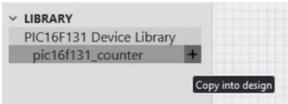
text_image
LIBRARY PIC16F131 Device Library pic16f131_counter + Copy into designOnce added to a design, it will appear as a module in the modules section of the left side-bar.

text_image
MODULES pic16f131_counterThe counter can now be placed onto the schematic canvas and connected up as required.

text_image
pic16f131_counter STOP COUNT_IS_0 RESET COUNT_IS_1 COUNT_IS_2 COUNT_IS_3 COUNT_IS_4 COUNT_IS_5 COUNT_IS_6 COUNT_IS_78.3 Using Modules from the Microchip Library
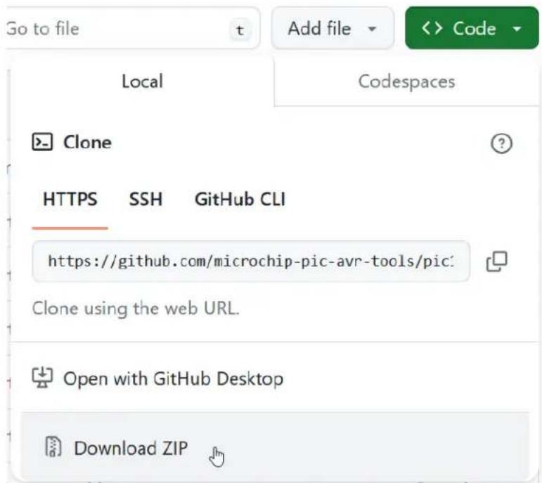
Microchip publishes a library of modules for the CLB Synthesizer on GitHub in the Microchip PIC&AVR Tools pages. This library includes counters, shifters and other utility functions that can be used in a logic design in the CLB Synthesizer.
Download the library from GitHub before it can be used in a logic design. To save the library to local storage, use the Download ZIP menu option in the Code drop-down menu.
text_image
Go to file t Add file Code Local Codespaces Clone HTTPS SSH GitHub CLI https://github.com/microchip-pic-avr-tools/pic Clone using the web URL. Open with GitHub Desktop Download ZIPFollow the procedure outlined in 8.4. Using Modules from a Custom Library to use a module from the library.
8.4 Using Modules from a Custom Library
Load a library into the CLB Synthesizer before its modules can be used in a design.
Note: The CLB Synthesizer currently supports only loading libraries from locally stored archives. First, download the library as a zip archive and store it locally to use the stored libraries in version control systems like GitHub.
To load a library to be used in a design:
-
Use the Load Library from file option on the drawer menu on the library section of the left-side panel.
-
Browse and select the library zip archive.
- The newly loaded library will appear as a new entry in the library section of the left-side panel. The individual modules included in that library are listed below the library.
- Click the + next to a module to include that module in the current design. It appears in the modules section, and the associated sheets and Verilog files appear in the documents section.
- Use the module by dragging the module representation from the modules section onto the canvas and connecting it as required in the design.
Note: A module included in a design is a copy of the module from the Library section, meaning that if the library source is changed, it has to be re-imported into the design. This also means that it is possible to use a module from a library and make changes to it after importing it without affecting the original library source.
8.5 Creating a Library with Modules
The re-used logic functionality designs can be saved as modules, which can be included in a library archive.
Step 1: Create the module using sub-sheets
Start with a new design in the CLB Synthesizer. Create at least one document in addition to main and sketch logic content or write Verilog to perform the function of the module. During this process the main schematic page (top-level) functions as a test bench. The entire module (all sub-sheets) and the test bench (main) must synthesize successfully before continuing.
This example:
- Creates a document called "myinverter"
- Uses off-sheet ports to invert signal 'a' to signal 'b'
- Uses the "myinverter" module in main and connects it to PPS ports as a test bench
• Synthesizes successfully

text_image
CLB Synthesizer DOCUMENTS main myinverter COMPONENTS unconfigured unconfigured D main × D myinverter × a b
flowchart
graph LR
    A["CLBIN0PPS"] --> B["myinverter"]
    B --> C["PPS_OUT1"]
Step 2: Remove the testbench
Before exporting a module, the test bench must be removed since it is not part of the module.
Click the trash can icon next to main in the documents section and remove it.

text_image
CLB Synthesizer ≡ DOCUMENTS ≡ main myinverter Delete this fileNote: The design will no longer synthesize successfully since it no longer has an entry point. This is the correct behaviour for creating a module.
Step 3: Save the module
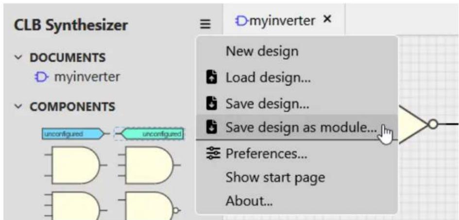
In the main drawer-menu in the CLB Synthesizer, select Save design as module
text_image
CLB Synthesizer DOCUMENTS myinverter COMPONENTS unconfigured unconfigured New design Load design... Save design... Save design as module... Preferences... Show start page About...Give the module an appropriate name.
This example saves the module as "myinverter.zip"
Save the module in a convenient place.
Step 4: Create a library structure
Create a new folder in a convenient place. This will be known as the "library folder".

Tip: The working folder can be in a git version control system if the library is to be distributed by browsing in the git repository. This is optional.

Important: When adding a new module to an existing library, skip this step.
Inside the library folder, create a new folder/directory with the same name as the module in a convenient place and copy the entire contents of the archive from 8.5. Step 3: Save the module into this folder. This includes a manifest, readme and one or more sheets.
Step 5: Document the library
In the library folder, create a new text file called manifest.json and add a manifest in this form, using a suitable name in the "name" field and a new GUID in the "id" field.
{
    "type": "CLB Synthesizer Library",
}
"formatversion": "1.0",
"name": "DemoLib",
"id": "xxxxxxxx-xxxx-xxxx-xxxx-xxxxxxxxxxxx",
"version": "1.0.0"
}

Attention: When adding a new module to an existing library, skip this step.

Important: A new library required a new GUID. Use an online tool to generate a globally unique ID.
Add a readme.md file and describe the library using markdown format.
Step 6: Document the module (optional)
Edit the readme.md to describe the module
Step 7: Create and test the library archive
Add all the content of the library folder to a new zip archive. Any name can be used here, but take care not to include the library folder itself inside the archive.
The resulting zip archive is now the library which contains the module.
To test it, start a new design in the CLB synthesizer and use the Load library from file option in the drawer-menu in the library section of the left-pane. The newly created library should appear, with the module inside it, ready to be used.
Step 8: Deployment of libraries
A library can be deployed in the simplest of ways by storing the archive zip file and distributing it.
Alternatively, the library folder from step 4 can be placed inside a version control system such as git. Note: The library zip archive itself should not be checked into version control, but rather the contents.
Once under version control, new modules can be added and module versions managed accordingly.
Users can download library archives using the web interface to the version control system as supported by most modern version control system interfaces. For example this is done in GitHub using the Download ZIP menu on the repository.
text_image
Go to file Add file Code Local Codespaces Clone HTTPS SSH GitHub CLI git@github.com:mraardvark/clblib.git Use a password-protected SSH key. Open with GitHub Desktop Download ZIP9. Advanced Topics
Additional reading for advanced users.
9.1 Clocking the Configurable Logic Block
How the CLB relates to clocks
The CLB peripheral receives its clock input from the source specified in the CLK field in the CLBCLK register which is written from the CPU. Consult the datasheet for available clock sources.
The CLB also includes a clock divider which must be configured along with the logic design, and is incorporated into the bitstream. The clock source can be divided by 1, 2, 4, 8, 16, 32, 64 or 128.
Note: The CLB clock divider is configured in the Easy View window inside MCC and the Global Settings panel in the Web version.
The CLB clock is distributed to all BLE flip-flops, so the entire logic design runs off the same clock. So although logic design schematics can include various flip-flop types, it is not possible to connect or configure an individual clock source.

natural_image
Pure electrical circuit symbol for a D flip-flop without any text or labels9.2 Preferences
The preferences panel is accessed via the main drawer-menu.
text_image
Preferences Synthesis backend URL https://logic.microchip.com/api/v2/synthesize Reset Localhost Synthesis settings Always allow synthesis View Show model Show HDL Show output OK Cancel| Option Description | |
| Synthesis backend URL | URL for the synthesis server. This should not be changed unless instructed to by Microchip support engineers. |
| Show model | The right-hand pane will show the "GUI model" of the current design - this is for internal debugging of the GUI. |
| Show HDL The right-hand pane will show the intermediate HDL of the current design. This content will be sent to the backend for synthesis - it is for internal debugging of the interface between GUI and backend. | |
| Show output The right-hand pane will show output from the synthesis engine - this is for internal debugging of the backend logic-synthesis engine. | |
9.3 Making Use of the Output ZIP
How to use the output
The synthesis process should always return a ZIP file with outputs.
Note: MCC users do not need to relate to the ZIP file contents.
The ZIP file is intended for the CLB Synthesizer Web version's users who want to convert a logic design into a bitstream.
The ZIP file contains a readme file which provides details about:
• The resultant bitstream
• A basic CLB driver for configuring the peripheral
- Build artefacts
For further details, read the readme inside the ZIP.
9.4 Description of Output Files
After synthesis, a ZIP file containing many build artifacts can be downloaded. The filename prefix (XXX) is determined by the server in some cases.
The files in the zip are intended for bare-metal users and/or for debugging purposes:
- Root folder: outputs for use in bare-metal projects
• Build folder: debug artifacts from the build process - Build/input folder: inputs passed into the server for processing
| Filename Description | |
| readme.txt Instructions for bare-metal users | |
| clb1.c; clb1.h Driver for configuring and enabling the CLB | |
| clb1_output_mappings.h | Header file defining output mappings from eh CLB to peripherals |
| bitstream.s Bitstream in assembler format for embedding into a bare-metal project | |
| input/*.v Verilog representation of input design | |
| input/*.xdc Mappings to physical pins | |
| input/project.json Top level description of the design | |
| input/stats.json | Statistical summary of the design |
| input/*.clb | Save-file for the design |
| XXX.inputs.json | List of design Inputs in json format |
| XXX.outputs.json | List of design outputs in json format |
| XXX.bitstream.output Declarations.json | Peripheral output mappings in json format |
| XXX.bitstream | Raw bitstream words |
| XXX.bitstream.json | Bitstream words in json format |
| XXX.result.json | Entire operation output summary as json |
| ......continued | |
| Filename Description | |
| XXX.json json formatted netlist output from Yosys | |
| XXX.v Verilog netlist output from Yosys (before place and route) | |
| XXX.netlist Binary form of netlist | |
| XXX.phys Binary form of physical netlist | |
| XXX.net Packed netlist in XML format | |
| XXX.net.post_routing Post-routing packed netlist in XML format | |
| XXX.place Placer output report | |
| XXX.route Router output report | |
| packaging_pin_util.rpt Packing pin usage report | |
| XXX.fasm Output from FASM stage | |
| XXX.svg Diagramatic representation output from Yosys (generic) | |
| XXX-2.svg Alternative diagramatic representation output from Yosys (generic) | |
| XXX.dot Input to svg above | |
| vpr_stdout.log Place and route output | |
| XXX.yosys.log | Log from Yosys synthesis stage |
| XXX.stderr.txt | Stderr output |
9.5 Synthesis and Place-and-Route Process
What goes on behind the scenes
Once an application has been captured in the CLB Synthesizer GUI, it needs to be converted into a configuration bitstream which can be loaded into the CLB module itself. This process is known as "synthesis", although it also includes place and route steps, and is done by Microchip's online web-service.
It is not necessary for a user to understand how this process works - a brief summary is given here for advanced or curious users.
How it works
- The schematic drawings of the CLB application are converted to equivalent Verilog descriptions which are then passed to the backend for processing.
- The first stage in the backend process is logic synthesis. Logic synthesis is a process of converting the Verilog textual representation of a logic design into a netlist which describes the hardware in equivalent logic gates and wires. Logic synthesis is done using Yosys Open SYNthesis Suite which is equipped with a plug-in that describes the actual structure of the logic elements in the CLB module. The output of the synthesis stage is a Verilog netlist.
- The next stage is place-and-route (PNR). During this stage the netlist elements are mapped into physical locations in the CLB array (placement), and interconnects are made between them (routing). This is a complex and iterative process, and is not guaranteed to achieve an outcome (eg: if space or routing constraints are exceeded). Place-and-route is done using the VPR provided by Verilog to Routing (VTR) which is equipped with a plug-in that describes the actual available interconnects within the CLB module. The output of the PNR stage is a FASM file, which specifies the CLB configuration content in a generic, plain-text format.
- The final stage is bitstream generation. The bitstream generator parses the FASM file and converts configuration of generic configurable logic resources into bit patterns in a bitstream according to the actual CLB bitstream implementation. The bitstream generator is a script which is specific to the Microchip CLB implementation. The output of the bitstream generator is a sequence of bits which are to be loaded into the CLB during configuration. This is embedded as
a sequence of data words (DW) which are stored as constants in flash by the compiler during building of the application.
10. Known Issues and Change Log
If you experience unexpected behavior, read the known issues list here.
The CLB Synthesizer toolchain comprises of:
- The synthesis engine (backend), hosted in the cloud
- CLB Synthesizer GUI hosted in the cloud at logic.microchip.com/clbsynthesizer/
- CLB Synthesizer GUI integrated into MCC, deployed via Content Manager
Find the latest changes for all of these components here.
11. Revision History
| Doc. Rev. Date Comments | ||
| A 04/2024 Initial document release | ||
Microchip Information
The Microchip Website
Microchip provides online support via our website at www.microchip.com/. This website is used to make files and information easily available to customers. Some of the content available includes:
- Product Support – Data sheets and errata, application notes and sample programs, design resources, user's guides and hardware support documents, latest software releases and archived software
- General Technical Support – Frequently Asked Questions (FAQs), technical support requests, online discussion groups, Microchip design partner program member listing
- Business of Microchip – Product selector and ordering guides, latest Microchip press releases, listing of seminars and events, listings of Microchip sales offices, distributors and factory representatives
Product Change Notification Service
Microchip's product change notification service helps keep customers current on Microchip products. Subscribers will receive email notification whenever there are changes, updates, revisions or errata related to a specified product family or development tool of interest.
To register, go to www.microchip.com/pcn and follow the registration instructions.
Customer Support
Users of Microchip products can receive assistance through several channels:
• Distributor or Representative
- Local Sales Office
- Embedded Solutions Engineer (ESE)
- Technical Support
Customers should contact their distributor, representative or ESE for support. Local sales offices are also available to help customers. A listing of sales offices and locations is included in this document.
Technical support is available through the website at: www.microchip.com/support
Microchip Devices Code Protection Feature
Note the following details of the code protection feature on Microchip products:
- Microchip products meet the specifications contained in their particular Microchip Data Sheet.
- Microchip believes that its family of products is secure when used in the intended manner, within operating specifications, and under normal conditions.
- Microchip values and aggressively protects its intellectual property rights. Attempts to breach the code protection features of Microchip product is strictly prohibited and may violate the Digital Millennium Copyright Act.
- Neither Microchip nor any other semiconductor manufacturer can guarantee the security of its code. Code protection does not mean that we are guaranteeing the product is "unbreakable". Code protection is constantly evolving. Microchip is committed to continuously improving the code protection features of our products.
Legal Notice
This publication and the information herein may be used only with Microchip products, including to design, test, and integrate Microchip products with your application. Use of this information in any other manner violates these terms. Information regarding device applications is provided only for your convenience and may be superseded by updates. It is your responsibility to ensure
that your application meets with your specifications. Contact your local Microchip sales office for additional support or, obtain additional support at www.microchip.com/en-us/support/design-help/client-support-services.
THIS INFORMATION IS PROVIDED BY MICROCHIP "AS IS". MICROCHIP MAKES NO REPRESENTATIONS OR WARRANTIES OF ANY KIND WHETHER EXPRESS OR IMPLIED, WRITTEN OR ORAL, STATUTORY OR OTHERWISE, RELATED TO THE INFORMATION INCLUDING BUT NOT LIMITED TO ANY IMPLIED WARRANTIES OF NON-INFRINGEMENT, MERCHANTABILITY, AND FITNESS FOR A PARTICULAR PURPOSE, OR WARRANTIES RELATED TO ITS CONDITION, QUALITY, OR PERFORMANCE.
IN NO EVENT WILL MICROCHIP BE LIABLE FOR ANY INDIRECT, SPECIAL, PUNITIVE, INCIDENTAL, OR CONSEQUENTIAL LOSS, DAMAGE, COST, OR EXPENSE OF ANY KIND WHATSOEVER RELATED TO THE INFORMATION OR ITS USE, HOWEVER CAUSED, EVEN IF MICROCHIP HAS BEEN ADVISED OF THE POSSIBILITY OR THE DAMAGES ARE FORESEEABLE. TO THE FULLEST EXTENT ALLOWED BY LAW, MICROCHIP'S TOTAL LIABILITY ON ALL CLAIMS IN ANY WAY RELATED TO THE INFORMATION OR ITS USE WILL NOT EXCEED THE AMOUNT OF FEES, IF ANY, THAT YOU HAVE PAID DIRECTLY TO MICROCHIP FOR THE INFORMATION.
Use of Microchip devices in life support and/or safety applications is entirely at the buyer's risk, and the buyer agrees to defend, indemnify and hold harmless Microchip from any and all damages, claims, suits, or expenses resulting from such use. No licenses are conveyed, implicitly or otherwise, under any Microchip intellectual property rights unless otherwise stated.
Trademarks
The Microchip name and logo, the Microchip logo, Adaptec, AVR, AVR logo, AVR Freaks, BesTime, BitCloud, CryptoMemory, CryptoRF, dsPIC, flexPWR, HELDO, IGLOO, JukeBlox, KeeLoq, Kleer, LANCheck, LinkMD, maXStylus, maXTouch, MediaLB, megaAVR, Microsemi, Microsemi logo, MOST, MOST logo, MPLAB, OptoLyzer, PIC, picoPower, PICSTART, PIC32 logo, PolarFire, Prochip Designer, QTouch, SAM-BA, SenGenuity, SpyNIC, SST, SST Logo, SuperFlash, Symmetricom, SyncServer, Tachyon, TimeSource, tinyAVR, UNI/O, Vectron, and XMEGA are registered trademarks of Microchip Technology Incorporated in the U.S.A. and other countries.
AgileSwitch, ClockWorks, The Embedded Control Solutions Company, EtherSynch, Flashtec, HyperSpeed Control, HyperLight Load, Libero, motorBench, mTouch, Powermite 3, Precision Edge, ProASIC, ProASIC Plus, ProASIC Plus logo, Quiet-Wire, SmartFusion, SyncWorld, TimeCesium, TimeHub, TimePictra, TimeProvider, and ZL are registered trademarks of Microchip Technology Incorporated in the U.S.A.
Adjacent Key Suppression, AKS, Analog-for-the-Digital Age, Any Capacitor, AnyIn, AnyOut, Augmented Switching, BlueSky, BodyCom, Clockstudio, CodeGuard, CryptoAuthentication, CryptoAutomotive, CryptoCompanion, CryptoController, dsPICDEM, dsPICDEM.net, Dynamic Average Matching, DAM, ECAN, Espresso T1S, EtherGREEN, EyeOpen, GridTime, IdealBridge, IGaT, In-Circuit Serial Programming, ICSP, INICnet, Intelligent Paralleling, IntelliMOS, Inter-Chip Connectivity, JitterBlocker, Knob-on-Display, MarginLink, maxCrypto, maxView, memBrain, Mindi, MiWi, MPASM, MPF, MPLAB Certified logo, MPLIB, MPLINK, mSiC, MultiTRAK, NetDetach, Omniscient Code Generation, PICDEM, PICDEM.net, PICkit, PICtail, Power MOS IV, Power MOS 7, PowerSmart, PureSilicon, QMatrix, REAL ICE, Ripple Blocker, RTAX, RTG4, SAM-ICE, Serial Quad I/O, simpleMAP, SimpliPHY, SmartBuffer, SmartHLS, SMART-I.S., storClad, SQL, SuperSwitcher, SuperSwitcher II, Switchtec, SynchroPHY, Total Endurance, Trusted Time, TSHARC, Turing, USBCheck, VariSense, VectorBlox, VeriPHY, ViewSpan, WiperLock, XpressConnect, and ZENA are trademarks of Microchip Technology Incorporated in the U.S.A. and other countries.
SQTP is a service mark of Microchip Technology Incorporated in the U.S.A.
The Adaptec logo, Frequency on Demand, Silicon Storage Technology, and Symmcom are registered trademarks of Microchip Technology Inc. in other countries.
GestIC is a registered trademark of Microchip Technology Germany II GmbH & Co. KG, a subsidiary of Microchip Technology Inc., in other countries.
All other trademarks mentioned herein are property of their respective companies.
© 2024, Microchip Technology Incorporated and its subsidiaries. All Rights Reserved.
ISBN: 978-1-6683-4156-8
Quality Management System
For information regarding Microchip's Quality Management Systems, please visit www.microchip.com/quality.
AMERICAS ASIA/PACIFIC ASIA/PACIFIC EUROPE
| Corporate Office | Australia - Sydney | India - Bangalore | Austria - Wels |
| 2355 West Chandler Blvd. | Tel: 61-2-9868-6733 | Tel: 91-80-3090-4444 | Tel: 43-7242-2244-39 |
| Chandler, AZ 85224-6199 | China - Beijing | India - New Delhi | Fax: 43-7242-2244-393 |
| Tel: 480-792-7200 | Tel: 86-10-8569-7000 | Tel: 91-11-4160-8631 | Denmark - Copenhagen |
| Fax: 480-792-7277 | China - Chengdu | India - Pune | Tel: 45-4485-5910 |
| Technical Support: | Tel: 86-28-8665-5511 | Tel: 91-20-4121-0141 | Fax: 45-4485-2829 |
| www.microchip.com/support | China - Chongqing | Japan - Osaka | Finland - Espoo |
| Web Address: | Tel: 86-23-8980-9588 | Tel: 81-6-6152-7160 | Tel: 358-9-4520-820 |
| www.microchip.com | China - Dongguan | Japan - Tokyo | France - Paris |
| Atlanta | Tel: 86-769-8702-9880 | Tel: 81-3-6880-3770 | Tel: 33-1-69-53-63-20 |
| Duluth, GA | China - Guangzhou | Korea - Daegu | Fax: 33-1-69-30-90-79 |
| Tel: 678-957-9614 | Tel: 86-20-8755-8029 | Tel: 82-53-744-4301 | Germany - Garching |
| Fax: 678-957-1455 | China - Hangzhou | Korea - Seoul | Tel: 49-8931-9700 |
| Austin, TX | Tel: 86-571-8792-8115 | Tel: 82-2-554-7200 | Germany - Haan |
| Tel: 512-257-3370 | China - Hong Kong SAR | Malaysia - Kuala Lumpur | Tel: 49-2129-3766400 |
| Boston | Tel: 852-2943-5100 | Tel: 60-3-7651-7906 | Germany - Heilbronn |
| Westborough, MA | China - Nanjing | Malaysia - Penang | Tel: 49-7131-72400 |
| Tel: 774-760-0087 | Tel: 86-25-8473-2460 | Tel: 60-4-227-8870 | Germany - Karlsruhe |
| Fax: 774-760-0088 | China - Qingdao | Philippines - Manila | Tel: 49-721-625370 |
| Chicago | Tel: 86-532-8502-7355 | Tel: 63-2-634-9065 | Germany - Munich |
| Itasca, IL | China - Shanghai | Singapore | Tel: 49-89-627-144-0 |
| Tel: 630-285-0071 | Tel: 86-21-3326-8000 | Tel: 65-6334-8870 | Fax: 49-89-627-144-44 |
| Fax: 630-285-0075 | China - Shenyang | Taiwan - Hsin Chu | Germany - Rosenheim |
| Dallas | Tel: 86-24-2334-2829 | Tel: 886-3-577-8366 | Tel: 49-8031-354-560 |
| Addison, TX | China - Shenzhen | Taiwan - Kaohsiung | Israel - Ra'anana |
| Tel: 972-818-7423 | Tel: 86-755-8864-2200 | Tel: 886-7-213-7830 | Tel: 972-9-744-7705 |
| Fax: 972-818-2924 | China - Suzhou | Taiwan - Taipei | Italy - Milan |
| Detroit | Tel: 86-186-6233-1526 | Tel: 886-2-2508-8600 | Tel: 39-0331-742611 |
| Novi, MI | China - Wuhan | Thailand - Bangkok | Fax: 39-0331-466781 |
| Tel: 248-848-4000 | Tel: 86-27-5980-5300 | Tel: 66-2-694-1351 | Italy - Padova |
| Houston, TX | China - Xian | Vietnam - Ho Chi Minh | Tel: 39-049-7625286 |
| Tel: 281-894-5983 | Tel: 86-29-8833-7252 | Tel: 84-28-5448-2100 | Netherlands - Drunen |
| Indianapolis | China - Xiamen | Tel: 31-416-690399 | |
| Noblesville, IN | Tel: 86-592-2388138 | Fax: 31-416-690340 | |
| Tel: 317-773-8323 | China - Zhuhai | Norway - Trondheim | |
| Fax: 317-773-5453 | Tel: 86-756-3210040 | Tel: 47-72884388 | |
| Tel: 317-536-2380 | Poland - Warsaw | ||
| Los Angeles | Tel: 48-22-3325737 | ||
| Mission Viejo, CA | Romania - Bucharest | ||
| Tel: 949-462-9523 | Tel: 40-21-407-87-50 | ||
| Fax: 949-462-9608 | Spain - Madrid | ||
| Tel: 951-273-7800 | Tel: 34-91-708-08-90 | ||
| Raleigh, NC | Fax: 34-91-708-08-91 | ||
| Tel: 919-844-7510 | Sweden - Gothenberg | ||
| New York, NY | Tel: 46-31-704-60-40 | ||
| Tel: 631-435-6000 | Sweden - Stockholm | ||
| San Jose, CA | Tel: 46-8-5090-4654 | ||
| Tel: 408-735-9110 | UK - Wokingham | ||
| Tel: 408-436-4270 | Tel: 44-118-921-5800 | ||
| Canada - Toronto | Fax: 44-118-921-5820 | ||
| Tel: 905-695-1980 | |||
| Fax: 905-695-2078 |