203 - Memory Card Cactus - Free user manual and instructions
Find the device manual for free 203 Cactus in PDF.

User questions about 203 Cactus
0 question about this device. Answer the ones you know or ask your own.
Ask a new question about this device
Download the instructions for your Memory Card in PDF format for free! Find your manual 203 - Cactus and take your electronic device back in hand. On this page are published all the documents necessary for the use of your device. 203 by Cactus.
USER MANUAL 203 Cactus
203 Series Industrial
Grade 2.5" FlashDrive
Product Manual
Cactus Technologies Limited
Suite C, 15/F, Capital Trade Center
62 Tsun Yip Street, Kwun Tong
Kowloon, Hong Kong
Tel: +852-2797-2277
Email:sales@cactus-tech.com
Cactus USA
3112 Windsor Road
Suite A356
Austin, Texas 78703
Tel:+512-775-0746
Email:americas@cactus-tech.com
Cactus-Tech.com
The information in this manual is believed to be accurate at the time of publication but is subject to change without notice. Cactus Technologies® Limited shall not be liable for technical or editorial errors or omissions contained herein; nor for incidental or consequential damages resulting from the furnishing, performance, or use of this material.
Cactus Technologies® makes no warranty, representation or guarantee regarding the suitability of its products for any particular purpose, nor does Cactus Technologies® assume any liability arising out of the application or use of its products, and specifically disclaims any and all liability, including without limitation consequential or incidental damages.
Cactus Technologies® products are not designed, intended or authorized for use as components in systems intended for surgical implant into the body or in other applications intended to support or sustain life or for any application where the failure of a Cactus Technologies® product can result in personal injury or death. Users of Cactus Technologies® products for such unintended and unauthorized applications shall assume all risk of such use and shall indemnify and hold Cactus Technologies® and its officers, employees, subsidiaries, affiliates and distributors harmless against all claims, costs, damages, expenses and attorney fees arising out of, directly or indirectly, any claim of personal injury or death associated with such unintended and unauthorized use, even if such claim alleges that Cactus Technologies® was negligent regarding the design or manufacture of the part.
All parts of the Cactus Technologies® documentation are protected by copyright law and all rights are reserved. This documentation may not, in whole or in part, be copied, photocopied, reproduced, translated, or reduced to any electronic medium or machine-readable form without prior consent, in writing, from Cactus Technologies®, Limited.
© 2005-2013 Cactus Technologies Limited. All rights reserved.
Table of
CONTENTS
Cactus®
Technologies
1. Introduction to Cactus Technologies 203 Series
Industrial Grade FlashDrive Products 1
1.1.Supported Standards....2
1.2.Product Features 2
1.2.1.Host and Technology Independence.... 2
1.2.2.Defect and Error Management 2
1.2.3.Intelligent Power Management.... 3
1.2.4.Power Supply Requirements 3
2. Product Specifications
2.1.System Environmental Specifications 4
2.2.System Power Requirements....4
2.3.System Performance....5
2.4.System Reliability....5
2.5.Physical Specifications 5
2.5.1.2.5" SSD Physical Specifications....6
2.6.Capacity Specifications 7
2.6.1.2.5" SSD Capacity Specifications 7
3. Interface Description
3.1.SSD Pin Assignments and Pin Type 8
3.2.Signal Description....9
3.3.Electrical Specification 11
3.3.1. Absolute Maximum Ratings ...... 11
3.3.2.DC Characteristics....11
3.3.3.I/O Read (Input) Timing Specification....12
3.3.4.I/O Write (Output) Timing Specification 14
3.3.4.1.Deskewing....15
3.3.4.2.PIO Transfer Timing....15
3.3.4.3.DMA Transfer Timing 17
3.4.I/O Transfer Function 18
4. ATA Drive Register Set Definition and Protocol
4.1.Task File Addressing....19
4.2.ATA Registers 20
4.2.1.Data Register (Address—1F0[170])....20
4.2.2.Error Register (Address—1F1[171]; Read Only) 20
4.2.3.Feature Register (Address—1F1[171]; Write Only)....20
4.2.4.Sector Count Register (Address—1F2[172]) 20
4.2.5.Sector Number (LBA 7-0) Register (Address—1F3[173])....21
4.2.6.Cylinder Low (LBA 15-8) Register (Address—1F4[174])......21
4.2.7.Cylinder High (LBA 23-16) Register (Address—1F5[175])......21
4.2.8.Drive/Head (LBA 27-24) Register (Address 1F6[176])....21
4.2.9. Status and Alternate Status Registers
Table of
CONTENTS
Cactus®
Technologies
(Address 1F7[177] and 3F6[376]) 22
4.2.10.Device Control Register (Address—3F6[376]) 22
4.2.11.Card (Drive) Address Register (Address 3F7[377])....23
5. ATA Command Description 25
5.1. ATA Command Set....25
5.1.1.Check Power Mode-98H, E5H 26
5.1.2.Execute Drive Diagnostic-90H 27
5.1.3.Erase Sector(s)-COH 27
5.1.4.Format Track-50H 27
5.1.5.Identify Drive-ECH....28
5.1.5.1.Word 0: General Configuration....29
5.1.5.2.Word 1: Default Number of Cylinders....29
5.1.5.3.Word 3: Default Number of Heads....29
5.1.5.4.Word 4: Number of Unformatted Bytes per Track 29
5.1.5.5.Word 5: Number of Unformatted Bytes per Sector 29
5.1.5.6.Word 6: Default Number of Sectors per Track....29
5.1.5.7.Words 7-8: Number of Sectors per Drive....30
5.1.5.8.Words 10-19: Drive Serial Numbers 30
5.1.5.9.Word 20: BufferType 30
5.1.5.10.Word 21: Buffer Size....30
5.1.5.11.Word 22: ECC Count 30
5.1.5.12.Words 23-26: Firmware Revision 30
5.1.5.13.Words 27-46: Model Number....30
5.1.5.14.Word 47: Read/Write Multiple Sector Count....30
5.1.5.15.Word 48: Double Word Support 30
5.1.5.16.Word 49: Capabilities 30
5.1.5.17.Word 51: PIO Data Transfer Cycle Timing Mode ....30
5.1.5.18.Word 52: Single Word DMA Data Transfer Cycle Timing Mode ......31
5.1.5.19.Word 53: Translation Parameters Valid 31
5.1.5.20.Words 54-56: Current Number of Cylinders, Heads, Sectors/Tracks .....31
5.1.5.21.Words 57-58: Current Capacity 31
5.1.5.22.Word 59: Multiple Sector Setting 31
5.1.5.23.Words 60-61: Total Sectors Addressable in LBA Mode 31
5.1.5.24.Word 64: Advanced PIO Transfer Modes Supported 31
5.1.6.Idle-97H, E3H 32
5.1.7.Idle Immediate-95H, E1H 32
5.1.8. Initialize Drive Parameters-91H 32
5.1.9.Read Buffer-E4H 33
5.1.10.Read Multiple-C4H....33
5.1.11.Read Long Sector-22H, 23H....34
5.1.12.Read Sector(s)-20H, 21H 34
5.1.13.Read Verify Sector(s)-40H, 41H 35
5.1.14. Recalibrate-1XH 36
5.1.15.Request Sense-03H 36
5.1.16.Seek-7XH 37
5.1.17.Set Features-EFH 37
5.1.18.Set Multiple Mode-C6H 38
Table of
CONTENTS
Cactus®
Technologies
5.1.19.Set Sleep Mode-99H, E6H 39
5.1.20.Standby-96H, E2H 39
5.1.21.Standby Immediate-94H, E0H 39
5.1.22. Translate Sector-87H....40
5.1.23.Wear Level-F5H 40
5.1.24.Write Buffer-E8H....40
5.1.25.Write Long Sector-23H, 33H 41
5.1.26.Write Multiple Command-CH5....41
5.1.27.Write Multiple without Erase-CDH....42
5.1.28.Write Sector(s)-30H, 31H....43
5.1.29.Write Sector(s) without Erase-38H....43
5.1.30. Write Verify Sector(s)-3CH 44
5.2.Error Posting 44
Appendix A.Ordering Information....46
Appendix B. Technical Support Services 47
Appendix C.Cactus Technologies® Worldwide Sales Offices....48
Appendix D. Limited Warranty....49
Introduction to Cactus Technologies 203 Series Industrial Grade FlashDrive Products

Features
- Solid state design with no moving parts
- Industry standard 2.5" IDE Drive form factor
• Supports ATA PIO Modes 0-4
• Supports MultiWord DMA Modes 0-2
• High reliability, MTBF > 4,000,000 hrs. - Enhanced error correction, < 1 error in 10^4 bits read
- Intelligent power management to reduce power consumption
• Dual voltage support: 3.3V/5.0V
Overview
The Cactus Technologies 2.5" Solid State Drive(SSD) is a high capacity solidstate flash memory product that complies with the ANSI ATA standard and is electrically compatible with an IDE disk drive. Cactus SSDs provide up to 16GB of formatted storage capacity in the 2.5" IDE form factor.
The Cactus Technologies Industrial Grade SSD products use high quality flash memory from well known vendors, such as Samsung Corporation. In addition, it include an ondrive intelligent controller that manages interface protocols, data storage and retrieval as well as ECC, defect handling and diagnostics, power management, and clock control. The controller's firmware is upgradeable, thus allowing feature enhancements and firmware updates in the field.
1.1. Supported Standards
Cactus Technologies 2.5" SSD is fully electrically compatible with the following specification:
• ATA 5 Specification published by ANSI: X3.221 AT Attachment Interface for Disk Drives
1.2. Product Features
Cactus Technologies Industrial SSD contains a high level, intelligent controller. This intelligent controller provides many capabilities including the following:
- Standard ATA register and command set (same as found on most magnetic disk drives).
- Manages details of erasing and programming flash memory independent of the host system
- Sophisticated defect managing capabilities (similar to magnetic disk drives).
- Sophisticated system for error recovery using powerful error correction code (ECC).
- Intelligent power management for low power operation.
1.2.1. Host and Technology Independence
Cactus Technologies Industrial SSD appears as a standard ATA disk drive to the host system. The drive utilizes a 512byte sector which is the same as that in an IDE magnetic disk drive. To write or read a sector (or multiple sectors), the host computer software simply issues an ATA Read or Write command to the drive as per the ATA protocol. The host software then waits for the command to complete. The host system does not get involved in the details of how the flash memory is erased, programmed or read as this is all managed by the builtin controller in the drive. Also, with the intelligent onboard controller, the host system software will not require changing as new flash memory evolves. Thus, systems that support the Cactus Technologies Industrial SSD products today will continue to work with future Cactus Technologies Industrial SSDs built with new flash technology without having to update or change host software.
1.2.2. Defect and Error Management
Cactus Technologies Industrial SSD contains a sophisticated defect and error management system similar to those found in magnetic disk drives. The defect management is completely transparent to the host and does not consume any user data space.
The soft error rate for Cactus Technologies Industrial SSDs is much lower than that of magnetic disk drives. In the extremely rare case where a read error does occur, the drive has sophisticated ECC to recover the data.
These defect and error management systems, coupled with the solid-state construction, give Cactus Technologies Industrial SSDs unparalleled reliability.
1.2.3. Intelligent Power Management
Cactus Technologies SSDs employ sophisticated power management algorithms to conserve power. Upon completion of a command, the drive will automatically enter sleep mode if no further commands are received. In most situations, the drive will be in sleep mode except when the host is accessing it, thus conserving power.
When the drive is in sleep mode, any command issued to the drive will cause it to exit sleep and respond.
1.2.4. Power Supply Requirements
Cactus Technologies Industrial SSD is a dual voltage product, which means it will operate at a voltage range of 3.30 volts ±10% or 5.00 volts ±10%.
For all the following specifications, values are defined at ambient temperature and nominal supply voltage unless otherwise stated.
2.1. System Environmental Specifications
Table 2-1. Environmental Specifications
| [X604] Temperature | Operating: | 0°C to +70°C (Standard)-45°C to +90°C (Extended) |
 Humidity Humidity | Operating & Non-Operating: | 8% to 95%, non-condensing |
| [±28C] Acoustic Noise | 0 dB | |
| [H853] Vibration | Operating & Non-Operating: | 30 G peak to peak maximum |
| [DC52] Shock | Operating & Non-Operating: | 1,000 G maximum |
| [A43C] Altitude(relative to sea level) | Operating & Non-Operating: | 100,000 feet maximum |
2.2. System Power Requirements
Table 2-2. Power Requirements
| DC Input Voltage (VCC)100 mV max. ripple (p-p) | 3.3V ±10% | 5.0V ±10% | |
| (Maximum Average Value)See Notes. | Sleep:Reading:Writing: | 400 μA45 mA53 mA | 800 μA47 mA58 mA |
NOTES: All values quoted are typical at ambient temperature and nominal supply voltage unless otherwise stated.
Sleep mode is specified under the condition that all drive inputs are static CMOS levels and in a "Not Busy" operating state.
2.3. System Performance
All performance timings assume the drive controller is in the default (i.e., fastest) mode.
Table 2-3. Performance
| → Start Up Times | Reset to ready: | 35 msec typical |
| → Read Transfer Rate | 8.0 MBytes/sec | |
| → Write Transfer Rate | 6.0 MBytes/sec | |
| → Controller Overhead | Command to DRQ | 2 msec maximum |
2.4. System Reliability
Table 2-4. Reliability
| MTBF (@ 25°C) | >4,000,000 hours |
| Data Reliability | <1 non-recoverable error in 10^14 bits READ |
| Endurance: | >2,000,000 erase/program cycles |
2.5. Physical Specifications
The following sections provide the physical specifications for Cactus Technologies Industrial SSD products.
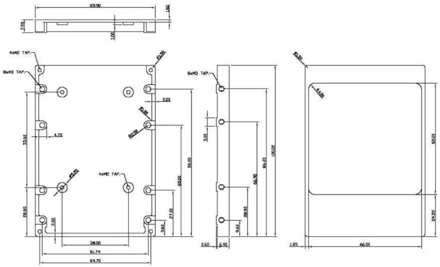
2.5.1. 2.5" SSD Physical Specifications
See Figure 2-1 for 2.5" SSD Physical specifications and dimensions.
Figure 2-1. 2.5" SSD Dimensions
2.6. Capacity Specifications
The following sections provide capacity specifications for Cactus Technologies 2.5" SSD products.
2.6.1. 2.5" SSD Capacity Specifications
Table 2-5 shows the specific capacity for the various models and the default number of heads, sectors/track and cylinders.
Table 2-5. Model Capacities
| Capacity Capacity (formatted) | Sectors/Drive (Max LBA+1) | No. of Heads | No. of Sectors/Track | No. of Cylinders | |
| 128MB | 129,761,280 bytes | 253,440 8 32 | 990 | ||
| 256MB | 259,522,560 bytes | 506,880 16 32 | 990 | ||
| 512MB | 521,256,960 bytes | 1018080 16 63 | 1,010 | ||
| 1GB | 1,047,674,880 bytes | 2,046,240 16 63 | 2,030 | ||
| 2GB | 2,097,930,240 bytes | 4,097,520 16 63 | 4,065 | ||
| 4GB | 4,224,245,760 bytes | 8,250,480 16 63 | 8,185 | ||
| 8GB | 8,456,749,056 bytes | 16,517,088 16 63 | 16,386 | ||
| 16GB | 16,829,890,560 bytes | 32,870,880 16 63 | 32,610 | ||
The following sections provide detailed information on the Cactus Technologies Industrial SSD interface.
3.1. SSD Pin Assignments and Pin Type
The signal/pin assignments are listed in Table 3-6. Low active signals have a "-" prefix. Pin types are Input, Output or Input/Output. Sections 3.3.1 to 3.3.4 define the DC characteristics for all input and output type structures.
Table 3-6. SSD Pin Assignments and Pin Type
| Pin Num | Signal Name | Pin Type | Pin Num | Signal Name | Pin Type |
| 1 | -Reset | I | 2 | GND | |
| 3 | Data 7 | I/O | 4 | Data 8 | I/O |
| 5 | Data 6 | I/O | 6 | Data 9 | I/O |
| 7 | Data 5 | I/O | 8 | Data 10 | I/O |
| 9 | Data 4 | I/O | 10 | Data 11 | I/O |
| 11 | Data 3 | I/O | 12 | Data 12 | I/O |
| 13 | Data 2 | I/O | 14 | Data 13 | I/O |
| 15 | Data 1 | I/O | 16 | Data 14 | I/O |
| 17 | Data 0 | I/O | 18 | Data 15 | I/O |
| 19 | GND | 20 | Key | ||
| 21 | -DMARQ | O | 22 | GND | |
| 23 | -IOW/STOP | I | 24 | GND | |
| 25 | -IOR/-HDMARDY/HSTROBE | I | 26 | GND | |
| 27 | IORDY/-DDMARDY/DSTROBE | O | 28 | -CSEL | I |
| 29 | -DMACK | I | 30 | GND | |
| 31 | IRQ | O | 32 | (reserved) | |
| 33 | A1 | I | 34 | -PDIAG | I/O |
| 35 | A0 | I | 36 | A2 | I |
| 37 | -CS0 | I | 38 | -CS1 | I |
| 39 | -DASP | I/O | 40 | GND | |
| 41 | Vcc | 42 | Vcc | ||
| 43 | GND | 44 | Reserved |
3.2. Signal Description
Table 3-7 describes the I/O signals. Signals whose source is the host are designated as inputs while signals that the SSD sources are outputs. The SSD logic levels conform to those specified in the ANSI ATA Specification.
Table 3-7. Signal Description
| Signal Name Dir. Description | ||
| A2—A0 | I | A[2:0] is used to select the one of eight registers in the Task File. |
| -PDIAG | I/O | This input/output is the Pass Diagnostic signal in the Master/Slave handshake protocol. |
| -DASP | I/O | This input/output is the Disk Active/Slave Present signal in the Master/Slave handshake protocol. |
| -CSO, -CS1 | I | -CSO is the chip select for the task file registers while -CS1 is used to select the Alternate Status Register and the Device Control Register. |
| -CSEL | I | This internally pulled up signal is used to configure this device as a Master or a Slave. When this pin is grounded, this device is configured as a Master. When the pin is open, this device is configured as a Slave. |
| D15—D00 | I/O | These lines carry the Data, Commands and Status information between the host and the controller. D00 is the LSB of the Even Byte of the Word. D08 is the LSB of the Odd Byte of the Word. All Task File operations occur in byte mode on the low order bus D00-D07 while all data transfers are 16 bits using D00-D15. |
| GND | -- | Ground. |
| -IORD | I | This is an I/O Read strobe generated by the host. This signal gates I/O data onto the bus from the SSD. |
| -IOWR | I | The I/O Write strobe pulse is used to clock I/O data on the Data bus into the SSD.The clocking will occur on the negative to positive edge of the signal (trailing edge). |
| INTRQ | O | This signal is the active high Interrupt Request to the host. |
| -RESET | I | This input pin is the active low hardware reset from the host. |
| VCC | -- | +5 V, +3.3 V power. |
| -IORDY | O | The -IORDY signal is driven by the SSD to extend the I/O cycle in progress. |
| -IOCS16 | O | This output signal is asserted low when this device is expecting a word data transfer cycle. |
3.3. Electrical Specification
The following table defines all D.C. Characteristics for the SSD Series. Unless otherwise stated, conditions are:
$$ \mathrm{Vcc} = 5 \mathrm{V} \pm 10 \% \text { or } \mathrm{Vcc} = 3.3 \mathrm{V} \pm 10 \% $$
$$ \mathrm{Ta} = - 4 5 ^ {\circ} \mathrm{C} \text { to } 9 0 ^ {\circ} \mathrm{C} $$
3.3.1. Absolute Maximum Ratings
| Parameter Symbol MIN MAX Units | ||||
| Storage Temperature | Ts | -65 +150 °C | ||
| Operating Temperature | TA | -45 +90 °C | ||
| Vcc with respect to GND | Vcc | -0.3 6.5 V | ||
3.3.2. DC Characteristics
| Parameter Symbol MIN MAX Units | ||||
| Input Voltage | Vin | -0.5 Vcc + 0.5 V | ||
| Output Voltage | Vout | -0.3 Vcc + 0.3 V | ||
| Input Leakage Current | I_LI | -10 10 uA | ||
| Output Leakage Current | I_LO | -10 10 uA | ||
| Input/Output Capacitance | C_I/C_o | 10 pF | ||
| Operating Current Sleep Mode @20 MHz (3.3V) @40 MHz (3.3V) @20 MHz (5.0V) @40 MHz (5.0V) | I_cc | 0.220403050 | mA | |
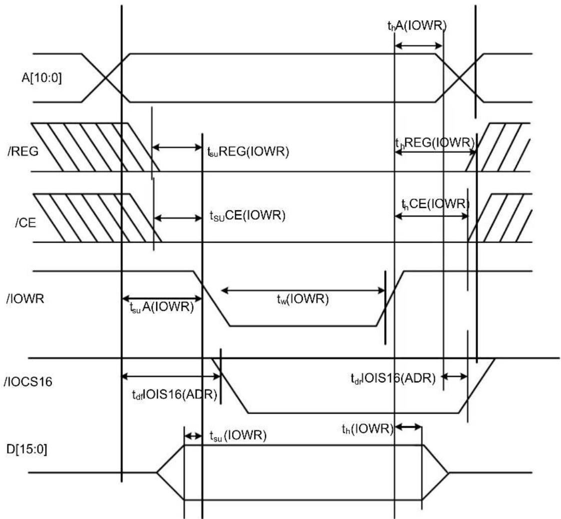
3.3.3. I/O Read (Input) Timing Specification
Figure 3-2. I/O Read Timing Diagram

text_image
A[10:0] /t_hA(IORD) /REG t_su REG(IORD) /t_hREG(IORD) /CE t_suCE(IORD) /t_hCE(IORD) /IORD t_suA(IORD) t_w(IORD) t_dr NPACK(IORD) /INPACK t_df INPACK(IORD) /t_doIS16(ADR) /t_dr IOIS16(ADR) D[15:0] t_df IOIS16(ADR) t_d(IORD) t_h(IORD)- All timings are measured at the drive.
- Skews and delays from the host system driver/receiver to the drive must be accounted for by the system design.
- D[15::0] signifies data provided by the drive to the host system.
Table 3-8. I/O Read (Input) Timing Specification
| Parameter Symbol Min Max | |||
| Data Delay after -IORD tdIORD 100 | |||
| Data Hold following -IORD thIORD 0 | |||
| -IORD Width Time twIORD 165 | |||
| Address Setup before -IORD tsuA(IORD) 70 | |||
| Address Hold following -IORD thA(IORD) 20 | |||
| -CE Setup before -IORD tsuCE(IORD) 5 | |||
| -CE Hold following -IORD | thCE(IORD) | 20 | |
| -REG Setup before -IORD | tsuREG(IORD) | 5 | |
| -REG Hold following -IORD th(REG(IORD) | 0 | ||
| -INPACK Delay Falling from -IORD | tdfINPACK(IORD) | 0 | 45 |
| -INPACK Delay Rising from -IORD | tdrINPACK(IORD) | 45 | |
| -IOIS16 Delay Falling from Address | tdfIOIS16(ADR) | 35 | |
| -IOIS16 Delay Rising from Address | tdrIOIS16(ADR) | 35 |
- All timings in ns.
- The maximum load on -INPACK and -IOIS16 is 1 LSTTL with 50 pF total load.
3.3.4. I/O Write (Output) Timing Specification
Figure 3-2. I/O Write Timing Diagram
text_image
A[10:0] t_hA(IOWR) /REG t_suREG(IOWR) t_hREG(IOWR) /CE t_suCE(IOWR) t_hCE(IOWR) /IOWR t_suA(IOWR) t_w(IOWR) /IOCS16 t_dIOLIS16(ADR) t_dIOLIS16(ADR) D[15:0] t_su(IOWR) t_h(IOWR)- All timings are measured at the drive.
- Skews and delays from the host system driver/receiver to the drive must be accounted for by the system design.
- D[15::0] signifies data provided by the drive to the host system.
Table 3-9. I/O Write Timing Specification
| Parameter Symbol Min Max | |||
| Data Setup before -IOWR tsu(IOWR) 60 | |||
| Data Hold following -IOWR th(IOWR) 30 | |||
| -IOWR Width Time tw(IOWR) 165 | |||
| Address Setup before -IOWR tsuA(IOWR) 70 | |||
| Address Hold following -IOWR thA(IOWR) 20 | |||
| -CE Setup before -IOWR tsuCE(IOWR) 5 | |||
| -CE Hold following -IOWR | thCE(IOWR) | 20 | |
| -REG Setup before -IOWR | tsuREG(IOWR) | 5 | |
| -REG Hold following -IOWR | thREG(IOWR) | 0 | |
| -IOIS16 Delay Falling from Address | tdfIOIS16(ADR) | 35 | |
| -IOIS16 Delay Rising from Address | tdrIOIS16(ADR) | 35 | |
| -IOIS16 Delay Falling from Address | tdfIOIS16(ADR) | 35 | |
| -IOIS16 Delay Rising from Address | tdrIOIS16(ADR) | 35 |
- All timings in ns.
- The maximum load on -IOIS16 is 1 LSTTL with 50 pF total load.
3.3.4.1. Deskewing
The host shall provide cable deskewing for all signals originating from the device. The device shall provide cable deskewing for all signals originating at the host.
All timing values and diagrams are shown and measured at the connector of the selected device.
3.3.4.2. PIO Transfer Timing
Figure 3-3 defines the relationships between the interface signals for register transfers.
For PIO modes 3 and above, the minimum value of tcR is specified by word 68 in the IDENTIFY DEVICE parameter list.
Figure 3-3. Register Transfer To/From Device
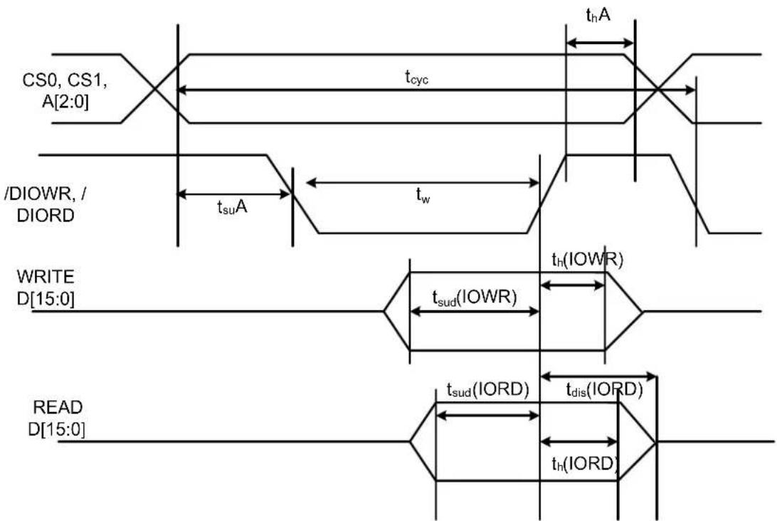
text_image
CS0, CS1, A[2:0] t_cyc t_hA /DIOWR, / DIORD t_suA t_w WRITE D[15:0] t_sud(IOWR) t_h(IOWR) READ D[15:0] t_sud(IORD) t_dis(IORD) t_h(IORD)- Device address consists of signals -CS0, -CS1 and -DA(2:0).
- Data consists of DD(7:0).
| PIO Timing Parameters | Mode 4 ns | Note | ||
| tcyc | Cycle time | (min) | 120 | 1 |
| tsuA Address valid to IORD-/IOWR- setup | (min) 25 | |||
| tw | IORD-/IOWR- pulse width | (min) | 70 | 1 |
| thA | IORD-/IOWR- recovery time | (min) | 25 | 1 |
| tsu(IOWR) | IOWR- data setup | (min) | 20 | |
| thD | IOWR- data hold | (min) | 10 | |
| tsu(IORD) | IORD- data setup | (min) | 20 | |
| th(IORD) | IORD- data hold | (min) | 5 | |
| tdis(IORD) | IORD- data tri-state | (min) | 30 | 2 |
| thA | IORD-/IOWR- to address valid hold | (min) | 10 | |
- tcyc is the minimum total cycle time, tw is the minimum command active time, and trec is the minimum command recovery time or command inactive time. The actual cycle time equals the sum of the actual command active time and the actual command inactive time. A host implementation must ensure that tcyc is equal to or greater than the value reported in the devices IDENTIFY DEVICE data.
- This parameter specifies the time from the negation edge of /IORD to the time that the data bus is no longer driven by the device (tri-state).

3.3.4.3. DMA Transfer Timing
Figure 3-4. DMA Transfer To/From Device
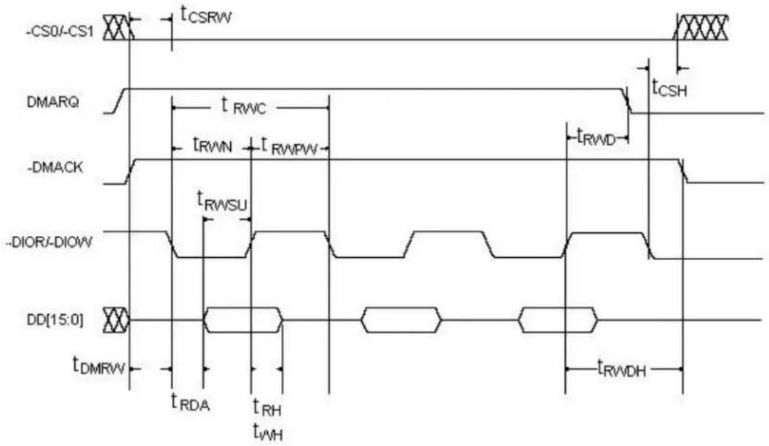
text_image
-CS0/-CS1 t_CSRW DMARQ t_RWC t_CSH t_RWN t_RWPW -t_RWD -DMACK t_RWSU -DIOR/-DIOW DD[15:0] t_DMRW t_RDA t_RH t_WH t_RWDHDMA Timing Parameters Mode 2 ns
| Trwc | Cycle time | (min) | 100 |
| tsuA Address valid to IORD-/IOWR- setup | (min) 65 | ||
| Trwpw DIOR-/DIOW- pulse width high | (min) 65 | ||
| Tdmrw DMACK to DIOR/DIOW setup | (min) 0 | ||
| trda | DIORD access time | (max) | 50 |
| Trwsu | DIOR/DIOW- data setup | (min) | 15 |
| Twh | DIOW- data hold | (min) | 5 |
| Trwd | DIOW/DIOR to DMARQ delay | (max) | 35 |
| Trwdh | DIOR/DIOW to DMACK hold time | (min) | 5 |
| Trh | DIOR- data hold | (min) | 5 |
| Trwn | DIOR/DIOW pulse width low | (min) | 25 |
| Tcsrw | CS[1:0] valid to DIOR/DIOW | (min) | 10 |
| tcsh | CS[1:0] hold time | (min) | 10 |
3.4. I/O Transfer Function
Table 3-10 defines the function of the operations for the FlashDrive.
Table 3-10 FlashDrive I/O Function
| Function Code -CE2 -CE1 A0 -IORD -IOWR D15-D8 D7-D0 | |||||||
| Invalid Mode | L | L X X | X High Z | High Z | |||
| Standby Mode | H | H X X | X High Z | High Z | |||
| Task File Write | H | L | 1-7h | H | L | Do not care | Data In |
| Task File Read | H | L 1-7h | L | H | High Z Data Out | ||
| Data Register Write | H | L 0 | H | L | Odd-Byte In | Even-Byte In | |
| Data Register Read | H | L 0 | L | H | Odd-Byte Out | Even-Byte Out | |
| Control Register Write | L | H | 6h | H | L | Do not care | Control In |
| Alt Status Read | L | H | 6h | L | H | High Z | Status Out |
The communication to or from the FlashDrive is done using the Task File registers, which provide all the necessary registers for control and status information. The ATA interface connects peripherals to the host using four register mapping methods. Table 4-8 is a detailed description of these methods.
Table 4-8. I/O Configurations
| Address Drive # Description | |
| 1F0-1F7, 3F6-3F7 0 Primary I/O Mapped Drive 0 | |
| 1F0-1F7, 3F6-3F7 1 Primary I/O Mapped Drive 1 | |
| 170-177, 376-377 0 Secondary I/O Mapped Drive 0 | |
| 170-177, 376-377 1 Secondary I/O Mapped Drive 1 |
4.1. Task File Addressing
I/O decoding to access the task file registers is as listed in Table 4-9.
Table 4-9. Task File I/O Decoding
| -CE2 -CE1 A2 A1 A0 -IORD=0 -IOWR=0 | |||||
| 1 0 0 0 | 0 | RD Data | WR Data | ||
| 1 0 0 0 | 1 | Error Register | Features | ||
| 1 0 0 1 | 0 | Sector Count | Sector Count | ||
| 1 0 0 1 | 1 | Sector No. | Sector No. | ||
| 1 0 1 0 | 0 | Cylinder Low | Cylinder Low | ||
| 1 0 1 0 | 1 | Cylinder High | Cylinder High | ||
| 1 0 1 1 | 0 | Select Drive/Head | Select Drive/Head | ||
| 1 0 1 1 | 1 | Status | Command | ||
| 0 1 1 1 | 0 | Alt Status | Device Control | ||
| 0 1 1 1 | 1 | Drive Address | Reserved | ||
4.2. ATA Registers
4.2.1. Data Register (Address-1F0[170])
The Data Register is a 16-bit register, and it is used to transfer data blocks between the FlashDrive data buffer and the Host.
4.2.2. Error Register (Address-1F1[171]; Read Only)
This register contains additional information about the source of an error when an error is indicated in bit 0 of the Status register. The bits are defined as follows:
| D7 D6 D5 D4 D3 D2 D1 D0 | |||||
| BBK UNC 0 IDNF 0 ABRT 0 AMNF |
Bit 7 (BBK) This bit is set when a Bad Block is detected.
Bit 6 (UNC) This bit is set when an Uncorrectable Error is encountered.
Bit 5 This bit is 0.
Bit 4 (IDNF) The requested sector ID is in error or cannot be found.
Bit 3 This bit is 0.
Bit 2 (Abort) This bit is set if the command has been aborted because of a status condition: (Not Ready, Write Fault, etc.) or when an invalid command has been issued.
Bit 1 This bit is 0.
Bit 0 (AMNF) This bit is set in case of a general error.
4.2.3. Feature Register (Address-1F1[171]; Write Only)
This register provides information regarding features of the FlashDrive that the host can utilize.
4.2.4. Sector Count Register (Address-1F2[172])
This register contains the number of sectors of data requested to be transferred on a read or write operation between the host and the FlashDrive. If the value in this register is zero, a count of 256 sectors is specified. If the command was successful, this register is zero at command completion. If not successfully completed, the register contains the number of sectors that need to be transferred in order to complete the request.
4.2.5. Sector Number (LBA 7-0) Register (Address-1F3[173])
This register contains the starting sector number or bits 7-0 of the Logical Block Address (LBA) for any FlashDrive data access for the subsequent command.
4.2.6. Cylinder Low (LBA 15-8) Register (Address-1F4[174])
This register contains the low order 8 bits of the starting cylinder address or bits 15-8 of the Logical Block Address.
4.2.7. Cylinder High (LBA 23-16) Register (Address-1F5[175])
This register contains the high order bits of the starting cylinder address or bits 23-16 of the Logical Block Address.
4.2.8. Drive/Head (LBA 27-24) Register (Address 1F6[176])
The Drive/Head register is used to select the drive and head. It is also used to select LBA addressing instead of cylinder/head/sector addressing. The bits are defined as follows:
Bit 7 This bit is set to 1.
Bit 6 LBA is a flag to select either Cylinder/Head/Sector (CHS) or Logical Block Address Mode (LBA). When LBA=0, Cylinder/Head/Sector mode is selected. When LBA=1, Logical Block Address is selected. In Logical Block Mode, the Logical Block Address is interpreted as follows:
LBA07-LBA00: Sector Number Register D7-D0.
LBA15-LBA08: Cylinder Low Register D7-D0.
LBA23-LBA16: Cylinder High Register D7-D0.
LBA27-LBA24: Drive/Head Register bits HS3-HS0.
Bit 5 This bit is set to 1.
Bit 4 (DRV) This bit will have the following meaning. DRV is the drive number. When DRV=0, drive 0 is selected When DRV=1, drive 1 is selected.
Bit 3 (HS3) When operating in the Cylinder, Head, Sector mode, this is bit 3 of the head number. It is Bit 27 in the Logical Block Address mode.
Bit 2 (HS2) When operating in the Cylinder, Head, Sector mode, this is bit 2 of the head number. It is Bit 26 in the Logical Block Address mode.
Bit 1 (HS1) When operating in the Cylinder, Head, Sector mode, this is bit 1 of the head number. It is Bit 25 in the Logical Block Address mode.
Bit 0 (HS0) When operating in the Cylinder, Head, Sector mode, this is bit 0 of the head number. It is Bit 24 in the Logical Block Address mode.
4.2.9. Status and Alternate Status Registers (Address 1F7[177] and 3F6[376])
These registers return the status when read by the host. Reading the Status register does clear a pending interrupt while reading the Auxiliary Status register does not. The meaning of the status bits are described as follows:
BUSY RDY DWF DSC DRQ CORR 0 ERR
Bit 7 (BUSY) The busy bit is set when the device has access to the command buffer and registers and the host is locked out from accessing the command register and buffer. No other bits in this register are valid when this bit is set to a 1.
Bit 6 (RDY) RDY indicates whether the device is capable of performing operations requested by the host. This bit is cleared at power up and remains cleared until the device is ready to accept a command.
Bit 5 (DWF) This bit, if set, indicates a write fault has occurred.
Bit 4 (DSC) This bit is set when the device is ready.
Bit 3 (DRQ) The Data Request is set when the device requires that information be transferred either to or from the host through the Data register.
Bit 2 (CORR) This bit is set when a Correctable data error has been encountered and the data has been corrected. This condition does not terminate a multi-sector read operation.
Bit 1 (IDX) This bit is always set to 0.
Bit 0 (ERR) This bit is set when the previous command has ended in some type of error. The bits in the Error register contain additional information describing the error.
4.2.10. Device Control Register (Address-3F6[376])
This register is used to control the drive interrupt request and to issue an ATA soft reset to the drive. The bits are defined as follows:
| D7 D6 D5 D4 D3 D2 D1 D0 | |||||||
| X | X | X | X | 1 | SW Rst | -1En | 0 |
Bit 7 This bit is an X (Do not care).
Bit 6 This bit is an X (Do not care).
Bit 5 This bit is an X (Do not care).
Bit 4 This bit is an X (Do not care).
Bit 3 This bit is ignored by the drive.
Bit 2 (SW Rst) This bit is set to 1 in order to force the drive to perform an AT Disk controller. Soft Reset operation. The drive remains in Reset until this bit is reset to '0'.
Bit 1 (-IEn) The Interrupt Enable bit enables interrupts when the bit is 0. When the bit is 1, interrupts from the drive are disabled. This bit is set to 0 at power on and Reset.
Bit 0 This bit is ignored by the drive.
4.2.11. Drive Address Register (Address 3F7[377])
This register is provided for compatibility with the AT disk drive interface. It is recommended that this register not be mapped into the host's I/O space because of potential conflicts on Bit 7. The bits are defined as follows:
Bit 7 This bit is unknown.
Implementation Note:
Conflicts may occur on the host data bus when this bit is provided by a Floppy Disk Controller operating at the same addresses as the SSD. Following are some possible solutions to this problem:
- Locate the SSD at a non-conflicting address (i.e., Secondary address (377) when a Floppy Disk Controller is located at the Primary addresses).
- Do not install a Floppy and a SSD in the system at the same time.
- Implement a socket adapter that can be programmed to (conditionally) tri-state D7 of I/O address 3F7/377 when a SSD product is installed and conversely to tri-state D6-D0 of I/O address 3F7/377 when a floppy controller is installed.
- Do not use the SSD's Drive Address register. This may be accomplished by either a) If possible, program the host adapter to enable only I/O addresses 1F0-1F7, 3F6 (or 170-177, 176) to the SSD or b) if provided use an additional Primary/Secondary configuration in the SSD that does not respond to accesses to I/O locations 3F7 and 377. With either of these implementations, the host software must not attempt to use information in the Drive Address Register.
Bit 6 (-WTG) This bit is 0 when a write operation is in progress, otherwise, it is 1.
Bit 5 (-HS3) This bit is the negation of bit 3 in the Drive/Head register.
Bit 4 (-HS2) This bit is the negation of bit 2 in the Drive/Head register.
Bit 3 (-HS1) This bit is the negation of bit 1 in the Drive/Head register.
Bit 2 (-HS0) This bit is the negation of bit 0 in the Drive/Head register.
Bit 1 (-nDS1) This bit is 0 when drive 1 is active and selected.
Bit 0 (-nDS0) This bit is 0 when the drive 0 is active and selected.
This section defines the software requirements and the format of the commands the host sends to the Industrial FlashDrive products. Commands are issued by loading the required registers in the command block with the supplied parameters, and then writing the command code to the Command Register. The manner in which a command is accepted varies. There are three classes (see Table 5-10) of command acceptance, all dependent on the host not issuing commands unless the drive is not busy. (The BUSY bit in the status and alternate status registers is 0.)
- Upon receipt of a Class 1 command, the drive sets the BUSY bit within 400 nsec.
- Upon receipt of a Class 2 command, the drive sets the BUSY bit within 400 nsec, sets up the sector buffer for a write operation, sets DRQ within 700 μsec, and clears the BUSY bit within 400 nsec of setting DRQ.
- Upon receipt of a Class 3 command, the drive sets the BUSY bit within 400 nsec, sets up the sector buffer for a write operation, sets DRQ within 20 msec (assuming no re-assignments), and clears the BUSY bit within 400 nsec of setting DRQ.
5.1. ATA Command Set
Table 5-10 summarizes the supported ATA command set with the paragraphs that follow describing the individual commands and the task file for each.
Table 5-10. ATA Command Set
| Class COMMAND Code FR SC SN CY DH LBA | ||||||||
| 1 Check | Power Mode E5h or 98h - - - - D | - | ||||||
| 1 | Execute Drive Diagnostic | 90h | - | - | - | - | D | - |
| 1 | Erase Sector(s) | C0h | - | Y | Y | Y | Y | Y |
| 2 | Format Track | 50h | - | Y | - | Y | Y | Y |
| 1 | Identify Drive | ECh | - | - | - | - | D | - |
| 1 | Idle | E3h or 97h - Y - - D | - | |||||
| 1 | Idle Immediate | E1h or 95h - - - - D | - | |||||
| 1 | Initialize Drive Parameters | 91h | - | Y | - | - | Y | - |
| 1 | Read Buffer | E4h | - | - | - | - | D | - |
| 1 | Read Multiple | C4h | - | Y | Y | Y | Y | Y |
| 1 | Read Long Sector | 22h or 23h | - | - | Y | Y | Y | Y |
| 1 | Read Sector(s) | 20h or 21h | - | Y | Y | Y | Y | Y |
| 1 | Read Verify Sector(s) | 40h or 41h | - | Y | Y | Y | Y | Y |
| 1 | Recalibrate | 1Xh | - | - | - | - | D | - |
| 1 | Request Sense | 03h | - | - | - | - | D | - |
| 1 | Seek | 7Xh | - | - | Y | Y | Y | Y |
| 1 | Set Features | EFh | Y | - | - | - | D | - |
| 1 | Set Multiple Mode | C6h | - | Y | - | - | D | - |
| 1 Set Sleep Mode E6h or 99h - - - - D - | ||||||||
| 1 | Stand By | E2h or 96h - - - - D - | ||||||
| 1 | Stand By Immediate | E0h or 94h - - - - D - | ||||||
| 1 | Translate Sector | 87h | - | Y | Y | Y | Y | Y |
| 1 | Wear Level | F5h | - | - | - | - | Y | - |
| 2 | Write Buffer | E8h | - | - | - | - | D | - |
| 2 | Write Long Sector | 32h or 33h | - | - | Y | Y | Y | Y |
| 3 | Write Multiple | C5h | - | Y | Y | Y | Y | Y |
| 3 | Write Multiple w/o Erase | CDh | - | Y | Y | Y | Y | Y |
| 2 | Write Sector(s) | 30h or 31h | - | Y | Y | Y | Y | Y |
| 2 | Write Sector(s) w/o Erase | 38h | - | Y | Y | Y | Y | Y |
| 2 | Write Verify Sector(s) | 3Ch | - | Y | Y | Y | Y | Y |
Definitions: FR = Features Register, SC = Sector Count Register, SN = Sector Number Register, CY = Cylinder Registers, DH = Drive/Drive/Head Register, LBA = Logical Block Address Mode Supported (see command descriptions for use).
Y—The register contains a valid parameter for this command. For the Drive/Head Register Y means both the drive and head parameters are used; D—only the drive parameter is valid and not the head parameter.
5.1.1. Check Power Mode-98H, E5H
The Check Power Mode command in Table 5-11 checks the power mode.
Table 5-11. Check Power Mode
| Bit -> | 7 | 6 | 5 | 4 | 3 | 2 | 1 | 0 |
| Command (7) | E5H or 98H | |||||||
| C/D/H (6) | X | Drive | X | |||||
| Cyl High (5) | X | |||||||
| Cyl Low (4) | X | |||||||
| Sec Num (3) | X | |||||||
| Sec Cnt (2) | X | |||||||
| Feature (1) | X | |||||||
If the drive is in, going to, or recovering from the standby mode, the drive sets BSY, sets the Sector Count Register to 00h, clears BSY and generates an interrupt. If the drive is in active mode, the drive sets BSY, sets the Sector Count Register to FFh, clears BSY and generates an interrupt.
5.1.2. Execute Drive Diagnostic-90H
The Executive Drive Diagnostic command in Table 5-12 performs the internal diagnostic tests implemented by the drive.
Table 5-12. Executive Drive Diagnostic
| Bit -> 7 6 5 4 3 2 1 0 | |||||||
| Command (7) | 90H | ||||||
| C/D/H (6) | X Drive X | ||||||
| Cyl High (5) | X | ||||||
| Cyl Low (4) | X | ||||||
| Sec Num (3) | X | ||||||
| Sec Cnt (2) | X | ||||||
| Feature (1) | X | ||||||
A code of 01h will be returned in the Error Register at the end of the command.
5.1.3. Erase Sector(s)-COH
Table 5-13. Erase Sectors
| Bit -> 7 6 5 4 3 2 1 0 | ||||||||
| Command (7) | C0H | |||||||
| C/D/H (6) | 1 LBA | 1 Drive Head | LBA 27-24) | |||||
| Cyl High (5) | Cylinder High (LBA 23-16) | |||||||
| Cyl Low (4) | Cylinder Low (LBA 15-8) | |||||||
| Sec Num (3) | Sector Number (LBA 7-0) | |||||||
| Sec Cnt (2) | Sector Count | |||||||
| Feature (1) | X | |||||||
The sectors indicated in the task file are left in erased states. This command is used in advanced of a write w/o erase or write multiple w/o erase command. Erased sectors return all zero data when read.
5.1.4. Format Track-50H
Table 5-14. Format Track
| Bit -> 7 6 5 4 3 2 1 0 | ||||||||
| Command (7) | 50H | |||||||
| C/D/H (6) | 1 LBA | 1 Drive Head | LBA 27-24) | |||||
| Cyl High (5) | Cylinder High (LBA 23-16) | |||||||
| Cyl Low (4) | Cylinder Low (LBA 15-8) | |||||||
| Sec Num (3) | X (LBA 7-0) | |||||||
| Sec Cnt (2) | Count (LBA mode only) | |||||||
| Feature (1) | X | |||||||
This command writes the desired head and cylinder of the selected drive with a vendor unique pattern. To remain host backward compatible, the drive expects a sector buffer of data from the host to follow the command with the same protocol as the Write Sector(s) command although the information in the buffer is not used by the drive. If LBA=1 then the number of sectors to format is taken from the Sec Cnt register (0=256).
5.1.5. Identify Drive-ECH
The Identify Drive command in Table 5-15 enables the host to receive parameter information from the drive. This command has the same protocol as the Read Sector(s) command. The parameter words in the buffer have the arrangement and meanings defined in Table 5-16. All reserved bits or words are zero. Table 5-16 is the definition for each field in the Identify Drive Information.
Table 5-15. Identify Drive
| Bit -> 7 6 5 4 3 2 1 0 | ||||||||
| Command (7) | ECH | |||||||
| C/D/H (6) | XXX Drive X | |||||||
| Cyl High (5) | X | |||||||
| Cyl Low (4) | X | |||||||
| Sec Num (3) | X | |||||||
| Sec Cnt (2) | X | |||||||
| Feature (1) | X | |||||||
Table 5-16. Identify Drive Information
| Word Address | Default Value | Total Bytes | Data Field Type Information |
| 0 044AH 2 General configuration bit-significant information. | |||
| 1 01EFH 2 Default number of cylinders. | |||
| 2 0000H 2 Reserved. | |||
| 3 0004H 2 | Default number of heads. | ||
| 4 0000H 2 | Number of unformatted bytes per track. | ||
| 5 0200H 2 | Number of unformatted bytes per sector. | ||
| 6 0020H 2 | Default number of sectors per track. | ||
| 7-8 | 0000H,F780H 4 Number of sectors per drive (Word 7 = MSW, Word 8 = LSW). | ||
| 9 0000H 2 | Reserved. | ||
| 10-19 | aaaa | 20 | Serial number in ASCII (Right Justified). |
| 20 | 0001H 2 | Buffer type (single port). | |
| 21 | 0001H | 2 | Buffer size in 512 byte increments. |
| 22 | 0004H 2 | Number of ECC bytes passed on Read/Write Long Commands. | |
| 23-26 | aaaa | 8 | Firmware revision in ASCII . Big Endian Byte Order in Word. |
| 27-46 | aaaa | 40 | Model number in ASCII (Left Justified) Big Endian Byte Order in Word. |
| 47 | 0001H 2 | Maximum of 1 sector on Read/Write Multiple command. | |
| 48 0000H 2 Double Word not supported. | |||
| 49 0F00H 2 | Capabilities: DMA Supported in True IDE mode (bit 8), LBA supported (bit 9). | ||
| 50 0000H 2 Reserved. | |||
| 51 0200H 2 PIO data transfer cycle timing mode | |||
| 52 0000H 2 | Single Word DMA data transfer cycle timing mode (not supported). | ||
| 53 0001H 2 Data fields 54-58 are valid. | |||
| 54 XXXX 2 Current numbers of cylinders. | |||
| 55 XXXX 2 Current numbers of heads. | |||
| 56 XXXX 2 Current sectors per track. | |||
| 57-58 XXXX 4 | Current capacity in sectors (LBAs) (Word 57 = LSW, Word 58 = MSW). | ||
| 59 0100H 2 Multiple sector setting is valid. | |||
| 60-61 XXXX 4 | Total number of sectors addressable in LBA Mode. | ||
| 62-63 | 0000H 2 | Reserved | |
| 64 0003H 1 | Advanced PIO modes supported (modes 3 and 4) | ||
| 65-255 | 0000H 2 | Reserved | |
5.1.5.1. Word 0: General Configuration
This field informs the host that this is a non-magnetic, hard sectored, removable storage device with a transfer rate greater than 10 mb/sec and is not MFM encoded.
5.1.5.2. Word 1: Default Number of Cylinders
This field contains the number of translated cylinders in the default translation mode. This value will be the same as the number of cylinders.
5.1.5.3. Word 3: Default Number of Heads
This field contains the number of translated heads in the default translation mode.
5.1.5.4. Word 4: Number of Unformatted Bytes per Track
This field contains the number of unformatted bytes per translated track in the default translation mode.
5.1.5.5. Word 5: Number of Unformatted Bytes per Sector
This field contains the number of unformatted bytes per sector in the default translation mode.
5.1.5.6. Word 6: Default Number of Sectors per Track
This field contains the number of sectors per track in the default translation mode.
5.1.5.7. Words 7-8: Number of Sectors per Drive
This field contains the number of sectors per drive. This double word value is also the first invalid address in LBA translation mode.
5.1.5.8. Words 10-19: Drive Serial Numbers
The contents of this field are right justified and padded with spaces (20h).
5.1.5.9. Word 20: BufferType
This field defines the buffer capability with the 0001h meaning a single ported multi-sector buffer capable of single source data transfers to or from either the host or the drive.
5.1.5.10. Word 21: Buffer Size
This field defines the buffer capacity of 1 sector or 512 bytes of SRAM.
5.1.5.11. Word 22: ECC Count
This field defines the number of ECC bytes used on each sector in the Read and Write Long commands.
This field defines the number of ECC bytes used on each sector in the Read and Write Long commands.
5.1.5.13. Words 27-46: Model Number
This field contains the model number for this product and is left justified and padded with spaces (20h).
5.1.5.14. Word 47: Read/Write Multiple Sector Count
This field contains the maximum number of sectors that can be read or written per interrupt using the Read Multiple or Write Multiple commands.
5.1.5.15. Word 48: Double Word Support
This field indicates this product will not support double word transfers.
5.1.5.16. Word 49: Capabilities
This field indicates if this product supports DMA Data transfers and LBA mode. All Cactus Technologies products support LBA mode. Multiword DMA operation is also supported.
5.1.5.17. Word 51: PIO Data Transfer Cycle Timing Mode
This field indicated the supported PIO transfer timing for the FlashDrive.
NOTE: For backward compatibility with BIOSs written before Word 64 was defined for advanced modes, a device reports in Word 51 the highest original PIO mode it can support (i.e., PIO mode 0, 1 or 2).
5.1.5.18. Word 52: Single Word DMA Data Transfer Cycle Timing Mode
This field states this product doesn't support Single Word DMA data transfer mode.
5.1.5.19. Word 53: Translation Parameters Valid
Bit 0 of this field is set, indicating that words 54 to 58 are valid and reflect the current number of cylinders, heads and sectors. Bit 1 is also set, indicating values in words 64 through 70 are valid.
5.1.5.20. Words 54-56: Current Number of Cylinders, Heads, Sectors/Tracks
These fields contain the current number of user addressable Cylinders, Heads, and Sectors/Track in the current translation mode.
5.1.5.21. Words 57-58: Current Capacity
This field contains the product of the current cylinders times heads times sectors.
5.1.5.22. Word 59: Multiple Sector Setting
This field contains a validity flag in the odd byte and the current number of sectors that can be transferred per interrupt for R/W Multiple in the even byte. The odd byte is always 01H, which indicates that the even byte is always valid.
The even byte value depends on the value set by the Set Multiple command. The even byte of this word by default contains a 00H, which indicates that R/W Multiple commands are not valid. The only other value returned by the drive in the even byte is a 01H value, which indicates that 1 sector per interrupt, can be transferred in R/W Multiple mode.
5.1.5.23. Words 60-61: Total Sectors Addressable in LBA Mode
This field contains the number of sectors addressable for the drive in LBA mode only.
5.1.5.24. Word 64: Advanced PIO Transfer Modes Supported
Bits 0 and 1 of this field are set to indicate support for PIO transfer modes 3 and 4, respectively.
5.1.6. Idle-97H, E3H
These commands are treated as NOPs by the drive. Since the drive goes into sleep mode after every command, these extra IDLE commands are redundant.
Table 5-17. Idle
| Bit -> 7 6 5 4 3 2 1 0 | |||||||
| Command (7) | E3H or 97H | ||||||
| C/D/H (6) | X Drive X | ||||||
| Cyl High (5) | X | ||||||
| Cyl Low (4) | X | ||||||
| Sec Num (3) | X | ||||||
| Sec Cnt (2) | X | ||||||
| Feature (1) | X | ||||||
5.1.7. Idle Immediate-95H, E1H
Table 5-18. Idle Immediate
| Bit -> 7 6 5 4 3 2 1 0 | |||||||
| Command (7) | E1H or 95H | ||||||
| C/D/H (6) | X Drive X | ||||||
| Cyl High (5) | X | ||||||
| Cyl Low (4) | X | ||||||
| Sec Num (3) | X | ||||||
| Sec Cnt (2) | X | ||||||
| Feature (1) | X | ||||||
5.1.8. Initialize Drive Parameters-91H
The Initialize Drive Parameters command in Table 5-19 causes the drive to set BSY, enter the Idle (Read) mode, clear BSY and generate an interrupt. This command enables the host to set the number of sectors per track and the number of heads per cylinder. Only the Sector Count and the Drive/Drive/Head registers are used by this command.
Table 5-19. Initialize Drive Parameters
| Bit -> 7 6 5 4 3 2 1 0 | ||||||||
| Command (7) | 91H | |||||||
| C/D/H (6) | X 0 X Drive Max Head (no. of heads-1) | |||||||
| Cyl High (5) | X | |||||||
| Cyl Low (4) | X | |||||||
| Sec Num (3) | X | |||||||
| Sec Cnt (2) | Number of Sectors | |||||||
| Feature (1) | X | |||||||
5.1.9. Read Buffer-E4H
The Read Buffer command in Table 5-20 enables the host to read the current contents of the FlashDrive's sector buffer. This command has the same protocol as the Read Sector(s) command.
Table 5-20. Read Buffer
| Bit -> 7 6 5 4 3 2 1 0 | |||||||
| Command (7) | E4H | ||||||
| C/D/H (6) | X Drive X | ||||||
| Cyl High (5) | X | ||||||
| Cyl Low (4) | X | ||||||
| Sec Num (3) | X | ||||||
| Sec Cnt (2) | X | ||||||
| Feature (1) | X | ||||||
The Read Multiple command in Table 5-21 performs similarly to the Read Sectors command. Interrupts are not generated on every sector, but on the transfer of a block, which contains the number of sectors defined by a Set Multiple, command.
Table 5-21. Read Multiple
| Bit -> 7 6 5 4 3 2 1 0 | ||||||||
| Command (7) | C4H | |||||||
| C/D/H (6) | 1 LBA | 1 Drive Head | (LBA 27-24) | |||||
| Cyl High (5) | Cylinder High (LBA 23-16) | |||||||
| Cyl Low (4) | Cylinder Low (LBA 15-8) | |||||||
| Sec Num (3) | Sector Number (LBA 7-0) | |||||||
| Sec Cnt (2) | Sector Count | |||||||
| Feature (1) | X | |||||||
Command execution is identical to the Read Sectors operation except that the number of sectors defined by a Set Multiple command is transferred without intervening interrupts. DRQ qualification of the transfer is required only at the start of the data block, not on each sector.
The block count of sectors to be transferred without intervening interrupts is programmed by the Set Multiple Mode command, which must be executed prior to the Read Multiple command. When the Read Multiple command is issued, the Sector Count Register contains the number of sectors (not the number of blocks or the block count) requested. If the number of requested sectors is not evenly divisible by the block count, as many full blocks as possible are transferred, followed by a final, partial block transfer. The partial block transfer is for n sectors, where:
$$ n = (\text { sector count }) - \text { module (block count) }. $$
If the Read Multiple command is attempted before the Set Multiple Mode command has been executed or when Read Multiple commands are disabled, the Read Multiple operation is rejected with an Aborted Command error. Disk errors encountered during Read Multiple commands are posted at the beginning of the block or partial block transfer, but DRQ is still set and the data transfer will take place as it normally would, including transfer of corrupted data, if any.
Interrupts are generated when DRQ is set at the beginning of each block or partial block. The error reporting is the same as that on a Read Sector(s) Command. This command reads from 1 to 256 sectors as specified in the Sector Count register. A sector count of 0 requests 256 sectors. The transfer begins at the sector specified in the Sector Number Register.
At command completion, the Command Block Registers contain the cylinder, head and sector number of the last sector read. If an error occurs, the read terminates at the sector where the error occurred. The Command Block Registers contain the cylinder, head and sector number of the sector where the error occurred. The flawed data is pending in the sector buffer.
Subsequent blocks or partial blocks are transferred only if the error was a correctable data error. All other errors cause the command to stop after transfer of the block that contained the error.
5.1.11. Read Long Sector-22H, 23H
The Read Long command in Table 5-22 performs similarly to the Read Sector(s) command except that it returns 516 bytes of data instead of 512 bytes. During a Read Long command, the drive does not check the ECC bytes to determine if there has been a data error. Only single sector read long operations are supported. The transfer consists of 512 bytes of data transferred in word mode followed by 4 bytes of random data transferred in byte mode. Random data is returned instead of ECC bytes because of the nature of the ECC system used. This command has the same protocol as the Read Sector(s) command.
Table 5-22. Read Long Sector
| Bit -> 7 6 5 4 3 2 1 0 | ||||||||
| Command (7) | 22H or 23H | |||||||
| C/D/H (6) | 1 LBA | 1 Drive Head | (LBA 27-24) | |||||
| Cyl High (5) | Cylinder High (LBA 23-16) | |||||||
| Cyl Low (4) | Cylinder Low (LBA 15-8) | |||||||
| Sec Num (3) | Sector Number (LBA 7-0) | |||||||
| Sec Cnt (2) | X | |||||||
| Feature (1) | X | |||||||
5.1.12. Read Sector(s)-20H, 21H
The Read Sector(s) command in Table 5-23 reads from 1 to 256 sectors as specified in the Sector Count register. A sector count of 0 requests 256 sectors. The transfer begins at the sector specified in the Sector Number Register. When this command is issued and after each sector of data (except the last one) has been read by the host, the drive sets BSY, puts the sector of data in the buffer, sets DRQ, clears BSY, and generates an interrupt. The host then reads the 512 bytes of data from the buffer.
At command completion, the Command Block Registers contain the cylinder, head and sector number of the last sector read. If an error occurs, the read terminates at the sector where the error occurred. The Command Block Registers contain the cylinder, head, and sector number of the sector where the error occurred. The flawed data is pending in the sector buffer.
Table 5-23. Read Sectors
| Bit -> 7 6 5 4 3 2 1 0 | ||||||||
| Command (7) | 20H or 21H | |||||||
| C/D/H (6) | 1 LBA | 1 Drive Head | (LBA 27-24) | |||||
| Cyl High (5) | Cylinder High (LBA 23-16) | |||||||
| Cyl Low (4) | Cylinder Low (LBA 15-8) | |||||||
| Sec Num (3) | Sector Number (LBA 7-0) | |||||||
| Sec Cnt (2) | Sector Count | |||||||
| Feature (1) | X | |||||||
5.1.13. Read Verify Sector(s)-40H, 41H
The Read Verify Sector(s) command in Table 5-24 is identical to the Read Sectors command, except that DRQ is never set and no data is transferred to the host. When the command is accepted, the drive sets BSY.
When the requested sectors have been verified, the drive clears BSY and generates an interrupt. Upon command completion, the Command Block Registers contain the cylinder, head, and sector number of the last sector verified.
If an error occurs, the verify terminates at the sector where the error occurs. The Command Block Registers contain the cylinder, head and sector number of the sector where the error occurred. The Sector Count Register contains the number of sectors not yet verified.
Table 5-24. Read Verify Sectors
| Bit -> 7 6 5 4 3 2 1 0 | ||||||||
| Command (7) | 40H or 41H | |||||||
| C/D/H (6) | 1 LBA | 1 Drive Head | LBA 27-24) | |||||
| Cyl High (5) | Cylinder High (LBA 23-16) | |||||||
| Cyl Low (4) | Cylinder Low (LBA 15-8) | |||||||
| Sec Num (3) | Sector Number (LBA 7-0) | |||||||
| Sec Cnt (2) | Sector Count | |||||||
| Feature (1) | X | |||||||
5.1.14. Recalibrate-1XH
The Recalibrate command in Table 5-25 is effectively a NOP command to the drive and is provided for compatibility purposes. After this command is executed the Cyl High and Cyl Low as well as the Head number will be 0 and Sec Num will be 1 if LBA=0 and 0 if LBA=1 (i.e., the first block in LBA is 0 while CHS mode the sector number starts at 1).
Table 5-25. Recalibrate
| Bit -> 7 6 5 4 3 2 1 0 | ||||||||
| Command (7) | 1XH | |||||||
| C/D/H (6) | 1 LBA | 1 Drive X | ||||||
| Cyl High (5) | X | |||||||
| Cyl Low (4) | X | |||||||
| Sec Num (3) | X | |||||||
| Sec Cnt (2) | X | |||||||
| Feature (1) | X | |||||||
5.1.15. Request Sense-03H
The Request Sense command in Table 5-26 requests an extended error code after a command ends with an error.
Table 5-26. Request Sense
| Bit -> 7 6 5 4 3 2 1 0 | ||||||||
| Command (7) | 03H | |||||||
| C/D/H (6) | 1 X 1 Drive X | |||||||
| Cyl High (5) | X | |||||||
| Cyl Low (4) | X | |||||||
| Sec Num (3) | X | |||||||
| Sec Cnt (2) | X | |||||||
| Feature (1) | X | |||||||
Table 5-27 defines the valid extended error codes for Cactus Technologies Industrial FlashDrive products. The extended error code is returned to the host in the Error Register. This command must be the next command issued to the drive following the command that returned an error.
Table 5-27. Extended Error Codes
| Extended Error Code Description | |
| 01h Self Test OK (No Error) | |
| 03h Write Failed | |
| 09h Miscellaneous Error | |
| 11h Uncorrectable ECC Error | |
| 18h Corrected ECC Error | |
| 20h Invalid Command | |
| 21h Invalid Address | |
| 27h Write Protection Violation | |
5.1.16. Seek-7XH
The Seek command in Table 5-28 is effectively a NOP command to the drive although it does perform a range check of cylinder and head or LBA address and returns an error if the address is out of range.
Table 5-28. Seek
| Bit -> 7 6 5 4 3 2 1 0 | ||||||||
| Command (7) | 7XH | |||||||
| C/D/H (6) | 1 LBA | 1 Drive Head | (LBA 27-24) | |||||
| Cyl High (5) | Cylinder High (LBA 23-16) | |||||||
| Cyl Low (4) | Cylinder Low (LBA 15-8) | |||||||
| Sec Num (3) | X (LBA 7-0) | |||||||
| Sec Cnt (2) | X | |||||||
| Feature (1) | X | |||||||
5.1.17. Set Features-EFH
The Set Features command in Table 5-29 is used by the host to establish or select certain features.
Table 5-29. Set Features
| Bit -> 7 6 5 4 3 2 1 0 | |||||||
| Command (7) | EFH | ||||||
| C/D/H (6) | X | Drive | X | ||||
| Cyl High (5) | X | ||||||
| Cyl Low (4) | X | ||||||
| Sec Num (3) | X | ||||||
| Sec Cnt (2) | X | ||||||
| Feature (1) | Feature | ||||||
Table 5-30 defines all features that are supported.
Table 5-30. Features Supported
| Feature Operation |
| 03H Set transfer mode. |
| 55H Disable Read Look Ahead. |
| 66H Disable Power on Reset (POR) establishment of defaults at Soft Reset. |
| 69H NOP; accepted for backward compatibility. |
| 81H Disable 8-bit data transfer. |
| 96H NOP; accepted for backward compatibility. |
| 97H NOP; accepted for backward compatibility. |
| BBH 4 bytes of data apply on Read/Write Long commands. |
| CCH Enable Power on Reset (POR) establishment of defaults at Soft Reset. |
Features 03H is used by the host to set the desired transfer mode for PIO, MWDMA or UDMA transfers.
Features 55H and BBH are the default features for the drive; thus, the host does not have to issue this command with these features unless it is necessary for compatibility reasons.
Features 66H and CCH can be used to enable and disable whether the Power On Reset (POR) Defaults will be set when a soft reset occurs. The default setting is to revert to the POR defaults when a soft reset occurs. POR defaults the number of heads and sectors along with 16 bit data transfers and the read/write multiple block count.
5.1.18. Set Multiple Mode-C6H
The Set Multiple Mode command in Table 5-31 enables the drive to perform Read and Write Multiple operations and establishes the block count for these commands. The Sector Count Register is loaded with the number of sectors per block. Upon receipt of the command, the FlashDrive sets BSY to 1 and checks the Sector Count Register.
Table 5-31. Set Multiple Mode
| Bit -> 7 6 5 4 3 2 1 0 | |||||||
| Command (7) | C6H | ||||||
| C/D/H (6) | X Drive X | ||||||
| Cyl High (5) | X | ||||||
| Cyl Low (4) | X | ||||||
| Sec Num (3) | X | ||||||
| Sec Cnt (2) | Sector Count | ||||||
| Feature (1) | X | ||||||
If the Sector Count Register contains a valid value and the block count is supported, the value is loaded for all subsequent Read Multiple and Write Multiple commands and execution of those commands is enabled. If a block count is not supported, an Aborted Command error is posted, and Read Multiple and Write Multiple commands are disabled. If the Sector Count Register contains 0 when the command is issued, Read and Write Multiple commands are disabled. At power on, or after a hardware or (unless disabled by a Set Feature command) software reset, the default mode is Read and Write Multiple disabled.
5.1.19. Set Sleep Mode-99H, E6H
These commands are treated as NOPs by the drive. Since the drive goes into sleep mode after every command execution, these extra SLEEP commands are redundant.
Table 5-32. Set Sleep Mode
| Bit -> 7 6 5 4 3 2 1 0 | |||||||
| Command (7) | E6H or 99H | ||||||
| C/D/H (6) | X Drive X | ||||||
| Cyl High (5) | X | ||||||
| Cyl Low (4) | X | ||||||
| Sec Num (3) | X | ||||||
| Sec Cnt (2) | X | ||||||
| Feature (1) | X | ||||||
5.1.20. Standby-96H, E2H
The Standby and Standby Immediate commands are treated as NOPs by the drive. Since the drive goes into sleep mode after every command execution, these extra Standby commands are redundant.
Table 5-33. Standby
| Bit -> 7 6 5 4 3 2 1 0 | |||||||
| Command (7) | E2H or 96H | ||||||
| C/D/H (6) | X Drive X | ||||||
| Cyl High (5) | X | ||||||
| Cyl Low (4) | X | ||||||
| Sec Num (3) | X | ||||||
| Sec Cnt (2) | X | ||||||
| Feature (1) | X | ||||||
5.1.21. Standby Immediate-94H, E0H
Table 5-34. Standby Immediate
| Bit -> 7 6 5 4 3 2 1 0 | |||||||
| Command (7) | E0H or 94H | ||||||
| C/D/H (6) | X Drive X | ||||||
| Cyl High (5) | X | ||||||
| Cyl Low (4) | X | ||||||
| Sec Num (3) | X | ||||||
| Sec Cnt (2) | X | ||||||
| Feature (1) | X | ||||||

5.1.22. Translate Sector-87H
This is a NOP command for the drive. The sector count register will always return 0.
Table 5-35. Translate Sector
| Bit -> 7 6 5 4 3 2 1 0 | ||||||||
| Command (7) | 87H | |||||||
| C/D/H (6) | 1 LBA | 1 Drive Head | (LBA 27-24) | |||||
| Cyl High (5) | Cylinder High (LBA 23-16) | |||||||
| Cyl Low (4) | Cylinder Low (LBA 15-8) | |||||||
| Sec Num (3) | Sector Number (LBA 7-0) | |||||||
| Sec Cnt (2) | X | |||||||
| Feature (1) | X | |||||||

5.1.23. Wear Level-F5H
The Wear Level command in Table 5-36 is effectively a NOP command and only implemented for backward compatibility. The Sector Count Register will always be returned with a 00H indicating Wear Level is not needed.
Table 5-36. Wear Level
| Bit -> 7 6 5 4 3 2 1 0 | ||||||||
| Command (7) | F5H | |||||||
| C/D/H (6) | X X X Drive Flag | |||||||
| Cyl High (5) | X | |||||||
| Cyl Low (4) | X | |||||||
| Sec Num (3) | X | |||||||
| Sec Cnt (2) | Completion Status | |||||||
| Feature (1) | X | |||||||

5.1.24. Write Buffer-E8H
The Write Buffer command in Table 5-37 enables the host to overwrite contents of the drive's sector buffer with any data pattern desired. This command has the same protocol as the Write Sector(s) command and transfers 512 bytes.
Table 5-37. Write Buffer
| Bit -> 7 6 5 4 3 2 1 0 | ||||||||
| Command (7) | E8H | |||||||
| C/D/H (6) | X Drive X | |||||||
| Cyl High (5) | X | |||||||
| Cyl Low (4) | X | |||||||
| Sec Num (3) | X | |||||||
| Sec Cnt (2) | X | |||||||
| Feature (1) | X | |||||||
5.1.25. Write Long Sector-23H, 33H
The Write Multiple command in Table 5-38 is provided for compatibility purposes and is similar to the Write Sector(s) command except that it writes 516 bytes instead of 512 bytes. Only single sector Write Long operations are supported. The transfer consists of 512 bytes of data transferred in word mode followed by 4 bytes of vendor unique data supplied by the host. The drive discards these four bytes and writes the sector with valid ECC fields. This command has the same protocol as the Write Sector(s) command.
Table 5-38. Write Long Sector
| Bit -> 7 6 5 4 3 2 1 0 | ||||||||
| Command (7) | 32H or 33H | |||||||
| C/D/H (6) | 1 LBA | 1 Drive Head | (LBA 27-24) | |||||
| Cyl High (5) | Cylinder High (LBA 23-16) | |||||||
| Cyl Low (4) | Cylinder Low (LBA 15-8) | |||||||
| Sec Num (3) | Sector Number (LBA 7-0) | |||||||
| Sec Cnt (2) | X | |||||||
| Feature (1) | X | |||||||
5.1.26. Write Multiple Command-C5H
The Write Multiple command in Table 5-39 is similar to the Write Sectors command. The drive sets BSY within 400 nsec of accepting the command. Interrupts are not presented on each sector but on the transfer of a block that contains the number of sectors defined by Set Multiple. Command execution is identical to the Write Sectors operation except that the number of sectors defined by the Set Multiple command is transferred without intervening interrupts.
Table 5-39. Write Multiple Command
| Bit -> 7 6 5 4 3 2 1 0 | ||||||||
| Command (7) | C5H | |||||||
| C/D/H (6) | X LBA | X Drive Head | ||||||
| Cyl High (5) | Cylinder High | |||||||
| Cyl Low (4) | Cylinder Low | |||||||
| Sec Num (3) | Sector Number | |||||||
| Sec Cnt (2) | Sector Count | |||||||
| Feature (1) | X | |||||||
DRQ qualification of the transfer is required only at the start of the data block, not on each sector. The block count of sectors to be transferred without intervening interrupts is programmed by the Set Multiple Mode command, which must be executed prior to the Write Multiple command.
When the Write Multiple command is issued, the Sector Count Register contains the number of sectors (not the number of blocks or the block count) requested. If the number of requested sectors is not evenly divisible by the sector/block, as many full blocks as possible are transferred, followed by a final, partial block transfer. The partial block transfer is for n sectors, where:
n = remainder (sector count/block count).
If the Write Multiple command is attempted before the Set Multiple Mode command has been executed or when Write Multiple commands are disabled, the Write Multiple operation will be rejected with an aborted command error.
Errors encountered during Write Multiple commands are posted after the attempted writes of the block or partial block transferred. The Write command ends with the sector in error, even if it is in the middle of a block. Subsequent blocks are not transferred in the event of an error. Interrupts are generated when DRQ is set at the beginning of each block or partial block.
The Command Block Registers contain the cylinder, head and sector number of the sector where the error occurred and the Sector Count Register contains the residual number of sectors that need to be transferred for successful completion of the command e.g., each block has 4 sectors, a request for 8 sectors is issued and an error occurs on the third sector. The Sector Count Register contains 6 and the address is that of the third sector.

5.1.27. Write Multiple without Erase-CDH
This command is similar to the Write Multiple command except that an implied erase is not performed.
Table 5-40. Write Multiple without Erase
| Bit -> 7 6 5 4 3 2 1 0 | ||||||||
| Command (7) | CDH | |||||||
| C/D/H (6) | X LBA | X Drive Head | ||||||
| Cyl High (5) | Cylinder High | |||||||
| Cyl Low (4) | Cylinder Low | |||||||
| Sec Num (3) | Sector Number | |||||||
| Sec Cnt (2) | Sector Count | |||||||
| Feature (1) | X | |||||||
5.1.28. Write Sector(s)-30H, 31H
The Write Sectors command in Table 5-41 writes from 1 to 256 sectors as specified in the Sector Count Register. A sector count of zero requests 256 sectors. The transfer begins at the sector specified in the Sector Number Register. When this command is accepted, the drive sets BSY, then sets DRQ and clears BSY, then waits for the host to fill the sector buffer with the data to be written. No interrupt is generated to start the first buffer fill operation. No data should be transferred by the host until BSY has been cleared by the host.
Table 5-41. Write Sectors
| Bit -> 7 6 5 4 3 2 1 0 | ||||||||
| Command (7) | 30H or 31H | |||||||
| C/D/H (6) | 1 LBA | 1 Drive Head | LBA 27-24 | |||||
| Cyl High (5) | Cylinder High (LBA 23-16) | |||||||
| Cyl Low (4) | Cylinder Low (LBA 15-8) | |||||||
| Sec Num (3) | Sector Number (LBA 7-0) | |||||||
| Sec Cnt (2) | Sector Count | |||||||
| Feature (1) | X | |||||||
For multiple sectors, after the first sector of data is in the buffer, BSY will be set and DRQ will be cleared. After the next buffer is ready for data, BSY is cleared, DRQ is set and an interrupt is generated. When the final sector of data is transferred, BSY is set and DRQ is cleared. It will remain in this state until the command is completed at which time BSY is cleared and an interrupt is generated.
If an error occurs during a write of more than one sector, writing terminates at the sector where the error occurs. The Command Block Registers contain the cylinder, head and sector number of the sector where the error occurred. The host may then read the command block to determine what error has occurred, and on which sector.
5.1.29. Write Sector(s) without Erase-38H
This command is similar to the Write Sector command except that an implied erase is not performed.
Table 5-42. Write Sectors without Erase
| Bit -> 7 6 5 4 3 2 1 0 | ||||||||
| Command (7) | 38H | |||||||
| C/D/H (6) | 1 LBA | 1 Drive Head | LBA 27-24) | |||||
| Cyl High (5) | Cylinder High (LBA 23-16) | |||||||
| Cyl Low (4) | Cylinder Low (LBA 15-8) | |||||||
| Sec Num (3) | Sector Number (LBA 7-0) | |||||||
| Sec Cnt (2) | Sector Count | |||||||
| Feature (1) | X | |||||||
5.1.30. Write Verify Sector(s)-3CH
The Write Verify Sector(s) command in Table 5-43 writes and verifies from 1 to 256 sectors as specified in the Sector Count Register. A sector count of zero requests 256 sectors. The transfer begins at the sector specified in the Sector Number Register. When this command is accepted, the drive sets BSY, then sets DRQ and clears BSY, then waits for the host to fill the sector buffer with the data to be written. No interrupt is generated to start the first buffer fill operation. No data should be transferred by the host until BSY has been cleared by the host.
Table 5-43. Write Verify Sectors
| Bit -> 7 6 5 4 3 2 1 0 | ||||||||
| Command (7) | 3CH | |||||||
| C/D/H (6) | 1 LBA | 1 Drive Head | (LBA 27-24) | |||||
| Cyl High (5) | Cylinder High (LBA 23-16) | |||||||
| Cyl Low (4) | Cylinder Low (LBA 15-8) | |||||||
| Sec Num (3) | Sector Number (LBA 7-0) | |||||||
| Sec Cnt (2) | Sector Count | |||||||
| Feature (1) | X | |||||||
For multiple sectors, after the first sector of data is in the buffer, BSY will be set and DRQ will be cleared. After the next buffer is ready for data, BSY is cleared, DRQ is set and an interrupt is generated. When the final sector of data is transferred, BSY is set and DRQ is cleared. It will remain in this state until the command is completed at which time BSY is cleared and an interrupt is generated.
If an error occurs during a write of more than one sector, writing terminates at the sector where the error occurs. The Command Block Registers contain the cylinder, head and sector number of the sector where the error occurred. The host may then read the command block to determine what error has occurred, and on which sector.
5.2. Error Posting
Table 5-44 summarizes the valid status and error value for all the ATA Command set.
Table 5-44. Error and Status Register
| Command | Error Register Status Register | |||||||||
| BBK | UNC | IDNF | ABRT | AMNF | DRDY | DWF | DSC | CORR | ERR | |
| Check Power Mode | VV | V | V | V | ||||||
| Execute Drive Diagnostic(1) | V | V | ||||||||
| Erase Sector(s) | V | V | V | V | V | V | V | |||
| Format Track | V | V | V | V | V | V | ||||
| Identify Drive | V | V | V | V | ||||||
| Idle | V | V | V | V | ||||||
| Idle Immediate | V | V | V | V | ||||||
| Initialize Drive Parameters | VVV | |||||||||
| Read Buffer | VVVVV | |||||||||
| Read DMA | VVVVV | VVV | V | V | ||||||
| Read Multiple | VVVVV | VVV | V | V | ||||||
| Read Long Sector | V | VVV | VVV | |||||||
| Read Sector(s) | VVVVV | VVV | V | V | ||||||
| Read Verify Sectors | VVVVV | VVV | V | V | ||||||
| Recalibrate | VVVVV | |||||||||
| Request Sense | VVVV | |||||||||
| Seek | VVVV | VV | ||||||||
| Set Features | VVVVV | |||||||||
| Set Multiple Mode | VVVVV | |||||||||
| Set Sleep Mode | VVVVV | |||||||||
| Stand By | VVVVV | |||||||||
| Stand By Immediate | VVVVV | |||||||||
| Translate Sector | V | VVV | VVV | |||||||
| Wear Level | VVVVV | VVV | V | |||||||
| Write Buffer | VVVVV | |||||||||
| Write DMA | V | VVVV | V | |||||||
| Write Long Sector | V | VVV | VVV | |||||||
| Write Multiple | V | VVV | VVV | |||||||
| Write Multiple w/o Erase | V | VVV | VVV | |||||||
| Write Sector(s) | V | VVV | VVV | |||||||
| Write Sector(s) w/o Erase | V | VVV | VVV | |||||||
| Write Verify Sector(s) | V | VVV | VVV | |||||||
| Invalid Command Code | VVVVV | |||||||||
V = valid on this command
^1 See Table 5-11.
Model KDXFZ-203
Where X is card capacities:
128M....128MB
256M 256MB
512M 512MB
1G 1GB
2G 2GB
4G 4GB
8G 8GB
Where Z is temperature
Blank ...... Standard temperature (0°C to +70°C)
I .... Extended temperature (-45°C to +90°C)
Example:
- 512MB Flash Drive KD512MF-303
- 1GB Flash Drive Extended Temp KD1GFI-203
- 2GB 2.5" Flash Drive KD2GF-203
- 128MB Flash Drive Extended Temp KD128MFI-203
Cactus Technologies® Limited
Suite C, 15/F, Capital Trade Center
62 Tsun Yip Street, Kwun Tong
Kowloon, Hong Kong
Tel: +852-27972261
Fax: +852-27973777
Email: tech@cactus-tech.com
Cactus Technologies® Limited
Santa Clara, CA 95054
Email: tech@cactus-tech.com
Cactus Technologies® Limited
Suite C, 15/F, Capital Trade Center
62 Tsun Yip Street, Kwun Tong
Kowloon, Hong Kong
Tel: +852-27972277
Fax: +852-27973777
Email: sales@cactus-tech.com
Cactus® USA
3112 Windsor Road
Suite A-356
Austin, Texas
Tel: +512-775-0746
Email: americas@cactus-tech.com
I. WARRANTY STATEMENT
Cactus Technologies ^® warrants its Industrial Grade products only to be free of any defects in materials or workmanship that would prevent them from functioning properly for five years from the date of purchase. This express warranty is extended by Cactus Technologies ^® Limited
II. GENERAL PROVISIONS
This warranty sets forth the full extent of Cactus Technologies ^® responsibilities regarding the Cactus Industrial Grade 2.5" Flash Drive products. In satisfaction of its obligations hereunder, Cactus Technologies ^® , at its sole option, will either repair, replace or refund the purchase price of the product.
NOTWITHSTANDING ANYTHING ELSE IN THIS LIMITED WARRANTY OR OTHERWISE, THE EXPRESS WARRANTIES AND OBLIGATIONS OF SELLER AS SET FORTH IN THIS LIMITED WARRANTY, ARE IN LIEU OF, AND BUYER EXPRESSLY WAIVES ALL OTHER OBLIGATIONS, GUARANTIES AND WARRANTIES OF ANY KIND, WHETHER EXPRESS OR IMPLIED, INCLUDING WITHOUT LIMITATION, ANY IMPLIED WARRANTY OF MERCHANTABILITY OR FITNESS FOR A PARTICULAR PURPOSE OR INFRINGEMENT, TOGETHER WITH ANY LIABILITY OF SELLER UNDER ANY CONTRACT, NEGLIGENCE, STRICT LIABILITY OR OTHER LEGAL OR EQUITABLE THEORY FOR LOSS OF USE, REVENUE, OR PROFIT OR OTHER INCIDENTAL OR CONSEQUENTIAL DAMAGES, INCLUDING WITHOUT LIMITATION PHYSICAL INJURY OR DEATH, PROPERTY DAMAGE, LOST DATA, OR COSTS OF PROCUREMENT OF SUBSTITUTE GOODS, TECHNOLOGY OR SERVICES. IN NO EVENT SHALL THE SELLER BE LIABLE FOR DAMAGES IN EXCESS OF THE PURCHASE PRICE OF THE PRODUCT, ARISING OUT OF THE USE OR INABILITY TO USE SUCH PRODUCT, TO THE FULL EXTENT SUCH MAY BE DISCLAIMED BY LAW.
Cactus Technologies ^® products are not warranted to operate without failure. Accordingly, in any use of products in life support systems or other applications where failure could cause injury or loss of life, the products should only be incorporated in systems designed with appropriate redundancy, fault tolerant or back-up features.
III. WHAT THIS WARRANTY COVERS
For products found to be defective within five years of purchase, Cactus Technologies® will have the option of repairing or replacing the defective product, if the following conditions are met:
A. The defective product is returned to Cactus Technologies® for failure analysis as soon as possible after the failure occurs.
B. An incident card filled out by the user, explaining the conditions of usage and the nature of the failure, accompanies each returned defective product.
C. Noevidence is found of abuse or operation of products not in accordance with the published specifications, or of exceeding storage or maximum ratings or operating conditions.
All failing products returned to Cactus Technologies® under the provisions of this limited warranty
shall be tested to the product's functional and performance specifications. Upon confirmation of failure, each product will be analyzed, by whatever means necessary, to determine the root cause of failure. If the root cause of failure is found to be not covered by the above provisions, then the product will be returned to the customer with a report indicating why the failure was not covered under the warranty.
This warranty does not cover defects, malfunctions, performance failures or damages to the unit resulting from use in other than its normal and customary manner, misuse, accident or neglect; or improper alterations or repairs.
Cactus Technologies ^® reserves the right to repair or replace, at its discretion, any product returned by its customers, even if such product is not covered under warranty, but is under no obligation to do so.
Cactus Technologies ^® may, at its discretion, ship repaired or rebuilt products identified in the same way as new products, provided such cards meet or exceed the same published specifications as new products. Concurrently, Cactus Technologies ^® also reserves the right to market any products, whether new, repaired, or rebuilt, under different specifications and product designations if such products do not meet the original product s specifications.
IV. RECEIVING WARRANTY SERVICE
According to Cactus Technologies ^® warranty procedure, defective product should be returned only with prior authorization from Cactus Technologies ^® Limited. Please contact Cactus Technologies ^® Customer Service department with the following information: product model number and description, nature of defect, conditions of use, proof of purchase and purchase date. If approved, Cactus Technologies ^® will issue a Return Material Authorization or Product Repair Authorization number. Ship the defective product to:
Cactus Technologies® Limited
Suite C, 15/F, Capital Trade Center 62 Tsun Yip Street, Kwun Tong Kowloon, Hong Kong