MCP16415 - Electronic component Microchip - Free user manual and instructions
Find the device manual for free MCP16415 Microchip in PDF.

User questions about MCP16415 Microchip
0 question about this device. Answer the ones you know or ask your own.
Ask a new question about this device
Download the instructions for your Electronic component in PDF format for free! Find your manual MCP16415 - Microchip and take your electronic device back in hand. On this page are published all the documents necessary for the use of your device. MCP16415 by Microchip.
USER MANUAL MCP16415 Microchip
Low I_Q Boost Converter with Programmable Low Battery, UVLO and Automatic Input-to-Output Bypass Operation
Features
- Input Voltage Range: 0.8V (after Start-up) to 5.25V
- Low Device Quiescent Current: 5 μA (typical), PFM Mode (not switching)
- Up to 96% Efficiency
• 1A Typical Inductor Peak Current Limit: - I_OUT > 170 mA at 2V V_OUT , 1.2V V_IN
- I_OUT > 200 mA at 3.3V V_OUT , 1.5V V_IN
- I_OUT > 600 mA at 5.0V V_OUT , 3.6V V_IN
- Adjustable Output Voltage Range
• Automatic Input-to-Output Bypass Operation
- Selectable Switching Mode:
- PWM operation: 500 kHz (MCP16412/4/6/8)
- Automatic PFM/PWM operation (MCP16411/3/5/7)
• Programmable Undervoltage Lockout (UVLO)
- Programmable Low Battery Output (LBO)
- Selectable Status Indicator:
- Power Good and Die Overtemperature output (MCP16411/2/3/4)
- Power Good output (MCP16415/6/7/8)
- Internal Synchronous Rectifier
- Internal Compensation
- Inrush Current Limiting and Internal Soft Start
- Low Noise, Anti-Ringing Control
- Thermal Shutdown
- Selectable Shutdown States:
- Output discharge option (MCP16411/2/5/6)
- Input-to-output bypass option (MCP16413/4/7/8)
- Shutdown Current: 2.3 A (typical)
• Available Packages:
- 10-Lead MSOP
- 10-Lead 3 mm x 3 mm TDFN
Applications
• Personal and Health Care Products
- Single-Cell or Two-Cell Powered IoT Devices
- Blue® Headsets
- Remote Controllers, Portable Instruments
• Wireless Sensors, Data Loggers
Description
The MCP1641X Step-up DC-DC Converters family provides an automatic input-to-output voltage bypass operation, which helps optimize battery utilization and achieve high efficiency, while the nominal voltage of fresh batteries remains in the same range with the converter's output value. The MCP1641X can be powered by either single-cell, two-cell alkaline/NiMH batteries or single-cell Li-Ion/Li-Polymer batteries.
A low-voltage designed architecture allows the regulator to start up without high inrush current or output voltage overshoot from a low input voltage. The start-up voltage is easily programmed by a resistive divider connected to the UVLO pin. If the resistive divider is not used, the default start-up voltage is 0.85V. The 0.8V built-in UVLO STOP helps prevent deep discharge of the alkaline battery, which can cause battery leakage. An open-drain Low Battery Output (LBO) pin warns the user to replace the battery if the input voltage ramps down to the programmed UVLO START value.
The MCP1641X family introduces an additional safety feature to a low-voltage boost converter: Overtemperature Output. Devices, such as personal care products, Bluetooth headsets or toys, will benefit from the combined Power Good and Die Overtemperature (PGT) output, which flags a warning signal when the output voltage level drops within 10% or the die temperature exceeds the +75°C (typical). ^(1) Both functions are implemented in the MCP16411/2/3/4 devices (on the same pin, PGT), while the MCP16415/6/7/8 devices have only the Power Good option.
Note 1: Factory programmable from +55°C to +85°C, at +10°C increments, by customer request.
Package Types

text_image
MCP1641X 10-Lead MSOP UVLO 1 10 EN LBO 2 9 VIN PGT** 3 8 SGND VFB 4 7 PGND VOUT 5 6 SW MCP1641X 3x3 TDFN* UVLO 1 10 EN LBO 2 9 VIN PGT** 3 EP 8 SGND VFB 4 11 7 PGND VOUT 5 6 SW *Includes Exposed Thermal Pad (EP), see Table 4-1. **See Table 3-1 for device options – PGT or PG pin.Typical Applications
text_image
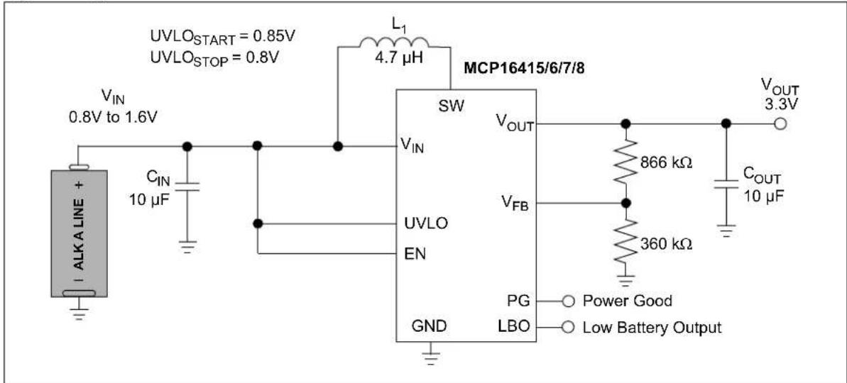
UVLOSTART = 0.85V UVLOSTOP = 0.8V VIN 0.8V to 1.6V L1 4.7 μH MCP16415/6/7/8 SW VOUT VIN UVLO EN GND PG LBO VFB 866 kΩ 360 kΩ COUT 10 μF VOUT 3.3V Power Good Low Battery Output CIN 10 μF ALK A LINE +
text_image
UVLOSTART = 2.4V UVLOSTOP = 0.8V L1 4.7 μH MCP16411/2/3/4 VIN 1.6V to 3.2V SW VOUT CIN 10 μF 1.69 MΩ 485 mV VREF 430 kΩ ENABLE ON OFF UVLO EN GND VOUT 768 kΩ VFB 360 kΩ 1 M Ω PGT LBO COUT 10 μF LBO Low if VIN < 2.4V VLW 2 x Fresh Alkaline Batteries Batteries with Low Voltage 3.2V 2.7V 3.0V Programmed UVLOSTART UVLOSTOP LBO 0V 3.2V 2.7V 3.0V Auto IN-OUT BYPASS area REGULATION area Time1.0 ELECTRICAL CHARACTERISTICS
Absolute Maximum Ratings ^†
EN, V_FB , V_IN , V_SW , V_OUT – GND .....+5.5V
EN, V_FB < Maximum between V_OUT or V_IN > (GND - 0.3V)
Output Short-Circuit Current Continuous
Output Current Bypass Mode 600 mA
Power Dissipation....Internally Limited
Storage Temperature -65°C to +150°C
Ambient Temperature with Power Applied ....-40°C to +85°C
Operating Junction Temperature, T_J ....-40°C to +125°C
ESD Protection on All Pins:
Human Body Model ≥ 4 kV
Charged Device Model ≥ 2 kV
† Notice: Stresses above those listed under “Absolute Maximum Ratings” may cause permanent damage to the device. This is a stress rating only and functional operation of the device at those or any other conditions above those indicated in the operational listings of this specification is not intended. Exposure to maximum rating conditions for extended periods may affect device reliability.
AC/DC CHARACTERISTICS
| Electrical Specifications: Unless otherwise noted, V_IN = 1.2V , C_OUT = C_IN = 10 μF, L = 4.7 μH, V_OUT = 3.3V , I_OUT = 10 mA , T_A = +25°C . Boldface specifications apply over the T_A range of -40°C to +85°C. | ||||||
| Parameters Sym. | Min. Typ. Max. Units | Conditions | ||||
| Input Voltage Range | V_IN | 0.82 | — | 5.25 | V | Values apply for the entire V_OUT range |
| Minimum Input Voltage for Start-up | V_IN | — | — | 0.88 | V | |
| Undervoltage Lockout (UVLO) | UVLO_START | 0.83 | 0.85 | 0.87 | V | Resistive load; UVLO pin connected to V_IN pin |
| UVLO_STOP | 0.74 | 0.8 | 0.81 | V | ||
| UVLO_HYS | — | 50 | — | mV | ||
| Output Voltage Adjust Range | V_OUT | 1.8 | — | 5.25 | V | Note 1 |
| Maximum Output Current | I_OUT | 170 | — | — | mA | 1.2V V_IN , 2.0V V_OUT (Note 4) |
| 200 | — | — | mA | 1.5V V_IN , 3.3V V_OUT (Note 4) | ||
| 600 | — | — | mA | 3.6V V_IN , 5.0V V_OUT (Note 4) | ||
| Feedback Voltage | V_FB | 0.95 | 0.97 | 0.985 | V | Note 3 |
| Feedback Input Bias Current | I_VFB | — | 1 | — | nA | Note 4 |
| Quiescent Current at V_OUT | I_QOUT | — | 5.0 | 7.0 | μA | EN = V_IN , does not include FB divider current, PFM mode (MCP16411/3/5/7) (Note 2) |
Note 1: For V_IN > V_OUT , the device enters Automatic Input-to-Output Bypass mode, V_OUT = V_IN - R_DS(ON)P * I_OUT , maximum V_IN is 5.25V.
2: V_OUT pin is forced biased with a voltage higher than the nominal V_OUT (device is not switching) at I_OUT = 0 mA. I_QIN and I_QOUT are the device's current consumption at V_IN and V_OUT pins during Sleep periods. The device selects its bias from V_IN and/or V_OUT .
3: 330Ω resistive load, 3.3V VOUT (10 mA).
4: Determined by characterization, not production tested.
5: This is ensured by design.
AC/DC CHARACTERISTICS (CONTINUED)
| Electrical Specifications: Unless otherwise noted, V_IN = 1.2V , C_OUT = C_IN = 10 μF , L = 4.7 μH , V_OUT = 3.3V , I_OUT = 10 mA , T_A = +25°C . Boldface specifications apply over the T_A range of -40°C to +85°C. | ||||||
| Parameters | Sym. | Min. | Typ. | Max. | Units | Conditions |
| Quiescent Current at V_IN | I_QIN | — | 4 | . | 5 | 5 IN A E PFM mode (MCP16411/3/5/7) (Notes 2, 4) |
| Quiescent Current – Shutdown Mode | I_QSHDN | — | 2 | . | 3 | 3 OUT = EN = GND, μ includes N-Channel and P-Channel switch leakage |
| NMOS Switch Leakage I | NLK | — | 8 | 5 | — | n A Note 5 |
| PMOS Switch Leakage I | PLK | — | 1 | — | n | A Note 5 |
| NMOS Switch On-Resistance | R_DS(ON)N | — | 0 | . | 4 | —SW = 100mA (Note 4) |
| PMOS Switch On-Resistance | R_DS(ON)P | — | 0 | . | 5 | —SW = 100mA (Note 4) |
| NMOS Peak Switch Current Limit | I_N(MAX) | 0.8 | 1 | — | A | Note 4 |
| V_OUT Accuracy | V_OUT % | — | — | +1 | % | Includes line and load regulation, V_IN = 1.5V , PWM Only options |
| Line Regulation | |( V_OUT/V_OUT) / V_DD| | — | 0 | . | 1 | 0 IN = 1.5V to 2.7V, I_OUT % 25 mA /PWM Only options |
| Load Regulation | | V_OUT/V_OUT| | — | 0 | . | 1 | 0 OUT = 1.0 mA to 2100 mA,% I_VIN = 1.5V , PWM Only options |
| Maximum Duty Cycle | DC_MAX | — | 9 | 0 | — | % Note 4 |
| Switching Frequency | f_SW | 425 | 500 | 575 | kHz | I_OUT = 100 mA |
| EN Input Logic High | V_IH | 82 | — | — | % of V_IN | I_OUT = 10 mA |
| EN Input Logic Low | V_IL | — | — | 25 | % of V_IN | I_OUT = 10 mA |
| EN Input Leakage Current | I_ENLK | — | 1 | — | n | A Note 4 |
| Power Good Threshold | PG_TH | — | 9 | 0 | — | % O%T (part of PGT signal) for MCP16411/2/3/4 |
| Power Good Hysteresis | PG_HYS | — | 5 | — | % | % OUT o f V |
| Power Good Delay | PG_DELAY | — | 250 | — | μs | Note 4 |
| Power Good Response | PG_RESPONSE | — | 250 | — | μs | Note 4 |
| PGT Pin Low-Level Output | PGT_LOW | — | 0 | . | 4 | —SINK = 2 mA (Note 4) |
| Low Battery Output Delay | LBO_DELAY | — | 150 | — | μs | Note 4 |
| Low Battery Output Response | LBI_RESPONSE | — | 150 | — | μs | Note 4 |
| Low Battery Input Hysteresis | LBI_HYS | — | 20 | 40 | mV | UVLO pin |
Note 1: For V_IN > V_OUT , the device enters Automatic Input-to-Output Bypass mode, V_OUT = V_IN - R_DS(ON)P * I_OUT , maximum V_IN is 5.25V.
2: V_OUT pin is forced biased with a voltage higher than the nominal V_OUT (device is not switching) at I_OUT = 0 mA. I_QIN and I_QOUT are the device's current consumption at V_IN and V_OUT pins during Sleep periods. The device selects its bias from V_IN and/or V_OUT .
3: 330Ω resistive load, 3.3V VOUT (10 mA).
4: Determined by characterization, not production tested.
5: This is ensured by design.
AC/DC CHARACTERISTICS (CONTINUED)
| Electrical Specifications: Unless otherwise noted, V_IN = 1.2V , C_OUT = C_IN = 10 μF, L = 4.7 μH, V_OUT = 3.3V , I_OUT = 10 mA , T_A = +25°C . Boldface specifications apply over the T_A range of -40°C to +85°C. | ||||||
| Parameters | Sym. | Min. | Typ. | Max. | Units | Conditions |
| Low Battery Output Low Level | LBI_LOW | — | 0 | . | 4 | —SINK= 2 mA (Note 4) I |
| Start-up Time t | s | — 1 — | ms EN low-to-high, | 90% of V | (Notes 3, 4) OUT | |
| Thermal Shutdown Die Temperature | T_SHDN | — | 1 | 4 | 0 | — °C |
| Thermal Shutdown Temperature Hysteresis | T_SHDNHYS | — | 1 | 0 | — | °C |
| Internal Overtemperature Output | PGT_OT | — | 7 | 5 | — | °C PGT signal switch from high-to-low level,MCP16411/2/3/4 only |
Note 1: For V_IN > V_OUT , the device enters Automatic Input-to-Output Bypass mode, V_OUT = V_IN - R_DS(ON)P * I_OUT , maximum V_IN is 5.25V.
2: V_OUT pin is forced biased with a voltage higher than the nominal V_OUT (device is not switching) at I_OUT = 0 mA. I_QIN and I_QOUT are the device's current consumption at V_IN and V_OUT pins during Sleep periods. The device selects its bias from V_IN and/or V_OUT .
3: 330Ω resistive load, 3.3V VOUT (10 mA).
4: Determined by characterization, not production tested.
5: This is ensured by design.
TEMPERATURE SPECIFICATIONS
| Parameters | Sym. | Min. | Typ. | Max. | Units | Conditions |
| Temperature Ranges | ||||||
| Operating Temperature Range | T_J | -40 | — | +125 | °C | Steady state |
| Storage Temperature Range | T_A | -65 | — | +150 | °C | |
| Maximum Junction Temperature | T_J | — | — | +150 | °C | Transient |
| Package Thermal Resistances | ||||||
| Thermal Resistance, 10-Lead MSOP | _JA | — | 7 | 1 | — | °C/W |
| Thermal Resistance, 10-Lead 3 mm x 3 mm TDFN | _JA | — | 54 | — | °C | /W |
NOTES:
2.0 TYPICAL PERFORMANCE CURVES
Note: The graphs and tables provided following this note are a statistical summary based on a limited number of samples and are provided for informational purposes only. The performance characteristics listed herein are not tested or guaranteed. In some graphs or tables, the data presented may be outside the specified operating range (e.g., outside specified power supply range) and therefore outside the warranted range.
Note: Unless otherwise indicated, V_IN = EN = 1.2V , C_OUT = C_IN = 10 F , L = 4.7 H , V_OUT = 3.3V , I_LOAD = 10mA , T_A = +25^ C , 10-Lead MSOP Package, PFM/PWM Options = MCP16411/3/5/7, PWM Only Options = MCP16412/4/6/8.
line
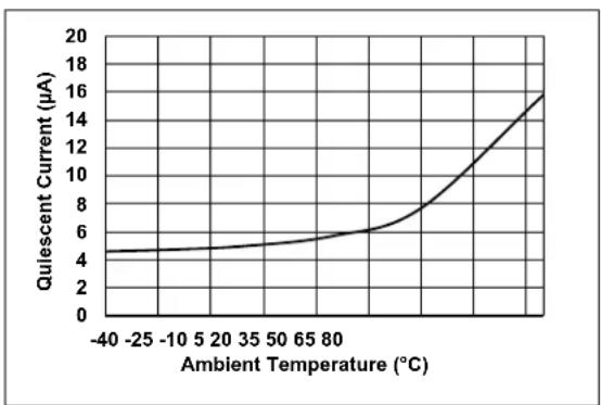
| Ambient Temperature (°C) | Quiescent Current (μA) | | :--- | :--- | | -40 | 4.5 | | -25 | 4.6 | | -10 | 4.7 | | 5 | 4.8 | | 20 | 4.9 | | 35 | 5.0 | | 50 | 5.2 | | 65 | 5.5 | | 80 | 6.0 | | 100 | 7.5 | | 120 | 9.5 | | 140 | 11.5 | | 160 | 13.5 | | 180 | 15.5 | The chart displays a single curve representing the relationship between ambient temperature and quiescent current. The x-axis is labeled as 'Ambient Temperature (°C)' and the y-axis is labeled as 'Quiescent Current (μA)'. There are no labels or additional data series in this image.FIGURE 2-1: I QOUT vs. Ambient Temperature, PFM/PWM Options.
line
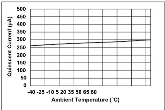
| Ambient Temperature (°C) | Quiescent Current (µA) | | ------------------------ | ---------------------- | | -40 | 260 | | -25 | 270 | | -10 | 275 | | 5 | 280 | | 20 | 285 | | 35 | 290 | | 50 | 295 | | 65 | 300 | | 80 | 305 |FIGURE 2-4: I QOUT vs. Ambient Temperature, PWM Only Options.
line
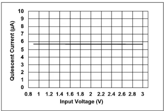
| Input Voltage (V) | Quiescent Current (µA) | |---|---| | 1.0 | 5.6 | | 3.0 | 5.6 |FIGURE 2-2: I QOUT vs. V_IN , PFM/PWM Options.
line
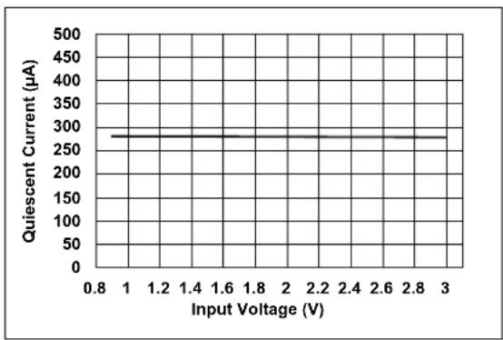
| Input Voltage (V) | Quiescent Current (µA) | | ----------------- | ---------------------- | | 0.8 | 270 | | 1.0 | 270 | | 1.2 | 270 | | 1.4 | 270 | | 1.6 | 270 | | 1.8 | 270 | | 2.0 | 270 | | 2.2 | 270 | | 2.4 | 270 | | 2.6 | 270 | | 2.8 | 270 | | 3.0 | 270 |FIGURE 2-5: I QOUT vs. V_IN , PWM Only Options.
line
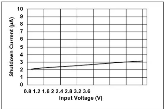
| Input Voltage (V) | Shutdown Current (µA) | | ----------------- | -------------------- | | 0.8 | 2.0 | | 1.2 | 2.2 | | 1.6 | 2.4 | | 2.0 | 2.6 | | 2.4 | 2.8 | | 2.8 | 3.0 | | 3.2 | 3.2 | | 3.6 | 3.4 |FIGURE 2-3: Shutdown Current vs. V IN.
line
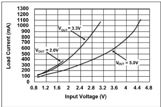
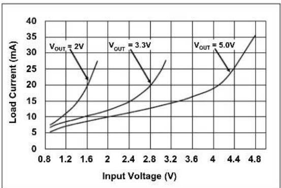
| Input Voltage (V) | Load Current (mA) for VOUT = 2.0V | Load Current (mA) for VOUT = 3.3V | Load Current (mA) for VOUT = 5.0V | | ----------------- | -------------------------------- | -------------------------------- | -------------------------------- | | 1.2 | 500 | - | - | | 1.6 | - | - | - | | 2.4 | - | 800 | - | | 3.6 | - | - | 500 | | 4.4 | - | - | 1100 |FIGURE 2-6: Maximum I OUT vs. V_IN , after Start-up, V_OUT Maximum 5% below Regulation Point.
Note: Unless otherwise indicated, V_IN = EN = 1.2V , C_OUT = C_IN = 10 F , L = 4.7 H , V_OUT = 3.3V , I_LOAD = 10 mA , T_A = +25^ , 10-Lead MSOP Package, PFM/PWM Options = MCP16411/3/5/7, PWM Only Options = MCP16412/4/6/8.
line
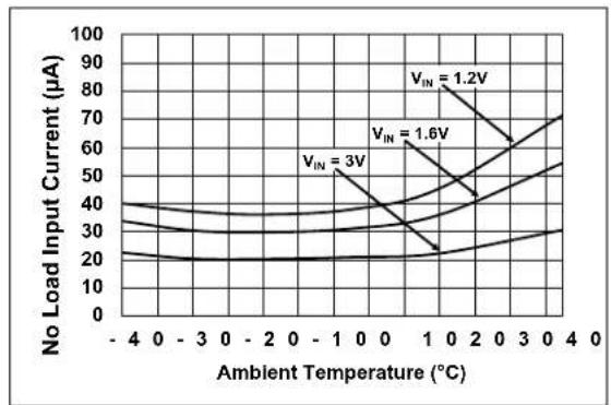
| Ambient Temperature (°C) | V_IN = 3V (μA) | V_IN = 1.2V (μA) | V_IN = 1.6V (μA) | | ------------------------ | -------------- | ---------------- | ---------------- | | -4 | 20 | 40 | 35 | | 0 | 20 | 40 | 35 | | 3 | 20 | 40 | 35 | | 4 | 20 | 40 | 35 | | 0 | 20 | 50 | 40 | | 1 | 25 | 60 | 50 | | 2 | 30 | 70 | 60 | | 3 | 35 | 80 | 70 | | 4 | 40 | 90 | 80 |FIGURE 2-7: No Load Input Current vs. Ambient Temperature, PFM/PWM Options.
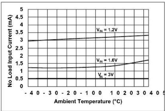
FIGURE 2-10: No Load Input Current vs. Ambient Temperature, PWM Only Options.
line
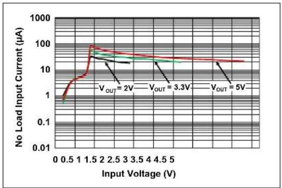
| Input Voltage (V) | No Load Input Current (μA) | | ----------------- | --------------------------- | | 0.5 | ~1 | | 1.5 | ~100 | | 2.5 | ~10 | | 3.3 | ~10 | | 4.5 | ~10 | | 5 | ~10 |FIGURE 2-8: No Load Input Current vs. V_IN , PFM/PWM Options.

line
| Input Voltage (V) | No Load Input Current (mA) | | ----------------- | -------------------------- | | 0 | 0.0001 | | 5 | 10 | | 1 | 1 | | 2 | 0.1 | | 5 | 0.01 | | 3 | 0.001 |FIGURE 2-11: No Load Input Current vs. V_IN , PWM Only Options.
line
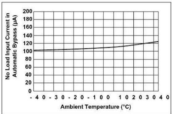
| Ambient Temperature (°C) | No Load Input Current in Automatic Bypass (µA) | | ------------------------ | ----------------------------------------------- | | -4 | 100 | | 0 | 105 | | 3 | 110 | | 0 | 115 | | 2 | 120 | | 3 | 125 | | 4 | 130 |FIGURE 2-9: Automatic Bypass Mode – No Load Input Current vs. Ambient Temperature.
line
| Input Voltage (V) | Load Current (mA) for VOUT = 2V | Load Current (mA) for VOUT = 3.3V | Load Current (mA) for VOUT = 5.0V | | ----------------- | ------------------------------ | ------------------------------- | ------------------------------- | | 1.2 | 30 | - | - | | 1.6 | 20 | - | - | | 2.4 | - | 30 | - | | 2.8 | - | 20 | - | | 3.2 | - | - | - | | 4.4 | - | - | 25 | | 4.8 | - | - | 35 |FIGURE 2-12: Average of PFM/PWM Threshold Current vs. V_IN .
Note: Unless otherwise indicated, V_IN = EN = 1.2V , C_OUT = C_IN = 10 F , L = 4.7 H , V_OUT = 3.3V , I_LOAD = 10mA , T_A = +25^ C , 10-Lead MSOP Package, PFM/PWM Options = MCP16411/3/5/7, PWM Only Options = MCP16412/4/6/8.

line
| Iout (mA) | Efficiency (%) for VIN = 1V | Efficiency (%) for VIN = 1.2V | Efficiency (%) for VIN = 1.6V | | --------- | --------------------------- | ----------------------------- | ----------------------------- | | 0.01 | ~65 | ~65 | ~65 | | 0.1 | ~68 | ~68 | ~68 | | 1 | ~70 | ~70 | ~70 | | 10 | ~72 | ~72 | ~72 | | 100 | ~75 | ~75 | ~75 | | 1000 | ~78 | ~78 | ~78 | | 10000 | ~80 | ~80 | ~80 | | 100000 | ~82 | ~82 | ~82 | | 1000000 | ~85 | ~85 | ~90 | | 10000000 | ~83 | ~83 | ~90 |FIGURE 2-13: 2.0V V OUT, Efficiency vs. IOUT, PFM/PWM Options.

line
| I_OUT (mA) | V_IN = 1V | V_IN = 1.2V | V_IN = 1.6V | | ---------- | --------- | ----------- | ----------- | | 0.1 | 20 | 20 | 20 | | 1 | 30 | 30 | 30 | | 10 | 45 | 45 | 45 | | 100 | 60 | 60 | 60 | | 1000 | 75 | 75 | 75 | | 10000 | 85 | 85 | 85 | | >1000 | ~90 | ~85 | ~90 |FIGURE 2-16: 2.0V V OUT, Efficiency vs. IOUT, PWM Only Options.

line
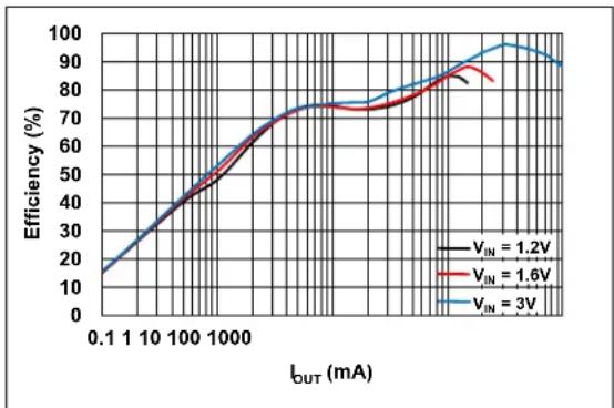
| IOUT (mA) | V_IN = 1.2V | V_IN = 1.6V | V_IN = 3V | | --------- | ----------- | ----------- | --------- | | 0.01 | ~60% | ~60% | ~60% | | 0.1 | ~65% | ~65% | ~65% | | 1 | ~70% | ~70% | ~70% | | 10 | ~75% | ~75% | ~75% | | 100 | ~80% | ~80% | ~80% | | 1000 | ~85% | ~85% | ~85% | | 10000 | ~90% | ~90% | ~90% |FIGURE 2-14: 3.3V V OUT, Efficiency vs. IOUT, PFM/PWM Options.
line
| Iout (mA) | V_IN = 1.2V | V_IN = 1.6V | V_IN = 3V | | --------- | ----------- | ----------- | --------- | | 0.1 | 15 | 15 | 15 | | 1 | 30 | 30 | 30 | | 10 | 45 | 45 | 45 | | 100 | 60 | 60 | 60 | | 1000 | 75 | 75 | 75 | | 10000 | 85 | 85 | 90 | | >1000 | ~90 | ~85 | ~95 |FIGURE 2-17: 3.3V V OUT, Efficiency vs. IOUT, PWM Only Options.
line
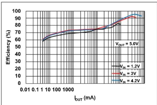
| IOUT (mA) | V_IN = 1.2V | V_IN = 3V | V_IN = 4.2V | | --------- | ----------- | --------- | ----------- | | 0.01 | ~60% | ~60% | ~60% | | 0.1 | ~65% | ~65% | ~65% | | 1 | ~70% | ~70% | ~70% | | 10 | ~75% | ~75% | ~75% | | 100 | ~80% | ~80% | ~80% | | 1000 | ~85% | ~85% | ~85% | | 10000 | ~90% | ~90% | ~90% | | 100000 | ~95% | ~95% | ~95% | | 1000000 | ~95% | ~95% | ~95% |FIGURE 2-15: 5.0V V OUT, Efficiency vs. IOUT, PFM/PWM Options.
line
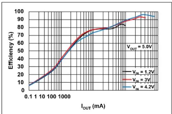
| I_OUT (mA) | V_IN = 1.2V | V_IN = 3V | V_IN = 4.2V | | ---------- | ----------- | --------- | ----------- | | 0.1 | ~5 | ~5 | ~5 | | 1 | ~10 | ~10 | ~10 | | 10 | ~20 | ~20 | ~20 | | 100 | ~40 | ~40 | ~40 | | 1000 | ~60 | ~60 | ~60 | | 10000 | ~80 | ~80 | ~80 | | 5000 | ~90 | ~90 | ~90 | | 10000 | ~95 | ~95 | ~95 |FIGURE 2-18: 5.0V V OUT, Efficiency vs. IOUT, PWM Only Options.
Note: Unless otherwise indicated, V_IN = EN = 1.2V , C_OUT = C_IN = 10 F , L = 4.7 H , V_OUT = 3.3V , I_LOAD = 10 mA , T_A = +25^ , 10-Lead MSOP Package, PFM/PWM Options = MCP16411/3/5/7, PWM Only Options = MCP16412/4/6/8.
line
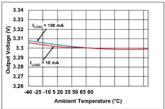
| Ambient Temperature (°C) | Output Voltage (V) for I_LOAD = 10 mA | Output Voltage (V) for I_LOAD = 10 mA | | ------------------------ | ------------------------------------- | ------------------------------------- | | -40 | 3.31 | 3.31 | | -25 | 3.30 | 3.30 | | -10 | 3.29 | 3.29 | | 5 | 3.29 | 3.29 | | 20 | 3.29 | 3.29 | | 35 | 3.29 | 3.29 | | 50 | 3.29 | 3.29 | | 65 | 3.29 | 3.29 | | 80 | 3.29 | 3.29 |FIGURE 2-19: 3.3V V OUT vs. Ambient Temperature.
line
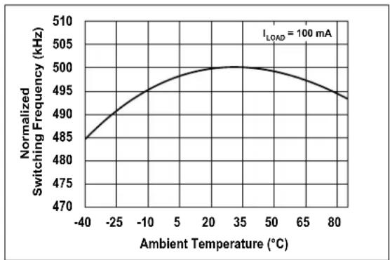
| Ambient Temperature (°C) | Normalized Switching Frequency (kHz) | | ------------------------ | ------------------------------------- | | -40 | 485 | | -25 | 490 | | -10 | 495 | | 5 | 500 | | 20 | 500 | | 35 | 500 | | 50 | 498 | | 65 | 495 | | 80 | 490 |FIGURE 2-22: Normalized Switching Frequency vs. Ambient Temperature.
line
| Ambient Temperature (°C) | Output Voltage (V) | | ------------------------ | ------------------ | | -40 | 3.31 | | -25 | 3.30 | | -10 | 3.29 | | 5 | 3.28 | | 20 | 3.27 | | 35 | 3.26 | | 50 | 3.27 | | 65 | 3.28 | | 80 | 3.29 |FIGURE 2-20: 3.3V V OUT vs. Ambient Temperature.
line
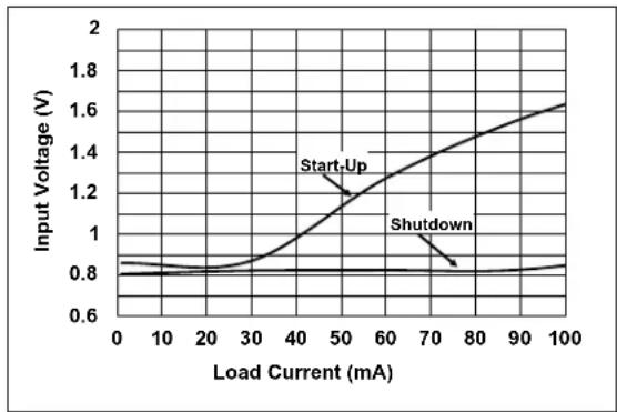
| Load Current (mA) | Input Voltage (V) | | ----------------- | ----------------- | | 0 | 0.8 | | 10 | 0.8 | | 20 | 0.8 | | 30 | 0.8 | | 40 | 0.9 | | 50 | 1.2 | | 60 | 1.3 | | 70 | 1.4 | | 80 | 1.5 | | 90 | 1.6 | | 100 | 1.7 |FIGURE 2-23: 3.3V V OUT, Minimum Start-up and Shutdown V_IN vs. Resistive Load.
line
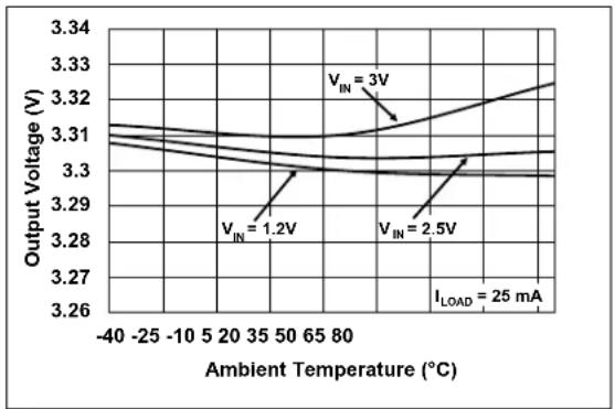
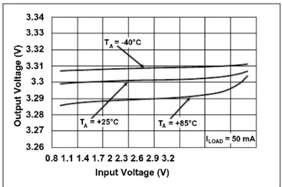
| Input Voltage (V) | Output Voltage (V) for T_A = -40°C | Output Voltage (V) for T_A = +25°C | Output Voltage (V) for T_A = +85°C | | ----------------- | ---------------------------------- | ---------------------------------- | ---------------------------------- | | 2.3 | 3.31 | 3.29 | 3.27 |FIGURE 2-21: 3.3V V OUT vs. V_IN .

line
| Load Current (mA) | Input Voltage (V) | | ----------------- | ----------------- | | 0 | 0.8 | | 20 | 0.8 | | 30 | 1.2 | | 40 | 1.6 | | 50 | 1.8 | | 60 | 2.0 | | 70 | 2.2 | | 80 | 2.4 | | 90 | 2.6 | | 100 | 2.8 |FIGURE 2-24: 5.0V V OUT, Minimum Start-Up and Shutdown V_IN vs. Resistive Load.
Note: Unless otherwise indicated, V_IN = EN = 1.2V , C_OUT = C_IN = 10 F , L = 4.7 H , V_OUT = 3.3V , I_LOAD = 10mA , T_A = +25^ C , 10-Lead MSOP Package, PFM/PWM Options = MCP16411/3/5/7, PWM Only Options = MCP16412/4/6/8.
line
| Input Voltage (V) | Ia Peak Current (A) for TA = +25°C | Ia Peak Current (A) for TA = +85°C | Ia Peak Current (A) for TA = -40°C | | ----------------- | ---------------------------------- | ---------------------------------- | ---------------------------------- | | 0.8 | 0.8 | 0.8 | 0.8 | | 1.0 | 0.8 | 0.8 | 0.8 | | 1.2 | 0.8 | 0.8 | 0.8 | | 1.4 | 0.8 | 0.8 | 0.8 | | 1.6 | 0.8 | 0.8 | 0.8 | | 1.8 | 0.8 | 0.8 | 0.8 | | 2.0 | 0.8 | 0.8 | 0.8 | | 2.2 | 0.8 | 0.8 | 0.8 | | 2.4 | 0.8 | 0.8 | 0.8 | | 2.6 | 0.8 | 0.8 | 0.8 | | 2.8 | 0.8 | 0.8 | 0.8 | | 3.0 | 1.0 | 1.0 | 1.0 | | 3.2 | 1.2 | 1.2 | 1.2 | | 3.4 | 1.4 | 1.4 | 1.4 | | 3.6 | 1.6 | 1.6 | 1.6 | | 3.8 | 1.8 | 1.8 | 1.8 | | 4.0 | 2.0 | 2.0 | 2.0 | | 4.2 | 2.2 | 2.2 | 2.2 | | 4.4 | 2.4 | 2.4 | 2.4 |FIGURE 2-25: 3.3V V OUT, Inductor Peak Current Limit vs. V_IN .
line
| Input Voltage (V) | IL Peak Current (A) for TA = +25°C | IL Peak Current (A) for TA = +85°C | IL Peak Current (A) for TA = -40°C | | ----------------- | ---------------------------------- | ---------------------------------- | ---------------------------------- | | 0.8 | 1.0 | 0.9 | 1.3 | | 0.9 | 1.1 | 1.0 | 1.4 | | 1.0 | 1.2 | 1.1 | 1.5 | | 1.1 | 1.25 | 1.15 | 1.55 | | 1.2 | 1.3 | 1.2 | 1.6 | | 1.3 | 1.35 | 1.25 | 1.65 | | 1.4 | 1.4 | 1.3 | 1.7 | | 1.5 | 1.45 | 1.35 | 1.75 | | 1.6 | 1.5 | 1.4 | 1.8 | | 1.7 | 1.55 | 1.45 | 1.85 | | 1.8 | 1.6 | 1.5 | 1.9 | | 1.9 | 1.65 | 1.55 | 1.95 |FIGURE 2-28: 2.0V V OUT, Inductor Peak Current Limit vs. V_IN .
line
| Input Voltage (V) | Ic Peak Current (A) for TA = +25°C | Ic Peak Current (A) for TA = +85°C | Ic Peak Current (A) for TA = -40°C | | ----------------- | ---------------------------------- | ---------------------------------- | ---------------------------------- | | 0.8 | 0.8 | 0.8 | 0.8 | | 1.2 | 0.9 | 0.9 | 0.9 | | 1.6 | 0.95 | 0.95 | 0.95 | | 2.0 | 1.0 | 1.0 | 1.0 | | 2.4 | 1.05 | 1.05 | 1.05 | | 2.8 | 1.1 | 1.1 | 1.1 | | 3.2 | 1.15 | 1.15 | 1.15 | | 3.6 | 1.2 | 1.2 | 1.2 | | 4.0 | 1.3 | 1.3 | 1.3 | | 4.4 | 1.5 | 1.5 | 1.5 | | 4.8 | 2.2 | 1.8 | 2.2 |FIGURE 2-26: 5.0V V OUT, Inductor Peak Current Limit vs. V_IN .
line
| Ambient Temperature (°C) | Input Voltage (V) | | ------------------------ | ----------------- | | -40 | 0.86 | | -25 | 0.85 | | -10 | 0.85 | | 5 | 0.85 | | 20 | 0.85 | | 35 | 0.85 | | 50 | 0.85 | | 65 | 0.85 | | 80 | 0.85 |FIGURE 2-29: UVLO START and UVLO STOP vs. Ambient Temperature.

line
| Load Current (mA) | Output Voltage (V) for V_IN = 1.5V | Output Voltage (V) for V_IN = 2.5V | | ----------------- | ---------------------------------- | ---------------------------------- | | 10 | 3.30 | 3.31 | | 20 | 3.29 | 3.30 | | 30 | 3.29 | 3.29 | | 40 | 3.29 | 3.29 | | 50 | 3.29 | 3.29 | | 60 | 3.29 | 3.29 | | 70 | 3.29 | 3.29 | | 80 | 3.29 | 3.29 | | 90 | 3.29 | 3.29 | | 100 | 3.29 | 3.29 |FIGURE 2-27: Load Regulation, PWM Only Options.
line
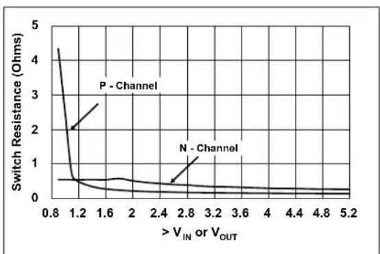
| > V_IN or V_OUT | Switch Resistance (Ohms) - P - Channel | Switch Resistance (Ohms) - N - Channel | | --------------- | -------------------------------------- | --------------------------------------- | | 0.8 | 4.5 | 0.5 | | 1.2 | 2.0 | 0.5 | | 1.6 | 0.5 | 0.5 | | 2.0 | 0.5 | 0.5 | | 2.4 | 0.5 | 0.5 | | 2.8 | 0.5 | 0.5 | | 3.2 | 0.5 | 0.5 | | 3.6 | 0.5 | 0.5 | | 4.0 | 0.5 | 0.5 | | 4.4 | 0.5 | 0.5 | | 4.8 | 0.5 | 0.5 | | 5.2 | 0.5 | 0.5 |FIGURE 2-30: N-Channel and P-Channel, R_DSON vs. > V_IN or V_OUT .
Note: Unless otherwise indicated, V_IN = EN = 1.2V , C_OUT = C_IN = 10 F , L = 4.7 H , V_OUT = 3.3V , I_LOAD = 10 mA , T_A = +25^ , 10-Lead MSOP Package, PFM/PWM Options = MCP16411/3/5/7, PWM Only Options = MCP16412/4/6/8.
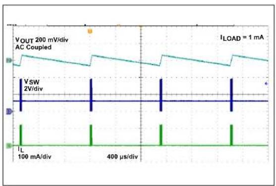
FIGURE 2-31: 3.3V V OUT, PFM Mode Waveforms.

FIGURE 2-34: 3.3V V OUT, No Load, PFM Mode Output Ripple.
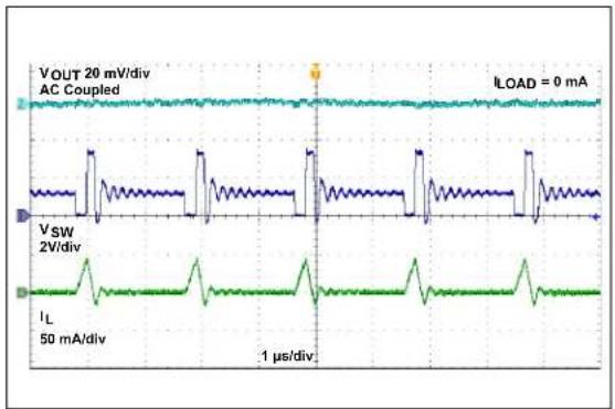
FIGURE 2-32: 3.3V V OUT, No Load, PWM Mode Waveforms.

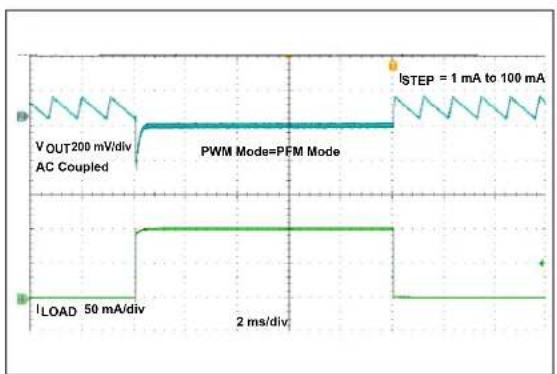
FIGURE 2-35: 3.3V V OUT, PWM Mode Waveforms.
line
| Time (ms) | Current (mA) | | --------- | ------------ | | 0 | 50 | | 2 | 50 | | 4 | 50 | | 6 | 50 | | 8 | 50 | | 10 | 50 | | 12 | 50 | | 14 | 50 | | 16 | 50 | | 18 | 50 | | 20 | 50 | | 22 | 50 | | 24 | 50 | | 26 | 50 | | 28 | 50 | | 30 | 50 | | 32 | 50 | | 34 | 50 | | 36 | 50 | | 38 | 50 | | 40 | 50 | | 42 | 50 | | 44 | 50 | | 46 | 50 | | 48 | 50 | | 50 | 50 | | 52 | 50 | | 54 | 50 | | 56 | 50 | | 58 | 50 | | 60 | 50 | | 62 | 50 | | 64 | 50 | | 66 | 50 | | 68 | 50 | | 70 | 50 | | 72 | 50 | | 74 | 50 | | 76 | 50 | | 78 | 50 | | 80 | 50 | | 82 | 50 | | 84 | 50 | | 86 | 50 | | 88 | 50 | | 90 | 50 | | 92 | 50 | | 94 | 50 | | 96 | 50 | | 98 | 50 | | 100 | 50 |FIGURE 2-33: 3.3V V OUT, Load Transient Waveforms, PFM/PWM Options.
line
| Time (ms) | VOUT 200 mV/div AC Coupled (mA) | LOAD 50 mA/div (mA) | |-----------|----------------------------------|---------------------| | 0 | 0 | 0 | | 1 | ~0.8 | ~0.8 | | 2 | ~0.8 | ~0.8 | | 3 | ~0.8 | ~0.8 | | 4 | ~0.8 | ~0.8 | | 5 | ~0.8 | ~0.8 | | 6 | ~0.8 | ~0.8 | | 7 | ~0.8 | ~0.8 | | 8 | ~0.8 | ~0.8 | | 9 | ~0.8 | ~0.8 | | 10 | ~0.8 | ~0.8 | | 11 | ~0.8 | ~0.8 | | 12 | ~0.8 | ~0.8 | | 13 | ~0.8 | ~0.8 | | 14 | ~0.8 | ~0.8 | | 15 | ~0.8 | ~0.8 | | 16 | ~0.8 | ~0.8 | | 17 | ~0.8 | ~0.8 | | 18 | ~0.8 | ~0.8 | | 19 | ~0.8 | ~0.8 | | 20 | ~0.8 | ~0.8 | | 21 | ~0.8 | ~0.8 | | 22 | ~0.8 | ~0.8 | | 23 | ~0.8 | ~0.8 | | 24 | ~0.8 | ~0.8 | | 25 | ~0.8 | ~0.8 | | 26 | ~0.8 | ~0.8 | | 27 | ~0.8 | ~0.8 | | 28 | ~0.8 | ~0.8 | | 29 | ~0.8 | ~0.8 | | 30 | ~0.8 | ~0.8 | | 31 | ~0.8 | ~0.8 | | 32 | ~0.8 | ~0.8 | | 33 | ~0.8 | ~0.8 | | 34 | ~0.8 | ~0.8 | | 35 | ~0.8 | ~0.8 | | 36 | ~0.8 | ~0.8 | | 37 | ~0.8 | ~0.8 | | 38 | ~0.8 | ~0.8 | | 39 | ~0.8 | ~0.8 | | 40 | ~0.8 | ~0.8 | | 41 | ~0.8 | ~0.8 | | 42 | ~0.8 | ~0.8 | | 43 | ~0.8 | ~0.8 | | 44 | ~0.8 | ~0.8 | | 45 | ~0.8 | ~0.8 | | 46 | ~0.8 | ~0.8 | | 47 | ~0.8 | ~0.8 | | 48 | ~0.8 | ~0.8 | | 49 | ~0.8 | ~0.8 | | 50 | ~0.8 | 50 | | 51 | ~0.8 | 50 | | 52 | ~0.8 | 50 | | 53 | ~0.8 | 50 | | 54 | ~0.8 | 50 | | 55 | ~0.8 | 50 | | 56 | ~0.8 | 50 | | 57 | ~0.8 | 50 | | 58 | ~0.8 | 50 | | 59 | ~0.8 | 50 | | 60 | ~0.8 | 50 | | 61 | ~0.8 | 50 | | 62 | ~0.8 | 50 | | 63 | ~0.8 | 50 | | 64 | ~0.8 | 50 | | 65 | ~0.8 | 50 | | 66 | ~0.8 | 50 | | 67 | ~0.8 | 50 | | 68 | ~0.8 | 50 | | 69 | ~0.8 | 50 | | 70 | ~0.8 | 50 | | 71 | ~0.8 | 50 | | 72 | ~0.8 | 50 | | 73 | ~0.8 | 50 | | 74 | ~0.8 | 50 | | 75 | ~0.8 | 50 | | 76 | ~0.8 | 50 | | 77 | ~0.8 | 50 | | 78 | ~0.8 | 50 | | 79 | ~0.8 | 50 | | 80 | ~0.8 | 50 | | 81 | ~0.8 | 50 | | 82 | ~0.8 | 50 | | 83 | ~0.8 | 50 | | 84 | ~0.8 | 50 | | 85 | ~0.8 | 50 | | 86 | ~0.8 | 50 | | 87 | ~0.8 | 50 | | 88 | ~0.8 | 50 | | 89 | ~0.8 | 50 | | 90 | ~0.8 | 50 | | 91 | ~0.8 | 50 | | 92 | ~0.8 | 50 | | 93 | ~0.8 | 50 | | 94 | ~0.8 | 50 | | 95 | ~0.8 | 50 | | 96 | ~0.8 | 50 | | 97 | ~0.8 | 50 | | 98 | ~0.8 | 50 | | 99 | ~0.8 | 50 | | 100 | - | - | Step = - A: AC Coupled; Step = + A: AC Coupled; Load = - A: LoadFIGURE 2-36: 3.3V V OUT, Load Transient Waveforms, PWM Only Options.
Note: Unless otherwise indicated, V_IN = EN = 1.2V , C_OUT = C_IN = 10 F , L = 4.7 H , V_OUT = 3.3V , I_LOAD = 10mA , T_A = +25^ C , 10-Lead MSOP Package, PFM/PWM Options = MCP16411/3/5/7, PWM Only Options = MCP16412/4/6/8.

line
| Time (μs) | VOUT (mA) | VIN (VEN) | IL (mA) | |-----------|-----------|-----------|---------| | 0 | 0 | 0 | 0 | | 200 | 1.0 | 0.5 | 0.1 | | 400 | 1.0 | 0.5 | 0.1 |FIGURE 2-37: 3.3V V OUT, Start-Up from V_IN , PFM/PWM Options.
line
| Time (μs) | VOUT (V) | VIN (V) | IL (mA) | |-----------|----------|---------|---------| | 0 | 0 | 0 | 0 | | 400 | 400 | 1 | 200 |FIGURE 2-40: 3.3V V OUT, Start-Up from V_IN , PWM Only Options.
line
| Time (ms) | VOUT (mV) | VIN (V) | |-----------|-----------|---------| | 0 | 100 | 1 | | 1 | ~0.8 | 1 | | 2 | ~0.7 | 1 | | 3 | ~0.6 | 1 | | 4 | ~0.5 | 1 | | 5 | ~0.4 | 1 | | 6 | ~0.3 | 1 | | 7 | ~0.2 | 1 | | 8 | ~0.1 | 1 | | 9 | ~0.05 | 1 | | 10 | ~0.02 | 1 | | 11 | ~0.01 | 1 | | 12 | ~0.005 | 1 | | 13 | ~0.002 | 1 | | 14 | ~0.001 | 1 | | 15 | ~0.0005 | 1 | | 16 | ~0.0002 | 1 | | 17 | ~0.0001 | 1 | | 18 | ~0.00005 | 1 | | 19 | ~0.00002 | 1 | | 20 | ~0.00001 | 1 | | 21 | ~0.000005 | 1 | | 22 | ~0.000002 | 1 | | 23 | ~0.000001 | 1 | | 24 | ~0.0000005| 1 | | 25 | ~0.0000002| 1 | | 26 | ~0.0000001| 1 | | 27 | ~0.00000005|1 | | 28 | ~0.00000002|1 | | 29 | ~0.00000001|1 | | 30 | ~0.000000005|1 | | 31 | ~0.000000002|1 | | 32 | ~0.000000001|1 | | 33 | ~0.0000000005|1 | | 34 | ~0.0000000002|1 | | 35 | ~0.0000000001|1 | | 36 | ~0.000000000 |1 | | 37 | ~- | - | | 38 | - | - | | 39 | - | - | | 40 | - | - | | 41 | - | - | | 42 | - | - | | 43 | - | - | | 44 | - | - | | 45 | - | - | | 46 | - | - | | 47 | - | - | | 48 | - | - | | 49 | - | - | | 50 | - | - | | 51 | - | - | | 52 | - | - | | 53 | - | - | | 54 | - | - | | 55 | - | - | | 56 | - | - | | 57 | - | - | | 58 | - | - | | 59 | - | - | | 60 | - | - | | 61 | - | - | | 62 | - | - | | 63 | - | - | | 64 | - | - | | 65 | - | - | | 66 | - | - | | 67 | - | - | | 68 | - | - | | 69 | - | - | | 70 | - | - | | 71 | - | - | | 72 | - | - | | 73 | - | - | | 74 | - | - | | 75 | - | - | | 76 | - | - | | 77 | - | - | | 78 | - | - | | 79 | - | - | | 80 | - | - | | 81 | - | - | | 82 | - | - | | 83 | - | - | | 84 | - | - | | 85 | - | - | | 86 | - | - | | 87 | - | - | | 88 | - | - | | 89 | - | - | | 90 | - | - | | 91 | - | - | | 92 | - | - | | 93 | - | - | | 94 | - | - | | 95 | - | - | | 96 | - | - | | 97 | - | - | | 98 | - | - | | 99 | - | - | | 1 | ~- | + | The chart displays two sets of values: AC Coupled (top) and VIN (bottom). The AC Coupled line is labeled 'AC Coupled', and the VIN line is labeled 'VIN step from 1V to 2.5V'. The data is presented in a table format with 'Time (ms)' as the index of the waveforms.FIGURE 2-38: 3.3V V OUT, Line Transient Waveforms.

line
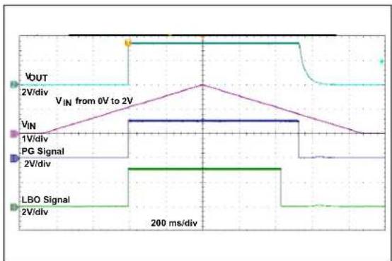
| Signal Type | Value | | ----------------- | --------- | | VOUT | 2V/div | | VIN from 0V to 2V | 0V to 2V | | VIN | 1V/div | | PG Signal | 2V/div | | LBO Signal | 2V/div |FIGURE 2-41: 3.3V V OUT, UVLO Connected to V_IN .
line
| Time (μs) | VEN (V) | VOUT (V) | |-----------|---------|----------| | 0 | 1 | 2 | | 200 | 1 | 2 | | 400 | 1 | 400 | | 600 | 1 | 400 | | 800 | 1 | 400 | | 1000 | 1 | 400 | | 1200 | 1 | 400 | | 1400 | 1 | 400 | | 1600 | 1 | 400 | | 1800 | 1 | 400 | | 2000 | 1 | 400 | | 2200 | 1 | 400 | | 2400 | 1 | 400 | | 2600 | 1 | 400 | | 2800 | 1 | 400 | | 3000 | 1 | 400 | | 3200 | 1 | 400 | | 3400 | 1 | 400 | | 3600 | 1 | 400 | | 3800 | 1 | 400 | | 4000 | 1 | 400 | | 4200 | 1 | 400 | | 4400 | 1 | 400 | | 4600 | 1 | 400 | | 4800 | 1 | 400 | | 5000 | 1 | 400 | | 5200 | 1 | 400 | | 5400 | 1 | 400 | | 5600 | 1 | 400 | | 5800 | 1 | 400 | | 6000 | 1 | 400 | | 6200 | 1 | 400 | | 6400 | 1 | 400 | | 6600 | 1 | 400 | | 6800 | 1 | 400 | | 7000 | 1 | 400 | | 7200 | 1 | 400 | | 7400 | 1 | 400 | | 7600 | 1 | 400 | | 7800 | 1 | 400 | | 8000 | 1 | 400 | | 8200 | 1 | 400 | | 8400 | 1 | 400 | | 8600 | 1 | 400 | | 8800 | 1 | 400 | | 9000 | 1 | 400 | | 9200 | 1 | 400 | | 9400 | 1 | 400 | | 9600 | 1 | 400 | | 9800 | 1 | 400 | | 10000 | 1 | 400 | | - | - | - | | - | - | - | | - | - | - | | - | - | - | | - | - | - | | - | - | - | | - | - | - | | - | - | - | | - | - | - | | - | - | - | | - | - | -2 | | - | - | -2 | | - | - | -2 | | - | - | -2 | | - | - | -2 | | - | - | -2 | | - | - | -2 | | - | - | -2 | | - | - | -2 | | - | - | -2.5 | | - | - | -2.5 | | - | - | -2.5 | | - | - | -2.5 | | - | - | -2.5 | | - | - | -2.5 | | - | - | -2.5 | | - | - | -2.5 | | - | - | +2 | | - | - | +2 | | - | - | +2 | | - | - | +2 | | - | - | +2 | | - | - | +2 | | - | - | +2 | | - | - | +2 | | - | - | +2 | | - | - | +2 | | Time (μs) vs. Voltage (VEN) / Output Voltage (VOUT) for each of the cycle (VEN) and time (VOUT) from start to end of the cycle (VOUT) for each of the cycle (VEN) and time (VOUT) of each cycle (VOUT). The cycle is labeled as 'VEN' and 'VOUT'. The cycle labels are 'A', 'B', 'C', 'D', 'E', 'F'.FIGURE 2-39: 3.3V V OUT, Start-Up after Enable.
line
| Signal Type | Value | |-------------|-----------| | VOUT | 0 | | VIN from 0V | 2V/div | | VOUT (peak)| 2V/div | | VIN (peak)| 1V/div | | PG Signal | 2V/div | | LBO Signal | 2V/div |FIGURE 2-42: 3.3V V OUT, UVLO Set for 1.1V.
Note: Unless otherwise indicated, V_IN = EN = 1.2V , C_OUT = C_IN = 10 F , L = 4.7 H , V_OUT = 3.3V , I_LOAD = 10 mA , T_A = +25^ , 10-Lead MSOP Package, PFM/PWM Options = MCP16411/3/5/7, PWM Only Options = MCP16412/4/6/8.

FIGURE 2-43: 3.3V V OUT, LBO Delay and Response Time.
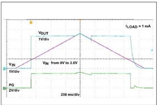
FIGURE 2-45: 3.3V V OUT, Boost to Automatic Bypass Transitions, PWM Only Options.
line
| Time (ms) | V_OUT (mA) | V_IN (V) | PG (V) | |-----------|------------|----------|--------| | 0 | 0 | 0 | 0 | | 1 | 1 | 1 | 0 | | 2 | 1 | 1 | 0 | | 3 | 1 | 1 | 0 | | 4 | 1 | 1 | 0 | | 5 | 1 | 1 | 0 | | 6 | 1 | 1 | 0 | | 7 | 1 | 1 | 0 | | 8 | 1 | 1 | 0 | | 9 | 1 | 1 | 0 | | 10 | 1 | 1 | 0 | | 11 | 1 | 1 | 0 | | 12 | 1 | 1 | 0 | | 13 | 1 | 1 | 0 | | 14 | 1 | 1 | 0 | | 15 | 1 | 1 | 0 | | 16 | 1 | 1 | 0 | | 17 | 1 | 1 | 0 | | 18 | 1 | 1 | 0 | | 19 | 1 | 1 | 0 | | 20 | 1 | 1 | 0 | | 21 | 1 | 1 | 0 | | 22 | 1 | 1 | 0 | | 23 | 1 | 1 | 0 | | 24 | 1 | 1 | 0 | | 25 | 1 | 1 | 0 | | 26 | 1 | 1 | 0 | | 27 | 1 | 1 | 0 | | 28 | 1 | 1 | 0 | | 29 | 1 | 1 | 0 | | 30 | 1 | 1 | 0 | | 31 | 1 | 1 | 0 | | 32 | 1 | 1 | 0 | | 33 | 1 | 1 | 0 | | 34 | 1 | 1 | 0 | | 35 | 1 | 1 | 0 | | 36 | 1 | 1 | 0 | | 37 | 1 | 1 | 0 | | 38 | 1 | 1 | 0 | | 39 | 1 | 1 | 0 | | 40 | 1 | 1 | 0 | | 41 | 1 | 1 | 0 | | 42 | 1 | 1 | 0 | | 43 | 1 | 1 | 0 | | 44 | 1 | 1 | 0 | | 45 | 1 | 1 | 0 | | 46 | 1 | 1 | 0 | | 47 | 1 | 1 | 0 | | 48 | 1 | 1 | 0 | | 49 | 1 | 1 | 0 | | 50 | 1 | 1 | 0 | | Note: The actual values for V_OUT and V_IN are not provided in the code. The data is presented as a table above. The values for PG and PG are labeled as '2V/div' in the chart. There is no additional data series in this case. The values for I_LOAD = -1 mA are shown on the chart.FIGURE 2-44: 3.3V V OUT, Boost to Automatic Bypass Transitions, PFM/PWM Options.
3.0 PART NUMBER SELECTION
TABLE 3-1: DEVICE OPTIONS
| Part Number | EN Pin Shutdown Option | Switching Mode Option | PGT/PG Pin Option |
| MCP16411 Output | Discharge PFM/PWM Power | Good and Die Overtemperature Output | |
| MCP16412 Output | Discharge PWM Only Power | Good and Die Overtemperature Output | |
| MCP16413 In-Out | Bypass PFM/PWM Power | Good and Die Overtemperature Output | |
| MCP16414 In-Out | Bypass PWM Only Power | Good and Die Overtemperature Output | |
| MCP16415 Output | Discharge PFM/PWM Power | Good Output | |
| MCP16416 Output | Discharge PWM Only Power | Good Output | |
| MCP16417 In-Out | Bypass PFM/PWM Power | Good Output | |
| MCP16418 In-Out | Bypass PWM Only Power | Good Output |
NOTES:
4.0 PIN DESCRIPTIONS
The descriptions of the pins are listed in Table 4-1.
TABLE 4-1: PIN FUNCTION TABLE
| MCP1641X10-Lead MSOP | MCP1641X10-Lead 3 mm x 3 mm TDFN | Symbol Description | ||
| 1 | 1 | UVLO | Undervoltage Lockout (0.485V internal reference) and Input Pin for Low Battery Output (LBO) Voltage Comparator | |
| 2 2 | LBO | Open-Drain Low Battery Comparator Output Pin | ||
| 3 | 3 | PGT, PG | Open-Drain Power Good and Die Overtemperature Comparators Output Pin. Only MCP16411/2/3/4 devices have both functions implemented on the same pin, PGT. See Table 3-1 for device options. | |
| 4 | 4 | V_FB | Feedback Voltage Pin, 0.97V Reference Voltage | |
| 5 | 5 | V_OUT | Output Voltage Pin | |
| 6 6 | SW | Switch Node, Boost Inductor Pin | ||
| 7 | 7 | P_GND | Power Ground Pin | |
| 8 | 8 | S_GND | Signal Ground Pin | |
| 9 | 9 | V_IN | Input Voltage Pin | |
| 10 | 10 | EN | Enable Control Input Pin. The device is in shutdown if EN is pulled to GND. | |
| — | 11 | EP | Exposed Thermal Pad (3 x 3 TDFN only); must be connected to P_GND and S_GND . | |
4.1 Undervoltage Lockout Input Pin (UVLO), Input for Low-Voltage Output Comparator
The UVLO and low battery comparator input use an internal 485 mV reference. Connect the UVLO pin to the V_IN pin for a default start-up threshold of 0.85V. The device stops switching at 0.8V typical input voltage. Connect an external resistive divider to this pin to increase the UVLO_START threshold. When the battery voltage or V_IN is ramping down to the programmed threshold, the LBO output pin will be asserted low.
4.2 Low Battery Output Pin (LBO)
The open-drain output shows a low-level warning signal if the UVLO pin detects a battery level below the 485 mV threshold. If no external divider on the UVLO pin is used (UVLO = V_IN ), low battery detection is ineffective.
4.3 Power Good and Die Overtemperature Pin (PGT)
The Power Good and Die Overtemperature (PGT) pin is an open-drain output, which can be connected to V_OUT through a pull-up resistor. The pin switches to a low level when V_OUT drops below 10% of its nominal value or when the internal die's temperature sensor detects a value higher than +75°C (typical).
The MCP16415/6/7/8 devices have only the Power Good function implemented – PG pin (see Table 3-1 for the device options).
4.4 Feedback Voltage Pin (V FB)
The V_FB pin is used to provide output voltage regulation by using a resistive divider network. The feedback voltage is typically 0.97V.
4.5 Output Voltage Pin (V OUT)
The Output Voltage pin connects the synchronous integrated P-Channel MOSFET to the output capacitor. The resistive divider network from FB is also connected to the V_OUT pin for voltage regulation.
4.6 Switch Node Pin (SW)
Connect the inductor from the input voltage to the SW pin. The SW pin carries inductor current which can be as high as 1A (typical). The integrated N-Channel switch drain and integrated P-Channel switch source are internally connected at the SW node.
4.7 Power Ground Pin (P GND)
The Power Ground pin is used as a return for the high-current N-Channel switch. The P_GND and S_GND pins are connected externally.
4.8 Signal Ground Pin (S GND)
The Signal Ground pin is used as a return for the integrated V_REF and error amplifier. The S_GND and power ground ( P_GND ) pins are connected externally.
4.9 Power Supply Input Voltage Pin ( V_IN )
Connect the input voltage source to V_IN . A local bypass capacitor is required. The input source should be decoupled to GND with a 10 F minimum capacitor.
4.10 Enable Pin (EN)
The EN pin is an input of a Schmitt Trigger circuit used to enable or disable the device's switching. While the EN pin is low (EN = GND), the device is in Shutdown mode – output discharge or input-to-output bypass (see Table 3-1) and consumes low quiescent current, 2.3 A (typical). A logic high (> 82% of V_IN ) enables the boost converter output. A logic low (< 25% of V_IN ) ensures that the boost converter is disabled. Do not allow this pin to float.
4.11 Exposed Thermal Pad (EP)
There is no internal electrical connection between the Exposed Thermal Pad (EP) and the S_GND and P_GND pins. They must be connected to the same electric potential on the Printed Circuit Board (PCB).
5.0 DEVICE OVERVIEW
5.1 Introduction
The MCP1641X is a low-voltage, step-up converter with battery monitoring features. The MCP1641X delivers high efficiency over a wide range of inputs: single-cell, two-cell, alkaline/NiMH batteries or single-cell Li-Ion/Li-Polymer batteries can be used.
A high level of integration lowers total system cost, eases implementation and reduces the Bill of Materials (BOM) and board area.
This family of devices features low quiescent current, a programmable start-up voltage (UVLO _START ), low battery indication, adjustable output voltage, dual modes of operation (PFM/PWM and PWM Only), integrated synchronous switch, internal compensation, low noise anti-ringing control, inrush current limit and soft start.
A new battery-friendly feature for the Microchip's step-up converters family is the Automatic Input-to-Output Voltage Bypass. This function helps optimize the capacity usage of the battery, and keeps the efficiency high and the noise low for a narrow step-up conversion ratio (e.g., two fresh alkaline cells powering a boost converter for a 3.0V or 3.3V output voltage). With automatic transition from Input-to-Output Bypass to Boost mode operation and low noise anti-ringing control circuitry, in addition to the PWM Only switching, the MCP1641X devices offer a good low noise DC-DC solution for compact battery-powered systems.
The monitoring of its internal temperature, while powering the converter from batteries, is an additional safety feature of the MCP1641X family. An output pin (PGT) provides an error signal if the temperature of the die exceeds +75°C.
There are two shutdown options for the MCP1641X family: Output Discharge and Input-to-Output Bypass.
5.2 MCP1641X Options
A summary of the device options is presented in Table 3-1.
The MCP16411/3/5/7 devices use an automatic switchover from PWM to PFM mode, for light load conditions, to maximize efficiency over a wide range of output current.
The PFM mode operation has a higher output voltage ripple and variable frequency as compared to the PWM mode.
During periods of light load operation, the MCP1641X devices continue to operate at a fixed 500 kHz switching frequency, allowing pulse-skipping.
The MCP16412/4/6/8 devices disable PFM mode switching and operate only in PWM mode over the entire load range.
5.2.3 OUTPUT DISCHARGE SHUTDOWN OPTION
The MCP16411/2/5/6 devices incorporate an output auto-discharge feature. While in Shutdown mode, the MCP16411/2/5/6 devices automatically discharge the output capacitor by using an internal N-Channel MOSFET switch.
The capacitors connected to the output are discharged by an integrated switch of 150-200Ω. The discharge time depends on the total output capacitance.
During the Output Discharge Shutdown mode, the output of the MCP16411/2/5/6 is completely disconnected from the input by turning off the integrated P-Channel switch and removing the switch bulk diode connection. This removes the DC path, which is typically present in boost converters and which allows the output to be disconnected from the input. While in this mode, a low quiescent current (2.3 A, typical) is consumed from the input (battery).
5.2.4 INPUT-TO-OUTPUT BYPASS SHUTDOWN OPTION
The MCP16413/4/7/8 devices incorporate the Input-to-Output Bypass Shutdown option. With the EN input pulled low, the output is connected to the input using the internal P-Channel MOSFET.
In this mode, the current drawn from the input (battery) is 2.3 A, typically, with no load. The Input-to-Output Bypass mode is used when the input voltage range is high enough for the load to operate in Standby or Low I_Q mode (e.g., a microcontroller). When a higher, regulated output voltage is necessary to operate the application, the EN input is pulled high, boosting the output to the regulated value.
5.2.5 POWER GOOD AND DIE OVERTEMPERATURE (PGT PIN OPTION)
The MCP16411/2/3/4 devices offer a combined output Power Good and Die Overtemperature signal to the PGT pin.
Pin switches to low level when either:
- The output voltage drops below 10% of its nominal value, with 5% hysteresis;
- The IC works at a temperature which is higher than +75^ .
5.2.6 POWER GOOD (PG PIN OPTION)
The MCP16415/6/7/8 devices offer only a Power Good output signal to the PG pin, which switches low when the output voltage drops below 10% of the V_OUT nominal value and resumes at 95% of the V_OUT nominal value.
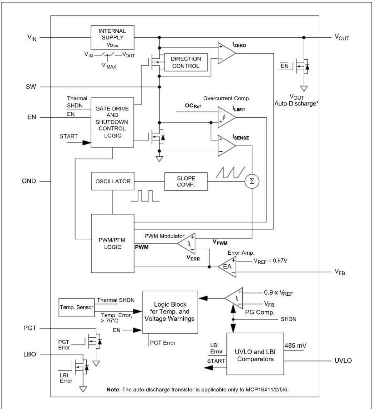
5.3 Functional Description
The MCP1641X is a compact, high-efficiency, fixed frequency, synchronous step-up DC-DC converter with programmable UVLO start-up, low battery detection and output discharge that provides an easy-to-use power supply solution for applications powered from batteries. Figure 5-1 depicts the functional block diagram of the MCP1641X. It incorporates a Current-mode control scheme, in which the PWM ramp signal is derived from the NMOS Power Switch Current ( I_SENSE ).
This ramp signal adds to the slope compensation signal and is compared to the output of the Error Amplifier ( V_ERR ) to control the on-time of the power switch. In addition, several voltage comparators (PG, UVLO internal overtemperature and LBO) protect the converter from heretical operation and overheating, as well as the battery from overdischarging and risk of leakage.
flowchart
graph TD
    A["VIN"] --> B["INTERNAL SUPPLY VMax"]
    B --> C["DIRECTION CONTROL"]
    C --> D["IZERO"]
    D --> E["EN"]
    E --> F["VOUT Auto-Discharge*"]
    G["SW"] --> H["GATE DRIVE AND SHUTDOWN CONTROL LOGIC"]
    I["EN"] --> J["START"]
    J --> K["OSCILLATOR"]
    K --> L["SLOPE COMP."]
    L --> M["Σ"]
    N["GND"] --> O["PWM/PFM LOGIC"]
    O --> P["PWM Modulator"]
    P --> Q["VREF = 0.97V"]
    Q --> R["Error Amp."]
    R --> S["VFB"]
    T["PGT"] --> U["Temp. Sensor"]
    U --> V["Thermal SHDN Temp. Error, >75°C"]
    V --> W["Logic Block for Temp. and Voltage Warnings"]
    X["LBO"] --> Y["PGT Error"]
    Y --> Z["PGT Error"]
    Z --> AA["PG Comp."]
    AA --> AB["UVLO and LBI Comparators"]
    AC["VOUT"] --> AD["Output Stage"]
    AE["VREF"] --> AF["Error Amp."]
    AF --> AG["VFB"]
    AH["EN"] --> AI["Auto-Discharge*"]
    AJ["Overcurrent Comp."] --> AK["OCRef"]
    AK --> AL["ILIMIT"]
    AL --> AM["ISENSE"]
    AM --> AN["Σ"]
    AO["VLO"] --> AP["Output Stage"]
FIGURE 5-1: MCP1641X Functional Block Diagram.
5.3.1 INTERNAL BIAS
The MCP1641X devices get their start-up bias from V_IN . The V_IN bias is used to power the device and drive circuits over the entire operating range. During normal operation, the internal V_MAX comparator selects the highest voltage rail between V_IN and V_OUT , in order to optimize operation and reduce power consumption. Once the output exceeds the input, bias comes from the output. The internal voltage reference of 485 mV is powered from the input voltage at all times. A voltage amplifier buffers and multiplies the reference to 0.97V for the FB input of the error amplifier. Once the UVLO comparator triggers the start-up, the internal control loop keeps the output in regulation, while V_IN ramps down to 0.8V (UVLO _STOP ).
5.3.2 LOW-VOLTAGE START-UP
The MCP1641X is capable of starting from a low input voltage. Start-up voltage is well-controlled by the UVLO circuitry, which uses the 485 mV voltage reference. The default start-up value is 0.85V (typical). The UVLO _START threshold can be programmed by using an external resistive divider connected to the UVLO pin. This input also serves as a low battery input.
When the device is enabled (EN set high) and the input voltage is higher than 0.85V (typical), the internal start-up logic turns on the rectifying P-Channel switch until the output capacitor is charged to a value close to the input voltage. This is commonly called the output precharging phase and the rectifying switch limits the current during this time. Precharge current varies and increases with V_IN . Precharge current starts from 25 mA for low input voltage and increases up to 250 mA or more near the maximum limit of V_IN .
After the output capacitor is charged to the input voltage, the device starts switching and runs in open loop, with limited inductor peak current, at approximately 30-40% of its nominal value. Once the output voltage ramps up to 60-70% of the nominal value, the normal closed-loop operation is initiated.
5.3.3 UNDERVOLTAGE LOCKOUT (UVLO)
The internal UVLO comparator input uses the 485 mV voltage reference to compare it with the battery input voltage. If the UVLO input is tied to V_IN , the comparator enables the converter at 0.85V typical input voltage. If a different UVLO_START voltage is desired, a resistive divider must be connected to the UVLO pin.
The UVLO _STOP threshold is set internally to 0.8V.
The MCP16411/3/5/7 devices use an automatic switchover from PWM to PFM mode, for light load conditions, to maximize efficiency over a wide range of output current. During PFM mode, a controlled peak current limit is used to pump the output up to the threshold. While operating in PFM or PWM mode, the P-Channel switch is used as a synchronous rectifier, turning off when the inductor current reaches 0 mA, in order to maximize efficiency.
In PFM mode, a voltage comparator is used to terminate switching when the output voltage reaches an upper threshold limit. Once switching has terminated, the output voltage decays or coasts down. During this Sleep period, a very low current is consumed from the input source, which keeps power efficiency high at light load.
The PFM mode frequency is a function of input voltage, output voltage and load. While in PFM mode, the boost converter periodically pumps the output with a fixed switching frequency of 500 kHz. The value of the output capacitor changes the low-frequency component ripple. The device itself is powered from the output and consumes 5 A (typical).
PFM operation is initiated if the output load current falls below an internally programmed threshold. The output voltage is continuously monitored; when the output voltage drops below its nominal value, PFM operation pulses one or several times to bring the output back into regulation. If the output load current rises above the upper threshold, the MCP16411/3/5/7 enters smoothly into the PWM mode.
Figure 2-12 represents the input voltage versus load current for the PFM to PWM threshold.
In normal PWM Operation mode, the MCP16412/4/6/8 devices operate as a fixed frequency, synchronous boost converter. The switching frequency is internally maintained with a precision oscillator, which is typically set to 500 kHz.
At light loads, the MCP16412/4/6/8 devices begin to skip pulses. By operating in PWM Only mode, the output ripple remains low and the frequency is constant. Operating in Fixed PWM mode results in low efficiency during light load operation, but with the advantage of low output ripple and noise for the supplied load. Lossless current sensing converts the peak current signal to voltage in order to sum it with the internal slope compensation. This summed signal is compared with the voltage error amplifier output to provide a peak current control command for the PWM signal. The converter provides the proper amount of slope compensation to ensure stability. The peak current limit is typically set to 1A.
The MCP1641X integrates a low noise anti-ringing switch that damps the oscillations observed at the switch node of the boost converter. This method reduces the noise spread when operating at light loads in Discontinuous Inductor Current (DCM) mode.
5.3.7 INTERNAL COMPENSATION
The error amplifier (a transconductance type), with its associated compensation network, completes the closed-loop system; it compares the output voltage ( V_FB pin) to a reference at the input of the error amplifier, and feeds the amplified and inverted signal to the control input of the inner current loop. The compensation network provides phase leads and lags at appropriate frequencies to cancel the excessive phase lags and leads of the power circuit. All necessary compensation components and slope compensation are integrated.
5.3.8 LOW BATTERY DETECTION
The LBO pin is connected to the output of the Low Battery Input (LBI) comparator to warn if the input voltage is low or the UVLO pin level is below the 485 mV trip point. The LBI comparator is active only when the device is active (EN is high), after the start-up sequence ends. The LBI comparator acts only during the V_IN down slope (e.g., battery is discharging). There is a hysteresis of 20 mV (typical) between the UVLO START and LBI thresholds. After the LBO output pin is asserted low for low battery, the boost converter continues to operate down to 0.8V (UVLO STOP ). In order to get a valid LBO signal, the input voltage must be lower for more than 150 s (see Figure 5-2). This blanking time eliminates false triggering of the LBI comparator due to voltage transients.

line
| Signal | Voltage (V) | |--------|-------------| | EN | 0.85 | | LBO | 0.8 | | VOUT | 0.85 | | PGT | 0.8 |FIGURE 5-2: UVLO and LBO Behavior (UVLO pin connected to V_IN pin).

line
| Signal | Voltage (V) | |--------|-------------| | UVLO | 0.85 | | V_IN | 0.8 | | UVLO | 485 | | LBI HYST | - | | EN | - | | LBO | - | | VOUT | - | | PGT | - |FIGURE 5-3: UVLO and LBO Behavior (UVLO pin connected to a resistive divider to program the UVLO _START value).
5.3.9 POWER GOOD AND DIE OVERTEMPERATURE SYSTEM RESPONSE
The PGT is an open-drain output pin, a mixed Power Good and Die Overtemperature function, which works as a general error pin if one of the following events occurs:
- V_OUT is below 90% of regulated value; there is a 5% hysteresis. It resumes when V_OUT gets back to 95% of its nominal value. A 250 μs delay is needed for a valid signal (see Figure 5-4).
- The device's temperature is higher than +75^ (only for MCP16411/2/3/4 devices; see Table 3-1). This feature can be preprogrammed by customer request (in the +55^ to +85^ range with +10^ increments).
Note: Contact the regional sales office for more details.
The open-drain transistor allows interfacing the PGT pin with an MCU I/O port. It can sink up to 2 mA from the power line with the pull-up resistor connected. The PGT signal is generated (comparator active) only if the device is active (EN is high).
The device's overtemperature protection feature helps in any case of overload, or other Fault conditions that generate the heating of the device or its proximity (e.g., PCB area), preventing the end equipment from overheating or melting.

other
| Time Period | Signal Type | Value Label | |-------------|-------------|-------------| | 250 µs | VOUT | VOUT | | <150 µs | VOUT | <150 µs | | 250 µs | PGT | PGT | | 250 µs | RESPONSE | RESPONSE |FIGURE 5-4: PGT Output Response.
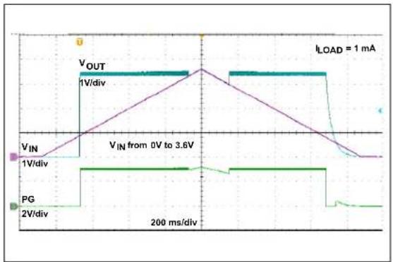
5.3.10 AUTOMATIC INPUT-TO-OUTPUT BYPASS MODE
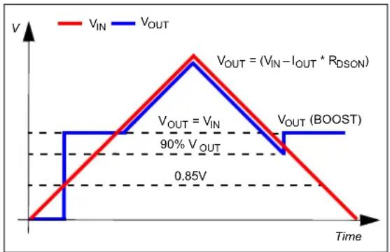
The MCP1641X features Automatic Input-to-Output Bypass mode if V_IN is close to the selected V_OUT or higher. In this situation, V_OUT tracks V_IN , which is "bypassed" to the output through the synchronous P-Channel MOSFET. The device resumes Boost mode if V_OUT decreases down to approximately 90% of the target regulation voltage.
This function has the advantage of offering a highly efficient Conversion mode while the battery is fresh, which translates into better battery utilization. This mode of operation also removes the high output ripple and noise, which is usually present in boost converters during operation when the value of the input is very close to the desired output voltage (where the switching duty cycle is minimum and limited). This mode is recommended for noise-sensitive power rail applications (e.g., audio, LCD displays). The disadvantage is that the output is not regulated in this range, but equal with battery voltage minus a drop on the synchronous P-MOS ( I_OUT * R_DSON ) rectifier.
line
| Time | VIN | VOUT | |------|---------|---------| | 0 | 0 | 0 | | Peak | 1 | 1 | | 0.85 | 0 | 0.85 | | Peak | 1 | 1 | | VOUT | 0 | 0 | | VOUT = (VIN - IOUT * RDSON) | 1 | 1 | | VOUT = VIN | 0 | 0.85 | | VOUT (BOOST) | 0 | 0.85 |FIGURE 5-5: Automatic Boost-Bypass Transition.
5.3.11 ENABLE
The MCP1641X devices are enabled when the EN pin is set high and are disabled when the EN pin is set low (Shutdown mode). The enable threshold voltage varies with the input voltage. To enable the boost converter, the EN voltage level must be greater than 82% of the V_IN voltage. To disable the boost converter, the EN voltage must be less than 25% of the V_IN voltage.
In Shutdown mode, a low quiescent current, 2.3 A (typical), is consumed from the input (battery).
5.3.12 SHORT-CIRCUIT PROTECTION
Unlike most boost converters, the MCP1641X allows its output to be shorted during normal operation. The 1A (typical) internal current limit and thermal shutdown reduce excessive stress and protect the device during periods of short-circuit, overcurrent and overtemperature.
5.3.13 INPUT OVERCURRENT LIMIT
The MCP1641X devices use a 1A (typical) cycle-by-cycle inductor peak current limit to protect the N-Channel switch. The overcurrent comparator resets the driving latch when the peak of the inductor current reaches the limit. In current limitation, the output voltage starts dropping. To assure highest load current operation, by design, the current limit is higher than typical for an input voltage close to the output voltage value.
5.3.14 THERMAL SHUTDOWN
Thermal shutdown circuitry is integrated in the MCP1641X devices. This circuitry monitors the device's junction temperature and shuts off the output if the junction temperature exceeds the typical +140°C value. If this threshold is exceeded, the device automatically restarts once the junction temperature drops by 10°C (typical).
6.0 APPLICATION INFORMATION
The MCP1641X synchronous boost converter operates over a wide input and output voltage range. The power efficiency is high for several decades of load range. The output current capability increases with the input voltage and decreases with the output voltage. The maximum output current is based on the N-Channel peak current limit. Section 2.0 "Typical Performance Curves" displays the typical output current capability.
6.1 Adjustable Output Voltage Calculations
To calculate the resistive divider values for the MCP1641X, use Equation 6-1, where R_TOP is connected to V_OUT , R_BOT is connected to GND, and both R_TOP and R_BOT are connected to the V_FB input pin.
EQUATION 6-1:
$$ R _ {T O P} = R _ {B O T} \times \left(\frac {V _ {O U T}}{V _ {F B}} - 1\right) $$
EXAMPLE 1:
$$ V _ {\text { OUT }} = 1. 8 \mathrm{V} $$
$$ V _ {F B} = 0. 9 7 V $$
$$ R _ {B O T} = 3 6 0 k \Omega $$
$$ R _ {T O P} = 3 0 9 \mathrm{k} \Omega $$
EXAMPLE 2:
$$ V _ {O U T} = 2. 0 V $$
$$ V _ {F B} = 0. 9 7 V $$
$$ R _ {B O T} = 3 6 0 k \Omega $$
$$ R _ {T O P} = 3 8 3 k \Omega $$
EXAMPLE 3:
$$ V _ {O U T} = 3. 3 V $$
$$ V _ {F B} = 0. 9 7 V $$
$$ R _ {B O T} = 3 6 0 \mathrm{k} \Omega $$
$$ R _ {T O P} = 8 6 6 k \Omega $$
EXAMPLE 4:
$$ V _ {O U T} = 5. 0 V $$
$$ V _ {F B} = 0. 9 7 V $$
$$ R _ {B O T} = 3 6 0 \mathrm{k} \Omega $$
$$ R _ {T O P} = 1. 5 \mathrm{M} \Omega $$
The internal error amplifier of the Peak Current mode control loop is a transconductance error amplifier; its gain is not related to the resistor's value. There are some potential issues with higher value resistors. For small surface-mount resistors, environment contamination can create leakage paths that significantly change the resistive divider ratio and the output voltage tolerance. Smaller feedback resistor values increase the quiescent current drained from the battery by a few A, but result in good regulation over the entire temperature range.
When R_TOP and R_BOT are higher, the efficiency of the DC-DC conversion is optimized at very light loads.
For boost converters, the removal of the feedback resistors during operation must be avoided. If feedback resistors are removed during operation, the output voltage increases above the absolute maximum output limits of the MCP1641X and damages the device (for additional information, see Application Note AN1337, "Optimizing Battery Life in DC Boost Converters Using MCP1640", DS00001337).
6.2 Programmable UVLO and LBO Calculations
This feature is used to increase the UVLO START threshold. To calculate the resistive divider values for a new UVLO threshold, use Equation 6-2, where RH is connected to V_IN , R_L is connected to GND, and both R_H and R_L are connected to the UVLO input pin.
The programmable UVLO resistors' calculations result in changing the low battery input detection level on the down slope of the input voltage, as detailed in Section 5.3.8 "Low Battery Detection".
EQUATION 6-2:
$$ R _ {H} = R _ {L} \times \left(\frac {U V L O _ {S T A R T}}{V r e f _ {U V L O}} - 1\right) $$
EXAMPLE 5:
$$ \mathrm{UVLO} _ {\text { START }} = 1. 1 \mathrm{V} $$
$$ \mathrm{Vref} _ {\mathrm{UVLO}} = 4 8 5 \mathrm{mV} $$
$$ R _ {L} = 4 3 0 \mathrm{k} \Omega $$
$$ R _ {H} = 5 4 9 \mathrm{k} \Omega $$
EXAMPLE 6:
$$ \mathrm{UVLO} _ {\text { START }} = 1. 8 \mathrm{V} $$
$$ \mathrm{Vref} _ {\mathrm{UVLO}} = 4 8 5 \mathrm{mV} $$
$$ R _ {L} = 4 3 0 \mathrm{k} \Omega $$
$$ \begin{array}{r c l} R _ {H} & = & 1. 1 6 5 \mathrm{M} \Omega (\text {with a standard value}) \ & & \text {of 1.15 M\Omega , UVLO_{START} is} \ & & 1. 7 8 2 \mathrm{V}) \end{array} $$
6.3 Input Capacitor Selection
The boost input current is smoothed by the boost inductor, reducing the amount of filtering necessary at the input. Some capacitance is recommended to provide decoupling from the source. Low-ESR X5R or X7R ceramic capacitors are well-suited, due to their low-temperature coefficient and small size. For most applications, 10 F of capacitance is sufficient at the input. For high-power applications that have high source impedance or long leads, connecting additional input capacitance to the battery provides a stable input voltage. Table 6-1 shows the recommended input capacitor value range.
6.4 Output Capacitor Selection
The output capacitor helps to provide a stable output voltage during sudden load transients and reduces the output voltage ripple. As with the input capacitor, X5R and X7R ceramic capacitors are well-suited for this application. While C_OUT provides load current, a voltage drop also appears across its internal ESR that results in ripple voltage. Using other capacitor types (e.g., aluminum) with large ESR has a detrimental impact on the converter's efficiency and maximum output power. For a proper value, the output capacitance can be estimated by Equation 6-3.
The MCP1641X is internally compensated, therefore, the output capacitance range is limited to 20 F.
An output capacitance higher than 10 F adds a better load step response and high-frequency noise attenuation, especially while stepping from light loads (PFM mode) to heavy loads (PWM mode).
For output voltages below 2V, 20 F capacitance is recommended.
See Table 6-1 for the recommended output capacitor range.
EQUATION 6-3:
$$ I _ {O U T} = C _ {O U T} \times \left(\frac {d V}{d t}\right) $$
Where:
$$ d V = \text { Ripple voltage } $$
$$ d t = \text { On - time of the N - Channel switch } $$
$$ (D \times 1 / f _ {S W}, D \text { is duty cycle }) $$
TABLE 6-1: CAPACITOR VALUE RANGE
| C_IN | C_OUT | |
| Minimum | 10 μF | 10 μF |
| Maximum | None | 20 μF |
6.5 Inductor Selection
The MCP1641X is designed to be used with small surface-mount inductors; the inductance value can range from 2.2 H to 4.7 H. An inductance value of 4.7 H is recommended to achieve a good balance between inductor size, converter load transient response and minimized noise. For an output below 2.0V, the inductor value must be reduced to 2.2 H. Several parameters should be considered when selecting the correct inductor: maximum rated current, saturation current and copper resistance (DCR). For boost converters, the inductor current can be much higher than the output current. The lower the inductor's DCR, the higher the efficiency of the converter; a common trade-off in size versus efficiency. See Table 6-2 for the recommended inductors.
TABLE 6-2: MCP1641X RECOMMENDED INDUCTORS
| Part Number | Value (μH) | DCR Ω (typ.) | ISAT(A) | Size WxLxH (mm) |
| Würth Elektronik | ||||
| WE-MAIA | 2.2 | 0.147 | 2.5 | 2.5x2x1 |
| 2.2 | 0.252 | 2.2 | 2.5x2x0.8 | |
| 4.7 | 0.356 | 2.4 | 3x3x1 | |
| 4.7 | 0.300 | 2.1 | 2.5x2x1.2 | |
| WE-MAPI | 2.2 | 0.123 | 2.9 | 2.5x2x1.2 |
| 2.2 | 0.150 | 3.9 | 3x3x1 | |
| 4.7 | 0.300 | 2.1 | 2.5x2x1.2 | |
| 4.7 | 0.267 | 3.8 | 3x3x1.2 | |
| WE-SPC | 4.7 | 0.086 | 2.9 | 4.8x4.8x2.8 |
| WE-LQS | 2.2 | 0.08 | 1.95 | 2.5x2x1.2 |
| 4.7 | 0.091 | 1.9 | 4x4x1.2 | |
| Coilcraft | ||||
| XAL4020 | 2.2 | 0.035 | 5.6 | 4x4x2.1 |
| XAL4030 | 4.7 | 0.040 | 4.5 | 4x4x3.1 |
| XEL4030 | 2.2 | 0.020 | 6.1 | 4x4x3.1 |
| 4.7 | 0.040 | 4.6 | 4x4x3.1 | |
| XFL4020 | 2.2 | 0.0235 | 3.7 | 4x4x2.1 |
| 4.7 | 0.057 | 2.7 | 4x4x2.1 | |
| XGL4020 | 2.2 | 0.019 | 6.2 | 4x4x2.1 |
| 4.7 | 0.043 | 4.1 | 4x4x2.1 | |
| LPS4018 | 4.7 | 0.125 | 1.9 | 3.9x3.9x1.7 |
| LPS4012 | 2.2 | 0.1 | 2.5 | 3.9x3.9x1.1 |
| TDK Corporation | ||||
| VLS3012HBX | 2.2 | 0.088 | 3.76 | 3x3x1.2 |
| 4.7 | 0.175 | 2.79 | 3x3x1.2 | |
| Eaton Electronics Division (Coiltronics) | ||||
| SD3118 | 2.2 | 0.074 | 2.00 | 3.1x3.1x1.8 |
| MPI25-V2 | 2.2 | 0.087 | 3.5 | 2.5x2x1.25 |
| 4.7 | 0.235 | 1.9 | 2.5x2x1.25 | |
The MCP1641X limits the inductor peak current to 1A; for proper operation, an inductor with a saturation current higher than this limit should be chosen. The saturation current typically specifies a point at which the inductance has rolled off a percentage of the rated value. This can range from a 20% to 40% reduction in inductance. As the inductance rolls off, the inductor current ripple increases, so does the peak switch current. It is important to keep the inductance from rolling off too much as it can cause switch current to reach the peak limit.
6.6 Thermal Calculations
The MCP1641X devices are available in two different packages, 10-lead MSOP and 3 mm x 3 mm 10-lead TDFN. The junction temperature is estimated by calculating the power dissipation and applying the package thermal resistance ( _JA ). The maximum operating junction temperature rating for the MCP1641X family of devices is +125°C.
To quickly estimate the internal power dissipation for the switching boost regulator, an empirical calculation using measured efficiency can be applied, as presented in Equation 6-4.
The difference between the first term, input power and the second term, power delivered, is the internal MCP1641X device's power dissipation. This is an estimate, assuming that most of the power lost is internal to the MCP1641X and not by the C_IN , C_OUT or the inductor. However, there is some percentage of power lost in the boost inductor with very little loss in the input and output capacitors. For a more accurate estimation of the internal power dissipation, subtract the I_LRMS^2 × L_DCR power dissipation.
6.7 PCB Layout Information
Good PCB layout techniques are important to any switching circuitry and switching power supplies is no different. When wiring the switching high-current paths, short and wide traces should be used. Therefore, it is important that the input and output capacitors should be placed as close as possible to the MCP1641X to minimize the loop area.
The feedback resistors and feedback signal should be routed away from the switching node and the switching current loop. When possible, ground planes and traces should be used to help shield the feedback signal and minimize noise and magnetic interference.
EQUATION 6-4:
$$ \left(\frac {V _ {O U T} \times I _ {O U T}}{E f f i c i e n c y}\right) (V _ {O U T} \times I _ {O U T}) = D i s $$
text_image
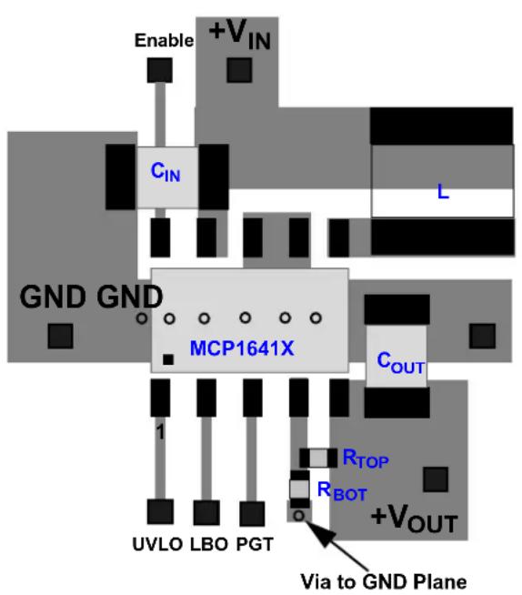
Enable +V_IN C_IN GND GND MCP1641X 1 UVLO LBO PGT R_TOP R_BOT C_OUT +V_OUT Via to GND PlaneFIGURE 6-1: MCP1641X Recommended Layout, Applicable to Both Packages.
NOTES:
7.0 APPLICATION CIRCUIT EXAMPLES
text_image
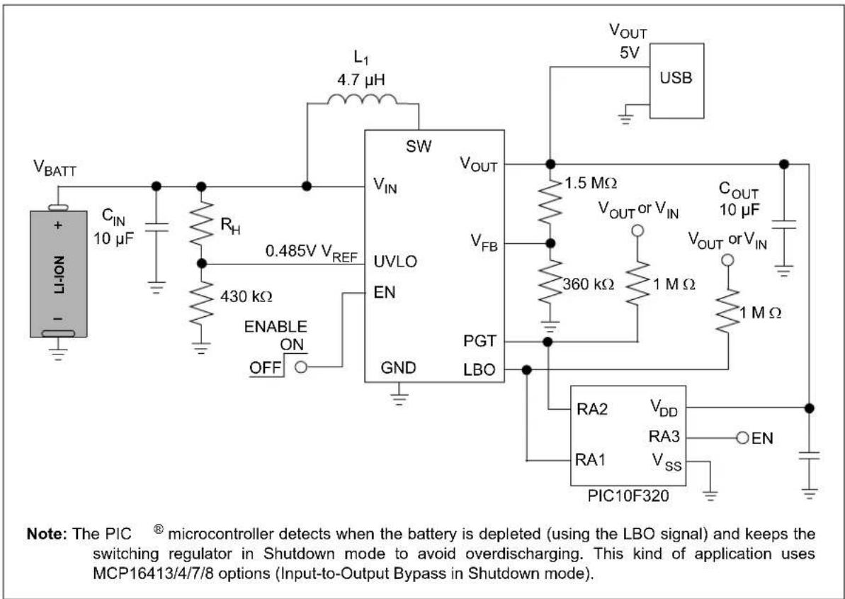
L1 4.7 μH V_BATT + - LI-ION C_IN 10 μF R_H 430 kΩ 0.485V V_REF ENABLE ON OFF SW V_IN UVLO EN GND V_OUT V_FB PGT LBO 1.5 MΩ V_OUT or V_IN 360 kΩ 1 M Ω C_OUT 10 μF V_OUT or V_IN 1 M Ω RA2 V_DD RA3 RA1 V_SS PIC10F320 EN Note: The PIC ® microcontroller detects when the battery is depleted (using the LBO signal) and keeps the switching regulator in Shutdown mode to avoid overdischarging. This kind of application uses MCP16413/4/7/8 options (Input-to-Output Bypass in Shutdown mode).FIGURE 7-1: Single Cell for USB Application Using Bypass Mode.

text_image
VIN 0.8V to 4.5V L1 4.7 μH CIN 10 μF R_H 1-3 Cells VREF 0.485V ENABLE ON OFF SW VOUT VFB UVLO EN GND PGT LBO To PIC® MCU VOUT 3.3V or VIN COUT 10 μF VOUT 1 M Ω 1 M Ω Note: For V_IN < VOUT, the device operates in Boost mode; otherwise, for VIN > VOUT, VIN is bypassed to VOUT.FIGURE 7-2: Multiple Cell Operation with Automatic Input-to-Output Bypass Mode.
text_image
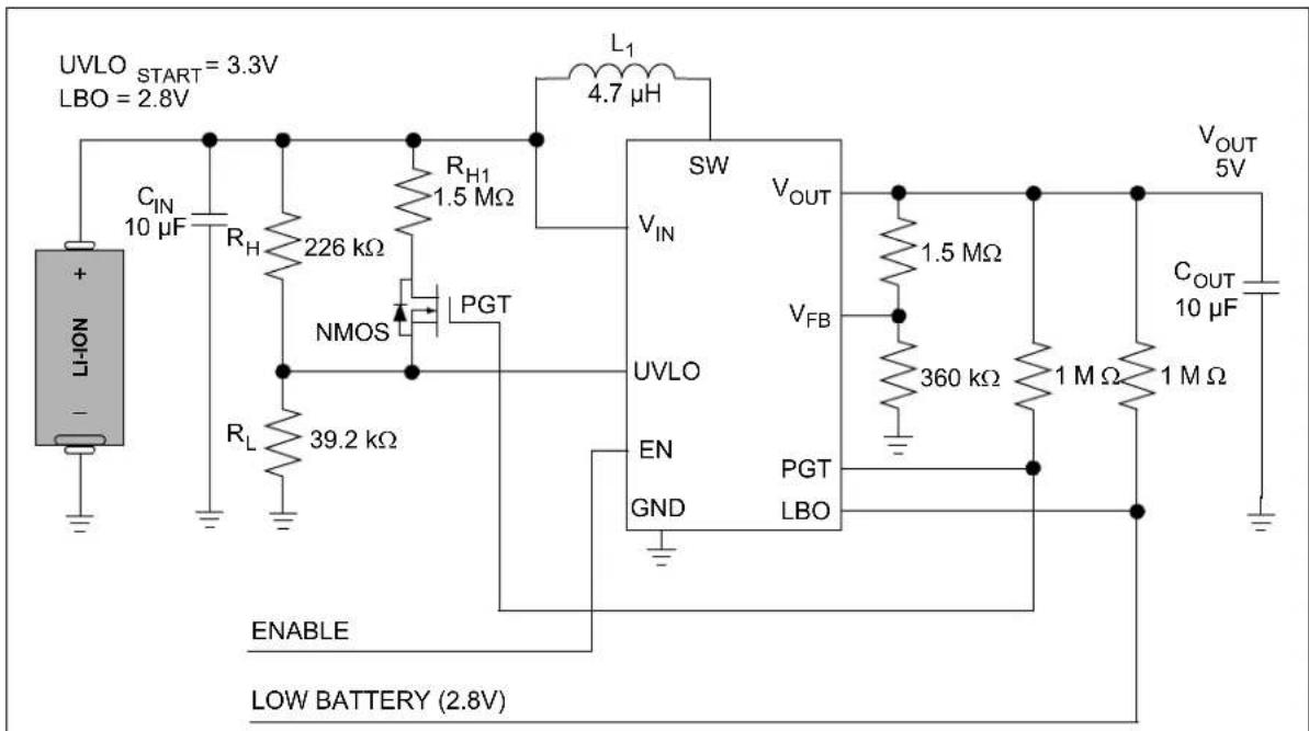
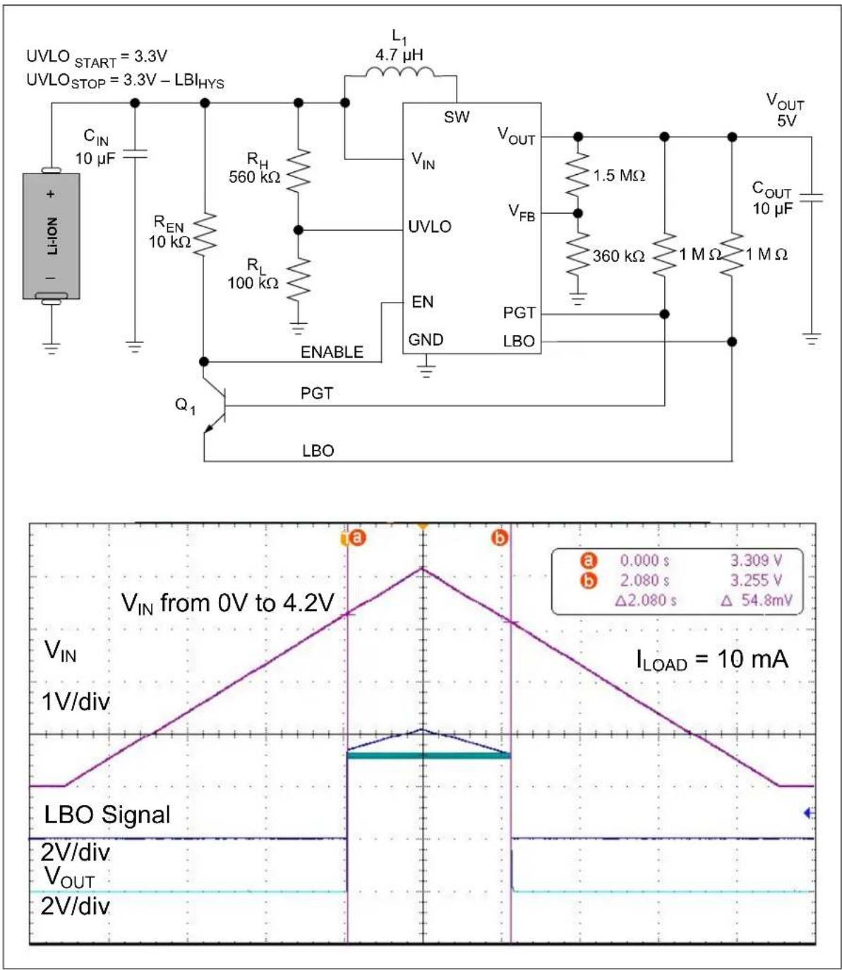
UVLO START = 3.3V LBO = 2.8V CIN 10 μF RH 226 kΩ RHI 1.5 MΩ L1 4.7 μH NMOS PGT RL 39.2 kΩ SW VIN VOUT VFB UVLO EN GND PGT LBO VOUT 5V 1.5 MΩ 360 kΩ 1 MΩ 1 MΩ COUT 10 μF ENABLE LOW BATTERY (2.8V)Note: R_H and R_L set the UVLO START to 3.3V. For battery voltage higher than 3.3V, the switching is enabled and the device regulates to 5V. After start-up, the PGT signal turns on the NMOS switch and puts in parallel RH and R_H1 , and UVLO _START changes to 2.8V. As a result, when the battery gets discharged to 2.8V, the LBO switches to a low level to indicate the low battery warning.
line
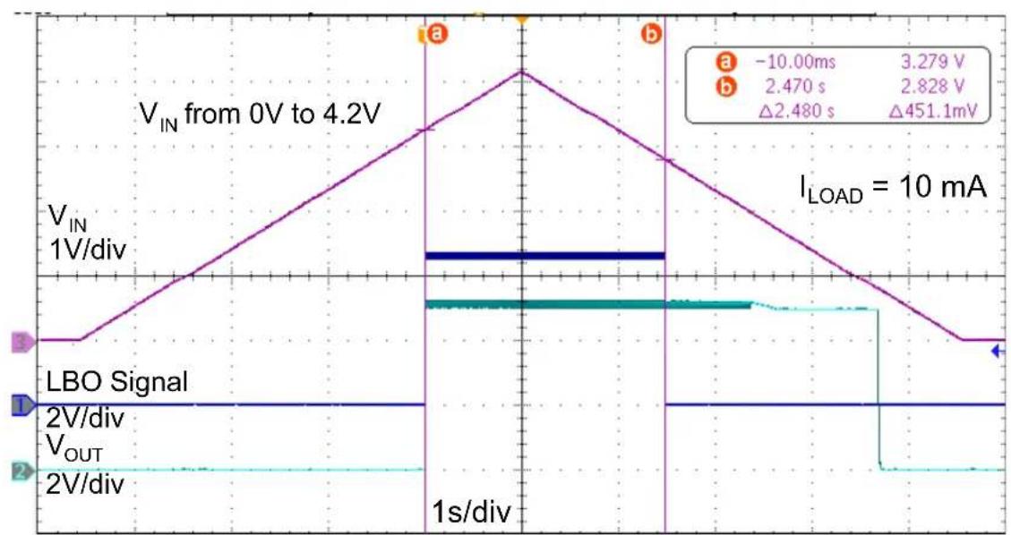
| Parameter | Value | | --------------- | ------------ | | Current (I_LOAD) | 3.279 V | | Time (ΔI_LOAD) | 2.470 s | | Time (ΔI_LOAD) | 2.828 V | | Time (ΔI_LOAD) | 451.1 mV |FIGURE 7-3: Dynamic LBO Threshold to Help Optimize Li-Ion Battery Life.
line
| Parameter | Value | | --------- | ----- | | UVLO_START | 3.3V | | UVLO_STOP | 3.3V - LBI_HYS | | C_IN | 10 μF | | R_EN | 10 kΩ | | R_L | 100 kΩ | | Q_1 | PGT | | LBO | | | SW | 4.7 μH | | V_IN | 560 kΩ | | V_FB | 1.5 MΩ | | V_OUT | 5V | | GND | 360 kΩ | | PGT | 1 M Ω | | LBO | 1 M Ω | | C_OUT | 10 μF | | VIN from 0V to 4.2V | Peak at I_LOAD = 10 mA | | VIN (1V/div) | V_IN from 0V to 4.2V | | LBO Signal (I_LOAD = 10 mA) | Currents: 0.000 s, 3.309 V, 2.080 s, 3.255 V, Δ2.080 s, Δ54.8 mV | | 2V/div | V_OUT | | 2V/div | V_OUT |FIGURE 7-4: Simple Method for Increased UVLO STOP for Li-Ion Battery Applications to the UVLO _START Value (minus internal LBI comparator's hysteresis of 20 mV, typically).
text_image
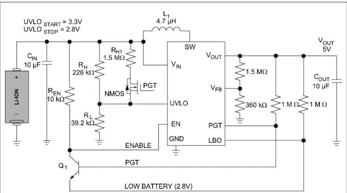
UVLO START = 3.3V UVLO STOP = 2.8V L1 4.7 μH CIN 10 μF REN 10 kΩ RH 226 kΩ RHI 1.5 MΩ NMOS PGT RL 39.2 kΩ ENABLE Q1 PGT SW VIN VOUT VFB UVLO EN PGT GND LBO VOUT 5V 1.5 MΩ 360 kΩ 1 MΩ 1 MΩ COUT 10 μF LOW BATTERY (2.8V)Note: R_H and R_L set the UVLO START to 3.3V. For battery voltage higher than 3.3V, the switching is enabled and the device regulates to 5V. After start-up, the PGT signal turns on the N-MOS switch and puts in parallel RH and R_H1 and UVLO START changes dynamically from 3.3V to 2.8V. As a result, when the battery gets discharged to 2.8V, the LBO switches to low level, turns on the NPN transistor ( Q1 ) and asserts to low the enable input, turning off the output of the converter.
line
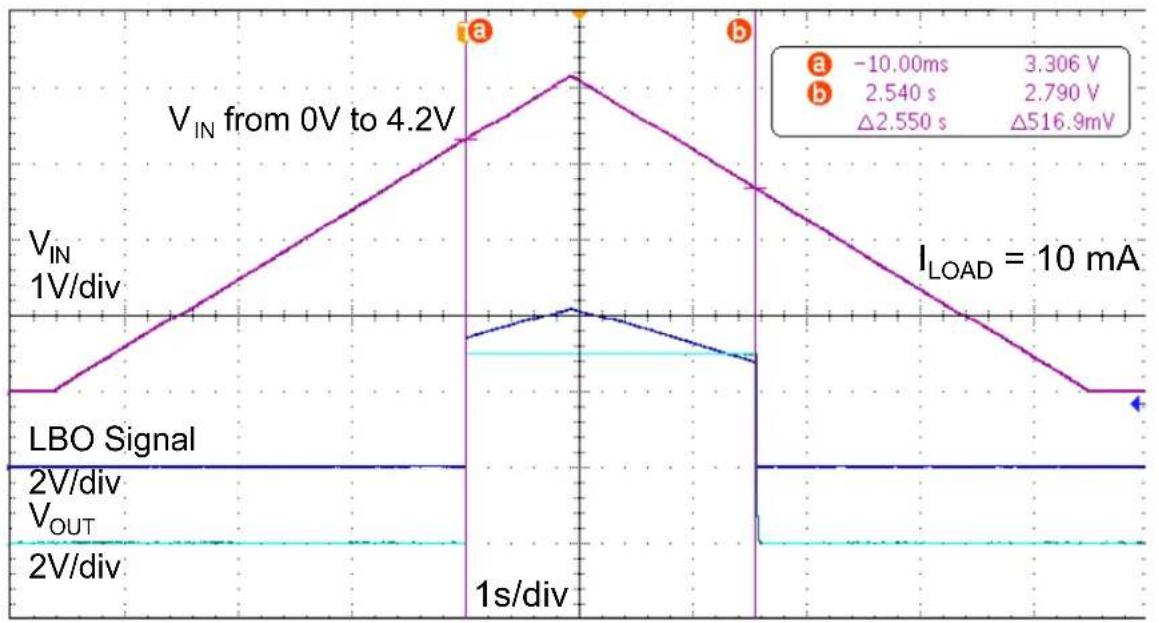
| Parameter | Value | | --------------- | --------- | | Time | -10.00ms | | Voltage | 3.306 V | | Time | 2.540 s | | Current | 2.790 V | | Delta | Δ2.550 s | | Current | Δ516.9 mV | | Load Current | 10 mA |FIGURE 7-5: Dynamic Changing Method for UVLOs' Thresholds with Output Shutdown at 2.8V to Protect Li-Ion Batteries from Overdischarging.
8.0 PACKAGING INFORMATION
8.1 Package Marking Information
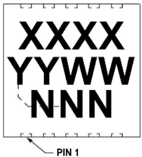
10-Lead MSOP (3x3 mm)

text_image
XXXXXX YWWNNNExample
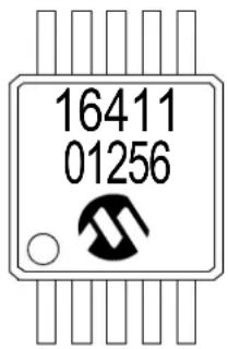
text_image
16411 0125610-Lead TDFN (3x3 mm)
text_image
XXXX YYWW NNN PIN 1Example

text_image
6411 2015 256 PIN 1Legend: XX...X Customer-specific information
Y Year code (last digit of calendar year)
YY Year code (last 2 digits of calendar year)
WW Week code (week of January 1 is week '01')
NNN Alphanumeric traceability code
ePb-free JEDEC ^® designator for Matte Tin (Sn)
This package is Pb-free. The Pb-free JEDEC designator (e3) can be found on the outer packaging for this package.
Note: In the event the full Microchip part number cannot be marked on one line, it will be carried over to the next line, thus limiting the number of available characters for customer-specific information.
10-Lead Plastic Micro Small Outline Package (UN) [MSOP]
Note: For the most current package drawings, please see the Microchip Packaging Specification located at http://www.microchip.com/packaging
![Microchip MCP16415 - 10-Lead Plastic Micro Small Outline Package (UN) [MSOP] - 1](/content/2026/06/1224270/images/63ff16bbb579d4eb4f0a45b7b9489fd050884adc052744c63054b07d080eaf48.jpg)
text_image
2X 0.20 H D/2 A D E/2 E1/2 E1 N NOTE 1 1 2 N/2 B e NX b 0.13 M C A-B D TOP VIEW A A2 A1 SIDE VIEW 0.10 C SEATING PLANE C H SEE DETAIL C END VIEWMicrochip Technology Drawing C04-021C Sheet 1 of 2
10-Lead Plastic Micro Small Outline Package (UN) [MSOP]
Note: For the most current package drawings, please see the Microchip Packaging Specification located at http://www.microchip.com/packaging
![Microchip MCP16415 - 10-Lead Plastic Micro Small Outline Package (UN) [MSOP] - 1](/content/2026/06/1224270/images/40e44514a91279cec9f622e6155b6f01ab88bfe0d608938b18134fc0ae5c4a6f.jpg)
text_image
SEATING PLANE C L (L1) GAUGE PLANE c φ DETAIL C| Units | MILLIMETERS | |||
| Dimension Limits | MIN | NOM | MAX | |
| Number of Pins | N | 10 | ||
| Pitch | e | 0.50 BSC | ||
| Overall Height | A | - | - | 1.10 |
| Molded Package Thickness | A2 | 0.75 | 0.85 | 0.95 |
| Standoff | A1 | 0.00 | - | 0.15 |
| Overall Width | E | 4.90 BSC | ||
| Molded Package Width | E1 | 3.00 BSC | ||
| Overall Length | D | 3.00 BSC | ||
| Foot Length | L | 0.40 | 0.60 | 0.80 |
| Footprint | L1 | 0.95 REF | ||
| Foot Angle | 0° | - | 8° | |
| Lead Thickness | c | 0.08 | - | 0.23 |
| Lead Width | b | 0.15 | - | 0.33 |
Notes:
- Pin 1 visual index feature may vary, but must be located within the hatched area.
- Dimensions D and E1 do not include mold flash or protrusions. Mold flash or protrusions shall not exceed 0.15mm per side.
- Dimensioning and tolerancing per ASME Y14.5M. BSC: Basic Dimension. Theoretically exact value shown without tolerances. REF: Reference Dimension, usually without tolerance, for information purposes only.
Microchip Technology Drawing C04-021C Sheet 2 of 2
10-Lead Plastic Micro Small Outline Package (UN) [MSOP]
Note: For the most current package drawings, please see the Microchip Packaging Specification located at http://www.microchip.com/packaging
![Microchip MCP16415 - 10-Lead Plastic Micro Small Outline Package (UN) [MSOP] - 1](/content/2026/06/1224270/images/8c825a93947b928a88e03a53f5ab8ea108d765e9a960c7842971dffae0efe6e6.jpg)
text_image
X Y Z C G1 SILK SCREEN GX ERECOMMENDED LAND PATTERN
| Units | MILLIMETERS | |||
| Dimension Limits | MIN | NOM | MAX | |
| Contact Pitch | E | 0.50 BSC | ||
| Contact Pad Spacing | C | 4.40 | ||
| Overall Width | Z | 5.80 | ||
| Contact Pad Width (X10) | X1 | 0.30 | ||
| Contact Pad Length (X10) | Y1 | 1.40 | ||
| Distance Between Pads | G1 | 3.00 | ||
| Distance Between Pads | GX | 0.20 | ||
Notes:
1. Dimensioning and tolerancing per ASME Y14.5M
BSC: Basic Dimension. Theoretically exact value shown without tolerances.
Microchip Technology Drawing No. C04-2021A
10-Lead Thin Plastic Dual Flat, No Lead Package (MN) - 3x3x0.8mm Body [TDFN]
Note: For the most current package drawings, please see the Microchip Packaging Specification located at http://www.microchip.com/packaging
![Microchip MCP16415 - 10-Lead Thin Plastic Dual Flat, No Lead Package (MN) - 3x3x0.8mm Body [TDFN] - 1](/content/2026/06/1224270/images/38c1aec616a2b9c04dd70247ce972b977201169d1e7fbe4b324ce499852b8072.jpg)
Microchip Technology Drawing C04-185A Sheet 1 of 2
10-Lead Thin Plastic Dual Flat, No Lead Package (MN) - 3x3x0.8mm Body [TDFN]
Note: For the most current package drawings, please see the Microchip Packaging Specification located at http://www.microchip.com/packaging
![Microchip MCP16415 - 10-Lead Thin Plastic Dual Flat, No Lead Package (MN) - 3x3x0.8mm Body [TDFN] - 1](/content/2026/06/1224270/images/94c39e8d00e02823465f6c675a86e5437604e7f15550973d17266b053a29664b.jpg)
text_image
NOTE 2| Units | MILLIMETERS | |||
| Dimension Limits | MIN | NOM | MAX | |
| Number of Pins | N | 10 | ||
| Pitch | e | 0.50 BSC | ||
| Overall Height | A | 0.70 | 0.75 | 0.80 |
| Standoff | A1 | 0.00 | 0.02 | 0.05 |
| Contact Thickness | A3 | 0.20 REF | ||
| Overall Length | D | 3.00 BSC | ||
| Exposed Pad Length | D2 | 2.20 | 2.30 | 2.35 |
| Overall Width | E | 3.00 BSC | ||
| Exposed Pad Width | E2 | 1.55 | 1.65 | 1.70 |
| Contact Width | b | 0.18 | 0.25 | 0.30 |
| Contact Length | L | 0.30 | 0.40 | 0.50 |
| Contact-to-Exposed Pad | K | 0.20 | - | - |
Notes:
1. Pin 1 visual index feature may vary, but must be located within the hatched area.
2. Package may have one or more exposed tie bars at ends.
3. Package is saw singulated
4. Dimensioning and tolerancing per ASME Y14.5M
BSC: Basic Dimension. Theoretically exact value shown without tolerances.
REF: Reference Dimension, usually without tolerance, for information purposes only.
Microchip Technology Drawing No. C04-0185A Sheet 2 of 2
APPENDIX A: REVISION HISTORY
Revision D (September 2021)
- Updated the maximum value of the Quiescent Current at V_OUT in the AC/DC Characteristics table.
Revision C (April 2021)
- Updated the AC/DC Characteristics table.
- Updated Table 6-2, Figure 7-3, Figure 7-4 and Figure 7-5.
• Editorial changes and updates.
Revision B (September 2020)
- Updated the AC/DC Characteristics table.
Revision A (September 2020)
- Initial release of this document.
NOTES:
PRODUCT IDENTIFICATION SYSTEM
To order or obtain information, e.g., on pricing or delivery, refer to the factory or the listed sales office.
PART NO.
Device

Tape and Reel

Temperature Range

Package Type
Device: MCP1641X: Low I
Q Boost Converter with
Programmable Low Battery, UVLO and Automatic Input-to-Output Bypass Operation
X = Device Option Number
Options:
MCP16411: PFM/PWM, Output Discharge and PGT
MCP16412: PFM Only, Output Discharge and PGT
MCP16413: PFM/PWM, In-Out Bypass and PGT
MCP16414: PWM Only, In-Out Bypass and PGT
MCP16415: PFM/PWM, Output Discharge and PG
MCP16416: PWM Only, Output Discharge and PG
MCP16417: PFM/PWM, In-Out Bypass and PG
MCP16418: PWM Only, In-Out Bypass and PG
Tape and Reel Option
I = -40°C to +85°C (Industrial)
Package Type MN = 10-Lead Thin Plastic Dual Flat, TDFN UN = 10-Lead Plastic Micro Small Outline, MSOP
Examples:
a) MCP16411-I/MN: Industrial Temperature, 10-LD TDFN package
b) MCP16411T-I/MN: Tape and Reel, Industrial Temperature, 10-LD TDFN package
c) MCP16412-I/MN: Industrial Temperature, 10-LD TDFN package
d) MCP16412T-I/MN: Tape and Reel, Industrial Temperature, 10-LD TDFN package
e) MCP16413-I/MN: Industrial Temperature, 10-LD TDFN package
f) MCP16413T-I/MN: Tape and Reel, Industrial Temperature, 10-LD TDFN package
g) MCP16414-I/MN: Industrial Temperature, 10-LD TDFN package
h) MCP16414T-I/MN: Tape and Reel, Industrial Temperature, 10-LD TDFN package
i) MCP16415-I/MN: Industrial Temperature, 10-LD TDFN package
j) MCP16415T-I/MN: Tape and Reel, Industrial Temperature, 10-LD TDFN package
k) MCP16416-I/MN: Industrial Temperature, 10-LD TDFN package
I) MCP16416T-I/MN: Tape and Reel, Industrial Temperature, 10-LD TDFN package
m) MCP16417-I/MN: Industrial Temperature, 10-LD TDFN package
n) MCP16417T-I/MN: Tape and Reel, Industrial Temperature, 10-LD TDFN package
o) MCP16418-I/MN: Industrial Temperature, 10-LD TDFN package
p) MCP16418T-I/MN: Tape and Reel, Industrial Temperature, 10-LD TDFN package
q) MCP16411-I/UN: Industrial Temperature, 10-LD MSOP package
r) MCP16411T-I/UN: Tape and Reel, Industrial Temperature, 10-LD MSOP package
s) MCP16412-I/UN: Industrial Temperature, 10-LD MSOP package
t) MCP16412T-I/UN: Tape and Reel, Industrial Temperature, 10-LD MSOP package
u) MCP16413-I/UN: Industrial Temperature, 10-LD MSOP package
v) MCP16413T-I/UN: Tape and Reel, Industrial Temperature, 10-LD MSOP package
w) MCP16414-I/UN: Industrial Temperature, 10-LD MSOP package
x) MCP16414T-I/UN: Tape and Reel, Industrial Temperature, 10-LD MSOP package
y) MCP16415-I/UN: Industrial Temperature, 10-LD MSOP package
z) MCP16415T-I/UN: Tape and Reel, Industrial Temperature, 10-LD MSOP package
aa) MCP16416-I/UN: Industrial Temperature, 10-LD MSOP package
ab) MCP16416T-I/UN: Tape and Reel, Industrial Temperature, 10-LD MSOP package
ac) MCP16417-I/UN: Industrial Temperature, 10-LD MSOP package
ad) MCP16417T-I/UN: Tape and Reel, Industrial Temperature, 10-LD MSOP package
ae) MCP16418-I/UN: Industrial Temperature, 10-LD MSOP package
af) MCP16418T-I/UN: Tape and Reel, Industrial Temperature, 10-LD MSOP package
Note 1: Tape and Reel identifier only appears in the catalog part number description. This identifier is used for ordering purposes and is not printed on the device package. Check with your Microchip Sales Office for package availability with the Tape and Reel option.
NOTES:
Note the following details of the code protection feature on Microchip products:
• Microchip products meet the specifications contained in their particular Microchip Data Sheet.
- Microchip believes that its family of products is secure when used in the intended manner, within operating specifications, and under normal conditions.
- Microchip values and aggressively protects its intellectual property rights. Attempts to breach the code protection features of Microchip product is strictly prohibited and may violate the Digital Millennium Copyright Act.
- Neither Microchip nor any other semiconductor manufacturer can guarantee the security of its code. Code protection does not mean that we are guaranteeing the product is “unbreakable”. Code protection is constantly evolving. Microchip is committed to continuously improving the code protection features of our products.
This publication and the information herein may be used only with Microchip products, including to design, test, and integrate Microchip products with your application. Use of this information in any other manner violates these terms. Information regarding device applications is provided only for your convenience and may be superseded by updates. It is your responsibility to ensure that your application meets with your specifications. Contact your local Microchip sales office for additional support or, obtain additional support at https://www.microchip.com/en-us/support/design-help/client-support-services.
THIS INFORMATION IS PROVIDED BY MICROCHIP "AS IS". MICROCHIP MAKES NO REPRESENTATIONS OR WARRANTIES OF ANY KIND WHETHER EXPRESS OR IMPLIED, WRITTEN OR ORAL, STATUTORY OR OTHERWISE, RELATED TO THE INFORMATION INCLUDING BUT NOT LIMITED TO ANY IMPLIED WARRANTIES OF NON-INFRINGEMENT, MERCHANTABILITY, AND FITNESS FOR A PARTICULAR PURPOSE, OR WARRANTIES RELATED TO ITS CONDITION, QUALITY, OR PERFORMANCE.
IN NO EVENT WILL MICROCHIP BE LIABLE FOR ANY INDIRECT, SPECIAL, PUNITIVE, INCIDENTAL, OR CONSEQUENTIAL LOSS, DAMAGE, COST, OR EXPENSE OF ANY KIND WHATSOEVER RELATED TO THE INFORMATION OR ITS USE, HOWEVER CAUSED, EVEN IF MICROCHIP HAS BEEN ADVISED OF THE POSSIBILITY OR THE DAMAGES ARE FORESEEABLE. TO THE FULLEST EXTENT ALLOWED BY LAW, MICROCHIP'S TOTAL LIABILITY ON ALL CLAIMS IN ANY WAY RELATED TO THE INFORMATION OR ITS USE WILL NOT EXCEED THE AMOUNT OF FEES, IF ANY, THAT YOU HAVE PAID DIRECTLY TO MICROCHIP FOR THE INFORMATION.
Use of Microchip devices in life support and/or safety applications is entirely at the buyer's risk, and the buyer agrees to defend, indemnify and hold harmless Microchip from any and all damages, claims, suits, or expenses resulting from such use. No licenses are conveyed, implicitly or otherwise, under any Microchip intellectual property rights unless otherwise stated.
For information regarding Microchip's Quality Management Systems, please visit www.microchip.com/quality.
Trademarks
The Microchip name and logo, the Microchip logo, Adaptec, AnyRate, AVR, AVR logo, AVR Freaks, BesTime, BitCloud, CryptoMemory, CryptoRF, dsPIC, flexPWR, HELDO, IGLOO, JukeBlox, KeeLoq, Kleer, LANCheck, LinkMD, maXStylus, maXTouch, MediaLB, megaAVR, Microsemi, Microsemi logo, MOST, MOST logo, MPLAB, OptoLyzer, PIC, picoPower, PICSTART, PIC32 logo, PolarFire, Prochip Designer, QTouch, SAM-BA, SenGenuity, SpyNIC, SST, SST Logo, SuperFlash, Symmetricom, SyncServer, Tachyon, TimeSource, tinyAVR, UNI/O, Vectron, and XMEGA are registered trademarks of Microchip Technology Incorporated in the U.S.A. and other countries.
AgileSwitch, APT, ClockWorks, The Embedded Control Solutions Company, EtherSynch, Flashtec, Hyper Speed Control, HyperLight Load, IntellIMOS, Libero, motorBench, mTouch, Powermite 3, Precision Edge, ProASIC, ProASIC Plus, ProASIC Plus logo, Quiet-Wire, SmartFusion, SyncWorld, Temux, TimeCesium, TimeHub, TimePictra, TimeProvider, TrueTime, WinPath, and ZL are registered trademarks of Microchip Technology Incorporated in the U.S.A.
Adjacent Key Suppression, AKS, Analog-for-the-Digital Age, Any Capacitor, AnyIn, AnyOut, Augmented Switching, BlueSky, BodyCom, CodeGuard, CryptoAuthentication, CryptoAutomotive, CryptoCompanion, CryptoController, dsPICDEM, dsPICDEM.net, Dynamic Average Matching, DAM, ECAN, Espresso T1S, EtherGREEN, GridTime, IdealBridge, In-Circuit Serial Programming, ICSP, INICnet, Intelligent Paralleling, Inter-Chip Connectivity, JitterBlocker, Knob-on-Display, maxCrypto, maxView, memBrain, Mindi, MiWi, MPASM, MPF, MPLAB Certified logo, MPLIB, MPLINK, MultiTRAK, NetDetach, NVM Express, NVMe, Omniscient Code Generation, PICDEM, PICDEM.net, PICkit, PICtail, PowerSmart, PureSilicon, QMatrix, REAL ICE, Ripple Blocker, RTAX, RTG4, SAM-ICE, Serial Quad I/O, simpleMAP, SimpliPHY, SmartBuffer, SmartHLS, SMART-I.S., storClad, SQI, SuperSwitcher, SuperSwitcher II, Switchtec, SynchroPHY, Total Endurance, TSHARC, USBCheck, VariSense, VectorBlox, VeriPHY, ViewSpan, WiperLock, XpressConnect, and ZENA are trademarks of Microchip Technology Incorporated in the U.S.A. and other countries.
SQTP is a service mark of Microchip Technology Incorporated in the U.S.A.
The Adaptec logo, Frequency on Demand, Silicon Storage Technology, Symmcom, and Trusted Time are registered trademarks of Microchip Technology Inc. in other countries.
GestIC is a registered trademark of Microchip Technology Germany II GmbH & Co. KG, a subsidiary of Microchip Technology Inc., in other countries.
All other trademarks mentioned herein are property of their respective companies.
© 2020-2021, Microchip Technology Incorporated and its subsidiaries.
All Rights Reserved.
ISBN: 978-1-5224-8964-1
Worldwide Sales and Service
AMERICAS
Corporate Office
2355 West Chandler Blvd.
Chandler, AZ 85224-6199
Tel: 480-792-7200
Fax: 480-792-7277
Technical Support:
http://www.microchip.com/
support
Web Address:
www.microchip.com
Atlanta
Duluth, GA
Tel: 678-957-9614
Fax: 678-957-1455
Austin, TX
Tel: 512-257-3370
Boston
Westborough, MA
Tel: 774-760-0087
Fax: 774-760-0088
Chicago
Itasca, IL
Tel: 630-285-0071
Fax: 630-285-0075
Dallas
Addison, TX
Tel: 972-818-7423
Fax: 972-818-2924
Detroit
Novi, MI
Tel: 248-848-4000
Houston, TX
Tel: 281-894-5983
Indianapolis
Noblesville, IN
Tel: 317-773-8323
Fax: 317-773-5453
Tel: 317-536-2380
Los Angeles
Mission Viejo, CA
Tel: 949-462-9523
Fax: 949-462-9608
Tel: 951-273-7800
Raleigh, NC
Tel: 919-844-7510
New York, NY
Tel: 631-435-6000
San Jose, CA
Tel: 408-735-9110
Tel: 408-436-4270
Canada - Toronto
Tel: 905-695-1980
Fax: 905-695-2078
ASIA/PACIFIC
Australia - Sydney
Tel: 61-2-9868-6733
China - Beijing
Tel: 86-10-8569-7000
China - Chengdu
Tel: 86-28-8665-5511
China - Chongqing
Tel: 86-23-8980-9588
China - Dongguan
Tel: 86-769-8702-9880
China - Guangzhou
Tel: 86-20-8755-8029
China - Hangzhou
Tel: 86-571-8792-8115
China - Hong Kong SAR
Tel: 852-2943-5100
China - Nanjing
Tel: 86-25-8473-2460
China - Qingdao
Tel: 86-532-8502-7355
China - Shanghai
Tel: 86-21-3326-8000
China - Shenyang
Tel: 86-24-2334-2829
China - Shenzhen
Tel: 86-755-8864-2200
China - Suzhou
Tel: 86-186-6233-1526
China - Wuhan
Tel: 86-27-5980-5300
China - Xian
Tel: 86-29-8833-7252
China - Xiamen
Tel: 86-592-2388138
China - Zhuhai
Tel: 86-756-3210040
ASIA/PACIFIC
India - Bangalore
Tel: 91-80-3090-4444
India - New Delhi
Tel: 91-11-4160-8631
India - Pune
Tel: 91-20-4121-0141
Japan - Osaka
Tel: 81-6-6152-7160
Japan - Tokyo
Tel: 81-3-6880-3770
Korea - Daegu
Tel: 82-53-744-4301
Korea - Seoul
Tel: 82-2-554-7200
Malaysia - Kuala Lumpur
Tel: 60-3-7651-7906
Malaysia - Penang
Tel: 60-4-227-8870
Philippines - Manila
Tel: 63-2-634-9065
Singapore
Tel: 65-6334-8870
Taiwan - Hsin Chu
Tel: 886-3-577-8366
Taiwan - Kaohsiung
Tel: 886-7-213-7830
Taiwan - Taipei
Tel: 886-2-2508-8600
Thailand - Bangkok
Tel: 66-2-694-1351
Tel: 43-7242-2244-39
Fax: 43-7242-2244-393
Denmark - Copenhagen
Tel: 45-4485-5910
Fax: 45-4485-2829
Finland - Espoo
Tel: 358-9-4520-820
France - Paris
Tel: 33-1-69-53-63-20
Fax: 33-1-69-30-90-79
Germany - Garching
Tel: 49-8931-9700
Germany - Haan
Tel: 49-2129-3766400
Germany - Heilbronn
Tel: 49-7131-72400
Germany - Karlsruhe
Tel: 49-721-625370
Germany - Munich
Tel: 49-89-627-144-0
Fax: 49-89-627-144-44
Germany - Rosenheim
Tel: 49-8031-354-560
Israel - Ra'anana
Tel: 972-9-744-7705
Italy - Milan
Tel: 39-0331-742611
Fax: 39-0331-466781
Italy - Padova
Tel: 39-049-7625286
Netherlands - Drunen
Tel: 31-416-690399
Fax: 31-416-690340
Norway - Trondheim
Tel: 47-7288-4388
Poland - Warsaw
Tel: 48-22-3325737
Romania - Bucharest
Tel: 40-21-407-87-50
Spain - Madrid
Tel: 34-91-708-08-90
Fax: 34-91-708-08-91
Sweden - Gothenberg
Tel: 46-31-704-60-40
Sweden - Stockholm
Tel: 46-8-5090-4654
UK - Wokingham
Tel: 44-118-921-5800
Fax: 44-118-921-5820