HCS365 - Electronic component Microchip - Free user manual and instructions
Find the device manual for free HCS365 Microchip in PDF.

User questions about HCS365 Microchip
0 question about this device. Answer the ones you know or ask your own.
Ask a new question about this device
Download the instructions for your Electronic component in PDF format for free! Find your manual HCS365 - Microchip and take your electronic device back in hand. On this page are published all the documents necessary for the use of your device. HCS365 by Microchip.
USER MANUAL HCS365 Microchip
HCS365 Programming Specifications
1.0 PROGRAMMING THE HCS365
HCS365 devices are programmed using a serial method that differs from previous KEELOQ ^® encoders. This Serial mode will still allow the HCS365 to be programmed while in the users system (ICSP ^™ ). This allows for great design flexibility. This programming specification applies to HCS365 devices in all packages.
1.1 Hardware Requirements
The HCS365 requires one programmable power supply for VDD (4.5V to 5.5V) and a VPP of 9V to 14V. Both supplies should have a minimum resolution of 0.25V.
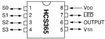
FIGURE 1-1: HCS365 DIAGRAM
PDIP, SOIC,
text_image
S0←→ 1 S1←→ 2 S2←→ 3 S3←→ 4 HCS365 8 7 6 5 VDD LED OUTPUT VssTABLE 1-1: PROGRAMMING PIN DESCRIPTION
| Pin Name | Function HCS365 | Pin Type | Pin Description | |
| S0 DATA 1 | I/O | Data Input Output | ||
| S1 | CLOCK | 2 | I | Clock Input |
| LED | VPP | 7 | P(*) Program mode select | |
| Vss | Vss | 5 | P | Ground |
| VDD | VDD | 8 | P | Power supply |
Legend: I = Input, O = Output, P = Power
Note: In the HCS365, the programming high voltage is internally generated. To activate the Programming mode, high voltage needs to be applied to LED input. This is used as a level source, meaning that LED does not draw any significant current.
1.2 Program Mode Entry
Program mode is entered by holding pins S1 and S0 low while raising VPP pin from VIL to VIHH. All other pins are don't care. Once in Program mode, the entire encoder memory can be accessed and programmed in a serial fashion. S1 and S0 are Schmitt Trigger inputs in this mode. It is important that VDD comes up first and VPP comes up less than 50 s later.
Programming of the device is obtained by writing to two separate memory areas: the encoder memory area and the configuration memory area.
The encoder memory consists of 64 bytes of EEPROM memory and contains the encoder specific data and user configuration options that determine the operation of the device as a KEELOQ encoder. Transmission baud rates, modulation formats and low voltage thresholds are examples of such encoder options.
The configuration memory contains important configuration bits affecting the basic functionality of the device, most of which are factory set and marked as Reserved. The only exception being the Encoder Protect Enable bit, that controls access to the encoder memory area.
In Program mode, all device memory is addressed by means of a single 10-bit Program Counter (PC) that upon entry is set to 3FFh.
FIGURE 1-1: PIN DIAGRAM

text_image
PDIP, SOIC DATA ← 1 8 ← VDD CLOCK → 2 7 ← VTEST MODE HCS365 4 6 5 ← VSS1.3 Encoder Memory Map
The encoder memory space is 8-bits wide and extends from address 00h to 7Fh (256 bytes) of which only the first block of 64 bytes is physically implemented from 00h to 3Fh.
In Program mode this memory is addressed by means of the 8 LSb of the Program Counter (PC), the upper 2 bits of it being ignored.
The non-implemented portion of the addressing space reads always as 0.
Immediately after Program mode entry PC=3FFh, therefore, the encoder memory address pointed to corresponds to location 0FFh, which is not implemented.
Note: An Increment Address command is required to move the Program Counter to location 00h.
FIGURE 1-2: ENCODER MEMORY MAPPING

text_image
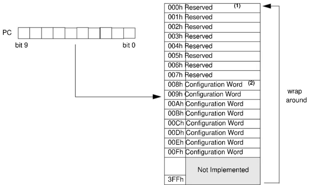
PC bit 9 bit 0bit 7 Encoder Configuration Memory 00h 3Fh Not Implemented 7Fh wrap aroundThe device configuration memory space is 12 bits wide and extends from 000h to 3FFh (1 Kbytes). Only the first part, containing 16 words from 000h to 00Fh, is physically implemented and available to the user. The remaining non-implemented portion of the addressing space reads always as 0.
Immediately after Program mode entry PC=3FFh, therefore, the configuration memory address pointed to corresponds to a non-implemented location.
Note: A Load Configuration Memory command followed by an Increment Address command is required to move the Program Counter to location 000h.
FIGURE 1-3: CONFIGURATION MEMORY MAPPING
text_image
PC bit 9 bit 0 000h Reserved (1) 001h Reserved 002h Reserved 003h Reserved 004h Reserved 005h Reserved 006h Reserved 007h Reserved 008h Configuration Word (2) 009h Configuration Word 00Ah Configuration Word 00Bh Configuration Word 00Ch Configuration Word 00Dh Configuration Word 00Eh Configuration Word 00Fh Configuration Word Not Implemented 3FFh wrap aroundNote 1: Reserved locations content should not be modified as it contains important factory calibration values.
2: Configuration Word is mapped to 8 locations in memory. Writing to any of these locations, modifies all the other locations.
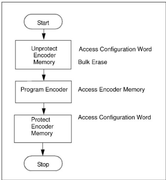
1.5 Programming Method
Programming of the device consists of three basic steps:
- The Configuration Word must be accessed to unprotect the encoder memory, turning the Encoder Protect bit from 0 to 1.
- As a side effect, turning the Encoder Protect bit from 0 back to 1, the encoder memory will be bulk erased (all locations set to 0FFh).
- The encoder memory can now be written with the new encoder data.
- Finally, the Configuration Word is accessed again to protect the encoder memory array.
FIGURE 1-2: PROGRAMMING METHOD
flowchart
graph TD
    A["Start"] --> B["Unprotect Encoder Memory"]
    B --> C["Program Encoder"]
    C --> D["Protect Encoder Memory"]
    D --> E["Stop"]
    style A fill:#f9f,stroke:#333
    style B fill:#ccf,stroke:#333
    style C fill:#cfc,stroke:#333
    style D fill:#fcc,stroke:#333
    style E fill:#cff,stroke:#333
It must be noted that if at the beginning the Encoder Protect bit is not RESET (1), later it will not be possible to modify the contents of the encoder memory.
Failing to set the Encoder Protect bit (0), after writing the new encoder data, on the contrary, will expose the encoder memory contents, including the crypto keys assigned to the device with an extremely severe impact on the security of the customer application.
1.6 The programming sequence
Both when accessing the configuration memory and the encoder memory, a simple basic sequence of four commands is used:
- Load Data command, transfers the data to the write latch ready for the following command
- Begin Programming Cycle command, initiates the self timed memory write sequence
- Read command, verifies the outcome of the previous command
- Increment Address command, so the Program Counter points to the next memory location
This sequence is repeated for the required number of consecutive locations.
In the following sections we will analyze in detail the implementation of such sequence for access to the two memory areas.
1.6.1 CONFIGURATION MEMORY ACCESS
Use the "Load Data For Configuration Memory" command followed by an Increment Address command, immediately after the Program Mode Entry sequence (see Section 1.4). This will set the PC to 000h, eight subsequent "Increment Address" commands will advance into the Configuration Word memory area (008h to 00Fh).
Continue using the "Load Data For Configuration Memory" command in step 1 of the programming sequence.
Use the "Read Data From Configuration Memory" command in step 3 of the programming sequence.
Use the "Increment Address" command immediately after the Program mode entry sequence. This will set the Program Counter to 00h where the actual Encoder programming sequence can start. (see Section 1.3)
Use the "Load Data For Encoder Memory" command in step 1 of the programming sequence.
Use the "Read Data From Encoder Memory" command in step 3 of the programming sequence.
1.6.3 RESERVED LOCATIONS
It is important that the programmer does not modify the content of any of the reserved locations as this might affect some of the factory programmed calibration parameters of the device such as the brown-out threshold levels or the internal RC oscillator frequency.
1.7 Serial Programming Operation
The S1 pin is used as a clock input pin and the S0 pin is used for entering command bits and data input/output during serial operation. To input a command, the clock pin (S1) is cycled 6 times. Each command bit is latched on the falling edge of the clock with the Least Significant bit (LSb) of the command being input first. The data on pin S0 is required to have a minimum setup and hold time of 100 ns, with respect to the falling edge of the clock. Commands that have data associated with them (read and load) are specified to have a minimum delay of 1 s, between the command and the data. After this delay, the clock pin is cycled 16 times,
with the first cycle being a START bit, followed by 12 data bits, two zeros and the last cycle being a STOP bit. START and STOP bits are also set to zero.
Data is input and output LSb first. Data is set on the rising edge of the clock and latched on the falling edge of the clock. Therefore, during a read operation, the LSb will be transmitted onto pin S0 on the rising edge of the second cycle, and during a load operation, the LSb will be latched on the falling edge of the second cycle. To allow for decoding of commands and reversal of data pin configuration, a time separation, of at least 1 s, is required between a command and a data word (or another command).
FIGURE 1-4: SERIAL COMMAND EXAMPLE

text_image
VDD LED S1 (CLOCK) S0 (DATA) RESET Program Mode 1µs min. strt_bit stp_bitTABLE 1-2: SERIAL PROGRAMMING COMMAND SET
| Command (MSb ... LSb) | Data (order of input/output)START bit, data LSb ... data MSb, padding, STOP bit | |||||||||||||||||||||
| Load Data For Configuration Memory | 0 | 0 | 0 | 0 | 0 | 0 | 0 | d0 | d1 | d2 | d3 | d4 | d5 | d6 | d7 | d8 | d9 | d10 | d11 | 0 | 0 | 0 |
| Load Data For Encoder Memory | 0 | 0 | 0 | 0 | 1 | 1 | 0 | d0 | d1 | d2 | d3 | d4 | d5 | d6 | d7 | 0 | 0 | 0 | 0 | 0 | 0 | 0 |
| Read Data From Configuration Memory | 0 | 0 | 0 | 1 | 0 | 0 | 0 | d0 | d1 | d2 | d3 | d4 | d5 | d6 | d7 | d8 | d9 | d10 | d11 | 0 | 0 | 0 |
| Read Data From Encoder Memory | 0 | 0 | 0 | 1 | 0 | 1 | 0 | d0 | d1 | d2 | d3 | d4 | d5 | d6 | d7 | 0 | 0 | 0 | 0 | 0 | 0 | 0 |
| Increment Address | 0 | 0 | 0 | 1 | 1 | 0 | ||||||||||||||||
| Begin Erase / Programming Cycle | 0 | 0 | 1 | 0 | 0 | 0 | ||||||||||||||||
| Begin Programming Only Cycle | 0 | 0 | 1 | 0 | 1 | 0 | ||||||||||||||||
| Bulk Erase Encoder Memory | 0 | 0 | 1 | 0 | 1 | 1 | ||||||||||||||||
Note: All other 6-bit combinations are Reserved.
1.7.1 LOAD DATA FOR CONFIGURATION MEMORY
After receiving this command, the program counter (PC) will be set to 3FFh. An "Increment Address" command will then advance the PC to 000h pointing to the Configuration Word memory. By then applying 16 cycles to the clock pin, the chip will load 12 bits in, as the "data word".
1.7.2 LOAD DATA FOR ENCODER MEMORY
After receiving this command, the chip will load in 12 bits as a "data word" when 16 cycles are applied. However, the encoder memory is only 8-bits wide, and thus, only the first 8 bits of data after the START bit will be programmed into the data memory. It is still necessary to cycle the clock the full 16 cycles in order to allow the internal circuitry to RESET properly.
The PC is used to address the encoder memory. Only the lower 8 bits of the PC are decoded by the encoder memory. Locations 0h-3Fh are physically implemented, while locations 40h-FFh are not implemented and read as zeroes (low). If the PC is greater than FFh, it will wrap around and address a location from 0h-FFh.
1.7.3 READ DATA FROM CONFIGURATION MEMORY
After receiving this command, the chip will transmit data bits out of the configuration memory currently accessed, starting with the second rising edge of the clock input. The S0 pin will go into Output mode on the second rising clock edge, and it will revert back to Input mode (hi-impedance) after the 16th rising edge.
Configuration Word memory will read irrespective of the Encoder Protect enable bit status.
1.7.4 READ DATA FROM ENCODER MEMORY
After receiving this command, the chip will transmit data bits out of the data memory starting with the second rising edge of the clock input. The S0 pin will go into Output mode on the second rising clock edge, and it will revert back to Input mode (hi-impedance) after the 16th rising edge. As previously stated, the data memory is 8-bits wide, and therefore, only the first 8 bits that are output are actual data. A timing diagram for this read command is shown in Figure 5-2.
If the Encoder Protect mechanism is enabled, all the Encoder configuration data will read as zeros. Writing to the encoder memory will also be disabled.
1.7.5 INCREMENT ADDRESS
The PC is incremented when this command is received. A timing diagram of this command is shown in Figure 5-3.
1.7.6 BEGIN ERASE/PROGRAMMING CYCLE
A Load command must be given before every Begin Programming command. Word erasure and programming of Configuration Word and encoder memory will begin, after this command is received and decoded. An internal timing mechanism executes an erase before write. The user must allow the combined time for erase and programming, as specified in the electrical specs, for programming to complete. No "End Programming" command is required.
1.7.7 BEGIN PROGRAMMING ONLY CYCLE
This command is similar to the Erase/Programming Cycle command, except that a word erase is not done. Programming Configuration Word and encoder memory will begin after this command is received and decoded. The user must allow the time for programming, as specified in the electrical specs, for programming to complete. No "End Programming" command is required.
It is recommended that the user do a bulk erase before starting a series of programming only cycles.
1.7.8 BULK ERASE ENCODER MEMORY
After this command is performed, the "Next Program" command will erase the entire encoder memory. The erase time is specified to be 10 ms.
All bulk erase operations must take place at 4.5 to 5.5V VDD range.
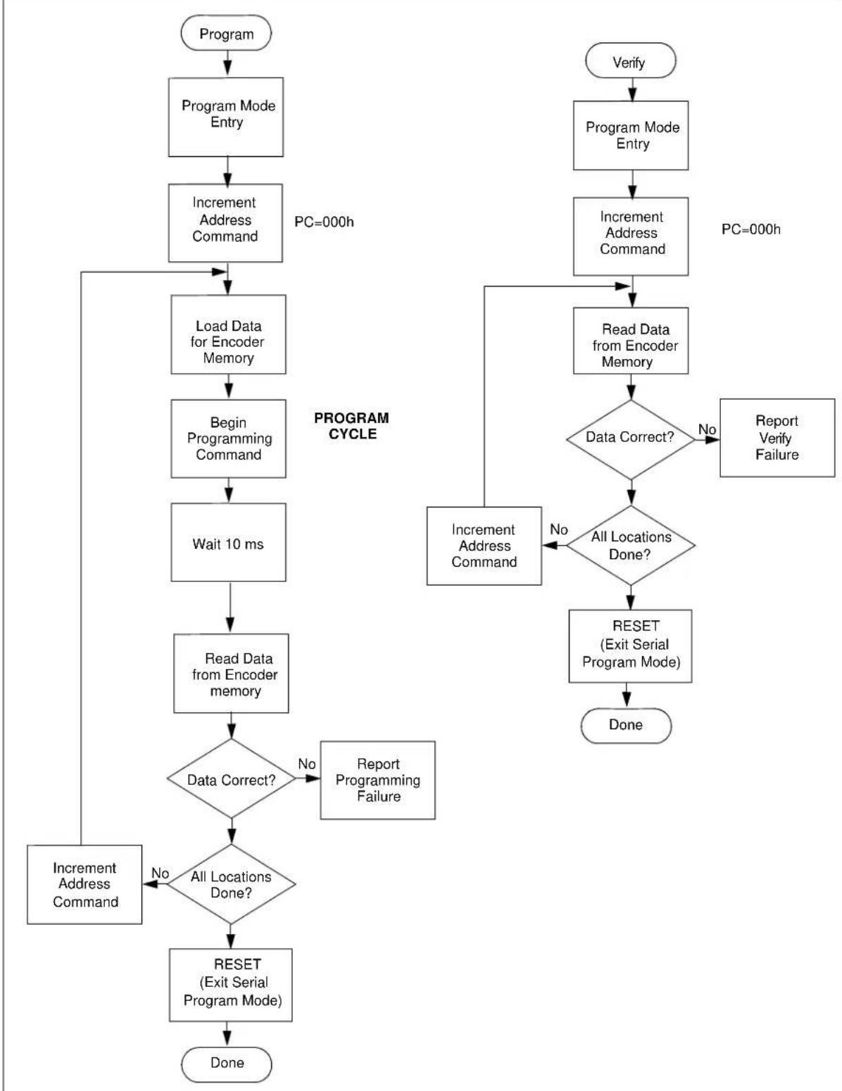
FIGURE 1-5: PROGRAM/VERIFY FLOW CHART - ENCODER MEMORY
flowchart
graph TD
    A["Program"] --> B["Program Mode Entry"]
    B --> C["Increment Address Command"]
    C --> D["Load Data for Encoder Memory"]
    D --> E["Begin Programming Command"]
    E --> F["Wait 10 ms"]
    F --> G["Read Data from Encoder memory"]
    G --> H{Data Correct?}
    H -->|No| I["Report Programming Failure"]
    H -->|Yes| J{All Locations Done?}
    J --> K["RESET (Exit Serial Program Mode)"]
    K --> L["Done"]
    M["Verify"] --> N["Program Mode Entry"]
    N --> O["Increment Address Command"]
    O --> P["Read Data from Encoder Memory"]
    P --> Q{Data Correct?}
    Q -->|No| R["Report Verification Failure"]
    Q -->|Yes| S["Reset (Exit Serial Program Mode)"]
    S --> T["Done"]
    U["Increment Address Command"] --> V["End"]
    style A fill:#f9f,stroke:#333
    style M fill:#f9f,stroke:#333
    style N fill:#f9f,stroke:#333
    style O fill:#f9f,stroke:#333
    style P fill:#f9f,stroke:#333
    style Q fill:#f9f,stroke:#333
    style R fill:#f9f,stroke:#333
    style S fill:#f9f,stroke:#333
    style T fill:#f9f,stroke:#333
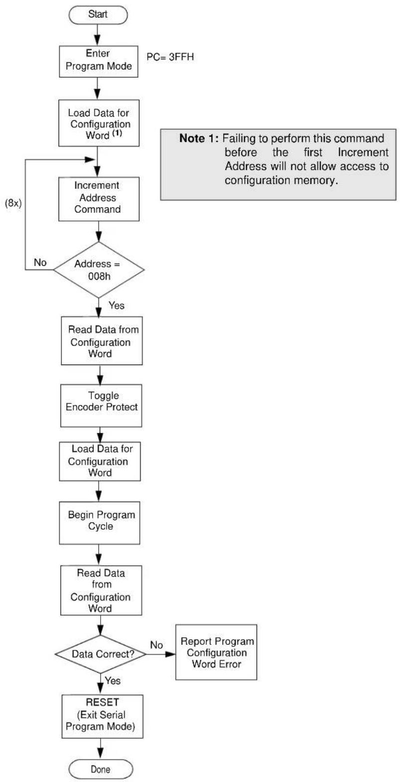
2.0 CONFIGURATION WORD
Special care must be taken when modifying the Configuration Word contents of the HCS365. In fact, in addition to the Encoder Protection enable bits, it contains several "factory calibration" parameters that are vital to the proper working of the device (marked Reserved).
Care must be taken not to lose these bits contents when manipulating the Configuration Word.
Writing the Configuration Word requires further consideration of the following constraints:
- writing will be performed only if the Encoder Protect bit differs from the current Configuration Word contents
- changing from 0 to 1, the Encoder Protect bit will produce a bulk erase of the encoder memory contents
Refer to Figure 2-1 (PROGRAM FLOW CHART CONFIGURATION WORD) to learn how to access and program the Configuration Word of an HCS365 device.
TABLE 2-1: CONFIGURATION WORD BIT MAP
| Res Res Res Res | Res EP | Res Res | Res Res | Res Res |
bit 11 bit 6 bit 0
Res: Reserved, preserve value of these bits when writing to the Configuration Word
bit 6: EP: Encoder Protection enable bit
Setting the bit from 0 to 1 removes read protection and bulk erases the Encoder EEPROM
1 = Not protected
0 = Protected - Can not read or write
2.1 Encoder Protection
The HCS365 features an Encoder Protection mechanism to control access to the encoder memory array. When Encoder Protection is enabled, the encoder memory locations read all '0's. Further programming is disabled for the entire array.
Once Encoder Protection has been enabled, disabling it will produce a bulk erase of the entire encoder memory array.
Configuration memory is not affected by the Encoder Protect bits and is always available to read.
| Note: Failing to set the Encoder Protect bit (0), after writing new encoder data will expose the encoder memory contents, including the crypto keys assigned to the device, with an extremely severe impact on the security of the customer application. |
TABLE 2-2: CODE PROTECTION
| Memory Segment | R/W Protected ( = 0 ) | R/W Unprotected ( = 1 ) |
| Configuration Memory [000h:00Fh] | Read Enabled, Write Enabled* | Read Enabled, Write Enabled* |
| Encoder memory [000h:03Fh] | Read Disabled (all 0's), Write Disabled | Read Enabled, Write Enabled |
Note*: The Configuration Word is not updated unless EP is changed from existing value.
FIGURE 2-1: PROGRAM FLOW CHART - CONFIGURATION WORD
flowchart
graph TD
    A["Start"] --> B["Enter Program Mode"]
    B --> C["Load Data for Configuration Word (1)"]
    C --> D{Address = 008h}
    D -->|No| E["(8x)"]
    D -->|Yes| F["Read Data from Configuration Word"]
    F --> G["Toggle Encoder Protect"]
    G --> H["Load Data for Configuration Word"]
    H --> I["Begin Program Cycle"]
    I --> J["Read Data from Configuration Word"]
    J --> K{Data Correct?}
    K -->|No| L["Report Program Configuration Word Error"]
    K -->|Yes| M["RESET (Exit Serial Program Mode)"]
    M --> N["Done"]
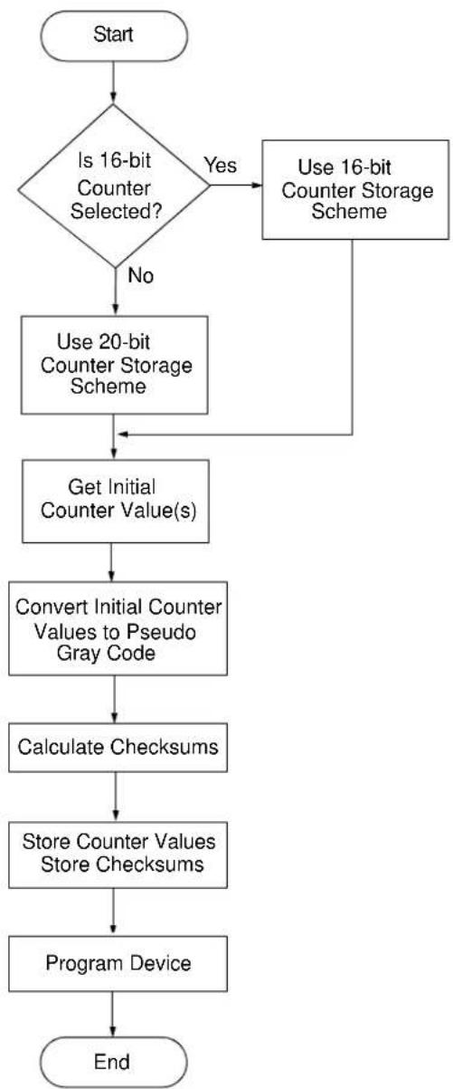
2.2 HCS365 Counter Implementation
The HCS365 uses a different method of storing the counter in EEPROM when compared to previous KEELOQ encoders. This section explains how to implement this different counter storage method and provides some examples for testing purposes.
FIGURE 2-1: COUNTER IMPLEMENTATION FLOWCHART
flowchart
graph TD
    A["Start"] --> B{Is 16-bit Counter Selected?}
    B -->|Yes| C["Use 16-bit Counter Storage Scheme"]
    B -->|No| D["Use 20-bit Counter Storage Scheme"]
    C --> E["Get Initial Counter Value(s)"]
    D --> E
    E --> F["Convert Initial Counter Values to Pseudo Gray Code"]
    F --> G["Calculate Checksums"]
    G --> H["Store Counter Values Store Checksums"]
    H --> I["Program Device"]
    I --> J["End"]
20-Bit Counter:
| Reg Bits | ||||||||
| A | 2 | 3 | 2 | 2 | 2 | 1 | 2 | 0 |
| x | x | 0 | 0 | D | D | D | D | |
MSb
1 8
| Reg Bits | ||||||||
| B | 1 | 5 | 1 | 4 | 1 | 3 | 1 | 2 |
| D | D | D | D | D | D | D | D | |
1 1 0
| Reg Bits | ||||||||
| C | 7 | 6 | 5 | 4 | 3 | |||
| D | D | D | D | D | D | D | D | |
2
LSb
• D represents a counter bit
• x represents a don't care
• 0 represents a logic zero
16-Bit Counter:
| Reg Bits | |||||||||
| A | 2 | 3 | 2 | 2 | 2 | 1 | 2 | 0 | 1 |
| x | x | 0 | 0 | 0 | 0 | 0 | F | F | |
1 8
MSb
| Reg Bits | ||||||||
| B | 1 | 5 | 1 | 4 | 1 | 3 | 1 | 2 |
| D | D | D | D | D | D | D | D | |
1 0
| Reg Bits | ||||||||
| C | 7 | 6 | 5 | 4 | 3 | 2 | 1 | |
| D | D | D | D | D | D | D | D | |
LSb
• D represents a counter bit
• x represents a don't care
• 0 represents a logic zero
- FF represents overflow conditions. FF = 11 -> None
FF = 01 -> Once
FF = 00 -> Twice
Convert Initial Counter Values to Pseudo Gray Code (C Implementation):
Note: See previous page for references to A, B, and C.
If ( B & 1 )
C ^= 0xFF;
If (A & 1)
B ^^ = 0xFF;
Calculate Checksums (C implementation):
Checksum1 = B^C;
Checksum2 = A^C;
Checksum3 = A^B;
Store Counter Values And Checksums:
Note: Checksum 3 comes before Checksum 2
For HCS365 Transmitter #1:
| Bits | ||||||||
| Address | 7 6 5 4 3 | 2 1 0 | ||||||
| 00 A | ||||||||
| 01 B | ||||||||
| 02 C | ||||||||
| 03 Checksum 1 | ||||||||
| 04 Checksum 3 | ||||||||
| 05 Checksum 2 | ||||||||
For HCS365 Transmitter #2:
| Bits | ||||||||
| Address | 7 | 6 | 5 | 4 | 3 | 2 | 1 | 0 |
| 08 A | ||||||||
| 09 B | ||||||||
| 0A C | ||||||||
| 0B | Checksum 1 | |||||||
| 0C | Checksum 3 | |||||||
| 0D | Checksum 2 | |||||||
Example 1:
Counter Scheme: 16-bit
Counter Value: 0x0000
Overflow Condition: None
| Reg Bits | ||||||||||
| A | 2 | 3 | 2 | 2 | 2 | 1 | 2 | 0 | 1 | 9 |
| 0 | 0 | 0 | 0 | 0 | 0 | 0 | 1 | 1 | ||
| MSb | ||||||||||
| Reg Bits | ||||||||||
| B | 1 | 5 | 1 | 4 | 1 | 3 | 1 | 2 | 1 | 1 |
| 0 | 0 | 0 | 0 | 0 | 0 | 0 | 0 | 0 | ||
| Reg Bits | ||||||||||
| C | 7 | 6 | 5 | 4 | 3 | 2 | 1 | |||
| 0 | 0 | 0 | 0 | 0 | 0 | 0 | 0 | |||
Get Initial Counter Values:
$$ A = 0 \times 0 3 $$
$$ B = 0 \times 0 0 $$
$$ C = 0 \times 0 0 $$
Convert Initial Counter Values To Pseudo Gray Code (See page 12):
$$ A = 0 x 0 3 $$
$$ B = 0 x F F $$
$$ C = 0 x 0 0 $$
Calculate Checksums:
$$ \text { Checksum1 } = \mathrm{B} \oplus \mathrm{C} = 0 \mathrm{xFF} \oplus 0 \mathrm{x00} = 0 \mathrm{xFF} $$
$$ \text { Checksum2 } = A \oplus C = 0 x 0 3 \oplus 0 x 0 0 = 0 x 0 3 $$
$$ \text { Checksum3 } = A \oplus B = 0 x 0 3 \oplus 0 x F F = 0 x F C $$
Store Counter Values And Checksums:
For HCS365 Transmitter #1:
| Bits | ||||||||
| Address | 7 | 6 | 5 | 4 | 3 | 2 | 1 | 0 |
| 00 | A = 0x03 | |||||||
| 01 | B = 0xFF | |||||||
| 02 | C = 0x00 | |||||||
| 03 | Checksum 1 = 0xFF | |||||||
| 04 | Checksum 3 = 0xFC | |||||||
| 05 | Checksum 2 = 0x03 | |||||||
Example 2:
Counter Scheme: 16-bit
Counter Value: 0x1234
Overflow Condition: Once
| Reg Bits | ||||||||
| A | 2 | 3 | 2 | 2 | 2 | 1 | 2 | 0 |
| 0 | 0 | 0 | 0 | 0 | 0 | 0 | 0 | |
| MSb | ||||||||
| Reg Bits | ||||||||
| B | 1 | 5 | 1 | 4 | 1 | 3 | 1 | 2 |
| 0 | 0 | 0 | 1 | 0 | 0 | 1 | 0 | |
| Reg Bits | ||||||||
| C | 7 | 6 | 5 | 4 | 3 | |||
| 0 | 0 | 1 | 1 | 1 | 0 | 0 | 0 | |
Get Initial Counter Values:
A = 0x01
B = 0x12
C = 0x34
Convert Initial Counter Values To Pseudo Gray Code (See page 12):
A = 0x01
B = 0xED
C = 0x34
Calculate Checksums:
Checksum1=B ⊕ C=0xED ⊕ 0x34=0xD9
Checksum2= A ⊕ C = 0x01 ⊕ 0x34 = 0x35
Checksum3= A ⊕ B = 0x01 ⊕ 0xED = 0xEC
Store Counter Values And Checksums:
For HCS365 Transmitter #1:
| Bits | ||||||||
| Address | 7 | 6 | 5 | 4 | 3 | 2 | 1 | 0 |
| 00 | A = 0x01 | |||||||
| 01 | B = 0xED | |||||||
| 02 | C = 0x34 | |||||||
| 03 | Checksum 1 = 0xD9 | |||||||
| 04 | Checksum 3 = 0xEC | |||||||
| 05 | Checksum 2 = 0x35 | |||||||
Example 3:
Counter Scheme: 16-bit
Counter Value: 0x789A
Overflow Condition: Twice
| Reg Bits | ||||||||||
| A | 2 | 3 | 2 | 2 | 2 | 1 | 2 | 0 | 1 | 9 |
| 0 | 0 | 0 | 0 | 0 | 0 | 0 | 0 | 0 | ||
| MSb | ||||||||||
| Reg Bits | ||||||||||
| B | 1 | 5 | 1 | 4 | 1 | 3 | 1 | 2 | 1 | 1 |
| 0 | 1 | 1 | 1 | 1 | 1 | 0 | 0 | 0 | ||
| Reg Bits | ||||||||||
| C | 7 | 6 | 5 | 4 | 3 | 2 | 1 | |||
| 1 | 0 | 0 | 1 | 1 | 0 | 1 | ||||
Get Initial Counter Values:
$$ A = 0 \times 0 0 $$
$$ B = 0 \times 7 8 $$
$$ C = 0 x 9 A $$
Convert Initial Counter Values To Pseudo Gray Code (See page 12):
$$ A = 0 x 0 0 $$
$$ B = 0 x 7 8 $$
$$ \mathrm{C} = 0 \times 9 \mathrm{A} $$
Calculate Checksums:
$$ \text { Checksum1 } = \mathrm{B} \oplus \mathrm{C} = 0 x 7 8 \oplus 0 x 9 \mathrm{A} = 0 x \mathrm{E2} $$
$$ \text { Checksum2 } = A \oplus C = 0 x 0 0 \oplus 0 x 9 A = 0 x 9 A $$
$$ \text { Checksum3 } = A \oplus B = 0 x 0 0 \oplus 0 x 7 8 = 0 x 7 8 $$
Store Counter Values And Checksums:
For HCS365 Transmitter #1:
| Bits | ||||||||
| Address | 7 | 6 | 5 | 4 | 3 | 2 | 1 | 0 |
| 00 | A = 0x00 | |||||||
| 01 | B = 0x78 | |||||||
| 02 | C = 0x9A | |||||||
| 03 | Checksum 1 = 0xE2 | |||||||
| 04 | Checksum 3 = 0x78 | |||||||
| 05 | Checksum 2 = 0x9A | |||||||
Example 4:
Counter Scheme: 20-Bit
Counter Value: 0xFABCD
| Reg Bits | |||||||||
| A | 2 | 3 | 2 | 2 | 2 | 1 | 2 | 0 | 1 9 |
| 0 | 0 | 0 | 0 | 0 | 1 | 1 | 1 | 1 | |
MSb
| Reg Bits | |||||||||
| B | 1 | 5 | 1 | 4 | 1 | 3 | 1 | 2 | 1 |
| 1 | 0 | 1 | 0 | 1 | 0 | 1 | 1 | ||
| Reg Bits | ||||||||
| C | 7 | 6 | 5 | 4 | 3 | 2 | 1 | 0 |
| 1 | 1 | 0 | 0 | 1 | 1 | 0 | 1 | |
LSb
Get Initial Counter Values:
$$ A = 0 \times 0 F $$
$$ B = 0 x A B $$
$$ C = 0 \times C D $$
Convert Initial Counter Values To Pseudo Gray Code (See page 12):
$$ A = 0 x 0 F $$
$$ B = 0 x 5 4 $$
$$ C = 0 x 3 2 $$
Calculate Checksums:
$$ \text { Checksum1 } = \mathrm{B} \oplus \mathrm{C} = 0 \times 5 4 \oplus 0 \times 3 2 = 0 \times 6 6 $$
$$ \text { Checksum2 } = A \oplus C = 0 x 0 F \oplus 0 x 3 2 = 0 x 3 D $$
$$ \text { Checksum3 } = A \oplus B = 0 x 0 F \oplus 0 x 5 4 = 0 x 5 B $$
Store Counter Values And Checksums:
For HCS365 Transmitter #1:
| Bits | ||||||||
| Address | 7 | 6 | 5 | 4 | 3 | 2 | 1 | 0 |
| 00 | A = 0x0F | |||||||
| 01 | B = 0x54 | |||||||
| 02 | C = 0x32 | |||||||
| 03 | Checksum 1 = 0x66 | |||||||
| 04 | Checksum 3 = 0x5B | |||||||
| 05 | Checksum 2 = 0x3D | |||||||
3.0 ENCODER MEMORY ORGANIZATION
A summary of the HCS365 encoder memory contents is shown in the table below.
TABLE 3-1: HCS365 ENCODER MEMORY MAP
| Bits | ||||||||
| Bytes 7 | 6 | 5 | 4 | 3 | 2 | |||
| 00 SYNC | COUNTER TX#1 USB | |||||||
| 01 SYNC | COUNTER TX#1 MSB | |||||||
| 02 SYNC | COUNTER TX#1 LSB | |||||||
| 03 SYNC | COUNTER TX#1 CHKSUM 1 | |||||||
| 04 SYNC | COUNTER TX#1 CHKSUM 3 | |||||||
| 05 SYNC | COUNTER TX#1 CHKSUM 2 | |||||||
| 06 | RESERVED | |||||||
| 07 | RESERVED | |||||||
| 08 SYNC | COUNTER TX#2 USB | |||||||
| 09 SYNC | COUNTER TX#2 MSB | |||||||
| 0A SYNC | COUNTER TX#2 LSB | |||||||
| 0B | SYNC COUNTER TX#2 CHKSUM 1 | |||||||
| 0C | SYNC COUNTER TX#2 CHKSUM 3 | |||||||
| 0D | SYNC COUNTER TX#2 CHKSUM 2 | |||||||
| 0E | RESERVED | |||||||
| 0F | RESERVED | |||||||
| 10 | 32-BIT SERIAL NUMBER TX #1 (MSB) | |||||||
| 11 | 32-BIT SERIAL NUMBER TX #1 | |||||||
| 12 | 32-BIT SERIAL NUMBER TX #1 | |||||||
| 13 | 32-BIT SERIAL NUMBER TX#1 (LSB) | |||||||
| 14 | 4-BIT SEED CODE TX#1 | 60-BIT SEED_1 VALUE (MS-NIBBLE) | ||||||
| 15 | 60-BIT SEED_1 VALUE | |||||||
| 16 | 60-BIT SEED_1 VALUE | |||||||
| 17 | 60-BIT SEED_1 VALUE | |||||||
| 18 | 60-BIT SEED_1 VALUE | |||||||
| 19 | 60-BIT SEED_1 VALUE | |||||||
| 1A | 60-BIT SEED_1 VALUE | |||||||
| 1B | 60-BIT SEED_1 VALUE (LSB) | |||||||
| 1C | STEN_1 | QUEN_1 | XSER_1 | HSEL_1 | MSEL_1 | DISC_1H (MS-BITS) | ||
| 1D | DISC_1L (LSB) | |||||||
| 1E | 64-BIT KEY_1 (MSB) | |||||||
| 1F | 64-BIT KEY_1 | |||||||
| 20 | 64-BIT KEY_1 | |||||||
| 21 | 64-BIT KEY_1 | |||||||
| 22 | 64-BIT KEY_1 | |||||||
| 23 | 64-BIT KEY_1 | |||||||
| 24 | 64-BIT KEY_1 | |||||||
| 25 | 64-BIT KEY_1 (LSB) | |||||||
| 26 | 32-BIT SERIAL NUMBER TX#2 (MSB) | |||||||
| 27 | 32-BIT SERIAL NUMBER TX#2 | |||||||
| 28 | 32-BIT SERIAL NUMBER TX#2 | |||||||
| 29 | 32-BIT SERIAL NUMBER TX#2 (LSB) | |||||||
| 2A | 4-BIT SEED CODE TX#2 | 60-BIT SEED_2 VALUE (MS-NIBBLE) | ||||||
| 2B | 60-BIT SEED_2 VALUE | |||||||
| 2C | 60-BIT SEED_2 VALUE | |||||||
| 2D | 60-BIT SEED_2 VALUE | |||||||
| 2E | 60-BIT SEED_2 VALUE | |||||||
| Bytes | 7 | 6 | 5 | 4 | 3 | 2 | 1 | 0 |
| 2F 60-BIT | SEED_2 VALUE | |||||||
| 30 60-BIT | SEED_2 VALUE | |||||||
| 31 60-BIT | SEED_2 VALUE (LSB) | |||||||
| 32 STEN_2 | QUEN_2 XS | ER_2 HSEL_2 | MSEL_2 DISC_2H (MS-BITS) | |||||
| 33 DISC_2L (LSB) | ||||||||
| 34 64-BIT | KEY_2 (MSB) | |||||||
| 35 | 64-BIT KEY_2 | |||||||
| 36 | 64-BIT KEY_2 | |||||||
| 37 | 64-BIT KEY_2 | |||||||
| 38 | 64-BIT KEY_2 | |||||||
| 39 | 64-BIT KEY_2 | |||||||
| 3A | 64-BIT KEY_2 | |||||||
| 3B | 64-BIT KEY_2 (LSB) | |||||||
| 3C | GSEL_1 | BSEL_1 | SDTM_1 | SDMD_1 | SDLM_1 | |||
| 3D | LEDOS_2 | LEDBL_2 | TSEL | RFENO | DUAL | MTX | ||
| 3E | GSEL_2 | BSEL_2 | SDTM_2 | SDMD_2 | SDLM_2 | |||
| 3F | LEDOS_1 | LEDBL_1 | PLLSEL | VLOWSEL | VLOWL | CNTSEL | WAKE | |
4.0 ENCODER CONFIGURATION OPTIONS SUMMARY
Data stored in the EEPROM can be classified as Encoder configuration (E) or System configuration (S). In the case of dual Encoder Operation, separate Encoder configuration options are stored for Encoder 1 and Encoder 2.
TABLE 4-1: FIRST ENCODER CONFIGURATION OPTIONS
| Symbol | Address Bits | Class Description (Note 1) | |||
| SYNC_1 00: 16 bits E Encoder Synchronization Counter (CNTSEL=1) | |||||
| SER_1 10: 32 bits E Encoder Serial Number | |||||
| SDBT_1 14: 7654---- E | Seed Button Code | ||||
| SEED_1 | 14: 60 bits E | Encoder Seed Value | |||
| STEN_1 | 1C: 7---- | E | START/STOP Pulse Enable | Disable = 0 | Enable = 1 |
| QUEN_1 | 1C: -6---- | E | Queue counter Enable | Disable = 0 | Enable = 1 |
| XSER_1 | 1C: --5---- | E | Extended Serial Number | 28 bits = 0 | 32 bits = 1 |
| HSEL_1 | 1C: ---4---- | E | Header Select | 4 TE = 0 | 10 TE = 1 |
| MSEL_1 | 1C: ----32-- | E | Transmission Modulation Format | Value | Format |
| 00b | PWM | ||||
| 01b | Manchester | ||||
| 10b | VPWM | ||||
| 11b | PPM | ||||
| DISC_1h 1C: ----10 | E | Encoder Discrimination value (2 MSB) | |||
| DISC_1I | 1D: 8 bits | E | Encoder Discrimination value (8 LSB) | ||
| KEY_1 1E: 64 bits E | Encoder Key | ||||
| SDLM_1 | 3C: ----0 | E | Limited Seed | Disable = 0 | Enable = 1 |
| SDMD_1 | 3C: ----1- | E | Seed Mode | User = 0 | Production = 1 |
| SDTM_1 | 3C: ----32-- | E | Time Before Seed Code Word | Value | Time (s) |
| 00b | 0.0 | ||||
| 01b | 0.8 | ||||
| 10b | 1.6 | ||||
| 11b | 3.2 | ||||
| BSEL_1 | 3C: --54---- | E | Transmission Baud Rate Select | Value | TE (μs) |
| 00b | 100 | ||||
| 01b | 200 | ||||
| 10b | 400 | ||||
| 11b | 800 | ||||
| GSEL_1 | 3C: 76---- | E | Guard Time Select | Value | Time (ms) |
| 00b | 0.0 | ||||
| 01b | 6.4 | ||||
| 10b | 51.2 | ||||
| 11b | 102.4 | ||||
| LEDBL_1 | 3F: -6---- | E | Low Voltage LED Blink | Continuous = 0 | Once = 1 |
| LEDOS_1 | 3F: 7---- | E | LED On Time Select | 50 ms = 0 | 100 ms = 1 |
Note 1: All Timing values vary ±10%.
TABLE 4-2: SECOND ENCODER CONFIGURATION OPTIONS
| Symbol | Address Bits | Class Description (Note 1) | |||
| SYNC_2 08: 20 bits E Encoder Synchronization Counter (CNTSEL=1) | |||||
| SER_2 26: 32 bits E Encoder Serial Number | |||||
| SDBT_2 2A: 7654---- E | Seed Button Code | ||||
| SEED_2 | 2A: 60 bits | E | Encoder Seed Value | ||
| STEN_2 | 32: 7---- | E | START/STOP Pulse Enable | Disable = 0 | Enable = 1 |
| QUEN_2 | 32: -6---- | E | Queue counter Enable | Disable = 0 | Enable = 1 |
| XSER_2 | 32: --5---- | E | Extended Serial Number | 28 bits = 0 | 32 bits = 1 |
| HSEL_2 | 32: ---4---- | E | Header Select | 4 TE = 0 | 10 TE = 1 |
| MSEL_2 | 32: ----32-- | E | Transmission Modulation Format | Value | Format |
| 00b | PWM | ||||
| 01b | Manchester | ||||
| 10b | VPWM | ||||
| 11b | PPM | ||||
| DISC_2h | 32: ----10 | E | Encoder Discrimination value (2 MSB) | ||
| DISC_2I 33: 8 bits | E | Encoder Discrimination value (8 LSB) | |||
| KEY_2 | 34: 64 bits E | Encoder Key | |||
| SDLM_2 | 3E: ----0 | E | Limited Seed | Disable = 0 | Enable = 1 |
| SDMD_2 | 3E: ----1- | E | Seed Mode | User = 0 | Production = 1 |
| SDTM_2 | 3E: ----32-- | E | Time Before Seed Code Word | Value | Time (s) |
| 00b | 0.0 | ||||
| 01b | 0.8 | ||||
| 10b | 1.6 | ||||
| 11b | 3.2 | ||||
| BSEL_2 | 3E: --54---- | E | Transmission Baud Rate Select | Value | TE (μs) |
| 00b | 100 | ||||
| 01b | 200 | ||||
| 10b | 400 | ||||
| 11b | 800 | ||||
| GSEL_2 | 3E: 76---- | E | Guard Time Select | Value | Time (ms) |
| 00b | 0.0 | ||||
| 01b | 6.4 | ||||
| 10b | 51.2 | ||||
| 11b | 102.4 | ||||
| LEDBL_2 | 3D: -6---- | E | Low Voltage LED Blink | Continuous = 0 | Once = 1 |
| LEDOS_2 | 3D: 7---- | E | LED On Time Select | 50 ms = 0 | 100 ms = 1 |
Note 1: All Timing values vary ±10%.
TABLE 4-3: SYSTEM CONFIGURATION OPTIONS
| Symbol | Address Bits | Class Description (Note 1) | |||
| MTX 3D: | ----10 S Minimum Code | Words Value Value | |||
| 00b 1 | |||||
| 01b 2 | |||||
| 10b 4 | |||||
| 11b 8 | |||||
| DUAL | 3D: ----2-- | S | Dual Encoder Enable | Disable = 0 | Enable = 1 |
| RFENO | 3D: ----3--- | S | RF Enable Output Select | Disable = 0 | Enable = 1 |
| TSEL | 3D: --54---- | S | Time-out Select | Value | Time (s) |
| 00b | Disabled | ||||
| 01b | 0.8 | ||||
| 10b | 3.2 | ||||
| 11b | 25.6 | ||||
| WAKE | 3F: ----10 | S | Wake-up | Value | Value |
| 00b | No Wake-up | ||||
| 01b | 75 ms 50% | ||||
| 10b | 50 ms 33.3% | ||||
| 11b | 100 ms 16.6% | ||||
| CNTSEL | 3F: ----2-- | S | Counter Select | 16 bits = 0 | 20 bits = 1 |
| VLOWL | 3F: ----3--- | S | Low Voltage Latch Enable | Disable = 0 | Enable = 1 |
| VLOWSEL | 3F: ----4---- | S | Low Voltage Trip Point Select | 2.2V = 0 | 3.2V = 1 |
| PLLSEL | 3F: --5---- | S | PLL Interface Select | ASK = 0 | FSK = 1 |
Note 1: All Timing values vary ±10%.
5.0 PROGRAM MODE ELECTRICAL CHARACTERISTICS
TABLE 5-1: AC/DC TIMING REQUIREMENTS FOR PROGRAM MODE
| AC/DC CHARACTERISTICS,POWER SUPPLY PINS | ||||||
| Characteristics Sym Min | Typ Max | Units Conditions | Comments | |||
| General | ||||||
| Supply voltage during programming V | BATT 4 | 5 5.0 5.5 | V | |||
| Supply voltage during verify | VBATT | VDD min. | VDDmax. | V | ||
| High voltage on MCLRTest mode entry | VIHH | VBATT + 4.5 | 14.0 | V | Always use minimum on VIHH | |
| Power-up Reset time before entering Test mode | tvdd | 50 | μs | |||
| MCLR rise time (Vss to VHH) for Test mode entry | tvhhr | 1.0 | ms | |||
| (S1, S0) input high level | VIH1 | 0.8VBATT | V | Schmitt Trigger input | ||
| (S1, S0) input low level | VIL1 | 0.2VBATT | V | Schmitt Trigger input | ||
| S<3:0> setup time before MCLR(Test mode selection pattern setup time) | tset0 100 | ns | ||||
| S<3:0> hold time after MCLR(Test mode selection pattern setup time) | thId0 | 5 | ms | |||
| Serial Program/Verify | ||||||
| Data in setup time before clock | tset1 | 100 | ns | |||
| Data in hold time after clock | thId1 | 100 | ns | |||
| Data input not driven to next clock input (delay required between command/data or command/command) | tdly1 1.0 | μs | ||||
| Delay between clock to clock of next command or data | tdly2 1.0 | μs | ||||
| Clock to data out valid (during read data) | tdly3 | 80 | ns | |||
| Serial Clock Period | 1 | μs | ||||
| Erase Cycle Time | 10 | ms | ||||
| Program Cycle Time | 10 | ms | ||||
FIGURE 5-1: LOAD DATA FOR CONFIG MEMORY COMMAND
flowchart
graph TD
    A["VBAT_Lvdd"] --> B["VIHH"]
    C["MCLR"] --> D["tset0"]
    D --> E["S1 (CLOCK)"]
    E --> F["thld0"]
    F --> G["S0 (DATA)"]
    G --> H["0 1 0 0 X X strt_bit"]
    H --> I["100 ns min."]
    I --> J["thld1"]
    J --> K["tset1"]
    K --> L["1 μs min."]
    L --> M["100 ns min."]
    M --> N["thld1"]
    N --> O["stp_bit"]
    style A fill:#f9f,stroke:#333
    style C fill:#f9f,stroke:#333
    style D fill:#ccf,stroke:#333
    style E fill:#cfc,stroke:#333
    style G fill:#fcc,stroke:#333
    style H fill:#ffc,stroke:#333
    style I fill:#cfc,stroke:#333
    style J fill:#cfc,stroke:#333
    style K fill:#cfc,stroke:#333
    style L fill:#cfc,stroke:#333
    style M fill:#cfc,stroke:#333
    style N fill:#cfc,stroke:#333
    style O fill:#cfc,stroke:#333
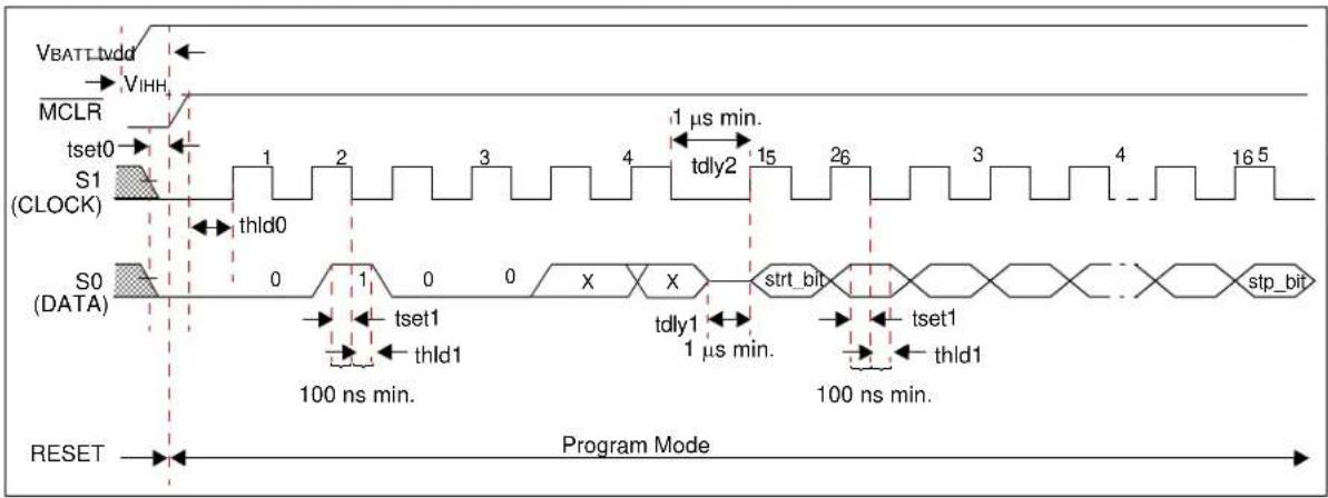
FIGURE 5-2: READ DATA FROM ENCODER MEMORY COMMAND
text_image
MCLR VIHH tset0 thld0 tdly2 1 μs min. S1 (CLOCK) 1 2 3 4 15 26 3 4 16 5 s0 (DATA) 1 0 1 0 X X strt_bit stdy3 stp_bit tset1 thld1 tdly1 1 μs min. 100 ns min. RC0 = input RC0 = output RC0 input RESET Program ModeFIGURE 5-3: INCREMENT ADDRESS COMMAND
text_image
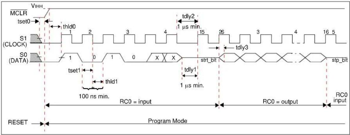
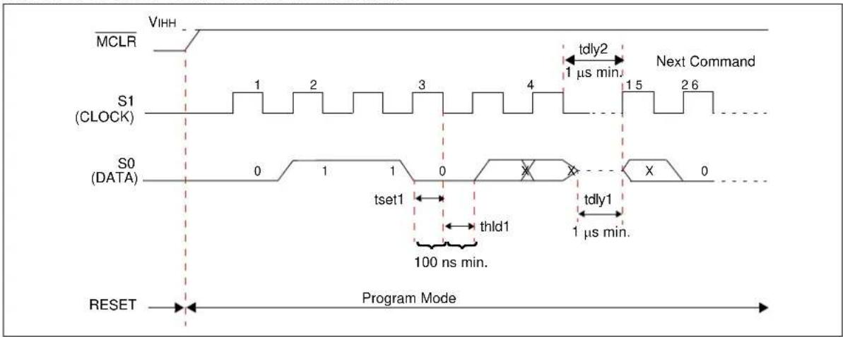
MCLR VIHH S1 (CLOCK) s0 (DATA) 0 1 1 0 tset1 thld1 100 ns min. tdly2 1 µs min. Next Command 15 26 X 0 tdly1 1 µs min. RESET Program Mode6.0 ADDITIONAL INFORMATION
Microchip's Secure Data Products are covered by some or all of the following: Code hopping encoder patents issued in European countries and U.S.A. Secure learning patents issued in European countries, U.S.A. and R.S.A.
Note the following details of the code protection feature on Microchip devices:
• Microchip products meet the specification contained in their particular Microchip Data Sheet.
- Microchip believes that its family of products is one of the most secure families of its kind on the market today, when used in the intended manner and under normal conditions.
- There are dishonest and possibly illegal methods used to breach the code protection feature. All of these methods, to our knowledge, require using the Microchip products in a manner outside the operating specifications contained in Microchip's Data Sheets. Most likely, the person doing so is engaged in theft of intellectual property.
- Microchip is willing to work with the customer who is concerned about the integrity of their code.
- Neither Microchip nor any other semiconductor manufacturer can guarantee the security of their code. Code protection does not mean that we are guaranteeing the product as "unbreakable."
Code protection is constantly evolving. We at Microchip are committed to continuously improving the code protection features of our products. Attempts to break Microchip's code protection feature may be a violation of the Digital Millennium Copyright Act. If such acts allow unauthorized access to your software or other copyrighted work, you may have a right to sue for relief under that Act.
Information contained in this publication regarding device applications and the like is provided only for your convenience and may be superseded by updates. It is your responsibility to ensure that your application meets with your specifications. MICROCHIP MAKES NO REPRESENTATIONS OR WARRANTIES OF ANY KIND WHETHER EXPRESS OR IMPLIED, WRITTEN OR ORAL, STATUTORY OR OTHERWISE, RELATED TO THE INFORMATION, INCLUDING BUT NOT LIMITED TO ITS CONDITION, QUALITY, PERFORMANCE, MERCHANTABILITY OR FITNESS FOR PURPOSE. Microchip disclaims all liability arising from this information and its use. Use of Microchip devices in life support and/or safety applications is entirely at the buyer's risk, and the buyer agrees to defend, indemnify and hold harmless Microchip from any and all damages, claims, suits, or expenses resulting from such use. No licenses are conveyed, implicitly or otherwise, under any Microchip intellectual property rights.
QUALITY MANAGEMENT SYSTEM CERTIFIED BY DNV
=ISO/TS 16949:2009=
Trademarks
The Microchip name and logo, the Microchip logo, dsPIC, KEELOQ, KEELOQ logo, MPLAB, PIC, PICmicro, PICSTART, PIC ^32 logo, rfPIC and UNI/O are registered trademarks of Microchip Technology Incorporated in the U.S.A. and other countries.
FilterLab, Hampshire, HI-TECH C, Linear Active Thermistor, MXDEV, MXLAB, SEEVAL and The Embedded Control Solutions Company are registered trademarks of Microchip Technology Incorporated in the U.S.A.
Analog-for-the-Digital Age, Application Maestro, chipKIT, chipKIT logo, CodeGuard, dsPICDEM, dsPICDEM.net, dsPICworks, dsSPEAK, ECAN, ECONOMONITOR, FanSense, HI-TIDE, In-Circuit Serial Programming, ICSP, Mindi, MiWi, MPASM, MPLAB Certified logo, MPLIB, MPLINK, mTouch, Omniscient Code Generation, PICC, PICC-18, PICDEM, PICDEM.net, PICkit, PICtail, REAL ICE, rfLAB, Select Mode, Total Endurance, TSHARC, UniWinDriver, WiperLock and ZENA are trademarks of Microchip Technology Incorporated in the U.S.A. and other countries.
SQTP is a service mark of Microchip Technology Incorporated in the U.S.A.
All other trademarks mentioned herein are property of their respective companies.
© 2001-2011, Microchip Technology Incorporated, Printed in the U.S.A., All Rights Reserved.

Printed on recycled paper.
ISBN: 978-1-61341-209-1
Microchip received ISO/TS-16949:2002 certification for its worldwide headquarters, design and wafer fabrication facilities in Chandler and Tempe, Arizona; Gresham, Oregon and design centers in California and India. The Company's quality system processes and procedures are for its PIC® MCUs and dsPIC® DSCs, KEELoQ® code hopping devices, Serial EEPROMs, microperipherals, nonvolatile memory and analog products. In addition, Microchip's quality system for the design and manufacture of development systems is ISO 9001:2000 certified.
Worldwide Sales and Service
AMERICAS
Corporate Office
2355 West Chandler Blvd.
Chandler, AZ 85224-6199
Tel: 480-792-7200
Fax: 480-792-7277
Technical Support:
http://www.microchip.com/
support
Web Address:
www.microchip.com
Atlanta
Duluth, GA
Tel: 678-957-9614
Fax: 678-957-1455
Boston
Westborough, MA
Tel: 774-760-0087
Fax: 774-760-0088
Chicago
Itasca, I
Tel: 630-285-0071
Fax: 630-285-0075
Cleveland
Independence, OH
Tel: 216-447-0464
Fax: 216-447-0643
Dallas
Addison, TX
Tel: 972-818-7423
Fax: 972-818-2924
Detroit
Farmington Hills, MI
Tel: 248-538-2250
Fax: 248-538-2260
Indianapolis
Noblesville, IN
Tel: 317-773-8323
Fax: 317-773-5453
Los Angeles
Mission Viejo, CA
Tel: 949-462-9523
Fax: 949-462-9608
Santa Clara
Santa Clara, CA
Tel: 408-961-6444
Fax: 408-961-6445
Toronto
Mississauga, Ontario,
Canada
Tel: 905-673-0699
Fax: 905-673-6509
ASIA/PACIFIC
Asia Pacific Office
Suites 3707-14, 37th Floor
Tower 6, The Gateway
Harbour City, Kowloon
Hong Kong
Tel: 852-2401-1200
Fax: 852-2401-3431
Australia - Sydney
Tel: 61-2-9868-6733
Fax: 61-2-9868-6755
China - Beijing
Tel: 86-10-8569-7000
Fax: 86-10-8528-2104
China - Chengdu
Tel: 86-28-8665-5511
Fax: 86-28-8665-7889
China - Chongqing
Tel: 86-23-8980-9588
Fax: 86-23-8980-9500
China - Hangzhou
Tel: 86-571-2819-3180
Fax: 86-571-2819-3189
China - Hong Kong SAR
Tel: 852-2401-1200
Fax: 852-2401-3431
China - Nanjing
Tel: 86-25-8473-2460
Fax: 86-25-8473-2470
China - Qingdao
Tel: 86-532-8502-7355
Fax: 86-532-8502-7205
China - Shanghai
Tel: 86-21-5407-5533
Fax: 86-21-5407-5066
China - Shenyang
Tel: 86-24-2334-2829
Fax: 86-24-2334-2393
China - Shenzhen
Tel: 86-755-8203-2660
Fax: 86-755-8203-1760
China - Wuhan
Tel: 86-27-5980-5300
Fax: 86-27-5980-5118
China - Xian
Tel: 86-29-8833-7252
Fax: 86-29-8833-7256
China - Xiamen
Tel: 86-592-2388138
Fax: 86-592-2388130
China - Zhuhai
Tel: 86-756-3210040
Fax: 86-756-3210049
ASIA/PACIFIC
India - Bangalore
Tel: 91-80-3090-4444
Fax: 91-80-3090-4123
India - New Delhi
Tel: 91-11-4160-8631
Fax: 91-11-4160-8632
India - Pune
Tel: 91-20-2566-1512
Fax: 91-20-2566-1513
Japan - Yokohama
Tel: 81-45-471-6166
Fax: 81-45-471-6122
Korea - Daegu
Tel: 82-53-744-4301
Fax: 82-53-744-4302
Korea - Seoul
Tel: 82-2-554-7200
Fax: 82-2-558-5932 or
82-2-558-5934
Malaysia - Kuala Lumpur
Tel: 60-3-6201-9857
Fax: 60-3-6201-9859
Malaysia - Penang
Tel: 60-4-227-8870
Fax: 60-4-227-4068
Philippines - Manila
Tel: 63-2-634-9065
Fax: 63-2-634-9069
Singapore
Tel: 65-6334-8870
Fax: 65-6334-8850
Taiwan - Hsin Chu
Tel: 886-3-6578-300
Fax: 886-3-6578-370
Taiwan - Kaohsiung
Tel: 886-7-213-7830
Fax: 886-7-330-9305
Taiwan - Taipei
Tel: 886-2-2500-6610
Fax: 886-2-2508-0102
Thailand - Bangkok
Tel: 66-2-694-1351
Fax: 66-2-694-1350
05/02/11