MIC2789 - Electronic component Microchip - Free user manual and instructions
Find the device manual for free MIC2789 Microchip in PDF.

User questions about MIC2789 Microchip
0 question about this device. Answer the ones you know or ask your own.
Ask a new question about this device
Download the instructions for your Electronic component in PDF format for free! Find your manual MIC2789 - Microchip and take your electronic device back in hand. On this page are published all the documents necessary for the use of your device. MIC2789 by Microchip.
USER MANUAL MIC2789 Microchip
The MIC2788/MIC2789 are low-current, ultra-small, push-button reset supervisors with long set-up delays. The devices feature two manual reset inputs and two reset outputs. The devices initiate a reset for the reset timeout period when the /MR0 and /MR1 inputs are asserted low for a period longer than the set-up delay. The two manual reset inputs and long set-up period help to avoid unintended system resets. Both manual reset inputs can be tied together if a single push-button reset is desired.
The MIC2788 features integrated pull-up resistors on the /MR0 and /MR1 inputs, while the MIC2789 requires external pull-up resistors. The PDY input pin selects between a 2s, 4s or 6s set-up period. Factory-programmed reset timeout periods of 140ms (min.) and 240ms (min.) are available. An active-low, open-drain reset output (/RST) and an active-high, push-pull reset output (RSTP) provide flexibility when interfacing to various microcontrollers, PMICs, or load switches.
The MIC2788/MIC2789 consume a quiescent current of only 2.9μA and are offered in a tiny, space-saving 8-pin thin MLF® (2mm x 2mm x 0.55mm) package.
Data sheets and support documentation can be found on Micrel's web site at: www.micrel.com.
Features
• 1.6V to 5.5V operating voltage
- 2.9μA supply current when /MR0, /MR1 are not asserted
- Asserting /MR0 and /MR1 for longer than set-up delay asserts reset output for the reset timeout period
- Programmable delay (PDY) input selects 2.0s, 4.0s or 6.0s set-up delay
- Factory-programmed 140ms (min.) or 240ms (min.) reset timeout period
- Integrated /MR0, /MR1 pull-up resistors (MIC2788)
- Dual Reset Outputs:
- Open-drain active-low reset (/RST) output
- Push-pull active-high reset (RSTP) output
- - 40^ C to 85^ C ambient operating temperature range
- 8-pin 2mm x 2mm x 0.55mm thin MLF® package
Applications
- Smart phones
- MP3 players
- Portable navigation devices
- Set-top boxes (STBs)
- Tablets/pads
Typical Application

text_image
VIN = 1.6V to 5.5V 100k 100k 0.1μF /MR0 /MR1 MIC2788 MIC2789 PDY /MR0 /MR1 GND RSTP VIN 100k VIN μP /RESET GND CONNECT TO VIN, GND OR FLOAT TO SET SETUP DELAY TIME TO PMIC OR LOAD SWITCH /MR0, /MR1 EXTERNAL RESISTORS NOT REQUIRED FOR MIC2788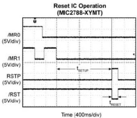
line
| Signal | Voltage (5V/div) | |--------|------------------| | /MR0 | 5 | | /MR1 | 5 | | RSTP | 5 | | /RST | 5 |MLF and MicroLeadFrame are registered trademarks of Amkor Technologies, Inc.
Micrel Inc. • 2180 Fortune Drive • San Jose, CA 95131 • USA • tel +1 (408) 944-0800 • fax +1 (408) 474-1000 • http://www.micrel.com
Ordering Information ^(1)
| Part Number Marking | Minimum t_RESET (ms) | Package^(3,4) Integrated | Pull-Up Resistors | |
| MIC2788-XYMT | 8XA | 140 | 8-Pin (2mm × 2mm) Thin MLF® | Yes |
| MIC2788-YYMT^(2) | 8YA | 240 | 8-Pin (2mm × 2mm) Thin MLF® | Yes |
| MIC2789-XYMT | 9XA | 140 | 8-Pin (2mm × 2mm) Thin MLF® | No |
| MIC2789-YYMT^(2) | 9YA | 240 | 8-Pin (2mm × 2mm) Thin MLF® | No |
Notes:
- All devices available in Tape and Reel only.
- Contact factory for availability.
- Thin MLF ▲ = Pin 1 identifier.
- Thin MLF is a Green RoHS compliant package. Lead finish is NiPdAu. Mold compound is Halogen Free.
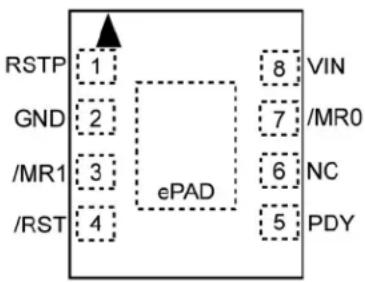
Pin Configuration
text_image
RSTP 1 GND 2 /MR1 3 /RST 4 ePAD 8 VIN 7 /MR0 6 NC 5 PDYMIC2788/89 8-Pin (2mm × 2mm) Thin MLF® Top View
Pin Description
| Pin Number | Pin Name | Pin Function |
| 1 | RSTP | Active-High Push-Pull Reset Output. This output changes from low-to-high when both manual reset pins are pulled low for the setup delay period. RSTP remains high for the reset timeout delay duration after the setup delay period has elapsed. |
| 2 | GND | Supply Ground. |
| 3 | /MR1 | Active-Low Manual Reset Input. The MIC2788 has an internal 65kΩ pull-up resistor to VIN while the MIC2789 requires an external pull-up resistor to VIN if used with a push-button. Pull this pin low to assert and force a reset. Pulling both manual reset inputs low for the setup delay time causes one reset output pulse for the reset timeout delay period. Connect to VIN if unused, do not leave floating. |
| 4 | /RST | Active-Low Open Drain Reset Output. This output changes from high to low when both manual reset pins are pulled low for the setup delay period. /RST remains low for the reset timeout delay after the setup delay has elapsed and it requires an external pull-up resistor. |
| 5 | PDY | Programmable Delay Input with Tri-State Connection. When left open, set-up delay is 2s, when connected to GND, set-up delay is 4s and when connected to VIN, set-up delay is 6s. |
| 6 NC No | Connect. Leave | pin floating. |
| 7 | /MR0 | Active-Low Manual Reset Input. The MIC2788 has an internal 65kΩ pull-up resistor to VIN while the MIC2789 requires an external pull-up resistor to VIN if used with a push-button. Pull this pin low to assert and force a reset. Pulling both manual reset inputs low for the setup delay time causes one reset output pulse for the reset timeout delay period. If unused, connect to VIN; do not leave floating. |
| 8 | VIN | Positive Supply Voltage. A minimum 0.1μF decoupling ceramic capacitor must be connected between VIN and GND close to the pins. |
| EPAD EPAD | Exposed Pad. | Connect to GND. |
Absolute Maximum Ratings ^(1)
Supply Voltage ( V_IN )....-0.3V to +6.0V
Reset Input Voltage (/MR0, /MR1)..... -0.3V to V_IN + 0.3V
Open Drain Reset Output (/RST)....-0.3V to +6.0V
Push-Pull Reset Output (RSTP)....-0.3V to V_IN + 0.3V
Tri-State Programmable Delay (PDY)... -0.3V to V_IN + 0.3V
Lead Temperature (soldering, 10sec.).....260°C
Junction Temperature ( T_J ) -40^ to +150^
Storage Temperature (Ts)....-55°C to +150°C
ESD Rating (Human Body Model) ^(3) 2kV
ESD Rating (Machine Model) ^(3) 300V
Operating Ratings ^(2)
Supply Voltage ( V_IN )....+1.6V to +5.5V
Reset Input Voltage (/MR0, /MR1).... 0V to V_IN
Open Drain Reset Output (/RST).... 0V to +5.5V
Push-Pull Reset Output (/RSTP) 0V to V_IN
Tri-State Programmable Delay (PDY).... 0V to V_IN
Ambient Temperature (T_A) ...... -40^ to +85^
Junction Thermal Resistance
2mm × 2mm Thin M ^1 L(θJA)....90°C/W
Electrical Characteristics ^(4)
V_IN = 3.0V, T_A = 25^, Bold values indicate -40^ ≤ T_A ≤ +85^; unless noted otherwise.
| Parameter | Conditions | Min. | Typ. | ||
| Power Supply Input | |||||
| Supply Voltage ( V_IN ) | 1.6 | 5.5 | V | ||
| Supply Current ( I_IN ) | V_IN = 5V; /MR0, /MR1, /RST, RSTP, and PDY open | 3.4 | 7.5 | μA | |
| V_IN = 3V; /MR0, /MR1, /RST, RSTP, and PDY open | 2.9 | ||||
| Reset Time | |||||
| Set-Up Delay ( t_SETUP ) | PDY = Open | 1.6 | 2.0 | 2.4 | s |
| PDY = 0V | 3.2 | 4.0 | 4.8 | ||
| PDY = V_IN | 4.8 | 6.0 | 7.2 | ||
| Reset Timeout Delay ( t_RESET ) | Option X | 140 | 220 | 280 | ms |
| Option Y | 240 | 350 | 480 | ||
| Reset Outputs (/RST, RSTP) | |||||
| Reset Output Voltage Low(/RST Output and RSTP Output)( V_OL ) | V_IN = 4.5V, I_SINK = 3.2mA | 0.3 | V | ||
| V_IN = 3.3V, I_SINK = 2.5mA | 0.3 | ||||
| V_IN = 1.6V, I_SINK = 1.0mA | 0.3 | ||||
| Reset Output Voltage High(RSTP Output) ( V_OH ) | V_IN = 4.5V, I_SOURCE = 0.8mA | 0.8 × VIN | V | ||
| V_IN = 2.7V, I_SOURCE = 0.5mA | 0.8 × VIN | ||||
| V_IN = 1.6V, I_SOURCE = 250μA | 0.8 × VIN | ||||
| /RST Output Leakage ( I_LO ) | V_/RST = 5.5V | 0.3 | μA | ||
Notes:
- Exceeding the absolute maximum rating may damage the device.
- The device is not guaranteed to function outside its operating rating.
- Devices are ESD sensitive. Handling precautions recommended. Human body model, 1.5kΩ in series with 100pF.
- Specification for packaged product only.
Electrical Characteristics ^(4) (Continued)
V_IN = 3.0V, T_A = 25^ C , Bold values indicate -40^ C ≤ T_A ≤ +85^ C ; unless noted otherwise.
| Parameter | Conditions | Min. | T_y | ||
| Manual Reset Inputs (/MR0, /MR1) | |||||
| Input High Voltage ( V_IH ) | 1.2 | V | |||
| Input Low Voltage ( V_IL ) | 0.3 | V | |||
| Internal Pull-Up Resistor ( R_PU ) | MIC2788 only 65 | kΩ | |||
| Leakage Current /MR0, /MR1 pin ( I_MR ) | /MR0, /MR1 inputs; MIC2789 only | -1.0 | 1.0 | μA | |
| Programmable Setup Delay Input (PDY) | |||||
| Input Bias Current PDY Pin ( I_PDY ) | PDY = V_IN , /MR0 = /MR1 = 0V | +60 | μA | ||
| PDY = V_IN , /MR0 = V_IN or /MR1= V_IN | 100 | nA | |||
| PDY = 0V, /MR0 = /MR1 = 0V | -60 | μA | |||
| PDY = 0V, /MR0 = V_IN or /MR1 = V_IN | 100 | nA | |||
Typical Characteristics

line
| TEMPERATURE (°C) | SUPPLY CURRENT (μA) | | ---------------- | ------------------- | | -40 | 2.2 | | -15 | 2.4 | | -10 | 2.6 | | -5 | 2.8 | | 0 | 3.0 | | 5 | 3.2 | | 10 | 3.4 | | 15 | 3.6 | | 20 | 3.8 | | 25 | 4.0 |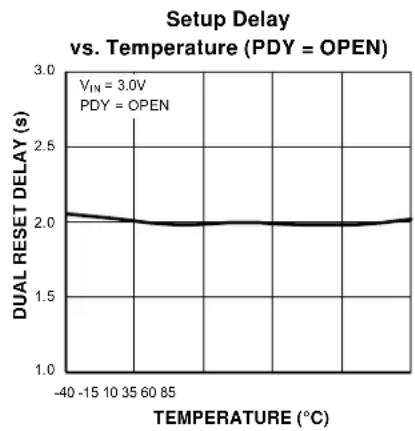
line
| TEMPERATURE (°C) | DUAL RESET DELAY (s) | | ---------------- | -------------------- | | -40 | 2.0 | | -15 | 2.0 | | 10 | 2.0 | | 35 | 2.0 | | 60 | 2.0 | | 85 | 2.0 |
line
| TEMPERATURE (°C) | RESET TIMEOUT DELAY (ms) | | ---------------- | ------------------------ | | -40 | 225 | | -15 | 228 | | 10 | 227 | | 35 | 225 | | 60 | 220 | | 85 | 218 | | 10 | 219 | | 15 | 220 | | 20 | 221 | | 25 | 222 | | 30 | 223 | | 35 | 224 | | 40 | 225 |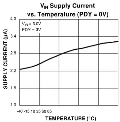
line
| TEMPERATURE (°C) | SUPPLY CURRENT (μA) | | ---------------- | ------------------- | | -40 | 2.2 | | -15 | 2.3 | | -10 | 2.4 | | -5 | 2.6 | | 0 | 2.8 | | 5 | 2.9 | | 10 | 3.0 | | 15 | 3.1 | | 20 | 3.2 | | 25 | 3.3 | | 30 | 3.4 | | 35 | 3.4 | | 40 | 3.4 | | 45 | 3.4 | | 50 | 3.4 | | 55 | 3.4 | | 60 | 3.4 | | 65 | 3.4 | | 70 | 3.4 | | 75 | 3.4 | | 80 | 3.4 | | 85 | 3.4 |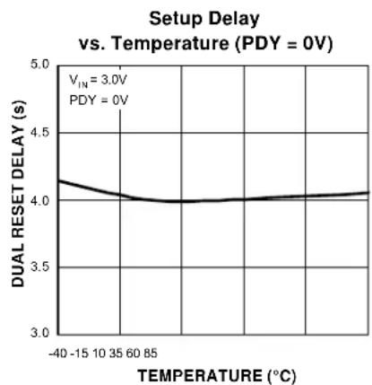
line
| TEMPERATURE (°C) | DUAL RESET DELAY (s) | | ---------------- | -------------------- | | -40 | 4.1 | | -15 | 4.0 | | 10 | 4.0 | | 35 | 4.0 | | 60 | 4.0 | | 85 | 4.0 |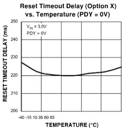
line
| TEMPERATURE (°C) | RESET TIMEOUT DELAY (ms) | | ---------------- | ------------------------ | | -40 | 228 | | -15 | 225 | | -10 | 222 | | -5 | 220 | | 0 | 219 | | 5 | 220 | | 10 | 221 | | 15 | 222 | | 20 | 223 | | 25 | 224 | | 30 | 225 | | 35 | 226 | | 40 | 227 | | 45 | 228 | | 50 | 229 | | 55 | 230 | | 60 | 231 | | 65 | 232 | | 70 | 233 | | 75 | 234 | | 80 | 235 | | 85 | 236 | | 90 | 237 | | 95 | 238 | | 100 | 239 |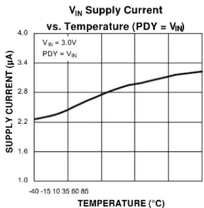
line
| TEMPERATURE (°C) | SUPPLY CURRENT (μA) | | ---------------- | ------------------- | | -40 | 2.2 | | -15 | 2.3 | | -10 | 2.4 | | -5 | 2.6 | | 0 | 2.8 | | 5 | 2.9 | | 10 | 3.0 | | 15 | 3.1 | | 20 | 3.2 | | 25 | 3.3 | | 30 | 3.4 | | 35 | 3.4 | | 40 | 3.4 | | 45 | 3.4 | | 50 | 3.4 | | 55 | 3.4 | | 60 | 3.4 | | 65 | 3.4 | | 70 | 3.4 | | 75 | 3.4 | | 80 | 3.4 | | 85 | 3.4 |
line
| TEMPERATURE (°C) | DUAL RESET DELAY (s) | | ---------------- | -------------------- | | -40 | 6.2 | | -15 | 6.1 | | -10 | 6.0 | | -5 | 6.0 | | 0 | 6.0 | | 5 | 6.0 | | 10 | 6.0 | | 15 | 6.0 | | 20 | 6.0 | | 25 | 6.0 | | 30 | 6.0 | | 35 | 6.0 | | 40 | 6.0 |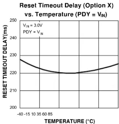
Typical Characteristics (Continued)
V_IN Supply Current vs. Input Voltage

line
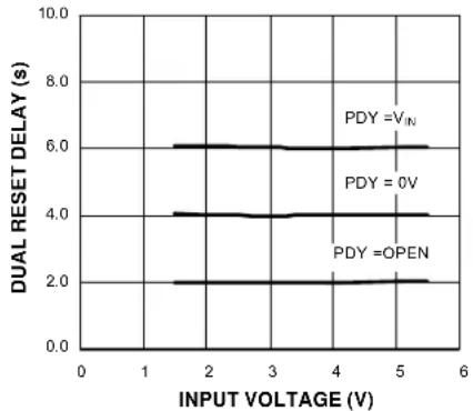
| INPUT VOLTAGE (V) | SUPPLY CURRENT (μA) | | ----------------- | ------------------- | | 1.5 | 2.3 | | 2.5 | 2.9 | | 3.0 | 2.9 | | 4.0 | 3.0 | | 5.0 | 3.6 | | 5.5 | 3.7 |Setup Delay vs. Input Voltage
line
| INPUT VOLTAGE (V) | DUAL RESET DELAY (s) | | ----------------- | --------------------- | | 1 | 6.0 | | 2 | 6.0 | | 3 | 6.0 | | 4 | 6.0 | | 5 | 6.0 | | 6 | 6.0 |Reset Timeout Delay (Option X) vs. Input Voltage

line
| INPUT VOLTAGE (V) | RESET TIMEOUT DELAY (ms) | | ----------------- | ------------------------- | | 1.5 | 225 | | 3.0 | 220 | | 4.0 | 225 | | 5.5 | 223 |Timing Diagram

text_image
VIN /MR0 /MR1 RSTP /UNITED STATE FOR VIN < 1.6V /RST t_SETUP t_RESET t_RESET UNDEFINED STATE FOR VIN < 1.6VFunctional Diagram
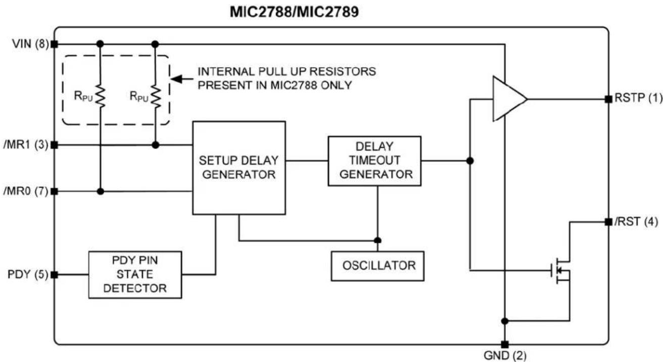
flowchart
graph TD
    A["VIN (8)"] --> B["RPU"]
    C["/MR1 (3)"] --> D["SETUP DELAY GENERATOR"]
    E["/MR0 (7)"] --> D
    F["PDY (5)"] --> G["PDY PIN STATE DETECTOR"]
    H["INTERNAL PULL UP RESISTORS PRESENT IN MIC2788 ONLY"] --> D
    D --> I["DELAY TIMEOUT GENERATOR"]
    I --> J["OSCILLATOR"]
    J --> K["GND (2)"]
    L["RSTP (1)"] --> K
    M["/RST (4)"] --> K
    K --> N["RSTP (1)"]
Application Information
Design and Product Advantages
The dual reset programmability of the MIC2788/MIC2789 allows for already existing manual push buttons to be used to generate a hardware reset based on pre-programmed timing requirements. This ability to increase the functionality of already existing buttons, allows for cost reduction and more robust phone designs. The dual reset delay time allows for significant protection against accidental resets due to its long time duration and dual push button requirement. The fixed reset timeout delay allows for more predictable phone operation during hardware resets. The tri-state option provides an easy to use way to select between three reset delay time options with no additional external components required.
Supply Bypass Capacitor
A 0.1 F input bypass capacitor must be placed from V_IN (Pin 8) to GND (Pin 2).
Programmable Delay Pin (PDY)
The MIC2788/MIC2789 has a programmable dual reset delay time, t_SETUP , that is set via a tri-state logic configuration. The PDY pin is intended to be connected to the V_IN supply voltage, ground or left floating.
| PDY Configuration t | SETUP |
| OPEN | 2s |
| GND | 4s |
| V_IN | 6s |
Dual Manual Reset Inputs (/MR0, /MR1)
The /MR0, /MR1 input pins have integrated pull-up resistors for the MIC2788 but require external pull-up resistors for the MIC2789. A recommended value is 100kΩ to keep the current consumption low when the push-button switches are pressed. The behavior of the reset outputs is independent of the order in which the /MR0, /MR1 inputs are driven low. If both inputs are low for a setup delay time, only one reset pulse, of width tRESET, is generated. Keeping both inputs low for a longer time does not generate additional reset output pulses.
Reset Outputs (/RST and RSTP)
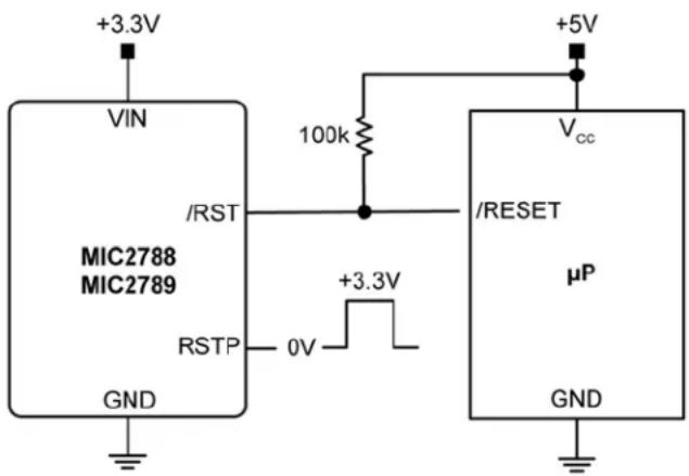
The /RST output is a simple open-drain N-channel MOSFET structure that requires a pull-up resistor. For most applications, the pull-up voltage will be the same as the power supply that supplies V_IN to the MIC2788/MIC2789. As shown in Figure 1, it is possible to tie this resistor to some other voltage, other than V_IN , thus enabling level-shifting of the /RST output. The pull-up voltage must be limited to 5.5V or less to avoid damage to the MIC2788/MIC2789. The pull-up resistor must be small enough to supply current to the inputs and leakage paths that are driven by the /RST output. A recommended value is 100kΩ. Leave floating if the /RST pin is unused.
The RSTP pin is a push-pull output that is driven to V_IN . It cannot be level-shifted to another voltage. It is an inverted signal of /RST.
text_image
+3.3V VIN MIC2788 MIC2789 /RST RSTP 0V +5V 100k Vcc /RESET μP GND GNDFigure 1. MIC2788/MIC2789 Used in Multiple Supply System
The reset outputs /RST and RSTP are asserted when the dual reset delay time, t_SETUP , is exceeded while the /MR0, /MR1 pins are driven low. Both the reset outputs remain asserted for a factory-programmed reset timeout delay time t_RESET . Two options are available with 140ms or 240ms minimum t_RESET duration. The /RST pin is driven active low while the RSTP pin is driven active high for the t_RESET duration. The reset outputs are de-asserted for V_IN < 1.6V .

line
| Signal | Voltage (5V/div) | |--------|------------------| | /MR0 | 5 | | /MR1 | 5 | | RSTP | 5 | | /RST | 5 |Figure 2. Manual Reset Function
Typical Applications

text_image
VIN = 1.6V to 5.5V 100k 100k 0.1μF /MR0 /MR1 MIC2788 MIC2789 /MR0 /MR1 EXTERNAL RESISTORS NOT REQUIRED FOR MIC2788 VIN /RST /PDY /RSTP GND CONNECT TO VIN, GND OR FLOAT TO SET SETUP DELAY TIME VIN REGULATOR OUT /SYSTEM POWER OUTPUTFigure 3. MIC2788/89 Used for Interrupting System Power
text_image
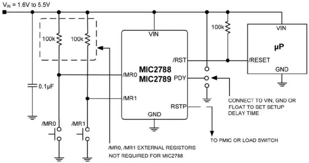
VIN = 1.6V to 5.5V 100k 100k 0.1μF /MR0 /MR1 VIN MIC2788 MIC2789 /MR0 /MR1 PDY /MR1 RSTP GND 100k VIN μP /RESET GND CONNECT TO VIN, GND OR FLOAT TO SET SETUP DELAY TIME TO PMIC OR LOAD SWITCH /MR0, /MR1 EXTERNAL RESISTORS NOT REQUIRED FOR MIC2788Figure 4. MIC2788/89 Used for Microcontroller Reset
Evaluation Board Schematic

text_image
1.6V to 5.5V VIN C1 0.1μF J8 VIN SW1 J1 J2 /MR0 SW2 J3 J4 /MR1 U1 8 VIN /MR0 7 /MR1 3 /MR0 R2* 100k RSTP GND 2 /RST PDY 4 5 1 R4 100k J5 J7 /RST J6 RSTP*RESISTORS R1 AND R2 ARE FOR MIC2789. R1 AND R2 ARE NOT REQUIRED FOR MIC2788.
Bill of Materials
| Item | Part Number | Manufacturer Description Qty. | |
| C1 | GRM188R71C104KA01D | M_urata^(1) 1 μF, 16V capacitor, X7R, 0603 1 | |
| R1, R2, R4 | RCW0603100KJNEA Vishay | ^(2) 100k, 5% resistor, 0603 3 | |
| MIC2788-XYMT U1 | Micrel, Inc. ^(3) Push-Button Supervisor Reset ICs 1 | ||
| MIC2789-XYMT | |||
Notes:
1. Murata Tel: www.murata.com.
2. Vishay Tel: www.vishay.com.
3. Micrel, Inc.: www.micrel.com.
PCB Layout Recommendations
text_image
MIC278 YMT SW2 SW1 /MR1 /RST RSTP C1 R1 /MRO U1 VIN PDY GND GND VIN PGND J1Top Layer

text_image
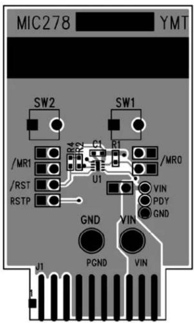
MIC278 YMT SW2 SW1 /MR1 /RST RSTP R4 R2 C1 R1 U1 /MRO VIN PDY GND VIN PGND VIN J1Top Silkscreen
PCB Layout Recommendations (Continued)
text_image
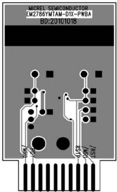
MICREL SEMICONDUCTOR EM2786YMTAM-D1X-PWBA BD:20101018 /MPD /MPD /RSTP /RSTCopper Layer

text_image
MICREL SEMICONDUCTOR BD:20101018 /PDY /MRO /RSTP /MRIBottom Silkscreen
Package Information
text_image
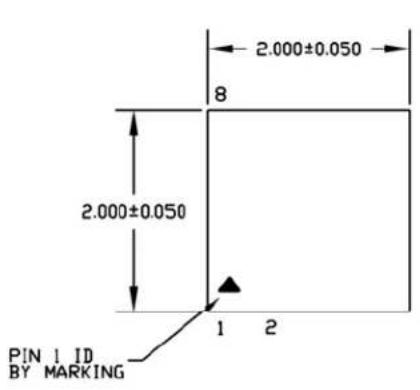
2.000±0.050 8 2.000±0.050 1 2 PIN 1 ID BY MARKINGTOP VIEW

text_image
1.200±0.050 Exp. DAP 0.500 Bsc 0.250±0.050 0.600±0.050 Exp. DAP 0.350±0.050 1.500 Ref. PIN #1 IDENTIFICATION R0.100BOTTOM VIEW
text_image
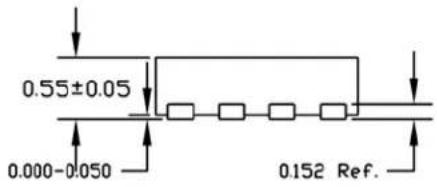
0.55±0.05 0.000-0.050 0.152 Ref.SIDE VIEW
NOTE:
1. ALL DIMENSIONS ARE IN MILLIMETERS.
2. MAX. PACKAGE WARPAGE IS 0.08 mm.
3. MAXIMUM ALLOWABE BURRS IS 0.076 mm IN ALL DIRECTIONS.
4. PIN #1 ID WILL BE LASER MARKED.
8-Pin 2mm × 2mm Thin MLF®
Recommended Landing Pattern

other
| Dimension | Value | | --------- | ----------- | | BSC | 0.25±0.02 | | Total | 0.35±0.02 | | Width | 1.20±0.02 | | Height | 1.50±0.05 | | Base | 2.20±0.05 | | Thickness | 0.60±0.02 | | Tolerance | ±0.05 |Red circle indicates Thermal Via. Size should be .300mm – .350mm in diameter and it should be connected to GND plane for maximum thermal performance.
8-Pin 2mm × 2mm Thin MLF®
MICREL, INC. 2180 FORTUNE DRIVE SAN JOSE, CA 95131 USA
TEL +1 (408) 944-0800 FAX +1 (408) 474-1000 WEB http://www.micrel.com
Micrel makes no representations or warranties with respect to the accuracy or completeness of the information furnished in this data sheet. This information is not intended as a warranty and Micrel does not assume responsibility for its use. Micrel reserves the right to change circuitry, specifications and descriptions at any time without notice. No license, whether express, implied, arising by estoppel or otherwise, to any intellectual property rights is granted by this document. Except as provided in Micrel's terms and conditions of sale for such products, Micrel assumes no liability whatsoever, and Micrel disclaims any express or implied warranty relating to the sale and/or use of Micrel products including liability or warranties relating to fitness for a particular purpose, merchantability, or infringement of any patent, copyright or other intellectual property right.
Micrel Products are not designed or authorized for use as components in life support appliances, devices or systems where malfunction of a product can reasonably be expected to result in personal injury. Life support devices or systems are devices or systems that (a) are intended for surgical implant into the body or (b) support or sustain life, and whose failure to perform can be reasonably expected to result in a significant injury to the user. A Purchaser's use or sale of Micrel Products for use in life support appliances, devices or systems is a Purchaser's own risk and Purchaser agrees to fully indemnify Micrel for any damages resulting from such use or sale.
© 2011 Micrel, Incorporated.