PS810 - Fuel gauge Microchip - Free user manual and instructions
Find the device manual for free PS810 Microchip in PDF.

User questions about PS810 Microchip
0 question about this device. Answer the ones you know or ask your own.
Ask a new question about this device
Download the instructions for your Fuel gauge in PDF format for free! Find your manual PS810 - Microchip and take your electronic device back in hand. On this page are published all the documents necessary for the use of your device. PS810 by Microchip.
USER MANUAL PS810 Microchip
Li Ion Single Cell Fuel Gauge
Hardware Features
- Highly accurate fuel gauge for single cell Li Ion applications
- Algorithms are implemented using an embedded PIC18 low-power microcontroller with 16-bit instruction set
- Reports current, voltage and temperature utilizing a programmable 8 to15-bit + sign, sigma-delta ADC
- Host communication accomplished through an industry standard SMBus interface or an alternative single pin serial interface
- I/O pins are available to provide functions such as digital GPIO, coin cell voltage measurement and thermistor input
- Integrated temperature sensor and regulator minimize external components
- Embedded fuel gauge algorithms and application specific parameters are stored in a 4K x 16 Flash memory
- 512 bytes of RAM are available for temporary storage of battery parameters
Software Features
- Provides battery status, such as average time to empty, relative State-Of-Charge and battery State-Of-Health
- In-system offset calibration compensates for offset error in current measurement
Package Features
• 16-pin QFN package or 14-pin TSSOP package
- -20°C to +85°C operating temperature range
1.0 PRODUCT OVERVIEW
The PS810 is a fuel gauge for one-cell Li Ion or Li Polymer applications. The device provides the host and the system user with critical battery information, such as voltage, current, temperature, run time, State-Of-Charge and State-Of-Health. This information is available through an industry standard SMBus or an alternative Single Pin Serial interface. Advanced fuel gauge algorithms are stored in on-board Flash memory and executed by the industry recognized PIC18 microcontroller. These algorithms include compensation factors which optimize the performance of the battery for a specific application and operating environment. Compensation is included for the effects of temperature, discharge rate, charge rate and battery aging.
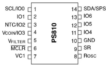
Pin Description
16-pin QFN (4 mm x 4 mm)

text_image
NTC/IO2 1 VCOIN/IO3 2 VFILTER 3 MCLR 4 PS810 VC1 5 6 7 8 N/C N/C Rosc SCL/IO0 SDA/SPS IO6 IO1 16 15 14 13 12 IO5 11 IO4 10 GND 9 SR 16 15 14 1314-pin TSSOP
text_image
SCL/IO0 1 IO1 2 NTC/IO2 3 VCOIN/IO3 4 V_FILTER 5 MCLR 6 VC1 7 PS810 14 SDA/SPS 13 IO6 12 IO5 11 IO4 10 GND 9 SR 8 RoscTo provide precise measurements of current, voltage and temperature, the PS810 integrates a highly accurate 15-bit + sign, sigma-delta A/D converter. Based upon operating conditions, this programmable converter can be configured to measure specific battery parameters with a resolution of 8 to 15 bits + sign. Precision measurements combined with advanced algorithms provide accurate indications of capacity, run time, State-Of-Health and safety and charge/discharge conditions.
The ability to operate directly from a single Li Ion or Li Polymer cell minimizes the need for external components, such as a voltage regulator and voltage divider. To further limit external circuitry and enhance accuracy, the PS810 provides an integrated temperature sensor and oscillator.
TABLE 1-1: PS810 QFN PIN SUMMARY TABLE 1-2: PS810 TSSOP PIN SUMMARY
| Pin# | Pin Name | Description |
| 1 | NTC/IO2 | External NTC input or GPIO |
| 2 | Vcoin/IO3 | Coin cell monitor input or GPIO |
| 3 | VFILTER | Power supply filter cap |
| 4 | M C L | Master Clear |
| 5 | VC1 | Cell voltage input |
| 6 | N/C | No connect |
| 7 | N/C | No connect |
| 8 | ROSC | Oscillator bias resistor |
| 9 | SR | Sense resistor input |
| 10 | GND | Power supply ground |
| 11 | IO4 | General purpose IO |
| 12 | IO5 | General purpose IO |
| 13 | IO6 | General purpose IO |
| 14 | SDA/SPS | SMBus data/one-wire serial line |
| 15 | SCL/IO0 | SMBus clock or GPIO0 |
| 16 | IO1 | General purpose IO |
| Pin# | Pin Name | Description |
| 1 SCL/IO0 | SMBus clock or GPIO | |
| 2 IO1 | General purpose IO | |
| 3 NTC/IO2 | External NTC input or GPIO | |
| 4 | VCOIN/IO3 | Coin cell monitor input or GPIO |
| 5 | VFILTER | Power supply filter cap |
| 6 | MCLR | Master Clear |
| 7 VC1 Cell voltage input | ||
| 8 | ROSC | Oscillator bias resistor |
| 9 SR | Sense resistor input | |
| 10 | GND | Power supply ground |
| 11 | IO4 | General purpose IO |
| 12 | IO5 | General purpose IO |
| 13 | IO6 | General purpose IO |
| 14 | SDA/SPS | SMBus data/one-wire serial line |
FIGURE 1-1: PS810 INTERNAL BLOCK DIAGRAM

flowchart
graph TD
    subgraph Digital Section
        A["4K x 16 Flash"] --> B["512-byte RAM/Registers"]
        C["COMM Interface"] --> D["PIC18F Microcontroller"]
        E["Input/Output"] --> F["Control and Status"]
        G["SDA/SPS"] --> C
        H["SCL"] --> C
        I["IO0"] --> C
        J["IO1"] --> C
        K["IO2"] --> C
        L["IO3"] --> C
        M["IO4"] --> C
        N["IO5"] --> C
        O["IO6"] --> C
    end

    subgraph Analog Section
        P["VOLTAGE Reference and Temp Sensor"] --> Q["Voltage Regulator"]
        R["15-bit + sign Sigma-Delta Integrating A/D Converter"] --> Q
        S["Analog Input Mux"] --> Q
        T["Run Oscillator"] --> U["Sleep Oscillator"]
        V["Rosc"] --> W["GND"]
        X["VFILTER"] --> Q
        Y["VC1"] --> Q
        Z["SR"] --> Q
        AA["NTC"] --> Q
        AB["VCOIN"] --> Q
    end

    B <--> C
    D <--> E
    F <--> G
    H <--> I
    L <--> M
    N <--> O
    Q <--> R
    S <--> T
    U <--> V
    W <--> X
    Y <--> Z
    Z <--> AA
    AA <--> AB
    AC["MCLR"] --> F
    AD["MCLR"] --> G
    AE["MCLR"] --> H
1.1 Schematic
FIGURE 1-2: PS810 APPLICATION SCHEMATIC – PS810-BASED BATTERY PACK

text_image
EXT. THERMISTOR INPUT NTC *D NVR COIN CELL INPUT VCOIN * * GROUND IF NOT USED CELL CONNECTIONS V1 VR R2240 R5 C2 100 nF C3 100 nF R4 20K C10 1.0 nF C5 100 nF 15 SCL/IO0 SDA/SPS 16 IO1 IO6 17 NTC/IO2 IO5 18 VCOIN/IO3 IO4 19 VFILTER GND 20 MCLR SR 21 VC1 Rosc 22 NC NC QFN PACKAGE U1PS810Q 13 12 11 10 9 8 7 R32 470 2 U2 S8241A VDD SAFETY IC VM Vss DO O R8 232K 3 C32 100 nF R9 0.020 GROUND PLANE CONNECTION Q1 R31 1.0K TPCS8209 3 D1 CMSZDA5V6 B+ C B- PACK CONNECTION1.2 Bill of Materials
TABLE 1-3: PS810 BILL OF MATERIALS
| ID | Part Number Symbol Description M | Mfr. Mftr. PN | Supplier Supplier PN Qty | |||||
| 1 | 04-826197 Rev. 1.1 | Raw PCB, PS8110 | Microchip | 04-826197 Rev. 1.1 | Microchip | 04-826197 Rev. 1.1 | 1 | |
| 2 | CC-0402-10X7R25-1.0NF-01 | C10 Capacitor | , Ceramic, 1.0 nF, 25V, +/-10%, X7R dielectric, 0402 | Panasonic | ECJ-0EB1E102K | Digikey | PCC102BQCT-ND | 1 |
| 3 | CC-0603-10X7R16-100NF-01 | C2, C3, C5, C32 | Capacitor, Ceramic, 100 nF, 16V, +/-10%, X7R dielectric, 0603 | Panasonic | ECJ-1VB1C104K | Digikey | PCC1762CT-ND | 4 |
| 4 | DZ-SOT323-10D-CMSZDA5V6-01 | D1 | Dual Zener Diode, 5.6V, +/-10%, 200 mW, common anode, SOT-323 | Central Semi, Diodes Inc. | CMSZDA5V6 AZ23C5V6W-7 | Central Semi, Diodes Inc. | CMSZDA5V6 AZ23C5V6W-7 | 1 |
| 5 | QM-TSSOP844-DN-TPCS8209-01 | Q1 | MOSFET, dual N-channel Enhancement mode, 20V, 5A, TSSOP-8/4.4 mm body width package | Toshiba | TPCS8209(TE12L) | Digikey | TPCS8209CT-ND | 1 |
| 6 | RF-0402-5-20-01 (Note 1) | R14, R15 | Resistor, film, 0402, 5%, 20 ohms | Panasonic | ERJ-2GEJ200X Digikey P20JCT-ND | 2 | ||
| 7 | RF-0402-5-20K-01 (Note 1) | R4 | Resistor, film, 0402, 5%, 20 kOhms | Panasonic | ERJ-2GEJ203X Digikey P20KJCT-ND 1 | |||
| 8 | RF-0603-ITC25-221K-01 (Note 1) | R8 | Resistor, film, 0603, 1%, 232 kOhms, 25 ppm TC | Susumu Co. Ltd. | RR0816P-2213-D-34D | Digikey | RR08P221KDCT-ND | 1 |
| 9 | RF-0603-5-1.0K-01 (Note 1) | R31 Resistor | , film, 0603, 5%, 1.0 kOhms | Panasonic | ERJ-3GEYJ102V | Digikey | P1.0KGCT-ND | 1 |
| 10 | RF-0603-5-470-01 (Note 1) | R32 Resistor | , film, 0603, 5%, 470 ohms | Panasonic | ERJ-3GEYJ471V | Digikey | P470GCT-ND | 1 |
| 11 | RF-0805-5-20-01 (Note 1) | R5 | Resistor, film, 0805, 5%, 20 ohms | Panasonic | ERJ-6GEYJ200V | Digikey | P20ACT-ND | 1 |
| 12 | RF-0805-5-240-01 (Note 1) | R2, R20, R21 | Resistor, film, 0805, 5%, 240 ohms | Panasonic | ERJ-6GEYJ241V | Digikey | P240ACT-ND | 3 |
| 13 | RF-1206-1-0.029-01 (Note 1) | R9 | Resistor, metal strip, 1206, 1%, 0.020 ohms | Vishay | WSL1206-0.020-1%-R86 | Vishay | WSL1206-0.020-1%-R86 | 1 |
| 14 | UM-SOT235-4085-S8241ABPMCGBPT2-01 | U2 | IC, Battery Protection Circuit, Li Ion, 1-cell, -40°C to +85°C, SOT23-5 package | Seiko Instruments | S-8241ABPMC-GBP-T2 (Note 2) | Seiko Instruments | S-8241ABPMC-GBP-T2 (Note 2) | 1 |
| 15 | UM-QFN164X4-2085-PS810-01 | U1 | IC, Low-Voltage Fuel Gauge, -20°C to +85°C, QFN-16/4.0x4.0 mm package | Microchip | PS810 | Microchip | PS810 | 1 |
Note 1: Resistor sizes shown are minimum recommended sizes for the application.
2: Other variants of the S-8241A series, with different trip points, are also available. Consult the S-8241A series data sheet.
2.0 ARCHITECTURAL OVERVIEW
The PS810 contains a complete analog "front-end" for battery monitoring as well as an embedded microcontroller, with supporting memory, for control, measurement accumulation, calculation and communications. Major functions within the PS810 include:
- Voltage Regulator
- Precision Time Base
• Temperature Sensor - 4K x 16 Flash Memory
- 512-byte RAM Memory
• 15-bit plus sign Analog-to-Digital (A/D) Converter - S M B ^2 C ^TM or Single Pin Serial Communications Interface
• PIC18 Microcontroller
Figure 1-1 is a block diagram of the internal circuitry of the PS810. Figure 1-2 is a schematic diagram that depicts the PS810 in a typical single cell lithium ion application. The function of each of the blocks listed above is summarized in the following sections.
2.1 Internal Voltage Regulator
The PS810 incorporates an internal voltage regulator that supports 1-cell lithium pack configurations. The internal regulator draws power directly from the VC1 input. No other external components are required to regulate circuit voltage.
2.2 Precision Time Base
The integrated precision time base is a highly accurate RC oscillator that provides precise timing for the sigma-delta A/D and for the on-chip elapsed time counters without the need for an external crystal. This time base is trimmed during manufacturing to a nominal frequency of 512 kHz.
2.3 Temperature Sensor
An integrated temperature sensor is provided that can eliminate the need for an external thermistor. As an option, a connection is provided for an external thermistor for applications where the battery cell is physically separated from the PS810.
2.4 Flash Memory
4K x 16 of Flash memory is incorporated for storage of nonvolatile parameters, such as PowerSmart ^® 3D cell models, fuel gauge algorithms and application specific data.
2.5 RAM Memory
512 bytes of general purpose RAM memory is provided for storage of temporary parameters.
2.6 A/D Converter
The PS810 incorporates an integrating sigma-delta A/D converter together with an analog that has inputs for charge and discharge current, cell voltage, coin cell voltage, the on-chip temperature sensor and an off-chip thermistor. The converter can be programmed to perform a conversion with resolutions of 8 to 15 bits + sign, while utilizing either a single-ended +300 mV or a differential ±150 mV reference.
2.7 SMBus/I ^2 C ^TM or Single Pin Serial Communications Interface
This communications port for the PS810 is selectable as a 2-pin industry standard SMBus/PC or a single pin interface. All commands, status and data are read or written from the host system via this interface.
2.7.1 SMBus/I ^2 C
The two pin communication interface uses one clock pin and one data pin and is compatible with the industry standard System Management Bus (SMBus) and the Inter IC Communication Bus ( ^2 C).
2.7.2 SINGLE PIN SERIAL INTERFACE
The Single Pin Serial (SPS) interface consists of one pin only: the SDA/SPS pin (pin 14). This communication is an asynchronous return-to-one protocol. The timing of the driven low pulses defines the communication.
2.8 PIC18 Microcontroller
The PIC18 is a high-performance, CMOS, fully static 8-bit microcontroller. The PIC18 employs an advanced RISC architecture. This device has enhanced core features, such as 31 level deep stack and multiple internal and external interrupt sources. The separate instruction and data buses of the Harvard architecture allow a 16-bit wide instruction word with a separate 8-bit wide data bus. The two-stage instruction pipeline allows all instructions to execute in a single cycle, except for program branches, which require two cycles. A total of 75 instructions are available.
NOTES:
3.0 OPERATIONAL DESCRIPTION
3.1 A/D Operation
The PS810 A/D converter measures current, voltage and temperature and integrates the current over time to calculate State-Of-Charge. Cell voltage is measured with a direct connection to the battery cell without requiring an external voltage divider. Using an external sense resistor, current is monitored during both charge and discharge and is integrated over time using the on-chip oscillator as the time base. Temperature is measured from the on-chip temperature sensor or an optional external thermistor. Voltage, current and temperature can be calibrated for accuracy over the operational range. The A/D converter performs sampling using a 32 kHz clock.
3.1.1 CURRENT MEASUREMENT
The A/D input channels for current measurement are the SR and GND pins. The voltage drop across the sense resistor is measured and converted mathematically into a current measurement. The current is also integrated over time to get the amount of charge entering or leaving the battery.
A sense resistor is connected to SR and GND. The maximum input voltage that can be measured at SR is +/-150 mV. The sense resistor should be properly sized to accommodate the lowest and highest expected charge and discharge currents, including suspend and/or standby currents.
The parameter NullCurr represents the zero-zone current of the battery. This is provided as a calibration guardband for reading zero current. Currents below +/- NullCurr (in mA) limit are read as zero and not included in the capacity algorithm calculations. A typical value for NullCurr is 3 mA, therefore, currents between -3 mA and +3 mA will be reported as zero and not included in the capacity calculations. This feature is provided so that electrical noise on the battery module current path is not interpreted as actual charge entering or leaving the battery.
3.1.1.1 Sense Resistor Selection and Current Measurement Range
The current resolution is based on the smallest amount of voltage the A/D converter can measure across the sense resistor. Since this measurement uses 13 bits (plus sign) and the reference used is the internal 150 mV reference, the smallest voltage across the sense resistor that can be measured is:
EQUATION 3-1:
$$ 1 5 0 \mathrm{mV} / (2 ^ {\wedge} 1 3 - 1) = 1 5 0 \mathrm{mV} / 3 2 7 6 7 = 1 8. 3 \mu \mathrm{V} $$
Thus, the smallest current that can be measured is: 18.3 μV/RSENSE (mΩ)
The largest current that can be measured is: 150 mV/RSENSE (mΩ)
Example: a 20 milliohm sense resistor will measure from:
$$ 1 8. 3 \mu \mathrm{V} / 2 0 \mathrm{m} \Omega = 0. 9 1 5 \mathrm{mA} $$
(though will be recorded as zero if <NullCurr)
up to:
$$ 1 5 0 \mathrm{mV} / 2 0 \mathrm{m} \Omega = 7. 5 \mathrm{Amps} $$
3.1.1.2 Current Calibration
In-circuit calibration of the current is done using the communication interface (SMBus/I²C or SPS) at time of manufacture to obtain optimal accuracy. A correction is calculated and stored for both offset and slope.
COD is a constant that is measured at calibration time and contains the offset due to external PCB components.
CFCurr is the “Correction Factor for Current” which compensates the A/D gain and any variances in the actual sense resistance over varying currents. It is multiplied against the raw A/D measurement.
COCurr is the "Correction Offset for Current" which is updated in real time by the A/D shorting the inputs and comparing any result to zero. This is added to COD and compensates for any offset that varies over time, such as temperature dependent offsets.
Figure 3-1 shows the relationship of the COCurr and CFCurr values.
FIGURE 3-1: COCurr AND CFCurr
VALUE RELATIONSHIP
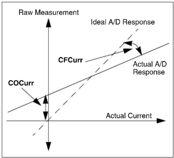
text_image
Raw Measurement Ideal A/D Response CFCurr Actual A/D Response COCurr Actual Current3.1.2 AUTO-OFFSET COMPENSATION
Accuracy drift is prevented using an automatic auto-zero self-calibration method which zeros the current measurement circuit periodically at a programmable rate. This feature can correct for drift in temperature during operation. The Auto-Offset Compensation circuit works internally by disconnecting the RS input and internally shorting it to GND to measure the zero input offset. Furthermore, the calibration factor, COD, contains the offset factor external to the IC, offset due to the circuit board, system, etc. COD is added to the internal offset calculated by the auto-offset cycle to determine the full offset, COCurr.
3.1.3 VOLTAGE MEASUREMENTS
The A/D input channel for cell voltage measurement is the VC1 pin. Measurements are taken each measurement period when the A/D is active. The maximum voltage at the VC1 pin is 5.5V, but voltages above 4.5V are not suggested since this will saturate the A/D. The cell voltage is measured with an integration method to reduce any sudden spikes or fluctuations. The A/D uses a default of 11-bit plus sign resolution for these measurements.
The VC1 input circuit contains an internal resistive divider to reduce the external voltage input to a range that the internal A/D circuit can accommodate (300 mV maximum). The divider is 15 to 1 based on a maximum cell voltage of 4.5 volts. The voltage divider is only connected to ground when the actual voltage measurement is occurring.
CFVoltage is the "Correction Factor for Pack Voltage" which compensates for any variance in the actual A/D response versus an ideal A/D response over varying voltage inputs. In-circuit calibration of the voltage is done at the time of manufacture to obtain accuracy in addition to high resolution. Cell voltage measurements can be accurate to within ± 20mV .
3.1.4 TEMPERATURE MEASUREMENTS
The A/D can measure temperature from the internal temperature sensor or an external thermistor connected to the NTC pin. The A/D uses a default of 11-bit plus sign resolution for the temperature measurements.
A standard 10 kOhms at 25°C Negative-Temperature-Coefficient (NTC) device of the 103ETB type is suggested for the optional external thermistor. One leg of the NTC should be connected to the NTC pin and the other to ground.
A linearization algorithm is used to convert the voltage measurement seen at the NTC pin to a temperature value. The external thermistor should be placed as close as possible to the battery cells and should be isolated from any other sources of heat that may affect its operation.
Calibration of the temperature measurements involves a correction factor and an offset exactly like the current measurement. The internal temperature measurement makes use of correction factor, CFTempl and offset, COTempl, while the NTC pin for the optional external thermistor makes use of correction factor, CFTempE.
TABLE 3-1: A/D OPERATION PARAMETERS
| Parameter Name | # of Bytes | Units | Typical Value | Operational Description |
| NullCurr 1 mA 3 | Zero zone | control is | built into the | PS810 so that electrical noise doesn't actually drain the gas gauge, when in fact the current is zero. For this reason, current less than NullCurr mA in either direction will be measured as zero. |
| CFCurr 2 unsigned | word | 4200 Correction Factor for Current. Adjusts the scaling of the sense resistor current measurements. | ||
| COCurr 1 signed | byte | 0 Correction Offset for Current. This is the value the A/D reads when zero current is flowing through the sense resistor. | ||
| COD 1 signed | byte | 0 Correction Offset Deviation. Offset value for the auto-zero calibration of the current readings. | ||
| AOMInterval | 1 | op cycles | 60 | Interval of time between auto-offset calibrations. |
| AVGIScale | 1 | coded | b00100000 | Time period over which current is averaged to calculate average current: IAVG = IAVG + (I - IAVG)/(AVGIScale * 2).Note: Only Most Significant set bit is used, others are ignored. |
| CFVoltage | 2 | integer | 2250 | Correction Factor for Pack Voltage. Adjusts the scaling of the VC1 pin measurement. |
| CFCoin | 2 | integer | 2250 | Correction Factor for Coin Cell Measurement. Adjusts the scaling of the VCOIN pin measurement. |
| CFTempE | 2 | integer | 326 | Correction Factor for Temperature. Adjusts the scaling of temperature measured across an external thermistor at the NTC input pin. |
| CFTempl | 2 | integer | 2038 | Correction Factor for Temperature. Adjusts the scaling of temperature measured from the internal temperature sensor. |
| COTempl | 2 signed word | 21298 | Correction Offset for Temperature. Used for temperature measurement using internal temperature sensor. | |
3.2 Operational Modes
The PS810 operates on a continuous cycle, measuring current, voltage and temperature, then performing fuel gauge calculations. There are four power modes: Run mode, in which the measuring and calculating loop constantly repeats; Bus Inactive Low-Power mode, in which only self-discharge is calculated; Low-Voltage Sleep mode, in which there are no measurements and only wake-up circuitry is powered; and Shelf-Sleep mode, in which only communication line sensors are powered.
3.2.1 RUN MODE
Run mode is the highest power consuming mode. During Run mode, all measurements and calculations occur. Current, voltage and temperature measurements are each made sequentially. Run mode is active until voltage drops below the Sleep voltage, the bus goes inactive or the Shelf-Sleep command is executed.
3.2.2 BUS INACTIVE LOW-POWER MODE
The PS810 enters Low-Power mode when all of the following conditions are true:
- Current is zero (optional)
- The communication pins are low for at least 8 periods of 512 ms each
- There is no communication attempt for at least 8 periods of 512 ms each
To enter this mode, typically, there must be no load or charger present and no communication host. The pack is out of the system. In this mode, the PS810 will draw less current from the battery, approximately 25 A and will only track self-discharge. Alternatively, if self-discharge tracking is not required, Ultra Low-Power mode can be used and the PS810 will draw less than 1 microamp.
3.2.3 LOW-VOLTAGE SLEEP MODE
Entry to Low-Voltage Sleep mode can only occur when the measured pack voltage at VC1 input is below a preset limit set by the parameter SleepVoltage (in mV) and the current is zero (less than NullCurr). Sleep mode may be exited to Run mode when the voltage at VC1 is greater than the wake-up voltage, which is 3.2 volts, 10%.
While in 10% Sleep mode, no measurements occur and no calculations are made. The fuel gauge display is not operational, no communications are recognized and only a wake-up condition will permit an exit from Sleep mode. Sleep mode is one of the lowest power consuming modes and is used to conserve battery energy following a complete discharge.
There are two power levels that can be chosen for Low-Voltage Sleep mode. Low-Power mode draws approximately 20 A and will wake-up automatically when the voltage rises above the wake-up voltage, which is a constant 3.2 volts above the wake-up volts, +/-5%. Ultra Low-Power mode draws less than 1 A and requires an external source to drive the communication line high to wake-up, since the voltage wake-up comparator is powered down.
3.2.4 SHELF-SLEEP MODE
Shelf-Sleep mode can be entered by a battery data command on the communication bus for conserving energy while shipping battery packs. It can be exited only by an external source driving the communication data line high. This mode uses the Ultra Low-Power Sleep mode, resulting in current draw less than 1 microamp. This mode is entered by writing a password to SMBus command code, 0x43. A word write protocol is used to write the password, 0x5A7A.
TABLE 3-2: OPERATIONAL MODES
| Mode Entry Exit Notes | |||
| Run Voltage > | Wake-up voltage or data line driven high | Voltage less thanSleepVoltage, bus Idle or Shelf-Sleep command issued | Highest power consumption and accuracy. |
| Bus Inactive Low-Power | Current < NullCurr, communication lines low and no communication attempts | Activity on communication lines Only self-discharge calculated. | |
| Low-Voltage Sleep | VC(1) < SleepVoltage, Current is not zero | Voltage > Wake-up voltage (Low-Power mode), Data line driven high (Ultra Low-Power mode) | No measurements made. |
| Shelf-Sleep | Can be entered by SMBus command | Data line driven high | No measurements made. |
TABLE 3-3: OPERATIONAL MODE PARAMETERS
| Parameter Name | # Bytes | Units | Typical Value | Operational Description |
| SleepVoltage 2 mV | 2700 The pack voltage at which | the PS810 will enter Low-Voltage Sleep mode. | ||
| PwrConsumSleep | 1 | 1/256 mA | 7 | The average current that the battery module typically draws from the battery while in Low-Power mode. |
| PowerModes 1 bitmap b000 | 00101 bit 5: | 1 = Bus Inactive mode, always uses Ultra Low-Power mode until first bus communication after POR0 = Disable Bus Inactive Low-Power modebit 4:1 = Enable Bus Inactive Low-Power mode0 = Disable Bus Inactive Low-Power modebit 3:1 = Use Ultra Low-Power mode as Bus Inactive Low-Power mode (no self-discharge calculations)0 = Use Low-Power mode with self-discharge calculations as Bus Inactive Low-Power modebit 2:1 = Require NullCurr for Bus Inactive Low-Power mode and Low-Voltage Sleep mode0 = No NullCurr requirement for Sleep modesbit 1:1 = Use Ultra Low-Power mode as Low-Voltage Sleep mode0 = Use Low-Power mode as Low-Voltage Sleep modebit 0:1 = Set remcap to zero when entering Low-Voltage Sleep mode0 = Do not change remcap when entering Low-Voltage Sleep mode | ||
NOTES:
4.0 CAPACITY MONITORING
The PS810 uses the voltage, current and temperature data from the A/D converter, along with battery algorithms and cell models, to determine the state of the battery and to process the battery data instruction set.
By integrating measured current, monitoring voltages and temperature, adjusting for self-discharge and checking for End-Of-Charge and End-Of-Discharge conditions, the PS810 creates an accurate fuel gauge under all battery conditions.
4.1 Capacity Calculations
The PS810 calculates State-Of-Charge and fuel gauging functions using a 'coulomb counting' method, with additional inputs from battery voltage and temperature measurements. By continuously and accurately measuring the current into and out of the battery cells, along with accurate three-dimensional cell models, the PS810 is able to provide accurate predictions of SOC and run time.
The capacity calculations consider two separate states: charge or Capacity Increasing (CI) and discharge or Capacity Decreasing (CD). The CI state only occurs when a charge current larger than the parameter NullCurr value is measured. Otherwise, while at rest and/or while being discharged, the state is CD. Conditions must persist for at least NChangeState measurement periods for a valid state change between CD and CI. A minimum value of 2 is suggested for NChangeState.
Regardless of the CI or CD state, self-discharge is also calculated and subtracted from the integrated capacity values. Even when charging, there is still a self-discharge occurring in the battery. Self-discharge is modelled internally in the PS810 and is a factor of temperature and State-Of-Charge.
Since the PS810 electronics also drain current from the battery system, another parameter value allows even this minor drain to be included in the capacity calculations. The PwrConsumption value represents the drain of the IC and associated circuitry, including additional safety monitoring electronics, if present. A typical value of 31 represents the modules nominal power consumption, including PS810 typical consumption of 85 A.
The total capacity added or subtracted from the battery (change in charge) per measurement period is expressed by the following formula:
EQUATION 4-1:
Charge = i t (the current integrated over time)
- PwrConsumption * Δt
- Self-discharge percentage * FCC
The battery current will be precisely measured and integrated in order to calculate total charge removed from or added to the battery. Based on look-up table values, the capacity is adjusted relative to discharge rate and temperature.
4.2 Discharge Termination
Remaining capacity is determined based on the End-Of-Discharge (EOD) voltage point. The voltage level at which this point occurs will change depending on the temperature and discharge rate, since these factors affect the voltage curve and total capacity of the battery. The EOD voltage look-up table predicts the voltage point at which this EOD will be reached based on discharge rate and temperature.
The PS810 will monitor temperature and discharge rate continuously and update the EOD voltage from the look-up table in real time. When the voltage measured on the cell is below the EOD voltage for the duration of EODRecheck x periods (500 ms), a valid EOD has occurred. When a valid EOD has been reached, the FULLY_DISCHARGED bit in BatteryStatus will be set.
4.3 Capacity Relearn
To maintain accurate capacity prediction ability, the FullCapacity value is relearned on each discharge, which has reached a valid EOD after a previous valid fully charged EOC. If a partial charge occurs before reaching a valid EOD, then no relearn will occur. The difference between the old FCC and the new learned FCC will be limited to 256 mAh, except when cycles are less than RLCycles.
4.4 EOD Voltage Look-up Table
4.4.1 NEAR EMPTY RESERVE CAPACITY POINT
Available capacity in the battery varies with temperature and discharge rate. Since the remaining capacity will vary with temperature and discharge rate, a shutdown point, or End-Of-Discharge voltage, will also vary with temperature and discharge rate in order to leave enough reserve energy in the battery to allow a system to perform a shutdown procedure under all conditions.
The End-Of-Discharge voltage look-up table allows for entry of 64 different voltages as a function of 8 different temperature regions and 8 different discharge rate regions. Linear interpolation is used to determine the End-Of-Discharge voltage within the regions.
It is recommended to use the table in one of three ways:
1. Constant Shutdown Voltage
If the system does not require any reserve energy, then the same voltage can be used in all table entries. This should be the lowest voltage the battery can safely discharge to, or the lowest voltage that will support system operation, whichever is higher.
2. Constant Remaining Capacity
To give a warning of a certain amount of capacity left, the voltage that represents this capacity for a certain temperature and discharge rate is used in each entry. Plotting voltage versus capacity for different temperatures and discharge rates will identify these points
3. Constant Reserve Energy for System Shutdown
If the system needs a certain amount of energy for a system shutdown procedure that will require a certain discharge rate and a certain amount of time, then the discharge rate could change suddenly as soon as the End-Of-Discharge voltage point is hit. The voltage entries should then represent a remaining capacity that exists at the future discharge rate of the shutdown procedure.
Plotting voltage versus capacity at various temperatures and discharge rates, along with the voltage versus capacity at the shutdown procedure discharge rate, will identify the voltage point at which shutdown should occur assuming a switch from the first discharge rate to the shutdown discharge rate.
The residual capacity entries represent the difference between the ideal capacity of the battery and the capacity available at the specific temperature and discharge rate. To compensate remaining capacity, the residual capacity will be subtracted from remaining capacity. The compensation adjustment will happen in real time to avoid sudden drops or jumps. Every time the temperature decreases by one degree, a new interpolated value will be subtracted from the remaining capacity. Every time the temperature increases by one degree, the remaining capacity will be held constant until the discharged capacity equals the interpolated value that should have been added to the remaining capacity (to avoid capacity increases during discharge). This compensation will not begin until after the fully charged status is reset, allowing the remaining capacity to be 100% when the battery is full.
TABLE 4-1: V_EOD LOOK-UP TABLE EXAMPLE
| <-10° <0° | <10° <20° | <30° <40° | <50° >50° | |||||
| < 0.2C 3200 mV 3100 mV | 3050 mV | — | ||||||
| < 0.5C 3125 mV — | — | |||||||
| < 0.8C 3075 mV — | ||||||||
| < 1.1C | — | |||||||
| < 1.4C | ||||||||
| < 1.7C | ||||||||
| < 2.0C | ||||||||
| > 2.0C | ||||||||
| Residual Capacity | 20% | 10% | 5% | 3% | 0% | 0% | 0% | 0% |
Table 4-1 is an example of the various voltage values that will signal the shutdown points as a function of temperature and discharge rate.
Table 4-2 shows the actual names of the values in the memory. Table 4-3 shows the value definitions.
TABLE 4-2: VALUE NAMES IN THE MEMORY
| TEOD(1) | TEOD(2) | TEOD(3) | TEOD(4) | TEOD(5) | TEOD(6) | TEOD(7) | TEOD(7) | |||
| CEOD(1) | VEOD1(1) | VEOD1(2) | VEOD1(3) | VEOD1(4) | VEOD1(5) | VEOD1(6) | VEOD1(7) | VEOD1(8) | ||
| CEOD(2) | VEOD2(1) | VEOD2(2) | VEOD2(3) | VEOD2(4) | VEOD2(5) | VEOD2(6) | VEOD2(7) | VEOD2(8) | ||
| CEOD(3) | VEOD3(1) | VEOD3(2) | VEOD3(3) | VEOD3(4) | VEOD3(5) | VEOD3(6) | VEOD3(7) | VEOD3(8) | ||
| CEOD(4) | VEOD4(1) | VEOD4(2) | VEOD4(3) | VEOD4(4) | VEOD4(5) | VEOD4(6) | VEOD4(7) | VEOD4(8) | ||
| CEOD(5) | VEOD5(1) | VEOD5(2) | VEOD5(3) | VEOD5(4) | VEOD5(5) | VEOD5(6) | VEOD5(7) | VEOD5(8) | ||
| CEOD(6) | VEOD6(1) | VEOD6(2) | VEOD6(3) | VEOD6(4) | VEOD6(5) | VEOD6(6) | VEOD6(7) | VEOD6(8) | ||
| CEOD(7) | VEOD7(1) | VEOD7(2) | VEOD7(3) | VEOD7(4) | VEOD7(5) | VEOD7(6) | VEOD7(7) | VEOD7(8) | ||
| CEOD(7) | VEOD8(1) | VEOD8(2) | VEOD8(3) | VEOD8(4) | VEOD8(5) | VEOD8(6) | VEOD8(7) | VEOD8(8) | ||
| FCCP(1) | FCCP(2) | FCCP(3) | FCCP(4) | FCCP(5) | FCCP(6) | FCCP(7) | FCCP(8) |
4.4.2 COMPENSATING FOR CELL AGING
As lithium ion cells age, the voltage versus capacity curves become depressed. That is, the battery cell can no longer deliver as high of a voltage as it once could for a given capacity. The overall capacity loss is adjusted for by the relearning of full charge capacity. The End-Of-Discharge voltage points, which are voltage points at which a certain capacity remains, are adjusted using a scaling factor.
The End-Of-Discharge voltage points will become lower with each cycle. A cycle is defined as a total amount of discharge capacity equal to full charge capacity. Cycle count is used to determine the age of the cells and the
parameter, AgeFactor, determines the number of millivolts that the voltage becomes depressed per cycle. AgeFactor is subtracted from the End-Of-Discharge voltage for every cycle the battery has been through. AgeFactor units are in eighths of millivolts. Thus, with the effect of aging, the actual End-Of-Discharge voltage becomes:
EQUATION 4-2:
$$ \mathrm{VEOD} _ {\text { aged }} = \mathbf {V E O D} - (\underline {{\text { CycleCount }}} * \text { AgeFactor } * 0. 1 2 5) \mathrm{mV} $$
TABLE 4-3: CAPACITY MONITORING PARAMETERS
| Parameter Name | # of Bytes | Units | Typical Value | Operational Description |
| DesignCapacity 2 | mAh 22 | 00 Battery data | value for D | DesignCapacity ____. This is the first capacity loaded into the FullChargeCapacityupon power-up. |
| RemCap 2 mAh 4 | 40 The initial capacity of the battery. When the PS810 is first powered up and initialized, before a learning cycle takes place to learn the full capacity, the full capacity will take the value programmed into RemCap to compute relative State-Of-Charge percentage. | |||
| NullCurr | 1 | mA | 3 | A zero zone control is built into the PS810 so that any electrical noise doesn't actually drain the gas gauge, when in fact, the current is zero. For this reason, current less than NullCurr mA in either direction will be measured as zero. |
| PwrConsumption | 1 | 1/256 mA | 31 | Current consumption of the battery module. This is the average current that the battery module typically draws from the battery (255 = 1 mA). |
| ClrFullyChrg | 1 | % | 90 | Reset FULLY_CHARGED bit at this level, 100 = 100%. When discharging begins, the FULLY_CHARGED bit must remain set until the cell voltages are below EOCVolt, so that a small current will not trigger a false End-Of-Charge trigger. Thus, ClrFullyChrg is set at about 90%. FULLY_CHARGED bit will be on until the battery has discharged to less than 90%. |
| ConfigCAP | 1 | bitmap | 11100100 | bit 7:Compensate remaining capacity – the displayed remaining capacity actually equals FCC minus capacity used minus residual capacity.bit 6:Remaining capacity decrease only – when compensating, if temperature changed causing a decrease in residual capacity, do not let remaining capacity rise to reflect this. Instead, hold it steady until discharge catches up.bit 5:Only compensate on discharge.bit 4:Compensate on null current.bit 3:Unused.bit 2:Set capacity to positive immediately upon charging. If discharged below zero, this allows capacity to count up immediately upon charging.bit 1:Learn unconditionally – relearn FCC under any conditions. Typically used for testing only.bit 0:Disable self-discharge. |
| FLAGS1 1 bitmap | b001000 | 00 Bit coded as follows: | Bit Function7 U n u s e d6 U n u s e d5 Int/Ext temperature4 Disable Sleep in main Idle mode.3 U n u s e d2 Disable safety GPIO1 U n u s e d0 U n u s e d | |
| RemCapDelta 1 | 1/4 mAh | 2 Maximum change in remaining capacity per measurement period. | ||
| EODRecheck | 1 | integer | 8 | Recheck period for EOD. Voltage must be below VEOD for this many measurement periods. |
| ClrFullyDischrg | 1 | % | 10 | Reset FULLY_DISCHARGED bit, 100 = 100%. Once fully discharged bit is set, it will stay set until capacity rises above this value, typically 10%. |
| EODCap | 2 | mAh | 100 | Capacity remaining in battery at EOD. Remaining capacity is loaded with EODCap at EOD. |
| FullCapacity | 2 | mAh | 2200 | Learned value of battery capacity. Used for battery data value of FullChargeCapacity. This is a learned parameter, which is the equivalent of all charge counted from fully charged to fully discharged, including self-discharge and error terms. This is reset after a learning cycle and used for remaining capacity and relative State-Of-Charge calculations. |
| RLCycles | 1 | integer | 2 | The number of initial cycles without a relearn limit. Normally, full charge capacity will change by a maximum of 256 mAh when relearned. Since FullCapacity can vary greatly with the first learning cycle, the initial capacity may not be correct; thus, this should be set to at least 2. |
| TEOD | 7 | (°Celsius * 10 + 200)/4 | 5, 20, 35, 50, 80, 113, 150 | EOD temperature boundaries - 8 increasing values of temperature coded as: TEODx = (°Celsius * 10 + 200)/4. |
| CEOD | 7 | 1/64 C | 19, 32, 48, 64, 77, 90, 109 | EOD C-rate boundaries - 8 increasing values of C-rates coded as: CEODx = C-rate * 64. |
| FCCP | 8 | 255 = 100% | 50, 25, 12, 8, 0, 0, 0, 0 | Unusable residual capacity before save to disk, corresponding to temperature, 255 = 100%. |
| VEODOffset | 2 | mV | 2700 | Baseline for VEOD formula. |
| VEOD | 64 | voltage - VEODOffset/4 | 75 | End-Of-Discharge voltage, voltage = VEODOffset + 4 * VEOD. Cell voltage at which save to disk is signaled. |
| AgeFactor | 1 | 0.125 mV | 1 | Scale factor for EOD voltages due to aging (in units of .125 mV), VEODaged = VEOD - (CycleCount * .125 * AgeFactor). |
| VEODCoin | 2 | mV | 2500 | Voltage at which coin cell is determined to be empty. |
NOTES:
5.0 CHARGE CONTROL
5.1 Full Charge Detection Methods
For a typical lithium ion constant-current/constant-voltage charge system, the PS810 will monitor the taper current that enters the battery. Once the battery has reached the final voltage level of the charger, when VC1 is greater than EOCVolt, taper monitoring will begin. Once the taper current falls between TaperCRate and TaperLow, indicating that the battery is full, the End-Of-Charge (EOC) will be triggered. For pulse charging, the average current will be monitored. When average current falls below EOCCurAvg, the EOC will be triggered. So that a sudden drop or removal of charge current doesn't trigger a false EOC when using taper current, the current and the average current must be within StableCurr of each other.
Thus, the conditions to trigger EOC are:
- Cell Voltage > EOCVolt and
- TaperCRate > Current > TaperLow and
- Average Current - Current < StableCurr
For pulse charging, replace condition 2 with Average Current < EOCCurAvg and remove condition 3.
When a valid, fully charged EOC condition is detected, the following actions occur:
- The FULLY_CHARGED status bit in BatteryStatus is set to '1' to indicate a full condition. (This will remain set until RelativeStateOfChargedrops below the CIrFullyChrg value in memory.)
- Remaining capacity is set to FCC and thus, RelativeStateOfCharge is set to 100%.
5.2 Temperature Algorithms
The PS810 provides a temperature alarm set point.
HighTempAI: When the measured temperature is greater than HighTempAI, the OVER_TEMP_ALARM bit is set.
TABLE 5-1: CHARGE CONTROL PARAMETERS
| Parameter Name | # Bytes | Units | Typical Value | Operational Description |
| HighTempAI 1 | (°Celsius * 10 + 200)/4 | 200 OVER_TEMP_ALARM threshold bit in AlarmWarning register, coded value = (°Celsius * 10 + 200)/4. When the temperature exceeds HighTempAI, the OVER_TEMP_ALARM becomes active. | ||
| EOCCurAvg | 2 | mA | 200 | EOC trigger for pulse charging. If the average current during pulse charging has dropped below the EOCCurAvg threshold for a pass count equal to the parameter value, EOCRecheck, the End-Of-Charge state will be reached. |
| EOCRecheck | 1 | integer | 6 | Number of checks before EOC trigger. The End-Of-Charge conditions must remain for at least this number of periods, before being considered true, to help filter out false full conditions due to spikes. |
| EOCVolt | 2 | mV | 4150 | EOC trigger cell voltage. When a cell reaches this voltage, the End-Of-Charge determination will start monitoring the current to determine when the battery is full. When the current is in the proper range and the cell voltage is greater than EOCVolt, then FULLY_CHARGED bit in BatteryStatus will be set. |
| StableCurr | 1 | mA | 50 | EOC trigger current deviation level. In order to prevent current spikes from causing a premature taper current trigger, the average current and the instantaneous current must be within StableCurr of each other. |
| TaperCRate | 1 | 1/64 C | 3 | Upper limit EOC taper current based on temperature, 64 = 1C. |
| TaperLow | 1 | 1/64 C | 1 | Lower limit EOC taper current, 64 = 1C. |
| ConfigEOCD | 1 | bitmap | 10011111 | Bit coded as follows:Bit Function7 Limit remcap to FCC6 Unused5 Trigger EOC on average current4 Trigger EOC on taper current3 Disallow multiple EODs2 Limit capacity to EODCap until EOD1 Set capacity to residual capacity at VEOD0 Learn FCC at VEOD |
NOTES:
6.0 GPIO CONFIGURATION
6.1 Configuring Inputs and Outputs
GPIOs can be set up to act as inputs or outputs that are based on conditions involving battery data parameters, or GPIO levels, compared to constants. This powerful programming model allows for customizing GPIO to set on any possible fuel gauge conditions and reset on any other possible fuel gauge conditions in any groupings.
Four parameters define the global behavior of each pin as follows:
- GPIOSTATE: defines the state, high or low, the GPIO is in during initialization of the fuel gauge.
- GPIODIRECTION: Defines whether the GPIO is an input or an output.
- GPIOCONFIG: enables analog functions NTC and Vcoin vs. GPIO (high byte), enables pull-up or pull-down on inputs (low byte).
- GPIOPOLARITY: defines active and inactive polarities. All GPIOs will drive high to VBAT, except for IO0 and IO3, which will drive high to VBAT - 1 volt. All GPIOs have pull-ups and pull-downs when configured as inputs, except IO0 and IO3, which only have pull-downs. IO0 is only available in SPS mode and IO3 is only available when not using VCOIN. Similarly, IO2 is only available when not using NTC.
TABLE 6-1: GPIO PARAMETERS
| Name Definition Bit Description | ||
| GPIOSTATE Reset State | of GPIO | Bit number corresponds to GPIO number bit setting:bit (x) = 1: GPIO defaults to highbit (x) = 0: GPIO defaults to low |
| GPIODIRECTION GPIO Input | or Output | Bit number corresponds to GPIO number bit setting:bit (x) = 1: GPIO is an inputbit (x) = 0: GPIO is an output |
| GPIOCONFIG High Byte Analog or GPIO | bit (5) = 1: Pin 1 is NTC thermistor inputbit (5) = 0: Pin 1 is GPIObit (4) = 1: Pin 2 is VCOIN coin cell inputbit (4) = 0: Pin 2 is GPIObit (0) = 1: Disable pull-up and pull-down resistors on inputsbit (0) = 0: Enable pull-up and pull-down resistors on inputs | |
| GPIOCONFIG Low Byte Pull-up or Pull-down on Inputs | If GPIO is configured as input, then:bit (7-2):1 = Pull-down0 = Pull-upbit (1-0):1 = 1.8V communication0 = TTL communication | |
| GPIOPOLARITY Default and | Active Polarity | Bit number corresponds to GPIO number bit setting:bit (x) = 1: GPIO is default high, active-lowbit (x) = 0: GPIO is default low, active-high |
TABLE 6-2: PARAMETER NUMBER/GPIO NUMBER CORRESPONDENCE
| Parameter Bit # GPIO # | |
| 0 | 0/SCL |
| 1 | SDA/SPS |
| 2 | 6 |
| 3 | 5 |
| 4 | 4 |
| 5 | 3 |
| 6 | 2 |
| 7 | 1 |
6.2 Configuring Output Functions
Powerful and flexible programming protocols allow GPIO configured as outputs to be defined with complex functions based on battery data. Virtually all information about the battery can be used in a multiple level trigger function or Reset function. This programming is accomplished using Microchip programming development tool, PowerTool™ 800.
GPIO output functions can be based on the following information functions:
- All battery data functions, such as voltage, current, battery status, etc.
• The high or low level of any other GPIO - The miscellaneous flags byte which contains the following information:
- bit 0: Charge started
- bit 1: Discharge started
- bit 2: Charge increasing
- bit 3: POR detected
- bit 4: Unused
- bit 5: Wake from Sleep
- bit 6: In Low-Voltage Sleep mode
- bit 7: In Shelf-Sleep mode
- bit 8: In Bus Sleep mode
Once an argument is selected from above, an operator is selected to compare it to a constant. The operators are >, <, =, AND and NOR. The latter two are used to compare individual bits in a bit map. For example, AND a bit map against the operand 00000000 00000010 will be true if bit one is a '1'. NOR a bit map against the operand 11111111 11111101 will be true if bit one is a '0'.
An example of a condition is :
$$ \text { Voltage } < 3 2 0 0 $$
This condition is true if the battery data of voltage is less than 3200 mV.
Condition groups can be created by ANDing and ORing individual conditions together. An example condition group is:
$$ (V o l t a g e < 3 2 0 0) A N D (C u r r e n t > 1 0 0) O R $$
$$ (T e m p e r a t u r e > 6 0) A N D (C u r r e n t > 2 0 0) $$
Because of precedence the equation would be interpreted:
$$ ((V o l t a g e < 3 2 0 0) \text { AND } (\text { Current } > 1 0 0)) \text { OR } $$
$$ ((T e m p e r a t u r e > 6 0) A N D (C u r r e n t > 2 0 0)) $$
This entire condition group can be programmed to activate a single GPIO. A Reset condition can then be assigned to reset the GPIO if it had triggered as a result of its trigger condition group.
Example Reset condition group:
$$ (V o l t a g e > 3 2 0 0) O R (C u r r e n t = 0) $$
Furthermore, multiple trigger condition groups, each with their own individual Reset condition groups, can be assigned to a single GPIO. This is all accomplished by programming with PowerTool™ 800.
7.0 KEELOQ ® SECURITY
The PS810 will employ KEELOQ security coding which can ensure only proprietary batteries can be used with the host device. Since the batteries are tailored to the system requirements, an incompatible battery may cause poor performance or even non-performance. A verification challenge will be issued to the battery from the host. The battery will encrypt the challenge data and return it to the host. The host will encrypt the challenge data also and verify that the battery's encrypted response matches. For technical KEELOQ specifications, see Microchip application note AN827, "Using KEELOQ® to Validate Subsystem Compatibility" (DS00827).
The host issues a “challenge” (i.e., a 32-bit random number) by writing it to the KEELoQ bus function on the PS810. The PS810 firmware contains the KEELoQ encryption algorithm and a 64-bit key. The PS810 runs the 32-bit challenge data along with its 64-bit key through the KEELoQ decrypt algorithm to create a 32-bit response. The host then reads the response from the PS810 using the KEELoQ bus function. The host verifies the response by also running the challenge through the decrypt algorithm using the same key. If the results are the same, authentication is successful.
When a challenge is written to the battery, it takes time to generate the encrypted response. Battery status bit 1 is set to one ('1') when a challenge is written and reset to zero ('0') when the response is ready and may be read from the PS810.
The security of authentication relies not on the secrecy of the algorithm, but on secrecy and management of the key. The key, the function that stores the key and the KEELOQ decrypt algorithm that uses it are located in memory that is protected from reads and writes. This prevents the key from being read except by code in the boot block and prevents the boot block from being altered without being first erased. The key is stored in an encoded form and during normal execution, never appears in its entirety in RAM.
A battery pack's key is stored at time of manufacture. Each pack can have a unique key, further improving security, which is a function of a master key and the pack's serial number. A host would use the master key, the pack serial number and a key generation algorithm to determine an individual pack's key.
NOTES:
8.0 COMMUNICATION
8.1 SMBus/I ^2 C Battery Data Interface
The PS810 uses a two-pin communication protocol compatible with the System Management Bus (SMBus) and the Inter IC Communication (I^2C^TM) protocols to communicate to the host. One pin is the clock and one is the data. The SMBus/I ^2C port responds to all battery data commands listed in Table 8-1. To receive information about the battery, the host sends the appropriate commands to the SMBus/I ^2C port. The battery data command set is summarized in Table 8-1.
The PS810 SMBus/PC communications port is fully compliant with the System Management Bus specification, version 1.1 and supports all previous and new
requirements, including bus time-outs and PEC (CRC-8) error checking. The SMBus port serves as a slave for both read and write functions. SMBus slave protocols supported include Read Word, Write Word, Read Block and Write Block, all with or without PEC (CRC-8) error correction.
The SMBus protocol used for PS810 is for the host to master the SMBus. PS810 operates only in Slave mode. The master will send the PS810 device's SMBus write address (0x16 for write) followed by the command code. The host will then send the PS810 device's read address (0x17 for read) and await data. As a response to the read request, the PS810 will send all the data bytes required.
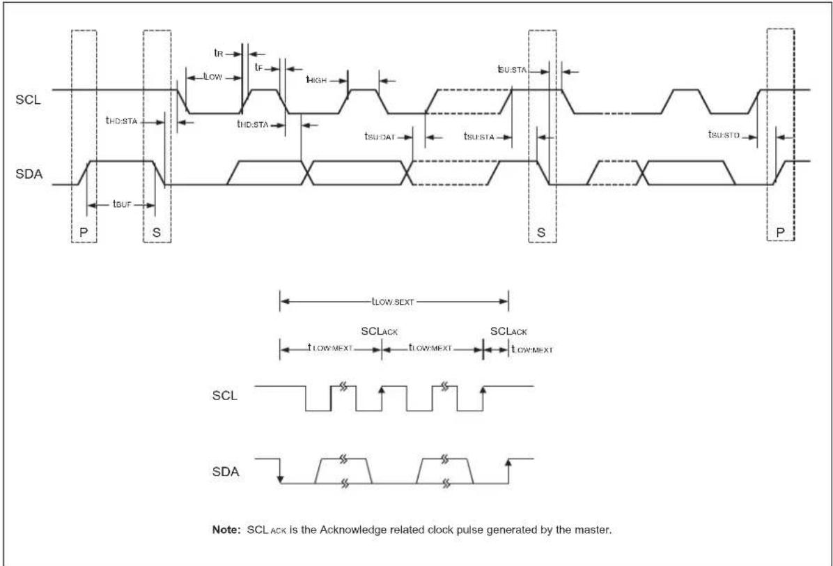
FIGURE 8-1: SMBus TIMING
text_image
SCL tHD:STA tSUB:STA tSUB:STA tSUB:STA tSUB:STA sLUSTA sLUSTA sLUSTA sLUSTA sLUSTA sLUSTA sLUSTA sLUSTA sLUSTA sLUSTA sLUSTA sLUSTA sLUSTA sLUSTA sLUSTA sLUSTA sLUSTA sLUSTA sLUSTA sLUSTA sLUSTa sLUSTa sLUSTa sLUSTa sLUSTa sLUSTa sLUSTa sLUSTa sLUSTa sLUSTa sLUSTa sLUSTa sLUSTa sLUSTa sLUSTa sLUSTa sLUSTa sLUSTa sLUSTa sLUSTa sLUSTe sLUSTe sLUSTe sLUSTe sLUSTe sLUSTe sLUSTe sLUSTe sLUSTe sLUSTe sLUSTe sLUSTe sLUSTe sLUSTe sLUSTe sLUSTe sLUSTe sLUSTe sLUSTe sLUSTe sLUSTu sLUSTu sLUSTu sLUSTu sLUSTu sLUSTu sLUSTu sLUSTu sLUSTu sLUSTu sLUSTu sLUSTu sLUSTu sLUSTu sLUSTu sLUSTu sLUSTu sLUSTu sLUSTu sLUSTu sLUSTU sLUSTU sLUSTU sLUSTU sLUSTU sLUSTU sLUSTU sLUSTU sLUSTU sLUSTU sLUSTU sLUSTU sLUSTU sLUSTU sLUSTU sLUSTU sLUSTU sLUSTU sLUSTU sLUSTU sLUSTu sLUSTu sLUSTu sLUSTu sLUSTu sLUSTu sLUSTu sLUSTu sLUSTu sLUSTu sLUSTu sLUSTu sLUSTu sLUSTu sLUSTu sLUSTu sLUSTu sLUSTu sLUSTu sLUSTt8.2 SPS Single Pin Serial Battery Data Interface
The PS810 can also communicate using one pin, the SDA pin with the Single Pin Serial protocol (SPS). The single pin serial interface communication is an asynchronous return-to-one protocol. The signal requires an external pull-up resistor. The timing of the driven low pulses defines the communication.
A Break cycle starts a command from the host to the battery. The command is eight bits long. After this, eight data bits are either sent to the battery or received from the battery. The Least Significant bits are sent first.
The Break cycle is defined by a low period for a time equal to or greater than t_B , then returned high for a time greater than or equal to t_BR .
The data bits consist of three sections each:
- Start: a logic low for at least time t STR.
- Data: data high or low valid by time t_DS and held until time t_DH/V .
- Stop: logic high by time t_SSU and held until time T_CYC .
The SPS protocol only allows one byte to be read per command code. Thus, commands that receive two-byte pieces of data must be executed one byte at a time. To get a two-byte data, the command code for the high byte must be sent, the high data byte received and then, the command code for the low data byte must be sent to receive the low data byte.
Furthermore, it is possible that the piece of data has changed in between the time it took to get the high byte and the low byte if the host system is communicating slowly. Therefore, it is recommended to always verify the data hasn't changed. This is done by reading the high byte, then reading the low byte, then rereading the high byte and comparing it to the first read to make sure it is the same. If it is not the same, then the low byte can be reread and matched with the new high byte.
FIGURE 8-2: SINGLE PIN SERIAL TIMING

text_image
Break Timing Break bit Break Reset t_B t_BR Host to PS810 Start bit Data bit Stop bit t_strh t_dsub t_dh t_ssub t_cych PS810 to Host Start bit Data bit Stop bit t_strb t_dsub t_ov t_ssub t_cych CMD and Data Protocol Break LSB MSB LSB Data to or from PS810 Communication Example CMD Addr = 04 hex Data = 25 hex Break 0 0010010100000118.3 Battery Data Function Description
The following subsections document the detailed operation of all of the individual battery data commands.
TABLE 8-1: PS810 SMBus DATA FUNCTIONS
| Battery Data Function Name | SMBus Command Code | Access Parameter Reference Units | ||
| Temperature | 0x00 Read 0.1° Celsius | |||
| Voltage 0x01 Read mV | ||||
| Current | 0x02 Read mA | |||
| AverageCurrent 0x03 Read mA | ||||
| RelativeStateOfCharge | 0x04 Read % | |||
| AbsoluteStateOfCharge | 0x05 Read % | |||
| RemainingCapacity | 0x06 Read mAh | |||
| FullChargeCapacity | 0x07 Read mAh | |||
| AverageTimeToEmpty | 0x08 Read Mlnutes | |||
| BatteryStatus | 0x09 | Read | BatStatus | Bit Code |
| CycleCount | 0x0A | Read | Cycles | Integer |
| DesignCapacity | 0x0B | Read | DesignCapacity | mAh |
| CoinVoltage | 0x0C | Read mV | ||
| ManufactureDate | 0x0D | Read | MFGDate | Coded |
| SerialNumber | 0x0E | Read | SerialNumber | Hex Word |
| ManufacturerID | 0x0F | Read | MFGID | Hex Word |
| DeviceID | 0x10 | Read | DevID | Hex Word |
| KEELoQ | 0x17 | Read/Write | Block Data | |
| UserData | 0x16 Read Block Data | |||
TABLE 8-2: PS810 SINGLE PIN SERIAL DATA FUNCTIONS
| Battery Data Function Name | SPS Command Code | Access Parameter Reference Units | ||
| Temperature (low byte) | 0x00 Read | 0.1°Celsius | ||
| Temperature (high byte) | 0x01 Read | |||
| Voltage (low byte) | 0x02 Read | mV | ||
| Voltage (high byte) | 0x03 Read | |||
| Current (low byte) | 0x04 Read | mA | ||
| Current (high byte) | 0x05 Read | |||
| AverageCurrent (low byte) | 0x06 Read | mA | ||
| AverageCurrent (high byte) | 0x07 Read | |||
| RelativeStateOfCharge 0x08 Read % | ||||
| reserved 0x09 — | ||||
| AbsoluteStateOfCharge | 0x0A Read % | |||
| reserved 0x0B — | ||||
| RemainingCapacity (low byte) | 0x0C | Read | mAh | |
| RemainingCapacity (high byte) | 0x0D | Read | ||
| FullChargeCapacity (low byte) | 0x0E Read | mAh | ||
| FullChargeCapacity (high byte) | 0x0F | Read | ||
| AverageTimeToEmpty (low byte) | 0x10 Read | Mlnutes | ||
| AverageTimeToEmpty (high byte) | 0x11 Read | |||
| BatteryStatus | 0x12 | Read | BatStatus | Bit Code |
| reserved 0x13 — | ||||
| CycleCount (low byte) | 0x14 Read | Cycles | Integer | |
| CycleCount (high byte) | 0x15 Read | Cycles | ||
| DesignCapacity (low byte) | 0x16 Read | DesignCapacity | mAh | |
| DesignCapacity (high byte) | 0x17 Read | DesignCapacity | ||
| CoinVoltage (low byte) | 0x18 Read | DesignVPack | mV | |
| CoinVoltage (high byte) | 0x19 Read | DesignVPack | ||
| ManufactureDate (low byte) | 0x1A Read | MFGDate | Coded | |
| ManufactureDate (high byte) | 0x1B Read | MFGDate | ||
| SerialNumber (low byte) | 0x1C | Read SerialNumber | Hex Word | |
| SerialNumber (high byte) | 0x1D | Read SerialNumber | ||
| ManufacturerID (low byte) | 0x1E Read | MFGID | Hex Word | |
| ManufacturerID (high byte) | 0x1F | Read MFGID | ||
| DeviceID (low byte) | 0x20 Read | DevID | Hex Word | |
| DeviceID (high byte) | 0x21 Read | DevID | ||
| KEELOQ (low byte) | 0x28 | Read/Write | MFGData | Hex Double Word |
| KEELOQ (second byte) | 0x29 | Read/Write | MFGData | |
| KEELOQ (third byte) | 0x2A | Read/Write | MFGData | |
| KEELOQ (high byte) | 0x2B | Read/Write | MFGData | |
8.3.1 Temperature (0.1° CELSIUS)
Returns the cell pack's internal temperature.
8.3.2 Voltage (mV)
Returns the pack voltage.
8.3.3 Current (mA)
Returns the current being supplied (or accepted) through the battery's terminals.
8.3.4 AverageCurrent (mA)
Returns a rolling average of the current being supplied (or accepted) through the battery's terminals. The time period over which current is averaged is adjustable.
8.3.5 RelativeStateOfCharge (%)
Returns the predicted remaining battery capacity expressed as a percentage of FullChargeCapacity.
8.3.6 AbsoluteStateOfCharge (%)
Returns the predicted remaining battery capacity expressed as a percentage of DesignCapacity Note that AbsoluteStateOfCharge can return values greater than 100%.
8.3.7 RemainingCapacity (mAh)
Returns the predicted remaining battery capacity. The RemainingCapacity value is expressed as: Current x Time.
8.3.8 FullChargeCapacity (mAh)
Returns the predicted pack capacity when it is fully charged.
8.3.9 AverageTimeToEmpty (MINUTES)
Returns a rolling average of the predicted remaining battery life. The time period over which it is averaged is the same as AverageCurrent.
8.3.10 BatteryStatus (FLAGS)
Returns the Smart Battery's status word. The BatteryStatusfunction is used by the power management system to get alarm and status bits.
Battery Status Bits:
bit 7: INITIALIZED
bit 6: DISCHARGING
bit 5: FULLY CHARGED
bit 4: FULLY_DISCHARGED
bit 3: OVER_TEMP_ALARM
bit 2: Unused
bit 1: K EELOQ response processing
bit 0: COIN_CELL_EMPTY
8.3.11 CycleCount (INTEGER)
CycleCount is updated to keep track of the total usage of the battery. CycleCount is increased whenever an amount of charge has been removed from the battery equivalent to the full capacity.
8.3.12 DesignCapacity (mAh)
Returns the theoretical capacity of a new pack.
8.3.13 CoinCellVoltage (mV)
Returns the voltage of the coin cell.
8.3.14 ManufactureDate (CODE)
This function returns the date the pack was manufactured in a coded integer. The date is packed in the following fashion: (year-1980) * 512 + month * 32 + day.
8.3.15 SerialNumber (HEX WORD)
This function is used to return a serial number. This number, when combined with the Manufactured, the DeviceID and the ManufacturedDate, will uniquely identify the battery.
8.3.16 ManufacturerID (HEX WORD)
This function returns a hex word containing the battery manufacturer's ID.
8.3.17 DeviceID (HEX WORD)
This function returns a hex word that contains the battery's ID.
8.3.18 KEELOQ (BLOCK DATA)
This function is used for identification of the battery to the system. The host system writes a 4-byte challenge of random data to the battery. The PS810 runs the challenge data through the KEELOQ algorithm using a safe key entered at time of manufacture. (An option is to have this key based on a manufacturer's key and the serial number.) The host then reads the 4-byte response and compares it with an internally generated response using the same key. The responses must match for validation.
8.3.19 UserData (BLOCK DATA)
Reads 1 to 32 bytes from the spirata block in Flash. The number of bytes read is determined by parameter spirataLen. This is a general purpose storage of any information a user may want to read.
Note: This command is only available in SMBus mode, not SPS mode.
9.0 PARAMETER SETUP
This section documents all of the programmable parameters that are resident in the memory.
TABLE 9-1: ALPHABETICAL LISTING OF PARAMETERS
| Parameter Name | # Bytes | Units | Typical Value | Operational Description |
| AgeFactor 1 0.125 | mV 0 Scale factor for EOD voltages | due to aging. In units of .125 mV, VEOD_aged = VEOD - (CycleCount * AgeFactor) . | ||
| AOMInterval 1 op cycles 60 | Interval between auto-offset calibrations. | |||
| AVGIScale | 1 | coded | b00100000 | Time period over which current is averaged to calculate average current, IAVG = IAVG + (I - IAVG)/AVGIScale.Note: Only Most Significant set bit is used, others are ignored.1xxxxxxxx: IAVG = IAVG + (I - IAVG)/25601xxxxxxxx: IAVG = IAVG + (I - IAVG)/128001xxxxx: IAVG = IAVG + (I - IAVG)/640001xxxxx: IAVG = IAVG + (I - IAVG)/3200001xxx: IAVG = IAVG + (I - IAVG)/16000001xx: IAVG = IAVG + (I - IAVG)/80000001x: IAVG = IAVG + (I - IAVG)/400000001: IAVG = IAVG + (I - IAVG)/2 |
| BGCal | 1 | integer | 14 | Band gap voltage calibration factor. |
| CalStatus | 1 | bitmap | b11111111 | Bit coded as follows:Bit Function7 RCOSC6 TEMP5 CURRENT4 VC13 VCOIN0 = Not calibrated1 = Calibrated |
| CFCoin | 2 | integer | 2250 | Correction Factor for Coin Cell Voltage. |
| CFCurr | 2 | integer | 4200 | Correction Factor for Current. Adjusts the scaling of the sense resistor current measurements. |
| CFTempE | 2 | integer | 326 | Correction Factor for Temperature. Adjusts the scaling of temperature measured across an external thermistor at the NTC input pin. |
| CFTempl | 2 | integer | 2038 | Correction Factor for Temperature. Adjusts the scaling of temperature measured from the internal temperature sensor. |
| CFVoltage | 2 | integer | 2250 | Correction Factor for Pack Voltage. Adjusts the scaling of the pack voltage measurements. Used to calibrate the measurement of pack voltage between VC1 input pin and ground. |
| ClrFullyChrg | 1 | % | 90 | Reset FULLY_CHARGED bit at this level, 100 = 100%. When discharging begins, the FULLY_CHARGED bit should remain set until the cell voltages are below EOCVolt, so that a small current will not trigger a false End-Of-Charge trigger. |
| ClrFullyDischrg | 1 | % | 10 | Reset FULLY_DISCHARGED bit, 100 = 100%. Once fully discharged bit is set, it will stay set until capacity rises above this value, typically 10%. |
| COCurr | 1 | signed byte | 0 | Correction Offset for Current. This is the value the A/D reads when zero current is flowing through the sense resistor. |
| COD 1 signed byte | 0 Correction offset Deviation. Offset | value for the module effect on the current readings. | ||
| Config1 1 bitmap b | 00010000 bit 7: | Internal use only.bit 6:1 = FG overrides bootloader high priority interrupt servicebit 5:1 = Bootloader write commands disabled until lockedbit 4:1 = Disable bootloader write commandsbit 3:1 = Start in SMBus mode0 = SPS modebit 2:1 = 32 ms SMBus time-out0 = 16 ms SMBus time-outbit 1:1 = Flash reading is locked0 = Flash reading is unlockedbit 0:Unused. | ||
| ConfigCAP 1 bitmap | 11100100 bit 7: | Compensate remaining capacity – the displayed remaining capacity actually equals FCC minus capacity used minus residual capacity.bit 6:Remaining capacity decrease only – when compensating, if temperature change causes a decrease in residual capacity, do not let remaining capacity rise to reflect this. Instead, hold it steady until discharge catches up.bit 5:Only compensate remaining capacity on discharge.bit 4:Enable compensation during null current.bit 3:Unusedbit 2:Set capacity to positive immediately upon charging. If discharged below zero, this allows capacity to count up immediately upon charging.bit 1:Learn unconditionally – relearn FCC under any conditions. Typically used for testing only.bit 0:Disable self-discharge. | ||
| ConfigEOCD 1 bit map 10011 | 11 Bit coded as follows: | Bit Function7 Limit remaining capacity to FCC6 U n u s e d5 Trigger EOC on average current4 Trigger EOC on taper current3 Disallow multiple EODs2 Limit capacity to EODCap until EOD1 Set capacity to residual capacity at VEOD0 Learn FCC at VEOD | ||
| COTempE | 2 | signed word | 21198 | Correction offset for external temperature. |
| COTempl | 2 | signed word | 21198 | Correction offset for internal temperature. |
| Cycles | 2 | integer | 0 | Battery data register for CycleCount. Cycles is updated to keep track of the total usage of the battery. Cycles is increased whenever an amount of charge has been removed from the battery, equivalent to the full capacity. |
| DesignCapacity | 2 | mAh | 2200 | Battery data value for DesignCapacity. This is the first capacity loaded into the FullChargeCapacity upon initial power-up. |
| DevID | 2 | hex word | AAAA | Battery data value for DeviceID (2-byte hex word). |
| EOCCurAvg | 2 | mA | 200 | EOC trigger for pulse charging. If the average current during charging has dropped below the threshold for a pass count equal to EOCRecheck, the End-Of-Charge state will be reached. |
| EOCRecheck | 1 | op cycles | 6 | Number of checks before EOC trigger. The End-Of-Charge conditions must remain for at least this number of periods before being considered true. |
| EOCVolt | 2 | mV | 4150 | EOC trigger cell voltage. When the cell reaches this voltage, the PS810 will start monitoring the current to determine when the battery is full. When the current is in the proper range and the cell voltage is greater than EOCVolt, then the FULLY_CHARGED bit in BatteryStatus will be set. |
| EODCap | 2 | mAh | 100 | Reserve remaining capacity at EOD. |
| EODRecheck | 1 | op cycles | 8 | Recheck period for EOD. Voltage must be below VEOD for this many measurement periods. |
| FDBVersion | 1 | integer | — | Flash data block version. |
| FLAGS1 | 1 | bitmap | 00100000 | Bit coded as follows:Bit Function7 Unused6 Unused5 Int/Ext temperature4 Disable Sleep in main Idle mode3 Unused2 Disable safety GPIO1 Unused0 Unused |
| FullCapacity | 2 | mAh | 2200 | Learned value of battery capacity. Used for battery data value of FullChargeCapacity. This is a learned parameter which is the equivalent of all charge counted from fully charged to fully discharged, including self-discharge and error terms. This is reset after a learning cycle and used for remaining capacity and relative State-Of-Charge calculations. |
| HighTempAI 1 coded | ed byte 200 | OVER_TEMP_ALARM | bit threshold,Coded Value = (°Celsius * 10 + 200)/4. | |
| MFGDate 2 coded | hex | word | 0x3246 Battery data value for ManufactureDate_. The date of manufacture of the battery pack can be programmed here and retrieved with the battery dataManufactureDate command,Coding: Date = (Year-1980) x 512 + Month x 32 + Day. | |
| MFGID 2 hex word | – Value for ManufacturerID | _____(2-byte hex word). | ||
| NChangeState | 1 | op cycles | 2 | State change delay filter. Delays the change between “charge increasing” state and “charge decreasing” state based on current direction. To avoid problems with current spikes in opposite directions, a delay filter is built in to control when to change from charging status to discharging status. The current must change directions and stay in the new direction for NChangeState periods before the status is changed and capacity is increased or decreased as a result of the new current direction. |
| NullCurr | 1 | mA | 3 | A zero zone control is built into the PS810 so that any electrical noise doesn’t actually drain the gas gauge, when in fact, the current is zero. For this reason, current less than NullCurr mA in either direction will be measured as zero. |
| OscCal | 1 | integer | 206 | RC oscillator trimming. |
| PowerModes | 1 | bitmap | b00000101 | bit 4:1 = Enable Bus Inactive Low-Power mode0 = Disable Bus Inactive Low-Power modebit 3:1 = Use Ultra Low-Power mode as Bus Inactive Low-Power mode (no self-discharge calculations)0 = Use Low-Power mode with self-discharge calculations as Bus Inactive Low-Power modebit 2:1 = Require NullCurr for Bus Inactive Low-Power mode and Low-Voltage Sleep mode0 = No NullCurr requirement for Sleep modesbit 1:1 = Use Ultra Low-Power mode as Low-Voltage Sleep mode0 = Use Low-Power mode as Low-Voltage Sleep modebit 0:1 = Set remcap to zero when entering Low-Voltage Sleep mode0 = Do not change remcap when entering Low-Voltage Sleep mode |
| PW1 | 2 | integer | – | First password for the battery pack lock. |
| PW2 | 2 | integer | – | Second password for the battery pack lock. |
| PwrConsumption | 1 | 1/256 mA | 31 | Current consumption of the battery module. This is the average current that the battery module typically draws from the battery (255 = 1 mA). |
| PwrConsumSleep | 1 | 1/256 mA | 7 | Current consumption of battery module when in Sleep mode. |
| RefCal | 1 | integer | 0 | Reference voltage calibration factor. |
| RemCap 2 mAh 44 | 0 The initial capacity of the battery. W | When the PS810 is first powered up and initialized, before a learning cycle takes place to learn the full capacity, the full capacity will take the value programmed into RemCap to compute relative State-Of-Charge percentage. | ||
| RemCapDelta 1 1/4 mAh 2 | Maximum change in remaining capacity per measurement period. | |||
| RLCycles 1 integer | 2 The number of initial cycles without a relearn limit. The initial number of cycles where the relearn limit is not active. Normally, full charge capacity will change by a maximum of 256 mAh when relearned. Since FullCapacity can vary greatly with the first learning cycle, the initial capacity may not be correct; thus, this should be set to at least 2. | |||
| SerialNumber 2 integer – B | Battery data value for SerialNumber ____. The serial number of the battery pack can be programmed here and retrieved with the battery data SerialNumber command. | |||
| SleepVoltage | 2 | mV | 2700 | The pack voltage at which the PS810 will enter Low-Voltage Sleep mode. |
| StableCurr | 1 | mA | 50 | EOC trigger current deviation level. In order to prevent current spikes from causing a premature taper current trigger, the average current and the instantaneous current must be within StableCurr of each other for the End-Of-Charge to trigger on the taper current. |
| TaperCRate | 1 | 1/64 C | 3 | Upper limit EOC taper current, 64 = 1C. |
| TaperLow | 1 | 1/64 C | 1 | Lower limit EOC taper current, 64 = 1C. |
| UserDataLen | 1 | bytes | 2 | Number of bytes read by spirata SMBus command. |
| VEODCoin | 2 | mV | 2500 | Empty voltage of coin cell. |
| VEODOffset | 2 | mV | 2700 | Base voltage for VEOD look-up table. |
NOTES:
10.0 ELECTRICAL CHARACTERISTICS
TABLE 10-1: ABSOLUTE MAXIMUM RATINGS
| Symbol Description Min. Max. Units | ||||
| VPIN Voltage Directly at any pin -0.5 7.0 V | ||||
| TBIAS | Temperature under Bias | -20 | 85 | °C |
| TSTORAGE | Storage Temperature (package dependent) | -35 | 120 | °C |
Note: These are stress ratings only. Stress greater than the listed ratings may cause permanent damage to the device. Exposure to absolute maximum ratings for an extended period may affect device reliability. Functional operation is implied only at the listed operating conditions below.
TABLE 10-2: DC CHARACTERISTICS (T A = -20°C TO +85°C; VDD (INTERNAL) = +2.8V ±7%)
| Symbol | Description | Min. | Typ. | Max. | Units | Condition |
| VC1 | Supply Voltage | 2.5 | — | 5.5 | V | (Note 3) |
| VDD | Internal Regulated Supply Voltage | — | 2.8 | — | V | |
| IDD | Supply Current – Run mode | — | 100 | 125 | μA | A/D active (Note 1) |
| PDSLP | Supply Current – Sleep mode | — | 22 | 25 | μA | Sleep mode (Note 1) |
| BDSLLP | Supply Current – Shelf-Sleep mode | — | 600 | 1000 | nA | Shelf-Sleep mode (Note 1) |
| VL | Input Low Voltage – GPIO | — | — | 0.2 * VDD | V | |
| VIH | Input High Voltage – GPIO | 0.8 * VDD | — | — | V | |
| IIL-IOOPU | GPIO Input Low Current – Pull-up mode | 7 | — | 90 | μA | Varies with battery voltage |
| L-IO | Leakage Current – IO pins Programmed as Outputs or Inputs without Pull-up | — | 1 | 2 | μA | |
| VOL-IO | Output Low Voltage for GPIO | — | — | 0.4 | V | IOL = 0.5 mA |
| VOH-IO | Output High Voltage for GPIO Configured as Push-Pull | 2.0 | — | — | V | IOH = 100 μA |
| VSR | Sense Resistor Input Voltage Range | -152 | — | 152 | mV | |
| INTC | Thermistor Output Current | — | 5.2 | — | μA | |
| VIL-SMB | Input Low Voltage for SMBus pins | -0.5 | — | 0.8 | V | |
| VIH-SMB | Input High Voltage for SMBus pins | 2.0 | — | 5.5 | V | |
| VOL-SMB | Output Low Voltage for SMBus pins | — | — | 0.4 | V | IPULLUP = 350 μA |
| VOH-SMB | Output High Voltage for SMBus pins | 2.1 | — | 5.5 | V | |
| VIL-SMB (1.8V) | Input Low Voltage for SMBus pins at 1.8V | -0.5 | — | 0.32 | V | |
| VIH-SMB (1.8V) | Input High Voltage for SMBus pins at 1.8V | 1.48 | — | 2.12 | V | |
| VOL-SMB (1.8V) | Output Low Voltage for SMBus pins at 1.8V | — | — | 0.32 | V | |
| VOH-SMB (1.8V) | Output High Voltage for SMBus pins at 1.8V | 1.48 | — | 2.12 | V | |
| IPULLUP-SMB | Current through Pull-up Resistor or Current Source for SMBus pins | 100 | — | 350 | μA | |
| LEAK-SMB | Input Leakage Current – SMBus pins | — | — | ±8 | μA |
Note 1: Does not include current consumption due to external loading on pins.
2: Sample mode current is specified during an A/D inactive cycle. Sample mode average current can be calculated using the formula: Average Sample Mode Supply Current = (bDRUN + (n - 1) * IDDINS)/n; where "n" is the programmed sample rate.
3: A/D accuracy is maintained between 2.7 volts and 4.5 volts.
TABLE 10-3: AC CHARACTERISTICS (TA = -20°C TO +85°C; VDD (INTERNAL) = +2.8V ±7%)
| Symbol | Description Min. Typ. Max. Units Condition | |||||
| fRC Internal RC Oscillator Frequency 509.952 | 512 514.0 | 48 kHz | ||||
| fA/D | Internal A/D Operating Clock | — | fRC/16 | — | kHz | |
| tPOR | Power-on Reset Delay | — | 2 | 10 | ms | Delay from time when VC1 voltage exceeds 2.7V |
| tSHELF | Delay to Entry of Shelf-Sleep mode | 1 | — | — | ms | |
| tWAKE | Delay to Exit of Shelf-Sleep mode | 1 | — | — | ms | SDA and SCL go high |
TABLE 10-4: AC CHARACTERISTICS – SMBus/I ^2C^TM (TA = -20°C TO +85°C; VDD (INTERNAL) = +2.8V ±7%)
| Symbol | Description | Min. | Typ. | Max. | Units | Condition |
| fSMB | SMBus Clock Operating Frequency | 10 | — | 100 | kHz | Slave mode |
| tBUF | Bus Free Time between Start and Stop | 4.7 | — | — | μs | |
| tSHLD | Bus Hold Time after Repeated Start | 4.0 | — | — | μs | |
| tSU:STA | Setup Time before Repeated Start | 4.7 | — | — | μs | |
| tSU:STOP | Stop Setup Time | 4.0 | — | — | μs | |
| tHLD | Data Hold Time | 0 | — | — | ns | |
| tSETUP | Data Setup Time | 250 | — | — | ns | |
| tLOW | Clock Low Period | 4.7 | — | — | μs | |
| tHIGH | Clock High Period | 4.0 | — | 50 | μs | (Note 2) |
| tLOW:SEXT | Message Buffering Time | — | — | 10 | ms | (Notes 1, 3) |
| tHIGH:MEXT | Message Buffering Time | — | — | 10 | ms | (Notes 1, 4) |
| tF | Clock/Data Fall Time | — | — | 300 | ns | (Note 5) |
| tR | Clock/Data Rise Time | — | — | 1000 | ns | (Note 5) |
Note 1: The PS810 will time-out when the cumulative message time defined from Start-to-Ack, Ack-to-Ack or Ack-to-Stop exceeds the value of TTIMEOUT, min. of 25 ms. The PS810 will reset the communication no later than TTIMEOUT, max. of 35 ms.
2: tHIGH max. provides a simple, ensured method for devices to detect bus Idle conditions.
3: tLOW:SEXT is the cumulative time a slave device is allowed to extend the clock cycles in one message from the initial start to the stop.
4: tHIGH:MEXT is the cumulative time a master device is allowed to extend its clock cycles within each byte of a message as defined from Start-to-Ack, Ack-to-Ack or Ack-to-Stop.
5: Rise and fall time is defined as follows: t_R = (V_ILMAX - 0.15) to (V_IHMIN + 0.15) t_F = 0.9 V_DD to (V_ILMAX - 0.15)
TABLE 10-5: AC CHARACTERISTICS: SPS INTERFACE (TA = -20°C TO +85°C; VDD (INTERNAL) = +2.8V ±7%)
| Symbol Description Min. Typ. Max. Units Condition | ||||||
| t_CYCH | Cycle Time, Host to Battery 190 — — μs | |||||
| t_CYCB | Cycle Time, Battery to Host | 190 | 205 | 250 | μs | |
| t_STRH | Start Time, Host to Battery | 5 | — — ns | |||
| t_STRB | Start Time, Battery to Host | 32 | — | — | μs | |
| t_DSUH | Data Setup Time, Host to Battery | — | — | 50 | μs | |
| t_DSUB | Data Setup Time, Battery to Host | — | — | 50 | μs | |
| t_DH | Data Hold Time, Host to Battery | 90 | — | — | μs | |
| t_DV | Data Valid Time, Battery to Host | — | — | 80 | μs | |
| t_SSUH | Stop Setup, Host to Battery | — | — | 145 | μs | |
| t_SSUB | Stop Setup Time, Battery to Host | — | — | 145 | μs | |
| t_RSPS | Response Time of Battery to Host | 190 | — | 320 | μs | |
| t_B | Break Time | 190 — — μs | ||||
| t_BR | Break Recovery Time | 40 | — | — | μs | |
TABLE 10-6: A/D CONVERTER CHARACTERISTICS (T A = -20°C TO +85°C; VREG (INTERNAL) = +2.8V ±7%)
| Symbol | Description | Min. | Typ. | Max. | Units | Condition |
| ADRES | A/D Converter Resolution | 9 | — | 15 | bits | |
| tCONV | A/D Conversion Measurement Time, n-bit + sign | — | 2^n/f_A/D | — | s | |
| VADIN | A/D Converter Input Voltage Range (internal) | -150 | — | 150 | mV | Differential (Note 1) |
| 0 | — | 300 | mV Single-Ended | |||
| EVGAIN | Supply Voltage Gain Error | — | — | 0.100 | % | |
| EVOFFSET | Compensated Offset Error | — | — | 0.100 | % | |
| ETEMP | Temperature Gain Error | — | — | 0.100 | % | |
| EINL | Integrated Nonlinearity Error | — | — | 0.004 | % | |
Note 1: Voltage is internal at A/D converter inputs. SR, PTAT and NTC are measured directly. VC1 and VCOIN inputs are measured using internal level translation circuitry that scales the input voltage range appropriately for the converter.
TABLE 10-7: SILICON TIME BASE CHARACTERISTICS (TA = -20°C TO +85°C; VREG(INTERNAL) = +2.8V ±7%)
| Symbol | Description | Min. | Typ. | Max. | Units | Condition |
| ETIME | Silicon Time Base Error | — | — | 0.4 | % | Bias Resistor Rosc Tolerance = 1%TL = ±25 ppm |
TABLE 10-8: TEMPERATURE MEASUREMENT ACCURACY ( TA = -20°C TO +85°C; VREG(INTERNAL) = +2.8V ±7%)
| Symbol | Description | Min. | Typ. | Max. | Units | Condition |
| TRES | Reported Temperature Resolution | — | 1 | — | °C | |
| TACC | Reported Temperature Accuracy | -3 | — | 3 | °C | VREG = 3.6V, requires calibration in the application |
| TDRIFT | Reported Temperature Drift | — | -2 | — | °C/V |
NOTES:
11.0 PACKAGING INFORMATION
11.1 Packaging Marking Information
14-Lead TSSOP

text_image
XXXXXXXX YYWW NNNExample
text_image
PS810 e3 0510 01716-Lead QFN

text_image
XXXXXXXX XXXXXXXX YYWWNNNExample

text_image
PS810 /ML®e3 0510017Legend: XX...X Customer-specific information
Y Year code (last digit of calendar year)
YY Year code (last 2 digits of calendar year)
WW Week code (week of January 1 is week '01')
NNN Alphanumeric traceability code
e3 Pb-free JEDEC designator for Matte Tin (Sn)
* This package is Pb-free. The Pb-free JEDEC designator (e3) can be found on the outer packaging for this package.
Note: In the event the full Microchip part number cannot be marked on one line, it will be carried over to the next line, thus limiting the number of available characters for customer-specific information.
11.2 Package Details
The following sections give the technical details of the packages.
14-Lead Plastic Thin Shrink Small Outline (ST) - 4.4 mm Body (TSSOP)
text_image
E E1 p n B 2 1 D
natural_image
Isometric line drawing of an integrated circuit chip with multiple pins (no text or symbols)
text_image
C β φ L
text_image
A A1 A2 α| Units | INCHES | MILLIMETERS* | |||||
| Dimension Limits | MIN | NOM | MAX | MIN | NOM | MAX | |
| Number of Pins | n | 14 | 14 | ||||
| Pitch | P | .026 | 0.65 | ||||
| Overall Height | A | .043 | 1.10 | ||||
| Molded Package Thickness | A2 | 0.950 | |||||
| Standoff § | A1 | .002 | .004 | .006 | 0.05 | 0.10 | 0.15 |
| Overall Width | E | .246 | .251 | .256 | 6.25 | 6.38 | 6.50 |
| Molded Package Width | E1 | .169 | .173 | .177 | 4.30 | 4.40 | 4.50 |
| Molded Package Length | D | .193 | .197 | .201 | 4.90 | 5.00 | 5.10 |
| Foot Length | L | .020 | .024 | .028 | 0.50 | 0.60 | 0.70 |
| Foot Angle | 840840 | ||||||
| Lead Thickness | c | 0.200 | |||||
| Lead Width | B | .007 | .010 | .012 | 0.19 | 0.25 | 0.30 |
| Mold Draft Angle Top | 10501050 | ||||||
| Mold Draft Angle Bottom | 10501050 | ||||||
* Controlling Parameter § Significant Characteristic
Notes:
Dimensions D and E1 do not include mold flash or protrusions. Mold flash or protrusions shall not exceed .005" (0.127mm) per side.
JEDEC Equivalent: MO-153
Drawing No. C04-087
16-Lead Plastic Quad Flat No Lead Package (ML) 4x4x0.9 mm Body (QFN) – Saw Singulated

text_image
D E TOP VIEW OPTIONAL INDEX AREA
text_image
EXPOSED METAL PAD D1 E1 2 1 n e b L BOTTOM VIEW
text_image
A A1 A3
natural_image
Isometric line drawing of a rectangular electronic component with square holes on both sides (no text or symbols)| Units | INCHES | MILLIMETERS* | |||||
| Dimension Limits | MIN | NOM MAX | MAX | MIN | NOM | ||
| Number of Pins | n | 16 | 16 | ||||
| Pitch | e | .026 BSC | 0.65 BSC | ||||
| Overall Height | A | .031 0.80 | .039 | 1.000.90.035 | |||
| Standoff | A1 | .000 | .001 0.02 | .002 0.00 | 0.05 | ||
| Contact Thickness | A3 | .008 REF | 0.20 REF | ||||
| Overall Width | E | 3.85 4.15 | 15.163.45 | 152 | |||
| Exposed Pad Width | E2 | .100 .106 | .110 2.55 2.70 | 2.80 | |||
| Overall Length | D | .152 .157 | .163 | 3.85 4.15 | 4.00 | ||
| Exposed Pad Length | D2 | .100 .106 | .110 | 2.55 2.80 | 2.70 | ||
| Contact Width | b .010 | .012 | .014 0.25 | 0.30 0.35 | |||
| Contact Length L .012 .016 .020 0.30 0.40 0.50 | |||||||
*Controlling Parameter
Notes:
JEDEC equivalent: MO-220
Drawing No. C04-127
Revised 04-24-05
NOTES:
Note the following details of the code protection feature on Microchip devices:
• Microchip products meet the specification contained in their particular Microchip Data Sheet.
- Microchip believes that its family of products is one of the most secure families of its kind on the market today, when used in the intended manner and under normal conditions.
- There are dishonest and possibly illegal methods used to breach the code protection feature. All of these methods, to our knowledge, require using the Microchip products in a manner outside the operating specifications contained in Microchip's Data Sheets. Most likely, the person doing so is engaged in theft of intellectual property.
• Microchip is willing to work with the customer who is concerned about the integrity of their code.
- Neither Microchip nor any other semiconductor manufacturer can guarantee the security of their code. Code protection does not mean that we are guaranteeing the product as “unbreakable.”
Code protection is constantly evolving. We at Microchip are committed to continuously improving the code protection features of our products. Attempts to break Microchip's code protection feature may be a violation of the Digital Millennium Copyright Act. If such acts allow unauthorized access to your software or other copyrighted work, you may have a right to sue for relief under that Act.
Information contained in this publication regarding device applications and the like is provided only for your convenience and may be superseded by updates. It is your responsibility to ensure that your application meets with your specifications. MICROCHIP MAKES NO REPRESENTATIONS OR WARRANTIES OF ANY KIND WHETHER EXPRESS OR IMPLIED, WRITTEN OR ORAL, STATUTORY OR OTHERWISE, RELATED TO THE INFORMATION, INCLUDING BUT NOT LIMITED TO ITS CONDITION, QUALITY, PERFORMANCE, MERCHANTABILITY OR FITNESS FOR PURPOSE. Microchip disclaims all liability arising from this information and its use. Use of Microchip devices in life support and/or safety applications is entirely at the buyer's risk, and the buyer agrees to defend, indemnify and hold harmless Microchip from any and all damages, claims, suits, or expenses resulting from such use. No licenses are conveyed, implicitly or otherwise, under any Microchip intellectual property rights.
Trademarks
The Microchip name and logo, the Microchip logo, Accuron, dsPIC, KEELOQ, microID, MPLAB, PIC, PICmicro, PICSTART, PRO MATE, PowerSmart, rfPIC, and SmartShunt are registered trademarks of Microchip Technology Incorporated in the U.S.A. and other countries.
AmpLab, FilterLab, Migratable Memory, MXDEV, MXLAB, PICMASTER, SEEVAL, SmartSensor and The Embedded Control Solutions Company are registered trademarks of Microchip Technology Incorporated in the U.S.A.
Analog-for-the-Digital Age, Application Maestro, dsPICDEM, dsPICDEM.net, dsPICworks, ECAN, ECONOMONITOR, FanSense, FlexROM, fuzzyLAB, In-Circuit Serial Programming, ICSP, ICEPIC, Linear Active Thermistor, MPASM, MPLIB, MPLINK, MPSIM, PICkit, PICDEM, PICDEM.net, PICLAB, PICtail, PowerCal, PowerInfo, PowerMate, PowerTool, Real ICE, rfLAB, rfPICDEM, Select Mode, Smart Serial, SmartTel, Total Endurance, UNI/O, WiperLock and Zena are trademarks of Microchip Technology Incorporated in the U.S.A. and other countries.
SQTP is a service mark of Microchip Technology Incorporated in the U.S.A.
All other trademarks mentioned herein are property of their respective companies.
© 2006, Microchip Technology Incorporated, Printed in the U.S.A., All Rights Reserved.

Printed on recycled paper.
QUALITY MANAGEMENT SYSTEM CERTIFIED BY DNV
=ISO/TS 16949:2002=
Microchip received ISO/TS-16949:2002 quality system certification for its worldwide headquarters, design and wafer fabrication facilities in Chandler and Tempe, Arizona and Mountain View, California in October 2003. The Company's quality system processes and procedures are for its PICmicro®8-bit MCUs, KEELOQ® code hopping devices, Serial EEPROMs, microperipherals, nonvolatile memory and analog products. In addition, Microchip's quality system for the design and manufacture of development systems is ISO 9001:2000 certified.
WORLDWIDE SALES AND SERVICE
AMERICAS
Corporate Office
2355 West Chandler Blvd.
Chandler, AZ 85224-6199
Tel: 480-792-7200
Fax: 480-792-7277
Technical Support:
http://support.microchip.com
Web Address:
www.microchip.com
Atlanta
Alpharetta, GA
Tel: 770-640-0034
Fax: 770-640-0307
Boston
Westborough, MA
Tel: 774-760-0087
Fax: 774-760-0088
Chicago
Itasca, IL
Tel: 630-285-0071
Fax: 630-285-0075
Dallas
Addison, TX
Tel: 972-818-7423
Fax: 972-818-2924
Detroit
Farmington Hills, MI
Tel: 248-538-2250
Fax: 248-538-2260
Kokomo
Kokomo, IN
Tel: 765-864-8360
Fax: 765-864-8387
Los Angeles
Mission Viejo, CA
Tel: 949-462-9523
Fax: 949-462-9608
San Jose
Mountain View, CA
Tel: 650-215-1444
Fax: 650-961-0286
Toronto
Mississauga, Ontario,
Canada
Tel: 905-673-0699
Fax: 905-673-6509
ASIA/PACIFIC
Australia - Sydney
Tel: 61-2-9868-6733
Fax: 61-2-9868-6755
China - Beijing
Tel: 86-10-8528-2100
Fax: 86-10-8528-2104
China - Chengdu
Tel: 86-28-8676-6200
Fax: 86-28-8676-6599
China - Fuzhou
Tel: 86-591-8750-3506
Fax: 86-591-8750-3521
China - Hong Kong SAR
Tel: 852-2401-1200
Fax: 852-2401-3431
China - Qingdao
Tel: 86-532-8502-7355
Fax: 86-532-8502-7205
China - Shanghai
Tel: 86-21-5407-5533
Fax: 86-21-5407-5066
China - Shenyang
Tel: 86-24-2334-2829
Fax: 86-24-2334-2393
China - Shenzhen
Tel: 86-755-8203-2660
Fax: 86-755-8203-1760
China - Shunde
Tel: 86-757-2839-5507
Fax: 86-757-2839-5571
China - Wuhan
Tel: 86-27-5980-5300
Fax: 86-27-5980-5118
China - Xian
Tel: 86-29-8833-7250
Fax: 86-29-8833-7256
ASIA/PACIFIC
India - Bangalore
Tel: 91-80-2229-0061
Fax: 91-80-2229-0062
India - New Delhi
Tel: 91-11-5160-8631
Fax: 91-11-5160-8632
India - Pune
Tel: 91-20-2566-1512
Fax: 91-20-2566-1513
Japan - Yokohama
Tel: 81-45-471-6166
Fax: 81-45-471-6122
Korea - Gumi
Tel: 82-54-473-4301
Fax: 82-54-473-4302
Korea - Seoul
Tel: 82-2-554-7200
Fax: 82-2-558-5932 or
82-2-558-5934
Malaysia - Penang
Tel: 60-4-646-8870
Fax: 60-4-646-5086
Philippines - Manila
Tel: 63-2-634-9065
Fax: 63-2-634-9069
Singapore
Tel: 65-6334-8870
Fax: 65-6334-8850
Taiwan - Hsin Chu
Tel: 886-3-572-9526
Fax: 886-3-572-6459
Taiwan - Kaohsiung
Tel: 886-7-536-4818
Fax: 886-7-536-4803
Taiwan - Taipei
Tel: 886-2-2500-6610
Fax: 886-2-2508-0102
Thailand - Bangkok
Tel: 66-2-694-1351
Fax: 66-2-694-1350
EUROPE
Austria - Wels
Tel: 43-7242-2244-399
Fax: 43-7242-2244-393
Denmark - Copenhagen
Tel: 45-4450-2828
Fax: 45-4485-2829
France - Paris
Tel: 33-1-69-53-63-20
Fax: 33-1-69-30-90-79
Germany - Munich
Tel: 49-89-627-144-0
Fax: 49-89-627-144-44
Italy - Milan
Tel: 39-0331-742611
Fax: 39-0331-466781
Netherlands - Drunen
Tel: 31-416-690399
Fax: 31-416-690340
Spain - Madrid
Tel: 34-91-708-08-90
Fax: 34-91-708-08-91
UK - Wokingham
Tel: 44-118-921-5869
Fax: 44-118-921-5820