SY84782U - Electronic component Microchip - Free user manual and instructions
Find the device manual for free SY84782U Microchip in PDF.

User questions about SY84782U Microchip
0 question about this device. Answer the ones you know or ask your own.
Ask a new question about this device
Download the instructions for your Electronic component in PDF format for free! Find your manual SY84782U - Microchip and take your electronic device back in hand. On this page are published all the documents necessary for the use of your device. SY84782U by Microchip.
USER MANUAL SY84782U Microchip
The SY84782U is a single 2.5V supply, ultra-low power, small form factor laser diode driver for telecom/datacom applications. Intended to drive FP/DFB lasers at data rates up to 1.25Gbps, it is especially useful for Compact SFP, SFP, and SFF modules where power requirements are quite stringent. The driver can deliver modulation current up to 90mA and offers a high compliance voltage, all of which make the SY84782U suitable for high current operations in both AC- and DC-coupled applications.
The SY84782U is intended to be used with Micrel's MIC3003 Optical Transceiver Management IC, which allows for both modulation and bias current control and monitoring. Furthermore, the MIC3003 offers power control and temperature compensation.
This device operates across the industrial temperature range ( -40^ to +95^ ) and is available in a small 3mm × 3mm QFN package.
All datasheets and support documentation can be found on Micrel's website at: www.micrel.com.
Features
• 2.5V power supply option
• Ultra low power consumption (63mW typ)
• Multirate up to 1.25Gbps
- Fast rise and fall time
• Modulation current up to 90mA
- Laser can be DC- or AC-coupled
• Small form factor 16-pin (3mm × 3mm) QFN package
- MIC3003G compatible
- Extensive temperature range (-40^ to +95^)
Applications
- Multirate LAN, MAN applications: Fibre Channel, GbE, SONET OC3/12/24, and SDH STM1/4/8
• CSFP/SFF/SFP optical modules
Typical Application

text_image
SY84782U +2.5V GND DIN+ DIN- GND EN M_SET VREF GND +3.3V MOD- MOD- MOD+ MOD+ +2.5V TL To VBIAS L +3.3V LD PD To FB/VMPD MIC3003 +3.3V VDDO NC GNDD RSIN VIN CLK DATA TX/DISAB E TX/FAULT XPN VRL SHDN (DEFN) +3.3V VMD+ VDDA VILD- VILD+ To VILD+ Serial interface to computer microcontrollerDC-Coupled Laser
text_image
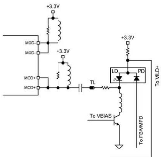
+3.3V MOD- MOD- +3.3V MCD+ MCD+ TL To VBIAS +3.3V LD PD To FBA/MPD To VILD+AC-Coupled Laser
Micrel Inc. • 2180 Fortune Drive • San Jose, CA 95131 • USA • tel +1 (408) 944-0800 • fax +1 (408) 474-1000 • http://www.micrel.com
Ordering Information
| Part Number | Package Type | Operating Range | Package Marking | Lead Finish |
| SY84782UMG | QFN-16 | Industrial | 782U Pb-Free Bar-Line Indicator | Pb-Free |
| SY84782UMG TR ^(1) | QFN-16 | Industrial | 782U Pb-Free Bar-Line Indicator | Pb-Free |
Note:
- Tape and Reel
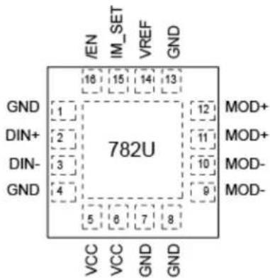
Pin Configuration
text_image
/EN IM_SET VREF GND 16 15 14 13 GND 1 782U 12 DIN+ 2 DIN- 3 GND 4 MOD+ MOD+ MOD- MOD- 5 6 7 8 VCC VCC GND GND16-Pin QFN
Pin Description
| Pin Number | Pin Name | Pin Function |
| 1, 4, 7,8, 13 | GND,ePad | Device Ground. Ground and exposed pad must be connected to the plane of the most negative potential. |
| 2 | DIN+ | Non-Inverting Input Data. Internally terminated with 50Ω to a reference voltage |
| 3 | DIN- | Inverting Input Data. Internally terminated with 50Ω to a reference voltage |
| 5, 6 | VCC | Supply Voltage. Bypass with a 0.1μF || 0.01μF low-ESR capacitor as close to VCC pin as possible. |
| 9, 10 | MOD- | Inverted Modulation Current Output. Provides modulation current when input data is negative |
| 11, 12 | MOD+ | Non-Inverted Modulation Current Output. Provides modulation current when input data is positive. |
| 14 | VREF | Reference Voltage. Install a 0.1μF capacitor between VREF and VCC |
| 15 | IM_SET | Modulation current setting and control. The voltage applied to this pin will set the modulation current. To be connected to the MIC3003 Pin 24 (VMOD+). Input impedance 25kΩ. |
| 16 /EN | Enable Pin. A high level signal applied to this pin will pull the MOD+ output HIGH and MOD- output LOW. Internally pulled down with a 75kΩ resistor. |
Truth Table
| DIN+ | DIN- | /EN | MOD+^(2) | MOD- | Laser Output (3) |
| L | H | L | H | L | L |
| H | L | L | L | H | H |
| X | X | H | H | L | L |
Notes:
- I_MOD = 0 when MOD + = H .
- Assuming that laser is tied to MOD+.
Absolute Maximum Ratings ^(4)
Supply Voltage ( V_CC ) -0.5V to +3.0V
Input Voltage ( V_IN ) -0.5V to V_CC
TTL Control Input Voltage ( V_IN ) 0V to V_CC
Lead Temperature (soldering, 20s)....+260°C
Storage Temperature ( T_S ) -65^ to +150^
Operating Ratings ^(5)
Supply Voltage ( V_CC ) 2.375V to 2.625V
Ambient Temperature ( T_A ) -40^ to +95^
Package Thermal Resistance ^(6)
Still-Air ( JA)....60°C/W
Junction-to-Board ( _JB )....33°C/W
DC Electrical Characteristics ^(7)
V_CC = 2.5V ± 5% , T_A = -40^ C to +95^ C . Typical values are V_CC = 2.5V , T_A = 25^ C , I_MOD = 60mA .
| Symbol | Parameter | Condition | Min. | Typ. | Max. | Units |
| I_CC | Power Supply Current | Modulation current excluded | 24 | 30^(8) mA | ||
| V_MOD\_MIN | Minimum voltage required at driver output for proper operation | 0.6 | V | |||
| R_IN(DATA) | Input Resistance (DIN+, DIN-) | 45 | 50 | 55 | Ω | |
| R_IN(IMOD\_SET) | Input Resistance (IM_SET) | 25 | kΩ | |||
| V_ID | Differential Input Voltage Swing | 200 | 2400 | mVpp | ||
| V_IH\_EN | /EN Input High | 2 | V | |||
| V_IL\_EN | /EN Input Low | 0.8 | V | |||
| V_IM\_SET Voltage Range on IM_SET Pin I | _MOD range 10mA – 90mA | 1.2 | V | |||
AC Electrical Characteristics ^(7)
V_CC = 2.5V ± 5% , T_A = -40^ C to +95^ C . Typical values are V_CC = 2.5V , T_A = 25^ C , I_MOD = 60mA .
| Symbol | Parameter | Condition | Min. | Typ. | Max. | Units |
| Data Rate | NRZ Data | 0.155 | 1.25 | Gbps | ||
| I_MOD | Modulation Current(15Ω Load) | AC-Coupled | 10 | 90 | mA | |
| DC-Coupled | 10 | 70^(9) | ||||
| I_MOD\_OFF Modulation OFF current | Current at MOD+ when the device is disabled | 750 | μA | |||
| Total Jitter | @ 1.25Gbps data rate | 20 | pspp | |||
| Pulse-Width Distortion I | _MOD range 10mA – 90mA | 20 | ps | |||
| t_r, t_i | Output Rise/Fall Times(20% to 80%) | 15Ω Load | 100 | 140 | ps | |
Notes:
- Exceeding the absolute maximum rating may damage the device.
- The device is not guaranteed to function outside its operating rating.
- Package thermal resistance assumes exposed pad is soldered (or equivalent) to the devices most negative potential on the PCB.
- Specification for packaged product only.
- Icc = 30mA (excluding I_MOD ) for worst case conditions with V_CC = 2.625V , T_A = 85^ , I_MOD = 60mA .
- Assuming V_CC = 2.375V , laser band gap voltage = 1V, laser package inductance = 1nH, laser equivalent series resistor = 5Ω, and damping resistor = 10Ω.
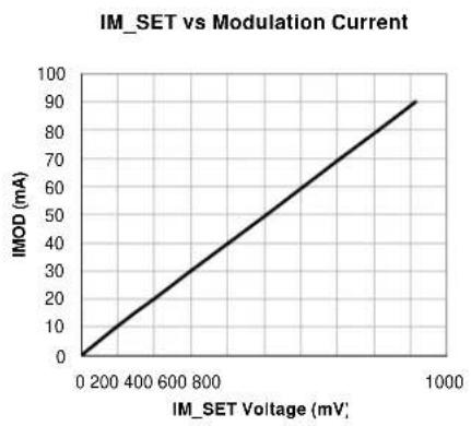
Typical Operating Characteristics
V_CC = 2.5V ± 5% , T_A = -40^ C to +95^ C . Typical values are V_CC = 2.5V , T_A = 25^ C , I_MOD = 60mA .
line
| IM_SET Voltage (mV) | IMOD (mA) | | ------------------- | --------- | | 0 | 0 | | 200 | 10 | | 400 | 20 | | 600 | 30 | | 800 | 40 | | 1000 | 50 | | 1200 | 60 | | 1400 | 70 | | 1600 | 80 | | 1800 | 90 | | 2000 | 100 |
line
| Modulation Current (mA) | Supply Current (mA) | | ----------------------- | ------------------- | | 10 | 17.5 | | 30 | 20.0 | | 60 | 23.0 | | 90 | 25.5 |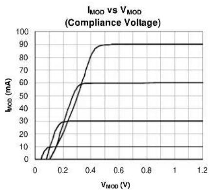
line
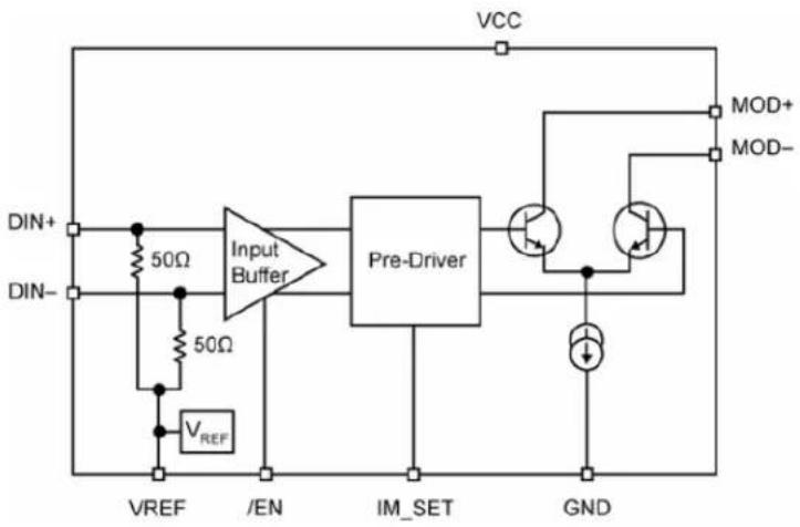
| V_MOD (V) | I_MOD (mA) | | --------- | ---------- | | 0.0 | 0 | | 0.2 | 30 | | 0.4 | 60 | | 0.6 | 90 | | 0.8 | 90 | | 1.0 | 90 | | 1.2 | 90 |Functional Block Diagram
text_image
VCC DIN+ 50Ω Input Buffer VREF /EN IM_SET GND 50Ω VREF Pre-Driver MOD+ MOD-Functional Characteristics
V_CC = 2.5V ± 5% , T_A = -40^ C to +95^ C . Typical values are V_CC = 2.5V , T_A = 25^ C , I_MOD = 60mA .
line
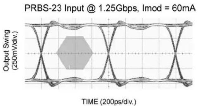
| Time (200ps/div.) | Output Swing (250mV/div.) | | ----------------- | ------------------------- | | 0 | 0 | | 1.25 | 1.25 | | 200 | 0 |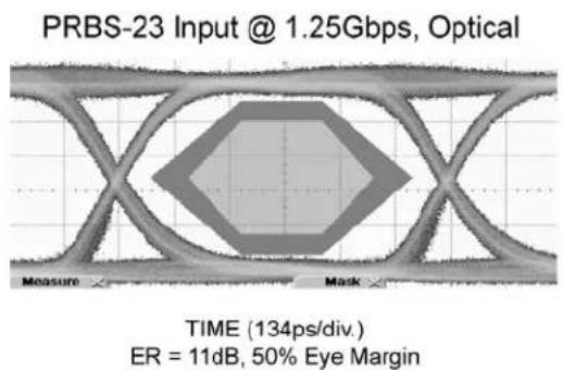
text_image
PRBS-23 Input @ 1.25Gbps, Optical Measure Mask TIME (134ps/div.) ER = 11dB, 50% Eye MarginInput and Output Stages
text_image
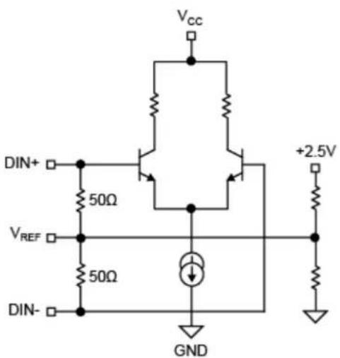
Vcc DIN+ 50Ω +2.5V VREF 50Ω DIN- GNDFigure 1. Simplified Input Stage
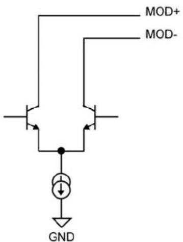
text_image
MOD+ MOD- GNDFigure 2. Simplified Output Stage
Application Information
The typical applications diagram on the first page shows how to connect the driver to the laser single-ended. To improve transition time and laser response, the laser can be driven differentially, as shown in Figures 3 and 4. Driving the laser differentially will also minimize crosstalk with the rest of the circuitry on the board, particularly the receiver.

text_image
MOD- MOD- MOD+ MOD+ Rd CComp RComp Rd C L +3.3V LD PD Bias to APC L = Murata BLM18HG102SNFigure 3. Laser DC-Coupled

text_image
+3.3V R2 R1 Rd +3.3V L MOD- MOD- MOD+ MOD+ R1 Rd C LD PD R L Bias to APC R2 +3.3VFigure 4. Laser AC-Coupled
DC-Coupling
In addition to the low power consumption and high modulation current, the SY84782U offers a high compliance voltage. The minimum voltage needed at the output of the driver for proper operation is less than 600mV, leaving a large headroom, V_cc - 600mV , to the laser with the damping resistor. To show the importance of this high compliance voltage, consider the voltage drops along the path from V_cc to ground through the laser, damping resistor, and driver:
$$ V _ {C C} = \text { Driver Headroom } + V _ {R d} + V _ {\text { laser }} $$
$$ V _ {R d} = R d \times I _ {M O D} $$
$$ V _ {\text { laser }} = V _ {\text { band - gap }} + R _ {\text { laser }} \times I _ {\text { MOD }} + L d i / d t $$
V_band-gap + R_laser × I_MOD = 1.6V at maximum for a Fabry Perrot or a DFB laser.
Ldi/dt is the voltage drop due to the laser parasitic inductance during I_MOD transitions. Assuming L = 1nH, t_f = t_f = 80ps (measured between 20% and 80% of I_MOD ), and I_MOD = 70mA (42mA from 20% to 80%), then Ldi/dt will be equal to 525mV. This number can be minimized by making the laser leads as short as possible and by using the RC compensation network between the cathode of the laser and ground or across the laser driver outputs, as shown in Figure 3.
To be able to drive the laser DC-coupled with a high current, it is necessary to keep the damping resistor as small as possible. For example, if the drop due to parasitic inductance of the laser is neglected (compensated for) and the maximum drop across the laser (1.6V) considered while keeping a minimum of 600mV headroom for the driver, then the maximum damping resistor that allows a 70mA modulation current into the laser is:
$$ R _ {d m a x} = \left(V _ {C C} - 0. 6 V - 1. 6 V\right) / 0. 0 7 A $$
The worst case will be with V_cc = 3.0V , leading to R_dmax = 11.4
On the other hand, the smaller the value of R_d , the higher is the overshoot/undershoot on the optical signal from the laser. In the circuit shown in Figure 4, the RC compensation network across the driver outputs (MOD+ and MOD-) allows the user R_d=10 . The optical eye diagrams at data rates of 1.25Gbps, shown in "Functional Characteristics" section, are all obtained with the same circuit using R_d=10 , R_Comp=100 , and C_Comp=3pF . The compensation network may change from one board to another and from one type of laser to another. An additional compensation network (RC) can be added at the laser cathode for further compensation and eye smoothing.
AC-Coupling
When trying to AC-couple the laser to the driver, the headroom of the driver is no longer a problem since it is DC isolated from the laser with the coupling capacitor. At the output, the headroom of the driver is determined by the pull-up network. In Figure 4, the modulation current out of the driver is split between the pull-up network and the laser. If, for example, the total pull-up resistor is twice the sum of the damping resistor and laser equivalent series resistance, then only two thirds (2/3) of the modulation current will be used by the laser. Therefore, to keep most of the modulation current going through the laser, the total pull-up resistor must be kept as high as possible. One solution involves using an inductor alone as pull-up, presenting a high impedance path for the modulation current and zero ohm (0Ω) path for the DC current offering headroom of the driver equal to V CC and almost all the modulation current goes into the laser. The inductor alone will cause signal distortion, and, to improve this phenomenon, a combination of resistors and inductors can be used (as shown on Figure 4). In this case, the headroom of the driver is V CC -R1 x αI MOD , where αI MOD is the portion of the modulation current that goes through the pull-up network.
When the laser is AC-coupled to the driver, the coupling capacitor creates a low-frequency cutoff in the circuit, and its value must be chosen to be as large as possible. If the value of the cap is too high, it will slow down the fast signals edges, and conversely, if its value is too small, it won't be able to hold a constant change between the first bit and the last bit of a long string of identical bits in a low data rate application. This leads to higher pattern-dependent jitter in the transmitter signal. 0.1 F is found to be good for all applications from 155Mbps to 1.25Gbps.
AC-coupling the laser to the driver brings a solution to the driver headroom problem at the expense of extra components, loss of part of the modulation current wasted in the pull-up network, and additional power consumption.
Package Information and Recommended Land Pattern ^(10)

text_image
PIN 1 DOT BY MARKING 3.0000±0.050 1 2 3.0000±0.050TOP VIEW NOTE: 1, 2, 3
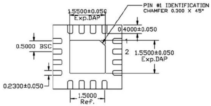
text_image
PIN #1 IDENTIFICATION CHAMFER 0.300 X 45° 1.5500±0.050 Exp.DAP 0 4000±0.050 2 1.5500±0.050 Exp.DAP 0.5000 BSC 0.2300±0.050 1.5000 Ref.BOTTOM VIEW NOTE: 1, 2, 3
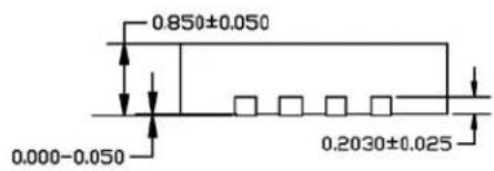
text_image
0.850±0.050 0.000-0.050 0.2030±0.025SIDE VIEW NOTE: 1, 2, 3
NOTE:
- MAX PACKAGE WARPAGE IS 0.05 MM
- MAX ALLOWABLE BURR IS 0.076 MM IN ALL DIRECTIONS
- PIN #1 IS ON TOP WILL BE LASER MARKED
- RED CIRCLE IN LAND PATTERN INDICATE THERMAL VIA. SIZE SHOULD BE 0.30-0.35 MM
IN DIAMETER AND SHOULD BE CONNECTED TO GND FOR MAX THERMAL PERFORMANCE - GREEN RECTANGLES (SHADED AREA) Indicate SOLDER STENCIL OPENING ON EXPOSED
PAD AREA. SIZE SHOULD BE 0.60×0.60 MM IN SIZE, 0.20 MM SPACING.
16-Pin (3mm × 3mm) QFN (QFN-16)
Note:
- Package information is correct as of the publication date. For updates and most current information, go to www.micrel.com.
Package Information and Recommended Land Pattern ^(10) (Continued)
RECOMMENDED LAND PATTERN
NOTE: 4, 5
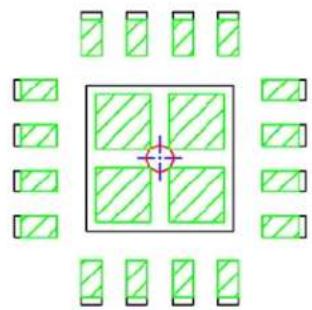
natural_image
Symmetrical geometric pattern with green hatched squares and a central crosshair (no text or symbols)STACKED-UP

text_image
0.48±0.02 0.80±0.02 0.23±0.02 1.60±0.02 2.24±0.02 3.20±0.02 0.50 BSC 1.60±0.02 2.24±0.02 3.20±0.02EXPOSED METAL TRACE
text_image
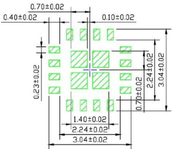
0.70±0.02 0.40±0.02 0.10±0.02 0.23±0.02 1.40±0.02 2.24±0.02 3.04±0.02 2.24±0.02 3.04±0.02Micrel, Inc. is a leading global manufacturer of IC solutions for the worldwide high performance linear and power, LAN, and timing & communications markets. The Company's products include advanced mixed-signal, analog & power semiconductors; high-performance communication, clock management, MEMs-based clock oscillators & crystal-less clock generators, Ethernet switches, and physical layer transceiver ICs. Company customers include leading manufacturers of enterprise, consumer, industrial, mobile, telecommunications, automotive, and computer products. Corporation headquarters and state-of-the-art wafer fabrication facilities are located in San Jose, CA, with regional sales and support offices and advanced technology design centers situated throughout the Americas, Europe, and Asia. Additionally, the Company maintains an extensive network of distributors and reps worldwide.
Micrel makes no representations or warranties with respect to the accuracy or completeness of the information furnished in this datasheet. This information is not intended as a warranty and Micrel does not assume responsibility for its use. Micrel reserves the right to change circuitry, specifications and descriptions at any time without notice. No license, whether express, implied, arising by estoppel or otherwise, to any intellectual property rights is granted by this document. Except as provided in Micrel's terms and conditions of sale for such products, Micrel assumes no liability whatsoever, and Micrel disclaims any express or implied warranty relating to the sale and/or use of Micrel products including liability or warranties relating to fitness for a particular purpose, merchantability, or infringement of any patent, copyright, or other intellectual property right.
Micrel Products are not designed or authorized for use as components in life support appliances, devices or systems where malfunction of a product can reasonably be expected to result in personal injury. Life support devices or systems are devices or systems that (a) are intended for surgical implant into the body or (b) support or sustain life, and whose failure to perform can be reasonably expected to result in a significant injury to the user. A Purchaser's use or sale of Micrel Products for use in life support appliances, devices or systems is a Purchaser's own risk and Purchaser agrees to fully indemnify Micrel for any damages resulting from such use or sale.
© 2011 Micrel, Incorporated.