SY58608U - Electronic component Microchip - Free user manual and instructions
Find the device manual for free SY58608U Microchip in PDF.

User questions about SY58608U Microchip
0 question about this device. Answer the ones you know or ask your own.
Ask a new question about this device
Download the instructions for your Electronic component in PDF format for free! Find your manual SY58608U - Microchip and take your electronic device back in hand. On this page are published all the documents necessary for the use of your device. SY58608U by Microchip.
USER MANUAL SY58608U Microchip
3.2 Gbps Precision, 1:2 LVDS Fanout Buffer with Internal Termination and Fail Safe Input
Features
• Precision 1:2 LVDS Fanout Buffer
- Guaranteed AC Performance Over Temperature and Voltage:
- DC-to > 3.2 Gbps Throughput
- <300 ps Propagation Delay (IN-to-Q)
- <20 ps Within-Device Skew
- <100 ps Rise/Fall Times
- Fail Safe Input
- Prevents Outputs From Oscillating When Input Is Invalid
- Ultra-Low Jitter Design
- 130 fs RMS Typical Additive Phase Jitter
- High-Speed LVDS Outputs
• 2.5V ±5% Power Supply Operation
- Industrial Temperature Range: -40^ to +85^
• Available In 16-pin (3 mm x 3 mm) QFN Package
Applications
• All SONET Clock And Data Distribution
• Fibre Channel Clock And Data Distribution
• Gigabit Ethernet Clock And Data Distribution
- Backplane Distribution
Markets
- DataCom
- Telecom
- Storage
- ATE
• Test and Measurement
General Description
The SY58608U is a 2.5V, high-speed, fully differential 1:2 LVDS fanout buffer optimized to provide two identical output copies with less than 20 ps of skew and 130 fs _RMS typical additive phase jitter. The SY58608U can process clock signals as fast as 2 GHz or data patterns up to 3.2 Gbps.
The differential input includes Microchip's unique, 3-pin input termination architecture that interfaces to LVPECL, LVDS or CML differential signals, (AC- or DC-coupled) as small as 100 mV (200 mV PP ) without any level-shifting or termination resistor networks in the signal path. For AC-coupled input interface applications, an integrated voltage reference (V REF-AC ) is provided to bias the V _T pin. The outputs are 325 mV LVDS, with rise/fall times guaranteed to be less than 100 ps.
The SY58608U operates from a 2.5V ±5% supply and is guaranteed over the full industrial temperature range ( -40^ to +85^ ). The SY58608U is part of Microchip's high-speed, Precision Edge ^® product line.
Package Type
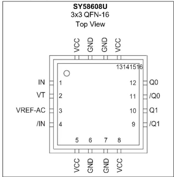
text_image
SY58608U 3x3 QFN-16 Top View VCC GND GND VCC IN 13141516 VT 2 12 Q0 VREF-AC 3 11 /Q0 /IN 4 10 Q1 5 6 7 8 /Q1 VCC GND GND VCCFunctional Block Diagram
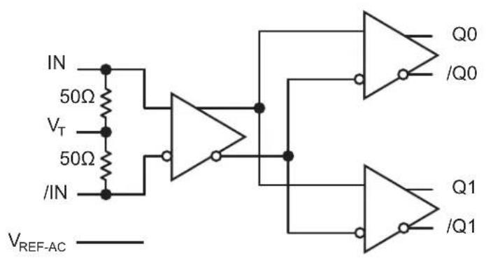
text_image
IN 50Ω VT 50Ω /IN VREF-AC Q0 /Q0 Q1 /Q11.0 ELECTRICAL CHARACTERISTICS
Absolute Maximum Ratings †
Supply Voltage, V_CC -0.5V to +4.0V
Input Voltage, V_IN ....-0.5V to V_CC +0.3V
LVDS Output Current, I_OUT ±10 mA
Input Current
Source or Sink Current on, IN, /IN ....±50 mA
Current, V_REF
Source or Sink Current on V_REF-AC (Note 1).... ±1.5 mA
Operating Ratings ††
Supply Voltage, V_IN +2.375V to +2.625V
† Notice: Permanent device damage may occur if absolute maximum ratings are exceeded. This is a stress rating only and functional operation is not implied at conditions other than those detailed in the operational sections of this data sheet. Exposure to absolute maximum ratings conditions for extended periods may affect device reliability.
†† Notice: The data sheet limits are not guaranteed if the device is operated beyond the operating ratings.
Note 1: Due to the limited drive capability, use for input of the same package only.
DC CHARACTERISTICS (Note 1)
| Electrical Characteristics: T_A = -40°C to +85°C, Unless otherwise stated. | ||||||
| Parameters Sym. | Min. Typ. Max. | Units Conditions | ||||
| Power Supply Voltage Range | V_CC | 2.375 2.5 | 2.625 | V | — | |
| Power Supply Current | I_CC | — | 55 | 75 | mA | No load, max. V_CC |
| Differential Input Resistance (IN-to-/IN) | R_DIFF\_IN | 90 | 100 | 110 | Ω | — |
| Input HIGH Voltage (IN, /IN) | V_IH | 1.2 | — | V_CC | V | IN, /IN |
| Input LOW Voltage (IN, /IN) | V_IL | 0 | — | V_IH-0.1 | V | IN, /IN |
| Input Voltage Swing (IN, /IN) | V_IN | 0.1 | — | 1.7 | V | See Figure 6-2, (Note 2) |
| Differential Input Voltage Swing (|IN - /IN|) | V_DIFF\_IN | 0.2 | — | — | V | See Figure 6-4 |
| Input Voltage Threshold that Triggers FSI | V_IN\_FSI | — | 30 | 100 | mV | — |
| Output Reference Voltage | V_REF-AC | V_CC-1.3 | V_CC-1.2 | V_CC-1.1 | V | — |
| Voltage from Input to V_T | IN to V_T | — | — | 1.28 | V | — |
Note 1: The circuit is designed to meet the DC specifications shown in the above table after thermal equilibrium has been established.
2: V_IN (max) is specified when V_T is floating.
LVDS OUTPUTS DC ELECTRICAL CHARACTERISTICS (Note 1)
| Electrical Characteristics: V_CC = +2.5V ± 5% , R_L = 100 across the output pairs; T_A = -40°C to +85°C , Unless otherwise stated. | ||||||
| Parameter Symbol | Min. Typ. | Max. Units | Condition | |||
| Output Voltage Swing V | OUT | 250 | 325 | — | mV | See Figure 6-2, 6-3. |
| Differential Output Voltage Swing | V_DIFF\_OUT | 500 650 | — mV | See Figure 6-4. | ||
| Output Common Mode Voltage | V_OCM | 1.125 | 1.20 | 1.275 | V | See Figure 6-5. |
| Change in Common Mode Voltage | V_OCM | -50 | — | 50 | mV | See Figure 6-5. |
Note 1: The circuit is designed to meet the DC specifications shown in the above table after thermal equilibrium has been established.
AC ELECTRICAL CHARACTERISTICS (Note 1)
| Electrical Characteristics: V_CC = +2.5V ± 5% , R_L = 100 across the output pairs; Input t_r/t_f : ≤300 ps; T_A = -40°C to +85°C, Unless otherwise stated. | ||||||
| Parameter | Symbol | Min. Typ. | Max. Units | Condition | ||
| Maximum Frequency | f_MAX | 3.2 4.25 — Gbps NRZ (Data) | ||||
| 2 | 3 | — | GHz | V_OUT > 200 mV (Clock) | ||
| Propagation Delay IN-to-Q | t_PD | 170 280 420 ps | V | IN: 100 mV - 200 mV | ||
| 130 200 300 ps | V | IN: 200 mV - 800 mV | ||||
| Within Device Skew | t_SKEW | — | 5 | 20 | ps | Note 2 |
| Part-to-Part Skew | — | — | 135 | ps | Note 3 | |
| Additive Phase Jitter | t_JITTER | — | 130 | — | fs_RMS | Carrier = 622 MHzIntegration Range: 12 kHz – 20 MHz |
| Output Rise/Fall Time(20% to 80%) | t_r, t_f | 35 | 60 | 100 | ps At full output swing | |
| Duty Cycle | — | 47 | — | 53 | % | Differential I/O |
Note 1: These high-speed parameters are guaranteed by design and characterization.
2: Within-device skew is measured between two different outputs under identical input transitions.
3: Part-to-part skew is defined for two parts with identical power supply voltages at the same temperature and no skew at the edges at the respective inputs.
TEMPERATURE SPECIFICATIONS
| Parameters Sym. Min. Typ. Max. Units Conditions | ||||||
| Temperature Ranges | ||||||
| Operating Ambient Temperature Range | T_A | -40 — | +85 °C — | |||
| Maximum Junction Operating Temperature | T_J | — — | +125 °C — | |||
| Storage Temperature Range | T_A | -65 — | +150 °C — | |||
| Package Thermal Resistances (Note 1) | ||||||
| Thermal Resistance, 3 x 3 QFN-16Ld | _JA | — | 60 | — °C/W Still-air | ||
| _JB | — | 33 | — °C/W Junction-to-board | |||
Note 1: Package thermal resistance assumes exposed pad is soldered (or equivalent) to the device's most negative potential on the PCB. _JB and _JA values are determined for a 4-layer board in still-air number, unless otherwise stated.
2.0 FUNCTIONAL DESCRIPTION
2.1 Fail-Safe Input (FSI)
The input includes a special fail-safe circuit to sense the amplitude of the input signal and to latch the outputs when there is no input signal present, or when the amplitude of the input signal drops sufficiently below 100 mV K (200 mV P ), typically 30 mV _K . Maximum frequency of SY58608U is limited by the FSI function.
2.2 Input Clock Failure Case
If the input clock fails to a floating, static, or extremely low signal swing such that the differential voltage across the input pair is less than 100 mV, the FSI function will eliminate a metastable condition and latch the outputs to the last valid state. No ringing and no indeterminate state will occur at the output under these conditions. The output recovers to normal operation once the input signal returns to a valid state with a differential voltage ≥ 100 mV.
Note that the FSI function will not prevent duty cycle distortion in case of a slowly deteriorating (but still toggling) input signal. Due to the FSI function, the propagation delay will depend on rise and fall time of the input signal and on its amplitude. Refer to “Typical Performance Curves” for detailed information.
3.0 TIMING DIAGRAMS

text_image
/IN IN t_pd /Q Q V_IN t_pd V_OUTFIGURE 3-1: Propagation Delay.

line
| Signal | Description | |--------|--------------------------------------| | IN | Decaying Input Signal | | Q | Decaying Input Signal | | /Q | Decaying Input Signal | | | Decaying Input Signal | | | Decaying Input Signal | | | Decaying Input Signal | | | Decaying Input Signal | | | Decaying Input Signal | | | Decaying Input Signal | | | Decaying Input Signal | | | Decaying Input Signal | | | Decaying Input Signal | | | Decaying Input Signal | | | Decaying Input Signal | | /Q | Decaying Input Signal | | /Q | Decaying Input Signal | | /Q | Decaying Input Signal | | /Q | Decaying Input Signal | | /Q | Decaying Input Signal | | /Q | Decaying Input Signal | | /Q | Decaying Input Signal | | /Q | Decaying Input Signal | | /Q | Decaying Output Signal | | /Q | Decaying Output Signal | | /Q | Decaying Output Signal | | /Q | Decaying Output Signal | | /Q | Decaying Output Signal | | /Q | Decaying Output Signal | | /Q | Decaying Output Signal | | /Q | Decaying Output Signal | | /Q | Decaying Output Signal | | //Q | Decaying Output Signal | | //Q | Decaying Output Signal | | //Q | Decaying Output Signal | | //Q | Decaying Output Signal | | //Q | Decaying Output Signal | | //Q | Decaying Output Signal | | //Q | Decaying Output Signal | | //Q | Decaying Output Signal | | //Q | Decaying Output Signal | | /Q | Decaying Output Signal | | /Q | Decaying Output Signal | | /Q | Decaying Output Signal | | /Q | Decaying Output Signal | | /Q | Decaying Output Signal | | /Q | Decaying Output Signal | | /Q | Decaying Output Signal | | /Q | Decaying Output Signal | | /Q | Decaying Output Signal | | //Q | Decaying Output Signal | | //Q | Decaying Output Signal | | //Q | Decaying Output Signal | | //Q | Decaying Output Signal | | //Q | Decaying Output Signal | | //Q | Decaying Output Signal | | //Q | Decaying Output Signal | | //Q | Decaying Output Signal | | //Q | DECK/DECK/DECK/DECK/DECK/DECK/DECK/DECK/DECK/DECK/DECK/DECK/DECK/DECK/DECK/DECK/DECK/DECK/DECK/DECK/DECK/DECK/DECK/DECK/DECK/DECK/DECK/DECK/DECK/DECK/DECK/DECK/DECK/DECK/DECH/DECK/DECK/DECK/DECK/DECK/DECK/DECK/DECK/DECK/DECK/DECK/DECK/DECK/DECK/DECK/DECK/DECK/DECK/DECK/DECK/DECK/DECK/DECK/DECK/DECK/DECK/DECK/DECK/DECK/DECK/DECK/DECK/DECK, DECK/DECK/DECK/DECK/DECK/DECK/DECK/DECK/DECK/DECK/DECK/DECK/DECK/DECK/DECK/DECK/DECK/DECK/DECK/DECK/DECK/DECK/DECK/DECK/DECK/DECK/DECK/DECK/DECK/DECK/DECK/DECK/DECK, DECEK/DEN | | | DECK/DEN | | | DECK/DEN | | | DECK/DEN | | | DECK/DEN | | | DECK/DEN | | | DECK/DEN | | | DECK/DEN | | | DECK/DEN | | | DECK/DEN | | | DECK/DEN | | | DECK/DEN | | | DECK/DEN |FIGURE 3-2: Fail Safe Feature.
4.0 TYPICAL PERFORMANCE CURVES
Note: The graphs and tables provided following this note are a statistical summary based on a limited number of samples and are provided for informational purposes only. The performance characteristics listed herein are not tested or guaranteed. In some graphs or tables, the data presented may be outside the specified operating range (e.g., outside specified power supply range) and therefore outside the warranted range.
NOTE: Unless otherwise indicated, V_CC = 2.5V , GND = 0V, V_IN = 100 mV , R_L = 100 across the output pairs, T_A = +25^ .
line
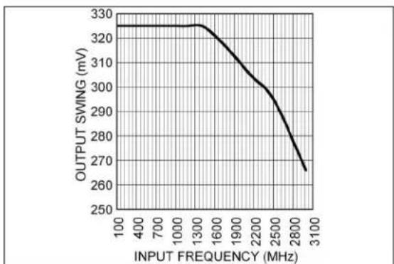
| INPUT FREQUENCY (MHz) | OUTPUT SWING (mV) | | --------------------- | ----------------- | | 100 | 325 | | 400 | 325 | | 700 | 325 | | 1000 | 325 | | 1300 | 325 | | 1600 | 315 | | 1900 | 305 | | 2200 | 295 | | 2500 | 285 | | 2800 | 270 | | 3100 | 265 |FIGURE 4-1: Frequency Response.
line
| INPUT RISE/FALL TIME (ps) | PROPAGATION DELAY (ps) | | ------------------------- | ---------------------- | | 0 | 200 | | 1000 | 300 |FIGURE 4-4: Propagation Delay vs. Input Rise/Fall Time.
line
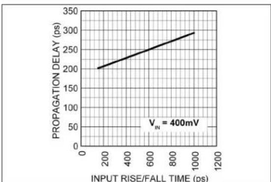
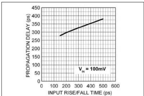
| INPUT RISE/FALL TIME (ps) | PROPAGATION DELAY (ps) | | ------------------------- | ---------------------- | | 150 | 280 | | 200 | 300 | | 250 | 320 | | 300 | 340 | | 350 | 360 | | 400 | 380 | | 450 | 390 | | 500 | 400 |FIGURE 4-2: Propagation Delay vs. Input Rise/Fall Time.
line
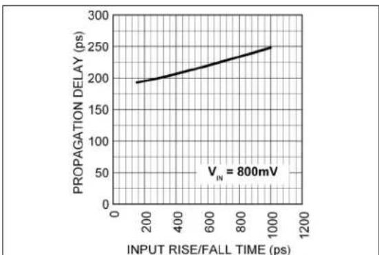
| INPUT RISE/FALL TIME (ps) | PROPAGATION DELAY (ps) | | ------------------------- | ---------------------- | | 200 | 195 | | 400 | 210 | | 600 | 225 | | 800 | 240 | | 1000 | 250 |FIGURE 4-5: Propagation Delay vs. Input Rise/Fall Time.
line
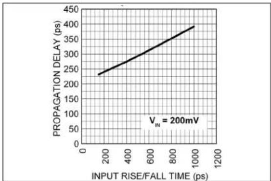
| INPUT RISE/FALL TIME (ps) | PROPAGATION DELAY (ps) | | ------------------------- | ---------------------- | | 0 | 230 | | 200 | 250 | | 400 | 280 | | 600 | 310 | | 800 | 340 | | 1000 | 370 | | 1200 | 400 |FIGURE 4-3: Propagation Delay vs. Input Rise/Fall Time.

line
| TIME (200ps/div) | OUTPUT SWING (75mV/div) | | ---------------- | ------------------------ | | 0 | 0% | | 20.0 | 20.0% |FIGURE 4-6: 1.25 Gbps Data.
line
| OUTPUT SWING (75mV/div.) | TIME (60ps/div) | | ------------------------ | --------------- | | 20.0 % | 60 |FIGURE 4-9: 4.25 Gbps Data.
line
| TIME (100ps/div) | OUTPUT SWING (75mV/div) | | ---------------- | ------------------------ | | 0 | 0% | | 300 | 20.0% |FIGURE 4-7: 2.5 Gbps Data.

line
| TIME (250ps/div.) | OUTPUT SWING (75mV/div.) | | ----------------- | ------------------------ | | 0 | 0 | | 1 | 1 | | 2 | 0 | | 3 | -1 | | 4 | 0 | | 5 | 1 | | 6 | 0 | | 7 | -1 | | 8 | 0 | | 9 | 1 | | 10 | 0 | | 11 | -1 | | 12 | 0 | | 13 | 1 | | 14 | 0 | | 15 | -1 | | 16 | 0 | | 17 | 1 | | 18 | 0 | | 19 | -1 | | 20 | 0 | | 21 | 1 | | 22 | 0 | | 23 | -1 | | 24 | 0 | | 25 | 1 | | 26 | 0 | | 27 | -1 | | 28 | 0 | | 29 | 1 | | 30 | 0 | | 31 | -1 | | 32 | 0 | | 33 | 1 | | 34 | 0 | | 35 | -1 | | 36 | 0 | | 37 | 1 | | 38 | 0 | | 39 | -1 | | 40 | 0 | | 41 | 1 | | 42 | 0 | | 43 | -1 | | 44 | 0 | | 45 | 1 | | 46 | 0 | | 47 | -1 | | 48 | 0 | | 49 | 1 | | 50 | 0 | | 51 | -1 | | 52 | 0 | | 53 | 1 | | 54 | 0 | | 55 | -1 | | 56 | 0 | | 57 | 1 | | 58 | 0 | | 59 | -1 | | 60 | 0 | | 61 | 1 | | 62 | 0 | | 63 | -1 | | 64 | 0 | | 65 | 1 | | 66 | 0 | | 67 | -1 | | 68 | 0 | | 69 | 1 | | 70 | 0 | | 71 | -1 | | 72 | 0 | | 73 | 1 | | 74 | 0 | | 75 | -1 | | 76 | 0 | | 77 | 1 | | 78 | 0 | | 79 | -1 | | 80 | 0 | | 81 | 1 | | 82 | 0 | | 83 | -1 | | 84 | 0 | | 85 | 1 | | 86 | 0 | | 87 | -1 | | 88 | 0 | | 89 | 1 | | 90 | 0 | | 91 | -1 | | 92 | 0 | | 93 | 1 | | 94 | 0 | | 95 | -1 | | 96 | 0 | | 97 | 1 | | 98 | 0 | | 99 | -1 | | Note: The data is in a single format for visual comparison. The output values are estimated based on the given code. There is no label for the output.FIGURE 4-10: 625 MHz Clock.

line
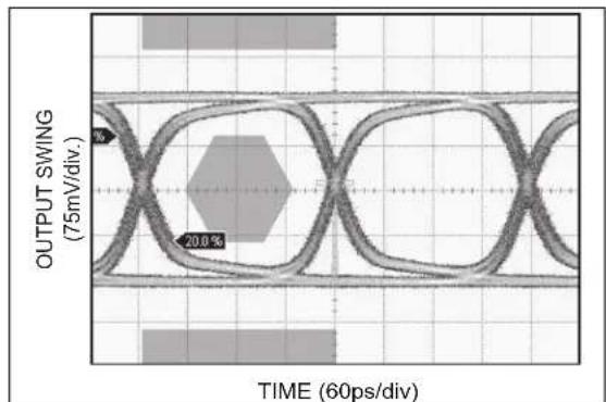
| OUTPUT SWING (75 mV/div.) | TIME (80 ps/div.) | | -------------------------- | ----------------- | | 20.0 % | 80 |FIGURE 4-8: 3.2 Gbps Data.
line
| TIME (120ps/div.) | OUTPUT SWING (75mV/div.) | | ----------------- | ------------------------ | | 0 | 0 | | 120 | 0 | | 240 | 0 | | 360 | 0 | | 480 | 0 | | 600 | 0 | | 720 | 0 | | 840 | 0 | | 960 | 0 | | 1080 | 0 | | 1200 | 0 |FIGURE 4-11: 1.25 Ghz Clock.
line
| TIME (75ps/div.) | OUTPUT SWING (75mV/div.) | | ---------------- | ------------------------ | | 0 | 0 | | 1 | 0.5 | | 2 | 1 | | 3 | 0.5 | | 4 | 0 | | 5 | -0.5 | | 6 | 0.5 | | 7 | 1 | | 8 | 0 | | 9 | -0.5 | | 10 | 0.5 | | 11 | 1 | | 12 | 0 | | 13 | -0.5 | | 14 | 0.5 | | 15 | 1 | | 16 | 0 | | 17 | -0.5 | | 18 | 0.5 | | 19 | 1 | | 20 | 0 | | 21 | -0.5 | | 22 | 0.5 | | 23 | 1 | | 24 | 0 | | 25 | -0.5 | | 26 | 0.5 | | 27 | 1 | | 28 | 0 | | 29 | -0.5 | | 30 | 0.5 | | 31 | 1 | | 32 | 0 | | 33 | -0.5 | | 34 | 0.5 | | 35 | 1 | | 36 | 0 | | 37 | -0.5 | | 38 | 0.5 | | 39 | 1 | | 40 | 0 | | 41 | -0.5 | | 42 | 0.5 | | 43 | 1 | | 44 | 0 | | 45 | -0.5 | | 46 | 0.5 | | 47 | 1 | | 48 | 0 | | 49 | -0.5 | | 50 | 0.5 | | 51 | 1 | | 52 | 0 | | 53 | -0.5 | | 54 | 0.5 | | 55 | 1 | | 56 | 0 | | 57 | -0.5 | | 58 | 0.5 | | 59 | 1 | | 60 | 0 | | 61 | -0.5 | | 62 | 0.5 | | 63 | 1 | | 64 | 0 | | 65 | -0.5 | | 66 | 0.5 | | 67 | 1 | | 68 | 0 | | 69 | -0.5 | | 70 | 0.5 | | 71 | 1 | | 72 | 0 | | 73 | -0.5 | | 74 | 0.5 | | 75 | 1 |FIGURE 4-12: 2 GHz Clock.

line
| TIME (50ps/div.) | OUTPUT SWING (75mV/div.) | | ---------------- | ------------------------ | | 0 | 0 | | 1 | 0.5 | | 2 | 1 | | 3 | 0.5 | | 4 | 0 | | 5 | -0.5 | | 6 | 0.5 | | 7 | 1 | | 8 | 0.5 | | 9 | 0 | | 10 | -0.5 | | 11 | 0.5 | | 12 | 1 | | 13 | 0.5 | | 14 | 0 | | 15 | -0.5 | | 16 | 0.5 | | 17 | 1 | | 18 | 0.5 | | 19 | 0 | | 20 | -0.5 | | 21 | 0.5 | | 22 | 1 | | 23 | 0.5 | | 24 | 0 | | 25 | -0.5 | | 26 | 0.5 | | 27 | 1 | | 28 | 0.5 | | 29 | 0 | | 30 | -0.5 | | 31 | 0.5 | | 32 | 1 | | 33 | 0.5 | | 34 | 0 | | 35 | -0.5 | | 36 | 0.5 | | 37 | 1 | | 38 | 0.5 | | 39 | 0 | | 40 | -0.5 | | 41 | 0.5 | | 42 | 1 | | 43 | 0.5 | | 44 | 0 | | 45 | -0.5 | | 46 | 0.5 | | 47 | 1 | | 48 | 0.5 | | 49 | 0 | | 50 | -0.5 |FIGURE 4-13: 3 GHz Clock.
5.0 ADDITIVE PHASE NOISE PLOT
$$ V _ {C C} = + 2. 5 V, T _ {A} = 2 5 ^ {\circ} C. $$

line
| OFFSET FREQUENCY (MHz) | ADDITIVE PHASE NOISE (dBc/Hz) | | ---------------------- | ------------------------------ | | 0.001 | -130.00 | | 0.01 | -140.00 | | 0.1 | -140.00 | | 1 | -140.00 | | 10 | -140.00 | | 100 | -140.00 |FIGURE 5-1: Additive Noise Plot.
6.0 INPUT STAGE

text_image
VCC IN 50Ω VT 50Ω /IN GNDFIGURE 6-1: Simplified Differential Input Buffer.

line
| Time (ms) | Voltage (mV) | | --------- | ------------ | | 0 | 0 | | 1 | 650 | | 2 | 0 | | 3 | 0 | | 4 | 0 | | 5 | 0 | | 6 | 0 | | 7 | 0 | | 8 | 0 | | 9 | 0 | | 10 | 0 | | 11 | 0 | | 12 | 0 | | 13 | 0 | | 14 | 0 | | 15 | 0 | | 16 | 0 | | 17 | 0 | | 18 | 0 | | 19 | 0 | | 20 | 0 | | 21 | 0 | | 22 | 0 | | 23 | 0 | | 24 | 0 | | 25 | 0 | | 26 | 0 | | 27 | 0 | | 28 | 0 | | 29 | 0 | | 30 | 0 | | 31 | 0 | | 32 | 0 | | 33 | 0 | | 34 | 0 | | 35 | 0 | | 36 | 0 | | 37 | 0 | | 38 | 0 | | 39 | 0 | | 40 | 0 | | 41 | 0 | | 42 | 0 | | 43 | 0 | | 44 | 0 | | 45 | 0 | | 46 | 0 | | 47 | 0 | | 48 | 0 | | 49 | 0 | | 50 | 0 | | 51 | 0 | | 52 | 0 | | 53 | 0 | | 54 | 0 | | 55 | 0 | | 56 | 0 | | 57 | 0 | | 58 | 0 | | 59 | 0 | | 60 | 0 | | 61 | 0 | | 62 | 0 | | 63 | 0 | | 64 | 0 | | 65 | 0 | | 66 | 0 | | 67 | 0 | | 68 | 0 | | 69 | 0 | | 70 | 0 | | 71 | 0 | | 72 | 0 | | 73 | 0 | | 74 | 0 | | 75 | 0 | | 76 | 0 | | 77 | 0 | | 78 | 0 | | 79 | 0 | | 80 | 0 | | 81 | 0 | | 82 | 0 | | 83 | 0 | | 84 | 0 | | 85 | 0 | | 86 | 0 | | 87 | 0 | | 88 | 0 | | 89 | 0 | | 90 | 0 | | 91 | 0 | | 92 | 0 | | 93 | 0 | | 94 | 0 | | 95 | 0 | | 96 | 0 | | 97 | 0 | | 98 | 0 | | 99 | 0 | | Note: The data for 'V_DIFF_IN' and 'V_DIFF_OUT' are not provided in the code. The values for 'V_DIFF_IN' and 'V_DIFF_OUT' are estimated based on the visual scale and may be different from the input field. There is no additional data series in this image. The output values for these series are estimated based on the given code.FIGURE 6-4: Differential Swing.

text_image
VOUT, VIN 325mV (typical)FIGURE 6-2: Single-Ended Swing.
text_image
50Ω 50Ω VOCM, ΔVOCM GNDFIGURE 6-5: LVDS Common Mode Measurement.
text_image
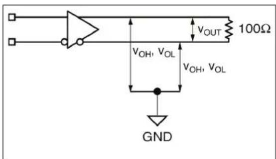
100Ω VOUT VOH, VOL VOH, VOL GNDFIGURE 6-3: LVDS Differential Measurement.
7.0 INPUT INTERFACE APPLICATIONS
text_image
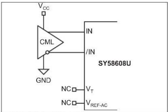
VCC CML IN /IN SY58608U GND NC □ VT NC □ VREF-ACFIGURE 7-1: CML Interface (DC-Coupled).
text_image
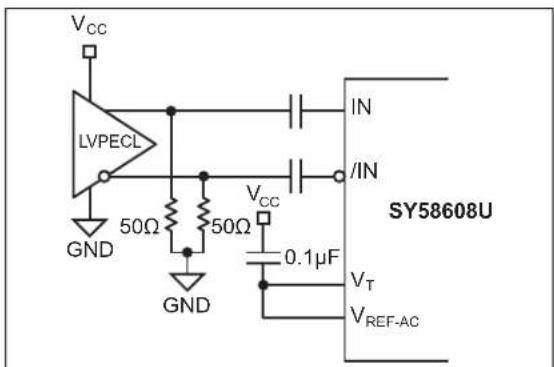
VCC LVPECL IN 50Ω 50Ω VCC /IN GND GND 0.1μF VT VREF-AC SY58608UFIGURE 7-4: LVPECL Interface (AC-Coupled).
text_image
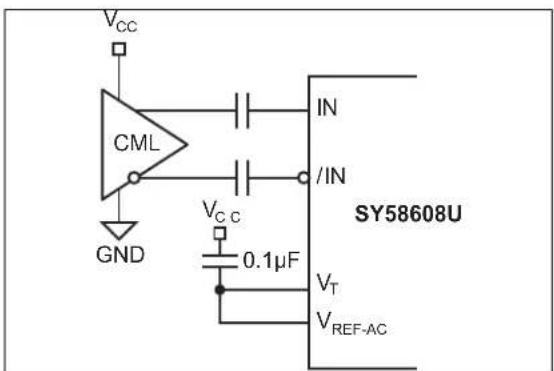
VCC CML IN /IN GND VCC 0.1μF SY58608U VT VREF-ACFIGURE 7-2: CML Interface (AC-Coupled).

text_image
VCC LVDS IN /IN SY58608U GND NC □ VT NC □ VREF-ACFIGURE 7-5: LVDS Interface (DC-Coupled).

text_image
VCC LVPECL GND VCC 0.1μF 19Ω IN /IN VT NC VREF-AC SY58608UFIGURE 7-3: LVPECL Interface (DC-Coupled).
8.0 PIN DESCRIPTIONS
The descriptions of the pins are listed in Table 8-1.
TABLE 8-1: PIN FUNCTION TABLE
| Pin Number Symbol Description | ||
| 1, 4 | IN, /IN | Differential Inputs: This input pair is the differential signal input to the device. Input accepts DC-coupled differential signals as small as 100 mV (200 mVPP). Each pin of this pair internally terminates with 50Ω to the VT pin. If the input swing falls below a certain threshold (typical 30 mV), the Fail Safe Input (FSI) feature will guarantee a stable output by latching the outputs to its last valid state. See “Input Interface Applications” section for more details. |
| 2 | VT | Input Termination Center-Tap: Each input terminates to this pin. The VT pin provides a center-tap for each input (IN, /IN) to a termination network for maximum interface flexibility. See “Input Interface Applications” section. |
| 3 | VREF-AC | Reference Voltage: This output bias to VCC-1.2V. It is used for AC-coupling inputs IN and /IN. Connect VREF-AC directly to the VT pin. Bypass with 0.01 μF low ESR capacitor to VCC. Maximum sink/source current is ±1.5 mA. See “Input Interface Applications” section for more details. |
| 5, 8,13, 16 | VCC | Positive Power Supply: Bypass with 0.1 μF//0.01 μF low ESR capacitors as close to the VCC pins as possible. |
| 6, 7, 14, 15 | GND, Exposed pad | Ground. Exposed pad must be connected to a ground plane that is the same potential as the ground pins. |
| 9, 10 | /Q1, Q1 | LVDS Differential Output Pairs: Differential buffered output copy of the input signal. The output swing is typically 325 mV. Normally terminated 100Ω across the output pairs (Q and /Q). |
| 11, 12 | /Q0, Q0 | |
9.0 PACKAGING INFORMATION
9.1 Package Marking Information
16-Lead QFN* Example

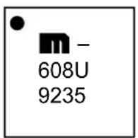
Legend: XX...X Product code or customer-specific information
Y Year code (last digit of calendar year)
YY Year code (last 2 digits of calendar year)
WW Week code (week of January 1 is week '01')
NNN Alphanumeric traceability code
ePb-free JEDEC ^® designator for Matte Tin (Sn)
* This package is Pb-free. The Pb-free JEDEC designator (e3) can be found on the outer packaging for this package.
- , ▲, ▼ Pin one index is identified by a dot, delta up, or delta down (triangle mark).
Note: In the event the full Microchip part number cannot be marked on one line, it will be carried over to the next line, thus limiting the number of available characters for customer-specific information. Package may or may not include the corporate logo.
Underbar (_) and/or Overbar (−) symbol may not be to scale.
TITLE
16 LEAD QFN 3x3mm PACKAGE OUTLINE & RECOMMENDED LAND PATTERN
DRAWING # QFN33-16LD-PL-1 UNIT MM

text_image
PIN 1 DOT BY MARKING 3.0000±0.050 1 2 3.0000±0.050TOP VIEW NOTE 1, 2, 3
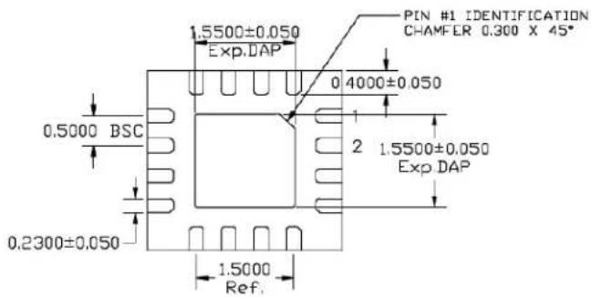
text_image
PIN #1 IDENTIFICATION CHAMFER 0.300 X 45° 1.5500±0.050 Exp.DAP 0 4000±0.050 2 1.5500±0.050 Exp.DAP 0.5000 BSC 0.2300±0.050 1.5000 Ref.BOTTOM VIEW NOTE 1, 2, 3
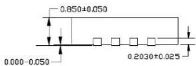
text_image
0.850±0.050 0.000-0.050 0.2030±0.025SIDE VIEW NOTE: 1, 2, 3
NOTE:
- MAX PACKAGE WARPAGE IS 0.05 MM
- MAX ALLOWABLE BURR IS 0.076 MM IN ALL DIRECTIONS
- PIN #1 IS ON TOP WILL BE LASER MARKED
- RED CIRCLE IN LAND PATTERN INDICATE THERMAL VIA. SIZE SHOULD BE 0.30-0.35 MM
IN DIAMETER AND SHOULD BE CONNECTED TO GND FOR MAX THERMAL PERFORMANCE - GREEN RECTANGLES (SHADED AREA) indicate SOLDER STENCIL OPENING ON EXPOSED
PAD AREA. SIZE SHOULD BE 0.60×0.60 MM IN SIZE, 0.20 MM SPACING.
POD-Land Pattern drawing # QFN33-16LD-PL-1
RECOMMENDED LAND PATTERN
NOTE: 4.5
natural_image
Symmetrical geometric pattern with green diagonal hatching and a central crosshair (no text or symbols)STACKED-UP

text_image
0.48±0.02 0.80±0.02 0.23±0.02 1.60±0.02 2.24±0.02 3.20±0.02 1.60±0.02 2.24±0.02 3.20±0.02 0.50 BSCEXPOSED METAL TRACE

text_image
0.70±0.02 0.40±0.02 0.10±0.02 0.23±0.02 1.40±0.02 2.24±0.02 3.04±0.02 2.24±0.02 3.04±0.02SOLDER STENCIL OPENING
Note: For the most current package drawings, please see the Microchip Packaging Specification located at http://www.microchip.com/packaging.
NOTES:
APPENDIX A: REVISION HISTORY
Revision A (December 2018)
- Converted Micrel document SY58608U to Microchip data sheet template DS20005605A.
- Minor text changes throughout.
- Corrected parameters of Figure 4-12.
- Corrected parameters for Figure 5-1.
NOTES:
PRODUCT IDENTIFICATION SYSTEM
To order or obtain information, e.g., on pricing or delivery, contact your local Microchip representative or sales office.

text_image
PART NO. X Device Output Voltage X Package Temperature Range XX Tape and ReelDevice:
SY58608: 3.2 Gbps Precision, 1:2 LVDS Fanout Buffer with Internal Termination and Fail Safe Input
Output Voltage: U = 2.5V
Package:
M = QFN-16
Temperature Range:
G = -40^ to 85^ (NiPdAu Lead-Free)
Special Processing:
Examples:
a) SY58608UMG: 3.2 Gbps Precision, 1:2
LVDS Fanout Buffer with Internal Termination and Fail Safe Input,
2.5V or 3.3 V Output Voltage, QFN-16, -40°C to 85°C (NiPdAu Lead-
Free), 100/Tube
b) SY58608UMGTR: 3.2 Gbps Precision, 1:2
LVDS Fanout Buffer with Internal Termination and Fail Safe Input,
2.5V or 3.3 V Output Voltage, QFN-16, -40°C to 85°C (NiPdAu Lead-Free), 1,000/Reel
Note 1: Tape and Reel identifier only appears in the catalog part number description. This identifier is used for ordering purposes and is not printed on the device package. Check with your Microchip Sales Office for package availability with the Tape and Reel option.
NOTES:
Note the following details of the code protection feature on Microchip devices:
• Microchip products meet the specification contained in their particular Microchip Data Sheet.
- Microchip believes that its family of products is one of the most secure families of its kind on the market today, when used in the intended manner and under normal conditions.
- There are dishonest and possibly illegal methods used to breach the code protection feature. All of these methods, to our knowledge, require using the Microchip products in a manner outside the operating specifications contained in Microchip's Data Sheets. Most likely, the person doing so is engaged in theft of intellectual property.
• Microchip is willing to work with the customer who is concerned about the integrity of their code.
- Neither Microchip nor any other semiconductor manufacturer can guarantee the security of their code. Code protection does not mean that we are guaranteeing the product as "unbreakable."
Code protection is constantly evolving. We at Microchip are committed to continuously improving the code protection features of our products. Attempts to break Microchip's code protection feature may be a violation of the Digital Millennium Copyright Act. If such acts allow unauthorized access to your software or other copyrighted work, you may have a right to sue for relief under that Act.
Information contained in this publication regarding device applications and the like is provided only for your convenience and may be superseded by updates. It is your responsibility to ensure that your application meets with your specifications. MICROCHIP MAKES NO REPRESENTATIONS OR WARRANTIES OF ANY KIND WHETHER EXPRESS OR IMPLIED, WRITTEN OR ORAL, STATUTORY OR OTHERWISE, RELATED TO THE INFORMATION, INCLUDING BUT NOT LIMITED TO ITS CONDITION, QUALITY, PERFORMANCE, MERCHANTABILITY OR FITNESS FOR PURPOSE. Microchip disclaims all liability arising from this information and its use. Use of Microchip devices in life support and/or safety applications is entirely at the buyer's risk, and the buyer agrees to defend, indemnify and hold harmless Microchip from any and all damages, claims, suits, or expenses resulting from such use. No licenses are conveyed, implicitly or otherwise, under any Microchip intellectual property rights unless otherwise stated.
Microchip received ISO/TS-16949:2009 certification for its worldwide headquarters, design and wafer fabrication facilities in Chandler and Tempe, Arizona; Gresham, Oregon and design centers in California and India. The Company's quality system processes and procedures are for its PIC® MCUs and dsPIC® DSCs, KEELQQ® code hopping devices, Serial EEPROMs, microperipherals, nonvolatile memory and analog products. In addition, Microchip's quality system for the design and manufacture of development systems is ISO 9001:2000 certified.
QUALITY MANAGEMENT SYSTEM CERTIFIED BY DNV = ISO/TS 16949=
Trademarks
The Microchip name and logo, the Microchip logo, AnyRate, AVR, AVR logo, AVR Freaks, BitCloud, chipKIT, chipKIT logo, CryptoMemory, CryptoRF, dsPIC, FlashFlex, flexPWR, Heldo, JukeBlox, KeeLoq, Kleer, LANCheck, LINK MD, maXStylus, maXTouch, MediaLB, megaAVR, MOST, MOST logo, MPLAB, OptoLyzer, PIC, picoPower, PICSTART, PIC32 logo, Prochip Designer, QTouch, SAM-BA, SpyNIC, SST, SST Logo, SuperFlash, tinyAVR, UNI/O, and XMEGA are registered trademarks of Microchip Technology Incorporated in the U.S.A. and other countries.
ClockWorks, The Embedded Control Solutions Company, EtherSynch, Hyper Speed Control, HyperLight Load, IntelliMOS, mTouch, Precision Edge, and Quiet-Wire are registered trademarks of Microchip Technology Incorporated in the U.S.A.
Adjacent Key Suppression, AKS, Analog-for-the-Digital Age, Any Capacitor, AnyIn, AnyOut, BodyCom, CodeGuard, CryptoAuthentication, CryptoAutomotive, CryptoCompanion, CryptoController, dsPICDEM, dsPICDEM.net, Dynamic Average Matching, DAM, ECAN, EtherGREEN, In-Circuit Serial Programming, ICSP, INICnet, Inter-Chip Connectivity, JitterBlocker, KleerNet, KleerNet logo, memBrain, Mindi, MiWi, motorBench, MPASM, MPF, MPLAB Certified logo, MPLIB, MPLINK, MultiTRAK, NetDetach, Omniscient Code Generation, PICDEM, PICDEM.net, PICkit, PICtail, PowerSmart, PureSilicon QMatrix, REAL ICE, Ripple Blocker, SAM-ICE, Serial Quad I/O, SMART-I.S., SQI, SuperSwitcher, SuperSwitcher II, Total Endurance, TSHARC, USBCheck, VariSense, ViewSpan, WiperLock, Wireless DNA, and ZENA are trademarks of Microchip Technology Incorporated in the U.S.A. and other countries.
SQTP is a service mark of Microchip Technology Incorporated in the U.S.A.
Silicon Storage Technology is a registered trademark of Microchip Technology Inc. in other countries.
GestIC is a registered trademark of Microchip Technology Germany II GmbH & Co. KG, a subsidiary of Microchip Technology Inc., in other countries.
All other trademarks mentioned herein are property of their respective companies.
© 2018, Microchip Technology Incorporated, All Rights Reserved. ISBN: 978-1-5224-3967-7
Worldwide Sales and Service
AMERICAS
Corporate Office
2355 West Chandler Blvd.
Chandler, AZ 85224-6199
Tel: 480-792-7200
Fax: 480-792-7277
Technical Support:
http://www.microchip.com/
support
Web Address:
www.microchip.com
Atlanta
Duluth, GA
Tel: 678-957-9614
Fax: 678-957-1455
Austin, TX
Tel: 512-257-3370
Boston
Westborough, MA
Tel: 774-760-0087
Fax: 774-760-0088
Chicago
Itasca, IL
Tel: 630-285-0071
Fax: 630-285-0075
Dallas
Addison, TX
Tel: 972-818-7423
Fax: 972-818-2924
Detroit
Novi, MI
Tel: 248-848-4000
Houston, TX
Tel: 281-894-5983
Indianapolis
Noblesville, IN
Tel: 317-773-8323
Fax: 317-773-5453
Tel: 317-536-2380
Los Angeles
Mission Viejo, CA
Tel: 949-462-9523
Fax: 949-462-9608
Tel: 951-273-7800
Raleigh, NC
Tel: 919-844-7510
New York, NY
Tel: 631-435-6000
San Jose, CA
Tel: 408-735-9110
Tel: 408-436-4270
Canada - Toronto
Tel: 905-695-1980
Fax: 905-695-2078
ASIA/PACIFIC
Australia - Sydney
Tel: 61-2-9868-6733
China - Beijing
Tel: 86-10-8569-7000
China - Chengdu
Tel: 86-28-8665-5511
China - Chongqing
Tel: 86-23-8980-9588
China - Dongguan
Tel: 86-769-8702-9880
China - Guangzhou
Tel: 86-20-8755-8029
China - Hangzhou
Tel: 86-571-8792-8115
China - Hong Kong SAR
Tel: 852-2943-5100
China - Nanjing
Tel: 86-25-8473-2460
China - Qingdao
Tel: 86-532-8502-7355
China - Shanghai
Tel: 86-21-3326-8000
China - Shenyang
Tel: 86-24-2334-2829
China - Shenzhen
Tel: 86-755-8864-2200
China - Suzhou
Tel: 86-186-6233-1526
China - Wuhan
Tel: 86-27-5980-5300
China - Xian
Tel: 86-29-8833-7252
China - Xiamen
Tel: 86-592-2388138
China - Zhuhai
Tel: 86-756-3210040
ASIA/PACIFIC
India - Bangalore
Tel: 91-80-3090-4444
India - New Delhi
Tel: 91-11-4160-8631
India - Pune
Tel: 91-20-4121-0141
Japan - Osaka
Tel: 81-6-6152-7160
Japan - Tokyo
Tel: 81-3-6880-3770
Korea - Daegu
Tel: 82-53-744-4301
Korea - Seoul
Tel: 82-2-554-7200
Malaysia - Kuala Lumpur
Tel: 60-3-7651-7906
Malaysia - Penang
Tel: 60-4-227-8870
Philippines - Manila
Tel: 63-2-634-9065
Singapore
Tel: 65-6334-8870
Taiwan - Hsin Chu
Tel: 886-3-577-8366
Taiwan - Kaohsiung
Tel: 886-7-213-7830
Taiwan - Taipei
Tel: 886-2-2508-8600
Thailand - Bangkok
Tel: 66-2-694-1351
Tel: 43-7242-2244-39
Fax: 43-7242-2244-393
Denmark - Copenhagen
Tel: 45-4450-2828
Fax: 45-4485-2829
Finland - Espoo
Tel: 358-9-4520-820
France - Paris
Tel: 33-1-69-53-63-20
Fax: 33-1-69-30-90-79
Germany - Garching
Tel: 49-8931-9700
Germany - Haan
Tel: 49-2129-3766400
Germany - Heilbronn
Tel: 49-7131-67-3636
Germany - Karlsruhe
Tel: 49-721-625370
Germany - Munich
Tel: 49-89-627-144-0
Fax: 49-89-627-144-44
Germany - Rosenheim
Tel: 49-8031-354-560
Israel - Ra'anana
Tel: 972-9-744-7705
Italy - Milan
Tel: 39-0331-742611
Fax: 39-0331-466781
Italy - Padova
Tel: 39-049-7625286
Netherlands - Drunen
Tel: 31-416-690399
Fax: 31-416-690340
Norway - Trondheim
Tel: 47-7288-4388
Poland - Warsaw
Tel: 48-22-3325737
Romania - Bucharest
Tel: 40-21-407-87-50
Spain - Madrid
Tel: 34-91-708-08-90
Fax: 34-91-708-08-91
Sweden - Gothenberg
Tel: 46-31-704-60-40
Sweden - Stockholm
Tel: 46-8-5090-4654
UK - Wokingham
Tel: 44-118-921-5800
Fax: 44-118-921-5820