SY58052AU - Electronic component Microchip - Free user manual and instructions
Find the device manual for free SY58052AU Microchip in PDF.

User questions about SY58052AU Microchip
0 question about this device. Answer the ones you know or ask your own.
Ask a new question about this device
Download the instructions for your Electronic component in PDF format for free! Find your manual SY58052AU - Microchip and take your electronic device back in hand. On this page are published all the documents necessary for the use of your device. SY58052AU by Microchip.
USER MANUAL SY58052AU Microchip
Ultra-Precision CML Data and Clock Synchronizer with Internal Input and Output Termination
Precision Edge®
General Description
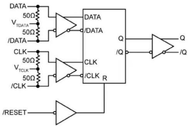
The SY58052AU is an ultra-fast, precision, low jitter data-to-clock resynchronizer with a guaranteed maximum data throughput of 10.7Gbps and a maximum clock of 10.7GHz. The SY58052AU is an ideal solution for backplane retiming or retiming after the data passes through long trace lengths. Serial data comes into the data input, and the CML output is synchronous to the input reference clock's rising edge.
The SY58052AU differential inputs include a unique, internal termination design that allows access to the termination network through a V_T pin. This feature allows the device to easily interface to different logic standards, both AC- and DC-coupled, without external resistor-bias and termination networks. The result is a clean, stub-free, low-jitter interface solution. The differential CML output is optimized for 50Ω environments with internal 50Ω source termination and a 400mV output swing.
The SY58052AU operates from a 2.5V or 3.3V supply and is guaranteed over the full industrial temperature range (-40°C to +85°C). The SY58052AU is part of a Micrel's Precision Edge® product family.
Datasheets and support documentation are available on Micrel's web site at: www.micrel.com.
Functional Block Diagram
flowchart
graph TD
    A["DATA"] --> B["NOT"]
    C["V_TDATA"] --> B
    D["/DATA"] --> B
    E["CLK"] --> F["NOT"]
    G["V_TCLK"] --> F
    H["/CLK"] --> F
    I["/RESET"] --> J["NOT"]
    B --> K["AND"]
    F --> K
    J --> K
    K --> L["OR Gate"]
    style L fill:#f9f,stroke:#333
    style K fill:#ccf,stroke:#333

Precision Edge®
Features
-
Resynchronize data to a reference clock
• Guaranteed AC performance over temperature and voltage: -
DC-to > 10.7Gbps data rate throughput
- DC-to > 10.7GHz clock f_MAX
- 160ps any in-to-out t_PD
- 30ps typical Rise/Fall time
- Ultra low-jitter design:
- 0.3ps_RMS typical random jitter
- 3ps_PP typical deterministic jitter (data)
- < 10psPP total jitter (clock)
• Internal 50Ω input termination
- Unique input termination and V_T pin accepts DC- and AC-coupled inputs (CML, PECL)
• Internal 50Ω output source termination
• 400mV CML output swing
• Power supply: 2.5V ±5% or 3.3V ±10% - -40°C to +85°C industrial temperature range
• Available in a 3mm × 3mm 16-pin QFN package
Applications
• Data communications systems
- Serial OC-192, OC192+FEC data-to-clock realignment
• Parallel 10Gbps for OC-768
• All SONET OC-3 – OC-768 applications
- Fiber channel
- Gigabit Ethernet
- ATE
• Test and measurement
AnyGate and Precision Edge are registered trademarks of Micrel, Inc.
Micrel Inc. • 2180 Fortune Drive • San Jose, CA 95131 • USA • tel +1 (408) 944-0800 • fax +1 (408) 474-1000 • http://www.micrel.com
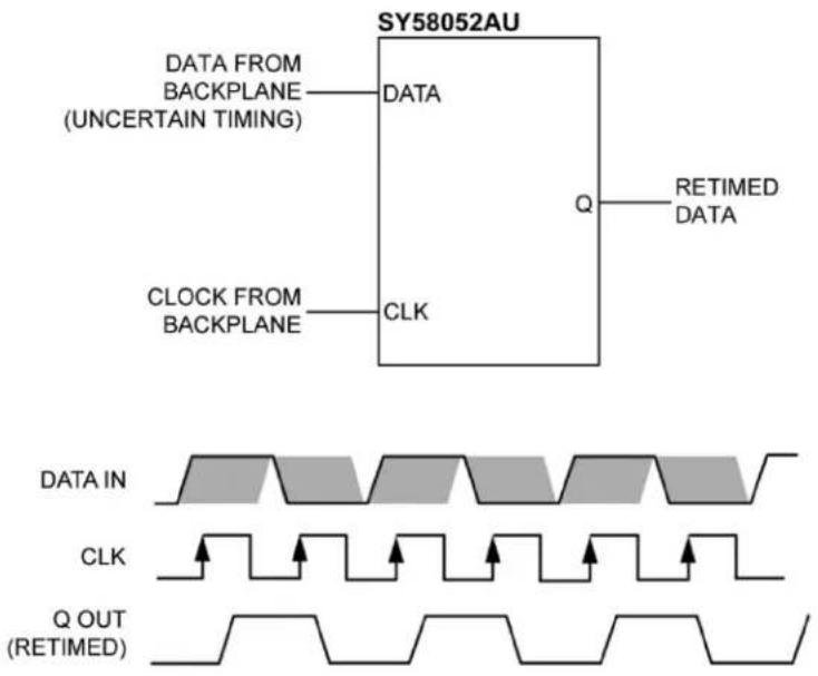
Typical Application
text_image
SY58052AU DATA FROM BACKPLANE (UNCERTAIN TIMING) DATA Q RETIMED DATA CLOCK FROM BACKPLANE CLK DATA IN CLK Q OUT (RETIMED)Ordering Information ^(1)
| Part Number | Package Type | Operating Range | Package Marking | Lead Finish |
| SY58052AUMG | 3mm × 3mm QFN-16 | Industrial | 052A with Pb-Free Bar Line Indicator | NiPdAu Pb-Free |
| SY58052AUMG TR ^(2) | 3mm × 3mm QFN-16 | Industrial | 052A with Pb-Free Bar Line Indicator | NiPdAu Pb-Free |
Notes:
-
Contact factory for die availability. Dice are guaranteed at T_A = 25^ , DC electricals only.
-
Tape and reel.
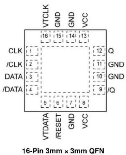
Pin Configuration
text_image
VTCLK GND GND VCC 16 15 14 13 CLK 1 12 Q /CLK 2 11 GND DATA 3 10 GND /DATA 4 9 /Q 5 6 7 8 VTDATA /RESET GND VCC 16-Pin 3mm × 3mm QFNPin Description
| Pin Number | Pin Name | Pin Function |
| 1, 2 CLK, /CLK | Differential Input: This input pair is the clock signal that re-times the data signal at DATA, /DATA. Each pin of this pair internally terminates to the VTCLK pin to 50Ω. Note that this input will default to an indeterminate state if left open (see Input Interface Applications). | |
| 3, 4 DATA, /DATA | Differential Input: This input pair is the signal to be synchronized by the CLK, /CLK signal. Each pin of this pair internally terminates to the VTDATA pin to 50Ω. Note that this input will default to an indeterminate state if left open (see Input Interface Applications). | |
| 5 VTDATA | Input Termination Center-Tap: Each of the two inputs, DATA, /DATA terminates to this pin. The VTDATA pin provides a center-tap to a termination network for maximum interface flexibility (see Input Interface Applications). | |
| 6 /RESET | TTL/CMOS-Compatible Input: The /RESET input asynchronously forces the Q output to a logic “0” state whenever it is active low. Possible state changes due to rising edges on CLK, /CLK are ignored until /RESET goes inactive high. | |
| 7, 10, 11, 14, 15 | GND(Exposed Pad) | Ground. Exposed pad must be connected to the same potential as the GND pin. |
| 8, 13 VCC | Positive Power Supply. Bypass with 0.1μF | 0.01μF low-ESR capacitors. | |
| 12, 9 Q, /Q | Differential Output: This CML output pair is the output of the flip-flop. The data input is transferred to the Q output at the rising edge of CLK (falling edge of /CLK) (see Input Interface Applications). | |
| 16 VTCLK | Input Termination Center-Tap: Each of the two inputs, CLK, /CLK terminates to this pin. The VTCLK pin provides a center-tap to a termination network for maximum interface flexibility (see Input Interface Applications). | |
Truth Table
| DATA | /DATA | CLK | /CLK | /RESET | Q | /Q |
| X | X | X | X | 0 | 0 | 1 |
| X | X | 0 | 1 | 1 | Q_N-1 | / Q_N-1 |
| X | X | 1 | 0 | 1 | Q_N-1 | / Q_N-1 |
| 0 | 1 | 1 | 0 | 1 | ||
| 1 | 0 | 1 | 1 | 0 |
Absolute Maximum Ratings ^(3)
Supply Voltage ( V_cc )....-0.5V to +4.0V
Input Voltage ( V_IN ). -0.5V to V_CC
CML Output Voltage ( V_OUT ) V_CC-1.0V to V_CC+0.5V
Termination Current ^(6)
Source or Sink Current on VTDATA, VCLK ....±60mA
Input Current
Source or Sink Current on DATA, /DATA, CLK, /CLK
±30mA
Lead Temperature (soldering, 20s)....+260°C
Storage Temperature ( T_s )....-65°C to +150°C
Operating Ratings ^(4)
Supply Voltage
(V_cc) ....+2.375V to +2.625V / +2.97V to 3.63V
Ambient Temperature ( T_A )....-40°C to +85°C
Package Thermal Resistance ^(5)
QFN ( _JA )
Still-Air 61°C/W
QFN (ψ JB)
Junction-to-Board....38°C/W
DC Electrical Characteristics ^(7)
T_A = -40^ to +85^ , unless otherwise noted.
| Symbol | Parameter | Condition | Min. | Typ. | Max. | Units |
| V_CC | Power Supply | 2.375 | 2.625 | V | ||
| 2.97 | 3.63 | |||||
| I_CC | Power Supply Current | With load, for either 2.5V or 3.3V supply | 42 | 60 | mA | |
| R_IN | Differential Input Resistance (DATA, /DATA or CLK, /CLK) | 90 | 100 | 110 | Ω | |
| V_IH | Input HIGH Voltage (DATA, /DATA or CLK, /CLK) | Note 8 | 1.2 | V_CC | V | |
| V_IL | Input LOW Voltage (DATA, /DATA or CLK, /CLK) | Note 8 | 0 | V_IH - 0.1 | V | |
| V_IN | Input Voltage Swing (DATA, /DATA or CLK, /CLK) | Note 8, see Figure 4 | 100 | mV | ||
| V_DIFF\_IN | Differential Input Voltage Swing (DATA, /DATA) or (CLK, /CLK) | Note 8, see Figure 5 | 200 | mV | ||
| |I_IN| | Input Current (DATA, /DATA) or (CLK, /CLK) | Note 8 | 21 | mA |
Notes:
- Permanent device damage may occur if the ratings in the Absolute Maximum Ratings are exceeded. This is a stress rating only and functional operation is not implied for conditions other than those detailed in the operational sections of this data sheet. Exposure to absolute maximum ratings conditions for extended periods may affect device reliability.
- The data sheet limits are not guaranteed if the device is operated beyond the operating ratings.
- Package thermal resistance assumes exposed pad is soldered (or equivalent) to the device's most negative potential on the PCB. _JB uses 4-layer 0_JA in still-air, unless otherwise stated.
- Due to the limited drive capability use for input of the same package only.
- The circuit is designed to meet the DC specifications shown in the DC Electrical Characteristics chart after thermal equilibrium has been established.
- Due to the internal termination (see Input and Output Stage Internal Termination) the input current depends on the applied voltages at DATA, /DATA and V_TDATA inputs, or the CLK, /CLK and V_TCLK inputs. Do not apply a combination of voltages that causes the input current to exceed the maximum limit.
LVTTL/CMOS DC Electrical Characteristics ^(9)
V_CC = 2.5V ± 5% or 3.3V ± 10% ; T_A = -40^ C to +85^ C , unless otherwise noted.
| Symbol | Parameter | Condition | Min. | Typ. | Max. | Units |
| V_IH | Input HIGH Voltage | 2.0 | V | |||
| V_IL | Input LOW Voltage | 0.8 | mV | |||
| I_IH | Input HIGH Current | -50 | 20 | μA | ||
| I_IL | Input LOW Current | -100 | μA |
CML Outputs DC Electrical Characteristics ^(9)
V_cc = 2.5V ± 5% or 3.3V ± 10% ; R_L = 100 across output pair or equivalent; T_A = -40^ C to +120^ C , unless otherwise noted.
| Symbol | Parameter | Condition | Min. | Typ. | Max. | Units |
| V_OH | Output HIGH Voltage (Q, /Q) | R_L = 50 to V_CC | V_CC - 0.020 | V_CC | V | |
| V_OUT | Output Voltage Swing (Q, /Q) | See Figure 4 | 325 | 400 | mV | |
| V_DIFF\_OUT | Differential Output Voltage Swing (Q, /Q) | See Figure 5 | 650 | 800 | mV | |
| R_OUT | Output Source Impedance (Q, /Q) | 45 | 50 | 55 |
AC Electrical Characteristics ^(10)
V_CC = 2.5V ± 5% or 3.3V ± 10% ; R_L = 100 across output pair or equivalent; T_A = -40^ to +85^ , unless otherwise noted.
| Symbol | Parameter | Condition | Min. | Typ. | Max. | Units |
| f_MAX | Maximum Operating Frequency | Clock | 10.7 | GHz | ||
| Data | 10.7 | Gbps | ||||
| t_PD | Propagation Delay (CLK-to-Q) | 70 | 160 | ps | ||
| t_RESET | Propagation Delay (Reset-to-Q) | 300 | ps | |||
| t_S | Set-Up Time | 20 | ps | |||
| t_H | Hold Time | 20 | ps | |||
| t_RR Reset | Recovery Time V | TH=V_CC/2 | 250 | ps | ||
| t_JITTER | Random Jitter ( R_J ) | Typical values at ambient temperature ^(11) . | 0.3 | 1 | p s_RMS | |
| Deterministic Jitter ( D_J ) | Typical values at ambient temperature ^(12) . | 3 | 10 | p s_PP | ||
| Total Jitter ( T_J ) | Clock ^(13) | 10 | ||||
| Data ^(13) | 14 | |||||
| t_r,t_f | Rise/Fall Times (20% to 80%) | At full output swing | 30 | 50 | ps |
Notes:
- The circuit is designed to meet the DC specifications shown in the above table after thermal equilibrium has been established.
- Measured with 100mV input swing (see Timing Diagrams for definition of parameters). High-frequency AC-parameters are guaranteed by design and characterization.
- Rj is measured with a K28.7 comma detect character pattern, measured at 10.7Gbps and 2.5Gbps.
- D_J is measured at 10.7Gbps and 2.5Gbps, with both K28.5 and 2^23-1 PRBS pattern.
- Total jitter definition: with an ideal clock input frequency of ≤ f_MAX , no more than one output edge in 10^12 output edges will deviate by more than the specified peak-to-peak jitter value.
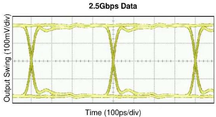
Typical Operating Characteristics
V_CC = 3.3V, GND = 0V, CLK = 400mV, DATA = 400mV, T_A = +25^
line
| Time (100ps/div) | Output Swing (100mV/div) | | ---------------- | ------------------------ | | 0 | 0 | | 1 | 0.5 | | 2 | 1 | | 3 | 0.5 | | 4 | 0 | | 5 | 0.5 | | 6 | 1 | | 7 | 0.5 | | 8 | 0 | | 9 | 0.5 | | 10 | 1 | | 11 | 0.5 | | 12 | 0 | | 13 | 0.5 | | 14 | 1 | | 15 | 0.5 | | 16 | 0 | | 17 | 0.5 | | 18 | 1 | | 19 | 0.5 | | 20 | 0 | | 21 | 0.5 | | 22 | 1 | | 23 | 0.5 | | 24 | 0 | | 25 | 0.5 |
line
| Time (50ps/div) | Output Swing (100mV/div) | | --------------- | ------------------------ | | 0 | 0 | | 50 | 0 | | 100 | 0 | | 150 | 0 | | 200 | 0 | | 250 | 0 | | 300 | 0 | | 350 | 0 | | 400 | 0 | | 450 | 0 | | 500 | 0 | | 550 | 0 | | 600 | 0 | | 650 | 0 | | 700 | 0 | | 750 | 0 | | 800 | 0 | | 850 | 0 | | 900 | 0 | | 950 | 0 | | 1000 | 0 |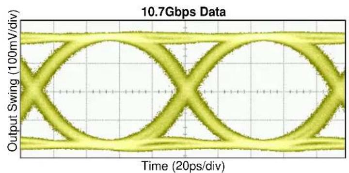
line
| Time (20ps/div) | Output Swing (100mV/div) | | --------------- | ------------------------ | | 0 | 0 | | 10 | 10 | | 20 | 0 | | 30 | -10 | | 40 | 0 | | 50 | 10 | | 60 | 0 | | 70 | -10 | | 80 | 0 | | 90 | 10 | | 100 | 0 | | 110 | -10 | | 120 | 0 | | 130 | 10 | | 140 | 0 | | 150 | -10 | | 160 | 0 | | 170 | 10 | | 180 | 0 | | 190 | -10 | | 200 | 0 |Typical Operating Characteristics (Continued)
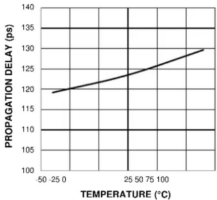
IN-to-Q Propagation Delay vs. Temperature
line
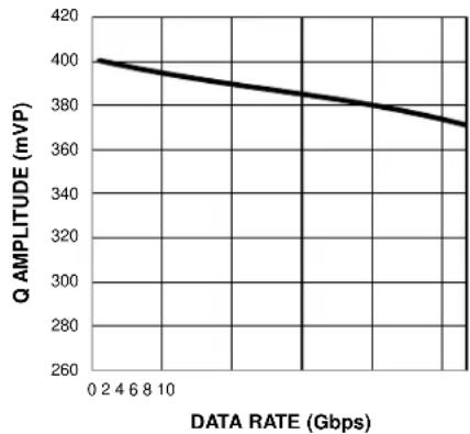
| TEMPERATURE (°C) | PROPAGATION DELAY (ps) | | ---------------- | ---------------------- | | -50 | 120 | | 0 | 122 | | 25 | 124 | | 50 | 126 | | 75 | 128 | | 100 | 130 |Single-Ended Output Swing vs. Data Rate
line
| DATA RATE (Gbps) | Q AMPLITUDE (mVP) | | ---------------- | ----------------- | | 0.2 | 400 | | 4 | 395 | | 8 | 390 | | 10 | 385 | | 12 | 380 | | 14 | 375 | | 16 | 370 | | 18 | 365 | | 20 | 360 |Timing Diagram

text_image
CLK 50% DATA tH 50% ts /RESET Vcc/2 tRR Q 50% tpd tpdInput and Output Stage Internal Termination

text_image
VCC CLK, DATA 50Ω VTCLK' VTDATA 50Ω /CLK, /DATAFigure 1. Simplified Differential Input Stage
Input and Output Stage Internal Termination (Continued)

text_image
Vcc 72kΩ R /RESET RFigure 2. Simplified TTL/CMOS Input
text_image
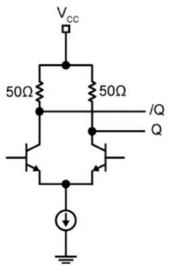
Vcc 50Ω 50Ω /Q Q ↓Figure 3. Simplified Differential Output Stage
Operating Characteristics
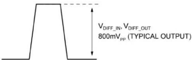
Definition of single-ended and differential swings.

text_image
VIN, VOUT 400mVp (TYPICAL OUTPUT)Figure 4. Single-Ended Swing
text_image
VDIFF_IN, VDIFF_OUT 800mVpp (TYPICAL OUTPUT)Figure 5. Differential Swing
Input Interface Applications

text_image
VCC DATA 1kΩ GND /DATA SY58052AU NC VTNOTE: INPUT HIGH LEVEL SHOWN
Figure 6. Static Input Level

text_image
Vcc LVDS GND DATA, CLK /DATA, /CLK SY58052AU NC VTFigure 7. LVDS Interface (DC-Coupled)
text_image
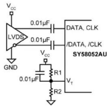
VCC LVDS 0.01μF DATA, CLK 0.01μF /DATA, /CLK SY58052AU GND VCC 0.01μF R1 VT R2NOTE: R1 = 1kΩ, R2 = 1.4kΩ
Figure 8. LVDS Interface (AC-Coupled)
Note: Be certain that the LVDS driver can be AC-coupled.
text_image
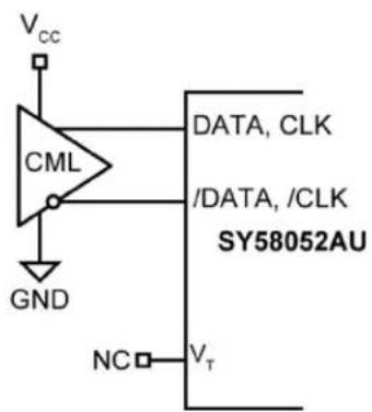
Vcc CML GND DATA, CLK /DATA, /CLK SY58052AU NC VTFigure 9. CML Interface (DC-Coupled)
(OPTION: V_T may be connected to V_cc )
text_image
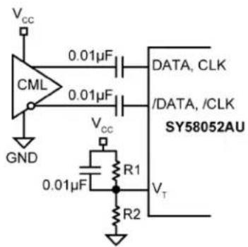
Vcc CML 0.01μF DATA, CLK 0.01μF DATA, /CLK SY58052AU GND Vcc R1 0.01μF VT R2NOTE: R1 = 1kΩ, R2 = 1.4kΩ
Figure 10. CML Interface (AC-Coupled)
Input Interface Applications (Continued)

text_image
Vcc LVPECL GND DATA, CLK /DATA, /CLK SY58052AU Vcc 0.01μF VT Rb GNDNOTE: FOR 3.3V SUPPLY, R_b = 50 FOR 2.5V SUPPLY, R_b = 19
Figure 11. LVPECL Interface (DC-Coupled)

text_image
Vcc LVPECL 0.01μF DATA, CLK 0.01μF /DATA, /CLK SY58052AU RPD RPD VCC 0.01μF R1 GND VT R2NOTE: FOR 2.5V, R_PD = 50 , R1 = 1kΩ, R2 = 1.4kΩ. FOR 3.3V, R_PD = 100 , R1 = 1kΩ, R2 = 1.4kΩ
Figure 12. LVPECL Interface (AC-Coupled)
Related Product and Support Documentation
| Part Number | Function | Data Sheet Link |
| SY58016L | 3.3V 10Gbps Differential CML Line Driver/Receiver with Internal Termination | www.micrel.com/product-info/products/sy58061l.shtml |
| SY58051AU | 10.7Gbps AnyGate® with Internal Input and Output Termination | www.micrel.com/ PDF/HBW/SY58051AU.pdf |
| HBW Solutions | New Products and Applications | www.micrel.com/product-info/products/solutions.shtml |
Package Information ^(14)
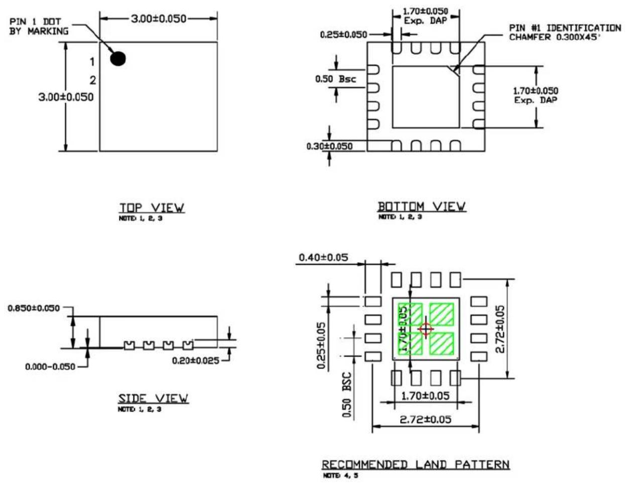
NOTE:
- MAXIMUM PACKAGE WARPAGE IS 0.05mm.
- MAXIMUM ALLOWABLE BURR IS 0.076mm IN ALL DIRECTIONS
- PIN #1 IS ON TOP AND WILL BE LASER MARKED.
- RED CIRCLE IN LAND PATTERN INDICATES THERMAL VIA. SIZE SHOULD BE 0.30-0.35mm IN DIAMETER AND SHOULD BE CONNECTED TO GND FOR MAXIMUM THERMAL PERFORMANCE.
- GREEN RECTANGLES (SHADED AREA) INDICATE SOLDER STENCIL OPENING ON EXPOSED PAD AREA. SIZE SHOULD BE 0.60mmx0.60mm IN SIZE, 0.20mm SPACING.
16-Pin 3mm × 3mm QFN Package (MM)
Note:
- Package information is correct as of the publication date. For updates and most current information, go to www.micrel.com.
MICREL, INC. 2180 FORTUNE DRIVE SAN JOSE, CA 95131 USA
TEL +1 (408) 944-0800 FAX +1 (408) 474-1000 WEB http://www.micrel.com
Micrel makes no representations or warranties with respect to the accuracy or completeness of the information furnished in this data sheet. This information is not intended as a warranty and Micrel does not assume responsibility for its use. Micrel reserves the right to change circuitry, specifications and descriptions at any time without notice. No license, whether express, implied, arising by estoppel or otherwise, to any intellectual property rights is granted by this document. Except as provided in Micrel's terms and conditions of sale for such products, Micrel assumes no liability whatsoever, and Micrel disclaims any express or implied warranty relating to the sale and/or use of Micrel products including liability or warranties relating to fitness for a particular purpose, merchantability, or infringement of any patent, copyright or other intellectual property right.
Micrel Products are not designed or authorized for use as components in life support appliances, devices or systems where malfunction of a product can reasonably be expected to result in personal injury. Life support devices or systems are devices or systems that (a) are intended for surgical implant into the body or (b) support or sustain life, and whose failure to perform can be reasonably expected to result in a significant injury to the user. A Purchaser's use or sale of Micrel Products for use in life support appliances, devices or systems is a Purchaser's own risk and Purchaser agrees to fully indemnify Micrel for any damages resulting from such use or sale.
© 2014 Micrel, Incorporated.