SY89546U - Multiplexeur Microchip - Free user manual and instructions
Find the device manual for free SY89546U Microchip in PDF.

User questions about SY89546U Microchip
0 question about this device. Answer the ones you know or ask your own.
Ask a new question about this device
Download the instructions for your Multiplexeur in PDF format for free! Find your manual SY89546U - Microchip and take your electronic device back in hand. On this page are published all the documents necessary for the use of your device. SY89546U by Microchip.
USER MANUAL SY89546U Microchip
2.5V, 3.2 Gbps Differential 4:1 LVDS Multiplexer with 1:2 Fanout and Internal Termination
Features
- Selects Among Four Differential Inputs
- Provides Two Copies of the Selected Input
• Guaranteed AC Parameters Over Temp/Voltage:
- DC- to >3.2 Gbps Data Rat Throughput
- <620 ps In-to-Out t PD
- <150 ps t_r/t_f Time
- Unique Input Isolation Design Minimize Crosstalk
- Ultra-Low Jitter Design:
- <1 ps RMS Random Jitter
- <10 ps PP Deterministic Jitter
- <10 ps PP Total Jitter (Clock)
-
<0.7 ps RMS Crosstalk Induced Jitter
-
Internal Input Termination
- Unique Input Termination and VT Pin Accepts DC-Coupled and AC-Coupled Inputs (LVDS, LVPECL, CML)
• 350 mV LVDS Output Swing
• Power Supply 2.5V ±5% - - 40^ C to + 85^ C Temperature Range
• Available in 32-pin (5 mm x 5 mm) VQFN Package
Applications
• SONET/SDH Multi-Channel Select applications
• Fibre Channel Applications
- GigE application
General Description
The SY89546U is a precision, high-speed 4:1 differential multiplexer that provides two copies of the selected input. The high speed LVDS (350 mV) compatible outputs with a guaranteed throughput of up to 3.2 Gbps over temperature and voltage.
The SY89546U differential inputs include Microchip's unique 3-pin internal termination design that allows access to the termination network through a VT pin. This feature allows the device to easily interface to different logic standards, both AC- and DC-coupled without external resistor-bias and termination networks. The result is a clean, stub-free, low jitter interface solution.
The SY89546U operates from a single 2.5V supply, and is guaranteed over the full industrial temperature range ( -40^ to +85^ ). For applications that require a 3.3V supply, consider the SY89547L. Or, for applications that only require one differential output, consider the SY89544U or SY89545L. The SY89546U is part of Microchip's Precision Edge ^® product family.
Package Type
text_image
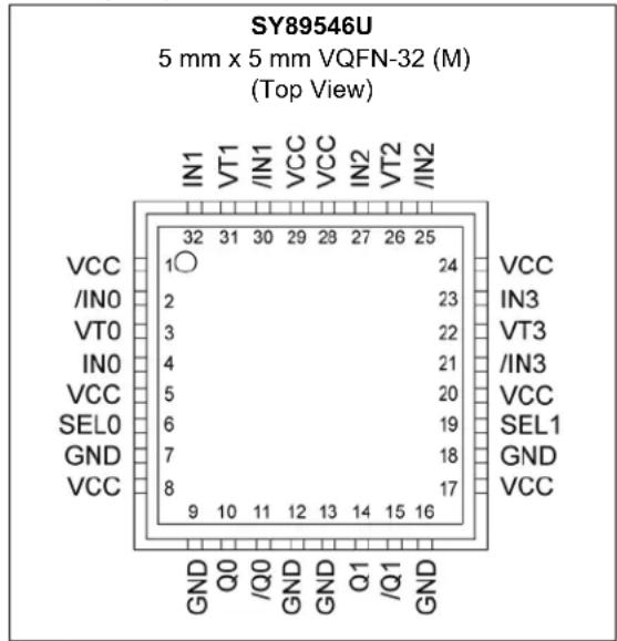
SY89546U 5 mm x 5 mm VQFN-32 (M) (Top View) IN1 VT1 /IN1 VCC VCC IN2 VT2 /IN2 VCC 32 31 30 29 28 27 26 25 1○ 24 VCC /INO 2 23 VT0 3 22 IN0 4 21 VCC 5 20 SEL0 6 19 GND 7 18 VCC 8 17 GND Q0 /Q0 GND GND Q1 /Q1 GNDFunctional Block Diagram

flowchart
graph TD
    subgraph Power supplies
        IN0["IN0"] --> VT0["VT0"]
        IN0 --> /IN0["/IN0"]
        VT0 --> MUX1["4:1 MUX"]
        /IN0 --> MUX1
        VT1["VT1"] --> MUX1
        /IN1["IN1"] --> MUX1
        VT1 --> MUX2["4:1 MUX"]
        /IN1 --> MUX2
        VT2["VT2"] --> MUX2
        /IN2["IN2"] --> MUX2
        VT2 --> MUX3["4:1 MUX"]
        /IN2 --> MUX3
        VT3["VT3"] --> MUX3
        /IN3["IN3"] --> MUX3
    end

    subgraph Control Inputs
        IN3["IN3"] --> SEL0["SEL0 (CMOS/TTL)"]
        IN3 --> SEL1["SEL1 (CMOS/TTL)"]
    end

    MUX1 --> S1["S1"]
    MUX2 --> S1
    MUX3 --> S1

    Q0["Q0"] --> LVDS["LVDS"]
    Q1["Q1"] --> LVDS
    LVDS --> Q0
    LVDS --> Q1

    4:1 MUX --> 0
    4:1 MUX --> 1
    4:1 MUX --> 2
    4:1 MUX --> 3
    4:1 MUX --> 4:1 MUX

    1:2 Fanout --> Q0
    1:2 Fanout --> Q1

    style Power supplies fill:#f9f,stroke:#333
    style Control inputs fill:#ccf,stroke:#333
1.0 ELECTRICAL CHARACTERISTICS
Absolute Maximum Ratings †
Supply Voltage ( V_CC ) -0.5V to +4.0V
Input Voltage ( V_IN ) -0.5V to V_CC
Termination Current ( I_VT ) Note 1 Source or Sink on VT Pin....±100 mA
Input Current Source or Sink Current on IN, /IN ....±50 mA
Storage Temperature Range ( T_S ) -65^ to +150^
Operating Ratings ††
Supply Voltage ( V_CC )....+2.375V to +2.675V
Ambient Temperature Range ( T_A )....-40°C to +85°C
† Notice: Permanent device damage may occur if absolute maximum ratings are exceeded. This is a stress rating only and functional operation is not implied at conditions other than those detailed in the operational sections of this data sheet. Exposure to absolute maximum ratings conditions for extended periods may affect device reliability.
†† Notice: The data sheet limits are not guaranteed if the device is operated beyond the operating ratings.
DC ELECTRICAL CHARACTERISTICS Note 3
Electrical Characteristics: V_CC = 2.5V ± 5% ; -40^ ≤ T_A ≤ +85^ , unless stated otherwise.
| Parameters Symbol | Min. Typ. | Max. Units | Conditions | |||
| Power Supply | V_CC | 2.375 | 2.5 | 2.625 | V | — |
| Power Supply Current | I_CC | — | 75 | 100 | mA | No load, max. V_CC Note 2 |
| Differential Input Resistance (IN-to-/IN) | R_DIFF\_IN | 80 | 100 | 120 | Ω | — |
| Input Resistance (IN-to- V_T , /IN-to- V_T ) | R_IN | 40 | 50 | 60 Ω | — | |
| Input HIGH Voltage IN, /IN | V_IH | 1.2 | — | V_CC | V | — |
| Input LOW Voltage IN, /IN | V_IL | 0 | — | V_IH-0.1 | V | — |
| Input Voltage Swing IN, /IN | V_IN | 0.1 | — | V_CC | V | Note 4 |
| Differential Input Voltage Swing | V_DIFF\_IN | 0.2 | — | — | V | Note 4 |
| Voltage from IN or /IN to V_T | IN-to- V_T | — | — | 1.8 | V | — |
Note 1: Due to the limited drive capability use for input of the same package only.
2: Includes current through internal 50Ω pull-ups.
3: The circuit is designed to meet the DC specifications shown in the above table after thermal equilibrium has been established.
4: See Section 5.0, Single-Ended and Differential Swings for V_IN and V_DIFF_IN definition.
LVDS OUTPUT DC ELECTRICAL CHARACTERISTICS Note 1
Electrical Characteristics: V_CC = 2.5V ± 5% ; -40^ ≤ T_A ≤ +85^ , R_L = 100 across Q and /Q, unless stated otherwise.
| Parameter Symbol Min. Typ. Max. | Units Condition | ||||
| Output High Voltage (Q, /Q) V | _OH | — — 1.475 V See Figure 8-1 | |||
| Output Low Voltage (Q0, /Q) | V_OL | 0.925 | — | — | V See Figure 8-1 |
| Output Voltage Swing (Q0, /Q) | V_OUT | 250 | 350 | — | mV See Figure 5-1, Figure 9-1 |
| Differential Output Voltage Swing (Q - /Q) | V_DIFF\_OUT | 500 | 700 | — | mV See Figure 5-2 |
| Output common Mode Voltage (Q, /Q) | V_OCM | 1.125 | — 1.275 V See Figure 8-2 | ||
| Change in Common Mode Voltage (Q, /Q) | V_OCM | -50 | — | +50 | mV See Figure 8-2 |
Note 1: The circuit is designed to meet the DC specifications shown in the above table after thermal equilibrium has been established.
LVTTL/CMOS OUTPUT DC ELECTRICAL CHARACTERISTICS Note 1
Electrical Characteristics: V_CC = 2.5V ± 5% ; -40^ ≤ T_A ≤ +85^ , R_L = 100 across Q and /Q, unless stated otherwise.
| Parameter Symbol Min. Typ. Max. | Units Condition | |||||
| Input High Voltage | V_IH | 2.0 | — | V_CC | V | — |
| Input Low Voltage | V_IL | 0 | — | 0.8 | V — | |
| Input High Current | I_IH | -125 | — 40 | μA | — | |
| Input Low Current | I_IL | -300 | — | — | μA | — |
Note 1: The circuit is designed to meet the DC specifications shown in the above table after thermal equilibrium has been established.
AC ELECTRICAL CHARACTERISTICS Note 1
Electrical Characteristics: V_CC = 2.5V ± 5% ; -40^ ≤ T_A ≤ +85^ , R_L = 100 across Q and /Q, unless stated otherwise.
| Parameter Symbol | Min. Typ. | Max. Units Condition | ||||
| Maximum Operating Frequency | f_MAX | 3.2 — | — Gbps | NRZ (Data) | ||
| 3 4 — | GHz V | OUT ≥ 200 mV (Clock) | ||||
| Differential Propagation Delay | t_PD | 330 430 530 | SEL-to-Q | IN-to-Q | ||
| 200 400 700 | ||||||
| Input-to-Input Skew | t_SKEW | — 4 | 20 | Note 2ps | ||
| Output-to-Output Skew | — | 8 | 20 | Note 3 | ||
| Part-to-Part Skew | — | — | 200 | Note 4 | ||
| Random Jitter ( R_J ) | t_JITTER | — — | 1 ps | RMS | Data Note 5 | |
| Deterministic Jitter ( D_J ) | — — | 10 | ps | PP | Data Note 6 | |
| Total Jitter ( T_J ) | — — | 10 | ps | PP | Clock Note 7 | |
| Cycle-to-Cycle Jitter | — — | 1 ps | RMS | Clock Note 8 | ||
| Crosstalk-Induced Jitter Crosstalk | — — 0.7 ps | RMS | Note 9 | |||
| Output Rise/Fall Time | t/t_f | 35 | 80 | 150 | ps | 20% to 80% at full output swing |
Note 1: Measured with 100 mV input swing. See Timing Diagrams for definition of parameters. High frequency AC parameters are guaranteed by design and characterization.
2: Input-to-input skew is the difference in time from an input-to-output in comparison to any other input-to-output. In addition, the input-to-input skew does not include the output skew.
3: Output-to-output skew is measured between two different outputs under identical input transitions.
4: Part-to-part skew is defined for two parts with identical power supply voltages at the same temperature and with no skew of the edges at the respective inputs. Total skew is calculated as the RMS (Root Mean Square) of the input skew and output skew.
5: Random jitter is measured with a K28.7 comma detect character pattern, measured at 1.25 Gbps and 3.2 Gbps.
6: Deterministic jitter is measured at 1.25 Gbps and 3.2 Gbps, with both K28.5 and 2^23-1 PRBS pattern.
7: Total jitter definition: with an ideal clock input of frequency ≤ f_MAX no more than one output edge in 10^12 output edges will deviate by more than the specified peak-to-peak jitter value.
8: Cycle-to-cycle jitter definition: the variation of periods between adjacent cycles, T-T _n-1 where T is the time between rising edges of the output cycle.
9: Crosstalk is measured at the output while applying two similar clock frequencies to adjacent inputs that are asynchronous with respect to each other at the inputs.
TEMPERATURE SPECIFICATIONS
| Parameters Symbol Min. | Typ. Max. | Units Conditions | ||||
| Temperature Ranges | ||||||
| Ambient Temperature T | A | -40 — | +85 °C — | |||
| Lead Temperature | — | — | — | +260 | °C | Soldering, 20 sec. |
| Storage Temperature Range | TS | -65 — | +150 | °C — | ||
| Package Thermal Resistances (Note 1) | ||||||
| Thermal Resistance, 5x5 VQFN-32 Lead | _JA | — | 35 | — | °C/W | Still-air, Multi-layer PCB |
| 28 | 500 lpfm, Multi-layer PCB | |||||
| _JB | — | 20 | — | °C/W | Junction-to-board | |
Note 1: Package thermal resistance assumes exposed pad is soldered (or equivalent) to the device's most negative potential on the PCB. _JB and _JA values are determined for a 4-layer board in still-air number, unless otherwise stated.
2.0 TYPICAL PERFORMANCE CURVES
Note: The graphs and tables provided following this note are a statistical summary based on a limited number of samples and are provided for informational purposes only. The performance characteristics listed herein are not tested or guaranteed. In some graphs or tables, the data presented may be outside the specified operating range (e.g., outside specified power supply range) and therefore outside the warranted range.
V_CC = 2.5V , GND = 0V, V_IN = 100 mV , T_A = +25^ , R_L = 100 across Q and /Q, unless otherwise stated.
line
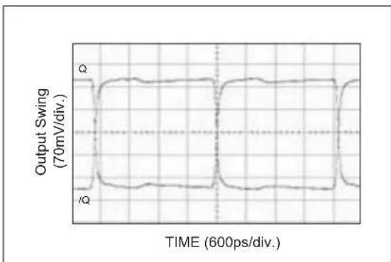
| Time (600ps/div.) | Output Swing (70mV/div.) | | ----------------- | ------------------------ | | 0 | 0 | | 1 | 0 | | 2 | 0 | | 3 | 0 | | 4 | 0 | | 5 | 0 | | 6 | 0 | | 7 | 0 | | 8 | 0 | | 9 | 0 | | 10 | 0 | | 11 | 0 | | 12 | 0 | | 13 | 0 | | 14 | 0 | | 15 | 0 | | 16 | 0 | | 17 | 0 | | 18 | 0 | | 19 | 0 | | 20 | 0 | | 21 | 0 | | 22 | 0 | | 23 | 0 | | 24 | 0 | | 25 | 0 | | 26 | 0 | | 27 | 0 | | 28 | 0 | | 29 | 0 | | 30 | 0 | | 31 | 0 | | 32 | 0 | | 33 | 0 | | 34 | 0 | | 35 | 0 | | 36 | 0 | | 37 | 0 | | 38 | 0 | | 39 | 0 | | 40 | 0 | | 41 | 0 | | 42 | 0 | | 43 | 0 | | 44 | 0 | | 45 | 0 | | 46 | 0 | | 47 | 0 | | 48 | 0 | | 49 | 0 | | 50 | 0 | | 51 | 0 | | 52 | 0 | | 53 | 0 | | 54 | 0 | | 55 | 0 | | 56 | 0 | | 57 | 0 | | 58 | 0 | | 59 | 0 | | 60 | 0 | | 61 | 0 | | 62 | 0 | | 63 | 0 | | 64 | 0 | | 65 | 0 | | 66 | 0 | | 67 | 0 | | 68 | 0 | | 69 | 0 | | 70 | 0 | | 71 | 0 | | 72 | 0 | | 73 | 0 | | 74 | 0 | | 75 | 0 | | 76 | 0 | | 77 | 0 | | 78 | 0 | | 79 | 0 | | 80 | 0 | | 81 | 0 | | 82 | 0 | | 83 | 0 | | 84 | 0 | | 85 | 0 | | 86 | 0 | | 87 | 0 | | 88 | 0 | | 89 | 0 | | 90 | 0 | | 91 | 0 | | 92 | 0 | | 93 | 0 | | 94 | 0 | | 95 | 0 | | 96 | 0 | | 97 | 0 | | 98 | 0 | | 99 | 0 | | Note: The output swing values are not provided in the code. The actual values are not provided in the code. Therefore, they are calculated from the formula `npdiv` to `npdiv*'.FIGURE 2-1: 200 MHz Output.

text_image
Output Swing (70mV/div.) TIME (100ps/div.)FIGURE 2-4: 1 x FC Mask (2 ^23 -1 PRBS).
line
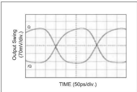
| TIME (50ps/div.) | Output Swing (70mV/div.) | | ---------------- | ------------------------ | | 0 | 0 | | 1 | 100 | | 2 | 0 | | 3 | -100 | | 4 | 0 | | 5 | 100 | | 6 | 0 | | 7 | -100 | | 8 | 0 | | 9 | 100 | | 10 | 0 | | 11 | -100 | | 12 | 0 | | 13 | 100 | | 14 | 0 | | 15 | -100 | | 16 | 0 | | 17 | 100 | | 18 | 0 | | 19 | -100 | | 20 | 0 | | 21 | 100 | | 22 | 0 | | 23 | -100 | | 24 | 0 | | 25 | 100 | | 26 | 0 | | 27 | -100 | | 28 | 0 | | 29 | 100 | | 30 | 0 | | 31 | -100 | | 32 | 0 | | 33 | 100 | | 34 | 0 | | 35 | -100 | | 36 | 0 | | 37 | 100 | | 38 | 0 | | 39 | -100 | | 40 | 0 | | 41 | 100 | | 42 | 0 | | 43 | -100 | | 44 | 0 | | 45 | 100 | | 46 | 0 | | 47 | -100 | | 48 | 0 | | 49 | 100 | | 50 | 0 |FIGURE 2-2: 2.5 GHz Output.
text_image
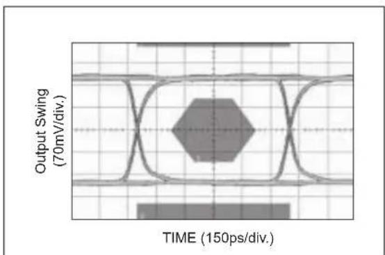
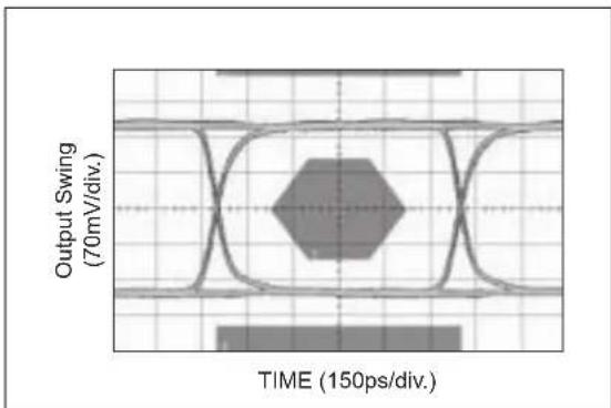
Output Swing (70mV/div.) TIME (150ps/div.)FIGURE 2-5: 1 x GBE Mask (2 PRBS).
line
| Time (150ps/div.) | Output Swing (70mV/div.) | | ----------------- | ------------------------ | | 0 | 0 | | 150 | 0 | | 300 | 0 | | 450 | 0 | | 600 | 0 | | 750 | 0 | | 900 | 0 | | 1050 | 0 | | 1200 | 0 | | 1350 | 0 | | 1500 | 0 | | 1650 | 0 | | 1800 | 0 | | 1950 | 0 | | 2100 | 0 | | 2250 | 0 | | 2400 | 0 | | 2550 | 0 | | 2700 | 0 | | 2850 | 0 | | 3000 | 0 | | 3150 | 0 | | 3300 | 0 | | 3450 | 0 | | 3600 | 0 | | 3750 | 0 | | 3900 | 0 | | 4050 | 0 | | 4200 | 0 | | 4350 | 0 | | 4500 | 0 | | 4650 | 0 | | 4800 | 0 | | 4950 | 0 | | 5100 | 0 | | 5250 | 0 | | 5400 | 0 | | 5550 | 0 | | 5700 | 0 | | 5850 | 0 | | 6000 | 0 | | 6150 | 0 | | 6300 | 0 | | 6450 | 0 | | 6600 | 0 | | 6750 | 0 | | 6900 | 0 | | 7150 | 0 | | 7300 | 0 | | 7450 | 0 | | 7600 | 0 | | 7750 | 0 | | 7900 | 0 | | 8150 | 0 | | 8300 | 0 | | 8450 | 0 | | 8650 | 0 | | 8850 | 0 | | 9125 | 0 | | Note: The data is in a single format for visual comparison. The output values are not explicitly provided in the code. There is only one data series labeled 'TIME (150ps/div.)'.FIGURE 2-3: OC-12 Mask (2 ^23 -1 PRBS).

text_image
Output Swing (70mV/div.) TIME (100ps/div.)FIGURE 2-6: 2 x FC Mask (2 ^23 -1 PRBS).
text_image
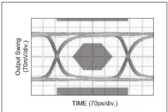
Output Swing (70mV/div.) TIME (70ps/div.)FIGURE 2-7: 1 x GBE Mask (2 PRBS).

line
| Time (70ps/div.) | Output Swing (70mV/div.) | | ---------------- | ------------------------ | | 0 | 0 | | 10 | 10 | | 20 | 0 | | 30 | -10 | | 40 | 0 | | 50 | 10 | | 60 | 0 | | 70 | -10 | | 80 | 0 | | 90 | 10 | | 100 | 0 | | 110 | -10 | | 120 | 0 | | 130 | 10 | | 140 | 0 | | 150 | -10 | | 160 | 0 | | 170 | 10 | | 180 | 0 | | 190 | -10 | | 200 | 0 | | 210 | 10 | | 220 | 0 | | 230 | -10 | | 240 | 0 | | 250 | 10 | | 260 | 0 | | 270 | -10 | | 280 | 0 | | 290 | 10 | | 300 | 0 | | 310 | -10 | | 320 | 0 | | 330 | 10 | | 340 | 0 | | 350 | -10 | | 360 | 0 | | 370 | 10 | | 380 | 0 | | 390 | -10 | | 400 | 0 | | 410 | 10 | | 420 | 0 | | 430 | -10 | | 440 | 0 | | 450 | 10 | | 460 | 0 | | 470 | -10 | | 480 | 0 | | 490 | 10 | | 500 | 0 | | 510 | -10 | | 520 | 0 | | 530 | 10 | | 540 | 0 | | 550 | -10 | | 560 | 0 | | 570 | 10 | | 580 | 0 | | 590 | -10 | | 600 | 0 | | 610 | 10 | | 620 | 0 | | 630 | -10 | | 640 | 0 | | 650 | 10 | | 660 | 0 | | 670 | -10 | | 680 | 0 | | 690 | 10 | | 700 | 0 | | 710 | -10 | | 720 | 0 | | 730 | 10 | | 740 | 0 | | 750 | -10 | | 760 | 0 | | 770 | 10 | | 780 | 0 | | 790 | -10 | | 800 | 0 | | 810 | 10 | | 820 | 0 | | 830 | -10 | | 840 | 0 | | 850 | 10 | | 860 | 0 | | 870 | -10 | | 880 | 0 | | 890 | 10 | | 900 | 0 | | 910 | -10 | | 920 | 0 | | 930 | 10 | | 940 | 0 | | 950 | -10 | | 960 | 0 | | 970 | 10 | | 980 | 0 | | 990 | -10 | | 100 | 0 |FIGURE 2-8: 3.2 Gbps Eye (2 ^23 -1 PRBS).

line
| FREQUENCY (MHz) | OUTPUT AMPLITUDE (mV) | |---|---| | 0 | 340 | | 1000 | 325 | | 2000 | 305 | | 3000 | 275 | | 4000 | 235 | | 5000 | 185 | | 6000 | 110 |FIGURE 2-9: Output Amplitude vs. Frequency.
3.0 PHASE NOISE PLOTS
V_CC=+3.3V,T_A=+25^.

line
| Frequency (MHz) | Value | | --------------- | --------- | | 100 | -129.5133 | | 1 | -143.5240 | | 10 | -153.8294 | | 100 | -151.5211 | | 1 | -154.5964 | | 5 | -154.5595 | | 10 | -154.6173 | | 20 | -154.6374 | | 30 | -154.5119 | | >10 | -154.3307 | | Start | 1.7 | | Stop | 20 | | Center | 10.006 | | Span | 19.988 | | *** Noise | *** | | Analysis Range X | Band Marker | | Analysis Range Y | Band Marker | | Intg Noise | -81.6286 | | RMS Noise | 117.243 | | RMS Jitter | 186.598 | | Residual FM | 1.31479 |FIGURE 3-1: 100 MHz Phase Jitter, Device.
line
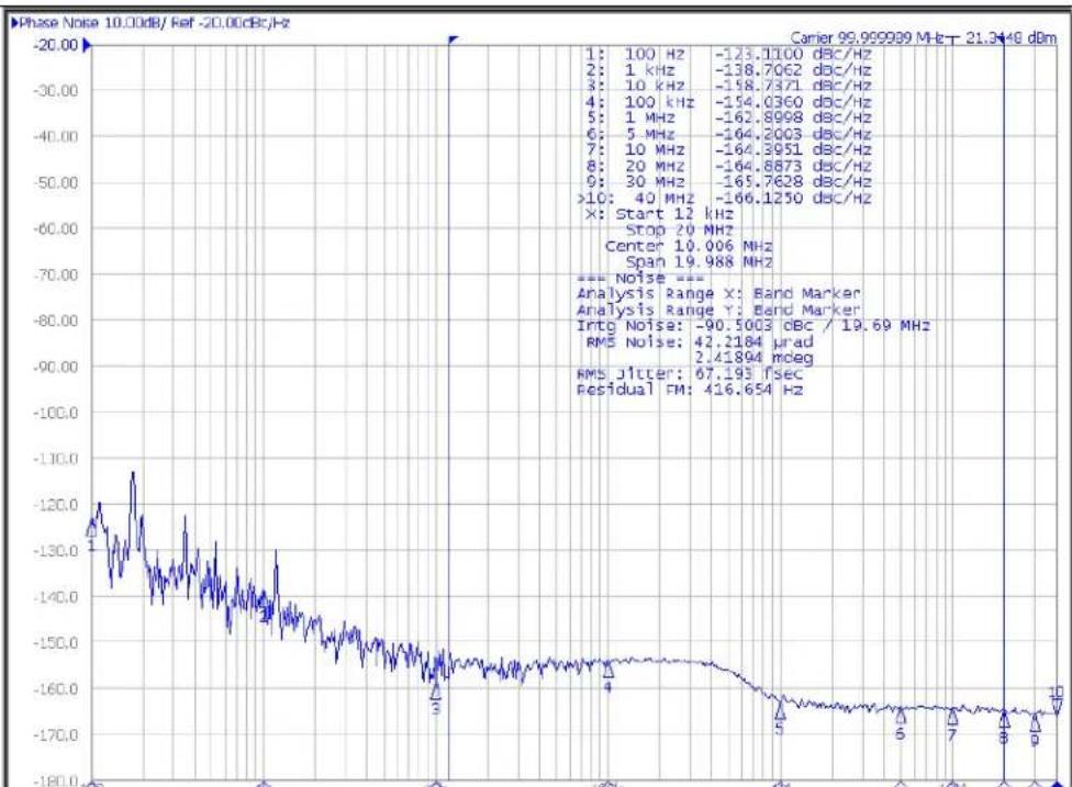
| Frequency (MHz) | Value | | --------------- | --------- | | 100 | -123.1100 | | 1 | -138.7062 | | 10 | -158.7371 | | 100 | -154.0360 | | 1 | -162.8998 | | 5 | -164.2003 | | 10 | -164.3951 | | 20 | -164.8873 | | 30 | -165.7628 | | >10 | -166.1250 | | Start | 12 | | Stop | 20 | | Center | 10.006 | | Span | 19.988 | | Noise | — | | Analysis Range X | Band Marker | | Analysis Range Y | Bend Marker | | Inte Noise | -90.5003 | | RMS Noise | 42.2184 | | RMS Jitter | 67.193 | | Residual FM | 416.654 |FIGURE 3-2: 100 MHz Phase Jitter, Source.
line
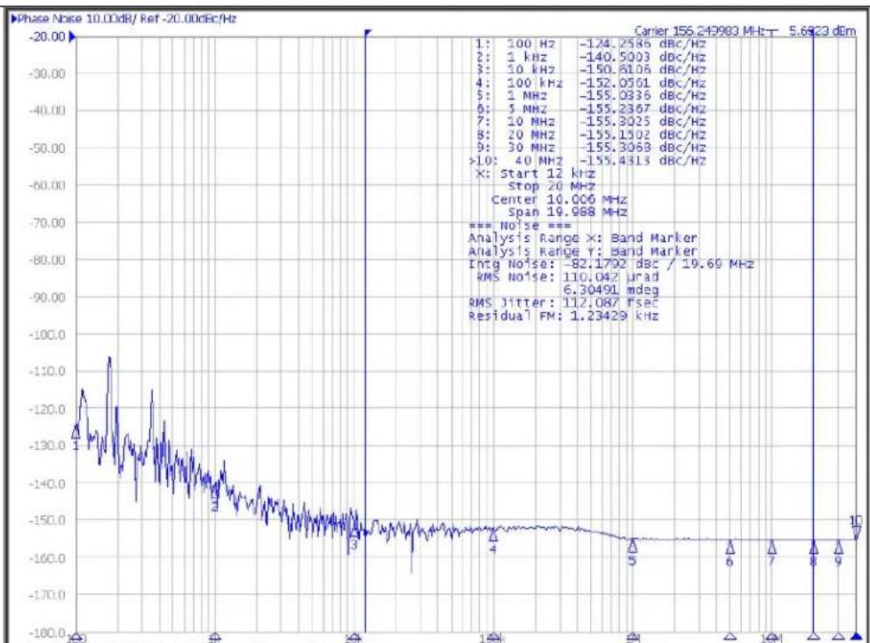
| Frequency (MHz) | Value (dBc/Hz) | | --------------- | -------------- | | 100 | -124.2586 | | 1 | -140.5003 | | 10 | -150.6106 | | 100 | -152.0561 | | 1 | -155.0336 | | 5 | -155.2367 | | 10 | -155.3025 | | 20 | -155.1502 | | 30 | -155.3068 | | >10 | -155.4313 |FIGURE 3-3: 156.25 MHz Phase Jitter, Device.
line
| Frequency | Value | | --------- | --------- | | 1 | -128.7905 | | 2 | -144.5313 | | 3 | -152.1475 | | 4 | -154.0474 | | 5 | -163.0303 | | 6 | -164.9306 | | 7 | -164.3425 | | 8 | -164.2873 | | 9 | -165.2001 | | >10 | -166.3993 |FIGURE 3-4: 156.25 MHz Phase Jitter, Source.

line
| Frequency (kHz) | Value | | --------------- | ----------- | | 100 | -114.5495 | | 1 | -126.4016 | | 10 | -139.6903 | | 100 | -142.6933 | | 1 | -148.5768 | | 5 | -149.8593 | | 10 | -149.7874 | | 20 | -149.7411 | | 30 | -149.8223 | | >10 | -149.7556 | | Stop | 20 MHz | | Center | 10.006 MHz | | Span | 19.988 MHz | | Noise | — | | Analysis Range X | Band Marker | | Analysis Range Y | Band Marker | | Intg Noise | -76.3082 | | RMS Noise | 216.324 | | RMS Jitter | 15.345 | | Residual FM | 2.3C103 |FIGURE 3-5: 622 MHz Phase Jitter, Device.
line
| Frequency | Value | | --------- | ----------- | | 1 | -109.7775 | | 2 | -132.7681 | | 3 | -139.0478 | | 4 | -143.7204 | | 5 | -154.8384 | | 6 | -161.1759 | | 7 | -161.7958 | | 8 | -161.8825 | | 9 | -162.3853 | | >10 | -162.2814 |FIGURE 3-6: 622 MHz Phase Jitter, Source.
4.0 PIN DESCRIPTIONS
The descriptions of the pins are listed in Table 4-1.
TABLE 4-1: PIN FUNCTION TABLE
| Pin Number Pin Name Description | ||
| 4, 2, 21, 32, 30, 27, 25, 23, 21 | IN0, /IN0 IN1, /IN1IN2, /IN2 IN3, /IN3 | Differential Inputs: These inputs pairs are the differential signal inputs to the device. Inputs accept AC- or DC-coupled signals as small as 100 mV. Each pin of a pair internally terminates to a VT pin through 50Ω. Note that these inputs will default to an indeterminate state if left open. Unused differential input pairs can be terminated by connecting one input to V_CC and the complementary input to GND through a 1 kΩ resistor. The VT pin is to be left open in this configuration. Please refer to Section 8.0 “Input Interface Applications” for details. |
| 3, 31, 26, 22 VT0, | VT1, VT2, VT3 | Input Termination Center-Tap: Each side of the differential input pair, terminates to a VT pin. The V_TA0 , V_TA1 , V_TB0 , V_TB1 pins provide a center-tap to a termination network for maximum interface flexibility. See Section 8.0 “Input Interface Applications”. |
| 6, 19 SEL0, | SEL1 | These single-ended TTL/CMOS-compatible inputs select the inputs to the multiplexers. Note that these inputs are internally connected to a 25 kΩ pull-up resistor and will default to a logic HIGH state if left open. Input switching threshold is V_CC/2 . |
| 1, 5, 8, 17, 20, 24, 28, 29 | VCC Positive | Power Supply: Bypass with 0.1 μF//0.01 μF low ESR capacitors. |
| 10, 11, 14, 15 Q0, | /Q0 Q1, /Q1 | Differential Outputs: These LVDS outputs pairs are the outputs of the device. They are a logic function of the INA0, INA1, INB0, INB1 and SELA and SELB inputs. Please refer to Table 4-2 for details. If an output is not used, it must be terminated with 100Ω across the differential pair. |
| 7, 9, 12, 13, 16, 18 | GND, Exposed Pad | Ground. Ground pin and exposed pad must be connected to the same ground plane. |
TRUTH TABLE
TABLE 4-2: TRUTH TABLE
| IN0 | IN1 | IN2 | IN3 | SEL0 | SEL1 | Q | /Q |
| 0 | X | X | X | 0 | 0 | 0 | 1 |
| 1 | X | X | X | 0 | 0 | 1 | 0 |
| X | 0 | X | X | 1 | 0 | 0 | 1 |
| X | 1 | X | X | 1 | 0 | 1 | 0 |
| X | X | 0 | X | 0 | 1 | 0 | 1 |
| X | X | 1 | X | 0 | 1 | 1 | 0 |
| X | X | X | 0 | 1 | 1 | 0 | 1 |
| X | X | X | 1 | 1 | 1 | 1 | 0 |
5.0 SINGLE-ENDED AND DIFFERENTIAL SWINGS
text_image
V_{IN} V_{OUT} 350mV (Typ.)FIGURE 5-1: Single-Ended Voltage Swing.
text_image
VDIFF_IN VDIFF_OUT 700mV (Typ.)FIGURE 5-2: Differential Voltage Swing.
6.0 TIMING DIAGRAMS
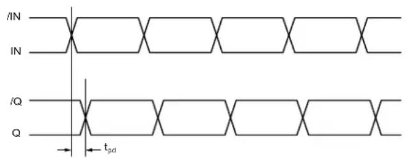
text_image
/IN IN /Q Q t_pd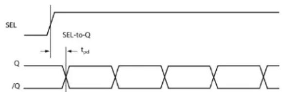
text_image
SEL SEL-to-Q Q /Q t_pdFIGURE 6-1: Timing Diagrams.
7.0 INPUT STAGE
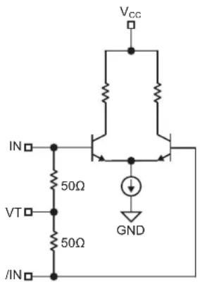
text_image
Vcc IN 50Ω VT 50Ω /IN GNDFIGURE 7-1: Simplified Differential Input Stage.
8.0 INPUT INTERFACE APPLICATIONS

text_image
VCC CML IN /IN SY89546U NC VTFIGURE 8-1: CML Interface (DC-Coupled).

text_image
VCC LVPECL IN Rp Rp GND GND VCC-1.4V VT GND /IN SY89546U For VCC = 2.5V, Rp = 50ΩFIGURE 8-4: LVPECL Interface (AC-Coupled).
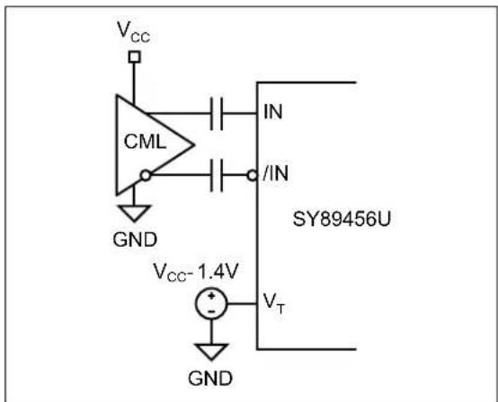
text_image
VCC CML IN /IN GND SY89456U VCC- 1.4V VT GNDFIGURE 8-2: CML Interface (AC-Coupled).
text_image
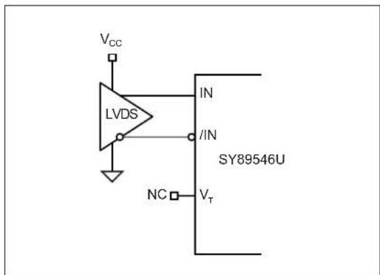
Vcc LVDS IN /IN SY89546U NC VTFIGURE 8-5: LVDS Interface.
text_image
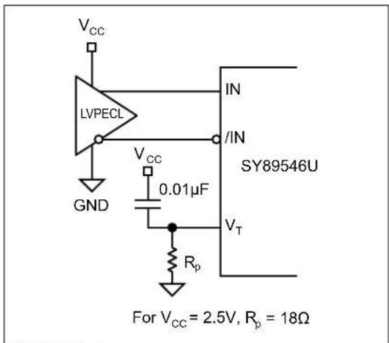
VCC LVPECL GND VCC 0.01μF IN /IN SY89546U VT Rp For VCC = 2.5V, Rp = 18ΩFIGURE 8-3: LVPECL Interface (AC-Coupled).
9.0 OUTPUT INTERFACE APPLICATIONS
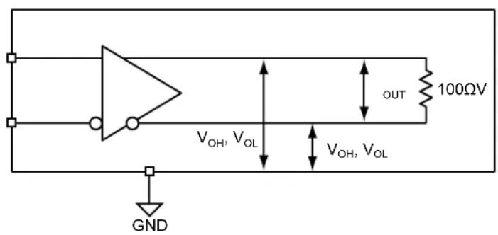
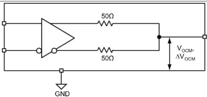
LVDS specifies a small swing of 350 mV typical, on a nominal 1.25V common mode above ground. The common mode voltage has tight limits to permit large variations in ground between an LVDS driver and receiver. Also, change in common mode voltage, as a function of data input, is kept to a minimum, to keep EMI low.
text_image
V_OH, V_OL V_OH, V_OL OUT 100ΩV GNDFIGURE 9-1: LVDS Differential Measurement.
text_image
50Ω 50Ω VOCM, ΔVOCM GNDFIGURE 9-2: LVDS Common Mode Measurement.
10.0 PACKAGING INFORMATION
10.1 Package Marking Information
32-Lead VQFN*


XXXXXXXXX
WWNNN
COO
Example


SY89546U
11924
USA
Legend: XX...X Product code or customer-specific information
Y Year code (last digit of calendar year)
YY Year code (last 2 digits of calendar year)
WW Week code (week of January 1 is week '01')
NNN Alphanumeric traceability code
eBb-free JEDEC ^® designator for Matte Tin (Sn)
* This package is Pb-free. The Pb-free JEDEC designator ( ) e3
can be found on the outer packaging for this package.
•, ▲, ▼ Pin one index is identified by a dot, delta up, or delta down (triangle mark).
Note: In the event the full Microchip part number cannot be marked on one line, it will be carried over to the next line, thus limiting the number of available characters for customer-specific information. Package may or may not include the corporate logo.
Underbar (_) and/or Overbar (−) symbol may not be to scale.
32-Lead Very Thin Plastic Quad Flat, No Lead Package (PEA) - 5x5x0.9 mm Body [VQFN] Micrel Legacy Package QFN55-32LD-PL-1
Note: For the most current package drawings, please see the Microchip Packaging Specification located at http://www.microchip.com/packaging
![Microchip SY89546U - 32-Lead Very Thin Plastic Quad Flat, No Lead Package (PEA) - 5x5x0.9 mm Body [VQFN] Micrel Legacy Package QFN55-32LD-PL-1 - 1](/content/2026/06/1224217/images/145d3180c4d6515b1ba4f418053ef9bfaa3f4a732fa6b919c7f59dd26e1f7923.jpg)
text_image
NOTE 1 N 1 2 (DATUM B) (DATUM A) 2X 0.10 C 2X 0.10 C TOP VIEW D2 0.10 A B K E2 A1 (A3) SEATING PLANE C SIDE VIEW NOTE 1 N L e 32X b 0.10 A B 0.05 B BOTTOM VIEWMicrochip Technology Drawing C04-1118-PEA Rev A Sheet 1 of 2
32-Lead Very Thin Plastic Quad Flat, No Lead Package (PEA) - 5x5x0.9 mm Body [VQFN] Micrel Legacy Package QFN55-32LD-PL-1
Note: For the most current package drawings, please see the Microchip Packaging Specification located at http://www.microchip.com/packaging
![Microchip SY89546U - 32-Lead Very Thin Plastic Quad Flat, No Lead Package (PEA) - 5x5x0.9 mm Body [VQFN] Micrel Legacy Package QFN55-32LD-PL-1 - 1](/content/2026/06/1224217/images/e855e6ef0e150fe94a5cad5763166410f8d06b498d39280d3b8fcc4e416c7beb.jpg)
natural_image
Technical line drawing of two integrated circuit chips with pinouts (no text or symbols)| Units | MILLIMETERS | |||
| Dimension Limits | MIN | NOM | MAX | |
| Number of Terminals | N | 32 | ||
| Pitch | e | 0.50 BSC | ||
| Overall Height | A | 0.80 | 0.85 | 0.90 |
| Standoff | A1 | 0.00 | 0.02 | 0.05 |
| Terminal Thickness | A3 | 0.203 REF | ||
| Overall Length | D | 5.00 BSC | ||
| Exposed Pad Length | D2 3 | 05 | 3.10 3.15 | |
| Overall Width | E | 5.00 BSC | ||
| Exposed Pad Width | E2 | 3.05 3.10 | 3.15 | |
| Terminal Width | b | 0.20 | 0.25 | 0.30 |
| Terminal Length | L | 0.35 | 0.40 | 0.45 |
| K | - | |||
0.20 -Terminal-to-Expos
Notes:
- Pin 1 visual index feature may vary, but must be located within the hatched area.
- Package is saw singulated
- Dimensioning and tolerancing per ASME Y14.5M BSC: Basic Dimension. Theoretically exact value shown without tolerances. REF: Reference Dimension, usually without tolerance, for information purposes only.
Microchip Technology Drawing C04-1118-PEA Rev A Sheet 2 of 2
32-Lead Very Thin Plastic Quad Flat, No Lead Package (PEA) - 5x5x0.9 mm Body [VQFN] Micrel Legacy Package QFN55-32LD-PL-1
Note: For the most current package drawings, please see the Microchip Packaging Specification located at http://www.microchip.com/packaging
![Microchip SY89546U - 32-Lead Very Thin Plastic Quad Flat, No Lead Package (PEA) - 5x5x0.9 mm Body [VQFN] Micrel Legacy Package QFN55-32LD-PL-1 - 1](/content/2026/06/1224217/images/6a19d1548c1ad805a0e1d1a7753aa7f019f0c775f9741d738ad6d6d42807b948.jpg)
text_image
C1 X2 EV 32 1 2 Y2 C2 EV G2 ØV G1 Y1 X1 SILK SCREEN ERECOMMENDED LAND PATTERN
| Units | MILLIMETERS | |||
| Dimension Limits | MIN | NOM | MAX | |
| Contact Pitch | E | 0.50 BSC | ||
| Optional Center Pad Width | X2 | 3.15 | ||
| Optional Center Pad Length | Y2 | 3.15 | ||
| C1 | Contact Pad Spacing 4.90 | |||
| Contact Pad Spacing | C2 | 4.90 | ||
| Contact Pad Width (Xnn) | X1 | 0.30 | ||
| Contact Pad Length (Xnn) | Y1 | 0.90 | ||
| Contact Pad to Center Pad (Xnn) G1 | 0.43 | |||
| Contact Pad to Contact Pad (Xnn) G2 | 0.20 | |||
| Thermal Via Diameter V | 0.33 | |||
| Thermal Via Pitch EV | 1.20 | |||
Notes:
1. Dimensioning and tolerancing per ASME Y14.5M
BSC: Basic Dimension. Theoretically exact value shown without tolerances.
2. For best soldering results, thermal vias, if used, should be filled or tented to avoid solder loss during reflow process
Microchip Technology Drawing C04-3118-PEA Rev A
NOTES:
APPENDIX A: REVISION HISTORY
Revision A (July 2023)
- Converted Micrel document SY89546U to Microchip data sheet template DS20006333A.
- Minor text changes throughout.
NOTES:
PRODUCT IDENTIFICATION SYSTEM
To order or obtain information, e.g., on pricing or delivery, contact your local Microchip representative or sales office.

text_image
PART NO. X Device Supply Voltage X Package Temperature Range XX Special ProcessingDevice:
SY89546: 2.5V, 3.2 Gbps Differential 4:1 LVDS Multiplexer with 1:2 Fanout and Internal Termination
Supply Voltage: U = 2.5V
Package:
M = 5 mm x 5 mm VQFN-32 (NiPdAu Lead-Free)
Temperature Range:
G = -40°C to 85°C
Special Processing:
Examples:
a) SY89546UMG: SY89546, 2.5V Supply
Voltage, 3 mm x 3 mm 32-Lead
VQFN, -40^ to +85^
Temperature Range, 60/Tray
b) SY89546UMG-TR: SY89546, 2.5V Supply
Voltage, 3 mm x 3 mm 32-Lead
VQFN, -40^ to +85^
Temperature Range, 1,000/Reel
Note 1: Tape and Reel identifier only appears in the catalog part number description. This identifier is used for ordering purposes and is not printed on the device package. Check with your Microchip Sales Office for package availability with the Tape and Reel option.
NOTES:
Note the following details of the code protection feature on Microchip products:
• Microchip products meet the specifications contained in their particular Microchip Data Sheet.
- Microchip believes that its family of products is secure when used in the intended manner, within operating specifications, and under normal conditions.
- Microchip values and aggressively protects its intellectual property rights. Attempts to breach the code protection features of Microchip product is strictly prohibited and may violate the Digital Millennium Copyright Act.
- Neither Microchip nor any other semiconductor manufacturer can guarantee the security of its code. Code protection does not mean that we are guaranteeing the product is "unbreakable" Code protection is constantly evolving. Microchip is committed to continuously improving the code protection features of our products.
This publication and the information herein may be used only with Microchip products, including to design, test, and integrate Microchip products with your application. Use of this information in any other manner violates these terms. Information regarding device applications is provided only for your convenience and may be superseded by updates. It is your responsibility to ensure that your application meets with your specifications. Contact your local Microchip sales office for additional support or, obtain additional support at https://www.microchip.com/en-us/support/design-help/client-support-services.
THIS INFORMATION IS PROVIDED BY MICROCHIP "AS IS". MICROCHIP MAKES NO REPRESENTATIONS OR WARRANTIES OF ANY KIND WHETHER EXPRESS OR IMPLIED, WRITTEN OR ORAL, STATUTORY OR OTHERWISE, RELATED TO THE INFORMATION INCLUDING BUT NOT LIMITED TO ANY IMPLIED WARRANTIES OF NON-INFRINGEMENT, MERCHANTABILITY, AND FITNESS FOR A PARTICULAR PURPOSE, OR WARRANTIES RELATED TO ITS CONDITION, QUALITY, OR PERFORMANCE.
IN NO EVENT WILL MICROCHIP BE LIABLE FOR ANY INDIRECT, SPECIAL, PUNITIVE, INCIDENTAL, OR CONSEQUENTIAL LOSS, DAMAGE, COST, OR EXPENSE OF ANY KIND WHATSOEVER RELATED TO THE INFORMATION OR ITS USE, HOWEVER CAUSED, EVEN IF MICROCHIP HAS BEEN ADVISED OF THE POSSIBILITY OR THE DAMAGES ARE FORESEEABLE. TO THE FULLEST EXTENT ALLOWED BY LAW, MICROCHIP'S TOTAL LIABILITY ON ALL CLAIMS IN ANY WAY RELATED TO THE INFORMATION OR ITS USE WILL NOT EXCEED THE AMOUNT OF FEES, IF ANY, THAT YOU HAVE PAID DIRECTLY TO MICROCHIP FOR THE INFORMATION.
Use of Microchip devices in life support and/or safety applications is entirely at the buyer's risk, and the buyer agrees to defend, indemnify and hold harmless Microchip from any and all damages, claims, suits, or expenses resulting from such use. No licenses are conveyed, implicitly or otherwise, under any Microchip intellectual property rights unless otherwise stated.
Trademarks
The Microchip name and logo, the Microchip logo, Adaptec, AVR, AVR logo, AVR Freaks, BesTime, BitCloud, CryptoMemory, CryptoRF, dsPIC, flexPWR, HELDO, IGLOO, JukeBlox, KeeLoq, Kleer, LANCheck, LinkMD, maXStylus, maXTouch, MediaLB, megaAVR, Microsemi, Microsemi logo, MOST, MOST logo, MPLAB, OptoLyzer, PIC, picoPower, PICSTART, PIC32 logo, PolarFire, Prochip Designer, QTouch, SAM-BA, SenGenuity, SpyNIC, SST, SST Logo, SuperFlash, Symmetricom, SyncServer, Tachyon, TimeSource, tinyAVR, UNI/O, Vectron, and XMEGA are registered trademarks of Microchip Technology Incorporated in the U.S.A. and other countries.
AgileSwitch, APT, ClockWorks, The Embedded Control Solutions Company, EtherSynch, Flashtec, Hyper Speed Control, HyperLight Load, Libero, motorBench, mTouch, Powermite 3, Precision Edge, ProASIC, ProASIC Plus, ProASIC Plus logo, Quiet-Wire, SmartFusion, SyncWorld, Temux, TimeCesium, TimeHub, TimePictra, TimeProvider, TrueTime, and ZL are registered trademarks of Microchip Technology Incorporated in the U.S.A.
Adjacent Key Suppression, AKS, Analog-for-the-Digital Age, Any Capacitor, AnyIn, AnyOut, Augmented Switching, BlueSky, BodyCom, Clockstudio, CodeGuard, CryptoAuthentication, CryptoAutomotive, CryptoCompanion, CryptoController, dsPICDEM, dsPICDEM.net, Dynamic Average Matching, DAM, ECAN, Espresso T1S, EtherGREEN, GridTime, IdealBridge, In-Circuit Serial Programming, ICSP, INICnet, Intelligent Paralleling, IntelliMOS, Inter-Chip Connectivity, JitterBlocker, Knob-on-Display, KoD, maxCrypto, maxView, memBrain, Mindi, MiWi, MPASM, MPF, MPLAB Certified logo, MPLIB, MPLINK, MultiTRAK, NetDetach, Omniscient Code Generation, PICDEM, PICDEM.net, PICkit, PICtail, PowerSmart, PureSilicon, QMatrix, REAL ICE, Ripple Blocker, RTAX, RTG4, SAM-ICE, Serial Quad I/O, simpleMAP, SimpliPHY, SmartBuffer, SmartHLS, SMART-I.S., storClad, SQI, SuperSwitcher, SuperSwitcher II, Switchtec, SynchroPHY, Total Endurance, Trusted Time, TSHARC, USBCheck, VariSense, VectorBlox, VeriPHY, ViewSpan, WiperLock, XpressConnect, and ZENA are trademarks of Microchip Technology Incorporated in the U.S.A. and other countries.
SQTP is a service mark of Microchip Technology Incorporated in the U.S.A.
The Adaptec logo, Frequency on Demand, Silicon Storage Technology, and Symmcom are registered trademarks of Microchip Technology Inc. in other countries.
GestIC is a registered trademark of Microchip Technology Germany II GmbH & Co. KG, a subsidiary of Microchip Technology Inc., in other countries.
All other trademarks mentioned herein are property of their respective companies.
© 2023, Microchip Technology Incorporated and its subsidiaries.
All Rights Reserved.
ISBN: 978-1-6683-2892-7
For information regarding Microchip's Quality Management Systems, please visit www.microchip.com/quality.
Worldwide Sales and Service
AMERICAS
Corporate Office
2355 West Chandler Blvd.
Chandler, AZ 85224-6199
Tel: 480-792-7200
Fax: 480-792-7277
Technical Support:
http://www.microchip.com/
support
Web Address:
www.microchip.com
Atlanta
Duluth, GA
Tel: 678-957-9614
Fax: 678-957-1455
Austin, TX
Tel: 512-257-3370
Boston
Westborough, MA
Tel: 774-760-0087
Fax: 774-760-0088
Chicago
Itasca, IL
Tel: 630-285-0071
Fax: 630-285-0075
Dallas
Addison, TX
Tel: 972-818-7423
Fax: 972-818-2924
Detroit
Novi, MI
Tel: 248-848-4000
Houston, TX
Tel: 281-894-5983
Indianapolis
Noblesville, IN
Tel: 317-773-8323
Fax: 317-773-5453
Tel: 317-536-2380
Los Angeles
Mission Viejo, CA
Tel: 949-462-9523
Fax: 949-462-9608
Tel: 951-273-7800
Raleigh, NC
Tel: 919-844-7510
New York, NY
Tel: 631-435-6000
San Jose, CA
Tel: 408-735-9110
Tel: 408-436-4270
Canada - Toronto
Tel: 905-695-1980
Fax: 905-695-2078
ASIA/PACIFIC
Australia - Sydney
Tel: 61-2-9868-6733
China - Beijing
Tel: 86-10-8569-7000
China - Chengdu
Tel: 86-28-8665-5511
China - Chongqing
Tel: 86-23-8980-9588
China - Dongguan
Tel: 86-769-8702-9880
China - Guangzhou
Tel: 86-20-8755-8029
China - Hangzhou
Tel: 86-571-8792-8115
China - Hong Kong SAR
Tel: 852-2943-5100
China - Nanjing
Tel: 86-25-8473-2460
China - Qingdao
Tel: 86-532-8502-7355
China - Shanghai
Tel: 86-21-3326-8000
China - Shenyang
Tel: 86-24-2334-2829
China - Shenzhen
Tel: 86-755-8864-2200
China - Suzhou
Tel: 86-186-6233-1526
China - Wuhan
Tel: 86-27-5980-5300
China - Xian
Tel: 86-29-8833-7252
China - Xiamen
Tel: 86-592-2388138
China - Zhuhai
Tel: 86-756-3210040
ASIA/PACIFIC
India - Bangalore
Tel: 91-80-3090-4444
India - New Delhi
Tel: 91-11-4160-8631
India - Pune
Tel: 91-20-4121-0141
Japan - Osaka
Tel: 81-6-6152-7160
Japan - Tokyo
Tel: 81-3-6880-3770
Korea - Daegu
Tel: 82-53-744-4301
Korea - Seoul
Tel: 82-2-554-7200
Malaysia - Kuala Lumpur
Tel: 60-3-7651-7906
Malaysia - Penang
Tel: 60-4-227-8870
Philippines - Manila
Tel: 63-2-634-9065
Singapore
Tel: 65-6334-8870
Taiwan - Hsin Chu
Tel: 886-3-577-8366
Taiwan - Kaohsiung
Tel: 886-7-213-7830
Taiwan - Taipei
Tel: 886-2-2508-8600
Thailand - Bangkok
Tel: 66-2-694-1351
Tel: 43-7242-2244-39
Fax: 43-7242-2244-393
Denmark - Copenhagen
Tel: 45-4485-5910
Fax: 45-4485-2829
Finland - Espoo
Tel: 358-9-4520-820
France - Paris
Tel: 33-1-69-53-63-20
Fax: 33-1-69-30-90-79
Germany - Garching
Tel: 49-8931-9700
Germany - Haan
Tel: 49-2129-3766400
Germany - Heilbronn
Tel: 49-7131-72400
Germany - Karlsruhe
Tel: 49-721-625370
Germany - Munich
Tel: 49-89-627-144-0
Fax: 49-89-627-144-44
Germany - Rosenheim
Tel: 49-8031-354-560
Israel - Ra'anana
Tel: 972-9-744-7705
Italy - Milan
Tel: 39-0331-742611
Fax: 39-0331-466781
Italy - Padova
Tel: 39-049-7625286
Netherlands - Drunen
Tel: 31-416-690399
Fax: 31-416-690340
Norway - Trondheim
Tel: 47-7288-4388
Poland - Warsaw
Tel: 48-22-3325737
Romania - Bucharest
Tel: 40-21-407-87-50
Spain - Madrid
Tel: 34-91-708-08-90
Fax: 34-91-708-08-91
Sweden - Gothenberg
Tel: 46-31-704-60-40
Sweden - Stockholm
Tel: 46-8-5090-4654
UK - Wokingham
Tel: 44-118-921-5800
Fax: 44-118-921-5820