SY89876L - Electronic component Microchip - Free user manual and instructions
Find the device manual for free SY89876L Microchip in PDF.

User questions about SY89876L Microchip
0 question about this device. Answer the ones you know or ask your own.
Ask a new question about this device
Download the instructions for your Electronic component in PDF format for free! Find your manual SY89876L - Microchip and take your electronic device back in hand. On this page are published all the documents necessary for the use of your device. SY89876L by Microchip.
USER MANUAL SY89876L Microchip
■ Integrated programmable clock divider and 1:2 fanout buffer
■ Guaranteed AC performance over temperature and voltage:
• >2.0GHz f MAX
• <190ps t_r / t_f
- <15ps within device skew
■ Low jitter design:
• <10ps PP total jitter
• <1ps RMS cycle-to-cycle jitter
■ Unique input termination and VT Pin for DC- and AC-coupled inputs; CML, PECL, LVDS and HSTL
■ LVDS-compatible outputs
■ TTL/CMOS inputs for select and reset
■ Parallel programming capability
■ Programmable divider ratios of 1, 2, 4, 8 and 16
■ Low voltage operation 3.3V
■ Output disable function
-40°C to 85°C industrial temperature range
■ Available in 16-pin (3mm x 3mm) MLP® package
APPLICATIONS
■ SONET/SDH line cards
■ Transponders
■ High-end, multiprocessor servers
FUNCTIONAL BLOCK DIAGRAM

flowchart
graph TD
    S2["TLTCMOS"] --> A1["AND"]
    /RESET["TLTCMOS"] --> A2["AND"]
    IN["50Ω"] --> A3["AND"]
    V["50Ω"] --> A4["AND"]
    /IN --> A5["AND"]
    S1["TLTCMOS"] --> B1["Decoder"]
    S0["TLTCMOS"] --> B2["Decoder"]
    B1 --> C1["Enable FF"]
    B2 --> C2["Enable MUX"]
    C1 --> D["MUX"]
    C2 --> D
    D --> Q0["Q0"]
    D --> Q1["Q1"]
    D --> Q0
    D --> Q1
    style S2 fill:#f9f,stroke:#333
    style /RESET fill:#f9f,stroke:#333
    style IN fill:#ccf,stroke:#333
    style V fill:#ccf,stroke:#333
    style /IN fill:#ccf,stroke:#333
    style S1 fill:#cfc,stroke:#333
    style S0 fill:#cfc,stroke:#333
    style B1 fill:#fcc,stroke:#333
    style B2 fill:#fcc,stroke:#333
    style B3 fill:#fcc,stroke:#333
    style B4 fill:#fcc,stroke:#333
    style B5 fill:#fcc,stroke:#333
    style B6 fill:#fcc,stroke:#333
    style B7 fill:#fcc,stroke:#333
    style B8 fill:#fcc,stroke:#333
    style B9 fill:#fcc,stroke:#333
    style B10 fill:#fcc,stroke:#333
    style B11 fill:#fcc,stroke:#333
    style B12 fill:#fcc,stroke:#333
    style B13 fill:#fcc,stroke:#333
    style B14 fill:#fcc,stroke:#333
    style B15 fill:#fcc,stroke:#333
    style B16 fill:#fcc,stroke:#333
    style B17 fill:#fcc,stroke:#333
    style B18 fill:#fcc,stroke:#333
    style B19 fill:#fcc,stroke:#333
    style B20 fill:#fcc,stroke:#333
    style B21 fill:#fcc,stroke:#333
    style B22 fill:#fcc,stroke:#333
    style B23 fill:#fcc,stroke:#333
    style B24 fill:#fcc,stroke:#333
    style B25 fill:#fcc,stroke:#333
    style B26 fill:#fcc,stroke:#333
    style B27 fill:#fcc,stroke:#333
    style B28 fill:#fcc,stroke:#333
    style B29 fill:#fcc,stroke:#333
    style B30 fill:#fcc,stroke:#333
    style B31 fill:#fcc,stroke:#333
    style B32 fill:#fcc,stroke:#333
    style B33 fill:#fcc,stroke:#333
    style B34 fill:#fcc,stroke:#333
    style B35 fill:#fcc,stroke:#333
    style B36 fill:#fcc,stroke:#333
    style B37 fill:#fcc,stroke:#333
    style B38 fill:#fcc,stroke:#333
    style B39 fill:#fcc,stroke:#333
    style B40 fill:#fcc,stroke:#333
Precision Edge is a registered trademark of Micrel, Inc.
MicroLeadFrame and MLF are registered trademarks of Amkor Technology, Inc.
DESCRIPTION
This low-skew, low-jitter device is capable of accepting a high-speed (e.g., 622MHz or higher) CML, LVPECL, LVDS or HSTL clock input signal and dividing down the frequency using a programmable divider ratio to create a lower speed version of the input clock. Available divider ratios are 2, 4, 8 and 16, or straight pass-through.
The differential input buffer has a unique internal termination design that allows access to the termination network through a VT pin. This feature allows the device to easily interface to different logic standards. A V_REF-AC reference is included for AC-coupled applications.
The /RESET input asynchronously resets the divider. In the pass-through function (divide by 1) the /RESET synchronously enables or disables the outputs on the next falling edge of IN (rising edge of /IN).
TYPICAL PERFORMANCE
text_image
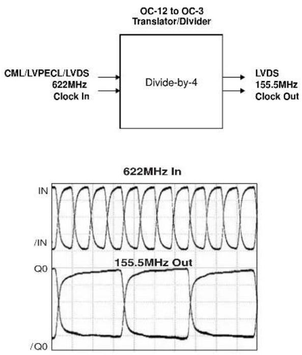
OC-12 to OC-3 Translator/Divider CML/LVPECL/LVDS 622MHz Clock In Divide-by-4 LVDS 155.5MHz Clock Out 622MHz In IN /IN Q0 /Q0 155.5MHz OutPACKAGE/ORDERING INFORMATION

text_image
S0 S1 VCC GND 16 15 14 13 Q0 1 12 IN /Q0 2 11 VT Q1 3 10 VREF-AC /Q1 4 9 /IN 5 6 7 8 S2 NC VCC /RESET16-Pin MLF ^® (MLF-16)
Ordering Information ^(1)
| Part Number Type P | Package Range Mark | Operating Package Finishing Finish | Package Lead | |
| SY89876LMI MLF-16 | Industrial 8 | 76L Sn-Pb | ||
| SY89876LMITR(2) | MLF-16 | Industrial 876L | Sn-Pb | |
| SY89876LMG(3) | MLF-16 | Industrial 876L | with Pb-FreePb-Free bar-line indicator NiPdAu | |
| SY89876LMGTR(2, 3) | MLF-16 | Industrial 876L | with Pb-FreePb-Free bar-line indicator NiPdAu |
Notes:
- Contact factory for die availability. Dice are guaranteed at T_A = 25^ , DC Electricals only.
- Tape and Reel.
- Pb-Free package is recommended for new designs.
PIN DESCRIPTION
| Pin Number | Pin Name | Pin | Function |
| 12, 9 | IN, /IN | Differential Input: Internal 50 termination resistors to V_T input. Flexible input accepts any differential input. See “Input Interface Applications” section. | |
| 1, 2, 3, 4 | Q0, /Q0Q1, /Q1 | Differential Buffered LVDS Outputs: Divided by 1, 2, 4, 8 or 16. See “Truth Table.” Unused output pairs must be terminated with 100 across the different pair. | |
| 16, 15, 5 | S0, S1, S2 | Select Pins: See “Truth Table.” LVTTL/CMOS logic levels. Internal 25k pull-up resistor. Logic HIGH if left unconnected (divided by 16 mode.) Input threshold is V_CC/2 . | |
| 6 | NC | No Connect. | |
| 8 | /RESET,/DISABLE | LVTTL/CMOS Logic Levels: Internal 25k pull-up resistor. Logic HIGH if left unconnected. Apply LOW to reset the divider (divided by 2, 4, 8 or 16 mode). Also acts as a disable/enable function. The reset and disable function occurs on the next high-to-low clock input transition. Input threshold is V_CC/2 . | |
| 10 | VREF-AC | Reference Voltage: Equal to V_CC-1.4V (approx.). Used for AC-coupled applications only.Decouple the VREF-AC pin with a 0.01 F capacitor. See “Input Interface Applications” section. | |
| 11 | VT | Termination Center-Tap: For CML or LVDS inputs, leave this pin floating. Otherwise, See Figures 4a to 4f “Input Interface Applications” section. | |
| 7, 14 | VCC | Positive Power Supply: Bypass with 0.1 F //0.01 F low ESR capacitor. | |
| 13 | GND, Exposed pad | Ground. Exposed pad must be connected to the same potential as the GND pin. |
TRUTH TABLE
| / RESET^(1) | S2 | S1 | S0 | Outputs |
| 1 | 0 | X | X | Reference Clock (pass through) |
| 1 | 1 | 0 | 0 | Reference Clock ÷2 |
| 1 | 1 | 0 | 1 | Reference Clock ÷4 |
| 1 | 1 | 1 | 0 | Reference Clock ÷8 |
| 1 | 1 | 1 | 1 | Reference Clock ÷16 |
| 0^(1) | X | X | X | Q = LOW, /Q = HIGHClock Disable |
Note:
- Reset/Disable function is asserted on the next clock input (IN, /IN) high-to-low transition.
Absolute Maximum Ratings ^(Note 1)
Supply Voltage ( V_CC )....-0.5V to +4.0V
Input Voltage ( V_IN ) ......-0.5V to V_CC +0.3
ECL Output Current ( I_OUT )
Continuous 50mA
Surge....100mA
Input Current IN, /IN ( I_IN ) ±50mA
V_T Current ( I_VT ) ±100mA
V_REF-AC Sink/Source Current ( I_VREF-AC ), Note 3 ..... ±2mA
Lead Temperature (soldering 20 sec.) 260°C
Storage Temperature ( T_S ) -65^ to +150^
Operating Ratings ^(Note 2)
Supply Voltage (V _CC )...... +3.3V ±10%
Ambient Temperature ( T_A ) -40^ to +85^
Package Thermal Resistance
MLF ^® ( _JA )
Still-Air.... 60°C/W
500lfpm 54°C/W
MLF ^® ( _JB ), Note 4
Junction-to-Board.... 32°C/W
Note 1. Permanent device damage may occur if absolute maximum ratings are exceeded. This is a stress rating only and functional operation is not implied at conditions other than those detailed in the operational sections of this data sheet. Exposure to absolute maximum rating conditions for extended periods may affect device reliability.
Note 2. The data sheet limits are not guaranteed if the device is operated beyond the operating ratings.
Note 3. Due to the limited drive capability use for input of the same package only.
Note 4. Junction-to-board resistance assumes exposed pad is soldered (or equivalent) to the device's most negative potential on the PCB.
DC ELECTRICAL CHARACTERISTICS (Notes 1, 2)
T_A = -40^ to +85^ ; Unless otherwise stated.
| Symbol Parameter Condition Min Typ Max Units | ||||||
| V_CC | Power Supply | 3.0 | 3.6 | V | ||
| I_CC | Power Supply Current | No load, max. V_CC | 75 | 100 | mA | |
| R_IN | Differential Input Resistance (IN-to-/IN) | 90 | 100 | 110 | ||
| V_IH | Input High Voltage (IN, /IN) | Note 2 | 0.1 | - | V_CC+0.3 V | |
| V_IL | Input Low Voltage (IN, /IN) | Note 2 | -0.3 | - | V_IH-0.1 | V |
| V_IN | Input Voltage Swing | Note 3 | 0.1 | - | V_CC | V |
| V_DIFF\_IN | Differential Input Voltage Swing | Note 4 | 0.2 | - | V | |
| |I_IN| | Input Current (IN, /IN) | Note 2 | - | - | 45 | mA |
| V_REF-AC | Reference Voltage | Note 5 | V_CC-1.525 | V_CC-1.425 | V_CC-1.325 | V |
Note 1. The circuit is designed to meet the DC specifications shown in the above table after thermal equilibrium has been established.
Note 2. Specification for packaged product only.
Note 3. Due to the internal termination (see Figure 2a) the input current depends on the applied voltages at IN, /IN and V_T inputs. Do not apply a combination of voltages that causes the input current to exceed the maximum limit!
Note 4. See "Timing Diagram" for V_IN definition. V_IN (Max) is specified when V_T is floating.
Note 5. See "Typical Operating Characteristics" section for V DIFF definition.
Note 6. Operating using V_IN is limited to AC-coupled PECL or CML applications only. Connect directly to V_T pin.
LVDS DC ELECTRICAL CHARACTERISTICS(Notes 1, 2)
V_CC = 3.3V ± 10% ; R_L = 100y across the outputs; T_A = -40^ to +85^ ; Unless otherwise stated.
| Symbol Parameter Condition Min Typ | Max Units | |||||
| V_OUT | Output Voltage Swing | Note 3, 4 | 250 | 350 | 400 | mV |
| V_OH | Output High Voltage | Note 3 | 1.475 | V | ||
| V_OL | Output Low Voltage | Note 3 | 0.925 | V | ||
| V_OCM | Output Common Mode Voltage | Note 4 | 1.125 | 1.375 | V | |
| V_OCM | Change in Common Mode Voltage | -50 | 50 | mV | ||
Note 1. The circuit is designed to meet the DC specifications shown in the above table after thermal equilibrium has been established.
Note 2. Specification for packaged product only.
Note 3. Measured as per Figure 3a, 100y across Q and /Q outputs.
Note 4. Measured as per Figure 3b.
LVTTL/CMOS DC ELECTRICAL CHARACTERISTICS(Notes 1, 2)
V_CC = 3.3V ± 10% ; T_A = -40^ to +85^ ; Unless otherwise stated.
| Symbol Parameter Condition Min Typ Max Units | ||||||
| V_IH | Input HIGH Voltage 2.0 V | |||||
| V_IL | Input LOW Voltage 0.8 V | |||||
| I_IH | Input HIGH Current -125 20 μA | |||||
| I_IL | Input LOW Current -300 μA | |||||
Note 1. The circuit is designed to meet the DC specifications shown in the above table after thermal equilibrium has been established.
Note 2. Specification for packaged product only.
AC ELECTRICAL CHARACTERISTICS(Notes 1)
V_CC = 3.3V ± 10% ; R_L = 100y across the outputs; T_A = -40^ to +85^ ; Unless otherwise stated.
| Symbol Parameter Condition Min Typ Max Units | ||||||
| f_MAX | Maximum Input Frequency V | OUT 200mV 2.0 2.5 GHz | ||||
| t_PD | Differential Propagation Delay Input S IN to Q | Swing < 400mV 590 690 870 ps | ||||
| Input Swing 400mV | 540 640 820 ps | |||||
| t_SKEW | Within-Device Skew (diff.) | Note 2 | 5 | 15 | ps | |
| Part-to-Part Skew (diff.) | Note 2 | 280 | ps | |||
| t_RR | Reset Recovery Time | Note 3 | 600 | ps | ||
| T_jitter | Cycle-to-Cycle Jitter | Note 4 | 1 | ps_RMS | ||
| Total Jitter | Note 5 | 10 | ps_PP | |||
| t_r,t_f | Rise/Fall Time (20% to 80%) | 60 110 190 ps | ||||
Note 1. Measured with 400mV input signal, 50% duty cycle, all outputs loaded with 100y across each output pair, unless otherwise stated.
Note 2. Skew is measured between outputs under identical transitions.
Note 3. See "Timing Diagram."
Note 4. Cycle-to-cycle jitter definition: the variation in period between adjacent cycles over a random sample of adjacent cycle pairs. T_jitter_cc = T_n - T_n+1 , where T is the time between rising edges of the output signal.
Note 5. Total jitter definition: with an ideal clock input of frequency - f_MAX : no more than one output edge in 10^12 output edges will deviate by more than the specified peak-to-peak jitter value.
TIMING DIAGRAM
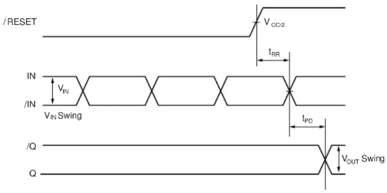
text_image
/RESET VCC/2 tRR IN VIN IN VIN Swing tPD /Q Q VOUT SwingTYPICAL OPERATING CHARACTERISTICS
V_CC = 3.3V, R_L = 100 across the output; T_A = 25^ , unless otherwise stated.
Q Output Amplitude vs. Frequency

line
| FREQUENCY (MHz) | Q AMPLITUDE (mV) | | --------------- | ---------------- | | 0.5 | 330 | | 1.0 | 330 | | 1.5 | 330 | | 2.0 | 330 | | 2.5 | 330 | | 3.0 | 320 | | 3.5 | 280 | | 4.0 | 220 |IN to Q Propagation Delay vs. Input Swing

line
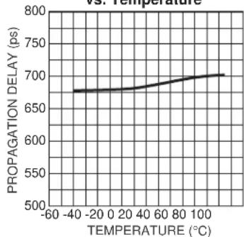
| INPUT SWING (mV) | PROPAGATION DELAY (ps) | | ---------------- | ---------------------- | | 100 | 690 | | 300 | 685 | | 500 | 675 | | 700 | 660 | | 900 | 645 | | 1100 | 630 | | 1300 | 625 |IN to Q Propagation Delay vs. Temperature
line
| TEMPERATURE (°C) | PROPAGATION DELAY (ps) | | ---------------- | ---------------------- | | -40 | 680 | | 0 | 685 | | 20 | 690 | | 40 | 695 | | 60 | 700 | | 80 | 705 | | 100 | 710 |Output Duty Cycle vs. Frequency

line
| FREQUENCY (MHz) | OUTPUT DUTY CYCLE (%) | | --------------- | --------------------- | | 0500 | 50.0 | | 1000 | 50.0 | | 1500 | 50.0 | | 2000 | 50.0 | | 2500 | 50.0 | | 3000 | 48.0 | | 3500 | 47.0 |TYPICAL OPERATING CHARACTERISTICS (Continued)
V_CC = 3.3V, V_IN = 100mV, R_L = 100 across the output; T_A = 25^ , unless otherwise stated.
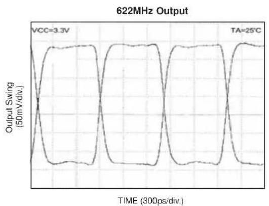
line
| Time (300ps/div.) | Output Swing (50mV/div.) | | ----------------- | ------------------------ | | VCC | 3.3 | | TA | 25 |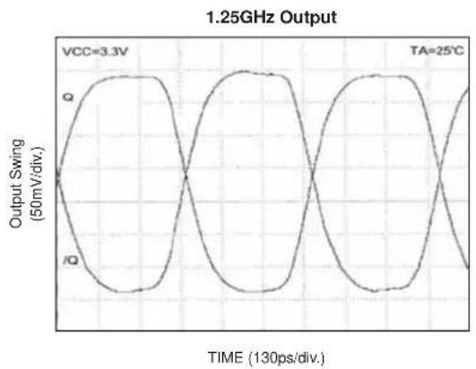
line
| Time (ps) | Output Swing (50mV/div) | | --------- | ------------------------ | | 0 | 0 | | 130 | 3.3 | | 250 | 0 |
line
| TIME (80ps/div.) | Output Swing (50mV/div.) | | ---------------- | ------------------------ | | 0 | 0 | | 1 | 1 | | 2 | 0 | | 3 | -1 | | 4 | 0 | | 5 | 1 | | 6 | 0 | | 7 | -1 | | 8 | 0 | | 9 | 1 | | 10 | 0 | | 11 | -1 | | 12 | 0 | | 13 | 1 | | 14 | 0 | | 15 | -1 | | 16 | 0 | | 17 | 1 | | 18 | 0 | | 19 | -1 | | 20 | 0 | | 21 | 1 | | 22 | 0 | | 23 | -1 | | 24 | 0 | | 25 | 1 | | 26 | 0 | | 27 | -1 | | 28 | 0 | | 29 | 1 | | 30 | 0 | | 31 | -1 | | 32 | 0 | | 33 | 1 | | 34 | 0 | | 35 | -1 | | 36 | 0 | | 37 | 1 | | 38 | 0 | | 39 | -1 | | 40 | 0 | | 41 | 1 | | 42 | 0 | | 43 | -1 | | 44 | 0 | | 45 | 1 | | 46 | 0 | | 47 | -1 | | 48 | 0 | | 49 | 1 | | 50 | 0 | | 51 | -1 | | 52 | 0 | | 53 | 1 | | 54 | 0 | | 55 | -1 | | 56 | 0 | | 57 | 1 | | 58 | 0 | | 59 | -1 | | 60 | 0 | | 61 | 1 | | 62 | 0 | | 63 | -1 | | 64 | 0 | | 65 | 1 | | 66 | 0 | | 67 | -1 | | 68 | 0 | | 69 | 1 | | 70 | 0 | | 71 | -1 | | 72 | 0 | | 73 | 1 | | 74 | 0 | | 75 | -1 | | 76 | 0 | | 77 | 1 | | 78 | 0 | | 79 | -1 | | 80 | 0 |DEFINITION OF SINGLE-ENDED AND DIFFERENTIAL SWINGS

text_image
V_{IN}, V_{OUT} \n 350mV (typical)Figure 1a. Single-Ended Swing

text_image
VDIFF IN, VDIFF OUT 700mV (typical)Figure 1b. Differential Swing
INPUT INTERFACE APPLICATIONS

text_image
VCC 1.86k 1.86k IN 50Ω VT 50Ω /IN GNDFigure 2a. Simplified Differential Input Buffer
text_image
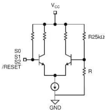
Vcc S0 S1 S2 /RESET R25kΩ R GNDFigure 2b. Simplified TTL/CMOS Input Buffer
LVDS OUTPUTS
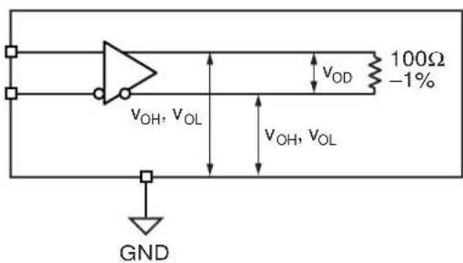
LVDS (Low Voltage Differential Swing) specifies a small swing of 350mV typical, on a nominal 1.25V common mode above ground. The common mode voltage has tight limits to permit large variations in ground between an LVDS driver and receiver.
text_image
vOH, vOL VOD 100Ω -1% VOH, vOL GNDFigure 3a. LVDS Differential Measurement

text_image
50Ω, ±1% 50Ω, ±1% VOCM ΔVOCM GNDFigure 3b. LVDS Common Mode Measurement
INPUT INTERFACE APPLICATIONS

text_image
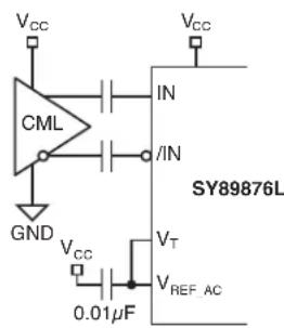
VCC CML GND IN /IN SY89876L NC □ VT NC □ VREF_ACFigure 4a. DC-Coupled CML Input Interface
text_image
VCC CML GND IN /IN SY89876L VCC VT VREF_AC 0.01μFFigure 4b. AC-Coupled CML Input Interface
text_image
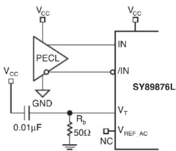
VCC PECL GND 0.01μF IN /IN SY89876L VT NC VREF_AC Rb 50ΩFigure 4c. DC-Coupled PECL Input Interface
text_image
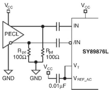
VCC PECL Rpd 100Ω GND GND Ppd 100Ω VCC IN /IN SY89876L VT VREF_AC 0.01μFFigure 4d. AC-Coupled PECL Input Interface

text_image
Vcc LVDS GND IN IN SY89876L NC □ VT NC □ VREF_ACFigure 4e. LVDS Input Interface
text_image
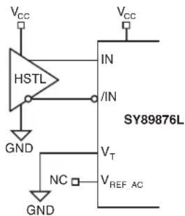
VCC HSTL GND IN /IN SY89876L VT NC VREF_AC VCCFigure 4f. HSTL Input Interface
RELATED PRODUCT AND SUPPORT DOCUMENTATION
| Part Number F | Function Data Sheet Link | |
| SY89873L | 3.3V, 2.5GHz Any Diff. IN-to-LVDS Programmable Clock Divider/Fanout Buffer w/ Internal Termination | http://www.micrel.com/product-info/products/sy89873l.shtml |
| MLF® Application Note http://www.amkor.com | products/notes_papers/mlf_appnote.pdf | |
| HBW Solutions | New Products and Applications | http://www.micrel.com/product-info/products/solutions.shtml |
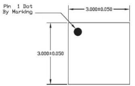
16-PIN MicroLeadFrame ^® (MLF-16)
text_image
Pin 1 Dot By Marking 3.000±0.050 3.000±0.050TOP VIEW

text_image
PIN #1 IDENTIFICATION CHAMFER 0.300 X 45° 1.550±0.050 Exp. DAP 0.400±0.050 1.550±0.050 Exp. DAP 0.500 Bsc 0.230±0.050 0.400±0.050 1.500 Ref.BOTTOM VIEW

text_image
0.850±0.050 0.000-0.050 0.203±0.025SIDE VIEW
NOTE:
1. ALL DIMENSIONS ARE IN MILLIMETERS.
2. MAX. PACKAGE WARPAGE IS 0.05 mm.
3. MAXIMUM ALLOWABE BURRS IS 0.076 mm IN ALL DIRECTIONS.
4. PIN #1 ID ON TOP WILL BE LASER/INK MARKED.
text_image
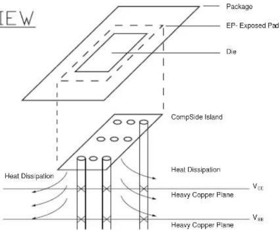
Package EP- Exposed Pad Die CompSide Island Heat Dissipation Heat Dissipation Heavy Copper Plane VCE VEE Heavy Copper PlanePCB Thermal Consideration for 16-Pin MLF® Package (Always solder, or equivalent, the exposed pad to the PCB)
Package Notes:
Note 1. Package meets Level 2 moisture sensitivity classification, and are shipped in dry-pack form.
Note 2. Exposed pads must be soldered to a ground for proper thermal management.
MICREL, INC. 2180 FORTUNE DRIVE SAN JOSE, CA 95131 USA
TEL + 1 (408) 944-0800 FAX + 1 (408) 474-1000 WEB http://www.micrel.com
The information furnished by Micrel in this datasheet is believed to be accurate and reliable. However, no responsibility is assumed by Micrel for its use.
Micrel reserves the right to change circuitry and specifications at any time without notification to the customer.
Micrel Products are not designed or authorized for use as components in life support appliances, devices or systems where malfunction of a product can reasonably be expected to result in personal injury. Life support devices or systems are devices or systems that (a) are intended for surgical implant into the body or (b) support or sustain life, and whose failure to perform can be reasonably expected to result in a significant injury to the user. A Purchaser's use or sale of Micrel Products for use in life support appliances, devices or systems is at Purchaser's own risk and Purchaser agrees to fully indemnify Micrel for any damages resulting from such use or sale.
© 2005 Micrel, Incorporated.