HV2621 - Carte d'évaluation Microchip - Free user manual and instructions
Find the device manual for free HV2621 Microchip in PDF.

User questions about HV2621 Microchip
0 question about this device. Answer the ones you know or ask your own.
Ask a new question about this device
Download the instructions for your Carte d'évaluation in PDF format for free! Find your manual HV2621 - Microchip and take your electronic device back in hand. On this page are published all the documents necessary for the use of your device. HV2621 by Microchip.
USER MANUAL HV2621 Microchip
Note the following details of the code protection feature on Microchip devices:
• Microchip products meet the specification contained in their particular Microchip Data Sheet.
- Microchip believes that its family of products is one of the most secure families of its kind on the market today, when used in the intended manner and under normal conditions.
- There are dishonest and possibly illegal methods used to breach the code protection feature. All of these methods, to our knowledge, require using the Microchip products in a manner outside the operating specifications contained in Microchip's Data Sheets. Most likely, the person doing so is engaged in theft of intellectual property.
• Microchip is willing to work with the customer who is concerned about the integrity of their code.
- Neither Microchip nor any other semiconductor manufacturer can guarantee the security of their code. Code protection does not mean that we are guaranteeing the product as "unbreakable."
Code protection is constantly evolving. We at Microchip are committed to continuously improving the code protection features of our products. Attempts to break Microchip's code protection feature may be a violation of the Digital Millennium Copyright Act. If such acts allow unauthorized access to your software or other copyrighted work, you may have a right to sue for relief under that Act.
Information contained in this publication regarding device applications and the like is provided only for your convenience and may be superseded by updates. It is your responsibility to ensure that your application meets with your specifications. MICROCHIP MAKES NO REPRESENTATIONS OR WARRANTIES OF ANY KIND WHETHER EXPRESS OR IMPLIED, WRITTEN OR ORAL, STATUTORY OR OTHERWISE, RELATED TO THE INFORMATION, INCLUDING BUT NOT LIMITED TO ITS CONDITION, QUALITY, PERFORMANCE, MERCHANTABILITY OR FITNESS FOR PURPOSE. Microchip disclaims all liability arising from this information and its use. Use of Microchip devices in life support and/or safety applications is entirely at the buyer's risk, and the buyer agrees to defend, indemnify and hold harmless Microchip from any and all damages, claims, suits, or expenses resulting from such use. No licenses are conveyed, implicitly or otherwise, under any Microchip intellectual property rights unless otherwise stated.
Trademarks
The Microchip name and logo, the Microchip logo, Adaptec, AnyRate, AVR, AVR logo, AVR Freaks, BesTime, BitCloud, chipKIT, chipKIT logo, CryptoMemory, CryptoRF, dsPIC, FlashFlex, flexPWR, HELDO, IGLOO, JukeBlox, KeeLoq, Kleer, LANCheck, LinkMD, maXStylus, maXTouch, MediaLB, megaAVR, Microsemi, Microsemi logo, MOST, MOST logo, MPLAB, OptoLyzer, PackeTime, PIC, picoPower, PICSTART, PIC32 logo, PolarFire, Prochip Designer, QTouch, SAM-BA, SenGenuity, SpyNIC, SST, SST Logo, SuperFlash, Symmetricom, SyncServer, Tachyon, TempTrackr, TimeSource, tinyAVR, UNI/O, Vectron, and XMEGA are registered trademarks of Microchip Technology Incorporated in the U.S.A. and other countries.
APT, ClockWorks, The Embedded Control Solutions Company, EtherSynch, FlashTec, Hyper Speed Control, HyperLight Load, IntelliMOS, Libero, motorBench, mTouch, Powermite 3, Precision Edge, ProASIC, ProASIC Plus, ProASIC Plus logo, Quiet-Wire, SmartFusion, SyncWorld, Temux, TimeCesium, TimeHub, TimePictra, TimeProvider, Vite, WinPath, and ZL are registered trademarks of Microchip Technology Incorporated in the U.S.A.
Adjacent Key Suppression, AKS, Analog-for-the-Digital Age, Any Capacitor, AnyIn, AnyOut, BlueSky, BodyCom, CodeGuard, CryptoAuthentication, CryptoAutomotive, CryptoCompanion, CryptoController, dsPICDEM, dsPICDEM.net, Dynamic Average Matching, DAM, ECAN, EtherGREEN, In-Circuit Serial Programming, ICSP, INICnet, Inter-Chip Connectivity, JitterBlocker, KleerNet, KleerNet logo, memBrain, Mindi, MiWi, MPASM, MPF, MPLAB Certified logo, MPLIB, MPLINK, MultiTRAK, NetDetach, Omniscient Code Generation, PICDEM, PICDEM.net, PICkit, PICtail, PowerSmart, PureSilicon, QMatrix, REAL ICE, Ripple Blocker, SAM-ICE, Serial Quad I/O, SMART-I.S., SQI, SuperSwitcher, SuperSwitcher II, Total Endurance, TSHARC, USBCheck, VariSense, ViewSpan, WiperLock, Wireless DNA, and ZENA are trademarks of Microchip Technology Incorporated in the U.S.A. and other countries.
SQTP is a service mark of Microchip Technology Incorporated in the U.S.A. The Adaptec logo, Frequency on Demand, Silicon Storage Technology, and Symmcom are registered trademarks of Microchip Technology Inc. in other countries. GestIC is a registered trademark of Microchip Technology Germany II GmbH & Co. KG, a subsidiary of Microchip Technology Inc., in other countries. All other trademarks mentioned herein are property of their respective companies.
© 2019, Microchip Technology Incorporated, All Rights Reserved.
ISBN: 978-1-5224-4990-4
For information regarding Microchip's Quality Management Systems, please visit www.microchip.com/quality.
Table of Contents
Preface 5
Introduction....5
Document Layout 5
Conventions Used in this Guide 6
Recommended Reading....7
The Microchip Website....7
Product Change Notification Service....7
Customer Support 7
Document Revision History .... 7
Chapter 1. Product Overview
1.1 Introduction 9
1.2 HV2722 Device Short Overview 9
1.3 HV2722 Analog Switch Evaluation Board Features 9
1.4 What is the HV2722 Analog Switch Evaluation Board? 10
1.5 HV2722 Analog Switch Evaluation Board Technical Parameters .... 10
1.6 HV2722 Analog Switch Evaluation Board Kit Contents 11
Chapter 2. Installation and Operation
2.1 Getting Started 13
2.2 HV MUX GUI Installation 13
2.3 HV2722 Analog Switch Evaluation Board Setup Procedure 17
2.4 Interface Connections 19
2.5 HV MUX Controller Board Setup Procedure 20
2.6 Testing the HV2722 Analog Switch Evaluation Board 21
2.7 Generation of Pulser Output at SW2A of HV2722 21
Chapter 3. GUI Description
3.1 HV2722 Analog Switch Evaluation Board GUI Description 23
Chapter 4. PCB Design and Layout Notes
4.1 PCB Layout Techniques for HV2722 25
Appendix A. Schematics and Layouts
A.1 Introduction 27
Appendix B. Bill of Materials (BOM)
B.1 HV2722 Analog Switch Evaluation Board (ADM00946) 51
B.2 HV MUX Controller Board (ADM00825) 53
Appendix C. Demo Board Waveforms
C.1 Board Typical Waveforms 57
Worldwide Sales and Service 58
NOTES:
Preface
NOTICE TO CUSTOMERS
All documentation becomes dated, and this manual is no exception. Microchip tools and documentation are constantly evolving to meet customer needs, so some actual dialogs and/or tool descriptions may differ from those in this document. Please refer to our website (www.microchip.com) to obtain the latest documentation available.
Documents are identified with a "DS" number. This number is located on the bottom of each page, in front of the page number. The numbering convention for the DS number is "DSXXXXXXXXA", where "XXXXXXXXX" is the document number and "A" is the revision level of the document.
For the most up-to-date information on development tools, see the MPLAB ^® IDE online help. Select the Help menu, and then Topics, to open a list of available online help files.
INTRODUCTION
This chapter contains general information that will be useful to know before using the HV2722 Analog Switch Evaluation Board. Items discussed in this chapter include:
- Document Layout
- Conventions Used in this Guide
• Recommended Reading
• The Microchip Website - Customer Support
• Document Revision History
DOCUMENT LAYOUT
This document describes how to use the HV2722 Analog Switch Evaluation Board as a development tool to emulate and debug firmware on a target board. The manual layout is as follows:
- Chapter 1. “Product Overview” – Important information about the HV2722 Analog Switch Evaluation Board.
- Chapter 2. “Installation and Operation” – This chapter includes a detailed description of each function of the demonstration board and instructions for how to begin using the HV2722 Analog Switch Evaluation Board.
- Chapter 3. "GUI Description" – This chapter describes the features of the GUI PC software.
- Chapter 4. "PCB Design and Layout Notes" – This chapter explains important points of the PCB design and layout of HV2722 Analog Switch Evaluation Board.
- Appendix A. “Schematics and Layouts” – Shows the schematic and PCB layout diagrams for the HV2722 Analog Switch Evaluation Board.
- Appendix B. “Bill of Materials (BOM)” – Lists the parts used to build the HV2722 Analog Switch Evaluation Board.
- Appendix C. "Demo Board Waveforms" – Describes the various demo waveforms for the HV2722 Analog Switch Evaluation Board.
CONVENTIONS USED IN THIS GUIDE
This manual uses the following documentation conventions:
DOCUMENTATION CONVENTIONS
| Description Represents Examples | ||
| Arial font: | ||
| Italic characters Referenced books | mPLAB | ^ IDE User's Guide |
| Emphasized text ...is the only compiler... | ||
| Initial caps A window the Output | ut window | |
| A dialog the Settings dialog | ||
| A menu selection select Enable Programmer | ||
| Quotes A field name in a window or dialog | "Save project before build" | |
| Underlined, italic text with right angle bracket | A menu path File>Save | ____ |
| Bold characters A dialog button | Click OK | |
| A tab | Click the Power tab | |
| N'Rnnnn | A number in verilog format, where N is the total number of digits, R is the radix and n is a digit. | 4'b0010, 2'hF1 |
| Text in angle brackets < > | A key on the keyboard | Press,, |
| Courier New font: | ||
| Plain Courier New | Sample source code | #define START |
| Filenames | autoexec.bat | |
| File paths | c:\mcc18\h | |
| Keywords | _asm, _endasm, static | |
| Command-line options | -Opa+, -Opa- | |
| Bit values | 0, 1 | |
| Constants | 0xFF, 'A' | |
| Italic Courier New | A variable argument | file.o, where file can be any valid filename |
| Square brackets [] | Optional arguments | mccl8 [options] file [options] |
| Curly brackets and pipe character: { | } | Choice of mutually exclusive arguments; an OR selection | errorlevel {0|1} |
| Ellipses... Replaces repeated text | var_name [, | var_name...] |
| Represents code supplied by user | void main (void){ ...} | |
RECOMMENDED READING
This user's guide describes how to use the HV2722 Analog Switch Evaluation Board. Another useful document is listed below. The following Microchip document is available and recommended as a supplemental reference resource:
HV2621/HV2721/HV2722 Data Sheet – “300V, Low-Charge Injection, 16-Channel, High-Voltage Analog Switch” (DS20006082A)
THE MICROCHIP WEBSITE
Microchip provides online support via our website at www.microchip.com. This website is used as a means to make files and information easily available to customers. Accessible by using your favorite Internet browser, the website contains the following information:
- Product Support – Data sheets and errata, application notes and sample programs, design resources, user's guides and hardware support documents, latest software releases and archived software
- General Technical Support – Frequently Asked Questions (FAQs), technical support requests, online discussion groups, Microchip consultant program member listing
- Business of Microchip – Product selector and ordering guides, latest Microchip press releases, listing of seminars and events, listings of Microchip sales offices, distributors and factory representatives
PRODUCT CHANGE NOTIFICATION SERVICE
Microchip's customer notification service helps keep customers current on Microchip products. Subscribers will receive email notifications whenever there are changes, updates, revisions or errata related to a specified product family or development tool of interest.
To register, access the Microchip website at www.microchip.com, click on Product Change Notification and follow the registration instructions.
CUSTOMER SUPPORT
Users of Microchip products can receive assistance through several channels:
• Distributor or Representative
- Local Sales Office
• Field Application Engineer (FAE)
- Technical Support
Customers should contact their distributor, representative or field application engineer (FAE) for support. Local sales offices are also available to help customers. A listing of sales offices and locations is included in the back of this document.
Technical support is available through the website at: http://www.microchip.com/support.
DOCUMENT REVISION HISTORY
Revision A (September 2019)
- Initial release of this document
NOTES:
Chapter 1. Product Overview
1.1 INTRODUCTION
The HV2722 Analog Switch Evaluation Board (ADM00946) works with the HV MUX Controller Board (ADM00825) to provide No High-Voltage Bias, 32-Channel, High-Voltage Analog Switches with L-Switch Architecture demonstration, including basic on/off switch operation, and 2:1 MUX operation with two built-in MD1822, TP2640 and TN2640 pulser circuits.
1.2 HV2722 DEVICE SHORT OVERVIEW
The HV2722 device is a 300V, low-charge injection, 16-channel high-voltage analog switch. It is designed to be used in applications requiring high-voltage switching, controlled by low-voltage command signals, such as medical ultrasound imaging, driving piezoelectric transducers and in printers. Using the 300V high-voltage CMOS technology, the typical 18Ω on-resistance analog switch can pass the analog pulse signal up to ±3A and ±135V, under high-voltage supplies of ±150V. It requires 3.3V or 5V for the logic operation.
1.3 HV2722 ANALOG SWITCH EVALUATION BOARD FEATURES
- HV2722 No High-Voltage Bias, 32-Channel, High-Voltage Analog Switches with L-Switch Architecture
- Designed to work with Microchip HV MUX Controller Board
- Two 2:1 MUX with Built-In MD1822, TP2640 and TN2640 Pulsers
- 5 MHz, 3-Level Voltage Pulse Waveform Outputs
- On-Board 330 pF//2.5 kΩ Dummy Load per SW2A, SW3A, SW12A, SW13A
- Switch On/Off Control through the PC GUI and the HV MUX Controller Board
- Pulser On/Off and Time Domain Control through the PC GUI and the HV MUX Controller Board
1.4 WHAT IS THE HV2722 ANALOG SWITCH EVALUATION BOARD?
The HV2722 Analog Switch Evaluation Board can control the HV2722 device's operation and built-in pulsers that are connected to the two 2:1 MUX switches for demonstration. Four switch outputs, on the one side of two 2:1 MUX, have SMA connectors to which the user can connect four transducer elements. The other side of the 2:1 MUX is connected to two built-in MD1822, TP2640 and TN2640 pulsers. The HV2722 Analog Switch Evaluation Board can drive four transducer elements with 5 MHz, ±135V pulse signals.
The HV2722 Analog Switch Evaluation Board features one HV2722K6-G 9x9x1 mm 64-Lead QFN packaged integrated circuit, two MD1822K6-G 3x3x1 mm 16-Lead QFN packaged integrated circuits, four TP2640LG-G 4.9x3.9x1.75 mm 8-Lead SOIC packaged PMOS and four TN2640LG-G 4.9x3.9x1.75 mm 8-Lead SOIC packaged NMOS.
The HV2722 Analog Switch Evaluation Board uses two high-speed 20-signal pair carrying capable right-angle backplane connectors, which are designed to work with the Microchip HV MUX Controller Board (ADM00825) as a control signal source.
The HV MUX Controller Board has an FPGA that generates pulser waveform and logic control signals, and a USB bridge IC that connects the control board to a PC. By using a Microsoft® Windows® operated PC and the GUI software, the user can control the HV2722 device and two built-in pulsers.
Four switch terminals, consisting of two 2:1 MUX configurations on the PCB, have SMA connectors to which the user can connect loads. The jumpers close to the SMA connectors are for optionally connecting the on-board dummy R-C load (330 pF//2.5 kΩ) to the pulser output.
WARNING
Risk warning of electrical shock. This board uses multiple hazardous high voltages. Disconnect all high-voltage supplies before working on it. Electrical safety precautions must be taken when working on or using this board.
1.5 HV2722 ANALOG SWITCH EVALUATION BOARD TECHNICAL PARAMETERS
TABLE 1-1: HV2722 ANALOG SWITCH EVALUATION BOARD TECHNICAL PARAMETERS
| Parameter Value | |
| Pulser Frequency 5 MHz | |
| Number of Pulses in the Train 1 to 90 | |
| TOFF Time between Pulse Trains 5 to | 30 msec |
| Pulse Peak Voltage and Current 0 to ±135V and ±3A (typical) | |
| Interface of FPGA Control Signals and USB PC-GUI Software | J1 and J2 connect to the ADM00825 HV MUX Controller Board |
| Pulser R-C Test-Load and User's Transducer Interface | Built-in, 330 pF//2.5 kΩ per channel with jumper and 50Ω SMA |
| PCB Board Dimension | 115 mm x 110 mm |
FIGURE 1-1: HV2722 ANALOG SWITCH EVALUATION BOARD SIMPLIFIED BLOCK DIAGRAM

flowchart
graph TD
    A["PC + GUI"] --> B["FPGA"]
    B --> C["CH1 Pulser MD1822 + TP2640 + TN2640"]
    B --> D["CH2 Pulser MD1822 + TP2640 + TN2640"]
    C --> E["SW2B"]
    C --> F["SW3B"]
    C --> G["SW12B"]
    C --> H["SW13B"]
    D --> I["SW12A"]
    D --> J["SW13A"]
    E --> K["SW2A"]
    F --> L["SW3A"]
    G --> M["SW12A"]
    H --> N["SW13A"]
    K --> O["330 pF 2.5 kΩ"]
    L --> P["330 pF 2.5 kΩ"]
    M --> Q["330 pF 2.5 kΩ"]
    N --> R["330 pF 2.5 kΩ"]
1.6 HV2722 ANALOG SWITCH EVALUATION BOARD KIT CONTENTS
The HV2722 Analog Switch Evaluation Board includes:
• HV2722 Analog Switch Evaluation Board (ADM00946)
• Important Information Sheet
NOTES:
Chapter 2. Installation and Operation
2.1 GETTING STARTED
The HV2722 Analog Switch Evaluation Board is fully assembled and tested. The board requires six power supply voltage rails of +5V, +10V, ±135V and ±150V. The +5V is supplied from the HV MUX Controller Board and the others need to be supplied from external power supplies.
2.1.1 Additional Tools Required for Operation
- An oscilloscope with minimum 500 MHz bandwidth and two high-impedance probes. Make sure the grounds of the power supply sources are correctly connected to the same ground as the testing oscilloscope ground.
- A Microchip HV MUX Controller Board (ADM00825).
- A Microsoft ^® Windows ^® 7 PC with the HV MUX Controller Board GUI software installed and running:
- Connect J1 and J2 to the HV MUX Controller Board
- Connect the HV MUX Controller Board through the USB port to the Windows 7 PC
2.2 HV MUX GUI INSTALLATION
The HV MUX GUI software installer can be downloaded from the Microchip website at www.microchip.com. Search for the evaluation board on the website by the part number: ADM00946.
- Open the HVMUXGUI-v1.0.0-windows-installer.exe.
- Initiate the HV MUX GUI software installer by launching the Application Install dialog box.
- Click Next to start the installation.
FIGURE 2-1: HV MUX GUI - APPLICATION INSTALL DIALOG BOX

text_image
HVMUX GUI v1.1.0 Setup MICROCHIP Application Install Welcome to the Setup Wizard for the HVMUX GUI. < Back Next > Cancel- Read the License Agreement and accept it by checking the box corresponding to "I accept the agreement". Click Next to proceed with the installation.
FIGURE 2-2: HV MUX GUI – LICENSE AGREEMENT DIALOG BOX
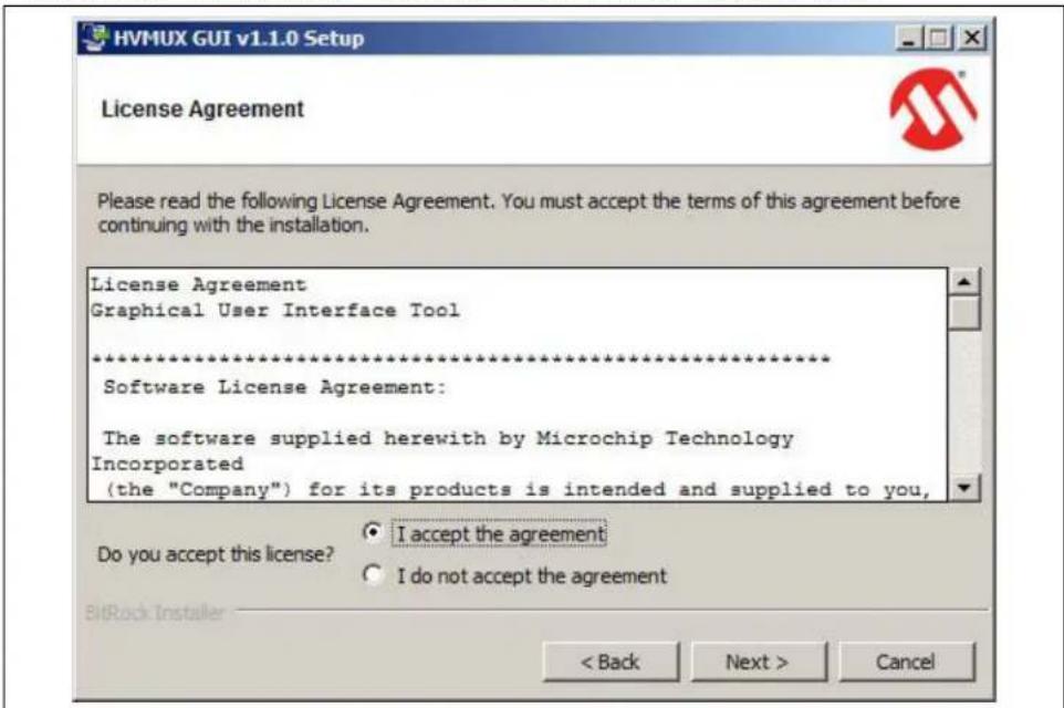
text_image
HVMUX GUI v1.1.0 Setup License Agreement Please read the following License Agreement. You must accept the terms of this agreement before continuing with the installation. License Agreement Graphical User Interface Tool ***** Software License Agreement: The software supplied herewith by Microchip Technology Incorporated (the "Company") for its products is intended and supplied to you, Do you accept this license? ● I accept the agreement ○ I do not accept the agreement < Back Next > Cancel- On the Installation Directory dialog box, browse for the desired location or click Next to install in the default location.
FIGURE 2-3: HV MUX GUI – INSTALLATION DIRECTORY DIALOG BOX

text_image
HVMUX GUI v1.1.0 Setup Installation Directory Please specify the directory where the HVMUX GUI will be installed. Installation Directory C:\Program Files (x86)\Microchip\HVMUXGUI BitRock Installer < Back Next > Cancel- Once the installation path is chosen, the software is ready to install. Click Next.
FIGURE 2-4: HV MUX GUI – READY TO INSTALL DIALOG BOX
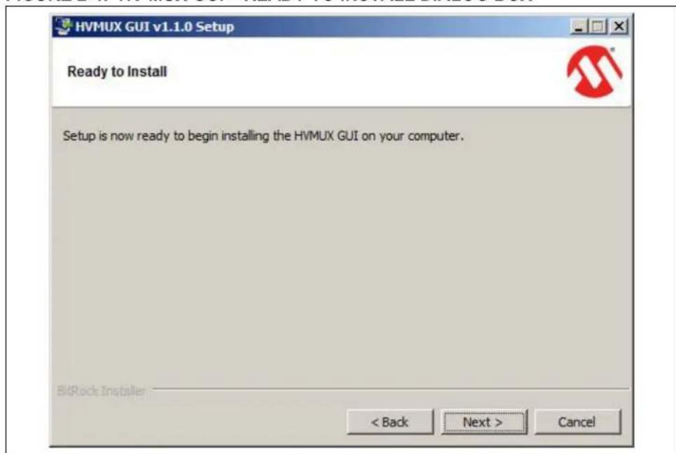
text_image
HVMUX GUI v1.1.0 Setup Ready to Install Setup is now ready to begin installing the HVMUX GUI on your computer. BitRock Installer < Back Next > Cancel- The Installation Status window appears, showing the installation progress.
- After the installation has completed, click Next.
FIGURE 2-5: HV MUX GUI – INSTALLATION STATUS DIALOG BOX

text_image
HVMUX GUI v1.1.0 Setup Installing Please wait while Setup installs the HVMUX GUI on your computer. Installing Creating uninstaller 25% BitRock Installer < Back Next > Cancel- Once the Installation Complete dialog box appears, click the Finish button to exit the installer.
FIGURE 2-6: HV MUX GUI - INSTALLATION COMPLETE DIALOG BOX

text_image
HVMUX GUI v1.1.0 Setup Install Complete The HVMUX GUI has been successfully installed on your computer. ✓ View Release Notes File < Back Finish Cancel2.3 HV2722 ANALOG SWITCH EVALUATION BOARD SETUP PROCEDURE
To operate the HV2722 Analog Switch Evaluation Board, the following steps must be completed:
- Attach it to the HV MUX Controller Board (ADM00825) with connectors J1 and J2.
- Connect all the jumpers on J12, J13, J28 and J29 for the on-board R-C load.
- Connect all the power supplies to the voltage supply input connectors J3 and J4, as indicated in Table 2-1, by observing the polarity.
WARNING
Please observe the polarity of each power supply rail, and set the voltage and current limit carefully.
- Connect a USB cable from the HV MUX Controller Board to the PC.
- Connect +12V/1A power to the HV MUX Controller Board.
- Turn on the V NN/VPP .
- Turn on the V GP and +P/-P.
- Run the HV MUX GUI software on the PC.
- Click the Initialize HV MUX Controller Board button in the GUI. This causes the message window at the bottom of the screen to display an “initialization complete” message.
- Clear the STBY check box and select the MODE check box. (Do not change these states. Not used for HV2722EVB.)
- Click the Set HV MUX button. All digital control signals are applied to HV2722.
- Set the number of pulses and T_OFF time of the pulser.
- Select CH1 or CH2 to set the Channel 1 pulser or the Channel 2 pulser, respectively.
- Click the Start button for the selected pulser to generate pulse trains.
- Click the Stop button for the selected pulser to stop generating pulse trains.
TABLE 2-1: POWER SUPPLY VOLTAGES AND CURRENT LIMIT SETTINGS
| Terminal Rail Name Voltage | Average Current Limit | ||
| J3-1 | +P | +60V to +135V | +20 mA |
| J3-2 | -P | -135V to 0V | -20 mA |
| J3-3 | GND | 0V | — |
| J3-4 | V_PP | +P +15V | +5 mA |
| J3-5 | V_NN | -P -15V | -5 mA |
| J4-1 | V_GP | +5 to +11.5V | +10 mA |
| J4-2 | GND | 0V | — |
FIGURE 2-7: HV2722 ANALOG SWITCH EVALUATION BOARD – FRONT VIEW
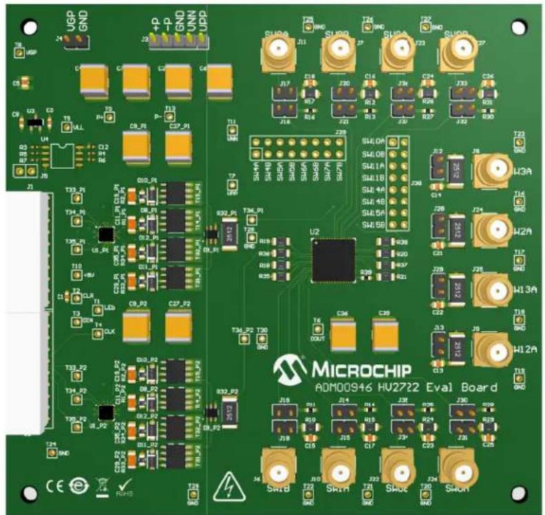
text_image
UGP GND + P GND UNN LDP T8 USB C C1 C2 C3 C4 T5 T6 T7 T8 T9 T10 T11 T12 T13 T14 T15 T16 T17 T18 T19 T20 T21 T22 T23 T24 T25 T26 T27 T28 T29 T30 T31 T32 T33 T34 T35 T36 T37 T38 T39 T40 T41 T42 T43 T44 T45 T46 T47 T48 T49 T50 T51 T52 T53 T54 T55 T56 T57 T58 T59 T60 T61 T62 T63 T64 T65 T66 T67 T68 T69 T70 T71 T72 T73 T74 T75 T76 T77 T78 T79 T80 T81 T82 T83 T84 T85 T86 T87 T88 T89 T90 T91 T92 T93 T94 T95 T96 T97 T98 T99 T100 T101 T102 T103 T104 T105 T106 T107 T108 T109 T110 T111 T112 U2 V22_P1 T34_01 U22_P2 T34_02 U22_P3 T34_04 U22_P5 T34_06 U22_P7 T34_08 U22_P9 T34_10 U22_P11 U22_P13 U22_P15 U22_P17 U22_P19 U22_P21 U22_P23 U22_P25 U22_P27 U22_P29 U22_P31 U22_P33 U22_P35 U22_P37 U22_P39 U22_P41 U22_P43 U22_P45 U22_P47 U22_P49 U22_P51 U22_P53 U22_P55 U22_P57 U22_P59 U22_P61 U22_P63 U22_P65 U22_P67 U22_P69 U22_P71 U22_P73 U22_P75 U22_P77 U22_P79 U22_P81 U22_P83 U22_P85 U22_P87 U22_P89 U22_P91 U22_P93 U22_P95 U22_P97 U22_P99 U3A HUA 0000000000000000000000000000000000000000000000000000000000000000000000000000000000000000000000000000 MicroCHIP ADM00946 HV2722 Eval Board2.3.1 Recommended Power-up and Power-Down Sequences
Table2-2 shows the recommended power-up and power-down sequences of the HV2722 Analog Switch Evaluation Board.
TABLE 2-2: HV2722 ANALOG SWITCH EVALUATION BOARD POWER-UP AND POWER-DOWN SEQUENCES
| Step | Power-up Description Step Power-Down | Description |
| 1 | V_NN and V_PP on 1 +P and -P off | |
| 2 | V_GP on | 2 V _GP off |
| 3 | +P and -P on | 3 V _NN and V_PP off |
WARNING
Powering the HV2722 Analog Switch Evaluation Board up/down in an arbitrary sequence may cause damage to the device.
2.4 INTERFACE CONNECTIONS
TABLE 2-3: J2 CONTROL INTERFACE SIGNALS (1)
| Pin # | Name Test | Point I/O Type | Signal Discretion | |
| J2-A2 | CK — LVC | MOS-2.5V Input | EEPROM Serial Clock | Input |
| J2-B2 | CSB — LVC | MOS-2.5V Input | EEPROM Chip Select | Input |
| J2-A3 | MISO — | LVCMOS-2.5V Output | EEPROM | Serial Data Output |
| J2-B3 | MOSI — LVC | MOS-2.5V Input | EEPROM Serial Data | Input |
| J2-A5 | CLR | T2 LVC | MOS-3.3V Input HV2722 | Latch Clear Logic Input |
| J2-B5 | CLK | T4 LVC | MOS-3.3V Input HV2722 | Clock Logic Input |
| J2-C5 | LE | T1 LVC | MOS-3.3V Input HV2722 | Latch Enable Logic Input |
| J2-A6 | DIN | T3 LVC | MOS-3.3V Input HV2722 | Data In Logic Input |
| J2-C6 | 1_A | T33_P2 | LVCMOS-3.3V Input | Ch1 Pulser Input for NMOS toV_{NN} |
| J2-D6 | 1_B | T34_P2 | LVCMOS-3.3V Input | Ch1 Pulser Input for PMOS toV_{PP} |
| J2-A7 | 1_DMP | T35_P2 | LVCMOS-3.3V Input | Ch1 Pulser Damp Input for PMOS/NMOS to GND |
| J2-B7 | 2_A | T33_P1 | LVCMOS-3.3V Input | Ch2 Pulser Input for NMOS toV_{NN} |
| J2-C7 | 2_B | T34_P1 | LVCMOS-3.3V Input | Ch2 Pulser Input for PMOS toV_{PP}$ |
| J2-D7 | 2_DMP | T35_P1 | LVCMOS-3.3V Input | Ch2 Pulser Damp Input for PMOS/NMOS to GND |
Note 1: All the pins that are not included in this table are No Connect.
2.5 HV MUX CONTROLLER BOARD SETUP PROCEDURE
The HV MUX Controller Board generates control signals for the HV2722 Analog Switch Evaluation Board and features a Spartan-6 XC6SLX9 FPGA.
- Before powering up the HV2722 Analog Switch Evaluation Board and the HV MUX Controller Board, make sure that the latest GUI software is installed on the PC.
- Start the GUI program. If the board is not connected, a "Not Connected" message is displayed in the Status bar, located at the bottom left of the screen.
- Connect the appropriate power supply and turn on the power switch to power up the HV MUX Controller Board. The FPGA_OK (LD1) and DC_IN (LD2) on the HV MUX Controller Board should light up green. A "Connected" message is displayed on the bottom left of the Status bar of the GUI.
The HV MUX Controller Board is now ready to control the HV2722 Analog Switch Evaluation Board.
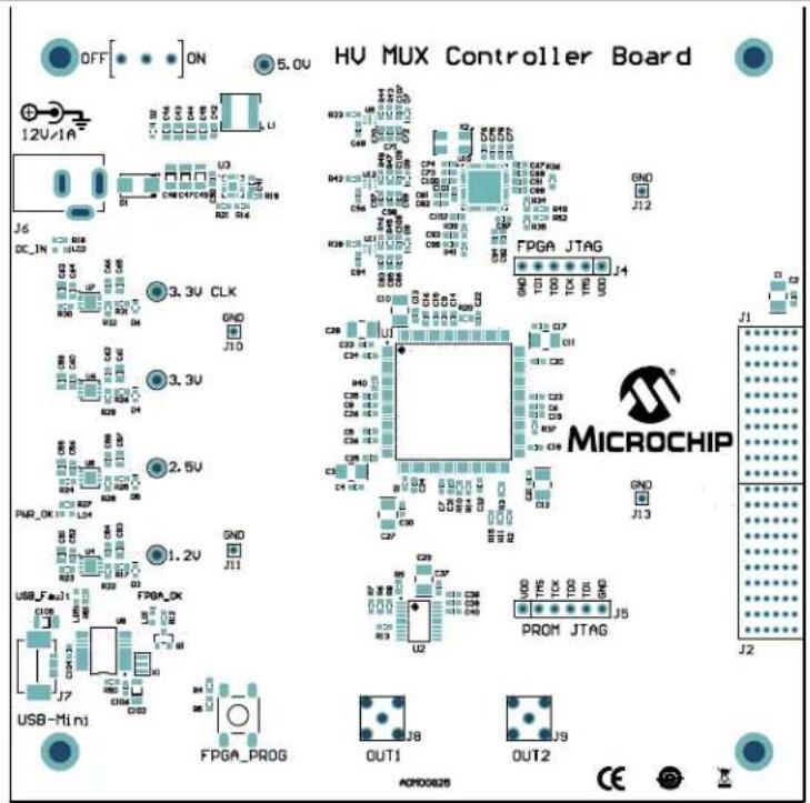
FIGURE 2-8: HV MUX CONTROLLER BOARD (ADM00825) – FRONT VIEW
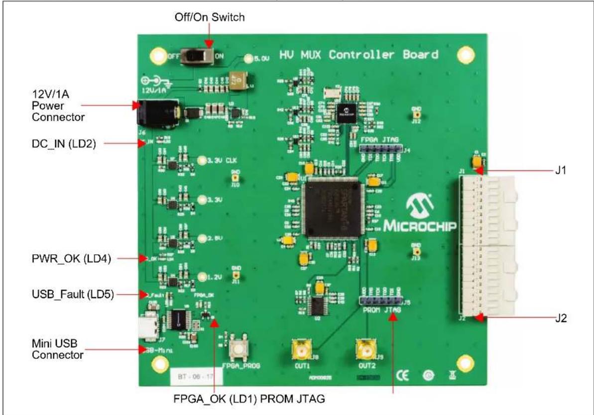
text_image
Off/On Switch 12V/1A Power Connector DC_IN (LD2) PWR_OK (LD4) USB_Fault (LD5) Mini USB Connector BT - 06 - 17 FPGA_OK (LD1) PROM JTAG HU MUX Controller Board J1 J2 J3 J4 J5 J6 J7 J8 J9 J10 J11 J12 J13 J14 J15 J16 J17 J18 J19 J20 J21 J22 J23 J24 J25 J26 J27 J28 J29 J30 J31 J32 J33 J34 J35 J36 J37 J38 J39 J40 J41 J42 J43 J44 J45 J46 J47 J48 J49 J50 J51 J52 J53 J54 J55 J56 J57 J58 J59 J60 J61 J62 J63 J64 J65 J66 J67 J68 J69 J70 J71 J722.6 TESTING THE HV2722 ANALOG SWITCH EVALUATION BOARD
The user can turn on/off each of the 16 switches through the USB connected PC GUI software program:
- Click the Initialize HV MUX Controller button located at the top left corner.
- Clear STBY.
- Select MODE.
- Put 16-bit data (from bit 15 to bit 0) in DIN to set switches on and off. Bit 31 to Bit 16 data are not used for the HV2722 Evaluation Board. Data '1' means the switch is on and data '0' means the switch is off.
- Click the Set HV MUX button.
- Then, the GUI and controller board generate 32-bit data and 32 clocks, followed by one LE negative pulse, and switches are on and off according to DIN in the GUI.
- If the user selects CLR and then clicks the Set HV MUX button, all the switches are off.
Note: The typical voltage and waveforms are provided in Appendix C. "Demo Board Waveforms".
2.7 GENERATION OF PULSER OUTPUT AT SW2A OF HV2722
This section provides the simple step-by-step procedure to make the Ch1 pulser output at the SW2A SMA connector by configuring the GUI.
- Before powering up the HV2722 Analog Switch Evaluation Board, make sure that the latest GUI software is installed on the PC.
- Start the GUI program. If the board is not connected, a "Not Connected" message is displayed in the Status bar, located at the bottom left of the screen.
- Power up the HV MUX Controller Board and HV2722 Analog Switch Evaluation Board as described in the previous section. The prompt, "Connected", is displayed in the Status bar.
-
Click the Initialize HV MUX Controller button and check the Message window to see "Initialization Complete".
-
Clear S TBY.
-
Select MODE.
-
Change the DIN to Bit 2 from '0' to '1' to set SW2 on (DIN = 00000000 00000000 00000000 00000100).
-
Click the Set HV MUX button to turn on the HV2722 SW2.
-
Change the Pulses to 10.
-
Select CH1.
-
Click the Start button so that the CH1 pulser starts to generate pulse trains with 10 pulses and a 30 ms T_OFF time.
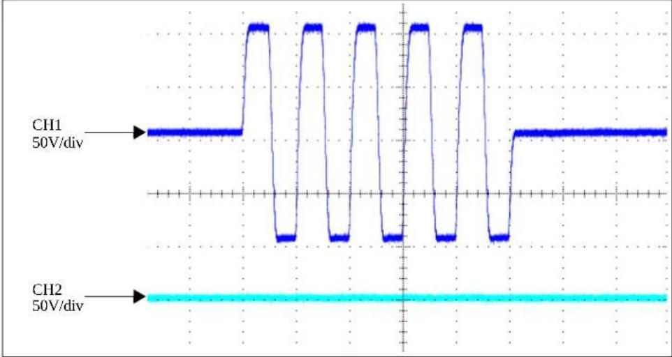
The Ch1 and Ch2 of the oscilloscope in Figure 2-9 show the SW2A and the SW3A.
FIGURE 2-9: TYPICAL WAVEFORM OF 2:1 MUX CONNECTED TO PULSER
line
| Channel | Voltage (V) | | ------- | ----------- | | CH1 | 50V/div | | CH2 | 50V/div |Chapter 3. GUI Description
3.1 HV2722 ANALOG SWITCH EVALUATION BOARD GUI DESCRIPTION
Figure 3-1 displays a screen capture of the HV MUX Controller Board GUI. Table 3-1 provides a detailed description of every item numbered in the screen capture. The selection of the check box, binary data in the DIN entry box, and the number in Pulses and TOFF entry box are just settings; they don't change the operation of HV2722 and the built-in pulsers immediately. By clicking the Set HV MUX, Start and Stop buttons, the control data set by the user in the GUI changes the operation of HV2722 and turns on/off the built-in pulsers in the HV2722 Analog Switch Evaluation Board. Follow the explanation for each corresponding item.
FIGURE 3-1: HV MUX CONTROLLER BOARD GUI SCREEN CAPTURE

text_image
HV MUX Controller Board Initialize HV MUX Controller ① HV MUX ② ③ STBY MODE Set HV MUX [MODE = H : Individual Switching] CLR DIN 00000000 00000000 00000000 00000000 31 24 23 16 15 8 7 0 [MODE = L : Bank Switching] EN A/B Pulser FREQUENCY Pulses TOFF 5 MHz 5 (1 to 128) (5ms to 30ms) Start Stop 12 ⑬ 13 11 CH1 ... Turr ... ... CH2 15 Clear ⑭ Con Status: Not Connected ⑮ 14 16TABLE 3-1: HV2722 ANALOG SWITCH EVALUATION BOARD GUI DESCRIPTION
| Item Number | Item Name Item | Description |
| 1 Initialize HV MUX Controller | This button controls whether the GUI starts the initialization of FPGA on the HV MUX Controller Board, and the communication between the GUI and the HV MUX Controller Board. If there is no error, the “Initialization Complete” message is displayed in the Message window. | |
| 2 | S T B | Stays unselected. Not used for the HV2722 Evaluation Board. |
| 3 MODE Stays selected. | Not used for the HV2722 Evaluation Board. | |
| 4 DIN | 32-bit data entry boxes | Bit 15 to bit 0 control the On/Off state of Switch 15 to Switch 0, respectively. Bit 32 to bit 16 are not used for the HV2722 Evaluation Board. If data entry is ‘1’, the associated switch is set to on. If data entry is ‘0’, the associated switch is set to off. |
| 5 CLR | When this check box | is selected, the CLR logic input is set to high and all the switches of HV2722 are set to off. When cleared, the CLR logic input is set to low and the 16 switches of HV2722 are set to On/Off states according to the DIN data entry. |
| 6 EN | Deactivated when MODE is selected, not used for the HV2722 Evaluation Board. | |
| 7 | A/B Deactivated when MODE is selected, not used for the HV2722 Evaluation Board. | |
| 8 | Set HV MUX | This button controls whether the data described in Items 2 to 7 are applied to HV2722. Note that the 32-bit DIN data, 32 clocks and one negative LE pulse are applied one time only. |
| 9 Pulses | This text box defines the number of pulses in the pulse train generated by the selected pulser. A pulse is half of the cycle and the pulse train always starts the positive pulse first. | |
| 10 | TOFF | This text box defines the interval between pulse trains generated by the selected pulser. |
| 11 | CH1/CH2 | When one of these check boxes is selected, the respective pulser is set to generate 5 MHz pulse trains defined at Steps 9 and 10 by the user. |
| 12 | Start | This button controls if the selected pulser starts generating the pulse train. |
| 13 | Stop | This button controls if the selected pulser stops generating the pulse train. |
| 14 | Message window | This window displays information from the GUI program. |
| 15 | Clear | This button clears the messages in the Message window. |
| 16 | Connection Status | This window displays status of the connection between the GUI and the HV MUX Controller Board. |
Chapter 4. PCB Design and Layout Notes
4.1 PCB LAYOUT TECHNIQUES FOR HV2722
The HV2722 Analog Switch Evaluation Board is equipped with the HV2722, which has 16 analog switches to pass high-voltage, high-current and high-frequency pulses. The PCB design and layout are important to ensure the success of the implementation.
4.1.1 High-Voltage and High-Speed Grounding and Layout Techniques
The center pad at the bottom of the HV2722 QFN package is internally connected to V_NN , and should be connected to V_NN externally on the PCB.
The user must pay attention to the connecting traces, since the analog switches pass the high-voltage and high-speed signals. In particular, controlled impedance of 50 to the ground plane and more trace spacing needs to be applied in this situation.
High-speed PCB trace design practices are used for the HV2722 Analog Switch Evaluation Board PCB layout. The internal circuitry of the HV2722 can operate at quite a high frequency, with the primary speed limitation being the load capacitance. Because of this high speed and the high transient currents that result from driving capacitive loads, the supply voltage bypass capacitors should be as close to the pins as possible.
All the GND pins should have low-inductance feedthrough via connections that are connected directly to a solid ground plane at the second layer of the PCB.
It is recommended to minimize the trace length to the ground plane and to insert a ferrite bead in the power supply lead to the capacitor to prevent resonance in the power supply lines.
It is important to minimize trace lengths and use sufficient trace width to reduce inductance. Surface mount components are highly recommended.
The use of a solid ground plane, and good power and signal layout practices, will prevent any possible parasitic capacitance coupling. The user should also ensure that the circulating ground return current from a capacitive load cannot react with common inductance to create noise voltages in the input logic circuitry.
4.1.2 Decoupling Capacitors Selection
The V_DD , V_PP and V_NN supply voltage rails are able to provide fast transient current. Therefore, they should have a low-impedance bypass capacitor close to each of the power supply pins. Use a surface mount ceramic capacitor of 1.0 to 2.2 F capacitance with an appropriate voltage rating.
It is important to verify what type of ceramic capacitor is selected for these bypass capacitors. The low-impedance means low-ESR/ESL impedance within the frequency bandwidth range of ultrasound pulses transmitted, including the very fast dV/dt of the pulse's rising and falling edges. A capacitor with low-temperature coefficient and low-voltage coefficient is also recommended. The type of X7R and X5R, or other more advanced multilayer ceramic types, should be selected for these purposes.
NOTES:
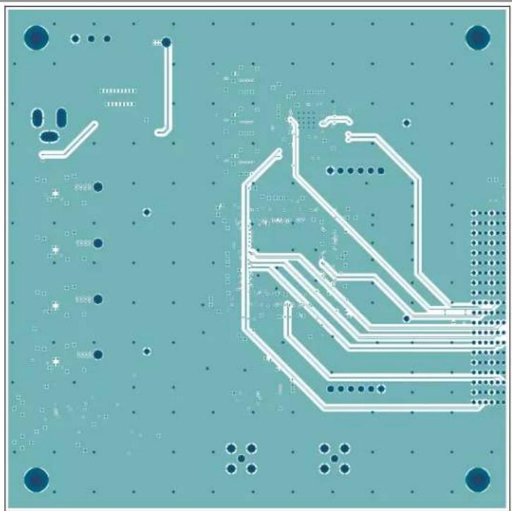
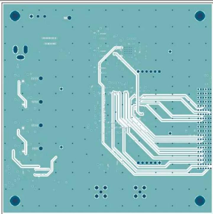
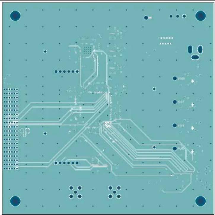
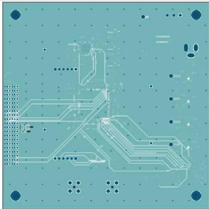
Appendix A. Schematics and Layouts
A.1 INTRODUCTION
This appendix contains the following schematics and layouts for the HV2722 Analog Switch Evaluation Board (ADM00946) and the HV MUX Controller Board (ADM00825).
• HV2722 Analog Switch Evaluation Board (ADM00946):
- Figure A-1: ADM00946 – Schematic
- Figure A-2: ADM00946 – Schematic (Output Connectors)
- Figure A-3: ADM00946 – Schematic (Power)
- Figure A-4: ADM00946 – Schematic (Pulse Generator 1)
- Figure A-5: ADM00946 – Schematic (Pulse Generator 2)
- Figure A-6: ADM00946 – Schematic (SPI Flash)
- Figure A-7: ADM00946 – Top Silk
- Figure A-8: ADM00946 – Top Copper and Silk
- Figure A-9: ADM00946 – Top Copper
- Figure A-10: ADM00946 – Inner 1
- Figure A-11: ADM00946 – Inner 2
- Figure A-12: ADM00946 – Inner 3
- Figure A-13: ADM00946 – Bottom Copper
- Figure A-14: ADM00946 – Bottom Copper and Silk
- Figure A-15: ADM00946 – Bottom Silk
• HV MUX Controller Board (ADM00825):
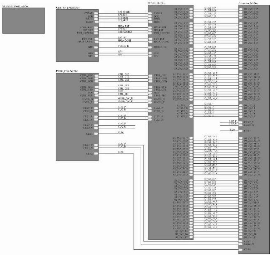
- Figure A-16: ADM00825 – Schematic (Connection)
- Figure A-17: ADM00825 – Schematic (Power Supply)
- Figure A-18: ADM00825 – Schematic (USB to SPI)
- Figure A-19: ADM00825 – Schematic (Programmable Clock)
- Figure A-20: ADM00825 – Schematic (FPGA)
- Figure A-21: ADM00825 – Schematic (FPGA Decoupling Capacitors)
- Figure A-22: ADM00825 – Schematic (Connectors)
- Figure A-23: ADM00825 – Top Silk
- Figure A-24: ADM00825 – Top Copper and Silk
- Figure A-25: ADM00825 – Top Copper
- Figure A-26: ADM00825 – Inner 1
- Figure A-27: ADM00825 – Inner 2
- Figure A-28: ADM00825 – Inner 3
- Figure A-29: ADM00825 – Inner 4
- Figure A-30: ADM00825 – Bottom Copper
- Figure A-31: ADM00825 – Bottom Copper and Silk
- Figure A-32: ADM00825 – Bottom Silk
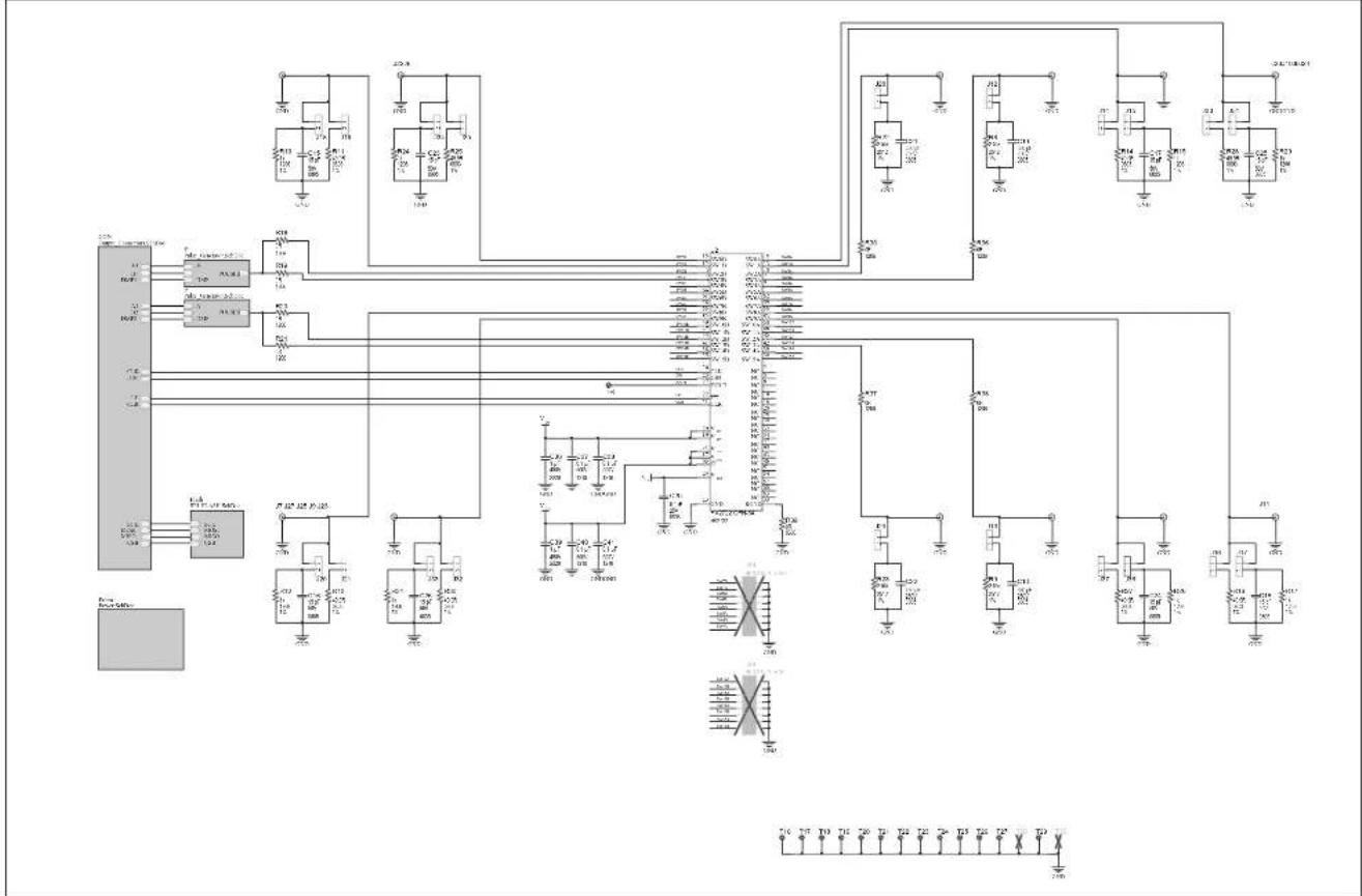
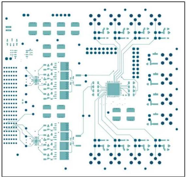
FIGURE A-1: ADM00946 - SCHEMATIC
text_image
Electrical schematic diagram with labeled components and connections, including ICs, resistors, capacitors, and a microcontroller interface.FIGURE A-2: ADM00946 - SCHEMATIC (OUTPUT CONNECTORS)
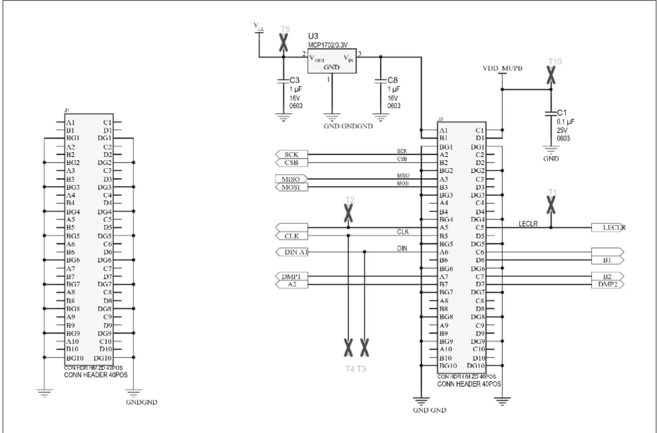
text_image
U3 MCP1702/3.3V VOUT VIN GND GNDGND C3 1 µF 16V 0603 C8 1 µF 16V 0603 T5 VLL T10 C1 0.1 µF 25V 0603 SCK CSB SCK CSB A2 B2 BG2 BG2 BG3 BG3 A3 B3 BG3 BG3 A4 B4 BG4 BG4 A5 B5 BG5 BG5 A6 B6 BG6 BG6 A7 B7 BG7 BG7 A8 B8 BG8 BG8 A9 B9 BG9 BG9 A10 B10 B10 D10 D10 D10 D10 D10 D10 D10 D10 D10 D10 D10 D10 D10 D10 D10 D10 D10 D10 D10 D10 D10 D10 D10 D10 D10 T2 CLK DIN A1 DMP1 A2 T4 T3 GND GND VDD MUPB LECLR LECLRFIGURE A-3: ADM00946 - SCHEMATIC (POWER)
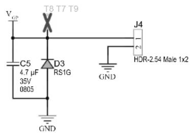
text_image
VGP T8 T7 T9 C5 4.7 μF 35V 0805 D3 RS1G GND J4 2.1 HDR-2.54 Male 1x2 GND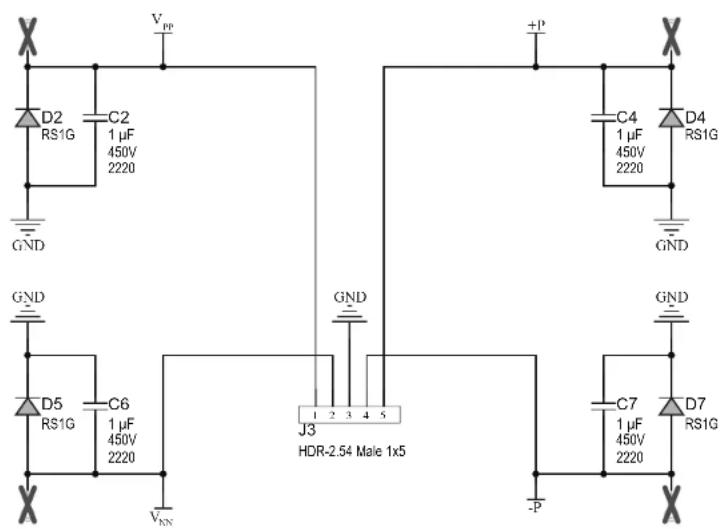
text_image
Vpp D2 C2 RS1G 1 μF 450V 2220 GND +P C4 D4 RS1G 1 μF 450V 2220 GND GND D5 C6 RS1G 1 μF 450V 2220 J3 HDR-2.54 Male 1x5 -VNN -C7 D7 RS1G 1 μF 450V 2220 -PT13T11
FIGURE A-4: ADM00946 - SCHEMATIC (PULSE GENERATOR 1)

text_image
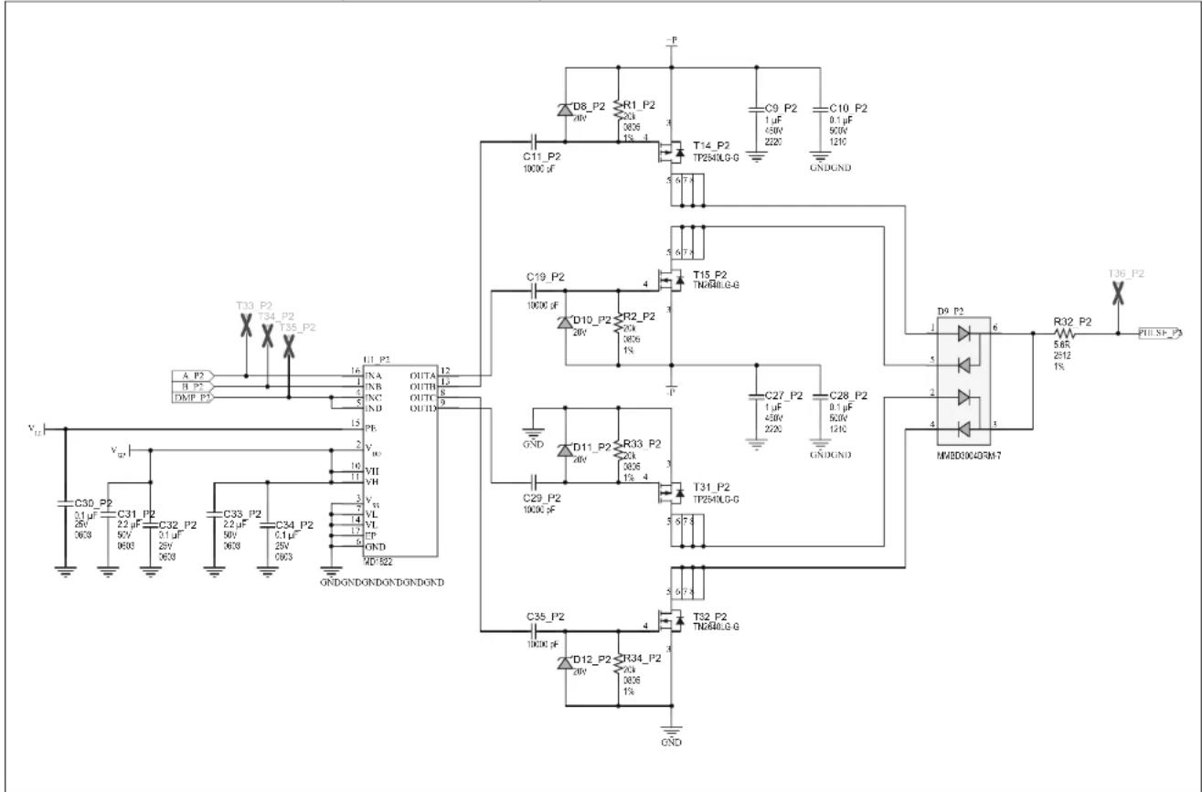
T33_P1 T34_P1 T35_P1 A_P1 H_P1 DSR_P1 V_L1 C30_P1 0.1 μF 25V 0638 C31_P1 22 μF 50V 0638 C32_P1 0.1 μF 25V 0638 C33_P1 22 μF 50V 0638 C34_P1 0.1 μF 25V 0638 E7 GND VD1022 U1_P1 INA INR INC IND OUTD PE V_DD V_H V_H V_SS V_L V_L GND QK_DGN_DGN_DGN_DGN_DGN_DGN_DGN_DGN_DGN_DGN_DGN_DGN_DGN_DGN_DGN_DGN_DGN_DGN_DGN_DGN_DGN_DGN_DGN_DGN_DGN_DGN_DGN_DGN_DGN_DGN_DGN_DGN_DGN_DGN_DGN_DGN_DGN_DGN_DKN_BP1_12_13_8_9_10_11_12_13_8_9_14_15_16_17_18_19_20_21_22_23_24_25_26_27_28_29_30_31_32_33_34_35_P1_4_T32_P1_TN24MILG_G C11_P1 1000μF D6_P1 20V R1_P1 2kΩS 1% 4 C9_P1 1μF 450V 222C C10_P1 0.1μF 500V 1210 GNDGND T14_P1 TP254LG-G 5 6 F X C19_P1 1000μF D10_P1 20V R2_P1 2kΩS 1% 4 T15_P1 TN24MILG-G 5 6 F X C27_P1 1μF 450V 222C C28_P1 0.1μF 500V 1210 GNDGND D9_P1 6 5 4 3 2 1 3 2 3 3 3 3 3 3 3 3 3 3 3 3 3 3 3 3 3 3 3 3 3 3 3 3 3 3 3 3 3 3 3 3 3 3 3 3 3 3 3 3 3 3 3 3 3 3 3 3 3 3 6 PULSC T: T36_P1 R32_P1 5.5R 25I2 1% MABD0XMERW-TFIGURE A-5: ADM00946 - SCHEMATIC (PULSE GENERATOR 2)
text_image
T33_P2 T34_P2 T35_P2 A_P2 B_P2 DMP_P2 V12 C30_P2 31 μF 28V 363 C31_P2 2.2 μF 50V 688 C32_P2 31 μF 28V 363 C33_P2 2.2 μF 50V 688 C34_P2 31 μF 28V 363 C35_P2 1000 pF D12_P2 28V R34_P2 31μF 385 1% GNDONDONDONDONDOND U1_P2 IN_A IN_B IN_C IN_D IN_D OUT_A OUT_B OUT_C OUT_D OUT_D 16 12 15 8 9 10 11 15 Vcc Vcc VII VH Vcc VL VL FP GND RD522 C11_P2 1000 pF D8_P2 48V R1_P2 31k 305k 1% - 1 T14_P2 TP2640LG-G C9_P2 1 μF 630V 220V C10_P2 0.1 μF 500V 12k GNDGND C19_P2 1000 pF D10_P2 28V R2_P2 31k 305k 1% T15_P2 TN640LG-G C27_P2 1 μF 450V 220V C28_P2 0.1 μF 500V 12k GNDGND D9_P2 6 5 4 MWED30043RM7 T36_P2 R32_P2 5.65V 2512V 1% PNDFIGURE A-6: ADM00946 - SCHEMATIC (SPI FLASH)
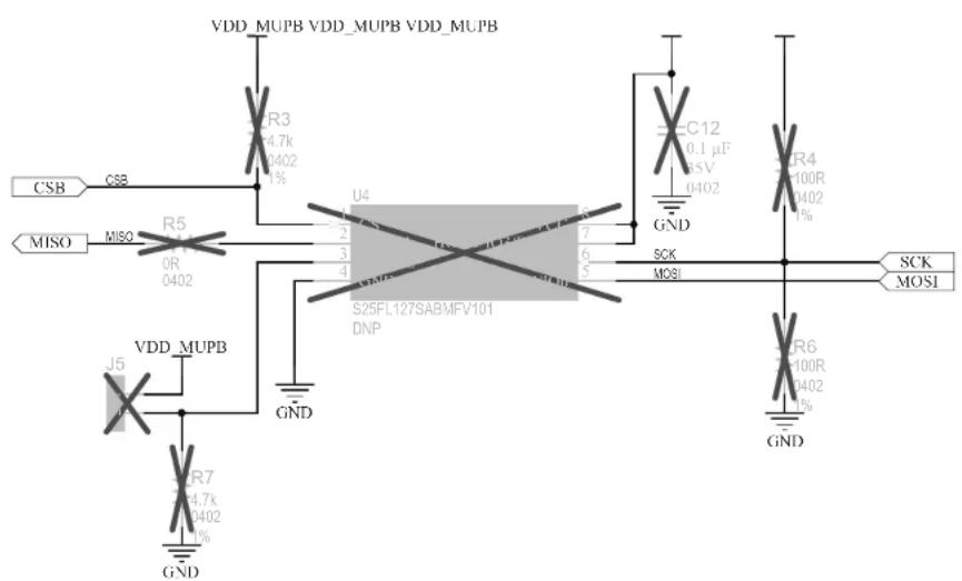
text_image
VDD_MUPB VDD_MUPB VDD_MUPB CSB CSB MISO MISO R5 0R 0402 VDD_MUPB J5 GND R7 0.47k 0402 GND U4 2 3 4 S25FL127SABMFV101 DNP C12 0.1 μF RSV 0402 GND SCK MOSI C4 100R 0402 1% R6 100R 0402 1% GND SCK MOSIFIGURE A-7: ADM00946 - TOP SILK

text_image
USB GND J3 GND GND UPP T8 VBP C4 C7 C2 C4 SHBA J11 SHBB J7 SH9A J23 SH9B J27 C6 C8 U3 C3 T8 U.L. T9 P- C8_P1 C27_P1 T11 U4 R3 R5 R7 J5 T33_R1 T34_R1 T35_R1 T36_R1 T37_R1 T38_R1 T39_R1 T40_R1 T41_R1 T42_R1 T43_R1 T44_R1 T45_R1 T46_R1 T47_R1 T48_R1 T49_R1 T50_R1 T51_R1 T52_R1 T53_R1 T54_R1 T55_R1 T56_R1 T57_R1 T58_R1 T59_R1 T60_R1 T61_R1 T62_R1 T63_R1 T64_R1 T65_R1 T66_R1 T67_R1 T68_R1 T69_R1 T70_R1 T71_R1 T72_R1 T73_R1 T74_R1 T75_R1 T76_R1 T77_R1 T78_R1 T79_R1 T80_R1 T81_R1 T82_R1 T83_R1 T84_R1 T85_R1 T86_R1 T87_R1 T88_R1 T89_R1 T90_R1 T91_R1 T92_R1 T93_R1 T94_R1 T95_R1 T96_R1 T97_R1 T98_R1 T99_R1 T100_R1 U2 R20 R27 R28 R29 R30 R31 R32 R33 R34 R35 R36 R37 R38 R39 R40 R41 R42 R43 R44 R45 R46 R47 R48 R49 R50 R51 R52 R53 R54 R55 R56 R57 R58 R59 R60 R61 R62 R63 R64 R65 R66 R67 R68 R69 R70FIGURE A-8: ADM00946 - TOP COPPER AND SILK
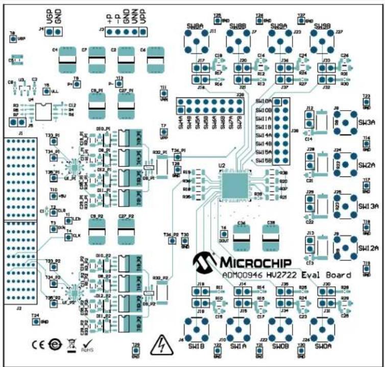
FIGURE A-9: ADM00946 - TOP COPPER
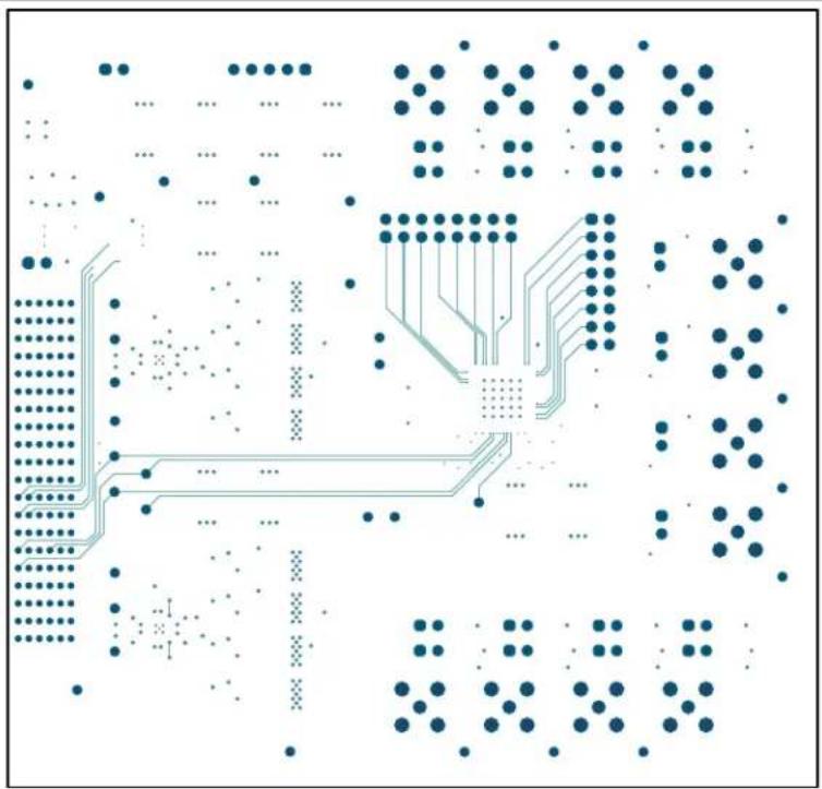
natural_image
Pure electrical circuit lines without any symbolsFIGURE A-10: ADM00946 - INNER 1
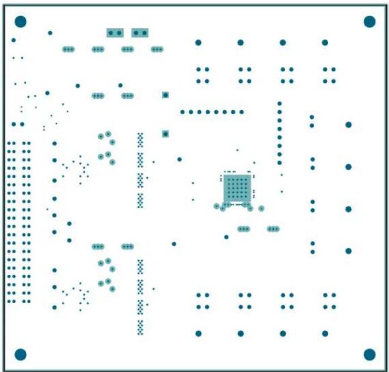
natural_image
Abstract geometric pattern with scattered dots and a central square (no text or symbols)FIGURE A-11: ADM00946 - INNER 2
natural_image
Pure electrical circuit lines without any symbolsFIGURE A-12: ADM00946 - INNER 3

natural_image
Pure electrical circuit lines without any symbolsFIGURE A-13: ADM00946 - BOTTOM COPPER
natural_image
Pure electrical circuit lines without any symbolsFIGURE A-14: ADM00946 - BOTTOM COPPER AND SILK
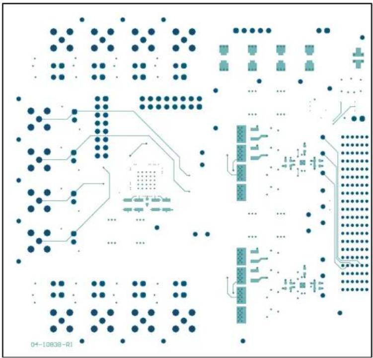
text_image
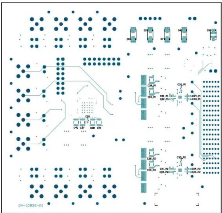
04-10838-R1FIGURE A-15: ADM00946 - BOTTOM SILK

text_image
Circuit board layout diagram with labeled components and connectionsFIGURE A-16: ADM00825 - SCHEMATIC (CONNECTION)
flowchart
graph TD
    A["Control Panel"] --> B["Control Module"]
    B --> C["Control Data"]
    C --> D["Output"]

    subgraph Control Panel
        E["Control Module"] --> F["Control Data"]
    end

    subgraph Control Module
        G["Control Data"] --> H["Control Data"]
    end

    subgraph Control Data
        I["Control Data"] --> J["Control Data"]
    end

    E --> K["OS"]
    E --> L["CSA"]
    E --> M["CSA"]
    E --> N["CSA"]
    E --> O["CSA"]
    E --> P["CSA"]
    E --> Q["CSA"]
    E --> R["CSA"]
    E --> S["CSA"]
    E --> T["CSA"]

    subgraph Control Module
        U["OS"] --> V["CSA"]
        U --> W["CSA"]
        U --> X["CSA"]
        U --> Y["CSA"]
        U --> Z["CSA"]
        U --> AA["CSA"]
        U --> AB["CSA"]
        U --> AC["CSA"]
        U --> AD["CSA"]
        U --> AE["CSA"]
        U --> AF["CSA"]
        U --> AG["CSA"]
        U --> AH["CSA"]
        U --> AI["CSA"]
        U --> AJ["CSA"]
        U --> AK["CSA"]
        U --> AL["CSA"]
        U --> AM["CSA"]
        U --> AN["CSA"]
        U --> AO["CSA"]
        U --> AP["CSA"]
        U --> AQ["CSA"]
        U --> AR["CSA"]
        U --> AS["CSA"]
        U --> AT["CSA"]
        U --> AU["CSA"]
        U --> AV["CSA"]
        U --> AW["CSA"]
        U --> AX["CSA"]
        U --> AY["CSA"]
        U --> AZ["CSA"]
        U --> BA["CSA"]
        U --> BB["CSA"]
        U --> BC["CSA"]
        U --> BD["CSA"]
        U --> BE["CSA"]
        U --> BF["CSA"]
        U --> BG["CSA"]
        U --> BH["CSA"]
        U --> BI["CSA"]
        U --> BJ["CSA"]
        U --> BK["CSA"]
        U --> BL["CSA"]
        U --> BM["CSA"]
        U --> BN["CSA"]
        U --> BO["CSA"]
        U --> BP["CSA"]
        U --> BQ["CSA"]
        U --> BR["CSA"]
        U --> BS["CSA"]
        U --> BT["CSA"]
        U --> BU["CSA"]
        U --> BV["CSA"]
        U --> BW["CSA"]
        U --> BX["CSA"]
        U --> BY["CSA"]
        U --> BZ["CSA"]
        U --> CA["CSA"]
        U --> CB["CSA"]
        U --> CC["CSA"]
        U --> CD["CSA"]
        U --> CE["CSA"]
        U --> CF["CSA"]
        U --> CG["CSA"]
        U --> CH["CSA"]
        U --> CI["CSA"]
        U --> CJ["CSA"]
        U --> CK["CSA"]
        U --> CL["CSA"]
        U --> CM["CSA"]
        U --> CN["CSA"]
        U --> CO["CSA"]
        U --> CP["CSA"]
        U --> CZ["CSA"]
    end

    subgraph Control Data
        D1["OS"] --> D2["CAS"]
        D3["CAS"] --> D4["CAS"]
        D5["CAS"] --> D6["CAS"]
        D7["CAS"] --> D8["CAS"]
        D9["CAS"] --> D10["CAS"]
        D10["CAS"] --> D11["CAS"]
        D11["CAS"] --> D12["CAS"]
        D12["CAS"] --> D13["CAS"]
        D13["CAS"] --> D14["CAS"]
        D14["CAS"] --> D15["CAS"]
        D15["CAS"] --> D16["CAS"]
        D16["CAS"] --> D17["CAS"]
        D17["CAS"] --> D18["CAS"]
        D18["CAS"] --> D19["CAS"]
        D19["CAS"] --> D20["CAS"]
    end

    style Control Panel fill:#f9f,stroke:#333
    style Control Module fill:#ccf,stroke:#333
    style Control Data fill:#cfc,stroke:#333
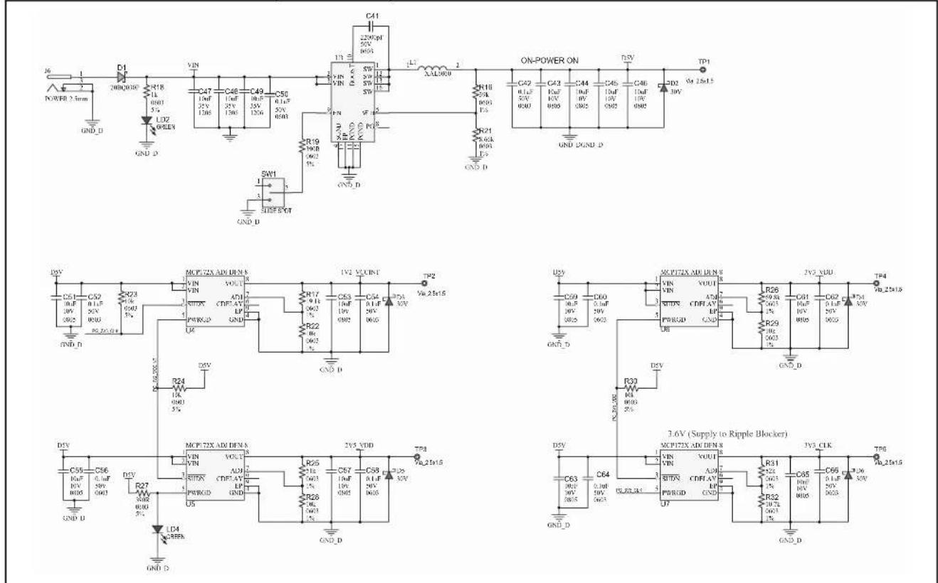
FIGURE A-17: ADM00825 - SCHEMATIC (POWER SUPPLY)
text_image
ON-POWER ON 16 D1 200Q000 GND_D R18 11 0001 5% LD2 85LE4 GND_D C47 1Mf 32V 130V C49 1Mf 35V 130V C50 1Mf 35V 120V C51 1Mf 35V 120V C52 1Mf 35V 120V C53 1Mf 35V 120V C54 1Mf 35V 120V C55 1Mf 35V 120V C56 1Mf 35V 120V C57 1Mf 35V 120V C58 1Mf 35V 120V C59 1Mf 35V 120V C60 1Mf 35V 120V C61 1Mf 35V 120V C62 1Mf 35V 120V C63 1Mf 35V 120V C64 1Mf 35V 120V C65 1Mf 35V 120V C66 1Mf 35V 120V C67 1Mf 35V 120V C68 1Mf 35V 120V C69 1Mf 35V 120V C70 1Mf 35V 120V C71 1Mf 35V 120V C72 1Mf 35V 120V C73 1Mf 35V 120V C74 1Mf 35V 120V C75 1Mf 35V 120V C76 1Mf 35V 120V C77 1Mf 35V 120V C78 1Mf 35V 120V C79 1Mf 35V 120V C80 1Mf 35V 120V C81 1Mf 35V 120V C82 1Mf 35V 120V C83 1Mf 35V 120V C84 1Mf 35V 120V C85 1Mf 35V 120VFIGURE A-18: ADM00825 - SCHEMATIC (USB TO SPI)
Ground Posts for Scope Probe ground
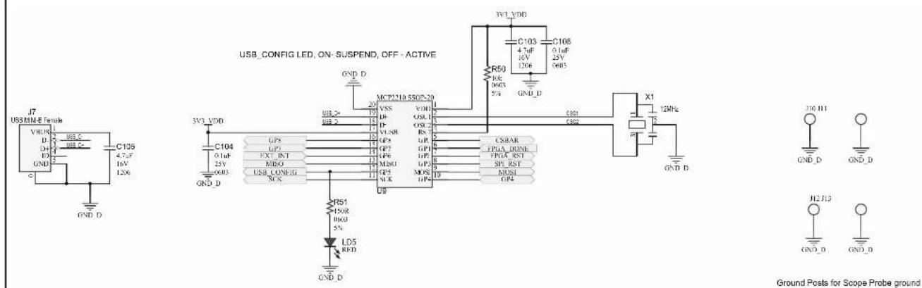
FIGURE A-19: ADM00825 - SCHEMATIC (PROGRAMMABLE CLOCK)
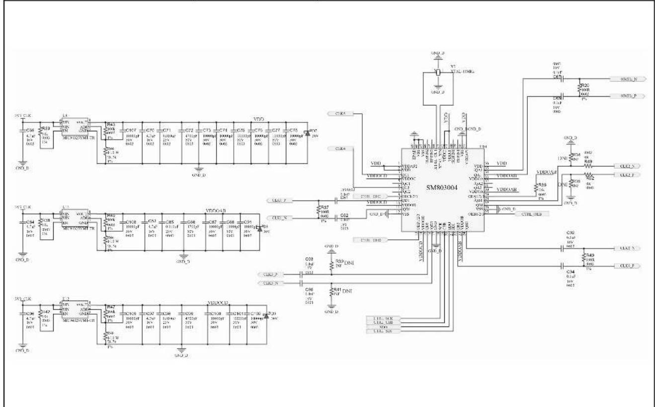
text_image
SM803004 C68 4.7kV 10V CKD GND_B C69 5.7kV 10V CKD GND_D C70 4.7kV 10V CKD GND_D C71 4.7kV 25V CKD GND_D C72 4.7kV 35V CKD GND_D C73 4.7kV 30V CKD GND_D C74 4.7kV 30V CKD GND_D C75 4.7kV 35V CKD GND_D C76 4.7kV 35V CKD GND_D C77 4.7kV 35V CKD GND_D C78 4.7kV 35V CKD GND_D C79 4.7kV 35V CKD GND_D C80 4.7kV 35V CKD GND_D C81 4.7kV 35V CKD GND_D C82 4.7kV 35V CKD GND_D C83 4.7kV 35V CKD GND_D C84 4.7kV 35V CKD GND_D C85 4.7kV 35V CKD GND_D C86 4.7kV 35V CKD GND_D C87 4.7kV 35V CKD GND_D C88 4.7kV 35V CKD GND_D C89 4.7kV 35V CKD GND_D C90 4.7kV 35V CKD GND_D C91 4.7kV 35V CKD GND_D C92 4.7kV 35V CKD GND_D C93 4.7kV 35V CKD GND_D C94 4.7kV 35V CKDFIGURE A-20: ADM00825 - SCHEMATIC (FPGA)

text_image
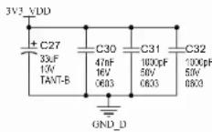
Circuit schematic diagram with labeled components including bank, FPGA JTAG, OUT1 OUT2, and 'DONE' LED, showing connections and pin assignments.FIGURE A-21: ADM00825 - SCHEMATIC (FPGA DECOUPLING CAPACITORS)
For 1V2 VCCINT
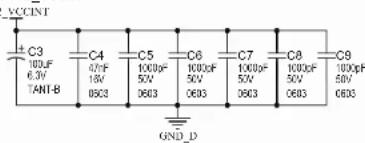
text_image
VCCINT C3 100pF 6.3V TANT-B C4 07pF 18V 0603 C5 100pF 50V 0603 C6 100pF 50V 0603 C7 100pF 50V 0603 C8 100pF 50V 0603 C9 100pF 50V 0603 GND_DFor VCCO 0
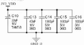
text_image
3V2 VDD ± C10 33uF 16V TANT-B C13 47nF 16V 0603 C14 100pF 50V 0603 C15 100pF 50V 0603 C16 100pF 50V 0603 GND_DFor VCCO_2
For VCCO_1
text_image
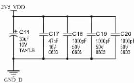
2V5 VDD C11 330F 10V TANT-B GND D C17 47nF 16V 0803 C18 100pF 50V 0803 C19 1000pF 50V 0803 C20 100pF 50V 0803For VCCO_3
text_image
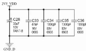
2V5 VDD C28 33uF 10V TANT-B GND_D C33 47uF 16V 0603 C34 100pF 50V 0603 C35 100pF 50V 0603 C36 100pF 50V 0603For VCCAUX

text_image
3V3 VDD + C12 330F 10V TANT-A C21 470F 16V 0603 C22 1000F 50V 0603 C23 1000F 50V 0603 C24 1000F 50V 0603 C25 1000F 50V 0603 C26 1000F 50V 0603 GND DFor XCF04S

text_image
JV3 VDD C29 33uF 10V TANT-8 C37 47uF 16V 0603 C38 100uF 50V 0603 C39 100uF 50V 0603 C40 100uF 50V 0603 GND_DFIGURE A-22: ADM00825 - SCHEMATIC (CONNECTORS)
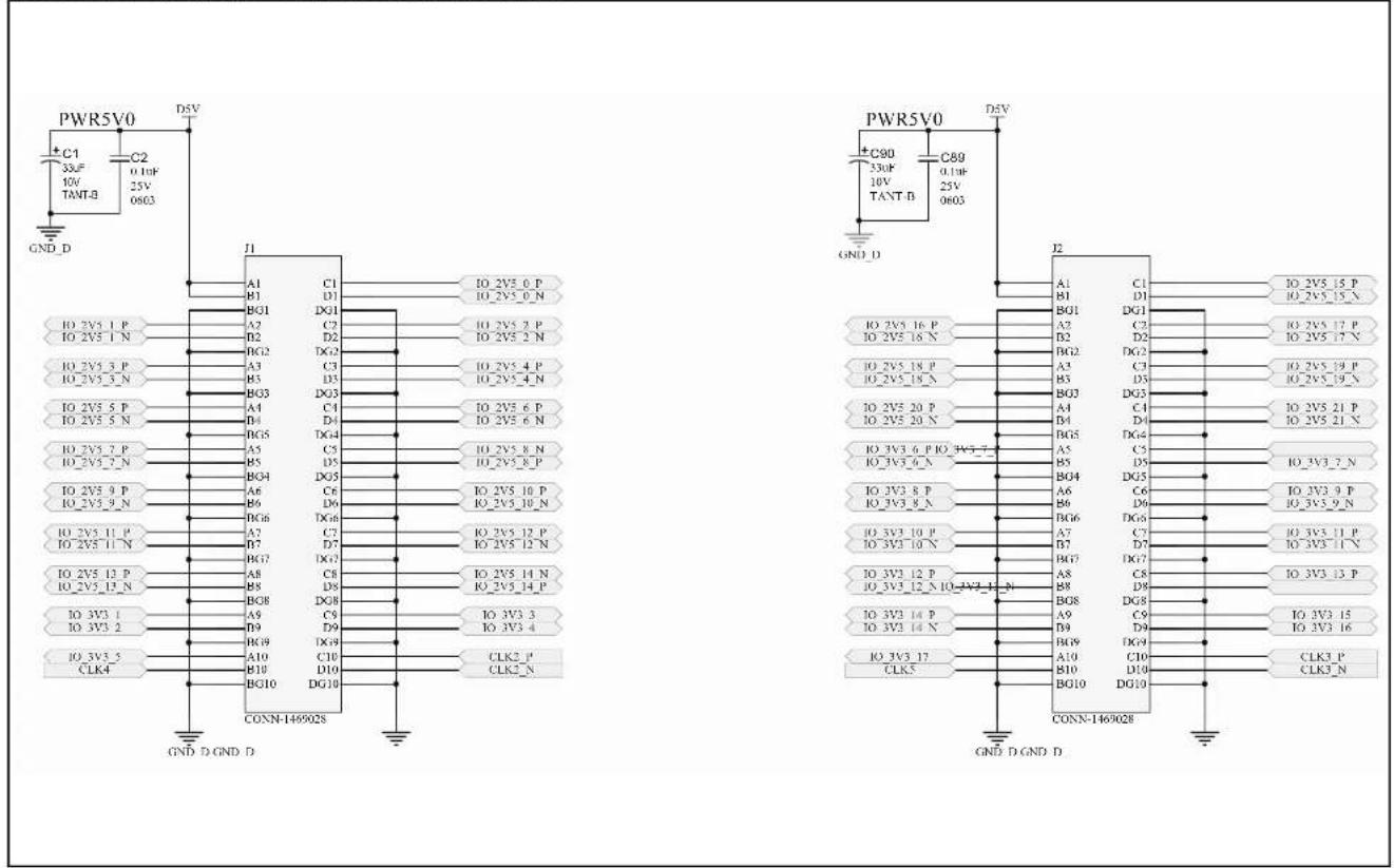
FIGURE A-23: ADM00825 - TOP SILK
text_image
OFF[• • ]ON 5.0V HV MUX Controller Board 12V/1A J6 DC_IN 3.3V CLK GND J10 3.3V 2.5V PWR_OK 1.2V USB_Fau1 FPGA_OK USB-Mini FPGA_PROG OUT1 J8 OUT2 ACR00625 GND J12 FPGA JTAG J4 MICROCHIP GND J13 J5 PROM JTAG J2FIGURE A-24: ADM00825 - TOP COPPER AND SILK

FIGURE A-26: ADM00825 - INNER 1
natural_image
Pure electrical circuit lines without any symbolsFIGURE A-27: ADM00825 - INNER 2

natural_image
Pure electrical circuit lines without any symbols or text, rendered on a teal background with dots and connectors (no readable text or labels)FIGURE A-28: ADM00825 - INNER 3
natural_image
Pure electrical circuit lines without any symbols or text, rendered on a teal background with dot patterns (no readable text or labels)FIGURE A-29: ADM00825 - INNER 4

natural_image
Pure electrical circuit lines without any symbolsFIGURE A-30: ADM00825 - BOTTOM COPPER
natural_image
Pure electrical circuit lines without any symbols or text, rendered in blue on a grid background (no readable text or labels)FIGURE A-31: ADM00825 - BOTTOM COPPER AND SILK
natural_image
Pure electrical circuit lines without any symbols or text, rendered on a teal background with no readable text or labels.FIGURE A-32: ADM00825 - BOTTOM SILK

text_image
Diagram with scattered dots and symbols, including a dotted grid and a vertical bar labeled 'CRO' with a plus sign.Appendix B. Bill of Materials (BOM)
B.1 HV2722 ANALOG SWITCH EVALUATION BOARD (ADM00946)
TABLE B-1: ADM00946 – BILL OF MATERIALS (BOM) ^(1)
| Qty. | Reference Description | Manufacturer Part Number | ||
| 8 C1 | C20, C30_P1,C30_P2, C32_P1,C32_P2, C34_P1,C34_P2 | Capacitor, Ceramic, 0.1 μF,25V, 20%, Y5V, SMD, 0603 | Cal-Chip Electronics Inc. G | MC10Y5V104Z25NTLF |
| 10 C2 | C4, C6, C7,C9_P1, C9_P2,C27_P1, C27_P2,C36, C39 | Capacitor, Ceramic, 1 μF,450V, 20%, X7T, SMD, 2220 | TDK Corporation | C5750X7T2W105M250KE |
| 2 | C3, C8 | Capacitor, Ceramic, 1 μF,16V, 10%, X5R, SMD, 0603 | AVX Corporation | 0603YD105KAT2A |
| 1 | C5 | Capacitor, Ceramic, 4.7 μF,35V, 10%, X7R, SMD, 0805 | TDK Corporation | C2012X7R1V475K125AC |
| 8 C1 | 10_P1, C10_P2,C28_P1, C28_P2,C37, C38, C40, C41 | Capacitor, Ceramic, 0.1 μF,500V, 10%, X7R, SMD, 1210 | KEMET | C1210C104KCRACTU |
| 8 C1 | 1_P1, C11_P2,C19_P1, C19_P2,C29_P1, C29_P2,C35_P1, C35_P2 | Capacitor, Ceramic,10000 pF, 500V, 10%, X7R,SMD, 1206 | KEMET | C1206C103KCRACTU |
| 1 | C12 | Capacitor, Ceramic, 0.1 μF,35V, 10%, X7R, SMD, 0402 | TDK Corporation | CGA2B3X7R1V104K050BB |
| 4 C1 | 3, C14, C21, C22 Capacitor, Ceramic, 330 pF,250V, 5%, C0G/NP0, SMD,0805 | Capacitor, Ceramic, 15 pF,50V, 5%, NP0, SMD, 0805 | Murata Electronics NorthAmerica | GRM21A5C2E331JW01D |
| 8 C1 | 5, C16, C17, C18,C23, C24, C25, C26 | Capacitor, Ceramic, 2.2 μF,50V, 10%, X5R, SMD, 0603 | Panasonic® - ECG | ECU-V1H150JCN |
| 4 C3 | 1_P1, C31_P2,C33_P1, C33_P2 | Capacitor, Ceramic, 2.2 μF,50V, 10%, X5R, SMD, 0603 | Murata Electronics NorthAmerica, Inc. | GRM188R61H225KE11D |
| 5 D2 | D3, D4, D5, D7 Diode, Rectifier RS1G, 1.3V,1A, 400V, DO-214AC_SMA | Diode, Rectifier RS1G, 1.3V,1A, 400V, DO-214AC_SMA | FairchildSemiconductor®/ON Semiconductor® | RS1G |
| 8 D8 | P1, D8_P2,D10_P1, D10_P2,D11_P1, D11_P2,D12_P1, D12_P2 | Diode, Zener, MMSZ5250B,20V, 500 mW, SMD,SOD-123 | Diodes Incorporated® | MMSZ5250B-7-F |
| 2 D9 | P1, D9_P2 Diode, Rectifier, Array,MMBD3004BRM, 1V,225 mA, 350V, SMD,SOT-23-6 | Diode, Rectifier, Array,MMBD3004BRM, 1V,225 mA, 350V, SMD,SOT-23-6 | Diodes Incorporated | MMBD3004BRM-7-F |
| Qty. | Reference | Description | Manufacturer | Part Number |
| 2 J1, J2 Connector, Header | 40 POS,R/A, HM-ZD, Tin | TE Connectivity AMP Connectors | 6469169-1 | |
| 1 J3 | Connector, HDR-2.54 | Male,1x5, Gold, 5.84MH, TH,Vertical | Samtec, Inc. TSW-105-07 | S-S |
| 2 J38, J39 Connector, HDR-2.54, Male,2x8, Tin, 5.84 MH, TH,Vertical | FCI 67996-416HLF | |||
| 22 J4, J5, J12, J13,J14, J15, J16, J17,J18, J19, J20, J21,J28, J29, J30, J31,J32, J33, J34, J35,J36, J37 | Connector, HDR-2.54, Male,1x2, Gold, 5.84MH, TH,Vertical | FCI 77311-118-02LF | ||
| 12 J6, J7, J8, J9, J10,J11, J22, J23, J24,J25, J26, J27 | Connector, RF, Coaxial, SMA,Female, 2P, TH, Vertical | TE Connectivity, Ltd. 5-18 | 14832-1 | |
| 1 LABEL1 Label, Assembly w/RevisionLevel (Small Modules) perMTS-0002 | Microchip TechnologyInc. | |||
| 1 PCB1 Printed Circuit Board Microchip TechnologyInc. | 04-10838-R1 | |||
| 8 R1_P1, R1_P2,R2_P1, R2_P2,R33_P1, R33_P2,R34_P1, R34_P2 | Resistor, TKF, 20k, 1%, 1/8W,SMD, 0805 | Yageo Corporation | RC0805FR-0720KL | |
| 2 R3, R7 Resistor, TKF, 4.7K, 1%,1/10W, 0402 | KOA Speer | RK73H1ETTP4701F | ||
| 2 R4, R6 Resistor, TKF, 100R, 1%,1/10W, SMD, 0402 | Panasonic® ElectronicComponents | ERJ-2RKF1000X | ||
| 1 R5 Resistor, TKF, 0R, 1/16W,SMD, 0402 | Yageo Corporation | RC0402JR-070RL | ||
| 4 R8, R9, R22, R23 Resistor, TKF, 2.55k, 1%, 1W,SMD, 2512 | Stackpole Electronics,Inc. | RMCF2512FT2K55 | ||
| 8 R10, R12, R15, R17,R24, R26, R29, R31 | Resistor, TKF, 1k, 1%, 1/4W,SMD, 1206 | Yageo Corporation | RC1206FR-071KL | |
| 8 R11, R13, R14, R16,R25, R27, R28, R30 | Resistor, TKF, 49.9R, 1%,1/4W, SMD, 0603 | Vishay Intertechnology,Inc. | CRCW060349R9FKEAHP | |
| 8 R18, R19, R20, R21,R35, R36, R37, R38 | Resistor, TKF, 0R, SMD, 1206 | Yageo Corporation | RC1206JR-070RL | |
| 2 R32_P1, R32_P2 Resistor, TKF, 5.6R, 1%, 1W,SMD, 2512, AEC-Q200 | Panasonic ElectronicComponents | ERJ-1TRQF5R6U | ||
| 1 R39 Resistor, TKF, 0R, 1/10W,SMD, 0603 | Panasonic® - ECG | ERJ-3GSY0R00V | ||
| 4 T14_P1, T14_P2,T31_P1, T31_P2 | Transistor, FET, P-CH,TP2640LG-G, 400V, 0.086A,740 mW, SOIC-8 | Microchip TechnologyInc. | TP2640LG-G | |
| 4 T15_P1, T15_P2,T32_P1, T32_P2 | Transistor, FET, N-CH,TN2640LG-G, 400V, 260 mA,1.3W, SOIC-8 | Microchip TechnologyInc. | TN2640LG-G | |
| Qty. | Reference Description | Manufacturer | Part Number | |
| 2 U1 | _P1, U1_P2 Microchip | Analog, FET Driver Quad-Two Inverting – Two Noninverting, MD1822K6-G, 16-Lead QFN | Microchip Technology Inc. | MD1822K6-G |
| 1 U2 | IC Logic, HV2722 x16, Analog Switch, 300V, QFN-64 | Microchip Technology Inc. | HV2722 | |
| 1 U3 | Microchip Analog, LD | O, 3.3V, MCP1702-3302E/CB | Microchip Technology Inc. | MCP1702-3302E/CB |
| 0 U4 | DO NOT POPULATE | - Microchip Memory Serial SPI Flash, 128 Mb (16M x 8), 108 MHz, S25FL127SABMFV101, SOIC-8 | Cypress Semiconductor Corp. | S25FL127SABMFV101 |
Note 1: The components listed in this Bill of Materials are representative of the PCB assembly. The released BOM used in manufacturing uses all RoHS-compliant components.
B.2 HV MUX CONTROLLER BOARD (ADM00825)
TABLE B-2: ADM00825 – BILL OF MATERIALS (BOM) ^(1)
| Qty. | Reference Description | Manufacturer Part Number | ||
| 8 C1 | C10, C11,C12, C27, C28,C29, C90 | Capacitor, Tantalum, 33 μF,10V, 10%, 1.4Ω, SMD, B | KEMET T494B336K010AT | |
| 2 | C103, C105 | Capacitor, Ceramic, 4.7 μF,16V, 10%, X7R, SMD, 1206 | KEMET C1206C475K4RACTU | |
| 4 C2 | C89, C104,C106 | Capacitor, Ceramic, 0.1 μF,25V, 10%, X7R, SMD, 0603 | MurataManufacturing Co., Ltd. | GRM188R71E104KA01D |
| 1 C3 | Capacitor, Tantalum | 100 μF,6.3V, 10%, 400 mΩ, SMD, B | AVX Corporation | TPSB107K006R0400 |
| 7 C4 | C13, C17,C21, C30, C33,C37 | Capacitor, Ceramic, 47 nF,16V, 10%, X7R, SMD, 0603 | MurataManufacturing Co., Ltd. | GRM188R71C473KA01D |
| 1 C41 | Capacitor, Ceramic,22000 pF, 50V, 5%, X7R,SMD, 0603 | AVX Corporation | 06035C223JAT2A | |
| 10 C42 | C50, C52,C54, C56, C58,C60, C62, C64,C66 | Capacitor, Ceramic, 0.1 μF50V, 20%, X7R, SMD, 0603 | TDK Corporation | C1608X7R1H104M |
| 12 C43, C44, C45,C46, C51, C53,C55, C57, C59,C61, C63, C65 | Capacitor, Ceramic, 10 μF,10V, 10%, X7R, SMD, 0805 | MurataManufacturing Co., Ltd. | GRM21BR71A106KE51L | |
| 3 | C47, C48, C49 | Capacitor, Ceramic, 10 μF,35V, 10%, X5R, SMD, 1206 | Taiyo Yuden Co., Ltd. | GMK316BJ106KL-T |
| Qty. | Reference | Description | Manufacturer | Part Number |
| 24 C5, | C6, C7, C8,C9, C14, C15,C16, C18, C19,C20, C22, C23,C24, C25, C26,C31, C32, C34,C35, C36, C38,C39, C40 | Capacitor, Ceramic, 1000 pF,50V, 10%, X7R, SMD, 0603 | NICComponents Corp. | NMC0603X7R102K50TRPF |
| 8 C6 | 7, C68, C81,C82, C92, C93,C94, C95 | Capacitor, Ceramic, 0.1 μF,16V, 10%, X7R, SMD, 0603 | SamsungElectro-MechanicsAmerica, Inc. | CL10B104KO8NNNC |
| 9 C6 | 9, C70, C83,C84, C96,C97,107,108,109 | Capacitor, Ceramic, 4.7 μF,16V, 10%, X5R, SMD, 0603 | TDK Corporation C1608X5R1C475K080AC | |
| 3 | C71, C85, C98 | Capacitor, Ceramic, 0.010 μF,25V, 10%, X7R, SMD, 0603 | Yageo Corporation CC0603KRX7R8BB103 | |
| 3 C7 | 2, C86, C99 Capacitor | Ceramic, 4700 pF,50V, 10%, X7R, SMD, 0603 | KEMET C0603C472K5RACTU | |
| 12 C7 | 3, C74, C75,C76, C77, C78,C87, C88, C91,C100, C101, C102 | Capacitor, Ceramic,10000 pF, 50V, 10%, X7R,0603 | AVX Corporation 06035C103KAT2A | |
| 1 D1 | Diode, Schottky, 20 | BQ030P,470 mV, 2A, 30V,DO-214AA_SMB | ON Semiconductor® | MBRS130LT3G |
| 8 D2 | D3, D4, D5,D6, D7, D8, D9 | Diode, Schottky, 30V,200 mA, SOD523 | Micro CommercialComponents | BAT54WX-TP |
| 2 J1, | J2 | Connector, Receptacle,40 POS, 2-Row, RT, ANG, T/H | TE Connectivity, Ltd. 1469028-1 | |
| 4 J10, | J11, J12, J13 | Connector, PC, Pin, Circuit,0.030, DIA, Gold | Mill-Max Mfg.Corporation | 3132-0-00-15-00-00-08-0 |
| 2 J4, | J5 | Connector, HDR-2.54, Male,1x6, Tin, 5.84, MH, TH,Vertical | SullinsConnector Solutions | PEC06SAAN |
| 1 J6 | Connector, Power, 2.5 mm,5.5 mm, Switch, TH, R/A | CUI Inc. | PJ-002B | |
| 1 J7 | Connector, USB, Mini-B,Female, SMD, R/A | Hirose Electric Co., Ltd. | UX60SC-MB-5ST(80) | |
| 2 J8, | J9 | Connector, RF, Coaxial, SMA,Female, 2P, TH, Vertical | TE Connectivity, Ltd. | 5-1814832-1 |
| 1 | L1 | 4.7 μH, 11A, Inductor | Coilcraft | XAL6060-472MEB |
| 3 LD | 1, LD2, LD4 Diode, L | ED, Green, 2.2V,25 mA, 15 mcd, Clear, SMD,0603 | KingbrightElectronic Co., Ltd. | APT1608SGC |
| 1 LD5 | Diode, LED, Red, 2V, 25 mA,104 mcd, Diffuse, SMD, 0603 | OSRAM OptoSemiconductors GmbH. | LS Q976-NR-1-0-20-R18 | |
| 1 PCB | HV MUX Controller Board –Printed Circuit Board | MicrochipTechnology Inc. | 04-10636 | |
| 1 Q1 | Transistor, FET, N-CH,BSS123, 100V, 170 mA,300 mW, SOT-23-3 | Diodes Incorporated® | BSS123-7-F | |
| 6 R1 | R2, R4, R11,R13, R14 | Resistor, TKF, 4.7 kΩ, 5%,1/10W, SMD, 0603 | Panasonic® - ECG ERJ-3GEYJ472V | |
| 1 R12 | Resistor, MF, 330R, 5%,1/16W, SMD, 0603 | Panasonic - ECG ERA-V33J331V | ||
| 1 R16 | Resistor, TKF, 39 kΩ, 1%,1/10W, SMD, 0603 | Panasonic - ECG ERJ-3EKF3902V | ||
| 1 | R17 | Resistor, TKF, 19.1 kΩ, 1%,1/10W, SMD, 0603 | Panasonic - ECG ERJ-3EKF1912V | |
| 1 R18 | Resistor, TKF, 1 kΩ, 5%,1/10W, SMD, 0603 | Panasonic - ECG ERJ-3GEYJ102V | ||
| 2 R19 | R27 Resistor, TKF, 390R, 5%,1/10W, SMD, 0603 | Panasonic - ECG ERJ-3GEYJ391V | ||
| 3 R20 | R37, R40 Resistor, TKF, 100R, 1%,1/10W, SMD, 0603 | Panasonic - ECG ERJ-3EKF1000V | ||
| 1 | R21 | Resistor, TKF, 8.66 kΩ, 1%,1/10W, SMD, 0603 | Yageo Corporation RC0603FR-078K66L | |
| 6 R22 | R28, R29,R33, R38, R42 | Resistor, TF, 10 kΩ, 1%,1/8W, SMD, 0603 | Vishay Beyschlag MCT06030C1002FP500 | |
| 4 R23 | R24, R30,R50 | Resistor, TKF, 10 kΩ, 5%,1/10W, SMD, 0603 | Panasonic - ECG ERJ-3GEYJ103V | |
| 1 R25 | Resistor, TKF, 51 kΩ, 1%,1/10W, SMD, 0603 | Panasonic - ECG ERJ-3EKF5102V | ||
| 1 | R26 | Resistor, TKF, 69.8 kΩ, 1%,1/10W, SMD, 0603 | Panasonic - ECG ERJ-3EKF6982V | |
| 2 R3 | R8 Resistor, TKF, 51R, 5%,1/10W, SMD, 0603 | Panasonic - ECG ERJ-3GEYJ510V | ||
| 1 R31 | Resistor, TKF, 82 kΩ, 1%,1/10W, SMD, 0603 | Panasonic - ECG ERJ-3EKF8202V | ||
| 1 | R32 | Resistor, TKF, 10.7 kΩ, 1%,1/10W, SMD, 0603 | Panasonic - ECG ERJ-3EKF1072V | |
| 4 R34 | R35, R39,R41 | Resistor, TKF, 150R, 1%,1/10W, SMD, 0603 | StackpoleElectronics, Inc. | RMCF0603FT150R |
| 1 R36 | Resistor, TKF, 75 kΩ, 1%,1/10W, SMD, 0603 | Panasonic - ECG | ERJ-3EKF7502V | |
| 3 | R43,R45,R47 | Resistor, TKF, 100 kΩ, 1%,1/10W, SMD, 0603 | Panasonic - ECG | — |
| 3 | R44, R46, R48 | Resistor, 78.7 kΩ, 1%, 1/10W,SMD, 0603 | Yageo Corporation RC0603FR-0778K7L | |
| 2 | R49,R52 | Resistor, SMD, 0.0Ω, Jumper,1/10W, 0603 | Panasonic - ECG | ERJ-3GEY0R00V |
| 3 R5 | R10, R15 Resistor, TKF, 0R, 1/10W,SMD, 0603 | NIC Components Corp. | NRC06Z0TRF | |
| 1 R51 | Resistor, TKF, 150R, 5%,1/10W, SMD, 0603 | Panasonic - ECG ERJ-3GEYJ151V | ||
| 2 R6 | R7 Resistor, TKF, 100R, 5%,1/10W, SMD, 0603 | VishayIntertechnology, Inc. | CRCW0603100RJNEA | |
| 1 R9 | Resistor, TKF, 22R, | 5%,1/10W, SMD, 0603 | Panasonic - ECG ERJ-3G | GSYJ220V |
| 1 SW | Switch, Slide, SPDT, Mini,50V, 0.5A, G4050X-R, TH | Jameco ^ Electronics G4050X-R | ||
| 1 SW | Switch, Tact, SPST, 12V,50 mA, TL3301NF,160QG/TR, SMD | E-Switch ^ , Inc. TL3301NF | F260QG/TR | |
| 1 U1 | IC, FPGA, 102, I/O, | 144T,QFP | Xilinx Inc. XC6SLX9-2TQ | G144C |
| 1 U10 | Flexible Ultra-Low | Jitter ClockGenerator | MicrochipTechnology Inc. | SM803234 |
| 1 U2 | IC, Prom. SRL for 4M | Gate Xilinx Inc. XCF04SVOG20C | ||
| 1 U3 | 3A Buck, 5V, QFN-16 | Semtech Corporation | TS30013-M000QFNR | |
| 4 U4, | U5, U6, U7 | Microchip Analog LDO,0.8V-5V,MCP1727T-ADJE/MF DFN-8 | MicrochipTechnology Inc. | MCP1727-ADJE/MF |
| 3 U8, | U11, U12 | Adjustable LDO RippleBlocker | MicrochipTechnology Inc. | MIC94325YMT-TR |
| 1 U9 | Microchip Interface, USB,SPI, MCP2210-I/SS SSOP-20 | MicrochipTechnology Inc. | MCP2210T-I/SS | |
| 1 X1 | Resonator, 12 MHz, 0.1%,SMD, CSTCE-G | MurataManufacturing Co., Ltd. | CSTCE12M0G15L99-R0 | |
| 1 X2 | 40 MHz, ±30 ppm, Crystal,12 pF, 40Ω, -20°C, +70°C,Surface Mount, 4-SMD | TXC Corporation | 7B-40.000MAAE-T | |
Note 1: The components listed in this Bill of Materials are representative of the PCB assembly. The released BOM used in manufacturing uses all RoHS-compliant components.
Appendix C. Demo Board Waveforms
C.1 BOARD TYPICAL WAVEFORMS
FIGURE C-1: 5 MHz, 4 PULSES, Ch1 PULSER INPUT AND OUTPUT WHEN ALL SW OFF

line
| Channel | Signal Value | |---------|--------------| | Ch1 | 5V/div | | 1_A | 1A | | Ch2 | 5V/div | | 1_B | 1_B | | Ch3 | 5V/div | | 1_DMP | 1_DMP | | Ch4 | 1V/div | | Ch1 Pulser Output | Pulser Output |FIGURE C-2: 5 MHz, 5 PULSES, +P/-P = ±100V, V PP/VNN = ±115V, VGP = 10V, 330 pF//2.5 kΩ Load
line
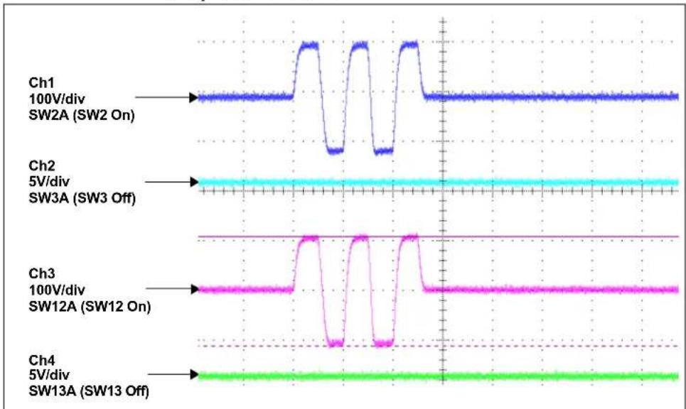
| Channel | Voltage | Timepoint | Signal | |---------|---------|-----------|--------| | Ch1 | 100V/div | SW2A | On | | Ch2 | 5V/div | SW3A | Off | | Ch3 | 100V/div | SW12A | On | | Ch4 | 5V/div | SW13A | Off |Worldwide Sales and Service
AMERICAS
Corporate Office
2355 West Chandler Blvd.
Chandler, AZ 85224-6199
Tel: 480-792-7200
Fax: 480-792-7277
Technical Support:
http://www.microchip.com/
support
Web Address:
www.microchip.com
Atlanta
Duluth, GA
Tel: 678-957-9614
Fax: 678-957-1455
Austin, TX
Tel: 512-257-3370
Boston
Westborough, MA
Tel: 774-760-0087
Fax: 774-760-0088
Chicago
Itasca, IL
Tel: 630-285-0071
Fax: 630-285-0075
Dallas
Addison, TX
Tel: 972-818-7423
Fax: 972-818-2924
Detroit
Novi, MI
Tel: 248-848-4000
Houston, TX
Tel: 281-894-5983
Indianapolis
Noblesville, IN
Tel: 317-773-8323
Fax: 317-773-5453
Tel: 317-536-2380
Los Angeles
Mission Viejo, CA
Tel: 949-462-9523
Fax: 949-462-9608
Tel: 951-273-7800
Raleigh, NC
Tel: 919-844-7510
New York, NY
Tel: 631-435-6000
San Jose, CA
Tel: 408-735-9110
Tel: 408-436-4270
Canada - Toronto
Tel: 905-695-1980
Fax: 905-695-2078
ASIA/PACIFIC
Australia - Sydney
Tel: 61-2-9868-6733
China - Beijing
Tel: 86-10-8569-7000
China - Chengdu
Tel: 86-28-8665-5511
China - Chongqing
Tel: 86-23-8980-9588
China - Dongguan
Tel: 86-769-8702-9880
China - Guangzhou
Tel: 86-20-8755-8029
China - Hangzhou
Tel: 86-571-8792-8115
China - Hong Kong SAR
Tel: 852-2943-5100
China - Nanjing
Tel: 86-25-8473-2460
China - Qingdao
Tel: 86-532-8502-7355
China - Shanghai
Tel: 86-21-3326-8000
China - Shenyang
Tel: 86-24-2334-2829
China - Shenzhen
Tel: 86-755-8864-2200
China - Suzhou
Tel: 86-186-6233-1526
China - Wuhan
Tel: 86-27-5980-5300
China - Xian
Tel: 86-29-8833-7252
China - Xiamen
Tel: 86-592-2388138
China - Zhuhai
Tel: 86-756-3210040
ASIA/PACIFIC
India - Bangalore
Tel: 91-80-3090-4444
India - New Delhi
Tel: 91-11-4160-8631
India - Pune
Tel: 91-20-4121-0141
Japan - Osaka
Tel: 81-6-6152-7160
Japan - Tokyo
Tel: 81-3-6880-3770
Korea - Daegu
Tel: 82-53-744-4301
Korea - Seoul
Tel: 82-2-554-7200
Malaysia - Kuala Lumpur
Tel: 60-3-7651-7906
Malaysia - Penang
Tel: 60-4-227-8870
Philippines - Manila
Tel: 63-2-634-9065
Singapore
Tel: 65-6334-8870
Taiwan - Hsin Chu
Tel: 886-3-577-8366
Taiwan - Kaohsiung
Tel: 886-7-213-7830
Taiwan - Taipei
Tel: 886-2-2508-8600
Thailand - Bangkok
Tel: 66-2-694-1351
Tel: 43-7242-2244-39
Fax: 43-7242-2244-393
Denmark - Copenhagen
Tel: 45-4450-2828
Fax: 45-4485-2829
Finland - Espoo
Tel: 358-9-4520-820
France - Paris
Tel: 33-1-69-53-63-20
Fax: 33-1-69-30-90-79
Germany - Garching
Tel: 49-8931-9700
Germany - Haan
Tel: 49-2129-3766400
Germany - Heilbronn
Tel: 49-7131-72400
Germany - Karlsruhe
Tel: 49-721-625370
Germany - Munich
Tel: 49-89-627-144-0
Fax: 49-89-627-144-44
Germany - Rosenheim
Tel: 49-8031-354-560
Israel - Ra'anana
Tel: 972-9-744-7705
Italy - Milan
Tel: 39-0331-742611
Fax: 39-0331-466781
Italy - Padova
Tel: 39-049-7625286
Netherlands - Drunen
Tel: 31-416-690399
Fax: 31-416-690340
Norway - Trondheim
Tel: 47-7288-4388
Poland - Warsaw
Tel: 48-22-3325737
Romania - Bucharest
Tel: 40-21-407-87-50
Spain - Madrid
Tel: 34-91-708-08-90
Fax: 34-91-708-08-91
Sweden - Gothenberg
Tel: 46-31-704-60-40
Sweden - Stockholm
Tel: 46-8-5090-4654
UK - Wokingham
Tel: 44-118-921-5800
Fax: 44-118-921-5820