MIC5370 - Electronic component Microchip - Free user manual and instructions
Find the device manual for free MIC5370 Microchip in PDF.

User questions about MIC5370 Microchip
0 question about this device. Answer the ones you know or ask your own.
Ask a new question about this device
Download the instructions for your Electronic component in PDF format for free! Find your manual MIC5370 - Microchip and take your electronic device back in hand. On this page are published all the documents necessary for the use of your device. MIC5370 by Microchip.
USER MANUAL MIC5370 Microchip
The MIC5370/1 is an advanced dual LDO ideal for powering general purpose portable devices. The MIC5370/1 provides two independently-controlled, high-performance 150mA LDOs in a tiny 1.6mm x 1.6mm Thin MLF® package.
Ideal for battery-powered applications, the MIC5370/1 offers 2% initial accuracy, low dropout voltage (155mV @ 150mA) and low ground current (typically 32μA per LDO). The MIC5370/1 can also be put into a zero-off-mode current state, drawing virtually no current when disabled.
When the MIC5371 is disabled an internal resistive load is automatically applied to the output to discharge the output capacitor. This LDO offers fast transient response and high PSRR while consuming a minimum operating current.
The MIC5370/1 is available in fixed output voltages in a lead-free (RoHS-compliant) 6-pin 1.6mm x 1.6mm Thin MLF® package.
Data sheets and support documentation can be found on Micrel's web site at: www.micrel.com.
Features
• 2.5V to 5.5V input voltage range
- Two 150mA output current LDOs
• High output accuracy
- ±2% initial accuracy
- Low quiescent current – 32μA per LDO
• Stable with 1μF ceramic output capacitors - Independent enable pins
- Low dropout voltage – 155mV at 150mA
• Thermal-shutdown protection - Current-limit protection
• Output discharge circuit – MIC5371 - 6-pin 1.6mm x 1.6mm Thin MLF ^® package
Applications
- Camera phones
- Mobile phones
• GPS, PMP, PDAs and handhelds - Portable electronics
Typical Application
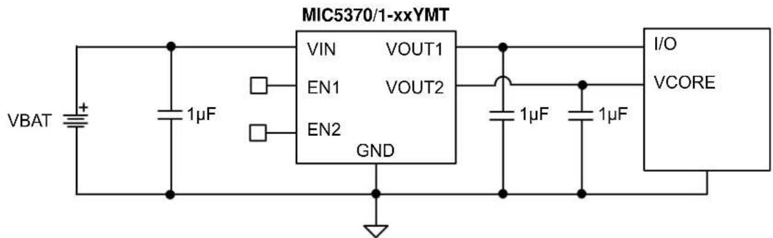
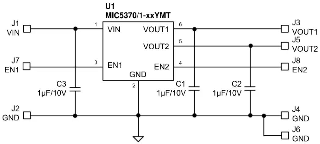
text_image
MIC5370/1-xxYMT VIN VOUT1 EN1 VOUT2 EN2 GND VBAT + 1µF 1µF 1µF I/O VCORECamera DSP Power Supply Circuit
MLF and MicroLeadFrame are registered trademarks of Amkor Technology, Inc.
Micrel Inc. • 2180 Fortune Drive • San Jose, CA 95131 • USA • tel +1 (408) 944-0800 • fax +1 (408) 474-1000 • http://www.micrel.com
Block Diagrams
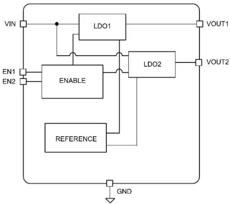
flowchart
graph TD
    VIN --> LDO1
    VIN --> LDO2
    EN1 --> ENABLE
    EN2 --> ENABLE
    ENABLE --> LDO1
    ENABLE --> LDO2
    LDO1 --> VOUT1
    LDO2 --> VOUT2
    REFERENCE --> LDO1
    REFERENCE --> LDO2
    GND --> VOUT2
MIC5370 Block Diagram
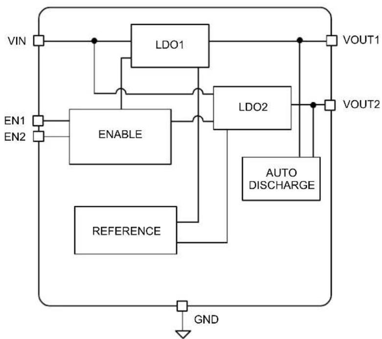
flowchart
graph TD
    VIN --> LDO1
    VOUT1 --> LDO1
    LDO1 --> LDO2
    VOUT2 --> LDO2
    LDO2 --> AUTO_DISCHARGE
    ENABLE --> LDO1
    ENABLE --> LDO2
    REFERENCE --> LDO2
    GND --> GND
    EN1 --> ENABLE
    EN2 --> ENABLE
    style LDO1 fill:#f9f,stroke:#333
    style LDO2 fill:#f9f,stroke:#333
    style AUTO_DISCHARGE fill:#ccf,stroke:#333
    style REFERENCE fill:#cfc,stroke:#333
MIC5371 Block Diagram
Ordering Information
| Part Number | Manufacturing Part Number | Marking Code | Voltage | Junction Temperature Range | Package | Lead Finish |
| MIC5370-3.3/3.3YMT | MIC5370-SSYMT | 8SS 3.3V/3.3V | -40°C to +125°C | 6-Pin 1.6mm × 1.6mm Thin MLF® | Pb-Free | |
| MIC5370-3.3/3.0YMT | MIC5370-SPYMT | SP8 3.3V/3.0V | -40°C to +125°C | 6-Pin 1.6mm × 1.6mm Thin MLF® | Pb-Free | |
| MIC5370-3.3/2.8YMT | MIC5370-SMYMT | SM8 3.3V/2.8V | -40°C to +125°C | 6-Pin 1.6mm × 1.6mm Thin MLF® | Pb-Free | |
| MIC5370-3.3/2.6YMT | MIC5370-SKYMT | S8K 3.3V/2.6V | -40°C to +125°C | 6-Pin 1.6mm × 1.6mm Thin MLF® | Pb-Free | |
| MIC5370-3.3/1.8YMT | MIC5370-SGYMT | SG8 3.3V/1.8V | -40°C to +125°C | 6-Pin 1.6mm × 1.6mm Thin MLF® | Pb-Free | |
| MIC5370-3.0/3.0YMT | MIC5370-PPYMT | P8P 3.0V/3.0V | -40°C to +125°C | 6-Pin 1.6mm × 1.6mm Thin MLF® | Pb-Free | |
| MIC5370-3.0/2.8YMT | MIC5370-PMYMT | PM8 3.0V/2.8V | -40°C to +125°C | 6-Pin 1.6mm × 1.6mm Thin MLF® | Pb-Free | |
| MIC5370-3.0/2.6YMT | MIC5370-PKYMT | P8K 3.0V/2.6V | -40°C to +125°C | 6-Pin 1.6mm × 1.6mm Thin MLF® | Pb-Free | |
| MIC5370-3.0/1.8YMT | MIC5370-PGYMT | PG8 3.0V/1.8V | -40°C to +125°C | 6-Pin 1.6mm × 1.6mm Thin MLF® | Pb-Free | |
| MIC5370-2.8/2.8YMT | MIC5370-MMYMT | MM8 2.8V/2.8V | -40°C to +125°C | 6-Pin 1.6mm × 1.6mm Thin MLF® | Pb-Free | |
| MIC5370-2.8/2.6YMT | MIC5370-MKYMT | M8K 2.8V/2.6V | -40°C to +125°C | 6-Pin 1.6mm × 1.6mm Thin MLF® | Pb-Free | |
| MIC5370-2.8/1.8YMT | MIC5370-MGYMT | MG8 2.8V/1.8V | -40°C to +125°C | 6-Pin 1.6mm × 1.6mm Thin MLF® | Pb-Free | |
| MIC5370-2.8/1.5YMT | MIC5370-MFYMT | MF8 2.8V/1.5V | -40°C to +125°C | 6-Pin 1.6mm × 1.6mm Thin MLF® | Pb-Free | |
| MIC5370-2.8/1.2YMT | MIC5370-M4YMT | J48 2.8V/1.2V | -40°C to +125°C | 6-Pin 1.6mm × 1.6mm Thin MLF® | Pb-Free | |
| MIC5370-1.8/1.2YMT | MIC5370-G4YMT | 8G4 1.8V/1.2V | -40°C to +125°C | 6-Pin 1.6mm × 1.6mm Thin MLF® | Pb-Free | |
| MIC5370-1.2/1.0YMT | MIC5370-4CYMT | 84C 1.2V/1.0V | -40°C to +125°C | 6-Pin 1.6mm × 1.6mm Thin MLF® | Pb-Free | |
| MIC5371-3.3/3.3YMT* | MIC5371-SSYMT | 9SS 3.3V/3.3V | -40°C to +125°C | 6-Pin 1.6mm × 1.6mm Thin MLF® | Pb-Free | |
| MIC5371-3.3/3.0YMT* | MIC5371-SPYMT | 9SP 3.3V/3.0V | -40°C to +125°C | 6-Pin 1.6mm × 1.6mm Thin MLF® | Pb-Free | |
| MIC5371-3.3/2.8YMT* | MIC5371-SMYMT | 9SM 3.3V/2.8V | -40°C to +125°C | 6-Pin 1.6mm × 1.6mm Thin MLF® | Pb-Free | |
| MIC5371-3.3/1.8YMT* | MIC5371-SGYMT | 9SG 3.3V/1.8V | -40°C to +125°C | 6-Pin 1.6mm × 1.6mm Thin MLF® | Pb-Free | |
| MIC5371-3.0/3.0YMT* | MIC5371-PPYMT | 9PP 3.0V/3.0V | -40°C to +125°C | 6-Pin 1.6mm × 1.6mm Thin MLF® | Pb-Free | |
| MIC5371-3.0/2.8YMT* | MIC5371-PMYMT | 9PM 3.0V | 2.8V -40°C to +125°C | 6-Pin 1.6mm × 1.6mm Thin MLF® | Pb-Free | |
| MIC5371-2.8/2.8YMT* | MIC5371-MMYMT | 9MM 2.8V | 2.8V -40°C to +125°C | 6-Pin 1.6mm × 1.6mm Thin MLF® | Pb-Free | |
| MIC5371-2.8/1.8YMT* | MIC5371-MGYMT | 9MG 2.8V | 1.8V -40°C to +125°C | 6-Pin 1.6mm × 1.6mm Thin MLF® | Pb-Free | |
| MIC5371-2.8/1.5YMT* | MIC5371-MFYMT | 9MF 2.8V | 1.5V -40°C to +125°C | 6-Pin 1.6mm × 1.6mm Thin MLF® | Pb-Free | |
| MIC5371-2.8/1.2YMT* | MIC5371-M4YMT | 9M4 2.8V | 1.2V -40°C to +125°C | 6-Pin 1.6mm × 1.6mm Thin MLF® | Pb-Free | |
| MIC5371-1.8/1.2YMT* | MIC5371-G4YMT | 9G4 1.8V | 1.2V -40°C to +125°C | 6-Pin 1.6mm × 1.6mm Thin MLF® | Pb-Free | |
| MIC5371-1.2/1.0YMT* | MIC5371-4CYMT | 94C 1.2V | 1.0V -40°C to +125°C | 6-Pin 1.6mm × 1.6mm Thin MLF® | Pb-Free |
Note:
1. Other voltages available. Contact Micrel for details.
2. Thin MLEPin 1 Identifier = ▲
3. Thin MLFs a GREEN RoHS-compliant package. Level finish is NiPdAu. Mold compound is Halogen Free.
* MIC5371 offers Auto-Discharge function.
Pin Configuration

text_image
VIN 1 GND 2 EN2 3 6 VOUT1 5 VOUT2 4 EN16-Pin 1.6mm x 1.6mm Thin MLF ^® (MT)
Pin Description
| Pin Number | Pin Name | Pin Function |
| 1 | VIN | Supply Input |
| 2 | GND | Ground |
| 3 | EN2 | Enable Input (regulator 2). Active High Input. Logic High = On; Logic Low = Off; Do not leave floating. |
| 4 | EN1 | Enable Input (regulator 1). Active High Input. Logic High = On; Logic Low = Off; Do not leave floating. |
| 5 VOUT2 | Regulator Output – LDO2 | |
| 6 VOUT1 | Regulator Output – LDO1 | |
| EPAD HS | Pad Heatsink | Pad internally connected to ground. |
Absolute Maximum Ratings ^(1)
Supply Voltage ( V_IN )....-0.3V to +6V
Enable Voltage ( V_EN1 , V_EN2 )....-0.3V to V_IN
Power Dissipation ( P_D ) ..... Internally Limited ^(B)
Lead Temperature (soldering, 10sec.)....260°C
Junction Temperature ( T_J ) -40^ to +125^
Storage Temperature ( T_s ) -65^ to +150^
ESD Rating ^(4) 2kV
Operating Ratings ^(2)
Supply Voltage ( V_IN )....+2.5V to 5.5V
Enable Voltage ( V_EN1 , V_EN2 )....-0.3V to V_IN
Junction Temperature ( T_J ) -40^ to +125^
Junction Thermal Resistance
1.6x1.6 Thin ^ -M(OF _JA ) 90°C/W
Electrical Characteristics ^(5)
V_IN = V_EN1 = V_EN2 = V_OUT + 1V ; higher of the two regulator outputs; I_OUTLDO1 = I_OUTLDO2 = 100 A ; C_OUT1 = C_OUT2 = 1 F ; T_J = 25^ , bold values indicate -40^ to +125^ , unless noted.
| Parameter | Condition | Min. | Typ. | ||
| Output Voltage Accuracy | Variation from nominal V_OUT -2.0 +2.0 | % | |||
| Variation from nominal V_OUT ; -40°C to +125°C | -3.0 | +3.0 | % | ||
| Line Regulation | V_IN = V_OUT + 1V to 5.5V, I_OUT = 100μA | 0.02 | 0.3 | %/V | |
| Load Regulation | I_OUT = 100μA to 150mA | 0.3 1 | % | ||
| Dropout Voltage | I_OUT = 50mA I_OUT = 150mA | 55155 | 110310 | mV | |
| Ground Pin Current | V_EN1 = High; V_EN2 = Low; I_OUT = 0mA V_EN1 = Low; V_EN2 = High; I_OUT = 0mA V_EN1 = V_EN2 = High; I_OUT1 = I_OUT2 = 0mA | 323257 | 454585 | μA | |
| Ground Pin Current in Shutdown | V_EN1 = V_EN2 = 0V | 0.05 | 1 | μA | |
| Ripple Rejection | f = 1kHz; C_OUT = 1μF | 60 | dB | ||
| Current Limit | V_OUT = 0V | 200 | 325 | 550 | mA |
| Output Voltage Noise | C_OUT = 1μF, 10Hz to 100kHz | 200 | μVRMS | ||
| Auto-Discharge NFET Resistance | MIC5371 Only; V_EN1 = V_EN2 = 0V; V_IN = 3.6V | 30 | Ω | ||
| Enable Inputs (EN1/EN2) | |||||
| Enable Input Voltage | Logic Low | 0.2 | V | ||
| Logic High | 1.2 | ||||
| Enable Input Current | V_IL ≤ 0.2V | 0.01 | 1 | μA | |
| V_IH ≥ 1.2V | 0.01 | 1 | |||
| Turn-on Time | C_OUT = 1μF | 50 | 125 | μs | |
Notes:
- Exceeding the absolute maximum rating may damage the device.
- The device is not guaranteed to function outside its operating rating.
- The maximum allowable power dissipation of any T_A (ambient temperature) is P_D() = (T_J() - T_A) / _JA . Exceeding the maximum allowable power dissipation will result in excessive die temperature, and the regulator will go into thermal shutdown.
- Devices are ESD sensitive. Handling precautions recommended. Human body model, 1.5kΩ in series with 100pF.
- Specification for packaged product only.
Typical Characteristics
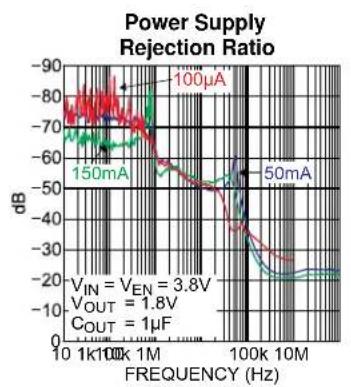
line
| FREQUENCY (Hz) | Power Supply Rejection Ratio (dB) | | -------------- | --------------------------------- | | 10 | -70 | | 1k | -60 | | 100k | -40 | | 1M | -20 | | 100k | -30 | | 10M | -40 |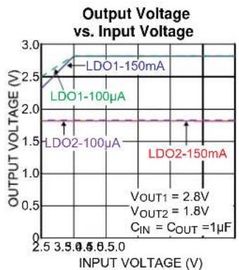
line
| INPUT VOLTAGE (V) | OUTPUT VOLTAGE (V) | | ---------------- | ------------------ | | 2.5 | 2.5 | | 3.5 | 2.7 | | 4.5 | 2.8 | | 5.0 | 2.8 |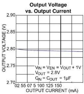
line
| OUTPUT CURRENT (mA) | OUTPUT VOLTAGE (V) | | ------------------- | ------------------ | | 0 | 2.80 | | 55 | 2.79 | | 07 | 2.79 | | 5 | 2.79 | | 100 | 2.79 | | 150 | 2.79 |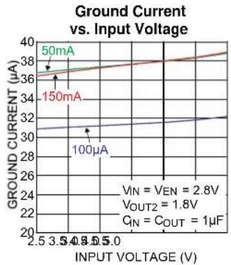
line
| INPUT VOLTAGE (V) | 50mA | 150mA | 100μA | | ----------------- | ---- | ----- | ----- | | 2.5 | 36 | 34 | 31 | | 3.5 | 37 | 35 | 32 | | 4.5 | 38 | 36 | 33 | | 5.0 | 39 | 37 | 34 |
line
| OUTPUT CURRENT (mA) | DUAL OUTPUT (μA) | SINGLE OUTPUT (μA) | | ------------------- | ---------------- | ------------------ | | 02 | 55 | 30 | | 55 | 65 | 35 | | 07 | 68 | 38 | | 100 | 69 | 38 | | 125 | 69 | 38 | | 150 | 69 | 38 |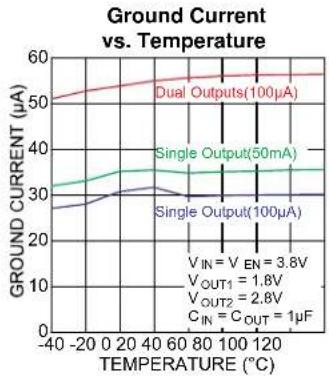
line
| TEMPERATURE (°C) | DUAL OUTPUTS(100μA) | SINGLE OUTPUTS(50mA) | SINGLE OUTPUTS(100μA) | | ---------------- | ------------------- | ------------------- | -------------------- | | -40 | 50 | 30 | 25 | | 0 | 52 | 32 | 26 | | 20 | 53 | 33 | 27 | | 40 | 54 | 34 | 28 | | 60 | 55 | 35 | 29 | | 80 | 56 | 36 | 30 | | 100 | 57 | 37 | 31 | | 120 | 58 | 38 | 32 |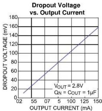
line
| OUTPUT CURRENT (mA) | DROPOUT VOLTAGE (mV) | | ------------------- | -------------------- | | 0 | 0 | | 55 | 20 | | 100 | 40 | | 150 | 60 | | 200 | 80 | | 250 | 100 | | 300 | 120 | | 350 | 140 | | 400 | 160 | | 450 | 180 |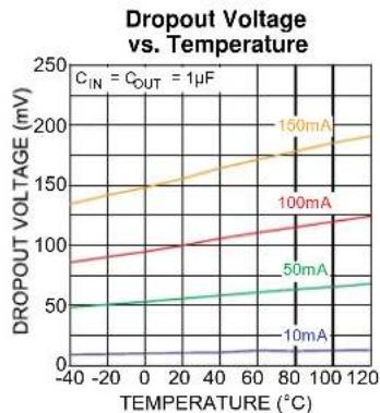
line
| TEMPERATURE (°C) | 10mA | 50mA | 100mA | 150mA | | ---------------- | ---- | ---- | ----- | ----- | | -40 | 50 | 50 | 80 | 130 | | 0 | 50 | 50 | 90 | 140 | | 20 | 50 | 50 | 100 | 150 | | 40 | 50 | 50 | 110 | 160 | | 60 | 50 | 50 | 120 | 170 | | 80 | 50 | 50 | 130 | 180 | | 100 | 50 | 50 | 140 | 190 | | 120 | 50 | 50 | 150 | 200 |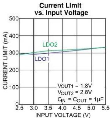
line
| INPUT VOLTAGE (V) | CURRENT LIMIT (mA) | | ----------------- | ------------------ | | 2.5 | 300 | | 3.0 | 300 | | 3.5 | 300 | | 4.0 | 300 | | 4.5 | 300 | | 5.0 | 300 | | 5.5 | 300 |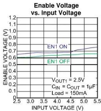
line
| INPUT VOLTAGE (V) | ENABLE VOLTAGE (V) | | ----------------- | ------------------ | | 2.5 | 0.6 | | 3.0 | 0.6 | | 3.5 | 0.6 | | 4.0 | 0.6 | | 4.5 | 0.7 | | 5.0 | 0.7 | | 5.5 | 0.8 |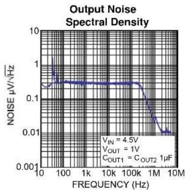
line
| FREQUENCY (Hz) | NOISE μV/Hz | | -------------- | ----------- | | 10 | ~0.3 | | 100 | ~0.3 | | 1k | ~0.3 | | 10k | ~0.3 | | 100k | ~0.3 | | 1M | ~0.01 | | 1MOUT2 | ~0.01 |Functional Characteristics
line
| Parameter | Value | | --------------- | --------- | | VIN | VOUT + 1V | | VOUT1 | 2.8V | | VOUT2 | 1.8V | | CIN | COUT = 1μF | | ILOAD | 150mA |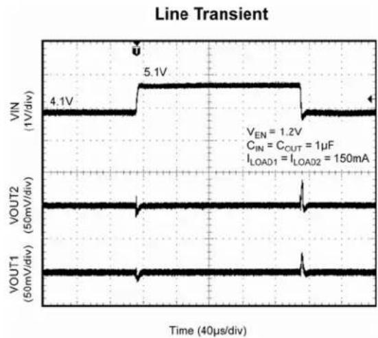
line
| Time (40μs/div) | VIN (1V/div) | VOUT2 (50mV/div) | VOUT1 (50mV/div) | | --------------- | ------------ | ---------------- | ---------------- | | 0 | 4.1 | - | - | | 5.1 | 5.1 | - | - | | 100 | - | - | - | | 150 | - | - | - | | 200 | - | - | - | | 250 | - | - | - | | 300 | - | - | - | | 350 | - | - | - | | 400 | - | - | - |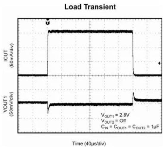
line
| Time (40μs/div) | IOUT (50mA/div) | VOUT1 (50mV/div) | | --------------- | --------------- | ---------------- | | 0 | 0 | 0 | | 1 | High | Low | | 2 | High | Low | | 3 | High | Low | | 4 | High | Low | | 5 | High | Low | | 6 | High | Low | | 7 | High | Low | | 8 | High | Low | | 9 | High | Low | | 10 | High | Low | | 11 | High | Low | | 12 | High | Low | | 13 | High | Low | | 14 | High | Low | | 15 | High | Low | | 16 | High | Low | | 17 | High | Low | | 18 | High | Low | | 19 | High | Low | | 20 | High | Low | | 21 | High | Low | | 22 | High | Low | | 23 | High | Low | | 24 | High | Low | | 25 | High | Low | | 26 | High | Low | | 27 | High | Low | | 28 | High | Low | | 29 | High | Low | | 30 | High | Low | | 31 | High | Low | | 32 | High | Low | | 33 | High | Low | | 34 | High | Low | | 35 | High | Low | | 36 | High | Low | | 37 | High | Low | | 38 | High | Low | | 39 | High | Low | | 40 | High | Low | | 41 | High | Low | | 42 | High | Low | | 43 | High | Low | | 44 | High | Low | | 45 | High | Low | | 46 | High | Low | | 47 | High | Low | | 48 | High | Low | | 49 | High | Low | | 50 | High | Low | | 51 | High | Low | | 52 | High | Low | | 53 | High | Low | | 54 | High | Low | | 55 | High | Low | | 56 | High | Low | | 57 | High | Low | | 58 | High | Low | | 59 | High | Low | | 60 | High | Low | | 61 | High | Low | | 62 | High | Low | | 63 | High | Low | | 64 | High | Low | | 65 | High | Low | | 66 | High | Low | | 67 | High | Low | | 68 | High | Low | | 69 | High | Low | | 70 | High | Low | | 71 | High | Low | | 72 | High | Low | | 73 | High | Low | | 74 | High | Low | | 75 | High | Low | | 76 | High | Low | | 77 | High | Low | | 78 | High | Low | | 79 | High | Low | | 80 | High | Low | | 81 | High | Low | | 82 | High | Low | | 83 | High | Low | | 84 | High | Low | | 85 | High | Low | | 86 | High | Low | | 87 | High | Low | | 88 | High | Low | | 89 | High | Low | | 90 | High | Low | | 91 | High | Low | | 92 | High | Low | | 93 | High | Low | | 94 | High | Low | | 95 | High | Low | | 96 | High | Low | | 97 | High | Low | | 98 | High | Low | | 99 | High | Low | | 100 | High | Low (VOUT1) | | nan | | | | nan | | | | nan | | | | nan | | | | nan | | | | nan | | | | nan | | | | nan | | | | nan | | | | nan | | | | nan | | | | nan | | (VOUT2) | | nan | | (VOUT1) | | nan | | (VOUT2) | | nan | | (VOUT1) | | nan | | (VOUT2) | | | nan | | (CIN = COUT1 = COUT2 = 1μF)|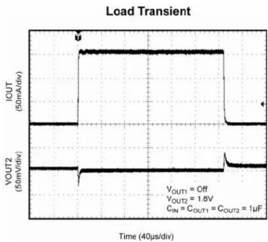
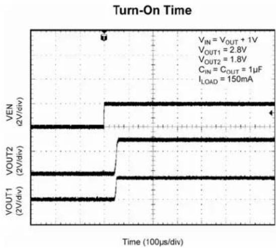
line
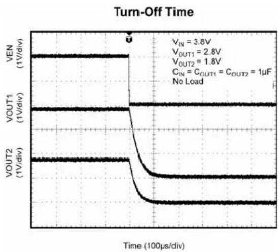
| Time (100μs/div) | VEN (1V/div) | VOUT1 (1V/div) | VOUT2 (1V/div) | | ---------------- | ------------ | -------------- | -------------- | | 0 | 3.8 | 2.8 | 1.8 | | Peak | 3.8 | 2.8 | 1.8 | | Low | 3.8 | 2.8 | 1.8 | | Peak | 3.8 | 2.8 | 1.8 | | Low | 3.8 | 2.8 | 1.8 | | Peak | 3.8 | 2.8 | 1.8 | | Low | 3.8 | 2.8 | 1.8 | | Peak | 3.8 | 2.8 | 1.8 | | Low | 3.8 | 2.8 | 1.8 | | Peak | 3.8 | 2.8 | 1.8 | | Low | 3.8 | 2.8 | 1.8 | | Peak | No Load | No Load | No Load | | Low | ~0 | ~0 | ~0 | | Peak | ~0 | ~0 | ~0 | | Low | ~0 | ~0 | ~0 | | Peak | ~0 | ~0 | ~0 | | Low | ~0 | ~0 | ~0 | | Peak | ~0 | ~0 | ~0 | | Low | ~0 | ~0 | ~0 | | Peak | ~0 | ~0 | ~0 | | Low (Peak) | ~0 | ~0 | ~0 | | Peak (Peak) | ~0 | ~0 | ~0 | | Low (Peak) | ~0 | ~0 | ~0 | | Peak (Peak) | ~0 | ~0 | ~0 | | Low (Peak) | ~0 | ~0 | ~0 | | Peak (Peak) | ~0 | ~0 | ~0 | | Low (Peak) | ~0 (Peak) | ~0 | ~0 | | Peak (Peak) | ~0 (Peak) | ~0 | ~0 | | Low (Peak) | ~0 (Peak) | ~0 | ~0 | | Peak (Peak) | ~0 (Peak) | ~0 | ~0 | | Low (Peak) | ~0 (Peak) | ~0 | ~0 | | Peak (Peak) | ~0 (Peak) | ~0 | ~0 | | Low (~100μs) | ~0 (Peak) | ~0 | ~0 | | Peak (~100μs) | ~3.8 | ~2.8 | ~1.8 | | Low (~100μs) | ~3.8 | ~2.8 | ~1.8 | | Peak (~100μs) | ~3.8 | ~2.8 | ~1.8 | | Low (~100μs) | ~3.8 | ~2.8 | ~1.8 | | Peak (~100μs) | ~3.8 | ~2.8 | ~1.8 | | Low (~100μs) | <3.8 | <3.8 | <3.8 | | Peak (~100μs) | <3.8 | <3.8 | <3.8 | | Low (~100μs) | <3.8 | <3.8 | <3.8 | | Peak (~100μs) | <3.8 | <3.8 | <3.8 | | Low (~100μs) | <3.8 | <3.8 | <3.8 | | Peak (~100μs)|Application Information
MIC5370/1 is a dual 150mA LDO in a small 1.6mm x 1.6mm package.. The MIC5371 includes an auto-discharge circuit for each of the LDO outputs that are activated when the output is disabled. The MIC5370/1 regulator is fully protected from damage due to fault conditions through linear current limiting and thermal shutdown.
Input Capacitor
The MIC5370/1 is a high-performance, high bandwidth device. An input capacitor of 1 F capacitor is required from the input to ground to provide stability. Low-ESR ceramic capacitors provide optimal performance at a minimum of space. Additional high-frequency capacitors, such as small-valued NPO dielectric-type capacitors, help filter out high-frequency noise and are good practice in any RF-based circuit. X5R or X7R dielectrics are recommended for the input capacitor. Y5V dielectrics lose most of their capacitance over temperature and are therefore, not recommended.
Output Capacitor
The MIC5370/1 requires an output capacitor of 1 F or greater to maintain stability. The design is optimized for use with low-ESR ceramic chip capacitors. High ESR capacitors may cause high frequency oscillation. The output capacitor can be increased, but performance has been optimized for a 1 F ceramic output capacitor and does not improve significantly with larger capacitance.
X7R/X5R dielectric-type ceramic capacitors are recommended because of their temperature performance. X7R-type capacitors change capacitance by 15% over their operating temperature range and are the most stable type of ceramic capacitors. Z5U and Y5V dielectric capacitors change value by as much as 50% and 60%, respectively, over their operating temperature ranges. To use a ceramic chip capacitor with Y5V dielectric, the value must be much higher than an X7R ceramic capacitor to ensure the same minimum capacitance over the equivalent operating temperature range.
No-Load Stability
Unlike many other voltage regulators, the MIC5370/1 will remain stable and in regulation with no load. This is especially important in CMOS RAM keep-alive applications.
Enable/Shutdown
The MIC5370/1 comes with two active-high enable pins that allow each regulator to be disabled independently. Forcing the enable pin low disables the regulator and sends it into a "zero" off-mode-current state. In this state, current consumed by the regulator goes nearly to zero. When disabled the MIC5371 switches a 30Ω (typical) load on the regulator output to discharge the external capacitor.
Forcing the enable pin high enables the output voltage. The active-high enable pin uses CMOS technology and the enable pin cannot be left floating; a floating enable pin may cause an indeterminate state on the output..
Thermal Considerations
The MIC5370/1 is designed to provide 150mA of continuous current for both outputs in a very small package. Maximum ambient operating temperature can be calculated based on the output current and the voltage drop across the part. For example if the input voltage is 3.6V, the output voltage is 2.8V for V_OUT1 , 1.8V for V_OUT2 and the output current = 150mA. The actual power dissipation of the regulator circuit can be determined using the equation:
$$ P _ {D} = \left(V _ {\text {IN}} - V _ {\text {OUT1}}\right) I _ {\text {OUT1}} + \left(V _ {\text {IN}} - V _ {\text {OUT2}}\right) I _ {\text {OUT2}} + V _ {\text {IN}} I _ {\text {GND}} $$
Because this device is CMOS and the ground current is typically <100 A over the load range, the power dissipation contributed by the ground current is <1% and can be ignored for this calculation:
$$ \begin{array}{r l} P _ {D} & = (3. 6 \mathrm{V} - 2. 8 \mathrm{V}) \times 1 5 0 \mathrm{mA} + (3. 6 \mathrm{V} - 1. 8) \times 1 5 0 \mathrm{mA} \ P _ {D} & = 0. 3 9 \mathrm{W} \end{array} $$
To determine the maximum ambient operating temperature of the package, use the junction-to-ambient thermal resistance of the device and the following basic equation:
$$ P _ {D (M A X)} = \left(\frac {T - T _ {A J (M A X)}}{\theta_ {J A}}\right) $$
T_J(max) = 125^ , and the maximum junction temperature of the die, _JA , thermal resistance = 90°C/W.
Substituting P_D for P_D(max) and solving for the ambient operating temperature will give the maximum operating conditions for the regulator circuit. The junction-to-ambient thermal resistance for the minimum footprint is 90°C/W.
The maximum power dissipation must not be exceeded for proper operation.
For example, when operating the MIC5370-MGYMT at an input voltage of 3.6V and 150mA loads at each output with a minimum footprint layout, the maximum ambient operating temperature T_A can be determined as follows:
$$ 0. 3 9 \mathrm{W} = (1 2 5 ^ {\circ} \mathrm{C} - \mathrm{T} _ {\mathrm{A}}) / (9 0 ^ {\circ} \mathrm{C} / \mathrm{W}) $$
$$ T _ {A} = 8 9. 9 ^ {\circ} C $$
Therefore, a 2.8V/1.8V application with 150mA at each output current can accept an ambient operating temperature of 89.9°C in a 1.6mm x 1.6mm MLF® package. For a full discussion of heat sinking and thermal effects on voltage regulators, refer to the "Regulator Thermals" section of Micrel's Designing with Low-Dropout Voltage Regulators handbook. This information can be found on Micrel's website at: http://www.micrel.com/ PDF/other/LDOBk_ds.pdf
text_image
U1 MIC5370/1-xxYMT VIN VOUT1 6 J3 VOUT1 VIN VOUT2 5 J5 EN1 EN2 EN1 GND 4 J8 GND C3 1μF/10V 2 C1 1μF/10V C2 1μF/10V J2 GND J4 GND J6 GNDBill of Materials
| Item | Part | Number | Manufacturer | Description | |
| C1, C2, C3 | GRM188R60J225KE19D | Murata ^(1) | Capacitor, 1μF Ceramic, 10V, X5R, Size 0402 3 | ||
| U1 | MIC5370/1-XXYMT | Micref ^(2) Dual, 150mA LDO, Size 1.6mm x 1.6mm Thin MLF® | 1 | ||
Notes:
1. Murata: www.murata.com
2. Micrel, Inc.: www.micrel.com
PCB Layout Recommendations
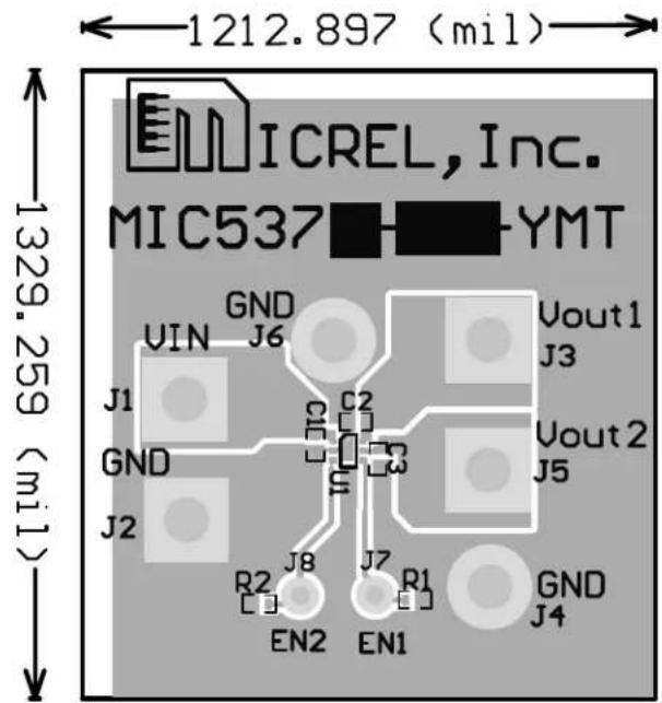
text_image
1212.897 (mil) MIC537 YMT 1329.259 (mil) ICREL, Inc. UIN GND J6 J1 C2 Vout1 GND C1 Vout2 J2 U1 J3 R2 J8 J7 R1 GND EN2 EN1 J4Top Layer
text_image
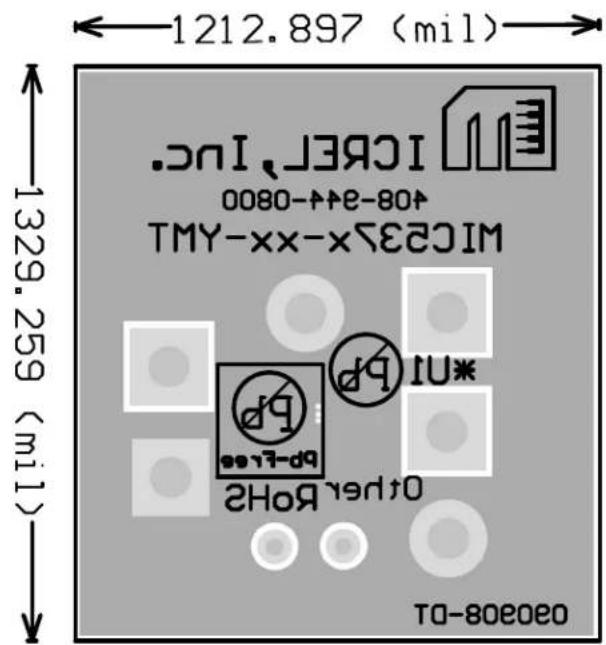
1212.897 (mil) ICBER, Inc. 000-44-0800 TMY-xx-XXIM MIC35X-XX-MLT *NU bp bp-16a p0 p0-16a p0-16a p0-16a p0-16a p0-16a p0-16a p0-16a p0-16a p0-16a p0-16a p0-16a p0-16a p0-16a p0-16a p0-16a TO-80e0eoBottom Layer
Package Information
NOTE:
1. ALL DIMENSIONS ARE IN MILLIMETERS.
2. MAX. PACKAGE WARPAGE IS 0.05 mm.
3. MAXIMUM ALLOWABLE BURRS IS 0.076 mm IN ALL DIRECTIONS.
4. PIN #1 ID ON TOP WILL BE LASER/INK MARKED.
5. DIMENSION APPLIES TO METALIZED TERMINAL AND IS MEASURED
750 DIMENSION APPLIES TO RETALIZED TERMINAL AND BETWEEN 0.20 AND 0.25 nm FROM TERMINAL TIP.
APPLIED ONLY FOR TERMINALS
APPLIED FOR EXPOSED PAD AND TERMINALS.
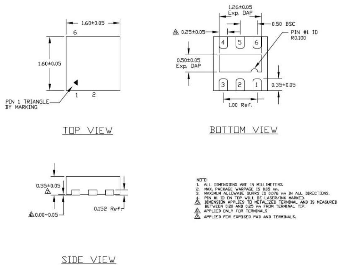
6-Pin 1.6mm x 1.6mm Thin MLF ^® (MT)
MICREL, INC. 2180 FORTUNE DRIVE SAN JOSE, CA 95131 USA
TEL +1 (408) 944-0800 FAX +1 (408) 474-1000 WEB http://www.micrel.com
Micrel makes no representations or warranties with respect to the accuracy or completeness of the information furnished in this data sheet. This information is not intended as a warranty and Micrel does not assume responsibility for its use. Micrel reserves the right to change circuitry, specifications and descriptions at any time without notice. No license, whether express, implied, arising by estoppel or otherwise, to any intellectual property rights is granted by this document. Except as provided in Micrel's terms and conditions of sale for such products, Micrel assumes no liability whatsoever, and Micrel disclaims any express or implied warranty relating to the sale and/or use of Micrel products including liability or warranties relating to fitness for a particular purpose, merchantability, or infringement of any patent, copyright or other intellectual property right.
Micrel Products are not designed or authorized for use as components in life support appliances, devices or systems where malfunction of a product can reasonably be expected to result in personal injury. Life support devices or systems are devices or systems that (a) are intended for surgical implant into the body or (b) support or sustain life, and whose failure to perform can be reasonably expected to result in a significant injury to the user. A Purchaser's use or sale of Micrel Products for use in life support appliances, devices or systems is a Purchaser's own risk and Purchaser agrees to fully indemnify Micrel for any damages resulting from such use or sale.
© 2008 Micrel, Incorporated.