MIC5374 - Electronic component Microchip - Free user manual and instructions
Find the device manual for free MIC5374 Microchip in PDF.

User questions about MIC5374 Microchip
0 question about this device. Answer the ones you know or ask your own.
Ask a new question about this device
Download the instructions for your Electronic component in PDF format for free! Find your manual MIC5374 - Microchip and take your electronic device back in hand. On this page are published all the documents necessary for the use of your device. MIC5374 by Microchip.
USER MANUAL MIC5374 Microchip
The MIC5374/84 is a four output device with three 200mA LDOs and a real time clock (RTC) 1mA LDO which is ideal for application processor support in mobile platforms. The MIC5374 provides independent control active high enables for each of the 200mA LDOs with an additional always-on RTC LDO. The MIC5384 provides active low enables. Both the MIC5374 and MIC5384 are available in the tiny 2.5mm x 2.5mm Thin MLF® package.
The MIC5374/84 is designed for high input ripple rejection (high PSRR) and provides low output noise making it ideal for powering sensitive RF circuitry such as GPS, WiFi, and Bluetooth applications. The MIC5374/84 also incorporates a power-on-reset (POR) supervisor with adjustable delay time set by an external capacitor, and an independent input pin to monitor any voltage level. Once high, the POR output can be asserted low again by enabling the manual reset (MR) pin. When the MR pin is restored low, the POR output will re-time the delay set by the external delay capacitor.
The MIC5374/84 operates with very small ceramic output capacitors to reduce board space and component cost. It is available in various fixed output voltages. The MIC5374/84 has a junction temperature range from -40^ to 125^ .
Datasheets and support documentation can be found on Micrel's web site at: www.micrel.com.
Features
• 1.7V to 5.5V input supply voltage range
• Output current - 200mA LDO1/2/3, 1mA LDO4
- LDO4 – Ultra low 8μA I _BIAS for RTC support
• High output accuracy (±2%)
- Independent enable pins
• POR with user-defined voltage monitoring
- POR voltage input
- Adjustable delay time
- Manual reset pin
- Low dropout voltage – 170mV at 150mA
• High PSRR – 55dB at 1kHz on each LDO
- Stable with tiny ceramic output capacitors
- 2.5mm x 2.5mm Thin MLF 16-pin package
• Thermal-shutdown and current-limit protection
Applications
- Mobile phones
- GPS receivers
• Application co-processors
• PDAs and handheld devices
Typical Application
text_image
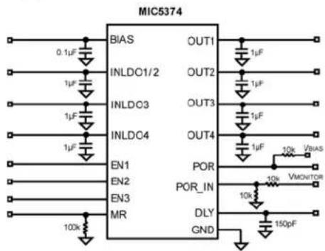
MIC5374 0.1µF BIAS OUT1 1µF INLDC1/2 OUT2 1µF INLDO3 OUT3 1µF INLDO4 OUT4 1µF EN1 POR 10k Vbias EN2 POR_IN 10k Vmonitor EN3 DLY 10k MR GND 150pFTypical MIC5374-xxxYMT Circuit (Active High Enable)

text_image
MIC5384 BIAS OUT1 INLDO1/2 1μF OUT2 INLDO3 1μF OUT3 INLDO4 1μF OUT4 1μF EN1 POR 10k Vbias EN2 Vmonitor EN3 POR_IN 10k DLY 150pF GND MR 100kTypical MIC5384-xxxYMT Circuit (Active Low Enable)
MLF and MicroLeadFrame are registered trademarks of Amkor Technology, Inc.
Micrel Inc. • 2180 Fortune Drive • San Jose, CA 95131 • USA • tel +1 (408) 944-0800 • fax +1 (408) 474-1000 • http://www.micrel.com
Ordering Information
| Part Number | Mark Code | Output Voltage^(1) | Junction Temperature Range | Package | Lead (2) |
| MIC5374-MG44YMT | MG44 | 2.8V/1.8V/1.2/1.2V | -40° to +125°C | 16-Pin 2.5mm x 2.5mm Thin MLF | Pb-free |
| MIC5374-SJG1YMT | SJG1 | 3.3V/2.5V/1.8V/1.0V | -40° to +125°C | 16-Pin 2.5mm x 2.5mm Thin MLF | Pb-free |
| MIC5384-MG44YMT | Z1U | 2.8V/1.8V/1.2/1.2V | -40° to +125°C | 16-Pin 2.5mm x 2.5mm Thin MLF | Pb-free |
| MIC5384-SJG1YMT | Z5U | 3.3V/2.5V/1.8V/1.0V | -40° to +125°C | 16-Pin 2.5mm x 2.5mm Thin MLF | Pb-free |
Note:
- Other voltage options available. Contact Micrel for details.
- Lead finish is NiPdAu. Mold compound material is halogen free.
Pin Configuration
text_image
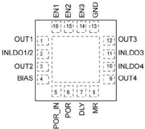
EN1 EN2 EN3 GND 16 15 14 13 OUT1 1 OUT3 INLDO1/2 2 INLDO3 OUT2 3 INLDO4 BIA5 4 OUT4 5 6 7 8 POR_IN POR DLY MRMIC5374 16-Pin 2.5mm x 2.5mm Thin MLF (MT) (Top View)
text_image
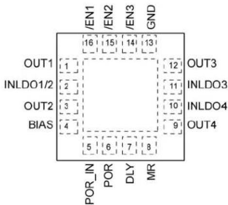
/EN1 /EN2 /EN3 GND OUT1 16 15 14 13 INLDO1/2 2 12 OUT3 OUT2 3 11 INLDO3 BIAS 4 10 INLDO4 5 6 7 8 OUT4 POR_IN POR DLY MRMIC5384 16-Pin 2.5mm x 2.5mm Thin MLF (MT) (Top View)
Pin Description
| Pin Number | Pin Name | Pin Function |
| 1 OUT1 | Regulator Output - LDO1. | |
| 2 INLDO | 1/2 Supply Input (LDO1/2). | |
| 3 OUT2 | Regulator Output – LDO2. | |
| 4 BIAS | Internal Bias Supply Voltage. Must be de-coupled to ground with a 0.1μF capacitor. | |
| 5 | POR_IN | Input to POR. Connect directly to output voltage or input voltage that is to be monitored for a 0.9V reference, or connect a resistor divider network to this pin to program the POR monitoring voltage. |
| 6 POR | Power-on-Reset | Output. Open drain. |
| 7 DLY | POR Delay Capacitor. Connect capacitor to ground to set POR delay time. | |
| 8 | MR | Manual Reset Input. Manually resets output of POR and delay generator. Do not leave floating. |
| 9 OUT4 | Regulator Output - LDO4. | |
| 10 | INLDO4 | Supply Input (LDO4). Ultra-low IQ RTC LDO. 1.7V to 5.5V input voltage range. |
| 11 | INLDO3 | Supply Input (LDO3). |
| 12 | OUT3 Regulator Output – LDO3. | |
| 13 | GND | Ground. |
| 14 | EN3 or /EN3 | LDO3 Enable Input. EN (MIC5374): Active High Input. Logic High = On; Logic Low = Off; /EN (MIC5384): Active Low Input. Logic High = Off; Logic Low = On. Do not leave floating. |
| 15 | EN2 or /EN2 | LDO2 Enable Input. EN (MIC5374): Active High Input. Logic High = On; Logic Low = Off; /EN (MIC5384): Active Low Input. Logic High = Off; Logic Low = On; Do not leave floating. |
| 16 | EN1 or /EN1 | LDO1 Enable Input. EN (MIC5374): Active High Input. Logic High = On; Logic Low = Off; /EN (MIC5384): Active Low Input. Logic High = Off; Logic Low = On; Do not leave floating. |
| HS Pad | EPAD | Exposed Heat Sink Pad. Connect to GND. |
Absolute Maximum Ratings ^(1)
Supply Voltage ( V_INLDO1/2, INLDO3, INLDO4 ) ..... -0.3V to +6V
Bias Supply Voltage ( V_BIAS )....-0.3V to +6V
Enable Input Voltage ( V_EN1, EN2, EN3 )....-0.3V to +6V
POR Output Voltage (POR) ...... -0.3V to +6V
POR Input Voltage (POR_IN) ....-0.3V to +6V
MR Voltage (MR) -0.3V to +6V
DLY Voltage (DLY)....-0.3V to +6V
Power Dissipation .... Internally Limited ^(2)
Lead Temperature (soldering, 10s).... 260°C
Storage Temperature ( T_s ) -60^ to +150^
ESD Rating ^(3) ESD Sensitive
Operating Ratings ^(4)
Supply Voltage ^(5) ( V_INLDO1/2, INLDO3, INLDO4 ) ..... +1.7V to V_BIAS
Bias Supply Voltage ( V_BIAS )....+2.5V to +5.5V
Enable Input Voltage (V EN1, EN2, EN3 )...... 0V to V BIAS
POR Output Voltage (POR) 0V to +5.5V
POR Input Voltage (POR_IN) 0V to VBIAS
MR Voltage (MR) 0V to V_BIAS
DLY Voltage (DLY).... 0V to V _BIAS
Junction Temperature (T _J ) ...... -40°C to +125°C
Junction Thermal Resistance
2.5 x 2.5 Thin MLF 16L ( _JA ).....100°C/W
Electrical Characteristics ^(6)
(MIC5374) V_IN = V_OUT + 1V ( V_OUT is highest of the three regulator outputs); V_BIAS = V_EN1 = V_EN2 = V_EN3 = 5.5V (ON);
(MIC5384) V_IN = V_OUT + 1V ( V_OUT is highest of the three regulator outputs); V_BIAS = 5.5V ; V_/EN1 = V_/EN2 = V_/EN3 = GND (ON);
I_OUT1 = I_OUT2 = I_OUT3 = I_OUT4 = 100 A; C_OUT1 = C_OUT2 = C_OUT3 = C_OUT4 = 1 F; T_A = 25^.
Bold values indicate -40^ ≤ T_J ≤ +125^ , unless noted.
| Parameter | Conditions | Min. | |||
| Output Voltage Accuracy (LDO1/2/3) | Variation from nominal V_OUT1,2,3 | -2.0 | +2.0 | % | |
| Variation from nominal V_OUT1,2,3 | -3.0 | +3.0 | |||
| Output Voltage Accuracy (LDO4 - RTC Support) | Variation from nominal V_OUT4 | -4.0 | +4.0 | % | |
| Variation from nominal V_OUT4 | -5.0 | +5.0 | |||
| Line Regulation V | _IN=V_OUT+1V to 5.5V; I_OUT=100μA 0.02 0.3 | %/V | |||
| Load Regulation | I_OUT=100μA to 150mA; LDO1/2/3 | 0.3 | 1 | % | |
| I_OUT=100μA to 1mA; LDO4 | 0.05 | 1 | |||
| Dropout Voltage | I_OUT=50mA; V_OUT≥ 2.8V | 60 | 115 | mV | |
| I_OUT=150mA; V_OUT≥ 2.8V | 170 | 330 | |||
| I_OUT=50mA; V_OUT<2.8V | 85 | 145 | |||
| I_OUT=150mA; V_OUT<2.8V | 275 | 450 | |||
| Input Ground Current | EN1 or EN2 or EN3 = ON; Not including I_BIAS | 10 | 20 | μA | |
| LDO4; EN1 = EN2 = EN3 = OFF; Not including I_BIAS | 3 | 8 | |||
| Input Bias Current | EN1 or EN2 or EN3 = ON; with LDO4 ON | 42 | 70 | μA | |
| EN1 = EN2 = EN3 = ON; with LDO4 ON | 106 | 170 | |||
| Shutdown Input Ground Current | EN1 = EN2 = EN3 = OFF | 0.04 | 2 | μA | |
| Shutdown Bias Current | EN1 = EN2 = EN3 = OFF; with LDO4 ON | 8 | 13 | μA | |
| Ripple Rejection | f = 1kHz; C_OUT=1.0μF | 55 | dB | ||
| Current Limit | V_OUT=0V; LDO1/2/3 | 200 | 350 | 700 | mA |
| V_OUT=0V; LDO4 | 2 | 12 | 50 | ||
Notes:
- Exceeding the absolute maximum rating may damage the device.
- The maximum allowable power dissipation of any T_A (ambient temperature) is P_D() = (T_J() - T_A) / _JA . Exceeding the maximum allowable power dissipation will result in excessive die temperature and the regulator will go into thermal shutdown.
- Devices are ESD sensitive. Handling precautions recommended. Human body model, 1.5kΩ in series with 100pF.
- The device is not guaranteed to function outside its operating rating.
- For V_IN range of 1.7V to 2.5V, output current is limited to 30mA.
- Specification for packaged product only.
Electrical Characteristics ^(6) (Continued)
(MIC5374) V_IN = V_OUT + 1V ( V_OUT is highest of the three regulator outputs); V_BIAS = V_EN1 = V_EN2 = V_EN3 = 5.5V (ON);
(MIC5384) V_IN = V_OUT + 1V ( V_OUT is highest of the three regulator outputs); V_BIAS = 5.5V ; V_/EN1 = V_/EN2 = V_/EN3 = GND (ON);
I_OUT1 = I_OUT2 = I_OUT3 = I_OUT4 = 100 A; C_OUT1 = C_OUT2 = C_OUT3 = C_OUT4 = 1 F; T_A = 25^.
Bold values indicate -40^ ≤ T_J ≤ +125^ , unless noted.
| Parameter | Conditions | Min. | Typ. | ||
| Output Voltage Noise C | _OUT = 1μF,10Hz to 100kHz; I_OUT = 150mA 200 μV | RMS | |||
| Enable Input Voltage | (MIC5374) LDO OFF; (MIC5384) LDO ON | 0.2 | V | ||
| (MIC5374) LDO ON; (MIC5384) LDO OFF | 1.2 | ||||
| Enable Input Current | VIL ≤ 0.2V | 0.01 | μA | ||
| VIH ≥ 1.2V | 0.01 | ||||
| Turn-On Time C | _OUT = 1μF 80 | 200 | μs | ||
| V_POR POR Output Low Voltage | 0.2 | V | |||
| DLY Pin Current Source | V_DLY = 0V | 0.75 | 1.25 | 2 | μA |
| DLY Pin Voltage Threshold | 1.13 | 1.25 | 1.38 | V | |
| I_POR | POR Output Leakage Current, V_POR OFF | 1 | μA | ||
| V_TH | POR Undervoltage Threshold | 0.873 | 0.9 | 0.927 | V |
| V_HYS | POR Voltage Threshold Hysteresis | 34 | mV | ||
| I_POR\_IN | POR Input Pin Leakage Current | 1 | μA | ||
| Thermal Shutdown | 155 | °C | |||
| Thermal-Shutdown Hysteresis | 10 | °C | |||
Typical Characteristics
line
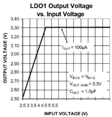
| INPUT VOLTAGE (V) | OUTPUT VOLTAGE (V) | | ----------------- | ------------------ | | 2.5 | 2.5 | | 3.0 | 2.7 | | 3.5 | 2.9 | | 4.0 | 3.0 | | 4.5 | 3.3 | | 5.0 | 3.3 | | 5.5 | 3.3 |
line
| INPUT VOLTAGE (V) | OUTPUT VOLTAGE (V) | | ----------------- | ------------------ | | 2 | 2.50 | | 5 | 3.25 | | 3 | 3.30 | | 4 | 3.30 |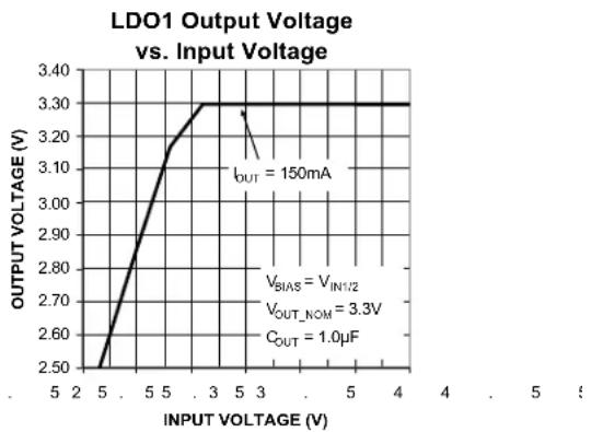
line
| INPUT VOLTAGE (V) | OUTPUT VOLTAGE (V) | | ----------------- | ------------------ | | 2 | 2.50 | | 3 | 3.30 |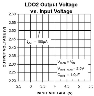
line
| INPUT VOLTAGE (V) | OUTPUT VOLTAGE (V) | | ----------------- | ------------------ | | 3.0 | 2.45 | | 3.5 | 2.45 | | 4.0 | 2.45 | | 4.5 | 2.45 | | 5.0 | 2.45 | | 5.5 | 2.45 |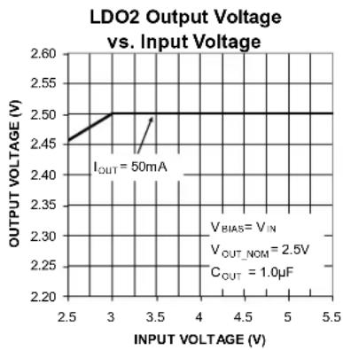
line
| INPUT VOLTAGE (V) | OUTPUT VOLTAGE (V) | | ----------------- | ------------------ | | 2.5 | 2.45 | | 3.0 | 2.50 | | 3.5 | 2.45 | | 4.0 | 2.50 | | 4.5 | 2.50 | | 5.0 | 2.50 | | 5.5 | 2.50 |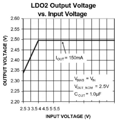
line
| INPUT VOLTAGE (V) | OUTPUT VOLTAGE (V) | | ----------------- | ------------------ | | 2.5 | 2.35 | | 3.5 | 2.50 | | 4.5 | 2.50 | | 5.5 | 2.50 |
line
| INPUT VOLTAGE (V) | OUTPUT VOLTAGE (V) | | ----------------- | ------------------ | | 1.7 | 1.7 | | 2.2 | 1.8 | | 2.7 | 1.8 | | 3.2 | 1.8 | | 3.7 | 1.8 | | 4.2 | 1.8 | | 4.7 | 1.8 | | 5.2 | 1.8 | | 5.7 | 1.8 |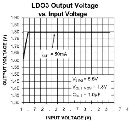
line
| INPUT VOLTAGE (V) | OUTPUT VOLTAGE (V) | | ----------------- | ------------------ | | 1 | 1.60 | | 2 | 1.80 | | 3 | 1.80 | | 4 | 1.80 |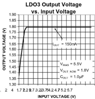
line
| INPUT VOLTAGE (V) | OUTPUT VOLTAGE (V) | | ----------------- | ------------------ | | 1.7 | 1.35 | | 2.2 | 1.80 | | 2.7 | 1.80 | | 3.2 | 1.80 | | 3.7 | 1.80 | | 4.2 | 1.80 | | 4.7 | 1.80 | | 5.2 | 1.80 | | 5.7 | 1.80 |Typical Characteristics (Continued)

line
| INPUT VOLTAGE (V) | OUTPUT VOLTAGE (V) | | ----------------- | ------------------ | | 2.7 | 1.00 | | 3.2 | 1.00 | | 3.7 | 1.00 | | 4.2 | 1.00 | | 4.7 | 1.00 | | 5.2 | 1.00 | | 5.7 | 1.00 |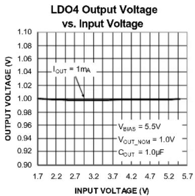
line
| INPUT VOLTAGE (V) | OUTPUT VOLTAGE (V) | | ----------------- | ------------------ | | 2.7 | 1.02 | | 3.2 | 1.00 |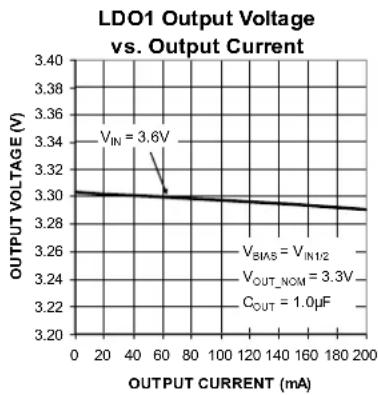
line
| OUTPUT CURRENT (mA) | OUTPUT VOLTAGE (V) | | ------------------- | ------------------ | | 0 | 3.30 | | 60 | 3.30 | | 200 | 3.29 |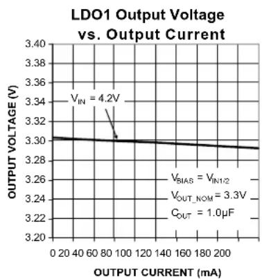
line
| OUTPUT CURRENT (mA) | OUTPUT VOLTAGE (V) | | ------------------- | ------------------ | | 0 | 3.30 | | 20 | 3.30 | | 40 | 3.30 | | 60 | 3.30 | | 80 | 3.30 | | 100 | 3.28 | | 120 | 3.28 | | 140 | 3.28 | | 160 | 3.28 | | 180 | 3.28 | | 200 | 3.28 |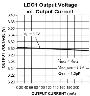
line
| OUTPUT CURRENT (mA) | OUTPUT VOLTAGE (V) | | ------------------- | ------------------ | | 0 | 3.30 | | 40 | 3.30 | | 80 | 3.30 | | 120 | 3.30 | | 160 | 3.30 | | 200 | 3.30 |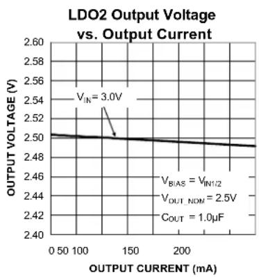
line
| OUTPUT CURRENT (mA) | OUTPUT VOLTAGE (V) | | ------------------- | ------------------ | | 0 | 2.50 | | 100 | 2.50 | | 150 | 2.49 | | 200 | 2.48 |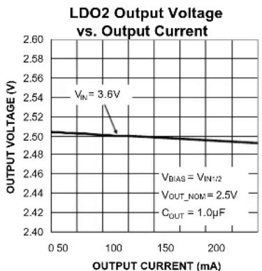
line
| OUTPUT CURRENT (mA) | OUTPUT VOLTAGE (V) | | ------------------- | ------------------ | | 0 | 2.50 | | 100 | 2.48 | | 200 | 2.46 |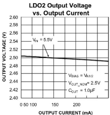
line
| OUTPUT CURRENT (mA) | OUTPUT VOLTAGE (V) | | ------------------- | ------------------ | | 0 | 2.50 | | 100 | 2.50 | | 130 | 2.54 | | 200 | 2.49 |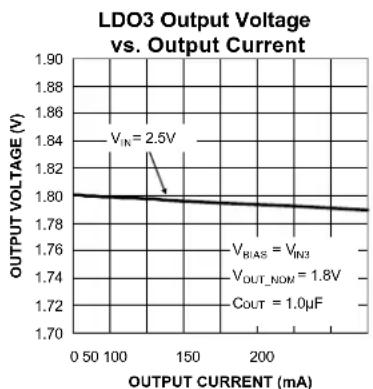
line
| OUTPUT CURRENT (mA) | OUTPUT VOLTAGE (V) | | ------------------- | ------------------ | | 0 | 1.80 | | 50 | 1.80 | | 100 | 1.80 | | 150 | 1.80 | | 200 | 1.79 |Typical Characteristics (Continued)
line
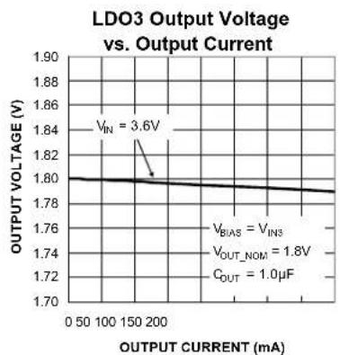
| OUTPUT CURRENT (mA) | OUTPUT VOLTAGE (V) | | ------------------- | ------------------ | | 0 | 1.80 | | 50 | 1.80 | | 100 | 1.80 | | 150 | 1.80 | | 200 | 1.79 |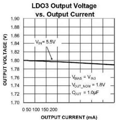
line
| OUTPUT CURRENT (mA) | OUTPUT VOLTAGE (V) | | ------------------- | ------------------ | | 0 | 1.80 | | 50 | 1.80 | | 100 | 1.80 | | 150 | 1.80 | | 200 | 1.80 |
line
| OUTPUT CURRENT (mA) | OUTPUT VOLTAGE (V) | | ------------------- | ------------------ | | 0 | 1.00 | | 1.0 | 1.02 | | 5.0 | 1.00 |
line
| OUTPUT CURRENT (mA) | OUTPUT VOLTAGE (V) | | ------------------- | ------------------ | | 0 | 1.00 | | 5 | 1.00 | | 1 | 1.00 | | 2 | 1.00 | | 3 | 1.00 | | 5 | 1.00 | | 1 | 1.00 | | 2 | 1.00 | | 3 | 1.00 | | 5 | 1.00 | | 1 | 1.00 | | 2 | 1.00 | | 3 | 1.00 | | 5 | 1.00 | | 1 | 1,000 | | 2 | 1,000 | | 3 | 1,000 | | 5 | 1,000 | | 1 | 1,000 | | 2 | 1,000 | | 3 | 1,000 | | 5 | 1,000 | | 1 | 1,000 | | 2 | 1,000 | | 3 | 1,000 | | 5 | 1.00 | | 1 | 1,00 | | 2 | 1,00 | | 3 | 1,00 | | 5 | 1,00 | | 1 | 1,00 | | 2 | 1,00 | | 3 | 1,00 | | 5 | 1,00 | | 1 | 1,00 | | 2 | 1,00 | | 3 | 1,00 | | 5 | 1,00 |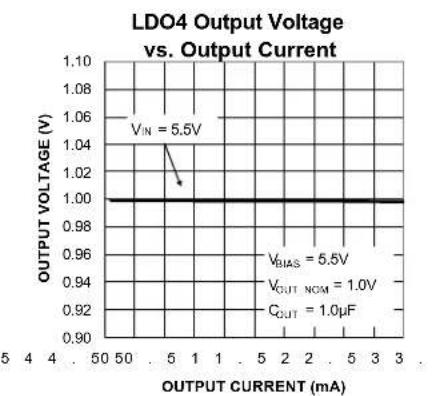
line
| OUTPUT CURRENT (mA) | OUTPUT VOLTAGE (V) | | ------------------- | ------------------ | | 5 | 1.02 | | 5.5 | 1.04 | | 1 | 1.00 | | 5 | 1.00 |
line
| TEMPERATURE (°C) | OUTPUT VOLTAGE (V) | | ---------------- | ------------------ | | -40 | 3.30 | | 0 | 3.30 | | 20 | 3.29 | | 40 | 3.28 | | 60 | 3.27 | | 80 | 3.26 | | 100 | 3.25 | | 120 | 3.24 |
line
| TEMPERATURE (°C) | OUTPUT VOLTAGE (V) | | --------------- | ------------------ | | -40 | 2.50 | | 0 | 2.50 | | 20 | 2.50 | | 40 | 2.49 | | 60 | 2.48 | | 80 | 2.47 | | 100 | 2.46 | | 120 | 2.45 |
line
| TEMPERATURE (°C) | OUTPUT VOLTAGE (V) | | --------------- | ------------------ | | -40 | 1.80 | | 0 | 1.80 | | 20 | 1.80 | | 40 | 1.80 | | 60 | 1.80 | | 80 | 1.80 | | 100 | 1.79 | | 120 | 1.78 |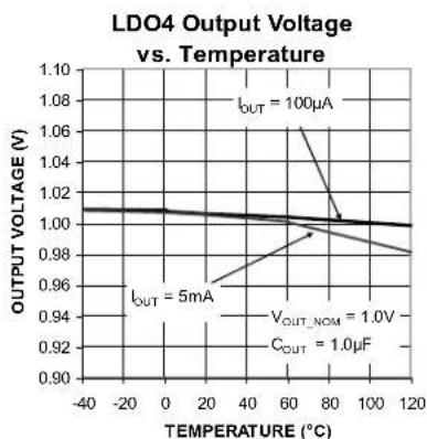
line
| TEMPERATURE (°C) | OUTPUT VOLTAGE (V) | | --------------- | ------------------ | | -40 | 1.02 | | 0 | 1.02 | | 20 | 1.02 | | 40 | 1.02 | | 60 | 1.02 | | 80 | 1.02 | | 100 | 1.02 | | 120 | 1.02 |Typical Characteristics (Continued)
line
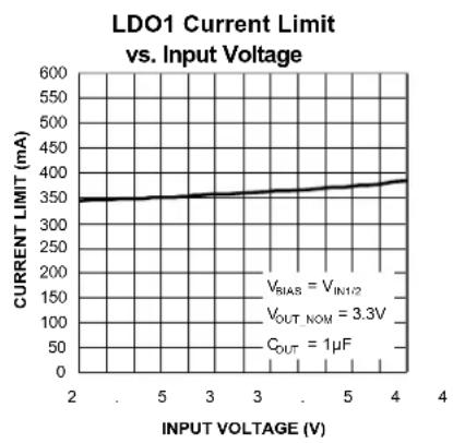
| INPUT VOLTAGE (V) | CURRENT LIMIT (mA) | | ----------------- | ------------------ | | 2 | 350 | | 5 | 360 | | 3 | 370 | | 5 | 380 | | 4 | 390 |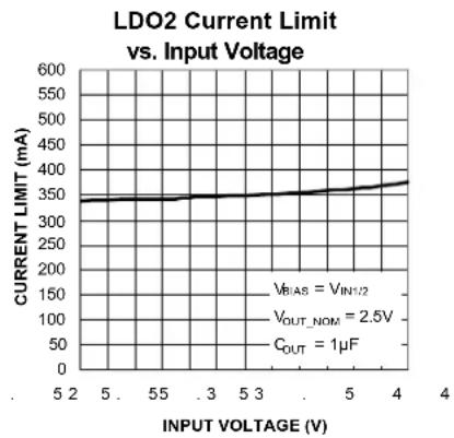
line
| INPUT VOLTAGE (V) | CURRENT LIMIT (mA) | | ----------------- | ------------------ | | 5 | 350 | | 4 | 370 |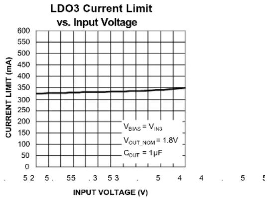
line
| INPUT VOLTAGE (V) | CURRENT LIMIT (mA) | | ----------------- | ------------------ | | 5 | 320 | | 4 | 330 |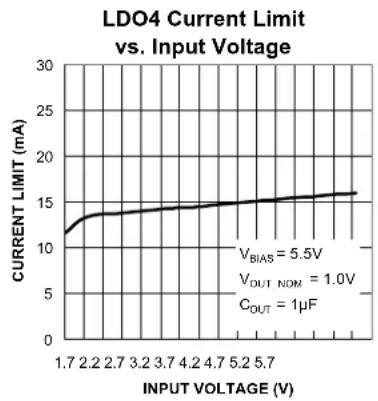
line
| INPUT VOLTAGE (V) | CURRENT LIMIT (mA) | | ----------------- | ------------------ | | 1.7 | 12.0 | | 2.2 | 13.5 | | 2.7 | 14.0 | | 3.2 | 14.5 | | 3.7 | 14.8 | | 4.2 | 15.0 | | 4.7 | 15.2 | | 5.2 | 15.5 | | 5.7 | 15.8 |
line
| V_BIAS (V) | V_IN (V) | V_OUT_NOM (V) | C_OUT (F) | | ---------- | -------- | ------------- | --------- | | 4.3 | 4.3 | 3.3 | 1 |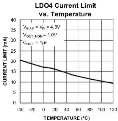
line
| TEMPERATURE (°C) | CURRENT LIMIT (mA) | | ---------------- | ------------------ | | -40 | 20 | | 0 | 18 | | 20 | 16 | | 40 | 14 | | 60 | 12 | | 80 | 10 | | 100 | 8 | | 120 | 6 |
line
| TEMPERATURE (°C) | I_OUT (mA) | V_BIAS (V) | V_OUT_NOM (V) | C_OUT (μF) | | ---------------- | ---------- | ---------- | ------------- | ---------- | | -40 | 120 | 4.3 | 3.3 | 1 | | 0 | 140 | 4.3 | 3.3 | 1 | | 20 | 160 | 4.3 | 3.3 | 1 | | 40 | 170 | 4.3 | 3.3 | 1 | | 60 | 180 | 4.3 | 3.3 | 1 | | 80 | 190 | 4.3 | 3.3 | 1 | | 100 | 195 | 4.3 | 3.3 | 1 | | 120 | 200 | 4.3 | 3.3 | 1 |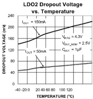
line
| TEMPERATURE (°C) | DROPOUT VOLTAGE (mV) | | --------------- | -------------------- | | -40 | 150 | | 0 | 160 | | 20 | 170 | | 40 | 180 | | 60 | 190 | | 80 | 200 | | 100 | 210 | | 120 | 220 | | 140 | 230 | | 160 | 240 |
line
| TEMPERATURE (°C) | I_OUT (mA) | V_BIAS (V) | V_OUT_NOM (V) | C_OUT (μF) | | --------------- | ---------- | ---------- | ------------- | ---------- | | -40 | 200 | 4.3 | 1.8 | 1 | | 0 | 240 | 4.3 | 1.8 | 1 | | 20 | 260 | 4.3 | 1.8 | 1 | | 40 | 280 | 4.3 | 1.8 | 1 | | 60 | 290 | 4.3 | 1.8 | 1 | | 80 | 295 | 4.3 | 1.8 | 1 | | 100 | 298 | 4.3 | 1.8 | 1 | | 120 | 300 | 4.3 | 1.8 | 1 |Typical Characteristics (Continued)
line
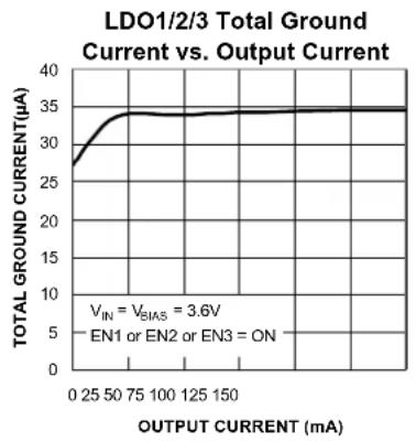
| OUTPUT CURRENT (mA) | TOTAL GROUND CURRENT(μA) | | ------------------- | ------------------------ | | 0 | 27 | | 25 | 30 | | 50 | 33 | | 75 | 34 | | 100 | 34 | | 125 | 34 | | 150 | 34 |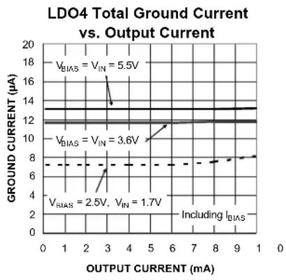
line
| V_BIAS | V_IN (μA) | | ------ | --------- | | 5.5 | 16 | | 3.6 | 12 | | 2.5 | 8 | | 1.7 | 6 |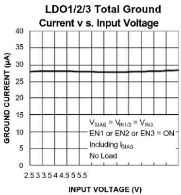
line
| INPUT VOLTAGE (V) | GROUND CURRENT (μA) | | ----------------- | ------------------- | | 2.5 | 28 | | 3 | 28 | | 3.5 | 28 | | 4 | 28 | | 4.5 | 28 | | 5 | 28 | | 5.5 | 28 |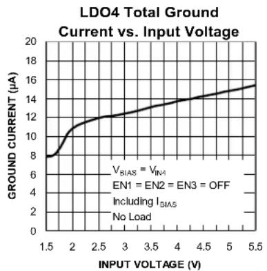
line
| INPUT VOLTAGE (V) | GROUND CURRENT (pA) | | ----------------- | ------------------- | | 1.5 | 8.0 | | 2.0 | 10.0 | | 2.5 | 11.5 | | 3.0 | 12.5 | | 3.5 | 13.0 | | 4.0 | 13.5 | | 4.5 | 14.0 | | 5.0 | 14.5 | | 5.5 | 15.0 |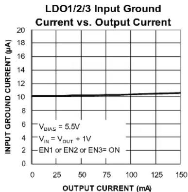
line
| OUTPUT CURRENT (mA) | INPUT GROUND CURRENT (μA) | | ------------------- | ------------------------- | | 0 | 10 | | 25 | 10 | | 50 | 10 | | 75 | 10 | | 100 | 10 | | 125 | 10 | | 150 | 10 |
line
| OUTPUT CURRENT (mA) | INPUT GROUND CURRENT (μA) | | ------------------- | ------------------------- | | 0 | 3 | | 1 | 3 | | 2 | 3 | | 3 | 3 | | 4 | 3 | | 5 | 3 | | 6 | 3 | | 7 | 3 | | 8 | 3 | | 9 | 3 | | 10 | 3 |
line
| INPUT VOLTAGE (V) | GROUND CURRENT (pA) | | ----------------- | ------------------- | | 2.5 | 10.0 | | 3.0 | 10.5 | | 3.5 | 11.0 | | 4.0 | 11.5 | | 4.5 | 12.0 | | 5.0 | 12.5 | | 5.5 | 13.0 |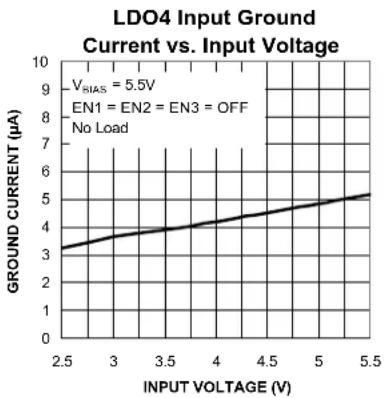
line
| INPUT VOLTAGE (V) | GROUND CURRENT (μA) | | ----------------- | ------------------- | | 2.5 | 3.0 | | 3.0 | 3.5 | | 3.5 | 4.0 | | 4.0 | 4.5 | | 4.5 | 5.0 | | 5.0 | 5.5 | | 5.5 | 6.0 |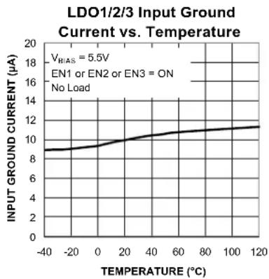
line
| TEMPERATURE (°C) | INPUT GROUND CURRENT (μA) | | ---------------- | ------------------------ | | -40 | 9.0 | | -20 | 9.5 | | 0 | 10.0 | | 20 | 10.5 | | 40 | 11.0 | | 60 | 11.5 | | 80 | 12.0 | | 100 | 12.5 | | 120 | 13.0 |Typical Characteristics (Continued)
line
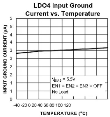
| TEMPERATURE (°C) | INPUT GROUND CURRENT (μA) | | ---------------- | ------------------------- | | -40 | 3.0 | | 0 | 3.1 | | 20 | 3.2 | | 40 | 3.3 | | 60 | 3.4 | | 80 | 3.5 | | 100 | 3.6 | | 120 | 3.7 |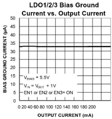
line
| OUTPUT CURRENT (mA) | BIAS GROUND CURRENT (μA) | | ------------------- | ------------------------ | | 0 | 33 | | 20 | 33 | | 40 | 33 | | 60 | 33 | | 80 | 33 | | 100 | 33 | | 120 | 33 | | 140 | 33 | | 160 | 33 | | 180 | 33 | | 200 | 33 |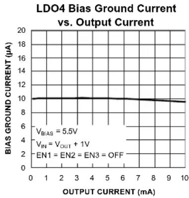
line
| OUTPUT CURRENT (mA) | BIAS GROUND CURRENT (pA) | | ------------------- | ------------------------ | | 0 | 10 | | 1 | 10 | | 2 | 10 | | 3 | 10 | | 4 | 10 | | 5 | 10 | | 6 | 10 | | 7 | 10 | | 8 | 10 | | 9 | 10 | | 10 | 10 |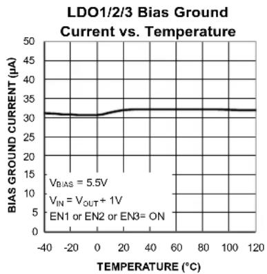
line
| V_BIAS (μA) | V_IN (μA) | EN1 or EN2 or EN3 (μA) | |-------------|-----------|------------------------| | 5.5 | - | - | | - | - | - | | - | - | - | | - | - | - | | - | - | - | | - | - | - | | - | - | - | | - | - | - | | - | - | - | | - | - | - | | - | - | - | | - | - | - | | - | - | - | | - | - | - | | - | - | - | | - | - | - | | - | - | - | | - | - | - | | - | - | - | | - | - | - | | - | - | - | | -3 | - | - | | 1 | - | - | | 3 | - | - | | 3 | - | - | | 3 | - | - | | 3 | - | - | | 3 | - | - | | 3 | - | - | | 3 | - | - | | 3 | - | - | | 3 | - | - | | 3.5 | - | - | | 3.5 | - | - | | 3.5 | - | - | | 3.5 | - | - | | 3.5 | - | - | | 3.5 | - | - | | 3.5 | - | - | | 3.5 | - | - | | ... | ... | ... | | ... | ... | ... | | ... | ... | ... | | ... | ... | ... | | ... | ... | ... | | ... | ... | ... | | ... | ... | ... | | ... | ... | ... | | ... | ... | ... | | ... | ... | ... | | ... | ... | ...67 | | ... | ... | ... | | ... | ... | ... | | ... | ... | ... | | ... | ... | ... | | ... | ... | ... | | ... | ... | ... | | ... | ... | ... | | ... | ... | ... | | ... | ... | ... | | ... | ... | ... | | ... | ... | ... | | ... | ... | ... | | ... | ... | ... | | ... | ... | ... | | ... | ... | ... | | ... | ... | ... | | ... | ... | ... | | ... | ... | ... | | ... | ... | ... | | ... | ... | ... | | ... | ... | ... | | ... | ... | ... | | ... | ... | ... | | ... | ... | ... | | ... | ... | ... | | ... | ... | ... | | ... | ... | ... | | ... | ... | ... | | ... | ... | ... | | ... | ... | ... | | ... | ... | ... | | ... | ... | ... | | ... | ... | ... | | ... | ... | ... | | ... | ... | ... | | ... | ... | ... | | ... | ... | ... | | ... | ... | ... | | ... | ... | ... | | ... | ... | ... (EN1 or EN2 or EN3) | | ... | ... | ... | | ... | ... | ... | | ... | ... | ... | | ... | ... | ... | | ... | ... | ... | | ... | ... | ... | | ... | ... |... | | ... | ... |... | | ... | ... |... | | ... | ... |... | | ..., #67 | ..., #67 | ..., #67 | | V_BIAS | V_BIAS | V_BIAS | | V_IN | V_IN | V_IN | | EN1 or EN2 or EN3 (EN1 or EN2 or EN3) 10% (in dB) (V_BIAS) (V_IN) (V_OUT) (V_IN) (EN1 or EN2 or EN3) (EN1 or EN2 or EN3) (EN3 or EN2 or EN3) (EN3 or EN2 or EN3) (EN1 or EN2 or EN3) (EN3 or EN2 or EN3) (EN1 or EN2 or EN3) (EN3 or EN2 or EN3) (EN1 or EN2 or EN3) (EN3 or EN2 or EN3) (EN1 or EN2 or EN3) (EN3 or EN2 or EN3) (EN1 or EN2 or EN3) (EN3 / EN2 or EN3) (EN1 or EN2 or EN3) (EN1 or EN2 or EN3) (EN1 or EN2 or EN3) (EN1 or EN2 or EN3) (EN1 or EN2 or EN3) (EN1 or EN2 or EN3) (EN1 or EN2 or EN3) (EN1 or EN2 or EN3) (EN1 or EN2 or EN3) (EN1 or En2 or EN3) (EN1 or En2 or EN3) (EN1 or En2 or EN3) (EN1 or En2 or EN3) (EN1 or En2 or EN3) (EN1 or En2 or EN3) (EN1 or En2 or EN3) (EN1 or En2 or EN3) (EN1 or En2 or EN3) (EN1 or En4 or EN4) (EN1 or En4 or EN4) (EN1 or En4 or EN4) (EN1 or En4 or EN4) (EN1 or En4 or EN4) (EN1 or En4 or EN4) (EN1 or En4 or EN4) (EN1 or En4 or EN4) (EN1 or En4 or EN4) (EN1 or En4 or EN4) nan , 0 , 0 , 0 , 0 , 0 , 0 , 0 , 0 , 0 , 0 , 0 , 0 , 0 , 0 , 0 , 0 , 0 , 0 , 0 , 0 , 0 , 0 , 0 , 0 , 0 , 5 , 5 , 5 , 5 , 5 , 5 , 5 , 5 , 5 , 5 , 5 , 5 , 5 , 5 , 5 , 5 , 5 , 5 , 5 , 5 , 5 , 5 , 5 , 5 , 5 , 5 , 5 , 5 , 5 , 5 , 5 , 5 , 5 , 5 , 5 , 5 , 5 , 5 , 5 , 5 , 5 , 5 , 5 , 5 , 5 , 5 , 5 , 5 , 5 , 5 , 5 , 5 , 5 , 5 , 5 , 5 , 5 , 5 , 5 , 5 , 5 , 5 , 5 , 5 , 5 , 5 , 5 , 5 , 5 , 5 , 5 , 5 , 5 , 5 , 5 , 5 , 5. . . .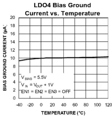
line
| V_BIAS | V_IN | EN1 | EN2 | EN3 | | ------ | ---- | --- | --- | --- | | 5.5V | V_OUT + 1V | EN2 | EN3 | OFF |
line
| Parameter | Value | | --------- | --------- | | Noise | 10Hz | | 100kHz | 100kHz | | 200μVrms | 200μVrms | | V_IN | 3.8V | | V_OUT | 2.8V | | C_OUT | 1μF | | Q_BIAS | 0.1μF | | Load | 150mA |
line
| Frequency (Hz) | Noise (uV/Hz) | | -------------- | ------------- | | 10 | ~0.5 | | 100 | ~0.5 | | 1,000 | ~0.5 | | 10,000 | ~0.5 | | 100,000 | ~1.0 |
line
| Frequency (Hz) | Noise (10Hz - 100kHz) (μV/ms) | | -------------- | ----------------------------- | | 10 | ~0.5 | | 100 | ~0.5 | | 1,000 | ~0.5 | | 10,000 | ~0.5 | | 100,000 | ~0.5 |
line
| FREQUENCY (Hz) | NOISE uV/Hz | | -------------- | ----------- | | 10 | ~0.8 | | 100 | ~0.6 | | 1,000 | ~0.5 | | 10,000 | ~0.4 | | 100,000 | ~0.1 |Typical Characteristics (Continued)
LDO3 Output Noise Spectral Density

line
| Parameter | Value | | --------- | --------- | | V_IN | 3.9V | | V_OUT | 1.2V | | C_OUT | 1μF | | C_BIAS | 0.1μF | | Load | 150mA |LDO1 PSRR ( I_OUT = 100 A )
line
| FREQUENCY(Hz) | PSRR (dB) | | ------------- | --------- | | 10 | -80 | | 100 | -75 | | 1000 | -60 | | 10000 | -40 | | 100000 | -20 |LDO1 PSRR ( I_OUT = 150mA )
line
| FREQUENCY(Hz) | PSRR (dB) | | ------------- | --------- | | 10 | -55 | | 100 | -56 | | 1000 | -58 | | 10000 | -70 | | 100000 | -40 | | 1000000 | -25 |LDO2 PSRR ( I_OUT = 100 A )
line
| FREQUENCY(Hz) | PSRR (dB) | | ------------- | --------- | | 10 | -80 | | 100 | -70 | | 1000 | -60 | | 10000 | -40 | | 100000 | -20 | | 1000000 | -20 |LDO2 PSRR ( I_OUT = 150mA )

line
| FREQUENCY(Hz) | PSRR (dB) | | ------------- | --------- | | 10 | -65 | | 100 | -68 | | 1000 | -70 | | 10000 | -72 | | 100000 | -40 | | 1000000 | -25 |LDO3 PSRR (IOUT = 100μA)
line
| FREQUENCY (Hz) | PSRR(dB) | | -------------- | -------- | | 10 | -80 | | 100 | -75 | | 1000 | -65 | | 10000 | -45 | | 100000 | -25 | | 1000000 | -30 |LDO3 PSRR ( I_OUT = 150mA )
line
| FREQUENCY(Hz) | PSRR (dB) | | ------------- | --------- | | 10 | -60 | | 100 | -65 | | 1000 | -70 | | 10000 | -40 | | 100000 | -25 | | 1000000 | -30 |Functional Characteristics
Start-Up Waveform for LDO1/2/3
line
| Time (20μs/div) | VOUT1 | VOUT2 | VOUT3 | | --------------- | ----- | ----- | ----- | | Start | 0 | 0 | 0 | | Peak | 4.3 | 4.3 | 4.3 | | End | 4.3 | 4.3 | 4.3 |Shutdown Waveform for LDO1/2/3
line
| Channel | Output Voltage | |---------|----------------| | EN1 | V_IN1/2.3 | | EN2 | V_IN1/2.3 | | EN3 | V_IN1/2.3 | | V_OUT1 | V_OUT1 | | V_OUT2 | V_OUT2 | | V_OUT3 | V_OUT3 | | Time (20μs/div) | V_IN1/2.3, C_OUT1.2.3 = 1μF, I_OUT1.2.3 = 150mALDO1 Load Transient (1mA to 150mA)

line
| Time (100μs/div) | IOUT1 (mA) | AC Coupled (20mV/div) | | ---------------- | ---------- | ---------------------- | | 0 | 1 | 4.3 | | 150 | 150 | 3.3 | | 50 | 50 | 1.5 |LDO2 Load Transient (1mA to 150mA)
line
| Time (100μs/div) | IOUT2 (mA) | VOUT2 (V) | | ---------------- | ---------- | --------- | | 0 | 1 | 4.3 | | 150 | 150 | 2.5 | | 50 | 50 | 1 |LDO3 Load Transient (1mA to 150mA)

line
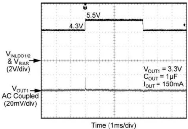
| Time (100μs/div) | IOUT3 (mA) | AC Coupled (20mV/div) | | ---------------- | ---------- | ---------------------- | | 0 | 1 | 1 | | 150 | 150 | 150 | | 200 | 200 | 200 |LDO1 Line Transient (4.3V to 5.5V)
line
| Signal Type | Voltage Level | |-----------------------|---------------| | V_INLDO1/2 & V_BIAS | 4.3V | | V_OUT1 | 3.3V | | C_OUT | 1μF | | I_OUT | 150mA |Functional Characteristics (Continued)
line
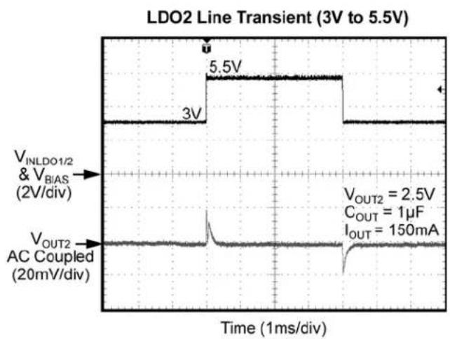
| Time (1ms/div) | V_INLDO1/2 & V_BIAS (2V/div) | V_OUT2 AC Coupled (20mV/div) | | -------------- | ---------------------------- | ---------------------------- | | 0 | 3V | 2.5V | | 5.5 | 3V | 2.5V | | 1ms | 3V | 2.5V |
line
| Time (1ms/div) | V_INLDO3 & V_BIAS (2V/div) | V_OUT3 AC Coupled (20mV/div) | | -------------- | -------------------------- | ---------------------------- | | 0 | 3V | 1.8V | | 5.5 | 5.5V | 1.8V | | 1ms | 3V | 1.8V | | 1ms | 0 | 1.8V | | 1ms | -3V | 1.8V | | 1ms | -6V | 1.8V | | 1ms | -9V | 1.8V | | 1ms | -12V | 1.8V | | 1ms | -15V | 1.8V | | 1ms | -18V | 1.8V | | 1ms | -21V | 1.8V | | 1ms | -24V | 1.8V | | 1ms | -27V | 1.8V | | 1ms | -30V | 1.8V | | 1ms | -33V | 1.8V | | 1ms | -36V | 1.8V | | 1ms | -39V | 1.8V | | 1ms | -42V | 1.8V | | 1ms | -45V | 1.8V | | 1ms | -48V | 1.8V | | 1ms | -51V | 1.8V | | 1ms | -54V | 1.8V | | 1ms | -57V | 1.8V | | 1ms | -60V | 1.8V | | 1ms | -63V | 1.8V | | 1ms | -66V | 1.8V | | 1ms | -69V | 1.8V | | 1ms | -72V | 1.8V | | 1ms | -75V | 1.8V | | 1ms | -78V | 1.8V | | 1ms | -81V | 1.8V | | 1ms | -84V | 1.8V | | 1ms | -87V | 1.8V | | 1ms | -90V | 1.8V | | 1ms | -93V | 1.8V | | 1ms | -96V | 1.8V | | 1ms | -99V | 1.8V | | 1ms | -102V | 1.8V | | 1ms | -105V | 1.8V | | 1ms | -108V | 1.8V | | 1ms | -111V | 1.8V | | 1ms | -114V | 1.8V | | 1ms | -117V | 1.8V | | 1ms | -120V | 1.8V | | 1ms | -123V | 1.8V | | 1ms | -126V | 1.8V | | 1ms | -129V | 1.8V | | 1ms | -132v | 1.8V | | 1ms | -135v | 1.8V | | 1ms | -138v | 1.8V | | 1ms | -141v | 1.8V | | 1ms | -144v | 1.8V | | 1ms | -147v | 1.8V | | 1ms | -150v | 1.8V | | 2ms | -3M | ~0 | | AC Coupled | ~0 | ~0 | | AC Coupled | ~0 | ~0 | | AC Coupled | ~0 | ~0 | | AC Coupled | ~0 | ~0 | | AC Coupled | ~0 | ~0 | | AC Coupled | ~0 | ~0 | | AC Coupled | ~0 | ~0 | | AC Coupled | ~0 | <0 | | AC Coupled | ~0 | <0 | | AC Coupled | ~0 | <0 | | AC Coupled | ~0 | <0 | | AC Coupled | ~0 | <0 | | AC Coupled | ~0 | <0 | | AC Coupled | ~0 | <0 | | AC Coupled | ~0 | <0 | | AC Coupled | ~0 | <0 | | AC Coupled | ~0 | <0 | | AC Coupled | ~0 | <0 | | AC Coupled | ~0 | <0 | | AC Coupled | ~0 | <0 | | AC Coupled | ~0 | <0 | | AC Coupled | ~0 | <0 | | | AC Coupled | ~0 | <0 | | AC Coupled | ~0 | <0 | | AC Coupled | ~0 | <0 | | AC Coupled | ~0 | <0 | | AC Coupled | ~0 | <0 | | AC Coupled | ~0 | <0 | | AC Coupled | ~0 | <0 | | Ac Coupled | ~0 | <0 | | AC Coupled | ~0 | <0 | | AC Coupled | ~0 | <0 | | AC Coupled | ~0 | <0 | | AC Coupled | ~0 | <0 | | AC Coupled | ~0 | <0 | | AC Coupled | ~0 | <0 | | AC Couプ (2M)| | AC Coupled (2M)| | AC Coupled (2M)| | AC Coupled (2M)| | AC Coupled (2M)| | AC Coupled (2M)| | AC Coupled (2M)| | AC Coupled (2M)| | AC Coupled (2M)| | AC Coupled (2M)| | AC Coupled (2M)| | AC Coupled (2M)| | AC Coupled (2M)| | AC Coupled (2M)| | AC Coupled (2M)| | AC Coupled (2M)| | AC Coupled (2M)| | AC Coupled (2M)| | AC Coupled (2M)| | AC Coupled (2M)| | AC Coupled (2M)| | AC Coupled (2M)| | AC Coupled (2M)| | AC Coupled (2M)| | AC Coupled (2M)| | AC Coupled (2M)| | AC Coupled (2M)| | AC Coupled (2M)| | AC Coupled (2M)| | AC Coupled (2M)| | AC Coupled (2M)| | AC Coupled (2M)| | AC Coupled (2M)| | AC Coupled (2M)| | AC Coupled (2M)| | AC Coupled (2M)| | AC Coupled (2M)| | AC Coupled (2M)| | AC Coupled (2M)| | AC Coupled (2M)| | AC Coupled (2M)| | AC Coupled (2M)|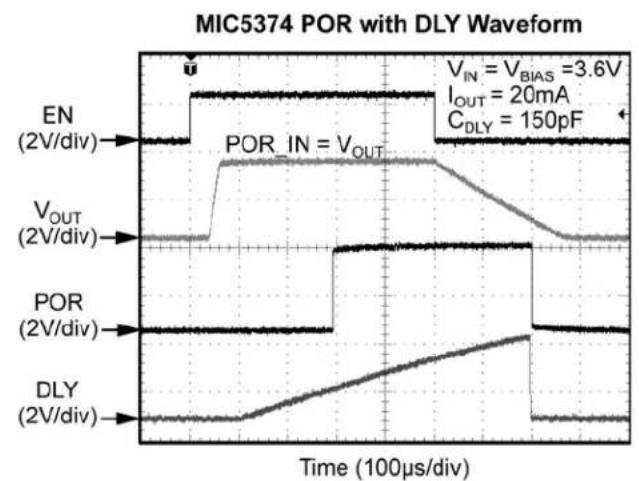
line
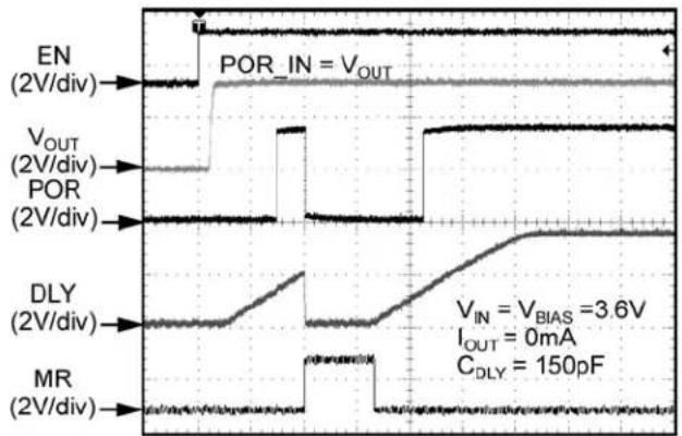
| Signal | Value | |--------|-----------| | EN | 2V/div | | VOUT | 2V/div | | POR | 2V/div | | DLY | 2V/div |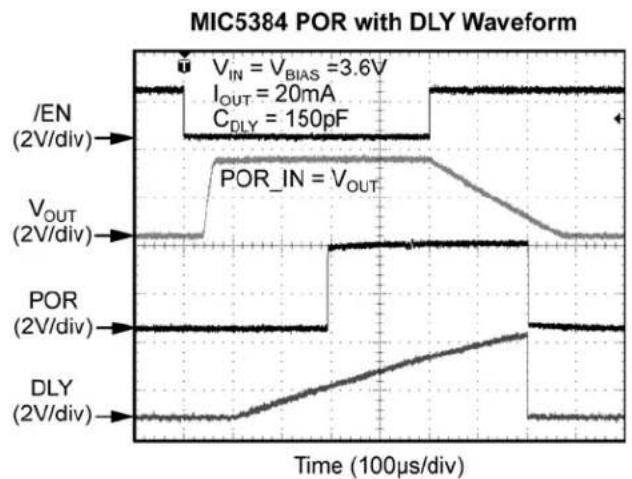
line
| Signal | Value | |------------|-------------| | VIN | 3.6V | | IOUT | 20mA | | CDLY | 150pF | | POR_IN | VOUT | | POR | 2V/div | | DLY | 2V/div |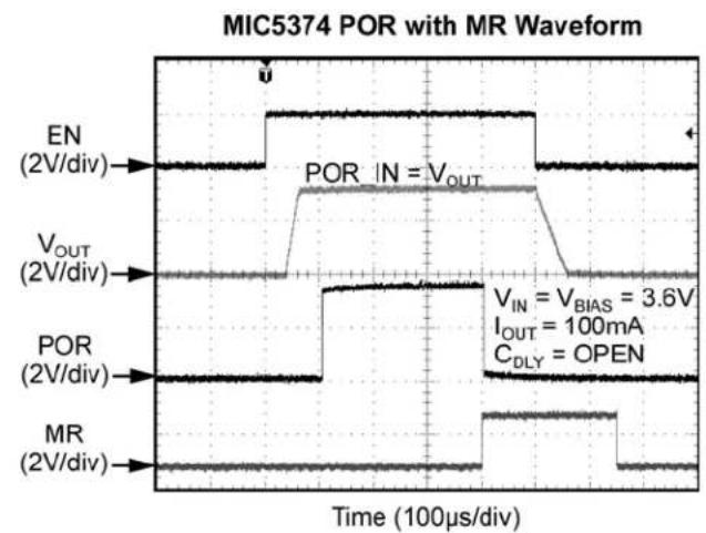
line
| Signal | Value | |--------|--------------| | EN | 2V/div | | VOUT | 2V/div | | POR | 2V/div | | MR | 2V/div |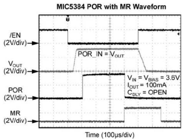
line
| Signal | Value | |--------|-----------| | V_IN | 3.6V | | I_OUT | 100mA | | C_DLY | OPEN |Functional Characteristics (Continued)
MIC5374 POR with DLY and MR Waveform
line
| Signal | Value | |--------|-----------| | EN | V_OUT | | VOUT | V_OUT | | POR | V_OUT | | DLY | V_BIAS | | MR | 3.6V |Time (200μs/div)
MIC5384 POR with DLY and MR Waveform
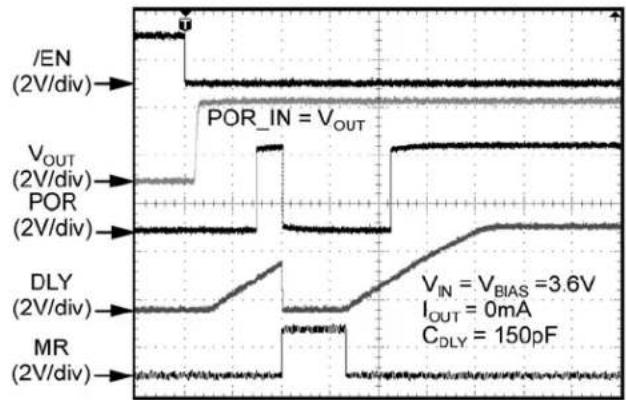
line
| Signal | Value | |--------|-----------| | EN | 2V/div | | VOUT | 2V/div | | POR | 2V/div | | DLY | 2V/div | | MR | 2V/div |Time (200μs/div)
Functional Diagrams

flowchart
graph TD
    A["INLDO1/2 EN1"] --> B["LDO1"]
    A --> C["LDO2"]
    D["INLDO3 EN3"] --> E["LDO3"]
    F["INLDO4"] --> G["LDO4"]
    H["POR_IN MR"] --> I["REFERENCE"]
    I --> J["POR"]
    K["BIAS"] --> B
    K --> E
    K --> G
    K --> I
    K --> J
    style A fill:#f9f,stroke:#333
    style D fill:#f9f,stroke:#333
    style F fill:#f9f,stroke:#333
    style H fill:#f9f,stroke:#333
    style K fill:#ccf,stroke:#333
    style K fill:#ccf,stroke:#333
MIC5374 Block Diagram
flowchart
graph TD
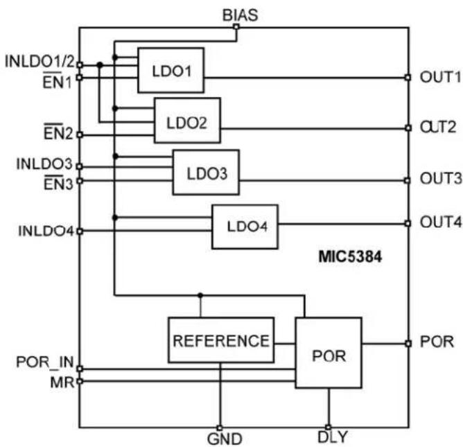
A["INLDO1/2 EN1"] --> B["LDO1"]
A --> C["LDO2"]
D["INLDO3 EN3"] --> E["LDO3"]
F["INLDO4"] --> G["LDO4"]
H["POR_IN MR"] --> I["REFERENCE"]
I --> J["POR"]
K["BIAS"] --> B
K --> E
K --> G
K --> I
K --> J
L["OUT1"] --> B
L --> E
L --> G
M["OUT2"] --> E
N["OUT3"] --> G
O["OUT4"] --> G
P["GND"] --> I
Q["DLY"] --> J
MIC5384 Block Diagram
Pin Descriptions
INLDO
The LDO input pins INLDO1/2, INLDO3 and INLDO4 provide the input power to the linear regulators LDO1, LDO2, LDO3 and LDO4. The input operating voltage range is from 1.7V to 5.5V. For input voltages from 1.7V to 2.5V the output current must be limited to 30mA each. Due to line inductance a 1 F capacitor placed close to the INLDO pins and the GND pin is recommended. Please refer to layout recommendations.
BIAS
The BIAS pin provides power to the internal reference and control sections of the MIC5374/84. A 0.1 F ceramic capacitor must be connected from BIAS to GND for clean operation.
EN (MIC5374)
The enable pins EN1, EN2 and EN3 provide logic level control for the outputs OUT1, OUT2 and OUT3, respectively. A logic high signal on an enable pin activates the respective LDO. A logic low signal on an enable pin deactivates the respective LDO. Do not leave the EN pins floating, as it would leave the regulator in an unknown state.
/EN (MIC5384)
The enable pins /EN1, /EN2 and /EN3 provide logic level control for the outputs OUT1, OUT2 and OUT3, respectively. A logic high signal on an enable pin deactivates the respective LDO. A logic low signal on an enable pin activates the respective LDO. Do not leave the EN pins floating, as it would leave the regulator in an unknown state.
OUT
OUT1, OUT2, OUT3 and OUT4 are the output pins of each LDO. A minimum of 1 F capacitor be placed as close as possible to each of the OUT pins. A minimum voltage rating of 6.3V is recommended for each capacitor.
GND
The ground (GND) pin is the ground path for the control circuitry and the power ground for all LDOs. The current loop for the ground should be kept as short as possible. Refer to the layout recommendations for more details.
POR
The power-on-reset (POR) pin is an open drain output. A resistor (10kΩ to 100kΩ) can be used for a pull up to either the input or the output voltage of the regulator. POR is pulled high by the external pull up resistor when the voltage at DLY reaches 1.25V.
A delay can be added by placing a capacitor from the DLY pin to ground.
POR\_IN
The power-on-reset input (POR_IN) pin compares any voltage to an internal 0.9V reference. This function can be used to monitor any of the LDO outputs or any external voltage rail. When the monitored voltage is greater than 0.9V, the POR_IN flag will internally trigger a 1.25μA source current to charge the external capacitor at the DLY pin. A resistor divider network may be used to divide down the monitored voltage to be compared with the 0.9V at the POR_IN. This resistor network can change the trigger point to any voltage level. A small decoupling capacitor is recommended between POR_IN and ground to reject high frequency noise that might interfere with the POR circuit. Do not leave the POR_IN pin floating.
DLY
The delay (DLY) pin is used to set the POR delay time. Adding a capacitor to this pin adjusts the delay of the POR signal. When the POR_IN flag is triggered, a constant 1.25μA current begins to charge the external capacitor tied to the DLY pin. When the capacitor reaches 1.25V the POR flag will be pulled high by the external pull up resistor. Equation 1 illustrates how to calculate the charge time is shown:
$$ t _ {\text { DELAY }} (s) = \left(\frac {C _ {D L 4} 2 5 V}{x 1 0 2 5 . 1}\right) ^ {x} \quad E q. $$
The delay time (t) is in seconds, the delay voltage is 1.25V internally, and the external delay capacitance ( C_DLY ) is in microfarads. For a 1 F delay capacitor, the delay time will be 1 second. A capacitor at the DLY pin is recommended when the POR function is used in order to prevent unexpected triggering of the POR signal in noisy systems.
MR
The manual reset (MR) pin resets the output of POR and DLY generator regardless if the monitored voltage is in regulation or not. Applying a voltage greater than 1.2V on the MR pin will cause the POR voltage to be pulled low. When a voltage below 0.2V is applied to the MR pin, the internal 1.25 A will begin to charge the DLY pin until it reaches 1.25V. When the DLY pin reaches 1.25V, the POR voltage will be pulled high by the external pull up resistor. Do not leave the MR pin floating.
Application Information
MIC5374/84 is a four output device with three 200mA LDOs and a 1mA RTC LDO. The MIC5374/84 incorporates a POR function with the capability to monitor any voltage using POR_IN. The monitored voltage can be set to any voltage threshold level to trigger the POR flag. A delay on the POR flag may also be set with an external capacitor at the DLY pin. All the LDOs have current limit and thermal shutdown protection to prevent damage from fault conditions. MIC5374 has active high enables while the MIC5384 has active low enables.
RTC LDO
LDO4 is an always-on RTC LDO used for application processor support and can provide 1mA of output current. Power must be provided to the INLDO4 and BIAS pins to keep LDO4 enabled.
Input Capacitor
The MIC5374/84 is a high-performance, high-bandwidth device. An input capacitor of 1 F from the input pin to ground is required to provide stability. Low-ESR ceramic capacitors provide optimal performance in small board area. Additional high-frequency capacitors, such as small valued NPO dielectric type capacitors, help filter out high-frequency noise and are good practice in any RF-based circuit. X5R or X7R dielectrics are recommended for the input capacitor. Y5V dielectrics lose most of their capacitance over temperature and are therefore not recommended.
Output Capacitor
The MIC5374/84 requires an output capacitor of 1 F or greater to maintain stability. The design is optimized for use with low-ESR ceramic chip capacitors. High-ESR capacitors may cause high-frequency oscillation. The output capacitor can be increased, but performance has been optimized for a 1 F ceramic output capacitor and does not improve significantly with larger capacitance.
X7R and X5R dielectric ceramic capacitors are recommended because of their temperature performance. X7R capacitors change capacitance by 15% over their operating temperature range and are the most stable type of ceramic capacitors. Z5U and Y5V dielectric capacitors change value by as much as 50% and 60% respectively over their operating temperature ranges. To use a ceramic chip capacitor with Y5V dielectric the value must be much higher than an X7R ceramic capacitor to ensure the same minimum capacitance over the equivalent operating temperature range.
No Load Stability
Unlike many other voltage regulators, the MIC5374/84 will remain stable and in regulation with no load.
Thermal Considerations
The MIC5374/84 is designed to provide three outputs up to 200mA each of continuous current in a very small package. Maximum ambient operating temperature can be calculated based on the output current and the voltage drop across the part. For example if the input voltages are 3.6V and the output voltages are 3.3V, 2.5V, and 1.8V each with an output current = 150mA. The actual power dissipation of the regulator circuit can be determined using Equation 2:
$$ P _ {D} = \left(V _ {\text { INLDO1 / 2 }} - V _ {\text { OUT1 }}\right) I _ {\text { OUT1 }} + $$
$$ \left(V _ {\text { INLDO1 / 2 }} - V _ {\text { OUT2 }}\right) I _ {\text { OUT2 }} + $$
$$ \left(V _ {\text { INLDO3 }} - V _ {\text { OUT3 }}\right) I _ {\text { OUT3 }} + $$
$$ \left(V _ {\text {INLDO4}} - V _ {\text {OUT4}}\right) I _ {\text {OUT4}} + V _ {\text {IN}} \times I _ {\text {GND}} \quad \text {Eq. 2} $$
As the MIC5374/84 is a CMOS device, the ground current is typically <100 A over the load range, the power dissipation contributed by the ground current is <1% and may be ignored for this calculation. Since LDO4 only supplies 1mA of current, it can also be ignored for this calculation, illustrated in Equation 3:
$$ P _ {D} \approx (3. 6 V - 3. 3 V) 1 5 0 m A + (3. 6 V - 2. 5 V) 1 5 0 m A + $$
$$ (3. 6 \mathrm{V} - 1. 8 \mathrm{V}) 1 5 0 \mathrm{mA} $$
$$ P _ {D} \approx 0. 4 8 W \quad E q. 3 $$
To determine the maximum ambient operating temperature of the package, use the junction to ambient thermal resistance of the device and the following Equation 4:
$$ P _ {D (M A X)} = \left(\frac {T - T _ {A J (M A X)}}{\theta_ {J A}}\right) E q. 4 $$
$$ T _ {J (M A X)} = 1 2 5 ^ {\circ} C $$
$$ \theta_ {\mathrm{JA}} = 1 0 0 ^ {\circ} \mathrm{C} / \mathrm{W} $$
Substituting P_D for P_D(max) and solving for the ambient operating temperature will give the maximum operating conditions for the regulator circuit.
The maximum power dissipation must not be exceeded for proper operation.
For example, when operating the MIC5374-SJG1YMT at an input voltage of 3.6V and 150mA load on LDO1, LDO2 and LDO3 with a minimum layout footprint, the maximum ambient operating temperature T_A can be determined as in Equation 5:
$$ 0. 4 8 \mathrm{W} = (1 2 5 ^ {\circ} \mathrm{C} - \mathrm{T} _ {\mathrm{A}}) / (1 0 0 ^ {\circ} \mathrm{C} / \mathrm{W}) $$
$$ T _ {A} = 7 7 ^ {\circ} \mathrm{C} \quad \text { Eq. } 5 $$
Therefore the maximum ambient operating temperature of 77^ C is allowed in a 2.5mm x 2.5mm Thin MLF package for the voltage options specified and at the maximum load of 150mA on each output. For a full discussion of heat sinking and thermal effects on voltage regulators, refer to the “Regulator Thermals” section of Micrel’s Designing with Low-Dropout Voltage Regulators handbook. This information can be found on Micrel’s website at:
http://www.micrel.com/_PDF/other/LDOBk_ds.pdf
Typical Circuit (MIC5374-xxxxYMT)
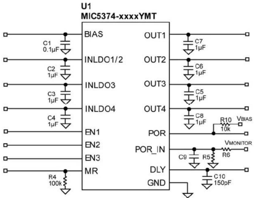
text_image
U1 MIC5374-xxxxYMT BIAS C1 0.1μF INLDO1/2 C2 1μF INLDO3 C3 1μF INLDO4 C4 1μF EN1 EN2 EN3 MR R4 100k OUT1 C7 1μF OUT2 C6 1μF OUT3 C5 1μF OUT4 C8 1μF POR POR_IN DLY GND R10 VBIAS 10k VMONITOR C9 R5 R6 C10 150pFBill of Materials
| Item | Part Number | Manufacturer Description | ||
| C1 | C1005X5R1A104K | ^(1) TDKapacitor, 0.1μF Ceramic, 10V, X5R, Size 0402 1 | ||
| C2, C3, C4, C5, C6, C7, C8 | C1005X5R1A105K TDK | Capacitor, 1μF Ceramic, 10V, X5R, Size 0402 7 | ||
| C9 | Optional | |||
| C10 | C1005C0G1H151J | TDK | Capacitor, 150pF Cermaic, 50V, C0G, Size 0402 | 1 |
| R4 | CRCW0402100KFKED | Vishay ^(2) | 100kΩ, 1%, 0402 | 1 |
| R5, R6 | Optional | Vishay | Optional | 2 |
| R10 | CRCW040210KFKED | Vishay | 10kΩ, 1%, 0402 | 1 |
| U1 | MIC5374-xxxxYMT | Micrel, Inc. ^(3) | High-Performance Active High Enable Triple 200mA LDO with 1mA RTC LDO | 1 |
Notes:
1. TDK: www.tdk.com.
2. Vishay: www.vishay.com.
3. Micrel, Inc.: www.micrel.com.
Typical Circuit (MIC5384-xxxxYMT)
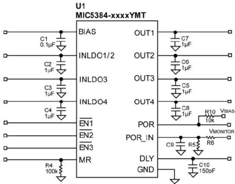
text_image
U1 MIC5384-xxxxYMT BIAS OUT1 C1 0.1µF INLDO1/2 OUT2 C2 1µF INLDO3 OUT3 C3 1µF INLDO4 OUT4 C4 1µF EN1 POR VBIAS EN2 POR_IN VMONITOR EN3 C9 R5 R6 DLY GND C10 150pF R4 100kBill of Materials
| Item | Part Number | Manufacturer Description | ||
| C1 | C1005X5R1A104K | ^(1) D Kapacitor, 0.1μF Ceramic, 10V, X5R, Size 0402 1 | ||
| C2, C3, C4, C5, C6, C7, C8 | C1005X5R1A105K TDK | Capacitor, 1μF Ceramic, 10V, X5R, Size 0402 7 | ||
| C9 | Optional | |||
| C10 | C1005C0G1H151J | TDK | Capacitor, 150pF Cermaic, 50V, C0G, Size 0402 | 1 |
| R4 | CRCW0402100KFKED | Vishay ^(2) | 100kΩ, 1%, 0402 | 1 |
| R5, R6 | Optional | Vishay | Optional | 2 |
| R10 | CRCW040210KFKED | Vishay | 10kΩ, 1%, 0402 | 1 |
| U1 | MIC5384-xxxxYMT | Micrel, Inc. ^(3) | High-Performance Active Low Enable Triple 200mA LDO with 1mA RTC LDO | 1 |
Notes:
1. TDK: www.tdk.com.
2. Vishay: www.vishay.com.
3. Micrel, Inc.: www.micrel.com.
PCB Layout Recommendations
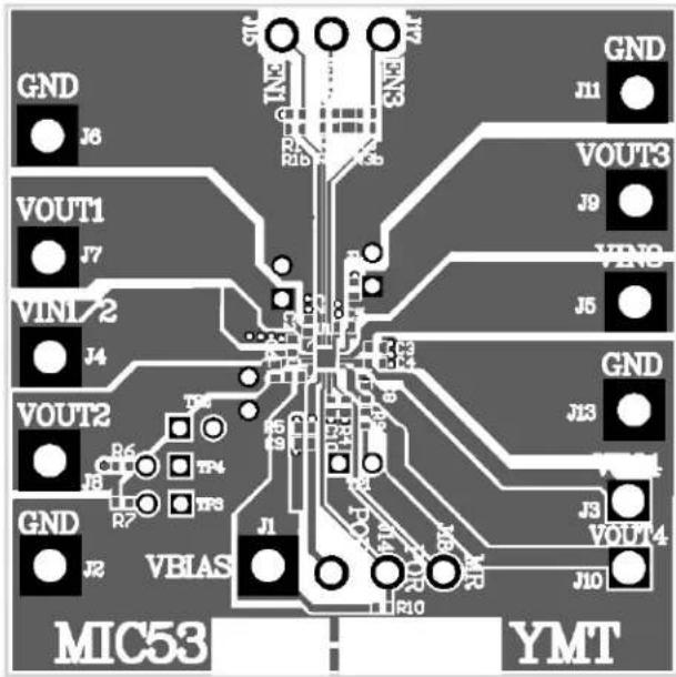
Recommended Top Layout

text_image
ICREF1JC 408-344-0800 I/O *NT OHPB R0H2 BD# 04010-DL TMYXXX\A7\88\G4\xxxxYMTRecommended Bottom Layout
Package Information

text_image
PIN 1# DOT BY MARKING 2.50±0.05 2.50±0.05TOP VIEW

text_image
0.20±0.05 1.40±0.05 Exp.DAP 0.35±0.05 0.40 Bsc 1.20 Ref. PIN #1 ID R0.10 1.40±0.05 Exp.DAPBOTTOM VIEW
text_image
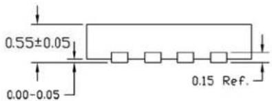
0.55±0.05 0.00-0.05 0.15 Ref.SIDE VIEW
NOTES
1. ALL DIMENSIONS ARE IN MILLIMETERS.
2. MAX. PACKAGE WARPAGE IS 0.05 mm.
3. MAXIMUM ALLOWABE BURRS IS 0.08 mm IN ALL DIRECTIONS.
4. PIN #1 ID ON TOP WILL BE LASER MARKED.
16-Pin 2.5mm x 2.5mm Thin MLF (MT)
MICREL, INC. 2180 FORTUNE DRIVE SAN JOSE, CA 95131 USA
TEL +1 (408) 944-0800 FAX +1 (408) 474-1000 WEB http://www.micrel.com
Micrel makes no representations or warranties with respect to the accuracy or completeness of the information furnished in this data sheet. This information is not intended as a warranty and Micrel does not assume responsibility for its use. Micrel reserves the right to change circuitry, specifications and descriptions at any time without notice. No license, whether express, implied, arising by estoppel or otherwise, to any intellectual property rights is granted by this document. Except as provided in Micrel's terms and conditions of sale for such products, Micrel assumes no liability whatsoever, and Micrel disclaims any express or implied warranty relating to the sale and/or use of Micrel products including liability or warranties relating to fitness for a particular purpose, merchantability, or infringement of any patent, copyright or other intellectual property right.
Micrel Products are not designed or authorized for use as components in life support appliances, devices or systems where malfunction of a product can reasonably be expected to result in personal injury. Life support devices or systems are devices or systems that (a) are intended for surgical implant into the body or (b) support or sustain life, and whose failure to perform can be reasonably expected to result in a significant injury to the user. A Purchaser's use or sale of Micrel Products for use in life support appliances, devices or systems is a Purchaser's own risk and Purchaser agrees to fully indemnify Micrel for any damages resulting from such use or sale.
© 2010 Micrel, Incorporated.