PIC16F1784 - Electronic component Microchip - Free user manual and instructions
Find the device manual for free PIC16F1784 Microchip in PDF.

User questions about PIC16F1784 Microchip
0 question about this device. Answer the ones you know or ask your own.
Ask a new question about this device
Download the instructions for your Electronic component in PDF format for free! Find your manual PIC16F1784 - Microchip and take your electronic device back in hand. On this page are published all the documents necessary for the use of your device. PIC16F1784 by Microchip.
USER MANUAL PIC16F1784 Microchip
PSMC Designer User's Guide
Note the following details of the code protection feature on Microchip devices:
• Microchip products meet the specification contained in their particular Microchip Data Sheet.
- Microchip believes that its family of products is one of the most secure families of its kind on the market today, when used in the intended manner and under normal conditions.
- There are dishonest and possibly illegal methods used to breach the code protection feature. All of these methods, to our knowledge, require using the Microchip products in a manner outside the operating specifications contained in Microchip's Data Sheets. Most likely, the person doing so is engaged in theft of intellectual property.
• Microchip is willing to work with the customer who is concerned about the integrity of their code.
- Neither Microchip nor any other semiconductor manufacturer can guarantee the security of their code. Code protection does not mean that we are guaranteeing the product as "unbreakable."
Code protection is constantly evolving. We at Microchip are committed to continuously improving the code protection features of our products. Attempts to break Microchip's code protection feature may be a violation of the Digital Millennium Copyright Act. If such acts allow unauthorized access to your software or other copyrighted work, you may have a right to sue for relief under that Act.
Information contained in this publication regarding device applications and the like is provided only for your convenience and may be superseded by updates. It is your responsibility to ensure that your application meets with your specifications. MICROCHIP MAKES NO REPRESENTATIONS OR WARRANTIES OF ANY KIND WHETHER EXPRESS OR IMPLIED, WRITTEN OR ORAL, STATUTORY OR OTHERWISE, RELATED TO THE INFORMATION, INCLUDING BUT NOT LIMITED TO ITS CONDITION, QUALITY, PERFORMANCE, MERCHANTABILITY OR FITNESS FOR PURPOSE. Microchip disclaims all liability arising from this information and its use. Use of Microchip devices in life support and/or safety applications is entirely at the buyer's risk, and the buyer agrees to defend, indemnify and hold harmless Microchip from any and all damages, claims, suits, or expenses resulting from such use. No licenses are conveyed, implicitly or otherwise, under any Microchip intellectual property rights.
QUALITY MANAGEMENT SYSTEM CERTIFIED BY DNV = ISO/TS 16949=
Trademarks
The Microchip name and logo, the Microchip logo, dsPIC, FlashFlex, KEELOQ, KEELOQ logo, MPLAB, PIC, PICmicro, PICSTART, PIC ^32 logo, rfPIC, SST, SST Logo, SuperFlash and UNI/O are registered trademarks of Microchip Technology Incorporated in the U.S.A. and other countries.
FilterLab, Hampshire, HI-TECH C, Linear Active Thermistor, MTP, SEEVAL and The Embedded Control Solutions Company are registered trademarks of Microchip Technology Incorporated in the U.S.A.
Silicon Storage Technology is a registered trademark of Microchip Technology Inc. in other countries.
Analog-for-the-Digital Age, Application Maestro, BodyCom, chipKIT, chipKIT logo, CodeGuard, dsPICDEM, dsPICDEM.net, dsPICworks, dsSPEAK, ECAN, ECONOMONITOR, FanSense, HI-TIDE, In-Circuit Serial Programming, ICSP, Mindi, MiWi, MPASM, MPF, MPLAB Certified logo, MPLIB, MPLINK, mTouch, Omniscient Code Generation, PICC, PICC-18, PICDEM, PICDEM.net, PICkit, PICtail, REAL ICE, rfLAB, Select Mode, SQI, Serial Quad I/O, Total Endurance, TSHARC, UniWinDriver, WiperLock, ZENA and Z-Scale are trademarks of Microchip Technology Incorporated in the U.S.A. and other countries.
SQTP is a service mark of Microchip Technology Incorporated in the U.S.A.
GestIC and ULPP are registered trademarks of Microchip Technology Germany II GmbH & Co. KG, a subsidiary of Microchip Technology Inc., in other countries.
All other trademarks mentioned herein are property of their respective companies.
© 2012-2013, Microchip Technology Incorporated, Printed in the U.S.A., All Rights Reserved.
Printed on recycled paper. ISBN: 9781620772737
Microchip received ISO/TS-16949:2009 certification for its worldwide headquarters, design and wafer fabrication facilities in Chandler and Tempe, Arizona; Gresham, Oregon and design centers in California and India. The Company's quality system processes and procedures are for its PIC® MCUs and dsPIC® DSCs, KEELoo® code hopping devices, Serial EEPROMs, microperipherals, nonvolatile memory and analog products. In addition, Microchip's quality system for the design and manufacture of development systems is ISO 9001:2000 certified.
Table of Contents
Chapter 1. PSMC Designer Overview
1.1 Introduction ...... 9
Chapter 2. Main PSMC Configuration GUI
2.1 Introduction ...... 11
2.2 Function Selection ...... 12
2.3 Device Selection 12
2.4 PSMC Selection 12
2.5 PSMC Enable 12
2.6 Interrupt Enables 12
2.6.1 Timed Event Interrupt Enable 12
2.6.2 Auto-Shutdown Interrupt Enable 12
2.7 Comments 12
2.8 Copy and Show Button 13
2.8.1 PSMC SFR Displays 13
2.9 Paste Button 13
2.10 Clear Button 13
2.11 Pull-down Menu 13
2.11.1 Save Assy 13
2.11.2 Save C 13
2.11.3 Load Code 14
2.12 Clock 14
2.12.1 Clock Source 14
2.12.2 Prescale 14
2.13 Timer 14
2.13.1 Sync Source 15
2.13.2 Timer Interrupt 15
2.14 Blanking 15
2.14.1 Blanking Times 16
2.14.2 Rising Event Trigger 16
2.14.3 Falling Event Trigger 17
2.14.4 Asynchronous Input Pin Polarity 17
2.15 Period Event ...... 17
2.15.1 Synchronous Selection .... 17
2.15.2 Asynchronous Selection 18
2.15.3 Asynchronous Polarity (not available on PIC16(L)F1782/3) 18
2.15.4 Interrupt 18
2.16 Rising Event 18
2.16.1 Synchronous Selection 19
2.16.2 Asynchronous Selection ...... 19
2.16.3 Interrupt 20
2.17 Falling Event ...... 20
2.17.1 Synchronous Selection 20
2.17.2 Asynchronous Selection ....21
2.17.3 Asynchronous Polarity (not available on PIC16(L)F1782/3) .....21
2.17.4 Interrupt 21
2.18 Modulation 21
2.18.1 Modulation Source Selection 22
2.18.2 Modulation Enable 22
2.19 PSMC Modes 22
2.19.1 Dead-Band Control 23
2.19.2 SPWM: Single PWM Mode 23
2.19.3 SPWMC: Single PWM Mode with Complementary Outputs .....24
2.19.4 PP: Push-Pull Mode 25
2.19.5 PPC: Push-Pull with Complementary Output 25
2.19.6 FBPP: Full-Bridge Push-Pull ..... 26
2.19.7 FBPPC: Full-Bridge Push-Pull with Complementary Mode Outputs .....27
2.19.8 PS: Pulse-Skipping Mode 27
2.19.9 PSC: Pulse-Skipping with Complementary Output 28
2.19.10 ECCPR: ECC PWM Full-Bridge Mode, Reverse Direction .....29
2.19.11 ECCPF: ECC PWM Full-Bridge Mode, Forward Direction ....30
2.19.12 FDC: Fixed Duty Cycle Mode 30
2.19.13 Fine Frequency Adjust 31
2.19.14 FDCC: Fixed Duty Cycle with Complementary Output ....31
2.19.15 3PH: 3-Phase PWM ....32
2.20 Output Control 33
2.20.1 Output Enable 34
2.20.2 Output Steering 34
2.20.3 Output Steering Synchronization 34
2.20.4 Output Polarity 35
2.20.5 Shutdown Level 35
2.21 Auto-Shutdown 35
2.21.1 Shutdown Enable 35
2.21.2 Shutdown Sources ....35
2.21.3 Shutdown Override 35
2.21.4 Auto/Manual Restart 35
2.22 Sync Control (not available on the PIC16(L)F1782/3) 36
Chapter 3. PSMC Tips
3.1 Variable Period with Fixed Off-time 37
3.2 3-Phase Variable Duty Cycle 38
3.3 Center Weighted Variable PWM 39
Preface
NOTICE TO CUSTOMERS
All documentation becomes dated, and this manual is no exception. Microchip tools and documentation are constantly evolving to meet customer needs, so some actual dialogs and/or tool descriptions may differ from those in this document. Please refer to our web site (www.microchip.com) to obtain the latest documentation available.
Documents are identified with a "DS" number. This number is located on the bottom of each page, in front of the page number. The numbering convention for the DS number is "DSXXXXXA", where "XXXXX" is the document number and "A" is the revision level of the document.
For the most up-to-date information on development tools, see the MPLAB IDE online help. Select the Help menu, and then Topics to open a list of available online help files.
INTRODUCTION
This chapter contains general information that will be useful to know before using the PSMC Designer. Items discussed in this chapter include:
- Conventions Used in this Guide
• The Microchip Web Site - Customer Support
• Document Revision History
DOCUMENT LAYOUT
This document describes how to use the PSMC Designer. The document is organized as follows:
• Chapter 1. "PSMC Designer Overview"
- Chapter 2. "Main PSMC Configuration GUI"
• Chapter 3. "PSMC Tips"
CONVENTIONS USED IN THIS GUIDE
This manual uses the following documentation conventions:
DOCUMENTATION CONVENTIONS
| Description Represents Examples | ||
| Arial font: | ||
| Italic characters Referenced books | oks MPLAB IDE User's Guide | |
| Emphasized text ...is the only compiler... | ||
| Initial caps A window the Output | ut window | |
| A dialog the Settings dialog | ||
| A menu selection select Enable Programmer | ||
| Quotes A field name in a window or dialog | "Save project before build" | |
| Underlined, italic text with right angle bracket | A menu path File>Save | —— |
| Bold characters A dialog button | Click OK | |
| A tab | Click the Power tab | |
| N'Rnnnn | A number in verilog format, where N is the total number of digits, R is the radix and n is a digit. | 4'b0010, 2'hF1 |
| Text in angle brackets <> | A key on the keyboard | Press,, |
| Courier New font: | ||
| Plain Courier New | Sample source code | #define START |
| Filenames | autoexec.bat | |
| File paths c:\mccl8\h | ||
| Keywords | _asm, _endasm, static | |
| Command-line options | -Opa+, -Opa- | |
| Bit values | 0, 1 | |
| Constants | 0xFF, 'A' | |
| Italic Courier New | A variable argument | file.o, where file can be any valid filename |
| Square brackets [] | Optional arguments | mccl8 [options] file [options] |
| Curly brackets and pipe character: { | } | Choice of mutually exclusive arguments; an OR selection | errorlevel {0|1} |
| Ellipses... | Replaces repeated text | var_name [, var_name...] |
| Represents code supplied by user | void main (void) { ... } | |
Microchip provides online support via our web site at www.microchip.com. This web site is used as a means to make files and information easily available to customers. Accessible by using your favorite Internet browser, the web site contains the following information:
- Product Support – Data sheets and errata, application notes and sample programs, design resources, user's guides and hardware support documents, latest software releases and archived software
- General Technical Support – Frequently Asked Questions (FAQs), technical support requests, online discussion groups, Microchip consultant program member listing
- Business of Microchip – Product selector and ordering guides, latest Microchip press releases, listing of seminars and events, listings of Microchip sales offices, distributors and factory representatives
CUSTOMER SUPPORT
Users of Microchip products can receive assistance through several channels:
• Distributor or Representative
- Local Sales Office
• Field Application Engineer (FAE)
- Technical Support
Customers should contact their distributor, representative or field application engineer (FAE) for support. Local sales offices are also available to help customers.
Technical support is available through the web site at:
http://www.microchip.com/support.
DOCUMENT REVISION HISTORY
Revision A (December 2012)
- Initial Release of this Document.
Revision B (June 2013)
- Updated Figure 2-3, Figure 2-6, Figure 2-7, Figure 2-18, and Figure 2-19.
NOTES:
Chapter 1. PSMC Designer Overview
1.1 INTRODUCTION
The PSMC peripheral is a sophisticated programmable switch mode controller intended to operate power conversion applications with little or no software intervention. The peripheral capabilities range from simple, single channel PWM generation to multi-channel complementary waveforms with dead bands between transitions. PWM modes include:
- PWM
- Push-Pull
- Full-bridge
- Push-Pull Full-bridge
- Pulse skipping
• High resolution fixed duty cycle
• 6-step 3-phase operation
Every mode, except the 6-step, has a complementary output mode, which drives at least two channels that are the complement of each other.
The PSMC also supports various driver and feedback configurations with the following programmable features:
- Dead band – delays the output drive for a time after the complement of that output turns off
- Blanking – Suppresses feedback signals for a time after the drive transitions on and off
- Asynchronous inputs – pulse Start and Stop events can be triggered by external asynchronous signals in combination with, or independent of, an internal time base
- Shutdown – immediate safe shutdown driven by an external asynchronous Fault signal
- Modulation – the PWM can be operated as a carrier and modulated by an independent input
There are thirty Special Function Registers (SFRs) in the PSMC configuration setup. Setting all thirty registers with the appropriate values for desired operation can be a daunting task. The PSMC Designer GUI was created to simplify that effort.
The GUI divides the PSMC into up to eleven major functions. These functions are shown in relation to each other in block diagram format in the main GUI window. Clicking on a block opens the control GUI for that function. The user is guided through the PSMC configuration design by completing signal paths and control options within each function by selecting switch positions. Entry boxes for times and frequencies appear within the diagrams where numeric entry is required.
There are two options for transferring the completed PSMC configuration to your project. One is to copy the code into the clipboard buffer which can then be pasted into your source code. The other transfer method is to generate an output file that can be included by reference in your source code. Include files are also the means by which PSMC configurations are stored for later retrieval by the PSMC designer.
Although a brief description of each function is included at the beginning of each function section, please refer to the device data sheet for a more detailed description of the PSMC operation. The sections of this guide are arranged in the same order of progression that a user would follow when creating a PSMC configuration.
Chapter 2. Main PSMC Configuration GUI
2.1 INTRODUCTION
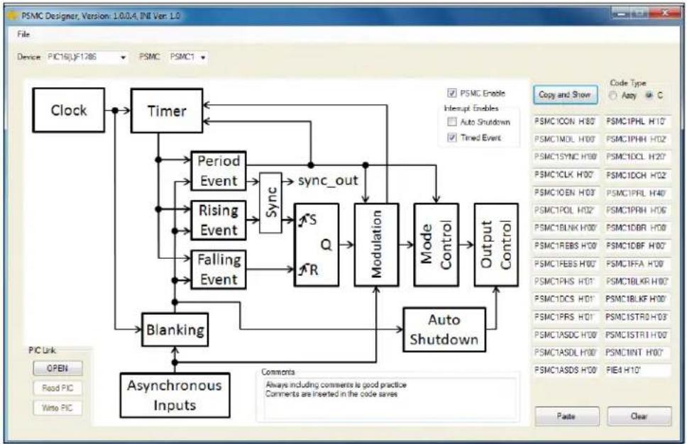
Figure 2-1 shows the main PSMC Designer user interface, referred to hereafter as the main GUI. Here you will see the eleven major functions of the PSMC:
- Clock 2. Timer
- Blanking 4. Period Event
- Rising Event 6. Falling Event
- Modulation 8. PSMC Modes
-
Output Control 10. Auto-Shutdown
-
Sync Output Control (not available on the PIC16(L)F1782/3)
The main GUI also contains the following:
- Device Selection 2. PSMC Selection
- Copy and Show Button 4. Paste Button
- Clear Button 6. Copy and Show Button
- PSMC SFR Displays 8. PSMC Enable
- Interrupt Enables 10. Pull-down Menu
- Comments
FIGURE 2-1: MAIN PSMC DESIGNER GUI
flowchart
graph TD
    A["Clock"] --> B["Timer"]
    B --> C["Period Event"]
    B --> D["Rising Event"]
    B --> E["Falling Event"]
    C --> F["Sync"]
    D --> F
    E --> F
    F --> G["Sync_out"]
    G --> H["Modulation"]
    H --> I["Mode Control"]
    I --> J["Output Control"]
    J --> K["Auto Shutdown"]
    K --> L["Blanking"]
    L --> M["Asynchronous Inputs"]
    M --> N["Comments: Always including comments is good practice; Comments are inserted in the code saves"]
2.2 FUNCTION SELECTION
As you move your cursor around the display, you will notice that the cursor shape changes to a hand whenever it is within the bounds of one of the function blocks. Clicking on the mouse when the cursor is a hand will open a control GUI for the function to which the hand is pointing. When you are finished configuring that block you can either close the associated GUI or leave it open. All functions remain active whether or not they are visible.
2.3 DEVICE SELECTION
Selecting the device is the first step in creating a PSMC configuration. The Device combination box lists all devices with PSMC peripherals. Make the selection by scrolling through the list to the desired device. The device selection also configures controls for all PSMC instances in that device with the proper input and output names associated with that device.
2.4 PSMC SELECTION
Selecting the desired PSMC instance is the second step in creating a PSMC configuration. Make the selection by scrolling through the list to the desired PSMC instance. The PSMC selection also configures all other controls with the proper input and output names associated with that PSMC instance.
2.5 PSMC ENABLE
This checkbox in the main GUI enables or disables the currently selected PSMC of the currently selected device.
2.6 INTERRUPT ENABLES
The interrupt enable checkboxes in the main GUI enable or disable the corresponding bit of the PIEx register for the currently selected PSMC of the currently selected device.
2.6.1 Timed Event Interrupt Enable
The timed event enable is the summary enable bit for the timed event interrupts.
2.6.2 Auto-Shutdown Interrupt Enable
The auto-shutdown enable is the enable bit for auto-shutdown events.
2.7 COMMENTS
The comments section in the lower center of the main GUI is where user comments about the PSMC configuration can be entered. Each PSMC instance has its own comment data, which is displayed when that PSMC is selected. Comments entered in this box are included as comments in the saved file output.
2.8 COPY AND SHOW BUTTON
The Copy and Show button does two things: It shows all SFR values in the PSMC instance configuration, and it copies those values to the clipboard. The clipboard format is consistent with the type selected by the Code Type radio buttons. C and Assembly are the two options. The clipboard capture can be pasted into your source code, however, code for only the presently selected PSMC instance is in the clipboard. Multiple copy and paste operations are required when working with multiple PSMC instances. A better method for saving multiple PSMC instances of the same device is the File Save option. Files can be saved in either C or Assembly format (see Save Assy or Save C).
2.8.1 PSMC SFR Displays
The PSMC SFRs are displayed by name and value in the 30 text boxes between the Copy and Show button and the Paste button. Only the SFRs for the selected PSMC instance are displayed as indicated by each of the SFR name prefixes.
2.9 PASTE BUTTON
The Paste button transfers SFR values of the PSMC instance, from which they were copied with the Copy and Show button, to the presently selected PSMC instance. In this manner, one PSMC configuration can be created then quickly copied to other desired PSMC instances. It is usually easier to make a few changes to a copied configuration than it is to re-enter the entire configuration for each PSMC instance. Note that the Paste button will not paste values copied from your source code.
2.10 CLEAR BUTTON
The Clear button clears all SFRs in the presently selected PSMC instance to zero. All GUIs of the various functions adjust accordingly.
2.11 PULL-DOWN MENU
In the upper left of the main GUI display there is a pull-down menu titled "File". This pull-down menu includes the following:
- Save Assy Code
- Save C Code
- Load Code
A file selection dialog will appear when the desired menu item is selected for both saving and loading code. A comment section, that includes the device number and clock frequency, is included in the saved code. This is used to reconstruct those parts of the configuration when the code is loaded back into the designer tool.
2.11.1 Save Assy
Selecting the Save Assy code menu option creates an include file containing assembly configuration code for all PSMCs in the selected device that have been configured. Any PSMC instance in the selected device that is clear will not be included in the output.
2.11.2 Save C
Selecting the Save C code menu option creates an include file containing C configuration code for all PSMCs in the selected device that have been configured. Any PSMC instance in the selected device that is clear will not be included in the output.
2.11.3 Load Code
Selecting the Load Code menu option retrieves the SFR information from the file and sets the device selection and all PSMC instance configurations contained in the code file. The load algorithm automatically recognizes whether the code was saved as C or assembly and reads it accordingly.
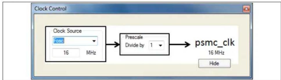
2.12 CLOCK
The clock control determines the rate at which the synchronous event timer, blanking timers, and dead-band timers all increment. The clock selections should be made first since the times in the aforementioned controls are all affected by the clock selections. The clock control GUI is shown in Figure 2-2.
FIGURE 2-2: CLOCK CONTROL
flowchart
graph LR
    A["Clock Source\nFosc\n16 MHz"] --> B["Prescale\nDivide by 1"]
    B --> C["psmc_clk\n16 MHz\nHide"]
2.12.1 Clock Source
The clock source selects one of three PSMC clock sources:
- Fosc – internal system oscillator
- 64 MHz – 64 MHz clock derived from the 16 MHz HFINTOC by multiplying by 4.
- PSMCxCLK pin – The I/O pin designated as the PSMC clock input.
When either the Fosc or PSMCxCLK pin is selected, then the actual frequency is specified by entering the number in MHz in the text box below the clock selection combination box. Selecting 64 MHz forces the frequency to 64 MHz, which cannot be altered.
2.12.2 Prescale
The prescale selection determines which of four dividers is used to reduce the selected clock source to the psmc_clk output frequency. The four selections are:
- Divide by 1
- Divide by 2
- Divide by 4
- Divide by 8
2.13 TIMER
The timer control GUI, shown in Figure 2-3, is opened by clicking on the timer block in the main GUI. The timer is a 16-bit counter to which the synchronous period event, rising event, and falling event count registers are compared to create their synchronous events.
FIGURE 2-3: TIMER CONTROL

flowchart
graph TD
    A["psmc_clk"] --> B["Timer"]
    C["Modulation"] --> D["AND"]
    E["Sync Source\nPeriod Ext"] --> D
    D --> F["R"]
    F --> B
    B --> G["CY"]
    G --> H["Interrupt"]
    H --> I["16-Bit Value"]
    I --> J["Ground"]
    style B fill:#f9f,stroke:#333
    style G fill:#ccf,stroke:#333
    style I fill:#cfc,stroke:#333
2.13.1 Sync Source
PSMCs in the device can be synchronized to a master PSMC by routing the sync_out signal from the master as one of the timer Reset inputs. The sync source selection determines the Reset source and thereby also determines which PSMC is the master. The number of selections varies by the number of PSMC instances in the device.
2.13.2 Timer Interrupt
The timer overflow can be selected as a timed interrupt source by clicking on the switch image at the CY terminal of the timer. Connecting this switch connects the timer carry out to the PMSC timed interrupt summary bit in the device PIRx register. Enabling the timer interrupt also requires checking the timed event interrupt enable box on the main window.
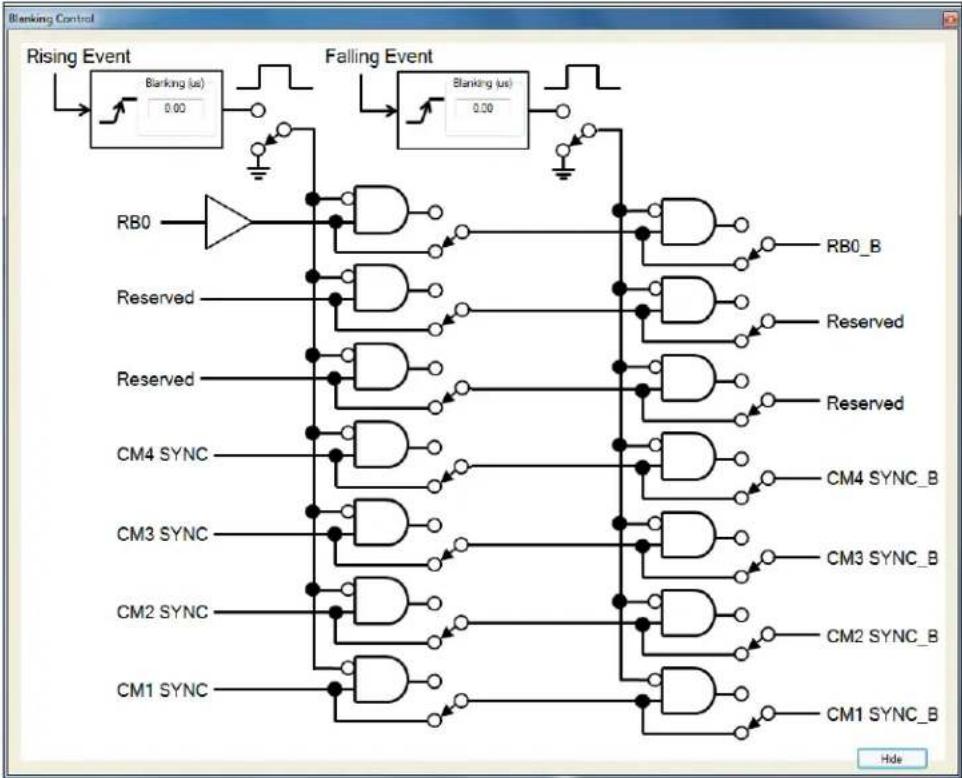
2.14 BLANKING
The blanking control GUI, shown in Figure 2-4, is opened by clicking on the blanking block in the main GUI. Blanking suppresses the selected inputs for a programmable period of time which starts at either a rising event or falling event or both.
FIGURE 2-4: BLANKING CONTROL
flowchart
graph TD
    A["Rising Event"] --> B["Blanking (us) 0.00"]
    B --> C["Ground"]
    D["Falling Event"] --> E["Blanking (us) 0.00"]
    E --> F["Ground"]
    G["RB0"] --> H["NOT"]
    I["Reserved"] --> J["D触发器"]
    K["Reserved"] --> L["D触发器"]
    M["CM4 SYNC"] --> N["D触发器"]
    O["CM3 SYNC"] --> P["D触发器"]
    Q["CM2 SYNC"] --> R["D触发器"]
    S["CM1 SYNC"] --> T["D触发器"]
    U["RB0_B"] --> V["AND Gate"]
    W["Reserved"] --> X["AND Gate"]
    Y["Reserved"] --> Z["AND Gate"]
    AA["CM4 SYNC_B"] --> AB["AND Gate"]
    AC["CM3 SYNC_B"] --> AD["AND Gate"]
    AE["CM2 SYNC_B"] --> AF["AND Gate"]
    AG["CM1 SYNC_B"] --> AH["AND Gate"]
    AI["Hide"] --> AJ["Feedback to AND Gate"]
All asynchronous inputs pass through blanking. Rising and falling events are used as the blanking triggers because these are the two events that signal the output power drivers to turn on and off. When a power driver switches it can cause spurious transients in the system that can cause false event triggers if not suppressed. A blanked input is suppressed for all of the following:
- Period event
- Rising event
- Falling event
- Shutdown event
Modulation sources are the only inputs that are not affected by blanking.
Note that, in Figure 2-4, the signal names entering the blanking control on the left are the same names, but appended by a “_B” when leaving on the right. You will notice that the input signal identifiers in the other GUIs are also appended with a “_B”, as a reminder that those inputs pass through the blanking function and may be blanked.
2.14.1 Blanking Times
The blanking time is entered in the appropriate text box in microseconds. The blanking count value is calculated from the entered time based on the psmc_clk frequency. If the calculated count value exceeds the maximum allowed then a warning dialog will appear indicating the limit. If the psmc_clk frequency is changed then a new time based on the new frequency and existing count will be displayed in the text box.
2.14.2 Rising Event Trigger
Click on the switch at the blanking time output to enable or disable the rising event blanking trigger. Asynchronous inputs are selected for rising event blanking individually by closing the switch to the AND gate output in their path.
2.14.3 Falling Event Trigger
Click on the switch at the blanking time output to enable or disable the falling event blanking trigger. Asynchronous inputs are selected for falling event blanking individually by closing the switch to the AND gate output in their path.
2.14.4 Asynchronous Input Pin Polarity
One of the asynchronous inputs comes directly from an I/O pin. For example, RB0 is that input in Figure 2-4. There is a buffer between the input label and the first AND gate. The polarity of the I/O pin input is selectable by clicking on the output of the buffer. When the buffer output is a line, clicking on it will change the line to a bubble indicating that the signal is inverted. Clicking on the bubble will change the output to a line.
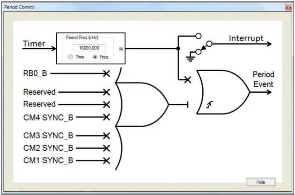
2.15 PERIOD EVENT
The period event GUI, shown in Figure 2-5, is opened by clicking on the period event block in the main GUI. The period event determines the frequency of the PSMC PWM waveform. Each period event resets the timer. The period event source can be synchronous or asynchronous.
FIGURE 2-5: PERIOD CONTROL
flowchart
graph TD
    A["Timer"] --> B["Period Freq (kHz)\n16000.000\nTime Freq"]
    B --> C["Interrupt"]
    C --> D["Period Event"]
    E["RB0_B"] --> F["X"]
    G["Reserved"] --> H["X"]
    I["Reserved"] --> J["X"]
    K["CM4 SYNC_B"] --> L["X"]
    M["CM3 SYNC_B"] --> N["X"]
    O["CM2 SYNC_B"] --> P["X"]
    Q["CM1 SYNC_B"] --> R["X"]
    S["×"] --> T["X"]
    U["X"] --> V["X"]
    W["X"] --> X["X"]
    Y["X"] --> Z["X"]
    AA["+"] --> AB["×"]
    AC["Hide"] --> AD["Feedback to AND Gate"]
2.15.1 Synchronous Selection
Synchronous period event selection is made by clicking on the X leading to the upper input to the output OR gate. When clicked, the X is replaced by a straight line leading from the period time selection box to the output OR gate. Synchronous period events can be deselected by clicking on the input line to the OR gate to change it back to a line terminated with an X.
The synchronous period event frequency is determined by the time or frequency entered in the Period Time/Period Freq text box. The Radio button below the box selects time or frequency as the display. When a value is entered the period count value is calculated based on the psmc_clk frequency. If the display mode is changed then the value changes to correspond with the existing count. Likewise, if the psmc_clk frequency is changed then the period value will be changed to correspond with the existing count.
2.15.2 Asynchronous Selection
Asynchronous period events are selected by clicking on any X leading to the 7-wide OR gate of the control. Inputs are identified by source signal name appended by a “_B”, which indicates that the signal first passed through the blanking function. Input selections vary by device. When all selections are open, then the connection to the output OR gate is shown as open. This connection cannot be changed by clicking. Instead, it closes automatically when any asynchronous input is selected.
2.15.3 Asynchronous Polarity (not available on PIC16(L)F1782/3)
The output from the 7-wide OR gate can be clicked to change the polarity of the asynchronous event. Figure 2-5 shows the polarity control enabled to invert the signal. The default polarity is not inverted, in which case the output will be shown as a straight line. The cursor will change to a hand when moved to the polarity selection area. The cursor will not change in devices that do not have this feature.
2.15.4 Interrupt
The synchronous period event can be selected as a timed interrupt source by clicking on the switch image leading to the line labeled as interrupt. Closing this switch connects the synchronous period event out to the PMSC timed interrupt summary bit in the device PIRx register. Enabling the synchronous period event interrupt also requires checking the timed event interrupt enable box on the main window.
2.16 RISING EVENT
The rising event control GUI, shown in Figure 2-6, is opened by clicking on the rising event block in the main GUI. The rising event starts the active drive of the PWM output.
The rising event source can be synchronous or asynchronous. In most applications the rising event will be synchronous at 0 us after period event. In this case, starting a PWM drive by an asynchronous input is accomplished by enabling that input in the period control. One application for synchronous times greater than 0 is center weighted PWM. See Center Weighted Variable PWM in Chapter 3. "PSMC Tips".
FIGURE 2-6: RISING EVENT CONTROL

flowchart
graph TD
    A["Timer"] --> B["Time from period event (us)<br>0.000"]
    B --> C["="]
    C --> D["Interrupt"]
    D --> E["Rising Event"]
    F["Reserved"] --> G["×"]
    H["Reserved"] --> I["×"]
    J["CM4 SYNC_B"] --> K["×"]
    L["CM3 SYNC_B"] --> M["×"]
    N["CM2 SYNC_B"] --> O["×"]
    P["CM1 SYNC_B"] --> Q["×"]
    R["B0_B"] --> S["×"]
    T["Async Rising Event"] --> U["×"]
    V["Hide"] --> W["Output"]
2.16.1 Synchronous Selection
Synchronous rising event selection is made by clicking on the X leading to the upper input to the output OR gate. When clicked, the X is replaced by a straight line leading from the rising event time selection box to the output OR gate. Synchronous rising events can be deselected by clicking on the input line to the OR gate to change it back to a line terminated with an X.
The Radio button below the text box selects time or percent as the display. When time is selected then the time entered in the text box will determine the number of microseconds the synchronous rising event will occur after the period event. When a time value is entered then the rising event count value is calculated based on the psmc_clk frequency. If the display mode is changed then the displayed value changes to correspond with the existing count. Likewise, if the psmc_clk frequency is changed then the rising event displayed value will be changed to correspond with the existing count except when the percent display mode is selected. The count remains constant and the displayed value changes to avoid invalid time entries as a result of a change to the psmc_clk value.
Entering the value as percent determines the percentage of the period the rising event will occur after the period event. When the percent value is entered then the rising event count is calculated based on the existing period count value. Unlike the time value, the percent value remains constant when the psmc_clk or period values are changed. This is possible because the new rising event count, as a result of changes to the psmc_clk, will always be valid.
2.16.2 Asynchronous Selection
Asynchronous rising events are selected by clicking on any X leading to the 7-wide OR gate of the control. Inputs are identified by source signal name appended by a “_B”, which indicates that the signal first passed through the blanking function. Input selections vary by device. When all selections are open then the connection to the output OR gate is shown as open. This connection cannot be changed by clicking. Instead it closes automatically when any asynchronous input is selected.
2.16.3 Interrupt
The synchronous rising event can be selected as a timed interrupt source by clicking on the switch image leading to the line labeled as interrupt. Closing this switch connects the synchronous rising event out to the PMSC timed interrupt summary bit in the device PIRx register. Enabling the synchronous rising event interrupt also requires checking the timed event interrupt enable box on the main window.
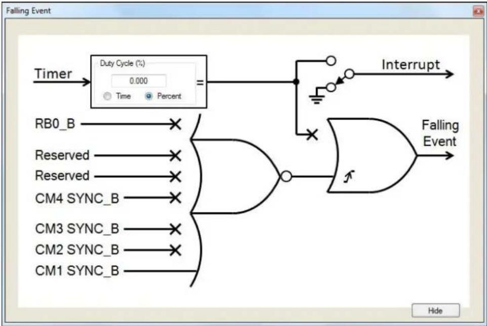
2.17 FALLING EVENT
The falling event control GUI, shown in Figure 2-7, is opened by clicking on the falling event block in the main GUI. The falling event terminates the active PWM drive output. The falling event source can be synchronous or asynchronous.
FIGURE 2-7: FALLING EVENT CONTROL
flowchart
graph TD
    A["Timer"] --> B["Duty Cycle (%)\n0.000\nTime Percent"]
    B --> C["Interrupt"]
    C --> D["Falling Event"]
    E["RB0_B"] --> F["X"]
    G["Reserved"] --> H["X"]
    I["Reserved"] --> J["X"]
    K["CM4 SYNC_B"] --> L["X"]
    M["CM3 SYNC_B"] --> N["X"]
    O["CM2 SYNC_B"] --> P["X"]
    Q["CM1 SYNC_B"] --> R["X"]
    S["Enable"] --> T["OR Gate"]
    U["Reset"] --> V["Inverter"]
    W["Feedback"] --> X["Inverter"]
    Y["Enable"] --> Z["OR Gate"]
    AA["Reset"] --> AB["X"]
    AC["Enable"] --> AD["X"]
    AE["Reset"] --> AF["X"]
    AG["Enable"] --> AH["X"]
    AI["Reset"] --> AJ["X"]
    AK["Reset"] --> AL["X"]
    AM["Reset"] --> AN["X"]
    AO["Reset"] --> AP["X"]
    AQ["Reset"] --> AR["X"]
    AS["Reset"] --> AT["X"]
    AU["Reset"] --> AV["X"]
    AW["Reset"] --> AX["X"]
    AY["Timer"] --> AZ["="]
    AZ --> BA["Interrupt"]
    BA --> BB["Falling Event"]
2.17.1 Synchronous Selection
Synchronous falling event selection is made by clicking on the X leading to the upper input to the output OR gate. When clicked, the X is replaced by a straight line leading from the falling event time selection box to the output OR gate. Synchronous falling events can be deselected by clicking on the input line to the OR gate to change it back to a line terminated with an X.
The Radio button below the text box selects time or percent as the display. When time is selected then the time entered in the text box will determine the number of microseconds the synchronous falling event will occur after the rising event. When a time value is entered, then the falling event count value is calculated based on the psmc_clk frequency and the rising event count. If the display mode is changed, then the displayed value changes to correspond with the existing count. Likewise, if either the psmc_clk frequency or rising event value is changed, then the falling event displayed value will be changed to correspond with the existing count except when the percent display mode is selected. The count remains constant and the displayed value changes to avoid invalid time entries as a result of a change to any of the psmc_clk, period, or rising event values.
Entering the value as percent determines the active pulse width as a percentage of the period. The active pulse width is the time from when the PWM output goes active (rising event) to the time the PWM output is terminated (falling event). When the percent value is entered then the falling event count is calculated based on the existing period count and rising event values. Unlike the time value, the percent value remains constant when the psmc_clk or period values are changed. This is possible when the rising event time is zero (most applications) because the new falling event count, as a result of changes to the psmc_clk and period, will always be valid. In the unlikely event that a percentage value is entered that causes the falling event count to exceed the period count, then a warning dialog will appear and the falling event count will be adjusted to the maximum valid count.
2.17.2 Asynchronous Selection
Asynchronous falling events are selected by clicking on any X leading to the 7-wide OR gate of the control. Inputs are identified by source signal name appended by a “_B”, which indicates that the signal first passed through the blanking function. Input selections vary by device. When all selections are open then the connection to the output OR gate is shown as open. This connection cannot be changed by clicking. Instead it closes automatically when any asynchronous input is selected.
2.17.3 Asynchronous Polarity (not available on PIC16(L)F1782/3)
The output from the 7-wide OR gate can be clicked to change the polarity of the asynchronous event. Figure 2-7 shows the polarity control enabled to invert the signal. The default polarity is not inverted and the output will be shown as a straight line. The cursor will change to a hand when moved to the output selection area. The cursor will not change in devices that do not have this feature.
2.17.4 Interrupt
The synchronous falling event can be selected as a timed interrupt source by clicking on the switch image leading to the line labeled as interrupt. Closing this switch connects the synchronous falling event out to the PMSC timed interrupt summary bit in the device PIRx register. Enabling the synchronous falling event interrupt also requires checking the timed event interrupt enable box on the main window.
2.18 MODULATION
The modulation control, shown in Figure 2-8, is opened by clicking on the modulation block in the main GUI. Modulation is used in applications that need to gate the PWM output on and off. For example, infrared communications typically have a carrier PWM frequency to pulse the IR emitters which is then modulated on and off by the intelligence data.
FIGURE 2-8: MODULATION CONTROL

flowchart
graph TD
    A["Period Event"] --> B["Modulation Source P1MDLBIT"]
    B --> C["NOT"]
    C --> D["D S Q R"]
    D --> E["AND"]
    E --> F["Timer Reset"]
    G["Enable"] --> H["On"]
    H --> I["NOT"]
    I --> J["Off"]
    J --> K["NOT"]
    K --> L["AND"]
    L --> M["MQ"]
    N["Q"] --> O["Ground"]
    P["Hide"] --> Q["Feedback to Q"]
2.18.1 Modulation Source Selection
The modulation source is selected from one of the external asynchronous PSMC inputs or peripheral outputs internal to the device. Modulation sources are mutually exclusive. The selection is made by choosing the desired source from those available in the Modulation Source combination box. Note that when modulation is enabled and the modulation source is low, then the Timer is held in Reset. This ensures that the first PWM pulse enabled by the modulation going high is a complete PWM period. Synchronization with the period event ensures that the last PWM pulse is also a complete period. It should be apparent that modulation should only be used when the PWM Q signal is completely synchronous (no asynchronous inputs to the period, rising, or falling events) to avoid an incomplete cycle of the first PWM period after modulation starts.
2.18.2 Modulation Enable
Modulation is enabled by clicking the enable switch to the On position. When enabled, the modulation signal gates the Q output from the PWM SR latch to the PWM mode input. Note that the PWM coming into the modulation function is labeled Q and going out it is labeled MQ. Modes that use the PWM signal take their input from the modulation function MQ output.
When the modulation enable switch is in the Off position, the MQ gate is always enabled, thereby passing the unmodulated Q out to the mode inputs.
2.19 PSMC MODES
The mode function is where the simple PWM signal derived from the rising and falling events becomes something more. There are five PWM modes, one High Resolution Frequency mode, and one Six-Step mode that simplifies steering pairs of outputs to the six PWM channels.
All modes, except the Six-Step mode, have a corresponding complementary output mode making a total of thirteen modes (2 x 6 + 1 = 13). The complementary modes include two dead-band controls: one triggered by the rising edge of the PWM signal and one triggered by the falling edge.
Modes are selected by clicking on the corresponding tab in the mode selection GUI. The tabs are labeled with the acronym of the mode control contained therein.
There are up to six PWM output channels. Not all modes use all six channels. Unused channels are indicated by an output line that begins with an X. The sections that follow detail each of the thirteen modes.
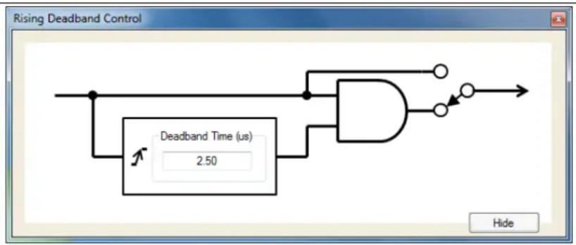
2.19.1 Dead-Band Control
Each of the six complementary modes contains two dead-band control blocks. One control delays the turn-on of the normal PWM output(s) and the other control delays the turn-on of the complementary PWM output(s). Dead-band control does not delay the turn-off of either normal or complementary outputs.
2.19.1.1 WHAT IS DEAD BAND?
Complementary outputs are generally used to drive power devices connected in series between the power rails. The complementary outputs drive the two power devices such that only one is on at a time, connecting one of the power rails to the load. When the PWM output is active, then one rail is connected to the output. When the complement is active, then the other rail is connected to the output. The turn-on time of a power device is generally faster than the turn-off time. It is necessary therefore, to disable the drives to both power devices for at least the activation difference to prevent both devices from conducting at the same time. This is accomplished with the dead-band time.
Click on either dead-band block to open the rising or falling dead-band control GUI shown in Figure 2-9. To enable dead band, click the switch to connect the AND gate output to the dead-band output. Enter the desired dead-band time in the text box.
Dead band operates as follows: When the input transitions from high-to-low the output goes low immediately. When the input transitions from low-to-high then the output transition is delayed by the dead-band time.
Note that the dead-band controls are identical for all modes. In other words, changes made to the rising dead-band control in one mode will appear in the rising dead-band control of all other modes. The same is true for the falling dead-band control.
FIGURE 2-9: DEAD-BAND CONTROL
flowchart
graph TD
    A["Start"] --> B["AND Gate"]
    B --> C["Output"]
    D["Deadband Time (us) 2.50"] --> B
    E["Hide"] --> B
2.19.2 SPWM: Single PWM Mode
Single PWM mode is selected by clicking on the SPWM tab, as shown in Figure 2-10. This mode directs the single PWM signal to the six output channels. This mode enables output steering which is a means of enabling or disabling any combination of the six channels. Output steering selection is discussed in the output control section. Output steering can be used to switch the output from one pin to another pin or to enable several outputs simultaneously, so they can be connected in parallel to boost the output current drive.
FIGURE 2-10: SINGLE PWM MODE

flowchart
graph TD
    A["MQ"] --> B["Channel A"]
    A --> C["Channel B"]
    A --> D["Channel C"]
    A --> E["Channel D"]
    A --> F["Channel E"]
    A --> G["Channel F"]
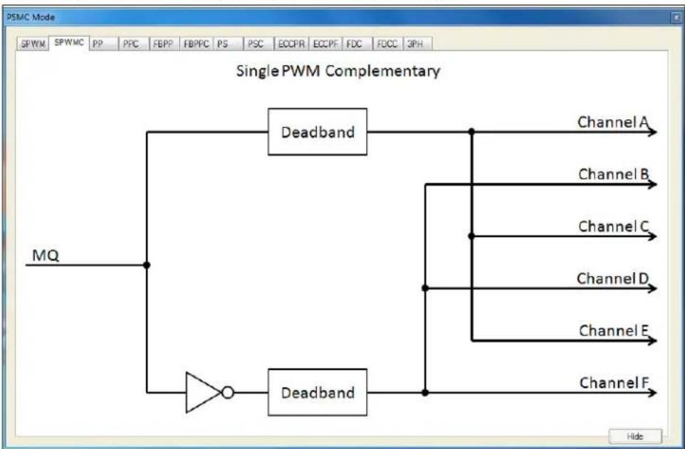
2.19.3 SPWMC: Single PWM Mode with Complementary Outputs
The Single PWM Complementary mode is selected by clicking on the SPWMC tab, as shown in Figure 2-11. This is identical to Single PWM mode, except the output channels are divided into two groups of three. One group has the PWM signal and the other group has the complement of the PWM signal.
Click on either dead-band block to open the dead-band control. See
Section 2.19.1 "Dead-Band Control" for more information.
FIGURE 2-11: SINGLE PWM COMPLEMENTARY MODE
flowchart
graph TD
    A["MQ"] --> B["Deadband"]
    A --> C["Deadband"]
    B --> D["Channel A"]
    B --> E["Channel B"]
    B --> F["Channel C"]
    B --> G["Channel D"]
    B --> H["Channel E"]
    B --> I["Channel F"]
    C --> J["Deadband"]
    J --> K["Channel F"]
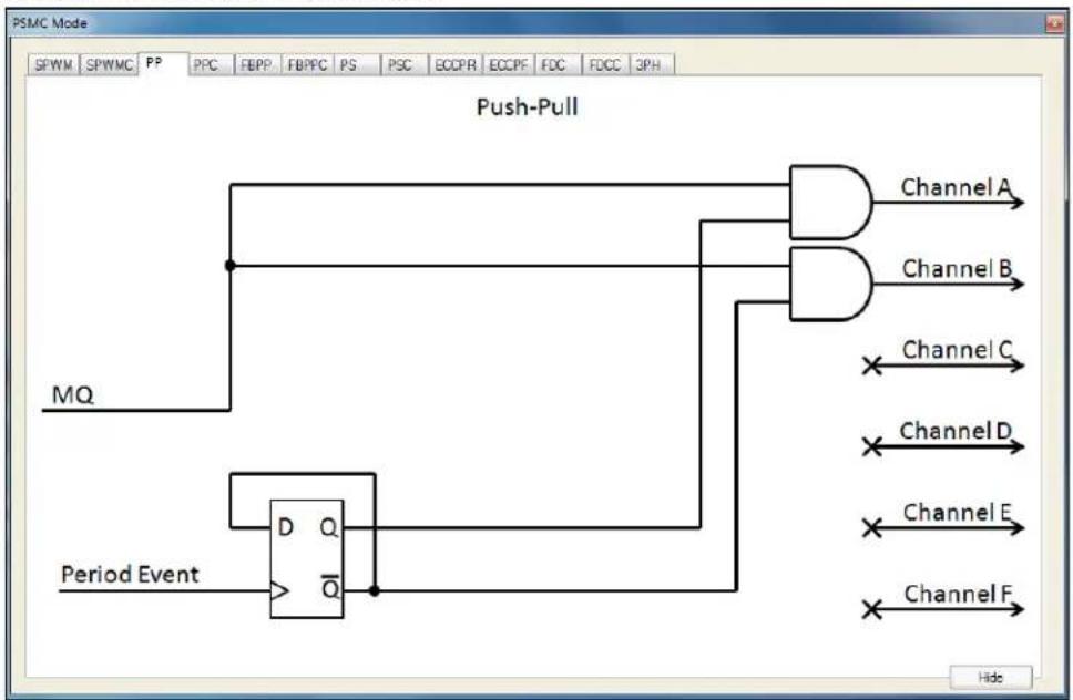
2.19.4 PP: Push-Pull Mode
The Push-Pull mode is selected by clicking on the PP tab as shown in Figure 2-12. The Push-pull mode is similar to the PWM mode, except that the PWM output alternates between Channel A and Channel B every PWM period.
FIGURE 2-12: PUSH-PULL MODE
flowchart
graph TD
    A["Period Event"] --> B["D Flip-Flop"]
    B --> C["Q"]
    C --> D["Q̅"]
    D --> E["Channel A"]
    D --> F["Channel B"]
    E --> G["Channel C"]
    F --> H["Channel D"]
    G --> I["Channel E"]
    H --> J["Channel F"]
    K["MQ"] --> L["Push-Pull"]
    M["SPWM"] --> N["SPWMC"] --> O["PP"] --> P["PFC"] --> Q["FBPP"] --> R["FBPPC"] --> S["PS"] --> T["PSC"] --> U["ECCPR"] --> V["ECCPF"] --> W["FDC"] --> X["FDCC"] --> Y["3PH"]
2.19.5 PPC: Push-Pull with Complementary Output
Push-Pull Complementary mode is selected by clicking on the PPC tab, as shown in Figure 2-13. This mode is identical to the Push-Pull mode with the addition of two complementary outputs on Channel E and Channel F.
Click on either dead-band block to open the dead-band control. See Section 2.19.1 "Dead-Band Control" for more information.
FIGURE 2-13: PUSH-PULL COMPLEMENTARY MODE

flowchart
graph TD
    A["Period Event"] --> B["D Q"]
    B --> C["Deadband"]
    C --> D["Deadband"]
    D --> E["Channel A"]
    D --> F["Channel B"]
    D --> G["Channel C"]
    D --> H["Channel D"]
    D --> I["Channel E"]
    D --> J["Channel F"]
    K["MQ"] --> L["NOT"]
    L --> M["Deadband"]
    M --> N["Deadband"]
    N --> O["Channel A"]
    N --> P["Channel B"]
    N --> Q["Channel C"]
    N --> R["Channel D"]
    N --> S["Channel E"]
    N --> T["Channel F"]
2.19.6 FBPP: Full-Bridge Push-Pull
Full-Bridge Push-Pull mode is selected by clicking on the FBPP tab, as shown in Figure 2-14. Full-Bridge Push-Pull mode is identical to Push-Pull mode, except that there are four channels, two of which are active at a time with the same waveform. Channels A and C alternate with Channels B and D every period event.
FIGURE 2-14: FULL-BRIDGE PUSH-PULL MODE

flowchart
graph TD
    A["Period Event"] --> B["D Flip-Flop"]
    B --> C["Q"]
    C --> D["Q"]
    D --> E["MQ"]
    E --> F["Channel A"]
    E --> G["Channel B"]
    E --> H["Channel C"]
    E --> I["Channel D"]
    E --> J["Channel E"]
    E --> K["Channel F"]
    style A fill:#f9f,stroke:#333
    style F fill:#ccf,stroke:#333
    style G fill:#ccf,stroke:#333
    style H fill:#ccf,stroke:#333
    style I fill:#ccf,stroke:#333
    style J fill:#ccf,stroke:#333
    style K fill:#ccf,stroke:#333
2.19.7 FBPPC: Full-Bridge Push-Pull with Complementary Mode Outputs
Full-Bridge Push-Pull Complementary mode is selected by clicking on the FBPPC tab as shown in Figure 2-15. This mode is identical to full-bridge push-pull with the addition of two complementary outputs on Channel E and Channel F. Channel E is the complement of Channels A and C. Channel F is the complement of Channels B and D.
Click on either dead-band block to open the dead-band control. See Section 2.19.1 "Dead-Band Control" for more information.
FIGURE 2-15: FULL-BRIDGE PUSH-PULL COMPLEMENTARY

flowchart
graph TD
    A["MQ"] --> B["Deadband"]
    C["Period Event"] --> D["D Q̅"]
    B --> E["Channel A"]
    B --> F["Channel B"]
    B --> G["Channel C"]
    B --> H["Channel D"]
    B --> I["Channel E"]
    B --> J["Channel F"]
    D --> K["Q̅"]
    E --> L["AND Gate"]
    F --> M["AND Gate"]
    G --> N["AND Gate"]
    H --> O["AND Gate"]
    I --> P["AND Gate"]
    J --> Q["AND Gate"]
    L --> R["AND Gate"]
    M --> S["AND Gate"]
    N --> T["AND Gate"]
    O --> U["AND Gate"]
    P --> V["AND Gate"]
    Q --> W["AND Gate"]
    R --> X["AND Gate"]
    S --> Y["AND Gate"]
    T --> Z["AND Gate"]
    U --> AA["AND Gate"]
    V --> AB["AND Gate"]
    W --> AC["AND Gate"]
    X --> AD["AND Gate"]
    Y --> AE["AND Gate"]
    Z --> AF["AND Gate"]
2.19.8 PS: Pulse-Skipping Mode
Pulse-Skipping mode is selected by clicking on the PS tab as shown in Figure 2-16. Pulse-Skipping mode uses the asynchronous rising event output to enable the PWM output. When the asynchronous input is low at the period event then PWM output for that period is suppressed, otherwise the PWM output occurs as it normally would in the Single PWM mode. Pulse-Skipping mode is generally used in hysteretic power conversion applications. Channel A is the only available output in Pulse-Skipping mode.
FIGURE 2-16: PULSE-SKIPPING MODE
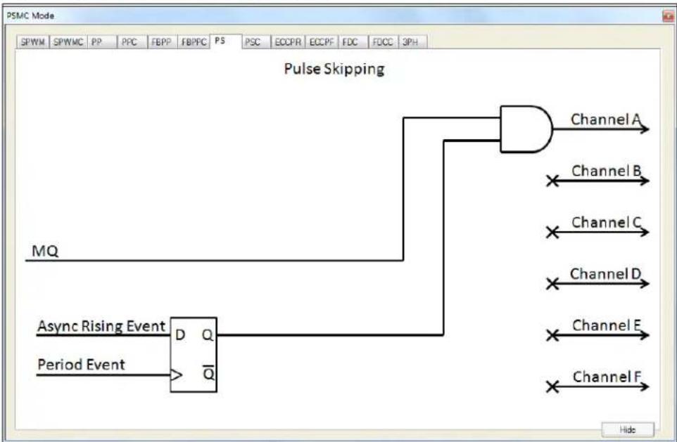
flowchart
graph TD
    A["MQ"] --> B["D Flip-Flop"]
    C["Async Rising Event"] --> B
    D["Period Event"] --> B
    B --> E["Channel A"]
    B --> F["Channel B"]
    B --> G["Channel C"]
    B --> H["Channel D"]
    B --> I["Channel E"]
    B --> J["Channel F"]
    E --> K["Pulse Skipping"]
    F --> K
    G --> K
    H --> K
    I --> K
    J --> K
2.19.9 PSC: Pulse-Skipping with Complementary Output
Pulse-skipping with complementary output is selected by clicking on the PSC tab as shown in Figure 2-17. Pulse-skipping with complementary output is identical to Pulse-Skipping mode with the complement of the PWM output to Channel B.
Click on either dead-band block to open the dead-band control. See Section 2.19.1 "Dead-Band Control" for more information.
FIGURE 2-17: PULSE-SKIPPING COMPLEMENTARY

flowchart
graph TD
    A["MQ"] --> B["AND Gate"]
    C["Async Rising Event"] --> D["D Flip-Flop"]
    E["Period Event"] --> F["Q̅"]
    B --> G["Deadband"]
    F --> G
    G --> H["Channel A"]
    G --> I["Deadband"]
    J["Channel B"] --> K["× Channel C"]
    L["Channel D"] --> M["× Channel D"]
    N["Channel E"] --> O["× Channel E"]
    P["Channel F"] --> Q["× Channel F"]
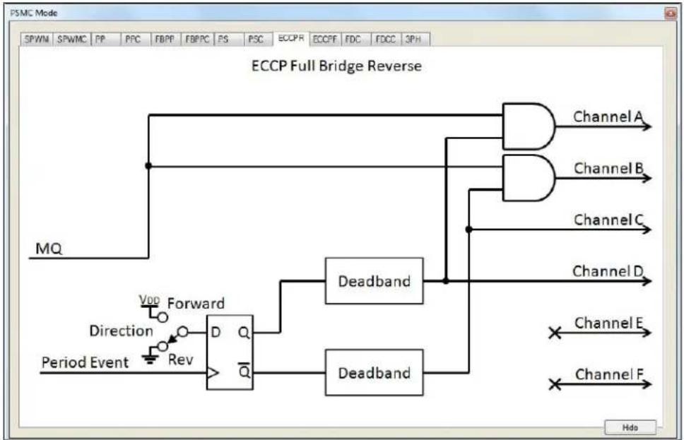
2.19.10 ECCPR: ECC PWM Full-Bridge Mode, Reverse Direction
ECC compatible PWM mode, reverse direction, is selected by clicking on the ECCPR tab as shown in Figure 2-18. This is a full-bridge driver with two of four outputs, Channels A and D, active. The Channel A output is the PWM drive and the Channel D output is true without Pulse-Width Modulation. This mode is intended to drive the high side and low side of opposite sides of an H-bridge power device configuration. Such configurations are used in brushed DC motor applications that need both speed and direction control. This mode is compatible with the Full-Bridge mode of the ECCP peripheral.
The mode can be changed to the forward direction mode by clicking on the direction switch or clicking on the ECCPF tab.
When the motor is running and the direction is changed, then the change is synchronized with the period event and dead-band time is inserted to prevent shoot-through on either side of the H-bridge. Click on either dead-band block to open the corresponding dead-band control. See Section 2.19.1 "Dead-Band Control" for more information.
FIGURE 2-18: ECC PWM FULL-BRIDGE REVERSE
flowchart
graph TD
    A["Period Event"] --> B["Forward"]
    B --> C{D}
    C --> D["Deadband"]
    D --> E["Deadband"]
    E --> F["Channel A"]
    E --> G["Channel B"]
    E --> H["Channel C"]
    E --> I["Channel D"]
    J["Direction"] --> K["Forward"]
    L["Rev"] --> M["Downward"]
    M --> N["Deadband"]
    O["MQ"] --> P["Forward"]
    Q["Hdo"] --> R["Deadband"]
2.19.11 ECCPF: ECC PWM Full-Bridge Mode, Forward Direction
ECC compatible PWM mode, forward direction, is selected by clicking on the ECCPF tab as shown in Figure 2-19. This mode is a full-bridge driver with two of four outputs, Channels B and C, active. The Channel B output is the PWM drive and the Channel C output is true without Pulse-Width Modulation. This mode is intended to drive the high side and low side of opposite sides of an H-bridge power device configuration. Such configurations are used in brushed DC motor applications that need speed and direction control. This mode is compatible with the Full-Bridge mode of the ECCP peripheral.
The mode can be changed to the reverse direction mode by clicking on the direction switch or clicking on the ECCPR tab.
When the motor is running and the direction is changed, then the change is synchronized with the period event and dead-band time is inserted to prevent shoot-through on either side of the H-bridge. Click on either dead-band block to open the corresponding dead-band control. See Section 2.19.1 "Dead-Band Control" for more information.
FIGURE 2-19: ECC PWM FULL-BRIDGE FORWARD

flowchart
graph TD
    A["Period Event"] --> B["Forward"]
    B --> C{D}
    C --> D["Deadband"]
    D --> E["Deadband"]
    E --> F["Channel A"]
    E --> G["Channel B"]
    E --> H["Channel C"]
    E --> I["Channel D"]
    J["Direction"] --> B
    K["Rev"] --> B
    L["MQ"] --> M["Forward"]
    M --> N["Deadband"]
    N --> O["Deadband"]
    O --> P["Channel E"]
    O --> Q["Channel F"]
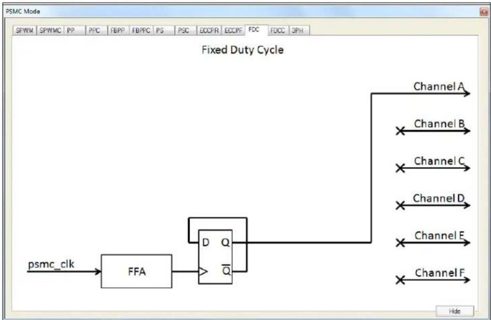
2.19.12 FDC: Fixed Duty Cycle Mode
Fixed Duty Cycle mode is selected by clicking on the FDC tab as shown in Figure 2-20. The Fixed Duty Cycle mode is used to generate frequencies with a much higher resolution than is possible with the period count alone. This mode provides only 50% duty cycle waveforms and should be used only with synchronous period time generation. This mode is generally used in fluorescent lamp ballast controls. Course frequency is determined with the period count (see synchronous period control).
FIGURE 2-20: FIXED DUTY CYCLE
flowchart
graph LR
    A["psmc_clk"] --> B["FFA"]
    B --> C["D Flip-Flop"]
    C --> D["Q"]
    D --> E["Channel A"]
    C --> F["Channel B"]
    C --> G["Channel C"]
    C --> H["Channel D"]
    C --> I["Channel E"]
    C --> J["Channel F"]
    E --> K["Hide"]
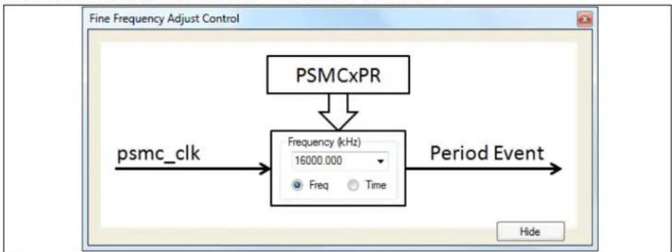
2.19.13 Fine Frequency Adjust
After the course frequency is determined with the clock and period controls, the frequency is fine tuned with the Fine Frequency Adjust control. Click on the FFA box to open the fine frequency adjust control shown in Figure 2-21.
The combination box in the center of the fixed frequency adjust control shows 16 possible selections based on the psmc_clk frequency and period count. Selections can be made by frequency or time by clicking on the desired display mode radio button. When any of the clock frequency, period frequency, or selection mode is changed, then the selection list and displayed selection are updated to correspond to the change. Note that the displayed frequency is twice the output waveform frequency because the fixed 50% duty cycle is derived by dividing the adjusted period frequency by two.
FIGURE 2-21: FINE FREQUENCY ADJUST CONTROL
flowchart
graph TD
    A["PSMCxPR"] --> B["Frequency (kHz)\n16000.000\nFreq Time"]
    C["psmc_clk"] --> B
    B --> D["Period Event"]
    D --> E["Hide"]
2.19.14 FDCC: Fixed Duty Cycle with Complementary Output
Fixed Duty Cycle Complementary Output mode is selected by clicking on the FDCC tab as shown in Figure 2-22. The Fixed Duty Cycle with Complementary Output mode is identical to the Fixed Duty Cycle mode with Channel B output as the complement to Channel A.
FIGURE 2-22: FIXED DUTY CYCLE COMPLEMENTARY OUTPUT

flowchart
graph LR
    A["psmc_clk"] --> B["FFA"]
    B --> C["D Flip-Flop"]
    C --> D["Deadband"]
    D --> E["Channel A"]
    D --> F["Channel B"]
    D --> G["Channel C"]
    D --> H["Channel D"]
    D --> I["Channel E"]
    D --> J["Channel F"]
    C --> K["Deadband"]
    K --> L["Channel F"]
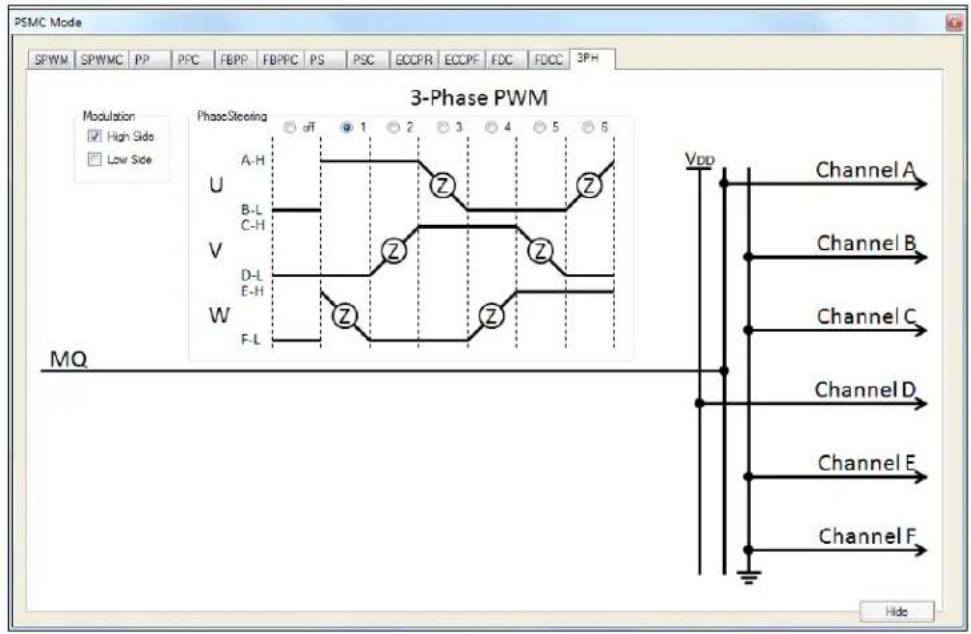
2.19.15 3PH: 3-Phase PWM
3-Phase PWM mode is selected by clicking on the 3PH tab as shown in Figure 2-23. 3-Phase PWM is a special mode that generates the waveform for 6-step 3-phase systems such as those for driving brushless DC motors. These systems have three half bridges requiring two drive outputs each for a total of six channels. This mode uses the steering control bits to drive two of the six channels at a time: one half-bridge high side drive and another half-bridge low side drive both on.
A diagram is presented in the top center of the control that indicates the power voltages applied to the system in each phase. Phases are labeled U, V and W. The phase U half bridge is driven by channels A (high side) and B (low side) as indicated to the right of the phase labels. Phases V and W are labeled similarly. You can also select which side of the half bridge receives the Pulse-Width Modulation: High side, low side, or both. Modulation is selected by the two check boxes to the left of the diagram.
Clicking on a radio button at the top of the diagram will select that phase drive configuration. For example, as shown in Figure 2-23, high side modulation is checked and radio button 1 is selected, thereby driving phase U high with modulation, phase V low with no modulation, and phase W floating. The channel connections to achieve this configuration are shown on the right.
FIGURE 2-23: 3-PHASE PWM
text_image
PSMC Mode SPWM SPWMC PP PFC FBPP FB/PC PS PSC ECOFR ECOFF FDC FDCC 3PH Modulation ✓ High Side □ Low Side 3-Phase PWM PhaseSteering A-H U B-L C-H V D-L E-H W F-L Z Z Z Z VDD Channel A Channel B Channel C Channel D Channel E Channel F HQ Hide2.20 OUTPUT CONTROL
Channels are directed to the output pins through the output control. Open the output control GUI shown in Figure 2-24 by clicking on the output control block in the main GUI.
There are four selections for each channel in this control:
- Output enable – switch furthest to the right
- Output steering – input to the buffer on the left
- Output polarity – bubble on output of the buffer figure
- Shutdown level – switch at input to MUX
FIGURE 2-24: OUTPUT CONTROL

flowchart
graph TD
    A["Channel A"] --> B["NOT"]
    B --> C["0"]
    C --> D["LATC0"]
    D --> E["PSMC1A"]
    F["Channel B"] --> G["NOT"]
    G --> H["0"]
    H --> I["LATC1"]
    I --> J["PSMC1B"]
    K["Channel C"] --> L["NOT"]
    L --> M["0"]
    M --> N["LATC2"]
    N --> O["PSMC1C"]
    P["Channel D"] --> Q["NOT"]
    Q --> R["0"]
    R --> S["LATC3"]
    S --> T["PSMC1D"]
    U["Channel E"] --> V["NOT"]
    V --> W["0"]
    W --> X["LATC4"]
    X --> Y["PSMC1E"]
    Z["Channel F"] --> AA["NOT"]
    AA --> AB["0"]
    AB --> AC["LATC5"]
    AC --> AD["PSMC1F"]
    AE["SHUTDOWN"] --> AF["Ground"]
    AG["Synchronize Steering With Period Event"] --> AH["Power Supply"]
    AI["Hide"] --> AJ["Power Supply"]
2.20.1 Output Enable
The output enable switch selects between the PORT latch output and the PSMC channel. When the PORT latch output is selected, then the output pin is not affected by the PSMC. When the PSMC channel is selected, then the pin is not affected by the PORT latch.
2.20.2 Output Steering
Two modes, SPWM and SPWMC, include steering. Steering gives the ability to steer the PWM output to one or more of the six outputs. Steering differs from the output enable because when steering is disabled then the pin output is forced false regardless of the PORT latch level.
Modes other than SPWM and SPWMC do not include steering and therefore, all steering controls are shown as connected for those modes and cannot be disconnected.
2.20.3 Output Steering Synchronization
The checkbox in the lower left of the control selects period event steering synchronization. When the PWM is active and steering is changed, then the synchronized steering change takes effect at the period event immediately following the change. When steering synchronization is not enabled then steering changes take effect immediately without waiting for the period event.
2.20.4 Output Polarity
The output polarity control determines the active-true level of the channel output. The active time starts at the rising event and ends at the falling event. Polarity is selected by clicking on the output of the channel buffer. The output will appear as a bubble for active-low polarity and as a line for active-high polarity.
2.20.5 Shutdown Level
Shutdown level is the level forced on the output when a shutdown condition is active. The shutdown level for a channel is selected by clicking on the switch at the input of the shutdown MUX. Note that the polarity control is ahead of the shutdown MUX so that the shutdown output level is not affected by the polarity control.
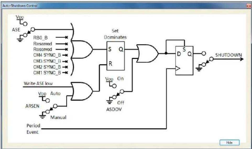
2.21 AUTO-SHUTDOWN
Auto-shutdown provides the ability to suspend the PWM output immediately upon an external input or program control. The auto-shutdown control, shown in Figure X Auto-Shutdown, is opened by clicking on the auto-shutdown block in the main GUI.
2.21.1 Shutdown Enable
Shutdown is enabled by clicking on the switch at the output of the control. When shutdown is enabled then a high on any shutdown source will force the PSMC outputs to a predetermined state until the shutdown source goes low and the PSMC is restarted.
2.21.2 Shutdown Sources
Shutdown sources are selected by clicking on the broken lines leading to the 8-input OR gate. The broken line will change to an unbroken line indicating that the connection is made. Remove source selections by clicking on the unbroken OR gate input line.
The ASE switch is a software control bit that provides software generated shutdown events. You can preset this bit by clicking on the switch.
2.21.3 Shutdown Override
Clicking on the ASDOV switch changes the state of the auto-shutdown override bit. When set, this bit forces a shutdown condition that remains in effect as long as the bit is set. Manual and automatic restarts have no affect while the ASDOV bit is set.
2.21.4 Auto/Manual Restart
Clicking on the ARSEN switch selects between automatic and manual restart. When restart is automatic then the PSMC will resume operation after all shutdown sources are low. When restart is manual, then the ASE bit must be cleared by software to restart the PSMC. The ASE bit can only be cleared if all input sources are low. In either case, PSMC operation resumes on the first period event after the shutdown is cleared.
FIGURE 2-25: AUTO-SHUTDOWN
flowchart
graph TD
    A["ASE"] --> B["Set Dominates"]
    B --> C["D Flip-Flop"]
    C --> D["SHUTDOWN"]
    E["Write ASE low"] --> F["AND Gate"]
    G["ARSEN"] --> H["Manual"]
    I["Period Event"] --> J["AND Gate"]
    K["VDD"] --> B
    L["RBO_B"] --> B
    M["Reserved"] --> B
    N["Reserved"] --> B
    O["CM4 SYNC_B"] --> B
    P["CM3 SYNC_B"] --> B
    Q["CM2 SYNC_B"] --> B
    R["CM1 SYNC_B"] --> B
    S["VDD"] --> F
    T["On"] --> C
    U["Off"] --> C
    V["ASDOV"] --> C
    W["Hide"] --> C
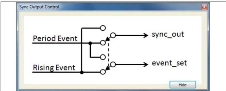
2.22 SYNC OUTPUT CONTROL (NOT AVAILABLE ON THE PIC16(L)F1782/3)
Slaves select the sync source as shown in Section 2.13 "Timer". The sync output of PIC16(L)F1783/3 devices is fixed to the period event output. All other devices can select either the period event or rising event as the sync output.
The sync output control, shown in Figure 2-26, is opened by clicking on the sync block of the main GUI. The synchronization signal output to other PSMC sync inputs may come directly from the period event or from the rising edge event. Clicking on the double-pole switch selects between the two possibilities.
When the switch selects the period event as the master PSMC sync source then all slave PSMCs will synchronize their period events to the master. This requires the period time for all slave PSMCs to be as long as or longer than the period time of the master.
When the switch selects the rising event as the master PSMC sync source, then the master PSMC rising event defaults to the master PSMC period event, and the slave PSMCs period is delayed by the master PSMC rising event time. Delaying slaves in this manner retains the 0 to 100% duty cycle range of the master and slave in phase delayed applications.
FIGURE 2-26: SYNC CONTROL
flowchart
graph TD
    A["Period Event"] --> B{?}
    B --> C["sync_out"]
    B --> D["?"]
    D --> E["event_set"]
    F["Rising Event"] --> G{?}
    G --> H["?"]
    H --> I["?"]
    I --> J["?"]
    J --> K["?"]
    style A fill:#f9f,stroke:#333
    style F fill:#f9f,stroke:#333
    style B fill:#ccf,stroke:#333
    style D fill:#ccf,stroke:#333
    style H fill:#ccf,stroke:#333
    style I fill:#ccf,stroke:#333
Chapter 3. PSMC Tips
The following sections provide useful tips for getting the most out of the PSMC peripheral.
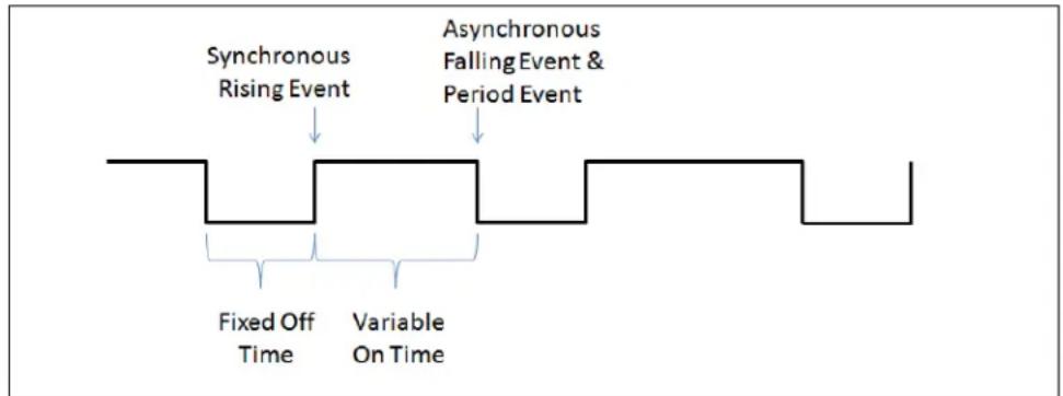
3.1 VARIABLE PERIOD WITH FIXED OFF-TIME
Some power supply designs use a fixed off-time and then vary the duty cycle by asynchronous feedback to terminate drive time and also start a new period. The first configuration that comes to mind is shown in Figure 3-1 and is setup as follows:
- Period event: Asynchronous feedback
- Rising event: Synchronous time set to desired fixed off-time
- Falling event: Asynchronous feedback – same source as period event
FIGURE 3-1: FIXED OFF-TIME WITH RISING EVENT DELAY
flowchart
graph TD
    A["Synchronous Rising Event"] --> B["Fixed Off Time"]
    B --> C["Variable On Time"]
    C --> D["Asynchronous Falling Event & Period Event"]
This will not work because the timing of the asynchronous event relative to the psmc_clk may cause the rising event to be suppressed.
An alternate method, shown in Figure 3-2 with Falling Event Delay, uses a fixed falling event delay, which avoids the timing issue is setup as follows:
- Period event: Asynchronous feedback
- Rising event: Synchronous time set to zero
- Falling event: Synchronous time set to desired fixed off-time
- Shutdown level: Low
- Output polarity: Inverted
FIGURE 3-2: FIXED OFF-TIME WITH FALLING EVENT DELAY
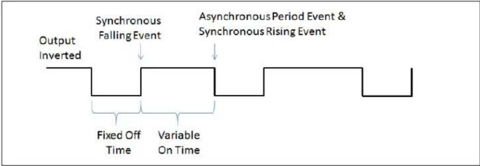
flowchart
graph LR
    A["Output Inverted"] --> B["Synchronous Falling Event"]
    B --> C["Fixed Off Time"]
    C --> D["Variable On Time"]
    D --> E["Asynchronous Period Event & Synchronous Rising Event"]
This method inverts the output so that the synchronous duty cycle becomes the off-time, and the off-time after the duty cycle end becomes the on-time. Use auto-shutdown to start and stop the application.
3.2 3-PHASE VARIABLE DUTY CYCLE
3-Phase applications such as power supplies, AC induction motors, and tri-color LED lighting, require three PWMs with a fixed-phase offset from each other. These applications also require a variance of the PWM duty cycle from 0 to 100%. The rising event phase-delay alone cannot be used to offset the waveforms because the rising event delay subtracts from the time available for the duty cycle. For example, if a period has 100 microseconds and the rising event time is 30 microseconds then the falling event time after the rising event can be no larger than 70 microseconds, which is a maximum duty cycle of 70%.
Phase delay can be implemented without losing duty cycle range by selecting the rising event sync output option. When that option is selected then the synchronous rising event time defaults to zero. In other words, the rising event time is the master's phase delayed sync output and the master's synchronous rising edge event occurs at the master's period event.
Now consider how this affects the three PSMCs generating the three PWMs in the three phase waveform:
• The first PSMC is the master for the second PSMC
- The second PSMC is the slave of the first PSMC but is also the master to the third PSMC
• The third PSMC is the slave of the second PSMC and master of none
Setup for the three PSMCs of a PIC16(L)F1786 is as follows:
- Select the PIC16(L)F1786 and PSMC1
- Click on the Sync function: Set rising event as the sync output
- Click on the Timer function: Set the sync source to Off
- Click on the Period Event function: Set the period event time to the desired value. Click on the upper input line to the output OR gate to make the synchronous connection.
- Click on the Rising Event function: Set the rising event delay to the desired phase offset. Click on the upper input line to the output OR gate to make the synchronous connection.
- Click on the Falling Event function: Set the falling event duty cycle to the desired value. Click on the upper input line to the output OR gate to make the synchronous connection.
-
Click on the Modulation function: Enable modulation and set the source to CM4 SYNC
-
Click on the Mode Control function: Click on the tab to set the desired PWM mode
- Click on the Output Control function: Connect the steering (if needed), channel polarity, and desired outputs to pins
- Check the PSMC enable box
- Write in the comments section notes about Phase 1 of this 3-phase setup
- Copy this setup using the Copy and Show button
Select PSMC2
- Paste the configuration copied from PSMC1 by clicking on the Paste button
- Click on the Timer function: Change the sync source to PSMC1
- Click on the Modulation function: Disable modulation
- Click on the Output Control function: Change if necessary the steering, polarity, and channel outputs to pins
- Write in the comments section notes about Phase 2 of this 3-phase setup
- All other settings are the same as PSMC1 and need not be changed
Select PSMC3
- Paste the configuration copied from PSMC1 by clicking on the Paste button
- Click on the Timer function: Change the sync source to PSMC2
- Click on the Output Control function: Change if necessary the steering, polarity, and channel outputs to pins
- Write in the comments section notes about Phase 3 of this 3-phase setup
- All other settings are the same as PSMC2 and need not be changed
Use the file pull-down menu to save the three-phase configuration setup as a C or Assembly code include file.
If your project initialization routine does not include the I/O pin initialization for the PSMC outputs, then add that initialization code to your project. Also add the reference to your project to include the PSMC configuration file.
Modulation has been used in this setup so that the 3-phase output starts in order with PSMC1 operating first when the modulation source is high. In this example,
Comparator 4 sync output is used as the modulation source. The 3-Phase PWM is started by Comparator 4 output high and stopped by Comparator 4 output low. This is accomplished by software setting the C4POL bit to start the PWM and clearing the C4POL bit to stop the PWM. The C4ON and C4SYNC bits should both be cleared. All other Comparator 4 control bits are don't care.
3.3 CENTER WEIGHTED VARIABLE PWM
Some applications benefit from a PWM that spreads from the middle of the period instead of expanding from the start of the period. This is sometimes referred to as center weighted PWM. Center weighted PWM can be accomplished by setting the rising event time to the middle of the period minus half the PWM width and setting the falling event time to the middle of the period plus half the PWM width (Figure 3-3).
Irregular PWM widths are avoided during the change, because the new settings are held until the PxLD bit (bit 6 of the PSMCxCON register) is set. The transfer to the counters is performed synchronous with the PWM period, ensuring that both new settings take effect in the same period.
FIGURE 3-3: CENTER WEIGHTED PWM

text_image
Period Event FallingEvent Rising EventNOTES:
Worldwide Sales and Service
AMERICAS
Corporate Office
2355 West Chandler Blvd.
Chandler, AZ 85224-6199
Tel: 480-792-7200
Fax: 480-792-7277
Technical Support
http://www.microchip.com/support
Web Address:
www.microchip.com
Atlanta
Duluth, GA
Tel: 678-957-9614
Fax: 678-957-1455
Boston
Westborough, MA
Tel: 774-760-0087
Fax: 774-760-0088
Chicago
Itasca,
Tel: 630-285-0071
Fax: 630-285-0075
Cleveland
Independence, OH
Tel: 216-447-0464
Fax: 216-447-0643
Dallas
Addison, TX
Tel: 972-818-7423
Fax: 972-818-2924
Detroit
Farmington Hills, MI
Tel: 248-538-2250
Fax: 248-538-2260
Indianapolis
Noblesville, IN
Tel: 317-773-8323
Fax: 317-773-5453
Los Angeles
Mission Viejo, CA
Tel: 949-462-9523
Fax: 949-462-9608
Santa Clara
Santa Clara, CA
Tel: 408-961-6444
Fax: 408-961-6445
Toronto
Mississauga, Ontario,
Canada
Tel: 905-673-0699
Fax: 905-673-6509
ASIA/PACIFIC
Asia Pacific Office
Suites 3707-14, 37th Floor
Tower 6, The Gateway
Harbour City, Kowloon
Hong Kong
Tel: 852-2401-1200
Fax: 852-2401-3431
Australia - Sydney
Tel: 61-2-9868-6733
Fax: 61-2-9868-6755
China - Beijing
Tel: 86-10-8569-7000
Fax: 86-10-8528-2104
China - Chengdu
Tel: 86-28-8665-5511
Fax: 86-28-8665-7889
China - Chongqing
Tel: 86-23-8980-9588
Fax: 86-23-8980-9500
China - Hangzhou
Tel: 86-571-2819-3187
Fax: 86-571-2819-3189
China - Hong Kong SAR
Tel: 852-2943-5100
Fax: 852-2401-3431
China - Nanjing
Tel: 86-25-8473-2460
Fax: 86-25-8473-2470
China - Qingdao
Tel: 86-532-8502-7355
Fax: 86-532-8502-7205
China - Shanghai
Tel: 86-21-5407-5533
Fax: 86-21-5407-5066
China - Shenyang
Tel: 86-24-2334-2829
Fax: 86-24-2334-2393
China - Shenzhen
Tel: 86-755-8864-2200
Fax: 86-755-8203-1760
China - Wuhan
Tel: 86-27-5980-5300
Fax: 86-27-5980-5118
China - Xian
Tel: 86-29-8833-7252
Fax: 86-29-8833-7256
China - Xiamen
Tel: 86-592-2388138
Fax: 86-592-2388130
China - Zhuhai
Tel: 86-756-3210040
Fax: 86-756-3210049
ASIA/PACIFIC
India - Bangalore
Tel: 91-80-3090-4444
Fax: 91-80-3090-4123
India - New Delhi
Tel: 91-11-4160-8631
Fax: 91-11-4160-8632
India - Pune
Tel: 91-20-2566-1512
Fax: 91-20-2566-1513
Japan - Osaka
Tel: 81-6-6152-7160
Fax: 81-6-6152-9310
Japan - Tokyo
Tel: 81-3-6880-3770
Fax: 81-3-6880-3771
Korea - Daegu
Tel: 82-53-744-4301
Fax: 82-53-744-4302
Korea - Seoul
Tel: 82-2-554-7200
Fax: 82-2-558-5932 or
82-2-558-5934
Malaysia - Kuala Lumpur
Tel: 60-3-6201-9857
Fax: 60-3-6201-9859
Malaysia - Penang
Tel: 60-4-227-8870
Fax: 60-4-227-4068
Philippines - Manila
Tel: 63-2-634-9065
Fax: 63-2-634-9069
Singapore
Tel: 65-6334-8870
Fax: 65-6334-8850
Taiwan - Hsin Chu
Tel: 886-3-5778-366
Fax: 886-3-5770-955
Taiwan - Kaohsiung
Tel: 886-7-213-7828
Fax: 886-7-330-9305
Taiwan - Taipei
Tel: 886-2-2508-8600
Fax: 886-2-2508-0102
Thailand - Bangkok
Tel: 66-2-694-1351
Fax: 66-2-694-1350
EUROPE
Austria - Wels
Tel: 43-7242-2244-39
Fax: 43-7242-2244-393
Denmark - Copenhagen
Tel: 45-4450-2828
Fax: 45-4485-2829
France - Paris
Tel: 33-1-69-53-63-20
Fax: 33-1-69-30-90-79
Germany - Munich
Tel: 49-89-627-144-0
Fax: 49-89-627-144-44
Italy - Milan
Tel: 39-0331-742611
Fax: 39-0331-466781
Netherlands - Drunen
Tel: 31-416-690399
Fax: 31-416-690340
Spain - Madrid
Tel: 34-91-708-08-90
Fax: 34-91-708-08-91
UK - Wokingham
Tel: 44-118-921-5869
Fax: 44-118-921-5820
11/29/12