VSC8489 - Electronic component Microchip - Free user manual and instructions
Find the device manual for free VSC8489 Microchip in PDF.

User questions about VSC8489 Microchip
0 question about this device. Answer the ones you know or ask your own.
Ask a new question about this device
Download the instructions for your Electronic component in PDF format for free! Find your manual VSC8489 - Microchip and take your electronic device back in hand. On this page are published all the documents necessary for the use of your device. VSC8489 by Microchip.
USER MANUAL VSC8489 Microchip
IEEE 1588v2 Support in the Microsemi PHY API
Released
2016
Contents
1 Revision History .... 1
1.1 Revision 1.1 .... 1
1.2 Revision 1.0 .... 1
2 IEEE 1588v2 Support in the Microsemi PHY API 2
3 Feature Description .... 3
4 Functional Description 7
4.1 FIFO 7
4.1.1 Enable 7
4.1.2 FIFO Overflow_Underflow Indication 7
4.2 Analyzer 7
4.2.1 Enable_Disable 7
4.2.2 Encapsulation Protocol(s) 7
4.2.3 Application Protocol(s) and Modes 7
4.2.4 Operation Mode 8
4.2.5 FrameSignature 12
4.3 Timestamp Block 13
4.3.1 LocalLatency 13
4.3.2 PathDelay 13
4.3.3 DelayAsymmetry 14
4.3.4 Correction Field Overflow Indication 14
4.4 LocalTimeCounter 14
4.4.1 PtpTime 14
4.4.2 SavedPtpTime 14
4.4.3 LocalClockAdjustment 15
4.4.4 LocalClockIncrementDecrement 15
4.4.5 LocalClockFrequency 15
4.5 Rewriter 15
4.5.1 PreambleShrink 15
4.5.2 StatisticCounters 15
4.6 TimestampFIFO 15
4.6.1 TxTimestampMode 15
4.6.2 TxTimestamps 15
4.6.3 TxTimestampFifo Not Empty Indication 16
4.6.4 TxTimestampFifo Overflow Indication 16
4.6.5 TxTimestampFifo AgeTime 16
4.6.6 RxTimestamp 16
4.6.7 RxTimestampMode 16
4.7 Module Bring-Up 16
4.7.1 Cold_Warm Restart 16
4.8 Other Functions 16
4.9 Control Module (PTP Engine) 16
4.9.1 Module Management 17
4.9.2 ClockRate Management 17
4.9.3 Multiple Timing Domain Support 19
4.9.4 CLI 19
4.10 Distributed Control Module 19
1 Revision History
The revision history describes the changes that were implemented in the document. The changes are listed by revision, starting with the most current publication.
1.1 Revision 1.1
The following is a summary of the changes in revision 2.0 of this document.
- Formatting was updated. For more information, see Table 1—Table 6.
• Information in Table 8 was updated.
1.2 Revision 1.0
Revision 1.0 was the first publication of this document.
2 IEEE 1588v2 Support in the Microsemi PHY API
This application note lists all Microsemi PHY API features related to IEEE 1588v2 support in Microsemi PHYs and is relevant for 1588 API customers, developers, and architects.
The documents for the following products are available for reference: VSC8492 Dual Channel Universal 10G PHY or 10 GbE PHY with OTN/FEC and IEEE 1588; VSC8494 Quad Channel Universal 10G PHY or 10 GbE PHY with OTN/FEC and IEEE 1588; VSC8488-15 Dual Channel WAN/LAN/Backplane XAUI to SFP+/KR Transceiver; VSC8487-15 WAN/LAN/Backplane XAUI to SFP+/KR Transceiver; and the datasheet section on IEEE 1588v2 PTP/ITU-T Y.1731 OAM timestamp update block. In addition, consult the ITU-T G.8265.1 [IEEE 1588 profile for telecom (frequency delivery without support from network nodes)] and IEEE Standard for a Precision Clock Synchronization Protocol for Networked Measurement and Control Systems (IEEE Std 1588-2008) standards.
3 Feature Description
The Microsemi 1588 PHY API provides an interface between different Microsemi hardware components and applications—it is a hardware abstraction layer. The API is responsible for setting up the hardware registers in the different 1588 PHY implementations. Possible applications include the Microsemi precision time protocol (PTP) engine or the customer's own applications. The Microsemi PTP engine implements the different PTP clock types defined in 1588 and G8265.1. The Microsemi PTP engine also has an interface for calling customer-defined offset and delay filters.
Figure 1 • 1588 API and Environment

flowchart
graph TD
    A["Applications"] --> B["API"]
    B --> C["PHY Hardware"]
    subgraph Applications
        D["Customer PTP Engine"]
        E["Microsemi PTP Engine"]
        F["Optional customer-defined PDV filter"]
    end
    subgraph API
        G["VSC8492, VSC8494 (10G PHY with OTN-FEC)"]
        H["VSC8484-15 (10G optical)"]
        I["VSC8574 (Quad PHY)"]
    end
    D --> E
    E --> F
    F --> G
    G --> H
    G --> I
The following two illustrations show typical applications where the API is used. For a more detailed description of the components, please see the device datasheet. The following illustration shows a one-step end-2-end (E2E) transparent clock (TC) application.
Figure 2 • Typical TC Application

flowchart
graph LR
    subgraph Ethernet Port
        A["1G PHY"] --> B["Linecard Control Processor"]
        C["MAC"] --> D["Packet Processing"]
        E["MAC or Switch"] --> F["Fabric Adapter"]
    end

    subgraph System Card
        G["System Control Processor"] <--> H["Fabric"]
    end

    subgraph Ethernet Port
        I["1G PHY"] <--> J["Linecard Control Processor"]
        K["MAC"] <--> L["Fabric Adapter"]
    end

    subgraph System Card
        M["System Control Processor"] <--> N["Fabric"]
    end

    subgraph Ethernet Port
        O["1G PHY"] <--> P["Linecard Control Processor"]
        Q["MAC"] <--> R["Fabric Adapter"]
        S["MAC or Switch"] <--> T["Fabric Adapter"]
    end

    subgraph System Card
        U["System Control Processor"] <--> V["Fabric"]
    end

    subgraph Ethernet Port
        W["1G PHY"] <--> X["Linecard Control Processor"]
        Y["MAC"] <--> Z["Fabric Adapter"]
        AA["MAC or Switch"] <--> AB["Fabric Adapter"]
        AC["MAC or Switch"] <--> AD["Fabric Adapter"]
        AE["MAC or Switch"] <--> AF["Fabric Adapter"]
        AG["MAC or Switch"] <--> AH["Fabric Adapter"]
        AI["MAC or Switch"] <--> AJ["Fabric Adapter"]
        AK["MAC or Switch"] <--> AL["Fabric Adapter"]
        AM["MAC or Switch"] <--> AN["Fabric Adapter"]
        AO["MAC or Switch"] <--> AP["Fabric Adapter"]
        AQ["MAC or Switch"] <--> AR["Fabric Adapter"]
        AS["MAC or Switch"] <--> AT["Fabric Adapter"]
        AU["MAC or Switch"] <--> AV["Fabric Adapter"]
        AW["MAC or Switch"] <--> AX["Fabric Adapter"]
        AY["1G PHY"] <--> AZ["Linecard Control Processor"]
        BA["MAC"] <--> BB["Linecard Control Processor"]
        BC["MAC or Switch"] <--> BD["Linecard Control Processor"]
        BE["MAC or Switch"] <--> BF["Linecard Control Processor"]
        BG["MAC or Switch"] <--> BH["Linecard Control Processor"]
        BI["MAC or Switch"] <--> BJ["Linecard Control Processor"]
        BK["MAC or Switch"] <--> BL["Linecard Control Processor"]
        BM["MAC or Switch"] <--> BN["Linecard Control Processor"]
        BO["MAC or Switch"] <--> BP["Linecard Control Processor"]
        BQ["MAC or Switch"] <--> BR["Linecard Control Processor"]
        BS["MAC or Switch"] <--> BT["Linecard Control Processor"]
        BU["MAC or Switch"] <--> BV["Linecard Control Processor"]
        BW["MAC or Switch"] <--> BX["Linecard Control Processor"]
        BY["MAC or Switch"] <--> BZ["Linecard Control Processor"]
        CA["MAC or Switch"] <--> CB["Linecard Control Processor"]
        CC["MAC or Switch"] <--> CD["Linecard Control Processor"]
        DE["MAC or Switch"] <--> DF["Linecard Control Processor"]
        DG["MAC or Switch"] <--> DH["Linecard Control Processor"]
        DI["MAC or Switch"] <--> DJ["Linecard Control Processor"]
        DK["MAC or Switch"] <--> DL["Linecard Control Processor"]
        DM["MAC or Switch"] <--> DJ
        EX["MAC or Switch"] <--> DY["Linecard Control Processor"]
        DX["MAC or Switch"] <--> DY
        DY --> DW["1588 frame updated in HW for Residence Time (internal delay)"]
    end

    subgraph Ethernet Port
        DW --> DW
    end

    style Ethernet Port fill:#f9f,stroke:#333
    style System Card fill:#ccf,stroke:#333
In this application, the API resides in the linecard control processor and sets up the PTP packet processing in PHYs. When this setup is done, the PHYs do all the PTP processing. Assuming that the system clock operates in free-running mode, a software PTP engine is not needed. If the system clock has to be syntonized to an external PTP master, a PTP engine has to be implemented in the system control processor to perform the syntonization. The following illustration shows a one-step boundary clock (BC) application.
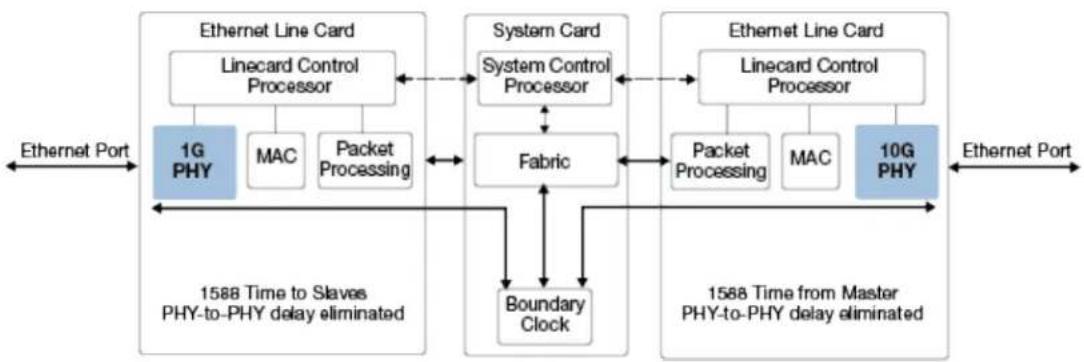
Figure 3 • Typical BC Application
flowchart
graph LR
    A["Ethernet Port"] --> B["1G PHY"]
    B --> C["MAC"]
    B --> D["Packet Processing"]
    C --> E["Linecard Control Processor"]
    D --> F["Fabric"]
    E --> G["System Card System Control Processor"]
    F --> G
    G --> H["10G PHY"]
    H --> I["Ethernet Port"]
    J["1588 Time to Slaves PHY-to-PHY delay eliminated"] --> K["Boundary Clock"]
    L["1588 Time from Master PHY-to-PHY delay eliminated"] --> M["Linecard Control Processor"]
    N["1588 Time to Slaves PHY-to-PHY delay eliminated"] --> O["Linecard Control Processor"]
    P["1588 Time from Master PHY-to-PHY delay eliminated"] --> Q["Linecard Control Processor"]
    R["1588 Time from Master PHY-to-PHY delay eliminated"] --> S["Linecard Control Processor"]
    T["1588 Time from Master PHY-to-PHY delay eliminated"] --> U["Linecard Control Processor"]
    V["1588 Time from Master PHY-to-PHY delay eliminated"] --> W["Linecard Control Processor"]
In this application, the API resides in the linecard control processor and sets up the PTP packet processing in PHYs. When this setup is done, the PHYs do all the PTP timestamping. The boundary clock PTP engine is implemented on the system card. All the PTP packets intended for the boundary clock are sent from the switch fabric to the PTP engine. The PTP engine processes the PTP messages and performs the system clock synchronization. The timestamping functionality exists in both the ingress and egress paths. Different setups are done on the two paths. The 1588 API is responsible for setting up the hardware registers in the 1588 PHYs. The following tables briefly describe the hardware interface. Where possible, the names in parentheses refer to interface names in the device datasheet.
Table 1 • PCS+PMA and Delay FIFO
| Name Description |
| Enable Enable/disable the timestamping feature, and hereby the delay FIFO. |
| FifoOfSticky Sticky bit indicating a FIFO overflow. |
| FifoUfSticky Sticky bit indicating a FIFO underflow. |
Table 2 • Analyzer
| Name Description | |
| FieldMatchPattern Configure which fields to match in the packet, which depends on the encapsulation layers, and what action to perform in case of a match. The pattern match is done at two levels: first the protocol flow is identified, and then the protocol action is identified. The software supports many protocol flows and action matches supported by the hardware. The current hardware version supports 8 protocol flows, with 8 protocol actions per flow. The FieldMatchPattern also defines the encapsulation protocol(s) and the application protocol. This component is shown in the following illustration. | |
| FlowEnable Enable/disable a flow in the analyzer. | |
| ActionMatch Set action pattern match (both ingress and egress). The match includes: 64-bit FlowMatch and Flowmask and a domain range. For more information, please see the device datasheet. | |
| Action Set action per pattern match (both ingress and egress). The action includes command, delay asymmetry action, save option, rewrite offset and size, clear offset, and size flag offset. | |
| FrameSignatureSet | Set frame signature per pattern match. The frame signature, up to 15 bytes, is selected from different positions in the packet (MAC: SA, DA; IP: SA, DA; PTP (OAM) header bytes). |
Figure 4 • Field Match Pattern

flowchart
graph TD
    A["Analyze protocol flow"] --> B["Flow 1 action: match 1 => action1\nmatch 2 => action2\n...\nmatch 8 => action8"]
    A --> C["Flow 2 action: match 1 => action1\nmatch 2 => action2\n...\nmatch 8 => action8"]
    A --> D["Flow 3 action: match 1 => action1\nmatch 2 => action2\n...\nmatch 8 => action8"]
    A --> E["Flow 4 action: match 1 => action1\nmatch 2 => action2\n...\nmatch 8 => action8"]
Table 3 • Timestamp Block
| Name Description |
| Local_correction_i Local_latency on ingress path. Unit: ns. (local_correction) |
| Path_delay Path delay ingress. Unit: ns. |
| Local_correction_e Local_latency on egress path. Unit: ns. (local_correction) |
| Asymmetry Path delay asymmetry. Unit: sub-ns. |
| Correction_field_too_big Indication from hardware correction field overflows. |
Table 4 • Rewriter
| Name Description |
| PreambleShrink Enable/disable preamble shrink. |
| Error_preamble_cnt Count number of frames with preambles too short to shrink when PreambleShrink is set. |
| Error_FCS_CNT Count of PTP frames with FCS errors. |
| Mod_frame_cnt 32-bit counter that counts the number of frames that have been modified. |
Table 5 • Timestamp FIFOs
| Name Description | |
| timestamp_FIFO | Handle egress. |
| block | |
| si_ena_i Enable the timestamp FIFO serial interface. When not enabled, the timestamps can be read from the normal CPU interface. When serial interface is enabled, the timestamps are pushed out on a SPI interface. | |
| TimeStampGet Get timestamp, including a frame identifier (signature). | |
Name Description
TimeStampSticky Sticky bit indicating that the TimestampFIFO is not empty. There is also a watermark-based sticky that indicates a configurable fill level of the TimestampFIFO.
Fifo_overflow Indicates that a TimestampFIFO overflow has occurred. (ts_overflow_o)
TimeStamp indicates timestamp format defined in [1588] (48-bit unsigned integer seconds, 32-bit unsigned integer nanoseconds).
Table 6 • Local Time Counter
| Name Description | |
| LocalTime Load local time to be synchronized for all modules in a node. Includes gating the load/save signal. (Local_Time is 10 bytes and the standard PTP timestamp.) | |
| LoadEnable Synchronize the local time to the value written to LocalTime by setting the load/save pin. Includes gating the load signal. | |
| CurrentTime Register with the current time latched by setting the load/save pin. Includes gating the save signal. | |
| ClockIncrements Configure input clock rate. | |
| AdjustableCounter | Adjust clock rate. If the clocks inputs are not synchronized to a master clock, a local clock rate adjust mechanism can adjust the rate. |
| IncCounter Increment timer adjusts timing skew (by one ns). | |
| DecCounter Increment timer adjusts timing skew (by one ns). | |
| ClockPulseWidth Configure 1 PPS clock output pulse width (duty cycle). | |
4 Functional Description
The following section provides a functional overview of the API.
4.1 FIFO
4.1.1 Enable
The timestamp processing can be enabled/disabled hitless, which means packets are not lost when enabling or disabling the TSU. HW ref: Enable.
4.1.2 FIFO Overflow\_Underflow Indication
If the FIFO overflows or underflows, it is reported as an event. The software will not perform any consequent action.
HW ref: FifoOfSticky, FifoUfSticky.
4.2 Analyzer
4.2.1 Enable\_Disable
The analyzer flow setup is changed in a series of steps; therefore, the flow in the analyzer during this sequence is disabled to avoid erroneous packet processing based on an incomplete setup. This is implicitly done by the API when the encapsulation is changed.
HW ref: FlowEnable
4.2.2 Encapsulation Protocol(s)
Add/remove a protocol encapsulation that is supported by the system.
Up to n (n is defined by HW implementation, currently n is 8) protocol encapsulation flows can be active at the same time. The API always supports the number of encapsulations supported by the actual HW implementation.
For a list of supported protocol encapsulations, please see the device datasheet.
HW ref: FieldMatchPattern.
4.2.3 Application Protocol(s) and Modes
Set/get the application protocol(s) and modes that are supported by the system.
This document only covers 1588v2 protocol support. For other application protocols that are supported, please see the device datasheet. The API maps the encapsulation protocol and application protocol to a setup of the five comparators in analyzer.
When 1588 PTP protocol is selected the actions to be performed on each PTP event type depends on the mode of the node (Boundary clock/Transparent clock, E2E/P2p delay measurement method). The actions in the different modes are shown in .Actions as a Function of Operation Modes Table HW ref: FieldMatchPattern.
Some examples of pattern match are as follows:
1588 PTP boundary clock, PTP over Ethernet:
- Ethertype = 0x88f7; → packet is a PTP message.
1588 PTP boundary clock, PTP over UDP over IP4 over otag: VLAN1 over Ethernet:
- TPID = 0x8100; VID = 1; Ethertype = 0x0800; Protocol = 17; Port = 319...320 ? pack
1588 PTP boundary clock, PTP over UDP over IP6 over otag: VLAN1 itag: VLAN2 over Ethernet:
- TPID = 0x8100; VID = 1; TPID = 0x8100; VID = 2; Ethertype = 0x86dd; Next Header = 17;
TPID means tag protocol identifier for VLAN tags and VID means VLAN identifier.
4.2.4 Operation Mode
Set/get the operation mode(s) for each interface. Individual modes can be set—for example, per timing domain. The number of analyzer entries that can be set up is hardware implementation specific.
The operation mode consists of mode and delay_method.
The following modes are supported:
BC One-step
- It is not necessary to configure a port as master or slave. The mode is determined by the event types that are sent and received.
- BC Two-step
- TC One-step
- TC Two-step
The following delay methods are supported:
• End-2-end (E2E)
- Peer-2-peer (P2P)
The API sets the desired actions in the analyzer according to the mode and delay method. HW ref: ActionMatch, Action, PreambleShrink
The pattern match depends on the node type and the PTP profile. Some examples are as follows (it is assumed that the encapsulation protocol match has identified the packet as a PTP packet):
Multicast one-step 1588 PTP boundary clock ingress port
- message_type = Sync(0), versionPTP = 2, domainNumber = 'mydomain', → write(RX_timestamp, reserved); add(Asymmetry, correctionField).
- message_type = DelayReq(1), versionPTP = 2, domainNumber = 'mydomain' → write(RX_timestamp, reserved).
- message_type > 1 → packet is P2P event or a PTP general message, no modification is done.
Multicast one-step 1588 PTP boundary clock egress port:
- message_type = Sync(0), versionPTP = 2, domainNumber = 'mydomain' → write(TX_timestamp, originTimestamp).
message_type = DelayReq(1), versionPTP = 2, domainNumber = 'mydomain' → save (TX_timestamp, TXFiFo); sub((Asymmetry, correctionField). -
message_type > 1 → packet is P2P event or a PTP general message, no modification is done.
-
Different TX_timestamp formats exist in the hardware. TX_timestamp = Raw_timestamp + Local_correction_e + Variable_latency (in the egress direction).
- The Variable_latency is an internal hardware value predicted from the PCS logic (not available from software).
1588 PTP one-step transparent P2P clock ingress port:
- message_type = Sync(0), versionPTP = 2 → write(RX_timestamp, Reserved); add (PathDelay + Asymmetry, correctionField).
message_type = Delay_Req(1), versionPTP = 2 → no operation.
message_type = Pdelay_Req(2), versionPTP = 2 → write(RX_timestamp, Reserved). - message_type = Pdelay_Resp(3), versionPTP = 2 → write(RX_timestamp, Reserved); add (Asymmetry, correctionField).
- message_type > 3, versionPTP = 2 → no operation.
Different RX_timestamp formats exist in the hardware. The version used depends on the field that it is written to (reserved field, correctionField or originTimestamp). These different formats are invisible for the software. RX_timestamp = Raw_timestamp - Local_correction_i -Variable_latency (in the ingress direction).
1588 PTP one-step transparent P2P clock egress port:
- message_type = Sync(0) | Pdelay_Resp(3), versionPTP = 2 → Subtract_add(TX_timestamp, Reserved, correctionField).
message_type = Pdelay_Req(2), versionPTP = 2 → write(TX_timestamp - Asymmetry, TXFiFo).
message_type = Delay_Req(1), versionPTP = 2 → no operation. - message_type > 3, versionPTP = 2 → no operation.
The following code shows how the multicast one-step 1588 PTP boundary, E2E Sync ingress example is mapped to the hardware registers defined in the device datasheet.
Action match:
PTP_Flow_Match = 0x0002 0000 0100 0000, /* assuming 'mydomain' = 1 */
PTP_Flow_Mask = 0x0F0F 0000 FF00 0000,
PTP_Flow_Offset = 0
PTP_Domain_Range_Enable = 0
Action:
PTP_Clear_ChkSum = 1,
PTP_Update_ChkSum = 0,
PTP_Action_Command = WRITE
PTP_Correction_Field_Offset = 8
PTP_Time_Storage_Field_Offset = 16
PTP_Add_Delay_Asymmetry_Enable = 1
PTP_Modified_Frame_Byte_Offset = 6 /* flag field */
PTP_Modified_Frame_Byte_Update = 1
The following definitions are used in the following table to show how the delay method mode maps to an action:
• Reserved—32-bit reserved field in the PTP packet.
• Asymmetry—the configured delay Asymmetry for a port.
- RX_timestamp—registered receive time (32-bit ns only), including the configured ingress latency.
- OriginTimestamp—originTimestamp field in the sync and Delay_Req messages.
- TX_timestamp—registered transmit time for a packet (48-bit second counter and 32-bit ns counter), including the configured egress latency.
- CorrectionField—correction field in the PTP packet.
• PathDelay—configured ingress PTP delay (measured by software).
- Subtract_add(x,y,z) means z += (x-y)
Table 7 • Actions as a Function of Operation Modes
E2E P2P
| E2E P2P | ||
| BC/OCOne-step | Ingress{Sync};write(RX_timestamp, Reserved); add (Asymmetry, correctionField) | Ingress{Sync};write(RX_timestamp, Reserved); add (PathDelay+Asymmetry, correctionField) |
| Ingress{DelayReq};write(RX_timestamp, Reserved) | Egress {Sync}; write(TX_timestamp, originTimestamp) | |
| Egress {Sync}; write(TX_timestamp, originTimestamp) | {Pdelay_Req, Pdelay_Resp} same as TC | |
| Egress{DelayReq};save (TX_timestamp, TXFiFo);sub ((Asymmetry, correctionField) | ||
| BC/OCTwo-step | Ingress{Sync};write(RX_timestamp, Reserved); add (Asymmetry, correctionField) | Ingress{Sync};write(RX_timestamp, Reserved); add (Asymmetry, correctionField) |
| Ingress{DelayReq};write(RX_timestamp, Reserved) | Egress {Sync}; save(TX_timestamp, TXFifo){Pdelay_Req, Pdelay_Resp} same as TC | |
| Egress {Sync}; save(TX_timestamp, TXFifo) | ||
| Egress{DelayReq};save (TX_timestamp, TXFiFo);sub ((Asymmetry, correctionField) | ||
| TCOne-step | Ingress {Sync, PdelayResp}: write(RX_timestamp, Reserved); add(Asymmetry, correctionField) | Ingress {Sync}: write(RX_timestamp, Reserved); add (PathDelay + Asymmetry, correctionField); |
| Ingress { DelayReq, PdelayReq }: write(RX_timestamp, Reserved) | Ingress {Pdelay_Req}: write(RX_timestamp, Reserved) | |
| Egress {Sync, PdelayResp}: Subtract_add(TX_timestamp, Reserved, correctionField) | Ingress {Pdelay_Resp}: write(RX_timestamp, Reserved); add (Asymmetry, correctionField); | |
| Egress { DelayReq, PdelayReq }: Subtract_add (TX_timestamp - Asymmetry, Reserved, correctionField) | Egress {Sync, Pdelay_Resp}: Subtract_add (TX_timestamp, Reserved, correctionField) | |
| Egress {Pdelay_Req} save(TX_timestamp - Asymmetry, TXFiFo) | ||
| TCTwo-step | Ingress {Sync, DelayReq, PdelayReq, PdelayResp}: write (RX_timestamp, Reserved) | Ingress {Sync, Pdelay_Req, Pdelay_Resp}: write (RX_timestamp, Reserved); |
| Egress {Sync, DelayReq, PdelayReq, PdelayResp}: save (TX_timestamp, TXFiFo) | Egress { Sync, Pdelay_Resp, Pdelay_Req} save (TX_timestamp, TXFiFo) | |
In a 2-step transparent clock, the PTP engine does the asymmetry corrections.
In the previous table, the RX_timestamp is stored in the reserved field. Other options exist that are not shown in the table. For example, RX_timestamp can overwrite the FCS field and append a new FSC field. When a timestamp is saved in the timestamp FIFO, a configuration specific (this is configured in the analyzer) identifier is assigned to the timestamp. The following illustrations show the previously described process.
Figure 5 • One-Step Boundary Clock

flowchart
graph TD
    A["write(RX_timestamp, Reserved); add(Asymmetry, correctionField)"] -->|Sync| B["PTP engine"]
    C["save(TX_timestamp, TXFiFo); sub(Asymmetry, correctionField)"] -->|Delay_Req| B
    D["write(TX_timestamp, originTimestamp)"] -->|Sync| B
    E["write(RX_timestamp, Reserved)"] -->|Delay_Req| B
    B --> F["Master port"]
    style A fill:#f9f,stroke:#333
    style C fill:#f9f,stroke:#333
    style E fill:#f9f,stroke:#333
    style B fill:#ccf,stroke:#333
    style D fill:#ccf,stroke:#333
    style F fill:#cfc,stroke:#333
Figure 6 • Two-Step Boundary Clock

flowchart
graph LR
    A["write(RX_timestamp, Reserved); add(Asymmetry, correctionField)"] -->|Sync| B["PTP engine"]
    C["save(TX_timestamp - Asymmetry, TXFiFo)"] -->|Delay_Req| B
    D["save(TX_timestamp, TXFiFo)"] -->|Sync| E["Master port"]
    F["write(RX_timestamp, Reserved)"] -->|Delay_Req| E
    B --> G["Slave port"]
    E --> G
The Dealy_Req operations in the previous two illustrations are only valid for E2E mode.
Figure 7 • Peer-2-Peer TC (One-Step)
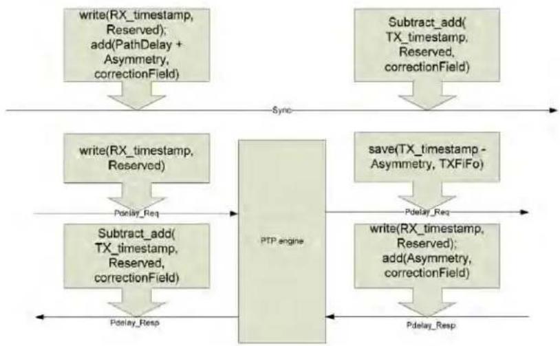
flowchart
graph TD
    A["write(RX_timestamp, Reserved); add(PathDelay + Asymmetry, correctionField)"] --> B["Sync"]
    C["Subtract_add(TX_timestamp, Reserved, correctionField)"] --> D["Sync"]
    E["write(RX_timestamp, Reserved)"] --> F["Pdelay_Req"]
    G["Subtract_add(TX_timestamp, Reserved, correctionField)"] --> H["Pdelay_Resp"]
    I["save(TX_timestamp - Asymmetry, TXFiFo)"] --> J["Pdelay_Req"]
    K["write(RX_timestamp, Reserved); add(Asymmetry, correctionField)"] --> L["Pdelay_Resp"]
    M["PTP_engine"] --> N["Pdelay_Req"]
    O["PTP_engine"] --> P["Pelay_Resp"]
Figure 8 • End-2-End TC (One-Step)

flowchart
graph TD
    A["write(RX_timestamp, Reserved); add(Asymmetry, correctionField)"] --> B["Subtract_add(TX_timestamp - Asymmetry, Reserved, correctionField)"]
    C["Subtract_add(TX_timestamp, Reserved, correctionField)"] --> D["write(Rx_timestamp, Reserved)"]
    B -->|Sync, PdelayResp| E
    D -->|DelayReq, PdelayReq| F
Two-step TC is not illustrated in the previous figures.
4.2.5 FrameSignature
Set/get the FrameSignature definitions. A FrameSignature is up to 16 bytes from the frame extracted from programmable locations in the frame. The size of the signature can be read.
HW ref: FrameSignatureSet.
The FrameSignature can be composed from the following fields in the packets:
- MAC addresses
IP addresses - messageType
- SourcePortIdentity
- sequenceld
- PortNo (this is implicit defined by the TimeStampFifo ID)
• domainNumber (in multicast mode) - destinationIP (in unicast mode)
The API defines a frame signature, depending on the operation mode. For instance, the application programmer does not need to know all the internal details for setting up the frame signature. The following lists the required frame structure by clock type:
- One-step E2E BC—the only timestamps to be read from the TxFiFo are DelayReq's (that is, the Signature must contain sequenceld and domainNumber).
• One-step E2E TC—no timestamps to be read from the TxFiFo are DelayReq's. - Two-step E2E BC (multicast)—the only timestamps to be read from the TxFiFo are Sync and DelayReq's (that is, the Signature must contain messageType, sequenceId, and domainNumber).
- Two-step E2E BC (unicast)—the timestamps to be read from the TxFiFo are Sync and DelayReq's. The destination IP address is used to identify the packets because individual messages are sent to different slave/master instances (that is, the Signature must contain messageType, sequenceld, and destinationIP).
- Two-step E2E TC (multicast)—the timestamps to be read from the TxFiFo are from forwarded sync and DelayReq's. The TC can forward messages from many masters and slaves; therefore, we also need the sourcePortIdentity (that is, the Signature must contain messageType, SourcePortIdentity, sequenceId, and domainNumber).
- Two-step E2E TC (unicast)—the timestamps to be read from the TxFiFo are from forwarded Sync and DelayReq's. The TC can forward messages from one master to many slaves and from many slaves to one master; therefore, we also need the destinationIP or sourceIP (that is, the Signature must contain messageType, sequenceld, domainNumber, and destinationIP/sourceIP).
Table 8 • Clock Type Versus Signature
| Field (size in bytes) | One-StepE2E BC | One-StepE2E TC | Two-Step E2EBC (multicast) | Two-StepE2E BC(unicast) | Two-Step E2ETC (multicast) | Two-StepE2E TC(unicast) |
| messageType (1) | XXXX | |||||
| domainNumber(1) | XXXX | |||||
| sourcePortIdentity(10) | X | |||||
| sequenceld (2) X | XXXX | |||||
| destinationIP (4) | X X or | |||||
| sourceIP (4) | X | |||||
| Signature size 3 N/A 4 7 13 8 | ||||||
4.3 Timestamp Block
4.3.1 LocalLatency
Set/get the local latency—the ingress latency on the ingress side and the egress latency on the egress side. The LocalLatency is set in units of TimeInterval. The value is converted to the unit supported by the hardware.
TimeInterval indicates time interval format defined in [1588] (64-bit signed integer, in nanoseconds*216).
HW ref: Local_correction_i, Local_correction_e.
4.3.2 PathDelay
Set/get the path delay for the ingress side. This is used in the P2P delay measurement mode. The PathDelay is set in units of TimeInterval. The value is converted to the unit supported by the hardware.
HW ref: Path_delay.
4.3.3 DelayAsymmetry
Set/get the delay asymmetry for a port.
The DelayAsymmetry is set in units of TimeInterval. The value is converted to the unit supported by the hardware.
The hardware uses the delayAsymmetry according to the 1588 standard.
Table 9 • All OC (Ordinary Clock) and BC Clocks and One-Step TC
| Event Action |
| Ingress{Sync, Pdelay_Resp} Add to correctionField |
| Egress{Delay_Req, Pdelay_Req} Subtract from correctionField, or TXFiFo timestamp. |
Table 10 • Two-Step TC
| Event Action |
| Ingress{Sync} Add to correctionField of corresponding Follow_Up |
| Ingress{Pdelay_Resp} Add to correctionField of corresponding Pdelay_Resp_Fpllow_Up |
| Egress{Delay_Req} Subtract from correctionField of corresponding Delay_Resp |
| Egress{Pdelay_Req} Subtract from correctionField of corresponding Pdelay_Resp_Follow_Up |
These corrections are done in software in the PTP engine
HW ref: Asymmetry
4.3.4 Correction Field Overflow Indication
Calculations done in the correctionField overflows are indicated and reported.
HW ref: Correction_field_too_big.
4.4 LocalTimeCounter
4.4.1 PtpTime
Set/get the actual PTP time.
The PtpTime is set in units of TimeStamp.
The PtpTime has to be synchronized on all modules in a node; therefore, the time is loaded into an intermediate register and applied to the hardware when a hardware trigger is set from a central module (the load command).
Setting the timestamp will only be done in situations where the node becomes locked to a new master and the clock offset is greater than a configurable value. In this situation, the timestamping may result in erroneous residence time and path delay; therefore, the timestamping is suspended within the time setting period. When a node is locked to a master, the clock rate adjustment is used to minimize the clock offset.
HW ref: LocalTime, LoadEnable.
4.4.2 SavedPtpTime
Get the PTP time saved when the load/save pin is activated. The function of the load/save pin depends on a configuration register.
HW ref: CurrentTime.
4.4.3 LocalClockAdjustment
Set/get the actual clock adjustment rate.
LocalClockAdjustment is set in units of greater than 1 ppb.
The AdjustmentCounter is programmed to either increment or decrement the local time with 1 ns periodically. The period is 1,000,000,000/LocalClockAdjustment.
HW ref: AdjustmentCounter.
4.4.4 LocalClockIncrementDecrement
Increment/decrement the actual clock value.
This is used to compensate for clock skews caused by clock buffering and routing delays. Each increment adds and each decrement subtracts one ns to or from the actual time.
HW ref: IncCounter, DecCounter.
4.4.5 LocalClockFrequency
Set/get the actual clock frequency.
The possible LocalClockFrequency values are {250MHz, 156_25MHz, 125MHz}.
HW ref: ClockIncrements
4.5 Rewriter
Only one direct software configuration of the rewriter is set by the API. The rewriter receives all other necessary commands from the analyzer. Some statistics can also be obtained from the rewriter.
4.5.1 PreambleShrink
Enable/disable preamble shrink.
HW ref: PreambleShrink.
4.5.2 StatisticCounters
Get counters indicating:
• Count of frames with preambles too short to shrink.
• Number of PTP frames with FCS errors.
• Number of frames that are modified.
HW ref: Error_preamble_cnt, Error_FCS_CNT, Mod_frame_cnt.
Counters are free-running counters—they are writable. The software can reset the counters, but will not write to them. When the counters are read periodically, the increment per period is calculated by subtracting the previous value. If the software writes a 0 to the counters, some increments may be lost.
4.6 TimestampFIFO
There is a timestamp FIFO per port.
The TimestampFiFo interface is disabled if the TimeStampMode is set to SPI.
4.6.1 TxTimestampMode
Set up the timestamp FIFO mode {Normal, SPI}. The timestamps can be read from the normal CPU interface or they are pushed out on a SPI interface.
HW ref: si_ena_i.
4.6.2 TxTimestamps
Get the TX_timestamps from the TimestampFIFO (frames transmitted on line side).
The TX_timestamp holds a TimeStamp and a FrameSignature. The size of the frame signature depends on the configuration, as described in section 4.2.5. The number of entries in the TimestampFiFo depends on the size of the frame signature.
HW ref: TimeStampGet.
4.6.3 TxTimestampFifo Not Empty Indication
An interrupt is generated when there are timestamps in the FIFO, or the indication is polled if interrupt is not supported. The API maintains a list of timestamps and a lookup function that uses the FrameSignature as a key. The timestamps are removed from the list when the lookup function has found a match or if the timestamp is older than AgeTime. A frame may be timestamped, but is never used by the control module.
HW ref: TimeStampSticky.
4.6.4 TxTimestampFifo Overflow Indication
It counts the overflow indication events and indicates that some timestamps have been lost. HW ref: Fifo_overflow.
4.6.5 TxTimestampFifo AgeTime
A timestamp is removed from the FIFO if it is more than AgeTime ms old. HW ref: none.
4.6.6 RxTimestamp
When an application receives a PTP event with a timestamp in the reserved field, it calls the API RxTimestamp function to convert the 32-bit timestamp to a whole 1588 timestamp value. It is assumed that this function is called within less than 1 sec after the packet is timestamped. HW ref: none.
4.6.7 RxTimestampMode
The PHY uses the following two timestamp format options internally in the reserved field.
- 30BitMode the value in the reserved field is simply the nanosecCounter 0..999999999
- 32BitMode—the value in the reserved field is a 32-bit value ((nanosecCounter + secCounter*10*9) mod 2*32).
4.7 Module Bring-Up
When a module is powered-up or a new software version is loaded, the API does the appropriate initialization of the hardware—for example, the ClockPulseWidth is set to an appropriate value.
4.7.1 Cold\_Warm Restart
The API supports the Microsemi Configuration Cold/Warm start feature. This feature ensures that the software can be rebooted and updated without reinitializing the entire hardware. That is to say, a one-step TC can run without any disturbance during a software reboot or update if the hardware is already initialized.
4.8 Other Functions
The API supports the complete family of Microsemi PHYs that feature IEEE 1588v2. The 1588 API can be instantiated independent of Microsemi switch and MAC APIs.
4.9 Control Module (PTP Engine)
The typical application will be distributed on more modules with the APIs on a number of interface blades and a central PTP control module on another module, such as the switch fabric module.
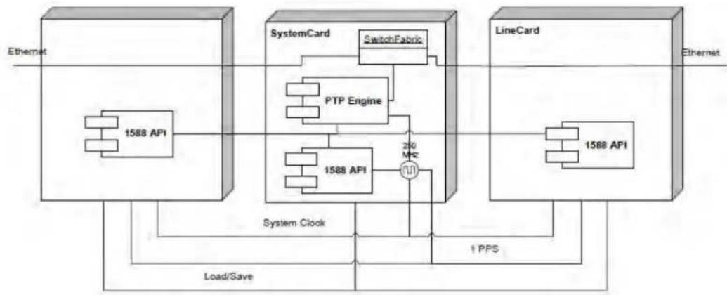
Figure 9 • System Overview
flowchart
graph TD
    A["Ethernet"] --> B["1588 API"]
    B --> C["SystemCard"]
    C --> D["SwitchFabric"]
    D --> E["PTP Engine"]
    E --> F["1588 API"]
    F --> G["200 MHz"]
    G --> H["1 PPS"]
    H --> I["LineCard"]
    I --> J["1568 API"]
    J --> K["1 PPS"]
    K --> L["System Clock"]
    L --> M["Load/Save"]
    M --> N["Ethernet"]
All packets handled by software are assumed to be terminated on the central system card—there is not local PTP engine functionality.
The CPU on the system card can communicate with the line cards, such as through a MIIM interface. It is assumed that this communication is possible, as communication method descriptions are outside this document's scope.
Each module manages its own PTP time—these must be synchronized within a whole node. One of the modules has a clock master, which may be either the system card or one of the line cards.
If there is not any local CPU on the blades, then the whole API may be running on the same central CPU system as the PTP software. Of course, there needs to be a communication path for register read/writes and read-back Tx timestamps.
The central PTP engine implements the part of the PTP engine that is executed on the central system card.
The central control module implements a module management function for the PTP engine to work correctly.
4.9.1 Module Management
4.9.1.1 Add Interface Module
When a new module is added to a node, the module's timestamps are synchronized to global PTP time before the timestamping function is enabled.
4.9.1.2 ClockSkew Adjustment
Clock sync is checked regularly when the distributed clocks are locked to the master.
The control module implements an adjust skew process that automatically detects the skew by setting a load/save pin. Then, it reads and compares the PHYs' save time. This process uses the LocakClockIncrementDecrement API to compensate for any skew.
4.9.2 ClockRate Management
This section describes the following three options for clock rate management:
- Central PTP clock
• Central SyncE clock
• Distributed clock
4.9.2.1 Central PTP Clock
The central PTP clock module has a VCXO or another type of programmable oscillator. This VCXO generates a clock signal that is distributed to all interface modules (see the system clock in System Overview). The system (VCXO) clock is locked to PTP. In this mode, the clock rate for all modules is statically configured and no local adjustment needs to be done—it can be assumed that the clock signal is exactly the nominal value because it is locked to the PTP clock.
In this mode, the distributed clocks are synchronized when the module is initialized (see Module ). Afterwards, the clock skew is regularly adjusted (see ).Management ClockSkew Adjustment
4.9.2.2 Central SyncE Clock
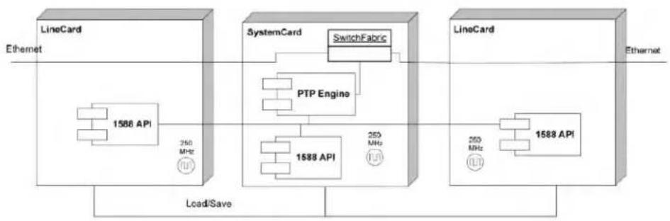
In the central SyncE clock option, the system clock is locked to SyncE, which is not necessarily locked to the PTP clock. In this mode, the clock rate for all the modules is adjusted equally—that is to say, the LocalClockAdjustment API function is used to distribute the clock adjustment rate calculated by a PTP slave. In this mode, the distributed clocks are synchronized when the module is initialized (see Module). Afterwards, the clock skew is regularly adjusted (see ).Management ClockSkew Adjustment
Figure 10 • SyncE Clock Option

flowchart
graph TD
    subgraph LineCard
        A["1588 API"] --> B["PTP Engine"]
        B --> C["SwitchFabric"]
        D["1588 API"] --> E["250 MHz"]
        E --> C
    end
    subgraph SystemCard
        F["1588 API"] --> G["250 MHz"]
        G --> C
    end
    H["Ethernet"] --> A
    I["Ethernet"] --> J["LineCard"]
    K["System Clock"] --> L["Load/Save"]
    M["SwitchFabric"] --> N["250 MHz"]
    O["1588 API"] --> P["250 MHz"]
    Q["1588 API"] --> R["250 MHz"]
4.9.2.3 Distributed Clock
Each module has its own oscillator, but a central load/save signal output from the master clock module latches the clocks onto the interface modules. For all interface modules, the latched clock is compared to the latched central clock and the local time counter is adjusted accordingly to the measured clock offset (see ).LocalClockAdjustment
Figure 11 • Distributed Clock Option
flowchart
graph LR
    subgraph Ethernet
        A["LineCard"] --> B["1588 API"]
        B --> C["350 MHz"]
        C --> D["Load/Save"]
    end

    subgraph SystemCard
        E["SystemCard"] --> F["SwitchFabric"]
        F --> G["PTP Engine"]
        G --> H["1588 API"]
        H --> I["250 MHz"]
        I --> J["LineCard"]
        J --> K["1588 API"]
        K --> L["250 MHz"]
        L --> M["LineCard"]
    end

    subgraph Ethernet
        N["LineCard"] --> O["1588 API"]
        O --> P["250 MHz"]
        P --> Q["LineCard"]
        Q --> R["1588 API"]
        R --> S["250 MHz"]
        S --> T["LineCard"]
    end
4.9.3 Multiple Timing Domain Support
The API uses different ways to support multiple timing domains, which depends on the clock type.
4.9.3.1 Transparent Clocks
A transparent clock only measures residence time, so it does not need to be aware of the absolute time. In a TC, the hardware clock is syntonized to a primary PTP domain and measures all residence times. A minor residence time measurement error occurs if the different PTP domains run at different rates, but this error can be ignored. For example, if rate offset is 10 ppm and residence time is 10 s, then measurement error is 0 (1 ns), which is far below the measurement accuracy.
4.9.3.2 Boundary Clocks
If multiple boundary clocks exist in a node, the SW maintains the offset between the clock domains. The HW only supports one timing domain per port. The HW timeOfDay is synchronized to one domain (called the primary domain).
When the SW receives an event message, which belongs to another domain than the primary domain, the Rx timestamp is compensated for the offset between the actual domain and the primary domain. When the SW initiates a one-step event message, the offset between the actual domain and the primary domain is saved in the correction field. When the HW transmits the event, the primary domain timestamp is saved in the originTimestamp:
originTimestamp + correctionField = origin timestamp for the actual domain.
This solution works fine as long as the offset between the time domains are less than the max correctionField value, which is ±39 hours.
When the software initiates a two-step event message, the offset between the actual and primary domain is added to the Tx timestamp received from TimestampFIFO.
4.9.4 CLI
A test CLI interface is implemented.
4.10 Distributed Control Module
An alternative application will be distributed on more modules with APIs on a number of interface blades. PTP engine modules will also be distributed on more modules.
Figure 12 • System Overview for Distributed Solution

flowchart
graph TD
    A["LineCard"] -->|Ethernet| B["1588 API"]
    B --> C["SystemCard"]
    C --> D["SwitchFabric"]
    D --> E["PTP Engine"]
    E --> F["1588 API"]
    F --> G["250 MHz"]
    G --> H["1 PPS"]
    H --> I["SwitchFabric"]
    I --> J["1588 API"]
    J --> K["250 MHz"]
    K --> L["Ethernet"]
    M["System Clock"] --> N["Load/Save"]
    O["1 PPS"] --> P["SwitchFabric"]
    P --> Q["1588 API"]
    Q --> R["250 MHz"]
All packets handled by the local PTP engine are assumed to be terminated on the local card—a PTP engine will typically be on each module that has a switch fabric.
The main purpose of this document is to show that the API supports a distributed solution. Description of how PTP engine responsibility is distributed among modules is outside this document's scope.

Microsemi.
a MICROCHIP company
Microsemi Headquarters
One Enterprise, Aliso Viejo,
CA 92656 USA
Within the USA: +1 (800) 713-4113
Outside the USA: +1 (949) 380-6100
Sales: +1 (949) 380-6136
© Microsemi. All rights reserved. Microsemi and the Microsemi logo are trademarks of Microsemi Corporation. All other trademarks and service marks are the property of their respective owners.
Microsemi makes no warranty, representation, or guarantee regarding the information contained herein or the suitability of its products and services for any particular purpose, nor does Microsemi assume any liability whatsoever arising out of the application or use of any product or circuit. The products sold hereunder and any other products sold by Microsemi have been subject to limited testing and should not be used in conjunction with mission-critical equipment or applications. Any performance specifications are believed to be reliable but are not verified, and Buyer must conduct and complete all performance and other testing of the products, alone and together with, or installed in, any end products. Buyer shall not rely on any data and performance specifications or parameters provided by Microsemi. It is the Buyer's responsibility to independently determine suitability of any products and to test and verify the same. The information provided by Microsemi hereunder is provided "as is, where is" and with all faults, and the entire risk associated with such information is entirely with the Buyer. Microsemi does not grant, explicitly or implicitly, to any party any patent rights, licenses, or any other IP rights, whether with regard to such information itself or anything described by such information. Information provided in this document is proprietary to Microsemi, and Microsemi reserves the right to make any changes to the information in this document or to any products and services at any time without notice.
Microsemi, a wholly owned subsidiary of Microchip Technology Inc. (Nasdaq: MCHP), offers a comprehensive portfolio of semiconductor and system solutions for aerospace & defense, communications, data center and industrial markets. Products include high-performance and radiation-hardened analog mixed-signal integrated circuits, FPGAs, SoCs and ASICs; power management products; timing and synchronization devices and precise time solutions, setting the world's standard for time; voice processing devices; RF solutions; discrete components; enterprise storage and communication solutions; security technologies and software; anti-lamper products; Ethernet solutions; Power-over-Ethernet ICs and midspans; as well as custom design capabilities and services. Microsemi is headquartered in Aliso Viejo, California, and has approximately 4,800 employees globally. Learn more at www.microsemi.com.
VPPD-02802