USB3613 - Electronic component Microchip - Free user manual and instructions
Find the device manual for free USB3613 Microchip in PDF.

User questions about USB3613 Microchip
0 question about this device. Answer the ones you know or ask your own.
Ask a new question about this device
Download the instructions for your Electronic component in PDF format for free! Find your manual USB3613 - Microchip and take your electronic device back in hand. On this page are published all the documents necessary for the use of your device. USB3613 by Microchip.
USER MANUAL USB3613 Microchip
Note the following details of the code protection feature on Microchip devices:
• Microchip products meet the specification contained in their particular Microchip Data Sheet.
- Microchip believes that its family of products is one of the most secure families of its kind on the market today, when used in the intended manner and under normal conditions.
- There are dishonest and possibly illegal methods used to breach the code protection feature. All of these methods, to our knowledge, require using the Microchip products in a manner outside the operating specifications contained in Microchip's Data Sheets. Most likely, the person doing so is engaged in theft of intellectual property.
• Microchip is willing to work with the customer who is concerned about the integrity of their code.
- Neither Microchip nor any other semiconductor manufacturer can guarantee the security of their code. Code protection does not mean that we are guaranteeing the product as "unbreakable."
Code protection is constantly evolving. We at Microchip are committed to continuously improving the code protection features of our products. Attempts to break Microchip's code protection feature may be a violation of the Digital Millennium Copyright Act. If such acts allow unauthorized access to your software or other copyrighted work, you may have a right to sue for relief under that Act.
Information contained in this publication regarding device applications and the like is provided only for your convenience and may be superseded by updates. It is your responsibility to ensure that your application meets with your specifications. MICROCHIP MAKES NO REPRESENTATIONS OR WARRANTIES OF ANY KIND WHETHER EXPRESS OR IMPLIED, WRITTEN OR ORAL, STATUTORY OR OTHERWISE, RELATED TO THE INFORMATION, INCLUDING BUT NOT LIMITED TO ITS CONDITION, QUALITY, PERFORMANCE, MERCHANTABILITY OR FITNESS FOR PURPOSE. Microchip disclaims all liability arising from this information and its use. Use of Microchip devices in life support and/or safety applications is entirely at the buyer's risk, and the buyer agrees to defend, indemnify and hold harmless Microchip from any and all damages, claims, suits, or expenses resulting from such use. No licenses are conveyed, implicitly or otherwise, under any Microchip intellectual property rights.
Trademarks
The Microchip name and logo, the Microchip logo, dsPIC, FlashFlex, KEELOQ, KEELOQ logo, MPLAB, PIC, PICmicro, PICSTART, PIC ^32 logo, rfPIC, SST, SST Logo, SuperFlash and UNI/O are registered trademarks of Microchip Technology Incorporated in the U.S.A. and other countries.
FilterLab, Hampshire, HI-TECH C, Linear Active Thermistor, MTP, SEEVAL and The Embedded Control Solutions Company are registered trademarks of Microchip Technology Incorporated in the U.S.A.
Silicon Storage Technology is a registered trademark of Microchip Technology Inc. in other countries.
Analog-for-the-Digital Age, Application Maestro, BodyCom, chipKIT, chipKIT logo, CodeGuard, dsPICDEM, dsPICDEM.net, dsPICworks, dsSPEAK, ECAN, ECONOMONITOR, FanSense, HI-TIDE, In-Circuit Serial Programming, ICSP, Mindi, MiWi, MPASM, MPF, MPLAB Certified logo, MPLIB, MPLINK, mTouch, Omniscient Code Generation, PICC, PICC-18, PICDEM, PICDEM.net, PICkit, PICtail, REAL ICE, rfLAB, Select Mode, SQL, Serial Quad I/O, Total Endurance, TSHARC, UniWinDriver, WiperLock, ZENA and Z-Scale are trademarks of Microchip Technology Incorporated in the U.S.A. and other countries.
SQTP is a service mark of Microchip Technology Incorporated in the U.S.A.
GestIC and ULPP are registered trademarks of Microchip Technology Germany II GmbH & Co. & KG, a subsidiary of Microchip Technology Inc., in other countries.
All other trademarks mentioned herein are property of their respective companies.
© 2013, Microchip Technology Incorporated, Printed in the U.S.A., All Rights Reserved.
ISBN: 978-1-62077-457-1
QUALITY MANAGEMENT SYSTEM
CERTIFIED BY DNV
= ISO/TS 16949=
Microchip received ISO/TS-16949:2009 certification for its worldwide headquarters, design and wafer fabrication facilities in Chandler and Tempe, Arizona; Gresham, Oregon and design centers in California and India. The Company's quality system processes and procedures are for its PIC® MCUs and dsPIC® DSCs, KEELoo® code hopping devices, Serial EEPROMs, microperipherals, nonvolatile memory and analog products. In addition, Microchip's quality system for the design and manufacture of development systems is ISO 9001:2000 certified.
Object of Declaration: EVB-USB3613 Evaluation Board
EU Declaration of Conformity
This declaration of conformity is issued by the manufacturer.
The development/evaluation tool is designed to be used for research and development in a laboratory environment. This development/evaluation tool is not a Finished Appliance, nor is it intended for incorporation into Finished Appliances that are made commercially available as single functional units to end users under EU EMC Directive 2004/108/EC and as supported by the European Commission's Guide for the EMC Directive 2004/108/EC (8 ^th February 2010).
This development/evaluation tool complies with EU RoHS2 Directive 2011/65/EU.
For information regarding the exclusive, limited warranties applicable to Microchip products, please see Microchip's standard terms and conditions of sale, which are printed on our sales documentation and available at www.microchip.com.
Signed for and on behalf of Microchip Technology Inc. at Chandler, Arizona, USA
Derek Carlson
DERK CANSON
VP Development Tools
16-July-2013 Date
NOTES:
Table of Contents
Preface 7
Introduction....7
Document Layout 7
Conventions Used in this Guide 8
The Microchip Web Site 9
Development Systems Customer Change Notification Service 9
Customer Support 9
Document Revision History 10
Chapter 1. Overview
1.1 Introduction ...... 11
1.2 Features 11
1.3 General Description ...... 12
Chapter 2. Hardware Configuration
2.1 Hardware Description ...... 13
2.1.1 Port Assignment 13
2.1.2 USB3613 Configuration 15
2.1.3 Clock Source - 12 MHz Oscillator 15
2.1.4 Power Source – Self-Powered 15
2.1.5 Powered State LED 15
2.1.6 RESETn LED 16
2.1.7 Port Power LEDs 16
2.1.8 Hub Connect LED 16
2.1.9 Connector Description 16
Chapter 3. Battery Charging Support
3.1 Battery Charging Modes 19
3.2 Charging Port Roles 19
3.2.1 BC1.2 Charging Downstream Port (CDP) Description 20
3.2.2 Standard Downstream Port (SDP) Description 20
3.2.3 Dedicated Charger Emulation Port (DCP) Description 20
Appendix A. EVB-USB3613 Evaluation Board
A.1 Introduction 23
Appendix B. EVB-USB3613 Evaluation Board Schematic
B.1 Introduction 25
Appendix C. Bill of Materials (BOM)
C.1 Introduction 27
Worldwide Sales and Service 31
NOTES:
Preface
NOTICE TO CUSTOMERS
All documentation becomes dated, and this manual is no exception. Microchip tools and documentation are constantly evolving to meet customer needs, so some actual dialogs and/or tool descriptions may differ from those in this document. Please refer to our web site (www.microchip.com) to obtain the latest documentation available.
Documents are identified with a "DS" number. This number is located on the bottom of each page, in front of the page number. The numbering convention for the DS number is "DSXXXXXA", where "XXXXX" is the document number and "A" is the revision level of the document.
For the most up-to-date information on development tools, see the MPLAB ^® IDE online help. Select the Help menu, and then Topics to open a list of available online help files.
INTRODUCTION
This chapter contains general information that will be useful to know before using the EVB-USB3613 Evaluation Board. Items discussed in this chapter include:
- Document Layout
- Conventions Used in this Guide
• The Microchip Web Site
• Development Systems Customer Change Notification Service - Customer Support
• Document Revision History
DOCUMENT LAYOUT
This document describes how to use the EVB-USB3613 Evaluation Board as a demonstration platform optimized for portable applications. The manual layout is as follows:
- Chapter 1. “Overview” – Shows a brief description of the EVB-USB3613 Evaluation Board.
- Chapter 2. "Hardware Configuration" – Includes information about the hardware configuration of the EVB-USB3613 Evaluation Board.
- Chapter 3. “Battery Charging Support” – Provides information about the EVB-USB3613 Evaluation Board battery charging features.
- Appendix A. "EVB-USB3613 Evaluation Board" – This appendix shows the EVB-USB3613 Evaluation Board.
- Appendix B. “EVB-USB3613 Evaluation Board Schematic” – This appendix shows the EVB-USB3613 Evaluation Board schematic.
- Appendix C. "Bill of Materials (BOM)" – This appendix includes the EVB-USB3613 Evaluation Board Bill of Materials (BOM).
CONVENTIONS USED IN THIS GUIDE
This manual uses the following documentation conventions:
DOCUMENTATION CONVENTIONS
| Description Represents Examples | ||
| Arial font: | ||
| Italic characters Referenced books | oks MPLAB | ^ IDE User's Guide |
| Emphasized text ...is the only compiler... | ||
| Initial caps A window the Output | window | |
| A dialog the Settings dialog | ||
| A menu selection select Enable Programmer | ||
| Quotes A field name in a window or dialog | "Save project before build" | |
| Underlined, italic text with right angle bracket | A menu path File>Save | —— |
| Bold characters A dialog button | Click OK | |
| A tab | Click the Power tab | |
| N'Rnnnn | A number in verilog format, where N is the total number of digits, R is the radix and n is a digit. | 4'b0010, 2'hF1 |
| Text in angle brackets <> | A key on the keyboard | Press,, |
| Courier New font: | ||
| Plain Courier New | Sample source code | #define START |
| Filenames | autoexec.bat | |
| File paths | c:\mcc18\h | |
| Keywords | _asm, _endasm, static | |
| Command-line options | -Opa+, -Opa- | |
| Bit values | 0, 1 | |
| Constants | 0xFF, 'A' | |
| Italic Courier New | A variable argument | file.o, where file can be any valid filename |
| Square brackets [] | Optional arguments | mcc18 [options] file [options] |
| Curly brackets and pipe character: { | } | Choice of mutually exclusive arguments; an OR selection | errorlevel {0|1} |
| Ellipses... Replaces repeated text var_name [, | var_name...] | |
| Represents code supplied by user void main (void){ ...} | ||
Microchip provides online support via our web site at www.microchip.com. This web site is used as a means to make files and information easily available to customers. Accessible by using your favorite Internet browser, the web site contains the following information:
- Product Support – Data sheets and errata, application notes and sample programs, design resources, user's guides and hardware support documents, latest software releases and archived software
- General Technical Support – Frequently Asked Questions (FAQs), technical support requests, online discussion groups, Microchip consultant program member listing
- Business of Microchip – Product selector and ordering guides, latest Microchip press releases, listing of seminars and events, listings of Microchip sales offices, distributors and factory representatives
DEVELOPMENT SYSTEMS CUSTOMER CHANGE NOTIFICATION SERVICE
Microchip's customer notification service helps keep customers current on Microchip products. Subscribers will receive e-mail notification whenever there are changes, updates, revisions or errata related to a specified product family or development tool of interest.
To register, access the Microchip web site at www.microchip.com, click on Customer Change Notification and follow the registration instructions.
The Development Systems product group categories are:
- Compilers – The latest information on Microchip C compilers, assemblers, linkers and other language tools. These include all MPLAB C compilers; all MPLAB assemblers (including MPASM assembler); all MPLAB linkers (including MPLINK object linker); and all MPLAB librarians (including MPLIB object librarian).
- Emulators – The latest information on Microchip in-circuit emulators. This includes the MPLAB REAL ICE and MPLAB ICE 2000 in-circuit emulators.
- In-Circuit Debuggers – The latest information on the Microchip in-circuit debuggers. This includes MPLAB ICD 3 in-circuit debuggers and PICkit 3 debug express.
- MPLAB IDE – The latest information on Microchip MPLAB IDE, the Windows Integrated Development Environment for development systems tools. This list is focused on the MPLAB IDE, MPLAB IDE Project Manager, MPLAB Editor and MPLAB SIM simulator, as well as general editing and debugging features.
- Programmers – The latest information on Microchip programmers. These include production programmers such as MPLAB REAL ICE in-circuit emulator, MPLAB ICD 3 in-circuit debugger and MPLAB PM3 device programmers. Also included are nonproduction development programmers such as PICSTART Plus and PICkit 2 and 3.
CUSTOMER SUPPORT
Users of Microchip products can receive assistance through several channels:
• Distributor or Representative
- Local Sales Office
• Field Application Engineer (FAE)
- Technical Support
Customers should contact their distributor, representative or field application engineer (FAE) for support. Local sales offices are also available to help customers. A listing of sales offices and locations is included in the back of this document.
Technical support is available through the web site at:
http://www.microchip.com/support
DOCUMENT REVISION HISTORY
Revision A (September 2013)
- Initial Release of this Document.
Chapter 1. Overview
1.1 INTRODUCTION
The USB3613 is a low-power, full-featured and OEM configurable Multi-Transaction Translator (MTT) USB 2.0 hub controller with three downstream ports optimized for portable applications. The USB3613 is fully compliant with the USB 2.0 Specification, USB 2.0 Link Power Management (LPM) Addendum, High-Speed Inter-Chip (HSIC) USB Electrical Specification Revision 1.0 and attaches to an upstream port as a high-speed hub. The 3-port hub supports low-speed, full-speed and high-speed downstream devices on all of the enabled (non-HSIC) downstream ports. HSIC ports support only high-speed operation. The USB3613 supports both upstream and downstream battery charging (BC1.2) detection. The EVB-USB3613BC Evaluation Board demonstrates a stand-alone application for the USB3613 device with advanced power saving options and configurable port assignments. See Section 1.2 "Features" for more information.
1.2 FEATURES
- USB3613 in a 30-pin WLCSP RoHS compliant package
- Two USB 2.0 downstream ports with ganged port power and overcurrent sense (OCS)
- One downstream HSIC port (downstream port 3)
• High-Speed (480 Mbps), Full-Speed (12 Mbps) and Low-Speed (1.5 Mbps) compatible - USB Battery Charging is supported on all downstream USB ports up to 2A (BC1.2 CDP, SDP and DCP)
- Multi-Transaction Translator is enabled
- Supports internal default hub configuration. Optionally supports configuration from external SPI or EEPROM
- SMBus interface header available
- Low-Cost, 4-Layer space saving design with two outer signal layers, a power inner layer and a ground inner layer
• Self-Powered operation - Operates from one single voltage (+5.0 VDC, 4 Amp regulated) external DC power supply
- On Board MCP1725 +3.3 VDC. 0.5 Amp regulator
• +5V, Reset, Hub Connect and port power LED indicators - ESD/EMI component footprints provided (optional)
• Single 12 MHz crystal clock source - External GPIO pin headers
- Schematics, layout and bill of materials are available to minimize new product development time
1.3 GENERAL DESCRIPTION
The EVB-USB3613BC is an evaluation and demonstration platform featuring the USB3613 Ultra Fast USB 2.0 Hub on a 4-layer RoHS compliant Printed Circuit Board (PCB).
The EVB-USB3613 is designed to demonstrate the unique features of this device using a low-cost PCB implementation with ganged port power control for the two downstream USB 2.0 ports. Both downstream USB 2.0 ports include a high current port power controller to fully support USB battery charging as a high current walk-up port.
Note: Do not exceed 4A total current consumption from 5 VDC.
The EVB-USB3613 is designed to support internal default configuration settings and an external I ^2 C ^TM EEPROM (optional) for custom configured functionality. A location is provided for an external I ^2 C EEPROM device for configuration at U8. Alternatively, a firmware can be downloaded onto a dual-output SPI Flash device located at U17.
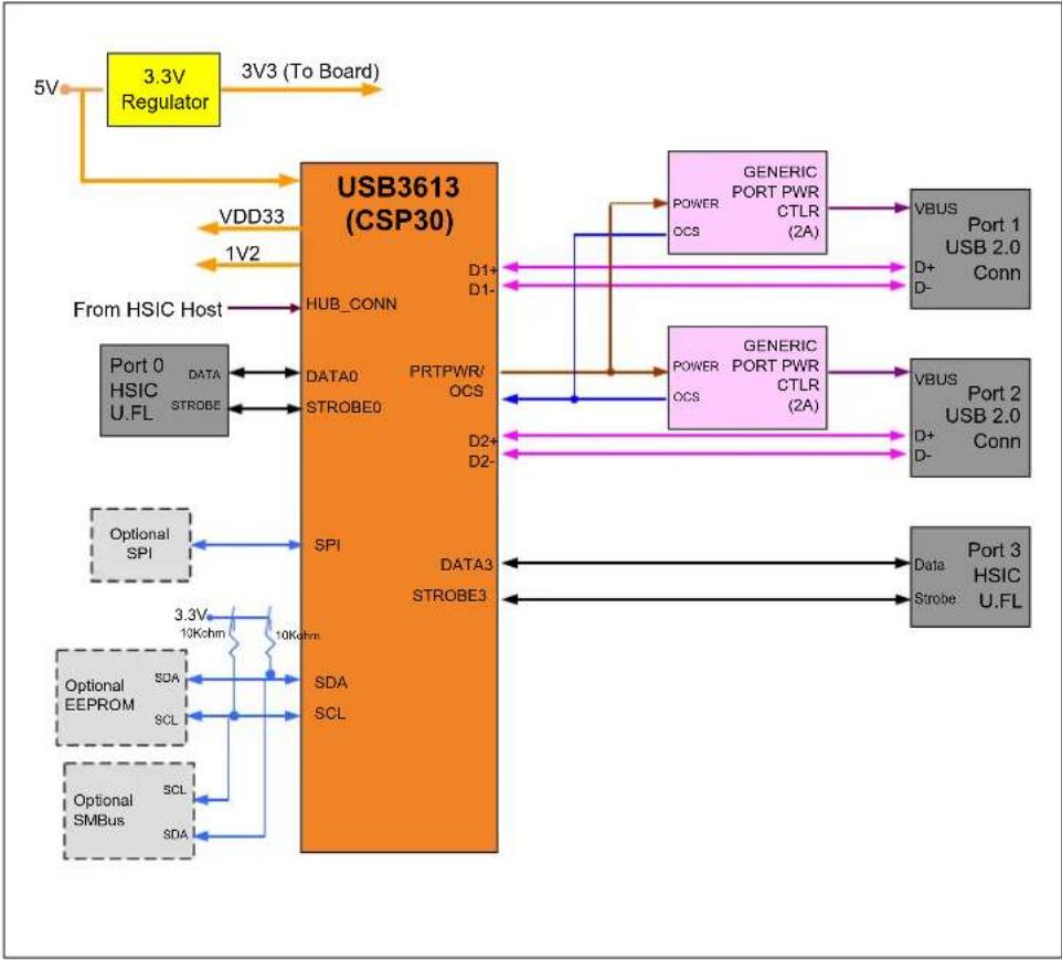
Figure 2-2 shows the top and bottom level silk screen and copper layers. A block diagram of the EVB-USB3613 is shown in Figure 2-3.
Chapter 2. Hardware Configuration
2.1 HARDWARE DESCRIPTION
The EVB-USB3613 has one on board regulator. The MCP1725 (U6) generates +3.3 VDC for the hub device circuitry and performs voltage supervisor and RESETn functions. The USB3613 generates its own +1.2 VDC for internal use with on-chip +1.2 VDC regulators. The internal +1.2 VDC regulator tied to the oscillator and Phase-Locked Loop (PLL) is turned off during suspend to minimize suspend current. Downstream port power is distributed by two independent power switches at up to 2A per port via U1 and U2.
Note: Do not exceed 4A total current consumption from +5 VDC.
Downstream port 1 and port 2 have USB 2.0 connectors with USB 2.0 compliant decoupling and separate shield grounds. Downstream port 3 has U.FL connectors (J20 and J21) to support Data and Strobe HSIC signals.
2.1.1 Port Assignment
The downstream ports are numbered 1 through 3. Downstream port 1 and port 2 are the USB 2.0 ports. Downstream port 3 is an HSIC port. The USB3613 allows downstream port 1 and/or port 2 to be configured for high current battery USB charging. Power to downstream port 1 and port 2 is controlled through the AP2111 devices U1 and U2. Each device provides up to 2A to the corresponding downstream port. Both of these port power controllers are enabled via a shared PRTPWR pin on the USB3613. Overcurrent sensing of both port power controllers is also monitored on the same PRTPWR pin.
Note: There is only a maximum of 4A provided across the entire evaluation board.
The EVB-USB3613 must be connected to an HSIC upstream host via the Data0 (J14) and Strobe0 (J15) connectors using the provided U.FL coaxial cables. When removing these cables from the evaluation board for any reason, the provided HSIC Extraction tool must be used. Figure 2-1 shows the recommended usage of the HSIC extraction tool per the Hirose U.FL data sheet on proper use of the plugs.
FIGURE 2-1: U.FL COAXIAL CABLE EXTRACTION GUIDELINES
Usage Precautions
1. Plugs
(1) Mating/Unmating
1) To disconnect the connectors, insert the end portion of U.FL-LP-N-2 under the connector flanges and pull off vertically, in the direction of the connector mating axis. 2) To mate the connectors, the mating axes of both connectors must be aligned. The "click" confirms a fully-mated connection. Do not attempt to insert on an extreme angle.
U.FL-LP-N-2 Plug Extraction Tool

text_image
Extraction Jig U.FL Cable Assembly U.FL-R-SMT-1(2) Pull forces on the cable after the connectors are mated. Do not apply a load to the cable in excess of the values indicated in the diagram below.
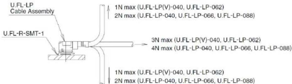
text_image
U.FL-LP Cable Assembly U.FL-R-SMT-1 1N max (U.FL-LP(V)-040, U.FL-LP-062) 2N max (U.FL-LP-040, U.FL-LP-066, U.FL-LP-088) 3N max (U.FL-LP(V)-040, U.FL-LP-062) 4N max (U.FL-LP-040, U.FL-LP-066, U.FL-LP-088) 1N max (U.FL-LP(V)-040, U.FL-LP-062) 2N max (U.FL-LP-040, U.FL-LP-066, U.FL-LP-088)(3) Precautions
Do NOT forcefully twist or deform wires.
An external HUB_CONN port control signal from the host must be wired to the "HubConn" pin on the J23 header. This signal lets the USB3613 know when an HSIC upstream host is ready to attach. Once a host has been attached and detected, the green "HubConn" LED D18 lights up.
The EVB-USB3613 is designed to allow flexible configuration options. It can be configured with default internal register settings through an SMBus or through a downloadable external firmware to an SPI Flash. It supports "Quad-Page" configuration OTP flash (four consecutive 200-byte configuration pages). The following sections detail the various configuration methods and features.
2.1.2 USB3613 Configuration
Default: Upon power-up, the USB3613 searches for an external SPI Flash device that contains a valid signature. If an SPI device is not present, the firmware checks to see whether SMBus is enabled. If the SMBus is disabled, the USB3613 attempts to load the configuration from an external I ^2 C EEPROM. If no external options are detected, the USB3613 will operate using the internal default register settings. It also sets the vendor ID, product ID, language ID, device ID and additional settings from internal ROM code.
SPI Flash Option: If upon power-up an external SPI Flash device is present, the external ROM is enabled and code execution is initiated from the external SPI device. The SPI Flash device on the EVB-USB3613 is populated by default. To hold this device in reset, the J33 "SPI Hold" two-pin header can be shorted together, thereby tying the HOLD signal low.
SMBus Option: The SMBus interface is disabled by default via the 100 kOhm pull down resistor on SMBCLK. To enable SMBus, the SMBCLK pin must be pulled high to +3.3 VDC with a strong pull up resistor. This is often embedded within the external SMBus tool (not included) when inserted onto the J13 SMBus header. All device configuration must be performed via the Pro-Touch Programming Tool. For information on this tool, contact your local sales representative. When SMBus is enabled, the firmware configures the GPIOs to act as an SMBus slave. As an SMBus slave, the firmware waits indefinitely for the SMBus configuration.
EEPROM Option: If the USB3613 does not detect an SMBus interface, it will check for an I²C EEPROM (not populated by default). The EVB-USB3613 loads configuration from an external two-wire I²C EEPROM when present. The EEPROM must be installed either directly or through a DIP socket located at the U8 footprint and the "Manual I²C Enable" headers J11 and J12 must be set to enable this option. By default, J11 and J12 are left open so that the I²C interface are only enabled by pull ups in the external EEPROM device. When both J11 and J12 are jumpered, SDA and SCL on the I²C interface are pulled high to +3.3 VDC externally. The EEPROM must be pre-programmed before installation as the EVB-USB3613 is tied to an HSIC host. The EVB-USB3613BC is compatible with I²C EEPROMs from several manufacturers. The memory capacity must be at least 512 bytes.
2.1.3 Clock Source - 12 MHz Oscillator
By default, a 12 MHz oscillator OSC1 is populated on the evaluation board as the clock source for the USB3613. An alternative clock source can be injected into the J54 SMA "External Clock Input" connector if desired. The REFSEL[1:0] pins are both pulled high to +3.3 VDC by default to configure the USB3613 to have an input reference clock frequency of 12 MHz.
2.1.4 Power Source – Self-Powered
The EVB-USB3613 only supports self-powered operation and is powered by one +5 VDC regulated external DC power supply. The +5 VDC, 4A external DC power supply plugs into the on board 2.1 mm connector J8. The external power supply controls the on board +3.3 VDC MCP1725 voltage regulator. The evaluation board is setup so that the +5 VDC feeds VBAT on the USB3613 which feeds the internal +3.3 VDC regulator. The +3.3 VDC comes out on the VDD33 power pin which then feeds the internal +1.2 VDC regulator via the VDDCRREG pin. A +1.2 VDC is then output onto the VDDCR12 pin of the USB3613. Therefore, the USB3613 is powered completely by the +5 VDC output of the external power supply.
2.1.5 Powered State LED
The LED D5 indicates when +5 VDC power is present.
2.1.6 RESETn LED
The LED D6 indicates when the RESETn signal is driven low and the USB3613 is held in the Reset state.
2.1.7 Port Power LEDs
LEDs D1 and D2 indicate when +5 VDC port power is available to the associated downstream USB port(s).
2.1.8 Hub Connect LED
The LED D18 indicates when an upstream HSIC host is present.
2.1.9 Connector Description
The EVB-USB3613 has two USB connectors for downstream port 1 and port 2. The upstream port as well as downstream port 3 have U.FL connectors for HSIC data and strobe signals. Power is supplied via 2.1 mm power jack. See Table 2-1 for the list of connectors. For more details, please see Appendix A. "EVB-USB3613 Evaluation Board".
TABLE 2-1: CONNECTOR DESCRIPTION
| Connector Type | Description | |
| J1 USB uAB | Downstream USB Port 1 | |
| J2 USB A Downstream USB Port 2 | ||
| J7 1x2 header External Reset Control | ||
| J8 Power Jack 2.1 mm +5 VDC Regulated Power Supply | ||
| J11, J12 | 1x2 headers | I^2C^TM External/Manual Enable |
| J13 2x5 header SMBus I/F connection | ||
| J14 | U.FL | Upstream HSIC Port 0 DATA |
| J15 | U.FL | Upstream HSIC Port 0 STROBE |
| J18, J19 | 1x2 headers | Charge Detect [1:0] |
| J20 | U.FL | Downstream HSIC Port 3 DATA |
| J21 | U.FL | Downstream HSIC Port 3 STROBE |
| J22 1x2 header Suspend/IRQ#/Interrupt | ||
| J33 1x2 header SPI HOLD (to hold SPI in reset) | ||
| J54 | SMA | External Clock Input |
Component side top and bottom layers are shown in Figure 2-2 with silk screen information to identify component locations.
FIGURE 2-2: EVB-USB3613 TOP AND BOTTOM LEVEL SILK SCREEN AND COPPER LAYERS
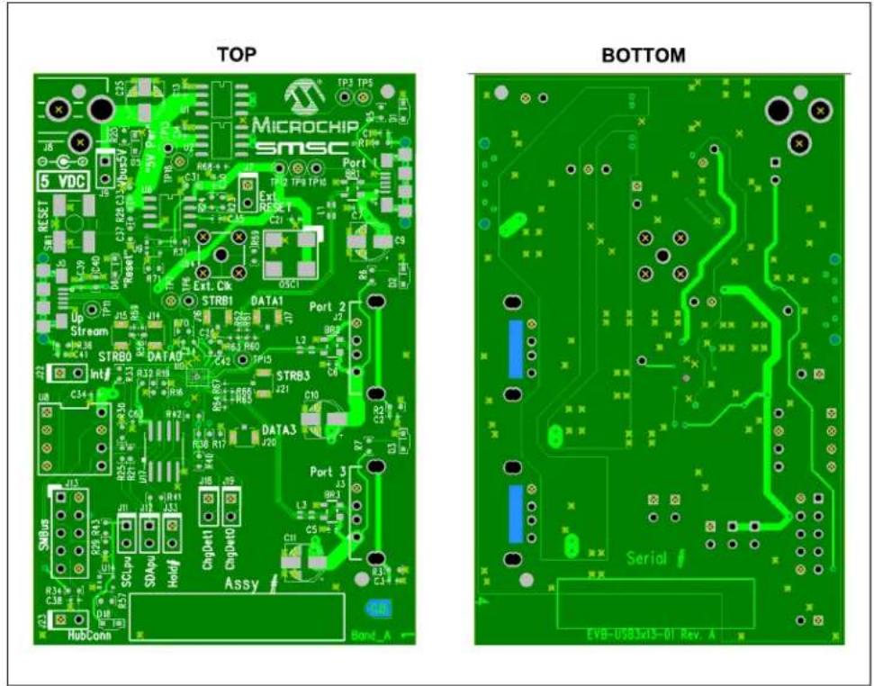
FIGURE 2-3: EVB-USB3613 BLOCK DIAGRAM
flowchart
graph TD
    A["3.3V Regulator"] -->|5V| B["USB3613 (CSP30)"]
    B --> C["PORT 0 HSIC U.FL DATA STROBE"]
    B --> D["PORT 0 HSIC U.FL DATA STROBE"]
    B --> E["PORT 0 HSIC U.FL DATA STROBE"]
    B --> F["PORT 0 HSIC U.FL DATA STROBE"]
    B --> G["PORT 0 HSIC U.FL DATA STROBE"]
    B --> H["PORT 0 HSIC U.FL DATA STROBE"]
    B --> I["PORT 0 HSIC U.FL DATA STROBE"]
    B --> J["PORT 0 HSIC U.FL DATA STROBE"]
    B --> K["PORT 0 HSIC U.FL DATA STROBE"]
    B --> L["PORT 0 HSIC U.FL DATA STROBE"]
    B --> M["PORT 0 HSIC U.FL DATA STROBE"]
    B --> N["PORT 0 HSIC U.FL DATA STROBE"]
    B --> O["PORT 0 HSIC U.FL DATA STROBE"]
    B --> P["PORT 0 HSIC U.FL DATA STROBE"]
    B --> Q["PORT 0 HSIC U.FL DATA STROBE"]
    B --> R["PORT 0 HSIC U.FL DATA STROBE"]
    B --> S["PORT 0 HSIC U.FL DATA STROBE"]
    B --> T["PORT 0 HSIC U.FL DATA STROBE"]
    B --> U["PORT 0 HSIC U.FL DATA STROBE"]
    B --> V["PORT 0 HSIC U.FL DATA STROBE"]
    B --> W["PORT 0 HSIC U.FL DATA STROBE"]
    B --> X["PORT 0 HSIC U.FL DATA STROBE"]
    B --> Y["PORT 0 HSIC U.FL DATA STROBE"]
    B --> Z["PORT 0 HSIC U.FL DATA STROBE"]
    B --> AA["PORT 0 HSIC U.FL DATA STROBE"]
    B --> AB["PORT 0 HSIC U.FL DATA STROBE"]
    B --> AC["PORT 0 HSIC U.FL DATA STROBE"]
    B --> AD["PORT 0 HSIC U.FL DATA STROBE"]
    B --> AE["PORT 0 HSIC U.FL DATA STROBE"]
    B --> AF["PORT 0 HSIC U.FL DATA STROBE"]
    B --> AG["PORT 0 HSIC U.FL DATA STROBE"]
    B --> AH["PORT 0 HSIC U.FL DATA STROBE"]
    B --> AI["PORT 0 HSIC U.FL DATA STROBE"]
    B --> AJ["PORT 0 HSIC U.FL DATA STROBE"]
    B --> AK["PORT 0 HSIC U.FL DATA STROBE"]
    B --> AL["PORT 0 HSIC U.FL DATA STROBE"]
    B --> AM["PORT 0 HSIC U.FL DATA STROBE"]
    B --> AN["PORT 0 HSIC U.FL DATA STROBE"]
    B --> AO["PORT 0 HSIC U.FL DATA STROBE"]
    B --> AP["PORT 0 HSIC U.FL DATA STROBE"]
    B --> AQ["PORT 0 HSIC U.FL DATA STROBE"]
    B --> AR["PORT 0 HSIC U.FL DATA STROBE"]
    B --> AS["PORT 0 HSIC U.FL DATA STROBE"]
    B --> AT["PORT 0 HSIC U.FL DATA STROBE"]
    B --> AU["PORT 0 HSIC U.FL DATA STROBE"]
    B --> AV["PORT 0 HSIC U.FL DATA STROBE"]
    B --> AW["PORT 0 HSIC U.FL DATA STROBE"]
    B --> AX["PORT 0 HSIC U.FL DATA STROBE"]
    B --> AY["PORT 0 HSIC U.FL DATA STROBE"]
    B --> AZ["PORT 0 HSIC U.FL DATA STROBE"]
    B --> BA["PORT 0 HSIC U.FL DATA STROBE"]
    B --> BB["PORT 0 HSIC U.FL DATA STROBE"]
    B --> BC["PORT 0 HSIC U.FL DATA STROBE"]
    B --> BD["PORT 0 HSIC U.FL DATA STROBE"]
    B --> BE["PORT 0 HSIC U.FL DATA STROBE"]
    B --> BF["PORT 0 HSIC U.FL DATA STROBE"]
    B --> BG["PORT 0 HSIC U.FL DATA STROBE"]
    B --> BH["PORT 0 HSIC U.FL DATA STROBE"]
    B --> BI["PORT 0 HSIC U.FL DATA STROBE"]
    B --> BJ["PORT 0 HSIC U.FL DATA STROBE"]
    B --> BK["PORT 0 HSIC U.FL DATA STROBE"]
    B --> BL["PORT 0 HSIC U.FL DATA STROBE"]
    B --> BM["PORT 0 HSIC U.FL DATA STROBE"]
    B --> BN["PORT 0 HSIC U.FL DATA STROBE"]
    B --> BO["PORT 0 HSIC U.FL DATA STROBE"]
    B --> BP["PORT 0 HSIC U.FL DATA STROBE"]
    B --> BQ["PORT 0 HSIC U.FL DATA STROBE"]
    B --> BR["PORT 0 HSIC U.FL DATA STROBE"]
    B --> BS["PORT 0 HSIC U.FL DATA STROBE"]
    B --> BT["PORT 0 HSIC U.FL DATA STROBE"]
    B --> BU["PORT 0 HSIC U.FL DATA STROBE"]
    B --> BV["PORT 0 HSIC U.FL DATA STROBE"]
    B --> BW["PORT 0 HSIC U.FL DATA STROBE"]
    B --> BX["PORT 0 HSIC U.FL DATA STROBE"]
    B --> BY["PORT 0 HSIC U.FL DATA STROBE"]
    B --> BZ["PORT 0 HSIC U.FL DATA STROBE"]
    B --> CA["PORT 0 HSIC U.FL DATA STROBE"]
    B --> CB["PORT 0 HSIC U.FL DATA STROBE"]
    B --> CC["PORT 0 HSIC U.FL DATA STROBE"]
    B --> CD["PORT 0 HSIC U.FL DATA STROBE"]
    B --> CE["PORT 0 HSIC U.FL DATA STROBE"]
Chapter 3. Battery Charging Support
3.1 BATTERY CHARGING MODES
The EVB-USB3613 supports several different Battery Charging modes, providing an array of flexible configuration solutions. Both downstream port 1 and port 2 can be separately configured for battery charging via OTP, downloadable external firmware to an on board SPI Flash or through SMBus commands. Each port's configuration is independent of the other ports.
The battery charging mechanism automatically switches ports between states that perform the BC1.2 CDP handshake (which allows full USB communication with a USB host while charging), and states that emulate the dedicated chargers from charging device vendors. This allows support for the BC1.2 CDP mode and emulation of dedicated chargers in DCP mode, without interfering with normal USB operation of any USB 2.0 device attached to the port. Battery charging is supported through the use of standard port power controllers.
Section 3.2 “Charging Port Roles” describes the modes of operation. For more information on battery charging, please refer to the Application Note 34.5 and the USB Battery Charging 1.2 specifications.
3.2 CHARGING PORT ROLES
The EVB-USB3613's battery charging enabled downstream ports automatically switch between various roles depending on the USB state of the EVB-USB3613. These roles are:
- BC1.2 charging downstream port (CDP - 1.5A with data)
- Standard downstream port (SDP - 0.5A with data)
- Dedicated charger emulation port (DCP - power brick without data)
- Custom profiles loaded via SMBus or OTP
When switching between roles, the EVB-USB3613 toggles power to the attached device if appropriate. The power toggle occurs if charger or USB renegotiation is necessary based on the following conditions:
- If the port is in an SDP role while the hub is disconnected from the host, the port toggles power when switching to a DCP role to allow the downstream device to negotiate with the DCP mechanism.
- If the port is in a DCP role and the port needs to switch to a CDP or an SDP role, the port toggles power to allow the device to renegotiate with a CDP handshake and/or USB attach.
When battery charging is disabled for a EVB-USB3613 port, the port acts as a normal USB hub port.
When a USB port is in a state in which device-host USB communication is not possible, a battery charging enabled port is not required to act as a USB hub port and is therefore free to enter states that emulate dedicated chargers. For the EVB-USB3613, there are two cases where this applies:
- The EVB-USB3613 upstream port is not connected to a USB host (which on this
evaluation board, it is tied to an HSIC host).
- The EVB-USB3613 is in USB suspend with remote wake on the USB 2.0 portion of the EVB-USB3613 disabled and no USB 2.0 device connected as a USB device on the downstream port. If USB 2.0 remote wake is disabled, the hub cannot generate resume signaling and does not need to detect a USB 2.0 attach.
In case 2, the EVB-USB3613's charging ports do not enter dedicated charging states when there is a USB 2.0 device attached as a USB device. There are two reasons for this behavior:
- Entering dedicated charging states may involve changing the state of an attached device due to power toggling and/or USB linestate changing. Because the host system is unaware of the battery charging mechanism of the EVB-USB3613, the host could find the device in an unexpected state when exiting suspend.
- The attached device will not be able to signal resume signaling to the host when the port is in a dedicated charging state. Hubs must propagate resume signaling from downstream devices even when remote wake generation is disabled for the hub.
If the EVB-USB3613 is in USB 2.0 suspend with USB 2.0 remote wake disabled and a USB-attached device is removed from a port, the port switches to the DCP role because possible resume propagation is no longer required.
3.2.1 BC1.2 Charging Downstream Port (CDP) Description
Devices that do not follow the BC1.2 CDP specification behave as they normally would when inserted into a standard USB port. The EVB-USB3613 ports in CDP mode allow normal USB operation or communication between normal devices and USB hosts by switching to the SDP role after downstream device detection and absence of a BC1.2 CDP handshake from the device. When a subsequent device detach is detected, the port switches back to the CDP role.
Devices that follow the BC1.2 CDP specification are also allowed to communicate normally with the USB host when inserted into the EVB-USB3613 ports in CDP mode. Additionally, prior to allowing the normal USB connection between the host and the BC1.2 device, the EVB-USB3613 port performs the BC1.2 CDP handshake to inform the BC1.2-compliant device that it may draw current exceeding the USB specified limits. When the handshake is complete, the port switches to the SDP role to allow USB functionality for the device. When a subsequent device detach is detected, the port switches back to the CDP role.
3.2.2 Standard Downstream Port (SDP) Description
When a port is in the SDP role, it behaves as a normal hub port and allow full USB functionality for an attached downstream device.
3.2.3 Dedicated Charger Emulation Port (DCP) Description
The advantage of the EVB-USB3613 dedicated charger emulation port over the BC1.2-specified DCP is that it supports BC1.2 compliant charging devices and many non-BC1.2 compliant charging devices. The following paragraphs describe the EVB-USB3613 modes of operation when its downstream ports are in dedicated charging states (when normal USB connection is not required as described in previous sections).
Dynamic Mode:
The EVB-USB3613 can be configured to dynamically react to devices inserted into the downstream ports and emulate the appropriate type of charger for the inserted device. In this configuration, the port begins in Apple ^® charger emulation mode and switches to China Charging, Blackberry ^® or BC1.2 device charger emulation when such devices are detected by the port. When a device is detached, the port starts again in Apple charger emulation mode.
Configurable 1A and 2A Apple modes are available depending on the capabilities of each port's port power controller.
An EVB-USB3613 port with a standard port power controller also supports Samsung ^® Galaxy Tab ^™ charger emulation in addition to the above modes.
Static Mode:
The EVB-USB3613 can be configured to keep the downstream ports in a fixed charger emulation state. Currently, Apple and Samsung Galaxy Tab or China Charging fixed charger emulation modes are available.
NOTES:
Appendix A. EVB-USB3613 Evaluation Board
A.1 INTRODUCTION
This appendix shows the EVB-USB3613 Evaluation Board.
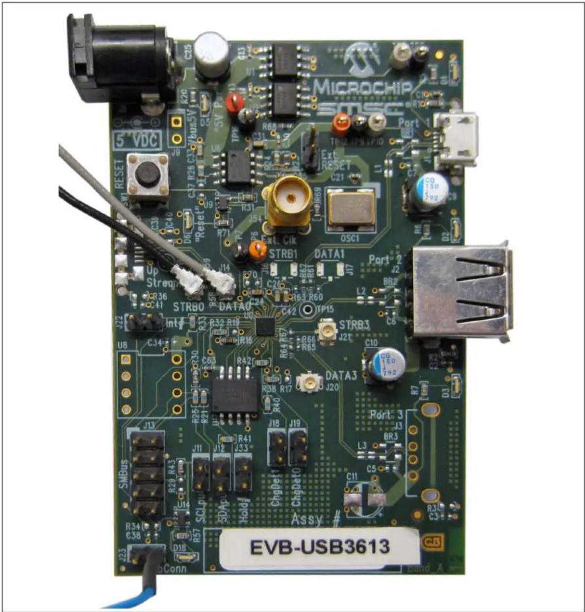
FIGURE A-1: EVB-USB3613 EVALUATION BOARD
text_image
MICROCHIP STSC 5 VDC SW RESET C25 K20 C37 R28 C33 Vbus5V 5V PAP R13 U1 TPE R68 C31 R24 R22 R21 R71 C39 D6 "Reset" J9 R31 J54 Ext. Clk STRB1 DATA1 Port 2 C21 OSC1 Up Strept C41 STRB0 DATA0 J14 C26 C42 TP15 L2 J22 Int R32 R19 STRB3 C34 R30 R33 R58 R63 R60 R64 R67 R66 R65 DATA3 J20 C10 U8 C34 R18 R42 R64 R67 R38 R17 R40 R68 ChgDet1 ChgDet0 SMBus J13 R29 R43 SCLpu J11 U12 J33 J18 J19 Holdf C5 ChgDet1 C11 Assy # SMBus C38 D18 Bond A EVB-USB3613NOTES:
Appendix B. EVB-USB3613 Evaluation Board Schematic
B.1 INTRODUCTION
This appendix shows the EVB-USB3613 Evaluation Board schematic.
FIGURE B-1: EVB-USB3613 EVALUATION BOARD SCHEMATIC
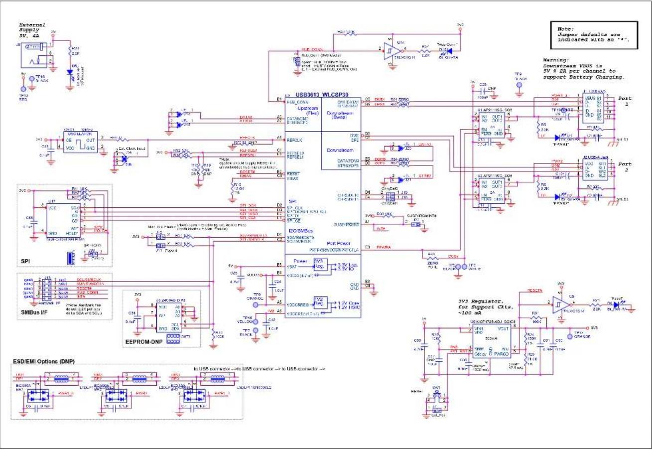
text_image
External Supply 5V, 4A 3 2 1 0 T16 9.4KG R1 R2 R3 R4 R5 R6 R7 R8 R9 R10 R11 R12 R13 R14 R15 R16 R17 R18 R19 R20 R21 R22 R23 R24 R25 R26 R27 R28 R29 R30 R31 R32 R33 R34 R35 R36 R37 R38 R39 R40 R41 R42 R43 R44 USB3613 WLCSP30 HUE_CONN Upstream (Flux) DOUT/RESET (Swap) REFOLX RESET/RESET1 SPI SP_CX SP_CY SP_OE SUSP-RESET I2C/SMBus SDASM202A7A SOLINKACK Port Power PERFWR/OSSEMREPTLA Power VBT VBAT VDDOREG VDDOREG/AT 5.5V Loa. VDDOREG/AT 5.5V I/O. EFPROM-DNP EEPROM-DNP SMBus IVF SPI USB/DNALEDIC USB/DNALEDIC USB/DNALEDIC USB/DNALEDIC USB/DNALEDIC USB/DNALEDIC USB/DNALEDIC USB/DNALEDIC USB/DNALEDIC USB/DNALEDIC USB/DNALEDIC USB/DNALEDIC USB/DNALEDIC USB/DNALEDIC USB/DNALEDIC USB/DNALEDIC USB/DNALEDIC USB/DNAMOS/DCAMOS/DCAMOS/DCAMOS/DCAMOS/DCAMOS/DCAMOS/DCAMOS/DCAMOS/DCAMOS/DCAMOS/DCAMOS/DCAMOS/DCAMOS/DCAMOS/DCAMOS/DCAMOS/DCAMOS/DCAMOS/DCAMOS/DCAMOS/DCAMOS/DCAMOS/DCAMOS/DCAMOS/DCAMOS/DTM/DTM/DTM/DTM/DTM/DTM/DTM/DTM/DTM/DTM/DTM/DTM/DTM/DTM/DTM/DTM/DTM/DTM/DTM/DTM/DTM/DTM/DTM/DTM/DTM/DTM/DTM/DTM/DTM/DTM/DTM/DTM/DTM/DTM/ ESD/EMI Options (DNP) USB/DNALEDIC USB/DNALEDIC USB/DNALEDIC USB/DNALEDIC USB/DNALEDIC USB/DNALEDIC USB/DNALEDIC USB/DNALEDIC USB/DNALEDIC USB/DNALEDIC USB/DNALEDIC USB/DNALEDIC USB/DNALEDIC USB/DNALEDIC USB/DNALEDIC USB/DNALEDIC USB/DNALEDAIDACIDACIDACIDACIDACIDACIDACIDACIDACIDACIDACIDACIDACIDACIDACIDACIDACIDACIDACIDACIDACIDACIDACIDACIDACIDACIDACIDACIDACIDACIDACIDACIDACIDACIDACIDACIDACIDACIDACIDACIDACIDACIDACIDACIDACIDACIDACIDACIDACIDACIDACAAppendix C. Bill of Materials (BOM)
C.1 INTRODUCTION
This appendix includes the EVB-USB3613 Evaluation Board Bill of Materials (BOM).
TABLE C-1: EVB-USB3613 EVALUATION BOARD BILL OF MATERIALS
| Item | Qty | Qty Populated | Reference Designator(s) Des | cription Manufacturer Manufacturer Part Number Notes | |||
| 1 2 | 2 C9, | C10 Capacitor | Low ESR, 150uF, 6.3 VDC, 20%, Aluminum, Radial-SMT, 5mm x 5.7mm | Electronics | Lelon VZS151M0JTR- | 0506 '3613 | |
| 2 1 | 1 C1 | Capacitor, 0.1 | uF, 25V, 10%, X5R, 0402 Murata B | Capacitor, 0.1uF, 25V, 10%, X5R, 0402 | Muralta Electronics | GRM155R61E104KA7D | '3613 |
| 3 | 6 | 6 | C2, C13, C14, C21, C30, C35 | Capacitor, 0.1uF, 25V, 10%, X5R, 0402 | Muralta Electronics | GRM155R61E104KA7D | |
| 4 | 1 | 1 | C63 | Capacitor, 0.1uF, 10V, 10%, X5R, 0402 | Muralta Electronics | GRM155R71A104KA01D | |
| 5 | 2 | 2 | C24, C42 | Capacitor, 1.0uF, 16 VDC, 10%, X5R, 0603 | Muralta Electronics | GRM188R61C105KA93D | |
| 6 | 3 | 3 | C26, C31, C33 | Capacitor, 4.7uF, 6.3 VDC, 20%, X5R, 0603 | Muralta Electronics | GRM188R60J475KE19D | |
| 7 4 | 4 R61, | R62, R64, R67 | Resistor, ZERO, | 0.1W, 0402 Panasonic | ® | ERJ-2GE0R00X | '3613 |
| 8 | 1 | 1 | R68 | Resistor, ZERO, 0.1W, 0402 | Panasonic | ERJ-2GE0R00X | PCTL |
| 9 | 1 | 1 | R1 | Resistor, 330, 5%, 1/16W, 0603 | Panasonic | ERJ-3GEYJ331V | '3613 |
| 10 | 1 | 1 | R2 | Resistor, 330, 5%, 1/16W, 0603 | Panasonic | ERJ-3GEYJ331V | |
| 11 | 6 | 6 | R5, R6, R7, R20, R57, R71 | Resistor, 2.2K, 5%, 1/16W, 0603 | Panasonic | ERJ-3GEYJ222V | |
| 12 | 1 | 1 | R16 | Resistor, 12.0K, 1%, 1/16W, 0603 | Panasonic | ERJ-3EKF1202V | |
| 13 | 7 7 | R26, R32, R33, R38, R40, R41, R42 | R3, R38, R40, R41, R42 | Resistor, 10K, 5%, 1/16W, 0603 | Panasonic | ERJ-3GEYJ103V | |
| 14 | 2 | 2 | R21, R25 | Resistor, 10K, 5%, 1/16W, 0603 | Panasonic | ERJ-3GEYJ103V | EEPROM |
| 15 | 1 | 1 | R23 | Resistor, 21.0K, 1%, 1/16W, 0603 | Yageo America | 9C06031A2102FKHFT | |
| 16 | 1 | 1 | R24 | Resistor, 150K, 1%, 1/10W, 0603 | Panasonic | ERJ-3EKF1503V | |
| 17 | 1 | 1 | R43 | Resistor, 100K, 5%, 1/16W, 0603 | Panasonic | ERJ-3GEYJ104V | '3613 |
| 18 | 2 | 2 | R30, R31 | Resistor, 100K, 5%, 1/16W, 0603 | Panasonic | ERJ-3GEYJ104V | |
| 19 | 1 | 1 | R69 | Resistor, 33, 5%, 1/16W, 0603 | Panasonic | ERJ-3GEYJ330V | |
| 20 | 4 | 4 | D1, D2, D3, D18 | LED, Green, Bright (40 mcd), 0804, Right Angle | Stanley Electric | DG1113F | |
| 21 | 2 | 2 | D5, D6 | LED, Bright Red, 0804, Right Angle | Stanley Electric | FR1113F | |
| 22 | 1 1 | J8 | Connector, Power Jack, 2.1 mm x 5.5 mm, 12V, 4A, Right Angle, TH | Cui Stack | PJ-002AH | ||
| 23 | 1 | 1 | J1 | Receptacle, USB, Micro-AB, Right Angle, SMT | Hirose | ZX62-AB-5PA(11) | '3613 |
| 24 | 1 | 1 | J2 | Receptacle, USB, Style A, Right Angle, Through-hole | AMP | 292303-1 | |
| 25 | 4 | 4 | J14, J15, J20, J21 | Receptacle, Coax, U.FL, SMT, Vertical | Hirose | U.FL-R-SMT-1 | '3613 |
| 26 | 1 | 1 | J54 | Receptacle, SMA, Vertical | AMP | 221789-1 | |
| 27 | 2 | 2 | J7, J33 | Header, 1x2, 0.1 Inch, Vertical (cut from 1x36) | Samtec | TSW-102-14-L-S | |
| 28 | 1 | 1 | J23 | Header, 1x2, 0.1 Inch, Vertical | Samtec | TSW-102-14-L-S | '3613 |
| 29 | 5 | 5 | J11, J12, J18, J19, J22 | Header, 2x1, 0.1 Inch, Vertical (cut from 2x36) | Samtec | TSW-102-14-L-S | |
TABLE C-1: EVB-USB3613 EVALUATION BOARD BILL OF MATERIALS
| Item | Qty | Qty Populated | Reference Designator(s) | Description | Manufacturer | Manufacturer Part Number | Notes |
| 30 1 | 1 J13 | Header, 2x5 | 0.1 Inch, Vertical AMP 146256-5 $MBus | ||||
| 31 1 | 1 SW | Switch, Mo | mentary, SPST, 100mA, J-lead, NO | E-Switch TL3301xF160QJor-RJ | |||
| 32 2 | 2 TP3 | TP10 Test | Point, White, Loop, Mini, 0.04 Inch | D Keystone 5002 | |||
| 33 | 4 | 4 | TP5, TP7, TP9, TP16 | Test Point, Black, Loop, Mini, 0.04 Inch ID | Keystone | 5001 | |
| 34 2 | 2 TP6 | TP12 Test | Point, Orange, Loop, Mini, 0.04 Inch ID | Keystone 5003 | |||
| 35 | 1 | 1 | TP13 | Test Point, Red, Loop, Mini, 0.04 Inch ID | Keystone | 5000 | |
| 36 | 1 | 1 | TP15 | Test Point, Yellow, Loop, Mini, 0.04 Inch ID | Keystone | 5004 | |
| 37 1 | 1 U0 | IC, USB3613, 3-Port USB 2.0/HSIC Hub, WLCSP30 Standard | Microsystems Corp | USB3613 | |||
| 38 | 2 | 2 | U1, U2 | IC, AP2111SG-13, Power Distribution Switch, SOP-8 | Diodes® Inc. | AP2111SG-13 | |
| 39 1 | 1 U6 | IC, MCP1725-ADJE/SN, LDO Regulator, Adj., 500 mA, SOIC8 | Microchip Technology | MCP1725(T)-ADJE/SN | |||
| 40 | 2 | 2 | U9, U14 | IC, 74LVC1G14, Inverter, Shottky, DCK | TI | SN74LVC1G14DCKR | |
| 41 1 | 1 U17 | IC, '25VF640C, 64Mb, (8M x 8) SPI Serial FLASH, 2.5V-3.6V, 75-80 MHz, Dual Read, SO8 | Microchip | SST25VF064C-80-4I-S3AE | SPI | ||
| 42 | 1 | 1 | OSC1 | Oscillator, 12.000 MHz, 50 ppm, 3.3V, SMT | CTS | CB3LV-3C-12M0000 | |
| 43 4 | 4 | Foot, Silicone Rubber, Adhesive, Clear, Cylindrical .375" x .190" | Richco® | RBS-35 | Place bottom side, one at each corner | ||
| 44 | 1 | 1 | Starting SN = Band-01 | Serial Number Labels, 6 mm x 27 mm | Place bottom side in white S/N box | ||
| 45 | 1 | 1 | Assy Labels: "EVB-USB3613_A1", 6 mm x 27 mm | EVB-USB3x13 | Place top side in Assy# box | ||
| 46 | 1 | 1 | PCB Fab | PCB, Band (EVB-USB3x13), Rev. A | ViaSystems/DDi | EVB-USB3x13 | Supplied by SMSC |
| 47 1 | 1 Assembly Assembly, Band (EVB-USB3613), Rev. A | ||||||
| 48 1 | 0 C25 | Capacitor, Low ESR, 100uF, 6.3 VDC, 20%, Aluminum, Radial-SMT, 5 mm x 5.8 mm | United Chemi-Con | EMZA6R3ADA101ME61G | DNP | ||
| 49 1 | 0 C11 | Capacitor, Low ESR, 150uF, 6.3 VDC, 20%, Aluminum, Radial-SMT, 5 mm x 5.7 mm | Lelon | VZS151M0JTR-0506 | '3813 | ||
| 50 | 2 | 0 | C3, C41 | Capacitor, 0.1uF, 25V, 10%, X5R, 0402 | Murata Electronics | GRM155R61E104KA7D | '3813 |
| 51 | 3 | 0 | C5, C6, C7 | Capacitor, 0.1uF, 25V, 10%, X5R, 0402 | Murata Electronics | GRM155R61E104KA7D | ESD |
| 52 | 1 | 0 | C34 | Capacitor, 0.1uF, 25V, 10%, X5R, 0402 | Murata Electronics | GRM155R61E104KA7D | EEPROM-DNP |
| 53 | 2 | 0 | C38, C39 | Capacitor, 1000pF, 50V, 10%, X7R, 0402 | Murata Electronics | GRM155R71H102KA01D | '3813 |
TABLE C-1: EVB-USB3613 EVALUATION BOARD BILL OF MATERIALS
| Item | Qty | Qty Populated | Reference Designator(s) | Description | Manufacturer | Manufacturer Part Number | Notes |
| 54 1 | 0 C37 | Capacitor, 1 | .0uF, 16VDC, 10%, X5R, 0603 Murata Electronics GRM188R61C105KA93D DNP | ||||
| 55 1 | 0 C40 | Capacitor, 2 | .2uF, 6.3 VDC, 10%, X5R, 0603 Murata Electronics GRM185R60J225KE26D '3813 | ||||
| 56 6 | 0 R58, | R59, R60, | R63, R65, R66 Resistor, ZERO, 0.1W, 0402 Panasonic ERJ-2GE0R00X '3813 | ||||
| 57 | 2 | 0 | R3, R36 | Resistor, 330, 5%, 1/16W, 0603 | Panasonic | ERJ-3GEYJ331V | '3813 |
| 58 | 2 | 0 | R17, R19 | Resistor, 10K, 5%, 1/16W, 0603 | Panasonic | ERJ-3GEYJ103V | DNP |
| 59 | 1 | 0 | R29 | Resistor, 100K, 5%, 1/16W, 0603 | Panasonic | ERJ-3GEY104V | '3813 |
| 60 | 1 | 0 | R34 | Resistor, 82K, 5%, 1/16W, 0603 | Panasonic | ERJ-3GEYJ823V | '3813 |
| 61 | 1 | 0 | R70 | Resistor, 33, 5%, 1/16W, 0603 | Panasonic | ERJ-3GEYJ330V | DNP |
| 62 | 1 | 0 | J0 | Receptacle, USB, Micro-AB, Right Angle, SMT | Hirose | ZX62-AB-5PA | '3813 |
| 63 | 1 | 0 | J3 | Receptacle, USB, Style A, Right Angle, Through-hole | AMP | 292303-1 | '3813 |
| 64 | 2 | 0 | J16, J17 | Receptacle, Coax, U.FL, SMT, Vertical | Hirose | U.FL-R-SMT-1 | '3813 |
| 65 | 1 | 0 | J9 | Header, 1x2, 0.1 Inch, Vertical | Samtec | TSW-102-14-L-S | '3813 |
| 66 3 | 0 BR1 | BR2, BR3 | Diode, Bridge, Switching, 50V, 140 mA, KCAC, SOT-143 | Infineon Tech | BGX50A | ESD | |
| 67 3 | 0 L1 | L2, L3 | Inductor, Common Mode Choke, DLP11SN900SL2, 0504 | Murata Electronics DLP11SN900SL2 ESD | |||
| 68 | 1 | 0 | SKT1 (Place at U8) | Socket, IC, 8-Pin DIP, Leaf Contacts, Through-hole | Assmann | A08-LC-TT-R | EEPROM-DNP |
| 69 | 1 | 0 | TP11 | Test Point, White, Loop, Mini, 0.04 Inch ID | Keystone | 5002 | '3813 |
| 70 | 1 | 0 | U8 | IC, 24C04, 2 Wire Serial EPROM, 4 Kb, 2.7V, DIP-8 | Microchip Technology | 24LC04B-I/P | EEPROM-DNP |
| 71 | 1 | 0 | SHUNT1 | Shunt, Insulated, 0.1 Inch | AMP | 881545-2 | DNP |
Worldwide Sales and Service
AMERICAS
Corporate Office
2355 West Chandler Blvd.
Chandler, AZ 85224-6199
Tel: 480-792-7200
Fax: 480-792-7277
Technical Support:
http://www.microchip.com/support
Web Address:
www.microchip.com
Atlanta
Duluth, GA
Tel: 678-957-9614
Fax: 678-957-1455
Boston
Westborough, MA
Tel: 774-760-0087
Fax: 774-760-0088
Chicago
Itasca, IL
Tel: 630-285-0071
Fax: 630-285-0075
Cleveland
Independence, OH
Tel: 216-447-0464
Fax: 216-447-0643
Dallas
Addison, TX
Tel: 972-818-7423
Fax: 972-818-2924
Detroit
Farmington Hills, MI
Tel: 248-538-2250
Fax: 248-538-2260
Indianapolis
Noblesville, IN
Tel: 317-773-8323
Fax: 317-773-5453
Los Angeles
Mission Viejo, CA
Tel: 949-462-9523
Fax: 949-462-9608
Santa Clara
Santa Clara, CA
Tel: 408-961-6444
Fax: 408-961-6445
Toronto
Mississauga, Ontario,
Canada
Tel: 905-673-0699
Fax: 905-673-6509
ASIA/PACIFIC
Asia Pacific Office
Suites 3707-14, 37th Floor
Tower 6, The Gateway
Harbour City, Kowloon
Hong Kong
Tel: 852-2401-1200
Fax: 852-2401-3431
Australia - Sydney
Tel: 61-2-9868-6733
Fax: 61-2-9868-6755
China - Beijing
Tel: 86-10-8569-7000
Fax: 86-10-8528-2104
China - Chengdu
Tel: 86-28-8665-5511
Fax: 86-28-8665-7889
China - Chongqing
Tel: 86-23-8980-9588
Fax: 86-23-8980-9500
China - Hangzhou
Tel: 86-571-2819-3187
Fax: 86-571-2819-3189
China - Hong Kong SAR
Tel: 852-2943-5100
Fax: 852-2401-3431
China - Nanjing
Tel: 86-25-8473-2460
Fax: 86-25-8473-2470
China - Qingdao
Tel: 86-532-8502-7355
Fax: 86-532-8502-7205
China - Shanghai
Tel: 86-21-5407-5533
Fax: 86-21-5407-5066
China - Shenyang
Tel: 86-24-2334-2829
Fax: 86-24-2334-2393
China - Shenzhen
Tel: 86-755-8864-2200
Fax: 86-755-8203-1760
China - Wuhan
Tel: 86-27-5980-5300
Fax: 86-27-5980-5118
China - Xian
Tel: 86-29-8833-7252
Fax: 86-29-8833-7256
China - Xiamen
Tel: 86-592-2388138
Fax: 86-592-2388130
China - Zhuhai
Tel: 86-756-3210040
Fax: 86-756-3210049
ASIA/PACIFIC
India - Bangalore
Tel: 91-80-3090-4444
Fax: 91-80-3090-4123
India - New Delhi
Tel: 91-11-4160-8631
Fax: 91-11-4160-8632
India - Pune
Tel: 91-20-3019-1500
Japan - Osaka
Tel: 81-6-6152-7160
Fax: 81-6-6152-9310
Japan - Tokyo
Tel: 81-3-6880-3770
Fax: 81-3-6880-3771
Korea - Daegu
Tel: 82-53-744-4301
Fax: 82-53-744-4302
Korea - Seoul
Tel: 82-2-554-7200
Fax: 82-2-558-5932 or
82-2-558-5934
Malaysia - Kuala Lumpur
Tel: 60-3-6201-9857
Fax: 60-3-6201-9859
Malaysia - Penang
Tel: 60-4-227-8870
Fax: 60-4-227-4068
Philippines - Manila
Tel: 63-2-634-9065
Fax: 63-2-634-9069
Singapore
Tel: 65-6334-8870
Fax: 65-6334-8850
Taiwan - Hsin Chu
Tel: 886-3-5778-366
Fax: 886-3-5770-955
Taiwan - Kaohsiung
Tel: 886-7-213-7828
Fax: 886-7-330-9305
Taiwan - Taipei
Tel: 886-2-2508-8600
Fax: 886-2-2508-0102
Thailand - Bangkok
Tel: 66-2-694-1351
Fax: 66-2-694-1350
EUROPE
Austria - Wels
Tel: 43-7242-2244-39
Fax: 43-7242-2244-393
Denmark - Copenhagen
Tel: 45-4450-2828
Fax: 45-4485-2829
France - Paris
Tel: 33-1-69-53-63-20
Fax: 33-1-69-30-90-79
Germany - Munich
Tel: 49-89-627-144-0
Fax: 49-89-627-144-44
Italy - Milan
Tel: 39-0331-742611
Fax: 39-0331-466781
Netherlands - Drunen
Tel: 31-416-690399
Fax: 31-416-690340
Spain - Madrid
Tel: 34-91-708-08-90
Fax: 34-91-708-08-91
UK - Wokingham
Tel: 44-118-921-5869
Fax: 44-118-921-5820
08/20/13