SY89467U - Electronic component Microchip - Free user manual and instructions
Find the device manual for free SY89467U Microchip in PDF.

User questions about SY89467U Microchip
0 question about this device. Answer the ones you know or ask your own.
Ask a new question about this device
Download the instructions for your Electronic component in PDF format for free! Find your manual SY89467U - Microchip and take your electronic device back in hand. On this page are published all the documents necessary for the use of your device. SY89467U by Microchip.
USER MANUAL SY89467U Microchip
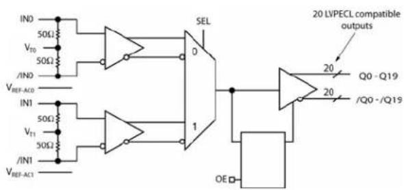
The SY89467U is a 2.5/3.3V, 1:20 LVPECL fanout buffer with a 2:1 differential input multiplexer (MUX). A unique Fail-Safe Input (FSI) protection prevents metastable output conditions when the selected input clock fails to a DC voltage (when voltage between the pins of the differential input drops significantly below 100mV).
The differential input includes Micrel's unique, 3-pin internal termination architecture that can interface to any differential signal (AC- or DC-coupled) as small as 100mV (200mV _PP ) without any level shifting or termination resistor networks in the signal path. The outputs are 800mV, LVPECL with fast rise/fall times guaranteed to be less than 270ps.
The SY89467U operates from a 2.5V ±5% or 3.3V ±10% supply and is guaranteed over the full industrial temperature range of -40°C to +85°C. The SY89467U is part of Micrel's high-speed, Precision Edge® product line.
All support documentation can be found on Micrel's web site at: www.micrel.com.
Functional Block Diagram
text_image
IND 50Ω V_T0 50Ω /IND V_REF-AC0 IN1 50Ω V_T1 50Ω /IN1 V_REF-AC1 SEL 0 1 20 LYPECL compatible outputs 20 Q0 - Q19 20 /Q0 - /Q19 OE
Precision Edge®
Features
- Selects between two inputs, and provides 20 precision LVPECL copies
- Fail-Safe Input
- Prevents outputs from oscillating when input is invalid
- Guaranteed AC performance over temperature and supply voltage:
- DC-to >1.5 GHz throughput
- < 1200ps Propagation Delay (In-to-Q)
- 270ps Rise/Fall times
• Ultra-low jitter design:
- <1psRMS random jitter
- <1ps RMS cycle-to-cycle jitter
- <10psPP total jitter (clock)
- < 0.7psRMS MUX crosstalk induced jitter
- Unique, patented MUX input isolation design minimizes adjacent channel crosstalk
- Unique patented internal termination and VT pin accepts DC- and AC-coupled inputs (CML, PECL, LVDS)
- Wide input voltage range: V_CC to GND
• 2.5V ±5% or 3.3V ±10% supply voltage
- -40°C to +85°C industrial temperature range
• Available in 64-pin TQFP package
Applications
- Fail-safe clock protection
• SONET clock distribution - Backplane distribution
Markets
• LAN/WAN
- Enterprise servers
- ATE
• Test and measurement
Precision Edge is a registered trademark of Micrel, Inc.
MicroLeadFrame and MLF are registered trademarks of Amkor Technology, Inc.
Micrel Inc. • 2180 Fortune Drive • San Jose, CA 95131 • USA • tel +1 (408) 944-0800 • fax +1 (408) 474-1000 • http://www.micrel.com
Ordering Information ^(1)
| Part Number | Package Type | Operating Range | Package Marking | Lead Finish |
| SY89467UHY | T64-1 | Industrial | SY89467UHY with Pb-Free bar-line Indicator | Matte-SnPb-Free |
| SY89467UHYTR^(2) | T64-1 | Industrial | SY89467UHY with Pb-Free bar-line Indicator | Matte-SnPb-Free |
Notes:
- Contact factory for die availability. Dice are guaranteed at T_A = 25^ , DC Electricals Only.
- Tape and Reel.
Pin Configuration

text_image
VCC GND VREF-AC0 VT0 IN0 /INO SEL OE IN1 /IN1 VT1 VREF-AC1 GND VCC 64 63 62 61 60 59 58 57 56 55 54 53 52 51 50 49 1 2 3 4 5 6 7 8 9 10 11 12 13 14 15 16 48 VCC 47 Q7 46 /Q7 45 Q6 44 /Q8 43 Q9 42 /Q9 41 VCC 40 GND 39 Q10 38 /Q10 37 Q11 36 /Q11 35 Q12 34 /Q12 33 VCC 17 18 19 20 21 22 23 24 25 26 27 28 29 30 31 32 /Q19 Q18 Q17 Q16 Q15 Q14 Q13 Q12 Q11 Q10 Q964-Pin EPAD-TQFP (T64-1)
Pin Description
| Pin Number | Pin Name Pin | Function |
| 1, 16, 23, 3341, 48, 58 | VCC | Positive Power Supply: Bypass with 0.1 F 0.01 F low ESR capacitors as close to the V_CC pins as possible. |
| 64, 6362, 6160, 5957, 5655, 5453, 5251, 5047, 4645, 4443, 4239, 3837, 3635, 3431, 3029, 2827, 2625, 2422, 2120, 1918, 17 | Q0, /Q0Q1, /Q1Q2, /Q2Q3, /Q3Q4, /Q4Q5, /Q5Q6, /Q6Q7, /Q7Q8, /Q8Q9, /Q9Q10, /Q10Q11, /Q11Q12, /Q12Q13, /Q13Q14, /Q14Q15, /Q15Q16, /Q16Q17, /Q17Q18, /Q18Q19, /Q19 | LVPECL Differential Output Pairs: Differential buffered output copies of the selected input signal. The output swing is typically 800mV. Unused output pairs may be left floating with no impact on jitter. See “LVPECL Output Termination” subsection. Normally terminated with 50 to V_CC-2V . These differential LVPECL outputs are a logic function of the IN0, IN1, and SEL inputs. See “Truth Table” below. |
| 4, 13 | VREF-AC0VREF-AC1 | Reference Voltage: These outputs bias to V_CC-1.2V . They are used for AC-coupling inputs IN and /IN. Connect VREF-AC directly to the corresponding VT pin. Bypass with 0.01 F low ESR capacitor to V_CC . Due to limited drive capability, each VREF-AC pin is only intended to drive its respective VT pin. Maximum sink/source current is ± 0.5mA . See “Input Interface Applications” subsection. |
| 5, 12 VT0 | VT1 | Input Termination Center-Tap: Each side of a differential input pair terminates to the VT pin. The VT pin provides a center-tap for each input (IN, /IN) to a termination network for maximum interface flexibility. See “Input Interface Applications” subsection. |
| 6, 710, 11 | IN0, /IN0IN1, /IN1 | Differential Inputs: These input pairs are the differential signal inputs to the device. These inputs accept AC- or DC-coupled signals as small as 100mV. The input pairs internally terminate to a VT pin through 50 . This allows a wide input voltage range from VCC to GND. See Figure 3a, Simplified Differential Input Stage for details. Note that when these inputs are left in an open state, the FSI feature will override this input state and provide a valid state at the output. See “Functional Description” subsection. |
| 2, 3, 14, 15,32, 40, 49 | GND,ExposedPad | Ground. Exposed pad must be connected to a ground plane that is the same potential as the ground pins. |
| 9 | OE | Single-Ended Input: This TTL/CMOS input disables and enables the Q0-Q19 outputs. It is internally connected to a 25k pull-up resistor and will default to a logic HIGH state if left open. When disabled, Q goes LOW and /Q goes HIGH. OE being synchronous, outputs will be enabled/disabled following a rising and a falling edge of the input clock. V_TH = V_CC/2 . |
| 8 | SEL | Single-Ended Input: This single-ended TTL/CMOS-compatible input selects the inputs to the multiplexer. Note that this input is internally connected to a 25k pull-up resistor and will default to logic HIGH state if left open. V_TH = V_CC/2 . |
Truth Table
| Inputs | Outputs | |||||
| IN0 | /IN0 | IN1 | /IN1 | SEL | Q | |
| 0 | 1 | X | X | 0 | 0 | 1 |
| 1 | 0 | X | X | 0 | 1 | 0 |
| X | X | 0 | 1 | 1 | 0 | 1 |
| X | X | 1 | 0 | 1 | 1 | 0 |
/Q
Absolute Maximum Ratings ^(1)
Supply Voltage (Vcc) -0.5V to +4.0V
Input Voltage ( V_IN ) ......-0.5V to V_CC
LVPECL Output Current ( I_OUT )......
Continuous.... 50mA Surge.... 100mA
Current ( V_T )
Source or sink on VT pin.... ±100mA
Input Current
Source or sink current on (IN, /IN) .... ±50mA
Current ( V_REF )
Source/Sink Current on V REF-AC (4) ±0.5mA
Maximum Operating Junction Temperature.....125°C
Lead Temperature (soldering, 20 sec.) .....+260°C
Storage Temperature ( T_s )....-65°C to 150°C
Operating Ratings ^(2)
Supply Voltage ( V_cc )....+2.375V to +2.625V .....+3.0V to +3.6V
Ambient Temperature ( T_A )....-40°C to +85°C
Package Thermal Resistance ^(3)
TQFP ( _JA )
Still-Air.... 35°C/W
TQFP ( _JB )
Junction-to-Board....21°C/W
DC Electrical Characteristics ^(5)
T_A = -40^ to +85^ , unless otherwise stated.
| Symbol | Parameter Condition | Min Typ Max Units | ||||||
| V_CC | Power Supply | 2.375 | 2.5 | 2.625 | V | |||
| 3.0 | 3.3 | 3.6 | V | |||||
| I_CC | Power Supply Current | No load, max V_CC | 120 | 165 | mA | |||
| R_IN | Input Resistance (IN-to- V_T ) | 45 | 50 | 55 | Ω | |||
| R_DIFF\_IN | Differential Input Resistance (IN-to-/IN) | 90 | 100 | 110 | Ω | |||
| V_IH | Input High Voltage (IN, /IN) | 0.1 | V_CC | V | ||||
| V_IL | Input Low Voltage (IN, /IN) | 0 | V_IH-0.1 | V | ||||
| V_IN | Input Voltage Swing (IN, /IN) | See Figure 2a. Note 6. | 0.1 | 1.0 | V | |||
| V_DIFF\_IN | Differential Input Voltage Swing |IN-/IN| | See Figure 2b. | 0.2 | V | ||||
| V_IN\_FSI | Input Voltage Threshold that Triggers FSI | 30 | 100 | mV | ||||
| V_REF-AC | Output Reference Voltage | I_VREF-AC = ± 0.5mA | V_CC-1.3 | V_CC-1.2 | V_CC-1.1 | V | ||
| V_T\_IN | Voltage from Input to V_T | 1.28 | V | |||||
Notes:
- Permanent device damage may occur if absolute maximum ratings are exceeded. This is a stress rating only and functional operation is not implied at conditions other than those detailed in the operational sections of this data sheet. Exposure to absolute maximum rating conditions for extended periods may affect device reliability.
- The data sheet limits are not guaranteed if the device is operated beyond the operating ratings.
- Package thermal resistance assumes exposed pad is soldered (or equivalent) to the devices most negative potential on the PCB. _JA and _JB values are determined for a 4-layer board in still air unless otherwise stated.
- Due to limited drive capability use for input of the same package only.
- The circuit is designed to meet the DC specifications shown in the above table after thermal equilibrium has been established.
- V_IN (max) is specified when V_T is floating.
LVPECL Outputs DC Electrical Characteristics ^(7)
V_CC = 2.5V ± 5% or 3.3V ± 10% ; R_L = 50 to V_CC-2V ; T_A = -40^ to +85^ , unless otherwise stated.
| Symbol | Parameter Condition | Min | Typ | Max | Units | ||
| V_OH Output | HIGH Voltage Q, /Q V | cc-1.145 | V_CC-0.895 V | ||||
| V_OL Output | LOW Voltage Q, /Q V | cc-1.945 | V_CC-1.695 | ||||
| V_OUT Output | Voltage Swing See Figure 2a. 550 | 800 | 950 mV | ||||
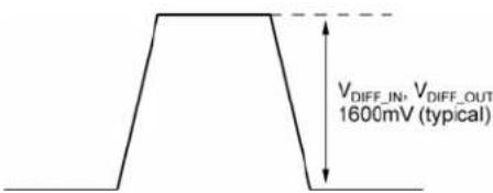
| V_DIFF\_OUT | Differential Output Voltage Swing | See Figure 2b. | 1100 | 1600 | 1900 | mV | |
LVTTL/CMOS DC Electrical Characteristics ^(7)
V_CC = 2.5V ± 5% or 3.3V ± 10% ; T_A = -40^ C to +85^ C , unless otherwise stated.
| Symbol | Parameter Condition | Min | Typ | Max | Units | ||
| V_IH | Input HIGH Voltage | 2.0 | V | ||||
| V_IL | Input LOW Voltage | 0.8 | V | ||||
| I_IH | Input HIGH Current | -125 | μA | ||||
| I_IL | Input LOW Current | -300 | μA |
Note:
- The circuit is designed to meet the DC specifications shown in the above table after thermal equilibrium has been established.
AC Electrical Characteristics ^(8)
V_CC = 2.5V ± 5% or 3.3V ± 10% ; R_L = 50 to V_CC-2V ; Input t_r/t_f ≤ 300ps ; T_A = -40^ to +85^ , unless otherwise stated.
| Symbol | Parameter Condition Min | Typ Max Units | ||||
| MAX Maximum Operating Frequency | V_OUT ≥ 200mV, V_IN ≥ 200mV 1.5 2.0 | GHz f | ||||
| V_OUT ≥ 200mV, V_IN ≥ 100mV 1.0 1.5 | GHz | |||||
| t_pd | Differential Propagation Delay IN-to-Q | 100mV < V_IN ≤ 200mV, Note 9 | 600 | 850 | 1200 | ps |
| IN-to-Q | 200mV < V_IN ≤ 800mV, Note 9 | 500 | 750 | 1100 | ps | |
| SEL-to-Q | V_TH=V_CC/2 | 350 | 600 | 850 | ps | |
| t_S OE | Set-up Time OE-to-IN | Note 10 | 300 | ps | ||
| t_H OE | Hold Time IN-to-OE | Note 10 | 800 | ps | ||
| t_SKEW | Output-to-Output Skew | Note 11 | 15 | 35 | ps | |
| Input-to-Input Skew | Note 12 | 5 | 20 | ps | ||
| Part-to-Part Skew | Note 13 | 300 | ps | |||
| t_JITTER | Clock Random Jitter | Note 14 | 1 | p_SRMS | ||
| Cycle-to-Cycle Jitter | Note 15 | 1 | p_SRMS | |||
| Total Jitter Note 16 | 10 ps | PP | ||||
| Crosstalk-Induced Jitter | Note 17 | 0.7 | p_SRMS | |||
| tr, t | Output Rise/Fall Time (20% to 80%) | At full output swing. | 110 | 170 | 250 | ps |
| Duty Cycle | V_IN>200mV | 45 | 55 | % | ||
| 100mV < V_IN ≤ 200mV | 45 | 55 | % | |||
Notes:
-
High-frequency AC-parameters are guaranteed by design and characterization.
-
Propagation delay is measured with input t_r , t_f ≤ 300ps (20% to 80%). The propagation delay is a function of the rise and fall times at IN. See “Typical Operating Characteristics” for details.
-
Set-up and hold times apply to synchronous applications that intend to enable/disable before the next clock cycle. For asynchronous applications, set-up and hold do not apply.
-
Output-to-Output skew is measured between two different outputs under identical transitions.
-
Input-to-Input skew is the time difference between the two inputs to one output, under identical input transitions.
-
Part-to-Part skew is defined for two parts with identical power supply voltages at the same temperature and with no skew of the edges at the respective inputs.
-
Random Jitter is measured with a K28.7 character pattern, measured at <fMAX.
-
Cycle-to-Cycle Jitter definition: the variation of periods between adjacent cycles, T_n - T_n-1 where T is the time between rising edges of the output signal.
-
Total Jitter definition: with an ideal clock input of frequency < f_MAX , no more than one output edge in 10^12 output edges will deviate by more than the specified peak-to-peak jitter value.
-
Crosstalk is measured at the output while applying two similar differential clock frequencies that are asynchronous with respect to each other at the inputs.
Functional Description
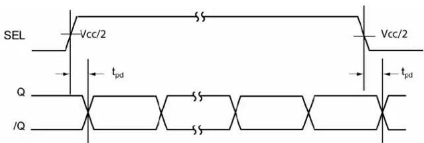
Clock Select (SEL)
SEL is an asynchronous TTL/CMOS compatible input that selects one of the two input signals. An internal 25kΩ pull-up resistor defaults the input to logic HIGH if left open. Input switching threshold is V_cc/2 . Refer to Figure 1a.
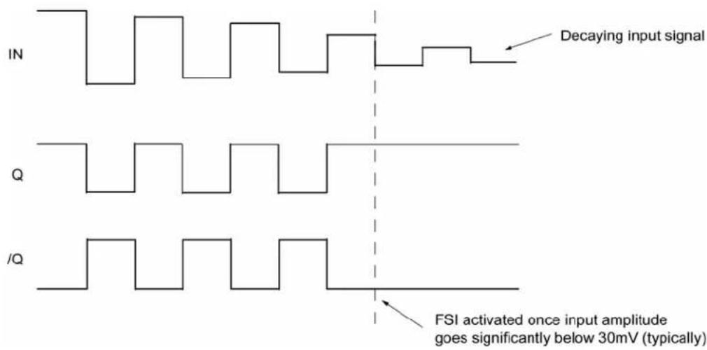
Fail-Safe Input (FSI)
The input includes a special failsafe circuit to sense the amplitude of the input signal and to latch the outputs when there is no input signal present, or when the amplitude of the input signal drops sufficiently below 100mV_PK , typically 30mV_PK . Maximum frequency of the SY89467U is limited by the FSI function. Refer to Figure 1b.
Input Clock Failure Case
If the input clock fails to a floating, static, or extremely low signal swing such that the voltage across the input pair is significantly less than 100mV, FSI function will eliminate a metastable condition and latch the outputs to the last valid state. No ringing and no undetermined state will occur at the output under these conditions. The output recovers to normal operation once the input signal returns to a valid state with a typical swing greater than 30mV.
Note that the FSI function will not prevent duty cycle distortion in case of a slowly deteriorating (but still toggling) input signal. Due to the FSI function, the propagation delay will depend on the rise and fall time of the input signal and on its amplitude.
Output Enable (OE)
OE is a synchronous TTL/CMOS compatible input that enables/disables the outputs based upon the input to this pin. The enable function is synchronous so that the clock outputs will be enabled or disabled following a rising and a falling edge of the input clock. Refer to Figure 1c. Internal 25kΩ pull-up resistor defaults the input to logic HIGH if left open. Input switching threshold is V_CC/2 .
Timing Diagrams
text_image
SEL Vcc/2 Vcc/2 tpd tpd Q /QFigure 1a. SEL-to-Q Delay
line
| Signal | Time (ms) | |--------|-----------| | IN | 0 | | Q | 0 | | /Q | 0 |Figure 1b. Fail-Safe Feature

text_image
IN Disabled Enabled OE /S QFigure 1c. Enable Output Timing Diagram
text_image
/IN IN t_pd /Q Q V_IN t_pd V_OUTFigure 1d. Propagation Delay

text_image
OE VCC/2 VCC/2 IN ts tH /INFigure 1e. Setup and Hold Time
Typical Operating Characteristics
V_CC = 3.3V , GND = 0V, V_IN = 200mV , R_L = 50 to V_CC - 2V ; T_A = 25^ , unless otherwise stated.

Functional Characteristics
V_CC = 3.3V , GND = 0V, V_IN = 100mV , R_L = 50 to V_CC-2V ; T_A = 25^ , unless otherwise stated.

line
| TIME (300ps/div.) | Output Swing (200mV/div.) | | ----------------- | -------------------------- | | 0 | 0 | | 1 | 1 | | 2 | 0 | | 3 | -1 | | 4 | 0 | | 5 | 1 | | 6 | 0 | | 7 | -1 | | 8 | 0 | | 9 | 1 | | 10 | 0 | | 11 | -1 | | 12 | 0 | | 13 | 1 | | 14 | 0 | | 15 | -1 | | 16 | 0 | | 17 | 1 | | 18 | 0 | | 19 | -1 | | 20 | 0 | | 21 | 1 | | 22 | 0 | | 23 | -1 | | 24 | 0 | | 25 | 1 | | 26 | 0 | | 27 | -1 | | 28 | 0 | | 29 | 1 | | 30 | 0 | | 31 | -1 | | 32 | 0 | | 33 | 1 | | 34 | 0 | | 35 | -1 | | 36 | 0 | | 37 | 1 | | 38 | 0 | | 39 | -1 | | 40 | 0 | | 41 | 1 | | 42 | 0 | | 43 | -1 | | 44 | 0 | | 45 | 1 | | 46 | 0 | | 47 | -1 | | 48 | 0 | | 49 | 1 | | 50 | 0 | | 51 | -1 | | 52 | 0 | | 53 | 1 | | 54 | 0 | | 55 | -1 | | 56 | 0 | | 57 | 1 | | 58 | 0 | | 59 | -1 | | 60 | 0 | | 61 | 1 | | 62 | 0 | | 63 | -1 | | 64 | 0 | | 65 | 1 | | 66 | 0 | | 67 | -1 | | 68 | 0 | | 69 | 1 | | 70 | 0 | | 71 | -1 | | 72 | 0 | | 73 | 1 | | 74 | 0 | | 75 | -1 | | 76 | 0 | | 77 | 1 | | 78 | 0 | | 79 | -1 | | 80 | 0 | | 81 | 1 | | 82 | 0 | | 83 | -1 | | 84 | 0 | | 85 | 1 | | 86 | 0 | | 87 | -1 | | 88 | 0 | | 89 | 1 | | 90 | 0 | | 91 | -1 | | 92 | 0 | | 93 | 1 | | 94 | 0 | | 95 | -1 | | 96 | 0 | | 97 | 1 | | 98 | 0 | | 99 | -1 | | Note: The data is in a single format for visual comparison. The output values are estimated based on the provided code. There is no label for the output.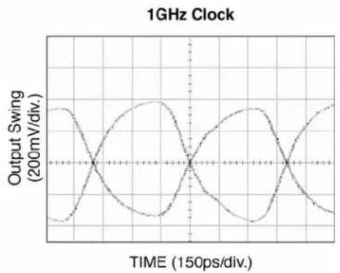
line
| TIME (150ps/div.) | Output Swing (200mV/div.) | | ----------------- | ------------------------- | | 0 | 0 | | 150 | 200 | | 300 | 0 | | 450 | -200 | | 600 | 0 | | 750 | 200 | | 900 | 0 | | 1050 | -200 | | 1200 | 0 | | 1350 | 200 | | 1500 | 0 | | 1650 | -200 | | 1800 | 0 | | 1950 | 200 | | 2100 | 0 | | 2250 | -200 | | 2400 | 0 | | 2550 | 200 | | 2700 | 0 | | 2850 | -200 | | 3000 | 0 | | 3150 | 200 | | 3300 | 0 | | 3450 | -200 | | 3600 | 0 | | 3750 | 200 | | 3900 | 0 | | 4050 | -200 | | 4200 | 0 | | 4350 | 200 | | 4500 | 0 | | 4650 | -200 | | 4800 | 0 | | 4950 | 200 | | 5100 | 0 | | 5250 | -200 | | 5400 | 0 | | 5550 | 200 | | 5700 | 0 | | 5850 | -200 | | 6000 | 0 | | 6150 | 200 | | 6300 | 0 | | 6450 | -200 | | 6600 | 0 | | 6750 | 200 | | 6900 | 0 | | 7150 | -200 | | 7311 | 0 | | 7471 | 200 | | 7631 | 0 | | 7791 | -200 | | 7951 | 0 | | 8111 | 200 | | 8271 | 0 | | 8431 | -200 | | 8591 | 0 | | 8751 | 200 | | 8911 | 0 | | 9111 | -200 | | 9271 | 0 | | 9431 | 200 | | 9611 | 0 | | 9771 | -200 | | 9931 | 0 | | | |
line
| TIME (100ps/div.) | Output Swing (200mV/div.) | | ----------------- | ------------------------- | | 0 | 0 | | 1 | 1 | | 2 | 0 | | 3 | -1 | | 4 | 0 | | 5 | 1 | | 6 | 0 | | 7 | -1 | | 8 | 0 | | 9 | 1 | | 10 | 0 | | 11 | -1 | | 12 | 0 | | 13 | 1 | | 14 | 0 | | 15 | -1 | | 16 | 0 | | 17 | 1 | | 18 | 0 | | 19 | -1 | | 20 | 0 | | 21 | 1 | | 22 | 0 | | 23 | -1 | | 24 | 0 | | 25 | 1 | | 26 | 0 | | 27 | -1 | | 28 | 0 | | 29 | 1 | | 30 | 0 | | 31 | -1 | | 32 | 0 | | 33 | 1 | | 34 | 0 | | 35 | -1 | | 36 | 0 | | 37 | 1 | | 38 | 0 | | 39 | -1 | | 40 | 0 | | 41 | 1 | | 42 | 0 | | 43 | -1 | | 44 | 0 | | 45 | 1 | | 46 | 0 | | 47 | -1 | | 48 | 0 | | 49 | 1 | | 50 | 0 | | 51 | -1 | | 52 | 0 | | 53 | 1 | | 54 | 0 | | 55 | -1 | | 56 | 0 | | 57 | 1 | | 58 | 0 | | 59 | -1 | | 60 | 0 | | 61 | 1 | | 62 | 0 | | 63 | -1 | | 64 | 0 | | 65 | 1 | | 66 | 0 | | 67 | -1 | | 68 | 0 | | 69 | 1 | | 70 | 0 | | 71 | -1 | | 72 | 0 | | 73 | 1 | | 74 | 0 | | 75 | -1 | | 76 | 0 | | 77 | 1 | | 78 | 0 | | 79 | -1 | | 80 | 0 | | 81 | 1 | | 82 | 0 | | 83 | -1 | | 84 | 0 | | 85 | 1 | | 86 | 0 | | 87 | -1 | | 88 | 0 | | 89 | 1 | | 90 | 0 | | 91 | -1 | | 92 | 0 | | 93 | 1 | | 94 | 0 | | 95 | -1 | | 96 | 0 | | 97 | 1 | | 98 | 0 | | 99 | -1 | | 100 | 0 |Single-Ended and Differential Swings

text_image
V_IN, V_OUT 800mV (typical)Figure 2a. Single-Ended Voltage Swing
text_image
VDIFF_IN, VDIFF_OUT 1600mV (typical)Figure 2b. Differential Voltage Swing
Input and Output Stages
text_image
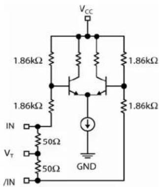
VCC 1.86kΩ 1.86kΩ 1.86kΩ IN 50Ω VT 50Ω /IN GNDFigure 3a. Simplified Differential Input Stage

text_image
VCC /Q QFigure 3b. Simplified Differential Output Stage
Input Interface Applications
text_image
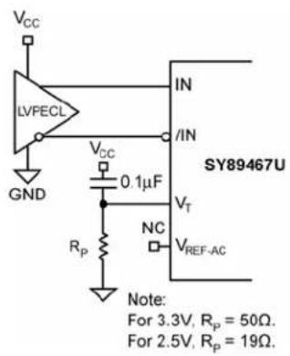
VCC LVFECL GND VCC 0.1μF RP NC VREF-AC IN /IN VT SY89467U Note: For 3.3V, RP = 50Ω. For 2.5V, RP = 19Ω.Figure 4a. LVPECL Interface (DC-Coupled)

text_image
VCC LVPECL GND Rp Rp GND IN IN VCC 0.1μF VT VREF-AC SY89467U Note: For 3.3V, Rp = 100Ω. For 2.5V, Rp = 50Ω.Figure 4b. LVPECL Interface (AC-Coupled)
text_image
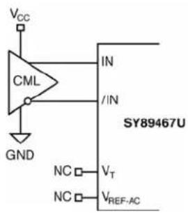
VCC CML IN /IN GND SY89467U NC □ VT NC □ VREF-ACOption: may connect V_T to V_CC
Figure 4c. CML Interface (DC-Coupled)

text_image
VCC CML GND IN IN VCC 0.1μF SY89467U VT VREF-ACFigure 4d. CML Interface (AC-Coupled)

text_image
VCC LVDS IN /IN GND SY89467U NC VT NC VREF-ACFigure 4e. LVDS Interface (DC-Coupled)
PECL Output Interface Applications
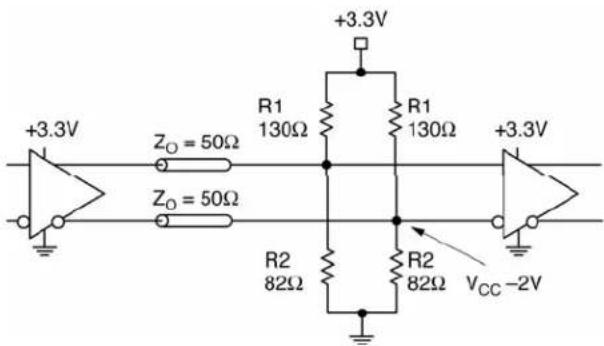
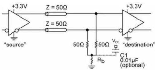
PECL has a high input impedance, a very low output impedance (open emitter), and a small signal swing which results in low EMI. PECL is ideal for driving 50ohm and 100ohm-controlled impedance transmission lines. There are several techniques for terminating the PECL output: parallel termination-thevenin equivalent, parallel termination (3-resistor), and AC-coupled termination. Unused output pairs may be left floating. However, single-ended outputs must be terminated or balanced.
text_image
+3.3V Z₀ = 50Ω Z₀ = 50Ω R1 130Ω +3.3V R1 130Ω +3.3V R2 82Ω R2 82Ω VCC -2VFigure 5a. Parallel Termination-Thevenin Equivalent
text_image
+3.3V Z = 50Ω Z = 50Ω "source" 50Ω 50Ω Vcc C1 0.01μF (optional) +3.3V "destination"Notes:
1. Power-saving alternative to Thevenin termination.
2. Place termination resistors as close to destination inputs as possible.
3. Rb resistor sets the DC bias voltage.
4. For 2.5V systems, R_b = 19 . For 3.3V systems, R_b = 50 .
Figure 5b. Parallel Termination (3-Resistor)
Related Product and Support Documentation
| Part Number Function Data Sheet Link | ||
| SY89468U | Precision LVDS 1:20 Fanout MUX with 2:1 MUX and internal termination with Fail Safe Input | http://www.micrel.com/_PDF/HBW/sy89467u.pdf#page=2 |
| MLF® Application Note | www.amkor.com/products/notes_papers/MLFAppNote.pdf | |
| HBW Solutions | New Products and Applications | www.micrel.com/product-info/products/solutions.shtml |
Package Information

text_image
12.00 [0.472] BSC SQ. 10.00 [0.394] BSC SQ. 4.50 ±0.03 [0.177 ±0.03] 64 49 48 4.50 ±0.03 [0.177 ±0.03] 16 17 32 33
text_image
1.20 [0.047] MAX. 0.60 [0.020] BSC SEE DETAIL "A" 0.01 [0.004] 0.22 +0.05 -0.06 +0.002 [0.009 -0.002]
text_image
DETAIL "A" 0° MIN. 0.20 [0.008] 0.09 [0.004] 0.15 [0.006] 0.05 [0.002] 0-7* 0.60 +0.15 [0.024 +0.366] 1.00 [0.039] REF.NOTES:
1. DIMENSIONS ARE IN MM[INCHES].
2. CONTROLLING DIMENSION: MM.
3. EXPOSED PAD: Cu WITH Sn/Pb PLATING.
4. DIMENSION DOES NOT INCLUDE MOLD FLASH OF 0.254[0.010] MAX.
5. DIE UP ORIENTATION SHOWN. EXPOSED PAD IS VISIBLE FROM BOTTOM OF PACKAGE.
6. MAXIMUM AND MINIMUM SPECIFICATIONS ARE INDICATED AS FOLIOWS: MAX
MIN
7. THIS DIMENSION INCLUDES LEAD FINISH.
64-Pin EPAD-TQFP (T64-1)
Packages Notes:
- Package meets Level 2 Moisture Sensitivity Classification.
- All parts are dry-packed before shipment.
- Exposed pad must be soldered to a ground for proper thermal management.
MICREL, INC. 2180 FORTUNE DRIVE SAN JOSE, CA 95131 USA
TEL +1 (408) 944-0800 FAX +1 (408) 474-1000 WEB http://www.micrel.com
The information furnished by Micrel in this data sheet is believed to be accurate and reliable. However, no responsibility is assumed by Micrel for its use. Micrel reserves the right to change circuitry and specifications at any time without notification to the customer.
Micrel Products are not designed or authorized for use as components in life support appliances, devices or systems where malfunction of a product can reasonably be expected to result in personal injury. Life support devices or systems are devices or systems that (a) are intended for surgical implant into the body or (b) support or sustain life, and whose failure to perform can be reasonably expected to result in a significant injury to the user. A Purchaser's use or sale of Micrel Products for use in life support appliances, devices or systems is a Purchaser's own risk and Purchaser agrees to fully indemnify Micrel for any damages resulting from such use or sale.
© 2007 Micrel. Inc.