USB2229 - Electronic component Microchip - Free user manual and instructions
Find the device manual for free USB2229 Microchip in PDF.

User questions about USB2229 Microchip
0 question about this device. Answer the ones you know or ask your own.
Ask a new question about this device
Download the instructions for your Electronic component in PDF format for free! Find your manual USB2229 - Microchip and take your electronic device back in hand. On this page are published all the documents necessary for the use of your device. USB2229 by Microchip.
USER MANUAL USB2229 Microchip
Design Guidelines for USB22XX/USB260X High-Speed SD
1 Introduction
This application note provides information on Printed Circuit Board layout for High-Speed Secure-Digital (SD) media sockets with USB22XX and USB260X.
2 Overview
Successful High-Speed operation of Secure-Digital media with USB22XX and USB260X requires special consideration for Printed Circuit Board (PCB) layout. This application note describes the important items to consider for layout of PCB.
3 PCB Layout Guidelines
The guidelines presented are applicable to all SMSC card-reader products that support High-Speed Secure-Digital operation. Guidelines for both two-layer and four-layer PCBs are presented here.
3.1 Power and Ground Distribution to SD Socket
Ground connection between the card-reader and the media socket is important, both for supply return current and signal return currents. The ground should be solid, have low impedance and few constrictions between the card-reader and the socket. The card-reader supplies the power to the socket in most applications since the power-FET is built-in to the SMSC card-reader.
■ SD socket VDD supply trace from card-reader should be 20 mils wide, 0.5 oz or thicker for a length up to 3000 mils.
■ SD socket ground connection: plane, 0.5 oz or thicker, between socket and card-reader.
Note: No constrictions or cuts allowed in the ground between card-reader and socket.
3.2 Signal Traces to SD Socket
The Secure-Digital interface has a total of seven signals to the card-reader. Six of these signals are critical for high-speed operation: SD_DAT[0:3], SD_CMD and SD_CLK and require special considerations.
■ Signal traces must be above a solid and continuous ground plane along the path from card-reader to socket.
- SD_CLK trace requires two grounded guard-traces, one on each side spaced, at 3 times minimum spacing.
■ SD_CLK guard traces must have a via connecting to the ground plane at both ends and every 500 mils along the path.
■ SD_CLK termination resistor must be placed close, within 400 mils to the SD_CLK pin on card-reader for two layers PCB.
- SD_CLK termination resistor must be placed close, within 400 mils to socket for four layers PCB.
SD_CLK must be buffered when trace length exceeds 1000 mils. A 74AHC1G125 or equivalent buffer can be used that has less than 2.5 ns propagation delay.
3.3 Signal Trace Length
Trace length for SD signals must be less than the maximum length specified in Table 3.1 and Table 3.2. An external buffer is required for SD_CLK when trace lengths exceed 1000 mils (800 mils excluding the socket itself). Table 3.1 provides the trace length when the unbuffered SD_CLK is driven directly by the SMSC card-reader. Table 3.2 provides the trace length when an external clock buffer is used. The buffer must be connected with a trace shorter than 50 mils to the card-reader SD_CLK pin. Skew control between data lines is not critical within the limits given in the tables.
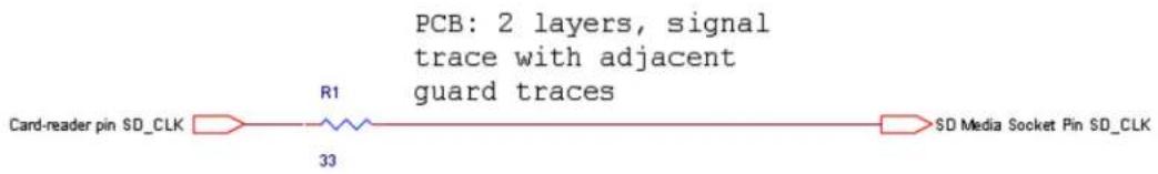
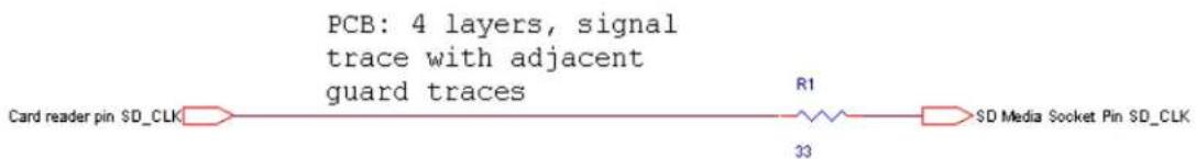
Figure 4.1 and Figure 4.2 show the suggested placement of a series termination resistor. Figure 4.3 shows the series termination resistor when an external buffer is used with a long SD_CLK trace. The details for guarding of the SD_CLK are shown in Figure 5.1.
Table 3.1 Trace length and tolerance for unbuffered SD_CLK
| Signal | Maximum Trace Length (including socket) [mils] | PCB Trace Impedance 2-layer PCB [Ohm] | PCB Trace Impedance 4-layer PCB [Ohm] | Trace Length Tolerance [mils] | Maximum Trace Length difference to SD_CLK [mils] |
| SD_CLK | 1000 100 - 130 > | 55 N/A N/A | |||
| SD_DAT[0:3] | 2500 80 - 150 > 50 | +/- 750 | -250 to +1500 | ||
| SD_CMD | 2500 80 - 150 > 50 | N/A -250 to + 1500 |
Table 3.2 Trace length and tolerance for buffered SD_CLK
| Signal | Maximum Trace Length (including socket) [mils] | PCB Trace Impedance 2-layer PCB [Ohm] | PCB Trace Impedance 4-layer PCB [Ohm] | Trace Length Tolerance [mils] | Maximum Trace Length difference to SD_CLK [mils] |
| SD_CLK | 3000 80 - 150 > 5 | 5 N/A N/A | |||
| SD_DAT[0:3] | 3500 80 - 150 > 5 | 50 +/- 750 | -500 to +500 | ||
| SD_CMD | 3500 80 - 150 > 5 | 50 N/A -500 to +500 |
Note: Trace length includes 200 mils for trace inside the socket.
4 Placement of Series Termination Resistor and Buffer
text_image
PCB: 2 layers, signal trace with adjacent guard traces Card-reader pin SD_CLK R1 33 SD Media Socket Pin SD_CLKFigure 4.1 Place series termination resistor close to card-reader pin SD_CLK for two layer PCBs.
text_image
PCB: 4 layers, signal trace with adjacent guard traces Card reader pin SD_CLK R1 33 SD Media Socket Pin SD_CLKFigure 4.2 Place series termination resistor close to media socket pin SD_CLK for four layer PCBs.

text_image
PCB: 2 or 4 layers when SD_CLK trace is longer than 800 mils Card reader pin SD_CLK SD_VDD U1 74AHC1G125 R1 33 SD Media Socket Pin SD_CLKFigure 4.3 Place buffer and series termination resistor close to card reader pin SD_CLK when SD_CLK trace is longer than 800 mils not including the socket.
5 Guarding of SD\_CLK

text_image
SD CLK Guard all components in the clock path. GND vias 1X spacing Ex. 7 mils < 400 mils All Guard vias 3X spacing Guards Using Floods Guards Using Traces < 400 mils All Guard viasFigure 5.1 Detailed view of guard trace for SD_CLK signal. Either flood or trace can be used.

SMSC™
80 Arkay Drive
Hauppauge, NY 11788
(631)
435-6000
FAX (631) 273-3123
Copyright © 2006 SMSC or its subsidiaries. All rights reserved.
Circuit diagrams and other information relating to SMSC products are included as a means of illustrating typical applications. Consequently, complete information sufficient for construction purposes is not necessarily given. Although the information has been checked and is believed to be accurate, no responsibility is assumed for inaccuracies. SMSC reserves the right to make changes to specifications and product descriptions at any time without notice. Contact your local SMSC sales office to obtain the latest specifications before placing your product order. The provision of this information does not convey to the purchaser of the described semiconductor devices any licenses under any patent rights or other intellectual property rights of SMSC or others. All sales are expressly conditional on your agreement to the terms and conditions of the most recently dated version of SMSC's standard Terms of Sale Agreement dated before the date of your order (the "Terms of Sale Agreement"). The product may contain design defects or errors known as anomalies which may cause the product's functions to deviate from published specifications. Anomaly sheets are available upon request. SMSC products are not designed, intended, authorized or warranted for use in any life support or other application where product failure could cause or contribute to personal injury or severe property damage. Any and all such uses without prior written approval of an Officer of SMSC and further testing and/or modification will be fully at the risk of the customer. Copies of this document or other SMSC literature, as well as the Terms of Sale Agreement, may be obtained by visiting SMSC's website at http://www.smsc.com. SMSC is a registered trademark of Standard Microsystems Corporation ("SMSC"). Product names and company names are the trademarks of their respective holders.
SMSC DISCLAIMS AND EXCLUDES ANY AND ALL WARRANTIES, INCLUDING WITHOUT LIMITATION ANY AND ALL IMPLIED WARRANTIES OF MERCHANTABILITY, FITNESS FOR A PARTICULAR PURPOSE, TITLE, AND AGAINST INFRINGEMENT AND THE LIKE, AND ANY AND ALL WARRANTIES ARISING FROM ANY COURSE OF DEALING OR USAGE OF TRADE. IN NO EVENT SHALL SMSC BE LIABLE FOR ANY DIRECT, INCIDENTAL, INDIRECT, SPECIAL, PUNITIVE, OR CONSEQUENTIAL DAMAGES; OR FOR LOST DATA, PROFITS, SAVINGS OR REVENUES OF ANY KIND; REGARDLESS OF THE FORM OF ACTION, WHETHER BASED ON CONTRACT; TORT; NEGLIGENCE OF SMSC OR OTHERS; STRICT LIABILITY; BREACH OF WARRANTY; OR OTHERWISE; WHETHER OR NOT ANY REMEDY OF BUYER IS HELD TO HAVE FAILED OF ITS ESSENTIAL PURPOSE, AND WHETHER OR NOT SMSC HAS BEEN ADVISED OF THE POSSIBILITY OF SUCH DAMAGES.