MIC2874 - Electronic component Microchip - Free user manual and instructions
Find the device manual for free MIC2874 Microchip in PDF.

User questions about MIC2874 Microchip
0 question about this device. Answer the ones you know or ask your own.
Ask a new question about this device
Download the instructions for your Electronic component in PDF format for free! Find your manual MIC2874 - Microchip and take your electronic device back in hand. On this page are published all the documents necessary for the use of your device. MIC2874 by Microchip.
USER MANUAL MIC2874 Microchip
1.2A High-Brightness Flash LED Driver with Single-Wire Serial Interface
Features
- Up to 1.2A Flash LED Driving Current
• Highly Efficient Synchronous Boost Driver
• Control through Single-Wire Serial Interface or External Control Pin - Input Voltage Range: 2.7V to 5.5V
- True Load Disconnect
- Configurable Safety Time-Out Protection
• Output Overvoltage Protection (OVP)
• LED Short Detection and Protection
• 1 μA Shutdown Current
• Available in 9-Bump 1.30 mm x 1.30 mm WLCSP Package
General Description
The MIC2874 is a high-current, high-efficiency Flash LED driver. The LED driver current is generated by an integrated inductive boost converter with a 4 MHz switching frequency, which allows for the use of a very small inductor and output capacitor. These features make the MIC2874 an ideal solution for high-resolution camera phone LED Flash light driver applications.
MIC2874 operates in either Flash or Torch mode that can be controlled through the single-wire serial interface and/or external control pin. A robust single-wire serial interface allows the host processor to control the LED current and brightness. The MIC2874 is available in a 9-bump 1.30 mm x 1.30 mm WLCSP package.
Applications
• Camera Phones/Mobile Handsets
• Cell Phones/Smartphones
• LED Light for Image Capture/Auto-Focus/White Balance
- Handset Video Light (Torch Light)
- Digital Cameras
- Portable Applications
Package Type
MIC2874
9-Bump 1.30 mm x 1.30 mm WLCSP (CS)
(Top View)
text_image
1 2 3 A LED DC OUT B LGND FEN SW C AGND V IN PGNDNote: WLCSP Bump A1 identifier = “•”.
Typical Application Schematic
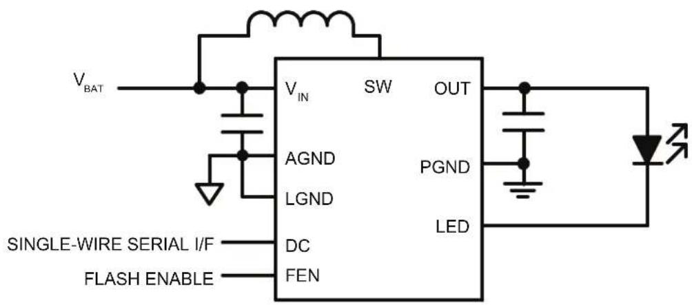
text_image
VBAT VIN SW OUT AGND PGND LGND DC LED FLASH ENABLEFunctional Block Diagram
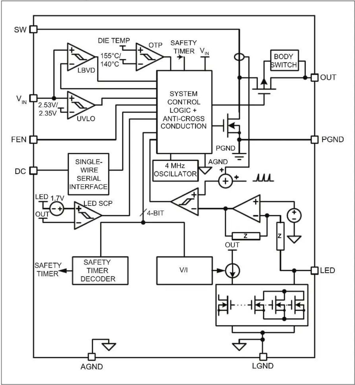
flowchart
graph TD
    SW --> LBVD
    LBVD --> DIE_TEMP
    DIE_TEMP --> OUT
    OUT --> V_IN
    V_IN --> 2.53V/2.35V
    2.53V/2.35V --> UVLO
    UVLO --> SYSTEM_CONTROL_LOGIC["SYSTEM CONTROL LOGIC + ANTI-CROSS CONDUCTION"]
    SYSTEM_CONTROL_LOGIC --> Safety_TIMER
    Safety_TIMER --> V_IN
    Safety_TIMER --> 4MHz_OSCILLATOR
    4MHz_OSCILLATOR --> AGND
    AGND --> PGND
    PGND --> OUT
    FEN --> SINGLE_WIRE_SERIAL_INTERFACE
    SINGLE_WIRE_SERIAL_INTERFACE --> LED_SCP
    LED_SCP --> 4-BIT
    4-BIT --> Safety_TIMER
    Safety_TIMER --> V/I
    V/I --> OUT
    OUT --> LGND
    LGND --> LED
    LED --> AGND
    AGND --> SAFETY_TIMER
    SAFETY_TIMER --> Safety_TIMER_DECODER
    Safety_TIMER_DECODER --> 4-BIT
    4-BIT --> Z
    Z --> OUT
    OUT --> V/I
    V/I --> Safety_TIMER
    Safety_TIMER --> 4-BIT
    Safety_TIMER --> 4-BIT
    Safety_TIMER --> 4-BIT
    Safety_TIMER --> 4-BIT
    Safety_TIMER --> 4-BIT
    Safety_TIMER --> 4-BIT
    Safety_TIMER --> 4-BIT
    Safety_TIMER --> 4-BIT
    Safety_TIMER --> 4-BIT
    Safety_TIMER --> 4-BIT
    Safety_TIMER --> 4-BIT
    Safety_TIMER --> 4-BIT
1.0 ELECTRICAL CHARACTERISTICS
Absolute Maximum Ratings†
Input Voltage ( V_IN )....-0.3V to +6.0V
General I/O Voltage ( V_FEN )....-0.3V to V_IN
V_OUT and V_LED Voltage....-0.3V to +6.0V
Single-Wire I/O Voltage ( V_DC )....-0.3V to V_IN
V_SW Voltage -0.3V to +6.0V
ESD Rating ^(1)
HBM 2 kV
MM....200V
Notice: Stresses above those listed under “Maximum Ratings” may cause permanent damage to the device. This is a stress rating only and functional operation of the device at those or any other conditions above those indicated in the operational sections of this specification is not intended. Exposure to maximum rating conditions for extended periods may affect device reliability.
Note 1: Devices are ESD-sensitive. Handling precautions are recommended. Human body model, 1.5 kΩ in series with 100 pF.
Operating Ratings ^(1)
Input Voltage ( V_IN )....+2.7V to +5.5V
Enable Input Voltage ( V_FEN )....0V to V_IN
Single-Wire I/O Voltage ( V_DC ) 0V to V_IN
Power Dissipation ( P_D ). Internally Limited ^(2)
Note 1: The device is not ensured to function outside the operating range.
2: The maximum allowable power dissipation at any T_A (ambient temperature) is P_D() = (T_J() - T_A)/_JA . Exceeding the maximum allowable power dissipation will result in excessive die temperature and the regulator will go into thermal shutdown.
TABLE 1-1: ELECTRICAL CHARACTERISTICS (Note 1)
| Electrical Specifications: unless otherwise specified, V_IN =3.6V; L=0.47 μH; C_OUT =4.7 μF; I_OUT =100 mA; T_A = T_J =+25°C. Boldface values indicate -40°C ≤ T_J ≤ +125°C. | ||||||
| Parameter Symbol | Min. Typ. Max. | Units Test | Conditions | |||
| Power Supply | ||||||
| Supply Voltage Range V | IN | 2.7 | — | 5.5 | V | — |
| UVLO Threshold (rising) | V_UVLO\_R | 2.41 | 2.53 | 2.68 | V | — |
| UVLO Hysteresis | V_UVLO\_HYS | — | 180 | — | mV | — |
| Standby Current | I_STB | 150 | 185 | 220 | μA | V_DC =3.6V, V_FEN =0V, boost regulator and LED current driver are both off |
| Shutdown Current | I_SD | — | 1 | 2 | μA | V_DC =0V |
| Maximum Duty Cycle | D_MAX | 82 | 86 | 90 | % | — |
| Minimum Duty Cycle | D_MIN | — | 6.4 | — | % | — |
| Switch Current Limit | I_SW | — | 4.1 | — | A | V_IN = V_OUT =2.7V |
| Switch-On Resistance | R_DS(ON)_P | — | 125 | — | mΩ | I_SW =100 mA |
| R_DS(ON)_N | — | — | I_SW =100 mA | |||
| Switch Leakage Current | I_SW\_LK | — | 0.01 | 1 | μA | V_DC =0V, V_SW =5.5V |
| Oscillator Frequency | F_SW | 3.6 | 4 | 4.4 | MHz | — |
| Overtemperature Shutdown Threshold | T_SD | — | 155 | — | °C | — |
| Overtemperature Shutdown Hysteresis | T_SD\_HYS | — | 15 | — | °C | — |
| Safety Time-out Shutdown | T_TO | — | 1.25 | — | s Default timer setting | |
| Safety Timer Current Threshold | I_TO | — | 250 | — | mA | Default current threshold setting |
| Low-Battery Voltage Detection Threshold | V_LBVD | — | 3.0 | — | V | Default LBVD threshold setting |
| Low-Battery Voltage Detection Threshold Accuracy | — | — | 50 | — | mV | All low-battery voltage detection threshold settings |
| LED Short-Circuit Detection Voltage Threshold | V_SHORT | 1.55 | 1.7 | 1.85 | V | V_OUT-V_LED |
| LED Short-Circuit Detection Test Current | I_TEST | 1.6 | 2 | 2.7 | mA | — |
| Current Sink Channel | ||||||
| Channel Current Accuracy | — | -6 | — | 6 | % | V_OUT =4.2V, I_LED =0.20A |
| -8 | — | 8 | V_OUT =4.2V, I_LED =1.0A | |||
| Current Sink Voltage Dropout | V_LED | — | 250 | — | mV | Boost mode |
| FEN Control Pin | ||||||
| FEN High-Level Voltage | V_FEN\_H | 1.3 — | — | V | Flash is on | |
| FEN Low-Level Voltage | V_FEN\_L | — | — | 0.6 Flash is off | ||
| FEN Pull-Down Current | I_FEN\_PD | — | 1.3 | 5 | μA | V_FEN =5.5V |
Note 1: Specification for packaged product only.
TABLE 1-2: ELECTRICAL CHARACTERISTICS – SINGLE-WIRE INTERFACE (ENSURED BY DESIGN)
| Electrical Specifications: unless otherwise specified, V_IN = 3.6V ; L = 0.47 μH; C_OUT = 4.7 μF; I_OUT = 100 mA ; T_A = T_J = +25°C . Boldface values indicate -40°C ≤ T_J ≤ +125°C. | ||||||
| Parameter Symbol | Min. Typ. Max. | Units Test | Conditions | |||
| Low-Level Input Voltage V | L | — | — | 0.4 | V | — |
| High-Level Input Voltage V | H | 1.3 | — | — | — | |
| DC Pull-Down Current | I_DC\_PD | — | 2.8 | 5 | μA | V_DC = 5.5V |
| On Time | T_ON | 0.1 | — | 72 | μs | — |
| Off Time | T_OFF | 0.1 | — | 72 | μs | — |
| Latch Time | T_LAT | 97 | — | 324 | μs | — |
| End Time | T_END | 405 | — | — | μs | — |
TEMPERATURE SPECIFICATIONS (Note 1)
| Parameters Symbol Min. | Typ. Max. | Units Conditions | ||||
| Temperature Ranges | ||||||
| Maximum Junction Temperature Range T | J | -40 — | 150 °C — | |||
| Operating Junction Temperature Range T | J | -40 — | 125 °C — | |||
| Operating Ambient Temperature | T_A | -40 — | 85 | °C — | ||
| Storage Temperature | T_S | -40 — | 150 °C — | |||
| Lead Temperature | — | — | — | 260 | °C | Soldering, 10s |
| Package Thermal Resistance | ||||||
| Thermal Resistance 1.3x1.3 WLCSP-9BL | _JA | — | 84 | — | °C/W | — |
Note 1: The maximum allowable power dissipation is a function of ambient temperature, the maximum allowable junction temperature and the thermal resistance from junction to air (i.e., T_A , T_J , _JA ). Exceeding the maximum allowable power dissipation will cause the device operating junction temperature to exceed the maximum +150°C rating. Sustained junction temperatures above +150°C can impact the device reliability.
2.0 TYPICAL CHARACTERISTIC CURVES
Note: The graphs and tables provided following this note are a statistical summary based on a limited number of samples and are provided for informational purposes only. The performance characteristics listed herein are not tested or guaranteed. In some graphs or tables, the data presented may be outside the specified operating range (e.g., outside specified power supply range) and therefore outside the warranted range.
line
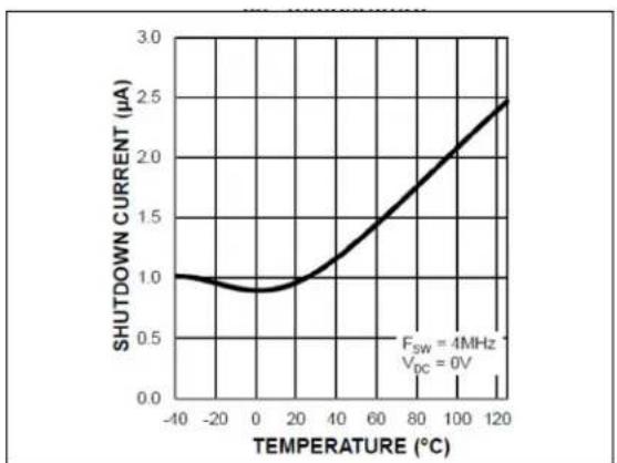
| TEMPERATURE (°C) | SHUTDOWN CURRENT (μA) | | ---------------- | ---------------------- | | -40 | 1.0 | | 0 | 0.9 | | 20 | 1.0 | | 40 | 1.2 | | 60 | 1.5 | | 80 | 1.8 | | 100 | 2.2 | | 120 | 2.5 |FIGURE 2-1: Shutdown Current vs. Temperature.
line
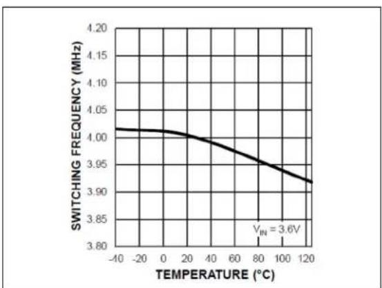
| TEMPERATURE (°C) | SWITCHING FREQUENCY (MHz) | | ---------------- | -------------------------- | | -10 | 4.01 | | 0 | 4.00 | | 20 | 3.99 | | 40 | 3.97 | | 60 | 3.95 | | 80 | 3.93 | | 100 | 3.91 | | 120 | 3.89 |FIGURE 2-4: Switching Frequency vs. Temperature.
line
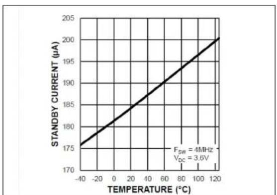
| TEMPERATURE (°C) | STANDBY CURRENT (μA) | | ---------------- | -------------------- | | -40 | 175 | | 0 | 180 | | 20 | 185 | | 40 | 190 | | 60 | 195 | | 80 | 200 | | 100 | 205 | | 120 | 210 |FIGURE 2-2: Standby Current vs. Temperature.

line
| TEMPERATURE (°C) | MAXIMUM DUTY CYCLE (%) | | ---------------- | ---------------------- | | -40 | 85 | | 0 | 87 | | 20 | 88 | | 40 | 87 | | 60 | 85 | | 80 | 83 | | 100 | 81 | | 120 | 80 |FIGURE 2-5: Maximum Duty Cycle vs. Temperature.

line
| TEMPERATURE (°C) | UVLO THRESHOLD (V) | | ---------------- | ------------------ | | -40 | 2.5 | | 0 | 2.5 | | 20 | 2.5 | | 40 | 2.5 | | 60 | 2.5 | | 80 | 2.5 | | 100 | 2.5 | | 120 | 2.5 |FIGURE 2-3: UVLO Thresholds vs. Temperature.
line
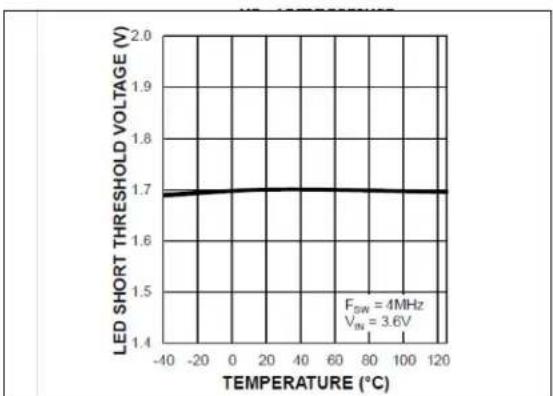
| TEMPERATURE (°C) | LED SHORT THRESHOLD VOLTAGE (V) | | ---------------- | ------------------------------- | | -40 | 1.7 | | 0 | 1.7 | | 20 | 1.7 | | 40 | 1.7 | | 60 | 1.7 | | 80 | 1.7 | | 100 | 1.7 | | 120 | 1.7 |FIGURE 2-6: LED Short Threshold Voltage vs. Temperature.

line
| TEMPERATURE (°C) | LED SHORT TEST CURRENT (mA) | | ---------------- | --------------------------- | | -40 | 2.1 | | 0 | 2.05 | | 20 | 2.0 | | 40 | 1.95 | | 60 | 1.9 | | 80 | 1.85 | | 100 | 1.8 | | 120 | 1.75 |FIGURE 2-7: LED Short Test Current vs. Temperature.

line
| INPUT VOLTAGE (V) | EFFICIENCY (%) | | ----------------- | -------------- | | 2.6 | ~85 | | 3.0 | ~88 | | 3.4 | ~90 | | 3.8 | ~90 | | 4.2 | ~88 | | 4.6 | ~75 | | 5.0 | ~65 |FIGURE 2-10: WLED Power Efficiency vs. Input Voltage ( V_F = 3.8V ).
line
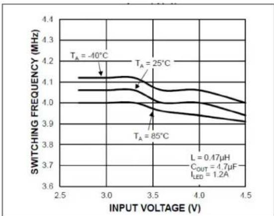
| INPUT VOLTAGE (V) | SWITCHING FREQUENCY (MHz) | | ----------------- | -------------------------- | | 2.5 | 4.1 | | 3.0 | 4.1 | | 3.5 | 4.0 | | 4.0 | 3.9 | | 4.5 | 3.9 |FIGURE 2-8: Boost Switching Frequency vs. Input Voltage.

line
| INPUT VOLTAGE (V) | FULL TORCH ILED ACCURACY (%) | | ----------------- | ----------------------------- | | 2.5 | -2.0 | | 3.0 | -6.0 | | 3.5 | 1.0 | | 4.0 | 1.5 | | 4.5 | 1.8 | | 5.0 | 2.0 | | 5.5 | 2.2 |FIGURE 2-11: Full Torch ILED Accuracy vs. Input Voltage.

line
| INPUT VOLTAGE (V) | EFFICIENCY (%) | LED Current (mA) | | ----------------- | -------------- | ---------------- | | 2.6 | ~85 | 1.2 | | 3.0 | ~88 | 1.0 | | 3.4 | ~90 | 600 | | 3.8 | ~90 | 400 | | 4.2 | ~75 | 250 | | 4.6 | ~65 | 100 | | 5.0 | ~60 | — |FIGURE 2-9: WLED Power Efficiency vs. Input Voltage ( V_F = 3.4V ).
line
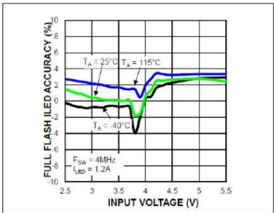
| INPUT VOLTAGE (V) | FULL FLASH ILED ACCURACY (%) | | ----------------- | ----------------------------- | | 2.5 | ~3 | | 3.0 | ~2 | | 3.5 | ~1 | | 4.0 | ~0 | | 4.5 | ~3 | | 5.0 | ~3 | | 5.5 | ~3 |FIGURE 2-12: Full Flash ILED Accuracy vs. Input Voltage.
line
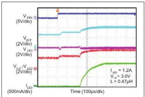
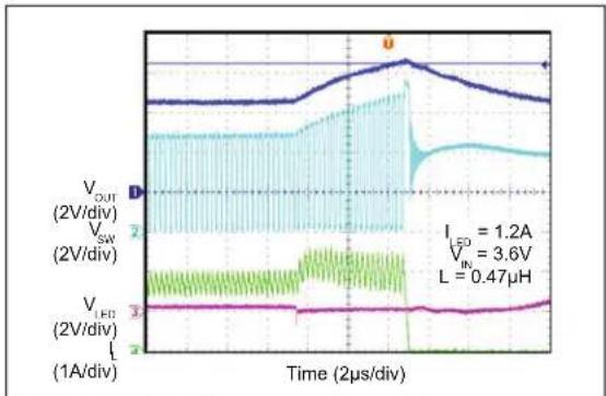
| Time (100μs/div) | V_FEN (5V/div) | V_OUT (2V/div) | V_LED (2V/div) | V_OUT - V_LED (2V/div) | I_LED (500mA/div) | | ---------------- | -------------- | -------------- | -------------- | ------------------------ | ----------------- | | 0 | ~1.0 | ~1.0 | ~1.0 | ~1.0 | ~1.0 | | 100 | ~1.0 | ~1.0 | ~1.0 | ~1.0 | ~1.0 | | 200 | ~1.0 | ~1.0 | ~1.0 | ~1.0 | ~1.0 | | 300 | ~1.0 | ~1.0 | ~1.0 | ~1.0 | ~1.0 | | 400 | ~1.0 | ~1.0 | ~1.0 | ~1.0 | ~1.0 | | 500 | ~1.0 | ~1.0 | ~1.0 | ~1.0 | ~1.0 | | 600 | ~1.0 | ~1.0 | ~1.0 | ~1.0 | ~1.0 | | 700 | ~1.0 | ~1.0 | ~1.0 | ~1.0 | ~1.0 | | 800 | ~1.0 | ~1.0 | ~1.0 | ~1.0 | ~1.0 | | 900 | ~1.0 | ~1.0 | ~1.0 | ~1.0 | ~1.0 | | 1000 | ~1.0 | ~1.0 | ~1.0 | ~1.0 | ~1.0 | | 1100 | ~1.0 | ~1.0 | ~1.0 | ~1.0 | ~1.0 | | 1200 | ~1.0 | ~1.0 | ~1.0 | ~1.0 | ~1.0 | | 1300 | ~1.0 | ~1.0 | ~1.0 | ~1.0 | ~1.0 | | 1400 | ~1.0 | ~1.0 | ~1.0 | ~1.0 | ~1.0 | | 1500 | ~1.0 | ~1.0 | ~1.0 | ~1.0 | ~1.0 | | 1600 | ~1.0 | ~1.0 | ~1.0 | ~1.0 | ~1.0 | | 1700 | ~1.0 | ~1.0 | ~1.0 | ~1.0 | ~1.0 | | 1800 | ~1.0 | ~1.0 | ~1.0 | ~1.0 | ~1.0 | | 1900 | ~1.0 | ~1.0 | ~1.0 | ~1.0 | ~1.0 | | 2000 | ~1.0 | ~1.0 | ~1.0 | ~1.0 | ~1.0 | | 2100 | ~1.0 | ~1.0 | ~1.0 | ~1.0 | ~1.0 | | 2200 | ~1.0 | ~1.0 | ~1.0 | ~1.0 | ~1.0 | | 2300 | ~1.0 | ~1.0 | ~1.0 | ~1.0 | ~1.0 | | 2400 | ~1.0 | ~1.0 | ~1.0 | ~1.0 | ~1.0 | | 2500 | ~1.0 | ~1.0 | ~1.0 | ~1.0 | ~1.0 | | 2600 | ~1.0 | ~1.0 | ~1.0 | ~1.0 | ~1.0 | | 2700 | ~1.0 | ~1.0 | ~1.0 | ~1.0 | ~1.0 | | 2800 | ~1.0 | ~1.0 | ~1.0 | ~1.0 | ~1.0 | | 2900 | ~1.0 | ~1.0 | ~1.0 | ~1.0 | ~1.0 | | 3000 | ~1.0 | ~1.0 | ~1.0 | ~1.0 | ~1.0 | | 3100 | ~1.0 | ~1.0 | ~1.0 | ~1.0 | ~1.0 | | 3200 | ~1.0 | ~1.0 | ~1.0 | ~1.0 | ~1.0 | | 3300 | ~1.0 | ~1.0 | ~1.0 | ~1.0 | ~1.0 | | 3400 | ~1.0 | ~1.0 | ~1.0 | ~1.0 | ~1.0 | | 3500 | ~1.0 | ~1.0 | ~1.0 | ~1.0 | ~1.0 | | 3600 | ~1.0 | ~1.0 | ~1.0 | ~1.0 | ~1.0 | | 3700 | ~1.0 | ~1.0 | ~1.0 | ~1.0 | ~1.0 | | 3800 | ~1.0 | ~1.0 | ~1.0 | ~1.0 | ~1.0 | | 3900 | ~1.0 | ~1.0 | ~1.0 | ~1.0 | ~1.0 | | 4000 | ~1.5 | - | - | - | - | | 4587 | - | - | - | - | - | | 5587 | - | - | - | - | - | | 6587 | - | - | - | - | - | | 7587 | - | - | - | - | - | | 8587 | - | - | - | - | - | | 9587 | - | - | - | - | - | | 4587 (labeled) (labeled) I_LFD = 3, v_IN = 3, L = 47μH (labeled) I_LFD = 3, v_IN = 3, L = 47μH (labeled) I_LFD = 3, v_IN = 3, L = 47μH (labeled) I_LFD = 3, v_IN = 3, L = 47μH (labeled) I_LFD = 3, v_IN = 3, L = 47μH (labeled) I_LFD = 3, v_IN = 3, L = 5 μH (labeled) I_LFD = 3, v_IN = 3, L = 5 μH (labeled) I_LFD = 3, v_IN = 3, L = 5 μH (labeled) I_LFD = 3, v_IN = 3, L = 5 μH (labeled) I_LFD = 3, v_IN = 3, L = 5 µH (labeled) I_LFD = 3, v_IN = 3, L = 5 µH (labeled) I_LFD = 3, v_IN = 3, L = 5 µH (labeled) I_LFD = 3, v_IN = 3, L = 5 µH (labeled) I_LFD = 3, v_IN = 3, L = 5 μH (labeled) I_LFD = 3, v_IN = 3, L = 5 µH (labeled) I_LFD = 3, v_IN = 3, L = 5 µH (labeled) I_LFD = 3, v_IN = 3, L = 5 μH (labeled) I_LFD = 3, v_IN = 3, L = 5 μH (labeled) I_LFD = 3, v_IN = 3, L = 5 μH (labeled) I_LFD = 3, v_IN = 3, L = 5 \mu H lFIGURE 2-13: Flash Mode Turn-On Sequence (Boost Mode).
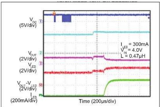
FIGURE 2-16: Torch Mode Turn-On Sequence (Linear Mode).
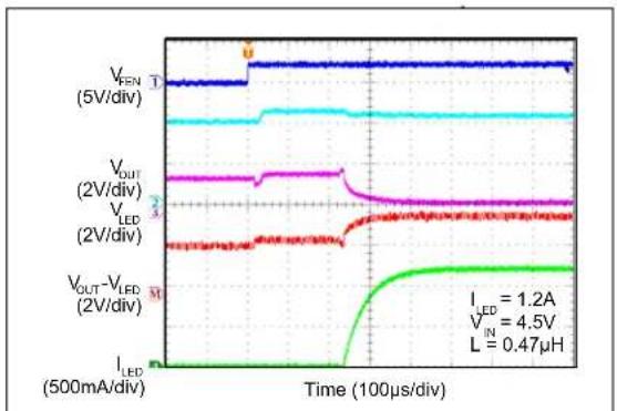
FIGURE 2-14: Flash Mode Turn-On Sequence (Linear Mode).
line
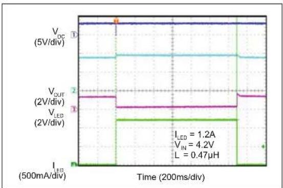
| Time (200ms/div) | V_DC (5V/div) | V_OUT (2V/div) | V_LED (2V/div) | | ---------------- | ------------- | -------------- | -------------- | | I_LED | 1.2A | 1.2A | 1.2A | | V_IN | 4.2V | - | - | | L | 0.47μH | - | - |FIGURE 2-17: Flash Safety Timer at 1250 ms.

line
| Time (200μs/div) | V_DC (5V/div) | V_OUT (2V/div) | V_LED (2V/div) | V_OUT - V_LED (2V/div) | I_LED | | ---------------- | ------------- | -------------- | -------------- | ---------------------- | ----- | | 0 | ~1.0 | ~1.0 | ~1.0 | ~1.0 | ~1.0 | | 200 | ~1.0 | ~1.0 | ~1.0 | ~1.0 | ~1.0 |FIGURE 2-15: Torch Mode Turn-On Sequence (Boost Mode).

line
| Time (200ms/div) | V_DC (5V/div) | V_OUT (2V/div) | V_LED (2V/div) | | ---------------- | ------------- | -------------- | -------------- | | 0 | 1.2A | 4.2V | 0.47μH |FIGURE 2-18: Flash Safety Timer at 156 ms.

line
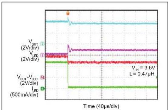
| Time (40μs/div) | V_FN (5V/div) | V_OUT (2V/div) | V_LED (2V/div) | V_OUT - V_LED (2V/div) | I_L (100mA/div) | | --------------- | ------------- | -------------- | -------------- | ---------------------- | ---------------- | | 0 | 3.6 | 0.47 | 0.47 | 0.47 | 0 |FIGURE 2-19: LED Short-Circuit Protection (LED is Shorted by 0Ω).

FIGURE 2-22: Load Disconnect at Shutdown ( V_IN = 5.0V ).

line
| Time (40μs/div) | V_FEN (5V/div) | V_OUT (2V/div) | V_LED (2V/div) | V_OUT - V_LED (2V/div) | I_L (100mA/div) | | --------------- | -------------- | -------------- | -------------- | ---------------------- | --------------- | | 0 | ~0.8 | ~0.8 | ~0.8 | ~0.8 | ~0.8 | | 2 | ~0.8 | ~0.8 | ~0.8 | ~0.8 | ~0.8 | | 4 | ~0.8 | ~0.8 | ~0.8 | ~0.8 | ~0.8 | | 6 | ~0.8 | ~0.8 | ~0.8 | ~0.8 | ~0.8 | | 8 | ~0.8 | ~0.8 | ~0.8 | ~0.8 | ~0.8 | | 10 | ~0.8 | ~0.8 | ~0.8 | ~0.8 | ~0.8 | | 12 | ~0.8 | ~0.8 | ~0.8 | ~0.8 | ~0.8 | | 14 | ~0.8 | ~0.8 | ~0.8 | ~0.8 | ~0.8 | | 16 | ~0.8 | ~0.8 | ~0.8 | ~0.8 | ~0.8 | | 18 | ~0.8 | ~0.8 | ~0.8 | ~0.8 | ~0.8 | | 20 | ~0.8 | ~0.8 | ~0.8 | ~0.8 | ~0.8 | | 22 | ~0.8 | ~0.8 | ~0.8 | ~0.8 | ~0.8 | | 24 | ~0.8 | ~0.8 | ~0.8 | ~0.8 | ~0.8 | | 26 | ~0.8 | ~0.8 | ~0.8 | ~0.8 | ~0.8 | | 28 | ~0.8 | ~0.8 | ~0.8 | ~0.8 | ~0.8 | | 30 | ~0.8 | ~0.8 | ~0.8 | ~0.8 | ~0.8 | | 32 | ~0.8 | ~0.8 | ~0.8 | ~0.8 | ~0.8 | | 34 | ~0.8 | ~0.8 | ~0.8 | ~0.8 | ~0.8 | | 36 | ~0.8 | ~0.8 | ~0.8 | ~0.8 | ~0.8 | | 38 | ~0.8 | ~0.8 | ~0.8 | ~0.8 | ~0.8 | | 40 | 36 | 36 | 36 | 36 | 36 | The chart displays a multi-scale waveform with labeled voltage values and current values at each time point.FIGURE 2-20: LED Short-Circuit Protection (LED is Shorted by 620Ω).

line
| Time (40μs/div) | V_OUT (2V/div) | V_SW (2V/div) | V_LED (2V/div) | | --------------- | -------------- | ------------- | -------------- | | 0 | ~0 | ~0 | ~0 | | Peak | ~1.5 | ~0.8 | ~0.9 | | In | 3.6 | - | - | | L | 0.47 | - | - | | Current (I_L) | - | - | - |FIGURE 2-23: V OUT Overvoltage Protection (Overvoltage during Start-up).

line
| Time (200ms/div) | V_IN (5V/div) | V_OUT (2V/div) | V_LED (2V/div) | I_LED (500mA/div) | | ---------------- | ------------- | -------------- | -------------- | ----------------- | | 0 | 1.2 | 2.7 | 2.7 | 500 |FIGURE 2-21: Load Disconnect at Shutdown ( V_IN = 2.7V ).
line
| Time (2μs/div) | V_OUT (2V/div) | V_SW (2V/div) | V_LED (2V/div) | | -------------- | -------------- | -------------- | --------------- | | 0 | ~0 | ~0 | ~0 | | Peak | ~1.2A | ~3.6V | ~0.47μH | | Low | ~0 | ~0 | ~0 |FIGURE 2-24: V OUT Overvoltage Protection (Overvoltage after Start-up).

line
| Time (100μs/div) | V_OUT (2V/div) | V_LED (2V/div) | V_OUT - V_LED (2V/div) | I_LED (500mA/div) | | ---------------- | -------------- | -------------- | ---------------------- | ----------------- | | 0 | ~2 | ~1 | ~1 | ~0.5 | | 500 | ~2 | ~1 | ~1 | ~0.5 | | 1000 | ~2 | ~1 | ~1 | ~0.5 |FIGURE 2-25: Load Transient (Torch 63 mA to Flash 1.2A).
line
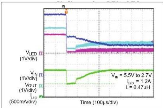
| Time (100μs/div) | V_LED (1V/div) | V_OUT (1V/div) | I_LED (500mA/div) | | ---------------- | -------------- | -------------- | ----------------- | | 0 | 5.5 | 1.2 | 0.47 |FIGURE 2-28: Line Transient (V IN Changes from 5.5V to 2.7V).
line
| Time (40μs/div) | V_IN (V) | L (μH) | | --------------- | -------- | ------ | | 0 | 3.6 | 0.47 |FIGURE 2-26: Load Transient (Flash 1.2A to Torch 63 mA).

line
| Time (400ns/div) | V_IN (2V/div) | V_OUT (2V/div) | V_SW (2V/div) | I_L (1A/div) | | ---------------- | ------------- | -------------- | ------------- | ------------ | | 0 | 3.6 | 5.2 | 0.47 | 0 |FIGURE 2-29: Switch Current Limit.

line
| Time (10μs/div) | V_LED (1V/div) | V_OUT (1V/div) | I_LD | | --------------- | -------------- | -------------- | ---- | | Start | ~0 | ~0 | ~0 | | Peak | ~5.5 | ~5.5 | ~5.5 | | End | ~5.5 | ~5.5 | ~5.5 |FIGURE 2-27: Line Transient (V IN Changes from 2.7V to 5.5V).
3.0 PIN DESCRIPTIONS
The descriptions of the pins are listed in Table 3-1.
TABLE 3-1: PIN FUNCTION TABLE
| MIC2874 Pin Number | Pin Name Pin Function | |
| A1 LED LED Current Sink Pin: Connect the LED anode to OUT and the cathode to this pin. | ||
| A2 DC Single-Wire Interface: Serial control input. | ||
| A3 OUT Boost Converter Output Pin: To be connected to the anode of the LED. Connect a low-ESR ceramic capacitor of at least 4.7 μF at this pin to PGND. | ||
| B1 LGND Linear Ground: LED current return path. | ||
| B2 FEN Flash Mode Enable Pin: Asserting this pin high enables the MIC2874 to enter Flash mode. If this pin is left floating, it is pulled down internally by a built-in 1 μA current source when the device is enabled. | ||
| B3 | SW | Inductor Connection Pin: It is connected to the internal power MOSFETs. |
| C1 | AGND | Analog Ground. |
| C2 | VIN | Supply Input Pin: Connect a low-ESR ceramic capacitor of at least 4.7 μF at this pin to AGND. |
| C3 | PGND | Power Ground: Inductor current return path. |
4.0 FUNCTIONAL DESCRIPTION
4.1 V IN
The input supply provides power to the internal MOSFETs' gate drive and controls circuitry for the Switch mode regulator. The operating input voltage range is from 2.7V to 5.5V. A 4.7 μF low-ESR ceramic input capacitor should be connected from V_N to AGND, as close to MIC2874 as possible, to ensure a clean supply voltage for the device. The minimum voltage rating of 10V is recommended for the input capacitor.
4.2 SW
The MIC2874 has internal low-side and synchronous MOSFET switches. The switch node (SW) between the internal MOSFET switches connects directly to one end of the inductor and provides the current paths during switching cycles.
The other end of the inductor is connected to the input supply voltage. Due to the high-speed switching on this pin, the switch node should be routed away from sensitive nodes wherever possible.
4.3 LGND
This is the ground path of the LED current sink. It should be connected to the AGND on the PCB. The current loop of the Analog Ground should be separated from that of the Power Ground (PGND). LGND and AGND should be connected to PGND at a single point.
4.4 AGND
This is the ground path for the internal biasing and control circuitry. AGND should be connected to the LGND directly. The current loop of the Analog Ground should be separated from that of the Power Ground (PGND). The AGND and LGND should be connected to PGND at a single point.
4.5 PGND
The Power Ground pin is the ground path for the high current in the boost switch. The current loop for the Power Ground should be as small as possible and separate from the Analog Ground (AGND) loop as applicable.
4.6 OUT
This is the boost converter output pin, which is connected to the anode of the LED. A low-ESR ceramic capacitor of 4.7 F or larger should be connected from OUT to PGND, as close as possible to the MIC2874. The minimum voltage rating of 10V is recommended for the output capacitor.
4.7 LED
This is the current sink pin for the LED. The LED anode is connected to the OUT pin and the LED cathode is connected to this pin.
4.8 DC
The DC is a single multiplexed device enable and serial data control pin used for functional control, and communication in GPIO limited applications. When the DC pin is used as a hardware device enable pin, a logic high signal on the DC pin enables the device and a logic low signal on the DC pin disables the device. When the DC pin is used as the single-wire serial interface Digital Control pin, a combination of bit edges and the period between edges is used to communicate a variable length data word across the single wire. Each word is transmitted as a series of pulses, with each pulse incrementing an internal data counter. A stop sequence, consisting of an inactive period, is used to latch the data word internally. Two data words in series received are then used to set a specific register with a specific value for controlling a specific function. The MIC2874 supports five writable registers for controlling Flash mode, Torch mode, safety timer duration, safety timer threshold current and low-battery threshold.
An address/data frame is used to improve protection against erroneous writes where communications are in error. When the DC is in a low state, and no data is detected for longer than 405 s, the MIC2874 will automatically go into a low-power Shutdown state, simultaneously resetting all internal registers to their default states.
4.9 FEN
FEN is the hardware enable pin for Flash mode. A logic low-to-high transition on the FEN pin can initiate the MIC2874 in Flash mode. If FEN is left floating, it is pulled down internally by a built-in 1 A current source when the device is enabled. Flash mode is terminated when FEN is pulled low or left floating and the Flash register is cleared.
5.0 APPLICATION INFORMATION
The MIC2874 can drive a high-current Flash WLED in either Flash mode or Torch mode.
5.1 Boost Converter
The internal boost converter is turned on/off automatically when the LED driver is activated/deactivated without any exception.
The boost converter is an internally compensated Current mode PWM boost converter running at 4 MHz. It is for stepping up the supply voltage to a high enough value at the OUT pin to drive the LED current. If the supply voltage is high enough, the synchronous switch of the converter is then fully turned on. In this case, all the excessive voltage is dropped over the linear LED driver.
5.2 Flash Mode
The maximum and default current levels in the Flash mode are 1.2A and 1A, respectively. The Flash mode current can be initiated by asserting the FEN pin high or by setting the Flash Control register (Address 1) for the desired Flash duration, subjected to the safety time-out setting. The Flash mode current is terminated when the FEN pin is brought low and the Flash register is cleared or when the configurable safety timer expires.
Flash mode current can be adjusted to a fraction of the maximum Flash mode current level by selecting the desired value in the Flash Control register through the single-wire serial interface.
5.3 Torch Mode
By default, the maximum Torch mode level is 300 mA. The Torch mode operation is activated by setting the Torch Control register (Address 2) for the desired duration. The Torch mode current is terminated when the Torch register is cleared or when the configurable safety timer expires.
Like the Flash mode current, the Torch mode current can be set to a fraction of the maximum Torch mode current level by selecting the desired torch current in the Torch Control register (Address 2) via the single-wire serial interface.
5.4 Configurable Safety Timer
The Flash safety time-out feature automatically shuts down the LED current, after the safety timer duration is expired, if the programmed LED current exceeds a certain current threshold. Both the current threshold and the timer duration are programmable via the Safety Timer registers (Addresses 3 and 5).
5.5 Low-Battery Voltage Detection (LBVD)
When the V_IN voltage drops below the LBVD threshold (default = 3.0V) in Flash or Torch mode, the LED current driver is disabled. The LED driver can be resumed by raising the V_IN above the LBVD threshold and toggling the corresponding Flash or torch command. The LBVD threshold is adjustable through the LBVD Control register (Address 4).
5.6 Overvoltage Protection
When the output voltage rises above an internal overvoltage protection (OVP) threshold, MIC2874 is latched off automatically to avoid permanent damage to the IC. To clear the latched off condition, either power cycle the MIC2874 or assert the DC pin low.
5.7 Short-Circuit Detection
Each time, before enabling the LED driver, the MIC2874 performs the short-circuit test by driving the Flash LED with a small (2 mA typical) current for 200 s. If ( V_OUT - V_LED ) is less than 1.7V at the end of the short-circuit test, then the LED is considered to be shorted and MIC2874 will ignore the Flash and/or Torch mode command. Note that the short-circuit test is carried out every time, prior to Flash and Torch mode, but the result is not latched.
5.8 Thermal Shutdown
When the internal die temperature of MIC2874 reaches 155^ C, the LED driver is disabled until the die temperature falls below 140^ C and either the FEN pin, FEN register, TEN register or V_IN is toggled.
5.9 Single-Wire Interface
The single-wire interface allows the use of a single multiplexed enable and data pin (DC) for control and communication in GPIO limited applications. The interface is implemented using a simple mechanism, allowing any open-drain or directly driven GPIO to control the MIC2874.
The MIC2874 uses the single-wire interface for simple command and control functions. The interface provides fast access to write-only registers with protection features to avoid potentially erroneous data writes and improve robustness. When the DC is in a low state and no data is detected for longer than 405 s, the MIC2874 will automatically go into a low-power Shutdown state, simultaneously resetting the internal registers to their default states.
5.10 Overview
The single-wire interface relies on a combination of bit edges and the period between edges in order to communicate across a single wire. Each word is transmitted as a series of pulses, with each pulse incrementing an internal data counter. A stop sequence, consisting of an inactive period of the DC pin remaining high, is used to latch the data word internally. An address and data framing format is used to improve protection against erroneous writes by enforcing address and data field lengths, as well as the timing duration between them.
Timing is designed such that when communicating with a device using a low-cost on-chip oscillator, the worst-case minimum and maximum conditions can be easily met within the wide operating range of the oscillator. Using this method ensures that the device can always detect the delay introduced by the communication master.
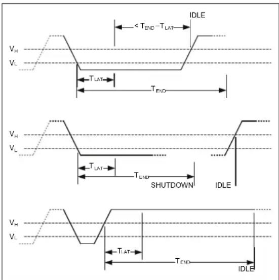
5.11 Idle States and Error Conditions
In Shutdown mode, the MIC2874 is in a Reset condition, with all functions off, while consuming minimal power. Register settings are reset to a default state when coming out of a Shutdown state. In Idle mode, all register settings persist and all MIC2874 functions continue in their current state. Table 5-1 summarizes the difference between the two Idle modes:
TABLE 5-1: DIFFERENCES BETWEEN IDLE MODES
| Mode | Shutdown | Idle |
| V_DC | Low | High |
| I_SUPPLY (all functions off) | 1 μA | 230 μA |
| Register State | Default | Persist |
| Start-up Time | 1 μs | 100 ns |
Idle mode is entered automatically at the end of a communication frame by holding DC high for ≥ T_END , by enabling the device by bringing DC high when in Shutdown mode or when an error is detected by the single-wire interface logic.
Shutdown mode can be entered at any time by pulling down DC for ≥ T_END , discarding any current communication and resetting the internal registers. If a communication is received before the shutdown period, but after the T_LAT period, the communication is discarded. This state is also used to create an internal error state to avoid erroneously latching data when the communication process cannot be serviced in time. Additionally, each register has a maximum value associated with it. If the number of bits clocked in exceeds the maximum value for the register, the data is assumed to be in error and the data is discarded.
text_image
V_H V_L T_LAT T_END V_H V_L T_LAT T_END SHUTDOWN IDLE V_H V_L T_LAT T_END IDLEFIGURE 5-1: Abort, Shutdown and Idle Timing Waveforms.
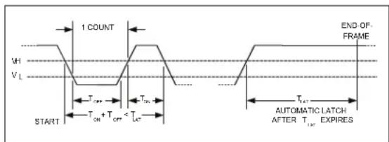
5.12 Communication Details
The serial interface requires delimiters to indicate the Start-of-Frame (SOF), data as a series of pulses and End-of-Frame (EOF), indicated by a lack of activity for longer than T_LAT . The Start-of-Frame is the first high-to-low transition of DC when in Idle mode. The first rising edge resets the internal data counter to 0.
text_image
1 COUNT MH VL START Tcrr Tcrr + Tcrr + Tcr Tcr Tcr AUTOMATIC LATCH AFTER Tcrr EXPIRES END OF-FRAMEFIGURE 5-2: Data Word Pulse Timing.
A pulse is delimited by the signal first going below V_L , and then above V_H , within the Latch Time-out, T_LAT . During this transition, the minimum on ( T_ON ) and off ( T_OFF ) periods are observed to improve tolerance to glitches. Each rising edge increments the internal Data register. Data is automatically latched into the internal shadow address or Data registers after an inactivity period of the DC remaining high for longer than T_LAT .
To send register write commands, the address and data are entered in series as two data words, using the above pattern, with the second word starting after the first latch period has expired. After the second word is entered, the IDLE command should be issued by leaving the DC pin high for ≥ T_END to indicate the stop sequence of the address/data words frame.
After receiving the stop sequence, the internal registers' decode and update cycle is started, with the Shadow register values being transferred to the decoder. Figure 5-3 shows an example of entering a write of Data 5 to Address 3.

text_image
ADDRESSDATA FRAME START LATCH START LATCH END REGISTER WRITE 0 2 3 T End 0 2 3 4 5 T End T LAGFIGURE 5-3: Communication Timing Example of Entering Write for Data 5 to Address 3.
Only a correctly formatted address/data combination will be treated as a valid frame and processed by the MIC2874. Any other input, such as a single data word followed by T_END or three successive data words, will be discarded by the target hardware as an erroneous entry. Additionally, any register write to either an invalid register or with invalid register data will also be discarded.
5.13 MIC2874 Registers
The MIC2874 supports five writable registers for controlling the Torch and the Flash modes of operation, as shown in Table 5-2. Note that register addressing starts at 1. Writing any value above the maximum value shown for each register will cause an invalid data error and the frame will be discarded.
TABLE 5-2: FIVE WRITABLE REGISTERS OF MIC2874
| Address | Name | Max. Value | Description |
| 1 | FEN/FCUR | 31 | Flash Enable/Current |
| 2 | TEN/TCUR | 31 | Torch Enable/Current |
| 3 | STDUR | 7 | Safety Timer Duration |
| 4 | LB_TH | 9 | Low-Battery Voltage Detection Threshold |
| 5 | ST_TH | 5 | Safety Timer Threshold |
5.13.1 FLASH CURRENT REGISTER (FEN/FCUR: DEFAULT 4)
The Flash Current register enables and sets the Flash mode current level. Valid values are 0 to 31. Values 0-15 will set the Flash current without enabling the Flash (such that it can be triggered externally). Values 16-31 will set the Flash current and enable the Flash. The Flash current register maps into the internal FEN and FCUR registers, as shown in the following table below. Table 5-3 describes the relationship between the Flash current and the FCUR register setting.
TABLE 5-3: FLASH CURRENT REGISTER MAPPING INTO INTERNAL FEN/FCUR REGISTERS AND RELATIONSHIP BETWEEN FLASH CURRENT AND FCUR REGISTER SETTING
| FEN/FCUR<4:0> Value | I_FLASH (A) | |||
| Dec. | Binary | FEN<4> | FCUR<3:0> | |
| 0 | 00000 | 0 | 0000 | 1.200 |
| 1 | 00001 | 0 | 0001 | 1.150 |
| 2 | 00010 | 0 | 0010 | 1.100 |
| 3 | 00011 | 0 | 0011 | 1.050 |
| 4 | 00100 | 0 | 0100 | 1.000 |
| 5 | 00101 | 0 | 0101 | 0.950 |
| 6 | 00110 | 0 | 0110 | 0.900 |
| 7 | 00111 | 0 | 0111 | 0.850 |
| 8 | 01000 | 0 | 1000 | 0.800 |
| 9 | 01001 | 0 | 1001 | 0.750 |
| 10 | 01010 | 0 | 1010 | 0.700 |
| 11 | 01011 | 0 | 1011 | 0.650 |
| 12 | 01100 | 0 | 1100 | 0.600 |
| 13 | 01101 | 0 | 1101 | 0.550 |
| 14 | 01110 | 0 | 1110 | 0.400 |
| 15 | 01111 | 0 | 1111 | 0.250 |
| 16 | 10000 | 1 | 0000 | 1.200 |
| 17 | 10001 | 1 | 0001 | 1.150 |
| 18 | 10010 | 1 | 0010 | 1.100 |
| 19 | 10011 | 1 | 0011 | 1.050 |
| 20 | 10100 | 1 | 0100 | 1.000 |
| 21 | 10101 | 1 | 0101 | 0.950 |
| 22 | 10110 | 1 | 0110 | 0.900 |
| 23 | 10111 | 1 | 0111 | 0.850 |
| 24 | 11000 | 1 | 1000 | 0.800 |
| 25 | 11001 | 1 | 1001 | 0.750 |
| 26 | 11010 | 1 | 1010 | 0.700 |
| 27 | 11011 | 1 | 1011 | 0.650 |
| 28 | 11100 | 1 | 1100 | 0.600 |
| 29 | 11101 | 1 | 1101 | 0.550 |
| 30 | 11110 | 1 | 1110 | 0.400 |
| 31 | 11111 | 1 | 1111 | 0.250 |
5.13.2 TORCH CURRENT REGISTER (TEN/TCUR: DEFAULT 4)
The Torch Current register enables and sets the Torch mode current level. Valid values are 0 to 31. Values 0-15 will set the torch current without enabling the torch (such that it can be triggered by setting the internal TEN register value to 1). Values 16-31 will set the torch current and enable the torch. A value of 0 at the internal TEN register will disable the torch. The Torch Current register maps into the internal TEN and TCUR registers, as shown in Table 5-4. The table also describes the relationship between the torch current and the TCUR register setting.
TABLE 5-4: TORCH CURRENT REGISTER MAPPING INTO INTERNAL TEN/TCUR REGISTERS AND RELATIONSHIP BETWEEN TORCH CURRENT AND TCUR REGISTER SETTING
| TEN/TCUR<4:0> Value | I_TORCH (mA) | |||
| Dec. | Binary TEN<4> TCUR<3:0> | |||
| 0 | 00000 | 0 | 0000 | 300.0 |
| 1 | 00001 | 0 | 0001 | 287.5 |
| 2 | 00010 | 0 | 0010 | 275.0 |
| 3 | 00011 | 0 | 0011 | 262.5 |
| 4 | 00100 | 0 | 0100 | 250.0 |
| 5 | 00101 | 0 | 0101 | 237.5 |
| 6 | 00110 | 0 | 0110 | 225.0 |
| 7 | 00111 | 0 | 0111 | 212.5 |
| 8 | 01000 | 0 | 1000 | 200.0 |
| 9 | 01001 | 0 | 1001 | 187.5 |
| 10 | 01010 | 0 | 1010 | 175.0 |
| 11 | 01011 | 0 | 1011 | 162.5 |
| 12 | 01100 | 0 | 1100 | 150.0 |
| 13 | 01101 | 0 | 1101 | 137.5 |
| 14 | 01110 | 0 | 1110 | 100.0 |
| 15 | 01111 | 0 | 1111 | 62.5 |
| 16 | 10000 | 1 | 0000 | 300.0 |
| 17 | 10001 | 1 | 0001 | 287.5 |
| 18 | 10010 | 1 | 0010 | 275.0 |
| 19 | 10011 | 1 | 0011 | 262.5 |
| 20 | 10100 | 1 | 0100 | 250.0 |
| 21 | 10101 | 1 | 0101 | 237.5 |
| 22 | 10110 | 1 | 0110 | 225.0 |
| 23 | 10111 | 1 | 0111 | 212.5 |
| 24 | 11000 | 1 | 1000 | 200.0 |
| 25 | 11001 | 1 | 1001 | 187.5 |
| 26 | 11010 | 1 | 1010 | 175.0 |
| 27 | 11011 | 1 | 1011 | 162.5 |
| 28 | 11100 | 1 | 1100 | 150.0 |
| 29 | 11101 | 1 | 1101 | 137.5 |
| 30 | 11110 | 1 | 1110 | 100.0 |
| TEN/TCUR<4:0> Value | I_TORCH (mA) | |||
| Dec. | Binary TEN<4> TCUR<3:0> | |||
| 31 | 11111 | 1 | 1111 | 62.5 |
5.13.3 SAFETY TIMER DURATION REGISTER (STDUR: DEFAULT 7)
The Safety Timer Duration register sets the duration of the Flash and Torch mode when the LED current exceeds the programmed threshold current. Valid values are 0 for the minimum timer duration to 7 for the maximum duration.
TABLE 5-5: SAFETY TIMER DURATION REGISTER SETTING AND SAFETY TIMER DURATION
| Value | STDUR<2:0>(Binary) | Time-out (ms) | |
| Dec. | Binary | ||
| 0 | 000 | 000 | 156.25 |
| 1 | 001 | 001 | 312.5 |
| 2 | 010 | 010 | 468.75 |
| 3 | 011 | 011 | 625 |
| 4 | 100 | 100 | 781.25 |
| 5 | 101 | 101 | 937.5 |
| 6 | 110 | 110 | 1093.75 |
| 7 | 111 | 111 | 1250 |
5.13.4 LOW-BATTERY THRESHOLD REGISTER (LB\_TH: DEFAULT 1)
The LB_TH register sets the supply threshold voltage, below which the internal low-battery flag is asserted and the LED current driver is disabled. Table 5-6 shows the threshold values that correspond to the register settings. Setting 0 is reserved for disabling the function, and settings between 1 and 9 inclusively enable and set the LB_TH value, between 3.0V and 3.8V, with 100 mV resolution.
TABLE 5-6: LOW-BATTERY THRESHOLD REGISTER SETTING AND SUPPLY THRESHOLD VOLTAGE
| Value | LB_TH<3:0> | VBAT Threshold (V) | |
| Dec. | Binary | ||
| 0 | 0000 | 0000 | Disabled |
| 1 | 0001 | 0001 | 3.0 |
| 2 | 0010 | 0010 | 3.1 |
| 3 | 0011 | 0011 | 3.2 |
| 4 | 0100 | 0100 | 3.3 |
| 5 | 0101 | 0101 | 3.4 |
| 6 | 0110 | 0110 | 3.5 |
| 7 | 011101113 | .6 | |
| 8 | 100010003 | .7 | |
| 9 | 100110013 | .8 | |
5.13.5 SAFETY TIMER THRESHOLD
CURRENT REGISTER
(ST\_TH: DEFAULT 4)
The Safety Timer Threshold Current register determines the amount of LED current flowing through the external LED before the internal LED safety timer is activated. Setting ST_TH to 0 disables the safety timer function, and setting the register to Values 1-5 sets the safety timer threshold current to 100 mA to 300 mA in 50 mA steps.
TABLE 5-7: SAFETY TIMER THRESHOLD CURRENT REGISTER SETTING AND SAFETY TIMER THRESHOLD CURRENT
| Value | ST_TH<2:0> | Safety Timer Threshold Current (mA) | |
| Dec. | Binary | ||
| 0 | 000000 | Disabled | |
| 1 | 001001 | 100 | |
| 2 | 010010 | 150 | |
| 3 | 011011 | 200 | |
| 4 | 100100 | 250 | |
| 5 | 101101 | 300 | |
6.0 COMPONENT SELECTION
6.1 Inductor
Inductor selection should strike a balance between efficiency, stability, cost, size, and rated current. Because the boost converter is compensated internally, the recommended inductance of L is limited from 0.47 H to 1 H to ensure system stability, and a 0.47 H inductor is typically recommended. It is usually a good balance between these considerations.
A large inductance value reduces the peak-to-peak inductor ripple current, hence the output ripple voltage and the LED ripple current. This also reduces both the DC loss and the transition loss at the same inductor's DC Resistance (DCR). However, the DCR of an inductor usually increases with the inductance in the same package size. This is due to the longer windings required for an increase in inductance. Because the majority of the input current passes through the inductor, the higher the DCR, the lower the efficiency is, and more significantly, at higher load currents. On the other hand, an inductor with a smaller DCR, but the same inductance, usually has a larger size. The saturation current rating of the selected inductor must be higher than the maximum peak inductor current to be encountered and should be at least 20% to 30% higher than the average inductor current at maximum output current.
6.2 Input Capacitor
A ceramic capacitor of 4.7 F or larger with low-ESR is recommended to reduce the input voltage ripple to ensure a clean supply voltage for the device. The input capacitor should be placed as close as possible to the MIC2874 V_IN pin with a short trace for good noise performance. X5R or X7R type ceramic capacitors are recommended for better tolerance over temperature. The Y5V and Z5U type temperature rating ceramic capacitors are not recommended due to their large reduction in capacitance over temperature and increased resistance at high frequencies. These reduce their ability to filter out high-frequency noise. The rated voltage of the input capacitor should be at least 20% higher than the maximum operating input voltage over the operating temperature range.
6.3 Output Capacitor
Output capacitor selection is also a trade-off between performance, size and cost. Increasing output capacitance will lead to an improved transient response; however, the size and cost also increase. The output capacitor's preferable range of 2.2 F to 10 F with ESR from 10 m to 50 m , and a 4.7 F ceramic capacitor is typically recommended. X5R or X7R type ceramic capacitors are recommended for better tolerance over temperature. The Y5V and Z5U type ceramic capacitors are not recommended due to their wide variation in capacitance over temperature and increased resistance at high frequencies. The rated voltage of the output capacitor should be at least 20% higher than the maximum operating output voltage over the operating temperature range.
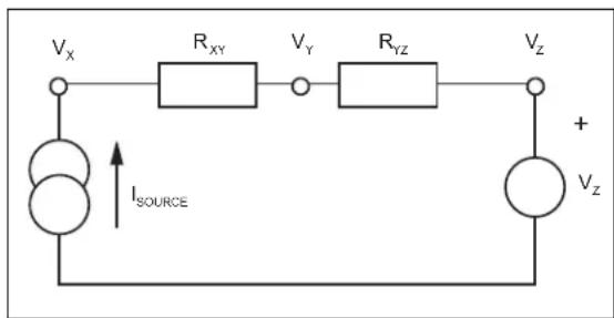
7.0 POWER DISSIPATION CONSIDERATION
As with all power devices, the ultimate current rating of the output is limited by the thermal properties of the device package and the PCB on which the device is mounted. There is a simple Ohm's law type relationship between thermal resistance, power dissipation and temperature, which are analogous to an electrical circuit:
text_image
Vₓ Rₓᵧ Vᵧ Rᵧ_z V_z ↑ IₓSOURCE + V_zFIGURE 7-1: Series Electrical Resistance Circuit.
From this simple circuit, we can calculate if we know I_SOURCE , V_Z and the resistor values, R_XY and R_YZ , using Equation 7-1:
EQUATION 7-1: CALCULATING V_X
$$ \mathrm{V} _ {\mathrm{X}} = \mathrm{I} _ {\text {SOURCE}} \times (\mathrm{R} _ {\mathrm{XY}} + \mathrm{R} _ {\mathrm{YZ}}) = \mathrm{V} _ {\mathrm{Z}} $$
Thermal circuits can be considered using this same rule and can be drawn similarly by replacing current sources with power dissipation (in watts), resistance with thermal resistance (in °C/W) and voltage sources with temperature (in °C).

text_image
T_J Θ_JC T_C Θ_CA T_A + P_DISS T_AFIGURE 7-2: Series Thermal Resistance Circuit.
Now replacing the variables in the equation for V_X , we can find the Junction Temperature ( T_J ) from the power dissipation, ambient temperature and the known thermal resistance of the PCB ( _CA ) and the package ( _JC ).
EQUATION 7-2: CALCULATING JUNCTION TEMPERATURE
$$ \mathrm {T_ {J} = P_ {DISS} \times(\theta_ {JC} + \theta_ {CA})+ T_ {A}} $$
As seen in Figure 7-2, the total thermal resistance is: 0_JA = 0_JC + 0_CA . Hence, this can also be written as in Equation 7-3:
EQUATION 7-3: CALCULATING THERMAL RESISTANCE
$$ \mathrm{T} _ {\mathrm{J}} = \mathrm{P} _ {\mathrm{DISS}} \times (\theta_ {\mathrm{JA}}) + \mathrm{T} _ {\mathrm{A}} $$
Where:
_JA = Thermal resistance between junction and ambient, which is typically 84^/W for 1.3 mm x 1.3 mm WLCSP package
Since effectively all of the power losses (minus the inductor losses) in the converter are dissipated within the MIC2874 package, P_DISS can be calculated thus:
EQUATION 7-4: CALCULATING P DISS
Linear Mode:
$$ \mathrm{P} _ {\text {DISS}} = \left[ \mathrm{P} _ {\text {OUT}} \times \left(\frac {1}{\eta} - 1\right) \right] - \mathrm{I} _ {\text {OUT}} ^ {2} \times \mathrm{DCR} $$
Boost Mode:
$$ \mathrm{P} _ {\text {DISS}} = \left[ \mathrm{P} _ {\text {OUT}} \times \left(\frac {1}{\eta} - 1\right) \right] - \left(\frac {\mathrm{I} _ {\text {OUT}}}{1 - \mathrm{D}}\right) ^ {2} \times \mathrm{DCR} $$
Duty Cycle in Boost Mode:
$$ \mathrm{D} = \frac {\mathrm{V} _ {\mathrm{OUT}} - \mathrm{V} _ {\mathrm{IN}}}{\mathrm{V} _ {\mathrm{OUT}}} $$
Where:
= Efficiency taken from efficiency curves DCR = Inductor DCR
Where the real board area differs from 1 inch square, _CA (the PCB thermal resistance) values for various PCB copper areas can be taken from Figure 7-3. Figure 7-3 is taken from "Designing with Low Dropout Voltage Regulators" available from the Microchip web site ("LDO Application Hints").

line
| PCB Heat Sink Area (mm²) | PCB Heat Sink Thermal Resistance (°C/W) - Solid Line | PCB Heat Sink Thermal Resistance (°C/W) - Dashed Line | | ------------------------ | ------------------------------------------------------ | ------------------------------------------------------- | | 0 | 70 | 48 | | 2000 | 35 | 25 | | 4000 | 25 | 18 | | 6000 | 20 | 15 |FIGURE 7-3: Graph to Determine PC Board Area for a Given PCB Thermal Resistance.
Figure 7-3 shows the total area of a round or square pad, centered on the device. The solid trace represents the area of a square, single-sided, horizontal orientation, solder masked, copper PC board trace heat sink, measured in square millimeters. No airflow is assumed. The dashed line shows the PC board's trace heat sink covered in black oil-based paint and with 1.3m/sec (250 feet per minute) airflow. This approaches a "best case" pad heat sink. Conservative design dictates using the solid trace data, which indicates that a maximum pad size of 5000 mm ^2 is needed. This is a pad that is 71 mm by 71 mm (2.8 inches per side).
8.0 PCB LAYOUT GUIDELINES
PCB layout is critical to achieve reliable, stable and efficient performance. A ground plane is required to control EMI and minimize the inductance in power and signal return paths. The following guidelines should be followed to ensure proper operation of the device.
8.1 IC (Integrated Circuit)
- Place the IC close to the point-of-load (in this case, the flash LED).
- Use fat traces to route the input and output power lines.
- Analog grounds (LGND and AGND) and power ground (PGND) should be kept separate and connected at a single location.
- 6 to 12 thermal vias must be placed on the PCB top layer PGND copper from the PGND pin and connected it to the ground plane to ensure a good PCB thermal resistance can be achieved.
- Since all the top copper areas connected directly to the CSP package bumps are used as the immediate PCB heat sink, these top copper areas should be spread out from the bumps in funnel-shape to maximize the top copper PCB heat sink areas.
8.2 VIN Decoupling Capacitor
- The VIN decoupling capacitor must be placed close to the VIN pin of the IC and preferably connected directly to the pin and not through any via. The capacitor must be located right at the IC.
- The VIN decoupling capacitor should be connected to analog ground (AGND).
- The VIN terminal is noise sensitive and the placement of capacitor is very critical.
8.3 Inductor
- Keep both the inductor connections to the switch node (SW) and input power line short and wide enough to handle the switching current. Keep the areas of the switching current loops small to minimize the EMI problem.
- Do not route any digital lines underneath or close to the inductor.
- Keep the switch node (SW) away from the noise sensitive pins.
- To minimize noise, place a ground plane underneath the inductor.
8.4 Output Capacitor
- The output capacitor must be placed close to the OUT pin and PGND pin of the IC and preferably connected directly and closely to the OUT pin and PGND pin without going through any via to minimize the switching current loop during the main switch off-cycle, and the switching noise.
- Use wide and short traces to connect the output capacitor to the OUT and PGND pins.
- Place several vias to the ground plane close to the output capacitor ground terminal.
- Use either X5R or X7R temperature rating ceramic capacitors. Do not use Y5V or Z5U type ceramic capacitors.
8.5 Flash LED
- Use wide and short trace to connect the LED anode to the OUT pin.
- Use wide and short trace to connect the LED cathode to the LED pin.
- Make sure that the LED's PCB land pattern can provide sufficient PCB pad heat sink to the flash LED, such as sufficient copper areas and thermal vias.
9.0 PACKAGING INFORMATION
9.1 Package Marking Information
9-Bump WLCSP*

text_image
XXX NNNExample

text_image
74A 007| Legend: XX...X Product code or customer-specific informationY Year code (last digit of calendar year)YY Year code (last 2 digits of calendar year)WW Week code (week of January 1 is week ‘01’)NNN Alphanumeric traceability codeeBb-free JEDEC® designator for Matte Tin (Sn)* This package is Pb-free. The Pb-free JEDEC designator (e3) can be found on the outer packaging for this package.•, ▲, ▼ Pin one index is identified by a dot, delta up or delta down (triangle mark). |
| Note: In the event the full Microchip part number cannot be marked on one line, it will be carried over to the next line, thus limiting the number of available characters for customer-specific information. Package may or may not include the corporate logo.Underbar(_) and/or Overbar(~) symbol may not be to scale. |
9.2 Package Details
The following sections give the technical details of the packages.
TITLE
9 BALL WLCSP 1.3x1.3mm PACKAGE OUTLINE & RECOMMENDED LAND PATTERN
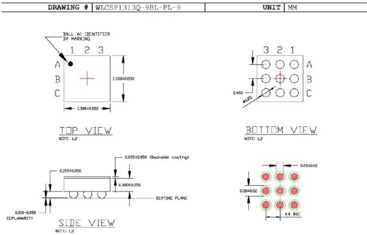
text_image
DRAWING # WLCSP1313Q-9BL-PL-9 UNIT MM BALL A1 IDENTIFIER BY MARKING 1 2 3 A B C 1.300±0.050 1.300±0.050 TOP VIEW NOTE: 1,2 BOTTOM VIEW NOTE: 1,2 0.195±0.050 0.380±0.050 SEATING PLANE 0.000-0.050 COPLANARITY SIDE VIEW NOTE: 1,2 0.20±0.02 0.30±0.02 0.4 BSCRECOMMENDED LAND PATTERN
NOTE: 3,4
NOTE:
- MAX PACKAGE WARPAGE IS 0.05 MM
- MAX ALLOWABLE BURR IS 0.076MM IN ALL DIRECTIONS
- NON-SOLDERMASK DEFINED PADS ARE RECOMMENDED FOR BOARD LAYOUT
- SHADED RED CIRCLES REPRESENT CONTACT PAD AREA, GREEN CIRCLES REPRESENT SOLDER MASK OPENING
Note: For the most current package drawings, please see the Microchip Packaging Specification located at http://www.microchip.com/packaging.
APPENDIX A: REVISION HISTORY
Revision A (October 2018)
- Converted Micrel document MIC2874 to Microchip data sheet DS20006081A.
- Minor text changes throughout document.
NOTES:
PRODUCT IDENTIFICATION SYSTEM
To order or obtain information, e.g., on pricing or delivery, contact your local Microchip representative or sales office.

text_image
PART NO. Device Temperature XX Package - XX Media TypeDevice: MIC2874: 1.2A High-Brightness Flash LED Driver with Single-Wire Serial Interface
Temperature: Y = -40°C to +125°C
Package: CS = 9-bump 1.30 mm x 1.30 mm WLCSP
Media Type: T5 = 500/Reel TR = 5,000/Reel
Examples:
a) MIC2874YCS-T5: MIC2874, -40°C to +125°C Temp. Range, 9-Bump WLCSP, 500/Reel
b) MIC2874YCS-TR: MIC2874, -40°C to +125°C Temp. Range, 9-Bump WLCSP, 5,000/Reel
Note 1: Tape and Reel identifier only appears in the catalog part number description. This identifier is used for ordering purposes and is not printed on the device package. Check with your Microchip Sales Office for package availability with the Tape and Reel option.
NOTES:
Note the following details of the code protection feature on Microchip devices:
• Microchip products meet the specification contained in their particular Microchip Data Sheet.
- Microchip believes that its family of products is one of the most secure families of its kind on the market today, when used in the intended manner and under normal conditions.
- There are dishonest and possibly illegal methods used to breach the code protection feature. All of these methods, to our knowledge, require using the Microchip products in a manner outside the operating specifications contained in Microchip's Data Sheets. Most likely, the person doing so is engaged in theft of intellectual property.
• Microchip is willing to work with the customer who is concerned about the integrity of their code.
- Neither Microchip nor any other semiconductor manufacturer can guarantee the security of their code. Code protection does not mean that we are guaranteeing the product as "unbreakable."
Code protection is constantly evolving. We at Microchip are committed to continuously improving the code protection features of our products. Attempts to break Microchip's code protection feature may be a violation of the Digital Millennium Copyright Act. If such acts allow unauthorized access to your software or other copyrighted work, you may have a right to sue for relief under that Act.
Information contained in this publication regarding device applications and the like is provided only for your convenience and may be superseded by updates. It is your responsibility to ensure that your application meets with your specifications. MICROCHIP MAKES NO REPRESENTATIONS OR WARRANTIES OF ANY KIND WHETHER EXPRESS OR IMPLIED, WRITTEN OR ORAL, STATUTORY OR OTHERWISE, RELATED TO THE INFORMATION, INCLUDING BUT NOT LIMITED TO ITS CONDITION, QUALITY, PERFORMANCE, MERCHANTABILITY OR FITNESS FOR PURPOSE. Microchip disclaims all liability arising from this information and its use. Use of Microchip devices in life support and/or safety applications is entirely at the buyer's risk, and the buyer agrees to defend, indemnify and hold harmless Microchip from any and all damages, claims, suits, or expenses resulting from such use. No licenses are conveyed, implicitly or otherwise, under any Microchip intellectual property rights unless otherwise stated.
Microchip received ISO/TS-16949:2009 certification for its worldwide headquarters, design and wafer fabrication facilities in Chandler and Tempe, Arizona; Gresham, Oregon and design centers in California and India. The Company's quality system processes and procedures are for its PIC® MCUs and dsPIC® DSCs, KEELQQ® code hopping devices, Serial EEPROMs, microperipherals, nonvolatile memory and analog products. In addition, Microchip's quality system for the design and manufacture of development systems is ISO 9001:2000 certified.
QUALITY MANAGEMENT SYSTEM CERTIFIED BY DNV = ISO/TS 16949=
Trademarks
The Microchip name and logo, the Microchip logo, AnyRate, AVR, AVR logo, AVR Freaks, BitCloud, chipKIT, chipKIT logo, CryptoMemory, CryptoRF, dsPIC, FlashFlex, flexPWR, Heldo, JukeBlox, KeeLoq, Kleer, LANCheck, LINK MD, maXStylus, maXTouch, MediaLB, megaAVR, MOST, MOST logo, MPLAB, OptoLyzer, PIC, picoPower, PICSTART, PIC32 logo, Prochip Designer, QTouch, SAM-BA, SpyNIC, SST, SST Logo, SuperFlash, tinyAVR, UNI/O, and XMEGA are registered trademarks of Microchip Technology Incorporated in the U.S.A. and other countries.
ClockWorks, The Embedded Control Solutions Company, EtherSynch, Hyper Speed Control, HyperLight Load, IntelliMOS, mTouch, Precision Edge, and Quiet-Wire are registered trademarks of Microchip Technology Incorporated in the U.S.A.
Adjacent Key Suppression, AKS, Analog-for-the-Digital Age, Any Capacitor, AnyIn, AnyOut, BodyCom, CodeGuard, CryptoAuthentication, CryptoAutomotive, CryptoCompanion, CryptoController, dsPICDEM, dsPICDEM.net, Dynamic Average Matching, DAM, ECAN, EtherGREEN, In-Circuit Serial Programming, ICSP, INICnet, Inter-Chip Connectivity, JitterBlocker, KleerNet, KleerNet logo, memBrain, Mindi, MiWi, motorBench, MPASM, MPF, MPLAB Certified logo, MPLIB, MPLINK, MultiTRAK, NetDetach, Omniscient Code Generation, PICDEM, PICDEM.net, PICkit, PICtail, PowerSmart, PureSilicon, QMatrix, REAL ICE, Ripple Blocker, SAM-ICE, Serial Quad I/O, SMART-I.S., SQL, SuperSwitcher, SuperSwitcher II, Total Endurance, TSHARC, USBCheck, VariSense, ViewSpan, WiperLock, Wireless DNA, and ZENA are trademarks of Microchip Technology Incorporated in the U.S.A. and other countries.
SQTP is a service mark of Microchip Technology Incorporated in the U.S.A.
Silicon Storage Technology is a registered trademark of Microchip Technology Inc. in other countries.
GestIC is a registered trademark of Microchip Technology Germany II GmbH & Co. KG, a subsidiary of Microchip Technology Inc., in other countries.
All other trademarks mentioned herein are property of their respective companies.
© 2018, Microchip Technology Incorporated, All Rights Reserved. ISBN: 978-1-5224-3693-5
Worldwide Sales and Service
AMERICAS
Corporate Office
2355 West Chandler Blvd.
Chandler, AZ 85224-6199
Tel: 480-792-7200
Fax: 480-792-7277
Technical Support:
http://www.microchip.com/
support
Web Address:
www.microchip.com
Atlanta
Duluth, GA
Tel: 678-957-9614
Fax: 678-957-1455
Austin, TX
Tel: 512-257-3370
Boston
Westborough, MA
Tel: 774-760-0087
Fax: 774-760-0088
Chicago
Itasca, IL
Tel: 630-285-0071
Fax: 630-285-0075
Dallas
Addison, TX
Tel: 972-818-7423
Fax: 972-818-2924
Detroit
Novi, MI
Tel: 248-848-4000
Houston, TX
Tel: 281-894-5983
Indianapolis
Noblesville, IN
Tel: 317-773-8323
Fax: 317-773-5453
Tel: 317-536-2380
Los Angeles
Mission Viejo, CA
Tel: 949-462-9523
Fax: 949-462-9608
Tel: 951-273-7800
Raleigh, NC
Tel: 919-844-7510
New York, NY
Tel: 631-435-6000
San Jose, CA
Tel: 408-735-9110
Tel: 408-436-4270
Canada - Toronto
Tel: 905-695-1980
Fax: 905-695-2078
ASIA/PACIFIC
Australia - Sydney
Tel: 61-2-9868-6733
China - Beijing
Tel: 86-10-8569-7000
China - Chengdu
Tel: 86-28-8665-5511
China - Chongqing
Tel: 86-23-8980-9588
China - Dongguan
Tel: 86-769-8702-9880
China - Guangzhou
Tel: 86-20-8755-8029
China - Hangzhou
Tel: 86-571-8792-8115
China - Hong Kong SAR
Tel: 852-2943-5100
China - Nanjing
Tel: 86-25-8473-2460
China - Qingdao
Tel: 86-532-8502-7355
China - Shanghai
Tel: 86-21-3326-8000
China - Shenyang
Tel: 86-24-2334-2829
China - Shenzhen
Tel: 86-755-8864-2200
China - Suzhou
Tel: 86-186-6233-1526
China - Wuhan
Tel: 86-27-5980-5300
China - Xian
Tel: 86-29-8833-7252
China - Xiamen
Tel: 86-592-2388138
China - Zhuhai
Tel: 86-756-3210040
ASIA/PACIFIC
India - Bangalore
Tel: 91-80-3090-4444
India - New Delhi
Tel: 91-11-4160-8631
India - Pune
Tel: 91-20-4121-0141
Japan - Osaka
Tel: 81-6-6152-7160
Japan - Tokyo
Tel: 81-3-6880-3770
Korea - Daegu
Tel: 82-53-744-4301
Korea - Seoul
Tel: 82-2-554-7200
Malaysia - Kuala Lumpur
Tel: 60-3-7651-7906
Malaysia - Penang
Tel: 60-4-227-8870
Philippines - Manila
Tel: 63-2-634-9065
Singapore
Tel: 65-6334-8870
Taiwan - Hsin Chu
Tel: 886-3-577-8366
Taiwan - Kaohsiung
Tel: 886-7-213-7830
Taiwan - Taipei
Tel: 886-2-2508-8600
Thailand - Bangkok
Tel: 66-2-694-1351
Tel: 43-7242-2244-39
Fax: 43-7242-2244-393
Denmark - Copenhagen
Tel: 45-4450-2828
Fax: 45-4485-2829
Finland - Espoo
Tel: 358-9-4520-820
France - Paris
Tel: 33-1-69-53-63-20
Fax: 33-1-69-30-90-79
Germany - Garching
Tel: 49-8931-9700
Germany - Haan
Tel: 49-2129-3766400
Germany - Heilbronn
Tel: 49-7131-67-3636
Germany - Karlsruhe
Tel: 49-721-625370
Germany - Munich
Tel: 49-89-627-144-0
Fax: 49-89-627-144-44
Germany - Rosenheim
Tel: 49-8031-354-560
Israel - Ra'anana
Tel: 972-9-744-7705
Italy - Milan
Tel: 39-0331-742611
Fax: 39-0331-466781
Italy - Padova
Tel: 39-049-7625286
Netherlands - Drunen
Tel: 31-416-690399
Fax: 31-416-690340
Norway - Trondheim
Tel: 47-7288-4388
Poland - Warsaw
Tel: 48-22-3325737
Romania - Bucharest
Tel: 40-21-407-87-50
Spain - Madrid
Tel: 34-91-708-08-90
Fax: 34-91-708-08-91
Sweden - Gothenberg
Tel: 46-31-704-60-40
Sweden - Stockholm
Tel: 46-8-5090-4654
UK - Wokingham
Tel: 44-118-921-5800
Fax: 44-118-921-5820