MIC4812 - Unspecified Microchip - Free user manual and instructions
Find the device manual for free MIC4812 Microchip in PDF.

User questions about MIC4812 Microchip
0 question about this device. Answer the ones you know or ask your own.
Ask a new question about this device
Download the instructions for your Unspecified in PDF format for free! Find your manual MIC4812 - Microchip and take your electronic device back in hand. On this page are published all the documents necessary for the use of your device. MIC4812 by Microchip.
USER MANUAL MIC4812 Microchip
The MIC4812 is a high efficiency linear White LED (WLED) driver designed to drive up to six high current WLEDs for signage lighting. The MIC4812 provides the highest possible efficiency as this architecture has no switching losses present in traditional charge pumps or inductive boost circuits. The MIC4812 provides six linear drivers which maintain constant current for up to six WLEDs. It features a typical dropout of 190mV at 100mA.
The MIC4812 features Dynamic Average Matching ^™ (DAM ^™ ) which is specifically designed to provide optimum matching across all WLEDs. The high accuracy (±1% typical) current regulated WLED channels ensure uniform display illumination under all conditions. The brightness is controlled through an Ultra Fast PWM ^™ interface operating down to less than 1% duty cycle.
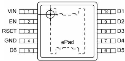
The MIC4812 is available in an 10-pin MSOP ePad package with a junction temperature range of -40°C to +125°C.
Datasheets and support documentation can be found on Micrel's web site at: www.micrel.com.
Features
• High Efficiency (no Voltage Boost losses)
- Ultra Fast PWM™ control (200Hz to 500kHz)
- Input voltage range: 3.0V to 5.5V
• LED current range up to 100mA per channel
- Programmable LED current with external resistor
- Dropout of 190mV at 100mA
- Matching better than ± 1% (typical)
• Current Accuracy better than ±1% (typical)
- Maintains proper regulation regardless of how many channels are utilized
• 10-pin MSOP with ePad package
Applications
- Billboard displays
- Marquee displays
- Instrument displays
- LCD display modules
Typical Application

text_image
MIC4812YMME D6 VIN C1 RSET EN PWM Control GND Low Dropout Linear Driver D1 D2 D3 D4 D5 VINHigh Current Lighting (Six WLEDs)
Ultra Fast PWM, DAM and Dynamic Average Matching are trademark of Micrel, Inc.
Micrel Inc. • 2180 Fortune Drive • San Jose, CA 95131 • USA • tel +1 (408) 944-0800 • fax +1 (408) 474-1000 • http://www.micrel.com
Ordering Information
| Part Number Mark Code | Junction Temperature Range Package |
| MIC4812YMME 4812 -40^ to +125^ 10-Pin ePad MSOP |
Pin Configuration
text_image
VIN 1 EN 2 RSET 3 GND 4 D6 5 ePad 10 D1 9 D2 8 D3 7 D4 6 D510-Pin ePad MSOP (MME) (Top View)
Pin Description
| Pin Number | Pin Name | Pin Function |
| 1 VIN Voltage Input. Connect at least 2.2μF ceramic capacitor between VIN and GND. | ||
| 2 | EN | Enable LED drivers. This pin can be used as a PWM input for dimming of WLEDs. Do not leave floating. |
| 3 | RSET | An internal 1.27V reference sets the nominal maximum WLED current. Example, apply a 8.25kΩ resistor between RSET and GND to set LED current to 100mA at 100% duty cycle. |
| 4 | GND | Ground. |
| 5 D6 LED6 driver input. Connect LED anode to VIN and cathode to this pin. | ||
| 6 D5 LED5 driver input. Connect LED anode to VIN and cathode to this pin. | ||
| 7 D4 LED4 driver input. Connect LED anode to VIN and cathode to this pin. | ||
| 8 D3 LED3 driver input. Connect LED anode to VIN and cathode to this pin. | ||
| 9 D2 LED2 driver input. Connect LED anode to VIN and cathode to this pin. | ||
| 10 D1 LED1 driver input. Connect LED anode to VIN and cathode to this pin. | ||
| ePad HS PAD Heat sink pad. Not internally connected. Connect to ground. | ||
Absolute Maximum Ratings ^(1)
Main Input Voltage ( V_IN ) ..... -0.3V to +6V
Enable Input Voltage ( V_EN )....-0.3V to +6V
LED Driver Voltage ( V_D1-D6 ) -0.3V to +6V
Power Dissipation ....Internally Limited
Lead Temperature (soldering, 10sec.)....260°C
Storage Temperature ( T_s ) -65^ to +150^
ESD Rating ^(3) 1.5kV
Operating Ratings ^(2)
Supply Voltage ( V_IN )....+3.0V to +5.5V
Enable Input Voltage ( V_EN ) 0V to V_IN
LED Driver Voltage ( V_D1-D6 ) 0V to V_IN
Junction Temperature ( T_J ) -40^ to +125^
Junction Thermal Resistance
ePad MSOP-10L ( JA) .....76.7°C/W
Electrical Characteristics
V_IN = V_EN = 5V, R_SET = 8.25k; V_D1-D6 = 1.2V; T_J = 25^ C, bold values indicate -40^ C ≤ T_J ≤ 125^ C; unless noted.
| Parameter | Conditions | Min | Typ | ||||
| Current Accuracy^(4) | 96 | 101 | 106 | mA | |||
| Matching^(5) | 1 | 3.6 | % | ||||
| Drop-out | Where I_LED = 90% of LED current seen at V_DROP NOM = 1.2V, 100% brightness level | 190 | 320 | mV | |||
| Ground/Supply Bias Current | 3.2 | 4.2 | mA | ||||
| Shutdown Current | V_EN = 0V | 0.01 | 1 | μA | |||
| PWM Dimming | |||||||
| Enable Input Voltage ( V_EN ) | Logic Low | 0.2 | V | ||||
| Logic High | 1.2 | V | |||||
| Enable Input Current | V_IH ≥ 1.2V | 0.01 | 1 | μA | |||
| Current Source Delay (50% levels) | Shutdown to on Standby to on On to Standby | 40 | 60 | μs | |||
| 1 | μs | ||||||
| 0.3 | μs | ||||||
| Current Source Transient Time (10%-90%) | T_RISE T_FALL | 1 | μs | ||||
| 0.3 | μs | ||||||
| Stand-by to Shutdown Time | V_EN = 0V | 10 | 20 | 40 | ms | ||
Notes:
- Exceeding the absolute maximum rating may damage the device.
- The device is not guaranteed to function outside its operating rating.
- Devices are ESD sensitive. Handling precautions recommended. Human body model, 1.5k in series with 100pF.
- As determined by average current of all channels in use and all channels loaded.
- The current through each LED meets the stated limits from the average current of all LEDs.
Typical Characteristics

line
| DUTY CYCLE (%) | AVERAGE CURRENT (mA) | | -------------- | ------------------- | | 0 | 0 | | 2 | 20 | | 4 | 40 | | 6 | 60 | | 8 | 80 | | 10 | 100 |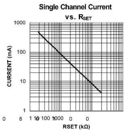
line
| RSET (kΩ) | CURRENT (mA) | | --------- | ------------ | | 1 | 500 | | 10 | 250 | | 100 | 125 | | 1000 | 62.5 | | 10000 | 31.25 | | 100000 | 15.625 | | 1000000 | 7.8125 |
line
| LED CURRENT (mA) | DROPOUT VOLTAGE (mV) | | ---------------- | -------------------- | | 0 | 0 | | 100 | 150 | | 200 | 300 | | 300 | 450 | | 400 | 600 | | 500 | 750 |
line
| TEMPERATURE (°C) | DROPOUT VOLTAGE (mV) | | ---------------- | -------------------- | | -40 | 150 | | 0 | 175 | | 20 | 200 | | 40 | 210 | | 60 | 220 | | 80 | 230 | | 10 | 240 | | 12 | 250 |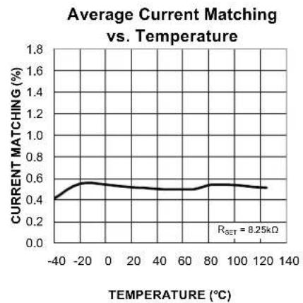
line
| TEMPERATURE (°C) | CURRENT MATCHING (%) | | ---------------- | -------------------- | | -40 | 0.4 | | -20 | 0.6 | | 0 | 0.55 | | 20 | 0.5 | | 40 | 0.5 | | 60 | 0.5 | | 80 | 0.55 | | 100 | 0.5 | | 120 | 0.5 |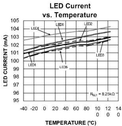
line
| TEMPERATURE (°C) | LED Current (mA) | | ---------------- | ---------------- | | -40 | 101.0 | | 0 | 101.5 | | 20 | 102.0 | | 40 | 102.5 | | 60 | 103.0 | | 80 | 103.5 | | 10 | 104.0 | | 12 | 104.5 | | 14 | 105.0 |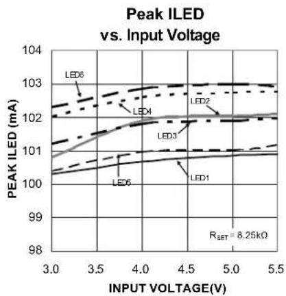
line
| INPUT VOLTAGE(V) | PEAK ILED (mA) | | ---------------- | -------------- | | 3.0 | 100 | | 3.5 | 101 | | 4.0 | 102 | | 4.5 | 103 | | 5.0 | 103 | | 5.5 | 103 |Functional Characteristics
line
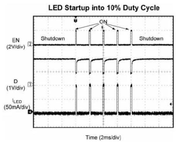
| Time (2ms/div) | EN (2V/div) | D (1V/div) | I_LED (50mA/div) | | -------------- | ----------- | ---------- | ---------------- | | 0 | 0 | 0 | 0 | | 1 | 0 | 0 | 0 | | 2 | 0 | 0 | 0 | | 3 | 0 | 0 | 0 | | 4 | 0 | 0 | 0 | | 5 | 0 | 0 | 0 | | 6 | 0 | 0 | 0 | | 7 | 0 | 0 | 0 | | 8 | 0 | 0 | 0 | | 9 | 0 | 0 | 0 | | 10 | 0 | 0 | 0 | | 11 | 0 | 0 | 0 | | 12 | 0 | 0 | 0 | | 13 | 0 | 0 | 0 | | 14 | 0 | 0 | 0 | | 15 | 0 | 0 | 0 | | 16 | 0 | 0 | 0 | | 17 | 0 | 0 | 0 | | 18 | 0 | 0 | 0 | | 19 | 0 | 0 | 0 | | 20 | 0 | 0 | 0 | | 21 | 0 | 0 | 0 | | 22 | 0 | 0 | 0 | | 23 | 0 | 0 | 0 | | 24 | 0 | 0 | 0 | | 25 | 0 | 0 | 0 | | 26 | 0 | 0 | 0 | | 27 | 0 | 0 | 0 | | 28 | 0 | 0 | 0 | | 29 | 0 | 0 | 0 | | 30 | 0 | 0 | 0 | | | | | | | | | | | | | | | | | | | | | | | | | | | | | | | | | | | | | | | | | | | | | | | | | | | | | | | | | | | | | | | | | |
line
| Time (10μs/div) | EN (2V/div) | I_LED (50mA/div) | | --------------- | ----------- | ---------------- | | Start | Low | Low | | End | High | Low |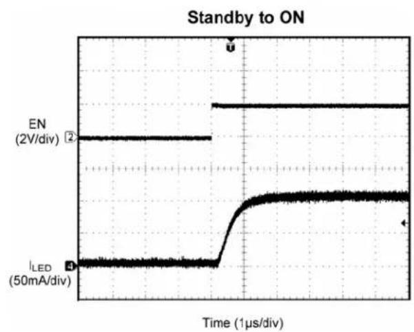

line
| Time (400ns/div) | EN (2V/div) | I_LED (50mA/div) | | ---------------- | ----------- | ---------------- | | 0 | 2 | 5 | | 400 | 2 | 5 | | 1000 | 2 | 5 | | 1500 | 2 | 5 | | 2000 | 2 | 5 | | 2500 | 2 | 5 | | 3000 | 2 | 5 | | 3500 | 2 | 5 | | 4000 | 2 | 5 | | 4500 | 2 | 5 | | 5000 | 2 | 5 | | 5500 | 2 | 5 | | 6000 | 2 | 5 | | 6500 | 2 | 5 | | 7000 | 2 | 5 | | 7500 | 2 | 5 | | 8000 | 2 | 5 | | 8500 | 2 | 5 | | 9000 | 2 | 5 | | 9500 | 2 | 5 | | 10000 | 2 | 5 | | 10500 | 2 | 5 | | 11000 | 2 | 5 | | 11500 | 2 | 5 | | 12000 | 2 | 5 | | 12500 | 2 | 5 | | 13000 | 2 | 5 | | 13500 | 2 | 5 | | 14000 | 2 | 5 | | 14500 | 2 | 5 | | 15000 | 2 | 5 | | 15500 | 2 | 5 | | 16000 | 2 | 5 | | 16500 | 2 | 5 | | 17000 | 2 | 5 | | 17500 | 2 | 5 | | 18000 | 2 | 5 | | 18500 | 2 | 5 | | 19000 | 2 | 5 | | 19500 | 2 | 5 | | 20000 | 2 | 5 | | 20500 | 2 | 5 | | 21000 | 2 | 5 | | 21500 | 2 | 5 | | 22000 | 2 | 5 | | 22500 | 2 | 5 | | 23000 | 2 | 5 | | 23500 | 2 | 5 | | 24000 | 2 | 5 | | 24500 | 2 | 5 | | 25000 | 2 | 5 | | 25500 | 2 | 5 | | 26000 | 2 | 5 | | 26500 | 2 | 5 | | 27000 | 2 | 5 | | 27500 | 2 | 5 | | 28000 | 2 | 5 | | 28500 | 2 | 5 | | 29000 | 2 | 5 | | 29500 | 2 | 5 | | 30000 | 2 | 5 | | Note: The data is extracted from the image and displayed as a PNG image. The 'EN' and 'ILED' labels are not present in the image. There is only one data series in the image.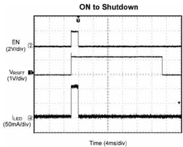
line
| Time (4ms/div) | EN (2V/div) | VRSFT (1V/div) | ILED (50mA/div) | | -------------- | ----------- | ------------- | --------------- | | 0 | 0 | 0 | 0 | | 2 | 0 | 0 | 0 | | 4 | 0 | 0 | 0 | | 6 | 0 | 0 | 0 | | 8 | 0 | 0 | 0 | | 10 | 0 | 0 | 0 | | 12 | 0 | 0 | 0 | | 14 | 0 | 0 | 0 | | 16 | 0 | 0 | 0 | | 18 | 0 | 0 | 0 | | 20 | 0 | 0 | 0 | | 22 | 0 | 0 | 0 | | 24 | 0 | 0 | 0 | | 26 | 0 | 0 | 0 | | 28 | 0 | 0 | 0 | | 30 | 0 | 0 | 0 | | 32 | 0 | 0 | 0 | | 34 | 0 | 0 | 0 | | 36 | 0 | 0 | 0 | | 38 | 0 | 0 | 0 | | 40 | 0 | 0 | 0 | | 42 | 0 | 0 | 0 | | 44 | 0 | 0 | 0 | | 46 | 0 | 0 | 0 | | 48 | 0 | 0 | 0 | | 50 | 0 | 0 | 0 | | 52 | 0 | 0 | 0 | | 54 | 0 | 0 | 0 | | 56 | 0 | 0 | 0 | | 58 | 0 | 0 | 0 | | 60 | 0 | 0 | 0 | | 62 | 0 | 0 | 0 | | 64 | 0 | 0 | 0 | | 66 | 0 | 0 | 0 | | 68 | 0 | 0 | 0 | | 70 | 0 | 0 | 0 | | 72 | 0 | 0 | 0 | | 74 | 0 | 0 | 0 | | 76 | 0 | 0 | 0 | | 78 | 0 | 0 | 0 | | 80 | 0 | 0 | 0 | | 82 | 0 | 0 | 0 | | 84 | 0 | 0 | 0 | | 86 | 0 | 0 | 0 | | 88 | 0 | 0 | 0 | | 90 | 0 | 0 | 0 | | 92 | 0 | 0 | 0 | | 94 | 0 | 0 | 0 | | 96 | 0 | 0 | 0 | | 98 | 0 | 0 | 0 | | Note: The data is extracted from the image. The 'ON to Shutdown' label indicates the corresponding waveform. The 'EN' and 'VRSFT' labels are not present in the image. The 'ILED' label is also shown but lacks the corresponding data points. There is no additional data series in this view. The 'Time' axis is labeled at the bottom.Functional Diagram
Functional Description
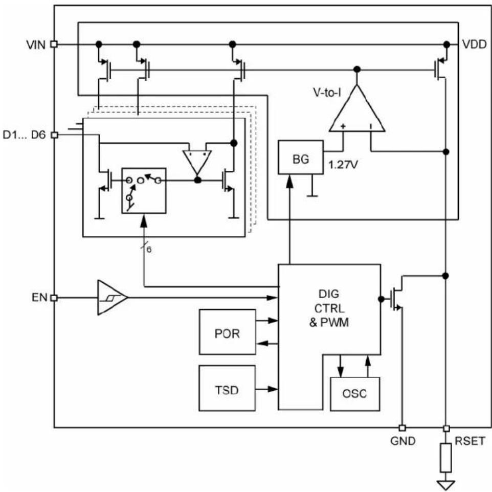
The MIC4812 is a six channel linear WLED driver. The WLED driver is designed to maintain proper current regulation with LED current accuracy of 1%, and typical matching of 1% across the six channels. The WLEDs are driven independently from the input supply and will maintain regulation with a dropout of 190mV at 100mA. The low dropout allows the WLEDs to be driven directly from the battery voltage and eliminates the need for large and inefficient charge pumps. The maximum WLED current for each channel is set by the external R_SET resistor. Dimming is controlled by applying a PWM signal to the EN pin. The MIC4812 accommodates a wide PWM frequency range as outlined in the application information section.
Block Diagram
As shown in Figure 1, the MIC4812 consists of six current mirrors set to copy a master current determined by the R_SET resistor. The linear drivers have a designated control block for enabling and dimming the WLEDs.
V_IN
The input supply ( V_IN ) provides power to the linear drivers and the control circuitry. The V_IN operating range is 3V to 5.5V. A bypass capacitor of 2.2 F should be placed close to input (VIN) pin and the ground (GND) pin. Refer to the layout recommendations section for details on placing the input capacitor (C1).
EN
The EN pin is equivalent to the enable pin for the linear drivers on the MIC4812. It can also be used for dimming using a PWM signal. See the PWM Dimming Interface in the Application Information section for details. Pulling the EN low for more than 20ms puts the MIC4812 into a low lq sleep mode. The EN pin cannot be left floating; a floating enable pin may cause an indeterminate state on the outputs.
The first pulse on the EN pin must be equal or greater to 60 s to wake the part up in a known state. This equates to 3.3Khz PWM signal at equal or greater than 50% duty cycle. Higher PWM frequencies may be used but the first pulse must be equal or greater than 60 s.
R_SET
The R_SET pin is used to set the peak current of the linear driver by connecting a R_SET resistor to ground. The average LED current can be calculated by equation (1):
$$ R _ {S E T} [ k \Omega ] = (8 2 0 / I _ {L E D} [ m A ]) + 0. 1 3 9 \tag {1} $$
A plot of I_LED versus R_SET is shown in Figure 2.

line
| RSET (kΩ) | CURRENT (mA) | | --------- | ------------ | | 1 | 1000 | | 10 | 100 | | 100 | 10 | | 1000 | 1 |Figure 2. Peak LED Current vs. R_SET
D1-D6
The D1 through D6 pins are the linear driver inputs for WLED 1 through 6, respectively. Connect the anodes of the WLEDs to V_IN and each cathode of the WLEDs to D1 through D6. When operating with less than six WLEDs, leave the unused D pins unconnected. The linear drivers are extremely versatile in that they may be used in any combinations, for example D1 thru D6 leaving D5 unconnected or paralleled for higher current applications.
GND
The ground pin is the ground path for the linear drivers. The current loop for the ground should be as small as possible. The ground of the input capacitor should be routed with low impedance traces to the GND pin and made as short as possible. Refer to the layout recommendations for more details.
Application Information
Dynamic Average Matching (DAM™)
The Dynamic average matching architecture multiplexes four voltage references to provide highly accurate LED current and channel matching. The MIC4812 achieves industry leading LED channel matching of 1% across the entire dimming range.
Ultra Fast PWM™ Dimming Interface
The MIC4812 supports a wide range of PWM control signal frequencies from 200Hz to 500kHz. This extremely wide range of control provides ultimate flexibility for handheld applications using high frequency PWM control signals.
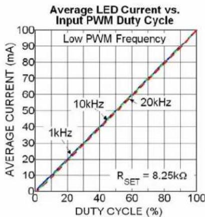
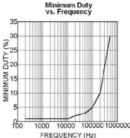
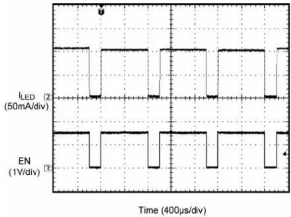
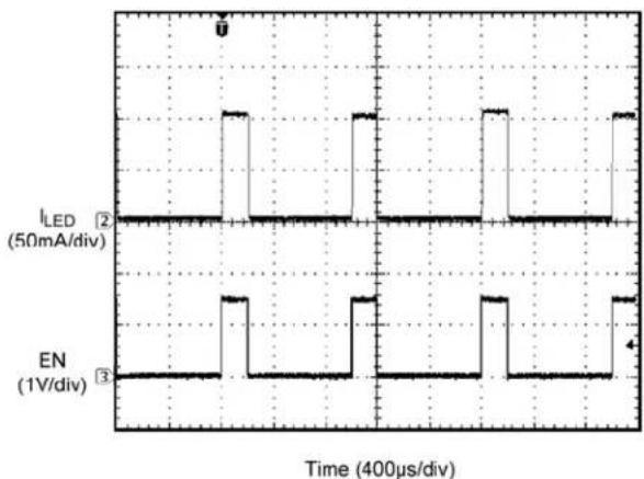
WLED dimming is achieved by pulse width modulating the linear drivers which are controlled by a PWM signal to the EN pin. For PWM frequencies between 200Hz – 20kHz the MIC4812 supports a duty cycle range from 1% to 100%, see Figure 3. The MIC4812 incorporates an internal shutdown delay to ensure that the internal control circuitry remains active during PWM dimming. This feature prevents the possibility of backlight flickering when using low frequency PWM control signals. The MIC4812 also supports Ultra Fast PWM™ frequencies from 20kHz to 500kHz. Due to input signal propagation delay, PWM frequencies above 20kHz have a non-linear relationship between the duty cycle and the average LED current, see Figures 4 and 5. Figures 6 through 10 show the WLED current response when a PWM signal is applied to the END pin ^(1) .
(1) From the low lq sleep mode higher PWM frequencies may require a logic high enable signal for 60 s to first enable the MIC4812 prior to PWM dimming.
line
| DUTY CYCLE (%) | AVERAGE CURRENT (mA) | | -------------- | ------------------- | | 20 | 25 | | 40 | 45 | | 60 | 60 | | 80 | 80 | | 100 | 100 |Figure 3. Average Current per LED Dimming by Changing PWM Duty Cycle for PWM Frequencies up to 20kHz
Average LED Current vs. Input PWM Duty Cycle

line
| DUTY CYCLE (%) | AVERAGE CURRENT (mA) | | -------------- | ------------------- | | 0 | 0 | | 20 | 10 | | 40 | 30 | | 60 | 50 | | 80 | 70 | | 100 | 90 |Figure 4. Channel Current Response to PWM Control Signal Frequencies from 50kHz to 500kHz
line
| FREQUENCY (Hz) | MINIMUM DUTY (%) | | -------------- | ---------------- | | 100 | 0 | | 1000 | 0 | | 10000 | 0 | | 100000 | 5 | | 1000000 | 30 |Figure 5. Minimum Duty Cycle for Varying PWM Frequency
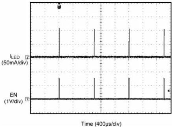
Figure 6. PWM Signal at 1% Duty Cycle ( I_avg = 1mA ) Figure 9. PWM Signal at 80% Duty Cycle (I
line
| Time (400μs/div) | I_LED (50mA/div) | EN (1V/div) | | ---------------- | ---------------- | ----------- | | 0 | 2 | 3 | | 1 | 2 | 3 | | 2 | 2 | 3 | | 3 | 2 | 3 | | 4 | 2 | 3 | | 5 | 2 | 3 | | 6 | 2 | 3 | | 7 | 2 | 3 | | 8 | 2 | 3 | | 9 | 2 | 3 | | 10 | 2 | 3 | | 11 | 2 | 3 | | 12 | 2 | 3 | | 13 | 2 | 3 | | 14 | 2 | 3 | | 15 | 2 | 3 | | 16 | 2 | 3 | | 17 | 2 | 3 | | 18 | 2 | 3 | | 19 | 2 | 3 | | 20 | 2 | 3 | | 21 | 2 | 3 | | 22 | 2 | 3 | | 23 | 2 | 3 | | 24 | 2 | 3 | | 25 | 2 | 3 | | 26 | 2 | 3 | | 27 | 2 | 3 | | 28 | 2 | 3 | | 29 | 2 | 3 | | 30 | 2 | 3 | | 31 | 2 | 3 | | 32 | 2 | 3 | | 33 | 2 | 3 | | 34 | 2 | 3 | | 35 | 2 | 3 | | 36 | 2 | 3 | | 37 | 2 | 3 | | 38 | 2 | 3 | | 39 | 2 | 3 | | 40 | 2 | 3 | | 41 | 2 | 3 | | 42 | 2 | 3 | | 43 | 2 | 3 | | 44 | 2 | 3 | | 45 | 2 | 3 | | 46 | 2 | 3 | | 47 | 2 | 3 | | 48 | 2 | 3 | | 49 | 2 | 3 | | 50 | 2 | 3 | | Note: The actual values for I_LED and EN are not provided in the code. The data is generated using numpy's LED and EN functions. There is only one data series in this case. The values for I_LED and EN are estimated based on the input conditions specified in the code.avg = 80mA)
line
| Time (μs) | I_LED (50mA/div) | EN (1V/div) | |-----------|------------------|-------------| | 0 | 2 | 3 | | 400 | 2 | 3 | | 800 | 2 | 3 | | 1200 | 2 | 3 | | 1600 | 2 | 3 | | 2000 | 2 | 3 | | 2400 | 2 | 3 | | 2800 | 2 | 3 | | 3200 | 2 | 3 | | 3600 | 2 | 3 | | 4000 | 2 | 3 | | 4400 | 2 | 3 | | 4800 | 2 | 3 | | 5200 | 2 | 3 | | 5600 | 2 | 3 | | 6000 | 2 | 3 | | 6400 | 2 | 3 | | 6800 | 2 | 3 | | 7200 | 2 | 3 | | 7600 | 2 | 3 | | 8000 | 2 | 3 | | 8400 | 2 | 3 | | 8800 | 2 | 3 | | 9200 | 2 | 3 | | 9600 | 2 | 3 | | 10000 | 2 | 3 | | 10400 | 2 | 3 | | 10800 | 2 | 3 | | 11200 | 2 | 3 | | 11600 | 2 | 3 | | 12000 | 2 | 3 | | 12400 | 2 | 3 | | 12800 | 2 | 3 | | 13200 | 2 | 3 | | 13600 | 2 | 3 | | 14000 | 2 | 3 | | 14400 | 2 | 3 | | 14800 | 2 | 3 | | 15200 | 2 | 3 | | 15600 | 2 | 3 | | 16000 | 2 | 3 | | 16400 | 2 | 3 | | 16800 | 2 | 3 | | 17200 | 2 | 3 | | 17600 | 2 | 3 | | 18000 | 2 | 3 | | 18400 | 2 | 3 | | 18800 | 2 | 3 | | 19200 | 2 | 3 | | 19600 | 2 | 3 | | 20000 | 2 | 3 | | | | |Figure 7. PWM Signal at 20% Duty Cycle ( I_avg = 20mA )

line
| Time (400μs/div) | I_LED (50mA/div) | EN (1V/div) | | ---------------- | ---------------- | ----------- | | 0 | 2 | 3 |Figure 10. PWM Signal at 100% Duty Cycle ( I_avg = 100mA )

line
| Time (400μs/div) | I_LED (50mA/div) | EN (1V/div) | | ---------------- | ---------------- | ----------- | | 0 | 0 | 0 | | 2 | 0 | 0 | | 4 | 0 | 0 | | 6 | 0 | 0 | | 8 | 0 | 0 | | 10 | 0 | 0 | | 12 | 0 | 0 | | 14 | 0 | 0 | | 16 | 0 | 0 | | 18 | 0 | 0 | | 20 | 0 | 0 | | 22 | 0 | 0 | | 24 | 0 | 0 | | 26 | 0 | 0 | | 28 | 0 | 0 | | 30 | 0 | 0 | | 32 | 0 | 0 | | 34 | 0 | 0 | | 36 | 0 | 0 | | 38 | 0 | 0 | | 40 | 0 | 0 | | 42 | 0 | 0 | | 44 | 0 | 0 | | 46 | 0 | 0 | | 48 | 0 | 0 | | 50 | 0 | 0 | | 52 | 0 | 0 | | 54 | 0 | 0 | | 56 | 0 | 0 | | 58 | 0 | 0 | | 60 | 0 | 0 | | 62 | 0 | 0 | | 64 | 0 | 0 | | 66 | 0 | 0 | | 68 | 0 | 0 | | 70 | 0 | 0 | | 72 | 0 | 0 | | 74 | 0 | 0 | | 76 | 0 | 0 | | 78 | 0 | 0 | | 80 | 0 | 0 | | 82 | 0 | 0 | | 84 | 0 | 0 | | 86 | 0 | 0 | | 88 | 0 | 0 | | 90 | 0 | 0 | | 92 | 0 | 0 | | 94 | 0 | 0 | | 96 | 0 | 0 | | 98 | 0 | 0 | | 100 | 0 | 0 | | -1 | -1 | -1 | | -2 | -2 | -2 | | -3 | -3 | -3 | | -4 | -4 | -4 | | -5 | -5 | -5 | | -6 | -6 | -6 | | -7 | -7 | -7 | | -8 | -8 | -8 | | -9 | -9 | -9 | | -10 | -10 | -10 | | -11 | -11 | -11 | | -12 | -12 | -12 | | -13 | -13 | -13 | | -14 | -14 | -14 | | -15 | -15 | -15 | | -16 | -16 | -16 | | -17 | -17 | -17 | | -18 | -18 | -18 | | -19 | -19 | -19 | | -20 | -20 | -20 | | -21 | -21 | -21 | | -22 | -22 | -22 | | -23 | -23 | -23 | | -24 | -24 | -24 | | -25 | -25 | -25 | | -26 | -26 | -26 | | -27 | -27 | -27 | | -28 | -28 | -28 | | -29 | -29 | -29 | | -30 | -30 | -30 | | -31 | -31 | -31 | | -32 | -32 | -32 | | -33 | -33 | -33 | | -34 | -34 | -34 | | -35 | -35 | -35 | | -36 | -36 | -36 | | -37 | -37 | -37 | | -38 | -38 | -38 | | -39 | -39 | -39 | | -40 | -40 | -40 | | -41 | -41 | -41 | | -42 | -42 | -42 | | -43 | -43 | -43 | | -44 | -44 | -44 | | -45 | -45 | -45 | | -46 | -46 | -46 | | -47 | -47 | -47 | | -48 | -48 | -48 | | -49 | -49 | -49 | | -50 | -50 | -50 | | -51 | -51 | -51 | | -52 | -52 | -52 | | -53 | -53 | -53 | | -54 | -54 | -54 | | -55 | -55 | -55 | | -56 | -56 | -56 | | -57 | -57 | -57 | | -58 | -58 | -58 | | -59 | -59 | -59 | | -60 | -60 | -60 | | -61 | -61 | -61 | | -62 | -62 | -62 | | -63 | -63 | -63 | | -64 | -64 | -64 | | -65 | -65 | -65 | | -66 | -66 | -66 | | -67 | -67 | -67 | | -68 | -68 | -68 | | -69 | -69 | -69 | | -70 | -70 | -70 | | -71 | -71 | -71 | | -72 | -72 | -72 | | -73 | -73 | -73 | | -74 | -74 | -74 | | -75 | -75 | -75 | | -76 | -76 | -76 | | -77 | -77 | -77 | | -78 | -78 | -78 | | -79 | -79 | -79 | | -80 | -80 | -80 | | +1 | +1 +2 | +1 | | +2 +3 | +2 +3 | +2 | | +3 +4 | +3 +4 | +3 | | +4 +5 | +4 +5 | +4 | | +5 +6 | +5 +6 | +5 | | +6 +7 | +6 +7 | +6 | | +7 +8 | +7 +8 | +7 | | +8 +9 | +8 +9 | +8 | | +9 +10 | +9 +10 | +9 | | +10 +11 | +10 +11 | +10 | | +11 +12 | +11 +12 | +11 | | +12 +13 | +12 +13 | +12 | | +13 +14 | +13 +14 | +13 | | +14 +15 | +14 +15 | +14 | | +15 +16 | +15 +16 | +15 | | +16 +17 | +16 +17 | +16 | | +17 +18 | +17 +18 | +17 | | +18 +19 | +18 +19 | +18 | | +19 +20 | +19 +20 | +19 | | +20 +21 | +20 +21 | +20 | | +21 +22 | +21 +22 | +21 | | +22 +23 | +22 +23 | +22 | | +23 +24 | +23 +24 | +23 | | +24 +25 | +24 +25 | +24 | | +25 +26 | +25 +26 | +25 | | +26 +27 | +26 +27 | +26 | | +27 +28 | +27 +28 | +27 | | +28 +29 | +28 +29 | +28 | | +29 +30 | +29 +30 | +29 | | +30 +31 | +30 +31 | +30 | | +31 +32 | +31 +32 | +31 | | +32 +33 | +32 +33 | +32 | | +33 +34 | +33 +34 | +33 | | +34 +35 | +34 +35 | +34 | | +35 +36 | +35 +36 | +35 | | +36 +37 | +36 +37 | +36 | | +37 +38 | +37 +38 | +37 | | +38 +39 | +38 +39 | +38 | | +39 +40 | +39 +40 | +39 | | +40 +41 | +40 +41 | +40 | | +41 +42 | +41 +42 | +41 | | +42 +43 | +42 +43 | +42 | | +43 +44 | +43 +44 | +43 | | +44 +45 | +44 +45 | +44 | | +45 +46 | +45 +46 | +45 | | +46 +47 | +46 +47 | +46 | | +47 +48 | +47 +48 | +47 | | +48 +49 | +48 +49 | +48 | | +49 +50 | +49 +50 | +49 | | +50 = U U U U U U U U U U U U U U U U U U U U U U U U U U U U U U U U U U U U U U U U U U U U U U U U U U U - ↓ - EN (EN) EN (EN) EN (EN) EN (EN) EN (EN) EN (EN) EN (EN) EN (EN) EN (EN) EN (EN) EN (EN) EN (EN) EN (EN) EN (EN) EN (EN) EN (EN) EN (EN) EN (EN) EN (EN) EN (EN) EN (EN) - ↓ - ↓ - ↓ - ↓ - ↓ - ↓ - ↓ - ↓ - ↓ - ↓ - ↓ - ↓ - ↓ - ↓ - ↓ - ↓ - ↓ - ↓ - ↓ - ↓ - ↓ - ↓ - ↓ - ↓ - ↓ - ↓Figure 8. PWM Signal at 50% Duty Cycle ( I_avg = 50mA )
Input Capacitor
The MIC4812 is a high-performance, high bandwidth device. Stability can be maintained using a ceramic input capacitor of 2.2 F . Low-ESR ceramic capacitors provide optimal performance at a minimum amount of space. X5R or X7R dielectrics are recommended for the input capacitor. Y5V dielectrics lose most of their capacitance over temperature and are therefore, not recommended.
MIC4812 Typical Application Circuit
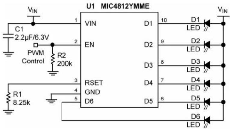
text_image
U1 MIC4812YMME VIN C1 2.2µF/6.3V PWM Control R2 200k VIN EN RSET GND D6 1 2 3 4 5 10 D1 9 D2 8 D3 7 D4 6 D5 D6 LED LED LED LED LED LED VINBill of Materials
| Item | Part Number | Manufacturer | Description | ||
| C1 | C1608X5R0J225K | TDK^(1) | Ceramic Capacitor, 2.2μF, 6.3V, X5R, Size 0603 1 | ||
| 06036D225KAT2A | AVX^(2) | ||||
| GRM188R60J225KE19D | Murata^(3) | ||||
| VJ0603G225KXYAT | Vishay^(4) | ||||
| D1 – D6 | OVS5WBCR4 | OPTEK | Technology^(5) , Inc | WLED | 6 |
| R1 | CRCW06038K25F5EA | Vishay^(4) Resistor, | 8.25k, 1%, 1/16W, Size 0603 1 | ||
| R2 | CRCW06032003FKEA | Vishay^(4) Resistor, | 200k, 1%, 1/16W, Size 0603 1 | ||
| U1 | MIC4812YMME | Micfel^(6) | High Current 6 Channel Linear WLED Driver with DAM^TM and Ultra Fast PWM^TM Control | 1 | |
Notes:
1. TDK: www.tdk.com
2. AVX: www.avx.com
3. Murata: www.murata.com
4. Vishay: www.vishay.com
5. OPTEK: www.optekinc.com
6. Micrel, Inc.: www.micrel.com
Qty.
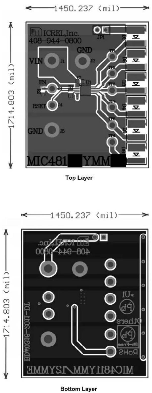
PCB Layout Recommendations
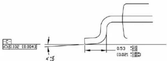
Package Information
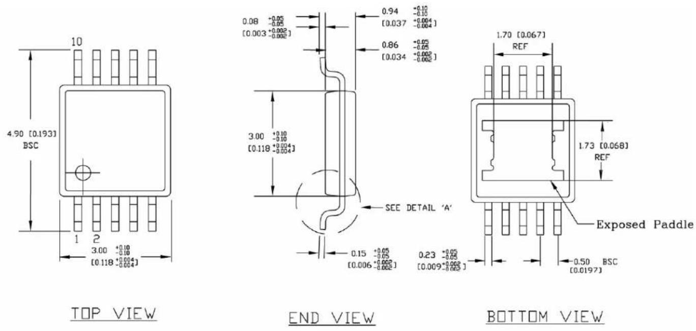
text_image
C 0.102 [0.004] 4° +0.5 -0.4 0.53 +0.10 -0.10 [0.021 -0.004]DETAIL A
NOTES:
1. DIMENSIONS ARE IN MM [INCHES].
2. CONTROLLING DIMENSION: MM
3. DIMENSION DOES NOT INCLUDE MOLD FLASH OR PROTRUSIONS, EITHER OF WHICH SHALL NOT EXCEED 0.20 [0.008] PER SIDE.
10-Pin EPAD MSOP (MME)
MICREL, INC. 2180 FORTUNE DRIVE SAN JOSE, CA 95131 USA
TEL +1 (408) 944-0800 FAX +1 (408) 474-1000 WEB http://www.micrel.com
Micrel makes no representations or warranties with respect to the accuracy or completeness of the information furnished in this data sheet. This information is not intended as a warranty and Micrel does not assume responsibility for its use. Micrel reserves the right to change circuitry, specifications and descriptions at any time without notice. No license, whether express, implied, arising by estoppel or otherwise, to any intellectual property rights is granted by this document. Except as provided in Micrel's terms and conditions of sale for such products, Micrel assumes no liability whatsoever, and Micrel disclaims any express or implied warranty relating to the sale and/or use of Micrel products including liability or warranties relating to fitness for a particular purpose, merchantability, or infringement of any patent, copyright or other intellectual property right.
Micrel Products are not designed or authorized for use as components in life support appliances, devices or systems where malfunction of a product can reasonably be expected to result in personal injury. Life support devices or systems are devices or systems that (a) are intended for surgical implant into the body or (b) support or sustain life, and whose failure to perform can be reasonably expected to result in a significant injury to the user. A Purchaser's use or sale of Micrel Products for use in life support appliances, devices or systems is a Purchaser's own risk and Purchaser agrees to fully indemnify Micrel for any damages resulting from such use or sale.
© 2010 Micrel, Incorporated.