MIC5203 - Electronic component Microchip - Free user manual and instructions
Find the device manual for free MIC5203 Microchip in PDF.

User questions about MIC5203 Microchip
0 question about this device. Answer the ones you know or ask your own.
Ask a new question about this device
Download the instructions for your Electronic component in PDF format for free! Find your manual MIC5203 - Microchip and take your electronic device back in hand. On this page are published all the documents necessary for the use of your device. MIC5203 by Microchip.
USER MANUAL MIC5203 Microchip
μCap 80 mA LDO Regulator
Features
- Tiny 4- and 5-Lead Surface-Mount Packages
- Wide Selection of Output Voltages
• Guaranteed 80 mA Output - Low Quiescent Current
- Low Dropout Voltage
- Low Temperature Coefficient
• Current and Thermal Limiting - Reversed Input Polarity Protection
• Zero Off-Mode Current - Logic-Controlled Shutdown
• Stability with Low-ESR Ceramic Capacitors
Applications
- Cellular Telephones
• Laptop, Notebook, and Palmtop Computers - Battery-Powered Equipment
- Barcode Scanners
• SMPS Post-Regulator and DC/DC Modules
• High-Efficiency Linear Power Supplies
General Description
The MIC5203 is a Cap 80 mA linear voltage regulator with very low dropout voltage (typically 20 mV at light loads and 300 mV at 80 mA) and very low ground current (225 A at 20 mA output), offering better than 3% initial accuracy with a logic-compatible enable input.
The Cap regulator design is optimized to work with low-value, low-cost ceramic capacitors. The outputs typically require only 0.47 F of output capacitance for stability.
Designed especially for hand-held, battery-powered devices, the MIC5203 can be controlled by a CMOS or TTL compatible logic signal. When disabled, power consumption drops nearly to zero. If on-off control is not required, the enable pin may be tied to the input for 3-terminal operation. The ground current of the MIC5203 increases only slightly in dropout, further prolonging battery life. Key MIC5203 features include current limiting, overtemperature shutdown, and protection against reversed battery.
The MIC5203 is available in 2.8V, 3.0V, 3.3V, 3.6V, 3.8V, 4.0V, 4.5V, 4.75V, and 5.0V fixed voltages. Other voltages are available.
Package Types
MIC5203
4-Lead SOT-143 (M4)

text_image
EN 2 Part Identification LAxx 3 4 OUTIN GND 1MIC5203
5-Lead SOT-23 (M5)

Typical Application Circuits
MIC5203
4-Lead SOT-143

text_image
Enable Shutdown 2 1 LAxx + 3 4 VOUT 0.47μFMIC5203
5-Lead SOT-23
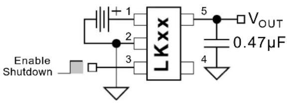
text_image
Enable Shutdown + 1 2 3 L × × 5 VOUT 0.47μF 41.0 ELECTRICAL CHARACTERISTICS
Absolute Maximum Ratings †
Supply Input Voltage ( V_IN ) -20V to +20V
Enable Input Voltage ( V_EN )....-20V to +20V
Power Dissipation ( P_D ) (Note 1)....Internally Limited
Operating Ratings ‡
Supply Input Voltage ( V_IN ) ....+2.5V to +16V
Enable Input Voltage ( V_EN )....0V to V_IN
† Notice: Stresses above those listed under “Absolute Maximum Ratings” may cause permanent damage to the device. This is a stress rating only and functional operation of the device at those or any other conditions above those indicated in the operational sections of this specification is not intended. Exposure to maximum rating conditions for extended periods may affect device reliability.
‡ Notice: The device is not guaranteed to function outside its operating ratings.
Note 1: The maximum allowable power dissipation at any T_A (ambient temperature) is P_D(MAX) = (T_J(MAX) - T_A)/_JA . Exceeding the maximum allowable power dissipation will result in excessive die temperature, and the regulator will go into thermal shutdown. The _JA of the MIC5205-xxYM5 (all versions) is 220°C/W mounted on a PC board.
ELECTRICAL CHARACTERISTICS
Electrical Characteristics: V_IN = V_OUT + 1V ; I_L = 1 mA ; C_L = 0.47 F ; V_EN ≥ 2.0V ; T_J = +25^ , bold values indicate -40^ < T_J ≤ +125^ , unless noted.
| Parameter Symbol Min. Typ. | Max. Units | Conditions | ||||
| Output Voltage Accuracy | V_O | -3 | — | 3 | % | — |
| -4 | — | 4 | ||||
| Output Voltage Temperature Coefficient | V_O/ T | — | 50 | 200 | ppm/°C | Note 1 |
| Line Regulation | V_O/V_O | — | 0.008 | 0.3 | % | V_IN=V_OUT+1V to 16V |
| — | — | 0.5 | ||||
| Load Regulation | V_O/V_O | — | 0.08 | 0.3 | % | I_L=0.1 mA to 80 mA, Note 2 |
| — | — | 0.5 | ||||
| Dropout Voltage, Note 3 | V_O/V_O | — | 20 | — | mV | I_L=100 μA |
| — | 200 | 350 | I_L=20 mA | |||
| — | 250 | — | I_L=50 mA | |||
| — | 300 | 600 | I_L=80 mA | |||
| Quiescent Current | I_Q | — | 0.01 | 10 | μA | V_EN≤0.4V (shutdown) |
| Ground Pin Current, Note 4 | I_GND | — | 180 | — | μA | I_L=100 μA, V_EN≥2.0V (active) |
| — | 225 | 750 | I_L=20 mA, V_EN≥2.0V (active) | |||
| — | 850 | — | I_L=50 mA, V_EN≥2.0V (active) | |||
| — | 1800 | 3000 | I_L=80 mA, V_EN≥2.0V (active) | |||
| Ground Pin Current at Dropout | I_GNDDO | — | 200 | 300 | μA | V_IN=V_OUT(nom)-0.5V, Note 4 |
| Current Limit | I_LIMIT | — | 180 | 250 | mA V | OUT=0V |
| Thermal Regulation | V_O/_PD | — | 0.05 | — | %/W | Note 5 |
ELECTRICAL CHARACTERISTICS (CONTINUED)
Electrical Characteristics: V_IN = V_OUT + 1V ; I_L = 1 mA ; C_L = 0.47 F ; V_EN ≥ 2.0V ; T_J = +25^ , bold values indicate -40^ < T_J ≤ +125^ , unless noted.
| Parameter | Symbol | Min. | Typ. | Max. | Units | Conditions |
| ENABLE Input | ||||||
| Enable Input Voltage Level V | IL | — — | 0.6 | V | Logic low (off) | |
| 2.0 — | — Logic | low (on) | ||||
| Enable Input Current | IIL | — 0.0 | 1 1 | μA | VIL≤ 0.6V | |
| IIH | — 15 | 50 V | IH≥ 2.0V | |||
Note 1: Output voltage temperature coefficient is defined as the worst case voltage change divided by the total temperature range.
2: Regulation is measured at constant junction temperature using low duty cycle pulse testing. Parts are tested for load regulation in the load range from 0.1 mA to 150 mA. Changes in output voltage due to heating effects are covered by the thermal regulation specification.
3: Dropout Voltage is defined as the input to output differential at which the output voltage drops 2% below its nominal value measured at 1V differential.
4: Ground pin current is the regulator quiescent current plus pass transistor base current. The total current drawn from the supply is the sum of the load current plus the ground pin current.
5: Thermal regulation is defined as the change in output voltage at a time "t" after a change in power dissipation is applied, excluding load or line regulation effects. Specifications are for a 150 mA load pulse at V_IN = 16V for t = 10 ms.
TEMPERATURE SPECIFICATIONS (Note 1)
| Parameters | Symbol | Min. | Typ. | Max. | Units | Conditions |
| Temperature Ranges | ||||||
| Junction Temperature Range T | _J | -40 — | +125 °C — | |||
| Storage Temperature Range | T_S | -60 — | +150 °C — | |||
| Lead Temperature | — | — | — | +260 | °C | Soldering, 5s |
| Package Thermal Resistances | ||||||
| Thermal Resistance SOT-143 | _JA | — 250 | — °C/W | Note 2 | ||
| Thermal Resistance SOT-23-5 | — 220 | — °C/W | ||||
Note 1: The maximum allowable power dissipation is a function of ambient temperature, the maximum allowable junction temperature and the thermal resistance from junction to air (i.e., T_A , T_J , _JA ). Exceeding the maximum allowable power dissipation will cause the device operating junction temperature to exceed the maximum +125°C rating. Sustained junction temperatures above +125°C can impact the device reliability.
2: The maximum allowable power dissipation at any T_A (ambient temperature) is P_D() = (T_J() - T_A) / _JA . Exceeding the maximum allowable power dissipation will result in excessive die temperature, and the regulator will go into thermal shutdown.
2.0 TYPICAL PERFORMANCE CURVES
Note: The graphs and tables provided following this note are a statistical summary based on a limited number of samples and are provided for informational purposes only. The performance characteristics listed herein are not tested or guaranteed. In some graphs or tables, the data presented may be outside the specified operating range (e.g., outside specified power supply range) and therefore outside the warranted range.

line
| OUTPUT CURRENT (mA) | DROPOUT VOLTAGE (mV) | | ------------------- | -------------------- | | 0.01 | ~10 | | 0.1 | ~20 | | 1 | ~50 | | 10 | ~100 | | 100 | ~200 |FIGURE 2-1: Dropout Voltage vs. Output Current.
line
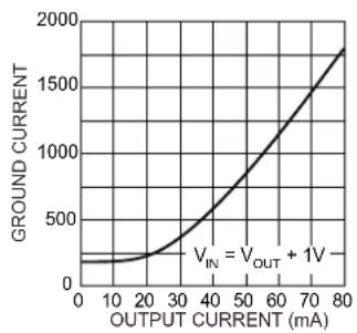
| OUTPUT CURRENT (mA) | GROUND CURRENT | | ------------------- | -------------- | | 0 | 0 | | 10 | 100 | | 20 | 200 | | 30 | 400 | | 40 | 600 | | 50 | 800 | | 60 | 1000 | | 70 | 1200 | | 80 | 1400 |FIGURE 2-4: Ground Current vs. Output Current.

line
| TEMPERATURE (°C) | DROPOUT VOLTAGE (mV) for I_L = 1mA | DROPOUT VOLTAGE (mV) for I_L = 80mA | | ---------------- | ----------------------------------- | ------------------------------------ | | -60 | ~40 | ~220 | | 0 | ~50 | ~250 | | 60 | ~60 | ~280 | | 90 | ~70 | ~300 | | 120 | ~80 | ~350 |FIGURE 2-2: Dropout Voltage vs. Temperature.
line
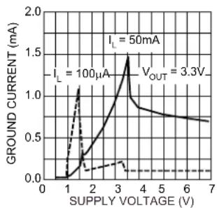
| SUPPLY VOLTAGE (V) | GROUND CURRENT (mA) | | ------------------ | ------------------- | | 1 | 0.0 | | 2 | 1.0 | | 3 | 1.5 | | 4 | 1.0 | | 5 | 0.8 | | 6 | 0.7 | | 7 | 0.6 |FIGURE 2-5: Ground Current vs. Supply Voltage.
line
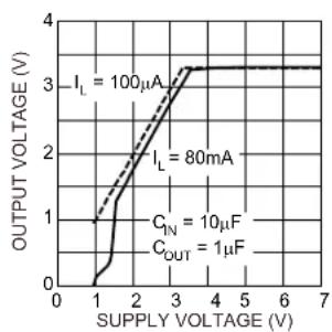
| SUPPLY VOLTAGE (V) | OUTPUT VOLTAGE (V) - IL = 100μA | OUTPUT VOLTAGE (V) - IL = 80mA | | ------------------ | ------------------------------- | ------------------------------ | | 0 | 0 | 0 | | 1 | ~0.5 | ~0.5 | | 2 | ~1.5 | ~1.5 | | 3 | ~2.5 | ~2.5 | | 4 | ~3.0 | ~3.0 | | 5 | ~3.0 | ~3.0 | | 6 | ~3.0 | ~3.0 | | 7 | ~3.0 | ~3.0 |FIGURE 2-3: Dropout Characteristics.

line
| TEMPERATURE (°C) | C_IN (mA) | C_OUT (mA) | | ---------------- | --------- | ---------- | | -60 | 1.5 | 1.0 | | -30 | 1.7 | 0.9 | | 0 | 1.8 | 0.8 | | 30 | 1.8 | 0.7 | | 60 | 1.7 | 0.6 | | 90 | 1.6 | 0.5 | | 120 | 1.5 | 0.4 |FIGURE 2-6: Ground Current vs. Temperature.
line
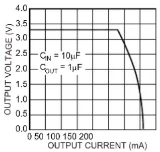
| OUTPUT CURRENT (mA) | OUTPUT VOLTAGE (V) | | ------------------- | ------------------ | | 0 | 0.0 | | 50 | 0.0 | | 100 | 0.0 | | 150 | 0.0 | | 200 | 0.0 | | 250 | 3.5 | | 300 | 3.5 | | 350 | 3.5 | | 400 | 3.5 | | 450 | 3.5 | | 500 | 3.5 | | 550 | 3.5 | | 600 | 3.5 | | 650 | 3.5 | | 700 | 3.5 | | 750 | 3.5 | | 800 | 3.5 | | 850 | 3.5 | | 900 | 3.5 | | 950 | 3.5 | | 1000 | 3.5 | | 1050 | 3.5 | | 1100 | 3.5 | | 1150 | 3.5 | | 1200 | 3.5 | | 1250 | 3.5 | | 1300 | 3.5 | | 1350 | 3.5 | | 1400 | 3.5 | | 1450 | 3.5 | | 1500 | 3.5 | | 1550 | 3.5 | | 1600 | 3.5 | | 1650 | 3.5 | | 1700 | 3.5 | | 1750 | 3.5 | | 1800 | 3.5 | | 1850 | 3.5 | | 1900 | 3.5 | | 1950 | 3.5 | | 2000 | 3.5 | | 2050 | 3.5 | | 2100 | 3.5 | | 2150 | 3.5 | | 2200 | 3.5 | | 2250 | 3.5 | | 2300 | 3.5 | | 2350 | 3.5 | | 2400 | 3.5 | | 2450 | 3.5 | | 2500 | 3.5 | | 2550 | 3.5 | | 2600 | 3.5 | | 2650 | 3.5 | | 2700 | 3.5 | | 2750 | 3.5 | | 2800 | 3.5 | | 2850 | 3.5 | | 2900 | 3.5 | | 2950 | 3.5 | | 3000 | 3.5 | | 3050 | 3.5 | | 3100 | 3.5 | | 3150 | 3.5 | | 3200 | 3.5 | | 3250 | 3.5 | | 3300 | 3.5 | | 3350 | 3.5 | | 3400 | 3.5 | | 3450 | 3.5 | | 3500 | 3.5 | | 3550 | 3.5 | | 3600 | 3.5 | | 3650 | 3.5 | | 3700 | 3.5 | | 3750 | 3.5 | | 3800 | 3.5 | | 3850 | 3.5 | | 3900 | 3.5 | | 3950 | 3.5 | | 4000 | 3.5 | | 4050 | 3.5 | | 4100 | 3.5 | | 4150 | 3.5 | | 4200 | 3.5 | | 4250 | 3.5 | | 4300 | 3.5 | | 4350 | 3.5 | | 4400 | 3.5 | | 4450 | 3.5 | | 4500 | 3.5 | | 4550 | 3.5 | | 4600 | 3.5 | | 4650 | 3.5 | | 4700 | 3.5 | | 4750 | 3.5 | | 4800 | 3.5 | | 4850 | 3.5 | | 4900 | 3.5 | | 4950 | 3.5 | | 5000 | 3.5 | | Note: The output values are labeled as 'C_IN' and 'C_OUT' respectively in the chart title, but they are not explicitly provided in the code snippet for this example.FIGURE 2-7: Output Voltage vs. Output Current.
line
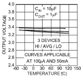
| TEMPERATURE (°C) | OUTPUT VOLTAGE (C_IN) | OUTPUT VOLTAGE (C_OUT) | | --------------- | --------------------- | ---------------------- | | -60 | 3.4 | 3.4 | | 0 | 3.3 | 3.3 | | 30 | 3.25 | 3.25 | | 60 | 3.2 | 3.2 | | 90 | 3.15 | 3.15 | | 120 | 3.1 | 3.1 | | 150 | 3.05 | 3.05 |FIGURE 2-10: Output Voltage vs. Temperature.
line
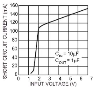
| INPUT VOLTAGE (V) | SHORT CIRCUIT CURRENT (mA) | | ----------------- | -------------------------- | | 0 | 0 | | 1 | 20 | | 2 | 100 | | 3 | 120 | | 4 | 130 | | 5 | 140 | | 6 | 150 | | 7 | 160 |FIGURE 2-8: Short Circuit vs. Input Voltage.
line
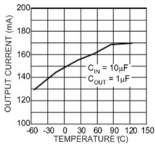
| TEMPERATURE (C) | OUTPUT CURRENT (mA) | | --------------- | ------------------- | | -60 | 130 | | -30 | 145 | | 0 | 155 | | 30 | 160 | | 60 | 165 | | 90 | 170 | | 120 | 170 |FIGURE 2-11: Short Circuit Current vs. Temperature.

line
| TIME (ms) | LOAD (mA) Δ OUTPUT (mV) | | --------- | ------------------------ | | 0 | 0 | | 2 | 0 | | 4 | 0 | | 6 | 0 | | 8 | 0 | | 10 | 50 | | 12 | 0 | | 14 | -40 | | 16 | -40 | | 18 | -40 | | 20 | -40 |FIGURE 2-9: Thermal Regulation (3.3V Version).

line
| TEMPERATURE (C) | MIN. SUPPLY VOLTAGE (V) | | --------------- | ------------------------ | | -60 | 3.35 | | 0 | 3.32 | | 30 | 3.38 | | 60 | 3.40 | | 90 | 3.42 | | 120 | 3.45 |FIGURE 2-12: Minimum Supply Voltage vs. Temperature.
line
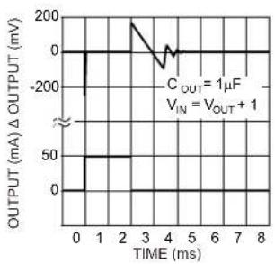
| TIME (ms) | OUTPUT (mA) Δ OUTPUT (mV) | | --------- | ------------------------- | | 0 | 0 | | 1 | 50 | | 2 | 100 | | 3 | 0 | | 4 | -100 | | 5 | 0 | | 6 | 0 | | 7 | 0 | | 8 | 0 |FIGURE 2-13: Load Transient.
line
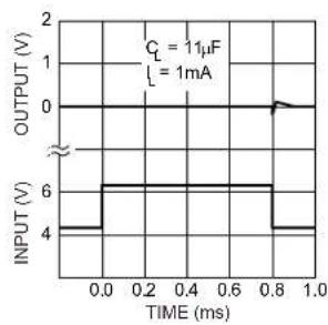
| TIME (ms) | OUTPUT (V) | INPUT (V) | | --------- | ---------- | --------- | | 0.0 | 0 | 4 | | 0.2 | 0 | 6 | | 0.4 | 0 | 6 | | 0.6 | 0 | 6 | | 0.8 | 0 | 4 | | 1.0 | 0 | 4 |FIGURE 2-16: Line Transient.
line
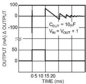
| TIME (ms) | OUTPUT (mA) Δ OUTPUT | | --------- | -------------------- | | 0 | 0 | | 5 | -100 | | 10 | 0 | | 15 | -100 | | 20 | 0 |FIGURE 2-14: Load Transient.
line
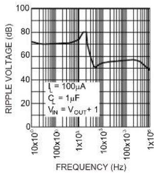
| FREQUENCY (Hz) | RIPPLE VOLTAGE (dB) | | -------------- | ------------------- | | 10x10^5 | 70 | | 100x10^4 | 70 | | 1x10^3 | 80 | | 1x10^2 | 50 | | 1x10^1 | 55 | | 1x10^0 | 50 |FIGURE 2-17: Ripple Voltage vs. Frequency.

line
| TIME (ms) | Δ OUTPUT | INPUT (V) | | --------- | --------- | --------- | | 0.0 | 0 | 6 | | 0.2 | -1 | 6 | | 0.4 | 0 | 6 | | 0.6 | 0 | 6 | | 0.8 | 0 | 6 | | 1.0 | 1 | 6 |FIGURE 2-15: Line Transient.

line
| FREQUENCY (Hz) | RIPPLE VOLTAGE (dB) | | -------------- | ------------------- | | 10x10^3 | 70 | | 1x10^3 | 85 | | 10x10^4 | 40 | | 10x10^5 | 50 | | 1x10^5 | 45 |FIGURE 2-18: Ripple Voltage vs. Frequency.

line
| FREQUENCY (Hz) | RIPPLE VOLTAGE (dB) | | -------------- | ------------------- | | 10x10^0 | 60 | | 100x10^0 | 75 | | 1x10^1 | 40 | | 10x10^2 | 30 | | 100x10^2 | 35 | | 1x10^2 | 40 |FIGURE 2-19: Ripple Voltage vs. Frequency.
line
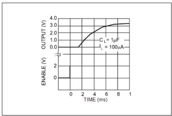
| TIME (ms) | OUTPUT (V) | | --------- | ---------- | | 0 | 0.0 | | 2 | 0.0 | | 4 | 1.0 | | 6 | 2.5 | | 8 | 3.0 | | 1 | 3.0 |FIGURE 2-22: Enable Characteristics (3.3 Version).
line
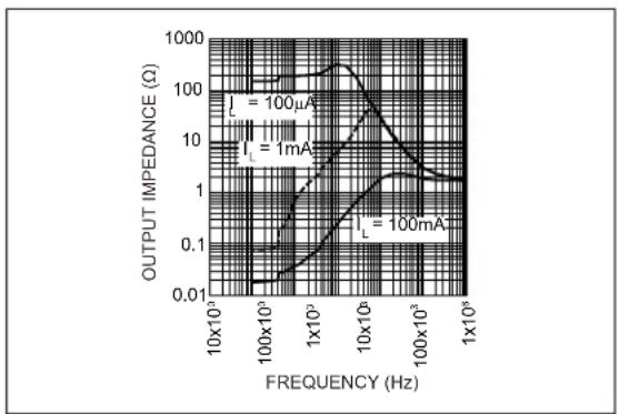
| FREQUENCY (Hz) | OUTPUT IMPEDANCE (Ω) for I_L = 100μA | OUTPUT IMPEDANCE (Ω) for I_L = 1mA | OUTPUT IMPEDANCE (Ω) for I_L = 100mA | | -------------- | ------------------------------------ | ----------------------------------- | ------------------------------------- | | 10x10³ | ~0.01 | ~0.01 | ~0.01 | | 100x10³ | ~0.1 | ~0.1 | ~0.1 | | 1x10⁴ | ~1 | ~1 | ~1 | | 10x10⁴ | ~10 | ~10 | ~1 | | 100x10⁴ | ~100 | ~100 | ~10 | | 1x10⁵ | ~100 | ~100 | ~10 |FIGURE 2-20: Output Impedance.

line
| TEMPERATURE (°C) | ENABLE VOLTAGE (mV) | | ---------------- | ------------------- | | -60 | 1.50 | | -30 | 1.25 | | 0 | 1.00 | | 30 | 0.75 | | 60 | 0.50 | | 90 | 0.25 | | 120 | 0.00 |FIGURE 2-23: Enable Voltage vs. Temperature.
line
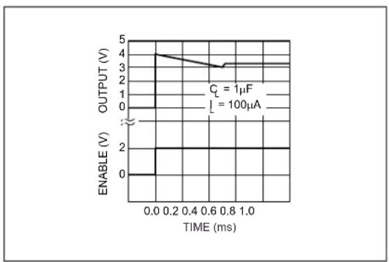
| TIME (ms) | OUTPUT (V) | ENABLE (V) | | --------- | ---------- | ---------- | | 0.0 | 4.0 | 0.0 | | 0.2 | 4.0 | 0.0 | | 0.4 | 4.0 | 0.0 | | 0.6 | 3.5 | 0.0 | | 0.8 | 3.5 | 0.0 | | 1.0 | 3.5 | 0.0 |FIGURE 2-21: Enable Characteristics (3.3 Version).
line
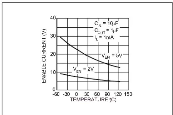
| TEMPERATURE (C) | ENABLE CURRENT (V) for V_EN = 2V | ENABLE CURRENT (V) for V_EN = 5V | | --------------- | ------------------------------- | ------------------------------- | | -60 | ~9 | ~30 | | 0 | ~7 | ~25 | | 30 | ~5 | ~20 | | 60 | ~4 | ~15 | | 90 | ~3 | ~12 | | 120 | ~2 | ~10 |FIGURE 2-24: Enable Current vs. Temperature.
3.0 PIN DESCRIPTIONS
The descriptions of the pins are listed in Table 3-1.
TABLE 3-1: PIN FUNCTION TABLE
| Pin Number SOT-143 | Pin Number SOT-23-5 | Pin Name | Description |
| 1 2 GND | Ground | ||
| 2 3 EN | Enable (Input): TTL/CMOS compatible control input. Logic high = enabled; logic low or open = shutdown | ||
| 3 1 IN Supply input | |||
| — 4 NC | Not internally connected | ||
| 4 5 | OUT Regulator output | ||
4.0 APPLICATION INFORMATION
4.1 Input Capacitor
A 0.1 F capacitor should be placed from IN to GND if there are more than 10 inches of wire between the input and the AC filter capacitor or if a battery is used as the input.
4.2 Output Capacitor
Typical PNP based regulators require an output capacitor to prevent oscillation. The MIC5203 is ultra-stable, requiring only 0.47 F of output capacitance for stability. The regulator is stable with all types of capacitors, including the tiny, low-ESR ceramic chip capacitors. The output capacitor value can be increased without limit to improve transient response.
The capacitor should have a resonant frequency above 500 kHz. Ceramic capacitors work, but some dielectrics have poor temperature coefficients, which will affect the value of the output capacitor over temperature. Tantalum capacitors are much more stable over temperature, but typically are larger and more expensive. Aluminum electrolytic capacitors will also work, but they have electrolytes that freeze at about -30^ C. Tantalum or ceramic capacitors are recommended for operation below -25^ C.
4.3 No-Load Stability
The MIC5203 will remain stable and in regulation with no load (other than the internal voltage divider) unlike many other voltage regulators. This is especially important in CMOS RAM keep-alive applications.
4.4 Enable Input
The MIC5203 features nearly zero off-mode current. When EN (enable input) is held below 0.6V, all internal circuitry is powered off. Pulling EN high (over 2.0V) reenables the device and allows operation. EN draws a small amount of current, typically 15 A. While the logic threshold is TTL/CMOS compatible, EN may be pulled as high as 20V, independent of V_IN .
5.0 PACKAGING INFORMATION
5.1 Package Marking Information
4-Lead SOT-143*

Example

5-Lead SOT-23*

Example

TABLE 5-1: MARKING CODES
| SOT-143 Part # | Marking Voltage | SOT-23 Part # | Marking Voltage | ||
| MIC5203-2.6YM4 | LA | __26 2.6V | MIC5203-2.6YM5 LK26 2.6V | — | |
| MIC5203-2.8YM4 | LA | __28 2.8V | MIC5203-2.8YM5 LK28 2.8V | — | |
| MIC5203-3.0YM4 | LA | __30 3.0V | MIC5203-3.0YM5 LK30 3.0V | — | |
| MIC5203-3.3YM4 | LA | __33 3.3V | MIC5203-3.3YM5 LK33 3.3V | — | |
| MIC5203-3.6YM4 | LA | __36 3.6V | MIC5203-3.6YM5 LK36 3.6V | — | |
| MIC5203-3.8YM4 | LA | __38 3.8V | MIC5203-3.8YM5 LK38 3.8V | — | |
| MIC5203-4.0YM4 | LA | __40 4.0V | MIC5203-4.0YM5 LK40 4.0V | — | |
| MIC5203-4.5YM4 | LA | __45 4.5V | MIC5203-4.5YM5 LK45 4.5V | — | |
| MIC5203-4.7YM4 | LA | __47 4.7V | MIC5203-4.7YM5 LK47 4.7V | — | |
| MIC5203-5.0YM4 | LA | __50 5.0V | MIC5203-5.0YM5 LK50 5.0V | — |
| Legend: XX...X Product code or customer-specific information | |
| Y | Year code (last digit of calendar year) |
| YY | Year code (last 2 digits of calendar year) |
| WW Week code (week of January 1 is week '01') | |
| NNN | Alphanumeric traceability code |
| e3 | Pb-free JEDEC® designator for Matte Tin (Sn) |
| * | This package is Pb-free. The Pb-free JEDEC designator (e3) can be found on the outer packaging for this package. |
| •, ▲, ▼ Pin one index is identified by a dot, delta up, or delta down (triangle mark). | |
| Note: | In the event the full Microchip part number cannot be marked on one line, it will be carried over to the next line, thus limiting the number of available characters for customer-specific information. Package may or may not include the corporate logo.Underbar (_) and/or Overbar (~) symbol may not be to scale. |
4-Lead SOT-143 Package Outline and Recommended Land Pattern
TITLE
4 LEAD SOT143 PACKAGE OUTLINE & RECOMMENDED LAND PATTERN
DRAWING # SOT143-4LD-PL-1
UNIT MM
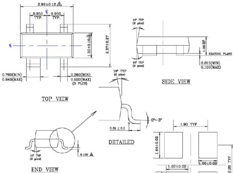
NOTE:
- Dimensions and tolerances are as per ANSI Y14.5M, 1982.
- Package surface to be mirror finish.
- Die is facing up for mold & trim/form.
④ Dimension are exclusive of mold flash and gate burr.
- Dimension are exclusive of solder plating.
text_image
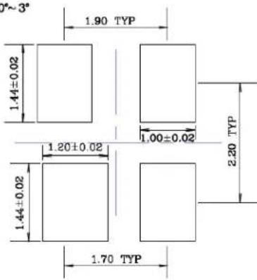
3°~3° 1.90 TYP 1.44±0.02 1.20±0.02 1.00±0.02 2.20 TYP 1.44±0.02 1.70 TYPRECOMMENDED LAND PATTERN
Note: For the most current package drawings, please see the Microchip Packaging Specification located at http://www.microchip.com/packaging.
5-Lead SOT-23 Package Outline and Recommended Land Pattern
TITLE
5 LEAD SOT23 PACKAGE OUTLINE & RECOMMENDED LAND PATTERN
DRAWING # SOT23-5LD-PL-1
UNIT MM
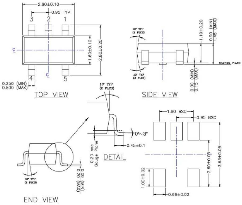
RECOMMENDED LAND PATTERN
NOTE:
1. PACKAGE OUTLINE EXCLUSIVE OF MOLD FLASH & BURR.
2. PACKAGE OUTLINE INCLUSIVE OF SOLER PLATING.
3. DIMENSION AND TOLERANCE PER ANSI Y14.5M, 1982.
4. FOOT LENGTH MEASUREMENT BASED ON GAUGE PLANE METHOD.
5. DIE FACES UP FOR MOLD, AND FACES DOWN FOR TRIM/FORM.
6. ALL DIMENSIONS ARE IN MILLIMETERS.
Note: For the most current package drawings, please see the Microchip Packaging Specification located at http://www.microchip.com/packaging.
NOTES:
APPENDIX A: REVISION HISTORY
Revision A (November 2021)
- Converted Micrel document MIC5203 to Microchip data sheet DS20006609A.
- Minor text changes throughout.
NOTES:
PRODUCT IDENTIFICATION SYSTEM
To order or obtain information, e.g., on pricing or delivery, contact your local Microchip representative or sales office.

Device

Voltage

Temperature

Package

Media Type
Device: MIC5203: μCap 80 mA LDO Regulator
Voltage: 2.8 = 2.8V
3.0 = 3.0V
3.3 = 3.3V
3.6 = 3.6V
3.8 = 3.8V
4.0 = 4.0V
4.5 = 4.5V
4.75 = 4.75V
5.0 = 5.0V
Temperature: Y = -40°C to +125°C
Package: M4 = 4-Lead SOT-143
M5 = 5-Lead SOT-23
Media Type:
TR = 3,000/Reel
Examples:
a) MIC5203-2.8YM4-TR MIC5203, μCap 80 mA LDO
Regulator, -40^ to +125^ ,
Temperature Range, 4-Lead
SOT-143, 3,000/Reel
b) MIC5203-5.0YM5-TR MIC5203, μCap 80 mA LDO
Regulator, -40^ to +125^ ,
Temperature Range, 5-Lead
SOT-23-5, 3,000/Reel
Note 1: Tape and Reel identifier only appears in the catalog part number description. This identifier is used for ordering purposes and is not printed on the device package. Check with your Microchip Sales Office for package availability with the Tape and Reel option.
NOTES:
Note the following details of the code protection feature on Microchip products:
• Microchip products meet the specifications contained in their particular Microchip Data Sheet.
- Microchip believes that its family of products is secure when used in the intended manner, within operating specifications, and under normal conditions.
- Microchip values and aggressively protects its intellectual property rights. Attempts to breach the code protection features of Microchip product is strictly prohibited and may violate the Digital Millennium Copyright Act.
- Neither Microchip nor any other semiconductor manufacturer can guarantee the security of its code. Code protection does not mean that we are guaranteeing the product is “unbreakable”. Code protection is constantly evolving. Microchip is committed to continuously improving the code protection features of our products.
This publication and the information herein may be used only with Microchip products, including to design, test, and integrate Microchip products with your application. Use of this information in any other manner violates these terms. Information regarding device applications is provided only for your convenience and may be superseded by updates. It is your responsibility to ensure that your application meets with your specifications. Contact your local Microchip sales office for additional support or, obtain additional support at https://www.microchip.com/en-us/support/design-help/client-support-services.
THIS INFORMATION IS PROVIDED BY MICROCHIP "AS IS". MICROCHIP MAKES NO REPRESENTATIONS OR WARRANTIES OF ANY KIND WHETHER EXPRESS OR IMPLIED, WRITTEN OR ORAL, STATUTORY OR OTHERWISE, RELATED TO THE INFORMATION INCLUDING BUT NOT LIMITED TO ANY IMPLIED WARRANTIES OF NON-INFRINGEMENT, MERCHANTABILITY, AND FITNESS FOR A PARTICULAR PURPOSE, OR WARRANTIES RELATED TO ITS CONDITION, QUALITY, OR PERFORMANCE.
IN NO EVENT WILL MICROCHIP BE LIABLE FOR ANY INDIRECT, SPECIAL, PUNITIVE, INCIDENTAL, OR CONSEQUENTIAL LOSS, DAMAGE, COST, OR EXPENSE OF ANY KIND WHATSOEVER RELATED TO THE INFORMATION OR ITS USE, HOWEVER CAUSED, EVEN IF MICROCHIP HAS BEEN ADVISED OF THE POSSIBILITY OR THE DAMAGES ARE FORESEEABLE. TO THE FULLEST EXTENT ALLOWED BY LAW, MICROCHIP'S TOTAL LIABILITY ON ALL CLAIMS IN ANY WAY RELATED TO THE INFORMATION OR ITS USE WILL NOT EXCEED THE AMOUNT OF FEES, IF ANY, THAT YOU HAVE PAID DIRECTLY TO MICROCHIP FOR THE INFORMATION.
Use of Microchip devices in life support and/or safety applications is entirely at the buyer's risk, and the buyer agrees to defend, indemnify and hold harmless Microchip from any and all damages, claims, suits, or expenses resulting from such use. No licenses are conveyed, implicitly or otherwise, under any Microchip intellectual property rights unless otherwise stated.
Trademarks
The Microchip name and logo, the Microchip logo, Adaptec, AnyRate, AVR, AVR logo, AVR Freaks, BesTime, BitCloud, CryptoMemory, CryptoRF, dsPIC, flexPWR, HELDO, IGLOO, JukeBlox, KeeLoq, Kleer, LANCheck, LinkMD, maXStylus, maXTouch, MediaLB, megaAVR, Microsemi, Microsemi logo, MOST, MOST logo, MPLAB, OptoLyzer, PIC, picoPower, PICSTART, PIC32 logo, PolarFire, Prochip Designer, QTouch, SAM-BA, SenGenuity, SpyNIC, SST, SST Logo, SuperFlash, Symmetricom, SyncServer, Tachyon, TimeSource, tinyAVR, UNI/O, Vectron, and XMEGA are registered trademarks of Microchip Technology Incorporated in the U.S.A. and other countries.
AgileSwitch, APT, ClockWorks, The Embedded Control Solutions Company, EtherSynch, Flashtec, Hyper Speed Control, HyperLight Load, IntelliMOS, Libero, motorBench, mTouch, Powermite 3, Precision Edge, ProASIC, ProASIC Plus, ProASIC Plus logo, Quiet-Wire, SmartFusion, SyncWorld, Temux, TimeCesium, TimeHub, TimePictra, TimeProvider, TrueTime, WinPath, and ZL are registered trademarks of Microchip Technology Incorporated in the U.S.A.
Adjacent Key Suppression, AKS, Analog-for-the-Digital Age, Any Capacitor, AnyIn, AnyOut, Augmented Switching, BlueSky, BodyCom, CodeGuard, CryptoAuthentication, CryptoAutomotive, CryptoCompanion, CryptoController, dsPICDEM, dsPICDEM.net, Dynamic Average Matching, DAM, ECAN, Espresso T1S, EtherGREEN, GridTime, IdealBridge, In-Circuit Serial Programming, ICSP, INICnet, Intelligent Paralleling, Inter-Chip Connectivity, JitterBlocker, Knob-on-Display, maxCrypto, maxView, memBrain, Mindi, MiWi, MPASM, MPF, MPLAB Certified logo, MPLIB, MPLINK, MultiTRAK, NetDetach, NVM Express, NVMe, Omniscient Code Generation, PICDEM, PICDEM.net, PICkit, PICtail, PowerSmart, PureSilicon, QMatrix, REAL ICE, Ripple Blocker, RTAX, RTG4, SAM-ICE, Serial Quad I/O, simpleMAP, SimpliPHY, SmartBuffer, SmartHLS, SMART-I.S., storClad, SQI, SuperSwitcher, SuperSwitcher II, Switchtec, SynchroPHY, Total Endurance, TSHARC, USBCheck, VariSense, VectorBlox, VeriPHY, ViewSpan, WiperLock, XpressConnect, and ZENA are trademarks of Microchip Technology Incorporated in the U.S.A. and other countries.
SQTP is a service mark of Microchip Technology Incorporated in the U.S.A.
The Adaptec logo, Frequency on Demand, Silicon Storage Technology, Symmcom, and Trusted Time are registered trademarks of Microchip Technology Inc. in other countries.
GestIC is a registered trademark of Microchip Technology Germany II GmbH & Co. KG, a subsidiary of Microchip Technology Inc., in other countries.
All other trademarks mentioned herein are property of their respective companies.
© 2021, Microchip Technology Incorporated and its subsidiaries.
All Rights Reserved.
ISBN: 978-1-5224-9289-4
For information regarding Microchip's Quality Management Systems, please visit www.microchip.com/quality.
Worldwide Sales and Service
AMERICAS
Corporate Office
2355 West Chandler Blvd.
Chandler, AZ 85224-6199
Tel: 480-792-7200
Fax: 480-792-7277
Technical Support:
http://www.microchip.com/
support
Web Address:
www.microchip.com
Atlanta
Duluth, GA
Tel: 678-957-9614
Fax: 678-957-1455
Austin, TX
Tel: 512-257-3370
Boston
Westborough, MA
Tel: 774-760-0087
Fax: 774-760-0088
Chicago
Itasca, IL
Tel: 630-285-0071
Fax: 630-285-0075
Dallas
Addison, TX
Tel: 972-818-7423
Fax: 972-818-2924
Detroit
Novi, MI
Tel: 248-848-4000
Houston, TX
Tel: 281-894-5983
Indianapolis
Noblesville, IN
Tel: 317-773-8323
Fax: 317-773-5453
Tel: 317-536-2380
Los Angeles
Mission Viejo, CA
Tel: 949-462-9523
Fax: 949-462-9608
Tel: 951-273-7800
Raleigh, NC
Tel: 919-844-7510
New York, NY
Tel: 631-435-6000
San Jose, CA
Tel: 408-735-9110
Tel: 408-436-4270
Canada - Toronto
Tel: 905-695-1980
Fax: 905-695-2078
ASIA/PACIFIC
Australia - Sydney
Tel: 61-2-9868-6733
China - Beijing
Tel: 86-10-8569-7000
China - Chengdu
Tel: 86-28-8665-5511
China - Chongqing
Tel: 86-23-8980-9588
China - Dongguan
Tel: 86-769-8702-9880
China - Guangzhou
Tel: 86-20-8755-8029
China - Hangzhou
Tel: 86-571-8792-8115
China - Hong Kong SAR
Tel: 852-2943-5100
China - Nanjing
Tel: 86-25-8473-2460
China - Qingdao
Tel: 86-532-8502-7355
China - Shanghai
Tel: 86-21-3326-8000
China - Shenyang
Tel: 86-24-2334-2829
China - Shenzhen
Tel: 86-755-8864-2200
China - Suzhou
Tel: 86-186-6233-1526
China - Wuhan
Tel: 86-27-5980-5300
China - Xian
Tel: 86-29-8833-7252
China - Xiamen
Tel: 86-592-2388138
China - Zhuhai
Tel: 86-756-3210040
ASIA/PACIFIC
India - Bangalore
Tel: 91-80-3090-4444
India - New Delhi
Tel: 91-11-4160-8631
India - Pune
Tel: 91-20-4121-0141
Japan - Osaka
Tel: 81-6-6152-7160
Japan - Tokyo
Tel: 81-3-6880-3770
Korea - Daegu
Tel: 82-53-744-4301
Korea - Seoul
Tel: 82-2-554-7200
Malaysia - Kuala Lumpur
Tel: 60-3-7651-7906
Malaysia - Penang
Tel: 60-4-227-8870
Philippines - Manila
Tel: 63-2-634-9065
Singapore
Tel: 65-6334-8870
Taiwan - Hsin Chu
Tel: 886-3-577-8366
Taiwan - Kaohsiung
Tel: 886-7-213-7830
Taiwan - Taipei
Tel: 886-2-2508-8600
Thailand - Bangkok
Tel: 66-2-694-1351
Tel: 43-7242-2244-39
Fax: 43-7242-2244-393
Denmark - Copenhagen
Tel: 45-4485-5910
Fax: 45-4485-2829
Finland - Espoo
Tel: 358-9-4520-820
France - Paris
Tel: 33-1-69-53-63-20
Fax: 33-1-69-30-90-79
Germany - Garching
Tel: 49-8931-9700
Germany - Haan
Tel: 49-2129-3766400
Germany - Heilbronn
Tel: 49-7131-72400
Germany - Karlsruhe
Tel: 49-721-625370
Germany - Munich
Tel: 49-89-627-144-0
Fax: 49-89-627-144-44
Germany - Rosenheim
Tel: 49-8031-354-560
Israel - Ra'anana
Tel: 972-9-744-7705
Italy - Milan
Tel: 39-0331-742611
Fax: 39-0331-466781
Italy - Padova
Tel: 39-049-7625286
Netherlands - Drunen
Tel: 31-416-690399
Fax: 31-416-690340
Norway - Trondheim
Tel: 47-7288-4388
Poland - Warsaw
Tel: 48-22-3325737
Romania - Bucharest
Tel: 40-21-407-87-50
Spain - Madrid
Tel: 34-91-708-08-90
Fax: 34-91-708-08-91
Sweden - Gothenberg
Tel: 46-31-704-60-40
Sweden - Stockholm
Tel: 46-8-5090-4654
UK - Wokingham
Tel: 44-118-921-5800
Fax: 44-118-921-5820