MCP4023 - Potentiomètre numérique Microchip - Free user manual and instructions
Find the device manual for free MCP4023 Microchip in PDF.

User questions about MCP4023 Microchip
0 question about this device. Answer the ones you know or ask your own.
Ask a new question about this device
Download the instructions for your Potentiomètre numérique in PDF format for free! Find your manual MCP4023 - Microchip and take your electronic device back in hand. On this page are published all the documents necessary for the use of your device. MCP4023 by Microchip.
USER MANUAL MCP4023 Microchip
Low-Cost NV Digital POT with WiperLock™ Technology
Features
• Nonvolatile Digital Potentiometer in SOT-23, SOIC, MSOP and DFN Packages
- 64 Taps: 63 Resistors with Taps to Terminal A and Terminal B
• Simple Up/Down (U/D) Protocol
• Power-on Recall of Saved Wiper Setting
• Resistance Values: 2.1 kΩ, 5 kΩ, 10 kΩ or 50 kΩ
- Low Tempco:
- Absolute (Rheostat): 50 ppm (0°C to 70°C Typ.)
- Ratiometric (Potentiometer): 10 ppm (Typ.)
- Low Wiper Resistance: 75 (Typ.)
- WiperLock™ Technology to Secure the wiper setting in nonvolatile memory (EEPROM)
• High-Voltage Tolerant Digital Inputs: up to 12.5V
- Low-Power Operation: 1 A Max Static Current
- Wide Operating Voltage: 2.7V to 5.5V
- Extended Temperature Range: -40^ to +125^
- Wide Bandwidth (-3 dB) Operation: - 4 MHz (Typ.) for 2.1 kΩ Device
Description
The MCP4021/2/3/4 devices are nonvolatile, 6-bit digital potentiometers that can be configured as either a potentiometer or rheostat. The wiper setting is controlled through a simple Up/Down (U/D) serial interface.
These device's implement Microchip's WiperLock technology, which allows application-specific calibration settings to be secured in the EEPROM without requiring the use of an additional write-protect pin.
Package Types
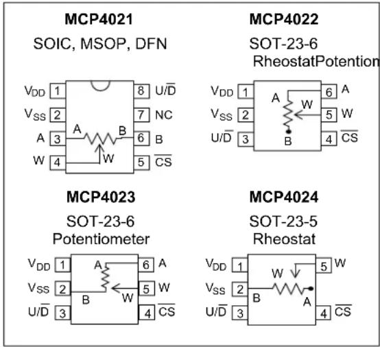
text_image
MCP4021 SOIC, MSOP, DFN VDD 1 8 U/D VSS 2 7 NC A 3 6 B W 4 5 CS MCP4022 SOT-23-6 RheostatPotention VDD 1 A 6 A VSS 2 5 W U/D 3 B 4 CS MCP4023 SOT-23-6 Potentiometer VDD 1 A 6 A VSS 2 5 W U/D 3 B 4 CS MCP4024 SOT-23-5 Rheostat VDD 1 W 5 W VSS 2 B A 4 CS U/D 3 B 4 CSBlock Diagram

flowchart
graph TD
    A["V_DD"] --> B["Power-Up and Brown-Out Control"]
    C["V_SS"] --> B
    D["CS"] --> E["2-Wire Interface and Control Logic"]
    F["U/D"] --> E
    B --> G["Wiper Register (Resistor Array)"]
    E --> G
    G --> H["A"]
    G --> I["W"]
    G --> J["B"]
    K["EEPROM and WiperLock Technology"] --> G
Device Features
| Device | Wiper Configuration | Memory Type | Resistance (typical) | # of Steps | V_DD Operating Range | Control Interface | WiperLock Technology | |
| Options (kΩ) | Wiper (Ω) | |||||||
| MCP4021 | Potentiometer (1) | EE | 2.1, 5.0, 10.0, 50.0 | 75 | 64 | 2.7V - 5.5V | U/D | Yes |
| MCP4022 | Rheostat | EE | 2.1, 5.0, 10.0, 50.0 | 75 | 64 | 2.7V- 5.5V | U/D | Yes |
| MCP4023 | Potentiometer | EE | 2.1, 5.0, 10.0, 50.0 | 75 | 64 | 2.7V - 5.5V | U/D | Yes |
| MCP4024 | Rheostat | EE | 2.1, 5.0, 10.0, 50.0 | 75 | 64 | 2.7V - 5.5V | U/D | Yes |
Note 1: Floating either terminal (A or B) allows the device to be used in Rheostat mode.
1.0 ELECTRICAL CHARACTERISTICS
Absolute Maximum Ratings †
V_DD 6.5V
and U/D inputs w.r.t V_SS -0.3V to 12.5V
A, B and W terminals w.r.t V_SS ____ -0.3V to V_DD + 0.3V
Current at Input Pins ....±10 mA
Current at Supply Pins ....±10 mA
Current at Potentiometer Pins ....±2.5 mA
Storage temperature -65^ to +150^
Ambient temp. with power applied ....-55°C to +125°C
ESD protection on all pins ....≥4 kV (HBM), ≥400V (MM)
Maximum Junction Temperature ( T_J ) .....+150°C
† Notice: Stresses above those listed under “Maximum Ratings” may cause permanent damage to the device. This is a stress rating only and functional operation of the device at those or any other conditions above those indicated in the operational listings of this specification is not implied. Exposure to maximum rating conditions for extended periods may affect device reliability.
AC/DC CHARACTERISTICS
| Electrical Specifications: Unless otherwise indicated, all parameters apply across the specified operating ranges. T_A = -40°C to +125°C, 2.1 kΩ, 5 kΩ, 10 kΩ and 50 kΩ devices. Typical specifications represent values for V_DD = 5.5V, VSS = 0V,\(T_A = +25°C . | ||||||
| Parameters Sym Min Typ | Max Units | Conditions | ||||
| Operating Voltage Range | V_DD | 2.7 | — | 5.5 | V | |
| Input Voltage | V_CS | V_SS | — | 12.5 | V | The pin will be at one of three input levels ( V_IL, V_IH or V_IHH ). (Note 6) |
| Supply Current | I_DD | — | 45 | — | μA | 5.5V, = V_SS, f_U/ = 1 MHz |
| — | 15 | — | μA | 2.7V, = V_SS, f_U/ = 1 MHz | ||
| — | 0.3 | 1 | μA | Serial Interface Inactive ( = V_IH, U/ = V_IH ) | ||
| — | 0.6 | 3 | mA | EE Write cycle, T_A = +25°C | ||
| Resistance(± 20%) | R_AB | 1.68 | 2.1 | 2.52 | kΩ | -202 devices (Note 1) |
| 4.0 | 5 | 6.0 | kΩ | -502 devices (Note 1) | ||
| 8.0 | 10 | 12.0 | kΩ | -103 devices (Note 1) | ||
| 40.0 | 50 | 60.0 | kΩ | -503 devices (Note 1) | ||
| Resolution | N | 64 | Taps | No Missing Codes | ||
| Step Resistance | R_S | — | R_AB/63 | — | Ω | Note 6 |
Note 1: Resistance is defined as the resistance between terminal A to terminal B.
2: INL and DNL are measured at V_W with V_A = V_DD and V_B = V_SS . (-202 devices V_A = 4V ).
3: MCP4021/23 only, test conditions are: I_W = 1.9 mA, code = 00h.
4: MCP4022/24 only, test conditions are:
| Device Resistance | Current at Voltage | Comments | |
| 5.5V | 2.7V | ||
| 2.1 kΩ | 2.25 mA | 1.1 mA | MCP4022 includes V_WZSE MCP4024 includes V_WFSE |
| 5 kΩ | 1.4 mA | 450 μA | |
| 10 kΩ | 450 μA | 210 μA | |
| 50 kΩ | 90 μA | 40 μA | |
5: Resistor terminals A, W and B's polarity with respect to each other is not restricted.
6: This specification by design
7: Non-linearity is affected by wiper resistance ( R_W ), which changes significantly over voltage and temperature. See Section 6.0, "Resistor" for additional information.
8: The MCP4021 is externally connected to match the configurations of the MCP4022 and MCP4024, and then tested.
9: This parameter is not tested, but specified by characterization.
AC/DC CHARACTERISTICS (CONTINUED)
| Electrical Specifications: Unless otherwise indicated, all parameters apply across the specified operating ranges. T_A = -40°C to +125°C, 2.1 kΩ, 5 kΩ, 10 kΩ and 50 kΩ devices. Typical specifications represent values for V_DD = 5.5V, VSS = 0V,\(T_A = +25°C . | |||||||
| Parameters | Sym | Min | Typ | Max | Units | Conditions | |
| Wiper Resistance (Note 3, Note 4) | R_W | —70 | 125 Ω 5.5V | ||||
| —70 | 325 Ω 2.7V | ||||||
| Nominal Resistance Tempco | R/ T | — | 50 | — | ppm/°C | T_A = -20°C to +70°C | |
| —100 | — ppm/°CT | A = -40°C to +85°C | |||||
| —150 | — ppm/°CT | A = -40°C to +125°C | |||||
| Ratiometeric Tempco V | W_A/ T | — | 10 | — | ppm/°C | MCP4021 and MCP4023 only, code = 1Fh | |
| Full-Scale Error | V_WFSE | -0.5 | -0.1 | +0.5 | LSb | Code 3Fh (MCP4021/23 only) | |
| Zero-Scale Error | V_WZSE | -0.5 | +0.1 | +0.5 | LSb | Code 00h (MCP4021/23 only) | |
| Monotonicity | N | Yes | Bits | ||||
| Potentiometer Integral Non-linearity | INL | -0.5 | ±0.25 | +0.5 | LSb | MCP4021/23 only (Note 2) | |
| Potentiometer Differential Nonlinearity | DNL | -0.5 | ±0.25 | +0.5 | LSb | MCP4021/23 only (Note 2) | |
| Resistor Terminal Input Voltage Range (Terminals A, B and W) | V_A,V_W,V_B | Vss — | V | DD | V | Note 5, Note 6 | |
| Maximum current through A, W or B | I_W | — | — | 2.5 | mA | Note 6 | |
| Leakage current into A, W or B | I_WL | —100 | — nA | MCP4021 A = W = B = V | |||
| —100 | — nA | MCP4022/23 A = W = V | |||||
| —100 | — nA | MCP4024 W = V | |||||
| Capacitance ( P_A ) | C_AW | —75 | — pF | f=1 MHz, code = 1Fh | |||
| Capacitance ( P_w ) | C_W | —120 | — pF | f=1 MHz, code = 1Fh | |||
| Capacitance ( P_B ) | C_BW | —75 | — pF | f=1 MHz, code = 1Fh | |||
| Bandwidth -3 dB | BW | — | 4 | — | MHz | -202 devices | Code = 1F, output load = 30 pF |
| — | 2 | — | MHz | -502 devices | |||
| — | 1 | — | MHz | -103 devices | |||
| —200 | — kHz | -503 | devices | ||||
Note 1: Resistance is defined as the resistance between terminal A to terminal B.
2: INL and DNL are measured at V_W with V_A = V_DD and V_B = V_SS . (-202 devices V_A = 4V ).
3: MCP4021/23 only, test conditions are: I_W = 1.9 mA, code = 00h.
4: MCP4022/24 only, test conditions are:
| Device Resistance | Current at Voltage | Comments | |
| 5.5V | 2.7V | ||
| 2.1 kΩ | 2.25 mA | 1.1 mA | MCP4022 includes V_WZSE MCP4024 includes V_WFSE |
| 5 kΩ | 1.4 mA | 450 μA | |
| 10 kΩ | 450 μA | 210 μA | |
| 50 kΩ | 90 μA | 40 μA | |
5: Resistor terminals A, W and B's polarity with respect to each other is not restricted.
6: This specification by design
7: Non-linearity is affected by wiper resistance ( R_W ), which changes significantly over voltage and temperature. See Section 6.0, "Resistor" for additional information.
8: The MCP4021 is externally connected to match the configurations of the MCP4022 and MCP4024, and then tested.
9: This parameter is not tested, but specified by characterization.
AC/DC CHARACTERISTICS (CONTINUED)
| Electrical Specifications: Unless otherwise indicated, all parameters apply across the specified operating ranges. T_A = -40°C to +125°C, 2.1 kΩ, 5 kΩ, 10 kΩ and 50 kΩ devices. Typical specifications represent values for V_DD = 5.5V, V_SS = 0V, T_A = +25°C . | |||||||
| Parameters | Sym | Min | Typ | Max | Units | Conditions | |
| Rheostat Integral Non-linearityMCP4021 (Note 4, Note 8)MCP4022 and MCP4024 (Note 4) | R-INL | -0.5 ±0. | .25 +0.5 L | Sb -202 | devices(2.1 kΩ) | 5.5V | |
| -8.5 +4 | .5 +8.5 LSb | 2.7V (Note 7) | |||||
| -0.5 ±0. | .25 +0.5 L | Sb -502 | devices(5 kΩ) | 5.5V | |||
| -5.5 +2 | .5 +5.5 LSb | 2.7V (Note 7) | |||||
| -0.5 ±0. | .25 +0.5 L | Sb -103 | devices(10 kΩ) | 5.5V | |||
| -3 +1 | +3 LSb 2.7V (Note 7) | ||||||
| -0.5 ±0. | .25 +0.5 L | Sb -503 | devices(50 kΩ) | 5.5V | |||
| -1 +0. | .25 +1 LSb | 2.7V (Note 7) | |||||
| Rheostat Differential Non-linearityMCP4021 (Note 4, Note 8)MCP4022 and MCP4024 (Note 4) | R-DNL | -0.5 ±0. | .25 +0.5 L | Sb -202 | devices(2.1 kΩ) | 5.5V | |
| -1 +0.5 | +2 LSb 2.7V (Note 7) | ||||||
| -0.5 ±0. | .25 +0.5 L | Sb -502 | devices(5 kΩ) | 5.5V | |||
| -1 | +0.25 | +1.25 | LSb | 2.7V (Note 7) | |||
| -0.5 ±0. | .25 +0.5 L | Sb -103 | devices(10 kΩ) | 5.5V | |||
| -1 | 0 | +1 | LSb | 2.7V (Note 7) | |||
| -0.5 ±0. | .25 +0.5 L | Sb -503 | devices(50 kΩ) | 5.5V | |||
| -0.5 | 0 | +0.5 | LSb | 2.7V (Note 7) | |||
Note 1: Resistance is defined as the resistance between terminal A to terminal B.
2: INL and DNL are measured at V_W with V_A = V_DD and V_B = V_SS . (-202 devices V_A = 4V ).
3: MCP4021/23 only, test conditions are: I_W = 1.9 mA, code = 00h.
4: MCP4022/24 only, test conditions are:
| Device Resistance | Current at Voltage | Comments | |
| 5.5V | 2.7V | ||
| 2.1 kΩ | 2.25 mA | 1.1 mA | MCP4022 includes V_WZSE MCP4024 includes V_WFSE |
| 5 kΩ | 1.4 mA | 450 μA | |
| 10 kΩ | 450 μA | 210 μA | |
| 50 kΩ | 90 μA | 40 μA | |
5: Resistor terminals A, W and B's polarity with respect to each other is not restricted.
6: This specification by design
7: Non-linearity is affected by wiper resistance ( R_W ), which changes significantly over voltage and temperature. See Section 6.0, "Resistor" for additional information.
8: The MCP4021 is externally connected to match the configurations of the MCP4022 and MCP4024, and then tested.
9: This parameter is not tested, but specified by characterization.
AC/DC CHARACTERISTICS (CONTINUED)
| Electrical Specifications: Unless otherwise indicated, all parameters apply across the specified operating ranges. T_A = -40°C to +125°C, 2.1 kΩ, 5 kΩ, 10 kΩ and 50 kΩ devices. Typical specifications represent values for V_DD = 5.5V, V_SS = 0V,\(T_A = +25°C . | ||||||
| Parameters | Sym | Min | Typ | Max | Units | Conditions |
| Digital Inputs/Outputs (CS, U/D) | ||||||
| Input High Voltage V | IH | 0.7 V_DD | — | — | V | |
| Input Low Voltage V | IL | — | — | 0 DD | V 3 | V |
| High-Voltage Input Entry Voltage(Threshold for WiperLock Technology) | V_IHH | 8.5^(9) | — | 1 (6) 2 | V +7°C to 5125°C | |
| 9.0 — | 12.5 | (6) | V -40°C to +125°C | |||
| High-Voltage Input Exit Voltage V | IHH | — | — | V_DD+0.8^(6) | V | |
| Pull-up/Pull-down Resistance | R_CS | — | 16 | — | kΩ | V_DD=5.5V, V_CS=3V |
| Weak Pull-up/Pull-down Current | I_PU | — 170 | — | μA | V | D_D=5.5V, V_CS=3V |
| Input Leakage Current | I_IL | -1 | — | 1 | μA | V_IN=V_DD |
| and U/D Pin Capacitance | C_IN, C_OUT | — | 10 | — | pF | f_C=1 MHz |
| RAM (Wiper) Value | ||||||
| Value Range | N | 0h | — | 3Fh | hex | |
| EEPROM | ||||||
| Endurance | E_ndurance | — | 1M | — | Cycles | |
| EEPROM Range | N | 0h | — | 3Fh | hex | |
| Initial Factory Setting | N | 1Fh | hex | WiperLock Technology = Off | ||
| Power Requirements | ||||||
| Power Supply Sensitivity(MCP4021 and MCP4023 only) | PSS | — | 0.0015 | 0.0035 | %/% | V_DD=4.5V to 5.5V, V_A=4.5V,Code=1Fh |
| — | 0.0015 | 0.0035 | %/% | V_DD=2.7V to 4.5V, V_A=2.7V,Code=1Fh | ||
Note 1: Resistance is defined as the resistance between terminal A to terminal B.
2: INL and DNL are measured at V_W with V_A = V_DD and V_B = V_SS . (-202 devices V_A = 4V ).
3: MCP4021/23 only, test conditions are: I_W = 1.9 mA, code = 00h.
4: MCP4022/24 only, test conditions are:
| Device Resistance | Current at Voltage | Comments | |
| 5.5V | 2.7V | ||
| 2.1 kΩ | 2.25 mA | 1.1 mA | MCP4022 includes V_WZSE MCP4024 includes V_WFSE |
| 5 kΩ | 1.4 mA | 450 μA | |
| 10 kΩ | 450 μA | 210 μA | |
| 50 kΩ | 90 μA | 40 μA | |
5: Resistor terminals A, W and B's polarity with respect to each other is not restricted.
6: This specification by design
7: Non-linearity is affected by wiper resistance ( R_W ), which changes significantly over voltage and temperature. See Section 6.0, "Resistor" for additional information.
8: The MCP4021 is externally connected to match the configurations of the MCP4022 and MCP4024, and then tested.
9: This parameter is not tested, but specified by characterization.
text_image
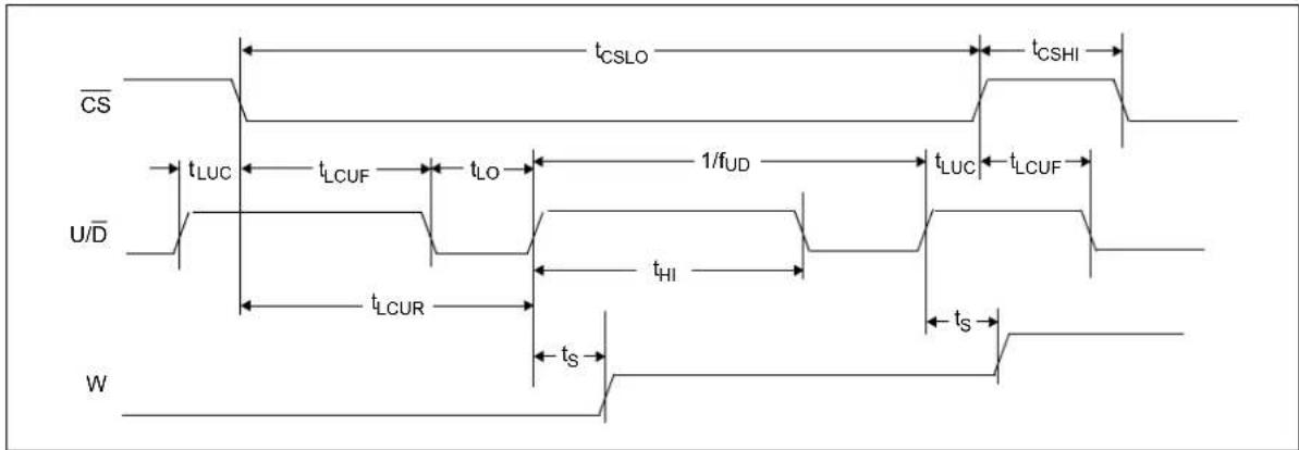
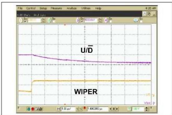
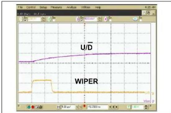
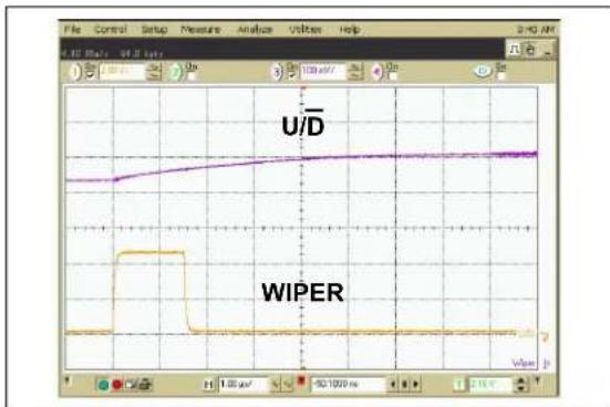
CS U/D W tLUC tLCUF tLO 1/fUD tHI tLCUR tS tCSLO tCSHI tLUC tLCUF ts tsFIGURE 1-1: Increment Timing Waveform.
SERIAL TIMING CHARACTERISTICS
| Electrical Specifications: Unless otherwise noted, all parameters apply across the specified operating ranges. Extended (E): V_DD=+2.7V to 5.5V, T_A=-40°C to +125°C . | ||||||
| Parameters Sym Min | Typ Max Units Conditions | |||||
| Low Time t | CSLO | 5 | — | — | μ | s |
| High Time t | CSHI | 500 | — | — | ns | |
| U/ to Hold Time | t_LUC | 500 | — | — | ns | |
| to U/ Low Setup Time t | LCUF | 500 | — | — | ns | |
| to U/ High Setup Time | t_CUR | 3 | — | — | μ | s |
| U/ High Time | t_HI | 500 | — | — | ns | |
| U/ Low Time | t_LO | 500 | — | — | ns | |
| Up/Down Toggle Frequency | f_UD | — | — | 1 | MHz | |
| Wiper Settling Time | t_S | 0.5 | — | — | μs | 2.1 kΩ, C_L=100 pF |
| 1 | — | — | μs | 5 kΩ, C_L=100 pF | ||
| 2 | — | — | μs | 10 kΩ, C_L=100 pF | ||
| 10 | 5 | — | μs | 50 kΩ, C_L=100 pF | ||
| Wiper Response on Power-Up | t_PU | — | 200 | — | ns | |
| Internal EEPROM Write Time | twc | — | — | 5 | ms | @25°C |
| — | — | 10 | ms | -40°C to +125°C | ||

text_image
CS U/D W tLUC tLCUR tHI 1/fUD tLO ts tCSLO tCSHI tLUC tLCUF tsFIGURE 1-2: Decrement Timing Waveform.
SERIAL TIMING CHARACTERISTICS
| Electrical Specifications: Unless otherwise noted, all parameters apply across the specified operating ranges. Extended (E): V_DD=+2.7V to 5.5V, T_A=-40°C to +125°C . | ||||||
| Parameters Sym Min | Typ Max Units Conditions | |||||
| Low Time t | CSLO | 5 | — | — | μ | s |
| High Time | t_CSHI | 500 | — | — | ns | |
| U/D to Hold Time | t_LUC | 500 | — | — | ns | |
| to U/D Low Setup Time t | LCUF | 500 | — | — | ns | |
| to U/D High Setup Time | t_LCUR | 3 | — | — | μ | s |
| U/D High Time | t_HI | 500 | — | — | ns | |
| U/D Low Time | t_LO | 500 | — | — | ns | |
| Up/Down Toggle Frequency | f_UD | — | — | 1 | MHz | |
| Wiper Settling Time | t_S | 0.5 | — | — | μs | 2.1 kΩ, C_L=100 pF |
| 1 | — | — | μs | 5 kΩ, C_L=100 pF | ||
| 2 | — | — | μs | 10 kΩ, C_L=100 pF | ||
| 10 | 5 | — | μs | 50 kΩ, C_L=100 pF | ||
| Wiper Response on Power-Up | t_PU | — | 200 | — | ns | |
| Internal EEPROM Write Time | twc | — | — | 5 | ms | @25°C |
| — | — | 10 | ms | -40°C to +125°C | ||
text_image
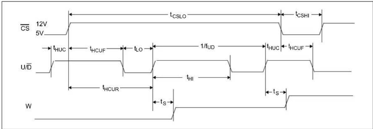
CS 12V 5V tHUC tHCUF tLO 1/fUD U/D tHCUR tHI W tCSLO tCSHI tHUC tHCUF tSFIGURE 1-3: High-Voltage Increment Timing Waveform.
SERIAL TIMING CHARACTERISTICS
| Electrical Specifications: Unless otherwise noted, all parameters apply across the specified operating ranges. Extended (E): V_DD=+2.7V to 5.5V, T_A=-40°C to +125°C . | ||||||
| Parameters Sym Min | Typ Max Units Conditions | |||||
| Low Time t | CSLO | 5 | — | — | μ | s |
| High Time t | CSHI | 500 — | — | ns | ||
| U/D High Time | t_HI | 500 — | — | ns | ||
| U/D Low Time | t_LO | 500 — | — | ns | ||
| Up/Down Toggle Frequency | f_UD | — | — | 1 | MHz | |
| HV U/D to CS Hold Time | t_HUC | 1.5 | — | — | μs | |
| HV CS to U/D Low Setup Time | t_HCUF | 8 | — | — | μ | s |
| HV CS to U/D High Setup Time | t_HCUR | 4.5 | — | — | μs | |
| Wiper Settling Time | t_S | 0.5 | — | — | μs | 2.1 kΩ, C_L=100 pF |
| 1 | — | — | μs | 5 kΩ, C_L=100 pF | ||
| 2 | — | — | μs | 10 kΩ, C_L=100 pF | ||
| 10 | 5 | — | μs | 50 kΩ, C_L=100 pF | ||
| Wiper Response on Power-Up | t_PU | — | 200 | — | ns | |
| Internal EEPROM Write Time | twc | — | — | 5 | ms | @25°C |
| — | — | 10 ms | -40°C to +125°C | |||

text_image
CS 12V 5V U/D W tHUC tHI tHCUR tLO ts 1/fUD tHUC tHCUF tCSLO tCSHI tsLO tsFIGURE 1-4: High-Voltage Decrement Timing Waveform.
SERIAL TIMING CHARACTERISTICS
| Electrical Specifications: Unless otherwise noted, all parameters apply across the specified operating ranges. Extended (E): V_DD=+2.7V to 5.5V, T_A=-40°C to +125°C . | ||||||
| Parameters Sym Min | Typ Max Units Conditions | |||||
| Low Time t | CSLO | 5 | — | — | μ | s |
| High Time t | CSHI | 500 | — | — | ns | |
| U/D High Time | t_HI | 500 | — | — | ns | |
| U/D Low Time | t_LO | 500 | — | — | ns | |
| Up/Down Toggle Frequency | f_UD | — | — | 1 | MHz | |
| HV U/D to Hold Time | t_HUC | 1.5 | — | — | μs | |
| HV to U/D Low Setup Time | t_HCUF | 8 | — | — | μ | s |
| HV to U/D High Setup Time | t_HCUR | 4.5 | — | — | μs | |
| Wiper Settling Time | t_S | 0.5 | — | — | μs | 2.1 kΩ, C_L=100 pF |
| 1 | — | — | μs | 5 kΩ, C_L=100 pF | ||
| 2 | — | — | μs | 10 kΩ, C_L=100 pF | ||
| 10 | 5 | — | μs | 50 kΩ, C_L=100 pF | ||
| Wiper Response on Power-Up | t_PU | — | 200 | — | ns | |
| Internal EEPROM Write Time | twc | — | — | 5 | ms | @25°C |
| — | — | 10 | ms | -40°C to +125°C | ||
TEMPERATURE CHARACTERISTICS
| Electrical Specifications: Unless otherwise indicated, V_DD = +2.7V to +5.5V , V_SS = G N D . | ||||||
| Parameters Sym Min Typ Max Units Conditions | ||||||
| Temperature Ranges | ||||||
| Specified Temperature Range T | A | -40 — | +125 °C | |||
| Operating Temperature Range T | A | -40 — | +125 °C | |||
| Storage Temperature Range | T_A | -65 — | +150 °C | |||
| Thermal Package Resistances | ||||||
| Thermal Resistance, 5L-SOT-23 | θ_JA | — | 255 | — | °C/W | |
| Thermal Resistance, 6L-SOT-23 | θ_JA | — | 230 | — | °C/W | |
| Thermal Resistance, 8L-DFN (2x3) | θ_JA | — | 85 | — | °C/W | |
| Thermal Resistance, 8L-MSOP | θ_JA | — | 206 | — | °C/W | |
| Thermal Resistance, 8L-SOIC θ | JA | — | 117 | — | °C/W | |
2.0 TYPICAL PERFORMANCE CURVES
Note: The graphs and tables provided following this note are a statistical summary based on a limited number of samples and are provided for informational purposes only. The performance characteristics listed herein are not tested or guaranteed. In some graphs or tables, the data presented may be outside the specified operating range (e.g., outside specified power supply range) and therefore outside the warranted range.
Note: Unless otherwise indicated, T_A=+25^ , V_DD=5V , V_SS=0V .
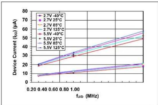
FIGURE 2-1: Device Current (I DD ) vs. U/D Frequency ( fU/D ) and Ambient Temperature ( V_DD = 2.7V and 5.5V).

line
| V cs (V) | R_cs (kOhms) | Ics (μA) | | -------- | ------------ | -------- | | 9 | 180 | - | | 8 | 150 | - | | 7 | 100 | - | | 6 | 250 | - | | 5 | 50 | - | | 4 | 0 | - | | 3 | 250 | - | | 2 | 0 | - | | 1 | 0 | - |FIGURE 2-4: CS Pull-up/Pull-down Resistance ( R_CS ) and Current ( I_CS ) vs. CS Input Voltage ( V_CS ) ( V_DD = 5.5V ).
line
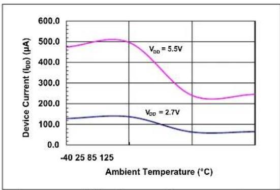
| Ambient Temperature (°C) | V_DD = 5.5V (μA) | V_DD = 2.7V (μA) | | ------------------------ | ---------------- | ---------------- | | -40 | 480.0 | 120.0 | | 25 | 500.0 | 130.0 | | 85 | 510.0 | 135.0 | | 125 | 500.0 | 130.0 | | 160 | 450.0 | 100.0 | | 200 | 300.0 | 70.0 | | 240 | 250.0 | 60.0 | | 280 | 230.0 | 65.0 | | 320 | 240.0 | 70.0 | | 360 | 250.0 | 75.0 | | 400 | 260.0 | 80.0 |FIGURE 2-2: Write Current (I WRITE) vs. Ambient Temperature and V_DD .
line
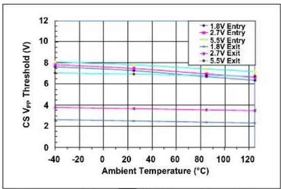
| Ambient Temperature (°C) | 1.8V Entry | 2.7V Entry | 5.5V Entry | 1.8V Exit | 2.7V Exit | 5.5V Exit | | ------------------------ | ---------- | ---------- | ---------- | --------- | --------- | --------- | | -40 | 8.0 | 8.0 | 8.0 | 3.0 | 3.0 | 3.0 | | 20 | 7.5 | 7.5 | 7.5 | 3.0 | 3.0 | 3.0 | | 80 | 7.0 | 7.0 | 7.0 | 3.0 | 3.0 | 3.0 | | 120 | 6.5 | 6.5 | 6.5 | 3.0 | 3.0 | 3.0 |FIGURE 2-5: CS High Input Entry/Exit Threshold vs. Ambient Temperature and V_DD .
line
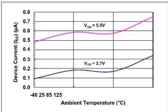
| Ambient Temperature (°C) | V_DD = 5.5V (μA) | V_DD = 2.7V (μA) | | ------------------------ | ---------------- | ---------------- | | -40 | 0.5 | 0.1 | | 25 | 0.6 | 0.15 | | 85 | 0.6 | 0.2 | | 125 | 0.6 | 0.2 | | 125 | 0.7 | 0.3 |FIGURE 2-3: Device Current (I SHDN) vs. Ambient Temperature and V_DD . ( = V_DD) .
Note: Unless otherwise indicated, T_A = +25^ , V_DD = 5V , V_SS = 0V .

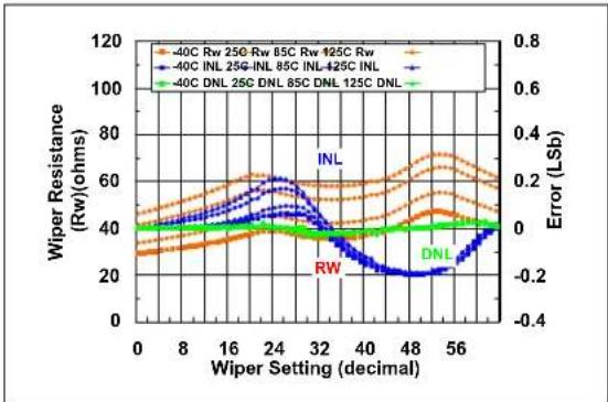
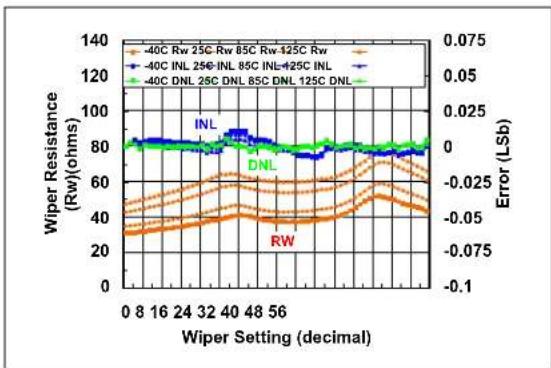
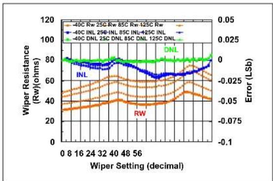
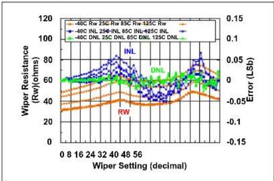
FIGURE 2-6: 2.1 k Pot Mode - R_W() , INL (LSb), DNL (LSb) vs. Wiper Setting and Ambient Temperature ( V_DD = 5.5V ).
line
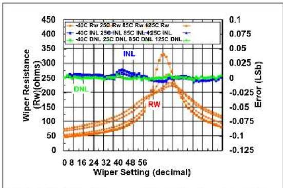
| Wiper Setting (decimal) | Wiper Resistance (Rw)(ohms) | Error (LSb) | | ----------------------- | ---------------------------- | ----------- | | 0 | 30 | 0.0 | | 8 | 40 | 0.1 | | 16 | 50 | 0.2 | | 24 | 60 | 0.3 | | 32 | 55 | 0.2 | | 40 | 45 | 0.1 | | 48 | 35 | 0.0 | | 56 | 25 | -0.1 |FIGURE 2-8: 2.1 k ΩRheo Mode - R_W (Ω), INL (LSb), DNL (LSb) vs. Wiper Setting and Ambient Temperature ( V_DD = 5.5V ).
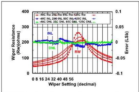
FIGURE 2-7: 2.1 k Ω Pot Mode - R_W() , INL (LSb), DNL (LSb) vs. Wiper Setting and Ambient Temperature ( V_DD = 2.7V ).
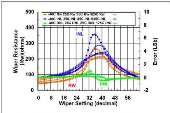
FIGURE 2-9: 2.1 k ΩRheo Mode - R_W (Ω), INL (LSb), DNL (LSb) vs. Wiper Setting and Ambient Temperature ( V_DD = 2.7V ).
Note: Unless otherwise indicated, T_A = +25^ C , V_DD = 5V , V_SS = 0V .

line
| Ambient Temperature (°C) | Nominal Resistance (R_AB) at V_DD = 5.5V | Nominal Resistance (R_AB) at V_DD = 2.7V | | ------------------------ | ---------------------------------------- | ---------------------------------------- | | -40 | 2065 | 2030 | | 0 | 2060 | 2025 | | 40 | 2055 | 2020 | | 80 | 2050 | 2015 | | 120 | 2055 | 2010 | | 160 | 2060 | 2015 | | 200 | 2075 | 2020 |FIGURE 2-10: 2.1 k Ω-Nominal
Resistance ( ) vs. Ambient Temperature and V_DD .

line
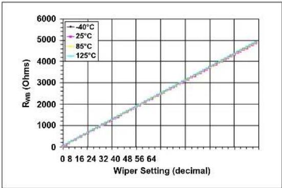
| Wiper Setting (decimal) | -40°C | 25°C | 85°C | 125°C | | ----------------------- | ----- | ---- | ---- | ----- | | 0 | 0 | 0 | 0 | 0 | | 8 | 24 | 24 | 24 | 24 | | 16 | 32 | 32 | 32 | 32 | | 24 | 40 | 40 | 40 | 40 | | 32 | 48 | 48 | 48 | 48 | | 40 | 56 | 56 | 56 | 56 | | 48 | 64 | 64 | 64 | 64 | | 56 | 72 | 72 | 72 | 72 | | 64 | 80 | 80 | 80 | 80 | | 72 | 88 | 88 | 88 | 88 | | 80 | 96 | 96 | 96 | 96 | | 88 | 104 | 104 | 104 | 104 | | 96 | 112 | 112 | 112 | 112 | | 104 | 120 | 120 | 120 | 120 | | 112 | 128 | 128 | 128 | 128 | | 120 | 136 | 136 | 136 | 136 | | 128 | 144 | 144 | 144 | 144 | | 136 | 152 | 152 | 152 | 152 | | 144 | 160 | 160 | 160 | 160 | | 152 | 168 | 168 | 168 | 168 | | 160 | 176 | 176 | 176 | 176 | | 168 | 184 | 184 | 184 | 184 | | 176 | 192 | 192 | 192 | 192 | | 184 | 200 | 200 | 200 | 200 | | 192 | 208 | 208 | 208 | 208 | | 200 | 216 | 216 | 216 | 216 | | Note: The data for -40°C to -125°C is not explicitly provided in the code snippet. The actual values are not provided in the code snippet. The code contains repeated '40°C' labels at the top and bottom of the chart. The values are estimated based on the 'Temperature' label in the code snippet.FIGURE 2-11: 2.1 k -R_WB() vs. Wiper Setting and Ambient Temperature.
Note: Unless otherwise indicated, T_A = +25^ , V_DD = 5V , V_SS = 0V .

line
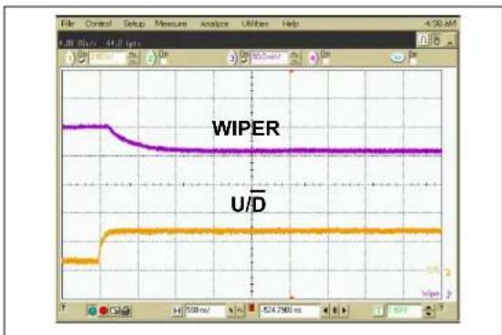
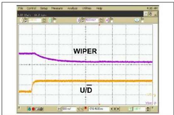
| Time (ms) | WIPER | U/D | |-----------|-------|-----| | 0 | ~0.5 | ~0.1| | 200 | ~0.5 | ~0.2| | 400 | ~0.5 | ~0.3| | 600 | ~0.5 | ~0.4| | 800 | ~0.5 | ~0.4| | 1000 | ~0.5 | ~0.4| | 1200 | ~0.5 | ~0.4| | 1400 | ~0.5 | ~0.4| | 1600 | ~0.5 | ~0.4| | 1800 | ~0.5 | ~0.4| | 2000 | ~0.5 | ~0.4| | 2200 | ~0.5 | ~0.4| | 2400 | ~0.5 | ~0.4| | 2600 | ~0.5 | ~0.4| | 2800 | ~0.5 | ~0.4| | 3000 | ~0.5 | ~0.4| | 3200 | ~0.5 | ~0.4| | 3400 | ~0.5 | ~0.4| | 3600 | ~0.5 | ~0.4| | 3800 | ~0.5 | ~0.4| | 4000 | ~0.5 | ~0.4| | 4200 | ~0.5 | ~0.4| | 4400 | ~0.5 | ~0.4| | 4600 | ~0.5 | ~0.4| | 4800 | ~0.5 | ~0.4| | 5000 | ~0.5 | ~0.4| | 5200 | ~0.5 | ~0.4| | 5400 | ~0.5 | ~0.4| | 5600 | ~0.5 | ~0.4| | 5800 | ~0.5 | ~0.4| | 6000 | ~0.5 | ~0.4| | 6200 | ~0.5 | ~0.4| | 6400 | ~0.5 | ~0.4| | 6600 | ~0.5 | ~0.4| | 6800 | ~0.5 | ~0.4| | 7000 | ~0.5 | ~0.4| | 7200 | ~0.5 | ~0.4| | 7400 | ~0.5 | ~0.4| | 7600 | ~0.5 | ~0.4| | 7800 | ~0.5 | ~0.4| | 8000 | ~0.5 | ~0.4| | 8200 | ~0.5 | ~0.4| | 8400 | ~0.5 | ~0.4| | 8600 | ~0.5 | ~0.4| | 8800 | ~0.5 | ~0.4| | 9000 | ~0.5 | ~0.4| | 9200 | ~0.5 | ~0.4| | 9400 | ~0.5 | ~0.4| | 9600 | ~0.5 | ~0.4| | 9800 | ~0.5 | ~0.4| | 1000 | ~0.5 | ~0.4| | 112 | - | - | | 124 | - | - | | 136 | - | - | | 148 | - | - | | 161 | - | - | | 173 | - | - | | 186 | - | - | | 198 | - | - | | 211 | - | - | | 223 | - | - | | 236 | - | - | | 249 | - | - | | 262 | - | - | | 275 | - | - | | 288 | - | - | | 311 | - | - | | 323 | - | - | | 336 | - | - | | 351 | - | - | | 363 | - | - | | 376 | - | - | | 391 | - | - | | 312 | - | - | | Note: The data is in milli-seconds format for WIPER and U/D signals.FIGURE 2-12: 2.1 k Ω-Low-Voltage Decrement Wiper Settling Time ( V_DD = 2.7V ).

FIGURE 2-15: 2.1 k -Low-Voltage Increment Wiper Settling Time ( V_DD = 2.7V ).
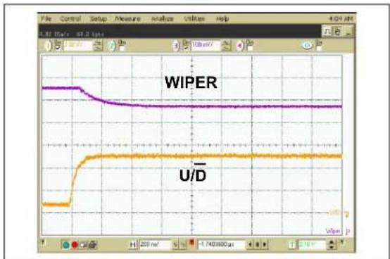
FIGURE 2-13: 2.1 k Ω-Low-Voltage Decrement Wiper Settling Time ( V_DD = 5.5V ).
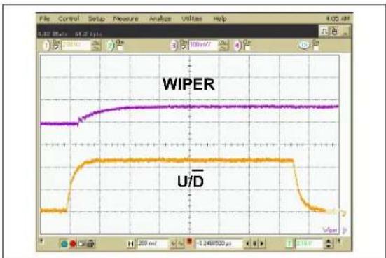
FIGURE 2-16: 2.1 k -Low-Voltage Increment Wiper Settling Time ( V_DD = 5.5V ).

FIGURE 2-14: 2.1 k Ω-Power-Up Wiper Response Time.
Note: Unless otherwise indicated, T_A=+25^ , V_DD=5V , V_SS=0V .
line
| Wiper Setting (decimal) | Wiper Resistance (Rw)(ohms) | Error (Lsb) | | ----------------------- | ---------------------------- | ----------- | | 0 | ~30 | ~-0.075 | | 8 | ~35 | ~-0.05 | | 16 | ~40 | ~-0.025 | | 24 | ~45 | ~0.0 | | 32 | ~50 | ~0.025 | | 40 | ~55 | ~0.05 | | 48 | ~60 | ~0.075 | | 56 | ~65 | ~0.05 |FIGURE 2-17: 5 k Pot Mode - R_W() , INL (LSb), DNL (LSb) vs. Wiper Setting and Ambient Temperature ( V_DD = 5.5V ).

line
| Wiper Setting (decimal) | Wiper Resistance (Rw)ohms | Error (LSb) | | ----------------------- | -------------------------- | ----------- | | 0 | ~30 | ~0.0 | | 8 | ~35 | ~0.0 | | 16 | ~40 | ~0.0 | | 24 | ~45 | ~0.0 | | 32 | ~50 | ~0.0 | | 40 | ~55 | ~0.0 | | 48 | ~60 | ~0.0 | | 56 | ~65 | ~0.0 |FIGURE 2-19: 5 k Ω Rheo Mode - R_W() , INL (LSb), DNL (LSb) vs. Wiper Setting and Ambient Temperature ( V_DD = 5.5V ).
line
| Wiper Setting (decimal) | Wiper Resistance (Rw) | Error (LSb) | | ----------------------- | ---------------------- | ----------- | | 0 | 0 | 0 | | 8 | 50 | -0.075 | | 16 | 100 | -0.1 | | 24 | 150 | -0.075 | | 32 | 200 | -0.05 | | 40 | 250 | -0.025 | | 48 | 300 | 0 | | 56 | 350 | 0.075 | | 64 | 300 | 0.05 | | 72 | 250 | 0 | | 80 | 200 | -0.025 | | 88 | 150 | -0.05 | | 96 | 100 | -0.075 | | 104 | 50 | -0.1 | | 112 | 0 | -0.125 | | 120 | -50 | -0.1 | | 128 | -100 | -0.075 | | 136 | -150 | -0.05 | | 144 | -200 | -0.025 | | 152 | -250 | 0 | | 160 | -300 | 0.075 | | 168 | -350 | 0.1 | | 176 | -400 | 0.075 | | 184 | -450 | 0.05 | | 192 | -400 | 0 | | 200 | -350 | -0.025 | | 208 | -300 | -0.05 | | 216 | -250 | -0.075 | | 224 | -200 | -0.1 | | 232 | -150 | -0.125 | | 240 | -100 | -0.1 | | 248 | -50 | -0.075 | | 256 | 0 | -0.05 | | 264 | 50 | -0.025 | | 272 | 100 | 0 | | 280 | 150 | 0.075 | | 288 | 200 | 0.1 | | 296 | 250 | 0.075 | | 304 | 300 | 0.05 | | 312 | 350 | 0 | | 320 | 400 | -0.025 | | 328 | 450 | -0.05 | | 336 | 400 | -0.075 | | 344 | 350 | -0.1 | | 352 | 300 | -0.125 | | 360 | 250 | -0.1 | | 368 | 200 | -0.075 | | 376 | 150 | -0.05 | | 384 | 100 | -0.025 | | 392 | 50 | 0 | | 400 | 0 | 0 | | 468 | -50 | -0.1 | | 476 | -100 | -0.125 | | 484 | -150 | -0.1 | | 492 | -200 | -0.075 | | 500 | -250 | -0.05 | | 568 | -350 | -0.1 | | 576 | -450 | -0.125 | | 647 | -450 | -0.1 | | 727 | -450 | -0.1 | | 826 | -450 | -0.1 | | 924 | -450 | -0.1 | | 1688 | -45 | -0.125 | | Note: The data is already in CSV format as it is not available in the image. The actual data is not available in the image.FIGURE 2-18: 5 k Ω Pot Mode - R_W() , INL (LSb), DNL (LSb) vs. Wiper Setting and Ambient Temperature ( V_DD = 2.7V ).

line
| Wiper Setting (decimal) | Wiper Resistance (Rw) | Error (Lsb) | | ----------------------- | ---------------------- | ----------- | | 0 | ~50 | ~0 | | 8 | ~70 | ~0 | | 16 | ~90 | ~0 | | 24 | ~120 | ~0 | | 32 | ~180 | ~0 | | 40 | ~300 | ~2.5 | | 48 | ~200 | ~1.5 | | 56 | ~100 | ~0 |FIGURE 2-20: 5 k Ω Rheo Mode - R_W() , INL (LSb), DNL (LSb) vs. Wiper Setting and Ambient Temperature ( V_DD = 2.7V ).
Note: Unless otherwise indicated, T_A = +25^ , V_DD = 5V , V_SS = 0V .

line
| Ambient Temperature (°C) | 2.7V Vdd (Ohms) | 5.5V Vdd (Ohms) | | ------------------------ | --------------- | --------------- | | -40 | 4860 | 4900 | | 0 | 4850 | 4890 | | 20 | 4840 | 4880 | | 40 | 4830 | 4875 | | 60 | 4825 | 4875 | | 80 | 4825 | 4875 | | 100 | 4825 | 4875 | | 120 | 4830 | 4880 | | 140 | 4840 | 4890 | | 160 | 4850 | 4900 | | 180 | 4860 | 4910 | | 200 | 4870 | 4920 |FIGURE 2-21: 5 k -Nominal Resistance ( ) vs. Ambient Temperature and V_DD .
line
| Wiper Setting (decimal) | -40°C | 25°C | 85°C | 125°C | | ----------------------- | ----- | ---- | ---- | ----- | | 0 | 0 | 0 | 0 | 0 | | 8 | 8 | 8 | 8 | 8 | | 16 | 16 | 16 | 16 | 16 | | 24 | 24 | 24 | 24 | 24 | | 32 | 32 | 32 | 32 | 32 | | 40 | 40 | 40 | 40 | 40 | | 48 | 48 | 48 | 48 | 48 | | 56 | 56 | 56 | 56 | 56 | | 64 | 64 | 64 | 64 | 64 | | 72 | 72 | 72 | 72 | 72 | | 80 | 80 | 80 | 80 | 80 | | 88 | 88 | 88 | 88 | 88 | | 96 | 96 | 96 | 96 | 96 | | 104 | 104 | 104 | 104 | 104 | | 112 | 112 | 112 | 112 | 112 | | 120 | 120 | 120 | 120 | 120 | | 128 | 128 | 128 | 128 | 128 | | 136 | 136 | 136 | 136 | 136 | | 144 | 144 | 144 | 144 | 144 | | 152 | 152 | 152 | 152 | 152 | | 160 | 160 | 160 | 160 | 160 | | 168 | 168 | 168 | 168 | 168 | | 176 | 176 | 176 | 176 | 176 | | 184 | 184 | 184 | 184 | 184 | | 192 | 192 | 192 | 192 | 192 | | 200 | 200 | 200 | 200 | 200 | | 208 | 208 | 208 | 208 | 208 | | 216 | 216 | 216 | 216 | 216 | | 224 | 224 | 224 | 224 | 224 | | 232 | 232 | 232 | 232 | 232 | | 240 | 240 | 240 | 240 | 240 | | Note: The actual values for -40°C and -125°C are not provided in the code. The data is generated using a single series of lines from the 'Wiper Setting' to 'RWA'. The numbers in the 'Wiper Setting' column are explicitly labeled as 'Ohms'. There is only one line in this case. The other three lines are unlabeled but implied by the position of the lines on the x-axis. The y-axis label 'RWA' is also 'Ohms'.FIGURE 2-22: 5 k - R_WB() vs. Wiper Setting and Ambient Temperature.
Note: Unless otherwise indicated, T_A = +25^ , V_DD = 5V , V_SS = 0V .
line
| Time (ms) | WIPER | U/D | |-----------|-------|-----| | 0 | 0 | 0 | | 10 | ~0.5 | ~0.2| | 20 | ~0.3 | ~0.4| | 30 | ~0.2 | ~0.5| | 40 | ~0.1 | ~0.6| | 50 | ~0.1 | ~0.7| | 60 | ~0.1 | ~0.8| | 70 | ~0.1 | ~0.9| | 80 | ~0.1 | ~1.0| | 90 | ~0.1 | ~1.1| | 100 | ~0.1 | ~1.2| | 110 | ~0.1 | ~1.3| | 120 | ~0.1 | ~1.4| | 130 | ~0.1 | ~1.5| | 140 | ~0.1 | ~1.6| | 150 | ~0.1 | ~1.7| | 160 | ~0.1 | ~1.8| | 170 | ~0.1 | ~1.9| | 180 | ~0.1 | ~2.0| | 190 | ~0.1 | ~2.1| | 200 | ~0.1 | ~2.2| | 210 | ~0.1 | ~2.3| | 220 | ~0.1 | ~2.4| | 230 | ~0.1 | ~2.5| | 240 | ~0.1 | ~2.6| | 250 | ~0.1 | ~2.7| | 260 | ~0.1 | ~2.8| | 270 | ~0.1 | ~2.9| | 280 | ~0.1 | ~3.0| | 290 | ~0.1 | ~3.1| | 300 | ~0.1 | ~3.2| | 310 | ~0.1 | ~3.3| | 320 | ~0.1 | ~3.4| | 330 | ~0.1 | ~3.5| | 340 | ~0.1 | ~3.6| | 350 | ~0.1 | ~3.7| | 360 | ~0.1 | ~3.8| | 370 | ~0.1 | ~3.9| | 380 | ~0.1 | ~4.0| | 390 | ~0.1 | ~4.1| | 400 | ~0.1 | ~4.2| | 410 | ~0.1 | ~4.3| | 420 | ~0.1 | ~4.4| | 430 | ~0.1 | ~4.5| | 440 | ~0.1 | ~4.6| | 450 | ~0.1 | ~4.7| | 460 | ~0.1 | ~4.8| | 470 | ~0.1 | ~4.9| | 480 | ~0.1 | ~5.0| | 490 | ~0.1 | ~5.1| | 500 | ~0.1 | ~5.2| | 510 | ~0.1 | ~5.3| | 520 | ~0.1 | ~5.4| | 530 | ~0.1 | ~5.5| | 540 | ~0.1 | ~5.6| | 550 | ~0.1 | ~5.7| | 560 | ~0.1 | ~5.8| | 570 | ~0.1 | ~5.9| | 580 | ~0.1 | ~6.0| | 590 | ~0.1 | ~6.1| | 600 | ~0.1 | ~6.2| | 610 | ~0.1 | ~6.3| | 620 | ~0.1 | ~6.4| | 630 | ~0.1 | ~6.5| | 640 | ~0.1 | ~6.6| | 650 | ~0.1 | ~6.7| | 660 | ~0.1 | ~6.8| | 670 | ~0.1 | ~6.9| | 680 | ~0.1 | ~7.0| | 690 | ~0.1 | ~7.1| | 700 | ~0.1 | ~7.2| | 710 | ~0.1 | ~7.3| | 720 | ~0.1 | ~7.4| | 730 | ~0.1 | ~7.5| | 740 | ~0.1 | ~7.6| | 750 | ~0.1 | ~7.7| | 760 | ~0.1 | ~7.8| | 770 | ~0.1 | ~7.9| | 780 | ~0.1 | ~8.0| | 790 | ~0.1 | ~8.1| | 800 | ~0.1 | ~8.2| | 810 | ~0.1 | ~8.3| | 820 | ~0.1 | ~8.4| | 830 | ~0.1 | ~8.5| | 840 | ~0.1 | ~8.6| | 850 | ~0.1 | ~8.7| | 860 | ~0.1 | ~8.8| | 870 | ~0.1 | ~8.9| | 880 | ~0.1 | ~9.0| | 890 | ~0.1 | ~9.1| | 900 | ~0.1 | ~9.2| | 910 | ~0.1 | ~9.3| | 920 | ~0.1 | ~9.4| | 930 | ~0.1 | ~9.5| | 940 | ~0.1 | ~9.6| | 950 | ~0.1 | ~9.7| | 960 | ~0.1 | ~9.8| | 970 | ~0.1 | ~9.9| | 980 | ~0.1 | >1 | | Note: The actual values may vary due to the random nature of the data generation process in the code execution.FIGURE 2-23: 5 k Ω - Low-Voltage Decrement Wiper Settling Time ( V_DD = 2.7V ).
line
| Time (μs) | WIPER | U/D | |-----------|-------|-----| | 0 | ~0.5 | ~0 | | 1 | ~0.5 | ~0 | | 2 | ~0.5 | ~0 | | 3 | ~0.5 | ~0 | | 4 | ~0.5 | ~0 | | 5 | ~0.5 | ~0 | | 6 | ~0.5 | ~0 | | 7 | ~0.5 | ~0 | | 8 | ~0.5 | ~0 | | 9 | ~0.5 | ~0 | | 10 | ~0.5 | ~0 | | 11 | ~0.5 | ~0 | | 12 | ~0.5 | ~0 | | 13 | ~0.5 | ~0 | | 14 | ~0.5 | ~0 | | 15 | ~0.5 | ~0 | | 16 | ~0.5 | ~0 | | 17 | ~0.5 | ~0 | | 18 | ~0.5 | ~0 | | 19 | ~0.5 | ~0 | | 20 | ~0.5 | ~0 | | 21 | ~0.5 | ~0 | | 22 | ~0.5 | ~0 | | 23 | ~0.5 | ~0 | | 24 | ~0.5 | ~0 | | 25 | ~0.5 | ~0 | | 26 | ~0.5 | ~0 | | 27 | ~0.5 | ~0 | | 28 | ~0.5 | ~0 | | 29 | ~0.5 | ~0 | | 30 | ~0.5 | ~0 | | 31 | ~0.5 | ~0 | | 32 | ~0.5 | ~0 | | 33 | ~0.5 | ~0 | | 34 | ~0.5 | ~0 | | 35 | ~0.5 | ~0 | | 36 | ~0.5 | ~0 | | 37 | ~0.5 | ~0 | | 38 | ~0.5 | ~0 | | 39 | ~0.5 | ~0 | | 40 | ~0.5 | ~0 | | 41 | ~0.5 | ~0 | | 42 | ~0.5 | ~0 | | 43 | ~0.5 | ~0 | | 44 | ~0.5 | ~0 | | 45 | ~0.5 | ~0 | | 46 | ~0.5 | ~0 | | 47 | ~0.5 | ~0 | | 48 | ~0.5 | ~0 | | 49 | ~0.5 | ~0 | | 50 | ~0.5 | ~0 | | 51 | ~0.5 | ~0 | | 52 | ~0.5 | ~0 | | 53 | ~0.5 | ~0 | | 54 | ~0.5 | ~0 | | 55 | ~0.5 | ~0 | | 56 | ~0.5 | ~0 | | 57 | ~0.5 | ~0 | | 58 | ~0.5 | ~0 | | 59 | ~0.5 | ~0 | | 60 | ~0.5 | ~0 | | 61 | ~0.5 | ~0 | | 62 | ~0.5 | ~0 | | 63 | ~0.5 | ~0 | | 64 | ~0.5 | ~0 | | 65 | ~0.5 | ~0 | | 66 | ~0.5 | ~0 | | 67 | ~0.5 | ~0 | | 68 | ~0.5 | ~0 | | 69 | ~0.5 | ~0 | | 70 | ~0.5 | ~0 | | 71 | ~0.5 | ~0 | | 72 | ~0.5 | ~0 | | 73 | ~0.5 | ~0 | | 74 | ~0.5 | ~0 | | 75 | ~0.5 | ~0 | | 76 | ~0.5 | ~0 | | 77 | ~0.5 | ~0 | | 78 | ~0.5 | ~0 | | 79 | ~0.5 | ~0 | | 80 | ~0.5 | ~0 | | 81 | ~0.5 | ~0 | | 82 | ~0.5 | ~0 | | 83 | ~0.5 | ~0 | | 84 | ~0.5 | ~0 | | 85 | ~0.5 | ~0 | | 86 | ~0.5 | ~0 | | 87 | ~0.5 | ~0 | | 88 | ~0.5 | ~0 | | 89 | ~0.5 | ~0 | | 90 | ~0.5 | ~0 | | 91 | ~0.5 | ~0 | | 92 | ~0.5 | ~0 | | 93 | ~0.5 | ~0 | | 94 | ~0.5 | ~0 | | 95 | ~0.5 | ~0 | | 96 | ~0.5 | ~0 | | 97 | ~0.5 | ~0 | | 98 | ~0.5 | ~0 | | 99 | ~0.5 | ~0 | |1 | - | - | The image displays a waveform graph with two distinct waveforms labeled 'WIPER' and 'U/D'. The x-axis is labeled 'Time (μs)' and the y-axis is labeled 'Signal Level'. The data series are labeled 'WIPER' and 'U/D'. The waveforms are plotted as colored lines on a grid background.FIGURE 2-25: 5 k Ω - Low-Voltage Increment Wiper Settling Time ( V_DD = 2.7V ).
line
| Time (ms) | WIPER | U/D | |-----------|-------|-----| | 0 | ~1.0 | ~0.0 | | 1 | ~0.95 | ~0.0 | | 2 | ~0.9 | ~0.0 | | 3 | ~0.85 | ~0.0 | | 4 | ~0.8 | ~0.0 | | 5 | ~0.75 | ~0.0 | | 6 | ~0.7 | ~0.0 | | 7 | ~0.65 | ~0.0 | | 8 | ~0.6 | ~0.0 | | 9 | ~0.55 | ~0.0 | | 10 | ~0.5 | ~0.0 | | 11 | ~0.45 | ~0.0 | | 12 | ~0.4 | ~0.0 | | 13 | ~0.35 | ~0.0 | | 14 | ~0.3 | ~0.0 | | 15 | ~0.25 | ~0.0 | | 16 | ~0.2 | ~0.0 | | 17 | ~0.15 | ~0.0 | | 18 | ~0.1 | ~0.0 | | 19 | ~0.05 | ~0.0 | | 20 | ~0.0 | ~0.0 | | 21 | ~-0.05| ~-0.05| | 22 | ~-0.1 | ~-0.1 | | 23 | ~-0.15| ~-0.15| | 24 | ~-0.2 | ~-0.2 | | 25 | ~-0.25| ~-0.25| | 26 | ~-0.3 | ~-0.3 | | 27 | ~-0.35| ~-0.35| | 28 | ~-0.4 | ~-0.4 | | 29 | ~-0.45| ~-0.45| | 30 | ~-0.5 | ~-0.5 | | 31 | ~-0.55| ~-0.55| | 32 | ~-0.6 | ~-0.6 | | 33 | ~-0.65| ~-0.65| | 34 | ~-0.7 | ~-0.7 | | 35 | ~-0.75| ~-0.75| | 36 | ~-0.8 | ~-0.8 | | 37 | ~-0.85| ~-0.85| | 38 | ~-0.9 | ~-0.9 | | 39 | ~-0.95| ~-0.95| | 40 | ~-1 | ~-1 | | 41 | ~-1 | ~-1 | | 42 | ~-1 | ~-1 | | 43 | ~-1 | ~-1 | | 44 | ~-1 | ~-1 | | 45 | ~-1 | ~-1 | | 46 | ~-1 | ~-1 | | 47 | ~-1 | ~-1 | | 48 | ~-1 | ~-1 | | 49 | ~-1 | ~-1 | | 50 | ~-1 | ~-1 | | 51 | ~-1 | ~-1 | | 52 | ~-1 | ~-1 | | 53 | ~-1 | ~-1 | | 54 | ~-1 | ~-1 | | 55 | ~-1 | ~-1 | | 56 | ~-1 | ~-1 | | 57 | ~-1 | ~-1 | | 58 | ~-1 | ~-1 | | 59 | ~-1 | ~-1 | | 60 | ~-1 | ~-1 | | 61 | ~-1 | ~-1 | | 62 | ~-1 | ~-1 | | 63 | ~-1 | ~-1 | | 64 | ~-1 | ~-1 | | 65 | ~-1 | ~-1 | | 66 | ~-1 | ~-1 | | 67 | ~-1 | ~-1 | | 68 | ~-1 | ~-1 | | 69 | ~-1 | ~-1 | | 70 | ~-1 | ~-1 | | 71 | ~-1 | ~-1 | | 72 | ~-1 | ~-1 | | 73 | ~-1 | ~-1 | | 74 | ~-1 | ~-1 | | 75 | ~-1 | ~-1 | | 76 | ~-1 | ~-1 | | 77 | ~-1 | ~-1 | | 78 | ~-1 | ~-1 | | 79 | ~-1 | ~-1 | | 80 | ~-1 | ~-1 | | 81 | ~-1 | ~-1 | | 82 | ~-1 | ~-1 | | 83 | ~-1 | ~-1 | | 84 | ~-1 | ~-1 | | 85 | ~-1 | ~-1 | | 86 | ~-1 | ~-1 | | 87 | ~-1 | ~-1 | | 88 | ~-1 | ~-1 | | 89 | ~-1 | ~-1 | | 90 | ~-1 | ~-1 | | 91 | ~-1 | ~-1 | | 92 | ~-1 | ~-1 | | 93 | ~-1 | ~-1 | | 94 | ~-1 | ~-1 | | 95 | ~-1 | ~-1 | | 96 | ~-1 | ~-1 | | 97 | ~-1 | ~-1 | | 98 | ~-1 | ~-1 | | 99 | ~-1 | ~-1 | | 100 | - | - | The data is extracted from the image file named 'WIPER' and 'U/D' charts, but it is not directly plotted on the graph.FIGURE 2-24: 5 k Ω - Low-Voltage Decrement Wiper Settling Time ( V_DD = 5.5V ).
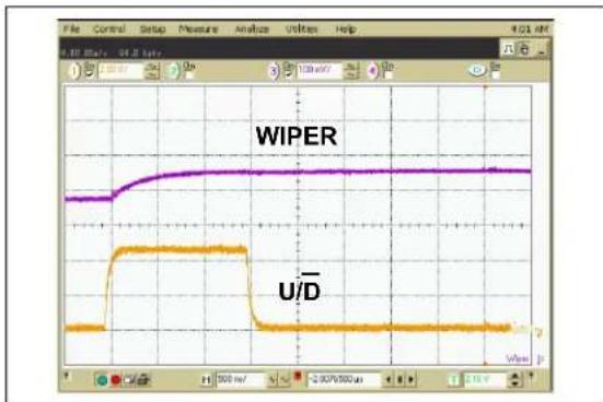
FIGURE 2-26: 5 k Ω - Low-Voltage Increment Wiper Settling Time ( V_DD = 5.5V ).
Note: Unless otherwise indicated, T_A = +25^ , V_DD = 5V , V_SS = 0V .
line
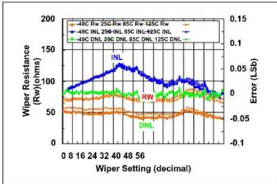
| Wiper Setting (decimal) | Wiper Resistance (Rw)(ohms) | Error (LSb) | | ----------------------- | ---------------------------- | ----------- | | 0 | ~30 | ~0.02 | | 8 | ~35 | ~0.01 | | 16 | ~40 | ~0.00 | | 24 | ~45 | ~0.01 | | 32 | ~50 | ~0.02 | | 40 | ~55 | ~0.01 | | 48 | ~60 | ~0.00 | | 56 | ~65 | ~0.01 | | 64 | ~70 | ~0.02 |FIGURE 2-27: 10 k Ω Pot Mode - R_W() , INL (LSb), DNL (LSb) vs. Wiper Setting and Ambient Temperature ( V_DD = 5.5V ).
line
| Wiper Setting (decimal) | Wiper Resistance (Rw)ohms | Error (Lsb) | | ----------------------- | -------------------------- | ----------- | | 0 | 30 | -0.05 | | 8 | 35 | -0.04 | | 16 | 40 | -0.03 | | 24 | 45 | -0.02 | | 32 | 50 | -0.01 | | 40 | 60 | 0.00 | | 48 | 70 | 0.01 | | 56 | 65 | 0.02 | | 64 | 60 | 0.03 | | 72 | 55 | 0.04 | | 80 | 50 | 0.05 | | 88 | 45 | 0.06 | | 96 | 40 | 0.07 | | 104 | 35 | 0.08 | | 112 | 30 | 0.09 | | 120 | 25 | 0.10 | | 128 | 20 | 0.11 | | 136 | 15 | 0.12 | | 144 | 10 | 0.13 | | 152 | 5 | 0.14 | | 160 | 0 | 0.15 | | 168 | -5 | 0.14 | | 176 | -10 | 0.13 | | 184 | -15 | 0.12 | | 192 | -20 | 0.11 | | 200 | -25 | 0.10 | | 208 | -30 | 0.09 | | 216 | -35 | 0.08 | | 224 | -40 | 0.07 | | 232 | -45 | 0.06 | | 240 | -50 | 0.05 | | 248 | -55 | 0.04 | | 256 | -60 | 0.03 | | 264 | -65 | 0.02 | | 272 | -70 | 0.01 | | 280 | -75 | 0.00 | | 288 | -80 | -0.01 | | 296 | -85 | -0.02 | | 304 | -90 | -0.03 | | 312 | -95 | -0.04 | | 320 | -100 | -0.05 | | 328 | -95 | -0.06 | | 336 | -90 | -0.07 | | 344 | -85 | -0.08 | | 352 | -80 | -0.09 | | 360 | -75 | -0.10 | | 368 | -70 | -0.11 | | 376 | -65 | -0.12 | | 384 | -60 | -0.13 | | 392 | -55 | -0.14 | | 400 | -50 | -0.15 | | 408 | -45 | -0.14 | | 416 | -40 | -0.13 | | 424 | -35 | -0.12 | | 432 | -30 | -0.11 | | 440 | -25 | -0.10 | | 448 | -20 | -0.09 | | 456 | -15 | -0.08 | | 464 | -10 | -0.07 | | 472 | -5 | -0.06 | | 480 | 0 | -0.05 | | 488 | 5 | -0.04 | | 496 | 10 | -0.03 | | 504 | 15 | -0.02 | | 512 | 20 | -0.01 | | 520 | 25 | 0.00 | | 528 | 30 | 0.01 | | 536 | 35 | 0.02 | | 544 | 40 | 0.03 | | 552 | 45 | 0.04 | | 560 | 50 | 0.05 | | 568 | 55 | 0.06 | | 576 | 60 | 0.07 | | 584 | 65 | 0.08 | | 592 | 70 | 0.09 | | 600 | 75 | 0.10 | | 608 | 80 | 0.11 | | 616 | 85 | 0.12 | | 624 | 90 | 0.13 | | 632 | 95 | 0.14 | | 640 | 100 | 0.15 | | 648 | 95 | - | | 656 | 90 | - | | 664 | 85 | - | | 672 | 80 | - | | 680 | 75 | - | | 688 | 70 | - | | 696 | 65 | - | | 704 | 60 | - | | 712 | 55 | - | | 720 | 50 | - | | 728 | 45 | - | | 736 | 40 | - | | 744 | 35 | - | | 752 | 30 | - | | 760 | 25 | - | | 768 | 20 | - | | 776 | 15 | - | | 784 | 10 | - | | 792 | 5 | - | | 800 | 0 | - | | Note: The actual values are not provided in the code snippet from the original data source to the original data source in the code source table, so they are represented as placeholders (e.g., 'RW' and 'DNL'). The actual values may vary due to the random nature of the data generation process.FIGURE 2-29: 10 k Ω Rheo Mode - R_W() , INL (LSb), DNL (LSb) vs. Wiper Setting and Ambient Temperature ( V_DD = 5.5V ).

FIGURE 2-28: 10 k Ω Pot Mode - R_W() , INL (LSb), DNL (LSb) vs. Wiper Setting and Ambient Temperature ( V_DD = 2.7V ).

FIGURE 2-30: 10 k Ω Rheo Mode - R_W() , INL (LSb), DNL (LSb) vs. Wiper Setting and Ambient Temperature ( V_DD = 2.7V ).
Note: Unless otherwise indicated, T_A = +25^ , V_DD = 5V , V_SS = 0V .

line
| Ambient Temperature (°C) | Nominal Resistance (Rₐₑ) (Ohms) | | ------------------------ | -------------------------------- | | -40 | 10230 | | 0 | 10190 | | 20 | 10170 | | 40 | 10150 | | 60 | 10130 | | 80 | 10110 | | 100 | 10100 | | 120 | 10090 | | 140 | 10100 | | 160 | 10150 |FIGURE 2-31: 10 k Ω-Nominal Resistance (Ω) vs. Ambient Temperature and V_DD .

line
| Wiper Setting (decimal) | -40°C | 25°C | 85°C | 125°C | | ----------------------- | ----- | ---- | ---- | ----- | | 0 | 0 | 0 | 0 | 0 | | 8 | 1000 | 1000 | 1000 | 1000 | | 16 | 2000 | 2000 | 2000 | 2000 | | 24 | 3000 | 3000 | 3000 | 3000 | | 32 | 4000 | 4000 | 4000 | 4000 | | 40 | 5000 | 5000 | 5000 | 5000 | | 48 | 6000 | 6000 | 6000 | 6000 | | 56 | 7000 | 7000 | 7000 | 7000 | | 64 | 8000 | 8000 | 8000 | 8000 | | >64 | >1000 | >1000| >1000| >1000 |FIGURE 2-32: 10 k - R_WB () vs. Wiper Setting and Ambient Temperature.
Note: Unless otherwise indicated, T_A = +25^ , V_DD = 5V , V_SS = 0V .
line
| Time (ms) | WIPER (mV) | U/D (mV) | |-----------|------------|----------| | 0 | 0.5 | 0.0 | | 100 | 0.45 | 0.2 | | 200 | 0.4 | 0.4 | | 300 | 0.35 | 0.6 | | 400 | 0.3 | 0.8 | | 500 | 0.25 | 1.0 | | 600 | 0.2 | 1.2 | | 700 | 0.15 | 1.4 | | 800 | 0.1 | 1.6 | | 900 | 0.05 | 1.8 | | 1000 | 0.0 | 2.0 |FIGURE 2-33: 10 k Ω - Low-Voltage Decrement Wiper Settling Time ( V_DD = 2.7V ).

FIGURE 2-35: 10 k Ω - Low-Voltage Increment Wiper Settling Time ( V_DD = 2.7V ).

line
| Time (ms) | WIPER | U/D | |-----------|-------|-----| | 0 | ~0.5 | ~0.5| | 100 | ~0.4 | ~0.5| | 200 | ~0.3 | ~0.5| | 300 | ~0.2 | ~0.5| | 400 | ~0.1 | ~0.5| | 500 | ~0.05 | ~0.5| | 600 | ~0.02 | ~0.5| | 700 | ~0.01 | ~0.5| | 800 | ~0.01 | ~0.5| | 900 | ~0.01 | ~0.5| | 1000 | ~0.01 | ~0.5| | 1100 | ~0.01 | ~0.5| | 1200 | ~0.01 | ~0.5| | 1300 | ~0.01 | ~0.5| | 1400 | ~0.01 | ~0.5| | 1500 | ~0.01 | ~0.5| | 1600 | ~0.01 | ~0.5| | 1700 | ~0.01 | ~0.5| | 1800 | ~0.01 | ~0.5| | 1900 | ~0.01 | ~0.5| | 2000 | ~0.01 | ~0.5| | 2100 | ~0.01 | ~0.5| | 2200 | ~0.01 | ~0.5| | 2300 | ~0.01 | ~0.5| | 2400 | ~0.01 | ~0.5| | 2500 | ~0.01 | ~0.5| | 2600 | ~0.01 | ~0.5| | 2700 | ~0.01 | ~0.5| | 2800 | ~0.01 | ~0.5| | 2900 | ~0.01 | ~0.5| | 3000 | ~0.01 | ~0.5| | 3100 | ~0.01 | ~0.5| | 3200 | ~0.01 | ~0.5| | 3300 | ~0.01 | ~0.5| | 3400 | ~0.01 | ~0.5| | 3500 | ~0.01 | ~0.5| | 3600 | ~0.01 | ~0.5| | 3700 | ~0.01 | ~0.5| | 3800 | ~0.01 | ~0.5| | 3900 | ~0.01 | ~0.5| | 4000 | ~- | - | | 4100 | - | - | | 4200 | - | - | | 4300 | - | - | | 4400 | - | - | | 4500 | - | - | | 4600 | - | - | | 4700 | - | - | | 4800 | - | - | | 4900 | - | - | | 500 | - | - | | 510 | - | - | | 52 | - | - | | 53 | - | - | | 54 | - | - | | 55 | - | - | | 56 | - | - | | 57 | - | - | | 58 | - | - | | 59 | - | - | | 60 | - | - | | 61 | - | - | | 62 | - | - | | 63 | - | - | | 64 | - | - | | 65 | - | - | | 66 | - | - | | 67 | - | - | | 68 | - | - | | 69 | - | - | | 70 | - | - | | 71 | - | - | | 72 | - | - | | 73 | - | - | | 74 | - | - | | 75 | - | - | | 76 | - | - | | 77 | - | - | | 78 | - | - | | 79 | - | - | | 80 | - | - | | 81 | - | - | | 82 | - | - | | 83 | - | - | | 84 | - | - | | 85 | - | - | | 86 | - | - | | 87 | - | - | | 88 | - | - | | 89 | - | - | | 90 | - | - | | 91 | - | - | | 92 | - | - | | 93 | - | - | | 94 | - | - | | 95 | - | - | | 96 | - | - | | 97 | - | - | | 98 | - | - | | 99 | - | - | | 1 | ~- | ~- | | Peak (approx.) from left to right (approx.) on Y-axis; Peak value on right Y-axis; U/PER and U/D values on left Y-axis; U/PER and U/D values on right Y-axis; U/D values on left Y-axis; U/PER and U/D values on right Y-axis; U/PER and U/D values on right Y-axis; U/PER and U/D values on left Y-axis; U/PER and U/D values on right Y-axis; U/PER and U/D values on right Y-axis; U/PER and U/D values on left Y-axis; U/PER and U/D values on right Y-axis; U/PER and U/D values on right Y-axis; U/PER and U/D values on left Y-axis; U/PER and U/D values on right Y-axis; U/PER and U/D values at left Y-axis; U/PER and U/D values at right Y-axis; U/PER and U/D values at left Y-axis; U/PER and U/D values at right Y-axis; U/PER and U/D values at left Y-axis; U/PER and U/D values at right Y-axis; U/PER and U/D values at left Y-axis; U/PER and U/D values at right Y-axis; U/PER and U/D values at left Y-axis; U/PER and U/D values at right Y-axis: Peak, Mid, Low, High, Low, Current, Current, Voltage, Current, Voltage, Current, Voltage, Current, Voltage, Current, Voltage, Current, Voltage, Current, Voltage, Current, Voltage, Current, Voltage, Current, Voltage, Current, Voltage, Current, Voltage, Current, Voltage, Current, Voltage, Current, Voltage, Current, Voltage, Current, Voltage, Current, Voltage, Current, Voltage, Current, Voltage, Current, Voltage, Current, Voltage, Current, Voltage, Current, Voltage, Current, Voltage, Current, Current, Voltage, Current, Current, Voltage, Current, Current, Voltage, Current, Current, Voltage, Current, Current, Voltage, Current, Current, Voltage, Current, Current, Voltage, Current, Current, Voltage, Current, Current, Voltage, Current, Current, Voltage, Current, Current, Voltage, Current, Current, Voltage, Current, Current, Voltage, Current, Current, Voltage, Current, Current, Voltage, Current, Current, Voltage, Current, Current, Vpeak/Max/Min/Max/Min/Max/Min/Max/Min/Max/Min/Max/Min/Max/Min/Max/Min/Max/Min/Max/Min/Max/Min/Max/Min/Max/Min/Max/Min/Max/Min/Max/Min/Max/Min/Max/Min/Max/Min/Max/Min/Max/Min/Max/Min/Max/Min/Max/Min/Max/Min/Max/Max/Min/Max/Min/Max/Min/Max/Min/Max/Min/Max/Min/Max/Min/Max/Min/Max/Min/Max/Min/Max/Min/Max/Min/Max/Min/Max/Min/Max/Min/Max/Min/Max/Min/Max/Min/Max/Min/Max/Min/Max/Min/Max/Min/Max/Min/Max/Min/Max/No / No / No / No / No / No / No / No / No / No / No / No / No / No / No / No / No / No / No / No / No / No / No / No / No / No / No / No / No / No / No / No / No / No / No / No / No / No / No / No / No / No / No / No / No / No / No / No / No / No / No / Yes / Yes / Yes / Yes / Yes / Yes / Yes / Yes / Yes / Yes / Yes / Yes / Yes / Yes / Yes / Yes / Yes / Yes / Yes / Yes / Yes / Yes / Yes / Yes / Yes / Yes / Yes / Yes / Yes / Yes / Yes / Yes / Yes / Yes / Yes / Yes / Yes / Yes / Yes / Yes / Yes / Yes / Yes / Yes / Yes / Yes / Yes / Yes / Yes / Yes /Yes , Yes , No , Min , Max , Min , Min , Min , Min , Min , Min , Min , Min , Min , Min , Min , Min , Min , Min , Min , Min , Min , Min , Min , Min , Min , Min , Min , Min , Min , Min , Min , Min , Min , Min , Min , Min , Min , Min , Min , Min , Min , Min , Min , Min , Min , Min , Min , Min , Min , Min , Min , Min , Min , Min , Max , Max , Max , Max , Max , Max , Max , Max , Max , Max , Max , Max , Max , Max , Max , Max , Max , Max , Max , Max , Max , Max , Max , Max , Max , Max , Max , Max , Max , Max , Max , Max , Max , Max , Max , Max , Max , Max , Max , Max , Max , Max , Max , Max , Max , Max , Max , Max , Max , Max , Min < .767 >767 >767 >767 >767 >767 >767 >767 >767 >767 >767 >767 >767 >767 >767 >767 >767 >767 >767 >767 >767 >767 >767 >767 >767 >767>767>767>767>767>767>767>767>767>767>767>767>767>767>767>767>767>767>767>767>767>767>767>767>767>767FIGURE 2-34: 10 k Ω - Low-Voltage Decrement Wiper Settling Time ( V_DD = 5.5V ).

line
| Time (ms) | WIPER | U/D | |-----------|-------|-----| | 0 | ~0.5 | ~0 | | 100 | ~0.8 | ~0 | | 200 | ~0.9 | ~0 | | 300 | ~0.95 | ~0 | | 400 | ~0.98 | ~0 | | 500 | ~0.99 | ~0 | | 600 | ~0.995| ~0 | | 700 | ~0.998| ~0 | | 800 | ~0.999| ~0 | | 900 | ~0.9995| ~0 | | 1000 | ~1.0 | ~0 | | 1100 | ~1.0 | ~0 | | 1200 | ~1.0 | ~0 |FIGURE 2-36: 10 k Ω - Low-Voltage Increment Wiper Settling Time ( V_DD = 5.5V ).
Note: Unless otherwise indicated, T_A=+25^ , V_DD=5V , V_SS=0V .
line
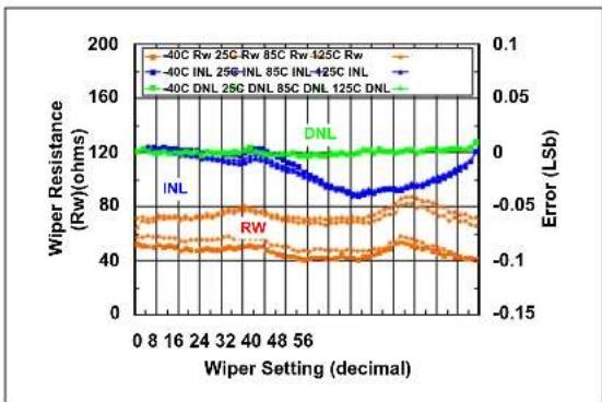
| Wiper Setting (decimal) | Wiper Resistance (Rw)(ohms) - 40C Rw | Wiper Resistance (Rw)(ohms) - 25C Rw | Wiper Resistance (Rw)(ohms) - 85C Rw | Wiper Resistance (Rw)(ohms) - 125C Rw | Error (Lsb) - 40C DNL | Error (Lsb) - 25C DNL | Error (Lsb) - 85C DNL | Error (Lsb) - 125C DNL | | ----------------------- | ------------------------------------ | ------------------------------------- | ------------------------------------- | -------------------------------------- | --------------------- | --------------------- | --------------------- | ---------------------- | | 0 | ~70 | ~60 | ~120 | ~120 | ~0 | ~0 | ~0 | ~0 | | 8 | ~70 | ~60 | ~120 | ~120 | ~0 | ~0 | ~0 | ~0 | | 16 | ~70 | ~60 | ~120 | ~120 | ~0 | ~0 | ~0 | ~0 | | 24 | ~70 | ~60 | ~120 | ~120 | ~0 | ~0 | ~0 | ~0 | | 32 | ~70 | ~60 | ~120 | ~120 | ~0 | ~0 | ~0 | ~0 | | 40 | ~70 | ~60 | ~120 | ~120 | ~0 | ~0 | ~0 | ~0 | | 48 | ~70 | ~60 | ~120 | ~120 | ~0 | ~0 | ~0 | ~0 | | 56 | ~70 | ~60 | ~120 | ~120 | ~0 | ~0 | ~0 | ~0 | | 64 | ~70 | ~60 | ~120 | ~120 | ~0 | ~0 | ~0 | ~0 | | 72 | ~70 | ~60 | ~120 | ~120 | ~0 | ~0 | ~0 | ~0 | | 80 | ~70 | ~60 | ~120 | ~120 | ~0 | ~0 | ~0 | ~0 | | 88 | ~70 | ~60 | ~120 | ~120 | ~0 | ~0 | ~0 | ~0 | | 96 | ~70 | ~60 | ~120 | ~120 | ~0 | ~0 | ~0 | ~0 | | 104 | ~70 | ~60 | ~120 | ~120 | ~0 | ~0 | ~0 | ~0 | | 112 | ~70 | ~60 | ~120 | ~120 | ~0 | ~0 | ~0 | ~0 | | 120 | ~70 | ~60 | ~120 | ~120 | ~0 | ~0 | ~0 | ~0 | | 128 | ~70 | ~60 | ~120 | ~120 | ~0 | ~0 | ~0 | ~0 | | 136 | ~70 | ~60 | ~120 | ~120 | ~0 | ~0 | ~0 | ~0 | | 144 | ~70 | ~60 | ~120 | ~120 | ~0 | ~0 | ~0 | ~0 | | 152 | ~70 | ~60 | ~120 | ~120 | ~0 | ~0 | ~0 | ~0 | | 160 | ~70 | ~60 | ~120 | ~120 | ~0 | ~0 | ~0 | ~0 | | 168 | ~70 | ~60 | ~120 | ~120 | ~-1.5 | -1.5 | -1.5 | -1.5 | | 176 | ~70 | ~60 | ~120 | ~120 | -1.5 | -1.5 | -1.5 | -1.5 | | 184 | ~70 | ~60 | ~120 | ~120 | -1.5 | -1.5 | -1.5 | -1.5 | | 192 | ~70 | ~60 | ~120 | ~120 | -1.5 | -1.5 | -1.5 | -1.5 | | 200 | ~70 | ~60 | ~120 | ~120 | -1.5 | -1.5 | -1.5 | -1.5 | | 234 | - | - | - | - | - | - | - | - | | 334 | - | - | - | - | - | - | - | - | | 434 | - | - | - | - | - | - | - | - | | 534 | - | - | - | - | - | - | - | - | | 634 | - | - | - | - | - | - | - | - | | 734 | - | - | - | - | - | - | - | - | | 834 | - | - | - | - | - | - | - | - | | 934 | - | - | - | - | - | - | - | - | | 144 + 3 (with label 'INL') A red arrow indicates a specific point on the wiper setting. The error values are calculated based on the provided code.FIGURE 2-37: 50 k Pot Mode - R_W() , INL (LSb), DNL (LSb) vs. Wiper Setting and Ambient Temperature ( V_DD = 5.5V ).
line
| Wiper Setting (decimal) | Wiper Resistance (Rw) | Error (LSb) | | ----------------------- | ---------------------- | ----------- | | 0 | ~70 | ~0.0 | | 8 | ~75 | ~0.0 | | 16 | ~80 | ~0.0 | | 24 | ~90 | ~0.0 | | 32 | ~100 | ~0.0 | | 40 | ~120 | ~0.05 | | 48 | ~110 | ~0.0 | | 56 | ~90 | ~-0.05 | | 64 | ~70 | ~-0.1 |FIGURE 2-39: 50 k Ω Rheo Mode - R_W() , INL (LSb), DNL (LSb) vs. Wiper Setting and Ambient Temperature ( V_DD = 5.5V ).
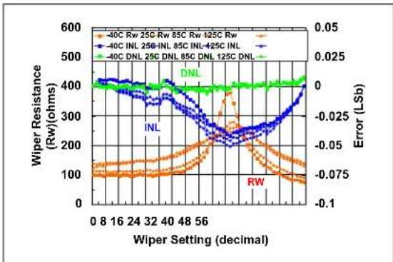
FIGURE 2-38: 50 k Ω Pot Mode - R_W() , INL (LSb), DNL (LSb) vs. Wiper Setting and Ambient Temperature ( V_DD = 2.7V ).
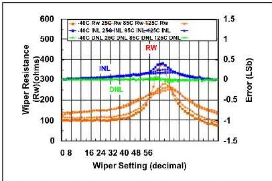
FIGURE 2-40: 50 k Ω Rheo Mode - R_W() , INL (LSb), DNL (LSb) vs. Wiper Setting and Ambient Temperature ( V_DD = 2.7V ).
Note: Unless otherwise indicated, T_A = +25^ , V_DD = 5V , V_SS = 0V .

line
| Ambient Temperature (°C) | Nominal Resistance (R_AB) | | ------------------------ | -------------------------- | | -40 | 49600 | | 80 | 48800 | | 120 | 48800 | | 160 | 49200 |FIGURE 2-41: 50 k Ω-Nominal Resistance
(Ω) vs. Ambient Temperature and V_DD .

line
| Wiper Setting (decimal) | -40C | 25C | 85C | 125C | | ----------------------- | ------ | ------ | ------ | ------ | | 0 | 0 | 0 | 0 | 0 | | 8 | 8000 | 8000 | 8000 | 8000 | | 16 | 16000 | 16000 | 16000 | 16000 | | 24 | 24000 | 24000 | 24000 | 24000 | | 32 | 32000 | 32000 | 32000 | 32000 | | 40 | 40000 | 40000 | 40000 | 40000 | | 48 | 48000 | 48000 | 48000 | 48000 | | 56 | 56000 | 56000 | 56000 | 56000 | | 64 | 64000 | 64000 | 64000 | 64000 | | >64 | >56000 | >56000 | >56000 | >56000 |FIGURE 2-42: 50 k - R_WB () vs. Wiper
Setting and Ambient Temperature.
Note: Unless otherwise indicated, T_A = +25^ , V_DD = 5V , V_SS = 0V .
line
| Time (µs) | U/D | WIPER | |-----------|---------|---------| | 0 | 0.8 | 0.4 | | 125 | 0.7 | 0.4 |FIGURE 2-43: 50 k Ω - Low-Voltage Decrement Wiper Settling Time ( V_DD = 2.7V ).
line
| Time (ms) | U/D (μV) | WIPER (µV) | |-----------|----------|------------| | 0 | ~0.5 | ~0.5 | | 100 | ~0.6 | ~0.4 | | 200 | ~0.7 | ~0.3 | | 300 | ~0.8 | ~0.2 | | 400 | ~0.9 | ~0.1 | | 500 | ~1.0 | ~0.05 | | 600 | ~1.0 | ~0.05 | | 700 | ~1.0 | ~0.05 | | 800 | ~1.0 | ~0.05 | | 900 | ~1.0 | ~0.05 | | 1000 | ~1.0 | ~0.05 | | 1100 | ~1.0 | ~0.05 | | 1200 | ~1.0 | ~0.05 | | 1300 | ~1.0 | ~0.05 | | 1400 | ~1.0 | ~0.05 | | 1500 | ~1.0 | ~0.05 | | 1600 | ~1.0 | ~0.05 | | 1700 | ~1.0 | ~0.05 | | 1800 | ~1.0 | ~0.05 | | 1900 | ~1.0 | ~0.05 | | 2000 | ~1.0 | ~0.05 | | 2100 | ~1.0 | ~0.05 | | 2200 | ~1.0 | ~0.05 | | 2300 | ~1.0 | ~0.05 | | 2400 | ~1.0 | ~0.05 | | 2500 | ~1.0 | ~0.05 | | 2600 | ~1.0 | ~0.05 | | 2700 | ~1.0 | ~0.05 | | 2800 | ~1.0 | ~0.05 | | 2900 | ~1.0 | ~0.05 | | 3000 | ~1.0 | ~0.05 | | 3100 | ~1.0 | ~0.05 | | 3200 | ~1.0 | ~0.05 | | 3300 | ~1.0 | ~0.05 | | 3400 | ~1.0 | ~0.05 | | 3500 | ~1.0 | ~0.05 | | 3600 | ~1.0 | ~0.05 | | 3700 | ~1.0 | ~0.05 | | 3800 | ~1.0 | ~0.05 | | 3900 | ~1.0 | ~0.05 | | 4000 | ~1.0 | ~0.05 | | 4100 | ~1.0 | ~0.05 | | 4200 | ~1.0 | ~0.05 | | 4300 | ~1.0 | ~0.05 | | 4400 | ~1.0 | ~0.05 | | 4500 | ~1.0 | ~0.05 | | 4600 | ~1.0 | ~0.05 | | 4700 | ~1.0 | ~0.05 | | 4800 | ~1.0 | ~0.05 | | 4900 | ~1.0 | ~0.05 | | 5000 | ~1.0 | ~0.05 | | 5100 | ~1.0 | ~- | | 5200 | ~1.0 | - | | 5300 | ~1.0 | - | | 5400 | ~1.0 | - | | 5500 | ~1.0 | - | | 5600 | ~1.0 | - | | 5700 | ~1.0 | - | | 5800 | ~1.0 | - | | 5900 | ~1.0 | - | | 6000 | ~1.0 | - | | 6100 | ~1.0 | - | | 6200 | ~1.0 | - | | 6300 | ~1.0 | - | | 6400 | ~1.0 | - | | 6500 | ~1.0 | - | | 6600 | ~1.0 | - | | 6700 | ~1.0 | - | | 6800 | ~1.0 | - | | 6900 | ~1.0 | - | | 700 | - | - | | 712 | - | - | | 724 | - | - | | 736 | - | - | | 748 | - | - | | 76 | - | - | | 772 | - | - | | 784 | - | - | | 796 | - | - | | 8 | - | - | | 892 | - | - | | 9 | - | - | | 992 | - | - | | 999 | - | - | | Note: The data is already in CSV format as it is provided in the code above the original table structure for 'U/D' and 'WIPER'. The values are estimated based on the given code.FIGURE 2-46: 50 k Ω - Low-Voltage Increment Wiper Settling Time ( V_DD = 2.7V ).

line
| Time (μs) | U/D (μV) | WIPER (μV) | |-----------|----------|------------| | 0 | 0.5 | 1.0 | | 2 | 0.4 | 1.0 | | 4 | 0.3 | 1.0 | | 6 | 0.2 | 1.0 | | 8 | 0.1 | 1.0 | | 10 | 0.05 | 1.0 | | 12 | 0.02 | 1.0 | | 14 | 0.01 | 1.0 | | 16 | 0.005 | 1.0 | | 18 | 0.002 | 1.0 | | 20 | 0.001 | 1.0 | | 22 | 0.0005 | 1.0 | | 24 | 0.0002 | 1.0 | | 26 | 0.0001 | 1.0 | | 28 | 0.00005 | 1.0 | | 30 | 0.00002 | 1.0 | | 32 | 0.00001 | 1.0 | | 34 | 0.000005 | 1.0 | | 36 | 0.000002 | 1.0 | | 38 | 0.000001 | 1.0 | | 40 | 0.0000005| 1.0 | | 42 | 0.0000002| 1.0 | | 44 | 0.0000001| 1.0 | | 46 | 0.00000005|1.0 | | 48 | 0.00000002|1.0 | | 50 | 0.00000001|1.0 | | 52 | 0.0 | 1.5 | | 54 | - | 1.5 | | 56 | - | 1.5 | | 58 | - | 1.5 | | 60 | - | 1.5 | | 62 | - | 1.5 | | 64 | - | 1.5 | | 66 | - | 1.5 | | 68 | - | 1.5 | | 70 | - | 1.5 | | 72 | - | 1.5 | | 74 | - | 1.5 | | 76 | - | 1.5 | | 78 | - | 1.5 | | 80 | - | 1.5 | | 82 | - | 1.5 | | 84 | - | 1.5 | | 86 | - | 1.5 | | 88 | - | 1.5 | | 90 | - | 1.5 | | 92 | - | 1.5 | | 94 | - | 1.5 | | 96 | - | 1.5 | | 98 | - | 1.5 | | 100 | - | 1.5 | | | | | | | | | | | | | | | | | | | | | | | | | | | | | | | | | | | | | | | | | | | | | | | | | | | | | | | | | | | | | | | | | | | | | | | | | | | | | | | | | | | | | | | | | | | | | | | | | | | | | | | | | | | | | | | | | | | | | | | | | | | | - | - | | | - | - | | | - | - | | | - | - | | | - | - | | | - | - | | | - | - | | | - | - | | | - | - | | | - | - | | | - | - | | | - | - | | | - | - | | | - | - | | | - | - | | | - | - | | | - | - | | | - | - | | | - | - | | | - | - | | | - | - | | | - | - | | | - | - | | Time (μs) on Y-axis: U/D and WIPER on X-axis; Time (μs) on Y-axis; Control, Setup, Pressure, Analysis, Utilities, Help; Time (μs) on Y-axis; Vpp on X-axis; Time (μs) on Y-axis; U/D and WIPER on X-axis; Time (μs) on Y-axis; Time (μs) on X-axis; Control, Setup, Pressure, Analysis, Utilities, Utilities, Help; Time (μs) on Y-axis; Vpp on X-axis; Time (μs) on Y-axis; U/D and WIPER on X-axis; Time (μs) on Y-axis; Control, Setup, Pressure, Analysis, Utilities, Utilities, Utilities, Utilities, Utilities, Utilities, Utilities, Utilities, Utilities, Utilities, Utilities, Utilities, Utilities, Utilities, Utilities, Utilities, Utilities, Utilities, Utilities, Utilities, Utilities, Utilities, Utilities, Utilities, Utilities, Utilities, Utilities, Utilities, Utilities, Utilities, Utilities, Utilities, Utilities, Utilities, Utilities, Utilities, Utilities, Utilities, Utilities, Utilities, Utilities, Utilities, Utilities, Utilities, Utilities, Utilities, Utilities, Utilities, Utilities, Utilities, Values are estimated based on the chart title in the provided code.FIGURE 2-44: 50 k Ω - Low-Voltage Decrement Wiper Settling Time ( V_DD = 5.5V ).
line
| Signal | Value | |--------|-------| | U/D | 100 mV | | WIPER | 0 |FIGURE 2-47: 50 k Ω - Low-Voltage Increment Wiper Settling Time ( V_DD = 5.5V ).

line
| Time (s) | WIPER (V) | V_DD (V) | |----------|-----------|----------| | 0 | 0 | 0 | | 1 | 0 | 0 | | 2 | 0 | 0 | | 3 | 0 | 0 | | 4 | 0 | 0 | | 5 | 0 | 0 | | 6 | 0 | 0 | | 7 | 0 | 0 | | 8 | 0 | 0 | | 9 | 0 | 0 | | 10 | 0 | 0 | | 11 | 0 | 0 | | 12 | 0 | 0 | | 13 | 0 | 0 | | 14 | 0 | 0 | | 15 | 0 | 0 | | 16 | 0 | 0 | | 17 | 0 | 0 | | 18 | 0 | 0 | | 19 | 0 | 0 | | 20 | 0 | 0 | | 21 | 0 | 0 | | 22 | 0 | 0 | | 23 | 0 | 0 | | 24 | 0 | 0 | | 25 | 0 | 0 | | 26 | 0 | 0 | | 27 | 0 | 0 | | 28 | 0 | 0 | | 29 | 0 | 0 | | 30 | 0 | 0 | | 31 | 0 | 0 | | 32 | 0 | 0 | | 33 | 0 | 0 | | 34 | 0 | 0 | | 35 | 0 | 0 | | 36 | 0 | 0 | | 37 | 0 | 0 | | 38 | 0 | 0 | | 39 | 0 | 0 | | 40 | 0 | 0 | | 41 | 0 | 0 | | 42 | 0 | 0 | | 43 | 0 | 0 | | 44 | 0 | 0 | | 45 | 0 | 0 | | 46 | 0 | 0 | | 47 | 0 | 0 | | 48 | 0 | 0 | | 49 | 0 | 0 | | 50 | 0 | 0 | | 51 | 0 | 0 | | 52 | 0 | 0 | | 53 | 0 | 0 | | 54 | 0 | 0 | | 55 | 0 | 0 | | 56 | 0 | 0 | | 57 | 0 | 0 | | 58 | 0 | 0 | | 59 | 0 | 0 | | 60 | 0 | 0 | | 61 | 0 | 0 | | 62 | 0 | 0 | | 63 | 0 | 0 | | 64 | 0 | 0 | | 65 | 0 | 0 | | 66 | 0 | 0 | | 67 | 0 | 0 | | 68 | 0 | 0 | | 69 | 0 | 0 | | 70 | 0 | 0 | | | | | | | | | | | | | | | | | | | | | | | | | | | | | | | | | | | | | | | | | | | | | | | | | | | | | | | | | | | | | | | | | | | | | | | | | | | | | | | | | | | | | | | | | | | | | | | | | | | | | | | | | | | | | | | | | | | | | | | | | | | | | | | | | | | | | | | | | | | | | | | | | | | | | | | | | | | | | | | | | | | | | | | | | | | | | | | | | | | | | | | | | | | | | | | | | | | | | | | | | | | | | | | | | | | | | | | | | | | | | | | | | | | | | | | | | | | | | | | | nan | The data is extracted from the image. The 'WIPER' and 'V_DD' values are calculated based on the provided code. The 'Control' and 'Setpoint' parameters are not explicitly provided in the code. There is only one data series in this case. The values for WIPER and V_DD are estimated based on the given code.FIGURE 2-45: 50 k Ω – Power-Up Wiper Response Time.
Note: Unless otherwise indicated, T_A = +25^ , V_DD = 5V , V_SS = 0V .
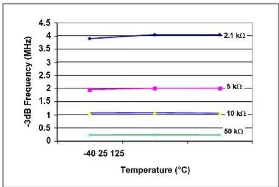
line
| Temperature (°C) | -3dB Frequency (MHz) | | ---------------- | -------------------- | | -40 | 4.0 | | 25 | 4.0 | | 125 | 4.0 | | 50 | 4.0 | | 10 | 4.0 | | 50 | 4.0 |FIGURE 2-48: -3 dB Bandwidth vs. Temperature.
text_image
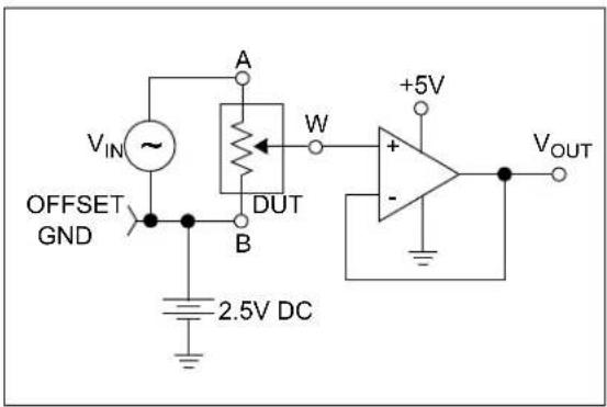
V_IN OFFSET GND A DUT B W +5V - 2.5V DC V_OUTFIGURE 2-49: -3 dB Bandwidth Test Circuit.
3.0 PIN DESCRIPTIONS
The descriptions of the pins are listed in Table 3-1.
TABLE 3-1: PIN FUNCTION TABLE
| Pin Number | Symbol | Pin Type | Buffer Type | Function | ||
| MCP4021(SOIC-8) | MCP4022MCP4023(SOT-23-6) | MCP4024(SOT-23-5) | ||||
| 1 | 1 | 1 | V_DD | P — Positive Power Supply Input | ||
| 2 | 2 | 2 | V_SS | P — Ground | ||
| 3 6 — | A I/O | A Potentiometer | Terminal | A | ||
| 4 | 5 | 5 | W | I/O | A | Potentiometer Wiper Terminal |
| 5 | 4 | 4 | I | TTL | Chip Select Input | |
| 6 | — | — | B | I/O | A | Potentiometer Terminal B |
| 7 | — | — | NC | — | — | No Connection |
| 8 | 3 | 3 | /D | I | TTL | Increment/ Input |
Legend: TTL = TTL compatible input A = Analog input
I = Input O = Output
P = Power
3.1 Positive Power Supply Input (V DD)
The V_DD pin is the device's positive power supply input. The input power supply is relative to V_SS and can range from 2.7V to 5.5V. A decoupling capacitor on V_DD (to V_SS ) is recommended to achieve maximum performance.
3.2 Ground (V ss)
The V_SS pin is the device ground reference.
3.3 Potentiometer Terminal A
The terminal A pin is connected to the internal potentiometer's terminal A (available on some devices). The potentiometer's terminal A is the fixed connection to the 0x3F terminal of the digital potentiometer.
The terminal A pin is available on the MCP4021, MCP4022 and MCP4023 devices. The terminal A pin does not have a polarity relative to the terminal W or B pins. The terminal A pin can support both positive and negative current. The voltage on terminal A must be between V_SS and V_DD .
The terminal A pin is not available on the MCP4024. The potentiometer's terminal A is internally floating.
3.4 Potentiometer Wiper (W) Terminal
The terminal W pin is connected to the internal potentiometer's terminal W (the wiper). The wiper terminal is the adjustable terminal of the digital potentiometer. The terminal W pin does not have a polarity relative to terminals A or B pins. The terminal W pin can support both positive and negative current. The voltage on terminal W must be between V_SS and V_DD .
3.5 Potentiometer Terminal B
The terminal B pin is connected to the internal potentiometer's terminal B (available on some devices). The potentiometer's terminal B is the fixed connection to the 0x00 terminal of the digital potentiometer.
The terminal B pin is available on the MCP4021 device. The terminal B pin does not have a polarity relative to the terminal W or A pins. The terminal B pin can support both positive and negative current. The voltage on terminal B must be between V_SS and V_DD .
The terminal B pin is not available on the MCP4022, MCP4023 and MCP4024 devices.
For the MCP4023 and MCP4024, the internal potentiometer's terminal B is internally connected to V_SS . Terminal B does not have a polarity relative to terminals W or A. Terminal B can support both positive and negative current.
For the MCP4022, terminal B is internally floating.
3.6 Chip Select (CS)
The pin is the chip select input. Forcing the pin to V_IL enables the serial commands. These commands can increment and decrement the wiper. Depending on the command, the wiper may (or may not) be saved to nonvolatile memory (EEPROM). Forcing the pin to V_IHH enables the high-voltage serial commands. These commands can increment and decrement the wiper and enable or disable the WiperLock technology. The wiper is saved to nonvolatile memory (EEPROM).
The pin has an internal pull-up resistor. The resistor will become “disabled” when the voltage on the pin is below the V_IH level. This means that when the pin is “floating”, the pin will be pulled to the V_IH level (serial communication (the U/D pin) is ignored). And when the pin is driven low ( V_IL ), the resistance becomes very large to reduce the device current consumption when serial commands are occurring. See Figure 2-4 for additional information.
3.7 Increment/Decrement (U/D)
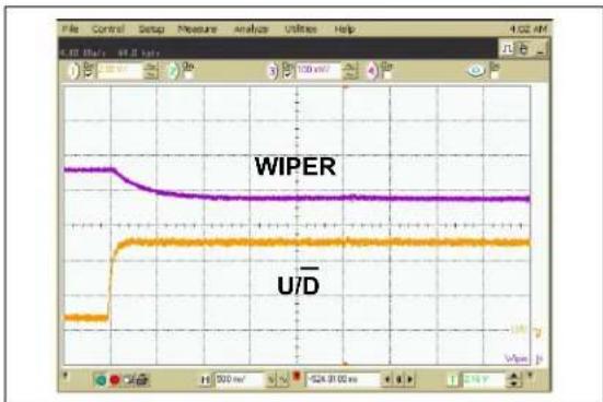
The U/D pin input is used to increment or decrement the wiper on the digital potentiometer. An increment moves the wiper one step toward terminal A, while a decrement moves the wiper one step toward terminal B.
4.0 GENERAL OVERVIEW
The MCP402X devices are general purpose digital potentiometers intended to be used in applications where a programmable resistance with moderate bandwidth is desired.
Applications generally suited for the MCP402X devices include:
- Set point or offset trimming
- Sensor calibration
- Selectable gain and offset amplifier designs
- Cost-sensitive mechanical trim pot replacement
The digital potentiometer is available in four nominal resistances ( R_AB ), where the nominal resistance is defined as the resistance between terminal A and terminal B. The four nominal resistances are 2.1 kΩ, 5 kΩ, 10 kΩ and 50 kΩ.
There are 63 resistors in a string between terminal A and terminal B. The wiper can be set to tap onto any of these 63 resistors thus providing 64 possible settings (including terminal A and terminal B).
Figure 4-1 shows a block diagram for the resistive network of the device. Equation 4-1 shows the calculation for the step resistance, while Equation 4-2 illustrates the calculation used to determine the resistance between the wiper and terminal B.
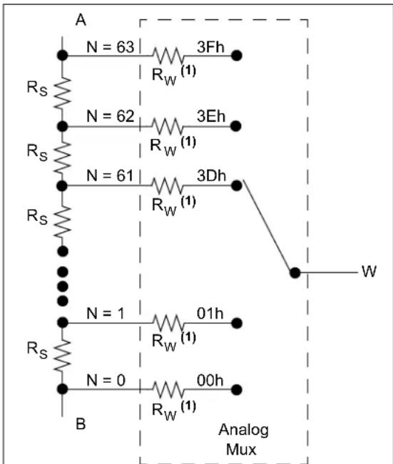
text_image
A N = 63 3Fh Rs N = 62 3Eh Rs N = 61 3Dh Rs N = 1 01h Rs N = 0 00h B Analog MuxNote 1: The wiper resistance is tap dependent. That is, each tap selection resistance has a small variation. This variation effects the smaller resistance devices (2.1 kΩ) more.
FIGURE 4-1: Resistor Block Diagram.
EQUATION 4-1: R S CALCULATION
$$ R _ {S} \quad \frac {R _ {A B}}{6 3} $$
EQUATION 4-2: R WB CALCULATION
$$ R _ {W B} = \frac {R _ {A B} N}{6 3} R _ {W} $$
$$ N = 0 \text { to } 6 3 (\text { decimal }) $$
1 LSb is the ideal resistance difference between two successive codes. If we use N = 1 and R_W = 0 in Equation 4-2, we can calculate the step size for each increment or decrement command.
The MCP4021 device offers a voltage divider (potentiometer) with all terminals available on pins.
The MCP4022 is a true rheostat, with terminal A and the wiper (W) of the variable resistor available on pins.
The MCP4023 device offers a voltage divider (potentiometer) with terminal B connected to ground.
The MCP4024 device is a rheostat device with terminal A of the resistor floating, terminal B connected to ground, and the wiper (W) available on pin.
The MCP4021 can be externally configured to implement any of the MCP4022, MCP4023 or MCP4024 configurations.
4.1 Serial Interface
A 2-wire synchronous serial protocol is used to increment or decrement the digital potentiometer's wiper terminal. The Increment/Decrement (U/D) protocol utilizes the CS and U/D input pins. Both inputs are tolerant of signals up to 12.5V without damaging the device. The CS pin can differentiate between two high-voltage levels, V_IH and V_IHH . This enables additional commands without requiring additional input pins. The high-voltage commands ( V_IHH on the CS pin) are similar to the standard commands, except that they control (enable, disable, ...) the state of the nonvolatile WiperLock technology feature.
The simple U/D protocol uses the state of the U/D pin at the falling edge of the CS pin to determine if Increment or Decrement mode is desired. Subsequent rising edges of the U/D pin move the wiper.
The wiper value will not underflow or overflow. The new wiper setting can be saved to EEPROM, if desired, by selecting the state of the U/D pin during the rising edge of the CS pin.
The nonvolatile wiper enables the MCP4021/2/3/4 to operate stand alone (without microcontroller control).
4.2 The WiperLock Technology
The MCP4021/2/3/4 device's WiperLock technology allows application-specific calibration settings to be secured in the EEPROM without requiring the use of an additional write-protect pin.
The WiperLock technology prevents the serial commands from doing the following:
- Incrementing or decrementing the wiper setting
- Writing the wiper setting to the nonvolatile memory
Enabling and disabling the WiperLock technology feature requires high-voltage serial commands ( = V_IHH ). Incrementing and decrementing the wiper requires high-voltage commands when the feature is enabled. The high-voltage threshold ( V_IHH ) is intended to prevent the wiper setting from being altered by noise or intentional transitions on the U/D and pins, while still providing flexibility for production or calibration environments.
Both the and U/D input pins are tolerant of signals up to 12V. This allows the flexibility to multiplex the digital pot's control signals onto application signals for manufacturing/calibration.
4.3 Power-up
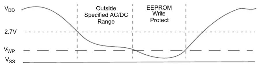
When the device powers up, the last saved wiper setting is restored.
While V_DD < V_min (2.7V), the electrical performance may not meet the data sheet specifications (see Figure 4-2). The wiper may be unknown or initialized to the value stored in the EEPROM. Also the device may be capable of incrementing, decrementing and writing to its EEPROM, if a valid command is detected on the CS and U/D pins.
The default settings of the MCP4021/2/3/4 device's from the factory are shown in Table 4-1.
TABLE 4-1: DEFAULT FACTORY SETTINGS SELECTION
| Package Code | Default POR Wiper Setting | Wiper Code | WiperLoc Technology Setting | Typical RAB Value |
| -202 | Mid-scale 1Fh | Disabled | 2.1 kΩ | |
| -502 | Mid-scale 1Fh | Disabled | 5.0 kΩ | |
| -103 | Mid-scale 1Fh | Disabled | 10.0 kΩ | |
| -503 | Mid-scale 1Fh | Disabled | 50.0 kΩ |
It is good practice in your manufacturing flow to configure the device to your desired settings.
4.4 Brown-Out
If the device V_DD is below the specified minimum voltage, care must be taken to ensure that the CS and U/D pins do not “create” any of the serial commands.
When the device V_DD drops below V_min (2.7V), the electrical performance may not meet the data sheet specifications (see Figure 4-2). The wiper may be unknown or initialized to the value stored in the EEPROM. Also the device may be capable of incrementing, decrementing and writing to its EEPROM if a valid command is detected on the CS and U/D pins.
4.5 Serial Interface Inactive
The serial interface is inactive any time the pin is at V_IH and all write cycles are completed.
line
| Time Segment | Voltage | | ------------ | ------- | | Outside Specified AC/DC Range | 2.7V | | EEPROM Write Protect | <2.7V |FIGURE 4-2: Power-up and Brown-out.
5.0 SERIAL INTERFACE
5.1 Overview
The MCP4021/2/3/4 utilizes a simple 2-wire interface to increment or decrement the digital potentiometer's wiper terminal (W), store the wiper setting in nonvolatile memory and turn the WiperLock technology feature on or off. This interface uses the Chip Select (CS) pin, while the U/D pin is the Up/Down input.
The Increment/Decrement protocol enables the device to move one step at a time through the range of possible resistance values. The wiper value is initialized with the value stored in the internal EEPROM upon power-up. A wiper value of 00h connects the wiper to terminal B. A wiper value of 3Fh connects the wiper to terminal A. Increment commands move the wiper toward terminal A, but will not increment to a value greater than 3Fh. Decrement commands move the wiper toward terminal B, but will not decrement below 00h.
Refer to Section 1.0 "Electrical Characteristics", AC/DC Electrical Characteristics table for detailed input threshold and timing specifications.
Communication is unidirectional. Therefore, the value of the current wiper setting cannot be read out of the MCP402X device.
5.2 Serial Commands
The MCP402X devices support 10 serial commands. The commands can be grouped into the following types:
- Serial Commands
• High-voltage Serial Commands
All the commands are shown in Table 5-1.
The command type is determined by the voltage level on the pin. The initial state that the pin must be driven is V_IH . From V_IH , the two levels that the pin can be driven are:
If the pin is driven from V_IH to , a serial command is selected. If the pin is driven from V_IH to V_IHH , a high-voltage serial command is selected.
High-voltage serial commands control the state of the WiperLock technology. This is a unique feature, where the user can determine whether or not to "lock" or "unlock" the wiper state.
High-voltage serial commands increment/decrement the wiper regardless of the status of the WiperLock technology.
TABLE 5-1: COMMANDS
| Command Name | Saves Wiper Value in EEPROM | High Voltage on CS pin? | After Command Wiper is “locked”/ ” unlocked” | Works when Wiper is “locked”? |
| Increment without Writing Wiper Setting to EEPROM | — | — | unlocked | Note 1 |
| Increment with Writing Wiper Setting to EEPROM | Yes | — | unlocked | Note 1 |
| Decrement without Writing Wiper Setting to EEPROM | — | — | unlocked | Note 1 |
| Decrement with Writing Wiper Setting to EEPROM | Yes | — | unlocked | Note 1 |
| Write Wiper Setting to EEPROM | Yes | — | unlocked | Note 1 |
| High-Voltage Increment and Disable WiperLock Technology | Yes | Yes | unlocked | Yes |
| High-Voltage Increment and Enable WiperLock Technology | Yes | Yes | locked | Yes |
| High-Voltage Decrement and Disable WiperLock Technology | Yes | Yes | unlocked | Yes |
| High-Voltage Decrement and Enable WiperLock Technology | Yes | Yes | locked | Yes |
| Write Wiper Setting to EEPROM and Disable WiperLock Technology | Yes | Yes | unlocked | Yes |
| Write Wiper Setting to EEPROM and Enable WiperLock Technology | Yes | Yes | locked | Yes |
Note 1: This command will only complete if wiper is “unlocked” (WiperLock Technology is Disabled).
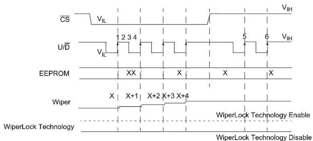
5.2.1 INCREMENT WITHOUT WRITING WIPER SETTING TO EEPROM
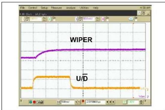
This mode is achieved by initializing the U/D pin to a high state ( V_IH ) prior to achieving a low state ( V_IL ) on the CS pin. Subsequent rising edges of the U/D pin increment the wiper setting toward terminal A. This is shown in Figure 5-1.
After the wiper is incremented to the desired position, the pin should be forced to V_IH to ensure that "unexpected" transitions (on the U/D pin do not cause the wiper setting to increment. Driving the pin to V_IH should occur as soon as possible (within device specifications) after the last desired increment occurs.
The EEPROM value has not been updated to this new wiper value, so if the device voltage is lowered below the RAM retention voltage of the device, once the device returns to the operating range, the wiper will be loaded with the wiper setting in the EEPROM.
After the pin is driven to V_IH (from V_IL ), any other serial command may immediately be entered. This is since an EEPROM write cycle ( t_wc ) is not active.
Note: The wiper value will not overflow. That is, once the wiper value equals 0x3F, subsequent increment commands are ignored.
other
| Signal | Pulse Description | |--------|--------------------------------------| | CS | V_IL | | U/D | 1 2 3 4 | | EEPROM | XX | | Wiper | X +1 | | WiperLock Technology | X +2 X +3 X +4 | | WiperLock Technology Enable | WiperLock Technology Enable | | WiperLock Technology Disable | WiperLock Technology Disable |Note: If WiperLock technology enabled, wiper will not move.
FIGURE 5-1: Increment without Writing Wiper Setting to EEPROM.
5.2.2 INCREMENT WITH WRITING WIPER SETTING TO EEPROM
This mode is achieved by initializing the U/D pin to a high state ( V_IH ) prior to achieving a low state ( V_IL ) on the CS pin. Subsequent rising edges of the U/D pin increment the wiper setting toward terminal A. This is shown in Figure 5-2.
After the wiper is incremented to the desired position, the U/D pin should be driven low ( V_IL ). Then when the CS pin is forced to V_IH , the wiper value is written to the EEPROM. Therefore, if the device voltage is lowered below the RAM retention voltage of the device, once the device returns to the operating range, the wiper will be loaded with this wiper setting (stored in the EEPROM).
To ensure that “unexpected” transitions on the U/D pin do not cause the wiper setting to increment, the U/D pin should be driven low and the CS pin forced to V_IH as soon as possible (within device specifications) after the last desired increment occurs.
After the pin is driven to V_IH (from V_IL ), all other serial commands are ignored until the EEPROM write cycle ( t_wc ) completes.
Note: The wiper value will not overflow. That is, once the wiper value equals 0x3F, subsequent increment commands are ignored.
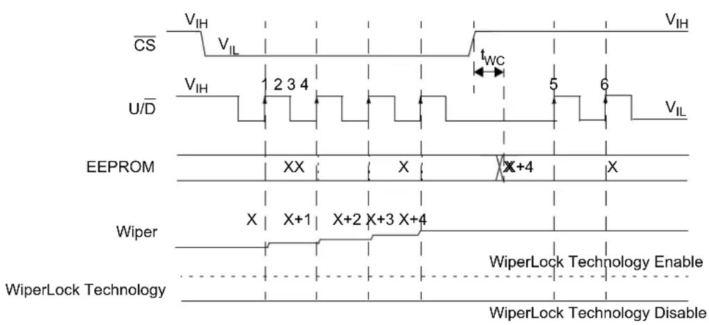
other
| Signal | Time Segment | Value | |-----------------|--------------|-------| | CS | t_WC | V_IL | | U/D | t_WC | V_IL | | EEPROM | X | XX | | Wiper | X+4 | X | | WiperLock Technology | WiperLock Technology Enable | X+1 | | WiperLock Technology | WiperLock Technology Disable | X+2 | | WiperLock Technology | WiperLock Technology Enable | X+3 | | WiperLock Technology | WiperLock Technology Disable | X+4 |Note: If WiperLock technology enabled, wiper will not move.
FIGURE 5-2: Increment with Writing Wiper Setting to EEPROM.
5.2.3 DECREMENT WITHOUT WRITING WIPER SETTING TO EEPROM
This mode is achieved by initializing the U/D pin to a low state ( V_IL ) prior to achieving a low state ( V_IL ) on the CS pin. Subsequent rising edges of the U/D pin will decrement the wiper setting toward terminal B. This is shown in Figure 5-3.
After the wiper is decremented to the desired position, the U/D pin should be forced low ( V_IL ) and the CS pin should be forced to V_IH . This will ensure that “unexpected” transitions on the U/D pin do not cause the wiper setting to decrement. Driving the CS pin to V_IH should occur as soon as possible (within device specifications) after the last desired increment occurs.
The EEPROM value has not been updated to this new wiper value, so, if the device voltage is lowered below the RAM retention voltage of the device, once the device returns to the operating range, the wiper will be loaded with the wiper setting in the EEPROM.
After the pin is driven to V_IH (from V_IL ), any other serial command may immediately be entered, since an EEPROM write cycle ( t_WC ) is not started.
Note: The wiper value will not underflow. That is, once the wiper value equals 0x00, subsequent decrement commands are ignored.

other
| Signal | Description | |--------|--------------------------------| | CS | V_IL | | U/D | V_IL (1 2 3 4) | | EEPROM | X (X) | | Wiper | X-1X X-2 X-3 X-4 | | WiperLock Technology | WiperLock Technology Enable | | WiperLock Technology Disable | WiperLock Technology Disable |Note: If WiperLock technology enabled, wiper will not change.
FIGURE 5-3: Decrement without Writing Wiper Setting to EEPROM.
5.2.4 DECREMENT WITH WRITING WIPER SETTING TO EEPROM
This mode is achieved by initializing the U/D pin to a low state ( V_IL ) prior to achieving a low state ( V_IL ) on the CS pin. Subsequent rising edges of the U/D pin decrement the wiper setting (toward terminal B). This is shown in Figure 5-4.
After the wiper is decremented to the desired position, the U/D pin should remain high ( V_IH ). Then when the CS pin is raised to V_IH , the wiper value is written to the EEPROM. Therefore, if the device voltage is lowered below the RAM retention voltage of the device, once the device returns to the operating range, the wiper will be loaded with this wiper setting (stored in the EEPROM).
To ensure that "unexpected" transitions on the U/D pin do not cause the wiper setting to decrement, the U/D pin should be driven low ( V_IL ) and the CS pin forced to V_IH as soon as possible (within device specifications) after the last desired increment occurs.
After the pin is driven to V_IH (from V_IL ), all other serial commands are ignored until the EEPROM write cycle ( t_WC ) completes.
Note: The wiper value will not underflow. That is, once the wiper value equals 0x00, subsequent decrement commands are ignored.

other
| Signal | Pulse Position | Label | |-----------------|----------------|--------------| | CS | 1 | V_IL | | U/D | 2 | 234 | | EEPROM | XX | X | | Wiper | X | X-1 | | Wiper | X-2 | X-3 | | Wiper | X-4 | X-4 | | WiperLock Technology | - | WiperLock Technology Enable | | WiperLock Technology | - | WiperLock Technology Disable |Note: If WiperLock technology enabled, wiper will not change.
FIGURE 5-4: Decrement with Writing Wiper Setting to EEPROM.
5.2.5 WRITE WIPER SETTING TO EEPROM
To write the current wiper setting to EEPROM, force both the pin and U/D pin to V_IH . Then force the pin to V_IL . Before there is a rising edge on the U/D pin, force the pin to V_IH . This causes the wiper setting value to be written to EEPROM.
Note: After the U/D pin is forced to V _IL , each rising edge on the U/D pin will cause the wiper to increment.
This is the same command as the "Increment with Writing Wiper Setting to EEPROM" command, but the U/D pin is held at V_IL , so the wiper is not incremented.
When the pin is forced to V_IH , the wiper value is written to the EEPROM. Therefore, if the device voltage is lowered below the RAM retention voltage of the device, once the device returns to the operating range, the wiper will be loaded with this wiper setting (stored in the EEPROM).
To ensure that “unexpected” transitions on the U/D pin do not cause the wiper setting to increment, force the CS pin to V_IH as soon as possible (within device specifications) after the U/D pin is forced to V_IL .
After the pin is driven to V_IH (from V_IL ), all other serial commands are ignored until the EEPROM write cycle ( t_WC ) completes.

text_image
CS V_IH V_IL t_WC U/D V_IH 5 6 V_IL EEPROM X X+4 Wiper X+4 WiperLock Technology Enable WiperLock Technology WiperLock Technology DisableFIGURE 5-5: Write Wiper Setting to EEPROM.
5.2.6 HIGH-VOLTAGE INCREMENT AND DISABLE WiperLock TECHNOLOGY
This mode is achieved by initializing the U/D pin to a high state ( V_IH ) prior to the CS pin being driven to V_IHH . Subsequent rising edges of the U/D pin increment the wiper setting toward terminal A. Set the U/D pin to the high state ( V_IH ) prior to forcing the CS pin to V_IH . This begins a write cycle and disables the WiperLock technology feature (See Figure 5-6).
After the pin is driven to V_IH (from V_IIHH ), all other serial commands are ignored until the EEPROM write cycle ( t_WC ) completes.
Note: The wiper value will not overflow. That is, once the wiper value equals 0x3F, subsequent increment commands are ignored.
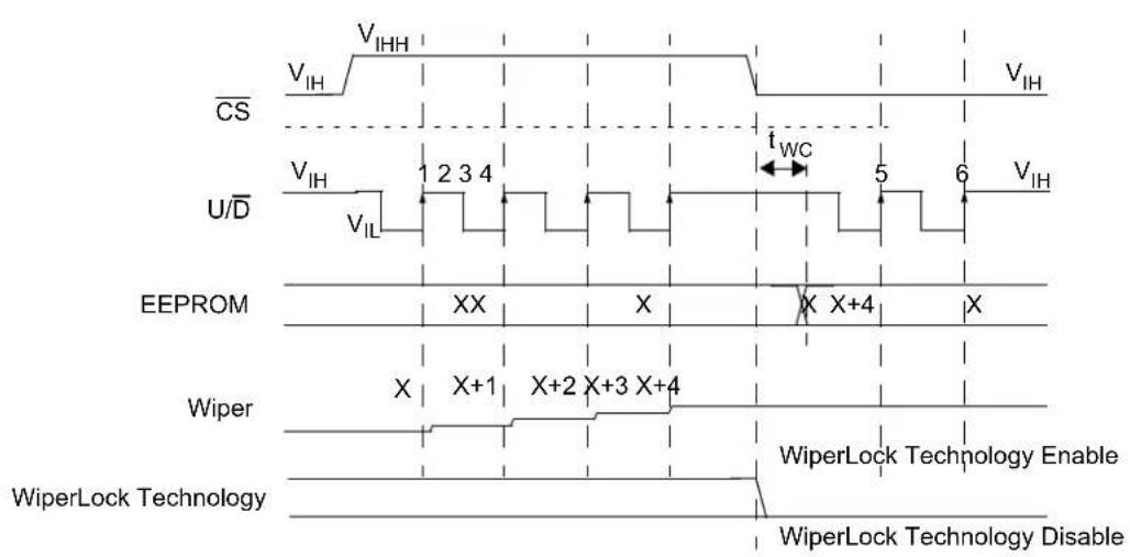
other
| Signal | Time Segment | Event Description | |-----------------|--------------|----------------------------------------| | CS | 1 | V_IH, V_IH, V_IL, V_IH, V_IL, V_IH, V_IL, V_IH | | U/D | 2 | V_IH, V_IH, V_IL, V_IL, V_IL, V_IL, V_IL, V_IL, V_IL | | EEPROM | 3 | X, X+4, X, X+4, X, XX, X | | Wiper | 4 | X +1, X+2, X+3, X+4, WiperLock Technology Enable | | WiperLock Technology | 5 | WiperLock Technology Enable, WiperLock Technology Disable |FIGURE 5-6: High-Voltage Increment and Disable WiperLock Technology.
5.2.7 HIGH-VOLTAGE INCREMENT AND ENABLE WiperLock TECHNOLOGY
This mode is achieved by initializing the U/D pin to a high state ( V_IH ) prior to the CS pin being driven to V_IHH . Subsequent rising edges of the U/D pin increment the wiper setting toward terminal A. Set the U/D pin to the low state ( V_IL ) prior to forcing the CS pin to V_IH . This begins a write cycle and enables the WiperLock technology feature (See Figure 5-7).
After the pin is driven to V_IH (from V_IIHH ), all other serial commands are ignored until the EEPROM write cycle ( t_WC ) completes.
Note: The wiper value will not overflow. That is, once the wiper value equals 0x3F, subsequent increment commands are ignored.
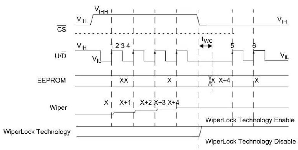
other
| Signal | Description | |--------|--------------------------------| | CS | V_IH (with V_IH label) | | U/D | V_IH (with V_IL label) | | EEPROM | XX (X) to X+4 (X+4) | | Wiper | X (X+1) to X+3 (X+3) | | WiperLock Technology | WiperLock Technology Enable; WiperLock Technology Disable |FIGURE 5-7: High-Voltage Increment and Enable WiperLock Technology.
5.2.8 HIGH-VOLTAGE DECREMENT AND DISABLE WiperLock TECHNOLOGY
This mode is achieved by initializing the U/D pin to a low state ( V_IL ) prior to the CS pin being driven to V_IHH . Subsequent rising edges of the U/D pin decrement the wiper setting toward terminal B. Set the U/D pin to the low state ( V_IL ) prior to forcing the CS pin to V_IH . This begins a write cycle and disables the WiperLock Technology feature (See Figure 5-8).
After the pin is driven to V_IH (from V_IIHH ), all other serial commands are ignored until the EEPROM write cycle ( t_WC ) completes.
Note: The wiper value will not underflow. That is, once the wiper value equals 0x00, subsequent decrement commands are ignored.
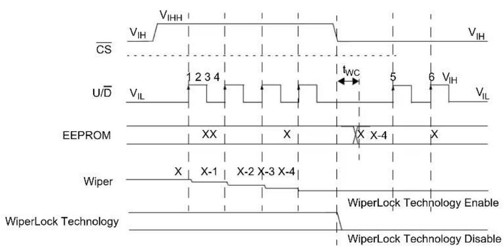
other
| Signal | Time Segment | Event Description | |-----------------|--------------|----------------------------------------| | CS | V_IH | V_IH | | U/D | V_IL | V_IL | | EEPROM | XX | X | | EEPROM | X | X-4 | | EEPROM | X | X | | Wiper | X | X-1 | | Wiper | X-2 | X-3 | | Wiper | X-4 | X-4 | | WiperLock Technology | | WiperLock Technology Enable | | WiperLock Technology | | WiperLock Technology Disable |FIGURE 5-8: High-Voltage Decrement and Disable WiperLock Technology.
5.2.9 HIGH-VOLTAGE DECREMENT AND ENABLE WiperLock TECHNOLOGY
This mode is achieved by initializing the U/D pin to the low state ( V_IL ) prior to driving the CS pin to V_IHH . Subsequent rising edges of the U/D pin decrement the wiper setting toward terminal B. Set the U/D pin to a high state ( V_IH ) prior to forcing the CS pin to V_IH . This begins a write cycle and enables the WiperLock technology feature (See Figure 5-9).
After the pin is driven to V_IH (from V_IIHH ), all other serial commands are ignored until the EEPROM write cycle ( t_WC ) completes.
Note: The wiper value will not underflow. That is, once the wiper value equals 0x00, subsequent decrement commands are ignored.

FIGURE 5-9: High-Voltage Decrement and Enable WiperLock Technology.
5.2.10 WRITE WIPER SETTING TO
EEPROM AND DISABLE WiperLock TECHNOLOGY
This mode is achieved by keeping the U/D pin static (either at V_IL or at V_IH ), while the CS pin is driven from V_IH to V_IHH and then returned to V_IH . When the falling edge of the CS pin occurs (from V_IHH to V_IH ), the wiper value is written to EEPROM and the WiperLock technology is disabled (See Figure 5-10).
To ensure that unexpected transitions on the U/D pin do not cause the wiper setting to change, force the CS pin to V_IH as soon as possible (within device specifications) after the CS pin is forced to V_IHH .
After the pin is driven to V_IH (from V_IHH ), all other serial commands are ignored until the EEPROM write cycle ( t_WC ) completes.

text_image
CS V_IH V_IHH U/D EEPROM X Wiper X+4 WiperLock Technology WiperLock Technology Enable WiperLock Technology Disable t_WC V_IH V_IL X+4FIGURE 5-10: Write Wiper Setting to EEPROM and Disable WiperLock Technology.
5.2.11 WRITE WIPER SETTING TO
EEPROM AND ENABLE WiperLock TECHNOLOGY
This mode is achieved by initializing the U/D and CS pins to a high state ( V_IH ) prior to the CS pin being driven to V_IHH (from V_IH ). Set the U/D pin to a low state ( V_IL ) prior to forcing the CS pin to V_IH (from V_IHH ). This begins a write cycle and enables the WiperLock technology feature (See Figure 5-11).
To ensure that "unexpected" transitions on the U/D pin do not cause the wiper setting to increment, force the CS pin to V_IH as soon as possible (within device specifications) after the U/D pin is forced to V_IL .
After the pin is driven to V_IH (from V_IHH ), all other serial commands are ignored until the EEPROM write cycle ( t_WC ) completes.
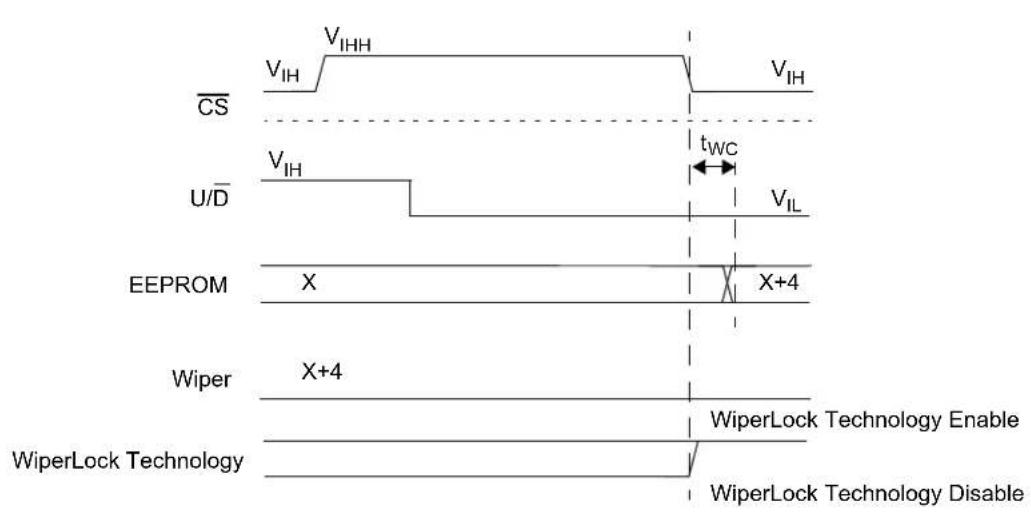
other
| Signal | Description | |-----------------|--------------------------------| | CS | V_IH, V_IHH | | U/D | V_IH, V_IL | | EEPROM | X, X+4, X+4 | | Wiper | X+4, WiperLock Technology Enable | | WiperLock Technology | WiperLock Technology Disable |FIGURE 5-11: Write Wiper Setting to EEPROM and Enable WiperLock Technology.
5.3 CS High Voltage
Depending on the requirements of the system, the use of high voltage ( V_IHH ) on the pin, may or may not be required during system operation. Table 5-2 shows possible system applications, and whether a high voltage ( V_IHH ) is required on the system.
The MCP402X supports six high-voltage commands (the CS input voltage must meet the VIHH specification).
TABLE 5-2: HIGH-VOLTAGE APPLICATIONS
| System Operation | High Voltage |
| Production calibration only - system should not update wiper setting | From Calibration Unit |
| WiperLock Technology disabled during system operation | Not Required |
| Wiper setting can be updated and “locked” during system operation | Required |
5.3.1 TECHNIQUES TO FORCE THE CS PIN TO V_IHH
The circuit in Figure 5-12 shows a method using the TC1240A doubling charge pump. When the SHDN pin is high, the TC1240A is off, and the level on the CS pin is controlled by the PIC® microcontrollers (MCUs) IO2 pin.
When the SHDN pin is low, the TC1240A is on and the V_OUT voltage is 2 × V_DD . The resistor R_1 allows the CS pin to go higher than the voltage such that the PIC MCU's IO2 pin "clamps" at approximately V_DD .

text_image
PIC® MCU IO1 IO2 TC1240A VIN SHDN VOUT C+ C- C1 R1 CS MCP402X C2FIGURE 5-12: Using the TC1240A to Generate the V_IHH Voltage.
The circuit in Figure 5-13 shows the method used on the MCP402X Nonvolatile Digital Potentiometer Evaluation Board. This method requires that the system voltage be approximately 5V. This ensures that when the PIC10F206 enters a brown-out condition, there is an insufficient voltage level on the pin to change the stored value of the wiper. The MCP402X Non-volatile Digital Potentiometer Evaluation Board User's Guide (DS51546) contains a complete schematic.
GP0 is a general purpose I/O pin, while GP2 can either be a general purpose I/O pin or it can output the internal clock.
For the serial commands, configure the GP2 pin as an input (high impedance). The output state of the GP0 pin will determine the voltage on the pin ( V_IL or V_IH ).
For high-voltage serial commands, force the GP0 output pin to output a high level ( V_OH ) and configure the GP2 pin to output the internal clock. This will form a charge pump and increase the voltage on the CS pin (when the system voltage is approximately 5V).
text_image
PIC10F206 GP0 R1 GPO GPO C1 MCP402X CS C2FIGURE 5-13: MCP402X Non-volatile Digital Potentiometer Evaluation Board (MCP402XEV) implementation to Generate the V_IHH Voltage.
6.0 RESISTOR
Digital potentiometer applications can be divided into two categories:
• Rheostat configuration
- Potentiometer (or voltage divider) configuration
Figure 6-1 shows a block diagram for the MCP402X resistors.
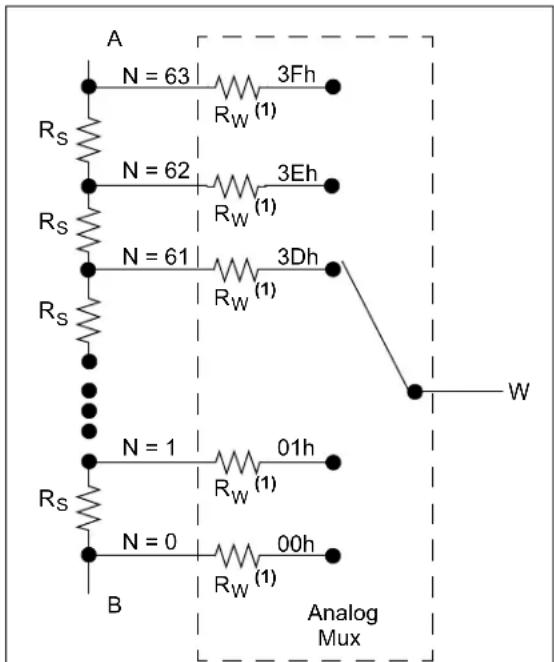
text_image
A N = 63 | 3Fh Rw (1) Rs N = 62 | 3Eh Rw (1) Rs N = 61 | 3Dh Rw (1) Rs N = 1 | 01h Rw (1) Rs N = 0 | 00h B Analog Mux WNote 1: The wiper resistance is tap dependent. That is, each tap selection resistance has a small variation. This variation effects the smaller resistance devices (2.1 kΩ) more.
FIGURE 6-1: Resistor Block Diagram.
Step resistance ( R_S ) is the resistance from one tap setting to the next. This value will be dependent on the R_AB value that has been selected. Table 6-1 shows the typical step resistances for each device.
The total resistance of the device has minimal variation due to operating voltage (see Figure 2-6, Figure 2-17, Figure 2-27 or Figure 2-37).
TABLE 6-1: TYPICAL STEP RESISTANCES
| Part Number | Typical Resistance (Ω) | |
| Total ( R_AB ) | Step (R s) | |
| MCP402X-202E 2100 | 33.33 | |
| MCP402X-502E 5000 | 79.37 | |
| MCP402X-103E 10000 | 158.73 | |
| MCP402X-503E 50000 | 793.65 | |
Terminal A and B, as well as the wiper W, do not have a polarity. These terminals can support both positive and negative current.
6.1 Resistor Configurations
6.1.1 RHEOSTAT CONFIGURATION
When used as a rheostat, two of the three digital potentiometer's terminals are used as a resistive element in the circuit. With terminal W (wiper) and either terminal A or terminal B, a variable resistor is created. The resistance will depend on the tap setting of the wiper and the wiper's resistance. The resistance is controlled by changing the wiper setting.
The unused terminal (B or A) should be left floating. Figure 6-2 shows the two possible resistors that can be used. Reversing the polarity of the A and B terminals will not affect operation.
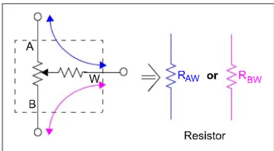
text_image
A B W ⇒ R_{AW} or R_{BW} ResistorFIGURE 6-2: Rheostat Configuration.
This allows the control of the total resistance between the two nodes. The total resistance depends on the "starting" terminal to the wiper terminal. At the code 00h, the R_BW resistance is minimal ( R_W ), but the R_AW resistance in maximized ( R_AB + R_W ). Conversely, at the code 3Fh, the R_AW resistance is minimal ( R_W ), but the R_BW resistance in maximized ( R_AB + R_W ).
The resistance step size ( R_S ) equates to one LSb of the resistor.
Note: To avoid damage to the internal wiper circuitry in this configuration, care should be taken to insure the current flow never exceeds 2.5 mA.
The change in wiper-to-end terminal resistance over temperature is shown in Figure 2-6, Figure 2-17, Figure 2-27 and Figure 2-37. The most variation over temperature will occur in the first few codes due to the wiper resistance coefficient affecting the total resistance. The remaining codes are dominated by the total resistance tempco R_AB .
6.1.2 POTENTIOMETER
CONFIGURATION
When used as a potentiometer, all three terminals are tied to different nodes in the circuit. This allows the potentiometer to output a voltage proportional to the input voltage. This configuration is sometimes called voltage divider mode. The potentiometer is used to provide a variable voltage by adjusting the wiper position between the two endpoints as shown in Figure 6-3. Reversing the polarity of the A and B terminals will not affect operation.

text_image
V₁ A B W V₃ V₂FIGURE 6-3: Potentiometer Configuration.
The temperature coefficient of the R_AB resistors is minimal by design. In this configuration, the resistors all change uniformly, so minimal variation should be seen.
The wiper resistor temperature coefficient is different from the R_AB temperature coefficient. The voltage at node V_3 (Figure 6-3) is not dependent on this wiper resistance, just the ratio of the R_AB resistors, so this temperature coefficient in most cases can be ignored.
Note: To avoid damage to the internal wiper circuitry in this configuration, care should be taken to insure the current flow never exceeds 2.5 mA.
6.2 Wiper Resistance
Wiper resistance is the series resistance of the wiper. This resistance is typically measured when the wiper is positioned at either zero-scale (00h) or full-scale (3Fh).
The wiper resistance in potentiometer-generated voltage divider applications is not a significant source of error.
The wiper resistance in rheostat applications can create significant nonlinearity as the wiper is moved toward zero-scale (00h). The lower the nominal resistance, the greater the possible error.
Wiper resistance is significant depending on the devices operating voltage. As the device voltage decreases, the wiper resistance increases (see Figure 6-4 and Table 6-2).
In a rheostat configuration, this change in voltage needs to be taken into account, particularly for the lower resistance devices. For the 2.1 kΩ device, the maximum wiper resistance at 5.5V is approximately 6% of the total resistance, while at 2.7V, it is approximately 15.5% of the total resistance.
In a potentiometer configuration, the wiper resistance variation does not effect the output voltage seen on the terminal W pin.
The slope of the resistance has a linear area (at the higher voltages) and a nonlinear area (at the lower voltages), where resistance increases faster than the voltage drop (at low voltages).
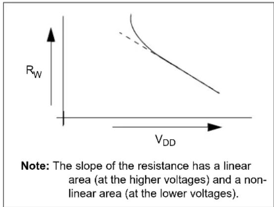
text_image
R_W V_DD Note: The slope of the resistance has a linear area (at the higher voltages) and a non-linear area (at the lower voltages).FIGURE 6-4: Relationship of Wiper Resistance ( R_W ) to Voltage.
Since there is minimal variation of the total device resistance over voltage, at a constant temperature (see Figure 2-6, Figure 2-17, Figure 2-27 or Figure 2-37), the change in wiper resistance over voltage can have a significant impact on the INL and DNL error.
TABLE 6-2: TYPICAL STEP RESISTANCES AND RELATIONSHIP TO WIPER RESISTANCE
| Resistance (Ω) | R_W/R_S(%)^(1) | R_W/R_AB(%)^(2) | ||||||||
| Typical | Wiper W) | (R R_W =Typical | R_W =Max@ 5.5V | R_W =Max@ 2.7V | R_W =Typical | R_W =Max@ 5.5V | R_W =Max@ 2.7V | |||
| Total( R_AB ) | Step( R_S ) | Typical | Max @5.5V | Max @2.7V | ||||||
| 2100 | 33.33 | 75 | 125 | 325 | 225.0% | 375.0% | 975.0% | 3.57% | 5.95% | 15.48% |
| 5000 | 79.37 | 75 | 125 | 325 | 94.5% | 157.5% | 409.5% | 1.5% | 2.50% | 6.50% |
| 10000 | 158.73 | 75 | 125 | 325 | 47.25% | 78.75% | 204.75% | 0.75% | 1.25% | 3.25% |
| 50000 | 793.65 | 75 | 125 | 325 | 9.45% | 15.75% | 40.95% | 0.15% | 0.25% | 0.65% |
Note 1: R_S is the typical value. The variation of this resistance is minimal over voltage.
2: R_AB is the typical value. The variation of this resistance is minimal over voltage.
6.3 Operational Characteristics
Understanding the operational characteristics of the device's resistor components is important to the system design.
6.3.1 ACCURACY
6.3.1.1 Integral Nonlinearity (INL)
INL error for these devices is the maximum deviation between an actual code transition point and its corresponding ideal transition point after offset and gain errors have been removed. These endpoints are from 0x00 to 0x3F. Refer to Figure 6-5.
Positive INL means higher resistance than ideal. Negative INL means lower resistance than ideal.
line
| Digital Input Code | Actual Transfer Function | Ideal Transfer Function | | ------------------ | ------------------------ | ----------------------- | | INL < 0 | 100 | 100 | | INL < 0 | 101 | 101 | | INL < 0 | 102 | 102 | | INL < 0 | 103 | 103 | | INL < 0 | 104 | 104 | | INL < 0 | 105 | 105 | | INL < 0 | 106 | 106 | | INL < 0 | 107 | 107 | | INL < 0 | 108 | 108 | | INL < 0 | 109 | 109 | | INL < 0 | 110 | 110 | | INL < 0 | 111 | 111 | | Digital Pot Output | 0 | 0 | | Digital Pot Output | 1 | 1 | | Digital Pot Output | 2 | 2 | | Digital Pot Output | 3 | 3 | | Digital Pot Output | 4 | 4 | | Digital Pot Output | 5 | 5 | | Digital Pot Output | 6 | 6 | | Digital Pot Output | 7 | 7 | | Digital Pot Output | 8 | 8 | | Digital Pot Output | 9 | 9 | | Digital Pot Output | 10 | 10 | | Digital Pot Output | 11 | 11 | | Digital Pot Output | 12 | 12 | | Digital Pot Output | 13 | 13 | | Digital Pot Output | 14 | 14 | | Digital Pot Output | 15 | 15 | | Digital Pot Output | 16 | 16 | | Digital Pot Output | 17 | 17 | | Digital Pot Output | 18 | 18 | | Digital Pot Output | 19 | 19 | | Digital Pot Output | 20 | 20 | | Digital Pot Output | 21 | 21 | | Digital Pot Output | 22 | 22 | | Digital Pot Output | 23 | 23 | | Digital Pot Output | 24 | 24 | | Digital Pot Output | 25 | 25 | | Digital Pot Output | 26 | 26 | | Digital Pot Output | 27 | 27 | | Digital Pot Output | 28 | 28 | | Digital Pot Output | 29 | 29 | | Digital Pot Output | 30 | 30 | | Digital Pot Output | 31 | 31 | | Digital Pot Output | 32 | 32 | | Digital Pot Output | 33 | 33 | | Digital Pot Output | 34 | 34 | | Digital Pot Output | 35 | 35 | | Digital Pot Output | 36 | 36 | | Digital Pot Output | 37 | 37 | | Digital Pot Output | 38 | 38 | | Digital Pot Output | 39 | 39 | | Digital Pot Output | 40 | 40 | | Digital Pot Output | 41 | 41 | | Digital Pot Output | 42 | 42 | | Digital Pot Output | 43 | 43 | | Digital Pot Output | 44 | 44 | | Digital Pot Output | 45 | 45 | | Digital Pot Output | 46 | 46 | | Digital Pot Output | 47 | 47 | | Digital Pot Output | 48 | 48 | | Digital Pot Output | 49 | 49 | | Digital Pot Output | 50 | 50 | | Digital Pot Output | 51 | 51 | | Digital Pot Output | 52 | 52 | | Digital Pot Output | 53 | 53 | | Digital Pot Output | 54 | 54 | | Digital Pot Output | 55 | 55 | | Digital Pot Output | 56 | 56 | | Digital Pot Output | 57 | 57 | | Digital Pot Output | 58 | 58 | | Digital Pot Output | 59 | 59 | | Digital Pot Output | 60 | 60 | | Digital Pot Output | 61 | 61 | | Digital Pot Output | 62 | 62 | | Digital Pot Output | 63 | 63 | | Digital Pot Output | 64 | 64 | | Digital Pot Output | 65 | 65 | | Digital Pot Output | 66 | 66 | | Digital Pot Output | 67 | 67 | | Digital Pot Output | 68 | 68 | | Digital Pot Output | 69 | 69 | | Digital Pot Output | 70 | 70 | | Digital Pot Output | 71 | 71 | | Digital Pot Output | 72 | 72 | | Digital Pot Output | 73 | 73 | | Digital Pot Output | 74 | 74 | | Digital Pot Output | 75 | 75 | | Digital Pot Output | 76 | 76 | | Digital Pot Output | 77 | 77 | | Digital Pot Output | 78 | 78 | | Digital Pot Output | 79 | 79 | | Digital Pot Output | 80 | 80 | | Digital Pot Output |FIGURE 6-5: INL Accuracy.
6.3.1.2 Differential Non-Linearity (DNL)
DNL error is the measure of variations in code widths from the ideal code width. A DNL error of zero would imply that every code is exactly 1 LSb wide.
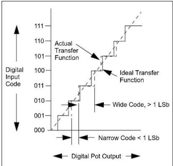
line
| Digital Input Code | Actual Transfer Function | Ideal Transfer Function | | ------------------ | ------------------------ | ----------------------- | | Narrow Code < 1 LSb | 000 | 000 | | Wide Code, > 1 LSb | 010 | 100 | | Narrow Code < 1 LSb | 001 | 100 | | Wide Code, > 1 LSb | 011 | 100 | | Narrow Code < 1 LSb | 010 | 100 | | Wide Code, > 1 LSb | 100 | 100 | | Actual Transfer Function | 101 | 100 | | Actual Transfer Function | 110 | 100 | | Actual Transfer Function | 111 | 100 |FIGURE 6-6: DNL Accuracy.
6.3.1.3 Ratiometric Temperature Coefficient
The ratiometric temperature coefficient quantifies the error in the ratio R_AW/R_WB due to temperature drift. This is typically the critical error when using a potentiometer device (MCP4021 and MCP4023) in a voltage divider configuration.
6.3.1.4 Absolute Temperature Coefficient
The absolute temperature coefficient quantifies the error in the end-to-end resistance (nominal resistance R_AB ) due to temperature drift. This is typically the critical error when using a rheostat device (MCP4022 and MCP4024) in an adjustable resistor configuration.
6.3.2 MONOTONIC OPERATION
Monotonic operation means that the device's resistance increases with every step change (from terminal A to terminal B or terminal B to terminal A).
The wiper resistance is different at each tap location. When changing from one tap position to the next (either increasing or decreasing), the R_W is less than the R_S . When this change occurs, the device voltage and temperature are the same for the two tap positions.
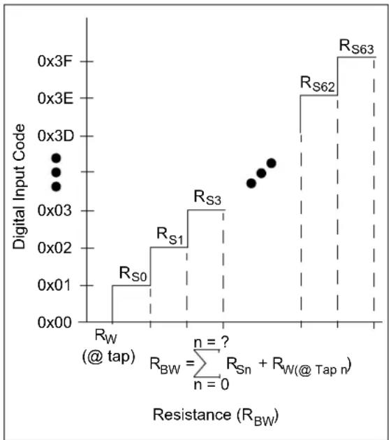
bar
| Resistance (R_BW) | Digital Input Code | |---|---| | R_W (@ tap) | 0x01 | | R_S0 | 0x01 | | R_S1 | 0x02 | | R_S3 | 0x03 | | R_S62 | 0x3E | | R_S63 | 0x3F | The chart displays discrete data points connected by a step line, indicating a stepwise increase in digital input code as resistance increases. The formula R_BW = Σ(R_BW / R_Sn + R_W(@Tap n)).FIGURE 6-7: Resistance, R
BW·
7.0 DESIGN CONSIDERATIONS
In the design of a system with the MCP402X devices, the following considerations should be taken into account:
- The power supply
- The layout
7.1 Power Supply Considerations
The typical application will require a bypass capacitor in order to filter high-frequency noise, which can be induced onto the power supply's traces. The bypass capacitor helps to minimize the effect of these noise sources on signal integrity. Figure 7-1 illustrates an appropriate bypass strategy.
In this example, the recommended bypass capacitor value is 0.1 F. This capacitor should be placed as close (within 4 mm) to the device power pin ( V_DD ) as possible.
The power source supplying these devices should be as clean as possible. If the application circuit has separate digital and analog power supplies, V_DD and V_SS should reside on the analog plane.
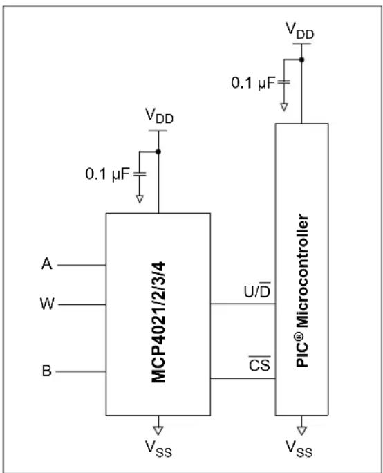
text_image
VDD 0.1 μF A W B MCP4021/2/3/4 U/D CS PIC® Microcontroller VSS VSS 0.1 μF VDDFIGURE 7-1: Typical Microcontroller Connections.
7.2 Layout Considerations
Inductively-coupled AC transients and digital switching noise can degrade the input and output signal integrity, potentially masking the MCP402X's performance. Careful board layout will minimize these effects and increase the Signal-to-Noise Ratio (SNR). Bench testing has shown that a multi-layer board utilizing a low-inductance ground plane, isolated inputs, isolated outputs and proper decoupling are critical to achieving the performance that the silicon is capable of providing. Particularly harsh environments may require shielding of critical signals.
If low noise is desired, breadboards and wire-wrapped boards are not recommended.
8.0 APPLICATIONS EXAMPLES
Nonvolatile digital potentiometers have a multitude of practical uses in modern electronic circuits. The most popular uses include precision calibration of set point thresholds, sensor trimming, LCD bias trimming, audio attenuation, adjustable power supplies, motor control overcurrent trip setting, adjustable gain amplifiers and offset trimming. The MCP4021/2/3/4 devices can be used to replace the common mechanical trim pot in applications where the operating and terminal voltages are within CMOS process limitations ( V_DD = 2.7V to 5.5V).
8.1 Set Point Threshold Trimming
Applications that need accurate detection of an input threshold event often need several sources of error eliminated. Use of comparators and operational amplifiers (op amps) with low offset and gain error can help achieve the desired accuracy, but in many applications, the input source variation is beyond the designer's control. If the entire system can be calibrated after assembly in a controlled environment (like factory test), these sources of error are minimized, if not entirely eliminated.
Figure 8-1 illustrates a common digital potentiometer configuration. This configuration is often referred to as a "windowed voltage divider". Note that R_1 and R_2 are not necessary to create the voltage divider, but their presence is useful when the desired threshold has limited range. It is "windowed" because R_1 and R_2 can narrow the adjustable range of V_TRIP to a value much less than V_DD - V_SS . If the output range is reduced, the magnitude of each output step is reduced. This effectively increases the trimming resolution for a fixed digital potentiometer resolution. This technique may allow a lower-cost digital potentiometer to be utilized (64 steps instead of 256 steps).
The MCP4021's and MCP4023's low DNL performance is critical to meeting calibration accuracy in production without having to use a higher precision digital potentiometer.
EQUATION 8-1: CALCULATING THE WIPER SETTING FROM THE DESIRED V _TRIP
$$ V _ {T R I P} = V _ {D D} \left(\frac {R _ {2} + R _ {W B}}{R _ {1} + R _ {A B} + R _ {2}}\right) $$
$$ R _ {A B} = R _ {\text { Nominal }} $$
$$ R _ {W B} \quad R _ {A B} = \left(\frac {D}{6 3}\right) $$
$$ D \quad \left(\left(\frac {V _ {T R I P}}{V _ {D D}}\right) \quad R _ {1} + R _ {A B} + R _ {2} - \left(\text { ( } _ {2}\right) \quad 6 3 \bullet \quad\right) $$
Where:
$$ D = \text { Digital Potentiometer Wiper Setting } (0 - 6 3) $$
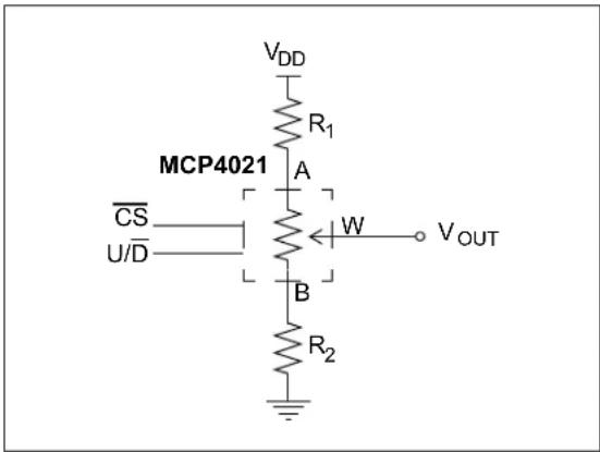
text_image
MCP4021 VDD R1 A CS U/D W VOUT B R2FIGURE 8-1: Using the Digital Potentiometer to Set a Precise Output Voltage.
8.1.1 TRIMMING A THRESHOLD FOR AN OPTICAL SENSOR
If the application has to calibrate the threshold of a diode, transistor or resistor, a variation range of 0.1V is common. Often, the desired resolution of 2 mV or better is adequate to accurately detect the presence of a precise signal. A "windowed" voltage divider, utilizing the MCP4021 or MCP4023, would be a potential solution, as shown in Figure 8-2.

text_image
VDD Rsense VCC+ Comparator MCP4021 CS U/D A W VTRIP + MCP6021 VCC- R1 R2 0.1 μFFIGURE 8-2: Set Point or Threshold Calibration.
8.2 Operational Amplifier Applications
Figure 8-3, Figure 8-4 and Figure 8-5 illustrate typical amplifier circuits that could replace fixed resistors with the MCP4021/2/3/4 to achieve digitally-adjustable analog solutions.
Figure 8-4 shows a circuit that allows a non-inverting amplifier to have its' offset and gain to be independently trimmed. The MCP4021 is used along with resistors R1 and R2 to set the offset voltage. The sum of R1 + R2 resistance should be significantly greater (> 100 times) the resistance value of the MCP4021. This allows each increment or decrement in the MCP4021 to be a fine adjustment of the offset voltage. The input voltage of the op amp ( V_IN ) should be centered at the op amps V_W voltage. The gain is adjusted by the MCP4022. If the resistance value of the MCP4022 is small compared to the resistance value of R3, then this is a fine adjustment of the gain. If the resistance value of the MCP4022 is equal (or large) compared to the resistance value of R3, then this is a course adjustment of the gain. In general, trim the course adjustments first and then trim the fine adjustments.

text_image
MCP4021 VIN R3 A B W R4 - Op Amp + VDD R1 A W B R2 MCP402X VOUT MCP6001FIGURE 8-3: Trimming Offset and Gain in an Inverting Amplifier.
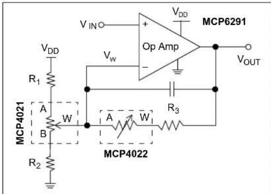
text_image
VDD + Op Amp VDD VIN - Vw VOUT R1 A W B R2 MCP4021 A W R3 MCP4022FIGURE 8-4: Trimming Offset and Gain in a Noninverting Amplifier.

text_image
MCP4021 R3 A B W Pot2 VDD R1 A W B Pot1 R2 MCP4022 VIN Op Amp + MCP6021 VOUT fc I / 2π·REq·C Thevenin Equivalent REq = R1 RA B - RWB || 2 + (RWB) + )FIGURE 8-5: Programmable Filter.
8.3 Temperature Sensor Applications
Thermistors are resistors with very predictable variation with temperature. Thermistors are a popular sensor choice when a low-cost, temperature-sensing solution is desired. Unfortunately, thermistors have nonlinear characteristics that are undesirable, typically requiring trimming in an application to achieve greater accuracy. There are several common solutions to trim and linearize thermistors. Figure 8-6 and Figure 8-7 are simple methods for linearizing a 3-terminal NTC thermistor. Both are simple voltage dividers using a Positive Temperature Coefficient (PTC) resistor ( R_1 ) with a transfer function capable of compensating for the linearity error in the Negative Temperature Coefficient (NTC) thermistor.
The circuit, illustrated by Figure 8-6, utilizes a digital rheostat for trimming the offset error caused by the thermistor's part-to-part variation. This solution puts the digital potentiometer's R_W into the voltage divider calculation. The MCP4021/2/3/4's R_AB temperature coefficient is 50 ppm (-20°C to +70°C). R_W 's error is substantially greater than R_AB 's error because R_W varies with V_DD , wiper setting and temperature. For the 50 kΩ devices, the error introduced by R_W is, in most cases, insignificant as long as the wiper setting is >6. For the 2 kΩ devices, the error introduced by R_W is significant because it is a higher percentage of R_WB . For these reasons, the circuit illustrated in Figure 8-6 is not the most optimum method for "exciting" and linearizing a thermistor.
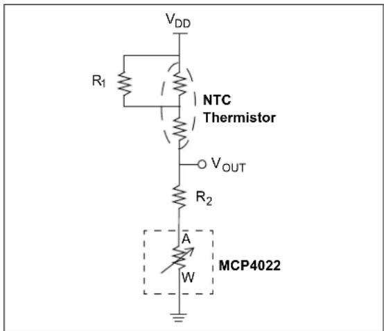
text_image
VDD R1 NTC Thermistor VOUT R2 A W MCP4022FIGURE 8-6: Thermistor Calibration using a Digital Potentiometer in a Rheostat Configuration.
The circuit illustrated by Figure 8-7 utilizes a digital potentiometer for trimming the offset error. This solution removes R_W from the trimming equation along with the error associated with R_W · R_2 is not required, but can be utilized to reduce the trimming “window” and reduce variation due to the digital potentiometer’s R_AB part-to-part variability.
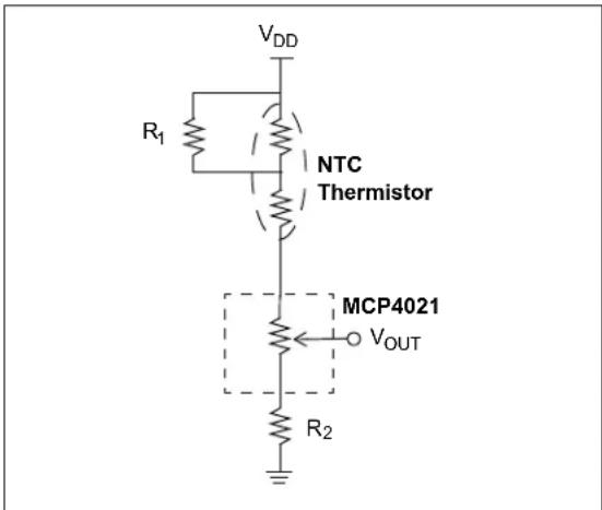
text_image
VDD R1 NTC Thermistor MCP4021 VOUT R2FIGURE 8-7: Thermistor Calibration using a Digital Potentiometer in a Potentiometer Configuration.
8.4 Wheatstone Bridge Trimming
Another common configuration to “excite” a sensor (such as a strain gauge, pressure sensor or thermistor) is the wheatstone bridge configuration. The wheatstone bridge provides a differential output instead of a single-ended output. Figure 8-8 illustrates a wheatstone bridge utilizing one to three digital potentiometers. The digital potentiometers in this example are used to trim the offset and gain of the wheatstone bridge.

text_image
VDD MCP4022 2.1 kΩ VOUT MCP4022 50 kΩ MCP4022 50 kΩFIGURE 8-8: Wheatstone Bridge Trimming.
9.0 DEVELOPMENT SUPPORT
9.1 Evaluation/Demonstration Boards
Currently there are three boards that are available that can be used to evaluate the MCP4021/2/3/4 family of devices.
- The MCP402X Digital Potentiometer Evaluation Board kit (MCP402XEV) contains a simple demonstration board utilizing a PIC10F206, the MCP4021 and a blank PCB, which can be populated with any desired MCP4021/2/3/4 device in a SOT-23-5, SOT-23-6 or 150 mil SOIC 8-pin package.
This board has two push buttons to control when the PIC ^® microcontroller generates MCP402X serial commands. The example firmware demonstrates the following commands:
- Increment
- Decrement
• High-Voltage Increment and Enable WiperLock Technology
• High-Voltage Decrement and Enable WiperLock Technology
• High-Voltage Increment and Disable WiperLock Technology
• High-Voltage Decrement and Disable WiperLock Technology
The populated board (with the MCP4021) can be used to evaluate the other MCP402X devices by appropriately jumpering the PCB pads.
- The SOT-23-5/6 Evaluation Board (VSUPEV2) can be used to evaluate the characteristics of the MCP4022, MCP4023 and MCP4024 devices.
- The 8-pin SOIC/MSOP/TSSOP/DIP Evaluation Board (SOIC8EV) can be used to evaluate the characteristics of the MCP4021 device in either the SOIC or MSOP package.
- The MCP4XXX Digital Potentiometer Daughter Board allows the system designer to quickly evaluate the operation of Microchip Technology's MCP42XXX and MCP402X Digital Potentiometers. The board supports two MCP42XXX devices and an MCP402X device, which can be replaced with an MCP401X device.
The board also has a voltage doubler device (TC1240A), which can be used to show the WiperLock Technology feature of the MCP4021.
These boards may be purchased directly from the Microchip web site at www.microchip.com.
10.0 PACKAGING INFORMATION
10.1 Package Marking Information
5-Lead SOT-23 (MCP4024)
text_image
XXNNExample:
text_image
DP25| Part Number Code | |
| MCP4024T-202E/OT DPNN | |
| MCP4024T-502E/OT DQNN | |
| MCP4024T-103E/OT DRNN | |
| MCP4024T-503E/OT DSNN | |
Note: Applies to 5-Lead SOT-23
6-Lead SOT-23 (MCP4022 / MCP4023)
text_image
XXNNExample:
text_image
BA25| Part Number | Code | |
| MCP4022 | MCP4023 | |
| MCP402xT-202E/CH | BANN BENN | |
| MCP402xT-502E/CH | BBNN BFNN | |
| MCP402xT-103E/CH | BCNN BGNN | |
| MCP402xT-503E/CH | BDNN BHNN | |
Note: Applies to 6-Lead SOT-23
Legend: XX...X Customer-specific information
Y Year code (last digit of calendar year)
YY Year code (last 2 digits of calendar year)
WW Week code (week of January 1 is week '01')
NNN Alphanumeric traceability code
e3 Pb-free JEDEC designator for Matte Tin (Sn)
* This package is Pb-free. The Pb-free JEDEC designator (e3) can be found on the outer packaging for this package.
Note: In the event the full Microchip part number cannot be marked on one line, it will be carried over to the next line, thus limiting the number of available characters for customer-specific information.
Package Marking Information
text_image
XXX YWW NN PIN 1Example:8-Lead DFN (2x3) (MCP40

text_image
AAA 640 25 PIN 1| Part Number Code |
| MCP4021T-202E/MC AAA |
| MCP4021T-502E/MC AAB |
| MCP4021T-103E/MC AAC |
| MCP4021T-503E/MC AAD |
Note: Applies to 8-Lead DFN
8-Lead MSOP (MCP4021)
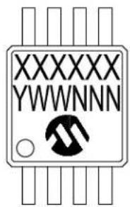
text_image
XXXXXXXX YWWNNNExample:

text_image
402122 6402568-Lead SOIC (150 mil) (MCP4021)
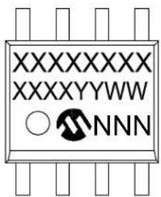
text_image
XXXXXXXXX XXXXXXXXYWW ○ NNNExample:

text_image
402153E SN e3 1640 256| Part Numbers | Code | |
| 8L-MSOP 8L-SOIC | ||
| MCP4021-202E/MS | MCP4021-202E/SN 22 | |
| MCP4021-502E/MS | MCP4021-502E/SN 52 | |
| MCP4021-103E/MS | MCP4021-103E/SN 13 | |
| MCP4021-503E/MS | MCP4021-503E/SN 53 | |
5-Lead Plastic Small Outline Transistor (OT) [SOT23]
Note: For the most current package drawings, please see the Microchip Packaging Specification located at http://www.microchip.com/packaging
![Microchip MCP4023 - 5-Lead Plastic Small Outline Transistor (OT) [SOT23] - 1](/content/2026/06/1221870/images/550d923f99084e7b30b0c0e22c11327ef93022e66053e3295b43291ff729e785.jpg)
text_image
0.20 C 2X D e1 A N E1/2 E1 E/2 E (DATUM D) (DATUM A-B) NOTE 1 1 2 e NX bB 0.15 C D 2X TOP VIEW![Microchip MCP4023 - 5-Lead Plastic Small Outline Transistor (OT) [SOT23] - 2](/content/2026/06/1221870/images/7e7a33e0cd81239e665b977263ba08cc2f0559c571d533287e68ad03985faf4e.jpg)
text_image
A A A2 A SEE SHEET 2 A1 SIDE VIEW 0.20 C SEATING PLANE CMicrochip Technology Drawing C04-028D [OT] Sheet 1 of 2
5-Lead Plastic Small Outline Transistor (OT) [SOT23]
Note: For the most current package drawings, please see the Microchip Packaging Specification located at http://www.microchip.com/packaging
![Microchip MCP4023 - 5-Lead Plastic Small Outline Transistor (OT) [SOT23] - 1](/content/2026/06/1221870/images/30fe111cd68a734ecffef0248e6e193cdc4b2d4d6afb074004c334cb7d13c8ec.jpg)
text_image
c L L1 θ cVIEW A-A SHEET 1
| Units | MILLIMETERS | |||
| Dimension Limits | MIN | NOM | MAX | |
| Number of Pins | N | 6 | ||
| Pitch | e | 0.95 BSC | ||
| Outside lead pitch | e1 | 1.90 BSC | ||
| Overall Height | A | 0.90 | - | 1.45 |
| Molded Package Thickness | A2 | 0.89 | - | 1.30 |
| Standoff | A1 | - | - | 0.15 |
| Overall Width | E | 2.80 BSC | ||
| Molded Package Width | E1 | 1.60 BSC | ||
| Overall Length | D | 2.90 BSC | ||
| Foot Length | L | 0.30 | - | 0.60 |
| Footprint | L1 | 0.60 REF | ||
| Foot Angle | 0° | - | 10° | |
| Lead Thickness | c | 0.08 | - | 0.26 |
| Lead Width | b | 0.20 - | 0.51 | |
Notes:
1. Dimensions D and E1 do not include mold flash or protrusions. Mold flash or protrusions shall not exceed 0.25mm per side.
2. Dimensioning and tolerancing per ASME Y14.5M
BSC: Basic Dimension. Theoretically exact value shown without tolerances.
REF: Reference Dimension, usually without tolerance, for information purposes only
Microchip Technology Drawing C04-091D [OT] Sheet 2 of 2
5-Lead Plastic Small Outline Transistor (OT) [SOT23]
Note: For the most current package drawings, please see the Microchip Packaging Specification located at http://www.microchip.com/packaging
![Microchip MCP4023 - 5-Lead Plastic Small Outline Transistor (OT) [SOT23] - 1](/content/2026/06/1221870/images/1e9b61da516affba0de81d745ac8a3dc9327ff05abc56bf7d29e2cc9cf5320b2.jpg)
text_image
X 5 SILK SCREEN Y Z C G 1 2 E GXRECOMMENDED LAND PATTERN
| Units | MILLIMETERS | |||
| Dimension Limits | NOM | MAXMIN | ||
| Contact Pitch | E | 0.95 BSC | ||
| Contact Pad Spacing | C | 2.80 | ||
| Contact Pad Width (X5) | X | 0.60 | ||
| Contact Pad Length (X5) | Y | 1.10 | ||
| Distance Between Pads | G | 1.70 | ||
| Distance Between Pads GX 0.35 | ||||
| Overall Width | Z | 3.90 | ||
Notes:
1. Dimensioning and tolerancing per ASME Y14.5M
BSC: Basic Dimension. Theoretically exact value shown without tolerances.
Microchip Technology Drawing No. C04-2091A [OT]
6-Lead Plastic Small Outline Transistor (CH, CHY) [SOT-23]
Note: For the most current package drawings, please see the Microchip Packaging Specification located at http://www.microchip.com/packaging
![Microchip MCP4023 - 6-Lead Plastic Small Outline Transistor (CH, CHY) [SOT-23] - 1](/content/2026/06/1221870/images/44cae3c44d11eda230e7144a68e3a4ab343522669c11bbac3743296923c1a8ac.jpg)
text_image
2X 0.15 C A-B D e1 A E1 E2 E 2X 0.20 C A-B 2X 0.15 C D 6X b ∅ 0.20 M A-E DTOP VIEW
![Microchip MCP4023 - 6-Lead Plastic Small Outline Transistor (CH, CHY) [SOT-23] - 2](/content/2026/06/1221870/images/6a91d50fb8957a38f23c1096ceb791b329644e0cff084ffadd640a10928b9368.jpg)
text_image
SEATING PLANE A A2 A1 SIDE VIEW 6X 0.10 C![Microchip MCP4023 - 6-Lead Plastic Small Outline Transistor (CH, CHY) [SOT-23] - 3](/content/2026/06/1221870/images/d405c3130a7b487efb56fbdfac35a29917975673b286042453bc825ce892e611.jpg)
text_image
c R1 R L2 GAUGE PLANE L ( L1 ) Θ END VIEWMicrochip Technology Drawing C04-028C (CH) Sheet 1 of 2
6-Lead Plastic Small Outline Transistor (CH, CHY) [SOT-23]
Note: For the most current package drawings, please see the Microchip Packaging Specification located at http://www.microchip.com/packaging
![Microchip MCP4023 - 6-Lead Plastic Small Outline Transistor (CH, CHY) [SOT-23] - 1](/content/2026/06/1221870/images/8fe74f0c005cf4d86fc8736e07ec77680480d50f8e62d14d3fd0f60db432f265.jpg)
natural_image
Isometric line drawing of an integrated circuit chip with four pins (no text or symbols)| Units | MILLIMETERS | |||
| Dimension Limits | MIN | NOM | MAX | |
| Number of Leads | N | 6 | ||
| Pitch | e | 0.95 BSC | ||
| Outside lead pitch | e1 | 1.90 BSC | ||
| Overall Height | A | 0.90 | - | 1.45 |
| Molded Package Thickness | A2 | 0.89 | 1.15 | 1.30 |
| Standoff | A1 | 0.00 | - | 0.15 |
| Overall Width | E | 2.80 BSC | ||
| Molded Package Width | E1 | 1.60 BSC | ||
| Overall Length | D | 2.90 BSC | ||
| Foot Length | L | 0.30 | 0.45 | 0.60 |
| Footprint | L1 | 0.60 REF | ||
| Seating Plane to Gauge Plane L1 | 0.25 BSC | |||
| Foot Angle | 0^ | - | 10^ | |
| Lead Thickness | c | 0.08 | - | 0.26 |
| Lead Width | b | 0.20 - | 0.51 | |
Notes:
- Dimensions D and E1 do not include mold flash or protrusions. Mold flash or protrusions shall not exceed 0.25mm per side.
- Dimensioning and tolerancing per ASME Y14.5M BSC: Basic Dimension. Theoretically exact value shown without tolerances. REF: Reference Dimension, usually without tolerance, for information purposes only.
Microchip Technology Drawing C04-028C (CH) Sheet 2 of 2
6-Lead Plastic Small Outline Transistor (CH, CHY) [SOT-23]
Note: For the most current package drawings, please see the Microchip Packaging Specification located at http://www.microchip.com/packaging
![Microchip MCP4023 - 6-Lead Plastic Small Outline Transistor (CH, CHY) [SOT-23] - 1](/content/2026/06/1221870/images/f418f058dd8f5e76e1b6bcb8e2c2ef0543242f755cf289e9274529b286b2564d.jpg)
text_image
GX Y Z C G G SILK SCREEN X ERECOMMENDED LAND PATTERN
| Units | MILLIMETERS | |||
| Dimension Limits | NOM | MAXMIN | ||
| Contact Pitch | E | 0.95 BSC | ||
| Contact Pad Spacing | C | 2.80 | ||
| Contact Pad Width (X3) | X | 0.60 | ||
| Contact Pad Length (X3) | Y | 1.10 | ||
| Distance Between Pads | G | 1.70 | ||
| Distance Between Pads GX 0.35 | ||||
| Overall Width | Z | 3.90 | ||
Notes:
- Dimensioning and tolerancing per ASME Y14.5M
BSC: Basic Dimension. Theoretically exact value shown without tolerances.
Microchip Technology Drawing No. C04-2028B (CH)
8-Lead Plastic Dual Flat, No Lead Package (MC) - 2x3x0.9 mm Body [DFN]
Note: For the most current package drawings, please see the Microchip Packaging Specification located at http://www.microchip.com/packaging
![Microchip MCP4023 - 8-Lead Plastic Dual Flat, No Lead Package (MC) - 2x3x0.9 mm Body [DFN] - 1](/content/2026/06/1221870/images/41c90788f7bb42d0c0c1705c2daeef0e49c71d7c5194bba17c293d4051eab301.jpg)
| Units MILLIMETERS | ||||
| Dimension Limits MIN NOM MAX | ||||
| Number of Pins N 8 | ||||
| Pitch e 0.50 BSC | ||||
| Overall Height | A | 0.80 | 0.90 | 1.00 |
| Standoff | A1 | 0.00 | 0.02 | 0.05 |
| Contact Thickness | A3 | 0.20 REF | ||
| Overall Length | D | 2.00 BSC | ||
| Overall Width | E | 3.00 BSC | ||
| Exposed Pad Length | D2 | 1.30 | - | 1.55 |
| Exposed Pad Width | E2 | 1.50 | - | 1.75 |
| Contact Width | b | 0.20 | 0.25 | 0.30 |
| Contact Length | L | 0.30 | 0.40 | 0.50 |
| Contact-to-Exposed Pad | K | 0.20 | - | - |
Notes:
- Pin 1 visual index feature may vary, but must be located within the hatched area.
- Package may have one or more exposed tie bars at ends.
- Package is saw singulated.
- Dimensioning and tolerancing per ASME Y14.5M.
BSC: Basic Dimension. Theoretically exact value shown without tolerances.
REF: Reference Dimension, usually without tolerance, for information purposes only.
Microchip Technology Drawing C04-123C
8-Lead Plastic Dual Flat, No Lead Package (MC) - 2x3x0.9mm Body [DFN]
Note: For the most current package drawings, please see the Microchip Packaging Specification located at http://www.microchip.com/packaging

text_image
W2 G C1 T2 E X1 Y1 SILK SCREENRECOMMENDED LAND PATTERN
| Units | MILLIMETERS | |||
| Dimension Limits | MIN | NOM | MAX | |
| Contact Pitch | E | 0.50 BSC | ||
| Optional Center Pad Width | W2 | 1.45 | ||
| Optional Center Pad Length | T2 | 1.75 | ||
| Contact Pad Spacing | C1 | 2.90 | ||
| Contact Pad Width (X8) | X1 | 0.30 | ||
| Contact Pad Length (X8) | Y1 | 0.75 | ||
| Distance Between Pads | G | 0.20 | ||
Notes:
1. Dimensioning and tolerancing per ASME Y14.5M
BSC: Basic Dimension. Theoretically exact value shown without tolerances.
Microchip Technology Drawing No. C04-2123B
8-Lead Plastic Micro Small Outline Package (MS) [MSOP]
Note: For the most current package drawings, please see the Microchip Packaging Specification located at http://www.microchip.com/packaging
![Microchip MCP4023 - 8-Lead Plastic Micro Small Outline Package (MS) [MSOP] - 1](/content/2026/06/1221870/images/53a9f0d0452236d2b7febf6fd43b50c7af6232d181c9a3751ae62c94c224d986.jpg)
text_image
2X 0.20 H D/2 A E/2 D E1/2 E1 N E/2 E NOTE 1 1 2 N/2 0.25 C e B NX b Φ 0.13 M C A-B D TOP VIEW A A2 A1 SEATING PLANE SIDE VIEW C H SEE DETAIL C END VIEWMicrochip Technology Drawing C04-111C Sheet 1 of 2
8-Lead Plastic Micro Small Outline Package (MS) [MSOP]
Note: For the most current package drawings, please see the Microchip Packaging Specification located at http://www.microchip.com/packaging
![Microchip MCP4023 - 8-Lead Plastic Micro Small Outline Package (MS) [MSOP] - 1](/content/2026/06/1221870/images/4a5573a69b91f4abbfa7d6c1ab614d1ba567a3a885f1ce5bc5b69a8fe0fe7f99.jpg)
text_image
SEATING PLANE L (L1) GAUGE PLANE c φDETAIL C
| Units | MILLIMETERS | |||
| Dimension Limits | MIN | NOM | MAX | |
| Number of Pins | N | 8 | ||
| Pitch | e | 0.65 BSC | ||
| Overall Height | A | - | - | 1.10 |
| Molded Package Thickness | A2 | 0.75 | 0.85 | 0.95 |
| Standoff | A1 | 0.00 | - | 0.15 |
| Overall Width | E | 4.90 BSC | ||
| Molded Package Width | E1 | 3.00 BSC | ||
| Overall Length | D | 3.00 BSC | ||
| Foot Length | L | 0.40 | 0.60 | 0.80 |
| Footprint | L1 | 0.95 REF | ||
| Foot Angle | 0° | - | 8° | |
| Lead Thickness | c | 0.08 | - | 0.23 |
| Lead Width | b | 0.22 | - | 0.40 |
Notes:
- Pin 1 visual index feature may vary, but must be located within the hatched area.
- Dimensions D and E1 do not include mold flash or protrusions. Mold flash or protrusions shall not exceed 0.15mm per side.
- Dimensioning and tolerancing per ASME Y14.5M. BSC: Basic Dimension. Theoretically exact value shown without tolerances. REF: Reference Dimension, usually without tolerance, for information purposes only.
Microchip Technology Drawing C04-111C Sheet 2 of 2
8-Lead Plastic Micro Small Outline Package (MS) [MSOP]
Note: For the most current package drawings, please see the Microchip Packaging Specification located at http://www.microchip.com/packaging
![Microchip MCP4023 - 8-Lead Plastic Micro Small Outline Package (MS) [MSOP] - 1](/content/2026/06/1221870/images/04fc6a430e31468a860315c55898e51d3e78c3a35703fe8039df294b3215e3fa.jpg)
text_image
X Y Z C G1 SILK SCREEN GX ERECOMMENDED LAND PATTERN
| Units | MILLIMETERS | |||
| Dimension Limits | MIN | NOM | MAX | |
| Contact Pitch | E | 0.65 BSC | ||
| Contact Pad Spacing | C | 4.40 | ||
| Overall Width | Z | 5.85 | ||
| Contact Pad Width (X8) | X1 | 0.45 | ||
| Contact Pad Length (X8) | Y1 | 1.45 | ||
| Distance Between Pads | G1 | 2.95 | ||
| Distance Between Pads | GX | 0.20 | ||
Notes:
1. Dimensioning and tolerancing per ASME Y14.5M
BSC: Basic Dimension. Theoretically exact value shown without tolerances.
Microchip Technology Drawing No. C04-2111A
8-Lead Plastic Small Outline (SN) - Narrow, 3.90 mm (.150 In.) Body [SOIC]
Note: For the most current package drawings, please see the Microchip Packaging Specification located at http://www.microchip.com/packaging
![Microchip MCP4023 - 8-Lead Plastic Small Outline (SN) - Narrow, 3.90 mm (.150 In.) Body [SOIC] - 1](/content/2026/06/1221870/images/43465342e5886fc7bbd6bb41eb367182e930cfaf84dbd36099ceb0f5cd9d21c7.jpg)
Microchip Technology Drawing No. C04-057-SN Rev D Sheet 1 of 2
8-Lead Plastic Small Outline (SN) - Narrow, 3.90 mm (.150 In.) Body [SOIC]
Note: For the most current package drawings, please see the Microchip Packaging Specification located at http://www.microchip.com/packaging
![Microchip MCP4023 - 8-Lead Plastic Small Outline (SN) - Narrow, 3.90 mm (.150 In.) Body [SOIC] - 1](/content/2026/06/1221870/images/4f5bfe01f78fa51918cbd1a3877fc166aaf1ecfab05fac914164318f192c95ee.jpg)
natural_image
Isometric line drawing of an integrated circuit chip with four pins (no text or symbols)| Units | MILLIMETERS | |||
| Dimension Limits | MIN | NOM | MAX | |
| NNumber of Pins 8 | ||||
| Pitch | e | 1.27 BSC | ||
| AOvera15Height | ||||
| --1.25A2Molded Package Thickness | ||||
| Standoff § | A1 | 0.25-0.10 | ||
| 6.00 BSCEOverall Width | ||||
| 3.90 BSCE1Molded Package Width | ||||
| 4.90 BSCDOverall Length | ||||
| Chamfer (Optional) | h | 0.25 | - | 0.50 |
| Foot Length | L | 0.40 | - | 1.27 |
| Footprint | L1 | 1.04 REF | ||
| Foot Angle 0° - 8° | φ | |||
| Lead Thickness | c | 0.25-0.17 | ||
| Lead Width | b | 0.51-0.31 | ||
| Mold Draft Angle Top | α | 15°-5° | ||
| Mold Draft Angle Bottom | β | 15°-5° | ||
Notes:
- Pin 1 visual index feature may vary, but must be located within the hatched area.
- § Significant Characteristic
- Dimensions D and E1 do not include mold flash or protrusions. Mold flash or protrusions shall not exceed 0.15mm per side.
- Dimensioning and tolerancing per ASME Y14.5M BSC: Basic Dimension. Theoretically exact value shown without tolerances. REF: Reference Dimension, usually without tolerance, for information purposes only.
- Datums A & B to be determined at Datum H.
Microchip Technology Drawing No. C04-057-SN Rev D Sheet 2 of 2
8-Lead Plastic Small Outline (SN) - Narrow, 3.90 mm Body [SOIC]
Note: For the most current package drawings, please see the Microchip Packaging Specification located at http://www.microchip.com/packaging
![Microchip MCP4023 - 8-Lead Plastic Small Outline (SN) - Narrow, 3.90 mm Body [SOIC] - 1](/content/2026/06/1221870/images/fd011a31b6099902464e0a443e8d91be516586bbade03565f61204b2bafe9993.jpg)
text_image
C SILK SCREEN Y1 X1 ERECOMMENDED LAND PATTERN
| Units | MILLIMETERS | |||
| Dimension Limits | MIN | NOM | MAX | |
| Contact Pitch | E | 1.27 BSC | ||
| CContact Pad Spacing40 | ||||
| Contact Pad Width (X8) | X1 | 0.60 | ||
| Contact Pad Length (X8) | Y1 | 1.55 | ||
Notes:
Dimensioning and tolerancing per ASME Y14.5M1.
BSC: Basic Dimension. Theoretically exact value shown without tolerances.
Microchip Technology Drawing C04-2057-SN Rev B
NOTES:
APPENDIX A: REVISION HISTORY
Revision F (December 2017)
The following is the list of modifications:
- Updated the High-Voltage Input Entry Voltage entry in the "AC/DC Characteristics" table.
- Updated Table 6-1 "Typical Step Resistances".
Revision E (December 2006)
The following is the list of modifications:
- Added device designators in conditions column to associate units (MHz) in Bandwidth -3 dB parameter in the table "AC/DC Characteristics" table.
- Added device designations in conditions column for R-INL and R-DNL specifications.
- Added disclaimers to package outline drawings.
Revision D (October 2006)
The following is the list of modifications:
- Changed the EEPROM write cycle time (T _WC ) from a maximum of 5 ms to a maximum of 10 ms (overvoltage and temperature) with a typical of 5 ms.
- For the 10 kΩ device, the rheostat differential nonlinearity specification at 2.7V was changed from ±0.5 LSb to ±1.0 LSb.
- Figure 2-9 in Section 2.0 "Typical Performance Curves" was updated with the correct data.
- Added Figure 2-48 for -3 db Bandwidth information.
- Updated available Development Tools.
- Added disclaimer to package outline drawings.
Revision C (November 2005)
The following is the list of modifications:
- Enhanced Descriptions.
- Reordered Sections.
- Added 8-lead MSOP and DFN packages.
Revision B (April 2005)
The following is the list of modifications:
- Updated part numbers in Product Identification Section (PIS).
- Added Appendix A: Revision History.
Revision A (April 2005)
• Original release of this document.
NOTES:
PRODUCT IDENTIFICATION SYSTEM
To order or obtain information, e.g., on pricing or delivery, refer to the factory or the listed sales office.
PART NO.
XXX
X
IXX
Device
Resistance Version
Temperature Package Range
Device: MCP4021: Single Potentiometer with U/D Interface
MCP4021T: Single Potentiometer with U/D Interface (Tape and Reel) (SOIC, MSOP)
MCP4022: Single Rheostat with U/D _ interface
MCP4022T: Single Rheostat with U/D interface
(Tape and Reel) (SOT-23-6)
MCP4023: Single Potentiometer to GND with U/D Interface
MCP4023T: Single Potentiometer to GND with U/D Interface (Tape and Reel) (SOT-23-6)
MCP4024: Single Rheostat to GND with U/D Interface
MCP4024T: Single Rheostat to GND with U/D Interface (Tape and Reel)(SOT-23-5)
Resistance Version: 202 = 2.1 kΩ
502 = 5 kΩ
103 = 10 kΩ
503 = 50 kΩ
Temperature Range: E = -40°C to +125°C
Package: CH = Plastic Small Outline Transistor, 6-lead
MC = Plastic Dual Flat No Lead (2x3x0.9 mm), 8-lead
MS = Plastic MSOP, 8-lead
SN = Plastic SOIC, (150 mil Body), 8-lead
OT = Plastic Small Outline Transistor, 5-lead
Examples:
a) MCP4021-103E/MS: 10 kΩ, 8-LD MSOP
b) MCP4021-103E/SN: 10 kΩ 8-LD SOIC
c) MCP4021T-103E/MC: T/R, 10 kΩ, 8-LD DFN
d) MCP4021T-103E/MS: T/R, 10 kΩ, 8-LD MSOP
e) MCP4021T-103E/SN: T/R, 10 kΩ, 8-LD SOIC
f) MCP4021-202E/MS: 2.1 kΩ, 8-LD MSOP
g) MCP4021-202E/SN: 2.1 kΩ, 8-LD SOIC
h) MCP4021T-202E/MC: T/R, 2.1 kΩ, 8-LD DFN
i) MCP4021T-202E/MS: T/R, 2.1 kΩ, 8-LD MSOP
i) MCP4021T-202E/SN: T/R, 2.1 kΩ, 8-LD SOIC
k) MCP4021-502E/MS: 5 kΩ, 8-LD MSOP
I) MCP4021-502E/SN: 5 kΩ, 8-LD SOIC
m) MCP4021T-502E/MC: T/R, 5 kΩ, 8-LD DFN
n) MCP4021T-502E/MS: T/R, 5 kΩ, 8-LD MSOP
o) MCP4021T-502E/SN: T/R, 5 kΩ, 8-LD SOIC
p) MCP4021-503E/MS: 50 kΩ, 8-LD MSOP
q) MCP4021-503E/SN: 50 kΩ, 8-LD SOIC
r) MCP4021T-503E/MC: T/R, 50 kΩ, 8-LD DFN
s) MCP4021T-503E/MS: T/R, 50 kΩ, 8-LD MSOP
t) MCP4021T-503E/SN: T/R, 50 kΩ, 8-LD SOIC
a) MCP4022T-202E/CH 2.1 kΩ, 6-LD SOT-23
b) MCP4022T-502E/CH 5 kΩ, 6-LD SOT-23
c) MCP4022T-103E/CH 10 kΩ, 6-LD SOT-23
d) MCP4022T-503E/CH 50 kΩ, 6-LD SOT-23
a) MCP4023T-202E/CH 2.1 kΩ, 6-LD SOT-23
b) MCP4023T-502E/CH 5 kΩ, 6-LD SOT-23
c) MCP4023T-103E/CH 10 kΩ, 6-LD SOT-23
d) MCP4023T-503E/CH 50 kΩ, 6-LD SOT-23
a) MCP4024T-202E/OT 2.1 kΩ, 5-LD SOT-23
b) MCP4024T-502E/OT 5 kΩ, 5-LD SOT-23
c) MCP4024T-103E/OT 10 kΩ, 5-LD SOT-23
d) MCP4024T-503E/OT 50 kΩ, 5-LD SOT-23
NOTES:
Note the following details of the code protection feature on Microchip devices:
• Microchip products meet the specification contained in their particular Microchip Data Sheet.
- Microchip believes that its family of products is one of the most secure families of its kind on the market today, when used in the intended manner and under normal conditions.
- There are dishonest and possibly illegal methods used to breach the code protection feature. All of these methods, to our knowledge, require using the Microchip products in a manner outside the operating specifications contained in Microchip's Data Sheets. Most likely, the person doing so is engaged in theft of intellectual property.
• Microchip is willing to work with the customer who is concerned about the integrity of their code.
- Neither Microchip nor any other semiconductor manufacturer can guarantee the security of their code. Code protection does not mean that we are guaranteeing the product as "unbreakable."
Code protection is constantly evolving. We at Microchip are committed to continuously improving the code protection features of our products. Attempts to break Microchip's code protection feature may be a violation of the Digital Millennium Copyright Act. If such acts allow unauthorized access to your software or other copyrighted work, you may have a right to sue for relief under that Act.
Information contained in this publication regarding device applications and the like is provided only for your convenience and may be superseded by updates. It is your responsibility to ensure that your application meets with your specifications. MICROCHIP MAKES NO REPRESENTATIONS OR WARRANTIES OF ANY KIND WHETHER EXPRESS OR IMPLIED, WRITTEN OR ORAL, STATUTORY OR OTHERWISE, RELATED TO THE INFORMATION, INCLUDING BUT NOT LIMITED TO ITS CONDITION, QUALITY, PERFORMANCE, MERCHANTABILITY OR FITNESS FOR PURPOSE. Microchip disclaims all liability arising from this information and its use. Use of Microchip devices in life support and/or safety applications is entirely at the buyer's risk, and the buyer agrees to defend, indemnify and hold harmless Microchip from any and all damages, claims, suits, or expenses resulting from such use. No licenses are conveyed, implicitly or otherwise, under any Microchip intellectual property rights unless otherwise stated.
Microchip received ISO/TS-16949:2009 certification for its worldwide headquarters, design and wafer fabrication facilities in Chandler and Tempe, Arizona; Gresham, Oregon and design centers in California and India. The Company's quality system processes and procedures are for its PIC® MCUs and dsPIC® DSCs, KEELQ® code hopping devices, Serial EEPROMs, microperipherals, nonvolatile memory and analog products. In addition, Microchip's quality system for the design and manufacture of development systems is ISO 9001:2000 certified.
QUALITY MANAGEMENT SYSTEM CERTIFIED BY DNV = ISO/TS 16949=
Trademarks
The Microchip name and logo, the Microchip logo, AnyRate, AVR, AVR logo, AVR Freaks, BeaconThings, BitCloud, CryptoMemory, CryptoRF, dsPIC, FlashFlex, flexPWR, Heldo, JukeBlox, KEELoQ, KEELoQ logo, Kleer, LANCheck, LINK MD, maXStylus, maXTouch, MediaLB, megaAVR, MOST, MOST logo, MPLAB, OptoLyzer, PIC, picoPower, PICSTART, PIC32 logo, Prochip Designer, QTouch, RightTouch, SAM-BA, SpyNIC, SST, SST Logo, SuperFlash, tinyAVR, UNI/O, and XMEGA are registered trademarks of Microchip Technology Incorporated in the U.S.A. and other countries.
ClockWorks, The Embedded Control Solutions Company, EtherSynch, Hyper Speed Control, HyperLight Load, IntelliMOS, mTouch, Precision Edge, and Quiet-Wire are registered trademarks of Microchip Technology Incorporated in the U.S.A.
Adjacent Key Suppression, AKS, Analog-for-the-Digital Age, Any Capacitor, AnyIn, AnyOut, BodyCom, chipKIT, chipKIT logo, CodeGuard, CryptoAuthentication, CryptoCompanion, CryptoController, dsPICDEM, dsPICDEM.net, Dynamic Average Matching, DAM, ECAN, EtherGREEN, In-Circuit Serial Programming, ICSP, Inter-Chip Connectivity, JitterBlocker, KleerNet, KleerNet logo, Mindi, MiWi, motorBench, MPASM, MPF, MPLAB Certified logo, MPLIB, MPLINK, MultiTRAK, NetDetach, Omniscient Code Generation, PICDEM, PICDEM.net, PICkit, PICtail, PureSilicon, QMatrix, RightTouch logo, REAL ICE, Ripple Blocker, SAM-ICE, Serial Quad I/O, SMART-I.S., SQL, SuperSwitcher, SuperSwitcher II, Total Endurance, TSHARC, USBCheck, VariSense, ViewSpan, WiperLock, Wireless DNA, and ZENA are trademarks of Microchip Technology Incorporated in the U.S.A. and other countries.
SQTP is a service mark of Microchip Technology Incorporated in the U.S.A.
Silicon Storage Technology is a registered trademark of Microchip Technology Inc. in other countries.
GestlC is a registered trademark of Microchip Technology Germany II GmbH & Co. KG, a subsidiary of Microchip Technology Inc., in other countries.
All other trademarks mentioned herein are property of their respective companies.
© 2017, Microchip Technology Incorporated, All Rights Reserved. ISBN: 978-1-5224-2436-9
Worldwide Sales and Service
AMERICAS
Corporate Office
2355 West Chandler Blvd.
Chandler, AZ 85224-6199
Tel: 480-792-7200
Fax: 480-792-7277
Technical Support:
http://www.microchip.com/
support
Web Address:
www.microchip.com
Atlanta
Duluth, GA
Tel: 678-957-9614
Fax: 678-957-1455
Austin, TX
Tel: 512-257-3370
Boston
Westborough, MA
Tel: 774-760-0087
Fax: 774-760-0088
Chicago
Itasca, IL
Tel: 630-285-0071
Fax: 630-285-0075
Dallas
Addison, TX
Tel: 972-818-7423
Fax: 972-818-2924
Detroit
Novi, MI
Tel: 248-848-4000
Houston, TX
Tel: 281-894-5983
Indianapolis
Noblesville, IN
Tel: 317-773-8323
Fax: 317-773-5453
Tel: 317-536-2380
Los Angeles
Mission Viejo, CA
Tel: 949-462-9523
Fax: 949-462-9608
Tel: 951-273-7800
Raleigh, NC
Tel: 919-844-7510
New York, NY
Tel: 631-435-6000
San Jose, CA
Tel: 408-735-9110
Tel: 408-436-4270
Canada - Toror
Tel: 905-695-1980
Fax: 905-695-2078
ASIA/PACIFIC
Australia - Sydney
Tel: 61-2-9868-6733
China - Beijing
Tel: 86-10-8569-7000
China - Chengdu
Tel: 86-28-8665-5511
China - Chongqing
Tel: 86-23-8980-9588
China - Dongguan
Tel: 86-769-8702-9880
China - Guangzhou
Tel: 86-20-8755-8029
China - Hangzhou
Tel: 86-571-8792-8115
China - Hong Kong SAR
Tel: 852-2943-5100
China - Nanjing
Tel: 86-25-8473-2460
China - Qingdao
Tel: 86-532-8502-7355
China - Shanghai
Tel: 86-21-3326-8000
China - Shenyang
Tel: 86-24-2334-2829
China - Shenzhen
Tel: 86-755-8864-2200
China - Suzhou
Tel: 86-186-6233-1526
China - Wuhan
Tel: 86-27-5980-5300
China - Xian
Tel: 86-29-8833-7252
China - Xiamen
Tel: 86-592-2388138
China - Zhuhai
Tel: 86-756-3210040
ASIA/PACIFIC
India - Bangalore
Tel: 91-80-3090-4444
India - New Delhi
Tel: 91-11-4160-8631
India - Pune
Tel: 91-20-4121-0141
Japan - Osaka
Tel: 81-6-6152-7160
Japan - Tokyo
Tel: 81-3-6880-3770
Korea - Daegu
Tel: 82-53-744-4301
Korea - Seoul
Tel: 82-2-554-7200
Malaysia - Kuala Lumpur
Tel: 60-3-7651-7906
Malaysia - Penang
Tel: 60-4-227-8870
Philippines - Manila
Tel: 63-2-634-9065
Singapore
Tel: 65-6334-8870
Taiwan - Hsin Chu
Tel: 886-3-577-8366
Taiwan - Kaohsiung
Tel: 886-7-213-7830
Taiwan - Taipei
Tel: 886-2-2508-8600
Thailand - Bangkok
Tel: 66-2-694-1351
Tel: 43-7242-2244-39
Fax: 43-7242-2244-393
Denmark - Copenhagen
Tel: 45-4450-2828
Fax: 45-4485-2829
Finland - Espoo
Tel: 358-9-4520-820
France - Paris
Tel: 33-1-69-53-63-20
Fax: 33-1-69-30-90-79
Germany - Garching
Tel: 49-8931-9700
Germany - Haan
Tel: 49-2129-3766400
Germany - Heilbronn
Tel: 49-7131-67-3636
Germany - Karlsruhe
Tel: 49-721-625370
Germany - Munich
Tel: 49-89-627-144-0
Fax: 49-89-627-144-44
Germany - Rosenheim
Tel: 49-8031-354-560
Israel - Ra'anana
Tel: 972-9-744-7705
Italy - Milan
Tel: 39-0331-742611
Fax: 39-0331-466781
Italy - Padova
Tel: 39-049-7625286
Netherlands - Drunen
Tel: 31-416-690399
Fax: 31-416-690340
Norway - Trondheim
Tel: 47-7289-7561
Poland - Warsaw
Tel: 48-22-3325737
Romania - Bucharest
Tel: 40-21-407-87-50
Spain - Madrid
Tel: 34-91-708-08-90
Fax: 34-91-708-08-91
Sweden - Gothenberg
Tel: 46-31-704-60-40
Sweden - Stockholm
Tel: 46-8-5090-4654
UK - Wokingham
Tel: 44-118-921-5800
Fax: 44-118-921-5820