USB3331 - Electronic component Microchip - Free user manual and instructions
Find the device manual for free USB3331 Microchip in PDF.

User questions about USB3331 Microchip
0 question about this device. Answer the ones you know or ask your own.
Ask a new question about this device
Download the instructions for your Electronic component in PDF format for free! Find your manual USB3331 - Microchip and take your electronic device back in hand. On this page are published all the documents necessary for the use of your device. USB3331 by Microchip.
USER MANUAL USB3331 Microchip
USB Device Design Checklist
Author: Rejo Titus
Microchip Technology Inc.
INTRODUCTION
The purpose of this application note is to provide a list of items that need to be considered when designing systems that incorporate the following categories of Microchip USB products:
- USB 2.0 Hubs
- USB 3.1 Gen 1 Hubs
- Flash Media Controllers
- Flash Media Controller Hub Combo
- USB Transceivers
The target audience of this document is system engineers and layout professionals who are familiar with industry standard practices. This application note must be used in conjunction with the device data sheet, reference design, and other relevant application notes.
Overview
This document includes the following chapters:
- Schematic Guidelines
- Layout Guidelines
Each chapter begins with a sub-section on the general design considerations for all products. Subsequent sub-sections detail design considerations for specific product categories and their applications. The order of these lists are arbitrary.
References
- Application Notes:
- AN 18.16, PCB Design Guidelines for USB223x/i & USB225x/i Controllers
- AN 26.2, Implementation Guidelines for Microchip's USB 2.0 and USB 3.1 Gen 1 Hub Devices
- AN 18.15, PCB Design Guidelines for QFN and DQFN Packages
- AN 19.17, ULPI Design Guide
-
WP 2.10, PCB Design for WLCSP BGA Packages
-
The data sheet for the respective product(s)
- Applicable USB specifications and ECNs available at usb.org
1.0 SCHEMATIC GUIDELINES
1.1 General Considerations
☐ A. Confirm the pin-out functions of the schematic symbol of the USB product matches what is provided in the product data sheet.
B. For designs with exposed USB connectors, connect the USB cable shield to digital ground with an RC network. Refer to the Microchip AN 26.2 application note for additional details.
FIGURE 1-1: SHIELD TO DIGITAL GROUND CONNECTION

text_image
J0 USB 3.0 B-REC THRU Vbus D- D+ GND1 R29 330 C63 0.1uF 10 11 SSTX- SSTX+ GND2 SH2 SSRX- SH1 SSRX+ 1 2 3 4 5 6 7 8 9☐ C. Ensure that the power rails, such as VDD12 or VDD33, are not noisy and are stable and accurate across all power consumption ranges. Refer to the Microchip AN 26.2 application note and the product data sheets for additional details.
☐ D. RESETn should be asserted buy a supervisory circuit when either VDD12 or VDD33 are below their thresholds or asserted under manual or host control. Refer to the Microchip AN 26.2 application note for additional details.
☐ E. To use in-system OTP programming through SMBus, SM_DAT should be pulled up with an external resistor and SM_CLK should be pulled down with an external resistor. The programmer pulls SM_CLK up with a resistor when connected to the PCB. Refer to the Microchip AN 26.2 application note for additional details.
☐ F. Make sure that the crystal and load capacitors are chosen correctly for proper operation. Refer to the product data sheet for additional details.
☐ G. If the Microchip product has internal regulators, place regulator capacitors on the regulator pins as described in the product data sheet.
☐ H. Internal regulators of the Microchip product must have the proper input voltage. No external voltage should be applied to the output of these internal regulators. Refer to the product data sheet for additional details.
☐ I. Place a 2.2uF capacitor on upstream Vbus to comply with the USB-IF decoupling capacitance requirements with margin for capacitor tolerances. Refer to the USB 2.0 Specification for additional details.
☐ J. VBUS_DET should be connected to the upstream VBUS through a resistor divider for stand-alone applications. Embedded applications should actively control this pin with a 3.3V signal. Refer to the Microchip AN 26.2 application note for additional details.
☐ K. The Rbias resistor must be the correct value and have, at worst, a 1% tolerance. Refer to the product data sheet for additional information.
☐ L. Pins that are identified as no connect should not be connected to any net. Refer to the product data sheet for additional information.
☐ M. Ensure that the product is configured correctly by either puling the relevant strap pins up/down appropriately, or via SMBus/I²C. Refer to the product data sheet for additional information.
☐ N. Ensure that any SPI or EEPROM devices are compatible with the Microchip product. Refer to the product data sheet for additional information.
1.1.1 USB2.0 SIGNALS
☐ A. Do not use common mode chokes unless needed. Chokes must have a DIFFERENTIAL IMPEDANCE of 90 ohms. Refer to the Microchip AN 26.2 application note for additional details.
1.1.2 USB 3.1 GEN 1 SIGNALS
☐ A. Do not use common mode chokes unless needed. Chokes must have a DIFFERENTIAL IMPEDANCE of 90 ohms. Refer to the Microchip AN 26.2 application note for additional details.
☐ B. Do not place ESD protection ICs on SuperSpeed Tx and Rx differential pairs unless proven necessary. Refer to the Microchip AN 26.2 application note for additional details.
1.2 USB Hubs
☐ A. The PRT_PWR/PRT_CTL pins should be connected to the USB Power switch IC with an open drain overcurrent signal when using individual port power for exposed downstream ports.
☐ B. For downstream embedded devices, the appropriate PRT_PWR or PRT_CTL pin should be connected to the input of the downstream device that controls its enumeration.
☐ C. Place a 150uF capacitor on Vbus pin on any exposed downstream ports to comply with the USB-IF requirements with margin for capacitor tolerances. Refer to USB 2.0 Specification.
1.3 Flash Media Signals
□ A. Place a capacitor on CRD_PWR pins with the appropriate value to meet the system requirements.
B. Ensure that the flash media card connector's card detect and write protect switch logic are compatible with the respective inputs to the controller. Refer to the product data sheet for additional information.
- C. If the flash media card connector's card detect or write protect switches are connected to the shield, make sure that the shield is connected to ground appropriately.
2.0 LAYOUT GUIDELINES
2.1 General Considerations
☐ A. Place RBIAS, bypass capacitors, and crystal components close to the respective pins. Refer to the Microchip AN 26.2 application note for additional details.
☐ B. Place electrically noisy devices, including switching regulators, far away from the hub circuit, RBIAS, crystal, and USB differential pairs. Refer to the Microchip AN 26.2 application note for additional details.
☐ C. Use a thin dielectric between PCB signal-to-plane layers. See AN 26.2 for more information.
D. The connection of bypass capacitors to their pins, and to power and ground, must be low inductance (short and very wide traces). Refer to the Microchip AN 26.2 application note for additional details.
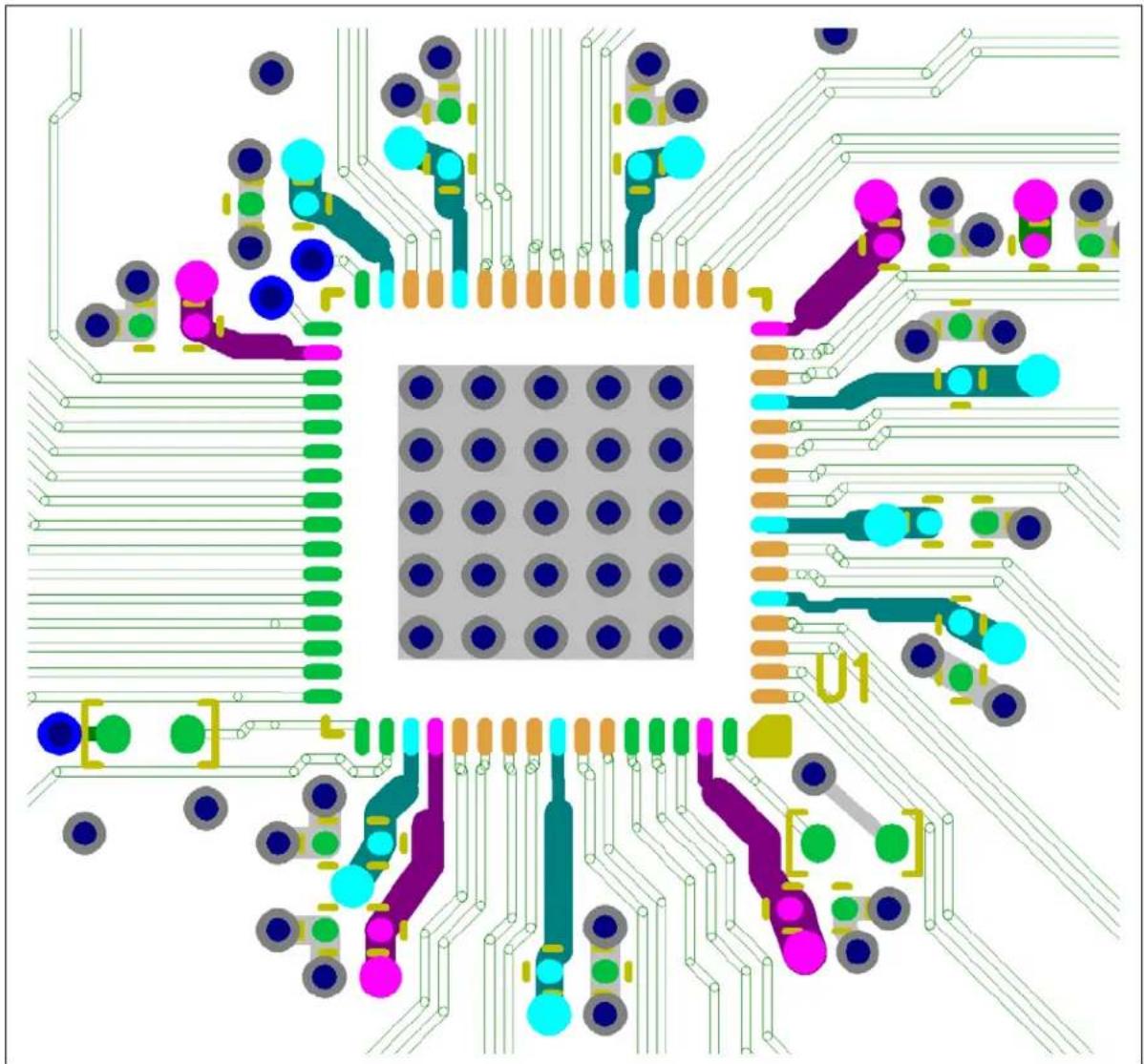
FIGURE 2-1: EXAMPLE BYPASS CAPACITOR PLACEMENT AND ROUTING
natural_image
Pure electrical circuit lines without any symbols☐ E. Fill the ground flag with vias to the ground plane layer, especially around the periphery of the flag. Refer to the Microchip AN 26.2 application note for additional details.
☐ F. RBIAS must be connected to the ground plane nearest to the RBIAS pin on the hub. This return path
must not be shared with any other components. Refer to the Microchip AN 26.2 application note for additional details.
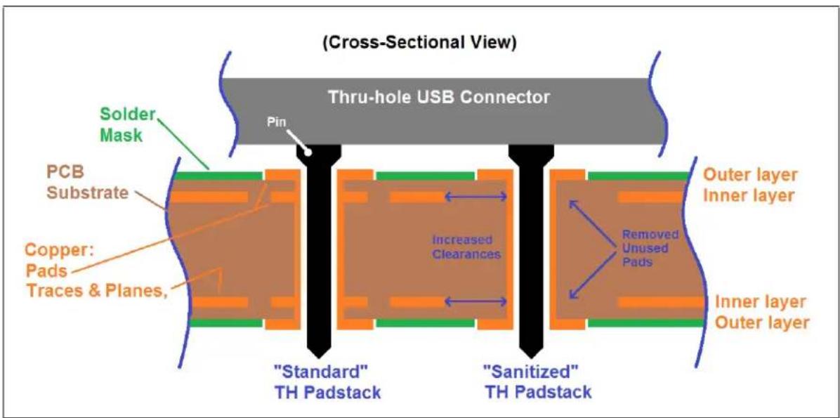
☐ G. Remove pin pads of through-hole USB connectors on unused layers and increase clearances. Refer to the Microchip AN 26.2 application note for additional details.
FIGURE 2-2: THROUGH HOLE PAD-STACK
text_image
(Cross-Sectional View) Thru-hole USB Connector Pin Solder Mask PCB Substrate Copper: Pads Traces & Planes, "Standard" TH Padstack Increased Clearances "Sanitized" TH Padstack Outer layer Inner layer Removed Unused Pads Inner layer Outer layer☐ H. Use surface mount USB connectors whenever possible. For through hole USB connectors, propagate the USB signals through the end of the through hole pin either by mounting the connector on the opposite side of the PCB or through the use of vias. Refer to the Microchip AN 26.2 application note for additional details.
☐ I. Route foreign traces no closer than 5 times the minimum trace spacing to crystal traces. Refer to the Microchip AN 26.2 application note for additional details.
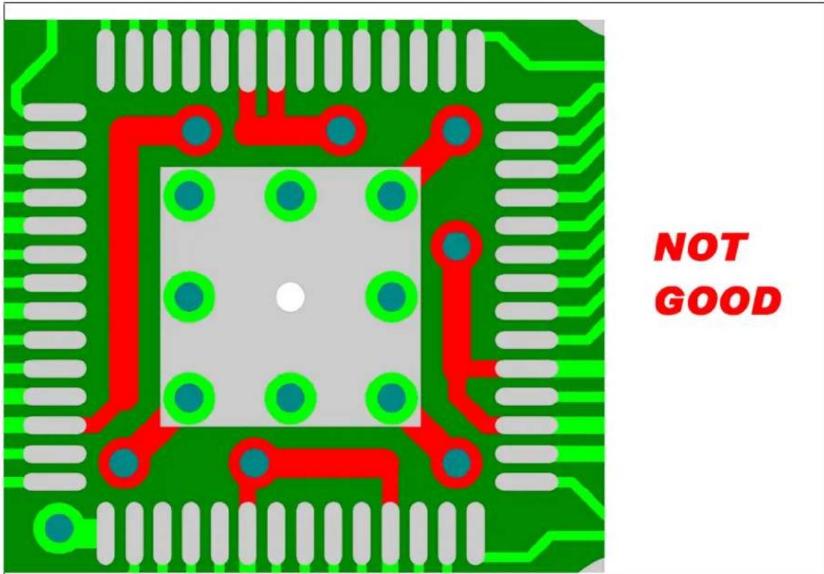
☐ J. Avoid routing between the ground flag and the pads for a QFN device. Refer to the Microchip AN 18.15 application note for additional details.
FIGURE 2-3: POOR QFN ROUTING
text_image
NOT GOOD☐ K. Route crystal traces at least 5 times the minimum trace spacing away from other traces. Refer to the Microchip AN 26.2 application note for additional details.
□ L. When using WLCSP products, the land pattern should conform to that described in WP 2.10.
2.1.1 HSIC SIGNALS
High-Speed Inter-Chip USB is a two-wire, single-ended signaling method that uses the USB 2.0 protocols for communication between ICs in a system. The interface is specifically High-Speed. Refer to the High-Speed Inter-Chip USB Electrical Specification (USB.org) for details.
□ A. Match the Strobe and Data trace lengths to within 0.5 mm (0.020").
☐ B. The Strobe and Data lines must be 2 – 10 cm (0.79 – 3.94") long.
□ C. Route Strobe and Data as single-ended traces, NOT as a differential pair.
☐ D. Space the Strobe and Data lines at least 0.65 mm (0.025") from each other and from any other traces.
□ E. Confirm that the characteristic trace impedance (Zchar) is 45 – 55 Ohm.
2.1.2 USB2.0 SIGNALS
☐ A. Maintain a routing spacing to foreign traces of at least 3 times the differential spacing between high speed DP and DM. Refer to the Microchip AN 26.2 application note for additional details.
☐ B. The length of SuperSpeed USB differential pair traces must be within 0.13mm of each other. Refer to the Microchip AN 26.2 application note for additional details.
☐ C. The differential impedance of USB 2.0 signals (DP and DM) must be 90 ohms +/- 15%. Microchip suggests 90 ohms +/- 10%. Refer to the USB 2.0 specification for additional information.
2.1.3 USB 3.1 GEN 1 SIGNALS
Note: Refer to AN 26.2 for more information on these items.
☐ A. The differential impedance of USB 3.1 Gen 1 signals (RX+/- & TX+/-) should be 90 ohms +/- 7 ohms. Refer to the USB 3.1 Gen 1 specification for additional information.
□ B. Place 0.1uF SS_TX AC coupling capacitors near the USB connectors.
☐ C. Keep SuperSpeed traces as short as possible, on outer layers, and over unbroken ground planes. Traces longer than 6 inches may degrade signal quality.
☐ D. Maintain a routing spacing to foreign traces of at least 5 times the differential spacing between Super-Speed lines.
☐ E. Eliminate or minimize the number of vias on USB 3.1 Gen 1 signals whenever possible. The +/- signals in the each USB 3.1 Gen 1 differential pair can be swapped for easier routing. See the product data sheet for more information on PortSwap.
☐ F. The length of a SuperSpeed USB differential pair traces must be within 0.13mm of each other.
2.2 USB Hubs
☐ A. The VBUS path to each downstream port must be wide and have very low impedance.
2.3 Flash Media Signals
Note: Refer to the Microchip AN 18.16 application note for more information on the following items.
□ A. The CRD_PWR traces must be wide enough to not produce a significant voltage drop.
☐ B. Unless otherwise specified in the product data sheet, route all time-sensitive media so that they are the same length, +/- 0.5 inches.
☐ C. Route all other traces, including other SD interface signals, at least three times the minimum trace spacing away from SD_CLK.
☐ D. Route all other traces, including other MS interface signals, at least three times the minimum trace spacing away from MS_CLK.
☐ E. Route all other traces, including other CF interface signals, at least three times the minimum trace spacing away from these traces.
☐ F. The multiplexed media interface signals must be routed to the connectors with minimal stubs.
2.4 USB Transceivers
☐ A. Processors/SoCs vary greatly in their timing specification for the ULPI bus. It is recommended to keep all ULPI traces less than 3 inches. However, consult your processor/SoC vendor for exact specifications.
☐ B. If deemed necessary via simulation, place a series termination resistor near the clock source. Refer to the Microchip AN 19.17 application note for additional details.
☐ C. Isolate the ULPI signals from adjacent signals and supplies. Refer to the Microchip AN 19.17 application note for additional details.
APPENDIX A: APPLICATION NOTE REVISION HISTORY
TABLE A-1: REVISION HISTORY
| Revision Level & Date Section/Figure/Entry Correction | ||
| DS00001863B (08-06-15) AI | Updated “USB 3.0” references | to “USB 3.1 Gen 1” throughout the document |
| DS00001863A (11-13-14) DS | 00001863A replaces former SMSC version Rev. 1.0 (06-26-13) | |
| Section 2.1.1, HSIC Signals Added section | ||
| Rev. 1.0 (06-26-13) All Initial Release | ||
Note the following details of the code protection feature on Microchip devices:
• Microchip products meet the specification contained in their particular Microchip Data Sheet.
- Microchip believes that its family of products is one of the most secure families of its kind on the market today, when used in the intended manner and under normal conditions.
- There are dishonest and possibly illegal methods used to breach the code protection feature. All of these methods, to our knowledge, require using the Microchip products in a manner outside the operating specifications contained in Microchip's Data Sheets. Most likely, the person doing so is engaged in theft of intellectual property.
• Microchip is willing to work with the customer who is concerned about the integrity of their code.
- Neither Microchip nor any other semiconductor manufacturer can guarantee the security of their code. Code protection does not mean that we are guaranteeing the product as “unbreakable.”
Code protection is constantly evolving. We at Microchip are committed to continuously improving the code protection features of our products. Attempts to break Microchip's code protection feature may be a violation of the Digital Millennium Copyright Act. If such acts allow unauthorized access to your software or other copyrighted work, you may have a right to sue for relief under that Act.
Information contained in this publication regarding device applications and the like is provided only for your convenience and may be superseded by updates. It is your responsibility to ensure that your application meets with your specifications. MICROCHIP MAKES NO REPRESENTATIONS OR WARRANTIES OF ANY KIND WHETHER EXPRESS OR IMPLIED, WRITTEN OR ORAL, STATUTORY OR OTHERWISE, RELATED TO THE INFORMATION, INCLUDING BUT NOT LIMITED TO ITS CONDITION, QUALITY, PERFORMANCE, MERCHANTABILITY OR FITNESS FOR PURPOSE. Microchip disclaims all liability arising from this information and its use. Use of Microchip devices in life support and/or safety applications is entirely at the buyer's risk, and the buyer agrees to defend, indemnify and hold harmless Microchip from any and all damages, claims, suits, or expenses resulting from such use. No licenses are conveyed, implicitly or otherwise, under any Microchip intellectual property rights unless otherwise stated.
Trademarks
The Microchip name and logo, the Microchip logo, dsPIC, FlashFlex, flexPWR, JukeBlox, KEELOQ, KEELOQ logo, Kleer, LANCheck, MediaLB, MOST, MOST logo, MPLAB, OptoLyzer, PIC, PICSTART, PIC ^32 logo, RightTouch, SpyNIC, SST, SST Logo, SuperFlash and UNI/O are registered trademarks of Microchip Technology Incorporated in the U.S.A. and other countries.
The Embedded Control Solutions Company and mTouch are registered trademarks of Microchip Technology Incorporated in the U.S.A.
Analog-for-the-Digital Age, BodyCom, chipKIT, chipKIT logo, CodeGuard, dsPICDEM, dsPICDEM.net, ECAN, In-Circuit Serial Programming, ICSP, Inter-Chip Connectivity, KleerNet, KleerNet logo, MiWi, MPASM, MPF, MPLAB Certified logo, MPLIB, MPLINK, MultiTRAK, NetDetach, Omniscient Code Generation, PICDEM, PICDEM.net, PICkit, PICtail, RightTouch logo, REAL ICE, SQI, Serial Quad I/O, Total Endurance, TSHARC, USBCheck, VariSense, ViewSpan, WiperLock, Wireless DNA, and ZENA are trademarks of Microchip Technology Incorporated in the U.S.A. and other countries.
SQTP is a service mark of Microchip Technology Incorporated in the U.S.A.
Silicon Storage Technology is a registered trademark of Microchip Technology Inc. in other countries.
GestIC is a registered trademarks of Microchip Technology Germany II GmbH & Co. KG, a subsidiary of Microchip Technology Inc., in other countries.
All other trademarks mentioned herein are property of their respective companies.
© 2013 - 2015, Microchip Technology Incorporated, Printed in the U.S.A., All Rights Reserved.
ISBN: 9781632776600
QUALITY MANAGEMENT SYSTEM
CERTIFIED BY DNV
=ISO/TS 16949=
Microchip received ISO/TS-16949:2009 certification for its worldwide headquarters, design and wafer fabrication facilities in Chandler and Tempe, Arizona; Gresham, Oregon and design centers in California and India. The Company's quality system processes and procedures are for its PIC® MCUs and dsPIC® DSCs, KEELoo® code hopping devices, Serial EEPROMs, microperipherals, nonvolatile memory and analog products. In addition, Microchip's quality system for the design and manufacture of development systems is ISO 9001:2000 certified.
Worldwide Sales and Service
AMERICAS
Corporate Office
2355 West Chandler Blvd.
Chandler, AZ 85224-6199
Tel: 480-792-7200
Fax: 480-792-7277
Technical Support:
http://www.microchip.com/
support
Web Address:
www.microchip.com
Atlanta
Duluth, GA
Tel: 678-957-9614
Fax: 678-957-1455
Austin, TX
Tel: 512-257-3370
Boston
Westborough, MA
Tel: 774-760-0087
Fax: 774-760-0088
Chicago
Itasca, IL
Tel: 630-285-0071
Fax: 630-285-0075
Cleveland
Independence, OH
Tel: 216-447-0464
Fax: 216-447-0643
Dallas
Addison, TX
Tel: 972-818-7423
Fax: 972-818-2924
Detroit
Novi, MI
Tel: 248-848-4000
Houston, TX
Tel: 281-894-5983
Indianapolis
Noblesville, IN
Tel: 317-773-8323
Fax: 317-773-5453
Los Angeles
Mission Viejo, CA
Tel: 949-462-9523
Fax: 949-462-9608
New York, NY
Tel: 631-435-6000
San Jose, CA
Tel: 408-735-9110
Canada - Toronto
Tel: 905-673-0699
Fax: 905-673-6509
ASIA/PACIFIC
Asia Pacific Office
Suites 3707-14, 37th Floor
Tower 6, The Gateway
Harbour City, Kowloon
Hong Kong
Tel: 852-2943-5100
Fax: 852-2401-3431
Australia - Sydney
Tel: 61-2-9868-6733
Fax: 61-2-9868-6755
China - Beijing
Tel: 86-10-8569-7000
Fax: 86-10-8528-2104
China - Chengdu
Tel: 86-28-8665-5511
Fax: 86-28-8665-7889
China - Chongqing
Tel: 86-23-8980-9588
Fax: 86-23-8980-9500
China - Dongguan
Tel: 86-769-8702-9880
China - Hangzhou
Tel: 86-571-8792-8115
Fax: 86-571-8792-8116
China - Hong Kong SAR
Tel: 852-2943-5100
Fax: 852-2401-3431
China - Nanjing
Tel: 86-25-8473-2460
Fax: 86-25-8473-2470
China - Qingdao
Tel: 86-532-8502-7355
Fax: 86-532-8502-7205
China - Shanghai
Tel: 86-21-5407-5533
Fax: 86-21-5407-5066
China - Shenyang
Tel: 86-24-2334-2829
Fax: 86-24-2334-2393
China - Shenzhen
Tel: 86-755-8864-2200
Fax: 86-755-8203-1760
China - Wuhan
Tel: 86-27-5980-5300
Fax: 86-27-5980-5118
China - Xian
Tel: 86-29-8833-7252
Fax: 86-29-8833-7256
ASIA/PACIFIC
China - Xiamen
Tel: 86-592-2388138
Fax: 86-592-2388130
China - Zhuhai
Tel: 86-756-3210040
Fax: 86-756-3210049
India - Bangalore
Tel: 91-80-3090-4444
Fax: 91-80-3090-4123
India - New Delhi
Tel: 91-11-4160-8631
Fax: 91-11-4160-8632
India - Pune
Tel: 91-20-3019-1500
Japan - Osaka
Tel: 81-6-6152-7160
Fax: 81-6-6152-9310
Japan - Tokyo
Tel: 81-3-6880-3770
Fax: 81-3-6880-3771
Korea - Daegu
Tel: 82-53-744-4301
Fax: 82-53-744-4302
Korea - Seoul
Tel: 82-2-554-7200
Fax: 82-2-558-5932 or
82-2-558-5934
Malaysia - Kuala Lumpur
Tel: 60-3-6201-9857
Fax: 60-3-6201-9859
Malaysia - Penang
Tel: 60-4-227-8870
Fax: 60-4-227-4068
Philippines - Manila
Tel: 63-2-634-9065
Fax: 63-2-634-9069
Singapore
Tel: 65-6334-8870
Fax: 65-6334-8850
Taiwan - Hsin Chu
Tel: 886-3-5778-366
Fax: 886-3-5770-955
Taiwan - Kaohsiung
Tel: 886-7-213-7828
Taiwan - Taipei
Tel: 886-2-2508-8600
Fax: 886-2-2508-0102
Thailand - Bangkok
Tel: 66-2-694-1351
Fax: 66-2-694-1350
EUROPE
Austria - Wels
Tel: 43-7242-2244-39
Fax: 43-7242-2244-393
Denmark - Copenhagen
Tel: 45-4450-2828
Fax: 45-4485-2829
France - Paris
Tel: 33-1-69-53-63-20
Fax: 33-1-69-30-90-79
Germany - Dusseldorf
Tel: 49-2129-3766400
Germany - Karlsruhe
Tel: 49-721-625370
Germany - Munich
Tel: 49-89-627-144-0
Fax: 49-89-627-144-44
Italy - Milan
Tel: 39-0331-742611
Fax: 39-0331-466781
Italy - Venice
Tel: 39-049-7625286
Netherlands - Drunen
Tel: 31-416-690399
Fax: 31-416-690340
Poland - Warsaw
Tel: 48-22-3325737
Spain - Madrid
Tel: 34-91-708-08-90
Fax: 34-91-708-08-91
Sweden - Stockholm
Tel: 46-8-5090-4654
UK - Wokingham
Tel: 44-118-921-5800
Fax: 44-118-921-5820
07/14/15