USB3341 - Electronic component Microchip - Free user manual and instructions
Find the device manual for free USB3341 Microchip in PDF.

User questions about USB3341 Microchip
0 question about this device. Answer the ones you know or ask your own.
Ask a new question about this device
Download the instructions for your Electronic component in PDF format for free! Find your manual USB3341 - Microchip and take your electronic device back in hand. On this page are published all the documents necessary for the use of your device. USB3341 by Microchip.
USER MANUAL USB3341 Microchip
EVB-USB3340 USB Transceiver Evaluation Board User Manual
natural_image
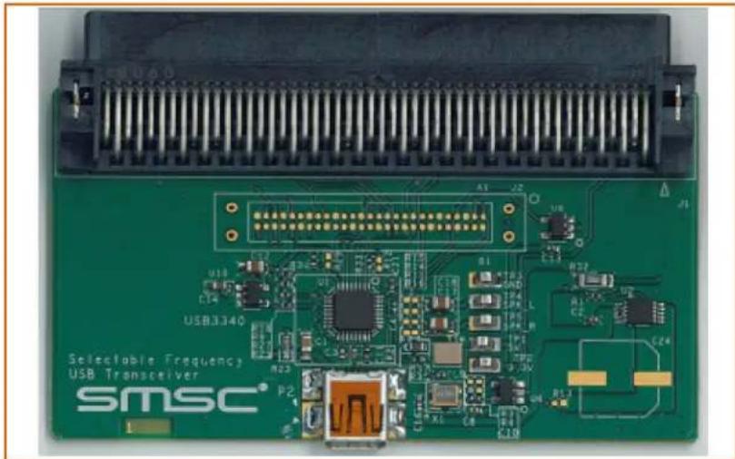
Close-up of a green Siemens 340 USB transceiver module with visible circuitry and components (no readable text or symbols)Copyright © 2013 SMSC or its subsidiaries. All rights reserved.
Circuit diagrams and other information relating to SMSC products are included as a means of illustrating typical applications. Consequently, complete information sufficient for construction purposes is not necessarily given. Although the information has been checked and is believed to be accurate, no responsibility is assumed for inaccuracies. SMSC reserves the right to make changes to specifications and product descriptions at any time without notice. Contact your local SMSC sales office to obtain the latest specifications before placing your product order. The provision of this information does not convey to the purchaser of the described semiconductor devices any licenses under any patent rights or other intellectual property rights of SMSC or others. All sales are expressly conditional on your agreement to the terms and conditions of the most recently dated version of SMSC's standard Terms of Sale Agreement dated before the date of your order (the "Terms of Sale Agreement"). The product may contain design defects or errors known as anomalies which may cause the product's functions to deviate from published specifications. Anomaly sheets are available upon request. SMSC products are not designed, intended, authorized or warranted for use in any life support or other application where product failure could cause or contribute to personal injury or severe property damage. Any and all such uses without prior written approval of an Officer of SMSC and further testing and/or modification will be fully at the risk of the customer. Copies of this document or other SMSC literature, as well as the Terms of Sale Agreement, may be obtained by visiting SMSC's website at http://www.smsc.com. SMSC is a registered trademark of Standard Microsystems Corporation ("SMSC"). Product names and company names are the trademarks of their respective holders.
The Microchip name and logo, and the Microchip logo are registered trademarks of Microchip Technology Incorporated in the U.S.A. and other countries.
SMSC DISCLAIMS AND EXCLUDES ANY AND ALL WARRANTIES, INCLUDING WITHOUT LIMITATION ANY AND ALL IMPLIED WARRANTIES OF MERCHANTABILITY, FITNESS FOR A PARTICULAR PURPOSE, TITLE, AND AGAINST INFRINGEMENT AND THE LIKE, AND ANY AND ALL WARRANTIES ARISING FROM ANY COURSE OF DEALING OR USAGE OF TRADE. IN NO EVENT SHALL SMSC BE LIABLE FOR ANY DIRECT, INCIDENTAL, INDIRECT, SPECIAL, PUNITIVE, OR CONSEQUENTIAL DAMAGES; OR FOR LOST DATA, PROFITS, SAVINGS OR REVENUES OF ANY KIND; REGARDLESS OF THE FORM OF ACTION, WHETHER BASED ON CONTRACT; TORT; NEGLIGENCE OF SMSC OR OTHERS; STRICT LIABILITY; BREACH OF WARRANTY; OR OTHERWISE; WHETHER OR NOT ANY REMEDY OF BUYER IS HELD TO HAVE FAILED OF ITS ESSENTIAL PURPOSE, AND WHETHER OR NOT SMSC HAS BEEN ADVISED OF THE POSSIBILITY OF SUCH DAMAGES.
1 Introduction
This user manual is for the USB3340 USB Transceiver Evaluation Board (EVB) for use with USB3340 products with the integrated USB switch.
The USB3340 features a ULPI interface to support systems with USB Host, Device, or On-the-Go (OTG) capability. The integrated switch can be used to multiplex a Full Speed USB signal or audio signals over the HS USB DP/DM pins.
2 Overview
The USB3340 EVB is a Daughter Card designed to plug into a user's test system using a T&MT connector. The card attaches to a USB link layer to create a USB Host, Device, or On-the-Go (OTG) system. The board edge connector meets the UTMI+ Low Pin Interface (ULPI) Standard requirements for the T&MT connector.
A link to the ULPI Working Group Page is available at www.smsc.com or may be obtained from your local FAE. The USB3340 EVB includes USB3340 packaged silicon and all external components required for the USB transceiver function.
This manual describes PCB assembly PCB-7220AZ.
2.1 Supplying VBUS Voltage
In Host or OTG operation, the USB3340 EVB must provide 5 Volts on V_BUS at the USB connector. The USB3340 EVB includes a switch that can drive V_BUS using the 5 Volt supply that comes from pin 28 of the T&MT connector.
The VBUS switch is controlled by the CPEN signal from the USB3340. The USB controller dictates the state of CPEN by programming the ULPI register in the USB3340. The 5 Volt switch is backdrive protected when in the off state. The switch does not provide protection from reverse currents when it is on. See Section 2.10 and Section 2.11 for more information on configuring the USB3340 EVB for OTG and Host operation.
2.2 ULPI I/O Voltage
The USB3340 supports variable ULPI I/O voltage signaling. The ULPI I/O voltage is supplied in one of two ways. By default, the EVB is shipped with VDDIO supplied by the on-board LDO.
Resistor R18 is used to set VDDIO, the digital logic high voltage. To change the value of VDDIO, calculate a new value for R18 (ohms) as follows.
$$ R 1 8 = (V D D I O / 1. 2 2 5 - 1) \times 1 6 9 0 0 0 $$
VDDIO must be in the range of 1.8 Volts - 3.3 Volts nominal.
VDDIO can also be supplied to the USB3340 from the T&MT connector instead of using the LDO. To do this, the LDO (U10) must be removed.
The VDDIO voltage level that has been configured on the USB3340 EVB must be the same as the ULPI I/O voltage level that the link is using.
2.3 Edge Connector for Digital I/O
The T&MT edge connector is compliant to the ULPI specification. Part numbers and manufacturers for this connector and it's mate are given in Table 2.1.
Table 2.1 Edge Connector on the USB3340 EVB
| PART NUMBER DESCRIPTION MANUFACTURER | |
| 2-557101-5 100 pin edge connector on USB3340 EVB AMP | |
| 2-557-101-5 Mating connector to the USB3340 EVB AMP | |
| 1-1734037-0 Alternate 100 pin edge connector for USB3340 EVB TYCO | |
| 1-1734099-0 Alternate mating connector to the USB3340 EVB TYCO |
2.4 REFCLK Frequency Selection
The USB3340 EVB offers a user selectable reference clock frequency. R25 - R30 are used to configure the REFCLK[2:0] signals which will select the reference clock frequency desired on the USB3340 EVB. Ensure that the frequency of the reference clock or reference crystal being used matches the desired operation frequency configured based on Table 2.2 below. By default, the USB3340 EVB is configured for 26MHz REFCLK operation.
Table 2.2 Reference Frequency Selection Resistor Configurations
| R25 | R26 | R27 | R28 | R29 | R30 | REFCLK FREQUENCY |
| INSTALL | EMPTY | INSTALL | EMPTY | EMPTY | INSTALL | 26.0 MHz (Default) |
| EMPTY | INSTALL | INSTALL | EMPTY | EMPTY | INSTALL | 12.0 MHz |
| EMPTY | INSTALL | EMPTY | INSTALL | EMPTY | INSTALL | 52.0 MHz |
| INSTALL | EMPTY | INSTALL | EMPTY | INSTALL | EMPTY | 24.0 MHz |
| INSTALL | EMPTY | EMPTY | INSTALL | INSTALL | EMPTY | 19.2 MHz |
| EMPTY | INSTALL | INSTALL | EMPTY | INSTALL | EMPTY | 27.0 MHz |
| EMPTY | INSTALL | EMPTY | INSTALL | INSTALL | EMPTY | 38.4 MHz |
| INSTALL | EMPTY | EMPTY | INSTALL | EMPTY | INSTALL | 13.0 MHz |
2.5 USB Connector
A standard Mini-AB connector is provided to attach a USB cable or connector. Provision is made on the PCB to accept a Micro-AB connector. See the bill of materials in Section 6 for connector part numbers. Do not substitute a different part number for the Mini-AB receptacle or a short circuit of the USB signals may result at the micro-AB connector PCB footprint.
2.6 VBUS Present Detection
The USB controller must detect VBUS when a USB cable is attached in device mode or when the USB controller turns on VBUS in host or OTG mode. The USB connector VBUS signal is connected to the VBUS pin of the USB3340. The USB3340 includes all of the comparators required to detect VBUS and report the state of VBUS to the USB controller via the ULPI bus.
2.7 ULPI Signal Test Points
Probe points at location J2, provide access to all ULPI signals. Install the Tektronix logic analyzer probe retention kit at J2 to probe these signals. Ordering information for the retention kit is provided in the bill of materials.
2.8 Other Signal Test Points
There are five other test points located on the board for easy access. TP1 connects to the 5V supply coming from the T&MT connector. TP2 connects to the 3.3V VDD supply coming from the T&MT connector. TP3 connects to Ground. TP4 and TP5 connect to the Speaker Left and Speaker Right pins respectively.
2.9 Speaker Left and Speaker Right signals
The Speaker Left and Speaker Right pins can accept audio signals ranging from 0V to 3.3V. If the audio signal coming into the test points goes below 0V, biasing circuitry is required. Install R11, R14, R15, and R16 with 10k resistors to add a DC bias to the audio signal. This will ensure the best signal quality when routing through the USB3340.
2.10 Converting the EVB to an OTG System
"Out of the box", the USB3340 EVB is delivered as a USB Device system. To convert it to be a USB OTG development board, the following modifications must be made:
- Install R13 (zero ohm resistor). This connects the VBUS 5V switch to the VBUS signal.
- Remove R23. This is the R_VBUS value required for a USB Device.
- Install R10 (1.0K, 1W resistor). This is the R_VBUS value required for a USB OTG Device.
Since the USB3340 is designed to accommodate up to 30V on VBUS, R10 is rated at 1W to accommodate this entire voltage range. Refer to the USB3340 datasheet for more information on sizing this resistor.
2.11 Converting the EVB to a Host System
"Out of the box", the USB3340 EVB is delivered as a USB Device System. To convert it to be a USB Host development board, the following modifications must be made:
- Install R13 (zero ohm resistor). This connects the VBUS 5V switch to the VBUS signal.
- Install C24 (120uF capacitor). This increases the value of C_VBUS to be USB 2.0 Host compliant.
2.12 Converting the EVB to Support ULPI Clock Input Mode
"Out of the box", the USB3340 EVB uses a crystal (Y1) as the clock reference, and is configured for ULPI Clock Output Mode where CLKOUT sources a 60MHz clock. To convert the EVB to support ULPI Clock Input Mode, the following changes must be made:
- Install R12 (zero ohm resistor). This shorts CLKOUT to VDD18.
- Install R3 (zero ohm resistor). This shorts REFCLK to the System Clock pin on the T&MT connector.
- Confirm that R4 is not populated.
- Remove the following components to remove the crystal circuit: Y1, R17, C22, C23
Refer to the USB3340 datasheet for more information on ULPI Clock Input Mode.
2.13 T&MT Pin Description
The T&MT signal names, pin number and function are described in Table 43 and Table 44 of the ULPI Specification rev 1.1.
The USB3340 EVB fully implements a ULPI compliant interface to the T&MT connector, including support for ULPI Clock Input Mode. This EVB supports a 1.8-3.3V ULPI I/O voltages. All signals are described in Table 2.3.
Table 2.3 T&MT Connector Pin Definitions
| PIN NAME DESCRIPTION DIRECTION | |||
| 86, 36,85, 34,83, 33,82, 31 | DATA[7:0]Refer to Schematic for Connector Pin Assignment | ULPI Data Bus IN/OUT | |
| 96 STP | ULPI STP Signal INPUT TO | EVB | |
| 70 DIR | ULPI DIR Signal OUTPUT | FROM EVB | |
| 71 NXT | ULPI | NXT Signal | OUTPUTFROM EVB |
| 90 CLKOUT | ULPI | Clock Signal | OUTPUTFROM EVB |
| 55 VBUS_FAULT_N | Driven low by the VBUS switch (U2) in the event of a switch fault condition. | OUTPUT | |
| 15 SPKR_L | In USB Audio mode, SPKR_L is connected to the DP pin via an analog switch in the USB3340. | IN/OUT | |
| 45 SPKR_RM | In USB Audio mode, SPKR_RM is connected to the DP pin via an analog switch in the USB3340. | IN/OUT | |
| 17 RESET | Asserting RESET will place the USB3340 in a low power state. Upon exiting this state (RESET=0), all ULPI registers will contain power-on reset values. | INPUT | |
| 47 VBUS_IN | This pin is not connected | NO CONNECT | |
| 28 VBUS_OUT | +5V from the T&MT connector | INPUT TO EVB | |
| 8,16, 57,69 | VDD | +3.3V from the T&MT connector | INPUT TO EVB |
| 52 | SYSTEM_CLOCK | Optional clock input to EVB. The EVB is built with the USB3340 REFCLK provided by a crystal. See Section 2.12 for more information on configuring the USB3340 EVB for ULPI Clock Input mode. | NO CONNECT (input to EVB if R3 is installed) |
| 100 | PSU_SHD_N | This pin is driven low indicating that +3.3V must be sourced from the link through the T&MT connector pins 8, 16, 57, 69 and +5.0V must be sourced from the link through the T&MT connector pin 28. | OUTPUTFROM EVB |
| 49 DC_PSNT_N | This pin is driven low indicating a daughter card is present. | OUTPUTFROM EVB | |
3 Getting Started
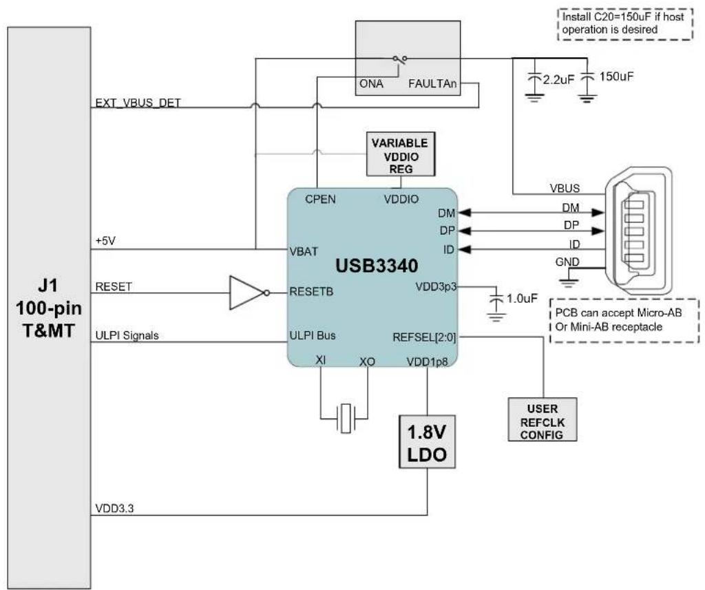
The block diagram in Figure 3.1 gives a simplified view of the USB3340 EVB. The USB3340 EVB is ready for device operation. To modify the board for OTG or Host applications, refer to Section 2.10 or Section 2.11, respectively.
It is required to provide +5V to T&MT connector pin 28 and +3.3V on T&MT pins 8,16,57,69 to power the USB3340 EVB.
The USB3340 EVB is built with a USB Mini-AB receptacle. Do not substitute a Mini-AB receptacle different from the one specified in the bill of materials, or a short circuit may occur on the USB signals at the Micro-AB connector PCB footprint.
flowchart
graph TD
    A["J1 100-pin T&MT"] -->|EXT_VBUS_DET| B["USB3340"]
    A -->|+5V| C["RESET"]
    A -->|ULPI Signals| D["RESETB"]
    A -->|VDD3.3| E["ULPI Bus"]
    B --> F["CPEN"]
    B --> G["VBAT"]
    B --> H["CPEN"]
    B --> I["VBAT"]
    B --> J["RESETB"]
    B --> K["ULPI Bus"]
    B --> L["1.8V LDO"]
    B --> M["1.0uF"]
    B --> N["REFSEL[2:0"]]
    B --> O["VDD3p3"]
    B --> P["VDD1p8"]
    B --> Q["DM"]
    B --> R["DP"]
    B --> S["ID"]
    B --> T["VAIRABLE VDDIO REG"]
    B --> U["VAIRABLE VDDIO"]
    B --> V["VAIRABLE VDDIO REG"]
    B --> W["VAIRABLE VDDIO REG"]
    B --> X["VAIRABLE VDDIO REG"]
    B --> Y["VAIRABLE VDDIO REG"]
    B --> Z["VAIRABLE VDDIO REG"]
    B --> AA["VAIRABLE VDDIO REG"]
    B --> AB["VAIRABLE VDDIO REG"]
    B --> AC["VAIRABLE VDDIO REG"]
    B --> AD["VAIRABLE VDDIO REG"]
    B --> AE["VAIRABLE VDDIO REG"]
    B --> AF["VAIRABLE VDDIO REG"]
    B --> AG["VAIRABLE VDDIO REG"]
    B --> AH["VAIRABLE VDDIO REG"]
    B --> AI["VAIRABLE VDDIO REG"]
    B --> AJ["VAIRABLE VDDIO REG"]
    B --> AK["VAIRABLE VDDIO REG"]
    B --> AL["VAIRABLE VDDIO REG"]
    B --> AM["VAIRABLE VDDIO REG"]
    B --> AN["VAIRABLE VDDIO REG"]
    B --> AO["VAIRABLE VDDIO REG"]
    B --> AP["VAIRABLE VDDIO REG"]
    B --> AQ["VAIRABLE VDDIO REG"]
    B --> AR["VAIRABLE VDDIO REG"]
    B --> AS["VAIRABLE VDDIO REG"]
    B --> AT["VAIRABLE VDDIO REG"]
    B --> AU["VAIRABLE VDDIO REG"]
    B --> AV["VAIRABLE VDDIO REG"]
    B --> AW["VAIRABLE VDDIO REG"]
    B --> AX["VAIRABLE VDDIO REG"]
    B --> AY["VAIRABLE VDDIO REG"]
    B --> AZ["VAIRABLE VDDIO REG"]
    B --> BA["VAIRABLE VDDIO REG"]
    B --> BB["VAIRABLE VDDIO REG"]
    B --> BC["VAIRABLE VDDIO REG"]
    B --> BD["VAIRABLE VDDIO REG"]
    B --> BE["VAIRABLE VDDIO REG"]
    B --> BF["VAIRABLE VDDIO REG"]
    B --> BG["VAIRABLE VDDIO REG"]
    B --> BH["VAIRABLE VDDIO REG"]
    B --> BI["VAIRABLE VDDIO REG"]
    B --> BJ["VAIRABLE VDDIO REG"]
    B --> BK["VAIRABLE VDDIO REG"]
    B --> BL["VAIRABLE VDDIO REG"]
    B --> BM["VAIRABLE VDDIO REG"]
    B --> BN["VAIRABLE VDDIO REG"]
    B --> BO["VAIRABLE VDDIO REG"]
    B --> BP["VAIRABLE VDDIO REG"]
    B --> BQ["VAIRABLE VDDIO REG"]
    B --> BR["VAIRABLE VDDIO REG"]
    B --> BS["VAIRABLE VDDIO REG"]
    B --> BT["VAIRABLE VDDIO REG"]
    B --> BU["VAIRABLE VDDIO REG"]
    B --> BV["VAIRABLE VDDIO REG"]
    B --> BW["VAIRABLE VDDIO REG"]
    B --> BX["VAIRABLE VDDIO REG"]
    B --> BY["VAIRABLE VDDIO REG"]
    B --> BZ["VAIRABLE VDDIO REG"]
    B --> CA["VAIRABLE VDDIO REG"]
    B --> CB["VAIRABLE VDDIO REG"]
    B --> CC["VAIRABLE VDDIO REG"]
    B --> CD["VAIRABLE VDDIO REG"]
    B --> CE["VAIRABLE VDDIO REG"]
    B --> CF["VAIRABLE VDDIO REG"]
    B --> CG["VAIRABLE VDDIO REG"]
    B --> CH["VAIRABLE VDDIO REG"]
    B --> CI["VAIRABLE VDDIO REG"]
    B --> CJ["VAIRABLE VDDIO REG"]
    B --> CK["VAIRABLE VDDIO REG"]
Figure 3.1 Block Diagram of USB3340 EVB
When the USB3340 EVB is powered on, check the following things to be certain the board is functioning normally:
- RESET should be de-asserted (logic low at the T&MT connector and RESETB at the USB3340 should be logic high = VDD18). If RESETB=0, the USB3340 will be in a low power state.
The voltage at R2 (RBIAS) should be 0.8V DC. If this voltage is not present, the USB3340 is in a low power state.
There should be a digital 60 MHz square wave signal at T&MT connector pin 90. The amplitude should be approximately VDDIO. This is the CLKOUT signal of the USB3340.
The voltage at C3 should be approximately 3.3V. This is the USB3340 internal 3.3V voltage regulator output.
The voltage at C4 should be 1.8V. This is the 1.8V regulator output.
4 Protecting VBUS from Non-Compliant VBUS Voltages
The USB3340 is fully tolerant to VBUS voltages up to 30V. An external resistor on the VBUS line ( R_VBUS ) is required for the integrated overvoltage protection circuit in the USB3340. R_VBUS is either R10 or R23 on the USB3340 EVB. For peripheral and host applications, R_VBUS is 10K (install R23, remove R10). For OTG applications, R_VBUS is 1K (install R10, remove R23).
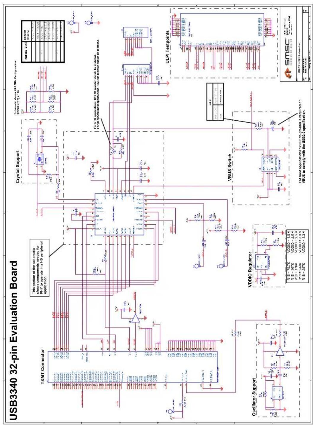
5 USB3340 EVB Schematic
text_image
USB3340 32-pin Evaluation Board T&MT Connector This portion of the schematic shows components needed for PHY to operate in a HS peripheral application. Crystal Support Schematic shows 28.0 MHz Configuration. REFCLK[2.0] = 110 For OTG applications, R10-1K resistor should be installed. For peripheral/host applications, R23 20K resistor should be installed. ULPI Testpoints VDDIO Regulator For host applications 120 uF to ground is required on VBUS to comply with the USB2.0 specification. Oscillator Support VDDIO Switch R13 New One circuit / 720 VDDIO = -1.8 V VDDIO = 1.8 V VDDIO = -1.8 V VDDIO = -1.8 V VDDIO = -1.8 V VDDIO = -1.8 V VDDIO = -1.8 V VDDIO = -1.8 V VDDIO = -1.8 V VDDIO = -1.8 V VDDIO = -1.8 V VDDIO = -1.8 V VDDIO = 1.8 V VDDIO = -1.8 V VDDIO = -1.8 V VDDIO = -1.8 V VDDIO = -1.8 V VDDIO = -1.8 V VDDIO = -1.8 V VDDIO = -1.8 V VDDIO = -1.8 W VDDIO = -1.8 W VDDIO = -1.8 W VDDIO = -1.8 W VDDIO = -1.8 W VDDIO = -1.8 W VDDIO = -1.8 W VDDIO = -1.8 W VDDIO = -1.8 W VDDIO = -1.8 W VDDIO = -1.8 V VDDIO = -1.8 V VDDIO = -1.8 V VDDIO = -1.8 V VDDIO = -1.8 V VDDIO = -1.8 V VDDIO = -1.8 V VDDIO = -1.8 V VDDIO = -1.8 V VDDIO = -1.8 W VDDIO = -1.8 W VDDIO = 1.8 V VDDIO = -1.8 V VDDIO = -1.8 V VDDIO = 1.8 V VDDIO = -1.8 V VDDIO = -1.8 V VDDIO = 1.8 V VDDIO = -1.8 V VDDIO = -1.8 V VDDIO = 1.8 V VDDIO = -1.8 V VDDIO = -1.8 V VDDIO = 1.8 W VDDIO = -1.8 W VDDIO = -1.8 W VDDIO = 1.8 W VDDIO = -1.8 W VDDIO = 1.8 W VDDIO = -1.8 W VDDIO = 1.8 W VDDIO = -1.8 W VDDIO = 1.8 W VDDIO = -1.8 W VDDIO = 1.8 W VDDIO = -1.8 W VDDIO = -3.3 VFigure 5.1 USB3340 EVB Schematic
6 USB3340 EVB Bill of Materials
| Item # | Quantit y | DNP Part | Reference Descrip tion Digikey_Numbe | r | Manuf | Manuf_PN RoHS | |
| 1 | 1 | C1CAPACITOR CERAMIC 2.2UF 50V Y5V 0805 445-3464 | 1-ND TDK C2012Y5V1 | H225Z Yes | |||
| 2 | 8 | C2 C8 C9 C10C11 C13 C16CAPACITOR CERAMIC 0.1UF 10V X5R 0402 PCC2146 | CT-ND PANASONIC ECJ-0EB1A104K Yes | ||||
| 3 | 2 | C3 C4CAPACITOR CERAMIC 1.0UF 6.3V 20% X5R 040 | 490-1319-1-ND | MURATA ERIE | GRM155R60J105ME19D | Yes | |
| 4 | 3 | C12 C17 C18CAPACITOR CERAMIC 10UF 6.3VDC 20% X5R 08 | PCC2225CT-ND | PANASONIC | ECJ-2FB0J106M | Yes | |
| 5 | 1 | C14CAPACITOR CERAMIC 1.0UF 16VDC 10% X5R 06 | PCC2224CT-ND | PANASONIC | ECJ-1VB1C105K | Yes | |
| 6 | 2 | C22 C23CAPACITOR CERAMIC 22PF 5% 50V NP0 0402 478-10 | 74-1-ND AVX 04025A2 | 20JAT2A | Yes | ||
| 7 | 0 | C24 | 565-3066-1-ND | United Chemi-Con | APXA100ARA121MH70G | Yes | |
| 8 | 0 | J1AMP_T&MT_UTMI+ULPI COMBO | A33470-ND | TYCO | 1-1734037-0 | Yes | |
| 9 | 0 | J2 | TEKTRONIX | P6960DM | Yes | ||
| 10 | 1 | P2CONNECTOR RECEPT USB MINI AB 5POS RT ANG | WM17122CT-ND | MOLEX | 56579-0576 | Yes | |
| 11 | 0 | P1 | A97799CT-ND | TYCO | 1981584-1 | Yes | |
| 12 | 1 | R1RESISTOR 100K OHM 1/10W 5% 0402 SMD | P100KJCT-ND | PANASONIC | ERJ-2GEJ104X | Yes | |
| 13 | 1 | R2RESISTOR 8.06K OHM 1/16W 1% 0402 SMD | P8.06KLCT-ND | PANASONIC | ERJ-2RKF8061X | Yes | |
| 14 | 3 | R3 R4 R12R13 R26 R28 | R25 R27 R30RESISTOR ZERO OHM 1/16W 5% 0402 SMD | 311-0.0JRCT-ND | YAGEO | RC0402JR-070RL | Yes |
| 15 | 3 | R6 R11 R14R15 R16 R5 R8 | 541-10.0KLCT-ND | VISHAY-DALE | CRCW040210K0FKED | Yes | |
| 16 | 1 | R7RESISTOR 27.0K OHM 1/16W 1% 0402 SMD | 311-27.0KLRCT-ND | YAGEO | RC0402FR-0727KL | Yes | |
| 17 | 1 | R9RESISTOR 169K OHM 1/16W 1% 0402 SMD | 311-169KLRCT-ND | VISHAY-DALE | CRCW0402169KFKED | Yes | |
| 18 | 0 | R10 | 541-1.0KXCT-ND | VISHAY-DALE | CRCW25121K00JNEG | Yes | |
| 19 | 1 | R17RESISTOR 1MEG OHM 1/10W 5% 0603 | 311-1.0MGRCT-ND | YAGEO | RC0603JR-071ML | Yes | |
| 20 | 1 | R18RESISTOR 78.7K OHM 1/16W 1% 0402 SMD | 541-78.7KLCT-ND | VISHAY-DALE | CRCW040278K7FKED | Yes | |
| 21 | 1 | R23RESISTOR 20K OHM 1/10W 0.1% 0603 SMD | P20KYCT-ND | PANASONIC | ERA-3YEB203V | Yes | |
| 22 | 1 | R32RESISTOR ZERO OHM 1/4W 5% 1206 | 311-0.0ERCT-ND | YAGEO | RC1206JR-070RL | Yes | |
| 23 | 1 | R33RESISTOR 27.0 OHM 1/16W 1% 0402 SMD | 541-27.0LCT-ND | VISHAY-DALE | CRCW040227R0FKED | Yes | |
| 24 | 1 | R35RESISTOR 10.0 OHM 1/16W 1% 0402 SMD | P10.0LCT-ND | PANASONIC | ERJ-2RKF10R0X | Yes | |
| 25 | 5 | TP1 TP2 TP3TEST POINT | 5015KCT-ND | KEYSTONE | 5015 Yes | ||
| 26 | 1 | U1USB33XX QFN32 | SMSC | USB33XX | Yes | ||
| 27 | 1 | U2IC SW DUAL USB AUTORESET 10-UMAX MAX1823 | MAX1823BEUB+-ND | MAXIM | MAX1823BEUB | Yes | |
| 28 | 2 | U6 U8INVERTER SINGLE LVC SOT23-5 SN74LVC1G04 | 296-11599-1-ND | TI | SN74LVC1G04DBVR | Yes | |
| 29 | 1 | U10IC ADJ 50MA LDO REG SOT-23-5 | 296-2762-1-ND | TI | TPS77001DBVT | Yes | |
| 30 | 1 | X1OSCILLATOR PROG 3.3V +-50PPM SMD | AP3S3EC-ND | ABRACON | AP3S-26.0MHz | Yes | |
| 31 | 1 | Y1CRYSTAL 26.000 MHZ 10PF SMD | 535-9624-1-ND | ABRACON | ABM10-26.000MHZ-7A15-T | Yes |
Figure 6.1 USB3340 EVB Bill of Materials
7 User Manual Revision History
Table 7.1 Customer Revision History
| REVISION LEVEL & DATE SECTION/FIGURE/ENTRY CORRECTION | ||
| Rev. 1.1 (05-06-13) Co-branded document. | ||
| Rev. 1.1 (12-14-10) R9 on Schematic and BOM Changed from 10k to 169k | ||
| Rev. 1.0 (05-01-10) Initial Release | ||