MIC2298 - Electronic component Microchip - Free user manual and instructions
Find the device manual for free MIC2298 Microchip in PDF.

User questions about MIC2298 Microchip
0 question about this device. Answer the ones you know or ask your own.
Ask a new question about this device
Download the instructions for your Electronic component in PDF format for free! Find your manual MIC2298 - Microchip and take your electronic device back in hand. On this page are published all the documents necessary for the use of your device. MIC2298 by Microchip.
USER MANUAL MIC2298 Microchip
3.5A Minimum, 1 MHz Boost High Brightness White LED Driver
Features
• 3.5A Minimum Switch Current Delivers at Least 7W of Output Power Over-Temperature
• 200 mV ±10% Feedback Voltage
• 2.5V to 10V Input Voltage
• Output Voltage up to 30V (Max)
• 12-Lead 3 mm × 3 mm Leadless VDFN Package
• Available Output Over-Voltage Protection (OVP)
- 1 MHz Operation
- Programmable Output Current
- < 1% Line Regulation
• 1 μA Shutdown Current
• Over Temperature Protection
- Externally Programmable Soft-Start
• Under-Voltage Lockout (UVLO)
- -40°C to +125°C Junction Temperature Range
Applications
- Cell phones
- PDAs
- Digital cameras
- White LED flashlights
General Description
The MIC2298 is a high power boost-switching regulator that is optimized for constant-current control. The MIC2298 is capable of driving up to 2 series 1A white LED for photoflash, flashlight, and other applications. The feedback voltage is only 200 mV, minimizing ballast power dissipation in constant-current control applications for improved operating efficiency.
The MIC2298 has a brightness pin that allows for a programmable torch mode as well full flash with a single pin when driving high current LEDs.
The MIC2298 implements a constant frequency 1 MHz PWM control scheme to make the smallest possible design.
The 2.5V to 10V input voltage range of MIC2298 allows direct operation from 1- and 2-cell Li Ion as well as 3-to 6-cell NiCad/NiMH/Alkaline battery sources. Maximum battery life is assured with a low 1 A shutdown current.
The MIC2298 is available in a low profile 12-lead 3 mm × 3 mm VDFN package.
Package Types
MIC2298
3 mm × 3 mm 12-Lead VDFN
(Top View)
text_image
BRT [1] 12 COMP SS/DIM [2] 11 EN FB [3] 10 VIN AGND [4] 9 OVP PGND [5] EP 8 SW PGND [6] 7 SWTypical Application Circuit

text_image
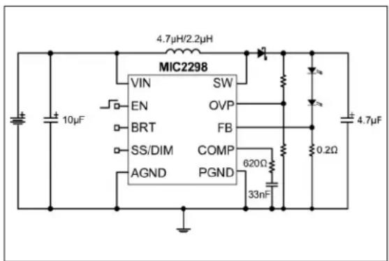
MIC2298 High Power White LED Driver 4.7μH / 2.2μH MIC2298 VIN SW EN OVP BRT FB SS/DIM COMP AGND PGND 620Ω 33nF 0.2Ω + + 4.7μF 10μFFunctional Block Diagram
text_image
MIC2298 VIN EN OVP SW 1.25V Bandgap 10k 2k 32k 30k 8k BRT SS / DIM 200mV Typ. FB 30k 1mS OVP CL Thermal UVLO Bandgap Fault Block OSC S Q Driver x2 M PWM Engine AGND COMP PGND1.0 ELECTRICAL CHARACTERISTICS
Absolute Maximum Ratings †
Supply Voltage ( V_IN ) 12V
Switch Voltage ( V_SW )....-0.3V to 34V
BRT Voltage ( V_BRT )....-0.3V to 6V
SS/DIM Voltage ( V_SS )....-0.3V to 6V
Enable Voltage ( V_EN )....-0.3V to 12V
FB Voltage ( V_FB ) 6V
Switch Current ( I_SW ) 6A
ESD Rating (Note 1)....2kV
Operating Ratings ‡
Supply Voltage ( V_IN ) 2.5V to 10V
BRT Voltage ( V_BRT ). 0V to 0.6 V_IN
Enable Voltage ( V_EN )....0V to V_IN
Output Voltage ( V_OUT ) V_IN + 1 to V_OVP
† Notice: Stresses above those listed under “Absolute Maximum Ratings” may cause permanent damage to the device. This is a stress rating only and functional operation of the device at those or any other conditions above those indicated in the operational sections of this specification is not intended. Exposure to maximum rating conditions for extended periods may affect device reliability.
‡ Notice: The device is not guaranteed to function outside its operating ratings.
Note 1: Devices are ESD sensitive. Handling precautions recommended..
ELECTRICAL CHARACTERISTICS (Note 1)
| T_A=25°C; V_IN=V_EN=3.6V; V_OUT=7V; I_OUT=1A, unless otherwise noted. Bold values indicate -40°C < T_J< +125°C. | ||||||
| Parameters Sym. Min. Typ. Max. Units Conditions | ||||||
| Supply Voltage Range V | IN | 2.5 | 10 | V | — | |
| Under-voltage Lockout | \(V_UVLO | 1.8 | 2.1 | 2.4 | V | — |
| Over-voltage Protection | V_OVP | 12 | 13.5 | 15 | V | — |
| Quiescent Current | I_VIN | — | 15 | 23 | mA V | FB >200 mV, Not Switching |
| Shutdown Current | I_SD | — 0.1 | 1 | μA V | V | EN = 0V (Note 2) |
| Feedback Voltage | V_FB | 184 | 200 | 216 | mV | (±8%) |
| 180 | — | 220 | (±10%) (Over Temp) | |||
| Feedback Input Curent | I_FB | — | -650 | — | nA | V_FB=200 mV |
| Line Regulation | — | 0.5 | — | % | 2.5V ≤ V_IN ≤ 4.5V | |
| BRT Accuracy (Note 3) | I_LED | 17 | 20 | 23 | % | R_BRT=GND |
| 45 | 50 | 55 | R_BRT=50K | |||
| Maximum Duty Cycle | D_MAX | 85 | 90 | — | % | — |
| Switch Current Limit | I_SW | 3.5 | 4.75 | 8 | A | V_IN=3V |
| Switch Saturation Voltage | V_SW | — | 350 | 500 | mV V | IN = 3.6V, I_SW =3.5A |
Note 1: Specification for packaged product only.
2: I_SD = I_VIN
3: As percentage of full brightness where V_IN = V_BRT = 3.6V (100% brightness)
ELECTRICAL CHARACTERISTICS (Note 1) (CONTINUED)
| T_A=25°C; V_IN=V_EN=3.6V; V_OUT=7V; I_OUT=1A, unless otherwise noted. Bold values indicate -40°C < T_J< +125°C. | ||||||
| Parameters | Sym. | Min. | Typ. | Max. | Units | Conditions |
| Switch Leakage Current I | SW | — 0.01 10 μA V | EN=0V, \(V_SW=15V | |||
| Enable Threshold V | EN | 1.5 — — | V | Turn On | ||
| — — 0.4 Turn Off | ||||||
| Enable Pin Current I | EN | — 20 40 μA V | EN=10V | |||
| Oscillator Frequency | f_SW | 0.8 1 | 1.2 MHz | — | ||
| Soft Start (SS) / DIM Current | I_SS | — | 5 | — μA | DIM=0V | |
| Overtemperature Threshold Shutdown | T_J | — | 150 — | °C — | ||
| — 10 — | °C | Hysteresis | ||||
Note 1: Specification for packaged product only.
2: I_SD = I_VIN
3: As percentage of full brightness where V_IN = V_BRT = 3.6V (100% brightness)
TEMPERATURE SPECIFICATIONS
| Parameters | Sym. | Min. | Typ. | Max. | Units | Conditions |
| Operating Junction Temperature Range | T_J | -40 | — | +125 | °C | — |
| Ambient Storage Temperature Range | T_S | -65 | — | +150 | °C | — |
| Thermal Resistance: 12-Lead 3 mm × 3 mm VDFN | θ_JA | — | +60 | — | °C/W | — |
2.0 TYPICAL PERFORMANCE CURVES
Note: The graphs and tables provided following this note are a statistical summary based on a limited number of samples and are provided for informational purposes only. The performance characteristics listed herein are not tested or guaranteed. In some graphs or tables, the data presented may be outside the specified operating range (e.g., outside specified power supply range) and therefore outside the warranted range.
line
| INPUT VOLTAGE (V) | INPUT CURRENT (mA) | | ----------------- | ------------------ | | 0 | 0 | | 2 | 16 | | 4 | 12 | | 6 | 11.5 | | 8 | 11.5 | | 10 | 11.5 | | 12 | 11.5 |FIGURE 2-1: Input Current vs. Input Voltage.

line
| TEMPERATURE (°C) | SWITCHING FREQUENCY (MHz) | | ---------------- | -------------------------- | | -40 | 0.8 | | -20 | 0.9 | | 0 | 1.0 | | 20 | 1.05 | | 40 | 1.1 | | 60 | 1.15 | | 80 | 1.2 |FIGURE 2-4: Switching Frequency vs. Temperature.

line
| TEMPERATURE (°C) | UVLO (V) | | ---------------- | -------- | | -40 | 2.2 | | 80 | 2.1 |FIGURE 2-2: UVLO vs. Temperature.

line
| INPUT VOLTAGE (V) | LED CURRENT (A) | | ----------------- | --------------- | | 3.5 | 0.208 | | 4.0 | 0.205 | | 4.5 | 0.202 | | 5.0 | 0.200 | | 5.5 | 0.198 | | 6.0 | 0.196 |FIGURE 2-5: LED Current vs. Input Voltage (BRT GND).

line
| INPUT VOLTAGE (V) | SWITCHING FREQUENCY (MHz) | | ----------------- | -------------------------- | | 3 | 0.9 | | 4 | 0.95 | | 5 | 0.98 | | 6 | 1.0 | | 7 | 1.02 | | 8 | 1.05 | | 9 | 1.08 | | 10 | 1.1 |FIGURE 2-3: Switching Frequency vs. Input Voltage.

line
| INPUT VOLTAGE (V) | LED CURRENT (A) | | ----------------- | --------------- | | 3.0 | 0.97 | | 3.5 | 0.98 | | 4.0 | 0.985 | | 4.5 | 0.99 | | 5.0 | 0.99 | | 5.5 | 0.99 | | 6.0 | 0.99 |FIGURE 2-6: LED Current vs. Input Voltage (BRT Open).
line
| DIM VOLTAGE (mV) | LED CURRENT (mA) | |---|---| | 0 | 0 | | 40 | 250 | | 80 | 500 | | 120 | 750 | | 160 | 900 | | 200 | 1000 |FIGURE 2-7: LED Current vs. SS/DIM Voltage.

line
| OUTPUT VOLTAGE (V) | 25°C OUTPUT CURRENT (A) | 50°C OUTPUT CURRENT (A) | | ------------------ | ---------------------- | ---------------------- | | 6 | 0.9 | 0.9 | | 8 | 0.7 | 0.6 | | 10 | 0.5 | 0.4 | | 12 | 0.4 | 0.3 |FIGURE 2-10: Max DC LED Current vs. Output Voltage.

line
| INPUT VOLTAGE (V) | EFFICIENCY (%) | | ----------------- | -------------- | | 3.0 | 75 | | 3.5 | 85 | | 4.0 | 88 | | 4.5 | 90 | | 5.0 | 91 | | 5.5 | 92 | | 6.0 | 93 |FIGURE 2-8: Efficiency vs. Input Voltage (BRT Open).
line
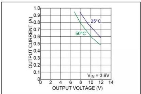
| OUTPUT VOLTAGE (V) | OUTPUT CURRENT (A) at 25°C | OUTPUT CURRENT (A) at 50°C | | ------------------ | -------------------------- | -------------------------- | | 8 | 0.9 | 0.9 | | 10 | 0.7 | 0.6 | | 12 | 0.6 | 0.5 |FIGURE 2-11: Max DC LED Current vs. Output Voltage.
line
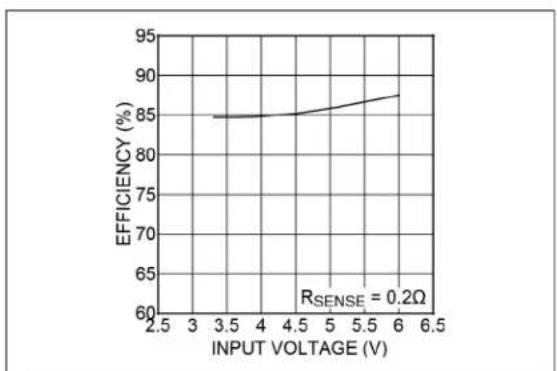
| INPUT VOLTAGE (V) | EFFICIENCY (%) | | ----------------- | -------------- | | 3.5 | 85 | | 4.0 | 85 | | 4.5 | 85 | | 5.0 | 86 | | 5.5 | 87 | | 6.0 | 88 |FIGURE 2-9: Efficiency vs. Input Voltage (BRT GND).
line
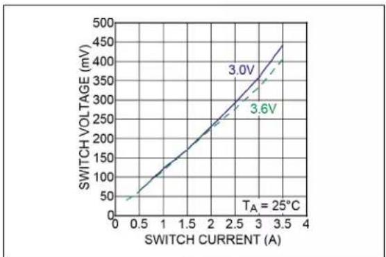
| SWITCH CURRENT (A) | SWITCH VOLTAGE (mV) | | ------------------ | ------------------- | | 0.5 | 50 | | 1.0 | 100 | | 1.5 | 150 | | 2.0 | 200 | | 2.5 | 250 | | 3.0 | 300 | | 3.5 | 350 | | 4.0 | 400 |FIGURE 2-12: Bipolar Saturation Voltage vs. Switch Current.
line
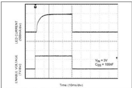
| Time (10ms/div) | LED CURRENT (500mA/div) | ENABLE VOLTAGE (1V/div) | | --------------- | ------------------------ | ----------------------- | | 0 | 0 | 0 | | 1 | High | Low | | 2 | High | Low | | 3 | High | Low | | 4 | High | Low | | 5 | High | Low | | 6 | High | Low | | 7 | High | Low | | 8 | High | Low | | 9 | High | Low | | 10 | High | Low | | 11 | High | Low | | 12 | High | Low | | 13 | High | Low | | 14 | High | Low | | 15 | High | Low | | 16 | High | Low | | 17 | High | Low | | 18 | High | Low | | 19 | High | Low | | 20 | High | Low | | 21 | High | Low | | 22 | High | Low | | 23 | High | Low | | 24 | High | Low | | 25 | High | Low | | 26 | High | Low | | 27 | High | Low | | 28 | High | Low | | 29 | High | Low | | 30 | High | Low | | 31 | High | Low | | 32 | High | Low | | 33 | High | Low | | 34 | High | Low | | 35 | High | Low | | 36 | High | Low | | 37 | High | Low | | 38 | High | Low | | 39 | High | Low | | 40 | High | Low | | 41 | High | Low | | 42 | High | Low | | 43 | High | Low | | 44 | High | Low | | 45 | High | Low | | 46 | High | Low | | 47 | High | Low | | 48 | High | Low | | 49 | High | Low | | 50 | High | Low | | 51 | High | Low | | 52 | High | Low | | 53 | High | Low | | 54 | High | Low | | 55 | High | Low | | 56 | High | Low | | 57 | High | Low | | 58 | High | Low | | 59 | High | Low | | 60 | High | Low | | 61 | High | Low | | 62 | High | Low | | 63 | High | Low | | 64 | High | Low | | 65 | High | Low | | 66 | High | Low | | 67 | High | Low | | 68 | High | Low | | 69 | High | Low | | 70 | High | Low | | 71 | High | Low | | 72 | High | Low | | 73 | High | Low | | 74 | High | Low | | 75 | High | Low | | 76 | High | Low | | 77 | High | Low | | 78 | High | Low | | 79 | High | Low | | 80 | High | Low | | 81 | High | Low | | 82 | High | Low | | 83 | High | Low | | 84 | High | Low | | 85 | High | Low | | 86 | High | Low | | 87 | High | Low | | 88 | High | Low | | 89 | High | Low | | 90 | High | Low | | 91 | High | Low | | 92 | High | Low | | 93 | High | Low | | 94 | High | Low | | 95 | High | Low | | 96 | High | Low | | 97 | High | Low | | 98 | High | Low | | 99 | High | Low | | 100 | High (min) | - | | V_IN | - | - | | C_SS | - | - | | VIN | - | - | | CSS | - | - | | (min) I end (max) endFIGURE 2-13: Enable (1A LED).
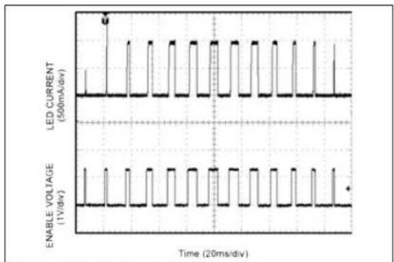
FIGURE 2-15: Enable (Frequency = 67 Hz).

line
| Time (400μs/div) | LED CURRENT (500m/div) | ENABLE VOLTAGE (1V/div) | | ---------------- | ---------------------- | ---------------------- | | 0 | 0 | 0 | | Peak | 3 | 3 | | End | 3 | 3 |FIGURE 2-14: Enable (1A LED).

line
| Time (200ns/div) | OUTPUT VOLTAGE (200mV/div) | INDUCTOR CURRENT (200mA/div) | SWITCH VOLTAGE (5V/div) | | ---------------- | --------------------------- | ---------------------------- | ----------------------- | | 0 | 0 | 0 | 0 | | 1 | 1 | 1 | 1 | | 2 | 0 | 0 | 0 | | 3 | -1 | -1 | -1 | | 4 | 0 | 0 | 0 | | 5 | 1 | 1 | 1 | | 6 | 0 | 0 | 0 | | 7 | -1 | -1 | -1 | | 8 | 0 | 0 | 0 | | 9 | 1 | 1 | 1 | | 10 | 0 | 0 | 0 | | 11 | -1 | -1 | -1 | | 12 | 0 | 0 | 0 | | 13 | 1 | 1 | 1 | | 14 | 0 | 0 | 0 | | 15 | -1 | -1 | -1 | | 16 | 0 | 0 | 0 | | 17 | 1 | 1 | 1 | | 18 | 0 | 0 | 0 | | 19 | -1 | -1 | -1 | | 20 | 0 | 0 | 0 | | 21 | 1 | 1 | 1 | | 22 | 0 | 0 | 0 | | 23 | -1 | -1 | -1 | | 24 | 0 | 0 | 0 | | 25 | 1 | 1 | 1 | | 26 | 0 | 0 | 0 | | 27 | -1 | -1 | -1 | | 28 | 0 | 0 | 0 | | 29 | 1 | 1 | 1 | | 30 | 0 | 0 | 0 | | 31 | -1 | -1 | -1 | | 32 | 0 | 0 | 0 | | 33 | 1 | 1 | 1 | | 34 | 0 | 0 | 0 | | 35 | -1 | -1 | -1 | | 36 | 0 | 0 | 0 | | 37 | 1 | 1 | 1 | | 38 | 0 | 0 | 0 | | 39 | -1 | -1 | -1 | | 40 | 0 | 0 | 0 | | 41 | 1 | 1 | 1 | | 42 | 0 | 0 | 0 | | 43 | -1 | -1 | -1 | | 44 | 0 | 0 | 0 | | 45 | 1 | 1 | 1 | | 46 | 0 | 0 | 0 | | 47 | -1 | -1 | -1 | | 48 | 0 | 0 | 0 | | 49 | 1 | 1 | 1 | | 50 | 0 | 0 | 0 | | Note: The output voltage values are not provided in the code. The input and switch voltages are calculated based on the input noise and the output current is calculated using the inductor current. There is only one data series in this case. The output current is calculated using the switch voltage. Since the input current is calculated by subtracting the output current from the inductor current. The output current is calculated by subtracting the switch voltage from the inductor current. The output current is calculated by subtracting the switch voltage from the inductor current. The output current is calculated by subtracting the switch voltage from the inductor current. Since the input current is calculated by subtracting the switch voltage from the inductor current. Since the output current is calculated by subtracting the switch voltage from the inductor current. The output current is calculated by subtracting the switch voltage from the inductor current. The output current is calculated by subtracting the switch voltage from the inductor current. Since the input current is calculated by subtracting the switch voltage from the inductor current. Since the output current is calculated by subtracting the switch voltage from the inductor current. Since the output current is calculated by subtracting the switch voltage from the inductor current. Since the output current is calculated by subtracting the switch voltage from the inductor current. Since the output current is calculated by subtracting the switch voltage from the inductor current. Since the output current is calculated by subtracting the switch voltage from the inductor current. Since the output current is calculated by subtracting the switch voltage. Since the output current is calculated by subtracting the switch voltage from the inductor current.FIGURE 2-16: Switching.
3.0 PIN DESCRIPTIONS
The descriptions of the pins are listed in Table 3-1.
TABLE 3-1: PIN FUNCTION TABLE
| Pin Number | Pin Name | Description |
| 1 | BRT | BRT (input): Apply a voltage greater than or equal to 1V to achieve full brightness current as determined by the ballast resistor. A 10 μA current source sets the voltage on the resistor. Hence a 50K resistor would yield 0.5V, which causes a reduction in LED current to 50% of full brightness. Grounding the BRT reduces the current further to 20% of full brightness. This pin may also be driven by a PWM signal for the same effect. |
| 2 | SS/DIM | Soft start/dimming (input) 40 kΩ source. Connect a capacitor to GND for soft start. Clamp the pin to a known voltage to control the internal reference voltage and hence the output current. This can also be done with a resistor to GND. |
| 3 | FB | Feedback (Input): Output voltage sense node. Connect the cathode of the LED to this pin. |
| 4 | AGND | Analog Ground. |
| 5, 6 | PGND | Power Ground. |
| 7, 8 | SW | Switch Node: Internal power BIPOLAR collector. |
| 9 | OVP | Over-Voltage Protection (OVP): Connect to the output voltage to clamp the maximum output voltage. A resistor divider from this pin to ground could be used to raise the OVP level beyond 15V (max). |
| 10 | VIN | Supply (Input): 2.5V to 10V for internal circuitry. |
| 11 | EN | Enable (Input): Applying 1.5V or greater enables the regulator. Applying a voltage of 0.4V or less disables the MIC2298. |
| 12 | COMP | Compensation pin (input): Add external R and C to GND to stabilize the converter. |
| Pad | EP | Ground (Return): Backside exposed pad. |
4.0 FUNCTIONAL DESCRIPTION
The MIC2298 is a constant frequency, pulse-width modulated (PWM) peak current-mode step-up regulator. The MIC2298 simplified control scheme is illustrated in the Functional Block Diagram. A reference voltage is fed into the PWM engine, where the duty cycle output of the constant frequency PWM engine is computed from the error, or difference, between the REF and FB voltages.
The PWM engine encompasses the necessary circuit blocks to implement a current-mode boost switch-mode power supply. The necessary circuit blocks include, but are not limited to, a oscillator/ramp generator, slope compensation ramp generator, gm error amplifier, current amplifier, PWM comparator, and drive logic for the internal 3.5A bipolar power transistor.
Inside the PWM engine, the oscillator functions as a trigger for the PWM comparator that turns on the bipolar power transistor and resets the slope compensation ramp generator.
The current amplifier is used to measure the power transistor's current by amplifying the voltage signal from the CS+ and CS- inputs from the sense resistor connected to the emitter of the bipolar power transistor. The output of the current amplifier is summed with the output of the slope compensation ramp generator where the result is connected to one of the inputs of the PWM comparator.
The gm error amplifier measures the white LED current through the external sense resistor and amplifies the error between the detected voltage signal from the feedback, or FB pin and the internal reference voltage. The output of the gm error amplifier provides the voltage loop signal that is fed to the other input of the PWM comparator.
When the current loop signal exceeds the voltage loop signal, the PWM comparator turns off the power transistor. The next oscillator or clock period initiates the next switching cycle, maintaining the constant frequency current-mode PWM control. The maximum white LED current is set by the feedback resistor (the resistor connected from the feedback pin to ground):
EQUATION 4-1:
$$ I _ {L E A K} = \frac {2 0 0 m V}{R _ {F B}} $$
The enable pin shuts down the output switching and disables control circuitry to reduce input current-to-leakage levels. Enable pin input current is zero at zero volts.
4.1 DC-to-DC PWM Boost Conversion
The MIC2298 is a constant-frequency boost converter. It operates by taking a DC input voltage and regulating a DC output voltage. Figure 4-1 shows a typical circuit. Boost regulation is achieved by turning on an internal switch, which draws current through the inductor (L1).
When the switch turns off, the inductor's magnetic field collapses. This causes the current to be discharged into the output capacitor through an external Schottky diode (D1). Figure 2-16 shows Input Voltage ripple, Output Voltage ripple, SW Voltage, and Inductor Current for 900 mA LED current. Regulation is achieved by modulating the pulse width i.e., pulse-width modulation (PWM).

text_image
4.7μH / 2.2μH L1 MIC2298 VIN SW EN OVP BRT FB SS/DIM COMP AGND PGND D1 0.2Ω R2 620Ω C4 33nF + 10μF + 4.7μFFIGURE 4-1: Typical Application Circuit.
4.2 Duty Cycle Considerations
Duty cycle refers to the switch on-to-off time ratio and can be calculated as follows for a boost regulator:
EQUATION 4-2:
$$ D = 1 - \frac {V _ {I N}}{V _ {O U T}} $$
However, at light loads, the inductor will completely discharge before the end of a switching cycle. The current in the inductor reaches 0A before the end of the switching cycle. This is known as discontinuous conduction mode (DCM). DCM occurs when:
EQUATION 4-3:
$$ I < \frac {V _ {I N}}{V _ {O U T}} \times \frac {I _ {P E A K}}{2} $$
Where:
EQUATION 4-4:
$$ I _ {P E A K} = \frac {(V _ {O U T} - V _ {I N})}{L \times f} \times \left(\frac {V _ {I N}}{V _ {O U T}}\right) $$
In DCM, the duty cycle is smaller than in continuous conduction mode. In DCM, the duty cycle is given by:
EQUATION 4-5:
$$ D = \frac {f \times \sqrt {2 \times L \times I _ {O U T} \times (V _ {O U T} - V _ {I N})}}{V _ {I N}} $$
The duty cycle required for voltage conversion should be less than the maximum duty cycle of 95%. Also, in light load conditions where the input voltage is close to the output voltage, the minimum duty cycle can cause pulse skipping. This is due to the energy stored in the inductor causing the output to slightly overshoot the regulated output voltage.
During the next cycle, the error amplifier detects the output as being high and skips the following pulse. This effect can be reduced by increasing the minimum load or by increasing the inductor value. Increasing the inductor value also reduces the peak current.
4.3 Over-Voltage Protection
The MIC2298 offers over-voltage protection functionality. If an LED is disconnected from the circuit or the feedback pin is shorted to ground, the feedback pin will fall to ground potential. This will cause the MIC2298 to switch at full duty cycle in an attempt to maintain the feedback voltage. As a result, the output voltage will climb out of control.
This may cause the switch node voltage to exceed its maximum voltage rating, possibly damaging the IC and the external components. To ensure the highest level of protection, the MIC2298 OVP pin will shut the switch off when an over-voltage condition is detected, saving itself and the output capacitor from damage.
The OVP threshold can be increased by adding a resistor divider between the output and ground. Be careful not to exceed the 30V rating of the switch.
text_image
4.7μH/2.2μH MIC2298 VIN SW EN OVP BRT FB SS/DIM COMP AGND PGND 620Ω 33nF 0.2Ω 10μF 4.7μFFIGURE 4-2: Adjustable OVP Circuit.
4.4 Brightness Control
TABLE 4-1: BRT PIN BRIGHTNESS FUNCTIONALITY
| BRT Pin | V_FB (V) |
| OPEN | 200 mV or V_SS/DIM |
| GND | 40 mV |
| ≥20 kΩ to 100 kΩ [ R_BRT ] to GND | (10 μA × R_BRT )/5 |
TABLE 4-2: SS/DIM PIN BRIGHTNESS FUNCTIONALITY
| SS/DIM | V_FB (V) |
| OPEN | 200 mV |
| Voltage v | V_FB = v |
The MIC2298 has built in brightness/dimming functionally for white LED applications. The BRT and SS/DIM pins are available for brightness/dimming control functionality. Table 4-1 and Table 4-2 illustrate the different modes of dimming functionality afforded by the BRT and SS/DIM pins. The resulting LED current is then calculated as:
EQUATION 4-6:
$$ I _ {L E D} = \frac {V _ {F B}}{R _ {S E N S E}} $$
Hence, a 200 mΩ sense resistor will achieve nominally 1A when both SS/DIM and BRT pins are left open.
4.5 PWM Control of Brightness
A control signal can be driven into the enable pin to vary average current through the LED for applications not sensitive to low frequency ( 100 Hz) light modulation.
For such applications, the SS/DIM pin capacitance should be minimized to achieve a fast turn on time. 0 nF will achieve approximately 1.5 ms with a C COMP value of 33 nF.
For other applications, where no analog control voltage is available, the BRT pin can be driven through a low pass filter (18 kΩ and 470 nF) at a PWM frequency of >5kHz to set the FB voltage, and therefore, the LED current from 20% to 100% of Nominal LED current (Figure 4-3).

text_image
4.7μH / 2.2μH MIC2298 VIN SW EN OVP BRT FB SS/DIM COMP AGND PGND 620Ω 33nF 0.2Ω 10μF 18kΩ 470nF 2.5V 0% - 200mA 30% - 1A 4.7μFFIGURE 4-3: High Frequency PWM Programming via BRT Pin.
Since the SS/DIM pin is typically utilized for soft start, it is recommended to use the enable and BRT pins for the PWM method of adjusting the average LED current. Figure 4-4 and Figure 4-5 show typical results for this method.
line
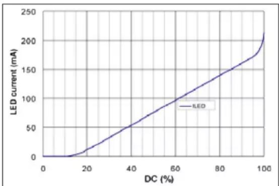
| DC (%) | LED current (mA) | | ------ | ---------------- | | 0 | 0 | | 20 | 20 | | 40 | 60 | | 60 | 100 | | 80 | 150 | | 100 | 210 |FIGURE 4-4: LED Current vs. DC (on Enable Pin).

line
| Duty Cycle at BRT input (%) | LED (Vpk=2.7V) (mA) | LED (Vpk=2.8V) (mA) | LED (Vpk=2.9V) (mA) | |---|---|---|---| | 0 | 200 | 200 | 200 | | 5 | 350 | 340 | 330 | | 10 | 500 | 490 | 480 | | 15 | 650 | 640 | 630 | | 20 | 800 | 790 | 780 | | 25 | 950 | 940 | 930 | | 30 | 1020 | 1010 | 1000 | | 35 | 1020 | 1010 | 1000 |FIGURE 4-5: LED Current vs. DC (on BRT Pin).
Should the SS/DIM pin be used for voltage programming the LED current, note that there will be a small offset due mismatches between the 30k FB input and the impedance driving the SS/DIM pin.
4.6 Soft Start Functionality
The soft start time is dependent up on both CSS and the comp capacitor values. C_COMP is fixed for stable operation (typically 33 nF); therefore, if any increases in soft start are desired, this should be done using the CSS capacitor. The approximate total startup time is given by the larger of:
EQUATION 4-7:
$$ T _ {S S} \quad 1 m s 1 7 5 k C \times + = _ {S S} $$
Or:
EQUATION 4-8:
$$ T _ {S S} \quad 1 m s G = _ {C O M P} \div 4 4 k 0 ^ {6 -} $$
For example: For C_COMP = 33 nF, use values of C_COMP > 4.3 nF to increase startup time from 1.75 ms. The soft start capacitor should be connected from the SS/DIM pin to ground.
5.0 COMPONENT SELECTION
5.1 Inductor
Inductor selection is a balance between efficiency, stability, cost, size, and rated current. For most applications, a 4.7 H is the recommended inductor value. It is usually a good balance between these considerations. Larger inductance values reduce the peak-to-peak ripple current, affecting efficiency.
This has the effect of reducing both the DC losses and the transition losses. There is also a secondary effect of an inductor's DC resistance (DCR). The DCR of an inductor will be higher for more inductance in the same package size. This is due to the longer windings required for an increase in inductance.
Since the majority of input current (minus the MIC2298 operating current) is passed through the inductor, higher DCR inductors will reduce efficiency. To maintain stability, increasing inductor size will have to be met with an increase in output capacitance. This is due to the unavoidable "right half plane zero" effect for the continuous current boost converter topology.
The frequency at which the right half plane zero occurs can be calculated as follows:
EQUATION 5-1:
$$ f _ {r h p z} = \frac {(V _ {I N}) ^ {2}}{V _ {O U T} \times L \times I _ {O U T} \times 2 \pi} $$
The right half plane zero has the undesirable effect of increasing gain, while decreasing phase. This requires that the loop gain is rolled off before this has significant effect on the total loop response. This can be accomplished by either reducing inductance (increasing RHPZ frequency) or increasing the output capacitor value (decreasing loop gain).
5.2 Output Capacitor
Output capacitor selection is also a trade-off between performance, size, and cost. Increasing output capacitance will lead to an improved transient response, but also an increase in size and cost. X5R or X7R dielectric ceramic capacitors are recommended for designs with the MIC2298.
The output capacitor sets the frequency of the dominant pole and zero in the power stage. The zero is given by:
EQUATION 5-2:
$$ f _ {z} = \frac {1}{C \cdot R _ {e s r} \times 2 \pi} $$
For ceramic capacitors, the ESR is very small. This puts the zero at a very high frequency where it can be ignored. Fortunately, the MIC2298 is current mode in operation which reduces the need for this output capacitor zero when compensating the feedback loop.
The frequency of the pole caused by the output capacitor is given by.
EQUATION 5-3:
$$ f _ {p} = \frac {I _ {O U T}}{C \times V _ {O U T} \times 2 \times \pi} $$
5.3 Diode Selection
The MIC2298 requires an external diode for operation. A Schottky diode is recommended for most applications due to their lower forward voltage drop and reverse recovery time. Ensure the diode selected can deliver the peak inductor current and the maximum reverse voltage is rated greater than the output voltage.
5.4 Input Capacitor
A minimum 1 F ceramic capacitor with an X5R or X7R dielectric is recommended for designing with the MIC2298. Increasing input capacitance will improve performance and greater noise immunity on the source.
The input capacitor should be as close as possible to the inductor and the MIC2298, with short traces for good noise performance.
The MIC2298 utilizes a feedback pin to compare the LED current to an internal reference. The LED current is adjusted by selecting the appropriate feedback resistor value. The desired output current can be calculated as follows:
EQUATION 5-4:
$$ I _ {L E D} \quad \frac {0 . 2 V}{R} $$
5.5 Compensation
The comp pin is connected to the output of the voltage error amplifier. The voltage error amplifier is a transconductance amplifier. Adding a series RC-to-ground adds a zero at:
EQUATION 5-5:
$$ f _ {Z E R O} \quad \frac {1}{2 \pi R _ {2} C _ {4}} $$
The resistor typically ranges from 1 kΩ to 50 kΩ. The capacitor typically ranges from 1 nF to 100 nF.
Adding an optional capacitor from comp pin-to-ground adds a pole at approximately:
EQUATION 5-6:
$$ f _ {p o l e} \quad \frac {1}{2 \pi R _ {2} C _ {3}} $$
This capacitor typically ranges from 100 pF to 10 nF. Generally, an RC to ground is all that is needed. The RC should be placed as close as possible to the compensation pin. The capacitor should be a ceramic with a X5R, X7R, or COG dielectric. Refer to the MIC2298 evaluation board document for component location.
6.0 APPLICATION INFORMATION
6.1 Grounding
Both the AGND and PGND pins must be connected to the exposed backside pad. The exposed backside pad also improves thermal performance. A large ground plane decreases thermal resistance to ambient air.
6.2 Thermal Considerations and the SOA
The SOA (safe operating area) of the MIC2298 is shown in the typical characteristics sub-section. This graph represents the maximum continuous output power capability of the part when used in the evaluation board layout. An alternative layout with more copper area for heat sinking will increase the area under the SOA curve.
Note that the SOA is for continuous power and not peak power and is effectively a thermal limitation. The SOA is true for a time constant of approximately >1 second.
Therefore, any load transient with a period of < 3s can exceed the SOA curve power up to a maximum limited by the current limit of the MIC2298. Figure 6-1 shows the theoretical output current limit of the MIC2298 using the Evaluation Board inductor value of 4.7 H.

line
| Output Voltage (V) | VIN = 3.6V | VIN = 3.4V | VIN = 3.2V | VIN = 3.0V | | ------------------ | ---------- | ---------- | ---------- | ---------- | | 5 | 1.8 | 1.7 | 1.6 | 1.5 | | 5.5 | 1.7 | 1.6 | 1.5 | 1.4 | | 6 | 1.6 | 1.5 | 1.4 | 1.3 | | 6.5 | 1.5 | 1.4 | 1.3 | 1.2 | | 7 | 1.4 | 1.3 | 1.2 | 1.1 | | 7.5 | 1.3 | 1.2 | 1.1 | 1.0 | | 8 | 1.2 | 1.1 | 1.0 | 0.9 | | 8.5 | 1.1 | 1.0 | 0.9 | 0.8 | | 9 | 1.0 | 0.9 | 0.8 | 0.7 | | 9.5 | 0.9 | 0.8 | 0.7 | 0.6 | | 10 | 0.8 | 0.7 | 0.6 | 0.5 | | 10.5 | 0.7 | 0.6 | 0.5 | 0.4 | | 11 | 0.6 | 0.5 | 0.4 | 0.3 | | 11.5 | 0.5 | 0.4 | 0.3 | 0.2 | | 12 | 0.4 | 0.3 | 0.2 | 0.1 |FIGURE 6-1: Peak Output Current vs. V_OUT .
If our load is within these limits, it is possible to drive the load at some repetition rate or duty cycle (DC). This is allowed as long as we limit the RMS current to below the SOA limit.
The RMS current for a pulsed current is known to be:
EQUATION 6-1:
$$ I _ {R M S} = (I _ {P K - P K} \times \sqrt {D C}) + I _ {D C} $$
Where the current pulse I_PK-PK sits on a DC level of I_DC . This simplifies to the following when there is no DC level:
$$ I _ {R M S} = I _ {P K} \times \sqrt {D C} $$
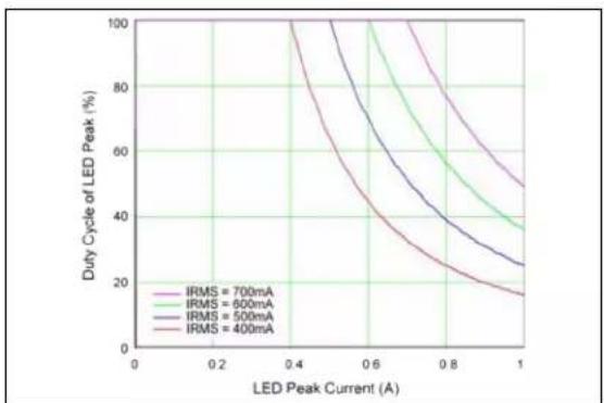
The graph in Figure 6-2 shows the peak LED current which can be pulsed at a given duty cycle (DC) to stay within SOA limits of 400 mA to 700 mA.
line
| LED Peak Current (A) | IRMS = 700mA | IRMS = 600mA | IRMS = 500mA | IRMS = 400mA | | -------------------- | ------------ | ------------ | ------------ | ------------ | | 0.0 | 100 | 100 | 100 | 100 | | 0.2 | ~98 | ~97 | ~96 | ~95 | | 0.4 | ~95 | ~93 | ~90 | ~85 | | 0.6 | ~90 | ~85 | ~75 | ~65 | | 0.8 | ~85 | ~75 | ~60 | ~50 | | 1.0 | ~80 | ~70 | ~55 | ~45 |FIGURE 6-2: Duty Cycle vs. Peak Current for Fixed RMS Current.
EXAMPLE 6-1:
Two high-brightness white LEDs connected in series with a V_f(MAX) of 4.2V and a peak current of 800 mA require pulses of 300 ms at 3 second intervals. The power source is a Li-ion cell of 3V minimum.
- Looking at the SOA curves in Figure 2-10 and Figure 2-11, these cannot be driven continuously.
- The time constant of the driver is < 3 seconds, so one can look at the peak current capability of the driver in Figure 6-1.
-
Looking at Figure 6-1, the MIC2298 can achieve more than the required 800mA peak current at 8.4V.
-
Reading from the SOA curve in Figure 2-10, the MIC2298 with V_IN = 3V , 50^ , and 8.4V output voltage can provide 580 mA RMS.
- Now looking at the curve in Figure 6-2, using the next lower value of 500mA RMS current, one can see that the 850mA peak can be driven at a duty cycle of 33% (or 1 second out of every 3 seconds). That is well within our target of 300~ms .
6.3 LED Protection
The operation of the Power LED must be limited to short pulses to prevent overheating. This is usually controlled by the micro controller in a typical application. For further protection, or where a micro controller is not used, the temperature of the LED can be limited by the addition of an NTC thermistor.
The value should be > 100 kΩ at its maximum safe temperature. This will then limit current drive to the LED as temperature rises further and prevents overheating. This thermistor should be connected directly from BRT to GND. Reference Figure 6-3.

text_image
4.7μH / 2.2μH MIC2298 VIN SW EN OVP COMP FB SS/DIM 8RT AGND PGND 10μF 620Ω 33nF 470kΩ 0.2Ω + 4.7μFFIGURE 6-3: LED Thermal Protection.
7.0 PACKAGING INFORMATION
7.1 Package Marking Information
12-Lead VDFN

text_image
XX XXXX NNNYExample
text_image
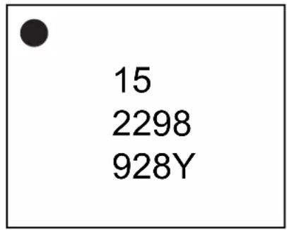
15 2298 928YTABLE 7-1: ORDERING INFORMATION
| Part Number OVP Frequency Junction Temp. Range Package | Lead Finish | ||||
| MIC2298-15YML | 15V | 1 MHz | -40^ to +125^ | 12-Lead 3 mm × 3 mm VDFN | Pb-Free |
Note: This VDFN is a GREEN RoHS compliant package. Lead finish is NiPdAu. Mold compound is Halogen Free.
PACKAGE MARKING DRAWING SYMBOLS LEGEND
| Symbol | Definition |
| XX . . . X | Product code or customer-specific information. (Note 1, Note 2) |
| YYWW | Date code, where YY is the last 2 digits of calendar year and WW is the work week (i.e., week of January 1 is week 01). (Note 3) |
| M | Month of assembly (if applicable). January is represented by “A” and each month thereafter follows the order of the alphabet through “L” for December. |
| NNN | Alphanumeric traceability code. (Note 3, Note 4) |
 | Pb-free JEDEC designator for Matte Tin (Sn). |
| * | Indicates this package is Pb-free. The Pb-free JEDEC designator (the symbol in the row above this one) can be found on the outer packaging for this package. |
| •, ▲, ▼ | Pin one index is identified by a dot, delta up, or delta down (triangle mark). |
| Note 1: If the full Microchip part number cannot fit on one line, it will be carried over to the next line, limiting the number of available characters for customer-specific information. The package may or may not include the corporate logo.2: Any underbar (_) and/or overbar (~) symbols shown in a package marking drawing may not be to scale.3: If the full date code (YYWW) and the alphanumeric traceability code (NNN)—usually marked together on the last or only line of a package marking as the seven-character YYWWNNN—cannot fit on the package together, the codes will be truncated based on the number of available character spaces, as follows:6 characters = YWWNNN; 5 characters = WWNNN; 4 characters = WNNN; 3 characters = NNN;2 characters = NN; 1 character = N.4: Some products might have a “Y” symbol at the end of the last or only line in a package marking, usually at the end of the alphanumeric traceability code (NNN or truncated versions), to indicate the product is Pb-free. | |
12-Lead 3 mm × 3 mm VDFN [JQA] Package Outline and Recommended Land Pattern
Note: For the most current package drawings, please see the Microchip Packaging Specification located at http://www.microchip.com/packaging
![Microchip MIC2298 - 12-Lead 3 mm × 3 mm VDFN [JQA] Package Outline and Recommended Land Pattern - 1](/content/2026/06/1221807/images/d2776d52c38aaf6931604396e2eeb1491888338a090532484c808f94a1d4e678.jpg)
text_image
(DATUM A) (DATUM B) NOTE 1 2X 0.05 C 2X 0.05 C TOP VIEW SEATING PLANE C A (A3) // 0.10 C SIDE VIEW A1 12X 0.05 C NOTE 1 D2 1 2 E2 K L N e 12X b BOTTOM VIEW ⊕ 0.10 MC A B ⊕ 0.10 MC A B ⊕ 0.05 MCMicrochip Technology Drawing C04-1020 Rev. A Sheet 1 of 2
12-Lead 3 mm × 3 mm VDFN [JQA] Package Outline and Recommended Land Pattern
Note: For the most current package drawings, please see the Microchip Packaging Specification located at http://www.microchip.com/packaging
![Microchip MIC2298 - 12-Lead 3 mm × 3 mm VDFN [JQA] Package Outline and Recommended Land Pattern - 1](/content/2026/06/1221807/images/92c9d80112a1aa4cf55dfced150c09501e16d2c47825ea614a78c75607e8f4a2.jpg)
natural_image
Technical line drawing of two integrated circuit chips with pinouts (no text or symbols)| Units | MILLIMETERS | |||
| Dimension Limits | MIN | NOM | MAX | |
| Number of Terminals | N | 12 | ||
| Pitch | e | 0.50 BSC | ||
| Overall Height | A | 0.80 | 0.85 | 0.90 |
| Standoff | A1 | 0.00 | 0.02 | 0.05 |
| Terminal Thickness | A3 | 0.203 REF | ||
| Overall Length | D | 3.00 BSC | ||
| Exposed Pad Length | D2 | 2.35 | 2.40 2.45 | |
| Overall Width | E | 3.00 BSC | ||
| Exposed Pad Width | E2 | 1.65 | 1.70 | 1.75 |
| Terminal Width | b | 0.18 | 0.23 | 0.28 |
| Terminal Length | L | 0.35 | 0.40 | 0.45 |
| K | - | |||
0.20 -Terminal-to-Exp
Notes:
- Pin 1 visual index feature may vary, but must be located within the hatched area.
- Package is saw singulated
- Dimensioning and tolerancing per ASME Y14.5M
BSC: Basic Dimension. Theoretically exact value shown without tolerances.
REF: Reference Dimension, usually without tolerance, for information purposes only.
Microchip Technology Drawing C04-1020 Rev. A Sheet 2 of 2
12-Lead 3 mm × 3 mm VDFN [JQA] Package Outline and Recommended Land Pattern
Note: For the most current package drawings, please see the Microchip Packaging Specification located at http://www.microchip.com/packaging
![Microchip MIC2298 - 12-Lead 3 mm × 3 mm VDFN [JQA] Package Outline and Recommended Land Pattern - 1](/content/2026/06/1221807/images/b92c66afee3d211fc1f0f9fb2d246f935c5b53fddabee41f83f3e4a0b44e738d.jpg)
text_image
X2 12 EV ØV C Y2 EV G1 Y1 SILK SCREEN 1 2 X1 ERECOMMENDED LAND PATTERN
| Units | MILLIMETERS | |||
| Dimension Limits | MIN | NOM | MAX | |
| Contact Pitch | E | 0.50 BSC | ||
| Optional Center Pad Width | X2 | 2.45 | ||
| Optional Center Pad Length | Y2 | 1.75 | ||
| CContact Pad Spacing 3.00 | ||||
| Contact Pad Width (X12) | X1 | 0.25 | ||
| Contact Pad Length (X12) | Y1 | 0.80 | ||
| Contact Pad to Center Pad (X12) | G1 0.20 | |||
| Thermal Via Diameter V 0.30 | ||||
| Thermal Via Pitch EV 1.00 | ||||
Notes:
- Dimensioning and tolerancing per ASME Y14.5M
BSC: Basic Dimension. Theoretically exact value shown without tolerances.
- For best soldering results, thermal vias, if used, should be filled or tented to avoid solder loss during reflow process
Microchip Technology Drawing C04-3020 Rev. A
NOTES:
APPENDIX A: REVISION HISTORY
Revision A (September 2023)
- Converted Micrel document MIC2298 to Microchip data sheet DS20006794A.
- Minor text changes throughout.
NOTES:
PRODUCT IDENTIFICATION SYSTEM
To order or obtain information, e.g., on pricing or delivery, contact your local Microchip representative or sales office.
PART No.
Device
-XX
Over-Voltage
Protection (max.)
X
Junction Temp.
Range
XX
Package Media Type
-XX
Device:
MIC2298: 3.5A Minimum, 1 MHz Boost High
Brightness White LED Driver
Over-Voltage Protection
(max.):
-15 = 15V
Junction Temperature
Range:
Y = -40^ to +125^
Package:
ML = 12-Lead 3 mm × 3 mm VDFN
Media Type:
-TR = 5000/Reel
Examples:
a) MIC2298-15YML-TR: MIC2298, 15V Over-Voltage
Protection (max.), -40^ to
+125°C Temp. Range,
12-Lead 3 mm × 3 mm VDFN
5000/Reel
Note 1: Tape and Reel identifier only appears in the catalog part number description. This identifier is used for ordering purposes and is not printed on the device package. Check with your Microchip Sales Office for package availability with the Tape and Reel option.
NOTES:
Note the following details of the code protection feature on Microchip products:
• Microchip products meet the specifications contained in their particular Microchip Data Sheet.
- Microchip believes that its family of products is secure when used in the intended manner, within operating specifications, and under normal conditions.
- Microchip values and aggressively protects its intellectual property rights. Attempts to breach the code protection features of Microchip product is strictly prohibited and may violate the Digital Millennium Copyright Act.
- Neither Microchip nor any other semiconductor manufacturer can guarantee the security of its code. Code protection does not mean that we are guaranteeing the product is "unbreakable" Code protection is constantly evolving. Microchip is committed to continuously improving the code protection features of our products.
This publication and the information herein may be used only with Microchip products, including to design, test, and integrate Microchip products with your application. Use of this information in any other manner violates these terms. Information regarding device applications is provided only for your convenience and may be superseded by updates. It is your responsibility to ensure that your application meets with your specifications. Contact your local Microchip sales office for additional support or, obtain additional support at https://www.microchip.com/en-us/support/design-help/client-support-services.
THIS INFORMATION IS PROVIDED BY MICROCHIP "AS IS". MICROCHIP MAKES NO REPRESENTATIONS OR WARRANTIES OF ANY KIND WHETHER EXPRESS OR IMPLIED, WRITTEN OR ORAL, STATUTORY OR OTHERWISE, RELATED TO THE INFORMATION INCLUDING BUT NOT LIMITED TO ANY IMPLIED WARRANTIES OF NON-INFRINGEMENT, MERCHANTABILITY, AND FITNESS FOR A PARTICULAR PURPOSE, OR WARRANTIES RELATED TO ITS CONDITION, QUALITY, OR PERFORMANCE.
IN NO EVENT WILL MICROCHIP BE LIABLE FOR ANY INDIRECT, SPECIAL, PUNITIVE, INCIDENTAL, OR CONSEQUENTIAL LOSS, DAMAGE, COST, OR EXPENSE OF ANY KIND WHATSOEVER RELATED TO THE INFORMATION OR ITS USE, HOWEVER CAUSED, EVEN IF MICROCHIP HAS BEEN ADVISED OF THE POSSIBILITY OR THE DAMAGES ARE FORESEEABLE. TO THE FULLEST EXTENT ALLOWED BY LAW, MICROCHIP'S TOTAL LIABILITY ON ALL CLAIMS IN ANY WAY RELATED TO THE INFORMATION OR ITS USE WILL NOT EXCEED THE AMOUNT OF FEES, IF ANY, THAT YOU HAVE PAID DIRECTLY TO MICROCHIP FOR THE INFORMATION.
Use of Microchip devices in life support and/or safety applications is entirely at the buyer's risk, and the buyer agrees to defend, indemnify and hold harmless Microchip from any and all damages, claims, suits, or expenses resulting from such use. No licenses are conveyed, implicitly or otherwise, under any Microchip intellectual property rights unless otherwise stated.
Trademarks
The Microchip name and logo, the Microchip logo, Adaptec, AVR, AVR logo, AVR Freaks, BesTime, BitCloud, CryptoMemory, CryptoRF, dsPIC, flexPWR, HELDO, IGLOO, JukeBlox, KeeLoq, Kleer, LANCheck, LinkMD, maXStylus, maXTouch, MediaLB, megaAVR, Microsemi, Microsemi logo, MOST, MOST logo, MPLAB, OptoLyzer, PIC, picoPower, PICSTART, PIC32 logo, PolarFire, Prochip Designer, QTouch, SAM-BA, SenGenuity, SpyNIC, SST, SST Logo, SuperFlash, Symmetricom, SyncServer, Tachyon, TimeSource, tinyAVR, UNI/O, Vectron, and XMEGA are registered trademarks of Microchip Technology Incorporated in the U.S.A. and other countries.
AgileSwitch, APT, ClockWorks, The Embedded Control Solutions Company, EtherSynch, Flashtec, Hyper Speed Control, HyperLight Load, Libero, motorBench, mTouch, Powermite 3, Precision Edge, ProASIC, ProASIC Plus, ProASIC Plus logo, Quiet-Wire, SmartFusion, SyncWorld, Temux, TimeCesium, TimeHub, TimePictra, TimeProvider, TrueTime, and ZL are registered trademarks of Microchip Technology Incorporated in the U.S.A.
Adjacent Key Suppression, AKS, Analog-for-the-Digital Age, Any Capacitor, AnyIn, AnyOut, Augmented Switching, BlueSky, BodyCom, Clockstudio, CodeGuard, CryptoAuthentication, CryptoAutomotive, CryptoCompanion, CryptoController, dsPICDEM, dsPICDEM.net, Dynamic Average Matching, DAM, ECAN, Espresso T1S, EtherGREEN, GridTime, IdealBridge, In-Circuit Serial Programming, ICSP, INICnet, Intelligent Paralleling, IntelliMOS, Inter-Chip Connectivity, JitterBlocker, Knob-on-Display, KoD, maxCrypto, maxView, memBrain, Mindi, MiWi, MPASM, MPF, MPLAB Certified logo, MPLIB, MPLINK, MultiTRAK, NetDetach, Omniscient Code Generation, PICDEM, PICDEM.net, PICkit, PICtail, PowerSmart, PureSilicon, QMatrix, REAL ICE, Ripple Blocker, RTAX, RTG4, SAM-ICE, Serial Quad I/O, simpleMAP, SimpliPHY, SmartBuffer, SmartHLS, SMART-I.S., storClad, SQI, SuperSwitcher, SuperSwitcher II, Switchtec, SynchroPHY, Total Endurance, Trusted Time, TSHARC, USBCheck, VariSense, VectorBlox, VeriPHY, ViewSpan, WiperLock, XpressConnect, and ZENA are trademarks of Microchip Technology Incorporated in the U.S.A. and other countries.
SQTP is a service mark of Microchip Technology Incorporated in the U.S.A.
The Adaptec logo, Frequency on Demand, Silicon Storage Technology, and Symmcom are registered trademarks of Microchip Technology Inc. in other countries.
GestIC is a registered trademark of Microchip Technology Germany II GmbH & Co. KG, a subsidiary of Microchip Technology Inc., in other countries.
All other trademarks mentioned herein are property of their respective companies.
© 2023, Microchip Technology Incorporated and its subsidiaries.
All Rights Reserved.
ISBN: 978-1-6683-3108-8
For information regarding Microchip's Quality Management Systems, please visit www.microchip.com/quality.
Worldwide Sales and Service
AMERICAS
Corporate Office
2355 West Chandler Blvd.
Chandler, AZ 85224-6199
Tel: 480-792-7200
Fax: 480-792-7277
Technical Support:
http://www.microchip.com/
support
Web Address:
www.microchip.com
Atlanta
Duluth, GA
Tel: 678-957-9614
Fax: 678-957-1455
Austin, TX
Tel: 512-257-3370
Boston
Westborough, MA
Tel: 774-760-0087
Fax: 774-760-0088
Chicago
Itasca, IL
Tel: 630-285-0071
Fax: 630-285-0075
Dallas
Addison, TX
Tel: 972-818-7423
Fax: 972-818-2924
Detroit
Novi, MI
Tel: 248-848-4000
Houston, TX
Tel: 281-894-5983
Indianapolis
Noblesville, IN
Tel: 317-773-8323
Fax: 317-773-5453
Tel: 317-536-2380
Los Angeles
Mission Viejo, CA
Tel: 949-462-9523
Fax: 949-462-9608
Tel: 951-273-7800
Raleigh, NC
Tel: 919-844-7510
New York, NY
Tel: 631-435-6000
San Jose, CA
Tel: 408-735-9110
Tel: 408-436-4270
Canada - Toronto
Tel: 905-695-1980
Fax: 905-695-2078
ASIA/PACIFIC
Australia - Sydney
Tel: 61-2-9868-6733
China - Beijing
Tel: 86-10-8569-7000
China - Chengdu
Tel: 86-28-8665-5511
China - Chongqing
Tel: 86-23-8980-9588
China - Dongguan
Tel: 86-769-8702-9880
China - Guangzhou
Tel: 86-20-8755-8029
China - Hangzhou
Tel: 86-571-8792-8115
China - Hong Kong SAR
Tel: 852-2943-5100
China - Nanjing
Tel: 86-25-8473-2460
China - Qingdao
Tel: 86-532-8502-7355
China - Shanghai
Tel: 86-21-3326-8000
China - Shenyang
Tel: 86-24-2334-2829
China - Shenzhen
Tel: 86-755-8864-2200
China - Suzhou
Tel: 86-186-6233-1526
China - Wuhan
Tel: 86-27-5980-5300
China - Xian
Tel: 86-29-8833-7252
China - Xiamen
Tel: 86-592-2388138
China - Zhuhai
Tel: 86-756-3210040
ASIA/PACIFIC
India - Bangalore
Tel: 91-80-3090-4444
India - New Delhi
Tel: 91-11-4160-8631
India - Pune
Tel: 91-20-4121-0141
Japan - Osaka
Tel: 81-6-6152-7160
Japan - Tokyo
Tel: 81-3-6880-3770
Korea - Daegu
Tel: 82-53-744-4301
Korea - Seoul
Tel: 82-2-554-7200
Malaysia - Kuala Lumpur
Tel: 60-3-7651-7906
Malaysia - Penang
Tel: 60-4-227-8870
Philippines - Manila
Tel: 63-2-634-9065
Singapore
Tel: 65-6334-8870
Taiwan - Hsin Chu
Tel: 886-3-577-8366
Taiwan - Kaohsiung
Tel: 886-7-213-7830
Taiwan - Taipei
Tel: 886-2-2508-8600
Thailand - Bangkok
Tel: 66-2-694-1351
Tel: 43-7242-2244-39
Fax: 43-7242-2244-393
Denmark - Copenhagen
Tel: 45-4485-5910
Fax: 45-4485-2829
Finland - Espoo
Tel: 358-9-4520-820
France - Paris
Tel: 33-1-69-53-63-20
Fax: 33-1-69-30-90-79
Germany - Garching
Tel: 49-8931-9700
Germany - Haan
Tel: 49-2129-3766400
Germany - Heilbronn
Tel: 49-7131-72400
Germany - Karlsruhe
Tel: 49-721-625370
Germany - Munich
Tel: 49-89-627-144-0
Fax: 49-89-627-144-44
Germany - Rosenheim
Tel: 49-8031-354-560
Israel - Ra'anana
Tel: 972-9-744-7705
Italy - Milan
Tel: 39-0331-742611
Fax: 39-0331-466781
Italy - Padova
Tel: 39-049-7625286
Netherlands - Drunen
Tel: 31-416-690399
Fax: 31-416-690340
Norway - Trondheim
Tel: 47-7288-4388
Poland - Warsaw
Tel: 48-22-3325737
Romania - Bucharest
Tel: 40-21-407-87-50
Spain - Madrid
Tel: 34-91-708-08-90
Fax: 34-91-708-08-91
Sweden - Gothenberg
Tel: 46-31-704-60-40
Sweden - Stockholm
Tel: 46-8-5090-4654
UK - Wokingham
Tel: 44-118-921-5800
Fax: 44-118-921-5820