PIC18F86J93 - Electronic component Microchip - Free user manual and instructions
Find the device manual for free PIC18F86J93 Microchip in PDF.

User questions about PIC18F86J93 Microchip
0 question about this device. Answer the ones you know or ask your own.
Ask a new question about this device
Download the instructions for your Electronic component in PDF format for free! Find your manual PIC18F86J93 - Microchip and take your electronic device back in hand. On this page are published all the documents necessary for the use of your device. PIC18F86J93 by Microchip.
USER MANUAL PIC18F86J93 Microchip
PIC18F87J90 Family Data Sheet
64/80-Pin, High-Performance Microcontrollers with LCD Driver and nanoWatt Technology
Note the following details of the code protection feature on Microchip devices:
• Microchip products meet the specification contained in their particular Microchip Data Sheet.
- Microchip believes that its family of products is one of the most secure families of its kind on the market today, when used in the intended manner and under normal conditions.
- There are dishonest and possibly illegal methods used to breach the code protection feature. All of these methods, to our knowledge, require using the Microchip products in a manner outside the operating specifications contained in Microchip's Data Sheets. Most likely, the person doing so is engaged in theft of intellectual property.
• Microchip is willing to work with the customer who is concerned about the integrity of their code.
- Neither Microchip nor any other semiconductor manufacturer can guarantee the security of their code. Code protection does not mean that we are guaranteeing the product as "unbreakable."
Code protection is constantly evolving. We at Microchip are committed to continuously improving the code protection features of our products. Attempts to break Microchip's code protection feature may be a violation of the Digital Millennium Copyright Act. If such acts allow unauthorized access to your software or other copyrighted work, you may have a right to sue for relief under that Act.
Information contained in this publication regarding device applications and the like is provided only for your convenience and may be superseded by updates. It is your responsibility to ensure that your application meets with your specifications. MICROCHIP MAKES NO REPRESENTATIONS OR WARRANTIES OF ANY KIND WHETHER EXPRESS OR IMPLIED, WRITTEN OR ORAL, STATUTORY OR OTHERWISE, RELATED TO THE INFORMATION, INCLUDING BUT NOT LIMITED TO ITS CONDITION, QUALITY, PERFORMANCE, MERCHANTABILITY OR FITNESS FOR PURPOSE. Microchip disclaims all liability arising from this information and its use. Use of Microchip devices in life support and/or safety applications is entirely at the buyer's risk, and the buyer agrees to defend, indemnify and hold harmless Microchip from any and all damages, claims, suits, or expenses resulting from such use. No licenses are conveyed, implicitly or otherwise, under any Microchip intellectual property rights.
Trademarks
The Microchip name and logo, the Microchip logo, dsPIC, KEELOQ, KEELOQ logo, MPLAB, PIC, PICmicro, PICSTART, rfPIC and UNI/O are registered trademarks of Microchip Technology Incorporated in the U.S.A. and other countries.
FilterLab, Hampshire, HI-TECH C, Linear Active Thermistor, MXDEV, MXLAB, SEEVAL and The Embedded Control Solutions Company are registered trademarks of Microchip Technology Incorporated in the U.S.A.
Analog-for-the-Digital Age, Application Maestro, CodeGuard, dsPICDEM, dsPICDEM.net, dsPICworks, dsSPEAK, ECAN, ECONOMONITOR, FanSense, HI-TIDE, In-Circuit Serial Programming, ICSP, Mindi, MiWi, MPASM, MPLAB Certified logo, MPLIB, MPLINK, mTouch, Octopus, Omniscient Code Generation, PICC, PICC-18, PICDEM, PICDEM.net, PICkit, PICtail, PIC ^32 logo, REAL ICE, rfLAB, Select Mode, Total Endurance, TSHARC, UniWinDriver, WiperLock and ZENA are trademarks of Microchip Technology Incorporated in the U.S.A. and other countries.
SQTP is a service mark of Microchip Technology Incorporated in the U.S.A.
All other trademarks mentioned herein are property of their respective companies.
© 2010, Microchip Technology Incorporated, Printed in the U.S.A., All Rights Reserved.
Printed on recycled paper.
QUALITY MANAGEMENT SYSTEM CERTIFIED BY DNV
=ISO/TS 16949:2002=
Microchip received ISO/TS-16949:2002 certification for its worldwide headquarters, design and wafer fabrication facilities in Chandler and Tempe, Arizona; Gresham, Oregon and design centers in California and India. The Company's quality system processes and procedures are for its PIC® MCUs and dsPIC® DSCs, KEELoo® code hopping devices, Serial EEPROMs, microperipherals, nonvolatile memory and analog products. In addition, Microchip's quality system for the design and manufacture of development systems is ISO 9001:2000 certified.
64/80-Pin, High-Performance Microcontrollers with LCD Driver and nanoWatt Technology
LCD Driver and Keypad Interface Features:
- Direct LCD Panel Drive Capability:
- Can drive LCD panel while in Sleep mode
- Up to 48 Segments and 192 Pixels, Software Selectable
- Programmable LCD Timing module:
- Multiple LCD timing sources available
- Up to four commons: static, 1/2, 1/3 or 1/4 multiplex
- Static, 1/2 or 1/3 bias configuration
- On-Chip LCD Boost Voltage Regulator for Contrast Control
- Charge Time Measurement Unit (CTMU) for Capacitive Touch Sensing
• ADC for Resistive Touch Sensing
Low-Power Features:
• Power-Managed modes:
- Run: CPU On, Peripherals On
- Idle: CPU Off, Peripherals On
- Sleep: CPU Off, Peripherals Off
- Two-Speed Oscillator Start-up
Flexible Oscillator Structure:
- Two Crystal modes, 4-25 MHz
- Two External Clock modes, up to 48 MHz
• 4x Phase Lock Loop (PLL) - Internal Oscillator Block with PLL:
- Eight user-selectable frequencies from 31.25 kHz to 8 MHz
• Secondary Oscillator using Timer1 at 32 kHz - Fail-Safe Clock Monitor:
- Allows for safe shutdown if peripheral clock fails
Peripheral Highlights:
• High-Current Sink/Source 25 mA/25 mA (PORTB and PORTC)
- Up to Four External Interrupts
- Four 8-Bit/16-Bit Timer/Counter modules
- Two Capture/Compare/PWM (CCP) modules
- Master Synchronous Serial Port (MSSP) module with Two Modes of Operation:
- 3-Wire/4-Wire SPI (supports all four SPI modes)
- I ^2 C ^TM Master and Slave mode
• One Addressable USART module
- One Enhanced Addressable USART module:
- LIN/J2602 support
- Auto-wake-up on Start bit and Break character
- Auto-Baud Detect (ABD)
• 10-Bit, up to 12-Channel A/D Converter:
- Auto-acquisition
- Conversion available during Sleep
- Two Analog Comparators
- Programmable Reference Voltage for Comparators
- Hardware Real-Time Clock and Calendar (RTCC) with Clock, Calendar and Alarm Functions
- Charge Time Measurement Unit (CTMU):
- Capacitance measurement
- Time measurement with 1 ns typical resolution
Special Microcontroller Features:
- 10,000 Erase/Write Cycle Flash Program Memory, Typical
• Flash Retention 20 Years, Minimum
• Self-Programmable under Software Control
- Word Write Capability for Flash Program Memory for Data EEPROM Emulators
| Device | Flash Program Memory (Bytes) | SRAM Data Memory (Bytes) | I/O | LCD (Pixels) | Timers 8/16-Bit | CCP | MSSP | EUSART AUSART | 10-Bit A/D (Channels) | Comparators | BOR/LVD | RTCC | CTMU | |
| SPI | Master I^2C^TM | |||||||||||||
| PIC18F66J90 | 64K | 3,923 | 51 | 132 | 1/3 | 2 | Yes | Yes | 1/1 | 12 | 2 | Yes | Yes | Yes |
| PIC18F67J90 | 128K | 3,923 | 51 | 132 | 1/3 | 2 | Yes | Yes | 1/1 | 12 | 2 | Yes | Yes | Yes |
| PIC18F86J90 | 64K | 3,923 | 67 | 192 | 1/3 | 2 | Yes | Yes | 1/1 | 12 | 2 | Yes | Yes | Yes |
| PIC18F87J90 | 128K | 3,923 | 67 | 192 | 1/3 | 2 | Yes | Yes | 1/1 | 12 | 2 | Yes | Yes | Yes |
Special Microcontroller Features (Continued):
• Priority Levels for Interrupts
- 8 x 8 Single-Cycle Hardware Multiplier
- Extended Watchdog Timer (WDT):
- Programmable period from 4 ms to 131s
- In-Circuit Serial Programming™ (ICSP™) via Two Pins
• In-Circuit Debug via Two Pins - Operating Voltage Range: 2.0V to 3.6V
- 5.5V Tolerant Input (digital pins only)
- Selectable Open-Drain Configuration for Serial Communication and CCP Pins for Driving Outputs up to 5V
- On-Chip 2.5V Regulator
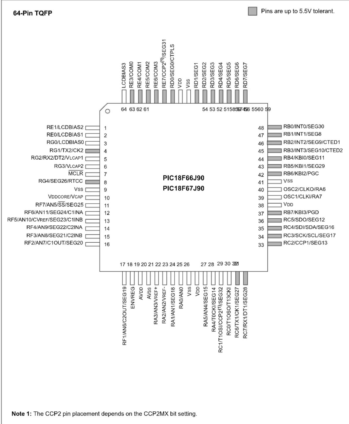
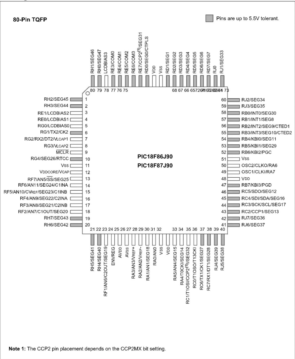
Pin Diagrams – PIC18F6XJ90
bar
64-Pin TQFP | Pin | Value | |---|---| | LCDBIAS3 | 64 | | RE3/COM0 | 63 | | RE4/COM1 | 62 | | RE5/COM2 | 61 | | RE6/COM3 | 60 | | RE7/CCP2(1)/SEG31 | 59 | | RD0/SEG0/CTPLS | 58 | | VDD | 57 | | Vss | 56 | | RD1/SEG1 | 55 | | RD2/SEG2 | 54 | | RD3/SEG3 | 53 | | RD4/SEG4 | 52 | | RD5/SEG5 | 51 | | RD6/SEG6 | 50 | | RD7/SEG7 | 49 | | RC0/T1OSO/T13CKI | 32 | | RC6/TX1/CK1/SEG27 | 31 | | RC7/RX1/DT1/SEG28 | 30 | Note 1: The CCP2 pin placement depends on the CCP2MX bit setting. PIC18F66J90 PIC18F67J90 Pin numbers and their corresponding ranges (e.g., RC0/T1OSO/T13CKI, RC7/RX1/DT1/SEG28) are up to 5.5V tolerant.Pin Diagrams – PIC18F8XJ90
bar
80-Pin TQFP | Chip | Pin | Pins | | :--- | :--- | :--- | | RH1/SEG46 | 80 | 79 | | RH0/SEG47 | 79 | 78 | | LCDBIAS3 | 78 | 77 | | RE3/COM0 | 77 | 76 | | RE4/COM1 | 76 | 75 | | RE5/COM2 | 75 | | | RE6/COM3 | 68 | 67 | | RE7/CCP2(1)/SEG31 | 67 | 66 | | RD0/SEG0/CTPLS | 65 | 64 | | VDD | 64 | 63 | | VSS | 63 | 62 | | RD1/SEG1 | 62 | 61 | | RD2/SEG2 | 61 | 60 | | RD3/SEG3 | 60 | 59 | | RD4/SEG4 | 59 | 58 | | RD5/SEG5 | 58 | 57 | | RD6/SEG6 | 57 | 56 | | RD7/SEG7 | 56 | 55 | | RJ0 | 55 | 54 | | RJ1/SEG33 | 54 | 53 | | RH2/SEG45 | 53 | 52 | | RH3/SEG44 | 52 | 51 | | RE1/LCDBIAS2 | 51 | 50 | | RE0/LCDBIAS1 | 50 | 49 | | RG0/LCDBIAS0 | 49 | 48 | | RG1/TX2/CK2 | 48 | 47 | | RG2/RX2/DT2/VCAP1 | 47 | 46 | | RG3/VCAP2 | 46 | 45 | | MCLR | 45 | 44 | | RG4/SEG26/RTCC | 44 | 43 | | VSS | 43 | 42 | | VDDCORE/VCAP | 42 | 41 | | RF7/AN5/SS/SEG25 | 41 | (Note: The CCP2 pin placement depends on the CCP2MX bit setting.)Table of Contents
1.0 Device Overview 9
2.0 Guidelines for Getting Started with PIC18FJ Microcontrollers 31
3.0 Oscillator Configurations 35
4.0 Power-Managed Modes 45
5.0 Reset 53
6.0 Memory Organization 65
7.0 Flash Program Memory 89
8.0 8 x 8 Hardware Multiplier....99
9.0 Interrupts 101
10.0 I/O Ports 117
11.0 Timer0 Module 139
12.0 Timer1 Module 143
13.0 Timer2 Module 149
14.0 Timer3 Module 151
15.0 Real-Time Clock and Calendar (RTCC) 155
16.0 Capture/Compare/PWM (CCP) Modules 173
17.0 Liquid Crystal Display (LCD) Driver Module 183
18.0 Master Synchronous Serial Port (MSSP) Module 211
19.0 Enhanced Universal Synchronous Asynchronous Receiver Transmitter (EUSART) 255
20.0 Addressable Universal Synchronous Asynchronous Receiver Transmitter (AUSART) 275
21.0 10-Bit Analog-to-Digital Converter (A/D) Module 289
22.0 Comparator Module.... 299
23.0 Comparator Voltage Reference Module 305
24.0 Charge Time Measurement Unit (CTMU) 309
25.0 Special Features of the CPU 325
26.0 Instruction Set Summary 339
27.0 Development Support 389
28.0 Electrical Characteristics.... 393
29.0 Packaging Information....427
Appendix A: Revision History 433
Appendix B: Migration From PIC18F85J90 to PIC18F87J90 433
The Microchip Web Site 447
Customer Change Notification Service 447
Customer Support 447
Reader Response 448
Product Identification System 449
TO OUR VALUED CUSTOMERS
It is our intention to provide our valued customers with the best documentation possible to ensure successful use of your Microchip products. To this end, we will continue to improve our publications to better suit your needs. Our publications will be refined and enhanced as new volumes and updates are introduced.
If you have any questions or comments regarding this publication, please contact the Marketing Communications Department via E-mail at docerrors@microchip.com or fax the Reader Response Form in the back of this data sheet to (480) 792-4150. We welcome your feedback.
Most Current Data Sheet
To obtain the most up-to-date version of this data sheet, please register at our Worldwide Web site at:
http://www.microchip.com
You can determine the version of a data sheet by examining its literature number found on the bottom outside corner of any page. The last character of the literature number is the version number, (e.g., DS30000A is version A of document DS30000).
Errata
An errata sheet, describing minor operational differences from the data sheet and recommended workarounds, may exist for current devices. As device/documentation issues become known to us, we will publish an errata sheet. The errata will specify the revision of silicon and revision of document to which it applies.
To determine if an errata sheet exists for a particular device, please check with one of the following:
- Microchip's Worldwide Web site; http://www.microchip.com
- Your local Microchip sales office (see last page)
When contacting a sales office, please specify which device, revision of silicon and data sheet (include literature number) you are using.
Customer Notification System
Register on our web site at www.microchip.com to receive the most current information on all of our products.
1.0 DEVICE OVERVIEW
This document contains device-specific information for the following devices:
• PIC18F66J90 • PIC18F86J90
• PIC18F67J90 • PIC18F87J90
This family combines the traditional advantages of all PIC18 microcontrollers – namely, high computational performance and a rich feature set – with a versatile, on-chip LCD driver, while maintaining an extremely competitive price point. These features make the PIC18F87J90 family a logical choice for many high-performance applications where price is a primary consideration.
1.1 Core Features
1.1.1 nanoWatt TECHNOLOGY
All of the devices in the PIC18F87J90 family incorporate a range of features that can significantly reduce power consumption during operation. Key items include:
- Alternate Run Modes: By clocking the controller from the Timer1 source or the Internal RC oscillator, power consumption during code execution can be reduced by as much as 90%.
- Multiple Idle Modes: The controller can also run with its CPU core disabled but the peripherals still active. In these states, power consumption can be reduced even further, to as little as 4% of normal operation requirements.
- On-the-Fly Mode Switching: The power-managed modes are invoked by user code during operation, allowing the user to incorporate power-saving ideas into their application's software design.
1.1.2 OSCILLATOR OPTIONS AND FEATURES
All of the devices in the PIC18F87J90 family offer six different oscillator options, allowing users a range of choices in developing application hardware. These include:
- Two Crystal modes, using crystals or ceramic resonators.
- Two External Clock modes, offering the option of a divide-by-4 clock output.
- A Phase Lock Loop (PLL) frequency multiplier, available to the External Oscillator modes which allows clock speeds of up to 40 MHz. PLL can also be used with the internal oscillator.
- An internal oscillator block which provides an 8 MHz clock (±2% accuracy) and an INTRC source (approximately 31 kHz, stable over temperature and VDD), as well as a range of six user-selectable clock frequencies, between 125 kHz to 4 MHz, for a total of eight clock frequencies. This option frees the two oscillator pins for use as additional general purpose I/O.
The internal oscillator block provides a stable reference source that gives the family additional features for robust operation:
- Fail-Safe Clock Monitor: This option constantly monitors the main clock source against a reference signal provided by the internal oscillator. If a clock failure occurs, the controller is switched to the internal oscillator, allowing for continued low-speed operation or a safe application shutdown.
- Two-Speed Start-up: This option allows the internal oscillator to serve as the clock source from Power-on Reset, or wake-up from Sleep mode, until the primary clock source is available.
1.1.3 MEMORY OPTIONS
The PIC18F87J90 family provides ample room for application code, from 64 Kbytes to 128 Kbytes of code space. The Flash cells for program memory are rated to last up to 10,000 erase/write cycles. Data retention without refresh is conservatively estimated to be greater than 20 years.
The Flash program memory is readable and writable. During normal operation, the PIC18F87J90 family also provides plenty of room for dynamic application data with up to 3,923 bytes of data RAM.
1.1.4 EXTENDED INSTRUCTION SET
The PIC18F87J90 family implements the optional extension to the PIC18 instruction set, adding 8 new instructions and an Indexed Addressing mode. Enabled as a device configuration option, the extension has been specifically designed to optimize re-entrant application code originally developed in high-level languages, such as 'C'.
1.1.5 EASY MIGRATION
Regardless of the memory size, all devices share the same rich set of peripherals, allowing for a smooth migration path as applications grow and evolve.
The consistent pinout scheme used throughout the entire family also aids in migrating to the next larger device. This is true when moving between the 64-pin members, between the 80-pin members, or even jumping from 64-pin to 80-pin devices.
The PIC18F87J90 family is also largely pin-compatible with other PIC18 families, such as the PIC18F8720 and PIC18F8722, the PIC18F85J11, and the PIC18F8490 and PIC18F85J90 families of microcontrollers with LCD drivers. This allows a new dimension to the evolution of applications, allowing developers to select different price points within Microchip's PIC18 portfolio, while maintaining a similar feature set.
1.2 LCD Driver
The on-chip LCD driver includes many features that make the integration of displays in low-power applications easier. These include an integrated voltage regulator with charge pump that allows contrast control in software and display operation above device VDD.
1.3 Other Special Features
- Communications: The PIC18F87J90 family incorporates a range of serial communication peripherals, including an Addressable USART, a separate Enhanced USART that supports LIN/J2602 specification 1.2, and one Master SSP module capable of both SPI and I ^2 C ^TM (Master and Slave) modes of operation.
- CCP Modules: All devices in the family incorporate two Capture/Compare/PWM (CCP) modules. Up to four different time bases may be used to perform several different operations at once.
- 10-Bit A/D Converter: This module incorporates programmable acquisition time, allowing for a channel to be selected and a conversion to be initiated without waiting for a sampling period and thus, reducing code overhead.
- Charge Time Measurement Unit (CTMU): The CTMU is a flexible analog module that provides accurate differential time measurement between pulse sources, as well as asynchronous pulse generation.
Together with other on-chip analog modules, the CTMU can precisely measure time, measure capacitance or relative changes in capacitance, or generate output pulses that are independent of the system clock.
- Extended Watchdog Timer (WDT): This enhanced version incorporates a 16-bit prescaler, allowing an extended time-out range that is stable across operating voltage and temperature. See Section 28.0 “Electrical Characteristics” for time-out periods.
• Real-Time Clock and Calendar Module (RTCC): The RTCC module is intended for applications requiring that accurate time be maintained for extended periods of time with minimum to no intervention from the CPU.
The module is a 100-year clock and calendar with automatic leap year detection. The range of the clock is from 00:00:00 (midnight) on January 1, 2000 to 23:59:59 on December 31, 2099.
1.4 Details on Individual Family Members
Devices in the PIC18F87J90 family are available in 64-pin and 80-pin packages. Block diagrams for the two groups are shown in Figure 1-1 and Figure 1-2.
The devices are differentiated from each other in four ways:
- Flash program memory (two sizes, 64 Kbytes for PIC18FX6J90 devices and 128 Kbytes for PIC18FX7J90 devices).
- Data RAM (3,923 bytes RAM for both PIC18FX6J90 and PIC18FX7J90 devices).
- I/O ports (7 bidirectional ports on PIC18F6XJ90 devices, 9 bidirectional ports on PIC18F8XJ90 devices).
- LCD Pixels: 132 pixels (33 SEGs x 4 COMs) can be driven by 64-pin devices; 192 pixels (48 SEGs x 4 COMs) can be driven by 80-pin devices.
All other features for devices in this family are identical. These are summarized in Table 1-1 and Table 1-2.
The pinouts for all devices are listed in Table 1-3 and Table 1-4.
TABLE 1-1: DEVICE FEATURES FOR THE PIC18F6XJ90 (64-PIN DEVICES)
| Features PIC18F66J90 PIC18F67J90 | |
| Operating Frequency DC – 48 MHz | |
| Program Memory (Bytes) 64K 128K | |
| Program Memory (Instructions) 32,768 65,536 | |
| Data Memory (Bytes) 3,923 3,923 | |
| Interrupt Sources 29 | |
| I/O Ports Ports A, B, C, D, E, F, G | |
| LCD Driver (available pixels to drive) | 132 (33 SEGs x 4 COMs) |
| Timers | 4 |
| Comparators | 2 |
| CTMU | Yes |
| RTCC | Yes |
| Capture/Compare/PWM Modules | 2 |
| Serial Communications MSSP, Addressable | USART, Enhanced USART |
| 10-Bit Analog-to-Digital Module | 12 Input Channels |
| Resets (and Delays) | POR, BOR, RESET Instruction, Stack Full, Stack Underflow, MCLR, WDT (PWRT, OST) |
| Instruction Set | 75 Instructions, 83 with Extended Instruction Set Enabled |
| Packages | 64-Pin TQFP |
TABLE 1-2: DEVICE FEATURES FOR THE PIC18F8XJ90 (80-PIN DEVICES)
| Features PIC18F86J90 | PIC18F87J90 | |
| Operating Frequency | DC – 48 MHz | |
| Program Memory (Bytes) | 64K | 128K |
| Program Memory (Instructions) | 32,768 | 65,536 |
| Data Memory (Bytes) | 3,923 | 3,923 |
| Interrupt Sources | 29 | |
| I/O Ports | Ports A, B, C, D, E, F, G, H, J | |
| LCD Driver (available pixels to drive) | 192 (48 SEGs x 4 COMs) | |
| Timers | 4 | |
| Comparators | 2 | |
| CTMU | Yes | |
| RTCC | Yes | |
| Capture/Compare/PWM Modules | 2 | |
| Serial Communications | MSSP, Addressable USART, Enhanced USART | |
| 10-Bit Analog-to-Digital Module | 12 Input Channels | |
| Resets (and Delays) | POR, BOR, RESET Instruction, Stack Full, Stack Underflow, MCLR, WDT (PWRT, OST) | |
| Instruction Set | 75 Instructions, 83 with Extended Instruction Set Enabled | |
| Packages | 80-Pin TQFP | |
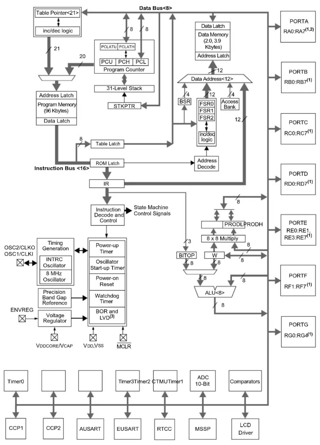
FIGURE 1-1: PIC18F6XJ90 (64-PIN) BLOCK DIAGRAM
flowchart
graph TD
    A["Table Pointer<21>"] --> B["inc/dec logic"]
    B --> C["21"]
    C --> D["Address Latch Program Memory (96 Kbytes)"]
    D --> E["Data Latch"]
    E --> F["ROM Latch"]
    F --> G["IR"]
    G --> H["Instruction Decode and Control"]
    H --> I["Power-up Timer"]
    I --> J["Oscillator Start-up Timer"]
    J --> K["Power-on Reset"]
    K --> L["Watchdog Timer"]
    L --> M["BOR and LVD(3)"]
    M --> N["VDDCORE/VCAP"]
    N --> O["Timing Generation"]
    O --> P["INTRC Oscillator 8 MHz Oscillator"]
    P --> Q["Precision Band Gap Reference"]
    Q --> R["Voltage Regulator"]
    R --> S["OUT"]
    S --> T["Timer0"]
    T --> U["CCP1"]
    T --> V["CCP2"]
    T --> W["AUSART"]
    T --> X["EUSART"]
    T --> Y["RTCC"]
    T --> Z["MSSP"]
    T --> AA["LCD Driver"]
    AB["Data Bus<8>"] --> AC["Data Latch Data Memory (2.0, 3.9 Kbytes)"]
    AC --> AD["Address Latch"]
    AD --> AE["31-Level Stack"]
    AE --> AF["STKPTR"]
    AF --> AG["Table Latch"]
    AG --> AH["ROM Latch"]
    AH --> AI["IR"]
    AI --> AJ["Instruction Decode and Control"]
    AJ --> AK["State Machine Control Signals"]
    AL["PORTA RA0:RA7(1,2)"] --> AM["PORTB RB0:RB7(1)"]
    AM --> AN["PORTC RC0:RC7(1)"]
    AN --> AO["PORTD RD0:RD7(1)"]
    AO --> AP["PORTE RE0:RE1, RE3:RE7(1)"]
    AP --> AQ["PORTF RF1:RF7(1)"]
    AQ --> AR["PORTG RG0:RG4(1)"]
    AL --> AS["PRODL PRODH"]
    AS --> AT["8 x 8 Multiply"]
    AT --> AU["W"]
    AU --> AV["BITOP"]
    AV --> AW["ALU<8>"]
    AW --> AX["ADC 10-Bit"]
    AX --> AY["Comparators"]
    AZ["OSC2/CLKO OSC1/CLKI"] --> BA["Timing Generation"]
    BA --> BB["Power-up Timer"]
    BB --> BC["Oscillator Start-up Timer"]
    BC --> BD["Power-on Reset"]
    BD --> BE["Watchdog Timer"]
    BE --> BF["BOR and LVD(3)"]
    BF --> BG["MCLR"]
Note 1: See Table 1-3 for I/O port pin descriptions.
2: RA6 and RA7 are only available as digital I/O in select oscillator modes. See Section 3.0 "Oscillator Configurations" for more information
3: Brown-out Reset and Low-Voltage Detect functions are provided when the on-board voltage regulator is enabled.
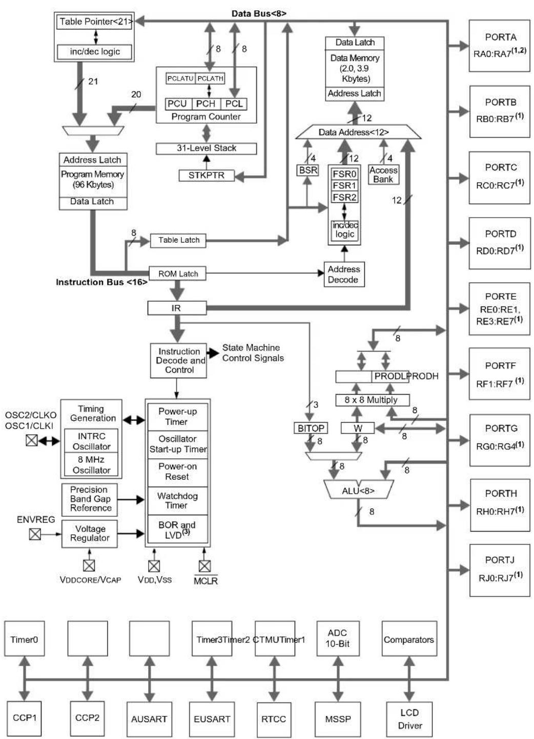
FIGURE 1-2: PIC18F8XJ90 (80-PIN) BLOCK DIAGRAM
flowchart
graph TD
    A["Table Pointer<21>"] --> B["inc/dec logic"]
    B --> C["21"]
    C --> D["Address Latch Program Memory (96 Kbytes)"]
    D --> E["Data Latch"]
    E --> F["ROM Latch"]
    F --> G["IR"]
    G --> H["Instruction Decode and Control"]
    H --> I["Power-up Timer"]
    I --> J["INC Oscillator 8 MHz Oscillator"]
    J --> K["Timing Generation"]
    K --> L["OUT"]
    L --> M["VDDCORE/VCAP"]
    M --> N["VDD,VSS"]
    N --> O["MCLR"]
    O --> P["Protection"]
    P --> Q["Power-on Reset"]
    Q --> R["Precision Band Gap Reference"]
    R --> S["Watchdog Timer"]
    S --> T["BOR and LVD(3)"]
    T --> U["VDDCORE/VCAP"]
    U --> V["OUT"]
    V --> W["OUT"]
    W --> X["MCLR"]
    X --> Y["Comparisoners"]
    Y --> Z["LCD Driver"]
    Y --> AA["ADC 10-Bit"]
    Y --> AB["RTCC"]
    Y --> AC["MSSP"]
    Y --> AD["PORTJ RJ0:RJ7(1)"]
    Y --> AE["PORTH RH0:RH7(1)"]
    Y --> AF["PORTG RG0:RG4(1)"]
    Y --> AG["PORTF RF1:RF7(1)"]
    Y --> AH["PORTER0:RE1, RE3:RE7(1)"]
    Y --> AI["PORTD RD0:RD7(1)"]
    Y --> AJ["PORTC RC0:RC7(1)"]
    Y --> AK["PORTB RB0:RB7(1)"]
    Y --> AL["PORTA RA0:RA7(1,2)"]
    B --> AM["Program Counter"]
    AM --> AN["PCLATU PCLATH"]
    AN --> AO["PCU PCH PCL"]
    AO --> AP["31-Level Stack"]
    AP --> AQ["STKPTR"]
    AQ --> AR["Address Latch"]
    AR --> AS["Data Latch Data Memory (2.0, 3.9 Kbytes)"]
    AS --> AT["Address Latch"]
    AT --> AU["Data Address<12>"]
    AU --> AV["BSR"]
    AV --> AW["FSR0 FSR1 FSR2"]
    AW --> AX["Inc/dec logic"]
    AX --> AY["Address Decode"]
    AY --> AZ["Output to PortA"]
    AY --> BA["Output to PortB"]
    AY --> BB["Output to PortC"]
    AY --> BC["Output to PortD"]
Note 1: See Table 1-3 for I/O port pin descriptions.
2: RA6 and RA7 are only available as digital I/O in select oscillator modes. See Section 3.0 "Oscillator Configurations" for more information.
3: Brown-out Reset and Low-Voltage Detect functions are provided when the on-board voltage regulator is enabled.
TABLE 1-3: PIC18F6XJ90 PINOUT I/O DESCRIPTIONS
| Pin Name | Pin Number | Pin Type | Buffer Type | Description |
| TQFP | ||||
| MCLR | 7 I ST M | Master | Clear (input) or programming voltage (input). This pin is an active-low Reset to the device. | |
| OSC1/CLKI/RA7 | 39 | Oscillator crystal or external clock input. | ||
| OSC1 | I | CMOS | Oscillator crystal input. | |
| CLKI | I | CMOS | External clock source input. Always associated with pin function, OSC1. (See related OSC1/CLKI, OSC2/CLKO pins.) | |
| RA7 | I/O | TTL | General purpose I/O pin. | |
| OSC2/CLKO/RA6 | 40 | Oscillator crystal or clock output. | ||
| OSC2 | O | — | Oscillator crystal output. Connects to crystal or resonator in Crystal Oscillator mode. | |
| CLKO | O | — | In EC modes, OSC2 pin outputs CLKO, which has 1/4 the frequency of OSC1 and denotes the instruction cycle rate. | |
| RA6 | I/O | TTL | General purpose I/O pin. | |
| PORTA is a bidirectional I/O port. | ||||
| RA0/AN0 | 24 | |||
| RA0 | I/O | TTL | Digital I/O. | |
| AN0 | I | Analog | Analog Input 0. | |
| RA1/AN1/SEG18 | 23 | |||
| RA1 | I/O | TTL | Digital I/O. | |
| AN1 | I | Analog | Analog Input 1. | |
| SEG18 | O | Analog | SEG18 output for LCD. | |
| RA2/AN2/VREF- | 22 | |||
| RA2 | I/O | TTL | Digital I/O. | |
| AN2 | I | Analog | Analog Input 2. | |
| VREF- | I | Analog | A/D reference voltage (low) input. | |
| RA3/AN3/VREF+ | 21 | |||
| RA3 | I/O | TTL | Digital I/O. | |
| AN3 | I | Analog | Analog Input 3. | |
| VREF+ | I | Analog | A/D reference voltage (high) input. | |
| RA4/T0CKI/SEG14 | 28 | |||
| RA4 | I/O | ST | Digital I/O. | |
| T0CKI | I | ST | Timer0 external clock input. | |
| SEG14 | O | Analog | SEG14 output for LCD. | |
| RA5/AN4/SEG15 | 27 | |||
| RA5 | I/O | TTL | Digital I/O. | |
| AN4 | I | Analog | Analog Input 4. | |
| SEG15 | O | Analog | SEG15 output for LCD. | |
| RA6 See the OSC2/CLKO/RA6 pin. | ||||
| RA7 See the OSC1/CLKI/RA7 pin. | ||||
Legend: TTL = TTL compatible input CMOS = CMOS compatible input or output
ST = Schmitt Trigger input with CMOS levels Analog = Analog input
I = Input O = Output
P = Power OD = Open-Drain (no P diode to VDD)
I^2C^TM = I^2C / SMBus
Note 1: Default assignment for CCP2 when the CCP2MX Configuration bit is set.
2: Alternate assignment for CCP2 when the CCP2MX Configuration bit is cleared.
TABLE 1-3: PIC18F6XJ90 PINOUT I/O DESCRIPTIONS (CONTINUED)
| Pin Name | Pin Number | Pin Type | Buffer Type | Description |
| TQFP | ||||
| PORTB is a bidirectional I/O port. PORTB can be software programmed for internal weak pull-ups on all inputs. | ||||
| RB0/INT0/SEG30 | 48 | |||
| RB0 | I/O | TTL | Digital I/O. | |
| INT0 | I | ST | External Interrupt 0. | |
| SEG30 | O | Analog | SEG30 output for LCD. | |
| RB1/INT1/SEG8 | 47 | |||
| RB1 | I/O | TTL | Digital I/O. | |
| INT1 | I | ST | External Interrupt 1. | |
| SEG8 | O | Analog | SEG8 output for LCD. | |
| RB2/INT2/SEG9/CTED1 | 46 | |||
| RB2 | I/O | TTL | Digital I/O. | |
| INT2 | I | ST | External Interrupt 2. | |
| CTED1 | I | ST | CTMU Edge 1 input. | |
| SEG9 | O | Analog | SEG9 output for LCD. | |
| RB3/INT3/SEG10/CTED2 | 45 | |||
| RB3 | I/O | TTL | Digital I/O. | |
| INT3 | I | ST | External Interrupt 3. | |
| SEG10 | O | Analog | SEG10 output for LCD. | |
| CTED2 | I | ST | CTMU Edge 2 input. | |
| RB4/KBI0/SEG11 | 44 | |||
| RB4 | I/O | TTL | Digital I/O. | |
| KBI0 | I | TTL | Interrupt-on-change pin. | |
| SEG11 | O | Analog | SEG11 output for LCD. | |
| RB5/KBI1/SEG29 | 43 | |||
| RB5 | I/O | TTL | Digital I/O. | |
| KBI1 | I | TTL | Interrupt-on-change pin. | |
| SEG29 | O | Analog | SEG29 output for LCD. | |
| RB6/KBI2/PGC | 42 | |||
| RB6 | I/O | TTL | Digital I/O. | |
| KBI2 | I | TTL | Interrupt-on-change pin. | |
| PGC | I/O | ST | In-Circuit Debugger and ICSPTM programming clock pin. | |
| RB7/KBI3/PGD | 37 | |||
| RB7 | I/O | TTL | Digital I/O. | |
| KBI3 | I | TTL | Interrupt-on-change pin. | |
| PGD | I/O | ST | In-Circuit Debugger and ICSP programming data pin. |
Legend: TTL = TTL compatible input CMOS = CMOS compatible input or output
ST = Schmitt Trigger input with CMOS levels Analog = Analog input
I = Input O = Output
P = Power
I^2C^TM = I^2C / SMBus
OD = Open-Drain (no P diode to V DD)
Note 1: Default assignment for CCP2 when the CCP2MX Configuration bit is set.
2: Alternate assignment for CCP2 when the CCP2MX Configuration bit is cleared.
TABLE 1-3: PIC18F6XJ90 PINOUT I/O DESCRIPTIONS (CONTINUED)
| Pin Name | Pin Number | Pin Type | Buffer Type | Description |
| TQFP | ||||
| PORTC is a bidirectional I/O port. | ||||
| RC0/T1OSO/T13CKI | 30 | |||
| RC0 | I/O | ST | Digital I/O. | |
| T1OSO | O | — | Timer1 oscillator output. | |
| T13CKI | I | ST | Timer1/Timer3 external clock input. | |
| RC1/T1OSI/CCP2/SEG32 | 29 | |||
| RC1 | I/O | ST | Digital I/O. | |
| T1OSI | I | CMOS | Timer1 oscillator input. | |
| CCP2^(1) | I/O | ST | Capture 2 input/Compare 2 output/PWM2 output. | |
| SEG32 | O | Analog | SEG32 output for LCD. | |
| RC2/CCP1/SEG13 | 33 | |||
| RC2 | I/O | ST | Digital I/O. | |
| CCP1 | I/O | ST | Capture 1 input/Compare 1 output/PWM1 output. | |
| SEG13 | O | Analog | SEG13 output for LCD. | |
| RC3/SCK/SCL/SEG17 | 34 | |||
| RC3 | I/O | ST | Digital I/O. | |
| SCK | I/O | ST | Synchronous serial clock input/output for SPI mode. | |
| SCL | I/O | I^2C | Synchronous serial clock input/output for I^2C^TM mode. | |
| SEG17 | O | Analog | SEG17 output for LCD. | |
| RC4/SDI/SDA/SEG16 | 35 | |||
| RC4 | I/O | ST | Digital I/O. | |
| SDI | I | ST | SPI data in. | |
| SDA | I/O | I^2C | I^2C data I/O. | |
| SEG16 | O | Analog | SEG16 output for LCD. | |
| RC5/SDO/SEG12 | 36 | |||
| RC5 | I/O | ST | Digital I/O. | |
| SDO | O | — | SPI data out. | |
| SEG12 | O | Analog | SEG12 output for LCD. | |
| RC6/TX1/CK1/SEG27 | 31 | |||
| RC6 | I/O | ST | Digital I/O. | |
| TX1 | O | — | EUSART asynchronous transmit. | |
| CK1 | I/O | ST | EUSART synchronous clock (see related RX1/DT1). | |
| SEG27 | O | Analog | SEG27 output for LCD. | |
| RC7/RX1/DT1/SEG28 | 32 | |||
| RC7 | I/O | ST | Digital I/O. | |
| RX1 | I | ST | EUSART asynchronous receive. | |
| DT1 | I/O | ST | EUSART synchronous data (see related TX1/CK1). | |
| SEG28 | O | Analog | SEG28 output for LCD. |
Legend: TTL = TTL compatible input CMOS = CMOS compatible input or output
ST = Schmitt Trigger input with CMOS levels Analog = Analog input
I = Input O = Output
P = Power OD = Open-Drain (no P diode to V DD)
I^2C^TM = I^2C / SMBus
Note 1: Default assignment for CCP2 when the CCP2MX Configuration bit is set.
2: Alternate assignment for CCP2 when the CCP2MX Configuration bit is cleared.
TABLE 1-3: PIC18F6XJ90 PINOUT I/O DESCRIPTIONS (CONTINUED)
| Pin Name | Pin Number | Pin Type | Buffer Type | Description |
| TQFP | ||||
| PORTD is a bidirectional I/O port. | ||||
| RD0/SEG0/CTPLS | 58 | |||
| RD0 | I/O | ST | Digital I/O. | |
| SEG0 | O | Analog | SEG0 output for LCD. | |
| CTPLS | O | — | CTMU pulse generator output. | |
| RD1/SEG1 | 55 | |||
| RD1 | I/O | ST | Digital I/O. | |
| SEG1 | O | Analog | SEG1 output for LCD. | |
| RD2/SEG2 | 54 | |||
| RD2 | I/O | ST | Digital I/O. | |
| SEG2 | O | Analog | SEG2 output for LCD. | |
| RD3/SEG3 | 53 | |||
| RD3 | I/O | ST | Digital I/O. | |
| SEG3 | O | Analog | SEG3 output for LCD. | |
| RD4/SEG4 | 52 | |||
| RD4 | I/O | ST | Digital I/O. | |
| SEG4 | O | Analog | SEG4 output for LCD. | |
| RD5/SEG5 | 51 | |||
| RD5 | I/O | ST | Digital I/O. | |
| SEG5 | O | Analog | SEG5 output for LCD. | |
| RD6/SEG6 | 50 | |||
| RD6 | I/O | ST | Digital I/O. | |
| SEG6 | O | Analog | SEG6 output for LCD. | |
| RD7/SEG7 | 49 | |||
| RD7 | I/O | ST | Digital I/O. | |
| SEG7 | O | Analog | SEG7 output for LCD. |
Legend: TTL = TTL compatible input CMOS = CMOS compatible input or output
ST = Schmitt Trigger input with CMOS levels Analog = Analog input
I = Input O = Output
P = Power OD = Open-Drain (no P diode to V DD)
I^2C^TM = I^2C / SMBus
Note 1: Default assignment for CCP2 when the CCP2MX Configuration bit is set.
2: Alternate assignment for CCP2 when the CCP2MX Configuration bit is cleared.
TABLE 1-3: PIC18F6XJ90 PINOUT I/O DESCRIPTIONS (CONTINUED)
| Pin Name | Pin Number | Pin Type | Buffer Type | Description |
| TQFP | ||||
| PORTE is a bidirectional I/O port. | ||||
| RE0/LCDBIAS1 | 2 | |||
| RE0 | I/O | ST | Digital I/O. | |
| LCDBIAS1 | I | Analog | BIAS1 input for LCD. | |
| RE1/LCDBIAS2 | 1 | |||
| RE1 | I/O | ST | Digital I/O. | |
| LCDBIAS2 | I | Analog | BIAS2 input for LCD. | |
| LCDBIAS3 64 I Analog BIAS3 input for LCD. | ||||
| RE3/COM0 | 63 | |||
| RE3 | I/O | ST | Digital I/O. | |
| COM0 | O | Analog | COM0 output for LCD. | |
| RE4/COM1 | 62 | |||
| RE4 | I/O | ST | Digital I/O. | |
| COM1 | O | Analog | COM1 output for LCD. | |
| RE5/COM2 | 61 | |||
| RE5 | I/O | ST | Digital I/O. | |
| COM2 | O | Analog | COM2 output for LCD. | |
| RE6/COM3 | 60 | |||
| RE6 | I/O | ST | Digital I/O. | |
| COM3 | O | Analog | COM3 output for LCD. | |
| RE7/CCP2/SEG31 | 59 | |||
| RE7 | I/O | ST | Digital I/O. | |
| CCP2^(2) | I/O | ST | Capture 2 input/Compare 2 output/PWM2 output. | |
| SEG31 | O | Analog | SEG31 output for LCD. | |
Legend: TTL = TTL compatible input CMOS = CMOS compatible input or output
ST = Schmitt Trigger input with CMOS levels Analog = Analog input
I = Input O = Output
P = Power OD = Open-Drain (no P diode to V DD)
I^2C^TM = I^2C / SMBus
Note 1: Default assignment for CCP2 when the CCP2MX Configuration bit is set.
2: Alternate assignment for CCP2 when the CCP2MX Configuration bit is cleared.
TABLE 1-3: PIC18F6XJ90 PINOUT I/O DESCRIPTIONS (CONTINUED)
| Pin Name | Pin Number | Pin Type | Buffer Type | Description |
| TQFP | ||||
| PORTF is a bidirectional I/O port. | ||||
| RF1/AN6/C2OUT/SEG19 | 17 | |||
| RF1 | I/O | ST | Digital I/O. | |
| AN6 | I | Analog | Analog Input 6. | |
| C2OUT | O | — | Comparator 2 output. | |
| SEG19 | O | Analog | SEG19 output for LCD. | |
| RF2/AN7/C1OUT/SEG20 | 16 | |||
| RF2 | I/O | ST | Digital I/O. | |
| AN7 | I | Analog | Analog Input 7. | |
| C1OUT | O | — | Comparator 1 output. | |
| SEG20 | O | Analog | SEG20 output for LCD. | |
| RF3/AN8/SEG21/C2INB | 15 | |||
| RF3 | I/O | ST | Digital I/O. | |
| AN8 | I | Analog | Analog Input 8. | |
| SEG21 | O | Analog | SEG21 output for LCD. | |
| C2INB | I | Analog | Comparator 2 Input B. | |
| RF4/AN9/SEG22/C2INA | 14 | |||
| RF4 | I/O | ST | Digital I/O. | |
| AN9 | I | Analog | Analog Input 9. | |
| SEG22 | O | Analog | SEG22 output for LCD | |
| C2INA | I | Analog | Comparator 2 Input A. | |
| RF5/AN10/CVREF/SEG23/C1INB | 13 | |||
| RF5 | I/O | ST | Digital I/O. | |
| AN10 | I | Analog | Analog Input 10. | |
| CVREF | O | Analog | Comparator reference voltage output. | |
| SEG23 | O | Analog | SEG23 output for LCD. | |
| C1INB | I | Analog | Comparator 1 Input B. | |
| RF6/AN11/SEG24/C1INA | 12 | |||
| RF6 | I/O | ST | Digital I/O. | |
| AN11 | I | Analog | Analog Input 11. | |
| SEG24 | O | Analog | SEG24 output for LCD | |
| C1INA | I | Analog | Comparator 1 Input A. | |
| RF7/AN5/SS/SEG25 | 11 | |||
| RF7 | I/O | ST | Digital I/O. | |
| AN5 | O | Analog | Analog Input 5. | |
| SS | I | TTL | SPI slave select input. | |
| SEG25 | O | Analog | SEG25 output for LCD. |
Legend: TTL = TTL compatible input CMOS = CMOS compatible input or output
ST = Schmitt Trigger input with CMOS levels Analog = Analog input
I = Input O = Output
P = Power OD = Open-Drain (no P diode to V DD)
I^2C^TM = I^2C / SMBus
Note 1: Default assignment for CCP2 when the CCP2MX Configuration bit is set.
2: Alternate assignment for CCP2 when the CCP2MX Configuration bit is cleared.
TABLE 1-3: PIC18F6XJ90 PINOUT I/O DESCRIPTIONS (CONTINUED)
| Pin Name | Pin Number | Pin Type | Buffer Type | Description |
| TQFP | ||||
| PORTG is a bidirectional I/O port. | ||||
| RG0/LCDBIAS0 | 3 | |||
| RG0 | I/O | ST | Digital I/O. | |
| LCDBIAS0 | I | Analog | BIAS0 input for LCD. | |
| RG1/TX2/CK2 | 4 | |||
| RG1 | I/O | ST | Digital I/O. | |
| TX2 | O | — | AUSART asynchronous transmit. | |
| CK2 | I/O | ST | AUSART synchronous clock (see related RX2/DT2). | |
| RG2/RX2/DT2/VLCAP1 | 5 | |||
| RG2 | I/O | ST | Digital I/O. | |
| RX2 | I | ST | AUSART asynchronous receive. | |
| DT2 | I/O | ST | AUSART synchronous data (see related TX2/CK2). | |
| VLCAP1 | I | Analog | LCD charge pump capacitor input. | |
| RG3/VLCAP2 | 6 | |||
| RG3 | I/O | ST | Digital I/O. | |
| VLCAP2 | I | Analog | LCD charge pump capacitor input. | |
| RG4/SEG26/RTCC | 8 | |||
| RG4 | I/O | ST | Digital I/O. | |
| SEG26 | O | Analog | SEG26 output for LCD. | |
| RTCC | O | — | RTCC output | |
| Vss 9, 25, 41, 56 P — Ground reference for logic and I/O pins. | ||||
| VDD 26, 38, 57 P — Positive supply for logic and I/O pins. | ||||
| AVss 20 P — Ground reference for analog modules. | ||||
| AVDD 19 P — Positive supply for analog modules. | ||||
| ENVREG 18 I ST Enable for on-chip voltage regulator. | ||||
| VDDCORE/VCAP | 10 | Core logic power or external filter capacitor connection. | ||
| VDDCORE | P | — | Positive supply for microcontroller core logic(regulator disabled). | |
| VCAP | P | — | External filter capacitor connection (regulator enabled). | |
Legend: TTL = TTL compatible input CMOS = CMOS compatible input or output
ST = Schmitt Trigger input with CMOS levels
Analog = Analog input
I = Input
O = Output
P = Power
OD = Open-Drain (no P diode to VDD)
I^2C^TM = I^2C / SMBus
Note 1: Default assignment for CCP2 when the CCP2MX Configuration bit is set.
2: Alternate assignment for CCP2 when the CCP2MX Configuration bit is cleared.
TABLE 1-4: PIC18F8XJ90 PINOUT I/O DESCRIPTIONS
| Pin Name | Pin Number | Pin Type | Buffer Type | Description |
| TQFP | ||||
| MCLR | 9 I ST Master | Clear (input) or programming voltage (input). This pin is an active-low Reset to the device. | ||
| OSC1/CLKI/RA7 | 49 | Oscillator crystal or external clock input. | ||
| OSC1 | I | CMOS | Oscillator crystal input. | |
| CLKI | I | CMOS | External clock source input. Always associated with pin function, OSC1. (See related OSC1/CLKI, OSC2/CLKO pins.) | |
| RA7 | I/O | TTL | General purpose I/O pin. | |
| OSC2/CLKO/RA6 | 50 | Oscillator crystal or clock output. | ||
| OSC2 | O | — | Oscillator crystal output. Connects to crystal or resonator in Crystal Oscillator mode. | |
| CLKO | O | — | In EC modes, OSC2 pin outputs CLKO, which has 1/4 the frequency of OSC1 and denotes the instruction cycle rate. | |
| RA6 | I/O | TTL | General purpose I/O pin. | |
| PORTA is a bidirectional I/O port. | ||||
| RA0/AN0 | 30 | |||
| RA0 | I/O | TTL | Digital I/O. | |
| AN0 | I | Analog | Analog Input 0. | |
| RA1/AN1/SEG18 | 29 | |||
| RA1 | I/O | TTL | Digital I/O. | |
| AN1 | I | Analog | Analog Input 1. | |
| SEG18 | O | Analog | SEG18 output for LCD. | |
| RA2/AN2/VREF- | 28 | |||
| RA2 | I/O | TTL | Digital I/O. | |
| AN2 | I | Analog | Analog Input 2. | |
| VREF- | I | Analog | A/D reference voltage (low) input. | |
| RA3/AN3/VREF+ | 27 | |||
| RA3 | I/O | TTL | Digital I/O. | |
| AN3 | I | Analog | Analog Input 3. | |
| VREF+ | I | Analog | A/D reference voltage (high) input. | |
| RA4/T0CKI/SEG14 | 34 | |||
| RA4 | I/O | ST | Digital I/O. | |
| T0CKI | I | ST | Timer0 external clock input. | |
| SEG14 | O | Analog | SEG14 output for LCD. | |
| RA5/AN4/SEG15 | 33 | |||
| RA5 | I/O | TTL | Digital I/O. | |
| AN4 | I | Analog | Analog Input 4. | |
| SEG15 | O | Analog | SEG15 output for LCD. | |
| RA6 See the OSC2/CLKO/RA6 pin. | ||||
| RA7 See the OSC1/CLKI/RA7 pin. | ||||
Legend: TTL = TTL compatible input CMOS = CMOS compatible input or output
ST = Schmitt Trigger input with CMOS levels Analog = Analog input
I = Input O = Output
P = Power OD = Open-Drain (no P diode to V DD)
Note 1: Default assignment for CCP2 when the CCP2MX Configuration bit is set.
2: Alternate assignment for CCP2 when the CCP2MX Configuration bit is cleared.
TABLE 1-4: PIC18F8XJ90 PINOUT I/O DESCRIPTIONS (CONTINUED)
| Pin Name | Pin Number | Pin Type | Buffer Type | Description |
| TQFP | ||||
| PORTB is a bidirectional I/O port. PORTB can be software programmed for internal weak pull-ups on all inputs. | ||||
| RB0/INT0/SEG30 | 58 | |||
| RB0 | I/O | TTL | Digital I/O. | |
| INT0 | I | ST | External Interrupt 0. | |
| SEG30 | O | Analog | SEG30 output for LCD. | |
| RB1/INT1/SEG8 | 57 | |||
| RB1 | I/O | TTL | Digital I/O. | |
| INT1 | I | ST | External Interrupt 1. | |
| SEG8 | O | Analog | SEG8 output for LCD. | |
| RB2/INT2/SEG9/CTED1 | 56 | |||
| RB2 | I/O | TTL | Digital I/O. | |
| INT2 | I | ST | External Interrupt 2. | |
| SEG9 | O | Analog | SEG9 output for LCD. | |
| CTED1 | I | ST | CTMU Edge 1 input. | |
| RB3/INT3/SEG10/CTED2 | 55 | |||
| RB3 | I/O | TTL | Digital I/O. | |
| INT3 | I | ST | External Interrupt 3. | |
| SEG10 | O | Analog | SEG10 output for LCD. | |
| CTED2 | I | ST | CTMU Edge 2 input. | |
| RB4/KBI0/SEG11 | 54 | |||
| RB4 | I/O | TTL | Digital I/O. | |
| KBI0 | I | TTL | Interrupt-on-change pin. | |
| SEG11 | O | Analog | SEG11 output for LCD. | |
| RB5/KBI1/SEG29 | 53 | |||
| RB5 | I/O | TTL | Digital I/O. | |
| KBI1 | I | TTL | Interrupt-on-change pin. | |
| SEG29 | O | Analog | SEG29 output for LCD. | |
| RB6/KBI2/PGC | 52 | |||
| RB6 | I/O | TTL | Digital I/O. | |
| KBI2 | I | TTL | Interrupt-on-change pin. | |
| PGC | I/O | ST | In-Circuit Debugger and ICSPTM programming clock pin. | |
| RB7/KBI3/PGD | 47 | |||
| RB7 | I/O | TTL | Digital I/O. | |
| KBI3 | I | TTL | Interrupt-on-change pin. | |
| PGD | I/O | ST | In-Circuit Debugger and ICSP programming data pin. |
Legend: TTL = TTL compatible input CMOS = CMOS compatible input or output
ST = Schmitt Trigger input with CMOS levels Analog = Analog input
I = Input O = Output
P = Power
OD = Open-Drain (no P diode to V DD)
I^2C^TM = I^2C / SMBus
Note 1: Default assignment for CCP2 when the CCP2MX Configuration bit is set.
2: Alternate assignment for CCP2 when the CCP2MX Configuration bit is cleared.
TABLE 1-4: PIC18F8XJ90 PINOUT I/O DESCRIPTIONS (CONTINUED)
| Pin Name | Pin Number | Pin Type | Buffer Type | Description |
| TQFP | ||||
| PORTC is a bidirectional I/O port. | ||||
| RC0/T1OSO/T13CKI | 36 | |||
| RC0 | I/O | ST | Digital I/O. | |
| T1OSO | O | — | Timer1 oscillator output. | |
| T13CKI | I | ST | Timer1/Timer3 external clock input. | |
| RC1/T1OSI/CCP2/SEG32 | 35 | |||
| RC1 | I/O | ST | Digital I/O. | |
| T1OSI | I | CMOS | Timer1 oscillator input. | |
| CCP2^(1) | I/O | ST | Capture 2 input/Compare 2 output/PWM2 output. | |
| SEG32 | O | Analog | SEG32 output for LCD. | |
| RC2/CCP1/SEG13 | 43 | |||
| RC2 | I/O | ST | Digital I/O. | |
| CCP1 | I/O | ST | Capture 1 input/Compare 1 output/PWM1 output. | |
| SEG13 | O | Analog | SEG13 output for LCD. | |
| RC3/SCK/SCL/SEG17 | 44 | |||
| RC3 | I/O | ST | Digital I/O. | |
| SCK | I/O | ST | Synchronous serial clock input/output for SPI mode. | |
| SCL | I/O | I^2C | Synchronous serial clock input/output for I^2C^TM mode. | |
| SEG17 | O | Analog | SEG17 output for LCD. | |
| RC4/SDI/SDA/SEG16 | 45 | |||
| RC4 | I/O | ST | Digital I/O. | |
| SDI | I | ST | SPI data in. | |
| SDA | I/O | I^2C | I^2C data I/O. | |
| SEG16 | O | Analog | SEG16 output for LCD. | |
| RC5/SDO/SEG12 | 46 | |||
| RC5 | I/O | ST | Digital I/O. | |
| SDO | O | — | SPI data out. | |
| SEG12 | O | Analog | SEG12 output for LCD. | |
| RC6/TX1/CK1/SEG27 | 37 | |||
| RC6 | I/O | ST | Digital I/O. | |
| TX1 | O | — | EUSART asynchronous transmit. | |
| CK1 | I/O | ST | EUSART synchronous clock (see related RX1/DT1). | |
| SEG27 | O | Analog | SEG27 output for LCD. | |
| RC7/RX1/DT1/SEG28 | 38 | |||
| RC7 | I/O | ST | Digital I/O. | |
| RX1 | I | ST | EUSART asynchronous receive. | |
| DT1 | I/O | ST | EUSART synchronous data (see related TX1/CK1). | |
| SEG28 | O | Analog | SEG28 output for LCD. |
Legend: TTL = TTL compatible input CMOS = CMOS compatible input or output
ST = Schmitt Trigger input with CMOS levels Analog = Analog input
I = Input O = Output
P = Power OD = Open-Drain (no P diode to V DD)
I^2C^TM = I^2C / SMBus
Note 1: Default assignment for CCP2 when the CCP2MX Configuration bit is set.
2: Alternate assignment for CCP2 when the CCP2MX Configuration bit is cleared.
TABLE 1-4: PIC18F8XJ90 PINOUT I/O DESCRIPTIONS (CONTINUED)
| Pin Name | Pin Number | Pin Type | Buffer Type | Description |
| TQFP | ||||
| PORTD is a bidirectional I/O port. | ||||
| RD0/SEG0/CTPLS | 72 | |||
| RD0 | I/O | ST | Digital I/O. | |
| SEG0 | O | Analog | SEG0 output for LCD. | |
| CTPLS | O | ST | CTMU pulse generator output. | |
| RD1/SEG1 | 69 | |||
| RD1 | I/O | ST | Digital I/O. | |
| SEG1 | O | Analog | SEG1 output for LCD. | |
| RD2/SEG2 | 68 | |||
| RD2 | I/O | ST | Digital I/O. | |
| SEG2 | O | Analog | SEG2 output for LCD. | |
| RD3/SEG3 | 67 | |||
| RD3 | I/O | ST | Digital I/O. | |
| SEG3 | O | Analog | SEG3 output for LCD. | |
| RD4/SEG4 | 66 | |||
| RD4 | I/O | ST | Digital I/O. | |
| SEG4 | O | Analog | SEG4 output for LCD. | |
| RD5/SEG5 | 65 | |||
| RD5 | I/O | ST | Digital I/O. | |
| SEG5 | O | Analog | SEG5 output for LCD. | |
| RD6/SEG6 | 64 | |||
| RD6 | I/O | ST | Digital I/O. | |
| SEG6 | O | Analog | SEG6 output for LCD. | |
| RD7/SEG7 | 63 | |||
| RD7 | I/O | ST | Digital I/O. | |
| SEG7 | O | Analog | SEG7 output for LCD. |
Legend: TTL = TTL compatible input CMOS = CMOS compatible input or output
ST = Schmitt Trigger input with CMOS levels Analog = Analog input
I = Input O = Output
P = Power OD = Open-Drain (no P diode to V DD)
I^2C^TM = I^2C / SMBus
Note 1: Default assignment for CCP2 when the CCP2MX Configuration bit is set.
2: Alternate assignment for CCP2 when the CCP2MX Configuration bit is cleared.
TABLE 1-4: PIC18F8XJ90 PINOUT I/O DESCRIPTIONS (CONTINUED)
| Pin Name | Pin Number | Pin Type | Buffer Type | Description |
| TQFP | ||||
| PORTE is a bidirectional I/O port. | ||||
| RE0/LCDBIAS1 | 4 | |||
| RE0 | I/O | ST | Digital I/O. | |
| LCDBIAS1 | I | Analog | BIAS1 input for LCD. | |
| RE1/LCDBIAS2 | 3 | |||
| RE1 | I/O | ST | Digital I/O. | |
| LCDBIAS2 | I | Analog | BIAS2 input for LCD. | |
| LCDBIAS3 78 | Analog BIAS3 input for LCD. | ||||
| RE3/COM0 | 77 | |||
| RE3 | I/O | ST | Digital I/O. | |
| COM0 | O | Analog | COM0 output for LCD. | |
| RE4/COM1 | 76 | |||
| RE4 | I/O | ST | Digital I/O. | |
| COM1 | O | Analog | COM1 output for LCD. | |
| RE5/COM2 | 75 | |||
| RE5 | I/O | ST | Digital I/O. | |
| COM2 | O | Analog | COM2 output for LCD. | |
| RE6/COM3 | 74 | |||
| RE6 | I/O | ST | Digital I/O. | |
| COM3 | O | Analog | COM3 output for LCD. | |
| RE7/CCP2/SEG31 | 73 | |||
| RE7 | I/O | ST | Digital I/O. | |
| CCP2^(2) | I/O | ST | Capture 2 input/Compare 2 output/PWM2 output. | |
| SEG31 | O | Analog | SEG31 output for LCD. | |
Legend: TTL = TTL compatible input CMOS = CMOS compatible input or output
ST = Schmitt Trigger input with CMOS levels Analog = Analog input
I = Input O = Output
P = Power OD = Open-Drain (no P diode to V DD)
I^2C^TM=I^2C/SMBus
Note 1: Default assignment for CCP2 when the CCP2MX Configuration bit is set.
2: Alternate assignment for CCP2 when the CCP2MX Configuration bit is cleared.
TABLE 1-4: PIC18F8XJ90 PINOUT I/O DESCRIPTIONS (CONTINUED)
| Pin Name | Pin Number | Pin Type | Buffer Type | Description |
| TQFP | ||||
| PORTF is a bidirectional I/O port. | ||||
| RF1/AN6/C2OUT/SEG19 | 23 | |||
| RF1 | I/O | ST | Digital I/O. | |
| AN6 | I | Analog | Analog Input 6. | |
| C2OUT | O | — | Comparator 2 output. | |
| SEG19 | O | Analog | SEG19 output for LCD. | |
| RF2/AN7/C1OUT/SEG20 | 18 | |||
| RF2 | I/O | ST | Digital I/O. | |
| AN7 | I | Analog | Analog Input 7. | |
| C1OUT | O | — | Comparator 1 output. | |
| SEG20 | O | Analog | SEG20 output for LCD. | |
| RF3/AN8/SEG21/C2INB | 17 | |||
| RF3 | I/O | ST | Digital I/O. | |
| AN8 | I | Analog | Analog Input 8. | |
| SEG21 | O | Analog | SEG21 output for LCD. | |
| C2INB | I | Analog | Comparator 2 Input B. | |
| RF4/AN9/SEG22/C2INA | 16 | |||
| RF4 | I/O | ST | Digital I/O. | |
| AN9 | I | Analog | Analog Input 9. | |
| SEG22 | O | Analog | SEG22 output for LCD. | |
| C2INA | I | Analog | Comparator 2 Input A. | |
| RF5/AN10/CVREF/SEG23/C1INB | 15 | |||
| RF5 | I/O | ST | Digital I/O. | |
| AN10 | I | Analog | Analog Input 10. | |
| CVREF | O | Analog | Comparator reference voltage output. | |
| SEG23 | O | Analog | SEG23 output for LCD. | |
| C1INB | I | Analog | Comparator 1 Input B. | |
| RF6/AN11/SEG24/C1INA | 14 | |||
| RF6 | I/O | ST | Digital I/O. | |
| AN11 | I | Analog | Analog Input 11. | |
| SEG24 | O | Analog | SEG24 output for LCD. | |
| C1INA | I | Analog | Comparator 1 Input A. | |
| RF7/AN5/SS/SEG25 | 13 | |||
| RF7 | I/O | ST | Digital I/O. | |
| AN5 | O | Analog | Analog Input 5. | |
| SS | I | TTL | SPI slave select input. | |
| SEG25 | O | Analog | SEG25 output for LCD. |
Legend: TTL = TTL compatible input CMOS = CMOS compatible input or output
ST = Schmitt Trigger input with CMOS levels Analog = Analog input
I = Input O = Output
P = Power OD = Open-Drain (no P diode to V DD)
I^2C^TM = I^2C / SMBus
Note 1: Default assignment for CCP2 when the CCP2MX Configuration bit is set.
2: Alternate assignment for CCP2 when the CCP2MX Configuration bit is cleared.
TABLE 1-4: PIC18F8XJ90 PINOUT I/O DESCRIPTIONS (CONTINUED)
| Pin Name | Pin Number | Pin Type | Buffer Type | Description |
| TQFP | ||||
| PORTG is a bidirectional I/O port. | ||||
| RG0/LCDBIAS0 | 5 | |||
| RG0 | I/O | ST | Digital I/O. | |
| LCDBIAS0 | I | Analog | BIAS0 input for LCD. | |
| RG1/TX2/CK2 | 6 | |||
| RG1 | I/O | ST | Digital I/O. | |
| TX2 | O | — | AUSART asynchronous transmit. | |
| CK2 | I/O | ST | AUSART synchronous clock (see related RX2/DT2). | |
| RG2/RX2/DT2/VLCAP1 | 7 | |||
| RG2 | I/O | ST | Digital I/O. | |
| RX2 | I | ST | AUSART asynchronous receive. | |
| DT2 | I/O | ST | AUSART synchronous data (see related TX2/CK2). | |
| VLCAP1 | I | Analog | LCD charge pump capacitor input. | |
| RG3/VLCAP2 | 8 | |||
| RG3 | I/O | ST | Digital I/O. | |
| VLCAP2 | I | Analog | LCD charge pump capacitor input. | |
| RG4/SEG26/RTCC | 10 | |||
| RG4 | I/O | ST | Digital I/O. | |
| SEG26 | O | Analog | SEG26 output for LCD. | |
| RTCC | O | — | RTCC output. |
Legend: TTL = TTL compatible input CMOS = CMOS compatible input or output
ST = Schmitt Trigger input with CMOS levels Analog = Analog input
I = Input O = Output
P = Power OD = Open-Drain (no P diode to V DD)
I^2C^TM = I^2C / SMBus
Note 1: Default assignment for CCP2 when the CCP2MX Configuration bit is set.
2: Alternate assignment for CCP2 when the CCP2MX Configuration bit is cleared.
TABLE 1-4: PIC18F8XJ90 PINOUT I/O DESCRIPTIONS (CONTINUED)
| Pin Name | Pin Number | Pin Type | Buffer Type | Description |
| TQFP | ||||
| PORTH is a bidirectional I/O port. | ||||
| RH0/SEG47 | 79 | |||
| RH0 | I/O | ST | Digital I/O. | |
| SEG47 | O | Analog | SEG47 output for LCD. | |
| RH1/SEG46 | 80 | |||
| RH1 | I/O | ST | Digital I/O. | |
| SEG46 | O | Analog | SEG46 output for LCD. | |
| RH2/SEG45 | 1 | |||
| RH2 | I/O | ST | Digital I/O. | |
| SEG45 | O | Analog | SEG45 output for LCD. | |
| RH3/SEG44 | 2 | |||
| RH3 | I/O | ST | Digital I/O. | |
| SEG44 | O | Analog | SEG44 output for LCD. | |
| RH4/SEG40 | 22 | |||
| RH4 | I/O | ST | Digital I/O. | |
| SEG40 | O | Analog | SEG40 output for LCD. | |
| RH5/SEG41 | 21 | |||
| RH5 | I/O | ST | Digital I/O. | |
| SEG41 | O | Analog | SEG41 output for LCD. | |
| RH6/SEG42 | 20 | |||
| RH6 | I/O | ST | Digital I/O. | |
| SEG42 | O | Analog | SEG42 output for LCD. | |
| RH7/SEG43 | 19 | |||
| RH7 | I/O | ST | Digital I/O. | |
| SEG43 | O | Analog | SEG43 output for LCD. |
Legend: TTL = TTL compatible input CMOS = CMOS compatible input or output
ST = Schmitt Trigger input with CMOS levels Analog = Analog input
I = Input O = Output
P = Power OD = Open-Drain (no P diode to V DD)
I^2C^TM = I^2C / SMBus
Note 1: Default assignment for CCP2 when the CCP2MX Configuration bit is set.
2: Alternate assignment for CCP2 when the CCP2MX Configuration bit is cleared.
TABLE 1-4: PIC18F8XJ90 PINOUT I/O DESCRIPTIONS (CONTINUED)
| Pin Name | Pin Number | Pin Type | Buffer Type | Description |
| TQFP | ||||
| PORTJ is a bidirectional I/O port. | ||||
| RJ0 62 I/O ST Digital I/O. | ||||
| RJ1/SEG33 | 61 | |||
| RJ1 | I/O | ST | Digital I/O. | |
| SEG33 | O | Analog | SEG33 output for LCD. | |
| RJ2/SEG34 | 60 | |||
| RJ2 | I/O | ST | Digital I/O. | |
| SEG34 | O | Analog | SEG34 output for LCD. | |
| RJ3/SEG35 | 59 | |||
| RJ3 | I/O | ST | Digital I/O. | |
| SEG35 | O | Analog | SEG35 output for LCD. | |
| RJ4/SEG39 | 39 | |||
| RJ4 | I/O | ST | Digital I/O. | |
| SEG39 | O | Analog | SEG39 output for LCD. | |
| RJ5/SEG38 | 40 | |||
| RJ5 | I/O | ST | Digital I/O | |
| SEG38 | O | Analog | SEG38 output for LCD. | |
| RJ6/SEG37 | 41 | |||
| RJ6 | I/O | ST | Digital I/O. | |
| SEG37 | O | Analog | SEG37 output for LCD. | |
| RJ7/SEG36 | 42 | |||
| RJ7 | I/O | ST | Digital I/O. | |
| SEG36 | O | Analog | SEG36 output for LCD. | |
| Vss 11, 31, 51, 70 P — Ground reference for logic and I/O pins. | ||||
| VDD 32, 48, 71 P — Positive supply for logic and I/O pins. | ||||
| AVss 26 P — Ground reference for analog modules. | ||||
| AVDD | 25 P — Positive supply for analog modules. | |||
| ENVREG | 24 | I | ST | Enable for on-chip voltage regulator. |
| VDDCORE/VCAP | 12 | Core logic power or external filter capacitor connection. | ||
| VDDCORE | P | — | Positive supply for microcontroller core logic(regulator disabled). | |
| VCAP | P | — | External filter capacitor connection (regulator enabled). | |
Legend: TTL = TTL compatible input CMOS = CMOS compatible input or output
ST = Schmitt Trigger input with CMOS levels Analog = Analog input
I = Input O = Output
P = Power OD = Open-Drain (no P diode to VDD) I^2C^TM = I^2C/SMBus
Note 1: Default assignment for CCP2 when the CCP2MX Configuration bit is set.
2: Alternate assignment for CCP2 when the CCP2MX Configuration bit is cleared.
NOTES:
2.0 GUIDELINES FOR GETTING STARTED WITH PIC18FJ MICROCONTROLLERS
2.1 Basic Connection Requirements
Getting started with the PIC18F87J90 family family of 8-bit microcontrollers requires attention to a minimal set of device pin connections before proceeding with development.
The following pins must always be connected:
• A I D and Vss pins
(see Section 2.2 "Power Supply Pins")
- A I I D A A d AVss pins, regardless of whether or not the analog device features are used (see Section 2.2 "Power Supply Pins")
- MCLR pin
(see Section 2.3 "Master Clear (MCLR) Pin")
- ENVREG (if implemented) and V CAP/VDDCORE pins (see Section 2.4 "Voltage Regulator Pins (ENVREG and VCAP/VDDCORE)")
These pins must also be connected if they are being used in the end application:
- PGC/PGD pins used for In-Circuit Serial Programming™ (ICSP™) and debugging purposes (see Section 2.5 "ICSP Pins")
- OSCI and OSCO pins when an external oscillator source is used (see Section 2.6 "External Oscillator Pins")
Additionally, the following pins may be required:
- VREF+/VREF- pins are used when external voltage reference for analog modules is implemented
Note: The AVDD and AVSS pins must always be connected, regardless of whether any of the analog modules are being used.
The minimum mandatory connections are shown in Figure 2-1.
FIGURE 2-1: RECOMMENDED MINIMUM CONNECTIONS

text_image
VDD R1 R2 MCLR C1 C6(2) VSS VDD AVDD AVss C5(2) C4(2) ENVREG VCAP/VDDCORE C2(2) VDD VSS (1) (1) C7 VDD VSS C3(2)Key (all values are recommendations):
C1 through C6: 0.1 μF, 20V ceramic
C7: 10 μF, 6.3V or greater, tantalum or ceramic
R1: 10 kΩ
R2: 100Ω to 470Ω
Note 1: See Section 2.4 "Voltage Regulator Pins (ENVREG and VCAP/VDDCORE)" for explanation of ENVREG pin connections.
2: The example shown is for a PIC18F device with five VDD/VSS and AVDD/AVSS pairs. Other devices may have more or less pairs; adjust the number of decoupling capacitors appropriately.
2.2 Power Supply Pins
2.2.1 DECOUPLING CAPACITORS
The use of decoupling capacitors on every pair of power supply pins, such as VDD, Vss, AVDD and AVss, is required.
Consider the following criteria when using decoupling capacitors:
- Value and type of capacitor: A 0.1 F (100 nF), 10-20V capacitor is recommended. The capacitor should be a low-ESR device, with a resonance frequency in the range of 200 MHz and higher. Ceramic capacitors are recommended.
- Placement on the printed circuit board: The decoupling capacitors should be placed as close to the pins as possible. It is recommended to place the capacitors on the same side of the board as the device. If space is constricted, the capacitor can be placed on another layer on the PCB using a via; however, ensure that the trace length from the pin to the capacitor is no greater than 0.25 inch (6 mm).
- Handling high-frequency noise: If the board is experiencing high-frequency noise (upward of tens of MHz), add a second ceramic type capacitor in parallel to the above described decoupling capacitor. The value of the second capacitor can be in the range of 0.01 F to 0.001 F . Place this second capacitor next to each primary decoupling capacitor. In high-speed circuit designs, consider implementing a decade pair of capacitances as close to the power and ground pins as possible (e.g., 0.1 F in parallel with 0.001 F ).
- Maximizing performance: On the board layout from the power supply circuit, run the power and return traces to the decoupling capacitors first, and then to the device pins. This ensures that the decoupling capacitors are first in the power chain. Equally important is to keep the trace length between the capacitor and the power pins to a minimum, thereby reducing PCB trace inductance.
2.2.2 TANK CAPACITORS
On boards with power traces running longer than six inches in length, it is suggested to use a tank capacitor for integrated circuits, including microcontrollers, to supply a local power source. The value of the tank capacitor should be determined based on the trace resistance that connects the power supply source to the device, and the maximum current drawn by the device in the application. In other words, select the tank capacitor so that it meets the acceptable voltage sag at the device. Typical values range from 4.7 F to 47 F.
2.3 Master Clear (MCLR) Pin
The MCLR pin provides two specific device functions: Device Reset, and Device Programming and Debugging. If programming and debugging are not required in the end application, a direct connection to VDD may be all that is required. The addition of other components, to help increase the application's resistance to spurious Resets from voltage sags, may be beneficial. A typical configuration is shown in Figure 2-1. Other circuit designs may be implemented, depending on the application's requirements.
During programming and debugging, the resistance and capacitance that can be added to the pin must be considered. Device programmers and debuggers drive the MCLR pin. Consequently, specific voltage levels (VIH and VIL) and fast signal transitions must not be adversely affected. Therefore, specific values of R1 and C1 will need to be adjusted based on the application and PCB requirements. For example, it is recommended that the capacitor, C1, be isolated from the MCLR pin during programming and debugging operations by using a jumper (Figure 2-2). The jumper is replaced for normal run-time operations.
Any components associated with the MCLR pin should be placed within 0.25 inch (6 mm) of the pin.
FIGURE 2-2: EXAMPLE OF MCLR PIN CONNECTIONS

text_image
VDD R1 R2 JP C1 MCLR PIC18FXXJXXNote 1: R1 ≤ 10 kΩ is recommended. A suggested starting value is 10 kΩ. Ensure that the MCLR pin VIH and VIL specifications are met.
2: R2 ≤ 470Ω will limit any current flowing into MCLR from the external capacitor, C, in the event of MCLR pin breakdown, due to Electrostatic Discharge (ESD) or Electrical Overstress (EOS). Ensure that the MCLR pin VIH and VIL specifications are met.
2.4 Voltage Regulator Pins (ENVREG and VCAP/VDDCORE)
The on-chip voltage regulator enable pin, ENVREG, must always be connected directly to either a supply voltage or to ground. Tying ENVREG to VDD enables the regulator, while tying it to ground disables the regulator. Refer to Section 25.3 "On-Chip Voltage Regulator" for details on connecting and using the on-chip regulator.
When the regulator is enabled, a low-ESR (< 5Ω) capacitor is required on the VCAP/VDDCORE pin to stabilize the voltage regulator output voltage. The VCAP/VDDCORE pin must not be connected to VDD and must use a capacitor of 10 μF connected to ground. The type can be ceramic or tantalum. A suitable example is the Murata GRM21BF50J106ZE01 (10 μF, 6.3V) or equivalent. Designers may use Figure 2-3 to evaluate ESR equivalence of candidate devices.
It is recommended that the trace length not exceed 0.25 inch (6 mm). Refer to Section 28.0 "Electrical Characteristics" for additional information.
When the regulator is disabled, the VCAP/VDDCORE pin must be tied to a voltage supply at the VDDCORE level. Refer to Section 28.0 "Electrical Characteristics" for information on VDD and VDDCORE.
Note that the "LF" versions of some low pin count PIC18FJ parts (e.g., the PIC18LF45J10) do not have the ENVREG pin. These devices are provided with the voltage regulator permanently disabled; they must always be provided with a supply voltage on the VDDCORE pin.
FIGURE 2-3: FREQUENCY vs. ESR PERFORMANCE FOR SUGGESTED VCAP

line
| Frequency (MHz) | ESR (Ω) | | --------------- | ------- | | 0.01 | 0.1 | | 0.1 | 0.05 | | 1 | 0.02 | | 10 | 0.01 | | 100 | 0.005 | | 1000 | 0.003 | | 10,000 | 0.01 | | 10,0000 | 0.1 | | 10,00000 | 1 | | 10,000000 | 10 |2.5 ICSP Pins
The PGC and PGD pins are used for In-Circuit Serial Programming ^™ (ICSP ^™ ) and debugging purposes. It is recommended to keep the trace length between the ICSP connector and the ICSP pins on the device as short as possible. If the ICSP connector is expected to experience an ESD event, a series resistor is recommended, with the value in the range of a few tens of ohms, not to exceed 100Ω.
Pull-up resistors, series diodes, and capacitors on the PGC and PGD pins are not recommended as they will interfere with the programmer/debugger communications to the device. If such discrete components are an application requirement, they should be removed from the circuit during programming and debugging. Alternatively, refer to the AC/DC characteristics and timing requirements information in the respective device Flash programming specification for information on capacitive loading limits, and pin input voltage high (VIH) and input low (VIL) requirements.
For device emulation, ensure that the "Communication Channel Select" (i.e., PGCx/PGDx pins) programmed into the device matches the physical connections for the ICSP to the Microchip debugger/emulator tool.
For more information on available Microchip development tools connection requirements, refer to Section 27.0 "Development Support".
2.6 External Oscillator Pins
Many microcontrollers have options for at least two oscillators: a high-frequency primary oscillator and a low-frequency secondary oscillator (refer to Section 3.0 "Oscillator Configurations" for details).
The oscillator circuit should be placed on the same side of the board as the device. Place the oscillator circuit close to the respective oscillator pins with no more than 0.5 inch (12 mm) between the circuit components and the pins. The load capacitors should be placed next to the oscillator itself, on the same side of the board.
Use a grounded copper pour around the oscillator circuit to isolate it from surrounding circuits. The grounded copper pour should be routed directly to the MCU ground. Do not run any signal traces or power traces inside the ground pour. Also, if using a two-sided board, avoid any traces on the other side of the board where the crystal is placed.
Layout suggestions are shown in Figure 2-4. In-line packages may be handled with a single-sided layout that completely encompasses the oscillator pins. With fine-pitch packages, it is not always possible to completely surround the pins and components. A suitable solution is to tie the broken guard sections to a mirrored ground layer. In all cases, the guard trace(s) must be returned to ground.
In planning the application's routing and I/O assignments, ensure that adjacent port pins and other signals in close proximity to the oscillator are benign (i.e., free of high frequencies, short rise and fall times, and other similar noise).
For additional information and design guidance on oscillator circuits, please refer to these Microchip Application Notes, available at the corporate web site (www.microchip.com):
- AN826, "Crystal Oscillator Basics and Crystal Selection for rfPIC™ and PICmicro® Devices"
• AN849, "Basic PICmicro ^® Oscillator Design" - AN943, "Practical PICmicro® Oscillator Analysis and Design"
• AN949, "Making Your Oscillator Work"
2.7 Unused I/Os
Unused I/O pins should be configured as outputs and driven to a logic low state. Alternatively, connect a 1 kΩ to 10 kΩ resistor to Vss on unused pins and drive the output to logic low.
FIGURE 2-4: SUGGESTED PLACEMENT OF THE OSCILLATOR CIRCUIT
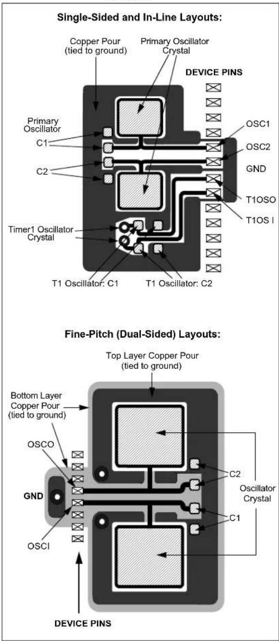
text_image
Single-Sided and In-Line Layouts: Copper Pour (tied to ground) Primary Oscillator Crystal DEVICE PINS Primary Oscillator C1 C2 Timer1 Oscillator Crystal T1 Oscillator: C1 T1 Oscillator: C2 OSC1 OSC2 GND T1OSO T1OS I Fine-Pitch (Dual-Sided) Layouts: Top Layer Copper Pour (tied to ground) Bottom Layer Copper Pour (tied to ground) OSCO GND C2 Oscillator Crystal C1 OSCI DEVICE PINS3.0 OSCILLATOR CONFIGURATIONS
3.1 Oscillator Types
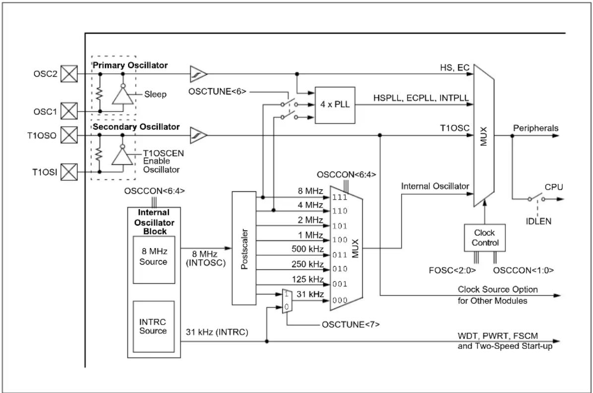
The PIC18F87J90 family of devices can be operated in eight different oscillator modes:
- ECPLL OSC1/OSC2 as primary; ECPLL oscillator with PLL enabled, CLKO on RA6
- EC OSC1/OSC2 as primary; external clock with Fosc/4 output
- HSPLL OSC1/OSC2 as primary; high-speed crystal/resonator with software PLL control
- HS OSC1/OSC2 as primary; high-speed crystal/resonator
- INTPLL1 Internal oscillator block with software PLL control, Fosc/4 output on RA6 and I/O on RA7
- INTIO1 Internal oscillator block with F osc/4 output on RA6 and I/O on RA7
- INTPLL2 Internal oscillator block with software PLL control and I/O on RA6 and RA7
- INTIO2 Internal oscillator block with I/O on RA6 and RA7
All of these modes are selected by the user by programming the FOSC<2:0> Configuration bits.
In addition, PIC18F87J90 family devices can switch between different clock sources, either under software control or automatically under certain conditions. This allows for additional power savings by managing device clock speed in real time without resetting the application.
The clock sources for the PIC18F87J90 family of devices are shown in Figure 3-1.
FIGURE 3-1: PIC18F87J90 FAMILY CLOCK DIAGRAM
flowchart
graph TD
    OSC2["OSC2"] --> PrimaryOscillator["Primary Oscillator"]
    OSC1["OSC1"] --> PrimaryOscillator
    T1OSO["T1OSO"] --> SecondaryOscillator["Secondary Oscillator"]
    T1OSI["T1OSI"] --> SecondaryOscillator
    PrimaryOscillator --> Sleep["Sleep"]
    SecondaryOscillator --> Sleep
    Sleep --> OSCTUNE6["OSCTUNE<6>"]
    OSCTUNE6 --> 4xPLL["4 x PLL"]
    4xPLL --> HSPLL["HSPPLL, ECPPLL, INTPLL"]
    HSPLL --> MUX["MUX"]
    T1OSC["T1OSC"] --> MUX
    MUX --> Peripherals["Peripherals"]
    Peripherals --> CPU["IDLEN"]
    CPU --> ClockControl["Clock Control"]
    ClockControl --> FOSC["FOSC<2:0>"]
    ClockControl --> OSCCON["OSCCON<1:0>"]
    OSCCON --> ClockSourceOption["Clock Source Option for Other Modules"]
    ClockSourceOption --> WDT["WDT, PWRT, FSCM and Two-Speed Start-up"]

    T1OSO --> T1OSCEN["Time Scan Enable Oscillator"]
    T1OSI --> T1OSCEN
    T1OSCEN --> OSCCON

    OSCCON --> InternalOscillatorBlock["Internal Oscillator Block"]
    InternalOscillatorBlock --> PostScaler["PostScaler"]
    PostScaler --> 8MHz["8 MHz Source"]
    PostScaler --> 4MHz["4 MHz Source"]
    PostScaler --> 2MHz["2 MHz Source"]
    PostScaler --> 1MHz["1 MHz Source"]
    PostScaler --> 500kHz["500 kHz"]
    PostScaler --> 250kHz["250 kHz"]
    PostScaler --> 125kHz["125 kHz"]

    INTRCSource["INTRC Source"] --> 31kHz["31 kHz (INTRC)"]

    OSCTUNE6 --> 4xPLL
    4xPLL --> HSPLL["HSPPLL, ECPPLL, INTPLL"]
    HSPLL --> MUX
    MUX --> Peripherals
3.2 Control Registers
The OSCCON register (Register 3-1) controls the main aspects of the device clock's operation. It selects the oscillator type to be used, which of the power-managed modes to invoke and the output frequency of the INTOSC source. It also provides status on the oscillators.
The OSCTUNE register (Register 3-2) controls the tuning and operation of the internal oscillator block. It also implements the PLLEN bits which control the operation of the Phase Locked Loop (PLL) (see Section 3.4.3 "PLL Frequency Multiplier").
REGISTER 3-1: OSCCON: OSCILLATOR CONTROL REGISTER
| R/W-0 R/W-1 R/W-1 R/W-0 R | (1) | R-0 R/W-0 R/W-0 | |||||
| IDLEN IRCF2 | (2) | IRCF1(2) | IRCF0(2) | OSTS IOF | S SCS1 | (4) | SCS0(4) |
| bit 7 bit 0 | |||||||
Legend:
R = Readable bit W = Writable bit U = Unimplemented bit, read as '0'
-n = Value at POR '1' = Bit is set '0' = Bit is cleared x = Bit is unknown
bit 7 IDLEN: Idle Enable bit
1 = Device enters an Idle mode when a SLEEP instruction is executed
0 = Device enters Sleep mode when a SLEEP instruction is executed
bit 6-4 IRCF<2:0>: INTOSC Source Frequency Select bits ^(2)
111 = 8 MHz (INTOSC drives clock directly)
110 = 4 MHz (default)
101 = 2 MHz
100 = 1 MHz
011 = 500 kHz
010 = 250 kHz
001 = 125 kHz
000 = 31 kHz (from either INTOSC/256 or INTRC) ^(3)
bit 3 OSTS: Oscillator Start-up Timer Time-out Status bit ^(1)
1 = Oscillator Start-up Timer (OST) time-out has expired; primary oscillator is running
0 = Oscillator Start-up Timer (OST) time-out is running; primary oscillator is not ready
bit 2 IOFS: INTOSC Frequency Stable bit
1 = Fast RC oscillator frequency is stable
0 = Fast RC oscillator frequency is not stable
bit 1-0 SCS<1:0>: System Clock Select bits ^(4)
11 = Internal oscillator block
10 = Primary oscillator
01 = Timer1 oscillator
00 = Default primary oscillator (as defined by the FOSC<2:0> Configuration bits)
Note 1: Reset state depends on the state of the IESO Configuration bit.
2: Modifying these bits will cause an immediate clock frequency switch if the internal oscillator is providing the device clocks.
3: Source selected by the INTSRC bit (OSCTUNE<7>), see text.
4: Modifying these bits will cause an immediate clock source switch.
REGISTER 3-2: OSCTUNE: OSCILLATOR TUNING REGISTER
| R/W-0 | R/W-0 | R/W-0 | R/W-0 | R/W-0 | R/W-0 | R/W-0 | R/W-0 |
| INTSRC PL | LEN TUN5 TUN4 | TUN3 TUN2 | TUN1 TUN0 | ||||
| bit 7 bit 0 | |||||||
Legend:
R = Readable bit W = Writable bit U = Unimplemented bit, read as '0'
-n = Value at POR '1' = Bit is set '0' = Bit is cleared x = Bit is unknown
bit 7 INTSRC: Internal Oscillator Low-Frequency Source Select bit
1 = 31.25 kHz device clock derived from 8 MHz INTOSC source (divide-by-256 enabled)
0 = 31 kHz device clock derived from the INTRC 31 kHz oscillator
bit 6 PLLEN: Frequency Multiplier PLL Enable bit
1 = PLL enabled
0 = PLL disabled
bit 5-0 TUN<5:0>: Fast RC Oscillator (INTOSC) Frequency Tuning bits
011111 = Maximum frequency
• •
• •
000001
000000 = Center frequency. Fast RC oscillator is running at the calibrated frequency.
111111
•
•
•
100000 = Minimum frequency
3.3 Clock Sources and Oscillator Switching
Essentially, PIC18F87J90 family devices have three independent clock sources:
- Primary oscillators
• Secondary oscillators - Internal oscillator
The primary oscillators can be thought of as the main device oscillators. These are any external oscillators connected to the OSC1 and OSC2 pins, and include the External Crystal and Resonator modes and the External Clock modes. If selected by the FOSC<2:0>Configuration bits, the internal oscillator block (either the 31 kHz INTRC or the 8 MHz INTOSC source) may be considered a primary oscillator. The particular mode is defined by the FOSC Configuration bits. The details of these modes are covered in Section 3.4 "External Oscillator Modes".
The secondary oscillators are external clock sources that are not connected to the OSC1 or OSC2 pins. These sources may continue to operate even after the
controller is placed in a power-managed mode. PIC18F87J90 family devices offer the Timer1 oscillator as a secondary oscillator source. This oscillator, in all power-managed modes, is often the time base for functions such as a Real-Time Clock (RTC). The Timer1 oscillator is discussed in greater detail in Section 12.0 "Timer1 Module".
In addition to being a primary clock source in some circumstances, the internal oscillator is available as a power-managed mode clock source. The INTRC source is also used as the clock source for several special features, such as the WDT and Fail-Safe Clock Monitor. The internal oscillator block is discussed in more detail in Section 3.5 "Internal Oscillator Block".
The PIC18F87J90 family includes features that allow the device clock source to be switched from the main oscillator, chosen by device configuration, to one of the alternate clock sources. When an alternate clock source is enabled, various power-managed operating modes are available.
3.3.1 CLOCK SOURCE SELECTION
The System Clock Select bits, SCS<1:0>(OSCCON<1:0>), select the clock source. The available clock sources are the primary clock defined by the FOSC<2:0> Configuration bits, the secondary clock (Timer1 oscillator) and the internal oscillator. The clock source changes after one or more of the bits is written to, following a brief clock transition interval.
The OSTS (OSCCON<3>) and T1RUN (T1CON<6>) bits indicate which clock source is currently providing the device clock. The OSTS bit indicates that the Oscillator Start-up Timer (OST) has timed out and the primary clock is providing the device clock in Primary Clock modes. The T1RUN bit indicates when the Timer1 oscillator is providing the device clock in Secondary Clock modes. In power-managed modes, only one of these bits will be set at any time. If neither of these bits is set, the INTRC is providing the clock, or the internal oscillator has just started and is not yet stable.
The IDLEN bit determines if the device goes into Sleep mode or one of the Idle modes when the SLEEP instruction is executed.
The use of the flag and control bits in the OSCCON register is discussed in more detail in Section 4.0 "Power-Managed Modes".
Note 1: The Timer1 oscillator must be enabled to select the secondary clock source. The Timer1 oscillator is enabled by setting the T1OSCEN bit in the Timer1 Control register (T1CON<3>). If the Timer1 oscillator is not enabled, then any attempt to select a secondary clock source when executing a SLEEP instruction will be ignored.
2: It is recommended that the Timer1 oscillator be operating and stable before executing the SLEEP instruction or a very long delay may occur while the Timer1 oscillator starts.
3.3.1.1 System Clock Selection and Device Resets
Since the SCS bits are cleared on all forms of Reset, this means the primary oscillator defined by the FOSC<2:0> Configuration bits is used as the primary clock source on device Resets. This could either be the internal oscillator block by itself or one of the other primary clock source (HS, EC, HSPLL, ECPLL1/2 or INTPLL1/2).
In those cases when the internal oscillator block, without PLL, is the default clock on Reset, the Fast RC oscillator (INTOSC) will be used as the device clock source. It will initially start at 1 MHz; the postscaler selection that corresponds to the Reset value of the IRCF<2:0> bits ('100').
Regardless of which primary oscillator is selected, INTRC will always be enabled on device power-up. It serves as the clock source until the device has loaded its configuration values from memory. It is at this point that the FOSC Configuration bits are read and the oscillator selection of the operational mode is made.
Note that either the primary clock source, or the internal oscillator, will have two bit setting options for the possible values of the SCS<1:0> bits at any given time.
3.3.2 OSCILLATOR TRANSITIONS
PIC18F87J90 family devices contain circuitry to prevent clock "glitches" when switching between clock sources. A short pause in the device clock occurs during the clock switch. The length of this pause is the sum of two cycles of the old clock source and three to four cycles of the new clock source. This formula assumes that the new clock source is stable.
Clock transitions are discussed in greater detail in Section 4.1.2 "Entering Power-Managed Modes".
3.4 External Oscillator Modes
3.4.1 CRYSTAL OSCILLATOR/CERAMIC RESONATORS (HS MODES)
In HS or HSPLL Oscillator modes, a crystal or ceramic resonator is connected to the OSC1 and OSC2 pins to establish oscillation. Figure 3-2 shows the pin connections.
The oscillator design requires the use of a crystal rated for parallel resonant operation.
Note: Use of a crystal rated for series resonant operation may give a frequency out of the crystal manufacturer's specifications.
TABLE 3-1: CAPACITOR SELECTION FOR CERAMIC RESONATORS
| Typical Capacitor Values Used: | |||
| Mode Freq. OSC1 OSC2 | |||
| HS 8.0 | MHz16.0 MHz | 27 pF22 pF | 27 pF22 pF |
| Capacitor values are for design guidance only.Different capacitor values may be required to produce acceptable oscillator operation. The user should test the performance of the oscillator over the expected VDD and temperature range for the application. Refer to the following application notes for oscillator specific information:AN588, “PIC®Microcontroller Oscillator Design Guide”AN826, “Crystal Oscillator Basics and Crystal Selection for rfPIC®and PIC®Devices”AN849, “Basic PIC®Oscillator Design”AN943, “Practical PIC®Oscillator Analysis and Design”AN949, “Making Your Oscillator Work”See the notes following Table 3-2 for additional information. | |||
TABLE 3-2: CAPACITOR SELECTION FOR CRYSTAL OSCILLATOR
| Osc Type | Crystal Freq. | Typical Capacitor Values Tested: | |
| C1 | C2 | ||
| HS | 4 MHz 27 | pF 27 | pF |
| 8 MHz 22 | pF 22 | pF | |
| 20 MHz | 15 pF 15 | pF | |
Capacitor values are for design guidance only.
Different capacitor values may be required to produce acceptable oscillator operation. The user should test the performance of the oscillator over the expected VDD and temperature range for the application.
Refer to the Microchip application notes cited in Table 3-1 for oscillator specific information. Also see the notes following this table for additional information.
Note 1: Higher capacitance increases the stability of oscillator but also increases the start-up time.
2: Since each resonator/crystal has its own characteristics, the user should consult the resonator/crystal manufacturer for appropriate values of external components.
3: Rs may be required to avoid overdriving crystals with low drive level specification.
4: Always verify oscillator performance over the VDD and temperature range that is expected for the application.
FIGURE 3-2: CRYSTAL/CERAMIC
RESONATOR OPERATION
(HS OR HSPLL
CONFIGURATION)

text_image
C1(1) XTAL OSC1 C2(1) Rs(2) OSC2 RF(3) To Internal Logic Sleep PIC18F87J90Note 1: See Table 3-1 and Table 3-2 for initial values of C1 and C2.
2: A series resistor (Rs) may be required for AT strip cut crystals.
3: RF varies with the oscillator mode chosen.
3.4.2 EXTERNAL CLOCK INPUT (EC MODES)
The EC and ECPLL Oscillator modes require an external clock source to be connected to the OSC1 pin. There is no oscillator start-up time required after a Power-on Reset or after an exit from Sleep mode.
In the EC Oscillator mode, the oscillator frequency divided by 4 is available on the OSC2 pin. This signal may be used for test purposes or to synchronize other logic. Figure 3-3 shows the pin connections for the EC Oscillator mode.
FIGURE 3-3: EXTERNAL CLOCK
INPUT OPERATION
(EC CONFIGURATION)

flowchart
graph LR
    A["Clock from Ext. System"] --> B((Osc1/CLKI PIC18F87J90))
    B --> C["Fosc/4"]
    C --> D["OSC2/CLKO"]
An external clock source may also be connected to the OSC1 pin in the HS mode, as shown in Figure 3-4. In this configuration, the divide-by-4 output on OSC2 is not available. Current consumption in this configuration will be somewhat higher than EC mode, as the internal oscillator's feedback circuitry will be enabled (in EC mode, the feedback circuit is disabled).
FIGURE 3-4: EXTERNAL CLOCK INPUT OPERATION (HS OSC CONFIGURATION)

flowchart
graph LR
    A["Clock from Ext. System"] --> B["AND"]
    B --> C["OSC1 PIC18F87J90 (HS Mode)"]
    D["Open"] --> E["OSC2"]
3.4.3 PLL FREQUENCY MULTIPLIER
A Phase Locked Loop (PLL) circuit is provided as an option for users who want to use a lower frequency oscillator circuit, or to clock the device up to its highest rated frequency from a crystal oscillator. This may be useful for customers who are concerned with EMI due to high-frequency crystals, or users who require higher clock speeds from an internal oscillator.
3.4.3.1 HSPLL and ECPLL Modes
The HSPLL and ECPLL modes provide the ability to selectively run the device at 4 times the external oscillating source to produce frequencies of up to 40 MHz.
The PLL is enabled by programming the FOSC<2:0> Configuration bits to either '111' (for ECPLL) or '101' (for HSPLL). In addition, the PLLEN bit (OSCTUNE<6>) must also be set. Clearing PLLEN disables the PLL, regardless of the chosen oscillator configuration. It also allows additional flexibility for controlling the application's clock speed in software.
FIGURE 3-5: PLL BLOCK DIAGRAM
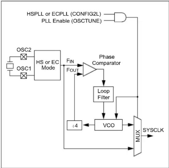
flowchart
graph TD
    A["OSC1"] --> B["HS or EC Mode"]
    C["OSC2"] --> B
    B --> D["FOUT"]
    D --> E["Phase Comparator"]
    E --> F["Loop Filter"]
    F --> G["VCO"]
    G --> H["MUX"]
    H --> I["SYSCLK"]
    J["HSPLL or ECPLL (CONFIG2L) PLL Enable (OSCTUNE)"] --> K["AND"]
    K --> L["Output"]
    M["÷4"] --> G
    N["FIN"] --> E
The PLL is also available to the internal oscillator block when the internal oscillator block is configured as the primary clock source. In this configuration, the PLL is enabled in software and generates a clock output of up to 32 MHz. The operation of INTOSC with the PLL is described in Section 3.5.2 "INTPLL Modes".
3.5 Internal Oscillator Block
The PIC18F87J90 family of devices includes an internal oscillator block which generates two different clock signals; either can be used as the microcontroller's clock source. This may eliminate the need for an external oscillator circuit on the OSC1 and/or OSC2 pins.
The main output is the Fast RC oscillator or INTOSC, an 8 MHz clock source which can be used to directly drive the device clock. It also drives a postscaler, which can provide a range of clock frequencies from 31 kHz to 4 MHz. INTOSC is enabled when a clock frequency from 125 kHz to 8 MHz is selected. The INTOSC output can also be enabled when 31 kHz is selected, depending on the INTSRC bit (OSCTUNE<7>).
The other clock source is the Internal RC oscillator (INTRC), which provides a nominal 31 kHz output. INTRC is enabled if it is selected as the device clock source; it is also enabled automatically when any of the following are enabled:
- Power-up Timer
- Fail-Safe Clock Monitor
- Watchdog Timer
- Two-Speed Start-up
These features are discussed in greater detail in Section 25.0 "Special Features of the CPU".
The clock source frequency (INTOSC direct, INTOSC with postscaler or INTRC direct) is selected by configuring the IRCF bits of the OSCCON register. The default frequency on device Resets is 4 MHz.
3.5.1 INTIO MODES
Using the internal oscillator as the clock source eliminates the need for up to two external oscillator pins, which can then be used for digital I/O. Two distinct oscillator configurations, which are determined by the FOSC Configuration bits, are available:
- In INTIO1 mode, the OSC2 pin outputs F osc/4, while OSC1 functions as RA7 (see Figure 3-6) for digital input and output.
- In INTIO2 mode, OSC1 functions as RA7 and OSC2 functions as RA6 (see Figure 3-7), both for digital input and output.
FIGURE 3-6: INTIO1 OSCILLATOR MODE

text_image
RA7 ← I/O (OSC1) PIC18F87J90 Fosc/4 ← OSC2FIGURE 3-7: INTIO2 OSCILLATOR MODE

text_image
RA7 ←→ I/O (OSC1) PIC18F87J90 RA6 ←→ I/O (OSC2)3.5.2 INTPLL MODES
The 4x Phase Locked Loop (PLL) can be used with the internal oscillator block to produce faster device clock speeds than are normally possible with the internal oscillator sources. When enabled, the PLL produces a clock speed of 16 MHz or 32 MHz.
PLL operation is controlled through software. The control bit, PLLEN (OSCTUNE<6>), is used to enable or disable its operation. The PLL is available only to INTOSC when the device is configured to use one of the INTPLL modes as the primary clock source (FOSC<2:0>=011 or 001). Additionally, the PLL will only function when the selected output frequency is either 4 MHz or 8 MHz (OSCCON<6:4>=111 or 110).
Like the INTIO modes, there are two distinct INTPLL modes available:
- In INTPLL1 mode, the OSC2 pin outputs F osc/4, while OSC1 functions as RA7 for digital input and output. Externally, this is identical in appearance to INTIO1 (Figure 3-6).
- In INTPLL2 mode, OSC1 functions as RA7 and OSC2 functions as RA6, both for digital input and output. Externally, this is identical to INTIO2 (Figure 3-7).
3.5.3 INTERNAL OSCILLATOR OUTPUT FREQUENCY AND TUNING
The internal oscillator block is calibrated at the factory to produce an INTOSC output frequency of 8 MHz. It can be adjusted in the user's application by writing to TUN<5:0> (OSCTUNE<5:0>) in the OSCTUNE register (Register 3-2).
When the OSCTUNE register is modified, the INTOSC frequency will begin shifting to the new frequency. The oscillator will stabilize within 1 ms. Code execution continues during this shift and there is no indication that the shift has occurred.
The INTRC oscillator operates independently of the INTOSC source. Any changes in INTOSC across voltage and temperature are not necessarily reflected by changes in INTRC or vice versa. The frequency of INTRC is not affected by OSCTUNE.
3.5.4 INTOSC FREQUENCY DRIFT
The INTOSC frequency may drift as VDD or temperature changes, and can affect the controller operation in a variety of ways. It is possible to adjust the INTOSC frequency by modifying the value in the OSCTUNE register. Depending on the device, this may have no effect on the INTRC clock source frequency.
Tuning INTOSC requires knowing when to make the adjustment, in which direction it should be made, and in some cases, how large a change is needed. Three compensation techniques are shown here.
3.5.4.1 Compensating with the EUSART
An adjustment may be required when the EUSART begins to generate framing errors or receives data with errors while in Asynchronous mode. Framing errors indicate that the device clock frequency is too high. To adjust for this, decrement the value in OSCTUNE to reduce the clock frequency. On the other hand, errors in data may suggest that the clock speed is too low. To compensate, increment OSCTUNE to increase the clock frequency.
3.5.4.2 Compensating with the Timers
This technique compares device clock speed to some reference clock. Two timers may be used; one timer is clocked by the peripheral clock, while the other is clocked by a fixed reference source, such as the Timer1 oscillator.
Both timers are cleared, but the timer clocked by the reference generates interrupts. When an interrupt occurs, the internally clocked timer is read and both timers are cleared. If the internally clocked timer value is much greater than expected, then the internal oscillator block is running too fast. To adjust for this, decrement the OSCTUNE register.
3.5.4.3 Compensating with the CCP Module in Capture Mode
A CCP module can use free-running Timer1 (or Timer3), clocked by the internal oscillator block and an external event with a known period (i.e., AC power frequency). The time of the first event is captured in the CCPRxH:CCPRxL registers and is recorded for use later. When the second event causes a capture, the time of the first event is subtracted from the time of the second event. Since the period of the external event is known, the time difference between events can be calculated.
If the measured time is much greater than the calculated time, the internal oscillator block is running too fast. To compensate, decrement the OSCTUNE register. If the measured time is much less than the calculated time, the internal oscillator block is running too slow. To compensate, increment the OSCTUNE register.
3.6 Effects of Power-Managed Modes on the Various Clock Sources
When PRI_IDLE mode is selected, the designated primary oscillator continues to run without interruption. For all other power-managed modes, the oscillator using the OSC1 pin is disabled. The OSC1 pin (and OSC2 pin if used by the oscillator) will stop oscillating.
In Secondary Clock modes (SEC_RUN and SEC_IDLE), the Timer1 oscillator is operating and providing the device clock. The Timer1 oscillator may also run in all power-managed modes if required to clock Timer1 or Timer3.
In RC_RUN and RC_IDLE modes, the internal oscillator provides the device clock source. The 31 kHz INTRC output can be used directly to provide the clock and may be enabled to support various special features, regardless of the power-managed mode (see Section 25.2 "Watchdog Timer (WDT)" through Section 25.5 "Fail-Safe Clock Monitor" for more information on WDT, Fail-Safe Clock Monitor and Two-Speed Start-up).
If Sleep mode is selected, all clock sources are stopped. Since all the transistor switching currents have been stopped, Sleep mode achieves the lowest current consumption of the device (only leakage currents).
Enabling any on-chip feature that will operate during Sleep will increase the current consumed during Sleep. The INTRC is required to support WDT operation. The
Timer1 oscillator may be operating to support a Real-Time Clock (RTC). Other features may be operating that do not require a device clock source (i.e., MSSP slave, INTx pins and others). Peripherals that may add significant current consumption are listed in Section 28.2 "DC Characteristics: Power-Down and Supply Current PIC18F87J90 Family (Industrial)".
3.7 Power-up Delays
Power-up delays are controlled by two timers, so that no external Reset circuitry is required for most applications. The delays ensure that the device is kept in Reset until the device power supply is stable under normal circumstances and the primary clock is operating and stable. For additional information on power-up delays, see Section 5.6 "Power-up Timer (PWRT)".
The first timer is the Power-up Timer (PWRT), which provides a fixed delay on power-up (parameter 33, Table 28-11); it is always enabled.
The second timer is the Oscillator Start-up Timer (OST), intended to keep the chip in Reset until the crystal oscillator is stable (HS modes). The OST does this by counting 1024 oscillator cycles before allowing the oscillator to clock the device.
There is a delay of interval, TCSD (parameter 38, Table 28-11), following POR, while the controller becomes ready to execute instructions.
TABLE 3-3: OSC1 AND OSC2 PIN STATES IN SLEEP MODE
| Oscillator Mode OSC1 | Pin OSC2 Pin | |
| EC, ECPLL Floating, pulled | by external clock At logic low (clock/4 output) | |
| HS, HSPLL Feedback inverter | disabled at quiescent voltage level | Feedback inverter disabled at quiescent voltage level |
| INTOSC, INTPLL1/2 I/O pin | RA6, direction controlled by TRISA<6> | I/O pin RA6, direction controlled by TRISA<7> |
Note: See Section 5.0 "Reset" for time-outs due to Sleep and MCLR Reset.
NOTES:
4.0 POWER-MANAGED MODES
The PIC18F87J90 family devices provide the ability to manage power consumption by simply managing clocking to the CPU and the peripherals. In general, a lower clock frequency and a reduction in the number of circuits being clocked constitutes lower consumed power. For the sake of managing power in an application, there are three primary modes of operation:
- Run mode
- Idle mode
- Sleep mode
These modes define which portions of the device are clocked and at what speed. The Run and Idle modes may use any of the three available clock sources (primary, secondary or internal oscillator block); the Sleep mode does not use a clock source.
The power-managed modes include several power-saving features offered on previous PIC ^® devices. One is the clock switching feature, offered in other PIC18 devices, allowing the controller to use the Timer1 oscillator in place of the primary oscillator. Also included is the Sleep mode, offered by all PIC devices, where all device clocks are stopped.
4.1 Selecting Power-Managed Modes
Selecting a power-managed mode requires two decisions: if the CPU is to be clocked or not and which clock source is to be used. The IDLEN bit (OSCCON<7>) controls CPU clocking, while the SCS<1:0> bits (OSCCON<1:0>) select the clock source. The individual modes, bit settings, clock sources and affected modules are summarized in Table 4-1.
4.1.1 CLOCK SOURCES
The SCS<1:0> bits allow the selection of one of three clock sources for power-managed modes. They are:
- the primary clock, as defined by the FOSC<2:0> Configuration bits
• the secondary clock (Timer1 oscillator)
• the internal oscillator
4.1.2 ENTERING POWER-MANAGED MODES
Switching from one power-managed mode to another begins by loading the OSCCON register. The SCS<1:0> bits select the clock source and determine which Run or Idle mode is to be used. Changing these bits causes an immediate switch to the new clock source, assuming that it is running. The switch may also be subject to clock transition delays. These are discussed in Section 4.1.3 "Clock Transitions and Status Indicators" and subsequent sections.
Entry to the power-managed Idle or Sleep modes is triggered by the execution of a SLEEP instruction. The actual mode that results depends on the status of the IDLEN bit.
Depending on the current mode and the mode being switched to, a change to a power-managed mode does not always require setting all of these bits. Many transitions may be done by changing the oscillator select bits, or changing the IDLEN bit, prior to issuing a SLEEP instruction. If the IDLEN bit is already configured correctly, it may only be necessary to perform a SLEEP instruction to switch to the desired mode.
TABLE 4-1: POWER-MANAGED MODES
| Mode | OSCCON Bits Module | Clocking | Available Clock and Oscillator Source | ||
| IDLEN<7>(1) | SCS<1:0>CPU | Peripherals | |||
| Sleep | 0 | N/A | Off | Off | None – All clocks are disabled |
| PRI_RUN | N/A | 10 | Clocked | Clocked | Primary – HS, EC, HSPLL, ECPPL; this is the normal full-power execution mode |
| SEC_RUN | N/A | 01 | Clocked | Clocked | Secondary – Timer1 Oscillator |
| RC_RUN | N/A | 11 | Clocked | Clocked | Internal Oscillator |
| PRI_IDLE | 1 | 10 | Off | Clocked | Primary – HS, EC, HSPLL, ECPPL |
| SEC_IDLE | 1 | 01 | Off | Clocked | Secondary – Timer1 Oscillator |
| RC_IDLE | 1 | 11 | Off | Clocked | Internal Oscillator |
Note 1: IDLEN reflects its value when the SLEEP instruction is executed.
4.1.3 CLOCK TRANSITIONS AND STATUS INDICATORS
The length of the transition between clock sources is the sum of two cycles of the old clock source and three to four cycles of the new clock source. This formula assumes that the new clock source is stable.
Two bits indicate the current clock source and its status: OSTS (OSCCON<3>) and T1RUN (T1CON<6>). In general, only one of these bits will be set while in a given power-managed mode. When the OSTS bit is set, the primary clock is providing the device clock. When the T1RUN bit is set, the Timer1 oscillator is providing the clock. If neither of these bits is set, INTRC is clocking the device.
Note: Executing a SLEEP instruction does not necessarily place the device into Sleep mode. It acts as the trigger to place the controller into either the Sleep mode, or one of the Idle modes, depending on the setting of the IDLEN bit.
4.1.4 MULTIPLE SLEEP COMMANDS
The power-managed mode that is invoked with the SLEEP instruction is determined by the setting of the IDLEN bit at the time the instruction is executed. If another SLEEP instruction is executed, the device will enter the power-managed mode specified by IDLEN at that time. If IDLEN has changed, the device will enter the new power-managed mode specified by the new setting.
4.2 Run Modes
In the Run modes, clocks to both the core and peripherals are active. The difference between these modes is the clock source.
4.2.1 PRI\_RUN MODE
The PRI_RUN mode is the normal, full-power execution mode of the microcontroller. This is also the default mode upon a device Reset unless Two-Speed Start-up is enabled (see Section 25.4 "Two-Speed Start-up" for details). In this mode, the OSTS bit is set (see Section 3.2 "Control Registers").
4.2.2 SEC\_RUN MODE
The SEC_RUN mode is the compatible mode to the "clock switching" feature offered in other PIC18 devices. In this mode, the CPU and peripherals are clocked from the Timer1 oscillator. This gives users the option of lower power consumption while still using a high-accuracy clock source.
SEC_RUN mode is entered by setting the SCS<1:0> bits to '01'. The device clock source is switched to the Timer1 oscillator (see Figure 4-1), the primary oscillator is shut down, the T1RUN bit (T1CON<6>) is set and the OSTS bit is cleared.
Note: The Timer1 oscillator should already be running prior to entering SEC_RUN mode. If the T1OSCEN bit is not set when the SCS<1:0> bits are set to '01', entry to SEC_RUN mode will not occur. If the Timer1 oscillator is enabled, but not yet running, device clocks will be delayed until the oscillator has started. In such situations, initial oscillator operation is far from stable and unpredictable operation may result.
On transitions from SEC_RUN mode to PRI_RUN mode, the peripherals and CPU continue to be clocked from the Timer1 oscillator while the primary clock is started. When the primary clock becomes ready, a clock switch back to the primary clock occurs (see
Figure 4-2). When the clock switch is complete, the T1RUN bit is cleared, the OSTS bit is set and the primary clock is providing the clock. The IDLEN and SCS bits are not affected by the wake-up; the Timer1 oscillator continues to run.
FIGURE 4-1: TRANSITION TIMING FOR ENTRY TO SEC_RUN MODE
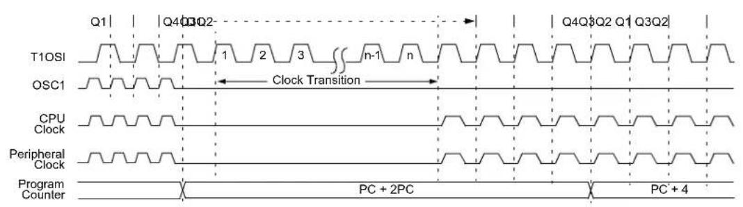
text_image
Q1 | Q4 Q2 T1OSI 1 2 3 n-1 n Q4 Q3 Q2 Q1 Q3Q2 | OSC1 Clock Transition CPU Clock Peripheral Clock Program Counter PC + 2PC PC + 4FIGURE 4-2: TRANSITION TIMING FROM SEC_RUN MODE TO PRI_RUN MODE (HSPLL)
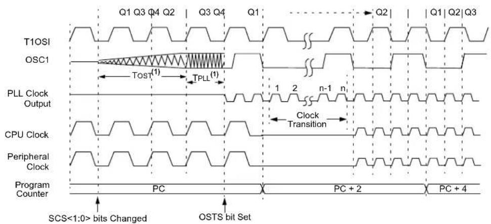
text_image
T1OSI OSC1 PLL Clock Output CPU Clock Peripheral Clock Program Counter Q1 Q3 Q4 Q2 | Q3 Q4 Q1 Tost(1) TPLL(1) Clock Transition 1 2 n-1 n PC + 2 PC + 4 SCS<1:0> bits Changed OSTS bit SetNote 1: TOST = 1024 TOSC; TPLL = 2 ms (approx). These intervals are not shown to scale.
4.2.3 RC\_RUN MODE
In RC_RUN mode, the CPU and peripherals are clocked from the internal oscillator; the primary clock is shut down. This mode provides the best power conservation of all the Run modes while still executing code. It works well for user applications which are not highly timing-sensitive or do not require high-speed clocks at all times.
This mode is entered by setting the SCS bits to '11'. When the clock source is switched to the INTRC (see Figure 4-3), the primary oscillator is shut down and the OSTS bit is cleared.
On transitions from RC_RUN mode to PRI_RUN mode, the device continues to be clocked from the INTRC while the primary clock is started. When the primary clock becomes ready, a clock switch to the primary clock occurs (see Figure 4-4). When the clock switch is complete, the OSTS bit is set and the primary clock is providing the device clock. The IDLEN and SCS bits are not affected by the switch. The INTRC source will continue to run if either the WDT or the Fail-Safe Clock Monitor is enabled.
FIGURE 4-3: TRANSITION TIMING TO RC_RUN MODE

text_image
Q1 Q4 Q3 Q2 INTRC 1 2 3 n - 1 n OSC1 Clock Transition CPU Clock Peripheral Clock Program Counter PC + 2PC PC + 4FIGURE 4-4: TRANSITION TIMING FROM RC_RUN MODE TO PRI_RUN MODE

text_image
INTRC OSC1 PLL Clock Output CPU Clock Peripheral Clock Program Counter Q1 Q2 Q3 Q4 Q1 Q2 Q3 TOST(1) TPLL(1) 1 2 n-1 n Clock Transition PC PC + 2 PC + 4 SCS<1:0> bits Changed OSTS bit SetNote 1: TOST = 1024 TOSC; TPLL = 2 ms (approx). These intervals are not shown to scale.
4.3 Sleep Mode
The power-managed Sleep mode is identical to the legacy Sleep mode offered in all other PIC devices. It is entered by clearing the IDLEN bit (the default state on device Reset) and executing the SLEEP instruction. This shuts down the selected oscillator (Figure 4-5). All clock source status bits are cleared.
Entering the Sleep mode from any other mode does not require a clock switch. This is because no clocks are needed once the controller has entered Sleep. If the WDT is selected, the INTRC source will continue to operate. If the Timer1 oscillator is enabled, it will also continue to run.
When a wake event occurs in Sleep mode (by interrupt, Reset or WDT time-out), the device will not be clocked until the clock source, selected by the SCS<1:0> bits, becomes ready (see Figure 4-6), or it will be clocked from the internal oscillator if either the Two-Speed Start-up or the Fail-Safe Clock Monitor is enabled (see Section 25.0 "Special Features of the CPU"). In either case, the OSTS bit is set when the primary clock is providing the device clocks. The IDLEN and SCS bits are not affected by the wake-up.
4.4 Idle Modes
The Idle modes allow the controller's CPU to be selectively shut down while the peripherals continue to operate. Selecting a particular Idle mode allows users to further manage power consumption.
If the IDLEN bit is set to a '1' when a SLEEP instruction is executed, the peripherals will be clocked from the clock source selected using the SCS<1:0> bits; however, the CPU will not be clocked. The clock source status bits are not affected. Setting IDLEN and executing a SLEEP instruction provides a quick method of switching from a given Run mode to its corresponding Idle mode.
If the WDT is selected, the INTRC source will continue to operate. If the Timer1 oscillator is enabled, it will also continue to run.
Since the CPU is not executing instructions, the only exits from any of the Idle modes are by interrupt, WDT time-out or a Reset. When a wake event occurs, CPU execution is delayed by an interval of TCSD (parameter 38, Table 28-11) while it becomes ready to execute code. When the CPU begins executing code, it resumes with the same clock source for the current Idle mode. For example, when waking from RC_IDLE mode, the internal oscillator block will clock the CPU and peripherals (in other words, RC_RUN mode). The IDLEN and SCS bits are not affected by the wake-up.
While in any Idle mode or Sleep mode, a WDT time-out will result in a WDT wake-up to the Run mode currently specified by the SCS<1:0> bits.
FIGURE 4-5: TRANSITION TIMING FOR ENTRY TO SLEEP MODE

text_image
OSC1 CPU Clock Peripheral Clock Sleep Program Counter Q4 Q3 Q2 1 PC + 2PCFIGURE 4-6: TRANSITION TIMING FOR WAKE FROM SLEEP (HSPLL)

other
| Signal | Phase | Value | |-----------------|---------|-------| | OSC1 | Q1-Q2 | TOST(1) | | OSC1 | Q3-Q4 | TPLL(1) | | OSC1 | Q1-Q2 | TOST(Q1) | | OSC1 | Q3-Q4 | TPLL(Q3) | | PLL Clock Output | Q1-Q2 | TOST(1) | | PLL Clock Output | Q3-Q4 | TPLL(1) | | CPU Clock | Q1-Q2 | TOST(Q1) | | CPU Clock | Q3-Q4 | TPLL(Q3) | | Peripheral Clock| Q1-Q2 | TOST(Q1) | | Peripheral Clock| Q3-Q4 | TPLL(Q3) | | Program Counter | Q1-Q2 | TOST(Q1) | | Program Counter | Q3-Q4 | TPLL(Q3) | | Note 1 | TOST | 1024 TOSC; TPLL = 2 ms (approx). These intervals are not shown to scale.4.4.1 PRI\_IDLE MODE
This mode is unique among the three low-power Idle modes, in that it does not disable the primary device clock. For timing-sensitive applications, this allows for the fastest resumption of device operation with its more accurate primary clock source, since the clock source does not have to "warm up" or transition from another oscillator.
PRI_IDLE mode is entered from PRI_RUN mode by setting the IDLEN bit and executing a SLEEP instruction. If the device is in another Run mode, set IDLEN first, then set the SCS bits to '10' and execute SLEEP. Although the CPU is disabled, the peripherals continue to be clocked from the primary clock source specified by the FOSC<1:0> Configuration bits. The OSTS bit remains set (see Figure 4-7).
When a wake event occurs, the CPU is clocked from the primary clock source. A delay of interval, TcsD, is required between the wake event and when code execution starts. This is required to allow the CPU to become ready to execute instructions. After the wake-up, the OSTS bit remains set. The IDLEN and SCS bits are not affected by the wake-up (see Figure 4-8).
4.4.2 SEC\_IDLE MODE
In SEC_IDLE mode, the CPU is disabled but the peripherals continue to be clocked from the Timer1 oscillator. This mode is entered from SEC_RUN by setting the IDLEN bit and executing a SLEEP instruction. If the device is in another Run mode, set IDLEN first, then set SCS<1:0> to '01' and execute SLEEP. When the clock source is switched to the Timer1 oscillator, the primary oscillator is shut down, the OSTS bit is cleared and the T1RUN bit is set.
When a wake event occurs, the peripherals continue to be clocked from the Timer1 oscillator. After an interval of Tcsd, following the wake event, the CPU begins executing code being clocked by the Timer1 oscillator. The IDLEN and SCS bits are not affected by the wake-up; the Timer1 oscillator continues to run (see Figure 4-8).
Note: The Timer1 oscillator should already be running prior to entering SEC_IDLE mode. If the T1OSCEN bit is not set when the SLEEP instruction is executed, the SLEEP instruction will be ignored and entry to SEC_IDLE mode will not occur. If the Timer1 oscillator is enabled, but not yet running, peripheral clocks will be delayed until the oscillator has started. In such situations, initial oscillator operation is far from stable and unpredictable operation may result.
FIGURE 4-7: TRANSITION TIMING FOR ENTRY TO IDLE MODE
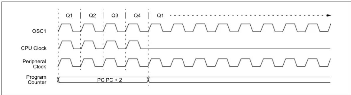
text_image
OSC1 CPU Clock Peripheral Clock Program Counter Q1 Q2 Q3 Q4 Q1 PC PC + 2FIGURE 4-8: TRANSITION TIMING FOR WAKE FROM IDLE TO RUN MODE

text_image
Q1 Q3-Q4 OSC1 CPU Clock Peripheral Clock Program Counter TCSD PC Wake Event Q24.4.3 RC\_IDLE MODE
In RC_IDLE mode, the CPU is disabled but the peripherals continue to be clocked from the internal oscillator. This mode allows for controllable power conservation during Idle periods.
From RC_RUN, this mode is entered by setting the IDLEN bit and executing a SLEEP instruction. If the device is in another Run mode, first set IDLEN, then clear the SCS bits and execute SLEEP. When the clock source is switched to the INTRC, the primary oscillator is shut down and the OSTS bit is cleared.
When a wake event occurs, the peripherals continue to be clocked from the INTOSC. After a delay of TcSD, following the wake event, the CPU begins executing code being clocked by the INTOSC. The IDLEN and SCS bits are not affected by the wake-up. The INTOSC source will continue to run if either the WDT or the Fail-Safe Clock Monitor is enabled.
4.5 Exiting Idle and Sleep Modes
An exit from Sleep mode, or any of the Idle modes, is triggered by an interrupt, a Reset or a WDT time-out. This section discusses the triggers that cause exits from power-managed modes. The clocking subsystem actions are discussed in each of the power-managed mode sections (see Section 4.2 "Run Modes", Section 4.3 "Sleep Mode" and Section 4.4 "Idle Modes").
4.5.1 EXIT BY INTERRUPT
Any of the available interrupt sources can cause the device to exit from an Idle mode, or the Sleep mode, to a Run mode. To enable this functionality, an interrupt source must be enabled by setting its enable bit in one of the INTCON or PIE registers. The exit sequence is initiated when the corresponding interrupt flag bit is set.
On all exits from Idle or Sleep modes by interrupt, code execution branches to the interrupt vector if the GIE/GIEH bit (INTCON<7>) is set. Otherwise, code execution continues or resumes without branching (see Section 9.0 "Interrupts").
A fixed delay of interval, TCSD, following the wake event, is required when leaving Sleep and Idle modes. This delay is required for the CPU to prepare for execution. Instruction execution resumes on the first clock cycle following this delay.
4.5.2 EXIT BY WDT TIME-OUT
A WDT time-out will cause different actions depending on which power-managed mode the device is in when the time-out occurs.
If the device is not executing code (all Idle modes and Sleep mode), the time-out will result in an exit from the power-managed mode (see Section 4.2 "Run Modes" and Section 4.3 "Sleep Mode"). If the device is executing code (all Run modes), the time-out will result in a WDT Reset (see Section 25.2 "Watchdog Timer (WDT)").
The Watchdog Timer and postscaler are cleared by one of the following events:
- executing a SLEEP or CLRWDT instruction
- the loss of a currently selected clock source (if the Fail-Safe Clock Monitor is enabled)
4.5.3 EXIT BY RESET
Exiting an Idle or Sleep mode by Reset automatically forces the device to run from the INTRC.
4.5.4 EXIT WITHOUT AN OSCILLATOR START-UP DELAY
Certain exits from power-managed modes do not invoke the OST at all. There are two cases:
- PRI_IDLE mode, where the primary clock source is not stopped; and
- the primary clock source is either the EC or ECPLL mode.
In these instances, the primary clock source either does not require an oscillator start-up delay, since it is already running (PRI_IDLE), or normally does not require an oscillator start-up delay (EC). However, a fixed delay of interval, TcsD, following the wake event is still required when leaving Sleep and Idle modes to allow the CPU to prepare for execution. Instruction execution resumes on the first clock cycle following this delay.
NOTES:
5.0 RESET
The PIC18F87J90 family of devices differentiates between various kinds of Reset:
• Power-on Reset (POR)
• M C Reset during normal operation
- M C L R Reset during power-managed modes
- Watchdog Timer (WDT) Reset (during execution)
- Brown-out Reset (BOR)
- Configuration Mismatch (CM) Reset
- RESET Instruction
- Stack Full Reset
- Stack Underflow Reset
This section discusses Resets generated by MCLR, POR and BOR, and covers the operation of the various start-up timers. Stack Reset events are covered in Section 6.1.4.4 "Stack Full and Underflow Resets". WDT Resets are covered in Section 25.2 "Watchdog Timer (WDT)".
A simplified block diagram of the on-chip Reset circuit is shown in Figure 5-1.
5.1 RCON Register
Device Reset events are tracked through the RCON register (Register 5-1). The lower five bits of the register indicate that a specific Reset event has occurred. In most cases, these bits can only be set by the event and must be cleared by the application after the event. The state of these flag bits, taken together, can be read to indicate the type of Reset that just occurred. This is described in more detail in Section 5.7 "Reset State of Registers".
The RCON register also has a control bit for setting interrupt priority (IPEN). Interrupt priority is discussed in Section 9.0 "Interrupts".
FIGURE 5-1: SIMPLIFIED BLOCK DIAGRAM OF ON-CHIP RESET CIRCUIT
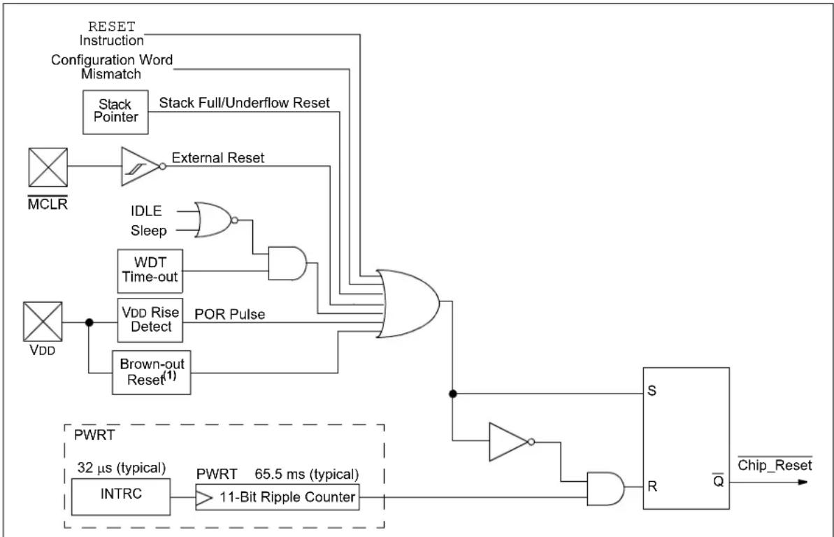
flowchart
graph TD
    A["RESET Instruction"] --> B["Configuration Word Mismatch"]
    B --> C["Stack Pointer"]
    C --> D["Stack Full/Underflow Reset"]
    D --> E["MCLR"]
    E --> F["External Reset"]
    F --> G["WDT Time-out"]
    G --> H["VDD Rise Detect"]
    H --> I["POR Pulse"]
    I --> J["Brown-out Reset(1)"]
    J --> K["32 µs (typical)"]
    K --> L["INTRC"]
    L --> M["11-Bit Ripple Counter"]
    M --> N["S Chip_Reset"]
    N --> O["R"]
    O --> P["Q̅"]
    P --> Q["Chip_Reset"]
    style A fill:#f9f,stroke:#333
    style Q fill:#ccf,stroke:#333
Note 1: The ENVREG pin must be tied high to enable Brown-out Reset. The Brown-out Reset is provided by the on-chip voltage regulator when there is insufficient source voltage to maintain regulation.
REGISTER 5-1: RCON: RESET CONTROL REGISTER
| R/W-0 U-0 R/W-1 R/W-1 R-1 R-1 R/W-0 R/W-0 | |||||||
| IPEN | — | M^- | RI TO PD P | OR BOR | — | — | |
| bit 7 bit 0 | |||||||
Legend:
| R = Readable bit W = Writable bit U = Unimplemented bit, read as '0' | |||
| -n = Value at POR | '1' = Bit is set | '0' = Bit is cleared | x = Bit is unknown |
bit 7 IPEN: Interrupt Priority Enable bit
1 = Enable priority levels on interrupts
0 = Disable priority levels on interrupts (PIC16XXXX Compatibility mode)
bit 6 Unimplemented: Read as '0'
bit 5 CM: Configuration Mismatch Flag bit
1 = A configuration mismatch has not occurred
0 = A configuration mismatch has occurred (must be set in software after a Configuration Mismatch Reset occurs)
bit 4 RI: RESET Instruction Flag bit
RI: RESET Instruction Flag bit
1 = The RESET instruction was not executed (set by firmware only)
0 = The RESET instruction was executed causing a device Reset (must be set in software after a Brown-out Reset occurs)
bit 3 TO: Watchdog Time-out Flag bit
TO: Watchdog Time-out Flag bit
1 = Set by power-up, CLRWDT instruction or SLEEP instruction
0 = A WDT time-out occurred
bit 2 PD: Power-Down Detection Flag bit
PD: Power-Down Detection Flag bit
1 = Set by power-up or by the CLRWDT instruction
0 = Set by execution of the SLEEP instruction
bit 1 POR: Power-on Reset Status bit
POR: Power-on Reset Status bit
1 = A Power-on Reset has not occurred (set by firmware only)
0 = A Power-on Reset occurred (must be set in software after a Power-on Reset occurs)
bit 0 BOR: Brown-out Reset Status bit
BOR: Brown-out Reset Status bit
1 = A Brown-out Reset has not occurred (set by firmware only)
0 = A Brown-out Reset occurred (must be set in software after a Brown-out Reset occurs)
Note 1: It is recommended that the bit be set after a Power-on Reset has been detected, so that subsequent Power-on Resets may be detected.
2: If the on-chip voltage regulator is disabled, BOR remains '0' at all times. See Section 5.4.1 "Detecting BOR" for more information.
3: Brown-out Reset is said to have occurred when is '0' and is '1' (assuming that was set to '1' by software immediately after a Power-on Reset).
5.2 Master Clear (MCLR)
The MCLR pin provides a method for triggering a hard external Reset of the device. A Reset is generated by holding the pin low. PIC18 extended microcontroller devices have a noise filter in the MCLR Reset path which detects and ignores small pulses.
The MCLR pin is not driven low by any internal Resets, including the WDT.
5.3 Power-on Reset (POR)
A Power-on Reset condition is generated on-chip whenever VDD rises above a certain threshold. This allows the device to start in the initialized state when VDD is adequate for operation.
To take advantage of the POR circuitry, tie the MCLR pin through a resistor (1 kΩ to 10 kΩ) to VDD. This will eliminate external RC components usually needed to create a Power-on Reset delay. A minimum rise rate for VDD is specified (parameter D004). For a slow rise time, see Figure 5-2.
When the device starts normal operation (i.e., exits the Reset condition), device operating parameters (voltage, frequency, temperature, etc.) must be met to ensure operation. If these conditions are not met, the device must be held in Reset until the operating conditions are met.
Power-on Reset events are captured by the bit (RCON<1>). The state of the bit is set to '0' whenever a Power-on Reset occurs; it does not change for any other Reset event. is not reset to '1' by any hardware event. To capture multiple events, the user manually resets the bit to '1' in software following any Power-on Reset.
5.4 Brown-out Reset (BOR)
The PIC18F87J90 family of devices incorporates a simple BOR function when the internal regulator is enabled (ENVREG pin is tied to VDD). The voltage regulator will trigger a Brown-out Reset when output of the regulator to the device core approaches the voltage at which the device is unable to run at full speed. The BOR circuit also keeps the device in Reset as VDD rises, until the regulator's output level is sufficient for full-speed operation.
Once a BOR has occurred, the Power-up Timer will keep the chip in Reset for TPWRT (parameter 33). If VDD drops below the threshold for full-speed operation while the Power-up Timer is running, the chip will go back into a Brown-out Reset and the Power-up Timer will be initialized. Once VDD rises to the point where the regulator output is sufficient, the Power-up Timer will execute the additional time delay.
FIGURE 5-2: EXTERNAL POWER-ON
RESET CIRCUIT (FOR
SLOW VDD POWER-UP)

text_image
VDD D VDD R C R1 MCLR PIC18F87J90Note 1: External Power-on Reset circuit is required only if the VDD power-up slope is too slow. The diode, D, helps discharge the capacitor quickly when VDD powers down.
2: R < 40 kΩ is recommended to make sure that the voltage drop across R does not violate the device's electrical specification.
3: R1 ≥ 1 kΩ will limit any current flowing into MCLR from external capacitor, C, in the event of MCLR/VPP pin breakdown, due to Electrostatic Discharge (ESD) or Electrical Overstress (EOS).
5.4.1 DETECTING BOR
The bit always resets to '0' on any Brown-out Reset or Power-on Reset event. This makes it difficult to determine if a Brown-out Reset event has occurred just by reading the state of alone. A more reliable method is to simultaneously check the state of both and . This assumes that the bit is reset to '1' in software immediately after any Power-on Reset event. If is '0' while is '1', it can be reliably assumed that a Brown-out Reset event has occurred.
If the voltage regulator is disabled, Brown-out Reset functionality is disabled. In this case, the bit cannot be used to determine a Brown-out Reset event. The bit is still cleared by a Power-on Reset event.
5.5 Configuration Mismatch (CM)
The Configuration Mismatch (CM) Reset is designed to detect, and attempt to recover from, random, memory corrupting events. These include Electrostatic Discharge (ESD) events that can cause widespread, single bit changes throughout the device and result in catastrophic failure.
In PIC18FXXJ Flash devices, the device Configuration registers (located in the configuration memory space) are continuously monitored during operation by comparing their values to complimentary shadow registers. If a mismatch is detected between the two sets of registers, a CM Reset automatically occurs. These events are captured by the CM bit (RCON<5>). The state of the bit is set to '0' whenever a CM event occurs. The bit does not change for any other Reset event.
5.6 Power-up Timer (PWRT)
PIC18F87J90 family devices incorporate an on-chip Power-up Timer (PWRT) to help regulate the Power-on Reset process. The PWRT is always enabled. The main function is to ensure that the device voltage is stable before code is executed.
The Power-up Timer (PWRT) of the PIC18F87J90 family devices is an 11-bit counter which uses the INTRC source as the clock input. This yields an approximate time interval of 2048 x 32 s = 65.6 ms. While the PWRT is counting, the device is held in Reset.
The power-up time delay depends on the INTRC clock and will vary from chip to chip due to temperature and process variation. See DC parameter 33 for details.
If enabled, the PWRT time-out is invoked after the POR pulse has cleared. The total time-out will vary based on the status of the PWRT. Figure 5-3, Figure 5-4, Figure 5-5 and Figure 5-6 all depict time-out sequences on power-up with the Power-up Timer enabled.
Since the time-outs occur from the POR pulse, if MCLR is kept low long enough, the PWRT will expire. Bringing MCLR high will begin execution immediately (Figure 5-5). This is useful for testing purposes or to synchronize more than one PIC18FXXXX device operating in parallel.
FIGURE 5-3: TIME-OUT SEQUENCE ON POWER-UP (MCLR TIED TO VDD, VDD RISE < TPWRT)

text_image
VDD MCLR INTERNAL POR TPWRT PWRT TIME-OUT INTERNAL RESETFIGURE 5-4: TIME-OUT SEQUENCE ON POWER-UP (MCLR NOT TIED TO VDD): CASE 1
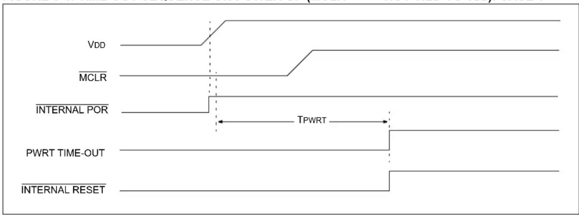
text_image
VDD MCLR INTERNAL POR TPWRT PWRT TIME-OUT INTERNAL RESETFIGURE 5-5: TIME-OUT SEQUENCE ON POWER-UP (MCLR NOT TIED TO VDD): CASE 2

text_image
VDD MCLR INTERNAL POR TPWRT PWRT TIME-OUT INTERNAL RESETFIGURE 5-6: SLOW RISE TIME (MCLR TIED TO VDD, VDD RISE > TPWRT)

other
| Signal | Value | |-----------------|-------| | VDD | 0V | | MCLR | 1V | | INTERNAL POR | TPWRT | | PWRT TIME-OUT | | | INTERNAL RESET | |5.7 Reset State of Registers
Most registers are unaffected by a Reset. Their status is unknown on POR and unchanged by all other Resets. The other registers are forced to a "Reset state" depending on the type of Reset that occurred.
Most registers are not affected by a WDT wake-up, since this is viewed as the resumption of normal operation. Status bits from the RCON register, , , and , are set or cleared differently in different Reset situations, as indicated in Table 5-1. These bits are used in software to determine the nature of the Reset.
Table 5-2 describes the Reset states for all of the Special Function Registers. These are categorized by Power-on and Brown-out Resets, Master Clear and WDT Resets, and WDT wake-ups.
TABLE 5-1: STATUS BITS, THEIR SIGNIFICANCE AND THE INITIALIZATION CONDITION FOR RCON REGISTER
| Condition | Program Counter(1) | RCON Register STKPTR Register | ||||||
| STKFUL | STKUNF | |||||||
| Power-on Reset 0000h 1 | 1 | 0 | 0 | 0 | 0 | |||
| RESET Instruction | 0000h | 0 | u | u | u | u | u | u |
| Brown-out Reset | 0000h | 1 | 1 | 1 | u | 0 | u | u |
| during power-managed Run modes | 0000h | u | 1 | u | u | u | u | u |
| during power-managed Idle modes and Sleep mode | 0000h | u | 1 | 0 | u | u | u | u |
| WDT time-out during full power or power-managed Run modes | 0000h | u | 0 | u | u | u | u | u |
| during full-power execution | 0000h | u | u | u | u | u | u | u |
| Stack Full Reset (STVREN = 1) | 0000h | u | u | u | u | u | 1 | u |
| Stack Underflow Reset (STVREN = 1) | 0000h | u | u | u | u | u | u | 1 |
| Stack Underflow Error (not an actual Reset, STVREN = 0) | 0000h | u | u | u | u | u | u | 1 |
| WDT time-out during power-managed Idle or Sleep modes | PC + 2 | u | 0 | 0 | u | u | u | u |
| Interrupt exit from power-managed modes | PC + 2 | u | u | 0 | u | u | u | u |
Legend: u = unchanged
Note 1: When the wake-up is due to an interrupt and the GIEH or GIEL bit is set, the PC is loaded with the interrupt vector (0008h or 0018h).
TABLE 5-2: INITIALIZATION CONDITIONS FOR ALL REGISTERS
| Register Applicable Devices | Power-on Reset, Brown-out Reset | MCLR Resets WDT Reset RESET Instruction Stack Resets | Wake-up via WDT or Interrupt | ||
| TOSU PIC18F6XJ90 PIC18F8XJ90 ---0 0000 | ---0 0000 ---0 uuuu | (1) | |||
| TOSH PIC18F6XJ90 PIC18F8XJ90 0000 0000 | 0000 0000 uuuu uuuu | (1) | |||
| TOSL PIC18F6XJ90 PIC18F8XJ90 0000 0000 | 0000 0000 uuuu uuuu | (1) | |||
| STKPTR PIC18F6XJ90 PIC18F8XJ90 uu-0 0000 | 0 00-0 0000 uu-u | uuuuu | (1) | ||
| PCLATU PIC18F6XJ90 PIC18F8XJ90 ---0 0000 | 0 ---0 0000 ---u | uuuuu | |||
| PCLATH PIC18F6XJ90 PIC18F8XJ90 0000 0000 | 0 0000 0000 uuuu | uuuuu | |||
| PCL PIC18F6XJ90 PIC18F8XJ90 0000 0000 | 0000 0000 PC + 2 | (2) | |||
| TBLPTRU PIC18F6XJ90 PIC18F8XJ90 ---00 0000 ---00 0000 | uuuuu | ||||
| TBLPTRH PIC18F6XJ90 PIC18F8XJ90 0000 0000 | 00 0000 0000 uuuu | uuuuu | |||
| TBLPTRL PIC18F6XJ90 PIC18F8XJ90 0000 | 0000 0000 0000 0000 | uuuuu uuuu | |||
| TABLAT | PIC18F6XJ90 PIC18F8XJ90 0000 | 0000 0000 0000 0000 | uuuuu uuuu | ||
| PRODH | PIC18F6XJ90 PIC18F8XJ90 xxxxx | xxxx uuuu uuuu | uuuuu uuuu | ||
| PRODL | PIC18F6XJ90 PIC18F8XJ90 xxxxx | xxxx uuuu uuuu | uuuuu uuuu | ||
| INTCON | PIC18F6XJ90 PIC18F8XJ90 0000 | 000x 0000 000u | uuuuu uuuu | (3) | |
| INTCON2 PIC18F6XJ90 PIC18F8XJ90 1111 | 1111 1111 1111 1111 | uuuuu uuuu | (3) | ||
| INTCON3 PIC18F6XJ90 PIC18F8XJ90 1100 | 0000 1100 0000 | uuuuu uuuu | (3) | ||
| INDF0 | PIC18F6XJ90 PIC18F8XJ90 | N/A | N/A | N/A | |
| POSTINC0 | PIC18F6XJ90 PIC18F8XJ90 | N/A | N/A | N/A | |
| POSTDEC0 | PIC18F6XJ90 PIC18F8XJ90 | N/A | N/A | N/A | |
| PREINC0 | PIC18F6XJ90 PIC18F8XJ90 | N/A | N/A | N/A | |
| PLUSW0 | PIC18F6XJ90 PIC18F8XJ90 | N/A | N/A | N/A | |
| FSR0H PIC18F6XJ90 PIC18F8XJ90 ---- | xxxx ---- uuuu ---- uuuu | ||||
| FSR0L | PIC18F6XJ90 PIC18F8XJ90 xxxxx | xxxx uuuu uuuu | uuuuu uuuu | ||
| WREG | PIC18F6XJ90 PIC18F8XJ90 xxxxx | xxxx uuuu uuuu | uuuuu uuuu | ||
| INDF1 | PIC18F6XJ90 PIC18F8XJ90 | N/A | N/A | N/A | |
| POSTINC1 | PIC18F6XJ90 PIC18F8XJ90 | N/A | N/A | N/A | |
| POSTDEC1 | PIC18F6XJ90 PIC18F8XJ90 | N/A | N/A | N/A | |
| PREINC1 | PIC18F6XJ90 PIC18F8XJ90 | N/A | N/A | N/A | |
| PLUSW1 | PIC18F6XJ90 PIC18F8XJ90 | N/A | N/A | N/A | |
Legend: u = unchanged, x = unknown, - = unimplemented bit, read as '0', q = value depends on condition. Shaded cells indicate conditions do not apply for the designated device.
Note 1: When the wake-up is due to an interrupt and the GIEL or GIEH bit is set, the TOSU, TOSH and TOSL are updated with the current value of the PC. The STKPTR is modified to point to the next location in the hardware stack.
2: When the wake-up is due to an interrupt and the GIEL or GIEH bit is set, the PC is loaded with the interrupt vector (0008h or 0018h).
3: One or more bits in the INTCONx or PIRx registers will be affected (to cause wake-up).
4: See Table 5-1 for Reset value for specific conditions.
5: Bits 6 and 7 of PORTA, LATA and TRISA are enabled depending on the oscillator mode selected. When not enabled as PORTA pins, they are disabled and read as '0'.
TABLE 5-2: INITIALIZATION CONDITIONS FOR ALL REGISTERS (CONTINUED)
| Register | Applicable Devices | Power-on Reset, Brown-out Reset | MCLR Resets WDT Reset RESET Instruction Stack Resets | Wake-up via WDT or Interrupt | |
| FSR1H PIC18F | 6XJ90 PIC18F8X | J90 ---- xxxx | ---- uuuu ---- uuuu | ||
| FSR1L PIC18F6 | 6XJ90 PIC18F8X | J90 xxxx xxxx | uuuu uuuu uuuu uuuu | ||
| BSR PIC18F6X | J90 PIC18F8XJ90 | ---- 0000 | ---- 0000 ---- uuuu | ||
| INDF2 PIC18F6 | XJ90 PIC18F8X | J90 N/A N/A N/A | |||
| POSTINC2 PIC | 18F6XJ90 PIC18 | F8XJ90 N/A N/A | N/A | ||
| POSTDEC2 PIC | 18F6XJ90 PIC18 | F8XJ90 N/A N/A | N/A N/A | ||
| PREINC2 PIC18 | F6XJ90 PIC18F8X | PIC18F8XJ90 N/A | N/A | ||
| PLUSW2 | PIC18F6XJ90 PIC18F8XJ90 | PIC18F8XJ90 N/A | N/A N/A | ||
| FSR2H PIC18F | 6XJ90 PIC18F8X | J90 ---- xxxx | ---- uuuu ---- uuuu | ||
| FSR2L PIC18F6 | 6XJ90 PIC18F8X | J90 xxxx xxxx | uuuu uuuu uuuu uuuu | ||
| STATUS | PIC18F6XJ90 | PIC18F8XJ90 | ----x xxxx | ----u uuuu | ----u uuuu |
| TMR0H | PIC18F6XJ90 PIC18F8XJ90 | PIC18F8XJ90 0000 | 0000 0000 0000 | uuuu uuuu | |
| TMR0L PIC18F | 6XJ90 PIC18F8X | J90 xxxx xxxx | uuuu uuuu uuuu uuuu | ||
| TOCON | PIC18F6XJ90 PIC18F8XJ90 | PIC18F8XJ90 1111 | 1111 1111 1111 | uuuu uuuu | |
| OSCCON PIC18 | F6XJ90 PIC18F8X | 8XJ90 0110 q000 | 0110 q000 uuuu | quuu | |
| LCDREG | PIC18F6XJ90 | PIC18F8XJ90 | -011 1100 | -011 1000 | -uuu uuuu |
| WDTCON | PIC18F6XJ90 PIC18F8XJ90 | PIC18F8XJ90 0-- | ---0 0--- ---0 | u--- ---u | |
| RCON^(4) | PIC18F6XJ90 PIC18F8XJ90 | PIC18F8XJ90 0-11 | 11q0 0-0q qquu | u-uu qquu | |
| TMR1H | PIC18F6XJ90 PIC18F8XJ90 | PIC18F8XJ90 xxx | xxxx uuuu uuuu | uuuu uuuu | |
| TMR1L PIC18F | 6XJ90 PIC18F8X | J90 xxxx xxxx | uuuu uuuu uuuu uuuu | ||
| T1CON | PIC18F6XJ90 PIC18F8XJ90 | PIC18F8XJ90 0000 | 0000 u0uu uuuu | uuuu uuuu | |
| TMR2 | PIC18F6XJ90 PIC18F8XJ90 | PIC18F8XJ90 0000 | 0000 0000 0000 | uuuu uuuu | |
| PR2 | PIC18F6XJ90 PIC18F8XJ90 | PIC18F8XJ90 1111 | 1111 1111 1111 | 1111 1111 | |
| T2CON | PIC18F6XJ90 PIC18F8XJ90 | PIC18F8XJ90 -000 | 0000 -000 0000 | -uuu uuuu | |
| SSPBUF | PIC18F6XJ90 | PIC18F8XJ90 | xxxx xxxx | uuuu uuuu | uuuu uuuu |
| SSPADD | PIC18F6XJ90 PIC18F8XJ90 | PIC18F8XJ90 0000 | 0000 0000 0000 | uuuu uuuu | |
| SSPSTAT | PIC18F6XJ90 | PIC18F8XJ90 | 0000 0000 | 0000 0000 | uuuu uuuu |
| SSPCON1 | PIC18F6XJ90 | PIC18F8XJ90 | 0000 0000 | 0000 0000 | uuuu uuuu |
| SSPCON2 | PIC18F6XJ90 | PIC18F8XJ90 | 0000 0000 | 0000 0000 | uuuu uuuu |
Legend: u = unchanged, x = unknown, - = unimplemented bit, read as '0', q = value depends on condition. Shaded cells indicate conditions do not apply for the designated device.
Note 1: When the wake-up is due to an interrupt and the GIEL or GIEH bit is set, the TOSU, TOSH and TOSL are updated with the current value of the PC. The STKPTR is modified to point to the next location in the hardware stack.
2: When the wake-up is due to an interrupt and the GIEL or GIEH bit is set, the PC is loaded with the interrupt vector (0008h or 0018h).
3: One or more bits in the INTCONx or PIRx registers will be affected (to cause wake-up).
4: See Table 5-1 for Reset value for specific conditions.
5: Bits 6 and 7 of PORTA, LATA and TRISA are enabled depending on the oscillator mode selected. When not enabled as PORTA pins, they are disabled and read as '0'.
TABLE 5-2: INITIALIZATION CONDITIONS FOR ALL REGISTERS (CONTINUED)
| Register Applicable Devices | Power-on Reset, Brown-out Reset | MCLR Resets WDT Reset RESET Instruction Stack Resets | Wake-up via WDT or Interrupt | ||
| ADRESH PIC18F6XJ90 PIC18F8XJ90xxxxxxx | uuuu | uuuu | uuuu | ||
| ADRESL PIC18F6XJ90 PIC18F8XJ90xxxxxxx | uuuu | uuuu | uuuu | ||
| ADCON0 PIC18F6XJ90 PIC18F8XJ90 0-00 0000 | 0-00 | 0000 | u-uu | uuuu | |
| ADCON1 PIC18F6XJ90 PIC18F8XJ90 0-00 0000 | 0-00 | 0000 | u-uu | uuuu | |
| ADCON2 PIC18F6XJ90 PIC18F8XJ90 0-00 0000 | 0-00 | 0000 | u-uu | uuuu | |
| LCDDATA4 PIC18F6XJ90 | PIC18F8XJ90 | ---- | ---x | ---u | ----u |
| LCDDATA4 | PIC18F6XJ90 PIC18F8XJ90 xxx | xxxx | uuuu | uuuu | uuuu |
| LCDDATA3 PIC18F6XJ90 PIC18F8XJ90 xxx | xxxx | uuuu | uuuu | uuuu | uuuu |
| LCDDATA2 PIC18F6XJ90 PIC18F8XJ90 xxx | xxxx | uuuu | uuuu | uuuu | uuuu |
| LCDDATA1 PIC18F6XJ90 PIC18F8XJ90 xxx | xxxx | uuuu | uuuu | uuuu | uuuu |
| LCDDATA0 PIC18F6XJ90 PIC18F8XJ90 xxx | xxxx | uuuu | uuuu | uuuu | uuuu |
| LCDSE5 | PIC18F6XJ90 PIC18F8XJ90 000 | 0000 | uuuu | uuuu | uuuu |
| LCDSE4 PIC18F6XJ90 PIC18F8XJ90 ---- | 0 | ---- | ---u | ----u | |
| LCDSE4 PIC18F6XJ90 PIC18F8XJ90 0000 000 | 0 | uuuu | uuuu | uuuu | |
| LCDSE3 PIC18F6XJ90 PIC18F8XJ90 0000 000 | 0 | uuuu | uuuu | uuuu | |
| LCDSE2 PIC18F6XJ90 PIC18F8XJ90 0000 000 | 0 | uuuu | uuuu | uuuu | |
| LCDSE1 PIC18F6XJ90 PIC18F8XJ90 0000 000 | 0 | uuuu | uuuu | uuuu | |
| CVRCON PIC18F6XJ90 PIC18F8XJ90 0000 000 | 0000 | 0000 | uuuu | uuuu | |
| CMCON PIC18F6XJ90 PIC18F8XJ90 0000 011 | 1 | 0000 | 0111 | uuuu | |
| TMR3H PIC18F6XJ90 PIC18F8XJ90 xxx | uuuu | uuuu | uuuu | uuuu | |
| TMR3L PIC18F6XJ90 PIC18F8XJ90 xxx | uuuu | uuuu | uuuu | uuuu | |
| T3CON | PIC18F6XJ90 PIC18F8XJ90 000 | 0000 | uuuu | uuuu | |
| SPBRG1 | PIC18F6XJ90 | PIC18F8XJ90 | 0000 | 0000 | 0000 |
| RCREG1 PIC18F6XJ90 PIC18F8XJ90 0000 000 | 0000 | 0000 | uuuu | uuuu | |
| TXREG1 PIC18F6XJ90 PIC18F8XJ90 0000 000 | 0000 | 0000 | uuuu | uuuu | |
| TXSTA1 | PIC18F6XJ90 PIC18F8XJ90 000 | 0010 | 0000 | 0010 | uuuu |
| RCSTA1 | PIC18F6XJ90 PIC18F8XJ90 000 | 000x | 0000 | 000x | uuuu |
| LCDPS | PIC18F6XJ90 PIC18F8XJ90 000 | 0000 | 0000 | 0000 | uuuu |
| LCDSE0 PIC18F6XJ90 PIC18F8XJ90 0000 000 | 0 | uuuu | uuuu | uuuu | |
| LCDCON | PIC18F6XJ90 PIC18F8XJ90 000- | 0000 | 000- | 0000 | uuu- |
| EECON2 | PIC18F6XJ90 PIC18F8XJ90 ---- | ---- | ---- | ---- | ---- |
| EECON1 | PIC18F6XJ90 PIC18F8XJ90 ---- | 0x00- | ----0 | u00- | ----0 |
Legend: u = unchanged, x = unknown, - = unimplemented bit, read as '0', q = value depends on condition. Shaded cells indicate conditions do not apply for the designated device.
Note 1: When the wake-up is due to an interrupt and the GIEL or GIEH bit is set, the TOSU, TOSH and TOSL are updated with the current value of the PC. The STKPTR is modified to point to the next location in the hardware stack.
2: When the wake-up is due to an interrupt and the GIEL or GIEH bit is set, the PC is loaded with the interrupt vector (0008h or 0018h).
3: One or more bits in the INTCONx or PIRx registers will be affected (to cause wake-up).
4: See Table 5-1 for Reset value for specific conditions.
5: Bits 6 and 7 of PORTA, LATA and TRISA are enabled depending on the oscillator mode selected. When not enabled as PORTA pins, they are disabled and read as '0'.
TABLE 5-2: INITIALIZATION CONDITIONS FOR ALL REGISTERS (CONTINUED)
| Register | Applicable Devices | Power-on Reset, Brown-out Reset | MCLR Resets WDT Reset RESET Instruction Stack Resets | Wake-up via WDT or Interrupt | ||
| IPR3 PIC18F6X | J90 PIC18F8XJ90 | -111 | 1111 | -111 1111 -uuu 1111 | ||
| PIR3 PIC18F6X | J90 PIC18F8XJ90 | -000 | 0000 | -000 0000 -uuu 0000 | (3) | |
| PIE3 PIC18F6X | J90 PIC18F8XJ90 | -000 | 0000 | -000 0000 -uuu 0000 | ||
| IPR2 PIC18F6X | J90 PIC18F8XJ90 | 11-- | 111- | 11-- 111- uu-- uuu- | ||
| PIR2 PIC18F6X | J90 PIC18F8XJ90 | 00-- | 000- | 00-- 000- uu-- uuu- | (3) | |
| PIE2 PIC18F6X | J90 PIC18F8XJ90 | 00-- | 000- | 00-- 000- uu-- uuu- | ||
| IPR1 PIC18F6X | J90 PIC18F8XJ90 | -111 | 1-11 | -111 1-11 -uuu u-uu | ||
| PIR1 PIC18F6X | J90 PIC18F8XJ90 | -000 | 0-00 | -000 0-00 -uuu u-uu | (3) | |
| PIE1 PIC18F6X | J90 PIC18F8XJ90 | -000 | 0-00 | -000 0-00 -uuu u-uu | ||
| OSCTUNE PIC | 18F6XJ90 PIC18F8XJ90 | 0000 | 0000 | 0000 0000 0000 uuuu | uuuu | |
| TRISJ PIC18F6 | XJ90 PIC18F8X | J90 | 1111 1111 | 1111 1111 uuuu uuuu | ||
| TRISH | PIC18F6XJ90 | PIC18F8XJ90 | 11 | 1111 1111 1111 | uuuu uuuu | |
| TRISG PIC18F6 | XJ90 PIC18F8X | J90 | 0001 1111 | 0001 1111 uuuu uuuu | ||
| TRISF PIC18F6 | XJ90 PIC18F8X | J90 | 1111 111- | 1111 111- uuuu uuu- | ||
| TRISE PIC18F6 | XJ90 PIC18F8X | J90 | 1111 1-11 | 1111 1-11 uuuu u-uu | ||
| TRISD PIC18F6 | XJ90 PIC18F8X | J90 | 1111 1111 | 1111 1111 uuuu uuuu | ||
| TRISC PIC18F6 | XJ90 PIC18F8X | J90 | 1111 1111 | 1111 1111 uuuu uuuu | ||
| TRISB PIC18F6 | XJ90 PIC18F8X | J90 | 1111 1111 | 1111 1111 uuuu uuuu | ||
| TRISA^(5) | PIC18F6XJ90 | PIC18F8XJ90 | 11 | 1111 (5) | 1111 1111^(5) | uuuu uuuu^(5) |
| LATJ PIC18F6 | XJ90 PIC18F8XJ90 | xxxx | xxxx | uuuu uuuu uuuu uuuu | ||
| LATH | PIC18F6XJ90 | PIC18F8XJ90 | xxxx | xxxx uuuu uuuu | uuuu uuuu | |
| LATG | PIC18F6XJ90 | PIC18F8XJ90 | 00 | -x xxxx 00-u uuuu | uu-u uuuu | |
| LATF | PIC18F6XJ90 | PIC18F8XJ90 | xxxx | xxx- uuuu uuuu- | uuuu uuuu- | |
| LATE | PIC18F6XJ90 | PIC18F8XJ90 | xxxx | x-xx uuuu u-uu | uuuu u-uu | |
| LATD | PIC18F6XJ90 | PIC18F8XJ90 | xxxx | xxxx uuuu uuuu | uuuu uuuu | |
| LATC | PIC18F6XJ90 | PIC18F8XJ90 | xxxx | xxxx uuuu uuuu | uuuu uuuu | |
| LATB | PIC18F6XJ90 | PIC18F8XJ90 | xxxx | xxxx uuuu uuuu | uuuu uuuu | |
| LATA^(5) | PIC18F6XJ90 | PIC18F8XJ90 | xxxx | xxxx (5) | uuuu uuuu^(5) | uuuu uuuu^(5) |
| PORTJ | PIC18F6XJ90 | PIC18F8XJ90 | xxxx xxxx | uuuu uuuu | uuuu uuuu | |
| PORTH | PIC18F6XJ90 | PIC18F8XJ90 | xxxx | xxxx uuuu uuuu | uuuu uuuu | |
| PORTG | PIC18F6XJ90 | PIC18F8XJ90 | 000 | x xxxx 000u uuuu | 000u uuuu | |
| PORTF | PIC18F6XJ90 | PIC18F8XJ90 | xxxx | xxx- uuuu uuuu- | uuuu uuuu- | |
Legend: u = unchanged, x = unknown, - = unimplemented bit, read as '0', q = value depends on condition. Shaded cells indicate conditions do not apply for the designated device.
Note 1: When the wake-up is due to an interrupt and the GIEL or GIEH bit is set, the TOSU, TOSH and TOSL are updated with the current value of the PC. The STKPTR is modified to point to the next location in the hardware stack.
2: When the wake-up is due to an interrupt and the GIEL or GIEH bit is set, the PC is loaded with the interrupt vector (0008h or 0018h).
3: One or more bits in the INTCONx or PIRx registers will be affected (to cause wake-up).
4: See Table 5-1 for Reset value for specific conditions.
5: Bits 6 and 7 of PORTA, LATA and TRISA are enabled depending on the oscillator mode selected. When not enabled as PORTA pins, they are disabled and read as '0'.
TABLE 5-2: INITIALIZATION CONDITIONS FOR ALL REGISTERS (CONTINUED)
| Register | Applicable Devices | Power-on Reset, Brown-out Reset | MCLR Resets WDT Reset RESET Instruction Stack Resets | Wake-up via WDT or Interrupt | |
| PORTE PIC18F | 6XJ90 PIC18F8XJ90xxxxx-xx | uuuu u-uu uuuu u-uu | |||
| PORTD PIC18F | 6XJ90 PIC18F8XJ90xxxxxxx | uuuu uuuuu uuuu uuuu | |||
| PORTC PIC18F | 6XJ90 PIC18F8XJ90xxxxxxx | uuuu uuuuu uuuu uuuu | |||
| PORTB PIC18F | 6XJ90 PIC18F8XJ90xxxxxxx | uuuu uuuuu uuuu uuuu | |||
| PORTA(5) | PIC18F6XJ90 PIC18F8XJ90xx | 0x 0000 (5) | uu0u 0000(5) | uuuu uuuu(5) | |
| SPBRGH1 PIC | 18F6XJ90 PIC18F8XJ90 0000 | 0000 0000 0000 uuu uuuu | |||
| BAUDCON1 PIC | 18F6XJ90 PIC18F8XJ90 0100 | 0-00 0100 0-00 uuuu u-uu | |||
| LCDDATA23 PIC | 18F6XJ90 PIC18F8XJ90xxxx | xxxx uuuuu uuuuu uuuu uuuu | |||
| LCDDATA22 PIC | 18F6XJ90 PIC18F8XJ90 | ---- ----x ---- --u ---- --u | |||
| LCDDATA22 PIC | 18F6XJ90 PIC18F8XJ90xxxx | xxxx uuuuu uuuuu uuuu uuuu | |||
| LCDDATA21 PIC | 18F6XJ90 PIC18F8XJ90xxxx | xxxx uuuuu uuuuu uuuuu uuuu | |||
| LCDDATA20 PIC | 18F6XJ90 PIC18F8XJ90xxxx | xxxx uuuuu uuuuu uuuuu uuuu | |||
| LCDDATA19 PIC | 18F6XJ90 PIC18F8XJ90xxxx | xxxx uuuuu uuuuu uuuuu uuuu | |||
| LCDDATA18 PIC | 18F6XJ90 PIC18F8XJ90xxxx | xxxx uuuuu uuuuu uuuuu uuuu | |||
| LCDDATA17 PIC | 18F6XJ90 PIC18F8XJ90xxx | xxxx uuuuu uuuuu uuuuu uuuu | |||
| LCDDATA16 PIC | 18F6XJ90 PIC18F8XJ90 ---- | ----x ---- --u ---- --u | |||
| LCDDATA16 PIC | 18F6XJ90 PIC18F8XJ90xxxx | xxxx uuuuu uuuuu uuuuu uuuu | |||
| LCDDATA15 PIC | 18F6XJ90 PIC18F8XJ90xxxx | xxxx uuuuu uuuuu uuuuu uuuu | |||
| LCDDATA14 PIC | 18F6XJ90 PIC18F8XJ90xxxx | xxxx uuuuu uuuuu uuuuu uuuu | |||
| LCDDATA13 PIC | 18F6XJ90 PIC18F8XJ90xxxx | xxxx uuuuu uuuuu uuuuu uuuu | |||
| LCDDATA12 PIC | 18F6XJ90 PIC18F8XJ90xxxx | xxxx uuuuu uuuuu uuuuu uuuu | |||
| LCDDATA11 PIC | 18F6XJ90 PIC18F8XJ90xxx | xxxx uuuuu uuuuu uuuuu uuuu | |||
| LCDDATA10 PIC | 18F6XJ90 PIC18F8XJ90 ---- | ----x ---- --u ---- --u | |||
| LCDDATA10 PIC | 18F6XJ90 PIC18F8XJ90xxx | xxxx uuuuu uuuuu uuuuu uuuu | |||
| LCDDATA9 PIC | 18F6XJ90 PIC18F8XJ90xxxx | xxxx uuuuu uuuuu uuuuu uuuu | |||
| LCDDATA8 PIC | 18F6XJ90 PIC18F8XJ90xxxx | xxxx uuuuu uuuuu uuuuu uuuu | |||
| LCDDATA7 PIC | 18F6XJ90 PIC18F8XJ90xxxx | xxxx uuuuu uuuuu uuuuu uuuu | |||
| LCDDATA6 PIC | 18F6XJ90 PIC18F8XJ90xxxx | xxxx uuuuu uuuuu uuuuu uuuu | |||
| LCDDATA5 PIC | 18F6XJ90 PIC18F8XJ90xxxx | xxxx uuuuu uuuuu uuuuu uuuu | |||
| CCPR1H PIC18F6XJ90 PIC18F8XJ90xxxx | uuuu uuuu uuuu | ||||
| CCPR1L PIC18F6XJ90 PIC18F8XJ90xxxx | xxxx uuuuu uuuuu uuuu | ||||
| CCP1CON PIC18F6XJ90 PIC18F8XJ90--00 0000--00 0000--uu uuuu | |||||
| CCPR2H PIC18F6XJ90 PIC18F8XJ90xxxx | uuuu uuuu uuuu | ||||
Legend: u = unchanged, x = unknown, - = unimplemented bit, read as '0', q = value depends on condition. Shaded cells indicate conditions do not apply for the designated device.
Note 1: When the wake-up is due to an interrupt and the GIEL or GIEH bit is set, the TOSU, TOSH and TOSL are updated with the current value of the PC. The STKPTR is modified to point to the next location in the hardware stack.
2: When the wake-up is due to an interrupt and the GIEL or GIEH bit is set, the PC is loaded with the interrupt vector (0008h or 0018h).
3: One or more bits in the INTCONx or PIRx registers will be affected (to cause wake-up).
4: See Table 5-1 for Reset value for specific conditions.
5: Bits 6 and 7 of PORTA, LATA and TRISA are enabled depending on the oscillator mode selected. When not enabled as PORTA pins, they are disabled and read as '0'.
TABLE 5-2: INITIALIZATION CONDITIONS FOR ALL REGISTERS (CONTINUED)
| Register | Applicable Devices | Power-on Reset, Brown-out Reset | MCLR Resets WDT Reset RESET Instruction Stack Resets | Wake-up via WDT or Interrupt | |
| CCPR2L PIC18 | F6XJ90 PIC18F8 | XJ90 xxxx xxxx | x uuuu uuuu uuuu | uuuu | |
| CCP2CON PIC18 | F6XJ90 PIC18F8 | XJ90 --00 0000 | --00 0000 --uu | uuuu | |
| SPBRG2 PIC18 | F6XJ90 PIC18F8 | XJ90 0000 0000 | 0000 0000 0000 uuuu | uuuu | |
| RCREG2 PIC18 | F6XJ90 PIC18F8 | XJ90 0000 0000 | 0000 0000 uuuu | uuuu | |
| TXREG2 PIC18 | F6XJ90 PIC18F8 | XJ90 0000 0000 | 0000 0000 uuuu | uuuu | |
| TXSTA2 PIC18 | F6XJ90 PIC18F8 | XJ90 0000 -01 | 0 0000 -010 uuuu | -uuu | |
| RCSTA2 PIC18 | F6XJ90 PIC18F8 | XJ90 0000 0000 | x 0000 000x uuuu | uuuu | |
| RTCCFG | PIC18F6XJ90 P | C18F8XJ90 0-0 | 0 0000 0-00 0000 | u-uu uuuu | |
| RTCCAL | PIC18F6XJ90 | PIC18F8XJ90 | 0000 0000 | 0000 0000 | uuuu uuuu |
| RTCVALH | PIC18F6XJ90 | PIC18F8XJ90 | xxxx xxxx | uuuu uuuu | uuuu uuuu |
| RTCVALL | PIC18F6XJ90 | PIC18F8XJ90 | xxxx xxxx | uuuu uuuu | uuuu uuuu |
| ALRMCFG | PIC18F6XJ90 | PIC18F8XJ90 | 0000 0000 | 0000 0000 | uuuu uuuu |
| ALRMRPT | PIC18F6XJ90 | PIC18F8XJ90 | 0000 0000 | 0000 0000 | uuuu uuuu |
| ALRMVALH | PIC18F6XJ90 | PIC18F8XJ90 | xxxx xxxx | uuuu uuuu | uuuu uuuu |
| ALRMVALL | PIC18F6XJ90 | PIC18F8XJ90 | xxxx xxxx | uuuu uuuu | uuuu uuuu |
| CTMUCONH | PIC18F6XJ90 PIC18F8XJ90 0-00 | 0000 0-00 0000 u-uu uuuu | |||
| CTMUCONL | PIC18F6XJ90 | PIC18F8XJ90 | 0000 0000 | 0000 0000 | uuuu uuuu |
| CTMUICON | PIC18F6XJ90 | PIC18F8XJ90 | 0000 0000 | 0000 0000 | uuuu uuuu |
| PADCFG1 | PIC18F6XJ90 | PIC18F8XJ90 | ---- -00- | ---- -00- | ---- -uu- |
Legend: u = unchanged, x = unknown, - = unimplemented bit, read as '0', q = value depends on condition. Shaded cells indicate conditions do not apply for the designated device.
Note 1: When the wake-up is due to an interrupt and the GIEL or GIEH bit is set, the TOSU, TOSH and TOSL are updated with the current value of the PC. The STKPTR is modified to point to the next location in the hardware stack.
2: When the wake-up is due to an interrupt and the GIEL or GIEH bit is set, the PC is loaded with the interrupt vector (0008h or 0018h).
3: One or more bits in the INTCONx or PIRx registers will be affected (to cause wake-up).
4: See Table 5-1 for Reset value for specific conditions.
5: Bits 6 and 7 of PORTA, LATA and TRISA are enabled depending on the oscillator mode selected. When not enabled as PORTA pins, they are disabled and read as '0'.
6.0 MEMORY ORGANIZATION
There are two types of memory in PIC18 Flash microcontroller devices:
- Program Memory
- Data RAM
As Harvard architecture devices, the data and program memories use separate busses; this allows for concurrent access of the two memory spaces.
Additional detailed information on the operation of the Flash program memory is provided in Section 7.0 "Flash Program Memory".
6.1 Program Memory Organization
PIC18 microcontrollers implement a 21-bit program counter which is capable of addressing a 2-Mbyte program memory space. Accessing a location between the upper boundary of the physically implemented memory and the 2-Mbyte address will return all '0's (a NOP instruction).
The entire PIC18F87J90 family offers a range of on-chip Flash program memory sizes, from 64 Kbytes (up to 16,384 single-word instructions) to 128 Kbytes (65,536 single-word instructions). The program memory maps for individual family members are shown in Figure 6-1.
FIGURE 6-1: MEMORY MAPS FOR PIC18F87J90 FAMILY DEVICES

flowchart
graph TD
    A["PC<20:0>"] --> B["Stack Level 1"]
    B --> C["21"]
    C --> D["User Memory Space"]
    D --> E["PIC18FX6J90 On-Chip Memory"]
    D --> F["PIC18FX7J90 On-Chip Memory"]
    E --> G["Config. Words"]
    F --> H["Config. Words"]
    G --> I["Unimplemented Read as '0'"]
    H --> J["Unimplemented Read as '0'"]
    I --> K["000000h"]
    J --> L["-1FFFFh"]
    K --> M["-00FFFFh"]
    L --> N["-01FFFFh"]
    M --> O["-1FFFFh"]
    N --> P["21"]
    O --> Q["21"]
Note: Sizes of memory areas are not to scale. Sizes of program memory areas are enhanced to show detail.
6.1.1 HARD MEMORY VECTORS
All PIC18 devices have a total of three hard-coded return vectors in their program memory space. The Reset vector address is the default value to which the program counter returns on all device Resets; it is located at 0000h.
PIC18 devices also have two interrupt vector addresses for the handling of high-priority and low-priority interrupts. The high-priority interrupt vector is located at 0008h and the low-priority interrupt vector is at 0018h. Their locations in relation to the program memory map are shown in Figure 6-2.
FIGURE 6-2: HARD VECTOR AND
CONFIGURATION WORD
LOCATIONS FOR
PIC18F87J90 FAMILY
FAMILY DEVICES
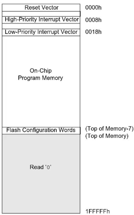
text_image
Reset Vector 0000h High-Priority Interrupt Vector 0008h Low-Priority Interrupt Vector 0018h On-Chip Program Memory Flash Configuration Words (Top of Memory-7) (Top of Memory) Read '0' 1FFFFFFhLegend: (Top of Memory) represents upper boundary of on-chip program memory space (see Figure 6-1 for device-specific values). Shaded area represents unimplemented memory. Areas are not shown to scale.
Because PIC18F87J90 family devices do not have persistent configuration memory, the top four words of on-chip program memory are reserved for configuration information. On Reset, the configuration information is copied into the Configuration registers.
The Configuration Words are stored in their program memory location in numerical order, starting with the lower byte of CONFIG1 at the lowest address and ending with the upper byte of CONFIG4. For these devices, only Configuration Words, CONFIG1 through CONFIG3, are used; CONFIG4 is reserved. The actual addresses of the Flash Configuration Word for devices in the PIC18F87J90 family are shown in Table 6-1. Their location in the memory map is shown with the other memory vectors in Figure 6-2.
Additional details on the device Configuration Words are provided in Section 25.1 "Configuration Bits".
TABLE 6-1: FLASH CONFIGURATION
WORD FOR PIC18F87J90 FAMILY DEVICES
| Device | Program Memory (Kbytes) | Configuration Word Addresses |
| PIC18F66J90 | 64 FFF8h to FFFFh | |
| PIC18F86J90 | ||
| PIC18F67J90 | 128 1FFF8h to 1FFFFh | |
| PIC18F87J90 | ||
6.1.3 PROGRAM COUNTER
The Program Counter (PC) specifies the address of the instruction to fetch for execution. The PC is 21 bits wide and is contained in three separate 8-bit registers. The low byte, known as the PCL register, is both readable and writable. The high byte, or PCH register, contains the PC<15:8> bits; it is not directly readable or writable. Updates to the PCH register are performed through the PCLATH register. The upper byte is called PCU. This register contains the PC<20:16> bits; it is also not directly readable or writable. Updates to the PCU register are performed through the PCLATU register.
The contents of PCLATH and PCLATU are transferred to the program counter by any operation that writes PCL. Similarly, the upper two bytes of the program counter are transferred to PCLATH and PCLATU by an operation that reads PCL. This is useful for computed offsets to the PC (see Section 6.1.6.1 "Computed GOTO").
The PC addresses bytes in the program memory. To prevent the PC from becoming misaligned with word instructions, the Least Significant bit of PCL is fixed to a value of '0'. The PC increments by 2 to address sequential instructions in the program memory.
The CALL, RCALL, GOTO and program branch instructions write to the program counter directly. For these instructions, the contents of PCLATH and PCLATU are not transferred to the program counter.
6.1.4 RETURN ADDRESS STACK
The return address stack allows any combination of up to 31 program calls and interrupts to occur. The PC is pushed onto the stack when a CALL or RCALL instruction is executed, or an interrupt is Acknowledged. The PC value is pulled off the stack on a RETURN, RETLW or a RETFIE instruction (and on ADDULNK and SUBULNK instructions if the extended instruction set is enabled). PCLATU and PCLATH are not affected by any of the RETURN or CALL instructions.
The stack operates as a 31-word by 21-bit RAM and a 5-bit Stack Pointer, STKPTR. The stack space is not part of either program or data space. The Stack Pointer is readable and writable, and the address on the top of the stack is readable and writable through the Top-of-Stack Special Function Registers. Data can also be pushed to, or popped from, the stack, using these registers.
A CALL type instruction causes a push onto the stack. The Stack Pointer is first incremented and the location pointed to by the Stack Pointer is written with the contents of the PC (already pointing to the instruction following the CALL). A RETURN type instruction causes a pop from the stack. The contents of the location pointed to by the STKPTR are transferred to the PC and then the Stack Pointer is decremented.
The Stack Pointer is initialized to '00000' after all Resets. There is no RAM associated with the location corresponding to a Stack Pointer value of '00000'; this is only a Reset value. Status bits indicate if the stack is full, has overflowed or has underflowed.
6.1.4.1 Top-of-Stack Access
Only the top of the return address stack (TOS) is readable and writable. A set of three registers, TOSU:TOSH:TOSL, holds the contents of the stack location pointed to by the STKPTR register (Figure 6-3). This allows users to implement a software stack, if necessary. After a CALL, RCALL or interrupt (and ADDULNK and SUBULNK instructions if the extended instruction set is enabled), the software can read the pushed value by reading the TOSU:TOSH:TOSL registers. These values can be placed on a user-defined software stack. At return time, the software can return these values to TOSU:TOSH:TOSL and do a return.
The user must disable the global interrupt enable bits while accessing the stack to prevent inadvertent stack corruption.
FIGURE 6-3: RETURN ADDRESS STACK AND ASSOCIATED REGISTERS

flowchart
graph TD
    A["Top-of-Stack Registers"] --> B["TOSLTOSHTOSU 34h1Ah00h"]
    B --> C["001A34h 000D58h"]
    D["Stack Pointer STKPTR<4:0> 00010"] --> E["00010"]
    E --> F["11111 11110 11101 ... 00011 00010 00000"]
    style A fill:#f9f,stroke:#333
    style D fill:#ccf,stroke:#333
    style E fill:#cfc,stroke:#333
    style F fill:#fcc,stroke:#333
6.1.4.2 Return Stack Pointer (STKPTR)
The STKPTR register (Register 6-1) contains the Stack Pointer value, the STKFUL (Stack Full) status bit and the STKUNF (Stack Underflow) status bit. The value of the Stack Pointer can be 0 through 31. The Stack Pointer increments before values are pushed onto the stack and decrements after values are popped off of the stack. On Reset, the Stack Pointer value will be zero. The user may read and write the Stack Pointer value. This feature can be used by a Real-Time Operating System (RTOS) for return stack maintenance.
After the PC is pushed onto the stack 31 times (without popping any values off the stack), the STKFUL bit is set. The STKFUL bit is cleared by software or by a POR.
The action that takes place when the stack becomes full depends on the state of the STVREN (Stack Overflow Reset Enable) Configuration bit. (Refer to Section 25.1 "Configuration Bits" for a description of the device Configuration bits.) If STVREN is set (default), the 31st push will push the (PC + 2) value onto the stack, set the STKFUL bit and reset the device. The STKFUL bit will remain set and the Stack Pointer will be set to zero.
If STVREN is cleared, the STKFUL bit will be set on the 31st push and the Stack Pointer will increment to 31. Any additional pushes will not overwrite the 31st push and the STKPTR will remain at 31.
When the stack has been popped enough times to unload the stack, the next pop will return a value of zero to the PC and set the STKUNF bit, while the Stack Pointer remains at zero. The STKUNF bit will remain set until cleared by software or until a POR occurs.
Note: Returning a value of zero to the PC on an underflow has the effect of vectoring the program to the Reset vector, where the stack conditions can be verified and appropriate actions can be taken. This is not the same as a Reset as the contents of the SFRs are not affected.
6.1.4.3 PUSH and POP Instructions
Since the Top-of-Stack is readable and writable, the ability to push values onto the stack and pull values off the stack, without disturbing normal program execution, is a desirable feature. The PIC18 instruction set includes two instructions, PUSH and POP, that permit the TOS to be manipulated under software control. TOSU, TOSH and TOSL can be modified to place data or a return address on the stack.
The PUSH instruction places the current PC value onto the stack. This increments the Stack Pointer and loads the current PC value onto the stack.
The POP instruction discards the current TOS by decrementing the Stack Pointer. The previous value pushed onto the stack then becomes the TOS value.
REGISTER 6-1: STKPTR: STACK POINTER REGISTER
| R/C-0 R/C-0 U-0 R/W-0 R/W-0 R/W-0 R/W-0 R/W-0 | |||||||
| STKFUL^(1) | STKUNF^(1) | — | SP4 | SP3 | SP2 | SP1 | SP0 |
| bit 7 bit 0 | |||||||
| Legend: | C = Clearable bit | ||
| R = Readable bit | W = Writable bit | U = Unimplemented bit, read as ‘0’ | |
| -n = Value at POR | ‘1’ = Bit is set | ‘0’ = Bit is cleared | x = Bit is unknown |
| bit 7 | STKFUL: Stack Full Flag bit ^(1) |
| 1 = Stack became full or overflowed | |
| 0 = Stack has not become full or overflowed | |
| bit 6 | STKUNF: Stack Underflow Flag bit ^(1) |
| 1 = Stack underflow occurred | |
| 0 = Stack underflow did not occur | |
| bit 5 | Unimplemented: Read as ‘0’ |
| bit 4-0 | SP<4:0>: Stack Pointer Location bits |
Note 1: Bit 7 and bit 6 are cleared by user software or by a POR.
6.1.4.4 Stack Full and Underflow Resets
Device Resets on stack overflow and stack underflow conditions are enabled by setting the STVREN bit in Configuration Register 1L. When STVREN is set, a full or underflow condition will set the appropriate STKFUL or STKUNF bit and then cause a device Reset. When STVREN is cleared, a full or underflow condition will set the appropriate STKFUL or STKUNF bit, but not cause a device Reset. The STKFUL or STKUNF bits are cleared by the user software or a Power-on Reset.
6.1.5 FAST REGISTER STACK
A Fast Register Stack is provided for the STATUS, WREG and BSR registers to provide a "fast return" option for interrupts. This stack is only one level deep and is neither readable nor writable. It is loaded with the current value of the corresponding register when the processor vectors for an interrupt. All interrupt sources will push values into the Stack registers. The values in the registers are then loaded back into the working registers if the RETFIE, FAST instruction is used to return from the interrupt.
If both low and high-priority interrupts are enabled, the Stack registers cannot be used reliably to return from low-priority interrupts. If a high-priority interrupt occurs while servicing a low-priority interrupt, the Stack register values stored by the low-priority interrupt will be overwritten. In these cases, users must save the key registers in software during a low-priority interrupt.
If interrupt priority is not used, all interrupts may use the Fast Register Stack for returns from interrupt. If no interrupts are used, the Fast Register Stack can be used to restore the STATUS, WREG and BSR registers at the end of a subroutine call. To use the Fast Register Stack for a subroutine call, a CALL label, FAST instruction must be executed to save the STATUS, WREG and BSR registers to the Fast Register Stack. A RETURN, FAST instruction is then executed to restore these registers from the Fast Register Stack.
Example 6-1 shows a source code example that uses the Fast Register Stack during a subroutine call and return.
EXAMPLE 6-1: FAST REGISTER STACK CODE EXAMPLE

text_image
CALL SUB1, FAST ;STATUS, WREG, BSR ;SAVED IN FAST REGISTER ;STACK SUB1 • RETURN FAST ;RESTORE VALUES SAVED ;IN FAST REGISTER STACK6.1.6 LOOK-UP TABLES IN PROGRAM MEMORY
There may be programming situations that require the creation of data structures, or look-up tables, in program memory. For PIC18 devices, look-up tables can be implemented in two ways:
- Computed GOTO
- Table Reads
6.1.6.1 Computed GOTO
A computed GOTO is accomplished by adding an offset to the program counter. An example is shown in Example 6-2.
A look-up table can be formed with an ADDWF PCL instruction and a group of RETLW nn instructions. The W register is loaded with an offset into the table before executing a call to that table. The first instruction of the called routine is the ADDWF PCL instruction. The next instruction executed will be one of the RETLW nn instructions that returns the value 'nn' to the calling function.
The offset value (in WREG) specifies the number of bytes that the program counter should advance and should be multiples of 2 (LSb = 0).
In this method, only one data byte may be stored in each instruction location and room on the return address stack is required.
EXAMPLE 6-2: COMPUTED GOTO USING AN OFFSET VALUE
| MOVF OFFSET, W | ||
| CALL TABLE | ||
| ORG | nn00h | |
| TABLE | ADDWF PCL | |
| RETLW nnh | ||
| RETLW nnh | ||
| RETLW nnh | ||
| . | ||
| . | ||
| . | ||
6.1.6.2 Table Reads
A better method of storing data in program memory allows two bytes of data to be stored in each instruction location.
Look-up table data may be stored two bytes per program word while programming. The Table Pointer (TBLPTR) specifies the byte address and the Table Latch (TABLAT) contains the data that is read from the program memory. Data is transferred from program memory, one byte at a time.
Table read operation is discussed further in Section 7.1 "Table Reads and Table Writes".
6.2 PIC18 Instruction Cycle
6.2.1 CLOCKING SCHEME
The microcontroller clock input, whether from an internal or external source, is internally divided by four to generate four non-overlapping quadrature clocks (Q1, Q2, Q3 and Q4). Internally, the program counter is incremented on every Q1; the instruction is fetched from the program memory and latched into the Instruction Register (IR) during Q4. The instruction is decoded and executed during the following Q1 through Q4. The clocks and instruction execution flow are shown in Figure 6-4.
6.2.2 INSTRUCTION FLOW/PIPELINING
An "Instruction Cycle" consists of four Q cycles, Q1 through Q4. The instruction fetch and execute are pipelined in such a manner that a fetch takes one instruction cycle, while the decode and execute take another instruction cycle. However, due to the pipelining, each instruction effectively executes in one cycle. If an instruction causes the program counter to change (e.g., GOTO), then two cycles are required to complete the instruction (Example 6-3).
A fetch cycle begins with the Program Counter (PC) incrementing in Q1.
In the execution cycle, the fetched instruction is latched into the Instruction Register (IR) in cycle, Q1. This instruction is then decoded and executed during the Q2, Q3 and Q4 cycles. Data memory is read during Q2 (operand read) and written during Q4 (destination write).
FIGURE 6-4: CLOCK/INSTRUCTION CYCLE
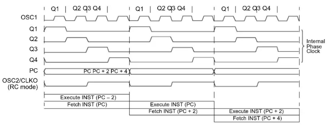
text_image
OSC1 Q1 Q2 Q3 Q4 | Q1 Q2 Q3 Q4 | Q1 Q2 Q3 Q4 | Internal Phase Clock Q1 Q2 Q3 Q4 PC PC PC + 2 PC + 4 OSC2/CLKO (RC mode) Execute INST (PC - 2) Fetch INST (PC) Execute INST (PC) Fetch INST (PC + 2) Execute INST (PC + 2) Fetch INST (PC + 4)EXAMPLE 6-3: INSTRUCTION PIPELINE FLOW
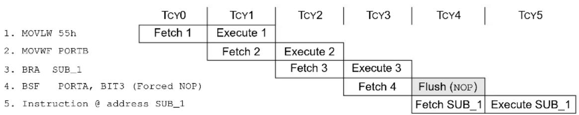
text_image
Tcy0 Tcy1 Tcy2 | Tcy3 | Tcy4 | Tcy5 1. MOVLW 55h Fetch 1 Execute 1 2. MOVWF PORTB Fetch 2 Execute 2 3. BRA SUB_1 Fetch 3 Execute 3 4. BSF PORTA, BIT3 (Forced NOP) Fetch 4 Flush (NOP) 5. Instruction @ address SUB_1 Fetch SUB_1 Execute SUB_1All instructions are single cycle, except for any program branches. These take two cycles since the fetch instruction is “flushed” from the pipeline while the new instruction is being fetched and then executed.
6.2.3 INSTRUCTIONS IN PROGRAM MEMORY
The program memory is addressed in bytes. Instructions are stored as two bytes or four bytes in program memory. The Least Significant Byte (LSB) of an instruction word is always stored in a program memory location with an even address (LSB = 0). To maintain alignment with instruction boundaries, the PC increments in steps of 2 and the LSB will always read '0' (see Section 6.1.3 "Program Counter").
Figure 6-5 shows an example of how instruction words are stored in the program memory.
The CALL and GOTO instructions have the absolute program memory address embedded into the instruction. Since instructions are always stored on word boundaries, the data contained in the instruction is a word address. The word address is written to PC<20:1> which accesses the desired byte address in program memory. Instruction #2 in Figure 6-5 shows how the instruction, GOTO 0006h, is encoded in the program memory. Program branch instructions, which encode a relative address offset, operate in the same manner. The offset value stored in a branch instruction represents the number of single-word instructions that the PC will be offset by. Section 26.0 "Instruction Set Summary" provides further details of the instruction set.
FIGURE 6-5: INSTRUCTIONS IN PROGRAM MEMORY
| Program Memory Byte Locations → | LSB = 1 | LSB = 0 | Word Address ↓ | ||
| 000000h | |||||
| 000002h | |||||
| 000004h | |||||
| 000006h | |||||
| Instruction 1: | MOVLW | 055h | 0Fh | 55h | 000008h |
| Instruction 2: | GOTO | 0006h | EFh | 03h | 00000Ah |
| F0h 00h | 00000Ch | ||||
| Instruction 3: | MOVFF | 123h, 456h | C1h | 23h | 00000Eh |
| F4h 56h | 000010h | ||||
| 000012h | |||||
| 000014h | |||||
6.2.4 TWO-WORD INSTRUCTIONS
The standard PIC18 instruction set has four, two-word instructions: CALL, MOVFF, GOTO and LSFR. In all cases, the second word of the instructions always has '1111' as its four Most Significant bits (MSb); the other 12 bits are literal data, usually a data memory address.
The use of '1111' in the 4 MSbs of an instruction specifies a special form of NOP. If the instruction is executed in proper sequence, immediately after the first word, the data in the second word is accessed and
used by the instruction sequence. If the first word is skipped for some reason and the second word is executed by itself, a NOP is executed instead. This is necessary for cases when the two-word instruction is preceded by a conditional instruction that changes the PC. Example 6-4 shows how this works.
Note: See Section 6.5 "Program Memory and the Extended Instruction Set" for information on two-word instructions in the extended instruction set.
EXAMPLE 6-4: TWO-WORD INSTRUCTIONS
| CASE 1: | |
| Object Code | Source Code |
| 0110 0110 0000 0000 | TSTFSZ REG1 ; is RAM location 0? |
| 1100 0001 0010 0011 | MOVFF REG1, REG2 ; No, skip this word |
| 1111 0100 0101 0110 | |
| 0010 0100 0000 0000 | ADDWF REG3 ; continue code |
| CASE 2: | |
| Object Code | Source Code |
| 0110 0110 0000 0000 | TSTFSZ REG1 ; is RAM location 0? |
| 1100 0001 0010 0011 | MOVFF REG1, REG2 ; Yes, execute this word |
| 1111 0100 0101 0110 | |
| 0010 0100 0000 0000 | ADDWF REG3 ; continue code |
6.3 Data Memory Organization
Note: The operation of some aspects of data memory are changed when the PIC18 extended instruction set is enabled. See Section 6.6 "Data Memory and the Extended Instruction Set" for more information.
The data memory in PIC18 devices is implemented as static RAM. Each register in the data memory has a 12-bit address, allowing up to 4,096 bytes of data memory. The memory space is divided into as many as 16 banks that contain 256 bytes each. PIC18FX6J90 and PIC18FX7J90 devices implement all 16 complete banks, for a total of 4 Kbytes. Figure 6-6 and Figure 6-7 show the data memory organization for the devices.
The data memory contains Special Function Registers (SFRs) and General Purpose Registers (GPRs). The SFRs are used for control and status of the controller and peripheral functions, while GPRs are used for data storage and scratchpad operations in the user's application. Any read of an unimplemented location will read as '0's.
The instruction set and architecture allow operations across all banks. The entire data memory may be accessed by Direct, Indirect or Indexed Addressing modes. Addressing modes are discussed later in this section.
To ensure that commonly used registers (select SFRs and select GPRs) can be accessed in a single cycle, PIC18 devices implement an Access Bank. This is a 256-byte memory space that provides fast access to select SFRs, and the lower portion of GPR Bank 0, without using the BSR. Section 6.3.2 "Access Bank" provides a detailed description of the Access RAM.
6.3.1 BANK SELECT REGISTER
Large areas of data memory require an efficient addressing scheme to make rapid access to any address possible. Ideally, this means that an entire address does not need to be provided for each read or write operation. For PIC18 devices, this is accomplished with a RAM banking scheme. This divides the memory space into 16 contiguous banks of 256 bytes. Depending on the instruction, each location can be addressed directly by its full 12-bit address, or an 8-bit low-order address and a 4-bit Bank Pointer.
Most instructions in the PIC18 instruction set make use of the Bank Pointer, known as the Bank Select Register (BSR). This SFR holds the 4 Most Significant bits of a location's address; the instruction itself includes the 8 Least Significant bits. Only the four lower bits of the BSR are implemented (BSR<3:0>). The upper four bits are unused; they will always read '0' and cannot be written to. The BSR can be loaded directly by using the MOVLB instruction.
The value of the BSR indicates the bank in data memory. The 8 bits in the instruction show the location in the bank and can be thought of as an offset from the bank's lower boundary. The relationship between the BSR's value and the bank division in data memory is shown in Figure 6-7.
Since up to 16 registers may share the same low-order address, the user must always be careful to ensure that the proper bank is selected before performing a data read or write. For example, writing what should be program data to an 8-bit address of F9h, while the BSR is 0Fh, will end up resetting the program counter.
While any bank can be selected, only those banks that are actually implemented can be read or written to. Writes to unimplemented banks are ignored, while reads from unimplemented banks will return '0's. Even so, the STATUS register will still be affected as if the operation was successful. The data memory map in Figure 6-6 indicates which banks are implemented.
In the core PIC18 instruction set, only the MOVFF instruction fully specifies the 12-bit address of the source and target registers. This instruction ignores the BSR completely when it executes. All other instructions include only the low-order address as an operand and must use either the BSR or the Access Bank to locate their target registers.
FIGURE 6-6: DATA MEMORY MAP FOR PIC18FX6J90 AND PIC18FX7J90 DEVICES

geo
| Bank | BSR Value | |------|-----------| | Bank 0 | 0000 | | Bank 1 | 0001 | | Bank 2 | 0010 | | Bank 3 | 0011 | | Bank 4 | 0100 | | Bank 5 | 0101 | | Bank 6 | 0110 | | Bank 7 | 0111 | | Bank 8 | 1000 | | Bank 9 | 1001 | | Bank 10 | 1010 | | Bank 11 | 1011 | | Bank 12 | 1100 | | Bank 13 | 1101 | | Bank 14 | 1110 | | Bank 15 | 1111 |Note 1: Addresses, F54h through F5Fh, are also used by SFRs, but are not part of the Access RAM. Users must always use the complete address, or load the proper BSR value, to access these registers.
FIGURE 6-7: USE OF THE BANK SELECT REGISTER (DIRECT ADDRESSING)

flowchart
graph TD
    A["7"] --> B["BSR(1) 0"]
    B --> C["Bank Select(2)"]
    C --> D["300h"]
    D --> E["Data Memory"]
    E --> F["00h"]
    E --> G["100h"]
    E --> H["200h"]
    E --> I["300h"]
    E --> J["E00h"]
    E --> K["F00h"]
    E --> L["FFFh"]

    M["7"] --> N["From Opcode(2) 0"]

    subgraph BSR
        B1["0"] --> B2["0"]
        B3["0"] --> B4["0"]
        B5["0"] --> B6["0"]
        B7["1"] --> B8["1"]
        B9["0"] --> B10["1"]
        B11["0"] --> B12["1"]
        B13["1"] --> B14["1"]
        B15["1"] --> B16["1"]
        B17["1"] --> B18["1"]
        B19["1"] --> B20["1"]
        B21["1"] --> B22["1"]
        B23["1"] --> B24["1"]
        B25["1"] --> B26["1"]
        B27["1"] --> B28["1"]
        B29["1"] --> B30["1"]
        B31["1"] --> B32["1"]
        B33["1"] --> B34["1"]
        B35["1"] --> B36["1"]
        B37["1"] --> B38["1"]
        B39["1"] --> B40["1"]
        B41["1"] --> B42["1"]
        B43["1"] --> B44["1"]
        B45["1"] --> B46["1"]
        B47["1"] --> B48["1"]
        B49["1"] --> B50["1"]
        B51["1"] --> B52["1"]
        B53["1"] --> B54["1"]
        B55["1"] --> B56["1"]
        B57["1"] --> B58["1"]
        B59["1"] --> B60["1"]
        B61["1"] --> B62["1"]
        B63["1"] --> B64["1"]
        B65["1"] --> B66["1"]
        B67["1"] --> B68["1"]
        B69["1"] --> B70["1"]
        B71["1"] --> B72["1"]
        B73["1"] --> B74["1"]
        B75["1"] --> B76["1"]
        B77["1"] --> B78["1"]
        B79["1"] --> B80["1"]
        B81["1"] --> B82["1"]
        B83["1"] --> B84["1"]
        B85["1"] --> B86["1"]
        B87["1"] --> B88["1"]
        B89["1"] --> B90["1"]
        B91["1"] --> B92["1"]
        B93["1"] --> B94["1"]
        B95["1"] --> B96["1"]
        B97["1"] --> B98["1"]
        B99["1"] --> B100["1"]

    end
Note 1: The Access RAM bit of the instruction can be used to force an override of the selected bank (BSR<3:0>) to the registers of the Access Bank.
2: The MOVFF instruction embeds the entire 12-bit address in the instruction.
6.3.2 ACCESS BANK
While the use of the BSR with an embedded 8-bit address allows users to address the entire range of data memory, it also means that the user must always ensure that the correct bank is selected. Otherwise, data may be read from, or written to, the wrong location. This can be disastrous if a GPR is the intended target of an operation, but an SFR is written to instead. Verifying and/or changing the BSR for each read or write to data memory can become very inefficient.
To streamline access for the most commonly used data memory locations, the data memory is configured with an Access Bank, which allows users to access a mapped block of memory without specifying a BSR. The Access Bank consists of the first 96 bytes of memory (00h-5Fh) in Bank 0 and the last 160 bytes of memory (60h-FFh) in Bank 15. The lower half is known as the "Access RAM" and is composed of GPRs. The upper half is where the device's SFRs are mapped. These two areas are mapped contiguously in the Access Bank and can be addressed in a linear fashion by an 8-bit address (Figure 6-6).
The Access Bank is used by core PIC18 instructions that include the Access RAM bit (the 'a' parameter in the instruction). When 'a' is equal to '1', the instruction uses the BSR and the 8-bit address included in the opcode for the data memory address. When 'a' is '0', however, the instruction is forced to use the Access Bank address map; the current value of the BSR is ignored entirely.
Using this “forced” addressing allows the instruction to operate on a data address in a single cycle without updating the BSR first. For 8-bit addresses of 60h and above, this means that users can evaluate and operate on SFRs more efficiently. The Access RAM below 60h is a good place for data values that the user might need to access rapidly, such as immediate computational results or common program variables. Access RAM also allows for faster and more code efficient context saving and switching of variables.
The mapping of the Access Bank is slightly different when the extended instruction set is enabled (XINST Configuration bit = 1). This is discussed in more detail in Section 6.6.3 "Mapping the Access Bank in Indexed Literal Offset Mode".
6.3.3 GENERAL PURPOSE REGISTER FILE
PIC18 devices may have banked memory in the GPR area. This is data RAM which is available for use by all instructions. GPRs start at the bottom of Bank 0 (address 000h) and grow upwards towards the bottom of the SFR area. GPRs are not initialized by a Power-on Reset and are unchanged on all other Resets.
6.3.4 SPECIAL FUNCTION REGISTERS
The Special Function Registers (SFRs) are registers used by the CPU and peripheral modules for controlling the desired operation of the device. These registers are implemented as static RAM. SFRs start at the top of data memory (FFFh) and extend downward to occupy more than the top half of Bank 15 (F60h to FFFh). A list of these registers is given in Table 6-2 and Table 6-3.
The SFRs can be classified into two sets: those associated with the "core" device functionality (ALU, Resets and interrupts) and those related to the peripheral functions. The Reset and Interrupt registers are described in their respective chapters, while the ALU's STATUS register is described later in this section. Registers related to the operation of the peripheral features are described in the chapter for that peripheral.
The SFRs are typically distributed among the peripherals whose functions they control. Unused SFR locations are unimplemented and read as '0's.
TABLE 6-2: SPECIAL FUNCTION REGISTER MAP FOR PIC18F87J90 FAMILY DEVICES
| Addr. | Name | Addr. | Name | Addr. | Name | Addr. | Name | Addr. | Name | Addr. | Name |
| FFFh | TOSU FDFh INDF2 | (1) | FBFh | LCDDATA4(3) | F9Fh | IPR1 F7Fh | SPBRGH1 F5Fh RTCCFG | ||||
| FFEh | TOSH FDEh POSTIN | C2 (1) | FBEh | LCDDATA3 | F9Eh | PIR1 | F7Eh | BAUDCON1 | F5Eh | RTCCAL | |
| FFDh | TOSL | FDDh | POSTDEC2(1) | FBDh | LCDDATA2 | F9Dh | PIE1 | F7Dh | LCDDATA23(3) | F5Dh | RTCVALH |
| FFCh | STKPTR | FDCh | PREINC2(1) | FBCh | LCDDATA1 | F9Ch | —(2) | F7Ch | LCDDATA22(3) | F5Ch | RTCVALL |
| FFBh | PCLATU | FDBh | PLUSW2(1) | FBBh | LCDDATA0 | F9Bh | OSCTUNE | F7Bh | LCDDATA21 | F5Bh | ALRMCFG |
| FFAh | PCLATH FD Ah | FSR2H FBAh | LCDS | E5 (3) | F9Ah | TRISJ(3) | F7Ah | LCDDATA20 | F5Ah | ALRMRPT | |
| FF9h | PCL | FD9h | FSR2L | FB9h | LCDSE4(3) | F99h | TRISH(3) | F79h | LCDDATA19 | F59h | ALRMVALH |
| FF8h | TBLPTRU | FD8h | STATUS | FB8h | LCDSE3 | F98h | TRISG | F78h | LCDDATA18 | F58h | ALRMVALL |
| FF7h | TBLPTRH | FD7h | TMR0H | FB7h | LCDSE2 | F97h | TRISF | F77h | LCDDATA17(3) | F57h | CTMUCONH |
| FF6h | TBLPTRL | FD6h | TMR0L | FB6h | LCDSE1 | F96h | TRISE | F76h | LCDDATA16(3) | F56h | CTMUCONL |
| FF5h | TABLAT | FD5h | T0CON | FB5h | CVRCON | F95h | TRISD | F75h | LCDDATA15 | F55h | CTMUICON |
| FF4h | PRODH FD4h | —(2) | FB4h | CMCON F94h | TRISC F74h | LCDDATA14 | F54h | PADCFG1 | |||
| FF3h | PRODL | FD3h | OSCCON | FB3h | TMR3H | F93h | TRISB | F73h | LCDDATA13 | ||
| FF2h | INTCON | FD2h | LCDREG | FB2h | TMR3L | F92h | TRISA | F72h | LCDDATA12 | ||
| FF1h | INTCON2 | FD1h | WDTCON | FB1h | T3CON | F91h | LATJ(3) | F71h | LCDDATA11(3) | ||
| FF0h | INTCON3 | FD0h | RCON | FB0h | —(2) | F90h | LATH(3) | F70h | LCDDATA10(3) | ||
| FEFh | INDF0(1) | FCFh | TMR1H | FAFh | SPBRG1 | F8Fh | LATG | F6Fh | LCDDATA9 | ||
| FEEh | POSTINC0(1) | FCEh | TMR1L | FAEh | RCREG1 | F8Eh | LATF | F6Eh | LCDDATA8 | ||
| FEDh | POSTDEC0(1) | FCDh | T1CON | FADh | TXREG1 | F8Dh | LATE | F6Dh | LCDDATA7 | ||
| FECh | PREINC0(1) | FCCh | TMR2 | FACh | TXSTA1 | F8Ch | LATD | F6Ch | LCDDATA6 | ||
| FEBh | PLUSW0(1) | FCBh | PR2 | FABh | RCSTA1 | F8Bh | LATC | F6Bh | LCDDATA5(3) | ||
| FEAh | FSROH | FCAh | T2CON | FAAh | LCDPS | F8Ah | LATB | F6Ah | CCPR1H | ||
| FE9h | FSROL | FC9h | SSPBUF | FA9h | LCDSE0 | F89h | LATA | F69h | CCPR1L | ||
| FE8h | WREG | FC8h | SSPADD | FA8h | LCDCON | F88h | PORTJ(3) | F68h | CCP1CON | ||
| FE7h | INDF1(1) | FC7h | SSPSTAT FA7h | EECON2 F87h | PORTH (3) | F67h | CCPR2H | ||||
| FE6h | POSTINC1(1) | FC6h | SSPCON1 | FA6h | EECON1 | F86h | PORTG | F66h | CCPR2L | ||
| FE5h | POSTDEC1(1) | FC5h | SSPCON2 | FA5h | IPR3 | F85h | PORTF | F65h | CCP2CON | ||
| FE4h | PREINC1(1) | FC4h | ADRESH | FA4h | PIR3 | F84h | PORTE | F64h | SPBRG2 | ||
| FE3h | PLUSW1(1) | FC3h | ADRESL | FA3h | PIE3 | F83h | PORTD | F63h | RCREG2 | ||
| FE2h | FSR1H | FC2h | ADCON0 | FA2h | IPR2 | F82h | PORTC | F62h | TXREG2 | ||
| FE1h | FSR1L | FC1h | ADCON1 | FA1h | PIR2 | F81h | PORTB | F61h | TXSTA2 | ||
| FE0h | BSR | FC0h | ADCON2 | FA0h | PIE2 | F80h | PORTA | F60h | RCSTA2 | ||
Note 1: This is not a physical register.
2: Unimplemented registers are read as '0'.
3: This register is not available on PIC18F6XJ90 devices.
TABLE 6-3: PIC18F87J90 FAMILY REGISTER FILE SUMMARY
| File Name Bit | 7 Bit 6 Bit 5 | Bit 4 Bit 3 Bit | 2 Bit 1 Bit 0 | Value onPOR, BOR | Details onpage | |||||
| TOSU — — — Top-of-Stack Upper Byte (TOS<20:16>) | ---0 0000 | 59, 67 | ||||||||
| TOSH Top-of-Stack High Byte (TOS<15:8>) | 0000 0000 | 59, 67 | ||||||||
| TOSL Top-of-Stack Low Byte (TOS<7:0>) | 0000 0000 | 59, 67 | ||||||||
| STKPTR STKFUL STKUNF | — Return Stack Pointer | uu-0 0000 | 59, 68 | |||||||
| PCLATU | — — | b | i (1) t | HoldingRegister for PC<20:16> | ---0 0000 | 59, 67 | ||||
| PCLATH Holding | Register for PC<15:8> | 0000 0000 | 59, 67 | |||||||
| PCL | PC Low Byte (PC<7:0>) | 0000 0000 | 59, 67 | |||||||
| TBLPTRU | — | — | bit 21 | Program Memory Table Pointer Upper Byte (TBLPTR<20:16>) | ---00 0000 | 59, 92 | ||||
| TBLPTRH | Program Memory Table Pointer High Byte (TBLPTR<15:8>) | 0000 0000 | 59, 92 | |||||||
| TBLPTRL | Program Memory Table Pointer Low Byte (TBLPTR<7:0>) | 0000 0000 | 59, 92 | |||||||
| TABLAT | Program Memory Table Latch | 0000 0000 | 59, 92 | |||||||
| PRODH | Product Register High Byte | xxxx xxxx | 59, 99 | |||||||
| PRODL | Product Register Low Byte | xxxx xxxx | 59, 99 | |||||||
| INTCON | GIE/GIEH | PEIE/GIEL | TMR0IE | INT0IE | RBIE | TMR0IF | INT0IF | RBIF | 0000 000x | 59, 103 |
| INTCON2 RBPU | —— | INTEDG0 | INTEDG1 | INTEDG2 | INTEDG3 | TMR0IP | INT3IP | RBIP | 1111 1111 | 59, 104 |
| INTCON3 | INT2IP | INT1IP | INT3IE | INT2IE | INT1IE | INT3IF | INT2IF | INT1IF | 1100 0000 | 59, 105 |
| INDF0 | Uses contents of FSR0 to address data memory – value of FSR0 not changed (not a physical register) | N/A | 59, 83 | |||||||
| POSTINC0 | Uses contents of FSR0 to address data memory – value of FSR0 post-incremented (not a physical register) | N/A | 59, 84 | |||||||
| POSTDEC0 | Uses contents of FSR0 to address data memory – value of FSR0 post-decremented (not a physical register) | N/A | 59, 84 | |||||||
| PREINC0 | Uses contents of FSR0 to address data memory – value of FSR0 pre-incremented (not a physical register) | N/A | 59, 84 | |||||||
| PLUSW0 | Uses contents of FSR0 to address data memory – value of FSR0 pre-incremented (not a physical register) –value of FSR0 offset by W | N/A | 59, 84 | |||||||
| FSR0H | — — — | — Indirect Data Memory Address Pointe 0 High Byte | ---- xxxx | 59, 83 | ||||||
| FSR0L | Indirect Data Memory Address Pointer 0 Low Byte | xxxx xxxx | 59, 83 | |||||||
| WREG | Working Register | xxxx xxxx | 59 | |||||||
| INDF1 | Uses contents of FSR1 to address data memory – value of FSR1 not changed (not a physical register) | N/A | 59, 83 | |||||||
| POSTINC1 | Uses contents of FSR1 to address data memory – value of FSR1 post-incremented (not a physical register) | N/A | 59, 84 | |||||||
| POSTDEC1 | Uses contents of FSR1 to address data memory – value of FSR1 post-decremented (not a physical register) | N/A | 59, 84 | |||||||
| PREINC1 | Uses contents of FSR1 to address data memory – value of FSR1 pre-incremented (not a physical register) | N/A | 59, 84 | |||||||
| PLUSW1 | Uses contents of FSR1 to address data memory – value of FSR1 pre-incremented (not a physical register) –value of FSR1 offset by W | N/A | 59, 84 | |||||||
| FSR1H | — — — | — Indirect Data Memory Address Pointe 1 High Byte | ---- xxxx | 60, 83 | ||||||
| FSR1L | Indirect Data Memory Address Pointer 1 Low Byte | xxxx xxxx | 60, 83 | |||||||
| BSR | — — — | — Bank Select Register | ---- 0000 | 60, 72 | ||||||
| INDF2 | Uses contents of FSR2 to address data memory – value of FSR2 not changed (not a physical register) | N/A | 60, 83 | |||||||
| POSTINC2 | Uses contents of FSR2 to address data memory – value of FSR2 post-incremented (not a physical register) | N/A | 60, 84 | |||||||
| POSTDEC2 | Uses contents of FSR2 to address data memory – value of FSR2 post-decremented (not a physical register) | N/A | 60, 84 | |||||||
| PREINC2 | Uses contents of FSR2 to address data memory – value of FSR2 pre-incremented (not a physical register) | N/A | 60, 84 | |||||||
| PLUSW2 | Uses contents of FSR2 to address data memory – value of FSR2 pre-incremented (not a physical register) –value of FSR2 offset by W | N/A | 60, 84 | |||||||
| FSR2H | — — — | — Indirect Data Memory Address Pointe 2 High Byte | ---- xxxx | 60, 83 | ||||||
| FSR2L | Indirect Data Memory Address Pointer 2 Low Byte | xxxx xxxx | 60, 83 | |||||||
| STATUS | — | — | — | N | OV | Z | DC | C | ----x xxxx | 60, 81 |
Legend: x = unknown, u = unchanged, - = unimplemented, q = value depends on condition, r = reserved, do not modify
Note 1: Bit 21 of the PC is only available in Test mode and Serial Programming modes.
2: These registers and/or bits are available only on 80-pin devices; otherwise, they are unimplemented and read as '0'. Reset states shown are for 80-pin devices.
3: Alternate names and definitions for these bits when the MSSP module is operating in I ^2 C ^TM Slave mode. See Section 18.4.3.2 "Address Masking" for details.
4: The PLLEN bit is only available in specific oscillator configurations; otherwise, it is disabled and reads as '0'. See Section 3.4.3 "PLL Frequency Multiplier" for details.
5: RA<7:6> and their associated latch and direction bits are configured as port pins only when the internal oscillator is selected as the default clock source (FOSC2 Configuration bit = 0); otherwise, they are disabled and these bits read as '0'.
TABLE 6-3: PIC18F87J90 FAMILY REGISTER FILE SUMMARY (CONTINUED)
| File Name | Bit 7 | Bit 6 | Bit 5 | Bit 4 | Bit 3 | Bit 2 | Bit 1 | Bit 0 | Value on POR, BOR | Details on page |
| TMR0H Timer0 Register High Byte | 0000 0000 | 60, 141 | ||||||||
| TMR0L Timer0 Register Low Byte | xxxx xxxx | 60, 141 | ||||||||
| T0CON TMR0ON T08BIT T0CS T0SE PSA T0PS2 T0PS1 T0PS0 | 1111 1111 | 60, 141 | ||||||||
| OSCCON IDLEN IRCF2 IRCF1 IRCF0 OSTIOFS SCS1 SCS0 | 0110 q000 | 36, 60 | ||||||||
| LCDREG | — | CPEN | BIAS2 | BIAS1 | BIAS0 | MODE13 | CKSEL1 | CKSEL0 | -011 1100 | 60, 189 |
| WDTCON | REGSLP | — | — | — | — | — | — | SWDTEN | 0--- ---0 | 60, 332 |
| RCON | IPEN | — | CM | RI | TO | PD | POR | BOR | 0-11 11q0 | 54, 60 |
| TMR1H Timer1 Register High Byte | xxxx xxxx | 60, 147 | ||||||||
| TMR1L Timer1 Register Low Byte | xxxx xxxx | 60, 147 | ||||||||
| T1CON | RD16 | T1RUN | T1CKPS1 | T1CKPS0 | T1OSCEN | T1SYNC | TMR1CS | TMR1ON | 0000 0000 | 60, 143 |
| TMR2 | Timer2 Register | 0000 0000 | 60, 150 | |||||||
| PR2 | Timer2 Period Register | 1111 1111 | 60, 150 | |||||||
| T2CON | — | T2OUTPS3 | T2OUTPS2 | T2OUTPS1 | T2OUTPS0 | TMR2ON | T2CKPS1 | T2CKPS0 | -000 0000 | 60, 149 |
| SSPBUF | MSSP Receive Buffer/Transmit Register | xxxx xxxx | 60, 219, 254 | |||||||
| SSPADD | MSSP Address Register inI^{2}C^{TM}Slave mode. MSSP1 Baud Rate Reload Register inI^{2}CMaster mode. | 0000 0000 | 60, 254 | |||||||
| SSPSTAT | SMP | CKE D/A | — | P | S | R/W | UA | BF | 0000 0000 | 60, 212, 221 |
| SSPCON1 | WCOL | SSPOV | SSPEN | CKP | SSPM3 | SSPM2 | SSPM1 | SSPM0 | 0000 0000 | 60, 213, 222 |
| SSPCON2 | GCEN | ACKSTAT | ACKDT | ACKEN | RCEN | PEN | RSEN | SEN | 0000 0000 | 60, 223, 224 |
| GCEN | ACKSTAT | ADMSK5(3) | ADMSK4(3) | ADMSK3(3) | ADMSK2(3) | ADMSK1(3) | SEN | |||
| ADRESH A/D Result Register High Byte | xxxx xxxx | 61, 297 | ||||||||
| ADRESL | A/D Result Register Low Byte | xxxx xxxx | 61, 297 | |||||||
| ADCON0 | ADCAL | — | CHS3 | CHS2 | CHS1 | CHS0 | GO/DONE | ADON | 0-00 0000 | 61, 289 |
| ADCON1 | TRIGSEL | — | VCFG1 | VCFG0 | PCFG3 | PCFG2 | PCFG1 | PCFG0 | 0-00 0000 | 61, 290 |
| ADCON2 | ADFM | — | ACQT2 | ACQT1 | ACQT0 | ADCS2 | ADCS1 | ADCS0 | 0-00 0000 | 61, 291 |
| LCDDATA4 S39C0 (2) | S38C0(2) | S37C0(2) | S36C0(2) | S35C0(2) | S34C0(2) | S33C0(2) | S32C0 | S32C0 | xxxx xxxx | 61, 187 |
| LCDDATA3 | S31C0 | S30C0 | S29C0 | S28C0 | S27C0 | S26C0 | S25C0 | S24C0 | xxxx xxxx | 61, 187 |
| LCDDATA2 | S23C0 | S22C0 | S21C0 | S20C0 | S19C0 | S18C0 | S17C0 | S16C0 | xxxx xxxx | 61, 187 |
| LCDDATA1 | S15C0 | S14C0 | S13C0 | S12C0 | S11C0 | S10C0 | S09C0 | S08C0 | xxxx xxxx | 61, 187 |
| LCDDATA0 | S07C0 | S06C0 | S05C0 | S04C0 | S03C0 | S02C0 | S01C0 | S00C0 | xxxx xxxx | 61, 187 |
| LCDSE5^{(2)}$ | SE47 | SE46 | SE45 | SE44 | SE43 | SE42 | SE41 | SE40 | 0000 0000 | 61, 187 |
| LCDSE4 | SE39 (2) | SE38(2) | S37(2) | SE36(2) | SE35(2) | SE34(2) | SE33(2) | SE32 | 0000 0000 | 61, 187 |
| LCDSE3 | SE31 | SE30 | SE29 | SE28 | SE27 | SE26 | SE25 | SE24 | 0000 0000 | 61, 187 |
| LCDSE2 | SE23 | SE22 | SE21 | SE20 | SE19 | SE18 | SE17 | SE16 | 0000 0000 | 61, 187 |
| LCDSE1 | SE15 | SE14 | SE13 | SE12 | SE11 | SE10 | SE09 | SE08 | 0000 0000 | 61, 187 |
| CVRCON | CVREN | CVROE | CVRR | CVRSS | CVR3 | CVR2 | CVR1 | CVR0 | 0000 0000 | 61, 305 |
| CMCON | C2OUT | C1OUT | C2INV | C1INV | CIS | CM2 | CM1 | CM0 | 0000 0111 | 61, 299 |
| TMR3H Timer3 Register High Byte | xxxx xxxx | 61, 153 | ||||||||
| TMR3L Timer3 Register Low Byte | xxxx xxxx | 61, 153 | ||||||||
| T3CON | RD16 | T3CCP2 | T3CKPS1 | T3CKPS0 | T3CCP1 | T3SYNC | TMR3CS | TMR3ON | 0000 0000 | 61, 151 |
Legend: x = unknown, u = unchanged, - = unimplemented, q = value depends on condition, r = reserved, do not modify
Note 1: Bit 21 of the PC is only available in Test mode and Serial Programming modes.
2: These registers and/or bits are available only on 80-pin devices; otherwise, they are unimplemented and read as '0'. Reset states shown are for 80-pin devices.
3: Alternate names and definitions for these bits when the MSSP module is operating in I ^2 C ^TM Slave mode. See Section 18.4.3.2 “Address Masking” for details.
4: The PLLEN bit is only available in specific oscillator configurations; otherwise, it is disabled and reads as '0'. See Section 3.4.3 "PLL Frequency Multiplier" for details.
5: RA<7:6> and their associated latch and direction bits are configured as port pins only when the internal oscillator is selected as the default clock source (FOSC2 Configuration bit = 0); otherwise, they are disabled and these bits read as '0'.
TABLE 6-3: PIC18F87J90 FAMILY REGISTER FILE SUMMARY (CONTINUED)
| File Name | Bit 7 | Bit 6 | Bit 5 | Bit 4 | Bit 3 | Bit 2 | Bit 1 | Bit 0 | Value on POR, BOR | Details on page |
| SPBRG1 EUSART | Baud Rate Generator Low Byte | 0000 0000 | 61, 259 | |||||||
| RCREG1 EUSART | Receive Register | 0000 0000 | 61, 267 | |||||||
| TXREG1 EUSART | Transmit Register | 0000 0000 | 61, 265 | |||||||
| TXSTA1 CSRC | TX9 TXEN SY | NC SENDB BRGH TRMT TX9D | 0000 0010 | 61, 256 | ||||||
| RCSTA1 SPEN RX | X9 SREN CREN | ADDEN FERR OERR RX9D | 0000 000x | 61, 257 | ||||||
| LCDPS | WFT | BIASMD | LCDA | WA | LP3 | LP2 | LP1 | LP0 | 0000 0000 | 61, 185 |
| LCDSE0 SE07 SE | E06 SE05 SE | 04 SE03 SE02 | SE01 SE00 | 0000 0000 | 61, 186 | |||||
| LCDCON | LCDEN | SLPEN WERR | — | CS1 | CS0 LMUX1 | LMUX0 | 000- 0000 | 61, 184 | ||
| EECON2 | EEPROM Control Register 2 (not a physical register) | ---- ---- | 61, 90 | |||||||
| EECON1 | — | — | WPROG | FREE | WRERR | WREN | WR | — | --00 x00- | 61, 90 |
| IPR3 | — | LCDIP | RC2IP | TX2IP | CTMUIP | CCP2IP | CCP1IP | RTCCIP | -111 1111 | 62, 114 |
| PIR3 | — | LCDIF | RC2IF | TX2IF | CTMUIF | CCP2IF | CCP1IF | RTCCIF | -000 0000 | 62, 108 |
| PIE3 | — | LCDIE | RC2IE | TX2IE | CTMUIE | CCP2IE | CCP1IE | RTCCIE | -000 0000 | 62, 111 |
| IPR2 | OSCFIP CMIP | — | — | BCLIP | LVDIP | TMR3IP | — | 11-- 111- | 62, 113 | |
| PIR2 | OSCFIF CMIF | — | — | BCLIF | LVDIF | TMR3IF | — | 00-- 000- | 62, 107 | |
| PIE2 | OSCFIE CMIE | — | — | BCLIE | LVDIE | TMR3IE | — | 00-- 000- | 62, 110 | |
| IPR1 | — | ADIP | RC1IP | TX1IP | SSPIP | — | TMR2IP | TMR1IP | -111 1-11 | 62, 112 |
| PIR1 | — | ADIF | RC1IF | TX1IF | SSPIF | — | TMR2IF | TMR1IF | -000 0-00 | 62, 106 |
| PIE1 | — | ADIE | RC1IE | TX1IE | SSPIE | — | TMR2IE | TMR1IE | -000 0-00 | 62, 109 |
| OSCTUNE INTSRC | PLLEN (4) | TUN5 TUN4 | TUN3 TUN2 | TUN1 TUN0 | 0000 0000 | 37, 62 | ||||
| TRISJ(2) | TRISJ7 | TRISJ6 | TRISJ5 | TRISJ4 | TRISJ3 | TRISJ2 | TRISJ1 | TRISJ0 | 1111 1111 | 62, 138 |
| TRISH(2) | TRISH7 | TRISH6 | TRISH5 | TRISH4 | TRISH3 | TRISH2 | TRISH1 | TRISH0 | 1111 1111 | 62, 136 |
| TRISG | SPIOD | CCP2OD | CCP1OD | TRISG4 | TRISG3 | TRISG2 | TRISG1 | TRISG0 | 0001 1111 | 62, 134 |
| TRISF | TRISF7 | TRISF6 | TRISF5 | TRISF4 | TRISF3 | TRISF2 | TRISF1 | — | 1111 111- | 62, 132 |
| TRISE | TRISE7 | TRISE6 | TRISE5 | TRISE4 | TRISE3 | — TRISE1 | TRISE0 | 1111 1-11 | 62, 129 | |
| TRISD | TRISD7 | TRISD6 | TRISD5 | TRISD4 | TRISD3 | TRISD2 | TRISD1 | TRISD0 | 1111 1111 | 62, 127 |
| TRISC | TRISC7 | TRISC6 | TRISC5 | TRISC4 | TRISC3 | TRISC2 | TRISC1 | TRISC0 | 1111 1111 | 62, 125 |
| TRISB | TRISB7 | TRISB6 | TRISB5 | TRISB4 | TRISB3 | TRISB2 | TRISB1 | TRISB0 | 1111 1111 | 62, 122 |
| TRISA TRISA7 (5) | TRISA6(5) | TRISA5 | TRISA4 | TRISA3 | TRISA2 | TRISA1 | TRISA0 | 1111 1111 | 62, 119 | |
| LATJ(2) | LATJ7 | LATJ6 | LATJ5 | LATJ4 | LATJ3 | LATJ2 | LATJ1 | LATJ0 | xxxx xxxx | 62, 138 |
| LATH(2) | LATH7 | LATH6 | LATH5 | LATH4 | LATH3 | LATH2 | LATH1 | LATH0 | xxxx xxxx | 62, 136 |
| LATG | U2OD | U1OD | — | LATG4 | LATG3 | LATG2 | LATG1 | LATG0 | 00-x xxxx | 62, 134 |
| LATF | LATF7 | LATF6 | LATF5 | LATF4 | LATF3 | LATF2 | LATF1 | — | xxxx xxxx- | 62, 132 |
| LATE | LATE7 | LATE6 | LATE5 | LATE4 | LATE3 | — | LATE1 | LATE0 | xxxx x-xx | 62, 129 |
| LATD | LATD7 | LATD6 | LATD5 | LATD4 | LATD3 | LATD2 | LATD1 | LATD0 | xxxx xxxx | 62, 127 |
| LATC | LATC7 | LATC6 | LATC5 | LATC4 | LATC3 | LATC2 | LATC1 | LATC0 | xxxx xxxx | 62, 125 |
| LATB | LATB7 | LATB6 | LATB5 | LATB4 | LATB3 | LATB2 | LATB1 | LATB0 | xxxx xxxx | 62, 122 |
| LATA | LATA7(5) | LATA6(5) | LATA5 | LATA4 | LATA3 | LATA2 | LATA1 | LATA0 | xxxx xxxx | 62, 119 |
Legend: x = unknown, u = unchanged, - = unimplemented, = value depends on condition, r = reserved, do not modify
Note 1: Bit 21 of the PC is only available in Test mode and Serial Programming modes.
2: These registers and/or bits are available only on 80-pin devices; otherwise, they are unimplemented and read as '0'. Reset states shown are for 80-pin devices.
3: Alternate names and definitions for these bits when the MSSP module is operating in I ^2 C ^TM Slave mode. See Section 18.4.3.2 “Address Masking” for details.
4: The PLLEN bit is only available in specific oscillator configurations; otherwise, it is disabled and reads as '0'. See Section 3.4.3 "PLL Frequency Multiplier" for details.
5: RA<7:6> and their associated latch and direction bits are configured as port pins only when the internal oscillator is selected as the default clock source (FOSC2 Configuration bit = 0); otherwise, they are disabled and these bits read as '0'.
TABLE 6-3: PIC18F87J90 FAMILY REGISTER FILE SUMMARY (CONTINUED)
| File Name | Bit 7 | Bit 6 | Bit 5 | Bit 4 | Bit 3 | Bit 2 | Bit 1 | Bit 0 | Value on POR, BOR | Details on page |
| PORTJ(2) | R | J | 7 | R | J | 6 | R | J | 5 | R |
| PORTH(2) | RH7 RH6 | RH5 RH4 | RH3 RH2 | RH1 RH0 | xxxxxxx | |||||
| PORTG RDPU R | EPU RJPU | (2) | R | G | 4 | R | 3 | R000x xxxG | ||
| PORTF RF7 RF6 | RF5 RF4 RF3 | RF2 RF1 | — | xxxxxxx- | ||||||
| PORTE RE7 RE6 | RE5 RE4 RE3 | — | R | E | 4xxx x-xxR | |||||
| PORTD | RD7 | RD6 | RD5 | RD4 | RD3 | RD2 | RD1 | RD0 | xxxxxxx | 63, 127 |
| PORTC | RC7 | RC6 | RC5 | RC4 | RC3 | RC2 | RC1 | RC0 | xxxxxxx | 63, 125 |
| PORTB RB7 RB6 | RB5 RB4 RB3 | RB2 | RB1 | RB0 | xxxxxxx | |||||
| PORTA | RA7(5) | RA6(5) | RA5 | RA4 | RA3 | RA2 | RA1 | RA0 | xx0x 0000 | 63, 119 |
| SPBRGH1 EUSART Baud Rate Generator High Byte | 0000 0000 | 63, 259 | ||||||||
| BAUDCON1 | ABDOVF | RCIDL | RXDTP | TXCKP | BRG16 | — | WUE | ABDEN | 0100 0-00 | 63, 258 |
| LCDDATA23(2) | S47C3 | S46C3 | S45C3 | S44C3 | S43C3 | S42C3 | S41C3 | S40C3 | xxxxxxx | 63, 187 |
| LCDDATA22 | S39C3(2) | S38C3(2) | S37C3(2) | S36C3(2) | S35C3(2) | S34C3(2) | S33C3(2) | S32C3 | xxxxxxx | 63, 187 |
| LCDDATA21 | S31C3 | S30C3 | S29C3 | S28C3 | S27C3 | S26C3 | S25C3 | S24C3 | xxxxxxx | 63, 187 |
| LCDDATA20 | S23C3 | S22C3 | S21C3 | S20C3 | S19C3 | S18C3 | S17C3 | S16C3 | xxxxxxx | 63, 187 |
| LCDDATA19 | S15C3 | S14C3 | S13C3 | S12C3 | S11C3 | S10C3 | S09C3 | S08C3 | xxxxxxx | 63, 187 |
| LCDDATA18 | S07C3 | S06C3 | S05C3 | S04C3 | S03C3 | S02C3 | S01C3 | S00C3 | xxxxxxx | 63, 187 |
| LCDDATA17(2) | S47C2 | S46C2 | S45C2 | S44C2 | S43C2 | S42C2 | S41C2 | S40C2 | xxxxxxx | 63, 187 |
| LCDDATA16 | S39C2(2) | S38C2(2) | S37C2(2) | S36C2(2) | S35C2(2) | S34C2(2) | S33C2(2) | S32C2 | xxxxxxx | 63, 187 |
| LCDDATA15 | S31C2 | S30C2 | S29C2 | S28C2 | S27C2 | S26C2 | S25C2 | S24C2 | xxxxxxx | 63, 187 |
| LCDDATA14 | S23C2 | S22C2 | S21C2 | S20C2 | S19C2 | S18C2 | S17C2 | S16C2 | xxxxxxx | 63, 187 |
| LCDDATA13 | S15C2 | S14C2 | S13C2 | S12C2 | S11C2 | S10C2 | S09C2 | S08C2 | xxxxxxx | 63, 187 |
| LCDDATA12 | S07C2 | S06C2 | S05C2 | S04C2 | S03C2 | S02C2 | S01C2 | S00C2 | xxxxxxx | 63, 187 |
| LCDDATA11(2) | S47C1 | S46C1 | S45C1 | S44C1 | S43C1 | S42C1 | S41C1 | S40C1 | xxxxxxx | 63, 187 |
| LCDDATA10 | S39C1(2) | S38C1(2) | S37C1(2) | S36C1(2) | S35C1(2) | S34C1(2) | S33C1(2) | S32C1 | xxxxxxx | 63, 187 |
| LCDDATA9 | S31C1 | S30C1 | S29C1 | S28C1 | S27C1 | S26C1 | S25C1 | S24C1 | xxxxxxx | 63, 187 |
| LCDDATA8 | S23C1 | S22C1 | S21C1 | S20C1 | S19C1 | S18C1 | S17C1 | S16C1 | xxxxxxx | 63, 187 |
| LCDDATA7 | S15C1 | S14C1 | S13C1 | S12C1 | S11C1 | S10C1 | S09C1 | S08C1 | xxxxxxx | 63, 187 |
| LCDDATA6 | S07C1 | S06C1 | S05C1 | S04C1 | S03C1 | S02C1 | S01C1 | S00C1 | xxxxxxx | 63, 187 |
| LCDDATA5(2) | S47C0 | S46C0 | S45C0 | S44C0 | S43C0 | S42C0 | S41C0 | S40C0 | xxxxxxx | 63, 187 |
| CCPR1H Capture/Compare/PWM Register 1 High Byte | xxxxxxx | 63, 174 | ||||||||
| CCPR1L Capture/Compare/PWM Register 1 Low Byte | xxxxxxx | 63, 174 | ||||||||
| CCP1CON — DC1B1 DC1B0 CCP1M3 CCP1M2 CCP1M1 CCP1M0 --00 0000 63, 173 | ||||||||||
| CCPR2H Capture/Compare/PWM Register 2 High Byte | xxxxxxx | 63, 174 | ||||||||
| CCPR2L Capture/Compare/PWM Register 2 Low Byte | xxxxxxx | 64, 174 | ||||||||
| CCP2CON — DC2B1 DC2B0 CCP2M3 CCP2M2 CCP2M1 CCP2M0 --00 0000 64, 173 | ||||||||||
| SPBRG2 AUSART Baud Rate Generator Register | 0000 0000 | 64, 278 | ||||||||
| RCREG2 AUSART Receive Register | 0000 0000 | 64, 283 | ||||||||
| TXREG2 AUSART Transmit Register | 0000 0000 | 64, 281 | ||||||||
| TXSTA2 CSRC TX9 TXEN SYNC — BRGH TRMT TX9D 0000 -010 64, 276 | ||||||||||
| RCSTA2 SPEN RX9 SREN CREN ADDEN FERR OERR RX9D 0000 000x 64, 277 | ||||||||||
| RTCCFG RTCEN — RTCWREN RTCSYNC HALFSEC RTCOE RTCPTR1 RTCPTR0 0-00 0000 64, 157 | ||||||||||
| RTCCAL CAL7 CAL6 CAL5 CAL4 CAL3 CAL2 CAL1 CAL0 0000 0000 64, 158 | ||||||||||
| RTCVALH RTCC Value High Register Window based on RTCPTR<1:0> | xxxxxxx | 64, 160 | ||||||||
Legend: x = unknown, u = unchanged, - = unimplemented, q = value depends on condition, r = reserved, do not modify
Note 1: Bit 21 of the PC is only available in Test mode and Serial Programming modes.
2: These registers and/or bits are available only on 80-pin devices; otherwise, they are unimplemented and read as '0'. Reset states shown are for 80-pin devices.
3: Alternate names and definitions for these bits when the MSSP module is operating in I ^2 C ^™ Slave mode. See Section 18.4.3.2 “Address Masking” for details.
4: The PLLEN bit is only available in specific oscillator configurations; otherwise, it is disabled and reads as '0'. See Section 3.4.3 "PLL Frequency Multiplier" for details.
5: RA<7:6> and their associated latch and direction bits are configured as port pins only when the internal oscillator is selected as the default clock source (FOSC2 Configuration bit = 0); otherwise, they are disabled and these bits read as '0'.
TABLE 6-3: PIC18F87J90 FAMILY REGISTER FILE SUMMARY (CONTINUED)
| File Name | Bit 7 | Bit 6 | Bit 5 | Bit 4 | Bit 3 | Bit 2 | Bit 1 | Bit 0 | Value on POR, BOR | Details on page |
| RTCVALL RTCC | Value Low Register Window based on RTCPTR<1:0> | xxxx xxxx | 64, 160 | |||||||
| ALRMCFG ALRMEN CHIME A | MASK3 AMA | SK2 AMASK1 | AMASK0 AL | RMPTR1 ALR | MPTR0 | 0000 0000 | 64, 159 | |||
| ALRMRPT ARPT7 | ARPT6 ARPT5 | ARPT4 ARPT3 | ARPT1 ARPT0 | 0000 0000 | 64, 160 | |||||
| ALRMVALH Alarm Value High Register Window based on ALRMPTR<1:0> | xxxx xxxx | 64, 163 | ||||||||
| ALRMVALL Alarm Value Low Register Window based on ALRMPTR<1:0> | xxxx xxxx | 64, 163 | ||||||||
| CTMUCONH CTMUEN | — | CTMUSIDL | TGEN | EDGEN | EDGSEQEN | IDISSEN | CTTRIG | 0-00 0000 | 64, 321 | |
| CTMUCONL | EDG2POL | EDG2SEL1 | EDG2SEL0 | EDG1POL | EDG1SEL1 | EDG1SEL0 | EDG2STAT | EDG1STAT | 0000 0000 | 64, 322 |
| CTMUICON | ITRIM5 | ITRIM4 | ITRIM3 | ITRIM2 | ITRIM1 | ITRIM0 | IRNG1 | IRNG0 | 0000 0000 | 64, 323 |
| PADCFG1 | — | — | — | — | — | RTSECSEL1 | RTSECSEL0 | — | ---- -00- | 64, 158 |
Legend: x = unknown, u = unchanged, - = unimplemented, = value depends on condition, r = reserved, do not modify
Note 1: Bit 21 of the PC is only available in Test mode and Serial Programming modes.
2: These registers and/or bits are available only on 80-pin devices; otherwise, they are unimplemented and read as '0'. Reset states shown are for 80-pin devices.
3: Alternate names and definitions for these bits when the MSSP module is operating in I ^2 C ^TM Slave mode. See Section 18.4.3.2 “Address Masking” for details.
4: The PLLEN bit is only available in specific oscillator configurations; otherwise, it is disabled and reads as '0'. See Section 3.4.3 "PLL Frequency Multiplier" for details.
5: RA<7:6> and their associated latch and direction bits are configured as port pins only when the internal oscillator is selected as the default clock source (FOSC2 Configuration bit = 0); otherwise, they are disabled and these bits read as '0'.
6.3.5 STATUS REGISTER
The STATUS register, shown in Register 6-2, contains the arithmetic status of the ALU. The STATUS register can be the operand for any instruction, as with any other register. If the STATUS register is the destination for an instruction that affects the Z, DC, C, OV or N bits, then the write to these five bits is disabled.
These bits are set or cleared according to the device logic. Therefore, the result of an instruction with the STATUS register as destination may be different than intended. For example, CLRF STATUS will set the Z bit but leave the other bits unchanged. The STATUS
register then reads back as '000u uluu'. It is recommended, therefore, that only BCF, BSF, SWAPF, MOVEF and MOVWF instructions are used to alter the STATUS register because these instructions do not affect the Z, C, DC, OV or N bits in the STATUS register.
For other instructions not affecting any Status bits, see the instruction set summaries in Table 26-2 and Table 26-3.
Note: The C and DC bits operate as a borrow and digit borrow bit, respectively, in subtraction.
REGISTER 6-2: STATUS REGISTER
| U-0 U-0 U-0 R/W-x R/W-x R/W-x R/W-x R/W-x | |||||||
| ——— | N | O | V | Z | D | (セ) | C(2) |
| bit 7 bit 0 | |||||||
Legend:
| R = Readable bit W = Writable bit | U = Unimplemented bit, read as '0' | ||
| -n = Value at POR | '1' = Bit is set | '0' = Bit is cleared | x = Bit is unknown |
bit 7-5 Unimplemented: Read as '0'
bit 4 N: Negative bit
This bit is used for signed arithmetic (2's complement). It indicates whether the result was negative (ALU MSB = 1).
1 = Result was negative
0 = Result was positive
bit 3 OV: Overflow bit
This bit is used for signed arithmetic (2's complement). It indicates an overflow of the
7-bit magnitude which causes the sign bit (bit 7) to change state.
1 = Overflow occurred for signed arithmetic (in this arithmetic operation)
0 = No overflow occurred
bit 2 Z: Zero bit
1 = The result of an arithmetic or logic operation is zero
0 = The result of an arithmetic or logic operation is not zero
bit 1 DC: Digit Carry/Borrow bit ^(1)
For ADDWF, ADDLW, SUBLW and SUBWF instructions:
1 = A carry-out from the 4th low-order bit of the result occurred
0 = No carry-out from the 4th low-order bit of the result
bit 0 C: Carry/Borrow bit ^(2)
For ADDWF, ADDLW, SUBLW and SUBWF instructions:
1 = A carry-out from the Most Significant bit of the result occurred
0 = No carry-out from the Most Significant bit of the result occurred
Note 1: For borrow, the polarity is reversed. A subtraction is executed by adding the 2's complement of the second operand. For rotate (RRF, RLF) instructions, this bit is loaded with either bit 4 or bit 3 of the source register.
2: For borrow, the polarity is reversed. A subtraction is executed by adding the 2's complement of the second operand. For rotate (RRF, RLF) instructions, this bit is loaded with either the high or low-order bit of the source register.
6.4 Data Addressing Modes
Note: The execution of some instructions in the core PIC18 instruction set are changed when the PIC18 extended instruction set is enabled. See Section 6.6 "Data Memory and the Extended Instruction Set" for more information.
While the program memory can be addressed in only one way, through the program counter, information in the data memory space can be addressed in several ways. For most instructions, the addressing mode is fixed. Other instructions may use up to three modes, depending on which operands are used and whether or not the extended instruction set is enabled.
The addressing modes are:
- Inherent
- Literal
- Direct
- Indirect
An additional addressing mode, Indexed Literal Offset, is available when the extended instruction set is enabled (XINST Configuration bit = 1). Its operation is discussed in greater detail in Section 6.6.1 "Indexed Addressing with Literal Offset".
6.4.1 INHERENT AND LITERAL ADDRESSING
Many PIC18 control instructions do not need any argument at all; they either perform an operation that globally affects the device or they operate implicitly on one register. This addressing mode is known as Inherent Addressing. Examples include: SLEEP, RESET and DAW.
Other instructions work in a similar way, but require an additional explicit argument in the opcode. This is known as Literal Addressing mode, because they require some literal value as an argument. Examples include: ADDLW and MOVLW, which respectively, add or move a literal value to the W register. Other examples include CALL and GOTO, which include a 20-bit program memory address.
6.4.2 DIRECT ADDRESSING
Direct Addressing specifies all or part of the source and/or destination address of the operation within the opcode itself. The options are specified by the arguments accompanying the instruction.
In the core PIC18 instruction set, bit-oriented and byte-oriented instructions use some version of Direct Addressing by default. All of these instructions include some 8-bit literal address as their Least Significant Byte. This address specifies either a register address in one of the banks of data RAM (Section 6.3.3 "General Purpose Register File") or a location in the Access Bank (Section 6.3.2 "Access Bank") as the data source for the instruction.
The Access RAM bit, 'a', determines how the address is interpreted. When 'a' is '1', the contents of the BSR (Section 6.3.1 "Bank Select Register") are used with the address to determine the complete 12-bit address of the register. When 'a' is '0', the address is interpreted as being a register in the Access Bank. Addressing that uses the Access RAM is sometimes also known as Direct Forced Addressing mode.
A few instructions, such as MOVFF, include the entire 12-bit address (either source or destination) in their opcodes. In these cases, the BSR is ignored entirely.
The destination of the operation's results is determined by the destination bit, 'd'. When 'd' is '1', the results are stored back in the source register, overwriting its original contents. When 'd' is '0', the results are stored in the W register. Instructions without the 'd' argument have a destination that is implicit in the instruction; their destination is either the target register being operated on or the W register.
6.4.3 INDIRECT ADDRESSING
Indirect Addressing allows the user to access a location in data memory without giving a fixed address in the instruction. This is done by using File Select Registers (FSRs) as pointers to the locations to be read or written to. Since the FSRs are themselves located in RAM as Special Function Registers, they can also be directly manipulated under program control. This makes FSRs very useful in implementing data structures, such as tables and arrays in data memory.
The registers for Indirect Addressing are also implemented with Indirect File Operands (INDFs) that permit automatic manipulation of the pointer value with auto-incrementing, auto-decrementing or offsetting with another value. This allows for efficient code using loops, such as the example of clearing an entire RAM bank in Example 6-5. It also enables users to perform Indexed Addressing and other Stack Pointer operations for program memory in data memory.
EXAMPLE 6-5: HOW TO CLEAR RAM
(BANK 1) USING INDIRECT ADDRESSING
LFSR FSRO, 100h ;
NEXT CLRF POSTINCO ; Clear INDF
    ; register then
    ; inc pointer
BTFSS FSROH, 1 ; All done with
    ; Bank1?
BRA NEXT ; NO, clear next
CONTINUE ; YES, continue
6.4.3.1 FSR Registers and the INDF Operand
At the core of Indirect Addressing are three sets of registers: FSR0, FSR1 and FSR2. Each represents a pair of 8-bit registers, FSRnH and FSRnL. The four upper bits of the FSRnH register are not used, so each FSR pair holds a 12-bit value. This represents a value that can address the entire range of the data memory in a linear fashion. The FSR register pairs, then, serve as pointers to data memory locations.
Indirect Addressing is accomplished with a set of Indirect File Operands, INDF0 through INDF2. These can be thought of as "virtual" registers: they are mapped in
the SFR space but are not physically implemented. Reading or writing to a particular INDF register actually accesses its corresponding FSR register pair. A read from INDF1, for example, reads the data at the address indicated by FSR1H:FSR1L. Instructions that use the INDF registers as operands actually use the contents of their corresponding FSR as a pointer to the instruction's target. The INDF operand is just a convenient way of using the pointer.
Because Indirect Addressing uses a full, 12-bit address, data RAM banking is not necessary. Thus, the current contents of the BSR and the Access RAM bit have no effect on determining the target address.
FIGURE 6-8: INDIRECT ADDRESSING

flowchart
graph TD
    A["Using an instruction with one of the Indirect Addressing registers as the operand..."] --> B["...uses the 12-bit address stored in the FSR pair associated with that register..."]
    B --> C["...to determine the data memory location to be used in that operation. In this case, the FSR1 pair contains FCCh. This means the contents of location, FCCh, will be added to that of the W register and stored back in FCCh."]
    C --> D["ADDWF, INDF1, 1"]
    D --> E["FSR1H:FSR1L"]
    E --> F["7x7x111111111000h"]
    E --> G["7x7x111111110000h"]
    E --> H["7x7x111111110000h"]
    E --> I["7x7x111111110000h"]
    E --> J["E00h"]
    E --> K["F00h"]
    E --> L["FFFh"]
    E --> M["Data Memory"]
    M --> N["Bank 0"]
    M --> O["Bank 1"]
    M --> P["Bank 2"]
    M --> Q["Bank 3 through Bank 13"]
    M --> R["Bank 14"]
    M --> S["Bank 15"]
6.4.3.2 FSR Registers and POSTINC, POSTDEC, PREINC and PLUSW
In addition to the INDF operand, each FSR register pair also has four additional indirect operands. Like INDF, these are "virtual" registers that cannot be indirectly read or written to. Accessing these registers actually accesses the associated FSR register pair, but also performs a specific action on its stored value. They are:
- POSTDEC: accesses the FSR value, then automatically decrements it by '1' afterwards
- POSTINC: accesses the FSR value, then automatically increments it by '1' afterwards
- PREINC: increments the FSR value by '1', then uses it in the operation
- PLUSW: adds the signed value of the W register (range of -127 to 128) to that of the FSR and uses the new value in the operation
In this context, accessing an INDF register uses the value in the FSR registers without changing them. Similarly, accessing a PLUSW register gives the FSR value offset by the value in the W register; neither value is actually changed in the operation. Accessing the other virtual registers changes the value of the FSR registers.
Operations on the FSRs with POSTDEC, POSTINC and PREINC affect the entire register pair; that is, rollovers of the FSRnL register from FFh to 00h carry over to the FSRnH register. On the other hand, results of these operations do not change the value of any flags in the STATUS register (e.g., Z, N, OV, etc.).
The PLUSW register can be used to implement a form of Indexed Addressing in the data memory space. By manipulating the value in the W register, users can reach addresses that are fixed offsets from pointer addresses. In some applications, this can be used to implement some powerful program control structure, such as software stacks, inside of data memory.
6.4.3.3 Operations by FSRs on FSRs
Indirect Addressing operations that target other FSRs or virtual registers represent special cases. For example, using an FSR to point to one of the virtual registers will not result in successful operations. As a specific case, assume that the FSR0H:FSR0L registers contain FE7h, the address of INDF1. Attempts to read the value of INDF1, using INDF0 as an operand, will return 00h. Attempts to write to INDF1, using INDF0 as the operand, will result in a NOP.
On the other hand, using the virtual registers to write to an FSR pair may not occur as planned. In these cases, the value will be written to the FSR pair but without any incrementing or decrementing. Thus, writing to INDF2 or POSTDEC2 will write the same value to the FSR2H:FSR2L registers.
Since the FSRs are physical registers mapped in the SFR space, they can be manipulated through all direct operations. Users should proceed cautiously when working on these registers, particularly if their code uses Indirect Addressing.
Similarly, operations by Indirect Addressing are generally permitted on all other SFRs. Users should exercise the appropriate caution that they do not inadvertently change settings that might affect the operation of the device.
6.5 Program Memory and the Extended Instruction Set
The operation of program memory is unaffected by the use of the extended instruction set.
Enabling the extended instruction set adds five additional two-word commands to the existing PIC18 instruction set: ADDFSR, CALLW, MOVSF, MOVSS and SUBFSR. These instructions are executed as described in Section 6.2.4 "Two-Word Instructions".
6.6 Data Memory and the Extended Instruction Set
Enabling the PIC18 extended instruction set (XINST Configuration bit = 1) significantly changes certain aspects of data memory and its addressing. Specifically, the use of the Access Bank for many of the core PIC18 instructions is different; this is due to the introduction of a new addressing mode for the data memory space. This mode also alters the behavior of Indirect Addressing using FSR2 and its associated operands.
What does not change is just as important. The size of the data memory space is unchanged, as well as its linear addressing. The SFR map remains the same. Core PIC18 instructions can still operate in both Direct and Indirect Addressing modes. Inherent and literal instructions do not change at all. Indirect Addressing with FSR0 and FSR1 also remains unchanged.
6.6.1 INDEXED ADDRESSING WITH LITERAL OFFSET
Enabling the PIC18 extended instruction set changes the behavior of Indirect Addressing using the FSR2 register pair and its associated file operands. Under the proper conditions, instructions that use the Access Bank – that is, most bit-oriented and byte-oriented instructions – can invoke a form of Indexed Addressing using an offset specified in the instruction. This special addressing mode is known as Indexed Addressing with Literal Offset, or Indexed Literal Offset mode.
When using the extended instruction set, this addressing mode requires the following:
- The use of the Access Bank is forced ('a' = 0); and
- The file address argument is less than or equal to 5Fh.
Under these conditions, the file address of the instruction is not interpreted as the lower byte of an address (used with the BSR in Direct Addressing) or as an 8-bit address in the Access Bank. Instead, the value is interpreted as an offset value to an Address Pointer specified by FSR2. The offset and the contents of FSR2 are added to obtain the target address of the operation.
6.6.2 INSTRUCTIONS AFFECTED BY INDEXED LITERAL OFFSET MODE
Any of the core PIC18 instructions that can use Direct Addressing are potentially affected by the Indexed Literal Offset Addressing mode. This includes all byte-oriented and bit-oriented instructions or almost one-half of the standard PIC18 instruction set. Instructions that only use Inherent or Literal Addressing modes are unaffected.
Additionally, byte-oriented and bit-oriented instructions are not affected if they do not use the Access Bank (Access RAM bit is '1') or include a file address of 60h or above. Instructions meeting these criteria will continue to execute as before. A comparison of the different possible addressing modes when the extended instruction set is enabled is shown in Figure 6-9.
Those who desire to use byte-oriented or bit-oriented instructions in the Indexed Literal Offset mode should note the changes to assembler syntax for this mode. This is described in more detail in Section 26.2.1 "Extended Instruction Syntax".
FIGURE 6-9: COMPARING ADDRESSING OPTIONS FOR BIT-ORIENTED AND BYTE-ORIENTED INSTRUCTIONS (EXTENDED INSTRUCTION SET ENABLED)
EXAMPLE INSTRUCTION: ADDWF, f, d, a (Opcode: 0010 01da ffff ffff)
When a = 0 and f ≥ 60h:
The instruction executes in Direct Forced mode. 'f' is interpreted as a location in the Access RAM between 060h and FFFh. This is the same as locations, F60h to FFFh (Bank 15), of data memory.
Locations below 060h are not available in this addressing mode.
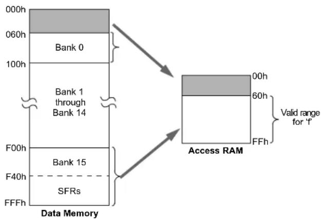
flowchart
graph TD
    A["000h"] --> B["Bank 0"]
    C["060h"] --> D["Bank 1 through Bank 14"]
    E["100h"] --> D
    F["F00h"] --> G["Bank 15"]
    H["F40h"] --> I["SFRs"]
    J["FFFh"] --> I
    B --> K["Access RAM"]
    D --> K
    G --> K
    I --> K
    K --> L["00h"]
    K --> M["60h"]
    K --> N["FFh"]
    L --> O["Valid range for 'f'"]
When a = 0 and f ≤ 5Fh :
The instruction executes in Indexed Literal Offset mode. 'f' is interpreted as an offset to the address value in FSR2. The two are added together to obtain the address of the target register for the instruction. The address can be anywhere in the data memory space.
Note that in this mode, the correct syntax is now:
ADDWF [k], d
where 'k' is the same as 'f'.

flowchart
graph TD
    A["000h Bank 0"] --> B["060h"]
    B --> C["100h"]
    C --> D["F00h"]
    D --> E["F40h"]
    E --> F["SFRs"]
    F --> G["FFFFh Data Memory"]
    H["FSR2H"] --> I["01001da"]
    J["FSR2L"] --> K["+"]
    I --> L["+"]
    K --> L
    style A fill:#f9f,stroke:#333
    style B fill:#f9f,stroke:#333
    style C fill:#f9f,stroke:#333
    style D fill:#f9f,stroke:#333
    style E fill:#f9f,stroke:#333
    style F fill:#f9f,stroke:#333
    style G fill:#ccf,stroke:#333
    style H fill:#ccf,stroke:#333
    style I fill:#ccf,stroke:#333
    style J fill:#ccf,stroke:#333
    style K fill:#ccf,stroke:#333
When a = 1 (all values of f ):
The instruction executes in Direct mode (also known as Direct Long mode). 'f' is interpreted as a location in one of the 16 banks of the data memory space. The bank is designated by the Bank Select Register (BSR). The address can be in any implemented bank in the data memory space.
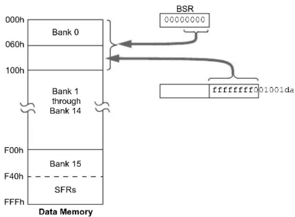
flowchart
graph TD
    A["000h"] --> B["Bank 0"]
    C["060h"] --> D["Bank 1 through Bank 14"]
    E["100h"] --> F["Bank 1"]
    G["F00h"] --> H["Bank 15"]
    I["F40h"] --> J["SFRs"]
    K["FFFh"] --> L["Data Memory"]
    M["BSR 00000000"] --> N["001001da"]
    O["Start"] --> P["Start"]
    Q["Start"] --> R["Start"]
    S["Start"] --> T["Start"]
    U["Start"] --> V["Start"]
    W["Start"] --> X["Start"]
    Y["Start"] --> Z["Start"]
6.6.3 MAPPING THE ACCESS BANK IN INDEXED LITERAL OFFSET MODE
The use of Indexed Literal Offset Addressing mode effectively changes how the lower part of Access RAM (00h to 5Fh) is mapped. Rather than containing just the contents of the bottom part of Bank 0, this mode maps the contents from Bank 0 and a user-defined "window" that can be located anywhere in the data memory space. The value of FSR2 establishes the lower boundary of the addresses mapped into the window, while the upper boundary is defined by FSR2 plus 95 (5Fh). Addresses in the Access RAM above 5Fh are mapped as previously described (see Section 6.3.2 "Access Bank"). An example of Access Bank remapping in this addressing mode is shown in Figure 6-10.
Remapping of the Access Bank applies only to operations using the Indexed Literal Offset mode. Operations that use the BSR (Access RAM bit is '1') will continue to use Direct Addressing as before. Any Indirect or Indexed Addressing operation that explicitly uses any of the indirect file operands (including FSR2) will continue to operate as standard Indirect Addressing. Any instruction that uses the Access Bank, but includes a register address of greater than 05Fh, will use Direct Addressing and the normal Access Bank map.
6.6.4 BSR IN INDEXED LITERAL OFFSET MODE
Although the Access Bank is remapped when the extended instruction set is enabled, the operation of the BSR remains unchanged. Direct Addressing, using the BSR to select the data memory bank, operates in the same manner as previously described.
FIGURE 6-10: REMAPPING THE ACCESS BANK WITH INDEXED LITERAL OFFSET ADDRESSING
Example Situation:
ADDWF f, d, a FSR2H:FSR2L = 120h
Locations in the region from the FSR2 Pointer (120h) to the pointer plus 05Fh (17Fh) are mapped to the bottom of the Access RAM (000h-05Fh).
Special Function Registers at F60h through FFFh are mapped to 60h through FFh, as usual.
Bank 0 addresses below 5Fh are not available in this mode. They can still be addressed by using the BSR.
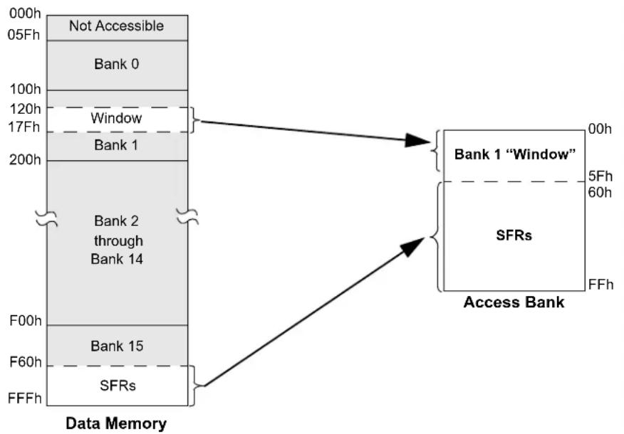
flowchart
graph TD
    A["000h"] --> B["Not Accessible"]
    B --> C["Bank 0"]
    C --> D["100h"]
    D --> E["Window"]
    E --> F["17Fh"]
    F --> G["Bank 1"]
    G --> H["200h"]
    H --> I["Bank 2 through Bank 14"]
    I --> J["F00h"]
    J --> K["Bank 15"]
    K --> L["F60h"]
    L --> M["FFH"]
    M --> N["SFRs"]
    N --> O["Data Memory"]
    P["Bank 1 "Window""] --> Q["5Fh"]
    Q --> R["60h"]
    R --> S["Access Bank"]
    T["SFRs"] --> U["FFh"]
NOTES:
7.0 FLASH PROGRAM MEMORY
The Flash program memory is readable, writable and erasable during normal operation over the entire VDD range.
A read from program memory is executed on one byte at a time. A write to program memory is executed on blocks of 64 bytes at a time or two bytes at a time. Program memory is erased in blocks of 1024 bytes at a time. A bulk erase operation may not be issued from user code.
Writing or erasing program memory will cease instruction fetches until the operation is complete. The program memory cannot be accessed during the write or erase, therefore, code cannot execute. An internal programming timer terminates program memory writes and erases.
A value written to program memory does not need to be a valid instruction. Executing a program memory location that forms an invalid instruction results in a NOP.
7.1 Table Reads and Table Writes
In order to read and write program memory, there are two operations that allow the processor to move bytes between the program memory space and the data RAM:
- Table Read (TBLRD)
- Table Write (TBLWT)
The program memory space is 16 bits wide, while the data RAM space is 8 bits wide. Table reads and table writes move data between these two memory spaces through an 8-bit register (TABLAT).
Table read operations retrieve data from program memory and place it into the data RAM space. Figure 7-1 shows the operation of a table read with program memory and data RAM.
Table write operations store data from the data memory space into holding registers in program memory. The procedure to write the contents of the holding registers into program memory is detailed in Section 7.5 "Writing to Flash Program Memory". Figure 7-2 shows the operation of a table write with program memory and data RAM.
Table operations work with byte entities. A table block containing data, rather than program instructions, is not required to be word-aligned. Therefore, a table block can start and end at any byte address. If a table write is being used to write executable code into program memory, program instructions will need to be word-aligned.
FIGURE 7-1: TABLE READ OPERATION

flowchart
graph LR
    A["Table Pointer(1)\nTBLPTRU\nTBLPTRH\nTBLPTRL"] --> B["Program Memory\n(TBLPTR)"]
    B --> C["Instruction: TBLRD*"]
    C --> D["Table Latch (8-bit)\nTABLAT"]
FIGURE 7-2: TABLE WRITE OPERATION
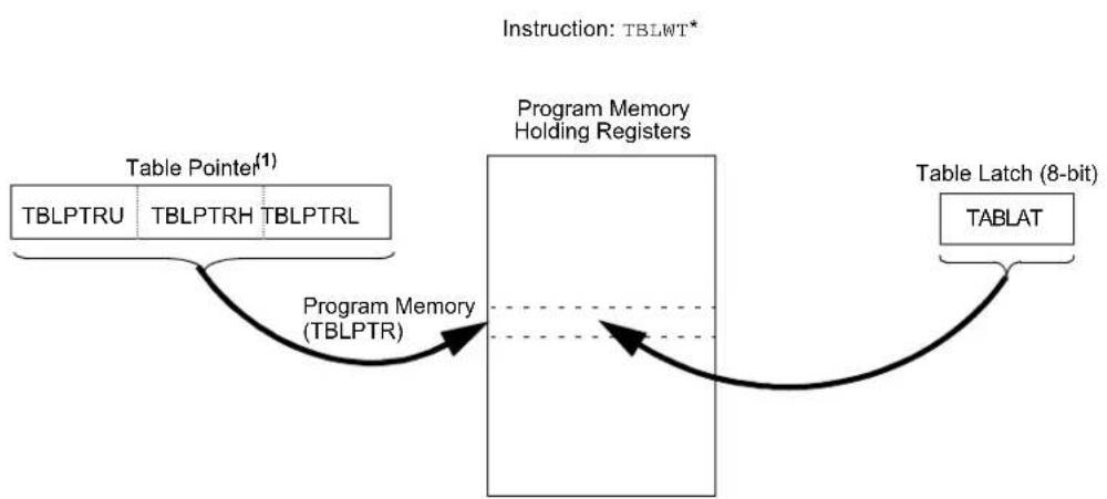
flowchart
graph TD
    A["Table Pointer (1)"] --> B["Program Memory Holding Registers"]
    C["TBLPTRU"] --> B
    D["TBLPTRH"] --> B
    E["TBLPTRL"] --> B
    F["Instruction: TBLWT*"] --> B
    G["Program Memory (TBLPTR)"] --> B
    H["Table Latch (8-bit)"] --> I["TABLAT"]
Note 1: The Table Pointer actually points to one of 64 holding registers, the address of which is determined by TBLPTRL<5:0>. The process for physically writing data to the program memory array is discussed in Section 7.5 "Writing to Flash Program Memory".
7.2 Control Registers
Several control registers are used in conjunction with the TBLRD and TBLWT instructions. These include the:
- EECON1 register
- EECON2 register
- TABLAT register
- TBLPTR registers
7.2.1 EECON1 AND EECON2 REGISTERS
The EECON1 register (Register 7-1) is the control register for memory accesses. The EECON2 register is not a physical register; it is used exclusively in the memory write and erase sequences. Reading EECON2 will read all '0's.
The WPROG bit, when set, allows the user to program a single word (two bytes) upon the execution of the WR command. If this bit is cleared, the WR command programs a block of 64 bytes.
The FREE bit, when set, will allow a program memory erase operation. When FREE is set, the erase operation is initiated on the next WR command. When FREE is clear, only writes are enabled.
The WREN bit, when set, will allow a write operation. On power-up, the WREN bit is clear. The WRERR bit is set in hardware when the WR bit is set, and cleared when the internal programming timer expires and the write operation is complete.
Note: During normal operation, the WRERR is read as '1'. This can indicate that a write operation was prematurely terminated by a Reset or a write operation was attempted improperly.
The WR control bit initiates write operations. The bit cannot be cleared, only set, in software. It is cleared in hardware at the completion of the write operation.
REGISTER 7-1: EECON1: EEPROM CONTROL REGISTER 1
| U-0 U-0 R/W-0 R/W-0 R/W-x R/W-0 R/S-0 U-0 | ||||||
| — — WPROG FREE WRERR | (1) | WREN WR | — | |||
| bit 7 bit 0 | ||||||
| Legend: | S = Settable bit (cannot be cleared in software) | ||
| R = Readable bit | W = Writable bit | U = Unimplemented bit, read as ‘0’ | |
| -n = Value at POR | ‘1’ = Bit is set | ‘0’ = Bit is cleared | x = Bit is unknown |
bit 7-6 Unimplemented: Read as '0'
bit 5 WPROG: One Word-Wide Program bit
1 = Program 2 bytes on the next WR command
0 = Program 64 bytes on the next WR command
bit 4 FREE: Flash Erase Enable bit
1 = Performs an erase operation on the next WR command (cleared by completion of erase operation)
0 = Perform write-only
bit 3 WRERR: Flash Program Error Flag bit ^(1)
1 = A write operation is prematurely terminated (any Reset during self-timed programming in normal operation, or an improper write attempt)
0 = The write operation completed
bit 2 WREN: Flash Program Write Enable bit
1 = Allows write cycles to Flash program memory
0 = Inhibits write cycles to Flash program memory
bit 1 WR: Write Control bit
1 = Initiates a program memory erase cycle or write cycle
(The operation is self-timed and the bit is cleared by hardware once write is complete. The WR bit can only be set (not cleared) in software.)
0 = Write cycle is complete
bit 0 Unimplemented: Read as '0'
Note 1: When a WRERR error occurs, the EEPGD and CFGS bits are not cleared. This allows tracing of the error condition.
7.2.2 TABLE LATCH REGISTER (TABLAT)
The Table Latch (TABLAT) is an 8-bit register mapped into the SFR space. The Table Latch register is used to hold 8-bit data during data transfers between program memory and data RAM.
7.2.3 TABLE POINTER REGISTER (TBLPTR)
The Table Pointer (TBLPTR) register addresses a byte within the program memory. The TBLPTR is comprised of three SFR registers: Table Pointer Upper Byte, Table Pointer High Byte and Table Pointer Low Byte (TBLPTRU:TBLPTRH:TBLPTRL). These three registers join to form a 22-bit wide pointer. The low-order 21 bits allow the device to address up to 2 Mbytes of program memory space. The 22nd bit allows access to the Device ID, the user ID and the Configuration bits.
The Table Pointer register, TBLPTR, is used by the TBLRD and TBLWT instructions. These instructions can update the TBLPTR in one of four ways based on the table operation. These operations are shown in Table 7-1. These operations on the TBLPTR only affect the low-order 21 bits.
7.2.4 TABLE POINTER BOUNDARIES
TBLPTR is used in reads, writes and erases of the Flash program memory.
When a TBLRD is executed, all 22 bits of the TBLPTR determine which byte is read from program memory into TABLAT.
When a TBLWT is executed, the seven LSbs of the Table Pointer register (TBLPTR<6:0>) determine which of the 64 program memory holding registers is written to. When the timed write to program memory begins (via the WR bit), the 12 MSbs of the TBLPTR (TBLPTR<21:10>) determine which program memory block of 1024 bytes is written to. For more detail, see Section 7.5 "Writing to Flash Program Memory".
When an erase of program memory is executed, the 12 MSbs of the Table Pointer register point to the 1024-byte block that will be erased. The Least Significant bits are ignored.
Figure 7-3 describes the relevant boundaries of TBLPTR based on Flash program memory operations.
TABLE 7-1: TABLE POINTER OPERATIONS WITH TBLRD AND TBLWT INSTRUCTIONS
| Example Operation on Table Pointer | |
| TBLRD*TBLWT* | TBLPTR is not modified |
| TBLRD*+TBLWT*+ | TBLPTR is incremented after the read/write |
| TBLRD*-TBLWT*- | TBLPTR is decremented after the read/write |
| TBLRD+*TBLWT+* | TBLPTR is incremented before the read/write |
FIGURE 7-3: TABLE POINTER BOUNDARIES BASED ON OPERATION

flowchart
graph TD
    A["21 16 15 8 TBLPTRU 0"] --> B["ERASE: TBLPTR<20:10>"]
    B --> C["TABLE WRITE: TBLPTR<20:6>"]
    C --> D["TABLE READ: TBLPTR<21:0>"]
    D --> E["TBLPTRH"]
    E --> F["TBLPTRL"]
7.3 Reading the Flash Program Memory
The TBLRD instruction is used to retrieve data program memory and places it into data RAM. Table reads from program memory are performed one byte at a time.
TBLPTR points to a byte address in program space. Executing TBLRD places the byte pointed to into TABLAT. In addition, TBLPTR can be modified automatically for the next table read operation.
The internal program memory is typically organized by words. The Least Significant bit of the address selects between the high and low bytes of the word. Figure 7-4 shows the interface between the internal program memory and the TABLAT.
FIGURE 7-4: READS FROM FLASH PROGRAM MEMORY
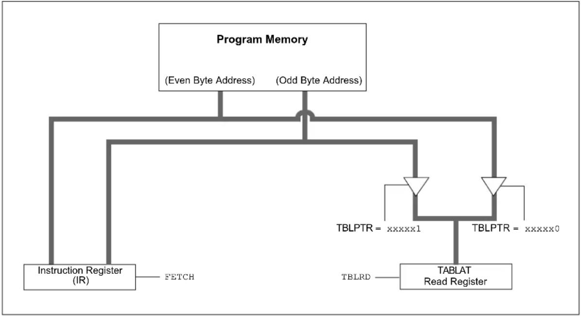
flowchart
graph TD
    A["Program Memory\n(Even Byte Address) (Odd Byte Address)"] --> B["Instruction Register (IR)"]
    A --> C["TBLPTR = xxxxx1"]
    A --> D["TBLPTR = xxxxx0"]
    A --> E["TBLRD"]
    B --> F["FETCH"]
    C --> G["TBLPTR = xxxxx1"]
    D --> H["TBLPTR = xxxxx0"]
    E --> I["TBLRD"]
    F --> J["FETCH"]
    G --> K["TBLPTR = xxxxx1"]
    H --> L["TBLPTR = xxxxx0"]
    I --> M["TBLRD"]
    J --> N["FETCH"]
    K --> O["TBLPTR = xxxxx1"]
    L --> P["TBLPTR = xxxxx0"]
EXAMPLE 7-1: READING A FLASH PROGRAM MEMORY WORD
MOVLW CODE_ADDR_UPPER ; Load TBLPTR with the base
MOVWF TBLPTRU ; address of the word
MOVLW CODE_ADDR_HIGH
MOVWF TBLPTRH
MOVLW CODE_ADDR_LOW
MOVWF TBLPTRL
READ_WORD
TBLRD*+ ; read into TABLAT and increment
MOVF TABLAT, W ; get data
MOVWF WORD_EVEN
TBLRD*+ ; read into TABLAT and increment
MOVF TABLAT, W ; get data
MOVWF WORD_ODD
7.4 Erasing Flash Program Memory
The minimum erase block is 512 words or 1024 bytes. Only through the use of an external programmer, or through ICSP control, can larger blocks of program memory be bulk erased. Word erase in the Flash array is not supported.
When initiating an erase sequence from the microcontroller itself, a block of 1024 bytes of program memory is erased. The Most Significant 12 bits of the TBLPTR<21:10> point to the block being erased. The TBLPTR<9:0> bits are ignored.
The EECON1 register commands the erase operation. The WREN bit must be set to enable write operations. The FREE bit is set to select an erase operation. For protection, the write initiate sequence for EECON2 must be used.
A long write is necessary for erasing the internal Flash. Instruction execution is halted while in a long write cycle. The long write will be terminated by the internal programming timer.
7.4.1 FLASH PROGRAM MEMORY ERASE SEQUENCE
The sequence of events for erasing a block of internal program memory location is:
- Load Table Pointer register with address being erased.
- Set the WREN and FREE bits (EECON1<2,4>) to enable the erase operation.
- Disable interrupts.
- Write 55h to EECON2.
- Write 0AAh to EECON2.
- Set the WR bit. This will begin the erase cycle.
- The CPU will stall for the duration of the erase for TiW (see parameter D133B).
- Re-enable interrupts.
EXAMPLE 7-2: ERASING FLASH PROGRAM MEMORY
MOVLW CODE_ADDR_UPPER ; load TBLPTR with the base
MOVWF TBLPTRU ; address of the memory block
MOVLFW CODE_ADDR_HIGH
MOVWF TBLPTRH
MOVLFW CODE_ADDR_LOW
MOVLFW TBLPTRL
ERASE
BSF EECON1, WREN
BSF EECON1, FREE ; enable Erase operation
BCF INTCON, GIE ; disable interrupts
Required
Sequence
MOVLW 55h
MOVWF EECON2 ; write 55h
MOVLFW 0AAh
MOVWF EECON2 ; write 0AAh
BSF EECON1, WR ; start erase (CPU stall)
BSF INTCON, GIE ; re-enable interrupts
7.5 Writing to Flash Program Memory
The programming block is 32 words or 64 bytes. Programming one word or two bytes at a time is also supported.
Table writes are used internally to load the holding registers needed to program the Flash memory. There are 64 holding registers used by the table writes for programming.
Since the Table Latch (TABLAT) is only a single byte, the TBLWT instruction may need to be executed 64 times for each programming operation (if WPROG = 0). All of the table write operations will essentially be short writes because only the holding registers are written. At the end of updating the 64 holding registers, the EECON1 register must be written to in order to start the programming operation with a long write.
The long write is necessary for programming the internal Flash. Instruction execution is halted while in a long write cycle. The long write will be terminated by the internal programming timer.
The on-chip timer controls the write time. The write/erase voltages are generated by an on-chip charge pump, rated to operate over the voltage range of the device.
Note 1: Unlike previous PIC18 Flash devices, members of the PIC18F87J90 family do not reset the holding registers after a write occurs. The holding registers must be cleared or overwritten before a programming sequence.
2: To maintain the endurance of the program memory cells, each Flash byte should not be programmed more than one time between erase operations. Before attempting to modify the contents of the target cell a second time, an erase of the target, or a bulk erase of the entire memory, must be performed.
FIGURE 7-5: TABLE WRITES TO FLASH PROGRAM MEMORY
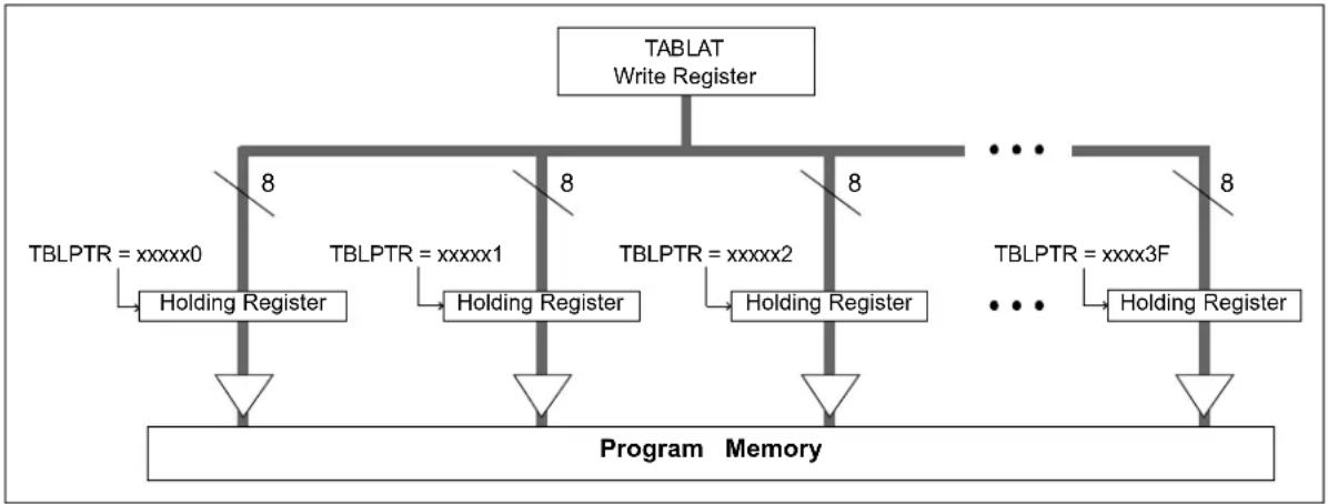
flowchart
graph TD
    A["TBLAT Write Register"] --> B["8"]
    B --> C["Holding Register"]
    C --> D["Program Memory"]
    D --> E["8"]
    E --> F["TBLPTR = xxxx0"]
    E --> G["TBLPTR = xxxx1"]
    E --> H["TBLPTR = xxxx2"]
    E --> I["TBLPTR = xxxx3F"]
    E --> J["Holding Register"]
    J --> K["8"]
    K --> L["Program Memory"]
7.5.1 FLASH PROGRAM MEMORY WRITE SEQUENCE
The sequence of events for programming an internal program memory location should be:
- Read 1024 bytes into RAM.
- Update data values in RAM as necessary.
- Load Table Pointer register with the address being erased.
- Execute the erase procedure.
- Load the Table Pointer register with the address of the first byte being written, minus 1.
- Write the 64 bytes into the holding registers with auto-increment.
-
Set the WREN bit (EECON1<2>) to enable byte writes.
-
Disable interrupts.
- Write 55h to EECON2.
- Write 0AAh to EECON2.
- Set the WR bit. This will begin the write cycle.
- The CPU will stall for the duration of the write for TiW (parameter D133A).
- Re-enable interrupts.
- Repeat steps 6 through 13 until all 1024 bytes are written to program memory.
- Verify the memory (table read).
An example of the required code is shown in Example 7-3 on the following page.
Note: Before setting the WR bit, the Table Pointer address needs to be within the intended address range of the 64 bytes in the holding register.
EXAMPLE 7-3: WRITING TO FLASH PROGRAM MEMORY
MOVLW CODE_ADDR_UPPER ; Load TBLPTR with the base address
MOVWF TBLPTRU ; of the memory block, minus 1
MOVLW CODE_ADDR_HIGH
MOVWF TBLPTRH
MOVLW CODE_ADDR_LOW
MOVWF TBLPTRL

ERASE_BLOCK
BSF EECON1, WREN ; enable write to memory
BSF EECON1, FREE ; enable Erase operation
BCF INTCON, GIE ; disable interrupts
MOVLW 55h
MOVWF EECON2 ; write 55h
MOVLW 0AAh
MOVWF EECON2 ; write 0AAh
BSF EECON1, WR ; start erase (CPU stall)
BSF INTCON, GIE ; re-enable interrupts
MOVLW D'16'
MOVWF WRITE_COUNTER ; Need to write 16 blocks of 64 to write
; one erase block of 1024

RESTART_BUFFER
MOVLW D'64'
MOVWF COUNTER
MOVLW BUFFER_ADDR_HIGH ; point to buffer
MOVWF FSROH
MOVLW BUFFER_ADDR_LOW
MOVWF FSROL

FILL_BUFFER
... ; read the new data from I2C, SPI,
; USART, etc.

WRITE_BUFFER
MOVLW D'64 ; number of bytes in holding register
MOVWF COUNTER

WRITE_BYTE_TO_HREGS
MOVFF POSTINCO, WREG ; get low byte of buffer data
MOVWF TABLAT ; present data to table latch
TBLWT+* ; write data, perform a short write
; to internal TBLWT holding register.

DECFSZ COUNTER ; loop until buffers are full
BRA WRITE_BYTE_TO_HREGS

PROGRAM_MEMORY
BSF EECON1, WREN ; enable write to memory
BCF INTCON, GIE ; disable interrupts

Required Sequence
MOVLW 55h
MOVWF EECON2 ; write 55h
MOVLW 0AAh
MOVWF EECON2 ; write 0AAh
BSF EECON1, WR ; start program (CPU stall)
BSF INTCON, GIE ; re-enable interrupts
BCF EECON1, WREN ; disable write to memory

DECFSZ WRITE_COUNTER ; done with one write cycle
BRA RESTART_BUFFER ; if not done replacing the erase block
7.5.2 FLASH PROGRAM MEMORY WRITE SEQUENCE (WORD PROGRAMMING).
The PIC18F87J90 family of devices has a feature that allows programming a single word (two bytes). This feature is enabled when the WPROG bit is set. If the memory location is already erased, the following sequence is required to enable this feature:
- Load the Table Pointer register with the address of the data to be written
-
Write the 2 bytes into the holding registers and perform a table write
-
Set WPROG to enable single-word write.
- Set WREN to enable write to memory.
- Disable interrupts.
- Write 55h to EECON2.
- Write 0AAh to EECON2.
- Set the WR bit. This will begin the write cycle.
- The CPU will stall for the duration of the write for Tiw (see parameter D133A).
- Re-enable interrupts.
EXAMPLE 7-4: SINGLE-WORD WRITE TO FLASH PROGRAM MEMORY
MOVLW CODE_ADDR_UPPER ; Load TBLPTR with the base address
MOVWF TBLPTRU
MOVLW CODE_ADDR_HIGH
MOVWF TBLPTRH
MOVLW CODE_ADDR_LOW
MOVWF TBLPTRL

MOVLW DATA0
MOVWF TABLAT
TBLWT*+
MOVLW DATA1
MOVWF TABLAT
TBLWT*

PROGRAM_MEMORY
BSF EECON1, WPROG ; enable single word write
BSF EECON1, WREN ; enable write to memory
BCF INTCON, GIE ; disable interrupts
MOVLW 55h
Required MOVWF EECON2 ; write 55h
Sequence MOVLW 0AAh
MOVWF EECON2 ; write 0AAh
BSF EECON1, WR ; start program (CPU stall)
BSF INTCON, GIE ; re-enable interrupts
BCF EECON1, WPROG ; disable single word write
BCF EECON1, WREN ; disable write to memory
7.5.3 WRITE VERIFY
Depending on the application, good programming practice may dictate that the value written to the memory should be verified against the original value. This should be used in applications where excessive writes can stress bits near the specification limit.
7.5.4 UNEXPECTED TERMINATION OF WRITE OPERATION
If a write is terminated by an unplanned event, such as loss of power or an unexpected Reset, the memory location just programmed should be verified and reprogrammed if needed. If the write operation is interrupted by a MCLR Reset or a WDT time-out Reset during normal operation, the user can check the WRERR bit and rewrite the location(s) as needed.
7.6 Flash Program Operation During Code Protection
See Section 25.6 "Program Verification and Code Protection" for details on code protection of Flash program memory.
TABLE 7-2: REGISTERS ASSOCIATED WITH PROGRAM FLASH MEMORY
| Name Bit 7 Bit 6 Bit | 5 Bit 4 Bit | 3 Bit 2 Bit | 1 Bit 0 | Reset Values on Page: | ||||
| TBLPTRU | — — bit 21 Program | Memory Table | Table Pointer Upper Byte (TBLPTR<20:16>) | 59 | ||||
| TBPLTRH | Program Memory Table | Pointer High Byte (TBLPTR<15:8>) | 59 | |||||
| TBLPTRL | Program Memory Table | Pointer Low Byte (TBLPTR<7:0>) | 59 | |||||
| TABLAT | Program Memory Table Latch | 59 | ||||||
| INTCON | GIE/GIEH | PEIE/GIEL | TMR0IE | INT0IE | RBIE | TMR0IF | INT0IF | RBIF |
| EECON2 | EEPROM Control Register 2 (not a physical register) | 61 | ||||||
| EECON1 | — | — | WPROG | FREE | WRERR | WREN | WR | — |
Legend: — = unimplemented, read as '0'. Shaded cells are not used during Flash program memory access.
8.0 8 x 8 HARDWARE MULTIPLIER
8.1 Introduction
All PIC18 devices include an 8 x 8 hardware multiplier as part of the ALU. The multiplier performs an unsigned operation and yields a 16-bit result that is stored in the product register pair, PRODH:PRODL. The multiplier's operation does not affect any flags in the STATUS register.
Making multiplication a hardware operation allows it to be completed in a single instruction cycle. This has the advantages of higher computational throughput and reduced code size for multiplication algorithms and allows the PIC18 devices to be used in many applications previously reserved for digital signal processors. A comparison of various hardware and software multiply operations, along with the savings in memory and execution time, is shown in Table 8-1.
8.2 Operation
Example 8-1 shows the instruction sequence for an 8 x 8 unsigned multiplication. Only one instruction is required when one of the arguments is already loaded in the WREG register.
Example 8-2 shows the sequence to do an 8 x 8 signed multiplication. To account for the sign bits of the arguments, each argument's Most Significant bit (MSb) is tested and the appropriate subtractions are done.
EXAMPLE 8-1: 8 x 8 UNSIGNED MULTIPLY ROUTINE
| MOVF ARG1, W |
| MULWF ARG2 ; ARG1 * ARG2 -> |
| ; PRODH:PRODL |
| BTFSC ARG2, SB ; Test Sign Bit |
| SUBWF PRODH, F ; PRODH = PRODH |
| ; - ARG1 |
| MOVF ARG2, W |
| BTFSC ARG1, SB ; Test Sign Bit |
| SUBWF PRODH, F ; PRODH = PRODH |
| ; - ARG2 |
TABLE 8-1: PERFORMANCE COMPARISON FOR VARIOUS MULTIPLY OPERATIONS
| Routine Multiply Method | Program Memory (Words) | Cycles (Max) | Time | |||
| @ 48 MHz | @ 10 MHz | @ 4 MHz | ||||
| 8 x 8 unsigned | Without hardware multiply | 13 | 69 | 5.7 μs | 27.6 μs | 69 μs |
| Hardware multiply | 1 | 1 | 83.3 ns | 400 ns | 1 μs | |
| 8 x 8 signed | Without hardware multiply | 33 | 91 | 7.5 μs | 36.4 μs | 91 μs |
| Hardware multiply | 6 | 6 | 500 ns | 2.4 μs | 6 μs | |
| 16 x 16 unsigned | Without hardware multiply | 21 | 242 | 20.1 μs | 96.8 μs | 242 μs |
| Hardware multiply | 28 | 28 | 2.3 μs | 11.2 μs | 28 μs | |
| 16 x 16 signed | Without hardware multiply | 52 | 254 | 21.6 μs | 102.6 μs | 254 μs |
| Hardware multiply | 35 | 40 | 3.3 μs | 16.0 μs | 40 μs | |
Example 8-3 shows the sequence to do a 16 x 16 unsigned multiplication. Equation 8-1 shows the algorithm that is used. The 32-bit result is stored in four registers (RES3:RES0).
EQUATION 8-1: 16 x 16 UNSIGNED MULTIPLICATION ALGORITHM
RES3:RES0 = ARG1H:ARG1L • ARG2H:ARG2L
= (ARG1H • ARG2H • 2^16 ) +
(ARG1H • ARG2L • 2^8 ) +
(ARG1L • ARG2H • 2^8 ) +
(ARG1L • ARG2L)
EXAMPLE 8-3: 16 x 16 UNSIGNED MULTIPLY ROUTINE
MOVE ARG1L, W
MULWF ARG2L ; ARG1L * ARG2L->
; PRODH:PRODL
MOVFF PRODH, RES1 ;
MOVFF PRODL, RES0 ;

MOVE ARG1H, W
MULWF ARG2H ; ARG1H * ARG2H->
; PRODH:PRODL
MOVFF PRODH, RES3 ;
MOVFF PRODL, RES2 ;

MOVE ARG1L, W
MULWF ARG2H ; ARG1L * ARG2H->
; PRODH:PRODL
MOVE PRODL, W ;
ADDWF RES1, F ; Add cross
MOVE PRODH, W ; products
ADDWFC RES2, F ;
CLRF WREG ;
ADDWFC RES3, F ;

MOVE ARG1H, W ;
MULWF ARG2L ; ARG1H * ARG2L->
; PRODH:PRODL
MOVE PRODL, W ;
ADDWF RES1, F ; Add cross
MOVE PRODH, W ; products
ADDWFC RES2, F ;
CLRF WREG ;
ADDWFC RES3, F ;
Example 8-4 shows the sequence to do a 16 x 16 signed multiply. Equation 8-2 shows the algorithm used. The 32-bit result is stored in four registers (RES3:RES0). To account for the sign bits of the arguments, the MSb for each argument pair is tested and the appropriate subtractions are done.
EQUATION 8-2: 16 x 16 SIGNED
MULTIPLICATION
ALGORITHM
RES3:RES0= ARG1H:ARG1L • ARG2H:ARG2L
= (ARG1H • ARG2H • 2 ^16 ) +
(ARG1H • ARG2L • 2 ^8 ) +
(ARG1L • ARG2H • 2 ^8 ) +
(ARG1L • ARG2L) +
(-1 • ARG2H<7> • ARG1H:ARG1L • 2 ^16 ) +
(-1 • ARG1H<7> • ARG2H:ARG2L • 2 ^16 )
EXAMPLE 8-4: 16 x 16 SIGNED
MULTIPLY ROUTINE
MOVF ARG1L, W
MULWF ARG2L ; ARG1L * ARG2L ->
MOVFF PRODH, RES1 ;
MOVFF PRODL, RES0 ;

MOVF ARG1H, W
MULWF ARG2H ; ARG1H * ARG2H ->
MOVFF PRODH, RES3 ;
MOVFF PRODL, RES2 ;

MOVF ARG1L, W
MULWF ARG2H ; ARG1L * ARG2H ->
MOVF PRODL, W ;
ADDWF RES1, F ; Add cross
MOVF PRODH, W ; products
ADDWFC RES2, F ;
CLRF WREG ;
ADDWFC RES3, F ;

MOVF ARG1H, W ;
MULWF ARG2L ; ARG1H * ARG2L ->
MOVF PRODL, W ;
ADDWF RES1, F ; Add cross
MOVF PRODH, W ; products
ADDWFC RES2, F ;
CLRF WREG ;
ADDWFC RES3, F ;

BTFSS ARG2H, 7 ; ARG2H:ARG2L neg?
BRA SIGN_ARG1 ; no, check ARG1
MOVF ARG1L, W ;
SUBWF RES2 ;
MOVF ARG1H, W ;
SUBWFB RES3

SIGN_ARG1
BTFSS ARG1H, 7 ; ARG1H:ARG1L neg?
BRA CONT_CODE ; no, done
MOVF ARG2L, W ;
SUBWF RES2 ;
MOVF ARG2H, W ;
SUBWFB RES3

CONT_CODE
9.0 INTERRUPTS
Members of the PIC18F87J90 family of devices have multiple interrupt sources and an interrupt priority feature that allows most interrupt sources to be assigned a high-priority level or a low-priority level. The high-priority interrupt vector is at 0008h and the low-priority interrupt vector is at 0018h. High-priority interrupt events will interrupt any low-priority interrupts that may be in progress.
There are thirteen registers which are used to control interrupt operation. These registers are:
• RCON
• I N T C O N
- INTCON2
- INTCON3
- PIR1, PIR2, PIR3
- PIE1, PIE2, PIE3
- IPR1, IPR2, IPR3
It is recommended that the Microchip header files, supplied with MPLAB ^® IDE, be used for the symbolic bit names in these registers. This allows the assembler/compiler to automatically take care of the placement of these bits within the specified register.
In general, interrupt sources have three bits to control their operation. They are:
- Flag bit to indicate that an interrupt event occurred
- Enable bit that allows program execution to branch to the interrupt vector address when the flag bit is set
- Priority bit to select high priority or low priority
The interrupt priority feature is enabled by setting the IPEN bit (RCON<7>). When interrupt priority is enabled, there are two bits which enable interrupts globally. Setting the GIEH bit (INTCON<7>) enables all interrupts that have the priority bit set (high priority). Setting the GIEL bit (INTCON<6>) enables all interrupts that have the priority bit cleared (low priority). When the interrupt flag, enable bit and appropriate global interrupt enable bit are set, the interrupt will vector immediately to address, 0008h or 0018h, depending on the priority bit setting. Individual interrupts can be disabled through their corresponding enable bits.
When the IPEN bit is cleared (default state), the interrupt priority feature is disabled and interrupts are compatible with PIC ^® mid-range devices. In Compatibility mode, the interrupt priority bits for each source have no effect. INTCON<6> is the PEIE bit which enables/disables all peripheral interrupt sources. INTCON<7> is the GIE bit which enables/disables all interrupt sources. All interrupts branch to address, 0008h, in Compatibility mode.
When an interrupt is responded to, the global interrupt enable bit is cleared to disable further interrupts. If the IPEN bit is cleared, this is the GIE bit. If interrupt priority levels are used, this will be either the GIEH or GIEL bit. High-priority interrupt sources can interrupt a low-priority interrupt. Low-priority interrupts are not processed while high-priority interrupts are in progress.
The return address is pushed onto the stack and the PC is loaded with the interrupt vector address (0008h or 0018h). Once in the Interrupt Service Routine, the source(s) of the interrupt can be determined by polling the interrupt flag bits. The interrupt flag bits must be cleared in software before re-enabling interrupts to avoid recursive interrupts.
The "return from interrupt" instruction, RETFIE, exits the interrupt routine and sets the GIE bit (GIEH or GIEL if priority levels are used) which re-enables interrupts.
For external interrupt events, such as the INTx pins or the PORTB input change interrupt, the interrupt latency will be three to four instruction cycles. The exact latency is the same for one or two-cycle instructions. Individual interrupt flag bits are set regardless of the status of their corresponding enable bit or the GIE bit.
| Note: | Do not use the MOVFF instruction to modify any of the Interrupt Control registers while any interrupt is enabled. Doing so may cause erratic microcontroller behavior. |
FIGURE 9-1: PIC18F87J90 FAMILY INTERRUPT LOGIC
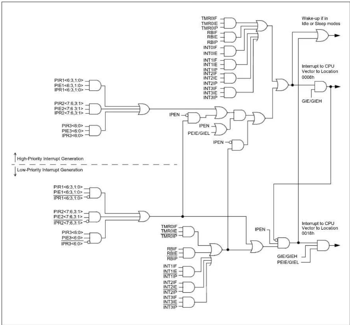
flowchart
graph TD
    A["High-Priority Interrupt Generation"] --> B["Low-Priority Interrupt Generation"]
    B --> C["High-Priority Interrupt Generation"]
    C --> D["Low-Priority Interrupt Generation"]
    D --> E["High-Priority Interrupt Generation"]
    E --> F["Low-Priority Interrupt Generation"]
    F --> G["High-Priority Interrupt Generation"]
    G --> H["Low-Priority Interrupt Generation"]
    H --> I["High-Priority Interrupt Generation"]
    I --> J["Low-Priority Interrupt Generation"]
    J --> K["High-Priority Interrupt Generation"]
    K --> L["Low-Priority Interrupt Generation"]
    L --> M["High-Priority Interrupt Generation"]
    M --> N["Low-Priority Interrupt Generation"]
    N --> O["High-Priority Interrupt Generation"]
    O --> P["Low-Priority Interrupt Generation"]
    P --> Q["High-Priority Interrupt Generation"]
    Q --> R["Low-Priority Interrupt Generation"]
    R --> S["High-Priority Interrupt Generation"]
    S --> T["Low-Priority Interrupt Generation"]
    T --> U["High-Priority Interrupt Generation"]
    U --> V["Low-Priority Interrupt Generation"]
    V --> W["High-Priority Interrupt Generation"]
    W --> X["Low-Priority Interrupt Generation"]
    X --> Y["High-Priority Interrupt Generation"]
    Y --> Z["Low-Priority Interrupt Generation"]
    Z --> AA["High-Priority Interrupt Generation"]
    AA --> AB["Low-Priority Interrupt Generation"]
    AB --> AC["High-Priority Interrupt Generation"]
    AC --> AD["Low-Priority Interrupt Generation"]
    AD --> AE["High-Priority Interrupt Generation"]
    AE --> AF["Low-Priority Interrupt Generation"]
    AF --> AG["High-Priority Interrupt Generation"]
    AG --> AH["Low-Priority Interrupt Generation"]
    AH --> AI["High-Priority Interrupt Generation"]
    AI --> AJ["Low-Priority Interrupt Generation"]
    AJ --> AK["High-Priority Interrupt Generation"]
    AK --> AL["Low-Priority Interrupt Generation"]
    AL --> AM["High-Priority Interrupt Generation"]
    AM --> AN["Low-Priority Interrupt Generation"]
    AN --> AO["High-Priority Interrupt Generation"]
    AO --> AP["Low-Priority Interrupt Generation"]
    AP --> AQ["High-Priority Interrupt Generation"]
    AQ --> AR["Low-Priority Interrupt Generation"]
    AR --> AS["High-Priority Interrupt Generation"]
    AS --> AT["Low-Priority Interrupt Generation"]
    AT --> AU["High-Priority Interrupt Generation"]
    AU --> AV["Low-Priority Interrupt Generation"]
    AV --> AW["High-Priority Interrupt Generation"]
    AW --> AX["Low-Priority Interrupt Generation"]
    AX --> AY["High-Priority Interrupt Generation"]
    AY --> AZ["Low-Priority Interrupt Generation"]
    AZ --> BA["High-Priority Interrupt Generation"]
    BA --> BB["Low-Priority Interrupt Generation"]
    BB --> BC["High-Priority Interrupt Generation"]
    BC --> BD["Low-Priority Interrupt Generation"]
    BD --> BE["High-Priority Interrupt Generation"]
    BE --> BF["Low-Priority Interrupt Generation"]
    BF --> BG["High-Priority Interrupt Generation"]
    BG --> BH["Low-Priority Interrupt Generation"]
9.1 INTCON Registers
The INTCON registers are readable and writable registers which contain various enable, priority and flag bits.
Note: Interrupt flag bits are set when an interrupt condition occurs regardless of the state of its corresponding enable bit or the global interrupt enable bit. User software should ensure the appropriate interrupt flag bits are clear prior to enabling an interrupt. This feature allows for software polling.
REGISTER 9-1: INTCON: INTERRUPT CONTROL REGISTER
| R/W-0 R/W-0 R/W-0 R/W-0 R/W-0 R/W-0 R/W-0 R/W-x | |||||||
| GIE/GIEH P | EIE/GIEL TMR | 0IE INT0IE RB | IE TMR0IF IN† | 0IF RBIF | (1) | ||
| bit 7 bit 0 | |||||||
Legend:
| R = Readable bit | W = Writable bit | U = Unimplemented bit, read as '0' |
| -n = Value at POR | '1' = Bit is set | '0' = Bit is cleared x = Bit is unknown |
bit 7 GIE/GIEH: Global Interrupt Enable bit
When IPEN = 0:
1 = Enables all unmasked interrupts
0 = Disables all interrupts
When IPEN = 1:
1 = Enables all high-priority interrupts
0 = Disables all interrupts
bit 6 PEIE/GIEL: Peripheral Interrupt Enable bit
When IPEN = 0:
1 = Enables all unmasked peripheral interrupts
0 = Disables all peripheral interrupts
When IPEN = 1:
1 = Enables all low-priority peripheral interrupts
0 = Disables all low-priority peripheral interrupts
bit 5 TMROIE: TMR0 Overflow Interrupt Enable bit
1 = Enables the TMR0 overflow interrupt
0 = Disables the TMR0 overflow interrupt
bit 4 INTOIE: INTO External Interrupt Enable bit
1 = Enables the INTO external interrupt
0 = Disables the INT0 external interrupt
bit 3 RBIE: RB Port Change Interrupt Enable bit
1 = Enables the RB port change interrupt
0 = Disables the RB port change interrupt
bit 2 TMR0IF: TMR0 Overflow Interrupt Flag bit
1 = TMR0 register has overflowed (must be cleared in software)
0 = TMR0 register did not overflow
bit 1 INTOIF: INTO External Interrupt Flag bit
1 = The INTO external interrupt occurred (must be cleared in software)
0 = The INTO external interrupt did not occur
bit 0 RBIF: RB Port Change Interrupt Flag bit ^(1)
1 = At least one of the RB<7:4> pins changed state (must be cleared in software)
0 = None of the RB<7:4> pins have changed state
Note 1: A mismatch condition will continue to set this bit. Reading PORTB, and then waiting one additional instruction cycle, will end the mismatch condition and allow the bit to be cleared.
REGISTER 9-2: INTCON2: INTERRUPT CONTROL REGISTER 2
| R/W-1 R/W-1 R/W-1 R/W-1 R/W-1 R/W-1 R/W-1 R/W-1 | |||||||
| INTEDG0 IN | TEDG1 INTED | DG2 INTEDG3 | TMR0IP INT3IP | RBIP | |||
| bit 7 bit 0 | |||||||
Legend:
| R = Readable bit W = Writable bit U = Unimplemented bit, read as '0' |
| -n = Value at POR '1' = Bit is set '0' = Bit is cleared x = Bit is unknown |
bit 7 RBPU: PORTB Pull-up Enable bit
1 = All PORTB pull-ups are disabled
0 = PORTB pull-ups are enabled by individual port latch values
bit 6 INTEDG0: External Interrupt 0 Edge Select bit
1 = Interrupt on rising edge 0 = Interrupt on falling edge
bit 5 INTEDG1: External Interrupt 1 Edge Select bit
1 = Interrupt on rising edge 0 = Interrupt on falling edge
bit 4 INTEDG2: External Interrupt 2 Edge Select bit
1 = Interrupt on rising edge 0 = Interrupt on falling edge
bit 3 INTEDG3: External Interrupt 3 Edge Select bit
1 = Interrupt on rising edge 0 = Interrupt on falling edge
bit 2 TMR0IP: TMR0 Overflow Interrupt Priority bit
1 = High priority 0 = Low priority
bit 1 INT3IP: INT3 External Interrupt Priority bit
1 = High priority 0 = Low priority
bit 0 RBIP: RB Port Change Interrupt Priority bit
1 = High priority 0 = Low priority
Note: Interrupt flag bits are set when an interrupt condition occurs regardless of the state of its corresponding enable bit or the global interrupt enable bit. User software should ensure the appropriate interrupt flag bits are clear prior to enabling an interrupt. This feature allows for software polling.
REGISTER 9-3: INTCON3: INTERRUPT CONTROL REGISTER 3
| R/W-1 R/W-1 R/W-0 R/W-0 R/W-0 R/W-0 R/W-0 R/W-0 | ||||
| INT2IP INT1IP INT3IE IN | T2IE INT1IE INT3IF INT2IF INT1IF | |||
| bit 7 bit 0 | ||||
Legend:
R = Readable bit W = Writable bit U = Unimplemented bit, read as '0'
-n = Value at POR '1' = Bit is set '0' = Bit is cleared x = Bit is unknown
bit 7 INT2IP: INT2 External Interrupt Priority bit
1 = High priority
0 = Low priority
bit 6 INT1IP: INT1 External Interrupt Priority bit
1 = High priority
0 = Low priority
bit 5 INT3IE: INT3 External Interrupt Enable bit
1 = Enables the INT3 external interrupt
0 = Disables the INT3 external interrupt
bit 4 INT2IE: INT2 External Interrupt Enable bit
1 = Enables the INT2 external interrupt
0 = Disables the INT2 external interrupt
bit 3 INT1IE: INT1 External Interrupt Enable bit
1 = Enables the INT1 external interrupt
0 = Disables the INT1 external interrupt
bit 2 INT3IF: INT3 External Interrupt Flag bit
1 = The INT3 external interrupt occurred (must be cleared in software)
0 = The INT3 external interrupt did not occur
bit 1 INT2IF: INT2 External Interrupt Flag bit
1 = The INT2 external interrupt occurred (must be cleared in software)
0 = The INT2 external interrupt did not occur
bit 0 INT1IF: INT1 External Interrupt Flag bit
1 = The INT1 external interrupt occurred (must be cleared in software)
0 = The INT1 external interrupt did not occur
Note: Interrupt flag bits are set when an interrupt condition occurs regardless of the state of its corresponding enable bit or the global interrupt enable bit. User software should ensure the appropriate interrupt flag bits are clear prior to enabling an interrupt. This feature allows for software polling.
9.2 PIR Registers
The PIR registers contain the individual flag bits for the peripheral interrupts. Due to the number of peripheral interrupt sources, there are three Peripheral Interrupt Request (Flag) registers (PIR1, PIR2, PIR3).
Note 1: Interrupt flag bits are set when an interrupt condition occurs regardless of the state of its corresponding enable bit or the Global Interrupt Enable bit, GIE (INTCON<7>).
2: User software should ensure the appropriate interrupt flag bits are cleared prior to enabling an interrupt and after servicing that interrupt.
REGISTER 9-4: PIR1: PERIPHERAL INTERRUPT REQUEST (FLAG) REGISTER 1
| U-0 R/W-0 R-0 R-0 R/W-0 U-0 R/W-0 R/W-0 | ||||||||
| — ADIF | RC1IF TX1IF $SPIF — | T | M | R | 2 | I | F | T |
| bit 7 bit 0 | ||||||||
| Legend: | |||
| R = Readable bit | W = Writable bit | U = Unimplemented bit, read as ‘0’ | |
| -n = Value at POR | ‘1’ = Bit is set | ‘0’ = Bit is cleared | x = Bit is unknown |
bit 7 Unimplemented: Read as '0'
bit 6 ADIF: A/D Converter Interrupt Flag bit
1 = An A/D conversion completed (must be cleared in software)
0 = The A/D conversion is not complete
bit 5 RC1IF: EUSART Receive Interrupt Flag bit
1 = The EUSART receive buffer, RCREG1, is full (cleared when RCREG1 is read)
0 = The EUSART receive buffer is empty
bit 4 TX1IF: EUSART Transmit Interrupt Flag bit
1 = The EUSART transmit buffer, TXREG1, is empty (cleared when TXREG1 is written)
0 = The EUSART transmit buffer is full
bit 3 SSPIF: Master Synchronous Serial Port Interrupt Flag bit
1 = The transmission/reception is complete (must be cleared in software)
0 = Waiting to transmit/receive
bit 2 Unimplemented: Read as '0'
bit 1 TMR2IF: TMR2 to PR2 Match Interrupt Flag bit
1 = TMR2 to PR2 match occurred (must be cleared in software)
0 = No TMR2 to PR2 match occurred
bit 0 TMR1IF: TMR1 Overflow Interrupt Flag bit
1 = TMR1 register overflowed (must be cleared in software)
0 = TMR1 register did not overflow
REGISTER 9-5: PIR2: PERIPHERAL INTERRUPT REQUEST (FLAG) REGISTER 2
| R/W-0 R/W-0 U-0 U-0 R/W-0 R/W-0 R/W-0 U-0 | |||||||
| OSCFIF CMIF — — | B | C | L | I | F | L | V D |
| bit 7 bit 0 | |||||||
Legend:
| R = Readable bit W = Writable bit | U = Unimplemented bit, read as '0' | ||
| -n = Value at POR | '1' = Bit is set | '0' = Bit is cleared | x = Bit is unknown |
bit 7 OSCFIF: Oscillator Fail Interrupt Flag bit
1 = Device oscillator failed, clock input has changed to INTOSC (must be cleared in software)
0 = Device clock operating
bit 6 CMIF: Comparator Interrupt Flag bit
1 = Comparator input has changed (must be cleared in software)
0 = Comparator input has not changed
bit 5-4 Unimplemented: Read as '0'
bit 3 BCLIF: Bus Collision Interrupt Flag bit
1 = A bus collision occurred (must be cleared in software)
0 = No bus collision occurred
bit 2 LVDIF: Low-Voltage Detect Interrupt Flag bit
1 = A low-voltage condition occurred (must be cleared in software)
0 = The device voltage is above the regulator's low-voltage trip point
bit 1 TMR3IF: TMR3 Overflow Interrupt Flag bit
1 = TMR3 register overflowed (must be cleared in software)
0 = TMR3 register did not overflow
bit 0 Unimplemented: Read as '0'
REGISTER 9-6: PIR3: PERIPHERAL INTERRUPT REQUEST (FLAG) REGISTER 3
| U-0 R/W-0 R-0 R-0 R/W-0 R/W-0 R/W-0 R/W-0 | |||||||
| — LCDIF | RC2IF | TX2IF | CTMUIF | CCP | 2IF | CCP1IF | RTCCIF |
| bit 7 bit 0 | |||||||
Legend:
| R = Readable bit | W = Writable bit | U = Unimplemented bit, read as '0' |
| -n = Value at POR | '1' = Bit is set | '0' = Bit is cleared x = Bit is unknown |
bit 7 Unimplemented: Read as '0'
bit 6 LCDIF: LCD Interrupt Flag bit (valid when Type-B waveform with Non-Static mode is selected)
1 = LCD data of all COMs is output (must be cleared in software)
0 = LCD data of all COMs is not yet output
bit 5 RC2IF: AUSART Receive Interrupt Flag bit
1 = The AUSART receive buffer, RCREG2, is full (cleared when RCREG2 is read)
0 = The AUSART receive buffer is empty
bit 4 TX2IF: AUSART Transmit Interrupt Flag bit
1 = The AUSART transmit buffer, TXREG2, is empty (cleared when TXREG2 is written)
0 = The AUSART transmit buffer is full
bit 3 CTMUIF: CTMU Interrupt Flag bit
1 = CTMU interrupt occurred (must be cleared in software)
0 = No CTMU interrupt occurred
bit 2 CCP2IF: CCP2 Interrupt Flag bit
Capture mode:
1 = A TMR1/TMR3 register capture occurred (must be cleared in software)
0 = No TMR1/TMR3 register capture occurred
Compare mode:
1 = A TMR1/TMR3 register compare match occurred (must be cleared in software)
0 = No TMR1/TMR3 register compare match occurred
PWM mode:
Unused in this mode.
bit 1 CCP1IF: CCP1 Interrupt Flag bit
Capture mode:
1 = A TMR1/TMR3 register capture occurred (must be cleared in software)
0 = No TMR1/TMR3 register capture occurred
Compare mode:
1 = A TMR1/TMR3 register compare match occurred (must be cleared in software)
0 = No TMR1/TMR3 register compare match occurred
PWM mode:
Unused in this mode.
bit 0 RTCCIF: RTCC Interrupt Flag bit
1 = RTCC interrupt occurred (must be cleared in software)
0 = No RTCC interrupt occurred
9.3 PIE Registers
The PIE registers contain the individual enable bits for the peripheral interrupts. Due to the number of peripheral interrupt sources, there are three Peripheral Interrupt Enable registers (PIE1, PIE2, PIE3). When IPEN = 0, the PEIE bit must be set to enable any of these peripheral interrupts.
REGISTER 9-7: PIE1: PERIPHERAL INTERRUPT ENABLE REGISTER 1
| U-0 R/W-0 R/W-0 R/W-0 R/W-0 U-0 R/W-0 R/W-0 | |||||||
| — ADIE | RC1IE TX1IE | SSPIE — TMR | 2IE TMR1IE | ||||
| bit 7 bit 0 | |||||||
Legend:
| R = Readable bit W = Writable bit U = Unimplemented bit, read as '0' | ||
| -n = Value at POR | '1' = Bit is set | '0' = Bit is cleared x = Bit is unknown |
bit 7 Unimplemented: Read as '0'
bit 6 ADIE: A/D Converter Interrupt Enable bit
1 = Enables the A/D interrupt
0 = Disables the A/D interrupt
bit 5 RC1IE: EUSART Receive Interrupt Enable bit
1 = Enables the EUSART receive interrupt
0 = Disables the EUSART receive interrupt
bit 4 TX1IE: EUSART Transmit Interrupt Enable bit
1 = Enables the EUSART transmit interrupt
0 = Disables the EUSART transmit interrupt
bit 3 SSPIE: Master Synchronous Serial Port Interrupt Enable bit
1 = Enables the MSSP interrupt
0 = Disables the MSSP interrupt
bit 2 Unimplemented: Read as '0'
bit 1 TMR2IE: TMR2 to PR2 Match Interrupt Enable bit
1 = Enables the TMR2 to PR2 match interrupt
0 = Disables the TMR2 to PR2 match interrupt
bit 0 TMR1IE: TMR1 Overflow Interrupt Enable bit
1 = Enables the TMR1 overflow interrupt
0 = Disables the TMR1 overflow interrupt
REGISTER 9-8: PIE2: PERIPHERAL INTERRUPT ENABLE REGISTER 2
| R/W-0 R/W-0 U-0 U-0 R/W-0 R/W-0 R/W-0 U-0 | ||||||
| OSCFIE CMIE — — BCLIE LVDIE TMR$IE — | ||||||
| bit 7 bit 0 | ||||||
Legend:
| R = Readable bit W = Writable bit U = Unimplemented bit, read as '0' | ||
| -n = Value at POR | '1' = Bit is set | '0' = Bit is cleared x = Bit is unknown |
bit 7 OSCFIE: Oscillator Fail Interrupt Enable bit
1 = Enabled
0 = Disabled
bit 6 CMIE: Comparator Interrupt Enable bit
1 = Enabled
0 = Disabled
bit 5-4 Unimplemented: Read as '0'
bit 3 BCLIE: Bus Collision Interrupt Enable bit
1 = Enabled
0 = Disabled
bit 2 LVDIE: Low-Voltage Detect Interrupt Enable bit
1 = Enabled
0 = Disabled
bit 1 TMR3IE: TMR3 Overflow Interrupt Enable bit
1 = Enabled
0 = Disabled
bit 0 Unimplemented: Read as '0'
REGISTER 9-9: PIE3: PERIPHERAL INTERRUPT ENABLE REGISTER 3
| U-0 R/W-0 R-0 R-0 R/W-0 R/W-0 R/W-0 R/W-0 | ||||||
| — LCDIE RC2IE TX2IE CTMUIE CCP2IE CCP1IE RTCCIE | ||||||
| bit 7 bit 0 | ||||||
Legend:
| R = Readable bit | W = Writable bit | U = Unimplemented bit, read as '0' |
| -n = Value at POR | '1' = Bit is set | '0' = Bit is cleared x = Bit is unknown |
bit 7 Unimplemented: Read as '0'
bit 6 LCDIE: LCD Interrupt Enable bit (valid when Type-B waveform with Non-Static mode is selected)
1 = Enabled
0 = Disabled
bit 5 RC2IE: AUSART Receive Interrupt Enable bit
1 = Enabled
0 = Disabled
bit 4 TX2IE: AUSART Transmit Interrupt Enable bit
1 = Enabled
0 = Disabled
bit 3 CTMUIE: CTMU Interrupt Enable bit
1 = Enabled
0 = Disabled
bit 2 CCP2IE: CCP2 Interrupt Enable bit
1 = Enabled
0 = Disabled
bit 1 CCP1IE: CCP1 Interrupt Enable bit
1 = Enables the CCP1 interrupt
0 = Disables the CCP1 interrupt
bit 0 RTCCIE: RTCC Interrupt Enable bit
1 = Enabled
0 = Disabled
9.4 IPR Registers
The IPR registers contain the individual priority bits for the peripheral interrupts. Due to the number of peripheral interrupt sources, there are three Peripheral Interrupt Priority registers (IPR1, IPR2, IPR3). Using the priority bits requires that the Interrupt Priority Enable (IPEN) bit be set.
REGISTER 9-10: IPR1: PERIPHERAL INTERRUPT PRIORITY REGISTER 1
| U-0 R/W-1 R/W-1 R/W-1 R/W-1 U-0 R/W-1 R/W-1 | |||||||
| — ADIP | RC1IP TX1IP | SSPIP — TMR | 2IP TMR1IP | ||||
| bit 7 bit 0 | |||||||
Legend:
| R = Readable bit W = Writable bit U = Unimplemented bit, read as '0' | ||
| -n = Value at POR | '1' = Bit is set | '0' = Bit is cleared x = Bit is unknown |
bit 7 Unimplemented: Read as '0'
bit 6 ADIP: A/D Converter Interrupt Priority bit
1 = High priority
0 = Low priority
bit 5 RC1IP: EUSART Receive Interrupt Priority bit
1 = High priority
0 = Low priority
bit 4 TX1IP: EUSART Transmit Interrupt Priority bit
1 = High priority
0 = Low priority
bit 3 SSPIP: Master Synchronous Serial Port Interrupt Priority bit
1 = High priority
0 = Low priority
bit 2 Unimplemented: Read as '0'
bit 1 TMR2IP: TMR2 to PR2 Match Interrupt Priority bit
1 = High priority
0 = Low priority
bit 0 TMR1IP: TMR1 Overflow Interrupt Priority bit
1 = High priority
0 = Low priority
REGISTER 9-11: IPR2: PERIPHERAL INTERRUPT PRIORITY REGISTER 2
| R/W-1 R/W-1 U-0 U-0 R/W-1 R/W-1 R/W-1 U-0 | ||||||
| OSCFIP CMIP | — — BCLIP LVDIP TMR3IP — | |||||
| bit 7 bit 0 | ||||||
Legend:
| R = Readable bit W = Writable bit U = Unimplemented bit, read as '0' | ||
| -n = Value at POR | '1' = Bit is set | '0' = Bit is cleared x = Bit is unknown |
bit 7 OSCFIP: Oscillator Fail Interrupt Priority bit
1 = High priority
0 = Low priority
bit 6 CMIP: Comparator Interrupt Priority bit
1 = High priority
0 = Low priority
bit 5-4 Unimplemented: Read as '0'
bit 3 BCLIP: Bus Collision Interrupt Priority bit
1 = High priority
0 = Low priority
bit 2 LVDIP: Low-Voltage Detect Interrupt Priority bit
1 = High priority
0 = Low priority
bit 1 TMR3IP: TMR3 Overflow Interrupt Priority bit
1 = High priority
0 = Low priority
bit 0 Unimplemented: Read as '0'
REGISTER 9-12: IPR3: PERIPHERAL INTERRUPT PRIORITY REGISTER 3
| U-0 R/W-1 R-1 R-1 R/W-1 R/W-1 R/W-1 R/W-1 | |||||||
| — LCDIP RC2IP TX2IP CTMUIP CCP2IP CCP1IP RTCCIP | |||||||
| bit 7 bit 0 | |||||||
Legend:
| R = Readable bit | W = Writable bit | U = Unimplemented bit, read as '0' |
| -n = Value at POR | '1' = Bit is set | '0' = Bit is cleared x = Bit is unknown |
bit 7 Unimplemented: Read as '0'
bit 6 LCDIP: LCD Interrupt Priority bit (valid when Type-B waveform with Non-Static mode is selected)
1 = High priority
0 = Low priority
bit 5 RC2IP: AUSART Receive Priority Flag bit
1 = High priority
0 = Low priority
bit 4 TX2IP: AUSART Transmit Interrupt Priority bit
1 = High priority
0 = Low priority
bit 3 CTMUIP: CTMU Interrupt Priority bit
1 = High priority
0 = Low priority
bit CCP2IP: CCP2 Interrupt Priority bit
1 = High priority
0 = Low priority
bit CCP1IP: CCP1 Interrupt Priority bit
1 = High priority
0 = Low priority
bit 0 RTCCIP: RTCC Interrupt Priority bit
1 = High priority
0 = Low priority
9.5 RCON Register
The RCON register contains bits used to determine the cause of the last Reset or wake-up from Idle or Sleep modes. RCON also contains the bit that enables interrupt priorities (IPEN).
REGISTER 9-13: RCON: RESET CONTROL REGISTER
| R/W-0 U-0 R/W-1 R/W-1 R-1 R-1 R/W-0 R/W-0 | |||||||
| IPEN | — | ||||||
| bit 7 bit 0 | |||||||
Legend:
R = Readable bit W = Writable bit U = Unimplemented bit, read as '0'
-n = Value at POR '1' = Bit is set '0' = Bit is cleared x = Bit is unknown
bit 7 IPEN: Interrupt Priority Enable bit
1 = Enable priority levels on interrupts
0 = Disable priority levels on interrupts (PIC16CXXX Compatibility mode)
bit 6 Unimplemented: Read as '0'
bit 5 CM: Configuration Mismatch Flag bit
1 = A Configuration Mismatch Reset has not occurred
0 = A Configuration Mismatch Reset has occurred (must be subsequently set in software)
bit 4 RI: RESET Instruction Flag bit
For details of bit operation, see Register 5-1.
bit 3 TO: Watchdog Timer Time-out Flag bit
For details of bit operation, see Register 5-1.
bit 2 PD: Power-Down Detection Flag bit
For details of bit operation, see Register 5-1.
bit 1 POR: Power-on Reset Status bit
For details of bit operation, see Register 5-1.
bit 0 BOR: Brown-out Reset Status bit
For details of bit operation, see Register 5-1.
9.6 INTx Pin Interrupts
External interrupts on the RB0/INT0, RB1/INT1, RB2/INT2 and RB3/INT3 pins are edge-triggered. If the corresponding INTEDGx bit in the INTCON2 register is set (= 1), the interrupt is triggered by a rising edge; if the bit is clear, the trigger is on the falling edge. When a valid edge appears on the RBx/INTx pin, the corresponding flag bit, INTxIF, is set. This interrupt can be disabled by clearing the corresponding enable bit, INTxIE. Flag bit, INTxIF, must be cleared in software in the Interrupt Service Routine before re-enabling the interrupt.
All external interrupts (INT0, INT1, INT2 and INT3) can wake-up the processor from the power-managed modes if bit, INTxIE, was set prior to going into the power-managed modes. If the Global Interrupt Enable bit, GIE, is set, the processor will branch to the interrupt vector following wake-up.
Interrupt priority for INT1, INT2 and INT3 is determined by the value contained in the Interrupt Priority bits, INT1IP (INTCON3<6>), INT2IP (INTCON3<7>) and INT3IP (INTCON2<1>). There is no priority bit associated with INT0. It is always a high-priority interrupt source.
9.7 TMR0 Interrupt
In 8-bit mode (which is the default), an overflow in the TMR0 register (FFh → 00h) will set flag bit, TMR0IF. In 16-bit mode, an overflow in the TMR0H:TMR0L register pair (FFFFh → 0000h) will set TMR0IF. The interrupt can be enabled/disabled by setting/clearing enable bit, TMR0IE (INTCON<5>). Interrupt priority for Timer0 is determined by the value contained in the interrupt priority bit, TMR0IP (INTCON2<2>). See Section 11.0 "Timer0 Module" for further details on the Timer0 module.
9.8 PORTB Interrupt-on-Change
An input change on PORTB<7:4> sets flag bit, RBIF (INTCON<0>). The interrupt can be enabled/disabled by setting/clearing enable bit, RBIE (INTCON<3>). Interrupt priority for PORTB interrupt-on-change is determined by the value contained in the interrupt priority bit, RBIP (INTCON2<0>).
9.9 Context Saving During Interrupts
During interrupts, the return PC address is saved on the stack. Additionally, the WREG, STATUS and BSR registers are saved on the Fast Return Stack. If a fast return from interrupt is not used (see Section 6.3 "Data Memory Organization"), the user may need to save the WREG, STATUS and BSR registers on entry to the Interrupt Service Routine (ISR). Depending on the user's application, other registers may also need to be saved. Example 9-1 saves and restores the WREG, STATUS and BSR registers during an Interrupt Service Routine.
EXAMPLE 9-1: SAVING STATUS, WREG AND BSR REGISTERS IN RAM
MOVWF W_TEMP ; W_TEMP is in virtual bank
MOVFF STATUS, STATUS_TEMP ; STATUS_TEMP located anywhere
MOVFF BSR, BSR_TEMP ; BSR_TMEP located anywhere
;
; USER ISR CODE
;
MOVFF BSR_TEMP, BSR ; Restore BSR
MOVF W_TEMP, W ; Restore WREG
MOVFF STATUS_TEMP, STATUS ; Restore STATUS
10.0 I/O PORTS
Depending on the device selected and features enabled, there are up to nine ports available. Some pins of the I/O ports are multiplexed with an alternate function from the peripheral features on the device. In general, when a peripheral is enabled, that pin may not be used as a general purpose I/O pin.
Each port has three memory mapped registers for its operation:
• TRIS register (Data Direction register)
- PORT register (reads the levels on the pins of the device)
• LAT register (Output Latch register)
Reading the PORT register reads the current status of the pins, whereas writing to the PORT register writes to the Output Latch (LAT) register.
Setting a TRIS bit (= 1) makes the corresponding port pin an input (i.e., puts the corresponding output driver in a high-impedance mode). Clearing a TRIS bit (= 0) makes the corresponding port pin an output (i.e., puts the contents of the corresponding LAT bit on the selected pin).
The Output Latch (LAT register) is useful for read-modify-write operations on the value that the I/O pins are driving. Read-modify-write operations on the LAT register read and write the latched output value for the PORT register.
A simplified model of a generic I/O port, without the interfaces to other peripherals, is shown in Figure 10-1.
FIGURE 10-1: GENERIC I/O PORT OPERATION

flowchart
graph TD
    A["RD LAT"] --> B["Data Bus"]
    B --> C["D Q"]
    C --> D["Data Latch"]
    D --> E["I/O pin"]
    F["WR LAT or PORT"] --> G["CKx"]
    G --> H["TRIS Latch"]
    H --> I["Input Buffer"]
    J["WR TRIS"] --> K["CKx"]
    K --> L["TRIS Latch"]
    L --> M["I/O pin"]
    N["RD TRIS"] --> O["AND Gate"]
    O --> P["Q D EN"]
    P --> Q["AND Gate"]
    R["RD PORT"] --> S["NOT Gate"]
    S --> T["AND Gate"]
    T --> U["AND Gate"]
    V["Input Buffer"] --> W["AND Gate"]
    W --> X["AND Gate"]
    Y["AND Gate"] --> Z["AND Gate"]
    AA["AND Gate"] --> AB["AND Gate"]
10.1 I/O Port Pin Capabilities
When developing an application, the capabilities of the port pins must be considered. Outputs on some pins have higher output drive strength than others. Similarly, some pins can tolerate higher than VDD input levels.
10.1.1 INPUT PINS AND VOLTAGE CONSIDERATIONS
The voltage tolerance of pins used as device inputs is dependent on the pin's input function. Pins that are used as digital only inputs are able to handle DC voltages up to 5.5V, a level typical for digital logic circuits. In contrast, pins that also have analog input functions of any kind can only tolerate voltages up to VDD. Voltage excursions beyond VDD on these pins should be avoided.
Table 10-1 summarizes the input voltage capabilities. Refer to Section 28.0 "Electrical Characteristics" for more details.
TABLE 10-1: INPUT VOLTAGE TOLERANCE
| PORT or Pin | Tolerated Input | Description |
| PORTA<7:0> | V_DD | Only VDD input levels tolerated. |
| PORTC<1:0> | ||
| PORTF<7:1> | ||
| PORTG<3:2> | ||
| PORTB<7:0> | 5.5V | Tolerates input levels above VDD, useful for most standard logic. |
| PORTC<7:2> | ||
| PORTD<7:0> | ||
| PORTE<7:3> | ||
| PORTG<4,1> | ||
| PORTH<7:0>(1) | ||
| PORTJ<7:0>(1) |
Note 1: Not available on PIC18F6XJ90 devices.
10.1.2 PIN OUTPUT DRIVE
When used as digital I/O, the output pin drive strengths vary for groups of pins intended to meet the needs for a variety of applications. In general, there are three classes of output pins in terms of drive capability.
PORTB and PORTC, as well as PORTA<7:6>, are designed to drive higher current loads, such as LEDs. PORTD, PORTE and PORTJ can also drive LEDs but only those with smaller current requirements. PORTF, PORTG and PORTH, along with PORTA<5:0>, have the lowest drive level but are capable of driving normal digital circuit loads with a high input impedance. Regardless of which port it is located on, all output pins in LCD Segment or Common mode have sufficient output to directly drive a display.
Table 10-2 summarizes the output capabilities of the ports. Refer to the “Absolute Maximum Ratings” in Section 28.0 “Electrical Characteristics” for more details.
TABLE 10-2: OUTPUT DRIVE LEVELS FOR VARIOUS PORTS
| Low Medium High | ||
| PORTA<5:0> PORTD PORTA<7:6> | ||
| PORTF | PORTE | PORTB |
| PORTG | PORTJ^(1) | PORTC |
| PORTH^(1) | ||
Note 1: Not available on PIC18F6XJ90 devices.
10.1.3 PULL-UP CONFIGURATION
Four of the I/O ports (PORTB, PORTD, PORTE and PORTJ) implement configurable weak pull-ups on all pins. These are internal pull-ups that allow floating digital input signals to be pulled to a consistent level without the use of external resistors.
The pull-ups are enabled with a single bit for each of the ports: RBPU (INTCON2<7>) for PORTB, and RDPU, REPU and PJPU (PORTG<7:5>) for the other ports.
10.1.4 OPEN-DRAIN OUTPUTS
The output pins for several peripherals are also equipped with a configurable, open-drain output option. This allows the peripherals to communicate with external digital logic, operating at a higher voltage level, without the use of level translators.
The open-drain option is implemented on port pins specifically associated with the data and clock outputs of the USARTs, the MSSP module (in SPI mode) and the CCP modules. This option is selectively enabled by setting the open-drain control bit for the corresponding module in TRISG and LATG. Their configuration is discussed in more detail in Section 10.4 "PORTC, TRISC and LATC Registers", Section 10.6 "PORTE, TRISE and LATE Registers" and Section 10.8 "PORTG, TRISG and LATG Registers".
When the open-drain option is required, the output pin must also be tied through an external pull-up resistor, provided by the user to a higher voltage level, up to 5V (Figure 10-2). When a digital logic high signal is output, it is pulled up to the higher voltage level.
FIGURE 10-2: USING THE OPEN-DRAIN OUTPUT (USART SHOWN AS EXAMPLE)

text_image
3.3V PIC18F87J90 VDD TXX (at logic '1') 3.3V +5V 5V10.2 PORTA, TRISA and LATA Registers
PORTA is an 8-bit wide, bidirectional port. The corresponding Data Direction and Output Latch registers are TRISA and LATA.
RA4/T0CKI is a Schmitt Trigger input. All other PORTA pins have TTL input levels and full CMOS output drivers.
The RA4 pin is multiplexed with the Timer0 clock input and one of the LCD segment drives. RA5 and RA<3:0> are multiplexed with analog inputs for the A/D Converter.
The operation of the analog inputs as A/D Converter inputs is selected by clearing or setting the PCFG<3:0> control bits in the ADCON1 register. The corresponding TRISA bits control the direction of these pins, even when they are being used as analog inputs. The user must ensure the bits in the TRISA register are maintained set when using them as analog inputs.
Note: RA5 and RA<3:0> are configured as analog inputs on any Reset and are read as '0'. RA4 is configured as a digital input.
OSC2/CLKO/RA6 and OSC1/CLKI/RA7 normally serve as the external circuit connections for the external (primary) oscillator circuit (HS Oscillator modes), or the external clock input and output (EC Oscillator modes). In these cases, RA6 and RA7 are not available as digital I/O and their corresponding TRIS and LAT bits are read as '0'. When the device is configured to use INTOSC or INTRC as the default oscillator mode (FOSC2 Configuration bit is '0'), RA6 and RA7 are automatically configured as digital I/O. The oscillator and clock in/clock out functions are disabled.
RA1, RA4 and RA5 are multiplexed with LCD segment drives, controlled by bits in the LCDSE1 and LCDSE2 registers. I/O port functionality is only available when the LCD segments are disabled.
EXAMPLE 10-1: INITIALIZING PORTA
| CLRF | PORTA | ; Initialize PORTA by clearing output latches |
| CLRF | LATA | ; Alternate method to clear output data latches |
| MOVLW | 07h | ; Configure A/D |
| MOVWF | ADCON1 | ; for digital inputs |
| MOVLW | 0BFh | ; Value used to initialize data direction |
| MOVWF | TRISA | ; Set RA<7, 5:0> as inputs, RA<6> as output |
TABLE 10-3: PORTA FUNCTIONS
| Pin Name Function | TRIS Setting | I/O | I/O Type | Description | |
| RA0/AN0 | RA0 | 0 | O | DIG | LATA<0> data output; not affected by analog input. |
| 1 I TTL PORTA<0> data input; disabled when analog input enabled. | |||||
| AN0 | 1 | I | ANA | A/D Input Channel 0. Default input configuration on POR; does not affect digital output. | |
| RA1/AN1/SEG18 | RA1 | 0 | O | DIG | LATA<1> data output; not affected by analog input. |
| 1 I TTL PORTA<1> data input; disabled when analog input enabled. | |||||
| AN1 | 1 | I | ANA | A/D Input Channel 1. Default input configuration on POR; does not affect digital output. | |
| SEG18 | x | O | ANA | LCD Segment 18 output; disables all other pin functions. | |
| RA2/AN2/VREF- | RA2 | 0 | O | DIG | LATA<2> data output; not affected by analog input. |
| 1 I TTL PORTA<2> data input; disabled when analog functions enabled. | |||||
| AN2 | 1 | I | ANA | A/D Input Channel 2. Default input configuration on POR. | |
| VREF- | 1 | I | ANA | A/D and comparator low reference voltage input. | |
| RA3/AN3/VREF+ | RA3 | 0 | O | DIG | LATA<3> data output; not affected by analog input. |
| 1 I TTL PORTA<3> data input; disabled when analog input enabled. | |||||
| AN3 | 1 | I | ANA | A/D Input Channel 3. Default input configuration on POR. | |
| VREF+ | 1 | I | ANA | A/D and comparator high reference voltage input. | |
| RA4/T0CKI/SEG14 | RA4 | 0 | O | DIG | LATA<4> data output. |
| 1 | I | ST | PORTA<4> data input. Default configuration on POR. | ||
| T0CKI | x | I | ST | Timer0 clock input. | |
| SEG14 | x | O | ANA | LCD Segment 14 output; disables all other pin functions. | |
| RA5/AN4/SEG15 | RA5 | 0 | O | DIG | LATA<5> data output; not affected by analog input. |
| 1 | I | TTL | PORTA<5> data input; disabled when analog input enabled. | ||
| AN4 | 1 | I | ANA | A/D Input Channel 4. Default configuration on POR. | |
| SEG15 | x | O | ANA | LCD Segment 15 output; disables all other pin functions. | |
| OSC2/CLKO/RA6 | OSC2 | x | O | ANA | Main oscillator feedback output connection (HS and HSPLL modes). |
| CLKO x | O DIG System cycle clock output (F osc/4) (EC and ECPLL modes). | ||||
| RA6 | 0 | O | DIG | LATA<6> data output; disabled when FOSC2 Configuration bit is set. | |
| 1 | I | TTL | PORTA<6> data input; disabled when FOSC2 Configuration bit is set. | ||
| OSC1/CLKI/RA7 | OSC1 | x | I | ANA | Main oscillator input connection (HS and HSPLL modes). |
| CLKI | x | I | ANA | Main external clock source input (EC and ECPLL modes). | |
| RA7 | 0 | O | DIG | LATA<7> data output; disabled when FOSC2 Configuration bit is set. | |
| 1 | I | TTL | PORTA<7> data input; disabled when FOSC2 Configuration bit is set. | ||
Legend: O = Output, I = Input, ANA = Analog Signal, DIG = Digital Output, ST = Schmitt Trigger Buffer Input, TTL = TTL Buffer Input, x = Don't care (TRIS bit does not affect port direction or is overridden for this option).
TABLE 10-4: SUMMARY OF REGISTERS ASSOCIATED WITH PORTA
| Name | Bit 7 | Bit 6 | Bit 5 | Bit 4 | Bit 3 | Bit 2 | Bit 1 | Bit 0 | Reset Values on page |
| PORTA | RA7^(1) | RA6^(1) | RA5 | RA4 | RA3 | RA2 | RA1 | RA0 | 63 |
| LATA | LATA7^(1) | LATA6^(1) | LATA5 | LATA4 | LATA3 | LATA2 | LATA1 | LATA0 | 62 |
| TRISA | TRISA7^(1) | TRISA6^(1) | TRISA5 | TRISA4 | TRISA3 | TRISA2 | TRISA1 | TRISA0 | 62 |
| ADCON1 TRIGSEL | — | VCFG1 | VCFG0 | PCFG3 | PCFG2 | PCFG1 | PCFG0 | 61 | |
| LCDSE1 | SE15 | SE14 | SE13 | SE12 | SE11 | SE10 | SE09 | SE08 | 61 |
| LCDSE2 | SE23 | SE22 | SE21 | SE20 | SE19 | SE18 | SE17 | SE16 | 61 |
Legend: — = unimplemented, read as '0'. Shaded cells are not used by PORTA.
Note 1: These bits are enabled depending on the oscillator mode selected. When not enabled as PORTA pins, they are disabled and read as 'x'.
10.3 PORTB, TRISB and LATB Registers
PORTB is an 8-bit wide, bidirectional port. The corresponding Data Direction and Output Latch registers are TRISB and LATB. All pins on PORTB are digital only and tolerate voltages up to 5.5V.
EXAMPLE 10-2: INITIALIZING PORTB
CLRF PORTB ; Initialize PORTB by
    ; clearing output
    ; data latches
CLRF LATB ; Alternate method
    ; to clear output
    ; data latches
MOVLW 0CFh ; Value used to
    ; initialize data
    ; direction
MOVWF TRISB ; Set RB<3:0> as inputs
    ; RB<5:4> as outputs
    ; RB<7:6> as inputs
Each of the PORTB pins has a weak internal pull-up. A single control bit can turn on all the pull-ups. This is performed by clearing bit, RBPU (INTCON2<7>). The weak pull-up is automatically turned off when the port pin is configured as an output. The pull-ups are disabled on a Power-on Reset.
Four of the PORTB pins (RB<7:4>) have an interrupt-on-change feature. Only pins configured as inputs can cause this interrupt to occur (i.e., any RB<7:4> pin configured as an output is excluded from the interrupt-on-change comparison). The input pins (of RB<7:4>) are compared with the old value latched on the last read of PORTB. The "mismatch" outputs of RB<7:4> are ORed together to generate the RB Port Change Interrupt with Flag bit, RBIF (INTCON<0>).
This interrupt can wake the device from power-managed modes. The user, in the Interrupt Service Routine, can clear the interrupt in the following manner:
a) Any read or write of PORTB (except with the MOVFF (ANY), PORTB instruction). This will end the mismatch condition.
b) Wait one instruction cycle (such as executing a NOP instruction).
c) Clear flag bit, RBIF.
A mismatch condition will continue to set flag bit, RBIF. Reading PORTB will end the mismatch condition and allow flag bit, RBIF, to be cleared after one TCY delay.
The interrupt-on-change feature is recommended for wake-up on key depression operation and operations where PORTB is only used for the interrupt-on-change feature. Polling of PORTB is not recommended while using the interrupt-on-change feature.
RB<3:2> are multiplexed as CTMU edge inputs.
RB<5:0> are also multiplexed with LCD segment drives, controlled by bits in the LCDSE1 and LCDSE3 registers. I/O port functionality is only available when the LCD segments are disabled.
TABLE 10-5: PORTB FUNCTIONS
| Pin Name Function | TRIS Setting | I/O | I/O Type | Description |
| RB0/INT0/SEG30 RB0 0 O DIG LATB<0> data output. | ||||
| 1 I TTL PORTB<0> data input; weak pull-up when RBPU bit is cleared. | ||||
| INT0 1 I ST External Interrupt 0 input. | ||||
| SEG30 | x | O | ANA LCD Segment 30 output; disables all other pin functions. | |
| RB1/INT1/SEG8 | RB1 | 0 | O | DIG LATB<1> data output. |
| 1 I TTL PORTB<1> data input; weak pull-up when RBPU bit is cleared. | ||||
| INT1 1 I ST External Interrupt 1 input. | ||||
| SEG8 | x | O | ANA LCD Segment 8 output; disables all other pin functions. | |
| RB2/INT2/SEG9/CTED1 | RB2 0 O DIG LATB<2> data output. | |||
| 1 I TTL PORTB<2> data input; weak pull-up when RBPU bit is cleared. | ||||
| INT2 1 I ST External Interrupt 2 input. | ||||
| SEG9 | x | O | ANA LCD Segment 9 output; disables all other pin functions. | |
| CTED1 x | ST CTMU Edge 1 input. | |||
| RB3/INT3/SEG10/CTED2 | RB3 0 O DIG LATB<3> data output. | |||
| 1 I TTL PORTB<3> data input; weak pull-up when RBPU bit is cleared. | ||||
| INT3 1 I ST External Interrupt 3 input. | ||||
| SEG10 | x | O | ANA LCD Segment 10 output; disables all other pin functions. | |
| CTED2 x | ST CTMU Edge 2 input. | |||
| RB4/KBI0/SEG11 | RB4 | 0 | O | DIG LATB<4> data output. |
| 1 I TTL PORTB<4> data input; weak pull-up when RBPU bit is cleared. | ||||
| KBI0 | 1 | I | TTL Interrupt-on-pin change. | |
| SEG11 | x | O | ANA LCD Segment 11 output; disables all other pin functions. | |
| RB5/KBI1/SEG29 RB5 0 O DIG LATB<5> data output. | ||||
| 1 | I | TTL PORTB<5> data input; weak pull-up when RBPU bit is cleared. | ||
| KBI1 | 1 | I | TTL Interrupt-on-pin change. | |
| SEG29 | x | O | ANA LCD Segment 29 output; disables all other pin functions. | |
| RB6/KBI2/PGC | RB6 | 0 | O | DIG LATB<6> data output. |
| 1 | I | TTL PORTB<6> data input; weak pull-up when RBPU bit is cleared. | ||
| KBI2 | 1 | I | TTL Interrupt-on-pin change. | |
| PGC | x | I | ST Serial execution (ICSPTM) clock input for ICSP and ICD operation. | |
| RB7/KBI3/PGD | RB7 | 0 | O | DIG LATB<7> data output. |
| 1 | I | TTL PORTB<7> data input; weak pull-up when RBPU bit is cleared. | ||
| KBI3 | 1 | I | TTL Interrupt-on-pin change. | |
| PGD | x | O | DIG Serial execution data output for ICSP and ICD operation. | |
| x | I | ST Serial execution data input for ICSP and ICD operation. | ||
Legend: O = Output, I = Input, ANA = Analog Signal, DIG = Digital Output, ST = Schmitt Trigger Buffer Input, TTL = TTL Buffer Input, x = Don't care (TRIS bit does not affect port direction or is overridden for this option).
TABLE 10-6: SUMMARY OF REGISTERS ASSOCIATED WITH PORTB
| Name Bit | 7 Bit 6 Bit | 5 Bit 4 Bit 3 | Bit 2 Bit 1 | Bit 0 | Reset Values on page | ||||
| PORTB RB7 | RB6 RB5 | RB4 RB3 RB2 | RB1 RB0 | 63 | |||||
| LATB | LATB7 | LATB6 | LATB5 | LATB4 | LATB3 | LATB2 | LATB1 | LATB0 | 62 |
| TRISB | TRISB7 | TRISB6 | TRISB5 | TRISB4 | TRISB3 | TRISB2 | TRISB1 | TRISB0 | 62 |
| INTCON | GIE/GIEH | PEIE/GIEL | TMR0IE | INT0IE | RBIE | TMR0IF | INT0IF | RBIF | 59 |
| INTCON2 | INTEDG0 | INTEDG1 | INTEDG2 | INTEDG3 | TMR0IP | INT3IP | RBIP | 59 | |
| INTCON3 | INT2IP | INT1IP | INT3IE | INT2IE | INT1IE | INT3IF | INT2IF | INT1IF | 59 |
| LCDSE1 | SE15 | SE14 | SE13 | SE12 | SE11 | SE10 | SE09 | SE08 | 61 |
| LCDSE3 | SE31 | SE30 | SE29 | SE28 | SE27 | SE26 | SE25 | SE24 | 61 |
Legend: Shaded cells are not used by PORTB.
10.4 PORTC, TRISC and LATC Registers
PORTC is an 8-bit wide, bidirectional port. The corresponding Data Direction and Output Latch registers are TRISC and LATC. Only PORTC pins, RC2 through RC7, are digital only pins and can tolerate input voltages up to 5.5V.
PORTC is multiplexed with CCP, MSSP and EUSART peripheral functions (Table 10-7). The pins have Schmitt Trigger input buffers. The pins for CCP, SPI and EUSART are also configurable for open-drain output whenever these functions are active. Open-drain configuration is selected by setting the SPIOD, CCPxOD and U1OD control bits (TRISG<7:5> and LATG<6>, respectively).
RC1 is normally configured as the default peripheral pin for the CCP2 module. Assignment of CCP2 is controlled by Configuration bit, CCP2MX (default state, CCP2MX = 1).
When enabling peripheral functions, care should be taken in defining TRIS bits for each PORTC pin. Some peripherals override the TRIS bit to make a pin an output, while other peripherals override the TRIS bit to make a pin an input. The user should refer to the corresponding peripheral section for the correct TRIS bit settings.
Note: These pins are configured as digital inputs on any device Reset.
The contents of the TRISC register are affected by peripheral overrides. Reading TRISC always returns the current contents, even though a peripheral device may be overriding one or more of the pins.
RC<7:1> pins are multiplexed with LCD segment drives, controlled by bits in the LCDSE1, LCDSE2, LCDSE3 and LCDSE4 registers. I/O port functionality is only available when the LCD segments are disabled.
EXAMPLE 10-3: INITIALIZING PORTC
CLRF PORTC ; Initialize PORTC by
    ; clearing output
    ; data latches

CLRF LATC ; Alternate method
    ; to clear output
    ; data latches

MOVLW 0CFh ; Value used to
    ; initialize data
    ; direction

MOVWF TRISC ; Set RC<3:0> as inputs
    ; RC<5:4> as outputs
    ; RC<7:6> as inputs
TABLE 10-7: PORTC FUNCTIONS
| Pin Name Function | TRIS Setting | I/O | I/O Type | Description |
| RC0/T1OSO/T13CKI | RC0 0 | O DIG LATC<0> | data output. | |
| 1 I ST PORTC<0> | data input. | |||
| T1OSO | x | O | ANA Timer1 oscillator output; enabled when Timer1 oscillator enabled. Disables digital I/O and LCD segment driver. | |
| T13CKI 1 | I ST Timer1/Timer3 counter input. | |||
| RC1/T1OSI/CCP2/SEG32 | RC1 0 | O DIG LATC<1> | data output. | |
| 1 I ST PORTC<1> | data input. | |||
| T1OSI | x | I | ANA Timer1 oscillator input. | |
| CCP2^(1) | 0 O DIG CCP2 compare/PWM output. | |||
| 1 I ST CCP2 capture input. | ||||
| SEG32 | x | O | ANA LCD Segment 32 output; disables all other pin functions. | |
| RC2/CCP1/SEG13 | RC2 0 | O DIG LATC<2> | data output. | |
| 1 I ST PORTC<2> | data input. | |||
| CCP1 | 0 | O | DIG CCP1 compare/PWM output; takes priority over port data. | |
| 1 I ST CCP1 capture input. | ||||
| SEG13 | x | O | ANA LCD Segment 13 output; disables all other pin functions. | |
| RC3/SCK/SCL/SEG17 | RC3 0 | O DIG LATC<3> | data output. | |
| 1 I ST PORTC<3> | data input. | |||
| SCK | 0 | O | DIG SPI clock output (MSSP module); takes priority over port data. | |
| 1 I ST SPI clock input (MSSP module). | ||||
| SCL | 0 | O | DIG I^2C^TM clock output (MSSP module); takes priority over port data. | |
| 1 I | I2C | I ^2C clock input (MSSP module); input type depends on module setting. | ||
| SEG17 | x | O | ANA LCD Segment 17 output; disables all other pin functions. | |
| RC4/SDI/SDA/SEG16 | RC4 0 | O DIG LATC<4> | data output. | |
| 1 I ST PORTC<4> | data input. | |||
| SDI | I ST SPI data input (MSSP module). | |||
| SDA | 1 | O | DIG I^2C data output (MSSP module); takes priority over port data. | |
| 1 I | I2C | I ^2C data input (MSSP module); input type depends on module setting. | ||
| SEG16 | x | O | ANA LCD Segment 16 output; disables all other pin functions. | |
| RC5/SDO/SEG12 | RC5 0 | O DIG LATC<5> | data output. | |
| 1 I ST PORTC<5> | data input. | |||
| SDO | 0 | O | DIG SPI data output (MSSP module). | |
| SEG12 | x | O | ANA LCD Segment 12 output; disables all other pin functions. | |
| RC6/TX1/CK1/SEG27 | RC6 0 | O DIG LATC<6> | data output. | |
| 1 I ST PORTC<6> | data input. | |||
| TX1 | 1 | O | DIG Synchronous serial data output (EUSART module); takes priority over port data. | |
| CK1 | 1 | O | DIG Synchronous serial data input (EUSART module); user must configure as an input. | |
| 1 I ST Synchronous serial clock input (EUSART module). | ||||
| SEG27 | x | O | ANA LCD Segment 27 output; disables all other pin functions. | |
| RC7/RX1/DT1/SEG28 | RC7 0 | O DIG LATC<7> | data output. | |
| 1 I ST PORTC<7> | data input. | |||
| RX1 | 1 | I | ST Asynchronous serial receive data input (EUSART module). | |
| DT1 | 1 | O | DIG Synchronous serial data output (EUSART module); takes priority over port data. | |
| 1 | I | ST Synchronous serial data input (EUSART module); user must configure as an input. | ||
| SEG28 | x | O | ANA LCD Segment 28 output; disables all other pin functions. | |
Legend: O = Output, I = Input, ANA = Analog Signal, DIG = Digital Output, ST = Schmitt Trigger Buffer Input, TTL = TTL Buffer Input, I2C = I²C/SMBus Buffer Input, x = Don't care (TRIS bit does not affect port direction or is overridden for this option).
Note 1: Default assignment for CCP2 when CCP2MX Configuration bit is set.
TABLE 10-8: SUMMARY OF REGISTERS ASSOCIATED WITH PORTC
| Name Bit | 7 Bit 6 Bit | 5 Bit 4 Bit 3 | Bit 2 Bit 1 | Bit 0 | Reset Values on page | ||||
| PORTC RC7 | RC6 RC5 | RC4 RC3 RC | 2 RC1 RC0 | 63 | |||||
| LATC LATC7 | LATBC6 | LATC5 LATC | B4 LATC3 | LATC2 LATC | C1 LATC0 | 62 | |||
| TRISC | TRISC7 | TRISC6 | TRISC5 | TRISC4 | TRISC3 | TRISC2 | TRISC1 | TRISC0 | 62 |
| LATG | U2OD | U1OD | — | LATG4 | LATG3 | LATG2 | LATG1 | LATG0 | 62 |
| TRISG | SPIOD | CCP2OD | CCP1OD | TRISG4 | TRISG3 | TRISG2 | TRISG1 | TRISG0 | 62 |
| LCDSE1 | SE15 | SE14 | SE13 | SE12 | SE11 | SE10 | SE09 | SE08 | 61 |
| LCDSE2 | SE23 | SE22 | SE21 | SE20 | SE19 | SE18 | SE17 | SE16 | 61 |
| LCDSE3 | SE31 | SE30 | SE29 | SE28 | SE27 | SE26 | SE25 | SE24 | 61 |
| LCDSE4 | SE39^(1) | SE38^(1) | SE37^(1) | SE36^(1) | SE35^(1) | SE34^(1) | SE33^(1) | SE32 | 61 |
Legend: Shaded cells are not used by PORTC.
Note 1: Unimplemented on PIC18F6XJ90 devices, read as '0'.
10.5 PORTD, TRISD and LATD Registers
PORTD is an 8-bit wide, bidirectional port. The corresponding Data Direction and Output Latch registers are TRISD and LATD. All pins on PORTD are digital only and tolerate voltages up to 5.5V.
All pins on PORTD are implemented with Schmitt Trigger input buffers. Each pin is individually configurable as an input or output.
Note: These pins are configured as digital inputs on any device Reset.
Each of the PORTD pins has a weak internal pull-up. A single control bit can turn off all the pull-ups. This is performed by clearing bit, RDPU (PORTG<7>). The weak pull-up is automatically turned off when the port pin is configured as an output. The pull-ups are disabled on all device Resets.
All of the PORTD pins are multiplexed with LCD segment drives, controlled by bits in the LCDSE0 register. RD0 is multiplexed with the CTMU pulse generator output.
I/O port functionality is only available when the LCD segments are disabled.
EXAMPLE 10-4: INITIALIZING PORTD
CLRF PORTD ; Initialize PORTD by
; clearing output
; data latches
CLRF LATD ; Alternate method
    ; to clear output
    ; data latches
MOVLW 0CFh ; Value used to
    ; initialize data
    ; direction
MOVWF TRISD ; Set RD<3:0> as inputs
    ; RD<5:4> as outputs
    ; RD<7:6> as inputs
TABLE 10-9: PORTD FUNCTIONS
| Pin Name Function | TRIS Setting | I/O | I/O Type | Description | |
| RD0/SEG0/CTPLS | RD0 0 O | DIG LATD | <0> data output. | ||
| 1 I ST PORT | D<0> data input. | ||||
| SEG0 | x | O | ANA | LCD Segment 0 output; disables all other pin functions. | |
| CTPLS | x | O | DIG | CTMU pulse generator output | |
| RD1/SEG1 | RD1 | 0 | O | DIG | LATD<1> data output. |
| 1 I ST PORT | D<1> data input. | ||||
| SEG1 | x | O | ANA | LCD Segment 1 output; disables all other pin functions. | |
| RD2/SEG2 | RD2 | 0 | O | DIG | LATD<2> data output. |
| 1 I ST PORT | D<2> data input. | ||||
| SEG2 | x | O | ANA | LCD Segment 2 output; disables all other pin functions. | |
| RD3/SEG3 | RD3 | 0 | O | DIG | LATD<3> data output. |
| 1 I ST PORT | D<3> data input. | ||||
| SEG3 | x | O | ANA | LCD Segment 3 output; disables all other pin functions. | |
| RD4/SEG4 | RD4 | 0 | O | DIG | LATD<4> data output. |
| 1 I ST PORT | D<4> data input. | ||||
| SEG4 | x | O | ANA | LCD Segment 4 output; disables all other pin functions. | |
| RD5/SEG5 | RD5 | 0 | O | DIG | LATD<5> data output. |
| 1 I ST PORT | D<5> data input. | ||||
| SEG5 | x | O | ANA | LCD Segment 5 output; disables all other pin functions. | |
| RD6/SEG6 | RD6 | 0 | O | DIG | LATD<6> data output. |
| 1 I ST PORT | D<6> data input. | ||||
| SEG6 | x | O | ANA | LCD Segment 6 output; disables all other pin functions. | |
| RD7/SEG7 | RD7 | 0 | O | DIG | LATD<7> data output. |
| 1 I ST PORT | D<7> data input. | ||||
| SEG7 | x | I | ANA | LCD Segment 7 output; disables all other pin functions. | |
Legend: O = Output, I = Input, ANA = Analog Signal, DIG = Digital Output, ST = Schmitt Trigger Buffer Input, x = Don't care (TRIS bit does not affect port direction or is overridden for this option).
TABLE 10-10: SUMMARY OF REGISTERS ASSOCIATED WITH PORTD
| Name | Bit 7 | Bit 6 | Bit 5 | Bit 4 | Bit 3 | Bit 2 | Bit 1 | Bit 0 | Reset Values on page |
| PORTD | RD7 RD6 | RD5 RD4 | RD3 RD2 RD1 | RD0 | 63 | ||||
| LATD | LATD7 | LATD6 | LATD5 | LATD4 | LATD3 | LATD2 | LATD1 | LATD0 | 62 |
| TRISD | TRISD7 | TRISD6 | TRISD5 | TRISD4 | TRISD3 | TRISD2 | TRISD1 | TRISD0 | 62 |
| PORTG RDPU | REPU | RJPU^(1) | RG4 | RG3 | RG2 | RG1 | RG0 | 62 | |
| LCDSE0 | SE07 | SE06 | SE05 | SE04 | SE03 | SE02 | SE01 | SE00 | 61 |
Legend: Shaded cells are not used by PORTD.
Note 1: Unimplemented on PIC18F6XJ90 devices, read as '0'.
10.6 PORTE, TRISE and LATE Registers
PORTE is a 7-bit wide, bidirectional port. The corresponding Data Direction and Output Latch registers are TRISE and LATE. All pins on PORTE are digital only and tolerate voltages up to 5.5V.
All pins on PORTE are implemented with Schmitt Trigger input buffers. Each pin is individually configurable as an input or output. The RE7 pin is also configurable for open-drain output when CCP2 is active on this pin. Open-drain configuration is selected by setting the CCP2OD control bit (TRISG<6>)
Note: These pins are configured as digital inputs on any device Reset.
Each of the PORTE pins has a weak internal pull-up. A single control bit can turn off all the pull-ups. This is performed by clearing bit, REPU (PORTG<6>). The weak pull-up is automatically turned off when the port pin is configured as an output. The pull-ups are disabled on any device Reset.
Pins, RE<6:3>, are multiplexed with the LCD common drives. I/O port functions are only available on those PORTE pins depending on which commons are active. The configuration is determined by the LMUX<1:0> control bits (LCDCON<1:0>). The availability is summarized in Table 10-11.
TABLE 10-11: PORTE PINS AVAILABLE IN DIFFERENT LCD DRIVE CONFIGURATIONS
| LCDCON<1:0> | Active LCDCommons | PORTE Availablefor I/O |
| 00 COM0 RE6, RE5, RE4 | ||
| 01 COM0, COM1 RE6, RE5 | ||
| 10 COM0, COM1and COM2 | RE6 | |
| 11 All (COM0through COM3) | None |
Pins, RE1 and RE0, are multiplexed with the functions of LCDBIAS2 and LCDBIAS1. When LCD bias generation is required (i.e., any application where the device is connected to an external LCD), these pins cannot be used as digital I/O.
Note: The pin corresponding to RE2 of other PIC18F parts has the function of LCDBIAS3 in this device. It cannot be used as digital I/O.
RE7 is multiplexed with the LCD segment drive (SEG31) controlled by the LCDSE3<7> bit. I/O port function is only available when the segment is disabled.
RE7 can also be configured as the alternate peripheral pin for the CCP2 module. This is done by clearing the CCP2MX Configuration bit.
EXAMPLE 10-5: INITIALIZING PORTE
CLRF PORTE ; Initialize PORTE by
    ; clearing output
    ; data latches
CLRF LATE ; Alternate method
    ; to clear output
    ; data latches
MOVLW 03h ; Value used to
    ; initialize data
    ; direction
MOVWF TRISE ; Set RE<1:0> as inputs
    ; RE<7:2> as outputs
TABLE 10-12: PORTE FUNCTIONS
| Pin Name Function | TRIS Setting | I/O | I/O Type | Description | |
| RE0/LCDBIAS1 | RE0 0 O DIG | LATE<0> data output. | |||
| 1 I ST PORTE<0> data input. | |||||
| LCDBIAS1 — | I ANA | LCD module bias voltage input. | |||
| RE1/LCDBIAS2 | RE1 0 O DIG | LATE<1> data output. | |||
| 1 I ST PORTE<1> data input. | |||||
| LCDBIAS2 — | I ANA | LCD module bias voltage input. | |||
| RE3/COM0 | RE3 | 0 | O | DIG | LATE<3> data output. |
| 1 I ST PORTE<3> data input. | |||||
| COM0 | x | O | ANA | LCD Common 0 output; disables all other outputs. | |
| RE4/COM1 | RE4 | 0 | O | DIG | LATE<4> data output. |
| 1 I ST PORTE<4> data input. | |||||
| COM1 | x | O | ANA | LCD Common 1 output; disables all other outputs. | |
| RE5/COM2 | RE5 | 0 | O | DIG | LATE<5> data output. |
| 1 I ST PORTE<5> data input. | |||||
| COM2 | x | O | ANA | LCD Common 2 output; disables all other outputs. | |
| RE6/COM3 | RE6 | 0 | O | DIG | LATE<6> data output. |
| 1 I ST PORTE<6> data input. | |||||
| COM3 | x | O | ANA | LCD Common 3 output; disables all other outputs. | |
| RE7/CCP2/SEG31 | RE7 0 O | DIG LATE<7> data output. | |||
| 1 I ST PORTE<7> data input. | |||||
| CCP2^(1) | 0 O DIG CCP2 compare/PWM output; takes priority over port data. | ||||
| 1 I ST CCP2 capture input. | |||||
| SEG31 | x | O | ANA | Segment 31 analog output for LCD; disables digital output. | |
Legend: O = Output, I = Input, ANA = Analog Signal, DIG = Digital Output, ST = Schmitt Trigger Buffer Input, x = Don't care (TRIS bit does not affect port direction or is overridden for this option).
Note 1: Alternate assignment for CCP2 when CCP2MX Configuration bit is cleared.
TABLE 10-13: SUMMARY OF REGISTERS ASSOCIATED WITH PORTE
| Name | Bit 7 | Bit 6 | Bit 5 | Bit 4 | Bit 3 | Bit 2 | Bit 1 | Bit 0 | Reset Values on page |
| PORTE | RE7 | RE6 | RE5 | RE4 | RE3 | — | RE1 | RE0 | 63 |
| LATE | LATE7 | LATE6 | LATE5 | LATE4 | LATE3 | — | LATE1 | LATE0 | 62 |
| TRISE | TRISE7 | TRISE6 | TRISE5 | TRISE4 | TRISE3 | — | TRISE1 | TRISE0 | 62 |
| PORTG | RDPU RE | EPU RJ | JPU^(1) | RG4 | RG3 | RG2 | RG1 | RG0 | 62 |
| TRISG | SPIOD | CCP2OD | CCP1OD | TRISG4 | TRISG3 | TRISG2 | TRISG1 | TRISG0 | 62 |
| LCDCON | LCDEN | SLPEN | WERR | — | CS1 | CS0 | LMUX1 | LMUX0 | 61 |
| LCDSE3 SE31 | SE30 | SE29 | SE28 | SE27 | SE26 | SE25 | SE24 | 61 | |
Legend: Shaded cells are not used by PORTE.
Note 1: Unimplemented on PIC18F6XJ90 devices, read as '0'.
10.7 PORTF, LATF and TRISF Registers
PORTF is a 7-bit wide, bidirectional port. The corresponding Data Direction and Output Latch registers are TRISF and LATF. All pins on PORTF are implemented with Schmitt Trigger input buffers. Each pin is individually configurable as an input or output.
PORTF is multiplexed with analog peripheral functions, as well as LCD segments. Pins, RF1 through RF6, may be used as comparator inputs or outputs by setting the appropriate bits in the CMCON register. To use RF<6:3> as digital inputs, it is also necessary to turn off the comparators.
Note 1: On device Resets, pins, RF<6:1>, are configured as analog inputs and are read as '0'.
2: To configure PORTF as digital I/O, turn off the comparators and set the ADCON1 value.
PORTF is also multiplexed with LCD segment drives controlled by bits in the LCDSE2 and LCDSE3 registers. I/O port functions are only available when the segments are disabled.
EXAMPLE 10-6: INITIALIZING PORTF
CLRF PORTF ; Initialize PORTF by
    ; clearing output
    ; data latches

CLRF LATF ; Alternate method
    ; to clear output
    ; data latches

MOVLW 07h ;
MOVWF CMCON ; Turn off comparators
MOVLW 0Fh ;
MOVWF ADCON1 ; Set PORTF as digital I/O
MOVLW 0CEh ; Value used to
    ; initialize data
    ; direction

MOVWF TRISF ; Set RF3:RF1 as inputs
    ; RF5:RF4 as outputs
    ; RF7:RF6 as inputs
TABLE 10-14: PORTF FUNCTIONS
| Pin Name Function | TRIS Setting | I/O | I/O Type | Description |
| RF1/AN6/C2OUT/SEG19 | RF1 | 0 | O | DIG |
| 1 I ST PORTF | <1> data | input; disabled when analog input is enabled. | ||
| AN6 1 | ANA A/D | Input Channel 6. | Default configuration on POR. | |
| C2OUT | 0 | O | DIG | |
| SEG19 | x | O | ANA | |
| RF2/AN7/C1OUT/SEG20 | RF2 | 0 | O | DIG |
| 1 I ST PORTF | <2> data | input; disabled when analog input is enabled. | ||
| AN7 1 | ANA A/D | Input Channel 7. | Default configuration on POR. | |
| C1OUT | 0 | O | DIG | |
| SEG20 | x | O | ANA | |
| RF3/AN8/SEG21/C2INB | RF3 | 0 | O | DIG |
| 1 I ST PORTF | <3> data | input; disabled when analog input is enabled. | ||
| AN8 | 1 | I | ANA | |
| SEG21 | x | O | ANA | |
| C2INB 1 | I ANA Comparator 2 Input B. | |||
| RF4/AN9/SEG22/C2INA | RF4 | 0 | O | DIG |
| 1 I ST PORTF | <4> data | input; disabled when analog input is enabled. | ||
| AN9 | 1 | I | ANA | |
| SEG22 | x | O | ANA | |
| C2INA 1 | I ANA Comparator 2 Input A. | |||
| RF5/AN10/CVREF/SEG23/C1INB | RF5 | 0 | O | DIG |
| 1 I ST PORTF | <5> data | input; disabled when analog input is enabled. Disabled when CVREF output is enabled. | ||
| AN10 | 1 | I | ANA | |
| CVREF | x | O | ANA | |
| SEG23 | x | O | ANA | |
| C1INB 1 | I ANA Comparator 1 Input B. | |||
| RF6/AN11/SEG24/C1INA | RF6 | 0 | O | DIG |
| 1 I ST PORTF | <6> data | input; disabled when analog input is enabled. | ||
| AN11 | 1 | I | ANA | |
| SEG24 | x | O | ANA | |
| C1INA 1 | I ANA Comparator 1 Input A. | |||
| RF7/AN5/SS/SEG25 | RF7 | 0 | O | DIG |
| 1 I ST PORTF | <7> data | input; disabled when analog input is enabled. | ||
| AN5 1 | ANA A/D | Input Channel 5. | Default configuration on POR. | |
| 1 I | TTL | Slave select input for MSSP module. | ||
| SEG25 | x | O | ANA | |
Legend: O = Output, I = Input, ANA = Analog Signal, DIG = Digital Output, ST = Schmitt Trigger Buffer Input, TTL = TTL Buffer Input, x = Don't care (TRIS bit does not affect port direction or is overridden for this option).
TABLE 10-15: SUMMARY OF REGISTERS ASSOCIATED WITH PORTF
| Name Bit | 7 Bit 6 Bit | 5 Bit 4 Bit | 3 Bit 2 Bit | 1 Bit 0 | Reset Values on page | ||||
| PORTF RF7 | RF6 RF5 RF | RF4 RF3 RF | 2 RF1 — | 6 | 2 | ||||
| LATF LATF7 | LATF6 LAT | TF5 LATF4 | LATF3 LAT | TF2 LATF1 | — | 62 | |||
| TRISF | TRISF7 | TRISF6 | TRISF5 | TRISF4 | TRISF3 | TRISF2 | TRISF1 | — | 62 |
| ADCON1 | TRIGSEL | — | VCFG1 | VCFG0 | PCFG3 | PCFG2 | PCFG1 | PCFG0 | 61 |
| CMCON | C2OUT | C1OUT | C2INV | C1INV | CIS | CM2 | CM1 | CM0 | 61 |
| CVRCON | CVREN | CVROE | CVRR | CVRSS | CVR3 | CVR2 | CVR1 | CVR0 | 61 |
| LCDSE2 | SE23 | SE22 | SE21 | SE20 | SE19 | SE18 | SE17 | SE16 | 61 |
| LCDSE3 | SE31 | SE30 | SE29 | SE28 | SE27 | SE26 | SE25 | SE24 | 61 |
Legend: — = unimplemented, read as '0'. Shaded cells are not used by PORTF.
10.8 PORTG, TRISG and LATG Registers
PORTG is a 5-bit wide, bidirectional port. The corresponding Data Direction and Output Latch registers are TRISG and LATG. All pins on PORTG are digital only and tolerate voltages up to 5.5V.
PORTG is multiplexed with both AUSART and LCD functions (Table 10-16). When operating as I/O, all PORTG pins have Schmitt Trigger input buffers. The RG1 pin is also configurable for open-drain output when the AUSART is active. Open-drain configuration is selected by setting the U2OD control bit (LATG<7>).
RG4 is multiplexed with LCD segment drives controlled by bits in the LCDSE2 register and as the RTCC pin. The I/O port function is only available when the segments are disabled.
RG3 and RG2 are multiplexed with the VLCAP pins for the LCD charge pump and RG0 is multiplexed with the LCDBIAS0 bias voltage input. When these pins are used for LCD bias generation, the I/O and other functions are unavailable.
When enabling peripheral functions, care should be taken in defining TRIS bits for each PORTG pin. Some peripherals override the TRIS bit to make a pin an output, while other peripherals override the TRIS bit to make a pin an input. The user should refer to the corresponding peripheral section for the correct TRIS bit settings. The pin override value is not loaded into the TRIS register. This allows read-modify-write of the TRIS register without concern due to peripheral overrides.
Although the port itself is only five bits wide, the PORTG<7:5> bits are still implemented to control the weak pull-ups on the I/O ports associated with PORTD, PORTE and PORTJ. Clearing these bits enables the respective port pull-ups. All pull-ups are disabled by default on all device Resets.
Most of the corresponding TRISG and LATG bits are implemented as open-drain control bits for CCP1, CCP2 and SPI (TRISG<7:5>), and the USARTs (LATG<7:6>). Setting these bits configures the output pin for the corresponding peripheral for open-drain operation. LATG<5> is not implemented.
EXAMPLE 10-7: INITIALIZING PORTG
CLRF PORTG ; Initialize PORTG by
    ; clearing output
    ; data latches
CLRF LATG ; Alternate method
    ; to clear output
    ; data latches
MOVLW 04h ; Value used to
    ; initialize data
    ; direction
MOVWF TRISG ; Set RG1:RG0 as outputs
    ; RG2 as input
    ; RG4:RG3 as inputs
TABLE 10-16: PORTG FUNCTIONS
| Pin Name Function | TRIS Setting | I/O | I/O Type | Description |
| RG0/LCDBIAS0 RG0 0 O DIG | LATG<0> | data output. | ||
| 1 I ST PORT | G<0> data input. | |||
| LCDBIAS0 | x | I | ANA | LCD module bias voltage input. |
| RG1/TX2/CK2 | RG1 | 0 | DIG | LATG<1> data output. |
| 1 I ST PORT | G<1> data input. | |||
| TX2 | 1 | O | DIG | Synchronous serial data output (AUSART module); takes priority over port data. |
| CK2 | 1 | O | DIG | Synchronous serial data input (AUSART module); user must configure as an input. |
| 1 I ST Synchronous serial clock input (AUSART module). | ||||
| RG2/RX2/DT2/VLCAP1 | RG2 0 O DIG LATG<2> data output. | |||
| 1 I ST PORT | G<2> data input. | |||
| RX2 | 1 | I | ST | Asynchronous serial receive data input (AUSART module). |
| DT2 | 1 | O | DIG | Synchronous serial data output (AUSART module); takes priority over port data. |
| 1 | I | ST | Synchronous serial data input (AUSART module); user must configure as an input. | |
| VLCAP1 | x | I | ANA | LCD charge pump capacitor input. |
| RG3/VLCAP2 | RG3 | 0 | DIG | LATG<3> data output. |
| 1 I ST PORT | G<3> data input. | |||
| VLCAP2 | x | I | ANA | LCD charge pump capacitor input. |
| RG4/SEG26/RTCC | RG4 0 O DIG LATG<4> data output. | |||
| SEG26 | x | O | ANA | |
| RTCC | x O DIG RTCC output. | |||
Legend: O = Output, I = Input, ANA = Analog Signal, DIG = Digital Output, ST = Schmitt Trigger Buffer Input,
x = Don't care (TRIS bit does not affect port direction or is overridden for this option).
TABLE 10-17: SUMMARY OF REGISTERS ASSOCIATED WITH PORTG
| Name | Bit 7 | Bit 6 | Bit 5 | Bit 4 | Bit 3 | Bit 2 | Bit 1 | Bit 0 | Reset Values on page |
| PORTG | RDPU | REPU | RJPU^(1) | RG4 | RG3 | RG2 | RG1 | RG0 | 62 |
| LATG | U2OD | U1OD | — | LATG4 | LATG3 | LATG2 | LATG1 | LATG0 | 62 |
| TRISG | SPIOD | CCP2OD | CCP1OD | TRISG4 | TRISG3 | TRISG2 | TRISG1 | TRISG0 | 62 |
| LCDSE3 | SE31 | SE30 | SE29 | SE28 | SE27 | SE26 | SE25 | SE24 | 61 |
Legend: — = unimplemented, read as '0'. Shaded cells are not used by PORTG.
Note 1: Unimplemented on PIC18F6XJ90 devices, read as '0'.
10.9 PORTH, LATH and TRISH Registers
Note: PORTH is available only on PIC18F8XJ90 devices.
PORTH is an 8-bit wide, bidirectional I/O port. The corresponding Data Direction and Output Latch registers are TRISH and LATH. All pins are digital only and tolerate voltages up to 5.5V.
All pins on PORTH are implemented with Schmitt Trigger input buffers. Each pin is individually configurable as an input or output.
All PORTH pins are multiplexed with LCD segment drives controlled by the LCDSE5 register. I/O port functions are only available when the segments are disabled.
EXAMPLE 10-8: INITIALIZING PORTH
CLRF PORTH ; Initialize PORTH by
    ; clearing output
    ; data latches
CLRF LATH ; Alternate method
    ; to clear output
    ; data latches
MOVLW 0Fh ; Configure PORTH as
MOVWF ADCON1 ; digital I/O
MOVLW 0CFh ; Value used to
    ; initialize data
    ; direction
MOVWF TRISH ; Set RH3:RH0 as inputs
    ; RH5:RH4 as outputs
    ; RH7:RH6 as inputs
TABLE 10-18: PORTH FUNCTIONS
| Pin Name Function | TRIS Setting | I/O | I/O Type | Description | |
| RH0/SEG47 RH0 | 0 O DIG LATH<0> data output. | ||||
| 1 I ST PORTH<0> data input. | |||||
| SEG47 | x | O | ANA | LCD Segment 47 output; disables all other pin functions. | |
| RH1/SEG46 RH1 | 0 O DIG LATH<1> data output. | ||||
| 1 I ST PORTH<1> data input. | |||||
| SEG46 | x | O | ANA | LCD Segment 46 output; disables all other pin functions. | |
| RH2/SEG45 RH2 | 0 O DIG LATH<2> data output. | ||||
| 1 I ST PORTH<2> data input. | |||||
| SEG45 | x | O | ANA | LCD Segment 45 output; disables all other pin functions. | |
| RH3/SEG44 RH3 | 0 O DIG LATH<3> data output. | ||||
| 1 I ST PORTH<3> data input. | |||||
| SEG44 | x | O | ANA | LCD Segment 44 output; disables all other pin functions. | |
| RH4/SEG40 RH4 | 0 O DIG LATH<4> data output. | ||||
| 1 I ST PORTH<4> data input. | |||||
| SEG40 | x | O | ANA | LCD Segment 40 output; disables all other pin functions. | |
| RH5/SEG41 RH5 | 0 O DIG LATH<5> data output. | ||||
| 1 I ST PORTH<5> data input. | |||||
| SEG41 | x | O | ANA | LCD Segment 41 output; disables all other pin functions. | |
| RH6/SEG42 RH6 | 0 O DIG LATH<6> data output. | ||||
| 1 I ST PORTH<6> data input. | |||||
| SEG42 | x | O | ANA | LCD Segment 42 output; disables all other pin functions. | |
| RH7/SEG43 RH7 | 0 O DIG LATH<7> data output. | ||||
| 1 I ST PORTH<7> data input. | |||||
| SEG43 | x | O | ANA | LCD Segment 43 output; disables all other pin functions. | |
Legend: O = Output, I = Input, ANA = Analog Signal, DIG = Digital Output, ST = Schmitt Trigger Buffer Input,
x = Don't care (TRIS bit does not affect port direction or is overridden for this option).
TABLE 10-19: SUMMARY OF REGISTERS ASSOCIATED WITH PORTH
| Name | Bit 7 | Bit 6 | Bit 5 | Bit 4 | Bit 3 | Bit 2 | Bit 1 | Bit 0 | Reset Values on page |
| PORTH | RH7 | RH6 | RH5 | RH4 | RH3 | RH2 | RH1 | RH0 | 62 |
| LATH | LATH7 | LATH6 | LATH5 | LATH4 | LATH3 | LATH2 | LATH1 | LATH0 | 62 |
| TRISH | TRISH7 | TRISH6 | TRISH5 | TRISH4 | TRISH3 | TRISH2 | TRISH1 | TRISH0 | 62 |
| LCDSE5 | SE47 | SE46 | SE45 | SE44 | SE43 | SE42 | SE41 | SE40 | 61 |
10.10 PORTJ, TRISJ and LATJ Registers
Note: PORTJ is available only on PIC18F8XJ90 devices.
PORTJ is an 8-bit wide, bidirectional port. The corresponding Data Direction and Output Latch registers are TRISJ and LATJ. All pins on PORTJ are digital only and tolerate voltages up to 5.5V.
All pins on PORTJ are implemented with Schmitt Trigger input buffers. Each pin is individually configurable as an input or output.
Note: These pins are configured as digital inputs on any device Reset.
All PORTJ pins, except RJ0, are multiplexed with LCD segment drives controlled by the LCDSE4 register. I/O port functions are only available on these pins when the segments are disabled.
Each of the PORTJ pins has a weak internal pull-up. The pull-ups are provided to keep the inputs at a known state for the external memory interface while powering up. A single control bit can turn off all the pull-ups. This is performed by clearing bit, RJPU (PORTG<5>). The weak pull-up is automatically turned off when the port pin is configured as an output. The pull-ups are disabled on any device Reset.
EXAMPLE 10-9: INITIALIZING PORTJ
CLRF PORTJ ; Initialize PORTJ by
    ; clearing output latches
CLRF LATJ ; Alternate method
    ; to clear output latches
MOVLW 0CFh ; Value used to
    ; initialize data
    ; direction
MOVWF TRISJ ; Set RJ3:RJ0 as inputs
    ; RJ5:RJ4 as output
    ; RJ7:RJ6 as inputs
TABLE 10-20: PORTJ FUNCTIONS
| Pin Name Function | TRIS Setting | I/O | I/O Type | Description | |
| RJ0 RJ0 0 O DI | G LATJ<0> data output. | ||||
| 1 I ST PORT | J<0> data | input. | |||
| RJ1/SEG33 | RJ1 | 0 | O | DIG | LATJ<1> data output. |
| 1 I ST PORT | J<1> data | input. | |||
| SEG33 | x | O | ANA | LCD Segment 33 output; disables all other pin functions. | |
| RJ2/SEG34 | RJ2 | 0 | O | DIG | LATJ<2> data output. |
| 1 I ST PORT | J<2> data | input. | |||
| SEG34 | x | O | ANA | LCD Segment 34 output; disables all other pin functions. | |
| RJ3/SEG35 | RJ3 | 0 | O | DIG | LATJ<3> data output. |
| 1 I ST PORT | J<3> data | input. | |||
| SEG35 | x | O | ANA | LCD Segment 35 output; disables all other pin functions. | |
| RJ4/SEG39 | RJ4 | 0 | O | DIG | LATJ<4> data output. |
| 1 I ST PORT | J<4> data | input. | |||
| SEG39 | x | O | ANA | LCD Segment 39 output; disables all other pin functions. | |
| RJ5/SEG38 | RJ5 | 0 | O | DIG | LATJ<5> data output. |
| 1 I ST PORT | J<5> data | input. | |||
| SEG38 | x | O | ANA | LCD Segment 38 output; disables all other pin functions. | |
| RJ6/SEG37 | RJ6 | 0 | O | DIG | LATJ<6> data output. |
| 1 I ST PORT | J<6> data | input. | |||
| SEG37 | x | O | ANA | LCD Segment 37 output; disables all other pin functions. | |
| RJ7/SEG36 | RJ7 | 0 | O | DIG | LATJ<7> data output. |
| 1 I ST PORT | J<7> data | input. | |||
| SEG36 | x | O | ANA | LCD Segment 36 output; disables all other pin functions. | |
Legend: O = Output, I = Input, ANA = Analog Signal, DIG = Digital Output, ST = Schmitt Trigger Buffer Input, x = Don't care (TRIS bit does not affect port direction or is overridden for this option).
TABLE 10-21: SUMMARY OF REGISTERS ASSOCIATED WITH PORTJ
| Name | Bit 7 | Bit 6 | Bit 5 | Bit 4 | Bit 3 | Bit 2 | Bit 1 | Bit 0 | Reset Values on page |
| PORTJ | RJ7 | RJ6 | RJ5 | RJ4 | RJ3 | RJ2 | RJ1 | RJ0 | 62 |
| LATJ | LATJ7 | LATJ6 | LATJ5 | LATJ4 | LATJ3 | LATJ2 | LATJ1 | LATJ0 | 62 |
| TRISJ | TRISJ7 | TRISJ6 | TRISJ5 | TRISJ4 | TRISJ3 | TRISJ2 | TRISJ1 | TRISJ0 | 62 |
| PORTG | RDPU | REPU R | JPU^(1) | RG4 | RG3 | RG2 | RG1 | RG0 | 62 |
| LCDSE4 | SE39 | SE38 | SE37 | SE36 | SE35 | SE34 | SE33 | SE32 | 61 |
Legend: Shaded cells are not used by PORTJ.
Note 1: Unimplemented on PIC18F6XJ90 devices, read as '0'.
11.0 TIMER0 MODULE
The Timer0 module incorporates the following features:
- Software selectable operation as a timer or counter in both 8-bit or 16-bit modes
- Readable and writable registers
• Dedicated 8-bit, software programmable prescaler - Selectable clock source (internal or external)
- Edge select for external clock
- Interrupt-on-overflow
The TOCON register (Register 11-1) controls all aspects of the module's operation, including the prescale selection; it is both readable and writable.
A simplified block diagram of the Timer0 module in 8-bit mode is shown in Figure 11-1. Figure 11-2 shows a simplified block diagram of the Timer0 module in 16-bit mode.
REGISTER 11-1: T0CON: TIMER0 CONTROL REGISTER
| R/W-1 R/W-1 R/W-1 R/W-1 R/W-1 R/W-1 R/W-1 R/W-1 | |||||
| TMR0ON T08BIT T0CS T0SE PSA T0PS2 T0PS1 T0P$0 | |||||
| bit 7 bit 0 | |||||
Legend:
| R = Readable bit W = Writable bit U = Unimplemented bit, read as '0' | ||
| -n = Value at POR | '1' = Bit is set | '0' = Bit is cleared x = Bit is unknown |
bit 7 TMR0ON: Timer0 On/Off Control bit
1 = Enables Timer0
0 = Stops Timer0
bit 6 T08BIT: Timer0 8-Bit/16-Bit Control bit
1 = Timer0 is configured as an 8-bit timer/counter
0 = Timer0 is configured as a 16-bit timer/counter
bit 5 TOCS: Timer0 Clock Source Select bit
1 = Transition on T0CKI pin
0 = Internal instruction cycle clock (CLKO)
bit 4 TOSE: Timer0 Source Edge Select bit
1 = Increment on high-to-low transition on T0CKI pin
0 = Increment on low-to-high transition on T0CKI pin
bit 3 PSA: Timer0 Prescaler Assignment bit
1 = Timer0 prescaler is not assigned. Timer0 clock input bypasses prescaler.
0 = Timer0 prescaler is assigned. Timer0 clock input comes from prescaler output.
bit 2-0 TOPS<2:0>: Timer0 Prescaler Select bits
111 = 1:256 Prescale value
110 = 1:128 Prescale value
101 = 1:64 Prescale value
100 = 1:32 Prescale value
011 = 1:16 Prescale value
010 = 1:8 Prescale value
001 = 1:4 Prescale value
000 = 1:2 Prescale value
11.1 Timer0 Operation
Timer0 can operate as either a timer or a counter. The mode is selected with the T0CS bit (T0CON<5>). In Timer mode (T0CS = 0), the module increments on every clock by default unless a different prescaler value is selected (see Section 11.3 "Prescaler"). If the TMR0 register is written to, the increment is inhibited for the following two instruction cycles. The user can work around this by writing an adjusted value to the TMR0 register.
The Counter mode is selected by setting the T0CS bit (= 1). In this mode, Timer0 increments either on every rising or falling edge of pin, RA4/T0CKI. The incrementing edge is determined by the Timer0 Source Edge Select bit, T0SE (T0CON<4>); clearing this bit selects the rising edge. Restrictions on the external clock input are discussed below.
An external clock source can be used to drive Timer0, however, it must meet certain requirements to ensure that the external clock can be synchronized with the
internal phase clock (Tosc). There is a delay between synchronization and the onset of incrementing the timer/counter.
11.2 Timer0 Reads and Writes in 16-Bit Mode
TMR0H is not the actual high byte of Timer0 in 16-bit mode. It is actually a buffered version of the real high byte of Timer0, which is not directly readable nor writable (refer to Figure 11-2). TMR0H is updated with the contents of the high byte of Timer0 during a read of TMR0L. This provides the ability to read all 16 bits of Timer0 without having to verify that the read of the high and low byte were valid, due to a rollover between successive reads of the high and low byte.
Similarly, a write to the high byte of Timer0 must also take place through the TMR0H Buffer register. The high byte is updated with the contents of TMR0H when a write occurs to TMR0L. This allows all 16 bits of Timer0 to be updated at once.
FIGURE 11-1: TIMER0 BLOCK DIAGRAM (8-BIT MODE)

flowchart
graph LR
    A["T0CKI pin"] --> B["AND Gate"]
    B --> C["Programmable Prescaler"]
    C --> D["Sync with Internal Clocks (2 Tcy Delay)"]
    D --> E["TMR0L"]
    E --> F["Set TMR0IF on Overflow"]
    G["FOSC/4"] --> C
    H["T0SE"] --> C
    I["T0CS"] --> C
    J["T0PS<2:0>"] --> C
    K["PSA"] --> C
    L["3"] --> C
    M["8"] --> N["Internal Data Bus"]
Note: Upon Reset, Timer0 is enabled in 8-bit mode with clock input from T0CKI max. prescale.
FIGURE 11-2: TIMER0 BLOCK DIAGRAM (16-BIT MODE)
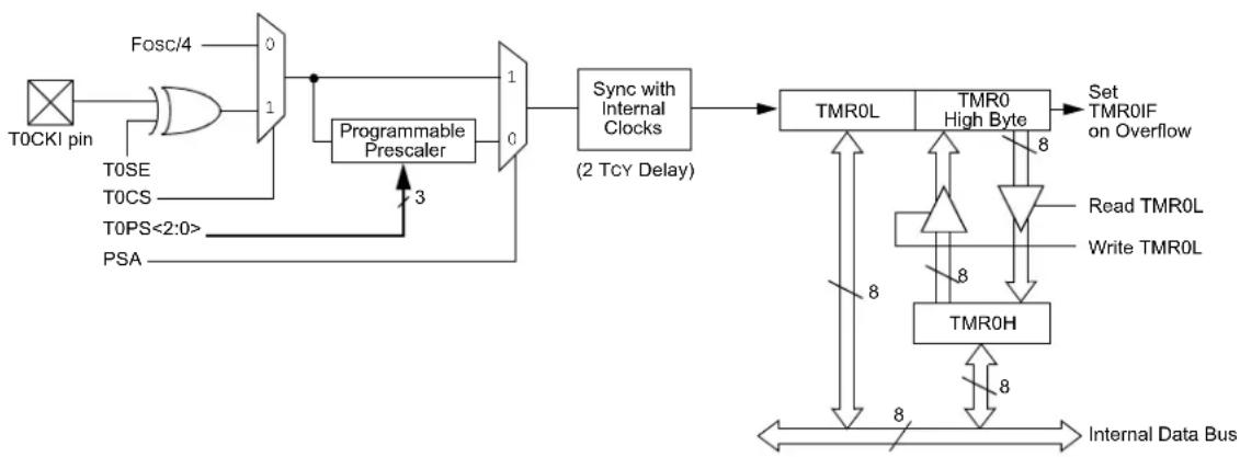
flowchart
graph LR
    A["TOCKI pin"] --> B["AND"]
    B --> C["Programmable Prescaler"]
    C --> D["Sync with Internal Clocks (2 TCY Delay)"]
    D --> E["TMR0L"]
    D --> F["TMR0 High Byte"]
    E --> G["Set TMR0IF on Overflow"]
    F --> H["Read TMR0L"]
    F --> I["Write TMR0L"]
    H --> J["TMR0H"]
    I --> J
    J --> K["Internal Data Bus"]
    L["Fosc/4"] --> M["0"]
    N["T0SE"] --> O["1"]
    P["T0CS"] --> Q["3"]
    R["T0PS<2:0>"] --> S["0"]
    T["PSA"] --> U["0"]
    V["8"] --> W["8"]
    X["8"] --> Y["8"]
Note: Upon Reset, Timer0 is enabled in 8-bit mode with clock input from T0CKI max. prescale.
11.3 Prescaler
An 8-bit counter is available as a prescaler for the Timer0 module. The prescaler is not directly readable or writable. Its value is set by the PSA and T0PS<2:0> bits (T0CON<3:0>) which determine the prescaler assignment and prescale ratio.
Clearing the PSA bit assigns the prescaler to the Timer0 module. When it is assigned, prescale values from 1:2 through 1:256, in power-of-2 increments, are selectable.
When assigned to the Timer0 module, all instructions writing to the TMR0 register (e.g., CLRF TMR0, MOVWF TMRO, BSF TMR0, etc.) clear the prescaler count.
Note: Writing to TMR0 when the prescaler is assigned to Timer0 will clear the prescaler count but will not change the prescaler assignment.
11.3.1 SWITCHING PRESCALER ASSIGNMENT
The prescaler assignment is fully under software control and can be changed "on-the-fly" during program execution.
11.4 Timer0 Interrupt
The TMR0 interrupt is generated when the TMR0 register overflows from FFh to 00h in 8-bit mode, or from FFFFh to 0000h in 16-bit mode. This overflow sets the TMR0IF flag bit. The interrupt can be masked by clearing the TMR0IE bit (INTCON<5>). Before re-enabling the interrupt, the TMR0IF bit must be cleared in software by the Interrupt Service Routine.
Since Timer0 is shut down in Sleep mode, the TMR0 interrupt cannot awaken the processor from Sleep.
TABLE 11-1: REGISTERS ASSOCIATED WITH TIMER0
| Name Bit | 7 Bit 6 Bit | 5 Bit 4 Bit 3 | Bit 2 Bit 1 | Bit 0 | Reset Values on page | ||||
| TMR0L Timer0 Register Low Byte 60 | |||||||||
| TMR0H | Timer0 Register High Byte | 60 | |||||||
| INTCON | GIE/GIEH | PEIE/GIEL | TMR0IE | INT0IE | RBIE | TMR0IF | INT0IF | RBIF | 59 |
| TOCON | TMR0ON | T08BIT | T0CS | T0SE | PSA | T0PS2 | T0PS1 | T0PS0 | 60 |
| TRISA | TRISA7^(1) | TRISA6^(1) | TRISA5 | TRISA4 | TRISA3 | TRISA2 | TRISA1 | TRISA0 | 62 |
Legend: — = unimplemented, read as '0'. Shaded cells are not used by Timer0.
Note 1: RA<7:6> and their associated latch and direction bits are configured as port pins only when the internal oscillator is selected as the default clock source (FOSC2 Configuration bit = 0); otherwise, they are disabled and these bits read as '0'.
NOTES:
12.0 TIMER1 MODULE
The Timer1 timer/counter module incorporates these features:
- Software selectable operation as a 16-bit timer or counter
- Readable and writable 8-bit registers (TMR1H and TMR1L)
- Selectable clock source (internal or external) with device clock or Timer1 oscillator internal options
- Interrupt-on-overflow
- Reset on CCP Special Event Trigger
• Device clock status flag (T1RUN)
A simplified block diagram of the Timer1 module is shown in Figure 12-1. A block diagram of the module's operation in Read/Write mode is shown in Figure 12-2.
The module incorporates its own low-power oscillator to provide an additional clocking option. The Timer1 oscillator can also be used as a low-power clock source for the microcontroller in power-managed operation.
Timer1 can also be used to provide Real-Time Clock (RTC) functionality to applications with only a minimal addition of external components and code overhead.
Timer1 is controlled through the T1CON Control register (Register 12-1). It also contains the Timer1 Oscillator Enable bit (T1OSCEN). Timer1 can be enabled or disabled by setting or clearing control bit, TMR1ON (T1CON<0>).
REGISTER 12-1: T1CON: TIMER1 CONTROL REGISTER
| R/W-0 R-0 R/W-0 R/W-0 R/W-0 R/W-0 R/W-0 R/W-0 | |||||||
| RD16 T1R | RUN T1CKPS1 | T1CKPS0 | T1OSCEN | 1SYNC | TMR1CS TMR1Q | N | |
| bit 7 | bit 0 | ||||||
| Legend: | |||
| R = Readable bit | W = Writable bit | U = Unimplemented bit, read as ‘0’ | |
| -n = Value at POR | ‘1’ = Bit is set | ‘0’ = Bit is cleared | x = Bit is unknown |
| bit 7 | RD16: 16-Bit Read/Write Mode Enable bit1 = Enables register read/write of Timer1 in one 16-bit operation0 = Enables register read/write of Timer1 in two 8-bit operations |
| bit 6 | T1RUN: Timer1 System Clock Status bit1 = Device clock is derived from Timer1 oscillator0 = Device clock is derived from another source |
| bit 5-4 | T1CKPS<1:0>: Timer1 Input Clock Prescale Select bits11 = 1:8 Prescale value10 = 1:4 Prescale value01 = 1:2 Prescale value00 = 1:1 Prescale value |
| bit 3 | T1OSCEN: Timer1 Oscillator Enable bit1 = Timer1 oscillator is enabled0 = Timer1 oscillator is shut offThe oscillator inverter and feedback resistor are turned off to eliminate power drain. |
| bit 2 | T1SYNC: Timer1 External Clock Input Synchronization Select bitWhen TMR1CS = 1:1 = Do not synchronize external clock input0 = Synchronize external clock inputWhen TMR1CS = 0:This bit is ignored. Timer1 uses the internal clock when TMR1CS = 0. |
| bit 1 | TMR1CS: Timer1 Clock Source Select bit1 = External clock from pin RC0/T1OSO/T13CKI (on the rising edge)0 = Internal clock (Fosc/4) |
| bit 0 | TMR1ON: Timer1 On bit1 = Enables Timer10 = Stops Timer1 |
12.1 Timer1 Operation
Timer1 can operate in one of these modes:
- Timer
- Synchronous Counter
- Asynchronous Counter
The operating mode is determined by the clock select bit, TMR1CS (T1CON<1>). When TMR1CS is cleared (= 0), Timer1 increments on every internal instruction
cycle (Fosc/4). When the bit is set, Timer1 increments on every rising edge of the Timer1 external clock input or the Timer1 oscillator, if enabled.
When Timer1 is enabled, the RC1/T1OSI and RC0/T1OSO/T13CKI pins become inputs. This means the values of TRISC<1:0> are ignored and the pins are read as '0'.
FIGURE 12-1: TIMER1 BLOCK DIAGRAM (8-BIT MODE)
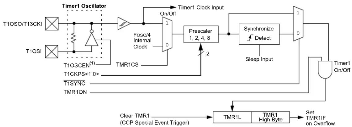
flowchart
graph TD
    A["T1OSO/T13CKI"] --> B["Timer1 Oscillator"]
    C["T1OSI"] --> D["Timer1 Oscillator"]
    B --> E["Fosc/4 Internal Clock"]
    D --> F["T1OSCEN(1)"]
    D --> G["T1CKPS<1:0>"]
    D --> H["T1SYNC"]
    D --> I["TMR1ON"]
    E --> J["On/Off"]
    F --> K["Prescaler 1, 2, 4, 8"]
    G --> L["2"]
    H --> M["TMR1L"]
    I --> N["TMR1 High Byte"]
    J --> O["Timer1 Clock Input"]
    K --> P["Synchronize Detect"]
    L --> Q["Sleep Input"]
    M --> R["Timer1 On/Off"]
    N --> S["Set TMR1IF on Overflow"]
    O --> T["Clear TMR1 (CCP Special Event Trigger)"]
    P --> U["Clear TMR1 (CCP Special Event Trigger)"]
    Q --> V["Clear TMR1 (CCP Special Event Trigger)"]
    R --> W["Clear TMR1 (CCP Special Event Trigger)"]
    S --> X["Clear TMR1 (CCP Special Event Trigger)"]
    T --> Y["Clear TMR1 (CCP Special Event Trigger)"]
Note 1: When enable bit, T1OSCEN, is cleared, the inverter and feedback resistor are turned off to eliminate power drain.
FIGURE 12-2: TIMER1 BLOCK DIAGRAM (16-BIT READ/WRITE MODE)

flowchart
graph TD
    A["T1OSO/T13CKI"] --> B["Timer1 Oscillator"]
    C["T1OSI"] --> D["Timer1 Oscillator"]
    B --> E["Fosc/4 Internal Clock"]
    D --> F["T1OSCEN(1)"]
    D --> G["T1CKPS<1:0>"]
    D --> H["T1SYNC"]
    D --> I["TMR1ON"]
    E --> J["Prescaler 1, 2, 4, 8"]
    F --> J
    J --> K["Synchronize Detect"]
    K --> L["Timer1 On/Off"]
    L --> M["Timer1 On/Off"]
    M --> N["Sleep Input"]
    N --> J
    J --> O["TMR1L"]
    J --> P["TMR1 High Byte"]
    O --> Q["Clear TMR1 (CCP Special Event Trigger)"]
    P --> R["Set TMR1IF on Overflow"]
    Q --> S["Read TMR1L"]
    Q --> T["Write TMR1L"]
    R --> U["TMR1H"]
    S --> V["Internal Data Bus"]
    T --> V
    U --> V
    V --> W["8"]
    W --> X["8"]
    X --> Y["8"]
    Y --> Z["8"]
    Z --> AA["8"]
    AA --> AB["8"]
    AB --> AC["8"]
    AC --> AD["8"]
Note 1: When enable bit, T1OSCEN, is cleared, the inverter and feedback resistor are turned off to eliminate power drain.
12.2 Timer1 16-Bit Read/Write Mode
Timer1 can be configured for 16-bit reads and writes (see Figure 12-2). When the RD16 control bit (T1CON<7>) is set, the address for TMR1H is mapped to a buffer register for the high byte of Timer1. A read from TMR1L will load the contents of the high byte of Timer1 into the Timer1 High Byte Buffer register. This provides the user with the ability to accurately read all 16 bits of Timer1 without having to determine whether a read of the high byte, followed by a read of the low byte, has become invalid due to a rollover between reads.
A write to the high byte of Timer1 must also take place through the TMR1H Buffer register. The Timer1 high byte is updated with the contents of TMR1H when a write occurs to TMR1L. This allows a user to write all 16 bits to both the high and low bytes of Timer1 at once.
The high byte of Timer1 is not directly readable or writable in this mode. All reads and writes must take place through the Timer1 High Byte Buffer register. Writes to TMR1H do not clear the Timer1 prescaler. The prescaler is only cleared on writes to TMR1L.
12.3 Timer1 Oscillator
An on-chip crystal oscillator circuit is incorporated between pins, T1OSI (input) and T1OSO (amplifier output). It is enabled by setting the Timer1 Oscillator Enable bit, T1OSCEN (T1CON<3>). The oscillator is a low-power circuit rated for 32 kHz crystals. It will continue to run during all power-managed modes. The circuit for a typical LP oscillator is shown in Figure 12-3. Table 12-1 shows the capacitor selection for the Timer1 oscillator.
The user must provide a software time delay to ensure proper start-up of the Timer1 oscillator.
FIGURE 12-3: EXTERNAL
COMPONENTS FOR THE TIMER1 LP OSCILLATOR

text_image
C1 27 pF XTAL 32.768 kHz C2 27 pF PIC18F87J90 T1OSI T1OSO Note: See the Notes with Table 12-1 for additional information about capacitor selection.TABLE 12-1: CAPACITOR SELECTION FOR THE TIMER1 OSCILLATOR ^(2,3,4)
| Oscillator Type | Freq. C1 | C2 | ||
| LP 32.768 kHz | 27 | pF | (1) | 27 pF(1) |
Note 1: Microchip suggests these values as a starting point in validating the oscillator circuit.
2: Higher capacitance increases the stability of the oscillator but also increases the start-up time.
3: Since each resonator/crystal has its own characteristics, the user should consult the resonator/crystal manufacturer for appropriate values of external components.
4: Capacitor values are for design guidance only.
12.3.1 USING TIMER1 AS A CLOCK SOURCE
The Timer1 oscillator is also available as a clock source in power-managed modes. By setting the System Clock Select bits, SCS<1:0> (OSCCON<1:0>), to '01', the device switches to SEC_RUN mode; both the CPU and peripherals are clocked from the Timer1 oscillator. If the IDLEN bit (OSCCON<7>) is cleared and a SLEEP instruction is executed, the device enters SEC_IDLE mode. Additional details are available in Section 4.0 "Power-Managed Modes".
Whenever the Timer1 oscillator is providing the clock source, the Timer1 System Clock Status Flag, T1RUN (T1CON<6>), is set. This can be used to determine the controller's current clocking mode. It can also indicate the clock source being currently used by the Fail-Safe Clock Monitor. If the Clock Monitor is enabled and the Timer1 oscillator fails while providing the clock, polling the T1RUN bit will indicate whether the clock is being provided by the Timer1 oscillator or another source.
12.3.2 TIMER1 OSCILLATOR LAYOUT CONSIDERATIONS
The Timer1 oscillator circuit draws very little power during operation. Due to the low-power nature of the oscillator, it may also be sensitive to rapidly changing signals in close proximity.
The oscillator circuit, shown in Figure 12-3, should be located as close as possible to the microcontroller. There should be no circuits passing within the oscillator circuit boundaries other than Vss or VDD.
If a high-speed circuit must be located near the oscillator (such as the CCP1 pin in Output Compare or PWM mode, or the primary oscillator using the OSC2 pin), a grounded guard ring around the oscillator circuit, as shown in Figure 12-4, may be helpful when used on a single-sided PCB or in addition to a ground plane.
FIGURE 12-4: OSCILLATOR CIRCUIT WITH GROUNDED GUARD RING
text_image
VDD Vss OSC1 OSC2 RC0 RC1 RC2 Note: Not drawn to scale.12.4 Timer1 Interrupt
The TMR1 register pair (TMR1H:TMR1L) increments from 0000h to FFFFh and rolls over to 0000h. The Timer1 interrupt, if enabled, is generated on overflow which is latched in interrupt flag bit, TMR1IF (PIR1<0>). This interrupt can be enabled or disabled by setting or clearing the Timer1 Interrupt Enable bit, TMR1IE (PIE1<0>).
12.5 Resetting Timer1 Using the CCP Special Event Trigger
If CCP1 or CCP2 is configured to use Timer1 and to generate a Special Event Trigger in Compare mode (CCPxM<3:0>=1011), this signal will reset Timer3. The trigger from CCP2 will also start an A/D conversion if the A/D module is enabled (see Section 16.3.4 "Special Event Trigger" for more information).
The module must be configured as either a timer or a synchronous counter to take advantage of this feature. When used this way, the CCPRxH:CCPRxL register pair effectively becomes a period register for Timer1.
If Timer1 is running in Asynchronous Counter mode, this Reset operation may not work.
In the event that a write to Timer1 coincides with a Special Event Trigger, the write operation will take precedence.
Note: The Special Event Triggers from the CCPx module will not set the TMR1IF interrupt flag bit (PIR1<0>).
12.6 Using Timer1 as a Real-Time Clock
Adding an external LP oscillator to Timer1 (such as the one described in Section 12.3 "Timer1 Oscillator") gives users the option to include RTC functionality to their applications. This is accomplished with an inexpensive watch crystal to provide an accurate time base and several lines of application code to calculate the time. When operating in Sleep mode and using a battery or supercapacitor as a power source, it can completely eliminate the need for a separate RTC device and battery backup.
The application code routine, RTCisr, shown in Example 12-1, demonstrates a simple method to increment a counter, at one-second intervals, using an Interrupt Service Routine. Incrementing the TMR1 register pair to overflow, triggers the interrupt and calls the routine which increments the seconds counter by one. Additional counters for minutes and hours are incremented as the previous counter overflows.
Since the register pair is 16 bits wide, counting up to overflow the register directly from a 32.768 kHz clock would take 2 seconds. To force the overflow at the required one-second intervals, it is necessary to preload it. The simplest method is to set the MSb of TMR1H with a BSF instruction. Note that the TMR1L register is never preloaded or altered; doing so may introduce cumulative error over many cycles.
For this method to be accurate, Timer1 must operate in Asynchronous mode and the Timer1 overflow interrupt must be enabled (PIE1<0> = 1) as shown in the routine, RTCinit. The Timer1 oscillator must also be enabled and running at all times.
EXAMPLE 12-1: IMPLEMENTING A REAL-TIME CLOCK USING A TIMER1 INTERRUPT SERVICE
RTCinit
MOVLW 80h ; Preload TMR1 register pair
MOVWF TMR1H ; for 1 second overflow
CLRF TMR1L
MOVLW b'00001111' ; Configure for external clock,
MOVWF T1CON ; Asynchronous operation, external oscillator
CLRF secs ; Initialize timekeeping registers
CLRF mins ;
MOVLW .12
MOVWF hours
BSF PIE1, TMR1IE ; Enable Timer1 interrupt
RETURN
RTCisr
BSF TMR1H, 7 ; Preload for 1 sec overflow
BCF PIR1, TMR1IF ; Clear interrupt flag
INCF secs, F ; Increment seconds
MOVLW .59 ; 60 seconds elapsed?
CPFSGT secs
RETURN ; No, done
CLRF secs ; Clear seconds
INCF mins, F ; Increment minutes
MOVLW .59 ; 60 minutes elapsed?
CPFSGT mins
RETURN ; No, done
CLRF mins ; clear minutes
INCF hours, F ; Increment hours
MOVLW .23 ; 24 hours elapsed?
CPFSGT hours
RETURN ; No, done
CLRF hours ; Reset hours
RETURN ; Done
TABLE 12-2: REGISTERS ASSOCIATED WITH TIMER1 AS A TIMER/COUNTER
| Name Bit 7 Bit 6 Bit | 5 Bit 4 Bit 3 | Bit 2 Bit 1 | Bit 0 | Reset Values on page | ||||
| INTCON | GIE/GIEH | PEIE/GIEL | TMR0IE | INT0IE | RBIE | TMR0IF | INT0IF | RBIF |
| PIR1 | — | ADIF | RC1IF | TX1IF | SSPIF | — | TMR2IF | TMR1IF |
| PIE1 | — | ADIE | RC1IE | TX1IE | SSPIE | — | TMR2IE | TMR1IE |
| IPR1 | — | ADIP | RC1IP | TX1IP | SSPIP | — | TMR2IP | TMR1IP |
| TMR1L | Timer1 Register Low Byte | 60 | ||||||
| TMR1H Timer1 Register High Byte | 60 | |||||||
| T1CON | RD16 | T1RUN | T1CKPS1 | T1CKPS0 | T1OSCEN | 1SYNC | TMR1CS | TMR1ON |
Legend: Shaded cells are not used by the Timer1 module.
NOTES:
13.0 TIMER2 MODULE
The Timer2 module incorporates the following features:
- 8-bit Timer and Period registers (TMR2 and PR2, respectively)
- Readable and writable (both registers)
- Software programmable prescaler (1:1, 1:4 and 1:16)
- Software programmable postscaler (1:1 through 1:16)
- Interrupt on TMR2 to PR2 match
- Optional use as the shift clock for the MSSP module
The module is controlled through the T2CON register (Register 13-1) which enables or disables the timer, and configures the prescaler and postscaler. Timer2 can be shut off by clearing control bit, TMR2ON (T2CON<2>), to minimize power consumption.
A simplified block diagram of the module is shown in Figure 13-1.
13.1 Timer2 Operation
In normal operation, TMR2 is incremented from 00h on each clock (Fosc/4). A 4-bit counter/prescaler on the clock input gives direct input, divide-by-4 and divide-by-16 prescale options. These are selected by the prescaler control bits, T2CKPS<1:0> (T2CON<1:0>). The value of TMR2 is compared to that of the Period register, PR2, on each clock cycle. When the two values match, the comparator generates a match signal as the timer output. This signal also resets the value of TMR2 to 00h on the next cycle and drives the output counter/postscaler (see Section 13.2 "Timer2 Interrupt").
The TMR2 and PR2 registers are both directly readable and writable. The TMR2 register is cleared on any device Reset, while the PR2 register initializes at FFh. Both the prescaler and postscaler counters are cleared on the following events:
• a write to the TMR2 register
- a write to the T2CON register
- any device Reset (Power-on Reset, MCLR Reset, Watchdog Timer Reset or Brown-out Reset)
TMR2 is not cleared when T2CON is written.
REGISTER 13-1: T2CON: TIMER2 CONTROL REGISTER
| U-0 R/W-0 R/W-0 R/W-0 R/W-0 R/W-0 R/W-0 R/W-0 | |||||||
| — T2OU | TPS3 | T2OUTP | S2 | T2OUTPS1 | T2OUTPS0 | TMR2ON | T2CKP1 T2CKP0 |
| bit 7 bit 0 | |||||||
| Legend: | |||
| R = Readable bit | W = Writable bit | U = Unimplemented bit, read as ‘0’ | |
| -n = Value at POR | ‘1’ = Bit is set | ‘0’ = Bit is cleared | x = Bit is unknown |
bit 7 Unimplemented: Read as '0'
bit 6-3 T2OUTPS<3:0>: Timer2 Output Postscale Select bits
0000 = 1:1 Postscale
0001 = 1:2 Postscale
•
•
•
1111 = 1:16 Postscale
bit 2 TMR2ON: Timer2 On bit
1 = Timer2 is on
0 = Timer2 is off
bit 1-0 T2CKPS<1:0>: Timer2 Clock Prescale Select bits
00 = Prescaler is 1
01 = Prescaler is 4
1x = Prescaler is 16
13.2 Timer2 Interrupt
Timer2 can also generate an optional device interrupt. The Timer2 output signal (TMR2 to PR2 match) provides the input for the 4-bit output counter/postscaler. This counter generates the TMR2 match interrupt flag which is latched in TMR2IF (PIR1<1>). The interrupt is enabled by setting the TMR2 Match Interrupt Enable bit, TMR2IE (PIE1<1>).
A range of 16 postscale options (from 1:1 through 1:16 inclusive) can be selected with the postscaler control bits, T2OUTPS<3:0> (T2CON<6:3>).
13.3 Timer2 Output
The unscaled output of TMR2 is available primarily to the CCP modules, where it is used as a time base for operations in PWM mode.
Timer2 can be optionally used as the shift clock source for the MSSP module operating in SPI mode. Additional information is provided in Section 18.0 "Master Synchronous Serial Port (MSSP) Module".
FIGURE 13-1: TIMER2 BLOCK DIAGRAM
flowchart
graph TD
    A["T2OUTPS<3:0>"] --> B["1:1 to 1:16 Postscaler"]
    C["T2CKPS<1:0>"] --> D["1:1, 1:4, 1:16 Prescaler"]
    E["Fosc/4"] --> D
    D --> F["TMR2"]
    F --> G["Comparator"]
    G --> H["PR2"]
    H --> I["Internal Data Bus"]
    F --> J["Reset"]
    J --> G
    G --> K["TMR2/PR2 Match"]
    K --> L["Set TMR2IF"]
    L --> M["TMR2 Output (to PWM or MSSP)"]
    F --> N["8"]
    H --> O["8"]
TABLE 13-1: REGISTERS ASSOCIATED WITH TIMER2 AS A TIMER/COUNTER
| Name | Bit 7 | Bit 6 | Bit 5 | Bit 4 | Bit 3 | Bit 2 | Bit 1 | Bit 0 | Reset Values on page | ||||
| INTCON | GIE/GIEH | PE | EIE/GIEL | TMR0IE | INT0IE | RBIE | TMR0IF | INT0IF | RBIF | 59 | |||
| PIR1 | — | ADIF | RC1IF | TX1IF | SSPIF | — | TMR2IF | TMR1IF | 62 | ||||
| PIE1 | — | ADIE | RC1IE | TX1IE | SSPIE | — | TMR2IE | TMR1IE | 62 | ||||
| IPR1 | — | ADIP | RC1IP | TX1IP | SSPIP | — | TMR2IP | TMR1IP | 62 | ||||
| TMR2 | Timer2 Register | 60 | |||||||||||
| T2CON | — | T2OUTPS3 | T2OUTPS2 | T2OUTPS1 | T2OUTPS0 | TMR2ON | T2CKPS1 | T2CKPS0 | 60 | ||||
| PR2 | Timer2 Period Register | 60 | |||||||||||
Legend: — = unimplemented, read as '0'. Shaded cells are not used by the Timer2 module.
14.0 TIMER3 MODULE
The Timer3 timer/counter module incorporates these features:
- Software selectable operation as a 16-bit timer or counter
- Readable and writable 8-bit registers (TMR3H and TMR3L)
- Selectable clock source (internal or external) with device clock or Timer1 oscillator internal options
- Interrupt on overflow
- Module Reset on CCP Special Event Trigger
A simplified block diagram of the Timer3 module is shown in Figure 14-1. A block diagram of the module's operation in Read/Write mode is shown in Figure 14-2.
The Timer3 module is controlled through the T3CON register (Register 14-1). It also selects the clock source options for the CCP modules. See Section 16.2.2 "Timer1/Timer3 Mode Selection" for more information.
REGISTER 14-1: T3CON: TIMER3 CONTROL REGISTER
| R/W-0 R/W-0 R/W-0 R/W-0 R/W-0 R/W-0 R/W-0 R/W-0 | |||
| RD16 T3CCP2 T3CKPS1 T3CKPS0 T3CCP1 T3SYNC | — | TMR3CS TMR3ON | |
| bit 7 bit 0 | |||
Legend:
| R = Readable bit W = Writable bit | U = Unimplemented bit, read as '0' | ||
| -n = Value at POR | '1' = Bit is set | '0' = Bit is cleared | x = Bit is unknown |
bit 7 RD16: 16-Bit Read/Write Mode Enable bit
1 = Enables register read/write of Timer3 in one 16-bit operation
0 = Enables register read/write of Timer3 in two 8-bit operations
bit 6,3 T3CCP<2:1>: Timer3 and Timer1 to CCPx Enable bits
1x = Timer3 is the capture/compare clock source for the CCP modules
01 = Timer3 is the capture/compare clock source for CCP2;
Timer1 is the capture/compare clock source for CCP1
00 = Timer1 is the capture/compare clock source for the CCP modules
bit 5-4 T3CKPS<1:0>: Timer3 Input Clock Prescale Select bits
11 = 1:8 Prescale value
10 = 1:4 Prescale value
01 = 1:2 Prescale value
00 = 1:1 Prescale value
bit 2 T3SYNC: Timer3 External Clock Input Synchronization Control bit
(Not usable if the device clock comes from Timer1/Timer3.)
When TMR3CS = 1:
1 = Does not synchronize the external clock input
0 = Synchronizes the external clock input
When TMR3CS = 0:
This bit is ignored. Timer3 uses the internal clock when TMR3CS = 0.
bit 1 TMR3CS: Timer3 Clock Source Select bit
1 = External clock input from Timer1 oscillator or T13CKI (on the rising edge after the first falling edge)
0 = Internal clock (Fosc/4)
bit 0 TMR3ON: Timer3 On bit
1 = Enables Timer3
0 = Stops Timer3
PIC18F87J90 FAMILY
14.1 Timer3 Operation
Timer3 can operate in one of three modes:
- Timer
- Synchronous Counter
- Asynchronous Counter
The operating mode is determined by the clock select bit, TMR3CS (T3CON<1>). When TMR3CS is cleared (= 0), Timer3 increments on every internal instruction cycle (Fosc/4). When the bit is set, Timer3 increments on every rising edge of the Timer1 external clock input or the Timer1 oscillator, if enabled.
As with Timer1, the RC1/T1OSI and RC0/T1OSO/T13CKI pins become inputs when the Timer1 oscillator is enabled. This means the values of TRISC<1:0> are ignored and the pins are read as '0'.
FIGURE 14-1: TIMER3 BLOCK DIAGRAM (8-BIT MODE)
other
| Category | Timer1 Oscillator | Timer1 Clock Input | Prescaler | Synchronize Detect | Sleep Input | Timer3 On/Off | | :--- | :--- | :--- | :--- | :--- | :--- | :--- | | T1OSO/T13CKI | | 1 | | | | | | T1OSI | | 0 | 1, 2, 4, 8 | | | | | T1OSCEN(1) | TMR3CS | | | | | | | T3CKPS<1:0> | | | | | | | | T3SYNC | | | | | | | | TMR3ON | | | | | | | | CCPx Special Event Trigger CCPx Select from T3CON<6,3> | | Clear TMR3 | TMR3L | TMR3 High Byte | Set TMR3IF on Overflow | | T1OSCEN(1)Note 1: When enable bit, T1OSCEN, is cleared, the inverter and feedback resistor are turned off to eliminate power drain.
FIGURE 14-2: TIMER3 BLOCK DIAGRAM (16-BIT READ/WRITE MODE)
Note 1: When enable bit, T1OSCEN, is cleared, the inverter and feedback resistor are turned off to eliminate power drain.
14.2 Timer3 16-Bit Read/Write Mode
Timer3 can be configured for 16-bit reads and writes (see Figure 14-2). When the RD16 control bit (T3CON<7>) is set, the address for TMR3H is mapped to a buffer register for the high byte of Timer3. A read from TMR3L will load the contents of the high byte of Timer3 into the Timer3 High Byte Buffer register. This provides the user with the ability to accurately read all 16 bits of Timer1 without having to determine whether a read of the high byte, followed by a read of the low byte, has become invalid due to a rollover between reads.
A write to the high byte of Timer3 must also take place through the TMR3H Buffer register. The Timer3 high byte is updated with the contents of TMR3H when a write occurs to TMR3L. This allows a user to write all 16 bits to both the high and low bytes of Timer3 at once.
The high byte of Timer3 is not directly readable or writable in this mode. All reads and writes must take place through the Timer3 High Byte Buffer register.
Writes to TMR3H do not clear the Timer3 prescaler. The prescaler is only cleared on writes to TMR3L.
14.3 Using the Timer1 Oscillator as the Timer3 Clock Source
The Timer1 internal oscillator may be used as the clock source for Timer3. The Timer1 oscillator is enabled by setting the T1OSCEN (T1CON<3>) bit. To use it as the Timer3 clock source, the TMR3CS bit must also be set. As previously noted, this also configures Timer3 to increment on every rising edge of the oscillator source.
The Timer1 oscillator is described in Section 12.0 "Timer1 Module".
14.4 Timer3 Interrupt
The TMR3 register pair (TMR3H:TMR3L) increments from 0000h to FFFFh and overflows to 0000h. The Timer3 interrupt, if enabled, is generated on overflow and is latched in interrupt flag bit, TMR3IF (PIR2<1>). This interrupt can be enabled or disabled by setting or clearing the Timer3 Interrupt Enable bit, TMR3IE (PIE2<1>).
14.5 Resetting Timer3 Using the CCP Special Event Trigger
If CCP1 or CCP2 is configured to use Timer3 and to generate a Special Event Trigger in Compare mode (CCPxM<3:0>=1011), this signal will reset Timer3. The trigger from CCP2 will also start an A/D conversion if the A/D module is enabled (see Section 16.3.4 "Special Event Trigger" for more information).
The module must be configured as either a timer or synchronous counter to take advantage of this feature. When used this way, the CCPRxH:CCPRxL register pair effectively becomes a period register for Timer3.
If Timer3 is running in Asynchronous Counter mode, the Reset operation may not work.
In the event that a write to Timer3 coincides with a Special Event Trigger from a CCP module, the write will take precedence.
| Note: The Special Event Triggers from the CCPx module will not set the TMR3IF interrupt flag bit (PIR2<1>). |
TABLE 14-1: REGISTERS ASSOCIATED WITH TIMER3 AS A TIMER/COUNTER
| Name Bit | 7 Bit 6 Bit | 5 Bit 4 Bit 3 | Bit 2 Bit 1 | Bit 0 | Reset Values on page | ||||
| INTCON GIE/GIEH PEIE/GIEL | TMR0IE | INT0IE | RBIE | TMR0IF | INT0IF | RBIF | 59 | ||
| PIR2 | OSCFIF | CMIF | — | — | BCLIF | LVDIF | TMR3IF | — | 62 |
| PIE2 | OSCFIE | CMIE | — | — | BCLIE | LVDIE | TMR3IE | — | 62 |
| IPR2 | OSCFIP | CMIP | — | — | BCLIP | LVDIP | TMR3IP | — | 62 |
| TMR3L | Timer3 Register Low Byte | 61 | |||||||
| TMR3H | Timer3 Register High Byte | 61 | |||||||
| T1CON | RD16 | T1RUN | T1CKPS1 | T1CKPS0 | T1OSCEN | 1SYNC | TMR1CS | TMR1ON | 60 |
| T3CON | RD16 | T3CCP2 | T3CKPS1 | T3CKPS0 | T3CCP1 | 3SYNC | TMR3CS | TMR3ON | 61 |
Legend: — = unimplemented, read as '0'. Shaded cells are not used by the Timer3 module.
NOTES:
15.0 REAL-TIME CLOCK AND CALENDAR (RTCC)
The key features of the Real-Time Clock and Calendar (RTCC) module are:
• Time: hours, minutes and seconds
• 24-hour format (military time)
• Calendar: weekday, date, month and year
- Alarm configurable
• Year range: 2000 to 2099
- Leap year correction
• BCD format for compact firmware
- Optimized for low-power operation
- User calibration with auto-adjust
• Calibration range: ±2.64 seconds error per month
- Requirements: external 32.768 kHz clock crystal
- Alarm pulse or seconds clock output on RTCC pin
The RTCC module is intended for applications where accurate time must be maintained for an extended period, with minimum to no intervention from the CPU. The module is optimized for low-power usage in order to provide extended battery life while keeping track of time.
The module is a 100-year clock and calendar with automatic leap year detection. The range of the clock is from 00:00:00 (midnight) on January 1, 2000 to 23:59:59 on December 31, 2099. Hours are measured in 24-hour (military time) format. The clock provides a granularity of one second with half-second visibility to the user.
FIGURE 15-1: RTCC BLOCK DIAGRAM

flowchart
graph TD
    A["32.768 kHz Input from Timer1 Oscillator"] --> B["Internal RC"]
    B --> C["RTCC Prescalers"]
    C --> D["0.5s"]
    D --> E["RTCC Timer"]
    E --> F["Comparator"]
    F --> G["Compare Registers with Masks"]
    F --> H["Repeat Counter"]
    G --> I["RTCC Interrupt Logic"]
    H --> I
    I --> J["RTCC Interrupt"]
    J --> K["Alarm Pulse"]
    K --> L["RTCC Pin"]
    L --> M["RTCOE"]
    N["CPU Clock Domain"] --> O["RTCCCFG"]
    N --> P["ALRMRPT"]
    O <--> Q["RTCVALx"]
    P <--> Q
    Q <--> R["YEAR"]
    Q <--> S["MTHDY"]
    Q <--> T["WKDYHR"]
    Q <--> U["MINSEC"]
    Q <--> V["ALMTHDY"]
    Q <--> W["ALWDHR"]
    Q <--> X["ALMINSEC"]
15.1 RTCC MODULE REGISTERS
The RTCC module registers are divided into following categories:
RTCC Control Registers
- RTCCFG
• RTCCAL - PADCFG1
• A L R M C F G
• ALRMRPT
RTCC Value Registers
- RTCVALH and RTCVALL – Can access the following registers
- YEAR
- MONTH
- DAY
- WEEKDAY
- HOUR
- MINUTE
- SECOND
Alarm Value Registers
- ALRMVALH and ALRMVALL – Can access the following registers:
- ALRMMNTH
- ALRMDAY
- A L R M W D
- ALRMHR
- ALRMMIN
- ALRMSEC
Note: The RTCVALH and RTCVALL registers can be accessed through RTCRPT<1:0>. ALRMVALH and ALRMVALL can be accessed through ALRMPTR<1:0>.
15.1.1 RTCC CONTROL REGISTERS
REGISTER 15-1: RTCCFG: RTCC CONFIGURATION REGISTER (1)
| R/W-0 U-0 R/W-0 R-0 R-0 R/W-0 R/W-0 R/W-0 | ||||||||
| RTCEN^(2) | — RTCW | WREN | RTCSYNC | HALFSEC | (3) | RTCOE | RTCPTR1 | RTCPTR0 |
| bit 7 bit 0 | ||||||||
| Legend: | |||
| R = Readable bit | W = Writable bit | U = Unimplemented bit, read as '0' | |
| -n = Value at POR | '1' = Bit is set | '0' = Bit is cleared | x = Bit is unknown |
bit 7 RTCEN: RTCC Enable bit ^(2)
1 = RTCC module is enabled
0 = RTCC module is disabled
bit 6 Unimplemented: Read as '0'
bit 5 RTCWREN: RTCC Value Registers Write Enable bit
1 = RTCVALH and RTCVALL registers can be written to by the user
0 = RTCVALH and RTCVALL registers are locked out from being written to by the user
bit 4 RTCSYNC: RTCC Value Registers Read Synchronization bit
1 = RTCVALH, RTCVALL and ALRMRPT registers can change while reading due to a rollover ripple resulting in an invalid data read. If the register is read twice and results in the same data, the data can be assumed to be valid.
0 = RTCVALH, RTCVALL and ALCFGRPT registers can be read without concern over a rollover ripple
bit 3 HALFSEC: Half-Second Status bit ^(3)
1 = Second half period of a second
0 = First half period of a second
bit 2 RTCOE: RTCC Output Enable bit
1 = RTCC clock output enabled
0 = RTCC clock output disabled
bit 1-0 RTCPTR<1:0>: RTCC Value Register Window Pointer bits
Points to the corresponding RTCC Value registers when reading the RTCVALH and RTCVALL registers.
The RTCPTR<1:0> value decrements on every read or write of RTCVALH<7:0> until it reaches '00'.
RTCVALH:
00 = Minutes
01 = Weekday
10 = Month
11 = Reserved
RTCVALL:
00 = Seconds
01 = Hours
10 = Day
11 = Year
Note 1: The RTCCFG register is only affected by a POR. For resets other than POR, RTCC will continue to run even if the device is in Reset.
2: A write to the RTCEN bit is only allowed when RTCWREN = 1.
3: This bit is read-only; it is cleared to '0' on a write to the lower half of the MINSEC register.
REGISTER 15-2: RTCCAL: RTCC CALIBRATION REGISTER
| R/W-0 R/W-0 R/W-0 R/W-0 R/W-0 R/W-0 R/W-0 R/W-0 | ||||||
| CAL7 CAL6 CAL5 CAL4 | CAL3 CAL2 CAL1 CAL0 | |||||
| bit 7 bit 0 | ||||||
Legend:
| R = Readable bit | W = Writable bit | U = Unimplemented bit, read as ‘0’ |
| -n = Value at POR | ‘1’ = Bit is set | ‘0’ = Bit is cleared x = Bit is unknown |
bit 7-0 CAL<7:0>: RTC Drift Calibration bits
01111111 = Maximum positive adjustment; adds 508 RTC clock pulses every minute
.
.
.
00000001 = Minimum positive adjustment; adds four RTC clock pulses every minute
00000000 = No adjustment
11111111 = Minimum negative adjustment; subtracts four RTC clock pulses every minute
.
.
广力云
10000000 = Maximum negative adjustment; subtracts 512 RTC clock pulses every minute
REGISTER 15-3: PADCFG1: PAD CONFIGURATION REGISTER
| U-0 | U-0 | U-0 | U-0 | U-0 | R/W-0 | R/W-0 | U-0 |
| — | — | — | — | — | RTSECSEL1(1) | RTSECSEL0(1) | — |
| bit 7 bit 0 | |||||||
Legend:
| R = Readable bit | W = Writable bit | U = Unimplemented bit, read as '0' |
| -n = Value at POR | '1' = Bit is set | '0' = Bit is cleared x = Bit is unknown |
bit 7-3 Unimplemented: Read as '0'
bit 2-1 RTSECSEL<1:0>: RTCC Seconds Clock Output Select bit ^(1)
11 = Reserved; do not use
10 = RTCC source clock is selected for the RTCC pin (pin can be INTOSC or Timer1 oscillator, depending on the RTCOSC (CONFIG3L<1>) bit setting) ^(2)
01 = RTCC seconds clock is selected for the RTCC pin
00 = RTCC alarm pulse is selected for the RTCC pin
bit 0 Unimplemented: Read as '0'
Note 1: To enable the actual RTCC output, the RTCOE (RTCCFG<2>) bit must be set.
2: If the Timer1 oscillator is the clock source for RTCC, the T1OSCEN bit should be set (T1CON<3>=1).
REGISTER 15-4: ALRMCFG: ALARM CONFIGURATION REGISTER
| R/W-0 R/W-0 R/W-0 R/W-0 R/W-0 R/W-0 R/W-0 R/W-0 | |||||||
| ALRMEN CH | HIME AMASK3 | AMASK2 AM | ASK1 AMASK0 | ALRMPTR1 | ALRMPTR0 | ||
| bit 7 bit 0 | |||||||
Legend:
| R = Readable bit | W = Writable bit | U = Unimplemented bit, read as '0' |
| -n = Value at POR | '1' = Bit is set | '0' = Bit is cleared x = Bit is unknown |
bit 7 ALRMEN: Alarm Enable bit
1 = Alarm is enabled (cleared automatically after an alarm event whenever ARPT<7:0> = 00 and CHIME = 0) 0 = Alarm is disabled
bit 6 CHIME: Chime Enable bit
1 = Chime is enabled; ALRMPTR<1:0> bits are allowed to roll over from 00h to FFh 0 = Chime is disabled; ALRMPTR<1:0> bits stop once they reach 00h
bit 5-2 AMASK<3:0>: Alarm Mask Configuration bits
0000 = Every half second 0001 = Every second 0010 = Every 10 seconds 0011 = Every minute 0100 = Every 10 minutes 0101 = Every hour 0110 = Once a day 0111 = Once a week 1000 = Once a month 1001 = Once a year (except when configured for February 29 ^th , once every four years) 101x = Reserved – do not use 11xx = Reserved – do not use
bit 1-0 ALRMPTR<1:0>: Alarm Value Register Window Pointer bits
Points to the corresponding Alarm Value registers when reading the ALRMVALH and ALRMVALL registers. The ALRMPTR<1:0> value decrements on every read or write of ALRMVALH until it reaches '00'.
ALRMVALH:
00 = ALRMMIN 01 = ALRMWD 10 = ALRMMNTH 11 = Unimplemented
ALRMVALL:
00 = ALRMSEC 01 = ALRMHR 10 = ALRMDAY 11 = Unimplemented
REGISTER 15-5: ALRMRPT: ALARM REPEAT REGISTER
| R/W-0 R/W-0 R/W-0 R/W-0 R/W-0 R/W-0 R/W-0 R/W-0 | |||||||
| ARPT7 ARPT6 ARPT5 ARPT4 ARPT3 ARPT2 | ARPT1 | ARPT0 | |||||
| bit 7 bit 0 | |||||||
Legend:
| R = Readable bit | W = Writable bit | U = Unimplemented bit, read as '0' |
| -n = Value at POR | '1' = Bit is set | '0' = Bit is cleared x = Bit is unknown |
bit 7-0
ARPT<7:0>: Alarm Repeat Counter Value bits
11111111 = Alarm will repeat 255 more times
.
.
.
00000000 = Alarm will not repeat
The counter decrements on any alarm event. The counter is prevented from rolling over from 00h to FFh unless CHIME = 1.
15.1.2 RTCVALH AND RTCVALL
REGISTER MAPPINGS
REGISTER 15-6: RESERVED REGISTER
| R = Readable bit | W = Writable bit | U = Unimplemented bit, read as '0' |
| -n = Value at POR | '1' = Bit is set | '0' = Bit is cleared x = Bit is unknown |
bit 7-0
Unimplemented: Read as '0'
REGISTER 15-7: YEAR: YEAR VALUE REGISTER ^(1)
| R/W-x | R/W-x | R/W-x | R/W-x | R/W-x | R/W-x | R/W-x | R/W-x |
| YRTEN3 | YRTEN2 | YRTEN1 | YRTEN0 | YRONE3 | YRONE2 | YRONE1 | YRONE0 |
| bit 7 bit 0 | |||||||
Legend:
| R = Readable bit | W = Writable bit | U = Unimplemented bit, read as ‘0’ |
| -n = Value at POR | ‘1’ = Bit is set | ‘0’ = Bit is cleared x = Bit is unknown |
bit 7-4
YRTEN<3:0>: Binary Coded Decimal Value of Year's Tens Digit bits
Contains a value from 0 to 9.
bit 3-0
YRONE<3:0>: Binary Coded Decimal Value of Year's Ones Digit bits
Contains a value from 0 to 9.
Note 1: A write to the YEAR register is only allowed when RTCWREN = 1.
REGISTER 15-8: MONTH: MONTH VALUE REGISTER (1)
| U-0 U-0 U-0 R/W-x R/W-x R/W-x R/W-x R/W-x | |||||||
| — | — | — | MTHTENO | MTHONE3 | MTHONE2 | MTHONE1 | MTHONE0 |
| bit 7 bit 0 | |||||||
| Legend:R = Readable bit W = Writable bit U = Unimplemented bit, read as '0'-n = Value at POR '1' = Bit is set '0' = Bit is cleared x = Bit is unknown | |||||||
bit 7-5 Unimplemented: Read as '0'
bit 4 MTHTENO: Binary Coded Decimal Value of Month's Tens Digit bit
Contains a value of 0 or 1.
bit 3-0 MTHONE<3:0>: Binary Coded Decimal Value of Month's Ones Digit bits
Contains a value from 0 to 9.
Note 1: A write to this register is only allowed when RTCWREN = 1.
REGISTER 15-9: DAY: DAY VALUE REGISTER ^(1)
| U-0 | U-0 | R/W-x | R/W-x | R/W-x | R/W-x | R/W-x | R/W-x |
| — | — | DAYTEN1 | DAYTEN0 | DAYONE3 | DAYONE2 | DAYONE1 | DAYONE0 |
| bit 7 bit 0 | |||||||
Legend:
| R = Readable bit | W = Writable bit | U = Unimplemented bit, read as '0' |
| -n = Value at POR | '1' = Bit is set | '0' = Bit is cleared x = Bit is unknown |
bit 7-6 Unimplemented: Read as '0'
bit 5-4 DAYTEN<1:0>: Binary Coded Decimal value of Day's Tens Digit bits
Contains a value from 0 to 3.
bit 3-0 DAYONE<3:0>: Binary Coded Decimal Value of Day's Ones Digit bits
Contains a value from 0 to 9.
Note 1: A write to this register is only allowed when RTCWREN = 1.
REGISTER 15-10: WEEKDAY: WEEKDAY VALUE REGISTER ^(1)
| U-0 U-0 U-0 | U-0 | U-0 | R/W-x R/W-x R/W-x | ||||
| — | — | — | — | — | WDAY2 | WDAY1 | WDAY0 |
| bit 7 bit 0 | |||||||
Legend:
| R = Readable bit | W = Writable bit | U = Unimplemented bit, read as '0' |
| -n = Value at POR | '1' = Bit is set | '0' = Bit is cleared x = Bit is unknown |
bit 7-3 Unimplemented: Read as '0'
bit 2-0 WDAY<2:0>: Binary Coded Decimal Value of Weekday Digit bits
Contains a value from 0 to 6.
Note 1: A write to this register is only allowed when RTCWREN = 1.
REGISTER 15-11: HOUR: HOUR VALUE REGISTER (1)
| U-0 U-0 R/W-x R/W-x R/W-x R/W-x R/W-x R/W-x | |||||||
| — — HRTEN1 HRTENO HRONE3 HRONE2 HRONE1 HRONE0 | |||||||
| bit 7 bit 0 | |||||||
Legend:
| R = Readable bit | W = Writable bit | U = Unimplemented bit, read as '0' |
| -n = Value at POR | '1' = Bit is set | '0' = Bit is cleared x = Bit is unknown |
bit 7-6 Unimplemented: Read as '0'
bit 5-4 HRTEN<1:0>: Binary Coded Decimal Value of Hour's Tens Digit bits
Contains a value from 0 to 2.
bit 3-0 HRONE<3:0>: Binary Coded Decimal Value of Hour's Ones Digit bits
Contains a value from 0 to 9.
Note 1: A write to this register is only allowed when RTCWREN = 1.
REGISTER 15-12: MINUTE: MINUTE VALUE REGISTER
| U-0 | R/W-x | R/W-x | R/W-x | R/W-x | R/W-x | R/W-x | R/W-x |
| — | MINTEN2 | MINTEN1 | MINTEN0 | MINONE3 | MINONE2 | MINONE1 | MINONE0 |
| bit 7 bit 0 | |||||||
Legend:
| R = Readable bit | W = Writable bit | U = Unimplemented bit, read as '0' |
| -n = Value at POR | '1' = Bit is set | '0' = Bit is cleared x = Bit is unknown |
bit 7 Unimplemented: Read as '0'
bit 6-4 MINTEN<2:0>: Binary Coded Decimal Value of Minute's Tens Digit bits
Contains a value from 0 to 5.
bit 3-0 MINONE<3:0>: Binary Coded Decimal Value of Minute's Ones Digit bits
Contains a value from 0 to 9.
REGISTER 15-13: SECOND: SECOND VALUE REGISTER
| U-0 | R/W-x | R/W-x | R/W-x | R/W-x | R/W-x | R/W-x | R/W-x |
| — | SECTEN2 | SECTEN1 | SECTEN0 | SECONE3 | SECONE2 | SECONE1 | SECONE0 |
| bit 7 bit 0 | |||||||
Legend:
| R = Readable bit | W = Writable bit | U = Unimplemented bit, read as '0' |
| -n = Value at POR | '1' = Bit is set | '0' = Bit is cleared x = Bit is unknown |
bit 7 Unimplemented: Read as '0'
bit 6-4 SECTEN<2:0>: Binary Coded Decimal Value of Second's Tens Digit bits
Contains a value from 0 to 5.
bit 3-0 SECONE<3:0>: Binary Coded Decimal Value of Second's Ones Digit bits
Contains a value from 0 to 9.
15.1.3 ALRMVALH AND ALRMVALL
REGISTER MAPPINGS
REGISTER 15-14: ALRMMNTH: ALARM MONTH VALUE REGISTER (1)
| U-0 U-0 U-0 R/W-x R/W-x R/W-x R/W-x R/W-x | |||||||
| — | — | — | MTHTEN0 | MTHONE3 | MTHONE2 | MTHONE1 | MTHONE0 |
| bit 7 bit 0 | |||||||
| Legend: | |||
| R = Readable bit | W = Writable bit | U = Unimplemented bit, read as '0' | |
| -n = Value at POR | '1' = Bit is set | '0' = Bit is cleared | x = Bit is unknown |
bit 7-5 Unimplemented: Read as '0'
bit 4 MTHTENO: Binary Coded Decimal Value of Month's Tens Digit bit Contains a value of 0 or 1.
bit 3-0 MTHONE<3:0>: Binary Coded Decimal Value of Month's Ones Digit bits Contains a value from 0 to 9.
Note 1: A write to this register is only allowed when RTCWREN = 1.
REGISTER 15-15: ALRMDAY: ALARM DAY VALUE REGISTER (1)
| U-0 | U-0 | R/W-x | R/W-x | R/W-x | R/W-x | R/W-x | R/W-x |
| — | — | DAYTEN1 | DAYTEN0 | DAYONE3 | DAYONE2 | DAYONE1 | DAYONE0 |
| bit 7 bit 0 | |||||||
| Legend: | |||
| R = Readable bit | W = Writable bit | U = Unimplemented bit, read as '0' | |
| -n = Value at POR | '1' = Bit is set | '0' = Bit is cleared | x = Bit is unknown |
bit 7-6 Unimplemented: Read as '0'
bit 5-4 DAYTEN<1:0>: Binary Coded Decimal Value of Day's Tens Digit bits Contains a value from 0 to 3.
bit 3-0 DAYONE<3:0>: Binary Coded Decimal Value of Day's Ones Digit bits Contains a value from 0 to 9.
Note 1: A write to this register is only allowed when RTCWREN = 1.
REGISTER 15-16: ALRMWD: ALARM WEEKDAY VALUE REGISTER (1)
| U-0 U-0 U-0 | U-0 | U-0 | R/W-x R/W-x R/W-x | |||||
| — | — | — | — | — | — | WDAY2 | WDAY1 | WDAY0 |
| bit 7 bit 0 | ||||||||
| Legend: | |||
| R = Readable bit | W = Writable bit | U = Unimplemented bit, read as '0' | |
| -n = Value at POR | '1' = Bit is set | '0' = Bit is cleared | x = Bit is unknown |
bit 7-3 Unimplemented: Read as '0'
bit 2-0 WDAY<2:0>: Binary Coded Decimal Value of Weekday Digit bits Contains a value from 0 to 6.
Note 1: A write to this register is only allowed when RTCWREN = 1.
REGISTER 15-17: ALRMHR: ALARM HOURS VALUE REGISTER (1)
| U-0 U-0 R/W-x R/W-x R/W-x R/W-x R/W-x R/W-x | |||||||
| — | — | HRTEN1 | HRTEN0 | HRONE3 | HRONE2 | HRONE1 | HRONE0 |
| bit 7 bit 0 | |||||||
Legend:
| R = Readable bit | W = Writable bit | U = Unimplemented bit, read as '0' |
| -n = Value at POR | '1' = Bit is set | '0' = Bit is cleared x = Bit is unknown |
bit 7-6 Unimplemented: Read as '0'
bit 5-4 HRTEN<1:0>: Binary Coded Decimal Value of Hour's Tens Digit bits Contains a value from 0 to 2.
bit 3-0 HRONE<3:0>: Binary Coded Decimal Value of Hour's Ones Digit bits Contains a value from 0 to 9.
Note 1: A write to this register is only allowed when RTCWREN = 1.
REGISTER 15-18: ALRMMIN: ALARM MINUTES VALUE REGISTER
| U-0 | R/W-x | R/W-x | R/W-x | R/W-x | R/W-x | R/W-x | R/W-x |
| — | MINTEN2 | MINTEN1 | MINTEN0 | MINONE3 | MINONE2 | MINONE1 | MINONE0 |
| bit 7 bit 0 | |||||||
Legend:
| R = Readable bit | W = Writable bit | U = Unimplemented bit, read as ‘0’ |
| -n = Value at POR | ‘1’ = Bit is set | ‘0’ = Bit is cleared x = Bit is unknown |
bit 7 Unimplemented: Read as '0'
bit 6-4 MINTEN<2:0>: Binary Coded Decimal Value of Minute's Tens Digit bits Contains a value from 0 to 5.
bit 3-0 MINONE<3:0>: Binary Coded Decimal Value of Minute's Ones Digit bits Contains a value from 0 to 9.
REGISTER 15-19: ALRMSEC: ALARM SECONDS VALUE REGISTER
| U-0 | R/W-x | R/W-x | R/W-x | R/W-x | R/W-x | R/W-x | R/W-x |
| — | SECTEN2 | SECTEN1 | SECTEN0 | SECONE3 | SECONE2 | SECONE1 | SECONE0 |
| bit 7 bit 0 | |||||||
Legend:
| R = Readable bit | W = Writable bit | U = Unimplemented bit, read as '0' |
| -n = Value at POR | '1' = Bit is set | '0' = Bit is cleared x = Bit is unknown |
bit 7 Unimplemented: Read as '0'
bit 6-4 SECTEN<2:0>: Binary Coded Decimal Value of Second's Tens Digit bits Contains a value from 0 to 5.
bit 3-0 SECONER<3:0>: Binary Coded Decimal Value of Second's Ones Digit bits Contains a value from 0 to 9.
15.1.4 RTCEN BIT WRITE
An attempt to write to the RTCEN bit while RTCWREN = 0 will be ignored. RTCWREN must be set before a write to RTCEN can take place.
Like the RTCEN bit, the RTCVALH and RTCVALL registers can only be written to when RTCWREN = 1. A write to these registers, while RTCWREN = 0, will be ignored.
15.2 Operation
15.2.1 REGISTER INTERFACE
The register interface for the RTCC and alarm values is implemented using the Binary Coded Decimal (BCD) format. This simplifies the firmware when using the module as each of the digits is contained within its own 4-bit value (see Figure 15-2 and Figure 15-3).
FIGURE 15-2: TIMER DIGIT FORMAT
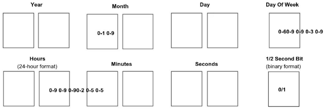
text_image
Year Month Day Day Of Week 0-1 0-9 0-60-9 0-9 0-3 0-9 Hours (24-hour format) Minutes Seconds 1/2 Second Bit (binary format) 0-9 0-9 0-90-2 0-5 0-5 0/1FIGURE 15-3: ALARM DIGIT FORMAT
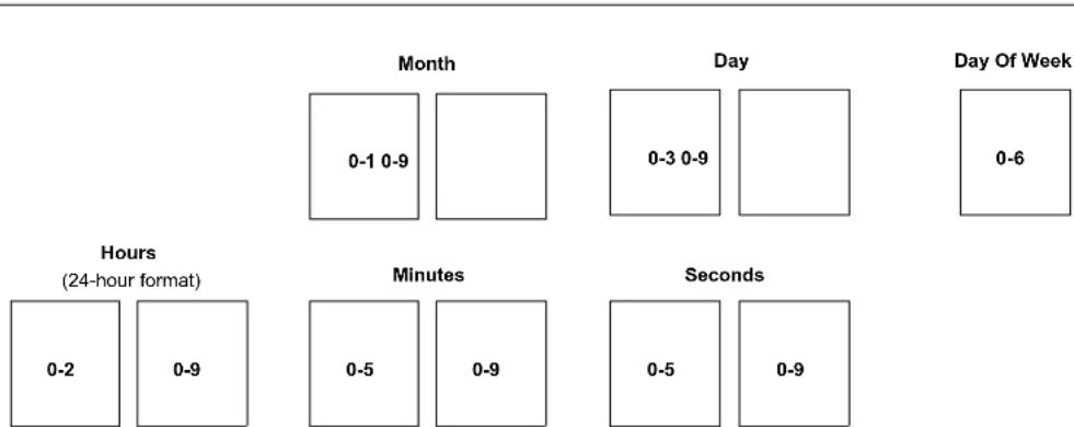
text_image
Month 0-1 0-9 Day 0-3 0-9 Day Of Week 0-6 Hours (24-hour format) Minutes 0-2 0-9 0-5 0-9 Seconds 0-5 0-915.2.2 CLOCK SOURCE
As mentioned earlier, the RTCC module is intended to be clocked by an external Real-Time Clock crystal, oscillating at 32.768 kHz, but can also be an internal oscillator. The RTCC clock selection is decided by the RTCOSC bit (CONFIG3L<1>).
Calibration of the crystal can be done through this module to yield an error of 3 seconds or less per month. (For further details, see Section 15.2.9 "Calibration".)
FIGURE 15-4: CLOCK SOURCE MULTIPLEXING

flowchart
graph LR
    A["32.768 kHz XTAL from SOSC"] --> C["1:16384 Clock Prescaler(1)"]
    B["Internal RC"] --> C
    C --> D["Half Second Clock One"]
    D --> E["Second Clock Half second(1)"]
    F["CONFIG 3L<1>"] --> G["Second"]
    G --> H["Hour:Minute"]
    H --> I["Day Day of Week"]
    I --> J["Month"]
    J --> K["Year"]
Note 1: Writing to the lower half of the MINSEC register resets all counters, allowing fraction of a second synchronization; clock prescaler is held in Reset when RTCEN = 0.
15.2.2.1 Real-Time Clock Enable
The RTCC module can be clocked by an external, 32.768 kHz crystal (Timer1 oscillator) or the Internal RC oscillator, which can be selected in CONFIG3L<1>.
If the external clock is used, the Timer1 oscillator should be enabled by setting the T1OSCEN bit (T1CON<3> = 1). If INTRC is providing the clock, the INTRC clock can be brought out to the RTCC pin by the RTSECSEL<1:0> bits in the PADCFG register.
15.2.3 DIGIT CARRY RULES
This section explains which timer values are affected when there is a rollover.
• Time of Day: from 23:59:59 to 00:00:00 with a carry to the Day field
• Month: from 12/31 to 01/01 with a carry to the Year field
• Day of Week: from 6 to 0 with no carry (see Table 15-1)
- Year Carry: from 99 to 00; this also surpasses the use of the RTCC
For the day to month rollover schedule, see Table 15-2.
Considering that the following values are in BCD format, the carry to the upper BCD digit will occur at a count of 10 and not at 16 (SECONDS, MINUTES, HOURS, WEEKDAY, DAYS and MONTHS).
TABLE 15-1: DAY OF WEEK SCHEDULE
| Day of Week | |
| Sunday 0 | |
| Monday | 1 |
| Tuesday | 2 |
| Wednesday | 3 |
| Thursday | 4 |
| Friday | 5 |
| Saturday | 6 |
TABLE 15-2: DAY TO MONTH ROLLOVER SCHEDULE
| Month | Maximum Day Field |
| 01 (January) | 31 |
| 02 (February) | 28 or 29(1) |
| 03 (March) | 31 |
| 04 (April) | 30 |
| 05 (May) | 31 |
| 06 (June) | 30 |
| 07 (July) | 31 |
| 08 (August) | 31 |
| 09 (September) | 30 |
| 10 (October) | 31 |
| 11 (November) | 30 |
| 12 (December) | 31 |
Note 1: See Section 15.2.4 "Leap Year".
15.2.4 LEAP YEAR
Since the year range on the RTCC module is 2000 to 2099, the leap year calculation is determined by any year divisible by 4 in the above range. Only February is effected in a leap year.
February will have 29 days in a leap year and 28 days in any other year.
15.2.5 GENERAL FUNCTIONALITY
All Timer registers containing a time value of seconds or greater are writable. The user configures the time by writing the required year, month, day, hour, minutes and seconds to the Timer registers, via register pointers (see Section 15.2.8 "Register Mapping").
The timer uses the newly written values and proceeds with the count from the required starting point.
The RTCC is enabled by setting the RTCEN bit (RTCCFG<7>). If enabled while adjusting these registers, the timer still continues to increment. However, any time the MINSEC register is written to, both of the timer prescalers are reset to '0'. This allows fraction of a second synchronization.
The Timer registers are updated in the same cycle as the write instruction's execution by the CPU. The user must ensure that when RTCEN = 1, the updated registers will not be incremented at the same time. This can be accomplished in several ways:
- By checking the RTCSYNC bit (RTCCFG<4>)
- By checking the preceding digits from which a carry can occur
- By updating the registers immediately following the seconds pulse (or alarm interrupt)
The user has visibility to the half-second field of the counter. This value is read-only and can be reset only by writing to the lower half of the SECONDS register.
15.2.6 SAFETY WINDOW FOR REGISTER READS AND WRITES
The RTCSYNC bit indicates a time window during which the RTCC clock domain registers can be safely read and written without concern about a rollover. When RTCSYNC = 0, the registers can be safely accessed by the CPU.
Whether RTCSYNC = 1 or 0, the user should employ a firmware solution to ensure that the data read did not fall on a rollover boundary, resulting in an invalid or partial read. This firmware solution would consist of reading each register twice and then comparing the two values. If the two values matched, then a rollover did not occur.
15.2.7 WRITE LOCK
In order to perform a write to any of the RTCC Timer registers, the RTCWREN bit (RTCCFG<5>) must be set.
To avoid accidental writes to the RTCC Timer register, it is recommended that the RTCWREN bit (RTCCFG<5>) be kept clear at any time other than while writing to it. For the RTCWREN bit to be set, there is only one instruction cycle time window allowed between the 55h/AA sequence and the setting of RTCWREN. For that reason, it is recommended that users follow the code example in Example 15-1.
EXAMPLE 15-1: SETTING THE RTCWREN BIT
movlw 0x55
movwf EECON2
movlw 0xAA
movwf EECON2
bsf RTCCFG, RTCWREN
15.2.8 REGISTER MAPPING
To limit the register interface, the RTCC Timer and Alarm Timer registers are accessed through corresponding register pointers. The RTCC Value register window (RTCVALH and RTCVALL) uses the RTCPTR bits (RTCCFG<1:0>) to select the required Timer register pair.
By reading or writing to the RTCVALH register, the RTCC Pointer value (RTCPTR<1:0>) decrements by '1' until it reaches '00'. Once it reaches '00', the MINUTES and SECONDS value will be accessible through RTCVALH and RTCVALL until the pointer value is manually changed.
TABLE 15-3: RTCVALH AND RTCVALL REGISTER MAPPING
| RTCPTR<1:0> | RTCC Value Register Window | |
| RTCVALH RTCVALL | ||
| 00 MINUTES SECONDS | ||
| 01 | WEEKDAY | HOURS |
| 10 | MONTH | DAY |
| 11 | — | YEAR |
The Alarm Value register window (ALRMVALH and ALRMVALL) uses the ALRMPTR bits (ALRMCFG<1:0>) to select the desired Alarm register pair.
By reading or writing to the ALRMVALH register, the Alarm Pointer value, ALRMPTR<1:0>, decrements by '1' until it reaches '00'. Once it reaches '00', the ALRMMIN and ALRMSEC value will be accessible through ALRMVALH and ALRMVALL until the pointer value is manually changed.
TABLE 15-4: ALRMVAL REGISTER MAPPING
| ALRMPTR<1:0> | Alarm Value Register Window | |
| ALRMVALH AL | RMVALL | |
| 00 ALRM | MIN ALRMSEC | |
| 01 ALRMWD ALRMHR | ||
| 10 | ALRMMNTH | ALRMDAY |
| 11 | — | — |
15.2.9 CALIBRATION
The real-time crystal input can be calibrated using the periodic auto-adjust feature. When properly calibrated, the RTCC can provide an error of less than three seconds per month.
To perform this calibration, find the number of error clock pulses and store the value into the lower half of the RTCCAL register. The 8-bit, signed value, loaded into RTCCAL, is multiplied by 4 and will either be added or subtracted from the RTCC timer, once every minute.
To calibrate the RTCC module:
- Use another timer resource on the device to find the error of the 32.768 kHz crystal.
- Convert the number of error clock pulses per minute (see Equation 15-1).
EQUATION 15-1: CONVERTING ERROR, CLOCK PULSES
(Ideal Frequency (32,758) - Measured Frequency) * 60 = Error Clocks per Minute
- If the oscillator is faster than ideal (negative result from step 2), the RCFGCALL register value needs to be negative. This causes the specified number of clock pulses to be subtracted from the timer counter once every minute.
-
If the oscillator is slower than ideal (positive result from step 2), the RCFGCALL register value needs to be positive. This causes the specified number of clock pulses to be added to the timer counter once every minute.
-
Load the RTCCAL register with the correct value.
Writes to the RTCCAL register should occur only when the timer is turned off or immediately after the rising edge of the seconds pulse.
| Note: | In determining the crystal's error value, it is the user's responsibility to include the crystal's initial error from drift due to temperature or crystal aging. |
15.3 Alarm
The alarm features and characteristics are:
- Configurable from half a second to one year
- Enabled using the ALRMEN bit (ALRMCFG<7>, Register 15-4)
- Offers one-time and repeat alarm options
15.3.1 CONFIGURING THE ALARM
The alarm feature is enabled using the ALRMEN bit.
This bit is cleared when an alarm is issued. The bit will not be cleared if the CHIME bit = 1 or if ALRMRPT ≠ 0.
The interval selection of the alarm is configured through the ALRMCFG (AMASK<3:0>) bits (see Figure 15-5). These bits determine which and how many digits of the alarm must match the clock value for the alarm to occur.
The alarm can also be configured to repeat based on a preconfigured interval. The number of times this occurs, after the alarm is enabled, is stored in the ALRMRPT register.
| Note: | While the alarm is enabled (ALRMEN = 1), changing any of the registers, other than the RTCCAL, ALRMCFG and ALRMRPT registers and the CHIME bit, can result in a false alarm event leading to a false alarm interrupt. To avoid this, only change the timer and alarm values while the alarm is disabled (ALRMEN = 0). It is recommended that the ALRMCFG and ALRMRPT registers and CHIME bit be changed when RTCSYNC = 0. |
FIGURE 15-5: ALARM MASK SETTINGS
| Alarm Mask SettingAMASK<3:0> | Day of theWeek Month Day | Hours | Minutes | Seconds | |
| 0000 – Every half second | |||||
| 0001 – Every second | |||||
| 0010 – Every 10 seconds | |||||
| 0011 – Every minute | |||||
| 0100 – Every 10 minutes | |||||
| 0101 – Every hour | |||||
| 0110 – Every day | |||||
| 0111 – Every week | d | ||||
| 1000 – Every month | |||||
| 1001 - Every year^(1) | |||||
Note 1: Annually, except when configured for February 29.
When ALRMCFG = 00 and the CHIME bit = 0 (ALRMCFG<6>), the repeat function is disabled and only a single alarm will occur. The alarm can be repeated up to 255 times by loading the ALRMRPT register with FFh.
After each alarm is issued, the ALRMRPT register is decremented by one. Once the register has reached '00', the alarm will be issued one last time.
After the alarm is issued a last time, the ALRMEN bit is cleared automatically and the alarm turned off. Indefinite repetition of the alarm can occur if the CHIME bit = 1.
When CHIME = 1, the alarm is not disabled when the ALRMRPT register reaches '00', but it rolls over to FF and continues counting indefinitely.
15.3.2 ALARM INTERRUPT
At every alarm event, an interrupt is generated. Additionally, an alarm pulse output is provided that operates at half the frequency of the alarm.
The alarm pulse output is completely synchronous with the RTCC clock and can be used as a trigger clock to other peripherals. This output is available on the RTCC pin. The output pulse is a clock with a 50% duty cycle and a frequency, half that of the alarm event (see Figure 15-6).
The RTCC pin also can output the seconds clock. The user can select between the alarm pulse, generated by the RTCC module, or the seconds clock output.
The RTSECSEL<1:0> (PADCFG1<2:1>) bits select between these two outputs:
- Alarm Pulse - RTSECSEL<1:0> = 00
- Seconds Clock - RTSECSEL<1:0> = 01
FIGURE 15-6: TIMER PULSE GENERATION

text_image
RTCEN bit ALRMEN bit RTCC Alarm Event RTCC Pin15.4 Sleep Mode
The timer and alarm continue to operate while in Sleep mode. The operation of the alarm is not affected by Sleep, as an alarm event can always wake-up the CPU.
The Idle mode does not affect the operation of the timer or alarm.
15.5 Reset
15.5.1 DEVICE RESET
When a device Reset occurs, the ALCFGRPT register is forced to its Reset state causing the alarm to be disabled (if enabled prior to the Reset). If the RTCC was enabled, it will continue to operate when a basic device Reset occurs.
15.5.2 POWER-ON RESET (POR)
The RTCCFG and ALRMRPT registers are reset only on a POR. Once the device exits the POR state, the clock registers should be reloaded with the desired values.
The timer prescaler values can be reset only by writing to the SECONDS register. No device Reset can affect the prescalers.
15.6 Register Maps
Table 15-5, Table 15-6 and Table 15-7 summarize the registers associated with the RTCC module.
TABLE 15-5: RTCC CONTROL REGISTERS
| File Name | Bit 7 Bit 6 Bit | 5 Bit 4 Bit 3 | Bit 2 Bit 1 Bit | 0 | All Resets on Page | ||||
| RTCCFG | RTCEN | — | RTCWREN | RTCSYNC | HALFSEC | RTCOE | RTCPTR1 | RTCPTR0 | 64 |
| RTCCAL | CAL7 | CAL6 | CAL5 | CAL4 | CAL3 | CAL2 | CAL1 | CAL0 | 64 |
| PADCFG1 | — | — | — | — | — | RTSECSEL1 | RTSECSEL0 | — | 64 |
| ALRMCFG | ALRMEN | CHIME | AMASK3 | AMASK2 | AMASK1 | AMASK0 | ALRMPTR1 | ALRMPTR0 | 64 |
| ALRMRPT | ARPT7 | ARPT6 | ARPT5 | ARPT4 | ARPT3 | ARPT2 | ARPT1 | ARPT0 | 64 |
Legend: — = unimplemented, read as '0'. Reset values are shown in hexadecimal for 80-pin devices.
TABLE 15-6: RTCC VALUE REGISTERS
| File Name | Bit 7 | Bit 6 | Bit 5 | Bit 4 | Bit 3 | Bit 2 | Bit 1 | Bit 0 | All Resets on Page |
| RTCVALH | RTCC Value High Register Window Based on RTCPTR<1:0> | 64 | |||||||
| RTCVALL | RTCC Value Low Register Window Based on RTCPTR<1:0> | 64 | |||||||
Legend: — = unimplemented, read as '0'. Reset values are shown in hexadecimal for 80-pin devices.
TABLE 15-7: ALARM VALUE REGISTERS
| File Name | Bit 7 | Bit 6 | Bit 5 | Bit 4 | Bit 3 | Bit 2 | Bit 1 | Bit 0 | All Resets on Page |
| ALRMVALH | Alarm Value High Register Window Based on ALRMPTR<1:0> | 64 | |||||||
| ALRMVALL | Alarm Value Low Register Window Based on ALRMPTR<1:0> | 64 | |||||||
Legend: — = unimplemented, read as '0'. Reset values are shown in hexadecimal for 80-pin devices.
NOTES:
16.0 CAPTURE/COMPARE/PWM (CCP) MODULES
PIC18F87J90 family devices have two CCP (Capture/Compare/PWM) modules, designated CCP1 and CCP2. Both modules implement standard capture, compare and Pulse-Width Modulation (PWM) modes.
Each CCP module contains two 8-bit registers that can operate as two 8-bit Capture registers, two 8-bit Compare registers or two PWM Master/Slave Duty Cycle registers. For the sake of clarity, all CCP module operation in the following sections is described with respect to CCP2, but is equally applicable to CCP1.
REGISTER 16-1: CCPxCON: CCPx CONTROL REGISTER (CCP1, CCP2 MODULES)
| U-0 U-0 R/W-0 R/W-0 R/W-0 R/W-0 R/W-0 R/W-0 | ||||||
| — — DCxB1 DCxB0 C | CPxM3 CCPxM2 | CCPxM1 CC | CPxM0 | |||
| bit 7 bit 0 | ||||||
Legend:
| R = Readable bit W = Writable bit | U = Unimplemented bit, read as '0' | ||
| -n = Value at POR | '1' = Bit is set | '0' = Bit is cleared | x = Bit is unknown |
bit 7-6 Unimplemented: Read as '0'
bit 5-4 DCxB<1:0>: PWM Duty Cycle bit 1 and bit 0 for CCPx Module
Capture mode:
Unused.
Compare mode:
Unused.
PWM mode:
These bits are the two Least Significant bits (bit 1 and bit 0) of the 10-bit PWM duty cycle. The eight Most Significant bits (DCx<9:2>) of the duty cycle are found in CCPRxL.
bit 3-0 CCPxM<3:0>: CCPx Module Mode Select bits
0000 = Capture/Compare/PWM disabled (resets CCPx module)
0001 = Reserved
0010 = Compare mode, toggle output on match (CCPxIF bit is set)
0011 = Reserved
0100 = Capture mode, every falling edge
0101 = Capture mode, every rising edge
0110 = Capture mode, every 4th rising edge
0111 = Capture mode, every 16th rising edge
1000 = Compare mode: initialize CCPx pin low; on compare match, force CCPx pin high (CCPxIF bit is set)
1001 = Compare mode: initialize CCPx pin high; on compare match, force CCPx pin low (CCPxIF bit is set)
1010 = Compare mode: generate software interrupt on compare match (CCPxIF bit is set, CCPx pin reflects I/O state)
1011 = Compare mode: Special Event Trigger; reset timer; start A/D conversion on CCPx match (CCPxIF bit is set) ^(1)
11xx = PWM mode
Note 1: CCPxM<3:0>=1011 will only reset the timer and not start an A/D conversion on a CCP1 match.
16.1 CCP Module Configuration
Each Capture/Compare/PWM module is associated with a control register (generically, CCPxCON) and a data register (CCPRx). The data register, in turn, is comprised of two 8-bit registers: CCPRxL (low byte) and CCPRxH (high byte). All registers are both readable and writable.
16.1.1 CCP MODULES AND TIMER RESOURCES
The CCP modules utilize timers 1, 2 or 3, depending on the mode selected. Timer1 and Timer3 are available to modules in Capture or Compare modes, while Timer2 is available for modules in PWM mode.
TABLE 16-1: CCP MODE – TIMER RESOURCE
| CCP Mode Timer | Resource |
| Capture | Timer1 or Timer3 |
| Compare | Timer1 or Timer3 |
| PWM | Timer2 |
The assignment of a particular timer to a module is determined by the Timer to CCP enable bits in the T3CON register (Register 14-1). Both modules may be active at any given time and may share the same timer resource if they are configured to operate in the same mode (Capture/Compare or PWM) at the same time. The interactions between the two modules are summarized in Table 16-2.
Depending on the configuration selected, up to four timers may be active at once, with modules in the same configuration (Capture/Compare or PWM) sharing timer resources. The possible configurations are shown in Figure 16-1.
16.1.2 OPEN-DRAIN OUTPUT OPTION
When operating in Output mode (i.e., in Compare or PWM modes), the drivers for the CCPx pins can be optionally configured as open-drain outputs. This feature allows the voltage level on the pin to be pulled to a higher level through an external pull-up resistor and allows the output to communicate with external circuits without the need for additional level shifters.
The open-drain output option is controlled by the CCP2OD and CCP1OD bits (TRISG<6:5>). Setting the appropriate bit configures the pin for the corresponding module for open-drain operation.
16.1.3 CCP2 PIN ASSIGNMENT
The pin assignment for CCP2 (capture input, compare and PWM output) can change, based on device configuration. The CCP2MX Configuration bit determines which pin CCP2 is multiplexed to. By default, it is assigned to RC1 (CCP2MX = 1). If the Configuration bit is cleared, CCP2 is multiplexed with RE7.
Changing the pin assignment of CCP2 does not automatically change any requirements for configuring the port pin. Users must always verify that the appropriate TRIS register is configured correctly for CCP2 operation, regardless of where it is located.
FIGURE 16-1: CCP AND TIMER INTERCONNECT CONFIGURATIONS
flowchart
graph TD
    subgraph T3CCP<2:1>=00
        TMR1["TMR1"] --> CCP1["CCP1"]
        TMR3["TMR3"] --> CCP2["CCP2"]
        TMR2["TMR2"] --> TMR2
    end

    subgraph T3CCP<2:1>=01
        TMR1["TMR1"] --> CCP1a["CCP1"]
        TMR3["TMR3"] --> CCP2a["CCP2"]
        TMR2["TMR2"] --> TMR2
    end

    subgraph T3CCP<2:1>=1x
        TMR1["TMR1 TMR3"] --> CCP1b["CCP1"]
        TMR3["TMR3"] --> CCP2b["CCP2"]
        TMR2["TMR2"] --> TMR2
    end

    note1["Timer1 is used for all capture and compare operations for all CCP modules. Timer2 is used for PWM operations for all CCP modules. Modules may share either timer resource as a common time base."]
    note2["Timer1 is used for capture and compare operations for CCP1 and Timer 3 is used for CCP2. Both the modules use Timer2 as a common time base if they are in PWM modes."]
    note3["Timer3 is used for all capture and compare operations for all CCP modules. Timer2 is used for PWM operations for all CCP modules. Modules may share either timer resource as a common time base."]
TABLE 16-2: INTERACTIONS BETWEEN CCP1 AND CCP2 FOR TIMER RESOURCES
| CCP1 Mode | CCP2 Mode | Interaction |
| Capture Capture | Each module | module can use TMR1 or TMR3 as the time base. The time base can be different for each CCP. |
| Capture Compare | CCP2 | can be configured for the Special Event Trigger to reset TMR1 or TMR3 (depending upon which time base is used). Automatic A/D conversions on a trigger event can also be done. Operation of CCP1 could be affected if it is using the same timer as a time base. |
| Compare Capture | CCP1 | can be configured for the Special Event Trigger to reset TMR1 or TMR3 (depending upon which time base is used). Operation of CCP2 could be affected if it is using the same timer as a time base. |
| Compare Compare | Either | module can be configured for the Special Event Trigger to reset the time base. Automatic A/D conversions on a CCP2 trigger event can be done. Conflicts may occur if both modules are using the same time base. |
| Capture PWM | None | |
| Compare PWM | None | |
| PWM Capture | None | |
| PWM Compare | None | |
| PWM | PWM Both PWMs will have the same frequency and update rate (TMR2 interrupt). | |
16.2 Capture Mode
In Capture mode, the CCPR2H:CCPR2L register pair captures the 16-bit value of the TMR1 or TMR3 register when an event occurs on the CCP2 pin (RC1 or RE7, depending on device configuration). An event is defined as one of the following:
- Every falling edge
- Every rising edge
• Every 4th rising edge
• Every 16th rising edge
The event is selected by the mode select bits, CCP2M<3:0> (CCP2CON<3:0>). When a capture is made, the interrupt request flag bit, CCP2IF (PIR3<2>), is set; it must be cleared in software. If another capture occurs before the value in register, CCPR2, is read, the old captured value is overwritten by the new captured value.
16.2.1 CCP PIN CONFIGURATION
In Capture mode, the appropriate CCPx pin should be configured as an input by setting the corresponding TRIS direction bit.
Note: If RC1/CCP2 or RE7/CCP2 is configured as an output, a write to the port can cause a capture condition.
16.2.2 TIMER1/TIMER3 MODE SELECTION
The timers that are to be used with the capture feature (Timer1 and/or Timer3) must be running in Timer mode or Synchronized Counter mode. In Asynchronous Counter mode, the capture operation may not work. The timer to be used with each CCP module is selected in the T3CON register (see Section 16.1.1 "CCP Modules and Timer Resources").
16.2.3 SOFTWARE INTERRUPT
When the Capture mode is changed, a false capture interrupt may be generated. The user should keep the CCP2IE bit (PIE3<2>) clear to avoid false interrupts and should clear the flag bit, CCP2IF, following any such change in operating mode.
16.2.4 CCP PRESCALER
There are four prescaler settings in Capture mode. They are specified as part of the operating mode selected by the mode select bits (CCP2M<3:0>). Whenever the CCP module is turned off, or the CCP module is not in Capture mode, the prescaler counter is cleared. This means that any Reset will clear the prescaler counter.
Switching from one capture prescaler to another may generate an interrupt. Also, the prescaler counter will not be cleared; therefore, the first capture may be from a non-zero prescaler. Example 16-1 shows the recommended method for switching between capture prescalers. This example also clears the prescaler counter and will not generate the "false" interrupt.
EXAMPLE 16-1: CHANGING BETWEEN CAPTURE PRESCALERS
CLRF CCP2CON ; Turn CCP module off
MOVLW NEW_CAPT_PS ; Load WREG with the
    ; new prescaler mode
    ; value and CCP ON
MOVWF CCP2CON ; Load CCP2CON with
    ; this value
FIGURE 16-2: CAPTURE MODE OPERATION BLOCK DIAGRAM
flowchart
graph TD
    A["CCP1 Pin"] --> B["Prescaler + 1, 4, 16"]
    B --> C["and Edge Detect"]
    C --> D["T3CCP2"]
    D --> E["TMR3H TMR3L"]
    C --> F["T3CCP2"]
    F --> G["AND"]
    G --> H["CCPR1H CCPR1L"]
    H --> I["TMR1H TMR1L"]
    C --> J["AND"]
    J --> K["TMR3 Enable"]
    C --> L["AND"]
    L --> M["TMR1 Enable"]
    C --> N["AND"]
    N --> O["TMR3TMR3L"]
    C --> P["AND"]
    P --> Q["CCPR2H CCPR2L"]
    Q --> R["TMR1H TMR1L"]
    C --> S["AND"]
    S --> T["T3CCP2 T3CCP1"]
    T --> U["AND"]
    U --> V["TMR1 Enable"]
    C --> W["AND"]
    W --> X["TMR3 Enable"]
    C --> Y["AND"]
    Y --> Z["TMR1TMR1L"]
    C --> AA["AND"]
    AA --> AB["TMR3TMR3L"]
    C --> AC["AND"]
    AC --> AD["TMR3 Enable"]
    C --> AE["AND"]
    AE --> AF["TMR1TMR1L"]
16.3 Compare Mode
In Compare mode, the 16-bit CCPR2 register value is constantly compared against either the TMR1 or TMR3 register pair value. When a match occurs, the CCP2 pin can be:
- driven high
- driven low
- toggled (high-to-low or low-to-high)
- remain unchanged (that is, reflects the state of the I/O latch)
The action on the pin is based on the value of the mode select bits (CCP2M<3:0>). At the same time, the interrupt flag bit, CCP2IF, is set.
16.3.1 CCP PIN CONFIGURATION
The user must configure the CCPx pin as an output by clearing the appropriate TRIS bit.
Note: Clearing the CCP2CON register will force the RC1 or RE7 compare output latch (depending on device configuration) to the default low level. This is not the PORTC or PORTE I/O data latch.
16.3.2 TIMER1/TIMER3 MODE SELECTION
Timer1 and/or Timer3 must be running in Timer mode, or Synchronized Counter mode, if the CCP module is using the compare feature. In Asynchronous Counter mode, the compare operation may not work.
16.3.3 SOFTWARE INTERRUPT MODE
When the Generate Software Interrupt mode is chosen (CCP2M<3:0> = 1010), the CCP2 pin is not affected. Only a CCP interrupt is generated, if enabled, and the CCP2IE bit is set.
16.3.4 SPECIAL EVENT TRIGGER
Both CCP modules are equipped with a Special Event Trigger. This is an internal hardware signal generated in Compare mode to trigger actions by other modules. The Special Event Trigger is enabled by selecting the Compare Special Event Trigger mode (CCP2M<3:0>=1011).
For either CCP module, the Special Event Trigger resets the Timer register pair for whichever timer resource is currently assigned as the module's time base. This allows the CCPRx registers to serve as a programmable period register for either timer.
The Special Event Trigger for CCP2 can also start an A/D conversion. In order to do this, the A/D Converter must already be enabled.
Note: The Special Event Trigger of CCP1 only resets Timer1/Timer3 and cannot start an A/D conversion, even when the A/D Converter is enabled.
FIGURE 16-3: COMPARE MODE OPERATION BLOCK DIAGRAM
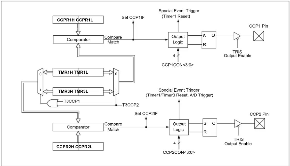
flowchart
graph TD
    A["CCPR1H CCPR1L"] --> B["Comparator"]
    B --> C["Compare Match"]
    C --> D["Output Logic"]
    D --> E["S R Q"]
    E --> F["TRIS Output Enable"]
    F --> G["CCP1 Pin"]
    H["TMR1H TMR1L"] --> I["0"]
    I --> J["0"]
    J --> K["T3CCP1"]
    L["TMR3H TMR3L"] --> M["1"]
    M --> N["T3CCP2"]
    O["CCPR2H CCPR2L"] --> P["Comparator"]
    P --> Q["Compare Match"]
    Q --> R["Output Logic"]
    R --> S["S R Q"]
    S --> T["TRIS Output Enable"]
    U["Set CCP1IF"] --> D
    V["Special Event Trigger (Timer1 Reset)"] --> D
    W["CCP1CON<3:0>"] --> D
    X["CCP2CON<3:0>"] --> R
    Y["Special Event Trigger (Timer1/Timer3 Reset, A/D Trigger)"] --> R
TABLE 16-3: REGISTERS ASSOCIATED WITH CAPTURE, COMPARE, TIMER1 AND TIMER3
| Name Bit | 7 Bit 6 Bit | 5 Bit 4 Bit 3 | Bit 2 Bit 1 | Bit 0 | Reset Values on Page | ||||
| INTCON | GIE/GIEH | PEIE/GIEL | TMR0IE | INT0IE | RBIE | TMR0IF | INT0IF | RBIF | 59 |
| RCON | IPEN | — | 60 | ||||||
| PIR3 | — | LCDIF | RC2IF | TX2IF | CTMUIF | CCP2IF | CCP1IF | RTCCIF | 62 |
| PIE3 | — | LCDIE | RC2IE | TX2IE | CTMUIE | CCP2IE | CCP1IE | RTCCIE | 62 |
| IPR3 | — | LCDIP | RC2IP | TX2IP | CTMUIP | CCP2IP | CCP1IP | RTCCIP | 62 |
| PIR2 | OSCFIF | CMIF | — | — | BCLIF | LVDIF | TMR3IF | — | 62 |
| PIE2 | OSCFIE | CMIE | — | — | BCLIE | LVDIE | TMR3IE | — | 62 |
| IPR2 | OSCFIP | CMIP | — | — | BCLIP | LVDIP | TMR3IP | — | 62 |
| TRISC | TRISC7 | TRISC6 | TRISC5 | TRISC4 | TRISC3 | TRISC2 | TRISC1 | TRISC0 | 62 |
| TRISE | TRISE7 | TRISE6 | TRISE5 | TRISE4 | TRISE3 | — | TRISE1 | TRISE0 | 62 |
| TRISG | SPIOD | CCP2OD | CCP1OD | TRISG4 | TRISG3 | TRISG2 | TRISG1 | TRISG0 | 62 |
| TMR1L | Timer1 Register Low Byte | 60 | |||||||
| TMR1H Timer1 Register High Byte | 60 | ||||||||
| T1CON | RD16 | T1RUN | T1CKPS1 | T1CKPS0 | T1OSCEN | 1SYNC | TMR1CS | TMR1ON | 60 |
| TMR3H Timer3 Register High Byte | 61 | ||||||||
| TMR3L | Timer3 Register Low Byte | 61 | |||||||
| T3CON | RD16 | T3CCP2 | T3CKPS1 | T3CKPS0 | T3CCP1 | 3SYNC | TMR3CS | TMR3ON | 61 |
| CCPR1L Capture/Compare/PWM Register 1 Low Byte | 63 | ||||||||
| CCPR1H | Capture/Compare/PWM Register 1 High Byte | 63 | |||||||
| CCP1CON | — | — | DC1B1 | DC1B0 | CCP1M3 | CCP1M2 | CCP1M1 | CCP1M0 | 63 |
| CCPR2L Capture/Compare/PWM Register 2 Low Byte | 64 | ||||||||
| CCPR2H | Capture/Compare/PWM Register 2 High Byte | 63 | |||||||
| CCP2CON | — | — | DC2B1 | DC2B0 | CCP2M3 | CCP2M2 | CCP2M1 | CCP2M0 | 64 |
Legend: — = unimplemented, read as '0'. Shaded cells are not used by Capture/Compare, Timer1 or Timer3.
16.4 PWM Mode
In Pulse-Width Modulation (PWM) mode, the CCP2 pin produces up to a 10-bit resolution PWM output. Since the CCP2 pin is multiplexed with a PORTC or PORTE data latch, the appropriate TRIS bit must be cleared to make the CCP2 pin an output.
Note: Clearing the CCP2CON register will force the RC1 or RE7 output latch (depending on the device configuration) to the default low level. This is not the PORTC or PORTE I/O data latch.
Figure 16-4 shows a simplified block diagram of the CCP1 module in PWM mode.
For a step-by-step procedure on how to set up the CCP module for PWM operation, see Section 16.4.3 "Setup for PWM Operation".
FIGURE 16-4: SIMPLIFIED PWM BLOCK DIAGRAM

flowchart
graph TD
    A["Duty Cycle Registers"] --> B["CCPR1L"]
    B --> C["CCPR1H (Slave)"]
    C --> D["Comparator"]
    D --> E["TMR2"]
    E --> F["Comparator"]
    F --> G["PR2"]
    H["CCP1CON<5:4>"] --> A
    I["R Q S"] --> J["RC2/CCP1"]
    J --> K["TRISC<2>"]
    L["Clear Timer, CCP1 pin and latch D.C."] --> F
Note 1: The 8-bit TMR2 value is concatenated with the 2-bit internal Q clock, or 2 bits of the prescaler, to create the 10-bit time base.
A PWM output (Figure 16-5) has a time base (period) and a time that the output stays high (duty cycle). The frequency of the PWM is the inverse of the period (1/period).
FIGURE 16-5: PWM OUTPUT
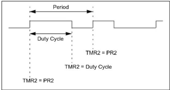
text_image
Period Duty Cycle TMR2 = PR2 TMR2 = Duty Cycle TMR2 = PR216.4.1 PWM PERIOD
The PWM period is specified by writing to the PR2 register. The PWM period can be calculated using the following formula:
EQUATION 16-1:
$$ \begin{array}{r l} \text { PWM Period } & = (\mathrm{PR2}) + 1 ] \cdot 4 \cdot \text { TOSC } \cdot \ & (\text { TMR2 Prescale Value }) \end{array} $$
PWM frequency is defined as 1/[PWM period].
When TMR2 is equal to PR2, the following three events occur on the next increment cycle:
• TMR2 is cleared
- The CCP2 pin is set (exception: if PWM duty cycle = 0%, the CCP2 pin will not be set)
- The PWM duty cycle is latched from CCPR2L into CCPR2H
Note: The Timer2 postscalers (see Section 13.0
"Timer2 Module") are not used in the determination of the PWM frequency. The postscaler could be used to have a servo update rate at a different frequency than the PWM output.
16.4.2 PWM DUTY CYCLE
The PWM duty cycle is specified by writing to the CCPR2L register and to the CCP2CON<5:4> bits. Up to 10-bit resolution is available. The CCPR2L contains the eight MSbs and the CCP2CON<5:4> contains the two LSbs. This 10-bit value is represented by CCPR2L:CCP2CON<5:4>. The following equation is used to calculate the PWM duty cycle in time:
EQUATION 16-2:
$$ \text { PWM Duty Cycle } = (\text { CCPR2L:CCP2CON } < 5: 4 >) \cdot $$
$$ \text { TOSC } \cdot (\text { TMR2 Prescale Value }) $$
CCPR2L and CCP2CON<5:4> can be written to at any time, but the duty cycle value is not latched into CCPR2H until after a match between PR2 and TMR2 occurs (i.e., the period is complete). In PWM mode, CCPR2H is a read-only register.
The CCPR2H register and a 2-bit internal latch are used to double-buffer the PWM duty cycle. This double-buffering is essential for glitchless PWM operation.
When the CCPR2H and 2-bit latch match TMR2, concatenated with an internal 2-bit Q clock or 2 bits of the TMR2 prescaler, the CCP2 pin is cleared.
The maximum PWM resolution (bits) for a given PWM frequency is given by the equation:
EQUATION 16-3:
PWM Resolution (max)
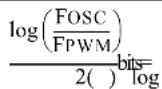
Note: If the PWM duty cycle value is longer than the PWM period, the CCP2 pin will not be cleared.
TABLE 16-4: EXAMPLE PWM FREQUENCIES AND RESOLUTIONS AT 40 MHz
| PWM Frequency | 2.44 kHz | 9.77 kHz | 39.06 kHz | 156.25 kHz | 312.50 kHz | 416.67 kHz |
| Timer Prescaler (1, 4, 16) | 16 | 4 | 1 | 1 | 1 | 1 |
| PR2 Value | FFh | FFh | FFh | 3Fh | 1Fh | 17h |
| Maximum Resolution (bits) | 14 | 12 | 10 | 8 | 7 | 6.58 |
The following steps should be taken when configuring the CCP module for PWM operation:
- Set the PWM period by writing to the PR2 register.
-
Set the PWM duty cycle by writing to the CCPR2L register and CCP2CON<5:4> bits.
-
Make the CCP2 pin an output by clearing the appropriate TRIS bit.
- Set the TMR2 prescale value, then enable Timer2 by writing to T2CON.
- Configure the CCP2 module for PWM operation.
TABLE 16-5: REGISTERS ASSOCIATED WITH PWM AND TIMER2
| Name Bit | 7 Bit 6 Bit | 5 Bit 4 Bit 3 | Bit 2 Bit 1 | Bit 0 | Reset Values on Page | ||||
| INTCON GIE/GIEH PEIE/GIEL | TMR0IE | INT0IE | RBIE | TMR0IF | INT0IF | RBIF | 59 | ||
| RCON | IPEN | — | 60 | ||||||
| PIR1 | — | ADIF | RC1IF | TX1IF | SSPIF | — | TMR2IF | TMR1IF | 62 |
| PIE1 | — | ADIE | RC1IE | TX1IE | SSPIE | — | TMR2IE | TMR1IE | 62 |
| IPR1 | — | ADIP | RC1IP | TX1IP | SSPIP | — | TMR2IP | TMR1IP | 62 |
| TRISC | TRISC7 | TRISC6 | TRISC5 | TRISC4 | TRISC3 | TRISC2 | TRISC1 | TRISC0 | 62 |
| TRISE | TRISE7 | TRISE6 | TRISE5 | TRISE4 | TRISE3 | — | TRISE1 | TRISE0 | 62 |
| TRISG | SPIOD | CCP2OD | CCP1OD | TRISG4 | TRISG3 | TRISG2 | TRISG1 | TRISG0 | 62 |
| TMR2 | Timer2 Register | 60 | |||||||
| PR2 | Timer2 Period Register | 60 | |||||||
| T2CON | — | T2OUTPS3 | T2OUTPS2 | T2OUTPS1 | T2OUTPS0 | TMR2ON | T2CKPS1 | T2CKPS0 | 60 |
| CCPR1L | Capture/Compare/PWM Register 1 Low Byte | 63 | |||||||
| CCPR1H | Capture/Compare/PWM Register 1 High Byte | 63 | |||||||
| CCP1CON | — | — | DC1B1 | DC1B0 | CCP1M3 | CCP1M2 | CCP1M1 | CCP1M0 | 63 |
| CCPR2L | Capture/Compare/PWM Register 2 Low Byte | 64 | |||||||
| CCPR2H | Capture/Compare/PWM Register 2 High Byte | 63 | |||||||
| CCP2CON | — | — | DC2B1 | DC2B0 | CCP2M3 | CCP2M2 | CCP2M1 | CCP2M0 | 64 |
Legend: — = unimplemented, read as '0'. Shaded cells are not used by PWM or Timer2.
NOTES:
17.0 LIQUID CRYSTAL DISPLAY (LCD) DRIVER MODULE
The Liquid Crystal Display (LCD) driver module generates the timing control to drive a static or multiplexed LCD panel. It also provides control of the LCD pixel data. The module can drive panels of up to 192 pixels (48 segments by 4 commons) in PIC18F8XJ90 devices and 132 pixels (33 segments by 4 commons) in PIC18F6XJ90 devices.
The LCD driver module supports these features:
- Direct driving of LCD panel
- On-chip bias generator with dedicated charge pump to support a range of fixed and variable bias options
- Up to four commons, with four Multiplexing modes
- Up to 48 (PIC18F8XJ90 devices) or 33 (PIC18F6XJ90 devices) segments
- Three LCD clock sources with selectable prescaler, with a fourth source available for use with the LCD charge pump
A simplified block diagram of the module is shown in Figure 17-1.
FIGURE 17-1: LCD DRIVER MODULE BLOCK DIAGRAM

flowchart
graph TD
    A["Data Bus"] --> B["LCD DATA 24 x 8 (= 4 x 48)"]
    B --> C["LCDDATA23"]
    B --> D["LCDDATA22"]
    B --> E["..."]
    B --> F["LCDDATA1"]
    B --> G["LCDDATA0"]
    C --> H["192 to 48 MUX"]
    D --> H
    E --> H
    F --> H
    G --> H
    H --> I["SEG<47:0>"]
    I --> J["To I/O Pins"]
    K["Timing Control"] --> L["LCDCON"]
    K --> M["LCDPS"]
    K --> N["LCDEx"]
    O["LCD Clock Source Select"] --> P["LCD Bias Generation"]
    P --> Q["LCD Charge Pump"]
    R["Fosc/4"] --> S["IntrC Oscillator"]
    T["T13CKI"] --> U["INTOSC Oscillator"]
    V["Bias Voltage"] --> W["COM<3:0>"]
    X["8"] --> B
    Y["4"] --> P
17.1 LCD Registers
The LCD driver module has 33 registers:
• LCD Control Register (LCDCON)
• LCD Phase Register (LCDPS)
• LCDREG Register (LCD Regulator Control)
- Six LCD Segment Enable Registers (LCDSE5:LCDSE0)
• 24 LCD Data Registers (LCDDATA23:LCDDATA0)
17.1.1 LCD CONTROL REGISTERS
The LCDCON register, shown in Register 17-1, controls the overall operation of the module. Once the module is configured, the LCDEN (LCDCON<7>) bit is used to enable or disable the LCD module. The LCD panel can also operate during Sleep by clearing the SLPEN (LCDCON<6>) bit.
The LCDPS register, shown in Register 17-2, configures the LCD clock source prescaler and the type of waveform: Type-A or Type-B. Details on these features are provided in Section 17.2 "LCD Clock Source", Section 17.3 "LCD Bias Generation" and Section 17.8 "LCD Waveform Generation".
The LCDREG register is described in Section 17.3 "LCD Bias Generation".
The LCD Segment Enable registers (LCDSEx) configure the functions of the port pins. Setting the segment enable bit for a particular segment configures that pin as an LCD driver. The prototype LCDSE register is shown in Register 17-3. There are six LCDSE registers (LCDSE5:LCDSE0) listed in Table 17-1.
REGISTER 17-1: LCDCON: LCD CONTROL REGISTER
| R/W-0 R/W-0 R/C-0 U-0 R/W-0 R/W-0 R/W-0 R/W-0 | |||||||
| LCDEN | SLPEN | WERR | — | CS1 | CS0 | LMUX1 | LMUX0 |
| bit 7 bit 0 | |||||||
| Legend: | C = Clearable bit | |
| R = Readable bit | W = Writable bit | U = Unimplemented bit, read as ‘0’ |
| -n = Value at POR | ‘1’ = Bit is set | ‘0’ = Bit is cleared x = Bit is unknown |
bit 7 LCDEN: LCD Driver Enable bit
1 = LCD driver module is enabled 0 = LCD driver module is disabled
bit 6 SLPEN: LCD Driver Enable in Sleep mode bit
1 = LCD driver module is disabled in Sleep mode 0 = LCD driver module is enabled in Sleep mode
bit 5 WERR: LCD Write Failed Error bit
1 = LCDDATAx register written while LCDPS<4> = 0 (must be cleared in software) 0 = No LCD write error
bit 4 Unimplemented: Read as '0'
bit 3-2 CS<1:0>: Clock Source Select bits
1x = INTRC (31 kHz) 01 = T13CKI (Timer1) 00 = System clock (Fosc/4)
bit 1-0 LMUX<1:0>: Commons Select bits
| LMUX<1:0> | Multiplex Type | Maximum Number of Pixels: | Bias Type | |
| PIC18F6XJ90 | PIC18F8XJ90 | |||
| 00 | Static (COM0) | 33 | 48 | Static |
| 01 | 1/2 (COM1:COM0) | 66 | 96 | 1/2 or 1/3 |
| 10 | 1/3 (COM2:COM0) | 99 | 144 | 1/2 or 1/3 |
| 11 | 1/4 (COM3:COM0) | 132 | 192 | 1/3 |
REGISTER 17-2: LCDPS: LCD PHASE REGISTER
| R/W-0 R/W-0 R-0 R-0 R/W-0 R/W-0 R/W-0 R/W-0 | ||||||
| WFT BIA$MD LCDA WA LP3 LP2 LP1 | LP0 | |||||
| bit 7 bit 0 | ||||||
Legend:
| R = Readable bit W = Writable bit U = Unimplemented bit, read as '0' | ||
| -n = Value at POR | '1' = Bit is set | '0' = Bit is cleared x = Bit is unknown |
bit 7 WFT: Waveform Type Select bit
1 = Type-B waveform (phase changes on each frame boundary)
0 = Type-A waveform (phase changes within each common type)
bit 6 BIASMD: Bias Mode Select bit
When LMUX<1:0>= 00:
0 = Static Bias mode (do not set this bit to '1')
When LMUX<1:0>= 01 or 10:
1 = 1/2 Bias mode
0 = 1/3 Bias mode
When LMUX<1:0>= 11:
0 = 1/3 Bias mode (do not set this bit to '1')
bit 5 LCDA: LCD Active Status bit
1 = LCD driver module is active
0 = LCD driver module is inactive
bit 4 WA: LCD Write Allow Status bit
1 = Write into the LCDDATAx registers is allowed
0 = Write into the LCDDATAx registers is not allowed
bit 3-0 LP<3:0>: LCD Prescaler Select bits
1111 = 1:16
1110 = 1:15
1101 = 1:14
1100 = 1:13
1011 = 1:12
1010 = 1:11
1001 = 1:10
1000 = 1:9
0111 = 1:8
0110 = 1:7
0101 = 1:6
0100 = 1:5
0011 = 1:4
0010 = 1:3
0001 = 1:2
0000 = 1:1
REGISTER 17-3: LCDSEx: LCD SEGMENT ENABLE REGISTERS
| R/W-0 R/W-0 R/W-0 R/W-0 R/W-0 R/W-0 R/W-0 R/W-0 | ||||||
| SE(n + 7) SE(n + 6) SE(n + 5) SE(n + 4) SE(n + 3) SE(n + 2) SE(n + 1) SE(n) | ||||||
| bit 7 bit 0 | ||||||
| Legend: | |
| R = Readable bit W = Writable bit U = Unimplemented bit, read as '0' | |
| -n = Value at POR '1' = Bit is set '0' = Bit is cleared | x = Bit is unknown |
bit 7-0 SEG(n + 7):SEG(n): Segment Enable bits
For LCDSE0: n = 0
For LCDSE1: n = 8
For LCDSE2: n = 16
For LCDSE3: n = 24
For LCDSE4: n = 32
For LCDSE5: n = 40
1 = Segment function of the pin is enabled, digital I/O disabled
0 = I/O function of the pin is enabled
TABLE 17-1: LCDSE REGISTERS AND ASSOCIATED SEGMENTS
| Register | Segments |
| LCDSE0 | 7:0 |
| LCDSE1 | 15:8 |
| LCDSE2 | 23:16 |
| LCDSE3 | 31:24 |
| LCDSE4^(1) | 39:32 |
| LCDSE5^(2) | 47:40 |
Note 1: LCDSE4<7:1> (SEG<39:33>) registers are not implemented in PIC18F6XJ90 devices.
2: LCDSE5 is not implemented in PIC18F6XJ90 devices.
17.1.2 LCD DATA REGISTERS
Once the module is initialized for the LCD panel, the individual bits of the LCDDATA23:LCDDATA0 registers are cleared or set to represent a clear or dark pixel, respectively. Specific sets of LCDDATA registers are used with specific segments and common signals. Each bit represents a unique combination of a specific segment connected to a specific common.
Individual LCDDATA bits are named by the convention "SxxCy", with "xx" as the segment number and "y" as the common number. The relationship is summarized in Table 17-2. The prototype LCDDATA register is shown in Register 17-4.
Note: In 64-pin devices, writing into the registers LCDDATA5, LCDDATA11, LCDDATA17 and LCDDATA23, will not affect the status of any pixels.
REGISTER 17-4: LCDDATAx: LCD DATA REGISTERS
| R/W-0 R/W-0 R/W-0 R/W-0 R/W-0 R/W-0 R/W-0 R/W-0 | ||||||
| S(n + 7)Cy | S(n + 6)Cy | S(n + 5)Cy | S(n + 4)Cy | S(n + 3)Cy | S(n + 2)Cy | S(n + 1)Cy |
| bit 7 bit 0 | ||||||
Legend:
| R = Readable bit W = Writable bit U = Unimplemented bit, read as '0' | ||
| -n = Value at POR | '1' = Bit is set | '0' = Bit is cleared x = Bit is unknown |
bit 7-0 S(n + 7)Cy:S(n)Cy: Pixel On bits
For LCDDATA0 through LCDDATA5: n = (8x), y = 0
For LCDDATA6 through LCDDATA11: n = (8(x - 6)), y = 1
For LCDDATA12 through LCDDATA17: n = (8(x - 12)) , y = 2
For LCDDATA18 through LCDDATA23: n = (8(x - 18)) , y = 3
1 = Pixel on (dark)
0 = Pixel off (clear)
TABLE 17-2: LCDDATA REGISTERS AND BITS FOR SEGMENT AND COM COMBINATIONS
| Segments | COM Lines | |||
| 0 | 1 | 2 | 3 | |
| 0 through 7 | LCDDATA0 | LCDDATA6 | LCDDATA12 | LCDDATA18 |
| S00C0:S07C0 | S00C1:S07C1 | S00C2:S07C2 | S00C3:S07C3 | |
| 8 through 15 | LCDDATA1 | LCDDATA7 | LCDDATA13 | LCDDATA19 |
| S08C0:S15C0 | S08C1:S15C1 | S08C2:S15C2 | S08C0:S15C3 | |
| 16 through 23 | LCDDATA2 | LCDDATA8 | LCDDATA14 | LCDDATA20 |
| S16C0:S23C0 | S16C1:S23C1 | S16C2:S23C2 | S16C3:S23C3 | |
| 24 through 31 | LCDDATA3 | LCDDATA9 | LCDDATA15 | LCDDATA21 |
| S24C0:S31C0 | S24C1:S31C1 | S24C2:S31C2 | S24C3:S31C3 | |
| 32 through 39 | LCDDATA4^(1) | LCDDATA10^(1) | LCDDATA16^(1) | LCDDATA22^(1) |
| S32C0:S39C0 | S32C1:S39C1 | S32C2:S39C2 | S32C3:S39C3 | |
| 40 through 47 | LCDDATA5^(2) | LCDDATA11^(2) | LCDDATA17^(2) | LCDDATA23^(2) |
| S40C0:S47C0 | S40C1:S47C1 | S40C2:S47C2 | S40C3:S47C3 | |
Note 1: Bits<7:1> of these registers are not implemented in PIC18F6XJ90 devices. Bit 0 of these registers (SEG32Cy) is always implemented.
2: These registers are not implemented on PIC18F6XJ90 devices.
17.2 LCD Clock Source
The LCD driver module generates its internal clock from 3 possible sources:
- System clock (F osc/4)
- Timer1 oscillator
- INTRC source
The LCD clock generator uses a configurable divide-by-32/divide-by-8192 postscaler to produce a baseline frequency of about 1 kHz nominal, regardless of the source selected. The clock source selection and the postscaler configuration are determined by the Clock Source Select bits, CS<1:0> (LCDCON<3:2>).
An additional programmable prescaler is used to derive the LCD frame frequency from the 1 kHz baseline. The prescaler is configured using the LP<3:0> bits (LCDPS<3:0>) for any one of 16 options, ranging from 1:1 to 1:16.
Proper timing for waveform generation is set by the LMUX<1:0> bits (LCDCON<1:0>). These bits determine which Commons Multiplexing mode is to be used and divide down the LCD clock source as required. They also determine the configuration of the ring counter that is used to switch the LCD commons on or off.
17.2.1 LCD VOLTAGE REGULATOR CLOCK SOURCE
In addition to the clock source for LCD timing, a separate 31 kHz nominal clock is required for the LCD charge pump. This is provided from a distinct branch of the LCD clock source.
The charge pump clock can use either the Timer1 oscillator or the INTRC source, as well as the 8 MHz INTOSC source (after being divided by 256 by a prescaler). The charge pump clock source is configured using the CKSEL<1:0> bits (LCDREG<1:0>).
17.2.2 CLOCK SOURCE CONSIDERATIONS
When using the system clock as the LCD clock source, it is assumed that the system clock frequency is a nominal 32 MHz (for a Fosc/4 frequency of 8 MHz). Because the prescaler option for the Fosc/4 clock selection is fixed at divide-by-8192, system clock speeds that differ from 32 MHz will produce frame frequencies and refresh rates different than discussed in this chapter. The user will need to keep this in mind when designing the display application.
The Timer1 and INTRC sources can be used as LCD clock sources when the device is in Sleep mode. To use the Timer1 oscillator, it is necessary to set the T1OSCEN bit (T1CON<3>). Selecting either Timer1 or INTRC as the LCD clock source will not automatically activate these sources.
Similarly, selecting the INTOSC as the charge pump clock source will not turn the oscillator on. To use INTOSC, it must be selected as the system clock source by using the FOSC2 Configuration bit.
If Timer1 is used as a clock source for the device, either as an LCD clock source or for any other purpose, LCD segment 32 become unavailable.
FIGURE 17-2: LCD CLOCK GENERATION

flowchart
graph TD
    A["INTOSC 8 MHz Source"] --> B["÷256"]
    C["LCDCON<3:2>"] --> D["00"]
    E["System Clock (Fosc/4)"] --> F["01"]
    G["Timer1 Oscillator"] --> H["1x"]
    I["Internal 31 kHz Source"] --> J["÷2"]
    K["LCDREG<1:0>"] --> L["11"]
    M["LCDCON<1:0>"] --> N["÷4"]
    O["LCDPS<3:0>"] --> P["4"]
    Q["1:1 to 1:16 Programmable Prescaler"] --> R["÷32 or +8192"]
    S["÷1, 2, 3, 4 Ring Counter"] --> T["COM0"]
    S --> U["COM1"]
    S --> V["COM2"]
    S --> W["COM3"]
    X["31 kHz Clock to LCD Charge Pump"] --> Y["÷256"]
    Z["LCDCON<3:2>"] --> AA["00"]
    AB["System Clock (Fosc/4)"] --> AC["01"]
    AD["Timer1 Oscillator"] --> AE["1x"]
    AF["Internal 31 kHz Source"] --> AG["÷2"]
    AH["LCDCON<3:2>"] --> AI["00"]
    AJ["System Clock (Fosc/4)"] --> AK["01"]
    AL["LCDPS<3:0>"] --> AM["00"]
    AN["LCDCON<3:2>"] --> AO["÷4"]
    AP["LCDPS<3:0>"] --> AQ["4"]
    AR["LCDCON<3:2>"] --> AS["÷2"]
    AT["LCDREG<1:0>"] --> AU["11"]
    AV["LCDPS<3:0>"] --> AW["4"]
17.3 LCD Bias Generation
The LCD driver module is capable of generating the required bias voltages for LCD operation with a minimum of external components. This includes the ability to generate the different voltage levels required by the different bias types that are required by the LCD. The driver module can also provide bias voltages, both above and below microcontroller VDD, through the use of an on-chip LCD voltage regulator.
17.3.1 LCD BIAS TYPES
PIC18F87J90 family devices support three bias types based on the waveforms generated to control segments and commons:
• Static (two discrete levels)
• 1/2 Bias (three discrete levels
• 1/3 Bias (four discrete levels)
The use of different waveforms in driving the LCD is discussed in more detail in Section 17.8 "LCD Waveform Generation".
17.3.2 LCD VOLTAGE REGULATOR
The purpose of the LCD regulator is to provide proper bias voltage and good contrast for the LCD, regardless of VDD levels. This module contains a charge pump and internal voltage reference. The regulator can be configured by using external components to boost bias voltage above VDD. It can also operate a display at a constant voltage below VDD. The regulator can also be selectively disabled to allow bias voltages to be generated by an external resistor network.
The LCD regulator is controlled through the LCDREG register (Register 17-5). It is enabled or disabled using the CKSEL<1:0> bits, while the charge pump can be selectively enabled using the CPEN bit. When the regulator is enabled, the MODE13 bit is used to select the bias type. The peak LCD bias voltage, measured as a difference between the potentials of LCDBIAS3 and LCDBIAS0, is configured with the BIAS bits.
REGISTER 17-5: LCDREG: VOLTAGE REGULATOR CONTROL REGISTER
| U - 0 | R W - 0 | R W - | |||||
| — | CPEN | BIAS2 | BIAS1 | BIAS0 | MODE13 | CKSEL1 | CKSEL0 |
| bit 7 bit 0 | |||||||
| Legend: | |||
| R = Readable bit | W = Writable bit | U = Unimplemented bit, read as ‘0’ | |
| -n = Value at POR | ‘1’ = Bit is set | ‘0’ = Bit is cleared | x = Bit is unknown |
bit 7 Unimplemented: Read as '0'
bit 6 CPEN: LCD Charge Pump Enable bit
1 = Charge pump enabled; highest LCD bias voltage is 3.6V 0 = Charge pump disabled; highest LCD bias voltage is A D
bit 5-3 BIAS<2:0>: Regulator Voltage Output Control bits
111 = 3.60V peak (offset on LCDBIAS0 of 0V)
110 = 3.47V peak (offset on LCDBIAS0 of 0.13V)
101 = 3.34V peak (offset on LCDBIAS0 of 0.26V)
100 = 3.21V peak (offset on LCDBIAS0 of 0.39V)
011 = 3.08V peak (offset on LCDBIAS0 of 0.52V)
010 = 2.95V peak (offset on LCDBIAS0 of 0.65V)
001 = 2.82V peak (offset on LCDBIAS0 of 0.78V)
000 = 2.69V peak (offset on LCDBIAS0 of 0.91V)
bit 2 MODE13: 1/3 LCD Bias Enable bit
1 = Regulator output supports 1/3 LCD Bias mode
0 = Regulator output supports static LCD Bias mode
bit 1-0 CKSEL<1:0>: Regulator Clock Source Select bits
11 = INTRC
10 = INTOSC 8 MHz source
01 = Timer1 oscillator
00 = LCD regulator disabled
17.3.3 BIAS CONFIGURATIONS
PIC18F87J90 family devices have four distinct circuit configurations for LCD bias generation:
• M0: Regulator with Boost
• M1: Regulator without Boost
• M2: Resistor Ladder with Software Contrast
• M3: Resistor Ladder with Hardware Contrast
17.3.3.1 M0 (Regulator with Boost)
In M0 operation, the LCD charge pump feature is enabled. This allows the regulator to generate voltages up to +3.6V to the LCD (as measured at LCDBIAS3).
M0 uses a flyback capacitor connected between VLCAP1 and VLCAP2, as well as filter capacitors on LCDBIAS0 through LCDBIAS3, to obtain the required voltage boost (Figure 17-3). The output voltage (VBIAS) is the difference of potential between LCDBIAS3 and LCDBIAS0. It is set by the BIAS<2:0> bits which adjust the offset between LCDBIAS0 and Vss. The flyback capacitor (CFLY) acts as a charge storage element for large LCD loads. This mode is useful in those cases where the voltage requirements of the LCD are higher than the microcontroller's VDD. It also permits software control of the display's contrast, by adjustment of bias voltage, by changing the value of the BIAS bits.
M0 supports Static and 1/3 Bias types. Generation of the voltage levels for 1/3 Bias is handled automatically, but must be configured in software.
M0 is enabled by selecting a valid regulator clock source (CKSEL<1:0> set to any value except '00') and setting the CPEN bit. If Static Bias type is required, the MODE13 bit must be cleared.
17.3.3.2 M1 (Regulator without Boost)
M1 operation is similar to M0, but does not use the LCD charge pump. It can provide VBIAS up to the voltage level supplied directly to LCDBIAS3. It can be used in cases where VDD for the application is expected to never drop below a level that can provide adequate contrast for the LCD. The connection of external components is very similar to M0, except that LCDBIAS3 must be tied directly to VDD (Figure 17-3).
Note: When the device is put to Sleep while operating in mode M0 or M1, make sure that the bias capacitors are fully discharged to get the lowest Sleep current.
The BIAS<2:0> bits can still be used to adjust contrast in software by changing VBIAS. As with M0, changing these bits changes the offset between LCDBIAS0 and Vss. In M1, this is reflected in the change between the LCDBIAS0 and the voltage tied to LCDBIAS3. Thus, if VDD should change, VBIAS will also change; where in M0, the level of VBIAS is constant.
Like M0, M1 supports Static and 1/3 Bias types. Generation of the voltage levels for 1/3 Bias is handled automatically but must be configured in software.
M1 is enabled by selecting a valid regulator clock source (CKSEL<1:0> set to any value except '00') and clearing the CPEN bit. If 1/3 Bias type is required, the MODE13 bit should also be set.
FIGURE 17-3: LCD REGULATOR CONNECTIONS FOR M0 AND M1 CONFIGURATIONS

text_image
PIC18F87J90 VDD AVDD VLCAP1 VLCAP2 CFLY 0.47 μF(1) LCDBIAS3 C3 0.47 μF(1) LCDBIAS2 C2 0.47 μF(1) LCDBIAS1 C1 0.47 μF(1) LCDBIAS0 C0 0.47 μF(1) Mode 0 (VBIAS up to 3.6V)
text_image
VDD CFLY 0.47 μF(1) VDD C2 0.47 μF(1) C1 0.47 μF(1) C0 0.47 μF(1) Mode 1 (VBIAS ≤ VDD)Note 1: These values are provided for design guidance only; they should be optimized for the application by the designer based on the actual LCD specifications.
17.3.3.3 M2 (Resistor Ladder with Software Contrast)
M2 operation also uses the LCD regulator but disables the charge pump. The regulator's internal voltage reference remains active as a way to regulate contrast. It is used in cases where the current requirements of the LCD exceed the capacity of the regulator's charge pump.
In this configuration, the LCD bias voltage levels are created by an external resistor voltage divider, connected across LCDBIAS0 through LCDBIAS3, with the top of the divider tied to VDD (Figure 17-4). The potential at the bottom of the ladder is determined by the LCD regulator's voltage reference, tied internally to LCDBIAS0. The bias type is determined by the voltages on the LCDBIAS pins, which are controlled by the
configuration of the resistor ladder. Most applications using M2 will use a 1/3 or 1/2 Bias type. While Static Bias can also be used, it offers extremely limited contrast range and additional current consumption over other bias generation modes.
Like M1, the LCDBIAS bits can be used to control contrast, limited by the level of VDD supplied to the device. Also, since there is no capacitor required across VLCAP1 and VLCAP2, these pins are available as digital I/O ports, RG2 and RG3.
M2 is selected by clearing the CKSEL<1:0> bits and setting the CPEN bit.
FIGURE 17-4: RESISTOR LADDER CONNECTIONS FOR M2 CONFIGURATION
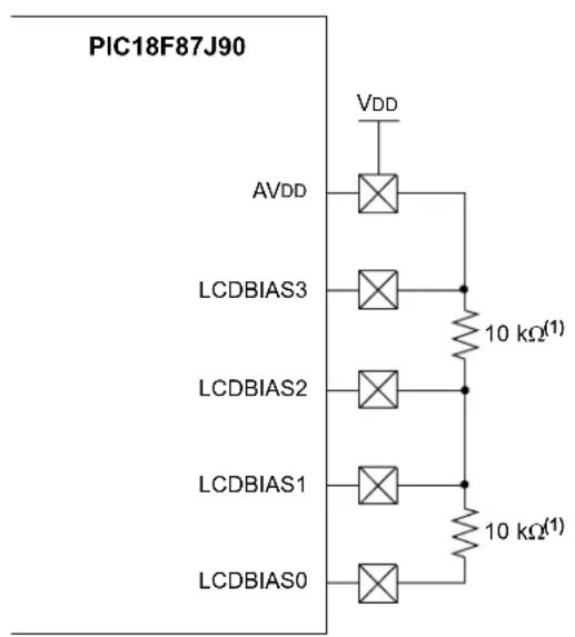
text_image
PIC18F87J90 VDD AVDD LCDBIAS3 10 kΩ(1) LCDBIAS2 10 kΩ(1) LCDBIAS1 10 kΩ(1) LCDBIAS01/2 Bias

text_image
10 kΩ(1) 10 kΩ(1) 10 kΩ(1)1/3 Bias
| Bias Level at Pin | Bias Type | |
| 1/2 Bias 1/3 Bias | ||
| LCDBIAS0 (Internal Low Reference Voltage) (Internal Low Reference Voltage) | ||
| LCDBIAS1 1/2 V | BIAS 1/3 VBIAS | |
| LCDBIAS2 | 1/2 VBIAS | 2/3 VBIAS |
| LCDBIAS3 | VBIAS (up to AVDD) | VBIAS (up to AVDD) |
Note 1: These values are provided for design guidance only; they should be optimized for the application by the designer based on the actual LCD specifications.
17.3.3.4 M3 (Hardware Contrast)
In M3, the LCD regulator is completely disabled. Like M2, LCD bias levels are tied to AVDD and are generated using an external divider. The difference is that the internal voltage reference is also disabled and the bottom of the ladder is tied to ground (Vss); see Figure 17-5. The value of the resistors, and the difference between Vss and VDD, determine the contrast range; no software adjustment is possible. This configuration is also used where the LCD's current requirements exceed the capacity of the charge pump and software contrast control is not needed.
Depending on the bias type required, resistors are connected between some or all of the pins. A potentiometer can also be connected between LCDBIAS3 and VDD to allow for hardware controlled contrast adjustment.
M3 is selected by clearing the CKSEL<1:0> and CPEN bits.
FIGURE 17-5: RESISTOR LADDER CONNECTIONS FOR M3 CONFIGURATION

text_image
PIC18F87J90 VDD AVDD LCDBIAS3 LCDBIAS2 LCDBIAS1 LCDBIAS0 (2)Static Bias

text_image
10 kΩ(1) 10 kΩ(1)1/2 Bias

text_image
10 kΩ(1) 10 kΩ(1) 10 kΩ(1)1/3 Bias
| Bias Level at Pin | Bias Type | ||
| Static 1/2 Bias 1/3 Bias | |||
| LCDBIAS0 AV | ss AVss AVss | ||
| LCDBIAS1 | AVss | 1/2 AVDD | 1/3 AVDD |
| LCDBIAS2 | AVDD | 1/2 AVDD | 2/3 AVDD |
| LCDBIAS3 AVDD AVDD AVDD | |||
Note 1: These values are provided for design guidance only; they should be optimized for the application by the designer based on the actual LCD specifications.
2: A potentiometer for manual contrast adjustment is optional; it may be omitted entirely.
17.3.4 DESIGN CONSIDERATIONS FOR THE LCD CHARGE PUMP
When designing applications that use the LCD regulator with the charge pump enabled, users must always consider both the dynamic current and RMS (static) current requirements of the display, and what the charge pump can deliver. Both dynamic and static current can be determined by Equation 17-1:
EQUATION 17-1:
$$ \mathrm{I} = \mathrm{Cx} \frac {\mathrm{dV}}{\mathrm{dT}} $$
For dynamic current, C is the value of the capacitors attached to LCDBIAS3 and LCDBIAS2. The variable, dV, is the voltage drop allowed on C2 and C3 during a voltage switch on the LCD display, and dT is the duration of the transient current after a clock pulse occurs. For practical design purposes, these will be assumed to be 0.047 μF for C, 0.1V for dV and 1 μs for dT. This yields a dynamic current of 4.7 mA for 1 μs.
RMS current is determined by the value of CFLY for C, the voltage across VLCAP1 and VLCAP2 for dV and the regulator clock period (TPER) for dT. Assuming a CFLY value of 0.047 μF, a value of 1.02V across CFLY and TPER of 30 μs, the maximum theoretical static current will be 1.8 mA. Since the charge pump must charge five capacitors, the maximum current becomes 360 μA. For a real-world assumption of 50% efficiency, this yields a practical current of 180 μA.
Users should compare the calculated current capacity against the requirements of the LCD. While dV and dT are relatively fixed by device design, the values of QFLY and the capacitors on the LCDBIAS pins can be changed to increase or decrease current. As always, any changes should be evaluated in the actual circuit for their impact on the application.
17.4 LCD Multiplex Types
The LCD driver module can be configured into four multiplex types:
- Static (only COM0 used)
• 1/2 Multiplex (COM0 and COM1 are used)
• 1/3 Multiplex (COM0, COM1 and COM2 are used) - 1/4 Multiplex (all COM0, COM1, COM2 and COM3 are used)
The number of active commons used is configured by the LMUX<1:0> bits (LCDCON<1:0>), which determines the function of the PORTE<6:4> pins (see Table 17-3 for details). If the pin is configured as a COM drive, the port I/O function is disabled and the TRIS setting of that pin is overridden.
Note: On a Power-on Reset, the LMUX<1:0> bits are '00'.
TABLE 17-3: PORTE<6:4> FUNCTION
| LMUX<1:0> | PORTE<6> | PORTE<5> | PORTE<4> |
| 00 Digital I/O Digital I/O Digital I/O | |||
| 01 Digital I/O Digital I/O COM1 Driver | |||
| 10 | Digital I/O | COM2 Driver | COM1 Driver |
| 11 | COM3 Driver | COM2 Driver | COM1 Driver |
17.5 Segment Enables
The LCDSEx registers are used to select the pin function for each segment pin. Setting a bit configures the corresponding pin to function as a segment driver. LCDSEx registers do not override the TRIS bit settings, so the TRIS bits must be configured as inputs for that pin.
Note: On a Power-on Reset, these pins are configured as digital I/O.
17.6 Pixel Control
The LCDDATAx registers contain bits which define the state of each pixel. Each bit defines one unique pixel.
Table 17-2 shows the correlation of each bit in the LCDDATAx registers to the respective common and segment signals. Any LCD pixel location not being used for display can be used as general purpose RAM.
17.7 LCD Frame Frequency
The rate at which the COM and SEG outputs change is called the LCD frame frequency. Frame frequency is set by the LP<3:0> bits (LCDPS<3:0>) and is also affected by the Multiplex mode being used. The relationship between the Multiplex mode, LP bits setting and frame rate is shown in Table 17-4 and Table 17-5.
TABLE 17-4: FRAME FREQUENCY FORMULAS
| Multiplex Mode | Frame Frequency (Hz) |
| Static Clock Source/(4 x 1 x (LP<3:0> + 1)) | |
| 1/2 Clock Source/(2 x 2 x (LP<3:0> + 1)) | |
| 1/3 Clock Source/(1 x 3 x (LP<3:0> + 1)) | |
| 1/4 Clock Source/(1 x 4 x (LP<3:0> + 1)) | |
TABLE 17-5: APPROXIMATE FRAME FREQUENCY (IN Hz) FOR LP PRESCALER SETTINGS
| LP<3:0> | Multiplex Mode | |||
| Static 1/2 1/3 1/4 | ||||
| 1 125 | 125 167 125 | |||
| 2 | 83 | 83 | 111 | 83 |
| 3 | 62 | 62 | 83 | 62 |
| 4 | 50 | 50 | 67 | 50 |
| 5 | 42 | 42 | 56 | 42 |
| 6 | 36 | 36 | 48 | 36 |
| 7 | 31 | 31 | 42 | 31 |
17.8 LCD Waveform Generation
LCD waveform generation is based on the principle that the net AC voltage across the dark pixel should be maximized and the net AC voltage across the clear pixel should be minimized. The net DC voltage across any pixel should be zero.
The COM signal represents the time slice for each common, while the SEG contains the pixel data. The pixel signal (COM-SEG) will have no DC component and it can take only one of the two rms values. The higher rms value will create a dark pixel and a lower rms value will create a clear pixel.
As the number of commons increases, the delta between the two rms values decreases. The delta represents the maximum contrast that the display can have.
The LCDs can be driven by two types of waveform: Type-A and Type-B. In the Type-A waveform, the phase changes within each common type, whereas in the Type-B waveform, the phase changes on each frame boundary. Thus, the Type-A waveform maintains 0 Vdc over a single frame, whereas the Type-B waveform takes two frames.
| Note 1: If the power-managed Sleep mode is invoked while the LCD Sleep bit (SLPEN) is set (LCDCON<6> is ‘1’), take care to execute Sleep only when the VDC on all the pixels is ‘0’.2: When the LCD clock source is the system clock, the LCD module will go to Sleep if the microcontroller goes into Sleep mode, regardless of the setting of the SLPEN bit. Thus, always take care to see that the VDC on all pixels is ‘0’ whenever Sleep mode is invoked. |
Figure 17-6 through Figure 17-16 provide waveforms for static, half multiplex, one-third multiplex and quarter multiplex drives for Type-A and Type-B waveforms.
FIGURE 17-6: TYPE-A/TYPE-B WAVEFORMS IN STATIC DRIVE
text_image
COM0 SEG7 SEG6 SEG5 SEG4 SEG3 SEG2 SEG1 SEG0 COM0 V1 V0 V1 V0 SEG1 V1 V0 COM0-SEG0 V1 V0 -V1 COM0-SEG1 V0 → 1 Frame ←FIGURE 17-7: TYPE-A WAVEFORMS IN 1/2 MUX, 1/2 BIAS DRIVE
text_image
COM1 COM0 COM0 V2 V1 V0 COM1 V2 V1 V0 SEG0 V2 V1 V0 SEG1 V2 V1 V0 COM0-SEG0 V2 V1 V0 -V1 -V2 COM0-SEG1 V2 V1 V0 -V1 -V2 1 FrameFIGURE 17-8: TYPE-B WAVEFORMS IN 1/2 MUX, 1/2 BIAS DRIVE
text_image
COM1 COM0 SEG3 SEG2 SEG1 SEG0 COM0 V2 V1 V0 COM1 V2 V1 V0 SEG0 V2 V1 V0 SEG1 V2 V1 V0 COM0-SEG0 V2 V1 V0 -V1 -V2 COM0-SEG1 V2 V1 V0 -V1 -V2 2 FramesFIGURE 17-9: TYPE-A WAVEFORMS IN 1/2 MUX, 1/3 BIAS DRIVE

text_image
COM1 COM0 COM0 COM1 SEG0 SEG1 COM0-SEG0 COM0-SEG1 V3 V2 V1 V0 V3 V2 V1 V0 V3 V2 V1 V0 V3 V2 V1 V0 V3 V2 V1 V0 V3 V2 V1 V0 -V1 -V2 -V3 V3 V2 V1 V0 -V1 -V2 -V3 ← 1 Frame →FIGURE 17-10: TYPE-B WAVEFORMS IN 1/2 MUX, 1/3 BIAS DRIVE
text_image
COM1 COM0 COM0 V3 V2 V1 V0 V3 V2 V1 V0 V3 V2 V1 V0 SEG0 SEG1 V3 V2 V1 V0 V3 V2 V1 V0 COM0-SEG0 V3 V2 V1 V0 -V1 -V2 -V3 COM0-SEG1 V3 V2 V1 V0 -V1 -V2 -V3 2 FramesFIGURE 17-11: TYPE-A WAVEFORMS IN 1/3 MUX, 1/2 BIAS DRIVE
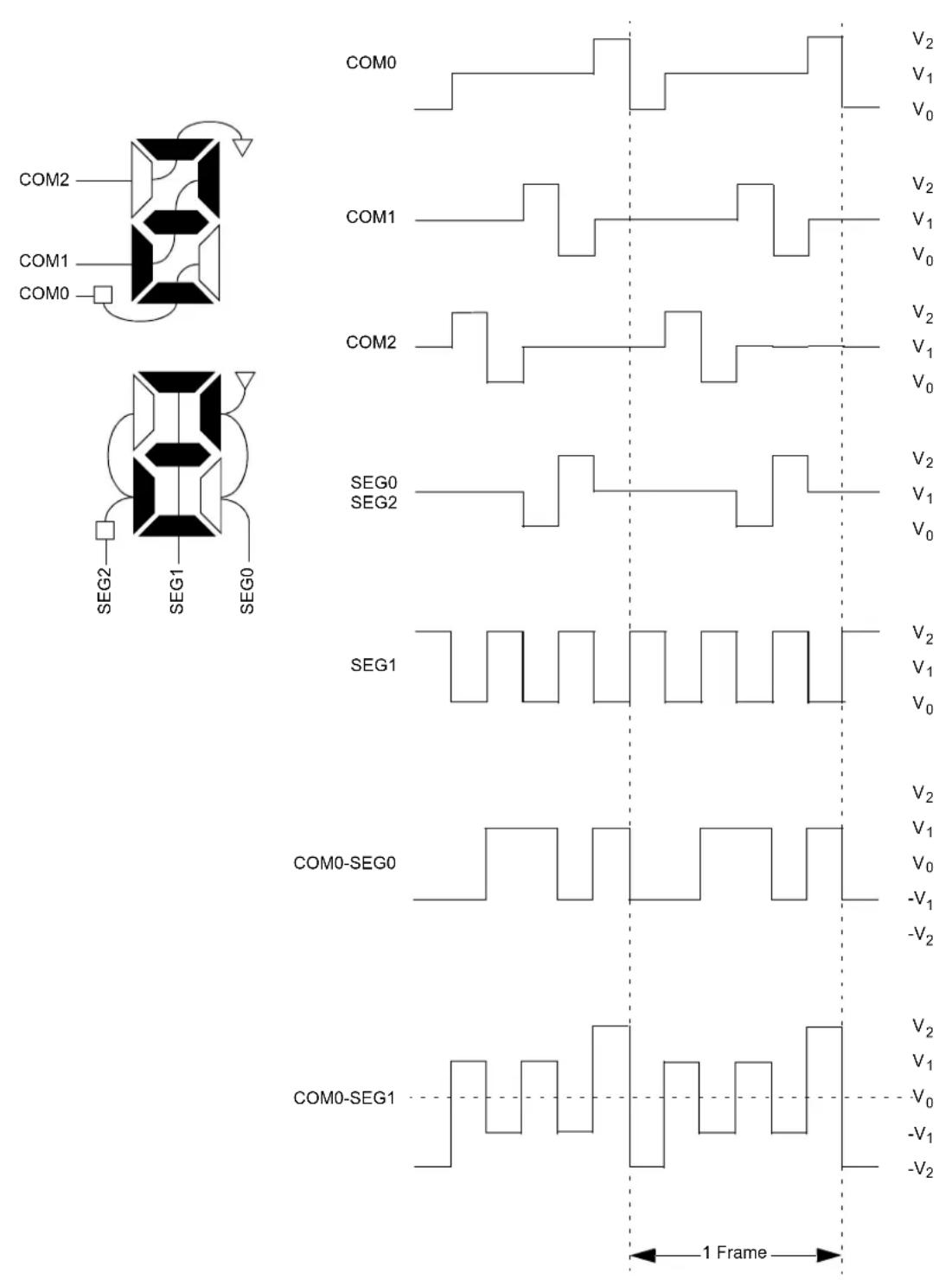
FIGURE 17-12: TYPE-B WAVEFORMS IN 1/3 MUX, 1/2 BIAS DRIVE
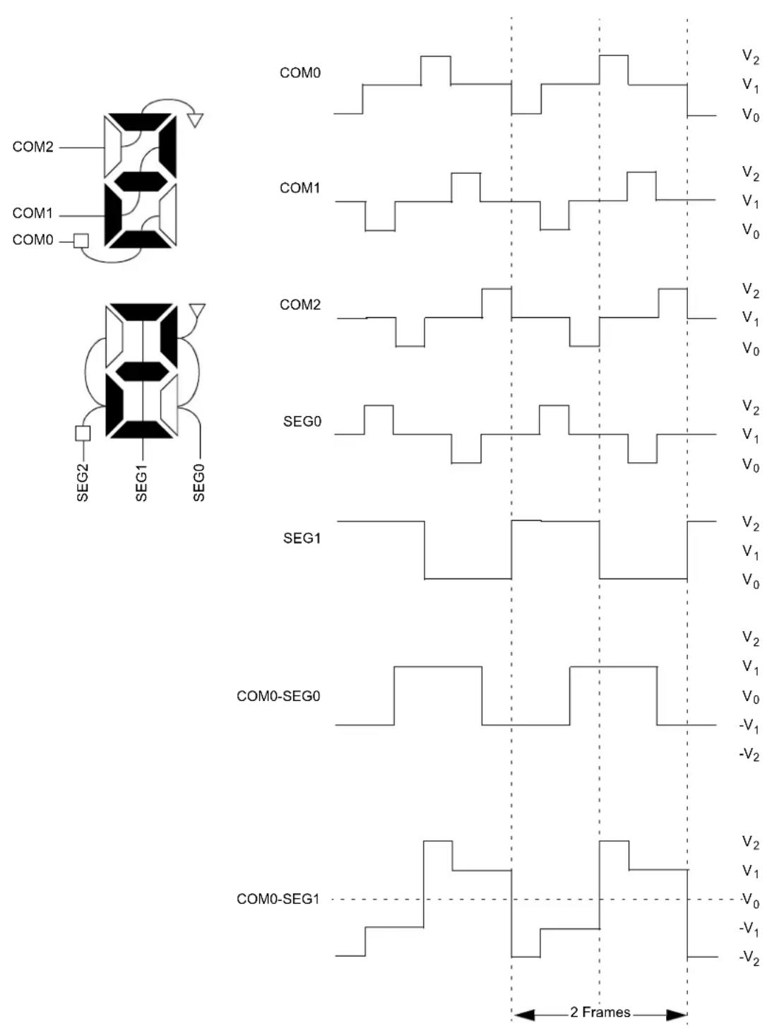
text_image
COM2 COM1 COM0 COM0 V2 V1 V0 COM1 V2 V1 V0 COM2 V2 V1 V0 SEG0 V2 V1 V0 SEG1 V2 V1 V0 COM0-SEG0 V2 V1 V0 -V1 -V2 COM0-SEG1 V2 V1 V0 -V1 -V2 2 FramesFIGURE 17-13: TYPE-A WAVEFORMS IN 1/3 MUX, 1/3 BIAS DRIVE

text_image
COM2 COM1 COM0 SEG2 SEG1 SEG0 COM0 V3 V2 V1 V0 V3 V2 V1 V0 V3 V2 V1 V0 V3 V2 V1 V0 V3 V2 V1 V0 V3 V2 V1 V0 V3 V2 V1 V0 V3 V2 V1 V0 V3 V2 V1 V0 V-1 -V2 -V3 V3 V2 V1 V0 -V1 -V2 -V3 COM0-SEG0 COM0-SEG1 1 FrameFIGURE 17-14: TYPE-B WAVEFORMS IN 1/3 MUX, 1/3 BIAS DRIVE

FIGURE 17-15: TYPE-A WAVEFORMS IN 1/4 MUX, 1/3 BIAS DRIVE
text_image
COM3 COM2 COM1 COM0
flowchart
graph TD
    A["SEG0"] --> B["8-Multiplexer"]
    C["SEG1"] --> B
    B --> D["Output"]

line
| Signal | Value | | ------------ | ----- | | COM0 | V3 | | COM0 | V2 | | COM0 | V1 | | COM0 | V0 | | COM1 | V3 | | COM1 | V2 | | COM1 | V1 | | COM1 | V0 | | COM2 | V3 | | COM2 | V2 | | COM2 | V1 | | COM2 | V0 | | COM3 | V3 | | COM3 | V2 | | COM3 | V1 | | COM3 | V0 | | SEG0 | V3 | | SEG0 | V2 | | SEG0 | V1 | | SEG0 | V0 | | SEG1 | V3 | | SEG1 | V2 | | SEG1 | V1 | | SEG1 | V0 | | COMO-SEG0 | V3 | | COMO-SEG0 | V2 | | COMO-SEG0 | V1 | | COMO-SEG0 | V0 | | COMO-SEG1 | V3 | | COMO-SEG1 | V2 | | COMO-SEG1 | V1 | | COMO-SEG1 | V0 | | | -V1 | | | -V2 | | | -V3 |FIGURE 17-16: TYPE-B WAVEFORMS IN 1/4 MUX, 1/3 BIAS DRIVE

17.9 LCD Interrupts
The LCD timing generation provides an interrupt that defines the LCD frame timing. This interrupt can be used to coordinate the writing of the pixel data with the start of a new frame. Writing pixel data at the frame boundary allows a visually crisp transition of the image. This interrupt can also be used to synchronize external events to the LCD. For example, the interface to an external segment driver can be synchronized for a segment data update to the LCD frame.
A new frame is defined to begin at the leading edge of the COM0 common signal. The interrupt will be set immediately after the LCD controller completes accessing all pixel data required for a frame. This will occur at a fixed interval before the frame boundary (TFINT), as shown in Figure 17-17. The LCD controller will begin to access data for the next frame within the interval from the interrupt to when the controller begins to access data after the interrupt (TFWR). New data must be written within TFWR, as this is when the LCD controller will begin to access the data for the next frame.
When the LCD driver is running with Type-B waveforms, and the LMUX<1:0> bits are not equal to '00', there are some additional issues that must be addressed. Since the DC voltage on the pixel takes two frames to maintain zero volts, the pixel data must not change between subsequent frames. If the pixel data was allowed to change, the waveform for the odd frames would not necessarily be the complement of the waveform generated in the even frames and a DC component would be introduced into the panel. Therefore, when using Type-B waveforms, the user must synchronize the LCD pixel updates to occur within a subframe after the frame interrupt.
To correctly sequence writing while in Type-B, the interrupt will only occur on complete phase intervals. If the user attempts to write when the write is disabled, the WERR (LCDCON<5>) bit is set.
Note: The interrupt is not generated when the Type-A waveform is selected and when the Type-B with no multiplex (static) is selected.
FIGURE 17-17: EXAMPLE WAVEFORMS AND INTERRUPT TIMING IN QUARTER DUTY CYCLE DRIVE
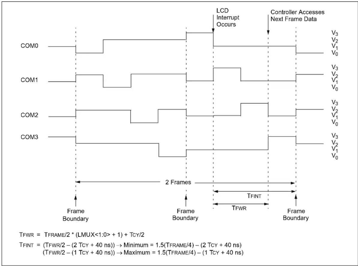
other
| Time Segment | Value | | ------------ | ----- | | Top Left | V3 | | Top Right | V2 | | Top Bottom | V1 | | Bottom Left | V0 | | Bottom Right| V3 | | Bottom Bottom| V2 | | Bottom Top | V1 | | Bottom Bottom| V0 | | Bottom Left | V3 | | Bottom Right| V2 | | Bottom Bottom| V1 | | Bottom Top | V3 | | Bottom Bottom| V2 | | Bottom Top | V1 | | Bottom Bottom| V0 | | Bottom Left | V3 | | Bottom Right| V2 | | Bottom Bottom| V1 | | Bottom Top | V3 | | Bottom Bottom| V2 | | Bottom Left | V3 | | Bottom Right| V1 | | Bottom Bottom| V0 | | Bottom Top | V3 | | Bottom Bottom| V2 | | Bottom Bottom| TFINT| | Bottom Left | TFWR | | Bottom Right| TFINT| | Bottom Bottom| TFWR | | Bottom Top | TFWR | | Bottom Bottom| TFWR |17.10 Operation During Sleep
The LCD module can operate during Sleep. The selection is controlled by the SLPEN bit (LCDCON<6>). Setting the SLPEN bit allows the LCD module to go to Sleep. Clearing the SLPEN bit allows the module to continue to operate during Sleep.
If a SLEEP instruction is executed and SLPEN = 1, the LCD module will cease all functions and go into a very low-current consumption mode. The module will stop operation immediately and drive the minimum LCD voltage on both segment and common lines. Figure 17-18 shows this operation.
To ensure that no DC component is introduced on the panel, the SLEEP instruction should be executed immediately after a LCD frame boundary. The LCD interrupt can be used to determine the frame boundary. See Section 17.9 "LCD Interrupts" for the formulas to calculate the delay.
If a SLEEP instruction is executed and SLPEN = 0, the module will continue to display the current contents of the LCDDATA registers. To allow the module to continue operation while in Sleep, the clock source must be either the Timer1 oscillator or one of the
internal oscillators (either INTRC or INTOSC as the default system clock). While in Sleep, the LCD data cannot be changed. The LCD module current consumption will not decrease in this mode; however, the overall consumption of the device will be lower due to shut down of the core and other peripheral functions.
If the system clock is selected, and the module is not configured for Sleep operation, the module will ignore the SLPEN bit and stop operation immediately. The minimum LCD voltage will then be driven onto the segments and commons
17.10.1 USING THE LCD REGULATOR DURING SLEEP
Applications that use the LCD regulator for bias generation may not achieve the same degree of power reductions in Sleep mode when compared to applications using Mode 3 (resistor ladder) biasing. This is particularly true with Mode 0 operation, where the charge pump is active.
If Modes 0, 1 or 2 are used for bias generation, software contrast control will not be available.
FIGURE 17-18: SLEEP ENTRY/EXIT WHEN SLPEN = 1 OR CS<1:0> = 00

other
| Signal | Wave Start | Wave End | Description | |--------|------------|----------|---------------------------------| | COM0 | 0 | 2 | | | COM1 | 0 | 2 | | | COM2 | 0 | 2 | | | SEG0 | 0 | 2 | | | V3 | 0 | 2 | | | V2 | 0 | 2 | | | V1 | 0 | 2 | | | V0 | 0 | 2 | | | V3 | 0 | 2 | | | V2 | 0 | 2 | | | V1 | 0 | 2 | | | V0 | 0 | 2 | | | V3 | 0 | 2 | | | V2 | 0 | 2 | Wake-up | | V1 | 0 | 2 | Wake-up | | V0 | 0 | 2 | Wake-up |17.11 Configuring the LCD Module
The following is the sequence of steps to configure the LCD module.
- Select the frame clock prescale using bits, LP<3:0> (LCDPS<3:0>).
- Configure the appropriate pins to function as segment drivers using the LCDSEx registers.
- Configure the appropriate pins as inputs using the TRISx registers.
-
Configure the LCD module for the following using the LCDCON register:
-
Multiplex and Bias mode (LMUX<1:0>)
- Timing source (CS<1:0>)
-
Sleep mode (SLPEN)
-
Write initial values to pixel data registers, LCDDATA0 through LCDDATA23.
-
Configure the LCD regulator:
a) If M2 or M3 bias configuration is to be used, turn off the regulator by setting CKSEL<1:0> (LCDREG<1:0>) to '00'. Set or clear the CPEN bit (LCDREG<6>) to select Mode 2 or Mode 3, as appropriate.
b) If M0 or M1 bias generation is to be used:
- Set tBAselevel using the BIAS<2:0> bits (LCDREG<5:3>).
- Set or clear the CPEN bit to enable or disable the charge pump.
- Set or clear the MODE13 bit (LCDREG<2>) to select the Bias mode.
-
Select a regulator clock source using the CKSEL<1:0> bits.
-
Clear LCD Interrupt Flag, LCDIF (PIR3<6>), and if desired, enable the interrupt by setting the LCDIE bit (PIE3<6>).
- Enable the LCD module by setting the LCDEN bit (LCDCON<7>).
TABLE 17-6: REGISTERS ASSOCIATED WITH LCD OPERATION
| Name Bit | 7 Bit 6 Bit 5 | Bit 4 Bit 3 | Bit 2 Bit 1 | Bit 0 | Reset Values on Page | ||||
| INTCON GIE/G | EH PEIE/G | EL | TMR0IE | INT0IE | RBIE | TMR0IF | INT0IF | RBIF | 59 |
| PIR3 | — | LCDIF | RC2IF | TX2IF | CTMUIF | CCP2IF | CCP1IF | RTCCIF | 62 |
| PIE3 | — | LCDIE | RC2IE | TX2IE | CTMUIE | CCP2IE | CCP1IE | RTCCIE | 62 |
| IPR3 | — | LCDIP | RC2IP | TX2IP | CTMUIP | CCP2IP | CCP1IP | RTCCIP | 62 |
| RCON | IPEN | — | 60 | ||||||
| LCDDATA23(1) | S47C3 | S46C3 | S45C3 | S44C3 | S43C3 | S42C3 | S41C3 | S40C3 | 63 |
| LCDDATA22 S | S39C3 (1) | S38C3(1) | S37C3(1) | S36C3(1) | S35C3(1) | S34C3(1) | S33C3(1) | S32C3 | 63 |
| LCDDATA21 | S31C3 | S30C3 | S29C3 | S28C3 | S27C3 | S26C3 | S25C3 | S24C3 | 63 |
| LCDDATA20 | S23C3 | S22C3 | S21C3 | S20C3 | S19C3 | S18C3 | S17C3 | S16C3 | 63 |
| LCDDATA19 | S15C3 | S14C3 | S13C3 | S12C3 | S11C3 | S10C3 | S09C3 | S08C3 | 63 |
| LCDDATA18 | S07C3 | S06C3 | S05C3 | S04C3 | S03C3 | S02C3 | S01C3 | S00C3 | 63 |
| LCDDATA17(1) | S47C2 | S46C2 | S45C2 | S44C2 | S43C2 | S42C2 | S41C2 | S40C2 | 63 |
| LCDDATA16 S | S39C2 (1) | S38C2(1) | S37C2(1) | S36C2(1) | S35C2(1) | S34C2(1) | S33C2(1) | S32C2 | 63 |
| LCDDATA15 | S31C2 | S30C2 | S29C2 | S28C2 | S27C2 | S26C2 | S25C2 | S24C2 | 63 |
| LCDDATA14 | S23C2 | S22C2 | S21C2 | S20C2 | S19C2 | S18C2 | S17C2 | S16C2 | 63 |
| LCDDATA13 | S15C2 | S14C2 | S13C2 | S12C2 | S11C2 | S10C2 | S09C2 | S08C2 | 63 |
| LCDDATA12 | S07C2 | S06C2 | S05C2 | S04C2 | S03C2 | S02C2 | S01C2 | S00C2 | 63 |
| LCDDATA11(1) | S47C1 | S46C1 | S45C1 | S44C1 | S43C1 | S42C1 | S41C1 | S40C1 | 63 |
| LCDDATA10 S | S39C1 (1) | S38C1(1) | S37C1(1) | S36C1(1) | S35C1(1) | S34C1(1) | S33C1(1) | S32C1 | 63 |
| LCDDATA9 | S31C1 | S30C1 | S29C1 | S28C1 | S27C1 | S26C1 | S25C1 | S24C1 | 63 |
| LCDDATA8 | S23C1 | S22C1 | S21C1 | S20C1 | S19C1 | S18C1 | S17C1 | S16C1 | 63 |
| LCDDATA7 | S15C1 | S14C1 | S13C1 | S12C1 | S11C1 | S10C1 | S09C1 | S08C1 | 63 |
| LCDDATA6 | S07C1 | S06C1 | S05C1 | S04C1 | S03C1 | S02C1 | S01C1 | S00C1 | 63 |
| LCDDATA5(1) | S47C0 | S46C0 | S45C0 | S44C0 | S43C0 | S42C0 | S41C0 | S40C0 | 63 |
| LCDDATA4 | S39C0(1) | S38C0(1) | S37C0(1) | S36C0(1) | S35C0(1) | S34C0(1) | S33C0(1) | S32C0 | 61 |
| LCDDATA3 | S31C0 | S30C0 | S29C0 | S28C0 | S27C0 | S26C0 | S25C0 | S24C0 | 61 |
| LCDDATA2 | S23C0 | S22C0 | S21C0 | S20C0 | S19C0 | S18C0 | S17C0 | S16C0 | 61 |
| LCDDATA1 | S15C0 | S14C0 | S13C0 | S12C0 | S11C0 | S10C0 | S09C0 | S08C0 | 61 |
| LCDDATA0 | S07C0 | S06C0 | S05C0 | S04C0 | S03C0 | S02C0 | S01C0 | S00C0 | 61 |
| LCDSE5(1) | SE47 | SE46 | SE45 | SE44 | SE43 | SE42 | SE41 | SE40 | 61 |
| LCDSE4 | SE39(1) | SE38(1) | SE37(1) | SE36(1) | SE35(1) | SE34(1) | SE33(1) | SE32 61 | |
| LCDSE3 | SE31 | SE30 | SE29 | SE28 | SE27 | SE26 | SE25 | SE24 | 61 |
| LCDSE2 | SE23 | SE22 | SE21 | SE20 | SE19 | SE18 | SE17 | SE16 | 61 |
| LCDSE1 | SE15 | SE14 | SE13 | SE12 | SE11 | SE10 | SE09 | SE08 | 61 |
| LCDSE0 | SE07 | SE06 | SE05 | SE04 | SE03 | SE02 | SE01 | SE00 | 61 |
| LCDCON | LCDEN S | LPEN WERR | — | CS1 CS0 LMU X1 LMUXO | 61 | ||||
| LCDPS | WFT | BIASMD | LCDA | WA | LP3 | LP2 | LP1 | LP0 | 61 |
| LCDREG | — | CPEN | BIAS2 | BIAS1 | BIAS0 | MODE13 | CKSEL1 | CKSEL0 | 60 |
Legend: — = unimplemented, read as '0'. Shaded cells are not used for LCD operation.
Note 1: These registers or individual bits are unimplemented on PIC18F6XJ90 devices.
NOTES:
18.0 MASTER SYNCHRONOUS SERIAL PORT (MSSP) MODULE
18.1 Master SSP (MSSP) Module Overview
The Master Synchronous Serial Port (MSSP) module is a serial interface, useful for communicating with other peripheral or microcontroller devices. These peripheral devices may be serial EEPROMs, shift registers, display drivers, A/D Converters, etc. The MSSP module can operate in one of two modes:
- Serial Peripheral Interface (SPI)
- Inter-Integrated Circuit (I ^2 C ^TM )
- Full Master mode
- Slave mode (with general address call)
The I²C interface supports the following modes in hardware:
- Master mode
- Multi-Master mode
- Slave mode
18.2 Control Registers
Each MSSP module has three associated control registers. These include a status register (SSPSTAT) and two control registers (SSPCON1 and SSPCON2). The use of these registers and their individual bits differ significantly depending on whether the MSSP module is operated in SPI or ^C mode.
Additional details are provided under the individual sections.
18.3 SPI Mode
The SPI mode allows 8 bits of data to be synchronously transmitted and received simultaneously. All four modes of SPI are supported. To accomplish communication, typically three pins are used:
- Serial Data Out (SDO) – RC5/SDO/SEG12
- Serial Data In (SDI) – RC4/SDI/SDA/SEG16
- Serial Clock (SCK) – RC3/SCK/SCL/SEG17
Additionally, a fourth pin may be used when in a Slave mode of operation:
- Slave Select (SS) – RF7/AN5/SS/SEG25
Figure 18-1 shows the block diagram of the MSSP module when operating in SPI mode.
FIGURE 18-1: MSSP BLOCK DIAGRAM (SPI MODE)

flowchart
graph TD
    A["Internal Data Bus"] --> B["Read Write"]
    B --> C["SSPBUF reg"]
    C --> D["SSPSR reg"]
    D --> E["Shift Clock"]
    E --> F["SSD1"]
    E --> G["SDO"]
    E --> H["SS"]
    H --> I["SSS"]
    I --> J["Control Enable"]
    J --> K["Edge Select"]
    K --> L["Clock Select"]
    L --> M["SCK"]
    M --> N["Edge Select"]
    N --> O["SMP:CKE 2"]
    O --> P["SSPM<3:0> 4 (TMR2 Output) 2"]
    P --> Q["Prescaler 4, 16, 64 Tosc"]
    Q --> R["Data to TXx/RXx in SSPSR TRIS bit"]
    R --> S["SSPSR reg bit 0"]
    S --> T["Shift Clock"]
    T --> U["SSPBUF reg"]
18.3.1 REGISTERS
Each MSSP module has four registers for SPI mode operation. These are:
• MSSP Control Register 1 (SSPCON1)
• MSSP Status Register (SSPSTAT)
- Serial Receive/Transmit Buffer Register (SSPBUF)
- MSSP Shift Register (SSPSR) – Not directly accessible
SSPCON1 and SSPSTAT are the control and status registers in SPI mode operation. The SSPCON1 register is readable and writable. The lower 6 bits of the SSPSTAT are read-only. The upper two bits of the SSPSTAT are read/write.
SSPSR is the shift register used for shifting data in or out. SSPBUF is the buffer register to which data bytes are written to or read from.
In receive operations, SSPSR and SSPBUF together, create a double-buffered receiver. When SSPSR receives a complete byte, it is transferred to SSPBUF and the SSPIF interrupt is set.
During transmission, the SSPBUF is not double-buffered. A write to SSPBUF will write to both, SSPBUF and SSPSR.
REGISTER 18-1: SSPSTAT: MSSP STATUS REGISTER (SPI MODE)
| R/W-0 R/W-0 R-0 R-0 R-0 R0 R-0 | |||||||
| SMP CKE | (1) | D/ P | S | R | —/ | W | UA |
| bit 7 bit 0 | |||||||
Legend:
| R = Readable bit | W = Writable bit | U = Unimplemented bit, read as '0' |
| -n = Value at POR | '1' = Bit is set | '0' = Bit is cleared x = Bit is unknown |
bit 7 SMP: Sample bit
SPI Master mode:
1 = Input data sampled at the end of data output time
0 = Input data sampled at the middle of data output time
SPI Slave mode:
SMP must be cleared when SPI is used in Slave mode.
bit 6 CKE: SPI Clock Select bit ^(1)
1 = Transmit occurs on transition from active to Idle clock state
0 = Transmit occurs on transition from Idle to active clock state
bit 5 D/A: Data/Address bit
Used in I^2C^TM mode only.
bit 4 P: Stop bit
Used in I²C mode only. This bit is cleared when the MSSP module is disabled; SSPEN is cleared.
bit 3 S: Start bit
Used in I^2C mode only.
bit 2 R/W: Read/Write Information bit
Used in I^2C mode only.
bit 1 UA: Update Address bit
Used in I^2C mode only.
bit 0 BF: Buffer Full Status bit (Receive mode only)
1 = Receive complete; SSPBUF is full
0 = Receive not complete; SSPBUF is empty
Note 1: Polarity of the clock state is set by the CKP bit (SSPCON1<4>).
REGISTER 18-2: SSPCON1: MSSP CONTROL REGISTER 1 (SPI MODE)
| R/W-0 R/W-0 R/W-0 R/W-0 R/W-0 R/W-0 R/W-0 R/W-0 | |||||||
| WCOL SSPOV (1) | SSPEN(2) | CKP SSPM3 (3) | SSPM2(3) | SSPM1(3) | SSPM0(3) | ||
| bit 7 bit 0 | |||||||
Legend:
R = Readable bit W = Writable bit U = Unimplemented bit, read as '0'
-n = Value at POR '1' = Bit is set '0' = Bit is cleared x = Bit is unknown
bit 7 WCOL: Write Collision Detect bit (Transmit mode only)
1 = The SSPBUF register is written while it is still transmitting the previous word (must be cleared in software)
0 = No collision
bit 6 SSPOV: Receive Overflow Indicator bit (1)
SPI Slave mode:
1 = A new byte is received while the SSPBUF register is still holding the previous data. In case of overflow, the data in SSPSR is lost. Overflow can only occur in Slave mode. The user must read the SSPBUF, even if only transmitting data, to avoid setting overflow (must be cleared in software).
0 = No overflow
bit 5 SSPEN: Master Synchronous Serial Port Enable bit (2)
1 = Enables serial port and configures SCK, SDO, SDI and as serial port pins
0 = Disables serial port and configures these pins as I/O port pins
bit 4 CKP: Clock Polarity Select bit
1 = Idle state for clock is a high level
0 = Idle state for clock is a low level
bit 3-0 SSPM<3:0>: Master Synchronous Serial Port Mode Select bits ^(3)
0101 = SPI Slave mode; clock = SCK pin, pin control disabled, can be used as I/O pin
0100 = SPI Slave mode; clock = SCK pin, SS pin control enabled
0011 = SPI Master mode; clock = TMR2 output/2
0010 = SPI Master mode; clock = Fosc/64
0001 = SPI Master mode; clock = Fosc/16
0000 = SPI Master mode; clock = Fosc/4
Note 1: In Master mode, the overflow bit is not set since each new reception (and transmission) is initiated by writing to the SSPBUF register.
2: When enabled, these pins must be properly configured as inputs or outputs.
3: Bit combinations not specifically listed here are either reserved or implemented in I ^2 C ^TM mode only.
18.3.2 OPERATION
When initializing the SPI, several options need to be specified. This is done by programming the appropriate control bits (SSPCON1<5:0> and SSPSTAT<7:6>). These control bits allow the following to be specified:
- Master mode (SCK is the clock output)
- Slave mode (SCK is the clock input)
- Clock Polarity (Idle state of SCK)
- Data Input Sample Phase (middle or end of data output time)
- Clock Edge (output data on rising/falling edge of SCK)
- Clock Rate (Master mode only)
- Slave Select mode (Slave mode only)
Each MSSP consists of a transmit/receive shift register (SSPSR) and a buffer register (SSPBUF). The SSPSR shifts the data in and out of the device, MSb first. The SSPBUF holds the data that was written to the SSPSR until the received data is ready. Once the 8 bits of data have been received, that byte is moved to the SSPBUF register. Then, the Buffer Full detect bit, BF (SSPSTAT<0>), and the interrupt flag bit, SSPIF, are set. This double-buffering of the received data (SSPBUF) allows the next byte to start reception before
reading the data that was just received. Any write to the SSPBUF register during transmission/reception of data will be ignored and the Write Collision detect bit, WCOL (SSPCON1<7>), will be set. User software must clear the WCOL bit so that it can be determined if the following write(s) to the SSPBUF register completed successfully.
When the application software is expecting to receive valid data, the SSPBUF should be read before the next byte of data to transfer is written to the SSPBUF. The Buffer Full bit, BF (SSPSTAT<0>), indicates when SSPBUF has been loaded with the received data (transmission is complete). When the SSPBUF is read, the BF bit is cleared. This data may be irrelevant if the SPI is only a transmitter. Generally, the MSSP interrupt is used to determine when the transmission/reception has completed. The SSPBUF must be read and/or written. If the interrupt method is not going to be used, then software polling can be done to ensure that a write collision does not occur. Example 18-1 shows the loading of the SSPBUF (SSPSR) for data transmission.
The SSPSR is not directly readable or writable and can only be accessed by addressing the SSPBUF register. Additionally, the SSPSTAT register indicates the various status conditions.
EXAMPLE 18-1: LOADING THE SSPBUF (SSPSR) REGISTER
LOOP BTFSS SSPSTAT, BF ;Has data been received (transmit complete)?
BRA LOOP ;No
MOVF SSPBUF, W ;WREG reg = contents of SSPBUF
MOVWF RXDATA ;Save in user RAM, if data is meaningful
MOVF TXDATA, W ;W reg = contents of TXDATA
MOVWF SSPBUF ;New data to xmit
18.3.3 ENABLING SPI I/O
To enable the serial port, the MSSP Enable bit, SSPEN (SSPCON1<5>), must be set. To reset or reconfigure SPI mode, clear the SSPEN bit, reinitialize the SSPCON registers and then set the SSPEN bit. This configures the SDI, SDO, SCK and pins as serial port pins. For the pins to behave as the serial port function, some must have their data direction bits (in the TRIS register) appropriately programmed as follows:
- SDI is automatically controlled by the SPI module
- SDO must have TRISC<5> bit cleared
- SCK (Master mode) must have TRISC<3> bit cleared
- SCK (Slave mode) must have TRISC<3> bit set
- must have TRISF<7> bit set
Any serial port function that is not desired may be overridden by programming the corresponding data direction (TRIS) register to the opposite value.
18.3.4 OPEN-DRAIN OUTPUT OPTION
The drivers for the SDO output and SCK clock pins can be optionally configured as open-drain outputs. This feature allows the voltage level on the pin to be pulled
to a higher level through an external pull-up resistor, and allows the output to communicate with external circuits without the need for additional level shifters.
The open-drain output option is controlled by the SPIOD bit (TRISG<7>). Setting this bit configures both pins for open-drain operation.
18.3.5 TYPICAL CONNECTION
Figure 18-2 shows a typical connection between two microcontrollers. The master controller (Processor 1) initiates the data transfer by sending the SCK signal. Data is shifted out of both shift registers on their programmed clock edge and latched on the opposite edge of the clock. Both processors should be programmed to the same Clock Polarity (CKP), then both controllers would send and receive data at the same time. Whether the data is meaningful (or dummy data) depends on the application software. This leads to three scenarios for data transmission:
- Master sends data – Slave sends dummy data
- Master sends data – Slave sends data
- Master sends dummy data – Slave sends data
FIGURE 18-2: SPI MASTER/SLAVE CONNECTION
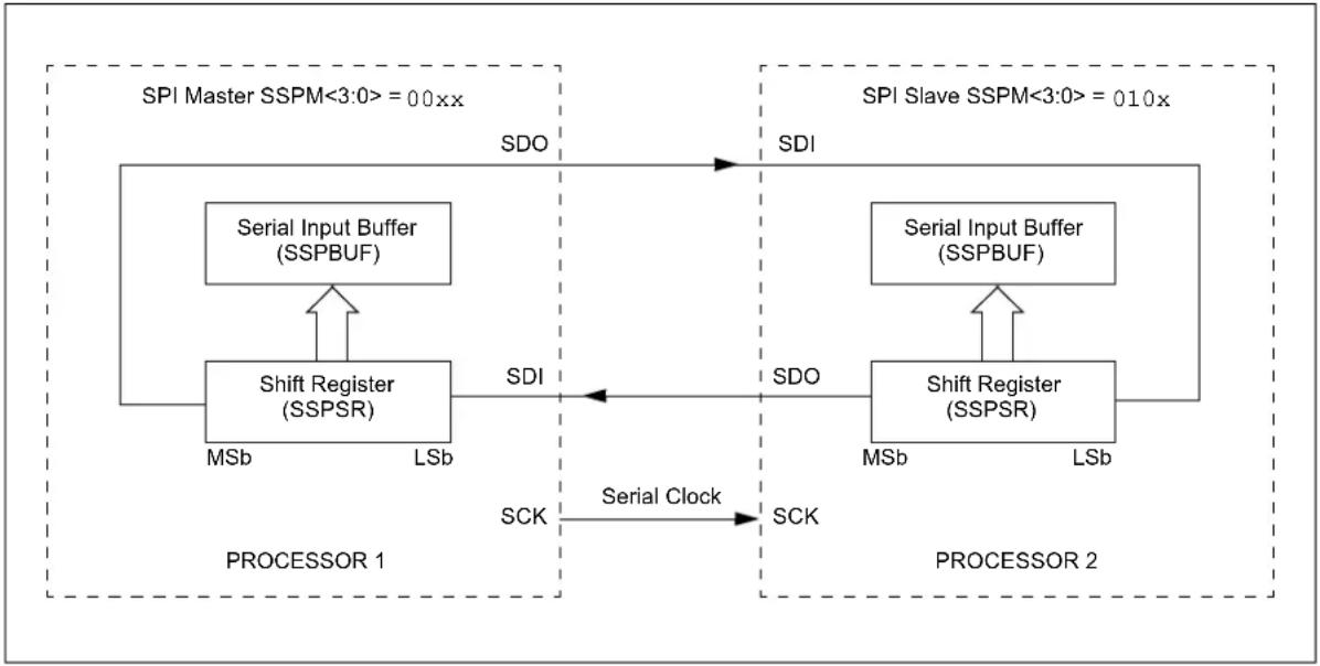
flowchart
graph TD
    subgraph_SPI_Master_SPM["SPI Master SSPM<3:0>=00xx"]
        A["Serial Input Buffer (SSPBUF)"] --> B["Shift Register (SSPSR)"]
        B --> C["MSb"] --> D["LSb"]
        E["MSb"] --> F["MSb"] --> G["LSb"]
    end

    subgraph_SPI_Slave_SPM["SPI Slave SSPM<3:0>=010x"]
        H["Serial Input Buffer (SSPBUF)"] --> I["Shift Register (SSPSR)"]
        I --> J["MSb"] --> K["LSb"]
        L["MSb"] --> M["MSb"] --> N["LSb"]
    end

    B <-->|SDI| I
    I <-->|SDO| H
    B <-->|SCK| I
    I <-->|SCK| N

    style SPI Master_SPM fill:#f9f,stroke:#333
    style SPI Slave_SPM fill:#f9f,stroke:#333
18.3.6 MASTER MODE
The master can initiate the data transfer at any time because it controls the SCK. The master determines when the slave (Processor 2, Figure 18-2) will broadcast data by the software protocol.
In Master mode, the data is transmitted/received as soon as the SSPBUF register is written to. If the SPI is only going to receive, the SDO output could be disabled (programmed as an input). The SSPSR register will continue to shift in the signal present on the SDI pin at the programmed clock rate. As each byte is received, it will be loaded into the SSPBUF register as if it was a normal received byte (interrupts and status bits appropriately set). This could be useful in receiver applications as a "Line Activity Monitor" mode.
The clock polarity is selected by appropriately programming the CKP bit (SSPCON1<4>). This, then, would give waveforms for SPI communication, as shown in Figure 18-3, Figure 18-5 and Figure 18-6, where the MSB is transmitted first. In Master mode, the SPI clock rate (bit rate) is user-programmable to be one of the following:
- Fosc/4 (or Tcy)
- Fosc/16 (or 4 • Tcy)
- Fosc/64 (or 16 • Tcy)
- Timer2 output/2
This allows a maximum data rate (at 40 MHz) of 10.00 Mbps.
Figure 18-3 shows the waveforms for Master mode. When the CKE bit is set, the SDO data is valid before there is a clock edge on SCK. The change of the input sample is shown based on the state of the SMP bit. The time when the SSPBUF is loaded with the received data is shown.
FIGURE 18-3: SPI MODE WAVEFORM (MASTER MODE)
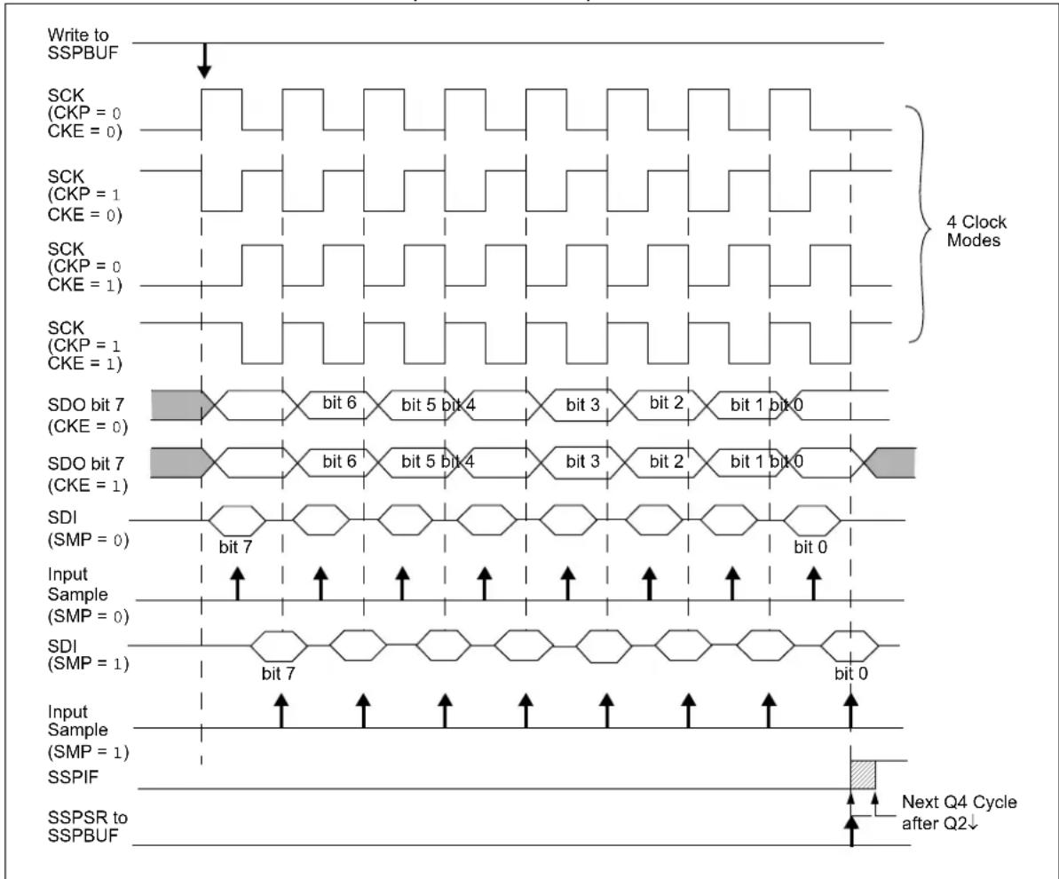
flowchart
graph TD
    A["Write to SSPBUF"] --> B["SCK (CKP = 0, CKE = 0)"]
    B --> C["SCK (CKP = 1, CKE = 0)"]
    C --> D["SCK (CKP = 0, CKE = 1)"]
    D --> E["SCK (CKP = 1, CKE = 1)"]
    E --> F["SDO bit 7 (CKE = 0)"]
    F --> G["SDO bit 7 (CKE = 1)"]
    G --> H["SDI (SMP = 0)"]
    H --> I["Input Sample (SMP = 0)"]
    I --> J["SDI (SMP = 1)"]
    J --> K["Input Sample (SMP = 1)"]
    K --> L["SSPIF"]
    L --> M["SSPSR to SSPBUF"]

    N["4 Clock Modes"] --> O["bit 6 bit 5 bit 4 bit 3 bit 2 bit 1 bit 0"]
    O --> P["bit 7 bit 6 bit 5 bit 4 bit 3 bit 2 bit 1 bit 0"]
    P --> Q["bit 7 bit 6 bit 5 bit 4 bit 3 bit 2 bit 1 bit 0"]
    Q --> R["bit 7 bit 6 bit 5 bit 4 bit 3 bit 2 bit 1 bit 0"]
    R --> S["bit 7 bit 6 bit 5 bit 4 bit 3 bit 2 bit 1 bit 0"]
    S --> T["bit 7 bit 6 bit 5 bit 4 bit 3 bit 2 bit 1 bit 0"]
    T --> U["bit 7 bit 6 bit 5 bit 4 bit 3 bit 2 bit 1 bit 0"]
    U --> V["bit 7 bit 6 bit 5 bit 4 bit 3 bit 2 bit 1 bit 0"]
    V --> W["bit 7 bit 6 bit 5 bit 4 bit 3 bit 2 bit 1 bit 0"]
    W --> X["bit 7 bit 6 bit 5 bit 4 bit 3 bit 2 bit 1 bit 0"]
    X --> Y["bit 7 bit 6 bit 5 bit 4 bit 3 bit 2 bit 1 bit 0"]
    Y --> Z["bit 7 bit 6 bit 5 bit 4 bit 3 bit 2 bit 1 bit 0"]
    Z --> AA["bit 7 bit 6 bit 5 bit 4 bit 3 bit 2 bit 1 bit 0"]
    AA --> AB["Next Q4 Cycle after Q2↓"]
18.3.7 SLAVE MODE
In Slave mode, the data is transmitted and received as the external clock pulses appear on SCK. When the last bit is latched, the SSPIF interrupt flag bit is set.
Before enabling the module in SPI Slave mode, the clock line must match the proper Idle state. The clock line can be observed by reading the SCK pin. The Idle state is determined by the CKP bit (SSPCON1<4>).
While in Slave mode, the external clock is supplied by the external clock source on the SCK pin. This external clock must meet the minimum high and low times as specified in the electrical specifications.
While in Sleep mode, the slave can transmit/receive data. When a byte is received, the device will wake-up from Sleep.
18.3.8 SLAVE SELECT SYNCHRONIZATION
The pin allows a Synchronous Slave mode. The SPI must be in Slave mode with pin control enabled (SSPCON1<3:0> = 04h). When the pin is low, transmission and reception are enabled and the SDO
pin is driven. When the pin goes high, the SDO pin is no longer driven, even if in the middle of a transmitted byte, and becomes a floating output. External pull-up/pull-down resistors may be desirable depending on the application.
Note 1: When the SPI is in Slave mode with the S pin control enabled (SSPCON1<3:0>=0100), the SPI module will reset if the SS pin is set to VDD.
2: If the SPI is used in Slave mode with CKE set, then the pin control must be enabled.
When the SPI module resets, the bit counter is forced to '0'. This can be done by either forcing the pin to a high level or clearing the SSPEN bit.
To emulate two-wire communication, the SDO pin can be connected to the SDI pin. When the SPI needs to operate as a receiver, the SDO pin can be configured as an input. This disables transmissions from the SDO. The SDI can always be left as an input (SDI function) since it cannot create a bus conflict.
flowchart
graph TD
    subgraph SS
        A["Write to SSPBUF"] --> B["SCK (CKP = 0, CKE = 0)"]
        B --> C["SCK (CKP = 1, CKE = 0)"]
    end
    subgraph SDO
        D["Input Sample (SMP = 0)"] --> E["SCK (CKP = 0, CKE = 0)"]
        E --> F["SCK (CKP = 1, CKE = 0)"]
    end
    subgraph SDI
        G["Input Sample (SMP = 0)"] --> H["SCK (CKP = 0, CKE = 0)"]
        H --> I["SCK (CKP = 1, CKE = 0)"]
    end
    subgraph SSPIF
        J["SSPIF Interrupt Flag"] --> K["Next Q4 Cycle after Q2"]
    end
    subgraph SSPSR to SSPBUF
        L["SSPSR to SSPBUF"] --> M["SSPSR to SSPBUF"]
    end
FIGURE 18-5: SPI MODE WAVEFORM (SLAVE MODE WITH CKE = 0)
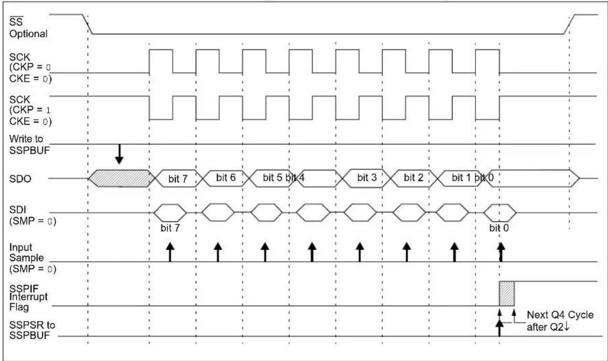
flowchart
graph TD
    A["SS Optional"] --> B["SCK (CKP = 0, CKE = 0)"]
    B --> C["SCK (CKP = 1, CKE = 0)"]
    C --> D["Write to SSPBUF"]
    D --> E["SDO"]
    E --> F["SDI (SMP = 0)"]
    F --> G["Input Sample (SMP = 0)"]
    G --> H["SSPIF Interrupt Flag"]
    H --> I["SSPSR to SSPBUF"]
    I --> J["Next Q4 Cycle after Q2↓"]
FIGURE 18-6: SPI MODE WAVEFORM (SLAVE MODE WITH CKE = 1)

flowchart
graph TD
    A["SS"] --> B["Not Optional"]
    C["SCK (CKP = 0) CKE = 1"] --> D["AND"]
    E["SCK (CKP = 1) CKE = 1"] --> F["NOT"]
    G["Write to SSPBUF"] --> H["↓"]
    I["SDO bit-7"] --> J["AND"]
    K["SDI (SMP = 0)"] --> L["AND"]
    M["Input Sample (SMP = 0)"] --> N["↑"]
    O["SSPIF Interrupt Flag"] --> P["↓"]
    Q["SSPSR to SSPBUF"] --> R["↑"]
    S["Next Q4 Cycle after Q2↓"] --> T["↓"]
    style A fill:#f9f,stroke:#333
    style C fill:#f9f,stroke:#333
    style E fill:#f9f,stroke:#333
    style G fill:#f9f,stroke:#333
    style I fill:#f9f,stroke:#333
    style K fill:#f9f,stroke:#333
    style M fill:#f9f,stroke:#333
    style O fill:#f9f,stroke:#333
    style Q fill:#f9f,stroke:#333
    style S fill:#f9f,stroke:#333
    style T fill:#f9f,stroke:#333
18.3.9 OPERATION IN POWER-MANAGED MODES
In SPI Master mode, module clocks may be operating at a different speed than when in Full-Power mode; in the case of Sleep mode, all clocks are halted.
In Idle modes, a clock is provided to the peripherals. That clock should be from the primary clock source, the secondary clock (Timer1 oscillator at 32.768 kHz) or the INTRC source. See Section 3.3 "Clock Sources and Oscillator Switching" for additional information.
In most cases, the speed that the master clocks SPI data is not important; however, this should be evaluated for each system.
If MSSP interrupts are enabled, they can wake the controller from Sleep mode, or one of the Idle modes, when the master completes sending data. If an exit from Sleep or Idle mode is not desired, MSSP interrupts should be disabled.
If the Sleep mode is selected, all module clocks are halted and the transmission/reception will remain in that state until the device wakes. After the device returns to Run mode, the module will resume transmitting and receiving data.
In SPI Slave mode, the SPI Transmit/Receive Shift register operates asynchronously to the device. This allows the device to be placed in any power-managed
mode and data to be shifted into the SPI Transmit/Receive Shift register. When all 8 bits have been received, the MSSP interrupt flag bit will be set, and if enabled, will wake the device.
18.3.10 EFFECTS OF A RESET
A Reset disables the MSSP module and terminates the current transfer.
18.3.11 BUS MODE COMPATIBILITY
Table 18-1 shows the compatibility between the standard SPI modes and the states of the CKP and CKE control bits.
TABLE 18-1: SPI BUS MODES
| Standard SPI Mode Terminology | Control Bits State | |
| CKP CKE | ||
| 0, 0 0 1 | ||
| 0, 1 0 0 | ||
| 1, 0 1 1 | ||
| 1, 1 1 0 | ||
There is also an SMP bit which controls when the data is sampled.
TABLE 18-2: REGISTERS ASSOCIATED WITH SPI OPERATION
| Name Bit | 7 Bit 6 Bit | 5 Bit 4 Bit 3 | Bit 2 Bit 1 | Bit 0 | Reset Values on page | ||||
| INTCON GIE | /GIEH PEIE | /GIEL | TMR0IE | INT0IE | RBIE | TMR0IF | INT0IF | RBIF | 59 |
| PIR1 | — | ADIF | RC1IF | TX1IF | SSPIF | — | TMR2IF | TMR1IF | 62 |
| PIE1 | — | ADIE | RC1IE | TX1IE | SSPIE | — | TMR2IE | TMR1IE | 62 |
| IPR1 | — | ADIP | RC1IP | TX1IP | SSPIP | — | TMR2IP | TMR1IP | 62 |
| TRISC | TRISC7 | TRISC6 | TRISC5 | TRISC4 | TRISC3 | TRISC2 | TRISC1 | TRISC0 | 62 |
| TRISF | TRISF7 | TRISF6 | TRISF5 | TRISF4 | TRISF3 | TRISF2 | TRISF1 | — | 62 |
| TRISG | SPIOD | CCP2OD | CCP1OD | TRISG4 | TRISG3 | TRISG2 | TRISG1 | TRISG0 | 62 |
| SSPBUF | MSSP Receive Buffer/Transmit Register | 60 | |||||||
| SSPCON1 | WCOL | SSPOV | SSPEN | CKP | SSPM3 | SSPM2 | SSPM1 | SSPM0 | 60 |
| SSPSTAT | SMP | CKE | D/A | P | S | R/W | UA | BF | 60 |
Legend: Shaded cells are not used by the MSSP module in SPI mode.
18.4 I ^2 C Mode
The MSSP module in I ^2 C mode fully implements all master and slave functions (including general call support), and provides interrupts on Start and Stop bits in hardware to determine a free bus (multi-master function). The MSSP module implements the standard mode specifications as well as 7-bit and 10-bit addressing.
Two pins are used for data transfer:
- Serial clock (SCL) – RC3/SCK/SCL
- Serial data (SDA) – RC4/SDI/SDA
The user must configure these pins as inputs by setting the TRISC<4:3> bits.
FIGURE 18-7: MSSP BLOCK DIAGRAM (I²C™ MODE)
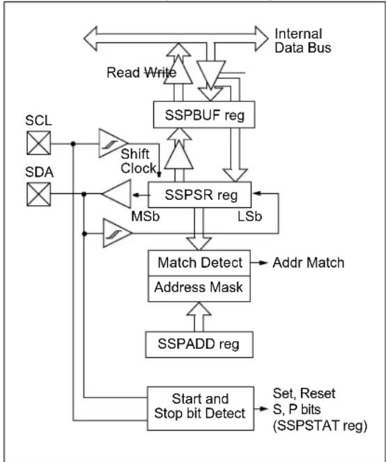
flowchart
graph TD
    A["SCL"] --> B["Shift Clock"]
    C["SDA"] --> D["Shift Clock"]
    B --> E["SSPSR reg"]
    D --> E
    E --> F["Match Detect"]
    F --> G["Address Mask"]
    G --> H["SSPADD reg"]
    H --> I["Start and Stop bit Detect"]
    I --> J["Set, Reset S, P bits (SSPSTAT reg)"]
    K["Internal Data Bus"] --> L["Read Write"]
    L --> M["SSPBUF reg"]
    M --> N["MSb"]
    N --> E
    O["LSb"] --> E
    P["Addr Match"] --> F
18.4.1 REGISTERS
The MSSP module has six registers for I^2C operation. These are:
• MSSP Control Register 1 (SSPCON1)
• MSSP Control Register 2 (SSPCON2)
• MSSP Status Register (SSPSTAT)
- Serial Receive/Transmit Buffer Register (SSPBUF)
- MSSP Shift Register (SSPSR) – Not directly accessible
- MSSP Address Register (SSPADD)
SSPCON1, SSPCON2 and SSPSTAT are the control and status registers in C mode operation. The SSPCON1 and SSPCON2 registers are readable and writable. The lower 6 bits of the SSPSTAT are read-only. The upper two bits of the SSPSTAT are read/write.
Many of the bits in SSPCON2 assume different functions, depending on whether the module is operating in Master or Slave mode. The SSPCON2<5:2> bits also assume different names in Slave mode. The different aspects of SSPCON2 are shown in Register 18-5 (for Master mode) and Register 18-6 (Slave mode).
SSPSR is the shift register used for shifting data in or out. SSPBUF is the buffer register to which data bytes are written to or read from.
The SSPADD register holds the slave device address when the MSSP is configured in I^2C Slave mode. When the MSSP is configured in Master mode, the lower seven bits of SSPADD act as the Baud Rate Generator reload value.
In receive operations, SSPSR and SSPBUF together, create a double-buffered receiver. When SSPSR receives a complete byte, it is transferred to SSPBUF and the SSPIF interrupt is set.
During transmission, the SSPBUF is not double-buffered. A write to SSPBUF will write to both SSPBUF and SSPSR.
REGISTER 18-3: SSPSTAT: MSSP STATUS REGISTER (I ^2 C ^TM MODE)
| R/W-0 R/W-0 R-0 R-0 R-0 R-0 R-0 | |||||||
| SMP CKE | D/A | — | P(1) | S(1) | R/ UA | BF | |
| bit 7 bit 0 | |||||||
Legend:
| R = Readable bit W = Writable bit U = Unimplemented bit, read as '0' | ||
| -n = Value at POR | '1' = Bit is set | '0' = Bit is cleared |
bit 7 SMP: Slew Rate Control bit
In Master or Slave mode:
1 = Slew rate control disabled for Standard Speed mode (100 kHz and 1 MHz)
0 = Slew rate control enabled for High-Speed mode (400 kHz)
bit 6 CKE: SMBus Select bit
In Master or Slave mode:
1 = Enable SMBus specific inputs
0 = Disable SMBus specific inputs
bit 5 D/A: Data/Address bit
In Master mode:
Reserved.
In Slave mode:
1 = Indicates that the last byte received or transmitted was data
0 = Indicates that the last byte received or transmitted was address
bit 4 P: Stop bit (1)
1 = Indicates that a Stop bit has been detected last
0 = Stop bit was not detected last
bit 3 S: Start bit (1)
1 = Indicates that a Start bit has been detected last
0 = Start bit was not detected last
bit 2 R/W: Read/Write Information bit (I²C™ mode only)
In Slave mode:(2)
1 = Read
0 = Write
In Master mode: ^(3)
1 = Transmit is in progress
0 = Transmit is not in progress
bit 1 UA: Update Address bit (10-Bit Slave mode only)
1 = Indicates that the user needs to update the address in the SSPADD register
0 = Address does not need to be updated
bit 0 BF: Buffer Full Status bit
In Transmit mode:
1 = SSPBUF is full
0 = SSPBUF is empty
In Receive mode:
1 = SSPBUF is full (does not include the ACK and Stop bits)
0 = SSPBUF is empty (does not include the ACK and Stop bits)
Note 1: This bit is cleared on Reset and when SSPEN is cleared.
2: This bit holds the R/W bit information following the last address match. This bit is only valid from the address match to the next Start bit, Stop bit or not ACKbit.
3: ORing this bit with SEN, RSEN, PEN, RCEN or ACKEN will indicate if the MSSP is in Active mode.
REGISTER 18-4: SSPCON1: MSSP CONTROL REGISTER 1 (I ^2 C ^TM MODE)
| R/W-0 R/W-0 R/W-0 R/W-0 R/W-0 R/W-0 R/W-0 R/W-0 | |||||||
| WCOL SS | POV SSPEN | (1) | CKP SSPM3 | SSPM2 | SPM1 | SSPM0 | |
| bit 7 bit 0 | |||||||
Legend:
| R = Readable bit W = Writable bit U = Unimplemented bit, read as '0' | |
| -n = Value at POR '1' = Bit is set '0' = Bit is cleared | x = Bit is unknown |
bit 7
WCOL: Write Collision Detect bit
| In Master Transmit mode: |
| 1 = A write to the SSPBUF register was attempted while the I^2C^TM conditions were not valid for a transmission to be started (must be cleared in software) |
| 0 = No collision |
| In Slave Transmit mode: |
| 1 = The SSPBUF register is written while it is still transmitting the previous word (must be cleared in software) |
| 0 = No collision |
| In Receive mode (Master or Slave modes): |
| This is a “don't care” bit. |
bit 6
SSPOV: Receive Overflow Indicator bit
| In Receive mode: |
| 1 = A byte is received while the SSPBUF register is still holding the previous byte (must be cleared in software) |
| 0 = No overflow |
| In Transmit mode: |
| This is a "don't care" bit in Transmit mode. |
bit 5
| SSPEN: Master Synchronous Serial Port Enable bit(1) |
| 1 = Enables the serial port and configures the SDA and SCL pins as the serial port pins |
| 0 = Disables serial port and configures these pins as I/O port pins |
| CKP: SCK Release Control bit |
| In Slave mode: |
| 1 = Release clock |
| 0 = Holds clock low (clock stretch), used to ensure data setup time |
| In Master mode: |
| Unused in this mode. |
bit 3-0
| SSPM<3:0>: Synchronous Serial Port Mode Select bits |
| 1111 = I2C Slave mode, 10-bit address with Start and Stop bit interrupts enabled |
| 1110 = I2C Slave mode, 7-bit address with Start and Stop bit interrupts enabled |
| 1011 = I2C Firmware Controlled Master mode (slave Idle) |
| 1000 = I2C Master mode, clock = Fosc/(4 * (SSPADD + 1)) |
| 0111 = I2C Slave mode, 10-bit address |
| 0110 = I2C Slave mode, 7-bit address |
| Bit combinations not specifically listed here are either reserved or implemented in SPI mode only. |
Note 1: When enabled, the SDA and SCL pins must be configured as inputs.
REGISTER 18-5: SSPCON2: MSSP CONTROL REGISTER 2 (I ^2 C ^TM MASTER MODE)
| R/W-0 R/W-0 R/W-0 R/W-0 R/W-0 R/W-0 R/W-0 R/W-0 | |||||||
| GCEN ACKSTAT ACKD ^ | (1) | ACKEN ^(2) | RCEN ^(2) | PEN ^(2) | RSEN ^(2) | SEN ^(2) | |
| bit 7 bit 0 | |||||||
Legend:
R = Readable bit W = Writable bit U = Unimplemented bit, read as '0'
-n = Value at POR '1' = Bit is set '0' = Bit is cleared x = Bit is unknown
bit 7 GCEN: General Call Enable bit
Unused in Master mode.
bit 6 ACKSTAT: Acknowledge Status bit (Master Transmit mode only)
1 = Acknowledge was not received from slave
0 = Acknowledge was received from slave
bit 5 ACKDT: Acknowledge Data bit (Master Receive mode only) ^(1)
1 = Not Acknowledge
0 = Acknowledge
bit 4 ACKEN: Acknowledge Sequence Enable bit (2)
1 = Initiate Acknowledge sequence on SDA and SCL pins and transmit ACKDT data bit; automatically cleared by hardware
0 = Acknowledge sequence Idle
bit 3 RCEN: Receive Enable bit (Master Receive mode only) ^(2)
1 = Enables Receive mode for I^2C^TM
0 = Receive Idle
bit 2 PEN: Stop Condition Enable bit (2)
1 = Initiate Stop condition on SDA and SCL pins. Automatically cleared by hardware.
0 = Stop condition Idle
bit 1 RSEN: Repeated Start Condition Enable bit (2)
1 = Initiate Repeated Start condition on SDA and SCL pins. Automatically cleared by hardware.
0 = Repeated Start condition Idle
bit 0 SEN: Start Condition Enable bit (2)
1 = Initiate Start condition on SDA and SCL pins; automatically cleared by hardware
0 = Start condition Idle
Note 1: Value that will be transmitted when the user initiates an Acknowledge sequence at the end of a receive.
2: If the I²C module is active, these bits may not be set (no spooling) and the SSPBUF may not be written to (or writes to the SSPBUF are disabled).
REGISTER 18-6: SSPCON2: MSSP CONTROL REGISTER 2 (I ^2 C ^TM SLAVE MODE)
| R/W-0 R/W-0 R/W-0 R/W-0 R/W-0 R/W-0 R/W-0 R/W-0 | |||||||
| GCEN ACKSTAT ADMSK5 ADMSK4 ADMSK3 ADMSK2 ADMSK1 SEN | (1) | ||||||
| bit 7 bit 0 | |||||||
Legend:
| R = Readable bit W = Writable bit U = Unimplemented bit, read as '0' | |
| -n = Value at POR '1' = Bit is set '0' = Bit is cleared | x = Bit is unknown |
| bit 7 | GCEN: General Call Enable bit1 = Enable interrupt when a general call address (0000h) is received in the SSPSR0 = General call address disabled |
| bit 6 | ACKSTAT: Acknowledge Status bit Unused in Slave mode. |
| bit 5-2 | ADMSK<5:2>: Slave Address Mask Select bits1 = Masking of corresponding bits of SSPADD is enabled0 = Masking of corresponding bits of SSPADD is disabled |
| bit 1 | ADMSK1: Slave Address Least Significant bit(s) Mask Select bit In 7-Bit Addressing mode: |
| 1 = Masking of SSPADD<1> only is enabled |
| 0 = Masking of SSPADD<1> only is disabled |
| In 10-Bit Addressing mode: |
| 1 = Masking of SSPADD<1:0> is enabled |
| 0 = Masking of SSPADD<1:0> is disabled |
| bit 0 | SEN: Stretch Enable bit(1) |
| 1 = Clock stretching is enabled for both slave transmit and slave receive (stretch enabled) |
| 0 = Clock stretching is disabled |
Note 1: If the I ^2 C ^TM module is active, this bit may not be set (no spooling) and the SSPBUF may not be written (or writes to the SSPBUF are disabled).
18.4.2 OPERATION
The MSSP module functions are enabled by setting the MSSP Enable bit, SSPEN (SSPCON1<5>).
The SSPCON1 register allows control of the I²C operation. Four mode selection bits (SSPCON1<3:0>) allow one of the following I²C modes to be selected:
- I²C Master mode, clock = (Fosc/4) x (SSPADD + 1)
- I²C Slave mode (7-bit address)
- I²C Slave mode (10-bit address)
- I²C Slave mode (7-bit address) with Start and Stop bit interrupts enabled
- I²C Slave mode (10-bit address) with Start and Stop bit interrupts enabled
- I²C Firmware Controlled Master mode, slave is Idle
Selection of any I ^2 C mode, with the SSPEN bit set, forces the SCL and SDA pins to be open-drain, provided these pins are programmed to inputs by setting the appropriate TRISC or TRISD bits. To ensure proper operation of the module, pull-up resistors must be provided externally to the SCL and SDA pins.
18.4.3 SLAVE MODE
In Slave mode, the SCL and SDA pins must be configured as inputs (TRISC<4:3> set). The MSSP module will override the input state with the output data when required (slave-transmitter).
The I ^2 C Slave mode hardware will always generate an interrupt on an exact address match. In addition, address masking will also allow the hardware to generate an interrupt for more than one address (up to 31 in 7-bit addressing and up to 63 in 10-bit addressing). Through the mode select bits, the user can also choose to interrupt on Start and Stop bits.
When an address is matched, or the data transfer after an address match is received, the hardware automatically will generate the Acknowledge (ACK) pulse and load the SSPBUF register with the received value currently in the SSPSR register.
Any combination of the following conditions will cause the MSSP module not to give this ACK pulse:
- The Buffer Full bit, BF (SSPSTAT<0>), was set before the transfer was received.
- The overflow bit, SSPOV (SSPCON1<6>), was set before the transfer was received.
In this case, the SSPSR register value is not loaded into the SSPBUF, but bit, SSPIF, is set. The BF bit is cleared by reading the SSPBUF register, while bit, SSPOV, is cleared through software. The SCL clock input must have a minimum high and low for proper operation. The high and low times of the I²C specification, as well as the requirement of the MSSP module, are shown in timing parameter 100 and parameter 101.
18.4.3.1 Addressing
Once the MSSP module has been enabled, it waits for a Start condition to occur. Following the Start condition, the 8 bits are shifted into the SSPSR register. All incoming bits are sampled with the rising edge of the clock (SCL) line. The value of register, SSPSR<7:1>, is compared to the value of the SSPADD register. The address is compared on the falling edge of the eighth clock (SCL) pulse. If the addresses match, and the BF and SSPOV bits are clear, the following events occur:
- The SSPSR register value is loaded into the SSPBUF register.
- The Buffer Full bit, BF, is set.
- An ACK pulse is generated.
- The MSSP Interrupt Flag bit, SSPIF, is set (and an interrupt is generated, if enabled) on the falling edge of the ninth SCL pulse.
In 10-Bit Addressing mode, two address bytes need to be received by the slave. The five Most Significant bits (MSbs) of the first address byte specify if this is a 10-bit address. The R/W (SSPSTAT<2>) bit must specify a write so the slave device will receive the second address byte. For a 10-bit address, the first byte would equal '11110 A9 A8 0', where 'A9' and 'A8' are the two MSbs of the address. The sequence of events for 10-bit addressing is as follows, with steps 7 through 9 for the slave-transmitter:
- Receive first (high) byte of address (bits, SSPIF, BF and UA (SSPSTAT<1>), are set).
- Update the SSPADD register with second (low) byte of address (clears bit, UA, and releases the SCL line).
- Read the SSPBUF register (clears bit, BF) and clear flag bit, SSPIF.
- Receive second (low) byte of address (SSPIF, BF and UA bits are set).
- Update the SSPADD register with the first (high) byte of address. If match releases SCL line, this will clear the UA bit.
- Read the SSPBUF register (clears bit, BF) and clear flag bit, SSPIF.
- Receive Repeated Start condition.
- Receive first (high) byte of address (SSPIF and BF bits are set).
- Read the SSPBUF register (clears BF bit) and clear flag bit, SSPIF.
18.4.3.2 Address Masking
Masking an address bit causes that bit to become a "don't care". When one address bit is masked, two addresses will be Acknowledged and cause an interrupt. It is possible to mask more than one address bit at a time, which makes it possible to Acknowledge up to 31 addresses in 7-bit mode and up to 63 addresses in 10-bit mode (see Example 18-2).
The I ^2 C slave behaves the same way, whether address masking is used or not. However, when address masking is used, the I ^2 C slave can Acknowledge multiple addresses and cause interrupts. When this occurs, it is necessary to determine which address caused the interrupt by checking SSPBUF.
In 7-Bit Addressing mode, address mask bits, ADMSK<5:1> (SSPCON<5:1>), mask the corresponding address bits in the SSPADD register. For any ADMSK bits that are set (ADMSK
In 10-Bit Addressing mode, the ADMSK<5:2> bits mask the corresponding address bits in the SSPADD register. In addition, ADMSK1 simultaneously masks the two LSbs of the address (SSPADD<1:0>). For any ADMSK bits that are active (ADMSK
Note 1: ADMSK1 masks the two Least Significant bits of the address.
2: The two Most Significant bits of the address are not affected by address masking.
EXAMPLE 18-2: ADDRESS MASKING EXAMPLES
7-Bit Addressing:
SSPADD<7:1> = A0h (1010000) (SSPADD<0> is assumed to be '0')
ADMSK<5:1> = 00111
Addresses Acknowledged: A0h, A2h, A4h, A6h, A8h, AAh, ACh, AEh
10-Bit Addressing:
SSPADD<7:0> = A0h (10100000) (the two MSbs of the address are ignored in this example, since they are not affected by masking)
ADMSK<5:1> = 00111
Addresses Acknowledged: A0h, A1h, A2h, A3h, A4h, A5h, A6h, A7h, A8h, A9h, AAh, ABh, ACh, ADh, AEh, AFh
18.4.3.3 Reception
When the R/W bit of the address byte is clear and an address match occurs, the R/W bit of the SSPSTAT register is cleared. The received address is loaded into the SSPBUF register and the SDA line is held low (ACK).
When the address byte overflow condition exists, then the no Acknowledge (ACK) pulse is given. An overflow condition is defined as either bit, BF (SSPSTAT<0>), is set or bit, SSPOV (SSPCON1<6>), is set.
An MSSP interrupt is generated for each data transfer byte. The interrupt flag bit, SSPIF, must be cleared in software. The SSPSTAT register is used to determine the status of the byte.
If SEN is enabled (SSPCON2<0> = 1), SCK/SCL will be held low (clock stretch) following each data transfer. The clock must be released by setting bit, CKP (SSPCON1<4>). See Section 18.4.4 "Clock Stretching" for more details.
18.4.3.4 Transmission
When the R/W bit of the incoming address byte is set and an address match occurs, the R/W bit of the SSPSTAT register is set. The received address is loaded into the SSPBUF register. The ACK pulse will be sent on the ninth bit and pin, RC3, is held low, regardless of SEN (see Section 18.4.4 "Clock Stretching" for more details). By stretching the clock, the master will be unable to assert another clock pulse until the slave is done preparing the transmit data. The transmit data must be loaded into the SSPBUF register which also loads the SSPSR register. Then, pin, RC3, should be enabled by setting bit, CKP (SSPCON1<4>). The eight data bits are shifted out on the falling edge of the SCL input. This ensures that the SDA signal is valid during the SCL high time (Figure 18-10).
The ACK pulse from the master-receiver is latched on the rising edge of the ninth SCL input pulse. If the SDA line is high (not ACK), then the data transfer is complete. In this case, when the ACK is latched by the slave, the slave logic is reset and the slave monitors for another occurrence of the Start bit. If the SDA line was low (ACK), the next transmit data must be loaded into the SSPBUF register. Again, pin, RC3, must be enabled by setting bit, CKP.
An MSSP interrupt is generated for each data transfer byte. The SSPIF bit must be cleared in software and the SSPSTAT register is used to determine the status of the byte. The SSPIF bit is set on the falling edge of the ninth clock pulse.
FIGURE 18-8: I ^2C^TM SLAVE MODE TIMING WITH SEN = 0 (RECEPTION, 7-BIT ADDRESSING)

text_image
Receiving Address R/W = 0 Receiving Data ACK Receiving Data D2 ACK SDA A7 A6 A5 A4 A3 A2 A1 D7 D6 D5 D4 D3 D2 D1 D0 D7 ACKD5 D4 D3 D1 D0 SCL S 1 2 3 4 5 6 7 8 9 1 2 3 4 5 6 7 8 9 1 2 3 4 5 6 7 8 9 SSPIF (PIR1<3>) Bus master terminates transfer BF (SSPSTAT<0>) Cleared in software SSPBUF is read SSPOV (SSPCON1<6>) SSPOV is set because SSPBUF is still full. ACK is not sent.CKP
(CKP does not reset to '0' when SEN = 0)
FIGURE 18-9: I ^2 C ^TM SLAVE MODE TIMING WITH SEN = 0 AND ADMSK<5:1> = 01011 (RECEPTION, 7-BIT ADDRESSING)
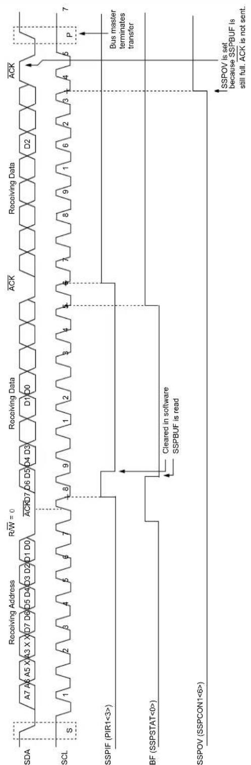
text_image
Receiving Address R/W = 0 Receiving Data ACK Receiving Data ACK SDA A7 A6 A5 X A3 X X D7 D6 D5 D4 D3 D2 D1 D0 ACKD7 D6 D5 D4 D3 D1 D0 SCL S 1 2 3 4 5 6 7 8 9 1 2 3 4 5 6 7 8 9 1 6 2 3 4 5 P 7 SSPIF (PIR1<3>) Bus master terminates transfer BF (SSPSTAT<0>) Cleared in software SSPBUF is read SSPOV (SSPCON1<6>) SSPOV is set because SSPBUF is still full. ACK is not sent.CKP (CKP does not reset to '0' when SEN = 0)
Note 1: x = Don't care (i.e., address bit can be either a '1' or a '0').
2: In this example, an address equal to A7.A6.A5.X.A3.X.X will be Acknowledged and cause an interrupt.
FIGURE 18-10: I ^2C^TM SLAVE MODE TIMING (TRANSMISSION, 7-BIT ADDRESSING)

flowchart
graph TD
    A["Receiving Address"] --> B["Data in sampled"]
    C["SCLx"] --> D["Data held low while CPU responds to SSPxIF"]
    E["Transmitting Data"] --> F["SCLx held low while CPU responds to SSPxIF"]
    G["CKP"] --> H["Clear by reading"]
    I["CP"] --> J["Cleared in software"]
    K["CP"] --> L["Cleared in software"]
    M["CP"] --> N["Cleared in software"]
    O["CP"] --> P["Cleared in software"]
    Q["CP"] --> R["Cleared in software"]
    S["CP"] --> T["Cleared in software"]
    U["CP"] --> V["Cleared in software"]
    W["CP"] --> X["Cleared in software"]
    Y["CP"] --> Z["Cleared in software"]
    AA["CP"] --> AB["Cleared in software"]
    AC["CP"] --> AD["Cleared in software"]
    AE["CP"] --> AF["Cleared in software"]
    AG["CP"] --> AH["Cleared in software"]
    AI["CP"] --> AJ["Cleared in software"]
    AK["CP"] --> AL["Cleared in software"]
    AM["CP"] --> AN["Cleared in software"]
    AO["CP"] --> AP["Cleared in software"]
    AQ["CP"] --> AR["Cleared in software"]
    AS["CP"] --> AT["Cleared in software"]
    AU["CP"] --> AV["Cleared in software"]
    AW["CP"] --> AX["Cleared in software"]
    AY["SDAx"] --> AZ["A7 D7 A6 A5 A4 A3 A2 A1 ACK"]
    BA["SCLx"] --> BB["S"]
    BC["SSPxIF (PIR1<3> or PIR3<7>"] --> BD
    BE["BF (SSPxSTAT<0>"] --> BF
    BG["CKP (SSPxCON1<4>"] --> BH
    BI["CKP is set in software"] --> BJ
    BK["CAP is set in software"] --> BL
    BM["CAP is set in software"] --> BN
    BO["CAP is set in software"] --> BP
    BQ["CAP is set in software"] --> BR
    BS["CAP is set in software"] --> BT
    BU["CAP is set in software"] --> BV
    BW["CAP is set in software"] --> BX
    BY["CAP is set in software"] --> BYX
    CA["CAP is set in software"] --> CAX
    CB["CAP is set in software"] --> CBX
    CC["CAP is set in software"] --> CCX
    DD["CAP is set in software"] --> DDY
    DB["CAP is set in software"] --> DBX
    DC["CAP is set in software"] --> DCY
    DX["CAP is set in software"] --> DXY
    DBX["CAP is set in software"] --> DBY
    DBY["CAP is set in software"] --> DBZ
    DBX["CAP is set in software"] --> DBYX
    DBY["X"] --> DBZ["X"]
    DBZ["X"] --> DBYX["X"]
FIGURE 18-11: I ^2C^TM SLAVE MODE TIMING WITH SEN = 0 (RECEPTION, 10-BIT ADDRESSING)

flowchart
graph TD
    A["Receive First Byte of Address"] --> B["Receive Second Byte of Address"]
    B --> C["Receive Data Byte"]
    C --> D["Receive Data Byte"]
    D --> E["ACK"]

    subgraph SDA
        F["1 1 0 1 0"] --> G["8 7 6 5 4 3"]
    end

    subgraph SCL
        H["S 1 2 3 4 5 6 7 8"] --> I["9 1 2 3 4 5 6 7 8"]
    end

    subgraph SSPIF (PIR1<3>) --> J["Cleared in software"]
    K["BU master terminates transfer"] --> L["Cleared in software"]
    M["BF (SSPSTAT<0>)"] --> N["SSPUF is written with contents of SSPSR"]
    O["SSPOV (SSPCON1<6>)"] --> P["Dummy read of SSPBUF to clear BF flag"]
    Q["UA (SSPSTAT<1>)"] --> R["UA is set indicating that the SSPADD needs to be updated"]
    S["Clock is held low until update of SSPADD has taken place"] --> T["Clock is held low until update of SSPADD has taken place"]
    U["BU master terminates transfer"] --> V["BU master terminates transfer"]
    W["Cleared by hardware when SSPADD is updated with low byte of address"] --> X["UA is set indicating that SSPADD needs to be updated"]
    Y["Cleared by hardware when SSPADD is updated with high byte of address"] --> Z["Cleared by hardware when SSPADD is updated with high byte of address"]
FIGURE 18-12: I ^2C^TM SLAVE MODE TIMING WITH SEN = 0 AND ADMSK<5:1> = 01001 (RECEPTION, 10-BIT ADDRESSING)
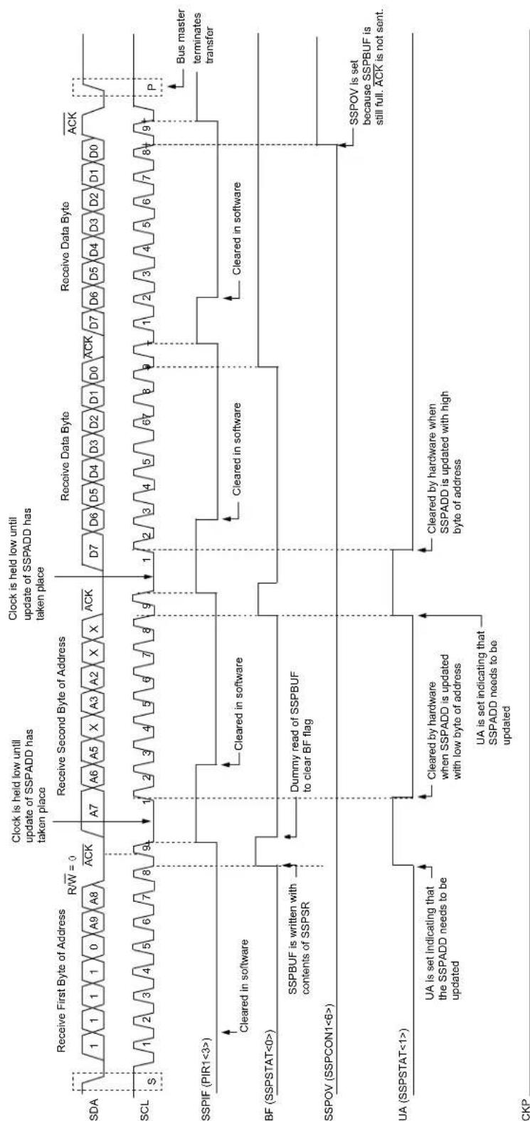
flowchart
graph TD
    A["SDA"] --> B["Receive First Byte of Address"]
    B --> C["R/W = 0"]
    C --> D["A7"]
    D --> E["Receive Second Byte of Address"]
    E --> F["D7"]
    F --> G["Receive Data Byte"]
    G --> H["D6"]
    H --> I["Receive Data Byte"]
    I --> J["D5"]
    J --> K["Receive Data Byte"]
    K --> L["D4"]
    L --> M["Receive Data Byte"]
    M --> N["D3"]
    N --> O["Receive Data Byte"]
    O --> P["D2"]
    P --> Q["Receive Data Byte"]
    Q --> R["D1"]
    R --> S["Receive Data Byte"]
    S --> T["D0"]
    T --> U["ACK"]
    U --> V["D7"]
    V --> W["D6"]
    W --> X["D5"]
    X --> Y["D4"]
    Y --> Z["D3"]
    Z --> AA["D2"]
    AA --> AB["D1"]
    AB --> AC["D0"]
    AC --> AD["P"]

    subgraph SDA
        B
        C
        D
        E
        F
        G
        H
        I
        J
        K
        L
        M
        N
        O
        P
        Q
        R
        S
        T
        U
        V
        W
        X
        Y
        Z
        AA
        AB
        AC
        AD
    end

    subgraph SCL
        S
        T
        U
        V
        W
        X
        Y
        Z
        AA
        AB
        AC
        AD
    end

    subgraph SSPIF (PIR1<3>)
        B
        C
        D
        E
        F
        G
        H
        I
        J
        K
        L
        M
        N
        O
        P
        Q
        R
        S
        T
        U
        V
        W
        X
        Y
        Z
        AA
        AB
        AC
    end

    subgraph BF (SSPSTAT<0>)
        B
        C
        D
        E
        F
        G
        H
        I
        J
        K
        L
        M
        N
        O --> P

    subgraph SSPOV (SSPCON1<6>)
        B
        C
        D
        E
        F
        G
        H
        I
        J
        K
        L
        M

    subgraph UA (SSPSTAT<1>)
        B
        C
        D
        E
        F
        G
        H
        I
        J
        K

    subgraph UA is set indicating that the SSPADD needs to be updated

    end

    subgraph UA is set indicating that the SSPADD needs to be updated

    end

    subgraph UA is set indicating that the SSPADD needs to be updated with low byte of address

    end

    subgraph UA is set indicating that SSPADD needs to be updated with high byte of address

    end

    subgraph UA is set indicating that SSPADD needs to be updated with low byte of address

    end

    subgraph UA is set indicating that SSPADD needs to be updated with high byte of address

    end

    subgraph UA is set indicating that SSPADD needs to be updated with low byte of address

    end

    subgraph UA is set indicating that SSPADD needs to be updated with high byte of address

    end

    subgraph UA is set indicating that SSPADD needs to be updated with high byte of address

    end

    subgraph UA is set indicating that SSPADD needs to be updated with high byte of address

    end

    subgraph UA is set indicating that SSPADD needs to be updated with high byte of address

    end

    subgraph UA is set indicating that SSPADD needs to be updated with high byte of address

    end
(CKP does not reset to '0' when SEN = 0)
Note 1: x = Don't care (i.e., address bit can be either a '1' or a '0').
2: In this example, an address equal to A9.A8.A7.A6.A5.X.A3.A2.X.X will be Acknowledged and cause an interrupt.
3: Note that the Most Significant bits of the address are not affected by the bit masking.
FIGURE 18-13: I ^2 C ^TM SLAVE MODE TIMING (TRANSMISSION, 10-BIT ADDRESSING)

flowchart
graph TD
    A["SDA"] --> B["Receive First Byte of Address"]
    B --> C{R/W = 0}
    C -->|Clock is held low until update of SSPADD has taken place| D["Receive Second Byte of Address"]
    D --> E{R/W = 1}
    E -->|Clock is held low until update of SSPADD has taken place| F["Receive First Byte of Address"]
    F --> G{R/W = 2}
    G -->|Clock is held low until CKP is set to '1'| H["Transmitting Data Byte"]
    H --> I["ACK"]
    J["SCL"] --> K["Receive First Byte of Address"]
    K --> L{R/W = 3}
    L -->|Clock is held low until update of SSPADD has taken place| M["Receive Second Byte of Address"]
    M --> N{R/W = 4}
    N -->|Clock is held low until update of SSPADD has taken place| O["Receive First Byte of Address"]
    O --> P{R/W = 5}
    P -->|Clock is held low until update of SSPADD has taken place| Q["Receive Second Byte of Address"]
    Q --> R{R/W = 6}
    R -->|Clock is held low until update of SSPADD has taken place| S["Receive First Byte of Address"]
    S --> T{R/W = 7}
    T -->|Clock is held low until update of SSPADD has taken place| U["Receive Second Byte of Address"]
    U --> V{R/W = 8}
    V -->|Clock is held low until update of SSPADD has taken place| W["Receive First Byte of Address"]
    W --> X{R/W = 9}
    X -->|Clock is held low until update of SSPADD has taken place| Y["Receive Second Byte of Address"]
    Y --> Z{R/W = 10}
    Z -->|Clock is held low until CKP is set to '1'| AA["ACK"]
    AB["SSPIF (PIR1<3>)"] --> AC["Cleared in software"]
    AC --> AD["BU master terminates transfer"]
    AE["BF (SSPSTAT<0>)"] --> AF["CCP (SSPCON1<4>)"]
    AG["UA (SSPSTAT<1>)"] --> AH["CCP is set in software"]
    AH --> AI["BU master terminates transfer"]
    AJ["CKP (SSPCON1<4>)"] --> AK["CCP is set in software"]
    AL["BU master terminates transfer"] --> AM["BU master terminates transfer"]
    AN["BU master terminates transfer"] --> AO["BU master terminates transfer"]
    AP["BU master terminates transfer"] --> AQ["BU master terminates transfer"]
    AR["BU master terminates transfer"] --> AS["BU master terminates transfer"]
    AT["BU master terminates transfer"] --> AU["BU master terminates transfer"]
    AV["BU master terminates transfer"] --> AW["BU master terminates transfer"]
    AX["BU master terminates transfer"] --> AY["BU master terminates transfer"]
    AZ["BU master terminates transfer"] --> BA["BU master terminates transfer"]
    BB["BU master terminates transfer"] --> BC["BU master terminates transfer"]
    BD["BU master terminates transfer"] --> BE["BU master terminates transfer"]
    BF["BU master terminates transfer"] --> BG["BU master terminates transfer"]
    BH["BU master terminates transfer"] --> BI["BU master terminates transfer"]
    BJ["BU master terminates transfer"] --> BK["BU master terminates transfer"]
    BL["BU master terminates transfer"] --> BM["BU master terminals"]
    BN["BU master terminals"] --> BO["BU master terminals"]
    BP["BU master terminals"] --> BQ["BU master terminals"]
    BR["BU master terminals"] --> BS["BU master terminals"]
    BT["BU master terminals"] --> BU["BU master terminals"]
    BV["BU master terminals"] --> BW["BU master terminals"]
    BX["BU master terminals"] --> BYB["BU master terminals"]
    BZ["BU master terminals"] --> CA["BU master terminals"]
    CB["BU master terminals"] --> CC["BU master terminals"]
    CD["BU master terminals"] --> CE["BU master terminals"]
    CF["BU master terminals"] --> CG["BU master terminals"]
    DH["BU master terminals"] --> DI["BU master terminals"]
    DJ["BU master terminals"] --> DJB["BU master terminals"]
    DK["BU master terminals"] --> DL["BU master terminals"]
18.4.4 CLOCK STRETCHING
Both 7-Bit and 10-Bit Slave modes implement automatic clock stretching during a transmit sequence.
The SEN bit (SSPCON2<0>) allows clock stretching to be enabled during receives. Setting SEN will cause the SCL pin to be held low at the end of each data receive sequence.
18.4.4.1 Clock Stretching for 7-Bit Slave Receive Mode (SEN = 1)
In 7-Bit Slave Receive mode, on the falling edge of the ninth clock at the end of the ACK sequence, if the BF bit is set, the CKP bit in the SSPCON1 register is automatically cleared, forcing the SCL output to be held low. The CKP being cleared to '0' will assert the SCL line low. The CKP bit must be set in the user's ISR before reception is allowed to continue. By holding the SCL line low, the user has time to service the ISR and read the contents of the SSPBUF before the master device can initiate another receive sequence. This will prevent buffer overruns from occurring (see Figure 18-15).
Note 1: If the user reads the contents of the SSPBUF before the falling edge of the ninth clock, thus clearing the BF bit, the CKP bit will not be cleared and clock stretching will not occur.
2: The CKP bit can be set in software regardless of the state of the BF bit. The user should be careful to clear the BF bit in the ISR before the next receive sequence in order to prevent an overflow condition.
18.4.4.2 Clock Stretching for 10-Bit Slave Receive Mode (SEN = 1)
In 10-Bit Slave Receive mode, during the address sequence, clock stretching automatically takes place but CKP is not cleared. During this time, if the UA bit is set after the ninth clock, clock stretching is initiated. The UA bit is set after receiving the upper byte of the 10-bit address, and following the receive of the second byte of the 10-bit address, with the R/W bit cleared to '0'. The release of the clock line occurs upon updating SSPADD. Clock stretching will occur on each data receive sequence as described in 7-bit mode.
Note: If the user polls the UA bit and clears it by updating the SSPADD register before the falling edge of the ninth clock occurs, and if the user hasn't cleared the BF bit by reading the SSPBUF register before that time, then the CKP bit will still NOT be asserted low. Clock stretching on the basis of the state of the BF bit only occurs during a data sequence, not an address sequence.
18.4.4.3 Clock Stretching for 7-Bit Slave Transmit Mode
The 7-Bit Slave Transmit mode implements clock stretching by clearing the CKP bit after the falling edge of the ninth clock if the BF bit is clear. This occurs regardless of the state of the SEN bit.
The user's ISR must set the CKP bit before transmission is allowed to continue. By holding the SCL line low, the user has time to service the ISR and load the contents of the SSPBUF before the master device can initiate another transmit sequence (see Figure 18-10).
Note 1: If the user loads the contents of SSPBUF, setting the BF bit before the falling edge of the ninth clock, the CKP bit will not be cleared and clock stretching will not occur.
2: The CKP bit can be set in software regardless of the state of the BF bit.
18.4.4.4 Clock Stretching for 10-Bit Slave Transmit Mode
In 10-Bit Slave Transmit mode, clock stretching is controlled during the first two address sequences by the state of the UA bit, just as it is in 10-Bit Slave Receive mode. The first two addresses are followed by a third address sequence which contains the high-order bits of the 10-bit address and the R/W bit set to '1'. After the third address sequence is performed, the UA bit is not set. The module is now configured in Transmit mode and clock stretching is controlled by the BF flag as in 7-Bit Slave Transmit mode (see Figure 18-13).
18.4.4.5 Clock Synchronization and the CKP bit
When the CKP bit is cleared, the SCL output is forced to '0'. However, clearing the CKP bit will not assert the SCL output low until the SCL output is already sampled low. Therefore, the CKP bit will not assert the SCL line until an external I²C master device has
already asserted the SCL line. The SCL output will remain low until the CKP bit is set and all other devices on the I^2C bus have deasserted SCL. This ensures that a write to the CKP bit will not violate the minimum high time requirement for SCL (see Figure 18-14).
FIGURE 18-14: CLOCK SYNCHRONIZATION TIMING

text_image
Q1 Q2 Q3 Q4 Q1 Q2 Q3 Q4 Q1 Q2 Q3 Q4 Q1 Q2 Q3 Q4 Q1 Q2 Q3 Q4 Q1 Q2 Q3 Q4 SDA SCL CKP WR SSPCON Master device asserts clock Master device deasserts clock DX - 1DXFIGURE 18-15: I ^2C^TM SLAVE MODE TIMING WITH SEN = 1 (RECEPTION, 7-BIT ADDRESSING)

text_image
Receiving Address R/W = 0 Clock is not held low because buffer full bit is clear prior to falling edge of 9th clock Receiving Data ACK D7 D6 D5 D4 D3 D2 D1 D0 D7 D6 D5 D4 D3 D1 D0 Clock is held low until CKP is set to '1' ACK Receiving Data ACK D2 Clock is not held low because ACK = 1 SDA SCL SSPIF (PIR1<3>) BF (SSPSTAT<0>) SSPOV (SSPCON1<6>) CKP If BF is cleared prior to the falling edge of the 9th clock, CKP will not be reset to '0' and no clock stretching will occur CCP written to '1' in software Clock is set after falling edge of the 9th clock, CKP is reset to '0' and clock stretching occurs Bus master terminates transfer SSPOV is set because SSPBUF is still full. ACK is not sent.FIGURE 18-16: I ^2C^TM SLAVE MODE TIMING WITH SEN = 1 (RECEPTION, 10-BIT ADDRESSING)
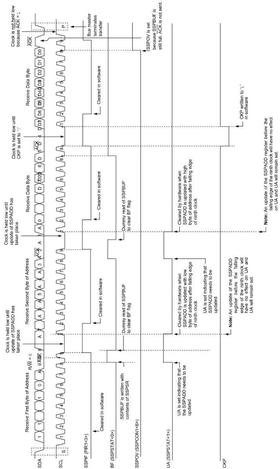
flowchart
graph TD
    A["SDA"] --> B["Receive First Byte of Address"]
    B --> C["R/W = 0"]
    C --> D["Clock is held low until update of SSPADD has taken place"]
    D --> E["Receive Second Byte of Address"]
    E --> F["Clock is held low until update of SSPADD has taken place"]
    F --> G["Receive Data Byte"]
    G --> H["ACK"]
    H --> I["Clock is not held low because ACK = 1"]
    J["SCL"] --> K["Receive Data Byte"]
    K --> L["ACK"]
    L --> M["BU master terminates transfer"]
    N["SSPIF (PIR1<3>)"] --> O["Cleared in software"]
    P["BF (SSPSTAT<0>)"] --> Q["SSPBUF is written with contents of SSPSR"]
    R["SSPOV (SSPCON1<6>)"] --> S["Dummy read of SSPBUF to clear BF flag"]
    T["UA (SSPSTAT<1>)"] --> U["UA is set indicating that the SSPADD needs to be updated"]
    V["CKP"] --> W["Note: An update of the SSPADD register before the falling edge of the ninth clock will have no effect on UA and UA will remain set."]
    X["Clock is held low until update of SSPADD has taken place"] --> Y["Receive Data Byte"]
    Z["Clock is held low until CKP is set to '1'"] --> AA["Receive Data Byte"]
    AB["BU master terminates transfer"] --> AC["SSPOV is set because SSPBUF is still full. ACK is not sent."]
18.4.5 GENERAL CALL ADDRESS SUPPORT
The addressing procedure for the I^2C bus is such that the first byte after the Start condition usually determines which device will be the slave addressed by the master. The exception is the general call address which can address all devices. When this address is used, all devices should, in theory, respond with an Acknowledge.
The general call address is one of eight addresses reserved for specific purposes by the I²C protocol. It consists of all '0's with R/W=0.
The general call address is recognized when the General Call Enable bit, GCEN, is enabled (SSPCON2<7> set). Following a Start bit detect, 8 bits are shifted into the SSPSR and the address is compared against the SSPADD. It is also compared to the general call address and fixed in hardware.
If the general call address matches, the SSPSR is transferred to the SSPBUF, the BF flag bit is set (eighth bit), and on the falling edge of the ninth bit (ACK bit), the SSPIF interrupt flag bit is set.
When the interrupt is serviced, the source for the interrupt can be checked by reading the contents of the SSPBUF. The value can be used to determine if the address was device-specific or a general call address.
In 10-bit mode, the SSPADD is required to be updated for the second half of the address to match and the UA bit is set (SSPSTAT<1>). If the general call address is sampled when the GCEN bit is set, while the slave is configured in 10-Bit Addressing mode, then the second half of the address is not necessary, the UA bit will not be set and the slave will begin receiving data after the Acknowledge (Figure 18-17).
FIGURE 18-17: SLAVE MODE GENERAL CALL ADDRESS SEQUENCE (7 OR 10-BIT ADDRESSING MODE)
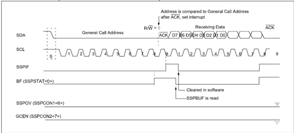
text_image
Address is compared to General Call Address after ACK, set interrupt R/W = 0 Receiving Data ACK General Call Address SDA SCL SSPIF BF (SSPSTAT<0>) SSPOV (SSPCON1<6>) GCEN (SSPCON2<7>) '0' '1'18.4.6 MASTER MODE
Master mode is enabled by setting and clearing the appropriate SSPM bits in SSPCON1 and by setting the SSPEN bit. In Master mode, the SCL and SDA lines are manipulated by the MSSP hardware.
Master mode of operation is supported by interrupt generation on the detection of the Start and Stop conditions. The Stop (P) and Start (S) bits are cleared from a Reset or when the MSSP module is disabled. Control of the I²C bus may be taken when the P bit is set, or the bus is Idle, with both the S and P bits clear.
In Firmware Controlled Master mode, user code conducts all I²C bus operations based on Start and Stop bit conditions.
Once Master mode is enabled, the user has six options.
- Assert a Start condition on SDA and SCL.
- Assert a Repeated Start condition on SDA and SCL.
- Write to the SSPBUF register initiating transmission of data/address.
- Configure the I ^2 C port to receive data.
- Generate an Acknowledge condition at the end of a received byte of data.
- Generate a Stop condition on SDA and SCL.
Note: The MSSP module, when configured in I²C Master mode, does not allow queueing of events. For instance, the user is not allowed to initiate a Start condition and immediately write the SSPBUF register to initiate transmission before the Start condition is complete. In this case, the SSPBUF will not be written to and the WCOL bit will be set, indicating that a write to the SSPBUF did not occur.
The following events will cause the MSSP Interrupt Flag bit, SSPIF, to be set (and an MSSP interrupt, if enabled):
- Start condition
- Stop condition
• Data transfer byte transmitted/received - Acknowledge transmit
- Repeated Start
FIGURE 18-18: MSSP BLOCK DIAGRAM (I ^2C^TM MASTER MODE)

flowchart
graph TD
    A["SDA"] --> B["SDA In"]
    C["SCL"] --> D["Receive Enable"]
    B --> E["SSPSR"]
    D --> F["Start bit, Stop bit, Acknowledge Generate"]
    E --> G["Shift Clock"]
    F --> H["Clock Cntl"]
    G --> I["Clock Arbitrate/WCOL Detect (hold off clock source)"]
    H --> I
    I --> J["Reset ACKSTAT, PEN (SSPCON2)"]
    K["SSPM<3:0> SSPADD<6:0>"] --> L["Baud Rate Generator"]
    M["SSPDF"] --> N["SSPDF"]
    O["SSPDF"] --> P["SSPDF"]
    Q["SSPDF"] --> R["SSPDF"]
    S["SSPDF"] --> T["SSPDF"]
    U["SSPDF"] --> V["SSPDF"]
    W["SSPDF"] --> X["SSPDF"]
    Y["SSPDF"] --> Z["SSPDF"]
    AA["SSPDF"] --> AB["SSPDF"]
    AC["SSPDF"] --> AD["SSPDF"]
    AE["SSPDF"] --> AF["SSPDF"]
    AG["SSPDF"] --> AH["SSPDF"]
    AI["SSPDF"] --> AJ["SSPDF"]
    AK["SSPDF"] --> AL["SSPDF"]
    AM["SSPDF"] --> AN["SSPDF"]
    AO["SSPDF"] --> AP["SSPDF"]
    AQ["SSPDF"] --> AR["SSPDF"]
    AS["SSPDF"] --> AT["SSPDF"]
    AU["SSPDF"] --> AV["SSPDF"]
    AW["SSPDF"] --> AX["SSPDF"]
    AY["Internal Data Bus"] --> AZ["Read Write"]
    BA["Receive Enable"] --> BB["SDA In"]
    BC["SCL In"] --> BD["SCL In"]
    BE["SCLK In"] --> BF["SCLK In"]
    BG["SCLK In"] --> BH["SCLK In"]
    BI["SCLK In"] --> BJ["SCLK In"]
    BK["SCLK In"] --> BL["SCLK In"]
    BM["SCLK In"] --> BN["SCLK In"]
    BO["SCLK In"] --> BP["SCLK In"]
    BQ["SCLK In"] --> BR["SCLK In"]
    BS["SCLK In"] --> BT["SCLK In"]
    BU["SCLK In"] --> BV["SCLK In"]
    BW["SCLK In"] --> BX["SCLK In"]
    BY["SCLK In"] --> BZ["SCLK In"]
    CA["SCLK In"] --> CB["SCLK In"]
    CC["SCLK In"] --> CD["SCLK In"]
    DD["SCLK In"] --> DE["SCLK In"]
    BEX["SCLK In"] --> BFX["SCLK In"]
    BFX["SCLK In"] --> BGX["SCLK In"]
    BGX["SCLK In"] --> BHX["SCLK In"]
    BHX["SCLK In"] --> BIX["SCLK In"]
    BIX["SCLK In"] --> BJX["SCLK In"]
    BKX["SCLK In"] --> BLX["SCLK In"]
    BLX["SCLK In"] --> BNX["SCLK In"]
    BNX["SCLK In"] --> BOX["SCLK In"]
    BOX["SCLK In"] --> BXX["SCLK In"]
    BXX["SCLK In"] --> BYX["SCLK In"]
18.4.6.1 I ^2 C Master Mode Operation
The master device generates all of the serial clock pulses and the Start and Stop conditions. A transfer is ended with a Stop condition or with a Repeated Start condition. Since the Repeated Start condition is also the beginning of the next serial transfer, the I ^2 C bus will not be released.
In Master Transmitter mode, serial data is output through SDA, while SCL outputs the serial clock. The first byte transmitted contains the slave address of the receiving device (7 bits) and the Read/Write (R/W) bit. In this case, the R/W bit will be logic '0'. Serial data is transmitted, 8 bits at a time. After each byte is transmitted, an Acknowledge bit is received. Start and Stop conditions are output to indicate the beginning and the end of a serial transfer.
In Master Receive mode, the first byte transmitted contains the slave address of the transmitting device (7 bits) and the R/W bit. In this case, the R/W bit will be logic '1'. Thus, the first byte transmitted is a 7-bit slave address followed by a '1' to indicate the receive bit. Serial data is received via SDA, while SCL outputs the serial clock. Serial data is received, 8 bits at a time. After each byte is received, an Acknowledge bit is transmitted. Start and Stop conditions indicate the beginning and end of transmission.
The Baud Rate Generator used for the SPI mode operation is used to set the SCL clock frequency for either 100 kHz, 400 kHz or 1 MHz ^2 C operation. See Section 18.4.7 "Baud Rate" for more detail.
A typical transmit sequence would go as follows:
- The user generates a Start condition by setting the Start Enable bit, SEN (SSPCON2<0>).
- SSPIF is set. The MSSP module will wait the required start time before any other operation takes place.
- The user loads the SSPBUF with the slave address to transmit.
- The address is shifted out on the SDA pin until all 8 bits are transmitted.
- The MSSP module shifts in the ACK bit from the slave device and writes its value into the SSPCON2 register (SSPCON2<6>).
- The MSSP module generates an interrupt at the end of the ninth clock cycle by setting the SSPIF bit.
- The user loads the SSPBUF with eight bits of data.
- Data is shifted out on the SDA pin until all 8 bits are transmitted.
- The MSSP module shifts in the ACK bit from the slave device and writes its value into the SSPCON2 register (SSPCON2<6>).
- The MSSP module generates an interrupt at the end of the ninth clock cycle by setting the SSPIF bit.
- The user generates a Stop condition by setting the Stop Enable bit, PEN (SSPCON2<2>).
- An interrupt is generated once the Stop condition is complete.
18.4.7 BAUD RATE
In I ^2 C Master mode, the Baud Rate Generator (BRG) reload value is placed in the lower 7 bits of the SSPADD register (Figure 18-19). When a write occurs to SSPBUF, the Baud Rate Generator will automatically begin counting. The BRG counts down to 0 and stops until another reload has taken place. The BRG count is decremented twice per instruction cycle (Tcy) on the Q2 and Q4 clocks. In I ^2 C Master mode, the BRG is reloaded automatically.
Once the given operation is complete (i.e., transmission of the last data bit is followed by ACK), the internal clock will automatically stop counting and the SCL pin will remain in its last state.
Table 18-3 demonstrates clock rates based on instruction cycles and the BRG value loaded into SSPADD.
18.4.7.1 Baud Rate Generation in Power-Managed Modes
When the device is operating in one of the power-managed modes, the clock source to the BRG may change frequency, or even stop, depending on the mode and clock source selected. Switching to a Run or Idle mode from either the secondary clock or internal oscillator is likely to change the clock rate to the BRG. In Sleep mode, the BRG will not be clocked at all.
FIGURE 18-19: BAUD RATE GENERATOR BLOCK DIAGRAM
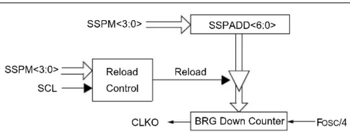
flowchart
graph TD
    A["SSPM<3:0>"] --> B["SSPADD<6:0>"]
    C["SSPM<3:0>"] --> D["Reload Control"]
    E["SCL"] --> D
    D --> F["RR"]
    G["CLKO"] --> H["BRG Down Counter"]
    I["Fosc/4"] --> H
    B --> J["M"]
    H --> J
TABLE 18-3: I ^2C^TM CLOCK RATE w/BRG
| FcY FcY * 2 BRG Value | FsCL(2 Rollovers of BRG) | ||
| 10 MHz 20 MHz 18h 400 kHz | |||
| 10 MHz 20 MHz 1Fh | 312.5 kHz | ||
| 10 MHz 20 MHz 63h 100 kHz | |||
| 4 MHz | 8 MHz | 09h 400 kHz | |
| 4 MHz | 8 MHz | 0Ch | 308 kHz |
| 4 MHz | 8 MHz | 27h 100 kHz | |
| 1 MHz | 2 MHz | 02h 333 kHz | |
| 1 MHz | 2 MHz | 09h 100 kHz | |
| 1 MHz | 2 MHz | 00h | 1 MHz |
18.4.7.2 Clock Arbitration
Clock arbitration occurs when the master, during any receive, transmit or Repeated Start/Stop condition, deasserts the SCL pin (SCL allowed to float high). When the SCL pin is allowed to float high, the Baud Rate Generator (BRG) is suspended from counting until the SCL pin is actually sampled high. When the
SCL pin is sampled high, the Baud Rate Generator is reloaded with the contents of SSPADD<6:0> and begins counting. This ensures that the SCL high time will always be at least one BRG rollover count in the event that the clock is held low by an external device (Figure 18-20).
FIGURE 18-20: BAUD RATE GENERATOR TIMING WITH CLOCK ARBITRATION
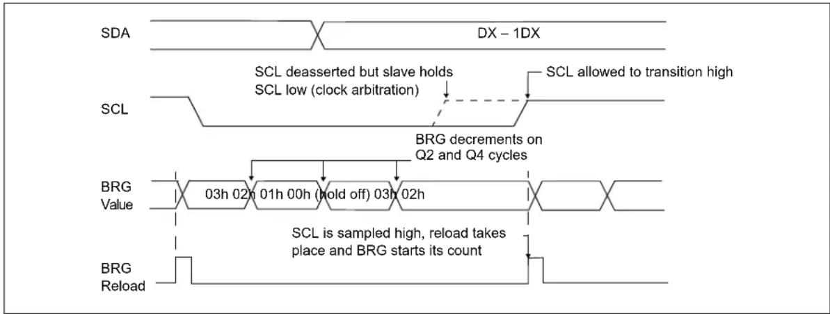
flowchart
graph TD
    A["SDA"] --> B["DX - 1DX"]
    C["SCL"] --> D["SCL deasserted but slave holds"]
    D --> E["SCL low (clock arbitration)"]
    E --> F["SCL allowed to transition high"]
    G["BRG Value"] --> H["03h 02h 01h 00h (hold off) 03h 02h"]
    H --> I["SCL is sampled high, reload takes place and BRG starts its count"]
    J["BRG Reload"] --> K["End"]
18.4.8 I ^2 C MASTER MODE START CONDITION TIMING
To initiate a Start condition, the user sets the Start Enable bit, SEN (SSPCON2<0>). If the SDA and SCL pins are sampled high, the Baud Rate Generator is reloaded with the contents of SSPADD<6:0> and starts its count. If SCL and SDA are both sampled high when the Baud Rate Generator times out (TBRG), the SDA pin is driven low. The action of the SDA pin being driven low while SCL is high is the Start condition and causes the S bit (SSPSTAT<3>) to be set. Following this, the Baud Rate Generator is reloaded with the contents of SSPADD<6:0> and resumes its count. When the Baud Rate Generator times out (TBRG), the SEN bit (SSPCON2<0>) will be automatically cleared by hardware. The Baud Rate Generator is suspended, leaving the SDA line held low and the Start condition is complete.
Note: If, at the beginning of the Start condition, the SDA and SCL pins are already sampled low, or if during the Start condition, the SCL line is sampled low before the SDA line is driven low, a bus collision occurs. The Bus Collision Interrupt Flag, BCLIF, is set, the Start condition is aborted and the I²C module is reset into its Idle state.
18.4.8.1 WCOL Status Flag
If the user writes the SSPBUF when a Start sequence is in progress, the WCOL bit is set and the contents of the buffer are unchanged (the write doesn't occur).
Note: Because queueing of events is not allowed, writing to the lower 5 bits of SSPCON2 is disabled until the Start condition is complete.
FIGURE 18-21: FIRST START BIT TIMING

text_image
Write to SEN bit occurs here SDA = 1, SCL = 1 Set S bit (SSPSTAT<3>) At completion of Start bit, hardware clears SEN bit and sets SSPIF bit TBRG TBRG Write to SSPBUF occurs here 1st bit 2nd bit SDA SCL TBRG TBRG S18.4.9 I ^2 C MASTER MODE REPEATED START CONDITION TIMING
A Repeated Start condition occurs when the RSEN bit (SSPCON2<1>) is programmed high and the I^2C logic module is in the Idle state. When the RSEN bit is set, the SCL pin is asserted low. When the SCL pin is sampled low, the Baud Rate Generator is loaded with the contents of SSPADD<6:0> and begins counting. The SDA pin is released (brought high) for one Baud Rate Generator count (TBRG). When the Baud Rate Generator times out, if SDA is sampled high, the SCL pin will be deasserted (brought high). When SCL is sampled high, the Baud Rate Generator is reloaded with the contents of SSPADD<6:0> and begins counting. SDA and SCL must be sampled high for one TBRG. This action is then followed by assertion of the SDA pin (SDA = 0) for one TBRG while SCL is high. Following this, the RSEN bit (SSPCON2<1>) will be automatically cleared and the Baud Rate Generator will not be reloaded, leaving the SDA pin held low. As soon as a Start condition is detected on the SDA and SCL pins, the S bit (SSPSTAT<3>) will be set. The SSPIF bit will not be set until the Baud Rate Generator has timed out.
Note 1: If RSEN is programmed while any other event is in progress, it will not take effect.
2: A bus collision during the Repeated Start condition occurs if:
- SDA is sampled low when SCL goes from low-to-high.
- SCL goes low before SDA is asserted low. This may indicate that another master is attempting to transmit a data '1'.
Immediately following the SSPIF bit getting set, the user may write the SSPBUF with the 7-bit address in 7-bit mode or the default first address in 10-bit mode. After the first eight bits are transmitted and an ACK is received, the user may then transmit an additional eight bits of address (10-bit mode) or eight bits of data (7-bit mode).
18.4.9.1 WCOL Status Flag
If the user writes the SSPBUF when a Repeated Start sequence is in progress, the WCOL flag is set and the contents of the buffer are unchanged (the write doesn't occur).
Note: Because queueing of events is not allowed, writing of the lower 5 bits of SSPCON2 is disabled until the Repeated Start condition is complete.
FIGURE 18-22: REPEATED START CONDITION WAVEFORM
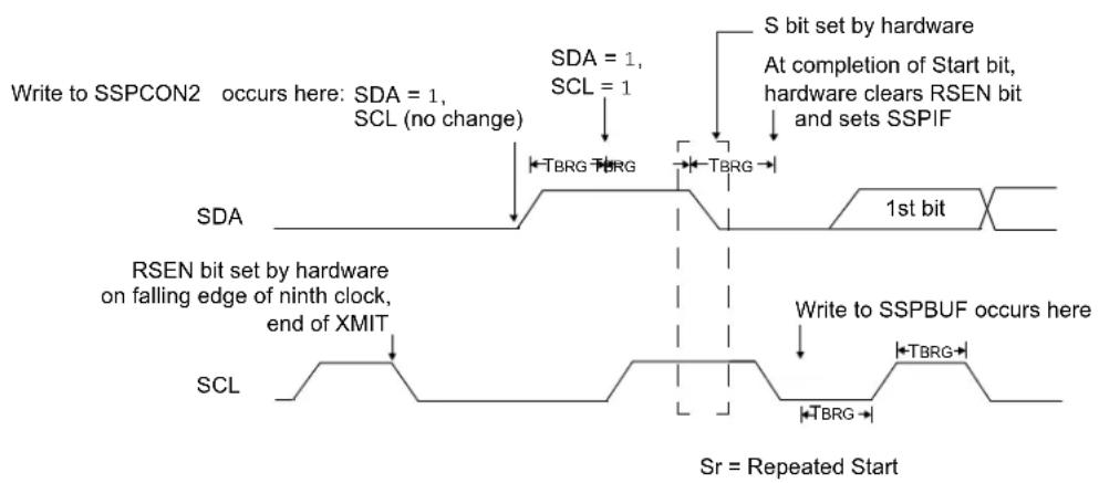
flowchart
graph TD
    A["Write to SSPCON2 occurs here: SDA = 1, SCL (no change)"] --> B["SDB = 1, SCL = 1"]
    B --> C["TBRG TBRG"]
    C --> D["TBRG"]
    D --> E["1st bit"]
    F["RSEN bit set by hardware on falling edge of ninth clock, end of XMIT"] --> G["SCL"]
    G --> H["TBRG"]
    H --> I["Write to SSPBUF occurs here"]
    J["S bit set by hardware at completion of Start bit, hardware clears RSEN bit and sets SSPIF"] --> K["1st bit"]
    L["Sr = Repeated Start"]
18.4.10 I ^2 C MASTER MODE TRANSMISSION
Transmission of a data byte, a 7-bit address or the other half of a 10-bit address is accomplished by simply writing a value to the SSPBUF register. This action will set the Buffer Full bit, BF, and allow the Baud Rate Generator to begin counting and start the next transmission. Each bit of address/data will be shifted out onto the SDA pin after the falling edge of SCL is asserted (see data hold time specification, parameter 106). SCL is held low for one Baud Rate Generator rollover count (TBRG). Data should be valid before SCL is released high (see data setup time specification, parameter 107). When the SCL pin is released high, it is held that way for TBRG. The data on the SDA pin must remain stable for that duration and some hold time after the next falling edge of SCL. After the eighth bit is shifted out (the falling edge of the eighth clock), the BF flag is cleared and the master releases SDA. This allows the slave device being addressed to respond with an ACK bit during the ninth bit time if an address match occurred, or if data was received properly. The status of ACK is written into the ACKDT bit on the falling edge of the ninth clock. If the master receives an Acknowledge, the Acknowledge Status bit, ACKSTAT, is cleared; if not, the bit is set. After the ninth clock, the SSPIF bit is set and the master clock (Baud Rate Generator) is suspended until the next data byte is loaded into the SSPBUF, leaving SCL low and SDA unchanged (Figure 18-23).
After the write to the SSPBUF, each bit of the address will be shifted out on the falling edge of SCL until all seven address bits and the R/W bit are completed. On the falling edge of the eighth clock, the master will deassert the SDA pin, allowing the slave to respond with an Acknowledge. On the falling edge of the ninth clock, the master will sample the SDA pin to see if the address was recognized by a slave. The status of the ACK bit is loaded into the ACKSTAT status bit (SSPCON2<6>). Following the falling edge of the ninth clock transmission of the address, the SSPIF is set, the BF flag is cleared and the Baud Rate Generator is turned off until another write to the SSPBUF takes place, holding SCL low and allowing SDA to float.
18.4.10.1 BF Status Flag
In Transmit mode, the BF bit (SSPSTAT<0>) is set when the CPU writes to SSPBUF and is cleared when all 8 bits are shifted out.
18.4.10.2 WCOL Status Flag
If the user writes to the SSPBUF when a transmit is already in progress (i.e., SSPSR is still shifting out a data byte), the WCOL bit is set and the contents of the buffer are unchanged (the write doesn't occur) for 2 Tcy after the SSPBUF write. If SSPBUF is rewritten within 2 Tcy, the WCOL bit is set and SSPBUF is updated. This may result in a corrupted transfer.
The user should verify that the WCOL is clear after each write to SSPBUF to ensure the transfer is correct. In all cases, WCOL must be cleared in software.
18.4.10.3 ACKSTAT Status Flag
In Transmit mode, the ACKSTAT bit (SSPCON2<6>) is cleared when the slave has sent an Acknowledge ( = 0 ) and is set when the slave does not Acknowledge ( = 1 ). A slave sends an Acknowledge when it has recognized its address (including a general call) or when the slave has properly received its data.
18.4.11 I ^2 C MASTER MODE RECEPTION
Master mode reception is enabled by programming the Receive Enable bit, RCEN (SSPCON2<3>).
Note: The MSSP module must be in an Idle state before the RCEN bit is set or the RCEN bit will be disregarded.
The Baud Rate Generator begins counting, and on each rollover, the state of the SCL pin changes (high-to-low/low-to-high) and data is shifted into the SSPSR. After the falling edge of the eighth clock, the receive enable flag is automatically cleared, the contents of the SSPSR are loaded into the SSPBUF, the BF flag bit is set, the SSPIF flag bit is set and the Baud Rate Generator is suspended from counting, holding SCL low. The MSSP is now in Idle state awaiting the next command. When the buffer is read by the CPU, the BF flag bit is automatically cleared. The user can then send an Acknowledge bit at the end of reception by setting the Acknowledge Sequence Enable bit, ACKEN (SSPCON2<4>).
18.4.11.1 BF Status Flag
In receive operation, the BF bit is set when an address or data byte is loaded into SSPBUF from SSPSR. It is cleared when the SSPBUF register is read.
18.4.11.2 SSPOV Status Flag
In receive operation, the SSPOV bit is set when 8 bits are received into the SSPSR and the BF flag bit is already set from a previous reception.
18.4.11.3 WCOL Status Flag
If the user writes the SSPBUF when a receive is already in progress (i.e., SSPSR is still shifting in a data byte), the WCOL bit is set and the contents of the buffer are unchanged (the write doesn't occur).
FIGURE 18-23: I ^2 C ^TM MASTER MODE WAVEFORM (TRANSMISSION, 7 OR 10-BIT ADDRESSING)

flowchart
graph TD
    A["Write SSPCON2<0>(SEN = 1), Start condition begins"] --> B["SEN = 0"]
    B --> C["Transmit Address to Slave"]
    C --> D["R/W = 0"]
    D --> E["ACK = 0"]
    E --> F["From slave, clear ACKSTAT bit (SSPCON2<6>)"]
    F --> G["ACKSTAT in SSPCON2 = 1"]
    H["SDA"] --> I["A7 A6 A5 A4 A3 A2 A1"]
    I --> J["SSPUF written with 7-bit address and R/W start transmit"]
    J --> K["SSPIF"]
    K --> L["Cleared in software"]
    L --> M["SCL held low while CPU responds to SSPIF"]
    M --> N["Cleared in software service routine from MSSP interrupt"]
    N --> O["Cleared in software"]
    P["SCL"] --> Q["S"]
    Q --> R["1 2 3 4 5 6 7 8 9"]
    R --> S["P"]
    T["BF (SSPSTAT<0>)"] --> U["SSPUF written"]
    U --> V["After Start condition, SEN cleared by hardware"]
    V --> W["Cleared in software"]
    W --> X["Cleared in software"]
    Y["SEN"] --> Z["After Start condition, SEN cleared by hardware"]
    Z --> AA["Cleared in software"]
    AB["PEN"] --> AC["After Start condition, SEN cleared by hardware"]
    AC --> AD["Cleared in software"]
FIGURE 18-24: I ^2C^TM MASTER MODE WAVEFORM (RECEPTION, 7-BIT ADDRESSING)

flowchart
graph TD
    A["Write to SSPCON2<0> (SEN = 1), begin Start condition"] --> B["Write to SSPBUF occurs here, start XMIT"]
    B --> C["Transmit Address to Slave"]
    C --> D["ACK from Slave"]
    D --> E["Receiving Data from Slave"]
    E --> F["ACK"]
    F --> G["ACK"]
    G --> H["ACK"]
    H --> I["ACK"]
    I --> J["ACK"]
    J --> K["ACK"]
    K --> L["ACK"]
    L --> M["ACK"]
    M --> N["ACK"]
    N --> O["ACK"]
    O --> P["ACK"]
    P --> Q["ACK"]
    Q --> R["ACK"]
    R --> S["ACK"]
    S --> T["ACK"]
    T --> U["ACK"]
    U --> V["ACK"]
    V --> W["ACK"]
    W --> X["ACK"]
    X --> Y["ACK"]
    Y --> Z["ACK"]
    Z --> AA["ACK"]
    AA --> AB["ACK"]
    AB --> AC["ACK"]
    AC --> AD["ACK"]
    AD --> AE["ACK"]
    AE --> AF["ACK"]
    AF --> AG["ACK"]
    AG --> AH["ACK"]
    AH --> AI["ACK"]
    AI --> AJ["ACK"]
    AJ --> AK["ACK"]
    AK --> AL["ACK"]
    AL --> AM["ACK"]
    AM --> AN["ACK"]
    AN --> AO["ACK"]
    AO --> AP["ACK"]
    AP --> AQ["ACK"]
    AQ --> AR["ACK"]
    AR --> AS["ACK"]
    AS --> AT["ACK"]
    AT --> AU["ACK"]
    AU --> AV["ACK"]
    AV --> AW["ACK"]
    AW --> AX["ACK"]
    AX --> AY["ACK"]
    AY --> AZ["ACK"]
    AZ --> BA["ACK"]
    BA --> BB["ACK"]
    BB --> BC["ACK"]
    BC --> BD["ACK"]
    BD --> BE["ACK"]
    BE --> BF["ACK"]
    BF --> BG["ACK"]
    BG --> BH["ACK"]
    BH --> BI["ACK"]
    BI --> BJ["ACK"]
    BJ --> BK["ACK"]
    BK --> BL["ACK"]
    BL --> BM["ACK"]
    BM --> BN["ACK"]
    BN --> BO["ACK"]
    BO --> BP["ACK"]
    BP --> BQ["ACK"]
    BQ --> BR["ACK"]
    BR --> BS["ACK"]
    BS --> BT["ACK"]
    BT --> BU["ACK"]
    BU --> BV["ACK"]
    BV --> BW["ACK"]
    BW --> BX["ACK"]
    BX --> BY["ACK"]
    BY --> BZ["ACK"]
18.4.12 ACKNOWLEDGE SEQUENCE TIMING
An Acknowledge sequence is enabled by setting the Acknowledge Sequence Enable bit, ACKEN (SSPCON2<4>). When this bit is set, the SCL pin is pulled low and the contents of the Acknowledge data bit are presented on the SDA pin. If the user wishes to generate an Acknowledge, then the ACKDT bit should be cleared. If not, the user should set the ACKDT bit before starting an Acknowledge sequence. The Baud Rate Generator then counts for one rollover period (TBRG) and the SCL pin is deasserted (pulled high). When the SCL pin is sampled high (clock arbitration), the Baud Rate Generator counts for TBRG. The SCL pin is then pulled low. Following this, the ACKEN bit is automatically cleared, the Baud Rate Generator is turned off and the MSSP module then goes into Idle mode (Figure 18-25).
18.4.12.1 WCOL Status Flag
If the user writes the SSPBUF when an Acknowledge sequence is in progress, then WCOL is set and the contents of the buffer are unchanged (the write doesn't occur).
18.4.13 STOP CONDITION TIMING
A Stop bit is asserted on the SDA pin at the end of a receive/transmit by setting the Stop Sequence Enable bit, PEN (SSPCON2<2>). At the end of a receive/transmit, the SCL line is held low after the falling edge of the ninth clock. When the PEN bit is set, the master will assert the SDA line low. When the SDA line is sampled low, the Baud Rate Generator is reloaded and counts down to 0. When the Baud Rate Generator times out, the SCL pin will be brought high and one TBRG (Baud Rate Generator rollover count) later, the SDA pin will be deasserted. When the SDA pin is sampled high while SCL is high, the P bit (SSPSTAT<4>) is set. A TBRG later, the PEN bit is cleared and the SSPIF bit is set (Figure 18-26).
18.4.13.1 WCOL Status Flag
If the user writes the SSPBUF when a Stop sequence is in progress, then the WCOL bit is set and the contents of the buffer are unchanged (the write doesn't occur).
text_image
Acknowledge sequence starts here, write to SSPCON2, ACKEN = 1, ACKDT = 0 TBRG TBRG ACKEN automatically cleared SDA D0 ACK SCL 8 9 SSPIF SSPIF set at the end of receive Cleared in software SSPIF set at the end of Acknowledge sequence Cleared in softwareNote: TBRG = one Baud Rate Generator period.
FIGURE 18-26: STOP CONDITION RECEIVE OR TRANSMIT MODE

text_image
Write to SSPCON2, set PEN SCL = 1 for TBRG, followed by SDA = 1 for TBRG after SDA sampled high. P bit (SSPSTAT<4>) is set. PEN bit (SSPCON2<2>) is cleared by hardware and the SSPIF bit is set Falling edge of 9th clock TBRG SDA ACK TBRG TBRG P TBRG SCL brought high after T BRG SDA asserted low before rising edge of clock to setup Stop conditionNote: TBRG = one Baud Rate Generator period.
18.4.14 SLEEP OPERATION
While in Sleep mode, the I^2C module can receive addresses or data, and when an address match or complete byte transfer occurs, wake the processor from Sleep (if the MSSP interrupt is enabled).
18.4.15 EFFECTS OF A RESET
A Reset disables the MSSP module and terminates the current transfer.
18.4.16 MULTI-MASTER MODE
In Multi-Master mode, the interrupt generation on the detection of the Start and Stop conditions allows the determination of when the bus is free. The Stop (P) and Start (S) bits are cleared from a Reset or when the MSSP module is disabled. Control of the I²C bus may be taken when the P bit (SSPSTAT<4>) is set, or the bus is Idle, with both the S and P bits clear. When the bus is busy, enabling the MSSP interrupt will generate the interrupt when the Stop condition occurs.
In multi-master operation, the SDA line must be monitored for arbitration to see if the signal level is the expected output level. This check is performed in hardware with the result placed in the BCLIF bit.
The states where arbitration can be lost are:
- Address Transfer
- Data Transfer
- A Start Condition
• A Repeated Start Condition
• An Acknowledge Condition
18.4.17 MULTI -MASTER COMMUNICATION, BUS COLLISION AND BUS ARBITRATION
Multi-Master mode support is achieved by bus arbitration. When the master outputs address/data bits onto the SDA pin, arbitration takes place when the master outputs a '1' on SDA by letting SDA float high, and another master asserts a '0'. When the SCL pin floats high, data should be stable. If the expected data on SDA is a '1' and the data sampled on the SDA pin = 0, then a bus collision has taken place. The master will set the Bus Collision Interrupt Flag, BCLIF, and reset the I²C port to its Idle state (Figure 18-27).
If a transmit was in progress when the bus collision occurred, the transmission is halted, the BF flag is cleared, the SDA and SCL lines are deasserted and the SSPBUF can be written to. When the user services the bus collision Interrupt Service Routine, and if the I²C bus is free, the user can resume communication by asserting a Start condition.
If a Start, Repeated Start, Stop or Acknowledge condition was in progress when the bus collision occurred, the condition is aborted, the SDA and SCL lines are deasserted and the respective control bits in the SSPCON2 register are cleared. When the user services the bus collision Interrupt Service Routine, and if the PC bus is free, the user can resume communication by asserting a Start condition.
The master will continue to monitor the SDA and SCL pins. If a Stop condition occurs, the SSPIF bit will be set.
A write to the SSPBUF will start the transmission of data at the first data bit regardless of where the transmitter left off when the bus collision occurred.
In Multi-Master mode, the interrupt generation on the detection of Start and Stop conditions allows the determination of when the bus is free. Control of the I^2C bus can be taken when the P bit is set in the SSPSTAT register or the bus is Idle and the S and P bits are cleared.
FIGURE 18-27: BUS COLLISION TIMING FOR TRANSMIT AND ACKNOWLEDGE
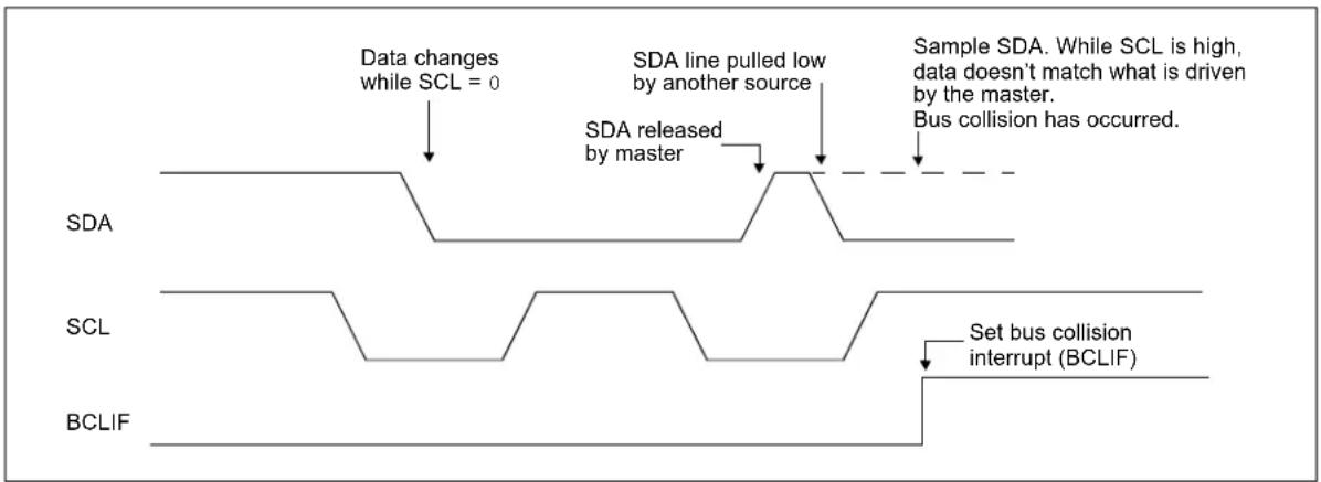
flowchart
graph TD
    A["Data changes while SCL = 0"] --> B["SDA released by master"]
    C["SDA line pulled low by another source"] --> D["Sample SDA. While SCL is high, data doesn't match what is driven by the master. Bus collision has occurred."]
    E["Set bus collision interrupt (BCLIF)"] --> F["BCLIF"]
18.4.17.1 Bus Collision During a Start Condition
During a Start condition, a bus collision occurs if:
a) SDA or SCL are sampled low at the beginning of the Start condition (Figure 18-28).
b) SCL is sampled low before SDA is asserted low (Figure 18-29).
During a Start condition, both the SDA and the SCL pins are monitored.
If the SDA pin is already low, or the SCL pin is already low, then all of the following occur:
• the Start condition is aborted;
- the BCLIF flag is set; and
- the MSSP module is reset to its Idle state (Figure 18-28).
The Start condition begins with the SDA and SCL pins deasserted. When the SDA pin is sampled high, the Baud Rate Generator is loaded from SSPADD<6:0> and counts down to 0. If the SCL pin is sampled low while SDA is high, a bus collision occurs, because it is assumed that another master is attempting to drive a data '1' during the Start condition.
If the SDA pin is sampled low during this count, the BRG is reset and the SDA line is asserted early (Figure 18-30). If, however, a '1' is sampled on the SDA pin, the SDA pin is asserted low at the end of the BRG count. The Baud Rate Generator is then reloaded and counts down to 0. If the SCL pin is sampled as '0' during this time, a bus collision does not occur. At the end of the BRG count, the SCL pin is asserted low.
Note: The reason that bus collision is not a factor during a Start condition is that no two bus masters can assert a Start condition at the exact same time. Therefore, one master will always assert SDA before the other. This condition does not cause a bus collision because the two masters must be allowed to arbitrate the first address following the Start condition. If the address is the same, arbitration must be allowed to continue into the data portion, Repeated Start or Stop conditions.
FIGURE 18-28: BUS COLLISION DURING START CONDITION (SDA ONLY)

flowchart
graph TD
    A["SDA"] --> B["SCL"]
    B --> C["SEN"]
    C --> D["BCLIF"]
    D --> E["S"]
    E --> F["SSPIF"]
    F --> G["SSPIF and BCLIF are cleared in software"]
    H["SDA goes low before the SEN bit is set.<br>Set BCLIF,<br>S bit and SSPIF set because<br>SDA = 0, SCL = 1."] --> I["Set SEN, enable Start condition if SDA = 1, SCL = 1"]
    I --> J["SEN cleared automatically because of bus collision.<br>MSSP module reset into Idle state."]
    K["SDA sampled low before Start condition. Set BCLIF.<br>S bit and SSPIF set because<br>SDA = 0, SCL = 1."] --> L["SSPIF and BCLIF are cleared in software"]
FIGURE 18-29: BUS COLLISION DURING START CONDITION (SCL = 0)

flowchart
graph TD
    A["SDA = 0, SCL = 1"] --> B["TBRG"]
    B --> C["TBRG"]
    D["SCL"] --> E["Set SEN, enable Start sequence if SDA = 1, SCL = 1"]
    E --> F["SCL = 0 before SDA = 0, bus collision occurs. Set BCLIF"]
    G["SEN"] --> H["SCL = 0 before BRG time-out, bus collision occurs. Set BCLIF"]
    H --> I["Interrupt cleared in software"]
    J["BCLIF"] --> K["End"]
    L["S"] --> M["'0'"]
    N["SSPIF"] --> O["'0'0'"]
FIGURE 18-30: BRG RESET DUE TO SDA ARBITRATION DURING START CONDITION
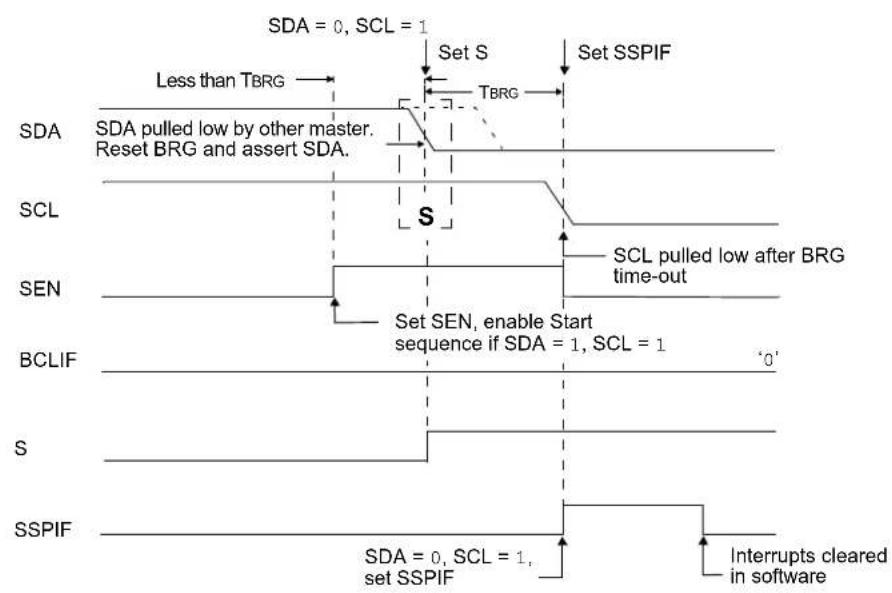
flowchart
graph TD
    A["SDA"] --> B["Less than TBRG"]
    B --> C["Set S"]
    C --> D["TBRG"]
    D --> E["Set SSPIF"]
    F["SCL"] --> G["S"]
    G --> H["SCL pulled low after BRG time-out"]
    I["SEN"] --> J["Set SEN, enable Start sequence if SDA = 1, SCL = 1"]
    K["BCLIF"] --> L["'0'"]
    M["S"] --> N["Set SSPIF"]
    O["SSPIF"] --> P["Set SSPIF"]
    Q["SDA = 0, SCL = 1"] --> R["Set S"]
    R --> S["Set SSPIF"]
    T["Interrupts cleared in software"] --> U["Set SSPIF"]
    V["SDA pulled low by other master. Reset BRG and assert SDA."] --> W["S"]
    X["SCL"] --> Y["S"]
    Z["SEN"] --> AA["S"]
    AB["BCLIF"] --> AC["'0'"]
18.4.17.2 Bus Collision During a Repeated Start Condition
During a Repeated Start condition, a bus collision occurs if:
a) A low level is sampled on SDA when SCL goes from a low level to a high level.
b) SCL goes low before SDA is asserted low, indicating that another master is attempting to transmit a data '1'.
When the user deasserts SDA, and the pin is allowed to float high, the BRG is loaded with SSPADD<6:0> and counts down to 0. The SCL pin is then deasserted, and when sampled high, the SDA pin is sampled.
If SDA is low, a bus collision has occurred (i.e., another master is attempting to transmit a data '0'; see Figure 18-31). If SDA is sampled high, the BRG is reloaded and begins counting. If SDA goes from high-to-low before the BRG times out, no bus collision occurs because no two masters can assert SDA at exactly the same time.
If SCL goes from high-to-low before the BRG times out, and SDA has not already been asserted, a bus collision occurs. In this case, another master is attempting to transmit a data '1' during the Repeated Start condition (see Figure 18-32).
If, at the end of the BRG time-out, both SCL and SDA are still high, the SDA pin is driven low and the BRG is reloaded and begins counting. At the end of the count, regardless of the status of the SCL pin, the SCL pin is driven low and the Repeated Start condition is complete.
FIGURE 18-31: BUS COLLISION DURING A REPEATED START CONDITION (CASE 1)

text_image
SDA SCL Sample SDA when SCL goes high. If SDA = 0, set BCLIF and release SDA and SCL. RSEN BCLIF Cleared in software S 'S0' SSPIF '0'FIGURE 18-32: BUS COLLISION DURING REPEATED START CONDITION (CASE 2)
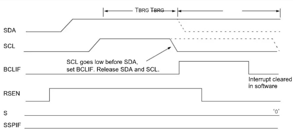
text_image
TBRG TBRG SDA SCL BCLIF SCL goes low before SDA, set BCLIF. Release SDA and SCL. Interrupt cleared in software RSEN S 'S0' SSPIF18.4.17.3 Bus Collision During a Stop Condition
Bus collision occurs during a Stop condition if:
a) After the SDA pin has been deasserted and allowed to float high, SDA is sampled low after the BRG has timed out.
b) After the SCL pin is deasserted, SCL is sampled low before SDA goes high.
The Stop condition begins with SDA asserted low. When SDA is sampled low, the SCL pin is allowed to float. When the pin is sampled high (clock arbitration), the Baud Rate Generator is loaded with SSPADD<6:0> and counts down to 0. After the BRG times out, SDA is sampled. If SDA is sampled low, a bus collision has occurred. This is due to another master attempting to drive a data '0' (Figure 18-33). If the SCL pin is sampled low before SDA is allowed to float high, a bus collision occurs. This is another case of another master attempting to drive a data '0' (Figure 18-34).
FIGURE 18-33: BUS COLLISION DURING A STOP CONDITION (CASE 1)
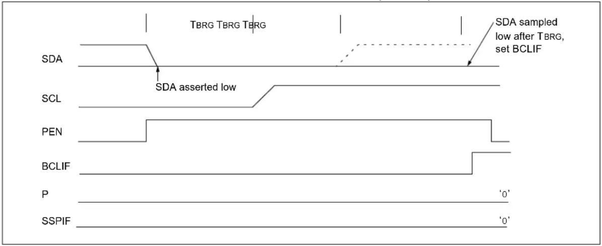
text_image
TBRG TBRG TBRG SDA SDA asserted low SDA sampled low after TBRG, set BCLIF SCL PEN BCLIF P 'S0' SSPIF 'S0'FIGURE 18-34: BUS COLLISION DURING A STOP CONDITION (CASE 2)

text_image
TBRG TBRG TBRG SDA Assert SDA SCL goes low before SDA goes high, set BCLIF PEN BCLIF P 'S0' SSPIF 'S0'TABLE 18-4: REGISTERS ASSOCIATED WITH I ^2C^TM OPERATION
| Name Bit | 7 Bit 6 Bit | 5 Bit 4 Bit | 3 Bit 2 Bit 1 | Bit 0 | Reset Values on Page | ||||
| INTCON GIE/GIEH PEIE/GIEL | TMR0IE | INT0IE | RBIE | TMR0IF | INT0IF | RBIF | 59 | ||
| PIR1 | — | ADIF | RC1IF | TX1IF | SSPIF | — | TMR2IF | TMR1IF | 62 |
| PIE1 | — | ADIE | RC1IE | TX1IE | SSPIE | — | TMR2IE | TMR1IE | 62 |
| IPR1 | — | ADIP | RC1IP | TX1IP | SSPIP | — | TMR2IP | TMR1IP | 62 |
| PIR2 | OSCFIF | CMIF | — | — | BCLIF | LVDIF | TMR3IF | — | 62 |
| PIE2 | OSCFIE | CMIE | — | — | BCLIE | LVDIE | TMR3IE | — | 62 |
| IPR2 | OSCFIP | CMIP | — | — | BCLIP | LVDIP | TMR3IP | — | 62 |
| TRISC | TRISC7 | TRISC6 | TRISC5 | TRISC4 | TRISC3 | TRISC2 | TRISC1 | TRISC0 | 62 |
| SSPBUF | MSSP Receive Buffer/Transmit Register | 60 | |||||||
| SSPADD | MSSP Address Register ( ^I^2C^TM Slave mode),MSSP Baud Rate Reload Register ( ^I^2C Master mode) | 60 | |||||||
| SSPCON1 | WCOL | SSPOV | SSPEN | CKP | SSPM3 | SSPM2 | SSPM1 | SSPM0 | 60 |
| SSPCON2 | GCEN | ACKSTAT | ACKDT | ACKEN | RCEN | PEN | RSEN | SEN | 60 |
| GCEN | ACKSTAT | ADMSK5^(1) | ADMSK4^(1) | ADMSK3^(1) | ADMSK2^(1) | ADMSK1^(1) | SEN | ||
| SSPSTAT | SMP | CKE | D/A | P | S | R/W | UA | BF | 60 |
Legend: — = unimplemented, read as '0'. Shaded cells are not used by the MSSP module in I²C™ mode.
Note 1: Alternate bit definitions for use in I ^2 C Slave mode operations only.
19.0 ENHANCED UNIVERSAL SYNCHRONOUS ASYNCHRONOUS RECEIVER TRANSMITTER (EUSART)
PIC18F87J90 family devices have three serial I/O modules: the MSSP module, discussed in the previous chapter and two Universal Synchronous Asynchronous Receiver Transmitter (USART) modules. (Generically, the USART is also known as a Serial Communications Interface or SCI.) The USART can be configured as a full-duplex, asynchronous system that can communicate with peripheral devices, such as CRT terminals and personal computers. It can also be configured as a half-duplex synchronous system that can communicate with peripheral devices, such as A/D or D/A integrated circuits, serial EEPROMs, etc.
There are two distinct implementations of the USART module in these devices: the Enhanced USART (EUSART) discussed here and the Addressable USART discussed in the next chapter. For this device family, USART1 always refers to the EUSART, while USART2 is always the AUSART.
The EUSART and AUSART modules implement the same core features for serial communications; their basic operation is essentially the same. The EUSART module provides additional features, including Automatic Baud Rate Detection and calibration, automatic wake-up on Sync Break reception, and 12-bit Break character transmit. These features make it ideally suited for use in Local Interconnect Network bus (LIN/J2602 bus) systems.
The EUSART can be configured in the following modes:
• Asynchronous (full-duplex) with:
- Auto-wake-up on character reception
- Auto-baud calibration
- 12-bit Break character transmission
- Synchronous – Master (half-duplex) with selectable clock polarity
- Synchronous – Slave (half-duplex) with selectable clock polarity
The pins of the EUSART are multiplexed with the functions of PORTC (RC6/TX1/CK1/SEG27 and RC7/RX1/DT1/SEG28). In order to configure these pins as an EUSART:
- bit, SPEN (RCSTA1<7>), must be set (= 1)
- bit, TRISC<7>, must be set (= 1)
- bit, TRISC<6>, must be set (= 1)
Note: The EUSART control will automatically reconfigure the pin from input to output as needed.
The driver for the TX1 output pin can also be optionally configured as an open-drain output. This feature allows the voltage level on the pin to be pulled to a higher level through an external pull-up resistor, and allows the output to communicate with external circuits without the need for additional level shifters.
The open-drain output option is controlled by the U1OD bit (LATG<6>). Setting the bit configures the pin for open-drain operation.
19.1 Control Registers
The operation of the Enhanced USART module is controlled through three registers:
• Transmit Status and Control Register 1 (TXSTA1)
- Receive Status and Control Register 1 (RCSTA1)
• Baud Rate Control Register 1 (BAUDCON1)
The registers are described in Register 19-1, Register 19-2 and Register 19-3.
REGISTER 19-1: TXSTA1: EUSART TRANSMIT STATUS AND CONTROL REGISTER
| R/W-0 R/W-0 R/W-0 R/W-0 R/W-0 R/W-0 R-1 R/W-0 | |||||||
| CSRC TX9 TXEN | (1) | SYNC SENDB BRGH TRMT TX9D | |||||
| bit 7 bit 0 | |||||||
Legend:
| R = Readable bit W = Writable bit U = Unimplemented bit, read as '0' | ||
| -n = Value at POR | '1' = Bit is set | '0' = Bit is cleared x = Bit is unknown |
bit 7 CSRC: Clock Source Select bit
Asynchronous mode:
Don't care.
Synchronous mode:
1 = Master mode (clock generated internally from BRG)
0 = Slave mode (clock from external source)
bit 6 TX9: 9-Bit Transmit Enable bit
1 = Selects 9-bit transmission
0 = Selects 8-bit transmission
bit 5 TXEN: Transmit Enable bit ^(1)
1 = Transmit enabled
0 = Transmit disabled
bit 4 SYNC: EUSART Mode Select bit
1 = Synchronous mode
0 = Asynchronous mode
bit 3 SENDB: Send Break Character bit
Asynchronous mode:
1 = Send Sync Break on next transmission (cleared by hardware upon completion)
0 = Sync Break transmission completed
Synchronous mode:
Don't care.
bit 2 BRGH: High Baud Rate Select bit
Asynchronous mode:
1 = High speed
0 = Low speed
Synchronous mode:
Unused in this mode.
bit 1 TRMT: Transmit Shift Register Status bit
1 = TSR empty
0 = TSR full
bit 0 TX9D: 9th bit of Transmit Data
Can be address/data bit or a parity bit.
Note 1: SREN/CREN overrides TXEN in Sync mode.
REGISTER 19-2: RCSTA1: EUSART RECEIVE STATUS AND CONTROL REGISTER
| R/W-0 R/W-0 R/W-0 R/W-0 R/W-0 R-0 R-0 R-x | ||||||
| SPEN RX9 | SREN CREN | ADDEN FERR | OERR RX9D | |||
| bit 7 bit 0 | ||||||
Legend:
| R = Readable bit W = Writable bit U = Unimplemented bit, read as '0' | ||
| -n = Value at POR | '1' = Bit is set | '0' = Bit is cleared x = Bit is unknown |
bit 7 SPEN: Serial Port Enable bit
1 = Serial port enabled (configures RX1/DT1 and TX1/CK1 pins as serial port pins)
0 = Serial port disabled (held in Reset)
bit 6 RX9: 9-Bit Receive Enable bit
1 = Selects 9-bit reception
0 = Selects 8-bit reception
bit 5 SREN: Single Receive Enable bit
Asynchronous mode:
Don't care.
Synchronous mode - Master:
1 = Enables single receive
0 = Disables single receive
This bit is cleared after reception is complete.
Synchronous mode – Slave:
Don't care.
bit 4 CREN: Continuous Receive Enable bit
Asynchronous mode:
1 = Enables receiver
0 = Disables receiver
Synchronous mode:
1 = Enables continuous receive until enable bit, CREN, is cleared (CREN overrides SREN)
0 = Disables continuous receive
bit 3 ADDEN: Address Detect Enable bit
Asynchronous mode 9-bit (RX9 = 1):
1 = Enables address detection, enables interrupt and loads the receive buffer when RSR<8> is set
0 = Disables address detection, all bytes are received and the ninth bit can be used as a parity bit
Asynchronous mode 9-bit (RX9 = 0):
Don't care.
bit 2 FERR: Framing Error bit
1 = Framing error (can be updated by reading RCREG1 register and receiving next valid byte)
0 = No framing error
bit 1 OERR: Overrun Error bit
1 = Overrun error (can be cleared by clearing bit, CREN)
0 = No overrun error
bit 0 RX9D: 9th bit of Received Data
This can be address/data bit or a parity bit and must be calculated by user firmware.
REGISTER 19-3: BAUDCON1: BAUD RATE CONTROL REGISTER 1
| R/W-0 R-1 R/W - 0 R/W-0 R/W-0 U-0 R/W-0 R/W-0 | |||||||
| ABDOVF RC | CIDL RXDTP T | TXCKP BRG16 | — WUE | ABDEN | |||
| bit 7 bit 0 | |||||||
Legend:
| R = Readable bit W = Writable bit | U = Unimplemented bit, read as '0' | ||
| -n = Value at POR | '1' = Bit is set | '0' = Bit is cleared | x = Bit is unknown |
bit 7 ABDOVF: Auto-Baud Acquisition Rollover Status bit
1 = A BRG rollover has occurred during Auto-Baud Rate Detect mode (must be cleared in software) 0 = No BRG rollover has occurred
bit 6 RCIDL: Receive Operation Idle Status bit
1 = Receive operation is Idle 0 = Receive operation is active
bit 5 RXDTP: Received Data Polarity Select bit
Asynchronous mode:
1 = RXx data is inverted 0 = RXx data is not inverted
Synchronous mode:
1 = CKx clocks are inverted 0 = CKx clocks are not inverted
bit 4 TXCKP: Clock and Data Polarity Select bit
Asynchronous mode:
1 = TXx data is inverted 0 = TXx data is not inverted
Synchronous mode:
1 = CKx clocks are inverted 0 = CKx clocks are not inverter
bit 3 BRG16: 16-Bit Baud Rate Register Enable bit
1 = 16-bit Baud Rate Generator – SPBRGH1 and SPBRG1 0 = 8-bit Baud Rate Generator – SPBRG1 only (Compatible mode), SPBRGH1 value ignored
bit 2 Unimplemented: Read as '0'
bit 1 WUE: Wake-up Enable bit
Asynchronous mode:
1 = EUSART will continue to sample the RX1 pin – interrupt generated on falling edge; bit cleared in hardware on following rising edge 0 = RX1 pin not monitored or rising edge detected Synchronous mode: Unused in this mode.
bit 0 ABDEN: Auto-Baud Detect Enable bit
Asynchronous mode:
1 = Enable baud rate measurement on the next character. Requires reception of a Sync field (55h); cleared in hardware upon completion. 0 = Baud rate measurement disabled or completed
Synchronous mode: Unused in this mode.
19.2 EUSART Baud Rate Generator (BRG)
The BRG is a dedicated, 8-bit or 16-bit generator that supports both the Asynchronous and Synchronous modes of the EUSART. By default, the BRG operates in 8-bit mode; setting the BRG16 bit (BAUDCON1<3>) selects 16-bit mode.
The SPBRGH1:SPBRG1 register pair controls the period of a free-running timer. In Asynchronous mode, the BRGH (TXSTA1<2>) and BRG16 (BAUDCON1<3>) bits also control the baud rate. In Synchronous mode, BRGH is ignored. Table 19-1 shows the formula for computation of the baud rate for different EUSART modes that only apply in Master mode (internally generated clock).
Given the desired baud rate and Fosc, the nearest integer value for the SPBRGH1:SPBRG1 registers can be calculated using the formulas in Table 19-1. From this, the error in baud rate can be determined. An example calculation is shown in Example 19-1. Typical baud rates and error values for the various Asynchronous modes
are shown in Table 19-2. It may be advantageous to use the high baud rate (BRGH = 1) or the 16-bit BRG to reduce the baud rate error, or achieve a slow baud rate for a fast oscillator frequency.
Writing a new value to the SPBRGH1:SPBRG1 registers causes the BRG timer to be reset (or cleared). This ensures the BRG does not wait for a timer overflow before outputting the new baud rate.
19.2.1 OPERATION IN POWER-MANAGED MODES
The device clock is used to generate the desired baud rate. When one of the power-managed modes is entered, the new clock source may be operating at a different frequency. This may require an adjustment to the value in the SPBRG1 register pair.
19.2.2 SAMPLING
The data on the RX1 pin is sampled three times by a majority detect circuit to determine if a high or a low level is present at the RX1 pin.
TABLE 19-1: BAUD RATE FORMULAS
| Configuration Bits | BRG/EUSART Mode Baud Rate Formula | ||
| SYNC BRG16 BRGH | |||
| 0 | 0 | 0 | 8-bit/AsynchronousFosc/[64 (n + 1)] |
| 0 | 0 | 1 | 8-bit/AsynchronousFosc/[16 (n + 1)] |
| 0 | 1 | 0 | 16-bit/Asynchronous |
| 0 | 1 | 1 | 16-bit/AsynchronousFosc/[4 (n + 1)] |
| 1 | 0 | x | 8-bit/Synchronous |
| 1 | 1 | x | 16-bit/Synchronous |
Legend: x = Don't care, n = Value of SPBRGH1:SPBRG1 register pair
EXAMPLE 19-1: CALCULATING BAUD RATE ERROR
| For a device with FOSC of 16 MHz, desired baud rate of 9600, Asynchronous mode, 8-bit BRG:Desired Baud Rate = FOSC/(64 ([SPBRGH1:SPBRG1] + 1))Solving for SPBRGH1:SPBRG1:X = ((FOSC/Desired Baud Rate)/64) - 1= ((16000000/9600)/64) - 1= [25.042] = 25Calculated Baud Rate = 16000000/(64 (25 + 1))= 9615Error = (Calculated Baud Rate – Desired Baud Rate)/Desired Baud Rate= (9615 – 9600)/9600 = 0.16% |
TABLE 19-2: REGISTERS ASSOCIATED WITH THE BAUD RATE GENERATOR
| Name | Bit 7 | Bit 6 | Bit 5 | Bit 4 | Bit 3 | Bit 2 | Bit 1 | Bit 0 | Reset Values on Page |
| TXSTA1 | CSRC | TX9 | TXEN | SYNC | SENDB | BRGH | TRMT | TX9D | 61 |
| RCSTA1 | SPEN | RX9 | SREN | CREN | ADDEN | FERR | OERR | RX9D | 61 |
| BAUDCON1 | ABDOVF | RCIDL | RXDTP | TXCKP | BRG16 | — | WUE | ABDEN | 63 |
| SPBRGH1 | EUSART Baud Rate Generator Register High Byte | 63 | |||||||
| SPBRG1 | EUSART Baud Rate Generator Register Low Byte | 61 | |||||||
Legend: — = unimplemented, read as '0'. Shaded cells are not used by the BRG.
TABLE 19-3: BAUD RATES FOR ASYNCHRONOUS MODES
| BAUD RATE (K) | SYNC = 0, BRGH = 0, BRG16 = 0 | |||||||||||
| Fosc = 40.000 MHz | Fosc = 20.000 MHz | Fosc = 10.000 MHz | Fosc = 8.000 MHz | |||||||||
| Actual Rate (K) | % Error | SPBRG value (decimal) | Actual Rate (K) | % Error | SPBRG value (decimal) | Actual Rate (K) | % Error | SPBRG value (decimal) | Actual Rate (K) | % Error | SPBRG value (decimal) | |
| 0 | 3 | — | — | — | — | — | — | — | — | — | — | — |
| 1.2 — | — 1.221 | 1.73 255 | 1.202 0.16 | 129 1.201 | -0.16 | 103 | ||||||
| 2.4 | 2.441 | 1.73 | 255 | 2.404 | 0.16 | 129 | 2.404 | 0.16 | 64 | 2.403 | -0.16 | 51 |
| 9.6 | 9.615 | 0.16 | 64 | 9.766 | 1.73 | 31 | 9.766 | 1.73 | 15 | 9.615 | -0.16 | 12 |
| 19.2 | 19.531 | 1.73 | 31 | 19.531 | 1.73 | 15 | 19.531 | 1.73 | 7 | — | — | — |
| 57.6 | 56.818 | -1.36 | 10 | 62.500 | 8.51 | 4 | 52.083 | -9.58 | 2 | — | — | — |
| 115.2 | 125.000 | 8.51 | 4 | 104.167 | -9.58 | 2 | 78.125 | -32.18 | 1 | — | — | — |
| BAUD RATE (K) | SYNC = 0, BRGH = 0, BRG16 = 0 | ||||||||
| Fosc = 4.000 MHz | Fosc = 2.000 MHz | Fosc = 1.000 MHz | |||||||
| Actual Rate (K) | % Error | SPBRG value (decimal) | Actual Rate (K) | % Error | SPBRG value (decimal) | Actual Rate (K) | % Error | SPBRG value (decimal) | |
| 0.3 | 0.300 | 0.16 | 207 | 0.300 | -0.16 | 103 | 0.300 | -0.16 | 51 |
| 1.2 | 1.202 | 0.16 | 51 | 1.201 | -0.16 | 25 | 1.201 | -0.16 | 12 |
| 2.4 | 2.404 | 0.16 | 25 2.403 | -0.16 | 12 — — — | ||||
| 9.6 | 8.929 | -6.99 | 6 | — | — | — | — | — | — |
| 19.2 | 20.833 | 8.51 2 | — | — — — — | |||||
| 57.6 | 62.500 | 8.51 0 | — | — — — — | |||||
| 115.2 | 62.500 | -45.75 | 0 | — | — | — | — | — | — |
| BAUD RATE (K) | SYNC = 0, BRGH = 1, BRG16 = 0 | |||||||||||
| Fosc = 40.000 MHz | Fosc = 20.000 MHz | Fosc = 10.000 MHz | Fosc = 8.000 MHz | |||||||||
| Actual Rate (K) | % Error | SPBRG value (decimal) | Actual Rate (K) | % Error | SPBRG value (decimal) | Actual Rate (K) | % Error | SPBRG value (decimal) | Actual Rate (K) | % Error | SPBRG value (decimal) | |
| 0 | . | 3 | — | — | — | — | — | — | — | — | — | — |
| 1 | . | 2 | — | — | — | — | — | — | — | — | — | — |
| 2.4 — | — — — | — 2.441 | 1.73 255 | 2.403 | -0.16 | 207 | ||||||
| 9.6 | 9.766 | 1.73 | 255 | 9.615 | 0.16 | 129 | 9.615 | 0.16 | 64 | 9.615 | -0.16 | 51 |
| 19.2 | 19.231 | 0.16 | 129 | 19.231 | 0.16 | 64 | 19.531 | 1.73 | 31 | 19.230 | -0.16 | 25 |
| 57.6 | 58.140 | 0.94 | 42 | 56.818 | -1.36 | 21 | 56.818 | -1.36 | 10 | 55.555 | 3.55 | 8 |
| 115.2 | 113.636 | -1.36 | 21 | 113.636 | -1.36 | 10 | 125.000 | 8.51 | 4 | — | — | — |
| BAUD RATE (K) | SYNC = 0, BRGH = 1, BRG16 = 0 | ||||||||
| Fosc = 4.000 MHz | Fosc = 2.000 MHz | Fosc = 1.000 MHz | |||||||
| Actual Rate (K) | % Error | SPBRG value (decimal) | Actual Rate (K) | % Error | SPBRG value (decimal) | Actual Rate (K) | % Error | SPBRG value (decimal) | |
| 0.3 — | — — — — | 0.300 | -0.16 | 207 | |||||
| 1.2 | 1.202 | 0.16 | 207 | 1.201 | -0.16 | 103 | 1.201 | -0.16 | 51 |
| 2.4 | 2.404 | 0.16 | 103 | 2.403 | -0.16 | 51 | 2.403 | -0.16 | 25 |
| 9.6 | 9.615 | 0.16 | 25 | 9.615 | -0.16 | 12 — — — | |||
| 19.2 | 19.231 | 0.16 | 12 — | — — — — | |||||
| 57.6 | 62.500 | 8.51 | 3 | — | — | — | — | — | — |
| 115.2 | 125.000 | 8.51 | 1 | — | — | — | — | — | — |
TABLE 19-3: BAUD RATES FOR ASYNCHRONOUS MODES (CONTINUED)
| BAUD RATE (K) | SYNC = 0, BRGH = 0, BRG16 = 1 | |||||||||||
| Fosc = 40.000 MHz | Fosc = 20.000 MHz | Fosc = 10.000 MHz | Fosc = 8.000 MHz | |||||||||
| Actual Rate (K) | % Error | SPBRG value (decimal) | Actual Rate (K) | % Error | SPBRG value (decimal) | Actual Rate (K) | % Error | SPBRG value (decimal) | Actual Rate (K) | % Error | SPBRG value (decimal) | |
| 0.3 0.3 | 00 0.00 | 8332 | 0.300 0.02 4165 | 0.300 0.02 | 2082 | 0.300 -0.04 | 1665 | |||||
| 1.2 1.2 | 00 0.02 | 2082 | 1.200 -0.03 1041 | 1.200 -0.03 | 520 | 1.201 -0.16 | 415 | |||||
| 2.4 2.4 | 02 0.06 | 1040 | 2.399 -0.03 520 | 2.404 0.16 | 259 | 2.403 -0.16 | 207 | |||||
| 9.6 9.6 | 15 0.16 | 259 | 9.615 0.16 129 9.6 | 15 0.16 | 64 | 9.615 -0.16 | 51 | |||||
| 19.2 | 19.231 | 0.16 | 129 | 19.231 | 0.16 | 64 | 19.531 | 1.73 | 31 | 19.230 | -0.16 | 25 |
| 57.6 | 58.140 | 0.94 | 42 | 56.818 | -1.36 | 21 | 56.818 | -1.36 | 10 | 55.555 | 3.55 | 8 |
| 115.2 | 113.636 | -1.36 | 21 | 113.636 | -1.36 | 10 | 125.000 | 8.51 | 4 | — | — | — |
| BAUD RATE (K) | SYNC = 0, BRGH = 0, BRG16 = 1 | ||||||||
| Fosc = 4.000 MHz | Fosc = 2.000 MHz | Fosc = 1.000 MHz | |||||||
| Actual Rate (K) | % Error | SPBRG value (decimal) | Actual Rate (K) | % Error | SPBRG value (decimal) | Actual Rate (K) | % Error | SPBRG value (decimal) | |
| 0.3 0.3 | 00 0.04 | 832 | 0.300 -0.16 | 4 | 15 0.300 | -0.16 207 | |||
| 1.2 1.2 | 02 0.16 | 207 | 1.201 -0.16 | 1 | 03 1.201 | -0.16 | 51 | ||
| 2.4 | 2.404 | 0.16 | 103 | 2 | 2.403 | -0.16 | 51 | 2.403 | -0.16 |
| 9.6 | 9.615 | 0.16 | 25 | 9 | 9.615 | -0.16 | 12 | — | — |
| 19.2 | 19.231 | 0.16 | 12 | — | — | — | — | — | — |
| 57.6 | 62.500 | 8.51 | 3 | — | — | — | — | — | — |
| 115.2 | 125.000 | 8.51 | 1 | — | — | — | — | — | — |
| BAUD RATE (K) | SYNC = 0, BRGH = 1, BRG16 = 1 or SYNC = 1, BRG16 = 1 | |||||||||||
| Fosc = 40.000 MHz | Fosc = 20.000 MHz | Fosc = 10.000 MHz | Fosc = 8.000 MHz | |||||||||
| Actual Rate (K) | % Error | SPBRG value (decimal) | Actual Rate (K) | % Error | SPBRG value (decimal) | Actual Rate (K) | % Error | SPBRG value (decimal) | Actual Rate (K) | % Error | SPBRG value (decimal) | |
| 0.3 | 0.300 | 0.00 | 33332 | 0.300 | 0.00 | 16665 | 0.300 | 0.00 | 8332 | 0.300 | -0.01 | 6665 |
| 1.2 1.2 | 00 0.00 | 8332 | 1.200 0.02 4165 | 1.200 0.02 | 2082 | 1.200 -0.04 1665 | ||||||
| 2.4 2.4 | 00 0.02 | 4165 | 2.400 0.02 2082 | 2.402 0.06 | 1040 | 2.400 -0.04 832 | ||||||
| 9.6 9.6 | 06 0.06 | 1040 | 9.596 -0.03 | 520 9.615 | 0.16 | 259 9.615 | -0.16 207 | |||||
| 19.2 | 19.193 | -0.03 | 520 | 19.231 | 0.16 | 259 | 19.231 | 0.16 | 129 | 19.230 | -0.16 | 103 |
| 57.6 | 57.803 | 0.35 | 172 | 57.471 | -0.22 | 86 | 58.140 | 0.94 | 42 | 57.142 | 0.79 | 34 |
| 115.2 | 114.943 | -0.22 | 86 | 116.279 | 0.94 | 42 | 113.636 | -1.36 | 21 | 117.647 | -2.12 | 16 |
| BAUD RATE (K) | SYNC = 0, BRGH = 1, BRG16 = 1 or SYNC = 1, BRG16 = 1 | ||||||||
| Fosc = 4.000 MHz | Fosc = 2.000 MHz | Fosc = 1.000 MHz | |||||||
| Actual Rate (K) | % Error | SPBRG value (decimal) | Actual Rate (K) | % Error | SPBRG value (decimal) | Actual Rate (K) | % Error | SPBRG value (decimal) | |
| 0.3 0.3 | 00 0.01 | 3332 | 0.300 -0.04 | 1665 | 0.300 -0.04 | 832 | |||
| 1.2 1.2 | 00 0.04 | 832 | 1.201 -0.16 | 415 | 1.201 -0.16 | 207 | |||
| 2.4 2.4 | 04 0.16 | 415 | 2.403 -0.16 | 207 | 2.403 -0.16 | 103 | |||
| 9.6 | 9.615 | 0.16 | 103 | 9.615 | -0.16 | 51 | 9.615 | -0.16 | 25 |
| 19.2 | 19.231 | 0.16 | 51 | 19.230 | -0.16 | 25 | 19.230 | -0.16 | 12 |
| 57.6 | 58.824 | 2.12 | 16 | 55.555 | 3.55 | 8 | — | — | — |
| 115.2 | 111.111 | -3.55 | 8 | — | — | — | — | — | — |
19.2.3 AUTO-BAUD RATE DETECT
The Enhanced USART module supports the automatic detection and calibration of baud rate. This feature is active only in Asynchronous mode and while the WUE bit is clear.
The automatic baud rate measurement sequence (Figure 19-1) begins whenever a Start bit is received and the ABDEN bit is set. The calculation is self-averaging.
In the Auto-Baud Rate Detect (ABD) mode, the clock to the BRG is reversed. Rather than the BRG clocking the incoming RX1 signal, the RX1 signal is timing the BRG. In ABD mode, the internal Baud Rate Generator is used as a counter to time the bit period of the incoming serial byte stream.
Once the ABDEN bit is set, the state machine will clear the BRG and look for a Start bit. The Auto-Baud Rate Detect must receive a byte with the value, 55h (ASCII "U", which is also the LIN/J2602 bus Sync character), in order to calculate the proper bit rate. The measurement is taken over both a low and a high bit time in order to minimize any effects caused by asymmetry of the incoming signal. After a Start bit, the SPBRG1 begins counting up, using the preselected clock source on the first rising edge of RX1. After eight bits on the RX1 pin, or the fifth rising edge, an accumulated value totalling the proper BRG period is left in the SPBRGH1:SPBRG1 register pair. Once the 5th edge is seen (this should correspond to the Stop bit), the ABDEN bit is automatically cleared.
If a rollover of the BRG occurs (an overflow from FFFFh to 0000h), the event is trapped by the ABDOVF status bit (BAUDCON1<7>). It is set in hardware by BRG rollovers and can be set or cleared by the user in software. ABD mode remains active after rollover events and the ABDEN bit remains set (Figure 19-2).
While calibrating the baud rate period, the BRG registers are clocked at 1/8th the preconfigured clock rate. Note that the BRG clock can be configured by the BRG16 and BRGH bits. The BRG16 bit must be set to use both SPBRG1 and SPBRGH1 as a 16-bit counter. This allows the user to verify that no carry occurred for 8-bit modes by checking for 00h in the SPBRGH1 register. Refer to Table 19-4 for counter clock rates to the BRG.
While the ABD sequence takes place, the EUSART state machine is held in Idle. The RC1IF interrupt is set once the fifth rising edge on RX1 is detected. The value in the RCREG1 needs to be read to clear the RC1IF interrupt. The contents of RCREG1 should be discarded.
Note 1: If the WUE bit is set with the ABDEN bit, Auto-Baud Rate Detection will occur on the byte following the Break character.
2: It is up to the user to determine that the incoming character baud rate is within the range of the selected BRG clock source. Some combinations of oscillator frequency and EUSART baud rates are not possible due to bit error rates. Overall system timing and communication baud rates must be taken into consideration when using the Auto-Baud Rate Detection feature.
TABLE 19-4: BRG COUNTER CLOCK RATES
| BRG16 | BRGH BRG Counter Clock | |
| 0 | 0 | Fsc/512 |
| 0 | 1 | Fosc/128 |
| 1 | 0 | Fosc/128 |
| 1 | 1 | Fsc/32 |
Note: During the ABD sequence, SPBRG1 and SPBRGH1 are both used as a 16-bit counter, independent of the BRG16 setting.
19.2.3.1 ABD and EUSART Transmission
Since the BRG clock is reversed during ABD acquisition, the EUSART transmitter cannot be used during ABD. This means that whenever the ABDEN bit is set, TXREG1 cannot be written to. Users should also ensure that ABDEN does not become set during a transmit sequence. Failing to do this may result in unpredictable EUSART operation.
FIGURE 19-1: AUTOMATIC BAUD RATE CALCULATION
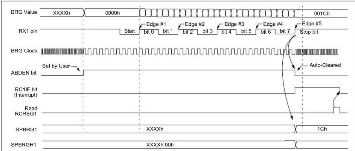
text_image
BRG Value XXXXh 0000h 001Ch RX1 pin Start Edge #1 bit 0 bit 1 Edge #2 bit 2 bit 3 Edge #3 bit 4 bit 5 Edge #4 bit 6 bit 7 Edge #5 Stop bit BRG Clock Set by User ABDEN bit Auto-Cleared RC1IF bit (Interrupt) Read RCREG1 SPBRG1 XXXXh 1Ch SPBRGH1 XXXXh 00hNote: The ABD sequence requires the EUSART module to be configured in Asynchronous mode and WUE = 0.
FIGURE 19-2: BRG OVERFLOW SEQUENCE
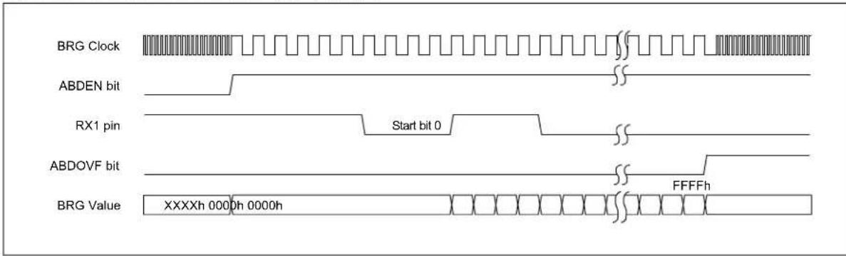
text_image
BRG Clock ABDEN bit RX1 pin Start bit 0 ABDOVF bit FFFFh BRG Value XXXXh 0000h 0000h19.3 EUSART Asynchronous Mode
The Asynchronous mode of operation is selected by clearing the SYNC bit (TXSTA1<4>). In this mode, the EUSART uses standard Non-Return-to-Zero (NRZ) format (one Start bit, eight or nine data bits and one Stop bit). The most common data format is 8 bits. An on-chip dedicated 8-bit/16-bit Baud Rate Generator can be used to derive standard baud rate frequencies from the oscillator.
The EUSART transmits and receives the LSb first. The EUSART's transmitter and receiver are functionally independent, but use the same data format and baud rate. The Baud Rate Generator produces a clock, either x16 or x64 of the bit shift rate, depending on the BRGH and BRG16 bits (TXSTA1<2> and BAUDCON1<3>). Parity is not supported by the hardware but can be implemented in software and stored as the 9th data bit.
When operating in Asynchronous mode, the EUSART module consists of the following important elements:
• Baud Rate Generator
- Sampling Circuit
• Asynchronous Transmitter
- Asynchronous Receiver
• Auto-Wake-up on Sync Break Character
• 12-Bit Break Character Transmit
• Auto-Baud Rate Detection
19.3.1 EUSART ASYNCHRONOUS TRANSMITTER
The EUSART transmitter block diagram is shown in Figure 19-3. The heart of the transmitter is the Transmit (Serial) Shift Register (TSR). The Shift register obtains its data from the Read/Write Transmit Buffer Register, TXREG1. The TXREG1 register is loaded with data in software. The TSR register is not loaded until the Stop bit has been transmitted from the previous load. As soon as the Stop bit is transmitted, the TSR is loaded with new data from the TXREG1 register (if available).
Once the TXREG1 register transfers the data to the TSR register (occurs in one Tcy), the TXREG1 register is empty and the TX1IF flag bit (PIR1<4>) is set. This interrupt can be enabled or disabled by setting or clearing the interrupt enable bit, TX1IE (PIE1<4>). TX1IF will be set regardless of the state of TX1IE; it cannot be cleared in software. TX1IF is also not cleared immediately upon loading TXREG1, but becomes valid in the second instruction cycle following the load instruction. Polling TX1IF immediately following a load of TXREG1 will return invalid results.
While TX1IF indicates the status of the TXREG1 register, another bit, TRMT (TXSTA1<1>), shows the status of the TSR register. TRMT is a read-only bit which is set when the TSR register is empty. No interrupt logic is tied to this bit, so the user has to poll this bit in order to determine if the TSR register is empty.
Note 1: The TSR register is not mapped in data memory, so it is not available to the user.
2: Flag bit, TX1IF, is set when enable bit, TXEN, is set.
To set up an Asynchronous Transmission:
- Initialize the SPBRGH1:SPBRG1 registers for the appropriate baud rate. Set or clear the BRGH and BRG16 bits, as required, to achieve the desired baud rate.
- Enable the asynchronous serial port by clearing bit, SYNC, and setting bit, SPEN.
- If interrupts are desired, set enable bit, TX1IE.
- If 9-bit transmission is desired, set transmit bit, TX9; can be used as address/data bit.
- Enable the transmission by setting bit, TXEN, which will also set bit, TX1IF.
- If 9-bit transmission is selected, the ninth bit should be loaded in bit, TX9D.
- Load data to the TXREG1 register (starts transmission).
- If using interrupts, ensure that the GIE and PEIE bits in the INTCON register (INTCON<7:6>) are set.
FIGURE 19-3: EUSART TRANSMIT BLOCK DIAGRAM
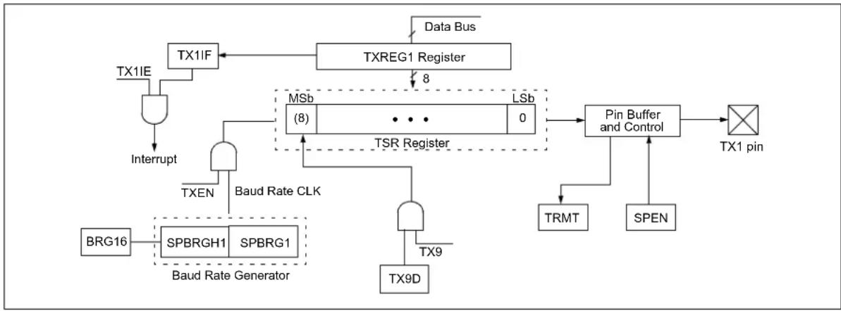
text_image
Write to TXREG1 BRG Output (Shift Clock) TX1 (pin) TX1IF bit (Transmit Buffer Reg. Empty Flag) TRMT bit (Transmit Shift Reg. Empty Flag) Word 1 Start bit bit 0 bit 1 bit 7/8 Stop bit Word 1 1 Tcy Word 1 Transmit Shift RegFIGURE 19-5: ASYNCHRONOUS TRANSMISSION (BACK TO BACK)
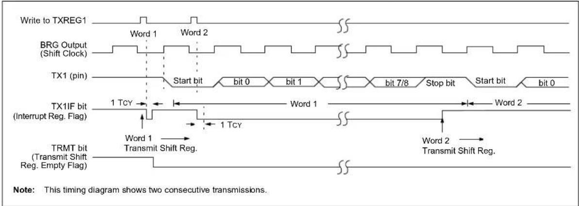
text_image
Write to TXREG1 BRG Output (Shift Clock) TX1 (pin) Start bit bit 0 bit 1 bit 7/8 Stop bit Start bit bit 0 TX1IF bit (Interrupt Reg. Flag) 1 TCY Word 1 Word 2 1 TCY Word 1 Transmit Shift Reg. TRMT bit (Transmit Shift Reg. Empty Flag) Word 2 Transmit Shift Reg. Note: This timing diagram shows two consecutive transmissions.TABLE 19-5: REGISTERS ASSOCIATED WITH ASYNCHRONOUS TRANSMISSION
| Name Bit | 7 Bit 6 Bit 5 | Bit 4 Bit 3 | Bit 2 Bit 1 | Bit 0 | Reset Values on Page | ||||
| INTCON GIE/GIEH PEIE/GIEL | TMR0IE | INT0IE | RBIE | TMR0IF | INT0IF | RBIF | 59 | ||
| PIR1 | — | ADIF | RC1IF | TX1IF | SSPIF | — | TMR2IF | TMR1IF | 62 |
| PIE1 | — | ADIE | RC1IE | TX1IE | SSPIE | — | TMR2IE | TMR1IE | 62 |
| IPR1 | — | ADIP | RC1IP | TX1IP | SSPIP | — | TMR2IP | TMR1IP | 62 |
| RCSTA1 | SPEN | RX9 | SREN | CREN | ADDEN | FERR | OERR | RX9D | 61 |
| TXREG1 | EUSART Transmit Register | 61 | |||||||
| TXSTA1 | CSRC | TX9 | TXEN | SYNC | SENDB | BRGH | TRMT | TX9D | 61 |
| BAUDCON1 | ABDOVF | RCIDL | RXDTP | TXCKP | BRG16 | — | WUE | ABDEN | 63 |
| SPBRGH1 | EUSART Baud Rate Generator Register High Byte | 63 | |||||||
| SPBRG1 | EUSART Baud Rate Generator Register Low Byte | 61 | |||||||
| LATG | U2OD | U1OD | — | LATG4 | LATG3 | LATG2 | LATG1 | LATG0 | 62 |
Legend: — = unimplemented locations read as '0'. Shaded cells are not used for asynchronous transmission.
19.3.2 EUSART ASYNCHRONOUS RECEIVER
The receiver block diagram is shown in Figure 19-6. The data is received on the RX1 pin and drives the data recovery block. The data recovery block is actually a high-speed shifter, operating at x16 times the baud rate, whereas the main receive serial shifter operates at the bit rate or at F osc. This mode would typically be used in RS-232 systems.
To set up an Asynchronous Reception:
- Initialize the SPBRGH1:SPBRG1 registers for the appropriate baud rate. Set or clear the BRGH and BRG16 bits, as required, to achieve the desired baud rate.
- Enable the asynchronous serial port by clearing bit, SYNC, and setting bit, SPEN.
- If interrupts are desired, set enable bit, RC1IE.
- If 9-bit reception is desired, set bit, RX9.
- Enable the reception by setting bit, CREN.
- Flag bit, RC1IF, will be set when reception is complete and an interrupt will be generated if enable bit, RC1IE, was set.
- Read the RCSTA1 register to get the 9th bit (if enabled) and determine if any error occurred during reception.
- Read the 8-bit received data by reading the RCREG1 register.
- If any error occurred, clear the error by clearing enable bit, CREN.
- If using interrupts, ensure that the GIE and PEIE bits in the INTCON register (INTCON<7:6>) are set.
19.3.3 SETTING UP 9-BIT MODE WITH ADDRESS DETECT
This mode would typically be used in RS-485 systems. To set up an Asynchronous Reception with Address Detect Enable:
- Initialize the SPBRGH1:SPBRG1 registers for the appropriate baud rate. Set or clear the BRGH and BRG16 bits, as required, to achieve the desired baud rate.
- Enable the asynchronous serial port by clearing the SYNC bit and setting the SPEN bit.
- If interrupts are required, set the RCEN bit and select the desired priority level with the RC1IP bit.
- Set the RX9 bit to enable 9-bit reception.
- Set the ADDEN bit to enable address detect.
- Enable reception by setting the CREN bit.
- The RC1IF bit will be set when reception is complete. The interrupt will be Acknowledged if the RC1IE and GIE bits are set.
- Read the RCSTA1 register to determine if any error occurred during reception, as well as read bit 9 of data (if applicable).
- Read RCREG1 to determine if the device is being addressed.
- If any error occurred, clear the CREN bit.
- If the device has been addressed, clear the ADDEN bit to allow all received data into the receive buffer and interrupt the CPU.
FIGURE 19-6: EUSART RECEIVE BLOCK DIAGRAM
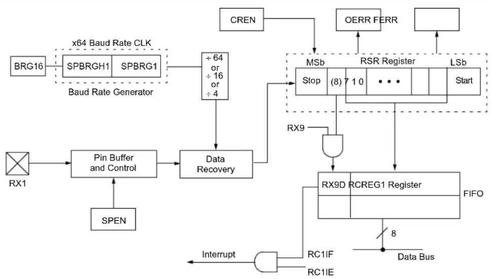
flowchart
graph TD
    A["BRG16"] --> B["x64 Baud Rate CLK"]
    B --> C["SPBRGH1"]
    B --> D["SPBRG1"]
    C --> E["÷ 64 or ÷ 16 or ÷ 4"]
    D --> F["÷ 4"]
    F --> G["Data Recovery"]
    G --> H["Spin Buffer and Control"]
    H --> I["SPEN"]
    J["RX1"] --> I
    I --> G
    K["CREN"] --> L["MSb"]
    L --> M["Stop (8) 7 10 ..."]
    M --> N["RSR Register"]
    N --> O["LSb Start"]
    P["OERR FERR"] --> L
    Q["RX9"] --> R["RX9D RCREG1 Register"]
    R --> S["FIFO"]
    T["Interrupt"] --> U["RC1IF RC1IE"]
    U --> V["Data Bus"]
FIGURE 19-7: ASYNCHRONOUS RECEPTION

flowchart
graph TD
    A["RX1 (pin)"] --> B["Start bit"]
    B --> C["bit 0"]
    C --> D["bit 1"]
    D --> E["bit 7/8"]
    E --> F["Stop bit"]
    F --> G["Start bit"]
    G --> H["bit 0"]
    H --> I["bit 7/8"]
    I --> J["Stop bit"]
    J --> K["Start bit"]
    K --> L["bit 7/8"]
    L --> M["Stop bit"]

    N["Rcv Shift Reg"] --> O["Word 1 RCREG1"]
    P["Rcv Buffer Reg"] --> Q["Word 2 RCREG1"]

    R["RCREG1"] --> S["Word 1"]
    T["Read Rcv"] --> U["Word 2"]
    V["Buffer Reg"] --> W["Word 2"]

    X["RC1IF (Interrupt Flag)"] --> Y["Word 1"]
    Z["OERR bit"] --> AA["Word 2"]
    AB["CREN bit"] --> AC["Word 2"]

    AD["Note: This timing diagram shows three words appearing on the RX1 input. The RCREG1 (Receive Buffer register) is read after the third word causing the OERR (Overrun) bit to be set."]
TABLE 19-6: REGISTERS ASSOCIATED WITH ASYNCHRONOUS RECEPTION
| Name Bit | 7 Bit 6 Bit | 5 Bit 4 Bit 3 | Bit 2 Bit 1 | Bit 0 | Reset Values on Page | ||||
| INTCON GIE/GIEH PEIE/GIEL | TMR0IE | INT0IE | RBIE | TMR0IF | INT0IF | RBIF | 59 | ||
| PIR1 | — | ADIF | RC1IF | TX1IF | SSPIF | — | TMR2IF | TMR1IF | 62 |
| PIE1 | — | ADIE | RC1IE | TX1IE | SSPIE | — | TMR2IE | TMR1IE | 62 |
| IPR1 | — | ADIP | RC1IP | TX1IP | SSPIP | — | TMR2IP | TMR1IP | 62 |
| RCSTA1 | SPEN | RX9 | SREN | CREN | ADDEN | FERR | OERR | RX9D | 61 |
| RCREG1 | EUSART Receive Register | 61 | |||||||
| TXSTA1 | CSRC | TX9 | TXEN | SYNC | SENDB | BRGH | TRMT | TX9D | 61 |
| BAUDCON1 | ABDOVF | RCIDL | RXDTP | TXCKP | BRG16 | — | WUE | ABDEN | 63 |
| SPBRGH1 EU/SART Baud Rate Generator Register High Byte | 61 | ||||||||
| SPBRG1 | EUSART Baud Rate Generator Register Low Byte | 61 | |||||||
Legend: — = unimplemented locations read as '0'. Shaded cells are not used for asynchronous reception.
19.3.4 AUTO-WAKE-UP ON SYNC BREAK CHARACTER
During Sleep mode, all clocks to the EUSART are suspended. Because of this, the Baud Rate Generator is inactive and a proper byte reception cannot be performed. The auto-wake-up feature allows the controller to wake-up, due to activity on the RX1/DT1 line, while the EUSART is operating in Asynchronous mode.
The auto-wake-up feature is enabled by setting the WUE bit (BAUDCON<1>). Once set, the typical receive sequence on RX1/DT1 is disabled and the EUSART remains in an Idle state, monitoring for a wake-up event independent of the CPU mode. A wake-up event consists of a high-to-low transition on the RX1/DT1 line. (This coincides with the start of a Sync Break or a Wake-up Signal character for the LIN/J2602 protocol.)
Following a wake-up event, the module generates an RC1IF interrupt. The interrupt is generated synchronously to the Q clocks in normal operating modes (Figure 19-8), and asynchronously, if the device is in Sleep mode (Figure 19-9). The interrupt condition is cleared by reading the RCREG1 register.
The WUE bit is automatically cleared once a low-to-high transition is observed on the RX1 line following the wake-up event. At this point, the EUSART module is in Idle mode and returns to normal operation. This signals to the user that the Sync Break event is over.
19.3.4.1 Special Considerations Using Auto-Wake-up
Since auto-wake-up functions by sensing rising edge transitions on RX1/DT1, information with any state changes before the Stop bit may signal a false End-Of-Character (EOF) and cause data or framing errors. Therefore, to work properly, the initial character in the transmission must be all '0's. This can be 00h (8 bytes) for standard RS-232 devices or 000h (12 bits) for LIN/J2602 bus.
Oscillator start-up time must also be considered, especially in applications using oscillators with longer start-up intervals (i.e., XT or HS mode). The Sync Break (or Wake-up Signal) character must be of sufficient length and be followed by a sufficient interval to allow enough time for the selected oscillator to start and provide proper initialization of the EUSART.
19.3.4.2 Special Considerations Using the WUE Bit
The timing of WUE and RC1IF events may cause some confusion when it comes to determining the validity of received data. As noted, setting the WUE bit places the EUSART in an Idle mode. The wake-up event causes a receive interrupt by setting the RC1IF bit. The WUE bit is cleared after this when a rising edge is seen on RX1/DT1. The interrupt condition is then cleared by reading the RCREG1 register. Ordinarily, the data in RCREG1 will be dummy data and should be discarded.
The fact that the WUE bit has been cleared (or is still set), and the RC1IF flag is set, should not be used as an indicator of the integrity of the data in RCREG1. Users should consider implementing a parallel method in firmware to verify received data integrity.
To assure that no actual data is lost, check the RCIDL bit to verify that a receive operation is not in process. If a receive operation is not occurring, the WUE bit may then be set just prior to entering the Sleep mode.
FIGURE 19-8: AUTO-WAKE-UP BIT (WUE) TIMINGS DURING NORMAL OPERATION

text_image
OSC1 Bit set by 'user' WUE bit(1) Auto-Cleared RX1/DT1 Line RC1IF Cleared due to user read of RCREG1Note 1: The EUSART remains in Idle while the WUE bit is set.
FIGURE 19-9: AUTO-WAKE-UP BIT (WUE) TIMINGS DURING SLEEP
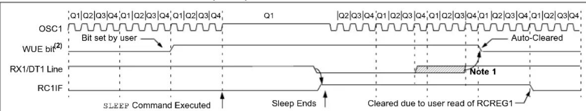
text_image
OSC1 WUE bit(2) RX1/DT1 Line RC1IF Q1|Q2|Q3|Q4|Q1|Q2|Q3|Q4|Q1|Q2|Q3|Q4| Q1 Bit set by user Auto-Cleared Note 1 SLEEP Command Executed Sleep Ends Cleared due to user read of RCREG1Note 1: If the wake-up event requires long oscillator warm-up time, the auto-clear of the WUE bit can occur while the stposc signal is still active. This sequence should not depend on the presence of Q clocks.
2: The EUSART remains in Idle while the WUE bit is set.
19.3.5 BREAK CHARACTER SEQUENCE
The Enhanced USART module has the capability of sending the special Break character sequences that are required by the LIN/J2602 bus standard. The Break character transmit consists of a Start bit, followed by twelve '0' bits and a Stop bit. The Frame Break character is sent whenever the SENDB and TXEN bits (TXSTA<3> and TXSTA<5>) are set while the Transmit Shift register is loaded with data. Note that the value of data written to TXREG1 will be ignored and all '0's will be transmitted.
The SENDB bit is automatically reset by hardware after the corresponding Stop bit is sent. This allows the user to preload the transmit FIFO with the next transmit byte following the Break character (typically, the Sync character in the LIN/J2602 specification).
Note that the data value written to the TXREG1 for the Break character is ignored. The write simply serves the purpose of initiating the proper sequence.
The TRMT bit indicates when the transmit operation is active or Idle, just as it does during normal transmission. See Figure 19-10 for the timing of the Break character sequence.
19.3.5.1 Break and Sync Transmit Sequence
The following sequence will send a message frame header made up of a Break, followed by an Auto-Baud Sync byte. This sequence is typical of a LIN/J2602 bus master.
- Configure the EUSART for the desired mode.
-
Set the TXEN and SENDB bits to set up the Break character.
-
Load the TXREG1 with a dummy character to initiate transmission (the value is ignored).
- Write '55h' to TXREG1 to load the Sync character into the transmit FIFO buffer.
- After the Break has been sent, the SENDB bit is reset by hardware. The Sync character now transmits in the preconfigured mode.
When the TXREG1 becomes empty, as indicated by the TX1IF, the next data byte can be written to TXREG1.
19.3.6 RECEIVING A BREAK CHARACTER
The Enhanced USART module can receive a Break character in two ways.
The first method forces configuration of the baud rate at a frequency of 9/13 the typical speed. This allows for the Stop bit transition to be at the correct sampling location (13 bits for Break versus Start bit and 8 data bits for typical data).
The second method uses the auto-wake-up feature described in Section 19.3.4 "Auto-Wake-up On Sync Break Character". By enabling this feature, the EUSART will sample the next two transitions on RX1/DT1, cause an RC1IF interrupt and receive the next data byte followed by another interrupt.
Note that following a Break character, the user will typically want to enable the Auto-Baud Rate Detect feature. For both methods, the user can set the ABD bit once the TX1IF interrupt is observed.
FIGURE 19-10: SEND BREAK CHARACTER SEQUENCE

flowchart
graph TD
    A["Write to TXREG1"] --> B["Dummy Write"]
    C["BRG Output (Shift Clock)"] --> D["Start bit"]
    E["TX1 (pin)"] --> F["bit 0 bit 1 bit 11"]
    G["TX1IF bit (Transmit Buffer Reg. Empty Flag)"] --> H["Break"]
    I["TRMT bit (Transmit Shift Reg. Empty Flag)"] --> J["SENDB sampled here"]
    K["SENDB (Transmit Shift Reg. Empty Flag)"] --> L["Auto-Cleared"]
19.4 EUSART Synchronous Master Mode
The Synchronous Master mode is entered by setting the CSRC bit (TXSTA<7>). In this mode, the data is transmitted in a half-duplex manner (i.e., transmission and reception do not occur at the same time). When transmitting data, the reception is inhibited and vice versa. Synchronous mode is entered by setting bit, SYNC (TXSTA<4>). In addition, enable bit, SPEN (RCSTA1<7>), is set in order to configure the TX1 and RX1 pins to CK1 (clock) and DT1 (data) lines, respectively.
The Master mode indicates that the processor transmits the master clock on the CK1 line. Clock polarity is selected with the SCKP bit (BAUDCON<4>). Setting SCKP sets the Idle state on CK1 as high, while clearing the bit, sets the Idle state as low. This option is provided to support Microwire devices with this module.
19.4.1 EUSART SYNCHRONOUS MASTER TRANSMISSION
The EUSART transmitter block diagram is shown in Figure 19-3. The heart of the transmitter is the Transmit (Serial) Shift Register (TSR). The Shift register obtains its data from the Read/Write Transmit Buffer Register, TXREG1. The TXREG1 register is loaded with data in software. The TSR register is not loaded until the last bit has been transmitted from the previous load. As soon as the last bit is transmitted, the TSR is loaded with new data from the TXREG1 (if available).
Once the TXREG1 register transfers the data to the TSR register (occurs in one TCYCLE), the TXREG1 is empty and the TX1IF flag bit (PIR1<4>) is set. The interrupt can be enabled or disabled by setting or clearing the interrupt enable bit, TX1IE (PIE1<4>). TX1IF is set regardless of the state of enable bit TX1IE; it cannot be cleared in software. It will reset only when new data is loaded into the TXREG1 register.
While flag bit, TX1IF, indicates the status of the TXREG1 register, another bit, TRMT (TXSTA<1>), shows the status of the TSR register. TRMT is a read-only bit which is set when the TSR is empty. No interrupt logic is tied to this bit so the user has to poll this bit in order to determine if the TSR register is empty. The TSR is not mapped in data memory so it is not available to the user.
To set up a Synchronous Master Transmission:
- Initialize the SPBRGH1:SPBRG1 registers for the appropriate baud rate. Set or clear the BRG16 bit, as required, to achieve the desired baud rate.
- Enable the synchronous master serial port by setting bits, SYNC, SPEN and CSRC.
- If interrupts are desired, set enable bit, TX1IE.
- If 9-bit transmission is desired, set bit, TX9.
- Enable the transmission by setting bit, TXEN.
- If 9-bit transmission is selected, the ninth bit should be loaded in bit, TX9D.
- Start transmission by loading data to the TXREG1 register.
- If using interrupts, ensure that the GIE and PEIE bits in the INTCON register (INTCON<7:6>) are set.
FIGURE 19-11: SYNCHRONOUS TRANSMISSION

text_image
RC7/RX1/DT1/SEG28 pin RC6/TX1/CK1/SEG27 pin (SCKP = 0) RC6/TX1/CK1/SEG27 pin (SCKP = 1) Write to TXREG1 Reg Write Word 1 Write Word 2 TX1IF bit (Interrupt Flag) TRMT bit TXEN bit '1' '1'Note: Sync Master mode, SPBRG1 = 0; continuous transmission of two 8-bit words.
FIGURE 19-12: SYNCHRONOUS TRANSMISSION (THROUGH TXEN)
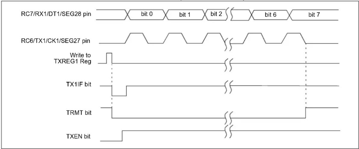
text_image
RC7/RX1/DT1/SEG28 pin bit 0 bit 1 bit 2 bit 6 bit 7 RC6/TX1/CK1/SEG27 pin Write to TXREG1 Reg TX1IF bit TRMT bit TXEN bitTABLE 19-7: REGISTERS ASSOCIATED WITH SYNCHRONOUS MASTER TRANSMISSION
| Name Bit | 7 Bit 6 Bit | 5 Bit 4 Bit 3 | Bit 2 Bit 1 | Bit 0 | Reset Values on Page | ||||
| INTCON GIE | GIEH PEIE | GIEL | TMR0IE | INT0IE | RBIE | TMR0IF | INT0IF | RBIF | 59 |
| PIR1 | — | ADIF | RC1IF | TX1IF | SSPIF | — | TMR2IF | TMR1IF | 62 |
| PIE1 | — | ADIE | RC1IE | TX1IE | SSPIE | — | TMR2IE | TMR1IE | 62 |
| IPR1 | — | ADIP | RC1IP | TX1IP | SSPIP | — | TMR2IP | TMR1IP | 62 |
| RCSTA1 | SPEN | RX9 | SREN | CREN | ADDEN | FERR | OERR | RX9D | 61 |
| TXREG1 | EUSART Transmit Register | 61 | |||||||
| TXSTA1 | CSRC TX9 | TX | EN SYNC | SENDB | BRGH | TRMT | TX9D | 61 | |
| BAUDCON1 | ABDOVF | RCIDL | RXDTP | TXCKP | BRG16 | — | WUE | ABDEN | 63 |
| SPBRGH1 | EUSART Baud Rate Generator Register High Byte | 63 | |||||||
| SPBRG1 | EUSART Baud Rate Generator Register Low Byte | 61 | |||||||
| LATG | U2OD | U1OD | — | LATG4 | LATG3 | LATG2 | LATG1 | LATG0 | 62 |
Legend: — = unimplemented, read as '0'. Shaded cells are not used for synchronous master transmission.
19.4.2 EUSART SYNCHRONOUS MASTER RECEPTION
Once Synchronous mode is selected, reception is enabled by setting either the Single Receive Enable bit, SREN (RCSTA1<5>), or the Continuous Receive Enable bit, CREN (RCSTA1<4>). Data is sampled on the RX1 pin on the falling edge of the clock.
If enable bit, SREN, is set, only a single word is received. If enable bit, CREN, is set, the reception is continuous until CREN is cleared. If both bits are set, then CREN takes precedence.
To set up a Synchronous Master Reception:
-
Initialize the SPBRGH1:SPBRG1 registers for the appropriate baud rate. Set or clear the BRG16 bit, as required, to achieve the desired baud rate.
-
Enable the synchronous master serial port by setting bits, SYNC, SPEN and CSRC.
-
Ensure bits, CREN and SREN, are clear.
- If interrupts are desired, set enable bit, RC1IE.
- If 9-bit reception is desired, set bit, RX9.
-
If a single reception is required, set bit, SREN. For continuous reception, set bit, CREN.
-
Interrupt flag bit, RC1IF, will be set when reception is complete and an interrupt will be generated if the enable bit, RC1IE, was set.
-
Read the RCSTA1 register to get the 9th bit (if enabled) and determine if any error occurred during reception.
-
Read the 8-bit received data by reading the RCREG1 register.
-
If any error occurred, clear the error by clearing bit, CREN.
-
If using interrupts, ensure that the GIE and PEIE bits in the INTCON register (INTCON<7:6>) are set.
FIGURE 19-13: SYNCHRONOUS RECEPTION (MASTER MODE, SREN)
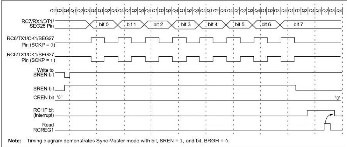
other
| Signal | Bit Position | Value | |--------|--------------|-------| | RC7/RX1/DT1/SEG28 Pin | bit 0 | 0 | | RC7/RX1/DT1/SEG28 Pin | bit 1 | 1 | | RC7/RX1/DT1/SEG28 Pin | bit 2 | 2 | | RC7/RX1/DT1/SEG28 Pin | bit 3 | 3 | | RC7/RX1/DT1/SEG28 Pin | bit 4 | 4 | | RC7/RX1/DT1/SEG28 Pin | bit 5 | 5 | | RC7/RX1/DT1/SEG28 Pin | bit 6 | 6 | | RC7/RX1/DT1/SEG28 Pin | bit 7 | 7 | | RC6/TX1/CK1/SEG27 Pin (SCKP = 0) | | | | RC6/TX1/CK1/SEG27 Pin (SCKP = 1) | | | | Write to SREN bit | | | | SREN bit | | | | CREN bit '0' | | '0' | | RC1IF bit (Interrupt) | | | | RC1IF bit (Interrupt) | | '0' | | RCREG1 | | | Note: Timing diagram demonstrates Sync Master mode with bit, SREN = 1, and bit, BRGH = 0.TABLE 19-8: REGISTERS ASSOCIATED WITH SYNCHRONOUS MASTER RECEPTION
| Name Bit | 7 Bit 6 Bit | 5 Bit 4 Bit 3 | Bit 2 Bit 1 | Bit 0 | Reset Values on Page | ||||
| INTCON GIE | /GIEH PEIE | /GIEL | TMR0IE | INT0IE | RBIE | TMR0IF | INT0IF | RBIF | 59 |
| PIR1 | — | ADIF | RC1IF | TX1IF | SSPIF | — | TMR2IF | TMR1IF | 62 |
| PIE1 | — | ADIE | RC1IE | TX1IE | SSPIE | — | TMR2IE | TMR1IE | 62 |
| IPR1 | — | ADIP | RC1IP | TX1IP | SSPIP | — | TMR2IP | TMR1IP | 62 |
| RCSTA1 SPEN RX9 SREN | CREN | ADDEN | FERR | OERR RX9D | 61 | ||||
| RCREG1 | EUSART Receive Register | 61 | |||||||
| TXSTA1 | CSRC | TX9 | TXEN | SYNC | SENDB | BRGH | TRMT | TX9D | 61 |
| BAUDCON1 | ABDOVF | RCIDL | RXDTP | TXCKP | BRG16 | — | WUE | ABDEN | 63 |
| SPBRGH1 E | USART Baud Rate Generator Register High Byte | 63 | |||||||
| SPBRG1 | EUSART Baud Rate Generator Register Low Byte | 61 | |||||||
Legend: — = unimplemented, read as '0'. Shaded cells are not used for synchronous master reception.
19.5 EUSART Synchronous Slave Mode
Synchronous Slave mode is entered by clearing bit, CSRC (TXSTA<7>). This mode differs from the Synchronous Master mode in that the shift clock is supplied externally at the CK1 pin (instead of being supplied internally in Master mode). This allows the device to transfer or receive data while in any Low-Power mode.
19.5.1 EUSART SYNCHRONOUS SLAVE TRANSMIT
The operation of the Synchronous Master and Slave modes is identical except in the case of Sleep mode.
If two words are written to the TXREG1 and then the SLEEP instruction is executed, the following will occur:
a) The first word will immediately transfer to the TSR register and transmit.
b) The second word will remain in the TXREG1 register.
c) Flag bit, TX1IF, will not be set.
d) When the first word has been shifted out of TSR, the TXREG1 register will transfer the second word to the TSR and flag bit, TX1IF, will now be set.
e) If enable bit, TX1IE, is set, the interrupt will wake the chip from Sleep. If the global interrupt is enabled, the program will branch to the interrupt vector.
To set up a Synchronous Slave Transmission:
- Enable the synchronous slave serial port by setting bits, SYNC and SPEN, and clearing bit, CSRC.
- Clear bits, CREN and SREN.
- If interrupts are desired, set enable bit, TX1IE.
- If 9-bit transmission is desired, set bit, TX9.
- Enable the transmission by setting enable bit, TXEN.
- If 9-bit transmission is selected, the ninth bit should be loaded in bit, TX9D.
- Start transmission by loading data to the TXREG1 register.
- If using interrupts, ensure that the GIE and PEIE bits in the INTCON register (INTCON<7:6>) are set.
TABLE 19-9: REGISTERS ASSOCIATED WITH SYNCHRONOUS SLAVE TRANSMISSION
| Name Bit | 7 Bit 6 Bit | 5 Bit 4 Bit 3 | Bit 2 Bit 1 | Bit 0 | Reset Values on Page | ||||
| INTCON GIE | /GIEH PEIE/GIEL | TMR0IE | INT0IE | RBIE | TMR0IF | INT0IF | RBIF | 59 | |
| PIR1 | — | ADIF | RC1IF | TX1IF | SSPIF | — | TMR2IF | TMR1IF | 62 |
| PIE1 | — | ADIE | RC1IE | TX1IE | SSPIE | — | TMR2IE | TMR1IE | 62 |
| IPR1 | — | ADIP | RC1IP | TX1IP | SSPIP | — | TMR2IP | TMR1IP | 62 |
| RCSTA1 | SPEN | RX9 | SREN | CREN | ADDEN | FERR | OERR | RX9D | 61 |
| TXREG1 EUSART Transmit Register | 61 | ||||||||
| TXSTA1 | CSRC TX9 TXEN SYNC | SENDB | BRGH | TRMT | TX9D | 61 | |||
| BAUDCON1 | ABDOVF | RCIDL | RXDTP | TXCKP | BRG16 | — | WUE | ABDEN | 63 |
| SPBRGH1 | EUSART Baud Rate Generator Register High Byte | 63 | |||||||
| SPBRG1 | EUSART Baud Rate Generator Register Low Byte | 61 | |||||||
| LATG | U2OD | U1OD | — | LATG4 | LATG3 | LATG2 | LATG1 | LATG0 | 62 |
Legend: — = unimplemented, read as '0'. Shaded cells are not used for synchronous slave transmission.
19.5.2 EUSART SYNCHRONOUS SLAVE RECEPTION
The operation of the Synchronous Master and Slave modes is identical except in the case of Sleep or any Idle mode, and bit, SREN, which is a “don’t care” in Slave mode.
If receive is enabled by setting the CREN bit prior to entering Sleep or any Idle mode, then a word may be received while in this Low-Power mode. Once the word is received, the RSR register will transfer the data to the RCREG1 register. If the RC1IE enable bit is set, the interrupt generated will wake the chip from the Low-Power mode. If the global interrupt is enabled, the program will branch to the interrupt vector.
To set up a Synchronous Slave Reception:
- Enable the synchronous master serial port by setting bits, SYNC and SPEN, and clearing bit, CSRC.
- If interrupts are desired, set enable bit, RC1IE.
- If 9-bit reception is desired, set bit, RX9.
- To enable reception, set enable bit, CREN.
- Flag bit, RC1IF, will be set when reception is complete. An interrupt will be generated if enable bit, RC1IE, was set.
- Read the RCSTA1 register to get the 9th bit (if enabled) and determine if any error occurred during reception.
- Read the 8-bit received data by reading the RCREG1 register.
- If any error occurred, clear the error by clearing bit, CREN.
- If using interrupts, ensure that the GIE and PEIE bits in the INTCON register (INTCON<7:6>) are set.
TABLE 19-10: REGISTERS ASSOCIATED WITH SYNCHRONOUS SLAVE RECEPTION
| Name Bit | 7 Bit 6 Bit | 5 Bit 4 Bit 3 | Bit 2 Bit 1 | Bit 0 | Reset Values on Page | ||||
| INTCON | GIE/GIEH | PEIE/GIEL | TMR0IE | INT0IE | RBIE | TMR0IF | INT0IF | RBIF | 59 |
| PIR1 | — | ADIF | RC1IF | TX1IF | SSPIF | — | TMR2IF | TMR1IF | 62 |
| PIE1 | — | ADIE | RC1IE | TX1IE | SSPIE | — | TMR2IE | TMR1IE | 62 |
| IPR1 | — | ADIP | RC1IP | TX1IP | SSPIP | — | TMR2IP | TMR1IP | 62 |
| RCSTA1 | SPEN | RX9 | SREN | CREN | ADDEN | FERR | OERR | RX9D 61 | |
| RCREG1 | EUSART Receive Register | 61 | |||||||
| TXSTA1 | CSRC | TX9 | TXEN | SYNC | SENDB | BRGH | TRMT | TX9D | 61 |
| BAUDCON1 | ABDOVF | RCIDL | RXDTP | TXCKP | BRG16 | — | WUE | ABDEN | 63 |
| SPBRGH1 | EUSART Baud Rate Generator Register High Byte | 63 | |||||||
| SPBRG1 EU$ART Baud Rate Generator Register Low Byte | 61 | ||||||||
Legend: — = unimplemented, read as '0'. Shaded cells are not used for synchronous slave reception.
20.0 ADDRESSABLE UNIVERSAL SYNCHRONOUS ASYNCHRONOUS RECEIVER TRANSMITTER (AUSART)
The Addressable Universal Synchronous Asynchronous Receiver Transmitter (AUSART) module is very similar in function to the Enhanced USART module, discussed in the previous chapter. It is provided as an additional channel for serial communication with external devices, for those situations that do not require auto-baud detection or LIN/J2602 bus support.
The AUSART can be configured in the following modes:
• Asynchronous (full-duplex)
- Synchronous – Master (half-duplex)
- Synchronous – Slave (half-duplex)
The pins of the AUSART module are multiplexed with the functions of PORTG (RG1/TX2/CK2 and RG2/RX2/DT2/VLCAP1, respectively). In order to configure these pins as an AUSART:
- bit, SPEN (RCSTA2<7>), must be set (= 1)
- bit, TRISG<2>, must be set (= 1)
- bit, TRISG<1>, must be cleared (= 0) for Asynchronous and Synchronous Master modes
- bit, TRISG<1>, must be set (= 1) for Synchronous Slave mode
Note: The AUSART control will automatically reconfigure the pin from input to output as needed.
The driver for the TX2 output pin can also be optionally configured as an open-drain output. This feature allows the voltage level on the pin to be pulled to a higher level through an external pull-up resistor, and allows the output to communicate with external circuits without the need for additional level shifters.
The open-drain output option is controlled by the U2OD bit (LATG<7>). Setting the bit configures the pin for open-drain operation.
20.1 Control Registers
The operation of the Addressable USART module is controlled through two registers, TXSTA2 and RXSTA2. These are detailed in Register 20-1 and Register 20-2, respectively.
REGISTER 20-1: TXSTA2: AUSART TRANSMIT STATUS AND CONTROL REGISTER
| R/W-0 R/W-0 R/W-0 R/W-0 U-0 R/W-0 R-1 R/W-0 | |||||||
| CSRC TX9 TXEN | (1) | SYNC — BRGH TRMT TX9D | |||||
| bit 7 bit 0 | |||||||
Legend:
| R = Readable bit W = Writable bit U = Unimplemented bit, read as '0' | ||
| -n = Value at POR | '1' = Bit is set | '0' = Bit is cleared x = Bit is unknown |
bit 7 CSRC: Clock Source Select bit
Asynchronous mode:
Don't care.
Synchronous mode:
1 = Master mode (clock generated internally from BRG)
0 = Slave mode (clock from external source)
bit 6 TX9: 9-Bit Transmit Enable bit
1 = Selects 9-bit transmission
0 = Selects 8-bit transmission
bit 5 TXEN: Transmit Enable bit
(1)
1 = Transmit enabled
0 = Transmit disabled
bit 4 SYNC: AUSART Mode Select bit
1 = Synchronous mode
0 = Asynchronous mode
bit 3 Unimplemented: Read as '0'
bit 2 BRGH: High Baud Rate Select bit
Asynchronous mode:
1 = High speed
0 = Low speed
Synchronous mode:
Unused in this mode.
bit 1 TRMT: Transmit Shift Register Status bit
1 = TSR empty
0 = TSR full
bit 0 TX9D: 9th bit of Transmit Data
Can be address/data bit or a parity bit.
Note 1: SREN/CREN overrides TXEN in Sync mode.
REGISTER 20-2: RCSTA2: AUSART RECEIVE STATUS AND CONTROL REGISTER
| R/W-0 R/W-0 R/W-0 R/W-0 R/W-0 R-0 R-0 R-x | |||||||
| SPEN RX9 | SREN CREN | ADDEN FERR | OERR RX9D | ||||
| bit 7 bit 0 | |||||||
Legend:
| R = Readable bit W = Writable bit U = Unimplemented bit, read as '0' | ||
| -n = Value at POR | '1' = Bit is set | '0' = Bit is cleared x = Bit is unknown |
bit 7 SPEN: Serial Port Enable bit
1 = Serial port enabled (configures RX2/DT2 and TX2/CK2 (TXEN = 1) pins as serial port pins) 0 = Serial port disabled (held in Reset)
bit 6 RX9: 9-Bit Receive Enable bit
1 = Selects 9-bit reception 0 = Selects 8-bit reception
bit 5 SREN: Single Receive Enable bit
Asynchronous mode: Don't care.
Synchronous mode - Master:
1 = Enables single receive 0 = Disables single receive This bit is cleared after reception is complete.
Synchronous mode – Slave: Don't care.
bit 4 CREN: Continuous Receive Enable bit
Asynchronous mode:
1 = Enables receiver 0 = Disables receiver
Synchronous mode: 1 = Enables continuous receive until enable bit, CREN, is cleared (CREN overrides SREN) 0 = Disables continuous receive
bit 3 ADDEN: Address Detect Enable bit
Asynchronous mode 9-bit (RX9 = 1):
1 = Enables address detection, enables interrupt and loads the receive buffer when RSR<8> is set 0 = Disables address detection, all bytes are received and ninth bit can be used as parity bit
Asynchronous mode 9-bit (RX9 = 0): Don't care.
bit 2 FERR: Framing Error bit
1 = Framing error (can be cleared by reading the RCREGx register and receiving the next valid byte) 0 = No framing error
bit 1 OERR: Overrun Error bit
1 = Overrun error (can be cleared by clearing bit CREN) 0 = No overrun error
bit 0 RX9D: 9th bit of Received Data
This can be address/data bit or a parity bit and must be calculated by user firmware.
20.2 AUSART Baud Rate Generator (BRG)
The BRG is a dedicated, 8-bit generator that supports both the Asynchronous and Synchronous modes of the AUSART.
The SPBRG2 register controls the period of a free-running timer. In Asynchronous mode, the BRGH bit (TXSTA<2>) also controls the baud rate. In Synchronous mode, BRGH is ignored. Table 20-1 shows the formula for computation of the baud rate for different AUSART modes, which only apply in Master mode (internally generated clock).
Given the desired baud rate and Fosc, the nearest integer value for the SPBRG2 register can be calculated using the formulas in Table 20-1. From this, the error in baud rate can be determined. An example calculation is shown in Example 20-1. Typical baud rates and error values for the various Asynchronous modes are shown in Table 20-2. It may be advantageous to use the high baud rate (BRGH = 1) to reduce the baud rate error, or achieve a slow baud rate for a fast oscillator frequency.
Writing a new value to the SPBRG2 register causes the BRG timer to be reset (or cleared). This ensures the BRG does not wait for a timer overflow before outputting the new baud rate.
20.2.1 OPERATION IN POWER-MANAGED MODES
The device clock is used to generate the desired baud rate. When one of the power-managed modes is entered, the new clock source may be operating at a different frequency. This may require an adjustment to the value in the SPBRG2 register.
20.2.2 SAMPLING
The data on the RX2 pin is sampled three times by a majority detect circuit to determine if a high or a low level is present at the RX2 pin.
TABLE 20-1: BAUD RATE FORMULAS
| Configuration Bits | BRG/AUSART Mode Baud Rate Formula | ||
| SYNC BRGH | |||
| 0 | 0 | Asynchronous F | osc/[64 (n + 1)] |
| 0 | 1 | Asynchronous F | osc/[16 (n + 1)] |
| 1 | x | Synchronous | Fosc/[4 (n + 1)] |
Legend: x = Don't care, n = Value of SPBRG2 register
EXAMPLE 20-1: CALCULATING BAUD RATE ERROR
| For a device with FOSC of 16 MHz, desired baud rate of 9600, Asynchronous mode, BRGH = 0:Desired Baud Rate = FOSC/(64 ([SPBRG2] + 1))Solving for SPBRG2:X = ((FOSC/Desired Baud Rate)/64) - 1= ((16000000/9600)/64) - 1= [25.042] = 25Calculated Baud Rate = 16000000/(64 (25 + 1))= 9615Error = (Calculated Baud Rate – Desired Baud Rate)/Desired Baud Rate= (9615 – 9600)/9600 = 0.16% |
TABLE 20-2: REGISTERS ASSOCIATED WITH THE BAUD RATE GENERATOR
| Name | Bit 7 | Bit 6 | Bit 5 | Bit 4 | Bit 3 | Bit 2 | Bit 1 | Bit 0 | Reset Values on Page |
| TXSTA2 | CSRC | TX9 | TXEN | SYNC | SENDB | BRGH | TRMT | TX9D | 64 |
| RCSTA2 | SPEN | RX9 | SREN | CREN | ADDEN | FERR | OERR | RX9D | 64 |
| SPBRG2 | AUSART Baud Rate Generator Register | 64 | |||||||
Legend: Shaded cells are not used by the BRG.
TABLE 20-3: BAUD RATES FOR ASYNCHRONOUS MODES
| BAUD RATE (K) | BRGH = 0 | |||||||||||
| Fosc = 40.000 MHz | Fosc = 20.000 MHz | Fosc = 10.000 MHz | Fosc = 8.000 MHz | |||||||||
| Actual Rate (K) | % Error | SPBRG value (decimal) | Actual Rate (K) | % Error | SPBRG value (decimal) | Actual Rate (K) | % Error | SPBRG value (decimal) | Actual Rate (K) | % Error | SPBRG value (decimal) | |
| 0 | . | 3 | — | — | — | — | — | — | — | — | — | — |
| 1.2 — | — | 1.221 | 1.73 255 | 1.202 0.16 | 129 1.201 | -0.16 | 103 | |||||
| 2.4 | 2.441 | 1.73 | 255 | 2.404 | 0.16 | 129 | 2.404 | 0.16 | 64 | 2.403 | -0.16 | 51 |
| 9.6 | 9.615 | 0.16 | 64 | 9.766 | 1.73 | 31 | 9.766 | 1.73 | 15 | 9.615 | -0.16 | 12 |
| 19.2 | 19.531 | 1.73 | 31 | 19.531 | 1.73 | 15 | 19.531 | 1.73 | 7 | — | — | — |
| 57.6 | 56.818 | -1.36 | 10 | 62.500 | 8.51 | 4 | 52.083 | -9.58 | 2 | — | — | — |
| 115.2 | 125.000 | 8.51 | 4 | 104.167 | -9.58 | 2 | 78.125 | -32.18 | 1 | — | — | — |
| BAUD RATE (K) | BRGH = 0 | ||||||||
| Fosc = 4.000 MHz | Fosc = 2.000 MHz | Fosc = 1.000 MHz | |||||||
| Actual Rate (K) | % Error | SPBRG value (decimal) | Actual Rate (K) | % Error | SPBRG value (decimal) | Actual Rate (K) | % Error | SPBRG value (decimal) | |
| 0.3 | 0.300 | 0.16 | 207 | 0.300 | -0.16 | 103 | 0.300 | -0.16 | 51 |
| 1.2 | 1.202 | 0.16 | 51 | 1.201 | -0.16 | 25 | 1.201 | -0.16 | 12 |
| 2.4 | 2.404 | 0.16 | 25 2.403 | -0.16 | 12 — — — | ||||
| 9.6 | 8.929 | -6.99 | 6 | — | — | — | — | — | — |
| 19.2 | 20.833 | 8.51 | 2 | — | — | — | — | — | — |
| 57.6 | 62.500 | 8.51 | 0 | — | — | — | — | — | — |
| 115.2 | 62.500 | -45.75 | 0 | — | — | — | — | — | — |
| BAUD RATE (K) | BRGH = 1 | |||||||||||
| Fosc = 40.000 MHz | Fosc = 20.000 MHz | Fosc = 10.000 MHz | Fosc = 8.000 MHz | |||||||||
| Actual Rate (K) | % Error | SPBRG value (decimal) | Actual Rate (K) | % Error | SPBRG value (decimal) | Actual Rate (K) | % Error | SPBRG value (decimal) | Actual Rate (K) | % Error | SPBRG value (decimal) | |
| 0 | . | 3 | — | — | — | — | — | — | — | — | — | — |
| 1 | . | 2 | — | — | — | — | — | — | — | — | — | — |
| 2.4 — | — — — | — 2.441 | 1.73 255 | 2.403 | -0.16 | 207 | ||||||
| 9.6 | 9.766 | 1.73 | 255 | 9.615 | 0.16 | 129 | 9.615 | 0.16 | 64 | 9.615 | -0.16 | 51 |
| 19.2 | 19.231 | 0.16 | 129 | 19.231 | 0.16 | 64 | 19.531 | 1.73 | 31 | 19.230 | -0.16 | 25 |
| 57.6 | 58.140 | 0.94 | 42 | 56.818 | -1.36 | 21 | 56.818 | -1.36 | 10 | 55.555 | 3.55 | 8 |
| 115.2 | 113.636 | -1.36 | 21 | 113.636 | -1.36 | 10 | 125.000 | 8.51 | 4 | — | — | — |
| BAUD RATE (K) | BRGH = 1 | ||||||||
| Fosc = 4.000 MHz | Fosc = 2.000 MHz | Fosc = 1.000 MHz | |||||||
| Actual Rate (K) | % Error | SPBRG value (decimal) | Actual Rate (K) | % Error | SPBRG value (decimal) | Actual Rate (K) | % Error | SPBRG value (decimal) | |
| 0.3 | — | — | — | — | — | — | 0.300 | -0.16 | 207 |
| 1.2 | 1.202 | 0.16 | 207 | 1.201 | -0.16 | 103 | 1.201 | -0.16 | 51 |
| 2.4 | 2.404 | 0.16 | 103 | 2.403 | -0.16 | 51 | 2.403 | -0.16 | 25 |
| 9.6 | 9.615 | 0.16 | 25 | 9.615 | -0.16 | 12 | — | — | — |
| 19.2 | 19.231 | 0.16 | 12 | — | — | — | — | — | — |
| 57.6 | 62.500 | 8.51 | 3 | — | — | — | — | — | — |
| 115.2 | 125.000 | 8.51 | 1 | — | — | — | — | — | — |
20.3 AUSART Asynchronous Mode
The Asynchronous mode of operation is selected by clearing the SYNC bit (TXSTA2<4>). In this mode, the AUSART uses standard Non-Return-to-Zero (NRZ) format (one Start bit, eight or nine data bits and one Stop bit). The most common data format is 8 bits. An on-chip, dedicated, 8-bit Baud Rate Generator can be used to derive standard baud rate frequencies from the oscillator.
The AUSART transmits and receives the LSb first. The AUSART's transmitter and receiver are functionally independent but use the same data format and baud rate. The Baud Rate Generator produces a clock, either x16 or x64 of the bit shift rate, depending on the BRGH bit (TXSTA2<2>). Parity is not supported by the hardware but can be implemented in software and stored as the 9th data bit.
When operating in Asynchronous mode, the AUSART module consists of the following important elements:
• Baud Rate Generator
- Sampling Circuit
• Asynchronous Transmitter
• Asynchronous Receiver
20.3.1 AUSART ASYNCHRONOUS TRANSMITTER
The AUSART transmitter block diagram is shown in Figure 20-1. The heart of the transmitter is the Transmit (Serial) Shift Register (TSR). The Shift register obtains its data from the Read/Write Transmit Buffer Register, TXREG2. The TXREG2 register is loaded with data in software. The TSR register is not loaded until the Stop bit has been transmitted from the previous load. As soon as the Stop bit is transmitted, the TSR is loaded with new data from the TXREG2 register (if available).
Once the TXREG2 register transfers the data to the TSR register (occurs in one Tcy), the TXREG2 register is empty and the TX2IF flag bit (PIR3<4>) is set. This interrupt can be enabled or disabled by setting or clearing the interrupt enable bit, TX2IE (PIE3<4>). TX2IF will be set regardless of the state of TX2IE; it cannot be cleared in software. TX2IF is also not cleared immediately upon loading TXREG2, but becomes valid in the second instruction cycle following the load instruction. Polling TX2IF immediately following a load of TXREG2 will return invalid results.
While TX2IF indicates the status of the TXREG2 register, another bit, TRMT (TXSTA2<1>), shows the status of the TSR register. TRMT is a read-only bit which is set when the TSR register is empty. No interrupt logic is tied to this bit so the user has to poll this bit in order to determine if the TSR register is empty.
Note 1: The TSR register is not mapped in data memory so it is not available to the user.
2: Flag bit, TX2IF, is set when enable bit, TXEN, is set.
To set up an Asynchronous Transmission:
- Initialize the SPBRG2 register for the appropriate baud rate. Set or clear the BRGH bit, as required, to achieve the desired baud rate.
- Enable the asynchronous serial port by clearing bit, SYNC, and setting bit, SPEN.
- If interrupts are desired, set enable bit, TX2IE.
- If 9-bit transmission is desired, set transmit bit, TX9. Can be used as address/data bit.
- Enable the transmission by setting bit, TXEN, which will also set bit, TX2IF.
- If 9-bit transmission is selected, the ninth bit should be loaded in bit, TX9D.
- Load data to the TXREG2 register (starts transmission).
- If using interrupts, ensure that the GIE and PEIE bits in the INTCON register (INTCON<7:6>) are set.
FIGURE 20-1: AUSART TRANSMIT BLOCK DIAGRAM
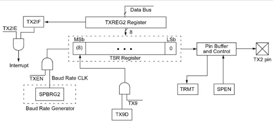
flowchart
graph TD
    A["TX2IE"] --> B["Interrupt"]
    B --> C["TX2IF"]
    C --> D["TXREG2 Register"]
    D --> E["Data Bus"]
    E --> D
    D --> F["TSR Register"]
    F --> G["MSb (8)"]
    F --> H["LSb 0"]
    F --> I["TXEN"]
    I --> J["Baud Rate CLK"]
    J --> K["SPBRG2"]
    K --> L["Baud Rate Generator"]
    F --> M["TX9D"]
    M --> N["TX9"]
    N --> O["TRMT"]
    O --> P["Pin Buffer and Control"]
    P --> Q["TX2 pin"]
    P --> R["SPEN"]
FIGURE 20-2: ASYNCHRONOUS TRANSMISSION
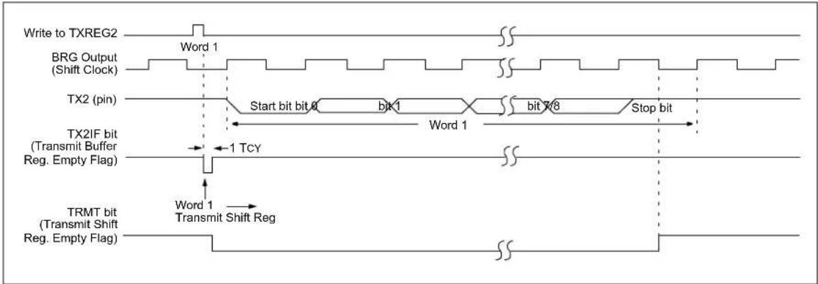
text_image
Write to TXREG2 BRG Output (Shift Clock) TX2 (pin) TX2IF bit (Transmit Buffer Reg. Empty Flag) TRMT bit (Transmit Shift Reg. Empty Flag) Word 1 Start bit bit 0 bit 1 bit 7/8 Stop bit Word 1 1 TCY Word 1 Transmit Shift RegFIGURE 20-3: ASYNCHRONOUS TRANSMISSION (BACK TO BACK)
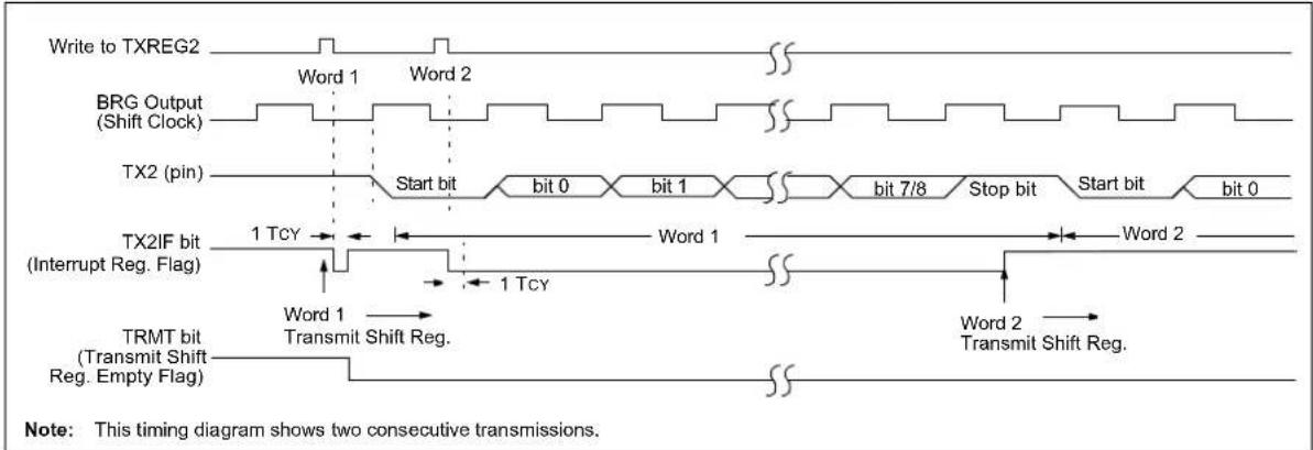
text_image
Write to TXREG2 BRG Output (Shift Clock) TX2 (pin) TX2IF bit (Interrupt Reg. Flag) TRMT bit (Transmit Shift Reg. Empty Flag) Word 1 Word 2 Start bit bit 0 bit 1 bit 7/8 Stop bit Start bit bit 0 1 Tcy Word 1 1 Tcy Word 2 Word 1 Transmit Shift Reg. SS SS SS SS Note: This timing diagram shows two consecutive transmissions.TABLE 20-4: REGISTERS ASSOCIATED WITH ASYNCHRONOUS TRANSMISSION
| Name Bit | 7 Bit 6 Bit 5 | Bit 4 Bit 3 | Bit 2 Bit 1 | Bit 0 | Reset Values on Page | ||||
| INTCON GIE/GIEH PEIE/GIEL | TMR0IE | INT0IE | RBIE | TMR0IF | INT0IF | RBIF | 59 | ||
| PIR3 | — | LCDIF | RC2IF | TX2IF | CTMUIF | CCP2IF | CCP1IF | RTCCIF | 62 |
| PIE3 | — | LCDIE | RC2IE | TX2IE | CTMUIE | CCP2IE | CCP1IE | RTCCIE | 62 |
| IPR3 | — | LCDIP | RC2IP | TX2IP | CTMUIP | CCP2IP | CCP1IP | RTCCIP | 62 |
| RCSTA2 | SPEN | RX9 | SREN | CREN | ADDEN | FERR | OERR | RX9D | 64 |
| TXREG2 AUSART Transmit Register | 64 | ||||||||
| TXSTA2 | CSRC | TX9 | TXEN | SYNC | — | BRGH | TRMT | TX9D | 64 |
| SPBRG2 | AUSART Baud Rate Generator Register | 64 | |||||||
| LATG | U2OD | U1OD | — | LATG4 | LATG3 | LATG2 | LATG1 | LATG0 | 62 |
Legend: — = unimplemented locations read as '0'. Shaded cells are not used for asynchronous transmission.
20.3.2 AUSART ASYNCHRONOUS RECEIVER
The receiver block diagram is shown in Figure 20-4. The data is received on the RX2 pin and drives the data recovery block. The data recovery block is actually a high-speed shifter operating at x16 times the baud rate, whereas the main receive serial shifter operates at the bit rate or at Fosc. This mode would typically be used in RS-232 systems.
To set up an Asynchronous Reception:
- Initialize the SPBRG2 register for the appropriate baud rate. Set or clear the BRGH bit, as required, to achieve the desired baud rate.
- Enable the asynchronous serial port by clearing bit, SYNC, and setting bit, SPEN.
- If interrupts are desired, set enable bit, RC2IE.
- If 9-bit reception is desired, set bit, RX9.
- Enable the reception by setting bit, CREN.
- Flag bit, RC2IF, will be set when reception is complete and an interrupt will be generated if enable bit, RC2IE, was set.
- Read the RCSTA2 register to get the 9th bit (if enabled) and determine if any error occurred during reception.
- Read the 8-bit received data by reading the RCREG2 register.
- If any error occurred, clear the error by clearing enable bit, CREN.
- If using interrupts, ensure that the GIE and PEIE bits in the INTCON register (INTCON<7:6>) are set.
20.3.3 SETTING UP 9-BIT MODE WITH ADDRESS DETECT
This mode would typically be used in RS-485 systems. To set up an Asynchronous Reception with Address Detect Enable:
- Initialize the SPBRG2 register for the appropriate baud rate. Set or clear the BRGH and BRG16 bits, as required, to achieve the desired baud rate.
- Enable the asynchronous serial port by clearing the SYNC bit and setting the SPEN bit.
- If interrupts are required, set the RCEN bit and select the desired priority level with the RC2IP bit.
- Set the RX9 bit to enable 9-bit reception.
- Set the ADDEN bit to enable address detect.
- Enable reception by setting the CREN bit.
- The RC2IF bit will be set when reception is complete. The interrupt will be Acknowledged if the RC2IE and GIE bits are set.
- Read the RCSTA2 register to determine if any error occurred during reception, as well as read bit 9 of data (if applicable).
- Read RCREG2 to determine if the device is being addressed.
- If any error occurred, clear the CREN bit.
- If the device has been addressed, clear the ADDEN bit to allow all received data into the receive buffer and interrupt the CPU.
FIGURE 20-4: AUSART RECEIVE BLOCK DIAGRAM
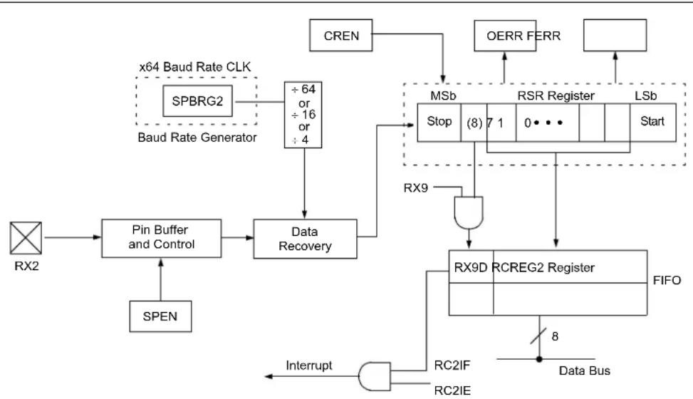
flowchart
graph TD
    A["RX2"] --> B["Pin Buffer and Control"]
    B --> C["Data Recovery"]
    C --> D["÷64 or ÷16 or ÷4"]
    D --> E["÷64 or ÷16 or ÷4"]
    E --> F["SPBRG2"]
    F --> G["x64 Baud Rate CLK"]
    G --> H["SpEN"]
    H --> B
    I["CREN"] --> J["MSb"]
    J --> K["Stop (8) 7 1 0 ..."]
    L["OERR FERR"] --> M["LSb"]
    M --> N["Start"]
    O["RX9"] --> P["RX9D RCREG2 Register"]
    P --> Q["FIFO"]
    Q --> R["Data Bus"]
    S["Interrupt"] --> T["RC2IF RC2IE"]
    T --> U["Data Bus"]
FIGURE 20-5: ASYNCHRONOUS RECEPTION

flowchart
graph TD
    A["Start bit"] --> B["bit 0"]
    B --> C["bit 1"]
    C --> D["bit 7/8"]
    D --> E["Stop bit"]
    E --> F["Start bit"]
    F --> G["bit 0"]
    G --> H["bit 7/8"]
    H --> I["Stop bit"]
    I --> J["Start bit"]
    J --> K["bit 7/8"]
    K --> L["Stop bit"]

    M["Rcv Shift Reg"] --> N["Word 1 RCREG2"]
    N --> O["Word 2 RCREG2"]

    P["Rcv Buffer Reg"] --> Q["Word 1 RCREG2"]
    Q --> R["Word 2 RCREG2"]

    S["Read Rcv Buffer Reg"] --> T["Word 1 RCREG2"]
    T --> U["Word 2 RCREG2"]

    V["RC2IF (Interrupt Flag)"] --> W["Word 1 RCREG2"]
    W --> X["Word 2 RCREG2"]

    Y["OERR bit"] --> Z["Word 1 RCREG2"]
    Z --> AA["Word 2 RCREG2"]

    AB["CREN"] --> AC["Word 1 RCREG2"]
    AC --> AD["Word 2 RCREG2"]

    AE["Note: This timing diagram shows three words appearing on the RX2 input. The RCREG2 (Receive Buffer Register 2) is read after the third word causing the OERR (Overrun) bit to be set."]
TABLE 20-5: REGISTERS ASSOCIATED WITH ASYNCHRONOUS RECEPTION
| Name Bit | 7 Bit 6 Bit | 5 Bit 4 Bit 3 | Bit 2 Bit 1 | Bit 0 | Reset Values on Page | ||||
| INTCON GIE/GIEH PEIE/GIEL | TMR0IE | INT0IE | RBIE | TMR0IF | INT0IF | RBIF | 59 | ||
| PIR3 | — | LCDIF | RC2IF | TX2IF | CTMUIF | CCP2IF | CCP1IF | RTCCIF | 62 |
| PIE3 | — | LCDIE | RC2IE | TX2IE | CTMUIE | CCP2IE | CCP1IE | RTCCIE | 62 |
| IPR3 | — | LCDIP | RC2IP | TX2IP | CTMUIP | CCP2IP | CCP1IP | RTCCIP | 62 |
| RCSTA2 | SPEN | RX9 | SREN | CREN | ADDEN | FERR | OERR | RX9D | 64 |
| RCREG2 | AUSART Receive Register | 64 | |||||||
| TXSTA2 | CSRC | TX9 | TXEN | SYNC | — | BRGH | TRMT | TX9D | 64 |
| SPBRG2 | AUSART Baud Rate Generator Register | 64 | |||||||
Legend: — = unimplemented locations read as '0'. Shaded cells are not used for asynchronous reception.
20.4 AUSART Synchronous Master Mode
The Synchronous Master mode is entered by setting the CSRC bit (TXSTA2<7>). In this mode, the data is transmitted in a half-duplex manner (i.e., transmission and reception do not occur at the same time). When transmitting data, the reception is inhibited and vice versa. Synchronous mode is entered by setting bit, SYNC (TXSTA2<4>). In addition, enable bit, SPEN (RCSTA2<7>), is set in order to configure the TX2 and RX2 pins to CK2 (clock) and DT2 (data) lines, respectively.
The Master mode indicates that the processor transmits the master clock on the CK2 line.
20.4.1 AUSART SYNCHRONOUS MASTER TRANSMISSION
The AUSART transmitter block diagram is shown in Figure 20-1. The heart of the transmitter is the Transmit (Serial) Shift Register (TSR). The Shift register obtains its data from the Read/Write Transmit Buffer Register, TXREG2. The TXREG2 register is loaded with data in software. The TSR register is not loaded until the last bit has been transmitted from the previous load. As soon as the last bit is transmitted, the TSR is loaded with new data from the TXREG2 (if available).
Once the TXREG2 register transfers the data to the TSR register (occurs in one TCYCLE), the TXREG2 is empty and the TX2IF flag bit (PIR3<4>) is set. The interrupt can be enabled or disabled by setting or clearing the interrupt enable bit, TX2IE (PIE3<4>). TX2IF is set regardless of the state of enable bit, TX2IE; it cannot be cleared in software. It will reset only when new data is loaded into the TXREG2 register.
While flag bit, TX2IF, indicates the status of the TXREG2 register, another bit, TRMT (TXSTA2<1>), shows the status of the TSR register. TRMT is a read-only bit which is set when the TSR is empty. No interrupt logic is tied to this bit so the user has to poll this bit in order to determine if the TSR register is empty. The TSR is not mapped in data memory so it is not available to the user.
To set up a Synchronous Master Transmission:
- Initialize the SPBRG2 register for the appropriate baud rate.
- Enable the synchronous master serial port by setting bits, SYNC, SPEN and CSRC.
- If interrupts are desired, set enable bit, TX2IE.
- If 9-bit transmission is desired, set bit, TX9.
- Enable the transmission by setting bit, TXEN.
- If 9-bit transmission is selected, the ninth bit should be loaded in bit, TX9D.
- Start transmission by loading data to the TXREG2 register.
- If using interrupts, ensure that the GIE and PEIE bits in the INTCON register (INTCON<7:6>) are set.
FIGURE 20-6: SYNCHRONOUS TRANSMISSION
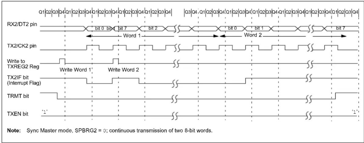
text_image
RX2/DT2 pin TX2/CK2 pin Write to TXREG2 Reg TX2IF bit (Interrupt Flag) TRMT bit TXEN bit '1' bit 0 bit bit 7 bit 2 bit 0 bit 1 Word 1 Word 2 SS SS SS SS SS SS SS SS SS SS SS SS SS SS Note: Sync Master mode, SPBRG2 = 0; continuous transmission of two 8-bit words.FIGURE 20-7: SYNCHRONOUS TRANSMISSION (THROUGH TXEN)
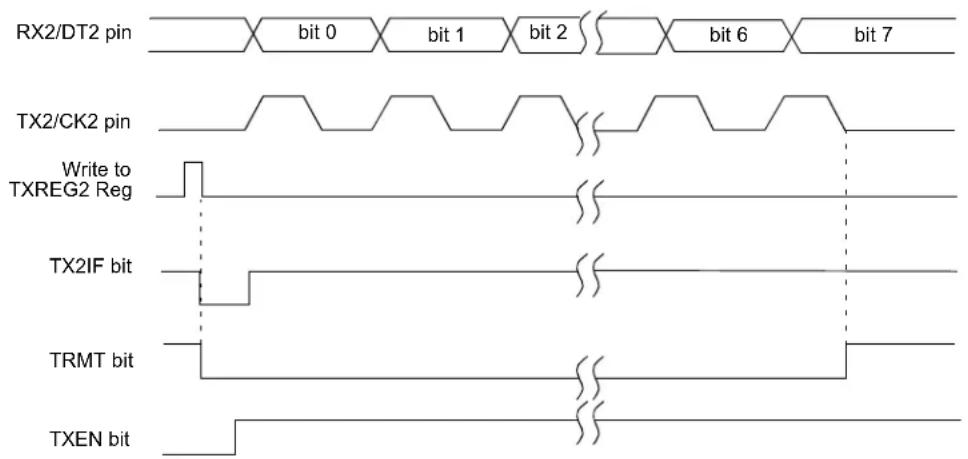
text_image
RX2/DT2 pin bit 0 bit 1 bit 2 bit 6 bit 7 TX2/CK2 pin Write to TXREG2 Reg TX2IF bit TRMT bit TXEN bitTABLE 20-6: REGISTERS ASSOCIATED WITH SYNCHRONOUS MASTER TRANSMISSION
| Name Bit | 7 Bit 6 Bit | 5 Bit 4 Bit 3 | Bit 2 Bit 1 | Bit 0 | Reset Values on Page | ||||
| INTCON GIE | GIEH PEIE | GIEL | TMR0IE | INT0IE | RBIE | TMR0IF | INT0IF | RBIF | 59 |
| PIR3 | — | LCDIF | RC2IF | TX2IF | CTMUIF | CCP2IF | CCP1IF | RTCCIF | 62 |
| PIE3 | — | LCDIE | RC2IE | TX2IE | CTMUIE | CCP2IE | CCP1IE | RTCCIE | 62 |
| IPR3 | — | LCDIP | RC2IP | TX2IP | CTMUIP | CCP2IP | CCP1IP | RTCCIP | 62 |
| RCSTA2 | SPEN | RX9 | SREN | CREN | ADDEN | FERR | OERR | RX9D | 64 |
| TXREG2 | AUSART Transmit Register | 64 | |||||||
| TXSTA2 | CSRC | TX9 | TXEN SYNC | — | BRGH | TRMT | TX9D | 64 | |
| SPBRG2 | AUSART Baud Rate Generator Register | 64 | |||||||
| LATG | U2OD | U1OD | — | LATG4 | LATG3 | LATG2 | LATG1 | LATG0 | 62 |
Legend: — = unimplemented, read as '0'. Shaded cells are not used for synchronous master transmission.
20.4.2 AUSART SYNCHRONOUS MASTER RECEPTION
Once Synchronous mode is selected, reception is enabled by setting either the Single Receive Enable bit, SREN (RCSTA2<5>), or the Continuous Receive Enable bit, CREN (RCSTA2<4>). Data is sampled on the RX2 pin on the falling edge of the clock.
If enable bit, SREN, is set, only a single word is received. If enable bit, CREN, is set, the reception is continuous until CREN is cleared. If both bits are set, then CREN takes precedence.
To set up a Synchronous Master Reception:
- Initialize the SPBRG2 register for the appropriate baud rate.
- Enable the synchronous master serial port by setting bits, SYNC, SPEN and CSRC.
-
Ensure bits, CREN and SREN, are clear.
-
If interrupts are desired, set enable bit, RC2IE.
- If 9-bit reception is desired, set bit, RX9.
- If a single reception is required, set bit, SREN. For continuous reception, set bit, CREN.
- Interrupt flag bit, RC2IF, will be set when reception is complete and an interrupt will be generated if the enable bit, RC2IE, was set.
- Read the RCSTA2 register to get the 9th bit (if enabled) and determine if any error occurred during reception.
- Read the 8-bit received data by reading the RCREG2 register.
- If any error occurred, clear the error by clearing bit, CREN.
- If using interrupts, ensure that the GIE and PEIE bits in the INTCON register (INTCON<7:6>) are set.
FIGURE 20-8: SYNCHRONOUS RECEPTION (MASTER MODE, SREN)

other
| Signal | Bit Position | |-----------------|--------------| | RX2/DT2 pin | bit 0 | | TX2/CK2 pin | bit 1 | | Write to bit SREN | - | | SREN bit | - | | CREN bit '0' | - | | RC2IF bit (Interrupt) | - | | Read RCREG2 | - |TABLE 20-7: REGISTERS ASSOCIATED WITH SYNCHRONOUS MASTER RECEPTION
| Name Bit 7 Bit 6 Bit | 5 Bit 4 Bit 3 | Bit 2 Bit 1 | Bit 0 | Reset Values on Page | |||||
| INTCON | GIE/GIEH | PEIE/GIEL | TMR0IE | INT0IE | RBIE | TMR0IF | INT0IF | RBIF | 59 |
| PIR3 | — | LCDIF | RC2IF | TX2IF | CTMUIF | CCP2IF | CCP1IF | RTCCIF | 62 |
| PIE3 | — | LCDIE | RC2IE | TX2IE | CTMUIE | CCP2IE | CCP1IE | RTCCIE | 62 |
| IPR3 | — | LCDIP | RC2IP | TX2IP | CTMUIP | CCP2IP | CCP1IP | RTCCIP | 62 |
| RCSTA2 | SPEN | RX9 SREN | CR EN | ADDEN F | ERR O | ERR R | RX9D 64 | ||
| RCREG2 | AUSART Receive Register | 64 | |||||||
| TXSTA2 | CSRC | TX9 | TXEN | SYNC | — | BRGH | TRMT | TX9D | 64 |
| SPBRG2 | AUSART Baud Rate Generator Register | 64 | |||||||
Legend: — = unimplemented, read as '0'. Shaded cells are not used for synchronous master reception.
20.5 AUSART Synchronous Slave Mode
Synchronous Slave mode is entered by clearing bit, CSRC (TXSTA2<7>). This mode differs from the Synchronous Master mode in that the shift clock is supplied externally at the CK2 pin (instead of being supplied internally in Master mode). This allows the device to transfer or receive data while in any Low-Power mode.
20.5.1 AUSART SYNCHRONOUS SLAVE TRANSMIT
The operation of the Synchronous Master and Slave modes are identical except in the case of the Sleep mode.
If two words are written to the TXREG2 and then the SLEEP instruction is executed, the following will occur:
a) The first word will immediately transfer to the TSR register and transmit.
b) The second word will remain in the TXREG2 register.
c) Flag bit, TX2IF, will not be set.
d) When the first word has been shifted out of TSR, the TXREG2 register will transfer the second word to the TSR and flag bit, TX2IF, will now be set.
e) If enable bit, TX2IE, is set, the interrupt will wake the chip from Sleep. If the global interrupt is enabled, the program will branch to the interrupt vector.
To set up a Synchronous Slave Transmission:
- Enable the synchronous slave serial port by setting bits, SYNC and SPEN, and clearing bit, CSRC.
- Clear bits, CREN and SREN.
- If interrupts are desired, set enable bit, TX2IE.
- If 9-bit transmission is desired, set bit, TX9.
- Enable the transmission by setting enable bit, TXEN.
- If 9-bit transmission is selected, the ninth bit should be loaded in bit, TX9D.
- Start transmission by loading data to the TXREG2 register.
- If using interrupts, ensure that the GIE and PEIE bits in the INTCON register (INTCON<7:6>) are set.
TABLE 20-8: REGISTERS ASSOCIATED WITH SYNCHRONOUS SLAVE TRANSMISSION
| Name Bit | 7 Bit 6 Bit | 5 Bit 4 Bit 3 | Bit 2 Bit 1 | Bit 0 | Reset Values on Page | ||||
| INTCON | GIE/GIEH | PEIE/GIEL | TMR0IE | INT0IE | RBIE | TMR0IF | INT0IF | RBIF | 59 |
| PIR3 | — | LCDIF | RC2IF | TX2IF | CTMUIF | CCP2IF | CCP1IF | RTCCIF | 62 |
| PIE3 | — | LCDIE | RC2IE | TX2IE | CTMUIE | CCP2IE | CCP1IE | RTCCIE | 62 |
| IPR3 | — | LCDIP | RC2IP | TX2IP | CTMUIP | CCP2IP | CCP1IP | RTCCIP | 62 |
| RCSTA2 | SPEN | RX9 | SREN | CREN | ADDEN | FERR | OERR | RX9D | 64 |
| TXREG2 AUSART Transmit Register | 64 | ||||||||
| TXSTA2 | CSRC TX9 TXEN SYNC | — BRGH TRMT TX9 D 64 | |||||||
| SPBRG2 | AUSART Baud Rate Generator Register | 64 | |||||||
| LATG | U2OD | U1OD | — | LATG4 | LATG3 | LATG2 | LATG1 | LATG0 | 62 |
Legend: — = unimplemented, read as '0'. Shaded cells are not used for synchronous slave transmission.
20.5.2 AUSART SYNCHRONOUS SLAVE RECEPTION
The operation of the Synchronous Master and Slave modes is identical, except in the case of Sleep or any Idle mode, and bit, SREN, which is a “don’t care” in Slave mode.
If receive is enabled by setting the CREN bit prior to entering Sleep, or any Idle mode, then a word may be received while in this Low-Power mode. Once the word is received, the RSR register will transfer the data to the RCREG2 register; if the RC2IE enable bit is set, the interrupt generated will wake the chip from Low-Power mode. If the global interrupt is enabled, the program will branch to the interrupt vector.
To set up a Synchronous Slave Reception:
- Enable the synchronous master serial port by setting bits, SYNC and SPEN, and clearing bit, CSRC.
- If interrupts are desired, set enable bit, RC2IE.
- If 9-bit reception is desired, set bit, RX9.
- To enable reception, set enable bit, CREN.
- Flag bit, RC2IF, will be set when reception is complete. An interrupt will be generated if enable bit, RC2IE, was set.
- Read the RCSTA2 register to get the 9th bit (if enabled) and determine if any error occurred during reception.
- Read the 8-bit received data by reading the RCREG2 register.
- If any error occurred, clear the error by clearing bit, CREN.
- If using interrupts, ensure that the GIE and PEIE bits in the INTCON register (INTCON<7:6>) are set.
TABLE 20-9: REGISTERS ASSOCIATED WITH SYNCHRONOUS SLAVE RECEPTION
| Name Bit | 7 Bit 6 Bit | 5 Bit 4 Bit 3 | Bit 2 Bit 1 | Bit 0 | Reset Values on Page | ||||
| INTCON | GIE/GIEH | PEIE/GIEL | TMR0IE | INT0IE | RBIE | TMR0IF | INT0IF | RBIF | 59 |
| PIR3 | — | LCDIF | RC2IF | TX2IF | CTMUIF | CCP2IF | CCP1IF | RTCCIF | 62 |
| PIE3 | — | LCDIE | RC2IE | TX2IE | CTMUIE | CCP2IE | CCP1IE | RTCCIE | 62 |
| IPR3 | — | LCDIP | RC2IP | TX2IP | CTMUIP | CCP2IP | CCP1IP | RTCCIP | 62 |
| RCSTA2 | SPEN RX9 | SREN | CREN | ADDEN | FERR | OERR | RX9D 64 | ||
| RCREG2 | AUSART Receive Register | 64 | |||||||
| TXSTA2 | CSRC | TX9 | TXEN | SYNC | — | BRGH | TRMT | TX9D | 64 |
| SPBRG2 | AUSART Baud Rate Generator Register | 64 | |||||||
Legend: — = unimplemented, read as '0'. Shaded cells are not used for synchronous slave reception.
21.0 10-BIT ANALOG-TO-DIGITAL CONVERTER (A/D) MODULE
The Analog-to-Digital (A/D) Converter module has 12 inputs for all PIC18F87J90 family devices. This module allows conversion of an analog input signal to a corresponding 10-bit digital number.
The ADCON0 register, shown in Register 21-1, controls the operation of the A/D module. The ADCON1 register, shown in Register 21-2, configures the functions of the port pins. The ADCON2 register, shown in Register 21-3, configures the A/D clock source, programmed acquisition time and justification.
The module has five registers:
• A/D Result High Register (ADRESH)
• A/D Result Low Register (ADRESL)
• A/D Control Register 0 (ADCON0)
• A/D Control Register 1 (ADCON1)
• A/D Control Register 2 (ADCON2)
REGISTER 21-1: ADCON0: A/D CONTROL REGISTER 0
| R/W-0 U-0 R/W-0 R/W-0 R/W-0 R/W-0 R/W-0 R/W-0 | |||||||
| ADCAL | — CHS3 | CHS2 CHS1 | CHS0 GO/DONE ADON | ||||
| bit 7 bit 0 | |||||||
Legend:
| R = Readable bit | W = Writable bit | U = Unimplemented bit, read as '0' |
| -n = Value at POR | '1' = Bit is set | '0' = Bit is cleared x = Bit is unknown |
bit 7 ADCAL: A/D Calibration bit
1 = Calibration is performed on next A/D conversion 0 = Normal A/D Converter operation (no calibration is performed)
bit 6 Unimplemented: Read as '0'
bit 5-2 CHS<3:0>: Analog Channel Select bits
0000 = Channel 00 (AN0)
0001 = Channel 01 (AN1)
0010 = Channel 02 (AN2)
0011 = Channel 03 (AN3)
0100 = Channel 04 (AN4)
0101 = Channel 05 (AN5)
0110 = Channel 06 (AN6)
0111 = Channel 07 (AN7)
1000 = Channel 08 (AN8)
1001 = Channel 09 (AN9)
1010 = Channel 10 (AN10)
1011 = Channel 11 (AN11)
11xx = Unused
bit 1 GO/DONE: A/D Conversion Status bit
When ADON = 1:
1 = A/D conversion in progress
0 = A/D Idle
bit 0 ADON: A/D On bit
1 = A/D Converter module is enabled
0 = A/D Converter module is disabled
REGISTER 21-2: ADCON1: A/D CONTROL REGISTER 1
| R/W-0 U-0 R/W-0 R/W-0 R/W-0 R/W-0 R/W-0 R/W-0 | |||||||
| TRIGSEL — | VCFG1 | VCFG0 | PCFG3 | PCFG2 | PCFG1 | PCFG0 | |
| bit 7 bit 0 | |||||||
Legend:
| R = Readable bit W = Writable bit U = Unimplemented bit, read as '0' | |
| -n = Value at POR '1' = Bit is set '0' = Bit is cleared | x = Bit is unknown |
bit 7 TRIGSEL: Special Trigger Select bit
1 = Selects the special trigger from the CTMU
0 = Selects the special trigger from the CCP2
bit 6 Unimplemented: Read as '0'
bit 5 VCFG1: Voltage Reference Configuration bit (V REF- source)
1 = VREF- (AN2)
0 = AVSS
bit 4 VCFG0: Voltage Reference Configuration bit (VREF+ source)
1 = VREF+ (AN3)
0 = AVDD
bit 3-0 PCFG<3:0>: A/D Port Configuration Control bits:
| PCFG<3:0> | AN11 | AN10 | AN9 | AN8 | AN7 | AN6 | AN5 | AN4 | AN3 | AN2 | AN1 | AN0 |
| 0000 | A | A | A | A | A | A | A | A | A | A | A | A |
| 0001 | A | A | A | A | A | A | A | A | A | A | A | A |
| 0010 | A | A | A | A | A | A | A | A | A | A | A | A |
| 0011 | A | A | A | A | A | A | A | A | A | A | A | A |
| 0100 | D | A | A | A | A | A | A | A | A | A | A | A |
| 0101 | D | D | A | A | A | A | A | A | A | A | A | A |
| 0110 | D | D | D | A | A | A | A | A | A | A | A | A |
| 0111 | D | D | D | D | A | A | A | A | A | A | A | A |
| 1000 | D | D | D | D | D | A | A | A | A | A | A | A |
| 1001 | D | D | D | D | D | D | A | A | A | A | A | A |
| 1010 | D | D | D | D | D | D | D | A | A | A | A | A |
| 1011 | D | D | D | D | D | D | D | D | A | A | A | A |
| 1100 | D | D | D | D | D | D | D | D | D | A | A | A |
| 1101 | D | D | D | D | D | D | D | D | D | D | A | A |
| 1110 | D | D | D | D | D | D | D | D | D | D | D | A |
| 1111 | D | D | D | D | D | D | D | D | D | D | D | D |
A = Analog input
D = Digital I/O
REGISTER 21-3: ADCON2: A/D CONTROL REGISTER 2
| R/W-0 U-0 R/W-0 R/W-0 R/W-0 R/W-0 R/W-0 R/W-0 | ||||||
| ADFM — | ACQT2 ACQT1 | ACQT0 ADC2 ADCS1 ADC0 | ||||
| bit 7 bit 0 | ||||||
Legend:
R = Readable bit W = Writable bit U = Unimplemented bit, read as '0'
-n = Value at POR '1' = Bit is set '0' = Bit is cleared x = Bit is unknown
bit 7 ADFM: A/D Result Format Select bit
1 = Right justified
0 = Left justified
bit 6 Unimplemented: Read as '0' bit 5-3 ACQT<2:0>: A/D Acquisition Time Select bits 111 = 20 TAD 110 = 16 TAD 101 = 12 TAD 100 = 8 TAD 011 = 6 TAD 010 = 4 TAD 001 = 2 TAD 000 = 0 TAD ^(1) bit 2-0 ADCS<2:0>: A/D Conversion Clock Select bits 111 = FRC (clock derived from A/D RC oscillator) ^(1) 110 = FOSC/64 101 = FOSC/16 100 = FOSC/4 011 = FRC (clock derived from A/D RC oscillator) ^(1) 010 = FOSC/32 001 = FOSC/8 000 = FOSC/2
Note 1: If the A/D FRC clock source is selected, a delay of one Tcy (instruction cycle) is added before the A/D clock starts. This allows the SLEEP instruction to be executed before starting a conversion.
The analog reference voltage is software selectable to either the device's positive and negative supply voltage (AVDD and AVSS), or the voltage level on the RA3/AN3/VREF+ and RA2/AN2/VREF- pins.
The A/D Converter has a unique feature of being able to operate while the device is in Sleep mode. To operate in Sleep, the A/D conversion clock must be derived from the A/D's Internal RC oscillator.
The output of the sample and hold is the input into the converter, which generates the result via successive approximation.
Each port pin associated with the A/D Converter can be configured as an analog input or as a digital I/O. The ADRESH and ADRESL registers contain the result of
the A/D conversion. When the A/D conversion is complete, the result is loaded into the ADRESH:ADRESL register pair, the GO/DONE bit (ADCON0<1>) is cleared and the A/D Interrupt Flag bit, ADIF, is set.
A device Reset forces all registers to their Reset state. This forces the A/D module to be turned off and any conversion in progress is aborted. The value in the ADRESH:ADRESL register pair is not modified for a Power-on Reset. These registers will contain unknown data after a Power-on Reset.
The block diagram of the A/D module is shown in Figure 21-1.
FIGURE 21-1: A/D BLOCK DIAGRAM (1,2)
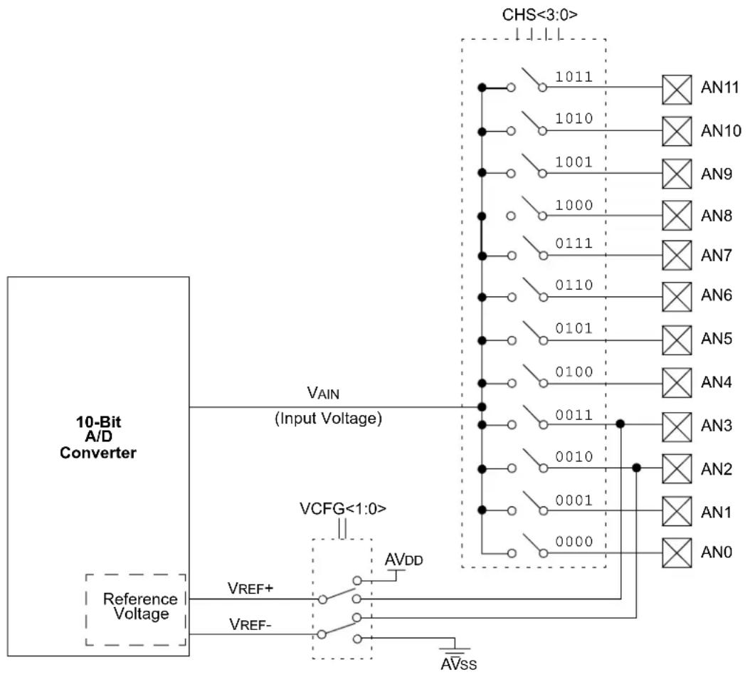
flowchart
graph TD
    A["10-Bit A/D Converter"] -->|VAIN (Input Voltage)| B["CHS<3:0>"]
    A -->|VCFG<1:0>| C["VREF+"]
    A -->|VREF-| D["VREF-"]
    C --> E["AVDD"]
    D --> F["AVss"]
    E --> G["AN11"]
    E --> H["AN10"]
    E --> I["AN9"]
    E --> J["AN8"]
    E --> K["AN7"]
    E --> L["AN6"]
    E --> M["AN5"]
    E --> N["AN4"]
    E --> O["AN3"]
    E --> P["AN2"]
    E --> Q["AN1"]
    E --> R["AN0"]
    style A fill:#f9f,stroke:#333
    style B fill:#ccf,stroke:#333
    style C fill:#cfc,stroke:#333
    style D fill:#fcc,stroke:#333
    style E fill:#ffc,stroke:#333
    style F fill:#fcc,stroke:#333
    style G fill:#cff,stroke:#333
    style H fill:#cff,stroke:#333
    style I fill:#cff,stroke:#333
    style J fill:#cff,stroke:#333
    style K fill:#cff,stroke:#333
    style L fill:#cff,stroke:#333
    style M fill:#cff,stroke:#333
    style N fill:#cff,stroke:#333
    style O fill:#cff,stroke:#333
    style P fill:#cff,stroke:#333
    style Q fill:#cff,stroke:#333
    style R fill:#cff,stroke:#333
Note 1: Channels, AN15 through AN12, are not available on PIC18F6XJ90 devices.
2: I/O pins have diode protection to V DD and Vss.
After the A/D module has been configured as desired, the selected channel must be acquired before the conversion is started. The analog input channels must have their corresponding TRIS bits selected as inputs. To determine acquisition time, see Section 21.1 "A/D Acquisition Requirements". After this acquisition time has elapsed, the A/D conversion can be started. An acquisition time can be programmed to occur between setting the GO/DONE bit and the actual start of the conversion.
The following steps should be followed to do an A/D conversion:
-
Configure the A/D module:
-
Configure analog pins, voltage reference and digital I/O (ADCON1)
- Select A/D input channel (ADCON0)
- Select A/D acquisition time (ADCON2)
- Select A/D conversion clock (ADCON2)
-
Turn on A/D module (ADCON0)
-
Configure A/D interrupt (if desired):
-
Clear the ADIF bit
- Set the ADIE bit
-
Set the GIE bit
-
Wait the required acquisition time (if required).
- Start conversion:
- Set GO/DONE bit (ADCON0<1>)
-
Wait for the A/D conversion to complete, by either:
-
Polling for the GO/DONE bit to be cleared OR
-
Waiting for the A/D interrupt
-
Read A/D Result registers (ADRESH:ADRESL); clear the ADIF bit, if required.
-
For the next conversion, go to step 1 or step 2, as required. The A/D conversion time per bit is defined as TAD. A minimum wait of 2 TAD is required before next acquisition starts.
FIGURE 21-2: ANALOG INPUT MODEL

text_image
RS ANx VAIN CPIN 5 pF VDD VT = 0.6V Ric ≤ 1k SS Sampling Switch RSS VT = 0.6V ILEAKAGE ±100 nA CHOLD = 25 pF VSS| Legend: CPIN | = Input Capacitance |
| VT | = Threshold Voltage |
| ILEAKAGE | = Leakage Current at the pin due to various junctions |
| RIC | = Interconnect Resistance |
| SS | = Sampling Switch |
| CHOLD | = Sample/Hold Capacitance (from DAC) = Sampling Switch ResistanceRSS |
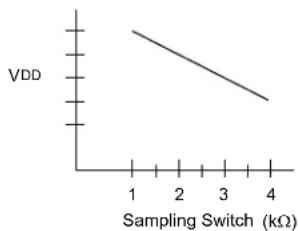
line
| Sampling Switch (kΩ) | VDD | | --------------------- | --- | | 1 | 0 | | 2 | -1 | | 3 | -2 | | 4 | -3 |21.1 A/D Acquisition Requirements
For the A/D Converter to meet its specified accuracy, the charge holding capacitor (QHOLD) must be allowed to fully charge to the input channel voltage level. The analog input model is shown in Figure 21-2. The source impedance (Rs) and the internal sampling switch (RSS) impedance directly affect the time required to charge the capacitor, QHOLD. The sampling switch (RSS) impedance varies over the device voltage (VDD). The source impedance affects the offset voltage at the analog input (due to pin leakage current). The maximum recommended impedance for analog sources is 2.5 kΩ. After the analog input channel is selected (changed), the channel must be sampled for at least the minimum acquisition time before starting a conversion.
Note: When the conversion is started, the holding capacitor is disconnected from the input pin.
To calculate the minimum acquisition time, Equation 21-1 may be used. This equation assumes that 1/2 LSb error is used (1024 steps for the A/D). The 1/2 LSb error is the maximum error allowed for the A/D to meet its specified resolution.
Equation 21-3 shows the calculation of the minimum required acquisition time, TACQ. This calculation is based on the following application system assumptions:
CHOLD = 2 5 p F
Rs = 2.5 kΩ
Conversion Error ≤ 1/2 LSb
V_DD = 3V → Rss = 2 kΩ
Temperature = 85°C (system max.)
EQUATION 21-1: A/D ACQUISITION TIME
TACQ = Amplifier Settling Time + Holding Capacitor Charging Time + Temperature Coefficient
= TAMP + TC + TCOFF
EQUATION 21-2: A/D MINIMUM CHARGING TIME
& = & (VREF - (VREF / 2048)) (1 - e^(-Tc / CHIOLD(RIC + RSS + Rs))) or TC & = & -(CHIOLD)(RIC + RSS + Rs) (1 / 2048)
EQUATION 21-3: CALCULATING THE MINIMUM REQUIRED ACQUISITION TIME
TACQ = TAMP + TC + TCOFF
TAMP = 0.2 μs
TCOFF = (Temp - 25°C)(0.02 μs/°C)
(85°C - 25°C)(0.02 μs/°C)
1.2 μs
Temperature coefficient is only required for temperatures > 25°C. Below 25°C, TCOFF = 0 ms.
TC = -(CHOLD)(RIC + RSS + RS) ln(1/2048) μs
-(25 pF) (1 kΩ + 2 kΩ + 2.5 kΩ) ln(0.0004883) μs
1.05 μs
TACQ = 0.2 μs + 1 μs + 1.2 μs
2.4 μs
21.2 Selecting and Configuring Automatic Acquisition Time
The ADCON2 register allows the user to select an acquisition time that occurs each time the GO/DONE bit is set.
When the GO/DONE bit is set, sampling is stopped and a conversion begins. The user is responsible for ensuring the required acquisition time has passed between selecting the desired input channel and setting the GO/DONE bit. This occurs when the ACQT<2:0> bits (ADCON2<5:3>) remain in their Reset state ('000') and is compatible with devices that do not offer programmable acquisition times.
If desired, the ACQT bits can be set to select a programmable acquisition time for the A/D module. When the GO/DONE bit is set, the A/D module continues to sample the input for the selected acquisition time, then automatically begins a conversion. Since the acquisition time is programmed, there may be no need to wait for an acquisition time between selecting a channel and setting the GO/DONE bit.
In either case, when the conversion is completed, the GO/DONE bit is cleared, the ADIF flag is set and the A/D begins sampling the currently selected channel again. If an acquisition time is programmed, there is nothing to indicate if the acquisition time has ended or if the conversion has begun.
21.3 Selecting the A/D Conversion Clock
The A/D conversion time per bit is defined as TAD. The A/D conversion requires 11 TAD per 10-bit conversion. The source of the A/D conversion clock is software selectable.
There are seven possible options for TAD:
• 2 Tosc
• 4 T osc
• 8 T osc
• 1 6 T osc
• 3 2 T osc
• 6 4osc
- Internal RC Oscillator
For correct A/D conversions, the A/D conversion clock (TAD) must be as short as possible, but greater than the minimum, TAD (see parameter 130 in Table 28-25 for more information).
Table 21-1 shows the resultant AD times derived from the device operating frequencies and the A/D clock source selected.
TABLE 21-1: TAD vs. DEVICE OPERATING FREQUENCIES
| AD Clock Source (TAD) | M a Device Frequency | |
| Operation AD | CS<2:0> | |
| 2 Tosc 000 | 2.86 MHz | |
| 4 Tosc 100 | 5.71 MHz | |
| 8 Tosc | 001 | 11.43 MHz |
| 16 Tosc | 101 | 22.86 MHz |
| 32 Tosc | 010 40.0 MHz | |
| 64 Tosc | 110 | 40.0 MHz |
| RC(2) | x11 | 1.00 MHz^(1) |
Note 1: The RC source has a typical TAD time of 4 s.
2: For device frequencies above 1 MHz, the device must be in Sleep mode for the entire conversion or the A/D accuracy may be out of specification.
21.4 Configuring Analog Port Pins
The ADCON1, TRISA, TRISF and TRISH registers control the operation of the A/D port pins. The port pins needed as analog inputs must have their corresponding TRIS bits set (input). If the TRIS bit is cleared (output), the digital output level (Voh or Vol) will be converted.
The A/D operation is independent of the state of the CHS<3:0> bits and the TRIS bits.
Note 1: When reading the PORT register, all pins configured as analog input channels will read as cleared (a low level). Pins configured as digital inputs will convert an analog input. Analog levels on a digitally configured input will be accurately converted.
2: Analog levels on any pin defined as a digital input may cause the digital input buffer to consume current out of the device's specification limits.
21.5 A/D Conversions
Figure 21-3 shows the operation of the A/D Converter after the GO/DONE bit has been set and the ACQT<2:0> bits are cleared. A conversion is started after the following instruction to allow entry into Sleep mode before the conversion begins.
Figure 21-4 shows the operation of the A/D Converter after the GO/DONE bit has been set, the ACQT<2:0> bits are set to '010' and selecting a 4 TAD acquisition time before the conversion starts.
Clearing the GO/DONE bit during a conversion will abort the current conversion. The A/D Result register pair will NOT be updated with the partially completed A/D conversion sample. This means the ADRESH:ADRESL registers will continue to contain the value of the last completed conversion (or the last value written to the ADRESH:ADRESL registers).
After the A/D conversion is completed or aborted, a 2 TAD wait is required before the next acquisition can be started. After this wait, acquisition on the selected channel is automatically started.
Note: The GO/DONE bit should NOT be set in the same instruction that turns on the A/D.
21.6 Use of the CCP2 Trigger
An A/D conversion can be started by the "Special Event Trigger" of the CCP2 module. This requires that the CCP2M<3:0> bits (CCP2CON<3:0>) be programmed as '1011' and that the A/D module is enabled (ADON bit is set). When the trigger occurs, the GO/DONE bit will be set, starting the A/D acquisition and conversion, and the Timer1 (or Timer3) counter will be reset to zero. Timer1 (or Timer3) is reset to automatically repeat the A/D acquisition period with minimal software overhead (moving ADRESH:ADRESL to the desired location). The appropriate analog input channel must be selected and the minimum acquisition period is either timed by the user, or an appropriate Tacq time is selected before the Special Event Trigger sets the GO/DONE bit (starts a conversion).
If the A/D module is not enabled (ADON is cleared), the Special Event Trigger will be ignored by the A/D module but will still reset the Timer1 (or Timer3) counter.
FIGURE 21-3: A/D CONVERSION TAD CYCLES (ACQT<2:0> = 000, TACQ = 0)

flowchart
graph TD
    A["TCY - TADTAD1"] --> B["Conversion starts"]
    B --> C["Holding capacitor is disconnected from analog input (typically 100 ns)"]
    C --> D["Set GO/DONE bit"]
    D --> E["Next Q4: ADRESH:ADRESL is loaded, GO/DONE bit is cleared, ADIF bit is set, holding capacitor is connected to analog input."]
FIGURE 21-4: A/D CONVERSION T AD CYCLES (ACQT<2:0> = 010, TACQ = 4 TAD)
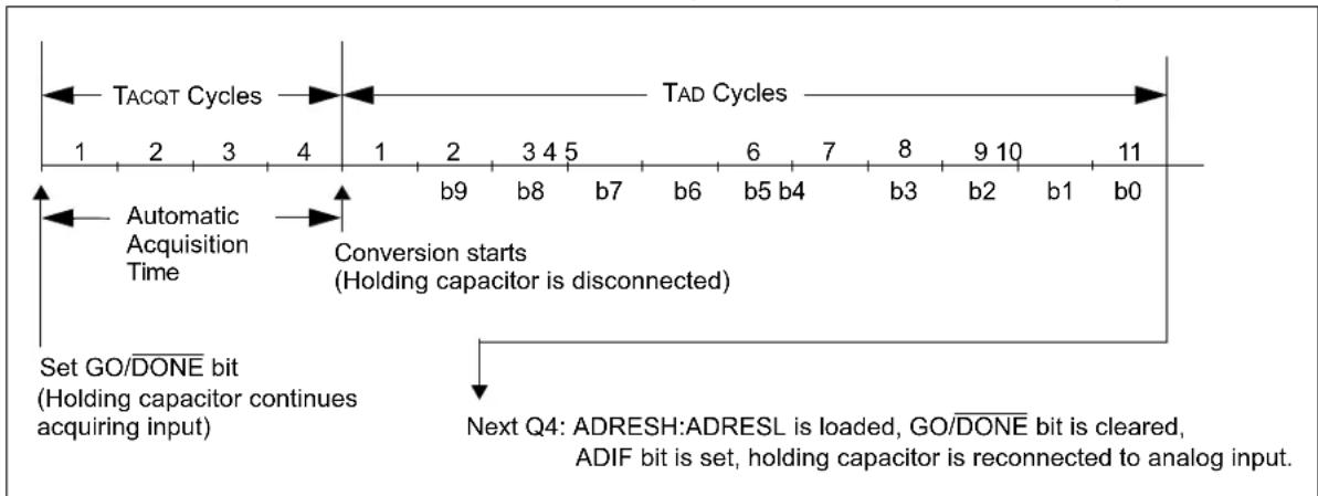
flowchart
graph LR
    A["TACQT Cycles"] --> B["1"]
    B --> C["2"]
    C --> D["3"]
    D --> E["4"]
    E --> F["1"]
    F --> G["b9"]
    G --> H["b8"]
    H --> I["3 4 5"]
    I --> J["b7"]
    J --> K["b6"]
    K --> L["b5 b4"]
    L --> M["6"]
    M --> N["7"]
    N --> O["b3"]
    O --> P["8"]
    P --> Q["b2"]
    Q --> R["9 10"]
    R --> S["b1"]
    S --> T["b0"]
    U["TAD Cycles"] --> V["11"]
    W["Automatic Acquisition Time"] --> X["Conversion starts (Holding capacitor is disconnected)"]
    Y["Set GO/DONE bit (Holding capacitor continues acquiring input)"] --> Z["Next Q4: ADRESH:ADRESL is loaded, GO/DONE bit is cleared, ADIF bit is set, holding capacitor is reconnected to analog input."]
21.7 A/D Converter Calibration
The A/D Converter, in the PIC18F87J90 family of devices, includes a self-calibration feature which compensates for any offset generated within the module. The calibration process is automated and is initiated by setting the ADCAL bit (ADCON0<7>). The next time the GO/DONE bit is set, the module will perform a "dummy" conversion (that is, with reading none of the input channels) and store the resulting value internally to compensate for the offset. Thus, subsequent offsets will be compensated.
The calibration process assumes that the device is in a relatively steady-state operating condition. If A/D calibration is used, it should be performed after each device Reset or if there are other major changes in operating conditions.
21.8 Operation in Power-Managed Modes
The selection of the automatic acquisition time and A/D conversion clock is determined, in part, by the clock source and frequency while in a power-managed mode.
If the A/D is expected to operate while the device is in a power-managed mode, the ACQT<2:0> and ADCS<2:0> bits in ADCON2 should be updated in accordance with the power-managed mode clock that will be used. After the power-managed mode is entered (either of the power-managed Run modes), an A/D acquisition or conversion may be started. Once an acquisition or conversion is started, the device should continue to be clocked by the same power-managed mode clock source until the conversion has been completed. If desired, the device may be placed into the corresponding power-managed Idle mode during the conversion.
If the power-managed mode clock frequency is less than 1 MHz, the A/D RC clock source should be selected.
Operation in Sleep mode requires the A/D RC clock to be selected. If bits, ACQT<2:0>, are set to '000' and a conversion is started, the conversion will be delayed one instruction cycle to allow execution of the SLEEP instruction and entry to Sleep mode. The IDLEN and SCSx bits in the OSCCON register must have already been cleared prior to starting the conversion.
TABLE 21-2: SUMMARY OF A/D REGISTERS
| Name Bit | 7 Bit 6 Bit | 5 Bit 4 Bit 3 | Bit 2 Bit 1 | Bit 0 | Reset Values on page | ||||
| INTCON GIE/GIEH PEIE/GIEL | TMR0IE | INT0IE | RBIE | TMR0IF | INT0IF | RBIF | 59 | ||
| PIR1 | — | ADIF | RC1IF | TX1IF | SSPIF | — | TMR2IF | TMR1IF | 62 |
| PIE1 | — | ADIE | RC1IE | TX1IE | SSPIE | — | TMR2IE | TMR1IE | 62 |
| IPR1 | — | ADIP | RC1IP | TX1IP | SSPIP | — | TMR2IP | TMR1IP | 62 |
| PIR3 | — | LCDIF | RC2IF | TX2IF | CTMUIF | CCP2IF | CCP1IF | RTCCIF | 62 |
| PIE3 | — | LCDIE | RC2IE | TX2IE | CTMUIE | CCP2IE | CCP1IE | RTCCIE | 62 |
| IPR3 | — | LCDIP | RC2IP | TX2IP | CTMUIP | CCP2IP | CCP1IP | RTCCIP | 62 |
| ADRESH | A/D Result Register High Byte | 61 | |||||||
| ADRESL | A/D Result Register Low Byte | 61 | |||||||
| ADCON0 | ADCAL | — | CHS3 | CHS2 | CHS1 | CHS0 | GO/DONE | ADON | 61 |
| ADCON1 TRIGSEL | — | VCFG1 | VCFG0 | PCFG3 | PCFG2 | PCFG1 | PCFG0 | 61 | |
| ADCON2 | ADFM | — | ACQT2 | ACQT1 | ACQT0 | ADCS2 | ADCS1 | ADCS0 | 61 |
| CCP2CON | — | — | DC2B1 | DC2B0 | CCP2M3 | CCP2M2 | CCP2M1 | CCP2M0 | 64 |
| PORTA | RA7(1) | RA6(1) | RA5 | RA4 | RA3 | RA2 | RA1 | RA0 | 63 |
| TRISA | TRISA7(1) | TRISA6(1) | TRISA5 TRISA4 TRISA3 TRISA2 TRISA1 TRISA0 62 | ||||||
| PORTF | RF7 | RF6 | RF5 | RF4 | RF3 | RF2 | RF1 | — | 62 |
| TRISF | TRISF5 | TRISF4 | TRISF5 | TRISF4 | TRISF3 | TRISF2 | TRISF1 | — | 62 |
Legend: — = unimplemented, read as '0'. Shaded cells are not used for A/D conversion.
Note 1: RA<7:6> and their associated latch and direction bits are configured as port pins only when the internal oscillator is selected as the default clock source (FOSC2 Configuration bit = 0); otherwise, they are disabled and these bits read as '0'.
NOTES:
22.0 COMPARATOR MODULE
The analog comparator module contains two comparators that can be configured in a variety of ways. The inputs can be selected from the analog inputs multiplexed with pins, RF1 through RF6, as well as the on-chip voltage reference (see Section 23.0
"Comparator Voltage Reference Module"). The digital outputs (normal or inverted) are available at the pin level and can also be read through the control register.
The CMCON register (Register 22-1) selects the comparator input and output configuration. Block diagrams of the various comparator configurations are shown in Figure 22-1.
REGISTER 22-1: CMCON: COMPARATOR MODULE CONTROL REGISTER
| R-0 R-0 R/W-0 R/W-0 R/W-0 R/W-1 R/W-1 R/W-1 | |||||||
| C2OUT C1 | OUT C2INV C1 | INV CIS CM2 | CM1 CM0 | ||||
| bit 7 bit 0 | |||||||
Legend:
| R = Readable bit | W = Writable bit | U = Unimplemented bit, read as ‘0’ |
| -n = Value at POR | ‘1’ = Bit is set | ‘0’ = Bit is cleared x = Bit is unknown |
bit 7 C2OUT: Comparator 2 Output bit
When C2INV = 0:
1 = C2 VIN+ > C2 VIN-
0 = C2 VIN+ < C2 VIN-
When C2INV = 1:
1 = C2 V_IN + < C2 V_IN-
0 = C2 V_IN + >C2 V_IN-
bit 6 C1OUT: Comparator 1 Output bit
When C1INV = 0:
1 = C1 VIN+ > C1 VIN-
0 = C1 VIN+ < C1 VIN-
When C1INV = 1:
1 = C1 VIN+ < C1 VIN-
0 = C1 V_IN + >C1 V_IN-
bit 5 C2INV: Comparator 2 Output Inversion bit
1 = C2 output inverted
0 = C2 output not inverted
bit 4 C1INV: Comparator 1 Output Inversion bit
1 = C1 output inverted
0 = C1 output not inverted
bit 3 CIS: Comparator Input Switch bit
When CM<2:0>=110:
1 = C1 VIN- connects to RF5/AN10/CVREF/SEG23/C1INB
C2 VIN- connects to RF3/AN8/SEG21/C2INB
0 = C1 VIN- connects to RF6/AN11/SEG24/C1INA
C2 Vin- connects to RF4/AN9/SEG22/C2INA
bit 2-0 CM<2:0>: Comparator Mode bits
Figure 22-1 shows the Comparator modes and the CM<2:0> bit settings.
22.1 Comparator Configuration
There are eight modes of operation for the comparators, shown in Figure 22-1. Bits, CM<2:0>, of the CMCON register are used to select these modes. The TRISF register controls the data direction of the comparator pins for each mode. If the Comparator
mode is changed, the comparator output level may not be valid for the specified mode change delay shown in Section 28.0 "Electrical Characteristics".
Note: Comparator interrupts should be disabled during a Comparator mode change; otherwise, a false interrupt may occur.
FIGURE 22-1: COMPARATOR I/O OPERATING MODES
Comparator Outputs DisabledCM<2:0> = 000 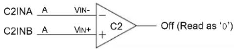 | Comparators Off (POR Default Value)CM<2:0> = 111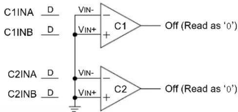 |
Two Independent ComparatorsCM<2:0> = 010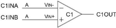 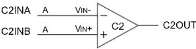 | Two Independent Comparators with OutputsCM<2:0> = 011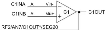  |
Two Common Reference ComparatorsCM<2:0> = 100 | Two Common Reference Comparators with OutputsCM<2:0> = 101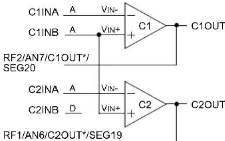 |
One Independent Comparator with OutputCM<2:0> = 001[RTXTX]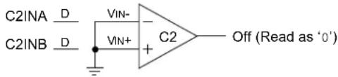 | Four Inputs Multiplexed to Two ComparatorsCM<2:0> = 110 |
| A = Analog Input, port reads zeros always D = Digital Input CIS (CMCON<3>) is the Comparator Input Switch* Setting the TRISF<2:1> bits will disable the comparator outputs by configuring the pins as inputs. | |
22.2 Comparator Operation
A single comparator is shown in Figure 22-2, along with the relationship between the analog input levels and the digital output. When the analog input at VIN+ is less than the analog input, VIN-, the output of the comparator is a digital low level. When the analog input at VIN+ is greater than the analog input, VIN-, the output of the comparator is a digital high level. The shaded areas of the output of the comparator in Figure 22-2 represent the uncertainty due to input offsets and response time.
22.3 Comparator Reference
Depending on the comparator operating mode, either an external or internal voltage reference may be used. The analog signal present at VIN- is compared to the signal at VIN+ and the digital output of the comparator is adjusted accordingly (Figure 22-2).
FIGURE 22-2: SINGLE COMPARATOR
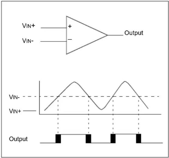
text_image
VIN+ VIN- Output VIN- VIN+ Output22.3.1 EXTERNAL REFERENCE SIGNAL
When external voltage references are used, the comparator module can be configured to have the comparators operate from the same or different reference sources. However, threshold detector applications may require the same reference. The reference signal must be between Vss and VDD and can be applied to either pin of the comparator(s).
22.3.2 INTERNAL REFERENCE SIGNAL
The comparator module also allows the selection of an internally generated voltage reference from the comparator voltage reference module. This module is described in more detail in Section 23.0 "Comparator Voltage Reference Module".
The internal reference is only available in the mode where four inputs are multiplexed to two comparators (CM<2:0>=110). In this mode, the internal voltage reference is applied to the + pin of both comparators.
22.4 Comparator Response Time
Response time is the minimum time, after selecting a new reference voltage or input source, before the comparator output has a valid level. If the internal reference is changed, the maximum delay of the internal voltage reference must be considered when using the comparator outputs. Otherwise, the maximum delay of the comparators should be used (see Section 28.0 "Electrical Characteristics").
22.5 Comparator Outputs
The comparator outputs are read through the CMCON register. These bits are read-only. The comparator outputs may also be directly output to the RF1 and RF2 I/O pins. When enabled, multiplexors in the output path of the RF1 and RF2 pins will switch and the output of each pin will be the unsynchronized output of the comparator. The uncertainty of each of the comparators is related to the input offset voltage and the response time given in the specifications. Figure 22-3 shows the comparator output block diagram.
The TRISF bits will still function as an output enable/disable for the RF1 and RF2 pins while in this mode.
The polarity of the comparator outputs can be changed using the C2INV and C1INV bits (CMCON<5:4>).
Note 1: When reading the PORT register, all pins configured as analog inputs will read as '0'. Pins configured as digital inputs will convert an analog input according to the Schmitt Trigger input specification.
2: Analog levels on any pin defined as a digital input may cause the input buffer to consume more current than is specified.
FIGURE 22-3: COMPARATOR OUTPUT BLOCK DIAGRAM

flowchart
graph TD
    A["Port Pins"] --> B["MULTIPLEX"]
    B --> C["+"]
    C --> D["AND"]
    D --> E["To RF1 or RF2 pin"]
    F["CxINV"] --> G["AND"]
    G --> H["D Q EN"]
    H --> I["Bus Data"]
    J["Read CMCON"] --> K["NOT"]
    K --> L["D Q EN CL"]
    L --> M["Set CMIF bit"]
    N["Reset"] --> O["AND"]
    O --> P["From Other Comparator"]
22.6 Comparator Interrupts
The comparator interrupt flag is set whenever there is a change in the output value of either comparator. Software will need to maintain information about the status of the output bits, as read from CMCON<7:6>, to determine the actual change that occurred. The CMIF bit (PIR2<6>) is the Comparator Interrupt Flag. The CMIF bit must be reset by clearing it. Since it is also possible to write a '1' to this register, a simulated interrupt may be initiated.
Both the CMIE bit (PIE2<6>) and the PEIE bit (INTCON<6>) must be set to enable the interrupt. In addition, the GIE bit (INTCON<7>) must also be set. If any of these bits are clear, the interrupt is not enabled, though the CMIF bit will still be set if an interrupt condition occurs.
Note: If a change in the CMCON register (C1OUT or C2OUT) should occur when a read operation is being executed (start of the Q2 cycle), then the CMIF (PIR2<6>) interrupt flag may not get set.
The user, in the Interrupt Service Routine, can clear the interrupt in the following manner:
a) Any read or write of CMCON will end the mismatch condition.
b) Clear flag bit, CMIF.
A mismatch condition will continue to set flag bit, CMIF. Reading CMCON will end the mismatch condition and allow flag bit, CMIF, to be cleared.
22.7 Comparator Operation During Sleep
When a comparator is active and the device is placed in Sleep mode, the comparator remains active and the interrupt is functional, if enabled. This interrupt will wake-up the device from Sleep mode, when enabled. Each operational comparator will consume additional current, as shown in the comparator specifications. To minimize power consumption while in Sleep mode, turn off the comparators (CM<2:0> = 111) before entering Sleep. If the device wakes up from Sleep, the contents of the CMCON register are not affected.
22.8 Effects of a Reset
A device Reset forces the CMCON register to its Reset state, causing the comparator modules to be turned off (CM<2:0>=111). However, the input pins (RF3 through RF6) are configured as analog inputs by default on device Reset. The I/O configuration for these pins is determined by the setting of the PCFG<3:0> bits (ADCON1<3:0>). Therefore, device current is minimized when analog inputs are present at Reset time.
22.9 Analog Input Connection Considerations
A simplified circuit for an analog input is shown in Figure 22-4. Since the analog pins are connected to a digital output, they have reverse biased diodes to VDD and Vss. The analog input, therefore, must be between Vss and VDD. If the input voltage deviates from this
range by more than 0.6V in either direction, one of the diodes is forward biased and a latch-up condition may occur. A maximum source impedance of 10 kΩ is recommended for the analog sources. Any external component connected to an analog input pin, such as a capacitor or a Zener diode, should have very little leakage current.
FIGURE 22-4: COMPARATOR ANALOG INPUT MODEL

text_image
Rs < 10k AIN VA CPIN 5 pF VDD VT = 0.6V VT = 0.6V ILEAKAGE ±100 nA Ric Comparator Input VssLegend: CPIN = Input Capacitance VT = Threshold Voltage ILEAKAGE = Leakage Current at the pin due to various junctions RIC = Interconnect Resistance Rs = Source Impedance VA = Analog Voltage
TABLE 22-1: REGISTERS ASSOCIATED WITH COMPARATOR MODULE
| Name Bit | 7 Bit 6 Bit | 5 Bit 4 Bit 3 | Bit 2 Bit 1 | Bit 0 | Reset Values on page | ||||
| INTCON GIE/GIEH PEIE/GIEL | TMR0IE | INT0IE | RBIE | TMR0IF | INT0IF | RBIF | 59 | ||
| PIR2 | OSCFIF | CMIF | — | — | BCLIF | LVDIF | TMR3IF | — | 62 |
| PIE2 | OSCFIE | CMIE | — | — | BCLIE | LVDIE | TMR3IE | — | 62 |
| IPR2 | OSCFIP | CMIP | — | — | BCLIP | LVDIP | TMR3IP | — | 62 |
| CMCON | C2OUT | C1OUT | C2INV | C1INV | CIS | CM2 | CM1 | CM0 | 61 |
| CVRCON CVREN CVROE CVRR | CVRSS | CVR3 | CVR2 | CVR1 | CVR0 | 61 | |||
| PORTF | RF7 | RF6 | RF5 | RF4 | RF3 | RF2 | RF1 | — | 62 |
| LATF | LATF7 | LATF6 | LATF5 | LATF4 | LATF3 | LATF2 | LATF1 | — | 62 |
| TRISF | TRISF7 | TRISF6 | TRISF5 | TRISF4 | TRISF3 | TRISF2 | TRISF1 | — | 62 |
Legend: — = unimplemented, read as '0'. Shaded cells are unused by the comparator module.
NOTES:
23.0 COMPARATOR VOLTAGE REFERENCE MODULE
The comparator voltage reference is a 16-tap resistor ladder network that provides a selectable reference voltage. Although its primary purpose is to provide a reference for the analog comparators, it may also be used independently of them.
A block diagram of the module is shown in Figure 23-1. The resistor ladder is segmented to provide two ranges of CVREF values and has a power-down function to conserve power when the reference is not being used. The module's supply reference can be provided from either the device VDD/VSS or an external voltage reference.
23.1 Configuring the Comparator Voltage Reference
The comparator voltage reference module is controlled through the CVRCON register (Register 23-1). The comparator voltage reference provides two ranges of output voltage, each with 16 distinct levels.
The range to be used is selected by the CVRR bit (CVRCON<5>). The primary difference between the ranges is the size of the steps selected by the CVREF Selection bits (CVR<3:0>), with one range offering finer resolution. The equations used to calculate the output of the comparator voltage reference are as follows:
$$ \begin{array}{l} \text { If CVRR } = 1: \ \mathrm{CV} _ {\text { REF }} = ((\mathrm{CVR} < 3: 0 >) / 2 4) \times (\mathrm{CV} _ {\text { RSRC }}) \ \text { If CVRR } = 0: \ \begin{array}{l} \text { CVREF } = (\text { CVRSRC } / 4) + ((\text { CVR } < 3: 0 >) / 3 2) \times \ (\text { CVRSRC }) \end{array} \ \end{array} $$
The comparator reference supply voltage can come from either VDD and VSS, or the external VREF+ and VREF- that are multiplexed with RA2 and RA3. The voltage source is selected by the CVRSS bit (CVRCON<4>).
The settling time of the comparator voltage reference must be considered when changing the CVREF output (see Table 28-3 in Section 28.0 "Electrical Characteristics").
REGISTER 23-1: CVRCON: COMPARATOR VOLTAGE REFERENCE CONTROL REGISTER
| R/W-0 R/W-0 R/W-0 R/W-0 R/W-0 R/W-0 R/W-0 R/W-0 | |||||||
| CVREN CVROE (1) | CVRR CVRSS CVR3 | CVR2 | CVR1 | CVR0 | |||
| bit 7 | bit 0 | ||||||
| Legend: | |||
| R = Readable bit | W = Writable bit | U = Unimplemented bit, read as ‘0’ | |
| -n = Value at POR | ‘1’ = Bit is set | ‘0’ = Bit is cleared | x = Bit is unknown |
bit 7 CVREN: Comparator Voltage Reference Enable bit 1 = CVREF circuit powered on 0 = CVREF circuit powered down
bit 6 CVROE: Comparator VREF Output Enable bit ^(1) 1 = CVREF voltage level is also output on the RF5/AN10/CVREF/SEG23/C1INB pin 0 = CVREF voltage is disconnected from the RF5/AN10/CVREF/SEG23/C1INB pin
bit 5 CVRR: Comparator VREF Range Selection bit 1 = 0 to 0.667 CV RSRC, with CVRSRC/24 step size (low range) 0 = 0.25 CV RSRC to 0.75 CVRSRC, with CVRSRC/32 step size (high range)
bit 4 CVRSS: Comparator VREF Source Selection bit 1 = Comparator reference source, CVRSRC = (VREF+) - (VREF-) 0 = Comparator reference source, CV RSRC = VDD - VSS
bit 3-0 CVR<3:0>: Comparator VREF Value Selection bits (0 ≤ (CVR<3:0>) ≤ 15)
When CVRR = 1:
CVREF = ((CVR<3:0>)/24) • (CVRSRC)
When CVRR = 0:
CVREF = (CVRSRC/4) + ((CVR<3:0>)/32) • (CVRSRC)
Note 1: CVROE overrides the TRISF<5> bit setting.
FIGURE 23-1: COMPARATOR VOLTAGE REFERENCE BLOCK DIAGRAM

text_image
VREF+ CVRSS = 1 VDD CVRSS = 0 8R CVREN 16 Steps R R R R ... ... R R R R 16-to-1 MUX CVREF CVRR VREF- CVRSS = 1 8R CVRSS = 023.2 Voltage Reference Accuracy/Error
The full range of voltage reference cannot be realized due to the construction of the module. The transistors on the top and bottom of the resistor ladder network (Figure 23-1) keep CVREF from approaching the reference source rails. The voltage reference is derived from the reference source; therefore, the CVREF output changes with fluctuations in that source. The tested absolute accuracy of the voltage reference can be found in Section 28.0 "Electrical Characteristics".
23.3 Operation During Sleep
When the device wakes up from Sleep through an interrupt or a Watchdog Timer time-out, the contents of the CVRCON register are not affected. To minimize current consumption in Sleep mode, the voltage reference should be disabled.
23.4 Effects of a Reset
A device Reset disables the voltage reference by clearing bit, CVREN (CVRCON<7>). This Reset also disconnects the reference from the RA2 pin by clearing bit, CVROE (CVRCON<6>), and selects the high-voltage range by clearing bit, CVRR (CVRCON<5>). The CVR value select bits are also cleared.
23.5 Connection Considerations
The voltage reference module operates independently of the comparator module. The output of the reference generator may be connected to the RF5 pin if the CVROE bit is set. Enabling the voltage reference output onto RA2 when it is configured as a digital input will increase current consumption. Connecting RF5 as a digital output with CVRSS enabled will also increase current consumption.
The RF5 pin can be used as a simple D/A output with limited drive capability. Due to the limited current drive capability, a buffer must be used on the voltage reference output for external connections to VREF. Figure 23-2 shows an example buffering technique.
FIGURE 23-2: COMPARATOR VOLTAGE REFERENCE OUTPUT BUFFER EXAMPLE
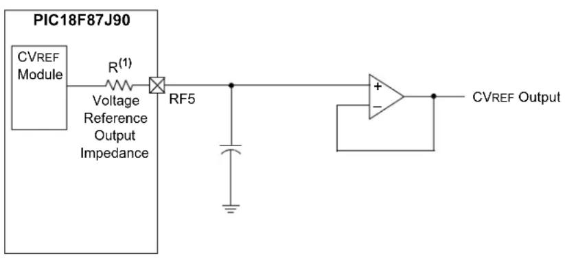
text_image
PIC18F87J90 CVREF Module R(1) Voltage Reference Output Impedance RF5 + - CVREF OutputNote 1: R is dependent upon the Comparator Voltage Reference bits, CVRCON<5> and CVRCON<3:0>.
TABLE 23-1: REGISTERS ASSOCIATED WITH COMPARATOR VOLTAGE REFERENCE
| Name Bit | 7 Bit 6 Bit 5 | Bit 4 Bit 3 | Bit 2 Bit 1 | Bit 0 | Reset Values on page | ||||
| CVRCON | CVREN | CVROE | CVRR | CVRSS | CVR3 | CVR2 | CVR1 | CVR0 | 61 |
| CMCON | C2OUT | C1OUT | C2INV | C1INV | CIS | CM2 | CM1 | CM0 | 61 |
| TRISF | TRISF7 | TRISF6 | TRISF5 | TRISF4 | TRISF3 | TRISF2 | TRISF1 | — | 62 |
Legend: — = unimplemented, read as '0'. Shaded cells are not used with the comparator voltage reference.
NOTES:
24.0 CHARGE TIME MEASUREMENT UNIT (CTMU)
The Charge Time Measurement Unit (CTMU) is a flexible analog module that provides accurate differential time measurement between pulse sources, as well as asynchronous pulse generation. By working with other on-chip analog modules, the CTMU can be used to precisely measure time, measure capacitance, measure relative changes in capacitance or generate output pulses with a specific time delay. The CTMU is ideal for interfacing with capacitive-based sensors.
The module includes the following key features:
- Up to 13 channels available for capacitive or time measurement input
- On-chip precision current source
• Four-edge input trigger sources - Polarity control for each edge source
• Control of edge sequence
• Control of response to edges
• Time measurement resolution of 1 nanosecond
• High-precision time measurement
- Time delay of external or internal signal asynchronous to the system clock
- Accurate current source suitable for capacitive measurement
The CTMU works in conjunction with the A/D Converter to provide up to 13 channels for time or charge measurement, depending on the specific device and the number of A/D channels available. When configured for time delay, the CTMU is connected to one of the analog comparators. The level-sensitive input edge sources can be selected from four sources: two external inputs or the CCP1/CCP2 Special Event Triggers.
Figure 24-1 provides a block diagram of the CTMU.
FIGURE 24-1: CTMU BLOCK DIAGRAM
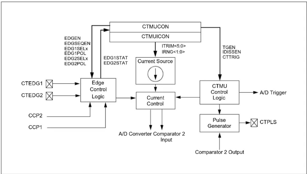
flowchart
graph TD
    A["CTMUCON"] --> B["CTMUICON"]
    B --> C["Current Source"]
    C --> D["Current Control"]
    D --> E["CTMU Control Logic"]
    E --> F["A/D Trigger"]
    E --> G["Pulse Generator"]
    G --> H["Comparator 2 Output"]
    I["CTEDG1"] --> J["Edge Control Logic"]
    K["CTEDG2"] --> J
    L["CCP2"] --> J
    M["CCP1"] --> J
    N["EDGEN EDGSEQEN EDG1SELx EDG1POL EDG2SELx EDG2POL"] --> J
    O["EDG1STAT EDG2STAT"] --> J
    P["ITRIM<5:0> IRNG<1:0>"] --> B
    Q["TGEN IDISSEN CTTRIG"] --> E
    R["A/D Converter Comparator 2 Input"] --> D
24.1 CTMU Operation
The CTMU works by using a fixed current source to charge a circuit. The type of circuit depends on the type of measurement being made. In the case of charge measurement, the current is fixed and the amount of time the current is applied to the circuit is fixed. The amount of voltage read by the A/D is then a measurement of the capacitance of the circuit. In the case of time measurement, the current, as well as the capacitance of the circuit, are fixed. In this case, the voltage read by the A/D is then representative of the amount of time elapsed from the time the current source starts and stops charging the circuit.
If the CTMU is being used as a time delay, both capacitance and current source are fixed, as well as the voltage supplied to the comparator circuit. The delay of a signal is determined by the amount of time it takes the voltage to charge to the comparator threshold voltage.
24.1.1 THEORY OF OPERATION
The operation of the CTMU is based on the equation for charge:
$$ \mathrm{C} = \mathrm{I} \cdot \frac {\mathrm{dV}}{\mathrm{dT}} $$
More simply, the amount of charge measured in coulombs in a circuit is defined as current in amperes (I) multiplied by the amount of time in seconds that the current flows (t). Charge is also defined as the capacitance in farads (C) multiplied by the voltage of the circuit (V). It follows that:
$$ \mathrm{I} \cdot \mathrm{t} = \mathrm{C} \cdot \mathrm{V} $$
The CTMU module provides a constant, known current source. The A/D Converter is used to measure (V) in the equation, leaving two unknowns: capacitance (C) and time (t). The above equation can be used to calculate capacitance or time, by either relationship using the known fixed capacitance of the circuit:
$$ \mathrm{t} = (\mathrm{C} \cdot \mathrm{V}) / \mathrm{I} $$
or by:
$$ \mathrm{C} = (\mathrm{I} \cdot \mathrm{t}) / \mathrm{V} $$
using a fixed time that the current source is applied to the circuit.
24.1.2 CURRENT SOURCE
At the heart of the CTMU is a precision current source, designed to provide a constant reference for measurements. The level of current is user-selectable across three ranges or a total of two orders of magnitude, with the ability to trim the output in ±2% increments (nominal). The current range is selected by the IRNG<1:0> bits (CTMUICON<1:0>), with a value of '00' representing the lowest range.
Current trim is provided by the ITRIM<5:0> bits (CTMUICON<7:2>). These six bits allow trimming of the current source in steps of approximately 2% per step. Note that half of the range adjusts the current source positively and the other half reduces the current source. A value of '000000' is the neutral position (no change). A value of '100000' is the maximum negative adjustment (approximately -62%) and '011111' is the maximum positive adjustment (approximately +62%).
24.1.3 EDGE SELECTION AND CONTROL
CTMU measurements are controlled by edge events occurring on the module's two input channels. Each channel, referred to as Edge 1 and Edge 2, can be configured to receive input pulses from one of the edge input pins (CTEDG1 and CTEDG2) or the CCPx Special Event Triggers. The input channels are level-sensitive, responding to the instantaneous level on the channel rather than a transition between levels. The inputs are selected using the EDG1SEL and EDG2SEL bit pairs (CTMUCONL<3:2, 6:5>).
In addition to source, each channel can be configured for event polarity using the EDGE2POL and EDGE1POL bits (CTMUCONL<7,4>). The input channels can also be filtered for an edge event sequence (Edge 1 occurring before Edge 2) by setting the EDGSEQEN bit (CTMUCONH<2>).
24.1.4 EDGE STATUS
The CTMUCON register also contains two status bits, EDG2STAT and EDG1STAT (CTMUCONL<1:0>). Their primary function is to show if an edge response has occurred on the corresponding channel. The CTMU automatically sets a particular bit when an edge response is detected on its channel. The level-sensitive nature of the input channels also means that the status bits become set immediately if the channel's configuration is changed and is the same as the channel's current state.
The module uses the edge status bits to control the current source output to external analog modules (such as the A/D Converter). Current is only supplied to external modules when only one (but not both) of the status bits is set, and shuts current off when both bits are either set or cleared. This allows the CTMU to measure current only during the interval between edges. After both status bits are set, it is necessary to clear them before another measurement is taken. Both bits should be cleared simultaneously, if possible, to avoid re-enabling the CTMU current source.
In addition to being set by the CTMU hardware, the edge status bits can also be set by software. This is also the user's application to manually enable or disable the current source. Setting either one (but not both) of the bits enables the current source. Setting or clearing both bits at once disables the source.
24.1.5 INTERRUPTS
The CTMU sets its interrupt flag (PIR3<2>) whenever the current source is enabled, then disabled. An interrupt is generated only if the corresponding interrupt enable bit (PIE3<2>) is also set. If edge sequencing is not enabled (i.e., Edge 1 must occur before Edge 2), it is necessary to monitor the edge status bits, and determine which edge occurred last and caused the interrupt.
24.2 CTMU Module Initialization
The following sequence is a general guideline used to initialize the CTMU module:
- Select the current source range using the IRNG bits (CTMUICON<1:0>).
- Adjust the current source trim using the ITRIM bits (CTMUICON<7:2>).
- Configure the edge input sources for Edge 1 and Edge 2 by setting the EDG1SEL and EDG2SEL bits (CTMUCONL<3:2 and 6:5>).
- Configure the input polarities for the edge inputs using the EDG1POL and EDG2POL bits (CTMUCONL<4,7>). The default configuration is for negative edge polarity (high-to-low transitions).
- Enable edge sequencing using the EDGSEQEN bit (CTMUCONH<2>). By default, edge sequencing is disabled.
- Select the operating mode (Measurement or Time Delay) with the TGEN bit. The default mode is Time/Capacitance Measurement.
- Configure the module to automatically trigger an A/D conversion, when the second edge event has occurred, using the CTTRIG bit (CTMUCONH<0>). The conversion trigger is disabled by default.
- Discharge the connected circuit by setting the IDISSEN bit (CTMUCONH<1>); after waiting a sufficient time for the circuit to discharge, clear IDISSEN.
- Disable the module by clearing the CTMUEN bit (CTMUCONH<7>).
- Clear the Edge Status bits, EDG2STAT and EDG1STAT (CTMUCONL<1:0>).
- Enable both edge inputs by setting the EDGEN bit (CTMUCONH<3>).
- Enable the module by setting the CTMUEN bit.
Depending on the type of measurement or pulse generation being performed, one or more additional modules may also need to be initialized and configured with the CTMU module:
- Edge Source Generation: In addition to the external edge input pins, CCPx Special Event Triggers can be used as edge sources for the CTMU.
- Capacitance or Time Measurement: The CTMU module uses the A/D Converter to measure the voltage across a capacitor that is connected to one of the analog input channels.
- Pulse Generation: When generating system clock independent output pulses, the CTMU module uses Comparator 2 and the associated comparator voltage reference.
24.3 Calibrating the CTMU Module
The CTMU requires calibration for precise measurements of capacitance and time, as well as for accurate time delay. If the application only requires measurement of a relative change in capacitance or time, calibration is usually not necessary. An example of this type of application would include a capacitive touch switch, in which the touch circuit has a baseline capacitance and the added capacitance of the human body changes the overall capacitance of a circuit.
If actual capacitance or time measurement is required, two hardware calibrations must take place: the current source needs calibration to set it to a precise current, and the circuit being measured needs calibration to measure and/or nullify all other capacitance other than that to be measured.
24.3.1 CURRENT SOURCE CALIBRATION
The current source on board the CTMU module has a range of ±60% nominal for each of three current ranges. Therefore, for precise measurements, it is possible to measure and adjust this current source by placing a high-precision resistor, Rcal, onto an unused analog channel. An example circuit is shown in Figure 24-2. The current source measurement is performed using the following steps:
- Initialize the A/D Converter.
- Initialize the CTMU.
- Enable the current source by setting EDG1STAT (CTMUCONL<0>).
- Issue settling time delay.
- Perform A/D conversion.
- Calculate the current source current using I = V/RCAL, where RCAL is a high-precision resistance and V is measured by performing an A/D conversion.
The CTMU current source may be trimmed with the trim bits in CTMUICON using an iterative process to get an exact desired current. Alternatively, the nominal value without adjustment may be used; it may be stored by the software for use in all subsequent capacitive or time measurements.
To calculate the value for RCAL , the nominal current must be chosen and then the resistance can be calculated. For example, if the A/D Converter reference voltage is 3.3V, use 70% of full scale or 2.31V as the desired approximate voltage to be read by the A/D Converter. If the range of the CTMU current source is selected to be 0.55 μA, the resistor value needed is calculated as RCAL = 2.31V/0.55 A for a value of 4.2 MΩ. Similarly, if the current source is chosen to be 5.5 μA, RCAL would be 420,000Ω, and 42,000Ω if the current source is set to 55 μA.
FIGURE 24-2: CTMU CURRENT SOURCE CALIBRATION CIRCUIT

flowchart
graph TD
    A["Current Source"] --> B["A/D Trigger"]
    B --> C["A/D Converter"]
    C --> D["MUX"]
    D --> E["ANx"]
    D --> F["RCAL"]
    G["CTMU"] --> H["Current Source"]
    I["A/D"] --> J["MUX"]
A value of 70% of full-scale voltage is chosen to make sure that the A/D Converter is in a range that is well above the noise floor. Keep in mind that if an exact current is chosen to incorporate the trimming bits from CTMUICON, the resistor value of RCAL may need to be adjusted accordingly. RCAL may be also adjusted to allow for available resistor values. RCAL should be of the highest precision available, keeping in mind the amount of precision needed for the circuit that the CTMU will be used to measure. A recommended minimum would be 0.1% tolerance.
The following examples show one typical method for performing a CTMU current calibration. Example 24-1 demonstrates how to initialize the A/D Converter and the CTMU; this routine is typical for applications using both modules. Example 24-2 demonstrates one method for the actual calibration routine. Note that this method manually triggers the A/D Converter. This is done to demonstrate the entire stepwise process. It is also possible to automatically trigger the conversion by setting the CTMU's CTTRIG bit (CTMUCONH<0>).
EXAMPLE 24-1: SETUP FOR CTMU CALIBRATION ROUTINES
#include "p18cxx.h"
/******************************************************************************************/
/*Setup CTMU ***************************
/******************************************************************************************/
void setup(void)
{
    //CTMUCON - CTMU Control register
    CTMUCONH = 0x00; //make sure CTMU is disabled
    CTMUCONL = 0X90;
    //CTMU continues to run when emulator is stopped,CTMU continues
    //to run in idle mode,Time Generation mode disabled, Edges are blocked
    //No edge sequence order, Analog current source not grounded, trigger
    //output disabled, Edge2 polarity = positive level, Edge2 source =
    //source 0, Edge1 polarity = positive level, Edge1 source = source 0,
    // Set Edge status bits to zero

    //CTMUICON - CTMU Current Control Register
    CTMUICON = 0x01; //0.55uA, Nominal - No Adjustment

    /******************************************************************************************/
    //Setup AD converter;
    /******************************************************************************************/

    TRISA=0x04; //set channel 2 as an input
    // ADCON2
    ADCON2bits.ADFM=1; // Resulst format 1= Right justified
    ADCON2bits.ACQT=1; // Acquisition time 7 = 20TAD 2 = 4TAD 1=2TAD
    ADCON2bits.ADCS=2; // Clock conversion bits 6= FOSC/64 2=FOSC/32

    // ADCON1
    ADCON1bits.ADCAL=0; // Normal A/D conversion operation
    ADCON1bits.PCFG=0xC; // Configures ANO to AN2 as analog

    // ADCON0
    ADCON0bits.VCFG0 =0; // Vref+ = AVdd
    ADCON0bits.VCFG1 =0; // Vref- = AVss
    ADCON0bits.CHS=2; // Select ADC channel

    ADCON0bits.ADON=1; // Turn on ADC
}
EXAMPLE 24-2: CURRENT CALIBRATION ROUTINE
#include "p18cxx.h"

#define COUNT 500 //@ 8MHz = 125uS.
#define DELAY for(i=0;i<COUNT;i++)
#define RCAL .027 //R value is 4200000 (4.2M)
    //scaled so that result is in
    //1/100th of uA

#define ADSCALE 1023 //for unsigned conversion 10 sig bits
#define ADREF 3.3 //Vdd connected to A/D Vr+

int main(void)
{
    int i;
    int j = 0; //index for loop
    unsigned int Vread = 0;
    double VTot = 0;
    float Vavg=0, Vcal=0, CTMUISrc = 0; //float values stored for calcs

//assume CTMU and A/D have been setup correctly
//see Example 25-1 for CTMU & A/D setup
setup();

CTMUCONHbits.CTMUEN = 1; //Enable the CTMU
    for(j=0;j<10;j++)
    {
    CTMUCONHbits.IDISSEN = 1; //drain charge on the circuit
    DELAY; //wait 125us
    CTMUCONHbits.IDISSEN = 0; //end drain of circuit

    CTMUCONLbits.EDG1STAT = 1; //Begin charging the circuit
    //using CTMU current source
    DELAY; //wait for 125us
    CTMUCONLbits.EDG1STAT = 0; //Stop charging circuit

    PIR1bits.ADIF = 0; //make sure A/D Int not set
    ADCON0bits.GO=1; //and begin A/D conv.
    while(!PIR1bits.ADIF); //Wait for A/D convert complete

    Vread = ADRES; //Get the value from the A/D
    PIR1bits.ADIF = 0; //Clear A/D Interrupt Flag
    VTot += Vread; //Add the reading to the total
}

Vavg = (float)(VTot/10.000); //Average of 10 readings
Vcal = (float)(Vavg/ADSCALE*ADREF);
CTMUISrc = Vcal/RCAL; //CTMUISrc is in 1/100ths of uA
}
24.3.2 CAPACITANCE CALIBRATION
There is a small amount of capacitance from the internal A/D Converter sample capacitor as well as stray capacitance from the circuit board traces and pads that affect the precision of capacitance measurements. A measurement of the stray capacitance can be taken by making sure the desired capacitance to be measured has been removed. The measurement is then performed using the following steps:
- Initialize the A/D Converter and the CTMU.
- Set EDG1STAT (= 1).
- Wait for a fixed delay of time, t.
- Clear EDG1STAT.
- Perform an A/D conversion.
- Calculate the stray and A/D sample capacitances:
$$ \mathrm{COFFSET} = \mathrm{CSTRAY} + \mathrm{CAD} = (\mathrm{I} \cdot \mathrm{t}) / \mathrm{V} $$
where I is known from the current source measurement step, t is a fixed delay and V is measured by performing an A/D conversion.
This measured value is then stored and used for calculations of time measurement or subtracted for capacitance measurement. For calibration, it is expected that the capacitance of C STRAY + C AD is approximately known; CAD is approximately 4 pF.
An iterative process may need to be used to adjust the time, t, that the circuit is charged to obtain a reasonable voltage reading from the A/D Converter. The value of t may be determined by setting C OFFSET to a theoretical value, then solving for t. For example, if CSTRAY is theoretically calculated to be 11 pF, and V is expected to be 70% of VDD, or 2.31V, then t would be:
$$ (4 \mathrm{pF} + 1 1 \mathrm{pF}) \cdot 2. 3 1 \mathrm{V} / 0. 5 5 \mu \mathrm{A} $$
or 63 μs.
See Example 24-3 for a typical routine for CTMU capacitance calibration.
EXAMPLE 24-3: CAPACITANCE CALIBRATION ROUTINE
#include "p18cxxx.h"

#define COUNT 25 //@ 8MHz INTFRC = 62.5 us.
#define ETIME COUNT*2.5 //time in uS
#define DELAY for(i=0;i<COUNT;i++)
#define ADSCALE 1023 //for unsigned conversion 10 sig bits
#define ADREF 3.3 //Vdd connected to A/D Vr+
#define RCAL .027 //R value is 4200000 (4.2M)
    //scaled so that result is in
    //1/100th of uA

int main(void)
{
    int i;
    int j = 0; //index for loop
    unsigned int Vread = 0;
    float CTMUISrc, CTMUCap, Vavg, VTot, Vcal;

    //assume CTMU and A/D have been setup correctly
    //see Example 25-1 for CTMU & A/D setup
    setup();

    CTMUCONHbits.CTMUEN = 1; //Enable the CTMU
    for(j=0;j<10;j++)
    {
    CTMUCONHbits.IDISSEN = 1; //drain charge on the circuit
    DELAY; //wait 125us
    CTMUCONHbits.IDISSEN = 0; //end drain of circuit

    CTMUCONLbits.EDG1STAT = 1; //Begin charging the circuit
    //using CTMU current source
    DELAY; //wait for 125us
    CTMUCONLbits.EDG1STAT = 0; //Stop charging circuit

    PIRIbits.ADIF = 0; //make sure A/D Int not set
    ADCON0bits.GO=1; //and begin A/D conv.
    while(!PIR1bits.ADIF); //Wait for A/D convert complete

    Vread = ADRES; //Get the value from the A/D
    PIRIbits.ADIF = 0; //Clear A/D Interrupt Flag
    VTot += Vread; //Add the reading to the total
    }

    Vavg = (float)(VTot/10.000); //Average of 10 readings
    Vcal = (float)(Vavg/ADSCALE*ADREF);
    CTMUISrc = Vcal/RCAL; //CTMUISrc is in 1/100ths of uA
    CTMUCap = (CTMUISrc*ETIME/Vcal)/100;
}
24.4 Measuring Capacitance with the CTMU
There are two separate methods of measuring capacitance with the CTMU. The first is the absolute method, in which the actual capacitance value is desired. The second is the relative method, in which the actual capacitance is not needed, rather an indication of a change in capacitance is required.
24.4.1 ABSOLUTE CAPACITANCE MEASUREMENT
For absolute capacitance measurements, both the current and capacitance calibration steps found in Section 24.3 "Calibrating the CTMU Module" should be followed. Capacitance measurements are then performed using the following steps:
- Initialize the A/D Converter.
- Initialize the CTMU.
- Set EDG1STAT.
- Wait for a fixed delay, T.
- Clear EDG1STAT.
- Perform an A/D conversion.
- Calculate the total capacitance, C TOTAL = (I * T)/V, where I is known from the current source measurement step (Section 24.3.1 "Current Source Calibration"), T is a fixed delay and V is measured by performing an A/D conversion.
- Subtract the stray and A/D capacitance (COFFSET from Section 24.3.2 "Capacitance Calibration") from CTOTAL to determine the measured capacitance.
24.4.2 RELATIVE CHARGE MEASUREMENT
An application may not require precise capacitance measurements. For example, when detecting a valid press of a capacitance-based switch, detecting a relative change of capacitance is of interest. In this type of application, when the switch is open (or not touched), the total capacitance is the capacitance of the combination of the board traces, the A/D Converter, etc. A larger voltage will be measured by the A/D Converter. When the switch is closed (or is touched), the total capacitance is larger due to the addition of the capacitance of the human body to the above listed capacitances and a smaller voltage will be measured by the A/D Converter.
Detecting capacitance changes is easily accomplished with the CTMU using these steps:
- Initialize the A/D Converter and the CTMU.
- Set EDG1STAT.
- Wait for a fixed delay.
- Clear EDG1STAT.
- Perform an A/D conversion.
The voltage measured by performing the A/D conversion is an indication of the relative capacitance. Note that in this case, no calibration of the current source or circuit capacitance measurement is needed. See Example 24-4 for a sample software routine for a capacitive touch switch.
EXAMPLE 24-4: ROUTINE FOR CAPACITIVE TOUCH SWITCH
#include "p18cxxx.h"

#define COUNT 500 //@ 8MHz = 125uS.
#define DELAY for(i=0;i<COUNT;i++)
#define OPENSW 1000 //Un-pressed switch value
#define TRIP 300 //Difference between pressed
//and un-pressed switch

#define HYST 65 //amount to change
//from pressed to un-pressed

#define PRESSED 1
#define UNPRESSED 0

int main(void)
{
    unsigned int Vread; //storage for reading
    unsigned int switchState;
    int i;

    //assume CTMU and A/D have been setup correctly
    //see Example 25-1 for CTMU & A/D setup
    setup();

    CTMUCONHbits.CTMUEN = 1; //Enable the CTMU

    CTMUCONHbits.IDISSEN = 1; //drain charge on the circuit
    DELAY; //wait 125us
    CTMUCONHbits.IDISSEN = 0; //end drain of circuit

    CTMUCONLbits.EDG1STAT = 1; //Begin charging the circuit
    //using CTMU current source
    DELAY; //wait for 125us
    CTMUCONLbits.EDG1STAT = 0; //Stop charging circuit

    PIRIbits.ADIF = 0; //make sure A/D Int not set
    ADCONObits.GO=1; //and begin A/D conv.
    while(!PIR1bits.ADIF); //Wait for A/D convert complete

    Vread = ADRES; //Get the value from the A/D

    if(Vread < OPENSW - TRIP)
    {
    switchState = PRESSED;
    }
    else if(Vread > OPENSW - TRIP + HYST)
    {
    switchState = UNPRESSED;
    }
}
24.5 Measuring Time with the CTMU Module
Time can be precisely measured after the ratio (C/I) is measured from the current and capacitance calibration step by following these steps:
- Initialize the A/D Converter and the CTMU.
- Set EDG1STAT.
- Set EDG2STAT.
- Perform an A/D conversion.
- Calculate the time between edges as T = (C / I)^*V , where I is calculated in the current calibration step
(Section 24.3.1 "Current Source Calibration"),
C is calculated in the capacitance calibration step
(Section 24.3.2 "Capacitance Calibration") and
V is measured by performing the A/D conversion.
It is assumed that the time measured is small enough that the capacitance, COFFSET, provides a valid voltage to the A/D Converter. For the smallest time measurement, always set the A/D Channel Select register (AD1CHS) to an unused A/D channel; the corresponding pin for which is not connected to any circuit board trace. This minimizes added stray capacitance, keeping the total circuit capacitance close to that of the A/D Converter itself (25 pF). To measure longer time intervals, an external capacitor may be connected to an A/D channel and this channel selected when making a time measurement.
FIGURE 24-3: TYPICAL CONNECTIONS AND INTERNAL CONFIGURATION FOR TIME MEASUREMENT
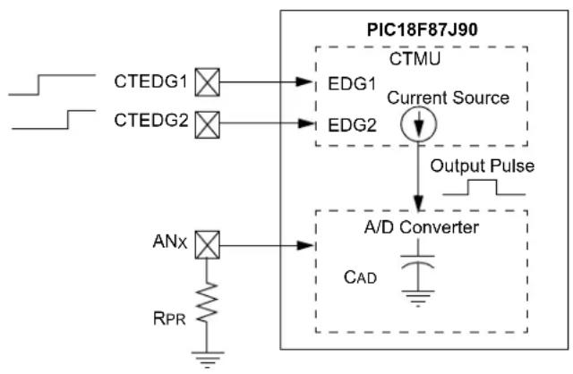
flowchart
graph TD
    A["CTEDG1"] --> B["EDG1"]
    C["CTEDG2"] --> D["EDG2"]
    E["ANx"] --> F["A/D Converter"]
    G["RPR"] --> F
    B --> H["Current Source"]
    D --> H
    F --> I["CAD"]
    H --> J["Output Pulse"]
    I --> J
    style A fill:#f9f,stroke:#333
    style C fill:#f9f,stroke:#333
    style E fill:#ccf,stroke:#333
    style G fill:#ccf,stroke:#333
    style B fill:#cff,stroke:#333
    style D fill:#cff,stroke:#333
    style F fill:#cff,stroke:#333
    style H fill:#ffc,stroke:#333
    style I fill:#ffc,stroke:#333
24.6 Creating a Delay with the CTMU Module
A unique feature on board the CTMU module is its ability to generate system clock independent output pulses based on an external capacitor value. This is accomplished using the internal comparator voltage reference module, Comparator 2 input pin and an external capacitor. The pulse is output onto the CTPLS pin. To enable this mode, set the TGEN bit.
See Figure 24-4 for an example circuit. ⒹPULSE is chosen by the user to determine the output pulse width on CTPLS. The pulse width is calculated by T = (CPULSE/I)*V, where I is known from the current source measurement step (Section 24.3.1 "Current Source Calibration") and V is the internal reference voltage (CVREF).
An example use of this feature is for interfacing with variable capacitive-based sensors, such as a humidity sensor. As the humidity varies, the pulse-width output on CTPLS will vary. The CTPLS output pin can be connected to an input capture pin and the varying pulse width is measured to determine the humidity in the application.
Follow these steps to use this feature:
- Initialize Comparator 2.
- Initialize the comparator voltage reference.
- Initialize the CTMU and enable time delay generation by setting the TGEN bit.
- Set EDG1STAT.
- When C PULSE charges to the value of the voltage reference trip point, an output pulse is generated on CTPLS.
FIGURE 24-4: TYPICAL CONNECTIONS AND INTERNAL CONFIGURATION FOR PULSE DELAY GENERATION

flowchart
graph TD
    A["CTEDG1"] --> B["EDG1"]
    B --> C["PTPLS"]
    D["C2INB"] --> E["Comparator"]
    F["CDELAY"] --> G["Ground"]
    H["CTMUL"] --> I["Current Source"]
    I --> J["C2"]
    J --> K["+"]
    L["CVREF"] --> M["Comparator"]
    M --> N["Current Source"]
    O["PIC18F87J90"] --> P["CTMUL"]
24.7 Operation During Sleep/Idle Modes
24.7.1 SLEEP MODE AND DEEP SLEEP MODES
When the device enters any Sleep mode, the CTMU module current source is always disabled. If the CTMU is performing an operation that depends on the current source when Sleep mode is invoked, the operation may not terminate correctly. Capacitance and time measurements may return erroneous values.
24.7.2 IDLE MODE
The behavior of the CTMU in Idle mode is determined by the CTMUSIDL bit (CTMUCONH<5>). If CTMUSIDL is cleared, the module will continue to operate in Idle mode. If CTMUSIDL is set, the module's current source is disabled when the device enters Idle mode. If the module is performing an operation when Idle mode is invoked, in this case, the results will be similar to those with Sleep mode.
24.8 Effects of a Reset on CTMU
Upon Reset, all registers of the CTMU are cleared. This leaves the CTMU module disabled, its current source is turned off and all configuration options return to their default settings. The module needs to be re-initialized following any Reset.
If the CTMU is in the process of taking a measurement at the time of Reset, the measurement will be lost. A partial charge may exist on the circuit that was being measured and should be properly discharged before the CTMU makes subsequent attempts to make a measurement. The circuit is discharged by setting and then clearing the IDISSEN bit (CTMUCONH<1>) while the A/D Converter is connected to the appropriate channel.
24.9 Registers
There are three control registers for the CTMU:
• CTMUCONH
• CTMUCONL
• CTMUICON
The CTMUCONH and CTMUCONL registers (Register 24-1 and Register 24-2) contain control bits for configuring the CTMU module edge source selection, edge source polarity selection, edge sequencing, A/D trigger, analog circuit capacitor discharge and enables. The CTMUICON register (Register 24-3) has bits for selecting the current source range and current source trim.
REGISTER 24-1: CTMUCONH: CTMU CONTROL HIGH REGISTER
| R/W-0 U-0 R/W-0 R/W-0 R/W-0 R/W-0 R/W-0 R/W-0 | |||||||
| CTMUEN | — CTMUSIDL TGEN E | DGEN EDGSE | QEN IDISSEN | CTTRIG | |||
| bit 7 bit 0 | |||||||
Legend:
| R = Readable bit | W = Writable bit | U = Unimplemented bit, read as '0' |
| -n = Value at POR | '1' = Bit is set | '0' = Bit is cleared x = Bit is unknown |
bit 7 CTMUEN: CTMU Enable bit
1 = Module is enabled
0 = Module is disabled
bit 6 Unimplemented: Read as '0'
bit 5 CTMUSIDL: Stop in Idle Mode bit
1 = Discontinue module operation when device enters Idle mode
0 = Continue module operation in Idle mode
bit 4 TGEN: Time Generation Enable bit
1 = Enables edge delay generation
0 = Disables edge delay generation
bit 3 EDGEN: Edge Enable bit
1 = Edges are not blocked
0 = Edges are blocked
bit 2 EDGSEQEN: Edge Sequence Enable bit
1 = Edge 1 event must occur before Edge 2 event can occur
0 = No edge sequence is needed
bit 1 IDISSEN: Analog Current Source Control bit
1 = Analog current source output is grounded
0 = Analog current source output is not grounded
bit 0 CTTRIG: Trigger Control bit
1 = Trigger output is enabled
0 = Trigger output is disabled
REGISTER 24-2: CTMUCONL: CTMU CONTROL LOW REGISTER
| R/W-0 R/W-0 R/W-0 R/W-0 R/W-0 R/W-0 R/W-0 R/W-0 | ||||||
| EDG2POL E | DG2SEL1 EDG2SEL0 EDG1 | POL EDG1SEL1 EDG1SEL0 | EDG2STAT EDG1STAT | |||
| bit 7 bit 0 | ||||||
Legend:
R = Readable bit W = Writable bit U = Unimplemented bit, read as '0'
-n = Value at POR '1' = Bit is set '0' = Bit is cleared x = Bit is unknown
bit 7 EDG2POL: Edge 2 Polarity Select bit
11 = CTEDG1 pin
10 = CTEDG2 pin
01 = CCP1 Special Event Trigger
00 = CCP2 Special Event Trigger
bit 4 EDG1POL: Edge 1 Polarity Select bit
11 = CTEDG1 pin
10 = CTEDG2 pin
01 = CCP1 Special Event Trigger
00 = CCP2 Special Event Trigger
bit 1 EDG2STAT: Edge 2 Status bit
1 = Edge 2 event has occurred
0 = Edge 2 event has not occurred
bit 0 EDG1STAT: Edge 1 Status bit
1 = Edge 1 event has occurred
0 = Edge 1 event has not occurred
REGISTER 24-3: CTMUICON: CTMU CURRENT CONTROL REGISTER
| R/W-0 R/W-0 R/W-0 R/W-0 R/W-0 R/W-0 R/W-0 R/W-0 | |||||||
| ITRIM5 ITRIM4 ITRIM3 ITRIM2 ITRIM1 | TRIM0 IRNG1 | IRNG0 | |||||
| bit 7 bit 0 | |||||||
Legend:
R = Readable bit W = Writable bit U = Unimplemented bit, read as '0' -n = Value at POR '1' = Bit is set '0' = Bit is cleared x = Bit is unknown
bit 7-2 ITRIM<5:0>: Current Source Trim bits
011111 = Maximum positive change from nominal current 011110
.
.
.
000001 = Minimum positive change from nominal current
000000 = Nominal current output specified by IRNG<1:0>
111111 = Minimum negative change from nominal current
.
.
.
100010
100001 = Maximum negative change from nominal current
bit 1-0 IRNG<1:0>: Current Source Range Select bits
11 = 100 x Base current 10 = 10 x Base current 01 = Base current level (0.55 μA nominal) 00 = Current source disabled
TABLE 24-1: REGISTERS ASSOCIATED WITH CTMU MODULE
| Name | Bit 7 | Bit 6 | Bit 5 | Bit 4 | Bit 3 | Bit 2 | Bit 1 | Bit 0 | Reset Values on page: |
| CTMUCONH | CTMUEN | — | CTMUSIDL | TGEN | EDGEN | EDGSEQEN | IDISSEN | CTTRIG | — |
| CTMUCONL | EDG2POL | EDG2SEL1 | EDG2SEL0 | EDG1POL | EDG1SEL1 | EDG1SEL0 | EDG2STAT | EDG1STAT | — |
| CTMUICON | ITRIM5 | ITRIM4 | ITRIM3 | ITRIM2 | ITRIM1 | ITRIM0 | IRNG1 | IRNG0 | — |
Legend: — = unimplemented, read as '0'. Shaded cells are not used during ECCP operation.
NOTES:
25.0 SPECIAL FEATURES OF THE CPU
PIC18F87J90 family devices include several features intended to maximize reliability and minimize cost through elimination of external components. These are:
- Oscillator Selection
-
Resets:
-
Power-on Reset (POR)
- Power-up Timer (PWRT)
- Oscillator Start-up Timer (OST)
-
Brown-out Reset (BOR)
-
Interrupts
- Watchdog Timer (WDT)
- Fail-Safe Clock Monitor
- Two-Speed Start-up
- Code Protection
• In-Circuit Serial Programming
The oscillator can be configured for the application depending on frequency, power, accuracy and cost. All of the options are discussed in detail in Section 3.0
"Oscillator Configurations".
A complete discussion of device Resets and interrupts is available in previous sections of this data sheet.
In addition to their Power-up and Oscillator Start-up Timers provided for Resets, the PIC18F87J90 family of devices have a configurable Watchdog Timer which is controlled in software.
The inclusion of an Internal RC oscillator also provides the additional benefits of a Fail-Safe Clock Monitor (FSCM) and Two-Speed Start-up. FSCM provides for background monitoring of the peripheral clock and automatic switchover in the event of its failure. Two-Speed Start-up enables code to be executed almost immediately on start-up, while the primary clock source completes its start-up delays.
All of these features are enabled and configured by setting the appropriate Configuration register bits.
25.1 Configuration Bits
The Configuration bits can be programmed (read as '0') or left unprogrammed (read as '1') to select various device configurations. These bits are mapped, starting at program memory location, 300000h. A complete list is shown in Table 25-2. A detailed explanation of the various bit functions is provided in Register 25-1 through Register 25-6.
25.1.1 CONSIDERATIONS FOR
CONFIGURING PIC18F87J90
FAMILY DEVICES
Devices of the PIC18F87J90 family do not use persistent memory registers to store configuration information. The configuration bytes are implemented as volatile memory which means that configuration data must be programmed each time the device is powered up.
Configuration data is stored in the four words at the top of the on-chip program memory space, known as the Flash Configuration Words. It is stored in program memory in the same order shown in Table 25-2, with CONFIG1L at the lowest address and CONFIG3H at the highest. The data is automatically loaded in the proper Configuration registers during device power-up.
When creating applications for these devices, users should always specifically allocate the location of the Flash Configuration Word for configuration data. This is to make certain that program code is not stored in this address when the code is compiled.
The volatile memory cells used for the Configuration bits always reset to '1' on Power-on Resets. For all other types of Reset events, the previously programmed values are maintained and used without reloading from program memory.
The four Most Significant bits of CONFIG1H, CONFIG2H and CONFIG3H in program memory should also be '1111'. This makes these Configuration Words appear to be NOP instructions in the remote event that their locations are ever executed by accident. Since Configuration bits are not implemented in the corresponding locations, writing '1's to these locations has no effect on device operation.
To prevent inadvertent configuration changes during code execution, all programmable Configuration bits are write-once. After a bit is initially programmed during a power cycle, it cannot be written to again. Changing a device configuration requires that power to the device be cycled.
TABLE 25-1: MAPPING OF THE FLASH CONFIGURATION WORDS TO THE CONFIGURATION REGISTERS
| Configuration Byte | Code Space Address | Configuration Register Address |
| CONFIG1L XXXF8h 300000h | ||
| CONFIG1H XXXF9h 300001h | ||
| CONFIG2L XXXFAh 300002h | ||
| CONFIG2H XXXFBh 300003h | ||
| CONFIG3L | XXXFCh 300004h | |
| CONFIG3H | XXXFDh 300005h |
TABLE 25-2: CONFIGURATION BITS AND DEVICE IDs
| File Name Bit 7 | Bit 6 Bit 5 | Bit 4 Bit 3 | Bit 2 Bit 1 | Bit 0 | Default/Unprogrammed Value (1) | |||||
| 300000h | CONFIG1L | XINST | STVREN | — | — | — | — | WDTEN | 111- ----1 | |
| 300001h | CONFIG1H | -(2) | -(2) | -(2) | -(2) | -(3) | CP0 | — | — | ---- 01-- |
| 300002h | CONFIG2L | IESO | FCMEN | — | LPT1OSC | T1DIG | FOSC2 | FOSC1 | FOSC0 | 11-1 1111 |
| 300003h | CONFIG2H | -(2) | -(2) | -(2) | -(2) | WDTPS3 | WDTPS2 | WDTPS1 | WDTPS0 | ---- 1111 |
| 300004h | CONFIG3L | -(2) | -(2) | -(2) | -(2) | — | — | RTCOSC | — | ---- --1- |
| 300005h | CONFIG3H | -(2) | -(2) | -(2) | -(2) | — | — | — | CCP2MX | ---- ---1 |
| 3FFFFEh | DEVID1 | DEV2 | DEV1 | DEV0 | REV4 | REV3 | REV2 | REV1 | REV0 | xxxx xxxx(4) |
| 3FFFFFFh | DEVID2 | DEV10 | DEV9 | DEV8 | DEV7 | DEV6 | DEV5 | DEV4 | DEV3 | 0000 10x1(4) |
Legend: x = unknown, - = unimplemented. Shaded cells are unimplemented, read as '0'.
Note 1: Values reflect the unprogrammed state as received from the factory and following Power-on Resets. In all other Reset states, the configuration bytes maintain their previously programmed states.
2: The value of these bits in program memory should always be '1'. This ensures that the location is executed as a NOP if it is accidentally executed.
3: This bit should always be maintained as '0'
4: See Register 25-7 and Register 25-8 for DEVID values. These registers are read-only and cannot be programmed by the user.
REGISTER 25-1: CONFIG1L: CONFIGURATION REGISTER 1 LOW (BYTE ADDRESS 300000h)
| R/WO-1 R/WO-1 R/WO-1 U-0 U-0 U-0 U-0 R/WO-1 | |||||||
| DEBUG | XINST ST | VREN — — — | — | W | D | T | E N |
| bit 7 bit 0 | |||||||
Legend:
R = Readable bit WO = Write-Once bit U = Unimplemented bit, read as '0' -n = Value when device is unprogrammed '1' = Bit is set '0' = Bit is cleared
bit 7 DEBUG: Background Debugger Enable bit
1 = Background debugger disabled; RB6 and RB7 configured as general purpose I/O pins
0 = Background debugger enabled; RB6 and RB7 are dedicated to In-Circuit Debug
bit 6 XINST: Extended Instruction Set Enable bit
1 = Instruction set extension and Indexed Addressing mode enabled
0 = Instruction set extension and Indexed Addressing mode disabled (Legacy mode)
bit 5 STVREN: Stack Overflow/Underflow Reset Enable bit
1 = Reset on stack overflow/underflow enabled
0 = Reset on stack overflow/underflow disabled
bit 4-1 Unimplemented: Read as '0'
bit 0 WDTEN: Watchdog Timer Enable bit
1 = WDT enabled
0 = WDT disabled (control is placed on SWDTEN bit)
REGISTER 25-2: CONFIG1H: CONFIGURATION REGISTER 1 HIGH (BYTE ADDRESS 300001h)
| U-0 U-0 U-0 U-0 U-0 R/WO-1 U-0 U-0 | |||||||
| _(1) | _(1) | _(1) | _(1) | _(2) | CP0 | — — | |
| bit 7 bit 0 | |||||||
Legend:
R = Readable bit WO = Write-Once bit U = Unimplemented bit, read as '0' -n = Value when device is unprogrammed '1' = Bit is set '0' = Bit is cleared
bit 7-3 Unimplemented: Read as '0'
bit 2 CP0: Code Protection bit
1 = Program memory is not code-protected
0 = Program memory is code-protected
bit 1-0 Unimplemented: Read as '0'
Note 1: The value of these bits in program memory should always be '1'. This ensures that the location is executed as a NOP if it is accidentally executed.
2: This bit should always be maintained as '0'.
REGISTER 25-3: CONFIG2L: CONFIGURATION REGISTER 2 LOW (BYTE ADDRESS 300002h)
| R/WO-1 R/WO-1 U-0 R/WO-1 R/WO-1 R/WO-1 R/WO-1 R/WO-1 | ||||||
| IESO FCMEN | — LPT1 | OSC T1DIG | FOSC2 | FOSC1 | FOSC0 | |
| bit 7 bit 0 | ||||||
Legend:
| R = Readable bit WO = Write-Once bit U = Unimplemented bit, read as '0' |
| -n = Value when device is unprogrammed '1' = Bit is set '0' = Bit is cleared |
bit 7 IESO: Two-Speed Start-up (Internal/External Oscillator Switchover) Control bit
1 = Two-Speed Start-up enabled
0 = Two-Speed Start-up disabled
bit 6 FCMEN: Fail-Safe Clock Monitor Enable bit
1 = Fail-Safe Clock Monitor enabled
0 = Fail-Safe Clock Monitor disabled
bit 5 Unimplemented: Read as '0'
bit 4 LPT1OSC: T1OSC/SOSC Power Selection Configuration bit
1 = High-power T1OSC/SOSC circuit selected
0 = Low-power T1OSC/SOSC circuit selected
bit 3 T1DIG: T1CKI for Digital Input Clock Enable bit
1 = T1CKI is available as a digital input without enabling T1OSCEN
0 = T1CKI is not available as a digital input without enabling T1OSCEN
bit 2-0 FOSC<2:0>: Oscillator Selection bits
111 = ECPLL OSC1/OSC2 as primary; ECPLL oscillator with PLL enabled; CLKO on RA6
110 = EC OSC1/OSC2 as primary; external clock with Fosc/4 output
101 = HSPLL OSC1/OSC2 as primary; high-speed crystal/resonator with software PLL control
100 = HS OSC1/OSC2 as primary; high-speed crystal/resonator
011 = INTPLL1 internal oscillator block with software PLL control; Fosc/4 output
010 = INTIO1 internal oscillator block with Fosc/4 output on RA6 and I/O on RA7
001 = INTPLL2 internal oscillator block with software PLL control and I/O on RA6 and RA7
000 = INTIO2 internal oscillator block with I/O on RA6 and RA7
REGISTER 25-4: CONFIG2H: CONFIGURATION REGISTER 2 HIGH (BYTE ADDRESS 300003h)
| U-0 U-0 U-0 U-0 R/WO-1 R/WO-1 R/WO-1 R/WO-1 | ||||||
| _(1) | _(1) | _(1) | _(1) | WDTPS3 WDTPS2 WDTPS1 WDTPS0 | ||
| bit 7 bit 0 | ||||||
Legend:
| R = Readable bit WO = Write-Once bit U = Unimplemented bit, read as '0' -n = Value when device is unprogrammed '1' = Bit is set '0' = Bit is cleared |
bit 7-4 Unimplemented: Read as '0'
bit 3-0 WDTPS<3:0>: Watchdog Timer Postscale Select bits
1111 = 1:32,768
1110 = 1:16,384
1101 = 1:8,192
1100 = 1:4,096
1011 = 1:2,048
1010 = 1:1,024
1001 = 1:512
1000 = 1:256
0111 = 1:128
0110 = 1:64
0101 = 1:32
0100 = 1:16
0011 = 1:8
0010 = 1:4
0001 = 1:2
0000 = 1:1
Note 1: The value of these bits in program memory should always be '1'. This ensures that the location is executed as a NOP if it is accidentally executed.
REGISTER 25-5: CONFIG3L: CONFIGURATION REGISTER 3 LOW (BYTE ADDRESS 300004h)
| R = Readable bit WO = Write-Once bit U = Unimplemented bit, read as '0' |
| -n = Value when device is unprogrammed '1' = Bit is set '0' = Bit is cleared |
bit 7-2 Unimplemented: Read as '0'
bit 1 RTCOSC: RTCC Reference Clock Select bit
1 = RTCC uses T1OSC/T1CKI as the reference clock
0 = RTCC uses INTRC as the reference clock
bit 0 Unimplemented: Read as '0'
Note 1: The value of these bits in program memory should always be '1'. This ensures that the location is executed as a NOP if it is accidentally executed.
REGISTER 25-6: CONFIG3H: CONFIGURATION REGISTER 3 HIGH (BYTE ADDRESS 300005h)
| U-0 U-0 U-0 U-0 U-0 U-0 R/WO-1 | |||||||
| _(1) | _(1) | _(1) | _(1) | ——— | CCP2MX | ||
| bit 7 bit 0 | |||||||
Legend:
R = Readable bit WO = Write-Once bit U = Unimplemented bit, read as '0' -n = Value when device is unprogrammed '1' = Bit is set '0' = Bit is cleared
bit 7-1 Unimplemented: Read as '0'
bit 0 CCP2MX: CCP2 MUX bit
1 = CCP2 is multiplexed with RC1 0 = CCP2 is multiplexed with RE7
Note 1: The value of these bits in program memory should always be '1'. This ensures that the location is executed as a NOP if it is accidentally executed.
REGISTER 25-7: DEVID1: DEVICE ID REGISTER 1 FOR PIC18F87J90 FAMILY DEVICES
| R | R | R | R | R | R | R | R |
| DEV2 | DEV1 | DEV0 | REV4 | REV3 | REV2 | REV1 | REV0 |
| bit 7 bit 0 | |||||||
Legend:
R = Read-only bit
bit 7-5 DEV<2:0>: Device ID bits
101 = PIC18F87J90 100 = PIC18F86J90 001 = PIC18F67J90 000 = PIC18F66J90
bit 4-0 REV<4:0>: Revision ID bits
These bits are used to indicate the device revision.
REGISTER 25-8: DEVID2: DEVICE ID REGISTER 2 FOR PIC18F87J90 FAMILY DEVICES
| R | R | R | R | R | R | R | R |
| DEV10^(1) | DEV9^(1) | DEV8^(1) | DEV7^(1) | DEV6^(1) | DEV5^(1) | DEV4^(1) | DEV3^(1) |
| bit 7 bit 0 | |||||||
Legend:
R = Read-only bit
bit 7-0 DEV<10:3>: Device ID bits (1)
These bits are used with the DEV<2:0> bits in the Device ID Register 1 to identify the part number. 0101 0000 = PIC18F87J90 family devices
Note 1: The values for DEV<10:3> may be shared with other device families. The specific device is always identified by using the entire DEV<10:0> bit sequence.
25.2 Watchdog Timer (WDT)
For PIC18F87J90 family devices, the WDT is driven by the INTRC oscillator. When the WDT is enabled, the clock source is also enabled. The nominal WDT period is 4 ms and has the same stability as the INTRC oscillator.
The 4 ms period of the WDT is multiplied by a 16-bit postscaler. Any output of the WDT postscaler is selected by a multiplexor, controlled by the WDTPS bits in Configuration Register 2H. Available periods range from 4 ms to 131.072 seconds (2.18 minutes). The WDT and postscaler are cleared whenever a SLEEP or CLRWDT instruction is executed, or a clock failure (primary or Timer1 oscillator) has occurred.
Note 1: The CLRWDT and SLEEP instructions clear the WDT and postscaler counts when executed.
2: When a CLRWDT instruction is executed, the postscaler count will be cleared.
25.2.1 CONTROL REGISTER
The WDTCON register (Register 25-9) is a readable and writable register. The SWDTEN bit enables or disables WDT operation. This allows software to override the WDTEN Configuration bit and enable the WDT only if it has been disabled by the Configuration bit.
FIGURE 25-1: WDT BLOCK DIAGRAM
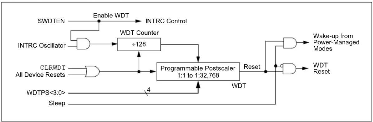
flowchart
graph TD
    A["SWDTEN"] --> B["Enable WDT"]
    B --> C["INTRC Control"]
    D["INTRC Oscillator"] --> E["÷128"]
    E --> F["WDT Counter"]
    G["CLRWDT All Device Resets"] --> H["÷128"]
    H --> I["Programmable Postscaler 1:1 to 1:32,768"]
    I --> J["Reset"]
    K["WDTPS<3:0>"] --> L["4"]
    M["Sleep"] --> N["WDT"]
    O["WDT Reset"] --> P["Wake-up from Power-Managed Modes"]
    Q["WDT Reset"] --> R["WDT"]
REGISTER 25-9: WDTCON: WATCHDOG TIMER CONTROL REGISTER
| R/W-0 U-0 U-0 U-0 U-0 U-0 R/W-0 | ||||||||
| REGSLP(1) | — — — | — — — | S | W | D | T | E | N |
| bit 7 bit 0 | ||||||||
Legend:
| R = Readable bit W = Writable bit U = Unimplemented bit, read as '0' | |
| -n = Value at POR '1' = Bit is set '0' = Bit is cleared | x = Bit is unknown |
bit 7 REGSLP: Voltage Regulator Low-Power Operation Enable bit ^(1)
1 = On-chip regulator enters low-power operation when device enters Sleep mode
0 = On-chip regulator continues to operate normally in Sleep mode
bit 6-1 Unimplemented: Read as '0'
bit 0 SWDTEN: Software Controlled Watchdog Timer Enable bit ^(2)
1 = Watchdog Timer is on
0 = Watchdog Timer is off
Note 1: The REGSLP bit is automatically cleared when a Low-Voltage Detect condition occurs.
2: This bit has no effect if the Configuration bit, WDTEN, is enabled.
TABLE 25-3: SUMMARY OF WATCHDOG TIMER REGISTERS
| Name | Bit 7 | Bit 6 | Bit 5 | Bit 4 | Bit 3 | Bit 2 | Bit 1 | Bit 0 | Reset Values on page |
| RCON | IPEN | — | 60 | ||||||
| WDTCON | REGSLP | — | — | — | — | — | — | SWDTEN | 60 |
Legend: — = unimplemented, read as '0'. Shaded cells are not used by the Watchdog Timer.
25.3 On-Chip Voltage Regulator
All of the PIC18F87J90 family devices power their core digital logic at a nominal 2.5V. For designs that are required to operate at a higher typical voltage, such as 3.3V, all devices in the PIC18F87J90 family incorporate an on-chip regulator that allows the device to run its core logic from VDD.
The regulator is controlled by the ENVREG pin. Tying VDD to the pin enables the regulator, which in turn, provides power to the core from the other VDD pins. When the regulator is enabled, a low-ESR filter capacitor must be connected to the VDDCORE/VCAP pin (Figure 25-2). This helps to maintain the stability of the regulator. The recommended value for the filter capacitor is provided in Section 28.3 "DC Characteristics: PIC18F87J90 Family (Industrial)".
If ENVREG is tied to Vss, the regulator is disabled. In this case, separate power for the core logic at a nominal 2.5V must be supplied to the device on the VDDCORE/VCAP pin to run the I/O pins at higher voltage levels, typically 3.3V. Alternatively, the VDDCORE/VCAP and VDD pins can be tied together to operate at a lower nominal voltage. Refer to Figure 25-2 for possible configurations.
25.3.1 VOLTAGE REGULATION AND LOW-VOLTAGE DETECTION
When it is enabled, the on-chip regulator provides a constant voltage of 2.5V nominal to the digital core logic. The regulator can provide this level from a VDD of about 2.5V, all the way up to the device's VDDMAX. It does not have the capability to boost VDD levels below 2.5V.
In order to prevent "brown-out" conditions when the voltage drops too low for the regulator, the regulator enters Tracking mode. In Tracking mode, the regulator output follows VDD with a typical voltage drop of 100 mV.
The on-chip regulator includes a simple Low-Voltage Detect (LVD) circuit. If VDD drops too low to maintain approximately 2.45V on VDDCORE, the circuit sets the Low-Voltage Detect Interrupt Flag, LVDIF (PIR2<2>), and clears the REGSLP (WDTCON<7>) bit, if it was set.
This can be used to generate an interrupt and put the application into a low-power operational mode, or trigger an orderly shutdown. Low-Voltage Detection is only available when the regulator is enabled.
FIGURE 25-2: CONNECTIONS FOR THE ON-CHIP REGULATOR
Regulator Enabled (ENVREG tied to VDD):
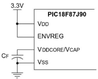
text_image
3.3V PIC18F87J90 VDD ENVREG VDDCORE/VCAP VSS CFRegulator Disabled (ENVREG tied to ground):
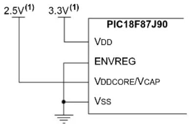
text_image
2.5V(1) 3.3V(1) PIC18F87J90 VDD ENVREG VDDCORE/VCAP VssRegulator Disabled (VDD tied to VDDCORE):

text_image
2.5V(1) PIC18F87J90 VDD ENVREG VDDCORE/VCAP VSSNote 1: These are typical operating voltages. For the full operating ranges of VDD and VDDCORE, refer to Section 28.1 "DC Characteristics: Supply Voltage PIC18F87J90 Family (Industrial)".
25.3.2 ON-CHIP REGULATOR AND BOR
When the on-chip regulator is enabled, PIC18F87J90 family devices also have a simple Brown-out Reset capability. If the voltage supplied to the regulator falls to a level that is inadequate to maintain a regulated output for full-speed operation, the regulator Reset circuitry will generate a Brown-out Reset. This event is captured by the BOR flag bit (RCON<0>).
The operation of the BOR is described in more detail in Section 5.4 "Brown-out Reset (BOR)" and Section 5.4.1 "Detecting BOR".
25.3.3 POWER-UP REQUIREMENTS
The on-chip regulator is designed to meet the power-up requirements for the device. If the application does not use the regulator, then strict power-up conditions must be adhered to. While powering up, VDDCORE must never exceed VDD by 0.3 volts.
25.3.4 OPERATION IN SLEEP MODE
When enabled, the on-chip regulator always consumes a small incremental amount of current over IDD. This includes when the device is in Sleep mode, even though the core digital logic does not require power. To provide additional savings in applications where power resources are critical, the regulator can be configured to automatically disable itself whenever the device goes into Sleep mode. This feature is controlled by the REGSLP bit (WDTCON<7>). Setting this bit disables the regulator in Sleep mode, and reduces its current consumption to a minimum.
Substantial Sleep mode power savings can be obtained by setting the REGSLP bit, but device wake-up time will increase in order to ensure the regulator has enough time to stabilize.
The REGSLP bit is automatically cleared by hardware when a Low-Voltage Detect condition occurs. The REGSLP bit can be set again in software, which would continue to keep the voltage regulator in Low-Power mode. This, however, is not recommended if any write operations to the Flash will be performed.
25.4 Two-Speed Start-up
The Two-Speed Start-up feature helps to minimize the latency period, from oscillator start-up to code execution, by allowing the microcontroller to use the INTRC oscillator as a clock source until the primary clock source is available. It is enabled by setting the IESO Configuration bit.
Two-Speed Start-up should be enabled only if the Primary Oscillator mode is HS or HSPLL (Crystal-Based) modes. Since the EC and ECPLL modes do not require an OST start-up delay, Two-Speed Start-up should be disabled.
When enabled, Resets and wake-ups from Sleep mode cause the device to configure itself to run from the internal oscillator block as the clock source, following the time-out of the Power-up Timer after a Power-on Reset is enabled. This allows almost immediate code execution while the primary oscillator starts and the OST is running. Once the OST times out, the device automatically switches to PRI_RUN mode.
In all other power-managed modes, Two-Speed Start-up is not used. The device will be clocked by the currently selected clock source until the primary clock source becomes available. The setting of the IESO bit is ignored.
FIGURE 25-3: TIMING TRANSITION FOR TWO-SPEED START-UP (INTRC TO HSPLL)

text_image
INTRC OSC1 PLL Clock Output CPU Clock Peripheral Clock Program Counter Q1 | Q2 | Q3 | Q4 | Q1 TOST(1) TPLL(1) 1 2 n - 1 n Clock Transition PC PC + 2 PC + 4 PC + 6 Wake from Interrupt Event OSTS bit SetNote 1: TOST = 1024 TOSC; TPLL = 2 ms (approx). These intervals are not shown to scale.
25.4.1 SPECIAL CONSIDERATIONS FOR USING TWO-SPEED START-UP
While using the INTRC oscillator in Two-Speed Start-up, the device still obeys the normal command sequences for entering power-managed modes, including serial SLEEP instructions (refer to Section 4.1.4 "Multiple Sleep Commands"). In practice, this means that user code can change the SCS<1:0> bits setting or issue SLEEP instructions before the OST times out. This would allow an application to briefly wake-up, perform routine "housekeeping" tasks and return to Sleep before the device starts to operate from the primary oscillator.
User code can also check if the primary clock source is currently providing the device clocking by checking the status of the OSTS bit (OSCCON<3>). If the bit is set, the primary oscillator is providing the clock. Otherwise, the internal oscillator block is providing the clock during wake-up from Reset or Sleep mode.
25.5 Fail-Safe Clock Monitor
The Fail-Safe Clock Monitor (FSCM) allows the microcontroller to continue operation in the event of an external oscillator failure by automatically switching the device clock to the internal oscillator block. The FSCM function is enabled by setting the FCMEN Configuration bit.
When FSCM is enabled, the INTRC oscillator runs at all times to monitor clocks to peripherals and provides a backup clock in the event of a clock failure. Clock monitoring (shown in Figure 25-4) is accomplished by creating a sample clock signal which is the INTRC output divided by 64. This allows ample time between FSCM sample clocks for a peripheral clock edge to occur. The peripheral device clock and the sample clock are presented as inputs to the Clock Monitor (CM) latch. The CM is set on the falling edge of the device clock source but cleared on the rising edge of the sample clock.
FIGURE 25-4: FSCM BLOCK DIAGRAM
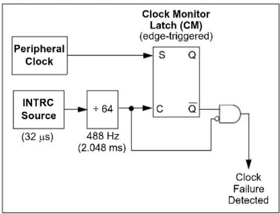
flowchart
graph TD
    A["Peripheral Clock"] --> B["÷64"]
    C["INTRC Source (32 µs)"] --> B
    B --> D["488 Hz (2.048 ms)"]
    D --> E["S Q"]
    D --> F["C Q̅"]
    E --> G["Clock Monitor Latch (CM) (edge-triggered)"]
    F --> G
    G --> H["Clock Failure Detected"]
Clock failure is tested for on the falling edge of the sample clock. If a sample clock falling edge occurs while CM is still set, a clock failure has been detected (Figure 25-5). This causes the following:
- the FSCM generates an oscillator fail interrupt by setting bit, OSCFIF (PIR2<7>);
- the device clock source is switched to the internal oscillator block (OSCCON is not updated to show the current clock source – this is the Fail-Safe condition); and
- the WDT is reset.
During switchover, the postscaler frequency from the internal oscillator block may not be sufficiently stable for timing-sensitive applications. In these cases, it may be desirable to select another clock configuration and enter an alternate power-managed mode. This can be done to attempt a partial recovery or execute a controlled shutdown. See Section 4.1.4 "Multiple Sleep Commands" and Section 25.4.1 "Special Considerations for Using Two-Speed Start-up" for more details.
The FSCM will detect failures of the primary or secondary clock sources only. If the internal oscillator block fails, no failure would be detected, nor would any action be possible.
25.5.1 FSCM AND THE WATCHDOG TIMER
Both the FSCM and the WDT are clocked by the INTRC oscillator. Since the WDT operates with a separate divider and counter, disabling the WDT has no effect on the operation of the INTRC oscillator when the FSCM is enabled.
As already noted, the clock source is switched to the INTRC clock when a clock failure is detected; this may mean a substantial change in the speed of code execution. If the WDT is enabled with a small prescale value, a decrease in clock speed allows a WDT time-out to occur and a subsequent device Reset. For this reason, Fail-Safe Clock Monitor events also reset the WDT and postscaler, allowing it to start timing from when execution speed was changed and decreasing the likelihood of an erroneous time-out.
If the interrupt is disabled, subsequent interrupts while in Idle mode will cause the CPU to begin executing instructions while being clocked by the INTRC source.
FIGURE 25-5: FSCM TIMING DIAGRAM
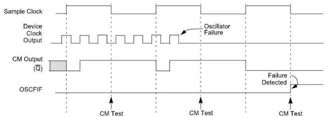
text_image
Sample Clock Device Clock Output Oscillator Failure CM Output (Q̅) OSCFIF CM Test CM Test CM Test Failure DetectedNote: The device clock is normally at a much higher frequency than the sample clock. The relative frequencies in this example have been chosen for clarity.
25.5.2 EXITING FAIL-SAFE OPERATION
The Fail-Safe condition is terminated by either a device Reset or by entering a power-managed mode. On Reset, the controller starts the primary clock source specified in Configuration Register 2H (with any required start-up delays that are required for the oscillator mode, such as the OST or PLL timer). The INTRC oscillator provides the device clock until the primary clock source becomes ready (similar to a Two-Speed Start-up). The clock source is then switched to the primary clock (indicated by the OSTS bit in the OSCCON register becoming set). The Fail-Safe Clock Monitor then resumes monitoring the peripheral clock.
The primary clock source may never become ready during start-up. In this case, operation is clocked by the INTOSC multiplexor. The OSCCON register will remain in its Reset state until a power-managed mode is entered.
25.5.3 FSCM INTERRUPTS IN POWER-MANAGED MODES
By entering a power-managed mode, the clock multiplexor selects the clock source selected by the OSCCON register. Fail-Safe Clock Monitoring of the power-managed clock source resumes in the power-managed mode.
If an oscillator failure occurs during power-managed operation, the subsequent events depend on whether or not the oscillator failure interrupt is enabled. If enabled (OSCFIF = 1), code execution will be clocked by the INTRC multiplexor. An automatic transition back to the failed clock source will not occur.
25.5.4 POR OR WAKE-UP FROM SLEEP
The FSCM is designed to detect oscillator failure at any point after the device has exited Power-on Reset (POR) or low-power Sleep mode. When the primary device clock is either EC or INTRC mode, monitoring can begin immediately following these events.
For HS or HSPLL modes, the situation is somewhat different. Since the oscillator may require a start-up time considerably longer than the FSCM sample clock time, a false clock failure may be detected. To prevent this, the internal oscillator block is automatically configured as the device clock and functions until the primary clock is stable (the OST and PLL timers have timed out). This is identical to Two-Speed Start-up mode. Once the primary clock is stable, the INTRC returns to its role as the FSCM source.
Note: The same logic that prevents false oscillator failure interrupts on POR, or wake from Sleep, will also prevent the detection of the oscillator's failure to start at all following these events. This can be avoided by monitoring the OSTS bit and using a timing routine to determine if the oscillator is taking too long to start. Even so, no oscillator failure interrupt will be flagged.
As noted in Section 25.4.1 "Special Considerations for Using Two-Speed Start-up", it is also possible to select another clock configuration and enter an alternate power-managed mode while waiting for the primary clock to become stable. When the new power-managed mode is selected, the primary clock is disabled.
25.6 Program Verification and Code Protection
For all devices in the PIC18F87J90 family of devices, the on-chip program memory space is treated as a single block. Code protection for this block is controlled by one Configuration bit, CP0. This bit inhibits external reads and writes to the program memory space. It has no direct effect in normal execution mode.
25.6.1 CONFIGURATION REGISTER PROTECTION
The Configuration registers are protected against untoward changes or reads in two ways. The primary protection is the write-once feature of the Configuration bits which prevents reconfiguration once the bit has been programmed during a power cycle. To safeguard against unpredictable events, Configuration bit changes resulting from individual cell-level disruptions (such as ESD events) will cause a parity error and trigger a device Reset.
The data for the Configuration registers is derived from the Flash Configuration Words in program memory. When the CP0 bit set, the source data for device configuration is also protected as a consequence.
25.7 In-Circuit Serial Programming
PIC18F87J90 family microcontrollers can be serially programmed while in the end application circuit. This is simply done with two lines for clock and data, and three other lines for power, ground and the programming voltage. This allows customers to manufacture boards with unprogrammed devices and then program the microcontroller just before shipping the product. This also allows the most recent firmware or a custom firmware to be programmed.
25.8 In-Circuit Debugger
When the DEBUG Configuration bit is programmed to a '0', the In-Circuit Debugger functionality is enabled. This function allows simple debugging functions when used with MPLAB ^® IDE. When the microcontroller has this feature enabled, some resources are not available for general use. Table 25-4 shows which resources are required by the background debugger.
TABLE 25-4: DEBUGGER RESOURCES
| I/O pins: RB6, RB7 | |
| Stack: 2 levels | |
| Program Memory: 512 bytes | |
| Data Memory: 10 bytes |
NOTES:
26.0 INSTRUCTION SET SUMMARY
The PIC18F87J90 family of devices incorporate the standard set of 75 PIC18 core instructions, as well as an extended set of 8 new instructions for the optimization of code that is recursive or that utilizes a software stack. The extended set is discussed later in this section.
26.1 Standard Instruction Set
The standard PIC18 MCU instruction set adds many enhancements to the previous PIC® MCU instruction sets, while maintaining an easy migration from these PIC MCU instruction sets. Most instructions are a single program memory word (16 bits), but there are four instructions that require two program memory locations.
Each single-word instruction is a 16-bit word divided into an opcode, which specifies the instruction type and one or more operands, which further specify the operation of the instruction.
The instruction set is highly orthogonal and is grouped into four basic categories:
- Byte-oriented operations
- Bit-oriented operations
- Literal operations
- Control operations
The PIC18 instruction set summary in Table 26-2 lists byte-oriented, bit-oriented, literal and control operations. Table 26-1 shows the opcode field descriptions.
Most byte-oriented instructions have three operands:
- The file register (specified by 'f')
- The destination of the result (specified by 'd')
- The accessed memory (specified by 'a')
The file register designator, 'f', specifies which file register is to be used by the instruction. The destination designator, 'd', specifies where the result of the operation is to be placed. If 'd' is zero, the result is placed in the WREG register. If 'd' is one, the result is placed in the file register specified in the instruction.
All bit-oriented instructions have three operands:
- The file register (specified by 'f')
- The bit in the file register (specified by 'b')
- The accessed memory (specified by 'a')
The bit field designator, 'b', selects the number of the bit affected by the operation, while the file register designator, 'f', represents the number of the file in which the bit is located.
The literal instructions may use some of the following operands:
- A literal value to be loaded into a file register (specified by 'k')
- The desired FSR register to load the literal value into (specified by 'f')
- No operand required (specified by ‘—’)
The control instructions may use some of the following operands:
- A program memory address (specified by 'n')
- The mode of the CALL or RETURN instructions (specified by 's')
- The mode of the table read and table write instructions (specified by 'm')
- No operand required (specified by ‘—’)
All instructions are a single word, except for four double-word instructions. These instructions were made double-word to contain the required information in 32 bits. In the second word, the 4 MSbs are '1's. If this second word is executed as an instruction (by itself), it will execute as a NOP.
All single-word instructions are executed in a single instruction cycle, unless a conditional test is true or the program counter is changed as a result of the instruction. In these cases, the execution takes two instruction cycles with the additional instruction cycle(s) executed as a NOP.
The double-word instructions execute in two instruction cycles.
One instruction cycle consists of four oscillator periods. Thus, for an oscillator frequency of 4 MHz, the normal instruction execution time is 1 s. If a conditional test is true, or the program counter is changed as a result of an instruction, the instruction execution time is 2 s. Two-word branch instructions (if true) would take 3 s.
Figure 26-1 shows the general formats that the instructions can have. All examples use the convention 'nnh' to represent a hexadecimal number.
The Instruction Set Summary, shown in Table 26-2, lists the standard instructions recognized by the Microchip MPASM™ Assembler.
Section 26.1.1 "Standard Instruction Set" provides a description of each instruction.
TABLE 26-1: OPCODE FIELD DESCRIPTIONS
| Field Description | |
| a RAM access bit: | a = 0: RAM location in Access RAM (BSR register is ignored)a = 1: RAM bank is specified by BSR register |
| bbb Bit address within an 8-bit file register (0 to 7). | |
| BSR Bank Select Register. Used to select the current RAM bank. | |
| C, DC, Z, OV, N | ALU Status bits: Carry, Digit Carry, Zero, Overflow, Negative. |
| d Destination select bit:d = 0: store result in WREGd = 1: store result in file register f | |
| dest Destination: either the WREG register or the specified register file location. | |
| f 8-bit Register file address (00h to FFh), or 2-bit FSR designator (0h to 3h). | |
| fs | 12-bit Register file address (000h to FFFh). This is the source address. |
| fd | 12-bit Register file address (000h to FFFh). This is the destination address. |
| GIE Global Interrupt Enable bit. | |
| k | Literal field, constant data or label (may be either an 8-bit, 12-bit or a 20-bit value). |
| label Label name. | |
| mm The mode of the TBLPTR register for the table read and table write instructions.Only used with table read and table write instructions:* No Change to register (such as TBLPTR with table reads and writes)*+ Post-Increment register (such as TBLPTR with table reads and writes)*- Post-Decrement register (such as TBLPTR with table reads and writes)+* Pre-Increment register (such as TBLPTR with table reads and writes) | |
| n | The relative address (2's complement number) for relative branch instructions or the direct address for Call/Branch and Return instructions. |
| PC Program Counter. | |
| PCL Program Counter Low Byte. | |
| PCH Program Counter High Byte. | |
| PCLATH Program Counter High Byte Latch. | |
| PCLATU Program Counter Upper Byte Latch. | |
| FD Power-Down bit. | |
| PRODH Product of Multiply High Byte. | |
| PRODL Product of Multiply Low Byte. | |
| s Fast Call/Return mode select bit:s = 0: do not update into/from shadow registerss = 1: certain registers loaded into/from shadow registers (Fast mode) | |
| TBLPTR 21-bit Table Pointer (points to a Program Memory location). | |
| TABLAT 8-bit Table Latch. | |
| TO Time-out bit. | |
| TOS Top-of-Stack. | |
| u Unused or Unchanged. | |
| WDT Watchdog Timer. | |
| WREG Working register (accumulator). | |
| x | Don't care ('0' or '1'). The assembler will generate code with x = 0. It is the recommended form of use for compatibility with all Microchip software tools. |
| zs | 7-bit offset value for Indirect Addressing of register files (source). |
| zd | 7-bit offset value for Indirect Addressing of register files (destination). |
| { } Optional argument. | |
| [text] Indicates an Indexed Address. | |
| (text) The contents of text. | |
| [expr]<n> | Specifies bit n of the register indicated by the pointer expr. |
| → | Assigned to. |
| < > Register bit field. | |
| ε | In the set of. |
| italics | User-defined term (font is Courier New). |
FIGURE 26-1: GENERAL FORMAT FOR INSTRUCTIONS
Byte-oriented file register operations
d = 0 for result destination to be WREG register
d = 1 for result destination to be file register (f)
a = 0 to force Access Bank
a = 1 for BSR to select bank
f = 8-bit file register address
Byte to Byte move operations (2-word)
f = 12-bit file register address
Bit-oriented file register operations
b = 3-bit position of bit in file register (f)
a = 0 to force Access Bank
a = 1 for BSR to select bank
f = 8-bit file register address
Literal operations
| 15 | 8 | 7 | 0 |
| OPCODE | k (literal) | ||
k = 8-bit immediate value
Control operations
CALL, GOTO and Branch operations
| 15 8 7 0 | |
| OPCODE | n<7:0> (literal) |
| 15 12 11 0 | |
| 1111 | n<19:8> (literal) |
n = 20-bit immediate value
| 15 | 8 | 7 | 0 | ||
| OPCODE | S | n<7:0> (literal) | |||
| 15 | 12 | 11 | 0 | ||
| 1111 | n<19:8> (literal) |
S = Fast bit
| 15 | 11 | 10 | 0 |
| OPCODE | n<10:0> (literal) | ||
| 15 | 8 | 7 | 0 |
| OPCODE | n<7:0> (literal) | ||
Example Instruction
ADDWF MYREG, W, B
MOVFF MYREG1, MYREG2
BSF MYREG, bit, B
MOVLW 7Fh
GOTO Label
CALL MYFUNC
BRA MYFUNC
BC MYFUNC
TABLE 26-2: PIC18F87J90 FAMILY INSTRUCTION SET
| Mnemonic, Operands | Description Cycles | 16-Bit Instruction Word | Status Affected | Notes | |||||
| MSb LSb | |||||||||
| BYTE-ORIENTED OPERATIONS | |||||||||
| ADDWF | f, d, a | Add WREG and f | 1 | 0010 | 01da | ffff | ffff | C, DC, Z, OV, N | 1, 2 |
| ADDWFC | f, d, a | Add WREG and Carry bit to f | 1 | 0010 | 00da | ffff | ffff | C, DC, Z, OV, N | 1, 2 |
| ANDWF | f, d, a | AND WREG with f | 1 | 0001 | 01da | ffff | ffff | Z, N | 1,2 |
| CLRF | f, a | Clear f | 1 | 0110 | 101a | ffff | ffff | Z | 2 |
| COMF | f, d, a | Complement f | 1 | 0001 | 11da | ffff | ffff | Z, N | 1, 2 |
| CPFSEQ | f, a | Compare f with WREG, Skip = | 1 (2 or 3) | 0110 | 001a | ffff | ffff | None | 4 |
| CPFSGT | f, a | Compare f with WREG, Skip > | 1 (2 or 3) | 0110 | 010a | ffff | ffff | None | 4 |
| CPFSLT | f, a | Compare f with WREG, Skip < | 1 (2 or 3) | 0110 | 000a | ffff | ffff | None | 1, 2 |
| DECF | f, d, a | Decrement f | 1 | 0000 | 01da | ffff | ffff | C, DC, Z, OV, N | 1, 2, 3, 4 |
| DECFSZ | f, d, a | Decrement f, Skip if 0 | 1 (2 or 3) | 0010 | 11da | ffff | ffff | None | 1, 2, 3, 4 |
| DCFSNZ | f, d, a | Decrement f, Skip if Not 0 | 1 (2 or 3) | 0100 | 11da | ffff | ffff | None | 1, 2 |
| INCF | f, d, a | Increment f | 1 | 0010 | 10da | ffff | ffff | C, DC, Z, OV, N | 1, 2, 3, 4 |
| INCFSZ | f, d, a | Increment f, Skip if 0 | 1 (2 or 3) | 0011 | 11da | ffff | ffff | None | 4 |
| INFSNZ | f, d, a | Increment f, Skip if Not 0 | 1 (2 or 3) | 0100 | 10da | ffff | ffff | None | 1, 2 |
| IORWF | f, d, a | Inclusive OR WREG with f | 1 | 0001 | 00da | ffff | ffff | Z, N | 1, 2 |
| MOVF | f, d, a | Move f | 1 | 0101 | 00da | ffff | ffff | Z, N | 1 |
| MOVFF | f_s , f_d | Move f_s (source) to 1st word f_d (destination) 2nd word | 2 | 1100 | ffff | ffff | ffff | None | |
| 1111 | ffff | ffff | ffff | ||||||
| MOVWF | f, a | Move WREG to f | 1 | 0110 | 111a | ffff | ffff | None | |
| MULWF | f, a | Multiply WREG with f | 1 | 0000 | 001a | ffff | ffff | None | 1, 2 |
| NEGF | f, a | Negate f | 1 | 0110 | 110a | ffff | ffff | C, DC, Z, OV, N | |
| RLCF | f, d, a | Rotate Left f through Carry | 1 | 0011 | 01da | ffff | ffff | C, Z, N | 1, 2 |
| RLNCF | f, d, a | Rotate Left f (No Carry) | 1 | 0100 | 01da | ffff | ffff | Z, N | |
| RRCF | f, d, a | Rotate Right f through Carry | 1 | 0011 | 00da | ffff | ffff | C, Z, N | |
| RRNCF | f, d, a | Rotate Right f (No Carry) | 1 | 0100 | 00da | ffff | ffff | Z, N | |
| SETF | f, a | Set f | 1 | 0110 | 100a | ffff | ffff | None | 1, 2 |
| SUBFWB | f, d, a | Subtract f from WREG with Borrow | 1 | 0101 | 01da | ffff | ffff | C, DC, Z, OV, N | |
| SUBWF | f, d, a | Subtract WREG from f | 1 | 0101 | 11da | ffff | ffff | C, DC, Z, OV, N | 1, 2 |
| SUBWFB | f, d, a | Subtract WREG from f with Borrow | 1 | 0101 | 10da | ffff | ffff | C, DC, Z, OV, N | |
| SWAPF | f, d, a | Swap Nibbles in f | 1 | 0011 | 10da | ffff | ffff | None | 4 |
| TSTFSZ | f, a | Test f, Skip if 0 | 1 (2 or 3) | 0110 | 011a | ffff | ffff | None | 1, 2 |
| XORWF | f, d, a | Exclusive OR WREG with f | 1 | 0001 | 10da | ffff | ffff | Z, N | |
Note 1: When a PORT register is modified as a function of itself (e.g., MOVF PORTB, 1, 0), the value used will be that value present on the pins themselves. For example, if the data latch is '1' for a pin configured as input and is driven low by an external device, the data will be written back with a '0'.
2: If this instruction is executed on the TMR0 register (and, where applicable, d = 1), the prescaler will be cleared if assigned.
3: If Program Counter (PC) is modified or a conditional test is true, the instruction requires two cycles. The second cycle is executed as a NOP.
4: Some instructions are two-word instructions. The second word of these instructions will be executed as a NOP unless the first word of the instruction retrieves the information embedded in these 16 bits. This ensures that all program memory locations have a valid instruction.
TABLE 26-2: PIC18F87J90 FAMILY INSTRUCTION SET (CONTINUED)
| Mnemonic, Operands | Description Cycles | 16-Bit Instruction Word | Status Affected | Notes | |||||
| MSb LSb | |||||||||
| BIT-ORIENTED OPERATIONS | |||||||||
| BCF | f, b, a | Bit Clear f | 1 | 1001 | bbba | ffff | ffff | None | 1, 2 |
| BSF | f, b, a | Bit Set f | 1 | 1000 | bbba | ffff | ffff | None | 1, 2 |
| BTFSC | f, b, a | Bit Test f, Skip if Clear | 1 (2 or 3) | 1011 | bbba | ffff | ffff | None | 3, 4 |
| BTFSS | f, b, a | Bit Test f, Skip if Set | 1 (2 or 3) | 1010 | bbba | ffff | ffff | None | 3, 4 |
| BTG | f, b, a | Bit Toggle f | 1 | 0111 | bbba | ffff | ffff | None | 1, 2 |
| CONTROL OPERATIONS | |||||||||
| BC | n | Branch if Carry | 1 (2) | 1110 | 0010 | nnnn | nnnn | None | |
| BN | n | Branch if Negative | 1 (2) | 1110 | 0110 | nnnn | nnnn | None | |
| BNC | n | Branch if Not Carry | 1 (2) | 1110 | 0011 | nnnn | nnnn | None | |
| BNN | n | Branch if Not Negative | 1 (2) | 1110 | 0111 | nnnn | nnnn | None | |
| BNOV | n | Branch if Not Overflow | 1 (2) | 1110 | 0101 | nnnn | nnnn | None | |
| BNZ | n | Branch if Not Zero | 1 (2) | 1110 | 0001 | nnnn | nnnn | None | |
| BOV | n | Branch if Overflow | 1 (2) | 1110 | 0100 | nnnn | nnnn | None | |
| BRA | n | Branch Unconditionally | 2 | 1101 | 0nnn | nnnn | nnnn | None | |
| BZ | n | Branch if Zero | 1 (2) | 1110 | 0000 | nnnn | nnnn | None | |
| CALL | n, s | Call Subroutine 1st word | 2 | 1110 | 110s | kkkk | kkkk | None | |
| 2nd word | 1111 | kkkk | kkkk | kkkk | |||||
| CLRWDT | — | Clear Watchdog Timer | 1 | 0000 | 0000 | 0000 | 0100 | TO, PD | |
| DAW | — | Decimal Adjust WREG | 1 | 0000 | 0000 | 0000 | 0111 | C | |
| GOTO | n | Go to Address 1st word | 2 | 1110 | 1111 | kkkk | kkkk | None | |
| 2nd word | 1111 | kkkk | kkkk | kkkk | |||||
| NOP | — | No Operation | 1 | 0000 | 0000 | 0000 | 0000 | None | |
| NOP | — | No Operation | 1 | 1111 | xxxx | xxxx | xxxx | None | 4 |
| POP | — | Pop Top of Return Stack (TOS) | 1 | 0000 | 0000 | 0000 | 0110 | None | |
| PUSH | — | Push Top of Return Stack (TOS) | 1 | 0000 | 0000 | 0000 | 0101 | None | |
| RCALL | n | Relative Call | 2 | 1101 | lnnn | nnnn | nnnn | None | |
| RESET | Software Device Reset | 1 | 0000 | 0000 | 1111 | 1111 | All | ||
| RETFIE | s | Return from Interrupt Enable | 2 | 0000 | 0000 | 0001 | 000s | GIE/GIEH, PEIE/GIEL | |
| RETLW | k | Return with Literal in WREG | 2 | 0000 | 1100 | kkkk | kkkk | None | |
| RETURN | s | Return from Subroutine | 2 | 0000 | 0000 | 0001 | 001s | None | |
| SLEEP | — | Go into Standby mode | 1 | 0000 | 0000 | 0000 | 0011 | TO, PD | |
Note 1: When a PORT register is modified as a function of itself (e.g., MOVF PORTB, 1, 0), the value used will be that value present on the pins themselves. For example, if the data latch is '1' for a pin configured as input and is driven low by an external device, the data will be written back with a '0'.
2: If this instruction is executed on the TMR0 register (and, where applicable, d = 1), the prescaler will be cleared if assigned.
3: If Program Counter (PC) is modified or a conditional test is true, the instruction requires two cycles. The second cycle is executed as a NOP.
4: Some instructions are two-word instructions. The second word of these instructions will be executed as a NOP unless the first word of the instruction retrieves the information embedded in these 16 bits. This ensures that all program memory locations have a valid instruction.
TABLE 26-2: PIC18F87J90 FAMILY INSTRUCTION SET (CONTINUED)
| Mnemonic, Operands | Description Cycles | 16-Bit Instruction Word | Status Affected | Notes | |||||
| MSb LSb | |||||||||
| LITERAL OPERATIONS | |||||||||
| ADDLW k | Add Literal and WREG | 1 | 0000 | 1111 | kkkk | kkkk | C, DC, Z, OV, N | ||
| ANDLW k | AND Literal with WREG | 1 | 0000 | 1011 | kkkk | kkkk | Z, N | ||
| IORLW k | Inclusive OR Literal with WREG | 1 | 0000 | 1001 | kkkk | kkkk | Z, N | ||
| LFSR f, k | Move literal (12-bit) 2nd word to FSR(f) 1st word | 2 | 1110 | 1110 | 00ff | kkkk | None | ||
| 1111 | 0000 | kkkk | kkkk | ||||||
| MOVLB k | Move Literal to BSR<3:0> | 1 | 0000 | 0001 | 0000 | kkkk | None | ||
| MOVLW k | Move Literal to WREG | 1 | 0000 | 1110 | kkkk | kkkk | None | ||
| MULLW k | Multiply Literal with WREG | 1 | 0000 | 1101 | kkkk | kkkk | None | ||
| RETLW k | Return with Literal in WREG | 2 | 0000 | 1100 | kkkk | kkkk | None | ||
| SUBLW k | Subtract WREG from Literal | 1 | 0000 | 1000 | kkkk | kkkk | C, DC, Z, OV, N | ||
| XORLW k | Exclusive OR Literal with WREG | 1 | 0000 | 1010 | kkkk | kkkk | Z, N | ||
| DATA MEMORY ↔ PROGRAM MEMORY OPERATIONS | |||||||||
| TBLRD* | Table Read | 2 | 0000 | 0000 | 0000 | 1000 | None | ||
| TBLRD*+ | Table Read with Post-Increment | 0000 | 0000 | 0000 | 1001 | None | |||
| TBLRD*- | Table Read with Post-Decrement | 0000 | 0000 | 0000 | 1010 | None | |||
| TBLRD+* | Table Read with Pre-Increment | 0000 | 0000 | 0000 | 1011 | None | |||
| TBLWT* | Table Write | 2 | 0000 | 0000 | 0000 | 1100 | None | ||
| TBLWT*+ | Table Write with Post-Increment | 0000 | 0000 | 0000 | 1101 | None | |||
| TBLWT*- | Table Write with Post-Decrement | 0000 | 0000 | 0000 | 1110 | None | |||
| TBLWT+* | Table Write with Pre-Increment | 0000 | 0000 | 0000 | 1111 | None | |||
Note 1: When a PORT register is modified as a function of itself (e.g., MOVF PORTB, 1, 0), the value used will be that value present on the pins themselves. For example, if the data latch is '1' for a pin configured as input and is driven low by an external device, the data will be written back with a '0'.
2: If this instruction is executed on the TMR0 register (and, where applicable, d = 1), the prescaler will be cleared if assigned.
3: If Program Counter (PC) is modified or a conditional test is true, the instruction requires two cycles. The second cycle is executed as a NOP.
4: Some instructions are two-word instructions. The second word of these instructions will be executed as a NOP unless the first word of the instruction retrieves the information embedded in these 16 bits. This ensures that all program memory locations have a valid instruction.
26.1.1 STANDARD INSTRUCTION SET
ADDLW ADD Literal to W
| Syntax: ADDLW k | |||||
| Operands: 0 ≤ k ≤ 255 | |||||
| Operation: (W) + k → W | |||||
| Status Affected: N, OV, C, DC, Z | |||||
| Encoding: 0000 1111 kkkk kkkk | |||||
Description: The contents of W are added to the 8-bit literal 'k' and the result is placed in W.
Words: 1
Cycles: 1
Q Cycle Activity:
Q1 Q2 Q3 Q4
| Decode Read | literal 'k' | Process Data | Write to W |
Example: ADDLW 15h
Before Instruction W = 10
After Instruction W = 25h
| ADDWF | ADD W to f | |||
| Syntax: ADDWF | f {,d {,a}} | |||
| Operands: | 0 ≤ f ≤ 255 | |||
| d ∈ [0,1] | ||||
| a ∈ [0,1] | ||||
| Operation: (W) + (f) → dest | ||||
| Status Affected: N, OV, C, DC, Z | ||||
| Encoding: 0010 01da | ffff | ffff | ||
| Description: Add W to register 'f'. If 'd' is '0', the result is stored in W. If 'd' is '1', the result is stored back in register 'f'. | ||||
Words: 1
Cycles: 1
Q Cycle Activity:
Q1 Q2 Q3 Q4
| Decode Readregister 'f' | ProcessData | Write todestination |
Example: ADDWF REG, 0, 0
Before Instruction
W = 17h REG = 0C2h
After Instruction
W = 0D9h REG = 0C2h
Note: All PIC18 instructions may take an optional label argument preceding the instruction mnemonic for use in symbolic addressing. If a label is used, the instruction format then becomes: {label} instruction argument(s).
ADDWFC ADD W and Carry bit to f
| Syntax: ADDWFC f {,d {,a}} | ||||
| Operands: 0 ≤ f ≤ 255 | ||||
| d ∈ [0,1] | ||||
| a ∈ [0,1] | ||||
| Operation: (W) + (f) + (C) → dest | ||||
| Status Affected: N,OV, C, DC, Z | ||||
| Encoding: 0010 00da | ffff | ffff | ||
Description: Add W, the Carry flag and data memory location 'f'. If 'd' is '0', the result is placed in W. If 'd' is '1', the result is placed in data memory location 'f'. If 'a' is '0', the Access Bank is selected. If 'a' is '1', the BSR is used to select the GPR bank. If 'a' is '0' and the extended instruction set is enabled, this instruction operates in Indexed Literal Offset Addressing mode whenever f ≤ 95 (5Fh). See Section 26.2.3 "Byte-Oriented and Bit-Oriented Instructions in Indexed Literal Offset Mode" for details.
Words: 1
Cycles: 1
Q Cycle Activity:
Q1 Q2 Q3 Q4
| Decode Readregister 'f' | ProcessData | Write todestination |
Example:
ADDWFC REG, 0, 1
Before Instruction
| Carry bit | = | 1 |
| REG | = | 02h |
| W | = | 4Dh |
After Instruction
| Carry bit | = | 0 |
| REG | = | 02h |
| W | = | 50h |
ANDLW
AND Literal with W
Syntax: ANDLW k
Operands: 0 ≤ k ≤ 255
Operation: (W). AND. k → W
Status Affected: N, Z
| Encoding: 0000 1011 | kkkk | kkkk |
Description: The contents of W are ANDed with the
8-bit literal 'k'. The result is placed in W.
Words: 1
Cycles: 1
Q Cycle Activity:
| Q1 | Q2 Q3 | Q4 | |
| Decode | Read literal‘k’ | ProcessData | Write toW |
Example:
ANDLW 05Fh
| Before Instruction | ||
| W | = | A3h |
| After Instruction | ||
| W | = | 03h |
ANDWF AND W with f
Syntax: ANDWF f {,d {,a}}
| Operands: | 0 ≤ f ≤ 255 |
| d ∈ [0,1] | |
| a ∈ [0,1] |
Operation: (W).AND. (f) → dest
Status Affected: N, Z
| Encoding: 0001 01da | ffff | ffff |
Description: The contents of W are ANDed with
register 'f'. If 'd' is '0', the result is stored in W. If 'd' is '1', the result is stored back in register 'f'.
If 'a' is '0', the Access Bank is selected. If 'a' is '1', the BSR is used to select the GPR bank.
If 'a' is '0' and the extended instruction set is enabled, this instruction operates in Indexed Literal Offset Addressing mode whenever f ≤ 95 (5Fh). See
Section 26.2.3 "Byte-Oriented and Bit-Oriented Instructions in Indexed Literal Offset Mode" for details.
Words: 1
Cycles: 1
Q Cycle Activity:
Q1 Q2 Q3 Q4
| Decode Readregister ‘f’ | ProcessData | Write todestination |
Example:
ANDWF REG, 0, 0
Before Instruction
$$ \begin{array}{r c l} \text {W} & = & 1 7 \text {h} \ \text {REG} & = & \text {C2h} \end{array} $$
After Instruction
$$ \begin{array}{r c l} \text {W} & = & 0 2 \text {h} \ \text {REG} & = & \text {C2h} \end{array} $$
BC
Branch if Carry
Syntax: BC n
Operands: -128 ≤ n ≤ 127
Operation: if Carry bit is '1',
$$ (P C) + 2 + 2 n \rightarrow P C $$
Status Affected: None
| Encoding: 1110 0010 nnnn rnnn |
Description: If the Carry bit is '1', then the program will branch.
The 2's complement number '2n' is added to the PC. Since the PC will have incremented to fetch the next instruction, the new address will be PC + 2 + 2n. This instruction is then a two-cycle instruction.
Words: 1
Cycles: 1(2)
Q Cycle Activity:
If Jump:
Q1 Q2 Q3 Q4
| Decode Read literal'n' | Process Data | Write to PC | |
| No operation | No operation | No operation | No operation |
If No Jump:
Q1 Q2 Q3 Q4
| Decode Read literal'n' | Process Data | No operation |
Example:
HERE BC 5
Before Instruction
$$ \mathrm{PC} \quad = \quad \text { address } (\text { HERE }) $$
After Instruction
$$ \begin{array}{l} \text { If } \text { Carry } = 1; \ \text { PC } = \text { address (HERE + 12) } \ \text { If } \text { Carry } = 0; \ \text { PC } = \text { address (HERE + 2) } \ \end{array} $$
BCF Bit Clear f
| Syntax: BCF f, b {,a} | ||||
| Operands: 0 ≤ f ≤ 2550 ≤ b ≤ 7a ∈ [0,1] | ||||
| Operation: 0 → f | ||||
| Status Affected: None | ||||
| Encoding: 1001 bbba | ffff | fff | ||
Description: Bit 'b' in register 'f' is cleared.
If 'a' is '0', the Access Bank is selected. If 'a' is '1', the BSR is used to select the GPR bank.
If 'a' is '0' and the extended instruction set is enabled, this instruction operates in Indexed Literal Offset Addressing mode whenever f ≤ 95 (5Fh). See Section 26.2.3 "Byte-Oriented and Bit-Oriented Instructions in Indexed Literal Offset Mode" for details.
Words: 1
Cycles: 1
Q Cycle Activity:
Q1 Q2 Q3 Q4
| Decode Readregister 'f' | ProcessData | Writeregister 'f' |
Example: BCF FLAG_REG, 7, 0
Before Instruction
FLAG_REG = C7h
After Instruction
FLAG_REG = 47h
BN Branch if Negative
| Syntax: BN n | |
| Operands: | -128 ≤ n ≤ 127 |
| Operation: if Negative bit is ‘1’,(PC) + 2 + 2n → PC | |
Status Affected: None
| Encoding: 1110 0110 nnnn nnnn |
Description: If the Negative bit is '1', then the program will branch.
The 2's complement number '2n' is added to the PC. Since the PC will have incremented to fetch the next instruction, the new address will be PC + 2 + 2n. This instruction is then a two-cycle instruction.
Words: 1
Cycles: 1(2)
Q Cycle Activity:
If Jump:
Q1 Q2 Q3 Q4
| Decode Read literal ‘n’ | Process Data | Write to PC | |
| No operation | No operation | No operation | No operation |
If No Jump:
Q1 Q2 Q3 Q4
| Decode Read literal‘n’ | Process Data | No operation |
Example: HERE BN Jump
| Before Instruction | ||
| PC | = | address (HERE) |
After Instruction
| If Negative | = | 1; |
| PC | = | address (Jump) |
| If Negative | = | 0; |
| PC | = | address (HERE + 2) |
BNC Branch if Not Carry
Syntax: BNC n
Operands: -128 ≤ n ≤ 127
Operation: if Carry bit is '0',
(PC) + 2 + 2n → PC
Status Affected: None
| Encoding: 1110 001 | nnnn | nnnn |
Description: If the Carry bit is '0', then the program will branch.
The 2's complement number '2n' is added to the PC. Since the PC will have incremented to fetch the next instruction, the new address will be PC + 2 + 2n. This instruction is then a two-cycle instruction.
Words: 1
Cycles: 1(2)
Q Cycle Activity:
If Jump:
Q1 Q2 Q3 Q4
| Decode Read literal 'n' | Process Data | Write to PC | |
| No operation | No operation | No operation | No operation |
If No Jump:
Q1 Q2 Q3 Q4
| Decode Read literal‘n’ | Process Data | No operation |
Example:
HERE BNC Jump
Before Instruction
PC = address (HERE)
After Instruction
| If Carry | = | 0; |
| PC | = | address (Jump) |
| If Carry | = | 1; |
| PC | = | address (HERE + 2) |
BNN Branch if Not Negative
Syntax: BNN n
Operands: -128 ≤ n ≤ 127
Operation: if Negative bit is '0',
(PC) + 2 + 2n → PC
Status Affected: None
| Encoding: 1110 0111 | nnnn | nnnn |
Description: If the Negative bit is '0', then the program will branch.
The 2's complement number '2n' is added to the PC. Since the PC will have incremented to fetch the next instruction, the new address will be PC + 2 + 2n. This instruction is then a two-cycle instruction.
Words: 1
Cycles: 1(2)
Q Cycle Activity:
If Jump:
Q1 Q2 Q3 Q4
| Decode Read literal 'n' | Process Data | Write to PC | |
| No operation | No operation | No operation | No operation |
If No Jump:
Q1 Q2 Q3 Q4
| Decode Read literal'n' | Process Data | No operation |
Example:
HERE BNN Jump
Before Instruction
PC = address (HERE)
After Instruction
| If Negative = | 0; | |
| PC | = | address (Jump) |
| If Negative = | 1; | |
| PC | = | address (HERE + 2) |
BNOV Branch if Not Overflow
Syntax: BNOV n
Operands: -128 ≤ n ≤ 127
Operation: if Overflow bit is '0',
$$ (\mathrm{PC}) + 2 + 2 \mathrm{n} \rightarrow \mathrm{PC} $$
Status Affected: None
| Encoding: 1110 0101 | nnnn | nnnn |
Description: If the Overflow bit is '0', then the
program will branch.
The 2's complement number '2n' is added to the PC. Since the PC will have incremented to fetch the next instruction, the new address will be PC + 2 + 2n . This instruction is then a two-cycle instruction.
Words: 1
Cycles: 1(2)
Q Cycle Activity:
If Jump:
Q1 Q2 Q3 Q4
| Decode Read literal 'n' | Process Data | Write to PC | |
| No operation | No operation | No operation | No operation |
If No Jump:
Q1 Q2 Q3 Q4
| Decode Read literal'n' | Process Data | No operation |
Example: HERE BNOV Jump
Before Instruction
$$ \text { PC } = \text { address (HERE) } $$
After Instruction
$$ \text { If Overflow } = 0; $$
$$ \mathrm{PC} \quad = \quad \text { address } (\text { Jump }) $$
$$ \begin{array}{r l} \text { If Overflow } = & 1; \ \text { PC } & = \text { address (HERE + 2) } \end{array} $$
BNZ Branch if Not Zero
Syntax: BNZ n
Operands: -128 ≤ n ≤ 127
Operation: if Zero bit is '0',
$$ (P C) + 2 + 2 n \rightarrow P C $$
Status Affected: None
| Encoding: 1110 0001 | nnnn | nnnn |
Description: If the Zero bit is '0', then the program
will branch.
The 2's complement number '2n' is added to the PC. Since the PC will have incremented to fetch the next instruction, the new address will be PC + 2 + 2n. This instruction is then a two-cycle instruction.
Words: 1
Cycles: 1(2)
Q Cycle Activity:
If Jump:
Q1 Q2 Q3 Q4
| Decode Read literal ‘n’ | Process Data | Write to PC | |
| No operation | No operation | No operation | No operation |
If No Jump:
Q1 Q2 Q3 Q4
| Decode Read literal‘n’ | Process Data | No operation |
Example: HERE BNZ Jump
Before Instruction
$$ \text { PC } = \text { address (HERE) } $$
After Instruction
$$ \begin{array}{l} \text { If Zero } = 0; \ \text { PC } = \text { address (Jump) } \ \text { If Zero } \quad = 1; \ \mathrm{PC} \quad = \quad \text { address (HERE + 2) } \ \end{array} $$
BRA Unconditional Branch
Syntax: BRA n
Operands: -1024 ≤ n ≤ 1023
Operation: (PC) + 2 + 2n → PC
Status Affected: None
| Encoding: 1101 0nnn nnnn nnnn |
Description: Add the 2's complement number '2n' to the PC. Since the PC will have incremented to fetch the next instruction, the new address will be PC + 2 + 2n. This instruction is a two-cycle instruction.
Words: 1
Cycles: 2
Q Cycle Activity:
Q1 Q2 Q3 Q4
| Decode Read literal ‘n’ | Process Data | Write to PC | |
| No operation | No operation | No operation | No operation |
Example:
HERE BRA Jump
| Before Instruction | ||
| PC | = | address (HERE) |
| After Instruction | ||
| PC | = | address (Jump) |
BSF
Bit Set f
Syntax: BSF f, b {,a}
| Operands: | 0 ≤ f ≤ 255 |
| 0 ≤ b ≤ 7 | |
| a ∈ [0,1] |
Operation: 1 f
Status Affected: None
| Encoding: 1000 bbba | ffff | fff |
Description: Bit 'b' in register 'f' is set.
If 'a' is '0', the Access Bank is selected. If 'a' is '1', the BSR is used to select the GPR bank.
If 'a' is '0' and the extended instruction set is enabled, this instruction operates in Indexed Literal Offset Addressing mode whenever f ≤ 95 (5Fh). See
Section 26.2.3 "Byte-Oriented and Bit-Oriented Instructions in Indexed Literal Offset Mode" for details.
Words: 1
Cycles: 1
Q Cycle Activity:
Q1 Q2 Q3 Q4
| Decode Readregister 'f' | ProcessData | Writeregister 'f' |
Example:
BSF FLAG_REG, 7, 1
| Before Instruction | ||
| FLAG_REG | = | 0Ah |
| After Instruction | ||
| FLAG_REG | = | 8Ah |
BTFSC Bit Test File, Skip if Clear
Syntax: BTFSC f, b {,a}
Operands: 0 ≤ f ≤ 255
$$ 0 \leq b \leq 7 $$
$$ a \in [ 0, 1 ] $$
Operation: skip if (f) = 0
Status Affected: None
| Encoding: 1011 bbba | ffff | fff |
Description:
If bit 'b' in register 'f' is '0', then the next instruction is skipped. If bit 'b' is '0', then the next instruction fetched during the current instruction execution is discarded and a NOP is executed instead, making this a two-cycle instruction.
If 'a' is '0', the Access Bank is selected. If 'a' is '1', the BSR is used to select the GPR bank.
If 'a' is '0' and the extended instruction set is enabled, this instruction operates in Indexed Literal Offset Addressing mode whenever f ≤ 95 (5Fh). See
Section 26.2.3 "Byte-Oriented and Bit-Oriented Instructions in Indexed Literal Offset Mode" for details.
Words: 1
Cycles: 1(2)
Note: 3 cycles if skip and followed by a 2-word instruction.
Q Cycle Activity:
Q1 Q2 Q3 Q4
| Decode Readregister 'f' | ProcessData | Nooperation |
If skip:
Q1 Q2 Q3 Q4
| No operation | No operation | No operation | No operation |
If skip and followed by 2-word instruction:
Q1 Q2 Q3 Q4
| No operation | No operation | No operation | No operation |
| No operation | No operation | No operation | No operation |
Example: HERE BTFSC FLAG, 1, 0
FALSE :
TRUE :
Before Instruction
PC = address (HERE)
After Instruction
If FLAG<1> = 0;
PC = address (TRUE)
If FLAG<1> = 1; PC = address (FALSE)
BTFSS Bit Test File, Skip if Set
Syntax: BTFSS f, b {,a}
Operands: 0 ≤ f ≤ 255
$$ 0 \leq b < 7 $$
$$ \mathbf {a} \in [ 0, 1 ] $$
Operation: skip if (f) = 1
Status Affected: None
Encoding: 1010
| bbba | ffff ffff |
Description:
If bit 'b' in register 'f' is '1', then the next instruction is skipped. If bit 'b' is '1', then the next instruction fetched during the current instruction execution is discarded and a NOP is executed instead, making this a two-cycle instruction.
If 'a' is '0', the Access Bank is selected. If 'a' is '1', the BSR is used to select the GPR bank.
If 'a' is '0' and the extended instruction set is enabled, this instruction operates in Indexed Literal Offset Addressing mode whenever f ≤ 95 (5Fh). See
Section 26.2.3 "Byte-Oriented and Bit-Oriented Instructions in Indexed Literal Offset Mode" for details.
Words: 1
Cycles: 1(2)
Note: 3 cycles if skip and followed by a 2-word instruction.
Q Cycle Activity:
Q1 Q2 Q3 Q4
| Decode Readregister 'f' | ProcessData | Nooperation |
If skip:
Q1 Q2 Q3 Q4
| No operation | No operation | No operation | No operation |
If skip and followed by 2-word instruction:
Q1 Q2 Q3 Q4
| No operation | No operation | No operation | No operation |
| No operation | No operation | No operation | No operation |
Example: HERE BTFSS FLAG, 1, 0
$$ \text { FALSE } \quad : $$
| Operands: | 0 ≤ f ≤ 255 |
| 0 ≤ b < 7 | |
| a ∈ [0,1] | |
| Operation: (f<b> | —) → f<b> |
Status Affected: None
| Encoding: 0111 bbba ffff ffff |
Description: Bit 'b' in data memory location 'f' is inverted.
If 'a' is '0', the Access Bank is selected. If 'a' is '1', the BSR is used to select the GPR bank.
If 'a' is '0' and the extended instruction set is enabled, this instruction operates in Indexed Literal Offset Addressing mode whenever f ≤ 95 (5Fh). See Section 26.2.3 "Byte-Oriented and Bit-Oriented Instructions in Indexed Literal Offset Mode" for details.
Words: 1
Cycles: 1
Q Cycle Activity:
Q1 Q2 Q3 Q4
| Decode Readregister 'f' | ProcessData | Writeregister 'f' |
Example:
BTG PORTC, 4, 0
Before Instruction:
PORTC = 0111 0101 [75h]
After Instruction:
PORTC = 0110 0101 [65h]
BOV Branch if Overflow
| Syntax: | BOV n |
| Operands: | -128 ≤ n ≤ 127 |
| Operation: | if Overflow bit is '1', (PC) + 2 + 2n → PC |
Status Affected: None
| Encoding: | 1110 | 0100 | nnnn | nnnn |
Description: If the Overflow bit is '1', then the program will branch. The 2's complement number '2n' is added to the PC. Since the PC will have incremented to fetch the next instruction, the new address will be PC + 2 + 2n. This instruction is then a two-cycle instruction.
Words: 1
Cycles: 1(2)
Q Cycle Activity:
If Jump:
Q1 Q2 Q3 Q4
| Decode | Read literal 'n' | Process Data | Write to PC |
| No operation | No operation | No operation | No operation |
If No Jump:
Q1 Q2 Q3 Q4
| Decode | Read literal 'n' | Process Data | No operation |
Example: HERE BOV Jump
Before Instruction PC = address (HERE)
After Instruction If Overflow = 1; PC = address (Jump) If Overflow = 0; PC = address (HERE + 2)
BZ Branch if Zero
Syntax: BZ n
Operands: -128 ≤ n ≤ 127
Operation: if Zero bit is '1',
(PC) + 2 + 2n → PC
Status Affected: None
| Encoding: 1110 0000 | nnnn | nnnn |
Description: If the Zero bit is '1', then the program will branch.
The 2's complement number '2n' is added to the PC. Since the PC will have incremented to fetch the next instruction, the new address will be PC + 2 + 2n. This instruction is then a two-cycle instruction.
Words: 1
Cycles: 1(2)
Q Cycle Activity:
If Jump:
Q1 Q2 Q3 Q4
| Decode Read literal'n' | Process Data | Write to PC | |
| No operation | No operation | No operation | No operation |
If No Jump:
Q1 Q2 Q3 Q4
| Decode Read literal'n' | ProcessData | Nooperation |
Example:
HERE BZ Jump
Before Instruction
PC = address (HERE)
After Instruction
If Zero = 1;
PC = address (Jump)
If Zero = 0;
PC = address (HERE + 2)
CALL
Subroutine Call
Syntax: CALL k {,s}
Operands: 0 ≤ k ≤ 1048575
s ∈ [0,1]
Operation: (PC) + 4 → TOS,
k → PC<20:1>;
if s = 1
(W) → WS,
(STATUS) → STATUS,
(BSR) → BSRS
Status Affected: None
Encoding:
1st word (k<7:0>)
2nd word(k<19:8>)
| 1110 | 110s | k7kkk | kkkk0 |
| 1111 | k19kkk | kkkk | kkkk8 |
Description: Subroutine call of entire 2-Mbyte
memory range. First, return address
(PC+4) is pushed onto the return stack.
If 's' = 1, the W, STATUS and BSR
registers are also pushed into their
respective shadow registers, WS,
STATUS and BSRS. If 's' = 0, no
update occurs. Then, the 20-bit value 'k'
is loaded into PC<20:1>. CALL is a
two-cycle instruction.
Words: 2
Cycles: 2
Q Cycle Activity:
Q1 Q2 Q3 Q4
| Decode Read literal 'k'<7:0>, | Push PC to stack | Read literal 'k'<19:8>, Write to PC |
| No operation | No operation | No operation |
Example:
HERE
CALL
THERE,1
Before Instruction
PC = address (HERE)
After Instruction
PC = address (THERE)
TOS = address (HERE + 4)
WS = W
BSRS = BSR
STATUS = STATUS
CLRF Clear f
Syntax: CLRF f{,a}
| Operands: | 0 ≤ f ≤ 255 |
| a ∈ [0,1] |
| Operation: 000h → f,1 → Z |
Status Affected: Z
| Encoding: 0110 101a ffff ffff |
Description: Clears the contents of the specified register.
If 'a' is '0', the Access Bank is selected. If 'a' is '1', the BSR is used to select the GPR bank.
If 'a' is '0' and the extended instruction set is enabled, this instruction operates in Indexed Literal Offset Addressing mode whenever f ≤ 95 (5Fh). See Section 26.2.3 "Byte-Oriented and Bit-Oriented Instructions in Indexed Literal Offset Mode" for details.
Words: 1
Cycles: 1
Q Cycle Activity:
Q1 Q2 Q3 Q4
| Decode Readregister 'f' | ProcessData | Writeregister 'f' |
Example:
CLRF FLAG_REG,1
Before Instruction
FLAG_REG = 5Ah
After Instruction
FLAG_REG = 00h
CLRWDT
Clear Watchdog Timer
Syntax: CLRWDT
Operands: None
| Operation: 000h → WDT, |
| 000h → WDT postscaler, |
| 1 → TO, |
| 1 → PD |
Status Affected: TO, PD
| Encoding: 0000 0000 0000 0100 |
Description: CLRWDT instruction resets the
Watchdog Timer. It also resets the post-scaler of the WDT. Status bits, TO and PD, are set.
Words: 1
Cycles: 1
Q Cycle Activity:
Q1 Q2 Q3 Q4
| Decode | No operation | Process Data | No operation |
Example:
CLRWDT
Before Instruction
WDT Counter = ?
After Instruction
WDT Counter = 00h
WDT Postscaler = 0
TO = 1
= 1
COMF Complement f
Syntax: COMF f {,d {,a}}
| Operands: | 0 ≤ f ≤ 255 |
| d ∈ [0,1] | |
| a ∈ [0,1] | |
| Operation: f | →dest |
Status Affected: N, Z
| Encoding: 0001 11da ffff f | fff |
Description: The contents of register 'f' are
complemented. If 'd' is '0', the result is stored in W. If 'd' is '1', the result is stored back in register 'f'.
If 'a' is '0', the Access Bank is selected. If 'a' is '1', the BSR is used to select the GPR bank.
If 'a' is '0' and the extended instruction set is enabled, this instruction operates in Indexed Literal Offset Addressing mode whenever f ≤ 95 (5Fh). See
Section 26.2.3 "Byte-Oriented and Bit-Oriented Instructions in Indexed Literal Offset Mode" for details.
Words: 1
Cycles: 1
Q Cycle Activity:
Q1 Q2 Q3 Q4
| Decode Readregister 'f' | ProcessData | Write todestination |
Example: COMF REG, 0, 0
Before Instruction
REG = 13h
After Instruction
REG = 13h W = ECh
CPFSEQ Compare f with W, Skip if f = W
Syntax: CPFSEQ f {,a}
| Operands: | 0 ≤ f ≤ 255 |
| a ∈ [0,1] |
Operation: (f) - (W),
| skip if (f) = (W) |
| (unsigned comparison) |
Status Affected: None
| Encoding: 0110 001a ffff ffff |
Description: Compares the contents of data memory
location 'f' to the contents of W by performing an unsigned subtraction.
If 'f' = W, then the fetched instruction is discarded and a NOP is executed instead, making this a two-cycle instruction.
If 'a' is '0', the Access Bank is selected. If 'a' is '1', the BSR is used to select the GPR bank.
If 'a' is '0' and the extended instruction set is enabled, this instruction operates in Indexed Literal Offset Addressing mode whenever f ≤ 95 (5Fh). See
Section 26.2.3 "Byte-Oriented and Bit-Oriented Instructions in Indexed Literal Offset Mode" for details.
Words: 1
Cycles: 1(2)
Note: 3 cycles if skip and followed by a 2-word instruction.
Q Cycle Activity:
Q1 Q2 Q3 Q4
| Decode Readregister 'f' | ProcessData | Nooperation |
If skip:
Q1 Q2 Q3 Q4
| No operation | No operation | No operation | No operation |
If skip and followed by 2-word instruction:
Q1 Q2 Q3 Q4
| No operation | No operation | No operation | No operation |
| No operation | No operation | No operation | No operation |
Example: HERE CPFSEQ REG, 0
NEQUAL :
EQUAL :
Before Instruction
| PC Address | = | HERE |
| W | = | ? |
| REG | = | ? |
After Instruction
| If REG | = | W; | |
| PC | = | Address | (EQUAL) |
| If REG | ≠ | W; | |
| PC | = | Address | (NEQUAL) |
CPFSGT Compare f with W, Skip if f > W
| Syntax: CPFSGT f {,a} | ||||
| Operands: | 0 ≤ f ≤ 255a ∈ [0,1] | |||
| Operation: (f) – (W),skip if (f) > (W)(unsigned comparison) | ||||
| Status Affected: None | ||||
| Encoding: 0110 010 | a ffff f | fff | ||
| Description: Compares the contents of data memorylocation 'f' to the contents of the W byperforming an unsigned subtraction.If the contents of 'f' are greater than thecontents of WREG, then the fetchedinstruction is discarded and a NOP isexecuted instead, making this atwo-cycle instruction.If 'a' is '0', the Access Bank is selected.If 'a' is '1', the BSR is used to select theGPR bank.If 'a' is '0' and the extended instructionset is enabled, this instruction operatesin Indexed Literal Offset Addressingmode whenever f ≤ 95 (5Fh). SeeSection 26.2.3 "Byte-Oriented andBit-Oriented Instructions in IndexedLiteral Offset Mode" for details. | ||||
Words: 1
Cycles: 1(2)
Note: 3 cycles if skip and followed by a 2-word instruction.
Q Cycle Activity:
Q1 Q2 Q3 Q4
| Decode Readregister 'f' | ProcessData | Nooperation |
If skip:
Q1 Q2 Q3 Q4
| No operation | No operation | No operation | No operation |
If skip and followed by 2-word instruction:
Q1 Q2 Q3 Q4
| No operation | No operation | No operation | No operation |
| No operation | No operation | No operation | No operation |
| Example: | HERE | CPFSGT REG, 0 |
| NGREATER | : | |
| GREATER | : |
Before Instruction
| PC | = | Address (HERE) |
| W | = | ? |
After Instruction
| If REG | > | W; | |
| PC | = | Address | (GREATER) |
| If REG | ≤ | W; | |
| PC | = | Address | (NGREATER) |
CPFSLT Compare f with W, Skip if f < W
| Syntax: CPFSLT f {,a} | |
| Operands: | 0 ≤ f ≤ 255a ∈ [0,1] |
| Operation: (f) – (W), | skip if (f) < (W)(unsigned comparison) |
Status Affected: None
| Encoding: 0110 000a ffff ffff |
Description: Compares the contents of data memory location 'f' to the contents of W by performing an unsigned subtraction. If the contents of 'f' are less than the contents of W, then the fetched instruction is discarded and a NOP is executed instead, making this a two-cycle instruction. If 'a' is '0', the Access Bank is selected. If 'a' is '1', the BSR is used to select the GPR bank.
Words: 1
Cycles: 1(2)
Note: 3 cycles if skip and followed by a 2-word instruction.
Q Cycle Activity:
Q1 Q2 Q3 Q4
| Decode Readregister 'f' | ProcessData | Nooperation |
If skip:
Q1 Q2 Q3 Q4
| No operation | No operation | No operation | No operation |
If skip and followed by 2-word instruction:
Q1 Q2 Q3 Q4
| No operation | No operation | No operation | No operation |
| No operation | No operation | No operation | No operation |
| Example: | HERE | CPFSLT REG, 1 |
| NLESS | : | |
| LESS | : |
Before Instruction
| PC | = | Address (HERE) |
| W | = | ? |
After Instruction
| If REG | < | Wi; | |
| PC | = | Address (LESS) | |
| If REG | ≥ | Wi; | |
| PC | = | Address (NLESS) | |
DAW Decimal Adjust W Register
Syntax: DAW
Operands: None
Operation: If [W<3:0>>9] or [DC=1], then
$$ (W < 3: 0 >) + 6 \rightarrow W < 3: 0 >; $$
$$ \text { else } $$
$$ (W < 3: 0 >) \rightarrow W < 3: 0 > $$
$$ \text { If } [ W < 7: 4 > > 9 ] \text { or } [ C = 1 ], \text { then } $$
$$ (W < 7: 4 >) + 6 \rightarrow W < 7: 4 >; $$
$$ (W < 7: 4 >) \rightarrow W < 7: 4 > $$
Status Affected: C
| Encoding: 0000 0000 0000 0111 |
Description: DAW adjusts the eight-bit value in W,
resulting from the earlier addition of two variables (each in packed BCD format) and produces a correct packed BCD result.
Words: 1
Cycles: 1
Q Cycle Activity:
Q1 Q2 Q3 Q4
| Decode | Read register W | Process Data | Write W |
Example 1: DAN
Before Instruction
| W | = | A5h |
| C | = | 0 |
| DC | = | 0 |
After Instruction
| W | = | 05h |
| C | = | 1 |
| DC | = | 0 |
Example 2:
Before Instruction
| W | = | CEh |
| C | = | 0 |
| DC | = | 0 |
After Instruction
| W | = | 34h |
| C | = | 1 |
| DC | = | 0 |
DECF Decrement f
Syntax: DECF f{,d{,a}}
Operands: 0 ≤ f ≤ 255
$$ d \in [ 0, 1 ] $$
$$ \mathbf {a} \in [ 0, 1 ] $$
Operation: (f) - 1 → dest
Status Affected: C, DC, N, OV, Z
| Encoding: 0000 01da | ffff | ffff |
Description: Decrement register 'f'. If 'd' is '0', the
result is stored in W. If 'd' is '1', the result is stored back in register 'f'.
If 'a' is '0', the Access Bank is selected. If 'a' is '1', the BSR is used to select the GPR bank.
If 'a' is '0' and the extended instruction set is enabled, this instruction operates in Indexed Literal Offset Addressing mode whenever f ≤ 95 (5Fh). See
Section 26.2.3 "Byte-Oriented and Bit-Oriented Instructions in Indexed Literal Offset Mode" for details.
Words: 1
Cycles: 1
Q Cycle Activity:
Q1 Q2 Q3 Q4
| Decode | Read register 'f' | Process Data | Write to destination |
Example: DECF CNT, 1, 0
Before Instruction
| CNT | = | 01h |
| Z | = | 0 |
After Instruction
| CNT | = | 00h |
| Z | = | 1 |
DECFSZ Decrement f, Skip if 0
Syntax: DECFSZ f {,d {,a}}
| Operands: | 0 ≤ f ≤ 255 |
| d ∈ [0,1] | |
| a ∈ [0,1] |
| Operation: | (f) - 1 → dest,skip if result = 0 |
Status Affected: None
| Encoding: 0010 11da ffff ffff |
Description: The contents of register 'f' are
decremented. If 'd' is '0', the result is placed in W. If 'd' is '1', the result is placed back in register 'f'.
If the result is '0', the next instruction which is already fetched is discarded and a NOP is executed instead, making it a two-cycle instruction.
If 'a' is '0', the Access Bank is selected. If 'a' is '1', the BSR is used to select the GPR bank.
If 'a' is '0' and the extended instruction set is enabled, this instruction operates in Indexed Literal Offset Addressing mode whenever f ≤ 95 (5Fh). See Section 26.2.3 "Byte-Oriented and Bit-Oriented Instructions in Indexed Literal Offset Mode" for details.
Words: 1
Cycles: 1(2)
Note: 3 cycles if skip and followed by a 2-word instruction.
Q Cycle Activity:
Q1 Q2 Q3 Q4
| Decode Read register ‘f’ | Process Data | Write to destination |
If skip:
Q1 Q2 Q3 Q4
| No operation | No operation | No operation | No operation |
If skip and followed by 2-word instruction:
Q1 Q2 Q3 Q4
| No operation | No operation | No operation | No operation |
| No operation | No operation | No operation | No operation |
Example:
| HERE | DECFSZ | CNT, 1, 1 |
| GOTO | LOOP |
CONTINUE
Before Instruction
PC = Address (HERE)
After Instruction
CNT = CNT - 1
If CNT = 0;
PC = Address (CONTINUE)
If CNT ≠ 0;
PC = Address (HERE + 2)
DCFSNZ Decrement f, Skip if Not 0
Syntax: DCFSNZ f {,d {,a}}
| Operands: | 0 ≤ f ≤ 255 |
| d ∈ [0,1] | |
| a ∈ [0,1] |
| Operation: | (f) - 1 → dest,skip if result ≠ 0 |
Status Affected: None
| Encoding: 0100 11da | ffff | ffff |
Description: The contents of register 'f' are
decremented. If 'd' is '0', the result is placed in W. If 'd' is '1', the result is placed back in register 'f'.
If the result is not '0', the next instruction which is already fetched is discarded and a NOP is executed instead, making it a two-cycle instruction.
If 'a' is '0', the Access Bank is selected. If 'a' is '1', the BSR is used to select the GPR bank.
If 'a' is '0' and the extended instruction set is enabled, this instruction operates in Indexed Literal Offset Addressing mode whenever f ≤ 95 (5Fh). See
Section 26.2.3 "Byte-Oriented and Bit-Oriented Instructions in Indexed Literal Offset Mode" for details.
Words: 1
Cycles: 1(2)
Note: 3 cycles if skip and followed by a 2-word instruction.
Q Cycle Activity:
Q1 Q2 Q3 Q4
| Decode Readregister 'f' | ProcessData | Write todestination |
If skip:
Q1 Q2 Q3 Q4
| No operation | No operation | No operation | No operation |
If skip and followed by 2-word instruction:
Q1 Q2 Q3 Q4
| No operation | No operation | No operation | No operation |
| No operation | No operation | No operation | No operation |
Example: HERE DCFSNZ TEMP, 1, 0
ZERO :
NZERO :
Before Instruction
TEMP = ?
After Instruction
TEMP = TEMP - 1,
If TEMP = 0;
PC = Address (ZERO)
If TEMP ≠ 0;
PC = Address (NZERO)
GOTO Unconditional Branch
Syntax: GOTO k
Operands: 0≤ k≤ 1048575
Operation: k → PC<20:1>
Status Affected: None
| Encoding: | ||||
| 1st word (k<7:0>) | 1110 | 1111 | k_7kkk | kkkk_0 |
| 2nd word(k<19:8>) | 1111 | k_13kkk | kkkk | kkkk_3 |
Description: GOTO allows an unconditional branch
anywhere within entire 2-Mbyte memory range. The 20-bit value 'k' is loaded into PC<20:1>. GOTO is always a two-cycle instruction.
Words: 2
Cycles: 2
Q Cycle Activity:
Q1 Q2 Q3 Q4
| Decode Read literal‘k’<7:0>, | No operation | Read literal‘k’<19:8>,Write to PC | |
| No operation | No operation | No operation | No operation |
Example: GOTO THERE
After Instruction
PC = Address (THERE)
INCF Increment f
Syntax: INCF f {,d {,a}}
Operands: 0 ≤ f ≤ 255
$$ \mathrm{d} \in [ 0, 1 ] $$
$$ \mathbf {a} \in [ 0, 1 ] $$
Operation: (f) + 1 → dest
Status Affected: C, DC, N, OV, Z
| Encoding: | 0010 | 10da | ffff | f | ffff | f |
Description: The contents of register 'f' are
incremented. If 'd' is '0', the result is placed in W. If 'd' is '1', the result is placed back in register 'f'.
If 'a' is '0', the Access Bank is selected. If 'a' is '1', the BSR is used to select the GPR bank.
If 'a' is '0' and the extended instruction set is enabled, this instruction operates in Indexed Literal Offset Addressing mode whenever f ≤ 95 (5Fh). See
Section 26.2.3 "Byte-Oriented and Bit-Oriented Instructions in Indexed Literal Offset Mode" for details.
Words: 1
Cycles: 1
Q Cycle Activity:
Q1 Q2 Q3 Q4
| Decode | Read register 'f' | Process Data | Write to destination |
Example: INCF CNT, 1, 0
Before Instruction
$$ \underline {{\mathrm{CNT}}} = \mathrm{FFh} $$
$$ \begin{array}{c c c} \angle & = & 0 \ C & = & 2 \end{array} $$
$$ \mathrm{DC} = ? $$
After Instruction
$$ \underline {{\mathrm{CNT}}} = 0 0 \mathrm{h} $$
$$ \begin{array}{c c c} \angle & = & 1 \ C & - & 1 \end{array} $$
$$ \mathrm{DC} = 1 $$
INCFSZ Increment f, Skip if 0
Syntax: INCFSZ f {,d {,a}}
| Operands: | 0 ≤ f ≤ 255 |
| d ∈ [0,1] | |
| a ∈ [0,1] |
| Operation: | (f) + 1 → dest,skip if result = 0 |
Status Affected: None
| Encoding: 0011 11da | ffff | fff |
Description: The contents of register 'f' are
incremented. If 'd' is '0', the result is placed in W. If 'd' is '1', the result is placed back in register 'f'.
If the result is '0', the next instruction which is already fetched is discarded and a NOP is executed instead, making it a two-cycle instruction.
If 'a' is '0', the Access Bank is selected. If 'a' is '1', the BSR is used to select the GPR bank.
If 'a' is '0' and the extended instruction set is enabled, this instruction operates in Indexed Literal Offset Addressing mode whenever f ≤ 95 (5Fh). See Section 26.2.3 "Byte-Oriented and Bit-Oriented Instructions in Indexed Literal Offset Mode" for details.
Words: 1
Cycles: 1(2)
Note: 3 cycles if skip and followed by a 2-word instruction.
Q Cycle Activity:
Q1 Q2 Q3 Q4
| Decode Read register 'f' | Process Data | Write to destination |
If skip:
Q1 Q2 Q3 Q4
| No operation | No operation | No operation | No operation |
If skip and followed by 2-word instruction:
Q1 Q2 Q3 Q4
| No operation | No operation | No operation | No operation |
| No operation | No operation | No operation | No operation |
| Example: | HERE | INCFSZ | CNT, 1, 0 |
| NZERO | : | ||
| ZERO | : |
Before Instruction
| PC | = | Address (HERE) |
After Instruction
| CNT | = | CNT + 1 |
| If CNT | = | 0; |
| PC | = | Address (ZERO) |
| If CNT | ≠ | 0; |
| PC | = | Address (NZERO) |
INFSNZ Increment f, Skip if Not 0
Syntax: INFSNZ f {,d {,a}}
| Operands: | 0 ≤ f ≤ 255 |
| d ∈ [0,1] | |
| a ∈ [0,1] | |
| Operation: | (f) + 1 → dest,skip if result ≠ 0 |
Status Affected: None
| Encoding: 0100 10da | ffff | fff |
Description: The contents of register 'f' are
incremented. If 'd' is '0', the result is placed in W. If 'd' is '1', the result is placed back in register 'f'.
If the result is not '0', the next instruction which is already fetched is discarded and a NOP is executed instead, making it a two-cycle instruction.
If 'a' is '0', the Access Bank is selected. If 'a' is '1', the BSR is used to select the GPR bank.
If 'a' is '0' and the extended instruction set is enabled, this instruction operates in Indexed Literal Offset Addressing mode whenever f ≤ 95 (5Fh). See
Section 26.2.3 "Byte-Oriented and Bit-Oriented Instructions in Indexed Literal Offset Mode" for details.
Words: 1
Cycles: 1(2)
Note: 3 cycles if skip and followed by a 2-word instruction.
Q Cycle Activity:
Q1 Q2 Q3 Q4
| Decode Readregister 'f' | ProcessData | Write todestination |
If skip:
Q1 Q2 Q3 Q4
| No operation | No operation | No operation | No operation |
If skip and followed by 2-word instruction:
Q1 Q2 Q3 Q4
| No operation | No operation | No operation | No operation |
| No operation | No operation | No operation | No operation |
| Example: | HERE | INFSNZ | REG, 1, 0 |
| ZERO | |||
| NZERO |
Before Instruction
| PC | = | Address (HERE) |
After Instruction
| REG | = | REG + 1 |
| If REG | ≠ | 0; |
| PC | = | Address (NZERO) |
| If REG | = | 0; |
| PC | = | Address (ZERO) |
IORLW Inclusive OR Literal with W
Syntax: IORLW k
Operands: 0 ≤ k ≤ 255
Operation: (W). OR. k → W
Status Affected: N, Z
| Encoding: 0000 1001 kkkk kkkk |
Description: The contents of W are ORed with the eight-bit literal 'k'. The result is placed in W.
Words: 1
Cycles: 1
Q Cycle Activity:
Q1 Q2 Q3 Q4
| Decode Read | literal 'k' | Process Data | Write to W |
Example: IORLW 35h
| Before Instruction | ||
| W | = | 9Ah |
| After Instruction | ||
| W | = | BFh |
IORWF Inclusive OR W with f
Syntax: IORWF f {,d {,a}}
Operands: 0 ≤ f ≤ 255
$$ \mathrm{d} \in [ 0, 1 ] $$
$$ \mathbf {a} \in [ 0, 1 ] $$
Operation: (W) .OR. (f) → dest
Status Affected: N, Z
| Encoding: 0001 00da | ffff | fff |
Description: Inclusive OR W with register 'f'. If 'd' is
'0', the result is placed in W. If 'd' is '1', the result is placed back in register 'f'.
If 'a' is '0', the Access Bank is selected. If 'a' is '1', the BSR is used to select the GPR bank.
If 'a' is '0' and the extended instruction set is enabled, this instruction operates in Indexed Literal Offset Addressing mode whenever f ≤ 95 (5Fh). See
Section 26.2.3 "Byte-Oriented and Bit-Oriented Instructions in Indexed Literal Offset Mode" for details.
Words: 1
Cycles: 1
Q Cycle Activity:
Q1 Q2 Q3 Q4
| Decode Readregister 'f' | ProcessData | Write todestination |
Example: IORWF RESULT, 0, 1
Before Instruction
$$ \text { RESULT } = 1 3 \mathrm{h} $$
$$ W = 9 1 h $$
After Instruction
$$ \text { RESULT } = 1 3 \mathrm{h} $$
$$ W = 9 3 h $$
LFSR Load FSR
Syntax: LFSR f, k
Operands:
$$ 0 \leq f \leq 2 $$
$$ 0 \leq k \leq 4 0 9 5 $$
Operation: k → FSRf
Status Affected: None
Encoding: 1110
| 1111 | 11100000 | 00ff k_7kkk | k_11kkkkkkk |
Description: The 12-bit literal 'k' is loaded into the file select register pointed to by 'f'.
Words: 2
Cycles: 2
Q Cycle Activity:
Q1 Q2 Q3 Q4
| Decode Read literal‘k’ MSB | Process Data | Write literal ‘k’MSB to FSRfH |
| Decode Read literal‘k’ LSB | Process Data | Write literal‘k’ to FSRfL |
Example:
LFSR 2, 3ABh
After Instruction
$$ \begin{array}{l} \text { FSR2H } = 0 3 \mathrm{h} \ \mathrm{FSR2L} = \mathrm{ABh} \ \end{array} $$
MOVF Move f
Syntax: MOVF f{,d{,a}}
Operands: 0 ≤ f ≤ 25
$$ d \in [ 0, 1 ] $$
$$ a \in [ 0, 1 ] $$
Operation: f dest
Status Affected: N, Z
Encoding: 01
| 0101 | 00da | ffff | ffff |
Description: The contents of register 'f' are moved to a destination dependent upon the status of 'd'. If 'd' is '0', the result is placed in W. If 'd' is '1', the result is placed back in register 'f'. Location, 'f', can be anywhere in the 256-byte bank. If 'a' is '0', the Access Bank is selected. If 'a' is '1', the BSR is used to select the GPR bank. If 'a' is '0' and the extended instruction set is enabled, this instruction operates in Indexed Literal Offset Addressing mode whenever f ≤ 95 (5Fh). See Section 26.2.3 "Byte-Oriented and Bit-Oriented Instructions in Indexed Literal Offset Mode" for details.
Words: 1
Cycles: 1
Q Cycle Activity:
| Q1 | Q2 Q3 | Q4 | |
| Decode | Readregister 'f' | ProcessData | WriteW |
Example: MOVF REG, 0, 0
Before Instruction
$$ \begin{array}{l} \text { REG } = 2 2 \mathrm{h} \ W = F F h \ \end{array} $$
After Instruction
$$ \begin{array}{l} \text { REG } = 2 2 \mathrm{h} \ W = 2 2 h \ \end{array} $$
MOVFF Move f to f
| Syntax: MOVFF f | _s,f_d |
| Operands: 0 ≤ f | _s ≤ 4095 |
| 0 ≤ f_d ≤ 4095 | |
| Operation: (f | _s) f_d |
Status Affected: None
| Encoding: | ||||
| 1st word (source) | 1100 | ffff | ffff | ffff_s |
| 2nd word (destin.) | 1111 | ffff | ffff | ffff_d |
Description: The contents of source register 'f s' are
moved to destination register f_d . Location of source f_s can be anywhere in the 4096-byte data space (000h to FFFh) and location of destination f_d can also be anywhere from 000h to FFFh.
Either source or destination can be W (a useful special situation).
MOVFF is particularly useful for transferring a data memory location to a peripheral register (such as the transmit buffer or an I/O port).
The MOVFF instruction cannot use the PCL, TOSU, TOSH or TOSL as the destination register
Words: 2
Cycles: 2
Q Cycle Activity:
Q1 Q2 Q3 Q4
| Decode Read | register 'f' (src) | Process Data | No operation |
| Decode No | operationNo dummy read | No operation | Write register 'f' (dest) |
Example:
MOVFF REG1, REG2
Before Instruction
REG1 = 33h
REG2 = 11h
After Instruction
REG1 = 33h
REG2 = 33h
MOVLB
Move Literal to Low Nibble in BSR
Syntax: MOVLW k
Operands: 0 ≤ k ≤ 255
Operation: k → BSR
Status Affected: None
Encoding:
| 0000 | 0001 | kkkk | kkkk |
Description: The eight-bit literal 'k' is loaded into the
Bank Select Register (BSR). The value of BSR<7:4> always remains '0' regardless of the value of k7:k4.
Words: 1
Cycles: 1
Q Cycle Activity:
Q1 Q2 Q3 Q4
| Decode Read literal ‘k’ | Process Data | Write literal ‘k’ to BSR |
Example:
MOVLB 5
Before Instruction
BSR Register = 02h
After Instruction
BSR Register = 05h
MOVLW Move Literal to W
Syntax: MOVLW k
Operands: 0 ≤ k ≤ 255
Operation: k → W
Status Affected: None
| Encoding: 0000 1110 kkkk kkkk |
Description: The eight-bit literal 'k' is loaded into W.
Words: 1
Cycles: 1
Q Cycle Activity:
Q1 Q2 Q3 Q4
| Decode Read | literal 'k' | Process Data | Write to W |
Example:
MOVLW 5Ah
After Instruction
W = 5Ah
MOVWF Move W to f
Syntax: MOVWF f{,a}
Operands: 0 ≤ f ≤ 255
a ∈ [0,1]
Operation: (W) → f
Status Affected: None
| Encoding: | 0110 | 111a | ffff | ffff |
Description: Move data from W to register 'f'.
Location 'f' can be anywhere in the 256-byte bank.
If 'a' is '0', the Access Bank is selected. If 'a' is '1', the BSR is used to select the GPR bank.
If 'a' is '0' and the extended instruction set is enabled, this instruction operates in Indexed Literal Offset Addressing mode whenever f ≤ 95 (5Fh). See Section 26.2.3 "Byte-Oriented and Bit-Oriented Instructions in Indexed Literal Offset Mode" for details.
Words: 1
Cycles: 1
Q Cycle Activity:
Q1 Q2 Q3 Q4
| Decode Readregister 'f' | ProcessData | Writeregister 'f' |
Example:
MOVWF REG, 0
Before Instruction
W = 4Fh REG = FFh
After Instruction
W = 4Fh REG = 4Fh
MULLW Multiply Literal with W
| Syntax: MULLW k | |||||
| Operands: 0 ≤ k ≤ 255 | |||||
| Operation: (W) x k → PRODH:PRODL | |||||
| Status Affected: None | |||||
| Encoding: 0000 1101 | kkkk | kkkk | |||
Description: An unsigned multiplication is carried
out between the contents of W and the 8-bit literal 'k'. The 16-bit result is placed in the PRODH:PRODL register pair. PRODH contains the high byte.
W is unchanged.
None of the Status flags are affected.
Note that neither Overflow nor Carry is possible in this operation. A Zero result is possible but not detected.
Words: 1
Cycles: 1
Q Cycle Activity:
Q1 Q2 Q3 Q4
| Decode Read literal 'k' | Process Data | Write registers PRODH: PRODL |
Example:
| MULLW | 0C4h |
Before Instruction
| W | = | E | 2 | |
| PRODH | = | ? | ||
| PRODL | = | ? |
After Instruction
| W | = | E | 2 | |
| PRODH | = | ADh | ||
| PRODL = | 08h |
MULWF Multiply W with f
| Syntax: | MULWF f {,a} |
| Operands: | 0 ≤ f ≤ 255a ∈ [0,1] |
| Operation: | (W) x (f) → PRODH:PRODL |
Status Affected: None
| Encoding: | 0000 | 001a | ffff | ffff |
Description:
An unsigned multiplication is carried out between the contents of W and the register file location 'f'. The 16-bit result is stored in the PRODH:PRODL register pair. PRODH contains the high byte. Both W and 'f' are unchanged.
None of the Status flags are affected.
Note that neither Overflow nor Carry is possible in this operation. A Zero result is possible but not detected.
If 'a' is '0', the Access Bank is selected. If 'a' is '1', the BSR is used to select the GPR bank.
If 'a' is '0' and the extended instruction set is enabled, this instruction operates in Indexed Literal Offset Addressing mode whenever f ≤ 95 (5Fh). See
Section 26.2.3 "Byte-Oriented and Bit-Oriented Instructions in Indexed Literal Offset Mode" for details.
Words: 1
h Cycles: 1
Q Cycle Activity:
Q1 Q2 Q3 Q4
| Decode Read register 'f' | Process Data | Write registers PRODH: PRODL |
Example: MULWF REG, 1
Before Instruction
| W | = | C | 4 | h | |
| REG | = | B5h | |||
| PRODH | = | ? | |||
| PRODL | = | ? |
After Instruction
| W | = | C | 4 | h | |
| REG | = | B5h | |||
| PRODH | = | 8Ah | |||
| PRODL = | 94h |
NEGF Negate f
Syntax: NEGF f{,a}
| Operands: | 0 ≤ f ≤ 255a ∈ [0,1] |
| Operation: (f) | ) + 1 f |
Status Affected: N, OV, C, DC, Z
| Encoding: 0110 110a ffff ffff |
Description: Location 'f' is negated using two's complement. The result is placed in the data memory location 'f'. If 'a' is '0', the Access Bank is selected. If 'a' is '1', the BSR is used to select the GPR bank. If 'a' is '0' and the extended instruction set is enabled, this instruction operates in Indexed Literal Offset Addressing mode whenever f ≤ 95 (5Fh). See Section 26.2.3 "Byte-Oriented and Bit-Oriented Instructions in Indexed Literal Offset Mode" for details.
Words: 1
Cycles: 1
Q Cycle Activity:
Q1 Q2 Q3 Q4
| Decode Readregister 'f' | ProcessData | Writeregister 'f' |
Example:
NEGF REG, 1
Before Instruction
REG = 0011 1010 [3Ah]
After Instruction
REG = 1100 0110 [C6h]
NOP
No Operation
Syntax: NOP
Operands: None
Operation: No operation
Status Affected: None
Encoding: 0000
| 1111 | 0000xxxx | 0000xxxx | 0000xxxx |
Description: No operation.
Words: 1
Cycles: 1
Q Cycle Activity:
Q1 Q2 Q3 Q4
| Decode | No operation | No operation | No operation |
Example:
None.
POP Pop Top of Return Stack
Syntax: POP
Operands: None
Operation: (TOS) → bit bucket
Status Affected: None
| Encoding: 0000 0000 0000 0110 |
Description: The TOS value is pulled off the return
stack and is discarded. The TOS value then becomes the previous value that was pushed onto the return stack. This instruction is provided to enable the user to properly manage the return stack to incorporate a software stack.
Words: 1
Cycles: 1
Q Cycle Activity:
Q1 Q2 Q3 Q4
| Decode No | operation | POP TOS value | No operation |
Example:
POP
GOTO NEW
Before Instruction
| TOS | = | 0031A2h |
| Stack (1 level down) | = | 014332h |
After Instruction
| TOS | = | 014332h |
| PC | = | NEW |
PUSH
Push Top of Return Stack
Syntax: PUSH
Operands: None
Operation: (PC + 2) → TOS
Status Affected: None
| Encoding: 0000 0000 0000 0101 |
Description: The PC + 2 is pushed onto the top of the return stack. The previous TOS value is pushed down on the stack. This instruction allows implementing a software stack by modifying TOS and then pushing it onto the return stack.
Words: 1
Cycles: 1
Q Cycle Activity:
Q1 Q2 Q3 Q4
| Decode | PUSHPC + 2 ontoreturn stack | Nooperation | Nooperation |
Example:
PUSH
Before Instruction
| TOS | = | 345Ah |
| PC | = | 0124h |
After Instruction
| PC | = | 0126h |
| TOS | = | 0126h |
| Stack (1 level down) | = | 345Ah |
RCALL Relative Call
Syntax: RCALL n
Operands: -1024 ≤ n ≤ 1023
Operation: (PC) + 2 → TOS,
(PC) + 2 + 2n → PC
Status Affected: None
| Encoding: 1101 1nnn nnnn nnnn |
Description: Subroutine call with a jump up to 1K
from the current location. First, return
address (PC + 2) is pushed onto the
stack. Then, add the 2's complement
number '2n' to the PC. Since the PC will
have incremented to fetch the next
instruction, the new address will be
PC + 2 + 2n. This instruction is a
two-cycle instruction.
Words: 1
Cycles: 2
Q Cycle Activity:
Q1 Q2 Q3 Q4
| Decode Read literal‘n’PUSH PC to stack | Process Data | Write to PC | |
| No operation | No operation | No operation | No operation |
Example:
HERE RCALL Jump
Before Instruction
PC = Address (HERE)
After Instruction
PC = Address (Jump)
TOS = Address (HERE + 2)
RESET Reset
Syntax: RESET
Operands: None
Operation: Reset all registers and flags that are
affected by a MCLR Reset.
Status Affected: All
| Encoding: 0000 0000 1111 111 |
Description: This instruction provides a way to
execute a MCLR Reset in software.
Words: 1
Cycles: 1
Q Cycle Activity:
Q1 Q2 Q3 Q4
| Decode | Start reset | No operation | No operation |
Example:
RESET
After Instruction
Registers = Reset Value
Flags* = Reset Value
RETFIE Return from Interrupt
Syntax: RETFIE {s}
Operands: s ∈ [0,1]
Operation: (TOS) → PC,
1 → GIE/GIEH or PEIE/GIEL;
if s = 1,
(WS) W,
(STATUS) → STATUS,
(BSRS) → BSR,
PCLATU, PCLATH are unchanged
Status Affected: GIE/GIEH, PEIE/GIEL.
| Encoding: 0000 0000 0001 000s |
Description: Return from interrupt. Stack is popped
and Top-of-Stack (TOS) is loaded into the PC. Interrupts are enabled by setting either the high or low-priority global interrupt enable bit. If 's' = 1, the contents of the shadow registers WS, STATUS and BSRS are loaded into their corresponding registers W, STATUS and BSR. If 's' = 0, no update of these registers occurs.
Words: 1
Cycles: 2
Q Cycle Activity:
Q1 Q2 Q3 Q4
| Decode No | operation | No operation | POP PC from stack Set GIEH or GIEL |
| No operation | No operation | No operation | No operation |
Example:
RETFIE 1
After Interrupt
PC = TOS
W = WS
BSR = BSRS
STATUS = STATUS
PCLATU, PCLATH are unchanged
Status Affected: None
| Encoding: 0000 1100 | kkkk | kkkk |
Description: W is loaded with the eight-bit literal 'k'.
The program counter is loaded from the top of the stack (the return address).
The high address latch (PCLATH) remains unchanged.
Words: 1
Cycles: 2
Q Cycle Activity:
Q1 Q2 Q3 Q4
| Decode | Read literal ‘k’ | Process Data | POP PC from stack, write to W |
| No operation | No operation | No operation | No operation |
Example:
CALL TABLE ; W contains table
; offset value
; W now has
; table value
:
TABLE
ADDWF PCL ; W = offset
RETLW k0 ; Begin table
RETLW k1 ;
:
:
RETLW kn ; End of table
Before Instruction
W = 07h
After Instruction
W = value of kn
RETURN Return from Subroutine
Syntax: RETURN {s}
Operands: s ∈ [0,1]
Operation: (TOS) → PC;
if s = 1,
(WS) W,
(STATUS) → STATUS,
(BSRS) → BSR,
PCLATU, PCLATH are unchanged
Status Affected: None
| Encoding: 0000 0000 0001 001s |
Description: Return from subroutine. The stack is
popped and the top of the stack (TOS) is loaded into the program counter. If 's' = 1, the contents of the shadow registers WS, STATUS and BSRS are loaded into their corresponding registers W, STATUS and BSR. If 's' = 0, no update of these registers occurs.
Words: 1
Cycles: 2
Q Cycle Activity:
Q1 Q2 Q3 Q4
| Decode No | operation | Process Data | POP PC from stack |
| No operation | No operation | No operation | No operation |
Example:
RETURN
After Instruction:
PC = TOS
RLCF Rotate Left f through Carry
Syntax: RLCF f {,d {,a}}
Operands: 0 ≤ f ≤ 255
d ∈ [0,1]
a ∈ [0,1]
Operation: (f
(f<7>) → C,
(C) → dest<0>
Status Affected: C, N, Z
Encoding:
| 0011 | 01da | ffff | ffff |
Description:
The contents of register 'f' are rotated one bit to the left through the Carry flag. If 'd' is '0', the result is placed in W. If 'd' is '1', the result is stored back in register 'f'.
If 'a' is '0', the Access Bank is selected. If 'a' is '1', the BSR is used to select the GPR bank.
If 'a' is '0' and the extended instruction set is enabled, this instruction operates in Indexed Literal Offset Addressing mode whenever f ≤ 95 (5Fh). See Section 26.2.3 "Byte-Oriented and Bit-Oriented Instructions in Indexed Literal Offset Mode" for details.
Words: 1
Cycles: 1
Q Cycle Activity:
Q1
Q2 Q3 Q4
| Decode | Read register 'f' | Process Data | Write to destination |
Example:
RLCF
REG, 0, 0
Before Instruction
REG = 1110 0110 C = 0
After Instruction
REG = 1110 0110 w= 1100 1100 C = 1
RLNCF Rotate Left f (No Carry)
| Syntax: RLNCF | f {,d {,a}} |
| Operands: | 0 ≤ f ≤ 255d ∈ [0,1]a ∈ [0,1] |
| Operation: | (f dest n + 1 ,(f<7>)→dest<0> |
Status Affected: N, Z
| Encoding: 0100 01da | ffff | fff |
Description: The contents of register 'f' are rotated
one bit to the left. If 'd' is '0', the result is placed in W. If 'd' is '1', the result is stored back in register 'f'.
If 'a' is '0', the Access Bank is selected. If 'a' is '1', the BSR is used to select the GPR bank.
If 'a' is '0' and the extended instruction set is enabled, this instruction operates in Indexed Literal Offset Addressing mode whenever f ≤ 95 (5Fh). See
Section 26.2.3 "Byte-Oriented and Bit-Oriented Instructions in Indexed Literal Offset Mode" for details.
Words: 1
Cycles: 1
Q Cycle Activity:
Q1 Q2 Q3 Q4
| Decode Readregister 'f' | ProcessData | Write todestination |
Example: RLNCF REG, 1, 0
Before Instruction
REG = 1010 1011
After Instruction
REG = 0101 0111
| RRCF | Rotate Right f through Carry | |||
| Syntax: | RRCF f {,d {,a}} | |||
| Operands: | 0 ≤ f ≤ 255d ∈ [0,1]a ∈ [0,1] | |||
| Operation: | (f) → dest(n-1),(f<0>) → C,(C) → dest<7> | |||
| Status Affected: | C, N, Z | |||
| Encoding: | 0011 00da ffff f ffff f | |||
| Description: | The contents of register 'f' are rotated one bit to the right through the Carry flag. If 'd' is '0', the result is placed in W.If 'd' is '1', the result is placed back in register 'f'.If 'a' is '0', the Access Bank is selected.If 'a' is '1', the BSR is used to select the GPR bank.If 'a' is '0' and the extended instruction set is enabled, this instruction operates in Indexed Literal Offset Addressing mode whenever f ≤ 95 (5Fh). See Section 26.2.3 "Byte-Oriented and Bit-Oriented Instructions in Indexed Literal Offset Mode" for details. | |||
| Words: | 1 | |||
| Cycles: | 1 | |||
| Q Cycle Activity:Q1 Q2 Q3 Q4 | ||||
| Decode Readregister 'f | ProcessData | Write todestination | ||
| Example: | RRCF REG, 0, 0 | |||
| Before InstructionREG = 1110 0110C = 0After InstructionREG = 1110 0110W = 0111 0011C = 0 | ||||
| Decode Readregister 'f' | ProcessData | Write todestination |
C = 0
RRNCF Rotate Right f (No Carry)
| Syntax: RRNCF | f {,d {,a}} |
| Operands: | 0 ≤ f ≤ 255 |
| d ∈ [0,1] | |
| a ∈ [0,1] | |
| Operation: | (f< n>) → dest<n-1>, (f<0>) → dest<7> |
Status Affected: N, Z
| Encoding: 0100 00da | ffff | ffff |
Description: The contents of register 'f' are rotated one bit to the right. If 'd' is '0', the result is placed in W. If 'd' is '1', the result is placed back in register 'f'.
If 'a' is '0', the Access Bank will be selected, overriding the BSR value. If 'a' is '1', then the bank will be selected as per the BSR value.
If 'a' is '0' and the extended instruction set is enabled, this instruction operates in Indexed Literal Offset Addressing mode whenever f ≤ 95 (5Fh). See
Section 26.2.3 "Byte-Oriented and Bit-Oriented Instructions in Indexed Literal Offset Mode" for details.

Words: 1
Cycles: 1
Q Cycle Activity:
Q1 Q2 Q3 Q4
| Decode Read register 'f' | Process Data | Write to destination |
Example 1:
RRNCF REG, 1, 0
Before Instruction
REG = 1101 0111
After Instruction
REG = 1110 1011
Example 2:
RRNCF REG, 0, 0
Before Instruction
W = ? REG = 1101 0111
After Instruction
w = 1110 1011 REG = 1101 0111
SETF Set f
| Syntax:SETF | f{,a} |
| Operands: | 0 ≤ f ≤ 255a ∈ [0,1] |
Operation: FFh → f
Status Affected: None
| Encoding: 0110 100a ffff ffff |
Description: The contents of the specified register are set to FFh.
If 'a' is '0', the Access Bank is selected. If 'a' is '1', the BSR is used to select the GPR bank.
If 'a' is 'o' and the extended instruction set is enabled, this instruction operates in Indexed Literal Offset Addressing mode whenever f ≤ 95 (5Fh). See Section 26.2.3 "Byte-Oriented and Bit-Oriented Instructions in Indexed Literal Offset Mode" for details.
Words: 1
Cycles: 1
Q Cycle Activity:
Q1 Q2 Q3 Q4
| Decode Readregister 'f' | ProcessData | Writeregister 'f' |
Example: SETF REG, 1
Before Instruction REG = 5Ah After Instruction REG = FFh
SLEEP Enter Sleep Mode
Syntax: SLEEP
Operands: None
Operation: 00h → WDT,
0 → WDT postscaler,
1 → TO
0 →
Status Affected: TO, PD
| Encoding: 0000 0000 | 0000 | 0011 |
Description: The Power-Down status bit (PD) is cleared. The Time-out status bit (TO) is set. The Watchdog Timer and its postscaler are cleared. The processor is put into Sleep mode with the oscillator stopped.
Words: 1
Cycles: 1
Q Cycle Activity:
Q1 Q2 Q3 Q4
| Decode No | operation | Process Data | Go to Sleep |
Example: SLEEP
Before Instruction
TO = ?
= ?
After Instruction
TO = 1 †
= 0
† If WDT causes wake-up, this bit is cleared.
SUBFWB Subtract f from W with Borrow
Syntax: SUBFWB f{,d{,a}}
Operands: 0 ≤ f ≤ 255
d ∈ [0,1]
a ∈ [0,1]
Operation: (W)-(f)-() dest
Status Affected: N, OV, C, DC, Z
| Encoding: | 0101 | 01da | ffff | ffff |
Description: Subtract register 'f' and Carry flag (borrow) from W (2's complement method). If 'd' is '0', the result is stored in W. If 'd' is '1', the result is stored in register 'f'.
If 'a' is '0', the Access Bank is selected. If 'a' is '1', the BSR is used to select the GPR bank.
If 'a' is '0' and the extended instruction set is enabled, this instruction operates in Indexed Literal Offset Addressing mode whenever f ≤ 95 (5Fh). See
Section 26.2.3 "Byte-Oriented and Bit-Oriented Instructions in Indexed Literal Offset Mode" for details.
Words: 1
Cycles: 1
Q Cycle Activity:
Q1 Q2 Q3 Q4
| Decode | Read register 'f' | Process Data | Write to destination |
Example 1: SUBFWB REG, 1, 0
Before Instruction
$$ \begin{array}{l l l} \text {REG} & = 3 \ \text {W} & = & 2 \ \text {C} & = & 1 \end{array} $$
After Instruction
$$ \begin{array}{l l} \text {REG} & = \text {FF} \ \text {W} & = 2 \ \text {C} & = 0 \ \text {Z} & = 0 \ \text {N} & = 1 \quad ; \text {result is negative} \end{array} $$
Example 2: SUBFWB REG, 0, 0
Before Instruction
$$ \begin{array}{l l l} \text {REG} & = 2 \ \text {W} & = & 5 \ \text {C} & = & 1 \end{array} $$
After Instruction
$$ \begin{array}{l l l} \text {REG} & = 2 \ \text {W} & = & 3 \ \text {C} & = & 1 \ \text {Z} & = & 0 \ \text {N} & = 0 \end{array} ; \text {result is positive} $$
Example 3: SUBFWB REG, 1, 0
Before Instruction
$$ \begin{array}{l l l} \text {REG} & = 1 \ \text {W} & = & 2 \ \text {C} & = & 0 \end{array} $$
After Instruction
$$ \begin{array}{l l} \text {REG} & = 0 \ \text {W} & = 2 \ \text {C} & = 1 \ \text {Z} = 1 & ; \text {result is zero} \ \text {N} & = 0 \end{array} $$
SUBLW Subtract W from Literal
| Syntax: SUBLW k | ||||
| Operands: 0 ≤ k ≤ 255 | ||||
| Operation: k - (W) → W | ||||
| Status Affected: N, OV, C, DC, Z | ||||
| Encoding: 0000 1000 | kkkk | kkkk | ||
| Description: W is subtracted from the eight-bit literal ‘k’. The result is placed in W. | ||||
Words: 1
Cycles: 1
Q Cycle Activity:
Q1 Q2 Q3 Q4
| Decode Read | literal 'k' | Process Data | Write to W |
Example 1: SUBLW 02h
Before Instruction
$$ \begin{array}{c c c} \text {W} & = & 0 1 \text {h} \ \text {C} & = & ? \end{array} $$
After Instruction
$$ \begin{array}{l c l} \mathsf {W} & = & 0 1 \mathsf {h} \ \mathsf {C} & = & 1 \ \mathsf {Z} & = & 0 \ \mathsf {N} & = & 0 \end{array} ; \text {result is positive} $$
Example 2: SUBLW 02h
Before Instruction
$$ \begin{array}{c c c} \text {W} & = & 0 2 \text {h} \ \text {C} & = & ? \end{array} $$
After Instruction
$$ \begin{array}{l c l} \mathsf {W} & = & 0 0 \mathsf {h} \ \mathsf {C} & = & 1 \ \mathsf {Z} & = & 1 \ \mathsf {N} & = & 0 \end{array} ; \text {result is zero} $$
Example 3: SUBLW 02h
Before Instruction
$$ \begin{array}{c c c} \text {W} & = & 0 3 \text {h} \ \text {C} & = & ? \end{array} $$
After Instruction
$$ \begin{array}{c c c c} \mathsf {W} & = & \mathsf {F F h} & ; (2 ^ {\prime} \text {s complement}) \ \mathsf {C} & = & 0 & ; \text {result is negative} \ \mathsf {Z} & = & 0 \ \mathsf {N} & = & 1 \end{array} $$
| SUBWF | Subtract W from f | |||
| Syntax: | SUBWF f{,d{,a}} | |||
| Operands: | 0 ≤ f ≤ 255 | |||
| d ∈ [0,1] | ||||
| a ∈ [0,1] | ||||
| Operation: | (f) - (W) → dest | |||
| Status Affected: | N, OV, C, DC, Z | |||
| Encoding: | 0101 | 11da | ffff | ffff |
| Description: | Subtract W from register 'f' (2's complement method). If 'd' is '0', the result is stored in W. If 'd' is '1', the result is stored back in register 'f'.If 'a' is '0', the Access Bank is selected.If 'a' is '1', the BSR is used to select the GPR bank.If 'a' is '0' and the extended instruction set is enabled, this instruction operates in Indexed Literal Offset Addressing mode whenever f ≤ 95 (5Fh). See Section 26.2.3 "Byte-Oriented and Bit-Oriented Instructions in Indexed Literal Offset Mode" for details. |
Words: 1
Cycles: 1
Q Cycle Activity:
Q1 Q2 Q3 Q4
| Decode Readregister 'f' | ProcessData | Write todestination |
Example 1: SUBWF REG, 1, 0
Before Instruction
$$ \begin{array}{r c l} \text {REG} & = & 3 \ \text {W} & = & 2 \ \text {C} & = & ? \end{array} $$
After Instruction
$$ \begin{array}{c c c} \text {REG} & = & 1 \ \text {W} & = & 2 \ \text {C} & = & 1 \ \text {Z} & = & 0 \ \text {N} & = & 0 \end{array} $$
Example 2: SUBWF REG, 0, 0
Before Instruction
$$ \begin{array}{c c c} \text {REG} & = & 2 \ \text {W} & = & 2 \ \text {C} & = & ? \end{array} $$
After Instruction
$$ \begin{array}{c c c} \text {REG} & = & 2 \ \text {W} & = & 0 \ \text {C} & = & 1 \ \text {Z} & = & 1 \ \text {N} & = & 0 \end{array} $$
Example 3: SUBWF REG, 1, 0
Before Instruction
$$ \begin{array}{c c c} \text {REG} & = & 1 \ \text {W} & = & 2 \ \text {C} & = & ? \end{array} $$
After Instruction
$$ \begin{array}{l c l c l} \text {REG} & = & \text {FFh} & ; (2 ^ {\prime} \text {s complement}) \ W & = & 2 \ C & = & 0 & ; \text {result is negative} \ Z & = & 0 \ N & = & 1 \end{array} $$
SUBWFB Subtract W from f with Borrow
| Syntax: SUBWFB f {,d {,a}} | ||||
| Operands: 0 ≤ f ≤ 255d ∈ [0,1]a ∈ [0,1] | ||||
| Operation: (f) - (W) - (C̅) → dest | ||||
| Status Affected: N, OV, C, DC, Z | ||||
| Encoding: 0101 10da ffff | Efff | |||
| Description: Subtract W and the Carry flag (borrow) from register 'f' (2's complement method). If 'd' is '0', the result is stored in W. If 'd' is '1', the result is stored back in register 'f'.If 'a' is '0', the Access Bank is selected.If 'a' is '1', the BSR is used to select the GPR bank.If 'a' is '0' and the extended instruction set is enabled, this instruction operates in Indexed Literal Offset Addressing mode whenever f ≤ 95 (5Fh). See Section 26.2.3 "Byte-Oriented and Bit-Oriented Instructions in Indexed Literal Offset Mode" for details. | ||||
Words: 1
Cycles: 1
Q Cycle Activity:
| Decode Readregister 'f' | ProcessData | Write todestination | |
Example 1:
SUBWFB REG, 1, 0
Before Instruction
$$ \begin{array}{l l l} \text {REG} = & 1 9 h & (0 0 0 1 1 0 0 1) \ w & = & 0 D h \ C & = & 1 \end{array} \quad (0 0 0 0 1 1 0 1) $$
After Instruction
$$ \begin{array}{l c l} \text {REG =} & 0 \text {Ch} & (0 0 0 0 1 0 1 1) \ \text {W} & = & 0 \text {Dh} \quad (0 0 0 0 1 1 0 1) \ \text {C} & = & 1 \ \text {Z} & = & 0 \ \text {N} & = & 0 \end{array} ; \text {result is positive} $$
Example 2:
SUBWFB REG, 0, 0
Before Instruction
$$ \begin{array}{l l l} \text {REG} = & 1 \text {Bh} & (0 0 0 1 1 0 1 1) \ \text {w} & = & 1 \text {Ah} \ \text {C} & = & 0 \end{array} $$
After Instruction
$$ \begin{array}{l l l} \text {REG} = & 1 \text {Bh} & (0 0 0 1 1 0 1 1) \ \text {W} & = & 0 0 \text {h} \ \text {C} & = & 1 \ \text {Z} & = & 1 \ \text {N} & = & 0 \end{array} ; \text {result is zero} $$
Example 3:
SUBWFB REG, 1, 0
Before Instruction
$$ \begin{array}{l l l} \text {REG} = & 0 3 h & (0 0 0 0 0 0 1 1) \ w & = & 0 E h \ C & = & 1 \end{array} \tag {000011} $$
After Instruction
$$ \begin{array}{l c l} \text {REG =} & \text {F5h} & (1 1 1 1 0 1 0 0) \ & & ; [ 2 ^ {\prime} s \text {comp} ] \ w & = & 0 E h \quad (0 0 0 0 1 1 0 1) \ C & = & 0 \ Z & = & 0 \ N & = & 1 \end{array} $$
SWAPF Swap f
| Syntax: | SWAPF f{,d{,a}} | |||
| Operands: | 0 ≤ f ≤ 255d ∈ [0,1]a ∈ [0,1] | |||
| Operation: (f<3:0>) → dest<7:4>,(f<7:4>) → dest<3:0> | ||||
| Status Affected: | None | |||
| Encoding: | 0011 | 10da | ffff | ffff |
| Description: | The upper and lower nibbles of register 'f' are exchanged. If 'd' is '0', the result is placed in W. If 'd' is '1', the result is placed in register 'f'.If 'a' is '0', the Access Bank is selected.If 'a' is '1', the BSR is used to select the GPR bank.If 'a' is '0' and the extended instruction set is enabled, this instruction operates in Indexed Literal Offset Addressing mode whenever f ≤ 95 (5Fh). See Section 26.2.3 "Byte-Oriented and Bit-Oriented Instructions in Indexed Literal Offset Mode" for details. | |||
Words: 1
Cycles: 1
Q Cycle Activity:
Q1 Q2 Q3 Q4
| Decode Readregister 'f' | ProcessData | Write todestination |
Example: SWAPF REG, 1, 0
Before Instruction REG = 53h
After Instruction REG = 35h
TBLRD Table Read
Syntax: TBLRD ( ^ ; ^ +; ^* -; ^+ )
Operands: None
Operation: if TBLRD *
| (Prog Mem (TBLPTR)) → TABLAT; |
| TBLPTR – No Change |
| if TBLRD *+, |
| (Prog Mem (TBLPTR)) → TABLAT; |
| (TBLPTR) + 1 → TBLPTR |
| if TBLRD *-, |
| (Prog Mem (TBLPTR)) → TABLAT; |
| (TBLPTR) - 1 → TBLPTR |
| if TBLRD +*, |
| (TBLPTR) + 1 → TBLPTR; |
| (Prog Mem (TBLPTR)) → TABLAT |
Status Affected: None
Encoding: 0000
| 0000 0000 | 10nn | nn=0 ^* =1 ^** =2 ^** =3 ^** |
Description: This instruction is used to read the contents of Program Memory (P.M.). To address the program memory, a pointer called Table Pointer (TBLPTR) is used.
The TBLPTR (a 21-bit pointer) points to each byte in the program memory. TBLPTR has a 2-Mbyte address range.
TBLPTR[0] = 0: Least Significant Byte of Program Memory Word
TBLPTR[0] = 1: Most Significant Byte of Program Memory Word
The TBLRD instruction can modify the value of TBLPTR as follows:
- no change
- post-increment
- post-decrement
- pre-increment
Words: 1
Cycles: 2
Q Cycle Activity:
Q1
Q2
Q3
Q4
| Decode | No operation | No operation | No operation |
| No operation | No operation (Read Program Memory) | No operation | No operation (Write TABLAT) |
TBLRD
Table Read (Continued)
Example 1:
TBLRD *+ ;
Before Instruction
| TABLAT | = | 55h |
| TBLPTR | = | 00A |
| MEMORY(00A356h) | = | 34h |
After Instruction
| TABLAT | = | 34h |
| TBLPTR | = | 00A357h |
Example 2:
TBLRD +* ;
Before Instruction
| TABLAT | = | AAh |
| TBLPTR | = | 01A357h |
| MEMORY(01A357h) | = | 12h |
| MEMORY(01A358h) | = | 34h |
After Instruction
| TABLAT | = | 34h |
| TBLPTR | = | 01A358h |
TBLWT
Table
Write
Syntax: TBLWT (*; *+; *-; +*)
Operands: None
Operation: if TBLWT*,
(TABLAT) → Holding Register;
TBLPTR - No Change
if TBLWT*+,
(TABLAT) → Holding Register;
(TBLPTR) + 1 → TBLPTR
if TBLWT ^* -,
(TABLAT) → Holding Register;
(TBLPTR) - 1 → TBLPTR
if TBLWT+*,
(TBLPTR) + 1 → TBLPTR;
(TABLAT) → Holding Register
Status Affected: None
Encoding: 0000
| 000 0000 11nn | nn=0 * =1 *+ =2 *- =3 +* |
Description: This instruction uses the 3 LSBs of
TBLPTR to determine which of the
8 holding registers the TABLAT is written
to. The holding registers are used to
program the contents of Program Memory
(P.M.). (Refer to Section 6.0 "Memory
Organization" for additional details on
programming Flash memory.)
The TBLPTR (a 21-bit pointer) points to each byte in the program memory.
TBLPTR has a 2-Mbyte address range.
The LSb of the TBLPTR selects which
byte of the program memory location to
access.
TBLPTR[0] = 0: Least Significant Byte
of Program Memory
Word
TBLPTR[0] = 1: Most Significant Byte
of Program Memory
Word
The TBLWT instruction can modify the value of TBLPTR as follows:
- no change
- post-increment
- post-decrement
- pre-increment
Words: 1
Cycles: 2
Q Cycle Activity:
Q1 Q2 Q3 Q4
| Decode | No operation | No operation | No operation |
| No operation | No operation (Read TABLAT) | No operation | No operation (Write to Holding Register) |
TBLWT
Table Write (Continued)
Example 1: TBLWT *+;
Before Instruction
TABLAT = 55h
TBLPTR = 00A356h
HOLDING REGISTER
(00A356h) = FFh
After Instructions (table write completion)
TABLAT = 55h
TBLPTR = 00A357h
HOLDING REGISTER
(00A356h) = 55h
Example 2: TBLWT +*;
Before Instruction
TABLAT = 34h
TBLPTR = 01389Ah
HOLDING REGISTER
(01389Ah) = FFh
HOLDING REGISTER
(01389Bh) = FFh
After Instruction (table write completion)
TABLAT = 34h
TBLPTR = 01389Bh
HOLDING REGISTER
(01389Ah) = FFh
HOLDING REGISTER
(01389Bh) = 34h
TSTFSZ Test f, Skip if 0
Syntax: TSTFSZ f {,a}
| Operands: | 0 ≤ f ≤ 255 |
| a ∈ [0,1] |
Operation: skip if f = 0
Status Affected: None
| Encoding: 0110 011a ffff ffff |
Description: If 'f' = 0, the next instruction fetched
during the current instruction execution is discarded and a NOP is executed, making this a two-cycle instruction.
If 'a' is '0', the Access Bank is selected. If 'a' is '1', the BSR is used to select the GPR bank.
If 'a' is '0' and the extended instruction set is enabled, this instruction operates in Indexed Literal Offset Addressing mode whenever f ≤ 95 (5Fh). See
Section 26.2.3 "Byte-Oriented and Bit-Oriented Instructions in Indexed Literal Offset Mode" for details.
Words: 1
Cycles: 1(2)
Note: 3 cycles if skip and followed by a 2-word instruction.
Q Cycle Activity:
Q1 Q2 Q3 Q4
| Decode Readregister 'f' | ProcessData | Nooperation |
If skip:
Q1 Q2 Q3 Q4
| No operation | No operation | No operation | No operation |
If skip and followed by 2-word instruction:
Q1 Q2 Q3 Q4
| No operation | No operation | No operation | No operation |
| No operation | No operation | No operation | No operation |
Example: HERE TSTFSZ CNT, 1
NZERO :
ZERO :
| Before Instruction | ||
| PC | = | Address (HERE) |
| After Instruction | ||
| If CNT | = | 00h, |
| PC | = | Address (ZERO) |
| If CNT | ≠ | 00h, |
| PC | = | Address (NZERO) |
XORLW Exclusive OR Literal with W
| Syntax: | XORLW k |
| Operands: | 0 ≤ k ≤ 255 |
| Operation: | (W) .XOR. k → W |
Status Affected: N, Z
| Encoding: | 0000 | 1010 | kkkk | kkkk |
Description: The contents of W are XORed with the 8-bit literal 'k'. The result is placed in W.
Words: 1
Cycles: 1
Q Cycle Activity:
Q1 Q2 Q3 Q4
| Decode Read | literal 'k' | Process Data | Write to W |
Example: XORLW 0AFh
Before Instruction
W = B5h
After Instruction
W = 1Ah
XORWF Exclusive OR W with f
| Syntax: XORWF | f {,d {,a}} |
| Operands: | 0 ≤ f ≤ 255 |
| d ∈ [0,1] | |
| a ∈ [0,1] |
Operation: (W). XOR. (f) → dest
Status Affected: N, Z
| Encoding: 0001 10da ffff ffff |
Description: Exclusive OR the contents of W with
register 'f'. If 'd' is '0', the result is stored in W. If 'd' is '1', the result is stored back in the register 'f'.
If 'a' is '0', the Access Bank is selected. If 'a' is '1', the BSR is used to select the GPR bank.
If 'a' is '0' and the extended instruction set is enabled, this instruction operates in Indexed Literal Offset Addressing mode whenever f ≤ 95 (5Fh). See
Section 26.2.3 "Byte-Oriented and Bit-Oriented Instructions in Indexed Literal Offset Mode" for details.
Words: 1
Cycles: 1
Q Cycle Activity:
Q1 Q2 Q3 Q4
| Decode Readregister 'f' | ProcessData | Write todestination |
Example: XORWF REG, 1, 0
Before Instruction
REG = AFh
W =
B5h
After Instruction
REG = 1Ah
W =
B5h
26.2 Extended Instruction Set
In addition to the standard 75 instructions of the PIC18 instruction set, the PIC18F87J90 family family of devices also provide an optional extension to the core CPU functionality. The added features include eight additional instructions that augment Indirect and Indexed Addressing operations and the implementation of Indexed Literal Offset Addressing for many of the standard PIC18 instructions.
The additional features of the extended instruction set are enabled by default on unprogrammed devices. Users must properly set or clear the XINST Configuration bit during programming to enable or disable these features.
The instructions in the extended set can all be classified as literal operations, which either manipulate the File Select Registers, or use them for Indexed Addressing. Two of the instructions, ADDFSR and SUBFSR, each have an additional special instantiation for using FSR2. These versions (ADDULNK and SUBULNK) allow for automatic return after execution.
The extended instructions are specifically implemented to optimize re-entrant program code (that is, code that is recursive or that uses a software stack) written in high-level languages, particularly C. Among other things, they allow users working in high-level languages to perform certain operations on data structures more efficiently. These include:
- Dynamic allocation and deallocation of software stack space when entering and leaving subroutines
• Function Pointer invocation - Software Stack Pointer manipulation
- Manipulation of variables located in a software stack
A summary of the instructions in the extended instruction set is provided in Table 26-3. Detailed descriptions are provided in Section 26.2.2 "Extended Instruction Set". The opcode field descriptions in Table 26-1 (page 340) apply to both the standard and extended PIC18 instruction sets.
Note: The instruction set extension and the Indexed Literal Offset Addressing mode were designed for optimizing applications written in C; the user may likely never use these instructions directly in assembler. The syntax for these commands is provided as a reference for users who may be reviewing code that has been generated by a compiler.
26.2.1 EXTENDED INSTRUCTION SYNTAX
Most of the extended instructions use indexed arguments, using one of the File Select Registers and some offset to specify a source or destination register. When an argument for an instruction serves as part of Indexed Addressing, it is enclosed in square brackets ("[]"). This is done to indicate that the argument is used as an index or offset. The MPASM™ Assembler will flag an error if it determines that an index or offset value is not bracketed.
When the extended instruction set is enabled, brackets are also used to indicate index arguments in byte-oriented and bit-oriented instructions. This is in addition to other changes in their syntax. For more details, see Section 26.2.3.1 "Extended Instruction Syntax with Standard PIC18 Commands".
Note: In the past, square brackets have been used to denote optional arguments in the PIC18 and earlier instruction sets. In this text and going forward, optional arguments are denoted by braces (“{}”).
TABLE 26-3: EXTENSIONS TO THE PIC18 INSTRUCTION SET
| Mnemonic, Operands | Description Cycles | 16-Bit Instruction Word | Status Affected | |||||
| MSb LSb | ||||||||
| ADDFSR | f, k | Add Literal to FSR | 1 | 1110 | 1000 | ffkk | kkkk | None |
| ADDULNK | k | Add Literal to FSR2 and Return | 2 | 1110 | 1000 | 11kk | kkkk | None |
| CALLW | Call Subroutine using WREG | 2 | 0000 | 0000 | 0001 | 0100 | None | |
| MOVSF | z_s , f_d | Move z_s (source) to 1st word f_d (destination) 2nd word | 2 | 1110 | 1011 | 0zzz | zzzz | None |
| 1111 | ffff | ffff | ffff | |||||
| MOVSS | z_s , z_d | Move z_s (source) to 1st word z_d (destination) 2nd word | 2 | 1110 | 1011 | 1zzz | zzzz | None |
| 1111 | xxxx | xzzz | zzzz | |||||
| PUSHL | k | Store Literal at FSR2, Decrement FSR2 | 1 | 1110 | 1010 | kkkk | kkkk | None |
| SUBFSR | f, k | Subtract Literal from FSR | 1 | 1110 | 1001 | ffkk | kkkk | None |
| SUBULNK | k | Subtract Literal from FSR2 and Return | 2 | 1110 | 1001 | 11kk | kkkk | None |
26.2.2 EXTENDED INSTRUCTION SET
ADDFSR Add Literal to FSR
| Syntax: ADDFSR f, k | ||||
| Operands: 0 ≤ k ≤ 63f ∈ [ 0, 1, 2 ] | ||||
| Operation: FSR(f) + k → FSR(f) | ||||
| Status Affected: None | ||||
| Encoding: 1110 1000 | ffkk k | kkk | ||
Description: The 6-bit literal 'k' is added to the contents of the FSR specified by 'f'.
Words: 1
Cycles: 1
Q Cycle Activity:
Q1 Q2 Q3 Q4
| Decode Read literal 'k' | Process Data | Write to FSR |
Example: ADDFSR 2, 23h
Before Instruction
FSR2 = 03FFh
After Instruction
FSR2 = 0422h
ADDULNK Add Literal to FSR2 and Return
Syntax: ADDULNK k
Operands: 0 ≤ k ≤ 63
Operation: FSR2 + k → FSR2, (TOS) → PC
Status Affected: None
Encoding: 1110 1000 11kk kkkk
Description: The 6-bit literal 'k' is added to the
contents of FSR2. A RETURN is then executed by loading the PC with the TOS.
The instruction takes two cycles to execute; a NOP is performed during the second cycle.
This may be thought of as a special case of the ADDESR instruction, where f = 3 (binary '11'); it operates only on FSR2.
Words: 1
Cycles: 2
Q Cycle Activity:
Q1 Q2 Q3 Q4
| Decode Read literal ‘k’ | Process Data | Write to FSR | |
| No Operation | No Operation | No Operation | No Operation |
Example: ADDULNK 23h
Before Instruction
FSR2 = 03FFh
PC = 0100h
After Instruction
FSR2 = 0422h
PC = (TOS)
Note: All PIC18 instructions may take an optional label argument preceding the instruction mnemonic for use in symbolic addressing. If a label is used, the instruction format then becomes: {label} instruction argument(s).
CALLW Subroutine Call Using WREG
Syntax: CALLW
Operands: None
Operation: (PC + 2) → TOS,
Status Affected: None
| Encoding: 0000 0000 0001 0100 |
Description First, the return address (PC + 2) is
pushed onto the return stack. Next, the contents of W are written to PCL; the existing value is discarded. Then, the contents of PCLATH and PCLATU are latched into PCH and PCU, respectively. The second cycle is executed as a NOP instruction while the new next instruction is fetched.
Unlike CALL, there is no option to update W, STATUS or BSR.
Words: 1
Cycles: 2
Q Cycle Activity:
Q1 Q2 Q3 Q4
| Decode | Read WREG | Push PC to stack | No operation |
| No operation | No operation | No operation | No operation |
Example:
HERE
CALLW
Before Instruction
| PC | = | address (HERE) |
| PCLATH | = | 10h |
| PCLATU | = | 00h |
| W | = | 06h |
After Instruction
| PC | = | 001006h |
| TOS | = | address (HERE + 2) |
| PCLATH | = | 10h |
| PCLATU | = | 00h |
| W | = | 06h |
MOVSF Move Indexed to f
Syntax: MOVSF [z s ], fd
Operands: 0 ≤ z s ≤ 127 0 ≤ f_d ≤ 4095
Operation: ((FSR2) + z s ) → f d
Status Affected: None
Encoding:
1st word (source)
2nd word (destin.)
Description:
| 1110 | 1011 | 0zzz | zzzz _s |
| 1111 | ffff | ffff | ffff_d |
The contents of the source register are moved to destination register f_d . The actual address of the source register is determined by adding the 7-bit literal offset z_s , in the first word, to the value of FSR2. The address of the destination register is specified by the 12-bit literal f_d in the second word. Both addresses can be anywhere in the 4096-byte data space (000h to FFFh).
The MOVSE instruction cannot use the PCL, TOSU, TOSH or TOSL as the destination register.
If the resultant source address points to an Indirect Addressing register, the value returned will be 00h.
Words: 2
Cycles: 2
Q Cycle Activity:
Q1 Q2 Q3 Q4
| Decode | Determine source addr | Determine source addr | Read source reg |
| Decode | No operationNo dummy read | No operation | Write register 'f' (dest) |
Example: MOVSF [05h], REG2
| Before Instruction | ||
| FSR2 | = | 80h |
| Contents | ||
| of 85h | = | 33h |
| REG2 | = | 11h |
After Instruction
| FSR2 | = | 80h |
| Contents of 85h | = | 33h |
| REG2 | = | 33h |
MOVSS Move Indexed to Indexed
| Syntax: MOVSS [zs], [zd] | ||||
| Operands: 0 ≤ zs ≤ 1270 ≤ zd ≤ 127 | ||||
| Operation: ((FSR2) + zs) → ((FSR2) + zd) | ||||
| Status Affected: None | ||||
| Encoding: | ||||
| 1st word (source) | 1110 | 1011 | 1zzz | zzzzs |
| 2nd word (dest.) | 1111 | xxxx | xzzz | zzzzci |
| Description The contents of the source register are moved to the destination register. The addresses of the source and destination registers are determined by adding the 7-bit literal offsets, 'zs' or 'zd', respectively, to the value of FSR2. Both registers can be located anywhere in the 4096-byte data memory space (000h to FFFh).The MOVSS instruction cannot use the PCL, TOSU, TOSH or TOSL as the destination register.If the resultant source address points to an Indirect Addressing register, the value returned will be 00h. If the resultant destination address points to an Indirect Addressing register, the instruction will execute as a NOP. | ||||
Words: 2
Cycles: 2
Q Cycle Activity:
Q1 Q2 Q3 Q4
| Decode Determine source addr | Determine source addr | Read source reg |
| Decode Determine dest addr | Determine dest addr | Write to dest reg |
Example:
MOVSS [05h], [06h]
Before Instruction
FSR2 = 80h
Contents
of 85h = 33h
Contents
of 86h = 11h
After Instruction
FSR2 = 80h
Contents
of 85h = 33h
Contents
of 86h = 33h
PUSHL Store Literal at FSR2, Decrement FSR2
| Syntax: | PUSHL k |
| Operands: | 0 ≤ k ≤ 255 |
| Operation: | k → (FSR2), FSR2 - 1 → FSR2 |
Status Affected: None
| Encoding: | 1111 | 1010 | kkkk | kkkk |
| Description: | The 8-bit literal ‘k’ is written to the data memory address specified by FSR2.FSR2 is decremented by 1 after the operation.This instruction allows users to push values onto a software stack. | |||
| Words: | 1 | |||
| Cycles: | 1 | |||
Q Cycle Activity:
Q1 Q2 Q3 Q4
| Decode | Read 'k' Process data | Write to destination |
Example:
PUSHL 08h
Before Instruction
FSR2H:FSR2L = 01ECh
Memory (01ECh) = 00h
After Instruction
FSR2H:FSR2L = 01EBh
Memory (01ECh) = 08h
SUBFSR Subtract Literal from FSR
| Syntax: SUBFSR f, k | ||||
| Operands: 0 ≤ k ≤ 63 | ||||
| f ∈ [0, 1, 2] | ||||
| Operation: FSRf - k → FSRf | ||||
| Status Affected: None | ||||
| Encoding: 1110 1001 | ffkk | kkkk | ||
Description: The 6-bit literal 'k' is subtracted from the contents of the FSR specified by 'f'.
Words: 1
Cycles: 1
Q Cycle Activity:
Q1 Q2 Q3 Q4
| Decode Readregister 'f' | ProcessData | Write todestination |
Example: SUBFSR 2, 23h
Before Instruction
FSR2 = 03FFh
After Instruction
FSR2 = 03DCh
SUBULNK Subtract Literal from FSR2 and Return
| Syntax: | SUBULNK k |
| Operands: | 0 ≤ k ≤ 63 |
| Operation: | FSR2 - k → FSR2, (TOS) → PC |
Status Affected: None
| Encoding: | 1110 | 1001 | 11kk | kkkk |
Description:
The 6-bit literal 'k' is subtracted from the contents of the FSR2. A RETURN is then executed by loading the PC with the TOS.
The instruction takes two cycles to execute; a NOP is performed during the second cycle.
This may be thought of as a special case of the SUBFSR instruction, where f = 3 (binary '11'); it operates only on FSR2.
Words: 1
Cycles: 2
Q Cycle Activity:
Q1 Q2 Q3 Q4
| Decode Read register 'f' | Process Data | Write to destination | |
| No Operation | No Operation | No Operation | No Operation |
Example:
SUBULNK 23h
Before Instruction
FSR2 = 03FFh
PC = 0100h
After Instruction
FSR2 = 03DCh
PC = (TOS)
26.2.3 BYTE-ORIENTED AND BIT-ORIENTED INSTRUCTIONS IN INDEXED LITERAL OFFSET MODE
Note: Enabling the PIC18 instruction set extension may cause legacy applications to behave erratically or fail entirely.
In addition to eight new commands in the extended set, enabling the extended instruction set also enables Indexed Literal Offset Addressing (Section 6.6.1 "Indexed Addressing with Literal Offset"). This has a significant impact on the way that many commands of the standard PIC18 instruction set are interpreted.
When the extended set is disabled, addresses embedded in opcodes are treated as literal memory locations: either as a location in the Access Bank (a = 0) or in a GPR bank designated by the BSR (a = 1). When the extended instruction set is enabled and a = 0, however, a file register argument of 5Fh or less is interpreted as an offset from the pointer value in FSR2 and not as a literal address. For practical purposes, this means that all instructions that use the Access RAM bit as an argument – that is, all byte-oriented and bit-oriented instructions, or almost half of the core PIC18 instructions – may behave differently when the extended instruction set is enabled.
When the content of FSR2 is 00h, the boundaries of the Access RAM are essentially remapped to their original values. This may be useful in creating backward-compatible code. If this technique is used, it may be necessary to save the value of FSR2 and restore it when moving back and forth between C and assembly routines in order to preserve the Stack Pointer. Users must also keep in mind the syntax requirements of the extended instruction set (see Section 26.2.3.1 "Extended Instruction Syntax with Standard PIC18 Commands").
Although the Indexed Literal Offset mode can be very useful for dynamic stack and pointer manipulation, it can also be very annoying if a simple arithmetic operation is carried out on the wrong register. Users who are accustomed to the PIC18 programming must keep in mind that, when the extended instruction set is enabled, register addresses of 5Fh or less are used for Indexed Literal Offset Addressing.
Representative examples of typical byte-oriented and bit-oriented instructions in the Indexed Literal Offset mode are provided on the following page to show how execution is affected. The operand conditions shown in the examples are applicable to all instructions of these types.
26.2.3.1 Extended Instruction Syntax with Standard PIC18 Commands
When the extended instruction set is enabled, the file register argument, 'f', in the standard byte-oriented and bit-oriented commands is replaced with the literal offset value, 'k'. As already noted, this occurs only when 'f' is less than or equal to 5Fh. When an offset value is used, it must be indicated by square brackets ("[]"). As with the extended instructions, the use of brackets indicates to the compiler that the value is to be interpreted as an index or an offset. Omitting the brackets, or using a value greater than 5Fh within the brackets, will generate an error in the MPASM Assembler.
If the index argument is properly bracketed for Indexed Literal Offset Addressing, the Access RAM argument is never specified; it will automatically be assumed to be '0'. This is in contrast to standard operation (extended instruction set disabled), when 'a' is set on the basis of the target address. Declaring the Access RAM bit in this mode will also generate an error in the MPASM Assembler.
The destination argument 'd' functions as before.
In the latest versions of the MPASM Assembler, language support for the extended instruction set must be explicitly invoked. This is done with either the command line option, /y, or the PE directive in the source listing.
26.2.4 CONSIDERATIONS WHEN ENABLING THE EXTENDED INSTRUCTION SET
It is important to note that the extensions to the instruction set may not be beneficial to all users. In particular, users who are not writing code that uses a software stack may not benefit from using the extensions to the instruction set.
Additionally, the Indexed Literal Offset Addressing mode may create issues with legacy applications written to the PIC18 assembler. This is because instructions in the legacy code may attempt to address registers in the Access Bank below 5Fh. Since these addresses are interpreted as literal offsets to FSR2 when the instruction set extension is enabled, the application may read or write to the wrong data addresses.
When porting an application to the PIC18F87J90 family family, it is very important to consider the type of code. A large, re-entrant application that is written in C and would benefit from efficient compilation will do well when using the instruction set extensions. Legacy applications that heavily use the Access Bank will most likely not benefit from using the extended instruction set.
| ADDWF | ADD W to Indexed(Indexed Literal Offset mode) | |||
| Syntax: ADDWF [k] {,d} | ||||
| Operands: 0 ≤ k ≤ 95d ∈ [0,1] | ||||
| Operation: (W) + ((FSR2) + k) → dest | ||||
| Status Affected: N, OV, C, DC, Z | ||||
| Encoding: 0010 01d0 kkkk kkkk | ||||
| Description: The contents of W are added to thecontents of the register indicated byFSR2, offset by the value 'k'.If 'd' is '0', the result is stored in W. If 'd'is '1', the result is stored back inregister 'f'. | ||||
| Words: 1 | ||||
| Cycles: 1 | ||||
| Q Cycle Activity:Q1 Q2 Q3 Q4 | ||||
| Decode Read 'k' Process | Data | Write todestination | ||
| Example: ADDWF [OFST] , 0 | ||||
| Before InstructionW = 17hOFST = 2ChFSR2 = 0A00hContentsof 0A2Ch = 20hAfter InstructionW = 37hContentsof 0A2Ch = 20h | ||||
| BSF | Bit Set Indexed(Indexed Literal Offset mode) | ||
| Syntax: BSF [k], b | |||
| Operands: 0 ≤ f ≤ 950 ≤ b ≤ 7 | |||
| Operation: 1 → ((FSR2) + k)<b> | |||
| Status Affected: None | |||
| Encoding: 1000 bbb0 kkkk kkkk | |||
| Description: Bit 'b' of the register indicated by FSR2, offset by the value 'k', is set. | |||
| Words: 1 | |||
| Cycles: 1 | |||
| Q Cycle Activity: | |||
| Q1 Q2 Q3 Q4 | |||
| Decode | Readregister 'f' | ProcessData | Write todestination |
| Example: BSF [FLAG_OFST], 7 | |||
| Before InstructionFLAG_OFST = 0AhFSR2= 0A00hContentsof 0A0Ah = 55hAfter InstructionContentsof 0A0Ah = D5h | |||
| SETF Set Indexed(Indexed Literal Offset mode) | |||
| Syntax: SETF [k] | |||
| Operands: 0 ≤ k ≤ 95 | |||
| Operation: FFh → ((FSR2) + k) | |||
| Status Affected: None | |||
| Encoding: 0110 1000 kkkk kkkk | |||
| Description: The contents of the register indicated by FSR2, offset by 'k', are set to FFh. | |||
| Words: 1 | |||
| Cycles: 1 | |||
| Q Cycle Activity: | |||
| Q1 Q2 Q3 Q4 | |||
| Decode Read 'k' Process | Data | Writeregister | |
| Example: SETF [OFST] | |||
| Before InstructionOFST = 2ChFSR2 = 0A00hContentsof 0A2Ch = 00hAfter InstructionContentsof 0A2Ch = FFh | |||
26.2.5 SPECIAL CONSIDERATIONS WITH MICROCHIP MPLAB ^® IDE TOOLS
The latest versions of Microchip's software tools have been designed to fully support the extended instruction set for the PIC18F87J90 family family. This includes the MPLAB C18 C Compiler, MPASM assembly language and MPLAB Integrated Development Environment (IDE).
When selecting a target device for software development, MPLAB IDE will automatically set default Configuration bits for that device. The default setting for the XINST Configuration bit is '1', enabling the extended instruction set and Indexed Literal Offset Addressing. For proper execution of applications developed to take advantage of the extended instruction set, XINST must be set during programming.
To develop software for the extended instruction set, the user must enable support for the instructions and the Indexed Addressing mode in their language tool(s). Depending on the environment being used, this may be done in several ways:
- A menu option or dialog box within the environment that allows the user to configure the language tool and its settings for the project
- A command line option
• A directive in the source code
These options vary between different compilers, assemblers and development environments. Users are encouraged to review the documentation accompanying their development systems for the appropriate information.
27.0 DEVELOPMENT SUPPORT
The PIC ^® microcontrollers and dsPIC ^® digital signal controllers are supported with a full range of software and hardware development tools:
• Integrated Development Environment
- MPLAB ^® IDE Software
- Compilers/Assemblers/Linkers
- MPLAB C Compiler for Various Device Families
- HI-TECH C for Various Device Families
- MPASM ^TM Assembler
- M P L ^TM Object Linker/MPLIB ^TM Object Librarian
- MPLAB Assembler/Linker/Librarian for Various Device Families
- Simulators
- MPLAB SIM Software Simulator
- Emulators
- MPLAB REAL ICE™ In-Circuit Emulator
- In-Circuit Debuggers
- MPLAB ICD 3
- PICkit™ 3 Debug Express
• Device Programmers
- PICkit™ 2 Programmer
- MPLAB PM3 Device Programmer
- Low-Cost Demonstration/Development Boards, Evaluation Kits, and Starter Kits
27.1 MPLAB Integrated Development Environment Software
The MPLAB IDE software brings an ease of software development previously unseen in the 8/16/32-bit microcontroller market. The MPLAB IDE is a Windows® operating system-based application that contains:
- A single graphical interface to all debugging tools
- Simulator
- Programmer (sold separately)
- In-Circuit Emulator (sold separately)
- In-Circuit Debugger (sold separately)
• A full-featured editor with color-coded context
• A multiple project manager
- Customizable data windows with direct edit of contents
• High-level source code debugging
- Mouse over variable inspection
- Drag and drop variables from source to watch windows
- Extensive on-line help
- Integration of select third party tools, such as IAR C Compilers
The MPLAB IDE allows you to:
- Edit your source files (either C or assembly)
- One-touch compile or assemble, and download to emulator and simulator tools (automatically updates all project information)
- Debug using:
- Source files (C or assembly)
- Mixed C and assembly
- Machine code
MPLAB IDE supports multiple debugging tools in a single development paradigm, from the cost-effective simulators, through low-cost in-circuit debuggers, to full-featured emulators. This eliminates the learning curve when upgrading to tools with increased flexibility and power.
27.2 MPLAB C Compilers for Various Device Families
The MPLAB C Compiler code development systems are complete ANSI C compilers for Microchip's PIC18, PIC24 and PIC32 families of microcontrollers and the dsPIC30 and dsPIC33 families of digital signal controllers. These compilers provide powerful integration capabilities, superior code optimization and ease of use.
For easy source level debugging, the compilers provide symbol information that is optimized to the MPLAB IDE debugger.
27.3 HI-TECH C for Various Device Families
The HI-TECH C Compiler code development systems are complete ANSI C compilers for Microchip's PIC family of microcontrollers and the dsPIC family of digital signal controllers. These compilers provide powerful integration capabilities, omniscient code generation and ease of use.
For easy source level debugging, the compilers provide symbol information that is optimized to the MPLAB IDE debugger.
The compilers include a macro assembler, linker, preprocessor, and one-step driver, and can run on multiple platforms.
27.4 MPASM Assembler
The MPASM Assembler is a full-featured, universal macro assembler for PIC10/12/16/18 MCUs.
The MPASM Assembler generates relocatable object files for the MPLINK Object Linker, Intel ^® standard HEX files, MAP files to detail memory usage and symbol reference, absolute LST files that contain source lines and generated machine code and COFF files for debugging.
The MPASM Assembler features include:
• Integration into MPLAB IDE projects
- User-defined macros to streamline assembly code
- Conditional assembly for multi-purpose source files
- Directives that allow complete control over the assembly process
27.5 MPLINK Object Linker/MPLIB Object Librarian
The MPLINK Object Linker combines relocatable objects created by the MPASM Assembler and the MPLAB C18 C Compiler. It can link relocatable objects from precompiled libraries, using directives from a linker script.
The MPLIB Object Librarian manages the creation and modification of library files of precompiled code. When a routine from a library is called from a source file, only the modules that contain that routine will be linked in with the application. This allows large libraries to be used efficiently in many different applications.
The object linker/library features include:
- Efficient linking of single libraries instead of many smaller files
- Enhanced code maintainability by grouping related modules together
- Flexible creation of libraries with easy module listing, replacement, deletion and extraction
27.6 MPLAB Assembler, Linker and Librarian for Various Device Families
MPLAB Assembler produces relocatable machine code from symbolic assembly language for PIC24, PIC32 and dsPIC devices. MPLAB C Compiler uses the assembler to produce its object file. The assembler generates relocatable object files that can then be archived or linked with other relocatable object files and archives to create an executable file. Notable features of the assembler include:
- Support for the entire device instruction set
- Support for fixed-point and floating-point data
- Command line interface
- Rich directive set
- Flexible macro language
- MPLAB IDE compatibility
27.7 MPLAB SIM Software Simulator
The MPLAB SIM Software Simulator allows code development in a PC-hosted environment by simulating the PIC MCUs and dsPIC® DSCs on an instruction level. On any given instruction, the data areas can be examined or modified and stimuli can be applied from a comprehensive stimulus controller. Registers can be logged to files for further run-time analysis. The trace buffer and logic analyzer display extend the power of the simulator to record and track program execution, actions on I/O, most peripherals and internal registers.
The MPLAB SIM Software Simulator fully supports symbolic debugging using the MPLAB C Compilers, and the MPASM and MPLAB Assemblers. The software simulator offers the flexibility to develop and debug code outside of the hardware laboratory environment, making it an excellent, economical software development tool.
27.8 MPLAB REAL ICE In-Circuit Emulator System
MPLAB REAL ICE In-Circuit Emulator System is Microchip's next generation high-speed emulator for Microchip Flash DSC and MCU devices. It debugs and programs PIC® Flash MCUs and dsPIC® Flash DSCs with the easy-to-use, powerful graphical user interface of the MPLAB Integrated Development Environment (IDE), included with each kit.
The emulator is connected to the design engineer's PC using a high-speed USB 2.0 interface and is connected to the target with either a connector compatible with in-circuit debugger systems (RJ11) or with the new high-speed, noise tolerant, Low-Voltage Differential Signal (LVDS) interconnection (CAT5).
The emulator is field upgradable through future firmware downloads in MPLAB IDE. In upcoming releases of MPLAB IDE, new devices will be supported, and new features will be added. MPLAB REAL ICE offers significant advantages over competitive emulators including low-cost, full-speed emulation, run-time variable watches, trace analysis, complex breakpoints, a ruggedized probe interface and long (up to three meters) interconnection cables.
27.9 MPLAB ICD 3 In-Circuit Debugger System
MPLAB ICD 3 In-Circuit Debugger System is Microchip's most cost effective high-speed hardware debugger/programmer for Microchip Flash Digital Signal Controller (DSC) and microcontroller (MCU) devices. It debugs and programs PIC® Flash microcontrollers and dsPIC® DSCs with the powerful, yet easy-to-use graphical user interface of MPLAB Integrated Development Environment (IDE).
The MPLAB ICD 3 In-Circuit Debugger probe is connected to the design engineer's PC using a high-speed USB 2.0 interface and is connected to the target with a connector compatible with the MPLAB ICD 2 or MPLAB REAL ICE systems (RJ-11). MPLAB ICD 3 supports all MPLAB ICD 2 headers.
27.10 PICkit 3 In-Circuit Debugger/Programmer and PICkit 3 Debug Express
The MPLAB PICkit 3 allows debugging and programming of PIC® and dsPIC® Flash microcontrollers at a most affordable price point using the powerful graphical user interface of the MPLAB Integrated Development Environment (IDE). The MPLAB PICkit 3 is connected to the design engineer's PC using a full speed USB interface and can be connected to the target via an Microchip debug (RJ-11) connector (compatible with MPLAB ICD 3 and MPLAB REAL ICE). The connector uses two device I/O pins and the reset line to implement in-circuit debugging and In-Circuit Serial Programming™.
The PICkit 3 Debug Express include the PICkit 3, demo board and microcontroller, hookup cables and CDROM with user's guide, lessons, tutorial, compiler and MPLAB IDE software.
27.11 PICkit 2 Development Programmer/Debugger and PICkit 2 Debug Express
The PICkit™ 2 Development Programmer/Debugger is a low-cost development tool with an easy to use interface for programming and debugging Microchip's Flash families of microcontrollers. The full featured Windows® programming interface supports baseline (PIC10F, PIC12F5xx, PIC16F5xx), midrange (PIC12F6xx, PIC16F), PIC18F, PIC24, dsPIC30, dsPIC33, and PIC32 families of 8-bit, 16-bit, and 32-bit microcontrollers, and many Microchip Serial EEPROM products. With Microchip's powerful MPLAB Integrated Development Environment (IDE) the PICkit™ 2 enables in-circuit debugging on most PIC® microcontrollers. In-Circuit-Debugging runs, halts and single steps the program while the PIC microcontroller is embedded in the application. When halted at a breakpoint, the file registers can be examined and modified.
The PICkit 2 Debug Express include the PICkit 2, demo board and microcontroller, hookup cables and CDROM with user's guide, lessons, tutorial, compiler and MPLAB IDE software.
27.12 MPLAB PM3 Device Programmer
The MPLAB PM3 Device Programmer is a universal, CE compliant device programmer with programmable voltage verification at VDDMIN and VDDMAX for maximum reliability. It features a large LCD display (128 x 64) for menus and error messages and a modular, detachable socket assembly to support various package types. The ICSP™ cable assembly is included as a standard item. In Stand-Alone mode, the MPLAB PM3 Device Programmer can read, verify and program PIC devices without a PC connection. It can also set code protection in this mode. The MPLAB PM3 connects to the host PC via an RS-232 or USB cable. The MPLAB PM3 has high-speed communications and optimized algorithms for quick programming of large memory devices and incorporates an MMC card for file storage and data applications.
27.13 Demonstration/Development Boards, Evaluation Kits, and Starter Kits
A wide variety of demonstration, development and evaluation boards for various PIC MCUs and dsPIC DSCs allows quick application development on fully functional systems. Most boards include prototyping areas for adding custom circuitry and provide application firmware and source code for examination and modification.
The boards support a variety of features, including LEDs, temperature sensors, switches, speakers, RS-232 interfaces, LCD displays, potentiometers and additional EEPROM memory.
The demonstration and development boards can be used in teaching environments, for prototyping custom circuits and for learning about various microcontroller applications.
In addition to the PICDEM™ and dsPICDEM™ demonstration/development board series of circuits, Microchip has a line of evaluation kits and demonstration software for analog filter design, KEELOQ® security ICs, CAN, IrDA®, PowerSmart battery management, SEEVAL® evaluation system, Sigma-Delta ADC, flow rate sensing, plus many more.
Also available are starter kits that contain everything needed to experience the specified device. This usually includes a single application and debug capability, all on one board.
Check the Microchip web page (www.microchip.com) for the complete list of demonstration, development and evaluation kits.
28.0 ELECTRICAL CHARACTERISTICS
Absolute Maximum Ratings ^()
Ambient temperature under bias....-40°C to +100°C
Storage temperature -65^ to +150^
Voltage on any digital only I/O pin or MCLR with respect to Vss (except VDD) -0.3V to 6.0V
Voltage on any combined digital and analog pin with respect to Vss (except VDD and MCLR)..... -0.3V to (VDD + 0.3V)
Voltage on VDDCORE with respect to Vss....-0.3V to 2.75V
Voltage on VDD with respect to Vss -0.3V to 3.6V
Total power dissipation (Note 1) 1.0W
Maximum current out of Vss pin ....300 mA
Maximum current into VDD pin 250 mA
Maximum output current sunk by PORTA<7:6> and any PORTB and PORTC I/O pins....25 mA
Maximum output current sunk by any PORTD, PORTE and PORTJ I/O pins....8 mA
Maximum output current sunk by PORTA<5:0> and any PORTF, PORTG and PORTH I/O pins ....2 mA
Maximum output current sourced by PORTA<7:6> and any PORTB and PORTC I/O pins ....25 mA
Maximum output current sourced by any PORTD, PORTE and PORTJ I/O pins....8 mA
Maximum output current sourced by PORTA<5:0> and any PORTF, PORTG and PORTH I/O pins ....2 mA
Maximum current sunk by all ports combined....200 mA
Note 1: Power dissipation is calculated as follows:
$$ \mathrm{Pdis} = \mathrm{V} _ {\mathrm{DD}} \times {\mathrm{I} _ {\mathrm{DD}} - \sum \mathrm{IoH} } + \sum \left{\left(\mathrm{V} _ {\mathrm{DD}} - \mathrm{V} _ {\mathrm{OH}}\right) \times \mathrm{IoH} \right} + \sum (\mathrm{Vol} \times \mathrm{IOL}) $$
† NOTICE: Stresses above those listed under “Absolute Maximum Ratings” may cause permanent damage to the device. This is a stress rating only and functional operation of the device at those or any other conditions above those indicated in the operation listings of this specification is not implied. Exposure to maximum rating conditions for extended periods may affect device reliability.
FIGURE 28-1: VOLTAGE-FREQUENCY GRAPH, REGULATOR ENABLED (INDUSTRIAL) ^(1)
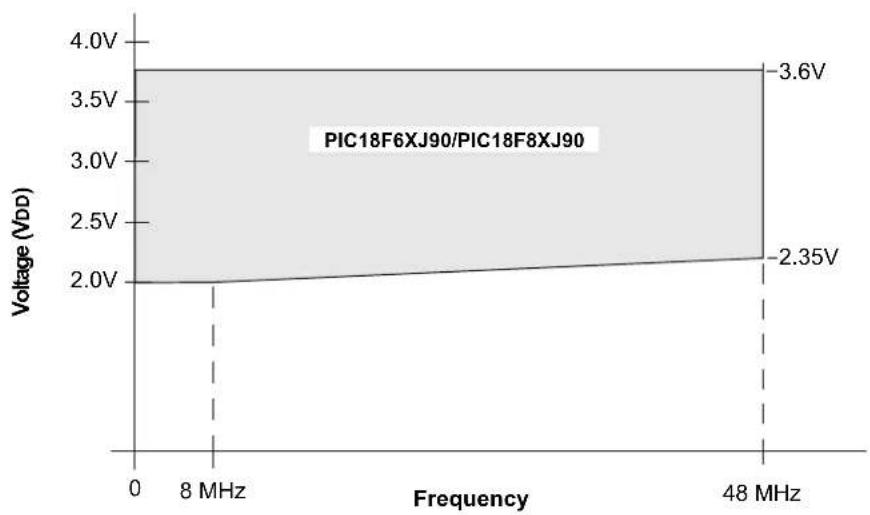
line
| Frequency | Voltage (VDD) | | --------- | ------------- | | 8 MHz | 2.0V | | 48 MHz | 2.35V | | 48 MHz | 3.6V |Note 1: When the on-chip regulator is enabled, its BOR circuit will automatically trigger a device Reset before VDD reaches a level at which full-speed operation is not possible.
FIGURE 28-2: VOLTAGE-FREQUENCY GRAPH, REGULATOR DISABLED (INDUSTRIAL) ^(1,2)

area
| Frequency | Voltage (VDDCORE) | | :--- | :--- | | 8 MHz | 2.00V | | 48 MHz | 2.35V | | 2.7V | 2.7V | PIC18F6XJ90/PIC18F8XJ90Note 1: When the on-chip voltage regulator is disabled, VDD and VDDCORE must be maintained so that VDDCORE ≤ VDD ≤ 3.6V.
28.1 DC Characteristics: Supply Voltage
PIC18F87J90 Family (Industrial)
| PIC18F87J90 Family(Industrial) | Standard Operating Conditions (unless otherwise stated)Operating temperature -40°C ≤ TA ≤ +85°C for industrial | ||||||
| Param No. | Symbol | Characteristic Min Typ Max | Units Conditions | ||||
| D001 V | DD | Supply Voltage | VDDCORE2.0 | — | 3.6 | V | ENVREG tied to Vss |
| — | 3.6 | V | ENVREG tied to VDD | ||||
| D001B | VDDCORE | External Supply for Microcontroller Core | 2.0 | — | 2.70 | V | ENVREG tied to Vss |
| D001C | AVDD | Analog Supply Voltage | VDD-0.3 | — | VDD+0.3 | V | |
| D001D | AVss | Analog Ground Potential | Vss-0.3 | — | Vss+0.3 | V | |
| D002 VDR RAM Data Retention Voltage (1) | 1.5 | — | — | V | |||
| D003 V | POR | VDD Start Voltage to Ensure Internal Power-on Reset Signal | — | — | 0.7 | V | See Section 5.3 “Power-on Reset (POR)” for details |
| D004 S | VDD | VDD Rise Rate to Ensure Internal Power-on Reset Signal | 0.05 | — | — | V/ms | See Section 5.3 “Power-on Reset (POR)” for details |
| D005 V | BOR | Brown-out Reset Voltage | — | 1.8 | — | V | |
Note 1: This is the limit to which VDD can be lowered in Sleep mode, or during a device Reset, without losing RAM data.
28.2 DC Characteristics: Power-Down and Supply Current
PIC18F87J90 Family (Industrial)
| PIC18F87J90 Family(Industrial) | Standard Operating Conditions (unless otherwise stated)Operating temperature -40°C ≤ TA ≤ +85°C for industrial | |||||
| Param No. | Device Typ Max | Units Conditions | ||||
| Power-Down Current (IPD)(1) | ||||||
| All devices | 0.4 1.4 μA | -40°C | 5[3]DD = 2.0V^(4) (Sleep mode) | |||
| 0.1 1.4 | μA | + 2 | ||||
| 0.8 | 6 | μA | +60°C | |||
| 5.5 | 10.2 | μA | +85°C | |||
| All devices | 0.5 1.5 μA | -40°C | 5[3]DD = 2.5V^(4) (Sleep mode) | |||
| 0.1 1.5 | μA | + 2 | ||||
| 1 | 8 | μA | +60°C | |||
| 6.8 | 12.6 | μA | +85°C | |||
| All devices | 2.9 | 7 | μA | -40°C | V_DD = 3.3V^(5) (Sleep mode) | |
| 3.6 | 7 | μA | +25°C | |||
| 4.1 | 10 | μA | +60°C | |||
| 9.6 | 19 | μA | +85°C | |||
Note 1: The power-down current in Sleep mode does not depend on the oscillator type. Power-down current is measured with the part in Sleep mode, with all I/O pins in a high-impedance state and tied to VDD or VSS, and all features that add delta current disabled (such as WDT, Timer1 oscillator, BOR, etc.).
2: The supply current is mainly a function of the operating voltage, frequency and mode. Other factors, such as I/O pin loading and switching rate, oscillator type and circuit, internal code execution pattern and temperature, also have an impact on the current consumption.
The test conditions for all IDD measurements in active operation mode are:
OSC1 = external square wave, from rail-to-rail; all I/O pins tri-stated, pulled to VDD;
= V_DD ; WDT enabled/disabled as specified.
3: Standard, low-cost 32 kHz crystals have an operating temperature range of -10^ to +70^ . Extended temperature crystals are available at a much higher cost.
4: Voltage regulator disabled (ENVREG = 0, tied to VSS).
5: Voltage regulator enabled (ENVREG = 1, tied to VDD, REGSLP = 1).
28.2 DC Characteristics:
Power-Down and Supply Current
PIC18F87J90 Family (Industrial) (Continued)
| PIC18F87J90 Family(Industrial) | Standard Operating Conditions (unless otherwise stated)Operating temperature -40°C ≤ TA ≤ +85°C for industrial | ||||||
| Param No. | Device | Typ Max | Units | Conditions | |||
| Supply Current (IDD)(2,3) | |||||||
| All devices | 5 14.2 μA -40°C | VDD=2.0V,VDDCORE=2.0V(4) | Fosc=31 kHz(RC_RUN mode,internal oscillator source) | ||||
| 5.5 14.2 μA +25°C | |||||||
| 10 19.0 μA +85°C | |||||||
| All devices | 6.8 16.5 μA -40°C | VDD=2.5V,VDDCORE=2.5V(4) | |||||
| 7.6 16.5 μA +25°C | |||||||
| 14 22.4 μA +85°C | |||||||
| All devices | 37 84 μA -40°C | DD=3.3V(5) | |||||
| 51 84 μA | +25°C V | ||||||
| 72 108 μA | +85°C | ||||||
| All devices | 0.43 | 0.82 | mA -40°C | VDD=2.0V,VDDCORE=2.0V(4) | Fosc=1 MHz(RC_RUN mode,internal oscillator source) | ||
| 0.47 | 0.82 | mA | +25°C | ||||
| 0.52 | 0.95 | mA | +85°C | ||||
| All devices | 0.52 | 0.98 | mA -40°C | VDD=2.5V,VDDCORE=2.5V(4) | |||
| 0.57 | 0.98 | mA | +25°C | ||||
| 0.63 | 1.10 | mA | +85°C | ||||
| All devices | 0.59 | 0.96 | mA -40°C | VDD=3.3V(5) | |||
| 0.65 | 0.96 | mA | +25°C | ||||
| 0.72 | 1.18 | mA | +85°C | ||||
| All devices | 0.88 | 1.45 | mA -40°C | VDD=2.0V,VDDCORE=2.0V(4) | Fosc=4 MHz(RC_RUN mode,internal oscillator source) | ||
| 1 1.45 mA | +25°C | ||||||
| 1.1 1.58 mA | +85°C | ||||||
| All devices | 1.2 1.72 mA -40°C | VDD=2.5V,VDDCORE=2.5V(4) | |||||
| 1.3 1.72 mA | +25°C | ||||||
| 1.4 1.85 mA | +85°C | ||||||
| All devices | 1.3 2.87 mA -40°C | DD=3.3V(5) | |||||
| 1.4 | 2.87 mA | +25°C | |||||
| 1.5 2.96 mA | +85°C | ||||||
Note 1: The power-down current in Sleep mode does not depend on the oscillator type. Power-down current is measured with the part in Sleep mode, with all I/O pins in a high-impedance state and tied to VDD or VSS, and all features that add delta current disabled (such as WDT, Timer1 oscillator, BOR, etc.).
2: The supply current is mainly a function of the operating voltage, frequency and mode. Other factors, such as I/O pin loading and switching rate, oscillator type and circuit, internal code execution pattern and temperature, also have an impact on the current consumption.
The test conditions for all IDD measurements in active operation mode are:
OSC1 = external square wave, from rail-to-rail; all I/O pins tri-stated, pulled to VDD;
= V_DD; WDT enabled/disabled as specified.
3: Standard, low-cost 32 kHz crystals have an operating temperature range of -10^ to +70^ . Extended temperature crystals are available at a much higher cost.
4: Voltage regulator disabled (ENVREG = 0, tied to Vss).
5: Voltage regulator enabled (ENVREG = 1, tied to VDD, REGSLP = 1).
28.2 DC Characteristics:
Power-Down and Supply Current
PIC18F87J90 Family (Industrial) (Continued)
| PIC18F87J90 Family(Industrial) | Standard Operating Conditions (unless otherwise stated)Operating temperature -40°C ≤ TA ≤ +85°C for industrial | |||||
| Param No. | Device | Typ Max | Units | Conditions | ||
| Supply Current (IDD) Cont.(2,3) | ||||||
| All devices | 3 9.4 μA -40°C | VDD=2.0V,VDDCORE=2.0V(4) | ||||
| 3.3 9.4 μA +25°C | ||||||
| 8.5 17.2 μA +85°C | ||||||
| All devices | 4 10.5 μA -40°C | VDD=2.5V,VDDCORE=2.5V(4) | ||||
| 4.3 10.5 μA +25°C | ||||||
| 10.3 19.5 μA +85°C | ||||||
| All devices | 34 82 μA -40°C | DD=3.3V(5) | ||||
| 48 82 μA | +25°C V | |||||
| 69 105 μA +85°C | ||||||
| All devices | 0.33 0.75 mA -40°C | VDD=2.0V,VDDCORE=2.0V(4) | ||||
| 0.37 0.75 mA +25°C | ||||||
| 0.41 0.84 mA +85°C | ||||||
| All devices | 0.39 0.78 mA -40°C | VDD=2.5V,VDDCORE=2.5V(4) | ||||
| 0.42 0.78 mA +25°C | ||||||
| 0.47 0.91 mA +85°C | ||||||
| All devices | 0.43 0.82 mA -40°C | DD≠3.3V(5) | ||||
| 0.48 0.82 mA +25°C | ||||||
| 0.54 0.95 mA +85°C | ||||||
| All devices | 0.53 0.98 mA -40°C | VDD=2.0V,VDDCORE=2.0V(4) | ||||
| 0.57 0.98 mA +25°C | ||||||
| 0.61 1.12 mA +85°C | ||||||
| All devices | 0.63 1.14 mA -40°C | VDD=2.5V,VDDCORE=2.5V(4) | ||||
| 0.67 1.14 mA +25°C | ||||||
| 0.72 1.25 mA +85°C | ||||||
| All devices | 0.7 1.27 mA -40°C | DD≠3.3V(5) | ||||
| 0.76 1.27 mA +25°C | ||||||
| 0.82 1.45 mA +85°C | ||||||
Note 1: The power-down current in Sleep mode does not depend on the oscillator type. Power-down current is measured with the part in Sleep mode, with all I/O pins in a high-impedance state and tied to VDD or VSS, and all features that add delta current disabled (such as WDT, Timer1 oscillator, BOR, etc.).
2: The supply current is mainly a function of the operating voltage, frequency and mode. Other factors, such as I/O pin loading and switching rate, oscillator type and circuit, internal code execution pattern and temperature, also have an impact on the current consumption.
The test conditions for all IDD measurements in active operation mode are:
OSC1 = external square wave, from rail-to-rail; all I/O pins tri-stated, pulled to VDD;
= V_DD ; WDT enabled/disabled as specified.
3: Standard, low-cost 32 kHz crystals have an operating temperature range of -10^ to +70^ . Extended temperature crystals are available at a much higher cost.
4: Voltage regulator disabled (ENVREG = 0, tied to Vss).
5: Voltage regulator enabled (ENVREG = 1, tied to VDD, REGSLP = 1).
28.2 DC Characteristics: Power-Down and Supply Current
PIC18F87J90 Family (Industrial) (Continued)
| PIC18F87J90 Family(Industrial) | Standard Operating Conditions (unless otherwise stated)Operating temperature -40°C ≤ TA ≤ +85°C for industrial | ||||||
| Param No. | Device Typ Max | Units | Conditions | ||||
| Supply Current (IDD) Cont.(2,3) | |||||||
| All devices | 0.17 0.35 mA | -40°C | VDD=2.0V,VDDCORE=2.0V(4) | Fosc=1 MHz(PRI_RUN mode,EC oscillator) | |||
| 0.18 0.35 mA | +25°C | ||||||
| 0.20 0.42 mA | +85°C | ||||||
| All devices | 0.29 0.52 mA | -40°C | VDD=2.5V,VDDCORE=2.5V(4) | ||||
| 0.31 0.52 mA | +25°C | ||||||
| 0.34 0.61 mA | +85°C | ||||||
| All devices | 0.59 1.1 mA | -40°C | VDD=3.3W(5) | ||||
| 0.44 | 0.85 | mA | +25°C | ||||
| 0.42 0.85 mA | +85°C | ||||||
| All devices | 0.70 1.25 mA | -40°C | VDD=2.0V,VDDCORE=2.0V(4) | Fosc=4 MHz(PRI_RUN mode,EC oscillator) | |||
| 0.75 1.25 mA | +25°C | ||||||
| 0.79 1.36 mA | +85°C | ||||||
| All devices | 1.10 1.7 mA | -40°C | VDD=2.5V,VDDCORE=2.5V(4) | ||||
| 1.10 1.7 mA | +25°C | ||||||
| 1.12 1.82 mA | +85°C | ||||||
| All devices | 1.55 1.95 mA | -40°C | VDD=2.5V,VDDCORE=2.5V(4) | ||||
| 1.47 | 1.89 | mA | +25°C | ||||
| 1.54 1.92 mA | +85°C | ||||||
| All devices | 9.9 14.8 mA | -40°C | VDD=2.5V,VDDCORE=2.5V(4) | Fosc=48 MHz(PRI_RUN mode,EC oscillator) | |||
| 9.5 14.8 mA | +25°C | ||||||
| 10.1 15.2 mA | +85°C | ||||||
| All devices | 13.3 23.2 mA | -40°C | VDD=3.3W(5) | ||||
| 12.2 | 22.7 | mA | +25°C | ||||
| 12.1 22.7 mA | +85°C | ||||||
Note 1: The power-down current in Sleep mode does not depend on the oscillator type. Power-down current is measured with the part in Sleep mode, with all I/O pins in a high-impedance state and tied to VDD or VSS, and all features that add delta current disabled (such as WDT, Timer1 oscillator, BOR, etc.).
2: The supply current is mainly a function of the operating voltage, frequency and mode. Other factors, such as I/O pin loading and switching rate, oscillator type and circuit, internal code execution pattern and temperature, also have an impact on the current consumption.
The test conditions for all IDD measurements in active operation mode are:
OSC1 = external square wave, from rail-to-rail; all I/O pins tri-stated, pulled to VDD;
MCLR = VDD; WDT enabled/disabled as specified.
3: Standard, low-cost 32 kHz crystals have an operating temperature range of -10^ to +70^ . Extended temperature crystals are available at a much higher cost.
4: Voltage regulator disabled (ENVREG = 0, tied to Vss).
5: Voltage regulator enabled (ENVREG = 1, tied to VDD, REGSLP = 1).
28.2 DC Characteristics: Power-Down and Supply Current
PIC18F87J90 Family (Industrial) (Continued)
| PIC18F87J90 Family(Industrial) | Standard Operating Conditions (unless otherwise stated)Operating temperature -40°C ≤ T A ≤ +85°C for industrial | ||||||
| Param No. | Device Typ Max | Units | Conditions | ||||
| Supply Current (IDD) Cont.(2,3) | |||||||
| All devices | 4.5 5.2 mA | -40°C | VDD=2.5V,VDDCORE=2.5V(4) | Fosc=4 MHz,16 MHz internal(PRI_RUN HSPLL mode) | |||
| 4.4 5.2 | mA +25°C | ||||||
| 4.5 5.2 | mA +85°C | ||||||
| All devices | 5.7 6.7 mA | -40°C | VDD=3.3V(5) | ||||
| 5.5 6.3 | mA +25°C | ||||||
| 5.3 6.3 | mA +85°C | ||||||
| All devices | 10.8 13.5 mA | -40°C | VDD=2.5V,VDDCORE=2.5V(4) | Fosc=10 MHz,40 MHz internal(PRI_RUN HSPLL mode) | |||
| 10.8 13.5 mA | +25°C | ||||||
| 9.9 13.0 mA | +85°C | ||||||
| All devices | 13.4 24.1 mA | -40°C | VDD=3.3V(5) | ||||
| 12.3 20.2 mA | +25°C | ||||||
| 11.2 19.5 mA | +85°C | ||||||
Note 1: The power-down current in Sleep mode does not depend on the oscillator type. Power-down current is measured with the part in Sleep mode, with all I/O pins in a high-impedance state and tied to VDD or VSS, and all features that add delta current disabled (such as WDT, Timer1 oscillator, BOR, etc.).
2: The supply current is mainly a function of the operating voltage, frequency and mode. Other factors, such as I/O pin loading and switching rate, oscillator type and circuit, internal code execution pattern and temperature, also have an impact on the current consumption.
The test conditions for all IDD measurements in active operation mode are:
OSC1 = external square wave, from rail-to-rail; all I/O pins tri-stated, pulled to VDD;
= V_DD; WDT enabled/disabled as specified.
3: Standard, low-cost 32 kHz crystals have an operating temperature range of -10^ to +70^ . Extended temperature crystals are available at a much higher cost.
4: Voltage regulator disabled (ENVREG = 0, tied to Vss).
5: Voltage regulator enabled (ENVREG = 1, tied to VDD, REGSLP = 1).
28.2 DC Characteristics: Power-Down and Supply Current
PIC18F87J90 Family (Industrial) (Continued)
| PIC18F87J90 Family(Industrial) | Standard Operating Conditions (unless otherwise stated)Operating temperature -40°C ≤ T A ≤ +85°C for industrial | ||||||
| Param No. | Device Typ Max | Units | Conditions | ||||
| Supply Current (IDD) Cont.(2,3) | |||||||
| All devices | 0.10 0.26 mA | -40°C | VDD=2.0V,VDDCORE=2.0V (4) | FOSC=1 MHz(PRI_IDLE mode,EC oscillator) | |||
| 0.07 0.18 | mA +25°C | ||||||
| 0.09 0.22 | mA +85°C | ||||||
| All devices | 0.25 0.48 mA | -40°C | VDD=2.5V,VDDCORE=2.5V (4) | ||||
| 0.13 0.30 | mA +25°C | ||||||
| 0.10 0.26 | mA +85°C | ||||||
| All devices | 0.45 0.68 mA | -40°C | C DD=3/3V (5) | ||||
| 0.26 | 0.45 | mA +25°C | |||||
| 0.30 0.54 | mA +85°C | ||||||
| All devices | 0.36 0.60 mA | -40°C | VDD=2.0V,VDDCORE=2.0V (4) | FOSC=4 MHz(PRI_IDLE mode,EC oscillator) | |||
| 0.33 0.56 | mA +25°C | ||||||
| 0.35 0.56 | mA +85°C | ||||||
| All devices | 0.52 0.81 mA | -40°C | VDD=2.5V,VDDCORE=2.5V (4) | ||||
| 0.45 0.70 | mA +25°C | ||||||
| 0.46 0.70 | mA +85°C | ||||||
| All devices | 0.80 1.15 mA | -40°C | C DD=3/3V (5) | ||||
| 0.66 | 0.98 | mA +25°C | |||||
| 0.65 0.98 | mA +85°C | ||||||
| All devices | 5.2 6.5 mA -40°C | VDD=2.5V,VDDCORE=2.5V (4) | FOSC=48 MHz(PRI_IDLE mode,EC oscillator) | ||||
| 4.9 5.9 mA +25°C | |||||||
| 3.4 4.5 mA +85°C | |||||||
| All devices | 6.2 12.4 mA -40°C | DD=8.3V (5) | |||||
| 5.9 | 11.5 | mA +25°C | |||||
| 5.8 11.5 | mA +85°C | ||||||
Note 1: The power-down current in Sleep mode does not depend on the oscillator type. Power-down current is measured with the part in Sleep mode, with all I/O pins in a high-impedance state and tied to V DD or Vss, and all features that add delta current disabled (such as WDT, Timer1 oscillator, BOR, etc.).
2: The supply current is mainly a function of the operating voltage, frequency and mode. Other factors, such as I/O pin loading and switching rate, oscillator type and circuit, internal code execution pattern and temperature, also have an impact on the current consumption.
The test conditions for all I DD measurements in active operation mode are:
OSC1 = external square wave, from rail-to-rail; all I/O pins tri-stated, pulled to V DD;
MCLR = VDD; WDT enabled/disabled as specified.
3: Standard, low-cost 32 kHz crystals have an operating temperature range of -10^ to +70^ . Extended temperature crystals are available at a much higher cost.
4: Voltage regulator disabled (ENVREG = 0, tied to V s5).
5: Voltage regulator enabled (ENVREG = 1, tied to V DD, REGSLP = 1).
28.2 DC Characteristics: Power-Down and Supply Current
PIC18F87J90 Family (Industrial) (Continued)
| PIC18F87J90 Family(Industrial) | Standard Operating Conditions (unless otherwise stated)Operating temperature -40°C ≤ T A ≤ +85°C for industrial | ||||||
| Param No. | Device Typ | Max Units | Conditions | ||||
| Supply Current (IDD) Cont.(2,3) | |||||||
| All devices | 18 35 μA -40°C | VDD=2.0V,VDDCORE=2.0V(4) | Fosc=32 kHz(3)(SEC_RUN mode,Timer1 as clock) | ||||
| 19 35 μA +25°C | |||||||
| 28 49 μA +85°C | |||||||
| All devices | 20 45 μA -40°C | VDD=2.5V,VDDCORE=2.5V(4) | |||||
| 21 45 μA +25°C | |||||||
| 32 61 μA +85°C | |||||||
| All devices | 0.06 0.11 mA -40°C | C DD=3.3W(5) | |||||
| 0.07 | 0.11 | mA | +25°C | ||||
| 0.09 0.15 mA +85°C | |||||||
| All devices | 14 28 μA -40°C | VDD=2.0V,VDDCORE=2.0V(4) | Fosc=32 kHz(3)(SEC_IDLE mode,Timer1 as clock) | ||||
| 15 28 μA +25°C | |||||||
| 24 43 μA +85°C | |||||||
| All devices | 15 31 μA -40°C | VDD=2.5V,VDDCORE=2.5V(4) | |||||
| 16 31 μA +25°C | |||||||
| 27 50 μA +85°C | |||||||
| All devices | 0.05 0.10 mA -40°C | C DD=3.3W(5) | |||||
| 0.06 | 0.10 | mA | +25°C | ||||
| 0.08 0.14 mA +85°C | |||||||
Note 1: The power-down current in Sleep mode does not depend on the oscillator type. Power-down current is measured with the part in Sleep mode, with all I/O pins in a high-impedance state and tied to VDD or VSS, and all features that add delta current disabled (such as WDT, Timer1 oscillator, BOR, etc.).
2: The supply current is mainly a function of the operating voltage, frequency and mode. Other factors, such as I/O pin loading and switching rate, oscillator type and circuit, internal code execution pattern and temperature, also have an impact on the current consumption.
The test conditions for all IDD measurements in active operation mode are:
OSC1 = external square wave, from rail-to-rail; all I/O pins tri-stated, pulled to VDD;
MCLR = VDD; WDT enabled/disabled as specified.
3: Standard, low-cost 32 kHz crystals have an operating temperature range of -10^ to +70^ . Extended temperature crystals are available at a much higher cost.
4: Voltage regulator disabled (ENVREG = 0, tied to Vss).
5: Voltage regulator enabled (ENVREG = 1, tied to VDD, REGSLP = 1).
28.2 DC Characteristics:
Power-Down and Supply Current
PIC18F87J90 Family (Industrial) (Continued)
| PIC18F87J90 Family(Industrial) | Standard Operating Conditions (unless otherwise stated)Operating temperature -40°C ≤ TA ≤ +85°C for industrial | ||||||
| Param No. | Device | Typ | Max | Units | Conditions | ||
| D022 | Module Differential Currents (ΔIWDT, ΔIOSCB, ΔIAD) | ||||||
| Watchdog Timer | 2.1 7.0 μA | -40°C | VDD=2.0V,VDDCORE=2.0V(4) | ||||
| 2.2 7.0 | μA +25°C | ||||||
| 4.3 9.5 | μA +85°C | ||||||
| 3.0 8.0 | μA -40°C | VDD=2.5V,VDDCORE=2.5V(4) | |||||
| 3.1 8.0 | μA +25°C | ||||||
| 5.5 10.4 | μA +85°C | ||||||
| 5.9 12.1 | μA -40°C | VDD=3.3V | |||||
| 6.2 12.1 | μA +25°C | ||||||
| 6.9 13.6 | μA +85°C | ||||||
| D024 (ΔILCD) | LCD Module | 2 (6,7) | 5 μA | +25°C | VDD=2.0V Resistive Ladder | CPEN=0;CKSEL<1:0>=00;CS<1:0>=10;LP<3:0>=0100 | |
| 2.7(6,7) | 5 μA | +25°C | VDD=2.5V | ||||
| 3.5(6,7) | 7 μA | +25°C | VDD=3.0V | ||||
| 16(7) | 25 μA | +25°C | VDD=2.0V Charge Pump | BIAS<2:0>=111;CPEN=1;CKSEL<1:0>=11;CS<1:0>=10 | |||
| 17(7) | 25 μA | +25°C | VDD=2.5V | ||||
| 24(7) | 40 μA | +25°C | VDD=3.0V | ||||
| D025 (ΔIOSCB) | RTCC + Timer1 Osc. with 32 kHz Crystal(6) | 0.9 4.0 | μA -10°C | VDD=2.0V,VDDCORE=2.0V(4) | 32 kHz on Timer1(3) | ||
| 1.0 4.5 | μA +25°C | ||||||
| 1.1 4.5 | μA +85°C | ||||||
| 1.1 4.5 | μA -10°C | VDD=2.5V,VDDCORE=2.5V(4) | 32 kHz on Timer1(3) | ||||
| 1.2 5.0 | μA +25°C | ||||||
| 1.2 5.0 | μA +85°C | ||||||
| 1.6 6.5 | μA -10°C | VDD=3.3V 32 k | Hz on Timer1 (3) | ||||
| 1.6 6.5 | μA +25°C | ||||||
| 2.1 8.0 | μA +85°C | ||||||
| D026 (ΔIAD) | A/D Converter | 3.0 10.0 μA | -40°C to +85°C | VDD=2.0V,VDDCORE=2.0V(4) | A/D on, not converting | ||
| 3.0 | 10.0 | μA | -40°C to +85°C | VDD=2.5V, | |||
Note 1: The power-down current in Sleep mode does not depend on the oscillator type. Power-down current is measured with the part in Sleep mode, with all I/O pins in a high-impedance state and tied to VDD or VSS, and all features that add delta current disabled (such as WDT, Timer1 oscillator, BOR, etc.).
2: The supply current is mainly a function of the operating voltage, frequency and mode. Other factors, such as I/O pin loading and switching rate, oscillator type and circuit, internal code execution pattern and temperature, also have an impact on the current consumption.
The test conditions for all IDD measurements in active operation mode are:
OSC1 = external square wave, from rail-to-rail; all I/O pins tri-stated, pulled to VDD;
MCLR = VDD; WDT enabled/disabled as specified.
3: Standard, low-cost 32 kHz crystals have an operating temperature range of -10^ to +70^ . Extended temperature crystals are available at a much higher cost.
4: Voltage regulator disabled (ENVREG = 0, tied to Vss).
5: Voltage regulator enabled (ENVREG = 1, tied to VDD, REGSLP = 1).
28.3 DC Characteristics: PIC18F87J90 Family (Industrial)
| DC CHARACTERISTICS | Standard Operating Conditions (unless otherwise stated)Operating temperature -40°C ≤ TA ≤ +85°C for industrial | |||||
| Param No. | Symbol | Characteristic Min Max Units Conditions | ||||
| VIL Input | Low Voltage | |||||
| All I/O Ports: | ||||||
| D030 with TTL Buffer V | SS | 0.15 VDD | V | VDD < 3.3V | ||
| D030A | — | 0.8 | V | 3.3V ≤ VDD ≤ 3.6V | ||
| D031 with Schmitt Trigger Buffer V | SS | 0.2 VDD | V | |||
| D031A | with RC3 and RC4 | Vss | 0.3 VDD | V | I2CTM enabled | |
| D031B | Vss | 0.8 | V | SMBus enabled | ||
| D032 | MCLR | Vss | 0.2 VDD | V | ||
| D033 | OSC1 | Vss | 0.3 VDD | V | HS, HSPLL modes | |
| D033A | OSC1 | Vss | 0.2 VDD | V | EC, ECPLL modes | |
| D034 | T13CKI | Vss | 0.3 | V | ||
| VIH | Input High Voltage | |||||
| I/O Ports with non 5.5V Tolerance: | ||||||
| D040 | with TTL Buffer | 0.25 V DD + 0.8V | VDD | V | VDD < 3.3V | |
| D040A | 2.0 | VDD | V | 3.3V ≤ VDD ≤ 3.6V | ||
| D041 | with Schmitt Trigger Buffer | 0.8 VDD | VDD | V | ||
| D041A | RC3 and RC4 | 0.7 VDD | VDD | V | I2C enabled | |
| D041B | 2.1 | VDD | V | SMBus enabled | ||
| I/O Ports with 5.5V Tolerance: | ||||||
| with TTL Buffer | 0.25 V DD + 0.8V | 5.5 | V | VDD < 3.3V | ||
| 2.0 | 5.5 | V | 3.3V ≤ VDD ≤ 3.6V | |||
| with Schmitt Trigger Buffer | 0.8 VDD | 5.5 | V | |||
| D042 | MCLR | 0.8 VDD | VDD | V | ||
| D043 | OSC1 | 0.7 VDD | VDD | V | HS, HSPLL modes | |
| D043A | OSC1 | 0.8 VDD | VDD | V | EC, ECPLL modes | |
| D044 | T13CKI | 1.6 | VDD | V | ||
| I/L | Input Leakage Current(1) | |||||
| D060 | I/O Ports with Analog Functions | — | 200 | nA | Vss ≤ VPIN ≤ VDD, Pin at high-impedance | |
| Digital Only I/O Ports | — | 200 | nA | Vss ≤ VPIN ≤ 5.5V | ||
| D061 | MCLR | — | ±1 | μA | Vss ≤ VPIN ≤ VDD | |
| D063 | OSC1 | — | ±1 | μA | Vss ≤ VPIN ≤ VDD | |
| IPU | Weak Pull-up Current | |||||
| D070 | IPURB | PORTB Weak Pull-up Current | 30 | 400 | μA | VDD = 3.3V, VPIN = Vss |
| Param No. | Symbol | Characteristic | Min | Max | Units | Conditions |
| D080 I/O | VOL Output Low VoltagePorts: | |||||
| PORTA, PORTF, PORTG, PORTH | — | 0 | . | OL = 2 mA, VDD = 3.3V, V-40°C to +85°C | ||
| PORTD, PORTE, PORTJ — 0.4 V I | OL = 3.4 mA, VDD = 3.3V,-40°C to +85°C | |||||
| PORTB, PORTC — 0.4 V I | OL = 3.4 mA, VDD = 3.3V,-40°C to +85°C | |||||
| D083 OSC2/CLKO(EC, ECPLL modes) | — | 0 | . | OL = 1.6 mA, VDD = 3.3W,-40°C to +85°C | ||
| D090 I/O | VOHPorts: | Output High Voltage(1) | ||||
| PORTA, PORTF, PORTG, PORTH | 2.4 | — | V | IOH = -2 mA, VDD = 3.3V,-40°C to +85°C | ||
| PORTD, PORTE, PORTJ | 2.4 — | VI | OH = -2 mA, VDD = 3.3V,-40°C to +85°C | |||
| PORTB, PORTC | 2.4 — | VI | OH = -2 mA, VDD = 3.3V,-40°C to +85°C | |||
| D092 OSC2/CLKO(INTOSC, EC, ECPLL modes) | 2.4 — | VI | OH = -1 mA, VDD = 3.3V,-40°C to +85°C | |||
| D100(4) | COSC2 | Capacitive Loading Specs on Output Pins | ||||
| OSC2 Pin | — | 15 | pF | In HS mode when external clock is used to drive OSC1 | ||
| D101 | CIO | All I/O Pins and OSC2 | — | 50 | pF | To meet the AC Timing Specifications |
| D102 | CB | SCL, SDA | — | 400 | pF | I2CTM Specification |
Note 1: Negative current is defined as current sourced by the pin.
28.4 DC Characteristics: CTMU Current Source Specifications
| DC CHARACTERISTICS | Standard Operating Conditions: 2.0V to 3.6V (unless otherwise stated)Operating temperature -40°C ≤ TA ≤ +85°C for Industrial | ||||||
| Param No. | Sym | Characteristic | Min | Typ^(1) | Max | Units C | conditions |
| IOUT1 | CTMU Current Source, Base Range | — | 550 | — | nA | CTMUICON<1:0> = 01 | |
| IOUT2 | CTMU Current Source, 10x Range | — | 5.5 | — | μA | CTMUICON<1:0> = 10 | |
| IOUT3 | CTMU Current Source, 100x Range | — | 55 | — | μA | CTMUICON<1:0> = 11 | |
Note 1: Nominal value at center point of current trim range (CTMUICON<7:2> = 000000).
TABLE 28-1: MEMORY PROGRAMMING REQUIREMENTS
| DC CHARACTERISTICS | Standard Operating Conditions (unless otherwise stated)Operating temperature -40°C ≤ TA ≤ +85°C for industrial | ||||||
| Param No. | Sym | Characteristic Min Typ† Max Units | Conditions | ||||
| Program Flash Memory | |||||||
| D130 E | P | Cell Endurance | 10K | — | — | E/W | -40°C to +85°C |
| D131 | VPR | VDD for Read | VMIN | — | 3.6 | V | VMIN = Minimum operating voltage |
| D132B | VPEW | Voltage for Self-Timed Erase or Write operations | |||||
| VDD | 2.35 | — | 3.6 | V | ENVREG tied to VDD | ||
| VDDCORE | 2.25 | — | 2.7 | V | ENVREG tied to Vss | ||
| D133A | TIW | Self-Timed Write Cycle Time | — | 2.8 | — | ms | |
| D133B | TIE | Self-Timed Block Erased Cycle Time | — | 33 | — | ms | |
| D134 T | RETD | Characteristic Retention | 20 | — | — | Year | Provided no other specifications are violated |
| D135 I | DDP | Supply Current during Programming | — | 3 | 14 | mA | |
| D140 T | WE | Writes per Erase Cycle | — | — | 1 | For each physical address | |
† Data in “Typ” column is at 3.3V, 25°C unless otherwise stated. These parameters are for design guidance only and are not tested.
TABLE 28-2: COMPARATOR SPECIFICATIONS
| Operating Conditions: 3.0V ≤ VDD ≤ 3.6V, -40°C ≤ TA ≤ +85°C (unless otherwise stated) | |||||||
| Param No. | Sym | Characteristics Min | Typ | Max | Units | Comments | |
| D300 V | IOFF Input | Offset Voltage — ±5.0 ±25 mV | |||||
| D301 V | ICM | Input Common Mode Voltage | 0 | — | AVDD – 1.5 | V | |
| D302 | CMRR | Common Mode Rejection Ratio | 55 | — | — | dB | |
| D303 TRESP | Response Time (1) | — | 150 | 400 | ns | ||
| D304 T | MC20V | Comparator Mode Change to Output Valid* | — | — | 10 | μs | |
Note 1: Response time measured with one comparator input at (AVDD - 1.5)/2, while the other input transitions from Vss to VDD.
TABLE 28-3: VOLTAGE REFERENCE SPECIFICATIONS
| Operating Conditions: 3.0V ≤ VDD ≤ 3.6V, -40°C ≤ TA ≤ +85°C (unless otherwise stated) | |||||||
| Param No. | Sym | Characteristics | Min | Typ | Max | Units | Comments |
| D310 | VRES | Resolution | VDD/24 | — | VDD/32 | LSb | |
| D311 | VRAA | Absolute Accuracy | — | — | 1/2 | LSb | |
| D312 | VRUR | Unit Resistor Value (R) | — | 2k | — | Ω | |
| D313 | TSET | Settling Time(1) | — | — | 10 | μs | |
Note 1: Settling time measured while CVRR = 1 and CVR<3:0> transitions from '0000' to '1111'.
TABLE 28-4: INTERNAL VOLTAGE REGULATOR SPECIFICATIONS
| Operating Conditions: -40°C ≤ TA ≤ +85°C (unless otherwise stated) | |||||||
| Param No. | Sym | Characteristics | Min | Typ | Max | Units | Comments |
| VRGOUT | Regulator Output Voltage | — | 2.5 | — | V | ||
| CEFC | External Filter Capacitor Value | 4.7 | 10 | — | μF | Capacitor must be low-ESR, a low series resistance (< 5Ω) | |
TABLE 28-5: INTERNAL LCD VOLTAGE REGULATOR SPECIFICATIONS
| Operating Conditions: 2.0V ≤ VDD ≤ 3.6V, -40°C ≤ TA ≤ +85°C (unless otherwise stated) | |||||||
| Param No. | Sym | Characteristics | Min | Typ | Max | Units | Comments |
| QFLY | Fly Back Capacitor | 0.47 | 4.7 | — | μF | Capacitor must be low-ESR | |
| VBIAS | VPK-PK between LCDBIAS0 & LCDBIAS3 | — | 3.40 | 3.6 | V | BIAS<2:0> = 111 | |
| — | 3.27 | — | V | BIAS<2:0> = 110 | |||
| — | 3.14 | — | V | BIAS<2:0> = 101 | |||
| — | 3.01 | — | V | BIAS<2:0> = 100 | |||
| — | 2.88 | — | V | BIAS<2:0> = 011 | |||
| — | 2.75 | — | V | BIAS<2:0> = 010 | |||
| — | 2.62 | — | V | BIAS<2:0> = 001 | |||
| — | 2.49 | — | V | BIAS<2:0> = 000 | |||
28.5 AC (Timing) Characteristics
28.5.1 TIMING PARAMETER SYMBOLOGY
The timing parameter symbols have been created following one of the following formats:
| 1. TppS2ppS 3. T | cc:ST | (I ^2 C specifications only) |
| 2. TppS 4. Ts (I | ^2 C specifications only) |
| TF Frequency T Time |
Lowercase letters (pp) and their meanings:
| pp | |||
| cc CCP1 osc OSC1 | |||
| ck CLKO rd RD | — | ||
| cs | rw | or | |
| di | SDI | sc SCK | — |
| do | SDO | ss SS | |
| dt | Data in | t0 | T0CKI |
| io | I/O port | t1 | T13CKI |
| mc | wr | ||
Uppercase letters and their meanings:
| S | |||
| F Fall | P | Period | |
| H | High | R Rise | |
| I | Invalid (High-impedance) | V Valid | |
| L | Low | Z High-impedance | |
| I^2C only | |||
| AA | output access | High High | |
| BUF | Bus free | Low Low | |
Tcc:ST (I²C specifications only)
| CC | |||
| HD | Hold | SU | Setup |
| ST | |||
| DAT | DATA input hold | STO | Stop condition |
| STA | Start condition | ||
28.5.2 TIMING CONDITIONS
The temperature and voltages specified in Table 28-6 apply to all timing specifications unless otherwise noted. Figure 28-3 specifies the load conditions for the timing specifications.
TABLE 28-6: TEMPERATURE AND VOLTAGE SPECIFICATIONS – AC
| AC CHARACTERISTICS | Standard Operating Conditions (unless otherwise stated) |
| Operating temperature -40^ ≤ TA ≤ +85^ for industrial | |
| Operating voltage VDD range as described in Section 28.1 and Section 28.3. |
FIGURE 28-3: LOAD CONDITIONS FOR DEVICE TIMING SPECIFICATIONS

text_image
Load Condition 1 VDD/2 RL Pin CL Vss
$$ \begin{array}{l} \mathrm{RL} = 4 6 4 \Omega \ \begin{array}{r l} \mathrm{CL} & = 5 0 \mathrm{pF} \text { for all pins except OSC2 / CLKO / RA6 } \ & \text { and including D and E outputs as ports } \end{array} \ \mathrm{CL} = 1 5 \mathrm{pF} \text { for OSC2 / CLKO / RA6 } \ \end{array} $$
28.5.3 TIMING DIAGRAMS AND SPECIFICATIONS
FIGURE 28-4: EXTERNAL CLOCK TIMING

text_image
OSC1 Q4 Q1 Q2 Q3 Q4 Q1 1 2 3 3 4 4 CLKOTABLE 28-7: EXTERNAL CLOCK TIMING REQUIREMENTS
| Param. No. | Symbol | Characteristic Min Max Units | Conditions | |||
| 1A | Fosc External CLKI Frequency (1) | DC 48 MHz EC Oscillator mode | ||||
| DC 10 | ECPLL Oscillator mode | |||||
| 4 | 25 MHz HS Oscillator mode | |||||
| 4 | 10 | HSPLL Oscillator mode | ||||
| 1 | Tosc External CLKI Period (1) | 20.8 | — | ns | EC Oscillator mode | |
| 100 | — | ECPLL Oscillator mode | ||||
| 40.0 250 | ns | HS Oscillator mode | ||||
| 100 | 250 | |||||
| 2 | TCY | Instruction Cycle Time(1) | 83.3 | — | ns | TCY = 4/Fosc, Industrial |
| 3 | TosL, TosH | External Clock in (OSC1)High or Low Time | 10 | — | ns | HS Oscillator mode |
| 4 | TosR, TosF | External Clock in (OSC1)Rise or Fall Time | — | 7.5 | ns | HS Oscillator mode |
Note 1: Instruction cycle period (TCY) equals four times the input oscillator time base period for all configurations except PLL. All specified values are based on characterization data for that particular oscillator type under standard operating conditions with the device executing code. Exceeding these specified limits may result in an unstable oscillator operation and/or higher than expected current consumption. All devices are tested to operate at "min." values with an external clock applied to the OSC1/CLKI pin. When an external clock input is used, the "max." cycle time limit is "DC" (no clock) for all devices.
TABLE 28-8: PLL CLOCK TIMING SPECIFICATIONS ( V_DD = 2.15V TO 3.6V)
| Param No. | Sym | Characteristic Min Typ† Max Units Conditions | |||||
| F10 F | osc | Oscillator Frequency Range | 4 | — | 10 | MHz | HS mode only |
| F11 | Fsys | On-Chip VCO System Frequency | 16 | — | 40 | MHz | HS mode only |
| F12 t | rc | PLL Start-up Time (Lock Time) | — — | 2 | ms | ||
| F13 | ΔCLK | CLKO Stability (Jitter) | -2 | — | +2 | % |
† Data in “Typ” column is at 3.3V, 25°C, unless otherwise stated. These parameters are for design guidance only and are not tested.
TABLE 28-9: INTERNAL RC ACCURACY (INTOSC AND INTRC SOURCES)
| PIC18F87J90 Family(Industrial) | Standard Operating Conditions (unless otherwise stated)Operating temperature -40°C ≤ TA ≤ +85°C for industrial | ||||||
| Param No. | Device | Min | Typ | Max | Units | Conditions | |
| INTOSC Accuracy @ Freq = 8 MHz, 4 MHz, 2 MHz, 1 MHz, 500 kHz, 250 kHz, 125 kHz, 31 kHz ^1) | |||||||
| All Devices | -2 | +/-1 | 2 | % | +25°C | VDD=2.7-3.3V | |
| -5 | — | 5 | % | -10°C to +85°C | VDD=2.0-3.3V | ||
| -10 | +/-1 | 10 | % | -40°C to +85°C | VDD=2.0-3.3V | ||
| INTRC Accuracy @ Freq = 31 kHz ^1) | |||||||
| All Devices | 21.7 | — | 40.3 | kHz | -40°C to +85°C | VDD=2.0-3.3V | |
Note 1: The accuracy specification of the 31 kHz clock is determined by which source is providing it at a given time. When INTSRC (OSCTUNE<7>) is '1', use the INTOSC accuracy specification. When INTSRC is '0', use the INTRC accuracy specification.
FIGURE 28-5: CLKO AND I/O TIMING
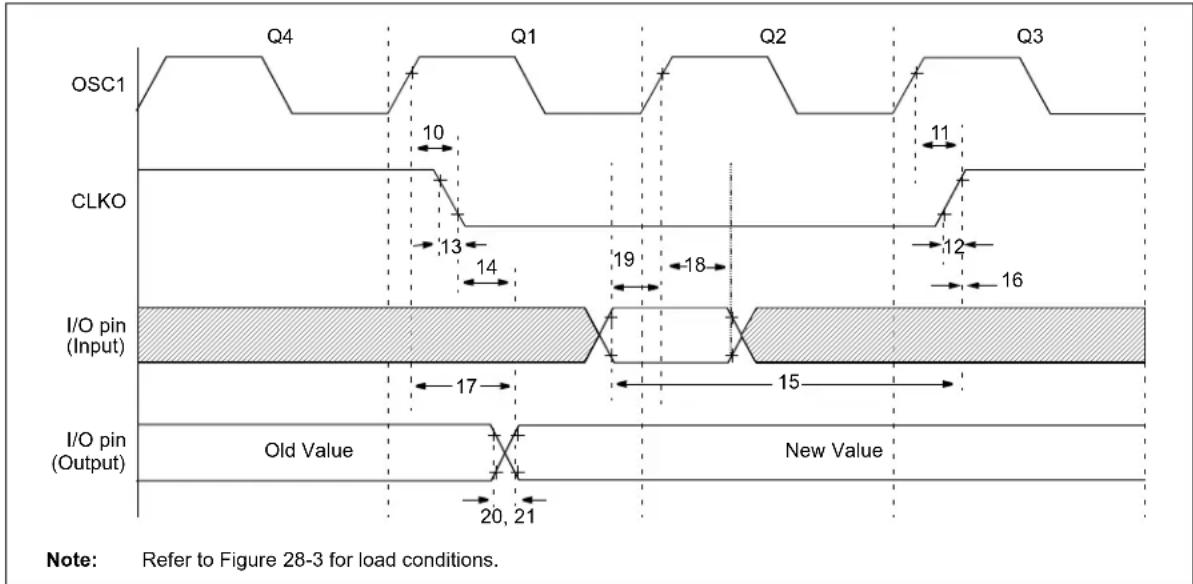
other
| Signal | Value | |------------|-------| | OSC1 | 10 | | CLKO | 13 | | I/O pin (Input) | 14 | | I/O pin (Output) | 17 | | Q4 | 20 | | Q1 | 21 | | Q2 | 15 | | Q3 | 16 |TABLE 28-10: CLKO AND I/O TIMING REQUIREMENTS
| Param No. | Symbol C | Characteristic Min Typ Max Units Conditions | |||||
| 10 | TosH2ckL | OSC1 ↑ to CLKO ↓ | — | 75 | 200 | ns | (Note 1) |
| 11 | TosH2ckH | OSC1 ↑ to CLKO ↑ | — | 75 | 200 | ns | (Note 1) |
| 12 | TckR | CLKO Rise Time | — | 15 | 30 | ns | (Note 1) |
| 13 | TckF | CLKO Fall Time | — | 15 | 30 | ns | (Note 1) |
| 14 | TckL2ioV | CLKO ↓ to Port Out Valid | — | — | 0.5 Tcy + 20 | ns | |
| 15 | TioV2ckH | Port In Valid before CLKO ↑ | 0.25 Tcy + 25 | — | — | ns | |
| 16 | TckH2iol | Port In Hold after CLKO ↑ | 0 | — | — | ns | |
| 17 | TosH2ioV | OSC1 ↑ (Q1 cycle) to Port Out Valid | — | 50 | 150 | ns | |
| 18 | TosH2iol | OSC1 ↑ (Q2 cycle) to Port Input Invalid (I/O in hold time) | 100 | — | — | ns | |
| 19 | TioV2osH | Port Input Valid to OSC1 ↑ (I/O in setup time) | 0 | — | — | ns | |
| 20 | TioR | Port Output Rise Time | — | — | 6 | ns | |
| 21 | TioF | Port Output Fall Time | — | — | 5 | ns | |
| 22† | TINP | INTx pin High or Low Time | TCY | — | — | ns | |
| 23† | TRBP | RB<7:4> Change INTx High or Low Time | TCY | — | — | ns |
† These parameters are asynchronous events not related to any internal clock edges.
Note 1: Measurements are taken in EC mode, where CLKO output is 4 x Tosc.
FIGURE 28-6: RESET, WATCHDOG TIMER, OSCILLATOR START-UP TIMER AND POWER-UP TIMER TIMING

other
| Component | Value | |-----------------------|-------| | VDD | 30 | | MCLR | 33 | | Internal POR | 32 | | PWRT Time-out | 30 | | Oscillator Time-out | 32 | | Internal Reset | 33 | | Watchdog Timer Reset | 34 | | I/O pins | 31 | | I/O pins | 34 |TABLE 28-11: RESET, WATCHDOG TIMER, OSCILLATOR START-UP TIMER, POWER-UP TIMER AND BROWN-OUT RESET REQUIREMENTS
| Param. No. | Symbol | Characteristic Min Typ Max Units | Conditions | ||||
| 30 | TMCL | Pulse Width (low) | 2 Tcy | 10 Tcy | — | (Note 1) | |
| 31 | TWDT | Watchdog Timer Time-out Period (no postscaler) | 3.4 | 4.0 | 4.6 | ms | |
| 32 | TOST | Oscillation Start-up Timer Period | 1024 Tosc | — | 1024 Tosc | Tosc = OSC1 period | |
| 33 | TPWRT | Power-up Timer Period | 45.8 | 65.5 | 85.2 | ms | |
| 34 | TIOZ | I/O High-Impedance from Low or Watchdog Timer Reset | — | 2 | — | μs | |
| 38 | TCSD | CPU Start-up Time | — | 10 | — | μs | |
| 200 | μs | Voltage Regulator enabled and put to sleep | |||||
| 39 | TIOBST | Time for INTOSC to Stabilize | — | 1 | — | μs |
Note 1: To ensure device Reset, MCLR must be low for at least 2 Tcy or 400 s, whichever is lower.
FIGURE 28-7: TIMER0 AND TIMER1 EXTERNAL CLOCK TIMINGS

text_image
T0CKI 40 41 42 T1OSO/T13CKI 45 46 47 48 TMR0 or TMR1Note: Refer to Figure 28-3 for load conditions.
TABLE 28-12: TIMER0 AND TIMER1 EXTERNAL CLOCK REQUIREMENTS
| Param No. | Symbol | Characteristic Min Max Units Conditions | ||||||
| 40 | TtOH | T0CKI High Pulse Width | No prescaler | 0.5 Tcy + 20 | — | ns | ||
| With prescaler | 10 — ns | |||||||
| 41 | TtOL | T0CKI Low Pulse Width | No prescaler | 0.5 Tcy + 20 | — | ns | ||
| With prescaler | 10 — ns | |||||||
| 42 | TtOP | T0CKI Period | No prescaler | Tcy + 10 | — | ns | ||
| With prescaler | Greater of: 20 ns or (Tcy + 40)/N | — | ns | N = prescale value (1, 2, 4,..., 256) | ||||
| 45 Tt1H | T13CKI High Time | Synchronous, no prescaler | 0.5 Tcy + 20 | — | ns | |||
| Synchronous, with prescaler | 10 | — ns | ||||||
| Asynchronous | 30 | — ns | ||||||
| 46 | Tt1L | T13CKI Low Time | Synchronous, no prescaler | 0.5 Tcy + 5 | — | ns | ||
| Synchronous, with prescaler | 10 | — ns | ||||||
| Asynchronous | 30 | — ns | ||||||
| 47 | Tt1P | T13CKI Input Period | Synchronous | Greater of: 20 ns or (Tcy + 40)/N | — | ns | N = prescale value (1, 2, 4, 8) | |
| Asynchronous | 60 | — ns | ||||||
| Ft1 | T13CKI Oscillator Input Frequency Range | DC | 50 | kHz | ||||
| 48 | TCKE2TMRI | Delay from External T13CKI Clock Edge to Timer Increment | 2 Tosc | 7 Tosc | — | |||
FIGURE 28-8: CAPTURE/COMPARE/PWM TIMINGS (CCP1, CCP2 MODULES)

text_image
CCPx (Capture Mode) 50 51 52 CCPx (Compare or PWM Mode) 53 54Note: Refer to Figure 28-3 for load conditions.
TABLE 28-13: CAPTURE/COMPARE/PWM REQUIREMENTS (CCP1, CCP2 MODULES)
| Param No. | Symbol | Characteristic Min Max Units Conditions | |||||
| 50 | TccL CC | Px Input Low Time | No prescaler | 0.5 Tcy + 20 | — | ns | |
| With prescaler | 10 | — | ns | ||||
| 51 TccH | CCP | x Input High Time | No prescaler | 0.5 Tcy + 20 | — | ns | |
| With prescaler | 10 | — | ns | ||||
| 52 | TccP | CCPx Input Period | 3 Tcy + 40 N | — | ns | N = prescale value (1, 4 or 16) | |
| 53 | TccR | CCPx Output Fall Time | — | 25 | ns | ||
| 54 | TccF | CCPx Output Fall Time | — | 25 | ns | ||
FIGURE 28-9: EXAMPLE SPI MASTER MODE TIMING (CKE = 0)
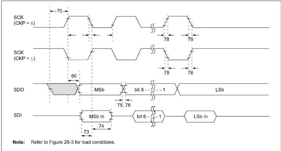
text_image
SCK (CKP = 0) 70 78 79 SCK (CKP = 1) 79 78 80 SDO MSb bit 6 - 1 LSb 75, 76 SDI MSb In bit 6 - 1 LSb In 73 Note: Refer to Figure 28-3 for load conditions.TABLE 28-14: EXAMPLE SPI MODE REQUIREMENTS (MASTER MODE, CKE = 0)
| Param No. | Symbol C | Characteristic Min Max Units Conditions | ||||
| 73 | TDIV2sCH, TDIV2sCL | Setup Time of SDI Data Input to SCK Edge 20 — ns | ||||
| 73A T | B2B | Last Clock Edge of Byte 1 to the 1st Clock Edge of Byte 2 | 1.5 TCY + 40 | — | ns | (Note 2) |
| 74 | TscH2dIL, TscL2dIL | Hold Time of SDI Data Input to SCK Edge | 40 — ns | |||
| 75 | TDOR | SDO Data Output Rise Time | — | 25 | ns | |
| 76 | TDOF | SDO Data Output Fall Time | — | 25 | ns | |
| 78 | Tscr | SCK Output Rise Time (Master mode) | — | 25 | ns | |
| 79 | TscF | SCK Output Fall Time (Master mode) | — | 25 | ns | |
| 80 | TscH2doV, TscL2doV | SDO Data Output Valid after SCK Edge | — 50 | ns | ||
Note 1: Requires the use of Parameter #73A.
2: Only if Parameter #71A and #72A are used.
FIGURE 28-10: EXAMPLE SPI MASTER MODE TIMING (CKE = 1)

text_image
SCK (CKP = 0) 81 79 SCK (CKP = 1) 73 80 78 SDO MSb bit 6 - - - 1 LSb 75, 76 SDI MSb In bit 6 - - - 1 LSb In 74 Note: Refer to Figure 28-3 for load conditions.TABLE 28-15: EXAMPLE SPI MODE REQUIREMENTS (MASTER MODE, CKE = 1)
| Param. No. | Symbol C | Characteristic Min Max Units Conditions | ||||
| 73 | TDIV2sCH, TDIV2sCL | Setup Time of SDI Data Input to SCK Edge 20 — ns | ||||
| 73A | TB2B | Last Clock Edge of Byte 1 to the 1st Clock Edge of Byte 2 | 1.5 TCY + 40 | — | ns | (Note 2) |
| 74 | TscH2dIL, TscL2dIL | Hold Time of SDI Data Input to SCK Edge | 40 — ns | |||
| 75 | TdoR | SDO Data Output Rise Time | — | 25 | ns | |
| 76 | TdoF | SDO Data Output Fall Time | — | 25 | ns | |
| 78 | Tscr | SCK Output Rise Time (Master mode) | — | 25 | ns | |
| 79 | TscF | SCK Output Fall Time (Master mode) | — | 25 | ns | |
| 80 | TscH2doV, TscL2doV | SDO Data Output Valid after SCK Edge | — 50 | ns | ||
| 81 | TdoV2sCH, TdoV2sCL | SDO Data Output Setup to SCK Edge | TCY | — | ns | |
Note 1: Requires the use of Parameter #73A.
2: Only if Parameter #71A and #72A are used.
FIGURE 28-11: EXAMPLE SPI SLAVE MODE TIMING (CKE = 0)
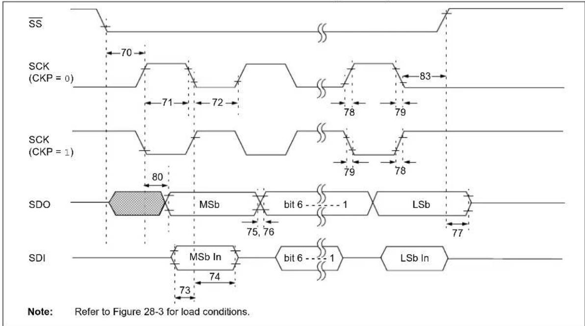
other
| Pattern | Bit Position | Value | |---------|--------------|-------| | SS | - | - | | SCK (CKP = 0) | - | 70 | | SCK (CKP = 0) | - | 71 | | SCK (CKP = 0) | - | 72 | | SCK (CKP = 0) | - | 78 | | SCK (CKP = 0) | - | 79 | | SCK (CKP = 0) | - | 83 | | SCK (CKP = 1) | - | - | | SCK (CKP = 1) | - | - | | SCK (CKP = 1) | - | - | | SDO | - | 80 | | SDO | - | MSb | | SDO | - | bit 6 | | SDO | - | LSb | | SDI | - | - | | SDI | - | MSb In | | SDI | - | bit 6 | | SDI | - | LSb In | | SDI | - | 73 | | SDI | - | 74 | Note: Refer to Figure 28-3 for load conditions.TABLE 28-16: EXAMPLE SPI MODE REQUIREMENTS (SLAVE MODE TIMING, CKE = 0)
| Param No. | Symbol C | Characteristic Min Max Units Conditions | |||||
| 70 | TssL2scH, TssL2scL | to SCK or SCK Input | 3 TCY | — | ns | ||
| 70A | TssL2WB | to write to SSPBUF | 3 TCY | — | ns | ||
| 71 | TschSCK | Input High Time (Slave mode) | Continuous | 1.25 TCY + 30 | — | ns | |
| 71A | Single Byte | 40 | — | ns | (Note 1) | ||
| 72 TscL | SCK | Input Low Time (Slave mode) | Continuous | 1.25 TCY + 30 | — | ns | |
| 72A | Single Byte | 40 | — | ns | (Note 1) | ||
| 73 | TDIV2scH, TDIV2scL | Setup Time of SDI Data Input to SCK Edge | 20 | — | ns | ||
| 73A | Tb2B | Last Clock Edge of Byte 1 to the First Clock Edge of Byte 2 | 1.5 TCY + 40 | — | ns | (Note 2) | |
| 74 | TschH2dIL, TsCL2dIL | Hold Time of SDI Data Input to SCK Edge | 40 | — | ns | ||
| 75 | TdoR | SDO Data Output Rise Time | — | 25 | ns | ||
| 76 | TboF | SDO Data Output Fall Time | — | 25 | ns | ||
| 77 | TssH2doZ | to SDO Output High-Impedance | 10 | 50 | ns | ||
| 78 | TscR | SCK Output Rise Time (Master mode) | — | 25 | ns | ||
| 79 | TscF | SCK Output Fall Time (Master mode) | — | 25 | ns | ||
| 80 | TschH2doV, TsCL2doV | SDO Data Output Valid after SCK Edge | — | 50 | ns | ||
| 83 | TschH2ssH, TsCL2ssH | after SCK Edge | 1.5 TCY + 40 | — | ns | ||
Note 1: Requires the use of Parameter #73A.
2: Only if Parameter #71A and #72A are used.
FIGURE 28-12: EXAMPLE SPI SLAVE MODE TIMING (CKE = 1)
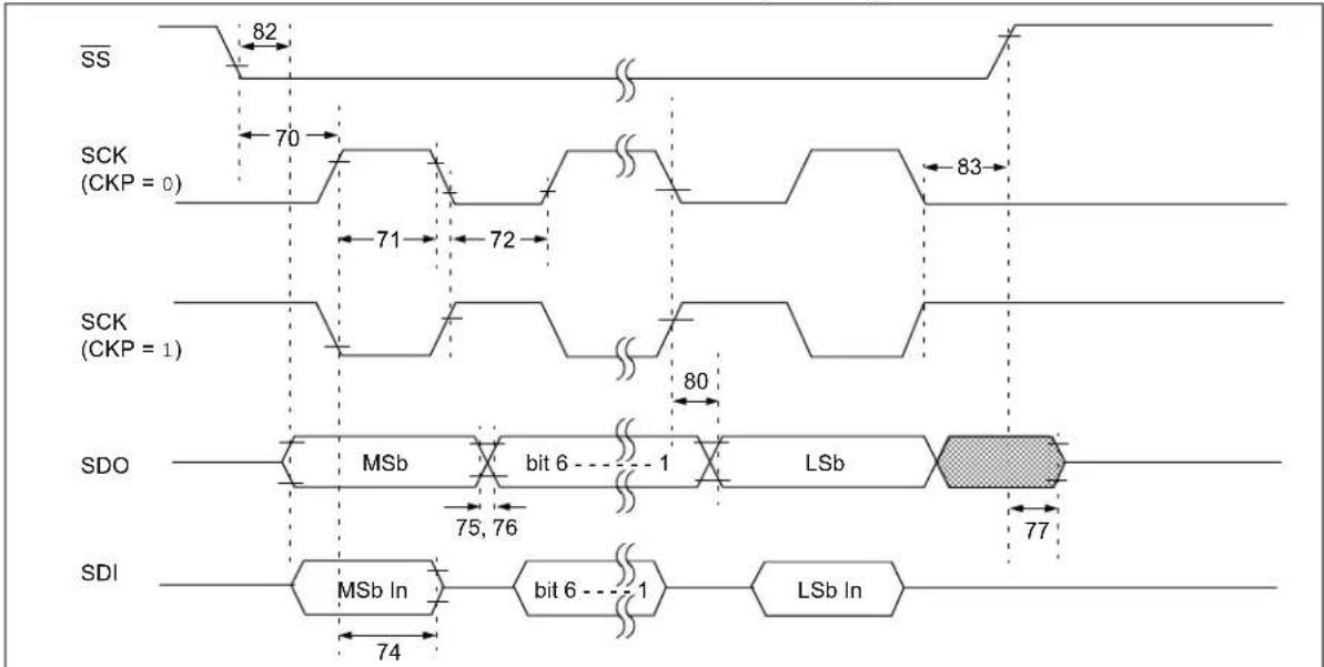
text_image
SS 82 SCK (CKP = 0) 70 71 72 83 SCK (CKP = 1) 80 SDO MSb bit 6 1 LSb 77 SDI MSb In bit 6 1 LSb In 74Note: Refer to Figure 28-3 for load conditions.
TABLE 28-17: EXAMPLE SPI SLAVE MODE REQUIREMENTS (CKE = 1)
| Param No. | Symbol | Characteristic Min Max Units Conditions | |||||
| 70 | TssL2scH, TssL2scL | to SCK or SCK Input | 3 TCY | — | ns | ||
| 70A | TssL2WB | to write to SSPBUF | 3 TCY | — | ns | ||
| 71 TscH 71A | SCK Input High Time (Slave mode) | Continuous | 1.25 TCY + 30 | — | ns | ||
| Single Byte | 40 | — | ns | (Note 1) | |||
| 72 | TscL | SCK Input Low Time (Slave mode) | Continuous | 1.25 TCY + 30 | — | ns | |
| 72A | Single Byte | 40 | — | ns | (Note 1) | ||
| 73A | TB2B | Last Clock Edge of Byte 1 to the First Clock Edge of Byte 2 | 1.5 TCY + 40 | — | ns | (Note 2) | |
| 74 | TscH2dIL, TscL2dIL | Hold Time of SDI Data Input to SCK Edge | 40 | — | ns | ||
| 75 | TDoR | SDO Data Output Rise Time | — | 25 | ns | ||
| 76 | TDoF | SDO Data Output Fall Time | — | 25 | ns | ||
| 77 | TssH2doZ | to SDO Output High-Impedance | 10 | 50 | ns | ||
| 78 | TscR | SCK Output Rise Time (Master mode) | — | 25 | ns | ||
| 79 | TscF | SCK Output Fall Time (Master mode) | — | 25 | ns | ||
| 80 | TscH2doV, TscL2doV | SDO Data Output Valid after SCK Edge | — | 50 | ns | ||
| 82 | TssL2doV | SDO Data Output Valid after Edge | — | 50 | ns | ||
| 83 | TscH2ssH, TscL2ssH | after SCK Edge | 1.5 TCY + 40 | — | ns | ||
Note 1: Requires the use of Parameter #73A.
2: Only if Parameter #71A and #72A are used.
FIGURE 28-13: I ^2 C ^TM BUS START/STOP BITS TIMING

text_image
SCL 90 91 93 SDA Start Condition Stop ConditionNote: Refer to Figure 28-3 for load conditions.
TABLE 28-18: I ^2 C ^TM BUS START/STOP BITS REQUIREMENTS (SLAVE MODE)
| Param. No. | Symbol | Characteristic Min Max Units Conditions | |||||
| 90 | TSU:STA | Start Condition Setup Time 400 kHz | 100 kHz mode | 4700 | — | ns | Only relevant for Repeated Start condition |
| mode 600 | — | ||||||
| 91 | THD:STA | Start Condition Hold Time | 100 kHz mode | 4000 | — | ns | After this period, the first clock pulse is generated |
| 400 kHz mode | 600 | — | |||||
| 92 | TSU:STO | Stop Condition Setup Time 400 kHz | 100 kHz mode | 4700 | — | ns | |
| mode 600 | — | ||||||
| 93 | THD:STO | Stop Condition Hold Time | 100 kHz mode | 4000 | — | ns | |
| 400 kHz mode | 600 | — | |||||
FIGURE 28-14: I ^2 C ^TM BUS DATA TIMING

text_image
SCL 103 100 101 102 90 106 107 92 91 SDA In 110 109 109 SDA OutNote: Refer to Figure 28-3 for load conditions.
TABLE 28-19: I ^2 C ^TM BUS DATA REQUIREMENTS (SLAVE MODE)
| Param. No. | Symbol | Characteristic Min Max Units Conditions | |||||
| 100 T | HIGH | Clock High Time | 100 kHz mode | 4.0 | — | μs | |
| 400 kHz mode 0.6 — μs | |||||||
| MSSP Module | 1.5 TCY | — | |||||
| 101 T | LOW | Clock Low Time | 100 kHz mode | 4.7 | — | μs | |
| 400 kHz mode 1.3 — μs | |||||||
| MSSP Module | 1.5 TCY | — | |||||
| 102 T | R | SDA and SCL Rise Time | 100 kHz mode | — | 1000 | ns | |
| 400 kHz mode | 20 + 0.1 CB | 300 | ns | CB is specified to be from 10 to 400 pF | |||
| 103 T | F | SDA and SCL Fall Time | 100 kHz mode | — | 300 | ns | |
| 400 kHz mode | 20 + 0.1 CB | 300 | ns | CB is specified to be from 10 to 400 pF | |||
| 90 | TSU:STA | Start Condition Setup Time | 100 kHz mode | 4.7 | — | μs | Only relevant for Repeated Start condition |
| 400 kHz mode 0.6 — μs | |||||||
| 91 | THD:STA | Start Condition Hold Time | 100 kHz mode | 4.0 | — | μs | After this period, the first clock pulse is generated |
| 400 kHz mode 0.6 — μs | |||||||
| 106 T | HD:DAT | Data Input Hold Time | 100 kHz mode | 0 | — | ns | |
| 400 kHz mode | 0 | 0.9 | μs | ||||
| 107 T | SU:DAT | Data Input Setup Time | 100 kHz mode | 250 | — | ns | (Note 2) |
| 400 kHz mode | 100 | — | ns | ||||
| 92 | TSU:STO | Stop Condition Setup Time | 100 kHz mode | 4.7 | — | μs | |
| 400 kHz mode 0.6 — μs | |||||||
| 109 T | AA | Output Valid from Clock | 100 kHz mode | — | 3500 | ns | (Note 1) |
| 400 kHz mode — | — | ns | |||||
| 110 | TBUF | Bus Free Time | 100 kHz mode | 4.7 | — | μs | Time the bus must be free before a new transmission can start |
| 400 kHz mode 1.3 — μs | |||||||
| D102 | CB | Bus Capacitive Loading | — | 400 | pF | ||
Note 1: As a transmitter, the device must provide this internal minimum delay time to bridge the undefined region (min. 300 ns) of the falling edge of SCL to avoid unintended generation of Start or Stop conditions.
2: A Fast mode I ^2 C ^TM bus device can be used in a Standard mode I ^2 C bus system, but the requirement, TSU:DAT ≥ 250 ns, must then be met. This will automatically be the case if the device does not stretch the LOW period of the SCL signal. If such a device does stretch the LOW period of the SCL signal, it must output the next data bit to the SDA line,
TR max. + TSU:DAT = 1000 + 250 = 1250 ns (according to the Standard mode I²C bus specification), before the SCL line is released.
FIGURE 28-15: MSSP I ^2 C ^TM BUS START/STOP BITS TIMING WAVEFORMS
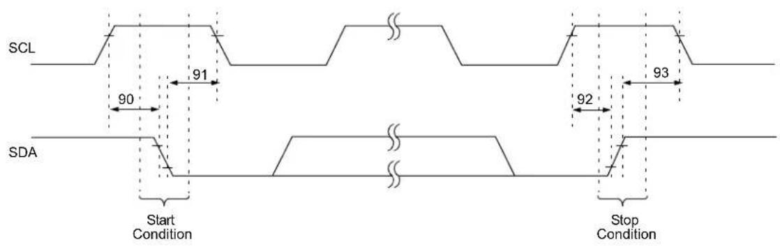
text_image
SCL 90 91 92 93 SDA Start Condition Stop ConditionNote: Refer to Figure 28-3 for load conditions.
TABLE 28-20: MSSP I ^2 C ^TM BUS START/STOP BITS REQUIREMENTS
| Param.No. | Symbol | Characteristic Min Max Units Conditions | |||||
| 90 | TSU:STA | Start Condition Setup Time | 100 kHz mode | 2(Tosc)(BRG + 1) | — | ns | Only relevant for Repeated Start condition |
| 400 kHz mode | 2(T osc)(BRG + 1) | — | |||||
| 1 MHz mode(1) | 2(Tosc)(BRG + 1) | — | |||||
| 91 | THD:STA | Start Condition Hold Time | 100 kHz mode | 2(Tosc)(BRG + 1) | — | ns | After this period, the first clock pulse is generated |
| 400 kHz mode | 2(T osc)(BRG + 1) | — | |||||
| 1 MHz mode(1) | 2(Tosc)(BRG + 1) | — | |||||
| 92 | TSU:STO | Stop Condition Setup Time | 100 kHz mode | 2(Tosc)(BRG + 1) | — | ns | |
| 400 kHz mode | 2(Tosc)(BRG + 1) | — | |||||
| 1 MHz mode(1) | 2(Tosc)(BRG + 1) | — | |||||
| 93 | THD:STO | Stop Condition Hold Time | 100 kHz mode | 2(Tosc)(BRG + 1) | — | ns | |
| 400 kHz mode | 2(Tosc)(BRG + 1) | — | |||||
| 1 MHz mode(1) | 2(Tosc)(BRG + 1) | — | |||||
Note 1: Maximum pin capacitance = 10 pF for all F^2C^TM pins.
FIGURE 28-16: MSSP I ^2 C ^TM BUS DATA TIMING

text_image
SCL 103 100 101 102 90 91 106 107 92 SDA In 109 109 110 SDA OutNote: Refer to Figure 28-3 for load conditions.
TABLE 28-21: MSSP I ^2 C ^TM BUS DATA REQUIREMENTS
| Param. No. | Symbol | Characteristic Min Max Units Conditions | |||||
| 100 T | HIGH Clock High Time | 100 kHz mode | 2(Tosc)(BRG + 1) — | ms | |||
| 400 kHz mode | 2(Tosc)(BRG + 1) — | ms | |||||
| 1MHzmode^(1) | 2(Tosc)(BRG + 1) | — ms | |||||
| 101 | TLOW | Clock Low Time | 100 kHz mode | 2(Tosc)(BRG + 1) | — | ms | |
| 400 kHz mode | 2(Tosc)(BRG + 1) — | ms | |||||
| 1MHzmode^(1) | 2(Tosc)(BRG + 1) | — ms | |||||
| 102 TR | SDA and SCL Rise Time | 100 kHz mode | — | 1000 | ns | C8 is specified to be from 10 to 400 pF ns | |
| 400 kHz mode | 20 + 0.1 CB | 300 | ns | ||||
| 1MHzmode^(1) | — | 300 | |||||
| 103 TF | SDA and SCL Fall Time | 100 kHz mode | — | 300 | ns | C8 is specified to be from 10 to 400 pF | |
| 400 kHz mode | 20 + 0.1 CB | 300 | ns | ||||
| 1MHzmode^(1) | — | 100 ns | |||||
| 90 | TSU:STA | Start Condition Setup Time | 100 kHz mode | 2(Tosc)(BRG + 1) | — | ms | Only relevant for Repeated Start condition |
| 400 kHz mode | 2(Tosc)(BRG + 1) — | ms | |||||
| 1MHzmode^(1) | 2(Tosc)(BRG + 1) — ms | ||||||
| 91 | THD:STA | Start Condition Hold Time | 100 kHz mode | 2(Tosc)(BRG + 1) | — | ms | After this period, the first clock pulse is generated |
| 400 kHz mode | 2(Tosc)(BRG + 1) — | ms | |||||
| 1MHzmode^(1) | 2(Tosc)(BRG + 1) — ms | ||||||
| 106 | THD:DAT | Data Input Hold Time | 100 kHz mode | 0 | — | ns | |
| 400 kHz mode | 0 | 0.9 | ms | ||||
| 107 T | SU:DAT | Data Input Setup Time | 100 kHz mode | 250 | — | ns | (Note 2) |
| 400 kHz mode | 100 — | ns | |||||
| 92 | TSU:STO | Stop Condition Setup Time | 100 kHz mode | 2(Tosc)(BRG + 1) — | ms | ||
| 400 kHz mode | 2(T osc)(BRG + 1) — ms | ||||||
| 1MHzmode^(1) | 2(Tosc)(BRG + 1) — ms | ||||||
| 109 TAA | Output Valid from Clock | 100 kHz mode | — | 3500 | ns | ||
| 400 kHz mode | — | 1000 | ns | ||||
| 1MHzmode^(1) | — | — | ns | ||||
| 110 | TBUF | Bus Free Time | 100 kHz mode | 4.7 | — | ms | Time the bus must be free before a new transmission can start |
| 400 kHz mode | 1.3 | — ms | |||||
| D102 | CB | Bus Capacitive Loading | — | 400 | pF | ||
Note 1: Maximum pin capacitance = 10 pF for all I²C™ pins.
2: A Fast mode I²C bus device can be used in a Standard mode fC bus system, but parameter #107 ≥ 250 ns must then be met. This will automatically be the case if the device does not stretch the LOW period of the SCL signal. If such a device does stretch the LOW period of the SCL signal, it must output the next data bit to the SDA line, parameter #102 + parameter #107 = 1000 + 250 = 1250 ns (for 100 kHz mode), before the SCL line is released.
FIGURE 28-17: EUSART/AUSART SYNCHRONOUS TRANSMISSION (MASTER/SLAVE) TIMING

text_image
TXx/CKx pin 121 121 RXx/DTx pin 120 122Note: Refer to Figure 28-3 for load conditions.
TABLE 28-22: EUSART/AUSART SYNCHRONOUS TRANSMISSION REQUIREMENTS
| Param No. | Symbol | Characteristic Min Max Units Conditions | ||||
| 120 T | CKH2DTV | SYNC XMIT (MASTER and SLAVE)Clock High to Data Out Valid — 40 ns | ||||
| 121 | TCKRF | Clock Out Rise Time and Fall Time (Master mode) | — | 20 | ns | |
| 122 | TDTRF | Data Out Rise Time and Fall Time | — | 20 | ns |
FIGURE 28-18: EUSART/AUSART SYNCHRONOUS RECEIVE (MASTER/SLAVE) TIMING
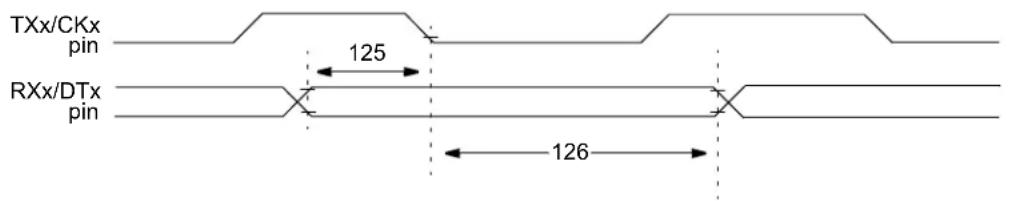
text_image
TXx/CKx pin 125 RXx/DTx pin 126Note: Refer to Figure 28-3 for load conditions.
TABLE 28-23: EUSART/AUSART SYNCHRONOUS RECEIVE REQUIREMENTS
| Param. No. | Symbol | Characteristic | Min | Max | Units | Conditions |
| 125 | TDTV2CKL | SYNC RCV (MASTER and SLAVE) Data Hold before CKx ↓ (DTx hold time) | 10 | — | ns | |
| 126 | TCKL2DTL | Data Hold after CKx ↓ (DTx hold time) | 15 | — | ns |
TABLE 28-24: A/D CONVERTER CHARACTERISTICS: PIC18F87J90 FAMILY (INDUSTRIAL)
| Param No. | Symbol | Characteristic Min Typ Max Units Conditions | |||||
| A01 N | R Resolution — — 10 bits | ||||||
| A03 | EIL | Integral Linearity Error | — | — | < ± 1 | LSb | VREF ≥ 3.0V |
| A04 E | DL | Differential Linearity Error | — | — | < ± 1 | LSb | VREF ≥ 3.0V |
| A06 | EOFF | Offset Error | — | — | < ± 3 | LSb | VREF ≥ 3.0V |
| A07 | EGN | Gain Error | — | — | < ± 3 | LSb | VREF ≥ 3.0V |
| A10 | — | Monotonicity | Guaranteed(1) | — | VSS ≤ VAIN ≤ VREF | ||
| A20 | VREF | Reference Voltage Range(VREFH – VREFL) | 2.02.0 | —— | —— | VV | V_DD < 3.0V V_DD > 3.0V |
| A21 V | REFH | Reference Voltage High | V_SS + VREF | — | V_DD | V | |
| A22 | VREFL | Reference Voltage Low | V_SS - 0.3V | — | V_DD - 3.0V | V | |
| A25 | VAIN | Analog Input Voltage | VREFL | — | VREFH | V | |
| A30 Z | AIN | Recommended Impedance of Analog Voltage Source | — | — | 2.5 | kΩ | |
| A50 I | REF | VREF Input Current(2) | —— | —— | 5150 | μAμA | During VAIN acquisition.During A/D conversion cycle. |
Note 1: The A/D conversion result never decreases with an increase in the input voltage and has no missing codes.
2: VREFH current is from RA3/AN3/VREF+ pin or VDD, whichever is selected as the VREFH source. VREFL current is from RA2/AN2/VREF- pin or VSS, whichever is selected as the VREFL source.
FIGURE 28-19: A/D CONVERSION TIMING
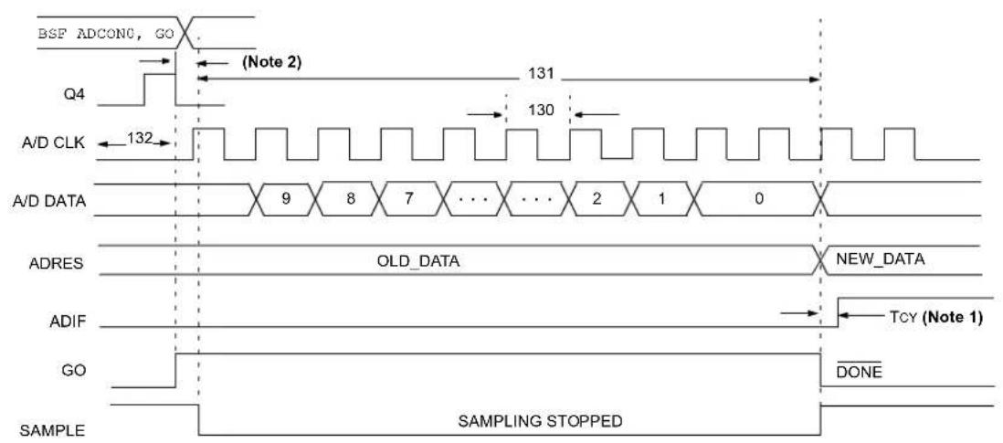
text_image
BSF ADCONC, GO (Q4) 131 130 A/D CLK 132 A/D DATA 9 8 7 ... ... 2 1 0 ADRES OLD_DATA NEW_DATA ADIF TCY (Note 1) GO DONE SAMPLE SAMPLING STOPPEDNote 1: If the A/D clock source is selected as RC, a time of TCY is added before the A/D clock starts. This allows the SLEEP instruction to be executed.
2: This is a minimal RC delay (typically 100 ns), which also disconnects the holding capacitor from the analog input.
TABLE 28-25: A/D CONVERSION REQUIREMENTS
| Param No. | Symbol | Characteristic Min Max Units Conditions | ||||
| 130 T | AD A/D | Clock Period 0.7 25.0 | (1) | μs | TOSC based, VREF ≥ 3.0V | |
| — | 1 | μs | A/D RC mode | |||
| 131 TCNV Conversion Time (not including acquisition time)(2) | 11 | 12 | TAD | |||
| 132 | TACQ | Acquisition Time(3) | 1.4 | — | μs | -40°C to +85°C |
| 135 | Tswc | Switching Time from Convert → Sample | — | (Note 4) | ||
| 136 T | DIS | Discharge Time | 0.2 | — | μs | |
Note 1: The time of the A/D clock period is dependent on the device frequency and the TAD clock divider.
2: ADRES registers may be read on the following TCY cycle.
3: The time for the holding capacitor to acquire the "New" input voltage when the voltage changes full scale after the conversion (VDD to Vss or Vss to VDD). The source impedance (Rs) on the input channels is 50Ω.
4: On the following cycle of the device clock.
29.0 PACKAGING INFORMATION
29.1 Package Marking Information
64-Lead TQFP

text_image
MICROCHIP XXXXXXXXX XXXXXXXXX XXXXXXXXX ○ YYWWNNNExample
text_image
MICROCHIP 18F65J90 -I/PT e3 101001780-Lead TQFP
text_image
MICROCHIP XXXXXXXXXXXXXX XXXXXXXXXXXXX YYWWNNNExample

text_image
MICROCHIP PIC18F85J90 -I/PTe3 1010017Legend: XX...X Customer-specific information
Y Year code (last digit of calendar year)
YY Year code (last 2 digits of calendar year)
WW Week code (week of January 1 is week '01')
NNN Alphanumeric traceability code
e3b-free JEDEC designator for Matte Tin (Sn)
* This package is Pb-free. The Pb-free JEDEC designator
can be found on the outer packaging for this package.
(e3)
Note: In the event the full Microchip part number cannot be marked on one line, it will be carried over to the next line, thus limiting the number of available characters for customer-specific information.
29.2 Package Details
The following sections give the technical details of the packages.
64-Lead Plastic Thin Quad Flatpack (PT) - 10x10x1 mm Body, 2.00 mm [TQFP]
Note: For the most current package drawings, please see the Microchip Packaging Specification located at http://www.microchip.com/packaging
![Microchip PIC18F86J93 - 64-Lead Plastic Thin Quad Flatpack (PT) - 10x10x1 mm Body, 2.00 mm [TQFP] - 1](/content/2026/06/1221796/images/01c2714f806a5c7b0fc153e9de601cfbfe9b80983beab7ae5a1c6be51b7438cc.jpg)
text_image
D D1 E E1 N b NOTE 1 1 2 3 NOTE 2![Microchip PIC18F86J93 - 64-Lead Plastic Thin Quad Flatpack (PT) - 10x10x1 mm Body, 2.00 mm [TQFP] - 2](/content/2026/06/1221796/images/ec5fca24cb819525577530a7303f917be8a63f68c2e6434ce59e8a04354f6e57.jpg)
natural_image
Line drawing of an integrated circuit chip with multiple pins (no text or symbols)![Microchip PIC18F86J93 - 64-Lead Plastic Thin Quad Flatpack (PT) - 10x10x1 mm Body, 2.00 mm [TQFP] - 3](/content/2026/06/1221796/images/c3226c5fbc9b206a38ab6f86e59bb9cbdcb1a47d6ea5951e62880bc31fa5704d.jpg)
text_image
C β L O![Microchip PIC18F86J93 - 64-Lead Plastic Thin Quad Flatpack (PT) - 10x10x1 mm Body, 2.00 mm [TQFP] - 4](/content/2026/06/1221796/images/a821e6bd216e2aabc38fef07e0f0f941f90d76f527f46167d6ed56309c623f48.jpg)
text_image
A A1 L1 α A2| UnitsvMILLIMETERS | ||||
| Dimension LimitsvMINvNOMvMAX | ||||
| Number of LeadsvNv64 | ||||
| Lead Pitchve 0.50 BSC | ||||
| Overall Height | Av- | - | 1.20 | |
| Molded Package Thickness | A2 | 0.95 | 1.00 | 1.05 |
| Standoff | A1 | 0.05 | - | 0.15 |
| Foot Length | L | 0.45 | 0.60 | 0.75 |
| Footprint | L1 | 1.00 REF | ||
| Foot Angle | 0° | 3.5° | 7° | |
| Overall Width | E | 12.00 BSC | ||
| Overall Length | D | 12.00 BSC | ||
| Molded Package Width | E1 | 10.00 BSC | ||
| Molded Package Length | D1 | 10.00 BSC | ||
| Lead Thickness | c | 0.09 | - | 0.20 |
| Lead Width | b | 0.17 | 0.22 | 0.27 |
| Mold Draft Angle Top | 11° | 12° | 13° | |
| Mold Draft Angle Bottom | 11° | 12° | 13° | |
Notes:
- Pin 1 visual index feature may vary, but must be located within the hatched area.
2.vChamfers at corners are optional; size may vary. - Dimensions D1 and E1 do not include mold flash or protrusions. Mold flash or protrusions shall not exceed 0.25 mm per side.
4.vDimensioning and tolerancing per ASME Y14.5M.
BSC:vBasic Dimension. Theoretically exact value shown without tolerances.
REF: Reference Dimension, usually without tolerance, for information purposes only.
Microchip Technology Drawing C04-085B
64-Lead Plastic Thin Quad Flatpack (PT) - 10x10x1 mm Body, 2.00 mm [TQFP]
Note: For the most current package drawings, please see the Microchip Packaging Specification located at http://www.microchip.com/packaging
![Microchip PIC18F86J93 - 64-Lead Plastic Thin Quad Flatpack (PT) - 10x10x1 mm Body, 2.00 mm [TQFP] - 1](/content/2026/06/1221796/images/0af4e5e9633aa70a236507f59754e8f5641aa0521fcec4d2ebbf2e76c2b8053c.jpg)
text_image
C1 G SILK SCREEN Y1 X1 E C2RECOMMENDED LAND PATTERN
| Units | MILLIMETERS | |||
| Dimension Limits | MIN | NOM | MAX | |
| Contact Pitch | E | 0.50 BSC | ||
| Contact Pad Spacing | C1 | 11.40 | ||
| Contact Pad Spacing | C2 | 11.40 | ||
| Contact Pad Width (X64) | X1 | 0.30 | ||
| Contact Pad Length (X64) | Y1 | 1.50 | ||
| Distance Between Pads | G | 0.20 | ||
Notes:
- Dimensioning and tolerancing per ASME Y14.5M
BSC: Basic Dimension. Theoretically exact value shown without tolerances.
Microchip Technology Drawing No. C04-2085A
80-Lead Plastic Thin Quad Flatpack (PT) - 12x12x1 mm Body, 2.00 mm [TQFP]
Note: For the most current package drawings, please see the Microchip Packaging Specification located at http://www.microchip.com/packaging
![Microchip PIC18F86J93 - 80-Lead Plastic Thin Quad Flatpack (PT) - 12x12x1 mm Body, 2.00 mm [TQFP] - 1](/content/2026/06/1221796/images/b4e2deef1553b30d0b39a7b34fcc330a589f217c91c93386d43c641156be457e.jpg)
text_image
D D1 E E1 e b N NOTE 1 123 NOTE 2 α A A1 L1 A2 c β φ L| UnitsvMILLIMETERS | ||||
| Dimension LimitsvMINvNOMvMAX | ||||
| Number of LeadsvNv80 | ||||
| Lead Pitchve 0.50 BSC | ||||
| Overall Height | Av- | - | 1.20 | |
| Molded Package Thickness | A2 | 0.95 | 1.00 | 1.05 |
| Standoff | A1 | 0.05 | - | 0.15 |
| Foot Length | L | 0.45 | 0.60 | 0.75 |
| Footprint | L1 | 1.00 REF | ||
| Foot Angle | 0° | 3.5° | 7° | |
| Overall Width | E | 14.00 BSC | ||
| Overall Length | D | 14.00 BSC | ||
| Molded Package Width | E1 | 12.00 BSC | ||
| Molded Package Length | D1 | 12.00 BSC | ||
| Lead Thickness | c | 0.09 | - | 0.20 |
| Lead Width | b | 0.17 | 0.22 | 0.27 |
| Mold Draft Angle Top | 11° | 12° | 13° | |
| Mold Draft Angle Bottom | 11° | 12° | 13° | |
Notes:
- Pin 1 visual index feature may vary, but must be located within the hatched area.
2.vChamfers at corners are optional; size may vary. - Dimensions D1 and E1 do not include mold flash or protrusions. Mold flash or protrusions shall not exceed 0.25 mm per side.
4.vDimensioning and tolerancing per ASME Y14.5M.
BSC:vBasic Dimension. Theoretically exact value shown without tolerances.
REF: Reference Dimension, usually without tolerance, for information purposes only.
Microchip Technology Drawing C04-092B
80-Lead Plastic Thin Quad Flatpack (PT) - 12x12x1 mm Body, 2.00 mm [TQFP]
Note: For the most current package drawings, please see the Microchip Packaging Specification located at http://www.microchip.com/packaging
![Microchip PIC18F86J93 - 80-Lead Plastic Thin Quad Flatpack (PT) - 12x12x1 mm Body, 2.00 mm [TQFP] - 1](/content/2026/06/1221796/images/b3097fbe8579807ad5287e8e9ef7799d1061a644a31444a8aeee396666160b14.jpg)
text_image
C1 G SILK SCREEN Y1 X1 E C2RECOMMENDED LAND PATTERN
| Units | MILLIMETERS | |||
| Dimension Limits | MIN | NOM | MAX | |
| Contact Pitch | E | 0.50 BSC | ||
| Contact Pad Spacing | C1 | 13.40 | ||
| Contact Pad Spacing | C2 | 13.40 | ||
| Contact Pad Width (X80) | X1 | 0.30 | ||
| Contact Pad Length (X80) | Y1 | 1.50 | ||
| Distance Between Pads | G | 0.20 | ||
Notes:
- Dimensioning and tolerancing per ASME Y14.5M
BSC: Basic Dimension. Theoretically exact value shown without tolerances.
Microchip Technology Drawing No. C04-2092A
NOTES:
APPENDIX A: REVISION HISTORY
Revision A (October 2008)
Original data sheet for PIC18F87J90 family devices.
Revision B (December 2008)
Changes to Section 28.2 "DC Characteristics: Power-Down and Supply Current PIC18F87J90 Family (Industrial)" and removal of Section 27.5 "DC Characteristics: RTCC Power-Down Current (IPD)".
Revision C (February 2009)
Added register CONFIG3L to Section 25.0 "Special Features of the CPU" and made minor corrections.
Revision D (January 2010)
Added 60°C IPD specification to Section 28.0 "Electrical Characteristics". Removed Preliminary condition tag. Minor edits to text throughout the document.
APPENDIX B: MIGRATION FROM PIC18F85J90 TO PIC18F87J90
Devices in the PIC18F87J90 and PIC18F85J90 families are almost similar in their functions and features. Code can be migrated from the 18F85J90 to the PIC18F87J90 without many changes. The differences between the two device families are listed in Table B-1.
TABLE B-1: NOTABLE DIFFERENCES BETWEEN PIC18F87J90 AND PIC18F85J90 FAMILIES
| Characteristic | PIC18F87J90 Family | 18F85J90 Family |
| Max Operating Frequency 48 MHz 40 MHz | ||
| Max Program Memory 128 Kbytes 32 Kbytes | ||
| Data Memory 3,923 Bytes 2,048 Bytes | ||
| Program Memory Endurance 10,000 Write/Erase (minimum) | 1,000 Write/Erase (minimum) | |
| Single-Word Write for Flash | Yes | No |
| Oscillator Options | PLL can be used with INTOSC | PLL cannot be used with INTOSC |
| CTMU | Yes | No |
| RTCC | Yes | No |
| Timer1 Oscillator Options | Low-power oscillator option for Timer1 | No |
| TICKI Clock | T1CKI can be used as a clock without enabling the Timer1 oscillator | No |
NOTES:
INDEX
A
A/D 289
A/D Converter Interrupt, Configuring 293
Acquisition Requirements 294
ADCAL Bit....297
ADCON0 Register.... 289
ADCON1 Register 289
ADCON2 Register 289
ADRESH Register.... 289, 292
ADRESL Register 289
Analog Port Pins, Configuring.... 295
Associated Registers 297
Automatic Selecting and Configuring Acquisition Time 295
Configuring the Module.... 293
Conversion Clock (TAD) 295
Conversion Requirements 426
Conversion Status (GO/DONE Bit).... 292
Conversions 296
Converter Calibration 297
Converter Characteristics 425
Operation in Power-Managed Modes 297
Special Event Trigger (CCP).... 296
Use of the CCP2 Trigger.... 296
Absolute Maximum Ratings 393
AC (Timing) Characteristics 408
Load Conditions for Device Timing Specifications.... 409
Parameter Symbology 408
Temperature and Voltage Specifications 409
Timing Conditions 409
ACKSTAT 245
ACKSTAT Status Flag 245
ADCAL Bit....297
ADCON0 Register 289
GO/DONE Bit....292
ADCON1 Register....289
ADCON2 Register.... 289
ADDFSR 382
ADDLW 345
Addressable Universal Synchronous Asynchronous Receiver Transmitter (AUSART). See AUSART.
ADDULNK.... 382
ADDWF 345
ADDWFC 346
ADRESH Register.... 289
ADRESL Register 289, 292
Analog-to-Digital Converter. See A/D
ANDLW 346
ANDWF 347
Assembler
MPASM Assembler.... 390
AUSART
Asynchronous Mode 280
Associated Registers, Receive 283
Associated Registers, Transmit 281
Receiver 282
Setting up 9-Bit Mode with Address Detect 282
Transmitter 280
Baud Rate Generator (BRG)...... 278
Associated Registers 278
Baud Rate Error, Calculating 278
Baud Rates, Asynchronous Modes ...... 279
High Baud Rate Select (BRGH Bit) 278
Operation in Power-Managed Modes.... 278
Sampling 278
Synchronous Master Mode.... 284
Associated Registers, Receive.... 286
Associated Registers, Transmit.... 285
Reception 286
Transmission 284
Synchronous Slave Mode.... 287
Associated Registers, Receive 288
Associated Registers, Transmit.... 287
Reception 288
Transmission 287
B
Baud Rate Generator 241
BC 347
BCF 348
BF 245
BF Status Flag 245
Bias Generation (LCD) Charge Pump Design Considerations .... 193
Block Diagrams
A/D 292
Analog Input Model.... 293
AUSART Receive 282
AUSART Transmit 280
Baud Rate Generator 241
Capture Mode Operation 176
Clock Source Multiplexing 166
Comparator Analog Input Model.... 303
Comparator I/O Operating Modes 300
Comparator Output 302
Comparator Voltage Reference.... 306
Comparator Voltage Reference Output Buffer Example .... 307
Compare Mode Operation 177
Connections for On-Chip Voltage Regulator 333
CTMU 309
CTMU Current Source Calibration Circuit 312
CTMU Typical Connections and Internal Configuration for Pulse Delay Generation..... 320
CTMU Typical Connections and Internal Configuration for Time Measurement .... 319
Device Clock 35
EUSART Receive 266
EUSART Transmit 264
External Power-on Reset Circuit (Slow VDD Power-up) 55
Fail-Safe Clock Monitor 335
Generic I/O Port Operation.... 117
Interrupt Logic.... 102
LCD Clock Generation.... 188
LCD Driver Module 183
LCD Regulator Connections (M0 and M1) 190
MSSP (I²C Master Mode) 239
MSSP (I²C Mode).... 220
MSSP (SPI Mode) 211
On-Chip Reset Circuit.... 53
PIC18F6XJ90 (64-Pin) 12
PIC18F8XJ90 (80-Pin) 13
PLL 40
PWM Operation (Simplified) 179
Reads From Flash Program Memory.... 93
Resistor Ladder Connections for M2 Configuration....191
Resistor Ladder Connections for M3 Configuration....192
RTCC 155
Single Comparator 30
SPI Master/Slave Connection 215
Table Read Operation.... 89
Table Write Operation....90
Table Writes to Flash Program Memory 9
Timer0 in 16-Bit Mode....140
Timer0 in 8-Bit Mode.... 14
Timer1 (16-Bit Read/Write Mode) 144
Timer1 (8-Bit Mode) 144
Timer2....150
Timer3 (16-Bit Read/Write Mode) 152
Timer3 (8-Bit Mode) 152
Watchdog Timer.... 331
BN 348
BNC 349
BNN 349
BNOV 350
BNZ 350
BOR. See Brown-out Reset.
BOV 353
BRA....351
Break Character (12-Bit) Transmit and Receive 269
BRG. See Baud Rate Generator.
BRGH Bit
TXSTA1 Register 259
TXSTA2 Register 278
Brown-out Reset (BOR) 55
and On-Chip Voltage Regulator.... 334
Detecting.... 55
BSF 351
BTFSC 352
BTFSS....352
BTG....353
BZ....354
C
C Compilers
MPLAB C18 390
CALL 354
CALLW 383
Capture (CCP Module).... 176
CCP Pin Configuration....176
CCPR2H:CCPR2L Registers.... 176
Software Interrupt 176
Timer1/Timer3 Mode Selection 176
Capture/Compare/PWM (CCP).... 173
Capture Mode. See Capture.
CCP Mode and Timer Resources 174
CCPRxH Register 174
CCPRxL Register.... 174
Compare Mode. See Compare.
Configuration.... 174
Interaction of CCP1 and CCP2 for
Timer Resources.... 175
Interconnect Configurations 174
Charge Time Measurement Unit (CTMU) 309
Associated Registers 323
Calibrating the Module 31
Creating a Delay 320
Effects of a Reset.... 320
Measuring Capacitance with the CTMU 317
Measuring Time.... 319
Module Initialization 311
Operation.... 310
During Sleep and Idle Modes 320
Clock Sources.... 37
Default System Clock on Reset.... 38
Selection Using OSCCON Register.... 38
CLRF 355
CLRWDT 355
Code Examples
16 x 16 Signed Multiply Routine .... 100
16 x 16 Unsigned Multiply Routine .... 100
8 x 8 Signed Multiply Routine 99
8 x 8 Unsigned Multiply Routine 99
Capacitance Calibration Routine 316
Changing Between Capture Prescalers.... 176
Computed GOTO Using an Offset Value.... 69
Current Calibration Routine 314
Erasing Flash Program Memory 94
Fast Register Stack 69
How to Clear RAM (Bank 1) Using Indirect Addressing . 82
Implementing a Real-Time Clock Using a
Timer1 Interrupt Service 147
Initializing PORTA.... 118
Initializing PORTB.... 120
Initializing PORTC 123
Initializing PORTD 126
Initializing PORTE.... 128
Initializing PORTF.... 130
Initializing PORTG 133
Initializing PORTH 135
Initializing PORTJ 137
Loading the SSPBUF (SSPSR) Register.... 214
Reading a Flash Program Memory Word 93
Routine for Capacitive Touch Switch.... 318
Saving STATUS, WREG and BSR Registers in RAM.... 116
Setting the RTCWREN Bit.... 167
Setup for CTMU Calibration Routines 313
Single-Word Write to Flash Program Memory 97
Writing to Flash Program Memory 96
Code Protection 325
COMF 356
Comparator....299
Analog Input Connection Considerations 303
Associated Registers 303
Configuration 300
Effects of a Reset 302
Interrupts 302
Operation.... 301
Operation During Sleep 302
Outputs 301
Reference 301
External Signal 301
Internal Signal.... 301
Response Time.... 301
Comparator Specifications.... 407
Comparator Voltage Reference 305
Accuracy and Error.... 306
Associated Registers 307
Configuring 305
Connection Considerations.... 306
Effects of a Reset 306
Operation During Sleep 306
Compare (CCP Module) 177
Capture, Compare, Timer1, Timers Associated Registers.... 178
CCP Pin Configuration.... 177
CCPR2 Register 177
Software Interrupt 177
Special Event Trigger.... 153, 177, 296
Timer1/Timer3 Mode Selection.... 177
Computed GOTO....69
Configuration Bits 325
Configuration Mismatch (CM) 55
Configuration Register Protection 337
Core Features Easy Migration 9
Extended Instruction Set....9
Memory Options....9
nanoWatt Technology 9
Oscillator Options and Features 9
CPFSEQ 356
CPFSGT 357
CPFSLT 357
Crystal Oscillator/Ceramic Resonator 39
Customer Change Notification Service 445
Customer Notification Service 445
Customer Support 445
D
Data Addressing Modes....82
Comparing Addressing Modes with the Extended Instruction Set Enabled 86
Direct....82
Indexed Literal Offset....85 BSR....87 Instructions Affected....85 Mapping Access Bank....87
Indirect 82
Inherent and Literal 82
Data Memory 72
Access Bank 74
Bank Select Register (BSR)....72
Extended Instruction Set.... 85
General Purpose Registers.... 74
Memory Maps PIC18FX6J90/X7J90 Devices .... 73 Special Function Registers .... 75
Special Function Registers 75
DAW 358
DC Characteristics 404
Power-Down and Supply Current 396
Supply Voltage.... 395
DCFSNZ 359
DECF 358
DECFSZ.... 359
Default System Clock.... 38
Details on Individual Family Members 10
Development Support 389
Device Overview 9
Features (64-Pin Devices) 11
Features (80-Pin Devices) 11
Direct Addressing....83
E
Effect on Standard PIC18 Instructions.... 386
Effects of Power-Managed Modes on Various Clock Sources 43
Electrical Characteristics 393
Enhanced Universal Synchronous Asynchronous Receiver Transmitter (EUSART). See EUSART.
ENVREG Pin 333
Equations 16 x 16 Signed Multiplication Algorithm.... 100
16 x 16 Unsigned Multiplication Algorithm.... 100
A/D Acquisition Time 294
A/D Minimum Charging Time 294
Calculating the Minimum Required Acquisition Time 294
Converting Error, Clock Pulses 168
LCD Static and Dynamic Current 193
Errata 8
EUSART Asynchronous Mode .... 264
12-Bit Break Transmit and Receive.... 269
Associated Registers, Receive.... 267
Associated Registers, Transmit.... 265
Auto-Wake-up on Sync Break Character ..... 268
Receiver 266
Setting up 9-Bit Mode with Address Detect....266
Transmitter 264
Baud Rate Generator (BRG) 259
Associated Registers.... 259
Auto-Baud Rate Detect.... 262
Baud Rate Error, Calculating.... 259
Baud Rates, Asynchronous Modes 260
High Baud Rate Select (BRGH Bit) 259
Operation in Power-Managed Modes.... 259
Sampling 259
Synchronous Master Mode 270
Associated Registers, Receive.... 272
Associated Registers, Transmit.... 271
Reception 272
Transmission 270
Synchronous Slave Mode 273
Associated Registers, Receive 274
Associated Registers, Transmit.... 273
Reception 274
Transmission 273
Extended Instruction Set
ADDFSR.... 382
ADDULNK 382
CALLW 383
MOVSF 383
MOVSS....384
PUSHL 384
SUBFSR 385
SUBULNK 385
External Oscillator Modes
Clock Input (EC Modes) 40
HS....39
F
Fail-Safe Clock Monitor.... 325, 335
Exiting Fail-Safe Operation 336
Interrupts in Power-Managed Modes 336
POR or Wake-up From Sleep 336
WDT During Oscillator Failure 335
Fast Register Stack....69
Firmware Instructions....339
Flash Configuration Words.... 325
Flash Program Memory....89
Associated Registers 98
Control Registers 90
EECON1 and EECON2 90
TABLAT (Table Latch) Register 92
TBLPTR (Table Pointer) Register....92
Erase Sequence 94
Erasing....94
Operation During Code-Protect 98
Reading....93
Table Pointer Boundaries Based on Operation.... 92
Table Pointer Boundaries 92
Table Reads and Table Writes 89
Write Sequence 95
Write Sequence (Word Programming) 97
Writing....95
Unexpected Termination.... 98
Write Verify 98
FSCM. See Fail-Safe Clock Monitor.
G
GOTO....360
H
Hardware Multiplier 99
8 x 8 Multiplication Algorithms ...... 99
Operation 99
Performance Comparison (table)....99
|
I/O Ports.... 117
Input Voltage Considerations.... 117
Open-Drain Outputs.... 118
Output Pin Drive.... 117
Pin Capabilities 117
Pull-up Configuration 118
I²C Mode (MSSP) 220
Acknowledge Sequence Timing.... 248
Associated Registers 254
Baud Rate Generator.... 241
Bus Collision
During a Repeated Start Condition.... 252
During a Stop Condition.... 253
Clock Arbitration....242
Clock Stretching.... 234
10-Bit Slave Receive Mode (SEN = 1).... 234
10-Bit Slave Transmit Mode.... 234
7-Bit Slave Receive Mode (SEN = 1).... 234
7-Bit Slave Transmit Mode....234
Clock Synchronization and the CKP Bit....235
Effects of a Reset....249
General Call Address Support 238
I²C Clock Rate w/BRG 241
Master Mode.... 239
Baud Rate Generator 241
Operation.... 240
Reception 245
Repeated Start Condition Timing 244
Start Condition Timing 243
Transmission 245
Multi-Master Communication, Bus Collision and Arbitration 249
Multi-Master Mode.... 249
Operation.... 225
Read/Write Bit Information (R/W Bit).... 225, 227
Registers 220
Serial Clock (SCK/SCL).... 227
Slave Mode.... 225
Address Masking 226
Addressing.... 225
Reception 227
Transmission 227
Sleep Operation....249
Stop Condition Timing 248
INCF 360
INCFSZ 361
In-Circuit Debugger.... 337
In-Circuit Serial Programming (ICSP).... 325, 337
Indexed Literal Offset Addressing and Standard PIC18 Instructions.... 386
Indexed Literal Offset Mode.... 386
Indirect Addressing 83
INFSNZ....361
Initialization Conditions for all Registers 59–64
Instruction Cycle 70
Clocking Scheme....70
Flow/Pipelining....70
Instruction Set.... 339
ADDLW 345
ADDWF 345
ADDWF (Indexed Literal Offset Mode) 387
ADDWFC 346
ANDLW 346
ANDWF 347
BC 347
BCF 348
BN 348
BNC 349
BNN 349
BNOV 350
BNZ 350
BOV 353
BRA 351
BSF 351
BSF (Indexed Literal Offset Mode) 387
BTFSC 352
BTFSS 352
BTG 353
BZ 354
CALL.... 354
CLRF 355
CLRWDT 355
COMF 356
CPFSEQ.... 356
CPFSGT 357
CPFSLT 357
DAW....358
DCFSNZ 359
DECF 358
DECFSZ 359
Extended Instructions 381
Considerations when Enabling 386
Syntax.... 381
Use with MPLAB IDE Tools 388
General Format.... 341
GOTO 360
INCF 360
INCFSZ.... 361
INFSNZ....361
IORLW 362
IORWF 362
LFSR.... 363
MOVF 363
MOVFF 364
MOVLB 364
MOVLW 365
MOVWF 365
MULLW.... 366
MULWF 366
NEGF 367
NOP 367
Opcode Field Descriptions.... 340
POP 368
PUSH.... 368
RCALL 369
RESET 369
RETFIE 370
RETLW 370
RETURN 371
RLCF 371
RLNCF 372
RRCF 372
RRNCF 373
SETF 373
SETF (Indexed Literal Offset Mode) 387
SLEEP 374
Standard Instructions 339
SUBFWB.... 374
SUBLW 375
SUBWF 375
SUBWFB 376
SWAPF 376
TBLRD 377
TBLWT 378
TSTFSZ 379
XORLW 379
XORWF 380
INTCON Register
RBIF Bit.... 120
Inter-Integrated Circuit. See I²C Mode.
Internal LCD Voltage Regulator Specifications.... 407
Internal Oscillator Block 41
Adjustment 42
INTIO Modes.... 41
INTOSC Frequency Drift 42
INTOSC Output Frequency.... 42
INTPLL Modes 41
Internal RC Oscillator
Use with WDT 331
Internal Voltage Regulator Specifications 407
Internet Address.... 445
Interrupt Sources 325
A/D Conversion Complete 293
Capture Complete (CCP) 176
Compare Complete (CCP) 177
Interrupt-on-Change (RB7:RB4).... 120
TMR0 Overflow.... 141
TMR1 Overflow.... 143
TMR2 to PR2 Match (PWM) 179
TMR3 Overflow.... 151, 153
Interrupts 101
During, Context Saving.... 116
INTx Pin.... 116
PORTB, Interrupt-on-Change.... 116
TMR0....116
Interrupts, Flag Bits
Interrupt-on-Change (RB7:RB4) Flag (RBIF Bit).... 120
INTOSC, INTRC. See Internal Oscillator Block.
IORLW 362
IORWF 362
L
LCD
Associated Registers 209
Bias Generation.... 189
Bias Configurations 190
M0 and M1 190
M2 191
M3 192
Bias Types.... 189
Voltage Regulator.... 189
Charge Pump 190, 193
Clock Source Selection 188
Configuring the Module 208
Frame Frequency 194
Interrupts 206
LCDCON Register 184
LCDDATA Registers.... 184
LCDPS Register 184
LCDREG Register 184
LCDSE Registers 184
Multiplex Types.... 193
Operation During Sleep 207
Pixel Control 193
Segment Enables 193
Waveform Generation 194
LCD Driver....10
LCDCON Register 184
LCDDATA Registers.... 184
LCDPS Register 184
LCDREG Register 184
LCDSE Registers.... 184
LFSR 363
Liquid Crystal Display (LCD) Driver.... 183
Low-Voltage Detection 333
M
Master Clear (MCLR).... 55
Master Synchronous Serial Port (MSSP). See MSSP.
Memory Organization 65
Data Memory 72
Program Memory 65
Memory Programming Requirements.... 406
Microchip Internet Web Site 445
Migration From PIC18F85J90 to PIC18F87J90.... 433
MOVF 363
MOVFF 364
MOVLB....364
MOVLW 365
MOVSF 383
MOVSS 384
MOVWF 365
MPLAB ASM30 Assembler, Linker, Librarian 390
MPLAB Integrated Development
Environment Software.... 389
MPLAB PM3 Device Programmer.... 392
MPLAB REAL ICE In-Circuit Emulator System.... 391
MPLINK Object Linker/MPLIB Object Librarian ....390
MSSP
ACK Pulse 225, 227
Control Registers (general).... 211
Module Overview 211
SSPBUF Register 216
SSPSR Register 216
MULLW 366
MULWF 366
N
NEGF 367
NOP 367
Notable Differences Between
PIC18F87J90 and PIC18F85J90 Families.... 433
0
Oscillator Configuration.... 35
EC 35
ECPLL.... 35
HS 35
HSPLL 35
Internal Oscillator Block 41
INTIO1 35
INTIO2 35
INTPLL1....35
INTPLL2....35
Oscillator Selection 325
Oscillator Start-up Timer (OST) 43
Oscillator Switching....37
Oscillator Transitions.... 38
Oscillator, Timer1 143, 153
Oscillator, Timer3 151
P
Packaging 427
Details 428
Marking 427
Pin Functions
AVDD 20
AVDD 29
AVss 29
AVss 20
ENVREG....20,29
LCDBIAS3.... 18,25
MCLR 14,21
OSC1/CLKI/RA7 14,21
OSC2/CLKO/RA6 14, 21
RA0/ANO 14,2
RA1/AN1/SEG18 14,21
RA2/AN2/VREF- 14, 21
RA3/AN3/VREF+ 14,21
RA4/T0CKI/SEG14 14,21
RA5/AN4/SEG15 14,21
RB0/INT0/SEG30 15,22
RB1/INT1/SEG8 15,22
RB2/INT2/SEG9/CTED1.... 15, 22
RB3/INT3/SEG10/CTED2.... 15, 22
RB4/KBI0/SEG11 15,22
RB5/KBI1/SEG29 15,22
RB6/KBI2/PGC 15,22
RB7/KBI3/PGD 15,22
RC0/T1OSO/T13CKI 16,23
RC1/T1OSI/CCP2/SEG32.... 16, 23
RC2/CCP1/SEG13 16, 23
RC3/SCK/SCL/SEG17.... 16, 23
RC4/SDI/SDA/SEG16.... 16, 23
RC5/SDO/SEG12 16, 23
RC6/TX1/CK1/SEG27 16, 23
RC7/RX1/DT1/SEG28 16, 23
RD0/SEG0/CTPLS 17,24
RD1/SEG1.... 17,24
RD2/SEG2.... 17, 24
RD3/SEG3....17,24
RD4/SEG4.... 17,24
RD5/SEG5.... 17, 24
RD6/SEG6.... 17, 24
RD7/SEG7 17,24
RE0/LCDBIAS1 18,25
RE1/LCDBIAS2 18, 25
RE3/COM0 18,25
RE4/COM1 18,25
RE5/COM2 18,25
RE6/COM3 18,25
RE7/CCP2/SEG31.... 18, 25
RF1/AN6/C2OUT/SEG19 19, 26
RF2/AN7/C1OUT/SEG20 19, 26
RF3/AN8/SEG21/C2INB.... 19, 26
RF4/AN9/SEG22/C2INA.... 19, 26
RF5/AN10/CVREF/SEG23/C1INB 19, 26
RF6/AN11/SEG24/C1INA.... 19, 26
RF7/AN5/SS/SEG25.... 19, 26
RG0/LCDBIAS0....20, 27
RG1/TX2/CK2.... 20, 27
RG2/RX2/DT2/VLCAP1 20, 27
RG3/VLCAP2 20,27
RG4/SEG26/RTCC.... 20, 27
RH0/SEG47 28
RH1/SEG46 28
RH2/SEG45 28
RH3/SEG44 28
RH4/SEG40 28
RH5/SEG41 28
RH6/SEG42 28
RH7/SEG43 28
RJ0 29
RJ1/SEG33....29
RJ2/SEG34.... 29
RJ3/SEG35....29
RJ4/SEG39....29
RJ5/SEG38....29
RJ6/SEG37 29
RJ7/SEG36....29
VDD 20
VDD 29
VDDCORE/VCAP....20, 29
Vss 20
Vss 29
Pinout I/O Descriptions
PIC18F6XJ90.... 14
PIC18F8XJ90....21
PLL 40
HSPLL and ECPLL Oscillator Modes 40
Use with INTOSC.... 40
POP 368
POR. See Power-on Reset.
PORTA
Associated Registers 119
LATA Register.... 118
PORTA Register 118
TRISA Register 118
PORTB
Associated Registers 122
LATB Register.... 120
PORTB Register 120
RB7:RB4 Interrupt-on-Change Flag (RBIF Bit) 120
TRISB Register 120
PORTC
Associated Registers 125
LATC Register 123
PORTC Register 123
RC3/SCK/SCL/SEG17 Pin.... 227
TRISC Register.... 123
PORTD
Associated Registers 127
LATD Register 126
PORTD Register 126
TRISD Register.... 126
PORTE
Associated Registers 129
LATE Register.... 128
PORTE Register 128
TRISE Register 128
PORTF
Associated Registers 132
LATF Register.... 130
PORTF Register 130
TRISF Register 130
PORTG
Associated Registers 134
LATG Register 133
PORTG Register.... 133
TRISG Register.... 133
PORTH
Associated Registers 136
LATH Register 135
PORTH Register 135
TRISH Register 135
PORTJ
Associated Registers 138
LATJ Register 137
PORTJ Register.... 137
TRISJ Register.... 137
Power-Managed Modes.... 45
and SPI Operation 219
Clock Sources.... 45
Clock Transitions and Status Indicators...... 46
Entering.... 45
Exiting Idle and Sleep Modes 51
By Interrupt 51
By Reset.... 51
By WDT Time-out 51
Without an Oscillator Start-up Delay 51
Idle Modes 49
PRI_IDLE 50
RC_IDLE 51
SEC_IDLE 50
Multiple Sleep Commands.... 46
Run Modes 46
PRI_RUN....46
RC_RUN 48
SEC_RUN 46
Selecting....45
Sleep Mode 49
OSC1 and OSC2 Pin States.... 43
Summary (table) 45
Power-on Reset (POR).... 55
Power-up Delays 43
Power-up Timer (PWRT) 43, 56
Time-out Sequence 56
Prescaler, Capture.... 176
Prescaler, Timer0 141
Prescaler, Timer2 180
PRI IDLE Mode 50
PRI_RUN Mode.... 46
Program Counter 67
PCL, PCH and PCU Registers 67
PCLATH and PCLATU Registers 67
Program Memory
Extended Instruction Set 84
Flash Configuration Words 66
Hard Memory Vectors.... 66
Instructions 71
Two-Word 71
Interrupt Vector 66
Look-up Tables....69
Memory Maps.... 65
Hard Vectors and Configuration Words.... 66
Reset Vector....66
Program Verification and Code Protection 337
Programming, Device Instructions.... 339
Pulse-Width Modulation. See PWM (CCP Module).
PUSH 368
PUSH and POP Instructions....68
PUSHL 384
PWM (CCP Module)
Associated Registers 181
Duty Cycle 180
Example Frequencies/Resolutions 180
Period 179
Setup for Operation 181
TMR2 to PR2 Match 179
Q
Q Clock.... 180
R
RAM. See Data Memory.
RC_IDLE Mode 51
RC RUN Mode 48
RCALL 369
RCON Register
Bit Status During Initialization 58
Reader Response 446
Real-Time Clock and Calendar
Operation 165
Registers.... 156
Real-Time Clock and Calendar (RTCC).... 155
Register File 74
Register File Summary.... 76–80
Registers
ADCON0 (A/D Control 0) 289
ADCON1 (A/D Control 1) 290
ADCON2 (A/D Control 2) 291
ALRMCFG (Alarm Configuration) 159
ALRMDAY (Alarm Day Value) 163
ALRMHR (Alarm Hours Value) 164
ALRMMIN (Alarm Minutes Value)....164
ALRMMNTH (Alarm Month Value)....163
ALRMRPT (Alarm Calibration).... 160
ALRMSEC (Alarm Seconds Value).... 164
ALRMWD (Alarm Weekday Value) 163
BAUDCON1 (Baud Rate Control) 1 258
CCPxCON (CCPx Control, CCP1 and CCP2) ..... 173
CMCON (Comparator Control) 299
CONFIG1H (Configuration 1 High) ......327
CONFIG1L (Configuration 1 Low)....327
CONFIG2H (Configuration 2 High) 329
CONFIG2L (Configuration 2 Low)....328
CONFIG3H (Configuration 3 High) 330
CONFIG3L (Configuration 3 Low)....329
CTMUCONH (CTMU Control High) 321
CTMUCONL (CTMU Control Low)....322
CTMUICON (CTMU Current Control) 323
CVRCON (Comparator Voltage
Reference Control).... 305
DAY (Day Value).... 161
DEVID1 (Device ID 1) 330
DEVID2 (Device ID 2) 330
EECON1 (EEPROM Control 1)....91
HOUR (Hour Value) 162
INTCON (Interrupt Control).... 103
INTCON2 (Interrupt Control 2).... 104
INTCON3 (Interrupt Control 3).... 105
IPR1 (Peripheral Interrupt Priority 1).... 112
IPR2 (Peripheral Interrupt Priority 2).... 113
IPR3 (Peripheral Interrupt Priority 3).... 114
LCDCON (LCD Control) 184
LCDDATAx (LCD Data) 187
LCDPS (LCD Phase) 185
LCDREG (LCD Voltage Regulator Control) 189
LCDSEx (LCD Segment Enable) 186
MINUTE (Minute Value).... 162
MONTH (Month Value) 161
OSCCON (Oscillator Control) 36
OSCTUNE (Oscillator Tuning) 37
PADCFG1 (Pad Configuration)....158
PIE1 (Peripheral Interrupt Enable 1) 109
PIE2 (Peripheral Interrupt Enable 2) 110
PIE3 (Peripheral Interrupt Enable 3) 111
PIR1 (Peripheral Interrupt Request (Flag) 1) ...... 106
PIR2 (Peripheral Interrupt Request (Flag) 2)...... 107
PIR3 (Peripheral Interrupt Request (Flag) 3).... 108
RCON (Reset Control).... 54, 115
RCSTA1 (EUSART Receive Status and Control).... 257
RCSTA2 (AUSART Receive Status and Control).... 277
Reserved 160
RTCCAL (RTCC Calibration).... 158
RTCCFG (RTCC Configuration).... 157
SECOND (Second Value).... 162
SSPCON1 (MSSP Control 1, I²C Mode) ...... 222
SSPCON1 (MSSP Control 1, SPI Mode).... 213
SSPCON2 (MSSP Control 2, I²C Master Mode) ..... 223
SSPCON2 (MSSP Control 2, I²C Slave Mode) ..... 224
SSPSTAT (MSSP Status, I²C Mode) 221
SSPSTAT (MSSP Status, SPI Mode).... 212
STATUS 81
STKPTR (Stack Pointer)....68
T0CON (Timer0 Control) 139
T1CON (Timer1 Control) 143
T2CON (Timer2 Control) 149
T3CON (Timer3 Control) 151
TXSTA1 (EUSART Transmit Status and Control) 256
TXSTA2 (AUSART Transmit Status and Control) 276
WDTCON (Watchdog Timer Control) 332
WEEKDAY (Weekday Value) 161
YEAR (Year Value).... 160
RESET.... 369
Reset 53
Brown-out Reset (BOR).... 53
Configuration Mismatch (CM) Reset.... 53
MCLR Reset, During Power-Managed Modes ..... 53
MCLR Reset, Normal Operation.... 53
Power-on Reset (POR).... 53
RESET Instruction 53
Stack Full Reset.... 53
Stack Underflow Reset 53
Watchdog Timer (WDT) Reset 53
Resets.... 325
Brown-out Reset (BOR) 325
Oscillator Start-up Timer (OST) 325
Power-on Reset (POR) 325
Power-up Timer (PWRT) 325
RETFIE.... 370
RETLW 370
RETURN.... 371
Return Address Stack.... 67
Return Stack Pointer (STKPTR) 68
Revision History...... 433
RLCF 371
RLNCF 372
RRCF 372
RRNCF 373
RTCC
Alarm 168
Configuring 168
Interrupt 169
Mask Settings 169
Alarm Value Registers (ALRMVAL).... 163
Control Registers 157
Operation
Calibration.... 168
Clock Source 166
Digit Carry Rules.... 166
General Functionality.... 167
Leap Year 167
Register Mapping.... 167
ALRMVAL.... 168
RTCVAL.... 167
Safety Window for Register Reads
and Writes.... 167
Write Lock.... 167
Register Interface.... 165
Register Maps.... 171
Reset....170
Device.... 170
Power-on Reset (POR).... 170
Sleep Mode.... 170
Value Registers (RTCVAL).... 160
RTCEN Bit Write 165
S
SCK....211
SDI 211
SDO 211
SEC_IDLE Mode....50
SEC_RUN Mode.... 46
Serial Clock, SCK 211
Serial Data In (SDI).... 211
Serial Data Out (SDO) 211
Serial Peripheral Interface. See SPI Mode.
SETF 373
Slave Select (SS).... 211
SLEEP 374
Software Simulator (MPLAB SIM).... 391
Special Event Trigger. See Compare (CCP Module).
Special Features of the CPU 325
SPI Mode (MSSP)
Associated Registers 219
Bus Mode Compatibility 219
Effects of a Reset 219
Enabling SPI I/O 215
Master Mode.... 216
Operation 214
Operation in Power-Managed Modes 219
Serial Clock.... 211
Serial Data In 21
Serial Data Out 211
Slave Mode.... 217
Slave Select.... 211
Slave Select Synchronization 217
SPI Clock 216
Typical Connection 215
211
SSPOV....245
SSPOV Status Flag 245
SSPSTAT Register
R/W Bit.... 225, 227
Stack Full/Underflow Resets 69
SUBFSR 385
SUBFWB.... 374
SUBLW 375
SUBULNK 385
SUBWF 375
SUBWFB 376
SWAPF 376
T
Table Pointer Operations (table)....92
Table Reads/Table Writes 69
TBLRD 377
TBLWT 378
Timer0 139
Associated Registers 141
Clock Source Select (T0CS Bit) 140
Operation.... 140
Overflow Interrupt 141
Prescaler 141
Switching Assignment 141
Prescaler Assignment (PSA Bit).... 141
Prescaler Select (TOPS2:TOPS0 Bits) 141
Prescaler. See Prescaler, Timer0.
Reads and Writes in 16-Bit Mode.... 140
Source Edge Select (T0SE Bit) 140
Timer1 143
16-Bit Read/Write Mode 14
Associated Registers 147
Interrupt 146
Operation.... 144
Oscillator.... 143, 145
Layout Considerations.... 146
Oscillator as Secondary Clock.... 37
Overflow Interrupt 143
Resetting, Using the CCP Special Event Trigger.... 146
TMR1H Register.... 143
TMR1L Register 143
Use as a Clock Source 145
Use as a Real-Time Clock 146
Timer2 149
Associated Registers 150
Interrupt 150
Operation.... 149
Output.... 150
PR2 Register 179
TMR2 to PR2 Match Interrupt.... 179
Timer3 151
16-Bit Read/Write Mode 153
Associated Registers 153
Operation.... 152
Oscillator.... 151, 153
Overflow Interrupt 151, 153
Special Event Trigger (CCP) 153
TMR3H Register.... 151
TMR3L Register 151
Timing Diagrams
A/D Conversion 426
Acknowledge Sequence 248
Asynchronous Reception 267, 283
Asynchronous Transmission 265, 281
Asynchronous Transmission (Back to Back) 265, 281
Automatic Baud Rate Calculation.... 263
Auto-Wake-up Bit (WUE) During Normal Operation 268
Auto-Wake-up Bit (WUE) During Sleep.... 268
Baud Rate Generator with Clock Arbitration.... 242
BRG Overflow Sequence 263
BRG Reset Due to SDA Arbitration During Start Condition.... 251
Bus Collision During a Repeated Start Condition (Case 1)....252
Bus Collision During a Repeated Start Condition (Case 2) 252
Bus Collision During a Start Condition (SCL = 0) .... 251
Bus Collision During a Stop Condition (Case 1) 253
Bus Collision During a Stop Condition (Case 2) .....253
Bus Collision During Start Condition (SDA Only).... 250
Bus Collision for Transmit and Acknowledge...... 249
Capture/Compare/PWM 415
CLKO and I/O 412
Clock Synchronization 235
Clock/Instruction Cycle 70
EUSART/AUSART Synchronous Receive (Master/Slave)....424
EUSART/AUSART Synchronous Transmission (Master/Slave)....424
Example SPI Master Mode (CKE = 0) 416
Example SPI Master Mode (CKE = 1) 417
Example SPI Slave Mode (CKE = 0) 418
Example SPI Slave Mode (CKE = 1) 419
External Clock 410
Fail-Safe Clock Monitor 336
First Start Bit Timing 243
I²C Bus Data.... 421
I²C Bus Start/Stop Bits.... 420
I²C Master Mode (7 or 10-Bit Transmission) ...... 246
I²C Master Mode (7-Bit Reception) 247
I^2C Slave Mode (10-Bit Reception, SEN = 0, ADMSK = 01001) ...... 232
I²C Slave Mode (10-Bit Reception, SEN = 0) ...... 231
I²C Slave Mode (10-Bit Reception, SEN = 1) ...... 237
I²C Slave Mode (10-Bit Transmission).... 233
I²C Slave Mode (7-Bit Reception, SEN = 0, ADMSK = 01011) ...... 229
I²C Slave Mode (7-Bit Reception, SEN = 0) ...... 228
I²C Slave Mode (7-Bit Reception, SEN = 1) ...... 236
I²C Slave Mode (7-Bit Transmission).... 230
I^2C Slave Mode General Call Address Sequence (7 or 10-Bit Addressing Mode)...... 238
I²C Stop Condition Receive or Transmit Mode ..... 248
LCD Interrupt in Quarter Duty Cycle Drive....206
LCD Sleep Entry/Exit When SLPEN = 1 or CS1:CS0 = 00.....207
MSSP I²C Bus Data 422
MSSP I²C Bus Start/Stop Bits 422
PWM Output 179
Repeated Start Condition.... 244
Reset, Watchdog Timer (WDT), Oscillator Start-up Timer (OST) and Power-up Timer (PWRT) ..... 413
Send Break Character Sequence 269
Slave Synchronization 217
Slow Rise Time (MCLR Tied to VDD, VDD Rise > TPWRT) 57
SPI Mode (Master Mode) 216
SPI Mode (Slave Mode, CKE = 0) 218
SPI Mode (Slave Mode, CKE = 1) 218
Synchronous Reception (Master Mode, SREN).... 272, 286
Synchronous Transmission.... 270, 284
Synchronous Transmission (Through TXEN).... 271, 285
Time-out Sequence on Power-up (MCLR Not Tied to VDD), Case 1 56
Time-out Sequence on Power-up (MCLR Not Tied to VDD), Case 2 57
Time-out Sequence on Power-up (MCLR Tied to VDD, VDD Rise Tpwrt) 56
Timer Pulse Generation.... 170
Timer0 and Timer1 External Clock 414
Transition for Entry to Idle Mode.... 50
Transition for Entry to SEC_RUN Mode 47
Transition for Entry to Sleep Mode 49
Transition for Two-Speed Start-up (INTRC to HSPLL) 334
Transition for Wake From Idle to Run Mode.... 50
Transition for Wake From Sleep (HSPLL) 49
Transition From RC_RUN Mode to PRI_RUN Mode....48
Transition From SEC_RUN Mode to PRI_RUN Mode (HSPLL) 47
Transition to RC RUN Mode 48
Type-A in 1/2 MUX, 1/2 Bias Drive 196
Type-A in 1/2 MUX, 1/3 Bias Drive 198
Type-A in 1/3 MUX, 1/2 Bias Drive 200
Type-A in 1/3 MUX, 1/3 Bias Drive 202
Type-A in 1/4 MUX, 1/3 Bias Drive 204
Type-A/Type-B in Static Drive 195
Type-B in 1/2 MUX, 1/2 Bias Drive 197
Type-B in 1/2 MUX, 1/3 Bias Drive 199
Type-B in 1/3 MUX, 1/2 Bias Drive 201
Type-B in 1/3 MUX, 1/3 Bias Drive 203
Type-B in 1/4 MUX, 1/3 Bias Drive 205
Timing Diagrams and Specifications
Capture/Compare/PWM Requirements 415
CLKO and I/O Requirements.... 412
EUSART/AUSART Synchronous Receive Requirements 424
EUSART/AUSART Synchronous Transmission Requirements 424
Example SPI Mode Requirements (Master Mode, CKE = 0)....416
Example SPI Mode Requirements (Master Mode, CKE = 1)....417
Example SPI Mode Requirements (Slave Mode, CKE = 0)....418
Example SPI Slave Mode Requirements (CKE = 1)....419
External Clock Requirements 410
I²C Bus Data Requirements (Slave Mode) 421
^12 C Bus Start/Stop Bits Requirements (Slave Mode) 420
Internal RC Accuracy (INTOSC and INTRC)...... 411
MSSP I²C Bus Data Requirements 423
MSSP I²C Bus Start/Stop Bits Requirements...... 422
PLL Clock 411
Reset, Watchdog Timer, Oscillator Start-up Timer, Power-up Timer and Brown-out Reset Requirements.... 413
Timer0 and Timer1 External Clock Requirements 414
Top-of-Stack Access.... 67
TSTFSZ 379
Two-Speed Start-up 325, 334
Two-Word Instructions Example Cases....71
V
VDDCORE/VCAP Pin....333
Voltage Reference Specifications 407
Voltage Regulator (On-Chip) 333
Brown-out Reset (BOR) 334
Low-Voltage Detection (LVD) 333
Operation in Sleep Mode 334
Power-up Requirements 334
W
Watchdog Timer (WDT) 325, 331
Associated Registers 332
Control Register 331
During Oscillator Failure 335
Programming Considerations 331
WCOL 243, 244, 245, 248
WCOL Status Flag 243, 244, 245, 248
WWW Address.... 445
WWW, On-Line Support 8
x
XORLW....379
XORWF 380
NOTES:
Microchip provides online support via our WWW site at www.microchip.com. This web site is used as a means to make files and information easily available to customers. Accessible by using your favorite Internet browser, the web site contains the following information:
- Product Support – Data sheets and errata, application notes and sample programs, design resources, user's guides and hardware support documents, latest software releases and archived software
- General Technical Support – Frequently Asked Questions (FAQ), technical support requests, online discussion groups, Microchip consultant program member listing
- Business of Microchip – Product selector and ordering guides, latest Microchip press releases, listing of seminars and events, listings of Microchip sales offices, distributors and factory representatives
CUSTOMER CHANGE NOTIFICATION SERVICE
Microchip's customer notification service helps keep customers current on Microchip products. Subscribers will receive e-mail notification whenever there are changes, updates, revisions or errata related to a specified product family or development tool of interest.
To register, access the Microchip web site at www.microchip.com, click on Customer Change Notification and follow the registration instructions.
CUSTOMER SUPPORT
Users of Microchip products can receive assistance through several channels:
• Distributor or Representative
- Local Sales Office
• Field Application Engineer (FAE)
- Technical Support
Customers should contact their distributor, representative or field application engineer (FAE) for support. Local sales offices are also available to help customers. A listing of sales offices and locations is included in the back of this document.
Technical support is available through the web site at: http://support.microchip.com
READER RESPONSE
It is our intention to provide you with the best documentation possible to ensure successful use of your Microchip product. If you wish to provide your comments on organization, clarity, subject matter, and ways in which our documentation can better serve you, please FAX your comments to the Technical Publications Manager at (480) 792-4150.
Please list the following information, and use this outline to provide us with your comments about this document.
To: Technical Publications Manager
Total Pages Sent ____
RE: Reader Response
From: Name
Company
Address
City / State / ZIP / Country
Telephone: (____) ____ - ____
FAX: (____) ____ - ____
Application (optional):
Would you like a reply? Y N
Device: Literature Number:
DS39933DPIC18F87J90 Family
Questions:
-
What are the best features of this document?
-
How does this document meet your hardware and software development needs?
-
Do you find the organization of this document easy to follow? If not, why?
-
What additions to the document do you think would enhance the structure and subject?
-
What deletions from the document could be made without affecting the overall usefulness?
-
Is there any incorrect or misleading information (what and where)?
-
How would you improve this document?
PRODUCT IDENTIFICATION SYSTEM
To order or obtain information, e.g., on pricing or delivery, refer to the factory or the listed sales office.
| PART NO. X /XX XXXDevice Range | PatternPackageTemperature | Examples:a) PIC18F87J90-I/PT 301 = Industrial temperature, TQFP package, QTP pattern #301.b) PIC18F87J90T-I/PT = Tape and reel, Industrial temperature, TQFP package.Note 1: F = Standard Voltage Range2: T = In tape and reel | |
| Device^(1,2) | PIC18F66J90, PIC18F66J90TPIC18F67J90, PIC18F67J90TPIC18F86J90, PIC18F86J90TPIC18F87J90, PIC18F87J90T | ||
| Temperature Range I = -40°C to +85°C (Industrial) | |||
| Package PT = TQFP (Thin Quad Flatpack) | |||
| Pattern QTP, SQTP, Code or Special Requirements (blank otherwise) | |||
WORLDWIDE SALES AND SERVICE
AMERICAS
Corporate Office
2355 West Chandler Blvd.
Chandler, AZ 85224-6199
Tel: 480-792-7200
Fax: 480-792-7277
Technical Support:
http://support.microchip.com
Web Address:
www.microchip.com
Atlanta
Duluth. GA
Tel: 678-957-9614
Fax: 678-957-1455
Boston
Westborough, MA
Tel: 774-760-0087
Fax: 774-760-0088
Chicago
Itasca, IL
Tel: 630-285-0071
Fax: 630-285-0075
Cleveland
Independence, OH
Tel: 216-447-0464
Fax: 216-447-0643
Dallas
Addison, TX
Tel: 972-818-7423
Fax: 972-818-2924
Detroit
Farmington Hills, MI
Tel: 248-538-2250
Fax: 248-538-2260
Kokomo
Kokomo, IN
Tel: 765-864-8360
Fax: 765-864-8387
Los Angeles
Mission Viejo, CA
Tel: 949-462-9523
Fax: 949-462-9608
Santa Clara
Santa Clara, CA
Tel: 408-961-6444
Fax: 408-961-6445
Toronto
Mississauga, Ontario,
Canada
Tel: 905-673-0699
Fax: 905-673-6509
ASIA/PACIFIC
Asia Pacific Office
Suites 3707-14, 37th Floor
Tower 6, The Gateway
Harbour City, Kowloon
Hong Kong
Tel: 852-2401-1200
Fax: 852-2401-3431
Australia - Sydney
Tel: 61-2-9868-6733
Fax: 61-2-9868-6755
China - Beijing
Tel: 86-10-8528-2100
Fax: 86-10-8528-2104
China - Chengdu
Tel: 86-28-8665-5511
Fax: 86-28-8665-7889
China - Chongqing
Tel: 86-23-8980-9588
Fax: 86-23-8980-9500
China - Hong Kong SAR
Tel: 852-2401-1200
Fax: 852-2401-3431
China - Nanjing
Tel: 86-25-8473-2460
Fax: 86-25-8473-2470
China - Qingdao
Tel: 86-532-8502-7355
Fax: 86-532-8502-7205
China - Shanghai
Tel: 86-21-5407-5533
Fax: 86-21-5407-5066
China - Shenyang
Tel: 86-24-2334-2829
Fax: 86-24-2334-2393
China - Shenzhen
Tel: 86-755-8203-2660
Fax: 86-755-8203-1760
China - Wuhan
Tel: 86-27-5980-5300
Fax: 86-27-5980-5118
China - Xian
Tel: 86-29-8833-7252
Fax: 86-29-8833-7256
China - Xiamen
Tel: 86-592-2388138
Fax: 86-592-2388130
China - Zhuhai
Tel: 86-756-3210040
Fax: 86-756-3210049
ASIA/PACIFIC
India - Bangalore
Tel: 91-80-3090-4444
Fax: 91-80-3090-4080
India - New Delhi
Tel: 91-11-4160-8631
Fax: 91-11-4160-8632
India - Pune
Tel: 91-20-2566-1512
Fax: 91-20-2566-1513
Japan - Yokohama
Tel: 81-45-471-6166
Fax: 81-45-471-6122
Korea - Daegu
Tel: 82-53-744-4301
Fax: 82-53-744-4302
Korea - Seoul
Tel: 82-2-554-7200
Fax: 82-2-558-5932 or
82-2-558-5934
Malaysia - Kuala Lumpur
Tel: 60-3-6201-9857
Fax: 60-3-6201-9859
Malaysia - Penang
Tel: 60-4-227-8870
Fax: 60-4-227-4068
Philippines - Manila
Tel: 63-2-634-9065
Fax: 63-2-634-9069
Singapore
Tel: 65-6334-8870
Fax: 65-6334-8850
Taiwan - Hsin Chu
Tel: 886-3-6578-300
Fax: 886-3-6578-370
Taiwan - Kaohsiung
Tel: 886-7-536-4818
Fax: 886-7-536-4803
Taiwan - Taipei
Tel: 886-2-2500-6610
Fax: 886-2-2508-0102
Thailand - Bangkok
Tel: 66-2-694-1351
Fax: 66-2-694-1350
EUROPE
Austria - Wels
Tel: 43-7242-2244-39
Fax: 43-7242-2244-393
Denmark - Copenhagen
Tel: 45-4450-2828
Fax: 45-4485-2829
France - Paris
Tel: 33-1-69-53-63-20
Fax: 33-1-69-30-90-79
Germany - Munich
Tel: 49-89-627-144-0
Fax: 49-89-627-144-44
Italy - Milan
Tel: 39-0331-742611
Fax: 39-0331-466781
Netherlands - Drunen
Tel: 31-416-690399
Fax: 31-416-690340
Spain - Madrid
Tel: 34-91-708-08-90
Fax: 34-91-708-08-91
UK - Wokingham
Tel: 44-118-921-5869
Fax: 44-118-921-5820