MCP6282 - Carte d'évaluation Microchip - Free user manual and instructions
Find the device manual for free MCP6282 Microchip in PDF.

User questions about MCP6282 Microchip
0 question about this device. Answer the ones you know or ask your own.
Ask a new question about this device
Download the instructions for your Carte d'évaluation in PDF format for free! Find your manual MCP6282 - Microchip and take your electronic device back in hand. On this page are published all the documents necessary for the use of your device. MCP6282 by Microchip.
USER MANUAL MCP6282 Microchip
8-Pin SOIC/MSOP/TSSOP/DIP Evaluation Board User's Guide
Note the following details of the code protection feature on Microchip devices:
• Microchip products meet the specification contained in their particular Microchip Data Sheet.
- Microchip believes that its family of products is one of the most secure families of its kind on the market today, when used in the intended manner and under normal conditions.
- There are dishonest and possibly illegal methods used to breach the code protection feature. All of these methods, to our knowledge, require using the Microchip products in a manner outside the operating specifications contained in Microchip's Data Sheets. Most likely, the person doing so is engaged in theft of intellectual property.
• Microchip is willing to work with the customer who is concerned about the integrity of their code.
- Neither Microchip nor any other semiconductor manufacturer can guarantee the security of their code. Code protection does not mean that we are guaranteeing the product as "unbreakable."
Code protection is constantly evolving. We at Microchip are committed to continuously improving the code protection features of our products. Attempts to break Microchip's code protection feature may be a violation of the Digital Millennium Copyright Act. If such acts allow unauthorized access to your software or other copyrighted work, you may have a right to sue for relief under that Act.
Information contained in this publication regarding device applications and the like is provided only for your convenience and may be superseded by updates. It is your responsibility to ensure that your application meets with your specifications. MICROCHIP MAKES NO REPRESENTATIONS OR WARRANTIES OF ANY KIND WHETHER EXPRESS OR IMPLIED, WRITTEN OR ORAL, STATUTORY OR OTHERWISE, RELATED TO THE INFORMATION, INCLUDING BUT NOT LIMITED TO ITS CONDITION, QUALITY, PERFORMANCE, MERCHANTABILITY OR FITNESS FOR PURPOSE. Microchip disclaims all liability arising from this information and its use. Use of Microchip's products as critical components in life support systems is not authorized except with express written approval by Microchip. No licenses are conveyed, implicitly or otherwise, under any Microchip intellectual property rights.
Trademarks
The Microchip name and logo, the Microchip logo, Accuron, dsPIC, KEELOQ, microID, MPLAB, PIC, PICmicro, PICSTART, PRO MATE, PowerSmart, rfPIC, and SmartShunt are registered trademarks of Microchip Technology Incorporated in the U.S.A. and other countries.
AmpLab, FilterLab, Migratable Memory, MXDEV, MXLAB, PICMASTER, SEEVAL, SmartSensor and The Embedded Control Solutions Company are registered trademarks of Microchip Technology Incorporated in the U.S.A.
Analog-for-the-Digital Age, Application Maestro, dsPICDEM, dsPICDEM.net, dsPICworks, ECAN, ECONOMONITOR, FanSense, FlexROM, fuzzyLAB, In-Circuit Serial Programming, ICSP, ICEPIC, MPASM, MPLIB, MPLINK, MPSIM, PICkit, PICDEM, PICDEM.net, PICLAB, PICtail, PowerCal, PowerInfo, PowerMate, PowerTool, rfLAB, rfPICDEM, Select Mode, Smart Serial, SmartTel, Total Endurance and WiperLock are trademarks of Microchip Technology Incorporated in the U.S.A. and other countries.
SQTP is a service mark of Microchip Technology Incorporated in the U.S.A.
All other trademarks mentioned herein are property of their respective companies.
© 2005, Microchip Technology Incorporated, Printed in the U.S.A., All Rights Reserved.

Printed on recycled paper.
QUALITY MANAGEMENT SYSTEM CERTIFIED BY DNV
=ISO/TS 16949:2002=
Microchip received ISO/TS-16949:2002 quality system certification for its worldwide headquarters, design and wafer fabrication facilities in Chandler and Tempe, Arizona and Mountain View, California in October 2003. The Company's quality system processes and procedures are for its PICmicro® 8-bit MCUs, KEELOC® code hopping devices, Serial EEPROMs, microperipherals, nonvolatile memory and analog products. In addition, Microchip's quality system for the design and manufacture of development systems is ISO 9001:2000 certified.
Table of Contents
Preface ....1
Chapter 1. Product Overview .... 5
1.1 Introduction ...... 5
1.2 What is the 8-Pin SOIC/MSOP/TSSOP/DIP Evaluation Board? .... 5
1.3 What the 8-Pin SOIC/MSOP/TSSOP/DIP Evaluation Board Kit Includes ..... 5
Chapter 2. Installation and Operation ....7
2.1 Introduction 7
2.2 Features 7
2.3 Getting Started 8
2.4 8-Pin SOIC/MSOP/TSSOP/DIP Evaluation Board Description ...... 12
Appendix A. Schematic and Layouts 19
A.1 Introduction 19
A.2 Schematics and PCB Layout 19
Appendix B. Bill of Materials (BOM)......27
Appendix C. Microchip Analog and Interface Device Compatibility 29
C.1 Introduction 29
Appendix D. Rev. 1 PCB Errata....35
D.1 Introduction 35
D.2 Rev 1 PCB Issues 35
Worldwide Sales and Service 38
8-Pin SOIC/MSOP/TSSOP/DIP Evaluation Board User's Guide
NOTES:
Preface
NOTICE TO CUSTOMERS
All documentation becomes dated, and this manual is no exception. Microchip tools and documentation are constantly evolving to meet customer needs, so some actual dialogs and/or tool descriptions may differ from those in this document. Please refer to our web site (www.microchip.com) to obtain the latest documentation available.
Documents are identified with a "DS" number. This number is located on the bottom of each page, in front of the page number. The numbering convention for the DS number is "DSXXXXXA", where "XXXXX" is the document number and "A" is the revision level of the document.
For the most up-to-date information on development tools, see the MPLAB ^® IDE on-line help. Select the Help menu, and then Topics to open a list of available on-line help files.
INTRODUCTION
This chapter contains general information that will be useful to know before using the 8-Pin SOIC/MSOP/TSSOP/DIP Evaluation Board. Items discussed in this chapter include:
- Document Layout
- Conventions Used in this Guide
- Recommended Reading
• The Microchip Web Site - Customer Support
- Document Revision History
DOCUMENT LAYOUT
This document describes how to use the 8-Pin SOIC/MSOP/TSSOP/DIP Evaluation Board. The manual layout is as follows:
- Chapter 1. “Product Overview” – Important information about the 8-Pin SOIC/MSOP/TSSOP/DIP Evaluation Board.
- Chapter 2. “Installation and Operation” – Includes instructions on how to get started with this evaluation board.
- Appendix A. “Schematic and Layouts” – Shows the schematic and layout diagrams for the 8-Pin SOIC/MSOP/TSSOP/DIP Evaluation Board.
- Appendix B. “Bill of Materials (BOM)” – Lists the parts used to build the 8-Pin SOIC/MSOP/TSSOP/DIP Evaluation Board.
- Appendix C. "Microchip Analog and Interface Device Compatibility" – Documents the Microchip Analog & Interface devices that are footprint compatible with this PCB.
- Appendix D. "Rev. 1 PCB Errata" – Describes the PCB Errata for the Revision 1 board.
CONVENTIONS USED IN THIS GUIDE
This manual uses the following documentation conventions:
DOCUMENTATION CONVENTIONS
| Description Represents Examples | ||
| Arial font: | ||
| Italic characters Referenced books | MPLAB | ^® IDE User's Guide |
| Emphasized text ...is the only compiler... | ||
RECOMMENDED READING
This blank PCB is generic and can be used with any Microchip device that is offered in one of the following 8-pin packages:
• SOIC
• DIP
• M S O P
• TSSOP
For more information regarding devices available in these 8-pin packages, please refer to the Microchip web site at www.microchip.com.
Microchip provides online support via our web site at www.microchip.com. This web site is used as a means to make files and information easily available to customers. Accessible by using your favorite Internet browser, the web site contains the following information:
- Product Support – Data sheets and errata, application notes and sample programs, design resources, user's guides and hardware support documents, latest software releases and archived software
- General Technical Support – Frequently Asked Questions (FAQs), technical support requests, online discussion groups, Microchip consultant program member listing
- Business of Microchip – Product selector and ordering guides, latest Microchip press releases, listing of seminars and events, listings of Microchip sales offices, distributors and factory representatives
CUSTOMER SUPPORT
Users of Microchip products can receive assistance through several channels:
• Distributor or Representative
- Local Sales Office
• Field Application Engineer (FAE)
- Technical Support
- Development Systems Information Line
Customers should contact their distributor, representative or field application engineer (FAE) for support. Local sales offices are also available to help customers. A listing of sales offices and locations is included in the back of this document.
Technical support is available through the web site at: http://support.microchip.com
In addition, there is a Development Systems Information Line which lists the latest versions of Microchip's development systems software products. This line also provides information on how customers can receive currently available upgrade kits.
The Development Systems Information Line numbers are:
1-800-755-2345 – United States and most of Canada
1-480-792-7302 - Other International Locations
DOCUMENT REVISION HISTORY
Revision A (March 2005)
- Initial Release of this Document.
8-Pin SOIC/MSOP/TSSOP/DIP Evaluation Board User's Guide
NOTES:
Chapter 1. Product Overview
1.1 INTRODUCTION
This chapter provides an overview of the 8-Pin SOIC/MSOP/TSSOP/DIP Evaluation Board and covers the following topics:
• What is the 8-Pin SOIC/MSOP/TSSOP/DIP Evaluation Board?
- What the 8-Pin SOIC/MSOP/TSSOP/DIP Evaluation Board kit includes
The 8-Pin SOIC/MSOP/TSSOP/DIP Evaluation Board allows the system designer to quickly evaluate the operation of Microchip Technology's devices in any of the following 8-pin packages:
• SOIC
• DIP
• M S O P
• TSSOP
Some of the Microchip family of devices that can be evaluated in the PCB include:
• A/D Converters (ADCs) (ADCs)
- Battery Chargers
- Comparators
• D/A Converters (DACs) (DACs)
- DC-to-DC Converters
• Digital Potentiometers (Digi-Pots)
- Fan Controllers
- Integrated Devices
- Interface Devices
- Linear Regulators
• Operational Amplifiers (Op Amps)
• Power MOSFET Drivers
- Switching Regulators
• Temperature Sensors
- P I C m®iMicrocontrollers
- Programmable Gain Amplifiers (PGAs)s (PGAs)
• Voltage Supervisors and Voltage Detectors
1.3 WHAT THE 8-PIN SOIC/MSOP/TSSOP/DIP EVALUATION BOARD KIT INCLUDES
This 8-Pin SOIC/MSOP/TSSOP/DIP Evaluation Board Kit includes:
- Three 8-Pin SOIC/MSOP/TSSOP/DIP Evaluation Board PCBs
- 8-Pin SOIC/MSOP/TSSOP/DIP Evaluation Board User's Guide (DS51544) (Electronic version on CD)
8-Pin SOIC/MSOP/TSSOP/DIP Evaluation Board User's Guide
NOTES:
Chapter 2. Installation and Operation
2.1 INTRODUCTION
This blank Printed Circuit Board (PCB) allows any 8-pin device in the following four package types to be installed:
- SOIC-8
- PDIP-8
- MSOP-8
- TSSOP-8
This board is generic so that any device may be installed. Refer to the device data sheet, however, for suitability of device evaluation.
As well as the device, other desired passive components (resistors and capacitors) and connection posts may be installed. This allows the board to evaluate a minimum configuration for the device. Also, this allows the device to be easily jumpered into an existing system.
2.2 FEATURES
The 8-Pin SOIC/MSOP/TSSOP/DIP Evaluation Board has the following features:
- Connection terminals may be either through-hole or surface-mount
- Four 8-pin package footprints supported:
- SOIC
- DIP
- M S O P
- TSSOP
- Footprints for optional passive components for:
- Power supply filtering
- Device bypass capacitor
- Output filtering
- Output pull-up resistor
- Output pull-down resistor
- Output loading resistor
- Output series resistor
- Up to four additional passive components
- Silk-screen area to write specifics of implemented circuit (on back of PCB), such as TC1232 4.75V, (to indicate that the device is the TC1232 with the 4.75V trip point)
- P I C m®iMCU Baseline Flash Microcontroller Programmer (BFMP) Header
- Can be used for SOIC-8, MSOP-8, TSSOP-8 to DIP-8 converter
2.3 GETTING STARTED
The 8-Pin SOIC/MSOP/TSSOP/DIP Evaluation Board is a blank PCB that allows the user to configure the circuit to the exact requirements. The passive components use the surface-mount 805 package layout.
This evaluation board supports the following Microchip device families:
• A/D Converters (ADCs) (ADCs)
- Battery Chargers
- Comparators
• D/A Converters (DACs) (DACs)
- DC-to-DC Converters
• Digital Potentiometers (Digi-Pots)
- Fan Controllers
- Integrated Devices
- Interface Devices
- Linear Regulators
• Operational Amplifiers (Op Amps)
• Power MOSFET Drivers
- Switching Regulators
• Temperature Sensors
• PICmicro Microcontrollers
- Programmable Gain Amplifiers (PGAs)s (PGAs)
• Voltage Supervisors and Voltage Detectors
Figure 2-1 shows the evaluation board circuit. Pin "n" of each device (U1, U2, U3 and U4) are tied together. These pins are then connected with pad "n" of the PCB (through a circuit). This circuit allows each pin to individually have any of the following: a pull-up resistor, a pull-down resistor, an in-line resistor and/or a loading/filtering capacitor. Device-filtering capacitors are available (C2 and C3), as well as a power supply filtering capacitor (C1).
There may be cases where some additional passive components are desired for the evaluation circuit. The PCB has four 805 footprints that are not connected (labeled P1, P2, P3 and P4) and can easily be jumpered into the desired circuit.
text_image
RAD1 R1A* (3) R2A* R3A* C1A* RAD2 R1B* (3) R2B* R3B* C1B* RAD3 R1C* (3) R2C* R3C* C1C* RAD4 R1D* (3) R2D* R3D* C1D* UX VSS C2 (2) VDD VDD C3 (2) VSS R2H* R3H* C1H* RAD5 RAD6 RAD7 RAD8 RAD9 RAD10 RAD11 TP11 TP12 TP13 TP14 RAD11 TP15 TP16 TP12 TP13 TP14 TP15 TP16 TP17 TP18 To power plane To ground plane* Optional components, circuit-dependent.
Note 1: Can be any passive component (R, C, ...) that fits onto a 805 surface-mount footprint.
2: Optional power/device filtering capacitors.
3: When installing this component, ensure to cut the trace between the two pads of the device.
FIGURE 2-1: 8-Pin SOIC/MSOP/TSSOP/DIP Evaluation Board Circuit.
2.3.1 The Hardware
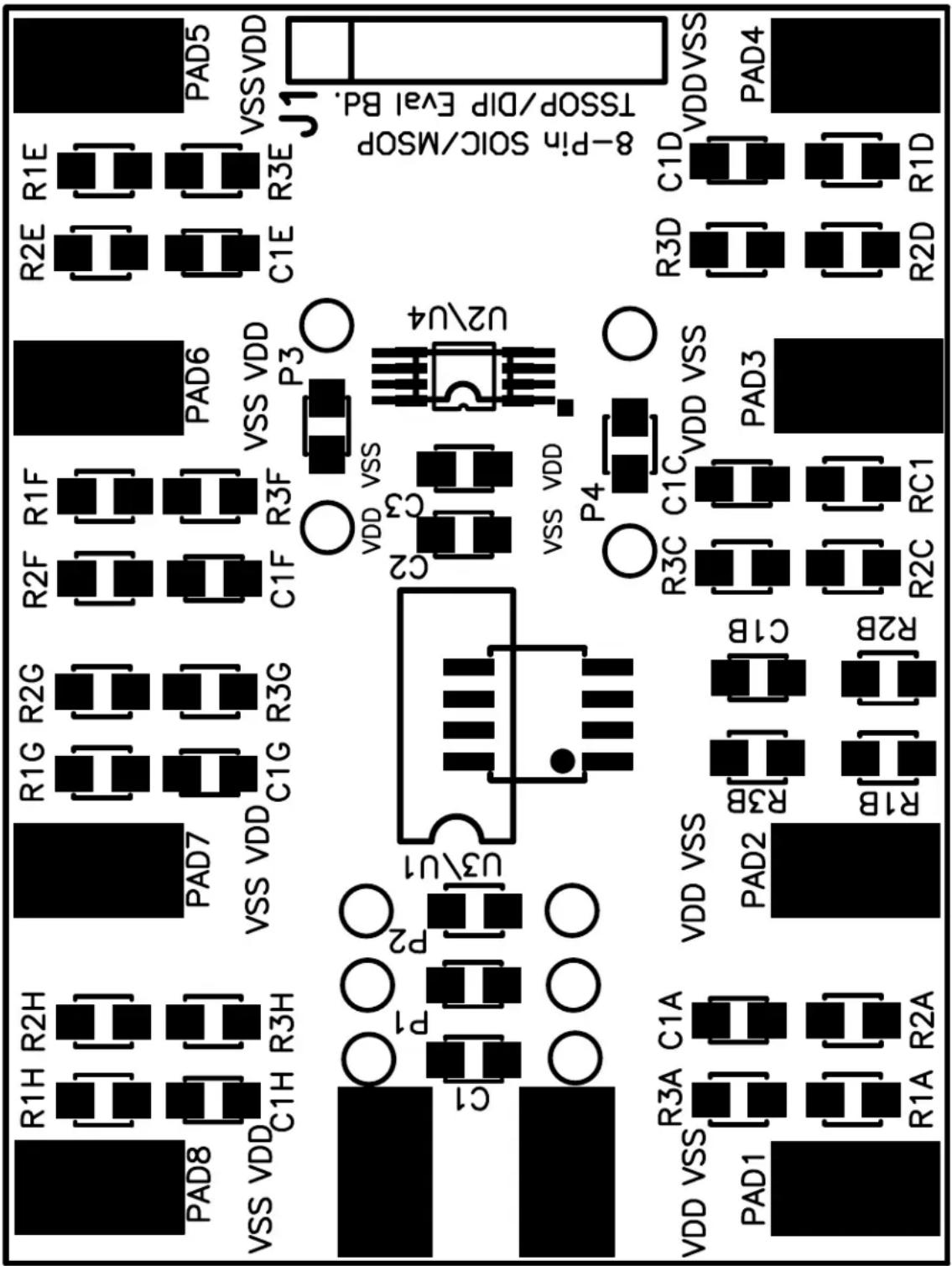
Figure 2-2 shows the layout of the 8-Pin SOIC/MSOP/TSSOP/DIP Evaluation Board. This is a small four-layer board (1.5" x 2" (38.1 mm x 50.8 mm)). There are ten connection points/pads that can use either through-hole or surface-mount connector posts.
The pad labeled VDD is connected to the PCB power plane, while the pad labeled VSS is connected to the PCB ground plane. All the passive components that are connected to VDD or VSS are connected to either the power plane or ground plane.
The eight remaining PCB pads correspond to the device pins (i.e.; pad 1 connects to pin 1).
Each pad has four passive components associated with them: a pull-up resistor, a pull-down resistor, an in-line resistor and a filtering/load capacitor. The pull-up resistor is always R2X, the pull-down resistor is R3X, the in-line resistor is R1X and the filtering/load capacitor is C1X. The "X" is an alpha character that corresponds to a particular pad (A to H). As an example, Pad 5's pull-up resistor is R2E.
The green area of Figure 2-2 shows the silk-screen on the bottom layer of the PCB. This is where the details of the implemented circuit can be written.
Capacitor C1 is the power supply filtering capacitor.
Capacitors C2 and C3 are bypass capacitors that may be required to be installed, depending on the device selected and the system requirements (such as the noise present on the power supply). Table 2-1 describes the components.
A 6-pin header interface is available that supports the PICmicro MCU Baseline Flash Microcontroller Programmer (BFMP) interface. For additional information, refer to Section 2.4.5 "Baseline Flash Microcontroller Programmer (BFMP) Interface (Header J1)".

text_image
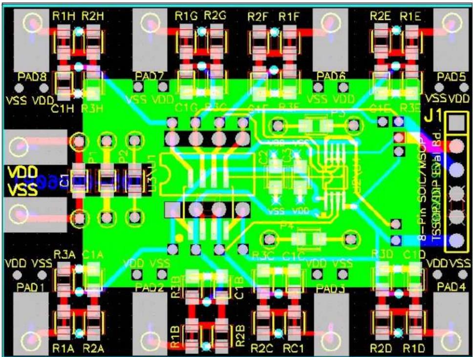
R1H R2H R1G R2G R2F R1F R2E R1E PAD8 VSS VDD C1H R3H PAD7 VSS VDD C1G R1G G1F R1F VSS VDD G1F R3E PAD6 VSS VDD J1 VDD VSS 8-Pin SOIC/MSO TSSORXNDIP GVA Bd. VDD VSS R3A C1A VDD VSS PAD1 PAD2 R1B R2B R2C RC1 R3D C1D PAD3 VDDVSS PAD4 R1A R2AFIGURE 2-2: 8-Pin SOIC/MSOP/TSSOP/DIP Evaluation Board Layout.
TABLE 2-1: OPTIONAL PASSIVE COMPONENTS
| Device Comment | |
| C1 Power supply bypass capacitor | |
| C2, C3 Device Filtering capacitor | |
| C1A, C1B C1C, C1D, C1E, C1F, C1G, C1H Output filter capacitor | |
| R1A, R1B, R1C, R1D, R1E, R1F, R1G, R1H In-line resistance of device output | |
| R2A, R2B, R2C, R2D, R2E, R2F, R2G, R2H Pull-up resistor | |
| R3A, R3B, R3C, R3D, R3E, R3F, R3G, R3H Pull-down resistor | |
| P1, P2, P3, P4 Optional Passive Components | |
2.4 8-PIN SOIC/MSOP/TSSOP/DIP EVALUATION BOARD DESCRIPTION
The 8-Pin SOIC/MSOP/TSSOP/DIP Evaluation Board PCB is designed to be flexible in the type of device evaluation that can be implemented.
The following sections describe each element of this evaluation board in further detail. Refer to Figure 2-3.
2.4.1 Power and Ground
The 8-Pin SOIC/MSOP/TSSOP/DIP Evaluation Board has a VDD Pad and a VSS pad. These pads can have connection posts installed that allows easy connection to the power ( V_DD ) and ground ( V_SS ) planes. The layout allows either through-hole or surface-mount connectors.
The power and ground planes are connected to the appropriate passive components on the PCB (such as power plane to R2X and ground plane to R3X and C1X).
2.4.2 PCB PADs
For each package pin (pins 1 to 8), there is a PCB pad (pads 1 to 8). The device will have some power pins ( V_DD ) and some ground pins ( V_SS ). To ease connections on the PCB, vias to the power and ground plane have been installed close to each PCB pad. This allows any pad to be connected to the power or ground plane, so when power is connected to the VDD and VSS pads, the power is connected to the appropriate device pin.
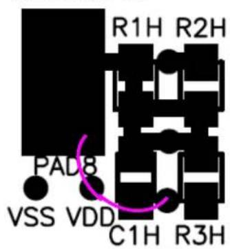
Jumpering to VSS

text_image
R1H R2H PAD8 VSS VDD C1H R3HJumpering to VDD
text_image
R1H R2H PAD8 VSS VDD C1H R3HFIGURE 2-3: Jumpering the PCB pad to either VDD or VSS.
Revision 1 of this PCB has an issue that these vias are not connected to the desired power and ground planes (they are open). For additional information, refer to Appendix D. "Rev. 1 PCB Errata".
2.4.3 Passive Components (R1X, R2X, R3X, C1X, R1, R2, C1, C2, C3, P1, P2, P3 and P4)
The footprints for these components are present to allow maximum flexibility in the use of this PCB to evaluate a wide range of SOT-23-3 devices. The purpose of these components may vary depending on the device under evaluation and how it is to be used in the desired circuit. Refer to the device data sheet for the recommended components that should be used when evaluating that device.
- Component R1X allows an in-line resistor that can be installed between the device pin and the PCB pad. This may be required when interfacing this PCB to other circuits
- Component R2X allows a pull-up resistor to be installed for the device pin
- Component R3X allows a pull-down resistor to be installed for the device pin
- Component C1X allows a capacitive load/filter to be installed for the device pin
- Component C1 allows a power supply filtering capacitor to be installed
- Components C2 and C3 allows a device filtering capacitor to be installed
- Components P1, P2, P3, and P4 are not connected and give a footprint (805 surface-mount) for a passive component (resistor, capacitor, etc.) to be installed and jumpered into the PCB circuit. This allows for the evaluation of some simple device circuits to be implemented on this PCB
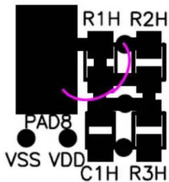
2.4.4 Installing Resistor R1X
Resistor R1X is shorted by default. Therefore, if resistor R1X is to be installed, the trace across the component must be cut before it is installed (see Figure 2-4).
While evaluating a device, it may be desirable to see the signals on both sides of this resistor. A test point is available so that both signals may be monitored. This test point is the avenue between components R3X and C1X (see Figure 2-4).

text_image
R1H R2H This trace must be cut before resistor R1X can be installed Test point PAD8 VSS VDD C1H R3HFIGURE 2-4: Test point when resistor R1X is installed.
2.4.5 Baseline Flash Microcontroller Programmer (BFMP) Interface (Header J1)
The BFMP interface allows a PICmicro MCU device to be programmed with programmers that support this interface, such as the BFMP programmer (part number PG164101).
The PCB supports two device pinouts. The default pinout already has the traces connected to the appropriate PICmicro MCU pins. The optional pinout requires three PCB traces to be cut and then three connections to be made (see Figure 2-5).
TABLE 2-2: BFMP HEADER SIGNALS AND PICMICRO MCU PINS
| BFMP Header Signal | Pin Number | Comment | |
| Default Pinout | Optional Pinout (1) | ||
| CLK 6 4 ICSPTM Clock | |||
| DT 7 5 ICSP Data | |||
| VPP 4 8 | |||
Note 1: Requires PCB traces to be cut and then jumpered.
text_image
U1 TP1A 1 P1 P8 8 TP8A TP2A 2 P2 P7 7 TP7A TP3A 3 P3 P6 6 TP6A TP4A 4 P4 P5 5 TP5A DIP-8 J1 NC CLK DT VSS VDD VPP TP4A TP6A TP5A TP7A GND TP8A TP4A Required "Cuts" and "Jumpers" for Optional PICmicro® MCU pinoutFIGURE 2-5: BFMP Header and Connections
text_image
Top-Layer Traces Bottom-Layer TracesFIGURE 2-6: PCB Traces (Top and Bottom Layers).
2.4.6 The PCB as a SOIC-8, MSOP-8, or TSSOP-8 to DIP-8 Socket Converter
There may be occasions when it is desirable to convert the footprint of the device to that of a DIP package. This allows the device to be installed into an existing DIP socket. Two 1x4 row pins need to be installed into the PCB's DIP footprint when the device is installed into the appropriate package footprint.
This allows the PCB to convert the SOIC-8, MSOP-8 or TSSOP-8 footprints to a 300-mil DIP-8 footprint.
2.4.7 Evaluating a Voltage Supervisor or Voltage Detector Device
2.4.7.1 VOLTAGE SUPERVISORS
The following voltage supervisor is supported by this evaluation board.
TABLE 2-3: 8-PIN VOLTAGE SUPERVISOR
| Device SO | IC DIP MSOP TSSOP Comment | ||||
| TC1232 Yes Yes | — | — | |||
When evaluating a voltage supervisor/voltage detector device, a minimum set of test equipment should be available. Table 2-4 shows the recommended test equipment.
TABLE 2-4: TEST EQUIPMENT
| Hardware | Connect to: | Comment |
| Variable Power Supply | V_DD, V_SS | This allows the voltage to the SOT23 Evaluation Board to be varied so the device output can be monitored. |
| Arbitrary Waveform Generator | V_DD, V_SS | This is similar to a variable power supply, but allows programmability into the input signal that the device will be subjected to. This also allows a particular waveform to be repeated (such as a 60 Hz sine wave that varies from 1V to 5V). |
| Digital Multi-Meter (D.M.M.) | V_OUT^(1) | Used to indicate the output state (low or high) of the voltage supervisor/voltage detector. |
| Oscilloscope | V_OUT^(1) | Allows the device conditions and response to be evaluated due to the ability to capture this information. This is useful for faster signals and cases where small spikes need to be detected. |
| Test Light (LED) V | OUT^(1) | Used to visually indicate the output state (low or high) of the voltage supervisor/voltage detector. Ensure that the current requirements of this LED can be supplied by the device's output pin. |
Note 1: The pad connection to connect to the V_OUT or pin will be dependent on the device and the footprint option used.
A typical system that would be used to evaluate the voltage supervisor/voltage detector device is shown in Figure 2-7. This also shows an example input and output waveform for a voltage supervisor/voltage detector device.

flowchart
graph LR
    A["Variable Power Supply or Arbitrary Waveform Generator"] --> B["Voltage Supervisor or Voltage Detector"]
    B --> C["C1"]
    B --> D["R2"]
    B --> E["R3"]
    B --> F["R1"]
    F --> G["Test Point"]
    G --> H["PCB Pad"]
    H --> I["Oscilloscope"]
    J["Arbitrary Waveform Generator Output"] --> K["Device V_DD out of valid operating range. Output voltage may be indeterminate."]
    L["Test Point or VOUT"] --> M["Device V_DD out of valid operating range. Output voltage may be indeterminate."]
FIGURE 2-7: Evaluation System.
2.4.8 Example Op Amp Circuits
This section shows how the 8-Pin SOIC/MSOP/TSSOP/DIP Evaluation Board could be used to evaluate op amp circuits. The first circuit is for the MCP601 and is shown in Figure 2-8. Figure 2-9 shows which components on the PCB would be installed and how the “unconnected” passive components would be jumpered into the circuit.
The second circuit is for the MCP6021 and is shown in Figure 2-10. Figure 2-11 shows which components on the PCB would be installed and how the “unconnected” passive components would be jumpered into the circuit.
text_image
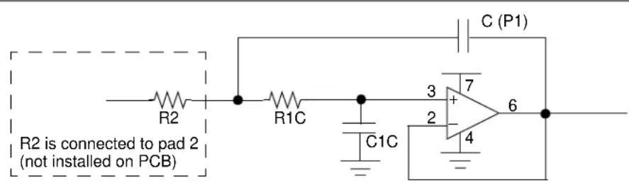
R2 is connected to pad 2 (not installed on PCB) R1C C1C C (P1) 3 7 + 2 4 6FIGURE 2-8: Op Amp Circuit #1 (MCP601).
text_image
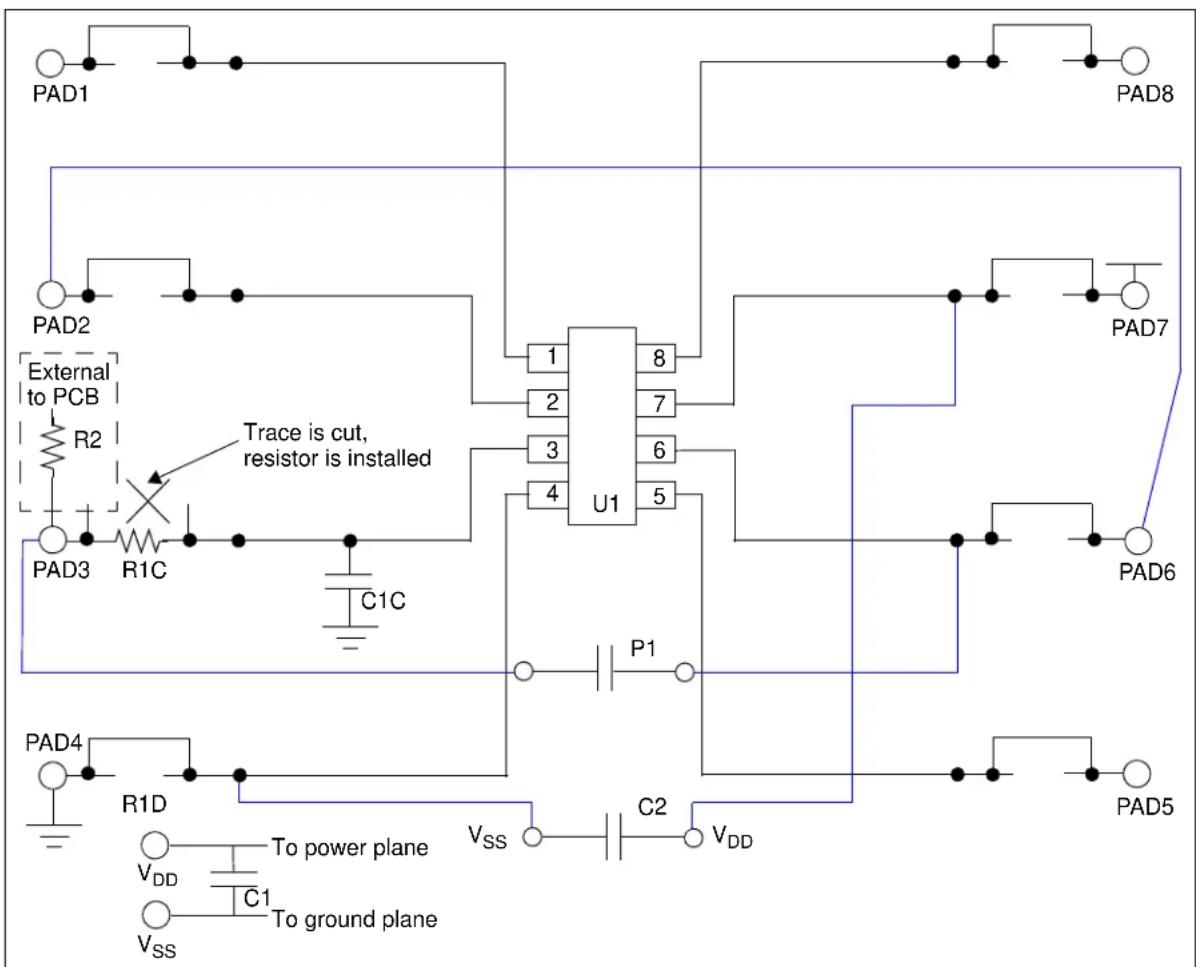
PAD1 PAD2 External to PCB R2 Trace is cut, resistor is installed PAD3 R1C C1C U1 1 8 2 7 3 6 4 5 P1 PAD4 R1D V_DD To power plane V_SS C1 To ground plane V_SS V_DD C2 V_DD PAD5 PAD6 PAD7 PAD8FIGURE 2-9: PCB Connections for Op Amp Circuit #1 (MCP601).

text_image
R1C R3C 3 + 7 2 4 6 R1B R (P1)FIGURE 2-10: Op Amp Circuit #2 (MCP6021).

text_image
PAD1 Trace is cut, resistor is installed PAD2 R1B* Trace is cut, resistor is installed PAD3 R1C* R3C* U1 1 8 2 7 3 6 4 5 P1 PAD6 PAD4 VDD C2 VDD VSS To power plane To ground planeFIGURE 2-11: PCB Op Amp Circuit #2 (MCP6021).
Appendix A. Schematic and Layouts
A.1 INTRODUCTION
This appendix contains the schematics and layouts for the 8-Pin SOIC/MSOP/TSSOP/DIP Evaluation Board. Diagrams included in this appendix:
• Board Schematic - Digital Circuitry
- Board – Top Layer + Bottom Layer + Silk-Screen
- Board – Top Layer + Silk-Screen
- Board – Bottom Layer
- Board – Power Plane
- Board – Ground Plane
- Board – Component Layer
A.2 SCHEMATICS AND PCB LAYOUT
Figure A-3 shows the schematic of the 8-Pin SOIC/MSOP/TSSOP/DIP Evaluation Board.
Figure A-2 shows the layout for the top layer of the 8-Pin SOIC/MSOP/TSSOP/DIP Evaluation Board. The layer order is shown in Figure A-1.

text_image
Top Layer Ground Layer Power Layer Bottom LayerFIGURE A-1: Layer Order.

other
| Pin | Component | |---|---| | VDD | R1A | | R2A | TP1 | | TP1A | C1A | | R3A | - | | VDD | R2A | | TP8 | TP8 | | R2H | R1H | | TP8A | C1H | | R3H | - | | VDD | R1H | | PAD8 | - | | U1 | TP1A-1 P1-8 TP8A TP2A-2 P2-7 TP7A TP3A-3 P3-6 TP6A TP4A-4 P4-5 TP5A | | U3 | TP1A-1 P1-8 TP8A TP2A-2 P2-7 TP7A TP3A-3 P3-6 TP6A TP4A-4 P4-5 TP5A | | DIP-B | - | | SOIC-B | - | | U2 | TP1A-1 P1-8 TP8A TP2A-2 P2-7 TP7A TP3A-3 P3-6 TP6A TP4A-4 P4-5 TP5A | | TSSOP-B | - | | U4 | TP1A-1 P1-8 TP8A TP2A-2 P2-7 TP7A TP3A-3 P3-6 TP6A TP4A-4 P4-5 TP5A | | MSOP-B | - | | TP11 | P1- - - - - - - - - - - - - - - - - - - - - - - - - - - - - - - - - - - - - - - - - - - - - - - - - - - - - - - - - - - - - - - - - - - - - - - - - - - - - - - - - - - - - - - - - - - - - - - - - - - - - 0.0000000000000000000000000000000000000000000000000000000000000000000000000000000000000000000000000000. | Label: TP11, TP12, TP13, TP14, TP15, TP16, TP17, TP18, TP9A, TP10B, TP9B, etc. | Note: Px = Passive Component x. Vias to VDD and VSS should be close to test points to allow flexibility on how devices are configured in the circuit. Access to VDD & VSS Via hole Located near Pads Microchip Date: Tue Mar 22, 28/85 Drawn by: J.Garcia Sheet 1 of 1 Rev Description Date Size B 1.1x 1.2 Rev 2 Eng: M. Palmer Date: Tue Mar 22, 28/85FIGURE A-2: 8-Pin SOIC/MSOP/TSSOP/DIP Evaluation Board Schematic.
text_image
R1H R2H R1G R2G R2F R1F R2E R1E PAD8 VSS VDD C1H R3H PAD7 VSS VDD C1G R1G PAD6 VSS VDD C1F R1F P3 G4F R3F PAD5 VSS VDD J1 VDD VSS VDD VSS R3A C1A VDD VSS PAD1 PAD2 R1B R2B R2C RC1 R3C C1C VDD VSS PAD3 R3D C1D VDDVSS PAD4 R1A R2A R2D R1DFIGURE A-3: 8-Pin SOIC/MSOP/TSSOP/DIP Evaluation Board Layout – Top Layer + Bottom Layer + Silk-Screen.

text_image
8-Pi 9 SOC/MSP TSSOP/DIP Eval.5.D. R2E R1E PAD5 VSSVDD C1E R3E J1 R2D R1D R3D C1D VDDVSS PAD4 R2D R1F PAD6 VSS VDD P3 U2 R2F R1F R3F VDD VSS C2 VSS VDD P4 R3C C1C VDD VSS PAD3 R2C RC1 R1G R2G C1G R3G PAD7 VSS VDD C1H R3H U3 U1 VDD VSS PAD2 R2B C1A VSS VDD P2 R1H R2H PAD8 VSS VDD C1H R3H VDD VSS R3A C1A VDD VSS PAD1 R1A R2AFIGURE A-4: 8-Pin SOIC/MSOP/TSSOP/DIP Evaluation Board Gerber – Top Layer + Silk-Screen.

text_image
102-0000005 SR0000005FIGURE A-5: 8-Pin SOIC/MSOP/TSSOP/DIP Evaluation Board Gerber – Bottom Layer.
FIGURE A-6: 8-Pin SOIC/MSOP/TSSOP/DIP Evaluation Board Gerber – Power Plane
bubble
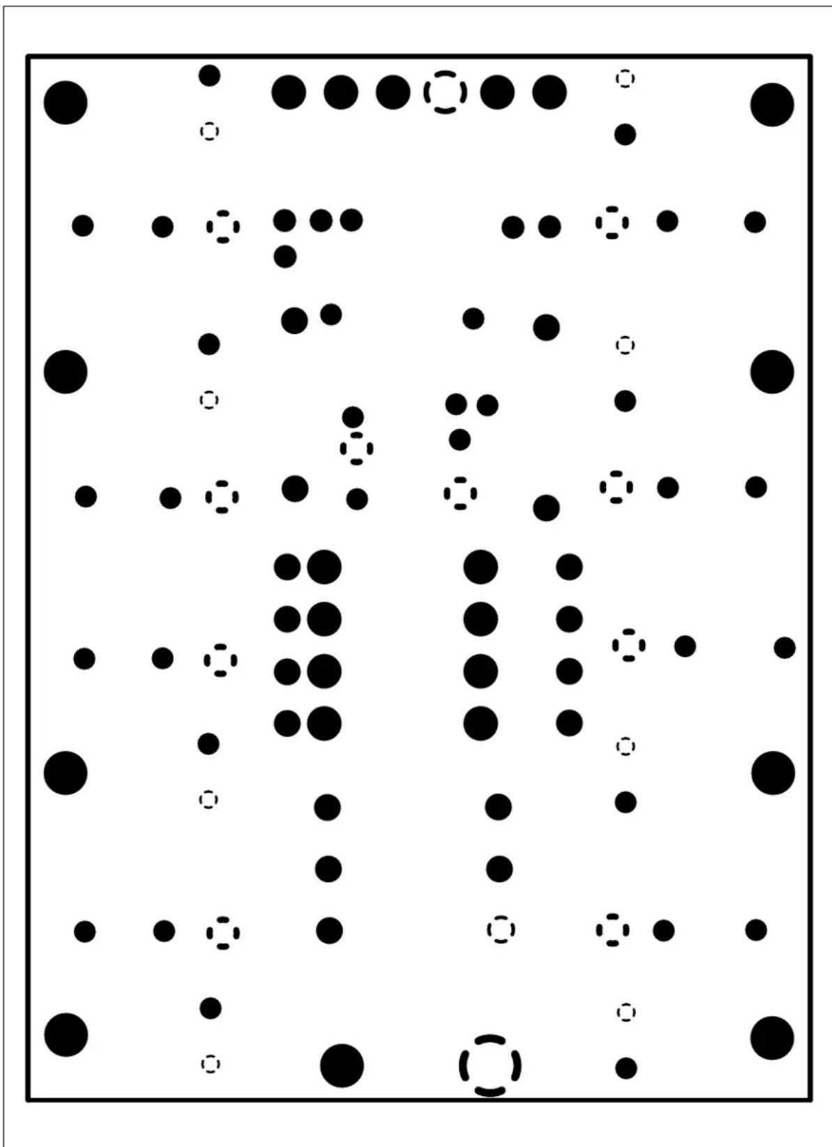
| Point ID | X Coordinate | Y Coordinate | Size | |----------|--------------|--------------|------| | 1 | 0.1 | 0.9 | 10 | | 2 | 0.3 | 0.8 | 5 | | 3 | 0.5 | 0.7 | 8 | | 4 | 0.7 | 0.6 | 3 | | 5 | 0.9 | 0.5 | 7 | | 6 | 0.2 | 0.4 | 2 | | 7 | 0.4 | 0.3 | 6 | | 8 | 0.6 | 0.2 | 4 | | 9 | 0.8 | 0.1 | 9 | | 10 | 0.1 | 0.8 | 2 | | 11 | 0.3 | 0.7 | 5 | | 12 | 0.5 | 0.6 | 3 | | 13 | 0.7 | 0.5 | 6 | | 14 | 0.9 | 0.4 | 4 | | 15 | 0.2 | 0.3 | 7 | | 16 | 0.4 | 0.2 | 2 | | 17 | 0.6 | 0.1 | 5 | | 18 | 0.8 | 0.0 | 3 | | 19 | 0.1 | 0.9 | 1 | | 20 | 0.3 | 0.8 | 6 | | 21 | 0.5 | 0.7 | 4 | | 22 | 0.7 | 0.6 | 7 | | 23 | 0.9 | 0.5 | 2 | | 24 | 0.2 | 0.4 | 5 | | 25 | 0.4 | 0.3 | 3 | | 26 | 0.6 | 0.2 | 6 | | 27 | 0.8 | 0.1 | 4 | | 28 | 0.1 | 0.8 | 1 | | 29 | 0.3 | 0.7 | 5 | | 30 | 0.5 | 0.6 | 3 | | 31 | 0.7 | 0.5 | 6 | | 32 | 0.9 | 0.4 | 2 | | 33 | 0.2 | 0.3 | 5 | | 34 | 0.4 | 0.2 | 3 | | 35 | 0.6 | 0.1 | 6 | | 36 | 0.8 | 0.0 | 4 | | 37 | 0.1 | 0.9 | 1 | | 38 | 0.3 | 0.8 | 5 | | 39 | 0.5 | 0.7 | 3 | | 40 | 0.7 | 0.6 | 6 | | 41 | 0.9 | 0.5 | 2 | | 42 | - | - | - | | 43 | - | - | - | | ... | ... | ... | ... | | ... | ... | ... | ... | | ... | ... | ... | ... | | ... | ... | ... | ... | | ... | ... | ... | ... | | ... | ... | ... | ... | | ... | ... | ... | ... | | ... | ... | ... | ... | | ... | ... |... | ... | | ... | ... | ... | ... | | ... | ... | ... | ... | | ... | ... | ... | ... | | ... | ... | ... | ... | | ... | ... | ... | ... | | ... | ... | ... | ... | | ... | ... | ... | ... | | ... (note: The actual values are not provided in the code)FIGURE A-7: 8-Pin SOIC/MSOP/TSSOP/DIP Evaluation Board Gerber – Ground Plane.
text_image
8-Pip SOC/MSP TSSOP/DIP Eval BD. PAD5 R1E VSSVDD R2E R3E C1E R1D PAD6 VSS VDD P3 R1F R2F C1F R3F VSS VDD P4 C2 VSS VDD P2 R1G R2G C1G R3G PAD7 VSS VDD R1H R2H C1H R3H PAD8 VSS VDD C1I R2A P1 U3\U1 P2 VDD VSS PAD2 R2B R3C C1C VDD VSS PAD3 R2C RC1 VDD VSS PAD1 R3A C1A R1A R2AFIGURE A-8: 8-Pin SOIC/MSOP/TSSOP/DIP Evaluation Board Gerber – Component Layer.
Appendix B. Bill of Materials (BOM)
TABLE B-1: BILL OF MATERIALS
| Qty | Reference Description | Manufacturer Part Number | ||
| 1 PCB | 103-00050 SOT23 | Evaluation Board PCB Microchip | Technology Inc. | 103-00060 |
| 0 U1 | SOIC-8 Device Microchip | Technology Inc. | User-specified | |
| 0 U2 | MSOP-8 Device Microchip | Technology Inc. | User-specified | |
| 0 U3 | DIP-8 Device | Microchip | Technology Inc. | User-specified |
| 0 U4 | TSSOP-8 Device | Microchip | Technology Inc. | User-specified |
| 0 C1, | C2, C3 | Device Power Supply Bypass CapacitorSurface-mount (805 package)(Optional - Application-dependent) | — | User-specified |
| 0 C1A | C1B, C1C,C1D, C1E, C1F,C1G, C1H | Output Filer CapacitorSurface-mount (805 package)(Optional - Application-dependent) | — | User-specified |
| 0 R1A | R1B, R1C,R1D, R1E, R1F,R1G, R1H | Output inline resistorSurface-mount (805 package)(Optional - Application-dependent) | — | User-specified |
| 0 R2A | R2B, R2C,R2D, R2E, R2F,R2G, R2H | Output Pull-up resistorSurface-mount (805 package)(Optional - Application-dependent) | — | User-specified |
| 0 R3A | R3B, R3C,R3D, R3E, R3F,R3G, R3H | Output Pull-down resistorSurface-mount (805 package)(Optional - Application-dependent) | — | User-specified |
| 0 P1, | P2, P3, P4 Passive component (not connected) that can be “blue wired” into the desired circuit. The device layout supports the 805 package.(Optional - Application-dependent) | |||
| 0 | J1 | BFMP Header (6-pin, 100 mil spacing) | — | — |
| 0 | PAD1, PAD2, PAD3,PAD4, PAD5, PAD6,PAD7, PAD8, V_DD , V_SS | Through-hole connector(s) for PAD1, PAD2, PAD3, PAD4, PAD5, PAD6, PAD7, PAD8, V_DD , V_SS | Keystone Electronics® | 5012 |
| 0 | PAD1, PAD2, PAD3, PAD4, PAD5, PAD6, PAD7, PAD8, V_DD , V_SS | Surface-mount connector(s) for PAD1, PAD2, PAD3, PAD4, PAD5, PAD6, PAD7, PAD8, V_DD , V_SS | Keystone Electronics® | 5016 |
8-Pin SOIC/MSOP/TSSOP/DIP Evaluation Board User's Guide
NOTES:
Appendix C. Microchip Analog and Interface Device Compatibility
C.1 INTRODUCTION
This appendix documents the Michrochip Analog and Interface devices that are footprint compatible with this PCB.
The Analog and Interface devices currently fall into the following categories:
• A/D Converters (ADCs) (ADCs)
- Battery Chargers
- Comparators
• D/A Converters (DACs) (DACs)
- DC-to-DC Converters
• Digital Potentiometers (Digi-Pots)
- Fan Controllers
- Integrated Devices
- Interface Devices
- Linear Regulators
• Operational Amplifiers (Op Amps)
• Power MOSFET Drivers
- Switching Regulators
• Temperature Sensors
- Programmable Gain Amplifiers (PGAs)s (PGAs)
• Voltage Supervisors and Voltage Detectors
Table C-1 shows the Michrochip Analog and Interface devices that are currently supported. As new devices become available, this PCB may be able to support them. Please check the device data sheet to verify if the device is available in one of the package types supported by this PCB.
TABLE C-1: ANALOG AND INTERFACE DEVICES PCB COMPATIBILITY
| Device SO | C DIP MSOP | TSSOP | Comment | ||
| Voltage Supervisors and Voltage Detectors | |||||
| TC1232 Yes Yes — — | |||||
| Digital Potentiometer | |||||
| M C | P | 4 | 0 | 2 | 1 Ye s |
| MCP41010 | Yes Yes — — | ||||
| MCP41050 | Yes Yes — — | ||||
| MCP41100 | Yes Yes — — | ||||
| Switching Regulator | |||||
| MCP1601 | — — Yes — | ||||
| MCP1612 | — — Yes — | ||||
| MCP1630 | — — Yes — | ||||
| MCP1650 | — — Yes — | ||||
| MCP1651 | — — Yes — | ||||
| MCP1652 | — — Yes — | ||||
| DC-to-DC Converters | |||||
| MCP1252 | — — Yes — | ||||
| MCP1253 | — — Yes — | ||||
| TC682 | Yes Yes — — | ||||
| TC962 | Yes Yes — — | ||||
| TC1044S Yes | Yes — — | ||||
| TC1121 | Yes Yes Yes | — | |||
| TC1142 | — — Yes — | ||||
| TC7660 Yes Yes — — | |||||
| TC7660B Yes Yes — — | |||||
| TC7660H | Yes Yes — — | ||||
| TC7660S Yes Yes — — | |||||
| TCM680 | Yes Yes — — | ||||
| Linear Regulators | |||||
| MCP1726 | Yes — — | ||||
| TC1107 | Yes — — | Yes | — | ||
| TC1173 | Yes — — | Yes | — | ||
| TC1174 | Yes — — | Yes | — | ||
| TC1263 Yes — — | |||||
| TC1265 Yes — — | |||||
| T C | 1 | 2 | 6 | 6 | Ye s — |
| TC1268 Yes — — | |||||
| TC1269 | — — Yes — | ||||
| TC1300 | — — Yes — | ||||
| TC1301A — — Yes — | |||||
| TC1301B — — Yes — | |||||
| TC1302A — — Yes — | |||||
| TC1302B — — Yes — | |||||
| TC1306 | — — Yes — | ||||
Note 1: Installation of PCB capacitor C2 (or C3) is recommended for all devices. See data sheet for recommended value.
2: Installation of PCB capacitor C1 recommended. See data sheet for recommended value.
TABLE C-1: ANALOG AND INTERFACE DEVICES PCB COMPATIBILITY
| Device SO | IC DIP | MSOP | TSSOP | Comment | |
| Operational Amplifiers (Op Amps) | |||||
| MCP601 Yes | Yes — Yes | Note 2 | |||
| MCP602 Yes | Yes — Yes | Note 2 | |||
| MCP603 Yes | Yes — Yes | Note 2 | |||
| MCP606 Yes | Yes — Yes | ||||
| MCP607 Yes | Yes — Yes | ||||
| MCP608 Yes | Yes — Yes | ||||
| MCP616 Yes | Yes Yes — | ||||
| MCP617 Yes | Yes Yes — | ||||
| MCP618 Yes | Yes Yes — | ||||
| MCP6001 Yes | Yes Yes — | ||||
| MCP6004 Yes | Yes Yes — | ||||
| MCP6021 Yes | Yes — Yes | Note 2 | |||
| MCP6022 Yes | Yes — Yes | Note 2 | |||
| MCP6023 Yes | Yes — Yes | Note 2 | |||
| MCP6041 Yes | Yes Yes — | ||||
| MCP6042 Yes | Yes Yes — | ||||
| MCP6043 Yes | Yes Yes — | ||||
| MCP6141 Yes | Yes Yes — | ||||
| MCP6142 Yes | Yes Yes — | ||||
| MCP6143 Yes | Yes Yes — | ||||
| MCP6231 Yes | Yes Yes — | ||||
| MCP6232 Yes | Yes Yes — | ||||
| MCP6241 Yes | Yes Yes — | ||||
| MCP6242 Yes | Yes Yes — | ||||
| MCP6271 Yes | Yes Yes — | Note 2 | |||
| MCP6272 Yes | Yes Yes — | Note 2 | |||
| MCP6273 Yes | Yes Yes — | Note 2 | |||
| MCP6275 Yes | Yes Yes — | Note 2 | |||
| MCP6281 Yes | Yes Yes — | Note 2 | |||
| MCP6282 Yes | Yes Yes — | Note 2 | |||
| MCP6283 Yes | Yes Yes — | Note 2 | |||
| MCP6285 Yes | Yes Yes — | Note 2 | |||
| MCP6291 Yes | Yes Yes — | Note 2 | |||
| MCP6292 Yes | Yes Yes — | Note 2 | |||
| MCP6293 Yes | Yes Yes — | Note 2 | |||
| MCP6295 Yes | Yes Yes — | Note 2 | |||
| TC913 — Yes | — | ||||
| TC1029 Yes | Yes Yes — | ||||
| TC7650 — Yes | — | ||||
| TC7652 — Yes | — | ||||
Note 1: Installation of PCB capacitor C2 (or C3) is recommended for all devices. See data sheet for recommended value.
2: Installation of PCB capacitor C1 recommended. See data sheet for recommended value.
TABLE C-1: ANALOG AND INTERFACE DEVICES PCB COMPATIBILITY
| Device | SOIC | DIP | MSOP | TSSOP | Comment |
| Programmable Gain Amplifiers (PGAs) | |||||
| MCP6S21 Yes | Yes Yes — | Note 2 | |||
| MCP6S22 Yes | Yes Yes — | Note 2 | |||
| MCP6S91 Yes | Yes Yes — | Note 2 | |||
| MCP6S92 Yes | Yes Yes — | Note 2 | |||
| Power MOSFET Drivers | |||||
| TC1410 Yes Yes Yes — | |||||
| TC1410N Yes Yes Yes — | |||||
| TC1411 Yes Yes Yes — | |||||
| TC1411N Yes Yes Yes — | |||||
| TC1426 Yes Yes — | |||||
| TC1427 Yes Yes — | |||||
| TC1428 Yes Yes — | |||||
| TC4403 — Yes — | |||||
| TC4426A Yes Yes — | |||||
| TC4427A Yes Yes — | |||||
| TC4428A Yes Yes — | |||||
| TC4426 Yes Yes Yes — | |||||
| TC4427 Yes Yes Yes — | |||||
| TC4428 Yes Yes Yes — | |||||
| TC426 Yes Yes — | |||||
| TC427 Yes Yes — | |||||
| TC428 Yes Yes — | |||||
| TC4404 Yes Yes — | |||||
| TC4405 Yes Yes — | |||||
| TC1412 Yes Yes Yes — | |||||
| TC1412N Yes Yes Yes — | |||||
| TC1413 Yes Yes Yes — | |||||
| TC1413N Yes Yes Yes — | |||||
| TC4423 — Yes — | |||||
| TC4424 — Yes — | |||||
| TC4425 — Yes — | |||||
| TC429 Yes Yes — | |||||
| TC4420 Yes Yes — | |||||
| TC4429 Yes Yes — | |||||
| TC4421 — Yes — | |||||
| TC4422 — Yes — | |||||
| TC4626 — Yes — | |||||
| TC4627 — Yes — | |||||
| TC4431 Yes Yes — | |||||
| TC4432 Yes Yes — | |||||
Note 1: Installation of PCB capacitor C2 (or C3) is recommended for all devices. See data sheet for recommended value.
2: Installation of PCB capacitor C1 recommended. See data sheet for recommended value.
TABLE C-1: ANALOG AND INTERFACE DEVICES PCB COMPATIBILITY
| Device SO | IC DIP | MSOP | TSSOP | Comment | |
| Comparators | |||||
| MCP6541 Yes | Yes Yes — | ||||
| MCP6542 Yes | Yes Yes — | ||||
| MCP6543 Yes | Yes Yes — | ||||
| MCP6546 Yes | Yes Yes — | ||||
| MCP6547 Yes | Yes Yes — | ||||
| MCP6548 Yes | Yes Yes — | ||||
| TC1025 Yes | Yes Yes — | ||||
| TC1028 — — | Yes — | ||||
| TC1031 — — | Yes — | ||||
| TC1040 — — | Yes — | ||||
| T C | 1 | 0 | 4 | 1 | Y e s |
| A/D Converters (ADCs) | |||||
| MCP3001 Yes | Yes — Yes | ||||
| MCP3002 Yes | Yes — Yes | ||||
| MCP3201 Yes | Yes — Yes | ||||
| MCP3202 Yes | Yes — Yes | ||||
| MCP3301 Yes | Yes Yes — | ||||
| TC3400 Yes | Yes — — | ||||
| D/A Converters (DACs) | |||||
| MCP4821 Yes | Yes Yes — | ||||
| MCP4822 Yes | Yes Yes — | ||||
| MCP4921 Yes | Yes Yes — | ||||
| T C | 1 | 3 | 2 | 0 | Y e s |
| T C | 1 | 3 | 2 | 1 | Y e s |
Note 1: Installation of PCB capacitor C2 (or C3) is recommended for all devices. See data sheet for recommended value.
2: Installation of PCB capacitor C1 recommended. See data sheet for recommended value.
TABLE C-1: ANALOG AND INTERFACE DEVICES PCB COMPATIBILITY
| Device | SOIC | DIP | MSOP | TSSOP | Comment |
| Temperature Sensors | |||||
| M C | P | 9 | 8 | 0 | 1 Y e |
| M C | P | 9 | 8 | 0 | 3 Y e |
| TC72 — Yes — | |||||
| TCN75 Yes — Yes — | |||||
| TC620 Yes Yes — — | |||||
| TC621 Yes Yes — — | |||||
| TC622 Yes Yes — — | |||||
| TC623 Yes Yes — — | |||||
| TC624 Yes Yes — — | |||||
| Fan Controllers | |||||
| TC642 Yes Yes Yes — | |||||
| TC642B Yes Yes Yes — | |||||
| TC646 Yes Yes Yes — | |||||
| TC646B Yes Yes Yes — | |||||
| TC647 Yes Yes Yes — | |||||
| TC647B Yes Yes Yes — | |||||
| TC648 Yes Yes Yes — | |||||
| TC648B Yes Yes Yes — | |||||
| TC649 Yes Yes Yes — | |||||
| TC649B Yes Yes Yes — | |||||
| TC650 | — — Yes — | ||||
| TC651 | — — Yes — | ||||
| TC652 | — — Yes — | ||||
| TC653 | — — Yes — | ||||
| Battery Chargers | |||||
| MCP7344 | — — Yes — | ||||
| MCP73827 | — — Yes — | ||||
| MCP73828 | — — Yes — | ||||
| MCP73843 | — — Yes — | ||||
| Integrated Devices | |||||
| TC1026C | Yes Yes | Yes — | |||
| Interface Devices | |||||
| MCP201 Yes Yes — — | |||||
| MCP2122 | Yes Yes | — — | |||
| MCP2551 | Yes Yes | — — | |||
Note 1: Installation of PCB capacitor C2 (or C3) is recommended for all devices. See data sheet for recommended value.
2: Installation of PCB capacitor C1 recommended. See data sheet for recommended value.
Appendix D. Rev. 1 PCB Errata
D.1 INTRODUCTION
This appendix documents the issues with the Rev 1 PCB. The Rev 2 PCB fixes these issues.
D.2 REV 1 PCB ISSUES
There are two issues with the Rev 1 PCB. These are:
- VDD and VSS vias near each pad are No Connects (they should have been connected to the appropriate power or ground plane). See Figure D-1 shows the location of these vias that are No Connects. Figure D-3 shows alternate connections that can be made.
- The silk-screen on the bottom layer was not processed. This was only intended for indicating the circuit of the board. This can be done with a sticky label.
Figure D-2 shows how to determine the PCB revision.

text_image
R1H R2H R1G R2G R2F R1F R2E R1E TP 4A TP 7A TP 5A TP 6A TP 7A TP 5A TP 6A TP 5A TP 7A TP 6A TP 5A TP 6A TP 5A TP 7A TP 6A TP 5A TP 6A TP 5A TP 7A TP 6A TP 5A TP 6A TP 5A TP 7A TP 6A TP 5A TP 6A TP 5A TP 7A TP 5A TP 6A TP 5A TP 7A TP 6A TP 5A TP 6A TP 5A TP 7A TP 6A TP 5A TP 6A TP 5A TP 7A TP 6A TP 5A TP 6A TP 5A TP 6A TP 5A TP 7A TP 6A TP 5A TP 6A TP 5A TP 7A TP 6A TP 5A TP 6A TP 5A TP 7A TP 6A TP 5A TP 6A TP 5A TP 6A TP 7A TP 6A TP 5A TP 6A TP 5A TP 7A TP 6A TP 5A TP 6A TP 5A TP 7A TP 6A TP 5A TP 6A TP 5A TP 7A TP 6A TP 5A TP 6A TP 7A TP 6A TP 5A TP 6A TP 5A TP 7A TP 6A TP 5A TP 6A TP 7A TP 6A TP 5A TP 6A TP 5A TP 7A TP 6A TP 5A TP 6A TP 7A TP 8-Pin SDIC/MSO PLSOS/SDIC/MSO PLSOS/SDIC/MSO PLSOS/SDIC/MSO PLSOS/SDIC/MSO PLSOS/SDIC/MSO PLSOS/SDIC/MSO PLSOS/SDIC/MSO PLSOS/SDIC/MSO PLSOS/SDIC/MSO PLSOS/SDIC/MSO PLSOS/SDIC/MSO PLSOS/SDI-0.0.0.0.0.0.0.0.0.0.0.0.0.0.0.0.0.0.0.0.0.0.0.0.0.0.0.0.0.0.0.0.0.0.0.0.0.0.0.0.0.0.0.0.0.0.0.0.0.0.0.FIGURE D-1: 8-Pin SOIC/MSOP/TSSOP/DIP Evaluation Board Gerber - Top Layer + Silk-Screen.

text_image
102-000001 This indicates a Rev 1 PCBFIGURE D-2: 8-Pin SOIC/MSOP/TSSOP/DIP Evaluation Board Revision Marking (Gerber – Bottom Layer)
Figure D-3 shows how the pad can be connected to either the V_DD or V_SS plane of the PCB.
Jumpering to VSS
text_image
R1H R2H PAD8 VSS VDD C1H R3HJumpering to VDD
text_image
R1H R2H PAD8 VSS VDD C1H R3HFIGURE D-3: Alternate Jumpering the PCB pad to either VSS or VDD.
WORLDWIDE SALES AND SERVICE
AMERICAS
Corporate Office
2355 West Chandler Blvd.
Chandler, AZ 85224-6199
Tel: 480-792-7200
Fax: 480-792-7277
Technical Support:
http://support.microchip.com
Web Address:
www.microchip.com
Atlanta
Alpharetta, GA
Tel: 770-640-0034
Fax: 770-640-0307
Boston
Westborough, MA
Tel: 774-760-0087
Fax: 774-760-0088
Chicago
Itasca, IL
Tel: 630-285-0071
Fax: 630-285-0075
Dallas
Addison, TX
Tel: 972-818-7423
Fax: 972-818-2924
Detroit
Farmington Hills, MI
Tel: 248-538-2250
Fax: 248-538-2260
Kokomo
Kokomo, IN
Tel: 765-864-8360
Fax: 765-864-8387
Los Angeles
Mission Viejo, CA
Tel: 949-462-9523
Fax: 949-462-9608
San Jose
Mountain View, CA
Tel: 650-215-1444
Fax: 650-961-0286
Toronto
Mississauga, Ontario,
Canada
Tel: 905-673-0699
Fax: 905-673-6509
ASIA/PACIFIC
Australia - Sydney
Tel: 61-2-9868-6733
Fax: 61-2-9868-6755
China - Beijing
Tel: 86-10-8528-2100
Fax: 86-10-8528-2104
China - Chengdu
Tel: 86-28-8676-6200
Fax: 86-28-8676-6599
China - Fuzhou
Tel: 86-591-8750-3506
Fax: 86-591-8750-3521
China - Hong Kong SAR
Tel: 852-2401-1200
Fax: 852-2401-3431
China - Shanghai
Tel: 86-21-5407-5533
Fax: 86-21-5407-5066
China - Shenyang
Tel: 86-24-2334-2829
Fax: 86-24-2334-2393
China - Shenzhen
Tel: 86-755-8203-2660
Fax: 86-755-8203-1760
China - Shunde
Tel: 86-757-2839-5507
Fax: 86-757-2839-5571
China - Qingdao
Tel: 86-532-502-7355
Fax: 86-532-502-7205
ASIA/PACIFIC
India - Bangalore
Tel: 91-80-2229-0061
Fax: 91-80-2229-0062
India - New Delhi
Tel: 91-11-5160-8631
Fax: 91-11-5160-8632
Japan - Kanagawa
Tel: 81-45-471-6166
Fax: 81-45-471-6122
Korea - Seoul
Tel: 82-2-554-7200
Fax: 82-2-558-5932 or
82-2-558-5934
Singapore
Tel: 65-6334-8870
Fax: 65-6334-8850
Taiwan - Kaohsiung
Tel: 886-7-536-4818
Fax: 886-7-536-4803
Taiwan - Taipei
Tel: 886-2-2500-6610
Fax: 886-2-2508-0102
Taiwan - Hsinchu
Tel: 886-3-572-9526
Fax: 886-3-572-6459
EUROPE
Austria - Weis
Tel: 43-7242-2244-399
Fax: 43-7242-2244-393
Denmark - Ballerup
Tel: 45-4450-2828
Fax: 45-4485-2829
France - Massy
Tel: 33-1-69-53-63-20
Fax: 33-1-69-30-90-79
Germany - Ismaning
Tel: 49-89-627-144-0
Fax: 49-89-627-144-44
Italy - Milan
Tel: 39-0331-742611
Fax: 39-0331-466781
Netherlands - Drunen
Tel: 31-416-690399
Fax: 31-416-690340
England - Berkshire
Tel: 44-118-921-5869
Fax: 44-118-921-5820