PIC24FJ64GA705 - Electronic component Microchip - Free user manual and instructions
Find the device manual for free PIC24FJ64GA705 Microchip in PDF.

User questions about PIC24FJ64GA705 Microchip
0 question about this device. Answer the ones you know or ask your own.
Ask a new question about this device
Download the instructions for your Electronic component in PDF format for free! Find your manual PIC24FJ64GA705 - Microchip and take your electronic device back in hand. On this page are published all the documents necessary for the use of your device. PIC24FJ64GA705 by Microchip.
USER MANUAL PIC24FJ64GA705 Microchip
Compiled Tips ‘N Tricks Guide
Note the following details of the code protection feature on Microchip devices:
• Microchip products meet the specification contained in their particular Microchip Data Sheet.
- Microchip believes that its family of products is one of the most secure families of its kind on the market today, when used in the intended manner and under normal conditions.
- There are dishonest and possibly illegal methods used to breach the code protection feature. All of these methods, to our knowledge, require using the Microchip products in a manner outside the operating specifications contained in Microchip's Data Sheets. Most likely, the person doing so is engaged in theft of intellectual property.
• Microchip is willing to work with the customer who is concerned about the integrity of their code.
- Neither Microchip nor any other semiconductor manufacturer can guarantee the security of their code. Code protection does not mean that we are guaranteeing the product as "unbreakable."
Code protection is constantly evolving. We at Microchip are committed to continuously improving the code protection features of our products. Attempts to break Microchip's code protection feature may be a violation of the Digital Millennium Copyright Act. If such acts allow unauthorized access to your software or other copyrighted work, you may have a right to sue for relief under that Act.
Information contained in this publication regarding device applications and the like is provided only for your convenience and may be superseded by updates. It is your responsibility to ensure that your application meets with your specifications. MICROCHIP MAKES NO REPRESENTATIONS OR WARRANTIES OF ANY KIND WHETHER EXPRESS OR IMPLIED, WRITTEN OR ORAL, STATUTORY OR OTHERWISE, RELATED TO THE INFORMATION, INCLUDING BUT NOT LIMITED TO ITS CONDITION, QUALITY, PERFORMANCE, MERCHANTABILITY OR FITNESS FOR PURPOSE. Microchip disclaims all liability arising from this information and its use. Use of Microchip devices in life support and/or safety applications is entirely at the buyer's risk, and the buyer agrees to defend, indemnify and hold harmless Microchip from any and all damages, claims, suits, or expenses resulting from such use. No licenses are conveyed, implicitly or otherwise, under any Microchip intellectual property rights.
Trademarks
The Microchip name and logo, the Microchip logo, Accuron, dsPIC, KEELOQ, KEELOQ logo, MPLAB, PIC, PICmicro, PICSTART, rfPIC, SmartShunt and UNI/O are registered trademarks of Microchip Technology Incorporated in the U.S.A. and other countries.
FilterLab, Hampshire, Linear Active Thermistor, MXDEV, MXLAB, SEEVAL, SmartSensor and The Embedded Control Solutions Company are registered trademarks of Microchip Technology Incorporated in the U.S.A.
Analog-for-the-Digital Age, Application Maestro, CodeGuard, dsPICDEM, dsPICDEM.net, dsPICworks, dsSPEAK, ECAN, ECONOMONITOR, FanSense, In-Circuit Serial Programming, ICSP, ICEPIC, Mindi, MiWi, MPASM, MPLAB Certified logo, MPLIB, MPLINK, mTouch, nanoWatt XLP, PICkit, PICDEM, PICDEM.net, PICtail, PIC ^32 logo, PowerCal, PowerInfo, PowerMate, PowerTool, REAL ICE, rfLAB, Select Mode, Total Endurance, TSHARC, WiperLock and ZENA are trademarks of Microchip Technology Incorporated in the U.S.A. and other countries.
SQTP is a service mark of Microchip Technology Incorporated in the U.S.A.
All other trademarks mentioned herein are property of their respective companies.
© 2009, Microchip Technology Incorporated, Printed in the U.S.A., All Rights Reserved.
Printed on recycled paper.
QUALITY MANAGEMENT SYSTEM CERTIFIED BY DNV
=ISO/TS 16949:2002=
Microchip received ISO/TS-16949:2002 certification for its worldwide headquarters, design and wafer fabrication facilities in Chandler and Tempe, Arizona; Gresham, Oregon and design centers in California and India. The Company's quality system processes and procedures are for its PIC® MCUs and dsPIO® DSCs, KEELOQ® code hopping devices, Serial EEPROMs, microperipherals, nonvolatile memory and analog products. In addition, Microchip's quality system for the design and manufacture of development systems is ISO 9001:2000 certified.
Tips 'n Tricks
TABLE OF CONTENTS
8-pin Flash PIC® Microcontrollers
Tips 'n Tricks
TIPS 'N TRICKS WITH HARDWARE
TIP #1: Dual Speed RC Oscillator 1-2
TIP #2: Input/Output Multiplexing.... 1-2
TIP #3: Read Three States From One Pin 1-3
TIP #4: Reading DIP Switches 1-3
TIP #5: Scanning Many Keys With One Input...... 1-4
TIP #6: Scanning Many Keys and Wake-up From Sleep 1-4
TIP #7: 8x8 Keyboard with 1 Input 1-5
TIP #8: One Pin Power/Data.... 1-5
TIP #9: Decode Keys and ID Settings 1-6
TIP #10: Generating High Voltages 1-6
TIP #11: VoSelf Starting Circuit 1-7
TIP #12: Using PIC ® MCU A/D For Smart Current Limiter.... 1-7
TIP #13: Reading A Sensor With Higher Accuracy ... 1-8
TIP #13.1: Reading A Sensor With Higher Accuracy – RC Timing Method 1-8
TIP #13.2: Reading A Sensor With Higher Accuracy – Charge Balancing Method .....1-10
TIP #13.3: Reading A Sensor With Higher Accuracy – A/D Method ..... 1-11
TIP #14: Delta Sigma Converter 1-11
TIPS 'N TRICKS WITH SOFTWARE
TIP #15: Delay Techniques 1-12
TIP #16: Optimizing Destinations....1-13
TIP #17: Conditional Bit Set/Clear 1-13
TIP #18: Swap File Register with W 1-14
TIP #19: Bit Shifting Using Carry Bit 1-14
PIC® Microcontroller Low Power
Tips 'n Tricks
GENERAL LOW POWER TIPS 'N TRICKS
TIP #1 Switching Off External Circuits/Duty Cycle 2-2
TIP #2 Power Budgeting 2-3
TIP #3 Configuring Port Pins 2-4
TIP #4 Use High-Value Pull-Up Resistors 2-4
TIP #5 Reduce Operating Voltage 2-4
TIP #6 Use an External Source for CPU Core Voltage 2-5
TIP #7 Battery Backup for PIC MCUs 2-6
DYNAMIC OPERATION TIPS 'N TRICKS
TIP #8 Enhanced PIC16 Mid-Range Core 2-6
TIP #9 Two-Speed Start-Up 2-7
TIP #10 Clock Switching 2-7
TIP #11 Use Internal RC Oscillators 2-7
TIP #12 Internal Oscillator Calibration 2-8
TIP #13 Idle and Doze Modes 2-8
TIP #14 Use NOP and Idle Mode 2-9
TIP #15 Peripheral Module Disable (PMD) Bits 2-9
STATIC POWER REDUCTION TIPS 'N TRICKS
TIP #16 Deep Sleep Mode....2-10
TIP #17 Extended WDT and Deep Sleep WDT 2-10
TIP #18 Low Power Timer1 Oscillator and RTCC ....2-10
TIP #19 Low Power Timer1 Oscillator Layout ......2-11
TIP #20 Use LVD to Detect Low Battery 2-11
TIP #21 Use Peripheral FIFO and DMA......2-11
TIP #22 Ultra Low-Power Wake-Up Peripheral ....2-12
PIC® Microcontroller CCP and ECCP
Tips 'n Tricks
CAPTURE TIPS 'N TRICKS
TIP #1: Measuring the Period of a Square Wave ... 3-3
TIP #2: Measuring the Period of a Square Wave with Averaging 3-3
TIP #3: Measuring Pulse Width 3-4
TIP #4: Measuring Duty Cycle 3-4
TIP #5: Measuring RPM Using an Encoder 3-5
TIP #6: Measuring the Period of an Analog Signal. 3-6
COMPARE TIPS 'N TRICKS
TIP #7: Periodic Interrupts 3-8
TIP #8: Modulation Formats.... 3-9
TIP #9: Generating the Time Tick for a RTOS .....3-10
TIP #10: 16-Bit Resolution PWM 3-10
TIP #11: Sequential ADC Reader 3-11
TIP #12: Repetitive Phase Shifted Sampling ......3-12
PWM TIPS 'N TRICKS
TIP #13: Deciding on PWM Frequency......3-14
TIP #14: Unidirectional Brushed DC Motor Control Using CCP ....3-14
TIP #15: Bidirectional Brushed DC Motor Control Using ECCP ....3-15
TIP #16: Generating an Analog Output 3-16
TIP #17: Boost Power Supply 3-17
TIP #18: Varying LED Intensity 3-18
TIP #19: Generating X-10 Carrier Frequency ......3-18
COMBINATION CAPTURE AND COMPARE TIPS
TIP #20: RS-232 Auto-baud 3-19
TIP #21: Dual-Slope Analog-to-Digital Converter .....3-21
PIC® Microcontroller Comparator Tips 'n Tricks
TIP #1: Low Battery Detection 4-2
TIP #2: Faster Code for Detecting Change...... 4-3
TIP #3: Hysteresis.... 4-4
TIP #4: Pulse Width Measurement 4-5
TIP #5: Window Comparison 4-6
TIP #6: Data Slicer 4-7
TIP #7: One-Shot 4-8
TIP #8: Multi-Vibrator (Square Wave Output) ...... 4-9
TIP #9: Multi-Vibrator (Ramp Wave Output) .....4-10
TIP #10: Capacitive Voltage Doubler 4-11
TIP #11: PWM Generator 4-12
TIP #12: Making an Op Amp Out of a Comparator ...4-13
TIP #13: PWM High-Current Driver 4-14
TIP #14: Delta-Sigma ADC 4-15
TIP #15: Level Shifter 4-16
TIP #16: Logic: Inverter....4-16
TIP #17: Logic: AND/NAND Gate 4-17
TIP #18: Logic: OR/NOR Gate....4-18
TIP #19: Logic: XOR/XNOR Gate 4-19
TIP #20: Logic: Set/Reset Flip Flop ....4-20
PIC® Microcontroller DC Motor Control Tips 'n Tricks
TIP #1: Brushed DC Motor Drive Circuits 5-2
TIP #2: Brushless DC Motor Drive Circuits 5-3
TIP #3: Stepper Motor Drive Circuits 5-4
TIP #4: Drive Software 5-6
TIP #5: Writing a PWM Value to the CCP Registers with a Mid-Range PIC ^ MCU ..... 5-7
TIP #6: Current Sensing 5-8
TIP #7: Position/Speed Sensing 5-9
Application Note References 5-11
Motor Control Development Tools 5-11
LCD PIC® Microcontroller Tips 'n Tricks
TIP #1: Typical Ordering Considerations and Procedures for Custom Liquid Displays ..... 6-2
TIP #2: LCD PIC ^® MCU Segment/Pixel Table ...... 6-2
TIP #3: Resistor Ladder for Low Current 6-3
TIP #4: Contrast Control with a Buck Regulator ..... 6-5
TIP #5: Contrast Control Using a Boost Regulator 6-5
TIP #6: Software Controlled Contrast with PWM for LCD Contrast Control 6-6
TIP #7: Driving Common Backlights 6-7
TIP #8: In-Circuit Debug (ICD) 6-8
TIP #9: LCD in Sleep Mode 6-8
TIP #10: How to Update LCD Data Through Firmware 6-9
TIP #11: Blinking LCD 6-9
TIP #12: 4 x 4 Keypad Interface that Conserves Pins for LCD Segment Drivers ....6-10
Application Note References 6-11
Intelligent Power Supply Design Tips 'n Tricks
TIP #1: Soft-Start Using a PIC10F200 7-2
TIP #2: A Start-Up Sequencer 7-3
TIP #3: A Tracking and Proportional Soft-Start of Two Power Supplies 7-4
TIP #4: Creating a Dithered PWM Clock 7-5
TIP #5: Using a PIC ^ Microcontroller as a Clock Source for a SMPS PWM Generator...... 7-6
TIP #6: Current Limiting Using the MCP1630 ..... 7-7
TIP #7: Using a PIC ^® Microcontroller for Power Factor Correction 7-8
TIP #8: Transformerless Power Supplies 7-9
TIP #9: An IR Remote Control Actuated AC Switch for Linear Power Supply Designs ...7-10
TIP #10: Driving High Side FETs 7-11
TIP #11: Generating a Reference Voltage with a PWM Output 7-12
TIP #12: Using Auto-Shutdown CCP .....7-13
TIP #13: Generating a Two-Phase Control Signal ....7-14
TIP #14: Brushless DC Fan Speed Control .....7-15
TIP #15: High Current Delta-Sigma Based Current Measurement Using a Slotted Ferrite and Hall Effect Device 7-16
TIP #16: Implementing a PID Feedback Control in a PIC12F683-Based SMPS Design.....7-17
TIP #17: An Error Detection and Restart Controller..7-18
TIP #18: Data-Indexed Software State Machine.....7-19
TIP #19: Execution Indexed Software State Machine 7-20
TIP #20: Compensating Sensors Digitally .....7-21
TIP #21: Using Output Voltage Monitoring to Create a Self-Calibration Function .....7-22
3V Tips 'n Tricks
TIP #1: Powering 3.3V Systems From 5V Using an LDO Regulator 8-3
TIP #2: Low-Cost Alternative Power System Using a Zener Diode 8-4
TIP #3: Lower Cost Alternative Power System Using 3 Rectifier Diodes 8-4
TIP #4: Powering 3.3V Systems From 5V Using Switching Regulators 8-5
TIP #5: 3.3V → 5V Direct Connect 8-6
TIP #6: 3.3V → 5V Using a MOSFET Translator .... 8-6
TIP #7: 3.3V → 5V Using A Diode Offset .... 8-7
TIP #8: 3.3V → 5V Using A Voltage Comparator .... 8-8
TIP #9: 5V → 3.3V Direct Connect ...... 8-9
TIP #10: 5V → 3.3V With Diode Clamp 8-9
TIP #11: 5V → 3.3V Active Clamp ....8-10
TIP #12: 5V → 3.3V Resistor Divider......8-10
TIP #13: 3.3V → 5V Level Translators......8-12
TIP #14: 3.3V → 5V Analog Gain Block....8-13
TIP #15: 3.3V → 5V Analog Offset Block ......8-13
TIP #16: 5V → 3.3V Active Analog Attenuator ......8-14
TIP #17: 5V → 3V Analog Limiter ....8-15
TIP #18: Driving Bipolar Transistors 8-16
TIP #19: Driving N-Channel MOSFET Transistors ...8-18
CHAPTER 1
8-Pin Flash PIC® Microcontrollers
Tips 'n Tricks
Table Of Contents
TIPS 'N TRICKS WITH HARDWARE
TIP #1: Dual Speed RC Oscillator 1-2
TIP #2: Input/Output Multiplexing 1-2
TIP #3: Read Three States From One Pin .... 1-3
TIP #4: Reading DIP Switches 1-3
TIP #5: Scanning Many Keys With One Input 1-4
TIP #6: Scanning Many Keys and Wake-up From Sleep 1-4
TIP #7: 8x8 Keyboard with 1 Input 1-5
TIP #8: One Pin Power/Data 1-5
TIP #9: Decode Keys and ID Settings ..... 1-6
TIP #10: Generating High Voltages 1-6
TIP #11: VpSelf Starting Circuit.... 1-7
TIP #12: Using PIC ® MCU A/D For Smart Current Limiter 1-7
TIP #13: Reading A Sensor With Higher Accuracy 1-8
TIP #13.1: Reading A Sensor With Higher Accuracy – RC Timing Method ..... 1-8
TIP #13.2: Reading A Sensor With Higher Accuracy – Charge Balancing Method 1-10
TIP #13.3: Reading A Sensor With Higher Accuracy – A/D Method ...... 1-11
TIP #14: Delta Sigma Converter 1-11
TIPS 'N TRICKS WITH SOFTWARE
TIP #15: Delay Techniques 1-12
TIP #16: Optimizing Destinations 1-13
TIP #17: Conditional Bit Set/Clear 1-13
TIP #18: Swap File Register with W 1-14
TIP #19: Bit Shifting Using Carry Bit 1-14
TIPS 'N TRICKS INTRODUCTION
Microchip continues to provide innovative products that are smaller, faster, easier to use and more reliable. The 8-pin Flash PIC® microcontrollers (MCU) are used in an wide range of everyday products, from toothbrushes, hair dryers and rice cookers to industrial, automotive and medical products.
The PIC12F629/675 MCUs merge all the advantages of the PIC MCU architecture and the flexibility of Flash program memory into an 8-pin package. They provide the features and intelligence not previously available due to cost and board space limitations. Features include a 14-bit instruction set, small footprint package, a wide operating voltage of 2.0 to 5.5 volts, an internal programmable 4 MHz oscillator, on-board EEPROM data memory, on-chip voltage reference and up to 4 channels of 10-bit A/D. The flexibility of Flash and an excellent development tool suite, including a low-cost In-Circuit Debugger, In-Circuit Serial Programming™ and MPLAB® ICE 2000 emulation, make these devices ideal for just about any embedded control application.
TIPS 'N TRICKS WITH HARDWARE
The following series of Tips 'n Tricks can be applied to a variety of applications to help make the most of the 8-pin dynamics.
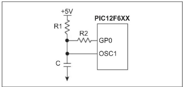
TIP #1 Dual Speed RC Oscillator
Figure 1-1
text_image
+5V R1 R2 PIC12F6XX GP0 OSC1 C- After reset I/O pin is High-Z
- Output '1' on I/O pin
- R1, R2 and C determine OSC frequency
- Also works with additional capacitors
Frequency of PIC MCU in external RC oscillator mode depends on resistance and capacitance on OSC1 pin. Resistance is changed by the output voltage on GP0. GP0 output '1' puts R2 in parallel with R1 reduces OSC1 resistance and increases OSC1 frequency. GP0 as an input increases the OSC1 resistance by minimizing current flow through R2, and decreases frequency and power consumption.
Summary:
GP0 = Input: Slow speed for low current
GP0 = Output high: High speed for fast processing
TIP #2 Input/Output Multiplexing
Individual diodes and some combination of diodes can be enabled by driving I/Os high and low or switching to inputs (Z). The number of diodes (D) that can be controlled depends on the number of I/Os (GP) used.
The equation is: D = GP x (GP - 1).
Example 2-1: Six LEDs on Three I/O Pins
| GPx LEDs | ||||||||
| 0 | 1 | 2 | 1 | 2 | 3 | 4 | 5 | 6 |
| 0 | 0 | 0 | 0 | 0 | 0 | 0 | 0 | 0 |
| 0 | 1 | Z | 1 | 0 | 0 | 0 | 0 | 0 |
| 1 | 0 | Z | 0 | 1 | 0 | 0 | 0 | 0 |
| Z | 0 | 1 | 0 | 0 | 1 | 0 | 0 | 0 |
| Z | 1 | 0 | 0 | 0 | 0 | 1 | 0 | 0 |
| 0 | Z | 1 | 0 | 0 | 0 | 0 | 1 | 0 |
| 1 | Z | 0 | 0 | 0 | 0 | 0 | 0 | 1 |
| 0 | 0 | 1 | 0 | 0 | 1 | 0 | 1 | 0 |
| 0 | 1 | 0 | 1 | 0 | 0 | 1 | 0 | 0 |
| 0 | 1 | 1 | 1 | 0 | 0 | 0 | 1 | 0 |
| 1 | 0 | 0 | 0 | 1 | 0 | 0 | 0 | 1 |
| 1 | 0 | 1 | 0 | 1 | 1 | 0 | 0 | 0 |
| 1 | 1 | 0 | 0 | 0 | 0 | 1 | 0 | 1 |
| 1 | 1 | 1 | 0 | 0 | 0 | 0 | 0 | 0 |
Figure 2-1

text_image
PIC12F6XX GP0 GP1 GP2 1 2 3 4 5 6TIP #3 Read Three States From One Pin
To check state Z:
- Drive output pin high
- Set to Input
- Read 1
- Drive output pin low
- Set to Input
- Read 0
To check state 0:
- Read 0 on pin
To check state 1:
- Read 1 on pin
Figure 3-1

text_image
PIC I/O 5V Link 1 Link 0 0V| State Link | 0 Link 1 | |
| 0 closed | open | |
| 1 open closed | ||
| NC open | open | |
Jumper has three possible states: not connected, Link 1 and Link 0. The capacitor will charge and discharge depending on the I/O output voltage allowing the “not connected” state. Software should check the “not connected” state first by driving I/O high, reading 1 and driving I/O low and reading 0. The “Link 1” and “Link 0” states are read directly.
TIP #4 Reading DIP Switches
The input of a timer can be used to test which switch(s) is closed. The input of Timer1 is held high with a pull-up resistor. Sequentially, each switch I/O is set to input and Timer1 is checked for an increment indicating the switch is closed.
Example 4-1
| LOOP | movlw | b'11111111' |
| movwf | TRISIO | |
| movwf | DIP | |
| movlw | b'00000111' | |
| movwf | T1CON | |
| movlw | b'11111110' | |
| movwf | Mask | |
| clrf | GPIO | |
| clrf | TMR1L | |
| movf | Mask,W | |
| movwf | TRISIO | |
| btfsc | TMR1L,0 | |
| andwf | DIP,F | |
| bsf | STATUS,C | |
| rlf | Mask,F | |
| btfsc | Mask,4 | |
| goto | Loop | |
| retlw | 0 |
Each bit in the DP register represents its corresponding switch position. By setting Timer1 to FFFFh and enabling its interrupt, an increment will cause a rollover and generate an interrupt. This will simplify the software by eliminating the bit test on the TMR1L register.
Sequentially set each GPIO to an input and test for TMR1 increment (or 0 if standard I/O pin is used).
Figure 4-1

text_image
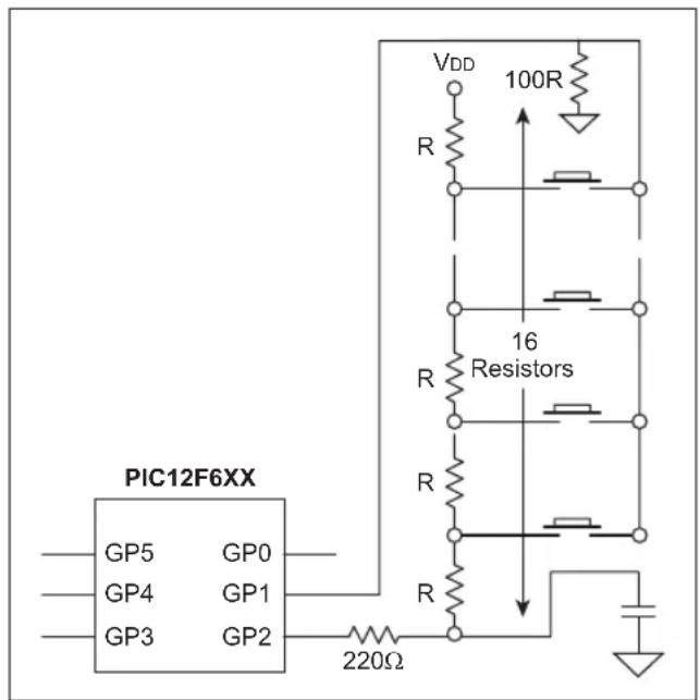
PIC12F6XX GP5/T1CKI 10K VDD GP3 GP2 GP1 GP4Data/IOTIP #5 Scanning Many Keys With One Input
The time required to charge a capacitor depends on resistance between V and capacitor. When a button is pressed, V is supplied to a different point in the resistor ladder. The resistance between V and the capacitor is reduced, which reduces the charge time of the capacitor. A timer is used with a comparator or changing digital input to measure the capacitor charge time. The charge time is used to determine which button is pressed.
Software sequence:
- Configure GP2 to output a low voltage to discharge capacitor through I/O resistor.
- Configure GP2 as one comparator input and CVas the other.
- Use a timer to measure when the comparator trips. If the time measured is greater than the maximum allowed time, then repeat; otherwise determine which button is pressed.
When a key is pressed, the voltage divider network changes the RC ramp rate.
Figure 5-1

text_image
PIC12F6XX GP5 GP0 GP4 GP1 GP3 GP2 220Ω R R 16 Resistors R RSee AN512, "Implementing Ohmmeter/ Temperature Sensor" for code ideas.
TIP #6 Scanning Many Keys and Wake-up From Sleep
An additional I/O can be added to wake the part when a button is pressed. Prior to Sleep, configure GP1 as an input with interrupt-on-change enabled and GP2 to output high. The pull-down resistor holds GP1 low until a button is pressed. GP1 is then pulled high via GP2 and V generating an interrupt. After wake-up, GP2 is configured to output low to discharge the capacitor through the 220Ω resistor. GP1 is set to output high and GP2 is set to an input to measure the capacitor charge time.
• GP1 pin connected to key common
- Enable wake-up on port change
- Set GP1 as input and GP2 high prior to Sleep
- If key is pressed the PIC MCU wakes up, GP2 must be set low to discharge capacitor
- Set GP1 high upon wake-up to scan keystroke
Figure 6-1
text_image
PIC12F6XX GP5 GP0 GP4 GP1 GP3 GP2 VDD 100R R R 16 Resistors R R 220ΩTIP #7 4x4 Keyboard with 1 Input
By carefully selecting the resistor values, each button generates a unique voltage. This voltage is measured by the A/D to determine which button is pressed. Higher precision resistors should be used to maximize voltage uniqueness. The A/D will read near 0 when no buttons are pressed.
Figure 7-1
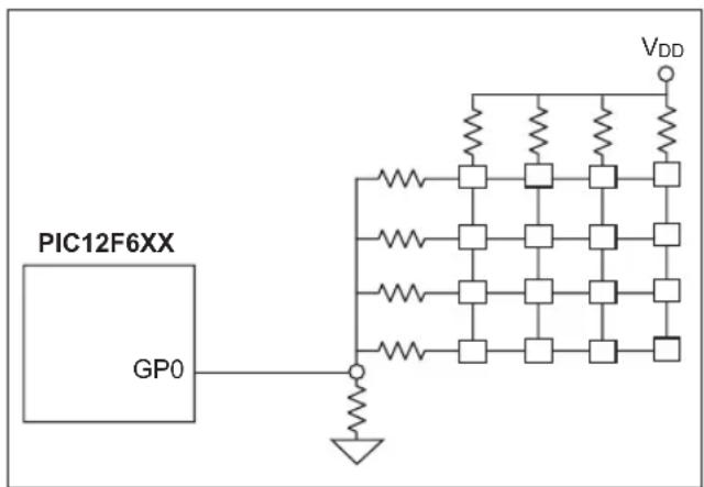
text_image
PIC12F6XX GP0 VDDTIP #8 One Pin Power/Data
A single I/O can be used for both a single-direction communication and the power source for another microcontroller. The I/O line is held high by the pull-up resistor connected to VD. The sender uses a pull-down transistor to pull the data line low or disables the transistor to allow the pull-up to raise it to send data to the receiver. Vois supplied to the sender through the data line. The capacitor stabilizes the sender's VD and a diode prevents the capacitor from discharging through the I/O line while it is low. Note that the VD of the sender is a diode-drop lower than the receiver.
Figure 8-1
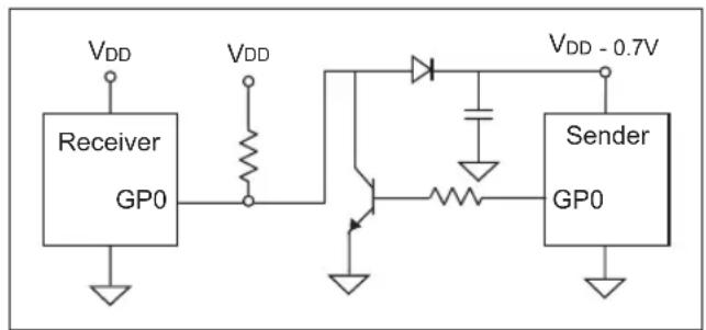
text_image
VDD Receiver GP0 VDD VDD - 0.7V Sender GP0TIP #9 Decode Keys and ID Settings
Buttons and jumpers can share I/O's by using another I/O to select which one is read. Both buttons and jumpers are tied to a shared pull-down resistor. Therefore, they will read as '0' unless a button is pressed or a jumper is connected. Each input (GP3/2/1/0) shares a jumper and a button. To read the jumper settings, set GP4 to output high and each connected jumper will read as '1' on its assigned I/O or '0' if it's not connected. With GP4 output low, a pressed button will be read as '1' on its assigned I/O and '0' otherwise.
Figure 9-1
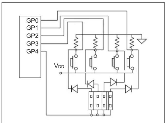
text_image
GP0 GP1 GP2 GP3 GP4 VDD- When GP4 = 1 and no keys are pressed, read ID setting
- When GP4 = 0, read the switch buttons
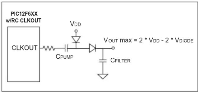
TIP #10 Generating High Voltages
Figure 10-1
text_image
PIC12F6XX w/RC CLKOUT CLKOUT VDD CPUMP VOUT max = 2 * VDD - 2 * VDIODE CFILTERVoltages greater than VDcan be generated using a toggling I/O. PIC MCUs CLKOUT/OSC2 pin toggles at one quarter the frequency of OSC1 when in external RC oscillator mode. When OSC2 is low, the VDdiode is forward biased and conducts current, thereby charging CAfter OSC2 is high, the other diode is forward biased, moving the charge to CThe result is a charge equal to twice the VD minus two diode drops. This can be used with a PWM, a toggling I/O or other toggling pin.
TIP #11 VpSelf Starting Circuit
Building on the previous topic, the same charge pump can be used by the MCU to supply its own Vp Before the switch is pressed, Vp has power and the Vp points are connected together but unpowered. When the button is pressed, power is supplied to Vp and the MCUs CLKOUT (in external RC oscillator mode) begins toggle. The voltage generated by the charge pump turns on the FET allowing Vp to remain powered. To power down the MCU, execute a Sleep instruction. This allows the MCU to switch off its power source via software.
Advantages:
• PIC MCU leakage current nearly 0
- Low cost (uses n-channel FET)
- Reliable
- No additional I/O pins required
Figure 11-1
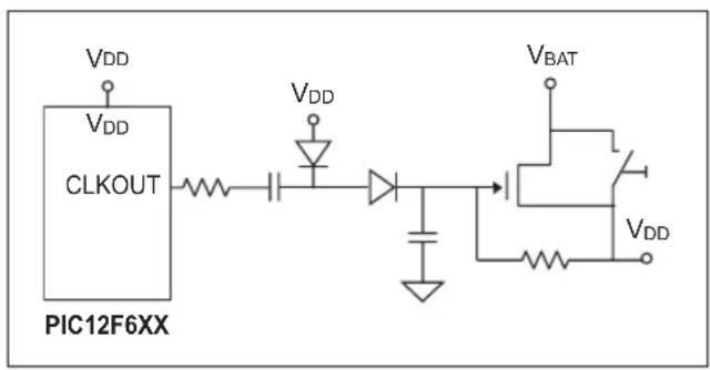
text_image
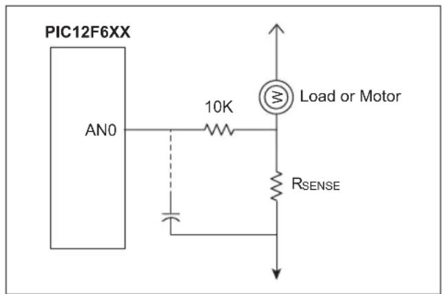
VDD VDD CLKOUT VDD PIC12F6XX VBAT VDDTIP #12 Using PIC® MCU A/D For Smart Current Limiter
Figure 12-1
text_image
PIC12F6XX AN0 10K Load or Motor RSENSE- Detect current through low side sense resistor
- Optional peak filter capacitor
- Varying levels of overcurrent response can be realized in software
By adding a resistor (R) in series with a motor, the A/D can be used to measure in-rush current, provide current limiting, over-current recovery or work as a smart circuit breaker. The 10K resistor limits the analog channel current and does not violate the source impedance limit of the A/D.
TIP #13 Reading a Sensor With Higher Accuracy
Sensors can be read directly with the A/D but in some applications, factors such as temperature, external component accuracy, sensor non-linearity and/or decreasing battery voltage need to be considered. In other applications, more than 10 bits of accuracy are needed and a slower sensor read is acceptable. The following tips deal with these factors and show how to get the most out of a PIC MCU.
13.1. RC Timing Method (with reference resistor)
13.2. Charge Balancing Method
13.3. A/D Method
Tip #13.1 Reading a Sensor With Higher Accuracy – RC Timing Method
RC Timing Method:
$$ \begin{array}{l} \text { Simple RC step response } \ V c (t) = V _ {D} ^ {} (1 - e - t / (R C)) \ t = - R C \ln (1 - V _ {V} V _ {D}) \ \mathrm{V} \nmid \text { V o i s c o n s t a n t } \ R 2 = (t 2 / t 1) ^ {} R 1 \ \end{array} $$
Figure 13-1

line
| Time | Vc(t) - R1 | Vc(t) - R2 | |------|------------|------------| | t = 0 | 0 | 0 | | t | VTH | VTH | | = t1 | > VTH | > VTH | | t = t2 | > VTH | > VTH |A reference resistor can be used to improve the accuracy of an analog sensor reading. In this diagram, the charge time of a resistor/capacitor combination is measured using a timer and a port input or comparator input switches from a '0' to '1'. The R1 curve uses a reference resistor and the R2 curve uses the sensor. The charge time of the R1 curve is known and can be used to calibrate the unknown sensor reading, R2. This reduces the affects of temperature, component tolerance and noise while reading the sensor.
Application Notes:
AN512, "Implementing Ohmmeter/Temperature Sensor"
AN611, "Resistance and Capacitance Meter Using a PIC16C622"
Here is the schematic and software flow for using a reference resistor to improve the accuracy of an analog sensor reading. The reference resistor (R 1 and sensor (R 2 ) are assigned an I/O and share a common capacitor. GP0 is used to discharge the capacitor and represents the capacitor voltage.
Through software, a timer is used to measure when GP0 switches from a '0' to a '1' for the sensor and reference measurements. Any difference measured between the reference measurement and its calibrated measurement is used to adjust the sensor reading, resulting in a more accurate measurement.
The comparator and comparator reference on the PIC12F629/675 can be used instead of a port pin for a more accurate measurement. Polypropylene capacitors are very stable and beneficial in this type of application.
- Set GP1 and GP2 to inputs, and GP0 to a low output to discharge C
- Set GP0 to an input and GP1 to a high output
- Measure tRs(GP0 changes to 1)
- Repeat step 1
- Set GP0 to an input and GP2 to a high output
- Measure tR(GP0 changes to 1)
- Use film polypropylene capacitor
- R_TH = x R_REF _SENtR_R
Figure 13-2
text_image
PIC12F629 RREF GP2 RSEN GP1 GP0Other alternatives: voltage comparator in the PIC12F6XX to measure capacitor voltage on GP0.
Tip #13.2 Reading a Sensor With Higher Accuracy – Charge Balancing Method
- Sensor charges a capacitor
- Reference resistor discharges the capacitor
- Modulate reference resistor to maintain constant average charge in the capacitor
- Use comparator to determine modulation
To improve resolution beyond 10 or 12 bits, a technique called “Charge Balancing” can be used. The basic concept is for the MCU to maintain a constant voltage on a capacitor by either allowing the charge to build through a sensor or discharge through a reference resistor. A timer is used to sample the capacitor voltage on regular intervals until a predetermined number of samples are counted. By counting the number of times the capacitor voltage is over an arbitrary threshold, the sensor voltage is determined.
The comparator and comparator voltage reference (CV) on the PIC12F629/675 are ideal for this application.
- GP1 average voltage = CV _R
- Time base as sampling rate
- At the end of each time base period:
- If GP1 > CV _R then GP2 Output Low
- If GP1 < CV _R then GP2 Input mode
- Accumulate the GP2 lows over many samples
- Number of samples determines resolution
- Number of GP2 lows determine effective duty cycle of R _E
Figure 13-3

text_image
VDD RSEN GP1 RREF T1G GP2 CVREF + - COUT PIC12F6XXTip #13.3 Reading a Sensor With Higher Accuracy – A/D Method
NTC (Negative Temperature Coefficient) sensors have a non-linear response to temperature changes. As the temperature drops, the amount the resistance changes becomes less and less. Such sensors have a limited useful range because the resolution becomes smaller than the A/D resolution as the temperature drops. By changing the voltage divider of the R, the temperature range can be expanded.
To select the higher temperature range, GP1 outputs '1' and GP2 is set as an input. For the lower range, GP2 outputs '1' and GP1 is configured as an input. The lower range will increase the amount the sensor voltage changes as the temperature drops to allow a larger usable sensor range.
Summary:
High range: GP1 output '1' and GP2 input Low range: GP1 input and GP2 output '1'
- 10K and 100K resistors are used to set the range
- V_REF for A/D = V_DD
- Rth calculation is independent of V_D
- Count = RSEN/(RSEN + RREF) x 255
- Don't forget to allow acquisition time for the A/D
Figure 13-4

text_image
PIC12F675 100K GP2 10K GP1 AN0 (A/D Input) RSENTIP #14 Delta-Sigma Converter
The charge on the capacitor on GP1 is maintained about equal to the CV by the MCU monitoring Co and switching GP2 from Input mode or output low appropriately. A timer is used to sample the Cobit on a periodic basis. Each time GP2 is driven low, a counter is incremented. This counter value corresponds to the input voltage.
To minimize the affects of external component tolerances, temperature, etc., the circuit can be calibrated. Apply a known voltage to the input and allow the microcontroller to count samples until the expected result is calculated. By taking the same number of samples for subsequent measurements, they become calibrated measurements.
Figure 14-1

text_image
PIC12F6XX VIN GP1 + - CVREF COUT GP2- GP1 average voltage = CV _R
- Time base as sampling rate
- At the end of each time base period:
- If GP1 > CV then GP2 Output Low
- If GP1 < CV then GP2 Output High
- Accumulate the GP2 lows over many samples
- Number of samples determines resolution
TIPS 'N TRICKS WITH SOFTWARE
To reduce costs, designers need to make the most of the available program memory in MCUs. Program memory is typically a large portion of the MCU cost. Optimizing the code helps to avoid buying more memory than needed. Here are some ideas that can help reduce code size.
TIP #15 Delay Techniques
- Use GOTO "next instruction" instead of two NOPs.
- Use CALL Rtrn as quad, 1 instruction NOP (where “Rtrn” is the exit label from existing subroutine).
Example 15-1
text_image
NOP NOP ;2 instructions, 2 cycles GOTO $+1 ;1 instruction, 2 cycles CALL Rtrn ;1 instruction, 4 cycles Rtrn RETURNMCUs are commonly used to interface with the “outside world” by means of a data bus, LEDs, buttons, latches, etc. Because the MCU runs at a fixed frequency, it will often need delay routines to meet setup/hold times of other devices, pause for a handshake or decrease the data rate for a shared bus.
Longer delays are well-suited for the DECFSZ and INCFSZ instructions where a variable is decremented or incremented until it reaches zero when a conditional jump is executed. For shorter delays of a few cycles, here a few ideas to decrease code size.
For a two-cycle delay, it is common to use two NOP instructions which uses two program memory locations. The same result can be achieved by using “goto \+1”. The “\” represents the current program counter value in MPASM™ Assembler. When this instruction is encountered, the MCU will jump to the next memory location. This is what it would have done if two NOP’s were used but since the GOTO instruction uses two instruction cycles to execute, a two-cycle delay was created. This created a two-cycle delay using only one location of program memory.
To create a four-cycle delay, add a label to an existing RETURN instruction in the code. In this example, the label "Rtrn" was added to the RETURN of subroutine that already existed somewhere in the code. When executing "CALL Rtrn", the MCU delays two instruction cycles to execute the CALL and two more to execute the RETURN. Instead of using four NOP instructions to create a four-cycle delay, the same result was achieved by adding a single CALL instruction.
TIP #16 Optimizing Destinations
- Destination bit determines W for F for result
- Look at data movement and restructure
Example 16-1
Example: A + B → A
| MOVF | A, W | MOVF | B, W |
| ADDWF | B, W | ADDWF | A, F |
| MOVWF | A | ||
| 3 instructions 2 instructions | |||
Careful use of the destination bits in instructions can save program memory. Here, register A and register B are summed and the result is put into the A register. A destination option is available for logic and arithmetic operations. In the first example, the result of the ADDWF instruction is placed in the working register. A MOVWF instruction is used to move the result from the working register to register A. In the second example, the ADDWF instruction uses the destination bit to place the result into the A register, saving an instruction.
TIP #17 Conditional Bit Set/Clear
• To move single bit of data from REGA to REGB
- Precondition REGB bit
- Test REGA bit and fix REGB if necessary
Example 17-1
text_image
BTFSS REGA, 2 BCF REGB, 5 BTFSC REGA, 2 BSF REGB, 5 4 instructions 3 instructions BCF REGB, 5 BTFSC REGA, 2 BSF REGB, 5One technique for moving one bit from the REGA register to REGB is to perform bit tests. In the first example, the bit in REGA is tested using a BTFSS instruction. If the bit is clear, the BCF instruction is executed and clears the REGB bit, and if the bit is set, the instruction is skipped. The second bit test determines if the bit is set, and if so, will execute the BSF and set the REGB bit, otherwise the instruction is skipped. This sequence requires four instructions.
A more efficient technique is to assume the bit in REGA is clear, and clear the REGB bit, and test if the REGA bit is clear. If so, the assumption was correct and the BSF instruction is skipped, otherwise the REGB bit is set. The sequence in the second example uses three instructions because one bit test was not needed.
One important point is that the second example will create a two-cycle glitch if REGB is a port outputting a high. This is caused by the BCF and BTFSC instructions that will be executed regardless of the bit value in REGA.
TIP #18 Swap File Register with W
Example 18-1
The following macro swaps the contents of W and REG without using a second register.
Needs: 0 TEMP registers
3 Instructions
3 TCY
An efficient way of swapping the contents of a register with the working register is to use three XORWF instructions. It requires no temporary registers and three instructions. Here's an example:
W REG Instruction
10101100 01011100 XORWF REG,F
10101100 11110000 XORWF REG,W
01011100 11110000 XORWF REG,F
01011100 10101100 Result
TIP #19 Bit Shifting Using Carry Bit
Rotate a byte through carry without using RAM variable for loop count:
- Easily adapted to serial interface transmit routines.
- Carry bit is cleared (except last cycle) and the cycle repeats until the zero bit sets indicating the end.
Example 19-1
LIST P=PIC12f629
INCLUDE P12f629.INC
buffer    equ    0x20

bsf STATUS,C ;Set 'end of loop' flag
rlf buffer,f ;Place first bit into C
bcf GPIO,Dout ;precondition output
btfsc STATUS,C ;Check data 0 or 1 ?
bsf GPIO,Dout
bcf STATUS,C ;Clear data in C
rlf buffer,f ;Place next bit into C
movf buffer,f ;Force Z bit
btfss STATUS,Z ;Exit?
goto Send_Loop
CHAPTER 2
PIC® Microcontroller Low Power
Tips 'n Tricks
Table Of Contents
GENERAL LOW POWER TIPS 'N TRICKS
TIP #1 Switching Off External Circuits/Duty Cycle 2-2
TIP #2 Power Budgeting 2-3
TIP #3 Configuring Port Pins 2-4
TIP #4 Use High-Value Pull-Up Resistors ..... 2-4
TIP #5 Reduce Operating Voltage 2-4
TIP #6 Use an External Source for CPU Core Voltage 2-5
TIP #7 Battery Backup for PIC MCUs 2-6
DYNAMIC OPERATION TIPS 'N TRICKS
TIP #8 Enhanced PIC16 Mid-Range Core ..... 2-6
TIP #9 Two-Speed Start-Up 2-7
TIP #10 Clock Switching 2-7
TIP #11 Use Internal RC Oscillators 2-7
TIP #12 Internal Oscillator Calibration 2-8
TIP #13 Idle and Doze Modes 2-8
TIP #14 Use NOP and Idle Mode 2-9
TIP #15 Peripheral Module Disable (PMD) Bits 2-9
STATIC POWER REDUCTION TIPS 'N TRICKS
TIP #16 Deep Sleep Mode 2-10
TIP #17 Extended WDT and Deep Sleep WDT 2-10
TIP #18 Low Power Timer1 Oscillator and RTCC....2-10
TIP #19 Low Power Timer1 Oscillator Layout..2-11
TIP #20 Use LVD to Detect Low Battery .....2-11
TIP #21 Use Peripheral FIFO and DMA ......2-11
TIP #22 Ultra Low-Power Wake-Up Peripheral 2-12
TIPS 'N TRICKS INTRODUCTION
Microchip continues to provide innovative products that are smaller, faster, easier to use and more reliable. The Flash-based PIC® microcontrollers (MCUs) are used in an wide range of everyday products, from smoke detectors, hospital ID tags and pet containment systems, to industrial, automotive and medical products.
PIC MCUs featuring nanoWatt technology implement a variety of important features which have become standard in PIC microcontrollers. Since the release of nanoWatt technology, changes in MCU process technology and improvements in performance have resulted in new requirements for lower power. PIC MCUs with nanoWatt eXtreme Low Power (nanoWatt XLP™) improve upon the original nanoWatt technology by dramatically reducing static power consumption and providing new flexibility for dynamic power management.
The following series of Tips n' Tricks can be applied to many applications to make the most of PIC MCU nanoWatt and nanoWatt XLP devices.
GENERAL LOW POWER TIPS 'N TRICKS
The following tips can be used with all PIC MCUs to reduce the power consumption of almost any application.
TIP #1 Switching Off External Circuits/Duty Cycle
All the low power modes in the world won't help your application if you are unable to control the power used by circuits external to the microprocessor. Lighting an LED is equivalent to running most PIC MCUs at 5V-20 MHz. When you are designing your circuitry, decide what physical modes or states are required and partition the electronics to shutdown unneeded circuitry.
Figure: 1-1
Example:
The application is a long duration data recorder. It has a sensor, an EEPROM, a battery and a microprocessor. Every two seconds, it must take a sensor reading, scale the sensor data, store the scaled data in EEPROM and wait for the next sensor reading.
text_image
3.3V 0.1 μF C1 R2 100k R3 1k U1 14 Vcc 4 MCLR 17 RA0 RB0/INT 6 18 RA1 RB1 7 1 RA2 RB2 8 2 RA3 RB3 9 3 RA4/TOCKI RB4 10 RB5 11 OSC1/CLKIN RB6 12 OSC2/CLKOUT RB7 13 Vss PIC16F819 C3 22 pF R1 100k C4 33 pF Y1 32.768 kHz C5 33 pF U2 8 Vcc A0 1 7 WP A1 2 6 SCL A2 3 5 SDA GND 4 C2 0.1 μF R5 R4 10k R4 Serial EEPROMThe system shown above is very simple and clearly has all the parts identified in the requirements. Unfortunately, it has a few problems in that the EEPROM, the sensor, and its bias circuit, are energized all the time. To get the minimum current draw for this design, it would be advantageous to shutdown these circuits when they are not required.
Figure: 1-2
In Figure 1-2, I/O pins are used to power the EEPROM and the sensor. Many PIC MCU devices can source up to 20 mA of current from each I/O, so there is no need to provide additional components to switch the power.
If more current than can be sourced by the PIC MCU is required, the PIC MCU can instead enable and disable a MOSFET to power the circuit. Refer to the data sheet for drive capabilities for a specific device.

text_image
3.3V 0.1 μF C1 R2 100k R3 1k R1 100k C3 22 pF U1 VDD MCLR RA0 RB0/INT 14 4 17 18 1 2 3 5 OSC1/CLKIN RB6 OSC2/CLKOUT RB7 Vss PIC16F819 U2 Vcc A0 1 WP A1 2 SCL A2 3 SDA GND 4 C2 0.1 μF 10k R5 10k R4 10k R4 8 7 6 5 Serial EEPROM Y1 32.768 kHz C4 33 pF C5 33 pFTIP #2 Power Budgeting
Power budgeting is a technique that is critical to predicting current consumption and battery life. Power budgeting is performed by calculating the total charge for each mode of operation of an application by multiplying that mode's current consumption by the time in the mode for a single application loop. The charge for each mode is added, then averaged over the total loop time to get average current. Table 1 calculates a power budget using the application from Figure 2 in Tip #1 using a typical nanoWatt XLP device.
| Mode | Time in Mode (mS) | Current (mA) Charge | Current * Time (mA * Sec) | |
| By Device | Mode Total | |||
| SleepMCU SleepSensor OffEEPROM Off | 1989 5.00E-05 9.95E-050 | |||
| InitializeMCU SleepSensor OnEEPROM Off | 1 1.66E-02 1.66E-050 | |||
| Sample SensorMCU RunSensor OnEEPROM Off | 1 6.45E-02 6.45E-050 | |||
| ScalingMCU RunSensor OffEEPROM Off | 1 4.80E-02 4.80E-050 | |||
| StoringMCU RunSensor OffEEPROM On | 8 1.05E+00 8.38E-031 | |||
| Total | 2000 — — | 8.61E-03 |
Average Current
= 8.61e-3 ^*SecSec
= 0.0043 mA
Peak Current 1.05 mA
Computing Battery Life
Using the average current from the calculated power budget, it is possible to determine how long a battery will be able to power the application. Table 2 shows lifetimes for typical battery types using the average power from Table 1.
| Battery | Capacity (mAh) | Life | |||
| Hours | Days | Months | Years | ||
| CR1212 | 18 | 4180 | 174 | 5.8 | .48 |
| CR1620 | 75 | 17417 | 726 | 24.2 | 1.99 |
| CR2032 | 220 | 51089 | 2129 7 | 1.0 5.83 | |
| Alkaline AAA | 1250 | 290276 | 12095 | 403.2 | 33.14 |
| Alkaline AA | 2890 | 671118 | 27963 | 932.1 | 76.61 |
| Li-ion* | 850 | 197388 | 8224 | 274.1 | 22.53 |
| NOTE: Calculations are based on average current draw only and do not include battery self-discharge.*Varies by size; value used is typical. | |||||
After completing a power budget, it is very easy to determine the battery size required to meet the application requirements. If too much power is consumed, it is simple to determine where additional effort needs to be placed to reduce the power consumption.
TIP #3 Configuring Port Pins
All PIC MCUs have bidirectional I/O pins. Some of these pins have analog input capabilities. It is very important to pay attention to the signals applied to these pins so the least amount of power will be consumed.
Unused Port Pins
If a port pin is unused, it may be left unconnected but configured as an output pin driving to either state (high or low), or it may be configured as an input with an external resistor (about 10 kΩ) pulling it to VDD or Vss. If configured as an input, only the pin input leakage current will be drawn through the pin (the same current would flow if the pin was connected directly to VDor Vs. Both options allow the pin to be used later for either input or output without significant hardware modifications.
Digital Inputs
A digital input pin consumes the least amount of power when the input voltage is near VD or Vs If the input voltage is near the midpoint between VD and Vs the transistors inside the digital input buffer are biased in a linear region and they will consume a significant amount of current. If such a pin can be configured as an analog input, the digital buffer is turned off, reducing both the pin current as well as the total controller current.
Analog Inputs
Analog inputs have a very high-impedance so they consume very little current. They will consume less current than a digital input if the applied voltage would normally be centered between V and Vs Sometimes it is appropriate and possible to configure digital inputs as analog inputs when the digital input must go to a low power state.
Digital Outputs
There is no additional current consumed by a digital output pin other than the current going through the pin to power the external circuit. Pay close attention to the external circuits to minimize their current consumption.
TIP #4 Use High-Value Pull-Up Resistors
It is more power efficient to use larger pull-up resistors on I/O pins such as MCLR, I ^2 C ^TM signals, switches and for resistor dividers. For example, a typical I ^2 C pull-up is 4.7k. However, when the I ^2 C is transmitting and pulling a line low, this consumes nearly 700 uA of current for each bus at 3.3V. By increasing the size of the I ^2 C pull-ups to 10k, this current can be halved. The tradeoff is a lower maximum I ^2 C bus speed, but this can be a worthwhile trade in for many low power applications. This technique is especially useful in cases where the pull-up can be increased to a very high resistance such as 100k or 1M.
TIP #5 Reduce Operating Voltage
Reducing the operating voltage of the device, V_D is a useful step to reduce the overall power consumption. When running, power consumption is mainly influenced by the clock speed. When sleeping, the most significant factor is leakage in the transistors. At lower voltages, less charge is required to switch the system clocks and transistors leak less current.
It is important to pay attention to how reducing the operating voltage reduces the maximum allowed operating frequency. Select the optimum voltage that allows the application to run at its maximum speed. Refer to the device data sheet for the maximum operating frequency of the device at the given voltage.
TIP #6 Use an External Source for CPU Core Voltage
Some PIC MCUs such as “J” type devices (ex. PIC18F87J90 or PIC24FJ64GA004) use separate power for CPU core. These devices have an internal voltage regulator that can be used to provide the core voltage. Alternatively, the core voltage can be provided externally by disabling the internal regulator. In some cases, it is more power efficient to use an external source for the core. This is because the internal regulator powers the core at the nominal voltage that allows full speed operation. However, if an application doesn’t require full speed, it is beneficial to use lower voltage to power the core. Disabling the internal regulator also turns off the BOR and LVD circuits, which saves power as well. The following examples show two different battery powered applications where it can be beneficial to disable the internal regulator.
Example 1: Constant Voltage Source
When using a regulated power source or a battery with a flat discharge curve, such as a lithium coin cell, the regulator can be disabled and the core powered directly from the battery through a diode. The diode provides the voltage drop necessary to power the core at the correct voltage. It may be necessary to use a zener diode with a higher forward voltage for applications using sleep mode, as the current consumed in sleep is too low to cause the full forward voltage drop which can result in applying a voltage too high for the core.
Figure 6-1:
text_image
PIC'MCU VDD GPIO ENVREG ~2.3V VDDCORE VSS 3.0V Coin Cell 0Example 2: Non-Constant Voltage Source
If the source for V _0 is not constant, a regulator will be required. It can be beneficial to use an external low quiescent current regulator, which can be selected to provide lower voltage to the core than the internal regulator. Additionally, devices such as the MCP1700, which consumes 1 uA quiescent current while asleep, require less power than the internal regulator.
Figure 6-2:
text_image
PIC MCU VDD GPIO ENVREG LDO 2.0 V VDDCORE VSS Alkaline Batteries 0TIP #7 Battery Backup for PIC MCUs
For an application that can operate from either an external supply or a battery backup, it is necessary to be able to switch from one to the other without user intervention. This can be accomplished with battery backup ICs, but it is also possible to implement with a simple diode OR circuit, shown in Figure 7-1. Diode D1 prevents current from flowing into the battery from VEXT when the external power is supplied. D2 prevents current from flowing into any external components from the battery if VEXT is removed. As long as the external source is present and higher voltage than the battery, no current from the battery will be used. When VEXT is removed and the voltage drops below VBAT, the battery will start powering the MCU. Low forward voltage Schottky diodes can be used in order to minimize the voltage dropout from the diodes. Additionally, inputs can be referenced to VEXT and VBAT in order to monitor the voltage levels of the battery and the external supply. This allows the micro to enter lower power modes when the supply is removed or the battery is running low. In order to avoid glitches on V D caused by the diode turn-on delay when switching supplies, ensure enough decoupling capacitance is used on V D (C1).
Figure 7-1:
text_image
VEXT D2 PIC VDD VBAT D1 C1Dynamic Operation Tips n' Tricks
The following tips and tricks apply to methods of improving the dynamic operating current consumption of an application. This allows an application to get processing done quicker which enables it to sleep more and will help reduce the current consumed while processing.
TIP #8 Enhanced PIC16 Mid-Range Core
The Enhanced PIC16 mid-range core has a few features to assist in low power. New instructions allow many applications to execute in less time. This allows the application to spend more time asleep and less time processing and can provide considerable power savings. It is important not to overlook these new instructions when designing with devices that contain the new core. The Timer1 oscillator and WDT have also been improved, now meeting nanoWatt XLP requirements and drawing much less current than in previous devices.
TIP #9 Two-Speed Start-Up
Two-speed startup is a useful feature on some nanoWatt and all nanoWatt XLP devices which helps reduce power consumption by allowing the device to wake up and return to sleep faster. Using the internal oscillator, the user can execute code while waiting for the Oscillator Start-up (OST) timer to expire (LP, XT or HS modes). This feature (called "Two-Speed Start-up") is enabled using the IESO configuration bit. A Two-Speed Start-up will clock the device from an internal RC oscillator until the OST has expired. Switching to a faster internal oscillator frequency during start-up is also possible using the OSCCON register. The example below shows several stages on how this can be achieved. The number of frequency changes is dependent upon the designer's discretion. Assume a 20 MHz crystal (HS Mode) in the PIC16F example below.
Example:
T
(Instruction Time) Instruction
ORG 0x05 ;Reset vector
125 μs @ 32 kHz BSF STATUS,RP0 ;bank1
125 μs @ 32 kHz BSF OSCCON,IRCF2 ;switch to 1 MHz
4 μs @ 1 MHz BSF OSCCON, IRCF1 ; switch to 4 MHz
1 μs @ 4 MHz BSF OSCCON, IRCF0 ; switch to 8 MHz
500 ns application code
500 ns application code
... ....
...
(eventually OST expires, 20 MHz crystal clocks the device)
200 ns application code
... ....
...
TIP #10 Clock Switching
Some nanoWatt devices and all nanoWatt XLP devices have multiple internal and external clock sources, as well as logic to allow switching between the available clock sources as the main system clock. This allows for significant power savings by choosing different clocks for different portions of code. For example, an application can use the slower internal oscillator when executing non-critical code and then switch to a fast high-accuracy oscillator for time or frequency sensitive code. Clock switching allows much more flexible applications than being stuck with a single clock source. Clock switching sequences vary by device family, so refer to device data sheets or Family Reference Manuals for the specific clock switching sequences.
TIP #11 Use Internal RC Oscillators
If frequency precision better than ±5% is not required, it is best to utilize the internal RC oscillators inside all nanoWatt and nanoWatt XLP devices. The internal RC oscillators have better frequency stability than external RC oscillators, and consume less power than external crystal oscillators. Additionally, the internal clock can be configured for many frequency ranges using the internal PLL module to increase frequency and the postscaler to reduce it. All these options can be configured in firmware.
TIP #12 Internal Oscillator Calibration
An internal RC oscillator calibrated from the factory may require further calibration as the temperature or V change. Timer1/SOSC can be used to calibrate the internal oscillator by connecting a 32.768 kHz clock crystal. Refer to AN244, "Internal RC Oscillator Calibration" for the complete application details. Calibrating the internal oscillator can help save power by allowing for use of the internal RC oscillator in applications which normally require higher accuracy crystals
Figure 12-1: Timer1 Used to Calibrate an Internal Oscillator
text_image
PIC16F818/819 C1 33 pF XTAL 32.768 kHz C2 33 pF T1OSI T1OSOThe calibration is based on the measured frequency of the internal RC oscillator. For example, if the frequency selected is 4 MHz, we know that the instruction time is 1 s (F64) and Timer1 has a period of 30.5 s (1/32.768 kHz). This means within one Timer1 period, the core can execute 30.5 instructions. If the Timer1 registers are preloaded with a known value, we can calculate the number of instructions that will be executed upon a Timer1 overflow.
This calculated number is then compared against the number of instructions executed by the core. With the result, we can determine if re-calibration is necessary, and if the frequency must be increased or decreased. Tuning uses the OSCTUNE register, which has a ±12% tuning range in 0.8% steps.
TIP #13 Idle and Doze Modes
nanoWatt and nanoWatt XLP devices have an Idle mode where the clock to the CPU is disconnected and only the peripherals are clocked. In PIC16 and PIC18 devices, Idle mode can be entered by setting the Idle bit in the OSCON register to '1' and executing the SLEEP instruction. In PIC24, dsPIC® DSCs, and PIC32 devices, Idle mode can be entered by executing the instruction "PWRSAV #1". Idle mode is best used whenever the CPU needs to wait for an event from a peripheral that cannot operate in Sleep mode. Idle mode can reduce power consumption by as much as 96% in many devices.
Doze mode is another low power mode available in PIC24, dsPIC DSCs, and PIC32 devices. In Doze mode, the system clock to the CPU is postscaled so that the CPU runs at a lower speed than the peripherals. If the CPU is not tasked heavily and peripherals need to run at high speed, then Doze mode can be used to scale down the CPU clock to a slower frequency. The CPU clock can be scaled down from 1:1 to 1:128. Doze mode is best used in similar situations to Idle mode, when peripheral operation is critical, but the CPU only requires minimal functionality.
TIP #14 Use NOP and Idle Mode
When waiting on a blocking loop (e.g. waiting for an interrupt), instead put the device into Idle mode to disable the CPU. The peripheral interrupt will wake up the device. Idle mode consumes much less current than constantly reading RAM and jumping back. If the CPU cannot be disabled because the loop required some calculations, such as incrementing a counter, instead of doing a very tight loop that loops many times, add NOPs into the loop. See the code example below. A NOP requires less current to execute than reading RAM or branching operations, so current can be reduced. The overall loop count can be adjusted to account for the extra instructions for the NOPs.
Example:
Replace:
    while(!_T1IF);
with Idle mode:
    IEC0bits.T1IE = 1;
    Idle();
and replace:
    while(!_T1IF){
    i++;
    }
with extra NOP instructions:
    while(!_T1IF){
    i++;
    Nop();
    Nop();
    Nop();
    Nop();
    Nop();
    Nop();
    }
TIP #15 Peripheral Module Disable (PMD) Bits
PIC24, dsPIC DSCs, and PIC32 devices have PMD bits that can be used to disable peripherals that will not be used in the application. Setting these bits disconnects all power to the module as well as SFRs for the module. Because power is completely removed, the PMD bits offer additional power savings over disabling the module by turning off the module's enable bit. These bits can be dynamically changed so that modules which are only used periodically can be disabled for the remainder of the application. The PMD bits are most effective at high clock speeds and when operating at full speed allowing the average power consumption to be significantly reduced.
Static Power Reduction Tips n' Tricks
The following tips and tricks will help reduce the power consumption of a device while it is asleep. These tips allow an application to stay asleep longer and to consume less current while sleeping.
TIP #16 Deep Sleep Mode
In Deep Sleep mode, the CPU and all peripherals except RTCC, DSWDT and LCD (on LCD devices) are not powered. Additionally, Deep Sleep powers down the Flash, SRAM, and voltage supervisory circuits. This allows Deep Sleep mode to have lower power consumption than any other operating mode. Typical Deep Sleep current is less than 50 nA on most devices. Four bytes of data are retained in the DSGPRx registers that can be used to save some critical data required for the application. While in Deep Sleep mode, the states of I/O pins and 32 kHz crystal oscillator (Timer1/SOSC) are maintained so that Deep Sleep mode does not interrupt the operation of the application. The RTCC interrupt, Ultra Low Power Wake-up, DSWDT time-out, External Interrupt 0 (INT0), MCLR or POR can wake-up the device from Deep Sleep. Upon wake-up the device resumes operation at the reset vector.
Deep Sleep allows for the lowest possible static power in a device. The trade-off is that the firmware must re-initialize after wake-up. Therefore, Deep Sleep is best used in applications that require long battery life and have long sleep times. Refer to the device datasheets and Family Reference Manuals for more information on Deep Sleep and how it is used.
TIP #17 Extended WDT and Deep Sleep WDT
A commonly used source to wake-up from Sleep or Deep Sleep is the Watchdog Timer (WDT) or Deep Sleep Watchdog Timer (DSWDT). The longer the PIC MCU stays in Sleep or Deep Sleep, the less power consumed. Therefore, it is appropriate to use as long a timeout period for the WDT as the application will allow.
The WDT runs in all modes except for Deep Sleep. In Deep Sleep, the DSWDT is used instead. The DSWDT uses less current and has a longer timeout period than the WDT. The timeout period for the WDT varies by device, but typically can vary from a few milliseconds to up to 2 minutes. The DSWDT time-out period can be programmed from 2.1ms to 25.7days
TIP #18 Low Power Timer1 Oscillator and RTCC
nanoWatt XLP microcontrollers all have a robust Timer1 oscillator (SOSC on PIC24) which draws less than 800 nA. nanoWatt technology devices offer a low power Timer1 oscillator which draws 2-3 uA. Some devices offer a selectable oscillator which can be used in either a low-power or high-drive strength mode to suit both low power or higher noise applications. The Timer1 counter and oscillator can be used to generate interrupts for periodic wakes from Sleep and other power managed modes, and can be used as the basis for a real-time clock. Timer1/SOSC wake-up options vary by device. Many nanoWatt XLP devices have a built-in hardware Real-Time Clock and Calendar (RTCC), which can be configured for wake-up periods from 1 second to many years.
Some nanoWatt devices and all nanoWatt XLP devices can also use the Timer1/SOSC oscillator as the system clock source in place of the main oscillator on the OSC1/OSC2 pins. By reducing execution speed, total current consumption can be reduced.
TIP #19 Low Power Timer1 Oscillator Layout
Applications requiring very low power Timer1/SOSC oscillators on nanoWatt and nanoWatt XLP devices must take PCB layout into consideration. The very low power Timer1/SOSC oscillators on nanoWatt and nanoWatt XLP devices consume very little current, and this sometimes makes the oscillator circuit sensitive to neighboring circuits. The oscillator circuit (crystal and capacitors) should be located as close as possible to the microcontroller.
No circuits should be passing through the oscillator circuit boundaries. If it is unavoidable to have high-speed circuits near the oscillator circuit, a guard ring should be placed around the oscillator circuit and microcontroller pins similar to the figure below. Placing a ground plane under the oscillator components also helps to prevent interaction with high speed circuits.
Figure 19-1: Guard Ring Around Oscillator Circuit and MCU Pins
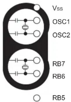
text_image
Vss OSC1 OSC2 RB7 RB6 RB5TIP #20 Use LVD to Detect Low Battery
The Low Voltage Detect (LVD) interrupt present in many PIC MCUs is critical in battery based systems. It is necessary for two reasons. First, many devices cannot run full speed at the minimum operating voltage. In this case, the LVD interrupt indicates when the battery voltage is dropping so that the CPU clock can be slowed down to an appropriate speed, preventing code misexecution. Second, it allows the MCU to detect when the battery is nearing the end of its life, so that a low battery indication can be provided and a lower power state can be entered to maximize battery lifetime. The LVD allows these functions to be implemented without requiring the use of extra analog channels to measure the battery level.
TIP #21 Use Peripheral FIFO and DMA
Some devices have peripherals with DMA or FIFO buffers. These features are not just useful to improve performance; they can also be used to reduce power. Peripherals with just one buffer register require the CPU to stay operating in order to read from the buffer so it doesn't overflow. However, with a FIFO or DMA, the CPU can go to sleep or idle until the FIFO fills or DMA transfer completes. This allows the device to consume a lot less average current over the life of the application.
TIP #22 Ultra Low-Power Wake-Up Peripheral
Newer devices have a modification to PORTA that creates an Ultra Low-Power Wake-Up (ULPWU) peripheral. A small current sink and a comparator have been added that allows an external capacitor to be used as a wake-up timer. This feature provides a low-power periodic wake-up source which is dependent on the discharge time of the external RC circuit.
Figure 22-1: Ultra Low-Power Wake-Up Peripheral

text_image
C I VREF Pin Wake-on-Change InterruptIf the accuracy of the Watchdog Timer is not required, this peripheral can save a lot of current.
Visit the low power design center at: www.microchip.com/lowpower for additional design resources.
CHAPTER 3
PIC® Microcontroller CCP and ECCP
Tips 'n Tricks
Table Of Contents
CAPTURE TIPS 'N TRICKS
TIP #1 Measuring the Period of a Square Wave 3-3
TIP #2 Measuring the Period of a Square Wave with Averaging 3-3
TIP #3 Measuring Pulse Width 3-4
TIP #4 Measuring Duty Cycle 3-4
TIP #5 Measuring RPM Using an Encoder .... 3-5
TIP #6 Measuring the Period of an Analog Signal 3-6
COMPARE TIPS 'N TRICKS
TIP #7 Periodic Interrupts 3-8
TIP #8 Modulation Formats 3-9
TIP #9 Generating the Time Tick for a RTOS 3-10
TIP #10 16-Bit Resolution PWM 3-10
TIP #11 Sequential ADC Reader 3-11
TIP #12 Repetitive Phase Shifted Sampling .... 3-12
PWM TIPS 'N TRICKS
TIP #13 Deciding on PWM Frequency ...... 3-14
TIP #14 Unidirectional Brushed DC Motor Control Using CCP .... 3-14
TIP #15 Bidirectional Brushed DC Motor Control Using ECCP......3-15
TIP #16 Generating an Analog Output 3-16
TIP #17 Boost Power Supply 3-17
TIP #18 Varying LED Intensity 3-18
TIP #19 Generating X-10 Carrier Frequency ... 3-18
COMBINATION CAPTURE AND COMPARE TIPS
TIP #20 RS-232 Auto-baud 3-19
TIP #21 Dual-Slope Analog-to-Digital Converter 3-21
TIPS 'N TRICKS INTRODUCTION
Microchip continues to provide innovative products that are smaller, faster, easier-to-use and more reliable. PIC® microcontrollers (MCUs) are used in a wide range of everyday products, from washing machines, garage door openers and television remotes to industrial, automotive and medical products.
The Capture, Compare and PWM (CCP) modules that are found on many of Microchip's microcontrollers are used primarily for the measurement and control of time-based pulse signals. The Enhanced CCP (ECCP), available on some of Microchip's devices, differs from the regular CCP module in that it provides enhanced PWM functionality – namely, full-bridge and half-bridge support, programmable dead-band delay and enhanced PWM auto-shutdown. The ECCP and CCP modules are capable of performing a wide variety of tasks. This document will describe some of the basic guidelines to follow when using these modules in each mode, as well as give suggestions for practical applications.
ECCP/CCP Register Listing
| Capture Mode | Compare Mode | PWM Mode | |
| CCPxCON Select mode Select mode Select mode, LSB of duty cycle | |||
| CCPRxL Timer1 capture (LSB) | Timer1 compare (LSB) | MSB of duty cycle | |
| CCPRxH Timer1 capture (MSB) | Timer1 compare (MSB) | N/A | |
| TRISx Set CCPx pin to input | Set CCPx pin to output | Set CCPx pin(s) to output(s) | |
| T1CON Timer1 on, prescaler | Timer1 on, prescaler | N/A | |
| T2CON N/A N/A Timer2 on, | prescaler | ||
| PR2 N/A N/A Timer2 period | |||
| PIE1 Timer1 interrupt enable | Timer1 interrupt enable | Timer2 interrupt enable | |
| PIR1 Timer1 interrupt flag | Timer1 interrupt flag | Timer2 interrupt flag | |
| INTCON Global/ peripheral interrupt enable | Global/ peripheral interrupt enable | Global/ peripheral interrupt enable | |
| PWM1CON(1) | N/A N/A Set dead band, | auto-restart control | |
| ECCPAS^(1) | N/A N/A Auto-shutdown | control | |
Note 1: Only on ECCP module.
CAPTURE TIPS 'N TRICKS
In Capture mode, the 16-bit value of Timer1 is captured in CCPRxH:CCPRxL when an event occurs on pin CCPx. An event is defined as one of the following and is configured by CCPxCON<3:0>:
- Every falling edge
- Every rising edge
- Every 4th rising edge
- Every 16th rising edge
"When Would I Use Capture Mode?"
Capture mode is used to measure the length of time elapsed between two events. An event, in general, is either the rising or falling edge of a signal (see Figure 1 “Defining Events”).
An example of an application where Capture mode is useful is reading an accelerometer. Accelerometers typically vary the duty cycle of a square wave in proportion to the acceleration acting on a system. By configuring the CCP module in Capture mode, the PIC microcontroller can measure the duty cycle of the accelerometer with little intervention on the part of the microcontroller firmware. Tip #4 goes into more detail about measuring duty cycle by configuring the CCP module in Capture mode.
Figure 1: Defining Events

line
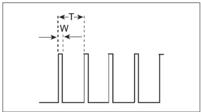
| Event | Time Segment | Voltage | | ------------------ | -------------------- | ------- | | Falling Edge | 0 | High | | Rising Edge | 1 | Low |TIP #1 Measuring the Period of a Square Wave
Figure 1-1: Period

text_image
T t1t2- Configure control bits CCPxM3:CCPxM0 (CCPxCON<3:0>) to capture every rising edge of the waveform.
- Configure the Timer1 prescaler so Timer1 with run T_M (1) without overflowing.
- Enable the CCP interrupt (CCPxIE bit).
- When a CCP interrupt occurs:
a) Subtract saved captured time (t1) from captured time (t2) and store (use Timer1 interrupt flag as overflow indicator).
b) Save captured time (t2).
c) Clear Timer1 flag if set.
The result obtained in step 4.a is the period (T).
Note 1: T_MAX is the maximum pulse period that will occur.
TIP #2 Measuring the Period of a Square Wave with Averaging
Figure 2-1: Period Measurement
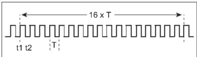
text_image
16 x T t1 t2 T- Configure control bits CCPxM3:CCPxM0 (CCPxCON<3:0>) to capture every 16th rising edge of the waveform.
- Configure the Timer1 prescaler so Timer1 will run 16 T _M (1) without overflowing.
- Enable the CCP interrupt (CCPxIE bit).
- When a CCP interrupt occurs:
a) Subtract saved captured time (t1) from captured time (t2) and store (use Timer1 interrupt flag as overflow indicator).
b) Save captured time (t2).
c) Clear Timer1 flag if set.
d) Shift value obtained in step 4.a right four times to divide by 16 - this result is the period (T).
Note 1: T_MAX is the maximum pulse period that will occur.
The following are the advantages of this method as opposed to measuring the periods individually.
- Fewer CCP interrupts to disrupt program flow
- Averaging provides excellent noise immunity
TIP #3 Measuring Pulse Width
Figure 3-1: Pulse Width

text_image
W t1t2- Configure control bits CCPxM3:CCPxM0 (CCPxCON<3:0>) to capture every rising edge of the waveform.
- Configure Timer1 prescaler so that Timer1 will run W without overflowing.
- Enable the CCP interrupt (CCPxIE bit).
- When CCP interrupt occurs, save the captured timer value (t1) and reconfigure control bits to capture every falling edge.
- When CCP interrupt occurs again, subtract saved value (t1) from current captured value (t2) – this result is the pulse width (W).
- Reconfigure control bits to capture the next rising edge and start process all over again (repeat steps 3 through 6).
TIP #4 Measuring Duty Cycle
Figure 4-1: Duty Cycle
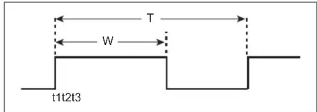
text_image
T W t1t2t3The duty cycle of a waveform is the ratio between the width of a pulse (W) and the period (T). Acceleration sensors, for example, vary the duty cycle of their outputs based on the acceleration acting on a system. The CCP module, configured in Capture mode, can be used to measure the duty cycle of these types of sensors. Here's how:
- Configure control bits CCPxM3:CCPxM0 (CCPxCON<3:0>) to capture every rising edge of the waveform.
- Configure Timer1 prescaler so that Timer1 will run TM ^(1) without overflowing.
- Enable the CCP interrupt (CCPxIE bit).
- When CCP interrupt occurs, save the captured timer value (t1) and reconfigure control bits to capture every falling edge.
Note 1: T_MAX is the maximum pulse period that will occur.
- When the CCP interrupt occurs again, subtract saved value (t1) from current captured value (t2) – this result is the pulse width (W).
- Reconfigure control bits to capture the next rising edge.
- When the CCP interrupt occurs, subtract saved value (t1) from the current captured value (t3) – this is the period (T) of the waveform.
- Divide T by W – this result is the Duty Cycle.
- Repeat steps 4 through 8.
TIP #5 Measuring RPM Using an Encoder
Revolutions Per Minute (RPM), or how fast something turns, can be sensed in a variety of ways. Two of the most common sensors used to determine RPM are optical encoders and Hall effect sensors. Optical encoders detect the presence of light shining through a slotted wheel mounted to a turning shaft (see Figure 5-1.) As the shaft turns, the slots in the wheel pass by the eye of the optical encoder. Typically, an infrared source on the other side of the wheel emits light that is seen by the optical encoder through slots in the wheel. Hall effect sensors work by sensing the position of the magnets in an electric motor, or by sensing a permanent magnet mounted to a rotating object (see Figure 5-2). These sensors output one or more pulses per revolution (depending on the sensor).
Figure 5-1: Optical Encoder

text_image
Slotted Wheel IR LED IR Sensor Front View □□e ViewFigure 5-2: Hall Effect Sensor
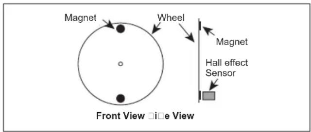
text_image
Magnet Wheel Magnet Hall effect Sensor Front View □i□e ViewIn Figure 5-3 and Figure 5-4, the waveform is high when light is passing through a slot in the encoder wheel and shining on the optical sensor. In the case of a Hall effect sensor, the high corresponds to the time that the magnet is in front of the sensor. These figures show the difference in the waveforms for varying RPMs. Notice that as RPM increases, the period (T) and pulse width (W) becomes smaller. Both period and pulse width are proportional to RPM. However, since the period is the greater of the two intervals, it is good practice to measure the period so that the RPM reading from the sensor will have the best resolution. See Tip #1 for measuring period. The technique for measuring period with averaging described in Tip #2 is useful for measuring high RPMs.
Figure 5-3: Low RPM

text_image
T WFigure 5-4: High RPM
text_image
T WTIP #6 Measuring the Period of an Analog Signal
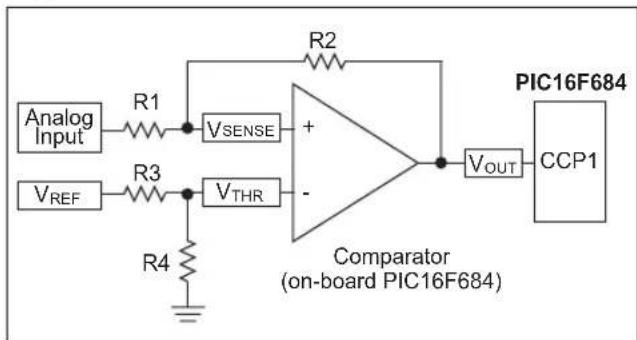
Microcontrollers with on-board Analog Comparator module(s), in addition to a CCP (or ECCP) module, can easily be configured to measure the period of an analog signal.
Figure 6-1 shows an example circuit using the peripherals of the PIC16F684.
Figure 6-1: Circuit
text_image
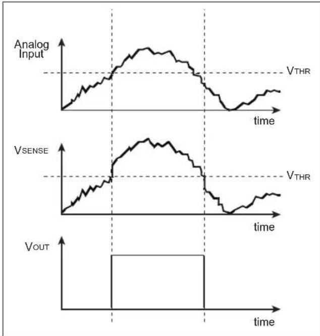
Analog Input R1 VSENSE + VREF R3 VTHR - R2 R4 Comparator (on-board PIC16F684) VOUT CCP1 PIC16F684R3 and R4 set the threshold voltage for the comparator. When the analog input reaches the threshold voltage, Vorwill toggle from low to high. R1 and R2 provide hysteresis to insure that small changes in the analog input won't cause jitter in the circuit. Figure 6-2 demonstrates the effect of hysteresis on the input. Look specifically at what Vone does when the analog input reaches the threshold voltage.
Figure 6-2: Signal Comparison
line
| Time | Analog Input (VTHR) | VSENSE (VTHR) | VOUT | |------|---------------------|--------------|------| | 0 | 0 | 0 | 0 | | Peak | ~1.5 | ~1.2 | 0 | | End | ~0.5 | ~0.3 | 0 |The CCP module, configured in Capture mode, can time the length between the rising edges of the comparator output (Vα) This is the period of the analog input, provided the analog signal reaches V _RD during every period.
COMPARE TIPS 'N TRICKS
In Compare mode, the 16-bit CCPRx register value is constantly compared against the TMR1 register pair values. When a match occurs, the CCPx pin is:
- Driven high
- Driven low
- Remains unchanged, or
- Toggles based on the module's configuration
The action on the pin is determined by control bits CCPxM3:CCPxM0 (CCPxCON<3:0>). A CCP interrupt is generated when a match occurs.
Special Event Trigger
Timer1 is normally not cleared during a CCP interrupt when the CCP module is configured in Compare mode. The only exception to this is when the CCP module is configured in Special Event Trigger mode. In this mode, when Timer1 and CCPRx are equal, the CCPx interrupt is generated, Timer1 is cleared, and an A/D conversion is started (if the A/D module is enabled.)
"Why Would I Use Compare Mode?"
Compare mode works much like the timer function on a stopwatch. In the case of a stopwatch, a predetermined time is loaded into the watch and it counts down from that time until zero is reached.
Compare works in the same way with one exception – it counts from zero to the predetermined time. This mode is useful for generating specific actions at precise intervals. A timer could be used to perform the same functionality, however, it would mean preloading the timer each time. Compare mode also has the added benefit of automatically altering the state of the CCPx pin based on the way the module is set up.
TIP #7 Periodic Interrupts
Generating interrupts at periodic intervals is a useful technique implemented in many applications. This technique allows the main loop code to run continuously, and then, at periodic intervals, jump to the interrupt service routine to execute specific tasks (i.e., read the ADC). Normally, a timer overflow interrupt is adequate for generating the periodic interrupt. However, sometimes it is necessary to interrupt at intervals that can not be achieved with a timer overflow interrupt. The CCP configured in Compare mode makes this possible by shortening the full 16-bit time period.
Example Problem:
A PIC16F684 running on its 8 MHz internal oscillator needs to be configured so that it updates a LCD exactly 5 times every second.
Step #1: Determine a Timer1 prescaler that allows an overflow at greater than 0.2 seconds
a) Timer1 overflows at: Tosc*4*65536* prescaler
b) For a prescaler of 1:1, Timer1 overflows in 32.8 ms.
c) A prescaler of 8 will cause an overflow at a time greater than 0.2 seconds. 8 × 32.8 ms = 0.25s
Step #2: Calculate CCPR1 (CCPR1L and CCPR1H) to shorten the time-out to exactly 0.2 seconds
a) CCPR1 = Interval Time/(T∞*4*prescaler) = 0.2/(125 ns*4*8) = 5000 = 0xC350
b) Therefore, CCPR1L = 0x50, and CCPR1H = 0xC3
Step #3: Configuring CCP1CON
The CCP module should be configured in Trigger Special Event mode. This mode generates an interrupt when the Timer1 equals the value specified in CCPR1L and Timer1 is automatically cleared ^(1) . For this mode, CCP1CON = 'b00001011'.
Note 1: Trigger Special Event mode also starts an A/D conversion if the A/D module is enabled. If this functionality is not desired, the CCP module should be configured in "generate software interrupt-on-match only" mode (i.e., CCP1CON = b'00001010'). Timer 1 must also be cleared manually during the CCP interrupt.
TIP #8 Modulation Formats
The CCP module, configured in Compare mode, can be used to generate a variety of modulation formats. The following figures show four commonly used modulation formats:
Figure 8-1: Pulse-width Modulation
text_image
TETETE Logic '0' Logic '1' TBPFigure 8-2: Manchester
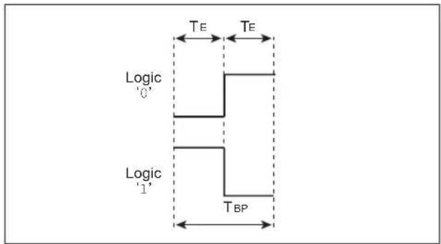
text_image
TE TE Logic '0' Logic '1' TBPFigure 8-3: Pulse Position Modulation
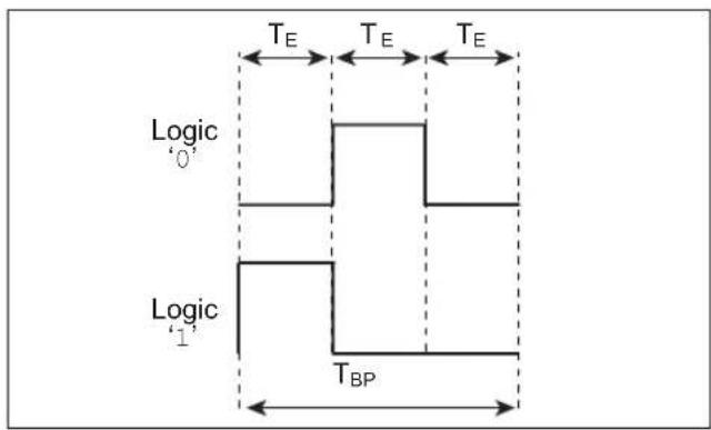
text_image
TE TE TE Logic '0' Logic '1' TBPFigure 8-4: Variable Pulse-width Modulation
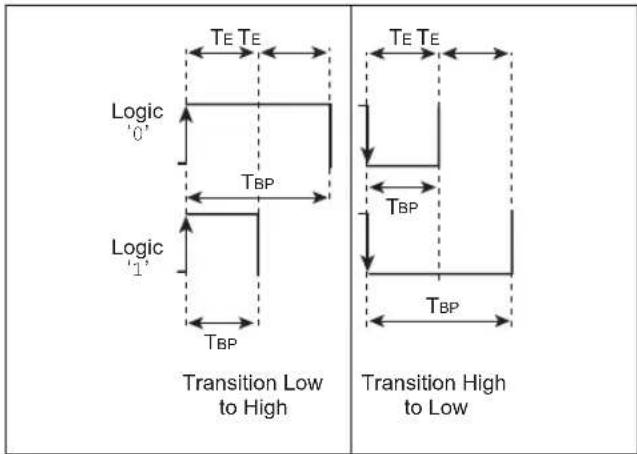
text_image
TE TE Logic '0' TBP Logic '1' TBP Transition Low to High TE TE TBP TBP Transition High to LowThe figures show what a logic '0' or a logic '1' looks like for each modulation format.
A transmission typically resembles an asynchronous serial transmission consisting of a Start bit, followed by 8 data bits, and a Stop bit.
T_E is the basic timing element in each modulation format and will vary based on the desired baud rate.
Trigger Special Event mode can be used to generate T_E , (the basic timing element). When the CCPx interrupt is generated, code in the ISR routine would implement the desired modulation format (additional modulation formats are also possible).
TIP #9 Generating the Time Tick for a RTOS
Real Time Operating Systems (RTOS) require a periodic interrupt to operate. This periodic interrupt, or "tick rate", is the basis for the scheduling system that RTOS's employ. For instance, if a 2 ms tick is used, the RTOS will schedule its tasks to be executed at multiples of the 2 ms. A RTOS also assigns a priority to each task, ensuring that the most critical tasks are executed first. Table 9-1 shows an example list of tasks, the priority of each task and the time interval that the tasks need to be executed.
Table 9-1: Tasks
| Task Interval | Priority | |
| Read ADC Input 1 20 ms 2 | ||
| Read ADC Input 2 60 ms 1 | ||
| Update LCD 24 ms 2 | ||
| Update LED Array 36 ms 3 | ||
| Read Switch 10 ms 1 | ||
| Dump Data to Serial Port 240 | ms 1 |
The techniques described in Tip #7 can be used to generate the 2 ms periodic interrupt using the CCP module configured in Compare mode.
Note: For more information on RTOSs and their use, see Application Note AN777 "Multitasking on the PIC16F877 with the Salvo™ RTOS".
TIP #10 16-Bit Resolution PWM
Figure 10-1: 16-Bit Resolution PWM

text_image
CCPx Interrupt: Clear CCPx pin Timer1 Interrupt: Set CCPx pin- Configure CCPx to clear output (CCPx pin) on match in Compare mode (CCPxCON
- Enable the Timer1 interrupt.
- Set the period of the waveform via Timer1 prescaler (T1CON <5:4>).
- Set the duty cycle of the waveform using CCPRxL and CCPRxH.
- Set CCPx pin when servicing the Timer1 overflow interrupt ^(1) .
Note 1: One hundred percent duty cycle is not achievable with this implementation due to the interrupt latency in servicing Timer1. The period is not affected because the interrupt latency will be the same from period to period as long as the Timer1 interrupt is serviced first in the ISR.
Timer1 has four configurable prescaler values. These are 1:1, 1:2, 1:4 and 1:8. The frequency possibilities of the PWM described above are determined by Equation 10-1.
Equation 10-1
$$ F _ {P W M} = F _ {\text { osc }} / (6 5 5 3 6 ^ {} 4 ^ {} \text { prescaler }) $$
For a microcontroller running on a 20 MHz oscillator (Fosc) this equates to frequencies of 76.3 Hz, 38.1 Hz, 19.1 Hz and 9.5 Hz for increasing prescaler values.
TIP #11 Sequential ADC Reader
Figure 11-1: Timeline
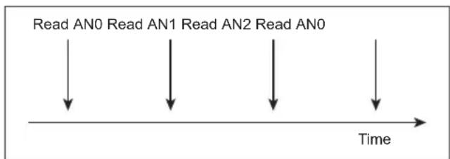
flowchart
graph TD
    A["Read AN0"] --> B["Time"]
    C["Read AN1"] --> D["Time"]
    E["Read AN2"] --> F["Time"]
    G["Read AN0"] --> H["Time"]
Trigger Special Event mode (a sub-mode in Compare mode) generates a periodic interrupt in addition to automatically starting an A/D conversion when Timer1 matches CCPRxL and CCPRxH. The following example problem demonstrates how to sequentially read the A/D channels at a periodic interval.
Example
Given the PIC16F684 running on its 8 MHz internal oscillator, configure the microcontroller to sequentially read analog pins AN0, AN1 and AN2 at 30 ms intervals.
Step #1: Determine Timer1 Prescaler
a) Timer1 overflows at: Tosc*4*65536* prescaler.
b) For a prescaler of 1:1, the Timer1 overflow occurs in 32.8 ms.
c) This is greater than 30 ms, so a prescaler of 1 is adequate.
Step #2: Calculate CCPR1 (CCPR1L and CCPR1H)
a) CCPR1 = Interval Time/(Tosc*4*prescaler) = 0.030/(125 ns*4*1) = 6000 = 0xEA60
b) Therefore, CCPR1L = 0x60, and CCPR1H = 0xEA
Step #3: Configuring CCP1CON
The ECCP module should be configured in Trigger Special Event mode. This mode generates an interrupt when Timer1 equals the value specified in CCPR1. Timer1 is automatically cleared and the GO bit in ADCON0 is automatically set. For this mode, CCP1CON = 'b00001011'.
Step #4: Add Interrupt Service Routine Logic
When the ECCP interrupt is generated, select the next A/D pin for reading by altering the ADCON0 register.
TIP #12 Repetitive Phase Shifted Sampling
Repetitive phase shifted sampling is a technique to artificially increase the sampling rate of an A/D converter when sampling waveforms that are both periodic and constant from period to period. The technique works by capturing regularly spaced samples of the waveform from the start to finish of the waveform's period. Sampling of the next waveform is then performed in the same manner, except that the start of the sample sequence is delayed a percentage of the sampling period. Subsequent waveforms are also sampled, with each sample sequence slightly delayed from the last, until the delayed start of the sample sequence is equal to one sample period. Interleaving the sample sets then produces a sample set of the waveform at a higher sample rate. Figure 12-1 shows an example of a high frequency waveform.
Figure 12-1: High Frequency Periodic Waveform
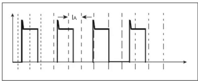
text_image
IAAs indicated in the key, the finely dotted lines show where the A/D readings are taken during the first period of the waveform. The medium sized dashed lines show when the A/D readings are taken during the second period, and so on. Figure 12-2 shows these readings transposed onto one period.
Figure 12-2: Transposed Waveform

line
| Time | Volts | |------|-------| | 0 | 0 | | 1 | High | | 2 | Low | | 3 | Low | | 4 | Low | | 5 | Low | | 6 | Low | | 7 | Low | | 8 | Low | | 9 | Low | | 10 | Low | | 11 | Low | | 12 | Low | | 13 | Low | | 14 | Low | | 15 | Low | | 16 | Low | | 17 | Low | | 18 | Low | | 19 | Low | | 20 | Low | | 21 | Low | | 22 | Low | | 23 | Low | | 24 | Low | | 25 | Low | | 26 | Low | | 27 | Low | | 28 | Low | | 29 | Low | | 30 | Low | | 31 | Low | | 32 | Low | | 33 | Low | | 34 | Low | | 35 | Low | | 36 | Low | | 37 | Low | | 38 | Low | | 39 | Low | | 40 | Low | | 41 | Low | | 42 | Low | | 43 | Low | | 44 | Low | | 45 | Low | | 46 | Low | | 47 | Low | | 48 | Low | | 49 | Low | | 50 | Low | | 51 | Low | | 52 | Low | | 53 | Low | | 54 | Low | | 55 | Low | | 56 | Low | | 57 | Low | | 58 | Low | | 59 | Low | | 60 | Low | | 61 | Low | | 62 | Low | | 63 | Low | | 64 | Low | | 65 | Low | | 66 | Low | | 67 | Low | | 68 | Low | | 69 | Low | | 70 | Low | | 71 | Low | | 72 | Low | | 73 | Low | | 74 | Low | | 75 | Low | | 76 | Low | | 77 | Low | | 78 | Low | | 79 | Low | | 80 | Low | | 81 | Low | | 82 | Low | | 83 | Low | | 84 | Low | | 85 | Low | | 86 | Low | | 87 | Low | | 88 | Low | | 89 | Low | | 90 | Low | | 91 | Low | | 92 | Low | | 93 | Low | | 94 | Low | | 95 | Low | | 96 | Low | | 97 | Low | | 98 | Low | | 99 | Low | | 100 | Low |The CCP module is configured in Compare Special Event Trigger mode to accomplish this task. The phase shift is implemented by picking values of CCPRxL and CCPRxH that are not synchronous with the period of the sampling waveform. For instance, if the period of a waveform is 100 s, then sampling at a rate of once every 22 s will give the following set of sample times over 11 periods (all values in s).
| 1st | 2nd | 3rd | 4th | 5th | 6th | 7th | 8th | 9th | 10th | 11th | ||
| 0 | 10 | 20 | 8 | 18 | 6 | 16 | 4 | 14 | 2 | 12 | ||
| 22 | 32 | 42 | 30 | 40 | 28 | 38 | 26 | 36 | 24 | 34 | ||
| 44 | 54 | 64 | 52 | 62 | 50 | 60 | 48 | 58 | 46 | 56 | ||
| 66 | 76 | 86 | 74 | 84 | 72 | 82 | 70 | 80 | 68 | 78 | ||
| 88 | 98 | 96 | 94 | 92 | 90 |
When these numbers are placed in sequential order, they reveal a virtual sampling interval (Iv) of 2 μs from 0 μs to 100 μs, although the actual sampling interval (IA) is 22 μs.
PWM TIPS 'N TRICKS
The ECCP and CCP modules produce a 10-bit resolution Pulse-Width Modulated (PWM) waveform on the CCPx pin. The ECCP module is capable of transmitting a PWM signal on one of four pins, designated P1A through P1D. The PWM modes available on the ECCP module are:
- Single output (P1A only)
• Half-bridge output (P1A and P1B only)
• Full-bridge output forward
• Full-bridge output reverse
One of the following configurations must be chosen when using the ECCP module in PWM Full-bridge mode:
• P1A, P1C active-high; P1B, P1D active-high
• P1A, P1C active-high; P1B, P1D active-low
• P1A, P1C active-low; P1B, P1D active-high
• P1A, P1C active-low; P1B, P1D active-low
"Why Would I Use PWM Mode?"
As the next set of Tips 'n Tricks demonstrate, Pulse-Width Modulation (PWM) can be used to accomplish a variety of tasks from dimming LEDs to controlling the speed of a brushed DC electric motor. All these applications are based on one basic principle of PWM signals – as the duty cycle of a PWM signal increases, the average voltage and power provided by the PWM increases. Not only does it increase with duty cycle, but it increases linearly. The following figure illustrates this point more clearly. Notice that the RMS and maximum voltage are functions of the duty cycle (DC) in the following Figure 12-3.
Figure 12-3: Duty Cycle Relation to V
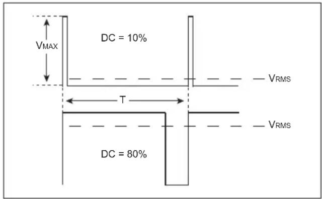
text_image
VMAX DC = 10% T DC = 80% VRMS VRMSEquation 12-1 shows the relation between V RMS and V VMK
Equation 12-1: Relation Between V and V
$$ V _ {R S} = D C \times V _ {M K} $$
TIP #13 Deciding on PWM Frequency
In general, PWM frequency is application dependent although two general rules-of-thumb hold regarding frequency in all applications. They are:
- As frequency increases, so does current requirement due to switching losses.
- Capacitance and inductance of the load tend to limit the frequency response of a circuit.
In low-power applications, it is a good idea to use the minimum frequency possible to accomplish a task in order to limit switching losses. In circuits where capacitance and/or inductance are a factor, the PWM frequency should be chosen based on an analysis of the circuit.
Motor Control
PWM is used extensively in motor control due to the efficiency of switched drive systems as opposed to linear drives. An important consideration when choosing PWM frequency for a motor control application is the responsiveness of the motor to changes in PWM duty cycle. A motor will have a faster response to changes in duty cycle at higher frequencies. Another important consideration is the sound generated by the motor. Brushed DC motors will make an annoying whine when driven at frequencies within the audible frequency range (20 Hz-4 kHz.) In order to eliminate this whine, drive brushed DC motors at frequencies greater than 4 kHz. (Humans can hear frequencies at upwards of 20 kHz, however, the mechanics of the motor winding will typically attenuate motor whine above 4 kHz).
LED and Light Bulbs
PWM is also used in LED and light dimmer applications. Flicker may be noticeable with rates below 50 Hz. Therefore, it is generally a good rule to pulse-width modulate LEDs and light bulbs at 100 Hz or higher.
TIP #14 Unidirectional Brushed DC Motor Control Using CCP
Figure 14-1: Brushed DC (BDC) Motor Control Circuit

text_image
PIC16F628 Vcc Motor 22 pF Place on motor EMI/RFI Suppression 100Ω 10 kΩ CCP1Figure 14-1 shows a unidirectional speed controller circuit for a brushed DC motor. Motor speed is proportional to the duty cycle of the PWM output on the CCP1 pin. The following steps show how to configure the PIC16F628 to generate a 20 kHz PWM with 50% duty cycle. The microcontroller is running on a 20 MHz crystal.
Step #1: Choose Timer2 Prescaler
a) F_MW = Fosc/((PR2 + 1)^4^prescaler) = 19531 Hz for PR2 = 255 and prescaler of 1
b) This frequency is lower than 20 kHz, therefore a prescaler of 1 is adequate.
Step #2: Calculate PR2
$$ \mathrm{PR2} = \text { Fosc } / (\mathrm{F} _ {\text { R }} 4 ^ {*} \text { prescaler }) - 1 = 2 4 9 $$
Step #3: Determine CCPR1L and CCP1CON<5:4>
a) CCPR1L:CCP1CON<5:4> = DutyCycle*0x3FF = 0x1FF
b) CCPR1L = 0x1FF >> 2 = 0x7F,
CCP1CON<5:4> = 3
Step #4: Configure CCP1CON
The CCP module is configured in PWM mode with the Least Significant bits of the duty cycle set, therefore, CCP1CON = 'b001111000'.
TIP #15 Bidirectional Brushed DC Motor Control Using ECCP
Figure 15-1: Full-Bridge BDC Drive Circuit

text_image
P1A 10 kΩ TC428 Vcc 10 pF P1B 10 kΩ TC428 10 pF Motor P1C 10 kΩ TC428 Vcc 10 pF P1D 10 kΩ TC428 10 pFThe ECCP module has brushed DC motor control options built into it. Figure 15-1 shows how a full-bridge drive circuit is connected to a BDC motor. The connections P1A, P1B, P1C and P1D are all ECCP outputs when the module in configured in "Full-bridge Output Forward" or "Full-bridge Output Reverse" modes (CCP1CON<7:6>). For the circuit shown in Figure 15-1, the ECCP module should be configured in PWM mode: P1A, P1C active high; P1B, P1D active high (CCP1CON<3:1>). The reason for this is the MOSFET drivers (TC428) are configured so a high input will turn on the respective MOSFET.
The following table shows the relation between the states of operation, the states of the ECCP pins and the ECCP Configuration register.
| State P | 1A P1B P | 1C P1D CCP1CON | ||
| Forward 1 | tri-state tri-state mod ‘b01xx1100’ | |||
| Reverse tri-state mod 1 tri-state ‘b11xx1100’ | ||||
| Coast tri-state tri-state tri-state tri-state N/A | ||||
| Brake tri-state 1 | 1 tri-state | N/A | ||
Legend: '1' = high, '0' = low, mod = modulated, tri-state = pin configured as input
TIP #16 Generating an Analog Output
Figure 16-1: Low-Pass Filter
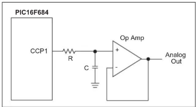
text_image
PIC16F684 CCP1 R C Op Amp + - Analog OutPulse-width modulated signals can be used to create Digital-to-Analog (D/A) converters with only a few external components. Conversion of PWM waveforms to analog signals involves the use of an analog low-pass filter. In order to eliminate unwanted harmonics caused by a PWM signal to the greatest degree possible, the frequency of the PWM signal ( F_WM ) should be significantly higher than the bandwidth ( F_BW ) of the desired analog signal. Equation 16-1 shows this relation.
Equation 16-1
$$ F _ {P W M} = K ^ {*} F _ {B W} $$
Where harmonics decrease as K increases
R and C are chosen based on the following equation:
Equation 16-2
$$ R C = 1 / (2 \pi F _ {B W}) $$
Pick a value of C arbitrarily and then calculate R. The attenuation of the PWM frequency for a given RC filter is:
Equation 16-3
$$ \operatorname{Att} (\mathrm{dB} = - 1 0 ^ {*} \log [ 1 + (2 \pi F _ {M R C}) 2 ] $$
If the attenuation calculated in Equation 16-3 is not sufficient, then K must be increased in Equation 16-1. See Application Note AN538 "Using PWM to Generate Analog Output in PIC17C42" for more details on using PWM to generate an analog output.
TIP #17 Boost Power Supply
Figure 17-1: Boost Power Supply Circuit

text_image
PIC16F684 CCP1 AN0 V_IN Feedback C1 10 μF R3 10 kΩ Q1 D1 R1 4.7 kΩ L1 680 μH V_CC C2 47 μF RL VOUTHardware
Pulse-width modulation plays a key role in boost power supply design. Figure 17-1 shows a typical boost circuit. The circuit works by Q1 grounding the inductor (L1) during the high phase of the PWM signal generated by CCP1. This causes an increasing current to flow through L1 while Vccis applied. During the low phase of the PWM signal, the energy stored in L1 flows through D1 to the storage capacitor (C2) and the load. VOUT is related to VIN by Equation 17-1.
Note: Technical Brief TB053 "Generating High Voltage Using the PIC16C781/782" provides details on boost power supply design.
The first parameter to determine is the duty cycle based upon the input and output voltages. See Equation 17-1.
Equation 17-1
$$ \frac {V _ {\text {OT}}}{V _ {\text {IN}}} = \frac {1}{1 - D} $$
Next, the value of the inductor is chosen based on the maximum current required by the load, the switching frequency and the duty cycle. A function for inductance in terms of load current is given by Equation 17-2, where T is the PWM period, D is the duty cycle, and I or is the maximum load current.
Equation 17-2
$$ L = \frac {V _ {\text {IN}} (1 - D) D T}{2 \log} $$
The value for L is chosen arbitrarily to satisfy this equation given lo, a maximum duty cycle of 75% and a PWM frequency in the 10 kHz to 100 kHz range.
Using the value chosen for L, the ripple current is calculated using Equation 17-3.
Equation 17-3
$$ I _ {R P E} = \frac {V _ {I N} D T}{L} $$
IRRE can not exceed the saturation current for the inductor. If the value for L does produce a ripple current greater than I_R , a bigger inductor is needed.
Note: All equations above assume a discontinuous current mode.
Firmware
The PWM duty cycle is varied by the microcontroller in order to maintain a stable output voltage over fluctuating load conditions. A firmware implemented PID control loop is used to regulate the duty cycle. Feedback from the boost power supply circuit provides the input to the PID control.
Note: Application Note AN258 "Low Cost USB Microcontroller Programmer" provides details on firmware-based PID control.
TIP #18 Varying LED Intensity
The intensity of an LED can be varied by pulse-width modulating the voltage across the LED. A microcontroller typically drives an LED with the circuit shown in Figure 18-1. The purpose of R1 is to limit the LED current so that the LED runs in its specified current and voltage range, typically around 1.4 volts at 20 mA. Modulating the LED drive pin on the microcontroller will vary the average current seen by the LED and thus its intensity. As mentioned in Tip #13, LEDs and other light sources should be modulated at no less than 100 Hz in order to prevent noticeable flicker.
Figure 18-1: LED Drive

text_image
PIC16F684 CCP1 R1 270ΩThe CCP module, configured in PWM mode, is ideal for varying the intensity of an LED. Adjustments to the intensity of the LED are made by simply varying the duty cycle of the PWM signal driving the LED. This is accomplished by varying the CCPRxL register between 0 and 0xFF.
TIP #19 Generating X-10 ^® Carrier Frequency
X-10 uses a piggybacked 120 kHz square wave (at 50% duty cycle) to transmit information over 60 Hz power lines. The CCP module, running in PWM mode, can accurately create the 120 kHz square wave, referred to as the carrier frequency. Figure 19-1 shows how the 120 kHz carrier frequency is piggybacked onto the sinusoidal 60 Hz power waveform.
Figure 19-1: Carrier Frequency With Sinusoidal Waveform
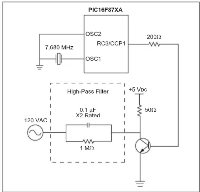
text_image
PIC16F87XA OSC2 RC3/CCP1 7.680 MHz OSC1 200Ω High-Pass Filter 0.1 μF X2 Rated +5 Vdc 50Ω 120 VAC 1 MΩX-10 specifies the carrier frequency at 120 kHz ( ± 2 kHz). The system oscillator in Figure 18-1 is chosen to be 7.680 MHz, so that the CCP module can generate precisely 120 kHz. X-10 requires that the carrier frequency be turned on and off at different points on the 60 Hz power waveform. This is accomplished by configuring the TRIS register for the CCP1 pin as either an input (carrier frequency off) or an output (carrier frequency on). Refer to Application Note AN236 “X-10 Home Automation Using the PIC16F877A” for more details on X-10 and for source code for setting up the CCP module appropriately.
COMBINATION CAPTURE AND COMPARE TIPS
The CCP and ECCP modules can be configured on the fly. Therefore, these modules can perform different functions in the same application provided these functions operate exclusively (not at the same time). This section will provide examples of using a CCP module in different modes in the same application.
TIP #20 RS-232 Auto-baud
RS-232 serial communication has a variety of baud rates to choose from. Multiple transmission rates require software which detects the transmission rate and adjusts the receive and transmit routines accordingly. Auto-baud is used in applications where multiple transmission rates can occur. The CCP module can be configured in Capture mode to detect the baud rate and then be configured in Compare mode to generate or receive RS-232 transmissions.
In order for auto-baud to work, a known calibration character must be transmitted initially from one device to another. One possible calibration character is shown in Figure 20-1. Timing this known character provides the device with the baud rate for all subsequent communications.
Figure 20-1: RS-232 Calibration Character
text_image
Start Bit 0 0 0 0 0 0 01 Stop Bit LSB MSBAuto-baud Routine Implementation:
- Configure CCP module to capture the falling edge (beginning of Start bit).
- When the falling edge is detected, store the CCPR1 value.
- Configure the CCP module to capture the rising edge.
- Once the rising edge is detected, store the CCPR1 value.
- Subtract the value stored in step 2 from the value in step 4. This is the time for 8 bits.
- Shift the value calculated in step 5 right 3 times to divide by 8. This result is the period of a bit ( T_B ).
- Shift value calculated in step 6 right by 1. This result is half the period of a bit.
The following code segments show the process for transmitting and receiving data in the normal program flow. This same functionality can be accomplished using the CCP module by configuring the module in Compare mode and generating a CCP interrupt every bit period. When this method is used, one bit is either sent or received when the CCP interrupt occurs.
Note: Refer to Application Note AN712 " RS-232 Auto-baud for the PIC16C5X Devices" for more details on auto-baud.
Example 20-1: Transmit Routine
TxRountine
MOVL W 8 ;preload bit counter
;with 8
MOVW F c ounter
BCF TxLine ;line initially high,
;toggle low for START
;bit
TxLoop
CALL DelayTb ;wait Tb (bit period)
RRF RxByte,f ;rotate LSB first into
;the Carry flag
BTFSS STATUS,C ;Tx line state equals
;state of Carry flag
BCF T xLine
BTFS C S TATUS, C
BSF T xLine
DECFSZ Counter,f ;Repeat 8 times
GOTO TxLoop
CALL Delay Tb ;Delay Tb before
;sending STOP bit
BSF TxLine ;send STOP bit
Example 20-2: Receive Routine
RxRoutine
BTFSC RxLine ;wait for receive
;line to go low
GOTO RxRout ine
MOVLW 8 ;initialize bit
;counter to 8
MOVWF Counte r
CALL Delay1HalfTb;delay 1/2 Tb here
;plus Tb in RxLoop
;in order to sample
;at the right time
RxLoop
CALL DelayTb ;wait Tb (bit
;period)
BTFSS RxLine ;Carry flag state
;equals Rx line
;state
BCF STATUS ,C
BTFSC RxLine
BSF STATUS ,C
BTFSC RxLine
BSF STATUS ,C
RRF RxByte,f ;Rotate LSB first
;into receive type
DECFSZ Counter,f ;Repeat 8 times
GOTO RxLoop
TIP #21 Dual-Slope Analog-to-Digital Converter
A circuit for performing dual-slope A/D conversion utilizing the CCP module is shown in Figure 21-1.
Figure 21-1: Dual-Slope Analog-to-Digital Converter
text_image
VIN -VREF PIC16F684 CCP1 Integrator Comparator (on-board PIC16F684)Dual-slope A/D conversion works by integrating the input signal ( V_IN ) for a fixed time (T1). The input is then switched to a negative reference (- V_REF ) and integrated until the integrator output is zero (T2). V_IN is a function of V_REF and the ratio of T2 to T1.
Figure 21-2: V vs. Time
line
| Time | Integrator output with V_IN input (V) | Integrator output with V_REF input (V) | |------|----------------------------------------|-----------------------------------------| | 0 | 0 | 0 | | T1 | Peak (T1) | Peak (T2) | | T2 | Peak (T2) | Peak (T2) |The components of this conversion type are the fixed time and the timing of the falling edge. The CCP module can accomplish both of these components via Compare mode and Capture mode respectively. Here's how:
- Configure the CCP module in Compare mode, Special Event Trigger.
- Switch the analog input into the integrator from V_REF to V_IN .
- Use the CCP module to wait T1 (T1 chosen based on capacitor value).
- When the CCP interrupt occurs, switch the analog input into the regulator from V_IN to V_REF and reconfigure the module in Capture mode; wait for falling edge.
- When the next CCP interrupt occurs, the time captured by the module is T2.
- Calculate V_IN using Equation 21-1.
Equation 21-1
$$ V _ {I N} = V _ {R E F} \frac {T 2}{T 1} $$
NOTES:
CHAPTER 4
PIC® Microcontroller Comparator Tips 'n Tricks
Table Of Contents
TIPS 'N TRICKS INTRODUCTION
TIP #1: Low Battery Detection 4-2
TIP #2: Faster Code for Detecting Change ..... 4-3
TIP #3: Hysteresis 4-4
TIP #4: Pulse Width Measurement 4-5
TIP #5: Window Comparison 4-6
TIP #6: Data Slicer 4-7
TIP #7: One-Shot 4-8
TIP #8: Multi-Vibrator (Square Wave Output). 4-9
TIP #9: Multi-Vibrator (Ramp Wave Output) ... 4-10
TIP #10: Capacitive Voltage Doubler 4-11
TIP #11: PWM Generator 4-12
TIP #12: Making an Op Amp Out of a Comparator ....4-13
TIP #13: PWM High-Current Driver .....4-14
TIP #14: Delta-Sigma ADC 4-15
TIP #15: Level Shifter 4-16
TIP #16: Logic: Inverter 4-16
TIP #17: Logic: AND/NAND Gate ....4-17
TIP #18: Logic: OR/NOR Gate 4-18
TIP #19: Logic: XOR/XNOR Gate 4-19
TIP #20: Logic: Set/Reset Flip Flop 4-20
TIPS 'N TRICKS INTRODUCTION
Microchip continues to provide innovative products that are smaller, faster, easier to use and more reliable. The Flash-based PIC® microcontrollers (MCUs) are used in a wide range of everyday products from smoke detectors to industrial, automotive and medical products.
The PIC12F/16F Family of devices with on-chip voltage comparators merge all the advantages of the PIC MCU architecture and the flexibility of Flash program memory with the mixed signal nature of a voltage comparator. Together they form a low-cost hybrid digital/analog building block with the power and flexibility to work in an analog world.
The flexibility of Flash and an excellent development tool suite, including a low-cost In-Circuit Debugger, In-Circuit Serial Programming™ (ICSP™) and MPLAB® ICE 2000 emulation, make these devices ideal for just about any embedded control application.
The following series of Tips ‘n Tricks can be applied to a variety of applications to help make the most of discrete voltage comparators or microcontrollers with on-chip voltage comparators.
TIP #1 Low Battery Detection
When operating from a battery power supply, it is important for a circuit to be able to determine when the battery charge is insufficient for normal operation of the circuit. Typically, this is a comparator-based circuit similar to the Programmable Low Voltage Detect (PLVD) peripheral. If the PLVD peripheral is not available in the microcontroller, a similar circuit can be constructed using a comparator and a few external components (see Figure 1-1 and Figure 1-2). The circuit in Figure 1-1 assumes that the microcontroller is operating from a regulated supply voltage. The circuit in Figure 1-2 assumes that the microcontroller supply is unregulated.
Figure 1-1: Regulated Supply

text_image
V_{BATT} R3 R4 R2 V_{DD} R1 + - Low Battery EnableThe comparator will trip when the battery voltage, V_B = 5.7V : R1 = 33k, R2 = 10k, R3 = 39k, R4 = 10k, V_D = 5V .
In Figure 1-1, resistors R1 and R2 are chosen to place the voltage at the non-inverting input at approximately 25% of VDD R3 and R4 are chosen to set the inverting input voltage equal to the non-inverting input voltage when the battery voltage is equal to the minimum operating voltage for the system.
Figure 1-2: Unregulated Supply
text_image
VBATT R3 R1 Comparator D1 R2 Low Battery EnableComparator will trip when V_B =3V: R1 = 33k, R2 = 10k and R3 = 470Ω.
In Figure 1-2, resistor R3 is chosen to bias diode D1 above its forward voltage when V_BAT is equal to the minimum battery voltage for the system. Resistors R1 and R2 are chosen to set the inverting input voltage equal to the forward voltage of D1.
TIP #2 Faster Code for Detecting Change
When using a comparator to monitor a sensor, it is often just as important to know when a change occurs as it is to know what the change is. To detect a change in the output of a comparator, the traditional method has been to store a copy of the output and periodically compare the held value to the actual output to determine the change. An example of this type of routine is shown below.
Example 2-1
Test
MOVF hold, w ; get old Cout
XORWF CMCON, w ; compare to new Cout
ANDLW COUTMASK
BTFSC STATUS, Z
RETLW 0 ; if = return "no change"
MOVF CMCON, w ; if not =, get new Cout
ANDLW COUTMASK ; remove all other bits
MOVWF hold ; store in holding var.
IORLW CHNGBIT ; add change flag
RETURN
This routine requires 5 instructions for each test, 9 instructions if a change occurs, and 1 RAM location for storage of the old output state.
A faster method for microcontrollers with a single comparator is to use the comparator interrupt flag to determine when a change has occurred.
Example 2-2
Test
BTFSS PIR1, CMIF ; test comparator flag
RETLW 0 ; if clear, return a 0
BTFSS CMCON, COUT ; test Cout
RETLW CHNGBIT ; if clear return
; CHNGFLAG
RETLW COUTMASK + CHNGBIT; if set,
; return both
This routine requires 2 instructions for each test, 3 instructions if a change occurs, and no RAM storage.
If the interrupt flag can not be used, or if two comparators share an interrupt flag, an alternate method that uses the comparator output polarity bit can be used.
Example 2-3
Test
BTFSS CMCON, COUT ; test Cout
RETLW 0 ; if clear, return 0
MOVLW CINVBIT ; if set, invert Cout
XORWF CMCON, f ; forces Cout to 0
BTFSS CMCON, CINV ; test Cout polarity
RETLW CHNGFLAG ; if clear, return
; CHNGFLAG
RETLW COUTMASK + CHNGFLAG; if set,
; return both
This routine requires 2 instructions for each test, 5 instructions if a change occurs, and no GPR storage.
TIP #3 Hysteresis
When the voltages on a comparator's input are nearly equal, external noise and switching noise from inside the microcontroller can cause the comparator output to oscillate or "chatter." To prevent chatter, some of the comparator output voltage is fed back to the non-inverting input of the comparator to form hysteresis (see Figure 3-1). Hysteresis moves the comparator threshold up when the input is below the threshold, and down when the input is above the threshold. The result is that the input must overshoot the threshold to cause a change in the comparator output. If the overshoot is greater than the noise present on the input, the comparator output will not chatter.
Figure 3-1: Comparator with Hysteresis

To calculate the resistor values required, first determine the high and low threshold values which will prevent chatter ( V_TH and V_TL ). Using V_TH and V_TL , the average threshold voltage can be calculated using the equation.
Equation 3-1
$$ V _ {A G} = \frac {V _ {D D} * V _ {T L}}{V _ {D D} - V _ {T H} + V _ {T L}} $$
Next, choose resistor values that satisfy Equation 3-2 and calculate the equivalent resistance using Equation 3-3.
Note: A continuous current will flow through R1 and R2. To limit the power dissipation in R1 and R2 the total resistance of R1 and R2 should be at least 1k. The total resistance of R1 and R2 should also be kept below 10K to keep the size of R3 small. Large values for R3, 100k-10 M, can produce voltage offsets at the non-inverting input due to the comparator's input bias current.
Equation 3-2
$$ V _ {A G} = \frac {V _ {D D} ^ {*} R 2}{R 1 + R 2} $$
Equation 3-3
$$ R _ {\text {EQ}} = \frac {R 1 * R 2}{R 1 + R 2} $$
Then, determine the feedback divider ratio DR, using Equation 3-4.
Equation 3-4
$$ D _ {R} = \frac {\left(V _ {T H} - V _ {T L}\right)}{V _ {D}} $$
Finally, calculate the feedback resistor R3 using Equation 3-5.
Equation 3-5
$$ R 3 = R _ {\text {EQ}} \left[ \left(\frac {1}{D _ {R}}\right) - 1 \right] $$
Example:
- A V_DD = 5.0V , V_H = 3.0V and V_L = 2.5V
- V_AG = 2.77V
• R = 8.2k and R2 = 10k, gives a VAG = 2.75V - R_EQ = 4.5k
- D_R = .1
• R3 = 39k (40.5 calculated) - V_HAC = 2.98V
- V_LACT = 2.46 ~V
TIP #4 Pulse Width Measurement
To measure the high or low pulse width of an incoming analog signal, the comparator can be combined with Timer1 and the Timer1 Gate input option (see Figure 4-1). Timer1 Gate acts as a count enable for Timer1. If the input is low, Timer1 will count. If the T1G input is high, Timer1 does not count. Combining T1G with the comparator allows the designer to measure the time between a high-to-low output change and a low-to-high output change.
To make a measurement between a low-to-high and a high-to-low transition, the only change required is to set the CINV bit in the comparator CMCON register which inverts the comparator output.
Because the output of the comparator can change asynchronously with the Timer1 clock, only comparators with the ability to synchronize their output with the Timer1 clock should be used and their C2SYNC bits should be set.
If the on-chip comparator does not have the ability to synchronize its output to the Timer1 clock, the output can be synchronized externally using a discrete D flip-flop (see Figure 4-2).
Note: The flip-flop must be falling edge triggered to prevent a race condition.
Figure 4-2: Externally Synchronized Comparator

text_image
VDD VINPUT Trigger Level - + Timer Clock COUT D O TIG Timer1 T1CKIFigure 4-1: Comparator with Timer1 and T1G

text_image
VDD VINPUT Trigger Level - + COUT TIG Timer1TIP #5 Window Comparison
When monitoring an external sensor, it is often convenient to be able to determine when the signal has moved outside a pre-established safe operating range of values or window of operation. This windowing provides the circuit with an alarm when the signal moves above or below safety limits, ignoring minor fluctuations inside the safe operating range.
To implement a window comparator, two voltage comparators and 3 resistors are required (see Figure 5-1).
Figure 5-1: Window Comparator
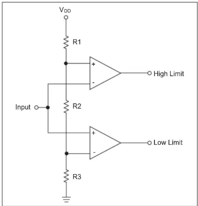
text_image
VDD R1 + - High Limit Input R2 + - Low Limit R3Resistors R1, R2 and R3 form a voltage divider which generates the high and low threshold voltages. The outputs HIGH LIMIT and LOW LIMIT are both active high, generating a logic one on the HIGH LIMIT output when the input voltage rises above the high threshold, and a logic one on the LOW LIMIT output when the input voltage falls below the low threshold.
To calculate values for R1, R2 and R3, find values that satisfy Equation 5-1 and Equation 5-2.
Note: A continuous current will flow through R1, R2 and R3. To limit the power dissipation in the resistors, the total resistance of R1, R2 and R3 should be at least 1k. The total resistance of R1, R2 and R3 should also be kept less than 1 M to prevent offset voltages due to the input bias currents of the comparator.
Equation 5-1
$$ V _ {T H + H} = \frac {V _ {D D} ^ {*} (R 3 + R 2)}{R 1 + R 2 + R 3} $$
Equation 5-2
$$ V _ {T H L O} = \frac {V _ {D D} ^ {*} R _ {3}}{R 1 + R 2 + R 3} $$
Example:
- V_DD = 5.0V , V_TH = 2.5V , V_TL = 2.0V
• R1 = 12k, R2 = 2.7k, R3 = 10k - V_TH (actual) = 2.57V, V_TL (actual) = 2.02V
Adding Hysteresis:
To add hysteresis to the HIGH LIMIT comparator, follow the procedure outlined in Tip #3. Use the series combination of R2 and R3 as the resistor R2 in Tip #3.
To add hysteresis to the LOW LIMIT comparator, choose a suitable value for Req, 1k to 10 k, and place it between the circuit input and the non-inverting input of the LOW LIMIT comparator. Then calculate the needed feedback resistor using Equation 3-4 and Equation 3-5.
TIP #6 Data Slicer
In both wired and wireless data transmission, the data signal may be subject to DC offset shifts due to temperature shifts, ground currents or other factors in the system. When this happens, using a simple level comparison to recover the data is not possible because the DC offset may exceed the peak-to-peak amplitude of the signal. The circuit typically used to recover the signal in this situation is a data slicer.
The data slicer shown in Figure 6-1 operates by comparing the incoming signal with a sliding reference derived from the average DC value of the incoming signal. The DC average value is found using a simple RC low-pass filter (R1 and C1). The corner frequency of the RC filter should be high enough to ignore the shifts in the DC level while low enough to pass the data being transferred.
Resistors R2 and R3 are optional. They provide a slight bias to the reference, either high or low, to give a preference to the state of the output when no data is being received. R2 will bias the output low and R3 will bias the output high. Only one resistor should be used at a time, and its value should be at least 50 to 100 times larger than R1.
Figure 6-1: Data Slicer
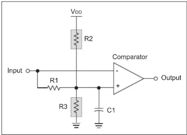
text_image
VDD R2 Input R1 Comparator - + Output R3 C1Example:
Data rate of 10 kbits/second. A low pass filter frequency of 500 Hz: R1 = 10k, C1 = 33 F. R2 or R3 should be 500k to 1 MB.
TIP #7 One-Shot
When dealing with short duration signals or glitches, it is often convenient to stretch out the event using a mono-stable, multi-vibrator or one-shot. Whenever the input pulses, the one-shot fires holding its output for a preset period of time. This stretches the short trigger input into a long output which the microcontroller can capture.
The circuit is designed with two feedback paths around a comparator. The first is a positive hysteresis feedback which sets a two level threshold, Vhand V10, based on the state of the comparator output. The second feedback path is an RC time circuit.
The one-shot circuit presented in Figure 7-1 is triggered by a low-high transition on its input and generates a high output pulse. Using the component values from the example, the circuit's operation is as follows.
Prior to triggering, C1 will have charged to a voltage slightly above 0.7V due to resistor R2 and D1 (R1 << R2 and will have only a minimal effect on the voltage). The comparator output will be low, holding the non-inverting input slightly below 0.7V due to the hysteresis feedback through R3, R4 and R5 (the hysteresis lower limit is designed to be less than 0.7V). With the non-inverting input held low, C2 will charge up to the difference between the circuit input and the voltage present at the non-inverting input.
When the circuit input is pulsed high, the voltage present at the non-inverting input is pulled above 0.7V due to the charge in C2. This causes the output of the comparator to go high, the hysteresis voltage at the non-inverting input goes to the high threshold voltage, and C1 begins charging through R2.
When the voltage across C1 exceeds the high threshold voltage, the output of the comparator goes low, C1 is discharged to just above the 0.7V limit, the non-inverting input is pulled below 0.7V, and the circuit is reset for the next pulse input, waiting for the next trigger input.
Figure 7-1: One-Shot Circuit

text_image
VDD R2 C1 V1 R1 D1 VDD R3 V2 + Comparator Output Input C2 R4 R5To design the one-shot, first create the hysteresis feedback using the techniques from Tip #3. Remember to set the low threshold below 0.7V. Next, choose values for R2 and C1 using Equation 7-1.
Equation 7-1
$$ T _ {P U S E} = \frac {R 2 * C 1 * \ln (V _ {T H} / V _ {T L})}{4} $$
D1 can be any low voltage switching diode. R1 should be 1% to 2% of R2 and C2 should be between 100 and 220 pF.
Example:
- V_DD = 5V, V_TH = 3.0V, V_TL = 2.5V
- From Tip #3, R4 = 1k, R5 = 1.5k and R3 = 12k
- T_PULSE = I_MS , C1 = .1 μF and R2 = 15k
• D1 is a 1N4148, R1 = 220 and C2 = 150 pF
TIP #8 Multi-Vibrator (Square Wave Output)
A multi-vibrator is an oscillator designed around a voltage comparator or operational amplifier (see Figure 8-1). Resistors R1 through R3 form a hysteresis feedback path from the output to the non-inverting input. Resistor RT and capacitor CT form a time delay network between the output and the inverting input. At the start of the cycle, CT is discharged holding the non-inverting input at ground, forcing the output high. A high output forces the non-inverting input to the high threshold voltage (see Tip #3) and charges CT through RT. When the voltage across CT reaches the high threshold voltage, the output is forced low. A low output drops the non-inverting input to the low threshold voltage and discharges CT through RT. When the voltage across CT reaches the low threshold voltage, the output is forced high and the cycle starts over.
Figure 8-1: Multi-Vibrator Circuit

text_image
CT RT - + Output VDD R1 Comparator R3 R2To design a multi-vibrator, first design the hysteresis feedback path using the procedure in Tip #3. Be careful to choose threshold voltages (VTH and VTL) that are evenly spaced within the common mode range of the comparator and centered on VDD/2. Then use VDD and VTL to calculate values for RT and CT that will result in the desired oscillation frequency Fosc Equation 8-1 defines the relationship between RT, CT, VTH, VTL and Fosc.
Equation 8-1
$$ F _ {\mathrm{GC}} = \frac {1}{2 * R T * C T * \ln (V _ {T H} / V _ {T L})} $$
Example:
- V_DD = 5V, V_TH = 3.333, V_TL = 1.666V
• R1, to R2, to R3 = 10k - R_T = 15 kHz , C_T = .1 F for F_osc = 480 Hz
TIP #9 Multi-Vibrator (Ramp Wave Output)
A multi-vibrator (ramp wave output) is an oscillator designed around a voltage comparator or operational amplifier that produces an asymmetrical output waveform (see Figure 9-1). Resistors R1 through R3 form a hysteresis feedback path from the output to the non-inverting input. Resistor RT, diode D1 and capacitor CT form a time delay network between the output and the inverting input. At the start of the cycle, CT is discharged holding the non-inverting input at ground, forcing the output high. A high output forces the non-inverting input to the high threshold voltage (see Tip #3) and charges CT through RT. When the voltage across CT reaches the high threshold voltage, the output is forced low. A low output drops the non-inverting input to the low threshold voltage and discharges CT through D1. Because the dynamic on resistance of the diode is significantly lower than RT, the discharge of CT is small when compared to the charge time, and the resulting waveform across CT is a pseudo ramp function with a ramping charge phase and a short-sharp discharge phase.
Figure 9-1: Ramp Waveform Multi-Vibrator
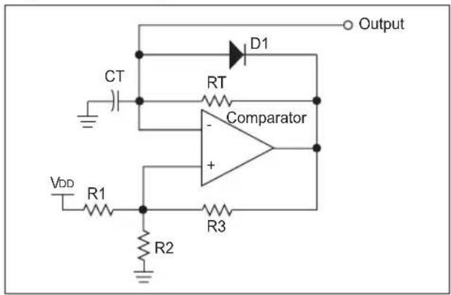
text_image
Output D1 CT RT Comparator + VDD R1 R2 R3To design this multi-vibrator, first design the hysteresis feedback path using the procedure in Tip #3. Remember that the peak-to-peak amplitude of the ramp wave will be determined by the hysteresis limits. Also, be careful to choose threshold voltages (VTH and VTL) that are evenly spaced within the common mode range of the comparator.
Then use V_TH and V_TL to calculate values for RT and CT that will result in the desired oscillation frequency Fosc Equation 9-1 defines the relationship between RT, CT, V_TH , V_TL and Fosc.
Equation 9-1
$$ F _ {\text { CC }} = \frac {1}{R T * C T * \ln (V _ {T H} / V _ {T L})} $$
This assumes that the dynamic on resistance of D1 is much less than RT.
Example:
- V_DD = 5V, V_TH = 1.666V and V_TH = 3.333V
- R1, R2 and R3 = 10k
- R_T = 15k , C_T = .1 F for a Fosc = 906 Hz
Note: Replacing RT with a current limiting diode will significantly improve the linearity of the ramp wave form. Using the example shown above, a CCL1000 (1 mA Central Semiconductor CLD), will produce a very linear 6 kHz output (see Equation 9-2).
Equation 9-2
$$ F _ {C S} = \frac {I _ {D D}}{C (V _ {T H} - V _ {T L})} $$
Figure 9-2: Alternate Ramp Waveform Multi-Vibrator Using a CLD
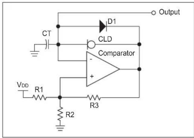
text_image
Output D1 CT CLD Comparator - + VDD R1 R2 R3TIP #10 Capacitive Voltage Doubler
This tip takes the multi-vibrator described in Tip #8 and builds a capacitive voltage doubler around it (see Figure 10-1). The circuit works by alternately charging capacitor C1 through diode D1, and then charge balancing the energy in C1 with C2 through diode D2. At the start of the cycle, the output of the multi-vibrator is low and charge current flows from V through D1 and into C1. When the output of the multi-vibrator goes high, D1 is reverse biased and the charge current stops. The voltage across C1 is added to the output voltage of the multi-vibrator, creating a voltage at the positive terminal of C1 which is 2 x V This voltage forward biases D2 and the charge in C1 is shared with C2. When the output of the multi-vibrator goes low again, the cycle starts over.
Figure 10-1: Capacitive Voltage Doubler

text_image
CT RT Comparator VDD R1 R2 R3 C1 D1 D2 VDD C2 VOLTNote: The output voltage of a capacitive double is unregulated and will sag with increasing load current. Typically, the output is modeled as a voltage source with a series resistance (see Figure 10-2).
Figure 10-2: Equivalent Output Model
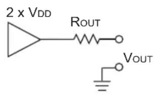
text_image
2 x VDD Rout VOUTTo design a voltage doubler, first determine the maximum tolerable output resistance based on the required output current and the minimum tolerable output voltage. Remember that the output current will be limited to one half of the output capability of the comparator. Then choose a transfer capacitance and switching frequency using Equation 10-1.
Equation 10-1
$$ R _ {\text {or}} = \frac {1}{F _ {\text {su}}} * C 1 $$
Note: ROUT will be slightly higher due to the dynamic resistance of the diodes. The equivalent series resistance or ESR, of the capacitors and the output resistance of the comparator. See the TC7660 data sheet for a more complete description.
Once the switching frequency is determined, design a square-wave multi-vibrator as described in Tip #8.
Finally, select diodes D1 and D2 for their current rating and set C2 equal to C1.
Example:
From Tip #8, the values are modified for a Fosc of 4.8 kHz.
• C1 and C2 = 10 μF
• RoT= 21
TIP #11 PWM Generator
This tip shows how the multi-vibrator (ramp wave) can be used to generate a voltage controlled PWM signal. The ramp wave multi-vibrator operates as described in Tip #9, generating a positive going ramp wave. A second comparator compares the instantaneous voltage of the ramp wave with the incoming voltage to generate the PWM output (see Figure 11-2).
When the ramp starts, it is below the input voltage, and the output of the second comparator is pulled high starting the PWM pulse. The output remains high until the ramp wave voltage exceeds the input, then the output of the second comparator goes low ending the PWM pulse. The output of the second comparator remains low for the remainder of the ramp waveform. When the ramp waveform returns to zero at the start of the next cycle, the second comparator output goes high again and the cycle starts over.
Figure 11-1: PWM Wave Forms
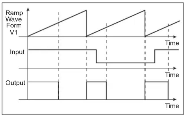
line
| Time | Input | Output | |------|-------|--------| | 0 | 0 | 0 | | 1 | High | Low | | 2 | Low | High | | 3 | High | Low | | 4 | Low | High | | 5 | High | Low | | 6 | Low | High | | 7 | High | Low | | 8 | Low | High | | 9 | High | Low | | 10 | Low | High | | 11 | High | Low | | 12 | Low | High | | 13 | High | Low | | 14 | Low | High | | 15 | High | Low | | 16 | Low | High | | 17 | High | Low | | 18 | Low | High | | 19 | High | Low | | 20 | Low | High | | 21 | High | Low | | 22 | Low | High | | 23 | High | Low | | 24 | Low | High | | 25 | High | Low | | 26 | Low | High | | 27 | High | Low | | 28 | Low | High | | 29 | High | Low | | 30 | Low | High | | 31 | High | Low | | 32 | Low | High | | 33 | High | Low | | 34 | Low | High | | 35 | High | Low | | 36 | Low | High | | 37 | High | Low | | 38 | Low | High | | 39 | High | Low | | 40 | Low | High | | 41 | High | Low | | 42 | Low | High | | 43 | High | Low | | 44 | Low | High | | 45 | High | Low | | 46 | Low | High | | 47 | High | Low | | 48 | Low | High | | 49 | High | Low | | 50 | Low | High | | 51 | High | Low | | 52 | Low | High | | 53 | High | Low | | 54 | Low | High | | 55 | High | Low | | 56 | Low | High | | 57 | High | Low | | 58 | Low | High | | 59 | High | Low | | 60 | Low | High | | 61 | High | Low | | 62 | Low | High | | 63 | High | Low | | 64 | Low | High | | 65 | High | Low | | 66 | Low | High | | 67 | High | Low | | 68 | Low | High | | 69 | High | Low | | 70 | Low | High | | 71 | High | Low | | 72 | Low | High | | 73 | High | Low | | 74 | Low | High | | 75 | High | Low | | 76 | Low | High | | 77 | High | Low | | 78 | Low | High | | 79 | High | Low | | 80 | Low | High | | 81 | High | Low | | 82 | Low | High | | 83 | High | Low | | 84 | Low | High | | 85 | High | Low | | 86 | Low | High | | 87 | High | Low | | 88 | Low | High | | 89 | High | Low | | 90 | Low | High | | 91 | High | Low | | 92 | Low | High | | 93 | High | Low | | 94 | Low | High | | 95 | High | Low | | 96 | Low | High | | 97 | High | Low | | 98 | Low | High | | 99 | High | Low | | 100 | Low | High | | Time (approx) - Ramp Wave Form V1; Time (approx) - Input; Time (approx) - Output; Time (approx) - Time (approx) - Output; Time (approx) - Time (approx) - Time (approx) - Time (approx) - Time (approx) - Time (approx) - Time (approx) - Time (approx) - Time (approx) - Time (approx) - Time (approx) - Time (approx) - Time (approx) - Time (approx) - Time (approx) - Time (approx) - Time (approx) - Time (approx) - Time (approx) - Time (approx) - Time (approx) = Time (approx) - Time (approx) - Time (approx) - Time (approx) - Time (approx) - Time (approx) - Time (approx) - Time (approx) - Time (approx) - Time (approx) - Time (approx) - Time (approx) - Time (approx) - Time (approx) - Time (approx) - Time (approx) - Time (approx) - Time (approx) - Time (approx) - Time (approx) / Time (approx) - Time (approx) - Time (approx) / Time (approx) - Time (approx) / Time (approx) - Time (approx) / Time (approx) / Time (approx) / Time (approx) / Time (approx) / Time (approx) / Time (approx) / Time (approx)Figure 11-2: PWM Circuit
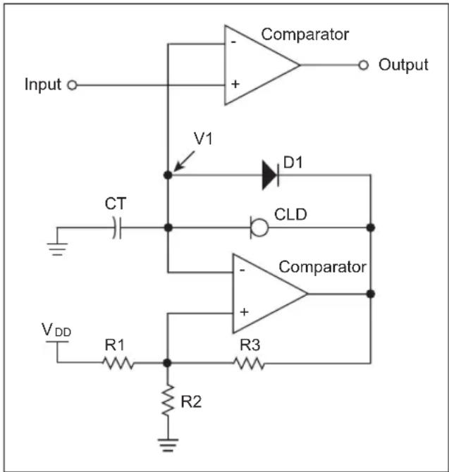
text_image
Input Comparator Output V1 D1 CT CLD Comparator VDD R1 R3 R2To design a PWM generator, start with the design of a ramp wave multi-vibrator using the design procedure from Tip #9. Choose high and low threshold voltages for the multi-vibrators hysteresis feedback that are slightly above and below the desired PWM control voltages.
Note: The PWM control voltage will produce a 0% duty cycle for inputs below the low threshold of the multi-vibrator. A control voltage greater than the high threshold voltage will produce a 100% duty cycle output.
Using the example values from Tip #9 will result in a minimum pulse width at an input voltage of 1.7V and a maximum at an input of 3.2V.
TIP #12 Making an Op Amp Out of a Comparator
When interfacing to a sensor, some gain is typically required to match the full range of the sensor to the full range of an ADC. Usually this is done with an operational amplifier, however, in cost sensitive applications, an additional active component may exceed the budget. This tip shows how an on-chip comparator can be used as an op amp like gain stage for slow sensor signals. Both an inverting and non-inverting topology are shown (see Figure 12-1 and Figure 12-2).
Figure 12-1: Non-Inverting Amplifier
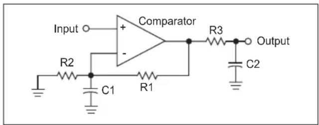
text_image
Input + Comparator - R2 C1 R1 R3 Output C2Figure 12-2: Inverting Amplifier
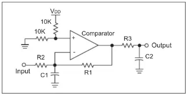
text_image
VDD 10K 10K Comparator R3 Output Input R2 C1 R1 C2To design a non-inverting amplifier, choose resistors R1 and R2 using the Gain formula for an op amp non-inverting amplifier (see Equation 12-1).
Equation 12-1
$$ \text { Gain } = \frac {\mathrm{R1} + \mathrm{R2}}{\mathrm{R2}} $$
Once the gain has been determined, values for R3 and C2 can be determined. R3 and C2 form a low-pass filter on the output of the amplifier. The corner frequency of the low pass should be 2 to 3 times the maximum frequency of the signal being amplified to prevent attenuation of the signal, and R3 should be kept small to minimize the output impedance of the amplifier. Equation 12-2 shows the relationship between R3, C2 and the corner frequency of the low pass filter.
Equation 12-2
$$ F _ {\text {CORNER}} = \frac {1}{2 ^ {} * R 3 ^ {} C 2} $$
A value for C1 can then be determined using Equation 12-3. The corner frequency should be the same as Equation 12-3.
Equation 12-3
$$ F _ {\text { CORR }} = \frac {1}{2 ^ {} * (R 1 I I R 2) ^ {} C 2} $$
To design an inverting amp, choose resistors R1 and R2 using the Gain formula for an op amp inverting amplifier (see Equation 12-4).
Equation 12-4
$$ \text { Gain } = \frac {\mathrm{R} _ {1}}{\mathrm{R} _ {2}} $$
Then choose values for the resistor divider formed by R4 and R5. Finally choose C1 and C2 as shown in the non-inverting amplifier design.
Example:
- For C2 will set the corner F
- Gain = 6.156, R1 = R3 = 19.8k
• R2 = 3.84k, C1 = .047 μF, FCORNER = 171 Hz
• C2 = .22 μF
TIP #13 PWM High-Current Driver
This tip combines a comparator with a MOSFET transistor and an inductor to create a switch mode high-current driver circuit. (See Figure 13-1).
The operation of the circuit begins with the MOSFET off and no current flowing in the inductor and load. With the sense voltage across R1 equal to zero and a DC voltage present at the drive level input, the output of the comparator goes low. The low output turns on the MOSFET and a ramping current builds through the MOSFET, inductor, load and R1.
Figure 13-1: High Current Driver
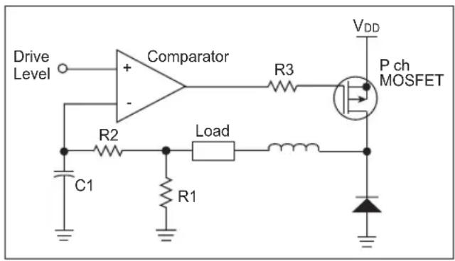
text_image
Drive Level Comparator R3 VDD P ch MOSFET R2 Load C1 R1When the current ramps high enough to generate a voltage across R1 equal to the drive level, the comparator output goes high turning off the MOSFET. The voltage at the junction of the MOSFET and the inductor then drops until D1 forward biases. The current continues ramping down from its peak level toward zero. When the voltage across the sense resistor R1 drops below the drive level, the comparator output goes low, the MOSFET turns on, and the cycle starts over.
R2 and C1 form a time delay network that limits the switching speed of the driver and causes it to slightly overshoot and undershoot the drive level when operating. The limit is necessary to keep the switching speed low, so the MOSFET switches efficiently. If R2 and C1 were not present, the system would run at a speed set by the comparator propagation delay and the switching speed of the MOSFET. At that speed, the switching time of the MOSFET would be a significant portion of the switching time and the switching efficiency of the MOSFET would be too low.
Figure 13-1: Current Through the Load
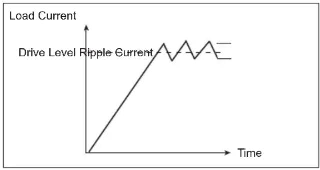
line
| Time | Load Current | |------|--------------| | 0 | 0 | | Peak | ~1.2 | | Low | ~0.8 | | High | ~1.1 |To design a PWM high current driver, first determine a switching speed (Fs) that is appropriate for the system. Next, choose a MOSFET and D1 capable of handling the load current requirements. Then choose values for R2 and C1 using Equation 13-1.
Equation 13-1
$$ F _ {\text {sx}} = \frac {2}{R 2 ^ {*} C 1} $$
Next determine the maximum ripple current that the load will tolerate, and calculate the required inductance value for L1 using Equation 13-2.
Equation 13-2
$$ L = \frac {V _ {\text {DD}} - V _ {\text {LOD}}}{\text {IRRE} * F _ {\text {SIX}} * 2} $$
Finally, choose a value for R1 that will produce a feedback ripple voltage of 100 mV for the maximum ripple current IRRE
Example:
- Fswx = 10 kHz, R2 = 22k, C1 = .01 μF
- I_RIPPLE = 100 mA, V_DD = 12V, V_L = 3.5V
• L = 4.25 mH
TIP #14 Delta-Sigma ADC
This tip describes the creation of a hardware/software-based Delta-Sigma ADC. A Delta-Sigma ADC is based on a Delta-Sigma modulator composed of an integrator, a comparator, a clock sampler and a 1-bit DAC output. In this example, the integrator is formed by R1 and C1. The comparator is an on-chip voltage comparator. The clock sampler is implemented in software and the 1-bit DAC output is a single I/O pin. The DAC output feeds back into the integrator through R2.
Resistors R3 and R4 form a V _1/2 reference for the circuit (see Figure 14-1).
Figure 14-1: Delta-Sigma Modulator
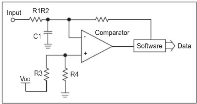
text_image
Input R1R2 C1 Comparator - + Software Data VDD R3 R4In operation, the feedback output from the software is a time sampled copy of the comparator output. In normal operation, the modulator output generates a PWM signal which is inversely proportional to the input voltage. As the input voltage increases, the PWM signal will drop in duty cycle to compensate. As the input decreases, the duty cycle rises.
To perform an A-to-D conversion, the duty cycle must be integrated over time, digitally, to integrate the duty cycle to a binary value. The software starts two counters. The first counts the total number of samples in the conversion and the second counts the number of samples that were low. The ratio of the two counts is equal to the ratio of the input voltage over V_DD .
Note: This assumes that R1 and R2 are equal and R3 is equal to R4. If R1 and R2 are not equal, then the input voltage is also scaled by the ratio of R2 over R1, and R3 must still be equal to R4.
For a more complete description of the operation of a Delta-Sigma ADC and example firmware, see Application Note AN700 "Make A Delta-Sigma Converter Using a Microcontroller's Analog Comparator Module."
Example:
• R3 = R4 = 10 kHz
• R1 = R2 = 5.1k
• C1 = 1000 pF
TIP #15 Level Shifter
This tip shows the use of the comparator as a digital logic level shifter. The inverting input is biased to the center of the input voltage range ( V_IN/2 ). The non-inverting input is then used for the circuit input. When the input is below the V_IN/2 threshold, the output is low. When the input is above V_IN/2 , then the output is high. Values for R1 and R2 are not critical, though their ratio should result in a threshold voltage V_IN/2 at the mid-point of the input signal voltage range. Some microcontrollers have the option to connect the inverting input to an internal voltage reference. To use the reference in place of R1 and R2, simply select the internal reference and configure it for one half the input voltage range.
Note: Typical propagation delay for the circuit is 250-350 ns using the typical on-chip comparator peripheral of a microcontroller.
Figure 15-1: Level Shifter

text_image
VDD R1 - A + Y R2Example:
- V_IN = 0 - 2V , V_IN/2 = 1V , V_DD = 5V
• R2 = 10k, R3 = 3.9k
TIP #16 Logic: Inverter
When designing embedded control applications, there is often the need for an external gate. Using the comparator, several simple gates can be implemented. This tip shows the use of the comparator as an inverter.
The non-inverting input is biased to the center of the input voltage range, typically V 1/2 . The inverting input is then used for the circuit input. When the input is below V 1/2 , the output is high. When the input is above V _1/2 , then the output is low.
Values for R1 and R2 are not critical, though they must be equal to set the threshold at V0/2.
Some microcontrollers have the option to connect the inverting input to an internal voltage reference. To use the reference in place of R1 and R2, move the input to the non-inverting input and set the output polarity bit in the comparator control register to invert the comparator output.
Note: Typical propagation delay for the circuit is 250-350 ns using the typical on-chip comparator peripheral of a microcontroller.
Figure 16-1: Inverter
text_image
VDD R1 A + - Y R2TIP #17 Logic: AND/NAND Gate
This tip shows the use of the comparator to implement an AND gate and its complement the NAND gate (see Figure 17-2). Resistors R1 and R2 drive the non-inverting input with 2/3 the supply voltage. Resistors R3 and R4 average the voltage of input A and B at the inverting input. If either A or B is low, the average voltage will be one half V DD and the output of the comparator remains low. The output will go high only if both inputs A and B are high, which raises the input to the inverting input above 2/3 V DD
The operation of the NAND gate is identical to the AND gate, except that the output is inverted due to the swap of the inverting and non-inverting inputs.
Note: Typical propagation delay for the circuit is 250-350 ns using the typical on-chip comparator peripheral of a microcontroller. Delay measurements were made with 10k resistance values.
While the circuit is fairly simple, there are a few requirements for correct operation:
- The inputs A and B must drive from ground to V_D for the circuit to operate properly.
- The combination of R1 and R2 will draw current constantly, so they must be kept large to minimize current draw.
- All resistances on the inverting input react with the input capacitance of the comparator. So the speed of the gate will be affected by the source resistance of A and B, as well as, the size of resistors R3 and R4.
- Resistor R2 must be 2 x R1.
- Resistor R3 must be equal to R4.
Figure 17-1: AND Gate

text_image
A ○─R3 B ○─R4 VDD ──R1 ──●─+ Y │ └─R2 ⊥Figure 17-2: NAND Gate
text_image
A ○─R3 B ○─R4 VDD ──●─┐ │ └─○ Y │ R1 ──●─┘ │ R2 ──┘ ————Example:
- V_DD = 5V, R3 = R4 = 10k
• R1 = 5.1k, R2 = 10k
TIP #18 Logic: OR/NOR Gate
This tip shows the use of the comparator to implement an OR gate, and its complement, the NOR gate.
Resistors R1 and R2 drive the non-inverting input of the comparator with 1/3 V DD Resistors R3 and R4 average the voltages of the inputs A and B at the inverting input. If either A or B is high, the average voltage is 1/2 V DD and the output of the comparator is high. Only if both A and B are low does the average voltage at the non-inverting input drop below 1/3 the supply voltage, causing the comparator output to go low. The operation of the NOR gate is identical to the OR gate, except the output is inverted due to the swap of the inverting and non-inverting inputs.
Note: Typical propagation delay for the circuit is 250-350 ns using the typical on-chip comparator peripheral of a microcontroller. Delay measurements were made with 10k resistance values.
While the circuit is fairly simple, there are a few requirements for correct operation:
- The inputs A and B must drive from ground to V for the circuit to operate properly.
- The combination of R1 and R2 will draw current constantly, so they must be kept large to minimize current draw.
- All resistances on the inverting input react with the input capacitance of the comparator, so the speed of the gate will be affected by the source resistance of A and B, as well as the size of resistors R3 and R4.
- Resistor R1 must be 2 x R2.
- Resistor R3 must be equal to R4.
Figure 18-1: OR Gate

text_image
A ○─R3 B ○─R4 VDD ──R1 ──●─+ ──○Y │ ┴─R2 | | ⊥ | | | | | | | | | | | | | | | | | | | | | | | | | | | | | | | | | | | | | | | | | | | | | | | | | | | R2Figure 18-2: NOR Gate

text_image
A ○─R3 B ○─R4 VDD ──●─┐ │ └─○ Y │ R1 ──●─┘ │ R2 ──┘ ——Example:
- V_DD = 5V, R3 = R4 = 10k
• R1 = 10k, R2 = 5.1k
TIP #19 Logic: XOR/XNOR Gate
This tip shows the use of the comparator to implement an XOR gate and its complement the XNOR gate.
The operation is best described in three sections:
- Both A and B inputs are low With both inputs low, the inverting input is held at .7V and the non-inverting is held at ground. This combination results in a low output.
- Both A and B inputs are high With both inputs high, the inverting input is pulled up to V DD and the non-inverting input is equal to 2/3 V DD (the average of V DD inputs and G ND ). This combination also results in a low output.
- Input A or B is high With one input high and one low, The inverting input is held at .7V and the non-inverting input is equal to 1/3 V DD (the average of a V DD input and G _ND ). This combination results in a high output.
Note: Typical propagation delay for the circuit is 250-350 ns using the typical on-chip comparator peripheral of a microcontroller. Delay measurements were made with 10k resistance values.
While the circuit is fairly simple, there are a few requirements for correct operation:
- The inputs A and B must drive from ground to V for the circuit to operate properly.
- All resistances on the both inputs react with the input capacitance of the comparator, so the speed of the gate will be affected by the source resistance of A and B, as well as, the size of resistors R1, R2, R3 and R4.
- Resistor R1, R2 and R3 must be equal.
- Resistor R4 must be small enough to produce a 1.0V, or lower, voltage drop across D1 and D2.
Figure 19-1: XOR Gate

text_image
A B R1 R2 R3 Comparator + - Y D1 D2 R4 VDDFigure 19-2: XNOR Gate
text_image
A B R1 R2 R3 Comparator + Y D1 D2 R4 VDDExample:
• D1 = D2, = 1N4148
• R4 = 10k, R1 = R2 = R3 = 5.1k
TIP #20 Logic: Set/Reset Flip Flop
This tip shows the use of the comparator to implement a Set/Reset Flip Flop.
The inverting and non-inverting inputs are biases at V 1/2 by resistors R1 through R4. The non-inverting input also receives positive feedback from the output through R5. The common bias voltages and the positive feedback configure the comparator as a bistable latch. If the output Q is high, the non-inverting input is also pulled high, which reinforces the high output. If Q is low, the non-inverting input is also pulled low, which reinforces the low output. To change state, the appropriate input must be pulled low to overcome the positive feedback. The diodes prevent a positive state on either input from pulling the bias of either input above V 1/2 .
Note: Typical propagation delay for the circuit is 250-350 ns using the typical on-chip comparator peripheral of a microcontroller. Delay measurements were made with 10k resistance values.
While the circuit is fairly simple, there are a few requirements for correct operation:
- The inputs Set and Reset must be driven near ground for the circuit to operate properly.
- The combination of R1/R2 and R3/R4 will draw current constantly, so they must be kept large to minimize current draw.
- R1 through R4 must be equal for a V0/2 trip level.
- R5 must be greater or equal to R3.
- R1 through R4 will react with the input capacitance of the comparator, so larger values will limit the minimum input pulse width.
Figure 20-1: Set/Reset Flip Flop
text_image
VDD VDD R1 R3 R5 SET + RESET R2 R4 QExample:
- Diodes = 1N4148
• R1 = R2 = R3 = R4 = 10k
• R5 = 10k
CHAPTER 5 DC Motor Control Tips 'n Tricks
Table Of Contents
TIPS 'N TRICKS INTRODUCTION
TIP #1: Brushed DC Motor Drive Circuits ..... 5-2
TIP #2: Brushless DC Motor Drive Circuits ..... 5-3
TIP #3: Stepper Motor Drive Circuits 5-4
TIP #4: Drive Software 5-6
TIP #5: Writing a PWM Value to the CCP
Registers with a Mid-Range
PIC ^ MCU 5-7
TIP #6: Current Sensing 5-8
TIP #7: Position/Speed Sensing 5-9
Application Note References 5-11
Motor Control Development Tools 5-11
TIPS 'N TRICKS INTRODUCTION
Every motor control circuit can be divided into the drive electronics and the controlling software. These two pieces can be fairly simple or extremely complicated depending upon the motor type, the system requirements and the hardware/software complexity trade-off. Generally, higher performance systems require more complicated hardware. This booklet describes many basic circuits and software building blocks commonly used to control motors. The booklet also provides references to Microchip application notes that describe many motor control concepts in more detail. The application notes can be found on the Microchip web site at www.microchip.com.
Additional motor control design information can be found at the Motor Control Design Center (www.microchip.com/motor).
TIP #1 Brushed DC Motor Drive Circuits
All motors require drive circuitry which controls the current flow through the motor windings. This includes the direction and magnitude of the current flow. The simplest type of motor, to drive, is the Brushed DC motor. Drive circuits for this type of motor are shown below.
Figure 1-1: High Side Drive

text_image
PIC® Microcontroller Digital Output MOSFET Driver V+ MThis drive can control a Brushed DC motor in one direction. This drive is often used in safety critical applications because a short circuit at the motor terminals cannot turn the motor on.
Figure 1-2: Low Side Drive
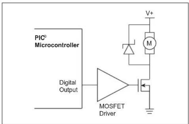
text_image
PIC® Microcontroller Digital Output MOSFET Driver V+ MThis is the lowest cost drive technique because of the MOSFET drive simplicity. Most applications can simply use an output pin from the PIC ^® microcontroller to turn the MOSFET on.
Figure 1-3: H-Bridge Drive

text_image
A-D are digital outputs from a PIC® MCU.The H-Bridge derived its name from the common way the circuit is drawn. This is the only solid state way to operate a motor in both directions.
Application notes that drive Brushed DC motors are listed below and can be found on the Microchip web site at: www.microchip.com.
• AN847, "RC Model Aircraft Motor Control" (DS00847)
- AN893, "Low-cost Bidirectional Brushed DC Motor Control Using the PIC16F684" (DS00893)
• AN905, "Brushed DC Motor Fundamentals" (DS00905)
TIP #2 Brushless DC Motor Drive Circuits
A Brushless DC motor is a good example of simplified hardware increasing the control complexity. The motor cannot commutate the windings (switch the current flow), so the control circuit and software must control the current flow correctly to keep the motor turning smoothly. The circuit is a simple half-bridge on each of the three motor windings.
There are two basic commutation methods for Brushless DC motors; sensored and sensorless. Because it is critical to know the position of the motor so the correct winding can be energized, some method of detecting the rotor position is required. A motor with sensors will directly report the current position to the controller. Driving a sensored motor requires a look-up table. The current sensor position directly correlates to a commutation pattern for the bridge circuits.
Without sensors, another property of the motor must be sensed to find the position. A popular method for sensorless applications is to measure the back EMF voltage that is naturally generated by the motor magnets and windings. The induced voltage in the un-driven winding can be sensed and used to determine the current speed of the motor. Then, the next commutation pattern can be determined by a time delay from the previous pattern.
Sensorless motors are lower cost due to the lack of the sensors, but they are more complicated to drive. A sensorless motor performs very well in applications that don't require the motor to start and stop. A sensor motor would be a better choice in applications that must periodically stop the motor.
Figure 2-1: 3 Phase Brushless DC Motor Control

text_image
OA-OF are digital outputs from a PIC® MCU. V V V OC OE A B C OB OD OF A B C Motor OA-OFFigure 2-2: Back EMF Sensing (Sensorless Motor)

flowchart
graph LR
    A["ADC"] --> B["Low Pass Filter"]
    B --> C["Analog MUX"]
    C --> D["A"]
    C --> E["B"]
    C --> F["C"]
Figure 2-3: Quadrature Decoder (Sensor Motor)

flowchart
graph TD
    A["PIC® MCU or dsPIC® DSC"] -->|Digital Outputs| B["Drive Circuit"]
    A -->|Digital Inputs| C["Motor"]
    B -->|A B C| C
    C -->|Hall Effect Motor Position Sensor| A
    C -->|Sensor Outputs| A
Application notes describing Brushless DC Motor Control are listed below and can be found on the Microchip web site at: www.microchip.com.
- AN857, "Brushless DC Motor Control Made Easy" (DS00857)
• AN885, "Brushless DC Motor Fundamentals" (DS00885) - AN899, "Brushless DC Motor Control Using PIC18FXX31" (DS00899)
- AN901, "Using the dsPIC30F for Sensorless BLDC Control" (DS00901)
- AN957, "Sensored BLDC Motor Control Using dsPIC30F2010" (DS00957)
• AN992, "Sensorless BLDC Motor Control Using dsPIC30F2010" (DS00992)
• AN1017, "Sinusoidal Control of PMSM with dsPIC30F DSC" (DS01017) - GS005, "Using the dsPIC30F Sensorless Motor Tuning Interface" (DS93005)
TIP #3 Stepper Motor Drive Circuits
Stepper motors are similar to Brushless DC motors in that the control system must commutate the motor through the entire rotation cycle. Unlike the brushless motor, the position and speed of a stepping motor is predictable and does not require the use of sensors.
There are two basic types of stepper motors, although some motors are built to be used in either mode. The simplest stepper motor is the unipolar motor. This motor has four drive connections and one or two center tap wires that are tied to ground or Vsupply, depending on the implementation. Other motor types are the bipolar stepper and various combinations of unipolar and bipolar, as shown in Figure 3-1 and Figure 3-2. When each drive connection is energized, one coil is driven and the motor rotates one step. The process is repeated until all the windings have been energized. To increase the step rate, often the voltage is increased beyond the motors rated voltage. If the voltage is increased, some method of preventing an over current situation is required.
There are many ways to control the winding current, but the most popular is a chopper system that turns off current when it reaches an upper limit and enables the current flow a short time later. Current sensor systems are discussed in Tip #6. Some systems are built with a current chopper, but they do not detect the current, rather the system is designed to begin a fixed period chopping cycle after the motor has stepped to the next position. These are simpler systems to build, as they only require a change in the software.
Figure 3-1: 4 and 5 Wire Stepper Motors
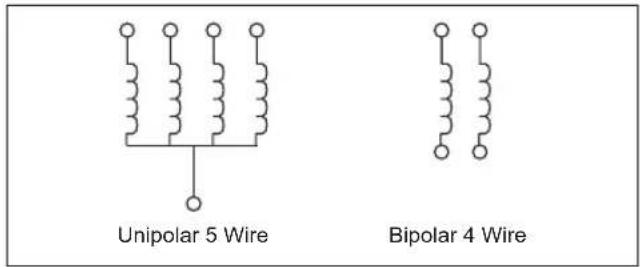
text_image
Unipolar 5 Wire Bipolar 4 WireFigure 3-2: 6 and 8 Wire Stepper Motors
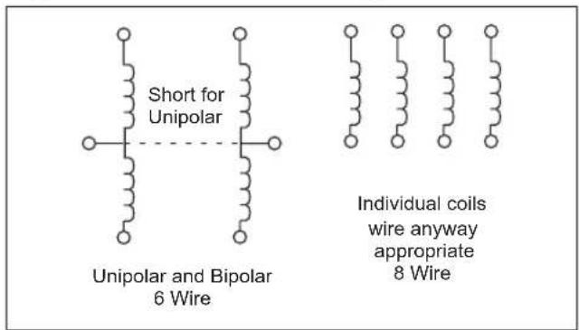
text_image
Short for Unipolar Unipolar and Bipolar 6 Wire Individual coils wire anyway appropriate 8 WireFigure 3-3: Unipolar Motor (4 Low Side Switches)

text_image
Motor V+ 01 02 03 04 01-04 are outputs from a PIC® MCU or dsPIC® DSC.Figure 3-4: Bipolar Motor (4 Half-Bridges)
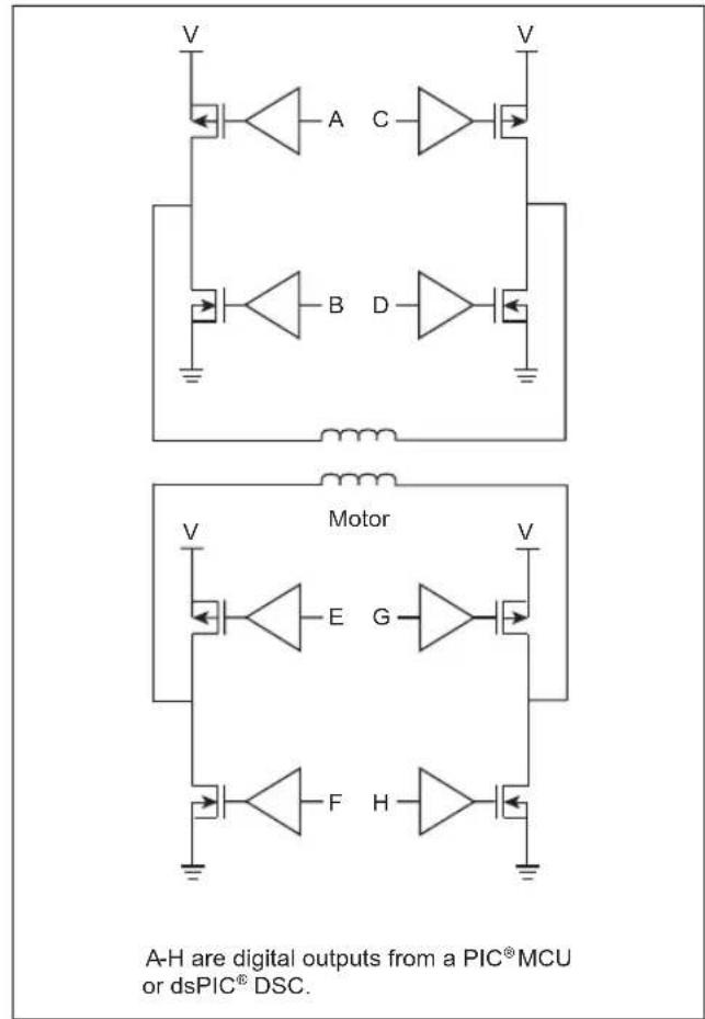
text_image
A-H are digital outputs from a PIC®MCU or dsPIC® DSC.TIP #4 Drive Software
Pulse-Width Modulation (PWM) Algorithms
Pulse-Width Modulation is critical to modern digital motor controls. By adjusting the pulse width, the speed of a motor can be efficiently controlled without larger linear power stages. Some PIC devices and all dsPIC DSCs have hardware PWM modules on them. These modules are built into the Capture/Compare/PWM (CCP) peripheral. CCP peripherals are intended for a single PWM output, while the Enhanced CCP (ECCP) is designed to produce the complete H-Bridge output for bidirectional Brushed DC motor control. If cost is a critical design point, a PIC device with a CCP module may not be available, so software generated PWM is a good alternative.
The following algorithms are designed to efficiently produce an 8-bit PWM output on the Mid-Range family of PIC microcontrollers. These algorithms are implemented as macros. If you want these macros to be a subroutine in your program, simply remove the macro statements and replace them with a label and a return statement.
Example 4-1: 1 Output 8-Bit PWM
pwm_counter equ xxx ;variable
pwm equ xxx ;variable

set_pwm macro A ;sets the pwm
    ;setpoint to the
    ;value A
MOVLW A
MOVWF pwm
endm

update_PWM macro ;performs one update
    ;of the PWM signal
    ;place the PWM output
    ;pin at bit 0 or 7 of
    ;the port
MOVF pwm_counter,w
SUBWF pwm, w ;if the output
    ;is on bit 0
RLF PORTC,f ;replace PORTC with
    ;the correct port if
    ;the output is on bit
    ;7 of the port
    ;replace the rlf with
    ;rrf incf
    ;pwm_counter,f
Example 4-2: 8 Output 8-Bit PWM
pwm_counter equ xxx ;variable
pwm0 equ xxx ;
pwm1 equ pwm0+1
pwm2 equ pwm1+1
pwm3 equ pwm2+1
pwm4 equ pwm3+1
pwm5 equ pwm4+1
pwm6 equ pwm5+1
pwm7 equ pwm6+1
output equ pwm7+1
set_pwm macro A,b ;sets pwm b with
;the value A
MOVLW pwm0
ADDLW b
MOVWF fsr
MOVLW a
MOVWF indf
endm

update_PWM macro ;peforms one
;update of all 8
;PWM signals
;all PWM signals
;must be on the
;same port
MOVF pwm_counter,w
SUBWF pwm0,w
RLF output,f
MOVF pwm_counter,w
SUBWF pwm1,w
RLF output,f
MOVF pwm_counter,w
SUBWF pwm2,w
RLF output,f
MOVF pwm_counter,w
SUBWF pwm3,w
RLF output,f
MOVF pwm_counter,w
SUBWF pwm4,w
RLF output,f
MOVF pwm_counter,w
SUBWF pwm5,w
RLF output,f
MOVF pwm_counter,w
SUBWF pwm6,w
RLF output,f
MOVF pwm_counter,w
SUBWF pwm7,w
RLF output,w
MOVWF PORTC
INCF pwm_counter,f
endm
TIP #5 Writing a PWM Value to the the CCP Registers With a Mid-Range PIC ^® Microcontroller
The two PWM LSb's are located in the CCPCON register of the CCP. This can make changing the PWM period frustrating for a developer. Example 5-1 through Example 5-3 show three macros written for the mid-range product family that can be used to set the PWM period. The first macro takes a 16-bit value and uses the 10 MSb's to set the PWM period. The second macro takes a 16-bit value and uses the 10 LSb's to set the PWM period. The last macro takes 8 bits and sets the PWM period. This assumes that the CCP is configured for no more than 8 bits.
Example 5-1: Left Justified 16-Bit Macro
pwm_tmp equ xxx ;this variable must be
    ;allocated someplace
setPeriod macro a ;a is 2 SFR's in
    ;Low:High arrangement
    ;the 10 MSb's are the
    ;desired PWM value
RRF a,w ;This macro will
    ;change w
MOVWF pwm_tmp
RRF pwm_tmp,w
ANDLW 0x30
IORLW 0x0F
MOVWF CCP1CON
MOVF a+1,w
MOVWF CCPR1L
Example 5-2: Right Justified 16-Bit Macro
pwm_tmp equ xxx ;this variable must be
    ;allocated someplace
setPeriod macro a ;a is 2 bytes in
    ;Low:High arrangement
    ;the 10 LSb's are the
    ;desired PWM value
SWAPF a,w ;This macro will
    ;change w
ANDLW 0x30
IORLW 0x0F
MOVWF CCP1CON
RLF a,w
IORLW 0x0F
MOVWF pwm_tmp
RRF pwm_tmp,f
RRF pwm_tmp,w
MOVWF CCPR1L
Example 5-3: 8-Bit Macro
pwm_tmp equ xxx ;this variable must be
;allocated someplace
setPeriod macro a ;a is 1 SFR
SWAPF a,w ;This macro will
;change w
ANDLW 0x30
IORLW 0x0F
MOVWF CCP1CON
RRF a,w
MOVWF pwm_tmp
RRF pwm_tmp,w
MOVWF CCPRIL
TIP #6 Current Sensing
The torque of an electric motor can be monitored and controlled by keeping track of the current flowing through the motor. Torque is directly proportional to the current. Current can be sensed by measuring the voltage drop through a known value resistor or by measuring the magnetic field strength of a known value inductor. Current is generally sensed at one of two places, the supply side of the drive circuit (high side current sense) or the sink side of the drive circuit (low side current sense). Low side sensing is much simpler but the motor will no longer be grounded, causing a safety issue in some applications. High side current sensing generally requires a differential amplifier with a common mode voltage range within the voltage of the supply.
Figure 6-1: Resistive High Side Current Sensing
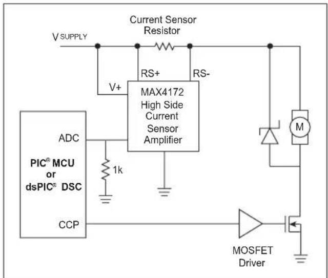
text_image
V SUPPLY Current Sensor Resistor RS+ RS- MAX4172 High Side Current Sensor Amplifier ADC PIC® MCU or dsPIC® DSC CCP 1k MOSFET DriverFigure 6-2: Resistive Low Side Current Sensing

flowchart
graph TD
    A["CCP\nPIC® MCU or dsPIC® DSC"] --> B["MOSFET Driver"]
    C["ADC"] --> B
    B --> D["MOSFET Driver"]
    D --> E["Current Sensor Resistor"]
    D --> F["Current Sensor Amplifier"]
    F --> G["Ground"]
    H["VSUPPLY"] --> I["M"]
    I --> D
Current measurement can also be accomplished using a Hall effect sensor to measure the magnetic field surrounding a current carrying wire. Naturally, this Hall effect sensor can be located on the high side or the low side of the load. The actual location of the sensor does not matter because the sensor does not rely upon the voltage on the wire. This is a non-intrusive method that can be used to measure motor current.
Figure 6-3: Magnetic Current Sensing
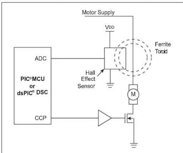
flowchart
graph TD
    A["ADC"] --> B["Hall Effect Sensor"]
    C["PIC®MCU or dsPIC® DSC"] --> B
    D["CCP"] --> E["Comparator"]
    B --> F["M"]
    F --> G["Ferrite Toroid"]
    H["Motor Supply"] --> I["VDD"]
    I --> B
    J["Ground"] --> K["Ground"]
TIP #7 Position/Speed Sensing
The motor RPM can be measured by understanding that a motor is a generator. As long as the motor is spinning, it will produce a voltage that is proportional to the motors RPM. This is called back EMF. If the PWM signal to the motor is turned off and the voltage across the windings is measured, the back EMF voltage can be sensed from there and the RPM's can be known.
Figure 7-1: Back EMF Motor Speed Sensing

text_image
Motor Supply VDD CCP PIC® MCU or dsPIC® DSC ADC Back EMF Monitor(1) Q1 MNote 1: If motor voltage is greater than V_DD , an attenuator will be required. Sample back EMF while Q1 is off.
Rotary Encoder Sensing
Rotary encoders are typically used to provide direct physical feedback of motor position, and/or speed. A rotary encoder consists of a rotary element attached to the motor that has a physical feature, measured by a stationary component. The measurements can yield motor speed and sometimes they can provide a motor position. Rotary encoders are built using many different technologies. The most common type is an optical rotary encoder. The optical rotary encoder is used in the computer mice that have a ball. It is built with an encoder disc that is attached to the motor. The encoder disc has many radial slots cut into the disc at a specific interval. An LED and a photo detector are used to count the slots as they go by. By timing the rate that the slots go by, the speed of rotation can be determined.
Sensing motor position requires a second LED and photo detector. The second sensor pair is mounted so the output pulses are 90^ out of phase from the first pair. The two outputs represent the motion of the encoder disc as a quadrature modulated pulse train. By adding a third index signal, that pulses once for each revolution, the exact position of the rotor can be known.
An encoder with quadrature outputs can be used to track relative position from a known reference point. Another type of encoder uses a binary encoded disk so that the exact rotor position is always known. This type of encoder is called an absolute encoder.
Figure 7-2: Optical Speed/Direction/Position Sensing

flowchart
graph TD
    A["Drive"] --> B["M"]
    B --> C["Encoder Wheel on Motor Shaft"]
    C --> D["Photo Transistor"]
    D --> E["LED"]
    E --> F["Encoder Wheel"]
    F --> G["pscope waveform A B forward B reverse"]
    H["PIC® MCU or dsPIC® DSC"] --> I["A"]
    H --> J["B"]
    style A fill:#f9f,stroke:#333
    style H fill:#ccf,stroke:#333
    style D fill:#cfc,stroke:#333
    style E fill:#fcc,stroke:#333
    style F fill:#cff,stroke:#333
    style G fill:#ffc,stroke:#333
Note: Frequency of one signal provides RPM of motor. Pulse count provides motor position. A-B phase provides motor direction.
Quadrature sensing can easily be accomplished in software, but there is generally an upper limit to the RPM. By using a few gates, the sensing can be done partially in hardware and partially in software. The new PIC18FXX31 and dsPIC 16-bit Digital Signal Controller families include an encoder interface that allows MUCH higher RPM motors to be measured with an excellent degree of accuracy.
Older Methods of Motor Sensing
Resolvers and analog tachometers are two older technologies for motor position/velocity sensing. An analog tachometer is simply an electric generator with a linear output over a specified range of RPM's. By knowing the output characteristics, the RPM can be known by simply measuring the voltage across the tachometer terminals.
A resolver is a pair of coils that are excited by an external AC signal. The two coils are at 90^ to each other so they pick up the AC signal at different strengths, depending on their orientation. The result is a sine or cosine output related to the angle of the resolver in reference to the AC signal. Inverse cosine/sine will produce the angle of the sensor. This type of sensor can be very accurate and is still used where absolute position must be known.
Application Note References
Application notes can be found on the Microchip web site at www.microchip.com.
- AN532, "Servo Control of a DC Brush Motor" (DS00532)
• AN696, "PIC18CXXX/PIC16CXXX DC Servomotor" (DS00696)
- AN718, "Brush-DC Servomotor Implementation using PIC17C756A" (DS00718)
- AN822, "Stepper Motor Microstepping with the PIC18C452" (DS00822)
- AN843, "Speed Control of 3-Phase Induction Motor Using PIC18 Microcontrollers" (DS00843)
- AN847, "RC Model Aircraft Motor Control" (DS00847)
- AN857, "Brushless DC Motor Control Made Easy" (DS00857)
- AN885, "Brushless DC (BLDC) Motor Fundamentals" (DS00885)
- AN899, "Brushless DC Motor Control Using the PIC18FXX31" (DS00899)
- AN893, "Low-cost Bidirectional Brushed DC Motor Control Using the PIC16F684" (DS00893)
- AN894, "Motor Control Sensor Feedback Circuits" (DS00894)
- AN898, "Determining MOSFET Driver Needs for Motor Drive Applications" (DS00898)
- AN901, "Using the dsPIC30F for Sensorless BLDC Control" (DS00901)
- AN905, "Brushed DC Motor Fundamentals" (DS00905)
- AN906, "Stepper Motor Control Using the PIC16F684" (DS00906)
• AN907, "Stepper Motor Fundamentals" (DS00907)
- AN1017, "Sinusoidal Control of PMSM Motors with dsPIC30F DSC" (DS01017)
- GS001, "Getting Started with BLDC Motors and dsPIC30F Devices" (DS93001)
Motor Control Development Tools
- PICDEM™ MC Development Board (DM183011)
Used to evaluate the PIC18FXX31 8-bit microcontroller family. - PICDEM™ MCLV Development Board (DM183021)
- dsPIC30F Motor Control Development System (DM300020)
Used to evaluate the dsPIC30F 16-bit Digital Signal Controller family. - Motor Control (MC) Graphical User Interface (GUI)
The MC-GUI allows user to configure the motor and a wide range of system parameters for a selected motor type.
The MC-GUI is free an can be downloaded at www.microchip.com
Visit the Motor Control Design Center at: www.microchip.com/motor for additional design resources.
NOTES:
CHAPTER 6
LCD PIC® Microcontroller
Tips 'n Tricks
Table Of Contents
TIPS 'N TRICKS INTRODUCTION
TIP #1: Typical Ordering Considerations and Procedures for Custom Liquid Displays 6-2
TIP #2: LCD PIC ^ MCU Segment/Pixel Table 6-2
TIP #3: Resistor Ladder for Low Current ..... 6-3
TIP #4: Contrast Control with a Buck Regulator 6-5
TIP #5: Contrast Control Using a Boost Regulator 6-5
TIP #6: Software Controlled Contrast with PWM for LCD Contrast Control ...... 6-6
TIP #7: Driving Common Backlights 6-7
TIP #8: In-Circuit Debug (ICD) 6-8
TIP #9: LCD in Sleep Mode 6-8
TIP #10: How to Update LCD Data Through Firmware 6-9
TIP #11: Blinking LCD 6-9
TIP #12: 4 x 4 Keypad Interface that Conserves Pins for LCD Segment Drivers 6-10
Application Note References 6-11
TIPS 'N TRICKS INTRODUCTION
Using an LCD PIC ^® MCU for any embedded application can provide the benefits of system control and human interface via an LCD. Design practices for LCD applications can be further enhanced through the implementation of these suggested “Tips ‘n Tricks”.
This booklet describes many basic circuits and software building blocks commonly used for driving LCD displays. The booklet also provides references to Microchip application notes that describe many LCD concepts in more detail.
TIP #1 Typical Ordering Considerations and Procedures for Custom Liquid Displays
- Consider what useful information needs to be displayed on the custom LCD and the combination of alphanumeric and custom icons that will be necessary.
- Understand the environment in which the LCD will be required to operate. Operating voltage and temperature can heavily influence the contrast of the LCD and potentially limit the type of LCD that can be used.
- Determine the number of segments necessary to achieve the desired display on the LCD and reference the PIC Microcontroller LCD matrix for the appropriate LCD PIC microcontroller.
- Create a sketch/mechanical print and written description of the custom LCD and understand the pinout of the LCD. (Pinout definition is best left to the glass manufacturer due to the constraints of routing the common and segment electrodes in two dimensions.)
-
Send the proposed LCD sketch and description for a written quotation to at least 3 vendors to determine pricing, scheduling and quality concerns.
a) Take into account total NRE cost, price per unit, as well as any setup fees.
b) Allow a minimum of two weeks for formal mechanical drawings and pin assignments and revised counter drawings. -
Request a minimal initial prototype LCD build to ensure proper LCD development and ensure proper functionality within the target application.
a) Allow typically 4-6 weeks for initial LCD prototype delivery upon final approval of mechanical drawings and pin assignments. - Upon receipt of prototype LCD, confirm functionality before giving final approval and beginning production of LCD.
Note: Be sure to maintain good records by keeping copies of all materials transferred between both parties, such as initial sketches, drawings, pinouts, etc.
TIP #2 LCD PIC® MCU Segment/Pixel Table
Table 2-1: Segment Matrix Table
| Multiplex Commons | Maximum Number of Segments/Pixels | Bias | ||||
| PIC16F913/916 | PIC16F914/917 | PIC16F946 | PIC18F6X90 (PIC18F6XJ90) | PIC18F8X90 (PIC18F8XJ90) | ||
| Static (COM0) | 15 24 42 | 32/ | (33) | 48 Static | ||
| 1/2 (COM1: COM0) | 30 48 84 | 64/ | (66) | 96 1/2 or | 1/3 | |
| 1/3 (COM2: COM0) | 45 72 126 | 96/ | (99) | 144 1/2 or | 1/3 | |
| 1/4 (COM3: COM0) | 60 96 168 | 128/ | (132) | 192 | 1/3 | |
This Segment Matrix table shows that Microchip's 80-pin LCD devices can drive up to 4 commons and 48 segments (192 pixels), 64-pin devices can drive up to 33 segments (132 pixels), 40/44 pin devices can drive up to 24 segments (96 pixels) and 28-pin devices can drive 15 segments (60 segments).
TIP #3 Resistor Ladder for Low Current
Bias voltages are generated by using an external resistor ladder. Since the resistor ladder is connected between V_DD and V_SS , there will be current flow through the resistor ladder in inverse proportion to the resistance. In other words, the higher the resistance, the less current will flow through the resistor ladder. If we use 10K resistors and V_DD=5V , the resistor ladder will continuously draw 166 A. That is a lot of current for some battery-powered applications.
Figure 3-1: Resistor Ladder
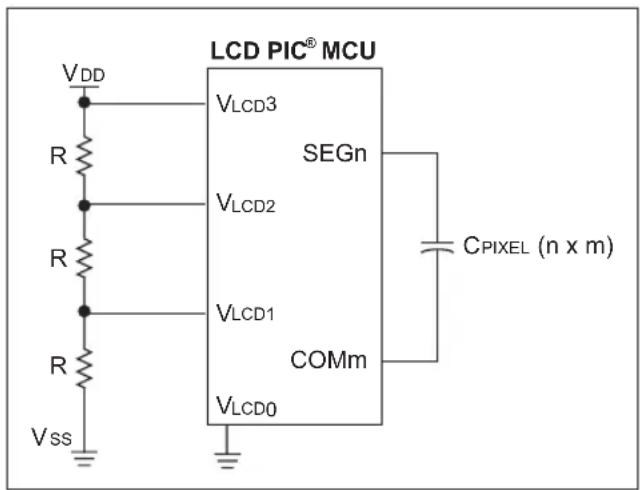
text_image
LCD PIC® MCU VDD VLCD3 SEGn VLCD2 VLCD1 COMm VLCD0 CPIXEL (n x m) R R R R VssHow do we maximize the resistance without adversely effecting the quality of the display? Some basic circuit analysis helps us determine how much we can increase the size of the resistors in the ladder.
The LCD module is basically an analog multiplexer that alternately connects the LCD voltages to the various segment and common pins that connect across the LCD pixels. The LCD pixels can be modeled as a capacitor. Each tap point on the resistor ladder can be modeled as a Thevenin equivalent circuit. The Thevenin resistance is 0 for VLCD3 and VLCD0, so we look at the two cases where it is nonzero, VLCD2 and VLCD1.
The circuit can be simplified as shown in Figure 3-2. Rwis the resistance of the segment multiplex switch; Rwis the resistance of the common multiplex switch.
Figure 3-2: Simplified LCD Circuit
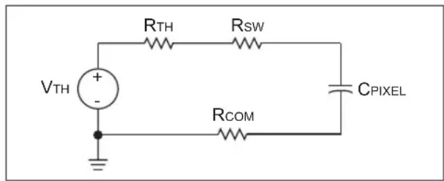
text_image
VTH + - RTH Rsw CPIXEL RCOMThe Thevenin voltage is equal to either 2/3 V or 1/3 V for the cases where the Thevenin resistance is non-zero. The Thevenin resistance is equal to the parallel resistance of the upper and lower parts of the resistor ladder.
Figure 3-3: LCD Circuit Resistance Estimate

text_image
RTH = (2R * R)/(2R + R) RTH = 2R²/3R RTH = 2R/3 RSW = 4.7K RCOM = 0.4K RTOTAL = RTH + RSW + RCOM VTH + - C PIXELAs you can see, we can model the drive of a single pixel as an RC circuit, where the voltage switches from 0V to V102, for example. For LCD PIC microcontrollers, we can estimate the resistance of the segment and common switching circuits as about 4.7K and 0.4K, respectively.
We can see that the time for the voltage across the pixel to change from 0 to Vth will depend on the capacitance of the pixel and the total resistance, of which the resistor ladder Thevenin resistance forms the most significant part.
Figure 3-4: Voltage Change Across Pixel

text_image
R TOTAL VTH + - VPIXEL CPIXELThe step response of the voltage across a pixel is subject to the following equation:
Equation 3-1
$$ V _ {R E L} = V _ {T H} (1 - e ^ {- t / R C}) $$
By manipulating the equation, we can see that it will take a time equal to 4 time constants for the pixel voltage to reach 98% of the bias voltage.
Figure 3-5: Step Response Diagram

line
| Parameter | Value | | ----------------- | --------- | | VPIXEL/VTH | 1 - e^(-t/RC) | | 98% / e^(-t/RC) | 1 - e^(-t/RC) | | 2% / e^(-t/RC) | 0.98 | | ln(.02) | -t/RC | | t = ~4 RC | 0 | | t = 4 RC | 0 |Now we need to estimate the capacitance. Capacitance is proportional to the area of a pixel. We can measure the area of a pixel and estimate the capacitance as shown. Obviously, a bigger display, such as a digital wall clock, will have bigger pixels and higher capacitance.
Equation 3-2
$$ \begin{array}{r l} \mathrm{C} _ {\text { PEL }} & = 1 5 0 0 \mathrm{pF/cm} ^ {2} \ \mathrm{AREA} _ {\text { PEL }} & = 1 \mathrm{mm} ^ {*} 3 \mathrm{mm} = . 0 3 \mathrm{cm} ^ {2} \ \mathrm{C} _ {\text { PEL }} & = 4 5 \mathrm{pF} \end{array} $$
We want the time constant to be much smaller than the period of the LCD waveform, so that rounding of the LCD waveform will be minimized. If we want the RC to be equal to 100 S , then the total resistance can be calculated as shown:
Equation 3-3
$$ R _ {\text { TOTAL }} = 1 0 0 \mu \mathrm{S} / 4 5 \mathrm{pF} = 2. 2 2 \mathrm{m} \Omega $$
$$ R _ {T H} = 2. 2 M - 5. 1 K = 2. 2 M $$
The resistance of the switching circuits within the LCD module is very small compared to this resistance, so the Thevenin resistance of the resistor ladder at Vcc2 and Vcc1 can be treated the same as Rta. We can then calculate the value for R that will give us the correct Thevenin resistance.
Equation 3-4
$$ R = 3 R _ {T H} / 2 = 3. 3 M $$
Now we can calculate the current through the resistor ladder if we used 3.3 mΩ resistors.
Equation 3-5
$$ \begin{array}{r l} & R _ {I A O B R} = 9. 9 M, \ & I _ {I A O B R} = 5 V / 9. 9 M = 0. 5 \mu A \end{array} $$
Use this process to estimate maximum resistor sizes for your resistor ladder and you will drastically reduce power consumption for your LCD application. Don't forget to observe the display over the operating conditions of your product (such as temperature, voltage and even, humidity) to ensure that contrast and display quality is good.
TIP #4: Contrast Control with a Buck Regulator
Contrast control in any of the LCD PIC MCUs is accomplished by controlling the voltages applied to the V o voltage inputs. The simplest contrast voltage generator is to place a resistor divider across the three pins. This circuit is shown in the data sheet. The resistor ladder method is good for many applications, but the resistor ladder does not work in an application where the contrast must remain constant over a range of V o s. The solution is to use a voltage regulator. The voltage regulator can be external to the device, or it can be built using a comparator internal to the LCD PIC microcontroller.
Figure 4-1: Voltage Generator with Resistor Divider
text_image
VDD RA1 RA5 VLCD3 0.6V PIC16F91X LCD Glass R6 C1 R1 C2 R2 C3 R3 R4 R5The PIC16F946/917/916/914/913 devices have a special Comparator mode that provides a fixed 0.6V reference. The circuit shown in Figure 4-1 makes use of this reference to provide a regulated contrast voltage. In this circuit, R1, R2 and R3 provide the contrast control voltages. The voltage on V _3 is compared to the internal voltage reference by dividing the voltage at V _3 at R4 and R5 and applying the reduced voltage to the internal comparator. When the voltage at V _3 is close to the desired voltage, the output of the comparator will begin to oscillate. The oscillations are filtered into a DC voltage by R6 and C1. C2 and C3 are simply small bypass capacitors to ensure that the voltages at V _1 and V _2 are steady.
TIP #5: Contrast Control Using a Boost Regulator
In LCD Tip #4, a buck converter was created using a comparator. This circuit works great when V _D is greater than the LCD voltage. The PIC microcontroller can operate all the way down to 2.0V, whereas most low-voltage LCD glass only operates down to 3V. In a battery application, it is important to stay operational as long as possible. Therefore, a boost converter is required to boost 2.0V up to 3.0V for the LCD.
The figure below shows one circuit for doing this.
Figure 5-1: Boost Converter

text_image
R1 D1 R2 R3 R4 D2 Q1 C1 C1 VDD C2 D3 R5 R6 C2 R7 PIC16F946/917/916/914/913 BoostIn this circuit, both comparators are used. The voltage setpoint is determined by the value of Zenier diode D3 and the voltage at R6:R7. The rest of the circuit creates a simple multivibrator to stimulate a boost circuit. The boost circuit can be inductor or capacitor-based. When the output voltage is too low, the multivibrator oscillates and causes charge to build up in C2. As the voltage at C2 increases, the multivibrator will begin to operate sporadically to maintain the desired voltage at C2.
Figure 5-2: Two Types of Boost Converter

text_image
VBAT VBAT L1 R8 Q2The two methods of producing a boost converter are shown above. The first circuit is simply a switched capacitor type circuit. The second circuit is a standard inductor boost circuit. These circuits work by raising V_DD . This allows the voltage at V_LCD to exceed V_DD .
TIP #6: Software Controlled Contrast with PWM for LCD Contrast Control
In the previous contrast control circuits, the voltage output was set by a fixed reference. In some cases, the contrast must be variable to account for different operating conditions. The CCP module, available in the LCD controller devices, allows a PWM signal to be used for contrast control. In Figure 6-1, you see the buck contrast circuit modified by connecting the input to RA6 to a CCP pin. The resistor divider created by R4 and R5 in the previous design are no longer required. An input to the ADC is used to provide feedback but this can be considered optional. If the ADC feedback is used, notice that it is used to monitor the Vsupply. The PWM will then be used to compensate for variations in the supply voltage.
Figure 6-1: Software Controlled Voltage Generator

text_image
VDD R5 D1 C1 C2 C3 R6 R1 R2 R3 VCCD3 VCCD2 VCCD1 LCD PIC® MCU VDD AN0 CCP VLCD3 VLCD2 VLCD1 LCD GlassTIP #7 Driving Common Backlights
Any application that operates in a low light condition requires a backlight. Most low-cost applications use one of the following backlights:
1) Electroluminescent (EL)
2) LEDs in series
3) LEDs in parallel
Other backlight technologies, such as CCFL, are more commonly used in high brightness graphical panels, such as those found in laptop computers. The use of white LEDs is also more common in color LCDs, where a white light source is required to generate the colors.
Driving an EL panel simply requires an AC signal. You may be able to generate this signal simply by using an unused segment on the LCD controller. The signal can also be generated by a CCP module or through software. The AC signal will need to pass through a transformer for voltage gain to generate the required voltage across the panel.
LEDs in series can be easily driven with a boost power supply. In the following diagram, a simple boost supply is shown. In this circuit, a pulse is applied to the transistor. The pulse duration is controlled by current through R2. When the pulse is turned off, the current stored in the inductor will be transferred to the LEDs. The voltage will rise to the level required to drive the current through the LEDs. The breakdown voltage of the transistor must be equal to the forward voltage of the LEDs multiplied by the number of LEDs. The comparator voltage reference can be adjusted in software to change the output level of the LEDs.
Figure 7-1: Simple Boost Supply
text_image
VDD L1 R1 Q2 LED String R2 To Comparator InputIf the LEDs are in parallel, the drive is much simpler. In this case, a single transistor can be used to sink the current of many LEDs in parallel. The transistor can be modulated by PWM to achieve the desired output level. If V_DD is higher than the maximum forward voltage, a resistor can be added to control the current, or the transistor PWM duty cycle can be adjusted to assure the LEDs are operating within their specification.
Figure 7-2: LEDs in Parallel
text_image
VDD LED String R1TIP #8 In-Circuit Debug (ICD)
There are two potential issues with using the ICD to debug LCD applications. First, the LCD controller can freeze while the device is Halted. Second, the ICD pins are shared with segments on the PIC16F946/917/916/914/913 MCUs.
When debugging, the device is Halted at breakpoints and by the user pressing the pause button. If the ICD is configured to Halt the peripherals with the device, the LCD controller will Halt and apply DC voltages to the LCD glass. Over time, these DC levels can cause damage to the glass; however, for most debugging situations, this will not be a consideration. The PIC18F LCD MCUs have a feature that allows the LCD module to continue operating while the device has been Halted during debugging. This is useful for checking the image of the display while the device is Halted and for preventing glass damage if the device will be Halted for a long period of time.
The PIC16F946/917/916/914/913 multiplex the ICSP™ and ICD pins onto pins shared with LCD segments 6 and 7. If an LCD is attached to these pins, the device can be debugged with ICD; however, all the segments driven by those two pins will flicker and be uncontrolled. As soon as debugging is finished and the device is programmed with Debug mode disabled, these segments will be controlled correctly.
TIP #9 LCD in Sleep Mode
If you have a power-sensitive application that must display data continuously, the LCD PIC microcontroller can be put to Sleep while the LCD driver module continues to drive the display.
To operate the LCD in Sleep, only two steps are required. First, a time source other than the main oscillator must be selected as the LCD clock source, because during Sleep, the main oscillator is Halted. Options are shown for the various LCD PIC MCUs.
Table 9-1: Options for LCD in Sleep Mode
| Part LCD Clock Source | Use in Sleep? | |
| PIC16C925/926 | Fos/256 No | |
| T1OSC Yes | ||
| Internal RC Oscillator Yes | ||
| PIC16F946/917/916/914/913 | Fos/8192 No | |
| T1OSC/32 Yes | ||
| LFINTOSC/32 Yes | ||
| PIC18F6X90 (Fos/4)/8192 No | ||
| PIC18F8X90 T1OSC Yes | ||
| PIC18F6XJ90 | INTRC/32 Yes | |
| PIC18F8XJ90 | ||
Second, the Sleep Enable bit (SLPEN) must be cleared. The LCD will then continue to display data while the part is in Sleep. It's that easy!
When should you select the internal RC oscillator (or LFINTOSC) over the Timer1 oscillator? It depends on whether your application is time-sensitive enough to require the accuracy of a crystal on the Timer1 oscillator or not. If you have a timekeeping application, then you will probably have a 32 kHz crystal oscillator connected to Timer1.
Since Timer1 continues to operate during Sleep, there is no penalty in using Timer1 as the LCD clock source. If you don't need to use an external oscillator on Timer1, then the internal RC oscillator (INTRC or LFINTOSC) is more than sufficient to use as the clock source for the LCD and it requires no external components.
TIP #10 How to Update LCD Data Through Firmware
To update the LCD, the content of the LCDDATA registers is modified to turn on, or off, each pixel on the LCD display. The application firmware will usually modify buffer variables that are created to correspond with elements on the display, such as character positions, bar graph, battery display, etc.
When the application calls for a display update, the values stored in the buffer variables must be converted to the correct setting of the pixel bits, located in the LCDDATA registers.
For Type-A waveforms, the LCD Data registers may be written any time without ill effect. However, for Type-B waveforms, the LCD Data registers can only be written every other LCD frame in order to ensure that the two frames of the Type-B waveform are compliments of one another. Otherwise, a DC bias can be presented to the LCD.
The LCD Data registers should only be written when a write is allowed, which is indicated by the WA bit in the LCDCON register being set.
On the PIC16C926 parts, there is no WA bit. The writing of the pixel data can be coordinated on an LCD interrupt. The LCD interrupt is only generated when a multiplexed (not static) Type-B waveform is selected.
TIP #11 Blinking LCD
Information can be displayed in more than one way with an LCD panel. For example, how can the user's attention be drawn to a particular portion of the LCD panel? One way that does not require any additional segments is to create a blinking effect.
Look at a common clock application. The “:” between the hours and minutes is commonly made to blink once a second (on for half a second, off for half a second). This shows that the clock is counting in absence of the ticking sound or second hand that accompanies the usual analog face clock. It serves an important purpose of letting the user know that the clock is operating.
If there is a power outage, then it is common for the entire clock display to blink. This gives the user of the clock an immediate indication that the clock is no longer showing the correct time.
When the user sets the time, then blinking is commonly used to show that a new mode has been entered, such as blinking the hours to identify that the hours are being set, or blinking the minutes to show that the minutes are being set. In a simple clock, blinking is used for several different purposes. Without blinking effects, the common digital clock would not be nearly as user friendly.
Figure 11-1: Common Clock Application

text_image
12:00 PMFortunately, blinking is quite easy to implement. There are many ways to implement a blinking effect in software. Any regular event can be used to update a blink period counter. A blink flag can be toggled each time the blink period elapses. Each character or display element that you want to blink can be assigned a corresponding blink enable flag. The flowchart for updating the display would look like:
Figure 11-2: Updating Display Flowchart

flowchart
graph TD
    A["Start"] --> B{Is Blink flag set?}
    B -->|Y| C{Is Character 1 Blink enable set?}
    B -->|N| D["Update Character 1 Pixels"]
    C -->|Y| E["Clear Character 1 Pixels"]
    C -->|N| F["Update Character 1 Pixels"]
    D --> G["Finish"]
    E --> H["LCDDATA Pixel Bits"]
    F --> H
    G --> H
    H --> I["Blink Flag"]
    H --> J["Character 1 Blink Enable"]
    H --> K["Character 1 Buffer"]
TIP #12 4 x 4 Keypad Interface that Conserves Pins for LCD Segment Drivers
A typical digital interface to a 4 x 4 keypad uses 8 digital I/O pins. But using eight pins as digital I/Os can take away from the number of segment driver pins available to interface to an LCD.
By using 2 digital I/O pins and 2 analog input pins, it is possible to add a 4 x 4 keypad to the PIC microcontroller without sacrificing any of its LCD segment driver pins.
The schematic for keypad hook-up is shown in Figure 12-1. This example uses the PIC18F8490, but the technique could be used on any of the LCD PIC MCUs.
Figure 12-1: Keypad Hook-up Schematic

text_image
RBB 1 2 3 4 5 6 7 8 1 2 3 4 5 6 7 8 RBB Output High RBB Output High ANB AN1 AN0 AN1 8V - - - - VDD/5.2 2 8 C E VDD/4.2 1 7 3 9 VDD/3 5 0 D F VDD/2 4 A B F DECODING TABLE RBB S1 S2 S3 S4 S5 S6 S7 S8 S9 S10 S11 S12 S13 S14 S15 S16 S17 S18 S19 S20 S21 S22 S23 S24 S25 S26 S27 S28 S29 S30 S31 S32 S33 S34 S35 S36 S37 S38 S39 S40 S41 S42 S43 S44 S45 S46 S47 S48 S49 S50 S51 S52 S53 S54 S55 S56 S57 S58 S59 S60 S61 S62 S63 S64 RBB0 RBB1 RBB2 RBB3 RBB4 RBB5 RBB6 RBB7 RBB8 RBB9 RBB10 RBB11 RBB12 RBB13 RBB14 RBB15 RBB16 RBB17 RBB18 RBB19 RBB20 RBB21 RBB22 RBB23 RBB24 RBB25 RBB26 RBB27 RBB28 RBB29 RBB30 RBB31 RBB32 RBB33 RBB34 RBB35 RBB36 RBB37 RBB38 RBB39 RBB40 RBB41 RBB42 RBB43 RBB44 RBB45 RBB46 RBB47 RBB48 RBB49 RBB50 RBB51 RBB52 RBB53 RBB54 RBB55 RBB56 RBB57 RBB58 RBB59 RBB60 RBB61 RBB62 RBB63 RBB64 RBB65 RBB66 RBB67 RBB68 RBB69 RBB70 RBB71 RBB72 RBB73 RBB74 RBB75 RBB76 RBB77 RBB78 RBB79 RBB80 RBB81 RBB82 RBB83 RBB84 RBB85 RBB86 RBB87 RBB88 RBB89 RBB90 RBB91 RBB92 RBB93 RBB94 RBB95 RBB96 RBB97 RBB98 RBB99 S1 & S2 & S3 & S4 & S5 & S6 & S7 & S8 & S9 & S10 & S11 & S12 & S13 & S14 & S15 & S16 & S17 & S18 & S19 & S20 & S21 & S22 & S23 & S24 & S25 & S26 & S27 & S28 & S29 & S30 & S31 & S32 & S33 & S34 & S35 & S36 & S37 & S38 & S39 & S40 & S41 & S42 & S43 & S44 & S45 & S46 & S47 & S48 & S49 & S50 & S51 & S52 & S53 & S54 & S55 & S56 & S57 & S58 & S59 & S60 & S61 & S62 & S63 & S64 & S65 & S66 & S67 & S68 & S69 & S70 & S71 & S72 & S73 & S74 & S75 & S76 & S77 & S78 & S79 & S80 & S81 & S82 & S83 & S84 & S85 & S86 & S87 & S88 & S89 & S90 & S91 & S92 & S93 & S94 & S95 & S96 & S97 & S98 & S99 & S100 & RCCs: (open J11, JP3) (open JP3, JP4)The two digital I/O pins that are used are RB0 and RB5, but any two digital I/O pins could work. The two analog pins used are AN0 and AN1.
To read the keypad, follow the steps below:
- First, make RB0 an output high and RB5 an input (to present a high impedance).
- Perform two successive A/D conversions, first on AN0, then on AN1.
- Save the conversion results to their respective variables; for example, RB0_AN0_Result and RB0_AN1_Result.
- Next, make RB5 an output high and RB0 an input (to present a high impedance).
- Perform two successive A/D conversions, first on AN0, then on AN1.
- Save the conversion results to their respective variables; for example, RB5_AN0_Result and RB5_AN1_Result.
-
There are now 4 variables that represent a key press in each quadrant of the 4 × 4 keypad:
-
RBO_ANO_Result denotes key press of 1, 2, 4 or 5
- RB0_AN1_Result denotes key press of 7, 8, A or 0
- RB5_AN0_Result denotes key press of 3, C, 6 or D
-
RB5_AN1_Result denotes key press of 9, E, B or F
-
Finally, check each value against the matching column of Table 12-1. If it is within ±10% of a value, then it can be taken to indicate that the corresponding key has been pressed.
Table 12-1: Keypad Values
| Value ±10% | RB0_AN0 | RB0_AN1 | RB5_AN0 | RB5_AN1 |
| V0/5.2 2 8 C E | ||||
| V0/4.2 1 7 3 9 | ||||
| V0/3 5 0 D F | ||||
| V0/2 4 A 6 B |
- This loop should be repeated about once every 20 ms or so.
Don't forget a debounce routine. For example, require the above steps (with 20 ms delay between) to return the same key value twice in a row for that key to be considered pressed. Also, require a no key press to be returned at least twice before looking for the next key press.
When keys within the same quadrant are pressed simultaneously, voltages other than the four valid levels shown in the table may be generated. These levels can either be ignored, or if you want to use simultaneous key presses to enable certain functions, you can add decoding for those levels as well.
Application Note References
- AN220, "Watt-Hour Meter Using PIC16C923 and CS5460" (DS00220)
- AN582, "Low-Power Real-Time Clock" (DS00582)
- AN587, "Interfacing PIC® MCUs to an LCD Module" (DS00587)
- AN649, "Yet Another Clock Featuring the PIC16C924" (DS00649)
- AN658, "LCD Fundamentals Using PIC16C92X Microcontrollers" (DS00658)
- TB084, "Contrast Control Circuits for the PIC16F91X" (DS91084)
Application notes can be found on the Microchip web site at www.microchip.com.
CHAPTER 7
Intelligent Power Supply Design
Tips 'n Tricks
Table Of Contents
TIPS 'N TRICKS INTRODUCTION
TIP #1: Soft-Start Using a PIC10F200 7-2
TIP #2: A Start-Up Sequencer 7-3
TIP #3: A Tracking and Proportional Soft-Start of Two Power Supplies ..... 7-4
TIP #4: Creating a Dithered PWM Clock ..... 7-5
TIP #5: Using a PIC ® Microcontroller as a Clock Source for a SMPS PWM Generator 7-6
TIP #6: Current Limiting Using the MCP1630 7-7
TIP #7: Using a PIC ^® Microcontroller for Power Factor Correction 7-8
TIP #8: Transformerless Power Supplies ..... 7-9
TIP #9: An IR Remote Control Actuated AC Switch for Linear Power Supply Designs 7-10
TIP #10: Driving High Side FETs 7-11
TIP #11: Generating a Reference Voltage with a PWM Output 7-12
TIP #12: Using Auto-Shutdown CCP 7-13
TIP #13: Generating a Two-Phase Control Signal 7-14
TIP #14: Brushless DC Fan Speed Control ..... 7-15
TIP #15: High Current Delta-Sigma Based Current Measurement Using a Slotted Ferrite and Hall Effect Device ....7-16
TIP #16: Implementing a PID Feedback Control in a PIC12F683-Based SMPS Design 7-17
TIP #17: An Error Detection and Restart Controller 7-18
TIP #18: Data-Indexed Software State Machine ....7-19
TIP #19: Execution Indexed Software State Machine 7-20
TIP #20: Compensating Sensors Digitally .....7-21
TIP #21: Using Output Voltage Monitoring to Create a Self-Calibration Function ..... 7-22
TIPS 'N TRICKS INTRODUCTION
Microchip continues to provide innovative products that are smaller, faster, easier-to-use and more reliable. PIC ^® microcontrollers (MCUs) are used in a wide range of everyday products from washing machines, garage door openers and television remotes to industrial, automotive and medical products.
While some designs such as Switch Mode Power Supplies (SMPS) are traditionally implemented using a purely analog control scheme, these designs can benefit from the configurability and intelligence that can only be realized by adding a microcontroller.
This document showcases several examples in which a PIC microcontroller may be used to increase the functionality of a design with a minimal increase in cost.
Several of the tips provide working software examples or reference other documents for more information. The software and referenced documents can be found on the Microchip web site at www.microchip.com/tipsntricks.
TIP #1 Soft-Start Using a PIC10F200
Almost all power supply controllers are equipped with shutdown inputs that can be used to disable the MOSFET driver outputs. Using Pulse-Width Modulation (PWM), the amount of time the power supply is allowed to operate can be slowly incremented to allow the output voltage to slowly rise from 0% to 100%.
Figure 1-1: Soft-Start Circuit Schematic
text_image
VDD 0.1 µF 5 On/Off Control Input 1 GP0 GP1 3 Shutdown PWM Output 10 kΩ 6 GP2 GP3 N.C.N.C. 2 4 Note: Assumes SOT-23 packaging.This technique is called soft-start and is used to prevent the large inrush currents that are associated with the start-up of a switching power supply.
GP0 on the PIC MCU is used to enable or disable the soft-start. Once enabled, the on-time of the PWM signal driving the shutdown output will increase each cycle until the power supply is fully on.
During the PIC MCU Power-on Reset, the PWM output (GP1) is initially in a high-impedance state. A pull-down resistor on the PWM output ensures the power supply will not unexpectedly begin operating.
Figure 1-2: Timing Diagram
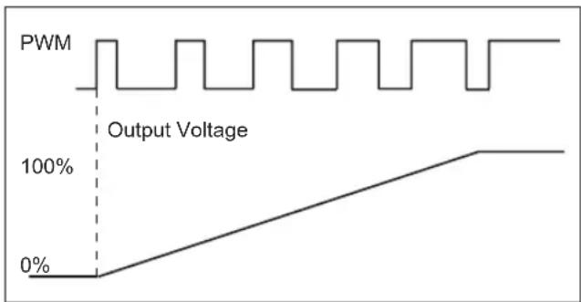
line
| Time | PWM | |------|-----| | 0% | 0% | | 100% | 100% |It is important to note that this type of soft-start controller can only be used for switching regulators that respond very quickly to changes on their shutdown pins (such as those that do cycle-by-cycle limiting). Some linear regulators have active-low shutdown inputs, however, these regulators do not respond fast enough to changes on their shutdown pins in order to perform soft-start.
Example software is provided for the PIC10F200 which was taken from TB081. Please refer to TB081, "Soft-Start Controller For Switching Power Supplies" (DS91081) for more information.
TIP #2 A Start-Up Sequencer
Some new devices have multiple voltage requirements (e.g., core voltages, I/O voltages, etc.). The sequence in which these voltages rise and fall may be important.
By expanding on the previous tip, a start-up sequencer can be created to control two output voltages. Two PWM outputs are generated to control the shutdown pins of two SMPS controllers. Again, this type of control only works on controllers that respond quickly to changes on the shutdown pin (such as those that do cycle-by-cycle limiting).
Figure 2-1: Multiple PWM Output Soft-Start Controller
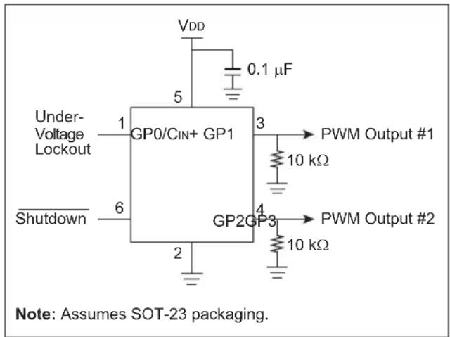
text_image
VDD 0.1 µF 5 Under- Voltage Lockout 1 GP0/CIN+ GP1 3 PWM Output #1 10 kΩ Shutdown 6 GP2GP3 4 PWM Output #2 2 10 kΩ Note: Assumes SOT-23 packaging.This design uses the PIC MCU comparator to implement an under-voltage lockout. The input on the GP0/CIN+ pin must be above the internal 0.6V reference for soft-start to begin, as shown in Figure 2-2.
Two conditions must be met in order for the soft-start sequence to begin:
- The shutdown pin must be held at V_DD (logic high).
- The voltage on GP0 must be above 0.6V.
Once both start-up conditions are met, the sequences will delay and PWM #1 will ramp from 0% to 100%. A second delay allows the first voltage to stabilize before the sequencer ramps PWM #2 from 0% to 100%. All delays and ramp times are under software control and can be customized for specific applications. If either soft-start condition becomes invalid, the circuit will shutdown the SMPS controllers.
Figure 2-2: Timing Diagram

line
| Time | V1 | V2 | PWM1 | PWM2 | |------|----|----|------|------| | 1 | 0 | 0 | 0 | 0 | | 2 | 0 | 0 | 0 | 0 | | 3 | 1 | 0 | 0 | 0 | | 4 | 1 | 0 | 0 | 0 | | 5 | 1 | 1 | 0 | 0 |Example software is provided for the PIC10F200 which was taken from TB093, "Multiple PWM Output Soft-Start Controller for Switching Power Supplies" (DS91093).
TIP #3 A Tracking and Proportional Soft-Start of Two Power Supplies
Expanding on the previous tip, we can also use a PIC MCU to ensure that two voltages in a system rise together or rise proportionally to one another, as shown in Figure 3-1. This type of start-up is often used in applications with devices that require multiple voltages (such as I/O and core voltages).
Like the previous two, this tip is designed to control the shutdown pin of the SMPS controller and will only work with controllers that respond quickly to changes on the shutdown pin.
Figure 3-1: Timing Diagram
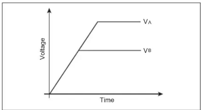
line
| Time | Voltage | |------|---------| | 0 | 0 | | V_A | High | | V_B | Low |Figure 3-2: Example Schematic
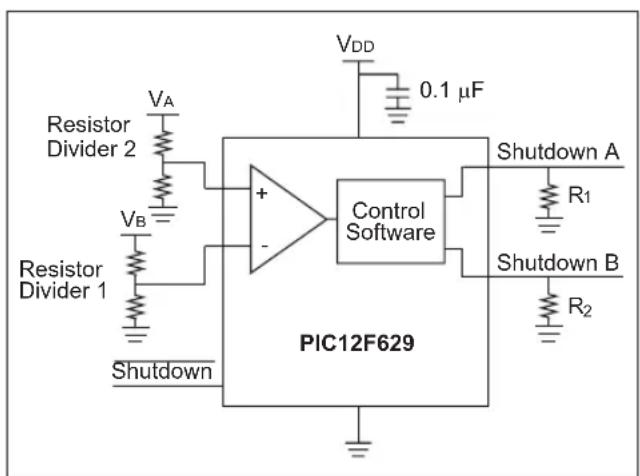
text_image
VDD 0.1 µF Resistor Divider 2 VA VB Resistor Divider 1 + - Control Software Shutdown A R1 Shutdown B R2 Shutdown PIC12F629The comparator of the PIC MCU is used to determine which voltage is higher and increases the on-time of the other output accordingly. The logic for the shutdown pins is as shown in Table 3-1.
Table 3-1: Shutdown Pin Logic
| Case | Shutdown A | Shutdown B |
| V_A > V_B | Low | High |
| V_B > V_A | High | Low |
| V_B > Internal Reference | High | High |
To determine if it has reached full voltage, V_B is compared to the internal voltage reference. If V_B is higher, both shutdown outputs are held high.
Resistor Divider 1 should be designed so that the potentiometer output is slightly higher than the comparator voltage reference when V_B is at full voltage.
The ratio of resistors in Resistor Divider 2 can be varied to change the slope at which V_A rises.
Pull-down resistors ensure the power supplies will not operate unexpectedly when the PIC MCU is being reset.
TIP #4 Creating a Dithered PWM Clock
In order to meet emissions requirements as mandated by the FCC and other regulatory organizations, the switching frequency of a power supply can be varied. Switching at a fixed frequency produces energy at that frequency. By varying the switching frequency, the energy is spread out over a wider range and the resulting magnitude of the emitted energy at each individual frequency is lower.
The PIC10F200 has an internal 4 MHz oscillator. A scaled version of oscillator can be output on a pin (Fosc/4). The scaled output is 1/4 of the oscillator frequency (1 MHz) and will always have a 50% duty cycle. Figure 4-1 shows a spectrum analyzer shot of the output of the Fosc/4 output.
Figure 4-1: Spectrum of Clock Output Before Dithering
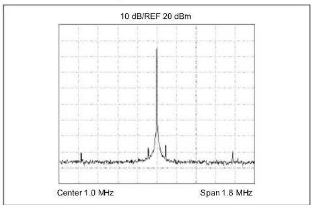
line
| Frequency | Value | | --------------- | ----- | | Center 1.0 MHz | 0 | | Span 1.8 MHz | 10 |The PIC10F200 provides an Oscillator Calibration (OSCCAL) register that is used to calibrate the frequency of the oscillator. By varying the value of the OSCCAL setting, the frequency of the clock output can be varied. A pseudo-random sequence was used to vary the OSCCAL setting, allowing frequencies from approximately 600 kHz to 1.2 MHz. The resulting spectrum is shown in Figure 4-2.
Figure 4-2: Spectrum of Clock Output After Dithering
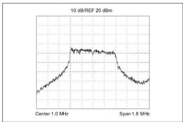
line
| Frequency | Amplitude | | --------- | --------- | | Center | ~0 | | Span 1.8 MHz | ~0 |By spreading the energy over a wider range of frequencies, a drop of more than 20 dB is achieved.
Example software is provided for the PIC10F200 that performs the pseudo-random sequence generation and loads the OSCCAL register.
TIP #5 Using a PIC® Microcontroller as a Clock Source for a SMPS PWM Generator
A PIC MCU can be used as the clock source for a PWM generator, such as the MCP1630.
Figure 5-1: PIC MCU and MCP1630 Example Boost Application
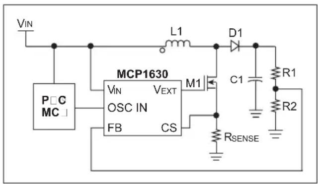
text_image
VIN P□C MC MCP1630 VOUT OSC IN FB CS L1 D1 M1 C1 R1 R2 RSENSEThe MCP1630 begins its cycle when its clock/oscillator source transitions from high-to-low, causing its PWM output to go high state. The PWM pulse can be terminated in any of three ways:
- The sensed current in the magnetic device reaches 1/3 of the error amplifier output.
- The voltage at the Feedback (FB) pin is higher than the reference voltage ( V_FE ).
- The clock/oscillator source transitions from low-to-high.
The switching frequency of the MCP1630 can be adjusted by changing the frequency of the clock source. The maximum on-timer of the MCP1630 PWM can be adjusted by changing the duty cycle of the clock source.
The PIC MCU has several options for providing this clock source:
- The Fosc/4 pin can be enabled. This will produce a 50% duty cycle square wave that is 1/4th of the oscillator frequency. Tip #4 provides both example software and information on clock dithering using the Fosc/4 output.
- For PIC MCUs equipped with a Capture/Compare/PWM (CCP) or Enhanced CCP (ECCP) module, a variable frequency, variable duty cycle signal can be created with little software overhead. This PWM signal is entirely under software control and allows advanced features, such as soft-start, to be implemented using software.
- For smaller parts that do not have a CCP or ECCP module, a software PWM can be created. Tips #1 and #2 use software PWM for soft-start and provide software examples.
TIP #6 Current Limiting Using the MCP1630
Figure 6-1: MCP1630 High-Speed PWM

text_image
0.1 μA OSC IN VIN VOUTemperature VIN UVLO (1) VEXT GND 100 kΩ VIN S Q Q̅ CS Comp + R Comp FB VREF EA 2R R 2.7V Clamp t t t t t e □ □ □ 0 0 Qn̅ 0 1 1 1 0 0 1 1 1Note 1: During overtemperature, VEXT driver is high-impedance.
The block diagram for the MCP1630 high-speed PWM driver is shown in Figure 6-1. One of the features of the MCP1630 is the ability to perform current limiting. As shown in the bottom left corner of the diagram, the output of the Error Amplifier (EA) is limited by a 2.7V clamp. Therefore, regardless of the actual error, the input to the negative terminal of the comparator (labeled Comp) is limited to 2.7V ÷ 3 or 0.9V.
It is possible to implement the current limiting by using a single sense resistor. In this case, the maximum current would be given by Equation 6-1.
Equation 6-1
$$ I _ {M K} = (0. 9 V) / R _ {S E N E} $$
For high current applications, this method may be acceptable. When lower current limits are required, the size of the sense resistor, R _AN , must be increased. This will cause additional power dissipation. An alternative method for lower current limits is shown in Figure 6-2.
Figure 6-2: Low Current Limits
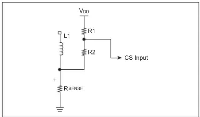
text_image
VDD L1 R1 R2 CS Input + RSENSEIn this case, the Current Sense (CS) input of the MCP1630 is biased upward using the R1/R2 resistor divider. The equations for the new current limit are shown in Equation 6-2.
Equation 6-2
$$ 0. 9 \mathrm{V} = \frac {\left(\mathrm{V} _ {\mathrm{DD}} - \mathrm{I} _ {\mathrm{MAX}} \cdot \mathrm{R} _ {\text { SENSE }}\right) \cdot \mathrm{R} 2}{\mathrm{R} 1 + \mathrm{R} 2} $$
Equation 6-2 can be solved to determine the values of R1 and R2 that provide the desired current limit.
TIP #7 Using a PIC® Microcontroller for Power Factor Correction
In AC power systems, the term Power Factor (PF) is used to describe the fraction of power actually used by a load compared to the total apparent power supplied.
Power Factor Correction (PFC) is used to increase the efficiency of power delivery by maximizing the PF.
The basis for most Active PFC circuits is a boost circuit, shown in Figure 7-1.
Figure 7-1: Typical Power Factor Correction Boost Supply
text_image
L1 D1 VBoost C1 PWM M1 + - C2The AC voltage is rectified and boosted to voltages as high as 400 VDC. The unique feature of the PFC circuit is that the inductor current is regulated to maintain a certain PF. A sine wave reference current is generated that is in phase with the line voltage. The magnitude of the sine wave is inversely proportional to the voltage at VBoost. Once the sine wave reference is established, the inductor current is regulated to follow it, as shown in Figure 7-2.
Figure 7-2: Desired and Actual Inductor Currents

line
| Type | Inductor Current | | ------------------------ | ---------------- | | Reference Inductor Current | Not labeled | | Actual Inductor Current | Not labeled |A PIC MCU has several features that allow it to perform power factor correction.
- The PIC MCUs CCP module can be used to generate a PWM signal that, once filtered, can be used to generate the sine wave reference signal.
- The PIC Analog-to-Digital (A/D) converter can be used to sense VBoost and the reference sine wave can be adjusted in software.
- The interrupt-on-change feature of the PIC MCU input pins can be used to allow the PIC MCU to synchronize the sine wave reference to the line voltage by detecting the zero crossings.
- The on-chip comparators can be used for driving the boost MOSFET(s) using the PWM sine wave reference as one input and the actual inductor current as another.
TIP #8 Transformerless Power Supplies
When using a microcontroller in a line-powered application, such as the IR remote control actuated AC switch described in Tip #9, the cost of building a transformer-based AC/DC converter can be significant. However, there are transformerless alternatives which are described below.
Capacitive Transformerless Power Supply
Figure 8-1: Capacitive Power Supply
text_image
L IN D1 5.1V C2 470 μF IOUT N R1 .47μ 250V D2 470Ω 1/2W VOUT IOUTFigure 8-1 shows the basics for a capacitive power supply. The Zener diode is reverse-biased to create the desired voltage. The current drawn by the Zener is limited by R1 and the impedance of C1.
Advantages:
• Significantly smaller than a transformer-based power supply
- Lower cost than a transformer-based or switcher-based power supply
- Power supply is more efficient than a resistive transformerless power supply
Disadvantages:
- Not isolated from the AC line voltage which introduces safety issues
• Higher cost than a resistive power supply because X2 rated capacitors are required
Resistive Power Supply
Figure 8-2: Resistive Power Supply

text_image
L IIN D1 5.1V C2 VOUT IOUT N R1 1KΩ 5W R2 1KΩ 5W D2The resistive power supply works in a similar manner to the capacitive power supply by using a reversed-biased Zener diode to produce the desired voltage. However, R1 is much larger and is the only current limiting element.
Advantages:
• Significantly smaller than a transformer-based power supply
- Lower cost than a transformer-based power supply
- Lower cost than a capacitive power supply
Disadvantages:
- Not isolated from the AC line voltage which introduces safety issues
- Power supply is less energy efficient than a capacitive power supply
- More energy is dissipated as heat in R1
More information on either of these solutions, including equations used for calculating circuit parameters, can be found in AN954, "Transformerless Power Supplies: Resistive and Capacitive" (DS00954) or in TB008, "Transformerless Power Supply" (DS91008).
TIP #9 An IR Remote Control Actuated AC Switch for Linear Power Supply Designs
Many line-powered applications (audio amplifiers, televisions, etc.) can be turned on and off using an infrared remote control. This requires that some components be energized to receive the remote signals even when the device is off. Low current PIC microcontrollers are best in this application. Figure 9-1 shows an example circuit layout.
Figure 9-1: PIC MCU Infrared Receiver Schematic
text_image
AC IN R1 U1 C2 Do + - Q1 Load +5V C1 VDD GP0/C+ GP2/Cout GP1/C- GP2/MCLR Vss R2 Zero Crossing DetectionThe PIC10F200 has several features that make it ideally suited for this type of application:
- Extremely low operating and standby current (350 A operating, 0.1 A when asleep)
- Input/Output pins with configurable pull-ups and reset-on-change capability
- High sink/source ability (±25 mA) allows driving external devices, such as the IR receiver, directly from the I/O pin
- Ability to use a low-cost resistive power supply
- Small form factor (SOT-23 packaging)
TB094, "Dimming AC Incandescent Lamps Using A PIC10F200" (DS91094) provides both software and hardware examples of an infrared controller.
TIP #10 Driving High Side FETs
In applications where high side N channel FETs are to be driven, there are several means for generating an elevated driving voltage. One very simple method is to use a voltage doubling charge pump as shown in Figure 10-1.
Method 1
Figure 10-1: Typical Change Pump
text_image
CLKOUT VDD D1 VOUT max = 2 * VDD - 2 * VDIODE CPUMP D2 CFILTERThe PIC MCUs CLKOUT pin toggles at 1/4 of the oscillator frequency. When CLKOUT is low, D1 is forward biased and conducts current, thereby charging CRPR After CLKOUT is high, D2 is forward biased, moving the charge to CRITER The result is a voltage equal to twice the VDD minus two diode drops. This can be used with a PWM or any other I/O pin that toggles.
In Figure 10-2, a standard FET driver is used to drive both the high and low side FETs by using the diode and capacitor arrangement.
Method 2
Figure 10-2: Schematic

text_image
+5V D1 D2 C2 FET Driver +12V PWM1 U1A M1 C1 L1 PWM2 U1B M2The +5V is used for powering the microcontroller. Using this arrangement, the FET driver would have approximately 12 + (5 - V_DIODE) - V_DIODE volts as a supply and is able to drive both the high and low side FETs.
The circuit above works by charging C1 through D1 to (5V - V DD ) while M2 is on, effectively connecting C1 to ground. When M2 turns off and M1 turns on, one side of C1 is now at 12V and the other side is at 12V + (5V - V DD ). The D2 turns on and the voltage supplied to the FET driver is 12V + (5V - V DD ) - V DD .
TIP #11 Generating a Reference Voltage with a PWM Output
Figure 11-1: Low-Pass Filter
text_image
CCP1 R C MCP6001 + - Analog OutA PWM signal can be used to create a Digital-to-Analog Converter (DAC) with only a few external components. Conversion of PWM waveforms to analog signals involves the use of an analog low-pass filter. In order to eliminate unwanted harmonics caused by a PWM signal, the PWM frequency ( F_W ) should be significantly higher than the bandwidth ( F_W ) of the desired analog signal. Equation 11-1 shows this relation.
Equation 11-1
$$ F _ {P W M} = K \cdot F _ {B W} $$
Where harmonics decrease as K increases.
R and C are chosen based on the following equation:
Equation 11-2
$$ R C = 1 / (2 \cdot \pi \cdot F _ {B N}) $$
Where harmonics decrease as K increases.
Choose the R value based on drive capability and then calculate the required C value. The attenuation of the PWM frequency for a given RC filter is shown in Equation 11-3.
Equation 11-3
$$ \operatorname{Att} (\mathrm{dB}) = - 1 0 \cdot \log [ 1 + (2 \pi \cdot F _ {\text { PWM }} \cdot R C) ^ {2} ] $$
If the attenuation calculated in Equation 11-3 is not sufficient, then K must be increased in Equation 11-1.
In order to sufficiently attenuate the harmonics, it may be necessary to use small capacitor values or large resistor values. Any current draw will effect the voltage across the capacitor. Adding an op amp allows the analog voltage to be buffered and, because of this, any current drawn will be supplied by the op amp and not the filter capacitor.
For more information on using a PWM signal to generate an analog output, refer to AN538, "Using PWM to Generate Analog Output" (DS00538).
TIP #12 Using Auto-Shutdown CCP
PWM Auto-Shutdown
Several of Microchip's PIC MCUs, such as the PIC16F684, PIC16F685 and PIC16F690, have a PWM auto-shutdown feature. When auto-shutdown is enabled, an event can terminate the current PWM pulse and prevent subsequent pulses unless the event is cleared. The ECCP can be setup to automatically start generating pulses again once the event clears.
Figure 12-1: PWM Auto-Shutdown Timing
text_image
PWM Signal Shutdown EventFigure 12-1 shows an example timing for the PWM auto-shutdown. When the shutdown event occurs, the current pulse is immediately terminated. In this example, the next two pulses are also terminated because the shutdown event had not been cleared by the beginning of the pulse period. After the event has cleared, pulses are allowed to resume, but only at the beginning of a pulse period.
Using Auto-Shutdown to Create a Boost Supply
By using the auto-shutdown feature, a very simple SMPS can be created. Figure 12-2 shows an example boost power supply.
Figure 12-2: Boost Power Supply
text_image
Internal to PIC® MCU PWM Module R1 Q1 D1 VOUT C1 R2 R3 Out +This power supply configuration has several unique features:
- The switching frequency is determined by the PWM frequency and, therefore, can be changed at any time.
- The maximum on-time is determined by the PWM duty cycle and, therefore, can be changed any time. This provides a very easy way to implement soft-start.
- On PIC MCUs that have a programmable reference module, the output voltage can be configured and changed at any time.
The topology can also be re-arranged to create other types of power supplies.
Example software is provided for the PIC16F685 (but can be adapted to any PIC MCU with the ECCP module). The software configures the PWM and comparator modules as shown in Figure 12-2.
TIP #13 Generating a Two-Phase Control Signal
Power supplies using a push-pull topology or with multiple switching components require a two-phase control signal as shown in Figure 13-1.
Figure 13-1: Two-Phase Control Signal

text_image
P1A P1BIt is possible to produce this type of control signal with two out-of-phase square waves using a PIC MCU with an ECCP module.
Figure 13-2: Two-Phase Control Signal Schematic

text_image
PIC® MCU P1A P1BIn order to configure the ECCP to produce this type of output:
- Configure the ECCP in half H-bridge configuration PWM pulse with both outputs active-high.
- Set the duty cycle register (CCPR1L) with the maximum duty cycle of 50%.
- Change the programmable dead-time generator to reduce the pulse width to the desired value.
The programmable dead-time generator has a 7-bit resolution and, therefore, the resulting pulses will only have a 7-bit resolution. Each pulse will have a 50% duty cycle, less the dead time.
Using an internal 4 MHz clock produces 31 kHz output pulses, and using a 20 MHz crystal would produce 156 kHz output. The frequency of the output could be increased with a loss in resolution.
Example software is provided for the PIC16F684, but this tip is applicable to all PIC MCUs with ECCP modules.
TIP #14 Brushless DC Fan Speed Control
There are several methods to control the speed of a DC brushless fan. The type of fan, allowable power consumption and the type of control desired are all factors in choosing the appropriate type.
Figure 14-1: Low-Side PWM Drive
text_image
PWM Drive 12VFigure 14-2: High-Side PWM Drive
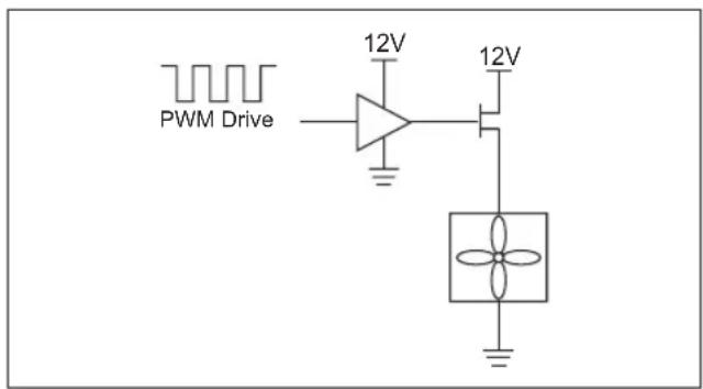
text_image
PWM Drive 12V 12VMethod 1 – Pulse-Width Modulation
As shown in Figure 14-1 and Figure 14-2, a simple PWM drive may be used to switch a two-wire fan on and off. While it is possible to use the circuit in Figure 14-1 without a high-side MOSFET driver, some manufacturers state that switching on the low side of the fan will void the warranty.
Because of this, it is necessary to switch the high side of the fan in order to control the speed. The simplest type of speed control is 'on' or 'off'. However, if a higher degree of control is desired, PWM can be used to vary the speed of the fan.
For 3-wire fans, the tachometer output will not be accurate if PWM is used. The sensor providing the tachometer output on 3-wire fans is powered from the same supply as the fan coils, thus using a PWM to control fan speed will render the fan's tachometer inaccurate.
One solution is to use a 4-wire fan which includes both the tachometer output and a drive input. Figure 14-3 shows a diagram of a 4-wire fan.
Figure 14-3: Typical 4-Wire Fan

text_image
V+ Drive TACH GND TACHA 4-wire fan allows speed to be controlled using PWM via the Drive line. Since power to the tachometer sensor is not interrupted, it will continue to output the correct speed.
Method 2 – Linear Control
When using PWM, the voltage will vary between a maximum and a minimum, however, is it also possible to use a linear method to control fan speed, as shown in Figure 14-4.
Figure 14-4: Linear Control Drive

text_image
VREF + Out 12V R1 R2The voltage applied at the non-inverting terminal of the op amp is used to vary the voltage across the op amp. The non-inverting terminal voltage can be produced by a Digital-to-Analog Converter (DAC) or by the method shown in Tip #11.
When using this method, care must be taken to ensure that the fan voltage is not too low or the fan will stop spinning. One advantage this method has over PWM is that the tachometer output will function properly on 3-wire fans. The disadvantage, however, is that it often offers less speed control. For example, a 12V fan will not spin below 8V, so a range of only 4V is available for speed control. A 5V fan will not spin below 4V and so the control range is only 1V, which is often unacceptable. Another disadvantage is the power consumption of the circuit. The transistor will dissipate more power than the PWM method.
TIP #15 High Current Delta-Sigma Based Current Measurement Using a Slotted Ferrite and Hall Effect Device
Many current sensors rely on ferrite cores. Non-linearity in the ferrite can lead to inaccurate results, especially at high currents. One way to avoid the non-linearities is to keep the net flux in the ferrite near zero. Consider the circuit in Figure 15-1.
Figure 15-1: Hall Effect Current Measurement Schematic
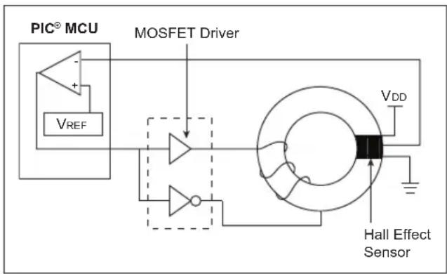
flowchart
graph TD
    A["PIC® MCU"] --> B["MOSFET Driver"]
    B --> C["Hall Effect Sensor"]
    C --> D["V_DD"]
    D --> E["Ground"]
    F["V_REF"] --> G["+"]
    G --> H["->"]
    H --> I["->"]
    I --> J["->"]
    J --> K["->"]
    K --> L["->"]
    L --> M["->"]
    M --> N["->"]
    N --> O["->"]
    O --> P["->"]
    P --> Q["->"]
    Q --> R["->"]
    R --> S["->"]
    S --> T["->"]
    T --> U["->"]
    U --> V["->"]
    V --> W["->"]
    W --> X["->"]
    X --> Y["->"]
    Y --> Z["->"]
    Z --> A
The Hall effect sensor output is proportional to the current being measured. When I_IN = 0 amps, the output of the sensor will be V _D2 . A current passing through the sensor in one direction will increase the output of the sensor, and a current in the other direction will decrease the output of the sensor.
The output of the comparator is used to drive a coil of wire wound around the ferrite core. This coil of wire will be used to create flux in the opposite direction as the flux imposed in the core.
Figure 15-2: Flux Directions

text_image
Flux due to input current I_IN Flux due to driven coilThe net flux in the core should be approximately zero. Because the flux will always be very near zero, the core will be very linear over the small operating range.
When I_IN = 0 , the output of the comparator will have an approximate 50% duty cycle. As the current moves one direction, the duty cycle will increase. As the current moves the other direction, the duty cycle will decrease. By measuring the duty cycle of the resulting comparator output, we can determine the value of I_IN .
Finally, a Delta-Sigma ADC can be used to perform the actual measurement. Features such as comparator sync and Timer1 gate allow the Delta-Sigma conversion to be taken care of entirely in hardware. By taking 65,536 (2^16) samples and counting the number of samples that the comparator output is low or high, we can obtain a 16-bit A/D result.
Example schematic and software are provided for the PIC12F683 in both C and Assembly.
For more information on using a PIC MCU to implement a Delta-Sigma converter, please refer to AN700, "Make a Delta-Sigma Converter Using a Microcontroller's Analog Comparator Module" (DS00700), which includes example software.
TIP #16 Implementing a PID Feedback Control in a PIC12F683-Based SMPS Design
Simple switching power supplies can be controlled digitally using a Proportional Integral Derivative (PID) algorithm in place of an analog error amplifier and sensing the voltage using the Analog-to-Digital Converter (ADC).
Figure 16-1: Simple PID Power Supply
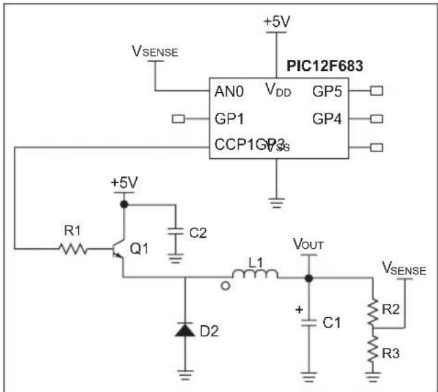
text_image
VSENSE +5V PIC12F683 AN0 VDD GP5 GP1 GP4 CCP1GP3 R1 Q1 C2 L1 VOUT VSENSE D2 C1 R2 R3The design in Figure 16-1 utilizes an 8-pin PIC12F683 PIC MCU in a buck topology. The PIC12F683 has the basic building blocks needed to implement this type of power supply: an A/D converter and a CCP module.
Figure 16-2: PID Block Diagram

flowchart
graph TD
    A["A/D Voltage Sense"] --> C["+"]
    B["Desired Value"] --> C
    C --> D["Software PID Routine"]
    D --> E["CCP Duty Cycle"]
The A/D converter is used to sense the output voltage for this particular application, V _DIS is used as the reference to the A/D converter. If desired, a more accurate reference could be used. The output voltage is subtracted from the desired value, creating an error value.
This error becomes the input to the PID routine. The PID routine uses the error voltage to determine the appropriate duty cycle for the output drive. The PID constants are weighted so that the main portion of the control is proportional and integral. The differential component is not essential to this system and is not used. Furthermore, the PID constants could be optimized if a particular type of transient response was desired, or if a predictable transient load was to be connected.
Finally, the CCP module is used to create a PWM signal at the chosen frequency with the proper duty cycle.
Example software is provided for the PIC12F683 using the schematic in Figure 16-1.
The following application notes are related to PID control algorithms and all include example software:
- AN258, "Low Cost USB Microcontroller Programmer The Building of the PICkit® 1 Flash Starter Kit" (DS00258)
- AN937, "Implementing a PID Controller Using a PIC18 MCU" (DS00937)
- AN964, "Software PID Control of an Inverted Pendulum Using the PIC16F684" (DS00937)
TIP #17 An Error Detection and Restart Controller
An error detection and restart controller can be created by combining Tip #18 and Tip #19. The controller uses the PIC microcontroller (MCU) Analog-to-Digital Converter (ADC) for making voltage and current measurements. Input voltage, input current, output voltage, output current, temperature and more can all be measured using the A/D converter. The on-board comparators are used for monitoring faster signals, such as output current, ensuring that they do not exceed maximum allowable levels. Many PIC MCUs have internal programmable comparator references, simplifying the circuit.
Figure 17-1: Block Diagram
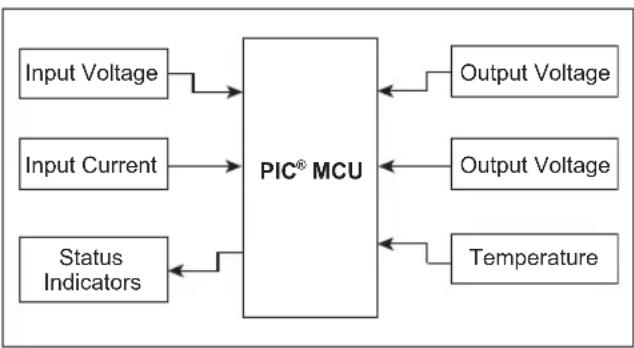
flowchart
graph LR
    A["Input Voltage"] --> B["PIC® MCU"]
    C["Input Current"] --> B
    D["Status Indicators"] --> B
    B --> E["Output Voltage"]
    B --> F["Output Voltage"]
    B --> G["Temperature"]
Using a PIC MCU as a controller allows for a greater level of intelligence in system monitoring. Rather than a single event causing a shutdown, a combination of events can cause a shutdown. A certain number of events in a certain time frame or possibly a certain sequence of events could be responsible for a shutdown.
The PIC MCU has the ability to restart the supply based on the shutdown event. Some events (such as overcurrent) may call for immediate restart, while other events (such as overtemperature) may require a delay before restarting, perhaps monitoring other parameters and using those to determine when to restart.
It is also possible to build this type of error detection and restart controller into many of the tips listed within this guide.
TIP #18 Data-Indexed Software State Machine
A state machine can be used to simplify a task by breaking the task up into smaller segments. Based on a state variable, the task performed or the data used by the state machine can be changed. There are three basic types of state machines: data-indexed, execution indexed and a hybrid of the two. This tip will focus on a data-indexed state machine.
The data-indexed state machine is ideal for monitoring multiple analog inputs with the Analog-to-Digital Converter (ADC). The state variable in these state machines determines which data is acted upon. In this case, the tasks of changing the ADC channel, storing the current result and starting a new conversion are always the same.
A very simple flow diagram for a data-indexed state machine is shown in Figure 18-1.
Figure 18-1: Data-Indexed State Machine Flowchart
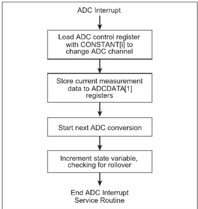
flowchart
graph TD
    A["ADC Interrupt"] --> B["Load ADC control register with CONSTANT[i"] to change ADC channel]
    B --> C["Store current measurement data to ADCDATA[1"] registers]
    C --> D["Start next ADC conversion"]
    D --> E["Increment state variable, checking for rollover"]
    E --> F["End ADC Interrupt Service Routine"]
As shown in Figure 18-1, a constant array (CONSTANT[i]) can be created to store the values to be loaded into the ADC control register to change the ADC channel.
Furthermore, a data array (ADCDATA[i]) can be used to store the results of the ADC conversion. Finally, the next conversion is started and the logic required to increment and bind the state variable is executed.
This particular example used the ADC interrupt to signal when a conversion has completed, and will attempt to take measurements as quickly as possible. A subroutine could also be built to perform the same task, allowing the user to call the subroutine when needed.
Example software is provided using the PIC16F676 and RS-232 to monitor several ADC channels.
TIP #19 Execution-Indexed Software State Machine
Another common type of state machine is the execution-indexed state machine. This type of state machine uses a state variable in order to determine what is executed. In C, this can be thought of as the switch statement structure as shown in Example 19-1.
Example 19-1: Example Using Switch Statement
SWITCH (State)
{
    CASE 0: IF (in_key() == 5) THEN state = 1,
    Break;
    CASE 1: IF (in_key() == 8) THEN State = 2,
    Else State = 0;
    Break;
    CASE 2: IF (in_key() == 3) THEN State = 3,
    Else State = 0;
    Break;
    CASE 3: IF (in_key() == 2) THEN UNLOCK();
    Else State = 0;
    Break;
}
Each time the software runs through the loop, the action taken by the state machine changes with the value in the state variable. By allowing the state machine to control its own state variable, it adds memory, or history, because the current state will be based on previous states. The microcontroller is able to make current decisions based on previous inputs and data.
In assembly, an execution-indexed state machine can be implemented using a jump table.
Example 19-2: Example Using a Jump Table
MOVFW state ;load state into w
ADDWF PCL,f ;jump to state
;number
GOTO state0 ;state 0
GOTO state1 ;state 1
GOTO state2 ;state 2
GOTO state3 ;state 3
GOTO state4 ;state 4
GOTO state5 ;state 5
In Example 19-2, the program will jump to a GOTO statement based on the state variable. The GOTO statement will send the program to the proper branch. Caution must be taken to ensure that the variable will never be larger than intended. For example, six states (000 to 101) require a three-bit state variable. Should the state variable be set to an undefined state (110 to 111), program behavior would become unpredictable.
Means for safeguarding this problem include:
- Mask off any unused bits of the variable. In the above example, ANDLW b'00000111' will ensure that only the lower 3 bits of the number contain a value.
- Add extra cases to ensure that there will always be a known jump. For example in this case, two extra states must be added and used as error or Reset states.
TIP #20 Compensating Sensors Digitally
Many sensors and references tend to drift with temperature. For example, the MCP9700 specification states that its typical is ±0.5^ and its max error is ±4^ .
Figure 20-1: MCP9700 Accuracy
line
| Temperature (°C) | Accuracy (°C) | | ---------------- | ------------- | | -35 | 2.0 | | -15 | 0.0 | | 5 | -2.0 | | 25 | -4.0 | | 105 | 0.0 | | 125 | 2.0 |Figure 20-1 shows the accuracy of a 100 sample lot of MCP9700 temperature sensors. Despite the fact that the sensor's error is nonlinear, a PIC microcontroller (MCU) can be used to compensate the sensor's reading.
Polynomials can be fitted to the average error of the sensor. Each time a temperature reading is received, the PIC MCU can use the measured result and the error compensation polynomials to determine what the true temperature is.
Figure 20-2: MCP9700 Average Accuracy After Compensation

line
| Temperature (°C) | Accuracy (°C) | | ---------------- | ------------- | | -35 | 0.0 | | -15 | -0.05 | | 25 | -0.02 | | 45 | 0.0 | | 65 | 0.0 | | 85 | 0.0 | | 105 | 0.0 | | 125 | 0.0 |Figure 20-2 shows the average accuracy for the 100 sample lot of MCP9700 temperature sensors after compensation. The average error has been decreased over the full temperature range.
It is also possible to compensate for error from voltage references using this method.
For more information on compensating a temperature sensor digitally, refer to AN1001, "IC Temperature Sensor Accuracy Compensation with a PIC Microcontroller" (DS01001).
TIP #21 Using Output Voltage Monitoring to Create a Self-Calibration Function
A PIC microcontroller can be used to create a switching power supply controlled by a PID loop (as described in Tip #16). This type of power supply senses its output voltage digitally, compares that voltage to the desired reference voltage and makes duty cycle changes accordingly. Without calibration, it is sensitive to component tolerances.
Figure 21-1: Typical Power Supply Output Stage
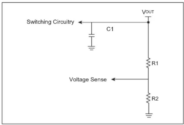
text_image
Switching Circuitry C1 VOUT R1 Voltage Sense R2The output stage of many power supplies is similar to Figure 21-1. R1 and R2 are used to set the ratio of the voltage that is sensed and compared to the reference.
A simple means of calibrating this type of power supply is as follows:
- Supply a known reference voltage to the output of the supply.
- Place the supply in Calibration mode and allow it to sense that reference voltage.
By providing the supply with the output voltage that it is to produce, it can then sense the voltage across the resistor divider and store the sensed value. Regardless of resistor tolerances, the sensed value will always correspond to the proper output value for that particular supply.
Furthermore, this setup could be combined with Tip #20 to calibrate at several temperatures.
This setup could also be used to create a programmable power supply by changing the supplied reference and the resistor divider for voltage feedback.
CHAPTER 8
3V Tips 'n Tricks
Table Of Contents
TIPS 'N TRICKS INTRODUCTION
TIP #1: Powering 3.3V Systems From 5V Using an LDO Regulator 8-3
TIP #2: Low-Cost Alternative Power System Using a Zener Diode 8-4
TIP #3: Lower Cost Alternative Power System Using 3 Rectifier Diodes 8-4
TIP #4: Powering 3.3V Systems From 5V Using Switching Regulators 8-5
TIP #5: 3.3V → 5V Direct Connect ...... 8-6
TIP #6: 3.3V → 5V Using a MOSFET Translator 8-6
TIP #7: 3.3V → 5V Using A Diode Offset ..... 8-7
TIP #8: 3.3V → 5V Using A Voltage Comparator .... 8-8
TIP #9: 5V → 3.3V Direct Connect ..... 8-9
TIP #10: 5V → 3.3V With Diode Clamp ...... 8-9
TIP #11: 5V → 3.3V Active Clamp .... 8-10
TIP #12: 5V → 3.3V Resistor Divider ...... 8-10
TIP #13: 3.3V → 5V Level Translators ...... 8-12
TIP #14: 3.3V → 5V Analog Gain Block ...... 8-13
TIP #15: 3.3V → 5V Analog Offset Block ...... 8-13
TIP #16: 5V → 3.3V Active Analog Attenuator .. 8-14
TIP #17: 5V → 3V Analog Limiter 8-15
TIP #18: Driving Bipolar Transistors .....8-16
TIP #19: Driving N-Channel MOSFET Transistors 8-18
TIPS 'N TRICKS INTRODUCTION
Overview - the 3.3 Volt to 5 Volt Connection
One of the by-products of our ever increasing need for processing speed is the steady reduction in the size of the transistors used to build microcontrollers. Up-integration at cheaper cost also drives the need for smaller geometries. With reduced size comes a reduction in the transistor breakdown voltage, and ultimately, a reduction in the supply voltage when the breakdown voltage falls below the supply voltage. So, as speeds increase and complexity mounts, it is an inevitable consequence that the supply voltages would drop from 5V to 3.3V, or even 1.8V for high density devices.
Microchip microcontrollers have reached a sufficient level of speed and complexity that they too are making the transition to sub-5V supply voltages. The challenge is that most of the interface circuitry is still designed for 5V supplies. This means that, as designers, we now face the task of interfacing 3.3V and 5V systems. Further, the task includes not only logic level translation, but also powering the 3.3V systems and translating analog signals across the 3.3V/5V barrier.
This Tips ‘n Tricks book addresses these challenges with a collection of power supply building blocks, digital level translation blocks and even analog translation blocks. Throughout the book, multiple options are presented for each of the transitions, spanning the range from all-in-one interface devices, to low-cost discrete solutions. In short, all the blocks a designer is likely to need for handling the 3.3V challenge, whether the driving force is complexity, cost or size.
Additional information can be found on the Microchip web site at www.microchip.com/3volts.
Note: The tips 'n tricks presented here assume a 3.3V supply. However, the techniques work equally well for other supply voltages with the appropriate modifications.
Power Supplies
One of the first 3.3V challenges is generating the 3.3V supply voltage. Given that we are discussing interfacing 5V systems to 3.3V systems, we can assume that we have a stable 5 V supply. This section will present voltage regulator solutions designed for the 5V to 3.3V transition. A design with only modest current requirements may use a simple linear regulator. Higher current needs may dictate a switching regulator solution. Cost sensitive applications may need the simplicity of a discrete diode regulator. Examples from each of these areas are included here, with the necessary support information to adapt to a wide variety of end applications.
Table 1: Power Supply Comparisons
| Method | VREG | Iq | Eff. | Size | Cost | Transient Response |
| Zener Shun Reg. | 10% Typ | 5 mA 60% | Sm Low Poor | |||
| Series Linear Reg. | 0.4% Typ | 1 μA to 100 μA | 60% Sm Med | Excellent | ||
| Switching Buck Reg. | 0.4% Typ | 30 μA to 2 mA | 93% Med to Lrg | High Good |
TIP #1 Powering 3.3V Systems From 5V Using an LDO Regulator
The dropout voltage of standard three-terminal linear regulators is typically 2.0-3.0V. This precludes them from being used to convert 5V to 3.3V reliably. Low Dropout (LDO) regulators, with a dropout voltage in the few hundred milli-volt range, are perfectly suited for this type of application. Figure 1-1 contains a block diagram of a basic LDO system with appropriate current elements labeled. From this figure it can be seen that an LDO consists of four main elements:
- Pass transistor
- Bandgap reference
- Operational amplifier
- Feedback resistor divider
When selecting an LDO, it is important to know what distinguishes one LDO from another. Device quiescent current, package size and type are important device parameters. Evaluating for each parameter for the specific application yields an optimal design.
Figure 1-1: LDO Voltage Regulator
text_image
IIN VIN C1 VREF + - IOUT C2 RL IGNDAn LDOs quiescent current, I_Q , is the device ground current, I_QD while the device is operating at no load. I_QD is the current used by the LDO to perform the regulating operation. The efficiency of an LDO can be approximated as the output voltage divided by the input voltage when I_QP>I_Q . However, at light loads, the I_Q must be taken into account when calculating the efficiency. An LDO with lower I_Q will have a higher light load efficiency. This increase in light load efficiency has a negative effect on the LDO performance. Higher quiescent current LDOs are able to respond quicker to sudden line and load transitions.
TIP #2 Low-Cost Alternative Power System Using a Zener Diode
Details a low-cost regulator alternative using a Zener diode.
Figure 2-1: Zener Supply
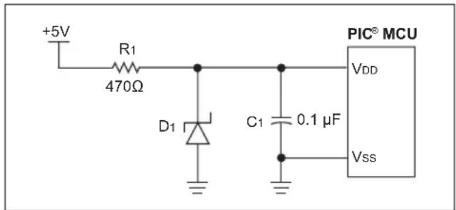
text_image
+5V R1 470Ω D1 C1 0.1 μF PIC® MCU VDD VssA simple, low-cost 3.3V regulator can be made out of a Zener diode and a resistor as shown in Figure 2-1. In many applications, this circuit can be a cost-effective alternative to using a LDO regulator. However, this regulator is more load sensitive than a LDO regulator. Additionally, it is less energy efficient, as power is always being dissipated in R1 and D1.
R1 limits the current to D1 and the PIC MCU so that V _D stays within the allowable range. Because the reverse voltage across a Zener diode varies as the current through it changes, the value of R1 needs to be considered carefully.
R1 must be sized so that at maximum load, typically when the PIC MCU is running and is driving its outputs high, the voltage drop across R1 is low enough so that the PIC MCU has enough voltage to operate. Also, R1 must be sized so that at minimum load, typically when the PIC MCU is in Reset, that V does not exceed either the Zener diode's power rating or the maximum V for the PIC MCU.
TIP #3 Lower Cost Alternative Power System Using 3 Rectifier Diodes
Figure 3-1 details a lower cost regulator alternative using 3 rectifier diodes.
Figure 3-1: Diode Supply
text_image
D2 D1 +5V D3 R1 C1 0.1 μF PIC®MCU VDD VssWe can also use the forward drop of a series of normal switching diodes to drop the voltage going into the PIC MCU. This can be even more cost-effective than the Zener diode regulator. The current draw from this design is typically less than a circuit using a Zener.
The number of diodes needed varies based on the forward voltage of the diode selected. The voltage drop across diodes D1-D3 is a function of the current through the diodes. R1 is present to keep the voltage at the PIC MCUs V D pin from exceeding the PIC MCUs maximum V D at minimum loads (typically when the PIC MCU is in Reset or sleeping). Depending on the other circuitry connected to V D , this resistor may have its value increased or possibly even eliminated entirely. Diodes D1-D3 must be selected so that at maximum load, typically when the PIC is running and is driving its outputs high, the voltage drop across D1-D3 is low enough to meet the PIC MCUs minimum V D requirements.
TIP #4 Powering 3.3V Systems From 5V Using Switching Regulators
A buck switching regulator, shown in Figure 4-1, is an inductor-based converter used to step-down an input voltage source to a lower magnitude output voltage. The regulation of the output is achieved by controlling the ON time of MOSFET Q1. Since the MOSFET is either in a lower or high resistive state (ON or OFF, respectively), a high source voltage can be converted to a lower output voltage very efficiently.
The relationship between the input and output voltage can be established by balancing the volt-time of the inductor during both states of Q1.
Equation 4-1
$$ (V s - V o) ^ {} t _ {o n} = V o ^ {} (T - t _ {o n}) $$
$$ \text { Where: } T \equiv t _ {\text { on }} / \text { Duty_Cycle } $$
It therefore follows that for MOSFET Q1:
Equation 4-2
$$ \text { Duty_Cycle } _ {\text { Q1 }} = \text { Vo / Vs } $$
When choosing an inductor value, a good starting point is to select a value to produce a maximum peak-to-peak ripple current in the inductor equal to ten percent of the maximum load current.
Equation 4-3
$$ V = L ^ {*} (d i / d t) $$
$$ L = (V s - V o) ^ {*} \left(t _ {o n} / I _ {o} * 0. 1 0\right) $$
When choosing an output capacitor value, a good starting point is to set the LC filter characteristic impedance equal to the load resistance. This produces an acceptable voltage overshoot when operating at full load and having the load abruptly removed.
Equation 4-4
$$ Z _ {0} \equiv \sqrt {L / C} $$
$$ C = L / R ^ {2} = \left( \begin{array}{c c} b & * \ o & L \end{array} \right) / V _ {o} ^ {2} $$
When choosing a diode for D1, choose a device with a sufficient current rating to handle the inductor current during the discharge part of the pulse cycle (IL).
Figure 4-1: Buck Regulator
text_image
Q1 Vs D1 L C Vo RLDigital Interfacing
When interfacing two devices that operate at different voltages, it is imperative to know the output and input thresholds of both devices. Once these values are known, a technique can be selected for interfacing the devices based on the other requirements of your application. Table 4-1 contains the output and input thresholds that will be used throughout this document. When designing an interface, make sure to reference your manufacturers data sheet for the actual threshold levels.
Table 4-1: Input/Output Thresholds
| VOH min | VOL max | VIH min | VIL max | |
| 5V TTL 2.4V | 0.5V 2.0V 0.8V | |||
| 3.3VLVTTL | 2.4V 0.4V | 2.0V 0.8V | ||
| 5VCMOS | 4.7V(Vcc-0.3V) | 0.5V 3.5V | (0.7xVcc) | 1.5V(0.3xVcc) |
| 3.3VLVCMOS | 3.0V(Vcc-0.3V) | 0.5V 2.3V | (0.7xVcc) | 1.0V(0.3xVcc) |
TIP #5 3.3V → 5V Direct Connect
The simplest and most desired way to connect a 3.3V output to a 5V input is by a direct connection. This can be done only if the following 2 requirements are met:
- The V_OH of the 3.3V output is greater than the V_IH of the 5V input
- The V_OL of the 3.3V output is less than the V_IL of the 5V input
An example of when this technique can be used is interfacing a 3.3V LVCMOS output to a 5V TTL input. From the values given in Table 4-1, it can clearly be seen that both of these requirements are met.
3.3V LVCMOS Voh of 3.0 volts is greater than 5V TTL VH of 2.0 volts, and
3.3V LVCMOS V Q of 0.5 volts is less than 5V TTL V L of 0.8 volts.
When both of these requirements are not met, some additional circuitry will be needed to interface the two parts. See Tips 6, 7, 8 and 13 for possible solutions.
TIP #6 3.3V → 5V Using a MOSFET Translator
In order to drive any 5V input that has a higher V_IH than the V_OH of a 3.3V CMOS part, some additional circuitry is needed. A low-cost two component solution is shown in Figure 6-1.
When selecting the value for R1, there are two parameters that need to be considered; the switching speed of the input and the current consumption through R1. When switching the input from a '0' to a '1', you will have to account for the time the input takes to rise because of the RC time constant formed by R1, and the input capacitance of the 5V input plus any stray capacitance on the board. The speed at which you can switch the input is given by the following equation:
Equation 6-1
$$ T _ {S W} = 3 \times R _ {1} \times \left(C _ {I N} + C _ {S}\right) $$
Since the input and stray capacitance of the board are fixed, the only way to speed up the switching of the input is to lower the resistance of R1. The trade-off of lowering the resistance of R1 to get faster switching times is the increase in current draw when the 5V input remains low. The switching to a '0' will typically be much faster than switching to a '1' because the ON resistance of the N-channel MOSFET will be much smaller than R1. Also, when selecting the N-channel FET, select a FET that has a lower VGS threshold voltage than the VOH of 3.3V output.
Figure 6-1: MOSFET Translator
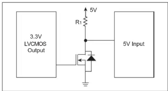
text_image
3.3V LVCMOS Output R1 5V 5V InputTIP #7 3.3V → 5V Using a Diode Offset
The inputs voltage thresholds for 5V CMOS and the output drive voltage for 3.3V LVTTL and LVCMOS are listed in Table 7-1.
Table 7-1: Input/Output Thresholds
| 5V CMOS Input | 3.3V LVTTL Output | 3.3V LVCMOS Output | |
| High Threshold | >3.5V>2 | .4V>3.0V | |
| Low Threshold | <1.5V<0 | .4V<0.5V |
Note that both the high and low threshold input voltages for the 5V CMOS inputs are about a volt higher than the 3.3V outputs. So, even if the output from the 3.3V system could be offset, there would be little or no margin for noise or component tolerance. What is needed is a circuit that offsets the outputs and increases the difference between the high and low output voltages.
Figure 7-1: Diode Offset
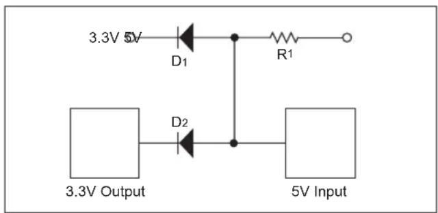
text_image
3.3V 5V D1 R1 D2 3.3V Output 5V InputWhen output voltage specifications are determined, it is done assuming that the output is driving a load between the output and ground for the high output, and a load between 3.3V and the output for the low output. If the load for the high threshold is actually between the output and 3.3V, then the output voltage is actually much higher as the load resistor is the mechanism that is pulling the output up, instead of the output transistor.
If we create a diode offset circuit (see Figure 7-1), the output low voltage is increased by the forward voltage of the diode D1, typically 0.7V, creating a low voltage at the 5V CMOS input of 1.1V to 1.2V. This is well within the low threshold input voltage for the 5V CMOS input. The output high voltage is set by the pull-up resistor and diode D2, tied to the 3.3V supply. This puts the output high voltage at approximately 0.7V above the 3.3V supply, or 4.0 to 4.1V, which is well above the 3.5V threshold for the 5V CMOS input.
Note: For the circuit to work properly, the pull-up resistor must be significantly smaller than the input resistance of the 5V CMOS input, to prevent a reduction in the output voltage due to a resistor divider effect at the input. The pull-up resistor must also be large enough to keep the output current loading on the 3.3V output within the specification of the device.
TIP #8 3.3V → 5V Using a Voltage Comparator
The basic operation of the comparator is as follows:
- When the voltage at the inverting (-) input is greater than that at the non-inverting (+) input, the output of the comparator swings to Vss
- When the voltage at the non-inverting (+) input is greater than that at the non-inverting (-) input, the output of the comparator is in a high state.
To preserve the polarity of the 3.3V output, the 3.3V output must be connected to the non-inverting input of the comparator. The inverting input of the comparator is connected to a reference voltage determined by R1 and R2, as shown in Figure 8-1.
Figure 8-1: Comparator Translator

text_image
5V (VDD) R1 Ro 3.3V Output + - Vss R2 Vss 5V InputCalculating R1 and R2
The ratio of R1 and R2 depends on the logic levels of the input signal. The inverting input should be set to a voltage halfway between V_0 and V_0 for the 3.3V output. For an LVCMOS output, this voltage is:
Equation 8-1:
$$ 1. 7 5 \mathrm{V} = \frac {(3 . 0 \mathrm{V} + . 5 \mathrm{V})}{2} $$
Given that R1 and R2 are related by the logic levels:
Equation 8-2:
$$ R _ {1} = R _ {2} \quad \left( \begin{array}{c c} 5 V & \ \hline 1. 7 5 V & - 1 \end{array} \right) $$
assuming a value of 1K for R2, R1 is 1.8K.
An op amp wired up as a comparator can be used to convert a 3.3V input signal to a 5V output signal. This is done using the property of the comparator that forces the output to swing high (VDD) or low (VSS), depending on the magnitude of difference in voltage between its 'inverting' input and 'non-inverting' input.
Note: For the op amp to work properly when powered by 5V, the output must be capable of rail-to-rail drive.
Figure 8-2: Op Amp as a Comparator

text_image
5V (VDD) R1 3.3V Output + - Vss R2 Vss 5V InputTIP #9 5V → 3.3V Direct Connect
5V outputs have a typical V_OH of 4.7 volts and a V_OL of 0.4 volts and a 3.3V LVCMOS input will have a typical V_IH of 0.7 x V_DD and a V_IL of 0.2 x V_DD
When the 5V output is driving low, there are no problems because the 0.4 volt output is less than in the input threshold of 0.8 volts. When the 5V output is high, the Vohof 4.7 volts is greater than 2.1 volt VIH, therefore, we can directly connect the 2 pins with no conflicts if the 3.3V CMOS input is 5 volt tolerant.
Figure 9-1: 5V Tolerant Input
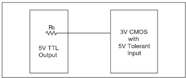
flowchart
graph LR
    A["5V TTL Output"] -->|Rs| B["3V CMOS with 5V Tolerant Input"]
If the 3.3V CMOS input is not 5 volt tolerant, then there will be an issue because the maximum volt specification of the input will be exceeded.
See Tips 10-13 for possible solutions.
TIP #10 5V → 3.3V With Diode Clamp
Many manufacturers protect their I/O pins from exceeding the maximum allowable voltage specification by using clamping diodes. These clamping diodes keep the pin from going more than a diode drop below Vss and a diode drop above VDD To use the clamping diode to protect the input, you still need to look at the current through the clamping diode. The current through the clamp diodes should be kept small (in the micro amp range). If the current through the clamping diodes gets too large, then you risk the part latching up. Since the source resistance of a 5V output is typically around 10Ω, an additional series resistor is still needed to limit the current through the clamping diode as shown Figure 10-1. The consequence of using the series resistor is it will reduce the speed at which we can switch the input because the RC time constant formed the capacitance of the pin (CL).
Figure 10-1: Clamping Diodes on the Input
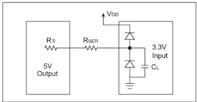
text_image
5V Output Rs RSER VDD 3.3V Input CLIf the clamping diodes are not present, a single external diode can be added to the circuit as shown in Figure 10-2.
Figure 10-2: Without Clamping Diodes
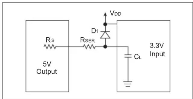
text_image
5V Output Rs RSER D1 VDD CL 3.3V InputTIP #11 5V → 3.3V Active Clamp
One problem with using a diode clamp is that it injects current onto the 3.3V power supply. In designs with a high current 5V outputs, and lightly loaded 3.3V power supply rails, this injected current can float the 3.3V supply voltage above 3.3V. To prevent this problem, a transistor can be substituted which routes the excess output drive current to ground instead of the 3.3V supply. Figure 11-1 shows the resulting circuit.
Figure 11-1: Transistor Clamp
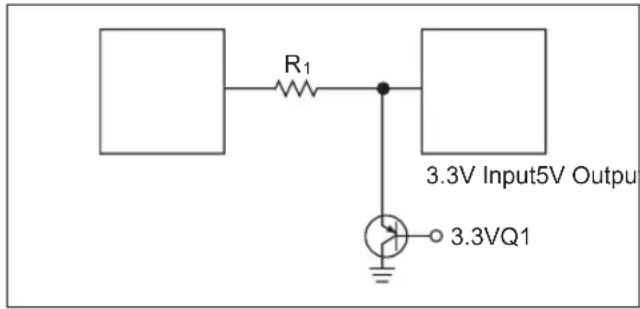
text_image
R₁ 3.3V Input5V Output 3.3VQ1The base-emitter junction of Q1 performs the same function as the diode in a diode clamp circuit. The difference is that only a small percentage of the emitter current flows out of the base of the transistor to the 3.3V rail, the bulk of the current is routed to the collector where it passes harmlessly to ground. The ratio of base current to collector current is dictated by the current gain of the transistor, typically 10-400, depending upon which transistor is used.
TIP #12 5V → 3.3V Resistor Divider
A simple resistor divider can be used to reduce the output of a 5V device to levels appropriate for a 3.3V device input. An equivalent circuit of this interface is shown in Figure 12-1.
Figure 12-1: Resistive Interface Equivalent Circuit

text_image
5V Device Rs Vs R1 R2 Cs 3.3V Device VL CL RLTypically, the source resistance, Rs, is very small (less than 10Ω) so its affect on R1 will be negligible provided that R1 is chosen to be much larger than Rs. At the receive end, the load resistance, RL, is very large (greater than 500 kΩ) so its affect on R2 will be negligible provided that R2 is chosen to be much less than RL.
There is a trade-off between power dissipation and transition times. To keep the power requirements of the interface circuit at a minimum, the series resistance of R1 and R2 should be as large as possible. However, the load capacitance, which is the combination of the stray capacitance, Cs, and the 3.3V device input capacitance, CL, can adversely affect the rise and fall times of the input signal. Rise and fall times can be unacceptably long if R1 and R2 are too large.
Neglecting the affects of Rs and RL, the formula for determining the values for R1 and R2 is given by Equation 12-1.
Equation 12-1: Divider Values
$$ \frac {V _ {S}}{R _ {1} + R _ {2}} = \frac {V _ {L}}{R _ {2}} \quad ; \text { General relationship } $$
$$ R _ {1} = \frac {\left(V _ {S} - V _ {L}\right) \cdot R _ {2}}{V _ {L}} \quad ; \text { Solving for } R _ {1} $$
$$ R _ {1} = 0. 5 1 5 \cdot R _ {2}; \text {Substituting voltages} $$
The formula for determining the rise and fall times is given in Equation 12-2. For circuit analysis, the Thevenin equivalent is used to determine the applied voltage, V_A , and the series resistance, R. The Thevenin equivalent is defined as the open circuit voltage divided by the short circuit current. The Thevenin equivalent, R, is determined to be 0.66*R1 and the Thevenin equivalent, V_A , is determined to be 0.66*Vs for the circuit shown in Figure 12-2 according to the limitations imposed by Equation 12-2.
Equation 12-2: Rise/Fall Time
$$ t = - \left[ R \cdot C \cdot \ln \left(\frac {V _ {F} - V _ {A}}{V _ {I} - V _ {A}}\right) \right] $$
Where:
t = Rise or Fall time
R = 0.66*R1
C = Cs + CL
V_I = Initial voltage on C (V_L)
V_F = Final voltage on C (V_L)
V_A = Applied voltage (0.66*Vs)
As an example, suppose the following conditions exist:
- Stray capacitance = 30 pF
- Load capacitance = 5 pF
• Maximum rise time from 0.3V to 3V ≤ 1 μS
• Applied source voltage Vs = 5V
The calculation to determine the maximum resistances is shown in Equation 12-3.
Equation 12-3: Example Calculation
Solve Equation 12-2 for R:
$$ R = - \left[ \frac {t}{C \cdot \ln \left(\frac {V _ {F} - V _ {A}}{V _ {I} - V _ {A}}\right)} \right] $$
Substitute values:
$$ R = - \left[ \frac {1 0 \cdot 1 0 ^ {- 7}}{3 5 \cdot 1 0 ^ {- 1 2} \cdot \ln \left(\frac {3 - (0 . 6 6 \cdot 5)}{0 . 3 - (0 . 6 6 \cdot 5)}\right)} \right] $$
Thevenin equivalent maximum R:
$$ R = 1 2 4 0 8 $$
Solve for maximum R1 and R2:
$$ R 1 = 0. 6 6 \cdot R R 2 = \frac {R 1}{0 . 5 1 5} $$
$$ R 1 = 8 1 9 0 \quad R 2 = 1 5 9 0 2 $$
TIP #13 3.3V → 5V Level Translators
While level translation can be done discretely, it is often preferred to use an integrated solution. Level translators are available in a wide range of capabilities. There are unidirectional and bidirectional configurations, different voltage translations and different speeds, all giving the user the ability to select the best solution.
Board-level communication between devices (e.g., MCU to peripheral) is most often done by either SPI or I²C™. For SPI, it may be appropriate to use a unidirectional level translator and for I²C, it is necessary to use a bidirectional solution. Figure 13-1 illustrates both solutions.
Figure 13-1: Level Translator
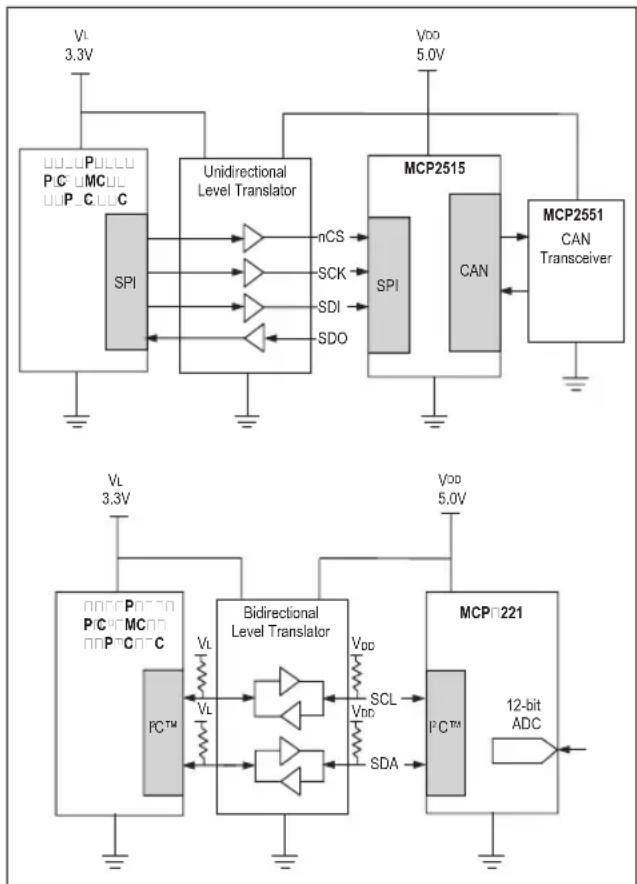
flowchart
graph TD
    subgraph Top_Circuit
        A["SPI"] --> B["Unidirectional Level Translator"]
        B --> C["nCS"]
        B --> D["SCK"]
        B --> E["SDI"]
        B --> F["SDO"]
        G["MCP2515"] --> H["CAN"]
        H --> I["MCP2551 CAN Transceiver"]
    end
    subgraph Bottom_Circuit
        J["Bidirectional Level Translator"] --> K["VDD"]
        K --> L["SCL"]
        K --> M["VDD"]
        K --> N["SDA"]
        O["MCP221"] --> P["ICTM"]
        P --> Q["12-bit ADC"]
    end
    A -->|V_L 3.3V| G
    G --> H
    H --> I
    I --> Q
    style Top_Circuit fill:#f9f,stroke:#333
    style Bottom_Circuit fill:#bbf,stroke:#333
Analog
The final 3.3V to 5V interface challenge is the translation of analog signals across the power supply barrier. While low level signals will probably not require external circuitry, signals moving between 3.3V and 5V systems will be affected by the change in supply. For example, a 1V peak analog signal converted by an ADC in a 3.3V system will have greater resolution than an ADC in a 5V system, simply because more of the ADCs range is used to convert the signal in the 3.3V ADC. Alternately, the relatively higher signal amplitude in a 3.3V system may have problems with the system's lower common mode voltage limitations.
Therefore, some interface circuitry, to compensate for the differences, may be needed. This section will discuss interface circuitry to help alleviate these problems when the signal makes the transition between the different supply voltages.
TIP #14 3.3V → 5V Analog Gain Block
To scale analog voltage up when going from 3.3V supply to 5V supply. The 33 kΩ and 17 kΩ set the op amp gain so that the full scale range is used in both sides. The 11 kΩ resistor limits current back to the 3.3V circuitry.
Figure 14-1: Analog Gain Block

text_image
+3.3V 11k +5.0V MCP6XXX 33k 17kTIP #15 3.3V → 5V Analog Offset Block
Offsetting an analog voltage for translation between 3.3V and 5V.
Shift an analog voltage from 3.3V supply to 5V supply. The 147 kΩ and 30.1 kΩ resistors on the top right and the +5V supply voltage are equivalent to a 0.85V voltage source in series with a 25 kΩ resistor. This equivalent 25 kΩ resistance, the three 25 kΩ resistors, and the op amp form a difference amplifier with a gain of 1 V/V. The 0.85V equivalent voltage source shifts any signal seen at the input up by the same amount; signals centered at 3.3V/2 = 1.65V will also be centered at 5.0V/2 = 2.50V. The top left resistor limits current from the 5V circuitry.
Figure 15-1: Analog Offset Block

text_image
+3.3V 25k 147k +5.0V 3 +5.0V MCP6XXX 2 5 0.1kTIP #16 5V → 3.3V Active Analog Attenuator
Reducing a signal's amplitude from a 5V to 3.3V system using an op amp.
The simplest method of converting a 5V analog signal to a 3.3V analog signal is to use a resistor divider with a ratio R1:R2 of 1.7:3.3. However, there are a few problems with this.
- The attenuator may be feeding a capacitive load, creating an unintentional low pass filter.
- The attenuator circuit may need to drive a low-impedance load from a high-impedance source.
Under either of these conditions, an op amp becomes necessary to buffer the signals.
The op amp circuit necessary is a unity gain follower (see Figure 16-1).
Figure 16-1: Unity Gain
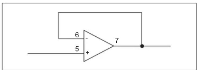
text_image
6 - 5 + 7This circuit will output the same voltage that is applied to the input.
To convert the 5V signal down to a 3V signal, we simply add the resistor attenuator.
Figure 16-2: Op Amp Attenuators
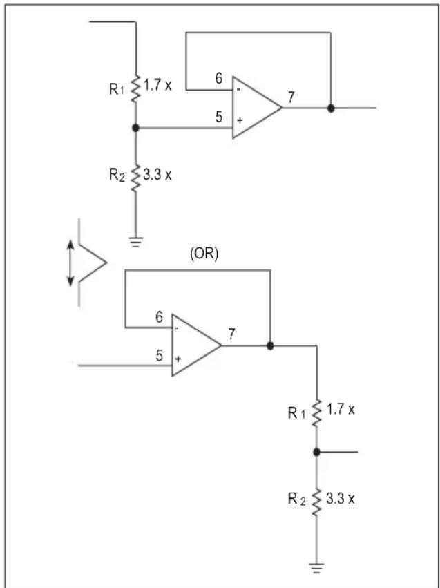
text_image
R1 1.7 x 6 5 + 7 R2 3.3 x (OR) 6 5 + 7 R1 1.7 x R2 3.3 xIf the resistor divider is before the unity gain follower, then the lowest possible impedance is provided for the 3.3V circuits. Also, the op amp can be powered from 3.3V, saving some power. If the X is made very large, then power consumed by the 5V side can be minimized.
If the attenuator is added after the unity gain follower, then the highest possible impedance is presented to the 5V source. The op amp must be powered from 5V and the impedance at the 3V side will depend upon the value of R1||R2.
TIP #17 5V → 3V Analog Limiter
When moving a 5V signal down to a 3.3V system, it is sometimes possible to use the attenuation as gain. If the desired signal is less than 5V, then attaching that signal to a 3.3V ADC will result in larger conversion values. The danger is when the signal runs to the 5V rail. A method is therefore required to control the out-of-range voltages while leaving the in-range voltages unaffected. Three ways to accomplish this will be discussed here.
- Using a diode to clamp the overvoltage to the 3.3V supply.
- Using a Zener diode to clamp the voltage to any desired limit.
- Using an op amp with a diode to perform a precision clamp.
The simplest method to perform the overvoltage clamp is identical to the simple method of interfacing a 5V digital signal to the 3.3V digital signals. A resistor and a diode are used to direct excess current into the 3.3V supply. The resistor must be sized to protect the diode and the 3.3V supply while not adversely affecting the analog performance. If the impedance of the 3.3V supply is too low, then this type of clamp can cause the 3.3V supply voltage to increase. Even if the 3.3V supply has a good low-impedance, this type of clamp will allow the input signal to add noise to the 3.3V supply when the diode is conducting and if the frequency is high enough, even when the diode is not conducting due to the parasitic capacitance across the diode.
Figure 17-1: Diode Clamp
text_image
+3.3V D1 VIN —— R1 —— VOUT VOUT = 3.3V + VF if VIN > 3.3V + VF VOUT = VIN if VIN ≤ 3.3V + VF VF is the forward drop of the diode.To prevent the input signal from affecting the supply or to make the input more robust to larger transients, a variation is to use a Zener diode. The Zener diode is slower than the fast signal diode typically used in the first circuit. However, they are generally more robust and do not rely on the characteristics of the power supply to perform the clamping. The amount of clamping they provide is dependant upon the current through the diode. This is set by the value of R1. R1 may not be required if the output impedance of the VIN source is sufficiently large.
Figure 17-2: Zener Clamp

text_image
VOUT = VBR if VIN > VBR VOUT = VIN if VIN ≤ VBR VBR is the reverse breakdown voltage of the Zener diode.If a more precise overvoltage clamp is required that does not rely upon the supply, then an op amp can be employed to create a precision diode. In Figure 17-3, such a circuit is shown. The op amp compensates for the forward drop in the diode and causes the voltage to be clamped at exactly the voltage supplied on the non-inverting input to the op amp. The op amp can be powered from 3.3V if it is rail-to-rail.
Figure 17-3: Precision Diode Clamp
text_image
+3.3V 5 + - 6 D1 VIN —— R1 —— VOUT VOUT = 3.3V if VIN > 3.3V VOUT = VIN if VIN ≤ 3.3VBecause the clamping is performed by the op amp, there is no affect on the power supply. The impedance presented to the low voltage circuit is not improved by the op amp, it remains R1 in addition to the source circuit impedance.
TIP #18 Driving Bipolar Transistors
When driving bipolar transistors, the amount of base current “drive” and forward current gain
(B/hFE) will determine how much current the transistor can sink. When driven by a microcontroller I/O port, the base drive current is calculated using the port voltage and the port current limit (typically 20 mA). When using 3.3V technology, smaller value base current limiting resistors should be used to ensure sufficient base drive to saturate the transistor.
Figure 18-1: Driving Bipolar Transistors Using Microcontroller I/O Port
text_image
+VDD RBASE hFE (Forward Gain) VBE Forward Drop VLOAD + - RLOADThe value of R BSE will depend on the microcontroller supply voltage. Equation 18-1 describes how to calculate R BSE
Table 18-1: Bipolar Transistor DC Specifications
| Characteristic Sym Min Max | Unit | Test Condition | |||
| OFF CHARACTERISTICS | |||||
| Collector-Base Breakdown Voltage | V(B)α60 | + V Ic = | 50 μA, | IE=0 | |
| Collector-Emitter Breakdown Voltage | V(BR)CEO | 50 | - | V | Ic=1.0 mA,IB=0 |
| Emitter-Base Breakdown Voltage | V(BR)EBO | 7.0 | - | V | IE=50 μA, Ic=0 |
| Collector Cutoff Current | Iα-100 | nA | Vα=60V | ||
| Emitter Cutoff Current | IEBO | - | 100 | nA | VEB=7.0V |
| ON CHARACTERISTICS | |||||
| DC Current Gain | hFE | 120 | 270 | - | Vα=6.0V, Ic=1.0 mA |
| 180 | 390 | ||||
| 270 | 560 | ||||
| Collector-Emitter Saturation Voltage | VCE(SAT) | - | 0.4 | V | Ic=50 mA, IB=5.0 mA |
When using bipolar transistors as switches to turn on and off loads controlled by the microcontroller I/O port pin, use the minimum hFE specification and margin to ensure complete device saturation.
Equation 18-1: Calculating the Base Resistor Value
$$ R _ {\text { BASE }} = \frac {(V _ {\text { DD }} - V _ {\text { BE }}) \times h _ {\text { FE }} \times R _ {\text { LOAD }}}{V _ {\text { LOAD }}} $$
3V Technology Example
$$ \begin{array}{l} \mathrm{V} _ {\mathrm{DD}} = + 3 \mathrm{V}, \mathrm{V} _ {\mathrm{LOAD}} = + 4 0 \mathrm{V}, \mathrm{R} _ {\mathrm{LOAD}} = 4 0 0 \Omega , \ \mathrm{hFe} \min. = 1 8 0, \mathrm{V} _ {\mathrm{BE}} = 0. 7 \mathrm{V} \end{array} $$
$$ R _ {\text { BASE }} = 4. 1 4 \mathrm{k} \Omega , \text { I / O port current } = 5 5 6 \mu \mathrm{A} $$
5V Technology Example
$$ \begin{array}{l} \mathrm {V_{DD}} = + 5 \mathrm{V}, \mathrm {V _ {LOAD}} = + 4 0 \mathrm{V}, \mathrm {R _ {LOAD}} = 4 0 0 \Omega , \ \mathrm {h _ {FE} min.} = 1 8 0, \mathrm {V _ {BE}} = 0. 7 \mathrm{V} \end{array} $$
$$ R _ {\text { BASE }} = 7. 7 4 \mathrm{k} \Omega , \text { I / O port current } = 5 5 6 \mu \mathrm{A} $$
For both examples, it is good practice to increase base current for margin. Driving the base with 1 mA to 2 mA would ensure saturation at the expense of increasing the input power consumption.
TIP #19 Driving N-Channel MOSFET Transistors
Care must be taken when selecting an external N-Channel MOSFET for use with a 3.3V microcontroller. The MOSFET gate threshold voltage is an indication of the device's capability to completely saturate. For 3.3V applications, select MOSFETs that have an ON resistance rating for gate drive of 3V or less. For example, a FET that is rated for 250 A of drain current with 1V applied from gate-to-source is not necessarily going to deliver satisfactory results for 100 mA load with a 3.3V drive. When switching from 5V to 3V technology, review the gate-to-source threshold and ON resistance characteristics very carefully as shown in Figure 19-1. A small decrease in gate drive voltage can significantly reduce drain current.
Figure 19-1: Drain Current Capability Versus Gate to Source Voltage
line
| VGS | ID | | --- | --- | | 0 | 0 | | VT | 0 | | 3.3V5V | High |Low threshold devices commonly exist for MOSFETs with drain-to-source voltages rated below 30V. MOSFETs with drain-to-source voltages above 30V typically have higher gate thresholds (VT).
Table 19-1: R(ON) and V(ath) Specifications for IRF7467
| Rα(on) | Static Drain-to-Source On-Resistance | -9.4 12 | mΩ | VGS=10V, ID=11A | |
| -10.6 13.5 | VGS=4.5V, ID=9.0A | ||||
| -17 35 | VGS=2.8V, ID=5.5A | ||||
| Vα(th) | Gate Threshold Voltage | 0.6 - | 2.0 V | VDS=VGS ID=250 μA |
As shown in Table 19-1, the threshold voltage for this 30V, N-Channel MOSFET switch is 0.6V. The resistance rating for this MOSFET is 35 mΩ with 2.8V applied gate, as a result, this device is well suited for 3.3V applications.
Table 19-2: R(ON) and V(ath) Specifications for IRF7201
| Rα(on) | Static Drain-to-Source On-Resistance | - | - | 0.030 | Ω | Vα=10V, ID=7.3A |
| - | - | 0.050 | Vα=4.5V, ID=3.7A | |||
| Vα(th) | Gate Threshold Voltage | 1.0 | - | - | V | Vα=Vα, ID=250 μA |
For the IRF7201 data sheet specifications, the gate threshold voltage is specified as a 1.0V minimum. This does not mean the device can be used to switch current with a 1.0V gate-to-source voltage as there is no RDS(ON) specification for V _ath values below 4.5V. This device is not recommended for 3.3V drive applications that require low switch resistance but can be used for 5V drive applications.
WORLDWIDE SALES AND SERVICE
AMERICAS
Corporate Office
2355 West Chandler Blvd.
Chandler, AZ 85224-6199
Tel: 480-792-7200
Fax: 480-792-7277
Technical Support:
http://support.microchip.com
Web Address:
www.microchip.com
Atlanta
Duluth, GA
Tel: 678-957-9614
Fax: 678-957-1455
Boston
Westborough, MA
Tel: 774-760-0087
Fax: 774-760-0088
Chicago
Itasca, IL
Tel: 630-285-0071
Fax: 630-285-0075
Cleveland
Independence, OH
Tel: 216-447-0464
Fax: 216-447-0643
Dallas
Addison, TX
Tel: 972-818-7423
Fax: 972-818-2924
Detroit
Farmington Hills, MI
Tel: 248-538-2250
Fax: 248-538-2260
Kokomo
Kokomo, IN
Tel: 765-864-8360
Fax: 765-864-8387
Los Angeles
Mission Viejo, CA
Tel: 949-462-9523
Fax: 949-462-9608
Santa Clara
Santa Clara, CA
Tel: 408-961-6444
Fax: 408-961-6445
Toronto
Mississauga, Ontario,
Canada
Tel: 905-673-0699
Fax: 905-673-6509
ASIA/PACIFIC
Asia Pacific Office
Suites 3707-14, 37th Floor
Tower 6. The Gateway
Harbour City, Kowloon
Hong Kong
Tel: 852-2401-1200
Fax: 852-2401-3431
Australia - Sydney
Tel: 61-2-9868-6733
Fax: 61-2-9868-6755
China - Beijing
Tel: 86-10-8528-2100
Fax: 86-10-8528-2104
China - Chengdu
Tel: 86-28-8665-5511
Fax: 86-28-8665-7889
China - Hong Kong SAR
Tel: 852-2401-1200
Fax: 852-2401-3431
China - Nanjing
Tel: 86-25-8473-2460
Fax: 86-25-8473-2470
China - Qingdao
Tel: 86-532-8502-7355
Fax: 86-532-8502-7205
China - Shanghai
Tel: 86-21-5407-5533
Fax: 86-21-5407-5066
China - Shenyang
Tel: 86-24-2334-2829
Fax: 86-24-2334-2393
China - Shenzhen
Tel: 86-755-8203-2660
Fax: 86-755-8203-1760
China - Wuhan
Tel: 86-27-5980-5300
Fax: 86-27-5980-5118
China - Xiamen
Tel: 86-592-2388138
Fax: 86-592-2388130
China - Xian
Tel: 86-29-8833-7252
Fax: 86-29-8833-7256
China - Zhuhai
Tel: 86-756-3210040
Fax: 86-756-3210049
ASIA/PACIFIC
India - Bangalore
Tel: 91-80-3090-4444
Fax: 91-80-3090-4080
India - New Delhi
Tel: 91-11-4160-8631
Fax: 91-11-4160-8632
India - Pune
Tel: 91-20-2566-1512
Fax: 91-20-2566-1513
Japan - Yokohama
Tel: 81-45-471-6166
Fax: 81-45-471-6122
Korea - Daegu
Tel: 82-53-744-4301
Fax: 82-53-744-4302
Korea - Seoul
Tel: 82-2-554-7200
Fax: 82-2-558-5932 or
82-2-558-5934
Malaysia - Kuala Lumpur
Tel: 60-3-6201-9857
Fax: 60-3-6201-9859
Malaysia - Penang
Tel: 60-4-227-8870
Fax: 60-4-227-4068
Philippines - Manila
Tel: 63-2-634-9065
Fax: 63-2-634-9069
Singapore
Tel: 65-6334-8870
Fax: 65-6334-8850
Taiwan - Hsin Chu
Tel: 886-3-6578-300
Fax: 886-3-6578-370
Taiwan - Kaohsiung
Tel: 886-7-536-4818
Fax: 886-7-536-4803
Taiwan - Taipei
Tel: 886-2-2500-6610
Fax: 886-2-2508-0102
Thailand - Bangkok
Tel: 66-2-694-1351
Fax: 66-2-694-1350
EUROPE
Austria - Wels
Tel: 43-7242-2244-39
Fax: 43-7242-2244-393
Denmark - Copenhagen
Tel: 45-4450-2828
Fax: 45-4485-2829
France - Paris
Tel: 33-1-69-53-63-20
Fax: 33-1-69-30-90-79
Germany - Munich
Tel: 49-89-627-144-0
Fax: 49-89-627-144-44
Italy - Milan
Tel: 39-0331-742611
Fax: 39-0331-466781
Netherlands - Drunen
Tel: 31-416-690399
Fax: 31-416-690340
Spain - Madrid
Tel: 34-91-708-08-90
Fax: 34-91-708-08-91
UK - Wokingham
Tel: 44-118-921-5869
Fax: 44-118-921-5820