PIC24FJ64GB410 - Microcontroller Microchip - Free user manual and instructions
Find the device manual for free PIC24FJ64GB410 Microchip in PDF.

User questions about PIC24FJ64GB410 Microchip
0 question about this device. Answer the ones you know or ask your own.
Ask a new question about this device
Download the instructions for your Microcontroller in PDF format for free! Find your manual PIC24FJ64GB410 - Microchip and take your electronic device back in hand. On this page are published all the documents necessary for the use of your device. PIC24FJ64GB410 by Microchip.
USER MANUAL PIC24FJ64GB410 Microchip
16-Bit Flash Microcontrollers with Dual Partition Flash Memory, XLP, LCD, Cryptographic Engine and USB On-The-Go
Extreme Low-Power Features
- Multiple Power Management Options for Extreme Power Reduction:
- VBAT allows for lowest power consumption on backup battery (with or without RTCC)
- Deep Sleep allows near total power-down with the ability to wake-up on external triggers
- Sleep and Idle modes selectively shut down peripherals and/or core for substantial power reduction and fast wake-up
- Doze mode allows CPU to run at a lower clock speed than peripherals
- Alternate Clock modes allow On-the-Fly Switching to a Lower Clock Speed for Selective Power Reduction
- Extreme Low-Power Current Consumption for Deep Sleep: - WDT: 650 nA @ 2V typical
- RTCC: 650 nA @ 32 kHz, 2V typical
- Deep Sleep current, 60 nA typical
• 160 μA/MHz in Run mode
High-Performance CPU
• Modified Harvard Architecture
- Up to 16 MIPS Operation @ 32 MHz
• 8 MHz Internal Oscillator:
- 96 MHz PLL option
- Multiple clock divide options
- Run-time self-calibration capability for maintaining better than ±0.20% accuracy
- Fast start-up
- 17-Bit x 17-Bit Single-Cycle Hardware Fractional/Integer Multiplier
• 32-Bit by 16-Bit Hardware Divider - 16 x 16-Bit Working Register Array
• C Compiler Optimized Instruction Set Architecture - Two Address Generation Units for Separate Read and Write Addressing of Data Memory
Cryptographic Engine
- Performs NIST Standard Encryption/Decryption
Operations without CPU Intervention
• AES Cipher Support for 128, 192 and 256-Bit Keys
• DES/3DES Cipher Support, with up to Three Unique Keys for 3DES
• Supports ECB, CBC, OFB, CTR and CFB128 modes
• Programmatically Secure OTP Array for Key Storage
• True Random Number Generation - Battery-Backed RAM Key Storage
Analog Features
• 10/12-Bit, up to 24-Channel Analog-to-Digital (A/D) Converter:
- Conversion rate of 500 ksps (10-bit), 200 kbps (12-bit)
- Auto-scan and threshold compare features
- Conversion available during Sleep
• One 10-Bit Digital-to-Analog Converter (DAC):
- 1 Msps update rate
- Three Rail-to-Rail, Enhanced Analog Comparators with Programmable Input/Output Configuration
- Charge Time Measurement Unit (CTMU):
- Used for capacitive touch sensing, up to 24 channels
- Time measurement down to 100 ps resolution
Dual Partition Flash with Live Update Capability
- Capable of Holding Two Independent Software Applications, including Bootloader
- Permits Simultaneous Programming of One Partition while Executing Application Code from the Other
- Allows Run-Time Switching Between Active Partitions
Universal Serial Bus Features (PIC24FJXXXGB4XX Only)
• USB v2.0 On-The-Go (OTG) Compliant
- Dual Role Capable – Can Act as Either Host or Peripheral
- Low-Speed (1.5 Mb/s) and Full-Speed (12 Mb/s) USB Operation in Host mode
• Full-Speed USB Operation in Device mode
• High-Precision PLL for USB
- USB Device mode Operation from FRC Oscillator – No Crystal Oscillator Required
- Supports up to 32 Endpoints (16 bidirectional):
- USB module can use any RAM locations on the device as USB endpoint buffers
- On-Chip USB Transceiver with Interface for Off-Chip USB Transceiver
• Supports Control, Interrupt, Isochronous and Bulk Transfers
- On-Chip Pull-up and Pull-Down Resistors
Special Microcontroller Features
• 20,000 Erase/Write Cycle Endurance, Typical
• Data Retention: 20 Years Minimum
• Self-Programmable under Software Control
• Supply Voltage Range of 2.0V to 3.6V
- Two On-Chip Voltage Regulators (1.8V and 1.2V) for Regular and Extreme Low-Power Operation
- Programmable Reference Clock Output
- In-Circuit Serial Programming™ (ICSP™) and In-Circuit Emulation (ICE) via 2 Pins
• JTAG Boundary Scan Support
- Fail-Safe Clock Monitor (FSCM) Operation:
- Detects clock failure and switches to on-chip, Low-Power RC (LPRC) Oscillator
• Power-on Reset (POR), Power-up Timer (PWRT) and Oscillator Start-up Timer (OST)
- Separate Brown-out Reset (BOR) and Deep Sleep Brown-out Reset (DSBOR) Circuits
- Programmable High/Low-Voltage Detect (HLVD)
- Flexible Watchdog Timer (WDT) with its Own RC Oscillator for Reliable Operation
- Standard and Ultra Low-Power Watchdog Timers (ULPW) for Reliable Operation in Standard and Deep Sleep modes
• Temperature Range: -40°C to +85°C
Peripheral Features
- LCD Display Controller:
- Up to 64 Segments by 8 Commons
- Internal charge pump and low-power, internal resistor biasing
- Operation in Sleep mode
- Up to Five External Interrupt Sources
- Peripheral Pin Select (PPS); allows Independent I/O Mapping of Many Peripherals
- Six-Channel DMA Supports All Peripheral modules:
- Minimizes CPU overhead and increases data throughput
- Five 16-Bit Timers/Counters with Prescalers: - Can be paired as 32-bit timers/counters
- Using a combination of Timer, CCP, IC and OC Timers, the Device can be Configured to use up to 31 16-Bit Timers, and up to 15 32-Bit Timers
- Six Input Capture modules, each with a Dedicated 16-Bit Timer
- Six Output Compare/PWM modules, each with a Dedicated 16-Bit Timer
- Six Single Output CCPs (SCCP) and One Multiple Output CCP (MCCP) modules:
- Independent 16/32-bit time base for each module
- Internal time base and Period registers
- Legacy PIC24F Capture and Compare modes (16 and 32-bit)
- Special variable frequency pulse and Brushless DC Motor (BDCM) Output modes
• Enhanced Parallel Master/Slave Port (EPMP/EPSP)
- Hardware Real-Time Clock/Calendar (RTCC) with Timestamping:
- Tamper detection with timestamping feature and tamper pin
- Runs in Deep Sleep and V BAT modes
- Four Three-Wire/Four-Wire SPI modules (support four Frame modes) with 8-Level FIFO Buffer
- T h r²Cemodules support Multi-Master/Slave mode and 7-Bit/10-Bit Addressing
- Six UART modules:
- Support RS-485, RS-232 and LIN/J2602
- On-chip hardware encoder/decoder for IrDA ^®
- Auto-wake-up on Auto-Baud Detect (ABD)
- Four-level deep FIFO buffer
- Programmable 32-Bit Cyclic Redundancy Check (CRC) Generator
- Four Configurable Logic Cells (CLCs):
- Two inputs and one output, all mappable to peripherals or I/O pins
- AND/OR/XOR logic and D/JK flip-flop functions
• High-Current Sink/Source (18 mA/18 mA) on All I/O Pins
- Configurable Open-Drain Outputs on Digital I/O Pins
• 5.5V Tolerant Inputs on Multiple I/O Pins
| Device | Memory | Pins | Analog Peripherals Digital Peripherals | USB OTG | Crypto Engine | LCD Controller (pixels) | Deep Sleep + VBAT | ||||||||||||
| Program(bytes) | Data(bytes) | 10/12-Bit A/D(ch) | 10-Bit DAC | Comparators | CTMU | MCCP/SCCP | 16/32-Bit Timers | IC/OC-PWM | I^2C | SPI | UART/IrDA® | EPMP/EPSP | CLC | ||||||
| PIC24FJ256GA412 | 256K | 16K | 121 | 24 | 1 | 3 | Y | 1/6 | 31/15 | 6/6 | 3 | 4 | 6 | Y | 4 | N | Y | 512 | Y |
| PIC24FJ256GA410 | 256K | 16K | 100 | 24 | 1 | 3 | Y | 1/6 | 31/15 | 6/6 | 3 | 4 | 6 | Y | 4 | N | Y | 480 | Y |
| PIC24FJ256GA406 | 256K | 16K | 64 | 16 | 1 | 3 | Y | 1/6 | 31/15 | 6/6 | 3 | 4 | 6 | Y | 4 | N | Y | 248 | Y |
| PIC24FJ128GA412 | 128K | 16K | 121 | 24 | 1 | 3 | Y | 1/6 | 31/15 | 6/6 | 3 | 4 | 6 | Y | 4 | N | Y | 512 | Y |
| PIC24FJ128GA410 | 128K | 16K | 100 | 24 | 1 | 3 | Y | 1/6 | 31/15 | 6/6 | 3 | 4 | 6 | Y | 4 | N | Y | 480 | Y |
| PIC24FJ128GA406 | 128K | 16K | 64 | 16 | 1 | 3 | Y | 1/6 | 31/15 | 6/6 | 3 | 4 | 6 | Y | 4 | N | Y | 248 | Y |
| PIC24FJ64GA412 | 64K | 8K | 121 | 24 | 1 | 3 | Y | 1/6 | 31/15 | 6/6 | 3 | 4 | 6 | Y | 4 | N | Y | 512 | Y |
| PIC24FJ64GA410 | 64K | 8K | 100 | 24 | 1 | 3 | Y | 1/6 | 31/15 | 6/6 | 3 | 4 | 6 | Y | 4 | N | Y | 480 | Y |
| PIC24FJ64GA406 | 64K | 8K | 64 | 16 | 1 | 3 | Y | 1/6 | 31/15 | 6/6 | 3 | 4 | 6 | Y | 4 | N | Y | 248 | Y |
| PIC24FJ256GB412 | 256K | 16K | 121 | 24 | 1 | 3 | Y | 1/6 | 31/15 | 6/6 | 3 | 4 | 6 | Y | 4 | Y | Y | 512 | Y |
| PIC24FJ256GB410 | 256K | 16K | 100 | 24 | 1 | 3 | Y | 1/6 | 31/15 | 6/6 | 3 | 4 | 6 | Y | 4 | Y | Y | 480 | Y |
| PIC24FJ256GB406 | 256K | 16K | 64 | 16 | 1 | 3 | Y | 1/6 | 31/15 | 6/6 | 3 | 4 | 6 | Y | 4 | Y | Y | 240 | Y |
| PIC24FJ128GB412 | 128K | 16K | 121 | 24 | 1 | 3 | Y | 1/6 | 31/15 | 6/6 | 3 | 4 | 6 | Y | 4 | Y | Y | 512 | Y |
| PIC24FJ128GB410 | 128K | 16K | 100 | 24 | 1 | 3 | Y | 1/6 | 31/15 | 6/6 | 3 | 4 | 6 | Y | 4 | Y | Y | 480 | Y |
| PIC24FJ128GB406 | 128K | 16K | 64 | 16 | 1 | 3 | Y | 1/6 | 31/15 | 6/6 | 3 | 4 | 6 | Y | 4 | Y | Y | 240 | Y |
| PIC24FJ64GB412 | 64K | 8K | 121 | 24 | 1 | 3 | Y | 1/6 | 31/15 | 6/6 | 3 | 4 | 6 | Y | 4 | Y | Y | 512 | Y |
| PIC24FJ64GB410 | 64K | 8K | 100 | 24 | 1 | 3 | Y | 1/6 | 31/15 | 6/6 | 3 | 4 | 6 | Y | 4 | Y | Y | 480 | Y |
| PIC24FJ64GB406 | 64K | 8K | 64 | 16 | 1 | 3 | Y | 1/6 | 31/15 | 6/6 | 3 | 4 | 6 | Y | 4 | Y | Y | 240 | Y |
Pin Diagrams
64-Pin TQFP 64-Pin QFN ^(1)

other
| Label | Value | |-------|-------| | RB6 | 17 | | RB7 | 18 | | AVDD | 19 | | AVss | 20 | | RB8 | 21 | | RB9 | 22 | | RB10 | 23 | | RB11 | 24 | | VSS | 25 | | VDD | 26 | | RB12 | 27 | | RB13 | 28 | | RB14 | 29 | | RB15 | 30 | | RF4 | 31 | | RF5 | 32 | | RB0 | 16 | | RB1 | 15 | | RB2 | 14 | | RB3 | 13 | | RB4 | 12 | | RB5 | 11 | | VDD | 10 | | VSS | 9 | | RG9 | 8 | | RG10 | 7 | | RG8 | 6 | | RG7 | 5 | | RG6 | 4 | | RG7 | 3 | | RG8 | 2 | | MCLR | 1 | | VSS | 4 | | RD0 | 4 | | RD1 | 4 | | RD2 | 5 | | RD3 | 5 | | RD4 | 5 | | RD5 | 5 | | RD6 | 5 | | RD7 | 5 | | VBAT | 5 | | VCAP | 5 | | RD0 | 5 | | RD1 | 5 | | RD2 | 5 | | RD3 | 5 | | RD4 | 5 | | RD5 | 5 | | RD6 | 5 | | RD7 | 5 | | RD8 | 4 | | RD9 | 4 | | RD10 | 4 | | RD11 | 4 | | RD12 | 4 | | RD13 | 4 | | RD14 | 4 | | RD15 | 4 | | RD16 | 4 | | SOSC0/RC14 | 48 | | SOSC1/RC13 | 47 | | RD0 | 46 | | RD11 | 45 | | RD10 | 44 | | RD9 | 43 | | RD8 | 42 | | VSS | 41 | | OSCO/RC15 | 40 | | OSCI/CLKI/RC12 | 39 | | VDD | 38 | | RG2 | 37 | | RG3 | 36 | | RF6 | 35 | | RF2 | 34 | | RF3 | 33 |Legend: Shaded pins indicate pins tolerant to up to +5.5 VDC. See Table 1 for a complete description of pin functions.
Note 1: It is recommended to connect the metal pad on the bottom of the 64-pin QFN package to Vss.
TABLE 1: COMPLETE PIN FUNCTION DESCRIPTIONS FOR PIC24FJXXXGA406 DEVICES
| P | i n | F u | |
| 1 LCDBIAS2/IC4/CTED4/PMD5/IOCE5/RE5 33 SEG12/RP16/IOCF3/RF3 | |||
| 2 LCDBIAS1/SCL3/IC5/PMD6/IOCE6/RE6 34 SEG40/RP30/IOCF2/RF2 | |||
| 3 LCDBIAS0/SDA3/IC6/PMD7/IOCE7/RE7 35 IOCF6/RF6 | |||
| 4 SEG0/C1IND/RP21/ICM1/OCM1A/PMA5/IOCG6/RG6 36 SDA1/IOCG3/RG3 | |||
| 5 VLCAP1/C1INC/RP26/OCM1B/PMA4/IOCG7/RG7 | 37 | SCL1/IOCG2/RG2 | |
| 6 VLCAP2/C2IND/RP19/ICM2/OCM2/PMA3/IOCG8/RG8 | 38 | VDD | |
| 7 M C L R 39 OSCI/CLKI/IOCC12/RC12 | |||
| 8 SEG1/C1INC/C2INC/C3INC/RP27/DAC1/PMA2/PMALU/IOCG9/RG9 | 40 OSCO/CLKO/IOCC15/RC15 | ||
| 9 Vss | 41 Vss | ||
| 10 VDD | 42 | SEG13/CLC4OUT/RP2/RTCC/ 6RTS /U6BCLK/ICM5/IOCD8/RD8 | |
| 11 PGEC3/SEG2/AN5/C1INA/RP18/ICM3/OCM3/IOCB5/RB5 | 43 | SEG14/RP4/PMACK2/IOCD9/RD9 | |
| 12 PGED3/SEG3/AN4/C1INB/RP28/IOCB4/RB4 | 44 | SEG15/C3IND/RP3/PMA15/APMCS2/IOCD10/RD10 | |
| 13 SEG4/AN3/C2INA/IOCB3/RB3 | 45 | SEG16/C3INC/RP12/PMA14/PMCS/APMCS1/IOCD11/RD11 | |
| 14 SEG5/AN2/CTCMP/C2INB/RP13/CTED13/IOCB2/RB2 | 46 | SEG17/CLC3OUT/RP11/ 6CTS /ICM6/INT0/IOCD0/RD0 | |
| 15 P GEC1/SEG6/V REF-/CVREF-/AN1/AN1-/RP1/CTED12/IOCB1/RB1 | 47 | SOSCI/IOCC13/RC13 | |
| 16 PGED1/SEG7/V REF+/CVREF+/DVREF+/AN0/RP0/PMA6/IOCB0/RB0 | 48 | SOSCO/SCLKI/RPI37/PWRLCLK/IOCC14/RC14 | |
| 17 PGEC2/LCDBIAS3/AN6/RP6/IOCB6/RB6 | 49 | SEG20/RP24/U5TX/ICM4/IOCD1/RD1 | |
| 18 PGED2/SEG63/AN7/RP7/U6TX/IOCB7/RB7 | 50 | SEG21/RP23/PMACK1/IOCD2/RD2 | |
| 19 AV DD | 51 | SEG22/RP22/ICM7/PMBE0/IOCD3/RD3 | |
| 20 AV SS | 52 | SEG23/RP25/PMWR/PMENB/IOCD4/RD4 | |
| 21 COM7/SEG31/AN8/RP8/PWRGT/IOCB8/RB8 | 53 | SEG24/RP20/PMRD/ /IOCD5/RD5 | |
| 22 COM6/SEG30/AN9/TMPR /RP9/T1CK/PMA7/IOCB9/RB9 | 54 | SEG25/C3INB/U5RX/OC4/IOCD6/RD6 | |
| 23 TMS/COM5/SEG29/CV REF/AN10/SDO4/PMA13/IOCB10/RB10 ^(1) | 55 | SEG26/C3INA/U5RTS/U5BCLK/OC5/IOCD7/RD7 | |
| 24 TDO/AN11/REF11/SS4 /FSYNC4/PMA12/IOCB11/RB11 | 56 VCAP | ||
| 25 Vss | 57 | VBAT | |
| 26 VDD | 58 SEG27/U5CTS/OC6/IOCF0/RF0 | ||
| 27 TCK/SEG18/AN12/U6RX/CTED2/PMA11/IOCB12/RB12 | 59 | COM4/SEG47/SCK4/IOCF1/RF1 | |
| 28 TDI/SEG19/AN13/SDI4/CTED1/PMA10/IOCB13/RB13 | 60 COM3/PMD0/IOCE0/RE0 | ||
| 29 SEG8/AN14/RP14/CTED5/CTPLS/PMA1/PMALH/IOCB14/RB14 | 61 | COM2/PMD1/IOCE1/RE1 | |
| 30 SEG9/AN15/RP29/CTED6/PMA0/PMALL/IOCB15/RB15 | 62 | COM1/PMD2/IOCE2/RE2 | |
| 31 SEG10/RP10/SDA2/PMA9/IOCF4/RF4 | 63 | COM0/CTED9/PMD3/IOCE3/RE3 | |
| 32 SEG11/RP17/SCL2/PMA8/IOCF5/RF5 | 64 | SEG62/LVDIN/CTED8/PMD4/IOCE4/RE4 | |
Legend: RPn and RPIn represent remappable pins for Peripheral Pin Select functions.
Note 1: A pull-up resistor is connected to this pin during programming.
Pin Diagrams (Continued)
64-Pin TQFP 64-Pin QFN ^(1)

other
| Pin | Value | |-----|-------| | RE4 | 64 | | RE3 | 63 | | RE2 | 62 | | RE1 | 61 | | RE0 | 60 | | RF1 | 59 | | RF0 | 58 | | VBAT | 57 | | VCAP | 56 | | RD7 | 55 | | RD6 | 54 | | RD5 | 53 | | RD4 | 52 | | RD3 | 51 | | RD2 | 50 | | RD1 | 49 | | MCLR | 7 | | RG9 | 8 | | Vss | 9 | | VDD | 10 | | RB5 | 11 | | RB4 | 12 | | RB3 | 13 | | RB2 | 14 | | RB1 | 15 | | RB0 | 16 | PIC24FJXXXGB406 Pin Numbers: RE5: 1 RE6: 2 RE7: 3 RG6: 4 RG7: 5 RG8: 6 MCLR: 7 RG9: 8 Vss: 9 VDD: 10 RB5: 11 RB4: 12 RB3: 13 RB2: 14 RB1: 15 RB0: 16 Pin Numbers: SOSCO/RC14 SOSCI/RC13 RD0: 46 RD11: 45 RD10: 44 RD9: 43 RD8: 42 VSS: 41 OSCO/RC15 OSCI/CLKI/RC12 VDD: 38 D+/RG2: 37 D-/RG3: 36 VUSB3v3(2): 35 VBus/RF7(2): 34 RF3: 33Legend: Shaded pins indicate pins tolerant to up to +5.5 VDC. See Table 2 for a complete description of pin functions.
Note 1: It is recommended to connect the metal pad on the bottom of the 64-pin QFN package to Vss.
2: PIC24FJ256GB406 devices use V USB3V3 instead of RF6 and VBUS/RF7 instead of RF2.
TABLE 2: COMPLETE PIN FUNCTION DESCRIPTIONS FOR PIC24FJXXXGB406 DEVICES
| P | i n | F u | |
| 1 | LCDBIAS2/IC4/CTED4/PMD5/IOCE5/RE5 | 33 | SEG12/RP16/USBID/IOCF3/RF3 |
| 2 LCDBIAS1/SCL3/IC5/PMD6/IOCE6/RE6 34 V | BUS/IOCF7/RF7 | ||
| 3 LCDBIAS0/SDA3/IC6/PMD7/IOCE7/RE7 35 V | USB3V3 | ||
| 4 SEG0/C1IND/RP21/ICM1/OCM1A/PMA5/IOCG6/RG6 36 D-/IOCG3/RG3 | |||
| 5 | VLCAP1/C1INC/RP26/OCM1B/PMA4/IOCG7/RG7 | 37 | D+/IOCG2/RG2 |
| 6 | VLCAP2/C2IND/RP19/ICM2/OCM2/PMA3/IOCG8/RG8 | 38 | VDD |
| 7 | M C L R 39 OSCI/CLKI/IOCC12/RC12 | ||
| 8 SEG1/C1INC/C2INC/C3INC/RP27/DAC1/PMA2/PMALU/IOCG9/RG9 | 40 | OSCO/CLKO/IOCC15/RC15 | |
| 9 | Vss | 41 | Vss |
| 10 | VDD | 42 | SEG13/CLC4OUT/RP2/RTCC/U6RTS/U6BCLK/ICM5/IOCD8/RD8 |
| 11 | PGEC3/SEG2/AN5/C1INA/RP18/ICM3/OCM3/IOCB5/RB5 | 43 | SEG14/RP4/SDA1/PMACK2/IOCD9/RD9 |
| 12 PGED3/SEG3/AN4/C1INB/RP28/USBOEN /IOCB4/RB4 | 44 | SEG15/C3IND/RP3/SCL1/PMA15/APMCS2/IOCD10/RD10 | |
| 13 | SEG4/AN3/C2INA/IOCB3/RB3 | 45 | SEG16/C3INC/RP12/PMA14/PMCS/APMCS1/IOCD11/RD11 |
| 14 | SEG5/AN2/CTCMP/C2INB/RP13/CTED13/IOCB2/RB2 | 46 | SEG17/CLC3OUT/RP11/U6CTS/ICM6/INT0/IOCD0/RD0 |
| 15 PGEC1/SEG6/V REF-/CVREF-/AN1/AN1-/RP1/CTED12/IOCB1/RB1 | 47 | SOSCI/IOCC13/RC13 | |
| 16 PGED1/SEG7/V REF+/CVREF+/DVREF+/AN0/RP0/PMA6/IOCB0/RB0 | 48 | SOSCO/SCLKI/RPI37/PWRLCLK/IOCC14/RC14 | |
| 17 | PGEC2/LCDBIAS3/AN6/RP6/IOCB6/RB6 | 49 | SEG20/RP24/U5TX/ICM4/IOCD1/RD1 |
| 18 | PGED2/SEG63/AN7/RP7/U6TX/IOCB7/RB7 | 50 | SEG21/RP23/PMACK1/IOCD2/RD2 |
| 19 AV DD | 51 | SEG22/RP22/ICM7/PMBE0/IOCD3/RD3 | |
| 20 AV SS | 52 | SEG23/RP25/PMWR/PMENB/IOCD4/RD4 | |
| 21 | COM7/SEG31/AN8/RP8/PWRGT/IOCB8/RB8 | 53 | SEG24/RP20/PMRD/PMWR/IOCD5/RD5 |
| 22 COM6/SEG30/AN9/TMPR /RP9/T1CK/PMA7/IOCB9/RB9 | 54 | SEG25/C3INB/U5RX/OC4/IOCD6/RD6 | |
| 23 TMS/COM5/SEG29/CV REF/AN10/SDO4/PMA13/IOCB10/RB10 ^(1) | 55 | SEG26/C3INA/U5RTS/U5BCLK/OC5/IOCD7/RD7 | |
| 24 TDO/AN11/REF11/SS4 /FSYNC4/PMA12/IOCB11/RB11 | 56 | VCAP | |
| 25 Vss | 57 | VBAT | |
| 26 | VDD | 58 | SEG27/U5CTS/OC6/IOCF0/RF0 |
| 27 TCK/SEG18/AN12/U6RX/CTED2/PMA11/IOCB12/RB12 | 59 | COM4/SEG47/SCK4/IOCF1/RF1 | |
| 28 TDI/SEG19/AN13/SDI4/CTED1/PMA10/IOCB13/RB13 | 60 | COM3/PMD0/IOCE0/RE0 | |
| 29 | SEG8/AN14/RP14/CTED5/CTPLS/PMA1/PMALH/IOCB14/RB14 | 61 | COM2/PMD1/IOCE1/RE1 |
| 30 | SEG9/AN15/RP29/CTED6/PMA0/PMALL/IOCB15/RB15 | 62 | COM1/PMD2/IOCE2/RE2 |
| 31 | SEG10/RP10/SDA2/PMA9/IOCF4/RF4 | 63 | COM0/CTED9/PMD3/IOCE3/RE3 |
| 32 SEG11/SCL2/PMA8/IOCF5/RF5 | 64 | SEG62/LVDIN/CTED8/PMD4/IOCE4/RE4 | |
Legend: RPn and RPIn represent remappable pins for Peripheral Pin Select functions.
Note 1: A pull-up resistor is connected to this pin during programming.
Pin Diagrams (Continued)
100-Pin TQFP

geo
PIC24FJXXXGA410 | Label | Pin Number | |---|---| | RG15 | 1 | | VDD | 2 | | RE5 | 3 | | RE6 | 4 | | RE7 | 5 | | RC1 | 6 | | RC2 | 7 | | RC3 | 8 | | RC4 | 9 | | RG6 | 10 | | RG7 | 11 | | RG8 | 12 | | MCLR | 13 | | RG9 | 14 | | Vss | 15 | | VDD | 16 | | RA0 | 17 | | RE8 | 18 | | RE9 | 19 | | RB5 | 20 | | RB4 | 21 | | RB3 | 22 | | RB2 | 23 | | RB1 | 24 | | RB0 | 25 | RB6 | 26 | RB7 | 27 | RA9 | 28 | RA10 | 29 | AVDD | 30 | AVSS | 31 | RB8 | 32 | RB9 | 33 | RB10 | 34 | RB11 | 35 | VSS | 36 | VDD | 37 | RA1 | 38 | RF13 | 39 | RF12 | 40 | RB12 | 41 | RB13 | 42 | RB14 | 43 | RB15 | 44 | VSS | 45 | VDD | 46 | RD14 | 47 | RD15 | 48 | RF4 | 49 | RF5 | 50 | 75 Vss 74 SOSCO/RC14 73 SOSCI/RC13 72 RD0 71 RD11 70 RD10 69 RD9 68 RD8 67 RA15 66 RA14 65 Vss 64 OSCO/RC15 63 OSCI/CLKI/RC12 62 Vdd 61 RA5 60 RA4 59 RA3 58 RA2 57 RG2 56 RG3 55 RF6 54 RF7 53 RF8 52 RF2 51 RF3Legend: Shaded pins indicate pins tolerant to up to +5.5 VDC. See Table 3 for a complete description of pin functions.
TABLE 3: COMPLETE PIN FUNCTION DESCRIPTIONS FOR PIC24FJXXXGA410 DEVICES
| Pin | Function Pin Function | ||
| 1 | SEG50/OCM1C/CTED3/IOCG15/RG15 51 SEG12/RP16/IOCF3/RF3 | ||
| 2 | VDD 52 SEG40/RP30/IOCF2/RF2 | ||
| 3 | LCDBIAS2/IC4/CTED4/PMD5/IOCE5/RE5 53 SEG41/RP15/IOCF8/RF8 | ||
| 4 | LCDBIAS1/SCL3/IC5/PMD6/IOCE6/RE6 54 IOCF7/RF7 | ||
| 5 | LCDBIAS0/SDA3/IC6/PMD7/IOCE7/RE7 55 IOCF6/RF6 | ||
| 6 | SEG32/RPI38/OCM1D/IOCC1/RC1 56 SDA1/IOCG3/RG3 | ||
| 7 | SEG51/RPI39/IOCC2/RC2 57 SCL1/IOCG2/RG2 | ||
| 8 | SEG33/RPI40/IOCC3/RC3 58 SEG55/SCL2/IOCA2/RA2 | ||
| 9 | SEG52/AN16/RPI41/PMCS2/IOCC4/RC4 | 59 | SEG56/SDA2/PMA20/IOCA3/RA3 |
| 10 | SEG0/AN17/C1IND/RP21/ICM1/OCM1A/PMA5/IOCG6/RG6 | 60 | TDI/PMA21/IOCA4/RA4 |
| 11 | VLCAP1/AN18/C1INC/RP26/OCM1B/PMA4/IOCG7/RG7 | 61 | TDO/SEG28/IOCA5/RA5 |
| 12 | VLCAP2/AN19/C2IND/RP19/ICM2/OCM2/PMA3/IOCG8/RG8 | 62 | VDD |
| 13 | MCLR | 63 | OSCI/CLKI/IOCC12/RC12 |
| 14 | SEG1/AN20/C1INC/C2INC/C3INC/RP27/DAC1/PMA2/PMALU/IOCG9/RG9 | 64 | OSCO/CLKO/IOCC15/RC15 |
| 15 | Vss | 65 | Vss |
| 16 | VDD | 66 | SEG42/RPI36/PMA22/IOCA14/RA14 |
| 17 | TMS/SEG48/CTED14/IOCA0/RA0 (1) | 67 | SEG43/RPI35/PMBE1/IOCA15/RA15 |
| 18 | SEG34/RPI33/PMCS1/IOCE8/RE8 | 68 | SEG13/CLC4OUT/RP2/RTCC/U6RTS/U6BCLK/ICM5/IOCD8/RD8 |
| 19 | SEG35/AN21/RPI34/PMA19/IOCE9/RE9 | 69 | SEG14/RP4/PMACK2/IOCD9/RD9 |
| 20 | PGEC3/SEG2/AN5/C1INA/RP18/ICM3/OCM3/IOCB5/RB5 | 70 | SEG15/C3IND/RP3/PMA15/APMCS2/IOCD10/RD10 |
| 21 | PGED3/SEG3/AN4/C1INB/RP28/IOCB4/RB4 | 71 | SEG16/C3INC/RP12/PMA14/PMCS/APMCS1/IOCD11/RD11 |
| 22 | SEG4/AN3/C2INA/IOCB3/RB3 | 72 | SEG17/CLC3OUT/RP11/U6CTS/ICM6/INT0/IOCD0/RD0 |
| 23 | SEG5/AN2/CTCMP/C2INB/RP13/CTED13/IOCB2/RB2 | 73 | SOSCI/IOCC13/RC13 |
| 24 | PGEC1/SEG6/V REF-/CVREF-/AN1/AN1-/RP1/CTED12/IOCB1/RB1 | 74 | SOSCO/SCLKI/RPI37/PWRLCLK/IOCC14/RC14 |
| 25 | PGED1/SEG7/V REF+/CVREF+/DVREF+/AN0/RP0/IOCB0/RB0 | 75 | Vss |
| 26 | PGEC2/LCDBIAS3/AN6/RP6/IOCB6/RB6 | 76 | SEG20/RP24/U5TX/ICM4/IOCD1/RD1 |
| 27 | PGED2/SEG63/AN7/RP7/U6TX/IOCB7/RB7 | 77 | SEG21/RP23/PMACK1/IOCD2/RD2 |
| 28 | SEG36/V REF-/CVREF-/PMA7/IOCA9/RA9 | 78 | SEG22/RP22/ICM7/PMBE0/IOCD3/RD3 |
| 29 | SEG37/V REF+/CVREF+/DVREF+/PMA6/IOCA10/RA10 | 79 | SEG44/RPI42/PMD12/IOCD12/RD12 |
| 30 | AV DD | 80 | SEG45/PMD13/IOCD13/RD13 |
| 31 | AV SS | 81 | SEG23/RP25/PMWR/PMENB/IOCD4/RD4 |
| 32 | COM7/SEG31/AN8/RP8/PWRGT/IOCB8/RB8 | 82 | SEG24/RP20/PMRD/PMWR/IOCD5/RD5 |
| 33 | COM6/SEG30/AN9/TMPR /RP9/T1CK/IOCB9/RB9 | 83 | SEG25/C3INB/U5RX/OC4/PMD14/IOCD6/RD6 |
| 34 | COM5/SEG29/CV REF/AN10/SDO4/PMA13/IOCB10/RB10 | 84 | SEG26/C3INA/U5RTS/U5BCLK/OC5/PMD15/IOCD7/RD7 |
| 35 | AN11/REF11/SS4/FSYNC4/PMA12/IOCB11/RB11 | 85 | VCAP |
| 36 | Vss | 86 | VBAT |
| 37 | VDD | 87 | SEG27/U5CTS/OC6/PMD11/IOCF0/RF0 |
| 38 | TCK/IOCA1/RA1 | 88 | COM4/SEG47/SCK4/PMD10/IOCF1/RF1 |
| 39 | SEG53/RP31/IOCF13/RF13 | 89 | SEG46/PMD9/IOCG1/RG1 |
| 40 | SEG54/RPI32/CTED7/PMA18/IOCF12/RF12 | 90 | SEG49/PMD8/IOCG0/RG0 |
| 41 | SEG18/AN12/U6RX/CTED2/PMA11/IOCB12/RB12 | 91 | SEG57/AN23/OCM1E/IOCA6/RA6 |
| 42 | SEG19/AN13/SDI4/CTED1/PMA10/IOCB13/RB13 | 92 | SEG58/AN22/OCM1F/PMA17/IOCA7/RA7 |
| 43 | SEG8/AN14/RP14/CTED5/CTPLS/PMA1/PMALH/IOCB14/RB14 | 93 | COM3/PMD0/IOCE0/RE0 |
| 44 | SEG9/AN15/RP29/CTED6/PMA0/PMALL/IOCB15/RB15 | 94 | COM2/PMD1/IOCE1/RE1 |
| 45 | Vss | 95 | SEG59/CTED11/PMA16/IOCG14/RG14 |
| 46 | VDD 96 SEG60/IOCG12/RG12 | ||
| 47 | SEG38/RPI43/IOCD14/RD14 | 97 | SEG61/CTED10/IOCG13/RG13 |
| 48 | SEG39/RP5/IOCD15/RD15 | 98 | COM1/PMD2/IOCE2/RE2 |
| 49 | SEG10/RP10/PMA9/IOCF4/RF4 | 99 | COM0/CTED9/PMD3/IOCE3/RE3 |
| 50 | SEG11/RP17/PMA8/IOCF5/RF5 | 100 | SEG62/LVDIN/CTED8/PMD4/IOCE4/RE4 |
Legend: RPn and RPIn represent remappable pins for Peripheral Pin Select functions.
Note 1: A pull-up resistor is connected to this pin during programming.
Pin Diagrams (Continued)
100-Pin TQFP

other
PIC24FJXXXGB410 | Label | Pin Number | Frequency | |---|---|---| | RG15 | 1 | 100 | | VDD | 2 | 99 | | RE5 | 3 | 98 | | RE6 | 4 | 97 | | RE7 | 5 | 96 | | RC1 | 6 | 95 | | RC2 | 7 | 94 | | RC3 | 8 | 93 | | RC4 | 9 | 92 | | RG6 | 10 | 91 | | RG7 | 11 | 90 | | RG8 | 12 | 89 | | MCLR | 13 | 88 | | RG9 | 14 | 87 | | Vss | 15 | 86 | | VDD | 16 | 85 | | RA0 | 17 | 84 | | RE8 | 18 | 83 | | RE9 | 19 | 82 | | RB5 | 20 | 81 | | RB4 | 21 | 80 | | RB3 | 22 | 79 | | RB2 | 23 | 78 | | RB1 | 24 | 77 | | RB0 | 25 | 76 | PIC24FJXXXGB410 Pin Numbers: - VSS: VSS - SOSCO/RC14: SOSCO/RC14 - SOSCI/RC13: SOSCI/RC13 - RD0: RD0 - RD1: RD1 - RD11: RD11 - RD10: RD10 - RD9: RD9 - RD8: RD8 - RA15: RA15 - RA14: RA14 - Vss: Vss - OSCO/RC15: OSCO/RC15 - OSCI/CLKI/RC12: OSCI/CLKI/RC12 - VDD: VDD - RA5: RA5 - RA4: RA4 - RA3: RA3 - RA2: RA2 - D+/RG2: D+/RG2 - D-/RG3: D-/RG3 - Vusb3v(1): Vusb3v(1) - VBUS/RF7: VBUS/RF7 - RF8: RF8 - RF2: RF2 - RF3: RF3 Pin Numbers: - RB6: RB6 (26) to - RB0: - RB0 (25) Pin Numbers: - RB7: RB7 (27) to - RB0: - RB0 (28) Pin Numbers: - RA9: RA9 (29) to - RA0: - RA0 (30) Pin Numbers: - AVDD: AVDD (31) to - AVSS: - AVSS (32) Pin Numbers: - RB8: RB8 (33) to - RB9: - RB9 (34) to - RB10: - RB10 (35) to - RB11: - RB11 (36) to - RB12: - RB12 (37) to - RB13: - RB13 (38) to - RB14: - RB14 (39) to - RB15: - RB15 (40) to - RB16: - RB16 (41) to - RB17: - RB17 (42) to - RB18: - RB18 (43) to - RB19: - RB19 (44) to - RB20: - RB20 (45) to - RB21: - RB21 (46) to - RB22: - RB22 (47) to - RB23: - RB23 (48) to - RB24: - RB24 (49) to - RB25: - RB25 (50) Pin Numbers: - VSS: VSS - SOSCO/RC14: SOSCO/RC14 - SOSCI/RC13: SOSCI/RC13 - RD0: RD0 - RD1: RD1 - RD11: RD11 - RD10: RD10 - RD9: RD9 - RD8: RD8 - RA15: RA15 - RA14; RSOSO/RC15; OSCI/CLKI/RC12; VDD; VSS; ROA5; ROA4; ROA3; ROA2; D+/RG2; D-/RG3; Vusb3v(1); Vbus/RF7; RF8; RF2; RF3Legend: Shaded pins indicate pins tolerant to up to +5.5 VDC. See Table 4 for a complete description of pin functions. Note 1: PIC24FJ256GB410 devices use V us83v3 instead of RF6.
TABLE 4: COMPLETE PIN FUNCTION DESCRIPTIONS FOR PIC24FJXXXGB410 DEVICES
| Pin | Function Pin Function | ||
| 1 | SEG50/OCM1C/CTED3/IOCG15/RG15 51 SEG12/RP16/USBID/IOCF8 | /RF3 | |
| 2 | VDD 52 SEG40/RP30/IOCF2/RF2 | ||
| 3 | LCDBIAS2/IC4/CTED4/PMD5/IOCE5/RE5 53 SEG41/RP15/IOCF8/RF8 | ||
| 4 | LCDBIAS1/SCL3/IC5/PMD6/IOCE6/RE6 54 V | BUS/IOCF7/RF7 | |
| 5 | LCDBIAS0/SDA3/IC6/PMD7/IOCE7/RE7 55 V | USB3V3 | |
| 6 | SEG32/RPI38/OCM1D/IOCC1/RC1 56 D-/IOCG3/RG3 | ||
| 7 | SEG51/RPI39/IOCC2/RC2 57 D+/IOCG2/RG2 | ||
| 8 | SEG33/RPI40/IOCC3/RC3 58 SEG55/SCL2/IOCA2/RA2 | ||
| 9 | SEG52/AN16/RPI41/PMCS2/IOCC4/RC4 59 SEG56/SDA2/PMA20/IOCA | A3/RA3 | |
| 10 | SEG0/AN17/C1IND/RP21/ICM1/OCM1A/PMA5/IOCG6/RG6 | 60 | TDI/PMA21/IOCA4/RA4 |
| 11 | VLCAP1/AN18/C1INC/RP26/OCM1B/PMA4/IOCG7/RG7 | 61 | TDO/SEG28/IOCA5/RA5 |
| 12 | VLCAP2/AN19/C2IND/RP19/ICM2/OCM2/PMA3/IOCG8/RG8 | 62 | VDD |
| 13 | MCLR | 63 | OSCI/CLKI/IOCC12/RC12 |
| 14 | SEG1/AN20/C1INC/C2INC/C3INC/RP27/DAC1/PMA2/PMALU/IOCG9/RG9 | 64 | OSCO/CLKO/IOCC15/RC15 |
| 15 | Vss | 65 | Vss |
| 16 | VDD | 66 | SEG42/RPI36/SCL1/PMA22/IOCA14/RA14 |
| 17 | TMS/SEG48/CTED14/IOCA0/RA0 (1) | 67 | SEG43/RPI35/SDA1/PMBE1/IOCA15/RA15 |
| 18 | SEG34/RPI33/PMCS1/IOCE8/RE8 | 68 | SEG13/CLC4OUT/RP2/RTCC/U6RTS/U6BCLK/ICM5/IOCD8/RD8 |
| 19 | SEG35/AN21/RPI34/PMA19/IOCE9/RE9 | 69 | SEG14/RP4/PMACK2/IOCD9/RD9 |
| 20 | PGEC3/SEG2/AN5/C1INA/RP18/ICM3/OCM3/IOCB5/RB5 | 70 | SEG15/C3IND/RP3/PMA15/APMCS2/IOCD10/RD10 |
| 21 | PGED3/SEG3/AN4/C1INB/RP28/USBOEN /IOCB4/RB4 | 71 | SEG16/C3INC/RP12/PMA14/PMCS/APMCS1/IOCD11/RD11 |
| 22 | SEG4/AN3/C2INA/IOCB3/RB3 | 72 | SEG17/CLC3OUT/RP11/U6CTS/ICM6/INT0/IOCD0/RD0 |
| 23 | SEG5/AN2/CTCMP/C2INB/RP13/CTED13/IOCB2/RB2 | 73 | SOSCI/IOCC13/RC13 |
| 24 | PGEC1/SEG6/V REF-/CVREF-/AN1/AN1-/RP1/CTED12/IOCB1/RB1 | 74 | SOSCO/SCLKI/RPI37/PWRLCLK/IOCC14/RC14 |
| 25 | PGED1/SEG7/V REF+/CVREF+/DVREF+/AN0/RP0/IOCB0/RB0 | 75 | Vss |
| 26 | PGEC2/LCDBIAS3/AN6/RP6/IOCB6/RB6 | 76 | SEG20/RP24/U5TX/ICM4/IOCD1/RD1 |
| 27 | PGED2/SEG63/AN7/RP7/U6TX/IOCB7/RB7 | 77 | SEG21/RP23/PMACK1/IOCD2/RD2 |
| 28 | SEG36/V REF-/CVREF-/PMA7/IOCA9/RA9 | 78 | SEG22/RP22/ICM7/PMBE0/IOCD3/RD3 |
| 29 | SEG37/V REF+/CVREF+/DVREF+/PMA6/IOCA10/RA10 | 79 | SEG44/RPI42/PMD12/IOCD12/RD12 |
| 30 | AV DD | 80 | SEG45/PMD13/IOCD13/RD13 |
| 31 | AV SS | 81 | SEG23/RP25/PMWR/PMENB/IOCD4/RD4 |
| 32 | COM7/SEG31/AN8/RP8/PWRGT/IOCB8/RB8 | 82 | SEG24/RP20/PMRD/PMWR/IOCD5/RD5 |
| 33 | COM6/SEG30/AN9/TMPR/RP9/T1CK/IOCB9/RB9 | 83 | SEG25/C3INB/U5RX/OC4/PMD14/IOCD6/RD6 |
| 34 | COM5/SEG29/CV REF/AN10/SDO4/PMA13/IOCB10/RB10 | 84 | SEG26/C3INA/U5RTS/U5BCLK/OC5/PMD15/IOCD7/RD7 |
| 35 | AN11/REF11/SS4 /FSYNC4/PMA12/IOCB11/RB11 | 85 | VCAP |
| 36 | Vss | 86 | VBAT |
| 37 | VDD | 87 | SEG27/U5CTS/OC6/PMD11/IOCF0/RF0 |
| 38 | TCK/IOCA1/RA1 | 88 | COM4/SEG47/SCK4/PMD10/IOCF1/RF1 |
| 39 | SEG53/RP31/IOCF13/RF13 | 89 | SEG46/PMD9/IOCG1/RG1 |
| 40 | SEG54/RPI32/CTED7/PMA18/IOCF12/RF12 | 90 | SEG49/PMD8/IOCG0/RG0 |
| 41 | SEG18/AN12/U6RX/CTED2/PMA11/IOCB12/RB12 | 91 | SEG57/AN23/OCM1E/IOCA6/RA6 |
| 42 | SEG19/AN13/SDI4/CTED1/PMA10/IOCB13/RB13 | 92 | SEG58/AN22/OCM1F/PMA17/IOCA7/RA7 |
| 43 | SEG8/AN14/RP14/CTED5/CTPLS/PMA1/PMALH/IOCB14/RB14 | 93 | COM3/PMD0/IOCE0/RE0 |
| 44 | SEG9/AN15/RP29/CTED6/PMA0/PMALL/IOCB15/RB15 | 94 | COM2/PMD1/IOCE1/RE1 |
| 45 | Vss | 95 | SEG59/CTED11/PMA16/IOCG14/RG14 |
| 46 | VDD 96 SEG60/IOCG12/RG12 | ||
| 47 | SEG38/RPI43/IOCD14/RD14 | 97 | SEG61/CTED10/IOCG13/RG13 |
| 48 | SEG39/RP5/IOCD15/RD15 | 98 | COM1/PMD2/IOCE2/RE2 |
| 49 | SEG10/RP10/PMA9/IOCF4/RF4 | 99 | COM0/CTED9/PMD3/IOCE3/RE3 |
| 50 | SEG11/RP17/PMA8/IOCF5/RF5 | 100 | SEG62/LVDIN/CTED8/PMD4/IOCE4/RE4 |
Legend: RPn and RPIn represent remappable pins for Peripheral Pin Select functions.
Note 1: A pull-up resistor is connected to this pin during programming.
Pin Diagrams (Continued)
PIC24FJXXXGA412, 121-Pin TFBGA

Legend: Shaded balls indicate pins tolerant to up to +5.5 VDC. See Table 5 for a complete description of pin functions.
TABLE 5: COMPLETE PIN FUNCTION DESCRIPTIONS FOR PIC24FJXXXGA412
| Pin Function Pin Function | |||
| A1 | SEG62/LVDIN/CTED8/PMD4/IOCE4/RE4 | E1 | SEG52/AN16/RPI41/PMCS2/IOCC4/RC4 |
| A2 COM0/CTED9/PMD3/IOCE3/RE3 E2 SEG33/RPI40/IOCC3/RC3 | |||
| A3 | SEG61/CTED10/IOCG13/RG13 | E3 | SEG0/AN17/C1IND/RP21/ICM1/OCM1A/PMA5/IOCG6/RG6 |
| A4 COM3/PMD0/IOCE0/RE0 E4 SEG51/RPI39/IOCC2/RC2 | |||
| A5 SEG49/PMD8/IOCG0/RG0 E5 IOCJ1/RJ1 | |||
| A6 SEG47/SCK4/PMD10/IOCF1/RF1 E6 SEG46/PMD9/IOCG1/RG1 | |||
| A7 VBAT E7 VDD | |||
| A8 IOCH14/RH14 | E8 | SEG43/RPI35/PMBE1/IOCA15/RA15 | |
| A9 SEG44/RPI42/PMD12/IOCD12/RD12 | E9 | SEG13/CLC4OUT/RP2/RTCC/U6RTS/U6BCLK/ICM5/IOCD8/RD8 | |
| A10 SEG21/RP23/PMACK1/IOCD2/RD2 | E10 | SEG14/RP4/PMACK2/IOCD9/RD9 | |
| A11 SEG20/RP24/U5TX/ICM4/IOCD1/RD1 | E11 | SEG42/RPI36/PMA22/IOCA14/RA14 | |
| B1 COM4/IOCH1/RH1 | F1 MCLR | ||
| B2 SEG50/OCM1C/CTED3/IOCG15/RG15 | F2 | VLCAP2/AN19/C2IND/RP19/ICM2/OCM2/PMA3/IOCG8/RG8 | |
| B3 COM1/PMD2/IOCE2/RE2 | F3 | SEG1/AN20/C1INC/C2INC/C3INC/RP27/DAC1/PMA2/PMALU/IOCG9/RG9 | |
| B4 COM2/PMD1/IOCE1/RE1 | F4 V | LCAP1/AN18/C1INC/RP26/OCM1B/PMA4/IOCG7/RG7 | |
| B5 SEG58/AN22/OCM1F/PMA17/IOCA7/RA7 | F5 V | SS | |
| B6 SEG27/U5CTS/OC6/PMD11/IOCF0/RF0 | F6 | IOCH15/RH15 | |
| B7 VCAP | F7 IOCH12/RH12 | ||
| B8 SEG24/RP20/PMRD/PMW R/IOCD5/RD5 | F8 VDD | ||
| B9 SEG22/RP22/ICM7/PMBE0/IOCD3/RD3 | F9 | OSCI/CLKI/IOCC12/RC12 | |
| B10 Vss | F10 | Vss | |
| B11 SOSCO/SCLKI/RPI37/PWRLCLK/IOCC14/RC14 | F11 | OSCO/CLKO/IOCC15/RC15 | |
| C1 LCDBIAS1/SCL3/IC5/PMD6/IOCE6/RE6 | G1 | SEG34/RPI33/PMCS1/IOCE8/RE8 | |
| C2 VDD | G2 | SEG35/AN21/RPI34/PMA19/IOCE9/RE9 | |
| C3 SEG60/IOCG12/RG12 | G3 TMS/SEG48/CTED14/IOCA0/RA0 (1) | ||
| C4 SEG59/CTED11/PMA16/IOCG14/RG14 | G4 | COM6/IOCH3/RH3 | |
| C5 SEG57/AN23/OCM1E/IOCA6/RA6 | G5 V DD | ||
| C6 Vss | G6 | Vss | |
| C7 SEG26/C3INA/U5RTS/U5BCLK/OC5/PMD15/IOCD7/RD7 | G7 | Vss | |
| C8 SEG23/RP25/PMWR/PMENB/IOCD4/RD4 | G8 | IOCH11/RH11 | |
| C9 IOCH13/RH13 | G9 TDO/SEG28/IOCA5/RA5 | ||
| C10 SOSCI/IOCC13/RC13 | G10 | SEG56/SDA2/PMA20/IOCA3/RA3 | |
| C11 SEG16/C3INC/RP12/PMA14/PMCS/APMCS1/IOCD11/RD11 | G11 | TDI/PMA21/IOCA4/RA4 | |
| D1 SEG32/RPI38/OCM1D/IOCC1/RC1 | H1 | PGEC3/SEG2/AN5/C1INA/RP18/ICM3/OCM3/IOCB5/RB5 | |
| D2 LCDBIAS0/SDA3/IC6/PMD7/IOCE7/RE7 | H2 | PGED3/SEG3/AN4/C1INB/RP28/IOCB4/RB4 | |
| D3 LCDBIAS2/IC4/CTED4/PMD5/IOCE5/RE5 | H3 COM7/IOCH4/RH4 | ||
| D4 COM5/IOCH2/RH2 | H4 IOCH5/RH5 | ||
| D5 IOCJ0/RJ0 | H5 SEG29/CV REF/AN10/SDO4/PMA13/IOCB10/RB10 | ||
| D6 VDD | H6 VDD | ||
| D7 SEG25/C3INB/U5RX/OC4/PMD14/IOCD6/RD6 | H7 IOCH8/RH8 | ||
| D8 SEG45/PMD13/IOCD13/RD13 | H8 IOCF7/RF7 | ||
| D9 SEG17/CLC3OUT/RP11/U6CTS /ICM6/INT0/IOCD0/RD0 | H9 | IOCF6/RF6 | |
| D10 Vss | H10 | SCL1/IOCG2/RG2 | |
| D11 SEG15/C3IND/RP3/PMA15/APMCS2/IOCD10/RD10 | H11 | SEG55/SCL2/IOCA2/RA2 | |
Legend: RPn and RPIn represent remappable pins for Peripheral Pin Select functions.
Note 1: A pull-up resistor is connected to this pin during programming.
TABLE 5: COMPLETE PIN FUNCTION DESCRIPTIONS FOR PIC24FJXXXGA412 (CONTINUED)
| Pin | Function | Pin | Function |
| J1 | SEG4/AN3/C2INA/IOCB3/RB3 | K7 | SEG8/AN14/RP14/CTED5/CTPLS/PMA1/PMALH/IOCB14/RB14 |
| J2 | SEG5/AN2/CTCMP/C2INB/RP13/CTED13/IOCB2/RB2 K8 V | DD | |
| J3 | PGED2/SEG63/AN7/RP7/U6TX/IOCB7/RB7 | K9 | SEG39/RP5/IOCD15/RD15 |
| J4 AV | DD K10 SEG12/RP16/IOCF3/RF3 | ||
| J5 | IOCH7/RH7 K11 SEG40/RP30/IOCF2/RF2 | ||
| J6 | TCK/IOCA1/RA1 L1 PGEC2/LCDBIAS3/AN6/RP6/IOCB6/RB6 | ||
| J7 | SEG18/AN12/U6RX/CTED2/PMA11/IOCB12/RB12 L2 SEG36/V | REF-/CVREF-/PMA7/IOCA9/RA9 | |
| J8 | IOCH9/RH9 | L3 AV | ss |
| J9 | IOCH10/RH10 | L4 | SEG30/AN9/TMPR/RP9/T1CK/IOCB9/RB9 |
| J10 | SEG41/RP15/IOCF8/RF8 | L5 | IOCH6/RH6 |
| J11 | SDA1/IOCG3/RG3 | L6 | SEG53/RP31/IOCF13/RF13 |
| K1 | PGEC1/SEG6/V REF-/CVREF-/AN1/AN1-/RP1/CTED12/IOCB1/RB1 | L7 | SEG19/AN13/SDI4/CTED1/PMA10/IOCB13/RB13 |
| K2 | PGED1/SEG7/V REF+/CVREF+/DVREF+/AN0/RP0/IOCB0/RB0 | L8 | SEG9/AN15/RP29/CTED6/PMA0/PMALL/IOCB15/RB15 |
| K3 | SEG37/V REF+/CVREF+/DVREF+/PMA6/IOCA10/RA10 | L9 | SEG38/RPI43/IOCD14/RD14 |
| K4 | SEG31/AN8/RP8/PWRGT/IOCB8/RB8 | L10 | SEG10/RP10/PMA9/IOCF4/RF4 |
| K5 | AN11/REF11/SS4 /FSYNC4/PMA12/IOCB11/RB11 | L11 | SEG11/RP17/PMA8/IOCF5/RF5 |
| K6 | SEG54/RPI32/CTED7/PMA18/IOCF12/RF12 | ||
Legend: RPn and RPIn represent remappable pins for Peripheral Pin Select functions.
Note 1: A pull-up resistor is connected to this pin during programming.
Pin Diagrams (Continued)
PIC24FJXXXGB412, 121-Pin TFBGA

Legend: Shaded balls indicate pins tolerant to up to +5.5 VDC. See Table 6 for a complete description of pin functions.
Note 1: PIC24FJ256GB412 devices use VUSB3v3 instead of RF6.
TABLE 6: COMPLETE PIN FUNCTION DESCRIPTIONS FOR PIC24FJXXXGB412
| Pin F | Function Pin Function | ||
| A1 | SEG62/LVDIN/CTED8/PMD4/IOCE4/RE4 | E1 | SEG52/AN16/RPI41/PMCS2/IOCC4/RC4 |
| A2 | COM0/CTED9/PMD3/IOCE3/RE3 E2 SEG33/RPI40/IOCC3/RC3 | ||
| A3 | SEG61/CTED10/IOCG13/RG13 | E3 | SEG0/AN17/C1IND/RP21/ICM1/OCM1A/PMA5/IOCG6/RG6 |
| A4 | COM3/PMD0/IOCE0/RE0 E4 SEG51/RPI39/IOCC2/RC2 | ||
| A5 | SEG49/PMD8/IOCG0/RG0 E5 IOCJ1/RJ1 | ||
| A6 | SEG47/SCK4/PMD10/IOCF1/RF1 E6 SEG46/PMD9/IOCG1/RG1 | ||
| A7 | VBAT E7 VDD | ||
| A8 | IOCH14/RH14 E8 SEG43/RPI35/SDA1/PMBE1/IOCA15/RA15 | ||
| A9 | SEG44/RPI42/PMD12/IOCD12/RD12 | E9 | SEG13/CLC4OUT/RP2/RTCC/U6RTS/U6BCLK/ICM5/IOCD8/RD8 |
| A10 | SEG21/RP23/PMACK1/IOCD2/RD2 | E10 | SEG14/RP4/PMACK2/IOCD9/RD9 |
| A11 | SEG20/RP24/U5TX/ICM4/IOCD1/RD1 | E11 | SEG42/RPI36/SCL1/PMA22/IOCA14/RA14 |
| B1 | COM4/IOCH1/RH1 | F1 MCLR | |
| B2 | SEG50/OCM1C/CTED3/IOCG15/RG15 | F2 | VLCAP2/AN19/C2IND/RP19/ICM2/OCM2/PMA3/IOCG8/RG8 |
| B3 | COM1/PMD2/IOCE2/RE2 | F3 | SEG1/AN20/C1INC/C2INC/C3INC/RP27/DAC1/PMA2/PMALU/IOCG9/RG9 |
| B4 | COM2/PMD1/IOCE1/RE1 F4 V | LCAP1/AN18/C1INC/RP26/OCM1B/PMA4/IOCG7/RG7 | |
| B5 | SEG58/AN22/OCM1F/PMA17/IOCA7/RA7 | F5 V | ss |
| B6 | SEG27/U5CTS/OC6/PMD11/IOCF0/RF0 | F6 IOCH15/RH15 | |
| B7 | VCAP | F7 IOCH12/RH12 | |
| B8 | SEG24/RP20/PMRD/PMW R/IOCD5/RD5 | F8 VDD | |
| B9 | SEG22/RP22/ICM7/PMBE0/IOCD3/RD3 | F9 | OSCI/CLKI/IOCC12/RC12 |
| B10 | Vss | F10 | Vss |
| B11 | SOSCO/SCLKI/RPI37/PWRLCLK/IOCC14/RC14 | F11 | OSCO/CLKO/IOCC15/RC15 |
| C1 | LCDBIAS1/SCL3/IC5/PMD6/IOCE6/RE6 | G1 | SEG34/RPI33/PMCS1/IOCE8/RE8 |
| C2 | VDD | G2 | SEG35/AN21/RPI34/PMA19/IOCE9/RE9 |
| C3 | SEG60/IOCG12/RG12 | G3 TMS/SEG48/CTED14/IOCA0/RA0 (1) | |
| C4 | SEG59/CTED11/PMA16/IOCG14/RG14 | G4 COM6/IOCH3/RH3 | |
| C5 | SEG57/AN23/OCM1E/IOCA6/RA6 | G5 V DD | |
| C6 | Vss | G6 | Vss |
| C7 | SEG26/C3INA/U5RTS/U5BCLK/OC5/PMD15/IOCD7/RD7 | G7 | Vss |
| C8 | SEG23/RP25/PMWR/PMENB/IOCD4/RD4 | G8 | IOCH11/RH11 |
| C9 | IOCH13/RH13 | G9 TDO/SEG28/IOCA5/RA5 | |
| C10 | SOSCI/IOCC13/RC13 | G10 | SEG56/SDA2/PMA20/IOCA3/RA3 |
| C11 | SEG16/C3INC/RP12/PMA14/PMCS/APMCS1/IOCD11/RD11 | G11 | TDI/PMA21/IOCA4/RA4 |
| D1 | SEG32/RPI38/OCM1D/IOCC1/RC1 | H1 | PGEC3/SEG2/AN5/C1INA/RP18/ICM3/OCM3/IOCB5/RB5 |
| D2 | LCDBIAS0/SDA3/IC6/PMD7/IOCE7/RE7 | H2 | PGED3/SEG3/AN4/C1INB/RP28/USBOE/IOCB4/RB4 |
| D3 | LCDBIAS2/IC4/CTED4/PMD5/IOCE5/RE5 | H3 COM7/IOCH4/RH4 | |
| D4 | COM5/IOCH2/RH2 | H4 IOCH5/RH5 | |
| D5 | IOCJ0/RJ0 | H5 SEG29/CV REF/AN10/SDO4/PMA13/IOCB10/RB10 | |
| D6 | VDD | H6 VDD | |
| D7 | SEG25/C3INB/U5RX/OC4/PMD14/IOCD6/RD6 | H7 IOCH8/RH8 | |
| D8 | SEG45/PMD13/IOCD13/RD13 | H8 V | BUS/IOCF7/RF7 |
| D9 | SEG17/CLC3OUT/RP11/U6CTS /ICM6/INT0/IOCD0/RD0 | H9 V USB3V3 | |
| D10 | Vss | H10 | D+/IOCG2/RG2 |
| D11 | SEG15/C3IND/RP3/PMA15/APMCS2/IOCD10/RD10 | H11 | SEG55/SCL2/IOCA2/RA2 |
Legend: RPn and RPIn represent remappable pins for Peripheral Pin Select functions.
Note 1: A pull-up resistor is connected to this pin during programming.
TABLE 6: COMPLETE PIN FUNCTION DESCRIPTIONS FOR PIC24FJXXXGB412 (CONTINUED)
| Pin | Function | Pin | Function |
| J1 | SEG4/AN3/C2INA/IOCB3/RB3 | K7 | SEG8/AN14/RP14/CTED5/CTPLS/PMA1/PMALH/IOCB14/RB14 |
| J2 | SEG5/AN2/CTCMP/C2INB/RP13/CTED13/IOCB2/RB2 K8 V | DD | |
| J3 | PGED2/SEG63/AN7/RP7/U6TX/IOCB7/RB7 | K9 | SEG39/RP5/IOCD15/RD15 |
| J4 AV | DD K10 SEG12/RP16/USBID/IOCF3/RF3 | ||
| J5 | IOCH7/RH7 K11 SEG40/RP30/IOCF2/RF2 | ||
| J6 | TCK/IOCA1/RA1 L1 PGEC2/LCDBIAS3/AN6/RP6/IOCB6/RB6 | ||
| J7 | SEG18/AN12/U6RX/CTED2/PMA11/IOCB12/RB12 L2 SEG36/V | REF-/CVREF-/PMA7/IOCA9/RA9 | |
| J8 | IOCH9/RH9 L3 AV | SS | |
| J9 | IOCH10/RH10 | L4 | SEG30/AN9/TMPR/RP9/T1CK/IOCB9/RB9 |
| J10 | SEG41/RP15/IOCF8/RF8 | L5 | IOCH6/RH6 |
| J11 | D-/IOCG3/RG3 | L6 | SEG53/RP31/IOCF13/RF13 |
| K1 | GEC1/SEG6/V REF-/CVREF-/AN1/AN1-/RP1/CTED12/IOCB1/RB1 | L7 | SEG19/AN13/SDI4/CTED1/PMA10/IOCB13/RB13 |
| K2 | GED1/SEG7/V REF+/CVREF+/DVREF+/AN0/RP0/IOCB0/RB0 | L8 | SEG9/AN15/RP29/CTED6/PMA0/PMALL/IOCB15/RB15 |
| K3 | SEG37/V REF+/CVREF+/DVREF+/PMA6/IOCA10/RA10 | L9 | SEG38/RPI43/IOCD14/RD14 |
| K4 | SEG31/AN8/RP8/PWRGT/IOCB8/RB8 | L10 | SEG10/RP10/PMA9/IOCF4/RF4 |
| K5 | AN11/REF11/SS4 /FSYNC4/PMA12/IOCB11/RB11 | L11 | SEG11/RP17/PMA8/IOCF5/RF5 |
| K6 | SEG54/RPI32/CTED7/PMA18/IOCF12/RF12 | ||
Legend: RPn and RPIn represent remappable pins for Peripheral Pin Select functions.
Note 1: A pull-up resistor is connected to this pin during programming.
Table of Contents
1.0 Device Overview 19
2.0 Guidelines for Getting Started with 16-Bit Microcontrollers....57
3.0 CPU 63
4.0 Memory Organization....69
5.0 Direct Memory Access Controller (DMA) 95
6.0 Flash Program Memory 103
7.0 Resets 107
8.0 Interrupt Controller 113
9.0 Oscillator Configuration....183
10.0 Power-Saving Features....197
11.0 I/O Ports 215
12.0 Timer1 249
13.0 Timer2/3 and Timer4/5 253
14.0 Capture/Compare/PWM/Timer Modules (MCCP and SCCP) 259
15.0 Input Capture with Dedicated Timers 277
16.0 Output Compare with Dedicated Timers 283
17.0 Serial Peripheral Interface (SPI)....293
18.0 Inter-Integrated Circuit (I ^2 C)....309
19.0 Universal Asynchronous Receiver Transmitter (UART) 317
20.0 Universal Serial Bus with On-The-Go Support (USB OTG) 329
21.0 Enhanced Parallel Master Port (EPMP) 363
22.0 Liquid Crystal Display (LCD) Controller 375
23.0 Configurable Logic Cell (CLC) 383
24.0 Real-Time Clock and Calendar (RTCC) with Timestamp 393
25.0 Cryptographic Engine 405
26.0 32-Bit Programmable Cyclic Redundancy Check (CRC) Generator 423
27.0 12-Bit A/D Converter with Threshold Detect 429
28.0 10-Bit Digital-to-Analog Converter (DAC)...... 447
29.0 Triple Comparator Module 451
30.0 Comparator Voltage Reference 457
31.0 Charge Time Measurement Unit (CTMU) 459
32.0 High/Low-Voltage Detect (HLVD) 467
33.0 Special Features 469
34.0 Development Support 489
35.0 Instruction Set Summary 491
36.0 Electrical Characteristics 499
37.0 Packaging Information....529
Appendix A: Revision History 543
Index 545
The Microchip WebSite 553
Customer Change Notification Service 553
Customer Support 553
Product Identification System 555
TO OUR VALUED CUSTOMERS
It is our intention to provide our valued customers with the best documentation possible to ensure successful use of your Microchip products. To this end, we will continue to improve our publications to better suit your needs. Our publications will be refined and enhanced as new volumes and updates are introduced.
If you have any questions or comments regarding this publication, please contact the Marketing Communications Department via E-mail at docerrors@microchip.com. We welcome your feedback.
Most Current Data Sheet
To obtain the most up-to-date version of this data sheet, please register at our Worldwide Website at:
http://www.microchip.com
You can determine the version of a data sheet by examining its literature number found on the bottom outside corner of any page. The last character of the literature number is the version number, (e.g., DS30000000A is version A of document DS30000000).
Errata
An errata sheet, describing minor operational differences from the data sheet and recommended workarounds, may exist for current devices. As device/documentation issues become known to us, we will publish an errata sheet. The errata will specify the revision of silicon and revision of document to which it applies.
To determine if an errata sheet exists for a particular device, please check with one of the following:
- Microchip's Worldwide Website; http://www.microchip.com
- Your local Microchip sales office (see last page)
When contacting a sales office, please specify which device, revision of silicon and data sheet (include literature number) you are using.
Customer Notification System
Register on our website at www.microchip.com to receive the most current information on all of our products.
1.0 DEVICE OVERVIEW
This document contains device-specific information for the following devices:
• PIC24FJ64GA406 • PIC24FJ64GB406
• PIC24FJ128GA406 • PIC24FJ128GB406
• PIC24FJ256GA406 • PIC24FJ256GB406
• PIC24FJ64GA410 • PIC24FJ64GB410
• PIC24FJ128GA410 • PIC24FJ128GB410
• PIC24FJ256GA410 • PIC24FJ256GB410
• PIC24FJ64GA412 • PIC24FJ64GB412
• PIC24FJ128GA412 • PIC24FJ128GB412
• PIC24FJ256GA412 • PIC24FJ256GB412
The PIC24FJ256GA412/GB412 family expands the capabilities of the PIC24F family by adding a complete selection of advanced analog peripherals to its existing digital features. This combination, along with its ultra low-power features, Direct Memory Access (DMA) for peripherals, USB On-The-Go (OTG) and a built-in LCD Controller and driver, makes this family the new standard for mixed-signal PIC ^® microcontrollers in one economical and power-saving package.
1.1 Core Features
1.1.1 16-BIT ARCHITECTURE
Central to all PIC24F devices is the 16-bit modified Harvard architecture, first introduced with Microchip's dsPIC® Digital Signal Controllers (DSCs). The PIC24F CPU core offers a wide range of enhancements, such as:
- 16-bit data and 24-bit address paths with the ability to move information between data and memory spaces
• Linear addressing of up to 12 Mbytes (program space) and 32 Kbytes (data) - A 16-element Working register array with built-in software stack support
- A 17 x 17 hardware multiplier with support for integer math
• Hardware support for 32 by 16-bit division - An instruction set that supports multiple addressing modes and is optimized for high-level languages, such as 'C'
• Operational performance up to 16 MIPS
1.1.2 XLP POWER-SAVING TECHNOLOGY
The PIC24FJ256GA412/GB412 family of devices incorporates a greatly expanded range of power-saving operating modes for the ultimate in power conservation. The new modes include:
- Retention Sleep, with essential circuits being powered from a separate low-voltage regulator
- Deep Sleep without RTCC, for the lowest possible power consumption under software control
- VBAT mode (with or without RTCC), to continue limited operation from a backup battery when VDD is removed
Many of these new low-power modes also support the continuous operation of the low-power, on-chip Real-Time Clock/Calendar (RTCC), making it possible for an application to keep time while the device is otherwise asleep.
Aside from these new features, the PIC24FJ256GA412/GB412 devices also include all of the legacy power-saving features of previous PIC24F microcontrollers, such as:
- On-the-Fly Clock Switching, allowing the selection of a lower power clock during run time
- Doze Mode Operation, for maintaining peripheral clock speed while slowing the CPU clock
- Instruction-Based Power-Saving Modes, for quick invocation of Idle and the many Sleep modes
1.1.3 DUAL PARTITION FLASH PROGRAM MEMORY
A brand new feature to the PIC24F family is the use of Dual Partition Flash program memory technology. This allows PIC24FJ256GA412/GB412 family devices a range of new operating options not available before:
- Dual Partition Operation, which can store two different applications in their own code partition, and allows for the support of robust bootloader applications and enhanced security
- Live Update Operation, which allows the main application to continue operation while the second Flash partition is being reprogrammed – all without adding Wait states to code execution
- Direct Run-Time Programming from Data RAM, with the option of data compression in the RAM image
PIC24FJ256GA412/GB412 family devices can also operate with their two Flash partitions as one large program memory, providing space for large and complex applications.
1.1.4 OSCILLATOR OPTIONS AND FEATURES
All of the devices in the PIC24FJ256GA412/GB412 family offer five different oscillator options, allowing users a range of choices in developing application hardware. These include:
- Two Crystal modes
- Two External Clock modes
- A Phase-Locked Loop (PLL) frequency multiplier, which allows clock speeds of up to 32 MHz
- A Fast Internal Oscillator (FRC) – nominal 8 MHz output with multiple frequency divider options and automatic frequency self-calibration during run time
- A separate Low-Power Internal RC Oscillator (LPRC) – 31 kHz nominal for low-power, timing-insensitive applications.
The internal oscillator block also provides a stable reference source for the Fail-Safe Clock Monitor (FSCM). This option constantly monitors the main clock source against a reference signal provided by the internal oscillator and enables the controller to switch to the internal oscillator, allowing for continued low-speed operation or a safe application shutdown.
1.1.5 EASY MIGRATION
Regardless of the memory size, all devices share the same rich set of peripherals, allowing for a smooth migration path as applications grow and evolve. This extends the ability of applications to grow from the relatively simple, to the powerful and complex, while still selecting a Microchip device.
1.2 Cryptographic Engine
The Cryptographic Engine provides a new set of data security options. Using its own free-standing math engine, the module can independently perform NIST standard encryption and decryption of data, independently of the CPU. The Cryptographic Engine supports AES and DES/3DES encryption ciphers in up to five modes, and supports key lengths from 128 to 256 bits. Additional features include True Random Number Generation (TRNG) within the engine, multiple encryption/decryption key storage options and secure data handling that prevents data in the engine from being compromised by external reads.
1.3 USB On-The-Go (OTG)
USB On-The-Go provides on-chip functionality as a target device compatible with the USB 2.0 standard, as well as limited stand-alone functionality as a USB embedded host. By implementing USB Host Negotiation Protocol (HNP), the module can also dynamically switch between device and host operation, allowing for a much wider range of versatile USB-enabled applications on a microcontroller platform.
PIC24FJ256GA412/GB412 family devices also incorporate an integrated USB transceiver and precision oscillator, minimizing the required complexity of implementing a complete USB device, embedded host, dual role or On-The-Go application.
1.4 DMA Controller
PIC24FJ256GA412/GB412 family devices also add a Direct Memory Access (DMA) Controller to the existing PIC24F architecture. The DMA acts in concert with the CPU, allowing data to move between data memory and peripherals without the intervention of the CPU, increasing data throughput and decreasing execution time overhead. Six independently programmable channels make it possible to service multiple peripherals at virtually the same time, with each channel peripheral performing a different operation. Many types of data transfer operations are supported.
1.5 LCD Controller
The versatile on-chip LCD Controller includes many features that make the integration of displays in low-power applications easier. These include an integrated voltage regulator with charge pump and an integrated internal resistor ladder that allows contrast control in software, and display operation above device VDD.
1.6 Other Special Features
- Integrated Interrupt-on-Change: All digital I/O ports now feature Interrupt-on-Change (IOC) functionality for convenient Change Notification interrupt generation on any I/O pin. IOC can be individually enabled or disabled on each pin, and configured for both edge detection polarity and the use of pull-ups or pull-downs.
- Peripheral Pin Select (PPS): The Peripheral Pin Select feature allows most digital peripherals to be mapped over a fixed set of digital I/O pins. Users may independently map the input and/or output of any one of the many digital peripherals to any one of the I/O pins.
- Communications: The PIC24FJ256GA412/GB412 family incorporates multiple serial communication peripherals to handle a range of application requirements. All devices have six independent UARTs with built-in IrDA® encoders/decoders. There are also three independent I²C modules that support both Master and Slave modes of operation, and three SPI modules with I²S and variable data width support.
- Analog Features: All members of the PIC24FJ256GA412/GB412 family include a 12-bit A/D Converter module, a triple comparator module and the CTMU interface. The A/D module incorporates a range of features that allow the converter to assess and make decisions on incoming data, reducing CPU overhead for routine A/D conversions.
The comparator module includes three analog comparators that are configurable for a wide range of operations. The CTMU provides a convenient method for precision time measurement and pulse generation, and can serve as an interface for capacitive sensors.
- Enhanced Parallel Master/Parallel Slave Port: This module allows rapid and transparent access to the microcontroller data bus, and enables the CPU to directly address external data memory. The parallel port can function in Master or Slave mode, accommodating data widths of 4, 8 or 16 bits, and address widths of up to 23 bits in Master modes.
• Real-Time Clock and Calendar (RTCC): This module implements a full-featured clock and calendar with alarm functions in hardware, freeing up timer resources and program memory space for use of the core application.
1.7 Details on Individual Family Members
Devices in the PIC24FJ256GA412/GB412 family are available in 64-pin, 100-pin and 121/124-pin packages. General block diagrams for general purpose and USB devices are shown in Figure 1-1 and Figure 1-2, respectively.
The devices are differentiated from each other in five ways:
- USB On-The-Go functionality (present only in PIC24FJXXXGB4XX devices).
- Available I/O pins and ports (up to 53 pins on 6 ports for 64-pin devices, up to 85 pins on 7 ports for 100-pin devices and up to 102 pins on 9 ports for 121/124-pin devices).
- Available remappable pins (29 pins on 64-pin devices and 44 pins on 100/121/124-pin devices).
- Maximum available drivable LCD pixels (up to 248 for 64-pin devices and 512 on 100/121/124-pin devices.)
- Analog input channels for the A/D Converter (16 channels for 64-pin devices and 24 channels for 100/121/124-pin devices).
All other features for devices in this family are identical. These are summarized in Table 1-1, Table 1-2 and Table 1-3.
A list of pin features available on the PIC24FJ256GA412/GB412 family devices, sorted by function, is shown in Table 1-4 (for general purpose devices) or Table 1-5 (for USB devices). Note that these tables show the pin location of individual peripheral features and not how they are multiplexed on the same pin. This information is provided in the pinout diagrams in the beginning of this data sheet. Multiplexed features are sorted by the priority given to a feature, with the highest priority peripheral being listed first.
TABLE 1-1: DEVICE FEATURES FOR THE PIC24FJ256GA412/GB412 FAMILY: 64-PIN
| Features | PIC24FJXXXGA/GB406 | |||||
| 64GA 128 | GA 256GA 64 | GB 128GB 25 | 6GB | |||
| Operating Frequency DC - 32 MHz | ||||||
| Program Memory (bytes) 64K 128K 256K 64K | 128K 256K | |||||
| Program Memory (instructions) 22,016 44,032 | 88,064 22,016 | 44,032 88,064 | ||||
| Data Memory (bytes) 8K 16K 8K 16K | ||||||
| Interrupt Sources (soft vectors/NMI traps) | 113 (107/6) | |||||
| I/O Ports Ports B, C, D, E, F, G | ||||||
| Total I/O Pins | 53 | 52 | ||||
| Remappable Pins | 30 (29 I/Os, 1 input only) | 29 (28 I/Os, 1 input only) | ||||
| Timers: | ||||||
| Total Number (16-bit) | 19^(1,2) | |||||
| 32-Bit (from paired 16-bit timers) | 9 | |||||
| Input Capture w/Timer Channels | 6^(2) | |||||
| Output Compare/PWM Channels | 6^(2) | |||||
| Capture/Compare/PWM/Timer: | ||||||
| Single Output (SCCP) | 6^(2) | |||||
| Multiple Output (MCCP) | 1^(2) | |||||
| Serial Communications: | ||||||
| UART | 6^(2) | |||||
| SPI (three-wire/four-wire) | 4^(2) | |||||
| I^2C | 3 | |||||
| USB On-The-Go | No | Yes | ||||
| Cryptographic Engine | Yes | |||||
| Parallel Communications(EPMP/PSP) | Yes | |||||
| 10/12-Bit Analog-to-DigitalConverter (A/D) (input channels) | 16 | |||||
| Digital-to-Analog Converter(DAC) | 1 | |||||
| Analog Comparators | 3 | |||||
| CTMU Interface | Yes | |||||
| LCD Controller (available pixels) | 248 (35 SEG x 8 COM) | 240 (34 SEG x 8 COM) | ||||
| JTAG Boundary Scan | Yes | |||||
| Resets (and delays) | Core POR, VDD POR, VBAT POR, BOR, RESET Instruction,MCLR, WDT, Illegal Opcode, REPEAT Instruction,Hardware Traps, Configuration Word Mismatch(OST, PLL Lock) | |||||
| Instruction Set | 77 Base Instructions, Multiple Addressing Mode Variations | |||||
| Packages | 64-Pin TQFP and QFN | |||||
Note 1: Includes the Timer modes of the SCCP and MCCP modules.
2: Some instantiations of these modules are only available through remappable pins.
TABLE 1-2: DEVICE FEATURES FOR THE PIC24FJ256GA412/GB412 FAMILY: 100-PIN
| Features | PIC24FJXXXGA/GB410 | |||||
| 64GA 128 | GA 256GA 64 | GB 128GB 25 | 6GB | |||
| Operating Frequency DC - 32 MHz | ||||||
| Program Memory (bytes) 64K 128K 256K 64K | 128K 256K | |||||
| Program Memory (instructions) 22,016 44,032 | 88,064 22,016 | 44,032 88,064 | ||||
| Data Memory (bytes) 8K 16K 8K 16K | ||||||
| Interrupt Sources (soft vectors/NMI traps) | 113 (107/6) | |||||
| I/O Ports Ports A, B, C, D, E, F, G | ||||||
| Total I/O Pins | 85 | 84 | ||||
| Remappable Pins | 44 (32 I/Os, 12 input only) | |||||
| Timers: | ||||||
| Total Number (16-bit) | 19^(1,2) | |||||
| 32-Bit (from paired 16-bit timers) | 9 | |||||
| Input Capture w/Timer Channels | 6^(2) | |||||
| Output Compare/PWM Channels | 6^(2) | |||||
| Capture/Compare/PWM/Timer: | ||||||
| Single Output (SCCP) | 6^(2) | |||||
| Multiple Output (MCCP) | 1^(2) | |||||
| Serial Communications: | ||||||
| UART | 6^(2) | |||||
| SPI (three-wire/four-wire) | 4^(2) | |||||
| I^2C | 3 | |||||
| USB On-The-Go | No | Yes | ||||
| Cryptographic Engine | Yes | |||||
| Parallel Communications(EPMP/PSP) | Yes | |||||
| 10/12-Bit Analog-to-DigitalConverter (A/D) (input channels) | 24 | |||||
| Digital-to-Analog Converter(DAC) | 1 | |||||
| Analog Comparators | 3 | |||||
| CTMU Interface | Yes | |||||
| LCD Controller (available pixels) | 512 (64 SEG x 8 COM) | |||||
| JTAG Boundary Scan | Yes | |||||
| Resets (and delays) | Core POR, VDD POR, VBAT POR, BOR, RESET Instruction,MCLR, WDT, Illegal Opcode, REPEAT Instruction,Hardware Traps, Configuration Word Mismatch(OST, PLL Lock) | |||||
| Instruction Set | 77 Base Instructions, Multiple Addressing Mode Variations | |||||
| Packages | 100-Pin TQFP | |||||
Note 1: Includes the Timer modes of the SCCP and MCCP modules.
2: Some instantiations of these modules are only available through remappable pins.
TABLE 1-3: DEVICE FEATURES FOR THE PIC24FJ256GA412/GB412 FAMILY: 121-PIN
| Features | PIC24FJXXXGA/GB412 | |||||
| 64GA 128 | GA 256GA 64 | GB 128GB 25 | 6GB | |||
| Operating Frequency DC - 32 MHz | ||||||
| Program Memory (bytes) 64K 128K 256K 64K | 128K 256K | |||||
| Program Memory (instructions) 22,016 44,032 | 88,064 22,016 | 44,032 88,064 | ||||
| Data Memory (bytes) 8K 16K 8K 16K | ||||||
| Interrupt Sources (soft vectors/NMI traps) | 113 (107/6) | |||||
| I/O Ports Ports A, B, C, D, E, F, G, H, J | ||||||
| Total I/O Pins | 102 | 101 | ||||
| Remappable Pins | 44 (32 I/O, 12 input only) | |||||
| Timers: | ||||||
| Total Number (16-bit) | 19^(1,2) | |||||
| 32-Bit (from paired 16-bit timers) | 9 | |||||
| Input Capture w/Timer Channels | 6^(2) | |||||
| Output Compare/PWM Channels | 6^(2) | |||||
| Single Output CCP (SCCP) | 6 | |||||
| Multiple Output CCP (MCCP) | 1 | |||||
| Serial Communications:UART | 6^(2) | |||||
| SPI (three-wire/four-wire) I^2C | 4^(2) | |||||
| 3 | ||||||
| USB On-The-Go | No | Yes | ||||
| Cryptographic Engine | Yes | |||||
| Parallel Communications(EPMP/PSP) | Yes | |||||
| 10/12-Bit Analog-to-DigitalConverter (A/D) (input channels) | 24 | |||||
| Digital-to-Analog Converter(DAC) | 1 | |||||
| Analog Comparators | 3 | |||||
| CTMU Interface | Yes | |||||
| LCD Controller (available pixels) | 512 (64 SEG x 8 COM) | |||||
| JTAG Boundary Scan | Yes | |||||
| Resets (and delays) | Core POR, VDD POR, VBAT POR, BOR, RESET Instruction,MCLR, WDT, Illegal Opcode, REPEAT Instruction,Hardware Traps, Configuration Word Mismatch(OST, PLL Lock) | |||||
| Instruction Set | 77 Base Instructions, Multiple Addressing Mode Variations | |||||
| Packages | 121-Pin TFBGA | |||||
Note 1: Includes the Timer modes of SCCP and MCCP modules.
2: Some instantiations of these modules are only available through remappable pins.
FIGURE 1-1: PIC24FJ256GA412 FAMILY GENERAL BLOCK DIAGRAM

flowchart
graph TD
    A["Interrupt Controller"] --> B["EDS and Table Data Access Control"]
    B --> C["23"]
    C --> D["Address Latch Program Memory/ Extended Data Space Data Latch"]
    D --> E["24"]
    E --> F["Instruction Decode and Control"]
    F --> G["Power-up Timer"]
    G --> H["Oscillator Start-up Timer"]
    H --> I["Power-on Reset"]
    I --> J["Watchdog Timer"]
    J --> K["HLVD & BOR"]
    K --> L["Voltage Regulators"]
    L --> M["Bit ALU"]
    M --> N["16-Bit DAC"]
    N --> O["Comparators (2)"]
    O --> P["LCD Driver"]
    Q["Data Bus"] --> R["PCH"]
    Q --> S["PCL"]
    Q --> T["Data Latch"]
    Q --> U["Data RAM"]
    Q --> V["Address Latch"]
    Q --> W["Read AGU Write AGU"]
    W --> X["EA MUX"]
    X --> Y["16 x 16 W Reg Array"]
    Y --> Z["16-Bit ALU"]
    AA["DMA Controller"] --> AB["PORTA (1) (12 I/Os)"]
    AA --> AC["PORTB (16 I/Os)"]
    AA --> AD["PORTD (1) (8 I/Os)"]
    AA --> AE["PORTD (1) (16 I/Os)"]
    AA --> AF["PORTE (1) (10 I/Os)"]
    AA --> AG["PORTF (1) (11 I/Os)"]
    AA --> AH["PORTG (1) (12 I/Os)"]
    AA --> AI["PORTH (1) (16 I/Os)"]
    AA --> AJ["PORTJ (1) (2 I/Os)"]
    AK["Timer1"] --> AL["Timer 2/3 & 4/5 (2)"]
    AK --> AM["RTCC"]
    AK --> AN["CLC 1-4"]
    AK --> AO["UART 1-6 (2)"]
    AK --> AP["12-Bit A/D"]
    AK --> AQ["10-Bit DAC"]
    AK --> AR["CTMU"]
    AK --> AS["Crypto Engine"]
    AK --> AT["LCD Driver"]
    AU["OSCO/CLKO OSCI/CLKI"] --> AV["Timing Generation"]
    AW["REFI"] --> AX["REFO"]
    AY["Interrupt Controller"] --> AZ["8"]
    AZ --> BA["16"]
    BA --> BB["16"]
    BB --> BC["16"]
    BC --> BD["16"]
    BD --> BE["16"]
    BE --> BF["16"]
    BF --> BG["16"]
    BG --> BH["16"]
    BH --> BI["16"]
    BI --> BJ["16"]
    BJ --> BK["16"]
Note 1: Not all I/O pins or features are implemented on all device pinout configurations. See Table 1-4 for specific implementations by pin count.
2: These peripheral I/Os are only accessible through remappable pins.
FIGURE 1-2: PIC24FJ256GB412 FAMILY GENERAL BLOCK DIAGRAM

flowchart
graph TD
    A["Interrupt Controller"] --> B["EDS and Table Data Access Control"]
    B --> C["23"]
    C --> D["Address Latch"]
    D --> E["Program Memory/ Extended Data Space"]
    E --> F["Data Latch"]
    F --> G["Address Bus"]
    G --> H["Inst Latch"]
    H --> I["Inst Register"]
    I --> J["Instruction Decode and Control"]
    J --> K["Power-up Timer"]
    K --> L["Oscillator Start-up Timer"]
    L --> M["Power-on Reset"]
    M --> N["Watchdog Timer"]
    N --> O["HLVD & BOR"]
    O --> P["Voltage Regulators"]
    P --> Q["VCAP"]
    P --> R["VBAT"]
    P --> S["VDD, VSS"]
    P --> T["MCLR"]
    U["Data Latch"] --> V["Data RAM"]
    V --> W["Address Latch"]
    W --> X["Read AGU Write AGU"]
    X --> Y["EA MUX"]
    Y --> Z["16 x 16 W Reg Array"]
    Z --> AA["16-Bit ALU"]
    AA --> AB["16x16 W Reg Array"]
    AC["DMA Controller"] --> AD["PORTA(1)(12 I/Os)"]
    AC --> AE["PORTB(16 I/Os)"]
    AC --> AF["PORTD(1)(8 I/Os)"]
    AC --> AG["PORTE(1)(10 I/Os)"]
    AC --> AH["PORTF(1)(10 I/Os)"]
    AC --> AI["PORTG(1)(12 I/Os)"]
    AC --> AJ["PORTH(1)(16 I/Os)"]
    AC --> AK["PORTJ(1)(2 I/Os)"]
    AC --> AL["EPMP/PSP"]
    AC --> AM["USB OTG"]
    AN["Timer1"] --> AO["IC 1-6(2)"]
    AN --> AP["OC/PWM 1-6(2)"]
    AN --> AQ["MCCP 1"]
    AN --> AR["SCCP 2-7"]
    AN --> AS["SPI 1-4(2)"]
    AN --> AT["I2C1-3"]
    AN --> AU["CTMU"]
    AN --> AV["Crypto Engine"]
    AN --> AW["LCD Driver"]
    AX["OSCO/CLKO OSCI/CLKI"] --> AY["Timing Generation"]
    AY --> AZ["FRC/LPRC Oscillators"]
    AZ --> BA["Band Gap Reference"]
    BA --> BB["Voltage Regulators"]
    BB --> BC["Power-up Timer"]
    BC --> BD["Oscillator Start-up Timer"]
    BD --> BE["Power-on Reset"]
    BE --> BF["Watchdog Timer"]
    BF --> BG["HLVD & BOR"]
    BH["DIVide Support"] --> BI["17x17 Multiplier"]
    BI <--> BK["16x16 W Reg Array"]
    BK <--> BL["16-Bit ALU"]
    BL <--> BM["OTA Data Bus"]
Note 1: Not all I/O pins or features are implemented on all device pinout configurations. See Table 1-5 for specific implementations by pin count.
2: These peripheral I/Os are only accessible through remappable pins.
TABLE 1-4: PIC24FJ256GA412 FAMILY PINOUT DESCRIPTION
| Pin Function | Pin/Pad Number | I/O Input Buffer Description | ||||
| 64-Pin TQFP | 100-Pin TQFP | 121-Pin TFBGA | ||||
| AN0 16 25 K2 I ANA | A/D Analog | Inputs | ||||
| AN1 15 24 K1 I ANA | ||||||
| AN1- 15 24 K1 I ANA | ||||||
| AN2 14 23 J2 I ANA | ||||||
| AN3 13 22 J1 I ANA | ||||||
| AN4 12 21 H2 | I ANA | |||||
| AN5 11 20 H1 | I ANA | |||||
| AN6 17 26 L1 I ANA | ||||||
| AN7 18 27 J3 I ANA | ||||||
| AN8 21 32 K4 I ANA | ||||||
| AN9 22 33 L4 I ANA | ||||||
| AN10 | 23 34 H5 | I | ANA | |||
| AN11 | 24 35 K5 I ANA | |||||
| AN12 | 27 41 | J7 I | ANA | |||
| AN13 | 28 42 L7 I ANA | |||||
| AN14 | 29 43 K7 I ANA | |||||
| AN15 | 30 44 L8 I ANA | |||||
| AN16 | — | 9 | E1 I ANA | |||
| AN17 | — | 10 E3 | ANA | |||
| AN18 | — | 11 F4 | ANA | |||
| AN19 | — | 12 F2 | ANA | |||
| AN20 | — | 14 F3 | ANA | |||
| AN21 | — | 19 G2 | I ANA | |||
| AN22 | — | 92 B5 | ANA | |||
| AN23 | — | 91 C5 | I ANA | |||
| AVDD | 19 | 30 | J4 | P | — | Positive Supply for Analog modules |
| AVss | 20 | 31 | L3 | P | — | Ground Reference for Analog modules |
| C1INA | 11 | 20 | H1 | I | ANA | Comparator 1 Input A |
| C1INB | 12 | 21 | H2 | I | ANA | Comparator 1 Input B |
| C1INC | 5,8 | 11,14 | F4,F3 | I | ANA | Comparator 1 Input C |
| C1IND | 4 | 10 | E3 | I | ANA | Comparator 1 Input D |
| C2INA | 13 | 22 | J1 | I | ANA | Comparator 2 Input A |
| C2INB | 14 | 23 | J2 | I | ANA | Comparator 2 Input B |
| C2INC | 8 | 14 | F3 | I | ANA | Comparator 2 Input C |
| C2IND | 6 | 12 | F2 | I | ANA | Comparator 2 Input D |
| C3INA | 55 | 84 | C7 | I | ANA | Comparator 3 Input A |
| C3INB | 54 | 83 | D7 | I | ANA | Comparator 3 Input B |
| C3INC | 8,45 | 14,71 | F3,C11 | I | ANA | Comparator 3 Input C |
| C3IND | 44 | 70 | D11 | I | ANA | Comparator 3 Input D |
| CLC3OUT | 46 72 D9 | O | DIG | CLC3 Output | ||
| CLC4OUT | 42 | 68 | E9 | O | DIG | CLC4 Output |
Legend: TTL = TTL input buffer
ANA = Analog-level input/output
DIG = Digital input/output
SMB = SMBus
ST = Schmitt Trigger input buffer
I^2C = I^2C / SMBus input buffer
XCVR = Dedicated transceiver
TABLE 1-4: PIC24FJ256GA412 FAMILY PINOUT DESCRIPTION (CONTINUED)
| Pin Function | Pin/Pad Number | I/O | Input Buffer | Description | ||
| 64-Pin TQFP | 100-Pin TQFP | 121-Pin TFBGA | ||||
| CLKI 39 63 F9 — — | Main Clock | Input Connection | ||||
| CLKO 40 64 F11 O DIG System | Clock Output | |||||
| COM0 63 99 A2 O | ANA | LCD Driver Common Outputs | ||||
| COM1 62 98 | B3 O | ANA | ||||
| COM2 61 94 | B4 O | ANA | ||||
| COM3 60 93 | A4 O | ANA | ||||
| COM4 59 88 | B1 O | ANA | ||||
| COM5 23 34 | D4 O | ANA | ||||
| COM6 22 33 | G4 O | ANA | ||||
| COM7 21 32 | H3 O | ANA | ||||
| CTCMP | 14 | 23 | J2 | O | ANA | CTMU Comparator 2 Input (Pulse mode) |
| CTED1 | 28 | 42 | L7 | I | ST | CTMU External Edge Inputs |
| CTED2 | 27 | 41 | J7 | I | ST | |
| CTED3 | — | 1 | B2 | I | ST | |
| CTED4 | 1 | 3 | D3 | I | ST | |
| CTED5 | 29 | 43 | K7 | I | ST | |
| CTED6 | 30 | 44 | L8 | I | ST | |
| CTED7 | — | 40 | K6 | I | ST | |
| CTED8 | 64 | 100 | A1 | I | ST | |
| CTED9 | 63 | 99 | A2 | I | ST | |
| CTED10 | — | 97 | A3 | I | ST | |
| CTED11 | — | 95 | C4 | I | ST | |
| CTED12 | 15 | 24 | K1 | I | ST | |
| CTED13 | 14 | 23 | J2 | I | ST | |
| CTED14 | — | 17 | G3 | I | ST | |
| CTPLS | 29 43 | K7 | O DIG CTMU Pulse Output | |||
| CVREF | 23 | 34 | H5 | O | ANA | Comparator Voltage Reference Output |
| CVREF+ | 16 | 25,29 | K2,K3 | I | ANA | Comparator Voltage Reference (high) Input |
| CVREF- | 15 | 24,28 | K1,L2 | I | ANA | Comparator Voltage Reference (low) Input |
| D+ | — | — | — | I/O | XCVR | USB D+ |
| D- | — | — | — | I/O | XCVR | USB D- |
| DAC1 | 8 | 14 | F3 | O | ANA | DAC1 Analog Output |
| DVREF+ | 16 | 25,29 | K2,K3 | I | ANA | DAC External Reference |
| IC4 | 1 | 3 | D3 | I | ST | Input Capture 4 |
| IC5 | 2 | 4 | C1 | I | ST | Input Capture 5 |
| IC6 | 3 | 5 | D2 | I | ST | Input Capture 6 |
| ICM1 | 4 | 10 | E3 | I | ST | MCCP1 Input Capture |
| ICM2 | 6 | 12 | F2 | I | ST | SCCP2 Input Capture |
| ICM3 | 11 | 20 | H1 | I | ST | SCCP3 Input Capture |
| ICM4 | 49 | 76 | A11 | I | ST | SCCP4 Input Capture |
| ICM5 | 42 | 68 | E9 | I | ST | SCCP5 Input Capture |
| ICM6 | 46 | 72 | D9 | I | ST | SCCP6 Input Capture |
| ICM7 | 51 | 78 | B9 | I | ST | SCCP7 Input Capture |
Legend: TTL = TTL input buffer
ANA = Analog-level input/output I
DIG = Digital input/output
SMB = SMBus
ST = Schmitt Trigger input buffer
^2 C = I ^2 C/SMBus input buffer
XCVR = Dedicated transceiver
TABLE 1-4: PIC24FJ256GA412 FAMILY PINOUT DESCRIPTION (CONTINUED)
| Pin Function | Pin/Pad Number | I/O | Input Buffer | Description | ||
| 64-PinTQFP | 100-PinTQFP | 121-PinTFBGA | ||||
| INT0 46 72 D9 I ST/STMV External Interrupt Input 0 | ||||||
| IOCA0 — 17 G3 I ST PORTA Interrupt-on-Change | ||||||
| IOCA1 — 38 J6 I ST | ||||||
| IOCA2 — 58 H11 | I ST | |||||
| IOCA3 — 59 | G10 | I ST | ||||
| IOCA4 — 60 | G11 | I ST | ||||
| IOCA5 — 61 | G9 | I ST | ||||
| IOCA6 — 91 | C5 | I ST | ||||
| IOCA7 — 92 B5 I ST | ||||||
| IOCA9 — 28 L2 I ST | ||||||
| IOCA10 | — 29 K3 I ST | |||||
| IOCA14 | — 66 E11 I ST | |||||
| IOCA15 | — 67 E8 I ST | |||||
| IOCB0 16 25 K2 I | ST PORTB Interrupt-on-Change | |||||
| IOCB1 15 24 K1 I | ST | |||||
| IOCB2 14 23 J2 I | ST | |||||
| IOCB3 13 22 J1 I | ST | |||||
| IOCB4 12 21 | H2 I ST | |||||
| IOCB5 11 20 H1 I ST | ||||||
| IOCB6 17 26 | L1 I ST | |||||
| IOCB7 18 27 J3 I | ST | |||||
| IOCB8 21 32 K4 I | ST | |||||
| IOCB9 22 33 | L4 I ST | |||||
| IOCB10 | 23 34 | H5 | I ST | |||
| IOCB11 | 24 35 K5 I | ST | ||||
| IOCB12 | 27 41 | J7 I | ST | |||
| IOCB13 | 28 42 | L7 I ST | ||||
| IOCB14 | 29 43 K7 I ST | |||||
| IOCB15 | 30 44 | L8 I ST | ||||
| IOCC1 — 6 D1 I ST PORTC Interrupt-on-Change | ||||||
| IOCC2 | — | 7 | E4 | I | ST | |
| IOCC3 | — | 8 | E2 | I | ST | |
| IOCC4 | — | 9 | E1 | I | ST | |
| IOCC12 | 39 63 | F9 | I ST | |||
| IOCC13 | 47 | 73 | C10 | I | ST | |
| IOCC14 | 48 74 E11 I ST | |||||
| IOCC15 | 40 64 F11 I ST | |||||
Legend: TTL = TTL input buffer
ANA = Analog-level input/output
DIG = Digital input/output
SMB = SMBus
ST = Schmitt Trigger input buffer
I^2C = I^2C / SMBus input buffer
XCVR = Dedicated transceiver
TABLE 1-4: PIC24FJ256GA412 FAMILY PINOUT DESCRIPTION (CONTINUED)
| Pin Function | Pin/Pad Number | I/O | Input Buffer | Description | ||
| 64-PinTQFP | 100-PinTQFP | 121-PinTFBGA | ||||
| IOCD0 46 72 D9 I ST PORTD In interrupt-on-Change | ||||||
| IOCD1 49 76 A11 I ST | ||||||
| IOCD2 50 77 A10 I ST | ||||||
| IOCD3 51 78 B9 I ST | ||||||
| IOCD4 52 81 C8 I ST | ||||||
| IOCD5 53 82 B8 I ST | ||||||
| IOCD6 54 83 D7 I ST | ||||||
| IOCD7 55 84 C7 I ST | ||||||
| IOCD8 42 68 E9 I ST | ||||||
| IOCD9 43 69 E10 I ST | ||||||
| IOCD10 44 70 D11 I ST | ||||||
| IOCD11 45 71 C11 I ST | ||||||
| IOCD12 — 79 A9 I ST | ||||||
| IOCD13 — 80 D8 I ST | ||||||
| IOCD14 — 47 L9 I ST | ||||||
| IOCD15 — 48 K9 I ST | ||||||
| IOCE0 | 60 93 A4 I ST POR TE Interrupt-on-Change | |||||
| IOCE1 | 61 94 B4 I ST | |||||
| IOCE2 | 62 98 B3 I ST | |||||
| IOCE3 | 63 99 A2 I ST | |||||
| IOCE4 | 64 | 100 A1 I ST | ||||
| IOCE5 | 1 | 3 | D3 I ST | |||
| IOCE6 | 2 | 4 | C1 I ST | |||
| IOCE7 | 3 | 5 | D2 I ST | |||
| IOCE8 | — 18 | G1 | I ST | |||
| IOCE9 | — 19 | G2 | I ST | |||
| IOCF0 | 58 87 B6 I ST POR TF Interrupt-on-Change | |||||
| IOCF1 | 59 88 A6 I ST | |||||
| IOCF2 | 34 52 K11 I ST | |||||
| IOCF3 | 33 51 | K10 | ST | |||
| IOCF4 | 31 49 L10 I ST | |||||
| IOCF5 | 32 50 L11 I ST | |||||
| IOCF6 | 35 55 | H9 I ST | ||||
| IOCF7 | — 54 | H8 | I ST | |||
| IOCF8 | — 53 J10 I ST | |||||
| IOCF12 | — 40 | K6 I ST | ||||
| IOCF13 | — 39 L6 I ST | |||||
Legend: TTL = TTL input buffer
ANA = Analog-level input/output
DIG = Digital input/output
SMB = SMBus
ST = Schmitt Trigger input buffer
I^2C = I^2C / SMBus input buffer
XCVR = Dedicated transceiver
TABLE 1-4: PIC24FJ256GA412 FAMILY PINOUT DESCRIPTION (CONTINUED)
| Pin Function | Pin/Pad Number | I/O | Input Buffer | Description | ||
| 64-Pin TQFP | 100-Pin TQFP | 121-Pin TFBGA | ||||
| IOCG0 — 90 A5 I ST | PORTG Interrupt-on-Change | |||||
| IOCG1 — 89 E6 I ST | ||||||
| IOCG2 37 57 H10 I ST | ||||||
| IOCG3 36 56 J11 | I ST | |||||
| IOCG6 | 4 | 10 E3 | ST | |||
| IOCG7 | 5 | 11 | F4 | I | ST | |
| IOCG8 | 6 | 12 F2 | ST | |||
| IOCG9 | 8 | 14 F3 | ST | |||
| IOCG12 | — 96 C3 | I ST | ||||
| IOCG13 | — 97 A3 I ST | |||||
| IOCG14 | — 95 C4 | I ST | ||||
| IOCG15 | — | 1 | B2 I ST | |||
| IOCH1 | — | — | B1 | I | ST | PORTH Interrupt-on-Change |
| IOCH2 | — | — | D4 I ST | |||
| IOCH3 | — | — G4 | ST | |||
| IOCH4 | — | — | H3 I ST | |||
| IOCH5 | — | — | H4 I ST | |||
| IOCH6 | — | — L5 I ST | ||||
| IOCH7 | — | — J5 I ST | ||||
| IOCH8 | — | — | H7 I ST | |||
| IOCH9 | — | — J8 I ST | ||||
| IOCH10 | — | — J9 | I ST | |||
| IOCH11 | — | — | G8 | I | ST | |
| IOCH12 | — | — | F7 I ST | |||
| IOCH13 | — | — | C9 | I | ST | |
| IOCH14 | — | — | A8 I ST | |||
| IOCH15 | — | — | F6 I ST | |||
| IOCJ0 | — | — | D5 | I | ST | PORTJ Interrupt-on-Change |
| IOCJ1 | — | — | E5 | I | ST | |
| LCDBIAS0 | 3 | 5 | D2 | O | ANA | Bias Inputs for LCD Driver Charge Pump |
| LCDBIAS1 | 2 | 4 | C1 | O | ANA | |
| LCDBIAS2 | 1 | 3 | D3 | O | ANA | |
| LCDBIAS3 | 17 | 26 | L1 | O | ANA | |
| LVDIN | 64 | 100 | A1 | I | ANA | Low-Voltage Detect Input |
| MCLR | 7 | 13 | F1 | I | ST/STMV | Master Clear (device Reset) Input. This line is brought low to cause a Reset. |
| OC4 | 54 | 83 | D7 | O | DIG | Output Compare 4 Output |
| OC5 | 55 | 84 | C7 | O | DIG | Output Compare 5 Output |
| OC6 | 58 | 87 | B6 | O | DIG | Output Compare 6 Output |
Legend: TTL = TTL input buffer
ANA = Analog-level input/output
DIG = Digital input/output
SMB = SMBus
ST = Schmitt Trigger input buffer
I^2C = I^2C / SMBus input buffer
XCVR = Dedicated transceiver
TABLE 1-4: PIC24FJ256GA412 FAMILY PINOUT DESCRIPTION (CONTINUED)
| Pin Function | Pin/Pad Number | I/O | Input Buffer | Description | ||
| 64-Pin TQFP | 100-Pin TQFP | 121-Pin TFBGA | ||||
| OCM1A 4 10 E3 O DIG MCCP1 | Outputs | |||||
| OCM1B 5 11 F4 O DIG | ||||||
| OCM1C — 1 B2 O DIG | ||||||
| OCM1D — 6 D1 O DIG | ||||||
| OCM1E — 91 C5 O DIG | ||||||
| OCM1F | — 92 E5 O DIG | |||||
| OCM2 | 6 12 F2 O DIG SCCP2 Output | |||||
| OCM3 | 11 | 20 H1 O DIG SCCP3 Output | ||||
| OSCI | 39 | 63 | F9 | I | ANA/ST | Main Oscillator Input Connection |
| OSCO | 40 | 64 | F11 | O | — | Main Oscillator Output Connection |
| PGEC1 | 15 | 24 | K1 | I | ST | ICSPTM Programming Clock |
| PGEC2 | 17 | 26 | L1 | I | ST | |
| PGEC3 | 11 | 20 | H1 | I | ST | |
| PGED1 | 16 | 25 | K2 | I/O | DIG/ST | ICSP Programming Data |
| PGED2 | 18 | 27 | J3 | I/O | DIG/ST | |
| PGED3 | 12 | 21 | H2 | I/O | DIG/ST | |
| PMA0/PMALL | 30 | 44 | L8 | I/O | DIG/ST/TTL | Parallel Master Port Address[0]/Address Latch Low |
| PMA1/PMALH | 29 | 43 | K7 | I/O | DIG/ST/TTL | Parallel Master Port Address[1]/Address Latch High |
| PMA14/PMCS/APMCS1 | 45 | 71 | C11 | I/O | DIG/ST/TTL | Parallel Master Port Address[14]/Slave Chip Select/Alternate Chip Select 1 Strobe |
| PMA15/APMCS2 | 44 | 70 | D11 | I/O | DIG/ST/TTL | Parallel Master Port Address[15]/Alternate Chip Select 2 Strobe |
| PMA6 | 16 | 29 K3 O DIG Parallel Master Port Address | ||||
| PMA7 | 22 | 28 L2 O DIG | ||||
| PMA8 | 32 | 50 | L11 | I/O | DIG/ST/TTL | Parallel Master Port Address (Demultiplexed Master mode) or Address/Data (Multiplexed Master modes) |
| PMA9 | 31 | 49 | L10 | I/O | DIG/ST/TTL | |
| PMA10 | 28 | 42 | L7 | I/O | DIG/ST/TTL | |
| PMA11 | 27 | 41 | J7 | I/O | DIG/ST/TTL | |
| PMA12 | 24 | 35 | K5 | I/O | DIG/ST/TTL | |
| PMA13 | 23 | 34 | H5 | I/O | DIG/ST/TTL | |
| PMA16 | — 95 | C4 O DIG | ||||
| PMA17 | — 92 | B5 O DIG | ||||
| PMA18 | — 40 | K6 O DIG | ||||
| PMA19 | — 19 | G2 O DIG | ||||
| PMA2/PMALU | 8 14 F3 O DIG Parallel Master Port Address[2]/Address Latch Upper | |||||
| PMA3 | 6 12 F2 O DIG Parallel Master Port Address | |||||
| PMA4 | 5 | 11 F4 O DIG | ||||
| PMA5 | 4 10 | E3 O DIG | ||||
| PMA20 | — | 59 | G10 | O | DIG | Parallel Master Port Address (Demultiplexed Master mode) or Address/Data (Multiplexed Master modes) |
| PMA21 | — | 60 | G11 | O | DIG | |
| PMA22 | — | 66 | E11 | O | DIG | |
Legend: TTL = TTL input buffer
ANA = Analog-level input/output
DIG = Digital input/output
SMB = SMBus
ST = Schmitt Trigger input buffer
I^2C = I^2C/SMBus input buffer
XCVR = Dedicated transceiver
TABLE 1-4: PIC24FJ256GA412 FAMILY PINOUT DESCRIPTION (CONTINUED)
| Pin Function | Pin/Pad Number | I/O | Input Buffer | Description | ||
| 64-Pin TQFP | 100-Pin TQFP | 121-Pin TFBGA | ||||
| PMACK1 50 77 A10 | IST/TTL Par | Parallel Master | Port Acknowledge | Input 1 | ||
| PMACK2 43 69 E10 | IST/TTL Par | Parallel Master | Port Acknowledge | Input 2 | ||
| PMBE0 51 78 B9 O | DIG Parallel | Master Port | Byte Enable | 0 Strobe | ||
| PMBE1 — 67 E8 O | DIG Parallel | Master Port | Byte Enable | 1 Strobe | ||
| PMCS1 — 18 G1 | O DIG | Parallel Master | Port Chip Select | 1 Strobe | ||
| PMCS2 | — | 9 | E1 | O | DIG | Parallel Master Port Chip Select 2 Strobe |
| PMD0 | 60 | 93 | A4 | I/O | DIG/ST/TTL | Parallel Master Port Data (Demultiplexed Master mode) or Address/Data (Multiplexed Master modes) |
| PMD1 | 61 94 B4 | I/O | DIG/ST/TTL | |||
| PMD2 | 62 98 B3 | I/O | DIG/ST/TTL | |||
| PMD3 | 63 99 A2 | I/O | DIG/ST/TTL | |||
| PMD4 | 64 | 100 | A1 | I/O | DIG/ST/TTL | |
| PMD5 | 1 | 3 | D3 | I/O | DIG/ST/TTL | |
| PMD6 | 2 | 4 | C1 | I/O | DIG/ST/TTL | |
| PMD7 | 3 | 5 | D2 | I/O | DIG/ST/TTL | |
| PMD8 | — 90 A5 | I/O | DIG/ST/TTL | |||
| PMD9 | — 89 E6 | I/O | DIG/ST/TTL | |||
| PMD10 — 88 A6 | I/O | DIG/ST/TTL | ||||
| PMD11 | — | 87 | B6 | I/O | DIG/ST/TTL | |
| PMD12 — 79 A9 | I/O | DIG/ST/TTL | ||||
| PMD13 — 80 D8 | I/O | DIG/ST/TTL | ||||
| PMD14 — 83 D7 | I/O | DIG/ST/TTL | ||||
| PMD15 — 84 C7 | I/O | DIG/ST/TTL | ||||
| PMRD/PMWR | 53 | 82 | B8 | I/O | DIG/ST/TTL | Parallel Master Port Read Strobe/Write Strobe |
| PMWR/PMENB | 52 | 81 | C8 | I/O | DIG/ST/TTL | Parallel Master Port Write Strobe/Enable Strobe |
| PWRGT | 21 32 K4 O | DIGMV Real-Time Clock Power Control Output | ||||
| PWRLCLK | 48 | 74 | B11 | I | STMV | Real-Time Clock 50/60 Hz Clock Input |
| RA0 | — | 17 | G3 | I/O | DIG/ST | PORTA Digital I/Os |
| RA1 | — | 38 | J6 | I/O | DIG/ST | |
| RA2 | — | 58 | H11 | I/O | DIG/ST/TTL | |
| RA3 | — | 59 | G10 | I/O | DIG/ST/TTL | |
| RA4 | — | 60 | G11 | I/O | DIG/ST | |
| RA5 | — 61 G9 | I/O | DIG/ST | |||
| RA6 | — 91 C5 | I/O | DIG/ST | |||
| RA7 | — 92 E5 | I/O | DIG/ST | |||
| RA9 | — | 28 | L2 | I/O | DIG/ST/TTL | |
| RA10 | — 29 K3 | I/O | DIG/ST | |||
| RA14 | — | 66 | E11 | I/O | DIG/ST/TTL | |
| RA15 | — 67 E8 | I/O | DIG/ST/TTL | |||
Legend: TTL = TTL input buffer
ANA = Analog-level input/output
DIG = Digital input/output
SMB = SMBus
ST = Schmitt Trigger input buffer
I^2C = I^2C / SMBus input buffer
XCVR = Dedicated transceiver
TABLE 1-4: PIC24FJ256GA412 FAMILY PINOUT DESCRIPTION (CONTINUED)
| Pin Function | Pin/Pad Number | I/O | Input Buffer | Description | ||
| 64-Pin TQFP | 100-Pin TQFP | 121-Pin TFBGA | ||||
| RB0 16 25 K2 I/O DIG/ST PORTB Digital I/Os | ||||||
| RB1 15 24 K1 I/O DIG/ST | ||||||
| RB2 14 23 J2 I/O | DIG/ST/TTL | |||||
| RB3 13 22 J1 I/O | DIG/ST/TTL | |||||
| RB4 12 21 H2 I/O | DIG/ST/TTL | |||||
| RB5 11 20 H1 I/O | DIG/ST/TTL | |||||
| RB6 17 26 L1 I/O DIG/ST | ||||||
| RB7 18 27 J3 I/O | DIG/ST/TTL | |||||
| RB8 21 32 K4 I/O DIG/ST | ||||||
| RB9 22 33 L4 I/O DIG/ST | ||||||
| RB10 | 23 34 H5 I/O DIG/ST | |||||
| RB11 | 24 35 K5 I/O DIG/ST | |||||
| RB12 | 27 41 J7 I/O DIG/ST | |||||
| RB13 | 28 42 | L7 I/O DIG/ST | ||||
| RB14 | 29 43 K7 I/O DIG/ST | |||||
| RB15 | 30 44 | L8 I/O DIG/ST | ||||
| RC1 | — | 6 | D1 | I/O | DIG/ST | PORTC Digital I/Os |
| RC2 — 7 | E4 I/O DIG/ST | |||||
| RC3 — 8 | E2 I/O DIG/ST | |||||
| RC4 — 9 | E1 I/O DIG/ST | |||||
| RC12 | 39 63 F9 I/O DIG/ST | |||||
| RC13 | 47 | 73 | C10 | I | ST | |
| RC14 | 48 | 74 | B11 | I | ST | |
| RC15 | 40 64 | F11 I/O DIG/ST | ||||
| RD0 46 72 D9 I/O DIG/ST PORTD Digital I/Os | ||||||
| RD1 49 76 A11 I/O DIG/ST | ||||||
| RD2 50 77 A10 I/O DIG/ST | ||||||
| RD3 | 51 78 B9 I/O DIG/ST | |||||
| RD4 | 52 81 C8 I/O DIG/ST | |||||
| RD5 | 53 82 B8 I/O DIG/ST | |||||
| RD6 | 54 83 D7 I/O DIG/ST | |||||
| RD7 | 55 84 C7 I/O DIG/ST | |||||
| RD8 | 42 68 E9 I/O DIG/ST | |||||
| RD9 | 43 69 | E10 | I/O DIG/ST | |||
| RD10 | 44 | 70 | D11 | I/O | DIG/ST | |
| RD11 | 45 | 71 | C11 | I/O | DIG/ST | |
| RD12 | — 79 A9 I/O DIG/ST | |||||
| RD13 | — 80 D8 I/O DIG/ST | |||||
| RD14 | — 47 | L9 I/O DIG/ST | ||||
| RD15 | — 48 K9 I/O DIG/ST | |||||
Legend: TTL = TTL input buffer
ANA = Analog-level input/output
DIG = Digital input/output
SMB = SMBus
ST = Schmitt Trigger input buffer
I^2C = I^2C / SMBus input buffer
XCVR = Dedicated transceiver
TABLE 1-4: PIC24FJ256GA412 FAMILY PINOUT DESCRIPTION (CONTINUED)
| Pin Function | Pin/Pad Number | I/O | Input Buffer | Description | ||
| 64-Pin TQFP | 100-Pin TQFP | 121-Pin TFBGA | ||||
| RE0 60 93 A4 I/O D | G/ST PORT | E Digital I/Os | ||||
| RE1 61 94 B4 I/O D | G/ST | |||||
| RE2 62 98 B3 I/O D | G/ST | |||||
| RE3 63 99 A2 I/O D | G/ST | |||||
| RE4 64 100 A1 I/O DIG/ST | ||||||
| RE5 1 3 D3 I/O DIG/ST | ||||||
| RE6 2 4 C1 I/O DIG/ST | ||||||
| RE7 3 5 D2 I/O DIG/ST | ||||||
| RE8 — 18 | G1 | I/O DIG/ST | ||||
| RE9 — 19 | G2 | I/O DIG/ST | ||||
| REFI1 | 24 | 35 | K5 | I | ST | Reference Clock Input |
| RF0 58 87 B6 I/O D | G/ST PORT | F Digital I/Os | ||||
| RF1 59 88 A6 I/O DIG/ST | ||||||
| RF2 34 52 K11 I/O DIG/ST | ||||||
| RF3 33 51 K10 | I/O DIG/ST/TTL | |||||
| RF4 31 49 L10 I/O DIG/ST | ||||||
| RF5 | 32 | 50 | L11 | I/O | DIG/ST | |
| RF6 35 55 H9 I/O | DIG/ST | |||||
| RF7 | — | 54 | H8 | I/O | DIG/ST | |
| RF8 | — | 53 | J10 | I/O | DIG/ST | |
| RF12 | — | 40 K6 | I/O DIG/ST | |||
| RF13 | — | 39 | L6 | I/O | DIG/ST | |
| RG0 | — | 90 A5 | I/O DIG/ST | PORTG | Digital I/Os | |
| RG1 | — | 89 E6 | I/O DIG/ST | |||
| RG2 | 37 57 H10 | I/O DIG/ST | ||||
| RG3 | 36 | 56 | J11 | I/O | DIG/ST | |
| RG6 | 4 | 10 E3 | I/O DIG/ST/TTL | |||
| RG7 | 5 | 11 | F4 | I/O | DIG/ST | |
| RG8 | 6 | 12 | F2 I/O DIG/ST | |||
| RG9 | 8 | 14 | F3 I/O DIG/ST | |||
| RG12 | — | 96 C3 | I/O DIG/ST | |||
| RG13 | — | 97 A3 | I/O DIG/ST | |||
| RG14 | — | 95 C4 | I/O DIG/ST | |||
| RG15 | — | 1 B2 | I/O DIG/ST | |||
Legend: TTL = TTL input buffer
ANA = Analog-level input/output
DIG = Digital input/output
SMB = SMBus
ST = Schmitt Trigger input buffer
I^2C = I^2C / SMBus input buffer
XCVR = Dedicated transceiver
TABLE 1-4: PIC24FJ256GA412 FAMILY PINOUT DESCRIPTION (CONTINUED)
| Pin Function | Pin/Pad Number | I/O | Input Buffer | Description | ||
| 64-Pin TQFP | 100-Pin TQFP | 121-Pin TFBGA | ||||
| RH1 — — B1 I/O DIG | G/ST PORT | H Digital I/Os | ||||
| RH2 — — D4 I/O DIG | G/ST | |||||
| RH3 — — G4 I/O DIG | G/ST | |||||
| RH4 — — H3 I/O DIG | G/ST/TTL | |||||
| RH5 — — H4 I/O DIG | G/ST | |||||
| RH6 — — L5 I/O DIG | G/ST | |||||
| RH7 — — J5 I/O DIG | G/ST | |||||
| RH8 — — H7 I/O DIG | G/ST | |||||
| RH9 — — J8 I/O DIG | G/ST | |||||
| RH10 — — J9 I/O DIG | G/ST | |||||
| RH11 | — — G8 I/O DIG/ST | |||||
| RH12 — — F7 | I/O DIG/ST | |||||
| RH13 | — — C9 I/O DIG/ST | |||||
| RH14 — — A8 I/O DIG/ST | ||||||
| RH15 — — F6 | I/O DIG/ST | |||||
| RJ0 | — — D5 I/O DIG/ST | PORTJ Digital I/Os | ||||
| RJ1 | — — E5 I/O DIG/ST | |||||
Legend: TTL = TTL input buffer
ANA = Analog-level input/output
DIG = Digital input/output
SMB = SMBus
ST = Schmitt Trigger input buffer
I^2C = I^2C / SMBus input buffer
XCVR = Dedicated transceiver
TABLE 1-4: PIC24FJ256GA412 FAMILY PINOUT DESCRIPTION (CONTINUED)
| Pin Function | Pin/Pad Number | I/O | Input Buffer | Description | ||
| 64-Pin TQFP | 100-Pin TQFP | 121-Pin TFBGA | ||||
| RP0 16 25 K2 I/O DIG/ST Remapping Peripherals (Input or Output) | ||||||
| RP1 15 24 K1 I/O DIG/ST | ||||||
| RP2 42 68 E9 I/O DIG/ST | ||||||
| RP3 44 70 D11 I/O DIG/ST | ||||||
| RP4 43 69 E10 I/O DIG/ST | ||||||
| RP5 — 48 K9 I/O DIG/ST | ||||||
| RP6 17 26 L1 I/O DIG/ST | ||||||
| RP7 18 27 J3 I/O DIG/ST | ||||||
| RP8 21 32 K4 I/O DIG/ST | ||||||
| RP9 22 33 L4 I/O DIG/ST | ||||||
| RP10 | 31 49 | L10 | I/O DIG/ST | |||
| RP11 | 46 72 D9 I/O DIG/ST | |||||
| RP12 | 45 71 | C11 | I/O DIG/ST | |||
| RP13 | 14 23 | J2 | I/O DIG/ST | |||
| RP14 | 29 43 K7 I/O DIG/ST | |||||
| RP15 | — 53 | J10 | I/O DIG/ST | |||
| RP16 | 33 51 K10 I/O DIG/ST | |||||
| RP17 | 32 50 | L11 | I/O DIG/ST | |||
| RP18 | 11 20 | H1 I/O DIG/ST | ||||
| RP19 | 6 | 12 F2 | I/O DIG/ST | |||
| RP20 | 53 82 B8 I/O DIG/ST | |||||
| RP21 | 4 | 10 | E3 I/O DIG/ST | |||
| RP22 | 51 78 E9 I/O DIG/ST | |||||
| RP23 | 50 77 A10 I/O DIG/ST | |||||
| RP24 | 49 76 | A11 I/O DIG/ST | ||||
| RP25 | 52 81 C8 I/O DIG/ST | |||||
| RP26 | 5 | 11 | F4 I/O DIG/ST | |||
| RP27 | 8 | 14 F3 | I/O DIG/ST | |||
| RP28 | 12 21 H2 I/O DIG/ST | |||||
| RP29 | 30 44 | L8 | I/O DIG/ST | |||
| RP30 | 34 52 | K11 I/O DIG/ST | ||||
| RP31 | — 39 | L6 | I/O DIG/ST | |||
Legend: TTL = TTL input buffer
ANA = Analog-level input/output
DIG = Digital input/output
SMB = SMBus
ST = Schmitt Trigger input buffer
I^2C = I^2C / SMBus input buffer
XCVR = Dedicated transceiver
TABLE 1-4: PIC24FJ256GA412 FAMILY PINOUT DESCRIPTION (CONTINUED)
| Pin Function | Pin/Pad Number | I/O | Input Buffer | Description | ||
| 64-Pin TQFP | 100-Pin TQFP | 121-Pin TFBGA | ||||
| RPI32 — 40 K6 I ST | Remappable Peripherals (Input only) | |||||
| RPI33 — 18 G1 I ST | ||||||
| RPI34 — 19 G2 I ST | ||||||
| RPI35 — 67 E8 I ST | ||||||
| RPI36 — 66 E11 I ST | ||||||
| RPI37 48 74 B11 I ST | ||||||
| RPI38 — 6 | D1 I | ST | ||||
| RPI39 — 7 | E4 I | ST | ||||
| RPI40 — 8 | E2 I | ST | ||||
| RPI41 — 9 | E1 I | ST | ||||
| RPI42 — 79 A9 I ST | ||||||
| RPI43 — 47 | L9 | I ST | ||||
| RTCC | 42 | 68 | E9 | O | DIGMV | Real-Time Clock Alarm/Seconds Pulse Output |
| SCK4 | 59 | 88 | A6 | I/O | DIG/ST | SPI4 Clock |
| SCL1 | 37 57 H10 | I/O | DIG/I | ^2C/SMB | I2C1 Synchronous Serial Clock Input/Output | |
| SCL2 | 32 58 H11 | I/O | DIG/I | ^2C/SMB | I2C2 Synchronous Serial Clock Input/Output | |
| SCL3 | 2 | 4 | C1 | I/O | DIG/ ^2C/SMB | I2C3 Synchronous Serial Clock Input/Output |
| SDA1 | 36 | 56 | J11 | I/O | DIG/ ^2C/SMB | I2C1 Data Input/Output |
| SDA2 | 31 | 59 | G10 | I/O | DIG/ ^2C/SMB | I2C2 Data Input/Output |
| SDA3 | 3 | 5 | D2 | I/O | DIG/ ^2C/SMB | I2C3 Data Input/Output |
| SDI4 | 28 | 42 | L7 | I | ST | SPI4 Data Input |
| SDO4 23 34 H5 O | DIG | SPI4 Data Output | ||||
Legend: TTL = TTL input buffer
ANA = Analog-level input/output
DIG = Digital input/output
SMB = SMBus
ST = Schmitt Trigger input buffer
I^2C = I^2C / SMBus input buffer
XCVR = Dedicated transceiver
TABLE 1-4: PIC24FJ256GA412 FAMILY PINOUT DESCRIPTION (CONTINUED)
| Pin Function | Pin/Pad Number | I/O | Input Buffer | Description | ||
| 64-Pin TQFP | 100-Pin TQFP | 121-Pin TFBGA | ||||
| SEG0 4 10 E3 O ANA | LCD Driver Segment Outputs | |||||
| SEG1 8 14 F3 O ANA | ||||||
| SEG2 11 20 H1 O ANA | ||||||
| SEG3 12 21 H2 O ANA | ||||||
| SEG4 13 22 | J1 O ANA | |||||
| SEG5 14 23 | J2 O ANA | |||||
| SEG6 15 24 K1 O ANA | ||||||
| SEG7 16 25 K2 O ANA | ||||||
| SEG8 29 43 K7 O ANA | ||||||
| SEG9 30 44 | L8 O ANA | |||||
| SEG10 | 31 | 49 | L10 | O | ANA | |
| SEG11 | 32 | 50 | L11 | O | ANA | |
| SEG12 | 33 | 51 | K10 | O | ANA | |
| SEG13 | 42 68 E9 O | ANA | ||||
| SEG14 | 43 | 69 | E10 | O | ANA | |
| SEG15 | 44 70 | D11 | O ANA | |||
| SEG16 | 45 71 | C11 | O ANA | |||
| SEG17 | 46 72 D9 O | ANA | ||||
| SEG18 | 27 | 41 | J7 | O | ANA | |
| SEG19 | 28 42 | L7 O ANA | ||||
| SEG20 | 49 | 76 | A11 | O | ANA | |
| SEG21 | 50 | 77 | A10 | O | ANA | |
| SEG22 | 51 78 B9 O | ANA | ||||
| SEG23 | 52 81 C8 O | ANA | ||||
| SEG24 | 53 82 B8 O | ANA | ||||
| SEG25 | 54 83 D7 O | ANA | ||||
| SEG26 | 55 84 C7 O | ANA | ||||
| SEG27 | 58 87 B6 O | ANA | ||||
| SEG28 | — 61 G9 O | ANA | ||||
| SEG29 | 23 34 H5 O | ANA | ||||
| SEG30 | 22 33 | L4 O ANA | ||||
| SEG31 | 21 32 K4 O | ANA | ||||
| SEG32 | — | 6 | D1 | O | ANA | |
| SEG33 | — | 8 | E2 | O | ANA | |
| SEG34 | — 18 G1 O | ANA | ||||
| SEG35 | — 19 G2 O | ANA | ||||
| SEG36 | — | 28 | L2 O ANA | |||
| SEG37 | — 29 K3 O | ANA | ||||
| SEG38 | — | 47 | L9 O ANA | |||
| SEG39 | — 48 K9 O | ANA | ||||
| SEG40 | 34 | 52 | K11 | O | ANA | |
Legend: TTL = TTL input buffer
ANA = Analog-level input/output
DIG = Digital input/output
SMB = SMBus
ST = Schmitt Trigger input buffer
I^2C = I^2C / SMBus input buffer
XCVR = Dedicated transceiver
TABLE 1-4: PIC24FJ256GA412 FAMILY PINOUT DESCRIPTION (CONTINUED)
| Pin Function | Pin/Pad Number | I/O | Input Buffer | Description | ||
| 64-Pin TQFP | 100-Pin TQFP | 121-Pin TFBGA | ||||
| SEG41 — 53 J10 O | ANA LCD Driver Segment Outputs | |||||
| SEG42 — 66 E11 O | ANA | |||||
| SEG43 — 67 E8 O | ANA | |||||
| SEG44 — 79 A9 O | ANA | |||||
| SEG45 — 80 D8 O | ANA | |||||
| SEG46 — 89 E6 O | ANA | |||||
| SEG47 59 | 88 A6 O ANA | |||||
| SEG48 — 17 G3 O | ANA | |||||
| SEG49 — 90 A5 O | ANA | |||||
| SEG50 — | 1 | B2 O ANA | ||||
| SEG51 — | 7 | E4 O ANA | ||||
| SEG52 — | 9 | E1 O ANA | ||||
| SEG53 — 39 | L6 | O ANA | ||||
| SEG54 — 40 K6 O | ANA | |||||
| SEG55 — 58 H11 | O ANA | |||||
| SEG56 — 59 | G10 | O ANA | ||||
| SEG57 — 91 C5 O | ANA | |||||
| SEG58 — 92 B5 O | ANA | |||||
| SEG59 — 95 C4 O | ANA | |||||
| SEG60 — 96 C3 O | ANA | |||||
| SEG61 — 97 A3 O | ANA | |||||
| SEG62 64 | 100 | A1 O ANA | ||||
| SEG63 18 | 27 | J3 O | ANA | |||
| SOSCI | 47 | 73 | C10 | — | — | Secondary Oscillator/Timer1 Clock Input |
| SOSCO | 48 | 74 | B11 | — | — | Secondary Oscillator/Timer1 Clock Output |
| SS4/FSYNC4 | 24 | 35 | K5 | I/O | DIG/ST | SPI4 Slave Select/Frame Sync |
| T1CK | 22 | 33 | L4 | I | ST | Timer1 Clock |
| TCK | 27 | 38 | J6 | I | ST | JTAG Test Clock/Programming Clock Input |
| TDI | 28 | 60 | G11 | I | ST | JTAG Test Data/Programming Data Input |
| TDO | 24 | 61 | G9 | O | DIG | JTAG Test Data Output |
| TMPR | 22 | 33 | L4 | — | — | Tamper Detect Input |
| TMS | 23 | 17 | G3 | I | ST | JTAG Test Mode Select Input |
| U5CTS | 58 | 87 | B6 | I | ST | UART5 Clear-to-Send Output |
| U5RTS/U5BCLK | 55 | 84 | C7 | O | DIG | UART5 Request-to-Send Input |
| U5RX | 54 | 83 | D7 | I | ST | UART5 Receive Input |
| U5TX | 49 | 76 | A11 | O | DIG | UART5 Transmit Output |
| U6CTS | 46 | 72 | D9 | I | ST | UART6 Clear-to-Send Output |
| U6RTS/U6BCLK | 42 | 68 | E9 | O | DIG | UART6 Request-to-Send Input |
| U6RX | 27 | 41 | J7 | I | ST | UART6 Receive Input |
| U6TX | 18 | 27 | J3 | O | DIG | UART6 Transmit Output |
| USBID | — | — | — | I | ST | USB OTG ID Input |
| USBOEN | — | — | — | O | DIG | USB Output Enable (active-low) |
Legend: TTL = TTL input buffer
ANA = Analog-level input/output
DIG = Digital input/output
SMB = SMBus
ST = Schmitt Trigger input buffer
I^2C = I^2C / SMBus input buffer
XCVR = Dedicated transceiver
TABLE 1-4: PIC24FJ256GA412 FAMILY PINOUT DESCRIPTION (CONTINUED)
| Pin Function | Pin/Pad Number | I/O | Input Buffer | Description | ||
| 64-Pin TQFP | 100-Pin TQFP | 121-Pin TFBGA | ||||
| VBAT 57 86 A7 P — | Backup Battery | |||||
| VBUS — | — | P | — | V | BUS Supply | |
| VCAP | 56 | 85 | B7 | I/O | — | External Filter Capacitor Connection (regulator enabled) |
| VDD | 10,26,38 | 2,16,37,46,62 | C2,G5,H6,K8,F8,E7 | P — | Positive Supply | for Peripheral Digital Logic and I/O Pins |
| VDD | — | — | D | 6 | P | — |
| VLCAP1 | 5 | 11 | F4 | O | ANA | LCD Drive Charge Pump Capacitor Inputs |
| VLCAP2 | 6 | 12 | F2 | O | ANA | |
| VREF+ | 16 | 25,29 | K2,K3 | I | ANA | Comparator and A/D Reference Voltage (high) Input |
| VREF- | 15 | 24,28 | K1,L2 | I | ANA | Comparator and A/D Reference Voltage (low) Input |
| VSS | 9,25,41 | 15,36,45,65,75 | F5,G6,G7,F10,D10,B10 | P — | Ground Referen | ce for Peripheral Digital Logic and I/O Pins |
| VSS | — | — | C | 6 | P | — |
| VUSB3V3 | — | — | — | P | — | 3.3V VUSB |
Legend: TTL = TTL input buffer
ANA = Analog-level input/output
DIG = Digital input/output
SMB = SMBus
ST = Schmitt Trigger input buffer
^2 C = I ^2 C/SMBus input buffer
XCVR = Dedicated transceiver
TABLE 1-5: PIC24FJ256GB412 FAMILY PINOUT DESCRIPTION
| Pin Function | Pin/Pad Number | I/O Input Buffer Description | ||||
| 64-Pin TQFP | 100-Pin TQFP | 121-Pin TFBGA | ||||
| AN0 16 25 K2 I ANA | A/D Analog | Inputs | ||||
| AN1 15 24 K1 I ANA | ||||||
| AN1- 15 24 K1 I ANA | ||||||
| AN2 14 23 J2 | I ANA | |||||
| AN3 13 22 J1 | I ANA | |||||
| AN4 12 21 H2 I ANA | ||||||
| AN5 | 11 20 | H1 I | ANA | |||
| AN6 17 26 L1 I ANA | ||||||
| AN7 18 27 J3 | I ANA | |||||
| AN8 21 32 K4 I ANA | ||||||
| AN9 22 33 L4 I ANA | ||||||
| AN10 | 23 34 | H5 I | ANA | |||
| AN11 | 24 35 K5 I ANA | |||||
| AN12 | 27 41 J7 I ANA | |||||
| AN13 | 28 42 | L7 I | ANA | |||
| AN14 | 29 43 K7 I ANA | |||||
| AN15 | 30 44 | L8 I | ANA | |||
| AN16 | — | 9 E1 I | ANA | |||
| AN17 | — 10 | E3 I | ANA | |||
| AN18 | — 11 | F4 I | ANA | |||
| AN19 | — 12 F | 2 I ANA | ||||
| AN20 | — 14 F | 3 I ANA | ||||
| AN21 | — 19 | G2 | I ANA | |||
| AN22 | — 92 | B5 I | ANA | |||
| AN23 | — 91 | C5 | I ANA | |||
| AVDD | 19 | 30 | J4 | P | — | Positive Supply for Analog modules |
| AVss | 20 | 31 | L3 | P | — | Ground Reference for Analog modules |
| C1INA | 11 | 20 | H1 | I | ANA | Comparator 1 Input A |
| C1INB | 12 21 | H2 I | ANA Comparator 1 | Input B | ||
| C1INC | 5,8 | 11,14 | F4,F3 | I | ANA | Comparator 1 Input C |
| C1IND | 4 | 10 E3 I | ANA Comparator 1 | Input D | ||
| C2INA | 13 | 22 | J1 | I | ANA | Comparator 2 Input A |
| C2INB | 14 | 23 | J2 | I | ANA | Comparator 2 Input B |
| C2INC | 8 | 14 F3 I | ANA Comparator 2 | Input C | ||
| C2IND | 6 | 12 F2 I | ANA Comparator 2 | Input D | ||
| C3INA | 55 84 | C7 I | ANA Comparator 3 | Input A | ||
| C3INB | 54 83 | D7 I | ANA Comparator 3 | Input B | ||
| C3INC | 8,45 | 14,71 | F3,C11 | I | ANA | Comparator 3 Input C |
| C3IND | 44 | 70 | D11 | I | ANA | Comparator 3 Input D |
| CLC3OUT | 46 | 72 | D9 | O | DIG | CLC3 Output |
| CLC4OUT | 42 | 68 | E9 | O | DIG | CLC4 Output |
Legend: TTL = TTL input buffer
ANA = Analog-level input/output
DIG = Digital input/output
SMB = SMBus
ST = Schmitt Trigger input buffer
I^2C = I^2C / SMBus input buffer
XCVR = Dedicated transceiver
TABLE 1-5: PIC24FJ256GB412 FAMILY PINOUT DESCRIPTION (CONTINUED)
| Pin Function | Pin/Pad Number | I/O | Input Buffer | Description | ||
| 64-Pin TQFP | 100-Pin TQFP | 121-Pin TFBGA | ||||
| CLKI 39 63 F9 — — | Main Clock | Input Connection | ||||
| CLKO 40 64 F11 O | DIG System | Clock Output | ||||
| COM0 63 99 A2 O | ANA | LCD Driver | Common Outputs | |||
| COM1 62 98 B3 O | ANA | |||||
| COM2 61 94 B4 O | ANA | |||||
| COM3 60 93 A4 O | ANA | |||||
| COM4 59 88 B1 O | ANA | |||||
| COM5 23 34 | D4 O | ANA | ||||
| COM6 22 33 | G4 O | ANA | ||||
| COM7 21 32 | H3 O | ANA | ||||
| CTCMP | 14 | 23 | J2 | O | ANA | CTMU Comparator 2 Input (Pulse mode) |
| CTED1 | 28 | 42 | L7 | I | ST | CTMU External Edge Inputs |
| CTED2 | 27 | 41 | J7 | I | ST | |
| CTED3 | — | 1 | B2 | I | ST | |
| CTED4 | 1 | 3 | D3 | I | ST | |
| CTED5 | 29 43 | K7 I | ST | |||
| CTED6 | 30 44 L8 | I | ST | |||
| CTED7 - 40 | K6 I | ST | ||||
| CTED8 | 64 | 100 | A1 | I | ST | |
| CTED9 | 63 99 | A2 I | ST | |||
| CTED10 | — | 97 | A3 | I | ST | |
| CTED11 | — | 95 | C4 | I | ST | |
| CTED12 | 15 24 | K1 I | ST | |||
| CTED13 | 14 | 23 | J2 | I | ST | |
| CTED14 | — | 17 | G3 | I | ST | |
| CTPLS | 29 43 | K7 O | DIG CTMU Pulse Output | |||
| CVREF | 23 | 34 | H5 | O | ANA | Comparator Voltage Reference Output |
| CVREF+ | 16 | 25,29 | K2,K3 | I | ANA | Comparator Voltage Reference (high) Input |
| CVREF- | 15 | 24,28 | K1,L2 | I | ANA | Comparator Voltage Reference (low) Input |
| D+ | 37 | 57 | H10 | I/O | XCVR | USB D+ |
| D- | 36 | 56 | J11 | I/O | XCVR | USB D- |
| DAC1 | 8 | 14 | F3 | O | ANA | DAC1 Analog Output |
| DVREF+ | 16 | 25,29 | K2,K3 | I | ANA | DAC External Reference |
| IC4 | 1 | 3 | D3 | I | ST | Input Capture 4 |
| IC5 | 2 | 4 | C1 | I | ST | Input Capture 5 |
| IC6 | 3 | 5 | D2 | I | ST | Input Capture 6 |
Legend: TTL = TTL input buffer
ANA = Analog-level input/output
DIG = Digital input/output
SMB = SMBus
ST = Schmitt Trigger input buffer
I^2C = I^2C / SMBus input buffer
XCVR = Dedicated transceiver
TABLE 1-5: PIC24FJ256GB412 FAMILY PINOUT DESCRIPTION (CONTINUED)
| Pin Function | Pin/Pad Number | I/O | Input Buffer | Description | ||
| 64-Pin TQFP | 100-Pin TQFP | 121-Pin TFBGA | ||||
| ICM1 4 10 E3 I ST M | MCCP1 Input | Capture | ||||
| ICM2 6 12 F2 I ST S | SCCP2 Input | Capture | ||||
| ICM3 11 20 H1 I ST | SCCP3 Input | Capture | ||||
| ICM4 49 76 A11 | I ST SC | CP4 Input | Capture | |||
| ICM5 42 68 E9 I ST | SCCP5 Input | Capture | ||||
| ICM6 46 72 | D9 I ST SC | CP6 Input | Capture | |||
| ICM7 51 78 | B9 I ST SC | CP7 Input | Capture | |||
| INT0 | 46 | 72 | D9 | I | ST/STMV | External Interrupt Input 0 |
| IOCA0 | — 17 G3 I ST PORTA Interrupt-on-Change | |||||
| IOCA1 | — | 38 | J6 | I | ST | |
| IOCA2 | — 58 H11 | I ST | ||||
| IOCA3 | — | 59 | G10 | I | ST | |
| IOCA4 | — | 60 | G11 | I | ST | |
| IOCA5 | — | 61 G9 | $T | |||
| IOCA6 | — 91 C5 I ST | |||||
| IOCA7 | — | 92 B5 I ST | ||||
| IOCA9 | — 28 | L2 I ST | ||||
| IOCA10 | — | 29 K3 I ST | ||||
| IOCA14 | — | 66 | E11 | I | ST | |
| IOCA15 | — | 67 E8 I ST | ||||
| IOCB0 | 16 | 25 K2 I ST PORTB | Interrupt-on-Change | |||
| IOCB1 | 15 | 24 | K1 I ST | |||
| IOCB2 | 14 | 23 | J2 | I | ST | |
| IOCB3 | 13 | 22 | J1 | I | ST | |
| IOCB4 | 12 | 21 H2 I ST | ||||
| IOCB5 | 11 20 H1 I ST | |||||
| IOCB6 | 17 | 26 | L1 I ST | |||
| IOCB7 | 18 | 27 | J3 | I | ST | |
| IOCB8 | 21 | 32 | K4 I ST | |||
| IOCB9 | 22 | 33 | L4 I ST | |||
| IOCB10 | 23 | 34 H5 | ST | |||
| IOCB11 | 24 | 35 K5 | ST | |||
| IOCB12 | 27 | 41 | J7 I ST | |||
| IOCB13 | 28 | 42 | L7 I ST | |||
| IOCB14 | 29 | 43 K7 I ST | ||||
| IOCB15 | 30 | 44 | L8 I ST | |||
Legend: TTL = TTL input buffer
ANA = Analog-level input/output I
DIG = Digital input/output
SMB = SMBus
ST = Schmitt Trigger input buffer
^2 C = I ^2 C/SMBus input buffer
XCVR = Dedicated transceiver
TABLE 1-5: PIC24FJ256GB412 FAMILY PINOUT DESCRIPTION (CONTINUED)
| Pin Function | Pin/Pad Number | I/O | Input Buffer | Description | ||
| 64-Pin TQFP | 100-Pin TQFP | 121-Pin TFBGA | ||||
| IOCC1 — 6 D1 I ST | PORTC Interrupt-on-Change | |||||
| IOCC2 — 7 E4 I ST | ||||||
| IOCC3 — 8 E2 I ST | ||||||
| IOCC4 — 9 E! I ST | ||||||
| IOCC12 39 63 F9 I T | ||||||
| IOCC13 47 73 C10 | I ST | |||||
| IOCC14 48 74 B11 | I ST | |||||
| IOCC15 40 64 F11 | I ST | |||||
| IOCD0 | 46 72 | D9 I | ST PORTD | Interrupt-on-Change | ||
| IOCD1 | 49 76 A11 | I ST | ||||
| IOCD2 | 50 77 | A10 | I ST | |||
| IOCD3 | 51 78 B9 I ST | |||||
| IOCD4 | 52 81 C8 I ST | |||||
| IOCD5 | 53 82 B8 I ST | |||||
| IOCD6 | 54 83 D7 I ST | |||||
| IOCD7 | 55 84 C7 I ST | |||||
| IOCD8 | 42 68 E9 I ST | |||||
| IOCD9 | 43 69 | E10 | I ST | |||
| IOCD10 44 70 | D11 | I ST | ||||
| IOCD11 | 45 | 71 | C11 | I | ST | |
| IOCD12 | — 79 | A9 I | ST | |||
| IOCD13 | — 80 D8 I ST | |||||
| IOCD14 | — 47 L9 | I ST | ||||
| IOCD15 | — 48 | K9 I | ST | |||
| IOCE0 60 93 | A4 I ST PORTE Interrupt-on-Change | |||||
| IOCE1 61 94 B4 I | ST | |||||
| IOCE2 62 98 B3 I | ST | |||||
| IOCE3 63 99 A2 I | ST | |||||
| IOCE4 64 100 A1 IT | ||||||
| IOCE5 | 1 | 3 D3 I | ST | |||
| IOCE6 | 2 | 4 C1 I | ST | |||
| IOCE7 | 3 | 5 D2 I | ST | |||
| IOCE8 | — 18 G1 I ST | |||||
| IOCE9 | — 19 G2 I ST | |||||
Legend: TTL = TTL input buffer
ANA = Analog-level input/output
DIG = Digital input/output
SMB = SMBus
ST = Schmitt Trigger input buffer
I^2C = I^2C / SMBus input buffer
XCVR = Dedicated transceiver
TABLE 1-5: PIC24FJ256GB412 FAMILY PINOUT DESCRIPTION (CONTINUED)
| Pin Function | Pin/Pad Number | I/O | Input Buffer | Description | ||
| 64-Pin TQFP | 100-Pin TQFP | 121-Pin TFBGA | ||||
| IOCF0 58 87 B6 I ST | PORTF Interrupt-on-Change | |||||
| IOCF1 59 88 A6 I ST | ||||||
| IOCF2 — 52 K11 I ST | ||||||
| IOCF3 33 51 K10 I ST | ||||||
| IOCF4 31 49 L10 I ST | ||||||
| IOCF5 32 50 L11 | I ST | |||||
| IOCF6 — — | I ST | |||||
| IOCF7 34 54 H8 I ST | ||||||
| IOCF8 — 53 J10 | I ST | |||||
| IOCF12 | — 40 K6 I | ST | ||||
| IOCF13 | — 39 | L6 I ST | ||||
| IOCG0 | — 90 A5 I ST PORTG Interrupt-on-Change | |||||
| IOCG1 | — 89 E6 I | ST | ||||
| IOCG2 | 37 57 H10 I ST | |||||
| IOCG3 | 36 56 J11 I ST | |||||
| IOCG6 | 4 | 10 E3 I ST | ||||
| IOCG7 | 5 | 11 | F4 I ST | |||
| IOCG8 | 6 | 12 | F2 | I | ST | |
| IOCG9 | 8 | 14 | F3 | I | ST | |
| IOCG12 | — 96 C3 I ST | |||||
| IOCG13 | — 97 A3 I | ST | ||||
| IOCG14 | — 95 C4 I ST | |||||
| IOCG15 | — | 1 | B2 I ST | |||
| IOCH1 | — | — | B1 | I | ST | PORTH Interrupt-on-Change |
| IOCH2 | — | — D4 I ST | ||||
| IOCH3 | — | — G4 I ST | ||||
| IOCH4 | — | — H3 I ST | ||||
| IOCH5 | — | — H4 I ST | ||||
| IOCH6 | — | — | L5 I ST | |||
| IOCH7 | — | — | J5 | I | ST | |
| IOCH8 | — | — H7 I ST | ||||
| IOCH9 | — | — | J8 | I | ST | |
| IOCH10 | — | — | J9 | I | ST | |
| IOCH11 | — | — G8 I ST | ||||
| IOCH12 | — | — | F7 I ST | |||
| IOCH13 | — | — C9 I ST | ||||
| IOCH14 | — | — | A8 I ST | |||
| IOCH15 | — | — | F6 I ST | |||
| IOCJ0 | — | — D5 I ST PORTJ Interrupt-on-Change | ||||
| IOCJ1 | — | — | E5 I ST | |||
Legend: TTL = TTL input buffer
ANA = Analog-level input/output
DIG = Digital input/output
SMB = SMBus
ST = Schmitt Trigger input buffer
I^2C = I^2C / SMBus input buffer
XCVR = Dedicated transceiver
TABLE 1-5: PIC24FJ256GB412 FAMILY PINOUT DESCRIPTION (CONTINUED)
| Pin Function | Pin/Pad Number | I/O | Input Buffer | Description | ||
| 64-Pin TQFP | 100-Pin TQFP | 121-Pin TFBGA | ||||
| LCDBIAS0 3 5 D2 O | ANA Bias Inputs for LCD Driver Charge Pump | |||||
| LCDBIAS1 2 4 C1 O | ANA | |||||
| LCDBIAS2 1 3 D3 O | ANA | |||||
| LCDBIAS3 17 26 L1 | O ANA | |||||
| LVDIN 64 100 | A1 | I ANA Low-Voltage Detect Input | ||||
| MCLR | 7 | 13 | F1 | I | ST/STMV | Master Clear (device Reset) Input. This line is brought low to cause a Reset. |
| OC4 | 54 | 83 | D7 | O | DIG | Output Compare 4 Output |
| OC5 | 55 | 84 | C7 | O | DIG | Output Compare 5 Output |
| OC6 | 58 | 87 | B6 | O | DIG | Output Compare 6 Output |
| OCM1A | 4 | 10 | E3 | O | DIG | MCCP1 Outputs |
| OCM1B | 5 | 11 F4 O DIG | ||||
| OCM1C | — | 1 | B2 | O | DIG | |
| OCM1D | — | 6 D1 O DIG | ||||
| OCM1E | — 91 | C5 O DIG | ||||
| OCM1F | — 92 | B5 O DIG | ||||
| OCM2 | 6 | 12 | F2 | O | DIG | SCCP2 Output |
| OCM3 11 20 | H1 O | DIG | SCCP3 Output | |||
| OSCI | 39 | 63 | F9 | I | ANA/ST | Main Oscillator Input Connection |
| OSCO | 40 | 64 | F11 | O | — | Main Oscillator Output Connection |
| PGEC1 | 15 | 24 | K1 | I | ST | ICSPTM Programming Clock |
| PGEC2 | 17 26 L1 I ST | |||||
| PGEC3 | 11 | 20 | H1 | I | ST | |
| PGED1 | 16 | 25 | K2 | I/O | DIG/ST | ICSP Programming Data |
| PGED2 | 18 27 J3 I/O DIG/ST | |||||
| PGED3 | 12 | 21 | H2 | I/O | DIG/ST | |
| PMA0/PMALL | 30 | 44 | L8 | I/O | DIG/ST/TTL | Parallel Master Port Address[0]/Address Latch Low |
| PMA1/PMALH | 29 | 43 | K7 | I/O | DIG/ST/TTL | Parallel Master Port Address[1]/Address Latch High |
| PMA14/PMCS/APMCS1 | 45 | 71 | C11 | I/O | DIG/ST/TTL | Parallel Master Port Address[14]/Slave Chip Select/Alternate Chip Select 1 Strobe |
| PMA15/APMCS2 | 44 | 70 | D11 | I/O | DIG/ST/TTL | Parallel Master Port Address[15]/Alternate Chip Select 2 Strobe |
| PMA6 | 16 | 29 | K3 | O | DIG | Parallel Master Port Address |
| PMA7 | 22 28 L2 O DIG | |||||
Legend: TTL = TTL input buffer
ANA = Analog-level input/output
DIG = Digital input/output
SMB = SMBus
ST = Schmitt Trigger input buffer
I^2C = I^2C / SMBus input buffer
XCVR = Dedicated transceiver
TABLE 1-5: PIC24FJ256GB412 FAMILY PINOUT DESCRIPTION (CONTINUED)
| Pin Function | Pin/Pad Number | I/O | Input Buffer | Description | ||
| 64-Pin TQFP | 100-Pin TQFP | 121-Pin TFBGA | ||||
| PMA8 32 50 L11 I/O | DIG/ST/TTL | Parallel Master Port Address (Demultiplexed) | Master mode) or Address/Data (Multiplexed Master modes) | |||
| PMA9 31 49 L10 I/O | DIG/ST/TTL | |||||
| PMA10 28 42 L7 I/O | DIG/ST/TTL | |||||
| PMA11 27 41 J7 I/O | DIG/ST/TTL | |||||
| PMA12 24 35 | K5 | I/O DIG/ST/TTL | ||||
| PMA13 23 34 | H5 | I/O DIG/ST/TTL | ||||
| PMA16 | — | 95 | C4 | O | DIG | |
| PMA17 | — | 92 | B5 | O | DIG | |
| PMA18 | — | 40 | K6 | O | DIG | |
| PMA19 | — | 19 | G2 | O | DIG | |
| PMA2/PMALU | 8 | 14 | F3 | O | DIG | Parallel Master Port Address[2]/Address Latch Upper |
| PMA3 | 6 | 12 | F2 | O | DIG | Parallel Master Port Address |
| PMA4 | 5 | 11 | F4 | O | DIG | |
| PMA5 | 4 | 10 | E3 | O | DIG | |
| PMA20 | — | 59 | G10 | O | DIG | Parallel Master Port Address (Demultiplexed Master mode) or Address/Data (Multiplexed Master modes) |
| PMA21 | — | 60 | G11 | O | DIG | |
| PMA22 — | 66 E11 O | DIG | ||||
| PMACK1 | 50 | 77 | A10 | I | ST/TTL | Parallel Master Port Acknowledge Input 1 |
| PMACK2 | 43 | 69 | E10 | I | ST/TTL | Parallel Master Port Acknowledge Input 2 |
| PMBE0 | 51 | 78 | B9 | O | DIG | Parallel Master Port Byte Enable 0 Strobe |
| PMBE1 | — | 67 | E8 | O | DIG | Parallel Master Port Byte Enable 1 Strobe |
| PMCS1 | — | 18 | G1 | O | DIG | Parallel Master Port Chip Select 1 Strobe |
| PMCS2 | — | 9 | E! | O | DIG | Parallel Master Port Chip Select 2 Strobe |
| PMD0 | 60 | 93 | A4 | I/O | DIG/ST/TTL | Parallel Master Port Data (Demultiplexed Master mode) or Address/Data (Multiplexed Master modes) |
| PMD1 | 61 | 94 | B4 | I/O | DIG/ST/TTL | |
| PMD2 | 62 | 98 | B3 | I/O | DIG/ST/TTL | |
| PMD3 | 63 | 99 | A2 | I/O | DIG/ST/TTL | |
| PMD4 | 64 | 100 | A1 | I/O | DIG/ST/TTL | |
| PMD5 | 1 | 3 | D3 | I/O | DIG/ST/TTL | |
| PMD6 | 2 | 4 | C1 | I/O | DIG/ST/TTL | |
| PMD7 | 3 | 5 | D2 | I/O | DIG/ST/TTL | |
| PMD8 | — | 90 | A5 | I/O | DIG/ST/TTL | |
| PMD9 | — | 89 | E6 | I/O | DIG/ST/TTL | |
| PMD10 — | 88 A6 I/O DIG/ST/TTL | |||||
| PMD11 — | 87 B6 I/O DIG/ST/TTL | |||||
| PMD12 — | 79 A9 I/O DIG/ST/TTL | |||||
| PMD13 — | 80 D8 I/O DIG/ST/TTL | |||||
| PMD14 — | 83 D7 I/O DIG/ST/TTL | |||||
| PMD15 — | 84 C7 I/O DIG/ST/TTL | |||||
Legend: TTL = TTL input buffer
ANA = Analog-level input/output
DIG = Digital input/output
SMB = SMBus
ST = Schmitt Trigger input buffer
I^2C = I^2C / SMBus input buffer
XCVR = Dedicated transceiver
TABLE 1-5: PIC24FJ256GB412 FAMILY PINOUT DESCRIPTION (CONTINUED)
| Pin Function | Pin/Pad Number | I/O | Input Buffer | Description | ||
| 64-Pin TQFP | 100-Pin TQFP | 121-Pin TFBGA | ||||
| PMRD/PMWR 53 82 | B8 I/O DIG | ST/TTL Par | Parallel Master | Port Read Strobe/Write | Strobe | |
| PMWR/PMENB 52 81 | C8 I/O DIG | ST/TTL Par | Parallel Master | Port Write Strobe/Enable | Strobe | |
| PWRGT 21 32 K4 O | DIGMV Real-Time Clock Power Control Output | |||||
| PWRLCLK | 48 | 74 | B11 | I | STMV | Real-Time Clock 50/60 Hz Clock Input |
| RA0 | — | 17 | G3 | I/O | DIG/ST | PORTA Digital I/Os |
| RA1 | — | 38 | J6 | I/O | DIG/ST | |
| RA2 | — | 58 | H11 | I/O | DIG/ST/TTL | |
| RA3 | — | 59 | G10 | I/O | DIG/ST/TTL | |
| RA4 | — | 60 | G11 | I/O | DIG/ST | |
| RA5 | — | 61 | G9 | I/O | DIG/ST | |
| RA6 | — | 91 C5 I/O D | G/ST | |||
| RA7 | — | 92 B5 I/O D | G/ST | |||
| RA9 | — | 28 | L2 I/O | DIG/ST/TTL | ||
| RA10 | — | 29 K3 I/O D | G/ST | |||
| RA14 | — | 66 | E11 | I/O | DIG/ST/TTL | |
| RA15 | — 67 E8 I/O DIG/ST/TTL | |||||
| RB0 | 16 | 25 | K2 | I/O | DIG/ST | PORTB Digital I/Os |
| RB1 | 15 24 K1 I/O | DIG/ST | ||||
| RB2 | 14 23 | J2 | I/O D | G/ST/TTL | ||
| RB3 | 13 22 | J1 | I/O D | G/ST/TTL | ||
| RB4 | 12 21 | H2 I/O DIG/ST/TTL | ||||
| RB5 | 11 20 H1 I/O DIG/ST/TTL | |||||
| RB6 | 17 26 | L1 I/O DIG/ST | ||||
| RB7 | 18 27 | J3 | I/O DIG/ST/TTL | |||
| RB8 | 21 32 K4 I/O | DIG/ST | ||||
| RB9 | 22 33 | L4 I/O DIG/ST | ||||
| RB10 | 23 34 | H5 I/O DIG/ST | ||||
| RB11 | 24 35 K5 I/O | DIG/ST | ||||
| RB12 | 27 | 41 | J7 | I/O | DIG/ST | |
| RB13 | 28 | 42 | L7 | I/O | DIG/ST | |
| RB14 | 29 43 K7 I/O | DIG/ST | ||||
| RB15 | 30 | 44 | L8 | I/O | DIG/ST | |
| RC1 | — | 6 | D1 | I/O | DIG/ST | PORTC Digital I/Os |
| RC2 | — | 7 | E4 | I/O | DIG/ST | |
| RC3 | — | 8 | E2 | I/O | DIG/ST | |
| RC4 | — | 9 | E! | I/O | DIG/ST | |
| RC12 | 39 63 F9 I/O DIG/ST | |||||
| RC13 | 47 73 C10 ST | |||||
| RC14 | 48 | 74 | B11 | I | ST | |
| RC15 | 40 | 64 | F11 | I/O | DIG/ST | |
Legend: TTL = TTL input buffer
ANA = Analog-level input/output
DIG = Digital input/output
SMB = SMBus
ST = Schmitt Trigger input buffer
I^2C = I^2C / SMBus input buffer
XCVR = Dedicated transceiver
TABLE 1-5: PIC24FJ256GB412 FAMILY PINOUT DESCRIPTION (CONTINUED)
| Pin Function | Pin/Pad Number | I/O | Input Buffer | Description | ||
| 64-Pin TQFP | 100-Pin TQFP | 121-Pin TFBGA | ||||
| RD0 46 72 D9 I/O DIG/ST PORTD Digital I/Os | ||||||
| RD1 49 76 A11 I/O DIG/ST | ||||||
| RD2 50 77 A10 I/O DIG/ST | ||||||
| RD3 51 78 B9 I/O DIG/ST | ||||||
| RD4 52 81 C8 I/O DIG/ST | ||||||
| RD5 53 82 B8 I/O DIG/ST | ||||||
| RD6 54 83 D7 I/O DIG/ST | ||||||
| RD7 55 84 C7 I/O DIG/ST | ||||||
| RD8 42 68 E9 I/O DIG/ST | ||||||
| RD9 43 69 E10 I/O DIG/ST | ||||||
| RD10 44 70 D11 I/O DIG/ST | ||||||
| RD11 45 71 C11 I/O DIG/ST | ||||||
| RD12 — 79 A9 I/O DIG/ST | ||||||
| RD13 — 80 D8 I/O DIG/ST | ||||||
| RD14 — 47 L9 I/O DIG/ST | ||||||
| RD15 — 48 K9 I/O DIG/ST | ||||||
| RE0 | 60 93 A4 I/O DIG/ST PORTE Digital I/Os | |||||
| RE1 | 61 94 B4 I/O DIG/ST | |||||
| RE2 | 62 98 B3 I/O DIG/ST | |||||
| RE3 | 63 99 A2 I/O DIG/ST | |||||
| RE4 | 64 100 A1 I/O DIG/ST | |||||
| RE5 | 1 3 D3 I/O DIG/ST | |||||
| RE6 | 2 4 C1 I/O DIG/ST | |||||
| RE7 | 3 5 D2 I/O DIG/ST | |||||
| RE8 | — 18 G1 I/O DIG/ST | |||||
| RE9 | — 19 G2 I/O DIG/ST | |||||
| REFI1 | 24 35 K5 I ST Reference Clock Input | |||||
| RF0 | 58 87 B6 I/O DIG/ST PORTF Digital I/Os | |||||
| RF1 | 59 88 A6 I/O DIG/ST | |||||
| RF2 | — 52 K11 I/O DIG/ST | |||||
| RF3 | 33 51 K10 I/O DIG/ST/TTL | |||||
| RF4 | 31 49 L10 I/O DIG/ST | |||||
| RF5 | 32 50 L11 I/O DIG/ST | |||||
| RF6 | — — — I/O DIG/ST | |||||
| RF7 | 34 54 H8 I/O DIG/ST | |||||
| RF8 | — 53 J10 I/O DIG/ST | |||||
| RF12 | — 40 K6 I/O DIG/ST | |||||
| RF13 | — 39 L6 I/O DIG/ST | |||||
Legend: TTL = TTL input buffer
ANA = Analog-level input/output
DIG = Digital input/output
SMB = SMBus
ST = Schmitt Trigger input buffer
I^2C = I^2C / SMBus input buffer
XCVR = Dedicated transceiver
TABLE 1-5: PIC24FJ256GB412 FAMILY PINOUT DESCRIPTION (CONTINUED)
| Pin Function | Pin/Pad Number | I/O | Input Buffer | Description | ||
| 64-Pin TQFP | 100-Pin TQFP | 121-Pin TFBGA | ||||
| RG0 — 90 A5 I/O DIG/ST PORTG Digital I/Os | ||||||
| RG1 — 89 E6 I/O DIG/ST | ||||||
| RG2 37 57 H10 I/O DIG/ST | ||||||
| RG3 36 56 J11 I/O DIG/ST | ||||||
| RG6 4 10 E3 I/O DIG/ST/TTL | ||||||
| RG7 5 11 F4 I/O DIG/ST | ||||||
| RG8 6 12 F2 I/O DIG/ST | ||||||
| RG9 8 14 F3 I/O DIG/ST | ||||||
| RG12 — 96 C3 I/O DIG/ST | ||||||
| RG13 — 97 A3 I/O DIG/ST | ||||||
| RG14 — 95 C4 I/O DIG/ST | ||||||
| RG15 — 1 B2 I/O DIG/ST | ||||||
| RH1 — — B1 I/O DIG/ST | PORTH Digital I/Os | |||||
| RH2 — — D4 I/O DIG/ST | ||||||
| RH3 — — G4 I/O DIG/ST | ||||||
| RH4 — — H3 I/O DIG/ST/TTL | ||||||
| RH5 — — H4 I/O DIG/ST | ||||||
| RH6 — — L5 I/O DIG/ST | ||||||
| RH7 — — J5 I/O DIG/ST | ||||||
| RH8 — — H7 I/O DIG/ST | ||||||
| RH9 — — J8 I/O DIG/ST | ||||||
| RH10 — — J9 I/O DIG/ST | ||||||
| RH11 — — G8 I/O DIG/ST | ||||||
| RH12 — — F7 I/O DIG/ST | ||||||
| RH13 — — C9 I/O DIG/ST | ||||||
| RH14 — — A8 I/O DIG/ST | ||||||
| RH15 — — F6 I/O DIG/ST | ||||||
| RJ0 — — D5 I/O DIG/ST | PORTJ Digital I/Os | |||||
| RJ1 — — E5 I/O DIG/ST | ||||||
Legend: TTL = TTL input buffer
ANA = Analog-level input/output
DIG = Digital input/output
SMB = SMBus
ST = Schmitt Trigger input buffer
I^2C = I^2C / SMBus input buffer
XCVR = Dedicated transceiver
TABLE 1-5: PIC24FJ256GB412 FAMILY PINOUT DESCRIPTION (CONTINUED)
| Pin Function | Pin/Pad Number | I/O | Input Buffer | Description | ||
| 64-Pin TQFP | 100-Pin TQFP | 121-Pin TFBGA | ||||
| RP0 16 25 K2 I/O D | G/ST Rema | ppable Peri | herals (Input or Out | put) | ||
| RP1 15 24 K1 I/O D | G/ST | |||||
| RP2 42 68 E9 I/O D | G/ST | |||||
| RP3 44 70 D11 I/O | DIG/ST | |||||
| RP4 43 69 E10 I/O | DIG/ST | |||||
| RP5 — 48 K9 I/O D | G/ST | |||||
| RP6 17 26 L1 I/O D | G/ST | |||||
| RP7 18 27 J3 | I/O DIG/ST | |||||
| RP8 21 32 K4 I/O D | G/ST | |||||
| RP9 22 33 L4 I/O D | G/ST | |||||
| RP10 | 31 49 | L10 | I/O DIG/ST | |||
| RP11 | 46 72 | D9 | I/O DIG/ST | |||
| RP12 | 45 71 C11 I/O DIG/ST | |||||
| RP13 | 14 23 | J2 | I/O DIG/ST | |||
| RP14 | 29 43 K7 I/O DIG/ST | |||||
| RP15 | — 53 | J10 | I/O DIG/ST | |||
| RP16 | 33 51 K10 I/O DIG/ST | |||||
| RP17 | 32 50 | L11 | I/O DIG/ST | |||
| RP18 | 11 20 | H1 | I/O DIG/ST | |||
| RP19 | 6 | 12 F2 | I/O DIG/ST | |||
| RP20 | 53 82 B8 I/O DIG/ST | |||||
| RP21 | 4 | 10 E3 | I/O DIG/ST | |||
| RP22 | 51 78 B9 I/O DIG/ST | |||||
| RP23 | 50 77 A10 I/O DIG/ST | |||||
| RP24 | 49 76 | A11 | I/O DIG/ST | |||
| RP25 | 52 81 | C8 | I/O DIG/ST | |||
| RP26 | 5 | 11 F4 | I/O DIG/ST | |||
| RP27 | 8 | 14 F3 | I/O DIG/ST | |||
| RP28 | 12 21 | H2 | I/O DIG/ST | |||
| RP29 | 30 44 L8 | I/O DIG/ST | ||||
| RP30 | — 52 | K11 | I/O DIG/ST | |||
| RP31 | — 39 L6 | I/O DIG/ST | ||||
Legend: TTL = TTL input buffer
ANA = Analog-level input/output
DIG = Digital input/output
SMB = SMBus
ST = Schmitt Trigger input buffer
I^2C = I^2C / SMBus input buffer
XCVR = Dedicated transceiver
TABLE 1-5: PIC24FJ256GB412 FAMILY PINOUT DESCRIPTION (CONTINUED)
| Pin Function | Pin/Pad Number | I/O | Input Buffer | Description | ||
| 64-Pin TQFP | 100-Pin TQFP | 121-Pin TFBGA | ||||
| RPI32 — 40 K6 I ST | Remappable Peripherals (Input only) | |||||
| RPI33 — 18 G1 I ST | ||||||
| RPI34 — 19 G2 I ST | ||||||
| RPI35 — 67 E8 I ST | ||||||
| RPI36 — 66 E11 I ST | ||||||
| RPI37 48 74 B11 I ST | ||||||
| RPI38 — 6 D1 I ST | ||||||
| RPI39 — 7 E4 I ST | ||||||
| RPI40 — 8 E2 I ST | ||||||
| RPI41 — 9 E1 I ST | ||||||
| RPI42 — 79 A9 I ST | ||||||
| RPI43 — 47 L9 I ST | ||||||
| RTCC 42 68 E9 O | DIGMV Real-Time Clock Alarm/Seconds Pulse Output | |||||
| SCK4 | 59 | 88 | A6 | I/O | DIG/ST | SPI4 Clock |
| SCL1 | 44 | 66 | E11 | I/O | DIG/I2C/SMB | I2C1 Synchronous Serial Clock Input/Output |
| SCL2 | 32 | 58 | H11 | I/O | DIG/I2C/SMB | I2C2 Synchronous Serial Clock Input/Output |
| SCL3 | 2 | 4 | C1 | I/O | DIG/I2C/SMB | I2C3 Synchronous Serial Clock Input/Output |
| SDA1 | 43 | 67 | E8 | I/O | DIG/I2C/SMB | I2C1 Data Input/Output |
| SDA2 | 31 | 59 | G10 | I/O | DIG/I2C/SMB | I2C2 Data Input/Output |
| SDA3 | 3 | 5 | D2 | I/O | DIG/I2C/SMB | I2C3 Data Input/Output |
| SDI4 | 28 42 | L7 | I ST | SPI4 Data Input | ||
| SDO4 23 34 H5 | O | DIG | SPI4 Data Output | |||
Legend: TTL = TTL input buffer
ANA = Analog-level input/output
DIG = Digital input/output
SMB = SMBus
ST = Schmitt Trigger input buffer
I^2C = I^2C / SMBus input buffer
XCVR = Dedicated transceiver
TABLE 1-5: PIC24FJ256GB412 FAMILY PINOUT DESCRIPTION (CONTINUED)
| Pin Function | Pin/Pad Number | I/O | Input Buffer | Description | ||
| 64-Pin TQFP | 100-Pin TQFP | 121-Pin TFBGA | ||||
| SEG0 4 10 E3 O ANA | LCD Driver Segment | Outputs | ||||
| SEG1 8 14 F3 O ANA | ||||||
| SEG2 11 20 H1 O ANA | ||||||
| SEG3 12 21 H2 O ANA | ||||||
| SEG4 13 22 J1 O ANA | ||||||
| SEG5 14 23 J2 O ANA | ||||||
| SEG6 15 24 K1 O ANA | ||||||
| SEG7 16 25 K2 O ANA | ||||||
| SEG8 29 43 K7 O ANA | ||||||
| SEG9 30 44 L8 O ANA | ||||||
| SEG10 31 49 | L10 | O ANA | ||||
| SEG11 | 32 | 50 | L11 | O | ANA | |
| SEG12 33 51 | K10 | O ANA | ||||
| SEG13 42 68 E9 O ANA | ||||||
| SEG14 43 69 | E10 | O ANA | ||||
| SEG15 44 70 | D11 | O ANA | ||||
| SEG16 45 71 | C11 | O ANA | ||||
| SEG17 46 72 D9 O ANA | ||||||
| SEG18 27 41 J7 O ANA | ||||||
| SEG19 28 42 L7 O ANA | ||||||
| SEG20 49 76 | A11 | O ANA | ||||
| SEG21 50 77 | A10 | O ANA | ||||
| SEG22 51 78 B9 O ANA | ||||||
| SEG23 52 81 C8 O ANA | ||||||
| SEG24 53 82 B8 O ANA | ||||||
| SEG25 54 83 D7 O ANA | ||||||
| SEG26 55 84 C7 O ANA | ||||||
| SEG27 58 87 B6 O ANA | ||||||
| SEG28 — | 61 | G9 O | ANA | |||
| SEG29 23 34 H5 O ANA | ||||||
| SEG30 22 33 L4 O ANA | ||||||
| SEG31 21 32 K4 O ANA | ||||||
| SEG32 | — | 6 | D1 | O | ANA | |
| SEG33 | — | 8 | E2 O | ANA | ||
| SEG34 — | 18 | G1 O | ANA | |||
| SEG35 — | 19 | G2 O | ANA | |||
| SEG36 | — 28 | L2 O | ANA | |||
| SEG37 | — | 29 K3 O | ANA | |||
| SEG38 | — 47 | L9 O | ANA | |||
| SEG39 | — | 48 K9 O | ANA | |||
| SEG40 | — | 52 | K11 | O | ANA | |
Legend: TTL = TTL input buffer
ANA = Analog-level input/output
DIG = Digital input/output
SMB = SMBus
ST = Schmitt Trigger input buffer
I^2C = I^2C / SMBus input buffer
XCVR = Dedicated transceiver
TABLE 1-5: PIC24FJ256GB412 FAMILY PINOUT DESCRIPTION (CONTINUED)
| Pin Function | Pin/Pad Number | I/O | Input Buffer | Description | ||
| 64-Pin TQFP | 100-Pin TQFP | 121-Pin TFBGA | ||||
| SEG41 — 53 J10 O | ANA LCD D | Driver Segment Outputs | ||||
| SEG42 — 66 E11 O | ANA | |||||
| SEG43 — 67 E8 O | ANA | |||||
| SEG44 — 79 A9 O | ANA | |||||
| SEG45 — 80 D8 O | ANA | |||||
| SEG46 — 89 E6 O | ANA | |||||
| SEG47 59 88 A6 O | ANA | |||||
| SEG48 — 17 G3 O | ANA | |||||
| SEG49 — 90 A5 O | ANA | |||||
| SEG50 — | 1 | B2 O ANA | ||||
| SEG51 — | 7 | E4 O ANA | ||||
| SEG52 — | 9 | E1 O ANA | ||||
| SEG53 — 39 | L6 | O ANA | ||||
| SEG54 — 40 K6 O | ANA | |||||
| SEG55 — 58 | H11 O ANA | |||||
| SEG56 — 59 | G10 | O ANA | ||||
| SEG57 — 91 C5 O | ANA | |||||
| SEG58 — 92 B5 O | ANA | |||||
| SEG59 — 95 C4 O | ANA | |||||
| SEG60 — 96 C3 O | ANA | |||||
| SEG61 — 97 A3 O | ANA | |||||
| SEG62 64 | 100 | A1 O ANA | ||||
| SEG63 18 27 | J3 | O ANA | ||||
| SOSCI | 47 | 73 | C10 | — | — | Secondary Oscillator/Timer1 Clock Input |
| SOSCO | 48 | 74 | B11 | — | — | Secondary Oscillator/Timer1 Clock Output |
| SS4/FSYNC4 | 24 | 35 | K5 | I/O | DIG/ST | SPI4 Slave Select/Frame Sync |
| T1CK | 22 | 33 | L4 | I | ST | Timer1 Clock |
| TCK | 27 | 38 | J6 | I | ST | JTAG Test Clock/Programming Clock Input |
| TDI | 28 | 60 | G11 | I | ST | JTAG Test Data/Programming Data Input |
| TDO | 24 | 61 | G9 | O | DIG | JTAG Test Data Output |
| TMPR | 22 33 L4 — | — Tamper Detect | Input | |||
| TMS | 23 | 17 | G3 | I | ST | JTAG Test Mode Select Input |
| U5CTS | 58 87 B6 I | ST | UART5 | Clear-to-Send Output | ||
| U5RTS/U5BCLK | 55 | 84 | C7 | O | DIG | UART5 Request-to-Send Input |
| U5RX | 54 83 D7 I | ST | UART5 | Receive Input | ||
| U5TX | 49 | 76 | A11 | O | DIG | UART5 Transmit Output |
| U6CTS | 46 72 D9 I | ST | UART6 | Clear-to-Send Output | ||
| U6RTS/U6BCLK | 42 | 68 | E9 | O | DIG | UART6 Request-to-Send Input |
| U6RX | 27 | 41 | J7 | I | ST | UART6 Receive Input |
| U6TX | 18 | 27 | J3 | O | DIG | UART6 Transmit Output |
Legend: TTL = TTL input buffer
ANA = Analog-level input/output
DIG = Digital input/output
SMB = SMBus
ST = Schmitt Trigger input buffer
I^2C = I^2C / SMBus input buffer
XCVR = Dedicated transceiver
TABLE 1-5: PIC24FJ256GB412 FAMILY PINOUT DESCRIPTION (CONTINUED)
| Pin Function | Pin/Pad Number | I/O | Input Buffer | Description | ||
| 64-Pin TQFP | 100-Pin TQFP | 121-Pin TFBGA | ||||
| USBID 33 51 K10 I | ST USB OTG ID Input | |||||
| 12 21 H2 O DIG USB Output Enable (active-low) | ||||||
| VBAT 57 86 A7 P — | Backup Battery | |||||
| VBUS | 34 | 54 | H8 | P | — | VBUS Supply |
| VCAP | 56 | 85 | B7 | I/O | — | External Filter Capacitor Connection (regulator enabled) |
| VDD | 10,26,38 | 2,16,37,46,62 | C2,G5,H6,K8,F8,E7 | P — | Positive Supply | for Peripheral Digital Logic and I/O Pins |
| VDD | — | — | D6 | P | — | |
| VLCAP1 | 5 | 11 | F4 | O | ANA | LCD Drive Charge Pump Capacitor Inputs |
| VLCAP2 | 6 | 12 | F2 | O | ANA | |
| VREF+ | 16 | 25,29 | K2,K3 | I | ANA | Comparator and A/D Reference Voltage (high) Input |
| VREF- | 15 | 24,28 | K1,L2 | I | ANA | Comparator and A/D Reference Voltage (low) Input |
| VSS | 9,25,41 | 15,36,45,65,75 | F5,G6,G7,F10,D10,B10 | P — | Ground Reference for Peripheral Digital Logic and I/O Pins | |
| VSS | — | — | C6 | P | — | |
| VUSB3V3 | 35 | 55 | H9 | P | — | 3.3V VUSB |
Legend: TTL = TTL input buffer
ANA = Analog-level input/output
DIG = Digital input/output
SMB = SMBus
ST = Schmitt Trigger input buffer I^2C = I^2C/SMBus input buffer
XCVR = Dedicated transceiver
2.0 GUIDELINES FOR GETTING STARTED WITH 16-BIT MICROCONTROLLERS
2.1 Basic Connection Requirements
Getting started with the PIC24FJ256GA412/GB412 family of 16-bit microcontrollers requires attention to a minimal set of device pin connections before proceeding with development.
The following pins must always be connected:
- A I D and Vss pins (see Section 2.2 "Power Supply Pins")
- All analog power pins (AV DD and AVss), regardless of whether or not the analog device features are used (see Section 2.2 "Power Supply Pins")
- The USB transceiver supply, V USB3v3, regardless of whether or not the USB module is used (see Section 2.2 "Power Supply Pins")
- M C lpinR (see Section 2.3 "Master Clear (MCLR) Pin")
- VCAP pin (see Section 2.4 "Voltage Regulator Pin (VCAP)")
These pins must also be connected if they are being used in the end application:
- PGECx/PGEDx pins used for In-Circuit Serial Programming™ (ICSP™) and debugging purposes (see Section 2.5 "ICSP Pins")
- OSCI and OSCO pins when an external oscillator source is used (see Section 2.6 "External Oscillator Pins")
Additionally, the following pins may be required:
- Any voltage reference pins used when external voltage reference for analog modules is implemented (AVREF+/AVREF-, CVREF+/CVREF- and DVREF+)
Note: All analog power supply and return pins must always be connected, regardless of whether any of the analog modules are being used.
The minimum mandatory connections are shown in Figure 2-1.
FIGURE 2-1: RECOMMENDED MINIMUM CONNECTIONS

text_image
VDD R1 R2 C7(4) MCLR VUSBV3 VSS VDD VSS C1 C2(2) VCAP PIC24FJXXX C6(2) VSS VDD AVDD AVSS C5(2) C8(1) C3(3)Key (all values are recommendations):
C1 through C7: 0.1 μF, 20V ceramic
C8: 10 μF, 6.3V or greater, tantalum or ceramic
R1: 10 kΩ
R2: 100Ω to 470Ω
Note 1: See Section 2.4 "Voltage Regulator Pin (VCAP)" for details on selecting the proper capacitor for VCAP.
2: The example shown is for a PIC24F device with five power and ground pairs (including analog and USB). Other devices may have more or less pairs; adjust the number of decoupling capacitors appropriately.
3: Implemented on PIC24FJXXXGB4XX devices only. See Section 20.1 "Hardware Configuration" for details on connecting the pins for USB operation.
4: C1 is optional, see Section 2.3 "Master Clear (MCLR) Pin" and Section 2.5 "ICSP Pins" for more information.
2.2 Power Supply Pins
2.2.1 DECOUPLING CAPACITORS
The use of decoupling capacitors on every pair of power supply pins is required. This includes digital supply (VDD and Vss) and all analog supplies (AVDD and AVss).
Consider the following criteria when using decoupling capacitors:
- Value and type of capacitor: A 0.1 F (100 nF), 10-20V capacitor is recommended. The capacitor should be a low-ESR device with a resonance frequency in the range of 200 MHz and higher. Ceramic capacitors are recommended.
- Placement on the printed circuit board: The decoupling capacitors should be placed as close to the pins as possible. It is recommended to place the capacitors on the same side of the board as the device. If space is constricted, the capacitor can be placed on another layer on the PCB using a via; however, ensure that the trace length from the pin to the capacitor is no greater than 0.25 inch (6 mm).
- Handling high-frequency noise: If the board is experiencing high-frequency noise (upward of tens of MHz), add a second ceramic type capacitor in parallel to the above described decoupling capacitor. The value of the second capacitor can be in the range of 0.01 F to 0.001 F . Place this second capacitor next to each primary decoupling capacitor. In high-speed circuit designs, consider implementing a pair of capacitances as close to the power and ground pins as possible (e.g., 0.1 F in parallel with 0.001 F ).
- Maximizing performance: On the board layout from the power supply circuit, run the power and return traces to the decoupling capacitors first, and then to the device pins. This ensures that the decoupling capacitors are first in the power chain. Equally important is to keep the trace length between the capacitor and the power pins to a minimum, thereby reducing PCB trace inductance.
2.2.2 BULK CAPACITORS
On boards with power traces running longer than six inches in length, it is suggested to use a tank capacitor for integrated circuits including microcontrollers to supply a local power source. The value of the tank capacitor should be determined based on the trace resistance that connects the power supply source to the device, and the maximum current drawn by the device in the application. In other words, select the tank capacitor so that it meets the acceptable voltage sag at the device. Typical values range from 4.7 F to 47 F.
2.3 Master Clear (MCLR) Pin
The MCLR pin provides two specific device functions: device Reset, and device programming and debugging. If programming and debugging are not required in the end application, a direct connection to VDD may be all that is required. The addition of other components, to help increase the application's resistance to spurious Resets from voltage sags, may be beneficial. A typical configuration is shown in Figure 2-1. Other circuit designs may be implemented, depending on the application's requirements.
During programming and debugging, the resistance and capacitance that can be added to the pin must be considered. Device programmers and debuggers drive the MCLR pin. Consequently, specific voltage levels (VIH and VIL) and fast signal transitions must not be adversely affected. Therefore, specific values of R1 and C1 will need to be adjusted based on the application and PCB requirements. For example, it is recommended that the capacitor, C1, be isolated from the MCLR pin during programming and debugging operations by using a jumper (Figure 2-2). The jumper is replaced for normal run-time operations.
Any components associated with the MCLR pin should be placed within 0.25 inch (6 mm) of the pin.
FIGURE 2-2: EXAMPLE OF MCLR PIN CONNECTIONS

text_image
VDD R1 R2 MCLR JP C1 PIC24FJXXXNote 1: R1 ≤ 10 kΩ is recommended. A suggested starting value is 10 kΩ. Ensure that the MCLR pin VIH and VIL specifications are met.
2: R2 ≤ 470Ω will limit any current flowing into MCLR from the external capacitor, C, in the event of MCLR pin breakdown, due to Electrostatic Discharge (ESD) or Electrical Overstress (EOS). Ensure that the MCLR pin VII and VIL specifications are met.
2.4 Voltage Regulator Pin (VCAP)
A low-ESR (< 5Ω) capacitor is required on the VCAP pin to stabilize the output voltage of the on-chip voltage regulator. The VCAP pin must not be connected to VDD and must use a capacitor of 10 μF connected to ground. The type can be ceramic or tantalum. Suitable examples of capacitors are shown in Table 2-1. Capacitors with equivalent specification can be used.
The placement of this capacitor should be close to VCAP. It is recommended that the trace length not exceed 0.25 inch (6 mm). Refer to Section 36.0 "ctrical Characteristics" for additional information.
Designers may use Figure 2-3 to evaluate ESR equivalence of candidate devices.
Refer to Section 33.2 "On-Chip Voltage Regulator" for details on connecting and using the on-chip regulator.
FIGURE 2-3: FREQUENCY vs. ESR PERFORMANCE FOR SUGGESTED VCAP

line
| Frequency (MHz) | ESR (Ω) | | --------------- | ------- | | 0.01 | 0.1 | | 0.1 | 0.05 | | 1 | 0.03 | | 10 | 0.015 | | 100 | 0.01 | | 1000 | 0.008 | | 10,000 | 0.01 | | 10,0000 | 0.1 | | 10,00000 | 1 |TABLE 2-1: SUITABLE CAPACITOR EQUIVALENTS (1)
| Make | Part # | Nominal Capacitance | Base Tolerance | Rated Voltage | Temp. Range |
| TDK | C3216X7R1C106K | 10 μF | ±10% | 16V | -55 to +125°C |
| TDK | C3216X5R1C106K | 10 μF | ±10% | 16V | -55 to +85°C |
| Panasonic | ECJ-3YX1C106K | 10 μF | ±10% | 16V | -55 to +125°C |
| Panasonic | ECJ-4YB1C106K | 10 μF | ±10% | 16V | -55 to +85°C |
| Murata | GRM32DR71C106KA01L | 10 μF | ±10% | 16V | -55 to +125°C |
| Murata | GRM31CR61C106KC31L | 10 μF | ±10% | 16V | -55 to +85°C |
Note 1: Microchip cannot ensure the active or obsolete manufacturing status for these components. In the case a component is obsolete, substitute with a component that has similar specifications.
2.4.1 CONSIDERATIONS FOR CERAMIC CAPACITORS
In recent years, large value, low-voltage, surface-mount ceramic capacitors have become very cost effective in sizes up to a few tens of microfarad. The low-ESR, small physical size and other properties make ceramic capacitors very attractive in many types of applications.
Ceramic capacitors are suitable for use with the internal voltage regulator of this microcontroller. However, some care is needed in selecting the capacitor to ensure that it maintains sufficient capacitance over the intended operating range of the application.
Typical low-cost, 10 F ceramic capacitors are available in X5R, X7R and Y5V dielectric ratings (other types are also available, but are less common). The initial tolerance specifications for these types of capacitors are often specified as ± 10% to ± 20% (X5R and X7R), or -20%/+80% (Y5V). However, the effective capacitance that these capacitors provide in an application circuit will also vary based on additional factors, such as the applied DC bias voltage and the temperature. The total in-circuit tolerance is, therefore, much wider than the initial tolerance specification.
The X5R and X7R capacitors typically exhibit satisfactory temperature stability (i.e., ±15% over a wide temperature range, but consult the manufacturer's data sheets for exact specifications). However, Y5V capacitors typically have extreme temperature tolerance specifications of +22%/-82%. Due to the extreme temperature tolerance, a 10 F nominal rated Y5V type capacitor may not deliver enough total capacitance to meet minimum internal voltage regulator stability and transient response requirements. Therefore, Y5V capacitors are not recommended for use with the internal regulator if the application must operate over a wide temperature range.
In addition to temperature tolerance, the effective capacitance of large value ceramic capacitors can vary substantially, based on the amount of DC voltage applied to the capacitor. This effect can be very significant, but is often overlooked or is not always documented.
Typical DC bias voltage vs. capacitance graph for X7R type capacitors is shown in Figure 2-4.
When selecting a ceramic capacitor to be used with the internal voltage regulator, it is suggested to select a high-voltage rating, so that the operating voltage is a small percentage of the maximum rated capacitor voltage. For example, choose a ceramic capacitor rated at 16V for the 2.5V or 1.8V core voltage. Suggested capacitors are shown in Table 2-1.
FIGURE 2-4: DC BIAS VOLTAGE vs. CAPACITANCE CHARACTERISTICS

line
| DC Bias Voltage (VDC) | 6.3V Capacitor | 10V Capacitor | 16V Capacitor | | --------------------- | -------------- | -------------- | -------------- | | 0 | 0 | 0 | 0 | | 1 | -10 | -5 | -2 | | 2 | -25 | -15 | -4 | | 3 | -40 | -25 | -6 | | 4 | -55 | -35 | -8 | | 5 | -70 | -45 | -10 | | 6 | -80 | -55 | -12 | | 7 | -80 | -60 | -14 | | 8 | -80 | -65 | -16 | | 9 | -80 | -70 | -18 | | 10 | -80 | -75 | -20 | | 1 | -80 | -80 | -22 | | 2 | -80 | -80 | -24 | | 3 | -80 | -80 | -26 | | 4 | -80 | -80 | -28 | | 5 | -80 | -80 | -30 | | 6 | -80 | -80 | -32 |2.5 ICSP Pins
The PGECx and PGEDx pins are used for In-Circuit Serial Programming (ICSP) and debugging purposes. It is recommended to keep the trace length between the ICSP connector and the ICSP pins on the device as short as possible. If the ICSP connector is expected to experience an ESD event, a series resistor is recommended, with the value in the range of a few tens of ohms, not to exceed 100Ω.
Pull-up resistors, series diodes and capacitors on the PGECx and PGEDx pins are not recommended as they will interfere with the programmer/debugger communications to the device. If such discrete components are an application requirement, they should be removed from the circuit during programming and debugging. Alternatively, refer to the AC/DC characteristics and timing requirements information in the respective device Flash programming specification for information on capacitive loading limits and pin Voltage Input High (VIH) and Voltage Input Low (VIL) requirements.
For device emulation, ensure that the "Communication Channel Select" (i.e., PGECx/PGEDx pins), programmed into the device, matches the physical connections for the ICSP to the Microchip debugger/emulator tool.
The MCLR connection from the ICSP header should connect directly to the MCLR pin on the device. A capacitor to ground (C1 in Figure 2-2) is optional, but if used, may interfere with ICSP operation if the value exceeds 0.01 F. In most cases, this capacitor is not required.
For more information on available Microchip development tools connection requirements, refer to Section 34.0 "Development Support".
2.6 External Oscillator Pins
Many microcontrollers have options for at least two oscillators: a high-frequency Primary Oscillator and a low-frequency Secondary Oscillator (refer to Section 9.0 "Oscillator Configuration" for details).
The oscillator circuit should be placed on the same side of the board as the device. Place the oscillator circuit close to the respective oscillator pins with no more than 0.5 inch (12 mm) between the circuit components and the pins. The load capacitors should be placed next to the oscillator itself, on the same side of the board.
Use a grounded copper pour around the oscillator circuit to isolate it from surrounding circuits. The grounded copper pour should be routed directly to the MCU ground. Do not run any signal traces or power traces inside the ground pour. Also, if using a two-sided board, avoid any traces on the other side of the board where the crystal is placed.
Layout suggestions are shown in Figure 2-5. In-line packages may be handled with a single-sided layout that completely encompasses the oscillator pins. With fine-pitch packages, it is not always possible to completely surround the pins and components. A suitable solution is to tie the broken guard sections to a mirrored ground layer. In all cases, the guard trace(s) must be returned to ground.
In planning the application's routing and I/O assignments, ensure that adjacent port pins, and other signals in close proximity to the oscillator, are benign (i.e., free of high frequencies, short rise and fall times, and other similar noise).
For additional information and design guidance on oscillator circuits, please refer to these Microchip Application Notes, available at the corporate website (www.microchip.com):
- AN943, "Practical PICmicro® Oscillator Analysis and Design"
• AN949, "Making Your Oscillator Work"
• AN1798, "Crystal Selection for Low-Power Secondary Oscillator"
FIGURE 2-5: SUGGESTED
PLACEMENT OF THE OSCILLATOR CIRCUIT
Single-Sided and In-Line Layouts:

text_image
Copper Pour (tied to ground) Primary Oscillator Crystal DEVICE PINS Primary Oscillator C1 C2 Secondary Oscillator Crystal OSCI OSCO GND SOSCO SOSC I Sec Oscillator: C1 Sec Oscillator: C2Fine-Pitch (Dual-Sided) Layouts:

text_image
Top Layer Copper Pour (tied to ground) Bottom Layer Copper Pour (tied to ground) OSCO GND OSCI C2 Oscillator Crystal C1 DEVICE PINS2.7 Configuration of Analog and Digital Pins During ICSP Operations
If an ICSP compliant emulator is selected as a debugger, it automatically initializes all of the A/D input pins (ANx) as "digital" pins. This is done by clearing all bits in the ANSx registers. Refer to Section 11.2 "Configuring Analog Port Pins (ANSx)" for more specific information.
The bits in these registers that correspond to the A/D pins that initialized the emulator must not be changed by the user application; otherwise, communication errors will result between the debugger and the device.
If your application needs to use certain A/D pins as analog input pins during the debug session, it must set the bits corresponding to the pin(s) to be configured as analog. Do not change any other bits, particularly those corresponding to the PGECx/PGEDx pair, at any time.
When a Microchip debugger/emulator is used as a programmer, the user application must correctly configure the ANSx registers. Automatic initialization of these registers is only done during debugger operation. Failure to correctly configure the register(s) will result in all A/D pins being recognized as analog input pins, resulting in the port value being read as a logic '0', which may affect user application functionality.
2.8 Unused I/Os
Unused I/O pins should be configured as outputs and driven to a logic low state. Alternatively, connect a 1 kΩ to 10 kΩ resistor to Vss on unused pins and drive the output to logic low.
3.0 CPU
Note: This data sheet summarizes the features of this group of PIC24F devices. It is not intended to be a comprehensive reference source. For more information on the CPU, refer to the "dsPIC33/PIC24 Family Reference Manual", "CPU with Extended Data Space (EDS)" (www.microchip.com/DS39732). The information in this data sheet supersedes the information in the FRM.
The PIC24F CPU has a 16-bit (data) modified Harvard architecture with an enhanced instruction set and a 24-bit instruction word with a variable length opcode field. The Program Counter (PC) is 23 bits wide and addresses up to 4M instructions of user program memory space. A single-cycle instruction prefetch mechanism is used to help maintain throughput and provides predictable execution. All instructions execute in a single cycle, with the exception of instructions that change the program flow, the double-word move (MOV.D) instruction and the table instructions. Overhead-free program loop constructs are supported using the REPEAT instructions, which are interruptible at any point.
PIC24F devices have sixteen, 16-bit Working registers in the programmer's model. Each of the Working registers can act as a data, address or address offset register. The 16^th Working register (W15) operates as a Software Stack Pointer (SSP) for interrupts and calls.
The lower 32 Kbytes of the Data Space (DS) can be accessed linearly. The upper 32 Kbytes of the Data Space are referred to as Extended Data Space to which the extended data RAM, EPMP memory space or program memory can be mapped.
The Instruction Set Architecture (ISA) has been significantly enhanced beyond that of the PIC18, but maintains an acceptable level of backward compatibility. All PIC18 instructions and addressing modes are supported, either directly, or through simple macros. Many of the ISA enhancements have been driven by compiler efficiency needs.
The core supports Inherent (no operand), Relative, Literal and Memory Direct Addressing modes, along with three groups of addressing modes. All modes support Register Direct and various Register Indirect modes. Each group offers up to seven addressing modes. Instructions are associated with predefined addressing modes depending upon their functional requirements.
For most instructions, the core is capable of executing a data (or program data) memory read, a Working register (data) read, a data memory write and a program (instruction) memory read per instruction cycle. As a result, three parameter instructions can be supported, allowing trinary operations (that is, A + B = C) to be executed in a single cycle.
A high-speed, 17-bit x 17-bit multiplier has been included to significantly enhance the core arithmetic capability and throughput. The multiplier supports Signed, Unsigned and Mixed mode, 16-bit x 16-bit or 8-bit x 8-bit, integer multiplication. All multiply instructions execute in a single cycle.
The 16-bit ALU has been enhanced with integer divide assist hardware that supports an iterative non-restoring divide algorithm. It operates in conjunction with the REPEAT instruction looping mechanism and a selection of iterative divide instructions to support 32-bit (or 16-bit), divided by 16-bit, integer signed and unsigned division. All divide operations require 19 cycles to complete but are interruptible at any cycle boundary.
The PIC24F has a vectored exception scheme with up to 8 sources of non-maskable traps and up to 118 interrupt sources. Each interrupt source can be assigned to one of seven priority levels.
A block diagram of the CPU is shown in Figure 3-1.
3.1 Programmer's Model
The programmer's model for the PIC24F is shown in Figure 3-2. All registers in the programmer's model are memory-mapped and can be manipulated directly by instructions.
A description of each register is provided in Table 3-1. All registers associated with the programmer's model are memory-mapped.
FIGURE 3-1: PIC24F CPU CORE BLOCK DIAGRAM

flowchart
graph TD
    A["EDS and Table Data Access Control Block"] -->|23| B["Address Latch"]
    B --> C["Program Memory/ Extended Data Space"]
    C --> D["Data Latch"]
    D -->|24| E["ROM Latch"]
    E --> F["Instruction Reg"]
    F --> G["16 x 16 W Register Array"]
    G --> H["16-Bit ALU"]
    H --> I["To Peripheral Modules"]
    I --> J["Data Bus"]
    J -->|8| K["PCH"]
    J -->|16| L["PCL"]
    J -->|16| M["Address Latch"]
    J -->|16| N["Data Latch"]
    J -->|16| O["Data RAM Up to 0x7FFF"]
    J --> P["Address Latch"]
    J --> Q["RAGU WAGU"]
    Q --> R["EA MUX"]
    R -->|16| S["Literal Data"]
    S --> G
    E --> T["Instruction Decode and Control"]
    T --> U["Control Signals to Various Blocks"]
    E --> V["Hardware Multiplier"]
    E --> W["Divide Support"]
    E --> X["Control Signals to Various Blocks"]
    style A fill:#f9f,stroke:#333
    style I fill:#ccf,stroke:#333
TABLE 3-1: CPU CORE REGISTERS
| Register(s) Name Description | |
| W0 through W15 Working Register Array | |
| PC 23-Bit Program Counter | |
| SR ALU STATUS Register | |
| SPLIM Stack Pointer Limit Value Register | |
| TBLPAG Table Memory Page Address Regi ster | |
| RCOUNT REPEAT Loop Counter Register | |
| CORCON CPU Control Register | |
| DISICNT Disable Interrupt Count Register | |
| DSRPAG Data Space Read Page Register | |
| DSWPAG | Data Space Write Page Register |
FIGURE 3-2: PROGRAMMER'S MODEL

bar_stacked
| Register Type | Bit Count | | --- | --- | | Divider Working Registers | 15 | | Multiplier Registers | 0 | | Frame Pointer | 13 | | Stack Pointer | 0 | | SFILIM | 0 | | PC | 22 | | TBLPAG | 7 | | DSRPAG | 9 | | DSWPAG | 8 | | RCOUNT | 15 | | SRH | 15 | | SRL | 15 | | DC | 15 | | IPL | 15 | | IPL3 | 15 | | CPU Control Register (CORCON) | 13 | | DISICNT | 0 | | ALU STATUS Register (SR) | 0 | | Disable Interrupt Count Register | 0 | | Stack Pointer Limit Value Register | 0 | | Program Counter | 0 | | Table Memory Page Address Register | 0 | | Data Space Read Page Register | 0 | | Data Space Write Page Register | 0 | | REPEAT Loop Counter Register | 0 | | DisCPOR | 0 | | CPU Control Register (CORCON) | 0 | | ALU STATUS Register (SR) | 0 | | Disable Interrupt Count Register | 0 | | Switching to Power Supply & POP-S instructions. | 0 |3.2 CPU Control Registers
REGISTER 3-1: SR: ALU STATUS REGISTER
| U-0 U-0 U-0 U-0 U-0 U-0 R/W-0 | |||||||
| —— | ——— | D | C | ||||
| bit 15 bit 8 | |||||||
| R/W-0^(1) | R/W-0^(1) | R/W-0^(1) | R-0 R/W-0 R/W-0 R/W-0 R/W-0 | ||||
| IPL2^(2) | IPL1^(2) | IPL0^(2) | RA N OV |Z | C | |||
| bit 7 bit 0 | |||||||
Legend:
| R = Readable bit | W = Writable bit | U = Unimplemented bit, read as '0' |
| -n = Value at POR | '1' = Bit is set | '0' = Bit is cleared x = Bit is unknown |
bit 15-9 Unimplemented: Read as '0'
bit 8 DC: ALU Half Carry/Borrow bit
1 = A carry out from the 4^th low-order bit (for byte-sized data) or 8^th low-order bit (for word-sized data) of the result occurred 0 = No carry out from the 4^th or 8^th low-order bit of the result has occurred
bit 7-5 IPL[2:0]: CPU Interrupt Priority Level Status bits ^(1,2)
111 = CPU Interrupt Priority Level is 7 (15); user interrupts are disabled 110 = CPU Interrupt Priority Level is 6 (14) 101 = CPU Interrupt Priority Level is 5 (13) 100 = CPU Interrupt Priority Level is 4 (12) 011 = CPU Interrupt Priority Level is 3 (11) 010 = CPU Interrupt Priority Level is 2 (10) 001 = CPU Interrupt Priority Level is 1 (9) 000 = CPU Interrupt Priority Level is 0 (8)
bit 4 RA: REPEAT Loop Active bit
1 = REPEAT loop is in progress 0 = REPEAT loop is not in progress
bit 3 N: ALU Negative bit
1 = Result was negative 0 = Result was not negative (zero or positive)
bit 2 OV: ALU Overflow bit
1 = Overflow occurred for signed (two's complement) arithmetic in this arithmetic operation 0 = No overflow has occurred
bit 1 Z: ALU Zero bit
1 = An operation, which affects the Z bit, has set it at some time in the past 0 = The most recent operation, which affects the Z bit, has cleared it (i.e., a non-zero result)
bit 0 C: ALU Carry/Borrow bit
1 = A carry out from the Most Significant bit (MSb) of the result occurred 0 = No carry out from the Most Significant bit of the result occurred
Note 1: The IPLx Status bits are read-only when NSTDIS (INTCON1[15]) = 1.
2: The IPLx Status bits are concatenated with the IPL3 Status (CORCON[3]) bit to form the CPU Interrupt Priority Level (IPL). The value in parentheses indicates the IPL when IPL3 = 1.
REGISTER 3-2: CORCON: CPU CORE CONTROL REGISTER
| U-0 U-0 U-0 U-0 U-0 U-0 U-0 U-0 | |||||||
| —— | —— | —— | |||||
| bit 15 bit 8 | |||||||
| U-0 U-0 U-0 U-0 R/C-0 r-1 U-0 U-0 | ||||||||
| ——— | — | I | P | L | 3 (1) | ——— | ||
| bit 7 bit 0 | ||||||||
| Legend: C = Clearable bit r = Reserved bit | |||
| R = Readable bit W = Writable bit | U = Unimplemented bit, read as '0' | ||
| -n = Value at POR | '1' = Bit is set | '0' = Bit is cleared | x = Bit is unknown |
bit 15-4 Unimplemented: Read as '0'
bit 3 IPL3: CPU Interrupt Priority Level Status bit (1)
1 = CPU Interrupt Priority Level is greater than 7
0 = CPU Interrupt Priority Level is 7 or less
bit 2 Reserved: Read as '1'
bit 1-0 Unimplemented: Read as '0'
Note 1: The IPL3 bit is concatenated with the IPL[2:0] bits (SR[7:5]) to form the CPU Interrupt Priority Level; see Register 3-1 for bit description.
3.3 Arithmetic Logic Unit (ALU)
The PIC24F ALU is 16 bits wide and is capable of addition, subtraction, bit shifts and logic operations. Unless otherwise mentioned, arithmetic operations are two's complement in nature. Depending on the operation, the ALU may affect the values of the Carry (C), Zero (Z), Negative (N), Overflow (OV) and Digit Carry (DC) Status bits in the SR register. The C and DC Status bits operate as Borrow and Digit Borrow bits, respectively, for subtraction operations.
The ALU can perform 8-bit or 16-bit operations depending on the mode of the instruction that is used. Data for the ALU operation can come from the W register array, or data memory, depending on the addressing mode of the instruction. Likewise, output data from the ALU can be written to the W register array or a data memory location.
The PIC24F CPU incorporates hardware support for both multiplication and division. This includes a dedicated hardware multiplier and support hardware for 16-bit divisor division.
3.3.1 MULTIPLIER
The ALU contains a high-speed, 17-bit x 17-bit multiplier. It supports unsigned, signed or mixed sign operation in several multiplication modes:
- 16-bit x 16-bit signed
- 16-bit x 16-bit unsigned
• 16-bit signed x 5-bit (literal) unsigned
• 16-bit unsigned x 16-bit unsigned
• 16-bit unsigned x 5-bit (literal) unsigned
• 16-bit unsigned x 16-bit signed - 8-bit unsigned x 8-bit unsigned
3.3.2 DIVIDER
The divide block supports 32-bit/16-bit and 16-bit/16-bit signed and unsigned integer divide operations with the following data sizes:
- 32-bit signed/16-bit signed divide
- 32-bit unsigned/16-bit unsigned divide
- 16-bit signed/16-bit signed divide
- 16-bit unsigned/16-bit unsigned divide
The quotient for all divide instructions ends up in W0 and the remainder in W1. The 16-bit signed and unsigned DIV instructions can specify any W register for both the 16-bit divisor (Wn), and any W register (aligned) pair (W(m + 1): Wm) for the 32-bit dividend. The divide algorithm takes one cycle per bit of divisor, so both 32-bit/16-bit and 16-bit/16-bit instructions take the same number of cycles to execute.
3.3.3 MULTIBIT SHIFT SUPPORT
The PIC24F ALU supports both single bit and single-cycle, multibit arithmetic and logic shifts. Multibit shifts are implemented using a shifter block, capable of performing up to a 15-bit arithmetic right shift, or up to a 15-bit left shift, in a single cycle. All multibit shift instructions only support Register Direct Addressing for both the operand source and result destination.
A full summary of instructions that use the shift operation is provided in Table 3-2.
TABLE 3-2: INSTRUCTIONS THAT USE THE SINGLE BIT AND MULTIBIT SHIFT OPERATION
| Instruction Description | |
| ASR Arithmetic Shift Right Source register by one or more bits. | |
| SL Shift Left Source register by one or more bits. | |
| LSR Logical Shift Right Source register by one or more bits. |
4.0 MEMORY ORGANIZATION
As Harvard architecture devices, PIC24F microcontrollers feature separate program and data memory spaces and buses. This architecture also allows direct access of program memory from the Data Space (DS) during code execution.
4.1 Program Memory Space
The program address memory space of the PIC24FJ256GA412/GB412 family devices is 4M instructions. The space is addressable by a 24-bit value
derived from either the 23-bit Program Counter (PC) during program execution, or from table operation or Data Space remapping, as described in Section 4.4 "Interfacing Program and Data Memory Spaces".
User access to the program memory space is restricted to the lower half of the address range (000000h to 7FFFFFFh). The exception is the use of TBLRD/TBLWT operations, which use TBLPAG[7] to permit access to the Configuration bits and Device ID sections of the configuration memory space.
Memory maps for PIC24FJ256GA412/GB412 family devices are shown in Figure 4-1.
FIGURE 4-1: DEFAULT PROGRAM MEMORY MAPS FOR PIC24FJ256GA412/GB412 FAMILY

Note: Shaded areas are reserved. Memory areas are not shown to scale.
4.1.1 PROGRAM MEMORY ORGANIZATION
The program memory space is organized in word-addressable blocks. Although it is treated as 24 bits wide, it is more appropriate to think of each address of the program memory as a lower and upper word, with the upper byte of the upper word being unimplemented. The lower word always has an even address, while the upper word has an odd address (Figure 4-2).
Program memory addresses are always word-aligned on the lower word and addresses are incremented or decremented by two during code execution. This arrangement also provides compatibility with data memory space addressing and makes it possible to access data in the program memory space.
4.1.2 HARD MEMORY VECTORS
All PIC24F devices reserve the addresses between 000000h and 000200h for hard-coded program execution vectors. A hardware Reset vector is provided to redirect code execution from the default value of the PC on device Reset to the actual start of code. A GOTO instruction is programmed by the user at 000000h with the actual address for the start of code at 000002h.
PIC24F devices also have two Interrupt Vector Tables (IVTs). The main IVT has a static location, from 000004h to 0000FFh. The Alternate IVT has a configurable location and is optionally enabled. A more detailed discussion of the Interrupt Vector Tables is provided in Section 8.0 "Interrupt Controller".
4.1.3 SINGLE AND DUAL PARTITION MEMORY ORGANIZATION
The PIC24FJ256GA412/GB412 family of devices supports a Single Partition Flash mode and two Dual Partition Flash modes. The Dual Partition modes allow the device to be programmed with two separate applications to facilitate bootloading or to allow an application to be programmed at run-time without stalling the CPU.
In the Dual Partition modes, the device's memory is divided evenly into two physical sections, known as Partition 1 and Partition 2. Each of these partitions contains its own program memory and Configuration Words. During program execution, the code on only one of these panels is executed; this is the Active Partition. The other partition, or the Inactive Partition, is not used, but can be programmed.
The Active Partition is always mapped to logical address, 000000h, while the Inactive Partition will always be mapped to logical address, 400000h. Note that even when the code partitions are switched between active and inactive by the user, the address of the Active Partition will still be 000000h and the address of the Inactive Partition will still be at 400000h. Figure 4-3 compares the mapping of the user memory space in Single and Dual Partition devices.
FIGURE 4-2: PROGRAM MEMORY ORGANIZATION

bar_stacked
| msw Address (Isw Address) | most significant word | least significant word | PC Address | | ------------------------- | --------------------- | ---------------------- | ---------- | | 0x000001 | 00000000 | 0 | 0x000000 | | 0x000003 | 00000000 | 0 | 0x000002 | | 0x000005 | 00000000 | 0 | 0x000004 | | 0x000007 | 00000000 | 0 | 0x000006 |FIGURE 4-3: PROGRAM MEMORY MAPS FOR SINGLE AND DUAL PARTITION FLASH MODES

bar_stacked
| User Memory Space | Single Partition Flash Mode (hh) | Dual Partition Flash Modes (hh) | | ----------------- | -------------------------------- | ------------------------------- | | Active | 000000 | 000000 | | Active | 0xxxFEh(1)/0xxx00h(1) | 0xxxFeh(1)/0xxx00h(1) | | Active | 400000 | 4xxxFeh(1)/4xxx00h(1) | | Inactive | 7FFFFFFh | 7FFFFFFh |Legend: Memory areas are not shown to scale.
Note 1: Exact boundary addresses are determined by the size of the implemented program memory. See Table 4-1 for details.
TABLE 4-1: PROGRAM MEMORY SIZES AND BOUNDARIES
| Device | Program Memory Upper Boundary (Instruction Words) | Write Blocks(1) | Erase Blocks(1) | ||
| Single Partition Flash Mode | Dual Partition Flash Mode | ||||
| Active Partition Inactive Partition | |||||
| PIC24FJ256GX4XX 02 | AFFEh (88K) 0157F | Eh(44K) 0157FEh(44K) 1376 172 | |||
| PIC24FJ128GX4XX 01 | 57FEh(44K) 00ABF | Eh (22K) 00ABFEh (22K) 688 | 86 | ||
| PIC24FJ64GX4XX | 00AFFEh (22K) | 0057FEh (11K) | 0057FEh (11K) | 352 | 44 |
Note 1: One Write Block = 64 Instruction Words; One Erase Block = 512 Instruction Words.
The Boot Sequence Configuration Words (FBTSEQ) determine whether Partition 1 or Partition 2 will be active after Reset. If the part is operating in Dual Partition mode, the partition with the lower boot sequence number will operate as the Active Panel (FBTSEQ is unused in Single Partition mode). The partitions can be switched between Active and Inactive by reprogramming their boot sequence numbers, but the Active Partition will not change until a device Reset is performed. If both boot sequence numbers are the same, or if both are corrupted, the part will use Partition 1 as the Active Partition. If only one boot sequence number is corrupted, the device will use the partition without a corrupted boot sequence number as the Active Partition.
The user can also change which partition is active at run time using the BOOTSWP instruction. Issuing a BOOTSWP instruction does not affect which partition will be the Active Partition after a Reset. Figure 4-4 demonstrates how the relationship between Partitions 1 and 2, shown in red and blue, respectively, and the Active and Inactive Partitions are affected by reprogramming the boot sequence number or issuing a BOOTSWP instruction.
The P2ACTIV bit (NVMCON[10]) can be used to determine which physical partition is the Active Partition. If P2ACTIV = 1, Partition 2 is active; if P2ACTIV = 0, Partition 1 is active.
FIGURE 4-4: RELATIONSHIP BETWEEN PARTITIONS 1 AND 2 AND ACTIVE/INACTIVE PARTITIONS

flowchart
graph TD
    subgraph Active Partition
        A["Partition 1\nFBTSEQ = 10"] --> B["Reprogram FBTSEQ"]
        B --> C["Partition 2\nFBTSEQ = 5"]
        C --> D["Reset"]
        D --> E["Partition 1\nFBTSEQ = 10"]
    end
    subgraph Inactive Partition
        F["Partition 2\nFBTSEQ = 15"] --> G["Reprogram FBTSEQ"]
        G --> H["Partition 2\nFBTSEQ = 5"]
        H --> I["Reset"]
        I --> J["Partition 1\nFBTSEQ = 10"]
    end
    style Active Partition fill:#f9f,stroke:#333
    style Inactive Partition fill:#bbf,stroke:#333
    note right of F: BOOTSWP Instruction Reset
    note left of G: 400000h
    note right of H: 400000h
In PIC24FJ256GA412/GB412 family devices, the top nine words of on-chip program memory are reserved for configuration information. On device Reset, the configuration information is copied into the actual Configuration registers, located in configuration space.
The address range of the Flash Configuration Words for devices in the PIC24FJ256GA412/GB412 family are shown in Table 4-2. Their location in the memory map is shown with the other memory vectors in Figure 4-1. Additional details on the device Configuration Words are provided in Section 33.0 "Special Features".
4.1.4.1 Dual Partition Configuration Words
In Dual Partition Flash modes, each partition has its own set of Flash Configuration Words. The full set of Configuration registers in the Active Partition is used to determine the device's configuration; the Configuration Words in the Inactive Partition are used to determine the device's configuration when that partition becomes active. However, some of the Configuration registers in the Inactive Partition (FSEC, FBSLIM and FSIGN) may be used to determine how the Active Partition is able or allowed to access the Inactive Partition.
4.1.5 ONE-TIME-PROGRAMMABLE (OTP) MEMORY
PIC24FJ256GA412/GB412 family devices provide 384 bytes of One-Time-Programmable (OTP) memory, located at addresses, 801380h through 8013FEh. This memory can be used for persistent storage of application-specific information that will not be erased by reprogramming the device. This includes many types of information, such as (but not limited to):
- Application checksums
• Code revision information - Product information
- Serial numbers
• System manufacturing dates
• Manufacturing lot numbers
OTP memory may be programmed in any mode, including user RTSP mode, but it cannot be erased. Data are not cleared by a Chip Erase. Once programmed, the OTP memory cannot be rewritten.
Do not perform repeated write operations on the OTP.
TABLE 4-2: FLASH CONFIGURATION WORDS FOR PIC24FJ256GA412/GB412 FAMILY DEVICES
| Device Family | Program Memory (Words) | Configuration Word Address Range | |
| Single Partition Dual Partition | (1) | ||
| PIC24FJ64GA4XX/GB4XX 22 | 016 00AF80h:00AFB0h | 005780h:0057FCh | |
| PIC24FJ128GA4XX/GB4XX | 44,032 | 015780h:0157B0h | 00AB80h:00ABFCh |
| PIC24FJ256GA4XX/GB4XX | 88,065 02AF | 80h:02AFB0h | 015780h:0157FCh |
Note 1: Addresses for the Active Partition are shown. For the Inactive Partitions, add 400000h.
4.2 Unique Device Identifier (UDID)
All PIC24FJ256GA412/GB412 family devices are individually encoded during final manufacturing with a Unique Device Identifier or UDID. This feature allows for manufacturing traceability of Microchip Technology devices in applications where this is a requirement. It may also be used by the application manufacturer for any number of things that may require unique identification, such as:
- Tracking the device
- Unique serial number
- Unique security key
The UDID comprises five 24-bit program words. When taken together, these fields form a unique 120-bit identifier.
The UDID is stored in five read-only locations, located between 801308h and 801310h in the device configuration space. Table4-3 lists the addresses of the identifier words and shows their contents.
TABLE 4-3: UDID ADDRESSES
| Name Address | Bits 23-16 Bits 15-8 | Bits 7-0 | ||
| UDID1 801308 | UDID Word 1 | |||
| UDID2 80130A | UDID Word 2 | |||
| UDID3 | 80130C | UDID Word 3 | ||
| UDID4 | 80130E | UDID Word 4 | ||
| UDID5 801310 | UDID Word 5 | |||
4.3 Data Memory Space
Note: This data sheet summarizes the features of this group of PIC24F devices. It is not intended to be a comprehensive reference source. For more information, refer to the "dsPIC33/PIC24 Family Reference Manual", "Data Memory with Extended Data Space (EDS)" (www.microchip.com/DS39733). The information in this data sheet supersedes the information in the FRM.
The PIC24F core has a 16-bit wide data memory space, addressable as a single linear range. The Data Space (DS) is accessed using two Address Generation Units (AGUs), one each for read and write operations. The Data Space memory map is shown in Figure 4-5.
The 16-bit wide data addresses in the data memory space point to bytes within the Data Space. This gives a DS address range of 64 Kbytes or 32K words. The lower half (0000h to 7FFFh) is used for implemented (on-chip) memory addresses.
The upper half of data memory address space (8000h to FFFFh) is used as a window into the Extended Data Space (EDS). This allows the microcontroller to directly access a greater range of data beyond the standard 16-bit address range. EDS is discussed in detail in Section 4.3.5 "Extended Data Space (EDS)".
Devices with 64 Kbytes of program memory implement 8 Kbytes of data RAM in the lower half of the DS, from 0800h to 27FFh. All other devices in this family implement 16 Kbytes of data RAM, from 0800h to 47FFh. The lower half of the DS is compatible with previous PIC24F microcontrollers without EDS.
4.3.1 DATA SPACE WIDTH
The data memory space is organized in byte-addressable, 16-bit wide blocks. Data are aligned in data memory and registers as 16-bit words, but all Data Space Effective Addresses (EAs) resolve to bytes. The Least Significant Bytes (LSBs) of each word have even addresses, while the Most Significant Bytes (MSBs) have odd addresses.
FIGURE 4-5: DATA SPACE MEMORY MAP FOR PIC24FJ256GA412/GB412 FAMILY DEVICES

text_image
MSB Address 0001h 07FFh 0801h 1FFFh 2001h xxFFh xx01h Lower 32 Kbytes Data Space 7FFFh 8001h Upper 32 Kbytes Data Space LSB Address SFR Space Data RAM Unimplemented EDS Window (Section 4.3.5) SSR Space 0000h 07FEh 0800h 1FFEh 2000h xxFEh xx00h 7FFEh 8000h Program Memory 64-Kbyte 128-Kbyte 256-Kbyte Data RAM (Kbyte) 8 16 Upper Boundary 27 FFh 47FFhNote: Memory areas are not shown to scale.
4.3.2 DATA MEMORY ORGANIZATION AND ALIGNMENT
To maintain backward compatibility with PIC ^® MCUs and improve Data Space memory usage efficiency, the PIC24F instruction set supports both word and byte operations. As a consequence of byte accessibility, all EA calculations are internally scaled to step through word-aligned memory. For example, the core recognizes that Post-Modified Register Indirect Addressing mode [Ws++] will result in a value of Ws + 1 for byte operations and Ws + 2 for word operations.
Data byte reads will read the complete word, which contains the byte, using the LSB of any EA to determine which byte to select. The selected byte is placed onto the LSB of the data path. That is, data memory and registers are organized as two parallel, byte-wide entities with shared (word) address decode, but separate write lines. Data byte writes only write to the corresponding side of the array or register which matches the byte address.
All word accesses must be aligned to an even address. Misaligned word data fetches are not supported, so care must be taken when mixing byte and word operations or translating from 8-bit MCU code. If a misaligned read or write is attempted, an address error trap will be generated. If the error occurred on a read, the instruction underway is completed; if it occurred on a write, the instruction will be executed but the write will not occur. In either case, a trap is then executed, allowing the system and/or user to examine the machine state prior to execution of the address Fault.
All byte loads into any W register are loaded into the LSB. The Most Significant Byte (MSB) is not modified.
A Sign-Extend (SE) instruction is provided to allow users to translate 8-bit signed data to 16-bit signed values. Alternatively, for 16-bit unsigned data, users can clear the MSB of any W register by executing a Zero-Extend (ZE) instruction on the appropriate address.
Although most instructions are capable of operating on word or byte data sizes, it should be noted that some instructions operate only on words.
4.3.3 NEAR DATA SPACE
The 8-Kbyte area between 0000h and 1FFFh is referred to as the Near Data Space. Locations in this space are directly addressable via a 13-bit absolute address field within all memory direct instructions. The remainder of the Data Space is addressable indirectly. Additionally, the whole Data Space is addressable using MOV instructions, which support Memory Direct Addressing with a 16-bit address field.
4.3.4 SPECIAL FUNCTION REGISTER (SFR) SPACE
The first 2 Kbytes of the Near Data Space, from 0000h to 07FFh, are primarily occupied with Special Function Registers (SFRs). These are used by the PIC24F core and peripheral modules for controlling the operation of the device.
SFRs are distributed among the modules that they control and are generally grouped together by module. A diagram of the SFR space, showing where the SFRs are actually implemented, is shown in Table 4-4. Each implemented area indicates a 32-byte region where at least one address is implemented as an SFR. A complete list of implemented SFRs, including their addresses, is shown in Tables 4-5 through 4-12.
TABLE 4-4: IMPLEMENTED REGIONS OF SFR DATA SPACE
| SFR Space Address | ||||||||||||
| xx00 xx20 xx40 xx60 | xx80 xxA0 xxC0 xxE0 | |||||||||||
| 000h Core | — Interrupts — | |||||||||||
| 100h | System | EPMP | CRC(1) | PMD | Timers | — | CTM | RTCC | ||||
| 200h | Capture | Compare | MCCP | CMP/DAC | ||||||||
| 300h | SCCP | UART | UART/SPI | |||||||||
| 400h | SPI | CLC | I2C | DMA | ||||||||
| 500h | DMA | Crypto Engine | USB(2) | LCD | ||||||||
| 600h | LCD | — | I/O | |||||||||
| 700h | I/O A/D NVM | — | PPS | — | ||||||||
Legend: — = Block is largely or entirely unimplemented.
Note 1: This region includes system control registers (Reference Oscillator).
2: Implemented in PIC24FJXXXGBXXX devices only.
TABLE 4-5: SFR BLOCK 000h
| Register Address All | Resets Register Address | All Resets | Register Address All Resets | |||||
| Core Interrupt Controller IPC7 0B6 010001000 | 1000100 | |||||||
| WREG0 | 000 | 0000000000000000 | INTCON1 | 080 | 0000000000000000 | IPC8 | 0B8 | 0100010001000100 |
| WREG1 | 002 | 0000000000000000 | INTCON2 | 082 | 1000000000000000 | IPC9 | 0BA | 0100010001000100 |
| WREG2 | 004 | 0000000000000000 | INTCON4 | 086 | 0000000000000000 | IPC10 | 0BC | 0100010001000100 |
| WREG3 | 006 | 0000000000000000 | IFS0 | 088 | 0000000000000000 | IPC11 | 0BE | 0100010001000100 |
| WREG4 | 008 | 0000000000000000 | IFS1 | 08A | 0000000000000000 | IPC12 | 0C0 | 0100010001000100 |
| WREG5 | 00A | 0000000000000000 | IFS2 | 08C | 0000000000000000 | IPC13 | 0C2 | 0100010001000000 |
| WREG6 | 00C | 0000000000000000 | IFS3 | 08E | 0000000000000000 | IPC14 | 0C4 | 0100010001000100 |
| WREG7 | 00E | 0000000000000000 | IFS4 | 090 | 0000000000000000 | IPC15 | 0C6 | 0100010001000100 |
| WREG8 | 010 | 0000000000000000 | IFS5 | 092 | 0000000000000000 | IPC16 | 0C8 | 0100010001000100 |
| WREG9 | 012 | 0000000000000000 | IFS6 | 094 | 0000000000000000 | IPC17 | 0CA | 010001000000000 |
| WREG10 | 014 | 0000000000000000 | IFS7 | 096 | 0000000000000000 | IPC18 | 0CC | 000000001000100 |
| WREG11 | 016 | 0000000000000000 | IEC0 | 098 | 0000000000000000 | IPC19 | 0CE | 0000010001000000 |
| WREG12 | 018 | 0000000000000000 | IEC1 | 09A | 0000000000000000 | IPC20 | 0D0 | 010001000100000 |
| WREG13 | 01A | 0000000000000000 | IEC2 | 09C | 0000000000000000 | IPC21 | 0D2 | 0100010001000100 |
| WREG14 | 01C | 0000000000000000 | IEC3 | 09E | 0000000000000000 | IPC22 | 0D4 | 0100010001000100 |
| WREG15 | 01E | 0000000000000000 | IEC4 | 0A0 | 0000000000000000 | IPC23 | 0D6 | 0100010001000100 |
| SPLIM | 020 | xxxxxxxxxxxxxxx0 | IEC5 | 0A2 | 0000000000000000 | IPC24 | 0D8 | 0100010001000100 |
| PCL | 02E | 0000000000000000 | IEC6 | 0A4 | 0000000000000000 | IPC25 | 0DA | 0000010001000100 |
| PCH | 030 | 0000000000000000 | IEC7 | 0A6 | 0000000000000000 | IPC26 | 0DC | 000001000000000 |
| DSRPAG | 032 | 0000000000000000 | IPC0 | 0A8 | 0100010001000100 | IPC27 | 0DE | 010001000100000 |
| DSWPAG | 034 | 0000000000000000 | IPC1 | 0AA | 0100010001000100 | IPC28 | 0E0 | 0100010001000100 |
| RCOUNT | 036 | xxxxxxxxxxxxxxx | IPC2 | 0AC | 0100010001000100 | IPC29 | 0E2 | 000000001000100 |
| SR | 042 | 000000000000000 | IPC3 | 0AE | 0100010001000100 | INTTREG | 0E4 | 00000000000000 |
| CORCON | 044 | 000000000000100 | IPC4 | OB0 | 0100010001000100 | |||
| DISICNT | 052 | 0xxxxxxxxxxxxxxxx | IPC5 | OB2 | 010001000000100 | |||
| TBLPAG | 054 | 00000000000000 | IPC6 | OB4 | 0100010001000100 | |||
Legend: x = unknown or indeterminate value. Reset and address values are in hexadecimal.
TABLE 4-6: SFR BLOCK 100h
| Register Address | Al Resets Register Address | All Resets Register Address | ||||||
| Clock/System Control | CRCDATH | 162 | xxxxxxxxxxxxxx | CTMU | ||||
| OSCCON | 100 | 0qqg0qqg00q00000^(1) | CRCWDATL | 164 | xxxxxxxxxxxxxx | CTMUCON1L | 1C0 | 0000000000000000 |
| CLKDIV | 102 | 0000000100q00000 | CRCWDATH | 166 | xxxxxxxxxxxxxx | CTMUCON1H | 1C2 | 0000000000000000 |
| OSCTUN | 106 | 0000000000000000 | REFOCONL | 168 | 0000000000000000 | CTMUCON2L | 1C4 | 0000000000000000 |
| RCON | 10C | 001000000000001^(2) | REFOCONH | 16A | 0000000000000000 | RTCC | ||
| RCON2 | 10E | 0000000000000000^(2) | REFOTRIM | 16E | 0000000000000000 | RTCCON1L | 1CC | 0000000000000000 |
| HLVDCON | 110 | 0000000000000000 | Peripheral Module Disable | RTCCON1H | 1CE | 0000000000000000 | ||
| DSCON | 112 | 000xx00000000000^(2) | PMD1 | 178 | 0000000000000000 | RTCCON2L | 1D0 | 1000000000000000 |
| DSWAKE | 114 | 000000000000000^(2) | PMD2 | 17A | 0000000000000000 | RTCCON2H | 1D2 | 001111111111111 |
| DSGPRO | 116 | 000000000000000^(2) | PMD3 | 17C | 0000000000000000 | RTCCON3L | 1D4 | 0000000000000000 |
| DSGPR1 | 118 | 00000000000000^(2) | PMD4 | 17E | 0000000000000000 | RTCSTATL | 1D8 | 0000000000000000 |
| Parallel Master Port | PMD5 | 180 | 0000000000000000 | TIMEL | 1DC | 000000000000000 | ||
| PMCON1 | 128 | 0000000000000000 | PMD6 | 182 | 0000000000000000 | TIMEH | 1DE | 000000000000000 |
| PMCON2 | 12A | 0000000000000000 | PMD7 | 184 | 0000000000000000 | DATEL | 1E0 | 00000010000110 |
| PMCON3 | 12C | 0000000000000000 | PMD8 | 186 | 0000000000000000 | DATEH | 1E2 | 00000000000001 |
| PMCON4 | 12E | 0000000000000000 | Timer | ALMTIMEL | 1E4 | 00000000000000 | ||
| PMCS1CF | 130 | 0000000000000000 | TMR1 | 190 | 000000000000000 | ALMTIMEH | 1E6 | 0000000000000 |
| PMCS1BS | 132 | 0000000000000000 | PR1 | 192 | 111111111111111 | ALMDATEL | 1E8 | 00000010000110 |
| PMCS1MD | 134 | 0000000000000000 | T1CON | 194 | 000000000000000 | ALMDATEH | 1EA | 00000000000001 |
| PMCS2CF | 136 | 0000000000000000 | TMR2 | 196 | 000000000000000 | TSATIMEL | 1EC | 0000000000000 |
| PMCS2BS | 138 | 0000000000000000 | TMR3HLD | 198 | 000000000000000 | TSATIMEH | 1EE | 000000000000 |
| PMCS2MD | 13A | 0000000000000000 | TMR3 | 19A | 000000000000000 | TSADATEL | 1F0 | 00000000000 |
| PMDOUT1 | 13C | xxxxxxxxxxxxxx | PR2 | 19C | 111111111111111 | TSADATEH | 1F2 | 00000000000 |
| PMDOUT2 | 13E | xxxxxxxxxxxxxx | PR3 | 19E | 111111111111111 | TSBTIMEL | 1F4 | 0000000000 |
| PMDIN1 | 140 | xxxxxxxxxxxxxx | T2CON | 1A0 | 00000xx00000 | TSBTIMEH | 1F6 | 000000000 |
| PMDIN2 | 142 | xxxxxxxxxxxxxx | T3CON | 1A2 | 00000xx00000 | TSBDATEL | 1F8 | 00000000 |
| PMSTAT | 144 | 00000001001111 | TMR4 | 1A4 | 0000000000000 | TSBDATEH | 1FA | 00000000 |
| CRC Generator/REFO | TMR5HLD | 1A6 | 00000000000 | |||||
| CRCCON1 | 158 | 00000001x000c | TMR5 | 1A8 | 000000000 | |||
| CRCCON2 | 15A | 0000000000 | ||||||
| CRCXORL | 15C | 000000000 | ||||||
| CRCXORH | 15E | 00000000 | ||||||
| CRCDATL | 160 | xxxxxxxxxx | ||||||
Legend: x = unknown or indeterminate value. Reset and address values are in hexadecimal.
Note 1: The Reset value of the OSCCON register is dependent on both the type of Reset event and the device configuration. See Section 9.0 "Oscillator Configuration" for more information.
2: The Reset value of these registers is dependent on the type of Reset event. See Section 7.0 "Resets" for more information.
TABLE 4-7: SFR BLOCK 200h
| Register Address All Resets Register Address All Resets | ||||||||
| Input Capture | OC3CON2 | 246 | 000000000001100 | CCP2CON1H | 292 | 0000000000000000 | ||
| IC1CON1 | 200 | 000000000000000 | OC3RS | 248 | xxxxxxxxxxxxxx | CCP2CON2L | 294 | 0000000000000000 |
| IC1CON2 | 202 | 000000000001101 | OC3R | 24A | xxxxxxxxxxxxxx | CCP2CON2H | 296 | 0000000100000000 |
| IC1BUF | 204 | 000000000000000 | OC3TMR | 2AC | xxxxxxxxxxxxxx | CCP2CON3H | 29A | 0000000000000000 |
| IC1TMR | 206 | 000000000000000 | OC4CON1 | 24E | 000000000000000 | CCP2STATL | 29C | 000000000xx0000 |
| IC2CON1 | 208 | 000000000000000 | OC4CON2 | 250 | 000000000001100 | CCP2TMRL | 2A0 | 000000000000000 |
| IC2CON2 | 20A | 00000000001101 | OC4RS | 252 | xxxxxxxxxxxxxx | CCP2TMRH | 2A2 | 000000000000000 |
| IC2BUF | 20C | 00000000000000 | OC4R | 254 | xxxxxxxxxxxxxx | CCP2PRL | 2A4 | 11111111111111 |
| IC2TMR | 20E | 00000000000000 | OC4TMR | 256 | xxxxxxxxxxxxxx | CCP2PRH | 2A6 | 11111111111111 |
| IC3CON1 | 210 | 00000000000000 | OC5CON1 | 258 | 00000000000000 | CCP2RAL | 2A8 | 00000000000000 |
| IC3CON2 | 212 | 00000000001101 | OC5CON2 | 25A | 00000000001100 | CCP2RBL | 2AC | 00000000000000 |
| IC3BUF | 214 | 0000000000000 | OC5RS | 25C | xxxxxxxxxxxxxx | CCP2BUFL | 2B0 | 00000000000000 |
| IC3TMR | 216 | 0000000000000 | OC5R | 25E | xxxxxxxxxxxxxx | CCP2BUFH | 2B2 | 0000000000000 |
| IC4CON1 | 218 | 0000000000000 | OC5TMR | 260 | xxxxxxxxxxxxxx | CCP3CON1L | 2B4 | 0000000000000 |
| IC4CON2 | 21A | 0000000001101 | OC6CON1 | 262 | 0000000000000 | CCP3CON1H | 2B6 | 0000000000000 |
| IC4BUF | 21C | 000000000000 | OC6CON2 | 264 | 0000000001100 | CCP3CON2L | 2B8 | 000000000000 |
| IC4TMR | 21E | 000000000000 | OC6RS | 266 | xxxxxxxxxxxxxx | CCP3CON2H | 2BA | 000000100000 |
| IC5CON1 | 220 | 000000000000 | OC6R | 268 | xxxxxxxxxxxxxx | CCP3CON3H | 2BE | 000000000000 |
| IC5CON2 | 222 | 0000000001101 | OC6TMR | 26A | xxxxxxxxxxxxxx | CCP3STATL | 2C0 | 00000000xx000 |
| IC5BUF | 224 | 00000000000 | CCP/Timer (MCCP) | CCP3TMRL | 2C4 | 00000000000 | ||
| IC5TMR | 226 | 00000000000 | CCP1CON1L | 26C | 000000000000 | CCP3TMRH | 2C6 | 00000000000 |
| IC6CON1 | 228 | 00000000000 | CCP1CON1H | 26E | 00000000000 | CCP3PRL | 2C8 | 111111111111 |
| IC6CON2 | 22A | 000000001101 | CCP1CON2L | 270 | 00000000000 | CCP3PRH | 2CA | 111111111111 |
| IC6BUF | 22C | 0000000000 | CCP1CON2H | 272 | 00000010000 | CCP3RAL | 2CC | 0000000000 |
| IC6TMR | 22E | 0000000000 | CCP1CON3L | 274 | 0000000000 | CCP3RBL | 2D0 | 000000000 |
| Output Compare/PWM | CCP1CON3H | 276 | 0000000000 | CCP3BUFL | 2D4 | 000000000 | ||
| OC1CON1 | 230 | 0000000000 | CCP1STATL | 278 | 00000000xx | CCP3BUFH | 2D6 | 000000000 |
| OC1CON2 | 232 | 00000000110 | CCP1TMRL | 27C | 000000000 | Comparator/DAC/Analog Pin Control | ||
| OC1RS | 234 | xxxxxxxxxx | CCP1TMRH | 27E | 000000000 | CMSTAT | 2E6 | 000000000 |
| OC1R | 236 | xxxxxxxxxx | CCP1PRL | 280 | 1111111111111 | CVRCON | 2E8 | 00000000 |
| OC1TMR | 238 | xxxxxxxxxx | CCP1PRH | 282 | 1111111111111 | CM1CON | 2EA | 00000000 |
| OC2CON1 | 23A | 000000000 | CCP1RAL | 284 | 00000000 | CM2CON | 2EC | 0000000 |
| OC2CON2 | 23C | 00000000110 | CCP1RBL | 288 | 00000000 | CM3CON | 2EE | 0000000 |
| OC2RS | 23E | xxxxxxxxxx | CCP1BUFL | 28C | 00000000 | ANCFG | 2F4 | 0000000 |
| OC2R | 240 | xxxxxxxxxx | CCP1BUFH | 28E | 00000000 | DAC1CON | 2F8 | 0000000 |
| OC2TMR | 242 | xxxxxxxxxx | CCP/Timer (SCCP) | DAC1DAT | 2FA | 0000000 | ||
| OC3CON1 | 244 | 000000000 | CCP2CON1L | 290 | 00000000 | |||
Legend: x = unknown or indeterminate value. Reset and address values are in hexadecimal.
TABLE 4-8: SFR BLOCK 300h
| Register Address All | Resets Register Address | Ass All Resets | Register Address All Resets | |||||
| CCP/Timer (SCCP) | CCP6PRL | 35C | 1111111111111111 | U2ADMD | 3B8 | 0000000000000000 | ||
| CCP4CON1L | 300 | 0000000000000000 | CCP6PRH | 35E | 1111111111111111 | U2SCCON | 3BA | 0000000000000000 |
| CCP4CON1H | 302 | 0000000000000000 | CCP6RAL | 360 | 0000000000000000 | U2SCINT | 3BC | 0000000000000000 |
| CCP4CON2L | 304 | 0000000000000000 | CCP6RBL | 364 | 0000000000000000 | U2GTC | 3BE | 0000000000000000 |
| CCP4CON2H | 306 | 0000000100000000 | CCP6BUFL | 368 | 0000000000000000 | U2WTCH | 3C0 | 0000000000000000 |
| CCP4CON3H | 30A | 0000000000000000 | CCP6BUFH | 36A | 0000000000000000 | U2WTCL | 3C2 | 0000000000000000 |
| CCP4STATL | 30C | 000000000xx0000 | CCP7CON1L | 36C | 0000000000000000 | U3MODE | 3C4 | 0000000000000000 |
| CCP4TMRL | 310 | 000000000000000 | CCP7CON1H | 36E | 0000000000000000 | U3STA | 3C6 | 000000100010000 |
| CCP4TMRH | 312 | 000000000000000 | CCP7CON2L | 370 | 0000000000000000 | U3TXREG | 3C8 | x00000xxxxxxx |
| CCP4PRL | 314 | 111111111111111 | CCP7CON2H | 372 | 00000010000000 | U3RXREG | 3CA | 000000000000000 |
| CCP4PRH | 316 | 111111111111111 | CCP7CON3H | 376 | 000000000000000 | U3BRG | 3CC | 000000000000000 |
| CCP4RAL | 318 | 000000000000000 | CCP7STATL | 378 | 000000000xx0000 | U3ADMD | 3CE | 000000000000000 |
| CCP4RBL | 31C | 000000000000000 | CCP7TMRL | 37C | 000000000000000 | U4MODE | 3D0 | 00000000000000 |
| CCP4BUFL | 320 | 00000000000000 | CCP7TMRH | 37E | 00000000000000 | U4STA | 3D2 | 00000010001000 |
| CCP4BUFH | 322 | 0000000000000 | CCP7PRL | 380 | 111111111111111 | U4TXREG | 3D4 | x00000xxxxxxx |
| CCP5CON1L | 324 | 0000000000000 | CCP7PRH | 382 | 111111111111111 | U4RXREG | 3D6 | 0000000000000 |
| CCP5CON1H | 326 | 000000000000 | CCP7RAL | 384 | 000000000000 | U4BRG | 3D8 | 000000000000 |
| CCP5CON2L | 328 | 000000000000 | CCP7RBL | 388 | 000000000000 | U4ADMD | 3DA | 00000000000 |
| CCP5CON2H | 32A | 00000010000 | CCP7BUFL | 38C | 00000000000 | U5MODE | 3DC | 00000000000 |
| CCP5CON3H | 32E | 0000000000 | CCP7BUFH | 38E | 0000000000 | U5STA | 3DE | 00000010010 |
| CCP5STATL | 330 | 00000000xx | UART | U5TXREG | 3E0 | x00000xxxxxxx | ||
| CCP5TMRL | 334 | 0000000000 | U1MODE | 398 | 0000000000 | U5RXREG | 3E2 | 0000000000 |
| CCP5TMRH | 336 | 000000000 | U1STA | 39A | 000001001 | U5BRG | 3E4 | 000000000 |
| CCP5PRL | 338 | 111111111111111 | U1TXREG | 39C | x0000xxxxxx | U5ADMD | 3E6 | 000000000 |
| CCP5PRH | 33A | 111111111111111 | U1RXREG | 39E | 000000000 | U6MODE | 3E8 | 000000000 |
| CCP5RAL | 33C | 00000000 | U1BRG | 3A0 | 00000000 | U6STAL | 3EA | 000001001 |
| CCP5RBL | 340 | 00000000 | U1ADMD | 3A2 | 00000000 | U6TXREG | 3EC | x0000xxxxxx |
| CCP5BUFL | 344 | 00000000 | U1SCCON | 3A4 | 00000000 | U6RXREG | 3EE | 00000000 |
| CCP5BUFH | 346 | 00000000 | U1SCINT | 3A6 | 00000000 | U6BRG | 3F0 | 00000000 |
| CCP6CON1L | 348 | 00000000 | U1GTC | 3A8 | 00000000 | U6ADMD | 3F2 | 00000000 |
| CCP6CON1H | 34A | 0000000 | U1WTCH | 3AA | 0000000 | SPI | ||
| CCP6CON2L | 34C | 0000000 | U1WTCL | 3AC | 0000000 | SPI1CON1L | 3F4 | 0000000 |
| CCP6CON2H | 34E | COCOOC1 | U2MODE | 3AE | COCOOC1 | SPI1CON1H | 3F6 | COCOOC1 |
| CCP6CON3H | 352 | COCOOC1 | U2STA | 3B0 | COCOOC1 | SPI1CON2L | 3F8 | COCOOC1 |
| CCP6STATL | 354 | COCOOC1 | U2TXREG | 3B2 | xCOCOOC1 | SPI1STATL | 3FC | COCOOC1 |
| CCP6TMRL | 358 | COCOOC1 | U2RXREG | 3B4 | COCOOC1 | SPI1STATH | 3FE | COCOOC1 |
| CCP6TMRH | 35A | COCOOC1 | U2BRG | 3B6 | COCOOC1 | SPI1STATH | 3FE | COCOOC1 |
Legend: x = unknown or indeterminate value. Reset and address values are in hexadecimal.
TABLE 4-9: SFR BLOCK 400h
| Register Address All Resets Register Address | All Resets Register Address All Resets | |||||||
| SPI (Continued) CLC I2C3ADD 4C0 000000000 | 00000000 | |||||||
| SPI1BUFL | 400 | 000000000000000 | CLC1CONL | 464 | 0000000000000000 | I2C3MSK | 4C2 | 000000000000000 |
| SPI1BUFH | 402 | 000000000000000 | CLC1CONH | 466 | 0000000000000000 | DMA | ||
| SPI1BRGL | 404 | 000xxxxxxxxxxxxxx | CLC1SEL | 468 | 0000000000000000 | DMACON | 4C4 | 000000000000000 |
| SPI1IMSKL | 408 | 0000000000000000 | CLC1GLSL | 46C | 0000000000000000 | DMABUF | 4C6 | 000000000000000 |
| SPI1IMSKH | 40A | 0000000000000000 | CLC1GLSH | 46E | 0000000000000000 | DMAL | 4C8 | 000000000000000 |
| SPI1URDTL | 40C | 0000000000000000 | CLC2CONL | 470 | 0000000000000000 | DMAH | 4CA | 000000000000000 |
| SPI1URDTH | 40E | 0000000000000000 | CLC2CONH | 472 | 0000000000000000 | DMACHO | 4CC | 000000000000000 |
| SPI2CON1L | 410 | 0000000000000000 | CLC2SEL | 474 | 0000000000000000 | DMAINTO | 4CE | 000000000000000 |
| SPI2CON1H | 412 | 0000000000000000 | CLC2GLSL | 478 | 0000000000000000 | DMASRCO | 4D0 | 000000000000000 |
| SPI2CON2L | 414 | 0000000000000000 | CLC2GLSH | 47A | 0000000000000000 | DMADSTO | 4D2 | 000000000000000 |
| SPI2STATL | 418 | 000000000101000 | CLC3CONL | 47C | 0101001100011000 | DMACNTO | 4D4 | 000000000000001 |
| SPI2STATH | 41A | 0000000000000000 | CLC3CONH | 47E | 0000000000000000 | DMACH1 | 4D6 | 000000000000000 |
| SPI2BUFL | 41C | 0000000000000000 | CLC3SEL | 480 | 0000000000000000 | DMAINT1 | 4D8 | 000000000000000 |
| SPI2BUFH | 41E | 0000000000000000 | CLC3GLSL | 484 | 0000000000000000 | DMASRC1 | 4DA | 00000000000000 |
| SPI2BRGL | 420 | 000xxxxxxxxxxxxxx | CLC3GLSH | 486 | 0000000000000000 | DMADST1 | 4DC | 00000000000000 |
| SPI2IMSKL | 424 | 0000000000000000 | CLC4CONL | 488 | 0000000000000000 | DMACNT1 | 4DE | 00000000000001 |
| SPI2IMSKH | 426 | 0000000000000000 | CLC4CONH | 48A | 0000000000000000 | DMACH2 | 4E0 | 00000000000000 |
| SPI2URDTL | 428 | 0000000000000000 | CLC4SEL | 48C | 0000000000000000 | DMAINT2 | 4E2 | 0000000000000 |
| SPI2URDTH | 42A | 0000000000000000 | CLC4GLSL | 490 | 0000000000000000 | DMASRC2 | 4E4 | 0000000000000 |
| SPI3CON1L | 42C | 0000000000000000 | CLC4GLSH | 492 | 0000000000000000 | DMADST2 | 4E6 | 0000000000000 |
| SPI3CON1H | 42E | 0000000000000000 | I2C | DMACNT2 | 4E8 | 0000000000001 | ||
| SPI3CON2L | 430 | 000000000000000 | I2C1RCV | 494 | 000000000000000 | DMACH3 | 4EA | 000000000000 |
| SPI3STATL | 434 | 00000000101000 | I2C1TRN | 496 | 00000011111111 | DMAINT3 | 4EC | 00000000000 |
| SPI3STATH | 436 | 00000000000000 | I2C1BRG | 498 | 000000000000 | |||
| SPI3BUFL | 438 | 00000000000 | I2C1CONL | 49A | 001111111111111111111111111111111111111111111111111111111111111111111111111111111111111111111111111111 | |||
| SPI3BUFH | 43A | 00000000000 | I2C1CONH | 49C | 0000001111111111111111111111111111111111111111111111111111111111111111111111111111111111111111111111111 | |||
Legend: x = unknown or indeterminate value. Reset and address values are in hexadecimal.
TABLE 4-10: SFR BLOCK 500h
| Register Address All Resets Register Address | All Resets Register Address All Resets | |||||||
| DMA (Continued) CRYTXTB6 564xxxxxxxxxx | XXXXXX U1EP8 | (1) | 5B2 CC | 000000000000000 | ||||
| DMAINT5 | 500 | 0000000000000000 | CRYTXTB7 | 566 | xxxxxxxxxxxxxx | U1EP9(1) | 5B4 CC | 000000000000000 |
| DMASRC5 | 502 | 0000000000000000 | CRYTXTC0 | 558 | xxxxxxxxxxxxxx | U1EP10(1) | 5B6 CC | 000000000000000 |
| DMADST5 | 504 | 0000000000000000 | CRYTXTC1 | 56A | xxxxxxxxxxxxxx | U1EP11(1) | 5B8 CC | 000000000000000 |
| DMACNT5 | 506 | 0000000000000001 | CRYTXTC2 | 56C | xxxxxxxxxxxxxx | U1EP12(1) | 5BA CC | 000000000000000 |
| Cryptographic Engine | CRYTXTC3 | 56E | xxxxxxxxxxxxxx | U1EP13(1) | 5BC CC | 000000000000000 | ||
| CRYCONL | 51C | x0xxxx0xxxxxxxxxx | CRYTXTC4 | 570 | xxxxxxxxxxxxxx | U1EP14(1) | 5BE CC | 000000000000000 |
| CRYCONH | 51E | 0xxxxxxxxxx0xxxx | CRYTXTC5 | 572 | xxxxxxxxxxxxxx | U1EP15(1) | 5C0 CC | 000000000000000 |
| CRYSTAT | 520 | 00000000xxxx0xxx | CRYTXTC6 | 574 | xxxxxxxxxxxxxx | LCD Controller | ||
| CRYOTP | 524 | 00000000xxxxxx | CRYTXTC7 | 576 | xxxxxxxxxxxxxx | LCDCON | 5C2 | 000000000000000(2) |
| CRYKEY0 | 528 | xxxxxxxxxx | USB | LCDREF | 5C4 | 000000000000000(2) | ||
| CRYKEY1 52A | xxxxxxxxxx | U1OTGIR (1) | 578 | 000000000000000 | LCDPS | 5C6 | 000000000000000(2) | |
| CRYKEY2 | 52C | xxxxxxxxxx | U1OTGIE (1) | 57A | 000000000000000 | LCDDATAO | 5C8 | 000000000000000(2) |
| CRYKEY3 | 52E | xxxxxxxxxx | U1OTGSTAT(1) | 57C | 000000000000000 | LCDDATA1 | 5CA | 000000000000000(2) |
| CRYKEY4 | 530 | xxxxxxxxxx | U1OTGCON (1) | 57E | 000000000000000 | LCDDATA2 | 5CC | 000000000000000(2) |
| CRYKEY5 532 | xxxx | xxxxxxxxxx U1PWRC (1) | 580 | 00000000x000000 | LCDDATA3 | 5CE | 000000000000000(2) | |
| CRYKEY6 534 | xxxx | xxxxxxxxxx U1IR (1) | 582 | 000000000000000 | LCDDATA4 | 5D0 | 000000000000000(2) | |
| CRYKEY7 536 | xxxx | xxxxxxxxxx U1IE (1) | 584 | 000000000000000 | LCDDATA5 | 5D2 | 000000000000000(2) | |
| CRYKEY8 | 538 | xxxxxxxxxx | U1EIR (1) | 586 | 000000000000000 | LCDDATA6 | 5D4 | 000000000000000(2) |
| CRYKEY9 53A | xxxxxxxxxx | U1EIE (1) | 588 | 000000000000000 | LCDDATA7 | 5D6 | 000000000000000(2) | |
| CRYKEY10 | 53C | xxxxxxxxxx | U1STAT(1) | 58A | 000000000000000 | LCDDATA8 | 5D8 | 00000000000000(2) |
| CRYKEY11 | 53E | xxxxxxxxxx U1CON (1) | 58C | 0000000xx00000 | LCDDATA9 | 5DA | 00000000000000(2) | |
| CRYKEY12 | 540 | xxxxxxxxxx | U1ADDR(1) | 58E | 0000000xxxxxx | LCDDATA10 | 5DC | 00000000000000(2) |
| CRYKEY13 | 542 | xxxxxxxxxx | U1BDTP1(1) | 590 | 00000000000000 | LCDDATA11 | 5DE | 00000000000000(2) |
| CRYKEY14 | 544 | xxxxxxxxxx | U1FRML(1) | 592 | 0000000000000 | LCDDATA12 | 5E0 | 0000000000000(2) |
| CRYKEY15 | 546 | xxxxxxxxxx | U1FRMH(1) | 594 | 0000000000000 | LCDDATA13 | 5E2 | 0000000000000(2) |
| CRYTXTA0 | 548 | xxxxxxxxxx | U1TOK(1) | 596 | 0000000000000 | LCDDATA14 | 5E4 | 0000000000000(2) |
| CRYTXTA1 | 54A | xxxxxxxxxx | U1SOF(1) | 598 | 000000000000 | LCDDATA15 | 5E6 | 000000000000(2) |
| CRYTXTA2 | 54C | xxxxxxxxxx U1BDTP2 (1) | 59A | 00000000000 | LCDDATA16 | 5E8 | 000000000000(2) | |
| CRYTXTA3 | 54E | xxxxxxxxxx U1BDTP3 (1) | 59C | 00000000000 | LCDDATA17 | 5EA | 00000000000(2) | |
| CRYTXTA4 | 550 | xxxxxxxxxx | U1CNFG1(1) | 59E | 00000000000 | LCDDATA18 | 5EC | 00000000000(2) |
| CRYTXTA5 | 552 | xxxxxxxxxx | U1CNFG2(1) | 5A0 | 0000000000 | LCDDATA19 | 5EE | 0000000000(2) |
| CRYTXTA6 | 554 | xxxxxxxxxx | U1EP0 (1) | 5A2 | 0000000000 | LCDDATA20 | 5F0 | 0000000000(2) |
| CRYTXTA7 | 556 | xxxxxxxxxx | U1EP1 (1) | 5A4 | 0000000000 | LCDDATA21 | 5F2 | 0000000000(2) |
| CRYXTB0 | 558 | xxxxxxxxxx | U1EP2 (1) | 5A6 | 0000000000 | LCDDATA22 | 5F4 | 0000000000(2) |
| CRYXTB1 | 55A | xxxxxxxxxx U1EP3 (1) | 5A8 | 000000000 | LCDDATA23 | 5F6 | 000000000(2) | |
| CRYXTB2 | 55C | xxxxxxxxxx U1EP4 (1) | 5AA | 000000000 | LCDDATA24 | 5F8 | 000000000(2) | |
| CRYXTB3 | 55E | xxxxxxxxxx U1EP5 (1) | 5AC | 000000000 | LCDDATA25 | 5FA | 000000000(2) | |
| CRYXTB4 | 560 | xxxxxxxxxx U1EP6 (1) | 5AE | 000000000 | LCDDATA26 | 5FC | 000000000(2) | |
| CRYXTB5 | 562 | xxxxxxxxxx U1EP7 (1) | 5B0 | 000000000 | LCDDATA27 | 5FE | 000000000(2) | |
Legend: x = unknown or indeterminate value. Reset and address values are in hexadecimal.
Note 1: Implemented in PIC24FJXXXGB4XX devices only.
2: LCD registers are only reset on a device POR.
TABLE 4-11: SFR BLOCK 600h
| Register Address All Resets Register Address | All Resets Register Address All Resets | |||||||
| LCD Controller (Continued) | IOCPDB | 684 | 000000000000000 | PORTF | 6C4 | 000000000000000 | ||
| LCDDATA28 | 600 | 00000000000000(1) | TRISC | 686 | 100100000011110 | LATF | 6C6 | 000000000000000 |
| LCDDATA29 | 602 | 00000000000000(1) | PORTC | 688 | 000000000000000 | ODCF | 6C8 | 000000000000000 |
| LCDDATA30 | 604 | 00000000000000(1) | LATC | 68A | 000000000000000 | ANSF | 6CA | 001100010011111 |
| LCDDATA31 | 606 | 00000000000000(1) | ODCC | 68C | 000000000000000 | IOCPF | 6CC | 000000000000000 |
| LCDSE0 | 608 | 000000000000000(1) | ANSC | 68E | 00000000011110 | IOCNF | 6CE | 00000000000000 |
| LCDSE1 | 60A | 00000000000000(1) | IOCPC | 690 | 00000000000000 | IOCFF | 6D0 | 00000000000000 |
| LCDSE2 | 60C | 00000000000000(1) | IOCNC | 692 | 00000000000000 | IOCPUF | 6D2 | 00000000000000 |
| LCDSE3 | 60E | 00000000000000(1) | IOCFC | 694 | 00000000000000 | IOCPDF | 6D4 | 00000000000000 |
| LCDREG | 610 | 00000000000000(1) | IOCPUC | 696 | 00000000000000 | TRISG | 6D6 | 111100111100111 |
| I/O(3) | IOCPDC | 698 | 0000000000000 | PORTG | 6D8 | 0000000000000 | ||
| PADCON | 65A | 00000000000000 | TRISD | 69A | 11111111111111 | LATG | 6DA | 0000000000000 |
| IOCSTAT | 65C | 00000000000000 | PORTD | 69C | 0000000000000 | ODCG | 6DC | 0000000000000 |
| TRISA | 65E | 110001101111111 | LATD | 69E | 000000000000 | ANSG | 6DE | 11110111100 |
| PORTA | 660 | 0000000000000 | ODCD | 6A0 | 00000000000 | IOCPG | 6E0 | 00000000000 |
| LATA | 662 | 000000000000 | ANSD | 6A2 | 1111111111111 | IOCNG | 6E2 | 00000000000 |
| ODCA | 664 | 00000000000 | IOCPD | 6A4 | 0000000000 | IOCFG | 6E4 | 0000000000 |
| ANSA | 666 | 1100011011111 | IOCND | 6A6 | 0000000000 | IOCPUG | 6E6 | 0000000000 |
| IOCPA | 668 | 0000000000 | IOCFD | 6A8 | 000000000 | IOCPDG | 6E8 | 000000000 |
| IOCNA | 66A | 000000000 | IOCPUD | 6AA | 000000000 | TRISH | 6EA | 1111111111111 |
| IOCFA | 66C | 000000000 | IOCPDD | 6AC | 000000000 | PORTH | 6EC | 000000000 |
| IOCPUA | 66E | 00000000 | TRISE | 6AE | 000001111111 | LATH | 6EE | 000000000 |
| IOCPDA | 670 | 00000000 | PORTE | 6B0 | 00000000 | ODCH | 6F0 | 00000000 |
| TRISB | 672 | 11111111111111 | LATE | 6B2 | 00000000 | ANSH | 6F2 | 00000000 |
| PORTB | 674 | 00000000 | ODCE | 6B4 | 00000000 | IOCPH | 6F4 | 00000000 |
| LATB | 676 | 00000000 | ANSE | 6B6 | 000001111111 | IOCNH | 6F6 | 00000000 |
| ODCB | 678 | 00000000 | IOCPE | 6B8 | 00000000 | IOCFH | 6F8 | 00000000 |
| ANSB | 67A | 11111111111111 | IOCNE | 6BA | 00000000 | IOCPUH | 6FA | 00000000 |
| IOCPB | 67C | 00000000 | IOCFE | 6BC | 00000000 | IOCPDH | 6FC | 00000000 |
| IOCNB | 67E | 00000000 | IOCPUE | 6BE | 00000000 | TRISJ | 6FE | 00000000 |
| IOCFB | 680 | 00000000 | IOCPDE | 6C0 | 00000000 | |||
| IOCPUB | 682 | 00000000 | TRISF(2) | 6C2 | 11001111111 | |||
Legend: x = unknown or indeterminate value. Reset and address values are in hexadecimal.
Note 1: LCD registers are only reset on a device POR.
2: TRISF6 is only '1' in PIC24FJXXXGA4XX devices.
3: Reset values shown are for full pin count devices. Please refer to Table 1-4 and Table 1-5 for pin count-specific devices.
TABLE 4-12: SFR BLOCK 700h
| Register A | Address All | Resets Register Address | All Resets Register Address | |||||
| I/O (Continued) | AD1CON1 | 746 | 0000000000000000 | RPINR13 | 7AA | 00111110011111 | ||
| PORTJ | 700 | 0000000000000000 | AD1CON2 | 748 | 0000000000000000 | RPINR14 | 7AC | 00111110011111 |
| LATJ | 702 | 0000000000000000 | AD1CON3 | 74A | 0000000000000000 | RPINR15 | 7AE | 00111110011111 |
| ODCJ | 704 | 0000000000000000 | AD1CHS | 74C | 0000000000000000 | RPINR16 | 7B0 | 00111110011111 |
| IOCPJ | 708 | 0000000000000000 | AD1CSSH | 74E | 0000000000000000 | RPINR17 | 7B2 | 00111110011111 |
| IOCNJ | 70A | 0000000000000000 | AD1CSSL | 750 | 0000000000000000 | RPINR18 | 7B4 | 00111110011111 |
| IOCFJ | 70C | 0000000000000000 | AD1CON4 | 752 | 0000000000000000 | RPINR19 | 7B6 | 00111110011111 |
| IOCPUJ | 70E | 0000000000000000 | AD1CON5 | 754 | 0000000000000000 | RPINR20 | 7B8 | 00111110011111 |
| IOCPDJ | 710 | 0000000000000000 | AD1CHITH | 756 | 0000000000000000 | RPINR21 | 7BA | 00111110011111 |
| A/D | AD1CHITL | 758 | 0000000000000000 | RPINR22 | 7BC | 00111110011111 | ||
| AD1BUF0 | 712 | xxxxxxxxxxxxxx | AD1TMENH | 75A | 0000000000000000 | RPINR23 | 7BE | 00111110011111 |
| AD1BUF1 | 714 | xxxxxxxxxxxxxx | AD1TMENL | 75C | 0000000000000000 | RPINR24 | 7C0 | 00111110011111 |
| AD1BUF2 | 716 | xxxxxxxxxxxxxx | AD1RESDMA | 75E | 0000000000000000 | RPINR25 | 7C2 | 00111110011111 |
| AD1BUF3 | 718 | xxxxxxxxxxxxxx | NVM Controller | RPINR26 | 7C4 | 00111110011111 | ||
| AD1BUF4 | 71A | xxxxxxxxxxxxxx | NVMCON | 760 | 000000000000000(1) | RPINR27 | 7C6 | 00111110011111 |
| AD1BUF5 | 71C | xxxxxxxxxxxxxx | NVMADRL | 762 | 0000000000000000 | RPINR28 | 7C8 | 00111110011111 |
| AD1BUF6 | 71E | xxxxxxxxxxxxxx | NVMADRH | 764 | 0000000000000000 | RPINR29 | 7CA | 00111110011111 |
| AD1BUF7 | 720 | xxxxxxxxxxxxxx | NVMKEY | 766 | 0000000000000000 | RPINR30 | 7CC | 00111110011111 |
| AD1BUF8 | 722 | xxxxxxxxxxxxxx | NVMSRCADRL | 768 | 0000000000000000 | RPINR31 | 7CE | 00111110011111 |
| AD1BUF9 | 724 | xxxxxxxxxxxxxx | NVMSRCADRH | 76A | 0000000000000000 | RPOR0 | 7D4 | 00000000000000 |
| AD1BUF10 | 726 | xxxxxxxxxxxxxx | JDATAL | 77C | xxxxxxxxxxxxxx | RPOR1 | 7D6 | 00000000000000 |
| AD1BUF11 | 728 | xxxxxxxxxxxxxx | JDATAH | 77E | xxxxxxxxxxxxxx | RPOR2 | 7D8 | 0000000000000 |
| AD1BUF12 | 72A | xxxxxxxxxxxxxx | Peripheral Pin Select | RPOR3 | 7DA | 0000000000000 | ||
| AD1BUF13 | 72C | xxxxxxxxxxxxxx | RPINR0 | 790 | 00111110011111 | RPOR4 | 7DC | 000000000000 |
| AD1BUF14 | 72E | xxxxxxxxxxxxxx | RPINR1 | 792 | 00111110011111 | RPOR5 | 7DE | 000000000000 |
| AD1BUF15 | 730 | xxxxxxxxxxxxxx | RPINR2 | 794 | 00111110011111 | RPOR6 | 7E0 | 00000000000 |
| AD1BUF16 | 732 | xxxxxxxxxxxxxx | RPINR3 | 796 | 00111110011111 | RPOR7 | 7E2 | 00000000000 |
| AD1BUF17 | 734 | xxxxxxxxxxxxxx | RPINR4 | 798 | 00111110011111 | RPOR8 | 7E4 | 00000000000 |
| AD1BUF18 | 736 | xxxxxxxxxxxxxx | RPINR5 | 79A | 00111110011111 | RPOR9 | 7E6 | 0000000000 |
| AD1BUF19 | 738 | xxxxxxxxxxxxxx | RPINR6 | 79C | 00111110011111 | RPOR10 | 7E8 | 0000000000 |
| AD1BUF20 | 73A | xxxxxxxxxxxxxx | RPINR7 | 7A2 | 00111110011111 | RPOR11 | 7EA | 0000000000 |
| AD1BUF21 | 73C | xxxxxxxxxxxxxx | RPINR8 | 7A0 | 00111110011111 | RPOR12 | 7EC | 000000000 |
| AD1BUF22 | 73E | xxxxxxxxxxxxxx | RPINR9 | 7A2 | 00111110011111 | RPOR13 | 7EE | 000000000 |
| AD1BUF23 | 740 | xxxxxxxxxxxxxx | RPINR10 | 7A4 | 00111110011111 | RPOR14 | 7F0 | 000000000 |
| AD1BUF24 | 742 | xxxxxxxxxxxxxx | RPINR11 | 7A6 | 00111110011111 | RPOR15 | 7F2 | 00000000 |
| AD1BUF25 | 744 | xxxxxxxxxxxxxx | RPINR12 | 7A8 | 00111110011111 | |||
Legend: x = unknown or indeterminate value. Reset and address values are in hexadecimal.
Note 1: The Reset value shown is for POR only. The value on other Reset states is dependent on the state of memory write/erase operations or partition swap at the time of Reset.
4.3.5 EXTENDED DATA SPACE (EDS)
The Extended Data Space (EDS) allows PIC24F devices to address a much larger range of data than would otherwise be possible with a 16-bit address range. EDS includes any additional internal data memory not directly accessible by the lower 32-Kbyte data address space and any external memory through the Enhanced Parallel Master Port (EPMP).
In addition, EDS also allows read access to the program memory space. This feature is called Program Space Visibility (PSV) and is discussed in detail in Section 4.4.3 "Reading Data from Program Memory Using EDS".
Figure 4-6 displays the entire EDS space. The EDS is organized as pages, called EDS pages, with one page equal to the size of the EDS window (32 Kbytes). A particular EDS page is selected through the Data Space Read Page register (DSRPAG) or Data Space Write Page register (DSWPAG). For PSV, only the DSRPAG register is used. The combination of the DSRPAG register value and the 16-bit wide data address forms a 24-bit Effective Address (EA).
The data addressing range of PIC24FJ256GA412/GB412 family devices depends on the version of the Enhanced Parallel Master Port (EPMP) implemented on a particular device; this is, in turn, a function of the device pin count. Table4-13 lists the total memory accessible by each of the devices in this family. For more details on accessing external memory using EPMP, refer to the "dsPIC33/PIC24 Family Reference Manual", "Enhanced Parallel Master Port (EPMP)" (www.microchip.com/DS39730).
TABLE 4-13: TOTAL ACCESSIBLE DATA MEMORY
| Family | Internal RAM | External RAM Access Using EPMP |
| PIC24FJXXXGX406 8 | Kbytes Up to | 64 Kbytes |
| PIC24FJXXXGX410 1 | 6 Kbytes Up to | 16 Mbytes |
| PIC24FJXXXGX412 1 | 6 Kbytes Up to | 16 Mbytes |
| Note: | Accessing Page 0 in the EDS window will generate an address error trap as Page 0 is the base data memory (data locations, 0800h to 7FFFh, in the lower Data Space). |
FIGURE 4-6: EXTENDED DATA SPACE

flowchart
graph LR
    A["Special Function Registers"] --> B["Internal Data Memory Space (up to 30 Kbytes)"]
    B --> C["32-Kbyte EDS Window"]
    C --> D["FFFEh"]
    D --> E["008000h External Memory Access Using EPMP(1)"]
    E --> F["00FFFEh DSxPAG = 001h"]
    F --> G["..."]
    G --> H["FF8000h External Memory Access Using EPMP(1)"]
    H --> I["00FFFHEh DSx PAG = 1FFh"]
    I --> J["FFFFFEh"]
    J --> K["000000h Program Space Access (Lower Word)"]
    K --> L["007FFEh DSRPAG = 200h"]
    L --> M["..."]
    M --> N["7F8000h Program Space Access (Lower Word)"]
    N --> O["7FFFFFFh DSRPAG = 2FFh"]
    O --> P["7F8001h Program Space Access (Upper Word)"]
    P --> Q["000001h Program Space Access (Upper Word)"]
    Q --> R["007FFFh DSRPAG = 300h"]
    R --> S["..."]
    S --> T["7FFFFFFh DSRPAG = 3FFh"]
    T --> U["Program Space Access (Upper Word)"]
    U --> V["7FFFFFFh DSRPAG = 3FFh"]
    V --> W["Program Memory"]
    style A fill:#f9f,stroke:#333
    style B fill:#ccf,stroke:#333
    style C fill:#cfc,stroke:#333
    style D fill:#fcc,stroke:#333
    style E fill:#cff,stroke:#333
    style F fill:#ffc,stroke:#333
    style G fill:#ffc,stroke:#333
    style H fill:#ffc,stroke:#333
    style I fill:#ffc,stroke:#333
    style J fill:#ffc,stroke:#333
    style K fill:#ffc,stroke:#333
    style L fill:#ffc,stroke:#333
    style M fill:#ffc,stroke:#333
    style N fill:#ffc,stroke:#333
    style O fill:#ffc,stroke:#333
    style P fill:#ffc,stroke:#333
    style Q fill:#ffc,stroke:#333
    style R fill:#ffc,stroke:#333
    style S fill:#ffc,stroke:#333
    style T fill:#ffc,stroke:#333
Note 1: The range of addressable memory available is dependent on the device pin count and EPMP implementation.
4.3.5.1 Data Read from EDS
In order to read the data from the EDS space, first, an Address Pointer is set up by loading the required EDS page number into the DSRPAG register and assigning the offset address to one of the W registers. Once the above assignment is done, the EDS window is enabled by setting bit 15 of the Working register assigned with the offset address; then, the contents of the pointed EDS location can be read.
Figure 4-7 illustrates how the EDS space address is generated for read operations.
When the Most Significant bit (MSb) of EA is '1' and DSRPAG[9] = 0, the lower 9 bits of DSRPAG are concatenated to the lower 15 bits of the EA to form a 24-bit EDS space address for read operations.
Example 4-1 shows how to read a byte, word and double-word from EDS.
Note: All read operations from EDS space have an overhead of one instruction cycle. Therefore, a minimum of two instruction cycles is required to complete an EDS read. EDS reads under the REPEAT instruction; the first two accesses take three cycles and the subsequent accesses take one cycle.
FIGURE 4-7: EDS ADDRESS GENERATION FOR READ OPERATIONS

flowchart
graph TD
    A["9"] --> B["8"]
    B --> C["DSRPAG Reg"]
    C --> D["Select"]
    D --> E["1"]
    E --> F["Wn"]
    C --> G["9 Bits"]
    G --> H["15 Bits"]
    H --> I["24-Bit EA"]
    I --> J["Wn[0"] is Byte Select]
    K["0 = Extended SRAM and EPMP"] --> C
EXAMPLE 4-1: EDS READ CODE IN ASSEMBLY
; Set the EDS page from where the data to be read
mov #0x0002, w0
mov w0, DSRPAG ;page 2 is selected for read
mov #0x0800, w1 ;select the location (0x800) to be read
bset w1, #15 ;set the MSB of the base address, enable EDS mode

;Read a byte from the selected location
mov.b [w1++], w2 ;read Low byte
mov.b [w1++], w3 ;read High byte

;Read a word from the selected location
mov [w1], w2 ;

;Read Double - word from the selected location
mov.d [w1], w2 ;two word read, stored in w2 and w3
4.3.5.2 Data Write into EDS
In order to write data to EDS space, such as in EDS reads, an Address Pointer is set up by loading the required EDS page number into the DSWPAG register and assigning the offset address to one of the W registers. Once the above assignment is done, then the EDS window is enabled by setting bit 15 of the Working register assigned with the offset address and the accessed location can be written.
Figure 4-8 illustrates how the EDS space address is generated for write operations.
When the MSb of EA is '1', the lower 9 bits of DSWPAG are concatenated to the lower 15 bits of EA to form a 24-bit EDS address for write operations. Example 4-2 shows how to write a byte, word and double-word to EDS.
The DS Page registers (DSRPAG/DSWPAG) do not update automatically while crossing a page boundary when the rollover happens from 0xFFFF to 0x8000.
While developing code in assembly, care must be taken to update the DS Page registers when an Address Pointer crosses the page boundary. The 'C' compiler keeps track of the addressing, and increments or decrements the DS Page registers accordingly, while accessing contiguous data memory locations.
Note 1: All write operations to EDS are executed in a single cycle.
2: Use of Read/Modify/Write operation on any EDS location under a REPEAT instruction is not supported. For example, BCLR, BSW, BTG, RLC f, RLNC f, RRC f, RRNC f, ADD f, SUB f, SUBR f, AND f, IOR f, XOR f, ASR f, ASL f.
3: Use the DSRPAG register while performing Read/Modify/Write operations.
FIGURE 4-8: EDS ADDRESS GENERATION FOR WRITE OPERATIONS

flowchart
graph TD
    A["DSWPAG Reg"] -->|Select| B["1"]
    B --> C["Wn"]
    D["24-Bit EA"] --> E["15 Bits9 Bits"]
    F["Wn[0"] is Byte Select] --> G["Output"]
EXAMPLE 4-2: EDS WRITE CODE IN ASSEMBLY
; Set the EDS page where the data to be written
    mov #0x0002, w0
    mov w0, DSWPAG ;page 2 is selected for write
    mov #0x0800, w1 ;select the location (0x800) to be written
    bset w1, #15 ;set the MSB of the base address, enable EDS mode

;Write a byte to the selected location
    mov #0x00A5, w2
    mov #0x003C, w3
    mov.b w2, [w1++] ;write Low byte
    mov.b w3, [w1++] ;write High byte

;Write a word to the selected location
    mov #0x1234, w2 ;
    mov w2, [w1] ;

;Write a Double - word to the selected location
    mov #0x1122, w2
    mov #0x4455, w3
    mov.d w2, [w1] ;2 EDS writes
TABLE 4-14: EDS MEMORY ADDRESS WITH DIFFERENT PAGES AND ADDRESSES
| DSRPAG(Data Space Read Register) | DSWPAG(Data Space Write Register) | Source/Destination Address While Indirect Addressing | 24-Bit EA Pointing to EDS | Comment |
| x^(1) | x^(1) | 0000h to 1FFFh 0000h to 001FFFh | 0000h to 001FFFh | Near Data Space^(2) |
| 2000h to 7FFFh 002000h to 007FFFh | 2000h to 007FFFh | |||
| 001h 001h | 8000h to FFFFh | 008000h to 00FFFEh | EPMP Memory Space | |
| 002h 002h 01 | 0000h to | 017FFEh | ||
| 003h | 003h | 018000h to 0187FEh | ||
| • | • | • | ||
| • | • | • | ||
| • | • | • | ||
| • | • | • | ||
| 1FFh | 1FFh | FF8000h to FFFFFFEh | ||
| 000h 000h Invalid Address Address | Error Trap | (3) | ||
Note 1: If the source/destination address is below 8000h, the DSRPAG and DSWPAG registers are not considered.
2: This Data Space can also be accessed by Direct Addressing.
3: When the source/destination address is above 8000h and DSRPAG/DSWPAG are '0', an address error trap will occur.
4.3.6 SOFTWARE STACK
Apart from its use as a Working register, the W15 register in PIC24F devices is also used as a Software Stack Pointer (SSP). The pointer always points to the first available free word and grows from lower to higher addresses. It predecrements for stack pops and post-increments for stack pushes, as shown in Figure 4-9. Note that for a PC push during any CALL instruction, the MSB of the PC is zero-extended before the push, ensuring that the MSB is always clear.
Note: A PC push during exception processing will concatenate the SRL register to the MSB of the PC prior to the push.
The Stack Pointer Limit Value register (SPLIM), associated with the Stack Pointer, sets an upper address boundary for the stack. SPLIM is uninitialized at Reset. As is the case for the Stack Pointer, SPLIM[0] is forced to '0' as all stack operations must be word-aligned. Whenever an EA is generated using W15 as a source or destination pointer, the resulting address is compared with the value in SPLIM. If the contents of the Stack Pointer (W15) and the SPLIM register are equal, and a push operation is performed, a stack error trap will not occur. The stack error trap will occur on a subsequent push operation. Thus, for example, if it is
desirable to cause a stack error trap when the stack grows beyond address, 2000h in RAM, initialize the SPLIM with the value, 1FFEh.
Similarly, a Stack Pointer underflow (stack error) trap is generated when the Stack Pointer address is found to be less than 0800h. This prevents the stack from interfering with the SFR space.
A write to the SPLIM register should not be immediately followed by an indirect read operation using W15.
FIGURE 4-9: CALL STACK FRAME

text_image
0000h 15 0 Stack Grows Towards Higher Address PC[15:0] 000000000 PC[22:16] [Free Word] W15 (before CALL) W15 (after CALL) POP : [--W15] PUSH : [w15++]4.4 Interfacing Program and Data Memory Spaces
The PIC24F architecture uses a 24-bit wide program space and 16-bit wide Data Space. The architecture is also a modified Harvard scheme, meaning that data can also be present in the program space. To use these data successfully, they must be accessed in a way that preserves the alignment of information in both spaces.
Aside from normal execution, the PIC24F architecture provides two methods by which program space can be accessed during operation:
- Using table instructions to access individual bytes or words anywhere in the program space
- Remapping a portion of the program space into the Data Space (Program Space Visibility)
Table instructions allow an application to read or write to small areas of the program memory. This makes the method ideal for accessing data tables that need to be updated from time to time. It also allows access to all bytes of the program word. The remapping method allows an application to access a large block of data on a read-only basis, which is ideal for look-ups from a large table of static data. It can only access the least significant word of the program word.
4.4.1 ADDRESSING PROGRAM SPACE
Since the address ranges for the data and program spaces are 16 and 24 bits, respectively, a method is needed to create a 23-bit or 24-bit program address from 16-bit data registers. The solution depends on the interface method to be used.
For table operations, the 8-bit Table Memory Page Address (TBLPAG) register is used to define a 32K word region within the program space. This is concatenated with a 16-bit EA to arrive at a full 24-bit program space address. In this format, the MSBs of TBLPAG are used to determine if the operation occurs in the user memory (TBLPAG[7] = 0) or the configuration memory (TBLPAG[7] = 1).
For remapping operations, the 10-bit Extended Data Space Read (DSRPAG) register is used to define a 16K word page in the program space. When the Most Significant bit (MSb) of the EA is '1', and the MSb (bit 9) of DSRPAG is '1', the lower 8 bits of DSRPAG are concatenated with the lower 15 bits of the EA to form a 23-bit program space address. The DSRPAG[8] bit decides whether the lower word (when the bit is '0') or the higher word (when the bit is '1') of program memory is mapped. Unlike table operations, this strictly limits remapping operations to the user memory area.
Table 4-15 and Figure 4-10 show how the program EA is created for table operations, and remapping accesses from the data EA. Here, P[23:0] refer to a program space word, whereas D[15:0] refer to a Data Space word.
TABLE 4-15: PROGRAM SPACE ADDRESS CONSTRUCTION
| Access Type | Access Space | Program Space Address | ||||
| [23] [22:16] [15] [14:1] [0] | ||||||
| Instruction Access (Code Execution) | User 0 PC[22:1] 0 | |||||
| 0xx xxxx xxxx xxxx xxxx xxxx | ||||||
| TBLRD/TBLWT (Byte/Word Read/Write) | User | TBLPAG[7:0] | Data EA[15:0] | |||
| 0xxx xxxx | xxxx xxxx xxxx xxxx | |||||
| Configuration | TBLPAG[7:0] | Data EA[15:0] | ||||
| 1xxx xxxx | xxxx xxxx xxxx xxxx | |||||
| Program Space Visibility (Block Remap/Read) | User 0 DSRPAG[7:0] | (2) | Data EA[14:0](1) | |||
| 0 | xxxx xxxx | xxxx xxxx xxxx xxxx | ||||
Note 1: Data EA[15] is always '1' in this case, but is not used in calculating the program space address. Bit 15 of the address is DSRPAG[0].
2: DSRPAG[9] is always '1' in this case. DSRPAG[8] decides whether the lower word or higher word of program memory is read. When DSRPAG[8] is '0', the lower word is read and when it is '1', the higher word is read.
FIGURE 4-10: DATA ACCESS FROM PROGRAM SPACE ADDRESS GENERATION

flowchart
graph TD
    A["Program Counter"] --> B["0"]
    B --> C["Program Counter"]
    C --> D["0"]
    D --> E["23 Bits"]
    F["Table Operations(2)"] --> G["1/0"]
    G --> H["TBLPAG"]
    H --> I["8 Bits"]
    I --> J["16 Bits"]
    J --> K["24 Bits"]
    L["Program Space Visibility(1) (Remapping)"] --> M["0"]
    M --> N["DSRPAG[7:0"]]
    N --> O["8 Bits"]
    O --> P["15 Bits"]
    P --> Q["23 Bits"]
    Q --> R["User/Configuration Space Select"]
    Q --> S["Byte Select"]
    T["Select"] --> U["1"]
    U --> V["EA"]
    V --> W["1/0"]
Note 1: DSRPAG[8] acts as word select. DSRPAG[9] should always be '1' to map program memory to data memory.
2: The instructions, TBLRDH/TBLWTH/TBLRDL/TBLWTL, decide if the higher or lower word of program memory is accessed. TBLRDH/TBLWTH instructions access the higher word and TBLRDL/TBLWTL instructions access the lower word. Table Read operations are permitted in the configuration memory space.
4.4.2 DATA ACCESS FROM PROGRAM MEMORY USING TABLE INSTRUCTIONS
The TBLRDL and TBLWTL instructions offer a direct method of reading or writing the lower word of any address within the program space without going through Data Space. The TBLRDH and TBLWTH instructions are the only method to read or write the upper eight bits of a program space word as data.
The PC is incremented by two for each successive 24-bit program word. This allows program memory addresses to directly map to Data Space addresses. Program memory can thus be regarded as two, 16-bit word-wide address spaces, residing side by side, each with the same address range. TBLRDL and TBLWTL access the space which contains the least significant data word, and TBLRDH and TBLWTH access the space which contains the upper data byte.
Two table instructions are provided to move byte or word-sized (16-bit) data to and from program space. Both function as either byte or word operations.
- TBLRDL (Table Read Low): In Word mode, it maps the lower word of the program space location (P[15:0]) to a data address (D[15:0]).
In Byte mode, either the upper or lower byte of the lower program word is mapped to the lower byte of a data address. The upper byte is selected when byte select is '1'; the lower byte is selected when it is '0'.
- TBLRDH (Table Read High): In Word mode, it maps the entire upper word of a program address (P[23:16]) to a data address. Note that D[15:8], the 'phantom' byte, will always be '0'.
In Byte mode, it maps the upper or lower byte of the program word to D[7:0] of the data address, as above. Note that the data will always be '0' when the upper 'phantom' byte is selected (Byte Select = 1).
In a similar fashion, two table instructions, TBLWTH and TBLWTL, are used to write individual bytes or words to a program space address. The details of their operation are described in Section 6.0 "Flash Program Memory".
For all table operations, the area of program memory space to be accessed is determined by the Table Memory Page Address (TBLPAG) register. TBLPAG covers the entire program memory space of the device, including user and configuration spaces. When TBLPAG[7] = 0, the table page is located in the user memory space. When TBLPAG[7] = 1, the page is located in configuration space.
Note: Only Table Read operations will execute in the configuration memory space where Device IDs are located. Table Write operations are not allowed.
FIGURE 4-11: ACCESSING PROGRAM MEMORY WITH TABLE INSTRUCTIONS

flowchart
graph TD
    A["TBLPAG 02"] --> B["Program Space"]
    B --> C["000000h"]
    B --> D["020000h"]
    B --> E["030000h"]
    C --> F["00000000"]
    D --> G["00000000"]
    E --> H["00000000"]
    F --> I["08162"]
    G --> I
    H --> I
    I --> J["'Phantom' Byte"]
    J --> K["TBLRDH.B (Wn[0"] = 0)]
    J --> L["TBLRDL.B (Wn[0"] = 1)]
    J --> M["TBLRDL.B (Wn[0"] = 0)]
    J --> N["TBLRDL.W"]
    style A fill:#f9f,stroke:#333
    style B fill:#ccf,stroke:#333
    style C fill:#cfc,stroke:#333
    style D fill:#fcc,stroke:#333
    style E fill:#cff,stroke:#333
    style F fill:#ffc,stroke:#333
    style G fill:#ffc,stroke:#333
    style H fill:#ffc,stroke:#333
    style I fill:#ccc,stroke:#333
    style J fill:#ccc,stroke:#333
    style K fill:#fff,stroke:#333
    style L fill:#fff,stroke:#333
    style M fill:#fff,stroke:#333
    style N fill:#fff,stroke:#333
4.4.3 READING DATA FROM PROGRAM MEMORY USING EDS
The upper 32 Kbytes of Data Space may optionally be mapped into any 16K word page of the program space. This provides transparent access of stored constant data from the Data Space without the need to use special instructions (i.e., TBLRDL/H).
Program space access through the Data Space occurs when the MSb of EA is '1' and the DSRPAG[9] is also '1'. The lower eight bits of DSRPAG are concatenated to the Wn[14:0] bits to form a 23-bit EA to access program memory. The DSRPAG[8] decides which word should be addressed; when the bit is '0', the lower word and when '1', the upper word of the program memory is accessed.
The entire program memory is divided into 512 EDS pages, from 200h to 3FFh, each consisting of 16K words of data. Pages, 200h to 2FFh, correspond to the lower words of the program memory, while 300h to 3FFh correspond to the upper words of the program memory.
Using this EDS technique, the entire program memory can be accessed. Previously, the access to the upper word of the program memory was not supported.
Table 4-16 provides the corresponding 23-bit EDS address for program memory with EDS page and source addresses.
For operations that use PSV, and are executed outside a REPEAT loop, the MOV and MOV.D instructions will require one instruction cycle in addition to the specified execution time. All other instructions will require two instruction cycles in addition to the specified execution time.
For operations that use PSV, which are executed inside a REPEAT loop, there will be some instances that require two instruction cycles in addition to the specified execution time of the instruction:
• Execution in the first iteration
• Execution in the last iteration
- Execution prior to exiting the loop due to an interrupt
- Execution upon re-entering the loop after an interrupt is serviced
Any other iteration of the REPEAT loop will allow the instruction accessing data, using PSV, to execute in a single cycle.
TABLE 4-16: EDS PROGRAM ADDRESS WITH DIFFERENT PAGES AND ADDRESSES
| DSRPAG(Data Space Read Register) | Source Address While Indirect Addressing | 23-Bit EA Pointing to EDS | Comment |
| 200h••••2FFh | 8000h to FFFFh | 000000h to 007FFEh•••7F8000h to 7FFFFFFh | Lower words of 4M program instructions; (8 Mbytes) for read operations only |
| 300h••••3FFh | 000001h to 007FFFh•••7F8001h to 7FFFFFFh | Upper words of 4M program instructions (4 Mbytes remaining, 4 Mbytes are phantom bytes); for read operations only | |
| 000h Invalid Address Error trap | (1) | ||
Note 1: When the source/destination address is above 8000h and DSRPAG/DSWPAG are '0', an address error trap will occur.
EXAMPLE 4-3: EDS READ CODE FROM PROGRAM MEMORY IN ASSEMBLY
; Set the EDS page from where the data to be read
    mov #0x0202, w0
    mov w0, DSRPAG ;page 0x202, consisting lower words, is selected for read
    mov #0x000A, w1 ;select the location (0x0A) to be read
    bset w1, #15 ;set the MSB of the base address, enable EDS mode
;Read a byte from the selected location
    mov.b [wl++], w2 ;read Low byte
    mov.b [wl++], w3 ;read High byte
;Read a word from the selected location
    mov [wl], w2 ;
;Read Double - word from the selected location
    mov.d [wl], w2 ;two word read, stored in w2 and w3
FIGURE 4-12: PROGRAM SPACE VISIBILITY OPERATION TO ACCESS LOWER WORD

flowchart
graph TD
    A["DSRPAG 202h"] --> B["Program Space 23 15 0"]
    B --> C["Data Space 0000h"]
    C --> D["EDS Window"]
    D --> E["Data EA[14:0"]]
    E --> F["7FFFFEh"]
    B --> G["00000h"]
    B --> H["01000h"]
    B --> I["017FFEh"]
    D --> J["8000h"]
    D --> K["FFFFh"]
    style A fill:#f9f,stroke:#333
    style B fill:#ccf,stroke:#333
    style C fill:#cfc,stroke:#333
    style D fill:#fcc,stroke:#333
    style E fill:#ffc,stroke:#333
    style F fill:#fcc,stroke:#333
    style G fill:#fff,stroke:#333
    style H fill:#fff,stroke:#333
    style I fill:#fff,stroke:#333
    style J fill:#fff,stroke:#333
    style K fill:#fff,stroke:#333
FIGURE 4-13: PROGRAM SPACE VISIBILITY OPERATION TO ACCESS UPPER WORD

flowchart
graph TD
    A["DSRPAG 302h"] --> B["Program Space 23 15 0"]
    B --> C["Data Space 0000h"]
    C --> D["EDS Window"]
    D --> E["Data EA[14:0"]]
    B --> F["7FFFFEh"]
    C --> G["8000h"]
    style A fill:#f9f,stroke:#333
    style B fill:#ccf,stroke:#333
    style C fill:#cfc,stroke:#333
    style D fill:#fcc,stroke:#333
    style E fill:#ffc,stroke:#333
NOTES:
5.0 DIRECT MEMORY ACCESS CONTROLLER (DMA)
Note: This data sheet summarizes the features of this group of PIC24F devices. It is not intended to be a comprehensive reference source. For more information, refer to the "dsPIC33/PIC24 Family Reference Manual", "Direct Memory Access Controller (DMA)" (www.microchip.com/DS30009742). The information in this data sheet supersedes the information in the FRM.
The Direct Memory Access Controller (DMA) is designed to service high data throughput peripherals operating on the SFR bus, allowing them to access data memory directly and alleviating the need for CPU-intensive management. By allowing these data-intensive peripherals to share their own data path, the main data bus is also deloaded, resulting in additional power savings.
The DMA Controller functions both as a peripheral and a direct extension of the CPU. It is located on the microcontroller data bus between the CPU and DMA-enabled peripherals, with direct access to SRAM. This partitions the SFR bus into two buses, allowing the DMA Controller access to the DMA-capable peripherals located on the new DMA SFR bus. The controller serves as a master device on the DMA SFR bus, controlling data flow from DMA-capable peripherals.
The controller also monitors CPU instruction processing directly, allowing it to be aware of when the CPU requires access to peripherals on the DMA bus and automatically relinquishing control to the CPU as needed. This increases the effective bandwidth for handling data without DMA operations causing a processor Stall. This makes the controller essentially transparent to the user.
The DMA Controller has these features:
- Six Multiple Independent and Independently Programmable Channels
- Concurrent Operation with the CPU (no DMA caused Wait states)
- DMA Bus Arbitration
- Five Programmable Address modes
• Four Programmable Transfer modes - Four Flexible Internal Data Transfer modes
- Byte or Word Support for Data Transfer
- 16-Bit Source and Destination Address Register for Each Channel, Dynamically Updated and Reloadable
- 16-Bit Transaction Count Register, Dynamically Updated and Reloadable
• Upper and Lower Address Limit Registers - Counter Half-Full Level Interrupt
- Software Triggered Transfer
- Null Write mode for Symmetric Buffer Operations
A simplified block diagram of the DMA Controller is shown if Figure 5-1.
FIGURE 5-1: DMA FUNCTIONAL BLOCK DIAGRAM

flowchart
graph TD
    A["CPU Execution Monitoring"] --> B["Control Logic"]
    B --> C["DMACON"]
    B --> D["DMAH"]
    B --> E["DMAL"]
    B --> F["DMABUF"]
    G["Data RAM"] --> H["Channel 0 Channel 1 Channel 2 Channel n"]
    H --> I["Data RAM Address Generation"]
    J["To I/O Ports and Peripherals"] --> K["Data Bus"]
    L["To DMA-Enabled Peripherals"] --> M["Data RAM Address Generation"]
    N["DMACH0"] --> O["DMACH1"]
    P["DMAINT0"] --> Q["DMAINT1"]
    R["DMASRC0"] --> S["DMASRC1"]
    T["DMADST0"] --> U["DMADST1"]
    V["DMACNT0"] --> W["DMACNT1"]
    X["DMACH2"] --> Y["DMAINT2"]
    Z["DMASRC2"] --> AA["DMADST2"]
    AB["DMACNT2"] --> AC["DMACNTn"]
5.1 Summary of DMA Operations
The DMA Controller is capable of moving data between addresses according to a number of different parameters. Each of these parameters can be independently configured for any transaction. In addition, any or all of the DMA channels can independently perform a different transaction at the same time. Transactions are classified by these parameters:
- Source and destination (SFRs and data RAM)
- Data size (byte or word)
- Trigger source
- Transfer mode (One-Shot, Repeated or Continuous)
- Addressing modes (Fixed Address or Address Blocks with or without Address Increment/Decrement)
In addition, the DMA Controller provides channel priority arbitration for all channels.
5.1.1 SOURCE AND DESTINATION
Using the DMA Controller, data may be moved between any two addresses in the Data Space. The SFR space (0000h to 07FFh) or the data RAM space (0800h to FFFFh) can serve as either the source or the destination. Data can be moved between these areas in either direction or between addresses in either area. The four different combinations are shown in Figure 5-2.
If it is necessary to protect areas of data RAM, the DMA Controller allows the user to set upper and lower address boundaries for operations in the Data Space above the SFR space. The boundaries are set by the DMAH and DMAL Limit registers. If a DMA channel attempts an operation outside of the address boundaries, the transaction is terminated and an interrupt is generated.
5.1.2 DATA SIZE
The DMA Controller can handle both 8-bit and 16-bit transactions. Size is user-selectable using the SIZE bit (DMACHn[1]). By default, each channel is configured for word-size transactions. When byte-size transactions are chosen, the LSb of the source and/or destination address determines if the data represent the upper or lower byte of the data RAM location.
5.1.3 TRIGGER SOURCE
The DMA Controller can use 63 of the device's interrupt sources to initiate a transaction. The DMA trigger sources occur in reverse order than their natural interrupt priority and are shown in Table 5-1.
Since the source and destination addresses for any transaction can be programmed independently of the trigger source, the DMA Controller can use any trigger to perform an operation on any peripheral. This also allows DMA channels to be cascaded to perform more complex transfer operations.
5.1.4 TRANSFER MODE
The DMA Controller supports four types of data transfers, based on the volume of data to be moved for each trigger.
- One-Shot: A single transaction occurs for each trigger.
- Continuous: A series of back-to-back transactions occur for each trigger; the number of transactions is determined by the DMACNTn transaction counter.
- Repeated One-Shot: A single transaction is performed repeatedly, once per trigger, until the DMA channel is disabled.
- Repeated Continuous: A series of transactions are performed repeatedly, one cycle per trigger, until the DMA channel is disabled.
All transfer modes allow the option to have the source and destination addresses, and counter value, automatically reloaded after the completion of a transaction; Repeated mode transfers do this automatically.
5.1.5 ADDRESSING MODES
The DMA Controller also supports transfers between single addresses or address ranges. The four basic options are:
• Fixed-to-Fixed: Between two constant addresses
- Fixed-to-Block: From a constant source address to a range of destination addresses
- Block-to-Fixed: From a range of source addresses to a single, constant destination address
- Block-to-Block: From a range of source addresses to a range of destination addresses
The option to select auto-increment or auto-decrement of source and/or destination addresses is available for Block Addressing modes.
In addition to the four basic modes, the DMA Controller also supports Peripheral Indirect Addressing (PIA) mode, where the source or destination address is generated jointly by the DMA Controller and a PIA-capable peripheral. When enabled, the DMA channel provides a base source and/or destination address, while the peripheral provides a fixed range offset address.
For PIC24FJ256GA412/GB412 family devices, the 12-bit A/D Converter module is the only PIA-capable peripheral. Details for its use in PIA mode are provided in Section 27.0 "12-Bit A/D Converter with Threshold Detect".
FIGURE 5-2: TYPES OF DMA DATA TRANSFERS

Note: Relative sizes of memory areas are not shown to scale.
5.1.6 CHANNEL PRIORITY
Each DMA channel functions independently of the others, but also competes with the others for access to the data and DMA buses. When access collisions occur, the DMA Controller arbitrates between the channels using a user-selectable priority scheme. Two schemes are available:
- Round Robin: When two or more channels collide, the lower numbered channel receives priority on the first collision. On subsequent collisions, the higher numbered channels each receive priority based on their channel number.
- Fixed: When two or more channels collide, the lowest numbered channel always receives priority, regardless of past history; however, any channel being actively processed is not available for an immediate retrigger. If a higher priority channel is continually requesting service, it will be scheduled for service after the next lower priority channel with a pending request.
5.2 Typical Setup
To set up a DMA channel for a basic data transfer:
- Enable the DMA Controller (DMAEN = 1) and select an appropriate channel priority scheme by setting or clearing PRSSEL.
- Program DMAH and DMAL with appropriate upper and lower address boundaries for data RAM operations.
- Select the DMA channel to be used and disable its operation (CHEN = 0).
- Program the appropriate source and destination addresses for the transaction into the channel's DMASRCn and DMADSTn registers. For PIA Addressing mode, use the base address value.
- Program the DMACNTn register for the number of triggers per transfer (One-Shot or Continuous modes) or the number of words (bytes) to be transferred (Repeated modes).
- Set or clear the SIZE bit to select the data size.
- Program the TRMODE[1:0] bits to select the Data Transfer mode.
- Program the SAMODE[1:0] and DAMODE[1:0] bits to select the addressing mode.
- Enable the DMA channel by setting CHEN.
- Enable the trigger source interrupt.
5.3 Peripheral Module Disable
Unlike other peripheral modules, the channels of the DMA Controller cannot be individually powered down using the Peripheral Module Disable (PMD) registers. Instead, the channels are controlled as two groups. The DMA0MD bit (PMD7[4]) selectively controls DMACH0 through DMACH3. The DMA1MD bit (PMD7[5]) controls DMACH4 and DMACH5. Setting both bits effectively disables the DMA Controller.
5.4 Registers
The DMA Controller uses a number of registers to control its operation. The number of registers depends on the number of channels implemented for a particular device.
There are always four module-level registers (one control and three buffer/address):
- DMACON: DMA Engine Control Register (Register 5-1)
- DMAH and DMAL: DMA High and Low Address Limit Registers
• DMABUF: DMA Transfer Data Buffer
Each of the DMA channels implements five registers (two control and three buffer/address):
- DMACHn: DMA Channel n Control Register (Register 5-2)
- DMAINTn: DMA Channel n Interrupt Register (Register 5-3)
- DMASRCn: DMA Data Source Address Pointer for Channel n Register
- DMADSTn: DMA Data Destination Source for Channel n Register
- DMACNTn: DMA Transaction Counter for Channel n Register
For PIC24FJ256GA412/GB412 family devices, there are a total of 34 registers.
REGISTER 5-1: DMACON: DMA ENGINE CONTROL REGISTER
| R = Readable bit W = Writable bit U = Unimplemented bit, read as '0' | |||
| -n = Value at POR | '1' = Bit is set | '0' = Bit is cleared | x = Bit is unknown |
bit 15 DMAEN: DMA Module Enable bit
1 = Enables module
0 = Disables module and terminates all active DMA operation(s)
bit 14-1 Unimplemented: Read as '0'
bit 0 PRSSEL: Channel Priority Scheme Selection bit
1 = Round robin scheme
0 = Fixed priority scheme
REGISTER 5-2: DMACHn: DMA CHANNEL n CONTROL REGISTER
| U-0 U-0 U-0 r-0 U-0 R/W-0 R/W-0 R/W-0 | |||||||
| — — — | — — NULLW | RELOAD | (1) | CHREQ^(3) | |||
| bit 15 bit 8 | |||||||
| R/W-0 R/W-0 R/W-0 R/W-0 R/W-0 R/W-0 R/W-0 R/W-0 | ||||||||
| SAMODE1 | SAMODE0 | DAMODE1 | DAMODE0 | TRMODE1 | TRMODE0 | SIZE | CHEN | |
| bit 7 bit 0 | ||||||||
| Legend: | r = Reserved bit | ||
| R = Readable bit W = Writable bit | U = Unimplemented bit, read as '0' | ||
| -n = Value at POR | '1' = Bit is set | '0' = Bit is cleared | x = Bit is unknown |
bit 15-13 Unimplemented: Read as '0'
bit 12 Reserved: Maintain as '0'
bit 11 Unimplemented: Read as '0'
bit 10 NULLW: Null Write Mode bit
1 = A dummy write is initiated to DMASRCn for every write to DMADSTn
0 = No dummy write is initiated
bit 9 RELOAD: Address and Count Reload bit ^(1)
1 = DMASRCn, DMADSTn and DMACNTn registers are reloaded to their previous values upon the start of the next operation
0 = DMASRCn, DMADSTn and DMACNTn are not reloaded on the start of the next operation ^(2)
bit 8 CHREQ: DMA Channel Software Request bit ^(3)
1 = A DMA request is initiated by software; automatically cleared upon completion of a DMA transfer
0 = No DMA request is pending
bit 7-6 SAMODE[1:0]: Source Address Mode Selection bits
11 = DMASRCn is used in Peripheral Indirect Addressing and remains unchanged
10 = DMASRCn is decremented based on the SIZE bit after a transfer completion
01 = DMASRCn is incremented based on the SIZE bit after a transfer completion
00 = DMASRCn remains unchanged after a transfer completion
bit 5-4 DAMODE[1:0]: Destination Address Mode Selection bits
11 = DMADSTn is used in Peripheral Indirect Addressing and remains unchanged
10 = DMADSTn is decremented based on the SIZE bit after a transfer completion
01 = DMADSTn is incremented based on the SIZE bit after a transfer completion
00 = DMADSTn remains unchanged after a transfer completion
bit 3-2 TRMODE[1:0]: Transfer Mode Selection bits
11 = Repeated Continuous mode
10 = Continuous mode
01 = Repeated One-Shot mode
00 = One-Shot mode
bit 1 SIZE: Data Size Selection bit
1 = Byte (8-bit)
0 = Word (16-bit)
bit 0 CHEN: DMA Channel Enable bit
1 = The corresponding channel is enabled
0 = The corresponding channel is disabled
Note 1: Only the original DMACNTn is required to be stored to recover the original DMASRCn and DMADSTn values.
2: DMACNTn will always be reloaded in Repeated mode transfers, regardless of the state of the RELOAD bit.
3: The number of transfers executed while CHREQ is set depends on the configuration of TRMODE[1:0].
REGISTER 5-3: DMAINTn: DMA CHANNEL n INTERRUPT REGISTER
| R-0 R/W-0 R/W-0 R/W-0 R/W-0 R/W-0 R/W-0 R/W-0 | |||||||
| DBUFWF(1) | CHSEL6 CH | HSEL5 CHSEL | 4 CHSEL3 CH | SEL2 CHSEL1 | CHSEL0 | ||
| bit 15 bit 8 | |||||||
| R/W-0 R/W-0 R/W-0 R/W-0 R/W-0 U-0 U-0 R/W-0 | |||||||
| HIGHIF(1,2) | LOWIF(1,2) | DONEIF(1) | HALFIF(1) | OVRUNIF(1) | — — | H | A L |
| bit 7 bit 0 | |||||||
Legend:
| R = Readable bit W = Writable bit | U = Unimplemented bit, read as '0' | ||
| -n = Value at POR | '1' = Bit is set | '0' = Bit is cleared | x = Bit is unknown |
bit 15 DBUFWF: DMA Buffered Data Write Flag bit ^(1)
1 = The content of the DMA buffer has not been written to the location specified in DMADSTn or DMASRCn in Null Write mode
0 = The content of the DMA buffer has been written to the location specified in DMADSTn or DMASRCn in Null Write mode
bit 14-8 CHSEL[6:0]: DMA Channel Trigger Selection bits
See Table 5-1 for a complete list.
bit 7 HIGHIF: DMA High Address Limit Interrupt Flag bit ^(1,2)
1 = The DMA channel has attempted to access an address higher than DMAH or the upper limit of the data RAM space
0 = The DMA channel has not invoked the high address limit interrupt
bit 6 LOWIF: DMA Low Address Limit Interrupt Flag bit ^(1,2)
1 = The DMA channel has attempted to access the DMA SFR address lower than DMAL, but above the SFR range (07FFh)
0 = The DMA channel has not invoked the low address limit interrupt
bit 5 DONEIF: DMA Complete Operation Interrupt Flag bit ^(1)
If CHEN = 1:
1 = The previous DMA session has ended with completion
0 = The current DMA session has not yet completed
If CHEN = 0:
1 = The previous DMA session has ended with completion
0 = The previous DMA session has ended without completion
bit 4 HALFIF: DMA 50% Watermark Level Interrupt Flag bit ^(1)
1 = DMACNTn has reached the halfway point to 0000h
0 = DMACNTn has not reached the halfway point
bit 3 OVRUNIF: DMA Channel Overrun Flag bit ^(1)
1 = The DMA channel is triggered while it is still completing the operation based on the previous trigger
0 = The overrun condition has not occurred
bit 2-1 Unimplemented: Read as '0'
bit 0 HALFEN: Halfway Completion Watermark bit
1 = Interrupts are invoked when DMACNTn has reached its halfway point and at completion
0 = An interrupt is invoked only at the completion of the transfer
Note 1: Setting these flags in software does not generate an interrupt.
2: Testing for address limit violations (DMASRCn or DMADSTn is either greater than DMAH or less than DMAL) is NOT done before the actual access.
TABLE 5-1: DMA CHANNEL TRIGGER SOURCES
| CHSEL[6:0] | Trigger (Interrupt) CHSEL[6:0] | Trigger (Interrupt) CHSEL[6:0] Trigger | (Interrupt) | |
| 00h (Unimplemented) 26h SPI1 Receive Event 4Ch DMA Channel 4 | ||||
| 01h SCCP7 IC/OC Event 27h SPI1 Transmit Event 4Dh DMA Channel 3 | ||||
| 02h SCCP7 Timer 28h SPI1 General Event 4Eh DMA Channel 2 | ||||
| 03h | SCCP6 IC/OC Event | 29h | (Reserved, do not use) | 4Fh DMA Channel 1 |
| 04h | SCCP6 Timer | 2Ah | (Reserved, do not use) | 50h DMA Channel 0 |
| 05h | SCCP5 IC/OC Event | 2Bh | (Reserved, do not use) | 51h A/D Converter |
| 06h | SCCP5 Timer | 2Ch | I2C3 Slave Event | 52h USB |
| 07h | SCCP4 IC/OC Event | 2Dh | I2C3 Master Event | 53h EPMP |
| 08h | SCCP4 Timer | 2Eh | I2C3 Collision Event | 54h HLVD |
| 09h | (Reserved, do not use) | 2Fh | I2C2 Slave Event | 55h CRC Done |
| 0Ah | (Reserved, do not use) | 30h | I2C2 Master Event | 56h LCD |
| 0Bh SCCP3 IC/OC Event 31h I2C2 Collision Event 57h Crypto Done | ||||
| 0Ch | SCCP3 Timer | 32h | I2C1 Slave Event | 58h Crypto OTP Done |
| 0Dh | SCCP2 IC/OC Event | 33h | I2C1 Master Event | 59h CLC4 Output |
| 0Eh | SCCP2 Timer 34h I2C1 Collision Event 5Ah CLC3 Output | |||
| 0Fh | MCCP1 IC/OC Event | 35h | UART6 Transmit | 5Bh CLC2 Output |
| 10h | MCCP1 Timer | 36h UART6 Receive 5Ch CLC1 Output | ||
| 11h | Output Compare 6 | 37h | UART6 Error | 5Dh (Reserved, do not use) |
| 12h | Output Compare 5 | 38h | UART5 Transmit | 5Eh RTCC |
| 13h | Output Compare 4 | 39h | UART5 Receive | 5Fh Timer5 |
| 14h | Output Compare 3 | 3Ah | UART5 Error | 60h Timer4 |
| 15h | Output Compare 2 | 3Bh | UART4 Transmit | 61h Timer3 |
| 16h | Output Compare 1 | 3Ch | UART4 Receive | 62h Timer2 |
| 17h | Input Capture 6 | 3Dh | UART4 Error | 63h Timer1 |
| 18h | Input Capture 5 | 3Eh | UART3 Transmit | 64h (Reserved, do not use) |
| 19h | Input Capture 4 | 3Fh | UART3 Receive | 65h DAC |
| 1Ah | Input Capture 3 | 40h | UART3 Error | 66h CTMU |
| 1Bh | Input Capture 2 | 41h | UART2 Transmit | 67h Comparators Event |
| 1Ch | Input Capture 1 | 42h | UART2 Receive | 68h External Interrupt 4 |
| 1Dh | SPI4 Receive Event | 43h | UART2 Error | 69h External Interrupt 3 |
| 1Eh | SPI4 Transmit Event | 44h | UART1 Transmit | 6Ah External Interrupt 2 |
| 1Fh SPI4 General Event 45h UART1 Receive 6Bh External Interrupt 1 | ||||
| 20h | SPI3 Receive Event | 46h | UART1 Error | 6Ch External Interrupt 0 |
| 21h | SPI3 Transmit Event | 47h | (Reserved, do not use) | 6Dh Interrupt-on-Change |
| 22h | SPI3 General Event | 48h | (Reserved, do not use) | 6Eh(Unimplemented) |
| 23h | SPI2 Receive Event | 49h | (Reserved, do not use) | |
| 24h | SPI2 Transmit Event 4Ah (Reserved, do not use) | |||
| 25h SPI2 General Event 4Bh DMA Channel 5 7Fh | ||||
6.0 FLASH PROGRAM MEMORY
Note: This data sheet summarizes the features of this group of PIC24F devices. It is not intended to be a comprehensive reference source. For more information, refer to the "dsPIC33/PIC24F Family Reference Manual", "Dual Partition Flash Program Memory" (www.microchip.com/DS70005156). The information in this data sheet supersedes the information in the FRM.
The PIC24FJ256GA412/GB412 family of devices contains internal Flash program memory for storing and executing application code. The program memory is readable, writable and erasable. The Flash memory can be programmed in three ways:
• In-Circuit Serial Programming™ (ICSP™)
• Run-Time Self-Programming (RTSP)
• Enhanced In-Circuit Serial Programming (Enhanced ICSP)
ICSP allows a PIC24FJ256GA412/GB412 family device to be serially programmed while in the end application circuit. This is simply done with two lines for the programming clock and programming data (named PGECx and PGEDx, respectively), and three other lines for power (VDD), ground (Vss) and Master Clear (MCLR). This allows customers to manufacture boards with unprogrammed devices and then program the microcontroller just before shipping the product. This also allows the most recent firmware or a custom firmware to be programmed.
RTSP is accomplished using TBLRD (Table Read) and TBLWT (Table Write) instructions. With RTSP, the user may write program memory data in blocks of 64 instructions (192 bytes) at a time and erase program memory in blocks of 512 instructions (1536 bytes) at a time.
6.1 Table Instructions and Flash Programming
Regardless of the method used, all programming of Flash memory is done with the Table Read and Table Write instructions. These allow direct read and write access to the program memory space from the data memory while the device is in normal operating mode. The 24-bit target address in the program memory is formed using the TBLPAG[7:0] bits and the Effective Address (EA) from a W register, specified in the table instruction, as shown in Figure 6-1.
The TBLRDL and the TBLWTL instructions are used to read or write to bits[15:0] of program memory. TBLRDL and TBLWTL can access program memory in both Word and Byte modes.
The TBLRDH and TBLWTH instructions are used to read or write to bits[23:16] of program memory. TBLRDH and TBLWTH can also access program memory in Word or Byte mode.
FIGURE 6-1: ADDRESSING FOR TABLE REGISTERS

flowchart
graph TD
    A["Using Program Counter"] --> B["Program Counter"]
    B --> C["Working Reg EA"]
    C --> D["Table Instruction"]
    D --> E["User/Configuration Space Select"]
    D --> F["24-Bit EA"]
    F --> G["Byte Select"]
    style A fill:#f9f,stroke:#333
    style B fill:#ccf,stroke:#333
    style C fill:#cfc,stroke:#333
    style D fill:#fcc,stroke:#333
    style E fill:#cff,stroke:#333
    style F fill:#ffc,stroke:#333
    style G fill:#fcc,stroke:#333
6.2 RTSP Operation
The PIC24F Flash program memory array is organized into rows of 64 instructions or 192 bytes. RTSP allows the user to erase blocks of eight rows (512 instructions) at a time and to program one row at a time. It is also possible to program two words.
The 8-row erase blocks and single row write blocks are edge-aligned, from the beginning of program memory on boundaries of 1536 bytes and 192 bytes, respectively.
When data are written to program memory using TBLWT instructions, the data are not written directly to memory. Instead, data written using Table Writes are stored in holding latches until the programming sequence is executed.
Any number of TBLWT instructions can be executed and a write will be successfully performed. However, 64 TBLWT instructions are required to write the full row of memory.
To ensure that no data are corrupted during a write, any unused address should be programmed with FFFFFFFh. This is because the holding latches reset to an unknown state, so if the addresses are left in the Reset state, they may overwrite the locations on rows which were not rewritten.
The basic sequence for RTSP programming is:
- Set up a Table Pointer to point to the programming latches
- Perform a series of TBLWT instructions to load the buffers
- Set the NVM Address registers to point to the destination
Programming is performed by setting the control bits in the NVMCON register.
Data can be loaded in any order and the holding registers can be written to multiple times before performing a write operation. Subsequent writes, however, will wipe out any previous writes.
Note: Writing to a location multiple times without erasing is not recommended.
All of the Table Write operations are single-word writes (two instruction cycles), because only the buffers are written. A programming cycle is required for programming each row.
6.3 JTAG Operation
The PIC24F family supports JTAG boundary scan. Boundary scan can improve the manufacturing process by verifying pin to PCB connectivity.
6.4 Enhanced In-Circuit Serial Programming
Enhanced In-Circuit Serial Programming uses an on-board bootloader, known as the Program Executive (PE), to manage the programming process. Using an SPI data frame format, the Program Executive can erase, program and verify program memory. For more information on Enhanced ICSP, see the device programming specification.
6.5 Programming Operations
A complete programming sequence is necessary for programming or erasing the internal Flash in RTSP mode. During a programming or erase operation, the processor stalls (waits) until the operation is finished. Setting the WR bit (NVMCON[15]) starts the operation and the WR bit is automatically cleared when the operation is finished. In Dual Partition modes, programming or erasing the Inactive Partition does not stall the processor; the code in the Active Partition continues to execute during the programming operation.
For more information on programming the device, please refer to the "dsPIC33/PIC24 Family Reference Manual", "Dual Partition Flash Program Memory" (www.microchip.com/DS70005156).
6.6 Control Registers
There are four SFRs used to read and write the program Flash memory:
• NVMCON
• NVMKEY
• NVMADRL
• NVMADRH
The NVMCON register (Register 6-1) controls which blocks are to be erased, which memory type is to be programmed and when the programming cycle starts.
NVMKEY is a write-only register that is used for write protection. To start a programming or erase sequence, the user must consecutively write 55h and AAh to the NVMKEY register. For more information, refer to Section 6.5 "Programming Operations".
The NVMADRL and NVMADRH registers contain the lower word and upper byte of the destination address of the NVM write or erase operation. Some operations (e.g., chip erase, Inactive Partition erase) operate on fixed locations and do not require an address value.
REGISTER 6-1: NVMCON: FLASH MEMORY CONTROL REGISTER
| HC/R/S-0(1) R/W-0(1) HSC/R-0(1) R/W-0 HSC/R/C-0 (2) R-0 U-0 U-0 | |||||||
| WR WREN WRERR NVMSIDL SFTS WP P2ACTIV | — | — | |||||
| bit 15 bit 8 | |||||||
| U-0 U-0 U-0 U-0 R/W-0 | (1) | R/W-0(1) | R/W-0(1) | R/W-0(1) | |||
| — — | — + | NVMOP[3:0] | (3) | ||||
| bit 7 | bit 0 | ||||||
| Legend: | S = Settable bit | U = Unimplemented, read as ‘0’ |
| R = Readable bit | W = Writable bit | HSC = Hardware Settable/Clearable bit |
| -n = Value at POR | ‘1’ = Bit is set | ‘0’ = Bit is cleared x = Bit is unknown |
| C = Clearable bit | HC = Hardware Clearable bit |
bit 15 WR: Write Control bit (1)
1 = Initiates a Flash memory program or erase operation; the operation is self-timed and the bit is cleared by hardware once the operation is complete 0 = Program or erase operation is complete and inactive
bit 14 WREN: Write Enable bit (1)
1 = Enables Flash program/erase operations 0 = Inhibits Flash program/erase operations
bit 13 WRERR: Write Sequence Error Flag bit ^(1)
1 = An improper program or erase sequence attempt, or termination has occurred (bit is set automatically on any set attempt of the WR bit) 0 = The program or erase operation completed normally
bit 12 NVMSIDL: NVM Power-Down in Idle Enable bit
1 = Removes power from program memory when device enters Idle mode 0 = Keeps program memory powered in Standby mode when device enters Idle mode
bit 11 SFTSWP: Soft Swap Status bit ^(2)
In Dual Partition Flash Modes (BTMOD[1:0] = 10 or 0x): 1 = Partitions have been successfully swapped using the BOOTSWP instruction 0 = Awaiting successful partition swap using the BOOTSWP instruction In Single Partition Flash Mode (BTMOD[1:0] = 11): Unimplemented, read as '0'.
bit 10 P2ACTIV: Dual Active Partition Status bit
In Dual Partition Flash Modes (BTMOD[1:0] = 10 or 0x): 1 = Partition 2 Flash is the Active Partition 0 = Partition 1 Flash is the Active Partition In Single Partition Flash Mode (BTMOD[1:0] = 11): Unimplemented, read as '0'.
bit 9-4 Unimplemented: Read as '0'
Note 1: These bits can only be reset on a Power-on Reset.
2: Clearable in software, as well as on device Resets.
3: All other combinations of NVMOP[3:0] are unimplemented in this device family.
4: Available only in Dual Partition modes (BTMOD[1:0] = 10 or 0x).
REGISTER 6-1: NVMCON: FLASH MEMORY CONTROL REGISTER (CONTINUED)
bit 3-0 NVMOP[3:0]: NVM Operation Select bits (1,3)
1110 = Chip erase operation, ERASE = 1 (does not erase Device ID, OTP or Program Executive)
0100 = Erase Inactive Partition, ERASE = 1 (user memory and Configuration Words) ^(4)
0011 = Memory page erase operation, ERASE = 1 (program or executive memory)
0010 = Memory row program operation, ERASE = 0
0001 = Memory double-word program operation, ERASE = 0
Note 1: These bits can only be reset on a Power-on Reset.
2: Clearable in software, as well as on device Resets.
3: All other combinations of NVMOP[3:0] are unimplemented in this device family.
4: Available only in Dual Partition modes (BTMOD[1:0] = 10 or 0x).
7.0 RESETS
Note: This data sheet summarizes the features of this group of PIC24F devices. It is not intended to be a comprehensive reference source. For more information, refer to the "dsPIC33/PIC24 Family Reference Manual", "Reset" (www.microchip.com/DS39712). The information in this data sheet supersedes the information in the FRM.
The Reset module combines all Reset sources and controls the device Master Reset Signal, SYSRST. The following is a list of device Reset sources:
- POR: Power-on Reset
• M C LMRster Clear Pin Reset - S W R : RESET Instruction
• WDT: Watchdog Timer Reset
• BOR: Brown-out Reset
• CM: Configuration Mismatch Reset
• TRAPR: Trap Conflict Reset
• IOPUWR: Illegal Opcode Reset
• UWR: Uninitialized W Register Reset
A simplified block diagram of the Reset module is shown in Figure 7-1.
Any active source of Reset will make the SYSRST signal active. Many registers associated with the CPU and peripherals are forced to a known Reset state. Most registers are unaffected by a Reset; their status is unknown on POR and unchanged by all other Resets.
Note: Refer to the specific peripheral or CPU section of this data sheet for register Reset states.
All types of device Reset will set a corresponding status bit in the RCON register to indicate the type of Reset (see Register 7-1). In addition, Reset events occurring while an extreme power-saving feature is in use (such as VBAT) will set one or more status bits in the RCON2 register (Register 7-2). A POR will clear all bits, except for the BOR and POR (RCON[1:0]) bits, which are set. The user may set or clear any bit at any time during code execution. The RCON bits only serve as status bits. Setting a particular Reset status bit in software will not cause a device Reset to occur.
The RCON register also has other bits associated with the Watchdog Timer and device power-saving states. The function of these bits is discussed in other sections of this data sheet.
Note: The status bits in the RCON registers should be cleared after they are read so that the next RCON register values after a device Reset will be meaningful.
FIGURE 7-1: RESET SYSTEM BLOCK DIAGRAM

flowchart
graph TD
    A["MCLR"] --> B["Inverter"]
    B --> C["Glitch Filter"]
    D["WDT Module"] --> E["AND"]
    F["Sleep or Idle"] --> E
    G["VDD"] --> H["VDD Rise Detect"]
    I["Brown-out Reset"] --> J["AND"]
    K["Enable Voltage Regulator"] --> J
    L["Trap Conflict"] --> J
    M["Illegal Opcode"] --> J
    N["Configuration Mismatch"] --> J
    O["Uninitialized W Register"] --> J
    P["RESET Instruction"] --> Q["OR"]
    Q --> R["SYSRST"]
REGISTER 7-1: RCON: RESET CONTROL REGISTER
| R/W-0 R/W-0 U-0 R/W-0 U-0 R/W-0 R/W-0 R/W-0 | |||||||
| TRAPR^(1) | IOPUWR^(1) | — RETEN | (2) | — DPSLP | (1) | CM(1) | PMSLP^(3) |
| bit 15 bit 8 | |||||||
| R/W-0 R/W-0 R/W-0 R/W-0 R/W-0 R/W-0 R/W-1 R/W-1 | |||||||
| EXTR^(1) | SWR^(1) | SWDTEN^(4) | WDTO^(1) | SLEEP^(1) | IDLE^(1) | BOR^(1) | POR^(1) |
| bit 7 bit 0 | |||||||
Legend:
| R = Readable bit W = Writable bit U = Unimplemented bit, read as '0' |
| -n = Value at POR '1' = Bit is set '0' = Bit is cleared x = Bit is unknown |
bit 15 TRAPR: Trap Reset Flag bit ^(1)
| bit 14 | 1 = A Trap Conflict Reset has occurred0 = A Trap Conflict Reset has not occurredIOPUWR: Illegal Opcode or Uninitialized W Access Reset Flag bit(1)1 = An illegal opcode detection, an illegal address mode or Uninitialized W register is used as an Address Pointer and caused a Reset0 = An illegal opcode or Uninitialized W Register Reset has not occurred |
bit 13 Unimplemented: Read as '0'
| bit 12 | RETEN: Retention Mode Enable bit(2) |
| 1 = Retention mode is enabled while device is in Sleep modes (1.2V regulator supplies to the core) | |
| 0 = Retention mode is disabled; normal voltage levels are present |
bit 11 Unimplemented: Read as '0'
| bit 10 | DPSLP: Deep Sleep Flag bit ^(1) |
| 1 = Device has been in Deep Sleep mode | |
| 0 = Device has not been in Deep Sleep mode |
bit 9 CM: Configuration Word Mismatch Reset Flag bit ^(1)
| 1 = A Configuration Word Mismatch Reset has occurred |
| 0 = A Configuration Word Mismatch Reset has not occurred |
bit 8 PMSLP: Program Memory Power During Sleep bit ^(3)
| 1 = Program memory bias voltage remains powered during Sleep |
| 0 = Program memory bias voltage is powered down during Sleep |
bit 7 EXTR: External Reset (MCLR) Pin bit ^(1)
| 1 = A Master Clear (pin) Reset has occurred |
| 0 = A Master Clear (pin) Reset has not occurred |
bit 6 SWR: Software Reset (Instruction) Flag bit ^(1)
| 1 = A RESET instruction has been executed |
| 0 = A RESET instruction has not been executed |
Note 1: All of the Reset status bits may be set or cleared in software. Setting one of these bits in software does not cause a device Reset.
2: If the LPCFG Configuration bit is '1' (unprogrammed), the retention regulator is disabled and the RETEN bit has no effect.
3: Re-enabling the regulator after it enters Standby mode will add a delay, TVREG, when waking up from Sleep. Applications that do not use the voltage regulator should set this bit to prevent this delay from occurring.
4: If the FWDTEN Configuration bit is '1' (unprogrammed), the WDT is always enabled, regardless of the SWDTEN bit setting.
REGISTER 7-1: RCON: RESET CONTROL REGISTER (CONTINUED)
bit 5 SWDTEN: Software Enable/Disable of WDT bit (4)
1 = WDT is enabled
0 = WDT is disabled
bit 4 WDTO: Watchdog Timer Time-out Flag bit (1)
1 = WDT time-out has occurred
0 = WDT time-out has not occurred
bit 3 SLEEP: Wake from Sleep Flag bit (1)
1 = Device has been in Sleep mode
0 = Device has not been in Sleep mode
bit 2 IDLE: Wake-up from Idle Flag bit (1)
1 = Device has been in Idle mode
0 = Device has not been in Idle mode
bit 1 BOR: Brown-out Reset Flag bit (1)
1 = A Brown-out Reset has occurred (also set after a Power-on Reset).
0 = A Brown-out Reset has not occurred
bit 0 POR: Power-on Reset Flag bit (1)
1 = A Power-on Reset has occurred
0 = A Power-on Reset has not occurred
Note 1: All of the Reset status bits may be set or cleared in software. Setting one of these bits in software does not cause a device Reset.
2: If the LPCFG Configuration bit is '1' (unprogrammed), the retention regulator is disabled and the RETEN bit has no effect.
3: Re-enabling the regulator after it enters Standby mode will add a delay, T vREG, when waking up from Sleep. Applications that do not use the voltage regulator should set this bit to prevent this delay from occurring.
4: If the FWDTEN Configuration bit is '1' (unprogrammed), the WDT is always enabled, regardless of the SWDTEN bit setting.
REGISTER 7-2: RCON2: RESET AND SYSTEM CONTROL REGISTER 2
| U-0 U-0 U-0 U-0 U-0 U-0 U-0 U-0 | |||||||
| —— | —— | —— | |||||
| bit 15 bit 8 | |||||||
| U-0 U-0 U-0 r-0 R/CO-1 R/CO-1 R/CO-1 R/CO-0 | |||||||
| — — — | — | VDD | BOR | (1) | VDDPOR^(1,2) | VBPOR^(1,3) | |
| bit 7 bit 0 | |||||||
| Legend: | CO = Clearable Only bit | r = Reserved bit | |
| R = Readable bit | W = Writable bit | U = Unimplemented bit, read as '0' | |
| -n = Value at POR | '1' = Bit is set | '0' = Bit is cleared | x = Bit is unknown |
bit 15-5 Unimplemented: Read as '0'
bit 4 Reserved: Maintain as '0'
bit 3 VDDBOR: VDD Brown-out Reset Flag bit ^(1)
1 = A VDD Brown-out Reset has occurred (set by hardware) 0 = A VDD Brown-out Reset has not occurred
bit 2 VDDPOR: VDD Power-on Reset Flag bit ^(1,2)
1 = A VDD Power-on Reset has occurred (set by hardware) 0 = A VDD Power-on Reset has not occurred
bit 1 VBPOR: VBPOR Flag bit ^(1,3)
1 = A VBAT POR has occurred (no battery connected to VBAT pin or VBAT power below Deep Sleep Semaphore register retention level is set by hardware) 0 = A VBAT POR has not occurred
bit 0 VBAT: VBAT Flag bit ^(1)
1 = A POR exit has occurred while power was applied to VBAT pin (set by hardware) 0 = A POR exit from VBAT has not occurred
Note 1: This bit is set in hardware only; it can only be cleared in software.
2: This bit indicates a VDD Power-on Reset. Setting the POR bit (RCON[0]) indicates a VCORE Power-on Reset.
3: This bit is set when the device is originally powered up, even if power is present on VBAT.
TABLE 7-1: RESET FLAG BIT OPERATION
| Flag Bit | Setting Event | Clearing Event |
| TRAPR (RCON[15]) | Trap Conflict Event | POR |
| IOPUWR (RCON[14]) | Illegal Opcode or Uninitialized W Register Access | POR |
| CM (RCON[9]) | Configuration Mismatch Reset | POR |
| EXTR (RCON[7]) | Reset | POR |
| SWR (RCON[6]) | RESET Instruction | POR |
| WDTO (RCON[4]) | WDT Time-out | CLRWDT, PWRSAV Instruction, POR |
| SLEEP (RCON[3]) | PWRSAV #0 Instruction | POR |
| DPSLP (RCON[10]) | PWRSAV #0 Instruction while DSEN bit is set | POR |
| IDLE (RCON[2]) | PWRSAV #1 Instruction | POR |
| BOR (RCON[1]) | POR, BOR | — |
| POR (RCON[0]) | POR | — |
Note: All Reset flag bits may be set or cleared by the user software.
7.1 Special Function Register Reset States
Most of the Special Function Registers (SFRs) associated with the PIC24F CPU and peripherals are reset to a particular value at a device Reset. The SFRs are grouped by their peripheral or CPU function and their Reset values are specified in each section of this manual.
The Reset value for each SFR does not depend on the type of Reset, with the exception of four registers. The Reset value for the Reset Control register, RCON, will depend on the type of device Reset. The Reset value for the Oscillator Control register, OSCCON, will depend on the type of Reset and the programmed values of the FNOSC[2:0] bits in the Oscillator Select Configuration Word (FOSCSEL) (see Table7-2). The NVMCON register is only affected by a POR.
7.2 Device Reset Times
The Reset times for various types of device Reset are summarized in Table7-3. Note that the Master Reset Signal, SYSRST, is released after the POR delay time expires.
The time at which the device actually begins to execute code will also depend on the system oscillator delays, which include the Oscillator Start-up Timer (OST) and the PLL lock time. The OST and PLL lock times occur in parallel with the applicable SYSRST delay times.
The Fail-Safe Clock Monitor (FSCM) delay determines the time at which the FSCM begins to monitor the system clock source after the SYSRST signal is released.
7.3 Brown-out Reset (BOR)
PIC24FJ256GA412/GB412 family devices implement a BOR circuit that provides the user with several configuration and power-saving options. The BOR is controlled by the BOREN (FPOR[0]) Configuration bit. When BOR is enabled, any drop of VDD below the BOR trip point results in a device BOR. The BOR trip point, VBOR, is characterized (Parameter DC17B) in Section 36.1 "DC Characteristics".
7.4 Clock Source Selection at Reset
If clock switching is enabled, the system clock source at device Reset is chosen, as shown in Table 7-2. If clock switching is disabled, the system clock source is always selected according to the Oscillator Configuration bits. For more information, refer to the "dsPIC33/PIC24 Family Reference Manual", "Oscillator" (www.microchip.com/DS39700).
TABLE 7-2: OSCILLATOR SELECTION vs. TYPE OF RESET (CLOCK SWITCHING ENABLED)
| Reset Type C | Clock Source Determinant |
| POR | FNOSC[2:0] Configuration bits (FOSCSEL[2:0]) |
| BOR | |
| MCLR | COSC[2:0] Control bits (OSCCON[14:12]) |
| WDTO | |
| SWR |
TABLE 7-3: RESET DELAY TIMES FOR VARIOUS DEVICE RESETS
| Reset Type C | Clock Source SYSRST | Delay | System Clock Delay | Notes |
| POR EC T | POR + TSTARTUP + TRST | — | 1, 2, 3 | |
| ECPLL TPOR | + TSTARTUP + TRST | TLOCK | 1, 2, 3, 5 | |
| XT, HS, SOsc | TPOR + TSTARTUP + TRST | TOST | 1, 2, 3, 4 | |
| XTPLL, HSPLL | TPOR + TSTARTUP + TRST | TOST + TLOCK | 1, 2, 3, 4, 5 | |
| FRC, FRCDIV | TPOR + TSTARTUP + TRST | TFRC | 1, 2, 3, 6, 7 | |
| FRCPLL | TPOR + TSTARTUP + TRST | TFRC + TLOCK | 1, 2, 3, 5, 6 | |
| LPRC | TPOR + TSTARTUP + TRST | TLPRC | 1, 2, 3, 6 | |
| BOR | EC | TSTARTUP + TRST | — | 2, 3 |
| ECPLL | TSTARTUP + TRST | TLOCK | 2, 3, 5 | |
| XT, HS, SOsc | TSTARTUP + TRST | TOST | 2, 3, 4 | |
| XTPLL, HSPLL | TSTARTUP + TRST | TOST + TLOCK | 2, 3, 4, 5 | |
| FRC, FRCDIV | TSTARTUP + TRST | TFRC | 2, 3, 6, 7 | |
| FRCPLL | TSTARTUP + TRST | TFRC + TLOCK | 2, 3, 5, 6 | |
| LPRC | TSTARTUP + TRST | TLPRC | 2, 3, 6 | |
| MCLR | Any Clock | TRST | — | 3 |
| WDT | Any Clock | TRST | — 3 | |
| Software | Any clock | TRST | — | 3 |
| Illegal Opcode | Any Clock | TRST | — | 3 |
| Uninitialized W | Any Clock | TRST | — | 3 |
| Trap Conflict | Any Clock | TRST | — | 3 |
Note 1: TPOR = Power-on Reset Delay (10 s nominal).
2: TSTARTUP = TVREG.
3: TRST = Internal State Reset Time (2 s nominal).
4: TOST = Oscillator Start-up Timer (OST). A 10-bit counter counts 1024 oscillator periods before releasing the oscillator clock to the system.
5: TLOCK = PLL Lock Time.
6: TFRC and TLPRC = RC Oscillator Start-up Times.
7: If Two-Speed Start-up is enabled, regardless of the Primary Oscillator selected, the device starts with FRC so the system clock delay is just TFRC, and in such cases, FRC start-up time is valid; it switches to the Primary Oscillator after its respective clock delay.
7.4.1 POR AND LONG OSCILLATOR START-UP TIMES
The oscillator start-up circuitry and its associated delay timers are not linked to the device Reset delays that occur at power-up. Some crystal circuits (especially low-frequency crystals) will have a relatively long start-up time. Therefore, one or more of the following conditions is possible after SYSRST is released:
- The oscillator circuit has not begun to oscillate.
- The Oscillator Start-up Timer has not expired (if a crystal oscillator is used).
- The PLL has not achieved a lock (if PLL is used).
The device will not begin to execute code until a valid clock source has been released to the system. Therefore, the oscillator and PLL start-up delays must be considered when the Reset delay time must be known.
7.4.2 FAIL-SAFE CLOCK MONITOR (FSCM) AND DEVICE RESETS
If the FSCM is enabled, it will begin to monitor the system clock source when SYSRST is released. If a valid clock source is not available at this time, the device will automatically switch to the FRC Oscillator and the user can switch to the desired crystal oscillator in the Trap Service Routine (TSR).
8.0 INTERRUPT CONTROLLER
Note: This data sheet summarizes the features of this group of PIC24F devices. It is not intended to be a comprehensive reference source. For more information, refer to the "dsPIC33/PIC24 Family Reference Manual", "Interrupts" (www.microchip.com/DS70000600). The information in this data sheet supersedes the information in the FRM.
The PIC24F interrupt controller reduces the numerous peripheral interrupt request signals to a single interrupt request signal to the PIC24F CPU. It has the following features:
- Up to Eight Processor Exceptions and Software Traps
- Seven User-Selectable Priority Levels
- Interrupt Vector Table (IVT) with up to 118 Vectors
- Unique Vector for Each Interrupt or Exception Source
- Fixed Priority within a Specified User Priority Level
- Alternate Interrupt Vector Table (AIVT) for Debug Support
• Fixed Interrupt Entry and Return Latencies
8.1 Interrupt Vector Table
The Interrupt Vector Table (IVT) is shown in Figure 8-1. The IVT resides in program memory, starting at location, 000004h. The IVT contains 126 vectors, consisting of eight non-maskable trap vectors, plus up to 118 source interrupts. In general, each interrupt source has its own vector. Each interrupt vector contains a 24-bit wide address. The value programmed into each interrupt vector location is the starting address of the associated Interrupt Service Routine (ISR).
Interrupt vectors are prioritized in terms of their natural priority; this is linked to their position in the vector table. All other things being equal, lower addresses have a higher natural priority. For example, the interrupt associated with Vector 0 will take priority over interrupts at any other vector address.
PIC24FJ256GA412/GB412 family devices implement non-maskable traps and unique interrupts. These are summarized in Table 8-1 and Table 8-2.
8.1.1 ALTERNATE INTERRUPT VECTOR TABLE
The Alternate Interrupt Vector Table (AIVT) is located after the IVT, as shown in Figure 8-1. The ALTIVT (INTCON2[8]) control bit provides access to the AIVT. If the ALTIVT bit is set, all interrupt and exception processes will use the alternate vectors instead of the default vectors. The alternate vectors are organized in the same manner as the default vectors.
The AIVT supports emulation and debugging efforts by providing a means to switch between an application, and a support environment, without requiring the interrupt vectors to be reprogrammed. This feature also enables switching between applications for evaluation of different software algorithms at run time. If the AIVT is not needed, the AIVT should be programmed with the same addresses used in the IVT.
8.2 Reset Sequence
A device Reset is not a true exception because the interrupt controller is not involved in the Reset process. The PIC24F devices clear their registers in response to a Reset, which forces the PC to zero. The microcontroller then begins program execution at location, 000000h. The user programs a GOTO instruction at the Reset address, which redirects program execution to the appropriate start-up routine.
Note: Any unimplemented or unused vector locations in the IVT and AIVT should be programmed with the address of a default interrupt handler routine that contains a RESET instruction.
FIGURE 8-1: PIC24F INTERRUPT VECTOR TABLES

Legend: BOA: Base Offset Address for AIVT, which is the starting address of the last page of the Boot Segment. All addresses are in hexadecimal.
Note 1: See Table 8-2 for the interrupt vector list.
2: AIVT is only available when a Boot Segment is implemented.
TABLE 8-1: TRAP VECTOR DETAILS
| Trap Description | MPLAB® XC16 Trap ISR Name | Vector # | IVT or AIVT Address Offset | Trap Bit Location | |||
| Generic Flag | Source Flag | Enable | Priority | ||||
| Oscillator Failure | _OscillatorFail 0 0000 | 004h INTC | ON1[1] — — | 15 | |||
| Address Error | _AddressError | 1 | 000006h | INTCON1[3] | — | — | 14 |
| General Hardware Error | _GeneralHardError | 2 | 000008h | — | — | — | 13 |
| Stack Error | _StackError | 3 | 00000Ah | — | — | — | 12 |
| Math Error | _MathError | 4 | 00000Ch | — | — | — | 11 |
| Reserved | _ReservedTrap5 | 5 | 00000Eh | — | — | — | — |
| General Software Error | _GeneralSoftError | 6 | 000010h | — | — | — | — |
| Reserved | _ReservedTrap7 | 7 | 000012h | — | — | — | — |
TABLE 8-2: IMPLEMENTED INTERRUPT VECTORS
| Interrupt Source MPLAB | ^ XC16 Trap ISR Name | Vector # | IRQ # | IVT or AIVT Address Offset | Interrupt Bit Locations | ||
| Flag Enable Priority | |||||||
| External Interrupt 0 _INT0Interrupt 8 0 000014h IFS0[0] IEC0[0] | IPC0[2:0] | ||||||
| Input Capture 1 _IC1Interrupt 9 1 000016h IFS0[1] IEC0[1] IPC0[6:4] | |||||||
| Output Compare 1 | _OC1Interrupt | 10 | 2 | 000018h | IFS0[2] | IEC0[2] | IPC0[10:8] |
| Timer1 | _T1Interrupt | 11 | 3 | 00001Ah | IFS0[3] | IEC0[3] | IPC0[14:12] |
| DMA Channel 0 | _DMA0Interrupt | 12 | 4 | 00001Ch | IFS0[4] | IEC0[4] | IPC1[2:0] |
| Input Capture 2 | _IC2Interrupt | 13 | 5 | 00001Eh | IFS0[5] | IEC0[5] | IPC1[6:4] |
| Output Compare 2 | _OC2Interrupt | 14 | 6 | 000020h | IFS0[6] | IEC0[6] | IPC1[10:8] |
| Timer2 | _T2Interrupt | 15 | 7 | 000022h | IFS0[7] | IEC0[7] | IPC1[14:12] |
| Timer3 | _T3Interrupt | 16 | 8 | 000024h | IFS0[8] | IEC0[8] | IPC2[2:0] |
| SPI1 General | _SPI1Interrupt | 17 | 9 | 000026h | IFS0[9] | IEC0[9] | IPC2[6:4] |
| SPI1 Transmit | _SPI1TXInterrupt | 18 | 10 | 000028h | IFS0[10] | IEC0[10] | IPC2[10:8] |
| UART1 Receiver | _U1RXInterrupt | 19 | 11 | 00002Ah | IFS0[11] | IEC0[11] | IPC2[14:12] |
| UART1 Transmitter | _U1TXInterrupt | 20 | 12 | 00002Ch | IFS0[12] | IEC0[12] | IPC3[2:0] |
| ADC1 Interrupt | _ADC1Interrupt | 21 | 13 | 00002Eh | IFS0[13] | IEC0[13] | IPC3[6:4] |
| DMA Channel 1 | _DMA1Interrupt | 22 | 14 | 000030h | IFS0[14] | IEC0[14] | IPC3[10:8] |
| Flash Write/Program Done | _NVMInterrupt | 23 | 15 | 000032h | IFS0[15] | IEC0[15] | IPC3[14:12] |
| I2C1 Slave Event | _SI2C1Interrupt | 24 | 16 | 000034h | IFS1[0] | IEC1[0] | IPC4[2:0] |
| I2C1 Master Event | _MI2C1Interrupt | 25 | 17 | 000036h | IFS1[1] | IEC1[1] | IPC4[6:4] |
| Comparator Event | _ComplInterrupt | 26 | 18 | 000038h | IFS1[2] | IEC1[2] | IPC4[10:8] |
| Interrupt-on-Change (IOC) | _CNInterrupt | 27 | 19 | 00003Ah | IFS1[3] | IEC1[3] | IPC4[14:12] |
| External Interrupt 1 | _INT1Interrupt | 28 | 20 | 00003Ch | IFS1[4] | IEC1[4] | IPC5[2:0] |
| SCCP5 Capture/Compare | _CCP5Interrupt | 30 | 22 | 000040h | IFS1[6] | IEC1[6] | IPC5[10:8] |
| SCCP6 Capture/Compare | _CCP6Interrupt | 31 | 23 | 000042h | IFS1[7] | IEC1[7] | IPC5[14:12] |
| DMA Channel 2 | _DMA2Interrupt | 32 | 24 | 000044h | IFS1[8] | IEC1[8] | IPC6[2:0] |
| Output Compare 3 | _OC3Interrupt | 33 | 25 | 000046h | IFS1[9] | IEC1[9] | IPC6[6:4] |
| Output Compare 4 | _OC4Interrupt | 34 | 26 | 000048h | IFS1[10] | IEC1[10] | IPC6[10:8] |
| Timer4 | _T4Interrupt | 35 | 27 | 00004Ah | IFS1[11] | IEC1[11] | IPC6[14:12] |
| Timer5 | _T5Interrupt | 36 | 28 | 00004Ch | IFS1[12] | IEC1[12] | IPC7[2:0] |
| External Interrupt 2 | _INT2Interrupt | 37 | 29 | 00004Eh | IFS1[13] | IEC1[13] | IPC7[6:4] |
| UART2 Receiver | _U2RXInterrupt | 38 | 30 | 000050h | IFS1[14] | IEC1[14] | IPC7[10:8] |
| UART2 Transmitter | _U2TXInterrupt | 39 | 31 | 000052h | IFS1[15] | IEC1[15] | IPC7[14:12] |
| SPI2 General | _SPI2Interrupt | 40 | 32 | 000054h | IFS2[0] | IEC2[0] | IPC8[2:0] |
| SPI2 Transmit | _SPI2TXInterrupt | 41 | 33 | 000056h | IFS2[1] | IEC2[1] | IPC8[6:4] |
| Crypto Buffer Ready | _CRYPTOBufferReadyInterrupt | 42 | 34 | 000058h | IFS2[2] | IEC2[2] | IPC8[10:8] |
| Crypto Rollover | _CRYPTORolloverInterrupt | 43 | 35 | 00005Ah | IFS2[3] | IEC2[3] | IPC8[14:12] |
| DMA Channel 3 | _DMA3Interrupt | 44 | 36 | 00005Ch | IFS2[4] | IEC2[4] | IPC9[2:0] |
| Input Capture 3 | _IC3Interrupt | 45 | 37 | 00005Eh | IFS2[5] | IEC2[5] | IPC9[6:4] |
| Input Capture 4 | _IC4Interrupt | 46 | 38 | 000060h | IFS2[6] | IEC2[6] | IPC9[10:8] |
| Input Capture 5 | _IC5Interrupt | 47 | 39 | 000062h | IFS2[7] | IEC2[7] | IPC9[14:12] |
| Input Capture 6 | _IC6Interrupt | 48 | 40 | 000064h | IFS2[8] | IEC2[8] | IPC10[2:0] |
| Output Compare 5 | _OC5Interrupt | 49 | 41 | 000066h | IFS2[9] | IEC2[9] | IPC10[6:4] |
| Output Compare 6 | _OC6Interrupt | 50 | 42 | 000068h | IFS2[10] | IEC2[10] | IPC10[10:8] |
| SCCP3 Timer | _CCT3Interrupt | 51 | 43 | 00006Ah | IFS2[11] | IEC2[11] | IPC10[14:12] |
| SCCP4 Timer | _CCT4Interrupt | 52 | 44 | 00006Ch | IFS2[12] | IEC2[12] | IPC11[2:0] |
| Enhanced Parallel Master Port (EPMP) | _PMPInterrupt | 53 | 45 | 00006Eh | IFS2[13] | IEC2[13] | IPC11[6:4] |
| Interrupt Source | MPLAB® XC16 Trap ISR Name | Vector # | IRQ # | IVT or AIVT Address Offset | Interrupt Bit Locations | ||
| Flag | Enable | Priority | |||||
| DMA Channel 4 _DMA4Interrupt 54 46 000070h IFS2[14] IEC2[14] IPC11 [10:8] | |||||||
| SCCP5 Timer _CCT5Interrupt 55 47 000072h IFS2[15] IEC2[15] IPC11[14:12] | |||||||
| SCCP6 Timer _CCT6Interrupt 56 48 000074h IFS3[0] IEC3[0] IPC12[2:0] | |||||||
| I2C2 Slave Event | _SI2C2Interrupt 57 49 000076h IFS3[1] IEC3[1] IPC12[6:4] | ||||||
| I2C2 Master Event | _MI2C2Interrupt | 58 | 50 | 000078h | IFS3[2] | IEC3[2] | IPC12[10:8] |
| SCCP7 Timer | _CCT7Interrupt | 59 | 51 | 00007Ah | IFS3[3] | IEC3[3] | IPC12[14:12] |
| External Interrupt 3 | _INT3Interrupt | 61 | 53 | 00007Eh | IFS3[5] | IEC3[5] | IPC13[6:4] |
| External Interrupt 4 | _INT4Interrupt | 62 | 54 | 000080h | IFS3[6] | IEC3[6] | IPC13[10:8] |
| Crypto Operation Done | _CRYPTOLInterrupt | 63 | 55 | 000082h | IFS3[7] | IEC3[7] | IPC13[14:12] |
| Crypto Key Store Program Done | _CRYPTOKyInterrupt | 64 56 | 000084h IFS3[8] IEC3[8] IPC14[2:0] | ||||
| SPI4 Receive | _SPI4RXInterrupt | 65 | 57 | 000086h | IFS3[9] | IEC3[9] | IPC14[6:4] |
| SPI1 Receive | _SPI1RXInterrupt | 66 | 58 | 000088h | IFS3[10] | IEC3[10] | IPC14[10:8] |
| SPI2 Receive | _SPI2RXInterrupt | 67 | 59 | 00008Ah | IFS3[11] | IEC3[11] | IPC14[14:12] |
| SPI3 Receive | _SPI3RXInterrupt | 68 | 60 | 00008Ch | IFS3[12] | IEC3[12] | IPC15[2:0] |
| DMA Channel 5 | _DMA5Interrupt | 69 | 61 | 00008Eh | IFS3[13] | IEC3[13] | IPC15[6:4] |
| Real-Time Clock and Calendar (RTCC) | _RTCCInterrupt 70 62 000090h IFS3[14] IEC3[14] IPC15[10:8] | ||||||
| MCCP1 Capture/Compare | _CCP1Interrupt | 71 | 63 | 000092h | IFS3[15] | IEC3[15] | IPC15[14:12] |
| SCCP2 Capture/Compare | _CCP2Interrupt | 72 | 64 | 000094h | IFS4[0] | IEC4[0] | IPC16[2:0] |
| UART1 Error | _U1ErrInterrupt 73 65 000096h IFS4[1] IEC4[1] IPC16[6:4] | ||||||
| UART2 Error | _U2ErrInterrupt | 74 | 66 | 000098h | IFS4[2] | IEC4[2] | IPC16[10:8] |
| CRC Generator | _CRCInterrupt | 75 | 67 | 00009Ah | IFS4[3] | IEC4[3] | IPC16[14:12] |
| I2C3 Slave Event | _SI2C3Interrupt | 78 | 70 | 0000A0h | IFS4[6] | IEC4[6] | IPC17[10:8] |
| I2C3 Master Event | _MI2C3Interrupt | 79 | 71 | 0000A2h | IFS4[7] | IEC4[7] | IPC17[14:12] |
| High/Low-Voltage Detect (HLVD) | _LVDInterrupt | 80 | 72 | 0000A4h | IFS4[8] | IEC4[8] | IPC18[2:0] |
| SCCP7 Capture/Compare | _CCP7Interrupt | 81 | 73 | 0000A6h | IFS4[9] | IEC4[9] | IPC18[6:4] |
| CTMU Event | _CTMUInterrupt | 85 | 77 | 0000AEh | IFS4[13] | IEC4[13] | IPC19[6:4] |
| DAC | _DAC1Interrupt | 86 | 78 | 0000B0h | IFS4[14] | IEC4[14] | IPC19[10:8] |
| UART3 Error | _U3ErrInterrupt | 89 | 81 | 0000B6h | IFS5[1] | IEC5[1] | IPC20[6:4] |
| UART3 Receiver | _U3RXInterrupt | 90 | 82 | 0000B8h | IFS5[2] | IEC5[2] | IPC20[10:8] |
| UART3 Transmitter | _U3TXInterrupt | 91 | 83 | 0000BAh | IFS5[3] | IEC5[3] | IPC20[14:12] |
| I2C1 Bus Collision | _I2C1BCLInterrupt | 92 | 84 | 0000BCh | IFS5[4] | IEC5[4] | IPC21[2:0] |
| I2C2 Bus Collision | _I2C2BCLInterrupt | 93 | 85 | 0000BEh | IFS5[5] | IEC5[5] | IPC21[6:4] |
| USB | _USB1Interrupt | 94 | 86 | 0000C0h | IFS5[6] | IEC5[6] | IPC21[10:8] |
| UART4 Error | _U4ErrInterrupt | 95 | 87 | 0000C2h | IFS5[7] | IEC5[7] | IPC21[14:12] |
| UART4 Receiver | _U4RXInterrupt | 96 | 88 | 0000C4h | IFS5[8] | IEC5[8] | IPC22[2:0] |
| UART4 Transmitter | _U4TXInterrupt | 97 | 89 | 0000C6h | IFS5[9] | IEC5[9] | IPC22[6:4] |
| SPI3 General | _SPI3Interrupt | 98 | 90 | 0000C8h | IFS5[10] | IEC5[10] | IPC22[10:8] |
| SPI3 Transmit | _SPI3TXInterrupt | 99 | 91 | 0000CAh | IFS5[11] | IEC5[11] | IPC22[14:12] |
| SPI4 General | _SPI4Interrupt | 100 | 92 | 0000CCh | IFS5[12] | IEC5[12] | IPC23[2:0] |
| SPI3 Transmit | _SPI4TXInterrupt | 101 | 93 | 0000CEh | IFS5[13] | IEC5[13] | IPC23[6:4] |
| SCCP3 Capture/Compare | _CCP3Interrupt | 102 | 94 | 0000D0h | IFS5[14] | IEC5[14] | IPC23[10:8] |
| SCCP4 Capture/Compare | _CCP4Interrupt | 103 | 95 | 0000D2h | IFS5[15] | IEC5[15] | IPC23[14:12] |
| CLC1 | _CLC1Interrupt | 104 | 96 | 0000D4h | IFS6[0] | IEC6[0] | IPC24[2:0] |
| CLC2 | _CLC2Interrupt | 105 | 97 | 0000D6h | IFS6[1] | IEC6[1] | IPC24[6:4] |
| Interrupt Source | MPLAB® XC16 Trap ISR Name | Vector # | IRQ # | IVT or ANT Address Offset | Interrupt Bit Locations | ||
| Flag Enable Priority | |||||||
| CLC3_CLC3Interrupt 106 98 | 0000D8h IFS6[2] IEC6[2] IPC24[10:8] | ||||||
| CLC4_CLC4Interrupt 107 99 | 0000DAh IFS6[3] IEC6[3] IPC24[14:12] | ||||||
| LCD_LCDInterrupt 108 100 | 0000DCh IFS6[4] IEC6[4] IPC25[2:0] | ||||||
| MCCP1 Timer | _CCT1Interrupt | 109 | 101 | 0000DEh | IFS6[5] | IEC6[5] | IPC25[6:4] |
| SCCP2 Timer | _CCT2Interrupt | 110 | 102 | 0000E0h | IFS6[6] | IEC6[6] | IPC25[10:8] |
| FRC Self-Tune | _FSTInterrupt | 114 | 106 | 0000E8h | IFS6[10] | IEC6[10] | IPC26[10:8] |
| IC23 Collision | _I2C3BCLInterrupt | 117 | 109 | 0000EEh | IFS6[13] | IEC6[13] | IPC27[6:4] |
| RTCC Timestamp | _RTCCTSInterrupt | 118 | 110 | 0000F0h | IFS6[14] | IEC6[14] | IPC27[10:8] |
| UART5 Receive | _U5RXInterrupt | 119 | 111 | 0000F2h | IFS6[15] | IEC6[15] | IPC27[14:12] |
| JTAG | _JTAGInterrupt | 125 | 117 | 0000FEh | IFS7[5] | IEC7[5] | IPC29[6:4] |
| UART5 Transmit | _U5TXInterrupt | 120 | 112 | 0000F4h | IFS7[0] | IEC7[0] | IPC28[2:0] |
| UART5 Error | _U5ErrInterrupt | 121 | 113 | 0000F6h | IFS7[1] | IEC7[1] | IPC28[6:4] |
| UART6 Transmit | _U6TXInterrupt | 123 | 113 | 0000FAh | IFS7[3] | IEC7[3] | IPC28[14:12] |
| UART6 Receive | _U6RXInterrupt | 122 | 114 | 0000F8h | IFS7[2] | IEC7[2] | IPC28[10:8] |
| UART6 Error | _U6ErrInterrupt | 124 | 116 | 0000FCh | IFS7[4] | IEC7[4] | IPC29[2:0] |
8.3 Interrupt Control and Status Registers
The PIC24FJ256GA412/GB412 family of devices implements a total of 50 registers for the interrupt controller:
- INTCON1
- INTCON2
- INTCON4
- IFS0 through IFS7
- IEC0 through IEC7
- IPC0 through ICP29
• INT TREG
Global interrupt control functions are controlled from INTCON1 and INTCON2. INTCON1 contains the Interrupt Nesting Disable (NSTDIS) bit, as well as the control and status flags for the processor trap sources. The INTCON2 register controls global interrupt generation, the external interrupt request signal behavior and the use of the Alternate Interrupt Vector Table (AIVT). INTCON2 and INTCON4 also contain status flags for various hardware trap events.
The IFSx registers maintain all of the interrupt request flags. Each source of interrupt has a status bit, which is set by the respective peripherals or an external signal and is cleared via software.
The IECx registers maintain all of the interrupt enable bits. These control bits are used to individually enable interrupts from the peripherals or external signals.
The IPCx registers are used to set the Interrupt Priority Level (IPL) for each source of interrupt. Each user interrupt source can be assigned to one of eight priority levels.
The INTTREG register contains the associated interrupt vector number and the new CPU Interrupt Priority Level, which are latched into the Vector Number (VECNUM[6:0]) and the Interrupt Priority Level (ILR[3:0]) bit fields in the INTTREG register. The new Interrupt Priority Level is the priority of the pending interrupt.
The interrupt sources are assigned to the IFSx, IECx and IPCx registers in the order of their vector numbers, as shown in Table 8-2. For example, the INT0 (External Interrupt 0) is shown as having a vector number and a natural order priority of 0. Thus, the INT0IF status bit is found in IFS0[0], the INT0IE enable bit in IEC0[0] and the INT0IP[2:0] priority bits in the first position of IPC0 (IPC0[2:0]).
Although they are not specifically part of the interrupt control hardware, two of the CPU Control registers contain bits that control interrupt functionality. The ALU STATUS Register (SR) contains the IPL[2:0] bits (SR[7:5]). These indicate the current CPU Interrupt Priority Level. The user can change the current CPU priority level by writing to the IPLx bits.
The CORCON register contains the IPL3 bit, which together with the IPL[2:0] bits, indicates the current CPU priority level. IPL3 is a read-only bit so that trap events cannot be masked by the user software.
The interrupt controller has the Interrupt Controller Test register, INTTREG, which displays the status of the interrupt controller. When an interrupt request occurs, its associated vector number and the new Interrupt Priority Level are latched into INTTREG. This information can be used to determine a specific interrupt source if a generic ISR is used for multiple vectors (such as when ISR remapping is used in bootloader applications) or to check if another interrupt is pending while in an ISR.
All Interrupt registers are described in Register 8-3 through Register 8-52 in the succeeding pages.
REGISTER 8-1: SR: ALU STATUS REGISTER (IN CPU)
| U-0 U-0 U-0 U-0 U-0 U-0 R/W-0 | |||||||
| — — — | — — — — DC | (1) | |||||
| bit 15 bit 8 | |||||||
| R/W-0 | R/W-0 | R/W-0 | R-0 | R/W-0 | R/W-0 | R/W-0 | R/W-0 |
| IPL2^(2,3) | IPL1^(2,3) | IPL0^(2,3) | RA^(1) | N^(1) | OV^(1) | Z^(1) | C^(1) |
| bit 7 bit 0 | |||||||
Legend:
| R = Readable bit | W = Writable bit | U = Unimplemented bit, read as '0' |
| -n = Value at POR | '1' = Bit is set | '0' = Bit is cleared x = Bit is unknown |
bit 15-9 Unimplemented: Read as '0'
bit 7-5 IPL[2:0]: CPU Interrupt Priority Level Status bits ^(2,3)
111 = CPU Interrupt Priority Level is 7 (15); user interrupts are disabled
110 = CPU Interrupt Priority Level is 6 (14)
101 = CPU Interrupt Priority Level is 5 (13)
100 = CPU Interrupt Priority Level is 4 (12)
011 = CPU Interrupt Priority Level is 3 (11)
010 = CPU Interrupt Priority Level is 2 (10)
001 = CPU Interrupt Priority Level is 1 (9)
000 = CPU Interrupt Priority Level is 0 (8)
Note 1: See Register 3-1 for the description of the remaining bits (bits 8, 4, 3, 2, 1 and 0) that are not dedicated to interrupt control functions.
2: The IPLx bits are concatenated with the IPL3 (CORCON[3]) bit to form the CPU Interrupt Priority Level. The value in parentheses indicates the Interrupt Priority Level if IPL3 = 1.
3: The IPLx Status bits are read-only when NSTDIS (INTCON1[15]) = 1.
REGISTER 8-2: CORCON: CPU CONTROL REGISTER
| U-0 U-0 U-0 U-0 U-0 U-0 U-0 U-0 | |||||||
| —— | —— | —— | |||||
| bit 15 bit 8 | |||||||
| U-0 U-0 U-0 U-0 R/C-0 r-1 U-0 U-0 | ||||||||
| ——— | I | P | L | 3 (1) | ——— | |||
| bit 7 bit 0 | ||||||||
| Legend: r = Reserved bit C = Clearable bit | |||
| R = Readable bit | W = Writable bit U = Unimplemented bit, read as '0' | ||
| -n = Value at POR | '1' = Bit is set | '0' = Bit is cleared | x = Bit is unknown |
bit 15-4 Unimplemented: Read as '0'
bit 3 IPL3: CPU Interrupt Priority Level Status bit ^(1)
1 = CPU Interrupt Priority Level is greater than 7
0 = CPU Interrupt Priority Level is 7 or less
bit 2 Reserved: Read as '1'
bit 1-0 Unimplemented: Read as '0'
Note 1: The IPL3 bit is concatenated with the IPL[2:0] bits (SR[7:5]) to form the CPU Interrupt Priority Level; see Register 3-2 for bit description.
REGISTER 8-3: INTCON1: INTERRUPT CONTROL REGISTER 1
| R/W-0 U-0 U-0 U-0 U-0 U-0 U-0 | |||||||
| NSTDIS | —— | —— | |||||
| bit 15 bit 8 | |||||||
| U-0 U-0 U-0 R/W-0 R/W-0 R/W-0 R/W-0 U-0 | |||||||
| — — — | MATHERR AD | DRERR STKE | RR OSCFAIL | — | |||
| bit 7 bit 0 | |||||||
| Legend: | |||
| R = Readable bit | W = Writable bit | U = Unimplemented bit, read as ‘0’ | |
| -n = Value at POR | ‘1’ = Bit is set | ‘0’ = Bit is cleared | x = Bit is unknown |
| bit 15 | NSTDIS: Interrupt Nesting Disable bit1 = Interrupt nesting is disabled0 = Interrupt nesting is enabled |
| bit 14-5 | Unimplemented: Read as ‘0’ |
| bit 4 | MATHERR: Arithmetic Error Trap Status bit1 = Overflow trap has occurred0 = Overflow trap has not occurred |
| bit 3 | ADDRERR: Address Error Trap Status bit1 = Address error trap has occurred0 = Address error trap has not occurred |
| bit 2 | STKERR: Stack Error Trap Status bit1 = Stack error trap has occurred0 = Stack error trap has not occurred |
| bit 1 | OSCFAIL: Oscillator Failure Trap Status bit1 = Oscillator failure trap has occurred0 = Oscillator failure trap has not occurred |
| bit 0 | Unimplemented: Read as ‘0’ |
REGISTER 8-4: INTCON2: INTERRUPT CONTROL REGISTER 2
| R/W-0 HSC/R-0 R/W-0 U-0 U-0 U-0 U-0 R/W-0 | |||||||
| GIE DISI | SWTRAP — — | — — | A | L | T | I | V T |
| bit 15 bit 8 | |||||||
| U-0 U-0 U-0 R/W-0 R/W-0 R/W-0 R/W-0 R/W-0 | |||||||
| — | — | — | INT4EP | INT3EP | INT2EP | INT1EP | INT0EP |
| bit 7 bit 0 | |||||||
| Legend: | HSC = Hardware Settable/Clearable bit | ||
| R = Readable bit | W = Writable bit | U = Unimplemented bit, read as ‘0’ | |
| -n = Value at POR | ‘1’ = Bit is set | ‘0’ = Bit is cleared | x = Bit is unknown |
| bit 15 | GIE: Global Interrupt Enable bit1 = Interrupt and associated interrupt enable bits are enabled0 = Interrupts are disabled; traps remain enabled |
| bit 14 | DISI: DISI Instruction Status bit1 = DISI instruction is active0 = DISI instruction is not active |
| bit 13 | SWTRAP: Software Trap Status bit1 = Generates a software trap0 = Software trap is not requested |
| bit 12-9 | Unimplemented: Read as '0' |
| bit 8 | ALTIVT: Enable Alternate Interrupt Vector Table bit1 = Uses Alternate Interrupt Vector Table0 = Uses standard (default) Interrupt Vector Table |
| bit 7-5 | Unimplemented: Read as '0' |
| bit 4 | INT4EP: External Interrupt 4 Edge Detect Polarity Select bit1 = Interrupt on negative edge0 = Interrupt on positive edge |
| bit 3 | INT3EP: External Interrupt 3 Edge Detect Polarity Select bit1 = Interrupt on negative edge0 = Interrupt on positive edge |
| bit 2 | INT2EP: External Interrupt 2 Edge Detect Polarity Select bit1 = Interrupt on negative edge0 = Interrupt on positive edge |
| bit 1 | INT1EP: External Interrupt 1 Edge Detect Polarity Select bit1 = Interrupt on negative edge0 = Interrupt on positive edge |
| bit 0 | INT0EP: External Interrupt 0 Edge Detect Polarity Select bit1 = Interrupt on negative edge0 = Interrupt on positive edge |
REGISTER 8-5: INTCON4: INTERRUPT CONTROL REGISTER 4
| U-0 U-0 U-0 U-0 U-0 U-0 U-0 U-0 | |||||||
| —— | —— | —— | |||||
| bit 15 bit 8 | |||||||
| U-0 U-0 U-0 U-0 U-0 U-0 HSC/R/W-0 | |||||||
| —— | —— | S | G | H | T | ||
| bit 7 bit 0 | |||||||
| Legend: HSC = Hardware Settable/Clearable bit | |||
| R = Readable bit W = Writable bit U = Unimplemented bit, read as '0' | |||
| -n = Value at POR | ‘1’ = Bit is set | ‘0’ = Bit is cleared | x = Bit is unknown |
bit 15-1 Unimplemented: Read as '0'
bit 0 SGHT: Software Generated Hard Trap Status bit
1 = A software generated hard trap has occurred
0 = No software generated hard trap has occurred
| R/W-0 R/W-0 R/W-0 R/W-0 R/W-0 R/W-0 R/W-0 R/W-0 | ||||||
| NVMIF DM | A1IF AD1IF U | TXIF U1RXIF | SPI1TXIF SPI | T3IF | ||
| bit 15 bit 8 | ||||||
| R/W-0 R/W-0 R/W-0 R/W-0 R/W-0 R/W-0, R/W-0 R/W-0 | |||||||
| T2IF | OC2IF | IC2IF | DMA0IF | T1IF | OC1IF | IC1IF | INT0IF |
| bit 7 bit 0 | |||||||
| Legend: | |||
| R = Readable bit | W = Writable bit | U = Unimplemented bit, read as ‘0’ | |
| -n = Value at POR | ‘1’ = Bit is set | ‘0’ = Bit is cleared | x = Bit is unknown |
bit 15 NVMIF: Flash Memory Write/Program Done Interrupt Flag Status bit
1 = Interrupt request has occurred
0 = Interrupt request has not occurred
bit 14 DMA1IF: DMA Channel 1 Interrupt Flag Status bit
1 = Interrupt request has occurred
0 = Interrupt request has not occurred
bit 13 AD1IF: 12-Bit Pipeline A/D Event Interrupt Flag Status bit
1 = Interrupt request has occurred
0 = Interrupt request has not occurred
bit 12 U1TXIF: UART1 Transmitter Interrupt Flag Status bit
1 = Interrupt request has occurred
0 = Interrupt request has not occurred
bit 11 U1RXIF: UART1 Receiver Interrupt Flag Status bit
1 = Interrupt request has occurred
0 = Interrupt request has not occurred
bit 10 SPI1TXIF: SPI1 Transmit Interrupt Flag Status bit
1 = Interrupt request has occurred
0 = Interrupt request has not occurred
bit 9 SPI1IF: SPI1 General Interrupt Flag Status bit
1 = Interrupt request has occurred
0 = Interrupt request has not occurred
bit 8 T3IF: Timer3 Interrupt Flag Status bit
1 = Interrupt request has occurred
0 = Interrupt request has not occurred
bit 7 T2IF: Timer2 Interrupt Flag Status bit
1 = Interrupt request has occurred
0 = Interrupt request has not occurred
bit 6 OC2IF: Output Compare Channel 2 Interrupt Flag Status bit
1 = Interrupt request has occurred
0 = Interrupt request has not occurred
bit 5 IC2IF: Input Capture Channel 2 Interrupt Flag Status bit
1 = Interrupt request has occurred
0 = Interrupt request has not occurred
bit 4 DMA0IF: DMA Channel 0 Interrupt Flag Status bit
1 = Interrupt request has occurred
0 = Interrupt request has not occurred
REGISTER 8-6: IFS0: INTERRUPT FLAG STATUS REGISTER 0 (CONTINUED)
bit 3 T1IF: Timer1 Interrupt Flag Status bit
1 = Interrupt request has occurred
0 = Interrupt request has not occurred
bit 2 OC1IF: Output Compare Channel 1 Interrupt Flag Status bit
1 = Interrupt request has occurred
0 = Interrupt request has not occurred
bit 1 IC1IF: Input Capture Channel 1 Interrupt Flag Status bit
1 = Interrupt request has occurred
0 = Interrupt request has not occurred
bit 0 INTOIF: External Interrupt 0 Flag Status bit
1 = Interrupt request has occurred
0 = Interrupt request has not occurred
REGISTER 8-7: IFS1: INTERRUPT FLAG STATUS REGISTER 1
| R/W-0 R/W-0 R/W-0 R/W-0 R/W-0 R/W-0 R/W-0 R/W-0 | ||||||
| U2TXIF U2 | RXIF INT2IF T | 5IF T4IF OC4IF | OC3IF DMA2IF | |||
| bit 15 bit 8 | ||||||
| R/W-0 R/W-0 U-0 R/W-0 R/W-0 R/W-0 R/W-0 R/W-0 | |||||||
| CCP6IF CCP5IF | — | INT1IF | CNIF | CMIF | MI2C1IF | SI2C1IF | |
| bit 7 bit 0 | |||||||
| Legend: | |||
| R = Readable bit | W = Writable bit | U = Unimplemented bit, read as ‘0’ | |
| -n = Value at POR | ‘1’ = Bit is set | ‘0’ = Bit is cleared | x = Bit is unknown |
bit 15 U2TXIF: UART2 Transmitter Interrupt Flag Status bit
1 = Interrupt request has occurred
0 = Interrupt request has not occurred
bit 14 U2RXIF: UART2 Receiver Interrupt Flag Status bit
1 = Interrupt request has occurred
0 = Interrupt request has not occurred
bit 13 INT2IF: External Interrupt 2 Flag Status bit
1 = Interrupt request has occurred
0 = Interrupt request has not occurred
bit 12 T5IF: Timer5 Interrupt Flag Status bit
1 = Interrupt request has occurred
0 = Interrupt request has not occurred
bit 11 T4IF: Timer4 Interrupt Flag Status bit
1 = Interrupt request has occurred
0 = Interrupt request has not occurred
bit 10 OC4IF: Output Compare Channel 4 Interrupt Flag Status bit
1 = Interrupt request has occurred
0 = Interrupt request has not occurred
bit 9 OC3IF: Output Compare Channel 3 Interrupt Flag Status bit
1 = Interrupt request has occurred
0 = Interrupt request has not occurred
bit 8 DMA2IF: DMA Channel 2 Interrupt Flag Status bit
1 = Interrupt request has occurred
0 = Interrupt request has not occurred
bit 7 CCP6IF: SCCP6 Capture/Compare Interrupt Flag Status bit
1 = Interrupt request has occurred
0 = Interrupt request has not occurred
bit 6 CCP5IF: SCCP5 Capture/Compare Interrupt Flag Status bit
1 = Interrupt request has occurred
0 = Interrupt request has not occurred
bit 5 Unimplemented: Read as '0'
bit 4 INT1IF: External Interrupt 1 Flag Status bit
1 = Interrupt request has occurred
0 = Interrupt request has not occurred
bit 3 CNIF: Interrupt-on-Change Interrupt Flag Status bit
1 = Interrupt request has occurred
0 = Interrupt request has not occurred
REGISTER 8-7: IFS1: INTERRUPT FLAG STATUS REGISTER 1 (CONTINUED)
bit 2 CMIF: Comparator Interrupt Flag Status bit
1 = Interrupt request has occurred
0 = Interrupt request has not occurred
bit 1 MI2C1IF: Master I2C1 Event Interrupt Flag Status bit
1 = Interrupt request has occurred
0 = Interrupt request has not occurred
bit 0 SI2C1IF: Slave I2C1 Event Interrupt Flag Status bit
1 = Interrupt request has occurred
0 = Interrupt request has not occurred
REGISTER 8-8: IFS2: INTERRUPT FLAG STATUS REGISTER 2
| R/W-0 R/W-0 R/W-0 R/W-0 R/W-0 R/W-0 R/W-0 R/W-0 | |||||||
| CCT5IF DMA4IF PMIF CCT4IF CCT3IF OC6IF OC5IF C6IF | |||||||
| bit 15 bit 8 | |||||||
| R/W-0 R/W-0 R/W-0 R/W-0 R/W-0 R/W-0 R/W-0 R/W-0 | |||||||
| IC5IF | IC4IF | IC3IF | DMA3IF | CRYROLLIF | CRYFREEIF | SPI2TXIF | SPI2IF |
| bit 7 bit 0 | |||||||
Legend:
| R = Readable bit | W = Writable bit | U = Unimplemented bit, read as '0' |
| -n = Value at POR | '1' = Bit is set | '0' = Bit is cleared x = Bit is unknown |
bit 15 CCT5IF: SCCP5 Timer Interrupt Flag Status bit
1 = Interrupt request has occurred
0 = Interrupt request has not occurred
bit 14 DMA4IF: DMA Channel 4 Interrupt Flag Status bit
1 = Interrupt request has occurred
0 = Interrupt request has not occurred
bit 13 PMIF: Parallel Master Port Interrupt Flag Status bit
1 = Interrupt request has occurred
0 = Interrupt request has not occurred
bit 12 CCT4IF: SCCP4 Timer Interrupt Flag Status bit
1 = Interrupt request has occurred
0 = Interrupt request has not occurred
bit 11 CCT3IF: SCCP3 Timer Interrupt Flag Status bit
1 = Interrupt request has occurred
0 = Interrupt request has not occurred
bit 10 OC6IF: Output Compare Channel 6 Interrupt Flag Status bit
1 = Interrupt request has occurred
0 = Interrupt request has not occurred
bit 9 OC5IF: Output Compare Channel 5 Interrupt Flag Status bit
1 = Interrupt request has occurred
0 = Interrupt request has not occurred
bit 8 IC6IF: Input Capture Channel 6 Interrupt Flag Status bit
1 = Interrupt request has occurred
0 = Interrupt request has not occurred
bit 7 IC5IF: Input Capture Channel 5 Interrupt Flag Status bit
1 = Interrupt request has occurred
0 = Interrupt request has not occurred
bit 6 IC4IF: Input Capture Channel 4 Interrupt Flag Status bit
1 = Interrupt request has occurred
0 = Interrupt request has not occurred
bit 5 IC3IF: Input Capture Channel 3 Interrupt Flag Status bit
1 = Interrupt request has occurred
0 = Interrupt request has not occurred
bit 4 DMA3IF: DMA Channel 3 Interrupt Flag Status bit
1 = Interrupt request has occurred
0 = Interrupt request has not occurred
REGISTER 8-8: IFS2: INTERRUPT FLAG STATUS REGISTER 2 (CONTINUED)
bit 3 CRYROLLIF: Cryptographic Rollover Status bit
1 = Interrupt request has occurred
0 = Interrupt request has not occurred
bit 2 CRYFREEIF: Cryptographic Buffer Free Status bit
1 = Interrupt request has occurred
0 = Interrupt request has not occurred
bit 1 SPI2TXIF: SPI2 Transmit Interrupt Flag Status bit
1 = Interrupt request has occurred
0 = Interrupt request has not occurred
bit 0 SPI2IF: SPI2 General Interrupt Flag Status bit
1 = Interrupt request has occurred
0 = Interrupt request has not occurred
REGISTER 8-9: IFS3: INTERRUPT FLAG STATUS REGISTER 3
| R/W-0 R/W-0 R/W-0 R/W-0 R/W-0 R/W-0 R/W-0 R/W-0 | |||||||
| CCP1IF RT | CIF DMA5IF | SPI3RXIF | SPI2 | RXIF SPI1RXIF | SPI4RXIF | KEYSTRIF | |
| bit 15 bit 8 | |||||||
| R/W-0 R/W-0 R/W-0 U-0 R/W-0 R/W-0 R/W-0 R/W-0 | |||||||
| CRYDNIF | INT4IF | INT3IF | — | CCT7IF | MI2C2IF | SI2C2IF | CCT6IF |
| bit 7 bit 0 | |||||||
| Legend: | |||
| R = Readable bit | W = Writable bit | U = Unimplemented bit, read as ‘0’ | |
| -n = Value at POR | ‘1’ = Bit is set | ‘0’ = Bit is cleared | x = Bit is unknown |
| bit 15 | CCP1IF: MCCP1 Capture/Compare Interrupt Flag Status bit1 = Interrupt request has occurred0 = Interrupt request has not occurred |
| bit 14 | RTCIF: Real-Time Clock and Calendar Interrupt Flag Status bit1 = Interrupt request has occurred0 = Interrupt request has not occurred |
| bit 13 | DMA5IF: DMA Channel 5 Interrupt Flag Status bit1 = Interrupt request has occurred0 = Interrupt request has not occurred |
| bit 12 | SPI3RXIF: SPI3 Receive Interrupt Flag Status bit1 = Interrupt request has occurred0 = Interrupt request has not occurred |
| bit 11 | SPI2RXIF: SPI2 Receive Interrupt Flag Status bit1 = Interrupt request has occurred0 = Interrupt request has not occurred |
| bit 10 | SPI1RXIF: SPI1 Receive Interrupt Flag Status bit1 = Interrupt request has occurred0 = Interrupt request has not occurred |
| bit 9 | SPI4RXIF: SPI4 Receive Interrupt Flag Status bit1 = Interrupt request has occurred0 = Interrupt request has not occurred |
| bit 8 | KEYSTRIF: Cryptographic Key Store Program Done Interrupt Flag Status bit1 = Interrupt request has occurred0 = Interrupt request has not occurred |
| bit 7 | CRYDNIF: Cryptographic Operation Done Interrupt Flag Status bit1 = Interrupt request has occurred0 = Interrupt request has not occurred |
| bit 6 | INT4IF: External Interrupt 4 Flag Status bit1 = Interrupt request has occurred0 = Interrupt request has not occurred |
| bit 5 | INT3IF: External Interrupt 3 Flag Status bit1 = Interrupt request has occurred0 = Interrupt request has not occurred |
| bit 4 | Unimplemented: Read as ‘0’ |
| bit 3 | CCT7IF: SCCP7 Timer Interrupt Flag Status bit1 = Interrupt request has occurred0 = Interrupt request has not occurred |
REGISTER 8-9: IFS3: INTERRUPT FLAG STATUS REGISTER 3 (CONTINUED)
bit 2 MI2C2IF: Master I2C2 Event Interrupt Flag Status bit
1 = Interrupt request has occurred
0 = Interrupt request has not occurred
bit 1 SI2C2IF: Slave I2C2 Event Interrupt Flag Status bit
1 = Interrupt request has occurred
0 = Interrupt request has not occurred
bit 0 CCT6IF: SCCP6 Timer Interrupt Flag Status bit
1 = Interrupt request has occurred
0 = Interrupt request has not occurred
REGISTER 8-10: IFS4: INTERRUPT FLAG STATUS REGISTER 4
| U-0 R/W-0 R/W-0 U-0 U-0 U-0 R/W-0 R/W-0 | ||||||||
| — | D | A | C | 1 | I | F | C | T M U |
| bit 15 bit 8 | ||||||||
| R/W-0 R/W-0 U-0 U-0 R/W-0 R/W-0 R/W-0 R/W-0 | |||||||
| MI2C3IF SI2C3IF | — | — | CRCIF | U2ERIF | U1ERIF | CCP2IF | |
| bit 7 bit 0 | |||||||
| Legend: | |||
| R = Readable bit W = Writable bit | U = Unimplemented bit, read as '0' | ||
| -n = Value at POR | '1' = Bit is set | '0' = Bit is cleared | x = Bit is unknown |
| bit 15 | Unimplemented: Read as ‘0’ |
| bit 14 | DAC1IF: DAC Converter Interrupt Flag Status bit1 = Interrupt request has occurred0 = Interrupt request has not occurred |
| bit 13 | CTMUIF: CTMU Interrupt Flag Status bit1 = Interrupt request has occurred0 = Interrupt request has not occurred |
| bit 12-10 | Unimplemented: Read as ‘0’ |
| bit 9 | CCP7IF: SCCP7 Capture/Compare Interrupt Flag Status bit1 = Interrupt request has occurred0 = Interrupt request has not occurred |
| bit 8 | HLVDIF: High/Low-Voltage Detect Interrupt Flag Status bit1 = Interrupt request has occurred0 = Interrupt request has not occurred |
| bit 7 | MI2C3IF: Master I2C3 Event Interrupt Flag Status bit1 = Interrupt request has occurred0 = Interrupt request has not occurred |
| bit 6 | SI2C3IF: Slave I2C3 Event Interrupt Flag Status bit1 = Interrupt request has occurred0 = Interrupt request has not occurred |
| bit 5-4 | Unimplemented: Read as ‘0’ |
| bit 3 | CRCIF: CRC Generator Interrupt Flag Status bit1 = Interrupt request has occurred0 = Interrupt request has not occurred |
| bit 2 | U2ERIF: UART2 Error Interrupt Flag Status bit1 = Interrupt request has occurred0 = Interrupt request has not occurred |
| bit 1 | U1ERIF: UART1 Error Interrupt Flag Status bit1 = Interrupt request has occurred0 = Interrupt request has not occurred |
| bit 0 | CCP2IF: SCCP2 Capture/Compare Interrupt Flag Status bit1 = Interrupt request has occurred0 = Interrupt request has not occurred |
| R/W-0 R/W-0 R/W-0 R/W-0 R/W-0 R/W-0 R/W-0 U-0 | |||||||
| U4ERIF US | B1IF I2C2BCIF | I2C1BCIF U3 | TXIF U3RXIF | U3ERIF | — | ||
| bit 7 bit 0 | |||||||
Legend:
| R = Readable bit | W = Writable bit | U = Unimplemented bit, read as '0' |
| -n = Value at POR | '1' = Bit is set | '0' = Bit is cleared x = Bit is unknown |
bit 15 CCP4IF: SCCP4 Capture/Compare Interrupt Flag Status bit
1 = Interrupt request has occurred
0 = Interrupt request has not occurred
bit 14 CCP3IF: SCCP3 Capture/Compare Interrupt Flag Status bit
1 = Interrupt request has occurred
0 = Interrupt request has not occurred
bit 13 SPI4TXIF: SPI4 Transmit Interrupt Flag Status bit
1 = Interrupt request has occurred
0 = Interrupt request has not occurred
bit 12 SPI4IF: SPI4 General Interrupt Flag Status bit
1 = Interrupt request has occurred
0 = Interrupt request has not occurred
bit 11 SPI3TXIF: SPI3 Transmit Interrupt Flag Status bit
1 = Interrupt request has occurred
0 = Interrupt request has not occurred
bit 10 SPI3IF: SPI3 General Interrupt Flag Status bit
1 = Interrupt request has occurred
0 = Interrupt request has not occurred
bit 9 U4TXIF: UART4 Transmitter Interrupt Flag Status bit
1 = Interrupt request has occurred
0 = Interrupt request has not occurred
bit 8 U4RXIF: UART4 Receiver Interrupt Flag Status bit
1 = Interrupt request has occurred
0 = Interrupt request has not occurred
bit 7 U4ERIF: UART4 Error Interrupt Flag Status bit
1 = Interrupt request has occurred
0 = Interrupt request has not occurred
bit 6 USB1IF: USB1 (USB OTG) Interrupt Flag Status bit
1 = Interrupt request has occurred
0 = Interrupt request has not occurred
bit 5 I2C2BCIF: I2C2 Bus Collision Interrupt Flag Status bit
1 = Interrupt request has occurred
0 = Interrupt request has not occurred
bit 4 I2C1BCIF: I2C1 Bus Collision Interrupt Flag Status bit
1 = Interrupt request has occurred
0 = Interrupt request has not occurred
REGISTER 8-11: IFS5: INTERRUPT FLAG STATUS REGISTER 5 (CONTINUED)
bit 3 U3TXIF: UART3 Transmitter Interrupt Flag Status bit
1 = Interrupt request has occurred
0 = Interrupt request has not occurred
bit 2 U3RXIF: UART3 Receiver Interrupt Flag Status bit
1 = Interrupt request has occurred
0 = Interrupt request has not occurred
bit 1 U3ERIF: UART3 Error Interrupt Flag Status bit
1 = Interrupt request has occurred
0 = Interrupt request has not occurred
bit 0 Unimplemented: Read as '0'
REGISTER 8-12: IFS6: INTERRUPT FLAG STATUS REGISTER 6
| R/W-0 R/W-0 R/W-0 U-0 U-0 R/W-0 U-0 U-0 | |||||||
| U5RXIF RT | CTSIF I2C3BCIF | — — | F | S | T | I | F |
| bit 15 bit 8 | |||||||
| U-0 R/W-0 R/W-0 R/W-0 R/W-0 R/W-0 R/W-0 R/W-0 | |||||||
| — CCT2IF CCT1IF LC | DIF CLC4IF CLC3IF CLC2IF | CLC1IF | |||||
| bit 7 bit 0 | |||||||
Legend:
| R = Readable bit | W = Writable bit | U = Unimplemented bit, read as '0' |
| -n = Value at POR | '1' = Bit is set | '0' = Bit is cleared x = Bit is unknown |
bit 15 U5RXIF: UART5 Receiver Interrupt Flag Status bit
1 = Interrupt request has occurred
0 = Interrupt request has not occurred
bit 14 RTCTSIF: RTCC Timestamp Interrupt Flag Status bit
1 = Interrupt request has occurred
0 = Interrupt request has not occurred
bit 13 I2C3BCIF: I2C3 Bus Collision Interrupt Flag Status bit
1 = Interrupt request has occurred
0 = Interrupt request has not occurred
bit 12-11 Unimplemented: Read as '0'
bit 10 FSTIF: FRC Self-Tune Interrupt Flag Status bit
1 = Interrupt request has occurred
0 = Interrupt request has not occurred
bit 9-7 Unimplemented: Read as '0'
bit 6 CCT2IF: SCCP2 Timer Interrupt Flag Status bit
1 = Interrupt request has occurred
0 = Interrupt request has not occurred
bit 5 CCT1IF: MCCP1 Timer Interrupt Flag Status bit
1 = Interrupt request has occurred
0 = Interrupt request has not occurred
bit 4 LCDIF: LCD Controller Interrupt Flag Status bit
1 = Interrupt request has occurred
0 = Interrupt request has not occurred
bit 3 CLC4IF: CLC4 Interrupt Flag Status bit
1 = Interrupt request has occurred
0 = Interrupt request has not occurred
bit 2 CLC3IF: CLC3 Interrupt Flag Status bit
1 = Interrupt request has occurred
0 = Interrupt request has not occurred
bit 1 CLC2IF: CLC2 Interrupt Flag Status bit
1 = Interrupt request has occurred
0 = Interrupt request has not occurred
bit 0 CLC1IF: CLC1 Interrupt Flag Status bit
1 = Interrupt request has occurred
0 = Interrupt request has not occurred
| R = Readable bit W = Writable bit U = Unimplemented bit, read as '0' | ||
| -n = Value at POR | '1' = Bit is set | '0' = Bit is cleared x = Bit is unknown |
bit 15-6 Unimplemented: Read as '0'
bit 5 JTAGIF: JTAG Controller Interrupt Flag Status bit 1 = Interrupt request has occurred 0 = Interrupt request has not occurred
bit 4 U6ERIF: UART6 Error Interrupt Flag Status bit 1 = Interrupt request has occurred 0 = Interrupt request has not occurred
bit 3 U6TXIF: UART6 Transmitter Interrupt Flag Status bit 1 = Interrupt request has occurred 0 = Interrupt request has not occurred
bit 2 U6RXIF: UART6 Receiver Interrupt Flag Status bit 1 = Interrupt request has occurred 0 = Interrupt request has not occurred
bit 1 U5ERIF: UART5 Error Interrupt Flag Status bit 1 = Interrupt request has occurred 0 = Interrupt request has not occurred
bit 0 U5TXIF: UART5 Transmitter Interrupt Flag Status bit 1 = Interrupt request has occurred 0 = Interrupt request has not occurred
REGISTER 8-14: IEC0: INTERRUPT ENABLE CONTROL REGISTER 0
| R/W-0 R/W-0 R/W-0 R/W-0 R/W-0 R/W-0 R/W-0 R/W-0 | ||||||
| NVMIE DM | A1IE AD1IE U | 1TXIE U1RXIE | SPI1TXIE SP | 1IE T3IE | ||
| bit 15 bit 8 | ||||||
| R/W-0 R/W-0 R/W-0 R/W-0 R/W-0 R/W-0, R/W-0 R/W-0 | ||||||
| T2IE OC2IE IC2IE | DMA0IE | T1IE OC1IE IC1IE INT0IE | ||||
| bit 7 bit 0 | ||||||
Legend:
| R = Readable bit | W = Writable bit | U = Unimplemented bit, read as '0' |
| -n = Value at POR | '1' = Bit is set | '0' = Bit is cleared x = Bit is unknown |
bit 15 NVMIE: Flash Memory Write/Program Done Interrupt Enable bit
1 = Interrupt request is enabled
0 = Interrupt request is not enabled
bit 14 DMA1IE: DMA Channel 1 Interrupt Enable bit
1 = Interrupt request is enabled
0 = Interrupt request is not enabled
bit 13 AD1IE: 12-Bit Pipeline A/D Interrupt Enable bit
1 = Interrupt request is enabled
0 = Interrupt request is not enabled
bit 12 U1TXIE: UART1 Transmitter Interrupt Enable bit
1 = Interrupt request is enabled
0 = Interrupt request is not enabled
bit 11 U1RXIE: UART1 Receiver Interrupt Enable bit
1 = Interrupt request is enabled
0 = Interrupt request is not enabled
bit 10 SPI1TXIE: SPI1 Transmit Interrupt Enable bit
1 = Interrupt request is enabled
0 = Interrupt request is not enabled
bit 9 SPI1IE: SPI1 General Interrupt Enable bit
1 = Interrupt request is enabled
0 = Interrupt request is not enabled
bit 8 T3IE: Timer3 Interrupt Enable bit
1 = Interrupt request is enabled
0 = Interrupt request is not enabled
bit 7 T2IE: Timer2 Interrupt Enable bit
1 = Interrupt request is enabled
0 = Interrupt request is not enabled
bit 6 OC2IE: Output Compare Channel 2 Interrupt Enable bit
1 = Interrupt request is enabled
0 = Interrupt request is not enabled
bit 5 IC2IE: Input Capture Channel 2 Interrupt Enable bit
1 = Interrupt request is enabled
0 = Interrupt request is not enabled
bit 4 DMA0IE: DMA Channel 0 Interrupt Flag Enable bit
1 = Interrupt request is enabled
0 = Interrupt request is not enabled
REGISTER 8-14: IEC0: INTERRUPT ENABLE CONTROL REGISTER 0 (CONTINUED)
bit 3 T1IE: Timer1 Interrupt Enable bit
1 = Interrupt request is enabled
0 = Interrupt request is not enabled
bit 2 OC1IE: Output Compare Channel 1 Interrupt Enable bit
1 = Interrupt request is enabled
0 = Interrupt request is not enabled
bit 1 IC1IE: Input Capture Channel 1 Interrupt Enable bit
1 = Interrupt request is enabled
0 = Interrupt request is not enabled
bit 0 INTOIE: External Interrupt 0 Enable bit
1 = Interrupt request is enabled
0 = Interrupt request is not enabled
REGISTER 8-15: IEC1: INTERRUPT ENABLE CONTROL REGISTER 1
| R/W-0 R/W-0 R/W-0 R/W-0 R/W-0 R/W-0 R/W-0 R/W-0 | |||||||
| U2TXIE U2 | RXIE INT2IE | (1) | T5IE T4IE | OC4IE OC3IE | DMA2IE | ||
| bit 15 bit 8 | |||||||
| R/W-0 R/W-0 U-0 R/W-0 R/W-0 R/W-0 R/W-0 R/W-0 | |||||||||
| CCP6IE CCP5IE | — | I (1) N | CNI E CM I E 1 MI2Q 1IE ISI2C 1IE | ||||||
| bit 7 bit 0 | |||||||||
| Legend: | |||
| R = Readable bit | W = Writable bit | U = Unimplemented bit, read as ‘0’ | |
| -n = Value at POR | ‘1’ = Bit is set | ‘0’ = Bit is cleared | x = Bit is unknown |
bit 15 U2TXIE: UART2 Transmitter Interrupt Enable bit
1 = Interrupt request is enabled
0 = Interrupt request is not enabled
bit 14 U2RXIE: UART2 Receiver Interrupt Enable bit
1 = Interrupt request is enabled
0 = Interrupt request is not enabled
bit 13 INT2IE: External Interrupt 2 Enable bit ^(1)
1 = Interrupt request is enabled
0 = Interrupt request is not enabled
bit 12 T5IE: Timer5 Interrupt Enable bit
1 = Interrupt request is enabled
0 = Interrupt request is not enabled
bit 11 T4IE: Timer4 Interrupt Enable bit
1 = Interrupt request is enabled
0 = Interrupt request is not enabled
bit 10 OC4IE: Output Compare Channel 4 Interrupt Enable bit
1 = Interrupt request is enabled
0 = Interrupt request is not enabled
bit 9 OC3IE: Output Compare Channel 3 Interrupt Enable bit
1 = Interrupt request is enabled
0 = Interrupt request is not enabled
bit 8 DMA2IE: DMA Channel 2 Interrupt Flag Enable bit
1 = Interrupt request is enabled
0 = Interrupt request is not enabled
bit 7 CCP6IE: SCCP6 Capture/Compare Interrupt Enable bit
1 = Interrupt request is enabled
0 = Interrupt request is not enabled
bit 6 CCP5IE: SCCP5 Capture/Compare Interrupt Enable bit
1 = Interrupt request is enabled
0 = Interrupt request is not enabled
bit 5 Unimplemented: Read as '0'
bit 4 INT1IE: External Interrupt 1 Enable bit ^(1)
1 = Interrupt request is enabled
0 = Interrupt request is not enabled
Note 1: If an external interrupt is enabled, the interrupt input must also be configured to an available RPn or RPIn pin. See Section 11.5 "Peripheral Pin Select (PPS)" for more information.
REGISTER 8-15: IEC1: INTERRUPT ENABLE CONTROL REGISTER 1 (CONTINUED)
bit 3 CNIE: Input Change Notification Interrupt Enable bit
1 = Interrupt request is enabled
0 = Interrupt request is not enabled
bit 2 CMIE: Comparator Interrupt Enable bit
1 = Interrupt request is enabled
0 = Interrupt request is not enabled
bit 1 MI2C1IE: Master I2C1 Event Interrupt Enable bit
1 = Interrupt request is enabled
0 = Interrupt request is not enabled
bit 0 SI2C1IE: Slave I2C1 Event Interrupt Enable bit
1 = Interrupt request is enabled
0 = Interrupt request is not enabled
Note 1: If an external interrupt is enabled, the interrupt input must also be configured to an available RPn or RPIn pin. See Section 11.5 "Peripheral Pin Select (PPS)" for more information.
REGISTER 8-16: IEC2: INTERRUPT ENABLE CONTROL REGISTER 2
| R/W-0 R/W-0 R/W-0 R/W-0 R/W-0 R/W-0 R/W-0 R/W-0 | |||||||
| CCT5IE DMA4IE PMIE CCT4IE CCT3IE | OC6IE OC5IE | IC6IE | |||||
| bit 15 bit 8 | |||||||
| R/W-0 R/W-0 R/W-0 R/W-0 R/W-0 R/W-0 R/W-0 R/W-0 | ||||||
| IC5IE IC4 | FE IC3IE DMA | 3IFE | CRYROLLIFE | CRYFREEIE | SPI2TXIE SPI2IE | |
| bit 7 bit 0 | ||||||
| Legend: | |||
| R = Readable bit | W = Writable bit | U = Unimplemented bit, read as ‘0’ | |
| -n = Value at POR | ‘1’ = Bit is set | ‘0’ = Bit is cleared | x = Bit is unknown |
bit 15 CCT5IE: SCCP5 Timer Interrupt Enable bit
1 = Interrupt request is enabled
0 = Interrupt request is not enabled
bit 14 DMA4IE: DMA Channel 4 Interrupt Enable bit
1 = Interrupt request is enabled
0 = Interrupt request is not enabled
bit 13 PMIE: Parallel Master Port Interrupt Enable bit
1 = Interrupt request is enabled
0 = Interrupt request is not enabled
bit 12 CCT4IE: SCCP4 Timer Interrupt Enable bit
1 = Interrupt request is enabled
0 = Interrupt request is not enabled
bit 11 CCT3IE: SCCP3 Timer Interrupt Enable bit
1 = Interrupt request is enabled
0 = Interrupt request is not enabled
bit 10 OC6IE: Output Compare Channel 6 Interrupt Enable bit
1 = Interrupt request is enabled
0 = Interrupt request is not enabled
bit 9 OC5IE: Output Compare Channel 5 Interrupt Enable bit
1 = Interrupt request is enabled
0 = Interrupt request is not enabled
bit 8 IC6IE: Input Capture Channel 6 Interrupt Enable bit
1 = Interrupt request is enabled
0 = Interrupt request is not enabled
bit 7 IC5IE: Input Capture Channel 5 Interrupt Enable bit
1 = Interrupt request is enabled
0 = Interrupt request is not enabled
bit 6 IC4IE: Input Capture Channel 4 Interrupt Enable bit
1 = Interrupt request is enabled
0 = Interrupt request is not enabled
bit 5 IC3IE: Input Capture Channel 3 Interrupt Enable bit
1 = Interrupt request is enabled
0 = Interrupt request is not enabled
bit 4 DMA3IE: DMA Channel 3 Interrupt Enable bit
1 = Interrupt request is enabled
0 = Interrupt request is not enabled
REGISTER 8-16: IEC2: INTERRUPT ENABLE CONTROL REGISTER 2 (CONTINUED)
bit 3 CRYROLLIE: Cryptographic Rollover Interrupt Enable bit
1 = Interrupt request is enabled
0 = Interrupt request is not enabled
bit 2 CRYFREEIE: Cryptographic Buffer Free Interrupt Enable bit
1 = Interrupt request is enabled
0 = Interrupt request is not enabled
bit 1 SPI2TXIE: SPI2 Transmit Interrupt Enable bit
1 = Interrupt request is enabled
0 = Interrupt request is not enabled
bit 0 SPI2IE: SPI2 General Interrupt Enable bit
1 = Interrupt request is enabled
0 = Interrupt request is not enabled
REGISTER 8-17: IEC3: INTERRUPT ENABLE CONTROL REGISTER 3
| R/W-0 R/W-0 R/W-0 R/W-0 R/W-0 R/W-0 R/W-0 R/W-0 | |||||||
| CCP1IE RT | CIE DMA5IE $ | PI3RXIE SPI2 | RXIE SPI1RXIE | SPI4RXIE K | EYSTRIE | ||
| bit 15 bit 8 | |||||||
| R/W-0 R/W-0 R/W-0 U-0 R/W-0 R/W-0 R/W-0 R/W-0 | |||||||||
| CRYDNIE INT4IE (1) | INT3IE(1) | — CCT7 IE | MI2C2 IE | SI2C2 IE | CCT6 IE | ||||
| bit 7 | bit 0 | ||||||||
| Legend: | |||
| R = Readable bit | W = Writable bit | U = Unimplemented bit, read as ‘0’ | |
| -n = Value at POR | ‘1’ = Bit is set | ‘0’ = Bit is cleared | x = Bit is unknown |
bit 15 CCP1IE: MCCP1 Capture/Compare Interrupt Enable bit
1 = Interrupt request is enabled
0 = Interrupt request is not enabled
bit 14 RTCIE: Real-Time Clock and Calendar Interrupt Enable bit
1 = Interrupt request is enabled
0 = Interrupt request is not enabled
bit 13 DMA5IE: DMA Channel 5 Interrupt Enable bit
1 = Interrupt request is enabled
0 = Interrupt request is not enabled
bit 12 SPI3RXIE: SPI3 Receive Interrupt Enable bit
1 = Interrupt request is enabled
0 = Interrupt request is not enabled
bit 11 SPI2RXIE: SPI2 Receive Interrupt Enable bit
1 = Interrupt request is enabled
0 = Interrupt request is not enabled
bit 10 SPI1RXIE: SPI1 Receive Interrupt Enable bit
1 = Interrupt request is enabled
0 = Interrupt request is not enabled
bit 9 SPI4RXIE: SPI4 Receive Interrupt Enable bit
1 = Interrupt request is enabled
0 = Interrupt request is not enabled
bit 8 KEYSTRIE: Cryptographic Key Store Program Done Interrupt Enable bit
1 = Interrupt request is enabled
0 = Interrupt request is not enabled
bit 7 CRYDNIE: Cryptographic Operation Done Interrupt Enable bit
1 = Interrupt request is enabled
0 = Interrupt request is not enabled
bit 6 INT4IE: External Interrupt 4 Enable bit ^(1)
1 = Interrupt request is enabled
0 = Interrupt request is not enabled
bit 5 INT3IE: External Interrupt 3 Enable bit ^(1)
1 = Interrupt request is enabled
0 = Interrupt request is not enabled
bit 4 Unimplemented: Read as '0'
Note 1: If an external interrupt is enabled, the interrupt input must also be configured to an available RPn or RPIn pin. See Section 11.5 "Peripheral Pin Select (PPS)" for more information.
REGISTER 8-17: IEC3: INTERRUPT ENABLE CONTROL REGISTER 3 (CONTINUED)
bit 3 CCT7IE: SCCP7 Timer Interrupt Enable bit
1 = Interrupt request is enabled
0 = Interrupt request is not enabled
bit 2 MI2C2IE: Master I2C2 Event Interrupt Enable bit
1 = Interrupt request is enabled
0 = Interrupt request is not enabled
bit 1 SI2C2IE: Slave I2C2 Event Interrupt Enable bit
1 = Interrupt request is enabled
0 = Interrupt request is not enabled
bit 0 CCT6IE: SCCP6 Timer Interrupt Enable bit
1 = Interrupt request is enabled
0 = Interrupt request is not enabled
Note 1: If an external interrupt is enabled, the interrupt input must also be configured to an available RPn or RPIn pin. See Section 11.5 "Peripheral Pin Select (PPS)" for more information.
REGISTER 8-18: IEC4: INTERRUPT ENABLE CONTROL REGISTER 4
| U-0 R/W-0 R/W-0 U-0 U-0 U-0 R/W-0 R/W-0 | ||||||||
| — | D | A | C | 1 | I | E | C | T M U |
| bit 15 bit 8 | ||||||||
| R/W-0 R/W-0 U-0 U-0 R/W-0 R/W-0 R/W-0 R/W-0 | |||||||
| MI2C3IE SI | 2C3IE | — | — | CRCIE | U2ERIE | U1ERIE | CCP2IE |
| bit 7 bit 0 | |||||||
| Legend: | |||
| R = Readable bit | W = Writable bit | U = Unimplemented bit, read as ‘0’ | |
| -n = Value at POR | ‘1’ = Bit is set | ‘0’ = Bit is cleared | x = Bit is unknown |
bit 15 Unimplemented: Read as '0'
bit 14 DAC1IE: DAC Converter Interrupt Enable bit
1 = Interrupt request is enabled
0 = Interrupt request is not enabled
bit 13 CTMUIE: CTMU Interrupt Enable bit
1 = Interrupt request is enabled
0 = Interrupt request is not enabled
bit 12-10 Unimplemented: Read as '0'
bit 9 CCP7IE: SCCP7 Capture/Compare Interrupt Enable bit
1 = Interrupt request is enabled
0 = Interrupt request is not enabled
bit 8 HLVDIE: High/Low-Voltage Detect Interrupt Enable bit
1 = Interrupt request is enabled
0 = Interrupt request is not enabled
bit 7 MI2C3IE: Master I2C3 Event Interrupt Enable bit
1 = Interrupt request is enabled
0 = Interrupt request is not enabled
bit 6 SI2C3IE: Slave I2C3 Event Interrupt Enable bit
1 = Interrupt request is enabled
0 = Interrupt request is not enabled
bit 5-4 Unimplemented: Read as '0'
bit 3 CRCIE: CRC Generator Interrupt Enable bit
1 = Interrupt request is enabled
0 = Interrupt request is not enabled
bit 2 U2ERIE: UART2 Error Interrupt Enable bit
1 = Interrupt request is enabled
0 = Interrupt request is not enabled
bit 1 U1ERIE: UART1 Error Interrupt Enable bit
1 = Interrupt request is enabled
0 = Interrupt request is not enabled
bit 0 CCP2IE: SCCP2 Capture/Compare Interrupt Enable bit
1 = Interrupt request is enabled
0 = Interrupt request is not enabled
REGISTER 8-19: IEC5: INTERRUPT ENABLE CONTROL REGISTER 5
| R/W-0 R/W-0 R/W-0 R/W-0 R/W-0 R/W-0 R/W-0 R/W-0 | |||||||
| CCP4IE CCP3IE SPI4TXIE SPI4IE SPI3TXIE SPI3IE U4TXIE U4RXIE | |||||||
| bit 15 bit 8 | |||||||
| R/W-0 R/W-0 R/W-0 R/W-0 R/W-0 R/W-0 R/W-0 U-0 | |||||||
| U4ERIE US$B1IE I2C2BCIE I2C1BCIFE U3TXIE U3RXIE U3ERIE | — | ||||||
| bit 7 bit 0 | |||||||
| Legend: | |||
| R = Readable bit W = Writable bit | U = Unimplemented bit, read as ‘0’ | ||
| -n = Value at POR | ‘1’ = Bit is set | ‘0’ = Bit is cleared | x = Bit is unknown |
bit 15 CCP4IE: SCCP4 Capture/Compare Interrupt Enable bit
1 = Interrupt request is enabled
0 = Interrupt request is not enabled
bit 14 CCP3IE: SCCP3 Capture/Compare Interrupt Enable bit
1 = Interrupt request is enabled
0 = Interrupt request is not enabled
bit 13 SPI4TXIE: SPI4 Transmit Interrupt Enable bit
1 = Interrupt request is enabled
0 = Interrupt request is not enabled
bit 12 SPI4IE: SPI4 General Interrupt Enable bit
1 = Interrupt request has occurred
0 = Interrupt request has not occurred
bit 11 SPI3TXIE: SPI3 Transmit Interrupt Enable bit
1 = Interrupt request is enabled
0 = Interrupt request is not enabled
bit 10 SPI3IE: SPI3 General Interrupt Enable bit
1 = Interrupt request is enabled
0 = Interrupt request is not enabled
bit 9 U4TXIE: UART4 Transmitter Interrupt Enable bit
1 = Interrupt request is enabled
0 = Interrupt request is not enabled
bit 8 U4RXIE: UART4 Receiver Interrupt Enable bit
1 = Interrupt request is enabled
0 = Interrupt request is not enabled
bit 7 U4ERIE: UART4 Error Interrupt Enable bit
1 = Interrupt request is enabled
0 = Interrupt request is not enabled
bit 6 USB1IE: USB1 (USB OTG) Interrupt Enable bit
1 = Interrupt request is enabled
0 = Interrupt request is not enabled
bit 5 I2C2BCIE: I2C2 Bus Collision Interrupt Enable bit
1 = Interrupt request is enabled
0 = Interrupt request is not enabled
bit 4 I2C1BCIE: I2C1 Bus Collision Interrupt Enable bit
1 = Interrupt request is enabled
0 = Interrupt request is not enabled
REGISTER 8-19: IEC5: INTERRUPT ENABLE CONTROL REGISTER 5 (CONTINUED)
bit 3 U3TXIE: UART3 Transmitter Interrupt Enable bit
1 = Interrupt request is enabled
0 = Interrupt request is not enabled
bit 2 U3RXIE: UART3 Receiver Interrupt Enable bit
1 = Interrupt request is enabled
0 = Interrupt request is not enabled
bit 1 U3ERIE: UART3 Error Interrupt Enable bit
1 = Interrupt request is enabled
0 = Interrupt request is not enabled
bit 0 Unimplemented: Read as '0'
REGISTER 8-20: IEC6: INTERRUPT ENABLE CONTROL REGISTER 6
| R/W-0 R/W-0 R/W-0 U-0 U-0 R/W-0 U-0 U-0 | |||||||
| U5RXIE RT | CTSIE I2C3BCIE | — — | F | S | T | I | E |
| bit 15 bit 8 | |||||||
| U-0 R/W-0 R/W-0 R/W-0 | R/W-0 R/W-0 R/W-0 R/W-0 | ||||||
| — | CCT2IE | CCT1IE | LCDIE | CLC4IE | CLC3IE | CLC2IE | CLC1IE |
| bit 7 bit 0 | |||||||
| Legend: | |||
| R = Readable bit | W = Writable bit | U = Unimplemented bit, read as ‘0’ | |
| -n = Value at POR | ‘1’ = Bit is set | ‘0’ = Bit is cleared | x = Bit is unknown |
| bit 15 | U5RXIE: UART5 Receiver Interrupt Enable bit1 = Interrupt request is enabled0 = Interrupt request is not enabled |
| bit 14 | RTCTSIE: RTCC Timestamp Interrupt Enable bit1 = Interrupt request is enabled0 = Interrupt request is not enabled |
| bit 13 | I2C3BCIE: I2C3 Bus Collision Interrupt Enable bit1 = Interrupt request is enabled0 = Interrupt request is not enabled |
| bit 12-11 | Unimplemented: Read as ‘0’ |
| bit 10 | FSTIE: FRC Self-Tune Interrupt Enable bit |
| 1 = Interrupt request is enabled | |
| 0 = Interrupt request is not enabled |
| bit 9-7 | Unimplemented: Read as '0' |
| bit 6 | CCT2IE: SCCP2 Timer Interrupt Enable bit1 = Interrupt request is enabled0 = Interrupt request is not enabled |
| bit 5 | CCT1IE: MCCP1 Timer Interrupt Enable bit |
| 1 = Interrupt request is enabled | |
| 0 = Interrupt request is not enabled |
| bit 4 | LCDIE: LCD Controller Interrupt Enable bit |
| 1 = Interrupt request is enabled | |
| 0 = Interrupt request is not enabled |
| bit 3 | CLC4IE: CLC4 Interrupt Enable bit1 = Interrupt request is enabled0 = Interrupt request is not enabled |
| bit 2 | CLC3IE: CLC3 Interrupt Enable bit1 = Interrupt request is enabled0 = Interrupt request is not enabled |
| bit 1 | CLC2IE: CLC2 Interrupt Enable bit |
| 1 = Interrupt request is enabled | |
| 0 = Interrupt request is not enabled |
| bit 0 | CLC1IE: CLC1 Interrupt Enable bit |
| 1 = Interrupt request is enabled | |
| 0 = Interrupt request is not enabled |
REGISTER 8-21: IEC7: INTERRUPT ENABLE CONTROL REGISTER 7
| U-0 U-0 U-0 U-0 U-0 U-0 U-0 U-0 | |||||||
| —— | —— | —— | |||||
| bit 15 bit 8 | |||||||
| U-0 U-0 R/W-0 R/W-0 R/W-0 R/W-0 R/W-0 R/W-0 | |||||||
| — — JTAGIE U6ERIE | U6TXIE U6RXIE U5ERIE U5TXIE | ||||||
| bit 7 bit 0 | |||||||
Legend:
| R = Readable bit W = Writable bit U = Unimplemented bit, read as '0' | |||
| -n = Value at POR | '1' = Bit is set | '0' = Bit is cleared | x = Bit is unknown |
bit 15-6 Unimplemented: Read as '0'
bit 5 JTAGIE: JATG Interrupt Enable bit
1 = Interrupt request is enabled
0 = Interrupt request is not enabled
bit 4 U6ERIE: UART6 Error Interrupt Enable bit
1 = Interrupt request has occurred
0 = Interrupt request has not occurred
bit 3 U6TXIE: UART6 Transmitter Interrupt Enable bit
1 = Interrupt request has occurred
0 = Interrupt request has not occurred
bit 2 U6RXIE: UART6 Receiver Interrupt Enable bit
1 = Interrupt request has occurred
0 = Interrupt request has not occurred
bit 1 U5ERIE: UART5 Error Interrupt Enable bit
1 = Interrupt request has occurred
0 = Interrupt request has not occurred
bit 0 U5TXIE: UART5 Transmitter Interrupt Enable bit
1 = Interrupt request has occurred
0 = Interrupt request has not occurred
REGISTER 8-22: IPC0: INTERRUPT PRIORITY CONTROL REGISTER 0
| U-0 R/W-1 R/W-0 R/W-0 U-0 R/W-1 R/W-0 R/W-0 | |||||||
| — T1IP2 | T1IP1 | T1IP0 | — OC1IP2 | OC1IP1 | OC1IP0 | ||
| bit 15 bit 8 | |||||||
| U-0 R/W-1 R/W-0 R/W-0 U-0 R/W-1 R/W-0 R/W-0 | |||||
| — IC1IP2 IC1IP1 IC1IP0 — INT0IP2 INT0IP1 INT0IP0 | |||||
| bit 7 bit 0 | |||||
Legend:
| R = Readable bit | W = Writable bit | U = Unimplemented bit, read as '0' |
| -n = Value at POR | '1' = Bit is set | '0' = Bit is cleared x = Bit is unknown |
bit 15 Unimplemented: Read as '0'
bit 14-12 T1IP[2:0]: Timer1 Interrupt Priority bits
111 = Interrupt is Priority 7 (highest priority interrupt)
•
•
[Non-Text]
001 = Interrupt is Priority 1
000 = Interrupt source is disabled
bit 11 Unimplemented: Read as '0'
bit 10-8 OC1IP[2:0]: Output Compare Channel 1 Interrupt Priority bits
111 = Interrupt is Priority 7 (highest priority interrupt)
+
.
[Non-Text]
。
001 = Interrupt is Priority 1
000 = Interrupt source is disabled
bit 7 Unimplemented: Read as '0'
bit 6-4 IC1IP[2:0]: Input Capture Channel 1 Interrupt Priority bits
111 = Interrupt is Priority 7 (highest priority interrupt)
•
.
[Non-Text]
•
001 = Interrupt is Priority 1
000 = Interrupt source is disabled
bit 3 Unimplemented: Read as '0'
bit 2-0 INTOIP[2:0]: External Interrupt 0 Priority bits
111 = Interrupt is Priority 7 (highest priority interrupt)
•
。
[Non-Text]
•
001 = Interrupt is Priority 1
000 = Interrupt source is disabled
REGISTER 8-23: IPC1: INTERRUPT PRIORITY CONTROL REGISTER 1
| U-0 R/W-1 R/W-0 R/W-0 U-0 R/W-1 R/W-0 R/W-0 | ||||||
| — T2IP2 | T2IP1 | T2IP0 | — OC2IP2 | OC2IP1 | OC2IP0 | |
| bit 15 bit 8 | ||||||
| U-0 R/W-1 R/W-0 R/W-0 U-0 R/W-1 R/W-0 R/W-0 | ||||||||
| — IC2IP2 IC2IP1 IC2IP0 — DMA0IP2 DMA0IP1 DMA0IP0 | ||||||||
| bit 7 bit 0 | ||||||||
| Legend: | |||
| R = Readable bit | W = Writable bit | U = Unimplemented bit, read as ‘0’ | |
| -n = Value at POR | ‘1’ = Bit is set | ‘0’ = Bit is cleared | x = Bit is unknown |
bit 15 Unimplemented: Read as '0'
bit 14-12 T2IP[2:0]: Timer2 Interrupt Priority bits
111 = Interrupt is Priority 7 (highest priority interrupt)
•
.
[Non-Text]
•
001 = Interrupt is Priority 1
000 = Interrupt source is disabled
bit 11 Unimplemented: Read as '0'
bit 10-8 OC2IP[2:0]: Output Compare Channel 2 Interrupt Priority bits
111 = Interrupt is Priority 7 (highest priority interrupt)
•
三
•
•
001 = Interrupt is Priority 1
000 = Interrupt source is disabled
bit 7 Unimplemented: Read as '0'
bit 6-4 IC2IP[2:0]: Input Capture Channel 2 Interrupt Priority bits
111 = Interrupt is Priority 7 (highest priority interrupt)
.
A
•
.
001 = Interrupt is Priority 1
000 = Interrupt source is disabled
bit 3 Unimplemented: Read as '0'
bit 2-0 DMA0IP[2:0]: DMA Channel 0 Interrupt Priority bits
111 = Interrupt is Priority 7 (highest priority interrupt)
•
•
(二)
.
001 = Interrupt is Priority 1
000 = Interrupt source is disabled
REGISTER 8-24: IPC2: INTERRUPT PRIORITY CONTROL REGISTER 2
| U-0 R/W-1 R/W-0 R/W-0 U-0 R/W-1 R/W-0 R/W-0 | ||||||
| — U1RXIP2 U1RXIP1 | U1RXIP0 — SPI1TXIP2 SPI1 | TXIP1 SPI1TXIP0 | ||||
| bit 15 bit 8 | ||||||
| U-0 R/W-1 R/W-0 R/W-0 U-0 R/W-1 R/W-0 R/W-0 | |||||||
| — SPI1IP2 SPI1IP1 SP11IP0 — T3IP2 T3IP1 T3IP0 | |||||||
| bit 7 bit 0 | |||||||
| Legend: | |||
| R = Readable bit | W = Writable bit | U = Unimplemented bit, read as '0' | |
| -n = Value at POR | '1' = Bit is set | '0' = Bit is cleared | x = Bit is unknown |
| bit 15 | Unimplemented: Read as '0' |
| bit 14-12 | U1RXIP[2:0]: UART1 Receiver Interrupt Priority bits111 = Interrupt is Priority 7 (highest priority interrupt)···.001 = Interrupt is Priority 1000 = Interrupt source is disabled |
| bit 11 | Unimplemented: Read as '0' |
| bit 10-8 | SPI1TXIP[2:0]: SPI1 Transmit Interrupt Priority bits111 = Interrupt is Priority 7 (highest priority interrupt)···.001 = Interrupt is Priority 1000 = Interrupt source is disabled |
| bit 7 | Unimplemented: Read as '0' |
| bit 6-4 | SPI1IP[2:0]: SPI1 General Interrupt Priority bits111 = Interrupt is Priority 7 (highest priority interrupt)···.001 = Interrupt is Priority 1000 = Interrupt source is disabled |
| bit 3 | Unimplemented: Read as '0' |
| bit 2-0 | T3IP[2:0]: Timer3 Interrupt Priority bits111 = Interrupt is Priority 7 (highest priority interrupt)···.001 = Interrupt is Priority 1000 = Interrupt source is disabled |
REGISTER 8-25: IPC3: INTERRUPT PRIORITY CONTROL REGISTER 3
| U-0 R/W-1 R/W-0 R/W-0 U-0 R/W-1 R/W-0 R/W-0 | ||||||
| — NVMIP2 NVMIP1 NVMIP0 — DMA1IP2 DMA1IP1 DMA1IP0 | ||||||
| bit 15 bit 8 | ||||||
| U-0 R/W-1 R/W-0 R/W-0 U-0 R/W-1 R/W-0 R/W-0 | |||||||
| — AD1IP2 AD1IP1 AD | 1IP0 — U1TXIP2 U1TXIP1 U | 1TXIP0 | |||||
| bit 7 bit 0 | |||||||
Legend:
| R = Readable bit | W = Writable bit | U = Unimplemented bit, read as '0' |
| -n = Value at POR | '1' = Bit is set | '0' = Bit is cleared x = Bit is unknown |
bit 15 Unimplemented: Read as '0'
bit 14-11 NVMIP[2:0]: Flash Memory Write/Program Interrupt Priority bits
111 = Interrupt is Priority 7 (highest priority interrupt)
•
.
[Non-Text]
•
001 = Interrupt is Priority 1
000 = Interrupt source is disabled
bit 7 Unimplemented: Read as '0'
bit 10-8 DMA1IP[2:0]: DMA Channel 1 Interrupt Priority bits
111 = Interrupt is Priority 7 (highest priority interrupt)
•
•
[Non-Text]
•
001 = Interrupt is Priority 1
000 = Interrupt source is disabled
bit 7 Unimplemented: Read as '0'
bit 6-4 AD1IP[2:0]: 12-Bit Pipeline A/D Interrupt Priority bits
111 = Interrupt is Priority 7 (highest priority interrupt)
•
.
[Non-Text]
•
001 = Interrupt is Priority 1
000 = Interrupt source is disabled
bit 3 Unimplemented: Read as '0'
bit 2-0 U1TXIP[2:0]: UART1 Transmitter Interrupt Priority bits
111 = Interrupt is Priority 7 (highest priority interrupt)
•
.
[Non-Text]
•
001 = Interrupt is Priority 1
000 = Interrupt source is disabled
REGISTER 8-26: IPC4: INTERRUPT PRIORITY CONTROL REGISTER 4
| U-0 R/W-1 R/W-0 R/W-0 U-0 R/W-1 R/W-0 R/W-0 | |||||
| — CNIP2 CNIP1 CNIP0 — CMIP2 CMIP1 CMIP0 | |||||
| bit 15 bit 8 | |||||
| U-0 R/W-1 R/W-0 R/W-0 U-0 R/W-1 R/W-0 R/W-0 | |||||||
| — MI2C | 1IP2 MI2C1IP1 | MI2C1IP0 — | SI2C1IP2 SI2C | 1IP1 SI2C1IP0 | |||
| bit 7 bit 0 | |||||||
Legend:
| R = Readable bit | W = Writable bit | U = Unimplemented bit, read as '0' |
| -n = Value at POR | '1' = Bit is set | '0' = Bit is cleared x = Bit is unknown |
bit 15 Unimplemented: Read as '0'
bit 14-12 CNIP[2:0]: Input Change Notification Interrupt Priority bits
111 = Interrupt is Priority 7 (highest priority interrupt)
•
[Non-Text]
•
•
001 = Interrupt is Priority 1
000 = Interrupt source is disabled
bit 11 Unimplemented: Read as '0'
bit 10-8 CMIP[2:0]: Comparator Interrupt Priority bits
111 = Interrupt is Priority 7 (highest priority interrupt)
•
。
。
•
001 = Interrupt is Priority 1
000 = Interrupt source is disabled
bit 7 Unimplemented: Read as '0'
bit 6-4 MI2C1IP[2:0]: Master I2C1 Event Interrupt Priority bits
111 = Interrupt is Priority 7 (highest priority interrupt)
•
[Non-Text]
•
•
001 = Interrupt is Priority 1
000 = Interrupt source is disabled
bit 3 Unimplemented: Read as '0'
bit 2-0 SI2C1IP[2:0]: Slave I2C1 Event Interrupt Priority bits
111 = Interrupt is Priority 7 (highest priority interrupt)
•
。
[Non-Text]
•
001 = Interrupt is Priority 1
000 = Interrupt source is disabled
REGISTER 8-27: IPC5: INTERRUPT PRIORITY CONTROL REGISTER 5
| U-0 R/W-1 R/W-0 R/W-0 U-0 R/W-1 R/W-0 R/W-0 | |||||||
| — CCP6IP2 CCP6IP1 | CCP6IP0 — CCP5IP2 CCP5IP1 | CCP5IP0 | |||||
| bit 15 bit 8 | |||||||
| U-0 U-0 U-0 U-0 R/W-1 R/W-0 R/W-0 | ||||||
| — — — | — — INT1IP2 | INT1IP1 INT1 IP0 | ||||
| bit 7 bit 0 | ||||||
Legend:
| R = Readable bit W = Writable bit | U = Unimplemented bit, read as '0' | ||
| -n = Value at POR | '1' = Bit is set | '0' = Bit is cleared | x = Bit is unknown |
bit 15 Unimplemented: Read as '0'
bit 14-12 CCP6IP[2:0]: SCCP6 Capture/Compare Interrupt Priority bits
111 = Interrupt is Priority 7 (highest priority interrupt)
•
•
[Non-Text]
•
001 = Interrupt is Priority 1
000 = Interrupt source is disabled
bit 11 Unimplemented: Read as '0'
bit 10-8 CCP5IP[2:0]: SCCP5 Capture/Compare Interrupt Priority bits
111 = Interrupt is Priority 7 (highest priority interrupt)
•
。
广力云
•
001 = Interrupt is Priority 1
000 = Interrupt source is disabled
bit 7-3 Unimplemented: Read as '0'
bit 2-0 INT1IP[2:0]: External Interrupt 1 Priority bits
111 = Interrupt is Priority 7 (highest priority interrupt)
•
A
[Non-Text]
.
001 = Interrupt is Priority 1
000 = Interrupt source is disabled
REGISTER 8-28: IPC6: INTERRUPT PRIORITY CONTROL REGISTER 6
| U-0 R/W-1 R/W-0 R/W-0 U-0 R/W-1 R/W-0 R/W-0 | |||||||
| — T4IP2 | T4IP1 | T4IP0 | — OC4IP2 | OC4IP1 | OC4IP0 | ||
| bit 15 bit 8 | |||||||
| U-0 R/W-1 R/W-0 R/W-0 U-0 R/W-1 R/W-0 R/W-0 | |||||||
| — OC3IP2 OC3IP1 OC3IP0 — DMA2IP2 DMA2IP1 DMA2IP0 | |||||||
| bit 7 bit 0 | |||||||
| Legend: | |||
| R = Readable bit | W = Writable bit | U = Unimplemented bit, read as '0' | |
| -n = Value at POR | '1' = Bit is set | '0' = Bit is cleared | x = Bit is unknown |
| bit 15 | Unimplemented: Read as ‘0’ |
| bit 14-12 | T4IP[2:0]: Timer4 Interrupt Priority bits111 = Interrupt is Priority 7 (highest priority interrupt)···001 = Interrupt is Priority 1000 = Interrupt source is disabled |
| bit 11 | Unimplemented: Read as ‘0’ |
| bit 10-8 | OC4IP[2:0]: Output Compare Channel 4 Interrupt Priority bits111 = Interrupt is Priority 7 (highest priority interrupt)···001 = Interrupt is Priority 1000 = Interrupt source is disabled |
| bit 7 | Unimplemented: Read as ‘0’ |
| bit 6-4 | OC3IP[2:0]: Output Compare Channel 3 Interrupt Priority bits111 = Interrupt is Priority 7 (highest priority interrupt)···001 = Interrupt is Priority 1000 = Interrupt source is disabled |
| bit 3 | Unimplemented: Read as ‘0’ |
| bit 2-0 | DMA2IP[2:0]: DMA Channel 2 Interrupt Priority bits111 = Interrupt is Priority 7 (highest priority interrupt)···001 = Interrupt is Priority 1000 = Interrupt source is disabled |
REGISTER 8-29: IPC7: INTERRUPT PRIORITY CONTROL REGISTER 7
| U-0 R/W-1 R/W-0 R/W-0 U-0 R/W-1 R/W-0 R/W-0 | ||||||
| — U2TXIP2 U2TXIP1 U2TXIP0 — U2RXIP2 U2RXIP1 U2RXIP0 | ||||||
| bit 15 bit 8 | ||||||
| U-0 R/W-1 R/W-0 R/W-0 U-0 R/W-1 R/W-0 R/W-0 | |||||||
| — INT2IP2 INT2IP1 IN | T2IP0 — T5IP2 T5IP1 T5IP0 | ||||||
| bit 7 bit 0 | |||||||
| Legend: | |||
| R = Readable bit | W = Writable bit | U = Unimplemented bit, read as ‘0’ | |
| -n = Value at POR | ‘1’ = Bit is set | ‘0’ = Bit is cleared | x = Bit is unknown |
| bit 15 | Unimplemented: Read as '0' |
| bit 14-12 | U2TXIP[2:0]: UART2 Transmitter Interrupt Priority bits111 = Interrupt is Priority 7 (highest priority interrupt)···001 = Interrupt is Priority 1000 = Interrupt source is disabled |
| bit 11 | Unimplemented: Read as '0' |
| bit 10-8 | U2RXIP[2:0]: UART2 Receiver Interrupt Priority bits111 = Interrupt is Priority 7 (highest priority interrupt)···001 = Interrupt is Priority 1000 = Interrupt source is disabled |
| bit 7 | Unimplemented: Read as '0' |
| bit 6-4 | INT2IP[2:0]: External Interrupt 2 Priority bits111 = Interrupt is Priority 7 (highest priority interrupt)···001 = Interrupt is Priority 1000 = Interrupt source is disabled |
| bit 3 | Unimplemented: Read as '0' |
| bit 2-0 | T5IP[2:0]: Timer5 Interrupt Priority bits111 = Interrupt is Priority 7 (highest priority interrupt)···001 = Interrupt is Priority 1000 = Interrupt source is disabled |
REGISTER 8-30: IPC8: INTERRUPT PRIORITY CONTROL REGISTER 8
| U-0 R/W-1 R/W-0 R/W-0 U-0 R/W-1 R/W-0 R/W-0 | |||||||
| — | CRYROLLIP2 | CRYROLLIP1 | CRYROLLIP0 | — | CRYFREEIP2 | CRYFREEIP1 | CRYFREEIP0 |
| bit 15 bit 8 | |||||||
| U-0 R/W-1 R/W-0 R/W-0 U-0 R/W-1 R/W-0 R/W-0 | |||||||
| — SPI2† | XIP2 SPI2TXI | IP1 SPI2TXIP0 | — SPI2IP2 SPI2IP1 SPI2IP0 | ||||
| bit 7 bit 0 | |||||||
| Legend: | |||
| R = Readable bit W = Writable bit | U = Unimplemented bit, read as '0' | ||
| -n = Value at POR | '1' = Bit is set | '0' = Bit is cleared | x = Bit is unknown |
| bit 15 | Unimplemented: Read as '0' |
| bit 14-12 | CRYROLLIP[2:0]: Cryptographic Rollover Interrupt Priority bits111 = Interrupt is Priority 7 (highest priority interrupt)···.001 = Interrupt is Priority 1000 = Interrupt source is disabled |
| bit 11 | Unimplemented: Read as '0' |
| bit 10-8 | CRYFREEIP[2:0]: Cryptographic Buffer Free Interrupt Priority bits111 = Interrupt is Priority 7 (highest priority interrupt)···.001 = Interrupt is Priority 1000 = Interrupt source is disabled |
| bit 7 | Unimplemented: Read as '0' |
| bit 6-4 | SPI2TXIP[2:0]: SPI2 Transmit Interrupt Priority bits111 = Interrupt is Priority 7 (highest priority interrupt)···.001 = Interrupt is Priority 1000 = Interrupt source is disabled |
| bit 3 | Unimplemented: Read as '0' |
| bit 2-0 | SPI2IP[2:0]: SPI2 General Interrupt Priority bits111 = Interrupt is Priority 7 (highest priority interrupt)···.001 = Interrupt is Priority 1000 = Interrupt source is disabled |
REGISTER 8-31: IPC9: INTERRUPT PRIORITY CONTROL REGISTER 9
| U-0 R/W-1 R/W-0 R/W-0 U-0 R/W-1 R/W-0 R/W-0 | ||||||
| — IC5IP2 IC5IP1 IC5IP0 — IC4IP2 IC4IP1 IC4IP0 | ||||||
| bit 15 bit 8 | ||||||
| U-0 R/W-1 R/W-0 R/W-0 U-0 R/W-1 R/W-0 R/W-0 | ||||||||
| — IC3IP2 IC3IP1 IC3IP0 — DMA3IP2 DMA3IP1 DMA3IP0 | ||||||||
| bit 7 bit 0 | ||||||||
Legend:
| R = Readable bit W = Writable bit U = Unimplemented bit, read as '0' | |||
| -n = Value at POR | '1' = Bit is set | '0' = Bit is cleared | x = Bit is unknown |
bit 15 Unimplemented: Read as '0'
bit 14-12 IC5IP[2:0]: Input Capture Channel 5 Interrupt Priority bits
111 = Interrupt is Priority 7 (highest priority interrupt)
•
.
[Non-Text]
•
001 = Interrupt is Priority 1
000 = Interrupt source is disabled
bit 11 Unimplemented: Read as '0'
bit 10-8 IC4IP[2:0]: Input Capture Channel 4 Interrupt Priority bits
111 = Interrupt is Priority 7 (highest priority interrupt)
•
三
•
•
001 = Interrupt is Priority 1
000 = Interrupt source is disabled
bit 7 Unimplemented: Read as '0'
bit 6-4 IC3IP[2:0]: Input Capture Channel 3 Interrupt Priority bits
111 = Interrupt is Priority 7 (highest priority interrupt)
•
[Non-Text]
•
•
001 = Interrupt is Priority 1
000 = Interrupt source is disabled
bit 3 Unimplemented: Read as '0'
bit 2-0 DMA3IP[2:0]: DMA Channel 3 Interrupt Priority bits
111 = Interrupt is Priority 7 (highest priority interrupt)
-
[Non-Text]
•
•
001 = Interrupt is Priority 1
000 = Interrupt source is disabled
REGISTER 8-32: IPC10: INTERRUPT PRIORITY CONTROL REGISTER 10
| U-0 R/W-1 R/W-0 R/W-0 U-0 R/W-1 R/W-0 R/W-0 | |||||||
| — CCT3IP2 CCT3IP1 | CCT3IP0 — OC6IP2 OC6IP1 | OC6IP0 | |||||
| bit 15 bit 8 | |||||||
| U-0 R/W-1 R/W-0 R/W-0 U-0 R/W-1 R/W-0 R/W-0 | ||||||
| — OC5IP2 OC5IP1 OC5IP0 — IC6IP2 IC6IP1 IC6IP0 | ||||||
| bit 7 bit 0 | ||||||
Legend:
| R = Readable bit | W = Writable bit | U = Unimplemented bit, read as '0' |
| -n = Value at POR | '1' = Bit is set | '0' = Bit is cleared x = Bit is unknown |
bit 15 Unimplemented: Read as '0'
bit 14-12 CCT3IP[2:0]: SCCP3 Timer Interrupt Priority bits
111 = Interrupt is Priority 7 (highest priority interrupt)
•
[Non-Text]
•
.
001 = Interrupt is Priority 1
000 = Interrupt source is disabled
bit 11 Unimplemented: Read as '0'
bit 10-8 OC6IP[2:0]: Output Compare Channel 6 Interrupt Priority bits
111 = Interrupt is Priority 7 (highest priority interrupt)
•
。
。
•
001 = Interrupt is Priority 1
000 = Interrupt source is disabled
bit 7 Unimplemented: Read as '0'
bit 6-4 OC5IP[2:0]: Output Compare Channel 5 Interrupt Priority bits
111 = Interrupt is Priority 7 (highest priority interrupt)
•
[Non-Text]
•
•
001 = Interrupt is Priority 1
000 = Interrupt source is disabled
bit 3 Unimplemented: Read as '0'
bit 2-0 IC6IP[2:0]: Input Capture Channel 6 Interrupt Priority bits
111 = Interrupt is Priority 7 (highest priority interrupt)
•
。
[Non-Text]
•
001 = Interrupt is Priority 1
000 = Interrupt source is disabled
REGISTER 8-33: IPC11: INTERRUPT PRIORITY CONTROL REGISTER 11
| U-0 R/W-1 R/W-0 R/W-0 U-0 R/W-1 R/W-0 R/W-0 | ||||||
| — CCT5IP2 CCT5IP1 CCT5IP0 — DMA4IP2 DMA4IP1 DMA4IP0 | ||||||
| bit 15 bit 8 | ||||||
| U-0 R/W-1 R/W-0 R/W-0 U-0 R/W-1 R/W-0 R/W-0 | |||||||
| — PMIP | 2 PMIP1 | PMIP0 | — CCT4IP2 | CCT4IP1 | CCT4IP0 | ||
| bit 7 bit 0 | |||||||
Legend:
| R = Readable bit | W = Writable bit | U = Unimplemented bit, read as '0' |
| -n = Value at POR | '1' = Bit is set | '0' = Bit is cleared x = Bit is unknown |
bit 15 Unimplemented: Read as '0'
bit 14-12 CCT5IP[2:0]: SCCP5 Timer Interrupt Priority bits 111 = Interrupt is Priority 7 (highest priority interrupt) . . . 001 = Interrupt is Priority 1 000 = Interrupt source is disabled
bit 10-8 DMA4IP[2:0]: DMA Channel 4 Interrupt Priority bits 111 = Interrupt is Priority 7 (highest priority interrupt) . . . 001 = Interrupt is Priority 1 000 = Interrupt source is disabled
bit 7 Unimplemented: Read as '0'
bit 6-4 PMIP[2:0]: Parallel Master Port Interrupt Priority bits 111 = Interrupt is Priority 7 (highest priority interrupt) . . . 001 = Interrupt is Priority 1 000 = Interrupt source is disabled
bit 3 Unimplemented: Read as '0'
bit 2-0 CCT4IP[2:0]: SCCP4 Timer Interrupt Priority bits 111 = Interrupt is Priority 7 (highest priority interrupt) . . . 001 = Interrupt is Priority 1 000 = Interrupt source is disabled
REGISTER 8-34: IPC12: INTERRUPT PRIORITY CONTROL REGISTER 12
| U-0 R/W-1 R/W-0 R/W-0 U-0 R/W-1 R/W-0 R/W-0 | ||||||
| — CCT7 | IP2 | CCT7IP1 | CCT7IP0 — M | 2C2IP2 | MI2C2 | IP1 MI2C2IP0 |
| bit 15 bit 8 | ||||||
| U-0 R/W-1 R/W-0 R/W-0 U-0 R/W-1 R/W-0 R/W-0 | |||||||
| — SI2C2IP2 SI2C2IP1 | SI2C2IP0 — CCT6IP2 CCT6 IP1 CCT6IP0 | ||||||
| bit 7 bit 0 | |||||||
| Legend: | |||
| R = Readable bit W = Writable bit | U = Unimplemented bit, read as '0' | ||
| -n = Value at POR | '1' = Bit is set | '0' = Bit is cleared | x = Bit is unknown |
bit 15 Unimplemented: Read as '0'
bit 14-12 CCT7IP[2:0]: SCCP7 Timer Interrupt Priority bits
111 = Interrupt is Priority 7 (highest priority interrupt)
.
.
.
001 = Interrupt is Priority 1
000 = Interrupt source is disabled

bit 11 Unimplemented: Read as '0'
bit 10-8 MI2C2IP[2:0]: Master I2C2 Event Interrupt Priority bits
111 = Interrupt is Priority 7 (highest priority interrupt)
.
.
.
001 = Interrupt is Priority 1
000 = Interrupt source is disabled

bit 7 Unimplemented: Read as '0'
bit 6-4 SI2C2IP[2:0]: Slave I2C2 Event Interrupt Priority bits
111 = Interrupt is Priority 7 (highest priority interrupt)
.
.
.
001 = Interrupt is Priority 1
000 = Interrupt source is disabled

bit 3 Unimplemented: Read as '0'
bit 2-0 CCT6IP[2:0]: SCCP6 Timer Interrupt Priority bits
111 = Interrupt is Priority 7 (highest priority interrupt)
.
.
.
001 = Interrupt is Priority 1
000 = Interrupt source is disabled
REGISTER 8-35: IPC13: INTERRUPT PRIORITY CONTROL REGISTER 13
| U-0 R/W-1 R/W-0 R/W-0 U-0 R/W-1 R/W-0 R/W-0 | |||||
| — CRYDNIP2 CRYDNIP21 CRYDNIP0 — INT4IP2 INT4IP1 INT4IP0 | |||||
| bit 15 bit 8 | |||||
| U-0 R/W-1 R/W-0 R/W-0 U-0 U-0 U-0 U-0 | |||||||
| — INT3IP2 INT3IP1 IN | T3IP0 — — — | — | |||||
| bit 7 bit 0 | |||||||
Legend:
| R = Readable bit | W = Writable bit | U = Unimplemented bit, read as '0' |
| -n = Value at POR | '1' = Bit is set | '0' = Bit is cleared x = Bit is unknown |
bit 15 Unimplemented: Read as '0'
bit 14-12 CRYDNIP[2:0]: Cryptographic Operation Done Interrupt Priority bits
111 = Interrupt is Priority 7 (highest priority interrupt)
•
-
[Non-Text]
•
001 = Interrupt is Priority 1
000 = Interrupt source is disabled
bit 11 Unimplemented: Read as '0'
bit 10-8 INT4IP[2:0]: External Interrupt 4 Priority bits
111 = Interrupt is Priority 7 (highest priority interrupt)
•
三
•
•
001 = Interrupt is Priority 1
000 = Interrupt source is disabled
bit 7 Unimplemented: Read as '0'
bit 6-4 INT3IP[2:0]: External Interrupt 3 Priority bits
111 = Interrupt is Priority 7 (highest priority interrupt)
•
[Non-Text]
•
.
001 = Interrupt is Priority 1
000 = Interrupt source is disabled
bit 3-0 Unimplemented: Read as '0'
REGISTER 8-36: IPC14: INTERRUPT PRIORITY CONTROL REGISTER 14
| U-0 R/W-1 R/W-0 R/W-0 U-0 R/W-1 R/W-0 R/W-0 | |||||||
| — SPI2RXIP2 SPI2RXIP1 SPI2RXIP0 — SPI1RXIP2 SPI1RXIP1 SPI1RXIP0 | |||||||
| bit 15 bit 8 | |||||||
| U-0 R/W-1 R/W-0 R/W-0 U-0 R/W-1 R/W-0 R/W-0 | |||||||
| — SPI4RXIP2 SPI4RXIP1 SPI4RXIP0 — KEYSTRIP2 KEYSTRIP1 KEYSTRIP0 | |||||||
| bit 7 bit 0 | |||||||
| Legend: | |||
| R = Readable bit W = Writable bit U = Unimplemented bit, read as '0' | |||
| -n = Value at POR | '1' = Bit is set | '0' = Bit is cleared | x = Bit is unknown |
| bit 15 | Unimplemented: Read as ‘0’ |
| bit 14-12 | SPI2RXIP[2:0]: SPI2 Receive Interrupt Priority bits111 = Interrupt is Priority 7 (highest priority interrupt)···001 = Interrupt is Priority 1000 = Interrupt source is disabled |
| bit 11 | Unimplemented: Read as ‘0’ |
| bit 10-8 | SPI1RXIP[2:0]: SPI1 Receive Interrupt Priority bits111 = Interrupt is Priority 7 (highest priority interrupt)···001 = Interrupt is Priority 1000 = Interrupt source is disabled |
| bit 7 | Unimplemented: Read as ‘0’ |
| bit 6-4 | SPI4RXIP[2:0]: SPI4 Receive Interrupt Priority bits111 = Interrupt is Priority 7 (highest priority interrupt)···001 = Interrupt is Priority 1000 = Interrupt source is disabled |
| bit 3 | Unimplemented: Read as ‘0’ |
| bit 2-0 | KEYSTRIP[2:0]: Cryptographic Key Store Program Done Interrupt Priority bits111 = Interrupt is Priority 7 (highest priority interrupt)···001 = Interrupt is Priority 1000 = Interrupt source is disabled |
REGISTER 8-37: IPC15: INTERRUPT PRIORITY CONTROL REGISTER 15
| U-0 R/W-1 R/W-0 R/W-0 U-0 R/W-1 R/W-0 R/W-0 | |||||||
| — CCP1 | IP2 | CCP1IP1 | CCP1IP0 — RT | TCIP2 | RTCIP1 | RTCIP0 | |
| bit 15 bit 8 | |||||||
| U-0 R/W-1 R/W-0 R/W-0 U-0 R/W-1 R/W-0 R/W-0 | ||||||
| — DMA$IP2 DMA5IP1 | DMA5IP0 — SPI3RXIP2 SPI | 3RXIP1 SPI3RXIP0 | ||||
| bit 7 bit 0 | ||||||
| Legend: | |||
| R = Readable bit W = Writable bit | U = Unimplemented bit, read as '0' | ||
| -n = Value at POR | '1' = Bit is set | '0' = Bit is cleared | x = Bit is unknown |
bit 15 Unimplemented: Read as '0'
bit 14-12 CCP1IP[2:0]: MCCP1 Capture/Compare Interrupt Priority bits
111 = Interrupt is Priority 7 (highest priority interrupt)
•
-
[Non-Text]
•
001 = Interrupt is Priority 1
000 = Interrupt source is disabled
bit 11 Unimplemented: Read as '0'
bit 10-8 RTCIP[2:0]: Real-Time Clock and Calendar Interrupt Priority bits
111 = Interrupt is Priority 7 (highest priority interrupt)
•
三
•
•
001 = Interrupt is Priority 1
000 = Interrupt source is disabled
bit 7 Unimplemented: Read as '0'
bit 6-4 DMA5IP[2:0]: DMA Channel 5 Interrupt Priority bits
111 = Interrupt is Priority 7 (highest priority interrupt)
•
注
•
•
001 = Interrupt is Priority 1
000 = Interrupt source is disabled
bit 3 Unimplemented: Read as '0'
bit 2-0 SPI3RXIP[2:0]: SPI3 Receive Interrupt Priority bits
111 = Interrupt is Priority 7 (highest priority interrupt)
•
[Non-Text]
•
•
001 = Interrupt is Priority 1
000 = Interrupt source is disabled
REGISTER 8-38: IPC16: INTERRUPT PRIORITY CONTROL REGISTER 16
| U-0 R/W-1 R/W-0 R/W-0 U-0 R/W-1 R/W-0 R/W-0 | ||||||
| — CRCIP2 CRCIP1 CRCIP0 — U2ERIP2 U2ERIP1 | U2ERIP0 | |||||
| bit 15 bit 8 | ||||||
| U-0 R/W-1 R/W-0 R/W-0 U-0 R/W-1 R/W-0 R/W-0 | |||||||
| — U1ERIP2 U1ERIP1 | U1ERIP0 — CC | CP2IP2 CCP2IP1 | CCP2IP0 | ||||
| bit 7 bit 0 | |||||||
| Legend: | |||
| R = Readable bit W = Writable bit U = Unimplemented bit, read as '0' | |||
| -n = Value at POR | '1' = Bit is set | '0' = Bit is cleared | x = Bit is unknown |
bit 15 Unimplemented: Read as '0'
bit 14-12 CRCIP[2:0]: CRC Generator Error Interrupt Priority bits
111 = Interrupt is Priority 7 (highest priority interrupt)
.
.
.
001 = Interrupt is Priority 1
000 = Interrupt source is disabled

bit 11 Unimplemented: Read as '0'
bit 10-8 U2ERIP[2:0]: UART2 Error Interrupt Priority bits
111 = Interrupt is Priority 7 (highest priority interrupt)
.
.
.
001 = Interrupt is Priority 1
000 = Interrupt source is disabled

bit 7 Unimplemented: Read as '0'
bit 6-4 U1ERIP[2:0]: UART1 Error Interrupt Priority bits
111 = Interrupt is Priority 7 (highest priority interrupt)
.
.
.
001 = Interrupt is Priority 1
000 = Interrupt source is disabled

bit 3 Unimplemented: Read as '0'
bit 2-0 CCP2IP[2:0]: SCCP2 Capture/Compare Interrupt Priority
111 = Interrupt is Priority 7 (highest priority interrupt)
.
.
.
001 = Interrupt is Priority 1
000 = Interrupt source is disabled
REGISTER 8-39: IPC17: INTERRUPT PRIORITY CONTROL REGISTER 17
| U-0 R/W-1 R/W-0 R/W-0 U-0 R/W-1 R/W-0 R/W-0 | |||||||
| — MI2C | 3IP2 | MI2C3IP1 | MI2C3IP0 — | SI2C3IP2 | SI2C3IP1 | SI2C3IP0 | |
| bit 15 bit 8 | |||||||
| U-0 U-0 U-0 U-0 U-0 U-0 U-0 U-0 | |||||||
| —— | —— | —— | |||||
| bit 7 bit 0 | |||||||
| Legend: | |||
| R = Readable bit W = Writable bit | U = Unimplemented bit, read as '0' | ||
| -n = Value at POR | '1' = Bit is set | '0' = Bit is cleared | x = Bit is unknown |
bit 15 Unimplemented: Read as '0'
bit 14-12 MI2C3IP[2:0]: Master I2C3 Event Interrupt Priority bits
111 = Interrupt is Priority 7 (highest priority interrupt)
•
.
•
001 = Interrupt is Priority 1
000 = Interrupt source is disabled
bit 11 Unimplemented: Read as '0'
bit 10-8 SI2C3IP[2:0]: Slave I2C3 Event Interrupt Priority bits
111 = Interrupt is Priority 7 (highest priority interrupt)
•
•
•
001 = Interrupt is Priority 1
000 = Interrupt source is disabled
bit 7-0 Unimplemented: Read as '0'
REGISTER 8-40: IPC18: INTERRUPT PRIORITY CONTROL REGISTER 18
| U-0 U-0 U-0 U-0 U-0 U-0 U-0 U-0 | |||||||
| —— | ——— | ||||||
| bit 15 bit 8 | |||||||
| U-0 R/W-1 R/W-0 R/W-0 U-0 R/W-1 R/W-0 R/W-0 | ||||||
| — CCP7IP2 CCP7IP1 | CCP7IP0 — HLVDIP2 HLVDIP1 | HLVDIP0 | ||||
| bit 7 bit 0 | ||||||
Legend:
| R = Readable bit W = Writable bit U = Unimplemented bit, read as '0' | |||
| -n = Value at POR | '1' = Bit is set | '0' = Bit is cleared | x = Bit is unknown |
bit 15-7 Unimplemented: Read as '0'
bit 6-4 CCP7IP[2:0]: SCCP7 Capture/Compare Interrupt Priority bits
111 = Interrupt is Priority 7 (highest priority interrupt)
•
•
•
001 = Interrupt is Priority 1
000 = Interrupt source is disabled
bit 3 Unimplemented: Read as '0'
bit 2-0 HLVDIP[2:0]: High/Low-Voltage Detect Interrupt Priority bits
111 = Interrupt is Priority 7 (highest priority interrupt)
•
•
•
001 = Interrupt is Priority 1
000 = Interrupt source is disabled
REGISTER 8-41: IPC19: INTERRUPT PRIORITY CONTROL REGISTER 19
| U-0 U-0 U-0 U-0 U-0 R/W-1 R/W-0 R/W-0 | ||||||
| — — — | — — DAC1IP2 | DAC1IP1 | DAC1IP0 | |||
| bit 15 bit 8 | ||||||
| U-0 R/W-1 R/W-0 R/W-0 U-0 U-0 U-0 U-0 | ||||||
| — CTMUIP2 CTMUIP1 | CTMUIP0 — | — — — | ||||
| bit 7 bit 0 | ||||||
Legend:
R = Readable bit W = Writable bit U = Unimplemented bit, read as '0'
-n = Value at POR '1' = Bit is set '0' = Bit is cleared x = Bit is unknown
bit 15-11 Unimplemented: Read as '0'
bit 10-8 DAC1IP[2:0]: DAC Converter Interrupt Priority bits
111 = Interrupt is Priority 7 (highest priority interrupt)
•
•
.
001 = Interrupt is Priority 1
000 = Interrupt source is disabled
bit 7 Unimplemented: Read as '0'
bit 6-4 CTMUIP[2:0]: CTMU Interrupt Priority bits
111 = Interrupt is Priority 7 (highest priority interrupt)
•
.
.
001 = Interrupt is Priority 1
000 = Interrupt source is disabled
bit 3-0 Unimplemented: Read as '0'
REGISTER 8-42: IPC20: INTERRUPT PRIORITY CONTROL REGISTER 20
| U-0 R/W-1 R/W-0 R/W-0 U-0 R/W-1 R/W-0 R/W-0 | |||||||
| — U3TX | IP2 U3TXIP1 | U3TXIP0 — U3 | RXIP2 U3RXIP1 | U3RXIP0 | |||
| bit 15 bit 8 | |||||||
| U-0 R/W-1 R/W-0 R/W-0 U-0 U-0 U-0 U-0 | ||||||
| — U3ERIP2 U3ERIP1 | U3ERIP0 — — | — — | ||||
| bit 7 bit 0 | ||||||
Legend:
| R = Readable bit W = Writable bit U = Unimplemented bit, read as '0' | ||
| -n = Value at POR | '1' = Bit is set | '0' = Bit is cleared x = Bit is unknown |
bit 15 Unimplemented: Read as '0'
bit 14-12 U3TXIP[2:0]: UART3 Transmitter Interrupt Priority bits
111 = Interrupt is Priority 7 (highest priority interrupt)
•
•
.
001 = Interrupt is Priority 1
000 = Interrupt source is disabled
bit 11 Unimplemented: Read as '0'
bit 10-8 U3RXIP[2:0]: UART3 Receiver Interrupt Priority bits
111 = Interrupt is Priority 7 (highest priority interrupt)
•
.
.
001 = Interrupt is Priority 1
000 = Interrupt source is disabled
bit 7 Unimplemented: Read as '0'
bit 6-4 U3ERIP[2:0]: UART3 Error Interrupt Priority bits
111 = Interrupt is Priority 7 (highest priority interrupt)
•
•
.
001 = Interrupt is Priority 1
000 = Interrupt source is disabled
bit 3-0 Unimplemented: Read as '0'
REGISTER 8-43: IPC21: INTERRUPT PRIORITY CONTROL REGISTER 21
| U-0 R/W-1 R/W-0 R/W-0 U-0 R/W-1 R/W-0 R/W-0 | |||||
| — U4ERIP2 U4ERIP1 | U4ERIP0 — USB1IP2 USB1IP1 USB1IP0 | ||||
| bit 15 bit 8 | |||||
| U-0 R/W-1 R/W-0 R/W-0 U-0 R/W-1 R/W-0 R/W-0 | ||||||
| — I2C2BCIP2 I2C2BCIP1 I2C2BCIP0 — I2C1BCIP2 I2C1BCIP1 I2C1BCIP0 | ||||||
| bit 7 bit 0 | ||||||
Legend:
| R = Readable bit W = Writable bit | U = Unimplemented bit, read as '0' | ||
| -n = Value at POR | '1' = Bit is set | '0' = Bit is cleared | x = Bit is unknown |
bit 15 Unimplemented: Read as '0'
bit 14-12 U4ERIP[2:0]: UART4 Error Interrupt Priority bits
111 = Interrupt is Priority 7 (highest priority interrupt)
•
.
.
001 = Interrupt is Priority 1
000 = Interrupt source is disabled
bit 11 Unimplemented: Read as '0'
bit 10-8 USB1IP[2:0]: USB1 (USB OTG) Interrupt Priority bits
111 = Interrupt is Priority 7 (highest priority interrupt)
•
•
。
001 = Interrupt is Priority 1
000 = Interrupt source is disabled
bit 7 Unimplemented: Read as '0'
bit 6-4 I2C2BCIP[2:0]: I2C2 Bus Collision Interrupt Priority bits
111 = Interrupt is Priority 7 (highest priority interrupt)
•
.
广力云智慧零售收银系统
001 = Interrupt is Priority 1
000 = Interrupt source is disabled
bit 3 Unimplemented: Read as '0'
bit 2-0 I2C1BCIP[2:0]: I2C1 Bus Collision Interrupt Priority bits
111 = Interrupt is Priority 7 (highest priority interrupt)
•
.
.
001 = Interrupt is Priority 1
000 = Interrupt source is disabled
REGISTER 8-44: IPC22: INTERRUPT PRIORITY CONTROL REGISTER 22
| U-0 R/W-1 R/W-0 R/W-0 U-0 R/W-1 R/W-0 R/W-0 | |||||||
| — SPI3† | XIP2 | SPI3TXIP1 | SPI3TXIP0 | — SPI3IP2 | SPI3IP1 | SPI3IP0 | |
| bit 15 bit 8 | |||||||
| U-0 R/W-1 R/W-0 R/W-0 U-0 R/W-1 R/W-0 R/W-0 | |||||||
| — U4TX | IP2 U4TXIP1 | U4TXIP0 — U4 | RXIP2 U4RXIP1 | U4RXIP0 | |||
| bit 7 bit 0 | |||||||
| Legend: | |||
| R = Readable bit | W = Writable bit | U = Unimplemented bit, read as ‘0’ | |
| -n = Value at POR | ‘1’ = Bit is set | ‘0’ = Bit is cleared | x = Bit is unknown |
bit 15 Unimplemented: Read as '0'
bit 14-12 SPI3TXIP[2:0]: SPI3 Transmit Interrupt Priority bits
111 = Interrupt is Priority 7 (highest priority interrupt)
•
•
.
001 = Interrupt is Priority 1
000 = Interrupt source is disabled
bit 11 Unimplemented: Read as '0'
bit 10-8 SPI3IP[2:0]: SPI3 General Interrupt Priority bits
111 = Interrupt is Priority 7 (highest priority interrupt)
•
•
。
001 = Interrupt is Priority 1
000 = Interrupt source is disabled
bit 7 Unimplemented: Read as '0'
bit 6-4 U4TXIP[2:0]: UART4 Transmitter Interrupt Priority bits
111 = Interrupt is Priority 7 (highest priority interrupt)
•
.
广力云智慧零售收银系统
001 = Interrupt is Priority 1
000 = Interrupt source is disabled
bit 3 Unimplemented: Read as '0'
bit 2-0 U4RXIP[2:0]: UART4 Receiver Interrupt Priority bits
111 = Interrupt is Priority 7 (highest priority interrupt)
•
.
。
001 = Interrupt is Priority 1
000 = Interrupt source is disabled
REGISTER 8-45: IPC23: INTERRUPT PRIORITY CONTROL REGISTER 23
| U-0 R/W-1 R/W-0 R/W-0 U-0 R/W-1 R/W-0 R/W-0 | |||||||
| — CCP4IP2 CCP4IP1 | CCP4IP0 — CCP3IP2 CCP3IP1 | P1 CCP3IP0 | |||||
| bit 15 bit 8 | |||||||
| U-0 R/W-1 R/W-0 R/W-0 U-0 R/W-1 R/W-0 R/W-0 | |||||||
| — SPI4 | XIP2 | SPI4TXI | P1 | SPI4TXIP0 | — SPI4IP2 | SPI4IP1 | SPI4IP0 |
| bit 7 bit 0 | |||||||
Legend:
| R = Readable bit W = Writable bit | U = Unimplemented bit, read as '0' | ||
| -n = Value at POR | '1' = Bit is set | '0' = Bit is cleared | x = Bit is unknown |
bit 15 Unimplemented: Read as '0'
bit 14-12 CCP4IP[2:0]: SCCP4 Capture/Compare Interrupt Priority bits
111 = Interrupt is Priority 7 (highest priority interrupt)
•
.
.
001 = Interrupt is Priority 1
000 = Interrupt source is disabled
bit 11 Unimplemented: Read as '0'
bit 10-8 CCP3IP[2:0]: SCCP3 Capture/Compare Interrupt Priority bits
111 = Interrupt is Priority 7 (highest priority interrupt)
•
•
。
001 = Interrupt is Priority 1
000 = Interrupt source is disabled
bit 7 Unimplemented: Read as '0'
bit 6-4 SPI4TXIP[2:0]: SPI4 Transmit Interrupt Priority bits
111 = Interrupt is Priority 7 (highest priority interrupt)
•
.
广力云智慧零售收银系统
001 = Interrupt is Priority 1
000 = Interrupt source is disabled
bit 3 Unimplemented: Read as '0'
bit 2-0 SPI4IP[2:0]: SPI4 General Interrupt Priority bits
111 = Interrupt is Priority 7 (highest priority interrupt)
•
.
.
001 = Interrupt is Priority 1
000 = Interrupt source is disabled
REGISTER 8-46: IPC24: INTERRUPT PRIORITY CONTROL REGISTER 24
| U-0 R/W-1 R/W-0 R/W-0 U-0 R/W-1 R/W-0 R/W-0 | ||||||||
| — CLC4 | IP2 | CLC4IP1 | CLC4IP0 — CL | C3IP2 | CLC3IP | 1 | CLC3IP0 | |
| bit 15 bit 8 | ||||||||
| U-0 R/W-1 R/W-0 R/W-0 U-0 R/W-1 R/W-0 R/W-0 | |||||||
| — CLC2IP2 CLC2IP1 CLC2IP0 — CLC1IP2 CLC1IP1 CLC1IP0 | |||||||
| bit 7 bit 0 | |||||||
Legend:
| R = Readable bit W = Writable bit U = Unimplemented bit, read as '0' | ||
| -n = Value at POR | '1' = Bit is set | '0' = Bit is cleared x = Bit is unknown |
bit 15 Unimplemented: Read as '0'
bit 14-12 CLC4IP[2:0]: CLC4 Interrupt Priority bits
111 = Interrupt is Priority 7 (highest priority interrupt)
•
•
广力云
001 = Interrupt is Priority 1
000 = Interrupt source is disabled
bit 11 Unimplemented: Read as '0'
bit 10-8 CLC3IP[2:0]: CLC3 Interrupt Priority bits
111 = Interrupt is Priority 7 (highest priority interrupt)
•
.
[Non-Text]
001 = Interrupt is Priority 1
000 = Interrupt source is disabled
bit 7 Unimplemented: Read as '0'
bit 6-4 CLC2IP[2:0]: CLC2 Interrupt Priority bits
111 = Interrupt is Priority 7 (highest priority interrupt)
•
.
(1)
[Non-Text]
001 = Interrupt is Priority 1
000 = Interrupt source is disabled
bit 3 Unimplemented: Read as '0'
bit 2-0 CLC1IP[2:0]: CLC1 Interrupt Priority bits
111 = Interrupt is Priority 7 (highest priority interrupt)
.
.
[Non-Text]
[Non-Text]
001 = Interrupt is Priority 1
000 = Interrupt source is disabled
REGISTER 8-47: IPC25: INTERRUPT PRIORITY CONTROL REGISTER 25
| U-0 U-0 U-0 U-0 U-0 R/W-1 R/W-0 R/W-0 | ||||||
| — — — | — — CCT2IP2 | CCT2IP1 | CCT2IP0 | |||
| bit 15 bit 8 | ||||||
| U-0 R/W-1 R/W-0 R/W-0 U-0 R/W-1 R/W-0 R/W-0 | |||||||
| — CCT1 | IP2 CCT1IP1 | CCT1IP0 — LCDIP2 LCDIP1 | LCDIP0 | ||||
| bit 7 bit 0 | |||||||
Legend:
R = Readable bit W = Writable bit U = Unimplemented bit, read as '0'
-n = Value at POR '1' = Bit is set '0' = Bit is cleared x = Bit is unknown
bit 15-11 Unimplemented: Read as '0'
bit 10-8 CCT2IP[2:0]: SCCP2 Timer Interrupt Priority bits
111 = Interrupt is Priority 7 (highest priority interrupt)
•
•
.
001 = Interrupt is Priority 1
000 = Interrupt source is disabled
bit 7 Unimplemented: Read as '0'
bit 6-4 CCT1IP[2:0]: MCCP1 Timer Interrupt Priority bits
111 = Interrupt is Priority 7 (highest priority interrupt)
•
•
。
001 = Interrupt is Priority 1
000 = Interrupt source is disabled
bit 3 Unimplemented: Read as '0'
bit 2-0 LCDIP[2:0]: LCD Controller Interrupt Priority bits
111 = Interrupt is Priority 7 (highest priority interrupt)
•
.
广力云智慧零售收银系统
001 = Interrupt is Priority 1
000 = Interrupt source is disabled
REGISTER 8-48: IPC26: INTERRUPT PRIORITY CONTROL REGISTER 26
| U-0 U-0 U-0 U-0 U-0 R/W-1 R/W-0 R/W-0 | ||||||
| — — — | — — FSTIP2 | FSTIP1 | FSTIP0 | |||
| bit 15 bit 8 | ||||||
| U-0 U-0 U-0 U-0 U-0 U-0 U-0 U-0 | |||||||
| —— | —— | —— | |||||
| bit 7 bit 0 | |||||||
Legend:
R = Readable bit W = Writable bit U = Unimplemented bit, read as '0'
-n = Value at POR '1' = Bit is set '0' = Bit is cleared x = Bit is unknown
bit 15-11 Unimplemented: Read as '0'
bit 10-8 FSTIP[2:0]: FRC Self-Tune Interrupt Priority bits
111 = Interrupt is Priority 7 (highest priority interrupt)
•
.
。
001 = Interrupt is Priority 1
000 = Interrupt source is disabled
bit 7-0 Unimplemented: Read as '0'
REGISTER 8-49: IPC27: INTERRUPT PRIORITY CONTROL REGISTER 27
| U-0 R/W-1 R/W-0 R/W-0 U-0 R/W-1 R/W-0 R/W-0 | |||||
| — U5RXIP2 U5RXIP1 | U5RXIP0 — RTCTSIP2 RTC | TSIP1 RTCTSIP0 | |||
| bit 15 bit 8 | |||||
| U-0 R/W-1 R/W-0 R/W-0 U-0 U-0 U-0 U-0 | |||||
| — I2C3BCIP2 I2C3BCIP1 I2C3BCIP0 — — — — | |||||
| bit 7 bit 0 | |||||
| Legend: | |||
| R = Readable bit | W = Writable bit | U = Unimplemented bit, read as ‘0’ | |
| -n = Value at POR | ‘1’ = Bit is set | ‘0’ = Bit is cleared | x = Bit is unknown |
bit 15 Unimplemented: Read as '0'
bit 14-12 U5RXIP[2:0]: UART5 Receiver Interrupt Priority bits
111 = Interrupt is Priority 7 (highest priority interrupt)
•
.
.
001 = Interrupt is Priority 1
000 = Interrupt source is disabled
bit 1 Unimplemented: Read as '0'
bit 10-8 RTCTSIP[2:0]: RTCC Timestamp Interrupt Priority bits
111 = Interrupt is Priority 7 (highest priority interrupt)
•
•
。
001 = Interrupt is Priority 1
000 = Interrupt source is disabled
bit 7 Unimplemented: Read as '0'
bit 6-4 I2C3BCIP[2:0]: I2C3 Bus Collision Interrupt Priority bits
111 = Interrupt is Priority 7 (highest priority interrupt)
•
•
•
001 = Interrupt is Priority 1
000 = Interrupt source is disabled
bit 3-0 Unimplemented: Read as '0'
REGISTER 8-50: IPC28: INTERRUPT PRIORITY CONTROL REGISTER 28
| U-0 R/W-1 R/W-0 R/W-0 U-0 R/W-1 R/W-0 R/W-0 | |||||||
| — U6TX | IP2 U6TXIP1 | U6TXIP0 — U6 | RXIP2 U6RXIP1 | U6RXIP0 | |||
| bit 15 bit 8 | |||||||
| U-0 R/W-1 R/W-0 R/W-0 U-0 R/W-1 R/W-0 R/W-0 | |||||
| — U5ERIP2 U5ERIP1 | U5ERIP0 — U5TXIP2 U5TXIP1 | U5TXIP0 | |||
| bit 7 bit 0 | |||||
Legend:
| R = Readable bit W = Writable bit U = Unimplemented bit, read as '0' | ||
| -n = Value at POR | '1' = Bit is set | '0' = Bit is cleared x = Bit is unknown |
bit 15 Unimplemented: Read as '0'
bit 14-12 U6TXIP[2:0]: UART6 Transmitter Interrupt Priority bits
111 = Interrupt is Priority 7 (highest priority interrupt)
•
•
[Non-Text]
•
001 = Interrupt is Priority 1
000 = Interrupt source is disabled
bit 11 Unimplemented: Read as '0'
bit 10-8 U6RXIP[2:0]: UART6 Receiver Interrupt Priority bits
111 = Interrupt is Priority 7 (highest priority interrupt)
•
[Non-Text]
•
•
001 = Interrupt is Priority 1
000 = Interrupt source is disabled
bit 7 Unimplemented: Read as '0'
bit 6-4 U5ERIP[2:0]: UART5 Error Interrupt Priority bits
111 = Interrupt is Priority 7 (highest priority interrupt)
•
[Non-Text]
•
.
001 = Interrupt is Priority 1
000 = Interrupt source is disabled
bit 3 Unimplemented: Read as '0'
bit 2-0 U5TXIP[2:0]: UART5 Transmitter Interrupt Priority bits
111 = Interrupt is Priority 7 (highest priority interrupt)
.
。
[Non-Text]
•
001 = Interrupt is Priority 1
000 = Interrupt source is disabled
REGISTER 8-51: IPC29: INTERRUPT PRIORITY CONTROL REGISTER 29
| U-0 U-0 U-0 U-0 U-0 U-0 U-0 U-0 | |||||||
| —— | —— | —— | |||||
| bit 15 bit 8 | |||||||
| U-0 R/W-1 R/W-0 R/W-0 U-0 R/W-1 R/W-0 R/W-0 | |||||||
| — JTAG | IP2 | JTAGIP1 | JTAGIP0 — U6 | ERIP2 | U6ERIP | 1 U6ERIP0 | |
| bit 7 bit 0 | |||||||
Legend:
| R = Readable bit | W = Writable bit | U = Unimplemented bit, read as '0' |
| -n = Value at POR | '1' = Bit is set | '0' = Bit is cleared x = Bit is unknown |
bit 15-7 Unimplemented: Read as '0'
bit 6-4 JTAGIP[2:0]: JTAG Interrupt Priority bits
111 = Interrupt is Priority 7 (highest priority interrupt)
•
•
.
001 = Interrupt is Priority 1
000 = Interrupt source is disabled
bit 3 Unimplemented: Read as '0'
bit 2-0 U6ERIP[2:0]: UART6 Error Interrupt Priority bits
111 = Interrupt is Priority 7 (highest priority interrupt)
•
•
。
001 = Interrupt is Priority 1
000 = Interrupt source is disabled
REGISTER 8-52: INTTREG: INTERRUPT CONTROLLER TEST REGISTER
| R-0 r-0 R/W-0 U-0 R-0 R-0 R-0 R-0 | |||||||
| CPUIRQ | — | V | H | O | L | D | — |
| bit 15 bit 8 | |||||||
| U-0 R-0 R-0 R-0 R-0 R-0 R-0 R-0 |
| — VECNUM[6:0] |
| bit 7 bit 0 |
| Legend: | r = Reserved bit | ||
| R = Readable bit | W = Writable bit | U = Unimplemented bit, read as ‘0’ | |
| -n = Value at POR | ‘1’ = Bit is set | ‘0’ = Bit is cleared | x = Bit is unknown |
bit 15 CPUIRQ: Interrupt Request from Interrupt Controller CPU bit 1 = An interrupt request has occurred but has not yet been Acknowledged by the CPU; this happens when the CPU priority is higher than the interrupt priority 0 = No interrupt request is unacknowledged
bit 14 Reserved: Maintain as '0'
bit 13 VHOLD: Vector Number Capture Configuration bit
1 = VECNUM[6:0] bits contain the value of the highest priority pending interrupt
0 = VECNUM[6:0] bits contain the value of the last Acknowledged interrupt (i.e., the last interrupt that has occurred with higher priority than the CPU, even if other interrupts are pending)
bit 12 Unimplemented: Read as '0'
bit 11-8 ILR[3:0]: New CPU Interrupt Priority Level bits
1111 = CPU Interrupt Priority Level is 15
•
.
.
0001 = CPU Interrupt Priority Level is 1
0000 = CPU Interrupt Priority Level is 0
bit 7 Unimplemented: Read as '0'
bit 6-0 VECNUM[6:0]: Vector Number of Pending Interrupt or Last Acknowledged Interrupt bits
When VHOLD = 1:
Indicates the vector number (from 0 to 118) of the last interrupt to occur.
When VHOLD = 0:
Indicates the vector number (from 0 to 118) of the interrupt request currently being handled.
8.4 Interrupt Setup Procedures
8.4.1 INITIALIZATION
To configure an interrupt source:
- Set the NSTDIS (INTCON1[15]) control bit if nested interrupts are not desired.
- Select the user-assigned priority level for the interrupt source by writing the control bits in the appropriate IPCx register. The priority level will depend on the specific application and type of interrupt source. If multiple priority levels are not desired, the IPCx register control bits, for all enabled interrupt sources, may be programmed to the same non-zero value.
Note: At a device Reset, the IPCx registers are initialized such that all user interrupt sources are assigned to Priority Level 4.
- Clear the interrupt flag status bit associated with the peripheral in the associated IFSx register.
- Enable the interrupt source by setting the interrupt enable control bit associated with the source in the appropriate IECx register.
8.4.2 INTERRUPT SERVICE ROUTINE (ISR)
The method that is used to declare an Interrupt Service Routine (ISR) and initialize the IVT with the correct vector address will depend on the programming language (i.e., 'C' or assembler), and the language development toolsuite that is used to develop the application. In general, the user must clear the interrupt flag in the appropriate IFSx register for the source of the interrupt that the ISR handles; otherwise, the ISR will be re-entered immediately after exiting the routine. If the ISR is coded in assembly language, it must be terminated using a RETFIE instruction to unstack the saved PC value, SRL value and old CPU priority level.
8.4.3 TRAP SERVICE ROUTINE (TSR)
A Trap Service Routine (TSR) is coded like an ISR, except that the appropriate trap status flag in the INTCON1 register must be cleared to avoid re-entry into the TSR.
8.4.4 INTERRUPT DISABLE
All user interrupts can be disabled using the following procedure:
- Push the current SR value onto the software stack using the PUSH instruction.
- Force the CPU to Priority Level 7 by inclusive ORing the value, 0Eh, with SRL.
To enable user interrupts, the POP instruction may be used to restore the previous SR value.
Note that only user interrupts with a priority level of 7 or less can be disabled. Trap sources (Levels 8-15) cannot be disabled.
The DISI instruction provides a convenient way to disable interrupts of Priority Levels 1-6 for a fixed period of time. Level 7 interrupt sources are not disabled by the DISI instruction.
NOTES:
Note: This data sheet summarizes the features of this group of PIC24F devices. It is not intended to be a comprehensive reference source. For more information, refer to the "dsPIC33/PIC24 Family Reference Manual", "Oscillator" (www.microchip.com/DS39700). The information in this data sheet supersedes the information in the FRM.
The oscillator system for PIC24FJ256GA412/GB412 family devices has the following features:
• A Total of Four External and Internal Oscillator Options
as Clock Sources, providing 11 Different Clock Modes
- An On-Chip PLL Block to provide a Wide Range of Precise Frequency Options for the System Clock, plus a Stable 48 MHz Clock for USB Devices
- Software-Controllable Switching between Various Clock Sources
- Software-Controllable Postscaler for Selective Clocking of CPU for System Power Savings
- A Fail-Safe Clock Monitor (FSCM) that Detects Clock Failure and Permits Safe Application Recovery or Shutdown
- A Separate and Independently Configurable Reference Clock for Synchronizing External Hardware
A simplified diagram of the oscillator system is shown in Figure 9-1.
FIGURE 9-1: PIC24FJ256GA412/GB412 FAMILY GENERAL CLOCK DIAGRAM

flowchart
graph TD
    A["OSCO"] --> B["Primary Oscillator"]
    C["OSCI"] --> B
    B --> D["PLL Block"]
    D --> E["PLL96 + DIV"]
    E --> F["PLLMODE[3:0"] CPDIV["1:0"]]
    F --> G["8 MHz (nominal)"]
    G --> H["Postscaler"]
    H --> I["RCDIV[2:0"]]
    I --> J["8 MHz 4 MHz"]
    J --> K["FRCDIV"]
    L["FRC Oscillator"] --> M["8 MHz (nominal)"]
    M --> N["Postscaler"]
    N --> O["RCDIV[2:0"]]
    P["FRC Self-Tune Control"] --> Q["31 kHz (nominal)"]
    Q --> R["LPRC Oscillator"]
    R --> S["Secondary Oscillator"]
    T["SOSCO"] --> U["SOSCEN Enable Oscillator"]
    V["SOSCI"] --> U
    U --> W["Reference Clock Generator"]
    X["REFI"] --> Y["REFO"]
    Z["Clock Control Logic"] --> AA["Fail-Safe Clock Monitor"]
    AB["CLKO"] --> AC["Postscaler"]
    AD["CPU"] --> AE["DOZE[2:0"]]
    AF["WDT, PWRT"] --> AG["Clock Source Option for Other Modules"]
    AH["REFO"] --> AI["REFO"]
    AJ["48 MHz USB Clock"] --> AK["XT, HS, EC"]
    AL["Peripherals"] --> AM["Postscaler"]
    AN["REFR"] --> AO["REFO"]
9.1 CPU Clocking Scheme
The system clock source can be provided by one of four sources:
• Primary Oscillator (POSC) on the OSCI and OSCO pins
• Secondary Oscillator (SOSC) on the SOSCI and SOSCO pins
- Fast Internal RC (FRC) Oscillator
- Low-Power Internal RC (LPRC) Oscillator
The Primary Oscillator and FRC sources have the option of using the internal USB PLL block, which generates both the USB module clock and a separate system clock from the 96 MHZ PLL. Refer to Section 9.6 "PLL Block" for additional information.
The internal FRC provides an 8 MHz clock source. It can optionally be reduced by the programmable clock divider to provide a range of system clock frequencies.
The selected clock source generates the processor and peripheral clock sources. The processor clock source is divided by two to produce the internal instruction cycle clock, FcY. In this document, the instruction cycle clock is also denoted by F osc/2. The internal instruction cycle clock, F osc/2, can be provided on the OSCO I/O pin for some operating modes of the Primary Oscillator.
9.2 Initial Configuration on POR
The oscillator source (and operating mode) that is used at a device Power-on Reset event is selected using Configuration bit settings. The Oscillator Configuration bit settings are located in the Configuration registers in the program memory (refer to Section 33.1 "Configuration Bits" for further details). The Primary Oscillator Configuration bits, POSCMOD[1:0] (FOSC[1:0]), and the Initial Oscillator Select Configuration bits, FNOSC[2:0] (FOSCSEL[2:0]), select the oscillator source that is used at a Power-on Reset. The FRC Primary Oscillator with Postscaler (FRCDIV) is the default (unprogrammed) selection. The Secondary Oscillator (SOSC), or one of the internal oscillators, may be chosen by programming these bit locations.
The Configuration bits allow users to choose between the various clock modes, as shown in Table9-1.
9.2.1 CLOCK SWITCHING MODE CONFIGURATION BITS
The FCKSM[1:0] Configuration bits (FOSC[7:6]) are used to jointly configure device clock switching and the Fail-Safe Clock Monitor (FSCM). Clock switching is enabled only when FCKSM1 is programmed ('0'). The FSCM is enabled only when FCKSM[1:0] are both programmed ('00').
TABLE 9-1: CONFIGURATION BIT VALUES FOR CLOCK SELECTION
| Oscillator Mode Oscillator | Source POSCMOD[1:0] FNOSC[2:0] Notes | |||
| Fast RC Oscillator with Postscaler (FRCDIV) | Internal | 11 | 111 | 1, 2 |
| (Reserved) | Internal | xx | 110 | 1 |
| Low-Power RC Oscillator (LPRC) | Internal | 11 | 101 | 1 |
| Secondary (Timer1) Oscillator (SOSC) | Secondary | 11 | 100 | 1 |
| Primary Oscillator (XT) with PLL Module (XTPLL) | Primary | 01 | 011 | |
| Primary Oscillator (EC) with PLL Module (ECPLL) | Primary | 00 | 011 | |
| Primary Oscillator (HS) | Primary | 10 | 010 | |
| Primary Oscillator (XT) | Primary | 01 | 010 | |
| Primary Oscillator (EC) | Primary | 00 | 010 | |
| Fast RC Oscillator with PLL Module (FRCPLL) | Internal | 11 | 001 | 1 |
| Fast RC Oscillator (FRC) | Internal | 11 | 000 | 1 |
Note 1: OSCO pin function is determined by the OSCIOFCN Configuration bit.
2: This is the default oscillator mode for an unprogrammed (erased) device.
9.3 Control Registers
The operation of the oscillator is controlled by three Special Function Registers:
- OSCCON
• CLKDIV
· O S C T U N
The OSCCON register (Register 9-1) is the main control register for the oscillator. It controls clock source switching and allows the monitoring of clock sources.
OSCCON is protected by a write lock to prevent inadvertent clock switches. See Section 9.4 "Clock Switching Operation" for more information.
The CLKDIV register (Register 9-2) controls the features associated with Doze mode, as well as the postscaler for the FRC Oscillator.
The OSCTUN register (Register 9-3) allows the user to fine-tune the FRC Oscillator over a range of approximately ±1.5%. It also controls the FRC self-tuning features, described in Section 9.5 "FRC Active Clock Tuning".
REGISTER 9-1: OSCCON: OSCILLATOR CONTROL REGISTER
| U-0 R-0 R-0 R-0 U-0 R/W-x | (1) | R/W-x(1) | R/W-x(1) | ||||
| — COSC2 COSC1 COSC0 — NOSC2 NOSC1 NOSC0 | |||||||
| bit 15 bit 8 | |||||||
| R/SO-0 R/W-0 R-0 | (3) | U-0 | R/CO-0 | R/W-0 | R/W-0 | R/W-0 | |
| CLKLOCK | IOLOCK(2) | LOCK | — | CF | POSCEN | SOSCEN | OSWEN |
| bit 7 bit 0 | |||||||
| Legend: | CO = Clearable Only bit | SO = Settable Only bit | |
| R = Readable bit | W = Writable bit | U = Unimplemented bit, read as ‘0’ | |
| -n = Value at POR | ‘1’ = Bit is set | ‘0’ = Bit is cleared | x = Bit is unknown |
bit 15 Unimplemented: Read as '0'
bit 14-12 COSC[2:0]: Current Oscillator Selection bits
111 = Fast RC Oscillator with Postscaler (FRCDIV)
110 = Reserved
101 = Low-Power RC Oscillator (LPRC)
100 = Secondary Oscillator (SOSC)
011 = Primary Oscillator with PLL module (XTPLL, HSPLL, ECPLL)
010 = Primary Oscillator (XT, HS, EC)
001 = Fast RC Oscillator with Postscaler and PLL module (FRCPLL) ^4
000 = Fast RC Oscillator (FRC)
bit 11 Unimplemented: Read as '0'
bit 10-8 NOSC[2:0]: New Oscillator Selection bits ^(1)
111 = Fast RC Oscillator with Postscaler (FRCDIV)
110 = Reserved
101 = Low-Power RC Oscillator (LPRC)
100 = Secondary Oscillator (SOSC)
011 = Primary Oscillator with PLL module (XTPLL, HSPLL, ECPLL)
010 = Primary Oscillator (XT, HS, EC)
001 = Fast RC Oscillator with Postscaler and PLL module (FRCPLL) ^4
000 = Fast RC Oscillator (FRC)
Note 1: Reset values for these bits are determined by the FNOSCx Configuration bits.
2: The state of the IOLOCK bit can only be changed once an unlocking sequence has been executed. In addition, if the IOL1WAY Configuration bit is '1' once the IOLOCK bit is set, it cannot be cleared.
3: This bit also resets to '0' during any valid clock switch or whenever a non-PLL Clock mode is selected.
4: The default divisor of the postscaler is 2, which will generate a 4 MHz clock to the PLL module.
REGISTER 9-1: OSCCON: OSCILLATOR CONTROL REGISTER (CONTINUED)
bit 7 CLKLOCK: Clock Selection Lock Enable bit
If FSCM is enabled (FCKSM1 = 1):
1 = Clock and PLL selections are locked
0 = Clock and PLL selections are not locked and may be modified by setting the OSWEN bit
If FSCM is disabled (FCKSM1 = 0):
Clock and PLL selections are never locked and may be modified by setting the OSWEN bit.
bit 6 IOLOCK: I/O Lock Enable bit (2)
1 = I/O lock is active
0 = I/O lock is not active
bit 5 LOCK: PLL Lock Status bit (3)
1 = PLL module is in lock or PLL module start-up timer is satisfied
0 = PLL module is out of lock, PLL start-up timer is running or PLL is disabled
bit 4 Unimplemented: Read as '0'
bit 3 CF: Clock Fail Detect bit
1 = FSCM has detected a clock failure
0 = No clock failure has been detected
bit 2 POSCEN: Primary Oscillator Sleep Enable bit
1 = Primary Oscillator continues to operate during Sleep mode
0 = Primary Oscillator is disabled during Sleep mode
bit 1 SOSCEN: 32 kHz Secondary Oscillator (SOSC) Enable bit
1 = Enables Secondary Oscillator
0 = Disables Secondary Oscillator
bit 0 OSWEN: Oscillator Switch Enable bit
1 = Initiates an oscillator switch to a clock source specified by the NOSC[2:0] bits
0 = Oscillator switch is complete
Note 1: Reset values for these bits are determined by the FNOSCx Configuration bits.
2: The state of the IOLOCK bit can only be changed once an unlocking sequence has been executed. In addition, if the IOL1WAY Configuration bit is '1' once the IOLOCK bit is set, it cannot be cleared.
3: This bit also resets to '0' during any valid clock switch or whenever a non-PLL Clock mode is selected.
4: The default divisor of the postscaler is 2, which will generate a 4 MHz clock to the PLL module.
REGISTER 9-2: CLKDIV: CLOCK DIVIDER REGISTER
| R/W-0 R/W-0 R/W-1 R/W-1 R/W-0 R/W-0 R/W-0 R/W-1 | |||||||
| ROI DOZE2 DOZE1 DOZE0 DOZEN | (1) | RCDIV2 RC | DIV1 RCDIV0 | ||||
| bit 15 bit 8 | |||||||
| R/W-0 R/W-0 R/W-0 U-0 U-0 U-0 U-0 U-0 | |||||||
| CPDIV1 CP | DIV0 PLLEN | — | — | — | — | — | |
| bit 7 bit 0 | |||||||
| Legend: | |||
| R = Readable bit | W = Writable bit | U = Unimplemented bit, read as '0' | |
| -n = Value at POR | '1' = Bit is set | '0' = Bit is cleared | x = Bit is unknown |
bit 15 ROI: Recover on Interrupt bit 1 = Interrupts clear the DOZEN bit and reset the CPU peripheral clock ratio to 1:1 0 = Interrupts have no effect on the DOZEN bit
bit 14-12 DOZE[2:0]: CPU Peripheral Clock Ratio Select bits
111 = 1:128
110 = 1:64
101 = 1:32
100 = 1:16
011 = 1:8 (d)
010 = 1:4
001 = 1:2
000 = 1:1
bit 11 DOZEN: Doze Enable bit ^(1) 1 = DOZE[2:0] bits specify the CPU peripheral clock ratio
0 = CPU peripheral clock ratio is set to 1:1
bit 10-8 RCDIV[2:0]: FRC Postscaler Select bits 111 = 31.25 kHz (divide-by-256) 110 = 125 kHz (divide-by-64) 101 = 250 kHz (divide-by-32) 100 = 500 kHz (divide-by-16) 011 = 1 MHz (divide-by-8) 010 = 2 MHz (divide-by-4) 001 = 4 MHz (divide-by-2) (default) 000 = 8 MHz (divide-by-1)
bit 7-6 CPDIV[1:0]: System Clock Select bits (postscaler select from fast PLL branch) 11 = 4 MHz (divide-by-8) ^(2) 10 = 8 MHz (divide-by-4) ^(2) 01 = 16 MHz (divide-by-2) 00 = 32 MHz (divide-by-1)
bit 5 PLLEN: USB PLL Enable bit 1 = PLL is always active 0 = PLL is only active when a PLL Oscillator mode is selected (OSCCON[14:12] = 011 or 001)
bit 4-0 Unimplemented: Read as '0'
Note 1: This bit is automatically cleared when the ROI bit is set and an interrupt occurs. 2: This setting is not allowed while the USB module is enabled.
REGISTER 9-3: OSCTUN: FRC OSCILLATOR TUNE REGISTER
| R/W-0 U-0 R/W-0 R/W-0 R-0 R/W-0 R-0 R/W-0 | ||||||
| STEN — | S | T | S (1) | STLOCK STLPOL STOR STORPOL T | S | |
| bit 15 bit 8 | ||||||
| U-0 | U-0 | R/W-0 | R/W-0 | R/W-0 | R/W-0 | R/W-0 | R/W-0 |
| — | — | TUN[5:0](2) | |||||
| bit 7 | bit 0 | ||||||
| Legend: | |||
| R = Readable bit | W = Writable bit | U = Unimplemented bit, read as ‘0’ | |
| -n = Value at POR | ‘1’ = Bit is set | ‘0’ = Bit is cleared | x = Bit is unknown |
bit 15 STEN: FRC Self-Tune Enable bit
1 = FRC self-tuning is enabled; TUNx bits are controlled by hardware
0 = FRC self-tuning is disabled; application may optionally control TUNx bits
bit 14 Unimplemented: Read as '0'
bit 13 STSIDL: FRC Self-Tune Stop in Idle bit
1 = Self-tuning stops during Idle mode
0 = Self-tuning continues during Idle mode
bit 12 STSRC: FRC Self-Tune Reference Clock Source bit ^(1)
1 = FRC is tuned to approximately match the USB host clock tolerance
0 = FRC is tuned to approximately match the 32.768 kHz SOSC tolerance
bit 11 STLOCK: FRC Self-Tune Lock Status bit
1 = FRC accuracy is currently within ±0.2% of the STSRC reference accuracy
0 = FRC accuracy may not be within ±0.2% of the STSRC reference accuracy
bit 10 STLPOL: FRC Self-Tune Lock Interrupt Polarity bit
1 = A self-tune lock interrupt is generated when STLOCK is '0'
0 = A self-tune lock interrupt is generated when STLOCK is '1'
bit 9 STOR: FRC Self-Tune Out of Range Status bit
1 = STSRC reference clock error is beyond the range of TUN[5:0]; no tuning is performed
0 = STSRC reference clock is within the tunable range; tuning is performed
bit 8 STORPOL: FRC Self-Tune Out of Range Interrupt Polarity bit
1 = A self-tune out of range interrupt is generated when STOR is '0'
0 = A self-tune out of range interrupt is generated when STOR is '1'
bit 7-6 Unimplemented: Read as '0'
bit 5-0 TUN[5:0]: FRC Oscillator Tuning bits ^(2)
011111 = Maximum frequency deviation
011110 =
...
000001 =
000000 = Center frequency, oscillator is running at factory calibrated frequency
111111 =
● ● ●
100001 =
100000 = Minimum frequency deviation
Note 1: Use of either clock tuning reference source has specific application requirements. See Section 9.5 "FRC Active Clock Tuning" for details.
2: These bits are read-only when STEN = 1.
9.4 Clock Switching Operation
With few limitations, applications are free to switch between any of the four clock sources (POSC, SOSC, FRC and LPRC) under software control and at any time. To limit the possible side effects that could result from this flexibility, PIC24F devices have a safeguard lock built into the switching process.
Note: The Primary Oscillator mode has three different submodes (XT, HS and EC) which are determined by the POSCMODx Configuration bits. While an application can switch to and from Primary Oscillator mode in software, it cannot switch between the different primary submodes without reprogramming the device.
9.4.1 ENABLING CLOCK SWITCHING
To enable clock switching, the FCKSMx Configuration bits in the FOSC Configuration Word must be programmed. (Refer to Section 33.1 "Configuration Bits" for further details.) If the bits are unmodified, the clock switching function and Fail-Safe Clock Monitor function are disabled; this is the default setting.
The NOSCx control bits (OSCCON[10:8]) do not control the clock selection when clock switching is disabled. However, the COSC[2:0] bits (OSCCON[14:12]) will reflect the clock source selected by the FNOSCx Configuration bits.
The OSWEN control bit (OSCCON[0]) has no effect when clock switching is disabled; it is held at '0' at all times.
9.4.2 OSCILLATOR SWITCHING SEQUENCE
At a minimum, performing a clock switch requires this basic sequence:
- If desired, read the COSC[2:0] bits (OSCCON[14:12]) to determine the current oscillator source.
- Perform the unlock sequence to allow a write to the OSCCON register high byte.
- Write the appropriate value to the NOSCx bits (OSCCON[10:8]) for the new oscillator source.
- Perform the unlock sequence to allow a write to the OSCCON register low byte.
- Set the OSWEN bit to initiate the oscillator switch.
Once the basic sequence is completed, the system clock hardware responds automatically as follows:
- The clock switching hardware compares the COSCx bits with the new value of the NOSCx bits. If they are the same, then the clock switch is a redundant operation. In this case, the OSWEN bit is cleared automatically and the clock switch is aborted.
- If a valid clock switch has been initiated, the LOCK (OSCCON[5]) and CF (OSCCON[3]) bits are cleared.
- The new oscillator is turned on by the hardware if it is not currently running. If a crystal oscillator must be turned on, the hardware will wait until the OST expires. If the new source is using the PLL, then the hardware waits until a PLL lock is detected (LOCK = 1).
- The hardware waits for 10 clock cycles from the new clock source and then performs the clock switch.
- The hardware clears the OSWEN bit to indicate a successful clock transition. In addition, the NOSCx bits value is transferred to the COSCx bits.
- The old clock source is turned off at this time, with the exception of LPRC (if WDT or FSCM is enabled) or SOSC (if SOSCEN remains set).
Note 1: The processor will continue to execute code throughout the clock switching sequence. Timing-sensitive code should not be executed during this time.
2: Direct clock switches between any Primary Oscillator mode with PLL and FRCPLL mode are not permitted. This applies to clock switches in either direction. In these instances, the application must switch to FRC mode as a transitional clock source between the two PLL modes.
A recommended code sequence for a clock switch includes the following:
- Disable interrupts during the OSCCON register unlock and write sequence.
-
Execute the unlock sequence for the OSCCON high byte by writing 78h and 9Ah to OSCCON[15:8] in two back-to-back instructions.
-
Write the new oscillator source to the NOSCx bits in the instruction immediately following the unlock sequence.
-
Execute the unlock sequence for the OSCCON low byte by writing 46h and 57h to OSCCON[7:0] in two back-to-back instructions.
-
Set the OSWEN bit in the instruction immediately following the unlock sequence.
-
Continue to execute code that is not clock-sensitive (optional).
-
Invoke an appropriate amount of software delay (cycle counting) to allow the selected oscillator and/or PLL to start and stabilize.
-
Check to see if OSWEN is '0'. If it is, the switch was successful. If OSWEN is still set, then check the LOCK bit to determine the cause of the failure.
The core sequence for unlocking the OSCCON register and initiating a clock switch is shown in Example 9-1.
EXAMPLE 9-1: BASIC CODE SEQUENCE FOR CLOCK SWITCHING
| ;Place the new oscillator selection in W0 | ||
| ;OSCCONH (high byte) Unlock Sequence | ||
| MOV | #OSCCONH, | w1 |
| MOV | #0x78, | w2 |
| MOV | #0x9A, | w3 |
| MOV.b w2, [w1] | ||
| MOV.b w3, [w1] | ||
| ;Set new oscillator selection | ||
| MOV.b | WREG, | OSCCONH |
| ;OSCCONL (low byte) unlock sequence | ||
| MOV | #OSCCONL, | w1 |
| MOV | #0x46, | w2 |
| MOV | #0x57, | w3 |
| MOV.b | w2, | [w1] |
| MOV.b | w3, | [w1] |
| ;Start oscillator switch operation | ||
| BSET | OSCCON,#0 | |
9.5 FRC Active Clock Tuning
PIC24FJ256GA412/GB412 family devices include an automatic mechanism to calibrate the FRC during run time. This system uses active clock tuning from a source of known accuracy to maintain the FRC within a very narrow margin of its nominal 8 MHz frequency. This allows for a frequency accuracy that is well within the requirements of the "USB 2.0 Specification", regarding full-speed USB devices.
Note: The self-tune feature maintains sufficient accuracy for operation in USB Device mode. For applications that function as a USB host, a high-accuracy clock source ( ±0.05% ) is still required.
The self-tune system is controlled by the bits in the upper half of the OSCTUN register. Setting the STEN bit (OSCTUN[15]) enables the self-tuning feature, allowing the hardware to calibrate to a source selected by the STSRC bit (OSCTUN[12]). When STSRC = 1, the system uses the Start-of-Frame (SOF) packets from an external USB host for its source. When STSRC = 0, the system uses the crystal-controlled SOSC for its calibration source. Regardless of the source, the system uses the TUN[5:0] bits (OSCTUN[5:0]) to change the FRC Oscillator's frequency. Frequency monitoring and adjustment is dynamic, occurring continuously during run time. While the system is active, the TUNx bits cannot be written to by software.
Note: To use the USB as a reference clock tuning source (STSRC = 1), the microcontroller must be configured for USB device operation and connected to a non-suspended USB host or hub port.
If the SOSC is to be used as the reference clock tuning source (STSRC = 0), the SOSC must also be enabled for clock tuning to occur.
The self-tune system can generate a hardware interrupt, FSTIF. The interrupt can result from a drift of the FRC from the reference by greater than 0.2%, in either direction, or whenever the frequency deviation is beyond the ability of the TUNx bits to correct (i.e., greater than 1.5%). The STLOCK and STOR status bits (OSCTUN[11,9]) are used to indicate these conditions.
The STLPOL and STORPOL bits (OSCTUN[10,8]) configure the FSTIF interrupt to occur in the presence or the absence of the conditions. It is the user's responsibility to monitor both the STLOCK and STOR bits to determine the exact cause of the interrupt.
Note: The STLPOL and STORPOL bits should be ignored when the self-tune system is disabled (STEN = 0).
9.6 PLL Block
PIC24FJ256GA412/GB412 family devices include a versatile PLL block as part of the clock generation system. This allows for economical high-speed operation up to FOSCMAX (32 MHz) without the need of an external HS crystal for most applications. It also provides the option to generate a high-precision 48 MHz clock for USB operation, without regard for the system clock frequency. The PLL block is shown in Figure 9-2.
The PLL block has two separate branches:
- A Fixed PLL branch that multiplies the input clock frequency by a factor of 4, 6 or 8. The output frequency is provided as the system clock, as well as an input for the reference clock.
- A 96 MHz PLL that multiplies the input frequency to 96 MHz. The PLL is able to generate a system clock output of 4 MHz, 8 MHz, 16 MHz or 32 MHz. In USB devices, this branch also generates the 48 MHz full-speed USB clock. The 96 MHz output is provided directly as an input for the reference clock.
The PLL block uses either the Primary Oscillator or the FRC as its input source, as selected by the COSC[2:0] or NOSC[2:0] oscillator select bits. For both PLL branches, the minimum input frequency is 4 MHz. For the FRC, the only valid input options are 4 MHz or 8 MHz. The input from the Primary Oscillator can range from up to 48 MHz, in 4 MHz increments.
The fixed PLL multiplier is selected by the PLLMODE[3:0] Configuration bits. As it does not automatically sense the input frequency, the user must select a frequency that will not result in an output frequency greater than 32 MHz.
The 96 MHz PLL branch does not automatically sense the incoming oscillator frequency. The user must manually configure the PLL for the input frequency in order to generate the 96 MHz output, using the PLLMODE[3:0] Configuration bits. This limits the choices for input frequencies to a total of eight possibilities, shown in Table 9-2. The CPDIV[1:0] bits independently select the system clock speed; available clock options are listed in Table 9-3.
TABLE 9-2: VALID OSCILLATOR INPUTS FOR 96 MHz PLL
| Input Oscillator Frequency | Clock Mode | PLL Multiplier (PLLMODE[3:0]) |
| 48 MHz ECPLL 2 (0111) | ||
| 32 MHz HSPPLL, ECPLL 3 (0110) | ||
| 24 MHz HSPPLL, ECPLL 4 (0101) | ||
| 20 MHz HSPPLL, ECPLL 4.8 (0100) | ||
| 16 MHz HSPPLL, ECPLL 6 (0011) | ||
| 12 MHz HSPPLL, ECPLL 8 (0010) | ||
| 8 MHz | ECPLL, XTPLL, FRCPLL ^(1) | 12 (0001) |
| 4 MHz | ECPLL, XTPLL, FRCPLL ^(1) | 24 (0000) |
Note 1: This requires the use of the FRC self-tune feature to maintain required clock accuracy.
FIGURE 9-2: PLL SYSTEM BLOCK

flowchart
graph TD
    A["Input from POSC (4-48 MHz)"] --> B["(Note 1)"]
    C["Input from FRC (4 or 8 MHz)"] --> B
    B --> D["x4/6/8 PLL"]
    D --> E["96 MHz PLL"]
    E --> F["CPU Divider"]
    F --> G["÷ 8 ÷ 4 ÷ 2 ÷ 1"]
    G --> H["CPDIV[1:0"]]
    H --> I["÷ 3"]
    I --> J["PLLMODE3"]
    J --> K["PLL Output for REFO"]
    J --> L["PLL Output for System Clock"]
    M["÷ 2"] --> N["48 MHz Clock for USB Module"]
    O["PLLMODE[3:0"]] --> D
    P["PLLMODE[3:0"]] --> E
Note 1: This MUX is controlled by the COSC[2:0] bits when running from the PLL or the NOSC[2:0] bits when preparing to switch to the PLL.
TABLE 9-3: SYSTEM CLOCK OPTIONS WITH 96 MHz PLL
| MCU Clock Division(CPDIV[1:0]) | MicrocontrollerClock Frequency |
| None (00) | 3 |
| ÷ 2 (01) | 1 |
| ÷ 4 (10)^(1) | 8 MHz |
| ÷ 8 (11)^(1) | 4 MHz |
Note 1: This is not compatible with USB operation. The USB module must be disabled to use this system clock option.
9.6.1 CONSIDERATIONS FOR USB OPERATION
The 96 MHz PLL branch allows for the generation of a USB clock signal that meets the timing requirements of the USB specification. However, some limitations, including the use of a crystal-controlled clock source during Host operation, must also be met to meet the timing requirements. When using the USB On-The-Go module in PIC24FJ256GB412 family devices, users must always observe these rules in configuring the system clock:
- Only the Crystal Oscillator modes listed in Table 9-2 can be used for USB operation. There is no provision to provide a separate external clock source to the USB module.
- The selected clock source (EC, HS or XT) must meet the USB clock tolerance requirements.
- When the FRCPLL Oscillator mode is used for USB applications, the FRC self-tune system should be used as well. While the FRC is accurate, the only two ways to ensure the level of accuracy required by the "USB 2.0 Specification", throughout the application's operating range, are either the self-tune system or manually changing the TUN[5:0] bits.
- The user must always ensure that the FRC source is configured to provide a frequency of 4 MHz or 8 MHz (RCDIV[2:0] = 001 or 000) and that the 96 MHz PLL is configured appropriately.
- All other oscillator modes are available; however, USB operation is not possible when these modes are selected. They may still be useful in cases where other power levels of operation are desirable and the USB module is not needed (e.g., the application is Sleeping and waiting for a bus attachment).
9.7 Secondary Oscillator
9.7.1 BASIC SOSC OPERATION
PIC24FJ256GA412/GB412 family devices do not have to set the SOSCEN bit to use the Secondary Oscillator. Any module requiring the SOSC (such as RTCC, Timer1 or DSWDT) will automatically turn on the SOSC when the clock signal is needed. The SOSC, however, has a long start-up time (as long as one second). To avoid delays for peripheral start-up, the SOSC can be manually started using the SOSCEN bit.
Z
Z
To use the Secondary Oscillator, the SOSCSEL Configuration bit (FOSC[3]) must be set to '1'. Programming the SOSCSEL bit to '0' configures the SOSC pins for Digital mode, enabling digital I/O functionality on the pins.
9.7.2 CRYSTAL SELECTION
The 32.768 kHz crystal used for the SOSC must have the following specifications in order to properly start up and run at the correct frequency:
• 12.5 pF loading capacitance
• 1.0 pF shunt capacitance
• A typical ESR of 50 kΩ; 70 kΩ maximum
In addition, the two external crystal loading capacitors should be in the range of 22-27 pF, which will be based on the PC board layout. The capacitors should be C0G, 5% tolerance and rated 25V or greater.
The accuracy and duty cycle of the SOSC can be measured on the REFO pin and is recommended to be in the range of 40-60% and accurate to ±0.65 Hz.
| Note: | Do not enable the LCD Segment pin, SEG17, on RD0 when using the 64-pin package if the SOSC is used for time-sensitive applications. Avoid high-frequency traces adjacent to the SOSCO and SOSCI pins as this can cause errors in the SOSC frequency and/or duty cycle. |
9.8 Reference Clock
In addition to the CLKO output (Fosc/2), available in certain oscillator modes, the device clock in the PIC24FJ256GA412/GB412 family devices can also be configured to provide a reference clock output signal to a port pin. This feature is available in all oscillator configurations and allows the user to select a greater range of clock submultiples to drive external devices in the application.
This reference clock output is controlled by the REFOCONL register (Register 9-4). Setting the ROEN bit (REFOCON[15]) makes the clock signal available on the REFO pin. The ROSEL[3:0] bits (REFOCONL[3:0]) determine which clock source is used for the reference clock output.
The REFOCONH and REFOTRIML registers (Register 9-5 and Register 9-6) select the divider from the selected clock input source from a wide range of options. The RODIV[14:0] bits (REFOCONH[14:0]) enable the selection of integer clock divider options, from 1:1 to 1:65,534. The ROTRIM[8:0] bits (REFOTRIML[15:7]) allow the user to add a fractional submultiple of the clock input to the RODIVx value.
The ROSWEN bit (REFOCONL[9]) indicates that the clock divider is currently being switched. In order to change the values of the RODIVx or ROTRIMx bits:
- Verify that ROSWEN is clear
- Write the updated values to the ROTRIMx and RODIVx bits.
- Set the ROSWEN bit, then wait until it is clear before assuming that the REFO clock is valid.
The ROSLP bit (REFOCONL[11]) determines if the reference source is available on REFO when the device is in Sleep mode. To use the reference clock output in Sleep mode, the ROSLP bit must be set and the clock selected by the ROSELx bits must be enabled for operation during Sleep mode, if possible. Clearing the ROSELx bits allows the reference output frequency to change as the system clock changes during any clock switches. The ROOUT bit enables/disables the reference clock output on the REFO pin.
The ROACTIV bit (REFOCONL[8]) indicates that the module is active; it can be cleared by disabling the module (ROEN = 0). The user must not change the reference clock source, or adjust the trim or divider when the ROACTIV bit indicates that the module is active. To avoid glitches, the user should not disable the module until the ROACTIV bit is '1'.
9.8.1 REMAPPABLE OUTPUT
For PIC24FJ256GA412/GB412 family devices, the reference clock output is not available as a dedicated pin function. Instead, it is made available as an optional remappable digital output. If the reference clock output is required for an external consumer, it must be mapped to an available output pin. See Section 11.5.3.2 "Output Mapping" for more information.
When REFO is mapped to RP29 (RB15 pin), a reference clock frequency of up to 32 MHz may be used. The drive strength on this pin is also compatible with the fixed REFO pin on previous PIC24F devices. If REFO is mapped to any other output pin, the maximum reference clock frequency is limited to 16 MHz, with a lower drive strength.
FIGURE 9-3: SIMPLIFIED REFERENCE CLOCK BLOCK DIAGRAM

flowchart
graph LR
    A["REFI"] --> B["ROSEL[3:0"]]
    B --> C["Divide-by-n"]
    C --> D["Trim Divisor"]
    D --> E["ROOUT"]
    E --> F["REFO"]
    C --> G["RODIV[14:0"]]
    D --> H["ROTRIM[8:0"]]
    H --> I["To Other Peripherals"]
    I --> E
    B --> J["Primary Osc"]
    B --> K["Secondary Osc"]
    B --> L["PLL Block Output"]
    B --> M["FRC"]
    B --> N["LPRC"]
    B --> O["CPU Clock"]
    B --> P["Peripheral Clock"]
REGISTER 9-4: REFOCONL: REFERENCE CLOCK CONTROL LOW REGISTER
| R/W-0 | U-0 | R/W-0 | R/W-0 | R/W-0 | U-0 | HC/R/W-0 |
| ROEN | — ROS | IDL ROOUT RO | SLP — ROSW | EN ROACTIV | ||
| bit 15 bit 8 | ||||||
| U-0 | U-0 | U-0 | U-0 | R/W-0 | R/W-0 | R/W-0 | R/W-0 |
| — | — | — | — | ROSEL[3:0] | |||
| bit 7 bit 0 | |||||||
| Legend: | HC = Hardware Clearable bit | HSC = Hardware Settable/Clearable bit |
| R = Readable bit | W = Writable bit | U = Unimplemented bit, read as ‘0’ |
| -n = Value at POR | ‘1’ = Bit is set | ‘0’ = Bit is cleared x = Bit is unknown |
| bit 15 | ROEN: Reference Clock Enable bit1 = Reference Oscillator is enabled on the REFO pin0 = Reference Oscillator is disabled |
| bit 14 | Unimplemented: Read as ‘0’ |
| bit 13 | ROSIDL: Reference Clock Stop in Idle bit1 = Reference Oscillator continues to run in Idle mode0 = Reference Oscillator is disabled in Idle mode |
| bit 12 | ROOUT: Reference Clock Output Enable bit1 = Reference clock external output is enabled and available on the REFO pin0 = Reference clock external output is disabled |
| bit 11 | ROSLP: Reference Clock Stop in Sleep bit1 = Reference Oscillator continues to run in Sleep modes0 = Reference Oscillator is disabled in Sleep |
| bit 10 | Unimplemented: Read as ‘0’ |
| bit 9 | ROSWEN: Reference Clock Output Enable bit1 = Clock divider change (requested by changes to ROTRIMx and/or RODIVx) is requested or is in progress (set in software, cleared by hardware upon completion)0 = Clock divider change has completed or is not pending |
| bit 8 | ROACTIV: Reference Clock Status bit1 = Reference clock is active; do not change clock source0 = Reference clock is stopped; clock source and configuration may be safely changed |
| bit 7-4 | Unimplemented: Read as ‘0’ |
bit 3-0 ROSEL[3:0]: Reference Clock Source Select bits
| 1111 = |
| ●●● = Reserved |
| 1001 = |
| 1000 = REFI pin |
| 0111 = Reserved |
| 0110 = PLL block (Fixed PLL output frequency or 96 MHz PLL output) |
| 0101 = Secondary Oscillator |
| 0100 = L P RC |
| 0011 = F R C |
| 0010 = Primary Oscillator |
| 0001 = Peripheral clock (FcY) |
| 0000 = CPU clock |
REGISTER 9-5: REFOCONH: REFERENCE CLOCK CONTROL HIGH REGISTER
| U-0 | R/W-0 | R/W-0 | R/W-0 | R/W-0 | R/W-0 | R/W-0 | R/W-0 |
| — ROD | V[14:8] | ||||||
| bit 15 bit 8 | |||||||
| R/W-0 | R/W-0 | R/W-0 | R/W-0 | R/W-0 | R/W-0 | R/W-0 | R/W-0 |
| RODIV[7:0] | |||||||
| bit 7 bit 0 | |||||||
Legend:
R = Readable bit W = Writable bit U = Unimplemented bit, read as '0'
-n = Value at POR '1' = Bit is set '0' = Bit is cleared x = Bit is unknown
bit 15 Unimplemented: Read as '0'
bit 14-0 RODIV[14:0]: Reference Clock Integer Divisor Select bits
Divisor for the selected input clock source is two times the selected value.
111 1111 1111 1111 = Base clock value divided by 65,534 (2 * 7FFFh)
111 1111 1111 1110 = Base clock value divided by 65,532 (2 * 7FFEh)
111 1111 1111 1101 = Base clock value divided by 65,530 (2 * 7FFDh)
...
000 0000 0000 0010 = Base clock value divided by 4 (2 * 2)
000 0000 0000 0001 = Base clock value divided by 2 (2 * 1)
000 0000 0000 0000 = Base clock value
REGISTER 9-6: REFOTRIML: REFERENCE CLOCK TRIM REGISTER
| R/W-0 | R/W-0 | R/W-0 | R/W-0 | R/W-0 | R/W-0 | R/W-0 | R/W-0 |
| ROTRIM[8:1] | |||||||
| bit 15 bit 8 | |||||||
| R/W-0 | U-0 | U-0 | U-0 | U-0 | U-0 | U-0 | U-0 |
| ROTRIMO | — | — | — | — | — | — | — |
| bit 7 bit 0 | |||||||
Legend:
R = Readable bit W = Writable bit U = Unimplemented bit, read as '0'
-n = Value at POR '1' = Bit is set '0' = Bit is cleared x = Bit is unknown
bit 15-7 ROTRIM[8:0]: Reference Clock Fractional Divisor Select bits
Added fractional portion of the divisor for the selected input clock source is the value, divided by 512.
111111111 = 1 (512/512)
111111110 = 0.998947 (511/512)
111111101 = 0.996094 (510/512)
...
000000010 = 0.003906 (2/512)
000000001 = 0.001953 (1/512)
000000000 = No fractional portion (0/512)
bit 6-0 Unimplemented: Read as '0'
NOTES:
10.0 POWER-SAVING FEATURES
Note: This data sheet summarizes the features of this group of PIC24F devices. It is not intended to be a comprehensive reference source. For more information, refer to the "dsPIC33/PIC24 Family Reference Manual", "Power-Saving Features with Deep Sleep" (www.microchip.com/DS39727). The information in this data sheet supersedes the information in the FRM.
The PIC24FJ256GA412/GB412 family of devices provides the ability to manage power consumption by selectively managing clocking to the CPU and the peripherals. In general, a lower clock frequency and a reduction in the number of circuits being clocked reduces consumed power.
PIC24FJ256GA412/GB412 family devices manage power consumption with five strategies:
- Instruction-Based Power Reduction Modes
- Hardware-Based Power Reduction Features
- Clock Frequency Control
- Software Controlled Doze Mode
- Selective Peripheral Control in Software
Combinations of these methods can be used to selectively tailor an application's power consumption, while still maintaining critical application features, such as timing-sensitive communications.
10.1 Overview of Power-Saving Modes
In addition to full-power operation, otherwise known as Run mode, the PIC24FJ256GA412/GB412 family of devices offers three Instruction-Based Power-Saving modes and one Hardware-Based mode:
• Idle
- Sleep (Sleep and Low-Voltage Sleep)
- Deep Sleep (without retention)
• VBAT (with and without RTCC)
All four modes can be activated by powering down different functional areas of the microcontroller, allowing progressive reductions of operating and idle power consumption. In addition, three of the modes can be tailored for more power reduction at a trade-off of some operating features. Table 10-1 lists all of the operating modes in order of increasing power savings. Table 10-2 summarizes how the microcontroller exits the different
TABLE 10-1: OPERATING MODES FOR PIC24FJ256GA412/GB412 FAMILY DEVICES
| Mode Entry | Active Systems | |||||
| Core Peripherals | Data RAM Retention | RTCC^(1) | DSGPR0/ DSGPR1 Retention | |||
| R u | n | ( | d | e | f | a |
| Idle | Instruction | N | Y | Y | Y | Y |
| Sleep: | ||||||
| Sleep | Instruction | N | S^(2) | Y | Y | Y |
| Low-Voltage Sleep | Instruction + RETEN bit | N | S^(2) | Y | Y | Y |
| Deep Sleep: | ||||||
| Deep Sleep | Instruction + DSEN bit | N | N | N | Y | Y |
| VBAT: | ||||||
| with RTCC | Hardware | N | N | N | Y | Y |
Note 1: If RTCC is otherwise enabled in firmware.
2: A select peripheral can operate during this mode from LPRC or some external clock.
TABLE 10-2: EXITING POWER-SAVING MODES
| Mode | Exit Conditions | Code Execution Resumes | |||||||
| Interrupts Resets | RTCC Alarm | WDT | V_DD Restore^(2) | ||||||
| All | INT0 | All | POR | MCLR | |||||
| Idle Y Y Y Y Y Y Y | N/A Next | instruction | |||||||
| Sleep (all modes) | Y Y Y Y Y | Y Y N/A | |||||||
| Deep Sleep | N Y N | Y Y Y | Y | (1) | N/A Reset vector | ||||
| VBAT | N | N | N | N | N | N | N | Y | Reset vector |
Note 1: Deep Sleep WDT.
2: A POR or POR-like Reset results whenever VDD is removed and restored in any mode.
10.1.1 INSTRUCTION-BASED POWER-SAVING MODES
Three of the power-saving modes are entered through the execution of the PWRSAV instruction. Sleep mode stops clock operation and halts all code execution. Idle mode halts the CPU and code execution, but allows peripheral modules to continue operation. Deep Sleep mode stops clock operation, code execution and all peripherals, except RTCC and DSWDT. It also freezes I/O states and removes power to Flash memory, and may remove power to SRAM.
The assembly syntax of the PWRSAV instruction is shown in Example 10-1. Sleep and Idle modes are entered directly with a single assembler command. Deep Sleep requires an additional sequence to unlock and enable the entry into Deep Sleep, which is described in Section 10.4.1 "Entering Deep Sleep Mode".
Note: SLEEP_MODE and IDLE_MODE are constants defined in the assembler include file for the selected device.
Sleep and Idle modes can be exited as a result of an enabled interrupt, WDT time-out or a device Reset. When the device exits these modes, it is said to "wake-up".
The features enabled with the low-voltage/retention regulator result in some changes to the way that Sleep and Deep Sleep modes behave. See Section 10.3 "Sleep Mode" and Section 10.4 "Deep Sleep Mode" for additional information.
10.1.1.1 Interrupts Coincident with Power Save Instructions
Any interrupt that coincides with the execution of a PWRSAV instruction will be held off until entry into Sleep or Idle mode has completed. The device will then wake-up from Sleep or Idle mode.
For Deep Sleep mode, interrupts that coincide with the execution of the PWRSAV instruction may be lost. The microcontroller resets on leaving Deep Sleep and the interrupt will be lost.
Interrupts that occur during the Deep Sleep unlock sequence will prevent Deep Sleep from being enabled. For this reason, it is recommended to disable all interrupts during the Deep Sleep unlock sequence.
EXAMPLE 10-1: PWRSAV INSTRUCTION SYNTAX
// Syntax to enter Sleep mode:
PWRSAV #SLEEP_MODE ; Put the device into SLEEP mode
//
//Syntax to enter Idle mode:
PWRSAV #IDLE_MODE ; Put the device into IDLE mode
//
// Syntax to enter Deep Sleep mode:
// First use the unlock sequence to set the DSEN bit (see Example 10-2)
PWRSAV #SLEEP_MODE ; Put the device into Deep SLEEP mode once DSEN is set
10.1.2 HARDWARE-BASED POWER-SAVING MODE
The hardware-based VBAT mode does not require any action by the user during code development. Instead, it is a hardware design feature that allows the microcontroller to retain critical data (using the DSGPRx registers) and maintain the RTCC when VDD is removed from the application. This is accomplished by supplying a backup power source to a specific power pin. VBAT mode is described in more detail in Section 10.5 "VBAT Mode".
10.1.3 LOW-VOLTAGE/RETENTION REGULATOR
PIC24FJ256GA412/GB412 family devices incorporate a second on-chip voltage regulator, designed to provide power to select microcontroller features at 1.2V, nominal. This regulator allows features, such as data RAM and the WDT, to be maintained in power-saving modes where they would otherwise be inactive, or maintain them at a lower power than would otherwise be the case.
The low-voltage/retention regulator is only available when Sleep mode is invoked. It is controlled by the LPCFG Configuration bit (FPOR[2]) and in firmware by the RETEN bit (RCON[12]). LPCFG must be programmed (= 0) and the RETEN bit must be set (= 1) for the regulator to be enabled.
10.2 Idle Mode
Idle mode provides these features:
- The CPU will stop executing instructions.
• The WDT is automatically cleared. - The system clock source remains active. By default, all peripheral modules continue to operate normally from the system clock source, but can also be selectively disabled (see Section 10.8 "Selective Peripheral Module Control").
- If the WDT or FSCM is enabled, the LPRC will also remain active.
The device will wake from Idle mode on any of these events:
- Any interrupt that is individually enabled
- Any device Reset
• A WDT time-out
On wake-up from Idle, the clock is reapplied to the CPU and instruction execution begins immediately, starting with the instruction following the PWRSAV instruction or the first instruction in the Interrupt Service Routine (ISR).
10.3 Sleep Mode
Sleep mode includes these features:
- The system clock source is shut down. If an on-chip oscillator is used, it is turned off.
- The device current consumption will be reduced to a minimum provided that no I/O pin is sourcing current.
- The I/O pin directions and states are frozen.
- The Fail-Safe Clock Monitor does not operate during Sleep mode since the system clock source is disabled.
- The LPRC clock will continue to run in Sleep mode if the WDT or RTCC, with LPRC as the clock source, is enabled.
- The WDT, if enabled, is automatically cleared prior to entering Sleep mode.
- Some device features or peripherals may continue to operate in Sleep mode. This includes items, such as the Input Change Notification (ICN) on the I/O ports or peripherals that use an external clock input. Any peripheral that requires the system clock source for its operation will be disabled in Sleep mode.
The device will wake-up from Sleep mode on any of these events:
- On any interrupt source that is individually enabled
- On any form of device Reset
- On a WDT time-out
On wake-up from Sleep, the processor will restart with the same clock source that was active when Sleep mode was entered.
10.3.1 LOW-VOLTAGE/RETENTION SLEEP MODE
Low-Voltage/Retention Sleep mode functions as Sleep mode with the same features and wake-up triggers. The difference is that the low-voltage/retention regulator allows Core Digital Logic Voltage (VCORE) to drop to 1.2V nominal. This permits an incremental reduction of power consumption over what would be required if VCORE was maintained at a 1.8V (minimum) level.
Low-Voltage Sleep mode requires a longer wake-up time than Sleep mode, due to the additional time required to bring VCORE back to 1.8V (known as TREG). In addition, the use of the low-voltage/retention regulator limits the amount of current that can be sourced to any active peripherals, such as the RTCC/LCD, etc.
10.4 Deep Sleep Mode
Deep Sleep mode provides the lowest levels of power consumption available from the Instruction-Based modes.
Deep Sleep modes have these features:
- The system clock source is shut down. If an on-chip oscillator is used, it is turned off.
- The device current consumption will be reduced to a minimum.
- The I/O pin directions and states are frozen.
- The Fail-Safe Clock Monitor does not operate during Sleep mode since the system clock source is disabled.
- The LPRC clock will continue to run in Deep Sleep mode if the WDT, or RTCC with LPRC as the clock source, is enabled.
- The dedicated Deep Sleep WDT and BOR systems, if enabled, are used.
- The RTCC and its clock source continue to run, if enabled. All other peripherals are disabled.
Entry into Deep Sleep mode is completely under software control. Exit from the Deep Sleep modes can be triggered from any of the following events:
- POR event
• M C levBnt
• RTCC alarm (if the RTCC is present) - External Interrupt 0
- Deep Sleep Watchdog Timer (DSWDT) time-out
10.4.1 ENTERING DEEP SLEEP MODE
Deep Sleep mode is entered by setting the DSEN bit in the DSCON register using the repeat sequence in Example 10-2, and then executing a Sleep command (PWRSAV #SLEEP_MODE). The DSEN bit is automatically cleared when exiting Deep Sleep mode.
Note: To re-enter Deep Sleep after a Deep Sleep wake-up, allow a delay of at least 3 Tcy after clearing the RELEASE bit.
The sequence to enter Deep Sleep mode is:
- If the application requires the Deep Sleep WDT, enable it and configure its clock source. For more information on Deep Sleep WDT, see Section 10.4.5 "Deep Sleep WDT".
- If the application requires Deep Sleep BOR, enable it by programming the DSBOREN Configuration bit (FDS[6]).
-
If the application requires wake-up from Deep Sleep on RTCC alarm, enable and configure the RTCC module. For more information on RTCC, see Section 24.0 "Real-Time Clock and Calendar (RTCC) with Timestamp".
-
If needed, save any critical application context data by writing them to the DSGPR0 and DSGPR1 registers (optional).
-
Enable Deep Sleep mode by setting the DSEN bit (DSCON[15]).
Note: A repeat sequence is required to set the DSEN bit. The repeat sequence (repeating the instruction twice) is required to write to any of the Deep Sleep registers (DSCON, DSWAKE, DSGPR0, DSGPR1). This is required to prevent the user from entering Deep Sleep by mistake. Any write to these registers has to be done twice to actually complete the write (see Example 10-2).
- Enter Deep Sleep mode by issuing a PWRSAV #0 instruction.
Any time the DSEN bit is set, all bits in the DSWAKE register will be automatically cleared.
EXAMPLE 10-2: THE REPEAT SEQUENCE
Example 1:
MOV #0x8000, W2 ;enable DS
MOV W2, DSCON
MOV W2, DSCON ;second write required to
;actually write to DSCON
Example 2:
CLR DSCON
CLR DSCON
BSET DSCON, #15
BSET DSCON, #15
10.4.2 EXITING DEEP SLEEP MODES
Deep Sleep modes exit on any one of the following events:
- POR event on VDD supply. If there is no DSBOR circuit to re-arm the VDD supply POR circuit, the external VDD supply must be lowered to the natural arming voltage of the POR circuit.
- DSWDT time-out. When the DSWDT timer times out, the device exits Deep Sleep.
- RTCC alarm (if RTCEN = 1).
- Assertion ('0') of the MCLR pin.
- Assertion of the INT0 pin (if the interrupt was enabled before Deep Sleep mode was entered). The polarity configuration is used to determine the assertion level ('0' or '1') of the pin that will cause an exit from Deep Sleep mode. Exiting from Deep Sleep mode requires a change on the INT0 pin while in Deep Sleep mode.
Note: Any interrupt pending when entering Deep Sleep mode is cleared.
Exiting Deep Sleep generally does not retain the state of the device and is equivalent to a Power-on Reset (POR) of the device. Exceptions to this include the RTCC (if present), which remains operational through the wake-up, the DSGPRx registers and DSWDT.
Wake-up events that occur from the time Deep Sleep exits, until the time the POR sequence completes, are not ignored. The DSWAKE register will capture ALL wake-up events, from setting DSEN to clearing RELEASE.
The sequence for exiting Deep Sleep mode is:
- After a wake-up event, the device exits Deep Sleep and performs a POR. The DSEN bit is cleared automatically. Code execution resumes at the Reset vector.
- To determine if the device exited Deep Sleep, read the Deep Sleep bit, DPSLP (RCON[10]). This bit will be set if there was an exit from Deep Sleep mode. If the bit is set, clear it.
- Determine the wake-up source by reading the DSWAKE register.
- Determine if a DSBOR event occurred during Deep Sleep mode by reading the DSBOR bit (DSCON[1]).
- If application context data have been saved, read them back from the DSGPR0 and DSGPR1 registers.
- Clear the RELEASE bit (DSCON[0]).
10.4.3 SAVING CONTEXT DATA WITH THE DSGPRx REGISTERS
As exiting Deep Sleep mode causes a POR, most Special Function Registers reset to their default POR values. In addition, because VCORE power is not supplied in Deep Sleep mode, information in data RAM may be lost when exiting this mode.
Applications which require critical data to be saved prior to Deep Sleep may use the Deep Sleep General Purpose registers, DSGPR0 and DSGPR1, or data EEPROM (if available). Unlike other SFRs, the contents of these registers are preserved while the device is in Deep Sleep mode. After exiting Deep Sleep, software can restore the data by reading the registers and clearing the RELEASE bit (DSCON[0]).
10.4.4 I/O PINS IN DEEP SLEEP MODES
During Deep Sleep, the general purpose I/O pins retain their previous states and the Secondary Oscillator (SOSC) will remain running, if enabled. Pins that are configured as inputs (TRISx bit is set), prior to entry into Deep Sleep, remain high-impedance during Deep Sleep. Pins that are configured as outputs (TRISx bit is clear), prior to entry into Deep Sleep, remain as output pins during Deep Sleep. While in this mode, they continue to drive the output level determined by their corresponding LATx bit at the time of entry into Deep Sleep.
Once the device wakes back up, all I/O pins continue to maintain their previous states, even after the device has finished the POR sequence and is executing application code again. Pins configured as inputs during Deep Sleep remain high-impedance and pins configured as outputs continue to drive their previous value. After waking up, the TRISx and LATx registers, and the SOSCEN bit (OSCCON[1]), are reset. If firmware modifies any of these bits or registers, the I/O will not immediately go to the newly configured states. Once the firmware clears the RELEASE bit (DSCON[0]), the I/O pins are "released". This causes the I/O pins to take the states configured by their respective TRISx and LATx bit values.
This means that keeping the SOSC running after waking up requires the SOSCEN bit to be set before clearing RELEASE.
If the Deep Sleep BOR (DSBOR) is enabled, and a DSBOR or a true POR event occurs during Deep Sleep, the I/O pins will be immediately released, similar to clearing the RELEASE bit. All previous state information will be lost, including the general purpose DSGPR0 and DSGPR1 contents.
If a MCLR Reset event occurs during Deep Sleep, the DSGPRx, DSCON and DSWAKE registers will remain valid, and the RELEASE bit will remain set. The state of the SOSC will also be retained. The I/O pins, however, will be reset to their MCLR Reset state. Since RELEASE is still set, changes to the SOSCEN bit (OSCCON[1]) cannot take effect until the RELEASE bit is cleared.
In all other Deep Sleep wake-up cases, application firmware must clear the RELEASE bit in order to reconfigure the I/O pins.
10.4.5 DEEP SLEEP WDT
To enable the DSWDT in Deep Sleep mode, program the Configuration bit, DSWDTEN (FDS[7]). The device WDT need not be enabled for the DSWDT to function. Entry into Deep Sleep modes automatically resets the DSWDT.
The DSWDT clock source is selected by the DSWDTOSC Configuration bit (FDS[5]). The postscaler options are programmed by the DSWDTPS[4:0] Configuration bits (FDS[4:0]). The minimum time-out period that can be achieved is 1 ms and the maximum is 25.7 days. For more details on DSWDT configuration options, refer to Section 33.0 "Special Features".
10.4.5.1 Switching Clocks in Deep Sleep Mode
Both the RTCC and the DSWDT may run from either SOSC or the LPRC clock source. This allows both the RTCC and DSWDT to run without requiring both the LPRC and SOSC to be enabled together, reducing power consumption.
Running the RTCC from LPRC will result in a loss of accuracy in the RTCC, of approximately 5 to 10%. If a more accurate RTCC is required, it must be run from the SOSC clock source. The RTCC clock source is selected with the CLKSEL[1:0] bits (RTCCON2L[1:0]).
Under certain circumstances, it is possible for the DSWDT clock source to be off when entering Deep Sleep mode. In this case, the clock source is turned on automatically (if DSWDT is enabled) without the need for software intervention. However, this can cause a delay in the start of the DSWDT counters. In order to avoid this delay when using SOSC as a clock source, the application can activate SOSC prior to entering Deep Sleep mode.
10.4.6 CHECKING AND CLEARING THE STATUS OF DEEP SLEEP
Upon entry into Deep Sleep mode, the status bit, DPSLP (RCON[10]), becomes set and must be cleared by the software.
On power-up, the software should read this status bit to determine if the Reset was due to an exit from Deep Sleep mode and clear the bit if it is set. Of the four possible combinations of DPSLP and POR bit states, three cases can be considered:
- Both the DPSLP and POR bits are cleared. In this case, the Reset was due to some event other than a Deep Sleep mode exit.
- The DPSLP bit is clear, but the POR bit is set; this is a normal POR.
- Both the DPSLP and POR bits are set. This means that Deep Sleep mode was entered, the device was powered down and Deep Sleep mode was exited.
10.4.7 POWER-ON RESETS (PORs)
VDD voltage is monitored to produce PORs. Since exiting from Deep Sleep mode functionally looks like a POR, the technique described in Section 10.4.6 "Checking and Clearing the Status of Deep Sleep" should be used to distinguish between Deep Sleep and a true POR event. When a true POR occurs, the entire device, including all Deep Sleep logic (Deep Sleep registers, RTCC, DSWDT, etc.), is reset.
10.5 VBAT Mode
This mode represents the lowest power state that the microcontroller can achieve and still resume operation. VBAT mode is automatically triggered when the microcontroller's main power supply on VDD fails. When this happens, the microcontroller's on-chip power switch connects to a backup power source, such as a battery, supplied to the VBAT pin. This maintains a few key systems at an extremely low-power draw until VDD is restored.
The power supplied on VBAT only runs two systems: the RTCC and the Deep Sleep Semaphore registers (DSGPR0 and DSGPR1). To maintain these systems during a sudden loss of VDD, it is essential to connect a power source, other than VDD or AVDD, to the VBAT pin.
When the RTCC is enabled, it continues to operate with the same clock source (SOSC or LPRC) that was selected prior to entering VBAT mode. There is no provision to switch to a lower power clock source after the mode switch.
Since the loss of VDD is usually an unforeseen event, it is recommended that the contents of the Deep Sleep Semaphore registers be loaded with the data to be retained at an early point in code execution.
10.5.1 WAKE-UP FROM VBAT MODES
When VDD is restored to a device in VBAT mode, it automatically wakes. Wake-up occurs with a POR, after which, the device starts executing code from the Reset vector. All SFRs, except the Deep Sleep Semaphore registers, are reset to their POR values. Wake-up timing is similar to that for a normal POR.
To differentiate a wake-up from VBAT mode from other POR states, check the VBAT status bit (RCON2[0]). If this bit is set while the device is starting to execute the code from the Reset vector, it indicates that there has been an exit from VBAT mode. The application must clear the VBAT bit to ensure that future VBAT wake-up events are captured.
If a POR occurs without a power source connected to the VBAT pin, the VBPOR bit (RCON2[1]) is set. If this bit is set on a POR, it indicates that a battery needs to be connected to the VBAT pin.
In addition, if the VBAT power source falls below the level needed for Deep Sleep semaphore operation while in VBAT mode (e.g., the battery has been drained), the VBPOR bit will be set. VBPOR is also set when the microcontroller is powered up the very first time, even if power is supplied to VBAT.
10.5.2 I/O PINS DURING VBAT MODES
All I/O pins switch to Input mode during VBAT mode. The only exceptions are the SOSCI and SOSCO pins, which maintain their states if the Secondary Oscillator is being used as the RTCC clock source. It is the user's responsibility to restore the I/O pins to their proper states, using the TRISx and LATx bits, once VDD has been restored.
10.5.3 SAVING CONTEXT DATA WITH THE DSGPRx REGISTERS
As with Deep Sleep mode (i.e., without the low-voltage/retention regulator), all SFRs are reset to their POR values after VDD has been restored. Only the Deep Sleep Semaphore registers are preserved. Applications which require critical data to be saved should save it in DSGPR0 and DSGPR1.
Note: If the VBAT mode is not used, it is recommended to connect the VBAT pin to VDD.
The POR should be enabled for the reliable operation of the VBAT.
REGISTER 10-1: DSCON: DEEP SLEEP CONTROL REGISTER (1)
| R/W-0 U-0 U-0 R/W-0 R/W-0 U-0 U-0 U-0 | ||||||
| DSEN | — — RT | CCMD | KEYRAMEN — — — | |||
| bit 15 bit 8 | ||||||
| U-0 | U-0 | U-0 | U-0 | U-0 | R/W-0 | R/W-0 | HS/R/C-0 |
| — | — | — | — | — | WAKEDIS | DSBOR(2) | RELEASE |
| bit 7 bit 0 | |||||||
| Legend: | C = Clearable bit | HS = Hardware Settable bit |
| R = Readable bit | W = Writable bit | U = Unimplemented bit, read as '0' |
| -n = Value at POR | '1' = Bit is set | '0' = Bit is cleared x = Bit is unknown |
bit 15 DSEN: Deep Sleep Enable bit
1 = Enters Deep Sleep on execution of PWRSAV #0
0 = Enters normal Sleep on execution of PWRSAV #0
bit 14-13 Unimplemented: Read as '0'
bit 12 RTCCMD: RTCC Module Disable bit
1 = Module is disabled
0 = Module power and clock sources are enabled
bit 11 KEYRAMEN: Cryptographic Engine Key RAM Deep Sleep Enable bit
1 = Power is maintained to Key RAM during Deep Sleep and VBAT modes
0 = Power is disabled during Deep Sleep and VBAT modes
bit 10-3 Unimplemented: Read as '0'
bit 2 WAKEDIS: External Wake-up Source Disable bit
1 = External wake-up source is disabled and ignored during Deep Sleep modes
0 = External wake-up source is enabled and can be used to wake device from Deep Sleep
bit 1 DSBOR: Deep Sleep BOR Event bit ^(2)
1 = The DSBOR was active and a BOR event was detected during Deep Sleep
0 = The DSBOR was not active, or was active, but did not detect a BOR event during Deep Sleep
bit 0 RELEASE: I/O Pin State Release bit
1 = Upon waking from Deep Sleep, I/O pins maintain their states previous to Deep Sleep entry
0 = Releases I/O pins from their state previous to Deep Sleep entry, and allows their respective TRISx and LATx bits to control their states
Note 1: All register bits are reset only in the case of a POR event outside of Deep Sleep mode.
2: Unlike all other events, a Deep Sleep BOR event will NOT cause a wake-up from Deep Sleep; this re-arms the POR.
REGISTER 10-2: DSWAKE: DEEP SLEEP WAKE-UP SOURCE REGISTER (1)
| U-0 U-0 U-0 U-0 U-0 U-0 HS/R/W-0 | |||||||
| —— | —— | D | S | I | N | T | 0 |
| bit 15 bit 8 | |||||||
| HS/R/W-0 U-0 U-0 HS/R/W-0 HS/R/W-0 HS/R/W-0 U-0 U-0 | |||||||
| DSFLT | — — DSWDT DSRTCC | DSMCLR | — — | ||||
| bit 7 bit 0 | |||||||
| Legend: | HS = Hardware Settable bit | ||
| R = Readable bit W = Writable bit | U = Unimplemented bit, read as '0' | ||
| -n = Value at POR | '1' = Bit is set | '0' = Bit is cleared | x = Bit is unknown |
bit 15-9 Unimplemented: Read as '0'
bit 8 DSINT0: Deep Sleep Interrupt-on-Change bit
1 = Interrupt-on-change was asserted during Deep Sleep
0 = Interrupt-on-change was not asserted during Deep Sleep
bit 7 DSFLT: Deep Sleep Fault Detect bit
1 = A Fault occurred during Deep Sleep and some Deep Sleep configuration settings may have been corrupted
0 = No Fault was detected during Deep Sleep
bit 6-5 Unimplemented: Read as '0'
bit 4 DSWDT: Deep Sleep Watchdog Timer Time-out bit
1 = The Deep Sleep Watchdog Timer timed out during Deep Sleep
0 = The Deep Sleep Watchdog Timer did not time out during Deep Sleep
bit 3 DSRTCC: Deep Sleep Real-Time Clock and Calendar Alarm bit
1 = The Real-Time Clock and Calendar triggered an alarm during Deep Sleep
0 = The Real-Time Clock and Calendar did not trigger an alarm during Deep Sleep
bit 2 DSMCLR: Deep Sleep MCLR Event bit
1 = The MCLR pin was active and was asserted during Deep Sleep
0 = The MCLR pin was not active, or was active, but not asserted during Deep Sleep
bit 1-0 Unimplemented: Read as '0'
Note 1: All register bits are cleared when the DSEN (DSCON[15]) bit is set.
REGISTER 10-3: RCON2: RESET AND SYSTEM CONTROL REGISTER 2
| U-0 U-0 U-0 U-0 U-0 U-0 U-0 U-0 | |||||||
| —— | —— | —— | |||||
| bit 15 bit 8 | |||||||
| U-0 U-0 U-0 r-0 R/CO-1 R/CO-1 R/CO-1 R/CO-0 | |||||||
| — — — | — VDDBOR | (1) | VDDPOR^(1,2) | VBPOR^(1,3) | VBAT^(1) | ||
| bit 7 bit 0 | |||||||
| Legend: r = Reserved bit CO = Clearable Only bit | |||
| R = Readable bit W = Writable bit | U = Unimplemented bit, read as '0' | ||
| -n = Value at POR | '1' = Bit is set | '0' = Bit is cleared | x = Bit is unknown |
bit 15-5 Unimplemented: Read as '0'
bit 4 Reserved: Maintain as '0'
bit 3 VDDBOR: VDD Brown-out Reset Flag bit ^(1)
1 = A VDD Brown-out Reset has occurred (set by hardware)
0 = A VDD Brown-out Reset has not occurred
bit 2 VDDPOR: VDD Power-on Reset Flag bit ^(1,2)
1 = A VDD Power-on Reset has occurred (set by hardware)
0 = A VDD Power-on Reset has not occurred
bit 1 VBPOR: VBAT Power-on Reset Flag bit ^(1,3)
1 = A VBAT POR has occurred (no battery connected to the VBAT pin or VBAT power is below Deep Sleep semaphore retention level, set by hardware)
0 = A VBAT POR has not occurred
bit 0 VBAT: VBAT Flag bit ^(1)
1 = A POR exit has occurred while power was applied to the VBAT pin (set by hardware)
0 = A POR exit from VBAT has not occurred
Note 1: This bit is set in hardware only; it can only be cleared in software.
2: This indicates a VDD POR. Setting the POR bit (RCON[0]) indicates a VCORE POR.
3: This bit is set when the device is originally powered up, even if power is present on VBAT.
10.6 Clock Frequency and Clock Switching
In Run and Idle modes, all PIC24FJ devices allow for a wide range of clock frequencies to be selected under application control. If the system clock configuration is not locked, users can choose low-power or high-precision oscillators by simply changing the NOSCx bits. The process of changing a system clock during operation, as well as limitations to the process, are discussed in more detail in Section 9.0 "Oscillator Configuration".
10.7 Doze Mode
Generally, changing clock speed and invoking one of the power-saving modes are the preferred strategies for reducing power consumption. There may be circumstances, however, where this is not practical. For example, it may be necessary for an application to maintain uninterrupted synchronous communication, even while it is doing nothing else. Reducing system clock speed may introduce communication errors, while using a power-saving mode may stop communications completely.
Doze mode is a simple and effective alternative method to reduce power consumption while the device is still executing code. In this mode, the system clock continues to operate from the same source and at the same speed. Peripheral modules continue to be clocked at the same speed, while the CPU clock speed is reduced. Synchronization between the two clock domains is maintained, allowing the peripherals to access the SFRs while the CPU executes code at a slower rate.
Doze mode is enabled by setting the DOZEN bit (CLKDIV[11]). The ratio between peripheral and core clock speed is determined by the DOZE[2:0] bits (CLKDIV[14:12]). There are eight possible configurations, from 1:1 to 1:128, with 1:8 being the default.
It is also possible to use Doze mode to selectively reduce power consumption in event-driven applications. This allows clock-sensitive functions, such as synchronous communications, to continue without interruption while the CPU Idles, waiting for something to invoke an interrupt routine. Enabling the automatic return to full-speed CPU operation on interrupts is enabled by setting the ROI bit (CLKDIV[15]). By default, interrupt events have no effect on Doze mode operation.
10.8 Selective Peripheral Module Control
Idle and Doze modes allow users to substantially reduce power consumption by slowing or stopping the CPU clock. Even so, peripheral modules still remain clocked, and thus, consume power. There may be cases where the application needs what these modes do not provide: the allocation of power resources to the CPU processing with minimal power consumption from the peripherals.
PIC24F devices address this requirement by allowing peripheral modules to be selectively disabled, reducing or eliminating their power consumption. This can be done with two control bits:
- The Peripheral Enable bit, generically named, "XXXEN", located in the module's main control SFR.
- The Peripheral Module Disable (PMD) bit, located in one of the PMDx registers (Register 10-4 through Register 10-11).
Both bits have similar functions in enabling or disabling its associated module. Setting the PMDx bit for a module disables all clock sources to that module, reducing its power consumption to an absolute minimum. In this state, the control and status registers associated with the peripheral will also be disabled, so writes to those registers will have no effect and read values will be invalid. Many peripheral modules have a corresponding PMDx bit.
In contrast, disabling a module by clearing its XXXEN bit disables its functionality, but leaves its registers available to be read and written to. Power consumption is reduced, but not by as much as when the PMDx bits are used. Most peripheral modules have an enable bit; exceptions include capture, compare and RTCC.
To achieve more selective power savings, peripheral modules can also be selectively disabled when the device enters Idle mode. This is done through the control bit of the generic name format, "XXXIDL". By default, all modules that can operate during Idle mode will do so. Using the disable on Idle feature disables the module while in Idle mode, allowing further reduction of power consumption during Idle mode, enhancing power savings for extremely critical power applications.
REGISTER 10-4: PMD1: PERIPHERAL MODULE DISABLE REGISTER 1
| R/W-0 R/W-0 R/W-0 R/W-0 R/W-0 U-0 U-0 U-0 | |||||
| T5MD T4MD T3MD T2MD T1MD — — — | |||||
| bit 15 bit 8 | |||||
| R/W-0 R/W-0 R/W-0 R/W-0 R/W-0 U-0 U-0 R/W-0 | ||||||
| I2C1MD U2MD U1MD SPI2MD SPI1MD | — — ADC1MD | |||||
| bit 7 bit 0 | ||||||
| Legend: | |||
| R = Readable bit W = Writable bit | U = Unimplemented bit, read as '0' | ||
| -n = Value at POR | '1' = Bit is set | '0' = Bit is cleared | x = Bit is unknown |
| bit 15 | T5MD: Timer5 Module Disable bit1 = Module is disabled0 = Module power and clock sources are enabled |
| bit 14 | T4MD: Timer4 Module Disable bit1 = Module is disabled0 = Module power and clock sources are enabled |
| bit 13 | T3MD: Timer3 Module Disable bit1 = Module is disabled0 = Module power and clock sources are enabled |
| bit 12 | T2MD: Timer2 Module Disable bit1 = Module is disabled0 = Module power and clock sources are enabled |
| bit 11 | T1MD: Timer1 Module Disable bit1 = Module is disabled0 = Module power and clock sources are enabled |
| bit 10-8 | Unimplemented: Read as '0' |
| bit 7 I2C1MD: I2C1 Module Disable bit |
| 1 = Module is disabled |
| 0 = Module power and clock sources are enabled |
| bit 6 U2MD: UART2 Module Disable bit |
| 1 = Module is disabled |
| 0 = Module power and clock sources are enabled |
| bit 5 U1MD: UART1 Module Disable bit |
| 1 = Module is disabled |
| 0 = Module power and clock sources are enabled |
| bit 4 SPI2MD: SPI2 Module Disable bit |
| 1 = Module is disabled |
| 0 = Module power and clock sources are enabled |
| bit 3 SPI1MD: SPI1 Module Disable bit |
| 1 = Module is disabled |
| 0 = Module power and clock sources are enabled |
| bit 2-1 | Unimplemented: Read as '0' |
| bit 0 ADC1MD: A/D Converter Module Disable bit | |
| 1 = Module is disabled | |
| 0 = Module power and clock sources are enabled | |
REGISTER 10-5: PMD2: PERIPHERAL MODULE DISABLE REGISTER 2
| U-0 U-0 R/W-0 R/W-0 R/W-0 R/W-0 R/W-0 R/W-0 | ||||||
| — — IC6MD IC5MD IC4MD IC3MD IC2MD IC1MD | ||||||
| bit 15 bit 8 | ||||||
| U-0 U-0 R/W-0 R/W-0 R/W-0 R/W-0 R/W-0 R/W-0 | |||||||
| — — OC6MD OC5MD | OC4MD OC3MD | OC2MD OC1MD | |||||
| bit 7 bit 0 | |||||||
Legend:
| R = Readable bit W = Writable bit U = Unimplemented bit, read as '0' | ||
| -n = Value at POR | '1' = Bit is set | '0' = Bit is cleared |
bit 15-14 Unimplemented: Read as '0'
bit 13 IC6MD: Input Capture 6 Module Disable bit
1 = Module is disabled
0 = Module power and clock sources are enabled
bit 12 IC5MD: Input Capture 5 Module Disable bit
1 = Module is disabled
0 = Module power and clock sources are enabled
bit 11 IC4MD: Input Capture 4 Module Disable bit
1 = Module is disabled
0 = Module power and clock sources are enabled
bit 10 IC3MD: Input Capture 3 Module Disable bit
1 = Module is disabled
0 = Module power and clock sources are enabled
bit 9 IC2MD: Input Capture 2 Module Disable bit
1 = Module is disabled
0 = Module power and clock sources are enabled
bit 8 IC1MD: Input Capture 1 Module Disable bit
1 = Module is disabled
0 = Module power and clock sources are enabled
bit 7-6 Unimplemented: Read as '0'
bit 5 OC6MD: Output Capture 6 Module Disable bit
1 = Module is disabled
0 = Module power and clock sources are enabled
bit 4 OC5MD: Output Capture 5 Module Disable bit
1 = Module is disabled
0 = Module power and clock sources are enabled
bit 3 OC4MD: Output Capture 4 Module Disable bit
1 = Module is disabled
0 = Module power and clock sources are enabled
bit 2 OC3MD: Output Capture 3 Module Disable bit
1 = Module is disabled
0 = Module power and clock sources are enabled
bit 1 OC2MD: Output Capture 2 Module Disable bit
1 = Module is disabled
0 = Module power and clock sources are enabled
bit 0 OC1MD: Output Capture 1 Module Disable bit
1 = Module is disabled
0 = Module power and clock sources are enabled
REGISTER 10-6: PMD3: PERIPHERAL MODULE DISABLE REGISTER 3
| U-0 U-0 U-0 U-0 U-0 R/W-0 U-0 R/W-0 | ||||||||
| — — — | — — CMPMD | — | P | M | M | D | ||
| bit 15 bit 8 | ||||||||
| R/W-0 R/W-0 U-0 U-0 R/W-0 R/W-0 R/W-0 U-0 | |||||
| CRCMD DACMD | ——U3MD I2C3MD I2C2MD — | ||||
| bit 7 bit 0 | |||||
| Legend: | |||
| R = Readable bit | W = Writable bit | U = Unimplemented bit, read as '0' | |
| -n = Value at POR | '1' = Bit is set | '0' = Bit is cleared | x = Bit is unknown |
| bit 15-11 | Unimplemented: Read as '0' |
| bit 10 | CMPMD: Triple Comparator Module Disable bit1 = Module is disabled0 = Module power and clock sources are enabled |
| bit 9 | Unimplemented: Read as '0' |
| bit 8 | PMMD: Enhanced Parallel Master Port Disable bit1 = Module is disabled0 = Module power and clock sources are enabled |
| bit 7 | CRCMD: CRC Module Disable bit1 = Module is disabled0 = Module power and clock sources are enabled |
| bit 6 | DACMD: DAC Module Disable bit1 = Module is disabled0 = Module power and clock sources are enabled |
| bit 5-4 | Unimplemented: Read as '0' |
| bit 3 | U3MD: UART3 Module Disable bit1 = Module is disabled0 = Module power and clock sources are enabled |
| bit 2 | I2C3MD: I2C3 Module Disable bit1 = Module is disabled0 = Module power and clock sources are enabled |
| bit 1 | I2C2MD: I2C2 Module Disable bit1 = Module is disabled0 = Module power and clock sources are enabled |
| bit 0 | Unimplemented: Read as '0' |
REGISTER 10-7: PMD4: PERIPHERAL MODULE DISABLE REGISTER 4
| U-0 U-0 U-0 U-0 U-0 U-0 U-0 U-0 | |||||||
| —— | —— | —— | |||||
| bit 15 bit 8 | |||||||
| U-0 U-0 R/W-0 U-0 R/W-0 R/W-0 R/W-0 R/W-0 | |||||||
| — | — | U4MD | — | REFOMD | CTMUMD | LVDMD | USB1MD |
| bit 7 bit 0 | |||||||
Legend:
| R = Readable bit W = Writable bit | U = Unimplemented bit, read as '0' | ||
| -n = Value at POR | '1' = Bit is set | '0' = Bit is cleared | x = Bit is unknown |
bit 15-6 Unimplemented: Read as '0'
bit 5 U4MD: UART4 Module Disable bit
1 = Module is disabled
0 = Module power and clock sources are enabled
bit 4 Unimplemented: Read as '0'
bit 3 REFOMD: Reference Output Clock Disable bit
1 = Module is disabled
0 = Module power and clock sources are enabled
bit 2 CTMUMD: CTMU Module Disable bit
1 = Module is disabled
0 = Module power and clock sources are enabled
bit 1 LVDMD: High/Low-Voltage Detect Module Disable bit
1 = Module is disabled
0 = Module power and clock sources are enabled
bit 0 USB1MD: USB On-The-Go Module Disable bit
1 = Module is disabled
0 = Module power and clock sources are enabled
REGISTER 10-8: PMD5: PERIPHERAL MODULE DISABLE REGISTER 5
| U-0 U-0 U-0 U-0 U-0 U-0 U-0 U-0 | |||||||
| —— | —— | —— | |||||
| bit 15 bit 8 | |||||||
| U-0 R/W-0 R/W-0 R/W-0 R/W-0 R/W-0 R/W-0 R/W-0 | ||||||
| — CCP7MD CCP6MD | CCP5MD CCP | 4MD CCP3MD | CCP2MD CCP | P1MD | ||
| bit 7 bit 0 | ||||||
| Legend: | |||
| R = Readable bit W = Writable bit | U = Unimplemented bit, read as '0' | ||
| -n = Value at POR | '1' = Bit is set | '0' = Bit is cleared | x = Bit is unknown |
| bit 15-7 | Unimplemented: Read as '0' |
| bit 6 | CCP7MD: SCCP7 Module Disable bit1 = Module is disabled0 = Module power and clock sources are enabled |
| bit 5 | CCP6MD: SCCP6 Module Disable bit1 = Module is disabled0 = Module power and clock sources are enabled |
| bit 4 | CCP5MD: SCCP5 Module Disable bit1 = Module is disabled0 = Module power and clock sources are enabled |
| bit 3 | CCP4MD: SCCP4 Module Disable bit1 = Module is disabled0 = Module power and clock sources are enabled |
| bit 2 | CCP3MD: SCCP3 Module Disable bit1 = Module is disabled0 = Module power and clock sources are enabled |
| bit 1 | CCP2MD: SCCP2 Module Disable bit1 = Module is disabled0 = Module power and clock sources are enabled |
| bit 0 | CCP1MD: MCCP1 Module Disable bit1 = Module is disabled0 = Module power and clock sources are enabled |
REGISTER 10-9: PMD6: PERIPHERAL MODULE DISABLE REGISTER 6
| U-0 U-0 U-0 U-0 U-0 U-0 U-0 U-0 | |||||||
| —— | —— | —— | |||||
| bit 15 bit 8 | |||||||
| U-0 R/W-0 U-0 U-0 U-0 U-0 R/W-0 R/W-0 | ||||||
| — LCDMD — — — — | SPI4MD SPI3MD | |||||
| bit 7 bit 0 | ||||||
| Legend: | |||
| R = Readable bit W = Writable bit | U = Unimplemented bit, read as '0' | ||
| -n = Value at POR | '1' = Bit is set | '0' = Bit is cleared | x = Bit is unknown |
bit 15-7 Unimplemented: Read as '0'
bit 6 LCDMD: LCD Controller Module Disable bit
1 = Module is disabled
0 = Module power and clock sources are enable
bit 5-2 Unimplemented: Read as '0'
bit 1 SPI4MD: SPI4 Module Disable bit
1 = Module is disabled
0 = Module power and clock sources are enabled
bit 0 SPI3MD: SPI3 Module Disable bit
1 = Module is disabled
0 = Module power and clock sources are enabled
REGISTER 10-10: PMD7: PERIPHERAL MODULE DISABLE REGISTER 7
| U-0 U-0 U-0 U-0 U-0 U-0 U-0 U-0 | |||||||
| —— | —— | —— | |||||
| bit 15 bit 8 | |||||||
| U-0 U-0 R/W-0 R/W-0 U-0 U-0 U-0 U-0 | |||||||
| — | — | DMA1MD | DMA0MD | — | — | — | — |
| bit 7 bit 0 | |||||||
| Legend: | |||
| R = Readable bit W = Writable bit | U = Unimplemented bit, read as '0' | ||
| -n = Value at POR | '1' = Bit is set | '0' = Bit is cleared | x = Bit is unknown |
bit 15-6 Unimplemented: Read as '0'
bit 5 DMA1MD: DMA1 Controller (Channels 4 and 5) Disable bit
1 = Controller is disabled
0 = Controller power and clock sources are enabled
bit 4 DMA0MD: DMA0 Controller (Channels 0 through 3) Disable bit
1 = Controller is disabled
0 = Controller power and clock sources are enabled
bit 3-0 Unimplemented: Read as '0'
REGISTER 10-11: PMD8: PERIPHERAL MODULE DISABLE REGISTER 8
| U-0 U-0 U-0 U-0 U-0 U-0 U-0 U-0 | |||||||
| —— | —— | —— | |||||
| bit 15 bit 8 | |||||||
| R/W-0 R/W-0 R/W-0 R/W-0 R/W-0 R/W-0 U-0 R/W-0 | |||||||
| U6MD U5 | MD CLC4MD | CLC3MD CLC2 | MD CLC1MD | — | CRYMD | ||
| bit 7 bit 0 | |||||||
Legend:
| R = Readable bit W = Writable bit | U = Unimplemented bit, read as '0' | ||
| -n = Value at POR | '1' = Bit is set | '0' = Bit is cleared | x = Bit is unknown |
bit 15-8 Unimplemented: Read as '0'
bit 7 U6MD: UART6 Module Disable bit
1 = Module is disabled
0 = Module power and clock sources are enabled
bit 6 U5MD: UART5 Module Disable bit
1 = Module is disabled
0 = Module power and clock sources are enabled
bit 5 CLC4MD: CLC4 Module Disable bit
1 = Module is disabled
0 = Module power and clock sources are enabled
bit 4 CLC3MD: CLC3 Module Disable bit
1 = Module is disabled
0 = Module power and clock sources are enabled
bit 3 CLC2MD: CLC2 Module Disable bit
1 = Module is disabled
0 = Module power and clock sources are enabled
bit 2 CLC1MD: CLC1 Module Disable bit
1 = Module is disabled
0 = Module power and clock sources are enabled
bit 1 Unimplemented: Read as '0'
bit 0 CRYMD: Cryptographic Engine Disable bit
1 = Module is disabled
0 = Module power and clock sources are enabled
11.0 I/O PORTS
Note: This data sheet summarizes the features of this group of PIC24F devices. It is not intended to be a comprehensive reference source. For more information, refer to the "dsPIC33/PIC24 Family Reference Manual", "I/O Ports with Interrupt-on-Change (IOC)" (www.microchip.com/DS70005186). The information in this data sheet supersedes the information in the FRM.
All of the device pins (except VDD, VSS, MCLR and OSCI/CLKI) are shared between the peripherals and the Parallel I/O ports. All I/O input ports feature Schmitt Trigger (ST) inputs for improved noise immunity.
11.1 Parallel I/O (PIO) Ports
A Parallel I/O port that shares a pin with a peripheral is, in general, subservient to the peripheral. The peripheral's output buffer data and control signals are provided to a pair of multiplexers. The multiplexers select whether the peripheral or the associated port has ownership of the output data and control signals of the I/O pin. The logic also prevents "loop through", in which a port's digital output can drive the input of a peripheral that shares the same pin. Figure 11-1 shows how ports are shared with other peripherals and the associated I/O pin to which they are connected.
When a peripheral is enabled and the peripheral is actively driving an associated pin, the use of the pin as a general purpose output pin is disabled. The I/O pin may be read, but the output driver for the parallel port bit will be disabled. If a peripheral is enabled, but the peripheral is not actively driving a pin, that pin may be driven by a port.
All port pins have three registers directly associated with their operation as digital I/Os and one register associated with their operation as analog inputs. The Data Direction register (TRIS) determines whether the pin is an input or an output. If the data direction bit is a '1', then the pin is an input. All port pins are defined as inputs after a Reset. Reads from the Output Latch register (LAT), read the latch; writes to the latch, write the latch. Reads from the PORT register, read the port pins; writes to the port pins, write the latch.
Any bit and its associated data and control registers that are not valid for a particular device will be disabled. That means the corresponding LAT and TRIS registers, and the port pin, will read as zeros.
When a pin is shared with another peripheral or function that is defined as an input only, it is regarded as a dedicated port because there is no other competing source of inputs.
FIGURE 11-1: BLOCK DIAGRAM OF A TYPICAL SHARED PORT STRUCTURE

flowchart
graph TD
    subgraph Peripheral Module
        A["Peripheral Input Data"] --> B["Peripheral Module Enable"]
        B --> C["Peripheral Output Enable"]
        C --> D["Peripheral Output Data"]
    end

    subgraph Output Multiplexers
        E["10"] --> F["Output Enable"]
        G["10"] --> H["Output Data"]
    end

    I["PIO Module"] --> J["Read TRISx"]
    I --> K["Data Bus"]
    I --> L["WR TRISx"]
    I --> M["WR LATx + WR PORTx"]
    I --> N["Read LATx"]
    I --> O["Read PORTx"]

    P["I/O Pin"] --> Q["Output Enable"]
    Q --> R["Data Bus"]
    Q --> S["WR TRISx"]
    Q --> T["WR LATx + WR PORTx"]
    Q --> U["Read LATx"]
    Q --> V["Read PORTx"]

    W["Input Data"] --> X["Feedback to Output Multiplexers"]
11.1.1 I/O PORT WRITE/READ TIMING
One instruction cycle is required between a port direction change or port write operation and a read operation of the same port. Typically, this instruction would be a NOP.
11.1.2 OPEN-DRAIN CONFIGURATION
In addition to the PORTx, LATx and TRISx registers for data control, each port pin can also be individually configured for either a digital or open-drain output. This is controlled by the Open-Drain Control register, ODCx, associated with each port. Setting any of the bits configures the corresponding pin to act as an open-drain output.
The open-drain feature allows the generation of outputs higher than VDD (e.g., 5V) on any desired digital only pins by using external pull-up resistors. The maximum open-drain voltage allowed is the same as the maximum VIH specification.
11.2 Configuring Analog Port Pins (ANSx)
The ANSx and TRISx registers control the operation of the pins with analog function. Each port pin with analog function is associated with one of the ANSx bits, which decides if the pin function should be analog or digital. Refer to Table 11-1 for detailed behavior of the pin for different ANSx and TRISx bit settings.
When reading the PORTx register, all pins configured as analog input channels will read as cleared (a low level).
11.2.1 ANALOG INPUT PINS AND VOLTAGE CONSIDERATIONS
The voltage tolerance of pins used as device inputs is dependent on the pin's input function. Most input pins are able to handle DC voltages of up to 5.5V, a level typical for digital logic circuits. However, several pins can only tolerate voltages up to VDD. Voltage excursions beyond VDD on these pins should always be avoided.
Information on voltage tolerance is provided in the pinout diagrams in the beginning of this data sheet. For more information, refer to Section 36.0 "Electrical Characteristics" for more details.
TABLE 11-1: CONFIGURING ANALOG/DIGITAL FUNCTION OF AN I/O PIN
| Pin Function | ANSx Setting | TRISx Setting | Comments |
| Analog Input | 1 | 1 | It is recommended to keep ANSx = 1. |
| Analog Output | 1 | 1 | It is recommended to keep ANSx = 1. |
| Digital Input | 0 | 1 | Firmware must wait at least one instruction cycle after configuring a pin as a digital input before a valid input value can be read. |
| Digital Output | 0 | 0 | Make sure to disable the analog output function on the pin if any is present. |
11.3 I/O Ports Register Maps
TABLE 11-2: PORTA REGISTER MAP (1)
| Register Name | Bit Range | Bits | ||||||||||||||
| 15 14 | 13 12 11 10 | 9 8 7 6 5 4 | 3 2 | 1 | 0 | |||||||||||
| ANSA | 15:0 | ANSA[15:14] | — | — | — | ANSA[10:9] | — | ANSA[7:5] | — | ANSA[3:2] | — | ANSA0 | ||||
| TRISA | 15:0 | TRISA[15:14] | — — | — TRISA[10:9] | TRISA[7:0] | |||||||||||
| PORTA | 15:0 | PORTA[15:14] | — | — | — | PORTA[10:9] | — | PORTA[7:0] | ||||||||
| LATA 15:0 | LATA[15:14] | — | — | — | LATA[10:9] | — | LATA[7:0] | |||||||||
| ODCA | 15:0 | ODCA[15:14] | — — | — ODCA[10:9] — | ODCA[7:0] | |||||||||||
| IOCPA | 15:0 | IOCPA[15:14] | — | — | — | IOCPA[10:9] | — | IOCPA[7:0] | ||||||||
| IOCNA | 15:0 | IOCNA[15:14] | — | — | — | IOCNA[10:9] | — | IOCNA[7:0] | ||||||||
| IOCFA | 15:0 | IOCFA[15:14] | — | — | — | IOCFA[10:9] | — | IOCFA[7:0] | ||||||||
| IOCPUA | 15:0 | IOCPUA[15:14] | — | — | — | IOCPUA[10:9] | — | IOCPUA[7:0] | ||||||||
| IOCPDA | 15:0 | IOCPDA[15:14] | — | — | — | IOCPDA[10:9] | — | IOCPDA[7:0] | ||||||||
Legend: — = unimplemented, read as '0'.
Note 1: Port register maps show full pin count devices. Please refer to Table 1-4 and Table 1-5 for pin count-specific port I/O implementation.
TABLE 11-3: PORTB REGISTER MAP (1)
| Register Name | Bit Range | Bits | |||||||||||||||
| 15 14 | 13 | 12 | 11 | 10 | 9 | 8 | 7 | 6 | 5 | 4 | 3 | 2 | 1 | 0 | |||
| ANSB | 15:0 | ANSB[15:0] | |||||||||||||||
| TRISB | 15:0 | TRISB[15:0] | |||||||||||||||
| PORTB | 15:0 | PORTB[15:0] | |||||||||||||||
| LATB | 15:0 | LATB[15:0] | |||||||||||||||
| ODCB | 15:0 | ODCB[15:0] | |||||||||||||||
| IOCPB | 15:0 | IOCPB[15:0] | |||||||||||||||
| IOCNB | 15:0 | IOCNB[15:0] | |||||||||||||||
| IOCFB | 15:0 | IOCFB[15:0] | |||||||||||||||
| IOCPUB | 15:0 | IOCPUB[15:0] | |||||||||||||||
| IOCPDB | 15:0 | IOCPDB[15:0] | |||||||||||||||
Legend: — = unimplemented, read as '0'.
Note 1: Port register maps show full pin count devices. Please refer to Table 1-4 and Table 1-5 for pin count-specific port I/O implementation.
TABLE 11-4: PORTC REGISTER MAP (1)
Legend: — = unimplemented, read as 'n'
Note 1: Port register maps show full pin count devices. Please refer to Table 1-4 and Table 1-5 for pin count-specific port I/O implementation.
TABLE 11-5: PORTD REGISTER MAP (1)
| Register Name | Bit Range | Bits | |||||||||||||||
| 15 | 14 | 13 | 12 | 11 | 10 | 9 | 8 | 7 | 6 | 5 | 4 | 3 | 2 | 1 | 0 | ||
| ANSD | 15:0 | ANSD[15:0] | |||||||||||||||
| TRISD | 15:0 | TRISD[15:0] | |||||||||||||||
| PORTD | 15:0 | PORTD[15:0] | |||||||||||||||
| LATD | 15:0 | LATD[15:0] | |||||||||||||||
| ODCD | 15:0 | ODCD[15:0] | |||||||||||||||
| IOCPD | 15:0 | IOCPD[15:0] | |||||||||||||||
| IOCND | 15:0 | IOCND[15:0] | |||||||||||||||
| IOCFD | 15:0 | IOCFD[15:0] | |||||||||||||||
| IOCPUD | 15:0 | IOCPUD[15:0] | |||||||||||||||
| IOCPDD | 15:0 | IOCPDD[15:0] | |||||||||||||||
Legend: — = unimplemented, read as 'b'
Note 1: Port register maps show full pin count devices. Please refer to Table 1-4 and Table 1-5 for pin count-specific port I/O implementation.
TABLE 11-6: PORTE REGISTER MAP (1)
Legend: — = unimplemented, read as '0'.
Note 1: Port register maps show full pin count devices. Please refer to Table 1-4 and Table 1-5 for pin count-specific port I/O implementation.
TABLE 11-7: PORTF REGISTER MAP (1)
| Register Name | Bit Range | Bits | |||||||||||||||
| 15 14 | 13 12 11 10 | 9 8 7 6 5 4 | 3 2 | 1 | 0 | ||||||||||||
| ANSF | 15:0 | — | — | ANSF[13:12] | — | — | — | ANSF8 | — | — | ANSF[5:0] | ||||||
| TRISF | 15:0 | — | — | TRISF[13:12] | — | — | — | TRISF[8:0](2) | |||||||||
| PORTF | 15:0 | — | — | PORTF[13:12] | — | — | — | PORTF[8:0] | |||||||||
| LATF | 15:0 | — | — | LATF[13:12] | — | — | — | LATF[8:0] | |||||||||
| ODCF | 15:0 | — | — | ODCF[13:12] | — | — | — | ODCF[8:0] | |||||||||
| IOCPF | 15:0 | — | — | IOCPF[13:12] | — | — | — | IOCPF[8:0] | |||||||||
| IOCNF | 15:0 | — | — | IOCNF[13:12] | — | — | — | IOCNF[8:0] | |||||||||
| IOCFF | 15:0 | — | — | IOCFF[13:12] | — | — | — | IOCFF[8:0] | |||||||||
| IOCPUF | 15:0 | — | — | IOCPUF[13:12] | — | — | — | IOCPUF[8:0] | |||||||||
| IOCPDF | 15:0 | — | — | IOCPDF[13:12] | — | — | — | IOCPDF[8:0] | |||||||||
Legend: — = unimplemented, read as '0'.
Note 1: Port register maps show full pin count devices. Please refer to Table 1-4 and Table 1-5 for pin count-specific port I/O implementation.
2: TRISF6 is only available on PIC24FJXXXGB4XX devices.
TABLE 11-8: PORTG REGISTER MAP (1)
| Register Name | Bit Range | Bits | |||||||||||||||
| 15 | 14 | 13 | 12 | 11 | 10 | 9 | 8 | 7 | 6 | 5 | 4 | 3 | 2 | 1 | 0 | ||
| ANSG | 15:0 | ANSG[15:12] | — | — | ANSG[9:6] | — | — | — | — | ANSG[1:0] | |||||||
| TRISG | 15:0 | TRISG[15:12] | — | — | TRISG[9:6] | — | — | TRISG[3:0] | |||||||||
| PORTG | 15:0 | PORTG[15:12] | — | — | PORTG[9:6] | — | — | PORTG[3:0] | |||||||||
| LATG 15:0 | LATG[15:12] | — | — | LATG[9:6] | — | — | LATG[3:0] | ||||||||||
| ODCG | 15:0 | ODCG[15:12] | — | — | ODCG[9:6] | — | — | ODCG[3:0] | |||||||||
| IOCPG | 15:0 | IOCPG[15:12] | — | — | IOCPG[9:6] | — | — | IOCPG[3:0] | |||||||||
| IOCNG | 15:0 | IOCNG[15:12] | — | — | IOCNG[9:6] | — | — | IOCNG[3:0] | |||||||||
| IOCFG | 15:0 | IOCFG[15:12] | — | — | IOCFG[9:6] | — | — | IOCFG[3:0] | |||||||||
| IOCPUG | 15:0 | IOCPUG[15:12] | — | — | IOCPUG[9:6] | — | — | IOCPUG[3:0] | |||||||||
| IOCPDG | 15:0 | IOCPDG[15:12] | — | — | IOCPDG[9:6] | — | — | IOCPDG[3:0] | |||||||||
Legend: — = unimplemented, read as 'p'
Note 1: Port register maps show full pin count devices. Please refer to Table 1-4 and Table 1-5 for pin count-specific port I/O implementation.
TABLE 11-9: PORTH REGISTER MAP (1)
| Register Name | Bit Range | Bits | |||||||||||||||
| 15 | 14 | 13 | 12 | 11 | 10 | 9 | 8 | 7 | 6 | 5 | 4 | 3 | 2 | 1 | 0 | ||
| ANSH | 15:0 | — | — | — | — | — | — | — | — | — | — | — | ANSH[4:1] | — | |||
| TRISH | 15:0 | TRISH[15:1] | — | ||||||||||||||
| PORTH | 15:0 | PORTH[15:1] | — | ||||||||||||||
| LATH | 15:0 | LATH[15:1] | — | ||||||||||||||
| ODCH | 15:0 | ODCH[15:1] | — | ||||||||||||||
| IOCPH | 15:0 | IOCPH[15:1] | — | ||||||||||||||
| IOCNH | 15:0 | IOCNH[15:1] | — | ||||||||||||||
| IOCFH | 15:0 | IOCFH[15:1] | — | ||||||||||||||
| IOCPUH | 15:0 | IOCPUH[15:1] | — | ||||||||||||||
| IOCPDH | 15:0 | IOCPDH[15:1] | — | ||||||||||||||
Legend: — = unimplemented, read as 'D'
Note 1: Port register maps show full pin count devices. Please refer to Table 1-4 and Table 1-5 for pin count-specific port I/O implementation.
TABLE 11-10: PORTJ REGISTER MAP (1)
Legend: — = unimplemented, read as '0'.
Note 1: Port register maps show full pin count devices. Please refer to Table 1-4 and Table 1-5 for pin count-specific port I/O implementation.
11.4 Interrupt-on-Change (IOC)
The interrupt-on-change function of the I/O ports allows the PIC24FJ256GA412/GB412 family of devices to generate interrupt requests to the processor in response to a Change-of-State (COS) on any of the input port pins. This feature is capable of detecting input Change-of-States, even in Sleep mode when the clocks are disabled.
Interrupt-on-change functionality is globally enabled by setting the IOCON bit in the PADCON register (Register 11-1). Functionality is then enabled for a particular pin by setting the IOCPx and/or IOCNx register bit for that pin. Setting a value of '1' in the IOCPx register enables interrupts for low-to-high transitions, while setting a value of '1' in the IOCNx register enables interrupts for high-to-low transitions. Setting a value of '1' in both register bits will enable interrupts for either case (e.g., a pulse on the pin will generate two interrupts).
When an interrupt request is generated for a pin, the corresponding status flag bit in the IOCFx register will be set, indicating that a Change-of-State occurred on that pin. The IOCFx register bit will remain set until cleared by writing a zero to it. When any IOCFx flag bit in a given port is set, the corresponding IOCPxF bit in the IOCSTAT register (Register 11-2) will also be set. This flag indicates that a change was detected on one of the bits on the given port. The IOCPxF flag will be cleared when all IOCFx[15:0] bits are cleared.
Multiple individual status flags can be cleared by writing a zero to one or more bits using a Read-Modify-Write operation. If another edge is detected on a pin whose status bit is being cleared during the Read-Modify-Write sequence, the associated change flag will still be set at the end of the Read-Modify-Write sequence.
The user should use the instruction sequence (or equivalent) shown in Example 11-1 to clear the Interrupt-on-Change Status registers.
At the end of this sequence, the W0 register will contain a zero for each bit for which the port pin had a change detected. In this way, any indication of a pin changing will not be lost.
Due to the asynchronous and real-time nature of the interrupt-on-change, the value read on the port pins may not indicate the state of the port when the change was detected, as a second change can occur during the interval between clearing the flag and reading the port. It is up to the user code to handle this case if it is a possibility in their application. To keep this interval to a minimum, it is recommended that any code modifying the IOCFx registers be run either in the interrupt handler or with interrupts disabled.
11.4.1 PULL-UPS AND PULL-DOWNS
Each IOC pin has both a weak pull-up and a weak pull-down connected to it. The pull-ups act as a current source connected to the pin, while the pull-downs act as a current sink connected to the pin. These eliminate the need for external resistors when push button or keypad devices are connected.
The pull-ups and pull-downs are separately enabled using the IOCPUx registers (for pull-ups) and the IOCPDx registers (for pull-downs). Each IOC pin has individual control bits for its pull-up and pull-down. Setting a control bit enables the weak pull-up or pull-down for the corresponding pin.
Note: Pull-ups and pull-downs on pins should always be disabled whenever the pin is configured as a digital output.
EXAMPLE 11-1: IOC STATUS READ/CLEAR IN ASSEMBLY
MOV 0xFFFF, W0 ; Initial mask value 0xFFFF -] W0
XOR IOCFx, W0 ; W0 has '1' for each bit set in IOCFx
AND IOCFx ; IOCFx & W0 -]IOCFx
EXAMPLE 11-2: PORT READ/WRITE IN ASSEMBLY
MOV 0xFF00, WO ; Configure PORTB[15:8] as inputs
MOV WO, TRISB ; and PORTB[7:0] as outputs
NOP ; Delay 1 cycle
BTSS PORTB, #13 ; Next Instruction
EXAMPLE 11-3: PORT READ/WRITE IN 'C'
TRISB = 0xFF00; // Configure PORTB[15:8] as inputs and PORTB[7:0] as outputs
Nop(); // Delay 1 cycle
If (PORTBbits.RB13){ }; // Next Instruction
REGISTER 11-1: PADCON: PORT CONFIGURATION REGISTER
| R/W-0 U-0 U-0 U-0 U-0 U-0 U-0 | |||||||
| IOCON | —— | —— | |||||
| bit 15 bit 8 | |||||||
| U-0 U-0 U-0 U-0 U-0 U-0 R/W-0 | ||||||
| ——— | ——— — PMTTL | |||||
| bit 7 bit 0 | ||||||
Legend:
R = Readable bit W = Writable bit U = Unimplemented bit, read as '0'
-n = Value at POR '1' = Bit is set '0' = Bit is cleared x = Bit is unknown
bit 15 IOCON: Interrupt-on-Change Enable bit
1 = Interrupt-on-change functionality is enabled
0 = Interrupt-on-change functionality is disabled
bit 14-1 Unimplemented: Read as '0'
bit 0 PMTTL: EPMP Module TTL Input Buffer Select bit (unused by the GPIO module)
Not used by IOC; see Register 21-9 for definition.
REGISTER 11-2: IOCSTAT: INTERRUPT-ON-CHANGE STATUS REGISTER
| U-0 U-0 U-0 U-0 U-0 U-0 HSC/R-0 | |||||||
| —— | ——— | I | ∅ | C | P | J | F |
| bit 15 bit 8 | |||||||
| HSC/R-0 HSC/R-0 HSC/R-0 HSC/R-0 HSC/R-0 HSC/R-0 HSC/R-0 HSC/R-0 | |||||||
| IOCPHF(1) | IOCPGF IO | CPFF IOCPEF | IOCPDF IO | PCF IOCPBF IO | CPAF | (2) | |
| bit 7 bit 0 | |||||||
| Legend: | HSC = Hardware Settable/Clearable bit | ||
| R = Readable bit W = Writable bit | U = Unimplemented bit, read as ‘0’ | ||
| -n = Value at POR | ‘1’ = Bit is set | ‘0’ = Bit is cleared | x = Bit is unknown |
bit 15-9 Unimplemented: Read as '0'
bit 8 IOCPJF: Interrupt-on-Change PORTJ Flag bit ^(1)
1 = A change was detected on an IOC-enabled pin on PORTJ
0 = No change was detected or the user has cleared all detected changes
bit 7 IOCPHF: Interrupt-on-Change PORTH Flag bit ^(1)
1 = A change was detected on an IOC-enabled pin on PORTH
0 = No change was detected or the user has cleared all detected changes
bit 6 IOCPGF: Interrupt-on-Change PORTG Flag bit
1 = A change was detected on an IOC-enabled pin on PORTG
0 = No change was detected or the user has cleared all detected changes
bit 5 IOCPFF: Interrupt-on-Change PORTF Flag bit
1 = A change was detected on an IOC-enabled pin on PORTF
0 = No change was detected or the user has cleared all detected changes
bit 4 IOCPEF: Interrupt-on-Change PORTE Flag bit
1 = A change was detected on an IOC-enabled pin on PORTE
0 = No change was detected or the user has cleared all detected changes
bit 3 IOCPDF: Interrupt-on-Change PORTD Flag bit
1 = A change was detected on an IOC-enabled pin on PORTD
0 = No change was detected or the user has cleared all detected changes
bit 2 IOCPCF: Interrupt-on-Change PORTC Flag bit
1 = A change was detected on an IOC-enabled pin on PORTC
0 = No change was detected or the user has cleared all detected changes
bit 1 IOCPBF: Interrupt-on-Change PORTB Flag bit
1 = A change was detected on an IOC-enabled pin on PORTB
0 = No change was detected or the user has cleared all detected changes
bit 0 IOCPAF: Interrupt-on-Change PORTA Flag bit ^(2)
1 = A change was detected on an IOC-enabled pin on PORTA
0 = No change was detected, or the user has cleared all detected change
Note 1: These ports are not available on 64-pin or 100-pin devices.
2: This port is not available on 64-pin devices.
11.5 Peripheral Pin Select (PPS)
A major challenge in general purpose devices is providing the largest possible set of peripheral features while minimizing the conflict of features on I/O pins. In an application that needs to use more than one peripheral multiplexed on a single pin, inconvenient work arounds in application code, or a complete redesign, may be the only option.
The Peripheral Pin Select (PPS) feature provides an alternative to these choices by enabling the user's peripheral set selection and its placement on a wide range of I/O pins. By increasing the pinout options available on a particular device, users can better tailor the microcontroller to their entire application, rather than trimming the application to fit the device.
The Peripheral Pin Select feature operates over a fixed subset of digital I/O pins. Users may independently map the input and/or output of any one of many digital peripherals to any one of these I/O pins. PPS is performed in software and generally does not require the device to be reprogrammed. Hardware safeguards are included that prevent accidental or spurious changes to the peripheral mapping once it has been established.
11.5.1 AVAILABLE PINS
The PPS feature is used with a range of up to 44 pins, depending on the particular device and its pin count. Pins that support the Peripheral Pin Select feature include the designation, "RPn" or "RPln", in their full pin designation, where "n" is the remappable pin number. "RP" is used to designate pins that support both remappable input and output functions, while "RPI" indicates pins that support remappable input functions only.
PIC24FJ256GA412/GB412 family devices support a larger number of remappable input only pins than remappable input/output pins. In this device family, there are up to 32 remappable input/output pins, depending on the pin count of the particular device selected. These pins are numbered: RP0 through RP31. See Table 1-4 and Table 1-5 for a summary of pinout options in each package offering.
11.5.2 AVAILABLE PERIPHERALS
The peripherals managed by the PPS are all digital only peripherals. These include general serial communications (UART and SPI), general purpose timer clock inputs, timer related peripherals (input capture and output compare) and external interrupt inputs. Also included are the outputs of the comparator module, since these are discrete digital signals.
PPS is not available for analog peripherals or these digital peripherals:
- I^2C (input and output)
• RTCC Alarm and Power Gate Outputs
• EPMP Signals (input and output)
• I N T O
A key difference between pin select and non-pin select peripherals is that pin select peripherals are not associated with a default I/O pin. The peripheral must always be assigned to a specific I/O pin before it can be used. In contrast, non-pin select peripherals are always available on a default pin, assuming that the peripheral is active and not conflicting with another peripheral.
11.5.2.1 Peripheral Pin Select Function Priority
Pin-selectable peripheral outputs (e.g., output compare, UART transmit) will take priority over general purpose digital functions on a pin, such as EPMP and port I/O. Specialized digital outputs will take priority over PPS outputs on the same pin. The pin diagrams list peripheral outputs in the order of priority. Refer to them for priority concerns on a particular pin.
Unlike PIC24F devices with fixed peripherals, pin-selectable peripheral inputs will never take ownership of a pin. The pin's output buffer will be controlled by the TRISx setting or by a fixed peripheral on the pin. If the pin is configured in Digital mode, then the PPS input will operate correctly. If an analog function is enabled on the pin, the PPS input will be disabled.
11.5.3 CONTROLLING PERIPHERAL PIN SELECT
PPS features are controlled through two sets of Special Function Registers (SFRs): one to map peripheral inputs and one to map outputs. Because they are separately controlled, a particular peripheral's input and output (if the peripheral has both) can be placed on any selectable function pin without constraint.
The association of a peripheral to a peripheral-selectable pin is handled in two different ways, depending on if an input or an output is being mapped.
The inputs of the Peripheral Pin Select options are mapped on the basis of the peripheral; that is, a control register associated with a peripheral dictates the pin it will be mapped to. The RPINRx registers (Register 11-3 through Register 11-22) are used to configure peripheral input mapping. Each register contains two sets of 6-bit fields, with each set associated with one of the pin-selectable peripherals. Programming a given peripheral's bit field with an appropriate 6-bit value maps the RPn/RPIn pin with that value to that peripheral.
Table 11-11 summarizes the remappable inputs available with Peripheral Pin Select. For any given device, the valid range of values for any of the bit fields corresponds to the maximum number of Peripheral Pin Selections supported by the device.
Note: Unless otherwise noted, all remappable inputs utilize Schmitt Trigger buffers.
TABLE 11-11: SELECTABLE INPUT SOURCES (MAPS INPUT TO FUNCTION)
| Input Name Function | Name Register Function | Mapping Bits | |
| CCP Clock Input A TCKIA RPINR | 12[5:0] TCKIAR[5:0] | ||
| CCP Clock Input B TCKIB RPINR | 12[13:8] TCKIBR[5:0] | ||
| CLC Input A CLCINA RPINR25[5:0] CLCINAR[5:0] | |||
| CLC Input B CLCINB | RPINR25[13:8] | CLCINBR[5:0] | |
| External Interrupt 1 | INT1 | RPINR0[13:8] INT1R[5:0] | |
| External Interrupt 2 | INT2 | RPINR1[5:0] | INT2R[5:0] |
| External Interrupt 3 | INT3 | RPINR1[13:8] INT3R[5:0] | |
| External Interrupt 4 | INT4 | RPINR2[5:0] | INT4R[5:0] |
| Generic Timer External input | TMRCK | RPINR23[13:8] | TXCKR[5:0] |
| Input Capture 1 | IC1 | RPINR7[5:0] | IC1R[5:0] |
| Input Capture 2 | IC2 | RPINR7[13:8] IC2R[5:0] | |
| Input Capture 3 | IC3 | RPINR8[5:0] | IC3R[5:0] |
| Output Compare Fault A | OCFA | RPINR11[5:0] | OCFAR[5:0] |
| Output Compare Fault B | OCFB | RPINR11[13:8] | OCFBR[5:0] |
| Output Compare Trigger 1 OCTRIG1 | RPINR0[5:0] | OCTRIG1R[5:0] | |
| Output Compare Trigger 1 | OCTRIG2 | RPINR2[13:8] | OCTRIG2R[5:0] |
| SPI1 Clock Input | SCK1IN | RPINR20[13:8] | SCK1R[5:0] |
| SPI1 Data Input | SDI1 | RPINR20[5:0] SDI1R[5:0] | |
| SPI1 Slave Select | SS1IN RPINR21[5:0] | SS1R[5:0] | |
| SPI2 Clock Input | SCK2IN | RPINR22[13:8] | SCK2R[5:0] |
| SPI2 Data Input | SDI2 | RPINR22[5:0] SDI2R[5:0] | |
| SPI2 Slave Select | SS2IN RPINR23[5:0] | SS2R[5:0] | |
| SPI3 Clock Input | SCK3IN | RPINR28[13:8] | SCK3R[5:0] |
| SPI3 Data Input | SDI3 | RPINR28[5:0] SDI3R[5:0] | |
| SPI3 Slave Select | SS3IN RPINR29[5:0] | SS3R[5:0] | |
| Timer2 External Clock | T2CK | RPINR3[5:0] | T2CKR[5:0] |
| Timer3 External Clock | T3CK | RPINR3[13:8] | T3CKR[5:0] |
| Timer4 External Clock | T4CK | RPINR4[5:0] | T4CKR[5:0] |
| Timer5 External Clock | T5CK | RPINR4[13:8] | T5CKR[5:0] |
| UART1 Clear-to-Send | U1CTS | RPINR18[13:8] | U1CTSR[5:0] |
| UART1 Receive | U1RX | RPINR18[5:0] | U1RXR[5:0] |
| UART2 Clear-to-Send | U2CTS | RPINR19[13:8] | U2CTSR[5:0] |
| UART2 Receive | U2RX | RPINR19[5:0] | U2RXR[5:0] |
| UART3 Clear-to-Send | U3CTS | RPINR21[13:8] | U3CTSR[5:0] |
| UART3 Receive | U3RX | RPINR17[13:8] | U3RXR[5:0] |
| UART4 Clear-to-Send | U4CTS | RPINR27[13:8] | U4CTSR[5:0] |
| UART4 Receive | U4RX | RPINR27[5:0] | U4RXR[5:0] |
11.5.3.2 Output Mapping
In contrast to inputs, the outputs of the Peripheral Pin Select options are mapped on the basis of the pin. In this case, a control register associated with a particular pin dictates the peripheral output to be mapped. The RPORx registers are used to control output mapping. Each register contains two 6-bit fields, with each field being associated with one RPn pin (see Register 11-23 through
Register 11-38). The value of the bit field corresponds to one of the peripherals and that peripheral's output is mapped to the pin (see Table 11-12).
Because of the mapping technique, the list of peripherals for output mapping also includes a null value of '000000'. This permits any given pin to remain disconnected from the output of any of the pin-selectable peripherals.
TABLE 11-12: SELECTABLE OUTPUT SOURCES (MAPS FUNCTION TO OUTPUT)
| Output Function Number(1) | Function Output Name | |
| 0 NULL | (2) | Null |
| 1 C1OUT Comparator 1 Output | ||
| 2 C2OUT Comparator 2 Output | ||
| 3 | U | 1 |
| 4 | ^(3) | UART1 Request-to-Send |
| 5 | U | 2 |
| 6 | ^(3) | UART2 Request-to-Send |
| 7 SDO1 | SPI1 Data Output | |
| 8 | SCK1OUT | SPI1 Clock Output |
| 9 | SS1OUT | SPI1 Slave Select Output |
| 10 | SDO2 | SPI2 Data Output |
| 11 | SCK2OUT | SPI2 Clock Output |
| 12 | SS2OUT | SPI2 Slave Select Output |
| 13 | OC1 | Output Compare 1 |
| 14 | OC2 | Output Compare 2 |
| 15 | OC3 | Output Compare 3 |
| 16 OCM4 | SCCP Output Compare 4 | |
| 17 OCM5 | SCCP Output Compare 5 | |
| 18 OCM6 | SCCP Output Compare 6 | |
| 19 | U3TX | UART3 Transmit |
| 20 | 3RTS | UART3 Request-to-Send |
| 21 | U4TX | UART4 Transmit |
| 22 | 4RTS^(3) | UART4 Request-to-Send |
| 23 | SDO3 | SPI3 Data Output |
| 24 | SCK3OUT | SPI3 Clock Output |
| 25 | SS3OUT | SPI3 Slave Select Output |
| 26 | C3OUT Comparator 3 Output | |
| 27 OCM7 | SCCP Output Compare 7 | |
| 28 | REFO(4) | Reference Clock Output |
| 29 | CLC1OUT | CLC1 Output |
| 30 | CLC2OUT | CLC2 Output |
Note 1: Setting the RPORx register with the listed value assigns that output function to the associated RPn pin.
2: The NULL function is assigned to all RPn outputs at device Reset and disables the RPn output function.
3: IrDA ^® BCLK functionality uses this output.
4: Map to RP29 (RB15) to maintain the high output driver found in previous PIC24F devices.
11.5.3.3 Mapping Limitations
The control schema of the Peripheral Pin Select is extremely flexible. Other than systematic blocks that prevent signal contention caused by two physical pins being configured as the same functional input or two functional outputs configured as the same pin, there are no hardware enforced lockouts. The flexibility extends to the point of allowing a single input to drive multiple peripherals or a single functional output to drive multiple output pins.
11.5.3.4 Mapping Exceptions for
PIC24FJ256GA412/GB412 Family Devices
Although the PPS registers theoretically allow for up to 44 remappable I/O pins, not all of these are implemented in all devices. For PIC24FJ256GA412/GB412 family devices, the maximum number of remappable pins available is 44, which includes 12 input only pins. The differences in available remappable pins are summarized in Table 11-13.
When developing applications that use remappable pins, users should also keep these things in mind:
- For the RPINRx registers, bit combinations corresponding to an unimplemented pin for a particular device are treated as invalid; the corresponding module will not have an input mapped to it.
- For RPORx registers, the bit fields corresponding to an unimplemented pin will also be unimplemented; writing to these fields will have no effect.
11.5.4 CONTROLLING CONFIGURATION CHANGES
Because peripheral remapping can be changed during run time, some restrictions on peripheral remapping are needed to prevent accidental configuration changes. PIC24F devices include three features to prevent alterations to the peripheral map:
• Control register lock sequence
• Continuous state monitoring
- Configuration bit remapping lock
11.5.4.1 Control Register Lock
Under normal operation, writes to the RPINRx and RPORx registers are not allowed. Attempted writes will appear to execute normally, but the contents of the registers will remain unchanged. To change these registers, they must be unlocked in hardware. The register lock is controlled by the IOLOCK bit (OSCCON[6]). Setting IOLOCK prevents writes to the control registers; clearing IOLOCK allows writes.
To set or clear IOLOCK, a specific command sequence must be executed:
- Write 46h to OSCCON[7:0].
- Write 57h to OSCCON[7:0].
- Clear (or set) IOLOCK as a single operation.
Unlike the similar sequence with the oscillator's LOCK bit, IOLOCK remains in one state until changed. This allows all of the Peripheral Pin Selects to be configured with a single unlock sequence, followed by an update to all control registers, then locked with a second lock sequence.
11.5.4.2 Continuous State Monitoring
In addition to being protected from direct writes, the contents of the RPINRx and RPORx registers are constantly monitored in hardware by shadow registers. If an unexpected change in any of the registers occurs (such as cell disturbances caused by ESD or other external events), a Configuration Mismatch Reset will be triggered.
11.5.4.3 Configuration Bit Pin Select Lock
As an additional level of safety, the device can be configured to prevent more than one write session to the RPINRx and RPORx registers. The IOL1WAY (FOSC[5]) Configuration bit blocks the IOLOCK bit from being cleared after it has been set once. If IOLOCK remains set, the register unlock procedure will not execute and the Peripheral Pin Select Control registers cannot be written to. The only way to clear the bit and re-enable peripheral remapping is to perform a device Reset.
In the default (unprogrammed) state, IOL1WAY is set, restricting users to one write session. Programming IOL1WAY allows users unlimited access (with the proper use of the unlock sequence) to the Peripheral Pin Select registers.
TABLE 11-13: REMAPPABLE PIN EXCEPTIONS FOR PIC24FJ256GA412/GB412 FAMILY DEVICES
| Device | RP Pins (I/O) RPI Pins | |||
| Total Unimplemented Total Unimplemented | ||||
| PIC24FJXXXGA406 29 | RP5, RP15, RP31 1 | RPI32-36, RPI38-43 | ||
| PIC24FJXXXGB406 | 28 | RP5, RP15, RP30, RP31 | 1 | RPI32-36, RPI38-43 |
11.5.5 CONSIDERATIONS FOR PERIPHERAL PIN SELECTION
The ability to control Peripheral Pin Selection introduces several considerations into application design that could be overlooked. This is particularly true for several common peripherals that are available only as remappable peripherals.
The main consideration is that the Peripheral Pin Selects are not available on default pins in the device's default (Reset) state. Since all RPINRx registers reset to '111111' and all RPORx registers reset to '000000', all Peripheral Pin Select inputs are tied to Vss, and all Peripheral Pin Select outputs are disconnected.
This situation requires the user to initialize the device with the proper peripheral configuration before any other application code is executed. Since the IOLOCK bit resets in the unlocked state, it is not necessary to execute the unlock sequence after the device has come out of Reset. For application safety, however, it is best to set IOLOCK and lock the configuration after writing to the control registers.
Because the unlock sequence is timing-critical, it must be executed as an assembly language routine in the same manner as changes to the oscillator configuration. If the bulk of the application is written in 'C', or another high-level language, the unlock sequence should be performed by writing in-line assembly.
Choosing the configuration requires the review of all Peripheral Pin Selects and their pin assignments, especially those that will not be used in the application. In all cases, unused pin-selectable peripherals should be disabled completely. Unused peripherals should have their inputs assigned to an unused RPn/RPIn pin function. I/O pins with unused RPn functions should be configured with the null peripheral output.
The assignment of a peripheral to a particular pin does not automatically perform any other configuration of the pin's I/O circuitry. In theory, this means adding a pin-selectable output to a pin may mean inadvertently driving an existing peripheral input when the output is driven. Users must be familiar with the behavior of other fixed peripherals that share a remappable pin and know when to enable or disable them. To be safe, fixed digital peripherals that share the same pin should be disabled when not in use.
Along these lines, configuring a remappable pin for a specific peripheral does not automatically turn that feature on. The peripheral must be specifically configured for operation and enabled as if it were tied to a fixed pin. Where this happens in the application code (immediately following a device Reset and peripheral configuration or inside the main application routine) depends on the peripheral and its use in the application.
A final consideration is that Peripheral Pin Select functions neither override analog inputs nor reconfigure pins with analog functions for digital I/O. If a pin is configured as an analog input on device Reset, it must be explicitly reconfigured as a digital I/O when used with a Peripheral Pin Select.
Example 11-4 shows a configuration for bidirectional communication with flow control using UART1. The following input and output functions are used:
- Input Functions: U1RX, U1CTS
• Output Functions: U1TX, U1RTS
EXAMPLE 11-4: CONFIGURING UART1 INPUT AND OUTPUT FUNCTIONS
// Unlock Registers
__builtin_write_OSCCONL(OSCCON & 0xbf);

// Configure Input Functions (Table 11-11)
    // Assign U1RX To Pin RP0
    RPINR18bits.U1RXR = 0;

    // Assign U1CTS To Pin RP1
    RPINR18bits.U1CTSR = 1;

// Configure Output Functions (Table 11-12)
    // Assign U1TX To Pin RP2
    RPOR1bits.RP2R = 3;

    // Assign U1RTS To Pin RP3
    RPOR1bits.RP3R = 4;

// Lock Registers
asm volatile ("MOV #OSCCON, w1 \n"
    "MOV #0x46, w2 \n"
    "MOV #0x57, w3 \n"
    "MOV.b w2, [w1] \n"
    "MOV.b w3, [w1] \n"
    "BSET OSCCON, #6");

// or use the XC16 built-in macro:
// __builtin_write_OSCCONL(OSCCON | 0x40);
11.5.6 PERIPHERAL PIN SELECT REGISTERS
The PIC24FJ256GA412/GB412 family of devices implements a total of 36 registers for remappable peripheral configuration:
Note: Input and output register values can only be changed if IOLOCK (OSCCON[6]) = 0. See Section 11.5.4.1 "Control Register Lock" for a specific command sequence.
- Input Remappable Peripheral Registers (20)
• Output Remappable Peripheral Registers (16)
REGISTER 11-3: RPINR0: PERIPHERAL PIN SELECT INPUT REGISTER 0
| U-0 U-0 R/W-1 R/W-1 R/W-1 R/W-1 R/W-1 R/W-1 | |||||||
| — | — | INT1R5 | INT1R4 | INT1R3 | INT1R2 | INT1R1 | INT1R0 |
| bit 15 bit 8 | |||||||
| U-0 U-0 R/W-1 R/W-1 R/W-1 R/W-1 R/W-1 R/W-1 | |||||||
| — | — | OCTRIG1R5 | OCTRIG1R4 | OCTRIG1R3 | OCTRIG1R2 | OCTRIG1R1 | OCTRIG1R0 |
| bit 7 bit 0 | |||||||
Legend:
| R = Readable bit W = Writable bit | U = Unimplemented bit, read as '0' | ||
| -n = Value at POR | '1' = Bit is set | '0' = Bit is cleared | x = Bit is unknown |
bit 15-14 Unimplemented: Read as '0'
bit 13-8 INT1R[5:0]: Assign External Interrupt 1 (INT1) to Corresponding RPn or RPIn Pin bits
bit 7-6 Unimplemented: Read as '0'
bit 5-0 OCTRIG1R[5:0]: Assign Output Compare Trigger 1 (OCTRIG1) to Corresponding RPn or RPIn Pin bits
REGISTER 11-4: RPINR1: PERIPHERAL PIN SELECT INPUT REGISTER 1
| U-0 U-0 R/W-1 R/W-1 R/W-1 R/W-1 R/W-1 R/W-1 | |||||||
| — | — | INT3R5 | INT3R4 | INT3R3 | INT3R2 | INT3R1 | INT3R0 |
| bit 15 bit 8 | |||||||
| U-0 U-0 R/W-1 R/W-1 R/W-1 R/W-1 R/W-1 R/W-1 | |||||||
| — | — | INT2R5 | INT2R4 | INT2R3 | INT2R2 | INT2R1 | INT2R0 |
| bit 7 bit 0 | |||||||
Legend:
| R = Readable bit W = Writable bit | U = Unimplemented bit, read as '0' | ||
| -n = Value at POR | '1' = Bit is set | '0' = Bit is cleared | x = Bit is unknown |
bit 15-14 Unimplemented: Read as '0'
bit 13-8 INT3R[5:0]: Assign External Interrupt 3 (INT3) to Corresponding RPn or RPIn Pin bits
bit 7-6 Unimplemented: Read as '0'
bit 5-0 INT2R[5:0]: Assign External Interrupt 2 (INT2) to Corresponding RPn or RPIn Pin bits
REGISTER 11-5: RPINR2: PERIPHERAL PIN SELECT INPUT REGISTER 2
| U-0 U-0 R/W-1 R/W-1 R/W-1 R/W-1 R/W-1 R/W-1 | ||||||
| — — OCTRIG2R5 OCT | TRIG2R4 OCT | RIG2R3 OCTR | IG2R2 OCTR | G2R1 OCTRIG | 2R0 | |
| bit 15 bit 8 | ||||||
| U-0 U-0 R/W-1 R/W-1 R/W-1 R/W-1 R/W-1 R/W-1 | |||||||||
| — — | I | N | T | 4 | R | 5 | I | N | T 4 |
| bit 7 bit 0 | |||||||||
Legend:
R = Readable bit W = Writable bit U = Unimplemented bit, read as '0'
-n = Value at POR '1' = Bit is set '0' = Bit is cleared x = Bit is unknown
bit 15-14 Unimplemented: Read as '0'
bit 13-8 OCTRIG2R[5:0]: Assign Output Compare Trigger 2 (OCTRIG2) to Corresponding RPn or RPIn Pin bits
bit 7-6 Unimplemented: Read as '0'
bit 5-0 INT4R[5:0]: Assign External Interrupt 4 (INT4) to Corresponding RPn or RPIn Pin bits
REGISTER 11-6: RPINR3: PERIPHERAL PIN SELECT INPUT REGISTER 3
| U-0 U-0 R/W-1 R/W-1 R/W-1 R/W-1 R/W-1 R/W-1 | |||||||
| — | — | T3CKR5 | T3CKR4 | T3CKR3 | T3CKR2 | T3CKR1 | T3CKR0 |
| bit 15 bit 8 | |||||||
| U-0 U-0 R/W-1 R/W-1 R/W-1 R/W-1 R/W-1 R/W-1 | |||||||
| — | — | T2CKR5 | T2CKR4 | T2CKR3 | T2CKR2 | T2CKR1 | T2CKR0 |
| bit 7 bit 0 | |||||||
Legend:
R = Readable bit W = Writable bit U = Unimplemented bit, read as '0'
-n = Value at POR '1' = Bit is set '0' = Bit is cleared x = Bit is unknown
bit 15-14 Unimplemented: Read as '0'
bit 13-8 T3CKR[5:0]: Assign Timer3 Clock Input (T3CK) to Corresponding RPn or RPIn Pin bits
bit 7-6 Unimplemented: Read as '0'
bit 5-0 T2CKR[5:0]: Assign Timer2 Clock Input (T2CK) to Corresponding RPn or RPln Pin bits
REGISTER 11-7: RPINR4: PERIPHERAL PIN SELECT INPUT REGISTER 4
| U-0 U-0 R/W-1 R/W-1 R/W-1 R/W-1 R/W-1 R/W-1 | |||||||||
| —— | T | 5 C | K R | 5 T | 5 C | K R | 4 T | ||
| bit 15 bit 8 | |||||||||
| U-0 U-0 R/W-1 R/W-1 R/W-1 R/W-1 R/W-1 R/W-1 | |||||||||
| — — | T | 4 C | K R | 5 T | 4 C | K R | 4 T | ||
| bit 7 bit 0 | |||||||||
Legend:
| R = Readable bit W = Writable bit U = Unimplemented bit, read as '0' | |||
| -n = Value at POR | '1' = Bit is set | '0' = Bit is cleared | x = Bit is unknown |
bit 15-14 Unimplemented: Read as '0'
bit 13-8 T5CKR[5:0]: Assign Timer5 Clock Input (T5CK) to Corresponding RPn or RPIn Pin bits
bit 7-6 Unimplemented: Read as '0'
bit 5-0 T4CKR[5:0]: Assign Timer4 Clock Input (T4CK) to Corresponding RPn or RPIn Pin bits
REGISTER 11-8: RPINR7: PERIPHERAL PIN SELECT INPUT REGISTER 7
| U-0 U-0 R/W-1 R/W-1 R/W-1 R/W-1 R/W-1 R/W-1 | |||||||
| — — | IC2R5 | IC2R4 | IC2R3 | IC2R2 | IC2R1 | IC2R0 | |
| bit 15 bit 8 | |||||||
| U-0 U-0 R/W-1 R/W-1 R/W-1 R/W-1 R/W-1 R/W-1 | |||||||
| — — | IC1R5 | IC1R4 | IC1R3 | IC1R2 | IC1R1 | IC1R0 | |
| bit 7 bit 0 | |||||||
Legend:
| R = Readable bit W = Writable bit U = Unimplemented bit, read as '0' | ||
| -n = Value at POR | '1' = Bit is set | '0' = Bit is cleared x = Bit is unknown |
bit 15-14 Unimplemented: Read as '0'
bit 13-8 IC2R[5:0]: Assign Input Capture 2 (IC2) to Corresponding RPn or RPIn Pin bits
bit 7-6 Unimplemented: Read as '0'
bit 5-0 IC1R[5:0]: Assign Input Capture 1 (IC1) to Corresponding RPn or RPIn Pin bits
REGISTER 11-9: RPINR8: PERIPHERAL PIN SELECT INPUT REGISTER 8
| U-0 U-0 U-0 U-0 U-0 U-0 U-0 U-0 | |||||||
| —— | —— | —— | |||||
| bit 15 bit 8 | |||||||
| U-0 U-0 R/W-1 R/W-1 R/W-1 R/W-1 R/W-1 R/W-1 | |||||||
| — — IC3R5 IC3R4 IC3R3 IC3R2 IC3R1 IC3R0 | |||||||
| bit 7 bit 0 | |||||||
Legend:
R = Readable bit W = Writable bit U = Unimplemented bit, read as '0' -n = Value at POR '1' = Bit is set '0' = Bit is cleared x = Bit is unknown
bit 15-6 Unimplemented: Read as '0'
bit 5-0 IC3R[5:0]: Assign Input Capture 3 (IC3) to Corresponding RPn or RPln Pin bits
REGISTER 11-10: RPINR11: PERIPHERAL PIN SELECT INPUT REGISTER 11
| U-0 U-0 R/W-1 R/W-1 R/W-1 R/W-1 R/W-1 R/W-1 | |||||||
| — | — | OCFBR5 | OCFBR4 | OCFBR3 | OCFBR2 | OCFBR1 | OCFBR0 |
| bit 15 bit 8 | |||||||
| U-0 U-0 R/W-1 R/W-1 R/W-1 R/W-1 R/W-1 R/W-1 | |||||||
| — | — | OCFAR5 | OCFAR4 | OCFAR3 | OCFAR2 | OCFAR1 | OCFAR0 |
| bit 7 bit 0 | |||||||
Legend:
R = Readable bit W = Writable bit U = Unimplemented bit, read as '0' -n = Value at POR '1' = Bit is set '0' = Bit is cleared x = Bit is unknown
bit 15-14 Unimplemented: Read as '0'
bit 13-8 OCFBR[5:0]: Assign Output Compare Fault B (OCFB) to Corresponding RPn or RPIn Pin bits
bit 7-6 Unimplemented: Read as '0'
bit 5-0 OCFAR[5:0]: Assign Output Compare Fault A (OCFA) to Corresponding RPn or RPIn Pin bits
REGISTER 11-11: RPINR12: PERIPHERAL PIN SELECT INPUT REGISTER 12
| U-0 U-0 R/W-1 R/W-1 R/W-1 R/W-1 R/W-1 R/W-1 | ||||||
| — — TCKIBR5 TCKIBR4 TCKIBR3 TCKIBR2 TCKIBR1 TCKIBR0 | ||||||
| bit 15 bit 8 | ||||||
| U-0 U-0 R/W-1 R/W-1 R/W-1 R/W-1 R/W-1 R/W-1 | |||||||
| — — TCKIAR5 TCKIAR4 TCKIAR3 TCKIAR2 TCKIAR1 TCKIAR0 | |||||||
| bit 7 bit 0 | |||||||
Legend:
| R = Readable bit W = Writable bit U = Unimplemented bit, read as '0' | |
| -n = Value at POR '1' = Bit is set '0' = Bit is cleared | x = Bit is unknown |
bit 15-14 Unimplemented: Read as '0'
bit 13-8 TCKIBR[5:0]: Assign CCP External Clock Input B (TCKIB) to Corresponding RPn or RPIn Pin bits
bit 7-6 Unimplemented: Read as '0'
bit 5-0 TCKIAR[5:0]: Assign CCP External Clock Input A (TCKIA) to Corresponding RPn or RPIn Pin bits
REGISTER 11-12: RPINR17: PERIPHERAL PIN SELECT INPUT REGISTER 17
| U-0 U-0 R/W-1 R/W-1 R/W-1 R/W-1 R/W-1 R/W-1 | |||||||
| — | — | U3RXR5 | U3RXR4 | U3RXR3 | U3RXR2 | U3RXR1 | U3RXR0 |
| bit 15 bit 8 | |||||||
| U-0 U-0 U-0 U-0 U-0 U-0 U-0 U-0 | |||||||
| —— | —— | —— | |||||
| bit 7 bit 0 | |||||||
Legend:
| R = Readable bit W = Writable bit U = Unimplemented bit, read as '0' | |
| -n = Value at POR '1' = Bit is set '0' = Bit is cleared | x = Bit is unknown |
bit 15-14 Unimplemented: Read as '0'
bit 13-8 U3RXR[5:0]: Assign UART3 Receive (U3RX) to Corresponding RPn or RPln Pin bits
bit 7-0 Unimplemented: Read as '0'
REGISTER 11-13: RPINR18: PERIPHERAL PIN SELECT INPUT REGISTER 18
| U-0 U-0 R/W-1 R/W-1 R/W-1 R/W-1 R/W-1 R/W-1 | |||||||
| — — U1 | CTSR5 | U1 | TSR4 | U1 | CTSR3 | U1 | CTSR2 U1 |
| bit 15 bit 8 | |||||||
| U-0 U-0 R/W-1 R/W-1 R/W-1 R/W-1 R/W-1 R/W-1 | |||||||
| — — U1RXR5 U1RXR4 U1RXR3 U1RXR2 U1RXR1 U1RXR0 | |||||||
| bit 7 bit 0 | |||||||
Legend:
| R = Readable bit W = Writable bit | U = Unimplemented bit, read as '0' | ||
| -n = Value at POR | '1' = Bit is set | '0' = Bit is cleared | x = Bit is unknown |
bit 15-14 Unimplemented: Read as '0'
bit 13-8 U1CTSR[5:0]: Assign UART1 Clear-to-Send (U1CTS) to Corresponding RPn or RPIn Pin bits
bit 7-6 Unimplemented: Read as '0'
bit 5-0 U1RXR[5:0]: Assign UART1 Receive (U1RX) to Corresponding RPn or RPIn Pin bits
REGISTER 11-14: RPINR19: PERIPHERAL PIN SELECT INPUT REGISTER 19
| U-0 U-0 R/W-1 R/W-1 R/W-1 R/W-1 R/W-1 R/W-1 | ||||||
| — — U2CTSR5 U2CTSR4 U2CTSR3 U2CTSR2 U2CTSR1 U2CTSR0 | ||||||
| bit 15 bit 8 | ||||||
| U-0 U-0 R/W-1 R/W-1 R/W-1 R/W-1 R/W-1 R/W-1 | ||||||
| — — U2RXR5 U2RXR4 U2RXR3 U2RXR2 U2RXR1 U2RXR0 | ||||||
| bit 7 bit 0 | ||||||
Legend:
| R = Readable bit W = Writable bit | U = Unimplemented bit, read as '0' | ||
| -n = Value at POR | '1' = Bit is set | '0' = Bit is cleared | x = Bit is unknown |
bit 15-14 Unimplemented: Read as '0'
bit 13-8 U2CTSR[5:0]: Assign UART2 Clear-to-Send (U2CTS) to Corresponding RPn or RPIn Pin bits
bit 7-6 Unimplemented: Read as '0'
bit 5-0 U2RXR[5:0]: Assign UART2 Receive (U2RX) to Corresponding RPn or RPIn Pin bits
REGISTER 11-15: RPINR20: PERIPHERAL PIN SELECT INPUT REGISTER 20
| U-0 U-0 R/W-1 R/W-1 R/W-1 R/W-1 R/W-1 R/W-1 | |||||||
| — — SCK1R5 SCK1R4 SCK1R3 SCK1R2 SCK1R1 SCK1R0 | |||||||
| bit 15 bit 8 | |||||||
| U-0 U-0 R/W-1 R/W-1 R/W-1 R/W-1 R/W-1 R/W-1 | ||||||||||
| —— | S | D | I | 1 | R | 5 | S | D | I 1 | R 4 |
| bit 7 bit 0 | ||||||||||
Legend:
| R = Readable bit W = Writable bit | U = Unimplemented bit, read as '0' | ||
| -n = Value at POR | '1' = Bit is set | '0' = Bit is cleared | x = Bit is unknown |
bit 15-14 Unimplemented: Read as '0'
bit 13-8 SCK1R[5:0]: Assign SPI1 Clock Input (SCK1IN) to Corresponding RPn or RPln Pin bits
bit 7-6 Unimplemented: Read as '0'
bit 5-0 SDI1R[5:0]: Assign SPI1 Data Input (SDI1) to Corresponding RPn or RPIn Pin bits
REGISTER 11-16: RPINR21: PERIPHERAL PIN SELECT INPUT REGISTER 21
| U-0 U-0 R/W-1 R/W-1 R/W-1 R/W-1 R/W-1 R/W-1 | |||||||
| — | — | U3CTSR5 | U3CTSR4 | U3CTSR3 | U3CTSR2 | U3CTSR1 | U3CTSR0 |
| bit 15 bit 8 | |||||||
| U-0 U-0 R/W-1 R/W-1 R/W-1 R/W-1 R/W-1 R/W-1 | |||||||
| — | — | SS1R5 | SS1R4 | SS1R3 | SS1R2 | SS1R1 | SS1R0 |
| bit 7 bit 0 | |||||||
Legend:
| R = Readable bit W = Writable bit | U = Unimplemented bit, read as '0' | ||
| -n = Value at POR | '1' = Bit is set | '0' = Bit is cleared | x = Bit is unknown |
bit 15-14 Unimplemented: Read as '0'
bit 13-8 U3CTSR[5:0]: Assign UART3 Clear-to-Send (U3CTS) to Corresponding RPn or RPIn Pin bits
bit 7-6 Unimplemented: Read as '0'
bit 5-0 SS1R[5:0]: Assign SPI1 Slave Select Input (SS1IN) to Corresponding RPn or RPIn Pin bits
REGISTER 11-17: RPINR22: PERIPHERAL PIN SELECT INPUT REGISTER 22
| U-0 U-0 R/W-1 R/W-1 R/W-1 R/W-1 R/W-1 R/W-1 | ||||||
| — — SCK2R5 SCK2R4 SCK2R3 SCK2R2 SCK2R1 SCK2R0 | ||||||
| bit 15 bit 8 | ||||||
| U-0 U-0 R/W-1 R/W-1 R/W-1 R/W-1 R/W-1 R/W-1 | ||||||||||
| — — | S | D | I | 2 | R | 5 | S | D | I 2 | R 4 |
| bit 7 bit 0 | ||||||||||
Legend:
| R = Readable bit W = Writable bit | U = Unimplemented bit, read as '0' | ||
| -n = Value at POR | '1' = Bit is set | '0' = Bit is cleared | x = Bit is unknown |
bit 15-14 Unimplemented: Read as '0'
bit 13-8 SCK2R[5:0]: Assign SPI2 Clock Input (SCK2IN) to Corresponding RPn or RPIn Pin bits
bit 7-6 Unimplemented: Read as '0'
bit 5-0 SDI2R[5:0]: Assign SPI2 Data Input (SDI2) to Corresponding RPn or RPIn Pin bits
REGISTER 11-18: RPINR23: PERIPHERAL PIN SELECT INPUT REGISTER 23
| U-0 U-0 R/W-1 R/W-1 R/W-1 R/W-1 R/W-1 R/W-1 | |||||||
| — | — | TXCKR5 | TXCKR4 | TXCKR3 | TXCKR2 | TXCKR1 | TXCKR0 |
| bit 15 bit 8 | |||||||
| U-0 U-0 R/W-1 R/W-1 R/W-1 R/W-1 R/W-1 R/W-1 | |||||||
| — | — | SS2R5 | SS2R4 | SS2R3 | SS2R2 | SS2R1 | SS2R0 |
| bit 7 bit 0 | |||||||
Legend:
| R = Readable bit W = Writable bit | U = Unimplemented bit, read as '0' | ||
| -n = Value at POR | '1' = Bit is set | '0' = Bit is cleared | x = Bit is unknown |
bit 15-14 Unimplemented: Read as '0'
bit 13-8 TXCKR[5:0]: Assign General Timer External Input (TMRCK) to Corresponding RPn or RPIn Pin bits
bit 7-6 Unimplemented: Read as '0'
bit 5-0 SS2R[5:0]: Assign SPI2 Slave Select Input (SS2IN) to Corresponding RPn or RPIn Pin bits
REGISTER 11-19: RPINR25: PERIPHERAL PIN SELECT INPUT REGISTER 25
| U-0 U-0 R/W-1 R/W-1 R/W-1 R/W-1 R/W-1 R/W-1 | ||||||
| — — CL | CINBR5 | CLCINBR4 | CLCINBR3 | CLCINBR2 | CLCINBR1 | CLCINBR0 |
| bit 15 bit 8 | ||||||
| U-0 U-0 R/W-1 R/W-1 R/W-1 R/W-1 R/W-1 R/W-1 | |||||||
| — — CLCINAR5 CLCINAR4 CLCINAR3 CLCINAR2 CLCINAR1 CLCINAR0 | |||||||
| bit 7 bit 0 | |||||||
Legend:
| R = Readable bit W = Writable bit U = Unimplemented bit, read as '0' | |||
| -n = Value at POR | '1' = Bit is set | '0' = Bit is cleared | x = Bit is unknown |
bit 15-14 Unimplemented: Read as '0'
bit 13-8 CLCINBR[5:0]: Assign CLC External Input B (CLCINB) to Corresponding RPn or RPln Pin bits
bit 7-6 Unimplemented: Read as '0'
bit 5-0 CLCINAR[5:0]: Assign CLC External Input A (CLCINA) to Corresponding RPn or RPIn Pin bits
REGISTER 11-20: RPINR27: PERIPHERAL PIN SELECT INPUT REGISTER 27
| U-0 U-0 R/W-1 R/W-1 R/W-1 R/W-1 R/W-1 R/W-1 | |||||||
| — | — | U4CTSR5 | U4CTSR4 | U4CTSR3 | U4CTSR2 | U4CTSR1 | U4CTSR0 |
| bit 15 bit 8 | |||||||
| U-0 U-0 R/W-1 R/W-1 R/W-1 R/W-1 R/W-1 R/W-1 | |||||||
| — | — | U4RXR5 | U4RXR4 | U4RXR3 | U4RXR2 | U4RXR1 | U4RXR0 |
| bit 7 bit 0 | |||||||
Legend:
| R = Readable bit W = Writable bit U = Unimplemented bit, read as '0' | ||
| -n = Value at POR | '1' = Bit is set | '0' = Bit is cleared x = Bit is unknown |
bit 15-14 Unimplemented: Read as '0'
bit 13-8 U4CTSR[5:0]: Assign UART4 Clear-to-Send Input (U4CTS) to Corresponding RPn or RPIn Pin bits
bit 7-6 Unimplemented: Read as '0'
bit 5-0 U4RXR[5:0]: Assign UART4 Receive Input (U4RX) to Corresponding RPn or RPIn Pin bits
REGISTER 11-21: RPINR28: PERIPHERAL PIN SELECT INPUT REGISTER 28
| U-0 U-0 R/W-1 R/W-1 R/W-1 R/W-1 R/W-1 R/W-1 | ||||||
| — — SCK3R5 SCK3R4 SCK3R3 SC K3R2 SCK3R1 SCK3R0 | ||||||
| bit 15 bit 8 | ||||||
| U-0 U-0 R/W-1 R/W-1 R/W-1 R/W-1 R/W-1 R/W-1 | ||||||||||
| — — | S | D | I | 3 | R | 5 | S | D | I 3 | R 4 |
| bit 7 bit 0 | ||||||||||
Legend:
| R = Readable bit W = Writable bit | U = Unimplemented bit, read as '0' | ||
| -n = Value at POR | '1' = Bit is set | '0' = Bit is cleared | x = Bit is unknown |
bit 15-14 Unimplemented: Read as '0'
bit 13-8 SCK3R[5:0]: Assign SPI3 Clock Input (SCK3IN) to Corresponding RPn or RPln Pin bits
bit 7-6 Unimplemented: Read as '0'
bit 5-0 SDI3R[5:0]: Assign SPI3 Data Input (SDI3) to Corresponding RPn or RPIn Pin bits
REGISTER 11-22: RPINR29: PERIPHERAL PIN SELECT INPUT REGISTER 29
| U-0 U-0 U-0 U-0 U-0 U-0 U-0 U-0 | |||||||
| —— | —— | —— | |||||
| bit 15 bit 8 | |||||||
| U-0 U-0 R/W-1 R/W-1 R/W-1 R/W-1 R/W-1 R/W-1 | |||||||
| — | — | SS3R5 | SS3R4 | SS3R3 | SS3R2 | SS3R1 | SS3R0 |
| bit 7 bit 0 | |||||||
Legend:
| R = Readable bit W = Writable bit | U = Unimplemented bit, read as '0' | ||
| -n = Value at POR | '1' = Bit is set | '0' = Bit is cleared | x = Bit is unknown |
bit 15-6 Unimplemented: Read as '0'
bit 5-0 SS3R[5:0]: Assign SPI3 Slave Select Input (SS3IN) to Corresponding RPn or RPln Pin bits
REGISTER 11-23: RPOR0: PERIPHERAL PIN SELECT OUTPUT REGISTER 0
| U-0 U-0 R/W-0 R/W-0 R/W-0 R/W-0 R/W-0 R/W-0 | ||||||
| — — RP1R5 RP1R4 RP1R3 RP1R2 RP1R1 RP1R0 | ||||||
| bit 15 bit 8 | ||||||
| U-0 U-0 R/W-0 R/W-0 R/W-0 R/W-0 R/W-0 R/W-0 | ||||||
| — — RP0R5 RP0R4 RP0R3 RP0R2 RP0R1 RP0R0 | ||||||
| bit 7 bit 0 | ||||||
Legend:
R = Readable bit W = Writable bit U = Unimplemented bit, read as '0'
-n = Value at POR '1' = Bit is set '0' = Bit is cleared x = Bit is unknown
bit 15-14 Unimplemented: Read as '0'
bit 13-8 RP1R[5:0]: RP1 Output Pin Mapping bits
Peripheral Output Number n is assigned to pin, RP1 (see Table 11-12 for peripheral function numbers).
bit 7-6 Unimplemented: Read as '0'
bit 5-0 RP0R[5:0]: RP0 Output Pin Mapping bits
Peripheral Output Number n is assigned to pin, RP0 (see Table 11-12 for peripheral function numbers).
REGISTER 11-24: RPOR1: PERIPHERAL PIN SELECT OUTPUT REGISTER 1
| U-0 U-0 R/W-0 R/W-0 R/W-0 R/W-0 R/W-0 R/W-0 | ||||||
| — — RP3R5 RP3R4 RP3R3 RP3R2 RP3R1 RP3R0 | ||||||
| bit 15 bit 8 | ||||||
| U-0 U-0 R/W-0 R/W-0 R/W-0 R/W-0 R/W-0 R/W-0 | |||||||
| — — RP | 2R5 | RP2R4 | RP2R3 | RP2R2 | RP2R1 | RP2R0 | |
| bit 7 bit 0 | |||||||
Legend:
R = Readable bit W = Writable bit U = Unimplemented bit, read as '0'
-n = Value at POR '1' = Bit is set '0' = Bit is cleared x = Bit is unknown
bit 15-14 Unimplemented: Read as '0'
bit 13-8 RP3R[5:0]: RP3 Output Pin Mapping bits
Peripheral Output Number n is assigned to pin, RP3 (see Table 11-12 for peripheral function numbers).
bit 7-6 Unimplemented: Read as '0'
bit 5-0 RP2R[5:0]: RP2 Output Pin Mapping bits
Peripheral Output Number n is assigned to pin, RP2 (see Table 11-12 for peripheral function numbers).
REGISTER 11-25: RPOR2: PERIPHERAL PIN SELECT OUTPUT REGISTER 2
| U-0 U-0 R/W-0 R/W-0 R/W-0 R/W-0 R/W-0 R/W-0 | |||||||
| — — | R | P (1)5 | RP5R4(1) | BP5R3(1) | RP5R2(1) | RP5R1(1) | RP5R0(1) |
| bit 15 bit 8 | |||||||
| U-0 U-0 R/W-0 R/W-0 R/W-0 R/W-0 R/W-0 R/W-0 | |||||||
| — — RP4R5 RP4R4 RP4R3 RP4R2 RP4R1 RP4R0 | |||||||
| bit 7 bit 0 | |||||||
Legend:
R = Readable bit W = Writable bit U = Unimplemented bit, read as '0'
-n = Value at POR '1' = Bit is set '0' = Bit is cleared x = Bit is unknown
bit 15-14 Unimplemented: Read as '0'
bit 13-8 RP5R[5:0]: RP5 Output Pin Mapping bits ^(1)
Peripheral Output Number n is assigned to pin, RP5 (see Table 11-12 for peripheral function numbers).
bit 7-6 Unimplemented: Read as '0'
bit 5-0 RP4R[5:0]: RP4 Output Pin Mapping bits
Peripheral Output Number n is assigned to pin, RP4 (see Table 11-12 for peripheral function numbers).
Note 1: RP5 and its associated bits are not available on PIC24FJXXXGA/GB406 devices.
REGISTER 11-26: RPOR3: PERIPHERAL PIN SELECT OUTPUT REGISTER 3
| U-0 U-0 R/W-0 R/W-0 R/W-0 R/W-0 R/W-0 R/W-0 | ||||||
| — — RP7R5 RP7R4 RP7R3 RP7R2 RP7R1 RP7R0 | ||||||
| bit 15 bit 8 | ||||||
| U-0 U-0 R/W-0 R/W-0 R/W-0 R/W-0 R/W-0 R/W-0 | |||||||
| — — RP6R5 RP6R4 RP6R3 RP6R2 RP6R1 RP6R0 | |||||||
| bit 7 bit 0 | |||||||
Legend:
R = Readable bit W = Writable bit U = Unimplemented bit, read as '0'
-n = Value at POR '1' = Bit is set '0' = Bit is cleared x = Bit is unknown
bit 15-14 Unimplemented: Read as '0'
bit 13-8 RP7R[5:0]: RP7 Output Pin Mapping bits
Peripheral Output Number n is assigned to pin, RP7 (see Table 11-12 for peripheral function numbers).
bit 7-6 Unimplemented: Read as '0'
bit 5-0 RP6R[5:0]: RP6 Output Pin Mapping bits
Peripheral Output Number n is assigned to pin, RP6 (see Table 11-12 for peripheral function numbers).
REGISTER 11-27: RPOR4: PERIPHERAL PIN SELECT OUTPUT REGISTER 4
| U-0 U-0 R/W-0 R/W-0 R/W-0 R/W-0 R/W-0 R/W-0 | ||||||
| — — RP9R5 RP9R4 RP9R3 RP9R2 RP9R1 RP9R0 | ||||||
| bit 15 bit 8 | ||||||
| U-0 U-0 R/W-0 R/W-0 R/W-0 R/W-0 R/W-0 R/W-0 | |||||||
| — — RP8R5 RP8R4 RP8R3 RP8R2 RP8R1 RP8R0 | |||||||
| bit 7 bit 0 | |||||||
Legend:
R = Readable bit W = Writable bit U = Unimplemented bit, read as '0'
-n = Value at POR '1' = Bit is set '0' = Bit is cleared x = Bit is unknown
bit 15-14 Unimplemented: Read as '0'
bit 13-8 RP9R[5:0]: RP9 Output Pin Mapping bits
Peripheral Output Number n is assigned to pin, RP9 (see Table 11-12 for peripheral function numbers).
bit 7-6 Unimplemented: Read as '0'
bit 5-0 RP8R[5:0]: RP8 Output Pin Mapping bits
Peripheral Output Number n is assigned to pin, RP8 (see Table 11-12 for peripheral function numbers).
REGISTER 11-28: RPOR5: PERIPHERAL PIN SELECT OUTPUT REGISTER 5
| U-0 U-0 R/W-0 R/W-0 R/W-0 R/W-0 R/W-0 R/W-0 | |||||||
| — | — | RP11R5 | RP11R4 | RP11R3 | RP11R2 | RP11R1 | RP11R0 |
| bit 15 bit 8 | |||||||
| U-0 U-0 R/W-0 R/W-0 R/W-0 R/W-0 R/W-0 | |||||||
| — | — | RP10R5 | RP10R4 | RP10R3 | RP10R2 | RP10R1 | RP10R0 |
| bit 7 bit 0 | |||||||
Legend:
R = Readable bit W = Writable bit U = Unimplemented bit, read as '0'
-n = Value at POR '1' = Bit is set '0' = Bit is cleared x = Bit is unknown
bit 15-14 Unimplemented: Read as '0'
bit 13-8 RP11R[5:0]: RP11 Output Pin Mapping bits
Peripheral Output Number n is assigned to pin, RP11 (see Table 11-12 for peripheral function numbers).
bit 7-6 Unimplemented: Read as '0'
bit 5-0 RP10R[5:0]: RP10 Output Pin Mapping bits
Peripheral Output Number n is assigned to pin, RP10 (see Table 11-12 for peripheral function numbers).
REGISTER 11-29: RPOR6: PERIPHERAL PIN SELECT OUTPUT REGISTER 6
| U-0 U-0 R/W-0 R/W-0 R/W-0 R/W-0 R/W-0 R/W-0 | |||||||
| — — RP13R5 RP13R4 RP13R3 RP1 3R2 RP13R1 RP13R0 | |||||||
| bit 15 bit 8 | |||||||
| U-0 U-0 R/W-0 R/W-0 R/W-0 R/W-0 R/W-0 R/W-0 | |||||||
| — — RP12R5 RP12R4 RP12R3 RP12R2 RP12R1 RP12R0 | |||||||
| bit 7 bit 0 | |||||||
Legend:
R = Readable bit W = Writable bit U = Unimplemented bit, read as '0'
-n = Value at POR '1' = Bit is set '0' = Bit is cleared x = Bit is unknown
bit 15-14 Unimplemented: Read as '0'
bit 13-8 RP13R[5:0]: RP13 Output Pin Mapping bits
Peripheral Output Number n is assigned to pin, RP13 (see Table 11-12 for peripheral function numbers).
bit 7-6 Unimplemented: Read as '0'
bit 5-0 RP12R[5:0]: RP12 Output Pin Mapping bits
Peripheral Output Number n is assigned to pin, RP12 (see Table 11-12 for peripheral function numbers).
REGISTER 11-30: RPOR7: PERIPHERAL PIN SELECT OUTPUT REGISTER 7
| U-0 U-0 R/W-0 R/W-0 R/W-0 R/W-0 R/W-0 R/W-0 | |||||||
| — — | RP15R5 | (1) | RP15R4(1) | RP15R3(1) | RP15R2(1) | RP15R1(1) | RP15R0(1) |
| bit 15 bit 8 | |||||||
| U-0 U-0 R/W-0 R/W-0 R/W-0 R/W-0 R/W-0 R/W-0 | |||||||
| — — RP14R5 RP14R4 RP14R3 RP14R2 RP14R1 RP14R0 | |||||||
| bit 7 bit 0 | |||||||
Legend:
R = Readable bit W = Writable bit U = Unimplemented bit, read as '0'
-n = Value at POR '1' = Bit is set '0' = Bit is cleared x = Bit is unknown
bit 15-14 Unimplemented: Read as '0'
bit 13-8 RP15R[5:0]: RP15 Output Pin Mapping bits ^(1)
Peripheral Output Number n is assigned to pin, RP15 (see Table 11-12 for peripheral function numbers).
bit 7-6 Unimplemented: Read as '0'
bit 5-0 RP14R[5:0]: RP14 Output Pin Mapping bits
Peripheral Output Number n is assigned to pin, RP14 (see Table 11-12 for peripheral function numbers).
Note 1: RP15 and its associated bits are not available on PIC24FJXXXGA/GB406 devices.
REGISTER 11-31: RPOR8: PERIPHERAL PIN SELECT OUTPUT REGISTER 8
| U-0 U-0 R/W-0 R/W-0 R/W-0 R/W-0 R/W-0 R/W-0 | |||||||
| — — RP17R5 RP17R4 RP17R3 RP17R2 RP17R1 RP17R0 | |||||||
| bit 15 bit 8 | |||||||
| U-0 U-0 R/W-0 R/W-0 R/W-0 R/W-0 R/W-0 R/W-0 | |||||||
| — — RP16R5 RP16R4 RP16R3 RP16R2 RP16R1 RP16R0 | |||||||
| bit 7 bit 0 | |||||||
Legend:
R = Readable bit W = Writable bit U = Unimplemented bit, read as '0'
-n = Value at POR '1' = Bit is set '0' = Bit is cleared x = Bit is unknown
bit 15-14 Unimplemented: Read as '0'
bit 13-8 RP17R[5:0]: RP17 Output Pin Mapping bits
Peripheral Output Number n is assigned to pin, RP17 (see Table 11-12 for peripheral function numbers).
bit 7-6 Unimplemented: Read as '0'
bit 5-0 RP16R[5:0]: RP16 Output Pin Mapping bits
Peripheral Output Number n is assigned to pin, RP16 (see Table 11-12 for peripheral function numbers).
REGISTER 11-32: RPOR9: PERIPHERAL PIN SELECT OUTPUT REGISTER 9
| U-0 U-0 R/W-0 R/W-0 R/W-0 R/W-0 R/W-0 R/W-0 | |||||||
| — — RP19R5 RP19R4 RP19R3 RP19R2 RP19R1 RP19R0 | |||||||
| bit 15 bit 8 | |||||||
| U-0 U-0 R/W-0 R/W-0 R/W-0 R/W-0 R/W-0 R/W-0 | |||||||
| — — RP18R5 RP18R4 RP18R3 RP18R2 RP18R1 RP18R0 | |||||||
| bit 7 bit 0 | |||||||
Legend:
R = Readable bit W = Writable bit U = Unimplemented bit, read as '0'
-n = Value at POR '1' = Bit is set '0' = Bit is cleared x = Bit is unknown
bit 15-14 Unimplemented: Read as '0'
bit 13-8 RP19R[5:0]: RP19 Output Pin Mapping bits
Peripheral Output Number n is assigned to pin, RP19 (see Table 11-12 for peripheral function numbers).
bit 7-6 Unimplemented: Read as '0'
bit 5-0 RP18R[5:0]: RP18 Output Pin Mapping bits
Peripheral Output Number n is assigned to pin, RP18 (see Table 11-12 for peripheral function numbers).
REGISTER 11-33: RPOR10: PERIPHERAL PIN SELECT OUTPUT REGISTER 10
| U-0 U-0 R/W-0 R/W-0 R/W-0 R/W-0 R/W-0 R/W-0 | |||||||
| — — RP21R5 RP21R4 RP21R3 RP21R2 RP21R1 RP21R0 | |||||||
| bit 15 bit 8 | |||||||
| U-0 U-0 R/W-0 R/W-0 R/W-0 R/W-0 R/W-0 R/W-0 | ||||||
| — — RP20R5 RP20R4 RP20R3 RP20R2 RP20R1 RP20R0 | ||||||
| bit 7 bit 0 | ||||||
Legend:
R = Readable bit W = Writable bit U = Unimplemented bit, read as '0'
-n = Value at POR '1' = Bit is set '0' = Bit is cleared x = Bit is unknown
bit 15-14 Unimplemented: Read as '0'
bit 13-8 RP21R[5:0]: RP21 Output Pin Mapping bits
Peripheral Output Number n is assigned to pin, RP21 (see Table 11-12 for peripheral function numbers).
bit 7-6 Unimplemented: Read as '0'
bit 5-0 RP20R[5:0]: RP20 Output Pin Mapping bits
Peripheral Output Number n is assigned to pin, RP20 (see Table 11-12 for peripheral function numbers).
REGISTER 11-34: RPOR11: PERIPHERAL PIN SELECT OUTPUT REGISTER 11
| U-0 U-0 R/W-0 R/W-0 R/W-0 R/W-0 R/W-0 R/W-0 | ||||||
| — — RP23R5 RP23R4 RP23R3 RP23R2 RP23R1 RP23R0 | ||||||
| bit 15 bit 8 | ||||||
| U-0 U-0 R/W-0 R/W-0 R/W-0 R/W-0 R/W-0 R/W-0 | ||||||
| — — RP22R5 RP22R4 RP22R3 RP22R2 RP22R1 RP22R0 | ||||||
| bit 7 bit 0 | ||||||
Legend:
R = Readable bit W = Writable bit U = Unimplemented bit, read as '0'
-n = Value at POR '1' = Bit is set '0' = Bit is cleared x = Bit is unknown
bit 15-14 Unimplemented: Read as '0'
bit 13-8 RP23R[5:0]: RP23 Output Pin Mapping bits
Peripheral Output Number n is assigned to pin, RP23 (see Table 11-12 for peripheral function numbers).
bit 7-6 Unimplemented: Read as '0'
bit 5-0 RP22R[5:0]: RP22 Output Pin Mapping bits
Peripheral Output Number n is assigned to pin, RP22 (see Table 11-12 for peripheral function numbers).
REGISTER 11-35: RPOR12: PERIPHERAL PIN SELECT OUTPUT REGISTER 12
| U-0 U-0 R/W-0 R/W-0 R/W-0 R/W-0 R/W-0 R/W-0 | |||||||
| — — RP25R5 RP25R4 RP25R3 RP25R2 RP25R1 RP25R0 | |||||||
| bit 15 bit 8 | |||||||
| U-0 U-0 R/W-0 R/W-0 R/W-0 R/W-0 R/W-0 R/W-0 | |||||||
| — — RP24R5 RP24R4 RP24R3 RP24R2 RP24R1 RP24R0 | |||||||
| bit 7 bit 0 | |||||||
Legend:
R = Readable bit W = Writable bit U = Unimplemented bit, read as '0'
-n = Value at POR '1' = Bit is set '0' = Bit is cleared x = Bit is unknown
bit 15-14 Unimplemented: Read as '0'
bit 13-8 RP25R[5:0]: RP25 Output Pin Mapping bits
Peripheral Output Number n is assigned to pin, RP25 (see Table 11-12 for peripheral function numbers).
bit 7-6 Unimplemented: Read as '0'
bit 5-0 RP24R[5:0]: RP24 Output Pin Mapping bits
Peripheral Output Number n is assigned to pin, RP24 (see Table 11-12 for peripheral function numbers).
REGISTER 11-36: RPOR13: PERIPHERAL PIN SELECT OUTPUT REGISTER 13
| U-0 U-0 R/W-0 R/W-0 R/W-0 R/W-0 R/W-0 R/W-0 | |||||
| — — RP27R5 RP27R4 RP27R3 RP27R2 RP27R1 RP27R0 | |||||
| bit 15 bit 8 | |||||
| U-0 U-0 R/W-0 R/W-0 R/W-0 R/W-0 R/W-0 R/W-0 | |||||||
| — — RP26R5 RP26R4 RP26R3 RP26R2 RP26R1 RP26R0 | |||||||
| bit 7 bit 0 | |||||||
Legend:
R = Readable bit W = Writable bit U = Unimplemented bit, read as '0'
-n = Value at POR '1' = Bit is set '0' = Bit is cleared x = Bit is unknown
bit 15-14 Unimplemented: Read as '0'
bit 13-8 RP27R[5:0]: RP27 Output Pin Mapping bits
Peripheral Output Number n is assigned to pin, RP27 (see Table 11-12 for peripheral function numbers).
bit 7-6 Unimplemented: Read as '0'
bit 5-0 RP26R[5:0]: RP26 Output Pin Mapping bits
Peripheral Output Number n is assigned to pin, RP26 (see Table 11-12 for peripheral function numbers).
REGISTER 11-37: RPOR14: PERIPHERAL PIN SELECT OUTPUT REGISTER 14
| U-0 U-0 R/W-0 R/W-0 R/W-0 R/W-0 R/W-0 R/W-0 | |||||||
| — — RP29R5 RP29R4 RP29R3 RP29R2 RP29R1 RP29R0 | |||||||
| bit 15 bit 8 | |||||||
| U-0 U-0 R/W-0 R/W-0 R/W-0 R/W-0 R/W-0 R/W-0 | ||||||
| — — RP28R5 RP28R4 RP28R3 RP28R2 RP28R1 RP28R0 | ||||||
| bit 7 bit 0 | ||||||
Legend:
R = Readable bit W = Writable bit U = Unimplemented bit, read as '0'
-n = Value at POR '1' = Bit is set '0' = Bit is cleared x = Bit is unknown
bit 15-14 Unimplemented: Read as '0'
bit 13-8 RP29R[5:0]: RP29 Output Pin Mapping bits
Peripheral Output Number n is assigned to pin, RP29 (see Table 11-12 for peripheral function numbers).
bit 7-6 Unimplemented: Read as '0'
bit 5-0 RP28R[5:0]: RP28 Output Pin Mapping bits
Peripheral Output Number n is assigned to pin, RP28 (see Table 11-12 for peripheral function numbers).
REGISTER 11-38: RPOR15: PERIPHERAL PIN SELECT OUTPUT REGISTER 15
| U-0 U-0 R/W-0 R/W-0 R/W-0 R/W-0 R/W-0 R/W-0 | |||||||
| — — | RP31R5 | ^(1) | RP31R4 ^(1) | RP31R3 ^(1) | RP31R2 ^(1) | RP31R1 ^(1) | RP31R0 ^(1) |
| bit 15 bit 8 | |||||||
| U-0 U-0 R/W-0 R/W-0 R/W-0 R/W-0 R/W-0 R/W-0 | |||||||
| — — | RP30R5 | ^(2) | RP30R4 ^(2) | RP30R3 ^(2) | RP30R2 ^(2) | RP30R1 ^(2) | RP30R0 ^(2) |
| bit 7 bit 0 | |||||||
Legend:
R = Readable bit W = Writable bit U = Unimplemented bit, read as '0'
-n = Value at POR '1' = Bit is set '0' = Bit is cleared x = Bit is unknown
bit 15-14 Unimplemented: Read as '0'
bit 13-8 RP31R[5:0]: RP31 Output Pin Mapping bits ^(1)
Peripheral Output Number n is assigned to pin, RP31 (see Table 11-12 for peripheral function numbers).
bit 7-6 Unimplemented: Read as '0'
bit 5-0 RP30R[5:0]: RP30 Output Pin Mapping bits ^(2)
Peripheral Output Number n is assigned to pin, RP30 (see Table 11-12 for peripheral function numbers).
Note 1: RP31 and its associated bits are not available on PIC24FJXXXGA/GB406 devices.
2: RP30 and its associated bits are not available on PIC24FJXXXGB406 devices.
12.0 TIMER1
Note: This data sheet summarizes the features of this group of PIC24F devices. It is not intended to be a comprehensive reference source. For more information, refer to the "dsPIC33/PIC24 Family Reference Manual", "Timers" (www.microchip.com/DS39704). The information in this data sheet supersedes the information in the FRM.
The Timer1 module is a 16-bit timer, which serves as a free-running, interval timer/counter. It can operate in three modes:
• 16 - Bit Timer
• 16-Bit Synchronous Counter
• 16-Bit Asynchronous Counter
Timer1 also supports these features:
- Timer Gate Operation
- Selectable Prescaler Settings
- Timer Operation during CPU Idle and Sleep Modes
- Interrupt on 16-Bit Period Register Match or Falling Edge of External Gate Signal
Figure 12-1 shows a block diagram of the 16-bit timer module.
To configure Timer1 for operation:
- Set the TON bit (= 1).
- Select the timer prescaler ratio using the TCKPS[1:0] bits.
- Set the Clock and Gating modes using the TCS, TECS[1:0] and TGATE bits.
- Set or clear the TSYNC bit to configure synchronous or asynchronous operation.
- Load the timer period value into the PR1 register.
- If interrupts are required, set the Timer1 Interrupt Enable bit, T1IE. Use the Timer1 Interrupt Priority bits, T1IP[2:0], to set the interrupt priority.
FIGURE 12-1: 16-BIT TIMER1 MODULE BLOCK DIAGRAM

flowchart
graph TD
    A["LPRC"] --> B["Clock Input Select"]
    C["SOSCO"] --> B
    D["SOSCI"] --> B
    B --> E["D Q CK"]
    E --> F["1 0"]
    F --> G["Set T1IF"]
    H["TGATE"] --> F
    I["TMR1"] --> J["Comparator"]
    K["Equal"] --> J
    J --> L["PR1"]
    M["SOSCSEL[1:0"] SOSCEN] --> B
    N["Reset"] --> J
Clock Input Select Detail

flowchart
graph LR
    A["SOSC Input"] --> B["T1CK Input"]
    B --> C["TMRCK Input"]
    C --> D["LPRC Input"]
    D --> E["TECS[1:0"]]
    E --> F["Gate Sync"]
    F --> G["AND Gate"]
    G --> H["TON Gate"]
    H --> I["Prescaler 1, 8, 64, 256"]
    I --> J["0"]
    J --> K["Sync"]
    K --> L["TSYNC"]
    L --> M["Clock Output to TMR1"]
    I --> N["TCKPS[1:0"]]
    N --> O["2"]
    O --> I
    F --> P["TGY"]
    P --> Q["TGATE"]
    Q --> R["TCS"]
    R --> S["Gate Sync"]
    S --> T["AND Gate"]
    T --> U["TON Gate"]
    U --> V["Prescaler 1, 8, 64, 256"]
    V --> W["0"]
REGISTER 12-1: T1CON: TIMER1 CONTROL REGISTER (1)
| R/W-0 U-0 R/W-0 U-0 U-0 U-0 R/W-0 R/W-0 | |||||||
| TON | — | T | S | I | D | L | —— TECS1 TECS0 |
| bit 15 bit 8 | |||||||
| U-0 R/W-0 R/W-0 R/W-0 U-0 R/W-0 R/W-0 U-0 | |||||||
| — | TGATE | TCKPS1 | TCKPS0 | — | TSYNC | TCS | — |
| bit 7 bit 0 | |||||||
Legend:
| R = Readable bit W = Writable bit | U = Unimplemented bit, read as '0' | ||
| -n = Value at POR | '1' = Bit is set | '0' = Bit is cleared | x = Bit is unknown |
bit 15 TON: Timer1 On bit
1 = Starts 16-bit Timer1
0 = Stops 16-bit Timer1
bit 14 Unimplemented: Read as '0'
bit 13 TSIDL: Timer1 Stop in Idle Mode bit
1 = Discontinues module operation when device enters Idle mode
0 = Continues module operation in Idle mode
bit 12-10 Unimplemented: Read as '0'
bit 9-8 TECS[1:0]: Timer1 Extended Clock Source Select bits (selected when TCS = 1)
When TCS = 1:
11 = Generic Timer (TMRCK) external input ^(2)
10 = LPRC Oscillator
01 = T1CK external clock input
00 = SOSC
When TCS = 0:
These bits are ignored; the timer is clocked from the internal system clock (Fosc/2).
bit 7 Unimplemented: Read as '0'
bit 6 TGATE: Timer1 Gated Time Accumulation Enable bit
When TCS = 1:
This bit is ignored.
When TCS = 0:
1 = Gated time accumulation is enabled
0 = Gated time accumulation is disabled
bit 5-4 TCKPS[1:0]: Timer1 Input Clock Prescale Select bits
11 = 1:256
10 = 1:64
01 = 1:8
00 = 1:1
bit 3 Unimplemented: Read as '0'
Note 1: Changing the value of T1CON while the timer is running (TON = 1) causes the timer prescale counter to reset and is not recommended.
2: The TMRCK input must also be assigned to an available RPn or RPIn pin. See Section 11.5 "Peripheral Pin Select (PPS)" for more information.
REGISTER 12-1: T1CON: TIMER1 CONTROL REGISTER (1) (CONTINUED)
bit 2 TSYNC: Timer1 External Clock Input Synchronization Select bit
When TCS = 1:
1 = Synchronizes external clock input
0 = Does not synchronize external clock input
When TCS = 0:
This bit is ignored.
bit 1 TCS: Timer1 Clock Source Select bit
1 = Extended clock selected by the TECS[1:0] bits
0 = Internal clock (Fosc/2)
bit 0 Unimplemented: Read as '0'
Note 1: Changing the value of T1CON while the timer is running (TON = 1) causes the timer prescale counter to reset and is not recommended.
2: The TMRCK input must also be assigned to an available RPn or RPIn pin. See Section 11.5 "Peripheral Pin Select (PPS)" for more information.
NOTES:
13.0 TIMER2/3 AND TIMER4/5
Note: This data sheet summarizes the features of this group of PIC24F devices. It is not intended to be a comprehensive reference source. For more information, refer to the "dsPIC33/PIC24 Family Reference Manual", "Timers" (www.microchip.com/DS39704). The information in this data sheet supersedes the information in the FRM.
The Timer2/3 and Timer4/5 modules are 32-bit timers, which can also be configured as four independent, 16-bit timers with selectable operating modes.
As 32-bit timers, Timer2/3 and Timer4/5 can each operate in three modes:
- Two Independent 16-Bit Timers with all 16-Bit Operating Modes (except Asynchronous Counter mode)
- Single 32-Bit Timer
• Single 32-Bit Synchronous Counter
They also support these features:
- Timer Gate Operation
- Selectable Prescaler Settings
- Timer Operation during Idle and Sleep Modes
- Interrupt on a 32-Bit Period Register Match
- A/D Event Trigger (only on Timer2/3 in 32-bit mode and Timer3 in 16-bit mode)
Individually, all four of the 16-bit timers can function as synchronous timers or counters. They also offer the features listed above, except for the A/D Event Trigger. This trigger is implemented only on Timer2/3 in 32-bit mode and Timer3 in 16-bit mode. The operating modes and enabled features are determined by setting the appropriate bit(s) in the T2CON, T3CON, T4CON and T5CON registers. T2CON and T4CON are shown in generic form in Register 13-1; T3CON and T5CON are shown in Register 13-2.
For 32-bit timer/counter operation, Timer2 and Timer4 are the least significant word; Timer3 and Timer5 are the most significant word of the 32-bit timers.
Note: For 32-bit operation, T3CON and T5CON control bits are ignored. Only T2CON and T4CON control bits are used for setup and control. Timer2 and Timer4 clock and gate inputs are utilized for the 32-bit timer modules, but an interrupt is generated with the Timer3 or Timer5 interrupt flags.
To configure Timer2/3 or Timer4/5 for 32-bit operation:
- Set the T32 or T45 bit (T2CON[3] or T4CON[3] = 1).
- Select the prescaler ratio for Timer2 or Timer4 using the TCKPS[1:0] bits.
- Set the Clock and Gating modes using the TCS and TGATE bits. If TCS is set to an external clock, RPINRx (TxCK) must be configured to an available RPn/RPIn pin. For more information, see Section 11.5 "Peripheral Pin Select (PPS)".
- Load the timer period value. PR3 (or PR5) will contain the most significant word (msw) of the value, while PR2 (or PR4) contains the least significant word (lsw).
- If interrupts are required, set the interrupt enable bit, T3IE or T5IE. Use the priority bits, T3IP[2:0] or T5IP[2:0], to set the interrupt priority. Note that while Timer2 or Timer4 controls the timer, the interrupt appears as a Timer3 or Timer5 interrupt.
- Set the TON bit (= 1).
The timer value, at any point, is stored in the register pair, TMR[3:2] (or TMR[5:4]). TMR3 (TMR5) always contains the most significant word of the count, while TMR2 (TMR4) contains the least significant word.
To configure any of the timers for individual 16-bit operation:
- Clear the T32 bit corresponding to that timer (T2CON[3] for Timer2 and Timer3 or T4CON[3] for Timer4 and Timer5).
- Select the timer prescaler ratio using the TCKPS[1:0] bits.
- Set the Clock and Gating modes using the TCS and TGATE bits. See Section 11.5 "Peripheral Pin Select (PPS)" for more information.
- Load the timer period value into the PRx register.
- If interrupts are required, set the interrupt enable bit, TxIE. Use the priority bits, TxIP[2:0], to set the interrupt priority.
- Set the TON (TxCON[15] = 1) bit.
FIGURE 13-1: TIMER2/3 AND TIMER4/5 (32-BIT) BLOCK DIAGRAM

flowchart
graph TD
    A["T2CK (T4CK)"] --> B["Comparator"]
    C["TMRCK"] --> B
    D["SOSC Input"] --> B
    E["LPRC Input"] --> B
    B --> F["TECS[1:0"]]
    F --> G["Gate Sync"]
    G --> H["AND Gate"]
    H --> I["Prescaler 1,8,64,256"]
    I --> J["TCKPS[1:0"]]
    J --> K["TCKPS[1:0"]]
    L["TGATE"] --> M["Set T3IF (T5IF)"]
    M --> N["Q D Q CK"]
    N --> O["Comparator"]
    P["PR3 PR2 (PR5) (PR4)"] --> O
    O --> Q["LSB MSB"]
    Q --> R["TMR3 (TMR5)"]
    Q --> S["TMR2 (TMR4)"]
    R --> T["Sync"]
    S --> U["Sync"]
    V["A/D Event Trigger(3)"] --> W["Reset"]
    W --> X["Equal"]
    X --> Y["Comparator"]
    Z["Read TMR2 (TMR4)(1)"] --> AA["16"]
    AB["Write TMR2 (TMR4)(1)"] --> AC["16"]
    AD["TMR3HLD (TMR5HLD)"] --> AE["Data Bus[15:0"]]
    AF["TECS[1:0"]] --> AG["Gate Sync"]
    AH["TCY"] --> AI["Gate Sync"]
    AJ["TGATE(2) TCS(2)"] --> AK["Gate Sync"]
    AL["TCKPS[1:0"] 2] --> AM["Prescaler 1,8,64,256"]
Note 1: The 32-Bit Timer Configuration bit, T32, must be set for 32-bit timer/counter operation. All control bits are respective to the T2CON and T4CON registers.
2: The timer clock input must be assigned to an available RPn/RPIn pin before use. See Section 11.5 "Peripheral Pin Select (PPS)" for more information.
3: The A/D event trigger is available only on Timer2/3 in 32-bit mode and Timer3 in 16-bit mode.
FIGURE 13-2: TIMER2 AND TIMER4 (16-BIT SYNCHRONOUS) BLOCK DIAGRAM

flowchart
graph TD
    A["T2CK (T4CK)"] --> B["NOT"]
    C["TMRCK"] --> D["NOT"]
    E["SOSC Input"] --> F["NOT"]
    G["LPRC Input"] --> H["NOT"]
    I["TECS[1:0"]] --> J["Gate Sync"]
    K["TGY"] --> L["AND Gate"]
    M["TON"] --> N["AND Gate"]
    O["TCKPS[1:0"] 2] --> P["Prescaler 1, 8, 64, 256"]
    Q["Set T2IF (T4IF)"] --> R["1/0"]
    R --> S["TGATE"]
    S --> T["Q D"]
    T --> U["Q̅ CK"]
    U --> V["Reset"]
    V --> W["TMR2 (TMR4)"]
    W --> X["Comparator"]
    X --> Y["Equal"]
    Y --> Z["PR2 (PR4)"]
    Z --> AA["Sync"]
    AA --> AB["Gate Sync"]
    AC["TCY"] --> AD["AND Gate"]
    AE["TGATE(1) TCS(1)"] --> AF["AND Gate"]
    AG["TCECS[1:0"]] --> AH["Gate Sync"]
Note 1: The timer clock input must be assigned to an available RPn/RPIn pin before use. See Section 11.5 "Peripheral Pin Select (PPS)" for more information.
FIGURE 13-3: TIMER3 AND TIMER5 (16-BIT ASYNCHRONOUS) BLOCK DIAGRAM

flowchart
graph TD
    A["T3CK (T5CK)"] --> B["NOT"]
    C["TMRCK"] --> D["NOT"]
    E["SOSC Input"] --> F["NOT"]
    G["LPRC Input"] --> H["NOT"]
    I["TECS[1:0"]] --> J["Gate Sync"]
    J --> K["AND Gate"]
    K --> L["TON"]
    M["TCKPS[1:0"] 2] --> N["Prescaler 1, 8, 64, 256"]
    O["Set T3IF (T5IF)"] --> P["1/0"]
    Q["A/D Event Trigger(2)"] --> R["Reset"]
    S["Equal"] --> T["Comparator"]
    U["PR3 (PR5)"] --> V["Comparator"]
    W["TCY"] --> K
    X["TGATE(1) TCS(1)"] --> K
    Y["TGATE"] --> Z["Q D Q̅ CK"]
    Z --> P
Note 1: The timer clock input must be assigned to an available RPn/RPIn pin before use. See Section 11.5 "Peripheral Pin Select (PPS)" for more information.
2: The A/D event trigger is available only on Timer3.
REGISTER 13-1: TxCON: TIMER2 AND TIMER4 CONTROL REGISTER (1)
| R/W-0 U-0 R/W-0 U-0 U-0 U-0 R/W-0 R/W-0 | ||||||||
| TON — | T | S | I | D | L | — — — | TECS1(2) | TECS0(2) |
| bit 15 bit 8 | ||||||||
| U-0 R/W-0 R/W-0 R/W-0 R/W-0 U-0 R/W-0 U-0 | |||||||
| — TGATE TCKPS1 TCKPS0 T32 | (3) | — | TCS(2) | — | |||
| bit 7 bit 0 | |||||||
Legend:
| R = Readable bit W = Writable bit | U = Unimplemented bit, read as '0' | ||
| -n = Value at POR | '1' = Bit is set | '0' = Bit is cleared | x = Bit is unknown |
bit 15
TON: Timerx On bit
When TxCON[3] = 1:
1 = Starts 32-bit Timerx/y
0 = Stops 32-bit Timerx/y
When TxCON[3] = 0:
1 = Starts 16-bit Timerx
0 = Stops 16-bit Timerx
bit 14
Unimplemented: Read as '0'
bit 13
TSIDL: Timerx Stop in Idle Mode bit
1 = Discontinues module operation when device enters Idle mode
0 = Continues module operation in Idle mode
bit 12-10
Unimplemented: Read as '0'
bit 9-8
TECS[1:0]: Timerx Extended Clock Source Select bits (selected when TCS = 1) ^(2)
When TCS = 1:
11 = Generic Timer (TMRCK) external input
10 = LPRC Oscillator
01 = TxCK external clock input
00 = SOSC
When TCS = 0:
These bits are ignored; the Timer is clocked from the internal system clock (Fosc/2).
bit 7
Unimplemented: Read as '0'
bit 6
TGATE: Timerx Gated Time Accumulation Enable bit
When TCS = 1:
This bit is ignored.
When TCS = 0:
1 = Gated time accumulation is enabled
0 = Gated time accumulation is disabled
bit 5-4
TCKPS[1:0]: Timerx Input Clock Prescale Select bits
11 = 1:256
10 = 1:64
01 = 1:8
00 = 1:1
Note 1: Changing the value of TxCON while the timer is running (TON = 1) causes the timer prescale counter to reset and is not recommended.
2: If TCS = 1 and TECS[1:0] = x1, the selected external timer input (TMRCK or TxCK) must be configured to an available RPn/RPIn pin. For more information, see Section 11.5 "Peripheral Pin Select (PPS)".
3: In T4CON, the T45 bit is implemented instead of T32 to select 32-bit mode. In 32-bit mode, the T3CON or T5CON control bits do not affect 32-bit timer operation.
REGISTER 13-1: TxCON: TIMER2 AND TIMER4 CONTROL REGISTER (1) (CONTINUED)
bit 3 T32: 32-Bit Timer Mode Select bit (3)
1 = Timerx and Timery form a single 32-bit timer
0 = Timerx and Timery act as two 16-bit timers
In 32-bit mode, T3CON control bits do not affect 32-bit timer operation.
bit 2 Unimplemented: Read as '0'
bit 1 TCS: Timerx Clock Source Select bit (2)
1 = Timer source is selected by TECS[1:0]
0 = Internal clock (Fosc/2)
bit 0 Unimplemented: Read as '0'
Note 1: Changing the value of TxCON while the timer is running (TON = 1) causes the timer prescale counter to reset and is not recommended.
2: If TCS = 1 and TECS[1:0] = x1, the selected external timer input (TMRCK or TxCK) must be configured to an available RPn/RPln pin. For more information, see Section 11.5 "Peripheral Pin Select (PPS)".
3: In T4CON, the T45 bit is implemented instead of T32 to select 32-bit mode. In 32-bit mode, the T3CON or T5CON control bits do not affect 32-bit timer operation.
REGISTER 13-2: TyCON: TIMER3 AND TIMER5 CONTROL REGISTER (1)
| R/W-0 U-0 R/W-0 U-0 U-0 U-0 R/W-0 R/W-0 | |||||||
| TON(2) | — | T (2) S —+— | TECS1 | L | (2,3) | TECS0(2,3) | |
| bit 15 bit 8 | |||||||
| U-0 R/W-0 R/W-0 R/W-0 U-0 U-0 R/W-0 U-0 | ||||||||
| — | T(2)G | TCKPSA(2) | TOKPSO(2) | E | — — | T | C(2,3)S | — |
| bit 7 bit 0 | ||||||||
| Legend: | |||
| R = Readable bit W = Writable bit | U = Unimplemented bit, read as '0' | ||
| -n = Value at POR | '1' = Bit is set | '0' = Bit is cleared | x = Bit is unknown |
| bit 15 | TON: Timery On bit(2) |
| 1 = Starts 16-bit Timery | |
| 0 = Stops 16-bit Timery | |
| bit 14 | Unimplemented: Read as '0' |
| bit 13 | TSIDL: Timery Stop in Idle Mode bit(2) |
| 1 = Discontinues module operation when device enters Idle mode | |
| 0 = Continues module operation in Idle mode | |
| bit 12-10 | Unimplemented: Read as '0' |
| bit 9-8 | TECS[1:0]: Timery Extended Clock Source Select bits (selected when TCS = 1)(2,3) |
| 11 = Generic Timer (TMRCK) external input | |
| 10 = LPRC Oscillator | |
| 01 = TxCK external clock input | |
| 00 = SOSC |
| bit 7 | Unimplemented: Read as '0' |
| bit 6 | TGATE: Timery Gated Time Accumulation Enable bit(2) |
| When TCS = 1: | |
| This bit is ignored. | |
| When TCS = 0: | |
| 1 = Gated time accumulation is enabled | |
| 0 = Gated time accumulation is disabled |
| bit 5-4 | TCKPS[1:0]: Timery Input Clock Prescale Select bits(2) |
| 11 = 1:256 | |
| 10 = 1:64 | |
| 01 = 1:8 | |
| 00 = 1:1 |
| bit 3-2 | Unimplemented: Read as '0' |
| bit 1 | TCS: Timery Clock Source Select bit(2,3)1 = External clock from pin, TyCK (on the rising edge)0 = Internal clock (Fosc/2) |
| bit 0 | Unimplemented: Read as '0' |
Note 1: Changing the value of TyCON while the timer is running (TON = 1) causes the timer prescale counter to reset and is not recommended.
2: When 32-bit operation is enabled (T2CON[3] or T4CON[3] = 1), these bits have no effect on Timery operation; all timer functions are set through T2CON and T4CON.
3: If TCS = 1 and TECS[1:0] = x1, the selected external timer input (TyCK) must be configured to an available RPn/RPIn pin. For more information, see Section 11.5 "Peripheral Pin Select (PPS)".
14.0 CAPTURE/COMPARE/PWM/ TIMER MODULES (MCCP AND SCCP)
Note: This data sheet summarizes the features of this group of PIC24F devices. It is not intended to be a comprehensive reference source. For more information on the MCCP/SCCP modules, refer to the "dsPIC33/PIC24 Family Reference Manual", "Capture/Compare/PWM/Timer (MCCP and SCCP)" (www.microchip.com/DS30003035). The information in this data sheet supersedes the information in the FRM.
PIC24FJ256GA412/GB412 family devices include several Capture/Compare/PWM/Timer base modules, which provide the functionality of three different peripherals of earlier PIC24F devices. The module can operate in one of three major modes:
- General Purpose Timer
- Input Capture
- Output Compare/PWM
The module is provided in two different forms, distinguished by the number of PWM outputs that the module can generate. Single output modules (SCCPs) provide only one PWM output. Multiple output modules (MCCPs) can provide up to six outputs and an extended range of power control features, depending on the pin count of the particular device. All other features of the modules are identical.
The SCCP and MCCP modules can be operated only in one of the three major modes at any time. The other modes are not available unless the module is reconfigured for the new mode.
A conceptual block diagram for the module is shown in Figure 14-1. All three modes share a time base generator and a common Timer register pair (CCPxTMRH/L); other shared hardware components are added as a particular mode requires.
Each module has a total of seven control and status registers:
• CCPxCON1L (Register 14-1)
• CCPxCON1H (Register 14-2)
- CCPxCON2L (Register 14-3)
• CCPxCON2H (Register 14-4)
- CCPxCON3L (Register 14-5)
• CCPxCON3H (Register 14-6)
- CCPxSTATL (Register 14-7)
Each module also includes eight buffer/counter registers that serve as Timer Value registers or data holding buffers:
- CCPxTMRH/CCPxTMRL (CCPx Timer High/Low Counters)
- CCPxPRH/CCPxPRL (CCPx Timer Period High/Low)
- CCPxRAH/CCPxRAL (CCPx Primary Output Compare Data High/Low Buffers)
- CCPxRBH/CCPxRBL (CCPx Secondary Output Compare Data High/Low Buffers)
- CCPxBUFH/CCPxBUFL (CCPx Input Capture
FIGURE 14-1: MCCPx/SCCPx CONCEPTUAL BLOCK DIAGRAM

flowchart
graph TD
    A["Clock Sources"] --> B["Time Base Generator"]
    C["T32"] --> B
    D["CCSEL"] --> B
    E["MOD[3:0"]] --> B
    F["Sync and Gating Sources"] --> G["16/32-Bit Timer"]
    H["External Capture Input"] --> I["Input Capture"]
    I --> J["CCPxTMRH/L"]
    J --> K["Output Compare/PWM"]
    K --> L["Compare/PWM Output(s)"]
    L --> M["OCFA/OCFB"]
    M --> N["Auxiliary Output (to CTMU)"]
    I --> J
    J --> K
14.1 Time Base Generator
The Timer Clock Generator (TCG) generates a clock for the module's internal time base, using one of the clock signals already available on the microcontroller. This is used as the time reference for the module in its three major modes. The internal time base is shown in Figure 14-2.
There are eight inputs available to the clock generator, which are selected using the CLKSEL[2:0] bits (CCPxCON1L[10:8]). Available sources include the FRC and LPRC, the Secondary Oscillator and the TCKI external clock inputs. The system clock is the default source (CLKSEL[2:0] = 000).
FIGURE 14-2: TIMER CLOCK GENERATOR

flowchart
graph LR
    A["Clock Sources"] --> B["Prescaler"]
    C["CLKSEL[2:0"]] --> B
    B --> D["Clock Synchronizer"]
    E["TMRPS[1:0"]] --> B
    F["TMRSYNC"] --> D
    G["SSDG"] --> D
    D --> H["Gate(1)"]
    H --> I["To Rest of Module"]
Note 1: Gating is available in Timer modes only.
14.2 General Purpose Timer
Timer mode is selected when CCSEL = 0 and MOD[3:0] = 0000. The timer can function as a 32-bit timer or a dual 16-bit timer, depending on the setting of the T32 bit (Table 14-1).
Dual 16-Bit Timer mode provides a simple timer function with two independent 16-bit timer/counters. The primary timer uses CCPxTMRL and CCPxPRL. Only the primary timer can interact with other modules on the device. It generates the MCCPx sync out signals for use by other MCCP modules. It can also use the SYNC[4:0] bits signal generated by other modules.
The secondary timer uses CCPxTMRH and CCPxPRH. It is intended to be used only as a periodic interrupt source for scheduling CPU events. It does not generate an output sync/trigger signal like the primary time base. In Dual Timer mode, the CCPx Secondary Timer Period register, CCPxPRH, generates the MCCP compare event (CCPxIF) used by many other modules on the device.
The 32-Bit Timer mode uses the CCPxTMRL and CCPxTMRH registers, together, as a single 32-bit timer. When CCPxTMRL overflows, CCPxTMRH increments by one. This mode provides a simple timer function when it is important to track long time periods. Note that the T32 bit (CCPxCON1L[5]) should be set before the CCPxTMRL or CCPxPRH registers are written to initialize the 32-bit timer.
In both 16-bit and 32-bit modes, the timer can also function in either synchronization ("sync") or trigger operation. Both use the SYNC[4:0] bits (CCPxCON1H[4:0]) to determine the input signal source. The difference is how that signal affects the timer.
In sync operation, the timer Reset or clear occurs when the input selected by SYNC[4:0] is asserted. The timer immediately begins to count again from zero unless it is held for some other reason. Sync operation is used whenever the TRIGEN bit (CCPxCON1H[7]) is cleared. SYNC[4:0] can have any value except '11111'.
In trigger operation, the timer is held in Reset until the input selected by SYNC[4:0] is asserted; when it occurs, the timer starts counting. Trigger operation is used whenever the TRIGEN bit is set. In Trigger mode, the timer will continue running after a trigger event as long as the CCPTRIG bit (CCPxSTATL[7]) is set. To clear CCPTRIG, the TRCLR bit (CCPxSTATL[5]) must be set to clear the trigger event, reset the timer and hold it at zero until another trigger event occurs. On PIC24FJ256GA412/GB412 family devices, trigger operation can only be used when the system clock is the time base source (CLKSEL[2:0] = 000).
FIGURE 14-3: DUAL 16-BIT TIMER MODE

flowchart
graph TD
    A["SYNC[4:0"]] --> B["Sync/Trigger Control"]
    C["Clock Sources"] --> D["Time Base Generator"]
    B --> E["Comparator"]
    D --> F["Comparator"]
    E --> G["CCPxTMRL"]
    F --> H["CCPxRBH/L"]
    G --> I["CCPxTMRH"]
    H --> I
    I --> J["Comparator"]
    J --> K["CCPxPRH"]
    L["CCPxPRL"] --> M["Comparator"]
    M --> N["Set CCTxIF"]
    O["Special Event Trigger"] --> P["Comparator"]
    P --> Q["CCPxTBRL"]
    R["Clock Sources"] --> S["Time Base Generator"]
    S --> T["Comparator"]
    T --> U["CCPxTRH"]
    V["CCPxTRH"] --> W["Comparator"]
    W --> X["Set CCPxIF"]
FIGURE 14-4: 32-BIT TIMER MODE

flowchart
graph TD
    A["SYNC[4:0"]] --> B["Sync/ Trigger Control"]
    C["Clock Sources"] --> D["Time Base Generator"]
    D --> E["CCPxTMRH"]
    D --> F["CCPxTMRL"]
    E --> G["Comparator"]
    F --> G
    G --> H["Set CCTxIF"]
    I["CCPxPRH"] --> G
    J["CCPxPRL"] --> G
14.3 Output Compare Mode
Output Compare mode compares the Timer register value with the value of one or two Compare registers, depending on its mode of operation. The Output Compare x module, on compare match events, has the ability to generate a single output transition or a train of
output pulses. Like most PIC ^® MCU peripherals, the Output Compare x module can also generate interrupts on a compare match event.
Table 14-2 shows the various modes available in Output Compare modes.
TABLE 14-2: OUTPUT COMPARE/PWM MODES
| MOD[3:0](CCPxCON1L[3:0]) | T32(CCPxCON1L[5]) | Operating Mode | |
| 0001 0 Output High on Compare (16-bit) | Single Edge Mode | ||
| 0001 1 Output High on Compare (32-bit) | |||
| 0010 0 Output Low on Compare (16-bit) | |||
| 0010 1 Output Low on Compare (32-bit) | |||
| 0011 0 Output Toggle on Compare (16-bit) | |||
| 0011 1 Output Toggle on Compare (32-bit) | |||
| 0100 0 Dual Edge Compare (16-bit) Dual Edge Mode | |||
| 0101 0 Dual Edge Compare (16-bit buffered) PWM Mode | |||
| 0110 0 Center-Aligned Pulse (16-bit buffered) (1) | Center PWM | ||
| 0111 0 Variable Frequency Pulse (16-bit) | |||
| 0111 1 Variable Frequency Pulse (32-bit) | |||
Note 1: Only MCCP supports center aligned PWM mode.
FIGURE 14-5: OUTPUT COMPARE x BLOCK DIAGRAM

flowchart
graph TD
    A["CCPxCON1H/L"] --> B["Comparator"]
    C["CCPxCON2H/L"] --> B
    D["CCPxCON3H/L"] --> B
    B --> E["CCPxRAH/L"]
    E --> F["CCPxRAH/L Buffer"]
    F --> G["Comparator"]
    G --> H["CCPxTMRH/L"]
    H --> I["Comparator"]
    I --> J["CCPxRBH/L Buffer"]
    J --> K["CCPxRBH/L"]
    K --> L["Reset"]
    M["OCx Clock Sources"] --> N["Time Base Generator"]
    O["Trigger and Sync Sources"] --> P["Trigger and Sync Logic"]
    N --> Q["Increment Reset"]
    P --> R["Match Event"]
    Q --> S["Match Event"]
    R --> T["Edge Detect"]
    S --> U["Fault Logic"]
    T --> U
    U --> V["Output Compare Interrupt"]
    W["CCPx Pin(s)"] --> X["CCPx Pin(s)"]
    Y["OCFA/OCFB"] --> Z["CCPx Pin(s)"]
    style A fill:#f9f,stroke:#333
    style C fill:#f9f,stroke:#333
    style D fill:#f9f,stroke:#333
    style M fill:#f9f,stroke:#333
    style O fill:#f9f,stroke:#333
    style W fill:#ccf,stroke:#333
    style N fill:#ccf,stroke:#333
    style O fill:#ccf,stroke:#333
    style P fill:#ccf,stroke:#333
    style Q fill:#ccf,stroke:#333
    style R fill:#ccf,stroke:#333
    style S fill:#ccf,stroke:#333
    style T fill:#ccf,stroke:#333
    style U fill:#ccf,stroke:#333
    style V fill:#ccf,stroke:#333
14.4 Input Capture Mode
Input Capture mode is used to capture a timer value from an independent timer base upon an event on an input pin or other internal trigger source. The input capture features are useful in applications requiring frequency (time period) and pulse measurement. Figure 14-6 depicts a simplified block diagram of Input Capture mode.
Input Capture mode uses a dedicated 16/32-bit, synchronous, up counting timer for the capture function. The timer value is written to the FIFO when a capture event occurs. The internal value may be read (with a synchronization delay) using the CCPxTMRH/L register.
To use Input Capture mode, the CCSEL bit (CCPxCON1L[4]) must be set. The T32 and the MOD[3:0] bits are used to select the proper Capture mode, as shown in Table 14-3.
TABLE 14-3: INPUT CAPTURE MODES
| MOD[3:0](CCPxCON1L[3:0]) | T32(CCPxCON1L[5]) | Operating Mode |
| 0000 0 Edge Detect (16-bit capture) | ||
| 0000 1 Edge Detect (32-bit capture) | ||
| 0001 0 Every Rising (16-bit capture) | ||
| 0001 1 Every Rising (32-bit capture) | ||
| 0010 0 Every Falling (16-bit capture) | ||
| 0010 1 Every Falling (32-bit capture) | ||
| 0011 0 Every Rise/Fall (16-bit capture) | ||
| 0011 1 Every Rise/Fall (32-bit capture) | ||
| 0100 0 Every 4th Rising (16-bit capture) | ||
| 0100 1 Every 4th Rising (32-bit capture) | ||
| 0101 0 Every 16th Rising (16-bit capture) | ||
| 0101 1 Every 16th Rising (32-bit capture) | ||
FIGURE 14-6: INPUT CAPTURE x BLOCK DIAGRAM

flowchart
graph TD
    A["ICx Clock Sources"] --> B["Clock Select"]
    C["Trigger and Sync Sources"] --> D["Trigger and Sync Logic"]
    B --> E["Edge Detect Logic and Clock Synchronizer"]
    D --> F["CCPxTMRH/L"]
    E --> G["Increment"]
    F --> H["T32"]
    G --> I["4-Level FIFO Buffer"]
    H --> I
    I --> J["CCPxBUFH/L"]
    K["MOD[3:0"]] --> E
    L["OPS[3:0"]] --> G
    M["ICS[2:0"]] --> B
    N["Set CCPxIF"] --> O["System Bus"]
    style A fill:#f9f,stroke:#333
    style C fill:#f9f,stroke:#333
    style K fill:#ccf,stroke:#333
    style L fill:#ccf,stroke:#333
    style M fill:#ccf,stroke:#333
    style N fill:#ccf,stroke:#333
14.5 Auxiliary Output
The MCCPx and SCCPx modules have an auxiliary (secondary) output that provides other peripherals access to internal module signals. The auxiliary output is intended to connect to other MCCP or SCCP modules, or other digital peripherals, to provide these types of functions:
• Time Base Synchronization
• Peripheral Trigger and Clock Inputs
- Signal Gating
The type of output signal is selected using the AUXOUT[1:0] control bits (CCPxCON2H[4:3]). The type of output signal is also dependent on the module operating mode.
On the PIC24FJ256GA412/GB412 family of devices, only the CTMU discharge trigger has access to the auxiliary output signal.
TABLE 14-4: AUXILIARY OUTPUT
| AUXOUT[1:0] C | CSEL MOD[3:0] Comments | Signal Description | ||
| 00 x xxx | Auxiliary output disabled No Output | |||
| 01 0 000 | Time Base modes Time Base Period Reset or Rollover | |||
| 10 | Special Event Trigger Output | |||
| 11 | No Output | |||
| 01 0 000 | 1 | through 1111 | Output Compare modes | Time Base Period Reset or Rollover |
| 10 | Output Compare Event Signal | |||
| 11 | Output Compare Signal | |||
| 01 | 1 | xxxx | Input Capture modes | Time Base Period Reset or Rollover |
| 10 | Reflects the Value of the ICDIS bit | |||
| 11 | Input Capture Event Signal | |||
REGISTER 14-1: CCPxCON1L: CCPx CONTROL 1 LOW REGISTERS
| R/W-0 U-0 R/W-0 r-0 R/W-0 R/W-0 R/W-0 R/W-0 | ||||||
| CCPON — | CCPSIDL — | TMRSYNC CLKSEL2 | CLKSEL1 | CLKSEL0 | ||
| bit 15 bit 8 | ||||||
| R/W-0 R/W-0 R/W-0 R/W-0 R/W-0 R/W-0 R/W-0 R/W-0 | |||||||
| TMRPS1 TMRPS0 T32 CCSEL MOD3 MOD2 MOD1 MOD0 | |||||||
| bit 7 bit 0 | |||||||
| Legend: | r = Reserved bit | ||
| R = Readable bit | W = Writable bit | U = Unimplemented bit, read as '0' | |
| -n = Value at POR | '1' = Bit is set | '0' = Bit is cleared | x = Bit is unknown |
bit 15 CCPON: CCPx Module Enable bit
1 = Module is enabled with an operating mode specified by the MOD[3:0] control bits
0 = Module is disabled

bit 14 Unimplemented: Read as '0'
bit 13 CCPSIDL: CCPx Stop in Idle Mode Bit
1 = Discontinues module operation when device enters Idle mode
0 = Continues module operation in Idle mode

bit 12 Reserved: Maintain as '0'
bit 11 TMRSYNC: Time Base Clock Synchronization bit
1 = Asynchronous module time base clock is selected and synchronized to the internal system clocks (CLKSEL[2:0] ≠ 000)
0 = Synchronous module time base clock is selected and does not require synchronization (CLKSEL[2:0] = 000)

bit 10-8 CLKSEL[2:0]: CCPx Time Base Clock Select bits
111 = External TCKIB input
110 = External TCKIA input
101 = CLC1
100 = 2 * System Clock
011 = CLCx output, as determined by the MCCPx or SCCPx module (see Table 14-5)
010 = Secondary Oscillator (SOSC)
001 = Reference clock (REFO)
000 = System clock (TCY)

bit 7-6 TMRPS[1:0]: Time Base Prescale Select bits
11 = 1:64 Prescaler
10 = 1:16 Prescaler
01 = 1:4 Prescaler
00 = 1:1 Prescaler

bit 5 T32: 32-Bit Time Base Select bit
1 = Uses 32-bit time base for timer, single edge output compare or input capture function
0 = Uses 16-bit time base for timer, single edge output compare or input capture function

bit 4 CCSEL: Capture/Compare Mode Select bit
1 = Input Capture peripheral
0 = Output Compare/PWM/Timer peripheral (exact function is selected by the MOD[3:0] bits)
Note 1: Only MCCP supports Center-Aligned PWM mode.
REGISTER 14-1: CCPxCON1L: CCPx CONTROL 1 LOW REGISTERS (CONTINUED)
bit 3-0 MOD[3:0]: CCPx Mode Select bits
For CCSEL = 1 (Input Capture Modes): 1xxx = Reserved 011x = Reserved 0101 = Capture every 16th rising edge 0100 = Capture every 4th rising edge 0011 = Capture every rising and falling edge 0010 = Capture every falling edge 0001 = Capture every rising edge 0000 = Capture every rising and falling edge (Edge Detect mode) For CCSEL = 0 (Output Compare/Timer Modes): 1111 = External Input mode: Pulse generator is disabled, source is selected by ICS[2:0] 1110 = Reserved 110x = Reserved 10xx = Reserved 0111 = Variable Frequency Pulse mode 0110 = Center-Aligned Pulse Compare mode, buffered ^(1) 0101 = Dual Edge Compare mode, buffered 0100 = Dual Edge Compare mode 0011 = 16-Bit/32-Bit Single Edge mode, toggles output on compare match 0010 = 16-Bit/32-Bit Single Edge mode, drives output low on compare match 0001 = 16-Bit/32-Bit Single Edge mode, drives output high on compare match 0000 = 16-Bit/32-Bit Timer mode, output functions are disabled
Note 1: Only MCCP supports Center-Aligned PWM mode.
TABLE 14-5: CLC CLOCK SOURCE SELECTION (CLKSEL[2:0] = 011)
| MCCPx/SCCPx Module MCCP1 | SCCP2 SCC | CP3 SCCP4 | SCCP5 SCC | CP6 SCCP7 | |||
| CLC Module for Clock Source 1 | 2 | 3 | 1 | 2 | 3 | 4 |
REGISTER 14-2: CCPxCON1H: CCPx CONTROL 1 HIGH REGISTERS
| R/W-0 R/W-0 U-0 U-0 R/W-0 R/W-0 R/W-0 R/W-0 | ||||||
| OPSSRC(1) | RTRGEN(2) | — — OPS3 | (3) | OPS2(3) | OPS1(3) | OPS0(3) |
| bit 15 bit 8 | ||||||
| R/W-0 R/W-0 R/W-0 R/W-0 R/W-0 R/W-0 R/W-0 R/W-0 | ||||||
| TRIGEN ON | NESHOT ALTS | SYNC SYNC4 | SYNC3 SYNC2 | SYNC1 SYNC0 | ||
| bit 7 bit 0 | ||||||
| Legend: | |||
| R = Readable bit W = Writable bit | U = Unimplemented bit, read as ‘0’ | ||
| -n = Value at POR | ‘1’ = Bit is set | ‘0’ = Bit is cleared | x = Bit is unknown |
bit 15 OPSSRC: Output Postscaler Source Select bit ^(1) 1 = Output postscaler scales module trigger output events
0 = Output postscaler scales time base interrupt events
bit 14 RTRGEN: Retrigger Enable bit ^(2) 1 = Time base can be retriggered when TRIGEN bit = 1 0 = Time base may not be retriggered when TRIGEN bit = 1
bit 13-12 Unimplemented: Read as '0'
bit 11-8 OPS3[3:0]: CCPx Interrupt Output Postscale Select bits ^(3)
1111 = Interrupt every 16th time base period match 1110 = Interrupt every 15th time base period match ... 0100 = Interrupt every 5th time base period match 0011 = Interrupt every 4th time base period match or 4th input capture event 0010 = Interrupt every 3rd time base period match or 3rd input capture event 0001 = Interrupt every 2nd time base period match or 2nd input capture event 0000 = Interrupt after each time base period match or input capture event
bit 7 TRIGEN: CCPx Trigger Enable bit 1 = Trigger operation of time base is enabled 0 = Trigger operation of time base is disabled
bit 6 ONESHOT: One-Shot Mode Enable bit 1 = One-Shot Trigger mode is enabled; trigger duration is set by OSCNT[2:0] 0 = One-Shot Trigger mode is disabled
bit 5 ALTSYNC: CCPx Clock Select bits 1 = An alternate signal is used as the module synchronization output signal 0 = The module synchronization output signal is the Time Base Reset/rollover event
bit 4-0 SYNC[4:0]: CCPx Synchronization Source Select bits See Table 14-6 for the definition of inputs.
Note 1: This control bit has no function in Input Capture modes.
2: This control bit has no function when TRIGEN = 0.
3: Output postscale settings, from 1:5 to 1:16 ('0100' to '1111'), will result in a FIFO buffer overflow for Input Capture modes.
TABLE 14-6: SYNCHRONIZATION SOURCES
| SYNC[4:0] Synchronization Source | |
| 00000 None; Timer with Rollover on CCPxPRH/L Match or FFFFh | |
| 00001 Module's Own Timer Sync Out | |
| 00010 MCCP1 Sync Output | |
| 00011 SCCP2 Sync Output | |
| 00100 SCCP3 Sync Output | |
| 00101 SCCP4 Sync Output | |
| 00110 SCCP5 Sync Output | |
| 00111 SCCP6 Sync Output | |
| 01000 SCCP7 Sync Output | |
| 01001 INT0 | |
| 01010 INT1 | |
| 01011 INT2 | |
| 01100 to 01111 Unused | |
| 10000 CLC1 Output (1) | |
| 10001 CLC2 Output (1) | |
| 10010 CLC3 Output (1) | |
| 10011 CLC4 Output (1) | |
| 10100 to 10111 Unused | |
| 11000 Comparator 1 Trigger | |
| 11001 Comparator 2 Trigger | |
| 11010 Comparator 3 Trigger | |
| 11011 A/D (1) | |
| 11100 CTMU Trigger | |
| 11101 and 11110 Unused | |
| 11111 | None; Timer with Auto-Rollover (FFFFh → 0000h) |
Note 1: These sources are only available when the source module is being used in a Synchronous mode.
REGISTER 14-3: CCPxCON2L: CCPx CONTROL 2 LOW REGISTERS
| R/W-0 R/W-0 U-0 R/W-0 U-0 U-0 U-0 U-0 | |||||
| PWMRSEN ASDGM — SSDG — — — — | |||||
| bit 15 bit 8 | |||||
| R/W-0 R/W-0 R/W-0 R/W-0 R/W-0 R/W-0 R/W-0 R/W-0 |
| ASDG[7:0] |
| bit 7 bit 0 |
| Legend: | |||
| R = Readable bit | W = Writable bit | U = Unimplemented bit, read as ‘0’ | |
| -n = Value at POR | ‘1’ = Bit is set | ‘0’ = Bit is cleared | x = Bit is unknown |
bit 15 PWMRSEN: CCPx PWM Restart Enable bit
1 = ASEVT bit clears automatically at the beginning of the next PWM period, after the shutdown input has ended
0 = ASEVT bit must be cleared in software to resume PWM activity on output pins
bit 14 ASDGM: CCPx Auto-Shutdown Gate Mode Enable bit
1 = Waits until the next Time Base Reset or rollover for shutdown to occur
0 = Shutdown event occurs immediately
bit 13 Unimplemented: Read as '0'
bit 12 SSDG: CCPx Software Shutdown/Gate Control bit
1 = Manually forces auto-shutdown, timer clock gate or input capture signal gate event (setting of ASDGM bit still applies)
0 = Normal module operation
bit 11-8 Unimplemented: Read as '0'
bit 7-0 ASDG[7:0]: CCPx Auto-Shutdown/Gating Source Enable bits
1 = ASDGx Source n is enabled (see Table 14-7 for auto-shutdown/gating sources)
0 = ASDGx Source n is disabled
TABLE 14-7: AUTO-SHUTDOWN AND GATING SOURCES
| ASDG[x] Bit | Auto-Shutdown/Gating Source | ||||||
| MCCP1 | SCCP2 | SCCP3 | SCCP4 | SCCP5 | SCCP6 | SCCP7 | |
| 0 | Comparator 1 Output | ||||||
| 1 | Comparator 2 Output | ||||||
| 2 | Comparator 3 Output | ||||||
| 3 | SCCP4 Output Compare | MCCP1 Output Compare | |||||
| 4 | SCCP5 Output Compare | SCCP2 Output Compare | |||||
| 5 | CLC1 Output | CLC2 Output | CLC3 Output | CLC1 Output | CLC2 Output | CLC3 Output | CLC4 Output |
| 6 | OCFA Fault Input | ||||||
| 7 | OCFB Fault Input | ||||||
REGISTER 14-4: CCPxCON2H: CCPx CONTROL 2 HIGH REGISTERS
| R/W-0 U-0 R/W-0 R/W-0 R/W-0 R/W-0 R/W-0 R/W-0 | |||||||
| OENSYNC + | O | C (1) | FOCEENE(2) | OCDEN(1) | OCCEN(1) | OCBEN(1) | OCAEN |
| bit 15 bit 8 | |||||||
| R/W-0 R/W-0 U-0 R/W-0 R/W-0 R/W-0 R/W-0 R/W-0 | ||||||
| ICGSM1 IC | GSM0 | — AUXOUT1 AUXOUT | 0 ICS2 ICS1 | ICS0 | ||
| bit 7 bit 0 | ||||||
Legend:
| R = Readable bit W = Writable bit | U = Unimplemented bit, read as '0' | ||
| -n = Value at POR | '1' = Bit is set | '0' = Bit is cleared | x = Bit is unknown |
bit 15 OENSYNC: Output Enable Synchronization bit
1 = Update by output enable bits occurs on the next Time Base Reset or rollover
0 = Update by output enable bits occurs immediately
bit 14 Unimplemented: Read as '0'
bit 13-8 OC[F:A]EN: Output Enable/Steering Control bits ^(1)
1 = OCx pin is controlled by the CCPx module and produces an output compare or PWM signal
0 = OCx pin is not controlled by the CCPx module; the pin is available to the port logic or another peripheral multiplexed on the pin
bit 7-6 ICGSM[1:0]: Input Capture Gating Source Mode Control bits
11 = Reserved
10 = One-Shot mode: Falling edge from gating source disables future capture events (ICDIS = 1)
01 = One-Shot mode: Rising edge from gating source enables future capture events (ICDIS = 0)
00 = Level-Sensitive mode: A high level from gating source will enable future capture events; a low level will disable future capture events
bit 5 Unimplemented: Read as '0'
bit 4-3 AUXOUT[1:0]: Auxiliary Output Signal on Event Selection bits
11 = Input capture or output compare event; no signal in Timer mode
10 = Signal output is defined by module operating mode (see Table 14-4)
01 = Time base rollover event (all modes)
00 = Disabled
bit 2-0 ICS[2:0]: Input Capture Source Select bits
111 = CLC4 output
110 = CLC3 output
101 = CLC2 output
100 = CLC1 output
011 = Comparator 3 output
010 = Comparator 2 output
001 = Comparator 1 output
000 = MCCP Input Capture x (ICMx) pin
Note 1: OCFEN through OCBEN (bits[13:9]) are implemented in MCCPx modules only.
REGISTER 14-5: CCPxCON3L: CCPx CONTROL 3 LOW REGISTERS (1)
| U-0 U-0 U-0 U-0 U-0 U-0 U-0 U-0 | |||||||
| —— | —— | —— | |||||
| bit 15 bit 8 | |||||||
| U-0 U-0 R/W-0 R/W-0 R/W-0 R/W-0 R/W-0 R/W-0 | ||
| — — | D T | |
| bit 7 bit 0 | ||
Legend:
R = Readable bit W = Writable bit U = Unimplemented bit, read as '0'
-n = Value at POR '1' = Bit is set '0' = Bit is cleared x = Bit is unknown
bit 15-6 Unimplemented: Read as '0'
bit 5-0 DT[5:0]: CCPx Dead-Time Select bits
111111 = Inserts 63 dead-time delay periods between complementary output signals
111110 = Inserts 62 dead-time delay periods between complementary output signals
...
000010 = Inserts 2 dead-time delay periods between complementary output signals
000001 = Inserts 1 dead-time delay period between complementary output signals
000000 = Dead-time logic is disabled
Note 1: This register is implemented in MCCPx modules only.
REGISTER 14-6: CCPxCON3H: CCPx CONTROL 3 HIGH REGISTERS
| R/W-0 R/W-0 R/W-0 R/W-0 U-0 R/W-0 R/W-0 R/W-0 | |||||||
| OETRIG OSCNT2 OSCNT1 OSCNT0 — | O | U | † | M(1) | OUTM1(1) | OUTM0(1) | |
| bit 15 bit 8 | |||||||
| U-0 U-0 R/W-0 R/W-0 R/W-0 R/W-0 R/W-0 R/W-0 | ||||||
| — — | P | O | L | A (1) | PSSACE1 PSSACE0 PSSBDF1 O (1) | RSSBDF0(8) |
| bit 7 bit 0 | ||||||
| Legend: | |||
| R = Readable bit | W = Writable bit | U = Unimplemented bit, read as ‘0’ | |
| -n = Value at POR | ‘1’ = Bit is set | ‘0’ = Bit is cleared | x = Bit is unknown |
| bit 15 | OETRIG: CCPx Dead-Time Select bit1 = For Triggered mode (TRIGEN = 1): Module does not drive enabled output pins until triggered0 = Normal output pin operation |
| bit 14-12 | OSCNT[2:0]: One-Shot Event Count bits111 = Extends one-shot event by seven time base periods (eight time base periods total)110 = Extends one-shot event by six time base periods (seven time base periods total)101 = Extends one-shot event by five time base periods (six time base periods total)100 = Extends one-shot event by four time base periods (five time base periods total)011 = Extends one-shot event by three time base periods (four time base periods total)010 = Extends one-shot event by two time base periods (three time base periods total)001 = Extends one-shot event by one time base period (two time base periods total)000 = Does not extend one-shot trigger event |
| bit 11 | Unimplemented: Read as ‘0’ |
| bit 10-8 | OUTM[2:0]: PWMx Output Mode Control bits(1) |
| 111 = Reserved | |
| 110 = Output Scan mode | |
| 101 = Brush DC Output mode, forward | |
| 100 = Brush DC Output mode, reverse | |
| 011 = Reserved | |
| 010 = Half-Bridge Output mode | |
| 001 = Push-Pull Output mode | |
| 000 = Steerable Single Output mode | |
| bit 7-6 | Unimplemented: Read as ‘0’ |
| bit 5 | POLACE: CCPx Output Pins, OCMx, OCMxA, OCMxC and OCMxE, Polarity Control bit |
| 1 = Output pin polarity is active-low | |
| 0 = Output pin polarity is active-high | |
| bit 4 | POLBDF: CCPx Output Pins, OCxB, OCxD and OCxF, Polarity Control bit(1) |
| 1 = Output pin polarity is active-low | |
| 0 = Output pin polarity is active-high | |
| bit 3-2 | PSSACE[1:0]: PWMx Output Pins, OCMx, OCMxA, OCMxC and OCMxE, Shutdown State Control bits |
| 11 = Pins are driven active when a shutdown event occurs | |
| 10 = Pins are driven inactive when a shutdown event occurs | |
| 0x = Pins are tri-stated when a shutdown event occurs | |
| bit 1-0 | PSSBDF[1:0]: PWMx Output Pins, OCxB, OCxD, and OCxF, Shutdown State Control bits(1) |
| 11 = Pins are driven active when a shutdown event occurs | |
| 10 = Pins are driven inactive when a shutdown event occurs | |
| 0x = Pins are in a high-impedance state when a shutdown event occurs |
Note 1: These bits are implemented in MCCPx modules only.
REGISTER 14-7: CCPxSTATL: CCPx STATUS REGISTER
| U-0 U-0 U-0 U-0 U-0 U-0 U-0 U-0 | |||||||
| —— | —— | —— | |||||
| bit 15 bit 8 | |||||||
| R-0 W1-0 W1-0 R/C-0 R/C-0 R/C-0 R/C-0 R/C-0 | |||||||
| CCPTRIG TRSET TRCLR | ASEVT SCEV† | ICDIS ICOV | ICBNE | ||||
| bit 7 bit 0 | |||||||
| Legend: | C = Clearable bit | ||
| R = Readable bit | W1 = Write ‘1’ Only bit | U = Unimplemented bit, read as ‘0’ | |
| -n = Value at POR | ‘1’ = Bit is set | ‘0’ = Bit is cleared | x = Bit is unknown |
bit 15-8 Unimplemented: Read as '0'
bit 7 CCPTRIG: CCPx Trigger Status bit
1 = Timer has been triggered and is running
0 = Timer has not been triggered and is held in Reset
bit 6 TRSET: CCPx Trigger Set Request bit
Writes '1' to this location to trigger the timer when TRIGEN = 1 (location always reads as '0').
bit 5 TRCLR: CCPx Trigger Clear Request bit
Writes '1' to this location to cancel the timer trigger when TRIGEN = 1 (location always reads as '0').
bit 4 ASEVT: CCPx Auto-Shutdown Event Status/Control bit
1 = A shutdown event is in progress; CCPx outputs are in the shutdown state
0 = CCPx outputs operate normally
bit 3 SCEVT: Single Edge Compare Event Status bit
1 = A single edge compare event has occurred
0 = A single edge compare event has not occurred
bit 2 ICDIS: Input Capture x Disable bit
1 = Event on Input Capture x pin (ICx) does not generate a capture event
0 = Event on Input Capture x pin will generate a capture event
bit 1 ICOV: Input Capture x Buffer Overflow Status bit
1 = The Input Capture x FIFO buffer has overflowed
0 = The Input Capture x FIFO buffer has not overflowed
bit 0 ICBNE: Input Capture x Buffer Status bit
1 = Input Capture x buffer has data available
0 = Input Capture x buffer is empty
REGISTER 14-8: CCPxSTATH: CCPx STATUS REGISTER HIGH
| U-0 U-0 U-0 U-0 U-0 U-0 U-0 U-0 | |||||||
| —— | —— | —— | |||||
| bit 15 bit 8 | |||||||
| U-0 U-0 U-0 R-0 R-0 R-0 R-0 R-0 | |||||||
| — — — | PRLWIP TMR | HWIP TMRLWIP | RBWIP RAWIP | ||||
| bit 7 bit 0 | |||||||
Legend:
| R = Readable bit W = Writable bit U = Unimplemented bit, read as '0' | ||
| -n = Value at POR | '1' = Bit is set | '0' = Bit is cleared |
bit 15-5 Unimplemented: Read as '0'
bit 4 PRLWIP: CCPxPRL Write in Progress Status bit
1 = An update to the CCPxPRL register with the buffered contents is in progress 0 = An update to the CCPxPRL register is not in progress
bit 3 TMRHWIP: CCPxTMRH Write in Progress Status Bit
1 = An update to the CCPxTMRH register with the buffered contents is in progress 0 = An update to the CCPxTMRH register is not in progress.
bit 2 TMRLWIP: CCPxTMRL Write in Progress Status bit
1 = An update to the CCPxTMRL register with the buffered contents is in progress
0 = An update to the CCPxTMRL register is not in progress
bit 1 RBWIP: CCPxRB Write in Progress Status bit
1 = An update to the CCPxRB register with the buffered contents is in progress 0 = An update to the CCPxRB register is not in progress
bit 0 RAWIP: CCPxRA Write in Progress Status bit
1 = An update to the CCPxRA register with the buffered contents is in progress 0 = An update to the CCPxRA register is not in progress
NOTES:
15.0 INPUT CAPTURE WITH DEDICATED TIMERS
Note: This data sheet summarizes the features of this group of PIC24F devices. It is not intended to be a comprehensive reference source. For more information, refer to the "dsPIC33/PIC24 Family Reference Manual", "Input Capture with Dedicated Timer" (www.microchip.com/DS70000352). The information in this data sheet supersedes the information in the FRM.
Devices in the PIC24FJ256GA412/GB412 family contain six independent input capture modules. Each of the modules offers a wide range of configuration and operating options for capturing external pulse events and generating interrupts.
Key features of the input capture module include:
- Hardware-Configurable for 32-Bit Operation in All Modes by Cascading Two Adjacent Modules
- Synchronous and Trigger modes of Output compare Operation, with up to 30 User-Selectable Sync/Trigger Sources Available
- A 4-Level FIFO Buffer for Capturing and Holding Timer Values for Several Events
- Configurable Interrupt Generation
- Up to Six Clock Sources Available for Each Module, Driving a Separate Internal 16-Bit Counter
The module is controlled through two registers: ICxCON1 (Register 15-1) and ICxCON2 (Register 15-2). A general block diagram of the module is shown in Figure 15-1.
15.1 General Operating Modes
15.1.1 SYNCHRONOUS AND TRIGGER MODES
When the input capture module operates in a Free-Running mode, the internal 16-bit counter, ICxTMR, counts up continuously, wrapping around from FFFFh to 0000h on each overflow. Its period is synchronized to the selected external clock source. When a capture event occurs, the current 16-bit value of the internal counter is written to the FIFO buffer.
In Synchronous mode, the module begins capturing events on the ICx pin as soon as its selected clock source is enabled. Whenever an event occurs on the selected sync source, the internal counter is reset. In Trigger mode, the module waits for a sync event from another internal module to occur before allowing the internal counter to run.
Standard, free-running operation is selected by setting the SYNCSEL[4:0] bits (ICxCON2[4:0]) to '00000' and clearing the ICTRIG bit (ICxCON2[7]). Synchronous and Trigger modes are selected any time the SYNCSELx bits are set to any value except '00000'. The ICTRIG bit selects either Synchronous or Trigger mode; setting the bit selects Trigger mode operation. In both modes, the SYNCSELx bits determine the sync/trigger source.
When the SYNCSELx bits are set to '00000' and ICTRIG is set, the module operates in Software Trigger mode. In this case, capture operations are started by manually setting the TRIGSTAT bit (ICxCON2[6]).
FIGURE 15-1: INPUT CAPTURE x BLOCK DIAGRAM

flowchart
graph TD
    A["ICx Pin(1)"] --> B["Prescaler Counter 1:1/4/16"]
    B --> C["Edge Detect Logic and Clock Synchronizer"]
    C --> D["Event and Interrupt Logic"]
    D --> E["Set ICxIF"]
    F["ICx Clock Sources"] --> G["Clock Select"]
    G --> H["Increment"]
    H --> I["ICxTMR"]
    I --> J["4-Level FIFO Buffer"]
    J --> K["ICxBUF"]
    K --> L["ICOV, ICBNE"]
    L --> M["System Bus"]
    N["Sync and Trigger Sources"] --> O["Sync and Trigger Logic"]
    O --> P["Reset"]
    P --> Q["SYNCSEL[4:0"] Trigger]
    Q --> R["Increment"]
    R --> S["ICxTMR"]
    S --> T["4-Level FIFO Buffer"]
    T --> U["ICxBUF"]
    U --> V["System Bus"]
    W["ICM[2:0"]] --> C
    X["ICI[1:0"]] --> D
Note 1: The ICx inputs must be assigned to an available RPn/RPIn pin before use. See Section 11.5 "Peripheral Pin Select (PPS)" for more information.
15.1.2 CASCADED (32-BIT) MODE
By default, each module operates independently with its own 16-bit timer. To increase resolution, adjacent even and odd modules can be configured to function as a single 32-bit module. (For example, Modules 1 and 2 are paired, as are Modules 3 and 4, and so on.) The odd numbered module, Input Capture x (ICx), provides the Least Significant 16 bits of the 32-bit register pairs and the even numbered module, Input Capture y (ICy), provides the Most Significant 16 bits. Wrap arounds of the ICx registers cause an increment of their corresponding ICy registers.
Cascaded operation is configured in hardware by setting the IC32 bits (ICxCON2[8]) for both modules.
15.2 Capture Operations
The input capture module can be configured to capture timer values and generate interrupts on rising edges on ICx or all transitions on ICx. Captures can be configured to occur on all rising edges or just some (every 4^th or 16^th ). Interrupts can be independently configured to generate on each event or a subset of events.
To set up the module for capture operations:
- Configure the ICx input for one of the available Peripheral Pin Select pins.
- If Synchronous mode is to be used, disable the sync source before proceeding.
- Make sure that any previous data have been removed from the FIFO by reading ICxBUF until the ICBNE bit (ICxCON1[3]) is cleared.
- Set the SYNCSELx bits (ICxCON2[4:0]) to the desired sync/trigger source.
- Set the ICTSELx bits (ICxCON1[12:10]) for the desired clock source.
- Set the IClx bits (ICxCON1[6:5]) to the desired interrupt frequency
- Select Synchronous or Trigger mode operation: a) Check that the SYNCSELx bits are not set to '00000'.
b) For Synchronous mode, clear the ICTRIG bit (ICxCON2[7]).
c) For Trigger mode, set ICTRIG and clear the TRIGSTAT bit (ICxCON2[6]). - Set the ICMx bits (ICxCON1[2:0]) to the desired operational mode.
- Enable the selected sync/trigger source.
For 32-bit cascaded operations, the setup procedure is slightly different:
- Set the IC32 bits for both modules (ICyCON2[8]) and (ICxCON2[8]), enabling the even numbered module first. This ensures that the modules will start functioning in unison.
- Set the ICTSELx and SYNCSELx bits for both modules to select the same sync/trigger and time base source. Set the even module first, then the odd module. Both modules must use the same ICTSELx and SYNCSELx bit settings.
- Clear the ICTRIG bit of the even module (ICyCON2[7]). This forces the module to run in Synchronous mode with the odd module, regardless of its trigger setting.
- Use the odd module's ICIx bits (ICxCON1[6:5]) to set the desired interrupt frequency.
- Use the ICTRIG bit of the odd module (ICxCON2[7]) to configure Trigger or Synchronous mode operation.
Note: For Synchronous mode operation, enable the sync source as the last step. Both input capture modules are held in Reset until the sync source is enabled.
- Use the ICMx bits of the odd module (ICxCON1[2:0]) to set the desired Capture mode.
The module is ready to capture events when the time base and the sync/trigger source are enabled. When the ICBNE bit (ICxCON1[3]) becomes set, at least one capture value is available in the FIFO. Read input capture values from the FIFO until the ICBNE clears to '0'.
For 32-bit operation, read both the ICxBUF and ICyBUF for the full 32-bit timer value (ICxBUF for the lsw, ICyBUF for the msw). At least one capture value is available in the FIFO buffer when the odd module's ICBNE bit (ICxCON1[3]) becomes set. Continue to read the buffer registers until ICBNE is cleared (performed automatically by hardware).
REGISTER 15-1: ICxCON1: INPUT CAPTURE x CONTROL REGISTER 1
| U-0 U-0 R/W-0 R/W-0 R/W-0 R/W-0 U-0 U-0 | ||||||
| — — IC | SIDL ICTSEL2 | ICTSEL1 ICT$ | EL0 — — | |||
| bit 15 bit 8 | ||||||
| U-0 R/W-0 R/W-0 HSC/R-0 HSC/R-0 R/W-0 R/W-0 R/W-0 | |||||||
| — ICI1 | ICI0 | COV | ICBNE | ICM2 | (1) | ICM1(1) | ICM0(1) |
| bit 7 bit 0 | |||||||
| Legend: | HSC = Hardware Settable/Clearable bit | ||
| R = Readable bit W = Writable bit | U = Unimplemented bit, read as '0' | ||
| -n = Value at POR | '1' = Bit is set | '0' = Bit is cleared | x = Bit is unknown |
bit 15-14 Unimplemented: Read as '0'
bit 13 ICSIDL: Input Capture x Module Stop in Idle Control bit 1 = Input capture module halts in CPU Idle mode 0 = Input capture module continues to operate in CPU Idle mode
bit 12-10 ICTSEL[2:0]: Input Capture x Timer Select bits 111 = System clock (Fosc/2) 110 = Reserved 101 = Reserved 100 = Timer1 011 = Timer5 010 = Timer4 001 = Timer2 000 = Timer3
bit 9-7 Unimplemented: Read as '0'
bit 6-5 ICI[1:0]: Select Number of Captures per Interrupt bits 11 = Interrupt on every fourth capture event 10 = Interrupt on every third capture event 01 = Interrupt on every second capture event 00 = Interrupt on every capture event
bit 4 ICOV: Input Capture x Overflow Status Flag bit (read-only) 1 = Input capture overflow has occurred 0 = No input capture overflow has occurred
bit 3 ICBNE: Input Capture x Buffer Empty Status bit (read-only) 1 = Input capture buffer is not empty, at least one more capture value can be read 0 = Input capture buffer is empty
bit 2-0 ICM[2:0]: Input Capture x Mode Select bits(1) 111 = Interrupt mode: Input capture functions as an interrupt pin only when the device is in Sleep or Idle mode (rising edge detect only, all other control bits are not applicable) 110 = Unused (module is disabled) 101 = Prescaler Capture mode: Capture on every 16^th rising edge 100 = Prescaler Capture mode: Capture on every 4^th rising edge 011 = Simple Capture mode: Capture on every rising edge 010 = Simple Capture mode: Capture on every falling edge 001 = Edge Detect Capture mode: Capture on every edge (rising and falling); ICI[1:0] bits do not control interrupt generation for this mode 000 = Input capture module is turned off
Note 1: The ICx input must also be configured to an available RPn/RPIn pin. For more information, see Section 11.5 "Peripheral Pin Select (PPS)".
REGISTER 15-2: ICxCON2: INPUT CAPTURE x CONTROL REGISTER 2
| U-0 U-0 U-0 U-0 U-0 U-0 R/W-0 | |||||||
| —— | —— | I | C | 3 | 2 | ||
| bit 15 bit 8 | |||||||
| R/W-0 HS/R/W-0 U-0 R/W-0 R/W-0 R/W-0 R/W-0 R/W-0 | |||||||
| ICTRIG TRIGSTAT | — | SYNCSEL4 | SYNCSEL3 | SYNCSEL2 | SYNCSEL1 | SYNCSEL0 | |
| bit 7 bit 0 | |||||||
| Legend: | HS = Hardware Settable bit | ||
| R = Readable bit W = Writable bit | U = Unimplemented bit, read as '0' | ||
| -n = Value at POR | '1' = Bit is set | '0' = Bit is cleared | x = Bit is unknown |
bit 15-9 Unimplemented: Read as '0'
bit 8 IC32: Cascade Two IC Modules Enable bit (32-bit operation)
1 = ICx and ICy operate in cascade as a 32-bit module (this bit must be set in both modules) 0 = ICx functions independently as a 16-bit module
bit 7 ICTRIG: ICx Sync/Trigger Select bit
1 = Triggers ICx from the source designated by the SYNCSELx bits 0 = Synchronizes ICx with the source designated by the SYNCSELx bits
bit 6 TRIGSTAT: Timer Trigger Status bit
1 = Timer source has been triggered and is running (set in hardware, can be set in software) 0 = Timer source has not been triggered and is being held clear
bit 5 Unimplemented: Read as '0'
Note 1: Use these inputs as trigger sources only and never as sync sources.
2: Never use an ICx module as its own trigger source by selecting this mode.
REGISTER 15-2: ICxCON2: INPUT CAPTURE x CONTROL REGISTER 2 (CONTINUED)
bit 4-0 SYNCSEL[4:0]: Synchronization/Trigger Source Selection bits
1111x = Reserved
11101 = Reserved
11100 = CTMU(1)
11011 = A/D(1)
11010 = Comparator 3(1)
11001 = Comparator 2(1)
11000 = Comparator 1(1)
10111 = SCCP5 capture/compare
10110 = SCCP4 capture/compare
10101 = SCCP3 capture/compare
10100 = SCCP2 capture/compare
10011 = MCCP1 capture/compare
10010 = Input Capture 3(2)
10001 = Input Capture 2(2)
10000 = Input Capture 1(2)
01111 = SCCP7 capture/compare
01110 = SCCP6 capture/compare
01101 = Timer3
01100 = Timer2
01011 = Timer1
01010 = SCCP7 sync/trigger
01001 = SCCP6 sync/trigger
01000 = SCCP5 sync/trigger
00111 = SCCP4 sync/trigger
00110 = SCCP3 sync/trigger
00101 = SCCP2 sync/trigger
00100 = MCCP1 sync/trigger
00011 = Output Compare 3
00010 = Output Compare 2
00001 = Output Compare 1
00000 = Not synchronized to any other module
Note 1: Use these inputs as trigger sources only and never as sync sources.
2: Never use an ICx module as its own trigger source by selecting this mode.
NOTES:
16.0 OUTPUT COMPARE WITH DEDICATED TIMERS
Note: This data sheet summarizes the features of this group of PIC24F devices. It is not intended to be a comprehensive reference source. For more information, refer to the "dsPIC33/PIC24 Family Reference Manual", "Output Compare with Dedicated Timer" (www.microchip.com/DS70005159). The information in this data sheet supersedes the information in the FRM.
Devices in the PIC24FJ256GA412/GB412 family all feature six independent output compare modules. Each of these modules offers a wide range of configuration and operating options for generating pulse trains on internal device events, and can produce Pulse-Width Modulated (PWM) waveforms for driving power applications.
Key features of the output compare module include:
- Hardware-Configurable for 32-Bit Operation in All Modes by Cascading Two Adjacent Modules
- Synchronous and Trigger Modes of Output Compare Operation, with up to 31 User-Selectable Trigger/Sync Sources Available
- Two Separate Period Registers (a main register, OCxR, and a secondary register, OCxRS) for Greater Flexibility in Generating Pulses of Varying Widths
- Configurable for Single Pulse or Continuous Pulse Generation on an Output Event, or Continuous PWM Waveform Generation
- Up to Six Clock Sources Available for Each Module, Driving a Separate Internal 16-Bit Counter
16.1 General Operating Modes
16.1.1 SYNCHRONOUS AND TRIGGER MODES
When the output compare module operates in a Free-Running mode, the internal 16-bit counter, OCxTMR, runs counts up continuously, wrapping around from 0xFFFF to 0x0000 on each overflow. Its period is synchronized to the selected external clock source. Compare or PWM events are generated each time a match between the internal counter and one of the Period registers occurs.
In Synchronous mode, the module begins performing its compare or PWM operation as soon as its selected clock source is enabled. Whenever an event occurs on the selected sync source, the module's internal counter is reset. In Trigger mode, the module waits for a sync event from another internal module to occur before allowing the counter to run.
Free-Running mode is selected by default or any time that the SYNCSEL[4:0] bits (OCxCON2[4:0]) are set to '00000'. Synchronous or Trigger modes are selected any time the SYNCSELx bits are set to any value except '00000'. The OCTRIG bit (OCxCON2[7]) selects either Synchronous or Trigger mode; setting the bit selects Trigger mode operation. In both modes, the SYNCSELx bits determine the sync/trigger source.
16.1.2 CASCADED (32-BIT) MODE
By default, each module operates independently with its own set of 16-bit Timer and Duty Cycle registers. To increase resolution, adjacent even and odd modules can be configured to function as a single 32-bit module. (For example, Modules 1 and 2 are paired, as are Modules 3 and 4, and so on.) The odd numbered module, Output Compare x (OCx), provides the Least Significant 16 bits of the 32-bit register pairs and the even numbered module, Output Compare y (OCy), provides the Most Significant 16 bits. Wrap arounds of the OCx registers cause an increment of their corresponding OCy registers.
Cascaded operation is configured in hardware by setting the OC32 bit (OCxCON2[8]) for both modules. For more information on cascading, refer to the "dsPIC33/PIC24 Family Reference Manual", "Output Compare with Dedicated Timer" (www.microchip.com/DS70005159).
FIGURE 16-1: OUTPUT COMPARE x BLOCK DIAGRAM (16-BIT MODE)

flowchart
graph TD
    A["Clock Select"] -->|Increment| B["Comparator"]
    B -->|Match Event| C["OCx Output and Fault Logic"]
    D["Trigger and Sync Sources"] -->|Match Event| E["Comparator"]
    E -->|Match Event| C
    F["OctSEL[2:0"] SYNCEL["4:0"] TRIGSTAT TRIGMODE OCTRIG] --> A
    G["OCx Clock Sources"] --> A
    H["OCxRS"] --> E
    I["OCxCON1"] --> C
    J["OCxCON2"] --> C
    K["OCxR and DCB[1:0"]] --> B
    L["OCxTMR"] --> E
    M["OCx Pin(1)"] --> C
    N["OCFA/OCFB(2)"] --> C
    O["OCx Interrupt"] --> C
Note 1: The OCx outputs must be assigned to an available RPn pin before use. For more information, see Section 11.5 "Peripheral Pin Select (PPS)".
2: The OCFA/OCFB Fault inputs must be assigned to an available RPn/RPIn pin before use. For more information, see Section 11.5 "Peripheral Pin Select (PPS)".
16.2 Compare Operations
In Compare mode (Figure 16-1), the output compare module can be configured for single-shot or continuous pulse generation. It can also repeatedly toggle an output pin on each timer event.
To set up the module for compare operations:
- Configure the OCx output for one of the available Peripheral Pin Select pins.
- Calculate the required values for the OCxR and (for Double Compare modes) OCxRS Duty Cycle registers:
a) Determine the instruction clock cycle time. Take into account the frequency of the external clock to the timer source (if one is used) and the timer prescaler settings.
b) Calculate the time to the rising edge of the output pulse relative to the timer start value (0000h).
c) Calculate the time to the falling edge of the pulse based on the desired pulse width and the time to the rising edge of the pulse.
- Write the rising edge value to OCxR and the falling edge value to OCxRS.
- Set the Timer Period register, PRy, to a value equal to or greater than the value in OCxRS.
- Set the OCM[2:0] bits for the appropriate compare operation ('0xx').
- For Trigger mode operations, set OCTRIG to enable Trigger mode. Set or clear TRIGMODE to configure trigger operation and TRIGSTAT to select a hardware or software trigger. For Synchronous mode, clear OCTRIG.
- Set the SYNCSEL[4:0] bits to configure the trigger or synchronization source. If free-running timer operation is required, set the SYNCSELx bits to '00000' (no sync/trigger source).
- Select the time base source with the OCTSEL[2:0] bits. If necessary, set the TON bits for the selected timer, which enables the compare time base to count. Synchronous mode operation starts as soon as the time base is enabled; Trigger mode operation starts after a trigger source event occurs.
For 32-bit cascaded operation, these steps are also necessary:
- Set the OC32 bits for both registers (OCyCON2[8]) and (OCxCON2[8]). Enable the even numbered module first to ensure the modules will start functioning in unison.
- Clear the OCTRIG bit of the even module (OCyCON2[7]), so the module will run in Synchronous mode.
- Configure the desired output and Fault settings for OCy.
- Force the output pin for OCx to the output state by clearing the OCTRIS bit.
- If Trigger mode operation is required, configure the trigger options in OCx by using the OCTRIG (OCxCON2[7]), TRIGMODE (OCxCON1[3]) and SYNCSELx (OCxCON2[4:0]) bits.
- Configure the desired Compare or PWM mode of operation (OCM[2:0]) for OCy first, then for OCx.
Depending on the output mode selected, the module holds the OCx pin in its default state and forces a transition to the opposite state when OCxR matches the timer. In Double Compare modes, OCx is forced back to its default state when a match with OCxRS occurs. The OCxIF interrupt flag is set after an OCxR match in Single Compare modes and after each OCxRS match in Double Compare modes.
Single-shot pulse events only occur once, but may be repeated by simply rewriting the value of the OCxCON1 register. Continuous pulse events continue indefinitely until terminated.
16.3 Pulse-Width Modulation (PWM) Mode
In PWM mode, the output compare module can be configured for edge-aligned or center-aligned pulse waveform generation. All PWM operations are double-buffered (buffer registers are internal to the module and are not mapped into SFR space).
To configure the output compare module for PWM operation:
- Configure the OCx output for one of the available Peripheral Pin Select pins.
- Calculate the desired duty cycles and load them into the OCxR register.
- Calculate the desired period and load it into the OCxRS register.
- Select the current OCx as the synchronization source by writing '0x1F' to the SYNCSEL[4:0] bits (OCxCON2[4:0]) and '0' to the OCTRIG bit (OCxCON2[7]).
- Select a clock source by writing to the OCTSEL[2:0] bits (OCxCON1[12:10]).
- Enable interrupts, if required, for the timer and output compare modules. The output compare interrupt is required for PWM Fault pin utilization.
- Select the desired PWM mode in the OCM[2:0] bits (OCxCON1[2:0]).
- Appropriate Fault inputs may be enabled by using the ENFLT[2:0] bits as described in Register 16-1.
- If a timer is selected as a clock source, set the selected timer prescale value. The selected timer's prescaler output is used as the clock input for the OCx timer and not the selected timer output.
Note: This peripheral contains input and output functions that may need to be configured by the Peripheral Pin Select. For more information, see Section 11.5 "Peripheral Pin Select (PPS)".
Note: Make sure the I/O ports are in Digital mode and the TRISx bits are configured for Output mode for the peripheral pin selected.
FIGURE 16-2: OUTPUT COMPARE x BLOCK DIAGRAM (DOUBLE-BUFFERED, 16-BIT PWM MODE)

flowchart
graph TD
    A["Clock Select"] -->|Increment| B["Comparator"]
    A -->|Reset| C["OCxTMR"]
    D["Trigger and Sync Sources"] -->|Match Event| E["Comparator"]
    D -->|Match Event| F["OCxRS Buffer"]
    E --> G["OCxOutput and Fault Logic"]
    F --> G
    G --> H["OCx Pin(1)"]
    G --> I["OCFA/OCFB(2)"]
    H --> J["OCx Interrupt"]
    I --> J
    K["OctSEL[2:0"] SYNCSEL["4:0"] TRIGSTAT TRIGMODE OCTRIG] --> L["OCxCON1"]
    K --> M["OCxCON2"]
    L --> N["OCxR and DCB[1:0"]]
    M --> O["OCxR and DCB[1:0"] Buffers]
    N --> P["Rollover/Reset"]
    O --> P
    P --> Q["OCxR and DCB[1:0"] Buffers]
    Q --> R["Comparator"]
    R --> S["OCxTMR"]
    S --> T["Comparator"]
    T --> U["OCxRS Buffer"]
    U --> V["OCxRS"]
    V --> W["OCxOutput and Fault Logic"]
    W --> X["OCx Pin(1)"]
    W --> Y["OCFA/OCFB(2)"]
    Z["OCx Clock Sources"] --> A
    AA["Reset"] --> W
Note 1: The OCx outputs must be assigned to an available RPn pin before use. For more information, see Section 11.5 "Peripheral Pin Select (PPS)".
2: The OCFA/OCFB Fault inputs must be assigned to an available RPn/RPln pin before use. For more information, see Section 11.5 "Peripheral Pin Select (PPS)".
16.3.1 PWM PERIOD
The PWM period is specified by writing to PRy, the Timery Period register. The PWM period can be calculated using Equation 16-1.
EQUATION 16-1: CALCULATING THE PWM PERIOD ^(1)
PWM Period = [(PRy) + 1] • TCY • (Timer Prescale Value)
where: PWM Frequency = 1/[PWM Period]
Note 1: Based on Tcy = Tosc * 2; Doze mode and PLL are disabled.
Note: A PRy value of N will produce a PWM period of N + 1 time base count cycles. For example, a value of seven written into the PRy register, will yield a period consisting of eight time base cycles.
16.3.2 PWM DUTY CYCLE
The PWM duty cycle is specified by writing to the OCxRS and OCxR registers. The OCxRS and OCxR registers can be written to at any time, but the duty cycle value is not latched until a match between PRy and TMRy occurs (i.e., the period is complete). This provides a double buffer for the PWM duty cycle and is essential for glitchless PWM operation.
Some important boundary parameters of the PWM duty cycle include:
- If OCxR, OCxRS and PRy are all loaded with 0000h, the OCx pin will remain low (0% duty cycle).
- If OCxRS is greater than PRy, the pin will remain high (100% duty cycle).
See Example 16-1 for PWM mode timing details. Table 16-1 and Table 16-2 show example PWM frequencies and resolutions for a device operating at 4 MIPS and 10 MIPS, respectively.
EQUATION 16-2: CALCULATION FOR MAXIMUM PWM RESOLUTION (1)
$$ \text { Maximum PWM Resolution (bits) } = \frac {\log_ {1 0} \left(\frac {\mathrm{FCY}}{\mathrm{FPWM} \cdot (\text { Timer Prescale Value })}\right)}{\log_ {1 0} ^ {(2)}} \text { bits } $$
Note 1: Based on FcY = Fosc/2; Doze mode and PLL are disabled.
EXAMPLE 16-1: PWM PERIOD AND DUTY CYCLE CALCULATIONS (1)
- Find the Timer Period register value for a desired PWM frequency of 52.08 kHz, where Fosc = 8 MHz with PLL (32 MHz device clock rate) and a Timer2 prescaler setting of 1:1.
TCY = 2 · TOSC = 62.5 ns
PWM Period = 1/PWM Frequency = 1/52.08 kHz = 19.2 ms
PWM Period = (PR2 + 1) · TCY · (Timer2 Prescale Value)
19.2 μs = (PR2 + 1) · 62.5 ns · 1
PR2 = 306
- Find the maximum resolution of the duty cycle that can be used with a 52.08 kHz frequency and a 32 MHz device clock rate:
PWM Resolution = _10(FCY/FPWM)/_102) bits =(_10(16 MHz/52.08 kHz)/_102) bits = 8.3 bits
Note 1: Based on TCY = 2 * Tosc; Doze mode and PLL are disabled.
TABLE 16-1: EXAMPLE PWM FREQUENCIES AND RESOLUTIONS AT 4 MIPS (Fcγ = 4 MHz) ^(1)
| PWM Frequency | 7.6 Hz | 61 Hz | 122 Hz | 977 Hz | 3.9 kHz | 31.3 kHz | 125 kHz |
| Timer Prescaler Ratio | 8 | 1 | 1 | 1 | 1 | 1 | 1 |
| Period Register Value | FFFFh | FFFFh | 7FFFh | 0FFFh | 03FFh | 007Fh | 001Fh |
| Resolution (bits) | 16 | 16 | 15 | 12 | 10 | 7 | 5 |
Note 1: Based on FcY = Fosc/2; Doze mode and PLL are disabled.
TABLE 16-2: EXAMPLE PWM FREQUENCIES AND RESOLUTIONS AT 16 MIPS (FcY = 16 MHz) ^(1)
| PWM Frequency | 30.5 Hz | 244 Hz | 488 Hz | 3.9 kHz | 15.6 kHz | 125 kHz | 500 kHz |
| Timer Prescaler Ratio | 8 | 1 | 1 | 1 | 1 | 1 | 1 |
| Period Register Value | FFFFh | FFFFh | 7FFFh | 0FFFh | 03FFh | 007Fh | 001Fh |
| Resolution (bits) | 16 | 16 | 15 | 12 | 10 | 7 | 5 |
Note 1: Based on Fcy = Fosc/2; Doze mode and PLL are disabled.
REGISTER 16-1: OCxCON1: OUTPUT COMPARE x CONTROL REGISTER 1
| U-0 U-0 R/W-0 R/W-0 R/W-0 R/W-0 R/W-0 R/W-0 | ||||||
| — — OCSIDL OCTSEL2 OCTSEL1 OCTSEL0 ENFLT2 | (2) | ENFLT1(2) | ||||
| bit 15 bit 8 | ||||||
| R/W-0 HSC/R/W-0 HSC/R/W-0 HSC/R/W-0 R/W-0 R/W-0 R/W-0 R/W-0 | |||||||
| ENFLT0(2) | OCFLT2(2,3) | OCFLT1(2,4) | OCFLT0(2,4) | TRIGMODE | OCM2(1) | OCM1(1) | OCM0(1) |
| bit 7 bit 0 | |||||||
| Legend: | HSC = Hardware Settable/Clearable bit | ||
| R = Readable bit W = Writable bit | U = Unimplemented bit, read as '0' | ||
| -n = Value at POR | ‘1’ = Bit is set | ‘0’ = Bit is cleared | x = Bit is unknown |
bit 15-14 Unimplemented: Read as '0'
bit 13 OCSIDL: Output Compare x Stop in Idle Mode Control bit 1 = Output Compare x halts in CPU Idle mode 0 = Output Compare x continues to operate in CPU Idle mode
bit 12-10 OCTSEL[2:0]: Output Compare x Timer Select bits 111 = Peripheral clock (FCY) 110 = Reserved 101 = Reserved 100 = Timer1 clock (only synchronous clock is supported) 011 = Timer5 clock 010 = Timer4 clock 001 = Timer3 clock 000 = Timer2 clock
bit 9 ENFLT2: Fault Input 2 Enable bit ^(2) 1 = Fault 2 (Comparator 1/2/3 out) is enabled ^(3) 0 = Fault 2 is disabled
bit 8 ENFLT1: Fault Input 1 Enable bit ^(2) 1 = Fault 1 (OCFB pin) is enabled ^(4) 0 = Fault 1 is disabled
bit 7 ENFLTO: Fault Input 0 Enable bit ^(2) 1 = Fault 0 (OCFA pin) is enabled ^(4) 0 = Fault 0 is disabled
bit 6 OCFLT2: PWM Fault 2 (Comparator 1/2/3) Condition Status bit ^(2,3) 1 = PWM Fault 2 has occurred 0 = No PWM Fault 2 has occurred
bit 5 OCFLT1: PWM Fault 1 (OCFB pin) Condition Status bit ^(2,4) 1 = PWM Fault 1 has occurred 0 = No PWM Fault 1 has occurred
Note 1: The OCx output must also be configured to an available RPn pin. For more information, see Section 11.5 "Peripheral Pin Select (PPS)".
2: The Fault input enable and Fault status bits are valid when OCM[2:0] = 111 or 110.
3: The Comparator 1 output controls the OC1-OC2 channels; Comparator 2 output controls the OC3-OC4 channels; Comparator 3 output controls the OC5-OC6 channels.
4: The OCFA/OCFB Fault input must also be configured to an available RPn/RPIn pin. For more information, see Section 11.5 "Peripheral Pin Select (PPS)".
REGISTER 16-1: OCxCON1: OUTPUT COMPARE x CONTROL REGISTER 1 (CONTINUED)
bit 4 OCFLT0: PWM Fault 0 (OCFA pin) Condition Status bit ^(2,4)
1 = PWM Fault 0 has occurred
0 = No PWM Fault 0 has occurred
bit 3 TRIGMODE: Trigger Status Mode Select bit
1 = TRIGSTAT (OCxCON2[6]) is cleared when OCxRS = OCxTMR or in software
0 = TRIGSTAT is only cleared by software
bit 2-0 OCM[2:0]: Output Compare x Mode Select bits (1)
111 = Center-Aligned PWM mode on OCx ^(2)
110 = Edge-Aligned PWM mode on OCx ^(2)
101 = Double Compare Continuous Pulse mode: Initializes the OCx pin low; toggles the OCx state continuously on alternate matches of OCxR and OCxRS
100 = Double Compare Single-Shot mode: Initializes the OCx pin low; toggles the OCx state on matches of OCxR and OCxRS for one cycle
011 = Single Compare Continuous Pulse mode: Compare events continuously toggle the OCx pin
010 = Single Compare Single-Shot mode: Initializes OCx pin high; compare event forces the OCx pin low
001 = Single Compare Single-Shot mode: Initializes OCx pin low; compare event forces the OCx pin high
000 = Output compare channel is disabled
Note 1: The OCx output must also be configured to an available RPn pin. For more information, see Section 11.5 "Peripheral Pin Select (PPS)".
2: The Fault input enable and Fault status bits are valid when OCM[2:0] = 111 or 110.
3: The Comparator 1 output controls the OC1-OC2 channels; Comparator 2 output controls the OC3-OC4 channels; Comparator 3 output controls the OC5-OC6 channels.
4: The OCFA/OCFB Fault input must also be configured to an available RPn/RPIn pin. For more information, see Section 11.5 "Peripheral Pin Select (PPS)".
REGISTER 16-2: OCxCON2: OUTPUT COMPARE x CONTROL REGISTER 2
| R/W-0 R/W-0 R/W-0 R/W-0 U-0 R/W-0 R/W-0 R/W-0 | |||||||
| FLTMD FL | TOUT FLTTRI | EN OCINV | — DCB1 | (3) | DCB0(3) | OC32 | |
| bit 15 bit 8 | |||||||
| R/W-0 HS/R/W-0 R/W-0 R/W-0 R/W-1 R/W-1 R/W-0 R/W-0 | |||||||
| OCTRIG | TRIGSTAT | OCTRIS | SYNCSEL4 | SYNCSEL3 | SYNCSEL2 | SYNCSEL1 | SYNCSEL0 |
| bit 7 bit 0 | |||||||
| Legend: | HS = Hardware Settable bit | ||
| R = Readable bit | W = Writable bit | U = Unimplemented bit, read as ‘0’ | |
| -n = Value at POR | ‘1’ = Bit is set | ‘0’ = Bit is cleared | x = Bit is unknown |
bit 15 FLTMD: Fault Mode Select bit 1 = Fault mode is maintained until the Fault source is removed and the corresponding OCFLT0 bit is cleared in software 0 = Fault mode is maintained until the Fault source is removed and a new PWM period starts
bit 14 FLTOUT: Fault Out bit 1 = PWM output is driven high on a Fault 0 = PWM output is driven low on a Fault
bit 13 FLTTRIEN: Fault Output State Select bit 1 = Pin is forced to an output on a Fault condition 0 = Pin I/O condition is unaffected by a Fault
bit 12 OCINV: Output Compare x Invert bit 1 = OCx output is inverted 0 = OCx output is not inverted
bit 11 Unimplemented: Read as '0' bit 10-9 DCB[1:0]: PWM Duty Cycle Least Significant bits ^(3) 11 = Delays OCx falling edge by 34 of the instruction cycle 10 = Delays OCx falling edge by 12 of the instruction cycle 01 = Delays OCx falling edge by 14 of the instruction cycle 00 = OCx falling edge occurs at the start of the instruction cycle
bit 8 OC32: Cascade Two Output Compare Modules Enable bit (32-bit operation) 1 = Cascade module operation is enabled 0 = Cascade module operation is disabled
bit 7 OCTRIG: Output Compare x Trigger/Sync Select bit 1 = Triggers OCx from the source designated by the SYNCSELx bits 0 = Synchronizes OCx with the source designated by the SYNCSELx bits
bit 6 TRIGSTAT: Timer Trigger Status bit 1 = Timer source has been triggered and is running 0 = Timer source has not been triggered and is being held clear
bit 5 OCTRIS: Output Compare x Output Pin Direction Select bit 1 = OCx pin is tri-stated 0 = Output Compare Peripheral x is connected to an OCx pin
Note 1: Never use an OCx module as its own trigger source, either by selecting this mode or another equivalent SYNCSELx setting.
2: Use these inputs as trigger sources only and never as sync sources.
3: The DCB[1:0] bits are double-buffered in PWM modes only (OCM[2:0] (OCxCON1[2:0]) = 111, 110).
REGISTER 16-2: OCxCON2: OUTPUT COMPARE x CONTROL REGISTER 2 (CONTINUED)
bit 4-0 SYNCSEL[4:0]: Trigger/Synchronization Source Selection bits
11111 = This OC module(1)
11110 = OCTRIG1 external input
11101 = OCTRIG2 external input
11100 = CTMU(2)
11011 = A/D(2)
11010 = Comparator 3(2)
11001 = Comparator 2(2)
11000 = Comparator 1(2)
10111 = SCCP5 capture/compare
10110 = SCCP4 capture/compare
10101 = SCCP3 capture/compare
10100 = SCCP2 capture/compare
10011 = MCCP1 capture/compare
10010 = Input Capture 3(2)
10001 = Input Capture 2(2)
10000 = Input Capture 1(2)
01111 = SCCP7 capture/compare
01110 = SCCP6 capture/compare
01101 = Timer3
01100 = Timer2
01011 = Timer1
01010 = SCCP7 sync/trigger
01001 = SCCP6 sync/trigger
01000 = SCCP5 sync/trigger
00111 = SCCP4 sync/trigger
00110 = SCCP3 sync/trigger
00101 = SCCP2 sync/trigger
00100 = MCCP1 sync/trigger
00011 = Output Compare 5(1)
00010 = Output Compare 3(1)
00001 = Output Compare 1(1)
00000 = Not synchronized to any other module
Note 1: Never use an OCx module as its own trigger source, either by selecting this mode or another equivalent SYNCSELx setting.
2: Use these inputs as trigger sources only and never as sync sources.
3: The DCB[1:0] bits are double-buffered in PWM modes only (OCM[2:0] (OCxCON1[2:0]) = 111, 110).
NOTES:
17.0 SERIAL PERIPHERAL INTERFACE (SPI)
Note: This data sheet summarizes the features of the PIC24FJ256GA412/GB412 family of devices. It is not intended to be a comprehensive reference source. To complement the information in this data sheet, refer to the "dsPIC33/PIC24 Family Reference Manual", "Serial Peripheral Interface (SPI) with Audio Codec Support" (www.microchip.com/DS70005136), which is available from the Microchip website (www.microchip.com). The information in this data sheet supersedes the information in the FRM.
The Serial Peripheral Interface (SPI) module is a synchronous serial interface useful for communicating with other peripheral or microcontroller devices. These peripheral devices may be serial EEPROMs, shift registers, display drivers, A/D Converters, etc. The SPI module is compatible with the Motorola® SPI and SIOP interfaces. All devices in the PIC24FJ256GA412/GB412 family include three SPI modules.
The module supports operation in two buffer modes: Standard and Enhanced. Variable length data can be transmitted and received, from 2 to 32 bits.
In Standard mode, data are shifted through a single serial buffer.
In Enhanced Buffer mode, two 128-bit FIFO buffers are used for the SPIx Transmit Buffer (SPIxTXB) and the SPIx Receive Buffer (SPIxRXB). SPIxBUF provides access to both the receive and transmit FIFOs. The data transmission and reception in the SPIxSR buffer is identical to that in the Standard Buffer mode. The FIFO depth depends on the data width chosen by the Serial Word Length Select (MODE[32,16]) bits in the SPIx Control Register 1 Low (SPIxCON1L). If the MODEx field selects 32-bit data lengths, the FIFO is 4-deep; if the MODEx selects 16-bit data lengths, the FIFO is 8-deep or if MODEx selects 8-bit data lengths, the FIFO is 16 deep.
Note: Do not perform Read-Modify-Write operations (such as bit-oriented instructions) on the SPIxBUF register in either Standard or Enhanced Buffer mode.
The module also supports a basic framed SPI protocol while operating in either Master or Slave mode. A total of four framed SPI configurations are supported.
The module also supports Audio modes. Four different Audio modes are available.
- I^2 S mode
- Left Justified
- Right Justified
- PCM / DSP
In each of these modes, the serial clock is free-running and audio data are always transferred.
If an audio protocol data transfer takes place between two devices, then usually one device is the master and the other is the slave. However, audio data can be transferred between two slaves. Because the audio protocols require free-running clocks, the master can be a third party controller. In either case, the master generates two free-running clocks: SCKx and LRC (Left, Right Channel Clock/SSx/FSYNC).
The SPI serial interface consists of four pins:
- SDlx: Serial Data Input
- SDOx: Serial Data Output
• SCKx: Shift Clock Input or Output - SSx : Active-Low Slave Select or Frame Synchronization I/O Pulse
The SPI module can be configured to operate using two, three or four pins. In the 3-pin mode, SSx is not used. In the 2-pin mode, both SDOx and SSx are not used.
The SPI module has the ability to generate three interrupts reflecting the events that occur during the data communication. The following types of interrupts can be generated:
-
Receive interrupts are signalled by SPIxRXIF. This event occurs when:
-
RX watermark interrupt
- SPIROV = 1
- SPIRBF = 1
- SPIRBE = 1
provided the respective mask bits are enabled in SPIxIMSKL/H.
-
Transmit interrupts are signalled by SPIxTXIF. This event occurs when:
-
TX watermark interrupt
- SPITUR = 1
- SPITBF = 1
- SPITBE = 1
provided the respective mask bits are enabled in SPIxIMSKL/H.
-
General interrupts are signalled by SPIxIF. This event occurs when
-
FRMERR = 1
- SPIBUSY = 1
- SRMT = 1
provided the respective mask bits are enabled in SPIxIMSKL/H.
Block diagrams of the module in Standard and Enhanced modes are shown in Figure 17-1 and Figure 17-2.
Note: In this section, the SPI modules are referred to together as SPIx, or separately as SPI1, SPI2 or SPI3. Special Function Registers will follow a similar notation. For example, SPIxCON1 and SPIxCON2 refer to the control registers for any of the three SPI modules.
To set up the SPIx module for the Standard Master mode of operation:
- If using interrupts:
a) Clear the interrupt flag bits in the respective IFSx register.
b) Set the interrupt enable bits in the respective IECx register.
c) Write the SPIxIP bits in the respective IPCx register to set the interrupt priority.
-
Write the desired settings to the SPIxCON1L and SPIxCON1H registers with the MSTEN bit (SPIxCON1L[5]) = 1.
-
Clear the SPIROV bit (SPIxSTATL[6]).
-
Enable SPIx operation by setting the SPIEN bit (SPIxCON1L[15]).
-
Write the data to be transmitted to the SPIxBUFL and SPIxBUFH registers. Transmission (and reception) will start as soon as data are written to the SPIxBUFL and SPIxBUFH registers.
To set up the SPIx module for the Standard Slave mode of operation:
- Clear the SPIxBUF registers.
- If using interrupts:
a) Clear the SPIxBUFL and SPIxBUFH registers.
b) Set the interrupt enable bits in the respective IECx register.
c) Write the SPIxIP bits in the respective IPCx register to set the interrupt priority.
- Write the desired settings to the SPIxCON1L, SPIxCON1H and SPIxCON2L registers with the MSTEN bit (SPIxCON1L[5]) = 0.
- Clear the SMP bit.
- If the CKE bit (SPIxCON1L[8]) is set, then the SSEN bit (SPIxCON1L[7]) must be set to enable the SSx pin.
- Clear the SPIROV bit (SPIxSTATL[6]).
- Enable SPIx operation by setting the SPIEN bit (SPIxCON1L[15]).
FIGURE 17-1: SPIx MODULE BLOCK DIAGRAM (STANDARD MODE)

flowchart
graph TD
    A["Read"] --> B["SPIxRXB"]
    B --> C["SPIxTXB"]
    C --> D["SPIxURDT"]
    D --> E["MSB"]
    E --> F["SPIxTXSR"]
    F --> G["Shift Control"]
    G --> H["Clock Control"]
    H --> I["Edge Select"]
    I --> J["Baud Rate Generator"]
    J --> K["Enable Master Clock"]
    K --> L["FOSC/2"]
    L --> M["REFO"]
    M --> N["MCLKEN"]
    N --> O["TXELM[5:0"] = 6'b0]
    P["SCKx"] --> Q["Edge Select"]
    Q --> R["Clock Control"]
    R --> S["SSx & FSYNC Control"]
    S --> T["Shift Control"]
    T --> U["Clock Control"]
    U --> V["Shift Control"]
    V --> W["Shift Control"]
    W --> X["Shift Control"]
    X --> Y["Shift Control"]
    Y --> Z["Shift Control"]
    Z --> AA["Shift Control"]
    AA --> AB["Shift Control"]
    AB --> AC["Shift Control"]
    AC --> AD["Shift Control"]
    AD --> AE["Shift Control"]
    AE --> AF["Shift Control"]
    AF --> AG["Shift Control"]
    AG --> AH["Shift Control"]
    AH --> AI["Shift Control"]
    AI --> AJ["Shift Control"]
    AJ --> AK["Shift Control"]
    AK --> AL["Shift Control"]
    AL --> AM["Shift Control"]
    AM --> AN["Shift Control"]
    AN --> AO["Shift Control"]
    AO --> AP["SCKx"]
    AP --> AQ["Edge Select"]
    AQ --> AR["Clock Control"]
    AR --> AS["SCKx"]
    AS --> AT["SCKx"]
    AT --> AU["SCKx"]
    AU --> AV["SCKx"]
    AV --> AW["SCKx"]
    AW --> AX["SCKx"]
    AX --> AY["SCKx"]
    AY --> AZ["SCKx"]
    AZ --> BA["SCKx"]
    BA --> BB["SCKx"]
    BB --> BC["SCKx"]
    BC --> BD["SCKx"]
    BD --> BE["SCKx"]
To set up the SPIx module for the Enhanced Buffer Master mode of operation:
- If using interrupts:
a) Clear the interrupt flag bits in the respective IFSx register.
b) Set the interrupt enable bits in the respective IECx register.
c) Write the SPIxIP bits in the respective IPCx register.
- Write the desired settings to the SPIxCON1L, SPIxCON1H and SPIxCON2L registers with MSTEN (SPIxCON1L[5]) = 1.
- Clear the SPIROV bit (SPIxSTATL[6]).
- Select Enhanced Buffer mode by setting the ENHBUF bit (SPIxCON1L[0]).
- Enable SPIx operation by setting the SPIEN bit (SPIxCON1L[15]).
- Write the data to be transmitted to the SPIxBUFL and SPIxBUFH registers. Transmission (and reception) will start as soon as data are written to the SPIxBUFL and SPIxBUFH registers.
To set up the SPIx module for the Enhanced Buffer Slave mode of operation:
- Clear the SPIxBUFL and SPIxBUFH registers.
- If using interrupts:
a) Clear the interrupt flag bits in the respective IFSx register.
b) Set the interrupt enable bits in the respective IECx register.
c) Write the SPIxIP bits in the respective IPCx register to set the interrupt priority.
- Write the desired settings to the SPIxCON1L, SPIxCON1H and SPIxCON2L registers with the MSTEN bit (SPIxCON1L[5]) = 0.
- Clear the SMP bit.
- If the CKE bit is set, then the SSEN bit must be set, thus enabling the SSx pin.
- Clear the SPIROV bit (SPIxSTATL[6]).
- Select Enhanced Buffer mode by setting the ENHBUF bit (SPIxCON1L[0]).
- Enable SPIx operation by setting the SPIEN bit (SPIxCON1L[15]).
FIGURE 17-2: SPIx MODULE BLOCK DIAGRAM (ENHANCED MODE)

flowchart
graph TD
    A["Read"] --> B["SPIxRXB"]
    C["Write"] --> D["SPIxTXB"]
    B --> E["SPIxRXSR"]
    D --> F["SPIxTXSR"]
    E --> G["Shift Control"]
    F --> H["MSB"]
    G --> I["Clock Control"]
    H --> J["Edge Select"]
    I --> K["Clock Control"]
    J --> L["Edge Select"]
    K --> M["Baud Rate Generator"]
    L --> M
    M --> N["Enable Master Clock"]
    O["SDIx"] --> P["->"]
    Q["SDOx"] --> R["->"]
    S["SSx/FSYNC"] --> T["SSx & FSYNC Control"]
    U["SCKx"] --> V["->"]
    W["TXELM[5:0"] = 6'b0] --> X["MCLKEN"]
    Y["URETEN"] --> Z["FOSC/2"]
    AA["REFO"] --> AB["Baud Rate Generator"]
    AC["External Data Bus"] --> B
    AD["Internal Data Bus"] --> B
To set up the SPIx module for Audio mode:
- Clear the SPIxBUFL and SPIxBUFH registers.
- If using interrupts:
a) Clear the interrupt flag bits in the respective IFSx register.
b) Set the interrupt enable bits in the respective IECx register.
a) Write the SPIxIP bits in the respective IPCx register to set the interrupt priority.
- Write the desired settings to the SPIxCON1L, SPIxCON1H and SPIxCON2L registers with AUDEN (SPIxCON1H[15]) = 1.
- Clear the SPIROV bit (SPIxSTATL[6]).
- Enable SPIx operation by setting the SPIEN bit (SPIxCON1L[15]).
- Write the data to be transmitted to the SPIxBUFL and SPIxBUFH registers. Transmission (and reception) will start as soon as data are written to the SPIxBUFL and SPIxBUFH registers.
REGISTER 17-1: SPIxCON1L: SPIx CONTROL REGISTER 1 LOW
| R/W-0 U-0 R/W-0 R/W-0 R/W-0 R/W-0 R/W-0 R/W-0 | |||||||||
| SPIEN | — | SP | ISIDL | DIS$ | DO | MODE | 32 | (1,4) | MODE16(1,4) |
| bit 15 bit 8 | |||||||||
| R/W-0 R/W-0 R/W-0 R/W-0 R/W-0 R/W-0 R/W-0 R/W-0 | |||||||
| SSEN^(2) | CKP MST | EN DISSDI | DISSCK | MCLKEN | (3) | SPIFE | ENHBUF |
| bit 7 bit 0 | |||||||
| Legend: | |||
| R = Readable bit | W = Writable bit | U = Unimplemented bit, read as ‘0’ | |
| -n = Value at POR | ‘1’ = Bit is set | ‘0’ = Bit is cleared | x = Bit is unknown |
1 = Enables module
0 = Turns off and resets module, disables clocks, disables interrupt event generation, allows SFR modifications
bit 14 Unimplemented: Read as '0'
bit 13 SPISIDL: SPIx Stop in Idle Mode bit
1 = Halts in CPU Idle mode
0 = Continues to operate in CPU Idle mode
bit 12 DISSDO: Disable SDOx Output Port bit
1 = SDOx pin is not used by the module; pin is controlled by port function
0 = SDOx pin is controlled by the module
bit 11-10 MODE32 and MODE16: Serial Word Length Select bits ^(1,4)
| MODE32 | MODE16 | AUDEN | Communication |
| 1 | x | 0 | 32-Bit |
| 0 | 1 | 16-Bit | |
| 0 | 0 | 8-Bit | |
| 1 | 1 | 1 | 24-Bit Data, 32-Bit FIFO, 32-Bit Channel/64-Bit Frame |
| 1 | 0 | 32-Bit Data, 32-Bit FIFO, 32-Bit Channel/64-Bit Frame | |
| 0 | 1 | 16-Bit Data, 16-Bit FIFO, 32-Bit Channel/64-Bit Frame | |
| 0 | 0 | 16-Bit FIFO, 16-Bit Channel/32-Bit Frame |
Note 1: When AUDEN (SPIxCON1H[15]) = 1, this module functions as if CKE = 0, regardless of its actual value.
2: When FRMEN = 1, SSEN is not used.
3: MCLKEN can only be written when the SPIEN bit = 0.
4: This channel is not meaningful for DSP/PCM mode as LRC follows FRMSYPW.
REGISTER 17-1: SPIxCON1L: SPIx CONTROL REGISTER 1 LOW (CONTINUED)
bit 9 SMP: SPIx Data Input Sample Phase bit
Master Mode:
1 = Input data are sampled at the end of data output time
0 = Input data are sampled at the middle of data output time
Slave Mode:
Input data are always sampled at the middle of data output time, regardless of the SMP setting.
bit 8 CKE: SPIx Clock Edge Select bit (1)
1 = Transmit happens on transition from active clock state to Idle clock state
0 = Transmit happens on transition from Idle clock state to active clock state
bit 7 SSEN: Slave Select Enable bit (Slave mode) (2)
1 = pin is used by the macro in Slave mode; pin is used as the slave select input
0 = SSx pin is not used by the macro (SSx pin will be controlled by the port I/O)
bit 6 CKP: Clock Polarity Select bit
1 = Idle state for clock is a high level; active state is a low level
0 = Idle state for clock is a low level; active state is a high level
bit 5 MSTEN: Master Mode Enable bit
1 = Master mode
0 = Slave mode
bit 4 DISSDI: Disable SDIx Input Port bit
1 = SDIx pin is not used by the module; pin is controlled by port function
0 = SDIx pin is controlled by the module
bit 3 DISSCK: Disable SCKx Output Port bit
1 = SCKx pin is not used by the module; pin is controlled by port function
0 = SCKx pin is controlled by the module
bit 2 MCLKEN: Master Clock Enable bit (3)
1 = REFO is used by the BRG
0 = Fosc/2 is used by the BRG
bit 1 SPIFE: Frame Sync Pulse Edge Select bit
1 = Frame Sync pulse (Idle-to-active edge) coincides with the first bit clock
0 = Frame Sync pulse (Idle-to-active edge) precedes the first bit clock
bit 0 ENHBUF: Enhanced Buffer Enable bit
1 = Enhanced Buffer mode is enabled
0 = Enhanced Buffer mode is disabled
Note 1: When AUDEN (SPIxCON1H[15]) = 1, this module functions as if CKE = 0, regardless of its actual value.
2: When FRMEN = 1, SSEN is not used.
3: MCLKEN can only be written when the SPIEN bit = 0.
4: This channel is not meaningful for DSP/PCM mode as LRC follows FRMSYPW.
REGISTER 17-2: SPIxCON1H: SPIx CONTROL REGISTER 1 HIGH
| R/W-0 R/W-0 R/W-0 R/W-0 R/W-0 R/W-0 R/W-0 R/W-0 | |||||||
| AUDEN(1) | SPISGNEXT | IGNROV | IGNTUR | AUDMONO (2) | URDTEN(3) | AUDMOD1(4) | AUDMOD0(4) |
| bit 15 bit 8 | |||||||
| R/W-0 R/W-0 R/W-0 R/W-0 R/W-0 R/W-0 R/W-0 R/W-0 | ||||||
| FRMEN FR | MSYNC FRMP | POL MSSEN | FRMSYPW FR | MCNT2 FRMCN | T1 FRMCNT0 | |
| bit 7 bit 0 | ||||||
Legend:
| R = Readable bit W = Writable bit | U = Unimplemented bit, read as '0' | ||
| -n = Value at POR | ‘1’ = Bit is set | ‘0’ = Bit is cleared | x = Bit is unknown |
bit 15 AUDEN: Audio Codec Support Enable bit (1)
| 1 = Audio protocol is enabled; MSTEN controls the direction of both SCKx and frame (a.k.a. LRC), and this module functions as if FRMEN = 1, FRMSYNC = MSTEN, FRMCNT[2:0] = 001 and SMP = 0, regardless of their actual values |
| 0 = Audio protocol is disabled |
bit 14 SPISGNEXT: SPIx Sign-Extend RX FIFO Read Data Enable bit
| 1 = Data from RX FIFO are sign-extended |
| 0 = Data from RX FIFO are not sign-extended |
bit 13 IGNROV: Ignore Receive Overflow bit
| 1 = A Receive Overflow (ROV) is NOT a critical error; during ROV, data in the FIFO are not overwritten by the receive data |
| 0 = A ROV is a critical error that stops SPI operation |
bit 12 IGNTUR: Ignore Transmit Underrun bit
| 1 = A Transmit Underrun (TUR) is NOT a critical error and data, indicated by URDTEN, are transmitted until the SPIxTXB is not empty |
| 0 = A TUR is a critical error that stops SPI operation |
bit 11 AUDMONO: Audio Data Format Transmit bit ^(2)
| 1 = Audio data are mono (i.e., each data word is transmitted on both left and right channels) |
| 0 = Audio data are stereo |
bit 10 URDTEN: Transmit Underrun Data Enable bit (3)
| 1 = Transmits data out of SPIxURDT register during Transmit Underrun conditions |
| 0 = Transmits the last received data during Transmit Underrun conditions |
bit 9-8 AUDMOD[1:0]: Audio Protocol Mode Selection bits ^(4)
| 11 = PCM/DSP mode |
| 10 = Right Justified mode: This module functions as if SPIFE = 1, regardless of its actual value |
| 01 = Left Justified mode: This module functions as if SPIFE = 1, regardless of its actual value |
| 00 = I2S mode: This module functions as if SPIFE = 0, regardless of its actual value |
bit 7 FRMEN: Framed SPIx Support bit
| 1 = Framed SPIx support is enabled ( pin is used as the FSYNC input/output) |
| 0 = Framed SPIx support is disabled |
Note 1: AUDEN can only be written when the SPIEN bit = 0.
| 2: AUDMONO can only be written when the SPIEN bit = 0 and is only valid for AUDEN = 1. |
3: URDTEN is only valid when IGNTUR = 1.
| 4: AUDMOD[1:0] can only be written when the SPIEN bit = 0 and is only valid when AUDEN = 1. When NOT in PCM/DSP mode, this module functions as if FRMSYPW = 1, regardless of its actual value. |
REGISTER 17-2: SPIxCON1H: SPIx CONTROL REGISTER 1 HIGH (CONTINUED)
bit 6 FRMSYNC: Frame Sync Pulse Direction Control bit
1 = Frame Sync pulse input (slave)
0 = Frame Sync pulse output (master)
bit 5 FRMPOL: Frame Sync/Slave Select Polarity bit
1 = Frame Sync pulse/slave select is active-high
0 = Frame Sync pulse/slave select is active-low
bit 4 MSSEN: Master Mode Slave Select Enable bit
1 = SPIx slave select support is enabled with polarity determined by FRMPOL (SSx pin is automatically driven during transmission in Master mode)
0 = Slave select SPIx support is disabled (SS x pin will be controlled by port IO)
bit 3 FRMSYPW: Frame Sync Pulse-Width bit
1 = Frame Sync pulse is one serial word length wide (as defined by MODE[32,16]/WLENGTH[4:0])
0 = Frame Sync pulse is one clock (SCK) wide
bit 2-0 FRMCNT[2:0]: Frame Sync Pulse Counter bits
Controls the number of serial words transmitted per Sync pulse.
111 = Reserved
110 = Reserved
101 = Generates a Frame Sync pulse on every 32 serial words
100 = Generates a Frame Sync pulse on every 16 serial words
011 = Generates a Frame Sync pulse on every 8 serial words
010 = Generates a Frame Sync pulse on every 4 serial words
001 = Generates a Frame Sync pulse on every 2 serial words (value used by audio protocols)
000 = Generates a Frame Sync pulse on each serial word
Note 1: AUDEN can only be written when the SPIEN bit = 0.
2: AUDMONO can only be written when the SPIEN bit = 0 and is only valid for AUDEN = 1.
3: URDTEN is only valid when IGNTUR = 1.
4: AUDMOD[1:0] can only be written when the SPIEN bit = 0 and is only valid when AUDEN = 1. When NOT in PCM/DSP mode, this module functions as if FRMSYPW = 1, regardless of its actual value.
REGISTER 17-3: SPIxCON2L: SPIx CONTROL REGISTER 2 LOW
| U-0 U-0 U-0 U-0 U-0 U-0 U-0 U-0 | |||||||
| —— | —— | —— | |||||
| bit 15 bit 8 | |||||||
| U-0 U-0 U-0 R/W-0 R/W-0 R/W-0 R/W-0 R/W-0 | ||
| — — — | WLENGTH[4:0] | (1,2) |
| bit 7 bit 0 | ||
Legend:
| R = Readable bit W = Writable bit U = Unimplemented bit, read as '0' | |||
| -n = Value at POR | '1' = Bit is set | '0' = Bit is cleared | x = Bit is unknown |
bit 15-5 Unimplemented: Read as '0'
| bit 4-0 | WLENGTH[4:0]: Variable Word Length bits(1,2) |
| 11111 = 32-bit data | |
| 11110 = 31-bit data | |
| 11101 = 30-bit data | |
| 11100 = 29-bit data | |
| 11011 = 28-bit data | |
| 11010 = 27-bit data | |
| 11001 = 26-bit data | |
| 11000 = 25-bit data | |
| 10111 = 24-bit data | |
| 10110 = 23-bit data | |
| 10101 = 22-bit data | |
| 10100 = 21-bit data | |
| 10011 = 20-bit data | |
| 10010 = 19-bit data | |
| 10001 = 18-bit data | |
| 10000 = 17-bit data | |
| 01111 = 16-bit data | |
| 01110 = 15-bit data | |
| 01101 = 14-bit data | |
| 01100 = 13-bit data | |
| 01011 = 12-bit data | |
| 01010 = 11-bit data | |
| 01001 = 10-bit data | |
| 01000 = 9-bit data | |
| 00111 = 8-bit data | |
| 00110 = 7-bit data | |
| 00101 = 6-bit data | |
| 00100 = 5-bit data | |
| 00011 = 4-bit data | |
| 00010 = 3-bit data | |
| 00001 = 2-bit data | |
| 00000 = See MODE[32,16] bits in SPIxCON1L |
Note 1: These bits are effective when AUDEN = 0 only.
2: Varying the length by changing these bits does not affect the depth of the TX/RX FIFO.
| HSC/R-0 HS/R/C-0 HSC/R-1 U-0 HSC/R-1 U-0 HSC/R-0 HSC/R-0 | ||||||||
| SRMT SP | ROV | SP | RBE | — | SPITBE | — | SPITBF | SPIRBF |
| bit 7 bit 0 | ||||||||
| Legend: | C = Clearable bit | U = Unimplemented, read as ‘0’ |
| R = Readable bit | W = Writable bit | HSC = Hardware Settable/Clearable bit |
| -n = Value at POR | ‘1’ = Bit is set | ‘0’ = Bit is cleared HS = Hardware Settable bit |
bit 15-13 Unimplemented: Read as '0'
bit 12 FRMERR: SPIx Frame Error Status bit
1 = Frame error is detected
0 = No frame error is detected
bit 11 SPIBUSY: SPIx Activity Status bit
1 = Module is currently busy with some transactions
0 = No ongoing transactions (at time of read)
bit 10-9 Unimplemented: Read as '0'
bit 8 SPITUR: SPIx Transmit Underrun Status bit ^(1)
1 = Transmit buffer has encountered a Transmit Underrun condition
0 = Transmit buffer does not have a Transmit Underrun condition
bit 7 SRMT: Shift Register Empty Status bit
1 = No current or pending transactions (i.e., neither SPIxTXB or SPIxTXSR contains data to transmit)
0 = Current or pending transactions
bit 6 SPIROV: SPIx Receive Overflow Status bit
1 = A new byte/half-word/word has been completely received when the SPIxRXB was full
0 = No overflow
bit 5 SPIRBE: SPIx RX Buffer Empty Status bit
1 = RX buffer is empty
0 = RX buffer is not empty
Standard Buffer Mode:
Automatically set in hardware when SPIxBUF is read from, reading SPIxRXB. Automatically cleared in hardware when SPIx transfers data from SPIxRXSR to SPIxRXB.
Enhanced Buffer Mode:
Indicates RXELM[5:0] = 000000.
bit 4 Unimplemented: Read as '0'
Note 1: SPITUR is cleared when SPIEN = 0. When IGNTUR = 1, SPITUR provides dynamic status of the Transmit Underrun condition, but does not stop RX/TX operation and does not need to be cleared by software.
bit 3 SPITBE: SPIx Transmit Buffer Empty Status bit
1 = SPIxTXB is empty
0 = SPIxTXB is not empty
Standard Buffer Mode:
Automatically set in hardware when SPIx transfers data from SPIxTXB to SPIxTXSR. Automatically cleared in hardware when SPIxBUF is written, loading SPIxTXB.
Enhanced Buffer Mode:
Indicates TXELM[5:0] = 000000.
bit 2 Unimplemented: Read as '0'
bit 1 SPITBF: SPIx Transmit Buffer Full Status bit
1 = SPIxTXB is full
0 = SPIxTXB not full
Standard Buffer Mode:
Automatically set in hardware when SPIxBUF is written, loading SPIxTXB. Automatically cleared in hardware when SPIx transfers data from SPIxTXB to SPIxTXSR.
Enhanced Buffer Mode:
Indicates TXELM[5:0] = 111111.
bit 0 SPIRBF: SPIx Receive Buffer Full Status bit
1 = SPIxRXB is full
0 = SPIxRXB is not full
Standard Buffer Mode:
Automatically set in hardware when SPIx transfers data from SPIxRXSR to SPIxRXB. Automatically cleared in hardware when SPIxBUF is read from, reading SPIxRXB.
Enhanced Buffer Mode:
Indicates RXELM[5:0] = 111111.
Note 1: SPITUR is cleared when SPIEN = 0. When IGNTUR = 1, SPITUR provides dynamic status of the Transmit Underrun condition, but does not stop RX/TX operation and does not need to be cleared by software.
| U-0 U-0 HSC/R-0 HSC/R-0 HSC/R-0 HSC/R-0 HSC/R-0 HSC/R-0 | |||||||
| — — RXELM5 | (3) | RXELM4(2) | RXELM3(1) | RXELM2 RX | ELM1 RXELM0 | ||
| bit 15 bit 8 | |||||||
| U-0 U-0 HSC/R-0 HSC/R-0 HSC/R-0 HSC/R-0 HSC/R-0 HSC/R-0 | ||||||
| — — | T | X | E(3) | TXELM4 (2) | M TXELM3(1) | TXELM2 TXELM1 TXELM0 |
| bit 7 bit 0 | ||||||
| Legend: | HSC = Hardware Settable/Clearable bit | ||
| R = Readable bit W = Writable bit | U = Unimplemented bit, read as ‘0’ | ||
| -n = Value at POR | ‘1’ = Bit is set | ‘0’ = Bit is cleared | x = Bit is unknown |
bit 15-14 Unimplemented: Read as '0'
bit 13-8 RXELM[5:0]: Receive Buffer Element Count bits (valid in Enhanced Buffer mode) ^(1,2,3)
bit 7-6 Unimplemented: Read as '0'
bit 5-0 TXELM[5:0]: Transmit Buffer Element Count bits (valid in Enhanced Buffer mode) ^(1,2,3)
Note 1: RXELM3 and TXELM3 bits are only present when FIFODEPTH = 8 or higher.
2: RXELM4 and TXELM4 bits are only present when FIFODEPTH = 16 or higher.
3: RXELM5 and TXELM5 bits are only present when FIFODEPTH = 32.
REGISTER 17-6: SPIxIMSKL: SPIx INTERRUPT MASK REGISTER LOW
| U-0 U-0 U-0 R/W-0 R/W-0 U-0 U-0 R/W-0 | |||||||
| — — — | FRMERREN | BUSYEN — — | SPITUREN | ||||
| bit 15 bit 8 | |||||||
| R/W-0 R/W-0 R/W-0 U-0 R/W-0 U-0 R/W-0 R/W-0 | |||||||
| SRMTEN SPIROVEN SPIRBEN | — | SPITBEN | — | SPITBFEN | SPIRBFEN | ||
| bit 7 bit 0 | |||||||
| Legend: | |||
| R = Readable bit | W = Writable bit | U = Unimplemented bit, read as '0' | |
| -n = Value at POR | '1' = Bit is set | '0' = Bit is cleared | x = Bit is unknown |
bit 15-13 Unimplemented: Read as '0'
bit 12 FRMERREN: Enable Interrupt Events via FRMERR bit
1 = Frame error generates an interrupt event
0 = Frame error does not generate an interrupt event
bit 11 BUSYEN: Enable Interrupt Events via SPIBUSY bit
1 = SPIBUSY generates an interrupt event
0 = SPIBUSY does not generate an interrupt event
bit 10-9 Unimplemented: Read as '0'
bit 8 SPITUREN: Enable Interrupt Events via SPITUR bit
1 = Transmit Underrun (TUR) generates an interrupt event
0 = Transmit Underrun does not generate an interrupt event
bit 7 SRMTEN: Enable Interrupt Events via SRMT bit
1 = Shift Register Empty (SRMT) generates interrupt events
0 = Shift Register Empty does not generate interrupt events
bit 6 SPIROVEN: Enable Interrupt Events via SPIROV bit
1 = SPIx Receive Overflow (ROV) generates an interrupt event
0 = SPIx Receive Overflow does not generate an interrupt event
bit 5 SPIRBEN: Enable Interrupt Events via SPIRBE bit
1 = SPIx RX buffer empty generates an interrupt event
0 = SPIx RX buffer empty does not generate an interrupt event
bit 4 Unimplemented: Read as '0'
bit 3 SPITBEN: Enable Interrupt Events via SPITBE bit
1 = SPIx transmit buffer empty generates an interrupt event
0 = SPIx transmit buffer empty does not generate an interrupt event
bit 2 Unimplemented: Read as '0'
bit 1 SPITBFEN: Enable Interrupt Events via SPITBF bit
1 = SPIx transmit buffer full generates an interrupt event
0 = SPIx transmit buffer full does not generate an interrupt event
bit 0 SPIRBFEN: Enable Interrupt Events via SPIRBF bit
1 = SPIx receive buffer full generates an interrupt event
0 = SPIx receive buffer full does not generate an interrupt event
REGISTER 17-7: SPIxIMSKH: SPIx INTERRUPT MASK REGISTER HIGH
| R/W-0 U-0 R/W-0 R/W-0 R/W-0 R/W-0 R/W-0 R/W-0 | |||||||
| RXWIEN | — RXMSK5 | (1) | RXMSK4(1,4) | RXMSK3(1,3) | RXMSK2(1,2) | RXMSK1(1) | RXMSK0(1) |
| bit 15 bit 8 | |||||||
| R/W-0 U-0 R/W-0 R/W-0 R/W-0 R/W-0 R/W-0 R/W-0 | |||||||
| TXWIEN | — TXMSK5 | ^(1) | TXMSK4 ^(1,4) | TXMSK3 ^(1,3) | TXMSK2 ^(1,2) | TXMSK1 ^(1) | TXMSK0 ^(1) |
| bit 7 bit 0 | |||||||
Legend:
R = Readable bit W = Writable bit U = Unimplemented bit, read as '0'
-n = Value at POR '1' = Bit is set '0' = Bit is cleared x = Bit is unknown
bit 15 RXWIEN: Receive Watermark Interrupt Enable bit
1 = Triggers receive buffer element watermark interrupt when RXMSK[5:0] ≤ RXELM[5:0]
0 = Disables receive buffer element watermark interrupt
bit 14 Unimplemented: Read as '0'
bit 13-8 RXMSK[5:0]: RX Buffer Mask bits ^(1,2,3,4)
RX mask bits; used in conjunction with the RXWIEN bit.
bit 7 TXWIEN: Transmit Watermark Interrupt Enable bit
1 = Triggers transmit buffer element watermark interrupt when TXMSK[5:0] = TXELM[5:0]
0 = Disables transmit buffer element watermark interrupt
bit 6 Unimplemented: Read as '0'
bit 5-0 TXMSK[5:0]: TX Buffer Mask bits ^(1,2,3,4)
TX mask bits; used in conjunction with the TXWIEN bit.
Note 1: Mask values higher than FIFODEPTH are not valid. The module will not trigger a match for any value in this case.
2: RXMSK2 and TXMSK2 bits are only present when FIFODEPTH = 8 or higher.
3: RXMSK3 and TXMSK3 bits are only present when FIFODEPTH = 16 or higher.
4: RXMSK4 and TXMSK4 bits are only present when FIFODEPTH = 32.
FIGURE 17-3: SPIx MASTER/SLAVE CONNECTION (STANDARD MODE)

flowchart
graph TD
    subgraph Processor 1 (SPIx Master)
        A["Serial Receive Buffer (SPIxRXB)²"] --> B["Shift Register (SPIxRXSR)"]
        B --> C["MSb"]
        B --> D["LSb"]
        E["Shift Register (SPIxTXSR)"] --> F["MSb"]
        F --> G["Serial Transmit Buffer (SPIxTXB)²"]
        G --> H["SPIx Buffer (SPIxBUF)²"]
    end

    subgraph Processor 2 (SPIx Slave)
        I["Serial Transmit Buffer (SPIxTXB)²"] --> J["Shift Register (SPIxTXSR)"]
        J --> K["MSb"]
        J --> L["LSb"]
        M["Shift Register (SPIxRXSR)"] --> N["MSb"]
        N --> O["Serial Receive Buffer (SPIxRXB)²"]
        O --> P["SSx(1)"]
        Q["Serial Clock"] --> R["SCKx"]
        S["SCKx"] --> T["SSx(1)"]
    end

    A --> B
    B --> C
    C --> D
    D --> E
    E --> F
    F --> G
    G --> H
    H --> I
    I --> J
    J --> K
    K --> L
    L --> M
    M --> N
    N --> O
    O --> P
    P --> Q
    style Processor 1 fill:#f9f,stroke:#333
    style Processor 2 fill:#f9f,stroke:#333
Note 1: Using the SSx pin in Slave mode of operation is optional.
2: User must write transmit data to read the received data from SPIxBUF. The SPIxTXB and SPIxRXB registers are memory-mapped to SPIxBUF.
FIGURE 17-4: SPIx MASTER/SLAVE CONNECTION (ENHANCED BUFFER MODES)

flowchart
graph TD
    subgraph Processor 1 (SPIx Master)
        A["Serial Receive FIFO (SPIxRXB)^(2)"] --> B["Shift Register (SPIxRXSR)"]
        B --> C["MSb"]
        B --> D["LSb"]
        E["Shift Register (SPIxTXSR)"] --> F["Serial Transmit FIFO (SPIxTXB)^(2)"]
        F --> G["MSb"]
        F --> H["LSb"]
        I["SPIx Buffer (SPIxBUF)^(2)"] --> J["MSb"]
        I --> K["LSb"]
    end

    subgraph Processor 2 (SPIx Slave)
        L["Serial Transmit FIFO (SPIxTXB)^(2)"] --> M["Shift Register (SPIxTXSR)"]
        M --> N["MSb"]
        M --> O["LSb"]
        P["Shift Register (SPIxRXSR)"] --> Q["Serial Receive FIFO (SPIxRXB)^(2)"]
        Q --> R["MSb"]
        Q --> S["LSb"]
        T["SSx^(1)"] --> U["Serial Clock"]
        U --> V["SCKx"]
        V --> W["SCKx"]
        X["SDIx"] --> Y["SDIx"]
        Z["SDIx"] --> AA["SDIx"]
    end

    style Processor 1 fill:#f9f,stroke:#333
    style Processor 2 fill:#f9f,stroke:#333
Note 1: Using the SSx pin in Slave mode of operation is optional.
2: User must write transmit data to read the received data from SPIxBUF. The SPIxTXB and SPIxRXB registers are memory-mapped to SPIxBUF.
FIGURE 17-5: SPIx MASTER, FRAME MASTER CONNECTION DIAGRAM

flowchart
graph LR
    subgraph PIC24F (SPIx Master, Frame Master)
        SDOx --> SDIx
        SDIx --> SCKx
        SCKx --> SSx
        SSx --> FrameSyncPulse
    end

    subgraph Processor 2
        SDOx --> SCKx
        SCKx --> SSx
        SSx --> FrameSyncPulse
    end
    SDOx <--> SCKx
    SCKx <--> SSx
    style PIC24F fill:#f9f,stroke:#333
    style Processor 2 fill:#ccf,stroke:#333
FIGURE 17-6: SPIx MASTER, FRAME SLAVE CONNECTION DIAGRAM

flowchart
graph LR
    subgraph PIC24F
        A["SDOx"] --> B["SDIx"]
        C["SDIx"] --> D["Serial Clock"]
        E["SCKx"] --> F["SCKx"]
        G["SSx"] --> H["Frame Sync Pulse"]
    end
    subgraph Processor 2
        I["SDIx"] --> J["SDOx"]
        K["SCKx"] --> L["SSx"]
    end
FIGURE 17-7: SPIx SLAVE, FRAME MASTER CONNECTION DIAGRAM

flowchart
graph LR
    subgraph PIC24F (SPIx Slave, Frame Master)
        A["SDOx"] --> B["SDIx"]
        C["SDIx"] <--_D["Serial Clock"]
        E["SCKx"] <--_F["SCKx"]
        G["SSx"] <--_H["Frame Sync Pulse"]
    end
    subgraph Processor 2
        I["SDIx"] --> J["SDOx"]
        K["SCKx"] <--_L["SSx"]
    end
FIGURE 17-8: SPIx SLAVE, FRAME SLAVE CONNECTION DIAGRAM

flowchart
graph LR
    subgraph PIC24F (SPIx Slave, Frame Slave)
        A["SDOx"] --> B["SDIx"]
        C["SDIx"] --> D["Serial Clock"]
        E["SCKx"] --> F["SCKx"]
        G["SSx"] --> H["Frame Sync Pulse"]
    end
    subgraph Processor 2
        I["SDIx"] --> J["SDOx"]
        K["SCKx"] --> L["SSx"]
    end
EQUATION 17-1: RELATIONSHIP BETWEEN DEVICE AND SPIx CLOCK SPEED
$$ \text { Baud Rate } = \frac {\mathrm{FPB}}{(2 * (\mathrm{SPI} \times \mathrm{BRG} + 1))} $$
Where:
FPB is the Peripheral Bus Clock Frequency.
18.0 INTER-INTEGRATED CIRCUIT (I²C)
Note: This data sheet summarizes the features of this group of PIC24F devices. It is not intended to be a comprehensive reference source. For more information, refer to the "dsPIC33/PIC24 Family Reference Manual", "Inter-Integrated Circuit (PC)" (www.microchip.com/DS70000195). The information in this data sheet supersedes the information in the FRM.
The Inter-Integrated Circuit (I²C) module is a serial interface useful for communicating with other peripheral or microcontroller devices. These peripheral devices may be serial EEPROMs, display drivers, A/D Converters, etc.
The I ^2 C module supports these features:
• Independent Master and Slave Logic
- 7-Bit and 10-Bit Device Addresses
- General Call Address as Defined in the I²C Protocol
- Clock Stretching to Provide Delays for the Processor to Respond to a Slave Data Request
- Both 100 kHz and 400 kHz Bus Specifications
- Configurable Address Masking
- Multi-Master Modes to Prevent Loss of Messages in Arbitration
- Bus Repeater mode, Allowing the Acceptance of All Messages as a Slave, Regardless of the Address
- Automatic SCL
A block diagram of the module is shown in Figure 18-1.
18.1 Communicating as a Master in a Single Master Environment
The details of sending a message in Master mode depends on the communications protocol for the device being communicated with. Typically, the sequence of events is as follows:
- Assert a Start condition on SDAx and SCLx.
-
Send the I ^2 C device address byte to the slave with a write indication.
-
Wait for and verify an Acknowledge from the slave.
-
Send the first data byte (sometimes known as the command) to the slave.
-
Wait for and verify an Acknowledge from the slave.
-
Send the serial memory address low byte to the slave.
-
Repeat Steps 4 and 5 until all data bytes are sent.
-
Assert a Repeated Start condition on SDAx and SCLx.
-
Send the device address byte to the slave with a read indication.
-
Wait for and verify an Acknowledge from the slave.
-
Enable master reception to receive serial memory data.
-
Generate an ACK or NACK condition at the end of a received byte of data.
-
Generate a Stop condition on SDAx and SCLx.
FIGURE 18-1: I2Cx BLOCK DIAGRAM

flowchart
graph TD
    A["I2CxRCV"] --> B["Shift Clock"]
    C["I2CxRSR"] --> D["Match Detect"]
    E["I2CxADD"] --> F["Address Match"]
    G["I2CxMSK"] --> H["Write"]
    G --> I["Read"]
    J["Start and Stop Bit Detect"] --> K["Control Logic"]
    L["Start and Stop Bit Generation"] --> K
    M["Collision Detect"] --> K
    N["Acknowledge Generation"] --> K
    O["Clock Stretching"] --> K
    P["I2CxTRN"] --> Q["LSB"]
    R["Shift Clock"] --> S["RLG Down Counter"]
    T["Reload Control"] --> U["I2CxBRG"]
    V["TcY/2"] --> U
    W["SCLx"] --> X["Shift Clock"]
    Y["SDAx"] --> Z["Match Detect"]
    AA["Internal Data Bus"] --> AB["Read"]
    AC["I2CxSTAT"] --> AD["Write"]
    AE["I2CxCON"] --> AF["Write"]
    AG["Write"] --> AH["Read"]
    AI["Write"] --> AJ["Read"]
18.2 Setting Baud Rate When Operating as a Bus Master
To compute the Baud Rate Generator reload value, use Equation 18-1.
EQUATION 18-1: COMPUTING BAUD RATE RELOAD VALUE ^(1,2)
$$ \mathrm{F} _ {\mathrm{SCL}} = \frac {\mathrm{F} _ {\mathrm{CY}}}{2 \cdot (\mathrm{BRG} + 2)} $$
or
$$ \mathrm{BRG} = \left(\frac {\mathrm{F} _ {\mathrm{CY}}}{2 \cdot \mathrm{F} _ {\mathrm{SCL}}}\right) - 2 $$
Note 1: Based on FCY = Fosc/2; Doze mode and PLL are disabled.
2: These clock rate values are for guidance only. The actual clock rate can be affected by various system-level parameters. The actual clock rate should be measured in its intended application.
18.3 Slave Address Masking
The I2CxMSK register (Register 18-4) designates address bit positions as "don't care" for both 7-Bit and 10-Bit Addressing modes. Setting a particular bit location (= 1) in the I2CxMSK register causes the slave module to respond, whether the corresponding address bit value is a '0' or a '1'. For example, when I2CxMSK is set to '0010000000', the slave module will detect both addresses, '0000000000' and '0010000000'.
To enable address masking, the Intelligent Peripheral Management Interface (IPMI) must be disabled by clearing the STRICT bit (I2CxCONH[11]).
Note: As a result of changes in the I ^2 C protocol, the addresses in Table 18-2 are reserved and will not be Acknowledged in Slave mode. This includes any address mask settings that include any of these addresses.
TABLE 18-1: I2Cx CLOCK RATES (1,2)
| Required System FsCL | FCY | I2CxBRG Value | Actual FsCL | |
| (Decimal) | (Hexadecimal) | |||
| 100 kHz | 16 MHz | 157 | 9D | 100 kHz |
| 100 kHz | 8 MHz | 78 | 4E | 100 kHz |
| 100 kHz | 4 MHz | 39 | 27 | 99 kHz |
| 400 kHz | 16 MHz | 37 | 25 | 404 kHz |
| 400 kHz | 8 MHz | 18 | 12 | 404 kHz |
| 400 kHz | 4 MHz | 9 | 9 | 385 kHz |
| 400 kHz | 2 MHz | 4 | 4 | 385 kHz |
| 1 MHz | 16 MHz | 13 | D | 1.026 MHz |
| 1 MHz | 8 MHz | 6 | 6 | 1.026 MHz |
| 1 MHz | 4 MHz | 3 | 3 | 0.909 MHz |
Note 1: Based on F CY = FOSC/2; Doze mode and PLL are disabled.
2: These clock rate values are for guidance only. The actual clock rate can be affected by various system-level parameters. The actual clock rate should be measured in its intended application.
TABLE 18-2: I2Cx RESERVED ADDRESSES (1)
| Slave Address R/W Bit | Description | |
| 0000 000 | 0 | General Call Address ^(2) |
| 0000 000 | 1 | Start Byte |
| 0000 001 | x | CBus Address |
| 0000 01x | x | Reserved |
| 0000 1xx | x | HS Mode Master Code |
| 1111 0xx | x | 10-Bit Slave Upper Byte ^(3) |
| 1111 1xx | x | Reserved |
Note 1: The address bits listed here will never cause an address match independent of address mask settings.
2: This address will be Acknowledged only if GCEN = 1.
3: A match on this address can only occur on the upper byte in 10-Bit Addressing mode.
REGISTER 18-1: I2CxCONL: I2Cx CONTROL REGISTER LOW
| R/W-0 U-0 HC/R/W-0 R/W-1 R/W-0 R/W-0 R/W-0 R/W-0 | ||||||
| I2CEN — | I2CSIDL SCKREL | (1) | STRICT A1 | OM DISSLW SMEN | ||
| bit 15 bit 8 | ||||||
| R/W-0 | R/W-0 | R/W-0 | HC/R/W-0 | HC/R/W-0 | HC/R/W-0 | HC/R/W-0 | HC/R/W-0 |
| GCEN | STREN | ACKDT | ACKEN | RCEN | PEN | RSEN | SEN |
| bit 7 bit 0 | |||||||
| Legend: | HC = Hardware Clearable bit | ||
| R = Readable bit | W = Writable bit | U = Unimplemented bit, read as '0' | |
| -n = Value at POR | '1' = Bit is set | '0' = Bit is cleared | x = Bit is unknown |
| bit 15 | I2CEN: I2Cx Enable bit (writable from SW only)1 = Enables the I2Cx module and configures the SDAx and SCLx pins as serial port pins0 = Disables the I2Cx module; all I^2C pins are controlled by port functions |
| bit 14 | Unimplemented: Read as '0' |
| bit 13 | I2CSIDL: I2Cx Stop in Idle Mode bit1 = Discontinues module operation when device enters Idle mode0 = Continues module operation in Idle mode |
| bit 12 | SCKREL: SCLx Release Control bit ( I^2C Slave mode only) ^(1) Module resets and (I2CEN = 0) sets SCKREL = 1.If STREN = 0: ^(2) 1 = Releases clock0 = Forces clock low (clock stretch)If STREN = 1:1 = Releases clock0 = Holds clock low (clock stretch); user may program this bit to '0'; clock stretch at next SCLx low |
| bit 11 | STRICT: I2Cx Strict Reserved Address Rule Enable bit1 = Strict reserved addressing is enforced; for reserved addresses, refer to Table 18-2.(In Slave Mode) – The device doesn't respond to reserved address space and addresses falling in that category are NACKed.(In Master Mode) – The device is allowed to generate addresses with reserved address space.0 = Reserved addressing would be Acknowledged.(In Slave Mode) – The device will respond to an address falling in the reserved address space.When there is a match with any of the reserved addresses, the device will generate an ACK.(In Master Mode) – Reserved. |
| bit 10 | A10M: 10-Bit Slave Address Flag bit1 = I2CxADD is a 10-bit slave address0 = I2CADD is a 7-bit slave address |
| bit 9 | DISSLW: Slew Rate Control Disable bit1 = Slew rate control is disabled for Standard Speed mode (100 kHz, also disabled for 1 MHz mode)0 = Slew rate control is enabled for High-Speed mode (400 kHz) |
| bit 8 | SMEN: SMBus Input Levels Enable bit1 = Enables input logic so thresholds are compliant with the SMBus specification0 = Disables SMBus-specific inputs |
Note 1: Automatically cleared to '0' at the beginning of slave transmission; automatically cleared to '0' at the end of slave reception.
2: Automatically cleared to '0' at the beginning of slave transmission.
REGISTER 18-1: I2CxCONL: I2Cx CONTROL REGISTER LOW (CONTINUED)
bit 7 GCEN: General Call Enable bit (I ^2 C Slave mode only)
1 = Enables interrupt when a general call address is received in I2CxRSR; module is enabled for reception 0 = General call address is disabled.
bit 6 STREN: SCLx Clock Stretch Enable bit
In I ^2 C Slave mode only; used in conjunction with the SCKREL bit.
1 = Enables clock stretching
0 = Disables clock stretching
bit 5 ACKDT: Acknowledge Data bit
In I²C Master mode during Master Receive mode. The value that will be transmitted when the user initiates an Acknowledge sequence at the end of a receive.
In I ^2 C Slave mode when AHEN = 1 or DHEN = 1. The value that the slave will transmit when it initiates an Acknowledge sequence at the end of an address or data reception.
1 = NACK is sent
0 = ACK is sent
bit 4 ACKEN: Acknowledge Sequence Enable bit
In I²C Master mode only; applicable during Master Receive mode.
1 = Initiates Acknowledge sequence on SDAx and SCLx pins, and transmits ACKDT data bit
0 = Acknowledge sequence is Idle
bit 3 RCEN: Receive Enable bit (I ^2 C Master mode only)
1 = Enables Receive mode for I²C; automatically cleared by hardware at end of 8-bit receive data byte
0 = Receive sequence is not in progress
bit 2 PEN: Stop Condition Enable bit (I ^2 C Master mode only)
1 = Initiates Stop condition on SDAx and SCLx pins
0 = Stop condition is Idle
bit 1 RSEN: Restart Condition Enable bit (I ^2 C Master mode only)
1 = Initiates Restart condition on SDAx and SCLx pins
0 = Restart condition is Idle
bit 0 SEN: Start Condition Enable bit (I ^2 C Master mode only)
1 = Initiates Start condition on SDAx and SCLx pins
0 = Start condition is Idle
Note 1: Automatically cleared to '0' at the beginning of slave transmission; automatically cleared to '0' at the end of slave reception.
2: Automatically cleared to '0' at the beginning of slave transmission.
REGISTER 18-2: I2CxCONH: I2Cx CONTROL REGISTER HIGH
| U-0 U-0 U-0 U-0 U-0 U-0 U-0 U-0 | |||||||
| —— | —— | —— | |||||
| bit 15 bit 8 | |||||||
| U-0 R/W-0 R/W-0 R/W-0 R/W-0 R/W-0 R/W-0 R/W-0 | |||||||
| — PCIE | SCIE BOEN S | DAHT SBCDE | AHEN DHEN | ||||
| bit 7 bit 0 | |||||||
| Legend: | |||
| R = Readable bit | W = Writable bit | U = Unimplemented bit, read as ‘0’ | |
| -n = Value at POR | ‘1’ = Bit is set | ‘0’ = Bit is cleared | x = Bit is unknown |
bit 15-7 Unimplemented: Read as '0'
bit 6 PCIE: Stop Condition Interrupt Enable bit ( I^2C Slave mode only).
1 = Enables interrupt on detection of Stop condition
0 = Stop detection interrupts are disabled
bit 5 SCIE: Start Condition Interrupt Enable bit (I²C Slave mode only)
1 = Enables interrupt on detection of Start or Restart conditions
0 = Start detection interrupts are disabled
bit 4 BOEN: Buffer Overwrite Enable bit (I²C Slave mode only)
1 = I2CxRCV is updated and an ACK is generated for a received address/data byte, ignoring the state of the I2COV bit only if RBF bit = 0
0 = I2CxRCV is only updated when I2COV is clear
bit 3 SDAHT: SDAx Hold Time Selection bit
1 = Minimum of 300 ns hold time on SDAx after the falling edge of SCLx
0 = Minimum of 100 ns hold time on SDAx after the falling edge of SCLx
bit 2 SBCDE: Slave Mode Bus Collision Detect Enable bit (I²C Slave mode only)
If, on the rising edge of SCLx, SDAx is sampled low when the module is outputting a high state, the BCL bit is set and the bus goes Idle. This detection mode is only valid during data and ACK transmit sequences.
1 = Enables slave bus collision interrupts
0 = Slave bus collision interrupts are disabled
bit 1 AHEN: Address Hold Enable bit (I²C Slave mode only)
1 = Following the 8th falling edge of SCLx for a matching received address byte; SCKREL bit (I2CxCONH[12]) will be cleared and the SCLx will be held low
0 = Address holding is disabled
bit 0 DHEN: Data Hold Enable bit (I²C Slave mode only)
1 = Following the 8th falling edge of SCLx for a received data byte; slave hardware clears the SCKREL bit (I2CxCONH[12]) and SCLx is held low
0 = Data holding is disabled
REGISTER 18-3: I2CxSTAT: I2Cx STATUS REGISTER
| HSC/R-0 HSC/R-0 HSC/R-0 U-0 U-0 HSC/R/C-0 HSC/R-0 HSC/R-0 | |||||||
| ACKSTAT TRSTAT ACKTIM | — — BCL GCS TAT ADD10 | ||||||
| bit 15 bit 8 | |||||||
| HS/R/C-0 | HS/R/C-0 | HSC/R-0 | HSC/R/C-0 | HSC/R/C-0 | HSC/R-0 | HSC/R-0 | HSC/R-0 |
| IWCOL | I2COV | D/ | P | S | R/ | RBF | TBF |
| bit 7 bit 0 | |||||||
| Legend: | C = Clearable bit HSC = Hardware Settable/Clearable bit | ||
| R = Readable bit W = Writable bit | U = Unimplemented bit, read as ‘0’ | ||
| -n = Value at POR | ‘1’ = Bit is set | ‘0’ = Bit is cleared | HS = Hardware Settable bit |
| bit 15 | ACKSTAT: Acknowledge Status bit (updated in all Master and Slave modes)1 = Acknowledge was not received from slave0 = Acknowledge was received from slave |
| bit 14 | TRSTAT: Transmit Status bit (when operating as I^2C master; applicable to master transmit operation)1 = Master transmit is in progress (8 bits + ACK)0 = Master transmit is not in progress |
| bit 13 | ACKTIM: Acknowledge Time Status bit (valid in I^2C Slave mode only)1 = Indicates I^2C bus is in an Acknowledge sequence, set on 8th falling edge of SCLx clock0 = Not an Acknowledge sequence, cleared on 9th rising edge of SCLx clock |
| bit 12-11 | Unimplemented: Read as ‘0’ |
| bit 10 | BCL: Bus Collision Detect bit (Master/Slave mode; cleared when I2C module is disabled, I2CEN = 0)1 = A bus collision has been detected during a master or slave transmit operation0 = No bus collision has been detected |
| bit 9 | GCSTAT: General Call Status bit (cleared after Stop detection) |
| 1 = General call address was received | |
| 0 = General call address was not received |
| bit 8 | ADD10: 10-Bit Address Status bit (cleared after Stop detection) |
| 1 = 10-bit address was matched | |
| 0 = 10-bit address was not matched |
| bit 7 | IWCOL: I2Cx Write Collision Detect bit1 = An attempt to write to the I2CxTRN register failed because the I^2C module is busy; must be cleared in software0 = No collision |
| bit 6 | I2COV: I2Cx Receive Overflow Flag bit1 = A byte was received while the I2CxRCV register is still holding the previous byte; I2COV is a “don’t care” in Transmit mode, must be cleared in software0 = No overflow |
| bit 5 | D/A: Data/Address bit (when operating as I2C slave) |
| 1 = Indicates that the last byte received was data | |
| 0 = Indicates that the last byte received or transmitted was an address |
| bit 4 | P: I2Cx Stop bitUpdated when Start, Reset or Stop is detected; cleared when the ?C module is disabled, I2CEN = 0.1 = Indicates that a Stop bit has been detected last0 = Stop bit was not detected last |
REGISTER 18-3: I2CxSTAT: I2Cx STATUS REGISTER (CONTINUED)
bit 3 S: I2Cx Start bit
Updated when Start, Reset or Stop is detected; cleared when the ^2 C module is disabled, I2CEN = 0.
1 = Indicates that a Start (or Repeated Start) bit has been detected last
0 = Start bit was not detected last
bit 2 R/W : Read/Write Information bit (when operating as ^2 C slave)
1 = Read: Indicates the data transfer is output from the slave
0 = Write: Indicates the data transfer is input to the slave
bit 1 RBF: Receive Buffer Full Status bit
1 = Receive is complete, |2CxRCV is full
0 = Receive is not complete, I2CxRCV is empty
bit 0 TBF: Transmit Buffer Full Status bit
1 = Transmit is in progress, I2CxTRN is full (eight bits of data)
0 = Transmit is complete, I2CxTRN is empty
REGISTER 18-4: I2CxMSK: I2Cx SLAVE MODE ADDRESS MASK REGISTER
| U-0 U-0 U-0 U-0 U-0 U-0 R/W-0 R/W-0 | |||||
| — — — | — — — MSK[9:8] | ||||
| bit 15 bit 8 | |||||
| R/W-0 R/W-0 R/W-0 R/W-0 R/W-0 R/W-0 R/W-0 R/W-0 |
| MSK[7:0] |
| bit 7 bit 0 |
Legend:
R = Readable bit W = Writable bit U = Unimplemented bit, read as '0'
-n = Value at POR '1' = Bit is set '0' = Bit is cleared x = Bit is unknown
bit 15-10 Unimplemented: Read as '0'
bit 9-0 MSK[9:0]: I2Cx Mask for Address Bit x Select bits
1 = Enables masking for bit x of the incoming message address; bit match is not required in this position
0 = Disables masking for bit x; bit match is required in this position
19.0 UNIVERSAL ASYNCHRONOUS RECEIVER TRANSMITTER (UART)
Note: This data sheet summarizes the features of this group of PIC24F devices. It is not intended to be a comprehensive reference source. For more information, refer to the "dsPIC33/PIC24 Family Reference Manual", "Universal Asynchronous Receiver Transmitter (UART)" (www.microchip.com/DS70000582). The information in this data sheet supersedes the information in the FRM.
The Universal Asynchronous Receiver Transmitter (UART) module is one of the serial I/O modules available in the PIC24F device family. The UART is a full-duplex, asynchronous system that can communicate with peripheral devices, such as personal computers, LIN/J2602, RS-232 and RS-485 interfaces. The module also supports a hardware flow control option with the UxCTS and UxRTS pins. The UART module includes IrDA ^® encoder/decoder unit.
The PIC24FJ256GA412/GB412 family devices are equipped with six UART modules, referred to as UART1 through UART6.
The primary features of the UARTx modules are:
• Full-Duplex, 8 or 9-Bit Data Transmission through the UxTX and UxRX Pins
• Even, Odd or No Parity Options (for 8-bit data)
• One or Two Stop bits
- Hardware Flow Control Option with the UxCTS and UxRTS Pins
• Fully Integrated Baud Rate Generator with 16-Bit Prescaler
- Baud Rates Range from up to 2.5 Mbps and Down to 38 Hz at 40 MIPS in 16x Mode
- Baud Rates Range from up to 10 Mbps and Down to 152 Hz at 40 MIPS in 4x Mode
• 4-Deep, First-In-First-Out (FIFO) Transmit Data Buffer
• 4-Deep FIFO Receive Data Buffer
- Parity, Framing and Buffer Overrun Error Detection
- Support for 9-Bit Mode with Address Detect ( 9^th bit = 1)
- Separate Transmit and Receive Interrupts
- Loopback Mode for Diagnostic Support
- Polarity Control for Transmit and Receive Lines
• Support for Sync and Break Characters
• Supports Automatic Baud Rate Detection
• I r D Encoder and Decoder Logic
• Includes DMA Support
• 16x Baud Clock Output for IrDA Support
A simplified block diagram of the UARTx module is shown in Figure 19-1. The UARTx module consists of these key important hardware elements:
• Baud Rate Generator
• Asynchronous Transmitter
• Asynchronous Receiver
Note: Throughout this section, references to register and bit names that may be associated with a specific UART module are referred to generically by the use of 'x' in place of the specific module number. Thus, "UxSTAL" might refer to the Status Low register for either UART1, UART2, UART3 or UART4.
FIGURE 19-1: UARTx SIMPLIFIED BLOCK DIAGRAM

flowchart
graph TD
    A["Baud Rate Generator"] --> B["IrDA®"]
    B --> C["Hardware Flow Control"]
    C --> D["UARTx Receiver"]
    D --> E["UARTx Transmitter"]
    E --> F["UxRTS/UxBCLK(1)"]
    E --> G["UxCTS(1)"]
    E --> H["UxRX(1)"]
    E --> I["UxTX(1)"]
Note 1: For UARTs that use Peripheral Pin Select (PPS), their inputs and outputs must all be assigned to available RPn/RPin pins before use. See Section 11.5 "Peripheral Pin Select (PPS)" for more information.
19.1 UARTx Baud Rate Generator (BRG)
The UARTx module includes a dedicated, 16-bit Baud Rate Generator. The UxBRG register controls the period of a free-running, 16-bit timer. Equation 19-1 shows the formula for computation of the baud rate when BRGH = 0.
EQUATION 19-1: UARTx BAUD RATE WITH BRGH = 0 ^(1,2)
$$ \begin{array}{r l} \text { Baud Rate } & = \frac {\mathrm{FCY}}{1 6 \cdot (\mathrm{UxBRG} + 1)} \ \mathrm{UxBRG} & = \frac {\mathrm{FCY}}{1 6 \cdot \text { Baud Rate }} - 1 \end{array} $$
Note 1: FcY denotes the instruction cycle clock frequency (Fosc/2).
2: Based on F CY = Fosc/2; Doze mode and PLL are disabled.
Example 19-1 shows the calculation of the baud rate error for the following conditions:
• F CY = 4 MHz
• Desired Baud Rate = 9600
The maximum baud rate (BRGH = 0) possible is Fcy/16 (for UxBRG = 0) and the minimum baud rate possible is Fcy/(16 * 65536).
Equation 19-2 shows the formula for computation of the baud rate when BRGH = 1.
EQUATION 19-2: UARTx BAUD RATE WITH BRGH = 1 ^(1,2)
$$ \begin{array}{r l} \text { Baud Rate } & = \frac {\mathrm{FCY}}{4 \cdot (\mathrm{UxBRG} + 1)} \ \mathrm{UxBRG} & = \frac {\mathrm{FCY}}{4 \cdot \text { Baud Rate }} - 1 \end{array} $$
Note 1: Fcy denotes the instruction cycle clock frequency. 2: Based on F cy = Fosc/2; Doze mode and PLL are disabled.
The maximum baud rate (BRGH = 1) possible is FcY/4 (for UxBRG = 0) and the minimum baud rate possible is FcY/(4 * 65536).
Writing a new value to the UxBRG register causes the BRG timer to be reset (cleared). This ensures the BRG does not wait for a timer overflow before generating the new baud rate.
EXAMPLE 19-1: BAUD RATE ERROR CALCULATION (BRGH = 0) ^(1)
Desired Baud Rate = FCY/(16 (UxBRG + 1))
Solving for UxBRG Value:
    UxBRG = ((F CY/Desired Baud Rate)/16) - 1
    UxBRG = ((4000000/9600)/16) - 1
    UxBRG = 25

Calculated Baud Rate = 4000000/(16 (25 + 1))
    = 9615

Error = (Calculated Baud Rate - Desired Baud Rate)
    Desired Baud Rate
    = (9615 - 9600)/9600
    = 0.16%
Note 1: Based on FcY = Fosc/2; Doze mode and PLL are disabled.
19.2 Transmitting in 8-Bit Data Mode
- Set up the UARTx:
a) Write appropriate values for data, parity and Stop bits.
b) Write appropriate baud rate value to the UxBRG register.
c) Set up transmit and receive interrupt enable and priority bits.
- Enable the UARTx.
- Set the UTXEN bit (causes a transmit interrupt, two cycles after being set).
- Write a data byte to the lower byte of the UxTXREG word. The value will be immediately transferred to the Transmit Shift Register (TSR) and the serial bit stream will start shifting out with the next rising edge of the baud clock.
- Alternatively, the data byte may be transferred while UTXEN = 0 and then the user may set UTXEN. This will cause the serial bit stream to begin immediately because the baud clock will start from a cleared state.
- A transmit interrupt will be generated as per interrupt control bits, UTXISEL[1:0].
19.3 Transmitting in 9-Bit Data Mode
- Set up the UARTx (as described in Section 19.2 "Transmitting in 8-Bit Data Mode").
- Enable the UARTx.
- Set the UTXEN bit (causes a transmit interrupt).
- Write UxTXREG as a 16-bit value only.
- A word write to UxTXREG triggers the transfer of the 9-bit data to the TSR. The serial bit stream will start shifting out with the first rising edge of the baud clock.
- A transmit interrupt will be generated as per the setting of control bits, UTXISELx.
19.4 Break and Sync Transmit Sequence
The following sequence will send a message frame header, made up of a Break, followed by an auto-baud Sync byte.
- Configure the UARTx for the desired mode.
- Set UTXEN and UTXBRK to set up the Break character.
- Load the UxTXREG with a dummy character to initiate transmission (value is ignored).
- Write 55h to UxTXREG; this loads the Sync character into the transmit FIFO.
- After the Break has been sent, the UTXBRK bit is reset by hardware. The Sync character now transmits.
19.5 Receiving in 8-Bit or 9-Bit Data Mode
- Set up the UARTx (as described in Section 19.2 "Transmitting in 8-Bit Data Mode").
- Enable the UARTx.
- Set the URXEN bit (UxSTAL[12]).
- A receive interrupt will be generated when one or more data characters have been received as per interrupt control bits, URXISEL[1:0].
- Read the OERR bit to determine if an overrun error has occurred. The OERR bit must be reset in software.
- Read UxRXREG.
The act of reading the UxRXREG character will move the next character to the top of the receive FIFO, including a new set of PERR and FERR values.
19.6 Operation of UxCTS and UxRTS Control Pins
UARTx Clear-to-Send (UxCTS) and Request-to-Send (UxRTS) are the two hardware controlled pins that are associated with the UARTx modules. These two pins allow the UARTx to operate in Simplex and Flow Control mode. They are implemented to control the transmission and reception between the Data Terminal Equipment (DTE). The UEN[1:0] bits in the UxMODE register configure these pins.
19.7 Infrared Support
The UARTx module provides two types of infrared UART support: one is the IrDA clock output to support an external IrDA encoder and decoder device (legacy module support), and the other is the full implementation of the IrDA encoder and decoder. Note that because the IrDA modes require a 16x baud clock, they will only work when the BRGH bit (UxMODE[3]) is '0'.
19.7.1 IrDA CLOCK OUTPUT FOR EXTERNAL IrDA SUPPORT
To support external IrDA encoder and decoder devices, the UxBCLK pin (same as the pin) can be configured to generate the 16x baud clock. With UEN[1:0] = 11, the UxBCLK pin will output the 16x baud clock if the UARTx module is enabled. It can be used to support the IrDA codec chip.
19.7.2 BUILT-IN IrDA ENCODER AND DECODER
The UARTx has full implementation of the IrDA encoder and decoder as part of the UARTx module. The built-in IrDA encoder and decoder functionality is enabled using the IREN bit (UxMODE[12]). When enabled (IREN = 1), the receive pin (UxRX) acts as the input from the infrared receiver. The transmit pin (UxTX) acts as the output to the infrared transmitter.
REGISTER 19-1: UxMODE: UARTx MODE REGISTER
| R/W-0 U-0 R/W-0 R/W-0 R/W-0 U-0 R/W-0 R/W-0 | |||||||
| UARTEN(1) | — USID | IREN | (2) | RTSMD — | UEN1 UEN0 | ||
| bit 15 bit 8 | |||||||
| HC/R/W-0 R/W-0 HC/R/W-0 R/W-0 R/W-0 R/W-0 R/W-0 R/W-0 | |||||||
| WAKE | LPBACK | ABAUD | URXINV | BRGH | PDSEL1 | PDSEL0 | STSEL |
| bit 7 bit 0 | |||||||
| Legend: | HC = Hardware Clearable bit | ||
| R = Readable bit | W = Writable bit | U = Unimplemented bit, read as '0' | |
| -n = Value at POR | '1' = Bit is set | '0' = Bit is cleared | x = Bit is unknown |
bit 15 UARTEN: UARTx Enable bit (1)
1 = UARTx is enabled; all UARTx pins are controlled by UARTx as defined by UEN[1:0]
0 = UARTx is disabled; all UARTx pins are controlled by port latches; UARTx power consumption is minimal
bit 14 Unimplemented: Read as '0'
bit 13 USIDL: UARTx Stop in Idle Mode bit
1 = Discontinues module operation when device enters Idle mode
0 = Continues module operation in Idle mode
bit 12 IREN: IrDA ^ Encoder and Decoder Enable bit ^(2)
1 = IrDA encoder and decoder are enabled
0 = IrDA encoder and decoder are disabled
bit 11 RTSMD: Mode Selection for UxRTS Pin bit
1 = UxRTS pin is in Simplex mode
0 = UxRTS pin is in Flow Control mode
bit 10 Unimplemented: Read as '0'
bit 9-8 UEN[1:0]: UARTx Enable bits
11 = UxTX, UxRX and UxBCLK pins are enabled and used; pin is controlled by port latches
10 = UxTX, UxRX, UxCTS and UxRTS pins are enabled and used
01 = UxTX, UxRX and UxRTS pins are enabled and used; UxCTS pin is controlled by port latches
00 = UxTX and UxRX pins are enabled and used; UxCTS and UxRTS/UxBCLK pins are controlled by port latches
bit 7 WAKE: Wake-up on Start Bit Detect During Sleep Mode Enable bit
1 = UARTx continues to sample the UxRX pin; interrupt is generated on the falling edge, bit is cleared in hardware on the following rising edge
0 = No wake-up is enabled
bit 6 LPBACK: UARTx Loopback Mode Select bit
1 = Enables Loopback mode
0 = Loopback mode is disabled
bit 5 ABAUD: Auto-Baud Enable bit
1 = Enables baud rate measurement on the next character – requires reception of a Sync field (55h); cleared in hardware upon completion
0 = Baud rate measurement is disabled or completed
Note 1: If UARTEN = 1, the peripheral inputs and outputs must be configured to an available RPn/RPIn pin. For more information, see Section 11.5 "Peripheral Pin Select (PPS)".
2: This feature is only available for the 16x BRG mode (BRGH = 0).
REGISTER 19-1: UxMODE: UARTx MODE REGISTER (CONTINUED)
bit 4 URXINV: UARTx Receive Polarity Inversion bit
1 = UxRX Idle state is '0'
0 = UxRX Idle state is '1'
bit 3 BRGH: High Baud Rate Enable bit
1 = High-Speed mode (4 BRG clock cycles per bit)
0 = Standard Speed mode (16 BRG clock cycles per bit)
bit 2-1 PDSEL[1:0]: Parity and Data Selection bits
11 = 9-bit data, no parity
10 = 8-bit data, odd parity
01 = 8-bit data, even parity
00 = 8-bit data, no parity
bit 0 STSEL: Stop Bit Selection bit
1 = Two Stop bits
0 = One Stop bit
Note 1: If UARTEN = 1, the peripheral inputs and outputs must be configured to an available RPn/RPIn pin. For more information, see Section 11.5 "Peripheral Pin Select (PPS)".
2: This feature is only available for the 16x BRG mode (BRGH = 0).
REGISTER 19-2: UxSTAL: UARTx STATUS LOW AND CONTROL REGISTER
| R/W-0 R/W-0 R/W-0 R/W-0 HC/R/W-0 R/W-0 HSC/R-0 HSC/R-1 | |||||||
| UTXISEL1 U | TXINV (1) | UTXISEL0 U | RXEN UTXBRK | UTXEN | (2) | UTXBF TR | MT |
| bit 15 bit 8 | |||||||
| R/W-0 | R/W-0 | R/W-0 | HSC/R-1 | HSC/R-0 | HSC/R-0 | HS/R/C-0 | HSC/R-0 |
| URXISEL1 | URXISEL0 | ADDEN | RIDLE | PERR | FERR | OERR | URXDA |
| bit 7 bit 0 | |||||||
| Legend: | C = Clearable bit | HSC = Hardware Settable/Clearable bit |
| R = Readable bit | W = Writable bit | U = Unimplemented bit, read as ‘0’ |
| -n = Value at POR | ‘1’ = Bit is set | ‘0’ = Bit is cleared x = Bit is unknown |
| HS = Hardware Settable bit | HC = Hardware Clearable bit |
bit 15,13 UTXISEL[1:0]: UARTx Transmission Interrupt Mode Selection bits
11 = Reserved; do not use
10 = Interrupt when a character is transferred to the Transmit Shift Register (TSR), and as a result, the transmit buffer becomes empty
01 = Interrupt when the last character is shifted out of the Transmit Shift Register; all transmit operations are completed
00 = Interrupt when a character is transferred to the Transmit Shift Register (this implies there is at least one character open in the transmit buffer)
bit 14 UTXINV: UARTx IrDA ^® Encoder Transmit Polarity Inversion bit ^(1)
For IREN = 0:
1 = UxTX Idle state is '0'
0 = UxTX Idle state is '1'
For IREN = 1:
1 = UxTX Idle state is '1'
0 = UxTX Idle state is '0'
bit 12 URXEN: UARTx Receive Enable bit
1 = Receive is enabled, UxRX pin is controlled by UARTx
0 = Receive is disabled, UxRX pin is controlled by the port
bit 11 UTXBRK: UARTx Transmit Break bit
1 = Sends Sync Break on next transmission – Start bit, followed by twelve '0' bits, followed by Stop bit; cleared by hardware upon completion
0 = Sync Break transmission is disabled or completed
bit 10 UTXEN: UARTx Transmit Enable bit ^(2)
1 = Transmit is enabled, UxTX pin is controlled by UARTx
0 = Transmit is disabled, any pending transmission is aborted and the buffer is reset; UxTX pin is controlled by the port
bit 9 UTXBF: UARTx Transmit Buffer Full Status bit (read-only)
1 = Transmit buffer is full
0 = Transmit buffer is not full, at least one more character can be written
bit 8 TRMT: Transmit Shift Register Empty bit (read-only)
1 = Transmit Shift Register is empty and transmit buffer is empty (the last transmission has completed)
0 = Transmit Shift Register is not empty, a transmission is in progress or queued
Note 1: The value of this bit only affects the transmit properties of the module when the IrDA encoder is enabled (IREN = 1).
2: If UARTEN = 1, the peripheral inputs and outputs must be configured to an available RPn/RPIn pin. For more information, see Section 11.5 "Peripheral Pin Select (PPS)".
REGISTER 19-2: UxSTAL: UARTx STATUS LOW AND CONTROL REGISTER (CONTINUED)
bit 7-6 URXISEL[1:0]: UARTx Receive Interrupt Mode Selection bits
11 = Interrupt is set on an RSR transfer, making the receive buffer full (i.e., has four data characters)
10 = Interrupt is set on an RSR transfer, making the receive buffer 3/4 full (i.e., has three data characters)
0x = Interrupt is set when any character is received and transferred from the RSR to the receive buffer; receive buffer has one or more characters
bit 5 ADDEN: Address Character Detect bit (bit 8 of received data = 1)
1 = Address Detect mode is enabled (if 9-bit mode is not selected, this does not take effect)
0 = Address Detect mode is disabled
bit 4 RIDLE: Receiver Idle bit (read-only)
1 = Receiver is Idle
0 = Receiver is active
bit 3 PERR: Parity Error Status bit (read-only)
1 = Parity error has been detected for the current character (the character at the top of the receive FIFO)
0 = Parity error has not been detected
bit 2 FERR: Framing Error Status bit (read-only)
1 = Framing error has been detected for the current character (the character at the top of the receive FIFO)
0 = Framing error has not been detected
bit 1 OERR: Receive Buffer Overrun Error Status bit (clear/read-only)
1 = Receive buffer has overflowed
0 = Receive buffer has not overflowed (clearing a previously set OERR bit (1 → 0 transition) will reset the receive buffer and the RSR to the empty state
bit 0 URXDA: UARTx Receive Buffer Data Available bit (read-only)
1 = Receive buffer has data, at least one more character can be read
0 = Receive buffer is empty
Note 1: The value of this bit only affects the transmit properties of the module when the IrDA encoder is enabled (IREN = 1).
2: If UARTEN = 1, the peripheral inputs and outputs must be configured to an available RPn/RPIn pin. For more information, see Section 11.5 "Peripheral Pin Select (PPS)".
REGISTER 19-3: UxSTAH: UARTx STATUS HIGH AND CONTROL REGISTER
| R/W-0 R/W-0 R/W-0 R/W-0 R/W-0 R/W-0 R/W-0 R/W-0 |
| ADMASK[7:0] |
| bit 15 bit 8 |
| R/W-0 R/W-0 R/W-0 R/W-0 R/W-0 R/W-0 R/W-0 R/W-0 |
| ADMADDR[7:0] |
| bit 7 bit 0 |
Legend:
| R = Readable bit | W = Writable bit | U = Unimplemented bit, read as '0' |
| -n = Value at POR | '1' = Bit is set | '0' = Bit is cleared x = Bit is unknown |
bit 15-8 ADMASK[7:0]: ADMADDR[7:0] Masking bits
1 = Corresponding ADMADDRx bit is used to detect the address match
0 = Corresponding ADMADDRx bit is not used to detect the address match
bit 7-0 ADMADDR[7:0]: Address Detect Task Off-Load bits
Used with the ADMASK[7:0] bits to off-load the task of detecting the address character from the processor during Address Detect mode.
REGISTER 19-4: UxTXREG: UARTx TRANSMIT REGISTER (NORMALLY WRITE-ONLY)
| W-x U-0 U-0 U-0 U-0 U-0 W-x | |||||||
| LAST(1) | — — — | — — — | T | X | 8 | ||
| bit 15 bit 8 | |||||||
| W-x W-x W-x W-x W-x W-x W-x W-x W-x |
| TX[7:0] |
| bit 7 bit 0 |
Legend:
R = Readable bit W = Writable bit U = Unimplemented bit, read as '0'
-n = Value at POR '1' = Bit is set '0' = Bit is cleared x = Bit is unknown
bit 15 LAST: Last Byte Indicator for Smart Card Support bit ^(1)
bit 14-9 Unimplemented: Read as '0'
bit 8 TX8: Data of the Transmitted Character bit (in 9-bit mode)
bit 7-0 TX[7:0]: Data of the Transmitted Character bits
Note 1: This bit is only available for UART1 and UART2.
REGISTER 19-5: UxSCCON: UARTx SMART CARD CONTROL REGISTER (1)
| U-0 U-0 U-0 U-0 U-0 U-0 U-0 U-0 | |||||||
| —— | —— | —— | |||||
| bit 15 bit 8 | |||||||
| U-0 U-0 R/W-0 R/W-0 R/W-0 R/W-0 R/W-0 R/W-0 | ||||||
| — — TXRPT1 | (2) | TXRPT0(2) | CONV TOPD | (2) | PTRCL SCEN | |
| bit 7 bit 0 | ||||||
Legend:
R = Readable bit W = Writable bit U = Unimplemented bit, read as '0'
-n = Value at POR '1' = Bit is set '0' = Bit is cleared x = Bit is unknown
bit 15-6 Unimplemented: Read as '0'
bit 5-4 TXRPT[1:0]: Transmit Repeat Selection bits ^(2)
11 = Retransmits the error byte four times
10 = Retransmits the error byte three times
01 = Retransmits the error byte twice
00 = Retransmits the error byte once
bit 3 CONV: Logic Convention Selection bit
1 = Inverse logic convention
0 = Direct logic convention
bit 2 T0PD: Pull-Down Duration for T = 0 Error Handling bit ^(2)
1 = Two ETUs
0 = One ETU
bit 1 PTRCL: Smart Card Protocol Selection bit
1 = T = 1 protocol
0 = T = 0 protocol
bit 0 SCEN: Smart Card Mode Enable bit
1 = Smart Card mode is enabled if UARTEN (UxMODE[15]) = 1
0 = Smart Card mode is disabled
Note 1: This register is only available for UART1 and UART2.
2: These bits are applicable to T = 0 only, see the PTRCL bit (UxSCCON[1]).
REGISTER 19-6: UxSCINT: UARTx SMART CARD INTERRUPT REGISTER (1)
| U-0 U-0 R/W-0 R/W-0 U-0 U-0 R/W-0 R/W-0 | |||||||
| — — RXRPTIF | (2) | TXRPTIF(2) | — — | W | T | C I | |
| bit 15 bit 8 | |||||||
| U-0 R/W-0 R/W-0 R/W-0 U-0 U-0 R/W-0 R/W-0 | ||||||||
| — | P (2) | A RXRPTIE(2) | TXRIPTIE(2) | E — — | W | T | C | I |
| bit 7 bit 0 | ||||||||
Legend:
| R = Readable bit W = Writable bit | U = Unimplemented bit, read as '0' | ||
| -n = Value at POR | '1' = Bit is set | '0' = Bit is cleared | x = Bit is unknown |
bit 15-14 Unimplemented: Read as '0'
bit 13 RXRPTIF: Receive Repeat Interrupt Flag bit ^(2)
1 = Parity error has persisted after the same character has been received five times (four retransmits) 0 = Flag is cleared
bit 12 TXRPTIF: Transmit Repeat Interrupt Flag bit ^(2)
1 = Line error has been detected after the last retransmit per TXRPT[1:0], see Register 19-5 0 = Flag is cleared
bit 11-10 Unimplemented: Read as '0'
bit 9 WTCIF: Waiting Time Counter (WTC) Interrupt Flag bit
1 = Waiting Time Counter has reached 0
0 = Waiting Time Counter has not reached 0
bit 8 GTCIF: Guard Time Counter (GTC) Interrupt Flag bit
1 = Guard Time Counter has reached 0
0 = Guard Time Counter has not reached 0
bit 7 Unimplemented: Read as '0'
bit 6 PARIE: Parity Interrupt Enable bit ^(2)
1 = An interrupt is invoked when a character is received with a parity error, see the PERR bit (UxSTAL[3]) in Register 19-2 for the interrupt flag 0 = Interrupt is disabled
bit 5 RXRPTIE: Receive Repeat Interrupt Enable bit ^(2)
1 = An interrupt is invoked when a parity error has persisted after the same character has been received five times (four retransmits) 0 = Interrupt is disabled
bit 4 TXRPTIE: Transmit Repeat Interrupt Enable bit ^(2)
1 = An interrupt is invoked when a line error is detected after the last retransmit per the TXRPT[1:0] bits has been completed, see Register 19-5 0 = Interrupt is disabled
bit 3-2 Unimplemented: Read as '0'
bit 1 WTCIE: Waiting Time Counter Interrupt Enable bit
1 = Waiting Time Counter interrupt is enabled
0 = Waiting Time Counter interrupt is disabled
bit 0 GTCIE: Guard Time Counter Interrupt Enable bit
1 = Guard Time Counter interrupt is enabled
0 = Guard Time Counter interrupt is disabled
Note 1: This register is only available for UART1 and UART2.
2: This bit is applicable to T = 0 only, see the PTRCL bit (UxSCCON[1]).
REGISTER 19-7: UxGTC: UARTx GUARD TIME COUNTER REGISTER (1)
| U-0 U-0 U-0 U-0 U-0 U-0 R/W-0 | |||||||
| —— | —— | G | T | C | 8 | ||
| bit 15 bit 8 | |||||||
| R/W-0 R/W-0 R/W-0 R/W-0 R/W-0 R/W-0 R/W-0 R/W-0 |
| GTC[7:0] |
| bit 7 bit 0 |
Legend:
R = Readable bit W = Writable bit U = Unimplemented bit, read as '0'
-n = Value at POR '1' = Bit is set '0' = Bit is cleared x = Bit is unknown
bit 15-9 Unimplemented: Read as '0'
bit 8-0 GTC[8:0]: Guard Time Counter bits
This counter is operated on the bit clock whose period is always equal to one ETU.
Note 1: This register is only available for UART1 and UART2.
REGISTER 19-8: UxWTCL: UARTx WAITING TIME COUNTER REGISTER (LOWER BITS) (1)
| R/W-0 R/W-0 R/W-0 R/W-0 R/W-0 R/W-0 R/W-0 R/W-0 |
| WTC[15:8] |
| bit 15 bit 8 |
| R/W-0 R/W-0 R/W-0 R/W-0 R/W-0 R/W-0 R/W-0 R/W-0 |
| WTC[7:0] |
| bit 7 bit 0 |
Legend:
R = Readable bit W = Writable bit U = Unimplemented bit, read as '0' -n = Value at POR '1' = Bit is set '0' = Bit is cleared x = Bit is unknown
bit 15-0 WTC[15:0]: Waiting Time Counter bits
This counter is operated on the bit clock whose period is always equal to one ETU.
Note 1: This register is only available for UART1 and UART2.
REGISTER 19-9: UxWTCH: WAITING TIME COUNTER REGISTER (UPPER BITS) ^(1)
| R/W-0 R/W-0 R/W-0 R/W-0 R/W-0 R/W-0 R/W-0 R/W-0 |
| WTC[23:16] |
| bit 7 bit 0 |
Legend:
R = Readable bit W = Writable bit U = Unimplemented bit, read as '0' -n = Value at POR '1' = Bit is set '0' = Bit is cleared x = Bit is unknown
bit 15-8 Unimplemented: Read as '0'
bit 7-0 WTC[23:16]: Waiting Time Counter bits
This counter is operated on the bit clock whose period is always equal to one ETU.
Note 1: This register is only available for UART1 and UART2.
20.0 UNIVERSAL SERIAL BUS WITH ON-THE-GO SUPPORT (USB OTG)
Note: This data sheet summarizes the features of this group of PIC24F devices. It is not intended to be a comprehensive reference source. For more information, refer to the "dsPIC33/PIC24 Family Reference Manual", "USB On-The-Go (OTG)" (www.microchip.com/DS39721). The information in this data sheet supersedes the information in the FRM.
PIC24FJ256GB412 family devices contain a full-speed and low-speed compatible, On-The-Go (OTG) USB Serial Interface Engine (SIE). The OTG capability allows the device to act as either a USB peripheral device or as a USB embedded host with limited host capabilities. The OTG capability allows the device to dynamically switch from device to host operation using OTG's Host Negotiation Protocol (HNP).
For more details on OTG operation, refer to the "On-The-Go Supplement" to the "USB 2.0 Specification", published by the USB-IF. For more details on USB operation, refer to the "Universal Serial Bus Specification", v2.0.
Note: USB functionality is not available on PIC24FJ256GA412 family devices.
The USB OTG module offers these features:
- USB Functionality in Device and Host Modes, and OTG Capabilities for Application-Controlled Mode Switching
- Software-Selectable Module Speeds of Full Speed (12 Mbps) or Low Speed (1.5 Mbps, available in Host mode only)
- Support for All Four USB Transfer Types: Control, Interrupt, Bulk and Isochronous
• 16 Bidirectional Endpoints for a Total of 32 Unique Endpoints
• DMA Interface for Data RAM Access - Queues up to Sixteen Unique Endpoint Transfers without Servicing
- Integrated, On-Chip USB Transceiver with Support for Off-Chip Transceivers via a Digital Interface
- Integrated V BUS Generation with On-Chip Comparators and Boost Generation, and Support of External VBUS Comparators and Regulators through a Digital Interface
- Configurations for On-chip Bus Pull-up and Pull-Down Resistors
A simplified block diagram of the USB OTG module is shown in Figure 20-1.
The USB OTG module can function as a USB peripheral device or as a USB host, and may dynamically switch between Device and Host modes under software control. In either mode, the same data paths and Buffer Descriptors (BDs) are used for the transmission and reception of data.
In discussing USB operation, this section will use a controller-centric nomenclature for describing the direction of the data transfer between the microcontroller and the USB. RX (Receive) will be used to describe transfers that move data from the USB to the microcontroller and TX (Transmit) will be used to describe transfers that move data from the microcontroller to the USB. Table 20-1 shows the relationship between data direction in this nomenclature and the USB tokens exchanged.
TABLE 20-1: CONTROLLER-CENTRIC DATA DIRECTION FOR USB HOST OR TARGET
| USB Mode | Direction | |
| RX TX | ||
| Device OUT or SETUP IN | ||
| Host IN OUT or SETUP | ||
This chapter presents the most basic operations needed to implement USB OTG functionality in an application. A complete and detailed discussion of the USB protocol and its OTG supplement are beyond the scope of this data sheet. It is assumed that the user already has a basic understanding of USB architecture and the latest version of the protocol.
Not all steps for proper USB operation (such as device enumeration) are presented here. It is recommended that application developers use an appropriate device driver to implement all of the necessary features. Microchip provides a number of application-specific resources, such as USB firmware and driver support. Refer to www.microchip.com/usb for the latest firmware and driver support.
FIGURE 20-1: USB OTG MODULE BLOCK DIAGRAM

flowchart
graph TD
    A["Full-Speed Pull-up"] --> B["Host Pull-Down"]
    B --> C["Transceiver"]
    C --> D["USB SIE"]
    D --> E["48 MHz USB Clock"]
    F["VUSB3V3(2)"] --> G["Transceiver Power 3.3V"]
    H["D-(1)"] --> I["Host Pull-Down"]
    J["USBID(1)"] --> K["SRP Charge"]
    L["VBUS(1)"] --> M["SRP Discharge"]
    N["Registers and Control Interface"] --> D
    O["System RAM"] --> D
Note 1: Pins are multiplexed with digital I/O and other device features.
2: Connecting V BUS3V3 to VDD is highly recommended, as floating this input can cause increased IPD currents. The pin should be tied to VDD when the USB functions are not used.
20.1 Hardware Configuration
20.1.1 DEVICE MODE
20.1.1.1 D+ Pull-up Resistor
PIC24FJ256GA412/GB412 family devices have a built-in 1.5 kΩ resistor on the D+ line that is available when the microcontroller is operating in Device mode. This is used to signal an external host that the device is operating in Full-Speed Device mode. It is engaged by setting the USBEN bit (U1CON[0]) and powering up the USB module (USBPWR = 1). If the OTGEN bit (U1OTGCON[2]) is set, then the D+ pull-up is enabled through the DPPULUP bit (U1OTGCON[7]).
20.1.1.2 The VBus Pin
In order to meet the USB 2.0 specification requirement, relating to the back drive voltage on the D+/D- pins, the USB module incorporates Vbus-level sensing comparators. When the comparators detect the Vbus level below the VA_SESS_VLD level, the hardware will automatically disable the D+ pull-up resistor described in Section 20.1.1.1 "D+ Pull-up Resistor". This allows the device to automatically meet the back drive requirement for D+ and D-, even if the application firmware does not explicitly monitor the Vbus level. Therefore, the Vbus microcontroller pin should not be left floating in USB Device mode application designs, and should normally be connected to the Vbus pin on the USB connector/cable (either directly or through a small resistance ≤ 100 ohms).
20.1.1.3 Power Modes
Many USB applications will likely have several different sets of power requirements and configuration. The most common power modes encountered are:
- Bus Power Only mode
- Self-Power Only mode
- Dual Power with Self-Power Dominance mode
Bus Power Only mode (Figure 20-2) is effectively the simplest method. All power for the application is drawn from the USB.
To meet the inrush current requirements of the "USB 2.0 OTG Specification", the total effective capacitance, appearing across Vbus and ground, must be no more than 10~ F .
In the USB Suspend mode, devices must consume no more than 2.5 mA from the 5V Vbus line of the USB cable. During the USB Suspend mode, the D+ or D-pull-up resistor must remain active, which will consume some of the allowed suspend current.
In Self-Power Only mode (Figure 20-3), the USB application provides its own power, with very little power being pulled from the USB. Note that an attach indication is added to indicate when the USB has been connected and the host is actively powering VBus.
To meet compliance specifications, the USB module (and the D+ or D- pull-up resistor) should not be enabled until the host actively drives Vbus high. One of the 5.5V tolerant I/O pins may be used for this purpose.
The application should never source any current onto the 5V Vbus pin of the USB cable when the USB module is operated in USB Device mode.
The Dual Power with Self-Power Dominance mode (Figure 20-4) allows the application to use internal power primarily, but switch to power from the USB when no internal power is available. Dual power devices must also meet all of the special requirements for inrush current and Suspend mode current previously described, and must not enable the USB module until Vbus is driven high.
FIGURE 20-2: BUS POWER ONLY INTERFACE EXAMPLE

text_image
VBUS ~5V 100Ω Attach Sense MCP1801 3.3V LDO 1 μF V_BUS VDD VUSB3v3 VssFIGURE 20-3: SELF-POWER ONLY

text_image
V_BUS ~5V 100Ω Attach Sense VSELF ~3.3V 100 kΩ V_BUS VDD VUSB3V3 VssFIGURE 20-4: DUAL POWER EXAMPLE

text_image
100Ω Attach Sense VBUS ~5V 3.3V Low IQ Regulator 100 kΩ VSELF ~3.3V VUSB3V3 VSS VDD20.1.2 HOST AND OTG MODES
20.1.2.1 D+ and D- Pull-Down Resistors
PIC24FJ256GA412/GB412 family devices have a built-in 15 kΩ pull-down resistor on the D+ and D- lines. These are used in tandem to signal to the bus that the microcontroller is operating in Host mode. They are engaged by setting the HOSTEN bit (U1CON[3]). If the OTGEN bit (U1OTGCON[2]) is set, then these pull-downs are enabled by setting the DPPULDWN and DMPULDWN bits (U1OTGCON[5:4]).
20.1.2.2 Power Configurations
In Host mode, as well as Host mode in On-The-Go operation, the "USB 2.0 OTG Specification" requires that the host application should supply power on Vbus. Since the microcontroller is running below Vbus, and is not able to source sufficient current, a separate power supply must be provided.
When the application is always operating in Host mode, a simple circuit can be used to supply Vbus and regulate current on the bus (Figure 20-5). For OTG operation, it is necessary to be able to turn Vbus on or off as needed, as the microcontroller switches between Device and Host modes. A typical example using an external charge pump is shown in Figure 20-6.
FIGURE 20-5: HOST INTERFACE EXAMPLE

text_image
Micro A/B Connector V_BUS D+ D- ID GND 150 µF Thermal Fuse Polymer PTC 2 kΩ 2 kΩ +5V +3.3V +3.3V 0.1 µF 3.3V A/D Pin PIC® MCU VDD VUSB3v3 V_BUS D+ D- ID VssFIGURE 20-6: OTG INTERFACE EXAMPLE

text_image
MCP1253 GND C+ VIN SELECT VDD 10 µF +3.3V +3.3V PIC® MCU VDD VUSB3V3 C- VOUT SHND PGOOD 4.7 µF 40 kΩ Micro A/B Connector V_BUS D+ D- ID GND I/O I/O V_BUS D+ D- ID Vss20.1.3 CALCULATING TRANSCEIVER POWER REQUIREMENTS
The USB transceiver consumes a variable amount of current depending on the characteristic impedance of the USB cable, the length of the cable, the USB3V3 supply voltage and the actual data patterns moving across the USB cable. Longer cables have larger capacitances and consume more total energy when switching output states. The total transceiver current consumption will be application-specific.
Equation 20-1 can help estimate how much current actually may be required in full-speed applications. Refer to the "dsPIC33/PIC24 Family Reference Manual", "USB On-The-Go (OTG)" (www.microchip.com/DS39721) for a complete discussion on transceiver power consumption.
EQUATION 20-1: ESTIMATING USB TRANSCEIVER CURRENT CONSUMPTION
$$ \mathrm{IXCVR} = \frac {4 0 \mathrm{mA} \cdot \mathrm{VUSB3V3} \cdot \mathrm{PZERO} \cdot \mathrm{PIN} \cdot \mathrm{LCABLE}}{3 . 3 \mathrm{V} \cdot 5 \mathrm{m}} + \mathrm{IPULLUP} $$
Legend: VUSB3V3 – Voltage applied to the VUSB3V3 pin in volts (3.0V to 3.6V).
PZERO – Percentage (in decimal) of the IN traffic bits sent by the PIC ^® microcontroller that are a value of '0'.
PIN - Percentage (in decimal) of total bus bandwidth that is used for IN traffic.
LCABLE – Length (in meters) of the USB cable. The "USB 2.0 OTG Specification" requires that full-speed applications use cables no longer than 5m.
IPULLUP – Current which the nominal, 1.5 kΩ pull-up resistor (when enabled) must supply to the USB cable.
20.2 USB Buffer Descriptors and the BDT
Endpoint buffer control is handled through a structure called the Buffer Descriptor Table (BDT). This provides a flexible method for users to construct and control endpoint buffers of various lengths and configurations.
The BDT can be located in any available 512-byte, aligned block of data RAM. The BDT Pointer (U1BDTP1) contains the upper address byte of the BDT and sets the location of the BDT in RAM. The user must set this pointer to indicate the table's location.
The BDT is composed of Buffer Descriptors (BDs) which are used to define and control the actual buffers in the USB RAM space. Each BD consists of two 16-bit, "soft" (non-fixed address) registers, BDnSTAT and BDnADR, where n represents one of the 64 possible BDs (range of 0 to 63). BDnSTAT is the status register for BDn, while BDnADR specifies the starting address for the buffer associated with BDn.
Note: Since BDnADR is a 16-bit register, only the first 64 Kbytes of RAM can be accessed by the USB module.
Depending on the endpoint buffering configuration used, there are up to 64 sets of Buffer Descriptors, for a total of 256 bytes. At a minimum, the BDT must be at least 8 bytes long. This is because the "USB 2.0 OTG Specification" mandates that every device must have Endpoint 0 with both input and output for initial setup.
Endpoint mapping in the BDT is dependent on three variables:
- Endpoint number (0 to 15)
• Endpoint direction (RX or TX)
• Ping-pong settings (U1CNFG1[1:0])
Figure 20-7 illustrates how these variables are used to map endpoints in the BDT.
In Host mode, only Endpoint 0 Buffer Descriptors are used. All transfers utilize the Endpoint 0 Buffer Descriptor and Endpoint Control register (U1EP0). For received packets, the attached device's source endpoint is indicated by the value of ENDPT[3:0] in the USB status register (U1STAT[7:4]). For transmitted packets, the attached device's destination endpoint is indicated by the value written to the USB Token register (U1TOK).
FIGURE 20-7: BDT MAPPING FOR ENDPOINT BUFFERING MODES

text_image
PPB[1:0] = 00 No Ping-Pong Buffers PPB[1:0] = 01 Ping-Pong Buffer on EP0 OUT PPB[1:0] = 10 Ping-Pong Buffers on All EPs PPB[1:0] = 11 Ping-Pong Buffers on All Other EPs Except EP0 Total BDT Space: Total BDT Space: Total BDT Space: Total BDT Space: 128 Bytes 132 Bytes 256 Bytes 248 BytesNote: Memory area is not shown to scale.
BDs have a fixed relationship to a particular endpoint, depending on the buffering configuration. Table 20-2 provides the mapping of BDs to endpoints. This relationship also means that gaps may occur in the BDT if endpoints are not enabled contiguously. This, theoretically, means that the BDs for disabled endpoints could be used as buffer space. In practice, users should avoid using such spaces in the BDT unless a method of validating BD addresses is implemented.
20.2.1 BUFFER OWNERSHIP
Because the buffers and their BDs are shared between the CPU and the USB module, a simple semaphore mechanism is used to distinguish which is allowed to update the BD and associated buffers in memory. This is done by using the UOWN bit as a semaphore to distinguish which is allowed to update the BD and associated buffers in memory. UOWN is the only bit that is shared between the two configurations of BDnSTAT.
When UOWN is clear, the BD entry is "owned" by the microcontroller core. When the UOWN bit is set, the BD entry and the buffer memory are "owned" by the USB peripheral. The core should not modify the BD or its corresponding data buffer during this time. Note that the microcontroller core can still read BDnSTAT while the SIE owns the buffer and vice versa.
The Buffer Descriptors have a different meaning based on the source of the register update. Register 20-1 and Register 20-2 show the differences in BDnSTAT depending on its current “ownership”.
When UOWN is set, the user can no longer depend on the values that were written to the BDs. From this point, the USB module updates the BDs as necessary, overwriting the original BD values. The BDnSTAT register is updated by the SIE with the token PID and the transfer count is updated.
20.2.2 DMA INTERFACE
The USB OTG module uses a dedicated DMA to access both the BDT and the endpoint data buffers. Since part of the address space of the DMA is dedicated to the Buffer Descriptors, a portion of the memory connected to the DMA must comprise a contiguous address space, properly mapped for the access by the module.
TABLE 20-2: ASSIGNMENT OF BUFFER DESCRIPTORS FOR THE DIFFERENT BUFFERING MODES
| Endpoint | BDs Assigned to Endpoint | |||||||
| Mode 0(No Ping-Pong) | Mode 1(Ping-Pong on EP0 OUT) | Mode 2(Ping-Pong on All EPs) | Mode 3(Ping-Pong on All Other EPs, Except EP0) | |||||
| Out In | Out In Out In | Out In | ||||||
| 0 | 0 | 1 | 0 (E), 1 (O) | 2 | 0 (E), 1 (O) | 2 (E), 3 (O) | 0 | 1 |
| 1 | 2 | 3 | 3 | 4 | 4 (E), 5 (O) | 6 (E), 7 (O) | 2 (E), 3 (O) | 4 (E), 5 (O) |
| 2 | 4 | 5 | 5 | 6 | 8 (E), 9 (O) | 10 (E), 11 (O) | 6 (E), 7 (O) | 8 (E), 9 (O) |
| 3 | 6 | 7 | 7 | 8 | 12 (E), 13 (O) | 14 (E), 15 (O) | 10 (E), 11 (O) | 12 (E), 13 (O) |
| 4 | 8 | 9 | 9 | 10 | 16 (E), 17 (O) | 18 (E), 19 (O) | 14 (E), 15 (O) | 16 (E), 17 (O) |
| 5 | 10 | 11 | 11 | 12 | 20 (E), 21 (O) | 22 (E), 23 (O) | 18 (E), 19 (O) | 20 (E), 21 (O) |
| 6 | 12 | 13 | 13 | 14 | 24 (E), 25 (O) | 26 (E), 27 (O) | 22 (E), 23 (O) | 24 (E), 25 (O) |
| 7 | 14 | 15 | 15 | 16 | 28 (E), 29 (O) | 30 (E), 31 (O) | 26 (E), 27 (O) | 28 (E), 29 (O) |
| 8 | 16 | 17 | 17 | 18 | 32 (E), 33 (O) | 34 (E), 35 (O) | 30 (E), 31 (O) | 32 (E), 33 (O) |
| 9 | 18 | 19 | 19 | 20 | 36 (E), 37 (O) | 38 (E), 39 (O) | 34 (E), 35 (O) | 36 (E), 37 (O) |
| 10 | 20 | 21 | 21 | 22 | 40 (E), 41 (O) | 42 (E), 43 (O) | 38 (E), 39 (O) | 40 (E), 41 (O) |
| 11 | 22 | 23 | 23 | 24 | 44 (E), 45 (O) | 46 (E), 47 (O) | 42 (E), 43 (O) | 44 (E), 45 (O) |
| 12 | 24 | 25 | 25 | 26 | 48 (E), 49 (O) | 50 (E), 51 (O) | 46 (E), 47 (O) | 48 (E), 49 (O) |
| 13 | 26 | 27 | 27 | 28 | 52 (E), 53 (O) | 54 (E), 55 (O) | 50 (E), 51 (O) | 52 (E), 53 (O) |
| 14 | 28 | 29 | 29 | 30 | 56 (E), 57 (O) | 58 (E), 59 (O) | 54 (E), 55 (O) | 56 (E), 57 (O) |
| 15 | 30 | 31 | 31 | 32 | 60 (E), 61 (O) | 62 (E), 63 (O) | 58 (E), 59 (O) | 60 (E), 61 (O) |
Legend: (E) = Even transaction buffer, (O) = Odd transaction buffer
REGISTER 20-1: BDnSTAT: BUFFER DESCRIPTOR n STATUS REGISTER PROTOTYPE, USB MODE (BD0STAT THROUGH BD63STAT)
| R/W-x R/W-x HSC/R/W-x HSC/R/W-x HSC/R/W-x HSC/R/W-x HSC/R/W-x HSC/R/W-x | ||||||
| UOWN DT | S PID3 PID2 P | ID1 PID0 BC[9:8] | ||||
| bit 15 bit 8 | ||||||
| HSC/R/W-x HSC/R/W-x HSC/R/W-x HSC/R/W-x HSC/R/W-x HSC/R/W-x HSC/R/W-x HSC/R/W-x |
| BC[7:0] |
| bit 7 bit 0 |
| Legend: | HSC = Hardware Settable/Clearable bit | ||
| R = Readable bit | W = Writable bit | U = Unimplemented bit, read as ‘0’ | |
| -n = Value at POR | ‘1’ = Bit is set | ‘0’ = Bit is cleared | x = Bit is unknown |
bit 15 UOWN: USB Own bit
1 = The USB module owns the BD and its corresponding buffer; the CPU must not modify the BD or the buffer
bit 14 DTS: Data Toggle Packet bit
1 = Data 1 packet
0 = Data 0 packet
bit 13-10 PID[3:0]: Packet Identifier bits (written by the USB module)
In Device Mode:
Represents the PID of the received token during the last transfer.
In Host Mode:
Represents the last returned PID or the transfer status indicator.
bit 9-0 BC[9:0]: Byte Count bits
This represents the number of bytes to be transmitted or the maximum number of bytes to be received during a transfer. Upon completion, the byte count is updated by the USB module with the actual number of bytes transmitted or received.
REGISTER 20-2: BDnSTAT: BUFFER DESCRIPTOR n STATUS REGISTER PROTOTYPE, CPU MODE (BD0STAT THROUGH BD63STAT)
| R/W-x R/W-x r-0 r-0 R/W-x R/W-x HSC/R/W-x HSC/R/W-x | ||||||
| UOWN DTS (1) | — — DT|SEN BSTALL | BC[9:8] | ||||
| bit 15 bit 8 | ||||||
| HSC/R/W-x HSC/R/W-x HSC/R/W-x HSC/R/W-x HSC/R/W-x HSC/R/W-x HSC/R/W-x HSC/R/W-x | |
| BC[7:0] | |
| bit 7 | bit 0 |
| Legend: | r = Reserved bit | HSC = Hardware Settable/Clearable bit | |
| R = Readable bit W = Writable bit | U = Unimplemented bit, read as '0' | ||
| -n = Value at POR | '1' = Bit is set | '0' = Bit is cleared | x = Bit is unknown |
bit 15 UOWN: USB Own bit
0 = The microcontroller core owns the BD and its corresponding buffer; the USB module ignores all other fields in the BD
bit 14 DTS: Data Toggle Packet bit ^(1)
1 = Data 1 packet
0 = Data 0 packet
bit 13-12 Reserved: Maintain as '0'
bit 11 DTSEN: Data Toggle Synchronization Enable bit
1 = Data toggle synchronization is enabled; data packets with incorrect Sync value will be ignored
0 = No data toggle synchronization is performed
bit 10 BSTALL: Buffer STALL Enable bit
1 = Buffer STALL is enabled; Stall handshake issued if a token is received that would use the BD in the given location (UOWN bit remains set, BD value is unchanged); corresponding EPSTALL bit will get set on any STALL handshake
0 = Buffer STALL is disabled
bit 9-0 BC[9:0]: Byte Count bits
This represents the number of bytes to be transmitted or the maximum number of bytes to be received during a transfer. Upon completion, the byte count is updated by the USB module with the actual number of bytes transmitted or received.
Note 1: This bit is ignored unless DTSEN = 1.
20.3 USB Interrupts
The USB OTG module has many conditions that can be configured to cause an interrupt. All interrupt sources use the same interrupt vector.
Figure 20-8 shows the interrupt logic for the USB module. There are two layers of interrupt registers in the USB module. The top level consists of overall USB status interrupts; these are enabled and flagged in the U1IE and U1IR registers, respectively. The second level consists of USB error conditions, which are enabled and flagged in the U1EIR and U1EIE registers.
An interrupt condition in any of these triggers a USB Error Interrupt Flag (UERRIF) in the top level. Unlike the device-level interrupt flags in the IFSx registers, USB interrupt flags in the U1IR registers can only be cleared by writing a '1' to the bit position.
Interrupts may be used to trap routine events in a USB transaction. Figure 20-9 provides some common events within a USB frame and their corresponding interrupts.
FIGURE 20-8: USB OTG INTERRUPT FUNNEL

flowchart
graph TD
    A["Top Level (USB Status) Interrupts"] --> B["Second Level (USB Error) Interrupts"]
    B --> C["Set USB1IF"]
    C --> D["StALLIF STALLIE"]
    C --> E["ATTACHIF ATTACHIE"]
    C --> F["RESUMEIF RESUMEIE"]
    C --> G["IDLEIF IDLEIE"]
    C --> H["TRNIF TRNIE"]
    C --> I["SOFIF SOFIE"]
    B --> J["BTSEF BTSEE DMAEF DMAEE"]
    B --> K["BTOEF BTOEE"]
    B --> L["DFN8EF DFN8EE"]
    B --> M["CRC16EF CRC16EE"]
    B --> N["CRC5EF (EOFEF) CRC5EE (EOFEE)"]
    B --> O["PIDEF PIDEE"]
    B --> P["(UERRIF) UERRIE"]
    P --> Q["IDIF IDIE T1MSECIF TIMSECIE LSTATEIF LSTATEIE ACTVIF ACTVIE SESVDIF SESVDIE SESENDIF SESENDIE VBUSVDIF VBUSVDIE"]
    P --> R["Top Level (USB OTG) Interrupts"]
20.3.1 CLEARING USB OTG INTERRUPTS
Unlike device-level interrupts, the USB OTG interrupt status flags are not freely writable in software. All USB OTG flag bits are implemented as hardware settable only bits. Additionally, these bits can only be cleared in software by writing a '1' to their locations (i.e., performing a MOV type instruction). Writing a '0' to a flag bit (i.e., a BCLR instruction) has no effect.
Note: Throughout this data sheet, a bit that can only be cleared by writing a '1' to its location is referred to as "Write 1 to Clear". In register descriptions, this function is indicated by the descriptor, "K".
FIGURE 20-9: EXAMPLE OF A USB TRANSACTION AND INTERRUPT EVENTS

flowchart
graph TD
    A["USB Reset URSTIF"] --> B["Start-of-Frame (SOF) SOFIF"]
    B --> C["SOFRESET SETUP DATA"]
    C --> D["STATUS"]
    D --> E["Control Transfer(1)"]
    E --> F["SOF"]
    C --> G["Transaction Complete"]
    G --> H["SET TRNIF"]
    D --> I["Transaction Complete"]
    I --> J["SET TRNIF"]
    K["From Host Setup Token Data ACK"] --> L["SET TRNIF"]
    M["From Host IN Token Data ACK"] --> N["Set TRNIF"]
    O["From Host OUT Token Empty Data ACK"] --> P["Set TRNIF"]
    Q["Control Transfer"] --> R["1 ms Frame"]
Note 1: The control transfer shown here is only an example showing events that can occur for every transaction. Typical control transfers will spread across multiple frames.
20.4 Device Mode Operation
The following section describes how to perform a common Device mode task. In Device mode, USB transfers are performed at the transfer level. The USB module automatically performs the status phase of the transfer.
20.4.1 ENABLING DEVICE MODE
- Reset the Ping-Pong Buffer Pointers by setting, then clearing, the Ping-Pong Buffer Reset bit, PPBRST (U1CON[1]).
- Disable all interrupts (U1IE and U1EIE = 00h).
- Clear any existing interrupt flags by writing FFh to U1IR and U1EIR.
-
Verify that VBUS is present (non-OTG devices only).
-
Enable the USB module by setting the USBEN bit (U1CON[0]).
- Set the OTGEN bit (U1OTGCON[2]) to enable OTG operation.
- Enable the endpoint zero buffer to receive the first setup packet by setting the EPRXEN and EPHSHK bits for Endpoint 0 (U1EP0[3,0] = 1).
- Power up the USB module by setting the USBPWR bit (U1PWRC[0]).
- Enable the D+ pull-up resistor to signal an attach by setting the DPPULUP bit (U1OTGCON[7]).
20.4.2 RECEIVING AN IN TOKEN IN DEVICE MODE
- Attach to a USB host and enumerate as described in Chapter 9 of the "USB 2.0 Specification".
- Create a data buffer and populate it with the data to send to the host.
- In the appropriate (even or odd) TX BD for the desired endpoint:
a) Set up the status register (BDnSTAT) with the correct data toggle (DATA0/1) value and the byte count of the data buffer.
b) Set up the address register (BDnADR) with the starting address of the data buffer.
c) Set the UOWN bit of the status register to '1'.
- When the USB module receives an IN token, it automatically transmits the data in the buffer. Upon completion, the module updates the status register (BDnSTAT) and sets the Token Complete Interrupt Flag, TRNIF (U1IR[3]).
20.4.3 RECEIVING AN OUT TOKEN IN DEVICE MODE
- Attach to a USB host and enumerate as described in Chapter 9 of the "USB 2.0 Specification".
- Create a data buffer with the amount of data you are expecting from the host.
- In the appropriate (even or odd) TX BD for the desired endpoint:
a) Set up the status register (BDnSTAT) with the correct data toggle (DATA0/1) value and the byte count of the data buffer.
b) Set up the address register (BDnADR) with the starting address of the data buffer.
c) Set the UOWN bit of the status register to '1'.
- When the USB module receives an OUT token, it automatically receives the data sent by the host to the buffer. Upon completion, the module updates the status register (BDnSTAT) and sets the Token Complete Interrupt Flag, TRNIF (U1IR[3]).
20.5 Host Mode Operation
The following sections describe how to perform common Host mode tasks. In Host mode, USB transfers are invoked explicitly by the host software. The host software is responsible for the Acknowledge portion of the transfer. Also, all transfers are performed using the USB Endpoint 0 Control register (U1EP0) and Buffer Descriptors.
20.5.1 ENABLE HOST MODE AND DISCOVER A CONNECTED DEVICE
- Enable Host mode by setting the HOSTEN bit (U1CON[3]). This causes the Host mode control bits in other USB OTG registers to become available.
- Enable the D+ and D- pull-down resistors by setting the DPPULDWN and DMPULDWN bits (U1OTGCON[5:4]). Disable the D+ and D-pull-up resistors by clearing the DPPULUP and DMPULUP bits (U1OTGCON[7:6]).
- At this point, SOF generation begins with the SOF counter loaded with 12,000. Eliminate noise on the USB by clearing the SOFEN bit (U1CON[0]) to disable Start-of-Frame (SOF) packet generation.
- Enable the device attached interrupt by setting the ATTACHIE bit (U1IE[6]).
- Wait for the device attached interrupt (U1IR[6] = 1). This is signaled by the USB device changing the state of D+ or D- from '0' to '1' (SE0 to J-state). After it occurs, wait 100 ms for the device power to stabilize.
- Check the state of the JSTATE and SE0 bits in U1CON. If the JSTATE bit (U1CON[7]) is '0', the connecting device is low speed. If the connecting device is low speed, set the LSPDEN and LSPD bits (U1ADDR[7] and U1EP0[7]) to enable low-speed operation.
- Reset the USB device by setting the USBRST bit (U1CON[4]) for at least 50 ms, sending Reset signaling on the bus. After 50 ms, terminate the Reset by clearing USBRST.
- In order to keep the connected device from going into suspend, enable the SOF packet generation by setting the SOFEN bit.
- Wait 10 ms for the device to recover from Reset.
- Perform enumeration as described by Chapter 9 of the "USB 2.0 Specification".
20.5.2 COMPLETE A CONTROL
TRANSACTION TO A CONNECTED DEVICE
- Follow the procedure described in Section 20.5.1 "Enable Host Mode and Discover a Connected Device" to discover a device.
- Set up the Endpoint Control register for bidirectional control transfers by writing 0Dh to U1EP0 (this sets the EPCONDIS, EPTXEN and EPHSHK bits).
- Place a copy of the device framework setup command in a memory buffer. See Chapter 9 of the "USB 2.0 Specification" for information on the device framework command set.
- Initialize the Buffer Descriptor (BD) for the current (even or odd) TX EP0 to transfer the eight bytes of command data for a device framework command (i.e., GET DEVICE DESCRIPTOR):
a) Set the BD Data Buffer Address (BD0ADR) to the starting address of the 8-byte memory buffer containing the command.
b) Write 8008h to BD0STAT (this sets the UOWN bit and sets a byte count of 8).
- Set the USB device address of the target device in the address register (U1ADDR[6:0]). After a USB bus Reset, the device USB address will be zero. After enumeration, it will be set to another value between 1 and 127.
- Write D0h to U1TOK; this is a SETUP token to Endpoint 0, the target device's default control pipe. This initiates a SETUP token on the bus, followed by a data packet. The device handshake is returned in the PID field of BD0STAT after the packets are complete. When the USB module updates BD0STAT, a Token Complete Interrupt Flag is asserted (the TRNIF flag is set). This completes the setup phase of the setup transaction, as referenced in Chapter 9 of the "USB 2.0 Specification".
-
To initiate the data phase of the setup transaction (i.e., get the data for the GET DEVICE DESCRIPTOR command), set up a buffer in memory to store the received data.
-
Initialize the current (even or odd) RX or TX (RX for IN, TX for OUT) EP0 BD to transfer the data.
a) Write C040h to BD0STAT. This sets the UOWN, configures Data Toggle (DTS) to DATA1 and sets the byte count to the length of the data buffer (64 or 40h in this case).
b) Set BD0ADR to the starting address of the data buffer.
- Write the Token register with the appropriate IN or OUT token to Endpoint 0, the target device's default control pipe (e.g., write 90h to U1TOK for an IN token for a GET DEVICE DESCRIPTOR command). This initiates an IN token on the bus, followed by a data packet from the device to the host. When the data packet completes, the BD0STAT is written and a Token Complete Interrupt Flag is asserted (the TRNIF flag is set). For control transfers with a single packet data phase, this completes the data phase of the setup transaction, as referenced in Chapter 9 of the "USB 2.0 Specification". If more data need to be transferred, return to Step 8.
- To initiate the status phase of the setup transaction, set up a buffer in memory to receive or send the zero length status phase data packet.
- Initialize the current (even or odd) TX EP0 BD to transfer the status data:
a) Set the BDT buffer address field to the start address of the data buffer.
b) Write 8000h to BD0STAT (set UOWN bit, configure DTS to DATA0 and set byte count to 0).
- Write the Token register with the appropriate IN or OUT token to Endpoint 0, the target device's default control pipe (e.g., write 01h to U1TOK for an OUT token for a GET DEVICE DESCRIPTOR command). This initiates an OUT token on the bus, followed by a zero length data packet from the host to the device. When the data packet completes, the BD is updated with the handshake from the device and a Token Complete Interrupt Flag is asserted (the TRNIF flag is set). This completes the status phase of the setup transaction, as described in Chapter 9 of the "USB 2.0 Specification".
Note: Only one control transaction can be performed per frame.
20.5.3 SEND A FULL-SPEED BULK DATA TRANSFER TO A TARGET DEVICE
- Follow the procedure described in Section 20.5.1 "Enable Host Mode and Discover a Connected Device" and Section 20.5.2 "Complete a Control Transaction to a Connected Device" to discover and configure a device.
- To enable transmit and receive transfers with handshaking enabled, write 1Dh to U1EP0. If the target device is a low-speed device, also set the LSPD (U1EP0[7]) bit. If you want the hardware to automatically retry indefinitely if the target device asserts a NAK on the transfer, clear the Retry Disable bit, RETRYDIS (U1EP0[6]).
- Set up the BD for the current (even or odd) TX EP0 to transfer up to 64 bytes.
- Set the USB device address of the target device in the address register (U1ADDR[6:0]).
- Write an OUT token to the desired endpoint to U1TOK. This triggers the module's transmit state machines to begin transmitting the token and the data.
- Wait for the Token Complete Interrupt Flag, TRNIF. This indicates that the BD has been released back to the microprocessor and the transfer has completed. If the Retry Disable bit (RETRYDIS) is set, the handshake (ACK, NAK, STALL or ERROR (0Fh)) is returned in the BD PID field. If a STALL interrupt occurs, the pending packet must be dequeued and the error condition in the target device cleared. If a detach interrupt occurs (SE0 for more than 2.5 s), then the target has detached (U1IR[0] is set).
- Once the Token Complete Interrupt Flag occurs (TRNIF is set), the BD can be examined and the next data packet queued by returning to Step 2.
Note: USB speed, transceiver and pull-ups should only be configured during the module setup phase. It is not recommended to change these settings while the module is enabled.
20.6 OTG Operation
20.6.1 SESSION REQUEST PROTOCOL (SRP)
An OTG A-device may decide to power down the VBUS supply when it is not using the USB link through the Session Request Protocol (SRP). Software may do this by configuring a GPIO pin to disable an external power transistor, or voltage regulator enable signal, which controls the VBUS supply. When the VBUS supply is powered down, the A-device is said to have ended a USB session.
An OTG A-device or embedded host may repower the VBUS supply at any time (initiate a new session). An OTG B-device may also request that the OTG A-device repower the VBUS supply (initiate a new session). This is accomplished via Session Request Protocol (SRP).
Prior to requesting a new session, the B-device must first check that the previous session has definitely ended. To do this, the B-device must check for two conditions:
- VBUS supply is below the session valid voltage.
- Both D+ and D- have been low for at least 2 ms.
The B-device will be notified of Condition 1 by the SESENDIF (U1OTGIR[2]) interrupt. Software will have to manually check for Condition 2.
Note: When the A-device powers down the Vbus supply, the B-device must disconnect its pull-up resistor from power. If the device is self-powered, it can do this by clearing DPPULUP (U1OTGCON[7]) and DMPULUP (U1OTGCON[6]).
The B-device may aid in achieving Condition 1 by discharging the VBUS supply through a resistor. Software may do this by setting VBUSDIS (U1OTGCON[0]).
After these initial conditions are met, the B-device may begin requesting the new session. The B-device begins by pulsing the D+ data line. Software should do this by setting DPPULUP (U1OTGCON[7]). The data line should be held high for 5 to 10 ms.
The B-device then proceeds by pulsing the Vbus supply. Software should do this by setting PUVBUS (U1CNFG2[4]). When an A-device detects SRP signaling (either via the ATTACHIF (U1IR[6]) interrupt or via the SESVDIF (U1OTGIR[3]) interrupt), the A-device must restore the Vbus supply by properly configuring the general purpose I/O port pin controlling the external power source.
The B-device should not monitor the state of the VBUS supply while performing VBUS supply pulsing. When the B-device does detect that the VBUS supply has been restored (via the SESVDIF (U1OTGIR[3]) interrupt), the B-device must reconnect to the USB link by pulling up D+ or D- (via the DPPULUP or DMPULUP bit).
The A-device must complete the SRP by driving USB Reset signaling.
20.6.2 HOST NEGOTIATION PROTOCOL (HNP)
In USB OTG applications, a Dual Role Device (DRD) is a device that is capable of being either a host or a peripheral. Any OTG DRD must support Host Negotiation Protocol (HNP).
HNP allows an OTG B-device to temporarily become the USB host. The A-device must first enable the B-device to follow HNP. Refer to the "On-The-Go Supplement" to the "USB 2.0 Specification" for more information regarding HNP. HNP may only be initiated at full speed.
After being enabled for HNP by the A-device, the B-device requests being the host any time that the USB link is in suspend state, by simply indicating a disconnect. This can be done in software by clearing DPPULUP and DMPULUP. When the A-device detects the disconnect condition (via the URSTIF (U1IR[0]) interrupt), the A-device may allow the B-device to take over as host. The A-device does this by signaling connect as a full-speed function. Software may accomplish this by setting DPPULUP.
If the A-device responds instead with resume signaling, the A-device remains as host. When the B-device detects the connect condition, via ATTACHIF (U1IR[6]), the B-device becomes host. The B-device drives Reset signaling prior to using the bus.
When the B-device has finished in its role as host, it stops all bus activity and turns on its D+ pull-up resistor by setting DPPULUP. When the A-device detects a suspend condition (Idle for 3 ms), the A-device turns off its D+ pull-up. The A-device may also power down the Vbus supply to end the session. When the A-device detects the connect condition (via ATTACHIF), the A-device resumes host operation and drives Reset signaling.
20.7 USB OTG Module Registers
There are a total of 37 memory-mapped registers associated with the USB OTG module. They can be divided into four general categories:
• USB OTG Module Control (12)
- USB Interrupt (7)
• USB Endpoint Management (16)
• USB Vbus Power Control (2)
This total does not include the (up to) 128 BD registers in the BDT. Their prototypes, described in Register 20-1 and Register 20-2, are shown separately in Section 20.2 "USB Buffer Descriptors and the BDT".
All USB OTG registers are implemented in the Least Significant Byte (LSB) of the register. Bits in the upper byte are unimplemented and have no function. Note that some registers are instantiated only in Host mode, while other registers have different bit instantiations and functions in Device and Host modes.
The registers described in the following sections are those that have bits with specific control and configuration features. The following registers are used for data or address values only:
- U1BDTP1: Specifies the 256-word page in data RAM used for the BDT; 8-bit value with bit 0 fixed as '0' for boundary alignment.
- U1FRML and U1FRMH: Contain the 11-bit byte counter for the current data frame.
20.7.1 USB OTG MODULE CONTROL
REGISTERS
REGISTER 20-3: U1OTGSTAT: USB OTG STATUS REGISTER (HOST MODE ONLY)
| U-0 U-0 U-0 U-0 U-0 U-0 U-0 U-0 | |||||||
| —— | —— | —— | |||||
| bit 15 bit 8 | |||||||
| HSC/R-0 U-0 HSC/R-0 U-0 HSC/R-0 HSC/R-0 U-0 HSC/R-0 | |||||||
| ID | — | LSTATE | — | SESVD | SESEND | — | VBUSVD |
| bit 7 bit 0 | |||||||
| Legend: | HSC = Hardware Settable/Clearable bit | ||
| R = Readable bit W = Writable bit | U = Unimplemented bit, read as ‘0’ | ||
| -n = Value at POR | ‘1’ = Bit is set | ‘0’ = Bit is cleared | x = Bit is unknown |
bit 15-8 Unimplemented: Read as '0'
bit 7 ID: ID Pin State Indicator bit
1 = No plug is attached or a Type B cable has been plugged into the USB receptacle
0 = A Type A plug has been plugged into the USB receptacle
bit 6 Unimplemented: Read as '0'
bit 5 LSTATE: Line State Stable Indicator bit
1 = The USB line state (as defined by SE0 and JSTATE) has been stable for the previous 1 ms
0 = The USB line state has not been stable for the previous 1 ms
bit 4 Unimplemented: Read as '0'
bit 3 SESVD: Session Valid Indicator bit
1 = The VBUS voltage is above VA_SESS_VLD (as defined in the "USB 2.0 OTG Specification") on the A or B-device
0 = The VBUS voltage is below VA_SESS_VLD on the A or B-device
bit 2 SESEND: B Session End Indicator bit
1 = The VBUS voltage is below VB_SESS_END (as defined in the "USB 2.0 OTG Specification") on the B-device
0 = The VBUS voltage is above VB_SESS_END on the B-device
bit 1 Unimplemented: Read as '0'
bit 0 VBUSVD: A VBUS Valid Indicator bit
1 = The VBUS voltage is above VA_VBUS_VLD (as defined in the "USB 2.0 OTG Specification") on the A-device
0 = The VBUS voltage is below VA_VBUS_VLD on the A-device
REGISTER 20-4: U1OTGCON: USB ON-THE-GO CONTROL REGISTER
| Legend: | |||
| R = Readable bit W = Writable bit | U = Unimplemented bit, read as '0' | ||
| -n = Value at POR | '1' = Bit is set | '0' = Bit is cleared | x = Bit is unknown |
bit 15-8 Unimplemented: Read as '0'
bit 7 DPPULUP: D+ Pull-up Enable bit
1 = D+ data line pull-up resistor is enabled
0 = D+ data line pull-up resistor is disabled
bit 6 DMPULUP: D- Pull-up Enable bit
1 = D-data line pull-up resistor is enabled
0 = D-data line pull-up resistor is disabled
bit 5 DPPULDWN: D+ Pull-Down Enable bit ^(1)
1 = D+ data line pull-down resistor is enabled
0 = D+ data line pull-down resistor is disabled
bit 4 DMPULDWN: D- Pull-Down Enable bit ^(1)
1 = D-data line pull-down resistor is enabled
0 = D-data line pull-down resistor is disabled
bit 3 VBUSON: VBUS Power-on bit
1 = VBUS line is powered
0 = VBUS line is not powered
bit 2 OTGEN: OTG Features Enable bit ^(1)
1 = USB OTG is enabled; all D+/D- pull-up and pull-down bits are enabled
0 = USB OTG is disabled; D+/D- pull-up and pull-down bits are controlled in hardware by the settings of the HOSTEN and USBEN (U1CON[3,0]) bits
bit 1 VBUSCHG: Vbus Charge bit
1 = VBUS line is charged through a resistor
0 = Vbus line is not charged
bit 0 VBUSDIS: VBus Discharge Enable bit ^(1)
1 = VBUS line is discharged through a resistor
0 = VBUS line is not discharged
Note 1: These bits are only used in Host mode; do not use in Device mode.
REGISTER 20-5: U1PWRC: USB POWER CONTROL REGISTER
| U-0 U-0 U-0 U-0 U-0 U-0 U-0 U-0 | |||||||
| —— | —— | —— | |||||
| bit 15 bit 8 | |||||||
| HSC/R-x U-0 U-0 R/W-0 U-0 U-0 HC/R/W-0 R/W-0 | |||||||
| UACTPND | — | — | USLPGRD | — | — | USUSPND | USBPWR |
| bit 7 bit 0 | |||||||
| Legend: | HC = Hardware Clearable bit | HSC = Hardware Settable/Clearable bit |
| R = Readable bit | W = Writable bit | U = Unimplemented bit, read as ‘0’ |
| -n = Value at POR | ‘1’ = Bit is set | ‘0’ = Bit is cleared x = Bit is unknown |
bit 15-8 Unimplemented: Read as '0'
bit 7 UACTPND: USB Activity Pending bit
1 = Module should not be suspended at the moment (requires the USLPGRD bit to be set) 0 = Module may be suspended or powered down
bit 6-5 Unimplemented: Read as '0'
bit 4 USLPGRD: USB Sleep/Suspend Guard bit
1 = Indicates to the USB module that it is about to be suspended or powered down 0 = No suspend
bit 3-2 Unimplemented: Read as '0'
bit 1 USUSPND: USB Suspend Mode Enable bit
1 = USB OTG module is in Suspend mode; USB clock is gated and the transceiver is placed in a low-power state 0 = Normal USB OTG operation
bit 0 USBPWR: USB Operation Enable bit
1 = USB OTG module is enabled 0 = USB OTG module is disabled ^(1)
Note 1: Do not clear this bit unless the HOSTEN, USBEN and OTGEN bits (U1CON[3,0] and U1OTGCON[2]) are all cleared.
REGISTER 20-6: U1STAT: USB STATUS REGISTER
| U-0 U-0 U-0 U-0 U-0 U-0 U-0 U-0 | |||||||
| —— | —— | —— | |||||
| bit 15 bit 8 | |||||||
| HSC/R-0 HSC/R-0 HSC/R-0 HSC/R-0 HSC/R-0 HSC/R-0 U-0 U-0 | |||||||
| ENDPT3 EN | NDPT2 ENDPT | 1 ENDPT0 DIR PPBI | (1) | — | — | ||
| bit 7 bit 0 | |||||||
| Legend: | HSC = Hardware Settable/Clearable bit | ||
| R = Readable bit W = Writable bit U = Unimplemented bit, read as '0' | |||
| -n = Value at POR | '1' = Bit is set | '0' = Bit is cleared | x = Bit is unknown |
bit 15-8 Unimplemented: Read as '0'
bit 7-4 ENDPT[3:0]: Number of the Last Endpoint Activity bits (Represents the number of the BDT updated by the last USB transfer.) 1111 = Endpoint 15 1110 = Endpoint 14 . . . 0001 = Endpoint 1 0000 = Endpoint 0
bit 3 DIR: Last BD Direction Indicator bit 1 = The last transaction was a transmit transfer (TX) 0 = The last transaction was a receive transfer (RX)
bit 2 PPBI: Ping-Pong BD Pointer Indicator bit ^(1) 1 = The last transaction was to the odd BD bank 0 = The last transaction was to the even BD bank
bit 1-0 Unimplemented: Read as '0'
Note 1: This bit is only valid for endpoints with available even and odd BD registers.
REGISTER 20-7: U1CON: USB CONTROL REGISTER (DEVICE MODE)
| U-0 U-0 U-0 U-0 U-0 U-0 U-0 U-0 | |||||||
| —— | —— | —— | |||||
| bit 15 bit 8 | |||||||
| U-0 HSC/R-x R/W-0 U-0 R/W-0 R/W-0 R/W-0 R/W-0 | |||||||
| — SE0 PKTDIS — HOSTEN RESUME PPBRST USBEN | |||||||
| bit 7 bit 0 | |||||||
| Legend: | HSC = Hardware Settable/Clearable bit | ||
| R = Readable bit W = Writable bit | U = Unimplemented bit, read as '0' | ||
| -n = Value at POR | '1' = Bit is set | '0' = Bit is cleared | x = Bit is unknown |
bit 15-7 Unimplemented: Read as '0'
bit 6 SE0: Live Single-Ended Zero Flag bit
1 = Single-ended zero is active on the USB bus
0 = No single-ended zero is detected
bit 5 PKTDIS: Packet Transfer Disable bit
1 = SIE token and packet processing are disabled; automatically set when a SETUP token is received 0 = SIE token and packet processing are enabled
bit 4 Unimplemented: Read as '0'
bit 3 HOSTEN: Host Mode Enable bit
1 = USB host capability is enabled; pull-downs on D+ and D- are activated in hardware 0 = USB host capability is disabled
bit 2 RESUME: Resume Signaling Enable bit
1 = Resume signaling is activated
0 = Resume signaling is disabled
bit 1 PPBRST: Ping-Pong Buffers Reset bit
1 = Resets all Ping-Pong Buffer Pointers to the even BD banks 0 = Ping-Pong Buffer Pointers are not reset
bit 0 USBEN: USB Module Enable bit
1 = USB module and supporting circuitry are enabled (device attached); D+ pull-up is activated in hardware 0 = USB module and supporting circuitry are disabled (device detached)
REGISTER 20-8: U1CON: USB CONTROL REGISTER (HOST MODE ONLY)
| U-0 U-0 U-0 U-0 U-0 U-0 U-0 U-0 | |||||||
| —— | —— | —— | |||||
| bit 15 bit 8 | |||||||
| HSC/R-x HSC/R-x R/W-0 R/W-0 R/W-0 R/W-0 R/W-0 R/W-0 | |||||||
| JSTATE SE0 TOKBUSY USBRST HOST TEN RESUME | PPBRST | SOFEN | |||||
| bit 7 bit 0 | |||||||
| Legend: | HSC = Hardware Settable/Clearable bit | ||
| R = Readable bit | W = Writable bit | U = Unimplemented bit, read as ‘0’ | |
| -n = Value at POR | ‘1’ = Bit is set | ‘0’ = Bit is cleared | x = Bit is unknown |
bit 15-8 Unimplemented: Read as '0'
bit 7 JSTATE: Live Differential Receiver J-State Flag bit
1 = J-state (differential '0' in low speed, differential '1' in full speed) is detected on the USB 0 = No J-state is detected
bit 6 SE0: Live Single-Ended Zero Flag bit
1 = Single-ended zero is active on the USB bus 0 = No single-ended zero is detected
bit 5 TOKBUSY: Token Busy Status bit
1 = Token is being executed by the USB module in On-The-Go state 0 = No token is being executed
bit 4 USBRST: USB Module Reset bit
1 = USB Reset has been generated for a software Reset; application must set this bit for 50 ms, then clear it 0 = USB Reset is terminated
bit 3 HOSTEN: Host Mode Enable bit
1 = USB host capability is enabled; pull-downs on D+ and D- are activated in hardware 0 = USB host capability is disabled
bit 2 RESUME: Resume Signaling Enable bit
1 = Resume signaling is activated; software must set bit for 10 ms and then clear to enable remote wake-up 0 = Resume signaling is disabled
bit 1 PPBRST: Ping-Pong Buffers Reset bit
1 = Resets all Ping-Pong Buffer Pointers to the even BD banks 0 = Ping-Pong Buffer Pointers are not reset
bit 0 SOFEN: Start-of-Frame Enable bit
1 = Start-of-Frame token is sent every one 1 ms 0 = Start-of-Frame token is disabled
REGISTER 20-9: U1ADDR: USB ADDRESS REGISTER
| U-0 U-0 U-0 U-0 U-0 U-0 U-0 U-0 | |||||||
| —— | ——— | ||||||
| bit 15 bit 8 | |||||||
| R/W-0 R/W-0 R/W-0 R/W-0 R/W-0 R/W-0 R/W-0 R/W-0 | |||||||
| LSPDEN(1) | ADDR6 | ADDR5 | ADDR4 | ADDR3 | ADDR2 | ADDR1 | ADDR0 |
| bit 7 bit 0 | |||||||
| Legend: | |||
| R = Readable bit | W = Writable bit | U = Unimplemented bit, read as ‘0’ | |
| -n = Value at POR | ‘1’ = Bit is set | ‘0’ = Bit is cleared | x = Bit is unknown |
bit 15-8 Unimplemented: Read as '0'
bit 7 LSPDEN: Low-Speed Enable Indicator bit ^(1)
1 = USB module operates at low speed
0 = USB module operates at full speed
bit 6-0 ADDR[6:0]: USB Device Address bits
Note 1: Host mode only. In Device mode, this bit is unimplemented and read as '0'.
REGISTER 20-10: U1TOK: USB TOKEN REGISTER (HOST MODE ONLY)
| R/W-0 | R/W-0 | R/W-0 | R/W-0 | R/W-0 | R/W-0 | R/W-0 | R/W-0 |
| PID3 | PID2 | PID1 | PID0 | EP3 | EP2 | EP1 | EP0 |
| bit 7 bit 0 | |||||||
| Legend: | |||
| R = Readable bit | W = Writable bit | U = Unimplemented bit, read as ‘0’ | |
| -n = Value at POR | ‘1’ = Bit is set | ‘0’ = Bit is cleared | x = Bit is unknown |
bit 15-8 Unimplemented: Read as '0'
bit 7-4 PID[3:0]: Token Type Identifier bits
1101 = SETUP (TX) token type transaction ^(1)
1001 = IN (RX) token type transaction ^(1)
0001 = OUT (TX) token type transaction ^(1)
bit 3-0 EP[3:0]: Token Command Endpoint Address bits
This value must specify a valid endpoint on the attached device.
Note 1: All other combinations are reserved and are not to be used.
REGISTER 20-11: U1SOF: USB OTG START-OF-TOKEN THRESHOLD REGISTER (HOST MODE ONLY)
| U-0 U-0 U-0 U-0 U-0 U-0 U-0 U-0 | |||||||
| —— | —— | —— | |||||
| bit 15 bit 8 | |||||||
| R/W-0 R/W-0 R/W-0 R/W-0 R/W-0 R/W-0 R/W-0 R/W-0 |
| CNT[7:0] |
| bit 7 bit 0 |
Legend:
R = Readable bit W = Writable bit U = Unimplemented bit, read as '0'
-n = Value at POR '1' = Bit is set '0' = Bit is cleared x = Bit is unknown
bit 15-8 Unimplemented: Read as '0'
bit 7-0 CNT[7:0]: Start-of-Frame Size bits
Value represents 10 + (packet size of n bytes). For example:
0100 1010 = 64-byte packet
0010 1010 = 32-byte packet
0001 0010 = 8-byte packet
REGISTER 20-12: U1CNFG1: USB CONFIGURATION REGISTER 1
| U-0 U-0 U-0 U-0 U-0 U-0 U-0 U-0 | |||||||
| —— | —— | —— | |||||
| bit 15 bit 8 | |||||||
| R/W-0 R/W-0 U-0 R/W-0 U-0 U-0 R/W-0 R/W-0 | ||||||
| UTEYE UOEMON (1) | — USB$IDL — — PPB1 PPB0 | |||||
| bit 7 bit 0 | ||||||
Legend:
| R = Readable bit W = Writable bit U = Unimplemented bit, read as '0' | |||
| -n = Value at POR | '1' = Bit is set | '0' = Bit is cleared | x = Bit is unknown |
bit 15-8 Unimplemented: Read as '0'
bit 7 UTEYE: USB Eye Pattern Test Enable bit
1 = Eye pattern test is enabled
0 = Eye pattern test is disabled
bit 6 UOEMON: USB OE Monitor Enable bit ^(1)
1 = signal is active; it indicates intervals during which the D+/D- lines are driving 0 = signal is inactive
bit 5 Unimplemented: Read as '0'
bit 4 USBSIDL: USB OTG Stop in Idle Mode bit
1 = Discontinues module operation when the device enters Idle mode 0 = Continues module operation in Idle mode
bit 3-2 Unimplemented: Read as '0'
bit 1-0 PPB[1:0]: Ping-Pong Buffers Configuration bits
11 = Even/Odd Ping-Pong Buffers are enabled for Endpoints 1 to 15
10 = Even/Odd Ping-Pong Buffers are enabled for all endpoints
01 = Even/Odd Ping-Pong Buffers are enabled for OUT Endpoint 0
00 = Even/Odd Ping-Pong Buffers are disabled
Note 1: This bit is only active when the UTRDIS bit (U1CNFG2[0]) is set.
REGISTER 20-13: U1CNFG2: USB CONFIGURATION REGISTER 2
| U-0 U-0 U-0 U-0 U-0 U-0 U-0 U-0 | |||||||
| —— | —— | —— | |||||
| bit 15 bit 8 | |||||||
| U-0 U-0 U-0 R/W-0 U-0 U-0 r-0 r-0 | |||||||
| — — — | PUVBUS | (1) | — — — | — | |||
| bit 7 bit 0 | |||||||
| Legend: | r = Reserved bit | ||
| R = Readable bit W = Writable bit U = Unimplemented bit, read as '0' | |||
| -n = Value at POR | '1' = Bit is set | '0' = Bit is cleared | x = Bit is unknown |
bit 15-5 Unimplemented: Read as '0'
bit 4 PUVBUS: VBUS Pull-up Enable bit ^(1)
1 = Pull-up on VBUS pin is enabled
0 = Pull-up on VBUS pin is disabled
bit 3-2 Unimplemented: Read as '0'
bit 1-0 Reserved: Maintain as '0'
Note 1: Never change this bit while the USBPWR bit is set (U1PWRC[0] = 1).
20.7.2 USB INTERRUPT REGISTERS
REGISTER 20-14: U1OTGIR: USB OTG INTERRUPT STATUS REGISTER (HOST MODE ONLY)
| U-0 U-0 U-0 U-0 U-0 U-0 U-0 U-0 | |||||||
| —— | —— — — | ||||||
| bit 15 bit 8 | |||||||
| HS/R/K-0 HS/R/K-0 HS/R/K-0 HS/R/K-0 HS/R/K-0 HS/R/K-0 U-0 HS/R/K-0 | ||||||
| IDIF T1M | SECIF LSTAT | EIF ACTVIF SESVDIF SESENDIF | — | VBUSVDIF | ||
| bit 7 bit 0 | ||||||
| Legend: | HS = Hardware Settable bit | ||
| R = Readable bit | K = Write ‘1’ to Clear bit | U = Unimplemented bit, read as ‘0’ | |
| -n = Value at POR | ‘1’ = Bit is set | ‘0’ = Bit is cleared | x = Bit is unknown |
bit 15-8 Unimplemented: Read as '0'
bit 7 IDIF: ID State Change Indicator bit
1 = Change in ID state is detected
0 = No ID state change is detected
bit 6 T1MSECIF: 1 Millisecond Timer bit
1 = The 1 millisecond timer has expired
0 = The 1 millisecond timer has not expired
bit 5 LSTATEIF: Line State Stable Indicator bit
1 = USB line state (as defined by the SE0 and JSTATE bits) has been stable for 1 ms, but different from the last time
0 = USB line state has not been stable for 1 ms
bit 4 ACTVIF: Bus Activity Indicator bit
1 = Activity on the D+/D- lines or VBUS is detected
0 = No activity on the D+/D- lines or VBUS is detected
bit 3 SESVDIF: Session Valid Change Indicator bit
1 = VBUS has crossed VA_SESS_END (as defined in the "USB 2.0 OTG Specification") ^(1)
0 = VBUS has not crossed VA_SESS_END
bit 2 SESENDIF: B-Device VBus Change Indicator bit
1 = VBUS change on B-device is detected; VBUS has crossed VB_SESS_END (as defined in the "USB 2.0 OTG Specification")(1)
0 = VBUS has not crossed VA_SESS_END
bit 1 Unimplemented: Read as '0'
bit 0 VBUSVDIF: A-Device VBus Change Indicator bit
1 = VBUS change on A-device is detected; VBUS has crossed VA_VBUS_VLD (as defined in the "USB 2.0 OTG Specification")(1)
0 = No VBUS change on A-device is detected
Note 1: Vbus threshold crossings may either be rising or falling.
Note: Individual bits can only be cleared by writing a '1' to the bit position as part of a word write operation on the entire register. Using Boolean instructions or bitwise operations to write to a single bit position will cause all set bits, at the moment of the write, to become cleared.
REGISTER 20-15: U1OTGIE: USB OTG INTERRUPT ENABLE REGISTER (HOST MODE ONLY)
| U-0 U-0 U-0 U-0 U-0 U-0 U-0 U-0 | |||||||
| —— | —— | —— | |||||
| bit 15 bit 8 | |||||||
| R/W-0 R/W-0 R/W-0 R/W-0 R/W-0 R/W-0 U-0 R/W-0 | |||||||
| IDIE T1M | SECIE LSTAT | EIE ACTVIE S | ESVDIE SESE | NDIE | — | VBUSVDIE | |
| bit 7 bit 0 | |||||||
Legend:
| R = Readable bit W = Writable bit | U = Unimplemented bit, read as '0' | ||
| -n = Value at POR | '1' = Bit is set | '0' = Bit is cleared | x = Bit is unknown |
bit 15-8 Unimplemented: Read as '0'
bit 7 IDIE: ID Interrupt Enable bit
1 = Interrupt is enabled
0 = Interrupt is disabled
bit 6 T1MSECIE: 1 Millisecond Timer Interrupt Enable bit
1 = Interrupt is enabled
0 = Interrupt is disabled
bit 5 LSTATEIE: Line State Stable Interrupt Enable bit
1 = Interrupt is enabled
0 = Interrupt is disabled
bit 4 ACTVIE: Bus Activity Interrupt Enable bit
1 = Interrupt is enabled
0 = Interrupt is disabled
bit 3 SESVDIE: Session Valid Interrupt Enable bit
1 = Interrupt is enabled
0 = Interrupt is disabled
bit 2 SESENDIE: B-Device Session End Interrupt Enable bit
1 = Interrupt is enabled
0 = Interrupt is disabled
bit 1 Unimplemented: Read as '0'
bit 0 VBUSVDIE: A-Device VBUS Valid Interrupt Enable bit
1 = Interrupt is enabled
0 = Interrupt is disabled
REGISTER 20-16: U1IR: USB INTERRUPT STATUS REGISTER (DEVICE MODE ONLY)
| U-0 U-0 U-0 U-0 U-0 U-0 U-0 U-0 | |||||||
| —— | —— | —— | |||||
| bit 15 bit 8 | |||||||
| HS/R/K-0 U-0 HS/R/K-0 HS/R/K-0 HS/R/K-0 HS/R/K-0 HS/R/K-0 HS/R/K-0 | ||||||
| STALLIF | — RESU | MEIF IDLEIF | TRNIF SOFIF | UERRIF URST | IF | |
| bit 7 bit 0 | ||||||
| Legend: | HS = Hardware Settable bit | ||
| R = Readable bit | K = Write ‘1’ to Clear bit | U = Unimplemented bit, read as ‘0’ | |
| -n = Value at POR | ‘1’ = Bit is set | ‘0’ = Bit is cleared | x = Bit is unknown |
bit 15-8 Unimplemented: Read as '0'
bit 7 STALLIF: STALL Handshake Interrupt bit
1 = A STALL handshake was sent by the peripheral during the handshake phase of the transaction in Device mode
0 = A STALL handshake has not been sent
bit 6 Unimplemented: Read as '0'
bit 5 RESUMEIF: Resume Interrupt bit
1 = A K-state is observed on the D+ or D- pin for 2.5 μs (differential '1' for low speed, differential '0' for full speed)
0 = No K-state is observed
bit 4 IDLEIF: Idle Detect Interrupt bit
1 = Idle condition is detected (constant Idle state of 3 ms or more)
0 = No Idle condition is detected
bit 3 TRNIF: Token Processing Complete Interrupt bit
1 = Processing of the current token is complete; read the U1STAT register for endpoint information
0 = Processing of the current token is not complete; clear the U1STAT register or load the next token from STAT (clearing this bit causes the STAT FIFO to advance)
bit 2 SOFIF: Start-of-Frame Token Interrupt bit
1 = A Start-of-Frame token is received by the peripheral or the Start-of-Frame threshold is reached by the host
0 = No Start-of-Frame token is received or threshold reached
bit 1 UERRIF: USB Error Condition Interrupt bit
1 = An unmasked error condition has occurred; only error states enabled in the U1EIE register can set this bit
0 = No unmasked error condition has occurred
bit 0 URSTIF: USB Reset Interrupt bit
1 = Valid USB Reset has occurred for at least 2.5 s; Reset state must be cleared before this bit can be reasserted
0 = No USB Reset has occurred; individual bits can only be cleared by writing a '1' to the bit position as part of a word write operation on the entire register. Using Boolean instructions or bitwise operations to write to a single bit position will cause all set bits, at the moment of the write, to become cleared
Note: Individual bits can only be cleared by writing a '1' to the bit position as part of a word write operation on the entire register. Using Boolean instructions or bitwise operations to write to a single bit position will cause all set bits, at the moment of the write, to become cleared.
REGISTER 20-17: U1IR: USB INTERRUPT STATUS REGISTER (HOST MODE ONLY)
| U-0 U-0 U-0 U-0 U-0 U-0 U-0 U-0 | |||||||
| —— | —— | —— | |||||
| bit 15 bit 8 | |||||||
| HS/R/K-0 HS/R/K-0 HS/R/K-0 HS/R/K-0 HS/R/K-0 HS/R/K-0 HS/R/K-0 | |||||||
| STALLIF | ATTACHIF | RESUMEIF | IDLEIF | TRNIF | SOFIF | UERRIF | DETACHIF |
| bit 7 bit 0 | |||||||
| Legend: | HS = Hardware Settable bit | ||
| R = Readable bit | K = Write '1' to Clear bit | U = Unimplemented bit, read as '0' | |
| -n = Value at POR | '1' = Bit is set | '0' = Bit is cleared | x = Bit is unknown |
bit 15-8 Unimplemented: Read as '0'
bit 7 STALLIF: STALL Handshake Interrupt bit
1 = A STALL handshake was sent by the peripheral device during the handshake phase of the transaction in Device mode 0 = A STALL handshake has not been sent
bit 6 ATTACHIF: Peripheral Attach Interrupt bit
1 = A peripheral attachment has been detected by the module; it is set if the bus state is not SE0 and there has been no bus activity for 2.5 μs 0 = No peripheral attachment has been detected
bit 5 RESUMEIF: Resume Interrupt bit
1 = A K-state is observed on the D+ or D- pin for 2.5 μs (differential '1' for low speed, differential '0' for full speed) 0 = No K-state is observed
bit 4 IDLEIF: Idle Detect Interrupt bit
1 = Idle condition is detected (constant Idle state of 3 ms or more) 0 = No Idle condition is detected
bit 3 TRNIF: Token Processing Complete Interrupt bit
1 = Processing of the current token is complete; read the U1STAT register for endpoint information 0 = Processing of the current token is not complete; clear the U1STAT register or load the next token from U1STAT
bit 2 SOFIF: Start-of-Frame Token Interrupt bit
1 = A Start-of-Frame token is received by the peripheral or the Start-of-Frame threshold is reached by the host 0 = No Start-of-Frame token is received or threshold reached
bit 1 UERRIF: USB Error Condition Interrupt bit
1 = An unmasked error condition has occurred; only error states enabled in the U1EIE register can set this bit 0 = No unmasked error condition has occurred
bit 0 DETACHIF: Detach Interrupt bit
1 = A peripheral detachment has been detected by the module; Reset state must be cleared before this bit can be reasserted 0 = No peripheral detachment is detected. Individual bits can only be cleared by writing a '1' to the bit position as part of a word write operation on the entire register. Using Boolean instructions or bitwise operations to write to a single bit position will cause all set bits, at the moment of the write, to become cleared.
Note: Individual bits can only be cleared by writing a '1' to the bit position as part of a word write operation on the entire register. Using Boolean instructions or bitwise operations to write to a single bit position will cause all set bits, at the moment of the write, to become cleared.
REGISTER 20-18: U1IE: USB INTERRUPT ENABLE REGISTER (ALL USB MODES)
| U-0 U-0 U-0 U-0 U-0 U-0 U-0 U-0 | |||||||
| —— | —— | —— | |||||
| bit 15 bit 8 | |||||||
| R/W-0 R/W-0 R/W-0 R/W-0 R/W-0 R/W-0 R/W-0 R/W-0 | |||||||
| STALLIE ATTACHIE (1) | RESUMEIE | DLEIE TRNIE | SOFIE UERRIE | URSTIE | |||
| DETACHIE | |||||||
| bit 7 bit 0 | |||||||
Legend:
| R = Readable bit W = Writable bit | U = Unimplemented bit, read as '0' | ||
| -n = Value at POR | '1' = Bit is set | '0' = Bit is cleared | x = Bit is unknown |
bit 15-8 Unimplemented: Read as '0'
bit 7 STALLIE: STALL Handshake Interrupt Enable bit
1 = Interrupt is enabled 0 = Interrupt is disabled
bit 6 ATTACHIE: Peripheral Attach Interrupt bit (Host mode only) ^(1)
1 = Interrupt is enabled 0 = Interrupt is disabled
bit 5 RESUMEIE: Resume Interrupt bit
1 = Interrupt is enabled 0 = Interrupt is disabled
bit 4 IDLEIE: Idle Detect Interrupt bit
1 = Interrupt is enabled 0 = Interrupt is disabled
bit 3 TRNIE: Token Processing Complete Interrupt bit
1 = Interrupt is enabled 0 = Interrupt is disabled
bit 2 SOFIE: Start-of-Frame Token Interrupt bit
1 = Interrupt is enabled 0 = Interrupt is disabled
bit 1 UERRIE: USB Error Condition Interrupt bit
1 = Interrupt is enabled 0 = Interrupt is disabled
bit 0 For Device Mode:
URSTIE: USB Reset Interrupt Enable bit For Host Mode:
DETACHIE: USB Detach Interrupt Enable bit
1 = Interrupt is enabled 0 = Interrupt is disabled
Note 1: This bit is unimplemented in Device mode, read as '0'.
REGISTER 20-19: U1EIR: USB ERROR INTERRUPT STATUS REGISTER
| U-0 U-0 U-0 U-0 U-0 U-0 U-0 U-0 | |||||||
| —— | —— | —— | |||||
| bit 15 bit 8 | |||||||
| HS/R/K-0 U-0 HS/R/K-0 HS/R/K-0 HS/R/K-0 HS/R/K-0 HS/R/K-0 HS/R/K-0 | |||||||
| BTSEF | — DMAEF | BTOEF DFN | N8EF CRC16EF | CRC5EF PIDEF | |||
| EOFEF | |||||||
| bit 7 bit 0 | |||||||
| Legend: | HS = Hardware Settable bit | ||
| R = Readable bit | K = Write ‘1’ to Clear bit | U = Unimplemented bit, read as ‘0’ | |
| -n = Value at POR | ‘1’ = Bit is set | ‘0’ = Bit is cleared | x = Bit is unknown |
bit 15-8 Unimplemented: Read as '0'
bit 7 BTSEF: Bit Stuff Error Flag bit
1 = Bit stuff error has been detected
0 = No bit stuff error has been detected
bit 6 Unimplemented: Read as '0'
bit 5 DMAEF: DMA Error Flag bit
1 = A USB DMA error condition is detected; the data size indicated by the BD byte count field is less than the number of received bytes, the received data are truncated
0 = No DMA error
bit 4 BTOEF: Bus Turnaround Time-out Error Flag bit
1 = Bus turnaround time-out has occurred
0 = No bus turnaround time-out has occurred
bit 3 DFN8EF: Data Field Size Error Flag bit
1 = Data field was not an integral number of bytes
0 = Data field was an integral number of bytes
bit 2 CRC16EF: CRC16 Failure Flag bit
1 = CRC16 failed
0 = CRC16 passed
bit 1 For Device Mode:
CRC5EF: CRC5 Host Error Flag bit
1 = Token packet is rejected due to CRC5 error
0 = Token packet is accepted (no CRC5 error)
For Host Mode:
EOFEF: End-of-Frame (EOF) Error Flag bit
1 = End-of-Frame error has occurred
0 = End-of-Frame interrupt is disabled
bit 0 PIDEF: PID Check Failure Flag bit
1 = PID check failed
0 = PID check passed
Note: Individual bits can only be cleared by writing a '1' to the bit position as part of a word write operation on the entire register. Using Boolean instructions or bitwise operations to write to a single bit position will cause all set bits, at the moment of the write, to become cleared.
REGISTER 20-20: U1EIE: USB ERROR INTERRUPT ENABLE REGISTER
| U-0 U-0 U-0 U-0 U-0 U-0 U-0 U-0 | |||||||
| —— | —— | —— | |||||
| bit 15 bit 8 | |||||||
| R/W-0 U-0 R/W-0 R/W-0 R/W-0 R/W-0 R/W-0 R/W-0 | |||||||
| BTSEE | — DMAEE BTOEE DFN8EE CRC16EE CRC5EE PIDEE | ||||||
| EOFEE | |||||||
| bit 7 bit 0 | |||||||
| Legend: | |||
| R = Readable bit W = Writable bit | U = Unimplemented bit, read as '0' | ||
| -n = Value at POR | ‘1’ = Bit is set | ‘0’ = Bit is cleared | x = Bit is unknown |
bit 15-8 Unimplemented: Read as '0'
bit 7 BTSEE: Bit Stuff Error Interrupt Enable bit
1 = Interrupt is enabled
0 = Interrupt is disabled
bit 6 Unimplemented: Read as '0'
bit 5 DMAEE: DMA Error Interrupt Enable bit
1 = Interrupt is enabled
0 = Interrupt is disabled
bit 4 BTOEE: Bus Turnaround Time-out Error Interrupt Enable bit
1 = Interrupt is enabled
0 = Interrupt is disabled
bit 3 DFN8EE: Data Field Size Error Interrupt Enable bit
1 = Interrupt is enabled
0 = Interrupt is disabled
bit 2 CRC16EE: CRC16 Failure Interrupt Enable bit
1 = Interrupt is enabled
0 = Interrupt is disabled
bit 1 For Device Mode:
CRC5EE: CRC5 Host Error Interrupt Enable bit
1 = Interrupt is enabled
0 = Interrupt is disabled
For Host Mode:
EOFEE: End-of-Frame (EOF) Error interrupt Enable bit
1 = Interrupt is enabled
0 = Interrupt is disabled
bit 0 PIDEE: PID Check Failure Interrupt Enable bit
1 = Interrupt is enabled
0 = Interrupt is disabled
20.7.3 USB ENDPOINT MANAGEMENT
REGISTERS
REGISTER 20-21: U1EPn: USB ENDPOINT n CONTROL REGISTERS (n = 0 to 15)
| U-0 U-0 U-0 U-0 U-0 U-0 U-0 U-0 | |||||||
| —— | —— | —— | |||||
| bit 15 bit 8 | |||||||
| R/W-0 | R/W-0 | U-0 | R/W-0 | R/W-0 | R/W-0 | R/W-0 | R/W-0 |
| LSPD^(1) | RETRYDIS^(1) | — | EPCONDIS | EPRXEN | EPTXEN | EPSTALL | EPHSHK |
| bit 7 bit 0 | |||||||
Legend:
| R = Readable bit | W = Writable bit | U = Unimplemented bit, read as '0' |
| -n = Value at POR | '1' = Bit is set | '0' = Bit is cleared x = Bit is unknown |
bit 15-8 Unimplemented: Read as '0'
bit 7 LSPD: Low-Speed Direct Connection Enable bit (U1EP0 only) ^(1)
1 = Direct connection to a low-speed device is enabled
0 = Direct connection to a low-speed device is disabled
bit 6 RETRYDIS: Retry Disable bit (U1EP0 only) ^(1)
1 = Retry NAK transactions are disabled
0 = Retry NAK transactions are enabled; retry is done in hardware
bit 5 Unimplemented: Read as '0'
bit 4 EPCONDIS: Bidirectional Endpoint Control bit
If EPTXEN and EPRXEN = 1:
1 = Disables Endpoint n from control transfers; only TX and RX transfers are allowed
0 = Enables Endpoint n for control (SETUP) transfers; TX and RX transfers are also allowed
For All Other Combinations of EPTXEN and EPRXEN:
This bit is ignored.
bit 3 EPRXEN: Endpoint Receive Enable bit
1 = Endpoint n receive is enabled
0 = Endpoint n receive is disabled
bit 2 EPTXEN: Endpoint Transmit Enable bit
1 = Endpoint n transmit is enabled
0 = Endpoint n transmit is disabled
bit 1 EPSTALL: Endpoint STALL Status bit
1 = Endpoint n was stalled
0 = Endpoint n was not stalled
bit 0 EPHSHK: Endpoint Handshake Enable bit
1 = Endpoint handshake is enabled
0 = Endpoint handshake is disabled (typically used for isochronous endpoints)
Note 1: These bits are available only for U1EP0 and only in Host mode. For all other U1EPn registers, these bits are always unimplemented and read as '0'.
NOTES:
21.0 ENHANCED PARALLEL MASTER PORT (EPMP)
Note: This data sheet summarizes the features of this group of PIC24F devices. It is not intended to be a comprehensive reference source. For more information, refer to the "dsPIC33/PIC24 Family Reference Manual", "Enhanced Parallel Master Port (EPMP)" (www.microchip.com/DS39730). The information in this data sheet supersedes the information in the FRM.
The Enhanced Parallel Master Port (EPMP) module provides a parallel, 4-bit (Master mode only), 8-bit (Master and Slave modes) or 16-bit (Master mode only) data bus interface to communicate with off-chip modules, such as memories, FIFOs, LCD controllers and other microcontrollers. This module can serve as either the master or the slave on the communication bus.
For EPMP Master modes, all external addresses are mapped into the internal Extended Data Space (EDS). This is done by allocating a region of the EDS for each Chip Select (CS), and then assigning each Chip Select to a particular external resource, such as a memory or external controller. This region should not be assigned to another device resource, such as RAM or SFRs. To perform a write or read on an external resource, the CPU simply performs a write or read within the address range assigned for the EPMP.
Key features of the EPMP module are:
- Extended Data Space (EDS) Interface allows Direct Access from the CPU
- Up to 23 Programmable Address Lines
- Up to Two Chip Select Lines
-
Up to Two Acknowledgment Lines (one per Chip Select)
• 4-Bit, 8-Bit or 16-Bit Wide Data Bus -
Programmable Strobe Options (per Chip Select):
- Individual Read and Write Strobes or;
- Read/Write Strobe with Enable Strobe
- Programmable Address/Data Multiplexing
- Programmable Address Wait States
- Programmable Data Wait States (per Chip Select)
- Programmable Polarity on Control Signals (per Chip Select)
• Legacy Parallel Slave Port Support
• Enhanced Parallel Slave Support: - Address Support
- 4-Byte Deep Auto-Incrementing Buffer
21.1 Specific Package Variations
While all PIC24FJ256GA412/GB412 family devices implement the EPMP, I/O pin constraints place some limits on 16-Bit Master mode operations in some package types. This is reflected in the number of dedicated Chip Select pins implemented and the number of dedicated address lines that are available. The differences are summarized in Table 21-1. All available EPMP pin functions are summarized in Table 21-2.
For 64-pin devices, the dedicated Chip Select pins (PMCS1 and PMS2) are not implemented. In addition, only 16 address lines (PMA[15:0]) are available. If required, PMA14 and PMA15 can be remapped to function as APMCS1 and APMCS2 (Alternate Chip Select 1/2), respectively.
The memory space addressable by the device depends on the number of address lines available, as well as the number of Chip Select signals required for the application. Devices with lower pin counts are more affected by Chip Select requirements, as these take away address lines. Table 21-1 shows the maximum addressable range for each pin count.
TABLE 21-1: EPMP FEATURE DIFFERENCES BY DEVICE PIN COUNT
| Device | Dedicated Chip Select | Address Lines 1CS | Address Range (bytes) | |||
| CS1 CS2 | No CS | 2 CS | ||||
| PIC24FJXXXGX406 (64-pin)(1) | — | — | 16 | 64K | 32K | 16K |
| PIC24FJXXXGX410 (100-pin) | X | X | 23 | 16M | ||
| PIC24FJXXXGX412 (121/124-pin) | X | X | 23 | 16M | ||
Note 1: The 64-pin devices can use the Alternate Chip Select pins, APMCS1 and APMCS2.
TABLE 21-2: ENHANCED PARALLEL MASTER PORT PIN DESCRIPTIONS
| Pin Name(Alternate Function) | Type Description | |
| PMA[22:16] O Address | Bus bits[22:16] | |
| PMA15(APMCS2) O Chip Select | O Address Bus bit 15 | |
| I/O Data Bus bit 15 (16-bit port with Multiplexed Addressing) | ||
| ct 2 (alternate location) | ||
| PMA14(APMCS1) O Chip Select | O Address Bus bit 14 | |
| I/O Data Bus bit 14 (16-bit port with Multiplexed Addressing) | ||
| ct 1 (alternate location) | ||
| PMA[13:8] | O Address Bus bits[13:8] | |
| I/O Data Bus bits[13:8] (16-bit port with Multiplexed Addressing) | ||
| PMA[7:3] O Address Bus bits[7:3] | ||
| PMA2 O Address Bus bit 2(PMALU) O Address Latch Upper Strobe for Multiplexed Address | ||
| PMA1 I/O Address Bus bit 1(PMALH) O Address Latch High Strobe for Multiplexed Address | ||
| PMA0 I/O Address Bus bit 0(PMALL) O Address Latch Low Strobe for Multiplexed Address | ||
| PMD[15:8] I/O Data Bus bits[15:8] (Demultiplexed Addressing) | ||
| PMD[7:4] | I/O Data Bus bits[7:4] | |
| O Address Bus bits[7:4] (4-bit port with 1-Phase Multiplexed Addressing) | ||
| PMD[3:0] I/O Data Bus bits[3:0] | ||
| PMCS1(1) | I/O Chip Select 1 | |
| PMCS2(1) | O Chip Select 2 | |
| PMWR | I/O Write Strobe (2) | |
| (PMENB) | I/O Enable Signal (2) | |
| PMRD | I/O (2) Read Strobe | |
| (PMRD/PMWR) | I/O Read/Write Signal(2) | |
| PMBE1 | O Byte Indicator | |
| PMBE0 | O Nibble or Byte Indicator | |
| PMACK1 | I Acknowledgment Signal 1 | |
| PMACK2 | I Acknowledgment Signal 2 | |
Note 1: These pins are implemented in 100-pin and 121/124-pin devices only.
2: Signal function depends on the setting of the MODE[1:0] and SM bits (PMCON1[9:8] and PMCSxCF[8]).
REGISTER 21-1: PMCON1: EPMP CONTROL REGISTER 1
| R/W-0 U-0 R/W-0 R/W-0 R/W-0 U-0 R/W-0 R/W-0 | |||||||||
| PMEN — | PSIDL ADRMU | X1 ADRMUX0 | — | M | O | D | E | 1 | M |
| bit 15 bit 8 | |||||||||
| R/W-0 R/W-0 R/W-0 R/W-0 U-0 R/W-0 R/W-0 R/W-0 | |||||||
| CSF1 | CSF0 | ALP | ALMODE | — | BUSKEEP | IRQM1 | IRQM0 |
| bit 7 bit 0 | |||||||
| Legend: | |||
| R = Readable bit | W = Writable bit | U = Unimplemented bit, read as '0' | |
| -n = Value at POR | '1' = Bit is set | '0' = Bit is cleared | x = Bit is unknown |
bit 15 PMEN: Parallel Master Port Enable bit
1 = EPMP is enabled
0 = EPMP is disabled
bit 14 Unimplemented: Read as '0'
bit 13 PSIDL: Parallel Master Port Stop in Idle Mode bit
1 = Discontinues module operation when device enters Idle mode
0 = Continues module operation in Idle mode
bit 12-11 ADRMUX[1:0]: Address/Data Multiplexing Selection bits
1.1 = Lower address bits are multiplexed with data bits using three address phases
10 = Lower address bits are multiplexed with data bits using two address phases
01 = Lower address bits are multiplexed with data bits using one address phase
00 = Address and data appear on separate pins
bit 10 Unimplemented: Read as '0'
bit 9-8 MODE[1:0]: Parallel Port Mode Select bits
11 = Master mode
10 = Enhanced PSP; pins used are PMRD, PMWR, PMCS, PMD[7:0] and PMA[1:0]
01 = Buffered PSP; pins used are PMRD, PMWR, PMCS and PMD[7:0]
00 = Legacy Parallel Slave Port; pins used are PMRD, PMWR, PMCS and PMD[7:0]
bit 7-6 CSF[1:0]: Chip Select Function bits
11 = Reserved
10 = PMA15 is used for Chip Select 2, PMA14 is used for Chip Select 1
01 = PMA15 is used for Chip Select 2, PMCS1 is used for Chip Select 1
00 = PMCS2 is used for Chip Select 2, PMCS1 is used for Chip Select 1
bit 5 ALP: Address Latch Polarity bit
1 = Active-high (PMALL, PMALH and PMALU)
0 = Active-low (PMALL, PMALH and PMALU)
bit 4 ALMODE: Address Latch Strobe Mode bit
1 = Enables "smart" address strobes (each address phase is only present if the current access would cause a different address in the latch than the previous address)
0 = Disables "smart" address strobes
bit 3 Unimplemented: Read as '0'
bit 2 BUSKEEP: Bus Keeper bit
1 = Data bus keeps its last value when not actively being driven
0 = Data bus is in a high-impedance state when not actively being driven
bit 1-0 IRQM[1:0]: Interrupt Request Mode bits
11 = Interrupt is generated when Read Buffer 3 is read or Write Buffer 3 is written (Buffered PSP mode), or on a read or write operation when PMA[1:0] = 11 (Addressable PSP mode only)
10 = Reserved
01 = Interrupt is generated at the end of a read/write cycle
00 = No interrupt is generated
REGISTER 21-2: PMCON2: EPMP CONTROL REGISTER 2
| HSC/R-0 U-0 HS/R/C-0 HS/R/C-0 U-0 U-0 U-0 U-0 | ||||||
| BUSY | — ERROR TIMEOUT — — — | |||||
| bit 15 bit 8 | ||||||
| R/W-0 R/W-0 R/W-0 R/W-0 R/W-0 R/W-0 R/W-0 R/W-0 |
| RADDR[23:16]^(1) |
| bit 7 bit 0 |
| Legend: C = Clearable bit HSC = Hardware Settable/Clearable bit | |||
| R = Readable bit W = Writable bit | U = Unimplemented bit, read as '0' | ||
| -n = Value at POR | '1' = Bit is set | '0' = Bit is cleared | HS = Hardware Settable bit |
bit 15 BUSY: Busy bit (Master mode only) 1 = Port is busy 0 = Port is not busy
bit 14 Unimplemented: Read as '0' bit 13 ERROR: Error bit 1 = Transaction error (illegal transaction was requested) 0 = Transaction completed successfully
bit 12 TIMEOUT: Time-out bit 1 = Transaction timed out 0 = Transaction completed successfully
bit 11-8 Unimplemented: Read as '0' bit 7-0 RADDR[23:16]: Parallel Master Port Reserved Address Space bits ^(1)
Note 1: If RADDR[23:16] = 00000000, then the last EDS address for Chip Select 2 will be FFFFFFFh.
REGISTER 21-3: PMCON3: EPMP CONTROL REGISTER 3
| R/W-0 R/W-0 R/W-0 R/W-0 U-0 R/W-0 R/W-0 R/W-0 | ||||||
| PTWREN P | TRDEN PTBE | EN PTBE0EN | — AWAITM1 | AWAITM0 AW | AITE | |
| bit 15 bit 8 | ||||||
| U-0 R/W-0 R/W-0 R/W-0 R/W-0 R/W-0 R/W-0 R/W-0 | |
| — PTEN[22:16] | (1) |
| bit 7 bit 0 | |
Legend:
| R = Readable bit | W = Writable bit | U = Unimplemented bit, read as '0' |
| -n = Value at POR | '1' = Bit is set | '0' = Bit is cleared x = Bit is unknown |
bit 15 PTWREN: Parallel Master Port Write/Enable Strobe Port Enable bit
1 = PMWR/PMENB port is enabled
0 = PMWR/PMENB port is disabled
bit 14 PTRDEN: Parallel Master Port Read/Write Strobe Port Enable bit
1 = PMRD/PMWR port is enabled
0 = PMRD/PMWR port is disabled
bit 13 PTBE1EN: Parallel Master Port High Nibble/Byte Enable Port Enable bit
1 = PMBE1 port is enabled
0 = PMBE1 port is disabled
bit 12 PTBE0EN: Parallel Master Port Low Nibble/Byte Enable Port Enable bit
1 = PMBE0 port is enabled
0 = PMBE0 port is disabled
bit 11 Unimplemented: Read as '0'
bit 10-9 AWAITM[1:0]: Address Latch Strobe Wait States bits
11 = Wait of 3½ TCY
10 = Wait of 2½ TcY
01 = Wait of 1½ TcY
00 = Wait of 12 TCY
bit bit 8 AWAITE: Address Hold After Address Latch Strobe Wait States bit
1 = Wait of 1¼ TCY
0 = Wait of 14 TCY
bit 7 Unimplemented: Read as '0'
bit 6-0 PTEN[22:16]: EPMP Address Port Enable bits ^(1)
1 = PMA[22:16] function as EPMP address lines
0 = PMA[22:16] function as port I/Os
Note 1: These bits are not available in 64-pin devices (PIC24FJXXXGA406/GB406).
REGISTER 21-4: PMCON4: EPMP CONTROL REGISTER 4
| R/W-0 R/W-0 R/W-0 R/W-0 R/W-0 R/W-0 R/W-0 R/W-0 |
| PTEN15 PTEN14 PTEN[13:8] |
| bit 15 bit 8 |
| R/W-0 R/W-0 R/W-0 R/W-0 R/W-0 R/W-0 R/W-0 R/W-0 | |
| PTEN[7:3] PTEN[2:0] | |
| bit 7 bit 0 | |
Legend:
| R = Readable bit W = Writable bit U = Unimplemented bit, read as '0' | |
| -n = Value at POR '1' = Bit is set '0' = Bit is cleared | x = Bit is unknown |
bit 15 PTEN15: PMA15 Port Enable bit
1 = PMA15 functions as either Address Line 15 or Chip Select 2
0 = PMA15 functions as port I/O
bit 14 PTEN14: PMA14 Port Enable bit
1 = PMA14 functions as either Address Line 14 or Chip Select 1
0 = PMA14 functions as port I/O
bit 13-3 PTEN[13:3]: EPM Address Port Enable bits
1 = PMA[13:3] function as EPM address lines
0 = PMA[13:3] function as port I/Os
bit 2-0 PTEN[2:0]: PMALU/PMALH/PMALL Strobe Enable bits
1 = PMA[2:0] function as either address lines or address latch strobes
0 = PMA[2:0] function as port I/Os
REGISTER 21-5: PMCSxCF: EPMP CHIP SELECT x CONFIGURATION REGISTER
| R/W-0 R/W-0 R/W-0 R/W-0 U-0 R/W-0 R/W-0 R/W-0 | ||||||
| CSDIS CSP CSPTEN BEP — WRSP RDSP SM | ||||||
| bit 15 bit 8 | ||||||
| R/W-0 R/W-0 R/W-0 U-0 U-0 U-0 U-0 | |||||||
| ACKP | PTSZ1 | PTSZ0 | — | — | — | — | — |
| bit 7 bit 0 | |||||||
Legend:
| R = Readable bit | W = Writable bit | U = Unimplemented bit, read as '0' |
| -n = Value at POR | '1' = Bit is set | '0' = Bit is cleared x = Bit is unknown |
bit 15 CSDIS: Chip Select x Disable bit
1 = Disables the Chip Select x functionality
0 = Enables the Chip Select x functionality
bit 14 CSP: Chip Select x Polarity bit
1 = Active-high (PMCSx)
0 = Active-low (PMCSx)
bit 13 CSPTEN: PMCSx Port Enable bit
1 = PMCSx port is enabled
0 = PMCSx port is disabled
bit 12 BEP: Chip Select x Nibble/Byte Enable Polarity bit
1 = Nibble/byte enable is active-high (PMBE0, PMBE1)
0 = Nibble/byte enable is active-low (PMBE0, PMBE1)
bit 11 Unimplemented: Read as '0'
bit 10 WRSP: Chip Select x Write Strobe Polarity bit
For Slave Modes and Master Mode when SM = 0:
1 = Write strobe is active-high (PMWR)
0 = Write strobe is active-low (PMWR)
For Master Mode when SM = 1:
1 = Enable strobe is active-high (PMENB)
0 = Enable strobe is active-low (PMENB)
bit 9 RDSP: Chip Select x Read Strobe Polarity bit
For Slave Modes and Master Mode when SM = 0:
1 = Read strobe is active-high (PMRD)
0 = Read strobe is active-low (PMRD)
For Master Mode when SM = 1:
1 = Read/write strobe is active-high (PMRD/PMWR)
0 = Read/Write strobe is active-low (PMRD/PMWR)
bit 8 SM: Chip Select x Strobe Mode bit
1 = Read/write and enable strobes (PMRD/PMWR and PMENB)
0 = Read and write strobes (PMRD and PMWR)
bit 7 ACKP: Chip Select x Acknowledge Polarity bit
1 = ACK is active-high (PMACK1)
0 = ACK is active-low (PMACK1)
bit 6-5 PTSZ[1:0]: Chip Select x Port Size bits
11 = Reserved
10 = 16-bit port size (PMD[15:0])
01 = 4-bit port size (PMD[3:0])
00 = 8-bit port size (PMD[7:0])
bit 4-0 Unimplemented: Read as '0'
REGISTER 21-6: PMCSxBS: EPMP CHIP SELECT x BASE ADDRESS REGISTER (2)
| R/W^(1) | R/W^(1) | R/W^(1) | R/W^(1) | R/W^(1) | R/W^(1) | R/W^(1) |
| BASE[23:16] | ||||||
| bit 15 bit 8 | ||||||
| R/W^(1) U-0 U-0 U-0 U-0 U-0 U-0 U-0 | |||||||
| BASE15 — | —— — — — | — | |||||
| bit 7 bit 0 | |||||||
Legend:
R = Readable bit W = Writable bit U = Unimplemented bit, read as '0'
-n = Value at POR '1' = Bit is set '0' = Bit is cleared x = Bit is unknown
bit 15-7 BASE[23:15]: Chip Select x Base Address bits (1)
bit 6-0 Unimplemented: Read as '0'
Note 1: The value at POR is 0080h for PMCS1BS and 0880h for PMCS2BS.
2: If the whole PMCS2BS register is written together as 0000h, then the last EDS address for Chip Select 1 will be FFFFFFFh. In this case, Chip Select 2 should not be used. PMCS1BS has no such feature.
REGISTER 21-7: PMCSxMD: EPMP CHIP SELECT x MODE REGISTER
| R/W-0 R/W-0 R/W-0 R/W-0 R/W-0 U-0 U-0 U-0 | ||||||
| ACKM1 ACKM0 AMWAIT2 AMWAIT1 AMWAIT0 | ——— | |||||
| bit 15 bit 8 | ||||||
| R/W-0 R/W-0 R/W-0 R/W-0 R/W-0 R/W-0 R/W-0 R/W-0 | |||||||
| DWAITB1 D | WAITB0 DWA | TM3 DWAITM2 | DWAITM1 D | WAITM0 DWA | TE1 | DWA | TE0 |
| bit 7 bit 0 | |||||||
Legend:
| R = Readable bit | W = Writable bit | U = Unimplemented bit, read as '0' |
| -n = Value at POR | '1' = Bit is set | '0' = Bit is cleared x = Bit is unknown |
bit 15-14 ACKM[1:0]: Chip Select x Acknowledge Mode bits
11 = Reserved
10 = PMACKx is used to determine when a read/write operation is complete
01 = PMACKx is used to determine when a read/write operation is complete with time-out
(If DWAITM[3:0] = 0000, the maximum time-out is 255 TCY or else it is DWAITM[3:0] cycles.)
00 = PMACKx is not used
bit 13-11 AMWAIT[2:0]: Chip Select x Alternate Master Wait States bits
111 = Wait of ten alternate master cycles
...
001 = Wait of four alternate master cycles
000 = Wait of three alternate master cycles
bit 10-8 Unimplemented: Read as '0'
bit 7-6 DWAITB[1:0]: Chip Select x Data Setup Before Read/Write Strobe Wait States bits
11 = Wait of 3¼ Tcy
10 = Wait of 2¼ TCY
01 = Wait of 1¼ TcY
00 = Wait of 14 TCY
bit 5-2 DWAITM[3:0]: Chip Select x Data Read/Write Strobe Wait States bits
For Write Operations:
1111 = Wait of 15½ TCY
...
0001 = Wait of 1½ Tcy
0000 = Wait of 1/2 TCY
For Read Operations:
1111 = Wait of 15 ^3/4 TCY
...
0001 = Wait of 1¾ TCY
0000 = Wait of 3% TCY
bit 1-0 DWAITE[1:0]: Chip Select x Data Hold After Read/Write Strobe Wait States bits
For Write Operations:
11 = Wait of 3¼ TCY
10 = Wait of 2¼ TCY
01 = Wait of 1¼ TCY
00 = Wait of 1/4 TCY
For Read Operations:
11 = Wait of 3 Tcy
10 = Wait of 2 Tcy
01 = Wait of 1 TcY
00 = Wait of 0 TcY
| HSC/R-0 HS/R/W-0 U-0 U-0 HSC/R-0 HSC/R-0 HSC/R-0 HSC/R-0 | |||||||
| IBF IBOV | — — | I | B (1) | 3 | IB2F(1) F | IB1F(1) | IB0F(1) |
| bit 15 bit 8 | |||||||
| HSC/R-1 HS/R/W-0 U-0 U-0 HSC/R-1 HSC/R-1 HSC/R-1 HSC/R-1 | |||||||
| OBE OBUF | — | — | OB3E | OB2E | OB1E | OB0E | |
| bit 7 bit 0 | |||||||
| Legend: | HS = Hardware Settable bit | HSC = Hardware Settable/Clearable bit |
| R = Readable bit | W = Writable bit | U = Unimplemented bit, read as ‘0’ |
| -n = Value at POR | ‘1’ = Bit is set | ‘0’ = Bit is cleared x = Bit is unknown |
| bit 15 | IBF: Input Buffer Full Status bit1 = All writable Input Buffer registers are full0 = Some or all of the writable Input Buffer registers are empty |
| bit 14 | IBOV: Input Buffer Overflow Status bit1 = A write attempt to a full Input register occurred (must be cleared in software)0 = No overflow occurred |
| bit 13-12 | Unimplemented: Read as ‘0’ |
| bit 11-8 | IB3F:IB0F: Input Buffer x Status Full bits(1)1 = Input buffer contains unread data (reading the buffer will clear this bit)0 = Input buffer does not contain unread data |
| bit 7 | OBE: Output Buffer Empty Status bit1 = All readable Output Buffer registers are empty0 = Some or all of the readable Output Buffer registers are full |
| bit 6 | OBUF: Output Buffer Underflow Status bit1 = A read occurred from an empty Output Buffer register (must be cleared in software)0 = No underflow occurred |
| bit 5-4 | Unimplemented: Read as ‘0’ |
| bit 3-0 | OB3E:OB0E: Output Buffer x Status Empty bits1 = Output buffer is empty (writing data to the buffer will clear this bit)0 = Output buffer contains untransmitted data |
Note 1: Even though an individual bit represents the byte in the buffer, the bits corresponding to the word (Byte 0 and 1, or Byte 2 and 3) get cleared, even on byte reading.
REGISTER 21-9: PADCON: PAD CONFIGURATION CONTROL REGISTER
| R/W-0 U-0 U-0 U-0 U-0 U-0 U-0 U-0 | |||||||
| IOCON — | — — — — — | — | |||||
| bit 15 bit 8 | |||||||
| U-0 U-0 U-0 U-0 U-0 U-0 R/W-0 | |||||||
| —— | —— — — PMTTL | ||||||
| bit 7 bit 0 | |||||||
Legend:
R = Readable bit W = Writable bit U = Unimplemented bit, read as '0' -n = Value at POR '1' = Bit is set '0' = Bit is cleared x = Bit is unknown
bit 15 IOCON: Interrupt-on-Change Enable bit
Not used by the EPMP; see Register 11-1 for definition.
bit 14-1 Unimplemented: Read as '0'
bit 0 PMTTL: EPMP Module TTL Input Buffer Select bit
1 = EPMP module inputs (PMDx, PMCS1) use TTL input buffers
0 = EPMP module inputs use Schmitt Trigger input buffers
NOTES:
22.0 LIQUID CRYSTAL DISPLAY (LCD) CONTROLLER
Note: This data sheet summarizes the features of the PIC24FJ256GA412/GB412 family devices. It is not intended to be a comprehensive reference source. To complement the information in this data sheet, refer to the "dsPIC33/PIC24 Family Reference Manual", "Liquid Crystal Display (LCD)" (www.microchip.com/DS30009740) which is available from the Microchip website (www.microchip.com).
The Liquid Crystal Display (LCD) Controller generates the data and timing control required to directly drive a static or multiplexed LCD panel. The module can drive up to 8 Commons signals on all devices, and from 34 to 64 Segments, depending on the specific device.
Note: To be driven by the LCD controller, pins must be set as analog inputs. For the port corresponding to the desired Common or Segment pin, set TRISx = 1 and ANSx = 1.
The LCD Controller has these features:
- Direct Driving of LCD Panel
- Three LCD Clock Sources with Selectable Prescaler
- Up to Eight Commons:
- Static (one Common)
- 1/2 multiplex (two Commons)
- 1/3 multiplex (three Commons)
- 1/8 multiplex (eight Commons)
- Ability to Drive up to 34 (in 64-pin USB devices), 35 (64-pin non-USB devices) or up to 64 (all other devices) Segments, depending on the Multiplexing Mode Selected
• Static, 1/2 or 1/3 LCD Bias
- On-Chip Bias Generator with Dedicated Charge Pump to Support a Range of Fixed and Variable Bias Options
- Internal Resistors for Bias Voltage Generation
- Software Contrast Control for LCD using Internal Biasing
A simplified block diagram of the module is shown in Figure 22-1.
FIGURE 22-1: LCD CONTROLLER MODULE BLOCK DIAGRAM

flowchart
graph TD
    A["Data Bus"] --> B["LCD DATA 32 x 16 (= 8 x 64)"]
    B --> C["LCDDATA31"]
    B --> D["LCDDATA30"]
    B --> E["..."]
    B --> F["LCDDATA1"]
    B --> G["LCDDATA0"]
    C --> H["512 to 64 MUX"]
    D --> H
    E --> H
    F --> H
    G --> H
    H --> I["SEG[62:0"]]
    I --> J["To I/O Pins"]
    K["Timing Control"] --> L["LCDCON"]
    K --> M["LCDPS"]
    K --> N["LCDSEx"]
    O["LCD Clock Source Select"] --> P["FRC Oscillator"]
    O --> Q["LPRC Oscillator"]
    O --> R["SOSC (Secondary Oscillator)"]
    S["LCD Bias Generation"] --> T["LCDREG"]
    S --> U["LCDREF"]
    S --> V["Resistor Ladder"]
    S --> W["LCD Charge Pump"]
    X["Bias Voltage"] --> Y["COM[7:0"]]
    Y --> Z["SEG[62:0"]]
22.1 Registers
The LCD Controller has up to 40 registers:
• LCD Control Register (LCDCON)
• LCD Charge Pump Control Register (LCDREG)
• LCD Phase Register (LCDPS)
• LCD Voltage Ladder Control Register (LCDREF)
- Four LCD Segment Enable Registers (LCDSE3:LCDSE0)
- Up to 32 LCD Data Registers (LCDDATA31:LCDDATA0)
REGISTER 22-1: LCDCON: LCD CONTROL REGISTER
| R/W-0 U-0 R/W-0 U-0 U-0 U-0 U-0 U-0 | |||||||
| LCDEN — | LCDSIDL — | ——— | |||||
| bit 15 bit 8 | |||||||
| U-0 | R/W-0 | R/C-0 | R/W-0 | R/W-0 | R/W-0 | R/W-0 | R/W-0 |
| — | SLPEN | WERR | CS1 | CS0 | LMUX2 | LMUX1 | LMUX0 |
| bit 7 bit 0 | |||||||
| Legend: | C = Clearable bit | ||
| R = Readable bit | W = Writable bit | U = Unimplemented bit, read as ‘0’ | |
| -n = Value at POR | ‘1’ = Bit is set | ‘0’ = Bit is cleared | x = Bit is unknown |
bit 15 LCDEN: LCD Driver Enable bit
1 = LCD driver module is enabled
0 = LCD driver module is disabled
bit 14 Unimplemented: Read as '0'
bit 13 LCDSIDL: Stop LCD Drive in CPU Idle Mode Control bit
1 = LCD driver halts in CPU Idle mode
0 = LCD driver continues to operate in CPU Idle mode
bit 12-7 Unimplemented: Read as '0'
bit 6 SLPEN: LCD Driver Enable in Sleep Mode bit
1 = LCD driver module is disabled in Sleep mode
0 = LCD driver module is enabled in Sleep mode
bit 5 WERR: LCD Write Failed Error bit
1 = LCDDATAx register is written while WA (LCDPS[4]) = 0 (must be cleared in software)
0 = No LCD write error
bit 4-3 CS[1:0]: Clock Source Select bits
1x = SOSC
01 = LPRC
00 = FRC
bit 2-0 LMUX[2:0]: LCD Commons Select bits
| LMUX[2:0] | Multiplex | Bias |
| 111 | 1/8 MUX (COM[7:0])^(1) | 1/3 |
| 110 | 1/7 MUX (COM[6:0])^(1) | 1/3 |
| 101 | 1/6 MUX (COM[5:0])^(1) | 1/3 |
| 100 | 1/5 MUX (COM[4:0])^(1) | 1/3 |
| 011 | 1/4 MUX (COM[3:0]) | 1/3 |
| 010 | 1/3 MUX (COM[2:0]) | 1/2 or 1/3 |
| 001 | 1/2 MUX (COM[1:0]) | 1/2 or 1/3 |
| 000 | Static (COM0) | Static |
Note 1: On 64-pin and 100-pin devices, COM4 through COM7 also have Segment functionality. If the COM is enabled in multiplexing, the Segment will not be available on that pin.
REGISTER 22-2: LCDREG: LCD CHARGE PUMP CONTROL REGISTER
R = Readable bit W = Writable bit U = Unimplemented bit, read as '0'
-n = Value at POR '1' = Bit is set '0' = Bit is cleared x = Bit is unknown
bit 15 CPEN: 3.6V Charge Pump Enable bit
1 = The regulator generates the highest (3.6V) voltage
0 = Highest voltage in the system is supplied externally (AV DD)
bit 14-2 Unimplemented: Read as '0'
bit 1-0 CLKSEL[1:0]: Regulator Clock Select Control bits
11 = SOSC
10 = 8 MHz FRC
01 = 31 kHz LPRC
00 = Disables regulator and floats regulator voltage output
REGISTER 22-3: LCDPS: LCD PHASE REGISTER
| U-0 U-0 U-0 U-0 U-0 U-0 U-0 U-0 | |||||||
| —— | —— | —— | |||||
| bit 15 bit 8 | |||||||
| R/W-0 R/W-0 R-0 R-0 R/W-0 R/W-0 R/W-0 R/W-0 | ||||||
| WFT BIA$MD LCDA WA LP3 LP2 LP1 LP0 | ||||||
| bit 7 bit 0 | ||||||
| Legend: | |||
| R = Readable bit W = Writable bit U = Unimplemented bit, read as '0' | |||
| -n = Value at POR | '1' = Bit is set | '0' = Bit is cleared | x = Bit is unknown |
| bit 15-8 | Unimplemented: Read as '0' |
| bit 7 | WFT: Waveform Type Select bit1 = Type-B waveform (phase changes on each frame boundary)0 = Type-A waveform (phase changes within each Common type) |
| bit 6 | BIASMD: Bias Mode Select bitWhen LMUX[2:0] = 000 or 011 through 111:0 = Static Bias mode (do not set this bit to '1')When LMUX[2:0] = 001 or 010:1 = 1/2 Bias mode0 = 1/3 Bias mode |
| bit 5 | LCDA: LCD Active Status bit1 = LCD driver module is active0 = LCD driver module is inactive |
| bit 4 | WA: LCD Write Allow Status bit1 = Write into the LCDDATAx registers is allowed0 = Write into the LCDDATAx registers is not allowed |
| bit 3-0 | LP[3:0]: LCD Prescaler Select bits1111 = 1:161110 = 1:151101 = 1:141100 = 1:131011 = 1:121010 = 1:111001 = 1:101000 = 1:90111 = 1:80110 = 1:70101 = 1:60100 = 1:50011 = 1:40010 = 1:30001 = 1:20000 = 1:1 |
REGISTER 22-4: LCDSEx: LCD SEGMENT x ENABLE REGISTER
| R/W-0 R/W-0 R/W-0 R/W-0 R/W-0 R/W-0 R/W-0 R/W-0 | |||||||
| SE(n+15)(1,2) | SE(n+14) | SE(n+13) | SE(n+12) | SE(n+11) | SE(n+10) | SE(n+9) | SE(n+8) |
| bit 15 bit 8 | |||||||
| R/W-0 R/W-0 R/W-0 R/W-0 R/W-0 R/W-0 R/W-0 R/W-0 | |||||||
| SE(n+7) SE | (n+6) SE(n+5) | SE(n+4) SE(n | +3) SE(n+2) SE | (n+1) SE(n) | |||
| bit 7 bit 0 | |||||||
| Legend: | |||
| R = Readable bit | W = Writable bit | U = Unimplemented bit, read as ‘0’ | |
| -n = Value at POR | ‘1’ = Bit is set | ‘0’ = Bit is cleared | x = Bit is unknown |
bit 15-0 SE(n+15):SE(n): Segment Enable bits
For LCDSE0: n = 0
For LCDSE1: n = 16
For LCDSE2: n = 32
For LCDSE3: n = 48 ^(1,2)
1 = Segment function of the pin is enabled, digital I/O is disabled
0 = Segment function of the pin is disabled, digital I/O is enabled
Note 1: SE63 (LCDSE3[15]) is not implemented.
2: For the SEG49 to work correctly, the JTAG needs to be disabled.
REGISTER 22-5: LCDDATAx: LCD DATA x REGISTER
| R/W-0 R/W-0 R/W-0 R/W-0 R/W-0 R/W-0 R/W-0 R/W-0 | |||||||
| S(n+15)Cy | S(n+14)Cy | S(n+13)Cy | S(n+12)Cy | S(n+11)Cy | S(n+10)Cy | S(n+9)Cy | S(n+8)Cy |
| bit 15 bit 8 | |||||||
| R/W-0 R/W-0 R/W-0 R/W-0 R/W-0 R/W-0 R/W-0 R/W-0 | |||||
| S(n+7)Cy S(n+6)Cy S(n+5)Cy S(n+4)Cy $(n+3)Cy S(n+2)Cy S(n+1)Cy S(n)Cy | |||||
| bit 7 bit 0 | |||||
| Legend: | |||
| R = Readable bit | W = Writable bit | U = Unimplemented bit, read as ‘0’ | |
| -n = Value at POR | ‘1’ = Bit is set | ‘0’ = Bit is cleared | x = Bit is unknown |
bit 15-0 S(n+15)Cy:S(n)Cy: Pixel On bits
For Registers, LCDDATA0 through LCDDATA3: n = (16x), y = 0
For Registers, LCDDATA4 through LCDDATA7: n = (16(x - 4)), y = 1
For Registers, LCDDATA8 through LCDDATA11: n = (16(x - 8)), y = 2
For Registers, LCDDATA12 through LCDDATA15: n = (16(x - 12)), y = 3
For Registers, LCDDATA16 through LCDDATA19: n = (16(x - 16)), y = 4
For Registers, LCDDATA20 through LCDDATA23: n = (16(x - 20)), y = 5
For Registers, LCDDATA24 through LCDDATA27: n = (16(x - 24)), y = 6
For Registers, LCDDATA28 through LCDDATA31: n = (16(x - 28)), y = 7
1 = Pixel is on
0 = Pixel is off
TABLE 22-1: LCDDATA REGISTERS AND BITS FOR SEGMENT AND COM COMBINATIONS
| COM Lines | Segments | |||
| 0 to 15 16 to 31 | 32 to 47 48 to 64 | |||
| 0 | LCDDATA0S00C0:S15C0 | LCDDATA1S16C0:S31C0 | LCDDATA2S32C0:S47C0 | LCDDATA3S48C0:S63C0 |
| 1 | LCDDATA4S00C1:S15C1 | LCDDATA5S16C1:S31C1 | LCDDATA6S32C1:S47C1 | LCDDATA7S48C1:S63C1 |
| 2 | LCDDATA8S00C2:S15C2 | LCDDATA9S16C2:S31C2 | LCDDATA10S32C2:S47C2 | LCDDATA11S48C2:S63C2 |
| 3 | LCDDATA12S00C3:S15C3 | LCDDATA13S16C3:S31C3 | LCDDATA14S32C3:S47C3 | LCDDATA15S48C3:S63C3 |
| 4 | LCDDATA16S00C4:S15C4 | LCDDATA17S16C4:S31C4 | LCDDATA18S32C4:S47C4 | LCDDATA19S48C4:S59C4 |
| 5 | LCDDATA20S00C5:S15C5 | LCDDATA21S16C5:S31C5 | LCDDATA22S32C5:S47C5 | LCDDATA23S48C5:S69C5 |
| 6 | LCDDATA24S00C6:S15C6 | LCDDATA25S16C6:S31C6 | LCDDATA26S32C6:S47C6 | LCDDATA27S48C6:S59C6 |
| 7 | LCDDATA28S00C7:S15C7 | LCDDATA29S16C7:S31C7 | LCDDATA30S32C7:S47C7 | LCDDATA31S48C7:S59C7 |
REGISTER 22-6: LCDREF: LCD REFERENCE LADDER CONTROL REGISTER
| R/W-0 U-0 R/W-0 R/W-0 R/W-0 R/W-0 R/W-0 R/W-0 | |||||||
| LCDIRE — | LCDCST2 LCD | DCST1 LCDCS | T0 VLCD3PE | VLCD2PE VLCD1PE | |||
| bit 15 bit 8 | |||||||
| R/W-0 R/W-0 R/W-0 R/W-0 U-0 R/W-0 R/W-0 R/W-0 | |||||||
| LRLAP1 LRLAP0 LRLBP1 | LRLBP0 | — | LRLAT2 | LRLAT1 | LRLAT0 | ||
| bit 7 bit 0 | |||||||
Legend:
| R = Readable bit | W = Writable bit | U = Unimplemented bit, read as '0' |
| -n = Value at POR | '1' = Bit is set | '0' = Bit is cleared x = Bit is unknown |
bit 15 LCDIRE: LCD Internal Reference Enable bit
1 = Internal LCD reference is enabled and connected to the internal contrast control circuit
0 = Internal LCD reference is disabled
bit 14 Unimplemented: Read as '0'
bit 13-11 LCDCST[2:0]: LCD Contrast Control bits
Selects the Resistance of the LCD Contrast Control Resistor Ladder:
111 = Resistor ladder is at maximum resistance (minimum contrast)
110 = Resistor ladder is at 6/7th of maximum resistance
101 = Resistor ladder is at 5/7th of maximum resistance
100 = Resistor ladder is at 4/7th of maximum resistance
011 = Resistor ladder is at 3/7th of maximum resistance
010 = Resistor ladder is at 2/7th of maximum resistance
001 = Resistor ladder is at 1/7th of maximum resistance
000 = Minimum resistance (maximum contrast); resistor ladder is shorted
bit 10 VLCD3PE: LCD Bias 3 Pin Enable bit
1 = Bias 3 level is connected to the external pin, LCDBIAS3
0 = Bias 3 level is internal (internal resistor ladder)
bit 9 VLCD2PE: LCD Bias 2 Pin Enable bit
1 = Bias 2 level is connected to the external pin, LCDBIAS2
0 = Bias 2 level is internal (internal resistor ladder)
bit 8 VLCD1PE: LCD Bias 1 Pin Enable bit
1 = Bias 1 level is connected to the external pin, LCDBIAS1
0 = Bias 1 level is internal (internal resistor ladder)
bit 7-6 LRLAP[1:0]: LCD Reference Ladder A Time Power Control bits
During Time Interval A:
11 = Internal LCD reference ladder is powered in High-Power mode
10 = Internal LCD reference ladder is powered in Medium Power mode
01 = Internal LCD reference ladder is powered in Low-Power mode
00 = Internal LCD reference ladder is powered down and unconnected
bit 5-4 LRLBP[1:0]: LCD Reference Ladder B Time Power Control bits
During Time Interval B:
11 = Internal LCD reference ladder is powered in High-Power mode
10 = Internal LCD reference ladder is powered in Medium Power mode
01 = Internal LCD reference ladder is powered in Low-Power mode
00 = Internal LCD reference ladder is powered down and unconnected
bit 3 Unimplemented: Read as '0'
REGISTER 22-6: LCDREF: LCD REFERENCE LADDER CONTROL REGISTER (CONTINUED)
bit 2-0
LRLAT[2:0]: LCD Reference Ladder A Time Interval Control bits
Sets the number of 32 clock counts when the A Time Interval Power mode is active.
For Type-A Waveforms (WFT = 0):
111 = Internal LCD reference ladder is in A Power mode for 7 clocks and B Power mode for 9 clocks
110 = Internal LCD reference ladder is in A Power mode for 6 clocks and B Power mode for 10 clocks
101 = Internal LCD reference ladder is in A Power mode for 5 clocks and B Power mode for 11 clocks
100 = Internal LCD reference ladder is in A Power mode for 4 clocks and B Power mode for 12 clocks
011 = Internal LCD reference ladder is in A Power mode for 3 clocks and B Power mode for 13 clocks
010 = Internal LCD reference ladder is in A Power mode for 2 clocks and B Power mode for 14 clocks
001 = Internal LCD reference ladder is in A Power mode for 1 clock and B Power mode for 15 clocks
000 = Internal LCD reference ladder is always in B Power mode
For Type-B Waveforms (WFT = 1):
111 = Internal LCD reference ladder is in A Power mode for 7 clocks and B Power mode for 25 clocks
110 = Internal LCD reference ladder is in A Power mode for 6 clocks and B Power mode for 26 clocks
101 = Internal LCD reference ladder is in A Power mode for 5 clocks and B Power mode for 27 clocks
100 = Internal LCD reference ladder is in A Power mode for 4 clocks and B Power mode for 28 clocks
011 = Internal LCD reference ladder is in A Power mode for 3 clocks and B Power mode for 29 clocks
010 = Internal LCD reference ladder is in A Power mode for 2 clocks and B Power mode for 30 clocks
001 = Internal LCD reference ladder is in A Power mode for 1 clock and B Power mode for 31 clocks
000 = Internal LCD reference ladder is always in B Power mode
23.0 CONFIGURABLE LOGIC CELL (CLC)
Note: This data sheet summarizes the features of the PIC24FJ256GA412/GB412 family devices. It is not intended to be a comprehensive reference source. To complement the information in this data sheet, refer to the "dsPIC33/PIC24 Family Reference Manual", "Configurable Logic Cell (CLC)" (www.microchip.com/DS33949), which is available from the Microchip website (www.microchip.com).
The Configurable Logic Cell (CLC) module allows the user to specify combinations of signals as inputs to a logic function and to use the logic output to control other peripherals or I/O pins. This provides greater flexibility and potential in embedded designs since the CLC module can operate outside the limitations of software execution and supports a vast amount of output designs.
There are four input gates to the selected logic function. These four input gates select from a pool of up to 32 signals that are selected using four data source selection multiplexers. Figure 23-1 shows an overview of the module. Figure 23-3 shows the details of the data source multiplexers and logic input gate connections.
FIGURE 23-1: CLCx MODULE

flowchart
graph LR
    A["CLC Inputs (32)"] --> B["Input Data Selection Gates"]
    B --> C["See Figure 23-3"]
    C --> D["Logic Function"]
    D --> E["CLCx Output"]
    E --> F["LCOUT"]
    E --> G["CLK"]
    E --> H["LCOE"]
    E --> I["TRISx Control"]
    E --> J["CLCx"]
    D --> K["Mode[2:0"]]
    D --> L["Gate 1"]
    D --> M["Gate 2"]
    D --> N["Gate 3"]
    D --> O["Gate 4"]
    D --> P["LCEN"]
    D --> Q["Logic Output"]
    Q --> R["AND Gate"]
    R --> S["CLCx"]
    S --> T["Interrupt det"]
    S --> U["INTP"]
    S --> V["INTN"]
    S --> W["Interrupt det"]
    T --> X["AND Gate"]
    U --> Y["AND Gate"]
    V --> Z["AND Gate"]
    W --> AA["AND Gate"]
    X --> AB["Set CLCxIF"]
    Y --> AC["Set CLCxIF"]
FIGURE 23-2: CLCx LOGIC FUNCTION COMBINATORIAL OPTIONS
AND - OR MODE[2:0] = 000 MODE[2:0] = 000 | OR - XOR MODE[2:0] = 001 MODE[2:0] = 001 |
4-Input AND MODE[2:0] = 010 MODE[2:0] = 010 | S-R Latch MODE[2:0] = 011 MODE[2:0] = 011 |
1-Input D Flip-Flop with S and R MODE[2:0] = 100 MODE[2:0] = 100 | 2-Input D Flip-Flop with R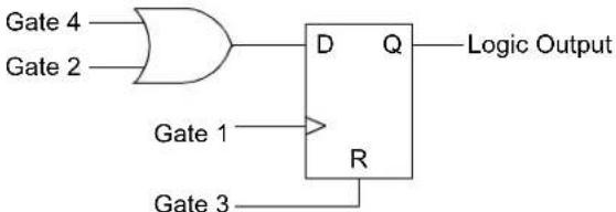 MODE[2:0] = 101 MODE[2:0] = 101 |
J-K Flip-Flop with R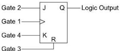 MODE[2:0] = 110 MODE[2:0] = 110 | 1-Input Transparent Latch with S and R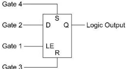 MODE[2:0] = 111 MODE[2:0] = 111 |
FIGURE 23-3: CLCx INPUT SOURCE SELECTION DIAGRAM

flowchart
graph TD
    subgraph_DS1x["DS1x (CLCxSEL[2:0"])]
        A["Input 0"] --> B["000"]
        C["Input 1"] --> D["111"]
        E["Input 2"] --> F["111"]
        G["Input 3"] --> H["111"]
        I["Input 4"] --> J["111"]
        K["Input 5"] --> L["111"]
        M["Input 6"] --> N["111"]
        O["Input 7"] --> P["111"]
    end

    subgraph_DS2x["DS2x (CLCxSEL[6:4"])]
        Q["Input 8"] --> R["000"]
        S["Input 9"] --> T["111"]
        U["Input 10"] --> V["111"]
        W["Input 11"] --> X["111"]
        Y["Input 12"] --> Z["111"]
        AA["Input 13"] --> AB["111"]
        AC["Input 14"] --> AD["111"]
        AE["Input 15"] --> AF["111"]

    end

    subgraph_DS3x["DS3x (CLCxSEL[10:8"])]
        AG["Input 16"] --> AH["000"]
        AI["Input 17"] --> AJ["111"]
        AK["Input 18"] --> AL["111"]
        AM["Input 19"] --> AN["111"]
        AO["Input 20"] --> AP["111"]
        AQ["Input 21"] --> AR["111"]
        AS["Input 22"] --> AT["111"]
        AU["Input 23"] --> AV["111"]

    end

    subgraph_DS4x["DS4x (CLCxSEL[14:12"])]
        AW["Input 24"] --> AX["000"]
        AY["Input 25"] --> AZ["111"]
        BA["Input 26"] --> BB["111"]
        BC["Input 27"] --> BD["111"]
        BE["Input 28"] --> BF["111"]
        BG["Input 29"] --> BH["111"]
        BI["Input 30"] --> BJ["111"]
        BK["Input 31"] --> BL["111"]

    A -->|Data 1 Noninverted| A
    B -->|Data 2 Noninverted| B
    C -->|Data 3 Noninverted| C
    AD -->|Data 4 Noninverted| AD
    AE -->|Data 4 Inverted| AE
    AF -->|Data Gate 2| AF
    AG -->|Data Gate 3| AG
    AH -->|Data Gate 4| AH
    AI -->|G1D1T| AI
    AJ -->|G1D2N| AJ
    AK -->|G1D3T| AK
    AL -->|G1D4T| AL
    AM -->|G1D4N| AM

    AN -->|Gate 2| AN
    AO -->|Gate 3| AO
    AP -->|Gate 4| AP

    AQ -->|Gate 2| AQ
    AR -->|Gate 3| AR
    BS -->|Gate 4| BS

    AT -->|Gate 2 Gate 2| AT
    AU -->|Gate 3 Gate 3| AU
    AV -->|Gate 4 Gate 4| AV
Note: All controls are undefined at power-up.
23.1 Control Registers
The CLCx module is controlled by the following registers:
• C L C x C O N L
• C L C x C O N H
- CLCxSEL
• C L C x G L S L
• C L C x G L S H
The CLCx Control registers (CLCxCONL and CLCxCONH) are used to enable the module and interrupts, control the output enable bit, select output polarity and select the logic function. The CLCx Control registers also allow the user to control the logic polarity of not only the cell output, but also some intermediate variables.
The CLCx Input MUX Select register (CLCxSEL) allows the user to select up to four data input sources using the four data input selection multiplexers. Each multiplexer has a list of eight data sources available.
The CLCx Gate Logic Input Select registers (CLCxGLSL and CLCxGLSH) allow the user to select which outputs from each of the selection MUXes are used as inputs to the input gates of the logic cell. Each data source MUX outputs both a true and a negated version of its output. All of these 8 signals are enabled, ORed together by the logic cell input gates.
REGISTER 23-1: CLCxCONL: CLCx CONTROL REGISTER (LOW)
| R/W-0 U-0 U-0 U-0 R/W-0 R/W-0 U-0 U-0 | ||||||
| LCEN — — INTP INTN — — | ||||||
| bit 15 bit 8 | ||||||
| R-0 R-0 R/W-0 U-0 U-0 R/W-0 | R/W-0 | R/W-0 | |||||
| LCOE | LCOUT | LCPOL | — — MODE2 | MODE1 | MODE0 | ||
| bit 7 bit 0 | |||||||
| Legend: | |||
| R = Readable bit | W = Writable bit | U = Unimplemented bit, read as ‘0’ | |
| -n = Value at POR | ‘1’ = Bit is set | ‘0’ = Bit is cleared | x = Bit is unknown |
| bit 15 | LCEN: CLCx Enable bit1 = CLCx is enabled and mixing input signals0 = CLCx is disabled and has logic zero outputs |
| bit 14-12 | Unimplemented: Read as ‘0’ |
| bit 11 | INTP: CLCx Positive Edge Interrupt Enable bit1 = Interrupt will be generated when a rising edge occurs on LCOUT0 = Interrupt will not be generated |
| bit 10 | INTN: CLCx Negative Edge Interrupt Enable bit1 = Interrupt will be generated when a falling edge occurs on LCOUT0 = Interrupt will not be generated |
| bit 9-8 | Unimplemented: Read as ‘0’ |
| bit 7 | LCOE: CLCx Port Enable bit1 = CLCx port pin output is enabled0 = CLCx port pin output is disabled |
| bit 6 | LCOUT: CLCx Data Output Status bit1 = CLCx output high0 = CLCx output low |
| bit 5 | LCPOL: CLCx Output Polarity Control bit1 = The output of the module is inverted0 = The output of the module is not inverted |
| bit 4-3 | Unimplemented: Read as ‘0’ |
REGISTER 23-1: CLCxCONL: CLCx CONTROL REGISTER (LOW) (CONTINUED)
bit 2-0 MODE[2:0]: CLCx Mode bits
111 = Single input transparent latch with S and R
110 = JK flip-flop with R
101 = Two-input D flip-flop with R
100 = Single input D flip-flop with S and R
011 = SR latch
010 = Four-input AND
001 = Four-input OR-XOR
000 = Four-input AND-OR
REGISTER 23-2: CLCxCONH: CLCx CONTROL REGISTER (HIGH)
| U-0 U-0 U-0 U-0 U-0 U-0 U-0 U-0 | |||||||
| —— | —— | —— | |||||
| bit 15 bit 8 | |||||||
| U-0 U-0 U-0 U-0 R/W-0 R/W-0 R/W-0 R/W-0 | ||||||
| — — — | — G4POL G3 | POL G2POL G | 1POL | |||
| bit 7 bit 0 | ||||||
| Legend: | |||
| R = Readable bit | W = Writable bit | U = Unimplemented bit, read as ‘0’ | |
| -n = Value at POR | ‘1’ = Bit is set | ‘0’ = Bit is cleared | x = Bit is unknown |
bit 15-4 Unimplemented: Read as '0'
bit 3 G4POL: Gate 4 Polarity Control bit
1 = Channel 4 logic output is inverted when applied to the logic cell
0 = Channel 4 logic output is not inverted
bit 2 G3POL: Gate 3 Polarity Control bit
1 = Channel 3 logic output is inverted when applied to the logic cell
0 = Channel 3 logic output is not inverted
bit 1 G2POL: Gate 2 Polarity Control bit
1 = Channel 2 logic output is inverted when applied to the logic cell
0 = Channel 2 logic output is not inverted
bit 0 G1POL: Gate 1 Polarity Control bit
1 = Channel 1 logic output is inverted when applied to the logic cell
0 = Channel 1 logic output is not inverted
REGISTER 23-3: CLCxSEL: CLCx INPUT MUX SELECT REGISTER
| U-0 R/W-0 R/W-0 R/W-0 U-0 R/W-0 R/W-0 R/W-0 | |||
| — | D | $ | 4 [ |
| bit 15 bit 8 | |||
| U-0 R/W-0 R/W-0 R/W-0 U-0 R/W-0 R/W-0 R/W-0 | |||
| — | D | $ | 2 [ |
| bit 7 bit 0 | |||
Legend:
R = Readable bit W = Writable bit U = Unimplemented bit, read as '0'
-n = Value at POR '1' = Bit is set '0' = Bit is cleared x = Bit is unknown
bit 15 Unimplemented: Read as '0'
bit 14-12 DS4[2:0]: Data Selection MUX 4 Signal Selection bits
111 = SCCP3 Compare Event Flag (CCP3IF)
110 = MCCP1 Compare Event Flag (CCP1IF)
101 = Unimplemented
100 = CTMU A/D trigger
011 = SPIx Input (SDIx) corresponding to CLCx module (see Table 23-1)
010 = Comparator 3 output
001 = Module-specific CLC output (see Table 23-1)
000 = CLCINB I/O pin
bit 11 Unimplemented: Read as '0'
bit 10-8 DS3[2:0]: Data Selection MUX 3 Signal Selection bits
111 = SCCP3 Compare Event Flag (CCP3IF)
110 = SCCP2 Compare Event Flag (CCP2IF)
101 = DMA Channel 1 interrupt
100 = UARTx RX output corresponding to CLCx module (see Table 23-1)
011 = SPIx Output (SDOx) corresponding to CLCx module (see Table 23-1)
010 = Comparator 2 output
001 = CLCx output (see Table 23-1)
000 = CLCINA I/O pin
bit 7 Unimplemented: Read as '0'
bit 6-4 DS2[2:0]: Data Selection MUX 2 Signal Selection bits
111 = SCCP2 Compare Event Flag (CCP2IF)
110 = MCCP1 Compare Event Flag (CCP1IF)
101 = DMA Channel 0 interrupt
100 = A/D conversion done interrupt
011 = UARTx TX input corresponding to CLCx module (see Table 23-1)
010 = Comparator 1 output
001 = CLCx output (see Table 23-1)
000 = CLCINB I/O pin
bit 3 Unimplemented: Read as '0'
bit 2-0 DS1[2:0]: Data Selection MUX 1 Signal Selection bits
111 = Timer3 match event
110 = Timer2 match event
101 = Unimplemented
100 = REFO output
011 = INTRC/LPRC clock source
010 = SOSC clock source
001 = System clock (TCY)
000 = CLCINA I/O pin
TABLE 23-1: MODULE-SPECIFIC INPUT DATA SOURCES
| Bit Field Value | Input Source | ||||
| CLC1 CLC2 CLC3 CLC4 | |||||
| DS4[2:0] 0 | 11 SDI1 SDI2 SDI3 SDI4 | ||||
| 001 CLC2 Output CLC1 Output CLC4 Output CLC3 Output | |||||
| DS3[2:0] 1 | 00 U1RX U2RX U3RX U4RX | ||||
| 011 SDO1 SDO2 SDO3 SDO4 | |||||
| 001 CLC1 Output CLC2 Output CLC3 Output CLC4 Output | |||||
| DS2[2:0] | 011 | U1TX | U2TX | U3TX | U4TX |
| 001 CLC2 Output CLC1 Output CLC4 Output CLC3 Output | |||||
REGISTER 23-4: CLCxGLSL: CLCx GATE LOGIC INPUT SELECT LOW REGISTER
| R/W-0 | R/W-0 | R/W-0 | R/W-0 | R/W-0 | R/W-0 | R/W-0 | R/W-0 |
| G2D4T | G2D4N | G2D3T | G2D3N | G2D2T | G2D2N | G2D1T | G2D1N |
| bit 15 bit 8 | |||||||
| R/W-0 | R/W-0 | R/W-0 | R/W-0 | R/W-0 | R/W-0 | R/W-0 | R/W-0 |
| G1D4T | G1D4N | G1D3T | G1D3N | G1D2T | G1D2N | G1D1T | G1D1N |
| bit 7 bit 0 | |||||||
| Legend: | |||
| R = Readable bit W = Writable bit | U = Unimplemented bit, read as ‘0’ | ||
| -n = Value at POR | ‘1’ = Bit is set | ‘0’ = Bit is cleared | x = Bit is unknown |
| bit 15 | G2D4T: Gate 2 Data Source 4 True Enable bit1 = Data Source 4 inverted signal is enabled for Gate 20 = Data Source 4 inverted signal is disabled for Gate 2 |
| bit 14 | G2D4N: Gate 2 Data Source 4 Negated Enable bit1 = Data Source 4 inverted signal is enabled for Gate 20 = Data Source 4 inverted signal is disabled for Gate 2 |
| bit 13 | G2D3T: Gate 2 Data Source 3 True Enable bit1 = Data Source 3 inverted signal is enabled for Gate 20 = Data Source 3 inverted signal is disabled for Gate 2 |
| bit 12 | G2D3N: Gate 2 Data Source 3 Negated Enable bit1 = Data Source 3 inverted signal is enabled for Gate 20 = Data Source 3 inverted signal is disabled for Gate 2 |
| bit 11 | G2D2T: Gate 2 Data Source 2 True Enable bit1 = Data Source 2 inverted signal is enabled for Gate 20 = Data Source 2 inverted signal is disabled for Gate 2 |
| bit 10 | G2D2N: Gate 2 Data Source 2 Negated Enable bit1 = Data Source 2 inverted signal is enabled for Gate 20 = Data Source 2 inverted signal is disabled for Gate 2 |
| bit 9 | G2D1T: Gate 2 Data Source 1 True Enable bit1 = Data Source 1 inverted signal is enabled for Gate 20 = Data Source 1 inverted signal is disabled for Gate 2 |
REGISTER 23-4: CLCxGLSL: CLCx GATE LOGIC INPUT SELECT LOW REGISTER (CONTINUED)
bit 8 G2D1N: Gate 2 Data Source 1 Negated Enable bit
1 = Data Source 1 inverted signal is enabled for Gate 2
0 = Data Source 1 inverted signal is disabled for Gate 2
bit 7 G1D4T: Gate 1 Data Source 4 True Enable bit
1 = Data Source 4 inverted signal is enabled for Gate 1
0 = Data Source 4 inverted signal is disabled for Gate 1
bit 6 G1D4N: Gate 1 Data Source 4 Negated Enable bit
1 = Data Source 4 inverted signal is enabled for Gate 1
0 = Data Source 4 inverted signal is disabled for Gate 1
bit 5 G1D3T: Gate 1 Data Source 3 True Enable bit
1 = Data Source 3 inverted signal is enabled for Gate 1
0 = Data Source 3 inverted signal is disabled for Gate 1
bit 4 G1D3N: Gate 1 Data Source 3 Negated Enable bit
1 = Data Source 3 inverted signal is enabled for Gate 1
0 = Data Source 3 inverted signal is disabled for Gate 1
bit 3 G1D2T: Gate 1 Data Source 2 True Enable bit
1 = Data Source 2 inverted signal is enabled for Gate 1
0 = Data Source 2 inverted signal is disabled for Gate 1
bit 2 G1D2N: Gate 1 Data Source 2 Negated Enable bit
1 = Data Source 2 inverted signal is enabled for Gate 1
0 = Data Source 2 inverted signal is disabled for Gate 1
bit 1 G1D1T: Gate 1 Data Source 1 True Enable bit
1 = Data Source 1 inverted signal is enabled for Gate 1
0 = Data Source 1 inverted signal is disabled for Gate 1
bit 0 G1D1N: Gate 1 Data Source 1 Negated Enable bit
1 = Data Source 1 inverted signal is enabled for Gate 1
0 = Data Source 1 inverted signal is disabled for Gate 1
REGISTER 23-5: CLCxGLSH: CLCx GATE LOGIC INPUT SELECT HIGH REGISTER
| R/W-0 R/W-0 R/W-0 R/W-0 R/W-0 R/W-0 R/W-0 R/W-0 | |||||||
| G4D4T G4 | D4N G4D3T G | 4D3N G4D2T | G4D2N G4D1T | G4D1N | |||
| bit 15 bit 8 | |||||||
| R/W-0 R/W-0 R/W-0 R/W-0 R/W-0 R/W-0 R/W-0 R/W-0 | |||||||
| G3D4T G3 | D4N G3D3T G | 3D3N G3D2T | G3D2N G3D1T | G3D1N | |||
| bit 7 bit 0 | |||||||
Legend:
R = Readable bit W = Writable bit U = Unimplemented bit, read as '0' -n = Value at POR '1' = Bit is set '0' = Bit is cleared x = Bit is unknown
bit 15 G4D4T: Gate 4 Data Source 4 True Enable bit
1 = Data Source 4 inverted signal is enabled for Gate 4
0 = Data Source 4 inverted signal is disabled for Gate 4
bit 14 G4D4N: Gate 4 Data Source 4 Negated Enable bit
1 = Data Source 4 inverted signal is enabled for Gate 4
0 = Data Source 4 inverted signal is disabled for Gate 4
bit 13 G4D3T: Gate 4 Data Source 3 True Enable bit
1 = Data Source 3 inverted signal is enabled for Gate 4
0 = Data Source 3 inverted signal is disabled for Gate 4
bit 12 G4D3N: Gate 4 Data Source 3 Negated Enable bit
1 = Data Source 3 inverted signal is enabled for Gate 4
0 = Data Source 3 inverted signal is disabled for Gate 4
bit 11 G4D2T: Gate 4 Data Source 2 True Enable bit
1 = Data Source 2 inverted signal is enabled for Gate 4
0 = Data Source 2 inverted signal is disabled for Gate 4
bit 10 G4D2N: Gate 4 Data Source 2 Negated Enable bit
1 = Data Source 2 inverted signal is enabled for Gate 4
0 = Data Source 2 inverted signal is disabled for Gate 4
bit 9 G4D1T: Gate 4 Data Source 1 True Enable bit
1 = Data Source 1 inverted signal is enabled for Gate 4
0 = Data Source 1 inverted signal is disabled for Gate 4
bit 8 G4D1N: Gate 4 Data Source 1 Negated Enable bit
1 = Data Source 1 inverted signal is enabled for Gate 4
0 = Data Source 1 inverted signal is disabled for Gate 4
bit 7 G3D4T: Gate 3 Data Source 4 True Enable bit
1 = Data Source 4 inverted signal is enabled for Gate 3
0 = Data Source 4 inverted signal is disabled for Gate 3
bit 6 G3D4N: Gate 3 Data Source 4 Negated Enable bit
1 = Data Source 4 inverted signal is enabled for Gate 3
0 = Data Source 4 inverted signal is disabled for Gate 3
bit 5 G3D3T: Gate 3 Data Source 3 True Enable bit
1 = Data Source 3 inverted signal is enabled for Gate 3
0 = Data Source 3 inverted signal is disabled for Gate 3
bit 4 G3D3N: Gate 3 Data Source 3 Negated Enable bit
1 = Data Source 3 inverted signal is enabled for Gate 3
0 = Data Source 3 inverted signal is disabled for Gate 3
REGISTER 23-5: CLCxGLSH: CLCx GATE LOGIC INPUT SELECT HIGH REGISTER (CONTINUED)
bit 3 G3D2T: Gate 3 Data Source 2 True Enable bit
1 = Data Source 2 inverted signal is enabled for Gate 3
0 = Data Source 2 inverted signal is disabled for Gate 3
bit 2 G3D2N: Gate 3 Data Source 2 Negated Enable bit
1 = Data Source 2 inverted signal is enabled for Gate 3
0 = Data Source 2 inverted signal is disabled for Gate 3
bit 1 G3D1T: Gate 3 Data Source 1 True Enable bit
1 = Data Source 1 inverted signal is enabled for Gate 3
0 = Data Source 1 inverted signal is disabled for Gate 3
bit 0 G3D1N: Gate 3 Data Source 1 Negated Enable bit
1 = Data Source 1 inverted signal is enabled for Gate 3
0 = Data Source 1 inverted signal is disabled for Gate 3
24.0 REAL-TIME CLOCK AND CALENDAR (RTCC) WITH TIMESTAMP
Note: This data sheet summarizes the features of this group of PIC24F devices. It is not intended to be a comprehensive reference source. For more information on the Real-Time Clock and Calendar, refer to the "dsPIC33/PIC24 Family Reference Manual", "RTCC with Timestamp" (www.microchip.com/DS70005193). The information in this data sheet supersedes the information in the FRM.
The RTCC provides the user with a Real-Time Clock and Calendar (RTCC) function that can be calibrated.
Key features of the RTCC module are:
• Time (Hours, Minutes and Seconds) in 24-Hour (Military Time) Format
• Calendar (Weekday, Date, Month and Year)
- Year range from 2000 to 2099 with automatic Leap Year correction
- Alarm with Configurable Mask and Repeat Options
• BCD Format for Compact Firmware - Optimized for Low-Power Operation
-
Multiple Clock Input Options, Including:
-
32.768 kHz crystal
- External Real-Time Clock (RTC)
- 50/60 Hz power line clock
- 31.25 kHz LPRC clock
-
System clock, up to 32 MHz
-
User Calibration with a Range of 2 ppm when using 32 kHz Source
- Interrupt on Alarm and Timestamp Events
- Optional Timestamp Capture for Tamper Pin or Other Events
- User-Configurable Power Control with Dedicated Output Pin to Periodically Wake External Devices
FIGURE 24-1: RTCC HIGH-LEVEL BLOCK DIAGRAM

flowchart
```mermaid
graph TD
    subgraph_RTCC_Clock_Domain["RTCC Clock Domain"]
        A["PWRLCLK Pin"] --> B["->"]
        C["SOSC"] --> B
        D["INTRC"] --> B
        E["FcY"] --> B
        B --> F["RTCC Prescaler/Clock Divider"]
        F --> G["0.5s"]
        G --> H["RTCC Timer"]
        H --> I["TIMEH"]
        H --> J["TIMEL"]
        H --> K["DATEH"]
        H --> L["DATEL"]
        G --> M["Comparator with Masks"]
    end

    subgraph_CPU_Clock_Domain["CPU Clock Domain"]
        N["RTCCON1H"] --> O["->"]
        P["RTCCON1L"] --> O
        Q["RTCCON2H"] --> R["->"]
        S["RTCCON2L"] --> T["->"]
        U["RTCCON3L"] --> V["->"]
        W["RTCSTATL"] --> X["->"]
        Y["ALMTIMEH"] --> Z["->"]
        AA["ALMTIMEL"] --> AB["->"]
        AC["ALMDATEH"] --> AD["->"]
        AE["ALMDATEL"] --> AF["->"]
        G --> M
        M --> Y
        M --> Z
        M --> AD
        M --> AF
    end

    subgraph_RTCC_Interrupt["RTCC Interrupt"]
        F --> G
        H --> I
        M --> J
        N --> K
        O --> L
        P --> Q
        Q --> R
        R --> S
        S --> T
        T --> U
        U --> V
        V --> W
        W --> X
        X --> Y
        Y --> Z
        Z --> R
        R --> S
        S --> T
        T --> U
        U --> V
        V --> W
    end

    subgraph_RTCC_Pin["RTCC Pin"]
        N --> O
        O --> P
        P --> Q
        Q --> R
        R --> S
        S --> T
        T --> U
        U --> V
        V --> W
    end

    subgraph_PWRGT_Pin["PWRGT Pin"]
        R --> S
        S --> T
        T --> U
        U --> V
        V --> W
    end

    style RTCC_Clock_Domain fill:#f9f,stroke:#333
    style CPU_Clock_Domain fill:#bbf,stroke:#333

    %% Note: The diagram shows connections between clock signals, timing logic, and interrupt logic for each component.
24.1 RTCC Source Clock
The RTCC clock divider block converts the incoming oscillator source into an accurate 1/2 second clock for the RTCC timer. The clock divider is optimized to work with four different oscillator sources:
• System clock, up to 32 MHz
• 32.768 kHz crystal oscillator
• 31 kHz Low-Power RC Oscillator (LPRC)
- External 50 Hz or 60 Hz power line frequency
An asynchronous prescaler, PS[1:0] (RTCCON2L[5:4]), is provided that allows the RTCC to work with higher speed clock sources, such as the system clock. Divide ratios of 1:16, 1:64 or 1:256 may be selected, allowing sources up to 32 MHz to clock the RTCC.
24.1.1 SELECTING RTCC CLOCK SOURCE
The clock source for the RTCC module can be selected using the CLKSEL[1:0] bits in the RTCCON2L register. When the bits are set to '00', the Secondary Oscillator (SOSC) is used as the reference clock and when the bits are '01', LPRC is used as the reference clock. When CLKSEL[1:0] = 10, the external power line (50 Hz and 60 Hz) is used as the clock source. When CLKSEL[1:0] = 11, the system clock is used as the clock source.
24.1.2 COARSE FREQUENCY DIVISION
The clock divider block has a 16-bit counter used to divide the input clock frequency. The divide ratio is set by the DIV[15:0] register bits (RTCCON2H[15:0]). The DIV[15:0] bits should be programmed with a value to produce a nominal 1/2 second clock divider count period.
24.1.3 FINE FREQUENCY DIVISION
The fine frequency division is set using the FDIV[4:0] (RTCCON2L[15:11]) bits. Increasing the FDIVx value will lengthen the overall clock divider period.
If FDIV[4:0] = 00000, the fine frequency division circuit is effectively disabled. Otherwise, it will optionally remove a clock pulse from the input of the clock divider every 1/2 second. This functionality will allow the user to remove up to 31 pulses over a fixed period of 16 seconds, depending on the value of FDIVx.
The value for DIV[15:0] is calculated as shown in Equation 24-1. The fractional remainder of the DIV[15:0] calculation result can be used to calculate the value for FDIV[4:0].
EQUATION 24-1: RTCC CLOCK DIVIDER OUTPUT FREQUENCY
$$ F _ {O U T} = \frac {F _ {I N}}{2 \cdot (P S [ 1 : 0 ] P r e s c a l e r) \cdot (D I V [ 1 5 : 0 ] + 1) + \left(\frac {F D I V [ 4 : 0 ]}{3 2}\right)} $$
The DIV[15:0] value is the integer part of this calculation:
$$ D I V [ 1 5: 0 ] = - \left(\frac {F _ {I N}}{2 \cdot (P S [ 1 : 0 ] P r e s c a l e r)}\right) $$
The FDIV[4:0] value is the fractional part of the DIV[15:0] calculation, multiplied by 32.
24.1.4 CLOCK SOURCE CALIBRATION
A crystal oscillator that is connected to the RTCC may be calibrated to provide an accurate 1-second clock in two ways. First, coarse frequency adjustment is performed by adjusting the value written to the DIV[15:0] bits. Secondly, a 5-bit value can be written to the FDIV[4:0] control bits to perform a fine clock division.
The DIVx and FDIVx values can be concatenated and considered as a 21-bit prescaler value. If the oscillator source is slightly faster than ideal, the FDIV[4:0] value can be increased to make a small decrease in the RTC frequency. The value of DIV[15:0] should be increased to make larger decreases in the RTC frequency. If the oscillator source is slower than ideal, FDIV[4:0] may be decreased for small calibration changes and DIV[15:0] may need to be decreased to make larger calibration changes.
Before calibration, the user must determine the error of the crystal. This should be done using another timer resource on the device or an external timing reference. It is up to the user to include in the error value the initial error of the crystal, drift due to temperature and drift due to crystal aging.
24.2 Alarm
The RTCC alarm includes these features:
- Configurable from half second to one year
• One-time alarm and repeat alarm options available
24.2.1 CONFIGURING THE ALARM
The alarm feature is enabled using the ALRMEN bit. This bit is cleared when an alarm is issued. Writes to ALRMVAL should only take place when ALRMEN = 0.
As shown in Figure 24-2, the interval selection of the alarm is configured through the AMASK[3:0] bits (RTCCON1H[11:8]). These bits determine which, and how many, digits of the alarm must match the clock value for the alarm to occur.
The alarm can also be configured to repeat based on a preconfigured interval. The amount of times this occurs, once the alarm is enabled, is stored in the ALMRPT[7:0] bits (RTCCON1H[7:0]). When the value of the ALMRPTx bits equals 00h and the CHIME bit (RTCCON1H[14]) is cleared, the repeat function is disabled and only a single alarm will occur. The alarm can be repeated, up to 255 times, by loading ALMRPT[7:0] with FFh.
After each alarm is issued, the value of the ALMRPTx bits is decremented by one. Once the value has reached 00h, the alarm will be issued one last time, after which, the ALRMEN bit will be cleared automatically and the alarm will turn off.
Indefinite repetition of the alarm can occur if the CHIME bit = 1. Instead of the alarm being disabled when the value of the ALMRPTx bits reaches 00h, it rolls over to FFh and continues counting indefinitely while CHIME is set.
24.2.2 ALARM INTERRUPT
At every alarm event, an interrupt is generated. This output is completely synchronous to the RTCC clock and can be used as a trigger clock to other peripherals.
Note: Changing any of the register bits, other than the RTCOE bit, the ALMRPT[7:0] bits and the CHIME bit, while the alarm is enabled (ALRMEN = 1), can result in a false alarm event leading to a false alarm interrupt. To avoid a false alarm event, the timer and alarm values should only be changed while the alarm is disabled (ALRMEN = 0).
FIGURE 24-2: ALARM MASK SETTINGS

other
Alarm Mask Setting (AMASK[3:0]) Day of the Week Month Day Hours Minutes Seconds 0000 - Every half second 0001 - Every second □ □/□ □ □: □ □: □ □ 0010 - Every 10 seconds □ □/□ □ □: □ □: □ s 0011 - Every minute □ □/□ □ □: □ □: s s 0100 - Every 10 minutes □ □/□ □ □: □ m: s s 0101 - Every hour □ □/□ □ □: m m: s □ s 0110 - Every day □ □/□ □ h h: m m: s s 0111 - Every week d □/□ □ h h: m m: s s 1000 - Every month □ □/d d h h: m m: $ 1001 - Every year(1) □ m m/ d d h h: m m: s sNote 1: Annually, except when configured for February 29.
24.3 Power Control
The RTCC includes a power control feature that allows the device to periodically wake-up an external device, wait for the device to be stable before sampling wake-up events from that device and then shut down the external device. This can be done completely autonomously by the RTCC, without the need to wake from the current lower power mode.
To use this feature:
- Enable the RTCC (RTCEN = 1).
- Set the PWCEN bit (RTCCON1L[10]).
- Configure the RTCC pin to drive the PWC control signal (RTCOE = 1 and OUTSEL[2:0] = 011).
The polarity of the PWC control signal is selected by the PWCPOL bit (RTCCON1L[9]). An active-low or active-high signal may be used with the appropriate external switch to turn on or off the power to one or more external devices. The active-low setting may also be used in conjunction with an open-drain setting on the RTCC pin, in order to drive the ground pin(s) of the external device directly (with the appropriate external VDD pull-up device), without the need for external switches. Finally, the CHIME bit should be set to enable the PWC periodicity.
Once the RTCC and PWC are enabled and running, the PWC logic will generate a control output and a sample gate output. The control output is driven out on the RTCC pin (when RTCOE = 1 and OUTSEL[2:0] = 011) and is used to power-up or power-down the device, as described above.
Once the control output is asserted, the Stability Window begins, in which the external device is given enough time to power-up and provide a stable output.
Once the output is stable, the RTCC provides a sample gate during the Sample Window. The use of this sample gate depends on the external device being used, but typically, it is used to mask out one or more wake-up signals from the external device.
Finally, both the Stability and the Sample Windows close after the expiration of the Sample Window, and the external device is powered down.
24.3.1 POWER CONTROL CLOCK SOURCE
The Stability and Sample Windows are controlled by the PWCSAMP[7:0] and PWCSTAB[7:0] bits field in the RTCCON3L register (RTCCON3L[15:8] and [7:0], respectively). As both the Stability and Sample Windows are defined in terms of the RTCC clock, their absolute values vary by the value of the PWC clock base period. The 8-bit magnitude of PWCSTABx and PWCSAMPx allows for a window size of 0 to 255 clock periods.
The period of the PWC clock can also be adjusted with a 1:1, 1:16, 1:64 or 1:256 prescaler, determined by the PWCPS[1:0] bits (RTCCON2L[7:6]).
In addition, certain values for the PWCSTABx and PWCSAMPx fields have specific control meanings in determining power control operations. If either bit field is 00h, the corresponding window is inactive. In addition, if the PWCSTABx field is FFh, the Stability Window remains active continuously, even if power control is disabled.
24.4 Event Timestamping
The RTCC includes two sets of Timestamp registers that may be used for the capture of Time and Date register values when an external input signal is received. The RTCC triggers the timestamps for two events:
- For Timestamp A, a falling edge on the TMPR pin
- For Timestamp B, when the devices transition from VDD to VBAT power
A Timestamp A event can be triggered while running the device in VBAT mode if the TMPR pin is pulled up to VBAT.
The event input is enabled for timestamping using the TSAEN bit (RTCCON1L[0]). When the timestamp event occurs, the present time and date values are stored in the TSATIMEL/H and TSADATEL/H registers, the TSAEVT status bit (RTCSTATL[3]) becomes set and an RTCC interrupt occurs. A new timestamp capture event cannot occur until the user clears the TSAEVT status bit.
Note 1: The TSATIMEL/H and TSADATEL/H register pairs can be used for data storage when TSAEN = 0. The values of TSATIMEL/H and TSADATEL/H will be maintained throughout all types of non-power Resets (MCLRWDT, etc).
24.4.2 MANUAL TIMESTAMP
The current time and date may be captured in the TSATIMEL/H and TSADATEL/H registers by writing a '1' to the TSAEVT bit location while the timestamp functionality is enabled (TSAEN = 1). This write will not set the TSAEVT bit, but it will initiate a timestamp capture. The TSAEVT bit will be set when the capture operation is complete. The user must poll the TSAEVT bit to determine when the capture operation is complete.
After the Timestamp registers have been read, the TSAEVT bit should be cleared to allow further hardware or software timestamp capture events.
24.5 RTCC Module Registers
The RTCC module registers are organized into three categories:
• RTCC Control and Status registers
• Time/Alarm/Timestamp Value registers
- Date/Alarm/Timestamp registers
All Date and Time registers are directly mapped to memory and are individually addressable. In addition, the Date and Time registers for the RTCC timer, the alarm and the timestamps are identical in format.
24.5.1 WRITE LOCK
To perform a write to certain RTCC Timer registers, the WRLOCK bit in the RTCCON1L register must be cleared. The WRLOCK bit affects only those registers associated with accurate timekeeping:
- RTCCON1L
- RTCCON2L
- RTCCON2H
• TIMEL
• TIMEH
• DATEL
• DATEH
Other register functions associated with alarm control, power control and timestamping are not affected by the WRLOCK bit. To avoid accidental writes to the timer, it is recommended that the WRLOCK bit be set after initializing the RTCC. WRLOCK may be set at any time without executing an unlock sequence.
Once the WRLOCK bit has been set by the user, it can only be cleared once an unlocking sequence has been executed. The unlocking sequence consists of writing 0x55, immediately followed by 0xAA, to the NVMKEY register.
The WRLOCK bit must be cleared on the very next instruction cycle after the unlock sequence. Due to the critical timing of the unlock sequence that is required to clear the WRLOCK bit, a built-in function has been provided in the MPLAB ^® XC16 compiler to perform the unlock sequence and clear the WRLOCK bit, as shown in Example 24-1.
EXAMPLE 24-1: SETTING THE WRLOCK BIT
// Initialize the RTCC as needed
// Lock the RTCC registers
RTCCON1Lbits.WRLOCK = 1;
// Clear WRLOCK to modify RTCC as needed
__builtin_write_RTCC_WRLOCK();
24.5.2 RTCC CONTROL AND STATUS
REGISTERS
REGISTER 24-1: RTCCON1L: RTCC CONTROL REGISTER 1 (LOW)
| R/W-0 U-0 U-0 U-0 R/W-0 R/W-0 R/W-0 R/W-0 | ||||||
| RTCEN — | — — WRLOCK | PWCEN PW | CPOL PW | CPOE | ||
| bit 15 bit 8 | ||||||
| R/W-0 R/W-0 R/W-0 R/W-0 U-0 U-0 R/W-0 R/W-0 | |||||||
| RTCOE | OUTSEL2 | OUTSEL1 | OUTSEL0 | — — TSBEN | TSAEN | ||
| bit 7 bit 0 | |||||||
Legend:
| R = Readable bit W = Writable bit | U = Unimplemented bit, read as '0' | ||
| -n = Value at POR | '1' = Bit is set | '0' = Bit is cleared | x = Bit is unknown |
bit 15 RTCEN: RTCC Enable bit
1 = RTCC is enabled and counts from selected clock source 0 = RTCC is not enabled
bit 14-12 Unimplemented: Read as '0'
bit 11 WRLOCK: RTCC Register Write Lock bit
1 = RTCC registers are locked 0 = RTCC registers may be written by the user
bit 10 PWCEN: Power Control Enable bit
1 = Power control is enabled 0 = Power control is disabled
bit 9 PWCPOL: Power Control Polarity bit
1 = Power control output is active-high 0 = Power control output is active-low
bit 8 PWCPOE: Power Control Output Enable bit
1 = Power control output pin is enabled 0 = Power control output pin is disabled
bit 7 RTCOE: RTCC Output Enable bit
1 = RTCC output is enabled 0 = RTCC output is disabled
bit 6-4 OUTSEL[2:0]: RTCC Output Signal Selection bits
11x = Unused 101 = Unused 100 = Timestamp A event 011 = Power control 010 = RTCC input clock 001 = Second clock 000 = Alarm event
bit 3-2 Unimplemented: Read as '0'
bit 1 TSBEN: Timestamp Source B Enable bit
1 = Timestamp Source B signal generates a timestamp event 0 = Timestamp Source B is disabled
bit 0 TSAEN: Timestamp Source A Enable bit
1 = Timestamp Source A event is generated when a low pulse is detected on the TMPRpin 0 = Timestamp Source A is disabled
REGISTER 24-2: RTCCON1H: RTCC CONTROL REGISTER 1 (HIGH)
| R/W-0 R/W-0 U-0 U-0 R/W-0 R/W-0 R/W-0 R/W-0 | ||||||
| ALRMEN | CHIME | — — AM | MASK3 AMASK | 2 AMASK1 AM | MASK0 | |
| bit 15 bit 8 | ||||||
| R/W-0 R/W-0 R/W-0 R/W-0 R/W-0 R/W-0 R/W-0 R/W-0 |
| ALMRPT[7:0] |
| bit 7 bit 0 |
Legend:
R = Readable bit W = Writable bit U = Unimplemented bit, read as '0'
-n = Value at POR '1' = Bit is set '0' = Bit is cleared x = Bit is unknown
bit 15 ALRMEN: Alarm Enable bit
1 = Alarm is enabled (cleared automatically after an alarm event whenever ALMRPT[7:0] = 00h and CHIME = 0)
0 = Alarm is disabled
bit 14 CHIME: Chime Enable bit
1 = Chime is enabled; ALMRPT[7:0] bits roll over from 00h to FFh
0 = Chime is disabled; ALMRPT[7:0] bits stop once they reach 00h
bit 13-12 Unimplemented: Read as '0'
bit 11-8 AMASK[3:0]: Alarm Mask Configuration bits
11xx = Reserved, do not use
101x = Reserved, do not use
1001 = Once a year (or once every four years when configured for February 29th)
1000 = Once a month
0111 = Once a week
0110 = Once a day
0101 = Every hour
0100 = Every ten minutes
0011 = Every minute
0010 = Every ten seconds
0001 = Every second
0000 = Every half second
bit 7-0 ALMRPT[7:0]: Alarm Repeat Counter Value bits
11111111 = Alarm will repeat 255 more times
11111110 = Alarm will repeat 254 more times
...
00000010 = Alarm will repeat 2 more times
00000001 = Alarm will repeat 1 more time
00000000 = Alarm will not repeat
REGISTER 24-3: RTCCON2L: RTCC CONTROL REGISTER 2 (LOW)
| R/W-0 R/W-0 R/W-0 R/W-0 R/W-0 U-0 U-0 U-0 | |||
| FDIV[4:0] | — — — | ||
| bit 15 bit 8 | |||
| R/W-0 R/W-0 R/W-0 R/W-0 U-0 U-0 R/W-0 R/W-0 | |||||||
| PWCPS1 P | WCPS0 PS1 PS0 | — — CLKSEL1 CLKSEL0 | |||||
| bit 7 bit 0 | |||||||
Legend:
R = Readable bit W = Writable bit U = Unimplemented bit, read as '0'
-n = Value at POR
'1' = Bit is set
'0' = Bit is cleared
x = Bit is unknown
bit 15-11 FDIV[4:0]: Fractional Clock Divide bits
11111 = Clock period increases by 31 RTCC input clock cycles every 16 seconds
11101 = Clock period increases by 30 RTCC input clock cycles every 16 seconds
...
00010 = Clock period increases by 2 RTCC input clock cycles every 16 seconds
00001 = Clock period increases by 1 RTCC input clock cycle every 16 seconds
00000 = No fractional clock division
bit 10-8 Unimplemented: Read as '0'
bit 7-6 PWCPS[1:0]: Power Control Prescale Select bits
11 = 1:256
10 = 1:64
01 = 1:16
00 = 1:1
bit 5-4 PS[1:0]: Prescale Select bits
11 = 1:256
10 = 1:64
01 = 1:16
00 = 1:1
bit 3-2 Unimplemented: Read as '0'
bit 1-0 CLKSEL[1:0]: Clock Select bits
11 = Peripheral clock (Fcy)
10 = PWRLCLK input pin
01 = LPRC
00 = SOSC
REGISTER 24-4: RTCCON2H: RTCC CONTROL REGISTER 2 (HIGH) ^(1)
| R/W-0 R/W-0 R/W-1 R/W-1 R/W-1 R/W-1 R/W-1 R/W-1 |
| DIV[15:8] |
| bit 15 bit 8 |
| R/W-1 R/W-1 R/W-1 R/W-1 R/W-1 R/W-1 R/W-1 R/W-1 |
| DIV[7:0] |
| bit 7 bit 0 |
Legend:
R = Readable bit W = Writable bit U = Unimplemented bit, read as '0' -n = Value at POR '1' = Bit is set '0' = Bit is cleared x = Bit is unknown
bit 15-0 DIV[15:0]: Clock Divide bits
Sets the period of the clock divider counter; value should cause a nominal 1/2 second underflow.
Note 1: A write to this register is only allowed when WRLOCK = 1.
REGISTER 24-5: RTCCON3L: RTCC CONTROL REGISTER 3 (LOW) ^(1)
| R/W-0 | R/W-0 | R/W-0 | R/W-0 | R/W-0 | R/W-0 | R/W-0 | R/W-0 |
| PWCSAMP[7:0] | |||||||
| bit 15 | bit 8 | ||||||
| R/W-0 | R/W-0 | R/W-0 | R/W-0 | R/W-0 | R/W-0 | R/W-0 | R/W-0 |
| PWCSTAB[7:0] | |||||||
| bit 7 | bit 0 | ||||||
Legend:
R = Readable bit W = Writable bit U = Unimplemented bit, read as '0' -n = Value at POR '1' = Bit is set '0' = Bit is cleared x = Bit is unknown
bit 15-8 PWCSAMP[7:0]: Power Control Sample Time Window bits
11111111 = Sample input is always allowed (not gated) 11111110 = Sample Time Window is 254 T PWC ... 00000010 = Sample Time Window is 2 T PWC 00000001 = Sample Time Window is 1 TPWC 00000000 = Sample input is always gated
bit 7-0 PWCSTAB[7:0]: Power Control Stability Time bits
11111111 = Stability Time Window is 255 TPWC 11111110 = Stability Time Window is 254 TPWC ... 00000010 = Stability Time Window is 2 TPWC 00000001 = Stability Time Window is 1 TPWC 00000000 = No Stability Time Window
Note 1: The Sample Window always starts when the Stability Window timer expires, except when its initial value is 00h.
REGISTER 24-6: RTCSTATL: RTCC STATUS REGISTER (LOW)
| U-0 U-0 U-0 U-0 U-0 U-0 U-0 U-0 | |||||||
| —— | —— | —— | |||||
| bit 15 bit 8 | |||||||
| U-0 U-0 HSC/R/C-0 HSC/R/W-0 HSC/R/W-0 HSC/R-0 HSC/R-0 HSC/R-0 | |||||||
| — — AL | MEVT | TSBEVT | (1) | TSAEVT(1) | SYNC | ALMSYNC H | ALFSEC (2) |
| bit 7 bit 0 | |||||||
| Legend: | C = Clearable bit | HSC = Hardware Settable/Clearable bit | |
| R = Readable bit W = Writable bit | U = Unimplemented bit, read as '0' | ||
| -n = Value at POR | ‘1’ = Bit is set | ‘0’ = Bit is cleared | x = Bit is unknown |
bit 15-6 Unimplemented: Read as '0'
bit 5 ALMEVT: Alarm Event bit
1 = An alarm event has occurred
0 = An alarm event has not occurred
bit 4 TSBEVT: Timestamp B Event bit ^(1)
1 = A Timestamp B event has occurred
0 = A Timestamp B event has not occurred
bit 3 TSAEVT: Timestamp A Event bit ^(1)
1 = A Timestamp A event has occurred
0 = A Timestamp A event has not occurred
bit 2 SYNC: Synchronization Status bit
1 = Time registers may change during software read
0 = Time registers may be read safely
bit 1 ALMSYNC: Alarm Synchronization Status bit
1 = Alarm registers (ALMTIME, ALMDATE) and AMASKx bits should not be modified and Alarm Control registers (ALRMEN, ALMRPT[7:0]) may change during software read
0 = Alarm registers and Alarm Control registers may be written/modified safely
bit 0 HALFSEC: Half Second Status bit ^(2)
1 = Second half of 1-second period
0 = First half of 1-second period
Note 1: User software may write a '1' to this location to initiate a Timestamp A event; timestamp capture is not valid until TSAEVT reads as '1'.
2: This bit is read-only; it is cleared to '0' on a write to the SECONE[3:0] bits in Register 24-7.
24.5.3 TIME/ALARM/TIMESTAMP VALUE REGISTERS
REGISTER 24-7: TIMEL/ALMTIMEL/TSATIMEL/TSBTIMEL: TIME REGISTER (LOW)
| U-0 R/W-0 R/W-0 R/W-0 R/W-0 R/W-0 R/W-0 R/W-0 | |||||||
| — SECTEN2 SECTEN1 SECTEN0 SECONE3 SECONE2 SECONE1 SECONE0 | |||||||
| bit 15 bit 8 | |||||||
| R = Readable bit | W = Writable bit | U = Unimplemented bit, read as '0' |
| -n = Value at POR | '1' = Bit is set | '0' = Bit is cleared x = Bit is unknown |
bit 15 Unimplemented: Read as '0'
bit 14-12 SECTEN[2:0]: Binary Coded Decimal Value of Seconds '10' Digit bits Contains a value from 0 to 5.
bit 11-8 SECONE[3:0]: Binary Coded Decimal Value of Seconds '1' Digit bits Contains a value from 0 to 9.
bit 7-0 Unimplemented: Read as '0'
REGISTER 24-8: TIMEH/ALMTIMEH/TSATIMEH/TSBTIMEH: TIME REGISTER (HIGH)
| U-0 U-0 R/W-0 R/W-0 R/W-0 R/W-0 R/W-0 R/W-0 | |||||||
| — | — | HRTEN1 | HRTEN0 | HRONE3 | HRONE2 | HRONE1 | HRONE0 |
| bit 15 bit 8 | |||||||
| U-0 R/W-0 R/W-0 R/W-0 R/W-0 R/W-0 R/W-0 R/W-0 | |||||||
| — | MINTEN2 | MINTEN1 | MINTENO | MINONE3 | MINONE2 | MINONE1 | MINONE0 |
| bit 7 bit 0 | |||||||
Legend:
| R = Readable bit | W = Writable bit | U = Unimplemented bit, read as '0' |
| -n = Value at POR | '1' = Bit is set | '0' = Bit is cleared x = Bit is unknown |
bit 15-14 Unimplemented: Read as '0'
bit 13-12 HRTEN[1:0]: Binary Coded Decimal Value of Hours '10' Digit bits Contains a value from 0 to 2.
bit 11-8 HRONE[3:0]: Binary Coded Decimal Value of Hours '1' Digit bits Contains a value from 0 to 9.
bit 7 Unimplemented: Read as '0'
bit 6-4 MINTEN[2:0]: Binary Coded Decimal Value of Minutes '10' Digit bits Contains a value from 0 to 5.
bit 3-0 MINONE[3:0]: Binary Coded Decimal Value of Minutes '1' Digit bits Contains a value from 0 to 9.
24.5.4 DATE/ALARM/TIMESTAMP VALUE REGISTERS
REGISTER 24-9: DATEL/ALMDATEL/TSADATEL/TSBDATEL: DATE REGISTER (LOW)
| U-0 U-0 R/W-0 R/W-0 R/W-0 R/W-0 R/W-0 R/W-1 | |||||||
| — — DAYTEN1 DAYTEN0 DAYONE3 DAYONE2 DAYONE1 DAYONE0 | |||||||
| bit 15 bit 8 | |||||||
| U-0 U-0 U-0 U-0 | U-0 R/W-1 R/W-1 R/W-0 | ||||
| — | — | — | — | — | WDAY[2:0] |
| bit 7 bit 0 | |||||
Legend:
| R = Readable bit W = Writable bit | U = Unimplemented bit, read as '0' | ||
| -n = Value at POR | '1' = Bit is set | '0' = Bit is cleared | x = Bit is unknown |
bit 15-14 Unimplemented: Read as '0'
bit 13-12 DAYTEN[1:0]: Binary Coded Decimal Value of Days '10' Digit bits Contains a value from 0 to 3.
bit 11-8 DAYONE[3:0]: Binary Coded Decimal Value of Days '1' Digit bits Contains a value from 0 to 9.
bit 7-3 Unimplemented: Read as '0'
bit 2-0 WDAY[2:0]: Binary Coded Decimal Value of Weekdays '1' Digit bits Contains a value from 0 to 6.
REGISTER 24-10: DATEH/ALMDATEH/TSADATEH/TSBDATEH: DATE REGISTER (HIGH)
| R/W-0 R/W-0 R/W-0 R/W-0 R/W-0 R/W-0 R/W-0 | |||||||
| YRTEN3 | YRTEN2 | YRTEN1 | YRTEN0 | YRONE3 | YRONE2 | YRONE1 | YRONE0 |
| bit 15 bit 8 | |||||||
| U-0 U-0 | U-0 | R/W-0 R/W-0 R/W-0 R/W-0 R/W-1 | ||||||
| — | — | — | — | MTHTEN | MTHONE3 | MTHONE2 | MTHONE1 | MTHONE0 |
| bit 7 bit 0 | ||||||||
Legend:
| R = Readable bit W = Writable bit | U = Unimplemented bit, read as '0' | ||
| -n = Value at POR | '1' = Bit is set | '0' = Bit is cleared | x = Bit is unknown |
bit 15-12 YRTEN[3:0]: Binary Coded Decimal Value of Years '10' Digit bits
bit 11-8 YRONE[3:0]: Binary Coded Decimal Value of Years '1' Digit bits
bit 7-5 Unimplemented: Read as '0'
bit 4 MTHTEN: Binary Coded Decimal Value of Months '10' Digit bit Contains a value from 0 to 1.
bit 3-0 MTHONE[3:0]: Binary Coded Decimal Value of Months '1' Digit bits Contains a value from 0 to 9.
25.0 CRYPTOGRAPHIC ENGINE
Note: This data sheet summarizes the features of the PIC24FJ256GA412/GB412 family of devices. It is not intended to be a comprehensive reference source. To complement the information in this data sheet, refer to the "dsPIC33/PIC24 Family Reference Manual", "Cryptographic Engine" (www.microchip.com/DS70005133) which is available from the Microchip website (www.microchip.com).
The Cryptographic Engine provides a new set of data security options. Using its own free-standing state machines, the engine can independently perform NIS standard encryption and decryption of data independently of the CPU. This eliminates the concerns of excessive CPU or program memory overhead that encryption and decryption would otherwise require, while enhancing the application's security.
The primary features of the Cryptographic Engine are:
• Memory-Mapped, 128-Bit and 256-Bit Memory Spaces for Encryption/Decryption Data
- Multiple Options for Key Storage, Selection and Management
• Support for Internal Context Saving
- Session Key Encryption and Loading
• Half-Duplex Operation
- DES and Triple DES (3DES) Encryption and Decryption (64-bit block size):
- Supports 64-bit keys and 2-key or 3-key Triple DES
- AES Encryption and Decryption (128-bit block size): - Supports key sizes of 128, 192 or 256 bits
• Supports ECB, CBC, CFB, OFB and CTR Modes for Both DES and AES Standards
- Programmatically Secure Key Storage:
- 512-byte OTP array for key storage, not readable from other memory spaces
- 32-bit Configuration Page
- Independent, 512-byte Key RAM for volatile key storage
- Simple in-module programming interface
-
Supports Key Encryption Key (KEK)
-
Support for True Random Number Generation (TRNG) and Pseudorandom Number Generation (PRNG), NIST SP800-90 Compliant
- Hardware Anti-Tamper Feature for Additional Data Security
A simplified block diagram of the Cryptographic Engine is shown in Figure 25-1.
FIGURE 25-1: CRYPTOGRAPHIC ENGINE BLOCK DIAGRAM

flowchart
graph TD
    A["CMapped to SFR Space"] --> B["CRYCONH"]
    A --> C["CRYCONL"]
    A --> D["CRYSTAT"]
    A --> E["CRYOTP"]
    B <--> F["Cryptographic and OTP Control"]
    C <--> F
    D <--> F
    E <--> F
    G["CFGPAGE"] --> H["OTP Key Store and Configuration"]
    H --> I["Key RAM"]
    J["OTP Programming"] --> K["Key Management"]
    L["TRN Generation"] --> M["DES Engine"]
    N["CRYKEY 256 Bits"] --> O["CRYTXTA 128 Bits"]
    P["CRYTXTB 128 Bits"] --> Q["CRYTXTC 128 Bits"]
    R["AES Engine"] --> S["End"]
    style A fill:#f9f,stroke:#333
    style B fill:#ccf,stroke:#333
    style C fill:#ccf,stroke:#333
    style D fill:#ccf,stroke:#333
    style E fill:#ccf,stroke:#333
    style F fill:#cfc,stroke:#333
    style G fill:#cfc,stroke:#333
    style H fill:#cfc,stroke:#333
    style I fill:#cfc,stroke:#333
    style J fill:#cfc,stroke:#333
    style K fill:#cfc,stroke:#333
    style L fill:#cfc,stroke:#333
    style M fill:#cfc,stroke:#333
    style N fill:#cfc,stroke:#333
    style O fill:#cfc,stroke:#333
    style P fill:#cfc,stroke:#333
    style Q fill:#cfc,stroke:#333
    style R fill:#cfc,stroke:#333
25.1 Data Register Spaces
There are four register spaces used for cryptographic data and key storage:
• C R Y T X T A
• C R Y T X T B
• C R Y T X T C
• C R Y K E Y
Although mapped into the SFR space, all of these Data Spaces are actually implemented as 128-bit or 256-bit wide arrays, rather than groups of 16-bit wide Data registers. Reads and writes to and from these arrays are automatically handled as if they were any other register in the SFR space.
CRYTXTA through CRYTXTC are 128-bit wide spaces; they are used for writing data to, and reading from, the Cryptographic Engine. Additionally, they are also used for storing intermediate results of the encryption/decryption operation. None of these registers may be written to when the module is performing an operation (CRYGO = 1).
CRYTXTA and CRYXTB normally serve as inputs to the encryption/decryption process.
CRYTXTA usually contains the initial plaintext or ciphertext to be encrypted or decrypted. Depending on the mode of operation, CRYTXTB may contain the ciphertext output or intermediate cipher data. It may also function as a programmable length counter in certain operations.
CRYTXTC is primarily used to store the final output of an encryption/decryption operation. It is also used as the input register for data to be programmed to the Secure OTP Array.
CRYKEY is a 256-bit wide space, used to store cryptographic keys for the selected operation; it is writable from both the SFR space and the Secure OTP Array. Although mapped into the SFR space, it is a write-only memory area; any data placed here, regardless of their source, cannot be read back by any run-time operations. This feature helps to ensure the security of any key data.
25.2 Modes of Operation
The Cryptographic Engine supports the following modes of operation, determined by the OPMOD[3:0] (CRYCONL[7:4]) bits:
- Block Encryption
- Block Decryption
• AES Decryption Key Expansion
• Random Number Generation - Session Key Generation
- Session Key Encryption
- Session Key Loading
The OPMOD[3:0] bits may be changed while CRYON is set. They should only be changed when a cryptographic operation is not being done (CRYGO = 0).
Once the encryption operation, and the appropriate and valid key configuration is selected, the operation is performed by setting the CRYGO bit. This bit is automatically cleared by hardware when the operation is complete. The CRYGO bit can also be manually cleared by software; this causes any operation in progress to terminate immediately. Clearing this bit in software also sets the CRYABRT bit (CRYSTAT[5]).
For most operations, CRYGO can only be set when an OTP operation is not being performed and there are no other error conditions. CRYREAD, CRYWR, CRYABRT, ROLLOVR, MODFAIL and KEYFAIL must all be '0'.
Setting CRYWR and CRYGO simultaneously will not initiate an OTP programming operation or any other operation. Setting CRYGO when the module is disabled (CRYON = 0) also has no effect.
25.3 Enabling the Engine
The Cryptographic Engine is enabled by setting the CRYON bit. Clearing this bit disables both the DES and AES engines, as well as causing the following register bits to be held in Reset:
• CRYGO (CRYCONL[8])
• TXTABSY (CRYSTAT[6])
• CRYWR (CRYOTP[0])
All other register bits and registers may be read and written while CRYON = 0.
25.4 Encrypting Data
- If not already set, set the CRYON bit.
- Configure the CPHRSEL, CPHRMODx, KEYMODx and KEYSRCx bits as desired to select the proper mode and key length.
- Set OPMOD[3:0] to '0000'.
- If a software key is being used, write it to the CRYKEY register. It is only necessary to write the lowest n bits of CRYKEY for a key length of n, as all unused CRYKEY bits are ignored.
- Read the KEYFAIL bit. If this bit is '1', an illegal configuration has been selected and the encrypt operation will NOT be performed.
- Write the data to be encrypted to the appropriate CRYTXT register. For a single DES encrypt operation, it is only necessary to write the lowest 64 bits. However, for data less than the block size (64 bits for DES, 128 bits for AES), it is the responsibility of the software to properly pad the upper bits within the block.
- Set the CRYGO bit.
- In ECB and CBC modes, set the FREEIE bit (CRYCONL[10]) to enable the optional CRYTXTA interrupt to indicate when the next plaintext block can be loaded.
- Poll the CRYGO bit until it is cleared or wait for the CRYDNIF module interrupt (DONEIE must be set). If other Cryptographic Engine interrupts are enabled, it will be necessary to poll the CRYGO bit to verify the interrupt source.
- Read the encrypted block from the appropriate CRYTXT register.
- Repeat Steps 5 through 8 to encrypt further blocks in the message with the same key.
25.5 Decrypting Data
- If not already set, set the CRYON bit.
- Configure the CPHRSEL, CPHRMODx, KEYMODx and KEYSRCx bits as desired to select the proper mode and key length.
- Set OPMOD[3:0] to '0001'.
- If a software key is being used, write the CRYKEY register. It is only necessary to write the lowest n bits of CRYKEY for a key length of n, as all unused CRYKEY bits are ignored.
- If an AES-ECB or AES-CBC mode decryption is being performed, you must first perform an AES decryption key expansion operation.
- Read the KEYFAIL status bit. If this bit is '1', an illegal configuration has been selected and the encrypt operation will not be performed.
- Write the data to be decrypted into the appropriate Text/Data register. For a DES decrypt operation, it is only necessary to write the lowest 64 bits of CRYTXTB.
- Set the CRYGO bit.
- If this is the first decrypt operation after a Reset, or if a key storage program operation was performed after the last decrypt operation, or if the KEYMODx or KEYSRCx fields are changed, the engine will perform a new key expansion operation. This will result in extra clock cycles for the decrypt operation, but will otherwise be transparent to the application (i.e., the CRYGO bit will be cleared only after the key expansion and the decrypt operation have completed).
- In ECB and CBC modes, set the FREEIE bit (CRYCONL[10]) to enable the optional CRYTXTA interrupt to indicate when the next plaintext block can be loaded.
- Poll the CRYGO bit until it is cleared or wait for the CRYDNIF module interrupt (DONEIE must be set). If other Cryptographic Engine interrupts are enabled, it will be necessary to poll the CRYGO bit to verify the interrupt source.
- Read the decrypted block out of the appropriate Text/Data register.
- Repeat Steps 6 through 10 to encrypt further blocks in the message with the same key.
25.6 Encrypting a Session Key
Note: ECB and CBC modes are restricted to 128-bit session keys only.
- If not already set, set the CRYON bit.
- If not already programmed, program the SKEYEN bit to '1'.
Note: Setting SKEYEN permanently makes Key #1 available as a Key Encryption Key only. It cannot be used for other encryption or decryption operations after that.
- Set OPMOD[3:0] to '1110'.
- Configure the CPHRSEL, CPHRMOD[2:0] and KEYMOD[1:0] register bit fields as desired, set SKEYSEL to '0'.
- Read the KEYFAIL status bit. If this bit is '1', an illegal configuration has been selected and the encrypt operation will not be performed.
- Write the software generated session key into the CRYKEY register or generate a random key into the CRYKEY register. It is only necessary to write the lowest n bits of CRYKEY for a key length of n, as all unused key bits are ignored.
- Set the CRYGO bit. Poll the bit until it is cleared by hardware; alternatively, set the DONEIE bit (CRYCONL[11]) to generate an interrupt when the encryption is done.
- Read the encrypted session key out of the appropriate CRYTXT register.
- For total key lengths of more than 128 bits, set SKEYSEL to '1' and repeat Steps 6 and 7.
- Set KEYSRC[3:0] to '0000' to use the session key to encrypt data.
25.7 Receiving a Session Key
Note: ECB and CBC modes are restricted to 128-bit session keys only.
- If not already set, set the CRYON bit.
- If not already programmed, program the SKEYEN bit to '1'.
Note: Setting SKEYEN permanently makes Key #1 available as a Key Encryption Key only. It cannot be used for other encryption or decryption operations after that. It also permanently disables the ability of software to decrypt the session key into the CRYTXTA register, thereby breaking programmatic security (i.e., software can read the unencrypted key).
- Set OPMOD[3:0] to '1111'.
- Configure the CPHRSEL, CPHRMOD[2:0] and KEYMOD[1:0] register bit fields as desired; set SKEYSEL to '0'.
- Read the KEYFAIL status bit. If this bit is '1', an illegal configuration has been selected and the encrypt operation will NOT be performed.
- Write the encrypted session key received into the appropriate CRYTXT register.
- Set the CRYGO bit. Poll the bit until it is cleared by hardware; alternatively, set the DONEIE bit (CRYCONL[11]) to generate an interrupt when the process is done.
- For total key lengths of more than 128 bits, set SKEYSEL to '1' and repeat Steps 6 and 7.
- Set KEYSRC[3:0] to '0000' to use the newly generated session key to encrypt and decrypt data.
25.8 Generating a Pseudorandom Number (PRN)
For operations that require a Pseudorandom Number (PRN), the method outlined in NIST SP800-90 can be adapted for efficient use with the Cryptographic Engine. This method uses the AES algorithm in CTR mode to create PRNs with minimal CPU overhead. PRNs generated in this manner can be used for cryptographic purposes or any other purpose that the host application may require.
The random numbers used as initial seeds can be taken from any source convenient to the user's application. If possible, a non-deterministic random number source should be used.
Note: PRN generation is not available when software keys are disabled (SWKYDIS = 1).
To perform the initial reseeding operation, and subsequent reseedings after the reseeding interval has expired:
- Store a random number (128 bits) in CRYTXTA.
- For the initial generation ONLY, use a key value of 0h (128 bits) and a counter value of 0h.
- Configure the engine for AES encryption, CTR mode (OPMOD[3:0] = 0000, CPHRSEL = 1, CPHRMOD[2:0] = 100).
- Perform an encrypt operation by setting CRYGO.
- Move the results in CRYTXTC to RAM. This is the New Key Value (NEW_KEY).
- Store another random number (128 bits) in CRYTXTA.
- Configure the module for encryption as in Step 3.
- Perform an encrypt operation by setting CRYGO.
- Store this value in RAM. This is the New Counter Value (NEW_CTR).
- For subsequent reseeding operations, use NEW_KEY and NEW_CTR for the starting key and counter values.
To generate the Pseudorandom Number:
- Load NEW_KEY value from RAM into CRYKEY.
- Load NEW CTR value from RAM into CRYTXTB.
-
Load CRYTXTA with 0h (128 bits).
-
Configure the engine for AES encryption, CTR mode (OPMOD[3:0] = 0000, CPHRSEL = 1, CPHRMOD[2:0] = 100).
-
Perform an encrypt operation by setting CRYGO.
-
Copy the generated PRN in CRYTXTC (PRNG_VALUE) to RAM.
-
Repeat the encrypt operation.
-
Store the value of CRYTXTC from this round as the new value of NEW_KEY.
-
Repeat the encrypt operation.
-
Store the value of CRYTXTC from this round as the new value of NEW_CTR.
Subsequent PRNs can be generated by repeating this procedure until the reseeding interval has expired. At that point, the reseeding operation is performed using the stored values of NEW_KEY and NEW_CTR.
25.9 Generating a True Random Number
- Enable the Cryptographic mode (CRYON (CRYCONL[15]) = 1).
- Set the OPMOD[3:0] bits to '1010'.
- Start the request by setting the CRYGO bit (CRYCONL[8]) to '1'.
- Wait for the CRYGO bit to be cleared to '0' by the hardware.
- Read the random number from the CRYTXTA register.
25.10 Testing the Key Source Configuration
The validity of the key source configuration can always be tested by writing the appropriate register bits and then reading the KEYFAIL register bit. No operation needs to be started to perform this check; the module does not even need to be enabled.
25.11 Programming CFGPAGE (Page 0) Configuration Bits
- If not already set, set the CRYON bit. Set KEYPG[3:0] to '0000'.
- Read the PGMFAIL status bit. If this bit is '1', an illegal configuration has been selected and the programming operation will not be performed.
- Write the data to be programmed into the Configuration Page into CRYTXTC[31:0]. Any bits that are set ('1') will be permanently programmed, while any bits that are cleared ('0') will not be programmed and may be programmed at a later time.
- Set the CRYWR bit. Poll the bit until it is cleared; alternatively, set the OTPIE bit (CRYOTP[6]) to enable the optional OTP done interrupt.
- Once all programming has completed, set the CRYREAD bit to reload the values from the on-chip storage. A read operation must be performed to complete programming.
Note: Do not clear the CRYON bit while the CRYREAD bit is set; this will result in an incomplete read operation and unavailable key data. To recover, set CRYON and CRYREAD, and allow the read operation to fully complete.
- Poll the CRYREAD bit until it is cleared; alternatively, set the OTPIE bit (CRYOTP[6]) to enable the optional OTP done interrupt.
- For production programming, the TSTPGM bit can be set to indicate a successful programming operation. When TSTPGM is set, the PGMTST bit (CRYOTP[7]) will also be set, allowing users to see the OTP array status by performing a read operation on the array.
Note: If the device enters Sleep mode during OTP programming, the contents of the OTP array may become corrupted. This is not a recoverable error. Users must ensure that entry into power-saving modes is disabled before OTP programming is performed.
25.12 Programming Keys
- If not already set, set the CRYON bit.
- Configure KEYPG[3:0] to the page you want to program.
- Select the key storage destination using the KEYPSEL bit (CRYOTP[8]).
- Read the PGMFAIL status bit. If this bit is '1', an illegal configuration has been selected and the programming operation will not be performed.
- Write the data to be programmed into the Configuration Page into CRYTXTC[63:0]. Any bits that are set ('1') will be permanently programmed, while any bits that are cleared ('0') will not be programmed and may be programmed at a later time.
- Set the CRYWR bit. Poll the bit until it is cleared; alternatively, set the OTPIE bit (CRYOTP[6]) to enable the optional OTP done interrupt.
- Repeat Steps 2 through 5 for each OTP array page to be programmed.
- Once all programming has completed, set the CRYREAD bit to reload the values from the on-chip storage. A read operation must be performed to complete programming.
Note: Do not clear the CRYON bit while the CRYREAD bit is set; this will result in an incomplete read operation and unavailable key data. To recover, set CRYON and CRYREAD, and allow the read operation to fully complete.
-
Poll the CRYREAD bit until it is cleared; alternatively, set the OTPIE bit (CRYOTP[6]) to enable the optional OTP done interrupt.
-
For production programming, the TSTPGM bit can be set to indicate a successful programming operation. When TSTPGM is set, the PGMTST bit (CRYOTP[7]) will also be set, allowing users to see the OTP array status by performing a read operation on the array.
Note: If the device enters Sleep mode during OTP programming, the contents of the OTP array may become corrupted. This is not a recoverable error. Users must ensure that entry into power-saving modes is disabled before OTP programming is performed.
25.12.1 KEY RAM WRITE PROTECTION
To prevent accidental overwriting of Key RAM data, each 64-bit block of Key RAM has an internal write lock bit that is not accessible from software. When a block is programmed, its write lock is set; this prevents further writes to the block. All write locks are cleared when the Key RAM is erased (resulting from either a tamper event or a software-initiated wipe) or on a device POR.
25.13 Verifying Programmed Keys
To maintain key security, the Secure OTP Array has no provision to read back its data to any user-accessible memory space in any operating mode. Therefore, there is no way to directly verify programmed data. The only method for verifying that they have been programmed correctly is to perform an encryption operation with a known plaintext/ciphertext pair for each programmed key.
25.14 Key Erasure
Cryptographic keys written to the Secure OTP Array are considered to be programmatically secure. As they cannot be read by any program operation in any operating mode, no provision is made for their erasure.
To prevent an unauthorized third party from obtaining data in Key RAM, two methods are provided to erase key data in the event of application tampering: hardware anti-tampering and software-based erasure.
Hardware anti-tampering monitors the pin. If a low pulse or sustained low-voltage level is detected, the Key RAM will be automatically erased. Anti-tampering is enabled as a device configuration option by programming (= 0) the TMPRWIP Configuration bit (FDEVOPT[3]).
Software-based erasure uses software monitoring in the application to detect an interruption of normal execution. Should this happen, the application can set the KEYWIPE bit (CRYCONH[4]) to immediately erase the Key RAM.
25.15 Operation During Sleep and Idle Modes
25.15.1 OPERATION DURING SLEEP MODES
Whenever the device enters any Sleep or Deep Sleep mode, all operation engine state machines are reset. This feature helps to preserve the integrity, or any data being encrypted or decrypted, by discarding any intermediate text that might be used to break the key.
Any OTP programming operations under way when a Sleep mode is entered are also halted. Depending on what is being programmed, this may result in permanent loss of a memory location or potentially the use of the entire Secure OTP Array. Users are advised to perform OTP programming only when entry into power-saving modes is disabled.
Note: OTP programming errors, regardless of the source, are not recoverable errors. Users should ensure that all foreseeable interruptions to the programming operation, including device interrupts and entry into power-saving modes, are disabled.
25.15.2 KEY STORAGE IN DEEP SLEEP AND VBAT MODES
Under normal circumstances, power is removed from the Key RAM along with the Cryptographic Engine during Deep Sleep and VBAT modes. This results in the loss of any key data that may be stored there. To maintain the Key RAM in these modes, set the KEYRAMEN bit (DSCON[11]). This will result in a fractional increase of current consumption.
25.15.3 OPERATION DURING IDLE MODE
When the CRYSIDL bit (CRYCONL[13]) is '0', the engine will continue any ongoing operations without interruption when the device enters Idle mode.
When CRYSIDL is '1', the module behaves as in Sleep modes.
REGISTER 25-1: CRYCONH: CRYPTOGRAPHIC CONTROL HIGH REGISTER
| U-0 R/W-0 ^(1) | R/W-0 ^(1) | R/W-0 ^(1) | R/W-0 ^(1) | R/W-0 ^(1) | R/W-0 ^(1) | R/W-0 ^(1) |
| — CTRSIZE[6:0] | (2,3) | |||||
| bit 15 bit 8 |
| R/W-0^(1) | R/W-0^(1) | R/W-0^(1) | R/S-0^(1) | R/W-0^(1) | R/W-0^(1) | R/W-0^(1) | R/W-0^(1) |
| SKEYSEL | KEYMOD1 (2) | KEYMOD0(2) | KEYWIPE | KEYSRC3 (2) | KEYSRC2(2) | KEYSRC1(2) | KEYSRC0(2) |
| bit 7 bit 0 | |||||||
Legend: S = Settable Only bit
R = Readable bit W = Writable bit U = Unimplemented bit, read as '0'
-n = Value at POR '1' = Bit is set '0' = Bit is cleared x = Bit is unknown
bit 15 Unimplemented: Read as '0'
bit 14-8 CTRSIZE[6:0]: Counter Size Select bits ^(1,2,3)
Counter is defined as CRYTXTB[n:0], where n = CTRSIZEx. The counter increments after each operation and generates a rollover event when the counter rolls over from (2^n-1-1) to 0.
1111111 = 128 bits (CRYTXTB[127:0]) 1111110 = 127 bits (CRYTXTB[126:0])
• • • 0000010 = 3 bits (CRYTXTB[2:0]) 0000001 = 2 bits (CRYTXTB[1:0]) 0000000 = 1 bit (CRYTXTB[0]); rollover event occurs when CRYTXTB[0] toggles from '1' to '0'
bit 7 SKEYSEL: Session Key Select bit ^(1)
1 = Key generation/encryption/loading performed with CRYKEY[255:128]
0 = Key generation/encryption/loading performed with CRYKEY[127:0]
bit 6-5 KEYMOD[1:0]: AES/DES Encrypt/Decrypt Key Mode/Key Length Select bits ^(1,2) For DES Encrypt/Decrypt Operations (CPHRSEL = 0):
11 = 64-bit, 3-key 3DES
10 = Reserved
01 = 64-bit, standard 2-key 3DES
00 = 64-bit DES
For AES Encrypt/Decrypt Operations (CPHRSEL = 1):
11 = Reserved
10 = 256-bit AES
01 = 192-bit AES
00 = 128-bit AES
bit 4 KEYWIPE: Key RAM Erase Enable bit ^(1)
1 = Erases Key RAM (set only by software, cleared only by hardware on the next clock cycle)
0 = Key RAM erase has not been requested or has completed
bit 3-0 KEYSRC[3:0]: Cipher Key Source bits ^(1,2)
Refer to Table 25-1 and Table 25-2 for KEYSRC[3:0] values.
Note 1: These bits are reset on system Resets or whenever the CRYMD bit (PMD8[0]) is set.
2: Writes to these bit fields are locked out whenever an operation is in progress (CRYGO bit is set).
3: Used only in CTR operations when CRYTXTB is being used as a counter; otherwise, these bits have no effect.
REGISTER 25-2: CRYCONL: CRYPTOGRAPHIC CONTROL LOW REGISTER
| R/W-0 U-0 R/W-0 R/W-0 | (1) | R/W-0(1) | R/W-0(1) | U-0 HC/R/W-0 | (1) | ||||
| CRYON— | C | R | (3) | ROLLIE DO | NEIE FREEIE | —L | C | R | Y |
| bit 15 bit 8 | |||||||||
| R/W-0^(1) | R/W-0^(1) | R/W-0^(1) | R/W-0^(1) | R/W-0^(1) | R/W-0^(1) | R/W-0^(1) | R/W-0^(1) |
| OPMOD3^(2) | OPMOD2^(2) | OPMOD1^(2) | OPMOD0^(2) | CPHRSEL^(2) | CPHRMOD2^(2) | CPHRMOD1^(2) | CPHRMOD0^(2) |
| bit 7 | bit 0 | ||||||
| Legend: | HC = Hardware Clearable bit | ||
| R = Readable bit | W = Writable bit | U = Unimplemented bit, read as '0' | |
| -n = Value at POR | ‘1’ = Bit is set | ‘0’ = Bit is cleared | x = Bit is unknown |
bit 15 CRYON: Cryptographic Enable bit
1 = Module is enabled
0 = Module is disabled
bit 14 Unimplemented: Read as '0'
bit 13 CRYSIDL: Cryptographic Stop in Idle Control bit ^(3)
1 = Stops module operation in Idle mode
0 = Continues module operation in Idle mode
bit 12 ROLLIE: CRYTXTB Rollover Interrupt Enable bit ^(1)
1 = Generates an interrupt event when the counter portion of CRYTXTB rolls over to '0'
0 = Does not generate an interrupt event when the counter portion of CRYTXTB rolls over to '0'
bit 11 DONEIE: Operation Done Interrupt Enable bit ^(1)
1 = Generates an interrupt event when the current cryptographic operation completes
0 = Does not generate an interrupt event when the current cryptographic operation completes; software must poll the CRYGO or CRYBSY bit to determine when the current cryptographic operation is complete
bit 10 FREEIE: Input Text Interrupt Enable bit ^(1)
1 = Generates an interrupt event when the input text (plaintext or ciphertext) is consumed during the current cryptographic operation
0 = Does not generate an interrupt event when the input text is consumed
bit 9 Unimplemented: Read as '0'
bit 8 CRYGO: Cryptographic Engine Start bit ^(1)
1 = Starts the operation specified by OPMOD[3:0] (cleared automatically when operation is done)
0 = Stops the current operation (when cleared by software); also indicates the current operation has completed (when cleared by hardware)
Note 1: These bits are reset on system Resets or whenever the CRYMD bit (PMD8[0]) is set.
2: Writes to these bit fields are locked out whenever an operation is in progress (CRYGO bit is set).
3: If the device enters Idle mode when CRYSIDL = 1, the module will stop its current operation. Entering into Idle mode while an OTP write operation is in process can result in irreversible corruption of the OTP.
REGISTER 25-2: CRYCONL: CRYPTOGRAPHIC CONTROL LOW REGISTER (CONTINUED)
bit 7-4 OPMOD[3:0]: Operating Mode Selection bits (1,2)
1111 = Loads session key (decrypts session key in CRYTXTA/CRYTXTB using the Key Encryption Key and writes to CRYKEY)
1110 = Encrypts session key (encrypts session key in CRYKEY using the Key Encryption Key and writes to CRYTXTA/CRYTXTB)
1011 = Generates a session key (generates a True Random Number with the TRNG) and loads it into CRYKEY
1010 = Generates a True Random Number (using the TRNG) and loads it into CRYTXTA
1001
• • = Reserved
•
0011
0010 = AES decryption key expansion
0001 = De c r y p t i o n
0000 = E n c r y p t i o n
bit 3 CPHRSEL: Cipher Engine Select bit (1,2)
1 = AES engine
0 = DES engine
bit 2-0 CPHRMOD[2:0]: Cipher Mode bits (1,2)
11x = Reserved
101 = Reserved
100 = Counter (CTR) mode
011 = Output Feedback (OFB) mode
010 = Cipher Feedback (CFB) mode
001 = Cipher Block Chaining (CBC) mode
000 = Electronic Codebook (ECB) mode
Note 1: These bits are reset on system Resets or whenever the CRYMD bit (PMD8[0]) is set.
2: Writes to these bit fields are locked out whenever an operation is in progress (CRYGO bit is set).
3: If the device enters Idle mode when CRYSIDL = 1, the module will stop its current operation. Entering into Idle mode while an OTP write operation is in process can result in irreversible corruption of the OTP.
REGISTER 25-3: CRYSTAT: CRYPTOGRAPHIC STATUS REGISTER
| U-0 U-0 U-0 U-0 U-0 U-0 U-0 U-0 | |||||||
| —— | —— | —— | — | ||||
| bit 15 | bit 8 | ||||||
| HSC/R-x(1) | HSC/R-0(1) | HS/R/C-0(2) | HS/R/C-0(2) | U-0 | HSC/R-0(1) | HSC/R-x(1) | HSC/R-x(1) |
| CRYBSY(4) | TXTABSY | CRYABRT(5) | ROLLOVR | — | MODFAIL(3) | KEYFAIL(3,4) | PGMFAIL(3,4) |
| bit 7 bit 0 | |||||||
| Legend: | C = Clearable bit | HSC = Hardware Settable/Clearable bit |
| R = Readable bit | HS = Hardware Settable bit | U = Unimplemented bit, read as '0' |
| -n = Value at POR '1' = Bit is set | '0' = Bit is cleared x = Bit is unknown | |
bit 15-8 Unimplemented: Read as '0'
bit 7 CRYBSY: Cryptographic Engine Busy Status bit ^(1,4)
1 = A cryptographic operation is in progress
0 = No cryptographic operation is in progress
bit 6 TXTABSY: CRYTXTA Busy Status bit (1)
1 = The CRYTXTA register is busy and may not be written to
0 = The CRYTXTA is free and may be written to
bit 5 CRYABRT: Cryptographic Operation Aborted Status bit ^(2,5)
1 = Last operation was aborted by clearing the CRYGO bit in software
0 = Last operation completed normally (CRYGO cleared in hardware)
bit 4 ROLLOVR: Counter Rollover Status bit (2)
1 = The CRYTXTB counter rolled over on the last CTR mode operation; once set, this bit must be cleared by software before the CRYGO bit can be set again
0 = No rollover event has occurred
bit 3 Unimplemented: Read as '0'
bit 2 MODFAIL: Mode Configuration Fail Flag bit (1,3)
1 = Currently selected operating and Cipher mode configuration is invalid; the CRYWR bit cannot be set until a valid mode is selected (automatically cleared by hardware with any valid configuration) 0 = Currently selected operating and Cipher mode configurations are valid
bit 1 KEYFAIL: Key Configuration Fail Status bit (1,3,4)
See Table 25-1 and Table 25-2 for invalid key configurations.
1 = Currently selected key and mode configurations are invalid; the CRYWR bit cannot be set until a valid mode is selected (automatically cleared by hardware with any valid configuration)
0 = Currently selected configurations are valid
bit 0 PGMFAIL: Key Storage/Configuration Program Fail Flag bit ^(1,3,4)
1 = The page indicated by KEYPG[3:0] is reserved or locked; the CRYWR bit cannot be set and no programming operation can be started
0 = The page indicated by KEYPG[3:0] is available for programming
Note 1: These bits are reset on system Resets or whenever the CRYMD bit (PMD8[0]) is set.
2: These bits are reset on system Resets when the CRYMD bit is set or when CRYGO is cleared.
3: These bits are functional even when the module is disabled (CRYON = 0); this allows mode configurations to be validated for compatibility before enabling the module.
4: These bits are automatically set during all OTP read operations, including the initial read at POR. Once the read is completed, the bit assumes the proper state that reflects the current configuration.
5: If this bit is set, a cryptographic operation cannot be performed.
REGISTER 25-4: CRYOTP: CRYPTOGRAPHIC OTP PAGE PROGRAM CONTROL REGISTER
| U-0 U-0 U-0 U-0 U-0 U-0 R/W-0 | ||||||
| ——— | ——— — KEYSEL | |||||
| bit 15 bit 8 | ||||||
| HSC/R-x(1) | R/W-0(1) | HC/R/S-1 | R/W-0 | (1) | R/W-0(1) | R/W-0(1) | R/W-0(1) | HC/R/S-0(2) |
| PGMTST O | TPIE | CRYREAD(3,4) | KEYPG3 | KEYPG2 | KEYPG1 | KEYPG0 | CRYWR(3,4) | |
| bit 7 bit 0 | ||||||||
| Legend: | S = Settable Only bit | HSC = Hardware Settable/Clearable bit |
| R = Readable bit | W = Writable bit | U = Unimplemented bit, read as '0' |
| -n = Value at POR | '1' = Bit is set | '0' = Bit is cleared x = Bit is unknown |
| HC = Hardware Clearable bit |
bit 15-9 Unimplemented: Read as '0'
bit 8 KEYPSEL: Key Storage Programming Select bit
1 = Programming operations write to Key RAM
0 = Programming operations write to the Secure OTP Array
bit 7 PGMTST: Key Storage/Configuration Program Test bit ^(1)
This bit mirrors the state of the TSTPGM bit and is used to test the programming of the Secure OTP Array after programming.
1 = TSTPGM (CFGPAGE[30]) is programmed ('1')
0 = TSTPGM is not programmed ('0')
bit 6 OTPIE: Key Storage/Configuration Program Interrupt Enable bit ^(1)
1 = Generates an interrupt when the current programming or read operation completes
0 = Does not generate an interrupt when the current programming or read operation completes; software must poll the CRYWR, CRYREAD or CRYBSY bit to determine when the current programming operation is complete
bit 5 CRYREAD: Cryptographic Key Storage/Configuration Read bit ^(3,4)
1 = This bit is set to start a read operation; read operation is in progress while this bit is set and CRYGO = 1 0 = Read operation has completed
bit 4-1 KEYPG[3:0]: Key Storage/Configuration Program Page Select bits ^(1)
1111
• • • = Reserved
1001
1000 = OTP Page 8
0111 = OTP Page 7
0110 = OTP Page 6
0101 = OTP Page 5
0100 = OTP Page 4
0011 = OTP Page 3
0010 = OTP Page 2
0001 = OTP Page 1
0000 = Configuration
bit 0 CRYWR: Cryptographic Key Storage/Configuration Program bit ^(2,3,4)
1 = Programs the Key Storage/Configuration bits with the value found in CRYTXTC[63:0] 0 = Program operation has completed
Note 1: These bits are reset on system Resets or whenever the CRYMD bit (PMD8[0]) is set.
2: These bits are reset on system Resets when the CRYMD bit is set or when CRYGO is cleared.
3: Set this bit only when CRYON = 1 and CRYGO = 0. Do not set CRYREAD or CRYWR both, at any given time.
4: Do not clear CRYON or these bits while they are set; always allow the hardware operation to complete and clear the bits automatically.
REGISTER 25-5: CFGPAGE: SECURE ARRAY CONFIGURATION BITS (OTP PAGE 0) REGISTER
| r-x R/PO-x R/P-x R/P-x R/PO-x R/PO-x R/PO-x R/PO-x | |||||||
| — TSTP | GM | (1) | KEYSZRAM1 | KEYSZRAM0 | KEY4TYPE1 | KEY4TYPE0 | KEY3TYPE1 KE |
| bit 31 bit 24 | |||||||
| R/PO-x R/PO-x R/PO-x R/PO-x R/PO-x R/PO-x R/PO-x | ||||||
| KEY2TYPE1 | KEY2TYPE0 | KEY1TYPE1 | KEY1TYPE0 | KEYEN | LKYSRC6 | LKYSRC5 |
| bit 23 bit 16 | ||||||
| R/PO-x R/PO-x R/PO-x R/PO-x R/PO-x R/PO-x R/PO-x R/PO-x | |||||||
| LKYSRC4 L | KYSRC3 LKYS | SRC2 LKYSRC | 1 LKYSRC0 S | RCLCK WRLO | CK8 | WRLO | CK7 |
| bit 15 | bit 8 | ||||||
| R/PO-x R/PO-x R/PO-x R/PO-x R/PO-x R/PO-x R/PO-x R/PO-x | |||||||
| WRLOCK6 | WRLOCK5 | WRLOCK74 | WRLOCK3 | WRLOCK2 | WRLOCK1 | WRLOCK0 | SWKYDIS |
| bit 7 bit 0 | |||||||
| Legend: | r = Reserved bit | ||
| R = Readable bit | PO = Program Once bit | U = Unimplemented bit, read as '0' | |
| -n = Value at POR | '1' = Bit is set | '0' = Bit is cleared | x = Bit is unknown |
bit 31 Reserved: Do not modify
bit 30 TSTPGM: Customer Program Test bit ^(1)
1 = CFGPAGE has been programmed
0 = CFGPAGE has not been programmed
bit 29-28 KEYSZRAM[1:0]: Key Type Selection bits (Key RAM Pages)
11 = Keys in these pages are 192/256-bit AES operations only
10 = Keys in these pages are 128-bit AES operations only
01 = Keys in these pages are DES3 operations only
00 = Keys in these pages are DES/DES2 operations only
bit 27-26 KEY4TYPE[1:0]: Key Type for OTP Pages 7 and 8 bits
11 = Keys in these pages are for 192-bit/256-bit AES operations only
10 = Keys in these pages are for 128-bit AES operations only
01 = Keys in these pages are for 3DES operations only
00 = Keys in these pages are for DES/2DES operations only
bit 25-24 KEY3TYPE[1:0]: Key Type for OTP Pages 5 and 6 bits
11 = Keys in these pages are for 192-bit/256-bit AES operations only
10 = Keys in these pages are for 128-bit AES operations only
01 = Keys in these pages are for 3DES operations only
00 = Keys in these pages are for DES/2DES operations only
bit 23-22 KEY2TYPE[1:0]: Key Type for OTP Pages 3 and 4 bits
11 = Keys in these pages are for 192-bit/256-bit AES operations only
10 = Keys in these pages are for 128-bit AES operations only
01 = Keys in these pages are for 3DES operations only
00 = Keys in these pages are for DES/2DES operations only
Note 1: This bit's state is mirrored by the PGMTST bit (CRYOTP[7]).
REGISTER 25-5: CFGPAGE: SECURE ARRAY CONFIGURATION BITS (OTP PAGE 0)
REGISTER (CONTINUED)
bit 21-20 KEY1TYPE[1:0]: Key Type for OTP Pages 1 and 2 bits
11 = Keys in these pages are for 192-bit/256-bit AES operations only
10 = Keys in these pages are for 128-bit AES operations only
01 = Keys in these pages are for 3DES operations only
00 = Keys in these pages are for DES/2DES operations only
bit 19 SKEYEN: Session Key Enable bit 1 = Stored Key #1 may be used only as a Key Encryption Key 0 = Stored Key #1 may be used for any operation
bit 18-11 LKYSRC[7:0]: Locked Key Source Configuration bits If SRCLCK = 1: 1xxxxxxxx = Key source is as if KEYSRC[3:0] = 1111 01xxxxxxxx = Key source is as if KEYSRC[3:0] = 0111 001xxxxxx = Key source is as if KEYSRC[3:0] = 0110 0001xxxxx = Key source is as if KEYSRC[3:0] = 0101 00001xxx = Key source is as if KEYSRC[3:0] = 0100 000001xx = Key source is as if KEYSRC[3:0] = 0011 0000001x = Key source is as if KEYSRC[3:0] = 0010 00000001 = Key source is as if KEYSRC[3:0] = 0001 00000000 = Key source is as if KEYSRC[3:0] = 0000 If SRCLCK = 0: These bits are ignored.
bit 10 SRCLCK: Key Source Lock bit 1 = The key source is determined by the LKYSRC[7:0] bits (software key selection is disabled) 0 = The key source is determined by the KEYSRC[3:0] (CRYCONH[3:0]) bits (locked key selection is disabled)
bit 9-1 WRLOCK[8:0]: Write Lock Page Enable bits For OTP Pages 0 (CFGPAGE) through 8: 1 = OTP Page is permanently locked and may not be programmed 0 = OTP Page is unlocked and may be programmed
bit 0 SWKYDIS: Software Key Disable bit 1 = Software key (CRYKEY register) is disabled; when KEYSRC[3:0] = 0000, the KEYFAIL status bit will be set and no encryption/decryption/session key operations can be started until KEYSRC[3:0] bits are changed to a value other than '0000' 0 = Software key (CRYKEY register) can be used as a key source when KEYSRC[3:0] = 0000
Note 1: This bit's state is mirrored by the PGMTST bit (CRYOTP[7]).
TABLE 25-1: DES/3DES KEY SOURCE SELECTION
| Mode of Operation | KEYMOD[1:0] KEYSRC[3:0] | Session Key Source (SESSKEY) | OTP OR RAM Array Address | ||
| 0 | 1 | ||||
| 64-Bit DES 00 | 0000^(1) | CRYKEY[63:0] — | |||
| 0001 DES | Key #1 Key Config Error | (2) | [63:0] | ||
| 0010 DES | Key #2 [127:64] | ||||
| 0011 DES | Key #3 [191:128] | ||||
| 0100 DES | Key #4 [255:192] | ||||
| 0101 DES | Key #5 [319:256] | ||||
| 0110 DES | Key #6 [383:320] | ||||
| 0111 DES | Key #7 [447:384] | ||||
| 1001 DES | Key #1 (RAM) [63:0] | ||||
| 1010 DES | Key #2 (RAM) [127:64] | ||||
| 1011 DES | Key #3 (RAM) | [191:128] | |||
| 1100 DES | Key #4 (RAM) | [255:192] | |||
| 1101 DES | Key #5 (RAM) | [319:256] | |||
| 1110 DES | Key #6 (RAM) | [383:320] | |||
| 1111 DES | Key #7 (RAM) | [447:384] | |||
| All Others | Key Config Error(2) | — | |||
| 64-Bit, 2-Key 3DES(Standard 2-Key E-D-E/D-E-D) | 01 | 0000^(1) | CRYKEY[63:0] (1st/3rd)CRYKEY[127:64] (2nd) | — | |
| 0001 | DES Key #1 (1st/3rd)DES Key #2 (2nd) | Key Config Error(2) | [63:0][127:64] | ||
| 0010 | DES Key #3 (1st/3rd)DES Key #4 (2nd) | [191:128][255:192] | |||
| 0011 | DES Key #5 (1st/3rd)DES Key #6 (2nd) | [319:256][383:320] | |||
| 0100 | DES Key #7 (1st/3rd)DES Key #8 (2nd) | [447:384][511:448] | |||
| 1001 | DES Key #9 (1st/3rd) (RAM)DES Key #10 (2nd) (RAM) | [63:0][127:64] | |||
| 1010 | DES Key #11 (1st/3rd) (RAM)DES Key #12 (2nd) (RAM) | [191:128][255:192] | |||
| 1011 | DES Key #13 (1st/3rd) (RAM)DES Key #14 (2nd) (RAM) | [319:256][383:320] | |||
| 1100 | DES Key #15 (1st/3rd) (RAM)DES Key #16 (2nd) (RAM) | [447:384][511:448] | |||
| 1111 | Reserved(2) | — | |||
| All Others | Key Config Error(2) | — | |||
| (Reserved) | 10 | xxxx | Key Config Error(2) | — | |
Note 1: This configuration is considered a key configuration error (KEYFAIL bit is set) if SWKYDIS is also set.
2: The KEYFAIL bit (CRYSTAT[1]) is set when these configurations are selected and remains set until a valid configuration is selected.
TABLE 25-1: DES/3DES KEY SOURCE SELECTION (CONTINUED)
| Mode of Operation | KEYMOD[1:0] KEYSRC[3:0] | Session Key Source (SESSKEY) | OTP OR RAM Array Address | ||
| 0 | 1 | ||||
| 64-Bit, 3-Key 3DES | 11 | 0000^(1) | CRYKEY[63:0] (1st Iteration)CRYKEY[127:64] (2nd Iteration)CRYKEY[191:128] (3rd Iteration) | — | |
| 0001 DES | Key #1 (1st)DES Key #2 (2nd)DES Key #3 (3rd) | Key Config Error ^(2) | [63:0][127:64][191:128] | ||
| 0010 DES | Key #4 (1st)DES Key #5 (2nd)DES Key #6 (3rd) | [255:192][319:256][383:320] | |||
| 1001 DES | Key #4 (1st) (RAM)DES Key #5 (2nd) (RAM)DES Key #6 (3rd) (RAM) | [63:0][127:64][191:128] | |||
| 1010 DES | Key #7 (1st) (RAM)DES Key #8 (2nd) (RAM)DES Key #9 (3rd) (RAM) | [255:192][319:256][383:320] | |||
| 1111 Reserved | (2) | — | |||
| All Others Key Config Error | (2) | — | |||
Note 1: This configuration is considered a key configuration error (KEYFAIL bit is set) if SWKYDIS is also set.
2: The KEYFAIL bit (CRYSTAT[1]) is set when these configurations are selected and remains set until a valid configuration is selected.
TABLE 25-2: AES KEY MODE/SOURCE SELECTION
| Mode of Operation | KEYMOD[1:0] | KEYSRC[3:0] | Key Source | OTP Address | |
| SKEYEN = 0 | SKEYEN = 1 | ||||
| 128-Bit AES 00 | 0000^(1) | CRYKEY[127:0] — | |||
| 0001 AES | Key #1 Key Config Error | (2) | [127:0] | ||
| 0010 AES | Key #2 [255:128] | ||||
| 0011 AES | Key #3 [383:256] | ||||
| 0100 AES | Key #4 [511:384] | ||||
| 1001 AES | Key #5 (RAM) [127:0] | ||||
| 1010 AES | Key #6 (RAM) [255:128] | ||||
| 1011 AES | Key #7 (RAM) [383:256] | ||||
| 1100 AES | Key #8 (RAM) | [511:384] | |||
| 1111 Reserved | (2) | — | |||
| All Others | Key Config Error(2) | — | |||
| 192-Bit AES 01 | 0000^(1) | CRYKEY[191:0] — | |||
| 0001 AES | Key #1 Key Config Error | (2) | [191:0] | ||
| 0010 AES | Key #2 [383:192] | ||||
| 1001 AES | Key #3 (RAM) [191:0] | ||||
| 1010 AES | Key #4 (RAM) [383:192] | ||||
| 1111 Reserved | (2) | — | |||
| All Others | Key Config Error(2) | — | |||
| 256-Bit AES 10 | 0000^(1) | CRYKEY[255:0] — | |||
| 0001 AES | Key #1 Key Config Error | (2) | [255:0] | ||
| 0010 AES | Key #2 [511:256] | ||||
| 1001 AES | Key #3 (RAM) [255:0] | ||||
| 1010 AES | Key #4 (RAM) | [511:256] | |||
| 1111 Reserved | (2) | — | |||
| All Others | Key Config Error(2) | — | |||
| (Reserved) | 11 | xxxx | Key Config Error(2) | — | |
Note 1: This configuration is considered a key configuration error (KEYFAIL bit is set) if SWKYDIS is also set.
2: The KEYFAIL bit (CRYSTAT[1]) is set when these configurations are selected and remains set until a valid configuration is selected.
NOTES:
26.0 32-BIT PROGRAMMABLE CYCLIC REDUNDANCY CHECK (CRC) GENERATOR
Note: This data sheet summarizes the features of this group of PIC24F devices. It is not intended to be a comprehensive reference source. For more information, refer to the "dsPIC33/PIC24 Family Reference Manual", "32-Bit Programmable Cyclic Redundancy Check (CRC)" (www.microchip.com/DS30009729). The information in this data sheet supersedes the information in the FRM.
The 32-bit programmable CRC generator provides a hardware implemented method of quickly generating checksums for various networking and security applications. It offers the following features:
- User-Programmable CRC Polynomial Equation, up to 32 bits
- Programmable Shift Direction (little or big-endian)
• Independent Data and Polynomial Lengths - Configurable Interrupt Output
- Data FIFO
Figure 26-1 displays a simplified block diagram of the CRC generator. A simple version of the CRC shift engine is displayed in Figure 26-2.
FIGURE 26-1: CRC MODULE BLOCK DIAGRAM

flowchart
graph TD
    A["CRCDATH"] --> B["Variable FIFO (4x32, 8x16 or 16x8)"]
    C["CRCDATL"] --> B
    B --> D["Shift Buffer"]
    D --> E["1"]
    E --> F["0"]
    F --> G["CRC Shift Engine"]
    G --> H["Shifter Clock 2 * FcY"]
    H --> D
    I["CRCWDATH"] --> G
    J["CRCWDATL"] --> G
    K["FIFO Empty"] --> L["CRCInterrupt"]
    M["Shift Complete"] --> L
    L --> N["CRCISEL"]
FIGURE 26-2: CRC SHIFT ENGINE DETAIL

flowchart
graph TD
    A["CRC Shift Engine"] --> B["CRCWDATH CRCWDATL"]
    B --> C["Read/Write Bus"]
    C --> D["Bit 0 Bit 1"]
    D --> E["Bit n(1)"]
    E --> F["Xn(1)"]
    F --> G["Bit 0 Bit 1"]
    G --> H["X0 X1"]
    H --> I["Shift Buffer Data"]
    I --> J["Bit 0 Bit 1"]
    J --> K["Bit n(1)"]
    K --> L["Xn(1)"]
    L --> M["Bit 0 Bit 1"]
    M --> N["Bit n(1)"]
    N --> O["Note 1: n = PLEN[4:1"] + 1.]
26.1 User Interface
26.1.1 POLYNOMIAL INTERFACE
The CRC module can be programmed for CRC polynomials of up to the 32^nd order, using up to 32 bits.
Polynomial length, which reflects the highest exponent in the equation, is selected by the PLEN[4:0] bits (CRCCON2[4:0]).
The CRCXORL and CRCXORH registers control which exponent terms are included in the equation. Setting a particular bit includes that exponent term in the equation. Functionally, this includes an XOR operation on the corresponding bit in the CRC engine. Clearing the bit disables the XOR.
For example, consider two CRC polynomials, one is a 16-bit and the other is a 32-bit equation.
EQUATION 26-1: 16-BIT, 32-BIT CRC POLYNOMIALS
$$ \begin{array}{c} \hline \text {X16 + X12 + X5 + 1} \ \text {and} \ \text {X32 + X26 + X23 + X22 + X16 + X12 + X11 + X10 +} \ \text {X8 + X7 + X5 + X4 + X2 + X + 1} \end{array} $$
To program these polynomials into the CRC generator, set the register bits, as shown in Table 26-1.
Note that the appropriate positions are set to '1' to indicate that they are used in the equation (for example, X26 and X23). The '0' bit required by the equation is always XORed; thus, X0 is a don't care. For a polynomial of length 32, it is assumed that the 32^nd bit will be used. Therefore, the X[31:1] bits do not have the 32^nd bit.
26.1.2 DATA INTERFACE
The module incorporates a FIFO that works with a variable data width. Input data width can be configured to any value, between 1 and 32 bits, using the DWIDTH[4:0] bits (CRCCON2[12:8]). When the data width is greater than 15, the FIFO is 4 words deep. When the DWIDTHx bits are between 15 and 8, the FIFO is 8 words deep. When the DWIDTHx bits are less than 8, the FIFO is 16 words deep.
The data for which the CRC is to be calculated must first be written into the FIFO. Even if the data width is less than 8, the smallest data element that can be written into the FIFO is 1 byte. For example, if the DWIDTHx bits are 5, then the size of the data is DWIDTH[4:0] + 1 or 6. The data are written as a whole byte; the two unused upper bits are ignored by the module.
Once data are written into the MSb of the CRCDAT registers (that is, the MSb as defined by the data width), the value of the VWORD[4:0] bits (CRCCON1[12:8]) increments by one. For example, if the DWIDTHx bits are 24, the VWORDx bits will increment when bit 7 of CRCDATH is written. Therefore, CRCDATL must always be written to before CRCDATH.
The CRC engine starts shifting data when the CRCGO bit is set and the value of the VWORDx bits is greater than zero.
Each word is copied out of the FIFO into a buffer register, which decrements the VWORDx bits. The data are then shifted out of the buffer. The CRC engine continues shifting at a rate of two bits per instruction cycle, until the VWORDx bits reach zero. This means that for a given data width, it takes half that number of instructions for each word to complete the calculation. For example, it takes 16 cycles to calculate the CRC for a single word of 32-bit data.
When the VWORDx bits reach the maximum value for the configured value of the DWIDTHx bits (4, 8 or 16), the CRCFUL bit becomes set. When the VWORDx bits reach zero, the CRCMPT bit becomes set. The FIFO is emptied and the VWORD[4:0] bits are set to '00000' whenever CRCEN is '0'.
At least one instruction cycle must pass after a write to CRCWDAT before a read of the VWORDx bits is done.
TABLE 26-1: CRC SETUP EXAMPLES FOR 16 AND 32-BIT POLYNOMIALS
| CRC Control Bits | Bit Values | |
| 16-Bit Polynomial 32-Bit Polynomial | ||
| PLEN[4:0] 01111 11111 | ||
| X[31:16] 0000 0000 | 0000 0001 0000 0100 1100 0001 | |
| X[15:0] 0001 0000 | 0010 000x 0001 1101 1011 011x | |
26.1.3 DATA SHIFT DIRECTION
The LENDIAN bit (CRCCON1[3]) is used to control the shift direction. By default, the CRC will shift data through the engine, MSb first. Setting LENDIAN (= 1) causes the CRC to shift data, LSb first. This setting allows better integration with various communication schemes and removes the overhead of reversing the bit order in software. Note that this only changes the direction the data are shifted into the engine. The result of the CRC calculation will still be a normal CRC result, not a reverse CRC result.
The module generates an interrupt that is configurable by the user for either of two conditions.
If CRCISEL is '0', an interrupt is generated when the VWORD[4:0] bits make a transition from a value of '1' to '0'. If CRCISEL is '1', an interrupt will be generated after the CRC operation finishes and the module sets the CRCGO bit to '0'. Manually setting CRCGO to '0' will not generate an interrupt. Note that when an interrupt occurs, the CRC calculation would not yet be complete. The module will still need (PLEN + 1)/2 clock cycles, after the interrupt is generated, until the CRC calculation is finished.
To use the module for a typical CRC calculation:
- Set the CRCEN bit to enable the module.
- Configure the module for desired operation: a) Program the desired polynomial using the CRCXORL and CRCXORH registers, and the PLEN[4:0] bits. b) Configure the data width and shift direction using the DWIDTH[4:0] and LENDIAN bits. c) Select the desired Interrupt mode using the CRCISEL bit.
-
Preload the FIFO by writing to the CRCDATL and CRCDATH registers until the CRCFUL bit is set or no data are left.
-
Clear old results by writing 00h to CRCWDATL and CRCWDATH. The CRCWDAT registers can also be left unchanged to resume a previously halted calculation.
- Set the CRCGO bit to start calculation.
- Write the remaining data into the FIFO as space becomes available.
- When the calculation completes, CRCGO is automatically cleared. An interrupt will be generated if CRCISEL = 1.
- Read CRCWDATL and CRCWDATH for the result of the calculation.
There are eight registers used to control programmable CRC operation:
• CRCCON1
- CRCCON2
- CRCXORL
• CRCXORH
• CRCDATL
• CRCDATH
- CRCWDATL
- CRCWDATH
The CRCCON1 and CRCCON2 registers (Register 26-1 and Register 26-2) control the operation of the module and configure the various settings.
The CRCXOR registers (Register 26-3 and Register 26-4) select the polynomial terms to be used in the CRC equation. The CRCDAT and CRCWDAT registers are each register pairs that serve as buffers for the double-word input data, and CRC processed output, respectively.
REGISTER 26-1: CRCCON1: CRC CONTROL REGISTER 1
| R/W-0 U-0 R/W-0 HSC/R-0 HSC/R-0 HSC/R-0 HSC/R-0 HSC/R-0 | ||||||
| CRCEN — | CSIDL VWO | RD4 VWORD3 | VWORD2 VWO | RD1 VWORD0 | ||
| bit 15 bit 8 | ||||||
| HSC/R-0 | HSC/R-1 | R/W-0 | HC/R/W-0 | R/W-0 | U-0 | U-0 | U-0 |
| CRCFUL | CRCMPT | CRCISEL CRCG | OLENDIAN | — | — | — | |
| bit 7 bit 0 | |||||||
| Legend: | HC = Hardware Clearable bit | HSC = Hardware Settable/Clearable bit |
| R = Readable bit | W = Writable bit | U = Unimplemented bit, read as ‘0’ |
| -n = Value at POR | ‘1’ = Bit is set | ‘0’ = Bit is cleared x = Bit is unknown |
bit 15 CRCEN: CRC Enable bit
1 = Enables module
0 = Disables module; all state machines, pointers and CRCWDAT/CRCDAT registers reset; other SFRs are NOT reset
bit 14 Unimplemented: Read as '0'
bit 13 CSIDL: CRC Stop in Idle Mode bit
1 = Discontinues module operation when device enters Idle mode
0 = Continues module operation in Idle mode
bit 12-8 VWORD[4:0]: Pointer Value bits
Indicates the number of valid words in the FIFO. Has a maximum value of 8 when PLEN[4:0] ≥ 7 or 16 when PLEN[4:0] ≤ 7.
bit 7 CRCFUL: FIFO Full bit
1 = FIFO is full
0 = FIFO is not full
bit 6 CRCMPT: CRC FIFO Empty bit
1 = FIFO is empty
0 = FIFO is not empty
bit 5 CRCISEL: CRC Interrupt Selection bit
1 = Interrupt on FIFO is empty; the final word of data is still shifting through the CRC
0 = Interrupt on shift is complete and results are ready
bit 4 CRCGO: Start CRC bit
1 = Starts CRC serial shifter
0 = CRC serial shifter is turned off
bit 3 LENDIAN: Data Shift Direction Select bit
1 = Data word is shifted into the FIFO, starting with the LSb (little-endian)
0 = Data word is shifted into the FIFO, starting with the MSb (big-endian)
bit 2-0 Unimplemented: Read as '0'
REGISTER 26-2: CRCCON2: CRC CONTROL REGISTER 2
| U-0 U-0 U-0 R/W-0 R/W-0 R/W-0 R/W-0 R/W-0 | |||
| — — — | DWIDTH[4:0] | ||
| bit 15 bit 8 | |||
| U-0 U-0 U-0 R/W-0 R/W-0 R/W-0 R/W-0 R/W-0 | |||
| — — — | PLEN[4:0] | ||
| bit 7 bit 0 | |||
Legend:
| R = Readable bit W = Writable bit U = Unimplemented bit, read as '0' | ||
| -n = Value at POR | '1' = Bit is set | '0' = Bit is cleared |
bit 15-13 Unimplemented: Read as '0'
bit 12-8 DWIDTH[4:0]: Data Word Width Configuration bits Configures the width of the data word (Data Word Width - 1).
bit 7-5 Unimplemented: Read as '0'
bit 4-0 PLEN[4:0]: Polynomial Length Configuration bits Configures the length of the polynomial (Polynomial Length - 1).
REGISTER 26-3: CRCXORL: CRC XOR POLYNOMIAL REGISTER, LOW BYTE
| R/W-0 R/W-0 R/W-0 R/W-0 R/W-0 R/W-0 R/W-0 R/W-0 |
| X[15:8] |
| bit 15 bit 8 |
| R/W-0 R/W-0 R/W-0 R/W-0 R/W-0 R/W-0 R/W-0 U-0 | |
| X[7:1] | — |
| bit 7 bit 0 | |
Legend:
R = Readable bit W = Writable bit U = Unimplemented bit, read as '0' -n = Value at POR '1' = Bit is set '0' = Bit is cleared x = Bit is unknown
bit 15-1 X[15:1]: XOR of Polynomial Term x ^n Enable bits
bit 0 Unimplemented: Read as '0'
REGISTER 26-4: CRCXORH: CRC XOR POLYNOMIAL REGISTER, HIGH BYTE
| R/W-0 R/W-0 R/W-0 R/W-0 R/W-0 R/W-0 R/W-0 R/W-0 |
| X[31:24] |
| bit 15 bit 8 |
| R/W-0 R/W-0 R/W-0 R/W-0 R/W-0 R/W-0 R/W-0 R/W-0 |
| X[23:16] |
| bit 7 bit 0 |
Legend:
R = Readable bit W = Writable bit U = Unimplemented bit, read as '0' -n = Value at POR '1' = Bit is set '0' = Bit is cleared x = Bit is unknown
bit 15-0 X[31:16]: XOR of Polynomial Term x n Enable bits
27.0 12-BIT A/D CONVERTER WITH THRESHOLD DETECT
Note: This data sheet summarizes the features of this group of PIC24F devices. It is not intended to be a comprehensive reference source. For more information on the 12-Bit A/D Converter, refer to the "dsPIC33/PIC24 Family Reference Manual", "12-Bit A/D Converter with Threshold Detect" (www.microchip.com/DS39739). The information in this data sheet supersedes the information in the FRM.
The 12-bit A/D Converter has the following key features:
- Successive Approximation Register (SAR) Conversion
- Conversion Speeds of up to 200 ksps
- Up to 20 Analog Input Channels (internal and external)
- Selectable 10-Bit or 12-Bit (default) Conversion Resolution
- Multiple Internal Reference Input Channels
- External Voltage Reference Input Pins
- Unipolar Differential Sample-and-Hold (S/H) Amplifier
- Automated Threshold Scan and Compare Operation to Pre-Evaluate Conversion Results
- Selectable Conversion Trigger Source
- Fixed Length (one word per channel), Configurable Conversion Result Buffer
- Four Options for Results Alignment
- Configurable Interrupt Generation
- Enhanced DMA Operations with Indirect Address Generation
• Operation During CPU Sleep and Idle modes
The 12-bit A/D Converter module is an enhanced version of the 10-bit module offered in earlier PIC24 devices. It is a Successive Approximation Register (SAR) Converter, enhanced with 12-bit resolution, a wide range of automatic sampling options, tighter integration with other analog modules and a configurable results buffer.
It also includes a unique Threshold Detect feature that allows the module itself to make simple decisions based on the conversion results, and enhanced operation with the DMA Controller through Peripheral Indirect Addressing (PIA).
A simplified block diagram for the module is shown in Figure 27-1.
27.1 Basic Operation
To perform a standard A/D conversion:
- Configure the module:
a) Configure port pins as analog inputs by setting the appropriate bits in the ANSx registers (see Section 11.2 "Configuring Analog Port Pins (ANSx)" for more information).
b) Select the voltage reference source to match the expected range on analog inputs (AD1CON2[15:13]).
c) Select the positive and negative multiplexer inputs for each channel (AD1CHS[15:0]).
d) Select the analog conversion clock to match the desired data rate with the processor clock (AD1CON3[7:0]).
e) Select the appropriate sample/conversion sequence (AD1CON1[7:4] and AD1CON3[12:8]).
f) For Channel A scanning operations, select the positive channels to be included (AD1CSSH and AD1CSSL registers).
g) Select how conversion results are presented in the buffer (AD1CON1[9:8] and AD1CON5 register).
h) Select the interrupt rate (AD1CON2[6:2]).
i) Turn on A/D module (AD1CON1[15]).
- Configure the A/D interrupt (if required):
a) Clear the AD1IF bit (IFS0[13]).
b) Enable the AD1IE interrupt (IEC0[13]).
c) Select the A/D interrupt priority (IPC3[6:4]).
- If the module is configured for manual sampling, set the SAMP bit (AD1CON1[1]) to begin sampling.
FIGURE 27-1: 12-BIT A/D CONVERTER BLOCK DIAGRAM (PIC24FJ256GA412/GB412 FAMILY)

flowchart
graph TD
    A["AVDD"] --> B["VR Select"]
    C["AVSS"] --> B
    D["VREF+"] --> B
    E["VREF-"] --> B
    B --> F["VR+"]
    F --> G["Comparator"]
    G --> H["12-Bit SAR"]
    H --> I["Data Formatting"]
    I --> J["ADC1BUF0: ADC1BUF25"]
    J --> K["Conversion Logic"]
    K --> L["Data Formatting"]
    L --> M["Data Formatting"]
    M --> N["Sample Control"]
    N --> O["Control Logic"]
    O --> P["Conversion Control"]
    P --> Q["Internal Data Bus"]
    R["CTMU"] --> S["MUX B"]
    T["AVSS"] --> U["MUX A"]
    V["VBAT/2"] --> W["VINH"]
    X["VBG"] --> Y["VINL"]
    Z["AN21(1)"] --> AA["MUX A"]
    AB["AN22(1)"] --> AC["MUX A"]
    AD["AN9"] --> AE["MUX A"]
    AF["AN1"] --> AG["MUX A"]
    AH["AN0"] --> AI["MUX A"]
    AJ["VINH"] --> AK["MUX A"]
    AL["VINL"] --> AM["MUX A"]
    AN["VINH"] --> AO["MUX B"]
    AP["VINL"] --> AQ["MUX B"]
    AR["16"] --> AS["16"]
    AT["16"] --> AU["DMA Data Bus"]
Note 1: AN16 through AN23 are not implemented on 64-pin devices.
27.2 Extended DMA Operations
In addition to the standard features available on all 12-bit A/D Converters, PIC24FJ256GA412/GB412 family devices implement a limited extension of DMA functionality. This extension adds features that work with the device's DMA Controller to expand the A/D module's data storage abilities beyond the module's built-in buffer.
The Extended DMA functionality is controlled by the DMAEN bit (AD1CON1[11]); setting this bit enables the functionality. The DMABM bit (AD1CON1[12]) configures how the DMA feature operates.
27.2.1 EXTENDED BUFFER MODE
Extended Buffer mode (DMABM = 1) is useful for storing the results of channels. It can also be used to store the conversion results on any A/D channel in any implemented address in data RAM.
In Extended Buffer mode, all data from the A/D Buffer register, and channels above 26, are mapped into data RAM. Conversion data are written to a destination specified by the DMA Controller, specifically by the DMADSTn register. This allows users to read the conversion results of channels above 26, which do not have their own memory-mapped A/D buffer locations, from data memory.
When using Extended Buffer mode, always set the BUFREGEN bit to disable FIFO operation. In addition, disable the Split Buffer mode by clearing the BUFM bit.
27.2.2 PIA MODE
When DMABM = 0, the A/D module is configured to function with the DMA Controller for Peripheral Indirect Addressing (PIA) mode operations. In this mode, the A/D module generates an 11-bit Indirect Address (IA). This is ORed with the destination address in the DMA Controller to define where the A/D conversion data will be stored.
In PIA mode, the buffer space is created as a series of contiguous smaller buffers, one per analog channel. The size of the channel buffer determines how many analog channels can be accommodated. The size of the buffer is selected by the DMABL[2:0] bits (AD1CON4[2:0]). The size options range from a single word per buffer to 128 words. Each channel is allocated a buffer of this size, regardless of whether or not the channel will actually have conversion data.
The IA is created by combining the base address within a channel buffer with three to five bits (depending on the buffer size) to identify the channel. The base address ranges from zero to seven bits wide, depending on the buffer size. The address is right-padded with a '0' in order to maintain address alignment in the Data Space. The concatenated channel and base address bits are then left-padded with zeros, as necessary, to complete the 11-bit IA.
The IA is configured to auto-increment during write operations by using the SMPIx bits (AD1CON2[6:2]).
As with PIA operations for any DMA-enabled module, the base destination address in the DMADSTn register must be masked properly to accommodate the IA. Table 27-1 shows how complete addresses are formed. Note that the address masking varies for each buffer size option. Because of masking requirements, some address ranges may not be available for certain buffer sizes. Users should verify that the DMA base address is compatible with the buffer size selected.
Figure 27-2 shows how the parts of the address define the buffer locations in data memory. In this case, the module “allocates” 256 bytes of data RAM (1000h to 1100h) for 32 buffers of four words each. However, this is not a hard allocation and nothing prevents these locations from being used for other purposes. For example, in the current case, if Analog Channels 1, 3 and 8 are being sampled and converted, conversion data will only be written to the channel buffers, starting at 1008h, 1018h and 1040h. The holes in the PIA buffer space can be used for any other purpose. It is the user's responsibility to keep track of buffer locations and prevent data overwrites.
27.3 A/D Operation with VBAT
One of the A/D channels is connected to the VBAT pin to monitor the VBAT voltage. This allows monitoring the VBAT pin voltage (battery voltage) with no external connection. The voltage measured, using the A/D VBAT monitor, is VBAT/2. The voltage can be calculated by reading A/D = ((VBAT/2)/VDD) * 1024 for 10-bit A/D and ((VBAT/2)/VDD) * 4096 for 12 bit A/D.
When using the VBAT A/D monitor:
- Connect the A/D channel to ground to discharge the sample capacitor.
- Because of the high-impedance of V BAT, select higher sampling time to get an accurate reading.
Since the VBAT pin is connected to the A/D during sampling, to prolong the VBAT battery life, the recommendation is to only select the VBAT channel when needed.
FIGURE 27-2: EXAMPLE OF BUFFER ADDRESS GENERATION IN PIA MODE (4-WORD BUFFERS PER CHANNEL)

flowchart
graph TD
    A["A/D Module (PIA Mode)"] --> B["BBA Channel"]
    B --> C["0-31"]
    C --> D["000 cccc cnn0 (IA)"]
    D --> E["Destination Range"]
    F["DMADSTn"] --> G["DMA Channel"]
    G --> H["1000h (DMA Base Address)"]
    I["Data RAM"] --> J["Ch 0 Buffer (4 Words)"]
    I --> K["Ch 1 Buffer (4 Words)"]
    I --> L["Ch 2 Buffer (4 Words)"]
    I --> M["Ch 3 Buffer (4 Words)"]
    I --> N["..."]
    I --> O["Ch 7 Buffer (4 Words)"]
    I --> P["Ch 8 Buffer (4 Words)"]
    I --> Q["..."]
    I --> R["Ch 29 Buffer (4 Words)"]
    I --> S["Ch 29 Buffer (4 Words)"]
    I --> T["Ch 31 Buffer (4 Words)"]
    U["Buffer Address"] --> V["Channel Address"]
    W["Address Mask"] --> X["DMA Base Address"]
    Y["1000h"] --> Z["0001 0000 0000 0000"]
    Y --> AA["1002h"]
    Y --> AB["1004h"]
    Y --> AC["1006h"]
    Y --> AD["1008h"]
    Y --> AE["100Ah"]
    Y --> AF["100Ch"]
    Y --> AG["100Eh"]
    Y --> AH["Ch 0, Word 0"]
    Y --> AI["Ch 0, Word 1"]
    Y --> AJ["Ch 0, Word 2"]
    Y --> AK["Ch 0, Word 3"]
    Y --> AL["Ch 1, Word 0"]
    Y --> AM["Ch 1, Word 1"]
    Y --> AN["Ch 1, Word 2"]
    Y --> AO["Ch 1, Word 3"]
TABLE 27-1: INDIRECT ADDRESS GENERATION IN PIA MODE
| DMABL[2:0] | Buffer Size per Channel (words) | Generated Offset Address (lower 11 bits) | Available Input Channels | Allowable DMADSTn Addresses |
| 000 | 1 | 000 00cc ccc0 | 32 | xxxx xxxx xx00 0000 |
| 001 | 2 | 000 0ccc ccn0 | 32 | xxxx xxxx x000 0000 |
| 010 | 4 | 000 cccc cnn0 | 32 | xxxx xxxx 0000 0000 |
| 011 8 00c cccc nnn0 32 xxx xxx0 0000 0000 | ||||
| 100 16 0cc cccn nnn0 32 xxxx xx00 0000 0000 | ||||
| 101 32 ccc ccnn nnn0 32 xxxx x000 0000 0000 | ||||
| 110 64 ccc cnnn nnn0 16 xxxx x000 0000 0000 | ||||
| 111 128 ccc nnnn nnn0 8 xxxx x000 0000 0000 | ||||
Legend: ccc = Channel number (three to five bits), n = Base buffer address (zero to seven bits), x = User-definable range of DMADSTn for base address, 0 = Masked bits of DMADSTn for IA.
27.4 Registers
The 12-bit A/D Converter is controlled through a total of 13 registers:
- AD1CON1 through AD1CON5 (Register 27-1 through Register 27-5)
• A D 1 C H S (Register 27-6) -
AD1CHITH and AD1CHITL (Register 27-8 and Register 27-9)
-
AD1CSSH and AD1CSSL (Register 27-10 and Register 27-11)
- AD1CTMENH and AD1CTMENL (Register 27-12 and Register 27-13)
- AD1DMBUF (not shown) – The 16-bit conversion buffer for Extended Buffer mode
In addition, the ANCFG register (Register 27-7) controls the band gap voltage resources for the A/D Converter, as well as other modules.
REGISTER 27-1: AD1CON1: A/D CONTROL REGISTER 1
| R/W-0 U-0 R/W-0 R/W-0 R/W-0 R/W-0 R/W-0 R/W-0 | ||||||||
| ADON — | A | D | S (1) | DMATEN MODE12 | FORM1 | MFORM0 | A | |
| bit 15 | bit 8 | |||||||
| R/W-0 | R/W-0 | R/W-0 | R/W-0 | U-0 | R/W-0 | HSC/R/W-0 | HSC/R/C-0 |
| SSRC3 | SSRC2 | SSRC1 | SSRC0 | — ASAM | SAMP | DONE | |
| bit 7 bit 0 | |||||||
| Legend: | C = Clearable bit | U = Unimplemented bit, read as '0' |
| R = Readable bit | W = Writable bit | HSC = Hardware Settable/Clearable bit |
| -n = Value at POR | '1' = Bit is set | '0' = Bit is cleared x = Bit is unknown |
bit 15 ADON: A/D Operating Mode bit
1 = A/D Converter module is operating
0 = A/D Converter is off
bit 14 Unimplemented: Read as '0'
bit 13 ADSIDL: A/D Stop in Idle Mode bit
1 = Discontinues module operation when device enters Idle mode
0 = Continues module operation in Idle mode
bit 12 DMABM: Extended DMA Buffer Mode Select bit ^(1)
1 = Extended Buffer mode: Buffer address is defined by the DMADSTn register
0 = PIA mode: Buffer addresses are defined by the DMA Controller and AD1CON4[2:0]
bit 11 DMAEN: Extended DMA/Buffer Enable bit
1 = Extended DMA and buffer features are enabled
0 = Extended features are disabled
bit 10 MODE12: 12-Bit Operation Mode bit
1 = 12-bit A/D operation
0 = 10-bit A/D operation
bit 9-8 FORM[1:0]: Data Output Format bits
11 = Fractional result, signed, left justified
10 = Absolute fractional result, unsigned, left justified
01 = Decimal result, signed, right justified
00 = Absolute decimal result, unsigned, right justified
Note 1: This bit is only available when Extended DMA/Buffer features are available (DMAEN = 1).
REGISTER 27-1: AD1CON1: A/D CONTROL REGISTER 1 (CONTINUED)
bit 7-4 SSRC[3:0]: Sample Clock Source Select bits
1xxx = Unimplemented, do not use
0111 = Internal counter ends sampling and starts conversion (auto-convert); do not use in Auto-Scan mode
0110 = Timer1 (also triggers in Sleep mode)
0101 = Timer1 (does not trigger in Sleep mode)
0100 = C T M U
0011 = T i m e r 5
0010 = T i m e r 3
0001 = I N T 0
0000 = The SAMP bit must be cleared by software to start conversion
bit 3 Unimplemented: Read as '0'
bit 2 ASAM: A/D Sample Auto-Start bit
1 = Sampling begins immediately after the last conversion; SAMP bit is auto-set
0 = Sampling begins when SAMP bit is manually set
bit 1 SAMP: A/D Sample Enable bit
1 = A/D Sample-and-Hold amplifiers are sampling
0 = A/D Sample-and-Hold amplifiers are holding
bit 0 DONE: A/D Conversion Status bit
1 = A/D conversion cycle has completed
0 = A/D conversion cycle has not started or is in progress
Note 1: This bit is only available when Extended DMA/Buffer features are available (DMAEN = 1).
REGISTER 27-2: AD1CON2: A/D CONTROL REGISTER 2
| R/W-0 R/W-0 R/W-0 r-0 R/W-0 R/W-0 U-0 U-0 | |||||
| PVCFG1 PVCFG0 NVCFG0 — BUFREGEN CSCNA — | — | ||||
| bit 15 bit 8 | |||||
| R/W-0 R/W-0 R/W-0 R/W-0 R/W-0 R/W-0 R/W-0 R/W-0 | |||||||
| BUFS(1) | SMPI4 SM | PI3 SMPI2 SM | PI1 SMPI0 BU | FM | (1) | ALTS | |
| bit 7 bit 0 | |||||||
| Legend: | r = Reserved bit | ||
| R = Readable bit | W = Writable bit | U = Unimplemented bit, read as '0' | |
| -n = Value at POR | '1' = Bit is set | '0' = Bit is cleared | x = Bit is unknown |
| bit 15-14 | PVCFG[1:0]: A/D Converter Positive Voltage Reference Configuration bits1x = Unimplemented, do not use01 = External VREF+00 = AVDD |
| bit 13 | NVCFG0: A/D Converter Negative Voltage Reference Configuration bit1 = External VREF-0 = AVss |
| bit 12 | Reserved: Maintain as ‘0’ |
| bit 11 | BUFREGEN: A/D Buffer Register Enable bit1 = Conversion result is loaded into the buffer location determined by the converted channel0 = A/D result buffer is treated as a FIFO |
| bit 10 | CSCNA: Scan Input Selections for CH0+ During Sample A bit1 = Scans inputs0 = Does not scan inputs |
| bit 9-8 | Unimplemented: Read as ‘0’ |
| bit 7 | BUFS: Buffer Fill Status bit(1)1 = A/D is currently filling ADC1BUF13-ADC1BUF25, user should access data in ADC1BUF0-ADC1BUF120 = A/D is currently filling ADC1BUF0-ADC1BUF12, user should access data in ADC1BUF13-ADC1BUF25 |
| bit 6-2 | SMPI[4:0]: Interrupt Sample/DMA Increment Rate Select bitsWhen DMAEN = 1:11111 = Increments the DMA address after completion of the 32nd sample/conversion operation11110 = Increments the DMA address after completion of the 31st sample/conversion operation00001 = Increments the DMA address after completion of the 2nd sample/conversion operation00000 = Increments the DMA address after completion of each sample/conversion operationWhen DMAEN = 0:11111 = Interrupts at the completion of the conversion for each 32nd sample11110 = Interrupts at the completion of the conversion for each 31st sample00001 = Interrupts at the completion of the conversion for every other sample00000 = Interrupts at the completion of the conversion for each sample |
Note 1: These bits are only applicable when the buffer is used in FIFO mode (BUFREGEN = 0). In addition, BUFS is only used when BUFM = 1.
REGISTER 27-2: AD1CON2: A/D CONTROL REGISTER 2 (CONTINUED)
bit 1 BUFM: Buffer Fill Mode Select bit (1)
1 = Starts buffer filling at ADC1BUF0 on first interrupt and ADC1BUF13 on next interrupt
0 = Always starts filling buffer at ADC1BUF0
bit 0 ALTS: Alternate Input Sample Mode Select bit
1 = Uses channel input selects for Sample A on first sample and Sample B on next sample
0 = Always uses channel input selects for Sample A
Note 1: These bits are only applicable when the buffer is used in FIFO mode (BUFREGEN = 0). In addition, BUFS is only used when BUFM = 1.
REGISTER 27-3: AD1CON3: A/D CONTROL REGISTER 3
| R/W-0 R-0 R/W-0 R/W-0 R/W-0 R/W-0 R/W-0 R/W-0 | |||||||
| ADRC EX | TSAM PUMPE | N SAMC4 SAM | MC3 SAMC2 SAM | AMC1 SAMC0 | |||
| bit 15 bit 8 | |||||||
| R/W-0 R/W-0 R/W-0 R/W-0 R/W-0 R/W-0 R/W-0 R/W-0 | |
| ADCS[7:0] | |
| bit 7 | bit 0 |
| Legend: | |||
| R = Readable bit | W = Writable bit | U = Unimplemented bit, read as ‘0’ | |
| -n = Value at POR | ‘1’ = Bit is set | ‘0’ = Bit is cleared | x = Bit is unknown |
bit 15 ADRC: A/D Conversion Clock Source bit
1 = RC clock
0 = Clock derived from system clock
bit 14 EXTSAM: Extended Sampling Time bit
1 = A/D is still sampling after SAMP = 0
0 = A/D is finished sampling
bit 13 PUMPEN: Charge Pump Enable bit
1 = Charge pump for switches is enabled
0 = Charge pump for switches is disabled
bit 12-8 SAMC[4:0]: Auto-Sample Time Select bits
11111 = 31 TAD
...
00001 = 1 TAD
00000 = 0 TAD
bit 7-0 ADCS[7:0]: A/D Conversion Clock Select bits
11111111 = 256 · TCY = TAD
...
00000001 = 2·TCY = TAD
00000000 = TCY = TAD
REGISTER 27-4: AD1CON4: A/D CONTROL REGISTER 4
| U-0 U-0 U-0 U-0 U-0 U-0 U-0 U-0 | |||||||
| —— | —— | —— | |||||
| bit 15 bit 8 | |||||||
| U-0 U-0 U-0 U-0 R/W-0 R/W-0 R/W-0 | ||||
| — — — | — — DMABL[2:0] | (1) | ||
| bit 7 bit 0 | ||||
Legend:
| R = Readable bit W = Writable bit U = Unimplemented bit, read as '0' | ||
| -n = Value at POR | '1' = Bit is set | '0' = Bit is cleared x = Bit is unknown |
bit 15-3 Unimplemented: Read as '0'
bit 2-0 DMABL[2:0]: DMA Buffer Size Select bits ^(1)
111 = Allocates 128 words of buffer to each analog input
110 = Allocates 64 words of buffer to each analog input
101 = Allocates 32 words of buffer to each analog input
100 = Allocates 16 words of buffer to each analog input
011 = Allocates 8 words of buffer to each analog input
010 = Allocates 4 words of buffer to each analog input
001 = Allocates 2 words of buffer to each analog input
000 = Allocates 1 word of buffer to each analog input
Note 1: The DMABL[2:0] bits are only used when AD1CON1[11] = 1 and AD1CON1[12] = 0; otherwise, their value is ignored.
REGISTER 27-5: AD1CON5: A/D CONTROL REGISTER 5
| R/W-0 R/W-0 R/W-0 R/W-0 U-0 U-0 R/W-0 R/W-0 | |||||||
| ASEN LPEN CTMREQ B | GREQ | — — ASINT1 ASINT0 | |||||
| bit 15 bit 8 | |||||||
| U-0 U-0 U-0 U-0 R/W-0 R/W-0 R/W-0 R/W-0 | |||||||
| — — — | — WM1 WM0 | CM1 CM0 | |||||
| bit 7 bit 0 | |||||||
Legend:
| R = Readable bit W = Writable bit | U = Unimplemented bit, read as '0' | ||
| -n = Value at POR | '1' = Bit is set | '0' = Bit is cleared | x = Bit is unknown |
bit 15 ASEN: Auto-Scan Enable bit
1 = Auto-scan is enabled
0 = Auto-scan is disabled
bit 14 LPEN: Low-Power Enable bit
1 = Low power is enabled after scan
0 = Full power is enabled after scan
bit 13 CTMREQ: CTMU Request bit
1 = CTMU is enabled when the A/D is enabled and active
0 = CTMU is not enabled by the A/D
bit 12 BGREQ: Band Gap Request bit
1 = Band gap is enabled when the A/D is enabled and active
0 = Band gap is not enabled by the A/D
bit 11-10 Unimplemented: Read as '0'
bit 9-8 ASINT[1:0]: Auto-Scan (Threshold Detect) Interrupt Mode bits
11 = Interrupt after Threshold Detect sequence has completed and valid compare has occurred
10 = Interrupt after valid compare has occurred
01 = Interrupt after Threshold Detect sequence has completed
00 = No interrupt
bit 7-4 Unimplemented: Read as '0'
bit 3-2 WM[1:0]: Write Mode bits
11 = Reserved
10 = Auto-compare only (conversion results are not saved, but interrupts are generated when a valid match occurs, as defined by the CMx and ASINTx bits)
01 = Convert and save (conversion results are saved to locations as determined by the register bits when a match occurs, as defined by the CMx bits)
00 = Legacy operation (conversion data are saved to a location determined by the buffer register bits)
bit 1-0 CM[1:0]: Compare Mode bits
11 = Outside Window mode (valid match occurs if the conversion result is outside of the window defined by the corresponding buffer pair)
10 = Inside Window mode (valid match occurs if the conversion result is inside the window defined by the corresponding buffer pair)
01 = Greater Than mode (valid match occurs if the result is greater than the value in the corresponding buffer register)
0.0 = Less Than mode (valid match occurs if the result is less than the value in the corresponding buffer register)
REGISTER 27-6: AD1CHS: A/D SAMPLE SELECT REGISTER
| R/W-0 R/W-0 R/W-0 R/W-0 R/W-0 R/W-0 R/W-0 R/W-0 | |||||||
| CH0NB2 CH0NB1 CH0NB0 CH0SB4 CH0SB3 CH0SB2 CH0SB1 CH0SB0 | |||||||
| bit 15 bit 8 | |||||||
| R/W-0 R/W-0 R/W-0 R/W-0 R/W-0 R/W-0 R/W-0 R/W-0 | |||||||
| CH0NA2 CH0NA1 CH0NA0 CH0SA4 CH0SA3 CH0SA2 CH0SA1 CH0SA0 | |||||||
| bit 7 bit 0 | |||||||
Legend:
R = Readable bit W = Writable bit U = Unimplemented bit, read as '0' -n = Value at POR '1' = Bit is set '0' = Bit is cleared x = Bit is unknown
bit 15-13 CHONB[2:0]: Sample B Channel 0 Negative Input Select bits
1xx = Unimplemented 011 = Unimplemented 010 = AN1 001 = Unimplemented 000 = VREF-/AVss
bit 12-8 CHOSB[4:0]: Sample B Channel 0 Positive Input Select bits See Table 27-2 for available options.
bit 7-5 CHONA[2:0]: Sample A Channel 0 Negative Input Select bits Same definitions as for CHONB[2:0].
bit 4-0 CHOSA[4:0]: Sample A Channel 0 Positive Input Select bits Same definitions as for CHOSB[4:0].
TABLE 27-2: POSITIVE CHANNEL SELECT OPTIONS (CHOSA[4:0] OR CHOSB[4:0])
| CH0SA[4:0] or CH0SB[4:0] | Analog Channel | CH0SA[4:0] or CH0SB[4:0] | Analog Channel |
| 11111 | VBAT/2^(1) | 01111 | AN15 |
| 11110 | AV_DD^(1) | 01110 | AN14 |
| 11101 | AV_SS^(1) | 01101 | AN13 |
| 11100 | VBG^(1) | 01100 | AN12 |
| 11011 | Reserved | 01011 | AN11 |
| 11010 | Reserved | 01010 | AN10 |
| 11001 | CTMU | 01001 | AN9 |
| 11000 CTMU | Temperature Sensor (2) | 01000 | AN8 |
| 10111 | AN23^(3) | 00111 | AN7 |
| 10110 | AN22^(3) | 00110 | AN6 |
| 10101 | AN21^(3) | 00101 | AN5 |
| 10100 | AN20^(3) | 00100 | AN4 |
| 10011 | AN19^(3) | 00011 | AN3 |
| 10010 | AN18^(3) | 00010 | AN2 |
| 10001 | AN17^(3) | 00001 | AN1 |
| 10000 | AN16^(3) | 00000 | AN0 |
Note 1: These input channels do not have corresponding memory-mapped result buffers.
2: Temperature sensor does not require AD1CTMENL[13] to be set.
3: These channels are not implemented in 64-pin devices.
REGISTER 27-7: ANCFG: A/D BAND GAP REFERENCE CONFIGURATION (1)
| U-0 U-0 U-0 U-0 U-0 U-0 U-0 U-0 | |||||||
| —— | —— | —— | |||||
| bit 15 bit 8 | |||||||
| U-0 U-0 R/W-0 R/W-0 R/W-0 R/W-0 R/W-0 R/W-0 | |||||||
| — — VBG6USB VBG2 | CMP VBGDAC | VBGAN VBG | ADC VBGEN | ||||
| bit 7 bit 0 | |||||||
| Legend: | |||
| R = Readable bit W = Writable bit | U = Unimplemented bit, read as '0' | ||
| -n = Value at POR | '1' = Bit is set | '0' = Bit is cleared | x = Bit is unknown |
bit 15-6 Unimplemented: Read as '0'
bit 5 VBG6USB: USB OTG VBG/6 Input Enable bit
1 = Band gap voltage, divided by six reference (VBG/6), is enabled 0 = Band gap voltage, divided by six reference (VBG/6), is disabled
bit 4 VBG2CMP: Comparator VBG/2 Input Enable bit
1 = Band gap voltage, divided by two reference (VBG/2), is enabled 0 = Band gap voltage, divided by two reference (VBG/2), is disabled
bit 3 VBGDAC: DAC Input Band Gap Reference Enable bit
1 = Band gap voltage reference (VBG) is enabled 0 = Band gap voltage reference (VBG) is disabled
bit 2 VBGAN: Analog Module VBG Input Enable bit
1 = Band gap voltage reference (VBG) is enabled 0 = Band gap voltage reference (VBG) is disabled
bit 1 VBGADC: A/D Input VBG Enable bit
1 = Band gap voltage reference (VBG) is enabled 0 = Band gap voltage reference (VBG) is disabled
bit 0 VBGEN: General Resource VBG Enable bit
1 = Band gap voltage reference (VBG) is enabled 0 = Band gap voltage reference (VBG) is disabled
Note 1: Band gap references are automatically enabled when their consumer modules request these resources, and disabled when the modules are disabled or do not require them. The individual control bits permit manual control of the band gap references. The state of the bits does not necessarily reflect the status of the associated reference and should not be used as a status flag.
REGISTER 27-8: AD1CHITH: A/D SCAN COMPARE HIT REGISTER (HIGH WORD)
| U-0 U-0 U-0 U-0 U-0 U-0 R/W-0 R/W-0 | |||||
| — — — | — — — CHH[25:24] | (1) | |||
| bit 15 bit 8 | |||||
| R/W-0 R/W-0 R/W-0 R/W-0 R/W-0 R/W-0 R/W-0 R/W-0 |
| CHH[23:16]^(1) |
| bit 7 bit 0 |
Legend:
| R = Readable bit W = Writable bit U = Unimplemented bit, read as '0' | |
| -n = Value at POR '1' = Bit is set '0' = Bit is cleared | x = Bit is unknown |
bit 15-10 Unimplemented: Read as '0'
bit 9-0 CHH[25:16]: A/D Compare Hit bits ^(1)
If CM[1:0] = 11:
1 = A/D Result Buffer n has been written with data or a match has occurred
0 = A/D Result Buffer n has not been written with data
For All Other Values of CM[1:0]:
1 = A match has occurred on A/D Result Channel n
0 = No match has occurred on A/D Result Channel n
Note 1: These bits are unimplemented in 64-pin devices, read as '0'.
REGISTER 27-9: AD1CHITL: A/D SCAN COMPARE HIT REGISTER (LOW WORD)
| R/W-0 R/W-0 R/W-0 R/W-0 R/W-0 R/W-0 R/W-0 R/W-0 |
| CHH[15:8] |
| bit 15 bit 8 |
| R/W-0 R/W-0 R/W-0 R/W-0 R/W-0 R/W-0 R/W-0 R/W-0 |
| CHH[7:0] |
| bit 7 bit 0 |
Legend:
| R = Readable bit W = Writable bit U = Unimplemented bit, read as '0' |
| -n = Value at POR '1' = Bit is set '0' = Bit is cleared x = Bit is unknown |
bit 15-0 CHH[15:0]: A/D Compare Hit bits
If CM[1:0] = 11:
1 = A/D Result Buffer n has been written with data or a match has occurred
0 = A/D Result Buffer n has not been written with data
For All Other Values of CM[1:0]:
1 = A match has occurred on A/D Result Channel n
0 = No match has occurred on A/D Result Channel n
REGISTER 27-10: AD1CSSH: A/D INPUT SCAN SELECT REGISTER (HIGH WORD)
| R/W-0 R/W-0 R/W-0 R/W-0 U-0 U-0 R/W-0 R/W-0 | |||
| CSS[31:28] — — CSS[25:24] | |||
| bit 15 bit 8 | |||
| R/W-0 R/W-0 R/W-0 R/W-0 R/W-0 R/W-0 R/W-0 R/W-0 |
| CSS[23:16](1) |
| bit 7 bit 0 |
| Legend: | |||
| R = Readable bit W = Writable bit U = Unimplemented bit, read as ‘0’ | |||
| -n = Value at POR | ‘1’ = Bit is set | ‘0’ = Bit is cleared | x = Bit is unknown |
| bit 15-12 | CSS[31:28]: A/D Input Scan Selection bits1 = Includes corresponding internal channel for input scan0 = Skips channel for input scan |
| bit 11-10 | Unimplemented: Read as ‘0’ |
| bit 9-8 | CSS[25:24]: A/D Input Scan Selection bits1 = Includes corresponding internal channel for input scan0 = Skips channel for input scan |
| bit 7-0 | CSS[23:16]: A/D Input Scan Selection bits ^(1) 1 = Includes corresponding A/D channel for input scan0 = Skips channel for input scan |
| bit 10-0 | Unimplemented: Read as ‘0’ |
Note 1: These bits are unimplemented in 64-pin devices, read as '0'.
REGISTER 27-11: AD1CSSL: A/D INPUT SCAN SELECT REGISTER (LOW WORD)
| R/W-0 R/W-0 R/W-0 R/W-0 R/W-0 R/W-0 R/W-0 R/W-0 |
| CSS[15:8] |
| bit 15 bit 8 |
| R/W-0 R/W-0 R/W-0 R/W-0 R/W-0 R/W-0 R/W-0 R/W-0 |
| CSS[7:0] |
| bit 7 bit 0 |
| Legend: | |||
| R = Readable bit W = Writable bit U = Unimplemented bit, read as '0' | |||
| -n = Value at POR | '1' = Bit is set | '0' = Bit is cleared | x = Bit is unknown |
bit 15-0 CSS[15:0]: A/D Input Scan Selection bits 1 = Includes corresponding A/D channel for input scan 0 = Skips channel for input scan
REGISTER 27-12: AD1CTMENH: A/D CTMU ENABLE REGISTER (HIGH WORD)
| R/W-0 R/W-0 R/W-0 R/W-0 U-0 U-0 R/W-0 R/W-0 | |||
| CTMEN[31:28] — — CTMEN[25:24] | |||
| bit 15 bit 8 | |||
| R/W-0 R/W-0 R/W-0 R/W-0 R/W-0 R/W-0 R/W-0 R/W-0 |
| CTMEN[23:16](1) |
| bit 7 bit 0 |
| Legend: | |||
| R = Readable bit | W = Writable bit | U = Unimplemented bit, read as ‘0’ | |
| -n = Value at POR | ‘1’ = Bit is set | ‘0’ = Bit is cleared | x = Bit is unknown |
bit 15-12 CTMEN[31:28]: CTMU Enabled During Conversion bits 1 = CTMU is enabled and connected to the selected internal channel during conversion 0 = CTMU is not connected to this channel
bit 11-10 Unimplemented: Read as '0'
bit 9-8 CTMEN[25:24]: CTMU Enabled During Conversion bits 1 = CTMU is enabled and connected to the selected internal channel during conversion 0 = CTMU is not connected to this channel
bit 7-0 CTMEN[23:16]: CTMU Enabled During Conversion bits (1) 1 = CTMU is enabled and connected to the selected A/D channel during conversion 0 = CTMU is not connected to this channel
Note 1: These bits are unimplemented in 64-pin devices, read as '0'.
REGISTER 27-13: AD1CTMENL: A/D CTMU ENABLE REGISTER (LOW WORD)
| R/W-0 R/W-0 R/W-0 R/W-0 R/W-0 R/W-0 R/W-0 R/W-0 |
| CTMEN[15:8] |
| bit 15 bit 8 |
| R/W-0 R/W-0 R/W-0 R/W-0 R/W-0 R/W-0 R/W-0 R/W-0 |
| CTMEN[7:0] |
| bit 7 bit 0 |
| Legend: | |||
| R = Readable bit | W = Writable bit | U = Unimplemented bit, read as ‘0’ | |
| -n = Value at POR | ‘1’ = Bit is set | ‘0’ = Bit is cleared | x = Bit is unknown |
bit 15-0 CTMEN[15:0]: CTMU Enabled During Conversion bits 1 = CTMU is enabled and connected to the selected A/D channel during conversion 0 = CTMU is not connected to this channel
FIGURE 27-3: 10-BIT A/D CONVERTER ANALOG INPUT MODEL

text_image
Rs ANx Ric ≤ 250Ω Sampling Switch RSS ≤ 3 kΩ CPIN ILEAKAGE ±500 nA CHOLD = 4.4 pF Vss| Legend: CPIN = Input Capacitance | |
| VT = Threshold Voltage | |
| ILEAKAGE = Leakage Current at the pin due to Various Junctions | |
| RIC = Interconnect Resistance | |
| RSS = Sampling Switch Resistance | |
| CHOLD = Sample/Hold Capacitance (from DAC) |
Note: The CPIN value depends on the device package and is not tested. The effect of CPIN is negligible if Rs ≤ 5 kΩ
EQUATION 27-1: A/D CONVERSION CLOCK PERIOD
$$ T A D = T C Y (A D C S + 1) $$
$$ A D C S = \frac {T A D}{T C Y} $$
Note: Based on Tcy = 2/Fosc; Doze mode and PLL are disabled.
FIGURE 27-4: 12-BIT A/D TRANSFER FUNCTION

line
| Output Code (Binary Decimal) | Voltage Level | | ---------------------------- | ------------- | | 1111 | 4095 | | 1111 | 4094 | | 0010 | 2051 | | 0010 | 2050 | | 0010 | 2049 | | 0010 | 2048 | | 0001 | 2047 | | 0001 | 2046 | | 0001 | 2045 | | 2048 * (V_R - V_R) | 4096 | | 4095 * (V_R + - V_R) | 4096 | | (VINH - VINL) | 4096 |FIGURE 27-5: 10-BIT A/D TRANSFER FUNCTION

line
| Output Code (Binary Decimal) | Voltage Level | | ---------------------------- | ------------- | | 11 | 1023 | | 11 | 1111 | | 11 | 1110 | | 11 | 1022 | | 10 | 515 | | 10 | 514 | | 10 | 513 | | 10 | 512 | | 0 | 511 | | 0 | 510 | | 0 | 509 | | 512 * (V_R - V_R) | 1024 | | 1023 * (V_R - V_R) | 1024 | | V_INH - VINL | (VINH - VINL) |28.0 10-BIT DIGITAL-TO-ANALOG CONVERTER (DAC)
Note: This data sheet summarizes the features of this group of PIC24F devices. It is not intended to be a comprehensive reference source. For more information, refer to the "dsPIC33/PIC24 Family Reference Manual", "10-Bit Digital-to-Analog Converter (DAC)" (www.microchip.comDS39615). The information in this data sheet supersedes the information in the FRM.
PIC24FJ256GA412/GB412 family devices include 10-bit Digital-to-Analog Converters (DACs) for generating analog outputs from digital data. A simplified block diagram for a the DAC is shown in Figure 28-1.
The DAC generates an analog output voltage based on the digital input code, according to the formula:
$$ \mathrm{VDAC} = \frac {\mathrm{VDACREF} \times \mathrm{DACxDAT}}{1 0 2 4} $$
where VDAC is the analog output voltage and VDACREF is the reference voltage selected by DACREF[1:0].
The DAC includes these features:
- Precision 10-Bit Resistor Ladder for High Accuracy
- Fast Settling Time, Supporting 1 Msps Effective Sampling Rates
- Buffered Output Voltage
- Three User-Selectable Voltage Reference Options
- Multiple Conversion Trigger Options, Plus a Manual Convert-on-Write Option
- Left and Right Justified Input Data Options
- User-Selectable Sleep and Idle mode Operation
When using the DAC, it is required to set the ANSx and TRISx bits for the DACx output pin to configure it as an analog output. See Section 11.2 "Configuring Analog Port Pins (ANSx)" for more information.
FIGURE 28-1: DAC SIMPLIFIED BLOCK DIAGRAM

flowchart
graph TD
    A["DVREF+"] --> B["DACREF[1:0"]]
    C["AVDD"] --> B
    D["VBG"] --> E["2x Gain Buffer"]
    E --> B
    B --> F["10-Bit Resistor Ladder"]
    G["DACxCON"] --> H["DACxDAT"]
    I["Trigger Sources"] --> J["DACTSEL[4:0"]]
    J --> K["Trigger and Interrupt Logic"]
    K --> L["DACTRIG"]
    L --> M["DACxIF"]
    M --> N["AVss"]
    O["DACSIDL"] --> P["DACEN"]
    Q["DACSLP"] --> P
    R["DACOE"] --> S["Unity Gain Buffer"]
    T["DACx Output Pin"] --> U["DACx"]
    style A fill:#f9f,stroke:#333
    style C fill:#f9f,stroke:#333
    style D fill:#f9f,stroke:#333
    style I fill:#ccf,stroke:#333
    style J fill:#ccf,stroke:#333
    style K fill:#ccf,stroke:#333
    style L fill:#ccf,stroke:#333
    style M fill:#ccf,stroke:#333
    style N fill:#ccf,stroke:#333
    style O fill:#ccf,stroke:#333
    style P fill:#ccf,stroke:#333
REGISTER 28-1: DACxCON: DACx CONTROL REGISTER
| R/W-0 U-0 R/W-0 R/W-0 R/W-0 U-0 U-0 R/W-0 | ||||||||
| DACEN — | DACSIDL DAC | SLP DACFM | — — | D | A | C | T | R |
| bit 15 bit 8 | ||||||||
| R/W-0 R/W-0 R/W-0 R/W-0 R/W-0 R/W-0 R/W-0 R/W-0 | |||||||
| DACOE | DACTSEL4 | DACTSEL3 | DACTSEL2 | DACTSEL1 | DACTSEL0 | DACREF1 | DACREF0 |
| bit 7 bit 0 | |||||||
| Legend: | |||
| R = Readable bit | W = Writable bit | U = Unimplemented bit, read as ‘0’ | |
| -n = Value at POR | ‘1’ = Bit is set | ‘0’ = Bit is cleared | x = Bit is unknown |
| bit 15 | DACEN: DAC Enable bit1 = Module is enabled0 = Module is disabled |
| bit 14 | Unimplemented: Read as ‘0’ |
| bit 13 | DACSIDL: DAC Peripheral Stop in Idle Mode bit1 = Discontinues module operation when device enters Idle mode0 = Continues module operation in Idle mode |
| bit 12 | DACSLP: DAC Enable Peripheral During Sleep bit1 = DAC continues to output the most recent value of DACxDAT during Sleep mode0 = DAC is powered down in Sleep mode; DACx output pin is controlled by the TRISx and LATx bits |
| bit 11 | DACFM: DAC Data Format Select bit1 = Data are left justified (data stored in DACxDAT[15:6])0 = Data are right justified (data stored in DACxDAT[9:0]) |
| bit 10-9 | Unimplemented: Read as ‘0’ |
| bit 8 | DACTRIG: DAC Trigger Input Enable bit1 = Analog output value updates when the event selected by DACTSEL[4:0] occurs0 = Analog output value updates as soon as DACxDAT is written (DAC trigger is ignored) |
| bit 7 | DACOE: DAC Output Enable bit1 = Analog output voltage is driven to the DAC pin0 = Analog output voltage is not available at pin (voltage at pin floats) |
Note 1: The internal band gap reference is automatically enabled whenever the DAC is enabled.
REGISTER 28-1: DACxCON: DACx CONTROL REGISTER (CONTINUED)
bit 6-2 DACTSEL[4:0]: DAC Trigger Source Select bits
11111
... = Unimplemented
10010
10001 = External Interrupt 1 (INT1)
10000 = SCCP7
01111 = SCCP6
01110 = SCCP5
01101 = SCCP4
01100 = SCCP3
01011 = SCCP2
01010 = MCCP1
01001 = Unimplemented
01000 = Timer5 match
00111 = Timer4 match
00110 = Timer3 match
00101 = Timer2 match
00100 = Timer1 match
00011 = A/D conversion done
00010 = Comparator 3 trigger
00001 = Comparator 2 trigger
00000 = Comparator 1 trigger
bit 1-0 DACREF[1:0]: DAC Reference Source Select bits
11 = 2.4V internal band gap (2 * VBG) ^(1) 10 = A V DD
01 = D V REF+
00 = Reference is not connected (lowest power but no DAC functionality)
Note 1: The internal band gap reference is automatically enabled whenever the DAC is enabled.
NOTES:
29.0 TRIPLE COMPARATOR MODULE
Note: This data sheet summarizes the features of this group of PIC24F devices. It is not intended to be a comprehensive reference source. For more information, refer to the "dsPIC33/PIC24 Family Reference Manual", "Scalable Comparator Module" (www.microchip.com/DS39734). The information in this data sheet supersedes the information in the FRM.
The triple comparator module provides three dual input comparators. The inputs to the comparator can be configured to use any one of five external analog inputs (CxINA, CxINB, CxINC, CxIND and VREF+) and a
voltage reference input from one of the internal band gap references or the comparator voltage reference generator (VBG, VBG/2 and CVREF).
The comparator outputs may be directly connected to the CxOUT pins. When the respective COE bit equals '1', the I/O pad logic makes the unsynchronized output of the comparator available on the pin.
A simplified block diagram of the module in shown in Figure 29-1. Diagrams of the possible individual comparator configurations are shown in Figure 29-2.
Each comparator has its own control register, CMxCON (Register 29-1), for enabling and configuring its operation. The output and event status of all three comparators is provided in the CMSTAT register (Register 29-2).
FIGURE 29-1: TRIPLE COMPARATOR MODULE BLOCK DIAGRAM

flowchart
graph TD
    subgraph_Stage1["Input Select Logic"]
        A["CCH[1:0"]] --> B["00"]
        C["CxINB"] --> D["01"]
        E["CxINC"] --> F["10"]
        G["CxIND"] --> H["11"]
        I["VBG"] --> J["00"]
        K["VBG/2"] --> L["01"]
        M["CVREF+"] --> N["11"]
        O["CVREFM[1:0"](1)] --> P["0"]
    end

    subgraph_Stage2["Trigger/Interrupt Logic"]
        Q["C1"] --> R["CPOL"]
        S["C2"] --> T["CPOL"]
        U["C3"] --> V["CPOL"]
        W["EVPOL[1:0"]] --> X["CEVT"]
        Y["CPOL"] --> Z["COE"]
        AA["CPOL"] --> AB["COUT Pin"]

    end

    subgraph_Stage3["Trigger/Interrupt Logic"]
        AC["C1OUT Pin"] --> AD["CEVT"]
        AE["C2OUT Pin"] --> AF["COE"]
        AG["C3OUT Pin"] --> AH["CEVT"]
        AI["EVPOL[1:0"]] --> AJ["CEVT"]
        AK["CPOL"] --> AL["COE"]
        AM["CPOL"] --> AN["COUT Pin"]

    end

    B --> D
    D --> F
    F --> N
    N --> P
    P --> P
    P --> Q
    Q --> AH
    AH --> AI
Note 1: Refer to the CVRCON register (Register 30-1) for bit details.
FIGURE 29-2: INDIVIDUAL COMPARATOR CONFIGURATIONS WHEN CREF = 0
| Comparator OffCON = 0, CREF = x, CCH[1:0] = xx | |
 | |
Comparator CxINB > CxINA CompareCON = 1, CCH[1:0] = 00, CVREFM[1:0] = xx | Comparator CxINC > CxINA CompareCON = 1, CCH[1:0] = 01, CVREFM[1:0] = xx |
Comparator CxIND > CxINA CompareCON = 1, CCH[1:0] = 10, CVREFM[1:0] = xx | Comparator VBG > CxINA CompareCON = 1, CCH[1:0] = 11, CVREFM[1:0] = 00 |
Comparator VBG > CxINA CompareCON = 1, CCH[1:0] = 11, CVREFM[1:0] = 01 | Comparator CxIND > CxINA CompareCON = 1, CCH[1:0] = 11, CVREFM[1:0] = 11 |
FIGURE 29-3: INDIVIDUAL COMPARATOR CONFIGURATIONS WHEN CREF = 1 AND CVREFP = 0
| Comparator CxINB > CVREF CompareCON = 1, CCH[1:0] = 00, CVREFM[1:0] = xx | Comparator CxINC > CVREF CompareCON = 1, CCH[1:0] = 01, CVREFM[1:0] = xx |
 |  |
| Comparator CxIND > CVREF CompareCON = 1, CCH[1:0] = 10, CVREFM[1:0] = xx | Comparator VBG > CVREF CompareCON = 1, CCH[1:0] = 11, CVREFM[1:0] = 00 |
 |  |
| Comparator VBG > CVREF CompareCON = 1, CCH[1:0] = 11, CVREFM[1:0] = 01 | Comparator CxIND > CVREF CompareCON = 1, CCH[1:0] = 11, CVREFM[1:0] = 11 |
 |  |
FIGURE 29-4: INDIVIDUAL COMPARATOR CONFIGURATIONS WHEN CREF = 1 AND CVREFP = 1
| Comparator CxINB > CVREF CompareCON = 1, CCH[1:0] = 00, CVREFM[1:0] = xx | Comparator CxINC > CVREF CompareCON = 1, CCH[1:0] = 01, CVREFM[1:0] = xx |
 |  |
| Comparator CxIND > CVREF CompareCON = 1, CCH[1:0] = 10, CVREFM[1:0] = xx | Comparator VBG > CVREF CompareCON = 1, CCH[1:0] = 11, CVREFM[1:0] = 00 |
 |  |

text_image
VBG/2 VIN- VREF+ VIN+ Cx COE CxOUT PinREGISTER 29-1: CMxCON: COMPARATOR x CONTROL REGISTERS (COMPARATORS 1 THROUGH 3)
| R/W-0 R/W-0 R/W-0 U-0 U-0 HS/R/W-0 HSC/R-0 | ||||||
| CON COE CPOL | — — — CEVT COUT | |||||
| bit 15 bit 8 | ||||||
| R/W-0 | R/W-0 | U-0 | R/W-0 | U-0 | U-0 | R/W-0 | R/W-0 |
| EVPOL1 | EVPOL0 | — | CREF | — | — | CCH1 | CCH0 |
| bit 7 bit 0 | |||||||
| Legend: | HS = Hardware Settable bit | HSC = Hardware Settable/Clearable bit |
| R = Readable bit | W = Writable bit | U = Unimplemented bit, read as ‘0’ |
| -n = Value at POR | ‘1’ = Bit is set | ‘0’ = Bit is cleared x = Bit is unknown |
bit 15 CON: Comparator Enable bit
1 = Comparator is enabled
0 = Comparator is disabled
bit 14 COE: Comparator Output Enable bit
1 = Comparator output is present on the CxOUT pin
0 = Comparator output is internal only
bit 13 CPOL: Comparator Output Polarity Select bit
1 = Comparator output is inverted
0 = Comparator output is not inverted
bit 12-10 Unimplemented: Read as '0'
bit 9 CEVT: Comparator Event bit
1 = Comparator event that is defined by EVPOL[1:0] has occurred; subsequent triggers and interrupts are disabled until the bit is cleared
0 = Comparator event has not occurred
bit 8 COUT: Comparator Output bit
When CPOL = 0:
1 = VIN+ > VIN-
0 = V_IN + < V_IN-
When CPOL = 1:
1 = VIN+ < VIN-
0 = V_IN + > V_IN-
bit 7-6 EVPOL[1:0]: Trigger/Event/Interrupt Polarity Select bits
11 = Trigger/event/interrupt is generated on any change of the comparator output (while CEVT = 0)
10 = Trigger/event/interrupt is generated on transition of the comparator output:
If CPOL = 0 (noninverted polarity):
High-to-low transition only.
If CPOL = 1 (inverted polarity):
Low-to-high transition only.
01 = Trigger/event/interrupt is generated on transition of the comparator output:
If CPOL = 0 (noninverted polarity):
Low-to-high transition only.
If CPOL = 1 (inverted polarity):
High-to-low transition only.
00 = Trigger/event/interrupt generation is disabled
bit 5 Unimplemented: Read as '0'
REGISTER 29-1: CMxCON: COMPARATOR x CONTROL REGISTERS (COMPARATORS 1 THROUGH 3) (CONTINUED)
bit 4 CREF: Comparator Reference Select bit (noninverting input)
1 = Noninverting input connects to the internal CVREF voltage
0 = Noninverting input connects to the CxINA pin
bit 3-2 Unimplemented: Read as '0'
bit 1-0 CCH[1:0]: Comparator Channel Select bits
11 = Inverting input of the comparator connects to the internal selectable reference voltage specified by the CVREFM[1:0] bits in the CVRCON register
10 = Inverting input of the comparator connects to the CxIND pin
01 = Inverting input of the comparator connects to the CxINC pin
00 = Inverting input of the comparator connects to the Cx|NB pin
REGISTER 29-2: CMSTAT: COMPARATOR MODULE STATUS REGISTER
| R/W-0 U-0 U-0 U-0 HSC/R-0 HSC/R-0 HSC/R-0 | |||||||
| CMIDL | — | — | — | — | C3EVT | C2EVT | C1EVT |
| bit 15 bit 8 | |||||||
| U-0 U-0 U-0 U-0 HSC/R-0 HSC/R-0 HSC/R-0 | |||||||
| — | — | — | — | — | C3OUT | C2OUT | C1OUT |
| bit 7 bit 0 | |||||||
| Legend: | HSC = Hardware Settable/Clearable bit | ||
| R = Readable bit | W = Writable bit | U = Unimplemented bit, read as ‘0’ | |
| -n = Value at POR | ‘1’ = Bit is set | ‘0’ = Bit is cleared | x = Bit is unknown |
bit 15 CMIDL: Comparator Stop in Idle Mode bit
1 = Discontinues operation of all comparators when device enters Idle mode
0 = Continues operation of all enabled comparators in Idle mode
bit 14-11 Unimplemented: Read as '0'
bit 10 C3EVT: Comparator 3 Event Status bit (read-only)
Shows the current event status of Comparator 3 (CM3CON[9]).
bit 9 C2EVT: Comparator 2 Event Status bit (read-only)
Shows the current event status of Comparator 2 (CM2CON[9]).
bit 8 C1EVT: Comparator 1 Event Status bit (read-only)
Shows the current event status of Comparator 1 (CM1CON[9]).
bit 7-3 Unimplemented: Read as '0'
bit 2 C3OUT: Comparator 3 Output Status bit (read-only)
Shows the current output of Comparator 3 (CM3CON[8]).
bit 1 C2OUT: Comparator 2 Output Status bit (read-only)
Shows the current output of Comparator 2 (CM2CON[8]).
bit 0 C1OUT: Comparator 1 Output Status bit (read-only)
Shows the current output of Comparator 1 (CM1CON[8]).
NOTES:
30.0 COMPARATOR VOLTAGE REFERENCE
Note: This data sheet summarizes the features of this group of PIC24F devices. It is not intended to be a comprehensive reference source. For more information, refer to the "dsPIC33/PIC24 Family Reference Manual", "Dual Comparator Module" (www.microchip.com/DS39710). The information in this data sheet supersedes the information in the FRM.
30.1 Configuring the Comparator Voltage Reference
The comparator voltage reference module is controlled through the CVRCON register (Register 30-1). The comparator voltage reference provides a range of output voltages with 32 distinct levels. The comparator reference supply voltage can come from either VDD and Vss or the external CVREF+ and CVREF- pins. The voltage source is selected by the CVRSS bit (CVRCON[5]).
The settling time of the comparator voltage reference must be considered when changing the CVREF output.
FIGURE 30-1: COMPARATOR VOLTAGE REFERENCE BLOCK DIAGRAM

flowchart
graph TD
    A["CVREF+"] --> B["AVDD"]
    B --> C["CVREN"]
    D["CVRSS = 1"] --> E["32 Steps"]
    F["AVDD"] --> G["32 Steps"]
    H["CVREF-"] --> I["32 Steps"]
    J["CVRSS = 0"] --> K["32 Steps"]
    L["AVss"] --> M["32 Steps"]
    N["CVR[4:0"]] --> O["32-to-1 MUX"]
    P["CVREF"] --> Q["32-to-1 MUX"]
    R["CVROE"] --> S["32-to-1 MUX"]
    T["CVREF Pin"] --> U["32-to-1 MUX"]
REGISTER 30-1: CVRCON: COMPARATOR VOLTAGE REFERENCE CONTROL REGISTER
| U-0 U-0 U-0 U-0 U-0 R/W-0 R/W-0 R/W-0 | ||||||
| — — — | — — CVREFP | CVREFM1 | CVREFM0 | |||
| bit 15 bit 8 | ||||||
| R/W-0 R/W-0 R/W-0 R/W-0 R/W-0 R/W-0 R/W-0 R/W-0 | |||||||
| CVREN | CVROE | CVRSS | CVR4 | CVR3 | CVR2 | CVR1 | CVR0 |
| bit 7 bit 0 | |||||||
| Legend: | |||
| R = Readable bit W = Writable bit | U = Unimplemented bit, read as ‘0’ | ||
| -n = Value at POR | ‘1’ = Bit is set | ‘0’ = Bit is cleared | x = Bit is unknown |
bit 15-11 Unimplemented: Read as '0'
bit 10 CVREFP: Comparator Voltage Reference Select bit (valid only when CREF is '1')
1 = VREF+ is used as a reference voltage to the comparators
0 = The CVR[4:0] bits (5-bit DAC) within this module provide the reference voltage to the comparators
bit 9-8 CVREFM[1:0]: Comparator Voltage Band Gap Reference Source Select bits (valid only when CCH[1:0] = 11)
00 = Band gap voltage is provided as an input to the comparators
01 = Band gap voltage, divided by two, is provided as an input to the comparators
10 = Reserved
11 = VREF+ pin is provided as an input to the comparators
bit 7 CVREN: Comparator Voltage Reference Enable bit
1 = CVREF circuit is powered on
0 = CVREF circuit is powered down
bit 6 CVROE: Comparator VREF Output Enable bit
1 = CVREF voltage level is output on the CVREF pin
0 = CVREF voltage level is disconnected from the CVREF pin
bit 5 CVRSS: Comparator VREF Source Selection bit
1 = Comparator reference source, CVRSRC = VREF+ - VREF-
0 = Comparator reference source, CVRSRC = AVDD - AVSS
bit 4-0 CVR[4:0]: Comparator VREF Value Selection bits
CV_REF = (CVR[4:0]/32) · (CV_RSRC)
31.0 CHARGE TIME MEASUREMENT UNIT (CTMU)
Note: This data sheet summarizes the features of this group of PIC24F devices. It is not intended to be a comprehensive reference source. For more information on the Charge Time Measurement Unit, refer to the "dsPIC33/PIC24 Family Reference Manual", "Charge Time Measurement Unit (CTMU) and CTMU Operation with Threshold Detect" (www.microchip.com/DS30009743). The information in this data sheet supersedes the information in the FRM.
The Charge Time Measurement Unit (CTMU) is a flexible analog module that provides charge measurement, accurate differential time measurement between pulse sources and asynchronous pulse generation. Its key features include:
• Thirteen External Edge Input Trigger Sources
- Polarity Control for Each Edge Source
• Control of Edge Sequence
• Control of Response to Edge Levels or Edge Transitions
• Time Measurement Resolution of One Nanosecond
- Accurate Current Source Suitable for Capacitive Measurement
Together with other on-chip analog modules, the CTMU can be used to precisely measure time, measure capacitance, measure relative changes in capacitance or generate output pulses that are independent of the system clock. The CTMU module is ideal for interfacing with capacitive-based touch sensors.
The CTMU is controlled through three registers: CTMUCON1L, CTMUCON1H and CTMUCON2L. CTMUCON1L enables the module and controls the mode of operation of the CTMU, edge sequencing and current source control. CTMUCON1H controls edge source selection and edge source polarity selection. The CTMUCON2L register controls the reset and discharge of the current source.
31.1 Measuring Capacitance
The CTMU module measures capacitance by generating an output pulse, with a width equal to the time between edge events, on two separate input channels. The pulse edge events to both input channels can be selected from four sources: two internal peripheral modules (OC1 and Timer1) and up to 13 external pins (CTED1 through CTED13). This pulse is used with the module's precision current source to calculate capacitance according to the relationship:
EQUATION 31-1:
$$ I = C \cdot \frac {d V}{d T} $$
For capacitance measurements, the A/D Converter samples an External Capacitor (CAPP) on one of its input channels after the CTMU output's pulse. A Precision Resistor (RPR) provides current source calibration on a second A/D channel. After the pulse ends, the converter determines the voltage on the capacitor. The actual calculation of capacitance is performed in software by the application.
Figure 31-1 illustrates the external connections used for capacitance measurements and how the CTMU and A/D modules are related in this application. This example also shows the edge events coming from Timer1, but other configurations using external edge sources are possible. A detailed discussion on measuring capacitance and time with the CTMU module is provided in the "dsPIC33/PIC24 Family Reference Manual", "Charge Time Measurement Unit (CTMU) and CTMU Operation with Threshold Detect" (www.microchip.com/DS30009743).
FIGURE 31-1: TYPICAL CONNECTIONS AND INTERNAL CONFIGURATION FOR CAPACITANCE MEASUREMENT

flowchart
graph TD
    A["PIC24F Device"] --> B["Timer1"]
    A --> C["CTMU"]
    A --> D["Current Source"]
    A --> E["Output Pulse"]
    A --> F["A/D Converter"]
    G["CAPP"] --> H["ANx"]
    I["ANy"] --> J["RPR"]
    H --> K["Diode symbol"]
    J --> L["Diode symbol"]
    K --> M["Current Source"]
    L --> M
31.2 Measuring Time
Time measurements on the pulse width can be similarly performed using the A/D module's Internal Capacitor (CAD) and a precision resistor for current calibration. Figure 31-2 displays the external connections used for time measurements, and how the CTMU and A/D
modules are related in this application. This example also shows both edge events coming from the external CTEDx pins, but other configurations using internal edge sources are possible.
FIGURE 31-2: TYPICAL CONNECTIONS AND INTERNAL CONFIGURATION FOR TIME MEASUREMENT

flowchart
graph TD
    A["CTEDx"] --> B["EDGE 1"]
    C["CTEDx"] --> D["EDGE 2"]
    E["ANx"] --> F["A/D Converter"]
    G["RPR"] --> F
    H["CTMU"] --> I["Current Source"]
    J["Output Pulse"] --> F
    F --> K["CAD"]
31.3 Pulse Generation and Delay
The CTMU module can also generate an output pulse with edges that are not synchronous with the device's system clock. More specifically, it can generate a pulse with a programmable delay from an edge event input to the module.
When the module is configured for pulse generation delay by setting the TGEN bit (CTMUCON1L[12]), the internal current source is connected to the B input of Comparator 2. A Capacitor (CDELAY) is connected to the Comparator 2 pin, C2INB, and the Comparator Voltage Reference, CVREF, is connected to C2INA. CVREF is then configured for a specific trip point. The module begins to charge CDELAY when an edge event
is detected. When CDELAY charges above the CVREF trip point, a pulse is output on CTPLS. The length of the pulse delay is determined by the value of CDELAY and the CVREF trip point.
Figure 31-3 illustrates the external connections for pulse generation, as well as the relationship of the different analog modules required. While CTED1 is shown as the input pulse source, other options are available. A detailed discussion on pulse generation with the CTMU module is provided in the "dsPIC33/PIC24 Family Reference Manual".
FIGURE 31-3: TYPICAL CONNECTIONS AND INTERNAL CONFIGURATION FOR PULSE DELAY GENERATION

flowchart
graph TD
    A["CTEDx"] --> B["EDGE 1"]
    B --> C["CTMUL"]
    D["C2INB"] --> E["Comparator"]
    F["CDELAY"] --> E
    E --> G["C2"]
    G --> H["+"]
    I["Current Source"] --> G
    J["CVREF"] --> G
    K["CTPLS"] --> L["Output"]
REGISTER 31-1: CTMUCON1L: CTMU CONTROL 1 LOW REGISTER
| R/W-0 U-0 R/W-0 R/W-0 R/W-0 R/W-0 R/W-0 R/W-0 | ||||||
| CTMUEN — | CTMUSIDL T | GEN EDGEN | EDGSEQEN ID | ISSEN CTTRIG | ||
| bit 15 bit 8 | ||||||
| R/W-0 R/W-0 R/W-0 R/W-0 R/W-0 R/W-0 R/W-0 R/W-0 | |||||||
| ITRIM5 ITRIM4 ITRIM3 ITRIM2 ITRIM1 | ITRIM0 IRNG1 IRNG0 | ||||||
| bit 7 bit 0 | |||||||
Legend:
| R = Readable bit | W = Writable bit | U = Unimplemented bit, read as '0' |
| -n = Value at POR | '1' = Bit is set | '0' = Bit is cleared x = Bit is unknown |
bit 15 CTMUEN: CTMU Enable bit
1 = Module is enabled
0 = Module is disabled
bit 14 Unimplemented: Read as '0'
bit 13 CTMUSIDL: CTMU Stop in Idle Mode bit
1 = Discontinues module operation when device enters Idle mode
0 = Continues module operation in Idle mode
bit 12 TGEN: Time Generation Enable bit
1 = Enables edge delay generation
0 = Disables edge delay generation
bit 11 EDGEN: Edge Enable bit
1 = Edges are not blocked
0 = Edges are blocked
bit 10 EDGSEQEN: Edge Sequence Enable bit
1 = Edge 1 event must occur before Edge 2 event can occur
0 = No edge sequence is needed
bit 9 IDISSEN: Analog Current Source Control bit
1 = Analog current source output is grounded
0 = Analog current source output is not grounded
bit 8 CTTRIG: CTMU Trigger Control bit
1 = Trigger output is enabled
0 = Trigger output is disabled
bit 7-2 ITRIM[5:0]: Current Source Trim bits
011111 = Maximum positive change from nominal current
011110
...
000001 = Minimum positive change from nominal current
000000 = Nominal current output specified by IRNG[1:0]
111111 = Minimum negative change from nominal current
...
100010
100001 = Maximum negative change from nominal current
bit 1-0 IRNG[1:0]: Current Source Range Select bits
11 = 100 × Base Current
10 = 10 × Base Current
01 = Base current level (0.55 μA nominal)
00 = 1000 × Base Current
REGISTER 31-2: CTMUCON1H: CTMU CONTROL 1 HIGH REGISTER
| R/W-0 | R/W-0 | R/W-0 | R/W-0 | R/W-0 | R/W-0 | R/W-0 | R/W-0 |
| EDG1MOD | EDG1POL | EDG1SEL3 | EDG1SEL2 | EDG1SEL1 | EDG1SEL0 | EDG2STAT | EDG1STAT |
| bit 15 bit 8 | |||||||
| R/W-0 | R/W-0 | R/W-0 | R/W-0 | R/W-0 | R/W-0 | U-0 | U-0 |
| EDG2MOD | EDG2POL | EDG2SEL3 | EDG2EL2 | EDG2EL1 | EDG2$EL0 | — | — |
| bit 7 bit 0 | |||||||
Legend:
R = Readable bit W = Writable bit U = Unimplemented bit, read as '0'
-n = Value at POR '1' = Bit is set '0' = Bit is cleared x = Bit is unknown
bit 15 EDG1MOD: Edge 1 Edge-Sensitive Select bit
1 = Input is edge-sensitive
0 = Input is level-sensitive
bit 14 EDG1POL: Edge 1 Polarity Select bit
1 = Edge 1 is programmed for a positive edge response
0 = Edge 1 is programmed for a negative edge response
bit 13-10 EDG1SEL[3:0]: Edge 1 Source Select bits
1111 = Comparator 3 output
1110 = Comparator 2 output
1101 = Comparator 1 output
1100 = IC3
1011 = IC2
1010 = IC1
1001 = CTED8
1000 = CTED7
0111 = CTED6
0110 = CTED5
0101 = CTED4
0100 = CTED3
0011 = CTED1
0010 = CTED2
0001 = OC1
0000 = Timer1 match
Indicates the status of Edge 2 and can be written to control current source.
1 = Edge 2 has occurred
0 = Edge 2 has not occurred
Indicates the status of Edge 1 and can be written to control current source.
1 = Edge 1 has occurred
0 = Edge 1 has not occurred
bit 7 EDG2MOD: Edge 2 Edge-Sensitive Select bit
1 = Input is edge-sensitive
0 = Input is level-sensitive
bit 6 EDG2POL: Edge 2 Polarity Select bit
1 = Edge 2 is programmed for a positive edge response
0 = Edge 2 is programmed for a negative edge response
REGISTER 31-2: CTMUCON1H: CTMU CONTROL 1 HIGH REGISTER (CONTINUED)
bit 5-2 EDG2SEL[3:0]: Edge 2 Source Select bits
1111 = Comparator 3 output
1110 = Comparator 2 output
1101 = Comparator 1 output
1100 = System clock
1011 = IC3
1010 = IC2
1001 = IC1
1000 = CTED13
0111 = CTED12
0110 = CTED11
0101 = CTED10
0100 = CTED9
0011 = CTED1
0010 = CTED2
0001 = OC1
0000 = Timer1 match
bit 1-0 Unimplemented: Read as '0'
REGISTER 31-3: CTMUCON2L: CTMU CONTROL 2 LOW REGISTER
| U-0 U-0 U-0 U-0 U-0 U-0 U-0 U-0 | |||||||
| —— | —— | —— | |||||
| bit 15 bit 8 | |||||||
| U-0 U-0 U-0 R/W-0 U-0 R/W-0 R/W-0 R/W-0 | |||||||
| — — — | I | R | S | T | E | N | — DSCH2 DS CH1 DSCH0 |
| bit 7 bit 0 | |||||||
Legend:
| R = Readable bit W = Writable bit | U = Unimplemented bit, read as '0' | ||
| -n = Value at POR | '1' = Bit is set | '0' = Bit is cleared | x = Bit is unknown |
bit 15-5 Unimplemented: Read as '0'
bit 4 IRSTEN: Current Source Reset Enable bit
1 = Current source is reset by the IDISSEN bit or by a source selected by DSCH[2:0] 0 = Edge detect logic does not occur
bit 3 Unimplemented: Read as '0'
bit 2-0 DSCH[2:0]: Discharge Trigger Source Select bits
111 = CLC2 output
110 = CLC1 output
101 = Unimplemented
100 = A/D end of conversion event
011 = SCCP5 auxiliary output
010 = SCCP2 auxiliary output
001 = MCCP1 auxiliary output
000 = Unimplemented
NOTES:
32.0 HIGH/LOW-VOLTAGE DETECT (HLVD)
Note: This data sheet summarizes the features of this group of PIC24F devices. It is not intended to be a comprehensive reference source. For more information on the High/Low-Voltage Detect, refer to the "dsPIC33/PIC24 Family Reference Manual", "High-Level Integration with Programmable High/Low-Voltage Detect (HLVD)" (www.microchip.com/DS39725). The information in this data sheet supersedes the information in the FRM.
The High/Low-Voltage Detect (HLVD) module is a programmable circuit that allows the user to specify both the device voltage trip point and the direction of change.
An interrupt flag is set if the device experiences an excursion past the trip point in the direction of change. If the interrupt is enabled, the program execution will branch to the interrupt vector address and the software can then respond to the interrupt.
The HLVD Control register (see Register 32-1) completely controls the operation of the HLVD module. This allows the circuitry to be "turned off" by the user under software control, which minimizes the current consumption for the device.
FIGURE 32-1: HIGH/LOW-VOLTAGE DETECT (HLVD) MODULE BLOCK DIAGRAM

flowchart
graph TD
    A["Externally Generated Trip Point"] --> B["VDD"]
    B --> C["LVDIN"]
    C --> D["16-to-1 MUX"]
    D --> E["HLVDL[3:0"]]
    D --> F["HLVDEN"]
    D --> G["VDIR"]
    D --> H["Internal Voltage Reference 1.20V Typical"]
    D --> I["HLVDEN"]
    I --> J["Set HLVDIF"]
REGISTER 32-1: HLVDCON: HIGH/LOW-VOLTAGE DETECT CONTROL REGISTER
| R/W-0 U-0 R/W-0 U-0 U-0 U-0 U-0 | |||||||
| HLVDEN | — | L | S | I | D | L | ——— |
| bit 15 bit 8 | |||||||
| R/W-0 R/W-0 R/W-0 U-0 R/W-0 R/W-0 R/W-0 R/W-0 | ||||||
| VDIR BGVST IRVST | — HLVD | L3 HLVDL2 | HLVDL1 | HLVDL0 | ||
| bit 7 bit 0 | ||||||
Legend:
| R = Readable bit W = Writable bit | U = Unimplemented bit, read as '0' | ||
| -n = Value at POR | '1' = Bit is set | '0' = Bit is cleared | x = Bit is unknown |
bit 15 HLVDEN: High/Low-Voltage Detect Power Enable bit
1 = HLVD is enabled
0 = HLVD is disabled
bit 14 Unimplemented: Read as '0'
bit 13 LSIDL: HLVD Stop in Idle Mode bit
1 = Discontinues module operation when device enters Idle mode
0 = Continues module operation in Idle mode
bit 12-8 Unimplemented: Read as '0'
bit 7 VDIR: Voltage Change Direction Select bit
1 = Event occurs when voltage equals or exceeds trip point (HLVDL[3:0])
0 = Event occurs when voltage equals or falls below trip point (HLVDL[3:0])
bit 6 BGVST: Band Gap Voltage Stable Flag bit
1 = Indicates that the band gap voltage is stable
0 = Indicates that the band gap voltage is unstable
bit 5 IRVST: Internal Reference Voltage Stable Flag bit
1 = Internal reference voltage is stable; the High-Voltage Detect logic generates the interrupt flag at the specified voltage range
0 = Internal reference voltage is unstable; the High-Voltage Detect logic will not generate the interrupt flag at the specified voltage range and the HLVD interrupt should not be enabled
bit 4 Unimplemented: Read as '0'
bit 3-0 HLVDL[3:0]: High/Low-Voltage Detection Limit bits
1111 = External analog input is used (input comes from the LVDIN pin)
1110 = Trip Point 1(1)
1101 = Trip Point 2(1)
1100 = Trip Point 3(1)
•
[Non-Text]
•
.
0100 = Trip Point 11(1)
00xx = Unused
Note 1: For the actual trip point, see Section 36.0 "Electrical Characteristics".
33.0 SPECIAL FEATURES
Note: This data sheet summarizes the features of this group of PIC24F devices. It is not intended to be a comprehensive reference source. For more information, refer to the following sections in the "dsPIC33/PIC24 Reference Manual". The information in this data sheet supersedes the information in the FRMs.
- "Watchdog Timer (WDT)" (www.microchip.com/DS39697)
- "High-Level Device Integration" (www.microchip.com/DS39719)
- “Programming and Diagnostics” (www.microchip.com/DS39716)
- "CodeGuard™ Intermediate Security" (www.microchip.com/DS70005182)
PIC24FJ256GA412/GB412 family devices include several features intended to maximize application flexibility and reliability, and minimize cost through elimination of external components. These are:
- Flexible Configuration
- Watchdog Timer (WDT)
- Code Protection
• JTAG Boundary Scan Interface
• In-Circuit Serial Programming™
• In-Circuit Emulation
33.1 Configuration Bits
The Flash Configuration Words are stored in the last page location of implemented program memory. Their bits can be programmed (read as '0'), or left unprogrammed (read as '1'), to select various device configurations. There are two types of Configuration bits: system operation bits and code-protect bits. The system operation bits determine the power-on settings for system-level components, such as the oscillator and the Watchdog Timer. The code-protect bits prevent program memory from being read and written.
Table 33-1 lists the Configuration register address ranges for each device in Single and Dual Partition Flash modes. A detailed explanation of the various bit functions is provided in Register 33-1 through Register 33-12.
33.1.1 CONSIDERATIONS FOR
CONFIGURING
PIC24FJ256GA412/GB412 FAMILY DEVICES
In PIC24FJ256GA412/GB412 family devices, most of the Configuration Words are implemented as volatile memory. This means that configuration data must be programmed each time the device is powered up. The configuration data are automatically loaded from the Flash Configuration Words to the proper Configuration registers during device Resets.
Note: Configuration data are reloaded on all types of device Resets.
When creating applications for these devices, users should always specifically allocate the location of the Flash Configuration Word for configuration data. This is to make certain that program code is not stored in this address when the code is compiled.
The upper byte of all Configuration Words in program memory should always be '0000 0000'. This makes them appear to be NOP instructions in the remote event that their locations are ever executed by accident. Since Configuration bits are not implemented in the corresponding locations, writing '0's to these locations has no effect on device operation.
Note: Performing a page erase operation on the last page of program memory clears the Flash Configuration Words, enabling code protection as a result. Therefore, users should avoid performing page erase operations on the last page of program memory.
33.1.2 FBOOT
Unlike the Configuration Words, the FBOOT register is not implemented as volatile Flash memory. It is located away from the other Flash Configuration Words, at a constant address for all devices outside of the program memory space. Device Resets do not affect its contents.
Note that the address for FBOOT, 801800h, belongs to the configuration memory space (800000h-FFFFFFh), which can only be accessed using Table Reads and Table Writes.
TABLE 33-1: CONFIGURATION WORD ADDRESSES
| Configuration Register | Single Partition Flash Mode | ||
| PIC24FJ256GX4XX PIC24FJ128GX4XX PIC24FJ64GX4XX | |||
| FSEC 02AF80h 015780h 00AF80h | |||
| FBSLIM 02AF90h 015790h 00AF90h | |||
| FSIGN 02AF94h 015794h 00AF94h | |||
| FOSCSEL 02AF98h 015798h 00AF98h | |||
| FOSC 02AF9Ch 01579Ch 00AF9Ch | |||
| FWDT 02AFA0h 0157A0h 00AFA0h | |||
| FPOR 02AFA4h 0157A4h 00AFA4h | |||
| FICD | 02AFA8h | 0157A8h 00AFA8h | |
| FDS | 02AFACh | 0157ACh | 00AFACh |
| FDEVOPT1 | 02AFB0h 0157B0h 00AFB0h | ||
| FBOOT | 801800h | ||
| Dual Partition Flash Modes(1) | |||
| FSEC^(2) | 015780h/415780h | 00AB80h/40AB80h | 005780h/405780h |
| FBSLIM^(2) | 015790h/415790h | 00AB90h/40AB90h | 005790h/405790h |
| FSIGN^(2) | 015794h/415794h | 00AB94h/40AB94h | 005794h/405794h |
| FOSCSEL | 015798h/415798h | 00AB98h/40AB98h | 005798h/405798h |
| FOSC | 01579Ch/41579Ch | 00AB9Ch/40AB9Ch | 00579Ch/40579Ch |
| FWDT | 0157A0h/4157A0h | 00ABA0h/40ABA0h | 0057A0h/4057A0h |
| FPOR | 0157A4h/4157A4h | 00ABA4h/40ABA4h | 0057A4h/4057A4h |
| FICD | 0157A8h/4157A8h | 00ABA8h/40ABA8h | 0057A8h/4057A8h |
| FDS | 0157ACh/4157ACh | 00ABACH/40ABACH | 0057ACH/4057ACh |
| FDEVOPT1 | 0157B0h/4157B0h | 00ABB0h/40ABB0h | 0057B0h/4057B0h |
| FBTSEQ | 0157FCh/4157FCh | 00ABFCh/40ABFCh | 0057FCh/4057FCh |
| FBOOT | 801800h | ||
Note 1: Addresses shown for Dual Partition modes are for the Active/Inactive Partitions, respectively.
2: Changes to these Inactive Partition Configuration Words affect how the Active Partition accesses the Inactive Partition.
REGISTER 33-1: FSEC: SECURITY CONFIGURATION WORD
| U-1 U-1 U-1 U-1 U-1 U-1 U-1 | |||||||
| —— | —— | —— | |||||
| bit 23 bit 16 | |||||||
| R/PO-1 U-1 U-1 U-1 R/PO-1 R/PO-1 R/PO-1 R/PO-1 | ||||||
| AIVTDIS | ——— | CSS2 CSS1 CSS0 CWRP | ||||
| bit 15 bit 8 | ||||||
| R/PO-1 R/PO-1 R/PO-1 U-1 R/PO-1 R/PO-1 R/PO-1 R/PO-1 | |||||||
| GSS1 GSS0 GWRP | — BSEN | BSS1 BSS0 | BWRP | ||||
| bit 7 bit 0 | |||||||
| Legend: | PO = Program Once bit | ||
| R = Readable bit | W = Writable bit | U = Unimplemented bit, read as ‘0’ | |
| -n = Value at POR | ‘1’ = Bit is set | ‘0’ = Bit is cleared | x = Bit is unknown |
bit 23-16 Unimplemented: Read as '1'
bit 15 AIVTDIS: Alternate Interrupt Vector Table (AIVT) Enable bit
1 = AIVT is disabled; the ALTIVT bit (INTCON2[8]) is also unavailable
0 = AIVT is enabled and may be selectively enabled in software by the ALTIVT bit
bit 14-12 Unimplemented: Read as '1'
bit 11-9 CSS[2:0]: Configuration Segment Memory Code Protection bits
111 = No security other than write protection (configured by the CWRP Configuration bit)
110 = Standard security
10x = Enhanced security
0xx = High security
bit 8 CWRP: Configuration Segment (CS) Flash Write Protection bit
1 = Writes to CS (last page of Flash program memory) memory are allowed
0 = Writes to CS are not allowed
bit 7-6 GSS[1:0]: General Segment (GS) Program Memory Code Protection bits
11 = No security other than write protection (configured by the GWRP Configuration bit)
10 = Standard security
0x = High security
bit 5 GWRP: General Segment Code Flash Write Protection bit
1 = Writes to program memory are allowed
0 = Writes to program memory are not allowed
bit 4 Unimplemented: Read as '1'
bit 3 BSEN: Boot Segment (BS) Enable bit
1 = Boot Segment is not instantiated
0 = Boot Segment is instantiated with a size determined by FBSLIM[12:0]
bit 2-1 BSS[1:0]: Boot Segment Program Memory Code Protection bits
11 = No security other than write protection (configured by the BWRP Configuration bit)
10 = Standard security
0x = High security
bit 0 BWRP: Boot Segment Code Flash Write Protection bit
1 = Writes to BS are allowed
0 = Writes to BS are not allowed
REGISTER 33-2: FBSLIM: BOOT SEGMENT LIMIT CONFIGURATION WORD
| U-1 U-1 U-1 U-1 U-1 U-1 U-1 | |||||||
| —— | —— | —— | |||||
| bit 23 bit 16 | |||||||
| U - 1 | U - 1 | U - 1 | R / | |||
| — — — | BSLIM[12:8] | |||||
| bit 15 bit 8 | ||||||
| R/PO-1 R/PO-1 R/PO-1 R/PO-1 R/PO-1 R/PO-1 R/PO-1 |
| BSLIM[7:0] |
| bit 7 bit 0 |
| Legend: PO = Program Once bit | |||
| R = Readable bit W = Writable bit | U = Unimplemented bit, read as '0' | ||
| -n = Value at POR | ‘1’ = Bit is set | ‘0’ = Bit is cleared | x = Bit is unknown |
bit 23-13 Unimplemented: Read as '1'
bit 12-0 BSLIM[12:0]: Boot Segment Upper Address Limit bits
Defines the address of the last page of the Boot Segment plus 1, when the Boot Segment is instantiated (BSEN = 0). The stored value is the inverse of the actual address value.
REGISTER 33-3: FSIGN: SIGNATURE CONFIGURATION WORD
| U-1 U-1 U-1 U-1 U-1 U-1 U-1 | |||||||
| —— | —— | —— | |||||
| bit 23 bit 16 | |||||||
| r-x U-1 U-1 U-1 U-1 U-1 U-1 | |||||||
| — | —— | —— | |||||
| bit 15 bit 8 | |||||||
| U-1 U-1 U-1 U-1 U-1 U-1 U-1 | |||||||
| —— | —— | —— | |||||
| bit 7 bit 0 | |||||||
| Legend: r = Reserved bit | |||
| R = Readable bit W = Writable bit | U = Unimplemented bit, read as '0' | ||
| -n = Value at POR | '1' = Bit is set | '0' = Bit is cleared | x = Bit is unknown |
bit 23-16 Unimplemented: Read as '1'
bit 15 Reserved: The value is unknown; program as '0'
bit 14-0 Unimplemented: Read as '1'
REGISTER 33-4: FOSCSEL: OSCILLATOR SELECT CONFIGURATION WORD
| U-1 U-1 U-1 U-1 U-1 U-1 U-1 | |||||||
| —— | —— | —— | |||||
| bit 23 bit 16 | |||||||
| U-1 U-1 U-1 U-1 U-1 U-1 U-1 | |||||||
| —— | —— | —— | |||||
| bit 15 bit 8 | |||||||
| R/PO-1 R/PO-1 R/PO-1 R/PO-1 R/PO-1 R/PO-1 R/PO-1 R/PO-1 | ||||||
| IESO PLL | MODE3 PLLM | ODE2 PLLMODE | DE1 PLLMODE | 0 FNOSC2 FNOSC1 FNOSC0 | ||
| bit 7 bit 0 | ||||||
| Legend: PO = Program Once bit | |||
| R = Readable bit W = Writable bit | U = Unimplemented bit, read as '0' | ||
| -n = Value at POR | ‘1’ = Bit is set | ‘0’ = Bit is cleared | x = Bit is unknown |
bit 23-8 Unimplemented: Read as '1'
bit 7 IESO: Internal External Switchover bit
1 = IESO mode (Two-Speed Start-up) is enabled
0 = IESO mode (Two-Speed Start-up) is disabled
bit 6-3 PLLMODE[3:0:] PLL Block Mode Select bits
1111 = PLL is disabled
1110 = Fixed PLL is selected, 8x operation
1101 = Fixed PLL is selected, 6x operation
1100 = Fixed PLL is selected, 4x operation
10xx = Reserved, do not use
0111 = 96 MHz PLL is selected; oscillator input multiplied by 2 (48 MHz input)
0110 = 96 MHz PLL is selected; oscillator input multiplied by 3 (32 MHz input)
0101 = 96 MHz PLL is selected; oscillator input multiplied by 4 (24 MHz input)
0100 = 96 MHz PLL is selected; oscillator input multiplied by 4.8 (20 MHz input)
0011 = 96 MHz PLL is selected; oscillator input multiplied by 6 (16 MHz input)
0010 = 96 MHz PLL is selected; oscillator input multiplied by 8 (12 MHz input)
0001 = 96 MHz PLL is selected; oscillator input multiplied by 12 (8 MHz input)
0000 = 96 MHz PLL is selected; oscillator input multiplied by 24 (4 MHz input)
bit 2-0 FNOSC[2:0]: Initial Oscillator Select bits
111 = Fast RC Oscillator with Postscaler (FRCDIV)
110 = Reserved
101 = Low-Power RC Oscillator (LPRC)
100 = Secondary Oscillator (SOSC)
011 = Primary Oscillator with PLL module (XTPLL, HSPLL, ECPLL)
010 = Primary Oscillator (XT, HS, EC)
001 = Fast RC Oscillator with Postscaler and PLL module (FRCPLL)
000 = Fast RC Oscillator (FRC)
REGISTER 33-5: FOSC: OSCILLATOR CONFIGURATION WORD
| U-1 U-1 U-1 U-1 U-1 U-1 U-1 | |||||||
| —— | —— | —— | |||||
| bit 23 bit 16 | |||||||
| U-1 U-1 U-1 U-1 U-1 U-1 U-1 | |||||||
| —— | —— | —— | |||||
| bit 15 bit 8 | |||||||
| R/PO-1 R/PO-1 R/PO-1 R/PO-1 R/PO-1 R/PO-1 R/PO-1 | |||||||
| FCKSM1 FCKSM0 | IOL1WAY | PLLSS(1) | SOSCSEL | OSCIOFCN P | OSCMOD1 PO | SCMOD0 | |
| bit 7 bit 0 | |||||||
| Legend: PO = Program Once bit | |||
| R = Readable bit W = Writable bit | U = Unimplemented bit, read as ‘0’ | ||
| -n = Value at POR | ‘1’ = Bit is set | ‘0’ = Bit is cleared | x = Bit is unknown |
bit 23-8 Unimplemented: Read as '1'
bit 7-6 FCKSM[1:0]: Clock Switching and Fail-Safe Clock Monitor Configuration bits
1x = Clock switching and Fail-Safe Clock Monitor are disabled
01 = Clock switching is enabled, Fail-Safe Clock Monitor is disabled
00 = Clock switching is enabled, Fail-Safe Clock Monitor is enabled
bit 5 IOL1WAY: IOLOCK One-Way Set Enable bit
1 = The IOLOCK bit (OSCCON[6]) can be set once, provided the unlock sequence has been completed; once set, the Peripheral Pin Select registers cannot be written to a second time
0 = The IOLOCK bit can be set and cleared as needed, provided the unlock sequence has been completed
bit 4 PLLSS: PLL Block Secondary Selection Configuration bit ^(1)
1 = PLL is driven by the Primary Oscillator
0 = PLL is driven by the FRC Oscillator
bit 3 SOSCSEL: SOSC Selection bit
1 = SOSC circuit is selected
0 = Digital (SCLKI) mode ^(2)
bit 2 OSCIOFCN: OSCO Pin Configuration bit
If POSCMOD[1:0] = 11 or 00:
1 = OSCO/CLKO/RC15 functions as CLKO (Fosc/2)
0 = OSCO/CLKO/RC15 functions as port I/O (RC15)
If POSCMOD[1:0] = 10 or 01:
OSCIOFCN has no effect on OSCO/CLKO/RC15.
bit 1-0 POSCMOD[1:0]: Primary Oscillator Configuration bits
11 = Primary Oscillator mode is disabled
10 = HS Oscillator mode is selected (HS mode is used if crystal ≥ 10 MHz)
01 = XT Oscillator mode is selected (XT mode is used if crystal < 10 MHz)
00 = EC Oscillator mode is selected
Note 1: Used only when the PLL block is not being used as the system clock source.
2: Ensure that the SCLKI pin is made a digital input while using this configuration (see Table 11-1).
REGISTER 33-6: FWDT: WATCHDOG TIMER CONFIGURATION WORD
| U-1 U-1 U-1 U-1 U-1 U-1 U-1 | |||||||
| —— | —— | —— | |||||
| bit 23 bit 16 | |||||||
| U-1 R/PO-1 R/PO-1 U-1 R/PO-1 U-1 R/PO-1 R/PO-1 | |||||
| — | WDTCLK1 | WDTCLK0 | — | WDTCMX | — WDTWIN1 WDTWIN0 |
| bit 15 bit 8 | |||||
| R/PO-1 R/PO-1 R/PO-1 R/PO-1 R/PO-1 R/PO-1 R/PO-1 | |||||||
| WINDIS | FWDTEN1 | FWDTEN0 | FWPSA | WDTPS3 | WDTPS2 | WDTPS1 | WDTPS0 |
| bit 7 bit 0 | |||||||
| Legend: | PO = Program Once bit | ||
| R = Readable bit | W = Writable bit | U = Unimplemented bit, read as ‘0’ | |
| -n = Value at POR | ‘1’ = Bit is set | ‘0’ = Bit is cleared | x = Bit is unknown |
bit 23-15 Unimplemented: Read as '1'
bit 14-13 WDTCLK[1:0]: WDT Clock Source Select bits
When WDTCMX = 1:
11 = Always uses LPRC
10 = Uses FRC when WINDIS = 0, system clock is not LPRC and device is not in Sleep; otherwise, uses LPRC
01 = Always uses SOSC
00 = Uses Fosc/2 when system clock is not LPRC and device is not in Sleep; otherwise, uses LPRC
When WDTCMX = 0:
LPRC is always the WDT clock source.
bit 12 Unimplemented: Read as '1'
bit 11 WDTCMX: WDT Clock Multiplexer Control bit
1 = Enables WDT clock multiplexing
0 = WDT clock multiplexing is disabled
bit 10 Unimplemented: Read as '1'
bit 9-8 WDTWIN[1:0]: Watchdog Timer Window Width Select bits
11 = 25%
10 = 37.5%
01 = 50%
00 = 75%
bit 7 WINDIS: Windowed Watchdog Timer Disable bit
1 = Standard Watchdog Timer is enabled
0 = Windowed Watchdog Timer is enabled (FWDTEN[1:0] must not be '00')
bit 6-5 FWDTEN[1:0]: Watchdog Timer Configuration bits
11 = WDT is always enabled; SWDTEN bit has no effect
10 = WDT is enabled and controlled in firmware by the SWDTEN bit
01 = WDT is enabled only in Run mode and disabled in Sleep modes; SWDTEN bit is disabled
00 = WDT is disabled; SWDTEN bit is disabled
bit 4 FWPSA: WDT Prescaler Ratio Select bit
1 = Prescaler ratio of 1:128
0 = Prescaler ratio of 1:32
REGISTER 33-6: FWDT: WATCHDOG TIMER CONFIGURATION WORD (CONTINUED)
bit 3-0 WDTPS[3:0]: Watchdog Timer Postscaler Select bits
1111 = 1:32,768
1110 = 1:16,384
1101 = 1:8,192
1100 = 1:4,096
1011 = 1:2,048
1010 = 1:1,024
1001 = 1:512
1000 = 1:256
0111 = 1:128
0110 = 1:64
0101 = 1:32
0100 = 1:16
0011 = 1:8
0010 = 1:4
0001 = 1:2
0000 = 1:1
REGISTER 33-7: FPOR: POR CONFIGURATION WORD
| U-1 U-1 U-1 U-1 U-1 U-1 U-1 | |||||||
| —— | —— | —— | |||||
| bit 23 bit 16 | |||||||
| U-1 U-1 U-1 U-1 U-1 U-1 U-1 | |||||||
| —— | —— | —— | |||||
| bit 15 bit 8 | |||||||
| r-0 U-1 U-1 U-1 R/PO-1 U-1 R/PO-1 | ||||||||
| —— | —— | L | P | C | F | G—— | B | O |
| bit 7 bit 0 | ||||||||
| Legend: r = Reserved bit | PO = Program Once bit | ||
| R = Readable bit | W = Writable bit | U = Unimplemented bit, read as '0' | |
| -n = Value at POR | '1' = Bit is set | '0' = Bit is cleared | x = Bit is unknown |
bit 23-8 Unimplemented: Read as '1'
bit 7 Reserved: Maintain this bit as '0'
bit 6-3 Unimplemented: Read as '1'
bit 2 LPCFG: Low-Voltage/Retention Regulator Configuration bit
1 = Low-voltage/retention regulator is always disabled
0 = Low-power, low-voltage/retention regulator is enabled and controlled in firmware by the RETEN bit
bit 1 Unimplemented: Read as '1'
bit 0 BOREN: Brown-out Reset Enable bit
1 = BOR is enabled (all modes except Deep Sleep)
0 = BOR is disabled
REGISTER 33-8: FICD: ICD CONFIGURATION WORD
| U-1 U-1 U-1 U-1 U-1 U-1 U-1 | |||||||
| —— | —— | —— | |||||
| bit 23 bit 16 | |||||||
| R/PO-1 U-1 U-1 U-1 U-1 U-1 U-1 | |||||||
| BTSWP | —— | ——— | |||||
| bit 15 bit 8 | |||||||
| R/PO-1 U-1 R/PO-1 U-1 U-1 U-1 R/PO-1 R/PO-1 | |||||||
| DEBUG | — | J | T | A | G | E | N — — ICS1 ICS0 |
| bit 7 bit 0 | |||||||
| Legend: PO = Program Once bit | |||
| R = Readable bit | W = Writable bit | U = Unimplemented bit, read as '0' | |
| -n = Value at POR | '1' = Bit is set | '0' = Bit is cleared | x = Bit is unknown |
bit 23-16 Unimplemented: Read as '1'
bit 15 BTSWP: BOOTSWP Instruction Disable bit
1 = BOOTSWP instruction is disabled
0 = BOOTSWP instruction is allowed
bit 14-8 Unimplemented: Read as '1'
bit 7 DEBUG: Background Debugger Enable bit
1 = Device resets into Operational mode
0 = Device resets into Debug mode
bit 6 Unimplemented: Read as '1'
bit 5 JTAGEN: JTAG Port Enable bit
1 = JTAG port is enabled
0 = JTAG port is disabled
bit 4-2 Unimplemented: Read as '1'
bit 1-0 ICS[1:0]: Emulator Pin Placement Select bits
11 = Emulator functions are shared with PGEC1/PGED1
10 = Emulator functions are shared with PGEC2/PGED2
01 = Emulator functions are shared with PGEC3/PGED3
00 = Reserved; do not use
REGISTER 33-9: FDS: DEEP SLEEP CONFIGURATION WORD
| U-1 U-1 U-1 U-1 U-1 U-1 U-1 | |||||||
| —— | —— | —— | |||||
| bit 23 bit 16 | |||||||
| R/PO-1 U-1 U-1 U-1 U-1 U-1 U-1 | |||||||
| DSSWEN | ——— | ——— | |||||
| bit 15 bit 8 | |||||||
| Legend: PO = Program Once bit | |||
| R = Readable bit W = Writable bit | U = Unimplemented bit, read as '0' | ||
| -n = Value at POR | '1' = Bit is set | '0' = Bit is cleared | x = Bit is unknown |
bit 23-16 Unimplemented: Read as '1'
bit 15 DSSWEN: Deep Sleep Software Control Select bit
1 = Deep Sleep operation is enabled and controlled by the DSEN bit
0 = Deep Sleep operation is disabled
bit 14-8 Unimplemented: Read as '1'
bit 7 DSWDTEN: Deep Sleep Watchdog Timer Enable bit
1 = Deep Sleep WDT is enabled
0 = Deep Sleep WDT is disabled
bit 6 DSBOREN: Deep Sleep Brown-out Reset Enable bit
1 = BOR is enabled in Deep Sleep mode
0 = BOR is disabled in Deep Sleep mode (remains active in other Sleep modes)
bit 5 DSWDTOSC: Deep Sleep Watchdog Timer Clock Select bit
1 = Clock source is LPRC
0 = Clock source is SOSC
REGISTER 33-9: FDS: DEEP SLEEP CONFIGURATION WORD (CONTINUED)
bit 4-0
DSWDTPS[4:0]: Deep Sleep Watchdog Timer Postscaler Select bits
11111 = 1:68,719,476,736 (25.7 days)
11110 = 1:34,359,738,368(12.8 days)
11101 = 1:17,179,869,184 (6.4 days)
11100 = 1:8,589,934592 (77.0 hours)
11011 = 1:4,294,967,296 (38.5 hours)
11010 = 1:2,147,483,648 (19.2 hours)
11001 = 1:1,073,741,824 (9.6 hours)
11000 = 1:536,870,912 (4.8 hours)
10111 = 1:268,435,456(2.4 hours)
10110 = 1:134,217,728(72.2 minutes)
10101 = 1:67,108,864 (36.1 minutes)
10100 = 1:33,554,432(18.0 minutes)
10011 = 1:16,777,216 (9.0 minutes)
10010 = 1:8,388,608 (4.5 minutes)
10001 = 1:4,194,304 (135.3s)
10000 = 1:2,097,152 (67.7s)
01111 = 1:1,048,576 (33.825s)
01110 = 1:524,288 (16.912s)
01101 = 1:262,114(8.456s)
01100 = 1:131,072 (4.228s)
01011 = 1:65,536 (2.114s)
01010 = 1:32,768 (1.057s)
01001 = 1:16,384 (528.5 ms)
01000 = 1:8,192 (264.3 ms)
00111 = 1:4,096 (132.1 ms)
00110 = 1:2,048 (66.1 ms)
00101 = 1:1,024 (33 ms)
00100 = 1:512 (16.5 ms)
00011 = 1:256 (8.3 ms)
00010 = 1:128 (4.1 ms)
00001 = 1:64 (2.1 ms)
00000 = 1:32 (1 ms)
REGISTER 33-10: FDEVOPT1: DEVICE OPTIONS CONFIGURATION WORD
| U-1 U-1 U-1 U-1 U-1 U-1 U-1 | |||||||
| —— | —— | —— | |||||
| bit 23 bit 16 | |||||||
| U-1 U-1 U-1 U-1 U-1 U-1 U-1 | |||||||
| —— | —— | —— | |||||
| bit 15 bit 8 | |||||||
| U-1 U-1 U-1 R/PO-1 R/PO-1 R/PO-1 R/PO-1 U-1 | |||||||
| — — — | ALTVREF | (1) | TMPRWipe | TMPR PIN ALT | MPI (2) | — | |
| bit 7 bit 0 | |||||||
| Legend: PO = Program Once bit | |||
| R = Readable bit | W = Writable bit | U = Unimplemented bit, read as ‘0’ | |
| -n = Value at POR | ‘1’ = Bit is set | ‘0’ = Bit is cleared | x = Bit is unknown |
bit 23-5 Unimplemented: Read as '1'
bit 4 ALTVREF: Alternate External Voltage Reference Location Select bit ^(1)
1 = VREF+/CVREF+/DVREF+ and VREF-/CVREF- are mapped to RA10 and RA9, respectively
0 = VREF+/CVREF+/DVREF+ and VREF-/CVREF- are mapped to RB0 and RB1, respectively
bit 3 TMPRWIPE: Erase Key RAM on Tamper Event Enable Pin bit
1 = Cryptographic Engine Key RAM is not erased on TMPR pin events
0 = Cryptographic Engine Key RAM is erased when a TMPR pin event is detected
bit 2 TMPRPIN: Tamper Pin Disable bit
1 = TMPR pin is disabled
0 = TMPR pin is enabled
bit 1 ALTCMPI: Alternate Comparator Input Location Select bit ^(2)
1 = C1INC, C2INC and C3INC are mapped to their default pin locations
0 = C1INC, C2INC and C3INC are all mapped to RG9
bit 0 Unimplemented: Read as '1'
Note 1: Unimplemented on 64-pin devices; maintain this bit as '0' in those devices.
2: Unimplemented in PIC24FJXXXGAXXX devices.
REGISTER 33-11: FBTSEQ: BOOT SEQUENCE CONFIGURATION WORD (1)
| R/PO-1 R/PO-1 R/PO-1 R/PO-1 R/PO-1 R/PO-1 R/PO-1 |
| IBSEQ[11:4] |
| bit 23 bit 16 |
| R/PO-1 R/PO-1 R/PO-1 R/PO-1 R/PO-1 R/PO-1 R/PO-1 R/PO-1 | |
| IBSEQ[3:0] BSEQ[11:8] | |
| bit 15 bit 8 | |
| R/PO-1 R/PO-1 R/PO-1 R/PO-1 R/PO-1 R/PO-1 R/PO-1 |
| BSEQ[7:0] |
| bit 7 bit 0 |
| Legend: PO = Program Once bitR = Readable bit W = Writable bit U = Unimplemented bit, read as '0'-n = Value at POR '1' = Bit is set '0' = Bit is cleared x = Bit is unknown |
bit 23-12 IBSEQ[11:0]: Inverse Boot Sequence Number bits
The inverse of the boot sequence number (FBTSEQ[11:0]). The user is responsible for correctly calculating and programming this value.
bit 11-0 BSEQ[11:0]: Inverse Boot Sequence Number bits
An arbitrary value assigned by the user at device programming. On device initialization, the code segment with the lower value of the boot sequence number becomes the Active (executable) Partition.
Note 1: Implemented only when a Dual Partition mode is selected (FBOOT[1:0] are any value except '11').
REGISTER 33-12: FBOOT: BOOT MODE CONFIGURATION WORD
| U-1 U-1 U-1 U-1 U-1 U-1 U-1 | |||||||
| —— | —— | —— | |||||
| bit 23 bit 16 | |||||||
| U-1 U-1 U-1 U-1 U-1 U-1 U-1 | |||||||
| — — — | — — — — — | ||||||
| bit 15 bit 8 | |||||||
| U-1 U-1 U-1 U-1 U-1 R/PO-1 R/PO-1 | ||||||
| — — — | — — — BTMOD[1:0] | |||||
| bit 7 bit 0 | ||||||
| Legend: PO = Program Once bit | |||
| R = Readable bit W = Writable bit U = Unimplemented bit, read as '0' | |||
| -n = Value at POR | ‘1’ = Bit is set | ‘0’ = Bit is cleared | x = Bit is unknown |
bit 23-2 Unimplemented: Read as '1'
bit 1-0 BTMOD[1:0]: Boot Mode Select bits
11 = Standard (Single Partition Flash) mode
10 = Dual Partition Flash mode
01 = Protected Dual Partition Flash mode
00 = Reserved, do not use
REGISTER 33-13: DEVID: DEVICE ID REGISTER
| U-1 U-1 U-1 U-1 U-1 U-1 U-1 | |||||||
| —— | —— | —— | |||||
| bit 23 bit 16 | |||||||
| R | R | R | R | R | R | R | R |
| FAMID[7:0] | |||||||
| bit 15 bit 8 | |||||||
| R | R | R | R | R | R | R | R |
| DEV[7:0] | |||||||
| bit 7 bit 0 | |||||||
Legend: R = Readable bit U = Unimplemented bit
bit 23-16 Unimplemented: Read as '1'
bit 15-8 FAMID[7:0]: Device Family Identifier bits
0110 0001 = PIC24FJ256GA412/GB412 Family
bit 7-0 DEV[7:0]: Individual Device Identifier bits
| 0000 | 0000 = PIC24FJ64GA406 | 0000 0100 = PIC24FJ64GB406 |
| 0000 | 0001 = PIC24FJ64GA410 | 0000 0101 = PIC24FJ64GB410 |
| 0000 | 0010 = PIC24FJ64GA412 | 0000 0110 = PIC24FJ64GB412 |
| 0000 | 1000 = PIC24FJ128GA406 | 0000 1100 = PIC24FJ128GB406 |
| 0000 | 1001 = PIC24FJ128GA410 | 0000 1101 = PIC24FJ128GB410 |
| 0000 | 1010 = PIC24FJ128GA412 | 0000 1110 = PIC24FJ128GB412 |
| 0001 | 0000 = PIC24FJ256GA406 | 0001 0100 = PIC24FJ256GB406 |
| 0001 | 0001 = PIC24FJ256GA410 | 0001 0101 = PIC24FJ256GB410 |
| 0001 | 0010 = PIC24FJ256GA412 | 0001 0110 = PIC24FJ256GB412 |
REGISTER 33-14: DEVREV: DEVICE REVISION REGISTER
| U-0 | U-0 | U-0 | U-0 | R | R | R | R |
| — — | — — | REV[3:0] | |||||
| bit 7 bit 0 | |||||||
Legend: R = Readable bit U = Unimplemented bit
bit 23-4 Unimplemented: Read as '0'
bit 3-0 REV[3:0]: Device Revision Identifier bits
33.2 On-Chip Voltage Regulator
All PIC24FJ256GA412/GB412 family devices power their core digital logic at a nominal 1.8V. This may create an issue for designs that are required to operate at a higher typical voltage, such as 3.3V. To simplify system design, all devices in the PIC24FJ256GA412/GB412 family incorporate an on-chip regulator that allows the device to run its core logic from VDD.
This regulator is always enabled. It provides a constant voltage (1.8V nominal) to the digital core logic, from a VDD of 2.0V all the way up to the device's VDDMAX. It does not have the capability to boost VDD levels. In order to prevent "brown-out" conditions when the voltage drops too low for the regulator, the Brown-out Reset occurs. Then, the regulator output follows VDD with a typical voltage drop of 300 mV.
A low-ESR capacitor (such as ceramic) must be connected to the VCAP pin (Figure 33-1). This helps to maintain the stability of the regulator. The recommended value for the Filter Capacitor (CEFC) is provided in Section 36.1 "DC Characteristics".
FIGURE 33-1: CONNECTIONS FOR THE ON-CHIP REGULATOR

text_image
3.3V(1) PIC24FJXXXGX4XX VDD CEFC (10 µF typ) VCAP VSSNote 1: This is a typical operating voltage. Refer to Section 36.0 "Electrical Characteristics" for the full operating ranges of VDD.
33.2.1 ON-CHIP REGULATOR AND POR
The voltage regulator requires a small amount of time to transition from a disabled or standby state into normal operating mode. During this time, designated as TVREG, code execution is disabled. TVREG is applied every time the device resumes operation after any power-down, including Sleep mode. TVREG is determined by the status of the PMSLP bit (RCON[8]). Refer to Section 36.0 "Electrical Characteristics" for more information on TVREG.
Note: For more information, see Section 36.0 "Electrical Characteristics". The information in this data sheet supersedes the information in the "dsPIC33/PIC24 Family Reference Manual".
33.2.2 VOLTAGE REGULATOR STANDBY MODE
The on-chip regulator always consumes a small incremental amount of current over IDD/IPD, including when the device is in Sleep mode, even though the core digital logic does not require power. To provide additional savings in applications where power resources are critical, the regulator can be made to enter Standby mode on its own whenever the device goes into Sleep mode. This feature is controlled by the PMSLP bit (RCON[8]). Clearing the PMSLP bit enables the Standby mode. When waking up from Standby mode, the regulator needs to wait for TVREG to expire before wake-up.
33.2.3 LOW-VOLTAGE/RETENTION REGULATOR
When power-saving modes, such as Sleep is used, PIC24FJ256GA412/GB412 family devices may use a separate low-power, low-voltage/retention regulator to power critical circuits. This regulator, which operates at 1.2V nominal, maintains power to data RAM and the RTCC while all other core digital logic is powered down. It operates only in Sleep and VBAT modes.
The low-voltage/retention regulator is described in more detail in Section 10.1.3 "Low-Voltage/Retention Regulator".
33.3 Watchdog Timer (WDT)
For PIC24FJ256GA412/GB412 family devices, the WDT is driven by the LPRC Oscillator. When the WDT is enabled, the clock source is also enabled.
The nominal WDT clock source from LPRC is 31 kHz. This feeds a prescaler that can be configured for either 5-bit (divide-by-32) or 7-bit (divide-by-128) operation. The prescaler is set by the FWPSA Configuration bit. With a 31 kHz input, the prescaler yields a nominal WDT Time-out period (TWDT) of 1 ms in 5-bit mode or 4 ms in 7-bit mode.
A variable postscaler divides down the WDT prescaler output and allows for a wide range of time-out periods. The postscaler is controlled by the WDTPS[3:0] Configuration bits (FWDT[3:0]), which allows the selection of a total of 16 settings, from 1:1 to 1:32,768. Using the prescaler and postscaler time-out periods, ranges from 1 ms to 131 seconds can be achieved.
The WDT, prescaler and postscaler are reset:
- On any device Reset
- On the completion of a clock switch, whether invoked by software (i.e., setting the OSWEN bit after changing the NOSCx bits) or by hardware (i.e., Fail-Safe Clock Monitor)
- When a PWRSAV instruction is executed (i.e., Sleep or Idle mode is entered)
- When the device exits Sleep or Idle mode to resume normal operation
- By a CLRWDT instruction during normal execution If the WDT is enabled, it will continue to run during Sleep or Idle modes. When the WDT time-out occurs, the device will wake the device and code execution will continue from where the PWRSAV instruction was executed. The corresponding SLEEP or IDLE (RCON[3:2]) bit will need to be cleared in software after the device wakes up.
The WDT Flag bit, WDTO (RCON[4]), is not automatically cleared following a WDT time-out. To detect subsequent WDT events, the flag must be cleared in software.
Note: The CLRWDT and PWRSAV instructions clear the prescaler and postscaler counts when executed.
The Watchdog Timer has an optional Fixed Window mode of operation. In this Windowed mode, CLRWDT instructions can only reset the WDT during the last 1/4 of the programmed WDT period. A CLRWDT instruction executed before that window causes a WDT Reset, similar to a WDT time-out.
Windowed WDT mode is enabled by programming the WINDIS Configuration bit (FWDT[7]) to '0'.
33.3.2 CONTROL REGISTER
The WDT is enabled or disabled by the FWDTEN[1:0] Configuration bits. When the Configuration bits, FWDTEN[1:0] = 11, the WDT is always enabled.
The WDT can be optionally controlled in software when the Configuration bits, FWDTEN[1:0] = 10. When FWDTEN[1:0] = 00, the Watchdog Timer is always disabled. The WDT is enabled in software by setting the SWDTEN control bit (RCON[5]). The SWDTEN control bit is cleared on any device Reset. The software WDT option allows the user to enable the WDT for critical code segments and disable the WDT during non-critical segments for maximum power savings.
FIGURE 33-2: WDT BLOCK DIAGRAM

flowchart
graph TD
    A["SWDTEN FWDTEN[1:0"]] --> B["AND"]
    C["LPRC Input"] --> D["AND"]
    D --> E["31 kHz Prescaler (5-bit/7-bit)"]
    E --> F["WDT Counter"]
    F --> G["Postscaler 1:1 to 1:32.768"]
    G --> H["AND"]
    I["All Device Resets"] --> J["AND"]
    K["Transition to New Clock Source"] --> J
    L["Exit Sleep or Idle Mode"] --> J
    M["CLRWDT Instr. PWRSAV Instr."] --> J
    N["Sleep or Idle Mode"] --> J
    O["LPRC Control"] --> B
    P["WTPS[3:0"]] --> G
    Q["Wake from Sleep"] --> H
    R["WDT Overflow Reset"] --> H
33.4 Code Protection and CodeGuard™ Security
To help protect individual intellectual property in software applications, PIC24FJ256GA412/GB412 family devices offer an intermediate implementation of CodeGuard Security. This version implements the following features:
- General Segment (GS) security
- Boot Segment (BS) security, including boot block resizing protection
- Configuration Segment (CS) security
- Separately configurable write protection for all segments
• Enhanced features for Dual Partition applications
Security features are controlled by the FSEC and FBSLIM registers. The Boot Segment (BS) is the higher privileged segment and the General Segment (GS) is the lower privileged segment. The total user code memory can be split into BS or GS. The size of the segments is determined by BSLIM[12:0]. The relative location of the segments within user space does not change, such that BS (if present) occupies the memory area just after the Interrupt Vector Table (IVT), and the GS occupies the space just after the BS (or if the Alternate IVT is enabled, just after it).
The Configuration Segment (or CS) is a small segment (less than a page, typically just one row) within user Flash address space. It contains all user configuration data that are loaded by the NVM Controller during the Reset sequence.
Refer to “CodeGuard™ Intermediate Security” (www.microchip.com/DS70005182) in the “dsPIC33/PIC24 Family Reference Manual” for further information on usage, configuration and operation of CodeGuard Security.
33.4.1 CONFIGURATION REGISTER PROTECTION
The Configuration registers are protected against inadvertent or unwanted changes, or reads in two ways. The primary protection method is the same as that of the RP registers – shadow registers contain a complimentary value which is constantly compared with the actual value.
To safeguard against unpredictable events, Configuration bit changes resulting from individual cell-level disruptions (such as ESD events) will cause a parity error and trigger a device Reset.
The data for the Configuration registers are derived from the Flash Configuration Words in program memory. When the configuration security is enabled, the source data for device configuration are protected.
33.5 JTAG Interface
PIC24FJ256GA412/GB412 family devices implement a JTAG interface, which supports boundary scan device testing.
33.6 In-Circuit Serial Programming
PIC24FJ256GA412/GB412 family microcontrollers can be serially programmed while in the end application circuit. This is simply done with two lines for clock (PGECx) and data (PGEDx), and three other lines for power (VDD), ground (Vss) and MCLR. This allows customers to manufacture boards with unprogrammed devices and then program the microcontroller just before shipping the product. This also allows the most recent firmware or a custom firmware to be programmed.
33.7 In-Circuit Debugger
When MPLAB ^® ICD 3 is selected as a debugger, the in-circuit debugging functionality is enabled. This function allows simple debugging functions when used with MPLAB IDE. Debugging functionality is controlled through the PGECx (Emulation/Debug Clock) and PGEDx (Emulation/Debug Data) pins.
To use the in-circuit debugger function of the device, the design must implement ICSP™ connections to MCLR, VDD, Vss and the PGECx/PGEDx pin pair, designated by the ICSx Configuration bits. In addition, when the feature is enabled, some of the resources are not available for general use. These resources include the first 80 bytes of data RAM and two I/O pins.
NOTES:
34.0 DEVELOPMENT SUPPORT
Move a design from concept to production in record time with Microchip's award-winning development tools. Microchip tools work together to provide state of the art debugging for any project with easy-to-use Graphical User Interfaces (GUIs) in our free MPLAB ^® X and Atmel Studio Integrated Development Environments (IDEs), and our code generation tools.
Providing the ultimate ease-of-use experience, Microchip's line of programmers, debuggers and emulators work seamlessly with our software tools. Microchip development boards help evaluate the best silicon device for an application, while our line of third party tools round out our comprehensive development tool solutions.
Microchip's MPLAB X and Atmel Studio ecosystems provide a variety of embedded design tools to consider, which support multiple devices, such as PIC ^® MCUs, AVR ^® MCUs, SAM MCUs and dsPIC ^® DSCs. MPLAB X tools are compatible with Windows ^® , Linux ^® and Mac ^® operating systems while Atmel Studio tools are compatible with Windows.
Go to the following website for more information and details:
https://www.microchip.com/development-tools/
NOTES:
35.0 INSTRUCTION SET SUMMARY
Note: This chapter is a brief summary of the PIC24F Instruction Set Architecture (ISA) and is not intended to be a comprehensive reference source.
The PIC24F instruction set adds many enhancements to the previous PIC ^® MCU instruction sets, while maintaining an easy migration from previous PIC MCU instruction sets. Most instructions are a single program memory word. Only three instructions require two program memory locations.
Each single-word instruction is a 24-bit word divided into an 8-bit opcode, which specifies the instruction type and one or more operands, which further specify the operation of the instruction. The instruction set is highly orthogonal and is grouped into four basic categories:
• Word or byte-oriented operations
- Bit-oriented operations
- Literal operations
• Control operations
Table 35-1 shows the general symbols used in describing the instructions. The PIC24F instruction set summary in Table 35-2 lists all the instructions, along with the status flags affected by each instruction.
Most word or byte-oriented W register instructions (including barrel shift instructions) have three operands:
- The first source operand, which is typically a register, 'Wb', without any address modifier
- The second source operand, which is typically a register, 'Ws', with or without an address modifier
- The destination of the result, which is typically a register, 'Wd', with or without an address modifier
However, word or byte-oriented file register instructions have two operands:
- The file register specified by the value, 'f'
- The destination, which could either be the file register, 'f', or the W0 register, which is denoted as 'WREG'
Most bit-oriented instructions (including simple rotate/shift instructions) have two operands:
- The W register (with or without an address modifier) or file register (specified by the value of 'Ws' or 'f')
- The bit in the W register or file register (specified by a literal value or indirectly by the contents of register, 'Wb')
The literal instructions that involve data movement may use some of the following operands:
- A literal value to be loaded into a W register or file register (specified by the value of 'k')
- The W register or file register where the literal value is to be loaded (specified by 'Wb' or 'f')
However, literal instructions that involve arithmetic or logical operations use some of the following operands:
- The first source operand, which is a register, 'Wb', without any address modifier
- The second source operand, which is a literal value
- The destination of the result (only if not the same as the first source operand), which is typically a register, 'Wd', with or without an address modifier
The control instructions may use some of the following operands:
• A program memory address
- The mode of the Table Read and Table Write instructions
All instructions are a single word, except for certain double-word instructions, which were made double-word instructions so that all the required information is available in these 48 bits. In the second word, the 8 MSbs are '0's. If this second word is executed as an instruction (by itself), it will execute as a NOP.
Most single-word instructions are executed in a single instruction cycle, unless a conditional test is true or the Program Counter is changed as a result of the instruction. In these cases, the execution takes two instruction cycles, with the additional instruction cycle(s) executed as a NOP. Notable exceptions are the BRA (unconditional/computed branch), indirect CALL/GOTO, all Table Reads and Writes, and RETURN/RETFIE instructions, which are single-word instructions but take two or three cycles.
Certain instructions that involve skipping over the subsequent instruction require either two or three cycles if the skip is performed, depending on whether the instruction being skipped is a single-word or two-word instruction. Moreover, double-word moves require two cycles. The double-word instructions execute in two instruction cycles.
TABLE 35-1: SYMBOLS USED IN OPCODE DESCRIPTIONS
| Field Description | |
| #text Means literal defined by "text" | |
| (text) Means "content of text" | |
| [text] Means "the location addressed by text" | |
| { } Optional field or operation | |
| [n:m] Register bit field | |
| .b Byte mode selection | |
| .d Double-Word mode selection | |
| .S Shadow register select | |
| .w Word mode selection (default) | |
| bit4 | 4-bit Bit Selection field (used in word addressed instructions) ∈ {0...15} |
| C, DC, N, OV, Z MCU Status bits: | Carry, Digit Carry, Negative, Overflow, Sticky Zero |
| Expr | Absolute address, label or expression (resolved by the linker) |
| f | File register address ∈ {0000h...1FFFh} |
| lit1 | 1-bit unsigned literal ∈ {0,1} |
| lit4 | 4-bit unsigned literal ∈ {0...15} |
| lit5 | 5-bit unsigned literal ∈ {0...31} |
| lit8 | 8-bit unsigned literal ∈ {0...255} |
| lit10 | 10-bit unsigned literal ∈ {0...255} for Byte mode, {0:1023} for Word mode |
| lit14 | 14-bit unsigned literal ∈ {0...16383} |
| lit16 | 16-bit unsigned literal ∈ {0...65535} |
| lit23 | 23-bit unsigned literal ∈ {0...8388607}; LSB must be '0' |
| None | Field does not require an entry, may be blank |
| PC | Program Counter |
| Slit10 | 10-bit signed literal ∈ {-512...511} |
| Slit16 | 16-bit signed literal ∈ {-32768...32767} |
| Slit6 | 6-bit signed literal ∈ {-16...16} |
| Wb | Base W register ∈ {W0..W15} |
| Wd | Destination W register ∈ { Wd, [Wd], [Wd++], [Wd--], (++Wd], [--Wd]} |
| Wdo | Destination W register ∈ { Wnd, [Wnd], [Wnd++], [Wnd--], (++Wnd], [--Wnd], [Wnd+Wb]} |
| Wm,Wn | Dividend, Divisor Working register pair (direct addressing) |
| Wn | One of 16 Working registers ∈ {W0..W15} |
| Wnd | One of 16 Destination Working registers ∈ {W0..W15} |
| Wns | One of 16 Source Working registers ∈ {W0..W15} |
| WREG | W0 (Working register used in file register instructions) |
| Ws | Source W register ∈ { Ws, [Ws], [Ws++], [Ws--], (++Ws], [--Ws]} |
| Wso | Source W register ∈ { Wns, [Wns], [Wns++], [Wns--], (++Wns], [--Wns], [Wns+Wb]} |
TABLE 35-2: INSTRUCTION SET OVERVIEW
| Assembly Mnemonic | Assembly Syntax Description | # of Words | # of Cycles | Status Flags Affected | ||
| ADD ADD f | f=f+WREG 1 1 C, DC, N, OV, Z | |||||
| ADD f,WREG WREG = f+WREG 1 1 C, DC, N, OV, Z | ||||||
| ADD #lit10, Wn Wd = lit10 + Wd 1 1 C, DC, N, OV, Z | ||||||
| ADD Wb, Ws, Wd | Wd = Wb + Ws | 1 | 1 | C, DC, N, OV, Z | ||
| ADD Wb, #lit5, Wd | Wd = Wb + lit5 | 1 | 1 | C, DC, N, OV, Z | ||
| ADDC | ADDC f | f=f+WREG+(C) | 1 | 1 | C, DC, N, OV, Z | |
| ADDC f,WREG | WREG = f+WREG+(C) | 1 | 1 | C, DC, N, OV, Z | ||
| ADDC #lit10, Wn | Wd = lit10 + Wd+(C) | 1 | 1 | C, DC, N, OV, Z | ||
| ADDC Wb, Ws, Wd | Wd = Wb + Ws+(C) | 1 | 1 | C, DC, N, OV, Z | ||
| ADDC Wb, #lit5, Wd | Wd = Wb + lit5+(C) | 1 | 1 | C, DC, N, OV, Z | ||
| AND AND f | f=f.AND.WREG | 1 1 N, Z | ||||
| AND f,WREG WREG = f.AND.WREG | 1 1 N, Z | |||||
| AND #lit10, Wn Wd = lit10.AND.Wd | 1 1 N, Z | |||||
| AND Wb, Ws, Wd Wd = Wb.AND. Ws 1 1 N, Z | ||||||
| AND Wb, #lit5, Wd | Wd = Wb.AND. lit5 | 1 | 1 | N, Z | ||
| ASR ASR f | f= Arithmetic Right Shift f | 1 1 C, N, OV, Z | ||||
| ASR f,WREG WREG = Arithmetic Right Shift f | 1 1 C, N, OV, Z | |||||
| ASR Ws, Wd | Wd = Arithmetic Right Shift Ws | 1 | 1 | C, N, OV, Z | ||
| ASR Wb, Wns, Wnd | Wnd = Arithmetic Right Shift Wb by Wns | 1 | 1 | N, Z | ||
| ASR Wb, #lit5, Wnd | Wnd = Arithmetic Right Shift Wb by lit5 | 1 | 1 | N, Z | ||
| BCLR | BCLR f,#bit4 | Bit Clear f | 1 | 1 | None | |
| BCLR Ws,#bit4 | Bit Clear Ws | 1 | 1 | None | ||
| BRA | BRA C, Expr | Branch if Carry | 1 | 1 (2) | None | |
| BRA GE, Expr | Branch if Greater Than or Equal | 1 | 1 (2) | None | ||
| BRA GEU, Expr | Branch if Unsigned Greater Than or Equal | 1 | 1 (2) | None | ||
| BRA GT, Expr | Branch if Greater Than | 1 | 1 (2) | None | ||
| BRA GTU, Expr | Branch if Unsigned Greater Than | 1 | 1 (2) | None | ||
| BRA LE, Expr | Branch if Less Than or Equal | 1 | 1 (2) | None | ||
| BRA LEU, Expr | Branch if Unsigned Less Than or Equal | 1 | 1 (2) | None | ||
| BRA LT, Expr | Branch if Less Than | 1 | 1 (2) | None | ||
| BRA LTU, Expr | Branch if Unsigned Less Than | 1 | 1 (2) | None | ||
| BRA N, Expr | Branch if Negative | 1 | 1 (2) | None | ||
| BRA NC, Expr | Branch if Not Carry | 1 | 1 (2) | None | ||
| BRA NN, Expr | Branch if Not Negative | 1 | 1 (2) | None | ||
| BRA NOV, Expr | Branch if Not Overflow | 1 | 1 (2) | None | ||
| BRA NZ, Expr | Branch if Not Zero | 1 | 1 (2) | None | ||
| BRA OV, Expr | Branch if Overflow | 1 | 1 (2) | None | ||
| BRA Expr | Branch Unconditionally | 1 | 2 | None | ||
| BRA Z, Expr | Branch if Zero | 1 | 1 (2) | None | ||
| BRA Wn Computed Branch 1 2 None | ||||||
| BSET | BSET f,#bit4 | Bit Set f | 1 | 1 | None | |
| BSET Ws,#bit4 | Bit Set Ws | 1 | 1 | None | ||
| BSW | BSW.C Ws, Wb | Write C bit to Ws[Wb] | 1 | 1 | None | |
| BSW.Z Ws, Wb | Write Z bit to Ws[Wb] | 1 | 1 | None | ||
| BTG | BTG f,#bit4 | Bit Toggle f | 1 | 1 | None | |
| BTG Ws,#bit4 | Bit Toggle Ws | 1 | 1 | None | ||
| BTSC | BTSC f,#bit4 | Bit Test f, Skip if Clear | 1 | 1(2 or 3) | None | |
| BTSC Ws,#bit4 | Bit Test Ws, Skip if Clear | 1 | 1(2 or 3) | None | ||
| Assembly Mnemonic | Assembly Syntax | Description | # of Words | # of Cycles | Status Flags Affected | |
| BTSS BTSS | f,#bit4 Bit Test f, Skip if Set 1 1 | (2 or 3) | None | |||
| BTSS Ws,#bit4 Bit Test Ws, Skip if Set 1 1 | (2 or 3) | None | ||||
| BTST BTST | f,#bit4 Bit Test f 1 1 Z | |||||
| BTST.C Ws,#bit4 Bit Test Ws to C 1 1 C | ||||||
| BTST.Z Ws,#bit4 Bit Test Ws to Z 1 1 Z | ||||||
| BTST.C Ws,Wb | Bit Test Ws[Wb] to C | 1 | 1 | C | ||
| BTST.Z Ws,Wb | Bit Test Ws[Wb] to Z | 1 | 1 | Z | ||
| BTSTS | BTSTS f,#bit4 | Bit Test then Set f | 1 | 1 | Z | |
| BTSTS.C Ws,#bit4 | Bit Test Ws to C, then Set | 1 | 1 | C | ||
| BTSTS.Z Ws,#bit4 | Bit Test Ws to Z, then Set | 1 | 1 | Z | ||
| BTSWP | BTSWP | Swap Active and Inactive Flash Address Spaces | 1 | 1 | None | |
| CALL | CALL lit23 | Call Subroutine | 2 | 2 | None | |
| CALL Wn | Call Indirect Subroutine | 1 | 2 | None | ||
| CLR | CLR f | f = 0x0000 | 1 | 1 | None | |
| CLR WREG | WREG = 0x0000 | 1 | 1 | None | ||
| CLR Ws | Ws = 0x0000 | 1 | 1 | None | ||
| CLRWDT | CLRWDT | Clear Watchdog Timer | 1 | 1 | WDTO, SLEEP | |
| COM | COM f | f = f | 1 | 1 | N, Z | |
| COM f,WREG | WREG = f | 1 | 1 | N, Z | ||
| COM Ws,Wd | Wd = Ws | 1 | 1 | N, Z | ||
| CP | CP f | Compare f with WREG | 1 | 1 | C, DC, N, OV, Z | |
| CP Wb,#lit5 | Compare Wb with lit5 | 1 | 1 | C, DC, N, OV, Z | ||
| CP Wb,Ws | Compare Wb with Ws (Wb - Ws) | 1 | 1 | C, DC, N, OV, Z | ||
| CPO | CPO f | Compare f with 0x0000 | 1 | 1 | C, DC, N, OV, Z | |
| CPO Ws | Compare Ws with 0x0000 | 1 | 1 | C, DC, N, OV, Z | ||
| CPB | CPB f | Compare f with WREG, with Borrow | 1 | 1 | C, DC, N, OV, Z | |
| CPB Wb,#lit5 | Compare Wb with lit5, with Borrow | 1 | 1 | C, DC, N, OV, Z | ||
| CPB Wb,Ws | Compare Wb with Ws, with Borrow (Wb - Ws - C) | 1 1 C | DC, N, O V, Z | |||
| CPSEQ | CPSEQ Wb,Wn | Compare Wb with Wn, Skip if = | 1 | 1 (2 or 3) | None | |
| CPSGT | CPSGT Wb,Wn | Compare Wb with Wn, Skip if > | 1 | 1 (2 or 3) | None | |
| CPSLT | CPSLT Wb,Wn | Compare Wb with Wn, Skip if < | 1 | 1 (2 or 3) | None | |
| CPSNE | CPSNE Wb,Wn | Compare Wb with Wn, Skip if ≠ | 1 | 1 (2 or 3) | None | |
| DAW | DAW.B Wn | Wn = Decimal Adjust Wn | 1 | 1 | C | |
| DEC | DEC f | f = f - 1 | 1 | 1 | C, DC, N, OV, Z | |
| DEC f,WREG | WREG = f - 1 | 1 | 1 | C, DC, N, OV, Z | ||
| DEC Ws,Wd | Wd = Ws - 1 | 1 | 1 | C, DC, N, OV, Z | ||
| DEC2 | DEC2 f | f = f - 2 | 1 | 1 | C, DC, N, OV, Z | |
| DEC2 f,WREG | WREG = f - 2 | 1 | 1 | C, DC, N, OV, Z | ||
| DEC2 Ws,Wd | Wd = Ws - 2 | 1 | 1 | C, DC, N, OV, Z | ||
| DISI | DISI #lit14 | Disable Interrupts for k Instruction Cycles | 1 | 1 | None | |
| DIV | DIV.SW Wm,Wn | Signed 16/16-bit Integer Divide | 1 | 18 | N, Z, C, OV | |
| DIV.SD Wm,Wn | Signed 32/16-bit Integer Divide | 1 | 18 | N, Z, C, OV | ||
| DIV.UW Wm,Wn | Unsigned 16/16-bit Integer Divide | 1 | 18 | N, Z, C, OV | ||
| DIV.UD Wm,Wn | Unsigned 32/16-bit Integer Divide | 1 | 18 | N, Z, C, OV | ||
| EXCH EXCH | Xna,Wnd Swap Wns with Wnd | 1 1 None | ||||
| FFIL | FFIL Ws,Wnd | Find First One from Left (MSb) Side | 1 | 1 | C | |
| FFIR | FFIR Ws,Wnd | Find First One from Right (LSb) Side | 1 | 1 | C | |
| GOTO GOTO | Expr Go to Address 2 2 None | |||||
| GOTO Wn Go to Indirect 1 2 None | ||||||
| INC INC f | f=f+1 1 1 C, DC, N, OV, Z | |||||
| INC f,WREG | WREG=f+1 | 1 | 1 | C, DC, N, OV, Z | ||
| INC Ws,Wd | Wd=Ws+1 | 1 | 1 | C, DC, N, OV, Z | ||
| INC2 INC2 | f f=f+2 1 1 C, DC, N, OV, Z | |||||
| INC2 f,WREG | WREG=f+2 | 1 | 1 | C, DC, N, OV, Z | ||
| INC2 Ws,Wd | Wd=Ws+2 | 1 | 1 | C, DC, N, OV, Z | ||
| IOR IOR f | f=f.IOR.WREG | 1 1 N, Z | ||||
| IOR f,WREG | WREG=f.IOR.WREG | 1 | 1 | N, Z | ||
| IOR #lit10,Wn | Wd=lit10.IOR.Wd | 1 | 1 | N, Z | ||
| IOR Wb,Ws,Wd | Wd=Wb.IOR.Ws | 1 | 1 | N, Z | ||
| IOR Wb,#lit5,Wd | Wd=Wb.IOR.lit5 | 1 | 1 | N, Z | ||
| LINK LNK Wl | lt14 Link Frame Pointer 1 1 None | |||||
| LSR LSR f | f=Logical Right Shift f | 1 1 C, N, OV, Z | ||||
| LSR f,WREG | WREG=Logical Right Shift f | 1 | 1 | C, N, OV, Z | ||
| LSR Ws,Wd | Wd=Logical Right Shift Ws | 1 | 1 | C, N, OV, Z | ||
| LSR Wb,Wns,Wnd | Wnd=Logical Right Shift Wb by Wns | 1 | 1 | N, Z | ||
| LSR Wb,#lit5,Wnd | Wnd=Logical Right Shift Wb by lit5 | 1 | 1 | N, Z | ||
| MOV MOV f, | Wn Move f to Wn | 1 1 None | ||||
| MOV [Wns+Slit10],Wnd | Move [Wns+Slit10] to Wnd | 1 | 1 | None | ||
| MOV f Move f to f | 1 1 N, Z | |||||
| MOV f,WREG | Move f to WREG | 1 | 1 | N, Z | ||
| MOV #lit16,Wn | Move 16-bit Literal to Wn | 1 | 1 | None | ||
| MOV.b #lit8,Wn | Move 8-bit Literal to Wn | 1 | 1 | None | ||
| MOV Wn,f Move Wn to f | 1 1 None | |||||
| MOV Wns,[Wns+Slit10] | Move Wns to [Wns+Slit10] | 1 | 1 | |||
| MOV Wso,Wdo | Move Ws to Wd | 1 | 1 | None | ||
| MOV WREG,f | Move WREG to f | 1 | 1 | N, Z | ||
| MOV.D Wns,Wd | Move Double from W(ns):W(ns+1) to Wd | 1 | 2 | None | ||
| MOV.D Ws,Wnd | Move Double from Ws to W(nd+1):W(nd) | 1 | 2 | None | ||
| MUL | MUL.SS Wb,Ws,Wnd | {Wnd+1, Wnd} = Signed(Wb) * Signed(WS) | 1 | 1 | None | |
| MUL.SU Wb,Ws,Wnd | {Wnd+1, Wnd} = Signed(Wb) * Unsigned(WS) | 1 | 1 | None | ||
| MUL.US Wb,Ws,Wnd | {Wnd+1, Wnd} = Unsigned(Wb) * Signed(WS) | 1 | 1 | None | ||
| MUL.UU Wb,Ws,Wnd | {Wnd+1, Wnd} = Unsigned(Wb) * Unsigned(WS) | 1 | 1 | None | ||
| MUL.SU Wb,#lit5,Wnd | {Wnd+1, Wnd} = Signed(Wb) * Unsigned(lit5) | 1 | 1 | None | ||
| MUL.UU Wb,#lit5,Wnd | {Wnd+1, Wnd} = Unsigned(Wb) * Unsigned(lit5) | 1 | 1 | None | ||
| MUL f W3:W2=f*WREG | 1 1 None | |||||
| NEG NEG f | f=f | -+1 1 1 C, DC, N, OV, Z | ||||
| NEG f,WREG WREG = f + 1 | 1 1 C | DC, N, OV, Z | ||||
| NEG Ws,Wd Wd = Ws + 1 | 1 1 C | DC, N, OV, Z | ||||
| NOP NOP | No Operation 1 1 None | |||||
| NOPR | No Operation | 1 1 None | ||||
| POP POP f | Pop f from Top-of-Stack (TOS) | 1 1 None | ||||
| POP Wdo | Pop from Top-of-Stack (TOS) to Wdo | 1 | 1 | None | ||
| POP.D Wnd | Pop from Top-of-Stack (TOS) to W(nd):W(nd+1) | 1 | 2 | None | ||
| POP.S | Pop Shadow Registers | 1 | 1 | All | ||
| PUSH PUSH | f Push f to Top-of-Stack (TOS) | 1 1 None | ||||
| PUSH Wso | Push Wso to Top-of-Stack (TOS) | 1 | 1 | None | ||
| PUSH.D Wns | Push W(ns):W(ns+1) to Top-of-Stack (TOS) | 1 | 2 | None | ||
| PUSH.S | Push Shadow Registers | 1 | 1 | None | ||
| PWRSAV | PWRSAV #llit1 | Go into Sleep or Idle mode | 1 | 1 | WDTO, SLEEP | |
| RCALL RCALL Expr Relative Call 1 2 None | ||||||
| RCALL Wn Computed Call 1 2 None | ||||||
| REPEAT | REPEAT #lit14 | Repeat Next Instruction lit14 + 1 Times | 1 | 1 | None | |
| REPEAT Wn | Repeat Next Instruction (Wn) + 1 Times | 1 | 1 | None | ||
| RESET | RESET | Software Device Reset | 1 | 1 | None | |
| RETFIE | RETFIE | Return from Interrupt | 1 | 3 (2) | None | |
| RETLW | RETLW #llit10,Wn | Return with Literal in Wn | 1 | 3 (2) | None | |
| RETURN | RETURN | Return from Subroutine | 1 | 3 (2) | None | |
| RLC | RLC f | f = Rotate Left through Carry f | 1 | 1 | C, N, Z | |
| RLC f,WREG | WREG = Rotate Left through Carry f | 1 | 1 | C, N, Z | ||
| RLC Ws,Wd | Wd = Rotate Left through Carry Ws | 1 | 1 | C, N, Z | ||
| RLNC | RLNC f | f = Rotate Left (No Carry) f | 1 | 1 | N, Z | |
| RLNC f,WREG | WREG = Rotate Left (No Carry) f | 1 | 1 | N, Z | ||
| RLNC Ws,Wd | Wd = Rotate Left (No Carry) Ws | 1 | 1 | N, Z | ||
| RRC | RRC f | f = Rotate Right through Carry f | 1 | 1 | C, N, Z | |
| RRC f,WREG | WREG = Rotate Right through Carry f | 1 | 1 | C, N, Z | ||
| RRC Ws,Wd | Wd = Rotate Right through Carry Ws | 1 | 1 | C, N, Z | ||
| RRNC | RRNC f | f = Rotate Right (No Carry) f | 1 | 1 | N, Z | |
| RRNC f,WREG | WREG = Rotate Right (No Carry) f | 1 | 1 | N, Z | ||
| RRNC Ws,Wd | Wd = Rotate Right (No Carry) Ws | 1 | 1 | N, Z | ||
| SR | SE Ws,Wnd | Wnd = Sign-Extended Ws | 1 | 1 | C, N, Z | |
| SETM | SETM f | f = FFFFh | 1 | 1 | None | |
| SETM WRXG WREG = FFFFh | 1 1 None | |||||
| SETM Ws Ws = FFFFh 1 1 None | ||||||
| SL | SL f | f = Left Shift f | 1 | 1 | C, N, OV, Z | |
| SL f,WREG | WREG = Left Shift f | 1 | 1 | C, N, OV, Z | ||
| SL Ws,Wd | Wd = Left Shift Ws | 1 | 1 | C, N, OV, Z | ||
| SL Wb,Wns,Wnd | Wnd = Left Shift Wb by Wns | 1 | 1 | N, Z | ||
| SL Wb,#lit5,Wnd | Wnd = Left Shift Wb by lit5 | 1 | 1 | N, Z | ||
| SUB | SUB f | f = f - WREG | 1 | 1 | C, DC, N, OV, Z | |
| SUB f,WREG | WREG = f - WREG | 1 | 1 | C, DC, N, OV, Z | ||
| SUB #llit10,Wn | Wn = Wn - lit10 | 1 | 1 | C, DC, N, OV, Z | ||
| SUB Wb,Ws,Wd | Wd = Wb - Ws | 1 | 1 | C, DC, N, OV, Z | ||
| SUB Wb,#lit5,Wd | Wd = Wb - lit5 | 1 | 1 | C, DC, N, OV, Z | ||
| SUBB | SUBB f | f = f - WREG - (C) | 1 1 C, DC, N, OV, Z | |||
| SUBB f,WREG | WREG = f - WREG - (C) | 1 1 C, DC, N, OV, Z | ||||
| SUBB #llit10,Wn | Wn = Wn - lit10 - (C) | 1 1 C, DC, N, OV, Z | ||||
| SUBB Wb,Ws,Wd | Wd = Wb - Ws - (C) | 1 1 C, DC, N, OV, Z | ||||
| SUBB Wb,#lit5,Wd | Wd = Wb - lit5 - (C) | 1 1 C, DC, N, OV, Z | ||||
| SUBR | SUBR f | f = WREG - f | 1 | 1 | C, DC, N, OV, Z | |
| SUBR f,WREG | WREG = WREG - f | 1 | 1 | C, DC, N, OV, Z | ||
| SUBR Wb,Ws,Wd | Wd = Ws - Wb | 1 | 1 | C, DC, N, OV, Z | ||
| SUBR Wb,#llit5,Wd | Wd = lit5 - Wb | 1 | 1 | C, DC, N, OV, Z | ||
| SUBBR SUBR f f = WREG - f - (C) | 1 1 C, DC, N, OV, Z | |||||
| TBLRDH TBLRDH Ws,Wd Read Prog [23:16] to Wd[7:0] 1 2 None | ||||||
| TBLRDL TBLRDL Ws,Wd Read Prog[15:0] to Wd 1 2 None | ||||||
| TBLWTH TBLWTH Ws,Wd Write Ws[7:0] to Prog[23:16] 1 2 None | ||||||
| TBLWTL TBLWTL Ws,Wd Write Ws to Prog[15:0] 1 2 None | ||||||
| ULNK ULNK | Unlink Frame Pointer 1 1 None | |||||
| XOR | XOR ± | f = f .XOR. WREG | 1 | 1 | N, Z | |
| XOR f,WREG | WREG = f .XOR. WREG | 1 | 1 | N, Z | ||
| XOR #lit10,Wn | Wd = lit10 .XOR. Wd | 1 | 1 | N, Z | ||
| XOR Wb,Ws,Wd | Wd = Wb .XOR. Ws | 1 | 1 | N, Z | ||
| XOR Wb,#lit5,Wd | Wd = Wb .XOR. lit5 | 1 | 1 | N, Z | ||
| ZE | ZE Ws,Wnd | Wnd = Zero-Extend Ws | 1 | 1 | C, Z, N | |
NOTES:
36.0 ELECTRICAL CHARACTERISTICS
This section provides an overview of the PIC24FJ256GA412/GB412 family electrical characteristics. Additional information will be provided in future revisions of this document as it becomes available.
Absolute maximum ratings for the PIC24FJ256GA412/GB412 family are listed below. Exposure to these maximum rating conditions for extended periods may affect device reliability. Functional operation of the device at these, or any other conditions above the parameters indicated in the operation listings of this specification, is not implied.
Absolute Maximum Ratings ^()
Ambient temperature under bias....-40°C to +100°C
Storage temperature .... -65°C to +150°C
Voltage on VDD with respect to Vss -0.3V to +4.0V
Voltage on any general purpose digital or analog pin (not 5.5V tolerant) with respect to ...... -0.3V to (VDD + 0.3V)
Voltage on any general purpose digital or analog pin (5.5V tolerant, including MCLR) with respect to Vss:
When V_DD = 0V : -0.3V to +4.0V
When V_DD ≥ 2.0V : -0.3V to +6.0V
Voltage on AVDD with respect to Vss (VDD - 0.3V) to (lesser of: 4.0V or (VDD + 0.3V))
Voltage on AVss with respect to Vss -0.3V to +0.3V
Voltage on VBAT with respect to Vss.... -0.3V to +4.0V
Voltage on VUSB3V3 with respect to Vss (VCAP - 0.3V) to +4.0V
Voltage on Vbus with respect to Vss -0.3V to +6.0V
Voltage on D+ or D- with respect to Vss:
(0Ω source impedance) (Note 1) -0.5V to (VUSB3V3 + 0.5V)
(Source Impedance ≥ 28Ω, VUSB3V3 ≥ 3.0V) -1.0V to +4.6V
Maximum current out of Vss pin 300 mA
Maximum current into VDD pin (Note 2)....250 mA
Maximum output current sunk by any I/O pin....25 mA
Maximum output current sourced by any I/O pin 25 mA
Maximum current sunk by all ports 200 mA
Maximum current sourced by all ports (Note 2)....200 mA
Note 1: The original "USB 2.0 Specification" indicated that USB devices should withstand 24-hour short circuits of D+ or D- to VBUS voltages. This requirement was later removed in an Engineering Change Notice (ECN) supplement to the USB specifications, which supersedes the original specifications.
PIC24FJ256GA412/GB412 family devices will typically be able to survive this short-circuit test, but it is recommended to adhere to the absolute maximum specified here to avoid damaging the device.
2: Maximum allowable current is a function of device maximum power dissipation (see Table 36-1).
NOTICE: Stresses above those listed under "Absolute Maximum Ratings" may cause permanent damage to the device. This is a stress rating only and functional operation of the device at those or any other conditions above those indicated in the operation listings of this specification is not implied. Exposure to maximum rating conditions for extended periods may affect device reliability.
36.1 DC Characteristics
FIGURE 36-1: PIC24FJ256GA412/GB412 FAMILY VOLTAGE-FREQUENCY GRAPH (INDUSTRIAL)

bar
| Frequency | Voltage (VDD) | | --------- | ------------- | | 0 | 3.6V | | 32 MHz | 3.6V |Note 1: Lower recommended operating boundary is 2.0V or VBOR (when BOR is enabled). For best analog performance, operation above 2.2V is suggested, but not required.
TABLE 36-1: THERMAL OPERATING CONDITIONS
| Rating Symbol Min Typ Max Unit | |||||
| PIC24FJ256GA412/GB412 Family:Operating Junction Temperature RangeOperating Ambient Temperature Range | TJTA | -40-40 | — | +100+85 | °C°C |
| Power Dissipation:Internal Chip Power Dissipation: P_INT = V_DD × (I_DD - I_OH) I/O Pin Power Dissipation: P_I/O = (_DD - V_OH × I_OH) + (V_OL × I_OL) | P_D | P_INT + P_I/O | W | ||
| Maximum Allowed Power Dissipation | P_DMAX | (T_JMAX - T_A)/0JA | W | ||
TABLE 36-2: THERMAL PACKAGING CHARACTERISTICS
| Characteristic | Symbol | Typ Max | Unit | Note | |
| Package Thermal Resistance, 12x12x1 mm 100-pin TQFP | _JA | 45.0 | — | °C/W | (Note 1) |
| Package Thermal Resistance, 10x10x1 mm 64-pin TQFP | _JA | 48.3 | — | °C/W | (Note 1) |
| Package Thermal Resistance, 9x9x0.9 mm 64-pin QFN | _JA | 28.0 | — | °C/W | (Note 1) |
| Package Thermal Resistance, 10x10x1.1 mm 121-pin TFBGA | _JA | 40.2 | — | °C/W | (Note 1) |
Note 1: Junction to ambient thermal resistance, Theta-JA ( JA) numbers are achieved by package simulations.
TABLE 36-3: DC CHARACTERISTICS: TEMPERATURE AND VOLTAGE SPECIFICATIONS
| DC CHARACTERISTICS | Standard Operating Conditions: 2.0V to 3.6V (unless otherwise stated)Operating temperature -40°C ≤ TA ≤ +85°C for Industrial | ||||||
| Param No. | Symbol | Characteristic Min Typ Max Units Conditions | |||||
| Operating Voltage | |||||||
| DC10 V | DD | Supply Voltage | 2.0 | — | 3.6 | V | BOR disabled |
| VBOR | — 3.6 V | BOR | enabled | ||||
| DC12 V | DR RAM | Data Retention Voltage(1) | Greater of:VPORREL or VBOR | — | — | V | VBOR used only if BOR is enabled (BOREN = 1) |
| DC16 | VPOR | VDD Start Voltage to Ensure Internal Power-on Reset Signal | VSS | — | — | V | (Note 2) |
| DC16A | VPORREL | VDD Power-on Reset Release Voltage | — | 1.95 | — | V | (Note 3) |
| DC17A | SRVDD | Recommended VDD Rise Skew Rate to Ensure Internal Power-on Reset Signal | 0.05 | — | — | V/ms | 0-3.3V in 66 ms,0-2.5V in 50 ms (Note 2) |
| DC17B | VBOR | Brown-out Reset Voltage on VDD Transition, High-to-Low | — | 2.2 | — | V | (Note 3) |
Note 1: This is the limit to which V DD may be lowered and the RAM contents will always be retained.
2: If the VPOR or SRVDD parameters are not met, or the application experiences slow power-down VDD ramp rates, it is recommended to enable and use the BOR.
3: On a rising V DD power-up sequence, application firmware execution begins at the higher of the VPORREL or VBOR level (when BOREN = 1).
TABLE 36-4: DC CHARACTERISTICS: OPERATING CURRENT (IDD) ^(3)
| DC CHARACTERISTICS | Standard Operating Conditions: 2.0V to 3.6V (unless otherwise stated)Operating temperature -40°C ≤ TA ≤ +85°C for Industrial | |||||
| Parameter No. | Typical(1) | Max Units | Operating Temperature | VDD Conditions | ||
| Operating Current (IDD)(2) | ||||||
| DC19 0.17 0.4 | mA -40°C to | +85°C 2.0V | 0.5 MIPS,Fosc = 1 MHz | |||
| 0.19 0.4 | mA -40°C to +85°C 3.3V | |||||
| DC20 0.28 0.7 | mA -40°C to | +85°C 2.0V | 1 MIPS,Fosc = 2 MHz | |||
| 0.31 0.7 | mA -40°C to +85°C 3.3V | |||||
| DC23 0.90 2.5 | mA -40°C to | +85°C 2.0V | 4 MIPS,Fosc = 8 MHz | |||
| 1.00 2.5 | mA -40°C to +85°C 3.3V | |||||
| DC24 5.13 9 | mA -40°C to +85°C 2.0V | 16 MIPS,Fosc = 32 MHz | ||||
| 5.28 9 | mA -40°C to +85°C 3.3V | |||||
| DC31 | 24.4 | 100 | μA | -40°C to +85°C | 2.0V | LPRC (15.5 KIPS),Fosc = 31 kHz |
| 24.5 | 110 | μA | -40°C to +85°C | 3.3V | ||
Note 1: Data in the "Typical" column are at 3.3V, +25^ unless otherwise stated. Typical parameters are for design guidance only and are not tested.
2: The supply current is mainly a function of the operating voltage and frequency. Other factors, such as I/O pin loading and switching rate, oscillator type, internal code execution pattern and temperature, also have an impact on the current consumption. No peripheral modules are operating and all of the Peripheral Module Disable x (PMDx) bits are set.
3: Due to the double-word instruction fetch process, the lowest IDD current is achieved when the BRA/GOTO instruction is aligned on an even address pair; for example, 0x00, 0x04, 0x08 and so on. The CPU should be executing:
while(1)
{
Nop();
// Nop(); /* add or remove second Nop(); to shift BRA/GOTO instruction alignment */
TABLE 36-5: DC CHARACTERISTICS: IDLE CURRENT (IIDLE)
| DC CHARACTERISTICS | Standard Operating Conditions: 2.0V to 3.6V (unless otherwise stated)Operating temperature -40°C ≤ TA ≤ +85°C for Industrial | |||||
| Parameter No. | Typical(1) | Max Units | Operating Temperature | VDD | Conditions | |
| Idle Current (IIDLE) | ||||||
| DC40 | 130 | 180 | μA | -40°C to +85°C | 2.0V | 1 MIPS,Fosc = 2 MHz |
| 180 | 200 | μA | -40°C to +85°C | 3.3V | ||
| DC43 | 0.33 | 0.7 | mA | -40°C to +85°C | 2.0V | 4 MIPS,Fosc = 8 MHz |
| 0.44 | 0.8 | mA | -40°C to +85°C | 3.3V | ||
| DC47 | 1.54 | 2.2 | mA | -40°C to +85°C | 2.0V | 16 MIPS,Fosc = 32 MHz |
| 1.67 | 2.3 | mA | -40°C to +85°C | 3.3V | ||
| DC50 | 0.56 | 0.8 | mA | -40°C to +85°C | 2.0V | 4 MIPS (FRC),Fosc = 8 MHz |
| 0.56 | 0.9 | mA | -40°C to +85°C | 3.3V | ||
| DC51 | 18.76 | 90 | μA | -40°C to +85°C | 2.0V | LPRC (15.5 KIPS),Fosc = 31 kHz |
| 19.30 | 100 | μA -40°C to +85°C | 3.3V | |||
Note 1: Data in the "Typical" column are at 3.3V , +25^ unless otherwise stated. Parameters are for design guidance only and are not tested.
TABLE 36-6: DC CHARACTERISTICS: POWER-DOWN CURRENT (IPD)
| DC CHARACTERISTICS | Standard Operating Conditions: 2.0V to 3.6V (unless otherwise stated)Operating temperature -40°C ≤ TA ≤ +85°C for Industrial | |||||
| Parameter No. | Typical (1) | Max Units | Operating Temperature | VDD Conditions | ||
| Power-Down Current (Pd) | ||||||
| DC60 3.24 | — μA -40°C | 2.0V | Sleep(2) | |||
| 4.08 22 | μA | +25°C | ||||
| 7.81 — | μA | +60°C | ||||
| 23.25 | 40 μA | +85°C | ||||
| 3.20 | — μA | -40°C | 3.3V | |||
| 4.07 25 | μA | +25°C | ||||
| 7.94 — | μA | +60°C | ||||
| 19.85 | 42 μA | +85°C | ||||
| DC61 0.07 | — μA -40°C | 2.0V | Low-Voltage Sleep(3) | |||
| 0.63 — | μA | +25°C | ||||
| 3.54 — | μA | +60°C | ||||
| 15.30 | — μA | +85°C | ||||
| 0.10 | — μA | -40°C | 3.3V | |||
| 0.63 — | μA | +25°C | ||||
| 3.68 — | μA | +60°C | ||||
| 15.65 | — μA | +85°C | ||||
| DC70 | 120 | — nA | -40°C | 2.0V | Deep Sleep, capacitor on VCAP is fully discharged | |
| 80 | 800 | nA | +25°C | |||
| 620 | — nA | +60°C | ||||
| 1.13 | 5 | μA | +85°C | |||
| 110 | — | nA | -40°C | 3.3V | ||
| 110 | 1500 nA | +25°C | ||||
| 830 | — nA | +60°C | ||||
| 3.67 10 | μA | +85°C | ||||
| DC74 | 0.6 | 3 | μA | -40°C to +85°C | 0V | RTCC with VBAT mode (LPRC/SOSC)(4) |
Note 1: Data in the “Typical” column are at 3.3V, +25°C unless otherwise stated. Parameters are for design guidance only and are not tested.
2: The low-voltage/retention regulator is disabled; RETEN (RCON[12]) = 0, LPCFG (FPOR[2]) = 1.
3: The low-voltage/retention regulator is enabled; RETEN (RCON[12]) = 1, LPCFG (FPOR[2]) = 0.
4: The VBAT pin is connected to the battery and RTCC is running with V_DD = 0 .
TABLE 36-7: DC CHARACTERISTICS: △ CURRENT (BOR, WDT, HLVD, RTCC, DSBOR, DSWDT, LCD)
| DC CHARACTERISTICS | Standard Operating Conditions: 2.0V to 3.6V (unless otherwise stated)Operating temperature -40°C ≤ TA ≤ +85°C for Industrial | |||||
| Parameter No. | Typical (1) | Max Units | Operating Temperature | VDD Conditions | ||
| Incremental Current Brown-out Reset (ABOR)(2) | ||||||
| DC25 4 8 μA | -40°C to +85°C VBOR | ΔBOR(2) | ||||
| 4 8 μA | -40°C to +85°C 3.3V | |||||
| Incremental Current Watchdog Timer (ΔWDT)(2) | ||||||
| DC71 | 0.15 | 2 μA -40°C to +85°C | 2.0V | ΔWDT (with LPRC selected)(2) | ||
| 0.24 | 2 μA -40°C to +85°C | 3.3V | ||||
| Incremental Current HLVD (ΔHLVD)(2) | ||||||
| DC75 | 3.8 | 25 | μA | -40°C to +85°C | 2.0V | ΔHLVD(2) |
| 3.8 | 25 | μA -40°C to +85°C | 3.3V | |||
| Incremental Current Real-Time Clock and Calendar (ΔRTCC)(2) | ||||||
| DC77 | 0.17 | 2.5 | μA | -40°C to +85°C | 2.0V | ΔRTCC (with SOSC)(2) |
| 0.17 | 2.5 | μA -40°C to +85°C | 3.3V | |||
| DC77A | 0.55 | 2.5 | μA | -40°C to +85°C | 2.0V | ΔRTCC (with LPRC)(2) |
| 0.55 | 2.5 | μA -40°C to +85°C | 3.3V | |||
| Incremental Current Deep Sleep BOR (ΔDSBOR)(2) | ||||||
| DC81 | 0.1 | 0.9 | μA | -40°C to +85°C | 2.0V | ΔDeep Sleep BOR(2) |
| 0.1 | 0.9 | μA -40°C to +85°C | 3.3V | |||
| Incremental Current Deep Sleep Watchdog Timer (ΔDSWDT)(2) | ||||||
| DC80 | 0.1 | 0.9 | μA | -40°C to +85°C | 2.0V | ΔDeep Sleep WDT(2) |
| 0.1 | 0.9 | μA -40°C to +85°C | 3.3V | |||
| VBAT A/D Monitor(5) | ||||||
| DC91 | 2 | — | μA | -40°C to +85°C | 3.3V | VBAT = 2V |
| 5 | — | μA | -40°C to +85°C | 3.3V | VBAT = 3.3V | |
| Incremental Current LCD (ΔLCD) | ||||||
| DC82 | 5 | — | μA | +25°C | 2.0V | (ΔLCD)/LCD internal, 1/8 MUX, 1/3 bias(2,4) |
| 5 | — | μA | +25°C | 3.3V | ||
| DC90 | 100 | — | μA | +25°C | 2.0V | (ΔLCD)/LCD charge pump, 1/8 MUX, 1/3 bias(2,3) |
| 6 | — | μA | +25°C | 3.3V | ||
Note 1: Data in the "Typical" column are at 3.3V, +25°C unless otherwise stated. Parameters are for design guidance only and are not tested.
2: Incremental current while the module is enabled and running.
3: LCD is enabled and running, no glass is connected; the resistor ladder current is not included.
4: LCD is enabled and running, no glass is connected; the low-power resistor ladder current is included.
5: The A/D channel is connected to the VBAT pin internally; this is the current during A/D VBAT operation.
TABLE 36-8: DC CHARACTERISTICS: I/O PIN INPUT SPECIFICATIONS
| DC CHARACTERISTICS | Standard Operating Conditions: 2.0V to 3.6V (unless otherwise stated)Operating temperature -40°C ≤ TA ≤ +85°C for Industrial | ||||||
| Param No. | Sym | Characteristic Min Typ | (1) | Max Units Conditions | |||
| VIL Input Low Voltage (3) | |||||||
| DI10 | I/O Pins with ST Buffer | Vss | — | 0.2 VDD | V | ||
| DI11 | I/O Pins with TTL Buffer | Vss | — | 0.15 VDD | V | ||
| DI15 | MCLR | Vss | — | 0.2 VDD | V | ||
| DI16 | OSCI (XT mode) | Vss | — | 0.2 VDD | V | ||
| DI17 | OSCI (HS mode) | Vss | — | 0.2 VDD | V | ||
| DI18 | I/O Pins with I2C Buffer | Vss | — | 0.3 VDD | V | ||
| DI19 I/O | Pins with SMBus Buffer | V | ss | — | 0.8 | V | SMBus enabled |
| VIH | Input High Voltage(3) | ||||||
| DI20 I/O | Pins with ST Buffer: | ||||||
| without 5V Tolerance | 0.65 VDD | — | VDD | V | |||
| with 5V Tolerance | 0.65 VDD | — | 5.5 | V | |||
| DI21 I/O | Pins with TTL Buffer: | ||||||
| without 5V Tolerance | 0.25 VDD + 0.8 | — | VDD | V | |||
| with 5V Tolerance | 0.25 VDD + 0.8 | — | 5.5 | V | |||
| DI25 | MCLR | 0.8 VDD | — | VDD | V | ||
| DI26 | OSCI (XT mode) | 0.7 VDD | — | VDD | V | ||
| DI27 | OSCI (HS mode) | 0.7 VDD | — | VDD | V | ||
| DI28 | I/O Pins with I2C Buffer | 0.7 VDD | — | 5.5 | V | ||
| DI29 | I/O Pins with SMBus Buffer | 2.1 | — | 5.5 | V | SMBus enabled | |
| DI30 I | CNPU | CNx Pull-up Current | 150 | 550 | 550 | μA | VDD = 3.3V, VPIN = VSS |
| DI30A | ICNPD | CNx Pull-Down Current | 15 | 150 | 150 | μA | VDD = 3.3V, VPIN = VDD |
| IIL | Input Leakage Current(2) | ||||||
| DI50 | I/O Ports | — | — | ±1 | μA | Vss ≤ VPIN ≤ VDD, pin at high-impedance | |
| DI51 | Analog Input Pins | — | — | ±1 | μA | Vss ≤ VPIN ≤ VDD, pin at high-impedance | |
| DI55 | MCLR | — | — | ±1 | μA | Vss ≤ VPIN ≤ VDD | |
| DI56 | OSCI/CLKI | — | — | ±1 | μA | Vss ≤ VPIN ≤ VDD, EC, XT and HS modes | |
Note 1: Data in the "Typ" column are at 3.3V, +25°C unless otherwise stated. Parameters are for design guidance only and are not tested.
2: Negative current is defined as current sourced by the pin.
3: Refer to Table 1-4 or Table 1-5 for I/O pin buffer types.
TABLE 36-9: DC CHARACTERISTICS: I/O PIN OUTPUT SPECIFICATIONS
| DC CHARACTERISTICS | Standard Operating Conditions: 2.0V to 3.6V (unless otherwise stated)Operating temperature -40°C ≤ TA ≤ +85°C for Industrial | ||||||
| Param No. | Symbol | Characteristic Min Typ | (1) | Max Units Conditions | |||
| DO10 | Vol Output Low Voltage | ||||||
| I/O Ports | — | — | 0.4 | V | |||
| — | — | 0.4 | V | ||||
| DO16 | OSCO/CLKO | — | — | 0.4 | V | ||
| — | — | 0.4 | V | ||||
| DO20 | VOH | Output High Voltage | |||||
| I/O Ports | 3.0 | — | — | V | IOH = -3.0 mA, VDD = 3.6V | ||
| 2.4 | — | — | V | IOH = -6.0 mA, VDD = 3.6V | |||
| 1.65 | — | — | V | IOH = -1.0 mA, VDD = 2V | |||
| DO26 | OSCO/CLKO | 1.4 | — — | V | I | OH = -3.0 mA, VDD = 2V | |
| 2.4 | — | — | V | IOH = -6.0 mA, VDD = 3.6V | |||
| 1.4 | — | — | V | IOH = -1.0 mA, VDD = 2V | |||
Note 1: Data in the "Typ" column are at 3.3V, +25°C unless otherwise stated.
TABLE 36-10: DC CHARACTERISTICS: PROGRAM MEMORY
| DC CHARACTERISTICS | Standard Operating Conditions: 2.0V to 3.6V (unless otherwise stated)Operating temperature -40°C ≤ TA ≤ +85°C for Industrial | ||||||
| Param No. | Symbol | Characteristic | Min | Typ^(1) | Max Units | Conditions | |
| Program Flash Memory | |||||||
| D130 | EP | Cell Endurance | 20000 | — | — | E/W | -40°C to +85°C |
| D131 | VPR | VDD for Read | VMIN | — | 3.6 | V | VMIN = Minimum operating voltage |
| D132B | VDD for Self-Timed Write | VMIN | — | 3.6 | V | VMIN = Minimum operating voltage | |
| D133A | TIW | Self-Timed Word Write Cycle Time | — | 20 | — | μs | |
| Self-Timed Row Write Cycle Time | — | 1.5 | — | ms | |||
| D133B | TIE Self-Timed Page Erase Time | 20 | — | 40 | ms | ||
| D134 | TRETD | Characteristic Retention | 20 | — | — | Year | If no other specifications are violated |
| D135 | IDDP | Supply Current During Programming | — | 5 | — | mA | |
Note 1: Data in the "Typ" column are at 3.3V, +25°C unless otherwise stated.
TABLE 36-11: INTERNAL VOLTAGE REGULATOR SPECIFICATIONS
| Operating Conditions: -40°C < TA < +85°C (unless otherwise stated) | |||||||
| Param No. | Symbol | Characteristics Min Typ | Max | Units | Comments | ||
| DVR10 | VBG | Internal Band Gap Reference | — | 1.2 | — | V | |
| DVR11 | TBG | Band Gap Reference Start-up Time | — | 1 | — | ms | |
| DVR20 | V RGOUT | Regulator Output Voltage | — | 1.8 | — | V | VDD > 2.0V |
| DVR21 | C EFC | External Filter Capacitor Value | 4.7 | 10 | — | μF | Series Resistance < 3Ω recommended; < 5Ω required. |
| DVR | TVREG | Start-up Time | — | 10 | — | μs | PMSLP = 1 with any POR or BOR |
| DVR30 | V LVR | Low-Voltage Regulator Output Voltage | — | 1.2 | — | V | RETEN = 1, LPCFG = 0 |
TABLE 36-12: V BAT OPERATING VOLTAGE SPECIFICATIONS
| Param No. | Symbol | Characteristic | Min | Typ | Max | Units | Comments |
| DVB01 | V BT | Operating Voltage | 1.6 | — | 3.6 | V | Battery connected to the VBAT pin, VBTBOR = 0 |
| DVB02 | VBATBOR | — | 3.6 | V | Battery connected to the VBAT pin, VBTBOR = 1 | ||
| DVB10 | V BTADC | VBAT A/D Monitoring Voltage Specification(1) | 1.6 | — | 3.6 | V | A/D is monitoring the VBAT pin using the internal A/D channel |
Note 1: Measuring the A/D value using the A/D is represented by the equation:
Measured Voltage = ((VBAT/2)/VDD) * 4096) for 12-bit A/D.
TABLE 36-13: CTMU CURRENT SOURCE SPECIFICATIONS
| DC CHARACTERISTICS | Standard Operating Conditions: 2.0V to 3.6V (unless otherwise stated)Operating temperature -40°C ≤ TA ≤ +85°C for Industrial | |||||||
| Param No. | Sym | Characteristic | Min | Typ^(1) | Max | Units | Comments | Conditions |
| DCT10 | IOUT1 | CTMU Current Source, Base Range | — | 550 | — | nA | CTMUCON1L[1:0] = 00 | 2.5V < VDD < VDDMAX |
| DCT11 | IOUT2 | CTMU Current Source, 10x Range | — | 5.5 | — | μA | CTMUCON1L[1:0] = 01 | |
| DCT12 | IOUT3 | CTMU Current Source, 100x Range | — | 55 | — | μA | CTMUCON1L[1:0] = 10 | |
| DCT13 | IOUT4 | CTMU Current Source, 1000x Range | — | 550 | — | μA | CTMUCON1L[1:0] = 11^(2) | |
| DCT21 | VΔ | Temperature Diode Voltage Change per Degree Celsius | — | -3 | — | mV/°C | ||
Note 1: Nominal value at center point of current trim range (CTMUCON1L[7:2] = 000000).
2: Do not use this current range with temperature sensing diode.
TABLE 36-14: USB ON-THE-GO MODULE SPECIFICATIONS
| DC CHARACTERISTICS | Standard Operating Conditions: 2.0V to 3.6V (unless otherwise stated)Operating temperature -40°C ≤ TA ≤ +85°C for Industrial | ||||||
| Param No. | Symbol | Characteristic Min Typ | Max Units Conditions | ||||
| Operating Voltage | |||||||
| DUS01 | VUSB3V3 | USB Supply Voltage Greater of:3.0 or(VDD-0.3V) | 3.3 | 3.6 | V | USB module enabled | |
| (V_DD-0.3V)^(1) | — | 3.6 | V | USB disabled, RG2/RG3 are unused and externally pulled low or left in a high-impedance state | |||
| (V_DD-0.3V) | VDD | 3.6 | V | USB disabled, RG2/RG3 are used as general purpose I/Os | |||
Note 1: The VUSB3V3 pin may also be left in a high-impedance state under these conditions. However, if the voltage floats below (VDD - 0.3V), this may result in higher IPD currents than specified. The preferred method is to tie the VUSB pin to VDD, even if the USB module is not used.
TABLE 36-15: HIGH/LOW-VOLTAGE DETECT CHARACTERISTICS
| Operating Conditions: -40°C < TA < +85°C (unless otherwise stated) | ||||||||
| Param No. | Symbol | Characteristic | Min | Typ | Max | Units | Conditions | |
| DC18 | VHLVD | HLVD Voltage on VDD Transition | HLVDL[3:0] = 0100^(1) | 3.45 | — | 3.73 | V | |
| HLVDL[3:0] = 0101 | 3.30 | — | 3.57 | V | ||||
| HLVDL[3:0] = 0110 | 3.00 | — | 3.25 | V | ||||
| HLVDL[3:0] = 0111 | 2.80 | — | 3.03 | V | ||||
| HLVDL[3:0] = 1000 | 2.67 | — | 2.92 | V | ||||
| HLVDL[3:0] = 1001 | 2.45 | — | 2.70 | V | ||||
| HLVDL[3:0] = 1010 | 2.33 | — | 2.60 | V | ||||
| HLVDL[3:0] = 1011 | 2.21 | — | 2.49 | V | ||||
| HLVDL[3:0] = 1100 | 2.11 | — | 2.38 | V | ||||
| HLVDL[3:0] = 1101 | 2.10 | — | 2.25 | V | ||||
| HLVDL[3:0] = 1110 | 2.00 | — | 2.15 | V | ||||
| DC101 | VTHL | HLVD Voltage on LVDIN Pin Transition | HLVDL[3:0] = 1111 | — | 1.20 | — | V | |
Note 1: Trip points for values of HLVD[3:0], from '0000' to '0011', are not implemented.
TABLE 36-16: COMPARATOR DC SPECIFICATIONS
| Operating Conditions: 2.0V < VDD < 3.6V, -40°C < TA < +85°C (unless otherwise stated) | |||||||
| Param No. | Symbol | Characteristic Min Typ Max Units | Comments | ||||
| D300 V | IOFF | Input Offset Voltage | — | 12 | ±30 | mV | |
| D301 | VICM | Input Common-Mode Voltage | 0 | — | VDD | V | |
| D302 CM | MRR Comm | on-Mode Rejection Ratio | 55 — | — | dB | ||
| D306 I | QCMP | AVDD Quiescent Current per Comparator | — 27 | — | μA | Comparator enabled | |
| D307 T | RESP | Response Time | — | 300 | — | ns | (Note 1) |
| D308 | TMC20V | Comparator Mode Change to Valid Output | — | 10 | — | μs | |
Note 1: Measured with one input at VDD/2 and the other transitioning from Vss to VDD, 40 mV step, 15 mV overdrive.
TABLE 36-17: COMPARATOR VOLTAGE REFERENCE DC SPECIFICATIONS
| Operating Conditions: 2.0V < VDD < 3.6V, -40°C < TA < +85°C (unless otherwise stated) | |||||||
| Param No. | Symbol | Characteristic | Min | Typ | Max | Units | Comments |
| VR310 | TSET | Settling Time | — | — | 10 | μs | (Note 1) |
| VRD311 | CVRAA | Absolute Accuracy | -100 | — | 100 | mV | |
| VRD312 | CVRUR | Unit Resistor Value (R) | — | 4.5 | — | kΩ | |
Note 1: Measures the interval while CVR[4:0] transitions from '11111' to '00000'.
36.2 AC Characteristics and Timing Parameters
The information contained in this section defines the PIC24FJ256GA412/GB412 family AC characteristics and timing parameters.
TABLE 36-18: TEMPERATURE AND VOLTAGE SPECIFICATIONS – AC
| AC CHARACTERISTICS | Standard Operating Conditions: 2.0V to 3.6V (unless otherwise stated)Operating temperature -40^ ≤ TA ≤ +85^ for IndustrialOperating voltage VDD range as described in Section 36.1 “DC Characteristics”. |
FIGURE 36-2: LOAD CONDITIONS FOR DEVICE TIMING SPECIFICATIONS
Load Condition 1 – for all pins except OSCO

text_image
Pin VDD/2 RL CL VssLoad Condition 2 – for OSCO

R_L = 464
CL = 50 pF for all pins except OSCO
15 pF for OSCO output
TABLE 36-19: CAPACITIVE LOADING REQUIREMENTS ON OUTPUT PINS
| Param No. | Symbol | Characteristic Min Typ | (1) | Max Units Conditions | |||
| DO50 C | osco | OSCO/CLKO Pin | — | — | 15 | pF | In XT and HS modes when external clock is used to drive OSCI |
| DO56 C | IO | All I/O Pins and OSCO | — | — | 50 | pF | EC mode |
| DO58 | CB | SCLx, SDAx | — | — | 400 | pF | In mode |
Note 1: Data in the "Typ" column are at 3.3V, +25°C unless otherwise stated.
FIGURE 36-3: EXTERNAL CLOCK TIMING

text_image
Q4 Q1 Q2 Q3 Q4 Q1 Q1 Q2 Q3 Q4 Q2 Q3 OSCI OS20 OS30 OS30 OS31OS31 OS25 CLKO OS40 OS41TABLE 36-20: EXTERNAL CLOCK TIMING REQUIREMENTS
| AC CHARACTERISTICS | Standard Operating Conditions: 2.0V to 3.6V (unless otherwise stated)Operating temperature -40°C ≤ TA ≤ +85°C for Industrial | ||||||
| Param No. | Symbol | Characteristic | Min | Typ(1) | Max | Units | Conditions |
| OS10 F | osc | External CLKI Frequency(External clocks allowed only in EC mode) | DC1.97 | — | 3248 | MHzMHz | ECECPLL (Note 2) |
| Oscillator Frequency | 3.54101231 | ——— | 108323233 | MHzMHzMHzkHz | XTXTPLLHSHSPLL SOSC | ||
| OS20 | Tosc | Tosc = 1/Fosc | — | — | — | — | See Parameter OS10 for Fosc value |
| OS25 T | cy | Instruction Cycle Time(3) | 62.5 | — | DC | ns | |
| OS30 | TosL,TosH | External Clock in (OSCI)High or Low Time | 0.45 x Tosc | — | — | ns | EC |
| OS31 | TosR,TosF | External Clock in (OSCI)Rise or Fall Time | — | — | 20 | ns | EC |
| OS40 | TckR | CLKO Rise Time(4) | — | 6 | 10 | ns | |
| OS41 | TckF | CLKO Fall Time(4) | — | 6 | 10 | ns | |
Note 1: Data in the "Typ" column are at 3.3V, +25°C unless otherwise stated.
2: Represents input to the system clock prescaler. PLL dividers and postscalers must still be configured so that the system clock frequency does not exceed the maximum frequency shown in Figure 36-1.
3: Instruction cycle period (TCY) equals two times the input oscillator time base period. All specified values are based on characterization data for that particular oscillator type, under standard operating conditions, with the device executing code. Exceeding these specified limits may result in an unstable oscillator operation and/or higher than expected current consumption. All devices are tested to operate at "Min." values with an external clock applied to the OSCI/CLKI pin. When an external clock input is used, the "Max." cycle time limit is "DC" (no clock) for all devices.
4: Measurements are taken in EC mode. The CLKO signal is measured on the OSCO pin. CLKO is low for the Q1-Q2 period (1/2 Tcy) and high for the Q3-Q4 period (1/2 Tcy).
TABLE 36-21: PLL CLOCK TIMING SPECIFICATIONS
| AC CHARACTERISTICS | Standard Operating Conditions: 2.0V to 3.6V (unless otherwise stated)Operating temperature -40°C ≤ TA ≤ +85°C for Industrial | ||||||
| Param No. | Symbol | Characteristic Min Typ | Max Units | Conditions | |||
| OS50 F | PLLI PLL | Input Frequency Range(1) | 1.97 4 | 4.04 MHz | ECPLL, XTP | PLL, HSPLL or FRCPLL modes | |
| OS52 T | LOCK | PLL Start-up Time (Lock Time) | — | — 128 | μs | ||
| OS53 D | CLK | CLKO Stability (Jitter) | -0.25 | — | 0.25 | % | |
Note 1: The PLL accepts a 1.97 MHz to 4.04 MHz input frequency. Higher input frequencies, up to 48 MHz, may be supplied to the PLL if they are prescaled down by the PLLMODE[3:0] Configuration bits into the 1.97 MHz to 4.04 MHz range.
TABLE 36-22: INTERNAL RC ACCURACY
| AC CHARACTERISTICS | Standard Operating Conditions: 2.0V to 3.6V (unless otherwise stated)Operating temperature -40°C ≤ TA ≤ +85°C for Industrial | |||||
| Param No. | Characteristic | Min | Typ | Max | Units | Conditions |
| F20 | FRC Accuracy @ 8 MHz(4) | -1 | ±0.15 | 1 | % | 2.0V ≤ VDD ≤ 3.6V, 0°C ≤ TA ≤ +85°C (Note 1) |
| -1.5 | — | 1.5 | % | 2.0V ≤ VDD ≤ 3.6V, -40°C ≤ TA < 0°C | ||
| -0.20 | ±0.05 | 0.20 | % | 2.0V ≤ VDD ≤ 3.6V, -40°C ≤ TA ≤ +85°C, self-tune is enabled and locked (Note 2) | ||
| F21 | LPRC @ 31 kHz | -20 | — | 20 | % | |
| F22 | OSCTUN Step-Size | — | 0.05 | — | %/bit | |
| F23 | FRC Self-Tune Lock Time | — | <5 | 8 | ms | (Note 3) |
Note 1: To achieve this accuracy, physical stress applied to the microcontroller package (ex., by flexing the PCB) must be kept to a minimum.
2: Accuracy measured with respect to reference source accuracy.
3: Time from when the reference clock is stable and in range until the FRC is tuned within the range specified by F20 (with self-tune).
4: Other frequencies that are derived from the FRC (either through digital division by prescalers or multiplication through a PLL) will also have the same accuracy tolerance specifications as provided here.
TABLE 36-23: RC OSCILLATOR START-UP TIME
| AC CHARACTERISTICS | Standard Operating Conditions: 2.0V to 3.6V (unless otherwise stated)Operating temperature -40°C ≤ TA ≤ +85°C for Industrial | ||||||
| Param No. | Symbol | Characteristic | Min | Typ | Max | Units | Conditions |
| FR0 | TFRC | FRC Oscillator Start-up Time | — | 15 | — | μs | |
| FR1 | TLPRC | Low-Power RC Oscillator Start-up Time | — | 50 | — | μs | |
FIGURE 36-4: CLKO AND I/O TIMING CHARACTERISTICS

text_image
I/O Pin (Input) DI35 DI40 I/O Pin (Output) Old Value New Value DO31 DO32 Note: Refer to Figure 36-2 for load conditions.TABLE 36-24: CLKO AND I/O TIMING REQUIREMENTS
| AC CHARACTERISTICS | Standard Operating Conditions: 2.0V to 3.6V (unless otherwise stated)Operating temperature -40°C ≤ TA ≤ +85°C for Industrial | ||||||
| Param No. | Symbol | Characteristic Min Typ | (1) | Max Units Conditions | |||
| DO31 T | IOR | Port Output Rise Time | — | 5 | 25 | ns | |
| DO32 | TIOF | Port Output Fall Time | — | 5 | 25 | ns | |
| DI35 | TINP | INTx Pin High or Low Time (input) | 20 | — | — | ns | |
| DI40 | TRBP | CNx High or Low Time (input) | 2 | — | — | TCY | |
Note 1: Data in the "Typ" column are at 3.3V, +25°C unless otherwise stated.
TABLE 36-25: RESET AND BROWN-OUT RESET REQUIREMENTS
| AC CHARACTERISTICS | Standard Operating Conditions: 2.0V to 3.6V (unless otherwise stated)Operating temperature -40°C ≤ TA ≤ +85°C for Industrial | ||||||
| Param No. | Symbol | Characteristic Min Typ Max Units Conditions | |||||
| SY10 T | MCL | Pulse Width (Low) | 2 | — | — | μs | |
| SY12 | TPOR | Power-on Reset Delay | — | 2 | — | μs | |
| SY13 T | IOZ | I/O High-Impedance from Low or Watchdog Timer Reset | Lesser of:(3 Tcy + 2)or 700 | — | (3 Tcy + 2) | μs | |
| SY25 T | BOR | Brown-out Reset Pulse Width | 1 | — | — | μs | VDD ≤ VBOR |
| SY45 | TRST | Internal State Reset Time | — | 50 | — | μs | |
| SY70 T | DSWU D | Deep Sleep Wake-up Time | — | 200 | — | μs | VCAP fully discharged before wake-up |
| SY71 T | PM | Program Memory Wake-up Time | — | 20 | — | μs | Sleep wake-up with PMSLP = 0 |
| — | 1 | — | μs | Sleep wake-up with PMSLP = 1 | |||
| SY72 T | LVR | Low-Voltage Regulator Wake-up Time | — | 90 | — | μs | Sleep wake-up with PMSLP = 0 |
| — | 70 | — | μs | Sleep wake-up with PMSLP = 1 | |||
FIGURE 36-5: TIMER1/2/3/4/5 EXTERNAL CLOCK INPUT TIMING

text_image
TxCK Pin TtL TtH TtPTABLE 36-26: TIMER1/2/3/4/5 EXTERNAL CLOCK INPUT REQUIREMENTS (1)
| Param. No. | Symbol | Characteristic Min Max Units Conditions | |||||
| TtH TxCK | High Pulse Time Synchronous w/Prescaler T | CY + 20 — ns | Must | also meet | Parameter TtP | ||
| Asynchronous w/Prescaler | 10 | — ns | |||||
| Asynchronous Counter | 20 | — ns | |||||
| TtL | TxCK Low Pulse Time | Synchronous w/Prescaler T | CY + 20 — ns | Must | also meet | Parameter TtP | |
| Asynchronous w/Prescaler | 10 | — ns | |||||
| Asynchronous Counter | 20 | — ns | |||||
| TtP TxCK | External Input Period | Synchronous w/Prescaler | 2 * TCY + 40 | — | ns | N = Prescale Value (1, 4, 8, 16) | |
| Asynchronous w/Prescaler | Greater of: 20 or 2 * TCY + 40N | — | ns | ||||
| Asynchronous Counter | 40 | — ns | |||||
| Delay for Input Edge to Timer Increment | Synchronous | 1 | 2 T | CY | |||
| Asynchronous | — | 20 ns | |||||
Note 1: Asynchronous mode is available only on Timer1.
FIGURE 36-6: INPUT CAPTURE x TIMINGS

text_image
ICx Pin (Input Capture Mode) IC10 IC11 IC15TABLE 36-27: INPUT CAPTURE x TIMINGS REQUIREMENTS
| Param.No. | Symbol | Characteristic Min Max Units Conditions | |||||
| IC10 TccL ICx Input | ut Low Time –Synchronous Timer | No Prescaler T | CY + 20 — | ns | Must also | so meetParameter IC15 | |
| With Prescaler | 20 | — | ns | ||||
| IC11 | TccH ICx | Input Low Time –Synchronous Timer | No Prescaler T | CY + 20 — | ns | Must also | so meetParameter IC15 |
| With Prescaler | 20 | — | ns | ||||
| IC15 TccP ICx Input | ut Period – Synchronous Timer 2 * T | CY + 40N | — | ns | N = PrescaleValue (1, 4, 16) | ||
FIGURE 36-7: OUTPUT COMPARE x TIMINGS

text_image
OCx (Output Compare or PWM Mode) OC11←→ OC10TABLE 36-28: OUTPUT COMPARE 1 TIMINGS
| Param. No. | Symbol | Characteristic | Min | Max | Unit | Condition |
| OC11 | TccR | OC1 Output Rise Time | — | 10 | ns | |
| — | — | ns | ||||
| OC10 T | ccF | OC1 Output Fall Time | — | 10 | ns | |
| — | — | ns |
FIGURE 36-8: PWMx MODULE TIMING REQUIREMENTS

text_image
OC20 OCFx OC15 PWMxTABLE 36-29: PWMx TIMING REQUIREMENTS
| Param. No. | Symbol | Characteristic Min Typ | (1) | Max Unit Condition | ||
| OC15 T | FD | Fault Input to PWM I/O Change | — | — | 25 | ns V_DD = 3.0V, -40°C to +85°C |
| OC20 T | FH | Fault Input Pulse Width | 50 | — | — | ns V_DD = 3.0V, -40°C to +85°C |
Note 1: Data in "Typ" column are at 3.3V, +25°C unless otherwise stated. These parameters are for design guidance only and are not tested.
FIGURE 36-9: I2Cx BUS START/STOP BITS TIMING CHARACTERISTICS (MASTER MODE)

text_image
SCLx IM30 IM31 SDAx Start Condition Stop Condition IM33 IM34TABLE 36-30: I2Cx BUS START/STOP BITS TIMING REQUIREMENTS (MASTER MODE)
| AC CHARACTERISTICS | Standard Operating Conditions: 2.0V to 3.6V(unless otherwise stated)Operating temperature -40°C ≤ T A ≤ +85°C for Industrial | ||||||
| Param No. | Symbol | Characteristic Min | (1) | Max Units Conditions | |||
| IM30 T | SU:STA S | Start Condition Setup Time | 100 kHz mode | Tcy/2 (BRG + 1) | — | μs | Only relevant for Repeated Start condition |
| 400 kHz mode T | cy/2 (BRG + 1) | — μs | |||||
| 1 MHz mode(2) | Tcy/2 (BRG + 1) | — | μs | ||||
| IM31 | THD:STA | Start Condition Hold Time | 100 kHz mode | Tcy/2 (BRG + 1) | — | μs | After this period, the first clock pulse is generated |
| 400 kHz mode T | cy/2 (BRG + 1) | — μs | |||||
| 1 MHz mode(2) | Tcy/2 (BRG + 1) | — | μs | ||||
| IM33 | TSU:STO | Stop Condition Setup Time | 100 kHz mode | Tcy/2 (BRG + 1) | — | μs | |
| 400 kHz mode T | cy/2 (BRG + 1) | — μs | |||||
| 1 MHz mode(2) | Tcy/2 (BRG + 1) | — | μs | ||||
| IM34 | THD:STO | Stop Condition Hold Time | 100 kHz mode | Tcy/2 (BRG + 1) | — | ns | |
| 400 kHz mode T | cy/2 (BRG + 1) | — ns | |||||
| 1 MHz mode(2) | Tcy/2 (BRG + 1) | — | ns | ||||
Note 1: BRG is the value of the I²C Baud Rate Generator. Refer to Section 18.2 “Setting Baud Rate When Operating as a Bus Master” for details.
2: Maximum Pin Capacitance = 10 pF for all I²C pins (for 1 MHz mode only).
FIGURE 36-10: I2Cx BUS DATA TIMING CHARACTERISTICS (MASTER MODE)

text_image
SCLx IM11 IM20 IM10 IM26 IM25 IM21 SDAx In IM40 IM45 SDAx OutTABLE 36-31: I2Cx BUS DATA TIMING REQUIREMENTS (MASTER MODE)
| AC CHARACTERISTICS | Standard Operating Conditions: 2.0V to 3.6V(unless otherwise stated)Operating temperature -40°C ≤ T A ≤ +85°C for Industrial | ||||||
| Param No. | Symbol | Characteristic Min | (1) | Max Units Conditions | |||
| IM10 T | LO:SCL | Clock Low Time | 100 kHz mode | Tcy/2 (BRG + 1) | — | μs | |
| 400 kHz mode T | cy/2 (BRG + 1) | — | μs | ||||
| 1MHzmode^( 2) | Tcy/2 (BRG + 1) | — | μs | ||||
| IM11 | THI:SCL | Clock High Time | 100 kHz mode | Tcy/2 (BRG + 1) | — | μs | |
| 400 kHz mode T | cy/2 (BRG + 1) | — | μs | ||||
| 1MHzmode^( 2) | Tcy/2 (BRG + 1) | — | |||||
| IM20 | TF:SCL | SDAx and SCLxFall Time | 100 kHz mode | — | 300 | ns | CB is specified to be from 10 to 400 pF |
| 400 kHz mode | 20 + 0.1 CB | 300 | ns | ||||
| 1MHzmode^( 2) | — | 100 | ns | ||||
| IM21 | TR:SCL | SDAx and SCLx Rise Time | 100 kHz mode | — | 1000 | ns | CB is specified to be from 10 to 400 pF |
| 400 kHz mode | 20 + 0.1 CB | 300 | ns | ||||
| 1MHzmode^( 2) | — | 300 | ns | ||||
| IM25 | TSU:DAT | Data Input Setup Time | 100 kHz mode | 250 | — | ns | |
| 400 kHz mode | 100 | — | ns | ||||
| 1MHzmode^( 2) | — | — | ns | ||||
| IM26 | THD:DAT | Data Input Hold Time | 100 kHz mode | 0 | — | ns | |
| 400 kHz mode | 0 | 0.9 | μs | ||||
| 1MHzmode^( 2) | — | — | ns | ||||
| IM40 | TAA:SCL | Output Valid from Clock | 100 kHz mode | — | 3500 | ns | |
| 400 kHz mode | — | 1000 | ns | ||||
| 1MHzmode^( 2) | — | — | ns | ||||
| IM45 T | BF:SDA | Bus Free Time | 100 kHz mode | 4.7 | — | μs | Time the bus must be free before a new transmission can start |
| 400 kHz mode | 1.3 | — | μs | ||||
| 1MHzmode^( 2) | — | — | μs | ||||
| IM50 C | B | Bus Capacitive Loading | — | 400 | pF | ||
Note 1: BRG is the value of the I ^2 C Baud Rate Generator. Refer to Section 18.2 “Setting Baud Rate When Operating as a Bus Master” for details.
2: Maximum Pin Capacitance = 10 pF for all I ^2 C pins (for 1 MHz mode only).
FIGURE 36-11: I2Cx BUS START/STOP BITS TIMING CHARACTERISTICS (SLAVE MODE)

text_image
SCLx IS30 IS31 SDAx Start Condition Stop Condition IS33 IS34TABLE 36-32: I2Cx BUS START/STOP BITS TIMING REQUIREMENTS (SLAVE MODE)
| AC CHARACTERISTICS | Standard Operating Conditions: 2.0V to 3.6V(unless otherwise stated)Operating temperature -40°C ≤ T A ≤ +85°C for Industrial | ||||||
| Param No. | Symbol | Characteristic Min Max Units Conditions | |||||
| IS30 | TSU:STA | Start Condition Setup Time | 100 kHz mode | 4.7 | — | μs | Only relevant for Repeated Start condition |
| 400 kHz mode 0.6 | — | μs | |||||
| 1MHzmode^(1) | 0.25 | — | μs | ||||
| IS31 T | HD:STA | Start Condition Hold Time | 100 kHz mode | 4.0 | — | μs | After this period, the first clock pulse is generated |
| 400 kHz mode 0.6 | — | μs | |||||
| 1MHzmode^(1) | 0.25 | — | μs | ||||
| IS33 T | SU:STO | Stop Condition Setup Time | 100 kHz mode 4.7 | — | μs | ||
| 400 kHz mode 0.6 | — | μs | |||||
| 1MHzmode^(1) | 0.6 | — | μs | ||||
| IS34 T | HD:STO | Stop Condition Hold Time | 100 kHz mode | 4000 | — | ns | |
| 400 kHz mode | 600 | — | ns | ||||
| 1MHzmode^(1) | 250 | — | ns | ||||
Note 1: Maximum Pin Capacitance = 10 pF for all I ^2 C pins (for 1 MHz mode only).
FIGURE 36-12: I2Cx BUS DATA TIMING CHARACTERISTICS (SLAVE MODE)

text_image
SCLx IS11 IS20 IS10 IS26 IS25 IS40 SDAx In IS21 IS45 SDAx OutTABLE 36-33: I2Cx BUS DATA TIMING REQUIREMENTS (SLAVE MODE)
| AC CHARACTERISTICS | Standard Operating Conditions: 2.0V to 3.6V(unless otherwise stated)Operating temperature -40°C ≤ T A ≤ +85°C for Industrial | ||||||
| Param No. | Symbol | Characteristic Min Max Units Conditions | |||||
| IS10 T | LO:SCL | Clock Low Time | 100 kHz mode | 4.7 | — | μs | Device must operate at a minimum of 1.5 MHz |
| 400 kHz mode | 1.3 | — | μs | Device must operate at a minimum of 10 MHz | |||
| 1MHzmode^( 1) | 0.5 | — | μs | ||||
| IS11 | THI:SCL | Clock High Time | 100 kHz mode | 4.0 | — | μs | Device must operate at a minimum of 1.5 MHz |
| 400 kHz mode | 0.6 | — | μs | Device must operate at a minimum of 10 MHz | |||
| 1MHzmode^( 1) | 0.5 | — | μs | ||||
| IS20 T | F:SCL | SDAx and SCLxFall Time | 100 kHz mode | — | 300 | ns | CB is specified to be from 10 to 400 pF |
| 400 kHz mode | 20 + 0.1 CB | 300 | ns | ||||
| 1MHzmode^( 1) | — | 100 ns | |||||
| IS21 T | R:SCL | SDAx and SCLx Rise Time | 100 kHz mode | — | 1000 | ns | CB is specified to be from 10 to 400 pF |
| 400 kHz mode | 20 + 0.1 CB | 300 ns | |||||
| 1MHzmode^( 1) | — | 300 ns | |||||
| IS25 T | SU:DAT Data Input Setup Time | 100 kHz mode | 250 | — | ns | ||
| 400 kHz mode | 100 | — | ns | ||||
| 1MHzmode^( 1) | 100 | — | ns | ||||
| IS26 T | HD:DAT | Data Input Hold Time | 100 kHz mode | 0 | — | ns | |
| 400 kHz mode | 0 | 0.9 | μs | ||||
| 1MHzmode^( 1) | 0 | 0.3 | μs | ||||
| IS40 T | AA:SCL | Output Valid From Clock | 100 kHz mode | 0 | 3500 | ns | |
| 400 kHz mode | 0 | 1000 | ns | ||||
| 1MHzmode^( 1) | 0 | 350 ns | |||||
| IS45 T | BF:SDA | Bus Free Time | 100 kHz mode | 4.7 | — | μs | Time the bus must be free before a new transmission can start |
| 400 kHz mode 1 | 3 — | μs | |||||
| 1MHzmode^( 1) | 0.5 | — | μs | ||||
| IS50 C | B | Bus Capacitive Loading | — | 400 | pF | ||
Note 1: Maximum Pin Capacitance = 10 pF for all I²C pins (for 1 MHz mode only).
FIGURE 36-13: SPIx MODULE MASTER MODE TIMING CHARACTERISTICS (CKE = 0)

flowchart
graph TD
    A["SCKx (CKP = 0)"] --> B["SP11"]
    B --> C["SP10"]
    C --> D["SP21"]
    D --> E["SP20"]
    F["SCKx (CKP = 1)"] --> G["SP35"]
    G --> H["SP20"]
    H --> I["SP21"]
    J["SDOx"] --> K["MSb"]
    K --> L["Bit 14 - -1"]
    L --> M["LSb"]
    N["SDIx"] --> O["MSb In"]
    O --> P["Bit 14 - -1"]
    P --> Q["LSb In"]
    style A fill:#f9f,stroke:#333
    style F fill:#f9f,stroke:#333
    style J fill:#f9f,stroke:#333
    style N fill:#f9f,stroke:#333
    style K fill:#ccf,stroke:#333
    style L fill:#ccf,stroke:#333
    style O fill:#ccf,stroke:#333
    style P fill:#ccf,stroke:#333
TABLE 36-34: SPIx MASTER MODE TIMING REQUIREMENTS (CKE = 0)
| AC CHARACTERISTICS | Standard Operating Conditions: 2.0V to 3.6V(unless otherwise stated)Operating temperature -40°C ≤ T A ≤ +85°C for Industrial | ||||||
| Param No. | Symbol C | Characteristic Min Typ | (1) | Max Units Conditions | |||
| SP10 TscL SCKx Output Low Time (2) | Tcy/2 — | — | ns | ||||
| SP11 | TscH | SCKx Output High Time(2) | Tcy/2 — | — | ns | ||
| SP20 TscF | SCKx Output Fall Time (3) | — | 10 | 25 | ns | ||
| SP21 TscR | SCKx Output Rise Time (3) | — | 10 | 25 | ns | ||
| SP30 TdoF | SDOx Data Output Fall Time (3) | — | 10 | 25 | ns | ||
| SP31 TdoR | SDOx Data Output Rise Time (3) | — | 10 | 25 | ns | ||
| SP35 | TscH2doV,TscL2doV | SDOx Data Output Valid After SCKx Edge | — | — | 30 | ns | |
| SP40 | TdiV2scH,TdiV2scL | Setup Time of SDIx Data Input to SCKx Edge | 20 | — — | ns | ||
| SP41 | TscH2diL,TscL2diL | Hold Time of SDIx Data Input to SCKx Edge | 20 | — — | ns | ||
Note 1: Data in "Typ" column are at 3.3V, +25°C unless otherwise stated. Parameters are for design guidance only and are not tested.
2: The minimum clock period for SCKx is 100 ns; therefore, the clock generated in Master mode must not violate this specification.
3: Assumes 50 pF load on all SPIx pins.
FIGURE 36-14: SPIx MODULE MASTER MODE TIMING CHARACTERISTICS (CKE = 1)

flowchart
graph TD
    A["SCKx (CKP = 0)"] -->|SP36| B["Timing Diagram"]
    B -->|SP11| C["Bit 14"]
    B -->|SP10| D["Bit 14"]
    B -->|SP21| E["Bit 14"]
    B -->|SP20| F["Bit 14"]
    G["SCKx (CKP = 1)"] -->|SP35| H["Timing Diagram"]
    H -->|SP20| I["Bit 14"]
    H -->|SP21| J["Bit 14"]
    G -->|SP40| K["MSb In"]
    G -->|SP30, SP31| L["LSb In"]
    M["SDOx"] --> N["MSb"]
    M --> O["Bit 14"]
    M --> P["LSb"]
TABLE 36-35: SPIx MODULE MASTER MODE TIMING REQUIREMENTS (CKE = 1)
| AC CHARACTERISTICS | Standard Operating Conditions: 2.0V to 3.6V(unless otherwise stated)Operating temperature -40°C ≤ TA ≤ +85°C for Industrial | ||||||
| Param No. | Symbol C | Characteristic Min Typ | (1) | Max Units Conditions | |||
| SP10 TscL SCKx Output Low Time (2) | Tcy/2 | — | — | ns | |||
| SP11 | TscH | SCKx Output High Time(2) | Tcy/2 | — | — | ns | |
| SP20 TscF | SCKx Output Fall Time (3) | — | 10 | 25 | ns | ||
| SP21 TscR | SCKx Output Rise Time (3) | — | 10 | 25 | ns | ||
| SP30 TdoF | SDOx Data Output Fall Time (3) | — | 10 | 25 | ns | ||
| SP31 TdoR | SDOx Data Output Rise Time (3) | — | 10 | 25 | ns | ||
| SP35 TscH2doV,TscL2doV | SDOx Data Output Valid After SCKx Edge | — | — | 30 | ns | ||
| SP36 TdoV2sc,TdoV2scL | SDOx Data Output Setup to First SCKx Edge | 30 | — | — | ns | ||
| SP40 TdiV2scH,TdiV2scL | Setup Time of SDIx Data Input to SCKx Edge | 20 | — | — | ns | ||
| SP41 TscH2diL,TscL2diL | Hold Time of SDIx Data Input to SCKx Edge | 20 | — | — | ns | ||
Note 1: Data in "Typ" column are at 3.3V , +25^ unless otherwise stated. Parameters are for design guidance only and are not tested.
2: The minimum clock period for SCKx is 100 ns; therefore, the clock generated in Master mode must not violate this specification.
3: Assumes 50 pF load on all SPIx pins.
FIGURE 36-15: SPIx MODULE SLAVE MODE TIMING CHARACTERISTICS (CKE = 0)

flowchart
graph TD
    subgraph SSx
        A["SSx"] --> B["SP50"]
        B --> C["SCKx (CKP = 0)"]
        C --> D["SP71"]
        D --> E["SP70"]
        E --> F["SP73"]
        F --> G["SP72"]
        G --> H["SP52"]
    end

    subgraph SCKx
        I["SCKx (CKP = 1)"] --> J["SP35"]
        J --> K["SDOx"]
        K --> L["MSb"]
        L --> M["Bit 14"]
        M --> N["LSb"]
        N --> O["SP51"]
        O --> P["SP30, SP31"]
        P --> Q["SP40"]
        Q --> R["SDIx"]
        R --> S["MSb In"]
        S --> T["Bit 14"]
        T --> U["LSb In"]
        U --> V["SP41"]
        V --> W["SP40"]
    end

    style SSx fill:#f9f,stroke:#333
    style SCKx fill:#ccf,stroke:#333
    style SCKx fill:#cfc,stroke:#333
    style SDOx fill:#fcc,stroke:#333
    style SDIx fill:#cff,stroke:#333
TABLE 36-36: SPIx MODULE SLAVE MODE TIMING REQUIREMENTS (CKE = 0)
| AC CHARACTERISTICS | Standard Operating Conditions: 2.0V to 3.6V(unless otherwise stated)Operating temperature -40°C ≤ TA ≤ +85°C for Industrial | ||||||
| Param No. | Symbol C | Characteristic Min Typ | (1) | Max Units Conditions | |||
| SP70 | TscL | SCKx Input Low Time | 30 | — | — | ns | |
| SP71 | TscH | SCKx Input High Time | 30 | — | — | ns | |
| SP72 | TscF SCKx | Input Fall Time (2) | — | 10 | 25 | ns | |
| SP73 | TscR | SCKx Input Rise Time(2) | — | 10 | 25 | ns | |
| SP30 TdoF | SDOx Data Output Fall Time (2) | — | 10 | 25 | ns | ||
| SP31 TdoR | SDOx Data Output Rise Time (2) | — | 10 | 25 | ns | ||
| SP35 TscH2doV,TscL2doV | SDOx Data Output Valid After SCKx Edge | — | — | 30 | ns | ||
| SP40 TdiV2scH,TdiV2scL | Setup Time of SDIx Data Input to SCKx Edge | 20 | — | — | ns | ||
| SP41 TscH2diL,TscL2diL | Hold Time of SDIx Data Input to SCKx Edge | 20 | — | — | ns | ||
| SP50 TssL2scH,TssL2scL | to SCKx ↑ or SCKx Input | 120 | — | — | ns | ||
| SP51 TssH2doZ SSx | ↑ to SDOx Output High-Impedance | 10 | — | 50 | ns | ||
| SP52 TscH2ssHTscL2ssH | After SCKx Edge | 1.5 TCy + 40 | — | — | ns | ||
Note 1: Data in "Typ" column are at 3.3V, +25°C unless otherwise stated. Parameters are for design guidance only and are not tested.
2: Assumes 50 pF load on all SPIx pins.
FIGURE 36-16: SPIx MODULE SLAVE MODE TIMING CHARACTERISTICS (CKE = 1)

flowchart
graph TD
    subgraph SSx
        A["SP60"] --> B["SP50"]
        B --> C["SCKx (CKP = 0)"]
        C --> D["SP71"]
        D --> E["SP70"]
        E --> F["SCKx (CKP = 1)"]
        F --> G["SP35"]
        G --> H["SP72"]
        H --> I["SDOx"]
        I --> J["MSb"]
        J --> K["Bit 14"]
        K --> L["LSb"]
        L --> M["SP51"]
        M --> N["SDlx"]
        N --> O["MSb In"]
        O --> P["Bit 14"]
        P --> Q["LSb In"]
        Q --> R["SP40"]
    end
TABLE 36-37: SPIx MODULE SLAVE MODE TIMING REQUIREMENTS (CKE = 1)
| AC CHARACTERISTICS | Standard Operating Conditions: 2.0V to 3.6V(unless otherwise stated)Operating temperature -40°C ≤ TA ≤ +85°C for Industrial | ||||||
| Param No. | Symbol | Characteristic Min Typ | (1) | Max Units | Conditions | ||
| SP70 TscL SCKx Input Low Time 30 — — | ns | ||||||
| SP71 | TscH | SCKx Input High Time | 30 | — | — | ns | |
| SP72 TscF SCKx Input Fall Time (2) | — | 10 | 25 | ns | |||
| SP73 TscR SCKx Input Rise Time (2) | — | 10 | 25 | ns | |||
| SP30 TdoF SDOx Data Output Fall Time (2) | — | 10 | 25 | ns | |||
| SP31 TdoR SDOx Data Output Rise Time (2) | — | 10 | 25 | ns | |||
| SP35 TscH2doV, TscL2doV | SDOx Data Output Valid After SCKx Edge | — | — | 30 | ns | ||
| SP40 TdiV2scH, TdiV2scL | Setup Time of SDIx Data Input to SCKx Edge | 20 | — | — | ns | ||
| SP41 TscH2diL, TscL2diL | Hold Time of SDIx Data Input to SCKx Edge | 20 | — | — | ns | ||
| SP50 TssL2scH, TssL2scL | to SCKx ↓ or SCKx ↑ Input | 120 | — | — | ns | ||
| SP51 TssH2doZ SSx to SDOx Output High-Impedance(3) | 10 | — | 50 ns | ||||
| SP52 TscH2ssH TscL2ssH | After SCKx Edge | 1.5 TCY + 40 | — | — | ns | ||
| SP60 TssL2doV SD | Ox Data Output Valid After SSx Edge | — | — | 50 | ns | ||
Note 1: Data in "Typ" column are at 3.3V, +25°C unless otherwise stated. Parameters are for design guidance only and are not tested.
2: The minimum clock period for SCKx is 100 ns; therefore, the clock generated in Master mode must not violate this specification.
3: Assumes 50 pF load on all SPIx pins.
FIGURE 36-17: UARTx BAUD RATE GENERATOR OUTPUT TIMING

text_image
BRGx + 1 * TCY TLW THW UxBCLK TBLD TBHD UxTXFIGURE 36-18: UARTx START BIT EDGE DETECTION

text_image
BRGx Any Value Cycle Clock TCY Start bit Detected, BRGx Started TSETUP UxRX TSTDELAYTABLE 36-38: UARTx AC SPECIFICATIONS
| Symbol | Characteristics Min Typ Max Units | ||||
| TLW | UxBCLK High Time | 20 | Tcy/2 | — | ns |
| THW | UxBCLK Low Time | 20 | (Tcy * BRGx) + Tcy/2 | — | ns |
| TBLD | UxBCLK Falling Edge Delay from UxTX | -50 | — | 50 | ns |
| TBHD | UxBCLK Rising Edge Delay from UxTX | Tcy/2 – 50 | — | Tcy/2 + 50 | ns |
| TWAK | Min. Low on UxRX Line to Cause Wake-up | — | 1 | — | μs |
| TCTS | Min. Low on Line to Start Transmission | Tcy | — | — | ns |
| TSETUP | Start bit Falling Edge to System Clock Rising Edge Setup Time | 3 | — | — | ns |
| TSTDELAY | Maximum Delay in the Detection of the Start bit Falling Edge | — | — | TCY + TSETUP | ns |
TABLE 36-39: A/D MODULE SPECIFICATIONS
| AC CHARACTERISTICS | Standard Operating Conditions: 2V to 3.6V(unless otherwise stated)Operating temperature -40°C ≤ TA ≤ +85°C for Industrial | ||||||
| Param No. | Symbol | Characteristic Min. Typ Max. | Units Conditions | ||||
| Device Supply | |||||||
| AD01 A | V DD Module | VDD Supply Greater of: | VDD-0.3or 2.2 | — Lesser of:VDD+0.3or 3.6 | V | ||
| AD02 A | V SS | Module Vss Supply | Vss-0.3 | — | Vss+0.3 | V | |
| Reference Inputs | |||||||
| AD05 | VREFH | Reference Voltage High | AVss+1.7 | — | AVDD | V | |
| AD06 V | REFL | Reference Voltage Low | AVss | — | AVDD-1.7 | V | |
| AD07 V | REF Absolute Reference Voltage | Absolute Reference Voltage | AVss-0.3 | — | AVDD+0.3 | V | |
| Analog Input | |||||||
| AD10 V | INH-VINL | Full-Scale Input Span | VREFL | — | VREFH | V | (Note 2) |
| AD11 | VIN | Absolute Input Voltage | AVss-0.3 | — | AVDD+0.3 | V | |
| AD12 | VINL | Absolute VINL Input Voltage | AVss-0.3 | — | AVDD/3 | V | |
| AD13 | Leakage Current | — | ±1.0 | ±610 | nA | VINL = AVSS = VREFL = 0V,AVDD = VREFH = 3V,Source Impedance = 2.5 kΩ | |
| AD17 R | IN | Recommended Impedance of Analog Voltage Source | — | — | 2.5K | Ω | 10-bit |
| Accuracy | |||||||
| AD20B | Nr Resolution — | 12 — | bits | ||||
| AD21B | INL | Integral Nonlinearity | — | ±1 | <±2 | LSb | VINL = AVSS = VREFL = 0V,AVDD = VREFH = 3V |
| AD22B | DNL | Differential Nonlinearity | — | — | <±1 | LSb | VINL = AVSS = VREFL = 0V,AVDD = VREFH = 3V |
| AD23B | GERR | Gain Error | — | ±1 | ±3 | LSb | VINL = AVSS = VREFL = 0V,AVDD = VREFH = 3V |
| AD24B | EOFF | Offset Error | — | ±1 | ±2 | LSb | VINL = AVSS = VREFL = 0V,AVDD = VREFH = 3V |
| AD25B | Monotonicity(1) | — | — — | — | Guaranteed | ||
Note 1: The conversion result never decreases with an increase in the input voltage and has no missing codes.
2: Measurements are taken with the external VREF+ and VREF- used as the voltage reference.
TABLE 36-40: A/D CONVERSION TIMING REQUIREMENTS (1)
| AC CHARACTERISTICS | Standard Operating Conditions: 2V to 3.6V(unless otherwise stated)Operating temperature -40°C ≤ T A ≤ +85°C for Industrial | ||||||
| Param No. | Symbol | Characteristic Min. Typ Max. Units | Conditions | ||||
| Clock Parameters | |||||||
| AD50 T | AD A/D C | lock Period 278 — — ns | |||||
| AD51 t | RC | A/D Internal RC Oscillator Period | — | 250 | — | ns | |
| Conversion Rate | |||||||
| AD55 | tCONV | Conversion Time | — | 14 | — | TAD | |
| AD56 | FCNV | Throughput Rate | — | — | 200 | ksps | AVDD > 2.7V |
| AD57 | tsAMP | Sample Time | — | 1 | — | TAD | |
| Clock Parameters | |||||||
| AD61 t | PSS | Sample Start Delay from Setting Sample bit (SAMP) | 2 | — | 3 | TAD | |
Note 1: Because the sample caps will eventually lose charge, clock rates below 10 kHz can affect linearity performance, especially at elevated temperatures.
TABLE 36-41: 10-BIT DAC SPECIFICATIONS
| AC CHARACTERISTICS | Operating Conditions: -40°C < TA < +85°C, 2.0V < (A)VDD < 3.6V(1) | ||||||
| Param No. | Sym | Characteristic | Min | Typ | Max | Units | Conditions |
| DAC01 | Resolution | 10 | — | — | bits | ||
| DAC02 | DVREF+ Input Voltage Range | — | — | AVDD | V | ||
| DAC03 | DNL | Differential Linearity Error | -1 | — | +1 | LSb | |
| DAC04 | INL | Integral Linearity Error | -3.0 | — | +3.0 | LSb | |
| DAC05 | Offset Error | -20 | — | +20 | mV | Code 000h | |
| DAC06 | Gain Error | -3.0 | — | +3.0 | LSb | Code 3FFh, not including offset error | |
Note 1: Unless otherwise stated, test conditions are with V_DD = AV_DD = DV_REF + = 3.3V , 3 kΩ load to Vss.
37.0 PACKAGING INFORMATION
37.1 Package Marking Information
64-Lead QFN (9x9x0.9 mm)

XXXXXXXXXXXX
XXXXXXXXXXXX
XXXXXXXXXXXX
YYWWNNN
Example

PIC24FJ256
GB406
1650017
64-Lead TQFP (10x10x1 mm)

MICROCHIP
XXXXXXXXXXXX
XXXXXXXXXXXX
XXXXXXXXXXXX
YYWWNNN
Example

MICROCHIP
PIC24FJ256
GB406
1620017
Legend: XX...X Customer-specific information
Y Year code (last digit of calendar year)
YY Year code (last 2 digits of calendar year)
WW Week code (week of January 1 is week '01')
NNN Alphanumeric traceability code
Note: In the event the full Microchip part number cannot be marked on one line, it will be carried over to the next line, thus limiting the number of available characters for customer-specific information.
37.2 Package Marking Information (Continued)
100-Lead TQFP (12x12x1 mm)

text_image
MICROCHIP XXXXXXXXXXXXXX XXXXXXXXXXXXX YYWWNNNExample

text_image
MICROCHIP PIC24FJ256 GB410 1620017121-TFBGA (10x10x1.1 mm)

text_image
MICROCHIP XXXXXXXXXX XXXXXXXXXX XXXXXXXXXX YYWWNNNExample

text_image
MICROCHIP PIC24FJ256 GB412 162001737.3 Package Details
The following sections give the technical details of the packages.
64-Lead Plastic Quad Flat, No Lead Package (MR) - 9x9x0.9 mm Body with 5.40 x 5.40 Exposed Pad [QFN]
Note: For the most current package drawings, please see the Microchip Packaging Specification located at http://www.microchip.com/packaging
![Microchip PIC24FJ64GB410 - 64-Lead Plastic Quad Flat, No Lead Package (MR) - 9x9x0.9 mm Body with 5.40 x 5.40 Exposed Pad [QFN] - 1](/content/2026/06/1221776/images/df9e3919f7faa12e73cc04bf16c2164bd42c76f076c1ef25999f2ba43e89c261.jpg)
text_image
D A B E 0.25 C 0.25 C N NOTE 1 2 1 TOP VIEW A // 0.10 C SEATING PLANE C (A3) A1 64X 0.08 C D2 0.10M C A B N 1/2 e 0.10M C A B (DATUM B) E2 e/2 NOTE 1 (DATUM A) K L 64X b 0.10M C A B 0.05M C BOTTOM VIEWMicrochip Technology Drawing C04-154A Sheet 1 of 2
64-Lead Plastic Quad Flat, No Lead Package (MR) - 9x9x0.9 mm Body with 5.40 x 5.40 Exposed Pad [QFN]
Note: For the most current package drawings, please see the Microchip Packaging Specification located at http://www.microchip.com/packaging
![Microchip PIC24FJ64GB410 - 64-Lead Plastic Quad Flat, No Lead Package (MR) - 9x9x0.9 mm Body with 5.40 x 5.40 Exposed Pad [QFN] - 1](/content/2026/06/1221776/images/4dbac15483a3f020a306bf13d589edce618af77af9c50fb8c2678090d560e701.jpg)
natural_image
Isometric line drawing of a rectangular electronic component with square holes on both sides (no text or symbols)| Units | MILLIMETERS | |||
| Dimension Limits | MIN | NOM | MAX | |
| Number of Pins | N | 64 | ||
| Pitch | e | 0.50 BSC | ||
| Overall Height | A | 0.80 | 0.90 | 1.00 |
| Standoff | A1 | 0.00 | 0.02 | 0.05 |
| Contact Thickness | A3 | 0.20 REF | ||
| Overall Width | E | 9.00 BSC | ||
| Exposed Pad Width | E2 | 5.30 | 5.40 | 5.50 |
| Overall Length | D | 9.00 BSC | ||
| Exposed Pad Length | D2 | 5.30 | 5.40 | 5.50 |
| Contact Width | b | 0.20 | 0.25 | 0.30 |
| Contact Length | L | 0.30 | 0.40 | 0.50 |
| Contact-to-Exposed Pad | K | 0.20 | - | - |
Notes:
- Pin 1 visual index feature may vary, but must be located within the hatched area.
- Package is saw singulated.
- Dimensioning and tolerancing per ASME Y14.5M.
BSC: Basic Dimension. Theoretically exact value shown without tolerances.
REF: Reference Dimension, usually without tolerance, for information purposes only.
Microchip Technology Drawing C04-154A Sheet 2 of 2
64-Lead Plastic Quad Flat, No Lead Package (MR) - 9x9x0.9 mm Body [QFN] With 0.40 mm Contact Length and 5.40x5.40mm Exposed Pad
Note: For the most current package drawings, please see the Microchip Packaging Specification located at http://www.microchip.com/packaging

text_image
C1 W2 E G Y1 X1 SILK SCREEN C2 T2RECOMMENDED LAND PATTERN
| Units | MILLIMETERS | |||
| Dimension Limits | MIN | NOM | MAX | |
| Contact Pitch | E | 0.50 BSC | ||
| Optional Center Pad Width | W2 | 5.50 | ||
| Optional Center Pad Length | T2 | 5.50 | ||
| Contact Pad Spacing | C1 | 8.90 | ||
| Contact Pad Spacing _N | C2 | 8.90 | ||
| Contact Pad Width (X64) | X1 | 0.30 | ||
| Contact Pad Length (X64) | Y1 | 0.85 | ||
| Distance Between Pads | G | 0.20 | ||
Notes:
- Dimensioning and tolerancing per ASME Y14.5M
BSC: Basic Dimension. Theoretically exact value shown without tolerances.
Microchip Technology Drawing No. C04-2154A
64-Lead Plastic Thin Quad Flatpack (PT)-10x10x1 mm Body, 2.00 mm Footprint [TQFP]
Note: For the most current package drawings, please see the Microchip Packaging Specification located at http://www.microchip.com/packaging
![Microchip PIC24FJ64GB410 - 64-Lead Plastic Thin Quad Flatpack (PT)-10x10x1 mm Body, 2.00 mm Footprint [TQFP] - 1](/content/2026/06/1221776/images/2e7bfb49ed014e2bc7aec66ba60b13a7f704c1afc2e53ea0be0609074b81ad11.jpg)
text_image
NOTE 2 A SEE DETAIL 1 N 4X N/4 TIPS 0.20 C A-B D NOTE 1 D1 D1/2 D A B E1/2 A A E1 1 2 3 4X 0.20 H A-B DTOP VIEW
![Microchip PIC24FJ64GB410 - 64-Lead Plastic Thin Quad Flatpack (PT)-10x10x1 mm Body, 2.00 mm Footprint [TQFP] - 2](/content/2026/06/1221776/images/1f214dd65a7b17baf0e8878e600a47280dd532d312bfe88baf0cd61b01e0e32e.jpg)
text_image
SEATING PLANE A C A2 0.05 64 X b A1 0.08 C e 0.08 A-B DSIDE VIEW
Microchip Technology Drawing C04-085C Sheet 1 of 2
64-Lead Plastic Thin Quad Flatpack (PT)-10x10x1 mm Body, 2.00 mm Footprint [TQFP]
Note: For the most current package drawings, please see the Microchip Packaging Specification located at http://www.microchip.com/packaging
![Microchip PIC24FJ64GB410 - 64-Lead Plastic Thin Quad Flatpack (PT)-10x10x1 mm Body, 2.00 mm Footprint [TQFP] - 1](/content/2026/06/1221776/images/988966b54f919cdc99e19428ff47203c5cdec79164e0b7d4f3618a240b93232e.jpg)
text_image
α H β L (L1) θ c X=A—B OR D e/2 SECTION A-ADETAIL 1
| Units | MILLIMETERS | |||
| Dimension Limits | MIN | NOM | MAX | |
| NNumber of Leads 64 | ||||
| Lead Pitch | e | 0.50 BSC | ||
| 1.20--AOOverall Height | ||||
| 1.051.000.95A2Molded Package | ||||
| 0.15-0.05A1Standoff | ||||
| 0.750.600.45LFoot Length | ||||
| Footprint | L1 | 1.00 REF | ||
| Foot Angle | 7°3.5°0° | |||
| 12.00 BSCEOverall Width | ||||
| 12.00 BSCDOverall Length | ||||
| 10.00 BSCE1Molded Package Width | ||||
| Molded Package Length | D1 | 10.00 BSC | ||
| Lead Thickness | c | 0.20-0.09 | ||
| Lead Width | b | 0.270.220.17 | ||
| Mold Draft Angle Top | 13°12°11° | |||
| Mold Draft Angle Bottom | 13°12°11° | |||
Notes:
- Pin 1 visual index feature may vary, but must be located within the hatched area.
- Chamfers at corners are optional; size may vary.
- Dimensions D1 and E1 do not include mold flash or protrusions. Mold flash or protrusions shall not exceed 0.25mm per side.
- Dimensioning and tolerancing per ASME Y14.5M BSC: Basic Dimension. Theoretically exact value shown without tolerances. REF: Reference Dimension, usually without tolerance, for information purposes only.
Microchip Technology Drawing C04-085C Sheet 2 of 2
64-Lead Plastic Thin Quad Flatpack (PT) 10x10x1 mm Body, 2.00 mm Footprint [TQFP]
Note: For the most current package drawings, please see the Microchip Packaging Specification located at http://www.microchip.com/packaging

text_image
C1 G SILK SCREEN Y1 X1 E C2RECOMMENDED LAND PATTERN
| Units | MILLIMETERS | |||
| Dimension Limits | MIN | NOM | MAX | |
| Contact Pitch | E | 0.50 BSC | ||
| Contact Pad Spacing | C1 | 11.40 | ||
| Contact Pad Spacing | C2 | 11.40 | ||
| Contact Pad Width (X64) | X1 | 0.30 | ||
| Contact Pad Length (X64) | Y1 | 1.50 | ||
| Distance Between Pads | G | 0.20 | ||
Notes:
1. Dimensioning and tolerancing per ASME Y14.5M
BSC: Basic Dimension. Theoretically exact value shown without tolerances.
Microchip Technology Drawing No. C04-2085B
100-Lead Plastic Thin Quad Flatpack (PT) - 12x12x1 mm Body, 2.00 mm [TQFP]
Note: For the most current package drawings, please see the Microchip Packaging Specification located at http://www.microchip.com/packaging
![Microchip PIC24FJ64GB410 - 100-Lead Plastic Thin Quad Flatpack (PT) - 12x12x1 mm Body, 2.00 mm [TQFP] - 1](/content/2026/06/1221776/images/ed14a7c7783ad16069ea50988f38d34bba49341f1958d3e08b5b49032bfb299c.jpg)
text_image
D D1 E E1 e b N NOTE 1 123 NOTE 2 α A A1 L1 A2 c β o L| Units | MILLIMETERS | |||
| Dimension Limits | MIN NOM MAX | |||
| Number of Leads | N | 100 | ||
| Lead Pitch e 0.40 BSC | ||||
| Overall Height | A - | - | 1.20 | |
| Molded Package Thickness | A2 | 0.95 | 1.00 | 1.05 |
| Standoff | A1 | 0.05 | - | 0.15 |
| Foot Length | L | 0.45 | 0.60 | 0.75 |
| Footprint | L1 | 1.00 REF | ||
| Foot Angle | 0° | 3.5° | 7° | |
| Overall Width | E | 14.00 BSC | ||
| Overall Length | D | 14.00 BSC | ||
| Molded Package Width | E1 | 12.00 BSC | ||
| Molded Package Length | D1 | 12.00 BSC | ||
| Lead Thickness | c | 0.09 | - | 0.20 |
| Lead Width | b | 0.13 | 0.18 | 0.23 |
| Mold Draft Angle Top | 11° | 12° | 13° | |
| Mold Draft Angle Bottom | 11° | 12° | 13° | |
Notes:
- Pin 1 visual index feature may vary, but must be located within the hatched area.
- Chamfers at corners are optional; size may vary.
- Dimensions D1 and E1 do not include mold flash or protrusions. Mold flash or protrusions shall not exceed 0.25 mm per side.
- Dimensioning and tolerancing per ASME Y14.5M.
BSC: Basic Dimension. Theoretically exact value shown without tolerances.
REF: Reference Dimension, usually without tolerance, for information purposes only.
Microchip Technology Drawing C04-100B
100-Lead Plastic Thin Quad Flatpack (PT)-12x12x1mm Body, 2.00 mm Footprint [TQFP]
Note: For the most current package drawings, please see the Microchip Packaging Specification located at http://www.microchip.com/packaging

text_image
C1 G SILK SCREEN Y1 X1 E C2 RECOMMENDED LAND PATTERN| Units | MILLIMETERS | |||
| Dimension Limits | MIN | NOM | MAX | |
| Contact Pitch | E | 0.40 BSC | ||
| Contact Pad Spacing | C1 | 13.40 | ||
| Contact Pad Spacing | C2 | 13.40 | ||
| Contact Pad Width (X100) | X1 | 0.20 | ||
| Contact Pad Length (X100) | Y1 | 1.50 | ||
| Distance Between Pads | G | 0.20 | ||
Notes:
1. Dimensioning and tolerancing per ASME Y14.5M
BSC: Basic Dimension. Theoretically exact value shown without tolerances.
Microchip Technology Drawing No. C04-2100B
121-Ball Plastic Thin Profile Fine Pitch Ball Grid Array (BG) - 10x10x1.10 mm Body [TFBGA]
Note: For the most current package drawings, please see the Microchip Packaging Specification located at http://www.microchip.com/packaging
![Microchip PIC24FJ64GB410 - 121-Ball Plastic Thin Profile Fine Pitch Ball Grid Array (BG) - 10x10x1.10 mm Body [TFBGA] - 1](/content/2026/06/1221776/images/903cb4513e1ed17c4658213fd8c58144b35d4fa140f7b90e6d14a6635a9d0266.jpg)
Microchip Technology Drawing C04-148 Rev F Sheet 1 of 2
121-Ball Plastic Thin Profile Fine Pitch Ball Grid Array (BG) - 10x10x1.10 mm Body [TFBGA]
Note: For the most current package drawings, please see the Microchip Packaging Specification located at http://www.microchip.com/packaging
![Microchip PIC24FJ64GB410 - 121-Ball Plastic Thin Profile Fine Pitch Ball Grid Array (BG) - 10x10x1.10 mm Body [TFBGA] - 1](/content/2026/06/1221776/images/c9eb66eea1322329553ffe3159d517be226c14baaf9015a9504dc4754c86ae03.jpg)
text_image
C 0.10 C DETAIL A![Microchip PIC24FJ64GB410 - 121-Ball Plastic Thin Profile Fine Pitch Ball Grid Array (BG) - 10x10x1.10 mm Body [TFBGA] - 2](/content/2026/06/1221776/images/f9efff5c08f9f221ab01759d118adf57e5286d10d5a15e2ccbc4e464f9ae243a.jpg)
text_image
0.15 M A B 0.08 M NX Øb![Microchip PIC24FJ64GB410 - 121-Ball Plastic Thin Profile Fine Pitch Ball Grid Array (BG) - 10x10x1.10 mm Body [TFBGA] - 3](/content/2026/06/1221776/images/ac7de1031d915d14075e7dd86e6d0a35511a1e436b387c3891688f30d119e9b0.jpg)
natural_image
Two isometric diagrams of a perforated plate and a square plate, both with circular holes and a small hole at the base (no text or symbols)DETAIL B
| Units | MILLIMETERS | |||
| Dimension Limits | MIN | NOM | MAX | |
| Number of Contacts N 121 | ||||
| Contact Pitch | e | 0.80 BSC | ||
| Overall Height A | 1.101.00 | 1.20 | ||
| Ball Height A1 | 0.25 | 0.30 0.35 | ||
| Overall Width | E | 10.00 BSC | ||
| Array Width | E1 | 8.00 BSC | ||
| Overall Length | D | 10.00 BSC | ||
| Array Length | D1 | 8.00 BSC | ||
| Contact Diameter | b | 0.35 0.45 | 0.40 | |
Notes:
- Ball A1 visual index feature may vary, but must be located within the hatched area.
- Dimensioning and tolerancing per ASME Y14.5M.
BSC: Basic Dimension. Theoretically exact value shown without tolerances.
REF: Reference Dimension, usually without tolerance, for information purposes only.
- The outer rows and columns of balls are located with respect to datums A and B.
- Ball interface to package body: 0.37mm nominal diameter.
Microchip Technology Drawing C04-148 Rev F Sheet 2 of 2
121-Lead Plastic Thin Profile Ball Grid Array (BG) - 10x10x1.10 mm Body [TFBGA--Formerly XBGA]
Note: For the most current package drawings, please see the Microchip Packaging Specification located at http://www.microchip.com/packaging
![Microchip PIC24FJ64GB410 - 121-Lead Plastic Thin Profile Ball Grid Array (BG) - 10x10x1.10 mm Body [TFBGA--Formerly XBGA] - 1](/content/2026/06/1221776/images/e778d5a485f2b449d07c2097c6bf120e249a0181955d68094af2a08136bd3712.jpg)
text_image
C1 C2 ØX E' E2RECOMMENDED LAND PATTERN
| Units | MILLIMETERS | |||
| Dimension Limits | MIN | NOM | MAX | |
| Contact Pitch | E1 | 0.80 BSC | ||
| Contact Pitch | E2 | 0.80 BSC | ||
| Contact Pad Spacing | C1 | 8.00 | ||
| Contact Pad Spacing | C2 | 8.00 | ||
| Contact Pad Diameter (X121) | X | 0.32 | ||
Notes:
- Dimensioning and tolerancing per ASME Y14.5M
BSC: Basic Dimension. Theoretically exact value shown without tolerances.
Microchip Technology Drawing No. C04-2148 Rev D
NOTES:
APPENDIX A: REVISION HISTORY
Revision A (February 2015)
Original data sheet for the PIC24FJ256GA412/GB412 family of devices.
Revision B (July 2015)
This revision incorporates the following updates:
- Sections:
- Updates the Special Microcontroller Features and Peripheral Features sections at the beginning of the data sheet (Page 1 and Page 2).
- A d d s Section 4.2 "Unique Device Identifier (UDID)" and Section 4.2 "Unique Device Identifier (UDID)".
- Updates Section 22.0 "Liquid Crystal Display (LCD) Controller".
- Registers:
- Updates Register 33-1 and Register 33-10.
- Tables:
- Updates the 16/32-Bit Timers column in the Device Features table on Page 2.
- Updates Table 1-5, Table 4-5, Table 4-6, Table 4-7, Table 4-8, Table 4-9, Table 4-10, Table 4-11, Table 4-12, Table 23-1, Table 36-4, Table 36-5 and Table 36-5.
- A d d s Table 36-41.
- Removes all references to ISO 7816 Support and Deep Sleep mode.
- Changes to text and formatting were incorporated throughout the document.
Revision C (September 2015)
This revision incorporates the following updates:
- Sections:
- Updates Section 2.6 "External Oscillator Pins".
- Removes Section 4.2 “Unique Device Identifier (UDID)” and updates what was Section 4.3 and is now Section 4.2 “Unique Device Identifier (UDID)”.
- Tables:
- Removes Table 4-3 and updates what was Table 4-4 and is now Table 4-3.
- Replaces all Reset values in Table4-5 through Table 4-12.
- Registers:
- Updates Register 24-3, Register 24-7, Register 24-8, Register 24-9 and Register 24-10.
Index and Table of Contents were updated accordingly.
Revision D (December 2016)
This revision incorporates the following updates:
- Sections:
- Updates Section 10.5 "VBAT Mode" and Section 24.5.1 "Write Lock".
- Figures:
Updates Figure 17-1 and Figure 17-2.
- Registers:
- Updates Register 14-6, Register 14-6, Register 15-2, Register 16-2, Register 17-1, Register 23-3, Register 24-3, Register 28-1, Register 31-3, Register 33-6 and Register 33-9.
- Tables:
- Updates all pin diagrams and Table 1 through Table 6.
- Updates Table 1-1, Table 1-2, Table 1-3, Table 1-4, Table 1-5, Table 4-2, Table 4-11, Table 14-6, Table 14-7, Table 33-1, Table 36-7 and Table 36-41.
- Examples:
- Updates Example 11-4 and Example 24-1.
Revision E (November 2019)
This revision incorporates the following updates:
- Sections:
- Updates Section 4.2 "Unique Device Identifier (UDID)", Section 5.1.5 "Addressing Modes", Section 5.2 "Typical Setup", Section 10.4.1 "Entering Deep Sleep Mode" and Section 17.0 "Serial Peripheral Interface (SPI)".
- Registers:
- Updates Register 5-2, Register 6-1 and Register 14-1.
- A d d s Register 14-8.
- Tables:
- Updates Table 1 through Table 6, Table 1-4, Table 4-3, Table 4-6, Table 4-7, Table 4-8, Table 4-12, Table 5-1, Table 8-1, Table 8-2, Table 11-2, Table 11-7, Table 14-2, Table 14-6 and Table 36-5.
- Examples:
- Updates Example 10-1 and Example 10-2
NOTES:
INDEX
A
A/D
Control Registers 433
Extended DMA Operations 431
Operation 429
Transfer Functions 10-Bit .... 446 12-Bit .... 445
AC Characteristics
10-Bit DAC Specifications.... 528
A/D Conversion Timing.... 528
A/D Module 527
CLKO and I/O Timing Requirements 513
External Clock Timing.... 511
I2Cx Bus Data (Master Mode) 519
I2Cx Bus Data (Slave Mode) 521
I2Cx Bus Start/Stop Bits (Master Mode) 518
I2Cx Bus Start/Stop Bits (Slave Mode) 520
Internal RC Accuracy 512
Load Conditions and Requirements for Specifications 510
PLL Clock Timing.... 512
RC Oscillator Start-up Time 512
Reset and Brown-out Reset Requirements .... 514
SPIx Master Mode (CKE = 0) 522
SPIx Master Mode (CKE = 1) 523
SPIx Slave Mode (CKE = 0) 524
SPIx Slave Mode (CKE = 1) 525
UARTx Specifications 526
Alternate Interrupt Vector Table (AIVT) 113
B
Block Diagrams
10-Bit A/D Converter Analog Input Model.... 444
12-Bit A/D Converter.... 430
16-Bit Asynchronous Timer3 and Timer5 .... 255
16-Bit Synchronous Timer2 and Timer4 255
16-Bit Timer1 Module.... 249
32-Bit Timer Mode 261
Accessing Program Memory Using Table Instructions 91
Addressing for Table Registers.... 103
BDT Mapping for Endpoint Buffering Modes .... 334
Buffer Address Generation in PIA Mode.... 432
CALL Stack Frame....88
CLCx Input Source Selection.... 385
CLCx Logic Function Combinatorial Options .... 384
CLCx Module 383
Comparator Voltage Reference Module 457
Conceptual MCCPx/SCCPx Modules 259
CPU Programmer's Model 65
CRC Module 423
CRC Shift Engine Detail 423
Cryptographic Engine 405
CTMU Connections and Internal Configuration Capacitance Measurement 460 Pulse Delay Generation 461 Time Measurement 460
Data Access from Program Space Address Generation 90
Direct Memory Access (DMA) Functional 95
Dual 16-Bit Timer Mode.... 261
EDS Address Generation for Read Operations ..... 86
EDS Address Generation for Write Operations ..... 87
High/Low-Voltage Detect (HLVD) 467
High-Level RTCC 393
I2Cx Module 310
Individual Comparator Configurations, CREF = 0 .... 452
Individual Comparator Configurations, CREF = 1 and CVREFP = 0 .... 453
Individual Comparator Configurations, CREF = 1 and CVREFP = 1 .... 453
Input Capture x Module 264, 277
LCD Controller 375
MCLR Pin Connections Example 58
On-Chip Regulator Connections.... 485
Output Compare x (16-Bit Mode) 284
Output Compare x (Double-Buffered, 16-Bit PWM Mode) 286
Output Compare x Module 263
PIC24F CPU Core 64
PIC24F256GA412 Family (General) 25
PIC24FJ256GB412 Family (General).... 26
PLL System 191
PSV Operation (Lower Word)....93
PSV Operation (Upper Word)....93
Recommended Minimum Connections.... 57
Reference Clock (Simplified) 193
Reset System 107
Shared I/O Port Structure 216
Simplified Single DAC 447
SPIx Master, Frame Master Connection .... 307
SPIx Master, Frame Slave Connection 308
SPIx Master/Slave Connection (Enhanced Buffer Modes).... 307
SPIx Master/Slave Connection (Standard Mode)..... 306
SPIx Module (Enhanced Mode).... 295
SPIx Module (Standard Mode) 294
SPIx Slave, Frame Master Connection 308
SPIx Slave, Frame Slave Connection 308
System Clock.... 183
Timer Clock Generator 260
Timer2/3 and Timer4/5 (32-Bit) 254
Triple Comparator Module 451
UARTx (Simplified) 317
USB OTG Bus Power Only Interface Mode.... 331
USB OTG Dual Power Mode 331
USB OTG Host Interface Example 332
USB OTG Interface Example 332
USB OTG Interrupt Funnel 338
USB OTG Module 330
USB OTG Self-Power Only Mode 33
Watchdog Timer (WDT)...... 486
C
Capture/Compare/PWM/Timer
Auxiliary Output 265
General Purpose Timer 260
Input Capture Mode.... 264
Output Compare Mode 262
Synchronization Sources.... 269
Time Base Generator 260
Capture/Compare/PWM/Timer (MCCP, SCCP) 259
Charge Time Measurement Unit. See CTMU.
CLC
Control Registers 386
Code Examples
Basic Clock Switching 190
Configuring UART1 Input/Output Functions ...... 230
EDS Read from Program Memory in Assembly Code....92
EDS Read in Assembly Code 86
EDS Write in Assembly Code 87
IOC Status Read/Clear in Assembly 223
Port Read/Write in Assembly 223
Port Read/Write in C 223
PWRSAV Instruction Syntax.... 198
Setting the WRLOCK Bit....397
The Repeat Sequence 201
Code Protection 487
CodeGuard™ Security 487
Comparator Voltage Reference 457
Configuring.... 457
Configurable Logic Cell (CLC) 383
Configurable Logic Cell. See CLC.
Configuration Bits 469
Configuration Word Addresses 470
Core Features 19
Dual Partition Flash Memory.... 19
XLP Technology.... 19
CPU
Arithmetic Logic Unit (ALU)....68
Clocking Scheme 184
Control Registers 66
Core Registers 64
Programmer's Model.... 63
CRC
Polynomials.... 424
Setup Examples for 16 and 32-Bit Polynomials..... 424
User Interface 424
Cryptographic Engine.... 20, 405
Data Register Spaces 406
Decrypting Data 407
Enabling 406
Encrypting Data 407
Key RAM.... 411
Operation Modes 406
Sleep and Idle modes 411
Programming
CFGPAGE Configuration Bits.... 410
Key Erasure 411
Keys....410
Verifying Keys 411
Pseudorandom Number (PRN) Generation 409
Session Keys
Encrypting.... 408
Receiving 408
Testing Key Source Configuration 409
True Random Number (TRN) Generation.... 409
CTMU
Measuring Capacitance 459
Measuring Time 460
Pulse Generation and Delay 461
Customer Change Notification Service 552
Customer Notification Service....552
Customer Support 552
Cyclic Redundancy Check. See CRC.
D
Data Memory
Address Space 75
Extended Data Space (EDS) 85
Near Data Space 76
SFR Space 76
Software Stack 88
Space Organization, Alignment 76
Data Space Memory Maps
PIC24FJ256GA412/GB412 Family....75
DC Characteristics
Comparator.... 509
Comparator Voltage Reference 509
CTMU Current Source.... 507
Delta Current (BOR, WDT, HLVD, RTCC, DSBOR, DSWDT, LCD) 504
I/O Pin Input Specifications.... 505
I/O Pin Output Specifications.... 506
Idle Current (IIDLE) 502
Operating Current (IDD) 502
Power-Down Current (IPD).... 503
Program Memory.... 506
Temperature and Voltage Specifications.... 501
USB OTG Specifications 508
Development Support 489
Device Features
100-Pin 23
121-Pin 24
64-Pin 22
Digital-to-Analog Converter. See DAC.
Direct Memory Access (DMA) Controller 20
Direct Memory Access Controller. See DMA.
DMA
Channel Trigger Sources.... 102
Control Registers 98
Peripheral Module Disable (PMD) 98
Summary of Operations.... 96
Types of Data Transfers 97
Typical Setup....98
E
Electrical Characteristics
Absolute Maximum Ratings 499
Capacitive Loading on Output Pins 510
High/Low-Voltage Detect 508
Input Capture x Requirements.... 516
Internal Voltage Regulator.... 507
Output Compare 1 516
PWMx Requirements.... 517
Thermal Operating Conditions.... 500
Thermal Packaging Characteristics 500
Timer1/2/3/4/5 External Clock Input 515
V/F Graph 500
VBAT Operating Voltage.... 507
Enhanced Parallel Master Port (EPMP)
Feature Differences by Pin Count.... 363
Key Features 363
Package Variations.... 363
Pin Descriptions.... 364
Enhanced Parallel Master Port. See EPMP.
Equations
16-Bit, 32-Bit CRC Polynomials 424
A/D Conversion Clock Period 444
Calculating the PWM Period.... 286
Calculation for Maximum PWM Resolution.... 287
Estimating USB Transceiver
Current Consumption.... 333
I²C Baud Rate Reload Calculation.... 311
Relationship Between Device and SPIx
Clock Speed 308
RTCC Clock Divider Output Frequency 394
UARTx Baud Rate with BRGH = 0 318
UARTx Baud Rate with BRGH = 1 318
Errata 18
Extended Data Space (EDS) 85,363
Reading from Program Memory 92
Reads from 86
Writes to....87
F
Flash Configuration Words 73
Flash Program Memory 103
and Table Instructions.... 103
Control Registers 104
Enhanced ICSP Operation.... 104
JTAG Operation.... 104
Operations 104
Programming Algorithm 104
RTSP Operation.... 104
G
Getting Started
Basic Connection Requirements.... 57
External Oscillator Pins 61
ICSP Operation
Analog and Digital Pin Configuration 62
Pins....60
Master Clear Reset (MCLR) Pin 58
Power Supply Pins....58
Voltage Regulator (VCAP) 59
H
High/Low-Voltage Detect (HLVD) 467
High/Low-Voltage Detect. See HLVD.
|
I/O Ports
Analog Port Pins Configuration (ANSx) 216
Configuring Analog/Digital Function of I/O Pin...... 217
Interrupt-on-Change (IOC).... 223
Open-Drain Configuration 216
Parallel (PIO) 215
Peripheral Pin Select 226
Pull-ups and Pull-Downs.... 223
Write/Read Timing 216
Communicating as Master in Single
Master Environment 309
Reserved Addresses.... 311
Setting Baud Rate as Bus Master.... 311
Slave Address Masking 311
Input Capture
32-Bit Cascaded Mode 278
Operations 278
Synchronous and Trigger Modes.... 277
Input Capture with Dedicated Timers 277
Instruction Set
Overview 493
Summary 491
Symbols Used in Opcode Descriptions 492
Interfacing Program and Data Spaces.... 89
Inter-Integrated Circuit. See I²C.
Internet Address 552
Interrupt Controller.... 113
Interrupt Vector Table (IVT).... 113
Interrupt-on-Change (IOC).... 223
Interrupts
Control and Status Registers.... 118
Implemented Vectors.... 115
Reset Sequence 113
Setup and Service Procedures.... 181
Trap Vectors 114
Vector Tables 114
J
JTAG Interface 487
K
Key Features 469
L
LCD Controller.... 20
Registers 376
Liquid Crystal Display (LCD) Controller 375
Liquid Crystal Display. See LCD.
Low-Voltage/Retention Regulator.... 199
M
Memory Organization 69
Microchip Internet Web Site 552
N
Near Data Space 76
0
On-Chip Voltage Regulator 485
POR 485
Standby Mode 485
Oscillator Configuration
Clock Switching 189
Sequence 189
Configuration Bit Values for Clock Selection 184
Control Registers 185
FRC Active Clock Tuning 190
Initial Configuration on POR 184
PLL Block 191
Reference Clock 193
Secondary Oscillator 192
USB Operation
Special Considerations.... 192
Output Compare
32-Bit Cascaded Mode 283
Operations 284
Synchronous and Trigger Modes 283
Output Compare with Dedicated Timers 283
P
Packaging....529
Details.... 531
Marking....529
Peripheral Pin Select (PPS) 226
Available Peripherals and Pins 226
Configuration Control 229
Considerations for Use 230
Input Mapping 226
PIC24FJXXXGA406 Devices 4
PIC24FJXXXGA410 Devices 8
PIC24FJXXXGA412 Devices 12
PIC24FJXXXGB406 Devices 6
PIC24FJXXXGB410 Devices 10
PIC24FJXXXGB412 Devices 15
Pinout Descriptions
PIC24FJ256GA412 Family 27
PIC24FJ256GB412 Family 42
Power-Saving Features....197
Clock Frequency and Clock Switching.... 207
Deep Sleep WDT 202
Doze Mode.... 207
Hardware-Based Modes 199
Instruction-Based Modes 198
Deep Sleep 200
I/O Pins 201
Idle 199
Sleep.... 199
Low-Voltage/Retention Sleep 199
Overview of Modes 197
Power-on Resets (PORs) 202
Selective Peripheral Control 207
VBAT Mode 203
Product Identification System....554
Program Memory
Access Using Table Instructions.... 91
Address Construction.... 89
Address Space....69
Dual Partition Configuration Words.... 73
Flash Configuration Words 73
Hard Memory Vectors ....70
Organization....70
OTP Memory 73
Reading from Program Memory Using EDS 92
Single and Dual Partition Memory Organization ..... 70
Program Memory Maps
Default for PIC24FJ256GA412/GB412 Family ...... 69
Single and Dual Partition Flash Modes 71
Pull-ups and Pull-Downs (I/O).... 223
Pulse-Width Modulation (PWM) Mode .....285
Pulse-Width Modulation. See PWM.
PWM
Duty Cycle and Period 286
R
Real-Time Clock and Calendar (RTCC)
with Timestamp.... 393
Real-Time Clock and Calendar. See RTCC.
Register Maps
PORTA 218
PORTB 218
PORTC 219
PORTD 219
PORTE 220
PORTF 220
PORTG 221
PORTH 221
PORTJ 222
Registers
AD1CHITH (A/D Scan Compare Hit, High Word) ..... 441
AD1CHITL (A/D Scan Compare Hit, Low Word) ..... 441
AD1CHS (A/D Sample Select) 439
AD1CON1 (A/D Control 1)....433
AD1CON2 (A/D Control 2)....435
AD1CON3 (A/D Control 3)....436
AD1CON4 (A/D Control 4).... 437
AD1CON5 (A/D Control 5)....438
AD1CSSH (A/D Input Scan Select, High Word) ..... 442
AD1CSSL (A/D Input Scan Select, Low Word)...... 442
AD1CTMENH (A/D CTMU Enable, High Word) ..... 443
AD1CTMENL (A/D CTMU Enable, Low Word)...... 443
ANCFG (A/D Band Gap Reference Configuration) 440
BDnSTAT Prototype (Buffer Descriptor n Status, CPU Mode).... 337
BDnSTAT Prototype (Buffer Descriptor n Status, USB Mode) 336
CCPxCON1H (CCPx Control 1 High).... 268
CCPxCON1L (CCPx Control 1 Low) 266
CCPxCON2H (CCPx Control 2 High).... 271
CCPxCON2L (CCPx Control 2 Low) 270
CCPxCON3H (CCPx Control 3 High)....273
CCPxCON3L (CCPx Control 3 Low) 272
CCPxSTATH (CCPx Status High) 275
CCPxSTATL (CCPx Status) 274
CFGPAGE (Secure Array Configuration Bits) ...... 417
CLCxCONH (CLCx Control High).... 387
CLCxCONL (CLCx Control Low) 386
CLCxGLSH (CLCx Gate Logic Input Select High) 391
CLCxGLSL (CLCx Gate Logic Input Select Low) ..... 389
CLCxSEL (CLCx Input MUX Select).... 388
CLKDIV (Clock Divider) 187
CMSTAT (Comparator Status) 455
CMxCON (Comparator x Control, Comparators 1-3) 454
CORCON (CPU Control) 120
CORCON (CPU Core Control) 67
CRCCON1 (CRC Control 1) 426
CRCCON2 (CRC Control 2) 427
CRCXORH (CRC XOR Polynomial, High Byte) ..... 428
CRCXORL (CRC XOR Polynomial, Low Byte)...... 428
CRYCONH (Cryptographic Control High).... 412
CRYCONL (Cryptographic Control Low) 413
CRYOTP (Cryptographic OTP Page Program Control).... 416
CRYSTAT (Cryptographic Status) 415
CTMUCON1H (CTMU Control 1 High) 463
CTMUCON1L (CTMU Control 1 Low) 462
CTMUCON2L (CTMU Control 2 Low) 465
CVRCON (Comparator Voltage
Reference Control) 458
DACxCON (DACx Control) 448
DATEH/ALMDATEH/TSADATEH/TSBDATEH
(RTCC Date High) 404
DATEL/ALMDATEL/TSADATEL/TSBDATEL
(RTCC Date Low) 404
DEVID (Device ID) 484
DEVREV (Device Revision) 484
DMACHn (DMA Channel n Control) 100
DMACON (DMA Engine Control) 99
DMAINTn (DMA Channel n Interrupt) 101
DSCON (Deep Sleep Control) 204
DSWAKE (Deep Sleep Wake-up Source) 205
FBOOT (Boot Mode Configuration Word).... 483
FBSLIM (Boot Segment Limit
Configuration Word).... 472
FBTSEQ (Boot Sequence Configuration Word)..... 482
FDEVOPT1 (Device Options
Configuration Word).... 481
FDS (Deep Sleep Configuration Word).... 479
FICD (ICD Configuration Word).... 478
FOSC (Oscillator Configuration Word).... 474
FOSCSEL (Oscillator Select
Configuration Word).... 473
FPOR (POR Configuration Word).... 477
FSEC (Security Configuration Word) 471
FSIGN (Signature Configuration Word) 472
FWDT (Watchdog Timer Configuration Word) ...... 475
HLVDCON (High/Low-Voltage Detect Control)...... 468
I2CxCONH (I2Cx Control High) 314
I2CxCONL (I2Cx Control Low).... 312
I2CxMSK (I2Cx Slave Mode Address Mask) ...... 316
I2CxSTAT (I2Cx Status) 315
ICxCON1 (Input Capture x Control 1).... 279
ICxCON2 (Input Capture x Control 2).... 280
IEC0 (Interrupt Enable Control 0) 137
IEC1 (Interrupt Enable Control 1) 139
IEC2 (Interrupt Enable Control 2) 141
IEC3 (Interrupt Enable Control 3) 143
IEC4 (Interrupt Enable Control 4) 145
IEC5 (Interrupt Enable Control 5) 146
IEC6 (Interrupt Enable Control 6) 148
IEC7 (Interrupt Enable Control 7) 149
IFS0 (Interrupt Flag Status 0) 124
IFS1 (Interrupt Flag Status 1) 126
IFS2 (Interrupt Flag Status 2) 128
IFS3 (Interrupt Flag Status 3) 130
IFS4 (Interrupt Flag Status 4) 132
IFS5 (Interrupt Flag Status 5) 133
IFS6 (Interrupt Flag Status 6) 135
IFS7 (Interrupt Flag Status 7) 136
INTCON1 (Interrupt Control 1).... 121
INTCON2 (Interrupt Control 2).... 122
INTCON4 (Interrupt Control 4).... 123
INTTREG (Interrupt Controller Test).... 180
IOCSTAT (Interrupt-on-Change Status) 225
IPC0 (Interrupt Priority Control 0) 150
IPC1 (Interrupt Priority Control 1) 151
IPC10 (Interrupt Priority Control 10) 160
IPC11 (Interrupt Priority Control 11) 161
IPC12 (Interrupt Priority Control 12) 162
IPC13 (Interrupt Priority Control 13) 163
IPC14 (Interrupt Priority Control 14) 164
IPC15 (Interrupt Priority Control 15) 165
IPC16 (Interrupt Priority Control 16) 166
IPC17 (Interrupt Priority Control 17) 167
IPC18 (Interrupt Priority Control 18) 168
IPC19 (Interrupt Priority Control 19) 169
IPC2 (Interrupt Priority Control 2) 152
IPC20 (Interrupt Priority Control 20) 170
IPC21 (Interrupt Priority Control 21) 171
IPC22 (Interrupt Priority Control 22) 172
IPC23 (Interrupt Priority Control 23) 173
IPC24 (Interrupt Priority Control 24) 174
IPC25 (Interrupt Priority Control 25) 175
IPC26 (Interrupt Priority Control 26) 176
IPC27 (Interrupt Priority Control 27) 177
IPC28 (Interrupt Priority Control 28) 178
IPC29 (Interrupt Priority Control 29) 179
IPC3 (Interrupt Priority Control 3) 153
IPC4 (Interrupt Priority Control 4) 154
IPC5 (Interrupt Priority Control 5) 155
IPC6 (Interrupt Priority Control 6) 156
IPC7 (Interrupt Priority Control 7) 157
IPC8 (Interrupt Priority Control 8) 158
IPC9 (Interrupt Priority Control 9) 159
LCDCON (LCD Control) 376
LCDDATAx (LCD Data x) 379
LCDPS (LCD Phase) 378
LCDREF (LCD Reference Ladder Control) 381
LCDREG (LCD Charge Pump Control) 377
LCDSEx (LCD Segment x Enable).... 379
NVMCON (Flash Memory Control).... 105
OCxCON1 (Output Compare x Control 1)...... 288
OCxCON2 (Output Compare x Control 2).... 290
OSCCON (Oscillator Control) 185
OSCTUN (FRC Oscillator Tune) 188
PADCON (Pad Configuration Control) 373
PADCON (Port Configuration).... 224
PMCON1 (EPMP Control 1) 365
PMCON2 (EPMP Control 2) 366
PMCON3 (EPMP Control 3) 367
PMCON4 (EPMP Control 4) 368
PMCSxBS (EPMP Chip Select x Base Address) ..... 370
PMCSxCF (EPMP Chip Select x Configuration) ..... 369
PMCSxMD (EPMP Chip Select x Mode) 371
PMD1 (Peripheral Module Disable 1) 208
PMD2 (Peripheral Module Disable 2) 209
PMD3 (Peripheral Module Disable 3) 210
PMD4 (Peripheral Module Disable 4) 211
PMD5 (Peripheral Module Disable 5) 212
PMD6 (Peripheral Module Disable 6) 213
PMD7 (Peripheral Module Disable 7) 213
PMD8 (Peripheral Module Disable 8) 214
PMSTAT (EPMP Status, Slave Mode) 372
RCON (Reset Control).... 108
RCON2 (Reset and System Control 2).... 110, 206
REFOCONH (Reference Clock Control High)...... 195
REFOCONL (Reference Clock Control Low) 194
REFOTRIML (Reference Clock Trim).... 195
RPINR0 (PPS Input 0)....231
RPINR1 (PPS Input 1)....231
RPINR11 (PPS Input 11)....234
RPINR12 (PPS Input 12).... 235
RPINR17 (PPS Input 17).... 235
RPINR18 (PPS Input 18)....236
RPINR19 (PPS Input 19).... 236
RPINR2 (PPS Input 2).... 232
RPINR20 (PPS Input 20).... 237
RPINR21 (PPS Input 21) 237
RPINR22 (PPS Input 22) 238
RPINR23 (PPS Input 23) 238
RPINR25 (PPS Input 25) 239
RPINR27 (PPS Input 27) 239
RPINR28 (PPS Input 28) 240
RPINR29 (PPS Input 29) 240
RPINR3 (PPS Input 3) 232
RPINR4 (PPS Input 4) 233
RPINR7 (PPS Input 7) 233
RPINR8 (PPS Input 8) 234
RPOR0 (PPS Output 0) ......241
RPOR1 (PPS Output 1) 241
RPOR10 (PPS Output 10) 246
RPOR11 (PPS Output 11) 246
RPOR12 (PPS Output 12) 247
RPOR13 (PPS Output 13) 247
RPOR14 (PPS Output 14) 248
RPOR15 (PPS Output 15) 248
RPOR2 (PPS Output 2) 242
RPOR3 (PPS Output 3) 242
RPOR4 (PPS Output 4) 243
RPOR5 (PPS Output 5) 243
RPOR6 (PPS Output 6) 244
RPOR7 (PPS Output 7) 244
RPOR8 (PPS Output 8) 245
RPOR9 (PPS Output 9) 245
RTCCON1H (RTCC Control 1 High).... 399
RTCCON1L (RTCC Control 1 Low) 398
RTCCON2H (RTCC Control 2 High).... 401
RTCCON2L (RTCC Control 2 Low) 400
RTCCON3L (RTCC Control 3 Low) 401
RTCSTATL (RTCC Status Low) 402
SPIxCON1H (SPIx Control 1 High).... 298
SPIxCON1L (SPIx Control 1 Low) 296
SPIxCON2L (SPIx Control 2 Low) 300
SPIxIMSKH (SPIx Interrupt Mask High).... 305
SPIxIMSKL (SPIx Interrupt Mask Low) 304
SR (ALU STATUS) 66, 119
T1CON (Timer1 Control).... 250
TIMEH/ALMTIMEH/TSATIMEH/TSBTIMEH (RTCC Time High) 403
TIMEL/ALMTIMEL/TSATIMEL/TSBTIMEL (RTCC Time Low)....403
TxCON (Timer2 and Timer4 Control).... 256
TyCON (Timer3 and Timer5 Control).... 258
U1ADDR (USB Address) 350
U1CNFG1 (USB Configuration 1) 352
U1CNFG2 (USB Configuration 2) 353
U1CON (USB Control, Device Mode) 348
U1CON (USB Control, Host Mode) 349
U1EIE (USB Error Interrupt Enable) 360
U1EIR (USB Error Interrupt Status) 359
U1EPn (USB Endpoint n Control) 361
U1IE (USB Interrupt Enable, All Modes) 358
U1IR (USB Interrupt Status, Device Mode) 356
U1IR (USB Interrupt Status, Host Mode) 357
U1OTGCON (USB OTG Control) 345
U1OTGIE (USB OTG Interrupt Enable, Host Mode) 355
U1OTGIR (USB OTG Interrupt Status, Host Mode) 354
U1OTGSTAT (USB OTG Status, Host Mode) ...... 344
U1PWRC (USB Power Control).... 346
U1SOF (USB OTG Start-of-Token Threshold, Host Mode) 351
U1STAT (USB Status) 347
U1TOK (USB Token, Host Mode) 350
UxGTC (UARTx Guard Time Counter) 327
UxMODE (UARTx Mode).... 320
UxSCCON (UARTx Smart Card Control) 325
UxSCINT (UARTx Smart Card Interrupt)...... 326
UxSTAH (UARTx Status High and Control)...... 323
UxSTAL (UARTx Status Low and Control) 322
UxTXREG (UARTx Transmit).... 324
UxWTCH (UARTx Waiting Time Counter, Upper Bits).... 328
UxWTCL (UARTx Waiting Time Counter, Lower Bits).... 328
Resets
BOR (Brown-out Reset).... 107
Brown-out Reset (BOR).... 111
Clock Source Selection.... 111
CM (Configuration Mismatch Reset).... 107
Delay Times.... 112
Device Times.... 111
IOPUWR (Illegal Opcode Reset) 107
MCLR (Master Clear Pin Reset).... 107
POR (Power-on Reset).... 107
RCON Flags, Operation.... 110
SFR States 111
SWR (RESET Instruction) 107
TRAPR (Trap Conflict Reset) 107
UWR (Uninitialized W Register Reset) 107
WDT (Watchdog Timer Reset) 107
Revision History.... 543
RTCC
Alarm Configuration 395
Alarm Mask Settings (figure) 395
Control and Status Registers.... 398
Date/Alarm/Timestamp Value Registers...... 404
Event Timestamping 396
Module Registers.... 397
Power Control 396
Source Clock 394
Selection.... 394
Time/Alarm/Timestamp Value Registers 403
Write Lock 397
S
Serial Peripheral Interface (SPI) 293
Serial Peripheral Interface. See SPI.
SFR Blocks
000h....77
100h....78
200h....79
300h....80
400h....81
500h....82
600h....83
700h....84
SFR Space 76
Software Stack 88
Special Features.... 21
T
Timer1....249
Timer2/3 and Timer4/5.... 253
Timing Diagrams
CLKO and I/O 513
External Clock.... 511
I2Cx Bus Data (Master Mode) 519
I2Cx Bus Data (Slave Mode) 521
I2Cx Bus Start/Stop Bits (Master Mode) 518
I2Cx Bus Start/Stop Bits (Slave Mode) 520
Input Capture x 516
Output Compare x.... 516
PWMx Requirements 517
SPIx Master Mode (CKE = 0) 522
SPIx Master Mode (CKE = 1) 523
SPIx Slave Mode (CKE = 0) 524
SPIx Slave Mode (CKE = 1) 525
Timer1/2/3/4/5 External Clock Input.... 515
UARTx Baud Rate Generator Output 526
UARTx Start Bit Edge Detection 526
Triple Comparator Module 451
U
UART
Baud Rate Generator (BRG) 318
Infrared Support 319
Operation of UxCTS and UxRTS Pins 319
Receiving
8-Bit or 9-Bit Data Mode 319
Transmitting
8-Bit Data Mode.... 319
9-Bit Data Mode.... 319
Break and Sync Sequence 319
Unique Device Identifier (UDID)....74
Universal Asynchronous Receiver Transmitter. See UART.
Universal Serial Bus. See USB OTG.
Unused I/Os....62
USB On-The-Go (OTG).... 20, 329
Buffer Descriptors and BDT.... 334
Assignment in Different Buffering Modes ..... 335
Device Mode Operation.... 339
DMA Interface.... 335
Hardware
Calculating Transceiver Power
Requirements 333
Device Mode Configuration 331
Host and OTG Mode Configuration 332
Host Mode Operation 340
Interrupts 338
and USB Transactions.... 339
Operation.... 342
HNP 343
SRP 342
Registers 343
W
Watchdog Timer (WDT)...... 486
Control Register 486
Windowed Operation 486
WWW Address 552
WWW, On-Line Support 18
NOTES:
THE MICROCHIP WEBSITE
Microchip provides online support via our WWW site at www.microchip.com. This website is used as a means to make files and information easily available to customers. Accessible by using your favorite Internet browser, the website contains the following information:
- Product Support – Data sheets and errata, application notes and sample programs, design resources, user's guides and hardware support documents, latest software releases and archived software
- General Technical Support – Frequently Asked Questions (FAQ), technical support requests, online discussion groups, Microchip consultant program member listing
- Business of Microchip – Product selector and ordering guides, latest Microchip press releases, listing of seminars and events, listings of Microchip sales offices, distributors and factory representatives
CUSTOMER CHANGE NOTIFICATION SERVICE
Microchip's customer notification service helps keep customers current on Microchip products. Subscribers will receive e-mail notification whenever there are changes, updates, revisions or errata related to a specified product family or development tool of interest.
To register, access the Microchip website at www.microchip.com. Under “Support”, click on “Customer Change Notification” and follow the registration instructions.
CUSTOMER SUPPORT
Users of Microchip products can receive assistance through several channels:
• Distributor or Representative
- Local Sales Office
• Field Application Engineer (FAE)
- Technical Support
Customers should contact their distributor, representative or Field Application Engineer (FAE) for support. Local sales offices are also available to help customers. A listing of sales offices and locations is included in the back of this document.
Technical support is available through the website at: http://microchip.com/support
NOTES:
PRODUCT IDENTIFICATION SYSTEM
To order or obtain information, e.g., on pricing or delivery, refer to the factory or the listed sales office.

text_image
PIC 24 FJ 256 GB4 10 T - I / PT - XXX Microchip Trademark Architecture Flash Memory Family Program Memory Size (Kbytes) Product Group Pin Count Tape and Reel Flag (if applicable) Temperature Range Package Pattern Architecture 24 = 16-Bit Modified Harvard without DSP Flash Memory Family FJ = Flash Program Memory Product Group GA4 = General Purpose Microcontrollers with Dual Partition Flash Program Memory and XLP Technology GB4 = USB OTG Microcontrollers with Dual Partition Flash Program Memory and XLP Technology Pin Count 06 = 64-pin (TQFP, QFN) 10 = 100-pin (TQFP) 12 = 121-pin (TFBGA) Temperature Range I = -40°C to +85°C (Industrial) Package BG = 121-ball (10x10x1.1 mm) TFBGA (Ball Grid Array) PT = 100-lead (12x12x1 mm) TQFP (Thin Quad Flatpack) PT = 64-lead (10x10x1 mm) TQFP (Thin Quad Flatpack) MR = 64-lead (9x9x0.9 mm) QFN (Quad Flatpack, No Lead) Pattern Three-digit QTP, SQTP, Code or Special Requirements (blank otherwise) ES = Engineering SampleExamples:
a) PIC24FJ64GA406-I/MR:
PIC24F General Purpose Device with Dual Partition Flash Program Memory and XLP Technology, 64-Kbyte Program Memory, 64-Pin, Industrial Temp., QFN Package.
b) PIC24FJ128GB410-I/PT:
PIC24F USB OTG Device with Dual Partition Flash Program Memory and XLP Technology, 128-Kbyte Program Memory, 100-Pin, Industrial Temp., TQFP Package.
c) PIC24FJ256GB412-I/BG: PIC24F USB OTG Device with Dual Partition Flash Program Memory and XLP Technology, 256-Kbyte Program Memory, 121-Pin, Industrial Temp., TFBGA Package.
NOTES:
Note the following details of the code protection feature on Microchip devices:
• Microchip products meet the specification contained in their particular Microchip Data Sheet.
- Microchip believes that its family of products is one of the most secure families of its kind on the market today, when used in the intended manner and under normal conditions.
- There are dishonest and possibly illegal methods used to breach the code protection feature. All of these methods, to our knowledge, require using the Microchip products in a manner outside the operating specifications contained in Microchip's Data Sheets. Most likely, the person doing so is engaged in theft of intellectual property.
- Microchip is willing to work with the customer who is concerned about the integrity of their code.
- Neither Microchip nor any other semiconductor manufacturer can guarantee the security of their code. Code protection does not mean that we are guaranteeing the product as "unbreakable."
Code protection is constantly evolving. We at Microchip are committed to continuously improving the code protection features of our products. Attempts to break Microchip's code protection feature may be a violation of the Digital Millennium Copyright Act. If such acts allow unauthorized access to your software or other copyrighted work, you may have a right to sue for relief under that Act.
Information contained in this publication regarding device applications and the like is provided only for your convenience and may be superseded by updates. It is your responsibility to ensure that your application meets with your specifications. MICROCHIP MAKES NO REPRESENTATIONS OR WARRANTIES OF ANY KIND WHETHER EXPRESS OR IMPLIED, WRITTEN OR ORAL, STATUTORY OR OTHERWISE, RELATED TO THE INFORMATION, INCLUDING BUT NOT LIMITED TO ITS CONDITION, QUALITY, PERFORMANCE, MERCHANTABILITY OR FITNESS FOR PURPOSE. Microchip disclaims all liability arising from this information and its use. Use of Microchip devices in life support and/or safety applications is entirely at the buyer's risk, and the buyer agrees to defend, indemnify and hold harmless Microchip from any and all damages, claims, suits, or expenses resulting from such use. No licenses are conveyed, implicitly or otherwise, under any Microchip intellectual property rights unless otherwise stated.
For information regarding Microchip's Quality Management Systems, please visit www.microchip.com/quality.
Trademarks
The Microchip name and logo, the Microchip logo, Adaptec, AnyRate, AVR, AVR logo, AVR Freaks, BesTime, BitCloud, chipKIT, chipKIT logo, CryptoMemory, CryptoRF, dsPIC, FlashFlex, flexPWR, HELDO, IGLOO, JukeBlox, KeeLoq, Kleer, LANCheck, LinkMD, maXStylus, maXTouch, MediaLB, megaAVR, Microsemi, Microsemi logo, MOST, MOST logo, MPLAB, OptoLyzer, PackeTime, PIC, picoPower, PICSTART, PIC32 logo, PolarFire, Prochip Designer, QTouch, SAM-BA, SenGenuity, SpyNIC, SST, SST Logo, SuperFlash, Symmetricom, SyncServer, Tachyon, TempTrackr, TimeSource, tinyAVR, UNI/O, Vectron, and XMEGA are registered trademarks of Microchip Technology Incorporated in the U.S.A. and other countries.
APT, ClockWorks, The Embedded Control Solutions Company, EtherSynch, FlashTec, Hyper Speed Control, HyperLight Load, IntelliMOS, Libero, motorBench, mTouch, Powermite 3, Precision Edge, ProASIC, ProASIC Plus, ProASIC Plus logo, Quiet-Wire, SmartFusion, SyncWorld, Temux, TimeCesium, TimeHub, TimePictra, TimeProvider, Vite, WinPath, and ZL are registered trademarks of Microchip Technology Incorporated in the U.S.A.
Adjacent Key Suppression, AKS, Analog-for-the-Digital Age, Any Capacitor, AnyIn, AnyOut, BlueSky, BodyCom, CodeGuard, CryptoAuthentication, CryptoAutomotive, CryptoCompanion, CryptoController, dsPICDEM, dsPICDEM.net, Dynamic Average Matching, DAM, ECAN, EtherGREEN, In-Circuit Serial Programming, ICSP, INICnet, Inter-Chip Connectivity, JitterBlocker, KleerNet, KleerNet logo, memBrain, Mindi, MiWi, MPASM, MPF, MPLAB Certified logo, MPLIB, MPLINK, MultiTRAK, NetDetach, Omniscient Code Generation, PICDEM, PICDEM.net, PICKit, PICtail, PowerSmart, PureSilicon, QMatrix, REAL ICE, Ripple Blocker, SAM-ICE, Serial Quad I/O, SMART-I.S., SQI, SuperSwitcher, SuperSwitcher II, Total Endurance, TSHARC, USBCheck, VariSense, ViewSpan, WiperLock, Wireless DNA, and ZENA are trademarks of Microchip Technology Incorporated in the U.S.A. and other countries.
SQTP is a service mark of Microchip Technology Incorporated in the U.S.A.
The Adaptec logo, Frequency on Demand, Silicon Storage Technology, and Symmcom are registered trademarks of Microchip Technology Inc. in other countries.
GestIC is a registered trademark of Microchip Technology Germany II GmbH & Co. KG, a subsidiary of Microchip Technology Inc., in other countries.
All other trademarks mentioned herein are property of their respective companies.
© 2015-2019, Microchip Technology Incorporated, All Rights Reserved.
ISBN: 978-1-5224-5260-7
Worldwide Sales and Service
AMERICAS
Corporate Office
2355 West Chandler Blvd.
Chandler, AZ 85224-6199
Tel: 480-792-7200
Fax: 480-792-7277
Technical Support:
http://www.microchip.com/
support
Web Address:
www.microchip.com
Atlanta
Duluth, GA
Tel: 678-957-9614
Fax: 678-957-1455
Austin, TX
Tel: 512-257-3370
Boston
Westborough, MA
Tel: 774-760-0087
Fax: 774-760-0088
Chicago
Itasca, IL
Tel: 630-285-0071
Fax: 630-285-0075
Dallas
Addison, TX
Tel: 972-818-7423
Fax: 972-818-2924
Detroit
Novi, MI
Tel: 248-848-4000
Houston, TX
Tel: 281-894-5983
Indianapolis
Noblesville, IN
Tel: 317-773-8323
Fax: 317-773-5453
Tel: 317-536-2380
Los Angeles
Mission Viejo, CA
Tel: 949-462-9523
Fax: 949-462-9608
Tel: 951-273-7800
Raleigh, NC
Tel: 919-844-7510
New York, NY
Tel: 631-435-6000
San Jose, CA
Tel: 408-735-9110
Tel: 408-436-4270
Canada - Toronto
Tel: 905-695-1980
Fax: 905-695-2078
ASIA/PACIFIC
Australia - Sydney
Tel: 61-2-9868-6733
China - Beijing
Tel: 86-10-8569-7000
China - Chengdu
Tel: 86-28-8665-5511
China - Chongqing
Tel: 86-23-8980-9588
China - Dongguan
Tel: 86-769-8702-9880
China - Guangzhou
Tel: 86-20-8755-8029
China - Hangzhou
Tel: 86-571-8792-8115
China - Hong Kong SAR
Tel: 852-2943-5100
China - Nanjing
Tel: 86-25-8473-2460
China - Qingdao
Tel: 86-532-8502-7355
China - Shanghai
Tel: 86-21-3326-8000
China - Shenyang
Tel: 86-24-2334-2829
China - Shenzhen
Tel: 86-755-8864-2200
China - Suzhou
Tel: 86-186-6233-1526
China - Wuhan
Tel: 86-27-5980-5300
China - Xian
Tel: 86-29-8833-7252
China - Xiamen
Tel: 86-592-2388138
China - Zhuhai
Tel: 86-756-3210040
ASIA/PACIFIC
India - Bangalore
Tel: 91-80-3090-4444
India - New Delhi
Tel: 91-11-4160-8631
India - Pune
Tel: 91-20-4121-0141
Japan - Osaka
Tel: 81-6-6152-7160
Japan - Tokyo
Tel: 81-3-6880-3770
Korea - Daegu
Tel: 82-53-744-4301
Korea - Seoul
Tel: 82-2-554-7200
Malaysia - Kuala Lumpur
Tel: 60-3-7651-7906
Malaysia - Penang
Tel: 60-4-227-8870
Philippines - Manila
Tel: 63-2-634-9065
Singapore
Tel: 65-6334-8870
Taiwan - Hsin Chu
Tel: 886-3-577-8366
Taiwan - Kaohsiung
Tel: 886-7-213-7830
Taiwan - Taipei
Tel: 886-2-2508-8600
Thailand - Bangkok
Tel: 66-2-694-1351
Tel: 43-7242-2244-39
Fax: 43-7242-2244-393
Denmark - Copenhagen
Tel: 45-4450-2828
Fax: 45-4485-2829
Finland - Espoo
Tel: 358-9-4520-820
France - Paris
Tel: 33-1-69-53-63-20
Fax: 33-1-69-30-90-79
Germany - Garching
Tel: 49-8931-9700
Germany - Haan
Tel: 49-2129-3766400
Germany - Heilbronn
Tel: 49-7131-72400
Germany - Karlsruhe
Tel: 49-721-625370
Germany - Munich
Tel: 49-89-627-144-0
Fax: 49-89-627-144-44
Germany - Rosenheim
Tel: 49-8031-354-560
Israel - Ra'anana
Tel: 972-9-744-7705
Italy - Milan
Tel: 39-0331-742611
Fax: 39-0331-466781
Italy - Padova
Tel: 39-049-7625286
Netherlands - Drunen
Tel: 31-416-690399
Fax: 31-416-690340
Norway - Trondheim
Tel: 47-7288-4388
Poland - Warsaw
Tel: 48-22-3325737
Romania - Bucharest
Tel: 40-21-407-87-50
Spain - Madrid
Tel: 34-91-708-08-90
Fax: 34-91-708-08-91
Sweden - Gothenberg
Tel: 46-31-704-60-40
Sweden - Stockholm
Tel: 46-8-5090-4654
UK - Wokingham
Tel: 44-118-921-5800
Fax: 44-118-921-5820