ATZBRF212 - Transmetteur-récepteur Microchip - Free user manual and instructions
Find the device manual for free ATZBRF212 Microchip in PDF.

User questions about ATZBRF212 Microchip
0 question about this device. Answer the ones you know or ask your own.
Ask a new question about this device
Download the instructions for your Transmetteur-récepteur in PDF format for free! Find your manual ATZBRF212 - Microchip and take your electronic device back in hand. On this page are published all the documents necessary for the use of your device. ATZBRF212 by Microchip.
USER MANUAL ATZBRF212 Microchip
- Fully integrated 769 – 935MHz transceiver including:
- Chinese WPAN band from 779 to 787MHz
- European SRD band from 863 to 870MHz
- North American ISM band from 902 to 928MHz
- Japanese band from 915 to 930MHz
- Direct Sequence Spread Spectrum with different modulation and data rates:
- BPSK with 20 and 40kb/s, compliant to IEEE ^® 802.15.4-2003/2006/2011
- O-QPSK with 100 and 250kb/s, compliant to IEEE 802.15.4-2006/2011
- O-QPSK with 250kb/s, compliant to IEEE 802.15.4-2011
- O-QPSK with 200, 400, 500, and 1000kb/s PSDU data rate
- Flexible combination of frequency bands and data rates
• Industry leading link budget:
- Receiver sensitivity up to -110dBm
- Programmable TX output power up to +11dBm
• Ultra-low current consumption:
- SLEEP = 0.2μA
- TRX_OFF = 450μA
- RX_ON = 9.2mA
- BUSY_TX = 18.0mA at TX output power +5dBm
• Ultra-low supply voltage (1.8V to 3.6V) with internal regulator
- Easy to use interface:
- Registers, frame buffer, and AES accessible through fast SPI
- Clock output with prescaler from radio transceiver
• Radio transceiver features:
- 128-byte FIFO (SRAM) for data buffering
- Fully integrated, fast settling PLL to support Frequency Hopping
- Battery monitor
- Adjustable receiver sensitivity
- Integrated TX/RX switch, LNA, and PLL loop filter
- Automatic VCO and filter calibration
- Integrated 16MHz crystal oscillator
• Special IEEE 802.15.4 ^™ -2011 hardware support:
- FCS computation and Clear Channel Assessment
- RSSI measurement, Energy Detection and Link Quality Indication
• MAC hardware accelerator:
- Automated acknowledgement and retransmission
- CSMA-CA and Listen Before Talk (LBT)
- Automatic address filtering and automated FCS check
- Extended feature set hardware support:
- AES 128-bit hardware accelerator
- Antenna Diversity
- RX/TX indication for external RF front end control
- True Random Number Generation for security application
- Optimized for low BoM Cost and ease of production:
- Few external components necessary (crystal, capacitors and antenna)
- Excellent ESD robustness
- Industrial temperature range from -40°C to +85°C
• I/O and packages:
- 32-pin Low-Profile QFN Package 5 x 5 x 0.9mm ^3
- RoHS/Fully Green
• Compliant to IEEE 802.15.4-2003/2006/2011
• Compliant to ETSI EN 300 220-1, and FCC 47 CFR Section 15.247
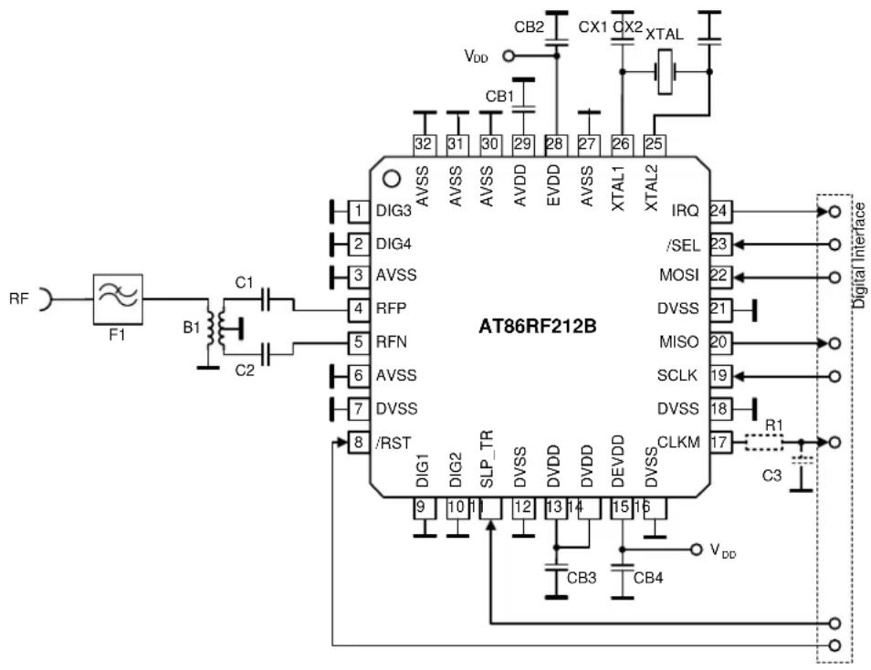
1 Pin-out Diagram
Figure 1-1. Atmel AT86RF212B Pin-out Diagram.

text_image
AVSS AVSS AVDD AVDD AVSS XTAL1 XTAL2 32 31 30 29 28 27 26 25 DIG3 1 DIG4 2 AVSS RFP 3 RFN 4 AVSS 5 DVSS 6 /RST 7 AT86RF212B 9 10 11 12 13 14 15 16 DIG1 DIG2 SLP_TR DVSS DVDD DVDD DEVDD DVSS exposed paddle 24 IRQ 23 /SEL 22 MOSI 21 DVSS 20 MISO 19 SCLK 18 DVSS 17 CLKMNote: 1. The exposed paddle is electrically connected to the die inside the package. It shall be soldered to the board to ensure electrical and thermal contact and good mechanical stability.
1.1 Pin Descriptions
Table 1-1. Atmel AT86RF212B Pin Description.
| Pins | Name | Type | Description |
| 1 | DIG3 | Digital output (Ground) | 1. RX/TX Indication, see Section 11.42. If disabled, pull-down enabled (AVSS) |
| 2 | DIG4 | Digital output (Ground) | 1. RX/TX Indication (DIG3 inverted), see Section 11.42. If disabled, pull-down enabled (AVSS) |
| 3 | AVSS | Ground | Ground for RF signals |
| 4 | RFP | RF I/O | Differential RF signal |
| 5 | RFN | RF I/O | Differential RF signal |
| 6 | AVSS | Ground | Ground for RF signals |
| 7 DVSS Ground Digital ground | |||
| 8 | /RST | Digital input | Chip reset; active low |
| 9 | DIG1 | Digital output (Ground) | 1. Antenna Diversity RF switch control, see Section 11.32. If disabled, pull-down enabled (DVSS) |
| 10 | DIG2 | Digital output (Ground) | 1. Antenna Diversity RF switch control (DIG1 inverted), see Section 11.32. RX Frame Time Stamping, see Section 11.53. If functions disabled, pull-down enabled (DVSS) |
| 11 | SLP_TR | Digital input | Controls sleep, transmit start, and receive states; active high; see Section 6.6 |
| 12 | DVSS | Ground | Digital ground |
| 13, 14 | DVDD | Supply | Regulated 1.8V voltage regulator output or regulated voltage input; digital domain, see Section 9.5 |
| 15 | DEVDD | Supply | External supply voltage; digital domain |
| 16 | DVSS | Ground | Digital ground |
| 17 | CLKM | Digital output | Master clock signal output; low if disabled, see Section 9.7 |
| 18 | DVSS | Ground | Digital ground |
| 19 | SCLK | Digital input | SPI clock |
| 20 | MISO | Digital output | SPI data output (master input slave output) |
| 21 | DVSS | Ground | Digital ground |
| 22 | MOSI | Digital input | SPI data input (master output slave input) |
| 23 | /SEL | Digital input | SPI select, active low |
| 24 | IRQ | Digital output | 1. Interrupt request signal; active high or active low; configurable, see Section 6.72. Frame Buffer Empty Indicator; active high, see Section 11.6 |
| 25 | XTAL2 | Analog input | Crystal pin, see Section 9.7 |
| 26 | XTAL1 | Analog input | Crystal pin or external clock supply, see Section 9.7 |
| 27 | AVSS | Ground | Analog ground |
| 28 | EVDD | Supply | External supply voltage, analog domain |
| 29 | AVDD | Supply | Regulated 1.8V voltage regulator output or regulated voltage input; analog domain, see Section 9.5 |
| 30, 31, 32 | AVSS | Ground | Analog ground |
| Paddle | AVSS | Ground | Analog ground; Exposed paddle of QFN package |
1.2 Analog and RF Pins
1.2.1 Supply and Ground Pins
EVDD, DEVDD
EVDD and DEVDD are analog and digital supply voltage pins of the Atmel® AT86RF212B radio transceiver.
AVDD, DVDD
AVDD and DVDD are outputs of the internal voltage regulators and require bypass capacitors for stable operation. The voltage regulators are controlled independently by the radio transceivers state machine and are activated depending on the current radio transceiver state. The voltage regulators can be configured for external supply; for details, refer to Section 9.5.
AVSS, DVSS
AVSS and DVSS are analog and digital ground pins respectively. The analog and digital power domains should be separated on the PCB.
1.2.2 RF Pins
RFN, RFP
A differential RF port (RFP/RFN) provides common-mode rejection to suppress the switching noise of the internal digital signal processing blocks. At board-level, the differential RF layout ensures high receiver sensitivity by reducing spurious emissions originated from other digital ICs such as a microcontroller.
The RF port is designed for a 100Ω differential load. A DC path between the RF pins is allowed; a DC path to ground or supply voltage is not allowed. Therefore, when connecting an RF-load providing a DC path to the power supply or ground, AC-coupling is required as indicated in Table 1-2.
A simplified schematic of the RF front end is shown in Figure 1-2.
Figure 1-2. Simplified RF Front-end Schematic.
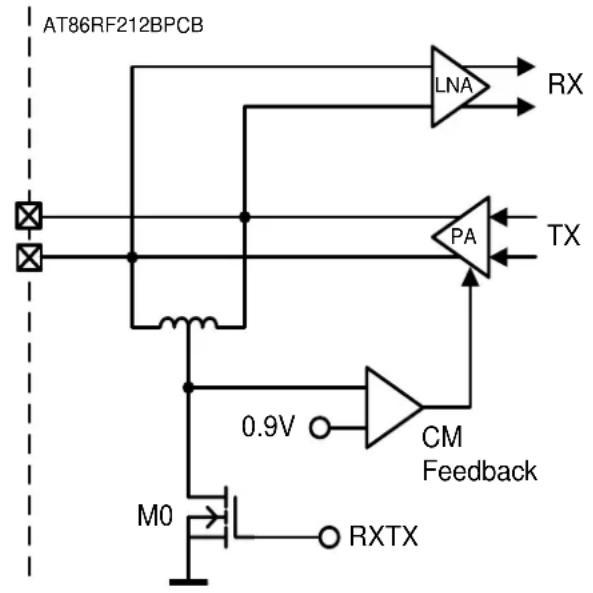
text_image
AT86RF212BPCB LNA RX PA TX 0.9V CM Feedback M0 RXTXThe RF port DC values depend on the operating state; refer to Chapter 7. In TRX_OFF state, when the analog front-end is disabled (see Section 7.1.2.3), the RF pins are pulled to ground, preventing a floating voltage larger than 1.8V which is not allowed for the internal circuitry.
In transmit mode, a control loop provides a common-mode voltage of 0.9V. Transistor M0 is off, allowing the PA to set the common-mode voltage. The common-mode capacitance at each pin to ground shall be <100pF to ensure the stability of this common-mode feedback loop.
In receive mode, the RF port provides a low-impedance path to ground when transistor M0 (see Figure 1-2) pulls the inductor center tap to ground. A DC voltage drop of 20mV across the on-chip inductor can be measured at the RF pins.
1.2.3 Crystal Oscillator Pins
XTAL1, XTAL2
The pin 26 (XTAL1) of Atmel AT86RF212B is the input of the reference oscillator amplifier (XOSC), the pin 25 (XTAL2) is the output. A detailed description of the crystal oscillator setup and the related XTAL1/XTAL2 pin configuration can be found in Section 9.7.
When using an external clock reference signal, XTAL1 shall be used as input pin. For further details, refer to Section 9.7.3.
1.2.4 Analog Pin Summary
Table 1-2. Analog Pin Behavior – DC Values.
| Pin | Values and Conditions | Comments |
| RFP/RFN V | _DC = 0.9V (BUSY\_TX) V_DC = 20mV (receive states) V_DC = 0mV (otherwise) | DC level at pins RFP/RFN for various transceiver states.AC coupling is required if a circuitry with a DC path to ground or supply is used. Serial capacitance and capacitance of each pin to ground must be < 100pF. |
| XTAL1/XTAL2 V | _DC = 0.9V at both pins C_PAR = 3pF | DC level at pins XTAL1/XTAL2 for various transceiver states.Parasitic capacitance ( C_PAR ) of the pins must be considered as additional load capacitance to the crystal. |
| DVDD V | _DC = 1.8V (all states, except SLEEP) V_DC = 0mV (otherwise) | DC level at pin DVDD for various transceiver states.Supply pins (voltage regulator output) for the digital 1.8V voltage domain. The outputs shall be bypassed by 1μF. |
| AVDD V | _DC = 1.8V (all states, except P_ON, SLEEP, RESET, and TRX_OFF) V_DC = 0mV (otherwise) | DC level at pin AVDD for various transceiver states.Supply pin (voltage regulator output) for the analog 1.8V voltage domain. The outputs shall be bypassed by 1μF. |
1.3 Digital Pins
The Atmel AT86RF212B provides a digital microcontroller interface. The interface comprises a slave SPI (/SEL, SCLK, MOSI, and MISO) and additional control signals (CLKM, IRQ, SLP_TR, /RST, and DIG2). The microcontroller interface is described in detail in Chapter 6.
Additional digital output signals DIG1, ..., DIG4 are provided to control external blocks, that is for Antenna Diversity RF switch control or as an RX/TX Indicator; see Section 11.3 and Section 11.4 respectively.
1.3.1 Driver Strength Settings
The driver strength of all digital output pins (MISO, IRQ, DIG1, ..., DIG4) and CLKM pin can be configured using register bits PAD_IO and PAD_IO_CLKM (register 0x03, TRX_CTRL_0); see Table 1-3.
Table 1-3. Digital Output Driver Configuration.
| Pin | Default Driver Strength | Comment |
| MISO, IRQ, DIG1, ..., DIG4 | 2mA | Adjustable to 2mA, 4mA, 6mA, and 8mA |
| CLKM | 4mA | Adjustable to 2mA, 4mA, 6mA, and 8mA |
The capacitive load should be as small as possible and not larger than 50pF when using the 2mA minimum driver strength setting. Generally, the output driver strength should be adjusted to the lowest possible value in order to keep the current consumption and the emission of digital signal harmonics low.
1.3.2 Pull-up and Pull-down Configuration
Pulling transistors (10 A current source) are internally connected to all digital input pins in radio transceiver state P_ON, including reset during P_ON; refer to Section 7.1.2.1 and Section 7.1.2.8.
Table 1-4 summarizes the pull-up and pull-down configuration.
Table 1-4. Pull-Up / Pull-Down Configuration of Digital Input Pins.
| Pin H | pull-up, L pull-down |
| /RST H | |
| /SEL H | |
| SCLK | L |
| MOSI | L |
| SLP_TR | L |
In all other radio transceiver states, including RESET, no pull-up or pull-down transistors are connected to any of the digital input pins mentioned in Table 1-4.
Note: 1. In all other states, external circuitry should guaranty defined levels at all input pins. Floating input pins may cause unexpected functionality and increased power consumption, for example in SLEEP state.
If the additional digital output signals DIG1, ..., DIG4 are not activated, these pins are pulled-down to digital ground (DIG1/DIG2) or analog ground (DIG3/DIG4).
1.3.3 Register Description
Note: 1. Throughout this datasheet, underlined values indicate reset settings.
Register 0x03 (TRX\_CTRL\_0):
The TRX_CTRL_0 register controls the driver current of the digital output pads and the CLKM clock rate.
Figure 1-3. Register TRX_CTRL_0.
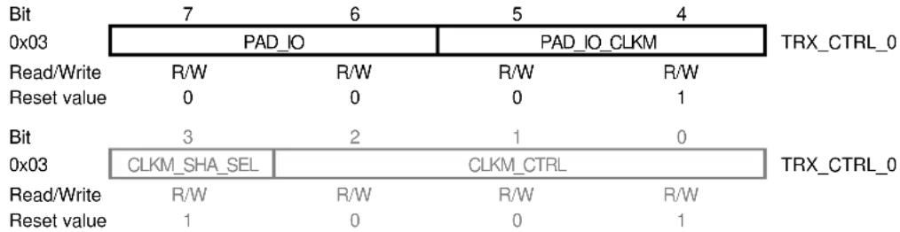
- Bit 7:6 - PAD\_IO
These register bits set the output driver current of digital output pads, except CLKM.
Table 1-5. PAD_IO.
| Register Bits Value Descriptio | n | |
| PAD_IO 0 2mA | - | |
| 1 4mA | ||
| 2 6mA | ||
| 3 8mA | ||
Note: 1. Selecting low-level driver current reduces power consumption and minimizes transceiver's harmonic distortion.
- Bit 5:4 - PAD\_IO\_CLKM
These register bits set the output driver current of pin CLKM. It is recommended to reduce the driver strength to 2mA (PAD_IO_CLKM = 0) if possible. This reduces power consumption and spurious emissions.
Table 1-6. PAD_IO_CLKM.
| Register Bits | Value | Description |
| PAD_IO_CLKM 0 2mA | ||
| 1 4mA | ||
| 2 6mA | ||
| 3 8mA | ||
2 Disclaimer
Typical values contained in this datasheet are based on simulations and testing. Minimum and maximum values are available when the radio transceiver has been fully characterized.
3 Overview
The Atmel AT86RF212B is a low-power, low-voltage 700/800/900MHz transceiver specially designed for the ZigBee/IEEE 802.15.4, 6LoWPAN, and high data rate sub-1GHz ISM applications.
For the sub-1GHz bands, all modulation schemes and data rates according to IEEE 802.15.4-2003 [1], IEEE 802.15.4-2006 [2] standards, and the respective 802.15.4c-2009 [3] amendment are supported. All these PHY modes are summarized in IEEE 802.15.4-2011 [4] Standard. Furthermore, proprietary High Data Rate Modes up to 1000kb/s can be employed.
The AT86RF212B is a true SPI-to-antenna solution. All RF-critical components except the antenna, crystal, and de-coupling capacitors are integrated on-chip. MAC and AES hardware accelerators improve overall system power efficiency and timing. Therefore, the AT86RF212B is particularly suitable for applications like:
- Sub-1GHz IEEE 802.15.4 and ZigBee systems
• Energy Harvesting systems - 6LoWPAN systems
- Wireless sensor networks
- Industrial Control
• Residential and commercial automation - Health care
- Consumer electronics
- PC peripherals
The AT86RF212B can be operated by using an external microcontroller like Atmel AVR ^® microcontrollers. A comprehensive software programming description can be found in reference [11].
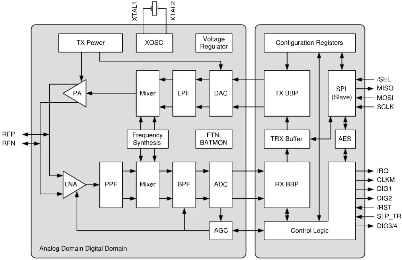
4 General Circuit Description
The Atmel AT86RF212B single-chip radio transceiver provides a complete radio transceiver interface between an antenna and a microcontroller. It comprises the analog radio, digital modulation and demodulation including time and frequency synchronization, as well as data buffering. A single 128-byte TRX buffer stores receive or transmit data. Communication between transmitter and receiver is based on direct sequence spread spectrum with different modulation schemes and spreading codes.
The AT86RF212B diagram is shown in Figure 4-1.
Figure 4-1. AT86RF212B Block Diagram.
flowchart
graph TD
    subgraph_Analog_Domain_Digital_Domain["Analog Domain Digital Domain"]
        A["TX Power"] --> B["PA"]
        C["XOSC"] --> D["Mixer"]
        E["Voltage Regulator"] --> F["DAC"]
        G["RFP"] --> H["LNA"]
        I["RFN"] --> H
        J["XTAL1"] --> K["XTAL2"]
        L["XTAL1"] --> M["XTAL2"]
        N["XTAL2"] --> O["XTAL1"]
        P["Configuration Registers"] --> Q["TX BBP"]
        Q --> R["SPI (Slave)"]
        S["Configuration Registers"] --> T["TRX Buffer"]
        U["Configuration Registers"] --> V["AES"]
        W["Configuration Registers"] --> X["RX BBP"]
        Y["Configuration Registers"] --> Z["Control Logic"]
    end

    B --> C
    D --> F
    F --> G
    G --> H
    H --> I
    I --> J
    J --> K
    K --> L
    L --> M
    M --> N
    N --> O
    O --> P
    P --> Q
    Q --> R
    R --> S
    S --> T
    T --> U
    U --> V
    V --> X
    X --> Z
    Z --> Y
    Y --> Z
    style Analog_Domain_Digital_Domain fill:#f9f9f9,stroke:#333
    style Analog_Domain_Digital_Domain fill:#e6f7ff,stroke:#333
The number of external components is minimized so that only the antenna, a filter (at high output power levels), the crystal, and four bypass capacitors are required. The bidirectional differential antenna pins (RFP, RFN) are used for transmission and reception, thus no external antenna switch is needed. Control of an external power amplifier is supported by two digital control signals (differential operation).
The AT86RF212B supports the IEEE 802.15.4-2006 [2] standard mandatory BPSK modulation and optional O-QPSK modulation in the 868.3MHz and 915MHz bands. In addition, it supports the O-QPSK modulation defined in IEEE 802.15.4-2011 [4] for the Chinese 780MHz band. For applications not necessarily targeting IEEE compliant networks, the radio transceiver supports proprietary High Data Rate Modes based on O-QPSK.
Atmel®
The Atmel AT86RF212B features hardware supported 128-bit security operation. The standalone AES encryption/decryption engine can be accessed in parallel to all PHY operational modes. Configuration of the AT86RF212B, reading and writing of data memory, as well as the AES hardware engine are controlled by the SPI interface and additional control signals.
On-chip low-dropout voltage regulators provide regulated analog and digital 1.8V power supply outputs. Control registers retain their settings in sleep mode when the regulators are turned off. The RX and TX signal processing paths are highly integrated and optimized for low power consumption.
Additional features of the Extended Feature Set, see Chapter 11, are provided to simplify the interaction between radio transceiver and microcontroller.
5 Application Schematic
5.1 Basic Application Schematic
A basic application schematic of the Atmel AT86RF212B with a single-ended RF connector is shown in Figure 5-1. The 50Ω single-ended RF input is transformed to the 100Ω differential RF port impedance using balun B1. The capacitors C1 and C2 provide AC coupling of the RF input to the RF port. If the balun pins at the differential side provide no DC path to ground and to the single-ended pin, the capacitors are not necessary.
Regulatory rules like FCC 47 CFR Section 15.247 [5], ETSI EN 300 220-1 [6], and ERC/REC 70-03 [7] may require an external filter F1, depending on used transmit power levels.
Figure 5-1. Basic Application Schematic.
text_image
RF F1 B1 C1 C2 AT86RF212B DIG3 1 2 3 4 5 6 7 8 /RSST DIG1 9 10 11 12 13 14 15 16 DVSS AVSS AVSS AVDD EVDD AVSS XTAL1 XTAL2 CB2 CB1 CX1 CX2 XTAL VDD CB3 CB4 VDD IRQ /SEL MOSI DVSS MISO SCLK DVSS CLKM R1 C3 Digital InterfaceThe power supply decoupling capacitors (CB2, CB4) are connected to the external analog supply pin 28 (EVDD) and external digital supply pin 15 (DEVDD). Capacitors CB1 and CB3 are bypass capacitors for the integrated analog and digital voltage regulators to ensure stable operation. All bypass capacitors should be placed as close as possible to the pins and should have a low-resistance and low-inductance connection to ground to achieve the best performance.
The crystal (XTAL), the two load capacitors (CX1, CX2), and the internal circuitry connected to pins XTAL1 and XTAL2 form the crystal oscillator. To achieve the best accuracy and stability of the reference frequency, large parasitic capacitances should be avoided. Crystal lines should be routed as short as possible and not in proximity of
digital I/O signals. This is especially required for the High Data Rate Modes; refer to Section 9.1.4.
Crosstalk from digital signals on the crystal pins or the RF pins can degrade the system performance. Therefore, a low-pass filter (C3, R1) is placed close to the Atmel AT86RF212B CLKM output pin to reduce the emission of CLKM signal harmonics. This is not needed if pin 17 (CLKM) is not used as a microcontroller clock source. In this case, pin 17 (CLKM) output should be disabled during device initialization.
The ground plane of the application board should be separated into four independent fragments: the analog, the digital, the antenna, and the XTAL ground plane. The exposed paddle shall act as the reference point of the individual grounds.
Note: 1. The pins DIG1, DIG2, DIG3, and DIG4 are connected to ground in the Basic Application Schematic; refer to Figure 5-1. Special programming of these pins requires a different schematic; refer to Section 5.2.
Table 5-1. Exemplary Bill of Materials (BoM) for Basic Application Schematic.
| Symbol | Description | Value | Manufacturer | Part Number | Comment |
| B1 | SMD balun | 800 – 1000MHz | WuerthJTI | 7484310900900BL18B100 | |
| F1 | SMD low pass filter | 902 – 928MHz | WuerthJTI | 7481310090915LP15A026 | |
| B1 + F1(alternatively) | Balun/Filter combination | 863 – 928MHz | JTI | 0896FB15A0100 | |
| 779 – 787MHz | JTI | 0783FB15A0100 | |||
| CB1CB3 | LDO VREGbypass capacitor | 1 F | AVXMurata | 0603YD105KAT2AGRM188R61E105KA12 | X5R 10% 16V(0603)X5R 15% 25V(0603) |
| CB2CB4 | Power supply bypasscapacitor | ||||
| CX1, CX2 | Crystal load capacitor | 12pF | AVXMurata | 06035A120JAGRM1555C1H120JA01 | C0G 5% 50V(0402 or 0603) |
| C1, C2 | RF coupling capacitor | 100pF | EpcosEpcosAVX | B37930B3792006035A680JAT2A | C0G 5% 50V(0402 or 0603) |
| C3 | CLKM low-pasfilter capacitor | 2.2pF | AVXMurata | 06035A229DAGRP1886C1H2R0DA01 | COG ± 0.5pF 50V(0603)Designed for fCLKM = 1MHz |
| R1 | CLKM low-passfilter resistor | 680Ω | Designed for fCLKM = 1MHz | ||
| XTAL | Crystal | CX-4025 16MHzSX-4025 16MHz | ACAL TaitjenSiward | XWBBPL-F-1A207-011 |
5.2 Extended Feature Set Application Schematic
The Atmel AT86RF212B supports additional features like:
• Security Module (AES) Section 11.1
- Random Number Generator Section 11.2
- Antenna Diversity uses pins DIG1(/2) Section 11.3
- RX/TX Indicator uses pins DIG3/4 Section 11.4
- RX Frame Time Stamping uses pin DIG2 Section 11.5
• Frame Buffer Empty Indicator uses pin IRQ Section 11.6
• Dynamic Frame Buffer Protection Section 11.7
• Alternate Start-Of-Frame Delimiter Section 11.8
An extended feature set application schematic illustrating the use of the AT86RF212B Extended Feature Set, see Chapter 11, is shown in Figure 5-2. Although this example shows all additional hardware features combined, it is possible to use all features separately or in various combinations.
Figure 5-2. Extended Feature Application Schematic.

flowchart
graph TD
    ANT0["ANT0"] --> RF_Switch["RF-Switch"]
    SW2["SW2"] --> RF_Switch
    ANT1["ANT1"] --> RF_Switch
    RF_Switch --> F1["F1"]
    F1 --> LNA["LNA"]
    LNA --> PA["PA"]
    PA --> SW1["SW1"]
    SW1 --> B1["B1"]
    B1 --> C1["C1"]
    C1 --> D1["DIG3"]
    D1 --> AVSS1["AVSS"]
    D1 --> AVSS2["AVSS"]
    D1 --> AVSS3["AVSS"]
    D1 --> AVSS4["AVDD"]
    D1 --> AVSS5["EVDD"]
    D1 --> AVSS6["AVSS"]
    D1 --> AVSS7["XTAL1"]
    D1 --> AVSS8["XTAL2"]
    AVSS1 --> AT86RF212B["AT86RF212B"]
    AVSS2 --> AT86RF212B
    AVSS3 --> AT86RF212B
    AVSS4 --> AT86RF212B
    AVSS5 --> AT86RF212B
    AVSS6 --> AT86RF212B
    AVSS7 --> AT86RF212B
    AVSS8 --> AT86RF212B
    AT86RF212B --> R1["R1"]
    AT86RF212B --> SCLK["SCLK"]
    AT86RF212B --> CLKM["CLKM"]
    AT86RF212B --> DVSS["VDS"]
    AT86RF212B --> DVDD["VDD"]
    AT86RF212B --> DVDDD["VDD"]
    AT86RF212B --> DVDD["DVDD"]
    AT86RF212B --> DVDDD["DVDD"]
    AT86RF212B --> DVDD["DVSS"]
    AT86RF212B --> DVSSD["DVSS"]
    AT86RF212B --> DVSSE["DVSS"]
    AT86RF212B --> DVSSF["DVSS"]
    AT86RF212B --> DVSSG["CVS"]
    AT86RF212B --> DVSSH["CVS"]
    AT86RF212B --> DVSSI["CVS"]
    AT86RF212B --> DVSSJ["CVS"]
    AT86RF212B --> DVSSK["CVS"]
    AT86RF212B --> DVSSL["CVS"]
    AT86RF212B --> DVSSM["CVS"]
    AT86RF212B --> DVSSN["CVS"]
    AT86RF212B --> DVSSO["CVS"]
    AT86RF212B --> DVSSP["CVS"]
    AT86RF212B --> DVSSQ["CVS"]
    AT86RF212B --> DVSSR["CVS"]
    AT86RF212B --> DVSSS["CVS"]
    AT86RF212B --> DVSST["CVS"]
    AT86RF212B --> DVSSU["CVS"]
    AT86RF212B --> DVSSV["CVS"]
    AT86RF212B --> DVSSW["CVS"]
    AT86RF212B --> DVSSX["CVS"]
    AT86RF212B --> DVSSY["CVS"]
    AT86RF212B --> DVSSZ["CVS"]
    AT86RF212B --> DVSSR["CVS"]
    AT86RF212B --> DVSSS["CVS"]
    AT86RF212B --> DVSST["CVS"]
    AT86RF212B --> DVSSU["CVS"]
    AT86RF212B --> DVSSV["CVS"]
    AT86RF212B --> SVLS["SLP_TR"]
    AT86RF212B --> VDD["V_DD"]

    subgraph Digital Interface
        direction TB
        A["AT86RF212B"] --> B["AVSS"]
        A --> C["AVSS"]
        A --> D["AVSS"]
        A --> E["MISO"]
        A --> F["MISO"]
        A --> G["SCLK"]
        A --> H["R1"]
        A --> I["C3"]
        J["Digital Interface"] --> K["AT86RF212B"]
Atmel®
In this example, a balun (B1) transforms the differential RF signal at the Atmel AT86RF212B radio transceiver RF pins (RFP/RFN) to a single ended RF signal, similar to the Basic Application Schematic; refer to Figure 5-1. The RF switches (SW1, SW2) separate between receive and transmit path in an external RF front-end. These switches are controlled by the RX/TX Indicator, represented by the differential pin pair DIG3/DIG4; refer to Section 11.4.
During receive, the corresponding microcontroller may search for the most reliable RF signal path using an Antenna Diversity algorithm or stored statistic data of link signal quality. One antenna is selected by an RF switch (SW2) controlled by pin 9 (DIG1) ^(1) . The RF signal is amplified by an optional low-noise amplifier (N2) and fed to the radio transceiver using an RX/TX switch (SW1).
During transmit, the AT86RF212B TX signal is amplified using an external PA (N1), low pass filtered to suppress spurious harmonics emission, and fed to the antennas via an RF switch (SW2). In this example, RF switch SW2 further supports Antenna Diversity controlled by pin 9 (DIG1) ^(1) .
Note: 1. DIG1/DIG2 can be used as a differential pin pair to control an RF switch if RX Frame Time Stamping is not used; refer to Section 11.3 and Section 11.5.
The Security Module (AES), Random Number Generator, Frame Buffer Empty Indicator, Dynamic Frame Buffer Protection or Alternate Start-Of-Frame Delimiter do not require specific circuitry to operate, for details refer to Section 11.1, Section 11.2, Section 11.6, Section 11.7 and Section 11.8.
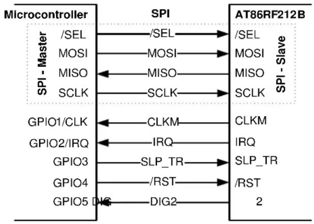
6 Microcontroller Interface
6.1 Overview
This section describes the Atmel AT86RF212B to microcontroller interface. The interface comprises a slave SPI and additional control signals; see Figure 6-1. The SPI timing and protocol are described below.
Figure 6-1. Microcontroller to AT86RF212B Interface.
flowchart
graph LR
    A["Microcontroller"] -->|/SEL| B["SPI - Master"]
    A -->|MOSI| B
    A -->|MISO| B
    A -->|SCLK| B
    A -->|GPIO1/CLK| B
    A -->|GPIO2/IRQ| B
    A -->|GPIO3| B
    A -->|GPIO4| B
    A -->|GPIO5 DIG| B
    B -->|/SEL| C["AT86RF212B"]
    B -->|MOSI| C
    B -->|MISO| C
    B -->|SCLK| C
    B -->|CLKM| C
    B -->|IRQ| C
    B -->|SLP_TR| C
    B -->|/RST| C
    B -->|DIG2| C
    C -->|/SEL| D["SPI - Slave"]
    C -->|MOSI| D
    C -->|MISO| D
    C -->|SCLK| D
    C -->|CLKM| D
    C -->|IRQ| D
    C -->|SLP_TR| D
    C -->|/RST| D
    C -->|2| D
Microcontrollers with a master SPI such as Atmel AVR family interface directly to the AT86RF212B. The SPI is used for register, Frame Buffer, SRAM, and AES access. The additional control signals are connected to the GPIO/IRQ interface of the microcontroller. Table 6-1 introduces the radio transceiver I/O signals and their functionality.
Table 6-1. Signal Description of Microcontroller Interface.
| Signal | Description |
| /SEL | SPI select signal, active low |
| MOSI | SPI data (master output slave input) signal |
| MISO | SPI data (master input slave output) signal |
| SCLK | SPI clock signal |
| CLKM | Optional, Clock output, refer to Section 9.7.4, usable as:- microcontroller clock source and/or MAC timer reference- high precision timing reference |
| IRQ | Interrupt request signal, further used as:- Frame Buffer Empty indicator; refer to Section 11.6 |
| SLP_TR | Multi purpose control signal (functionality is state dependent, see Section 6.6):- Sleep/Wakeup enable/disable SLEEP state- TX start BUSY_TX_(ARET) state- disable/enable CLKM |
| /RST | AT86RF212B reset signal; active low |
| DIG2 | Optional,- IRQ_2 (RX_START) for RX Frame Time Stamping, see Section 11.5 |
6.2 SPI Timing Description
Pin 17 (CLKM) can be used as a microcontroller master clock source. If the microcontroller derives the SPI master clock (SCLK) directly from CLKM, the SPI operates in synchronous mode, otherwise in asynchronous mode.
In asynchronous mode, the maximum SCLK frequency f_async is limited to 7.5MHz. The signal at pin 17 (CLKM) is not required to derive SCLK and may be disabled to reduced power consumption and spurious emissions.
Figure 6-2 and Figure 6-3 illustrate the SPI timing and introduces its parameters. The corresponding timing parameter definitions t_1 - t_9 are defined in Section 12.4.
Figure 6-2. SPI Timing, Global Map and Definition of Timing Parameters t_5 , t_6 , t_8 , t_9 .

text_image
/SEL SCLK MOSI MISO t₅ t₆ t₉ t₈Figure 6-3. SPI Timing, Detailed Drawing of Timing Parameters t_1 to t_4 .
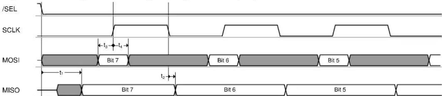
text_image
/SEL SCLK MOSI MISO t1 t2 Bit 7 Bit 6 Bit 5 Bit 7 Bit 6 Bit 5The SPI is based on a byte-oriented protocol and is always a bidirectional communication between the master and slave. The SPI master starts the transfer by asserting /SEL = L. Then the master generates eight SPI clock cycles to transfer one byte to the radio transceiver (via MOSI). At the same time, the slave transmits one byte to the master (via MISO). When the master wants to receive one byte of data from the slave, it must also transmit one byte to the slave. All bytes are transferred with the MSB first. An SPI transaction is finished by releasing /SEL = H.
An SPI register access consists of two bytes, a Frame Buffer or SRAM access of at least two or more bytes as described in Section 6.3.
/SEL = L enables the MISO output driver of the Atmel AT86RF212B. The MSB of MISO is valid after t_1 (see Section 12.4) and is updated on each SCLK falling edge. If the driver is disabled, there is no internal pull-up transistor connected to it. Driving the appropriate signal level must be ensured by the master device or an external pull-up resistor.
Note: 1. When both /SEL and /RST are active, the MISO output driver is also enabled.
Referring to Figure 6-2 and Figure 6-3, Atmel AT86RF212B MOSI is sampled at the rising edge of the SCLK signal and the output is set at the falling edge of SCLK. The signal must be stable before and after the rising edge of SCLK as specified by t_3 and t_4 , refer to Section 12.4 parameters.
This SPI operational mode is commonly known as "SPI mode 0".
6.3 SPI Protocol
Each SPI sequence starts with transferring a command byte from the SPI master via MOSI (see Table 6-2) with the MSB first. This command byte defines the SPI access mode and additional mode-dependent information.
Table 6-2. SPI Command Byte Definition.
| Bit 7 | Bit 6 | Bit 5 | Bit 4 | Bit 3 | Bit 2 | Bit 1 | Bit 0 | Access Mode | Access Type |
| 1 | 0 | Register address [5:0] | Register access | Read access | |||||
| 1 | 1 | Register address [5:0] | Write access | ||||||
| 0 | 0 | 1 | Reserved | Frame Buffer access | Read access | ||||
| 0 1 1 | Reserved | Write access | |||||||
| 0 0 0 | Reserved | SRAM access | Read access | ||||||
| 0 1 0 | Reserved | Write access | |||||||
Each SPI transfer returns bytes back to the SPI master on MISO output pin. The content of the first byte (see value "PHY_STATUS" in Figure 6-4 to Figure 6-14) is set to zero after reset. To transfer status information of the radio transceiver to the microcontroller, the content of the first byte can be configured with register bits SPI_CMD_MODE (register 0x04, TRX_CTRL_1). For details, refer to Section 6.4.1.
Note: 1. Return values on MISO stated as XX shall be ignored by the microcontroller.
The different access modes are described within the following sections.
6.3.1 Register Access Mode
Register Access Mode is used to read and write AT86RF212B registers (register address from 0x00 up to 0x3F).
A register access mode is a two-byte read/write operation initiated by /SEL = L. The first transferred byte on MOSI is the command byte including an identifier bit (bit[7] = 1), a read/write select bit (bit[6]), and a 6-bit register address.
On read access, the content of the selected register address is returned in the second byte on MISO (see Figure 6-4).
Figure 6-4. Packet Structure - Register Read Access.

text_image
byte 1 (command byte) byte 2 (data byte) MOSI 1 0 ADDRESS[5:0] XX MISO PHY_STATUS(1) READ DATA[7:0]Note: 1. Each SPI access can be configured to return radio controller status information (PHY_STATUS) on MISO, for details refer to Section 6.4.
On write access, the second byte transferred on MOSI contains the write data to the selected address (see Figure 6-5).
Figure 6-5. Packet Structure - Register Write Access.

text_image
byte 1 (command byte) by 2 (data-byte) 1 ADDYRES[DATA[7:0]MO$I PHY_STATUS XXMISOEach register access must be terminated by setting /SEL = H.
Figure 6-6 illustrates a typical SPI sequence for a register access sequence for write and read respectively.
Figure 6-6. Exemplary SPI Sequence – Register Access Mode.
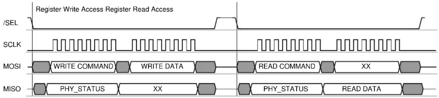
text_image
/SEL Register Write Access Register Read Access SCLK MOSI WRITE COMMAND WRITE DATA READ COMMAND XX MISO PHY_STATUS XX PHY_STATUS READ DATA6.3.2 Frame Buffer Access Mode
Frame Buffer Access Mode is used to read and write Atmel AT86RF212B frame buffer. The frame buffer address is always reset to zero and incremented to access PSDU, LQI, ED and RX_STATUS data.
The Frame Buffer can hold up to 128-byte of one PHY service data unit (PSDU) IEEE 802.15.4 data frame. A detailed description of the Frame Buffer can be found in Section 9.4. An introduction to the IEEE 802.15.4 frame format can be found in Section 8.1.
Each access starts with /SEL = L followed by a command byte on MOSI. Each frame read or write access command byte is followed by the PHR data byte, indicating the frame length, followed by the PSDU data, see Figure 6-7 and Figure 6-8.
In Frame Buffer Access Mode during buffer reads, the PHY header (PHR) and the PSDU data are transferred via MISO following PHY_STATUS byte. Once the PSDU data is uploaded, three more bytes are transferred containing the link quality indication (LQI) value, the energy detection (ED) value, and the status information (RX_STATUS) of the received frame, for LQI details refer to Section 8.8. The Figure 6-7 illustrates the packet structure of a Frame Buffer read access.
Note: 1. The frame buffer read access can be terminated immediately at any time by setting pin 23 (/SEL) = H, for example after reading the PHR byte only.
Figure 6-7. Packet Structure - Frame Read Access.

text_image
byte 1 (command byte) byte 2 (data byte) byte 3 (data byte) MOSI 0 0 1 reserved[4:0] XX XX ... MISO PHY_STATUS PHR[7:0] PSDU[7:0] ... byte n-1 (data byte) byte n (data byte) XX XX ED[7:0] RX_STATUS[7:0]The structure of RX_STATUS is described in Table 6-3.
Table 6-3. Structure of RX_STATUS.
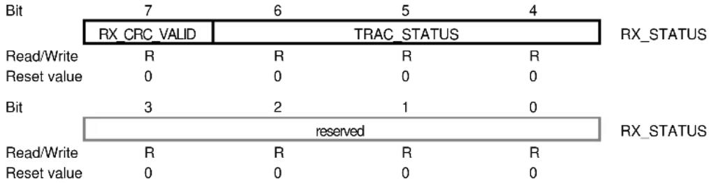
text_image
Bit 7 6 5 4 RX_CRC_VALID TRAC_STATUS RX_STATUS Read/Write R R R R Reset value 0 0 0 0 Bit 3 2 1 0 reserved RX_STATUS Read/Write R R R R Reset value 0 0 0 0Note: 2. More information to RX_CRC_VALID, see Section 8.3.5, and to TRAC_STATUS, see Section 7.2.6.
On frame buffer write access, the second byte transferred on MOSI contains the frame length (PHR field) followed by the payload data (PSDU) as shown in Figure 6-8.
Figure 6-8. Packet Structure - Frame Write Access.

text_image
byte 1 (command byte) byte 2 (data byte) byte 3 (data byte) MOSI 0 1 1 reserved[4:0] PHR[7:0] PSDU[7:0] MISO PHY_STATUS XX XX byte n-1 (data byte) byte n (data byte) ... PSDU[7:0] PSDU[7:0] ... XX XXThe number of bytes n for one frame buffer access is calculated as follows:
Read Access: n = 5 + frame_length
[PHY_STATUS, PHR byte, PSDU data, LQI, ED, and RX_STATUS]
Write Access: n = 2 + frame_length
[command byte, PHR byte, and PSDU data]
The maximum value of frame_length is 127 bytes. That means that n ≤ 132 for Frame Buffer read and n ≤ 129 for Frame Buffer write accesses.
Each read or write of a data byte automatically increments the address counter of the Frame Buffer until the access is terminated by setting /SEL = H. A Frame Buffer read access can be terminated at any time without any consequences by setting /SEL = H, for example after reading the frame length byte only. A successive Frame Buffer read operation starts again with the PHR field.
The content of the Atmel AT86RF212B Frame Buffer is overwritten by a new received frame or a Frame Buffer write access.
Figure 6-9 and Figure 6-10 illustrate an exemplary SPI sequence of a Frame Buffer access to read a frame with 2-byte PSDU and write a frame with 4-byte PSDU.
Figure 6-9. Exemplary SPI Sequence - Frame Buffer Read of a Frame with 2-byte PSDU.
text_image
SEL SCLK MOSI MISO PHY_STATUS PHR PSDU 1 2PSDU EDLQI RX_STATUSFigure 6-10. Exemplary SPI Sequence - Frame Buffer Write of a Frame with 4-byte PSDU.

text_image
/SEL SCLK MOSI MISO COMMAND PHR PSDU 1 PSDU 2 PSDU 3 PSDU 4 PHY_STATUS XX XX XX XXAccess violations during a Frame Buffer read or write access are indicated by interrupt IRQ_6 (TRX_UR). For further details, refer to Section 9.4.
Notes: 1. The Frame Buffer is shared between RX and TX operations, the frame data is overwritten by freshly received data frames. If an existing TX payload data frame is to be retransmitted, it must be ensured that no TX data is overwritten by newly received RX data.
2. To avoid overwriting during receive Dynamic Frame Buffer Protection can be enabled, refer to Section 11.7.
3. For exceptions, receiving acknowledgement frames in Extended Operating Mode (TX_ARET) refer to Section 7.2.4.
6.3.3 SRAM Access Mode
The SRAM access mode is used to read and write Atmel AT86RF212B frame buffer beginning with a specified byte address. It enables to access dedicated buffer data directly from a desired address without a need of incrementing the frame buffer from the top.
The SRAM access mode allows accessing dedicated bytes within the Frame Buffer or AES address space, refer to Section 11.1. This may reduce the SPI traffic.
During frame receive, after occurrence of IRQ_2 (RX_START), an SRAM access can be used to upload the PHR field while preserving Dynamic Frame Buffer Protection, see Section 11.7.
Each SRAM access starts with /SEL = L. The first transferred byte on MOSI shall be the command byte and must indicate an SRAM access mode according to the definition in Table 6-2. The following byte indicates the start address of the write or read access.
SRAM address space:
• Frame Buffer: 0x00 to 0x7F
• AES: 0x82 to 0x94
On SRAM read access, one or more bytes of read data are transferred on MISO starting with the third byte of the access sequence; refer to Figure 6-11.
Figure 6-11. Packet Structure – SRAM Read Access.
text_image
byte 1 (command byte) → byte 2 (address) → byte 3 (data byte) 0 0MReserved[4:0] ADDRESS[7:0] XX ... PHY_STATUSMISO XX DATA[7:0] ... byte n-1 (data byte) → byte n (data byte)On SRAM write access, one or more bytes of write data are transferred on MOSI starting with the third byte of the access sequence; refer to Figure 6-12. Do not attempt to read or write bytes beyond the SRAM buffer size.
Figure 6-12. Packet Structure – SRAM Write Access.
text_image
byte 1 (command byte) → byte 2 (address) → byte 3 (data byte) 0 | 1MDReserved[4:0] ADDRESS[7:0] DATA[7:0] PHY_STATUSMISO XX XX ... DATA[7:0] DATA[7:0] XX XXAs long as /SEL = L, every subsequent byte read or byte write increments the address counter of the Frame Buffer until the SRAM access is terminated by /SEL = H.
Figure 6-13 and Figure 6-14 illustrate an exemplary SPI sequence of an Atmel AT86RF212B SRAM access to read and write a data package of five byte length, respectively.
Figure 6-13. Exemplary SPI Sequence – SRAM Read Access of a 5-byte Data Package.
text_image
/SEL SCLK MOSI COMMAND ADDRESS XX XX XX XX XX MISO PHY_STATUS XX DATA 1 DATA 2 DATA 3 DATA 4 DATA 5Figure 6-14. Exemplary SPI Sequence – SRAM Write Access of a 5-byte Data Package.

text_image
/SEL SCLK MOSI COMMAND ADDRESS DATA 1 DATA 2 DATA 3 DATA 4 DATA 5 MISO PHY_STATUS XX XX XX XX XXNotes: 1. The SRAM access mode is not intended to be used as an alternative to the Frame Buffer access modes (see Section 6.3.2).
2. Frame Buffer access violations are not indicated by a TRX_UR interrupt when using the SRAM access mode, for further details refer to Section 9.4.3.
6.4 Radio Transceiver Status Information
Each Atmel AT86RF212B SPI access can return radio transceiver status information which is a first byte transmitted out of MISO output as the serial data is being shifted into MOSI input. Radio transceiver status information (PHY_STATUS) can be configured using register bits SPI_CMD_MODE (register 0x04, TRX_CTRL_1) to return TRX_STATUS, PHY_RSSI or IRQ_STATUS register as shown in below.
6.4.1 Register Description
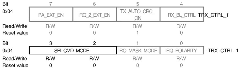
Register 0x04 (TRX\_CTRL\_1):
The TRX_CTRL_1 register is a multi-purpose register to control various operating modes and settings of the radio transceiver.
Figure 6-15. Register TRX_CTRL_1.
text_image
Bit 0x04 7 6 5 4 PA_EXT_EN IRQ_2_EXT_EN TX_AUTO_CRC_ON RX_BL_CTRL TRX_CTRL_1 Read/Write R/W R/W R/W R/W Reset value 0 0 1 0 Bit 3 2 1 0 0x04 SPI_CMD_MODE IRQ_MASK_MODE IRQ_POLARITY TRX_CTRL_1 Read/Write R/W R/W R/W R/W Reset value 0 0 0 0- Bit 3:2 - SPI\_CMD\_MODE
Each SPI transfer returns bytes back to the SPI master. The content of the first byte (PHY_STATUS) can be configured using register bits SPI_CMD_MODE.
Table 6-4. SPI_CMD_MODE.
| Register Bits | Value | Description |
| SPI_CMD_MODE | 0 | Default (empty, all bits zero) |
| 1 Monitor TRX_STATUS register | ||
| 2 Monitor PHY_RSSI register | ||
| 3 Monitor IRQ_STATUS register | ||
6.5 Radio Transceiver Identification
Atmel AT86RF212B can be identified by four registers. One 8-bit register contains a unique part number (PART_NUM) and one register contains the corresponding 8-bit version number (VERSION_NUM). Two additional 8-bit registers contain the JEDEC manufacture ID.
6.5.1 Register Description
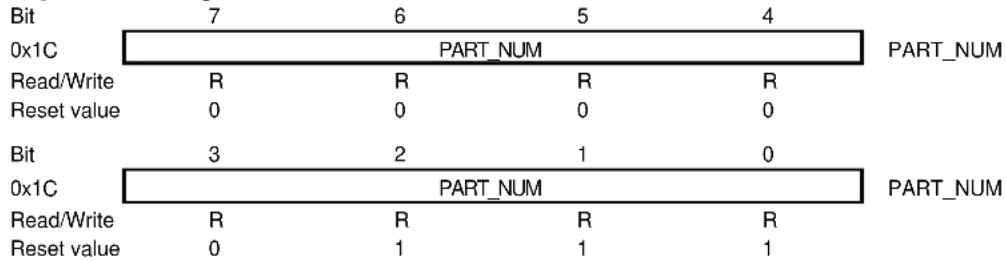
Register 0x1C (PART\_NUM):
The register PART_NUM can be used for the radio transceiver identification and includes the part number of the device.
Figure 6-16. Register PART_NUM.
bar_stacked
| Bit | PART_NUM | PART_NUM | | ------- | -------- | -------- | | 0x1C | 6 | 4 | | Read/Write | R | R | | Reset value | 0 | 0 | | Bit | 3 | 2 | | 0x1C | PART_NUM | PART_NUM |- Bit 7:0 - PART\_NUM
Table 6-5. PART_NUM.
| Register Bits | Value | Description |
| PART_NUM | 0x07 | AT86RF212B part number |
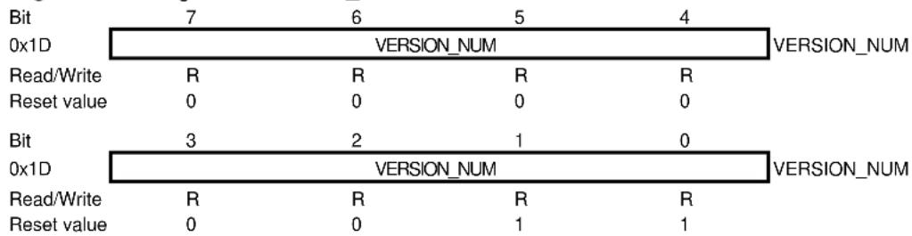
Register 0x1D (VERSION\_NUM):
The register VERSION_NUM can be used for the radio transceiver identification and includes the version number of the device.
Figure 6-17. Register VERSION_NUM.
text_image
Bit 7 6 5 4 0x1D VERSION_NUM VERSION_NUM Read/Write R R R R Reset value 0 0 0 0 Bit 3 2 1 0 0x1D VERSION_NUM VERSION_NUM Read/Write R R R R Reset value 0 0 1 1- Bit 7:0 - VERSION\_NUM
Table 6-6. VERSION_NUM.
| Register Bits | Value | Description |
| VERSION_NUM | 0x03 | Revision C |
Register 0x1E (MAN\_ID\_0):
Part one of the JEDEC manufacturer ID.
Figure 6-18. Register MAN_ID_0.

bar_stacked
| Bit | 7 | 6 | 5 | 4 | |-------|-----|-----|-----|-----| | 0x1E | MAN_ID_0 | | | | | Read/Write | R | R | R | R | | Reset value | 0 | 0 | 0 | 1 | | Bit | 3 | 2 | 1 | 0 | | 0x1E | MAN_ID_0 | | | | | Read/Write | R | R | R | R | | Reset value | 1 | 1 | 1 | 1 |- Bit 7:0 - MAN\_ID\_0
Table 6-7. MAN_ID_0.
| Register Bits | Value | Description |
| MAN_ID_0 | 0x1F | Atmel JEDEC manufacturer ID, bits[7:0] of the 32-bit JEDEC manufacturer ID are stored in register bits MAN_ID_0. Bits [15:8] are stored in register 0x1F (MAN_ID_1). The higher 16 bits of the ID are not stored in registers. |
Register 0x1F (MAN\_ID\_1):
Part two of the JEDEC manufacturer ID.
Figure 6-19. Register MAN_ID_1.

bar_stacked
| Bit | 7 | 6 | 5 | 4 | |---------|-----|-----|-----|-----| | 0x1F | MAN_ID_1 | | | MAN_ID_1 | | Read/Write | R | R | R | R | | Reset value | 0 | 0 | 0 | 0 | | Bit | 3 | 2 | 1 | 0 | | 0x1F | MAN_ID_1 | | | MAN_ID_1 | | Read/Write | R | R | R | R | | Reset value | 0 | 0 | 0 | 0 |- Bit 7:0 - MAN\_ID\_1
Table 6-8. MAN_ID 1.
| Register Bits | Value | Description |
| MAN_ID_1 | 0x00 | Atmel JEDEC manufacturer ID, bits[15:8] of the 32-bit JEDEC manufacturer ID are stored in register bits MAN_ID_1. Bits [7:0] are stored in register 0x1E (MAN_ID_0). The higher 16 bits of the ID are not stored in registers. |
6.6 Sleep/Wake-up and Transmit Signal (SLP\_TR)
Pin 11 (SLP_TR) is a multi-functional pin. Its function relates to the current state of the Atmel AT86RF212B and is summarized in Table 6-9. The radio transceiver states are explained in detail in Chapter 7.
Table 6-9. SLP TR Multi-functional Pin.
| Transceiver Status | Function | Transition | Description |
| PLL_ON | TX start | L ⇔ H | Starts frame transmission |
| TX_ARET_ON | TX start | L ⇔ H | Starts TX_ARET transaction |
| BUSY_RX_AACK | TX start | L ⇔ H | Starts ACK transmission during RX_AACK slotted operation, see Section 7.2.3.5 |
| TRX_OFF | Sleep | L ⇔ H | Takes the radio transceiver into SLEEP state; CLKM disabled |
| SLEEP | Wakeup | H ⇔ L | Takes the radio transceiver back into TRX_OFF state, level sensitive |
| RX_ON | Disable CLKM | L ⇔ H | Takes the radio transceiver into RX_ON_NOCLK state and disables CLKM |
| RX_ON_NOCLK | Enable CLKM | H ⇔ L | Takes the radio transceiver into RX_ON state and enables CLKM |
| RX_AACK_ON | Disable CLKM | L ⇔ H | Takes the radio transceiver into RX_AACK_ON_NOCLK state and disables CLKM |
| RX_AACK_ON_NOCLK | Enable CLKM | H ⇔ L | Takes the radio transceiver into RX_AACK_ON state and enables CLKM |
In states PLL_ON and TX_ARET_ON, pin 11 (SLP_TR) is used as trigger input to initiate a TX transaction. Here SLP_TR is sensitive on rising edge only.
After initiating a state change by a rising edge at pin 11 (SLP_TR) in radio transceiver states TRX_OFF, RX_ON or RX_AACK_ON, the radio transceiver remains in the new state as long as the pin is logical high and returns to the preceding state with the falling edge.
SLEEP state
The SLEEP state is used when radio transceiver functionality is not required, and thus the AT86RF212B can be powered down to reduce the overall power consumption.
A power-down scenario is shown in Figure 6-20. When the radio transceiver is in TRX_OFF state, the microcontroller forces the AT86RF212B to SLEEP by setting SLP_TR = H. If pin 17 (CLKM) provides a clock to the microcontroller, this clock is switched off after 35 CLKM cycles. This enables a microcontroller in a synchronous system to complete its power-down routine and prevent deadlock situations. The AT86RF212B awakes when the microcontroller releases pin 11 (SLP_TR). This concept provides the lowest possible power consumption.
The CLKM clock frequency settings for CLKM_CTRL values six and seven are not intended to directly clock the microcontroller. When using these clock rates, CLKM is turned off immediately when entering SLEEP state.
Figure 6-20. Sleep and Wake-up Initiated by Asynchronous Microcontroller Timer.

text_image
SLP_TR CLKM tTR3 (35 CLKM clock cycles) CLKM off tTR1a async timer elapses (microcontroller)Note: 1. Timing figures t_TR3 and t_TR1a refer to Table 7-1.
RX\_ON and RX\_AACK\_ON states
For synchronous systems where CLKM is used as a microcontroller clock source and the SPI master clock (SCLK) is directly derived from CLKM, the Atmel AT86RF212B supports an additional power-down mode for receive operating states (RX_ON and RX_AACK_ON).
If an incoming frame is expected and no other applications are running on the microcontroller, it can be powered down without missing incoming frames. This can be achieved by a rising edge on pin 11 (SLP_TR) that turns CLKM off. Then the radio transceiver state changes from RX_ON or RX_AACK_ON (Extended Operating Mode) to RX_ON_NOCLK or RX_AACK_ON_NOCLK, respectively. In case that a frame is received (for example indicated by an IRQ_2 (RX_START) interrupt), the clock output CLKM is automatically switched on again. This scenario is shown in Figure 6-21. In RX_ON state, the clock at pin 17 (CLKM) is switched off after 35 CLKM cycles when setting SLP_TR = H.
The CLKM clock frequency settings for CLKM_CTRL values six and seven are not intended to directly clock the microcontroller. When using these clock rates, CLKM is turned off immediately when entering RX_ON_NOCLK or RX_AACK_ON_NOCLK.
In states RX_(AACK)_ON_NOCLK and RX_(AACK)_ON, the radio transceiver current consumptions are equivalent. However, the RX_(AACK)_ON_NOCLK current consumption is reduced by the current required for driving pin 17 (CLKM).
Figure 6-21. Wake-Up Initiated by Radio Transceiver Interrupt.
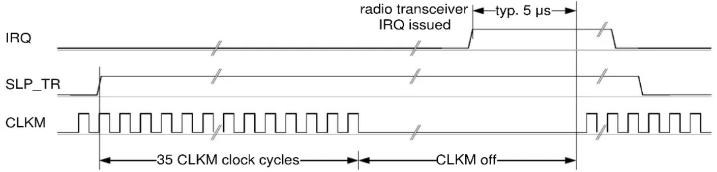
text_image
radio transceiver IRQ issued typ. 5 µs SLP_TR CLKM 35 CLKM clock cycles CLKM off6.7 Interrupt Logic
6.7.1 Overview
Atmel AT86RF212B differentiates between nine interrupt events (eight physical interrupt registers, one shared by two functions). Each interrupt is enabled by setting the corresponding bit in the interrupt mask register 0x0E (IRQ_MASK). Internally, each pending interrupt is flagged in the interrupt status register. All interrupt events are OR-combined to a single external interrupt signal (IRQ pin). If an interrupt is issued pin 24 (IRQ) = H, the microcontroller shall read the interrupt status register 0x0F (IRQ_STATUS) to determine the source of the interrupt. A read access to this register clears the interrupt status register and thus the IRQ pin, too.
Interrupts are not cleared automatically when the event trigger for respective interrupt flag bit in the register 0x0F (IRQ_STATUS) is no longer active. Only a read access to register 0x0F (IRQ_STATUS) clears the flag bits. Exceptions are IRQ_0 (PLL_LOCK) and IRQ_1 (PLL_UNLOCK) where each is cleared in addition by the appearance of the other.
The supported interrupts for the Basic Operating Mode are summarized in Table 6-10.
Table 6-10. Interrupt Description in Basic Operating Mode.
| IRQ Name Description Section | ||
| IRQ_7 (BAT_LOW) | Indicates a supply voltage below the programmed threshold. | 9.6.4 |
| IRQ_6 (TRX_UR) | Indicates a Frame Buffer access violation. | 9.4.3 |
| IRQ_5 (AMI) | Indicates address matching. | 8.2 |
| IRQ_4 (CCA_ED_DONE) | Multi-functional interrupt:1. AWAKE_END:Indicates radio transceiver reached TRX_OFF state at the end of P_ON ⇒ TRX_OFF and SLEEP ⇒ TRX_OFF state transition.2. CCA_ED_DONE:Indicates the end of a CCA or ED measurement. | 7.1.2.38.6.4 |
| IRQ_3 (TRX_END) | RX: Indicates the completion of a frame reception.TX: Indicates the completion of a frame transmission. | 7.1.37.1.3 |
| IRQ_2 (RX_START) | Indicates the start of a PSDU reception; the AT86RF212B state changed to BUSY_RX; the PHR can be read from Frame Buffer. | 7.1.3 |
| IRQ_1 (PLL_UNLOCK) | Indicates PLL unlock. If the radio transceiver is in BUSY_TX / BUSY_TX_ARET state, the PA is turned off immediately. | 9.8.5 |
| IRQ_0 (PLL_LOCK) | Indicates PLL lock. | 9.8.5 |
Note: 1. The IRQ_4 (AWAKE_END) interrupt can usually not be seen when the transceiver enters TRX_OFF state after P_ON or RESET, because register 0x0E (IRQ_MASK) is reset to mask all interrupts. It is recommended to enable IRQ_4 (AWAKE_END) to be notified once the TRX_OFF state is entered.
The interrupt handling in Extended Operating Mode is described in Section 7.2.5.
6.7.2 Interrupt Mask Modes and Pin Polarity
If register bit IRQ_MASK_MODE (register 0x04, TRX_CTRL_1) is set, an interrupt event can be read from IRQ_STATUS register even if the interrupt itself is masked. However, in that case no timing information for this interrupt is provided. The Table 6-11, Figure 6-22, and Figure 6-23 describes the function.
Table 6-11. IRQ Mask Configuration.
| IRQ_MASK Value | IRQ_MASK_MODE | Description |
| 0 0 | - | IRQ is suppressed entirely and none of interrupt sources are shown in register IRQ_STATUS. |
| 0 1 | IRQ is suppressed entirely but all interrupt causes are shown in register IRQ_STATUS. | |
| ≠0 0 | All enabled interrupts are signaled on IRQ pin and are also shown in register IRQ_STATUS. | |
| ≠0 1 | All enabled interrupts are signaled on IRQ pin and all interrupt causes are shown in register IRQ_STATUS. |
Figure 6-22. IRQ_MASK_MODE = 0.

flowchart
graph LR
    A["Interrupt Sources"] --> B["IRQ_MASK (register 0x0E)"]
    B --> C["IRQ_STATUS (register 0x0F)"]
    C --> D["OR"]
    D --> E["IRQ"]
Figure 6-23. IRQ_MASK_MODE = 1.
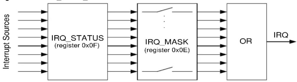
flowchart
graph LR
    A["Interrupt Sources"] --> B["IRQ_STATUS (register 0x0F)"]
    B --> C["IRQ_MASK (register 0x0E)"]
    C --> D["OR"]
    D --> E["IRQ"]
The Atmel AT86RF212B IRQ pin polarity can be configured with register bit IRQ_POLARITY (register 0x04, TRX_CTRL_1). The default behavior is active high, which means that pin 24 (IRQ) = H issues an interrupt request.
If the "Frame Buffer Empty Indicator" is enabled during Frame Buffer read access, the IRQ pin has an alternative functionality, refer to Section 11.6 for details.
A solution to monitor the IRQ_STATUS register (without clearing it) is described in Section 6.4.1.
6.7.3 Register Description
Register 0x0E (IRQ\_MASK):
The IRQ_MASK register controls the interrupt signaling via pin 24 (IRQ).
Figure 6-24. Register IRQ_MASK.
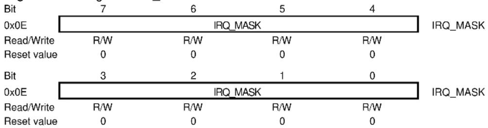
bar_stacked
| Bit/Read/Write | 0x0E | IRQ_MASK | | -------------- | ---- | -------- | | Read/Write | R/W | R/W | | Reset value | 0 | 0 | | Bit | 3 | 2 | | Read/Write | R/W | R/W | | Reset value | 0 | 0 |- Bit 7:0 - IRQ\_MASK
Mask register for interrupts. IRQ_MASK[7] correspondents to IRQ_7 (BAT_LOW). IRQ_MASK[0] correspondents to IRQ_0 (PLL_LOCK).
Table 6-12. IRQ_MASK.
| Register Bits | Value | Description |
| IRQ_MASK | 0x00 | The IRQ_MASK register is used to enable or disable individual interrupts. An interrupt is enabled if the corresponding bit is set to one. All interrupts are disabled after power-on sequence (P_ON state) or reset (RESET state).Valid values are [0xFF, 0xFE, ..., 0x00]. |
Note: 1. If an interrupt is enabled it is recommended to read the interrupt status register 0x0F (IRQ_STATUS) first to clear the history.
Register 0x0F (IRQ\_STATUS):
The IRQ_STATUS register contains the status of the pending interrupt requests.
Figure 6-25. Register IRQ_STATUS.
| Bit | 7 | 6 | 5 | 4 | |
| 0x0F | IRQ_7_BAT_LOW | IRQ_6_TRX_UR | IRQ_5_AMI | IRQ_4_CCA_ED_DONE | IRQ_STATUS |
| Read/Write | R | R | R | R | |
| Reset value | 0 | 0 | 0 | 0 | |
| Bit | 3 | 2 | 1 | 0 | |
| 0x0F | IRQ_3_TRX_END | IRQ_2_RX_START | IRQ_1_PLL_UNLOCK | IRQ_0_PLL_LOCK | IRQ_STATUS |
| Read/Write | R | R | R | R | |
| Reset value | 0 | 0 | 0 | 0 |
For more information to meanings of interrupts, see Table 6-10 Interrupt Description in Basic Operating Mode.
By reading the register after an interrupt is signaled at pin 24 (IRQ), the source of the issued interrupt can be identified. A read access to this register resets all interrupt bits, and so clears the IRQ_STATUS register.
Notes: 1. If register bit IRQ_MASK_MODE (register 0x04, TRX_CTRL_1) is set, an interrupt event can be read from IRQ_STATUS register even if the interrupt itself is masked; refer to Figure 6-23. However in that case no timing information for this interrupt is provided.
2. If register bit IRQ_MASK_MODE (register 0x04, TRX_CTRL_1) is set, it is recommended to read the interrupt status register 0x0F (IRQ_STATUS) first to clear the history.
Register 0x04 (TRX\_CTRL\_1):
The TRX_CTRL_1 register is a multi-purpose register to control various operating modes and settings of the radio transceiver.
Figure 6-26. Register TRX_CTRL_1.
| Bit 0x04 | 7 | 6 | 5 | 4 | |
| PA_EXT_EN | IRQ_2_EXT_EN | TX_AUTO_CRC_ON | RX_BL_CTRL | TRX_CTRL_1 | |
| Read/Write Reset value | R/W 0 | R/W 0 | R/W 1 | R/W 0 | |
| Bit 0x04 | 3 | 2 | 1 | 0 | |
| SPI_CMD_MODE | IRQ_MASK_MODE | IRQ_POLARITY | TRX_CTRL_1 | ||
| Read/Write Reset value | R/W 0 | R/W 0 | R/W 0 | R/W 0 | |
- Bit 6 - IRQ\_2\_EXT\_EN
The register bit IRQ_2_EXT_EN controls external signaling for time stamping via pin 10 (DIG2).
Table 6-13. IRQ 2 EXT EN.
| Register Bits | Value | Description |
| IRQ_2_EXT_EN | 0 | Time stamping over pin 10 (DIG2) is disabled |
| 1^(1) Time | time stamping over pin 10 (DIG2) is enabled |
Note: 1. The pin 10 (DIG2) is also active if the corresponding interrupt event IRQ_2 (RX_START) mask bit in register 0x0E (IRQ_MASK) is set to zero.
The timing of a received frame can be determined by a separate pin 10 (DIG2). If register bit IRQ_2_EXT_EN is set to one, the reception of a PHR field is directly issued on pin 10 (DIG2), similar to interrupt IRQ_2 (RX_START).
For further details refer to Section 11.5.
- Bit 1 - IRQ\_MASK\_MODE
The radio transceiver supports polling of interrupt events. Interrupt polling is enabled by setting register bit IRQ_MASK_MODE.
Table 6-14. IRQ_MASK_MODE.
| Register Bits | Value | Description |
| IRQ_MASK_MODE 0 Interrupt polling is disabled.Masked off IRQ bits will not appear in IRQ_STATUS register. | ||
With the interrupt polling enabled (IRQ_MASK_MODE = 1) the interrupt events are flagged in the register 0x0F (IRQ_STATUS) when their respective mask bits are disabled in the register 0x0E (IRQ_MASK).
- Bit 0 - IRQ\_POLARITY
The register bit IRQ_POLARITY controls the polarity for pin 24 (IRQ). The default polarity of the pin 24 (IRQ) is active high. The polarity can be configured to active low via register bit IRQ_POLARITY.
Table 6-15. IRQ POLARITY.
| Register Bits | Value | Description |
| IRQ_POLARITY | 0 | Pin IRQ is high active |
| 1 Pin | IRQ is low active |
Note: 1. A modification of register bit IRQ_POLARITY has no influence to RX_BL_CTRL behavior.
This setting does not affect the polarity of the "Frame Buffer Empty Indicator", refer to Section 11.6. The Frame Buffer Empty Indicator is always active high.
7 Operating Modes
7.1 Basic Operating Mode
This section summarizes all states to provide the basic functionality of Atmel AT86RF212B, such as receiving and transmitting frames, the power-on sequence, and sleep. The Basic Operating Mode is designed for IEEE 802.15.4 and general ISM band applications; the corresponding radio transceiver states are shown in Figure 7-1.
Figure 7-1. Basic Operating Mode State Diagram (for timing refer to Table 7-1).
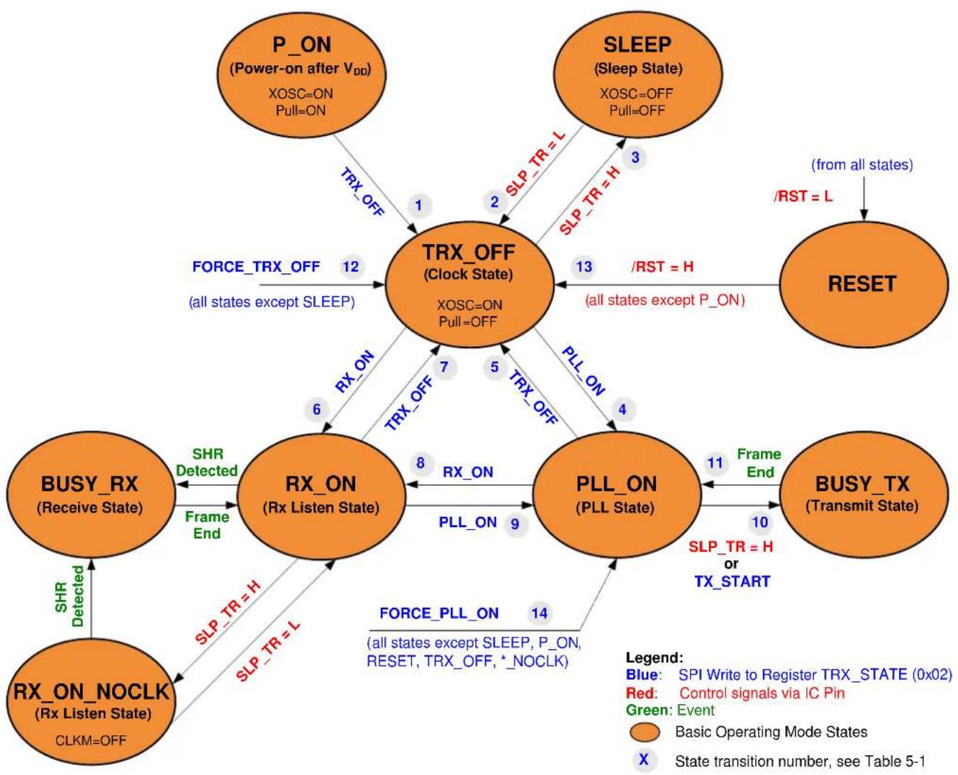
flowchart
graph TD
    subgraph TRX_OFF_Clock State
        A["XOSC=ON Pull=OFF"] -->|1| B["Power-on after V_DD"]
        B -->|2| C["SLEEP (Sleep State)<br>XOSC=OFF Pull=OFF"]
        C -->|3| D["RESET"]
        D -->|/RST = L| E["FROM all states"]
        D -->|12| F["FORCE_TRX_OFF (all states except SLEEP)"]
        F --> G["TRX_OFF (Clock State)<br>XOSC=ON Pull=OFF"]
        G --> H["PLL_ON (PLL State)"]
        H -->|4| I["BUSY_TX (Transmit State)"]
        I -->|10| J["FORCE_PLL_ON (all states except SLEEP, P_ON, RESET, TRX_OFF, *_NOCLK)"]
        J --> K["RX_ON (Rx Listen State)"]
        K -->|6| L["BUSY_RX (Receive State)"]
        L -->|8| M["RX_ON (Rx Listen State)"]
        M -->|9| N["PLL_ON (PLL State)"]
        N -->|11| O["FRAME End"]
        O -->|14| P["RX_ON (Rx Listen State)"]
        P -->|SHR Detected| Q["RX_ON (Rx Listen State)"]
        Q -->|SHR Detected| R["RX_ON_NOCLK (Rx Listen State)"]
        R -->|SLP_TR = H, SLP_TR = L| S["FX Detected"]
        S --> T["FX Detected"]
    end
    style TRX_OFF_ClockState fill:#f9f9f9,stroke:#333
    style PLL_ON fill:#f9f9f9,stroke:#333
    style RESET fill:#f9f9f9,stroke:#333
    style BUSY_TX fill:#f9f9f9,stroke:#333
    style RX_ON fill:#f9f9f9,stroke:#333
    style POLL_ON fill:#f9f9f9,stroke:#333
    style TRX_OFF_ClockState fill:#e6f7ff,stroke:#333
    style PLL_ON fill:#e6f7ff,stroke:#333
    style BUSY_RX fill:#e6f7ff,stroke:#333
    style RX_ON fill:#e6f7ff,stroke:#333
    style POLL_ON fill:#e6f7ff,stroke:#333
7.1.1 State Control
The radio transceiver's states are controlled by shifting serial digital data using the SPI to write individual commands to the command register bits TRX_CMD (register 0x02, TRX_STATE). Change of the transceiver state can also be triggered by driving directly two signal pins: pin 11 (SLP_TR) and pin 8 (/RST). A successful state change can be verified by reading the radio transceiver status from register bits TRX_STATUS (register 0x01, TRX_STATUS).
If TRX_STATUS = 0x1F (STATE_TRANSITION_IN_PROGRESS), the Atmel AT86RF212B is in a state transition. Do not try to initiate a further state change while the radio transceiver is in STATE_TRANSITION_IN_PROGRESS.
Pin 11 (SLP_TR) is a multifunctional pin, refer to Section 6.6. Depending on the radio transceiver state, a rising edge of pin 11 (SLP_TR) causes the following state transitions:
| • TRX_OFF | ⇒ | SLEEP | (level sensitive) |
| • RX_ON | ⇒ | RX_ON_NOCLK | (level sensitive) |
| • PLL_ON | ⇒ | BUSY_TX |
Whereas the falling edge of pin SLP_TR causes the following state transitions:
| SLEEP | TRX_OFF | (level sensitive) | |
| RX_ON_NOCLK | RX_ON |
A low level on pin 8 (/RST) causes a reset of all registers (register bits CLKM_CTRL are shadowed; for details, refer to Section 9.7.4) and forces the radio transceiver into TRX_OFF state. However, if the device was in P_ON state it remains in the P_ON state.
For all states except SLEEP, the state change commands FORCE_TRX_OFF or TRX_OFF lead to a transition into TRX_OFF state. If the radio transceiver is in active receive or transmit states (BUSY_ *), the command FORCE_TRX_OFF interrupts these active processes, and forces an immediate transition to TRX_OFF. In contrast a TRX_OFF command is stored until an active state (receiving or transmitting) has been finished. After that the transition to TRX_OFF is performed.
For a fast transition from any non sleep states to PLL_ON state the command FORCE_PLL_ON is provided. Active processes are interrupted. In contrast to FORCE_TRX_OFF, this command does not disable the PLL and the analog voltage regulator (AVREG). It is not available in states P_ON, SLEEP, RESET, and all *_NOCLK states.
The completion of each requested state change shall always be confirmed by reading the register bits TRX_STATUS (register 0x01, TRX_STATUS).
Note: 1. If FORCE_TRX_OFF and FORCE_PLL_ON commands are used, it is recommended to set pin 11 (SLP_TR) = L before.
7.1.2 Basic Operating Mode Description
7.1.2.1 P\_ON - Power-On after V_DD
When the external supply voltage ( V_DD ) is applied first to the AT86RF212B, the radio transceiver goes into P_ON state performing an on-chip reset. The crystal oscillator is activated and the default 1MHz master clock is provided at pin 17 (CLKM) after the
crystal oscillator has stabilized. CLKM can be used as a clock source to the microcontroller. The SPI interface and digital voltage regulator (DVREG) are enabled.
The on-chip power-on-reset sets all registers to their default values. A dedicated reset signal from the microcontroller at pin 8 (/RST) is not necessary, but recommended for hardware / software synchronization reasons.
All digital inputs are pulled-up or pulled-down during P_ON state, refer to Section 1.3.2. This is necessary to support microcontrollers where GPIO signals are floating after power-on or reset. The input pull-up and pull-down transistors are disabled when the radio transceiver leaves P_ON state towards TRX_OFF state. A reset during P_ON state does not change the pull-up and pull-down configuration.
Leaving P_ON state, output pins DIG1/DIG2 are pulled-down to digital ground, whereas pins DIG3/DIG4 are pulled-down to analog ground, unless their configuration is changed.
Prior to leaving P_ON, the microcontroller must set the Atmel AT86RF212B pins to the default operating values: pin 11 (SLP_TR) = L, pin 8 (/RST) = H and pin 23 (/SEL) = H.
All interrupts are disabled by default. Thus, interrupts for state transition control are to be enabled first, for example enable IRQ_4 (AWAKE_END) to indicate a state transition to TRX_OFF state or interrupt IRQ_0 (PLL_LOCK) to signal a locked PLL in PLL_ON state. In P_ON state a first access to the radio transceiver registers is possible after a default 1MHz master clock is provided at pin 17 (CLKM), refer to t_TR1 to Table 7-1.
Once the supply voltage has stabilized and the crystal oscillator has settled (see parameter t_XTAL refer to Table 7-2), the interrupt mask for the AWAKE_END should be set. A valid SPI write access to register bits TRX_CMD (register 0x02, TRX_STATE) with the command TRX_OFF or FORCE_TRX_OFF initiate a state change from P_ON towards TRX_OFF state, which is then indicated by an interrupt IRQ_4 (AWAKE_END) if enabled.
7.1.2.2 SLEEP – Sleep State
In SLEEP state, the radio transceiver is disabled. The radio transceiver current consumption is reduced to leakage current plus the current of a low power voltage regulator (typ. 100nA). This regulator provides the supply voltage to the registers to preserve their contents. SLEEP state can only be entered from state TRX_OFF, by setting SLP_TR = H.
If CLKM is enabled with a clock rates higher than 250kHz, the SLEEP state is entered 35 CLKM cycles after the rising edge at pin 11 (SLP_TR). At that time CLKM is turned off. If the CLKM output is already turned off (register bits CLKM_CTRL = 0), the SLEEP state is entered immediately.
At clock rates of 250kHz and symbol clock rate (CLKM_CTRL values six and seven; register 0x03, TRX_CTRL_0), the main clock at pin 17 (CLKM) is turned off immediately.
Setting SLP_TR = L returns the radio transceiver back to the TRX_OFF state. During SLEEP state the radio transceiver register contents and the AES register contents remain valid while the contents of the Frame Buffer are lost.
/RST = L in SLEEP state returns the radio transceiver to TRX_OFF state and thereby sets all registers to their default values. Exceptions are register bits CLKM_CTRL (register 0x03, TRX_CTRL_0). These register bits require a specific treatment; for details see Section 9.7.4.
7.1.2.3 TRX\_OFF - Clock State
In TRX_OFF the crystal oscillator is running and the master clock is available if enabled. The SPI interface and digital voltage regulator are enabled, thus the radio transceiver registers, the Frame Buffer and security engine (AES) are accessible (see Section 9.4 and Section 11.1).
In contrast to P_ON state the pull-up and pull-down configuration is disabled.
Notes: 1. Pin 11 (SLP_TR) and pin 8 (/RST) are available for state control.
- The analog front-end is disabled during TRX_OFF state. If TRX_OFF_AVDD_EN (register 0x0C, TRX_CTRL_2) is set, the analog voltage regulator is turned on, enabling faster switch to any transmit/receive state.
Entering the TRX_OFF state from P_ON, SLEEP, or RESET state, the state change is indicated by interrupt IRQ_4 (AWAKE_END) if enabled.
7.1.2.4 PLL\_ON - PLL State
Entering the PLL_ON state from TRX_OFF state enables the analog voltage regulator (AVREG) first, unless the AVREG is already switched on (register 0x0C, TRX_OFF_AVDD_EN). After the voltage regulator has been settled (see Table 7-2), the PLL frequency synthesizer is enabled. When the PLL has been settled at the receive frequency to a channel defined by register bits CHANNEL (register 0x08, PHY_CC_CCA) or register bits CC_NUMBER (register 0x13, CC_CTRL_0) and CC_BAND (register 0x14, CC_CTRL_1), refer to Section 9.8.2, a successful PLL lock is indicated by issuing an interrupt IRQ_0 (PLL_LOCK).
If an RX_ON command is issued in PLL_ON state, the receiver is enabled immediately. If the PLL has not been settled before the state change nevertheless takes place. Even if the register bits TRX_STATUS (register 0x01, TRX_STATUS) indicates RX_ON, actual frame reception can only start once the PLL has locked.
The PLL_ON state corresponds to the TX_ON state in IEEE 802.15.4.
7.1.2.5 RX\_ON and BUSY\_RX - RX Listen and Receive State
In RX_ON state the receiver is in the RX data polling mode and the PLL frequency synthesizer is locked to its preprogrammed frequency.
The Atmel AT86RF212B receive mode is internally separated into RX_ON state and BUSY_RX state. There is no difference between these states with respect to the analog radio transceiver circuitry, which are always turned on. In both states, the receiver and the PLL frequency synthesizer are enabled.
During RX_ON state, the receiver listens for incoming frames. After detecting a valid synchronization header (SHR), the AT86RF212B automatically enters the BUSY_RX state. The reception of a valid PHY header (PHR) generates an IRQ_2 (RX_START) if enabled.
During PSDU reception, the frame data are stored continuously in the Frame Buffer until the last byte was received. The completion of the frame reception is indicated by an interrupt IRQ_3 (TRX_END) and the radio transceiver reenters the state RX_ON. At the same time the register bit RX_CRC_VALID (register 0x06, PHY_RSSI) is updated with the result of the FCS check (see Section 8.3).
Received frames are passed to the frame filtering unit, refer to Section 8.2. If the content of the MAC addressing fields (refer to [2] IEEE 802.15.4-2006, Section 7.2.1) generates a match, IRQ_5 (AMI) interrupt is issued, refer to Section 6.7. The expected address values are to be stored in registers 0x20 - 0x2B (Short address, PAN-ID and
IEEE address). Frame filtering is available in Basic Operating Mode and Extended Operating Mode, refer to Section 8.2.
Leaving state RX_ON is possible by writing a state change command to register bits TRX_CMD in register 0x02 (TRX_STATE).
7.1.2.6 RX\_ON\_NOCLK - RX Listen State without CLKM
In RX_ON_NOCLK state the receiver is in the RX data polling mode with CLKM output disabled.
If the radio transceiver is listening for an incoming frame and the microcontroller is not running an application, the microcontroller may be powered down to decrease the total system power consumption. This specific power-down scenario – for systems running in clock synchronous mode (see Chapter 6) – is supported by the Atmel AT86RF212B using the state RX_ON_NOCLK.
This state can only be entered by asserting pin 11 (SLP_TR) = H while the radio transceiver is in RX_ON state. Pin 17 (CLKM) is disabled 35 CLKM cycles after the rising edge at pin 11 (SLP_TR), see Figure 6-21. This allows the microcontroller to complete its power-down sequence.
Note: 1. For CLKM clock rates 250kHz and symbol clock rates (CLKM_CTRL values six and seven; register 0x03, TRX_CTRL_0), the master clock signal CLKM is switched off immediately after the rising edge of pin 11 (SLP_TR).
Once in RX_ON_NOCLK state a valid SHR header triggers a state transition to BUSY_RX state. The reception of a frame shall be indicated to the microcontroller by an interrupt indicating the receive status. CLKM is turned on again, and the radio transceiver enters the BUSY_RX state (see Section 6.6 and Figure 6-21). When using RX_ON_NOCLK, it is essential to enable at least one interrupt request indicating the reception status.
After the receive transaction has been completed, the radio transceiver enters the RX_ON state. The radio transceiver only reenters the RX_ON_NOCLK state when the next rising edge of pin 11 (SLP_TR) occurs.
If the AT86RF212B is in the RX_ON_NOCLK state and pin 11 (SLP_TR) is reset to logic low, it enters the RX_ON state and it starts to supply clock on pin 17 (CLKM) again.
Note: 2. A reset in state RX_ON_NOCLK further requires to reset pin 11 (SLP_TR) to logic low, otherwise the radio transceiver enters directly the SLEEP state.
7.1.2.7 BUSY\_TX - Transmit State
In the BUSY_TX state AT86RF212B is in the data transmission state.
A transmission can only be initiated from the PLL_ON state. The transmission can be started either by driving event such as:
• A rising edge on pin 11 (SLP_TR), or
- A serial TX_START command via the SPI to register bits TRX_CMD (register 0x02, TRX_STATE).
Either of these forces the radio transceiver into the BUSY_TX state. Refer to Section 10.2 for more details.
During the transition to the BUSY_TX state, the PLL frequency shifts to the transmit frequency, refer to Section 9.8.3. The actual transmission of the first data chip of the
SHR starts after one symbol period (see note) in order to allow PLL settling and PA ramp-up, see Figure 7-6. After transmission of the SHR, the Frame Buffer content is transmitted. In case the PHR indicates a frame length of zero, the transmission is aborted immediately after the PHR field.
After the frame transmission has been completed, the AT86RF212B automatically turns off the power amplifier, generates an IRQ_3 (TRX_END) interrupt, and returns into PLL_ON state.
Note: 1. Throughout this datasheet, a “symbol period” refers to the definition described in Section 9.1.3.
7.1.2.8 RESET State
The RESET state is used to set back the state machine and to reset all registers of Atmel AT86RF212B to their default values; exceptions are register bits CLKM_CTRL (register 0x03, TRX_CTRL_0). These register bits require a specific treatment, for details see Section 9.7.4.
Once in RESET state a device enters TRX_OFF state by setting pulling a reset pin high pin 8 (/RST) = H. If the device is still in the P_ON state it remains in the P_ON state though. A reset is triggered by pulling /RST pin low pin 8 (/RST) = L and the state returns after setting /RST = H. The reset pulse should have a minimum length as specified in Section 7.1.4.5 and Section 12.4 (parameter t_10 ). During reset, the microcontroller has to set the radio transceiver control pins SLP_TR and /SEL to their default values.
An overview of the register reset values is provided in Table 14-2.
7.1.3 Interrupt Handling
All interrupts provided by the Atmel AT86RF212B (see Table 6-10) are supported in Basic Operating Mode. For example, interrupts are provided to observe the status of radio transceiver RX and TX operations.
When being in receive mode, IRQ_2 (RX_START) indicates the detection of a valid PHR first, IRQ_5 (AMI) an address match, and IRQ_3 (TRX_END) the completion of the frame reception. During transmission, IRQ_3 (TRX_END) indicates the completion of the frame transmission.
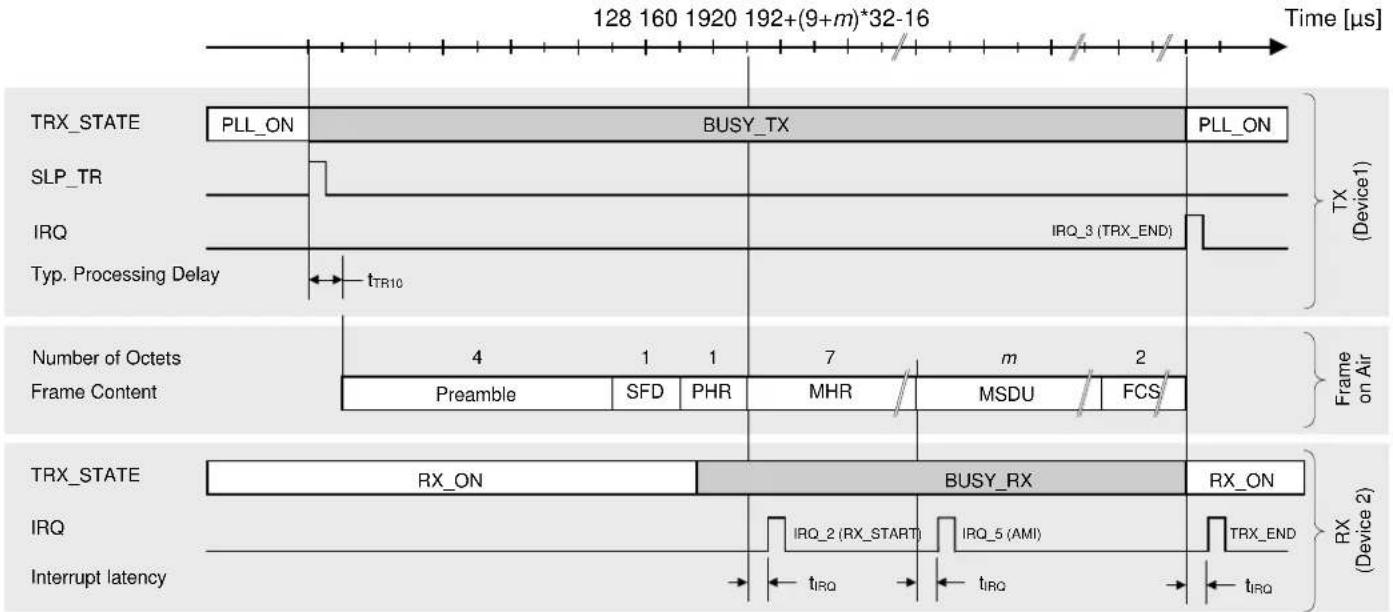
Figure 7-2 shows an example for a transmit/receive transaction between two devices and the related interrupt events in Basic Operating Mode. Device 1 transmits a frame containing a MAC header (in this example of length seven), MAC payload, and a valid FCS. The end of the frame transmission is indicated by IRQ_3 (TRX_END).
The frame is received by Device 2. Interrupt IRQ_2 (RX_START) indicates the detection of a valid PHR field and IRQ_3 (TRX_END) the completion of the frame reception. If the frame passes the Frame Filter (refer to Section 8.2), an address match interrupt IRQ_5 (AMI) is issued after the reception of the MAC header (MHR). The received frame is stored in the Frame Buffer.
In Basic Operating Mode the third interrupt IRQ_3 (TRX_END) is issued at the end of the received frame. In Extended Operating Mode, refer to Section 7.2; the interrupt is only issued if the received frame passes the address filter and the FCS is valid. Further exceptions are explained in Section 7.2.
Processing delay t_IRQ is a typical value, refer to Section 12.4.
Figure 7-2. Timing of RX_START, AMI and TRX_END Interrupts in Basic Operating Mode for O-QPSK 250kb/s Mode.
text_image
128 160 1920 192+(9+m)*32-16 Time [µs] TRX_STATE PLL_ON BUSY_TX PLL_ON SLP_TR IRQ Typ. Processing Delay tTR10 Number of Octets 4 1 1 7 m 2 Frame Content Preamble SFD PHR MHR MSDU FCS TRX_STATE RX_ON BUSY_RX RX_ON IRQ Interrupt latency tIRQ tIRQ RX (Device 2) TRX_END IRQ_2 (RX_START) IRQ_5 (AMI) TRX_END tIRQ tIRQ tIRQ7.1.4 Basic Operating Mode Timing
This section depicts Atmel AT86RF212B state transitions and their timing properties. Timing figures are explained in Table 7-1, Table 7-2, and Section 12.4.
7.1.4.1 Power-on Procedure
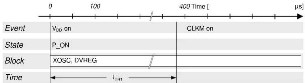
The power-on procedure to P_ON state is shown in Figure 7-3.
Figure 7-3. Power-on Procedure to P_ON State.
text_image
0 100 400 Time [ µs] Event VDD on CLKM on State P_ON Block XOSC, DVREG Time7.1.4.2 Wake-up Procedure from SLEEP
The wake-up procedure from SLEEP state is shown in Figure 7-4. Figure 7-4. Wake-up Procedure from SLEEP State. text_image
0 100 200 300 400 Time [µs] Event SLP_TR = L CLKM IRQ_4 (AWAKE_END) State SLEEP TRX_OFF Block XOSC, DVREG FTN XOSC, DVREG Time7.1.4.3 PLL\_ON and RX\_ON States
The transition from TRX\_OFF to PLL\_ON or RX\_ON state and further to RX\_ON or PLL\_ON is shown in Figure 7-5. Figure 7-5. Transition from TRX\_OFF to PLL\_ON/RX\_ON State and further to RX\_ON/PLL\_ON. text_image
0 200 Time [µs] Event State TRX_OFF Block Command Time IRQ_0 (PLL_LOCK) PLL_ON / RX_ON RX_ON / PLL_ON AVREG PLL PLL_ON / RX_ON RX_ON / PLL_ON tTR4 / tTR6 tTR8 / tTR97.1.4.4 BUSY\_TX to RX\_ON States
The transition from PLL\_ON to BUSY\_TX state and subsequently to RX\_ON state is shown in Figure 7-6. Figure 7-6. PLL\_ON to BUSY\_TX to RX\_ON Timing for O-QPSK 250kb/s Mode. text_image
Event SLP_TR=H or TRX_CMD = TX_START TRX_CMD=RX_ON IRQ_3 (TRX_END) State PLL_ON BUSY_TX RX_ON Block TX PLL RX Time tTR10 tTR117.1.4.5 Reset Procedure
The radio transceiver reset procedure is shown in Figure 7-7. Figure 7-7. Reset Procedure. text_image
Event State Any, except P_ON and SLEEP undefined Block FTN Pin /RST Time t10 tTR13 Time [µs] 0 x x + 30 [IRQ_4 (AWAKE_END)] TRX_OFF7.1.4.6 State Transition Timing Summary
The Atmel AT86RF212B transition numbers correspond to Figure 7-1 and do not include SPI access time if not otherwise stated. See measurement setup in Figure 5-1. Table 7-1. State Transition Timing.| Symbol | Parameter | Condition | Min. | Typ. | Max. | Unit |
| t_TR1 | P_ON⇒CLKM is available | Depends on crystal oscillator setup (Siward A207-011, C_L = 10pF) and external capacitor at DVDD ( CB3 = 1μF nom. ). | 420 | 1000 μs | ||
| t_TR1a | SLEEP⇒CLKM is available | Depends on crystal oscillator setup (Siward A207-011, C_L = 10pF) and external capacitor at DVDD ( CB3 = 1μF nom. ). | 390 | 1000 μs | ||
| t_TR2 | SLEEP⇒TRX_OFF | Depends on crystal oscillator setup (Siward A207-011, C_L = 10pF) and external capacitor at DVDD ( CB3 = 1μF nom. ); TRX_OFF state indicated by IRQ_4 (AWAKE_END). | 420 | 1000 μs | ||
| t_TR3 TRX_OFF⇒SLEEP For f | CLKM>250kHz.Otherwise. | 350 | CLKM cyclesCLKM cycles | |||
| t_TR4 | TRX_OFF⇒PLL_ON | Depends on external capacitor at AVDD ( CB1 = 1μF nom. ); register bit TRX_OFF_AVDD_EN (register 0x0C, TRX_CTRL_2) is not set. | 170 | μs | ||
| t_TR5 | PLL_ON⇒TRX_OFF | 1 | μs | |||
| t_TR6 | TRX_OFF⇒RX_ON | Depends on external capacitor at AVDD ( CB1 = 1μF nom. ); register bit TRX_OFF_AVDD_EN (register 0x0C, TRX_CTRL_2) is not set. | 170 | μs | ||
| t_TR7 | RX_ON⇒TRX_OFF | 1 | μs | |||
| t_TR8 | PLL_ON⇒RX_ON | 1 | μs | |||
| t_TR9 | RX_ON⇒PLL_ON | Transition time is also valid for TX_ARET_ON,RX_AACK_ON⇒PLL_ON. | 1 | μs | ||
| t_TR10 | PLL_ON⇒BUSY_TX | When asserting pin 11 (SLP_TR) or TRX_CMD = TX_START first symbol transmission is delayed by one symbol period (PLL settling and PA ramp-up). | 1 | symbol | period | |
| t_TR11 | BUSY_TX⇒PLL_ON | PLL settling time. | 32 | μs | ||
| t_TR12 | Various states⇒TRX_OFF | Using TRX_CMD = FORCE_TRX_OFF (see register 0x02, TRX_STATE); not valid for SLEEP⇒TRX_OFF (see t_TR2 ). | 1 | μs | ||
| t_TR13 | RESET⇒TRX_OFF | Not valid for P_ON or SLEEP. | 26 | μs | ||
| t_TR14 | Various states⇒PLL_ON | Using TRX_CMD = FORCE_PLL_ON (see register 0x02, TRX_STATE); not valid forstates SLEEP, P_ON, RESET, TRX_OFF, and *_NOCLK. | 1 | μs | ||
| Symbol | Parameter | Condition | Min. | Typ. | Max. | Unit |
| t_XTAL | Reference oscillator settling time | Start XTAL⇒clock available at pin 17 (CLKM). Depends on crystal oscillator setup (Siward A207-011, C_L = 10pF). | 420 | 1000 μs | ||
| t_FTN | FTN calibration time | 25 | μs | |||
| t_DVREG | DVREG settling time | Depends on external bypass capacitor at DVDD (CB3 = 1μF nom., 10μF worst case). | 150 | 1500 μs | ||
| t_AVREG | AVREG settling time | Depends on external bypass capacitor at AVDD (CB1 = 1μF nom., 10μF worst case). | 150 | 1500 μs | ||
| t_PLL\_INIT | Initial PLL settling time | PLL settling time TRX_OFF⇒PLL_ON, including 150μs AVREG settling time. | 170 | 370 | μs | |
| t_PLL\_SW | PLL settling time on channel switch | Duration of channel switch within frequency band. | 11 | 42 | μs | |
| t_PLL\_CF | PLL CF calibration | PLL center frequency calibration. | 8 | 8 | 270 | μs |
| t_PLL\_DCU | PLL DCU calibration | PLL DCU calibration. | 10 | 10 | μs | |
| t_RX\_TX | RX⇒TX | Maximum settling time RX⇒TX. | 16 | μs | ||
| t_TX\_RX | TX⇒RX | Maximum settling time TX⇒RX. | 32 | μs | ||
| t_RSSI | RSSI, update | RSSI update period in receive states.BPSK-20:BPSK-40:O-QPSK: | 32248 | μsμsμs | ||
| t_ED | ED measurement | ED measurement period is eight symbols. Different timing within High Data Rate Modes. | 8 | symbol | ||
| t_CCA | CCA measurement | CCA measurement period is eight symbols. | 8 | symbol | ||
| t_RND | Random value, update | Random value update period. | 1 | μs | ||
| t_AES | AES core cycle time | 23.4 | 24 | μs | ||
7.1.5 Register Description
Register 0x01 (TRX\_STATUS):
The read-only register TRX\_STATUS signals the present state of the radio transceiver as well as the status of a CCA operation. Figure 7-8. Register TRX\_STATUS. - Bit 4:0 - TRX\_STATUS
The register bits TRX\_STATUS signal the current radio transceiver status. Table 7-3. TRX STATUS.| Register Bits | Value | Description |
| TRX_STATUS 0x00 P_ON | ____ | |
| 0x01 BUSY_RX | ||
| 0x02 BUSY_TX | ||
| 0x06 RX_ON | ||
| 0x08 TRX_OFF (CLK Mode) | ||
| 0x09 PLL_ON (TX_ON) | ||
| 0x0F^(1) SLEEP | ||
| 0x11^(2) BUSY_RX_AACK | ||
| 0x12^(2) BUSY_TX_ARET | ||
| 0x16^(2) RX_AACK_ON | ||
| 0x19^(2) TX_ARET_ON | ||
| 0x1C RX_ON_NOCLK | ||
| 0x1D^(2) RX_AACK_ON_NOCLK | ||
| 0x1E^(2) BUSY_RX_AACK_NOCLK | ||
| 0x1F^(3) STATE_TRANSITION_IN_PROGRESS | ||
| All other values are reserved | ||
Register 0x02 (TRX\_STATE):
The radio transceiver states are advanced via register TRX\_STATE by writing a command word into register bits TRX\_CMD. The read-only register bits TRAC\_STATUS indicate the status or result of an Extended Operating Mode transaction. Figure 7-9. Register TRX\_STATE. - Bit 4:0 - TRX\_CMD
A write access to register bits TRX\_CMD initiate a radio transceiver state transition to the new state. Table 7-4. TRX\_CMD.| Register Bits | Value | Description |
| TRX_CMD 0x00 | _(1) | NOP |
| 0x02^(2) | TX_START | |
| 0x03 | FORCE_TRX_OFF | |
| 0x04^(3) | FORCE_PLL_ON | |
| 0x06 | RX_ON | |
| 0x08 | TRX_OFF (CLK Mode) | |
| 0x09 | P_L_ON (TX_ON) | |
| 0x16^(4) | RX_AACK_ON | |
| 0x19^(4) | TX_ARET_ON | |
| All other values are reserved | ||
7.2 Extended Operating Mode
Extended Operating Mode makes up for a large set of automated functionality add-ons which can be referred to as a hardware MAC accelerator. These add-ons go beyond the basic radio transceiver functionality provided by the Basic Operating Mode. Extended Operating Mode functions handle time critical MAC tasks, requested by the IEEE 802.15.4 standard, in hardware, such as automatic acknowledgement, automatic CSMA-CA, and retransmission. This results in a more efficient IEEE 802.15.4 software MAC implementation, including reduced code size, and may allow use of a smaller microcontroller or operation at low clock rates. The Extended Operating Mode is designed to support IEEE 802.15.4-2006 and IEEE 802.15.4-2011 compliant frames; the mode is backward compatible to IEEE 802.15.4-2003 and supports non IEEE 802.15.4 compliant frames. This mode comprises the following procedures:Automatic acknowledgement (RX\_AACK) divides into the tasks:
• Frame reception and automatic FCS check - Configurable addressing fields check - Interrupt indicating address match - Interrupt indicating frame reception, if it passes address filtering and FCS check - Automatic ACK frame transmission (if the received frame passed the address filter and FCS check and if an ACK is required by the frame type and ACK request) - Support of slotted acknowledgment using SLP\_TR pin (used for beacon-enabled operation)Automatic CSMA-CA and Retransmission (TX\_ARET) divides into the tasks:
• CSMA-CA, including automatic CCA retry and random backoff • Frame transmission and automatic FCS field generation - Reception of ACK frame (if an ACK was requested) • Automatic retry of transmissions if ACK was expected but not received or accepted - Interrupt signaling with transaction status Automatic FCS check and generation, refer to Section 8.3, is used by the RX\_AACK and TX\_ARET modes. In RX\_AACK mode, an automatic FCS check is always performed for incoming frames. In TX\_ARET mode, an ACK which is received within the time required by IEEE 802.15.4 is automatically accepted if the FCS is valid and the ACK sequence number must match the sequence number of the previously transmitted frame. Dependent on the value of the frame pending subfield in the received acknowledgement frame received, the transaction status is set, see register bits TRAC\_STATUS (register 0x02, TRX\_STATE), Section 7.2.7. An Atmel AT86RF212B state diagram, including the Extended Operating Mode states, is shown in Figure 7-10. Orange marked states represent the Basic Operating Mode; blue marked states represent the Extended Operating Mode. Figure 7-10. Extended Operating Mode State Diagram. flowchart
graph TD
    A["TRX_OFF (Clock State)"] -->|12 13 Force_TRX_OFF (all modes except SLEEP)| B["XOSC=ON Pull=OFF"]
    A -->|7 5 TRX_OFF| C["PLL_ON (PLL State)"]
    A -->|6 RX_ON| D["RX_ON (Rx Listen State)"]
    A -->|4 PLL_ON| E["BUSY_RX (Receive State)"]
    A -->|8 RX_ON| F["RX_ON (Rx Listen State)"]
    A -->|9 PLL_ON| G["BUSY_TX (Transmit State)"]
    A -->|10 11 Frame End| H["TX_ARET_ON"]
    A -->|14 PLL_ON| I["BUSY_TX_ARET"]
    B -->|12 13 Force_TRX_OFF (all modes except SLEEP)| A
    C -->|7 5 TRX_OFF| A
    D -->|6 RX_ON| B
    E -->|4 PLL_ON| C
    F -->|8 RX_ON| C
    G -->|10 11 Frame End| H
    I -->|14 PLL_ON| H
    J["P_ON (Power-on after V_DD)"] -->|12 13 Force_TRX_OFF (all modes except SLEEP)| A
    K["SLEEP (Sleep State)"] -->|7 5 TRX_OFF| A
    L["RESET"] -->|12 13 Force_TRX_OFF (all modes except SLEEP)| A
    M["RXY ON (Rx Listen State)"] -->|8 RX_ON| C
    N["RXY ON (Rx Listen State)"] -->|9 PLL_ON| C
    O["RXY ON (Rx Listen State)"] -->|10 11 Frame End| C
    P["RXY ON (Rx Listen State)"] -->|14 10 TX_ARET_ON| H
    Q["RXY ON (Rx Listen State)"] -->|14 10 TX_ARET_ON| H
    R["RXY ON (Rx Listen State)"] -->|14 10 TX_ARET_ON| H
    S["RXY ON (Rx Listen State)"] -->|14 10 TX_ARET_ON| H
    T["RXY ON (Rx Listen State)"] -->|14 10 TX_ARET_ON| H
    U["RXY ON (Rx Listen State)"] -->|14 10 TX_ARET_ON| H
    V["RXY ON (Rx Listen State)"] -->|14 10 TX_ARET_ON| H
    W["RXY ON (Rx Listen State)"] -->|14 10 TX_ARET_ON| H
    X["RXY ON (Rx Listen State)"] -->|14 10 TX_ARET_ON| H
    Y["RXY ON (Rx Listen State)"] -->|14 10 TX_ARET_ON| H
    Z["RXY ON (Rx Listen State)"] -->|14 10 TX_ARET_ON| H
    AA["RXY ON (Rx Listen State)"] -->|14 10 TX_ARET_ON| H
    AB["RXY ON (Rx Listen State)"] -->|14 10 TX_ARET_ON| H
    AC["RXY ON (Rx Listen State)"] -->|14 10 TX_ARET_ON| H
    AD["RXY ON (Rx Listen State)"] -->|14 10 TX_ARET_ON| H
    AE["RXY ON (Rx Listen State)"] -->|14 10 TX_ARET_ON| H
    AF["RXY ON (Rx Listen State)"] -->|14 10 TX_ARET_ON| H
    AG["RXY ON (Rx Listen State)"] -->|14 10 TX_ARET_ON| H
    AH["RXY ON (Rx Listen State)"] -->|14 10 TX_ARET_ON| H
    AI["RXY ON (Rx Listen State)"] -->|14 10 TX_ARET_ON| H
    AJ["RXY ON (Rx Listen State)"] -->|14 10 TX_ARET_ON| H
    AK["RXY ON (Rx Listen State)"] -->|14 10 TX_ARET_ON| H
    AL["RXY ON (Rx Listen State)"] -->|14 10 TX_ARET_ON| H
    AM["RXY ON (Rx Listen State)"] -->|14 10 TX_ARET_ON| H
    AN["RXY ON (Rx Listen State)"] -->|14 10 TX_ARET_ON| H
    AO["RXY ON (Rx Listen State)"] -->|14 10 TX_ARET_ON| H
    AP["RXY ON (Rx Listen State)"] -->|14 10 TX_ARET_ON| H
    AQ["RXY ON (Rx Listen State)"] -->|14 10 TX_ARET_ON| H
    AR["RXY ON (Rx Listen State)"] -->|14 10 TX_ARET_ON| H
    AS["RXY ON (Rx Listen State)"] -->|14 10 TX_ARET_ON| H
    AT["RXY ON (Rx Listen State)"] -->|14 10 TX_ARET_ON| H
    AU["RXY ON (Rx Listen State)"] -->|14 10 TX_ARET_ON| H
    AV["RXY ON (Rx Listen State)"] -->|14 10 TX_ARET_ON| H
    AW["RXY ON (Rx Listen State)"] -->|14 10 TX_ARET_ON| H
    AX["RXY ON (Rx Listen State)"] -->|14 10 TX_ARET_ON| H
7.2.1 State Control
The Extended Operating Mode include RX\_AACK and TX\_ARET modes and are controlled by writing respective command to register bits TRX\_CMD (register 0x02, TRX\_STATE). Receive with Auto matic Acknowledgement state RX\_AACK\_ON and Transmit with Automatic Frame Retransmission and CSMA-CA Retry state TX\_ARET\_ON can be entered either from TRX\_OFF or PLL\_ON state as illustrated in Figure 7-10. The completion of each change state command shall always be confirmed by reading the register bits TRX\_STATUS (register 0x01, TRX\_STATUS).RX\_AACK - Receive with Automatic Acknowledgement
A state transition to RX\_AACK\_ON from PLL\_ON or TRX\_OFF is initiated by writing the RX\_AACK\_ON command to register bits TRX\_CMD (register 0x02, TRX\_STATE). On success, reading register bits TRX\_STATUS (register 0x01, TRX\_STATUS) returns RX\_AACK\_ON or BUSY\_RX\_AACK. The latter one is returned when a frame is being received. The RX\_AACK Extended Operating Mode is terminated by writing command PLL\_ON to the register bits TRX\_CMD. If the Atmel AT86RF212B is within a frame receive or acknowledgment procedure (BUSY\_RX\_AACK), the state change is executed after finishing. Alternatively, the commands FORCE\_TRX\_OFF or FORCE\_PLL\_ON can be used to cancel the RX\_AACK transaction and switch to TRX\_OFF or PLL\_ON state respectively.TX\_ARET - Transmit with Automatic Frame Retransmission and CSMA-CA Retry
A state transition to TX\_ARET\_ON from PLL\_ON or TRX\_OFF is initiated by writing TX\_ARET\_ON command to register bits TRX\_CMD (register 0x02, TRX\_STATE). The radio transceiver is in the TX\_ARET\_ON state when register bits TRX\_STATUS (register 0x01, TRX\_STATUS) return TX\_ARET\_ON. The TX\_ARET transaction (frame transmission) is actually started by a rising edge on pin 11 (SLP\_TR) or by writing the command TX\_START to register bits TRX\_CMD. The TX\_ARET Extended Operating Mode is terminated by writing the command PLL\_ON to the TRX\_CMD register bits. If the AT86RF212B is in the mids of a CSMA-CA transaction, a frame transmission or an acknowledgment procedure (BUSY\_TX\_ARET), the state change is executed after completing of the operation. Alternatively, the command FORCE\_PLL\_ON can be used to instantly terminate the TX\_ARET transaction and change into transceiver state PLL\_ON, respectively. Note: 1. A stat e change request from TRX\_OFF to RX\_AACK\_ON or TX\_ARET\_ON internally passes through PLL\_ON state to initiate the radio transceiver front end. Inserting PLL\_ON state and associated delays while performing this transition are indicated in Table 7-1. State transitioning can be tracked when interrupt IRQ\_0 (PLL\_LOCK) is used as an indicator.7.2.2 Configuration
As the usage of the Extended Operating Mode is based on Basic Operating Mode functionality, only features beyond the basic radio transceiver functionality are described in the following sections. For details of the Basic Operating Mode, refer to Section 7.1. When using the RX\_AACK or TX\_ARET modes, the following registers need to be configured.RX\_AACK configuration steps:
- Set the short address, PAN ID, and IEEE address registers 0x20 – 0x2B - Configure RX\_AACK properties registers 0x2C, 0x2E - Handling of Frame Version Subfield - Handling of Pending Data Indicator ○ Characterization as PAN coordinator - Handling of Slotted Acknowledgement • Additional Frame Filtering Properties registers 0x17, 0x2E - Use of Promiscuous Mode - Use of automatic ACK generation - Handling of reserved frame types The configuration of the Frame Filter is described in Section 8.2.1. The addresses for the address match algorithm are to be stored in the appropriate address registers. Additional control of the RX\_AACK mode is done with register 0x17 (XAH\_CTRL\_1) and register 0x2E (CSMA\_SEED\_1). As long as a short address is not set, only broadcast frames and frames matching the full 64-bit IEEE address can be received. Configuration examples for different device operating modes and handling of various frame types can be found in Section 7.2.3.1.TX\_ARET configuration steps:
- Set register bit TX\_AUTO\_CRC\_ON = 1 register 0x04, TRX\_CTRL\_1 - Configure CSMA-CA - MAX\_FRAME\_RETRIES register 0x2C, XAH\_CTRL\_0 o MAX\_CSMA\_RETRIES register 0x2C, XAH\_CTRL\_0 - CSMA\_SEED registers 0x2D, 0x2E - MAX\_BE, MIN\_BE register 0x2F, CSMA\_BE \- Configure CCA (see Section 8.6) MAX\_FRAME\_RETRIES (register 0x2C, XAH\_CTRL\_0) defines the maximum number of frame retransmissions. The register bits MAX\_CSMA\_RETRIES (register 0x2C, XAH\_CTRL\_0) configure the number of CSMA-CA retries after a busy channel is detected. The register bits CSMA\_SEED (registers 0x2D, 0x2E) define a random seed for the backoff-time random-number generator in the Atmel AT86RF212B. The register bits MAX\_BE and MIN\_BE (register 0x2F, CSMA\_BE) set the maximum and minimum CSMA backoff exponent (see [2]), respectively.7.2.3 RX\_AACK\_ON - Receive with Automatic ACK
The RX\_AACK Extended Operating Mode handles reception and automatic acknowledgement of IEEE 802.15.4 compliant frames. The general functionality of the RX\_AACK procedure is shown in Figure 7-11. The gray shaded area is the standard flow of an RX\_AACK transaction for IEEE 802.15.4 compliant frames, refer to Section 7.2.3.2. All other procedures are exceptions for specific operating modes or frame formats, refer to Section 7.2.3.3. In RX\_AACK\_ON state, the Atmel AT86RF212B listens for incoming frames. After detecting a valid PHR, the radio transceiver changes into BUSY\_RX\_AACK state and parses the frame content of the MAC header (MHR), refer to Section 8.1.2. If the content of the MAC addressing fields of the received frame (refer to IEEE 802.15.4 Section 7.2.1) matches one of the configured addresses, dependent on the addressing mode, an address match interrupt IRQ\_5 (AMI) is issued, refer to Section 8.2. The reference address values are to be stored in registers 0x20 - 0x2B (Short address, PAN-ID and IEEE address). Frame filtering as described in Section 8.2 is also applied in Basic Operating Mode. However, in Basic Operating Mode, the result of frame filtering or FCS check do not affect the generation of an interrupt IRQ\_3 (TRX\_END). Generally, at nodes configured as a normal device or a PAN coordinator, a frame is indicated by interrupt IRQ\_3 (TRX\_END) if the frame passes the Frame Filter and the FCS is valid. The interrupt is issued after the completion of the frame reception. The microcontroller can then read the frame data. An exception applies if promiscuous mode is enabled, see Section 7.2.3.2. In this case, an interrupt IRQ\_3 (TRX\_END) is issued for all frames. During reception AT86RF212B parses bit[5] (ACK Request) of the frame control field of the received data or MAC command frame to check if an acknowledgement (ACK) reply is expected. If the bit is set and if the frame passes the third level of filtering, see IEEE 802.15.4-2006, Section 7.5.6.2, the radio transceiver automatically generates and transmits an ACK frame. The sequence number is copied from the received frame. The content of the frame pending subfield of the ACK response is set by register bit AACK\_SET\_PD (register 0x2E, CSMA\_SEED\_1) when the ACK frame is sent in response to a data request MAC command frame, otherwise this subfield is set to zero. By default, the acknowledgment frame is transmitted aTurnaroundTime (12 symbol periods; see IEEE 802.15.4-2006, Section 6.4.1) after the reception of the last symbol of a data or MAC command frame. Optionally, for non-compliant networks, this delay can be reduced to two symbols by register bit AACK\_ACK\_TIME (register 0x2E, XAH\_CTRL\_1). If the register bit AACK\_DIS\_ACK (register 0x2E, CSMA\_SEED\_1) is set, no acknowledgement frame is sent even if an acknowledgment frame is requested. This is useful for operating the MAC hardware accelerator in promiscuous mode, see Section 7.2.3.2. For slotted operation, the start of the transmission of acknowledgement frames is controlled by pin 11 (SLP\_TR), refer to Section 7.2.3.5. The status of the RX\_AACK transaction is indicated by register bits TRAC\_STATUS (register 0x02, TRX\_STATE), see Section 7.2.7. During the operations described above, the AT86RF212B remains in BUSY\_RX\_AACK state. Figure 7-11. Flow Diagram of RX\_AACK. flowchart
graph TD
    A["TRX_STATE = RX_AACK_ON"] --> B["Detect SHR"]
    B --> C["TRX_STATE = BUSY_RX_AACK"]
    C --> D["Issue IRQ_2 (RX_START)"]
    D --> E["Scan MHR"]
    E --> F{Address match?}
    F -->|Y| G["Issue IRQ_5 (AMI)"]
    F -->|N| H["AACK_PROM_MODE == 1 ?"]
    H --> I["Receive PSDU"]
    I --> J{FCS valid || AACK_PROM_MODE ?}
    J -->|Y| K["Issue IRQ_3 (TRX_END)"]
    J -->|N| L["ACK requested ? (see Note 2)"]
    K --> M{ACK requested ?}
    M -->|N| N["TRAC_STATUS = SUCCESS_WAIT_FOR_ACK"]
    M -->|N| O["Transmit ACK"]
    N --> P{No Slotted Operation ?}
    P -->|N| Q["Wait (AACK_ACK_TIME)"]
    P -->|N| R["Wait (PIN 11 / SLP_TR rising edge)"]
    Q --> S["TRX_STATE = RX_AACK_ON, TRAC_STATUS = SUCCESS"]
    R --> S
    S --> T["Transmit ACK"]
    style A fill:#f9f,stroke:#333
    style T fill:#ccf,stroke:#333
7.2.3.1 Description of RX\_AACK Configuration Bits
Overview
RX\_AACK configuration as described below shall be done prior to switching the AT86RF212B into state RX\_AACK\_ON, refer to Section 7.2.1. Table 7-5 summarizes all register bits which affect the behavior of an RX\_AACK transaction. For frame filtering it is further required to setup address registers to match the expected address. Table 7-5. Overview of RX\_AACK Configuration Bits.| Register Address | Register Bits | Register Name Description | |
| 0x20,0x210x22,0x230x24...0x2B | SHORT_ADDR_0/1PAN_ADDR_0/1IEEE_ADDR_0...IEEE_ADDR_7 | Setup Frame Filter, see Section 8.2.1. | |
| 0x0C 7 | RX_SAFE_MODE Dynamic frame buffer protection, see Section 11.7. | ||
| 0x17 | 1 | AACK_PROM_MODE | Support promiscuous mode. |
| 0x17 | 2 | AACK_ACK_TIME | Change auto acknowledge start time. |
| 0x17 4 | AACK_UPLD_RES_FT Enable reserved frame type reception,needed to receive non-standard compliantframes, see Section 7.2.3.3. | ||
| 0x17 | 5 | AACK_FLTR_RES_FT | Filter reserved frame types like data frametype, needed for filtering of non-standardcompliant frames, see Section 7.2.3.3. |
| 0x2C | 0 | SLOTTED_OPERATION | If set, acknowledgment transmission hasto be triggered by pin 11 (SLP_TR), seeSection 7.2.3.5. |
| 0x2E | 3 | AACK_I_AM_COORD | If set, the device is a PAN coordinator,that is responds to a null address, seeSection 7.2.3.2. |
| 0x2E | 4 | AACK_DIS_ACK | Disable generation of acknowledgment. |
| 0x2E | 5 | AACK_SET_PD | Set frame pending subfield in FrameControl Field (FCF), refer toSection 8.1.2.2. |
| 0x2E | 7:6 | AACK_FVN_MODE | Controls the ACK behavior, depending onFCF frame version number. |
7.2.3.2 Configuration of IEEE Compliant Scenarios
Device not operating as a PAN Coordinator
Table 7-6 shows a typical Atmel AT86RF212B RX\_AACK configuration of an IEEE 802.15.4 device operating as a normal device, rather than a PAN coordinator or router. Table 7-6. Configuration of IEEE 802.15.4 Devices.| Register Address | Register Bits | Register Name Description | |
| 0x20,0x210x22,0x230x24...0x2B | SHORT_ADDR_0/1PAN_ADDR_0/1IEEE_ADDR_0...IEEE_ADDR_7 | Setup Frame Filter, see Section 8.2.1. | |
| 0x0C | 7 | RX_SAFE_MODE | 0: Disable frame protection.1: Enable frame protection. |
| 0x2C | 0 | SLOTTED_OPERATION | 0: Slotted acknowledgment transmissions are not to be used.1: Slotted acknowledgment transmissions are to be used, see Section 7.2.3.5. |
| 0x2E | 7:6 | AACK_FVN_MODE | Controls the ACK behavior, depending on FCF frame version number.b00: Acknowledges only frames with version number 0, that is according to IEEE 802.15.4-2003 frames.b01: Acknowledges only frames with version number 0 or 1, that is frames according to IEEE 802.15.4-2006.b10: Acknowledges only frames with version number 0 or 1 or 2.b11: Acknowledges all frames, independent of the FCF frame version number. |
PAN Coordinator
Table 7-7 shows the Atmel AT86RF212B RX\_AACK configuration for a PAN coordinator. Table 7-7. Configuration of a PAN Coordinator.| Register Address | Register Bits | Register Name Description | |
| 0x20,0x210x22,0x230x24...0x2B | SHORT_ADDR_0/1PAN_ADDR_0/1IEEE_ADDR_0...IEEE_ADDR_7 | Setup Frame Filter, see Section 8.2.1. | |
| 0x0C | 7 | RX_SAFE_MODE | 0: Disable frame protection.1: Enable frame protection. |
| 0x2C | 0 | SLOTTED_OPERATION | 0: Slotted acknowledgment transmissions are not to be used.1: Slotted acknowledgment transmissions are to be used, see Section 7.2.3.5. |
| 0x2E | 3 | AACK_I_AM_COORD | 1: Device is PAN coordinator. |
| 0x2E | 5 | AACK_SET_PD | 0: Frame pending subfield is not set in FCF.1: Frame pending subfield is set in FCF. |
| 0x2E | 7:6 | AACK_FVN_MODE | Controls the ACK behavior, depends on FCF frame version number.b00: Acknowledges only frames with version number 0, that is according to IEEE 802.15.4-2003 frames.b01: Acknowledges only frames with version number 0 or 1, that is frames according to IEEE 802.15.4-2006.b10: Acknowledges only frames with version number 0 or 1 or 2.b11: Acknowledges all frames, independent of the FCF frame version number. |
Promiscuous Mode or Sniffer
The promiscuous mode is described in IEEE 802.15.4-2006, Section 7.5.6.5. This mode is further illustrated in Figure 7-11. According to IEEE 802.15.4-2006 when in promiscuous mode, the MAC sub layer shall pass received frames with correct FCS to the next higher layer and shall not process them further. This implies that received frames should never be automatically acknowledged. In order to support sniffer application and promiscuous mode, only second level filter rules as defined by IEEE 802.15.4-2006, Section 7.5.6.2, are applied to the received frame. Table 7-8 shows a typical configuration of a device operating in promiscuous mode. Table 7-8. Configuration of Promiscuous Mode.| Register Address | Register Bits | Register Name Description | |
| 0x20,0x210x22,0x230x24...0x2B | SHORT_ADDR_0/1PAN_ADDR_0/1IEEE_ADDR_0...IEEE_ADDR_7 | Each address shall be set: 0x00. | |
| 0x17 | 1 | AACK_PROM_MODE | 1: Enable promiscuous mode. |
| 0x2E | 4 | AACK_DIS_ACK | 1: Disable generation of acknowledgment. |
| 0x2E | 7:6 | AACK_FVN_MODE | Controls the ACK behavior, depends on FCF frame version number.b00: Acknowledges only frames with version number 0, that is according to IEEE 802.15.4-2003 frames.b01: Acknowledges only frames with version number 0 or 1, that is frames according to IEEE 802.15.4-2006.b10: Acknowledges only frames with version number 0 or 1 or 2.b11: Acknowledges all frames, independent of the FCF frame version number. |
7.2.3.3 Configuration of non IEEE 802.15.4 Compliant Scenarios
Sniffer
Table 7-9 shows an Atmel AT86RF212B RX\_AACK configuration to setup a sniffer device. Other RX\_AACK configuration bits, refer to Table 7-5, should be set to their reset values. All frames received are indicated by an IRQ\_2 (RX\_START) and IRQ\_3 (TRX\_END). After frame reception register bit RX\_CRC\_VALID (register 0x06, PHY\_RSSI) is updated with the result of the FCS check (see Section 8.3). The RX\_CRC\_VALID bit needs to be checked in order to dismiss corrupted frames. Table 7-9. Configuration of a Sniffer Device.| Register Address | Register Bits | Register Name Description |
| 0x17 | 1 | AACK_PROM_MODE |
| 0x2E | 4 | AACK_DIS_ACK |
Reception of Reserved Frames
In RX\_AACK mode, frames with reserved frame types (refer to Table 8-3) can also be handled. This might be required when implementing proprietary, non-standard compliant, protocols. The reception of reserved frame types is an extension of the AT86RF212B Frame Filter, see Section 8.2. Received frames are either handled like data frames, or may be allowed to completely bypass the Frame Filter. The flow chart in Figure 7-11 shows the corresponding state machine. In addition to Table 7-6 or Table 7-7, the following Table 7-10 shows RX\_AACK configuration registers required to setup a node to receive reserved frame types. Table 7-10. RX\_AACK Configuration to Receive Reserved Frame Types.| Register Address | Register Bits | Register Name Description | |
| 0x17 | 4 | AACK_UPLD_RES_FT | 1: Enable reserved frame type reception. |
| 0x17 | 5 | AACK_FLTR_RES_FT | Filter reserved frame types like data frame type, see note below.0: Disable reserved frame types filtering.1: Enable reserved frame types filtering. |
3. AACK\_UPLD\_RES\_FT = 0:
Any received frame with a reserved frame type is discarded.Short Acknowledgment Frame (ACK) Start Timing
Register bit AACK\_ACK\_TIME (register 0x17, XAH\_CTRL\_1), see Table 7-11 defines the delay between the end of the frame reception and the start of the transmission of an acknowledgment frame. Table 7-11. ACK Start Timing for Unslotted Operation.| Register Address | Register Bit | Register Name Description | |
| 0x17 | 2 | AACK_ACK_TIME | 0: IEEE 802.15.4 standard compliant acknowledgement timing of 12 symbol periods.1: Non-standard IEEE 802.15.4 reduced acknowledgment delay is set to two symbol periods (BPSK-20, O-QPSK-{100,200,400}) or three symbol periods (BPSK-40, O-QPSK-{250,500,1000}). |
| Register Address | Register Bit | Register Name Description |
| 0x17 | 2 | AACK_ACK_TIME |
7.2.3.4 RX\_AACK\_NOCLK - RX\_AACK\_ON without CLKM
If the AT86RF212B is listening for an incoming frame and the microcontroller is not running an application, the microcontroller can be powered down to decrease the total system power consumption. This special power-down scenario for systems running in clock synchronous mode (see Section 6.2) is supported by the AT86RF212B using the states RX\_AACK\_ON\_NOCLK and BUSY\_RX\_AACK\_NOCLK, see Figure 7-10. They achieve the same functionality as the states RX\_AACK\_ON and BUSY\_RX\_AACK with pin 17 (CLKM) disabled. The RX\_AACK\_NOCLK state is entered from RX\_AACK\_ON by a rising edge at pin 11 (SLP\_TR). The return to RX\_AACK\_ON state automatically results either from the reception of a valid frame, indicated by interrupt IRQ\_3 (TRX\_END), or a falling edge on pin 11 (SLP\_TR). A received frame is considered valid if it passes frame filtering and has a correct FCS. If an ACK was requested, the radio transceiver enters BUSY\_RX\_AACK state and follows the procedure described in Section 7.2.3. After the RX\_AACK transaction has been completed, the radio transceiver remains in RX\_AACK\_ON state. The AT86RF212B re-enters the RX\_AACK\_ON\_NOCLK state only by the next rising edge on pin 11 (SLP\_TR). The timing and behavior, when CLKM is disabled or enabled, are described in Section 6.6. Note: 1. RX\_AACK\_NOCLK is not available for slotted operation mode (see Section 7.2.3.5).7.2.3.5 RX\_AACK Slotted Operation – Slotted Acknowledgement
In networks using slotted operation the start of the acknowledgment frame, and thus the exact timing, must be provided by the microcontroller. Exact timing requirements for the transmission of acknowledgments in beacon-enabled networks are explained in IEEE 802.15.4-2006, Section 7.5.6.4.2. In conjunction with the microcontroller the Atmel AT86RF212B supports slotted acknowledgement operation. This mode is invoked by setting register bit SLOTTED\_OPERATION (register 0x2C, XAH\_CTRL\_0) to one. If an acknowledgment (ACK) frame is to be transmitted in RX\_AACK mode, the radio transceiver expects a rising edge on pin 11 (SLP\_TR) to actually start the transmission. During this waiting period, the transceiver reports SUCCESS\_WAIT\_FOR\_ACK through register bits TRAC\_STATUS (register 0x02, XAH\_CTRL\_0), see Figure 7-11. The minimum delay between the occurrence of interrupt IRQ\_3 (TRX\_END) and pin start of the ACK frame in slotted operation is three symbol periods. Figure 7-12 illustrates the timing of an RX\_AACK transaction in slotted operation. The acknowledgement frame is ready to transmit three symbol times after the reception of the last symbol of a data or MAC command frame indicated by IRQ\_3 (TRX\_END). The transmission of the acknowledgement frame is initiated by the microcontroller with the rising edge of pin 11 (SLP\_TR) and starts t_TR10 = 1 symbol period later. The interrupt latency t_IRQ is specified in Section 12.4. Figure 7-12. Timing Example of an RX\_AACK Transaction for Slotted Operation. flowchart
graph TD
    A["Frame Type"] --> B["SFO"]
    B --> C["Data Frame (ACK=1)"]
    C --> D["ACK Frame (Frame Pending = 0)"]
    D --> E["Frame on Air"]
    F["State"] --> G["RX_AACK_ON BUSY"]
    F --> H["RX_AACK"]
    I["RX/TX"] --> J["RX_TX"]
    K["IRQ"] --> L["TRX_END"]
    M["SLP_TR"] --> N["3 symbols"]
    O["TRAC_STATUS"] --> P["..."]
    Q["SUPCESS_WAIT_FOR_ACK"] --> R["SUCCESS"]
    S["BUSY_RX_AACK"] --> T["RX_AACK_ON"]
    U["TIR10"] --> V["TIRQ"]
    W["SLP_TR accepted"] --> X["SLP_TR"]
    style Q fill:#f9f,stroke:#333
    style R fill:#ccf,stroke:#333
    style S fill:#cfc,stroke:#333
    style T fill:#fcc,stroke:#333
    style U fill:#ffc,stroke:#333
    style V fill:#fcc,stroke:#333
    style W fill:#fcc,stroke:#333
    style X fill:#fcc,stroke:#333
7.2.3.6 RX\_AACK Mode Timing
A timing example of an RX\_AACK transaction is shown in Figure 7-13. In this example, a data frame with an ACK request is received. The Atmel AT86RF212B changes to state BUSY\_RX\_AACK after SFD detection. The completion of the frame reception is indicated by an IRQ\_3 (TRX\_END) interrupt. The interrupts IRQ\_2 (RX\_START) and IRQ\_5 (AMI) are disabled in this example. The ACK frame is automatically transmitted after aTurnaroundTime (12 symbols), assuming default acknowledgment frame start timing. The interrupt latency t_IRQ is specified in Section 12.4. Figure 7-13. Timing Example of an RX\_AACK Transaction. flowchart
graph TD
    A["Frame Type"] --> B["SFD"]
    B --> C["Data Frame (ACK=1)"]
    C --> D["ACK Frame (Frame Pending = 0)"]
    D --> E["Frame on Air"]
    F["State"] --> G["RX_AACK_ON"]
    G --> H["BUSY_RX_AACK"]
    H --> I["RX_AACK_ON"]
    J["RX/TX"] --> K["RX"]
    L["IRQ"] --> M["TRX_END"]
    M --> N["aTurnaroundTime (AACK_ACK_TIME)"]
    N --> O["TX"]
    O --> P["RX"]
    Q["TRAC_STATUS"] --> R["..."]
    S["SUCCESS_WAIT_FOR_ACK"] --> T["SUCCESS"]
7.2.4 TX\_ARET\_ON - Transmit with Automatic Frame Retransmission and CSMA-CA Retry
Figure 7-14. Flow Diagram of TX\_ARET. flowchart
graph TD
    A["TRX_STATE = TX_ARET_ON"] --> B["frame_rctr = 0"]
    B --> C{Start TX}
    C -->|N| D["TRX_STATE = BUSY_TX_ARET TRAC_STATUS = INVALID"]
    C -->|Y| E["CSMA_RETRIES <7"]
    E --> F{MAX_CSMA_RETRIES}
    F -->|N| G["csma_rectr = 0"]
    F -->|Y| H["CSMA_RETRIES"]
    H --> I["Random Back-Off csma_rectr = csma_rectr + 1 CCA"]
    I --> J{CCA Result}
    J -->|Failure| K{csma_rectr > MAX_CSMA_RETRIES}
    K -->|N| L["Transmit Frame frame_rectr = frame_rectr + 1"]
    K -->|Y| M["End"]
    J -->|Success| N["Transmit Frame frame_rectr = frame_rectr + 1"]
    N --> O{ACK requested}
    O -->|N| P{Receive ACK until timeout}
    P -->|N| Q{ACK valid}
    Q -->|Y| R{ACK requested}
    Q -->|N| S{force_rectr > MAX_FRAME_RETRIES}
    S -->|N| T["TRAC_STATUS = NO_ACK"]
    S -->|Y| U["Data Pending"]
    T --> V["Issue IRQ_3 (TRX_END) interrupt"]
    U --> V
    V --> W["TRX_STATE = TX_ARET_ON"]
    style A fill:#f9f,stroke:#333
    style W fill:#ccf,stroke:#333
Overview
The implementation of TX\_ARET algorithm is shown in Figure 7-14. The TX\_ARET Extended Operating Mode supports the frame transmission process as defined by IEEE 802.15.4-2006. It is invoked as described in Section 7.2.1 by writing TX\_ARET\_ON to register subfield TRX\_CMD (register 0x02, TRX\_STATE). If a transmission is initiated in TX\_ARET mode, the Atmel AT86RF212B executes the CSMA-CA algorithm as defined by IEEE 802.15.4-2006, Section 7.5.1.4. If the CCA reports IDLE, the frame is transmitted from the Frame Buffer. If an acknowledgement frame is requested, the radio transceiver checks for an ACK reply automatically. The CSMA-CA based transmission process is repeated until a valid acknowledgement is received or the number of frame retransmissions MAX\_FRAME\_RETRIES (register 0x2C, XAH\_CTRL\_0) is exceeded. The completion of the TX\_ARET transaction is indicated by the IRQ\_3 (TRX\_END) interrupt, see Section 7.2.5.Description
Prior to invoking AT86RF212B TX\_ARET mode, the basic configuration steps as described in Section 7.2.2 shall be executed. It is further recommended to write the PSDU transmit data to the Frame Buffer in advance. The transmit start event may either come from a rising edge on pin 11 (SLP\_TR), refer to Section 6.6, or by writing a TX\_START command to register bits TRX\_CMD (register 0x02, TRX\_STATE). If the CSMA-CA detects a busy channel, it is retried as specified by the register bits MAX\_CSMA\_RETRIES (register 0x2C, XAH\_CTRL\_0). In case that CSMA-CA does not detect a clear channel after MAX\_CSMA\_RETRIES, it aborts the TX\_ARET transaction, issues interrupt IRQ\_3 (TRX\_END), and sets the value of the register bits TRAC\_STATUS to CHANNEL\_ACCESS\_FAILURE. During transmission of a frame the radio transceiver parses bit[5] (ACK Request) of the MAC header (MHR) frame control field of the PSDU data (PSDU octet #1) to be transmitted to check if an ACK reply is expected. If no ACK is expected, the radio transceiver issues IRQ\_3 (TRX\_END) directly after the frame transmission has been completed. The register bits TRAC\_STATUS (register 0x02, TRX\_STATE) are set to SUCCESS. If an ACK is expected, after transmission the radio transceiver automatically switches to receive mode waiting for a valid ACK reply (that is matching sequence number and correct FCS). After receiving a valid ACK frame, the "Frame Pending" subfield of this frame is parsed and the status register bits TRAC\_STATUS are updated to SUCCESS or SUCCESS\_DATA\_PENDING accordingly, refer to Table 7-13. At the same time, the entire TX\_ARET transaction is terminated and interrupt IRQ\_3 (TRX\_END) is issued. If no valid ACK is received within the timeout period (refer to Section 7.2.4.1), the radio transceiver retries the entire transaction (CSMA-CA based frame transmission) until the maximum number of frame retransmissions is exceeded, see register bits MAX\_FRAME\_RETRIES (register 0x2C, XAH\_CTRL\_0). In that case, the TRAC\_STATUS is set to NO\_ACK, the TX\_ARET transaction is terminated, and interrupt IRQ\_3 (TRX\_END) is issued. Note: 1. T he acknowledgment receive procedure does not overwrite the Frame Buffer content. Transmit data in the Frame Buffer is not modified during the entire TX\_ARET transaction. Received frames, other than the expected ACK frame, are discarded automatically. After that, the microcontroller may read the value of the register bits TRAC\_STATUS (register 0x02, TRX\_STATE) to verify whether the transaction was successful or not. The register bits are set according to the following cases, additional exit codes are described in Section 7.2.6. Table 7-13 summarizes the Extended Operating Mode result codes in register subfield TRAC\_STATUS (register 0x02, TRX\_STATE) with respect to the TX\_ARET transaction. Values are meaningful after an interrupt until the next frame transmit. Table 7-13. Interpretation of TRAC\_STATUS Register Bits.| Value | Name Description | |
| 0 | SUCCESS | The transaction was responded to by a valid ACK, or, if no ACK is requested, after a successful frame transmission. |
| 1 | SUCCESS_DATA_PENDING Equivalent | to SUCCESS and indicating that the “Frame Pending” bit (see Section 8.1.2.2) of the received acknowledgment frame was set. |
| 3 | CHANNEL_ACCESS_FAILURE | Channel is still busy after attempting MAX_CSMA_RETRIES of CSMA-CA. |
| 5 | NO_ACK No acknowledgement frame | was received during all retry attempts. |
| 7 | INVALID |
7.2.4.1 Acknowledgment Timeout
If an acknowledgment (ACK) frame is expected following the frame transmission, the Atmel AT86RF212B sets a timeout for the ACK frame to arrive. This timeout macAckWaitDuration is defined according to [2] as follows: macAckWaitDuration [symbol periods] = aUnitBackoffPeriod + aTurnaroundTime + phySHRDuration + 6 x phySymbolsPerOctet where six represents the number of PHY header octets plus the number of PSDU octets in an acknowledgment frame. Specifically for the implemented PHY Modes (see Section 9.1), this formula results in the following values: • BPSK: macAckWaitDuration = 120 symbol periods - O-QPSK: macAckWaitDuration = 54 symbol periods Note: 1. For any PHY Mode the unit "symbol period" refers to the symbol duration of the appropriate synchronization header; see Section 9.1.3 for further information regarding symbol period.7.2.4.2 Timing
A timing example of a TX\_ARET transaction is shown in Figure 7-15. In the example shown, a data frame with an acknowledgment request is to be transmitted. The frame transmission is started by sending a pulse on pin 11 (SLP\_TR). By setting register bits MIN\_BE (register 0x2F, CSMA\_BE) to zero, the initial CSMA-CA backoff period is configured to zero length. Thus, the CSMA-CA duration time t_CSMA-CA consists only of eight symbols of CCA measurement period. If CCA returns IDLE (assumed here), the frame is transmitted. Upon frame transmission Atmel AT86RF212B switches to the receive mode and expects an acknowledgement response. This is indicated by register subfield TRAC\_STATUS (register 0x02, TRX\_STATE) set to SUCCESS\_WAIT\_FOR\_ACK. After a period of aTurnaroundTime + aUnitBackoff, the transmission of the ACK frame must be started. During the entire transaction, including frame transmit, wait for ACK, and ACK receive, the radio transceiver status register bits TRX\_STATUS (register 0x01, TRX\_STATUS) are set to BUSY\_TX\_ARET state. A successful reception of the acknowledgment frame is indicated by triggering of IRQ\_3 (TRX\_END). The status register bits TRX\_STATUS (register 0x01, TRX\_STATUS) changes back to TX\_ARET\_ON state. When the frame pending subfield of the received ACK frame is set to one (more data is to follow) register bits TRAC\_STATUS (register 0x02, TRX\_STATE) are set either to SUCCESS\_DATA\_PENDING status instead of SUCCESS status. Figure 7-15. Timing Example of a TX\_ARET Transaction (without Pending Data Bit set in ACK Frame). flowchart
graph TD
    A["Frame Type"] --> B["Data Frame (ACK=1) ACK Frame"]
    B --> C["ACK start timeout 20 symbols"]
    C --> D["Frame on Air"]
    E["State"] --> F["TX ARET_ON BUSY_TX ARET"]
    F --> G["TXCSMA-CA"]
    G --> H["32 μs"]
    H --> I["RX"]
    I --> J["TRX_END"]
    K["IRQ"] --> L["Typ. Delays"]
    L --> M["tCSMA-CA (8 symbols)"]
    M --> N["16 μs"]
    N --> O["aTurnaroundTime (12 symbols)"]
    O --> P["tIRQ"]
    Q["TRAC_STATUS"] --> R["SUCC. / INVALID"]
    R --> S["INVALID"]
    S --> T["SUCCESS"]
7.2.5 Interrupt Handling
The Atmel AT86RF212B interrupt handling in the Extended Operating Mode is similar to the Basic Operating Mode, refer to Section 7.1.3. Interrupts can be enabled by setting the appropriate bit in register 0x0E (IRQ\_MASK). For RX\_AACK and TX\_ARET modes the following interrupts inform about the status of a frame reception and transmission: Table 7-14. Interrupt Handling in Extended Operating Mode.| Mode | Interrupt | Description |
| RX_AACK | IRQ_2 (RX_START) | Indicates a PHR reception |
| IRQ_5 (AMI) | Issued at address match | |
| IRQ_3 (TRX_END) | Signals completion of RX_AACK transaction if successful- A received frame must pass the address filter- The FCS is valid | |
| TX_ARET | IRQ_3 (TRX_END) | Signals completion of TX_ARET transaction |
| RX_AACK/TX_ARET | IRQ_0 (PLL_LOCK) Entering RX_AACK_ON or TX_ARET_ON state from TRX_OFF state, the PLL_LOCK interrupt signals that the transaction can be started | |
RX\_AACK
For support of the RX\_AACK functionality, it is recommended to enable IRQ\_3 (TRX\_END). This interrupt is issued only if frames pass the frame filtering, refer to Section 8.2, and have a valid FCS to reflect data validity. This functionality differs in Basic Operating Mode, refer to Section 7.1.3. The usage of other interrupts is optional. On reception of a valid PHR an IRQ\_2 (RX\_START) is issued. IRQ\_5 (AMI) indicates address match, refer to filter rules in Section 8.2, and the completion of a frame reception with a valid FCS is indicated by interrupt IRQ\_3 (TRX\_END). Thus, it can happen that an IRQ\_2 (RX\_START) and/or IRQ\_5 (AMI) are issued, but the IRQ\_3 (TRX\_END) interrupt is never triggered when a frame does not pass the FCS computation check.TX\_ARET
The IRQ\_3 (TRX\_END) interrupt is always generated after completing a TX\_ARET transaction. Subsequently the transaction status can be read from register bits TRAC\_STATUS (register 0x02, TRX\_STATE). Several interrupts are automatically suppressed by the radio transceiver during TX\_ARET transaction. In contrast to Section 8.6, the CCA algorithm (part of CSMA-CA) does not generate interrupt IRQ\_4 (CCA\_ED\_DONE). Furthermore, the interrupts IRQ\_2 (RX\_START) and/or IRQ\_5 (AMI) are not generated during the TX\_ARET acknowledgment receive process. All other interrupts as described in Section 6.7, are also available in Extended Operating Mode.7.2.6 Register Summary
The following Atmel AT86RF212B registers are to be configured to control the Extended Operating Mode: Table 7-15. Register Summary.| Reg.-Addr. | Register Name | Description |
| 0x01 | TRX_STATUS | Radio transceiver status, CCA result |
| 0x02 | TRX_STATE | Radio transceiver state control, TX_ARET status |
| 0x04 TRX_CTRL_1 | TX_AUTO_CRC_ON | |
| 0x08 | PHY_CC_CCA | CCA mode control, see Section 8.6.6 |
| 0x09 | CCA_THRES | CCA ED threshold settings, see Section 8.6.6 |
| 0x17 | XAH_CTRL_1 | TX_ARET and RX_AACK control |
| 0x20 – 0x2B | Frame Filter configuration– Short address, PAN ID, and IEEE address– See Section 8.2.3 and Section 8.2.4 | |
| 0x2C | XAH_CTRL_0 | TX_ARET control, retries value control |
| 0x2D | CSMA_SEED_0 | CSMA-CA seed value |
| 0x2E | CSMA_SEED_1 | CSMA-CA seed value, RX_AACK control |
| 0x2F | CSMA_BE | CSMA-CA backoff exponent control |
7.2.7 Register Description
Register 0x01 (TRX\_STATUS):
The read-only register TRX\_STATUS signals the present state of the radio transceiver as well as the status of a CCA operation. Figure 7-16. Register TRX\_STATUS.| Bit | 7 | 6 | 5 | 4 | |
| 0x01 | CCA_DONE | CCA_STATUS | reserved | TRX_STATUS | TRX_STATUS |
| Read/Write | R | R | R | R | |
| Reset value | 0 | 0 | 0 | 0 | |
| Bit | 3 | 2 | 1 | 0 | |
| 0x01 | TRX_STATUS | TRX_STATUS | |||
| Read/Write | R | R | R | R | |
| Reset value | 0 | 0 | 0 | 0 | |
- Bit 4:0 - TRX\_STATUS
The register bits TRX\_STATUS signal the current radio transceiver status. Table 7-16. TRX\_STATUS.| Register Bits | Value | Description |
| TRX_STATUS | 0x00 | P_ON |
| 0x01 | BUSY_RX | |
| 0x02 | BUSY_TX | |
| 0x06 | RX_ON | |
| 0x08 | TRX_OFF (CLK Mode) | |
| 0x09 P_L_ON (TX_ON) | ||
| 0x0F^(1) SLEEP | ||
| 0x11^(2) BUSY_RX_AACK | ||
| 0x12^(2) BUSY_TX_ARET | ||
| 0x16^(2) RX_AACK_ON | ||
| 0x19^(2) TX_ARET_ON | ||
| 0x1C RX_ON_NOCLK | ||
| 0x1D^(2) RX_AACK_ON_NOCLK | ||
| 0x1E^(2) BUSY_RX_AACK_NOCLK | ||
| 0x1F^(3) STATE_TRANSITION_IN_PROGRESS | ||
| All other values are reserved | ||
Register 0x02 (TRX\_STATE):
The radio transceiver states are advanced via register TRX\_STATE by writing a command word into register bits TRX\_CMD. The read-only register bits TRAC\_STATUS indicate the status or result of an Extended Operating Mode transaction. Figure 7-17. Register TRX\_STATE. text_image
Bit 7 6 5 4 0x02 TRAC_STATUS TRX_CMD TRX_STATE Read/Write R R R R/W Reset value 0 0 0 0 Bit 3 2 1 0 0x02 TRX_CMD TRX_STATE Read/Write R/W R/W R/W Reset value 0 0 0 0- Bit 7:5 – TRAC STATUS
Table 7-17. TRAC\_STATUS.| Register Bits | Value | Description | RX_AACK | TX_ARET |
| TRAC_STATUS 0 | ^(1) SUCCESS X X | |||
| 1 SUCCESS_DATA_PENDING X | ||||
| 2 SUCCESS_WAIT_FOR_ACK X | ||||
| 3 CHANNEL_ACCESS_FAILURE X | ||||
| 5 NO_ACK X | ||||
| 7^(1) INVALID X X | ||||
| All other values are reserved | ||||
RX AACK
SUCCESS\_WAIT\_FOR\_ACK: Indicates an ACK frame is about to be sent in RX\_AACK slotted acknowledgement. Slotted acknowledgement operation must be enabled with register bit SLOTTED\_OPERATION (register 0x2C, XAH\_XTRL\_0). The microcontroller must pulse pin 11 (SLP\_TR) at the next backoff slot boundary in order to initiate a transmission of the ACK frame. For details refer to IEEE 802.15.4-2006, Section 7.5.6.4.2.TX ARET
SUCCESS\_DATA\_PENDING: Indicates a successful reception of an ACK frame with frame pending bit set to one.- Bit 4:0 - TRX\_CMD
A write access to register bits TRX\_CMD initiate a radio transceiver state transition to the new state. Table 7-18. TRX\_CMD.| Register Bits | Value | Description |
| TRX_CMD | 0x00^(1) | NOP |
| 0x02^(2) | TX_START | |
| 0x03 | FORCE_TRX_OFF | |
| 0x04^(3) | FORCE_PLL_ON | |
| 0x06 | RX_ON | |
| 0x08 | TRX_OFF (CLK Mode) | |
| 0x09 P_L_ON (TX_ON) | ||
| 0 × 16^(4) RX_AACK_ON | ||
| 0 × 19^(4) TX_ARET_ON | ||
| All other values are reserved | ||
Register 0x04 (TRX\_CTRL\_1):
The TRX\_CTRL\_1 register is a multi-purpose register to control various operating modes and settings of the radio transceiver. Figure 7-18. Register TRX\_CTRL\_1. text_image
Bit 7 6 5 4 0x04 PA_EXT_EN IRQ_2_EXT_EN TX_AUTO_CRC_ON RX_BL_CTRL TRX_CTRL_1 Read/Write R/W R/W R/W R/W Reset value 0 0 1 0 Bit 3 2 1 0 0x04 SPI_CMD_MODE IRQ_MASK_MODE IRQ_POLARITY TRX_CTRL_1 Read/Write R/W R/W R/W R/W Reset value 0 0 0 0- Bit 5 - TX\_AUTO\_CRC\_ON
The register bit TX\_AUTO\_CRC\_ON controls the automatic FCS generation for transmit operations. Table 7-19. TX AUTO CRC ON.| Register Bits Value Description | ||
| TX_AUTO_CRC_ON | 0 | Automatic FCS generation is disabled |
| 1 Automatic FCS generation is enabled | ||
Register 0x17 (XAH\_CTRL\_1):
The XAH\_CTRL\_1 register is a multi-purpose control register for Extended Operating Mode. Figure 7-19. Register XAH\_CTRL\_1. other
| Bit | 7 | 6 | 5 | 4 | XAH_CTRL_1 | |---|---|---|---|---|---| | 0x17 | reserved | CSMA_LBT_MODE | AACK_FLTR_RES_FT | AACK_UPLD_RES_FT | XAH_CTRL_1 | | Read/Write | R/W | R/W | R/W | R/W | | | Reset value | 0 | 0 | 0 | 0 | | | Bit | 3 | 2 | 1 | 0 | | | 0x17 | reserved | AACK_ACK_TIME | AACK_PROM_MODE | reserved | XAH_CTRL_1 | | Read/Write | R | R/W | R/W | R | | | Reset value | 0 | 0 | 0 | 0 | |- Bit 5 - AACK\_FLTR\_RES\_FT
Filter reserved frame types like data frame type. The register bit AACK\_FLTR\_RES\_FT shall only be set if register bit AACK\_UPLD\_RES\_FT = 1. Table 7-20. AACK\_FLTR\_RES\_FT.| Register Bits | Value | Description |
| AACK_FLTR_RES_FT 0 | _1^(1) Filtering reserved frame types is disabled | |
| 1^(2) Filtering reserved frame types is enabled | ||
- Bit 4 - AACK\_UPLD\_RES\_FT
Upload reserved frame types within RX\_AACK mode. Table 7-21. AACK UPLD RES FT.| Register Bits | Value | Description |
| AACK_UPLD_RES_FT | 0 | Upload of reserved frame types is disabled |
| 1^(1) Up | load of reserved frame types is enabled |
- Bit 2 - AACK\_ACK\_TIME
The register bit AACK\_ACK\_TIME controls the acknowledgment frame response time within RX\_AACK mode. Table 7-22. AACK ACK TIME.| Register Bits | Value | Description |
| AACK_ACK_TIME 0 Acknowledgment time is 12 symbol periods(aTurnaroundTime) | ||
| PHY Mode | ACK response time [symbol periods] |
| BPSK-20, OQPSK-{100,200,400} 2 | |
| BPSK-40, OQPSK-{250,500,1000} 3 |
- Bit 1 - AACK\_PROM\_MODE
The register bit AACK\_PROM\_MODE enables the promiscuous mode, within the RX\_AACK mode. Table 7-24. AACK\_PROM\_MODE.| Register Bits | Value | Description |
| AACK_PROM_MODE 0 | Promiscuous mode is disabled | |
| 1 Promiscuous mode is enabled | ||
Register 0x2C (XAH\_CTRL\_0):
The XAH\_CTRL\_0 register is a control register for Extended Operating Mode. Figure 7-20. Register XAH\_CTRL\_0.| Bit | 7 | 6 | 5 | 4 | |
| 0x2C | MAX_FRAME_RETRIES | XAH_CTRL_0 | |||
| Read/Write | R/W | R/W | R/W | R/W | |
| Reset value | 0 | 0 | 1 | 1 | |
| Bit | 3 | 2 | 1 | 0 | |
| 0x2C | MAX_CSMA_RETRIES | SLOTTED OPERATION | XAH_CTRL_0 | ||
| Read/Write | R/W | R/W | R/W | R/W | |
| Reset value | 1 | 0 | 0 | 0 | |
- Bit 7:4 - MAX\_FRAME\_RETRIES
Number of retransmission attempts in TX\_ARET mode before the transaction gets cancelled. Table 7-25. MAX FRAME RETRIES.| Register Bits | Value | Description |
| MAX_FRAME_RETRIES | 0x3 | The setting of MAX_FRAME_RETRIES in TX_ARET mode specifies the number of attempts to retransmit a frame, when it was not acknowledged by the recipient, before the transaction gets cancelled. Valid values are [0x7, 0x6, ..., 0x0]. |
- Bit 3:1 - MAX\_CSMA\_RETRIES
Number of retries in TX\_ARET mode to repeat the CSMA-CA procedure before the transaction gets cancelled. Table 7-26. MAX CSMA RETRIES.| Register Bits | Value | Description |
| MAX_CSMA_RETRIES 0 | ^(1) No | retries |
| 1^(1) One | retry | |
| 2^(1) Two | retries | |
| 3^(1) Three | retries | |
| 4^(1) Four | retries | |
| 5^(1) Five | retries | |
| 7^(3) Immediate frame transmission without performing CSMA-CA | ||
- Bit 0 - SLOTTED\_OPERATION
For RX\_AACK mode, the register bit SLOTTED\_OPERATION determines, if the transceiver will require a time base for slotted operation. Table 7-27. SLOTTED OPERATION.| Register Bits | Value | Description |
| SLOTTED_OPERATION | 0 The radio | transceiver operates in unslotted mode. An acknowledgment frame is automatically sent if requested. |
| 1 The | transmission of an acknowledgement frame has to be controlled by the microcontroller. |
Register 0x2D (CSMA\_SEED\_0):
The register CSMA\_SEED\_0 contains the lower 8-bit of CSMA\_SEED. Figure 7-21. Register CSMA\_SEED\_0. bar_stacked
| Bit/Write | CSMA_SEED_0 | CSMA_SEED_0 | | --------- | ----------- | ----------- | | 0x2D | 6 | 4 | | Reset value | 1 | 0 | | Bit | 3 | 0 | | 0x2D | 6 | 4 |- Bit 7:0 - CSMA\_SEED\_0
Lower 8-bit of CSMA\_SEED, bits[7:0]. Used as seed for random number generation in the CSMA-CA algorithm. Table 7-28. CSMA SEED 0.| Register Bits | Value | Description |
| CSMA_SEED_0 | 0xEA | This register contains the lower 8-bit of the CSMA_SEED, bits[7:0]. The higher 3-bit are part of register bits CSMA_SEED_1 (register 0x2E, CSMA_SEED_1). CSMA_SEED is the seed for the random number generation that determines the length of the backoff period in the CSMA-CA algorithm. |
Register 0x2E (CSMA\_SEED\_1):
The CSMA\_SEED\_1 register is a control register for RX\_AACK and contains a part of the CSMA\_SEED for the CSMA-CA algorithm. Figure 7-22. Register CSMA\_SEED\_1.| Bit | 7 | 6 | 5 | 4 | |
| 0x2E | AACK_FVN_MODE | AACK_SET_PD | AACK_DIS_ACK | CSMA_SEED_1 | |
| Read/Write | R/W | R/W | R/W | R/W | |
| Reset value | 0 | 1 | 0 | 0 | |
| Bit | 3 | 2 | 1 | 0 | |
| 0x2E AACK_I_AM_ COORD | CSMA_SEED_1 CSMA_SEED_1 | ||||
| Read/Write | R/W | R/W | R/W | R/W | |
| Reset value | 0 | 0 | 1 | 0 | |
- Bit 7:6 - AACK\_FVN\_MODE
The register bits AACK\_FVN\_MODE control the ACK behavior dependent on FCF frame version number within RX\_AACK mode. Table 7-29. AACK FVN MODE.| Register Bits | Value | Description |
| AACK_FVN_MODE 0 Accept frames with version number 0 | ||
- Bit 5 - AACK\_SET\_PD
The content of AACK\_SET\_PD bit is copied into the frame pending subfield of the acknowledgment frame if the ACK is the response to a data request MAC command frame. Table 7-30. AACK\_SET\_PD.| Register Bits | Value | Description |
| AACK_SET_PD 0 Pending data bit set to zero | ||
- Bit 4 - AACK\_DIS\_ACK
If this bit is set no acknowledgment frames are transmitted in RX\_AACK Extended Operating Mode, even if requested. Table 7-31. AACK\_DIS\_ACK.| Register Bits | Value | Description |
| AACK_DIS_ACK 0 Acknowledgment frames are transmitted | ||
- Bit 3 - AACK\_I\_AM\_COORD
This register bit has to be set if the node is a PAN coordinator. It is used for frame filtering in RX\_AACK. Table 7-32. AACK I AM COORD.| Register Bits | Value | Description |
| AACK_I_AM_COORD 0 | PAN_coordinator addressing is disabled | |
| 1 PAN coordinator addressing is enabled | ||
- Bit 2:0 - CSMA\_SEED\_1
Higher 3-bit of CSMA\_SEED, bits[10:8]. Seed for random number generation in the CSMA-CA algorithm. Table 7-33. CSMA\_SEED\_1.| Register Bits | Value | Description |
| CSMA_SEED_1 | 2 | These register bits are the higher 3-bit of the CSMA_SEED, bits [10:8]. The lower part is in register 0x2D (CSMA_SEED_0), see register CSMA_SEED_0 for details. |
Register 0x2F (CSMA\_BE):
The register CSMA\_BE contains the backoff exponents for the CSMA-CA algorithm. Figure 7-23. Register CSMA\_BE. other
| Bit | 7 | 6 | 5 | 4 | |---|---|---|---|---| | 0x2F | MAX_BE | | | CSMA_BE | | Read/Write | R/W | R/W | R/W | R/W | | Reset value | 0 | 1 | 0 | 1 | | Bit | 3 | 2 | 1 | 0 | | 0x2F | MIN_BE | | | CSMA_BE | | Read/Write | R/W | R/W | R/W | R/W | | Reset value | 0 | 0 | 1 | 1 |- Bit 7:4 - MAX\_BE
Maximum backoff exponent in the CSMA-CA algorithm. Table 7-34. MAX BE.| Register Bits | Value | Description |
| MAX_BE | 0x5 | Register bits MAX_BE defines the maximum backoff exponent used in the CSMA-CA algorithm to generate a pseudo random number for CCA backoff. Valid values are [0x8, 0x7, ..., 0x0]. |
- Bit 3:0 - MIN\_BE
Minimum backoff exponent in the CSMA-CA algorithm. Table 7-35. MIN BE.| Register Bits | Value | Description |
| MIN_BE | 0x3 | Register bits MIN_BE defines the minimum backoff exponent used in the CSMA-CA algorithm to generate a pseudo random number for CCA backoff. Valid values are [MAX_BE, (MAX_BE - 1), ..., 0x0]. |
8 Functional Description
8.1 Introduction – IEEE 802.15.4-2006 Frame Format
Figure 8-1 provides an overview of the physical layer (PHY) frame structure as defined by the IEEE 802.15.4-2006 standard. Figure 8-2 shows the medium access control layer (MAC) frame structure. Figure 8-1. IEEE 802.15.4 Frame Format - PHY-Layer Frame Structure (PPDU).| PHY Protocol Data Unit (PPDU) | |||
| Preamble Sequence | SFD | Frame Length | PHY Payload |
| 5 octets Synchronization Header (SHR) | 1 octet (PHR) | Maximum 127 octets PHY Service Data Unit (PSDU) | |
| MAC Protocol Data Unit (MPDU) | |||
8.1.1 PHY Protocol Data Unit (PPDU)
8.1.1.1 Synchronization Header (SHR)
The SHR consists of a four-octet preamble field (all zero), followed by a single byte start-of-frame delimiter (SFD) which has the predefined value 0xA7. During transmission, the SHR is automatically generated by the Atmel AT86RF212B, thus the Frame Buffer shall contain PHR and PSDU only, see Section 6.3.2. The transmission of the SHR requires 40 symbols for a transmission with BPSK modulation and 10 symbols for a transmission with O-QPSK modulation. Table 8-2 illustrates the SHR duration depending on the selected data rate, see also Section 12.5. The fact that the SPI data rate is normally higher than over-the-air data rate, allows the microcontroller to first initiate a frame transmission and then as the SHR is transmitted write the frame data. This is to minimize frame buffer data fill overhead transmission delay. During a frame reception, the SHR is used for synchronization purposes. The matching SFD determines the beginning of the PHR and the following PSDU payload data.8.1.1.2 PHY Header (PHR)
The PHY header is a single octet following the SHR. The least significant seven bits denote the frame length of the following PSDU, while the most significant bit of that octet is reserved, and shall be set to zero for IEEE 802.15.4 compliant frames. On reception, the PHR is returned as the first octet during Frame Buffer read access. While the IEEE 802.15.4-2006 standard declares bit seven of the PHR octet as being reserved, the AT86RF212B preserves this bit upon transmission and reception so it can be used to carry additional information within proprietary networks. Nevertheless, this bit is not considered to be a part of the frame length, so only frames between one and 127 octets are possible. For IEEE 802.15.4 compliant operation bit[7] has to be masked by software. In transmit mode, the PHR needs to be supplied as the first octet during Frame Buffer write access, see Section 6.3.2. In receive mode, the PHR (that is frame length greater than zero) is returned as the first octet during Frame Buffer read access (see Section 6.3.2) and is signaled by an interrupt IRQ\_2 (RX\_START).8.1.1.3 PHY Payload (PHY Service Data Unit, PSDU)
The PSDU has a variable length between zero and aMaxPHYPacketSize (127, maximum PSDU size in octets). The length of the PSDU is signaled by the frame length field (PHR), refer to Table 8-1. The PSDU contains the MAC protocol data unit (MPDU), where the last two octets are used for the Frame Check Sequence (FCS), see Section 8.3. Received frames with a frame length field set to zero (invalid PHR) are not signaled to the microcontroller. Table 8-1 summarizes the type of payload versus the frame length value. Table 8-1. Frame Length Field – PHR.| Frame Length Value | Payload |
| 0 - 4 Reserved | |
| 5 MPDU (Acknowledgement) | |
| 6 – 8 Reserved | |
| 9 - aMaxPHYPacketSize MPDU |
8.1.1.4 Timing Summary
Table 8-2 shows timing information for the above mentioned frame structure depending on the selected data rate. Table 8-2. PPDU Timing.| PHY Mode PSDU | Bit Rate [kb/s] | Header Bit Rate [kb/s] | Duration | ||
| SHR [μs] | PHR [μs] | Max. PSDU [ms] | |||
| BPSK^(1) | 20 | 20 | 2000 | 400 | 50.8 |
| 40 | 40 | 1000 | 200 | 25.4 | |
| O-QPSK^(1) | 100 | 100 | 300 | 80 | 10.16 |
| 250 | 250 | 160 | 32 | 4.064 | |
| O-QPSK^(2) | 200 | 100 | 300 | 80 | 5.08 |
| 400 | 100 | 300 | 80 | 2.54 | |
| 500 | 250 | 160 | 32 | 2.032 | |
| 1000 | 250 | 160 | 32 | 1.016 | |
8.1.2 MAC Protocol Data Unit (MPDU)
Figure 8-2 shows the frame structure of the MAC layer. Figure 8-2. IEEE 802.15.4-2006 Frame Format – MAC Layer Frame Structure (MPDU). 8.1.2.1 MAC Header (MHR) Fields
The MAC header consists of the Frame Control Field (FCF), a sequence number, and the addressing fields (which are of variable length, and can even be empty in certain situations).8.1.2.2 Frame Control Field (FCF)
The FCF consists of 16 bits, and occupies the first two octets of the MPDU or PSDU, respectively. Figure 8-3. IEEE 802.15.4-2006 Frame Control Field (FCF).| 0 1 2 3 4 5 6 | 7 | 8 | 9 | 10 11 12 13 14 15 | |||||||||
| Frame Type | Sec. Enabled | Frame Pending | ACK Request | PAN ID Comp. | Reserved Frame Version | Destination addressing mode | Source addressing mode | ||||||
| Frame Control Field 2 octets | |||||||||||||
| Frame Control Field Bit Assignments | Description | |
| Frame Type Value b_2 b_1 b_0 | Value | |
| 000 0 Beacon | ||
| 001 1 Data | ||
| 010 2 Acknowledge | ||
| 011 3 MAC command | ||
| 100 – 111 | 4 – 7 | Reserved |
| Frame Control Field Bit Assignments | Description | |
| Addressing Mode b_11 b_10 b_15 b_14 | Value | |
| 00 | 0 | PAN identifier and address fields are not present |
| 01 1 Reserved | ||
| 10 | 2 | Address field contains a 16-bit short address |
| 11 | 3 | Address field contains a 64-bit extended address |
| Frame Control Field Bit Assignments | Description | |
| Frame Version b_13 b_12 | Value | |
| 00 | 0 | Frames are compatible with IEEE 802.15.4-2003 |
| 01 | 1 | Frames are compatible with IEEE 802.15.4-2006 |
| 10 2 Reserved | ||
| 11 3 Reserved | ||
8.1.2.3 Frame Compatibility between IEEE 802.15.4-2003 and IEEE 802.15.4-2006
All unsecured frames according to IEEE 802.15.4-2006 are compatible with unsecured frames compliant with IEEE 802.15.4-2003 with two exceptions: a coordinator realignment command frame with the "Channel Page" field present (see IEEE 802.15.4-2006 [2], Section 7.3.8) and any frame with a MAC Payload field larger than aMaxMACSafePayloadSize octets. Compatibility for secured frames is shown in Table 8-6, which identifies the security operating modes for IEEE 802.15.4-2003 and IEEE 802.15.4-2006. Table 8-6. Frame Control Field – Security and Frame Version.| Frame Control Field Bit Assignments | Description | |
| Security Enabled b_3 | Frame Version b_13 b_12 | |
| 0 00 No security. Frames are compatible betweenIEEE 802.15.4-2003 and IEEE 802.15.4-2006. | ||
| 0 01 No security. Frames are not compatible betweenIEEE 802.15.4-2003 and IEEE 802.15.4-2006. | ||
| 1 00 Secured frame formatted according toIEEE 802.15.4-2003. This frame type is not supported in IEEE 802.15.4-2006. | ||
| 1 01 Secured frame formatted according toIEEE 802.15.4-2006. | ||
8.1.2.4 Sequence Number
The one-octet sequence number following the FCF identifies a particular frame, so that duplicated frame transmissions can be detected. While operating in RX\_AACK mode, the content of this field is copied from the frame to be acknowledged into the acknowledgment frame.8.1.2.5 Addressing Fields
The addressing fields of the MPDU are used by the Atmel AT86RF212B for address matching indication. The destination address (if present) is always first, followed by the source address (if present). Each address field consists of the PAN-ID and a device address. If both addresses are present, and the “PAN ID compression” subfield in the FCF is set to one, the source PAN-ID is omitted. Note that in addition to these general rules, IEEE 802.15.4 further restricts the valid address combinations for the individual possible MAC frame types. For example, the situation where both addresses are omitted (source addressing mode = 0 and destination addressing mode = 0) is only allowed for acknowledgment frames. The address filter in the AT86RF212B has been designed to apply to IEEE 802.15.4 compliant frames. It can be configured to handle other frame formats and exceptions.8.1.2.6 Auxiliary Security Header Field
The Auxiliary Security Header specifies information required for security processing and has a variable length. This field determines how the frame is actually protected (security level) and which keying material from the MAC security PIB is used (see IEEE 802.15.4-2006 [2], Section 7.6.1). This field shall be present only if the Security Enabled subfield b3, see Section 8.1.2.3, is set to one. For details of its structure, see IEEE 802.15.4-2006, Section 7.6.2 Auxiliary security header.8.1.2.7 MAC Service Data Unit (MSDU)
This is the actual MAC payload. It is usually structured according to the individual frame type. A description can be found in IEEE 802.15.4-2006, Section 5.5.3.2.8.1.2.8 MAC Footer (MFR) Fields
The MAC footer consists of a two octet Frame Checksum (FCS), for details refer to Section 8.3.8.2 Frame Filter
Frame Filtering is a procedure that evaluates whether or not a received frame matches predefined criteria, like source or destination address or frame types. A filtering procedure as described in IEEE 802.15.4-2006 Section 7.5.6.2 (Third level of filtering) is applied to the frame to accept a received frame and to generate the address match interrupt IRQ\_5 (AMI). The Atmel AT86RF212B Frame Filter passes only frames that satisfy all of the following requirements/rules (quote from IEEE 802.15.4-2006, Section 7.5.6.2): 1. The Frame Type subfield shall not contain a reserved frame type. 2. The Frame Version subfield shall not contain a reserved value. 3. If a destination PAN identifier is included in the frame, it shall match macPANId or shall be the broadcast PAN identifier (0xFFFF). 4. If a short destination address is included in the frame, it shall match either macShortAddress or the broadcast address (0xFFFF). Otherwise, if an extended destination address is included in the frame, it shall match aExtendedAddress. 5. If the frame type indicates that the frame is a beacon frame, the source PAN identifier shall match macPANId unless macPANId is equal to 0xFFFF, in which case the beacon frame shall be accepted regardless of the source PAN identifier. 6. If only source addressing fields are included in a data or MAC command frame, the frame shall be accepted only if the device is the PAN coordinator and the source PAN identifier matches macPANId. Moreover the AT86RF212B has two additional requirements: 7. The frame type shall indicate that the frame is not an acknowledgment (ACK) frame. 8. At least one address field must be present. Address match, indicated by interrupt IRQ\_5 (AMI), is further controlled by the content of subfields of the frame control field of a received frame according to the following rule: If Destination Addressing Mode is 0/1 and Source Addressing Mode is zero (see Section 8.1.2.2), no interrupt IRQ\_5 (AMI) is generated. This effectively causes all acknowledgement frames not to be announced, which would otherwise always pass the filter, regardless of whether they are intended for this device or not. For backward compatibility to IEEE 802.15.4-2003 third level filter rule two (Frame Version) can be disabled by register bits AACK\_FVN\_MODE (register 0x2E, CSMA\_SEED\_1). Frame filtering is available in Extended and Basic Operating Mode. A frame that passes the Frame Filter generates the interrupt IRQ\_5 (AMI) if not masked. Notes: 1. Filter rule one is affected by register bits AACK\_FLTR\_RES\_FT and AACK\_UPLD\_RES\_FT, Section 8.2.3. 2. Filter rule two is affected by register bits AACK\_FVN\_MODE, Section 8.2.3.8.2.1 Configuration
The Frame Filter is configured by setting the appropriate address variables and several additional properties as described in Table 8-7. Table 8-7. Frame Filter Configuration.| Register Address | Register Bits | Register Name Description | |
| 0x20,0x210x22,0x230x24...0x2B | SHORT_ADDR_0/1PAN_ADDR_0/1IEEE_ADDR_0...IEEE_ADDR_7 | Set macShortAddress, macPANId , and aExtendedAddress as described in [2]. | |
| 0x17 | 1 | AACK_PROM_MODE | 0: Disable promiscuous mode.1: Enable promiscuous mode. |
| 0x17 4 | AACK_UPLD_RES_FT Enable reserved frame type reception,needed to receive non-standard compliantframes, see Section 8.2.2.0: Disable reserved frame type reception.1: Enable reserved frame type reception. | ||
| 0x17 | 5 | AACK_FLTR_RES_FT | Filter reserved frame types like data frame type, needed for filtering of non-standard compliant frames.0: Disable reserved frame types filtering.1: Enable reserved frame types filtering. |
| 0x2E | 3 | AACK_I_AM_COORD | 0: Device is not PAN coordinator.1: Device is PAN coordinator. |
| 0x2E | 7:6 | AACK_FVN_MODE | Controls the ACK behavior, depending on FCF frame version number.b00: Acknowledges only frames with version number 0, that is according to IEEE 802.15.4-2003 frames.b01: Acknowledges only frames with version number 0 or 1, that is frames according to IEEE 802.15.4-2006.b10: Acknowledges only frames with version number 0 or 1 or 2.b11: Acknowledges all frames, independent of the FCF frame version number. |
8.2.2 Handling of Reserved Frame Types
Reserved frame types (as described in Section 7.2.3.3) are treated according to bits AACK\_UPLD\_RES\_FT and AACK\_FLTR\_RES\_FT of register 0x17 (XAH\_CTRL\_1) with three options: 1. AACK\_UPLD\_RES\_FT = 1, AACK\_FLT\_RES\_FT = 0: Any non-corrupted frame with a reserved frame type is indicated by an IRQ\_3 (TRX\_END) interrupt. No further address filtering is applied on those frames. An IRQ\_5 (AMI) interrupt is never generated and the acknowledgment subfield is ignored. 2. AACK\_UPLD\_RES\_FT = 1, AACK\_FLT\_RES\_FT = 1: If AACK\_FLT\_RES\_FT = 1 any frame with a reserved frame type is filtered by the address filter similar to a data frame as described in the standard. This implies the generation of the IRQ\_5 (AMI) interrupts upon address match. An IRQ\_3 (TRX\_END) interrupt is only generated if the address matched and the frame was not corrupted. An acknowledgment is only send, when the ACK request subfield was set in the received frame and an IRQ\_3 (TRX\_END) interrupt occurred. 3. AACK\_UPLD\_RES\_FT = 0: Any received frame with a reserved frame type is discarded.8.2.3 Register Description
Register 0x17 (XAH\_CTRL\_1):
The XAH\_CTRL\_1 register is a multi-purpose control register for Extended Operating Mode. Figure 8-4. Register XAH\_CTRL\_1. other
| Bit | 7 | 6 | 5 | 4 | XAH_CTRL_1 | |---|---|---|---|---|---| | 0x17 | reserved | CSMA_LBT_MODE | AACK_FLTR_RES_FT | AACK_UPLD_RES_FT | XAH_CTRL_1 | | Read/Write | R/W | R/W | R/W | R/W | | | Reset value | 0 | 0 | 0 | 0 | | | Bit | 3 | 2 | 1 | 0 | | | 0x17 | reserved | AACK_ACK_TIME | AACK_PROM_MODE | reserved | XAH_CTRL_1 | | Read/Write | R | R/W | R/W | R | | | Reset value | 0 | 0 | 0 | 0 | |- Bit 5 - AACK\_FLTR\_RES\_FT
Filter reserved frame types like data frame type. The register bit AACK\_FLTR\_RES\_FT shall only be set if register bit AACK\_UPLD\_RES\_FT = 1. Table 8-8. AACK\_FLTR\_RES\_FT.| Register Bits | Value | Description |
| AACK_FLTR_RES_FT 0 | _(1) Filtering reserved frame types is disabled | |
| 1^(2) Filtering reserved frame types is enabled | ||
- Bit 4 - AACK\_UPLD\_RES\_FT
Upload reserved frame types within RX\_AACK mode. Table 8-9. AACK UPLD RES FT.| Register Bits | Value | Description |
| AACK_UPLD_RES_FT | 0 | Upload of reserved frame types is disabled |
| 1^(1) Up | load of reserved frame types is enabled |
- Bit 1 - AACK\_PROM\_MODE
The register bit AACK\_PROM\_MODE enables the promiscuous mode, within the RX\_AACK mode. Table 8-10. AACK PROM MODE.| Register Bits | Value | Description |
| AACK_PROM_MODE 0 | Promiscuous mode is disabled | |
| 1 Promiscuous mode is enabled | ||
Register 0x2E (CSMA\_SEED\_1):
The CSMA\_SEED\_1 register is a control register for RX\_AACK and contains a part of the CSMA\_SEED for the CSMA-CA algorithm. Figure 8-5. Register CSMA\_SEED\_1.| Bit | 7 | 6 | 5 | 4 | |
| 0x2E | AACK_FVN_MODE | AACK_SET_PD | AACK_DIS_ACK | CSMA_SEED_1 | |
| Read/Write | R/W | R/W | R/W | R/W | |
| Reset value | 0 | 1 | 0 | 0 | |
| Bit | 3 | 2 | 1 | 0 | |
| 0x2E AACK_I_AM_ COORD | CSMA_SEED_1 | CSMA_SEED_1 | |||
| Read/Write | R/W | R/W | R/W | R/W | |
| Reset value | 0 | 0 | 1 | 0 | |
- Bit 7:6 - AACK\_FVN\_MODE
The register bits AACK\_FVN\_MODE control the ACK behavior dependent on FCF frame version number within RX\_AACK mode. Table 8-11. AACK FVN MODE.| Register Bits | Value | Description |
| AACK_FVN_MODE 0 Accept frames with version number 0 | ||
- Bit 3 - AACK\_I\_AM\_COORD
This register bit has to be set if the node is a PAN coordinator. It is used for frame filtering in RX\_AACK. Table 8-12. AACK\_I\_AM\_COORD.| Register Bits | Value | Description |
| AACK_I_AM_COORD 0 | PAN_coordinator addressing is disabled | |
| 1 PAN coordinator addressing is enabled | ||
8.2.4 Register Description – Address Registers
Register 0x20 (SHORT\_ADDR\_0):
This register contains the lower 8-bit of the MAC short address for Frame Filter address recognition, bits[7:0]. Figure 8-6. Register SHORT\_ADDR\_0.| Bit | 7 | 6 | 5 | 4 |
| 0x20 | SHORT_ADDR_0 | |||
| Read/Write | R/W | R/W | R/W | R/W |
| Reset value | 1 | 1 | 1 | 1 |
| Bit | 3 | 2 | 1 | 0 |
| 0x20 | SHORT_ADDR_0 | |||
| Read/Write | R/W | R/W | R/W | R/W |
| Reset value | 1 | 1 | 1 | 1 |
Register 0x21 (SHORT\_ADDR\_1):
This register contains the higher 8-bit of the MAC short address for Frame Filter address recognition, bits[15:8]. Figure 8-7. Register SHORT\_ADDR\_1.| Bit | 7 | 6 | 5 | 4 |
| 0x21 | SHORT_ADDR_1 | |||
| Read/Write | R/W | R/W | R/W | R/W |
| Reset value | 1 | 1 | 1 | 1 |
| Bit | 3 | 2 | 1 | 0 |
| 0x21 | SHORT_ADDR_1 | |||
| Read/Write | R/W | R/W | R/W | R/W |
| Reset value | 1 | 1 | 1 | 1 |
Register 0x22 (PAN\_ID\_0):
This register contains the lower 8-bit of the MAC PAN ID for Frame Filter address recognition, bits[7:0]. Figure 8-8. Register PAN\_ID\_0. bar_stacked
| Bit/Write | 0x22 | PAN_ID_0 | | --------- | ---- | -------- | | Read/Write | R/W | R/W | | Reset value | 1 | 1 | | Bit | 3 | 2 | | 0x22 | PAN_ID_0 | PAN_ID_0 |Register 0x23 (PAN\_ID\_1):
This register contains the higher 8-bit of the MAC PAN ID for Frame Filter address recognition, bits[15:8]. Figure 8-9. Register PAN\_ID\_1. bar_stacked
| Bit/Write Type | PAN_ID_1 | PAN_ID_1_PAN_ID_1 | | -------------- | -------- | ----------------- | | 0x23 | 6 | 4 | | Read/Write | 3 | 0 | | Reset value | 3 | 0 |Register 0x24 (IEEE\_ADDR\_0):
This register contains the lower 8-bit of the MAC IEEE address for Frame Filter address recognition, bits[7:0]. Figure 8-10. Register IEEE\_ADDR\_0. text_image
Bit 7 6 5 4 0x24 IEEE_ADDR_0 IEEE_ADDR_0 Read/Write R/W R/W R/W R/W Reset value 0 0 0 0 Bit 3 2 1 0 0x24 IEEE_ADDR_0 IEEE_ADDR_0 Read/Write R/W R/W R/W R/W Reset value 0 0 0 0Register 0x25 (IEEE\_ADDR\_1):
This register contains 8-bit of the MAC IEEE address for Frame Filter address recognition, bits[15:8]. Figure 8-11. Register IEEE\_ADDR\_1. text_image
Bit 7 6 5 4 0x25 IEEE_ADDR_1 IEEE_ADDR_1 Read/Write R/W R/W R/W R/W Reset value 0 0 0 0 Bit 3 2 1 0 0x25 IEEE_ADDR_1 IEEE_ADDR_1 Read/Write R/W R/W R/W R/W Reset value 0 0 0 0Register 0x26 (IEEE\_ADDR\_2):
This register contains 8-bit of the MAC IEEE address for Frame Filter address recognition, bits[23:16]. Figure 8-12. Register IEEE\_ADDR\_2.| Bit | 7 | 6 | 5 | 4 | |
| 0x26 | IEEE_ADDR_2 | IEEE_ADDR_2 | |||
| Read/Write | R/W | R/W | R/W | R/W | |
| Reset value | 0 | 0 | 0 | 0 | |
| Bit | 3 | 2 | 1 | 0 | |
| 0x26 | IEEE_ADDR_2 | IEEE_ADDR_2 | |||
| Read/Write | R/W | R/W | R/W | R/W | |
| Reset value | 0 | 0 | 0 | 0 | |
Register 0x27 (IEEE\_ADDR\_3):
This register contains 8-bit of the MAC IEEE address for Frame Filter address recognition, bits[31:24]. Figure 8-13. Register IEEE\_ADDR\_3.| Bit | 7 | 6 | 5 | 4 | |
| 0x27 | IEEE_ADDR_3 | IEEE_ADDR_3 | |||
| Read/Write | R/W | R/W | R/W | R/W | |
| Reset value | 0 | 0 | 0 | 0 | |
| Bit | 3 | 2 | 1 | 0 | |
| 0x27 | IEEE_ADDR_3 | IEEE_ADDR_3 | |||
| Read/Write | R/W | R/W | R/W | R/W | |
| Reset value | 0 | 0 | 0 | 0 | |
Register 0x28 (IEEE\_ADDR\_4):
This register contains 8-bit of the MAC IEEE address for Frame Filter address recognition, bits[39:32]. Figure 8-14. Register IEEE\_ADDR\_4. text_image
Bit 7 6 5 4 0x28 IEEE_ADDR_4 IEEE_ADDR_4 Read/Write R/W R/W R/W R/W Reset value 0 0 0 0 Bit 3 2 1 0 0x28 IEEE_ADDR_4 IEEE_ADDR_4 Read/Write R/W R/W R/W R/W Reset value 0 0 0 0Register 0x29 (IEEE\_ADDR\_5):
This register contains 8-bit of the MAC IEEE address for Frame Filter address recognition, bits[47:40]. Figure 8-15. Register IEEE\_ADDR\_5. text_image
Bit 7 6 5 4 0x29 IEEE_ADDR_5 IEEE_ADDR_5 Read/Write R/W R/W R/W R/W Reset value 0 0 0 0 Bit 3 2 1 0 0x29 IEEE_ADDR_5 IEEE_ADDR_5 Read/Write R/W R/W R/W R/W Reset value 0 0 0 0Register 0x2A (IEEE\_ADDR\_6):
This register contains 8-bit of the MAC IEEE address for Frame Filter address recognition, bits[55:48]. Figure 8-16. Register IEEE\_ADDR\_6. text_image
Bit 7 6 5 4 0x2A IEEE_ADDR_6 IEEE_ADDR_6 Read/Write R/W R/W R/W R/W Reset value 0 0 0 0 Bit 3 2 1 0 0x2A IEEE_ADDR_6 IEEE_ADDR_6 Read/Write R/W R/W R/W R/W Reset value 0 0 0 0Register 0x2B (IEEE\_ADDR\_7):
This register contains the higher 8-bit of the MAC IEEE Frame Filter address for address recognition, bits[63:56]. Figure 8-17. Register IEEE\_ADDR\_7. text_image
Bit 7 6 5 4 0x2B IEEE_ADDR_7 IEEE_ADDR_7 Read/Write R/W R/W R/W R/W Reset value 0 0 0 0 Bit 3 2 1 0 0x2B IEEE_ADDR_7 IEEE_ADDR_7 Read/Write R/W R/W R/W R/W Reset value 0 0 0 08.3 Frame Check Sequence (FCS)
The Frame Check Sequence (FCS) is characterized by: - Indication of bit errors, based on a cyclic redundancy check (CRC) of length 16 bit - A use of International Telecommunication Union (ITU) CRC polynomial • Automational evaluation during reception • Automational generation during transmission8.3.1 Overview
The FCS is intended for use at the MAC layer to detect corrupted frames at a first level of filtering. It is computed by applying an ITU CRC polynomial to all transferred bytes following the length field (MHR and MSDU fields). The frame check sequence has a length of 16 bit and is located in the last two bytes of a frame (MAC footer, see Figure 8-2). The Atmel AT86RF212B applies an FCS check on each received frame. The FCS check result is stored in register bit RX\_CRC\_VALID (register 0x06, PHY\_RSSI). On transmission the radio transceiver generates and appends the FCS bytes during the frame transmission. This behavior can be disabled by setting register bit TX\_AUTO\_CRC\_ON = 0 (register 0x04, TRX\_CTRL\_1).8.3.2 CRC Calculation
The CRC polynomial used in IEEE 802.15.4 networks is defined by $$ _ {1 6} (\quad) \quad^ {5 1 2 1 6} + 1. $$ The FCS shall be calculated for transmission using the following algorithm: Let $$ M (x) = b _ {0} x ^ {k - 1} + b _ {1} x ^ {k - 2} + \dots + b _ {k - 2} x + b _ {k - 1} $$ be the polynomial representing the sequence of bits for which the checksum is to be computed. Multiply M(x) by x^16 , giving the polynomial $$ N (x) = M (x) \cdot x ^ {1 6}. $$ Divide N(x) modulo two by the generator polynomial, G_16(x) , to obtain the remainder polynomial, $$ R \quad) (= _ {0} ^ {1 5} + r _ {1} x ^ {1 4} x + \dots + r _ {1 4} x + r _ {1 5}. $$ The FCS field is given by the coefficients of the remainder polynomial, R(x) .Example:
Considering a five octet ACK frame. The MHR field consists of 0100 0000 0000 0000 0101 0110. The leftmost bit (b_0) is transmitted first in time. The FCS is in this case 0010 0111 1001 1110. The leftmost bit (r_0) is transmitted first in time.8.3.3 Automatic FCS Generation
The automatic FCS generation is enabled with register bit TX\_AUTO\_CRC\_ON = 1. This allows the Atmel AT86RF212B to compute the FCS autonomously. For a frame with a frame length specified as N ( 3 ≤ N ≤ 127 ), the FCS is calculated on the first N-2 octets in the Frame Buffer, and the resulting FCS field is transmitted in place of the last two octets from the Frame Buffer. In RX\_AACK mode, when a received frame needs to be acknowledged, the FCS of the ACK frame is always automatically generated by the AT86RF212B, independent of the TX\_AUTO\_CRC\_ON setting.Example:
A frame transmission of length five with TX\_AUTO\_CRC\_ON set, is started with a Frame Buffer write access of five bytes (the last two bytes can be omitted). The first three bytes are used for FCS generation; the last two bytes are replaced by the internally calculated FCS.8.3.4 Automatic FCS Check
An automatic FCS check is applied on each received frame with a frame length N ≥ 2 . Register bit RX\_CRC\_VALID (register 0x06, PHY\_RSSI) is set if the FCS of a received frame is valid. The register bit is updated when issuing interrupt IRQ\_3 (TRX\_END) and remains valid until the next TRX\_END interrupt caused by a new frame reception. In addition, bit[7] of byte RX\_STATUS is set accordingly, refer to Section 6.3.2. In Extended Operating Mode, the RX\_AACK procedure does not accept a frame if the corresponding FCS is not valid, that is no IRQ\_3 (TRX\_END) interrupt is issued. When operating in TX\_ARET mode, the FCS of a received ACK is automatically checked. If it is not correct, the ACK is not accepted; refer to Section 7.2.4 for automated retries.8.3.5 Register Description
Register 0x04 (TRX\_CTRL\_1):
The TRX\_CTRL\_1 register is a multi-purpose register to control various operating modes and settings of the radio transceiver. Figure 8-18. Register TRX\_CTRL\_1.| Bit | 7 | 6 | 5 | 4 | |
| 0x04 | PA_EXT_EN | IRQ_2_EXT_EN | TX_AUTO_CRC_ON | RX_BL_CTRL | TRX_CTRL_1 |
| Read/Write | R/W | R/W | R/W | R/W | |
| Reset value | 0 | 0 | 1 | 0 | |
| Bit | 3 | 2 | 1 | 0 | |
| 0x04 | SPI_CMD_MODE | IRQ_MASK_MODE | IRQ_POLARITY | TRX_CTRL_1 | |
| Read/Write | R/W | R/W | R/W | R/W | |
| Reset value | 0 | 0 | 0 | 0 | |
- Bit 5 - TX\_AUTO\_CRC\_ON
The register bit TX\_AUTO\_CRC\_ON controls the automatic FCS generation for transmit operations. Table 8-13. TX\_AUTO\_CRC\_ON.| Register Bits | Value | Description |
| TX_AUTO_CRC_ON | 0 | Automatic FCS generation is disabled |
| 1 Automatic FCS generation is enabled | ||
Register 0x06 (PHY\_RSSI):
The PHY\_RSSI register is a multi-purpose register that indicates FCS validity, to provide random numbers, and a RSSI value. Figure 8-19. Register PHY\_RSSI.| Bit | 7 | 6 | 5 | 4 | |
| 0x06 | RX_CRC_VALID | RND_VALUE | RSSI | PHY_RSSI | |
| Read/Write | R | R | R | R | |
| Reset value | 0 | 0 | 0 | 0 | |
| Bit | 3 | 2 | 1 | 0 | |
| 0x06 | RSSI | PHY_RSSI | |||
| Read/Write | R | R | R | R | |
| Reset value | 0 | 0 | 0 | 0 | |
- Bit 7 - RX\_CRC\_VALID
The register bit RX\_CRC\_VALID signals the FCS check status for a received frame. Table 8-14. RX CRC VALID.| Register Bits | Value | Description |
| RX_CRC_VALID 0 FCS is not_valid | ||
| 1 FCS is valid | ||
8.4 Received Signal Strength Indicator (RSSI)
The Received Signal Strength Indicator is characterized by: • Minimum RSSI level is RSSI BASE\_VAL • Dynamic range is 87dB • Minimum RSSI value is 0 • Maximum RSSI value is 288.4.1 Overview
The RSSI is a 5-bit value indicating the receive power in the selected channel, in steps of 3.1dB. No attempt is made to distinguish IEEE 802.15.4 signals from others, only the received signal strength is evaluated. The RSSI provides the basis for an ED measurement, see Section 8.5.8.4.2 Reading RSSI
In Basic Operating Modes, the RSSI value is valid in any receive state and is updated at time intervals according to Table 8-15 (see parameter t_RSSI on Table 7-2). The current RSSI value can be accessed by reading register bits RSSI (register 0x06, PHY\_RSSI). Table 8-15. RSSI Update Interval.| PHY Mode | Update Interval [μs] |
| BPSK-20 32 | |
| BPSK-40 24 | |
| O-QPSK 8 |
8.4.3 Data Interpretation
The RSSI value is a 5-bit value in a range of zero to 28, indicating the receiver input power in steps of about 3.1dB. A RSSI value of zero indicates a receiver RF input power less than or equal to P_RF ≤ RSSI_BASE\_VAL . For a RSSI value in the range of one to 28, the RF input power can be calculated as follows: $$ P _ {R F} [ \mathrm{dBm} ] = R S S I _ {\text { BASE\_VAL }} [ \mathrm{dBm} ] + 3. 1 [ \mathrm{dB} ] \times R S S I $$ The value RSSI _BASE\_VAL itself depends on the PHY mode, refer to Section 9.1. For typical conditions, it is shown in Table 8-16. Table 8-16. RSSI\_BASE\_VAL.| PHY Mode RSSI | BASE_VAL [dBm] |
| BPSK with 300kchip/s -100 | |
| BPSK with 600kchip/s -99 | |
| O-QPSK with 400kchip/s, SIN and RC-0.2 shaping | -98 |
| O-QPSK with 400kchip/s, RC-0.2 shaping | -98 |
| O-QPSK with 1000kchip/s, SIN shaping | -98 |
| O-QPSK with 1000kchip/s, RC-0.8 shaping | -97 |
line
| Receiver Input Power [dBm] | BPSK with 300 kchip/s | BPSK with 600 kchip/s | O-QPSK with 400 kchip/s | O-QPSK with 1000 kchip/s (SIN) | | -------------------------- | --------------------- | --------------------- | ----------------------- | ------------------------------- | | -100 | 0 | 0 | 0 | 0 | | -80 | 2 | 2 | 2 | 2 | | -60 | 5 | 5 | 5 | 5 | | -40 | 10 | 10 | 10 | 10 | | -20 | 15 | 15 | 15 | 15 | | 0 | 25 | 25 | 25 | 25 | | 20 | 28 | 28 | 28 | 28 |8.4.4 Register Description
Register 0x06 (PHY\_RSSI):
The PHY\_RSSI register is a multi-purpose register that indicates FCS validity, to provide random numbers, and a RSSI value. Figure 8-21. Register PHY\_RSSI. other
| Bit | RX_CRC_VALID | RND_VALUE | RSSI | |---|---|---|---| | 0x06 | | | | | Read/Write | R | R | R | | Reset value | 0 | 0 | 0 | | Bit | 3 | 2 | 1 | | 0x06 | | RSSI | | | Read/Write | R | R | R | | Reset value | 0 | 0 | 0 | PHY_RSSI- Bit 4:0 - RSSI
Received signal strength as a linear curve on a logarithmic input power scale with a resolution of 3.1dB. Table 8-17. RSSI.| Register Bits | Value | Description |
| RSSI | 0x00 | Minimum RSSI value |
| 0x1C | Maximum RSSI value |
8.5 Energy Detection (ED)
The Atmel AT86RF212B Energy Detection (ED) module is characterized by • 85 unique energy levels defined - 1dB resolution - A measurement time of eight symbol periods for IEEE 802.15.4 compliant data rates8.5.1 Overview
The receiver ED measurement (ED scan procedure) can be used as a part of a channel selection algorithm. It is an estimation of the received signal power within the bandwidth of an IEEE 802.15.4 channel. No attempt is made to identify or decode signals on the channel. The ED value is calculated by averaging RSSI values over eight symbol periods, with the exception of the High Data Rate Modes (refer to Section 9.1.4).8.5.2 Measurement Description
There are two ways to initiate an ED measurement, - Manually by writing an arbitrary value to register 0x07 (PHY\_ED\_LEVEL), or - Automatically after detection of a valid SHR of an incoming frame. Manually: For manually initiated ED measurements, the radio transceiver needs to be either in the state RX\_ON or BUSY\_RX. The end of the ED measurement time (eight symbol periods plus a processing time) is indicated by the interrupt IRQ\_4 (CCA\_ED\_DONE) and the measurement result is stored in register 0x07 (PHY\_ED\_LEVEL), refer to t_ED in Table 7-2. In order to avoid interference with an automatically initiated ED measurement, the SHR detection can be disabled by setting register bit RX\_PDT\_DIS (register 0x15, RX\_SYN), refer to Section 9.2. Note: 1. I t is not recommended to manually initiate an ED measurement when using the Extended Operating Mode. Automatically: An automated ED measurement is started upon SHR detection. The end of the automated measurement is not signaled by an interrupt. When using the Basic Operating Mode and standard compliant data rates, a valid ED value (register 0x07, PHY\_ED\_LEVEL) of the currently received frame is accessible not later than eight symbol periods after IRQ\_2 (RX\_START) plus a processing time of 12 s. For High Data Rate Modes (refer to Section 9.1.4), the measurement duration is reduced to two symbol periods plus a processing time of 12 s. The ED value remains valid until a new RX\_START interrupt is generated by the next incoming frame or until another ED measurement is initiated. When using the Extended Operating Mode, it is useful to mask IRQ\_2 (RX\_START), thus the interrupt cannot be used as timing reference. A successful frame reception is signalized by interrupt IRQ\_3 (TRX\_END). In this case, the ED value needs to be read within the time span of a next SHR detection plus the ED measurement time in order to avoid overwrite of the current ED value. Note: 2. The ED result is not updated during the rest of the frame reception, even by requesting an ED measurement manually.8.5.3 Data Interpretation
The PHY\_ED\_LEVEL is an 8-bit register. The ED\_LEVEL value of the Atmel AT86RF212B has a valid range from 0x00 to 0x54 with a resolution of 1.03dB. Values 0x55 to 0xFE do not occur and a value of 0xFF indicates the reset value. Due to environmental conditions (temperature, voltage, semiconductor parameters, etc.) the calculated ED\_LEVEL value has a maximum tolerance of ±6dB , this is to be considered as constant offset over the measurement range. An ED\_LEVEL value of zero indicates a receiver RF input power less than or equal to RSSI_BASE\_VAL (refer to Table 8-16); a value of 84 indicates an input power equal to or larger than RSSI_BASE\_VAL + 87dB . The receiver input power can be calculated as follows: $$ P _ {R F} [ d B m ] = R S S I _ {B A S E \_ V A L} [ d B m ] + 1. 0 3 [ d B ] \times E D \_ L E V E L $$ Figure 8-22. Mapping between ED Value and Receiver Input Power. line
| ED_LEVEL | BPSK with 300 kchip/s | BPSK with 600 kchip/s | O-QPSK with 400 kchip/s | O-QPSK with 1000 kchip/s (SIN) | | -------- | --------------------- | --------------------- | ----------------------- | ------------------------------- | | 0 | 0 | 0 | 0 | 0 | | 20 | 20 | 20 | 20 | 20 | | 40 | 40 | 40 | 40 | 40 | | 60 | 60 | 60 | 60 | 60 | | 80 | 80 | 80 | 80 | 80 | | 100 | 85 | 85 | 85 | 85 |8.5.4 Interrupt Handling
Interrupt IRQ\_4 (CCA\_ED\_DONE) is issued at the end of a manually initiated ED measurement. Note: 1. An ED measurement should only be initiated in RX states but not in RX\_AACK states. Otherwise, the radio transceiver generates an IRQ\_4 (CCA\_ED\_DONE) without actually performing an ED measurement.8.5.5 Register Description
Register 0x07 (PHY\_ED\_LEVEL):
The PHY\_ED\_LEVEL register contains the result of an ED measurement. Figure 8-23. Register PHY ED LEVEL. bar_stacked
| Bit | 7 | 6 | 5 | 4 | | --- | --- | --- | --- | --- | | 0x07 | ED_LEVEL | ED_LEVEL | ED_LEVEL | PHY_ED_LEVEL | | Read/Write | R | R | R | R | | Reset value | 1 | 1 | 1 | 1 | | Bit | 3 | 2 | 1 | 0 | | 0x07 | ED_LEVEL | ED_LEVEL | ED_LEVEL | PHY_ED_LEVEL | | Read/Write | R | R | R | R | | Reset value | 1 | 1 | 1 | 1 |- Bit 7:0 - ED\_LEVEL
The register bits ED\_LEVEL signals the ED level for the current channel. Table 8-18. ED LEVEL.| Register Bits | Value | Description |
| ED_LEVEL | 0x00 | Minimum ED level value |
| 0x54 Maximum ED level value | ||
| 0xFF Reset value | ||
8.6 Clear Channel Assessment (CCA)
The main features of the Clear Channel Assessment (CCA) module are: - All four modes are available as defined by IEEE 802.15.4-2006 in Section 6.9.9 - Adjustable threshold for energy detection algorithm8.6.1 Overview
A CCA measurement is used to detect a clear channel. Four CCA modes are specified by IEEE 802.15.4-2006: Table 8-19. CCA Mode Overview.| CCA Mode | Description |
| 1 Energy above threshold.CCA shall report a busy medium upon detecting any energy above the ED threshold. | |
| 2 Carrier sense only.CCA shall report a busy medium only upon the detection of a signal with the modulation and spreading characteristics of an IEEE 802.15.4 compliant signal.The signal strength may be above or below the ED threshold. | |
| 0,3 | Carrier sense with energy above threshold.CCA shall report a busy medium using a logical combination of- Detection of a signal with the modulation and spreading characteristics of this standard and- Energy above the ED threshold.Where the logical operator may be configured as either OR (mode 0) or AND (mode 3). |
8.6.2 Configuration and Request
The CCA modes are configurable via register 0x08 (PHY\_CC\_CCA). When in Basic Operating Mode, a CCA request can be initiated manually by setting CCA\_REQUEST = 1 (register 0x08, PHY\_CC\_CCA), if the Atmel AT86RF212B is in any RX state. The current channel status (CCA\_STATUS) and the CCA completion status (CCA\_DONE) are accessible through register 0x01 (TRX\_STATUS). The end of a manually initiated CCA (eight symbol periods plus 12 s processing delay) is indicated by the interrupt IRQ\_4 (CCA\_ED\_DONE). The register bits CCA\_ED\_THRES (register 0x09, CCA\_THRES) defines the receive power threshold of the "energy above threshold" algorithm. The threshold is calculated by: $$ P _ {C C A \_ E D \_ T H R E S} [ d B m ] = R S S I _ {B A S E \_ V A L} [ d B m ] + 2. 0 7 [ d B ] \times C C A \_ E D \_ T H R E S. $$ Any received power above this level is interpreted as a busy channel. Note: 1. It is not recommended to manually initiate a CCA measurement when using the Extended Operating Mode.8.6.3 Data Interpretation
The Atmel AT86RF212B current channel status (CCA\_STATUS) and the CCA completion status (CCA\_DONE) are accessible through register 0x01 (TRX\_STATUS). Note: 1. The register bits CCA\_DONE and CCA\_STATUS are cleared in response to a CCA\_REQUEST. The completion of a measurement cycle is indicated by CCA\_DONE = 1. If the radio transceiver detects no signal (idle channel) during the CCA evaluation period, the CCA\_STATUS bit is set to one; otherwise, it is set to zero. When using the “energy above threshold” algorithm, a received power above P_CCA\_ED\_THRES is interpreted as a busy channel. When using the “carrier sense” algorithm (that is CCA\_MODE = 0, 2, and 3), the AT86RF212B reports a busy channel upon detection of a PHY mode specific IEEE 802.15.4 signal above RSSI _BASE\_VAL (see Table 8-16). The AT86RF212B is also capable of detecting signals below this value, but the detection probability decreases with decreasing signal power. It is almost zero at the radio transceivers sensitivity level (see parameter P _SENS on Section 12.7).8.6.4 Interrupt Handling
Interrupt IRQ\_4 (CCA\_ED\_DONE) is issued at the end of a manually initiated CCA measurement. Note: 1. A CCA request should only be initiated in Basic Operating Mode receive states. Otherwise the radio transceiver generates an IRQ\_4 (CCA\_ED\_DONE) and sets the register bit CCA\_DONE = 1, even though no CCA measurement was performed.8.6.5 Measurement Time
The response time of a manually initiated CCA measurement depends on the receiver state. In RX\_ON state, the CCA measurement is done over eight symbol periods and the result is accessible upon the event IRQ\_4 (CCA\_ED\_DONE) or upon CCA\_DONE = 1 (register 0x01, TRX\_STATUS). In BUSY\_RX state, the CCA measurement duration depends on the CCA mode and the CCA request relative to the detection of the SHR. The end of the CCA measurement is indicated by IRQ\_4 (CCA\_ED\_DONE). The variation of a CCA measurement period in BUSY\_RX state is described in Table 8-20. It is recommended to perform CCA measurements in RX\_ON state only. To avoid switching accidentally to BUSY\_RX state, the SHR detection can be disabled by setting register bit RX\_PDT\_DIS (register 0x15, RX\_SYN), refer to Section 9.2. The receiver remains in RX\_ON state to perform a CCA measurement until the register bit RX\_PDT\_DIS is set back to continue the frame reception. In this case, the CCA measurement duration is eight symbol periods. Table 8-20. CCA Measurement Period and Access in BUSY RX State.| CCA Mode | Request within ED measurement ^(1) | Request after ED measurement |
| 1 Energy above threshold. | ||
| 2 Carrier sense only. | ||
| 3 | Carrier sense with Energy above threshold (AND). | |
| 0 | Carrier sense with Energy above threshold (OR). | |
8.6.6 Register Description
Register 0x01 (TRX\_STATUS):
The read-only register TRX\_STATUS signals the present state of the radio transceiver as well as the status of a CCA operation. Figure 8-24. Register TRX\_STATUS.| Bit | 7 | 6 | 5 | 4 | |
| 0x01 | CCA_DONE | CCA_STATUS | reserved | TRX_STATUS | TRX_STATUS |
| Read/Write | R | R | R | R | |
| Reset value | 0 | 0 | 0 | 0 | |
| Bit | 3 | 2 | 1 | 0 | |
| 0x01 | TRX_STATUS | TRX_STATUS | |||
| Read/Write | R | R | R | R | |
| Reset value | 0 | 0 | 0 | 0 | |
- Bit 7 - CCA\_DONE
Table 8-21. CCA DONE.| Register Bits | Value | Description |
| CCA_DONE | 0 | CCA calculation not finished |
| 1 CCA | A calculation finished |
- Bit 6 - CCA\_STATUS
Table 8-22. CCA STATUS.| Register Bits | Value | Description |
| CCA_STATUS | 0 | Channel indicated as busy |
| 1 Channel indicated as idle | ||
Register 0x08 (PHY\_CC\_CCA):
The PHY\_CC\_CCA register is a multi-purpose register that controls CCA configuration, CCA measurement, and the IEEE 802.15.4 channel setting. Figure 8-25. Register PHY\_CC\_CCA.| Bit | 7 | 6 | 5 | 4 | |
| 0x08 | CCA_REQUEST | CCA_MODE | CHANNEL | PHY_CC_CCA | |
| Read/Write | R/W | R/W | R/W | R/W | |
| Reset value | 0 | 0 | 1 | 0 | |
| Bit | 3 | 2 | 1 | 0 | |
| 0x08 | CHANNEL | PHY_CC_CCA | |||
| Read/Write | R/W | R/W | R/W | R/W | |
| Reset value | 0 | 1 | 0 | 1 | |
- Bit 7 - CCA\_REQUEST
The register bit CCA\_REQUEST initiates a manual started CCA measurement. Table 8-23. CCA REQUEST.| Register Bits | Value | Description |
| CCA_REQUEST 0 Reset | value | |
| 1 Starts a CCA measurement | ||
- Bit 6:5 - CCA\_MODE
The CCA mode can be selected using register bits CCA\_MODE. Table 8-24. CCA MODE.| Register Bits | Value | Description |
| CCA_MODE | 0 | Mode 3a, Carrier sense OR energy above threshold |
| 1 Mode 1, Energy above threshold | ||
| 2 Mode 2, Carrier sense only | ||
| 3 Mode 3b, Carrier sense AND energy above threshold | ||
Register 0x09 (CCA\_THRES):
The CCA\_THRES register sets the CS and ED threshold level for CCA. Figure 8-26. Register CCA\_THRES.| Bit | 7 | 6 | 5 | 4 |
| 0x09 | CCA_CS_THRES | |||
| Read/Write | R/W | R/W | R/W | R/W |
| Reset value | 0 | 1 | 1 | 1 |
| Bit | 3 | 2 | 1 | 0 |
| 0x09 | CCA_ED_THRES | |||
| Read/Write | R/W | R/W | R/W | R/W |
| Reset value | 0 | 1 | 1 | 1 |
- Bit 7:4 - CCA\_CS\_THRES
The register bits CCA\_CS\_THRES are used for CCA carrier sense algorithm. Table 8-25. CCA CS THRES.| Register Bits Value Description | ||
| CCA_CS_THRES | 0x7 | Default value |
| 0xF | A threshold of 15 always signals an empty channel | |
| All other values are reserved | ||
- Bit 3:0 - CCA\_ED\_THRES
An ED value above the threshold signals the channel as busy during a CCA\_ED measurement. Table 8-26. CCA ED THRES.| Register Bits | Value | Description |
| CCA_ED_THRES | 0x7 | For CCA_MODE = 1, a busy channel is indicated if the measured received power is above P_THRES [dBm] = RSSI_BASE_VAL[dBm] + 2.07[dB] × CCA_ED_THRES. CCA modes 0 and 3 are logically related to this result. |
8.7 Listen Before Talk (LBT)
8.7.1 Overview
Equipment using the Atmel AT86RF212B shall conform to the established regulations. With respect to the regulations in Europe, CSMA-CA based transmission according to IEEE 802.15.4 is not appropriate. In principle, transmission is subject to low duty cycles (0.1% to 1%). However, according to [6], equipment employing listen before talk (LBT) and adaptive frequency agility (AFA) does not have to comply with duty cycle conditions. Hence, LBT can be attractive in order to reduce network latency.Minimum Listening Time
A device with LBT needs to comply with a minimum listening time, refer to Section 9.1.1.2 of [6]. Prior transmission, the device must listen for a receive signal at or above the LBT threshold level to determine whether the intended channel is available for use, unless transmission is pursuing acknowledgement. A device using LBT needs to listen for a fixed period of at least 5ms. If the channel is free after this period, transmission may immediately commence (that is no CSMA is required). Otherwise, a new minimum listening period of a randomly selected time span between 5ms and 10ms is required. The time resolution shall be approximately 0.5ms. The last step needs to be repeated until a free channel is available.LBT Threshold
According to [6], the maximum LBT threshold for an IEEE 802.15.4 signal is presumably -82dBm, assuming a channel spacing of 1MHz.8.7.2 LBT Mode
The AT86RF212B supports the previously described LBT specific listening mode when operating in the Extended Operating Mode. In particular, during TX\_ARET (see Section 7.2.4), the CSMA-CA algorithm can be replaced by the LBT listening mode when setting register bit CSMA\_LBT\_MODE (register 0x17, XAH\_CTRL\_1). In this case, however, the register bits MAX\_CSMA\_RETRIES (register 0x2C, XAH\_CTRL\_0) as well as register bits MIN\_BE and MAX\_BE (register 0x2F, CSMA\_BE) are ignored, implying that the listening mode will sustain unless a clear channel has been found or the TX\_ARET transaction will be canceled. The latter can be achieved by setting register bits TRX\_CMD (register 0x02, TRX\_STATE) to either FORCE\_PLL\_ON or FORCE\_TRX\_OFF, the value of register bits TRAC\_STATUS is not meaningful in this case. All other aspects of TX\_ARET remain unchanged, refer to Section 7.2.4. The LBT threshold can be configured in the same way as for CCA, that is via register bits CCA\_MODE (register 0x08, PHY\_CC\_CCA) and register bits CCA\_ED\_THRES (register 0x09, CCA\_THRES), refer to Section 8.6.8.7.3 Register Description
Register 0x08 (PHY\_CC\_CCA):
The PHY\_CC\_CCA register is a multi-purpose register that controls CCA configuration, CCA measurement, and the IEEE 802.15.4 channel setting. Figure 8-27. Register PHY\_CC\_CCA.| Bit | 7 | 6 | 5 | 4 | |
| 0x08 | CCA REQUEST | CCA MODE | CHANNEL | PHY_CC_CCA | |
| Read/Write | R/W | R/W | R/W | R/W | |
| Reset value | 0 | 0 | 1 | 0 | |
| Bit | 3 | 2 | 1 | 0 | |
| 0x08 | CHANNEL | PHY_CC_CCA | |||
| Read/Write | R/W | R/W | R/W | R/W | |
| Reset value | 0 | 1 | 0 | 1 | |
- Bit 6:5 - CCA\_MODE
The CCA mode can be selected using register bits CCA\_MODE. Table 8-27. CCA\_MODE.| Register Bits | Value | Description |
| CCA_MODE | 0 | Mode 3a, Carrier sense OR energy above threshold |
| 1 Mode 1, Energy above threshold | ||
| 2 Mode 2, Carrier sense only | ||
| 3 Mode 3b, Carrier sense AND energy above threshold | ||
Register 0x09 (CCA\_THRES):
The CCA\_THRES register sets the CS and ED threshold level for CCA. Figure 8-28. Register CCA\_THRES. other
| Bit | 7 | 6 | 5 | 4 | CCA_THRES | |---|---|---|---|---|---| | 0x09 | CCA_CS_THRES | | | | | | Read/Write | R/W | R/W | R/W | R/W | | | Reset value | 0 | 1 | 1 | 1 | | | Bit | 3 | 2 | 1 | 0 | | | 0x09 | CCA_ED_THRES | | | | CCA_THRES | | Read/Write | R/W | R/W | R/W | R/W | | | Reset value | 0 | 1 | 1 | 1 | |- Bit 3:0 - CCA\_ED\_THRES
An ED value above the threshold signals the channel as busy during a CCA\_ED measurement. Table 8-28. CCA ED THRES.| Register Bits | Value | Description |
| CCA_ED_THRES | 0x7 | For CCA_MODE = 1, a busy channel is indicated if the measured received power is above P_THRES [dBm] = RSSI_BASE_VAL[dBm] + 2.07[dB] x CCA_ED_THRES. CCA modes 0 and 3 are logically related to this result. |
Register 0x17 (XAH\_CTRL\_1):
The XAH\_CTRL\_1 register is a multi-purpose control register for Extended Operating Mode. Figure 8-29. Register XAH\_CTRL\_1. bar_stacked
| Bit | 7 | 6 | 5 | 4 | XAH_CTRL_1 | |---|---|---|---|---|---| | 0x17 | reserved | CSMA_LBT_MODE | AACK_FLTR_RES_FT | AACK_UPLD_RES_FT | XAH_CTRL_1 | | Read/Write | R/W | R/W | R/W | R/W | | | Reset value | 0 | 0 | 0 | 0 | | | Bit | 3 | 2 | 1 | 0 | | | 0x17 | reserved | AACK_ACK_TIME | AACK_PROM_MODE | reserved | XAH_CTRL_1 | | Read/Write | R | R/W | R/W | R | | | Reset value | 0 | 0 | 0 | 0 | |- Bit 6 - CSMA\_LBT\_MODE
The register bit CSMA\_LBT\_MODE switched between CSMA-CA or Listen Before Talk (LBT) algorithm within TX\_ARET mode. Table 8-29. CSMA LBT MODE.| Register Bits | Value | Description |
| CSMA_LBT_MODE | 0 | CSMA-CA algorithm is used |
| 1 LBT | algorithm is used |
8.8 Link Quality Indication (LQI)
The IEEE 802.15.4 standard defines the LQI as a characterization of the strength and/or quality of a received frame. The use of the LQI result by the network or application layer is not specified in this standard. The LQI value shall be an integer ranging from zero to 255, with at least eight unique values. The minimum and maximum LQI values (0x00 and 0xFF) should be associated with the lowest and highest quality compliant signals, respectively, and LQI values in between should be uniformly distributed between these two limits.8.8.1 Overview
During symbol detection within frame reception, the Atmel AT86RF212B uses correlation results of multiple symbols in order to compute an estimate of the LQI value. This is motivated by the fact that the mean value of the correlation result is inversely related to the probability of a detection error. LQI computation is automatically performed for each received frame, once the SHR has been detected. LQI values are integers ranging from zero to 255 as required by the IEEE 802.15.4 standard.8.8.2 Obtaining the LQI Value
The LQI value is available, once the corresponding frame has been completely received. This is indicated by the interrupt IRQ\_3 (TRX\_END). The value can be obtained by means of a frame buffer read access, see Section 6.3.2.8.8.3 Data Interpretation
The reason for a low LQI value can be twofold: a low signal strength and/or high signal distortions, for example by interference and/or multipath propagation. High LQI values, however, indicate a sufficient signal strength and low signal distortions. Notes: 1. T he LQI value is almost always 255 for scenarios with very low signal distortions and a signal strength much greater than the sensitivity level. In this case, the packet error rate tends towards zero and increase of the signal strength, that is by increasing the transmission power, cannot decrease the error rate any further. Received signal strength indication (RSSI) or energy detection (ED) can be used to evaluate the signal strength and the link margin. 2. The received signal power as indicated by received signal strength indication (RSSI) value or energy detection (ED) value of the Atmel AT86RF212B do not characterize the signal quality and the ability to decode a signal. ZigBee networks often require identification of the “best” routing between two nodes. LQI and RSSI/ED can be applied, depending on the optimization criteria. If a low frame error rate (corresponding to a high throughput) is the optimization criteria, then the LQI value should be taken into consideration. If, however, the target is a low transmission power, then the RSSI/ED value is also helpful. Various combinations of LQI and RSSI/ED are possible for routing decisions. As a rule of thumb, information on RSSI/ED is useful in order to differentiate between links with high LQI values. However, transmission links with low LQI values should be discarded for routing decisions, even if the RSSI/ED values are high, since it is merely an information about the received signal strength, whereas the source can be an interferer.9 Module Description
9.1 Physical Layer Modes
9.1.1 Spreading, Modulation, and Pulse Shaping
The Atmel AT86RF212B supports various physical layer (PHY) modes independent of the RF channel selection. Symbol mapping along with chip spreading, modulation, and pulse shaping is part of the digital base band processor, see Figure 9-1. Figure 9-1. Base Band Transmitter Architecture. flowchart
graph LR
    A["PPDU"] --> B["Symbol Mapping & Chip Spreading"]
    B --> C["Modulation BPSK/O-QPSK"]
    C --> D["Pulse Shaping"]
    D --> E["DAC"]
| Modulation Chip Rate [kchip/s] | Supported Data Rate for PPDU Header [kb/s] | Supported Data Rates for PSDU [kb/s] | Pulse Shaping | |
| BPSK | 300 | 20 | 20 | RC-1.0 |
| 600 40 40 | (1) RC-1.0 | |||
| O-QPSK | 400 | 100 | 100, 200, 400 | SIN and RC-0.2 |
| 400 | 100 | 100, 200, 400 | RC-0.2 | |
| 1000 250 | 250, 500 | (1), 1000 | SIN | |
| 1000 250 | 250, 500 | (1), 1000 | RC-0.8 | |
9.1.2 Configuration
The PHY mode can be selected by setting appropriate register bits BPSK\_OQPSK, SUB\_MODE, OQPSK\_DATA\_RATE, and ALT\_SPECTRUM (register 0x0C TRX\_CTRL\_2), refer to Section 9.1.5. During configuration, the transceiver needs to be in TRX\_OFF state.9.1.3 Symbol Period
Within IEEE 802.15.4 and, accordingly, within this document, time references are often specified in units of symbol periods, leading to a PHY mode independent description. Table 9-2 shows the duration of the symbol period. Table 9-2. Duration of the Symbol Period.| Modulation | PSDU Data Rate [kb/s] | Duration of Symbol Period [μs] |
| BPSK | 20 | 50 |
| 40 | 25 | |
| O-QPSK | 100, 200, 400 | 40 |
| 250, 500, 1000 | 16 |
9.1.4 Proprietary High Data Rate Modes
The main features are: • High data rates up to 1000kb/s • Support of Basic and Extended Operating Mode - Reduced ACK timing (optional)9.1.4.1 Overview
The Atmel AT86RF212B supports alternative data rates of 200, 400, 500, and 1000kb/s for applications not necessarily targeting IEEE 802.15.4 compliant networks. The High Data Rate Modes utilize the same RF channel bandwidth as the IEEE 802.15.4-2006 sub-1GHz O-QPSK modes. Higher data rates are achieved by using the modified O-QPSK spreading codes having reduced code lengths. The lengths are reduced by the factor of two or by the factor of four. For O-QPSK with 400kchip/s, this leads to a data rate of 200kb/s (2-fold) and 400kb/s (4-fold), respectively. For O-QPSK with 1000kchip/s, the resulting data rate is 500kb/s (2-fold) and 1000kb/s (4-fold), respectively. Due to the decreased spreading factor, the sensitivity of the receiver is reduced. Section 12.7, parameter P_SENS , shows typical values of the sensitivity for different data rates.9.1.4.2 High Data Rate Frame Structure
In order to allow robust frame synchronization, the Atmel AT86RF212B high data rate modulation is restricted to the PSDU part only. The PPDU header (the preamble, the SFD, and the PHR field) are transmitted with a rate of either 100kb/s or 250kb/s (basic rates), see Figure 9-2. Figure 9-2. High Date Rate Frame Structure. text_image
Basic Rate Transmission: 100 kb/s 250 kb/s High Rate Transmission: {200, 400} kb/s {500, 1000} kb/s Preamble SFD PHR PSDUline
| PSDU length in octets | B [Kb/s] (100kb/s) | B [Kb/s] (250kb/s) | B [Kb/s] (500kb/s) | B [Kb/s] (400kb/s) | B [Kb/s] (200kb/s) | B [Kb/s] (100kb/s) | | --------------------- | ------------------ | ------------------ | ------------------ | ------------------ | ------------------ | ------------------ | | 0 | 0 | 0 | 0 | 0 | 0 | 0 | | 20 | ~150 | ~250 | ~350 | ~450 | ~600 | ~750 | | 40 | ~250 | ~400 | ~550 | ~700 | ~900 | ~1100 | | 60 | ~350 | ~550 | ~750 | ~950 | ~1200 | ~1450 | | 80 | ~450 | ~700 | ~950 | ~1250 | ~1500 | ~1850 | | 100 | ~550 | ~850 | ~1150 | ~1600 | ~1850 | ~2250 | | 120 | ~650 | ~1000 | ~1350 | ~1950 | ~2250 | ~2650 |9.1.4.3 High Date Rate Mode Options
Reduced Acknowledgment Time
If register bit AACK\_ACK\_TIME (register 0x17, XAH\_CTRL\_1) is set, the acknowledgment time is reduced to the duration of two symbol periods for 200 and 400kb/s data rates, and to three symbol periods for 500 and 1000kb/s data rates, refer to Table 7-23. The reduced acknowledgment time is untouched in IEEE 802.15.4. Otherwise, it defaults to 12 symbol periods according to IEEE 802.15.4.Receiver Sensitivity Control
The different data rates between PPDU header (SHR and PHR) and PHY payload (PSDU) cause a different sensitivity between header and payload. This can be adjusted by defining sensitivity threshold levels of the receiver. With a sensitivity threshold level set, the Atmel AT86RF212B does not synchronize to frames with an RSSI level below that threshold. Refer to Section 9.2.4 for a configuration of the sensitivity threshold with register bits RX\_PDT\_LEVEL (register 0x15, RX\_SYN).Scrambler
For data rates 400kb/s and 1000kb/s, additional chip scrambling is applied per default in order to mitigate data dependent spectral properties. Scrambling can be disabled if register bit OQPSK\_SCRAM\_EN (register 0x0C, TRX\_CTRL\_2) is set to zero.Energy Detection
The ED measurement time span is eight symbol periods according to IEEE 802.15.4. For frames operated at a higher data rate, the automated measurement duration (see Section 8.5.2) is reduced to two symbol periods taking reduced frame durations into account. This means, the ED measurement time is 80 s for modes 200kb/s and 400kb/s, and 32 s for modes 500kb/s and 1000kb/s. For manually initiated ED measurements in these modes, the measurement time is still eight symbol periods.Carrier Sense
For clear channel assessment, IEEE 802.15.4-2006 specifies several modes which may either apply “energy above threshold” or “carrier sense” (CS) or a combination of both. Since signals of the High Data Rate Modes are not compliant to IEEE 802.15.4-2006, CS is not supported when the AT86RF212B is operating in these modes. However, “energy above threshold” is supported.Link Quality Indicator (LQI)
For the High Data Rate Modes, the link quality value does not contain useful information and should be discarded.9.1.5 Register Description
Register 0x0C (TRX\_CTRL\_2):
The TRX\_CTRL\_2 register is a multi-purpose control register to control various settings of the radio transceiver. Figure 9-4. Register TRX\_CTRL\_2.| Bit | 7 | 6 | 5 | 4 | |
| 0x0C | RX_SAFE_MODE | TRX_OFF_AVDD_EN | OQPSK_SCRAM_EN | ALT_SPECTRUM | TRX_CTRL_2 |
| Read/Write | R/W | R/W | R/W | R/W | |
| Reset value | 0 | 0 | 1 | 0 | |
| Bit | 3 | 2 | 1 | 0 | |
| 0x0C | BPSK_OQPSK | SUB_MODE | OQPSK_DATA_RATE | TRX_CTRL_2 | |
| Read/Write | R/W | R/W | R/W | R/W | |
| Reset value | 0 | 1 | 0 | 0 | |
- Bit 5 - OQPSK\_SCRAM\_EN
If register bit OQPSK\_SCRAM\_EN is enabled, an additional chip scrambling for O-QPSK is applied for data rate 400kb/s and 1000kb/s. Table 9-3. OQPSK SCRAM EN.| Register Bits | Value | Description |
| OQPSK_SCRAM_EN 0 | $crambler is disabled | |
| 1 Scrambler is enabled | ||
- Bit 4 - ALT\_SPECTRUM
The register bit ALT\_SPECTRUM controls an alternative spectrum for different modes. Table 9-4. ALT\_SPECTRUM.| Register Bits | Value | Description |
| ALT_SPECTRUM 0 The | alternative | spectrum mode is disabled |
| 1 The | alternative spectrum mode is enabled |
- Bit 3 - BPSK\_OQPSK
The register bit BPSK\_OQPSK controls the modulation scheme. Table 9-5. BPSK\_OQPSK.| Register Bits | Value | Description |
| BPSK_OQPSK 0 BPSK | modulation | is active |
| 1 O-QPSK modulation is active | ||
- Bit 2 - SUB\_MODE
Mode selection for European/North American/(Chinese) band. Table 9-6. SUB\_MODE.| Register Bits | Value | Description |
| SUB_MODE | 0 | BPSK-20, OQPSK-{100,200,400} |
| 1 BPSK-40, OQPSK-{250,500,1000} | ||
- Bit 1:0 - OQPSK\_DATA\_RATE
A write access to these register bits set the O-QPSK PSDU data rate used by the radio transceiver. The reset value OQPSK\_DATA\_RATE = 0 is the PSDU data rate according to IEEE 802.15.4. Table 9-7. OQPSK\_DATA\_RATE.| Register Bits | Value | Description |
| OQPSK_DATA_RATE | 0 | SUB_MODE = 0: 100kb/s orSUB_MODE = 1: 250kb/s |
| 1 SUB_MODE = 0: 200kb/s orSUB_MODE = 1: 500kb/s | ||
| 2 SUB_MODE = 0: 400kb/s orSUB_MODE = 1: 1000kb/s | ||
| 3 SUB_MODE = 0: Reserved orSUB_MODE = 1: 500kb/s | ||
| PHY Mode | Bits of Register 0x0C | Compliance | ||||||||
| 7 | 6 | 5 | 4 | 3 | 2 | 1 | 0 | |||
| BPSK-20 - - - 0 0 0 0 0 | IEEE 802.15.4-2003/2006/2011: channel page 0, channel 0 | |||||||||
| BPSK-40 - - - 0 0 1 0 0 | IEEE 802.15.4-2003/2006/2011: channel page 0, channel 1 to 10 | |||||||||
| BPSK-40-ALT | - | - | - | - | 1 | 0 | 1 | 0 | 0 | Proprietary, alternative spreading code |
| OQPSK-SIN-RC-100 | - | - | - | - | 0 | 1 | 0 | 0 | 0 | IEEE 802.15.4-2006/2011: channel page 2, channel 0 |
| OQPSK-SIN-RC-200 | - | - | - | - | 0 | 1 | 0 | 0 | 1 | Proprietary |
| OQPSK-SIN-RC-400-SCR-ON | - | - | 1 | 0 | 1 | 0 | 1 | 0 | 0 | Proprietary, scrambler on |
| OQPSK-SIN-RC-400-SCR-OFF | - | - | 0 | 0 | 1 | 0 | 1 | 0 | 0 | Proprietary, scrambler off |
| OQPSK-RC-100 | - | - | - | - | 1 | 1 | 0 | 0 | 0 | Proprietary |
| OQPSK-RC-200 | - | - | - | - | 1 | 1 | 0 | 0 | 1 | Proprietary |
| OQPSK-RC-400-SCR-ON | - | - | 1 | 1 | 1 | 1 | 0 | 1 | 0 | Proprietary, scrambler on |
| OQPSK-RC-400-SCR-OFF | - | - | 0 | 1 | 1 | 1 | 0 | 1 | 0 | Proprietary, scrambler off |
| OQPSK-SIN-250 | - | - | - | - | 0 | 1 | 1 | 0 | 0 | IEEE 802.15.4-2006/2011: channel page 2, channel 1 to 10 |
| OQPSK-SIN-500 | - | - | - | - | 0 | 1 | 1 | 0 | 1 | Proprietary |
| OQPSK-SIN-500-ALT | - | - | - | - | 0 | 1 | 1 | 1 | 1 | Proprietary, alternative spreading code |
| OQPSK-SIN-1000-SCR-ON | - | - | 1 | 0 | 1 | 1 | 1 | 1 | 0 | Proprietary, scrambler on |
| OQPSK-SIN-1000-SCR-OFF | - | - | 0 | 0 | 1 | 1 | 1 | 1 | 0 | Proprietary, scrambler off |
| OQPSK-RC-250 | - | - | - | - | 1 | 1 | 1 | 0 | 0 | IEEE 802.15.4-2011: channel page 5, channel 0 to 3 |
| OQPSK-RC-500 | - | - | - | - | 1 | 1 | 1 | 0 | 1 | Proprietary |
| OQPSK-RC-500-ALT | - | - | - | - | 1 | 1 | 1 | 1 | 1 | Proprietary, alternative spreading code |
| OQPSK-RC-1000-SCR-ON | - | - | 1 | 1 | 1 | 1 | 1 | 1 | 0 | Proprietary, scrambler on |
| OQPSK-RC-1000-SCR-OFF | - | - | 0 | 1 | 1 | 1 | 1 | 1 | 0 | Proprietary, scrambler off |
9.2 Receiver (RX)
9.2.1 Overview
The Atmel AT86RF212B transceiver is split into an analog radio front-end and a digital domain, see Figure 4-1. Referring to the receiver part of the analog domain, the differential RF signal is amplified by a low noise amplifier (LNA) and split into quadrature signals by a poly-phase filter (PPF). Two mixer circuits convert the quadrature signal down to an intermediate frequency. Channel selectivity is achieved by an integrated band-pass filter (BPF). The subsequent analog-to-digital converter (ADC) samples the receive signal and additionally generates a digital RSSI signal, see Section 6.4. The ADC output is then further processed by the digital baseband receiver (RX BBP), which is part of the digital domain. The BBP performs further filtering and signal processing. In RX\_ON state, the receiver searches for the synchronization header. Once the synchronization is established and the SFD is found, the received signal is demodulated and provided to the Frame Buffer. Upon synchronization the receiver performs a state change from RX\_ON to BUSY\_RX which is indicated by register bits TRX\_STATUS (register 0x01, TRX\_STATUS). Once the frame is received, the receiver switches back to RX\_ON in the listen mode on the selected channel. A similar scheme applies to the Extended Operating Mode. The receiver is designed to handle reference oscillator accuracies up to ±60ppm ; refer to Section 12.5, parameter f_SRD . This results in the estimation and correction of frequency and symbol rate errors up to ±120ppm . Several status information are generated during the receive process: LQI, ED, and RX\_STATUS. They are automatically appended during Frame Read Access, refer to Section 6.3.2. Some information is also available through register access, for example ED\_LEVEL (register 0x07, PHY\_ED\_LEVEL) and FCS correctness RX\_CRC\_VALID (register 0x06, PHY\_RSSI). The Extended Operating Mode of the AT86RF212B supports frame filtering and pending data indication.9.2.2 Frame Receive Procedure
The frame receive procedure, including the radio transceiver setup for reception and reading PSDU data from the Frame Buffer, is described in Section 10.1 Frame Receive Procedure.9.2.3 Configuration
In Basic Operating Mode, the receiver is enabled by writing command RX\_ON to register bits TRX\_CMD (register 0x02, TRX\_STATE) in states TRX\_OFF or PLL\_ON. In Extended Operating Mode, the receiver is enabled for RX\_AACK operation from state PLL\_ON by writing the command RX\_AACK\_ON. There is no additional configuration required to receive IEEE 802.15.4 compliant frames in Basic Operating Mode. However, the frame reception in the Atmel AT86RF212B Extended Operating Mode requires further register configurations, for details refer to Section 7.2.2. For specific applications, the receiver can additionally be configured to handle critical environment to simplify the interaction with the microcontroller, or to operate in different data rates. There are scenarios where CSMA-CA is not used before a transmission or where CSMA-CA is not really reliable, for example in hidden node scenarios. As two transceivers compete for the use of one channel they may interfere with each other which may produce unreliable transmission. Receiver Override can be used to cope with such scenarios. The level of interference (which can be caused by a new incoming frame) is continuously measured while decoding a frame. The synchronization to the potential new frame starts if the interference level does not allow for a reliable detection. The Atmel AT86RF212B receiver has an outstanding sensitivity performance. At certain environmental conditions or for High Data Rate Modes, refer to Section 9.1.4, it may be useful to manually decrease this sensitivity. This is achieved by adjusting the synchronization header detector threshold using register bits RX\_PDT\_LEVEL (register 0x15, RX\_SYN). Received signals with a RSSI value below the threshold do not activate the demodulation process. Furthermore, at times it may be useful to protect a received frame against overwriting by a new subsequent data frame, when the receive data buffer has not been read on time. A Dynamic Frame Buffer Protection is enabled with register bit RX\_SAFE\_MODE (register 0x0C, TRX\_CTRL\_2) set, see Section 11.7. The receiver remains in RX\_ON or RX\_AACK\_ON state until the whole frame is uploaded by the microcontroller, indicated by pin 23 (/SEL) = H during the SPI Frame Receive Mode. The Frame Buffer content is only protected if the FCS is valid. A Static Frame Buffer Protection is enabled with register bit RX\_PDT\_DIS (register 0x15, RX\_SYN) set. The receiver remains in RX\_ON or RX\_AACK\_ON state and no further SHR is detected until the register bit RX\_PDT\_DIS is set back.9.2.4 Register Description
Register 0x15 (RX\_SYN):
The register RX\_SYN controls parameters related to the synchronization unit of the receiver. Figure 9-5. Register RX\_SYN. other
| Bit | 7 | 6 | 5 | 4 | RX_SYN | |---|---|---|---|---|---| | 0x15 | RX PDT_DIS | RX_OVERRIDE | | | | | Read/Write | R/W | R/W | R/W | R/W | | | Reset value | 0 | 0 | 0 | 0 | | | Bit | 3 | 2 | 1 | 0 | | | 0x15 | RX PDT_LEVEL | RX_PDT_LEVEL | | | RX_SYN | | Read/Write | R/W | R/W | R/W | R/W | | | Reset value | 0 | 0 | 0 | 0 | |- Bit 7 - RX\_PDT\_DIS
The register bit RX\_PDT\_DIS prevents the reception of a frame during RX phase. Table 9-9. RX PDT DIS.| Register Bits | Value | Description |
| RX_PDT_DIS | 0 | RX path is enabled |
| 1 RX | path is disabled |
- Bit 6:4 - RX\_OVERRIDE
The register bits RX\_OVERRIDE control the RXO functions during RX phase. During the receive process the validity of the current frame and the occurrence of a strong interferer is checked continuously. In either of those cases the reception is automatically restarted to increase the overall system availability and throughput with respect to correct received packets. Table 9-10. RX OVERRIDE.| Register Bits | Value | Description |
| RX_OVERRIDE 0 | _(1) All | RX override functions are disabled (default) |
| 6^(2) IPAN scanning is enabled,9dB Energy Detection (ED) check is enabled,Link Quality (LQ) check is enabled | ||
| All other values are reserved | ||
- Bit 3:0 - RX\_PDT\_LEVEL
The register bits RX\_PDT\_LEVEL desensitize the receiver in steps of 3.1dB. Table 9-11. RX PDT LEVEL.| Register Bits Value Description | ||
| RX_PDT_LEVEL | 0x00 | Maximum RX sensitivity |
| 0x0F | RX input level > RSSI_BASE_VAL + 3.1[dB] x 14 | |
9.3 Transmitter (TX)
9.3.1 Overview
The Atmel AT86RF212B transmitter utilizes a direct up-conversion topology. The digital transmitter (TX BBP) generates the in-phase (I) and quadrature (Q) component of the modulation signal. A digital-to-analog converter (DAC) forms the analog modulation signal. A quadrature mixer pair converts the analog modulation signal to the RF domain. The power amplifier (PA) provides signal power delivered to the differential antenna pins (RFP, RFN). Both, the LNA of the receiver input and the PA of the transmitter output are internally connected to the bidirectional differential antenna pins so that no external antenna switch is needed. Using the default settings, the PA incorporates an equalizer to improve its linearity. The enhanced linearity keeps the spectral side lobes of the transmit spectrum low in order to meet the requirements of the European 868.3MHz band. If the PA boost mode is turned on, the equalizer is disabled. This allows to deliver a higher transmit power of up to +11dBm at the cost of higher spectral side lobes and higher harmonic power. In Basic Operating Mode, a transmission is started from PLL\_ON state by either writing TX\_START to register bits TRX\_CMD (register 0x02, TRX\_STATE) or by a rising edge of pin 11 (SLP\_TR). In Extended Operating Modes, a transmission might be started automatically depending on the transaction phase of either RX\_AACK or TX\_ARET, refer to Section 7.2.9.3.2 Frame Transmit Procedure
The frame transmit procedure, including writing PSDU data into the Frame Buffer and initiating a transmission, is described in Section 10.2.9.3.3 Spectrum Masks
The AT86RF212B can be operated in different frequency bands, using different power levels, modulation schemes, chip rates, and pulse shaping filters. The occupied bandwidth of the transmit signal depends on the chosen mode of operation. Values listed in Table 9-12 are based on a default power setting of +5dBm and usage of the Continuous Transmission Test Mode with Frame Buffer content {0x01, 0x00}, refer to Appendix A – Continuous Transmission Test Mode on page 203. Knowledge of modulation bandwidth, power spectrum, and side lobes is essential for proper system setup that produces non-overlapping channel spacing. Table 9-12. Physical Layer Mode and Occupied Bandwidth.| PHY Mode 99% Occupied | Bandwidth [kHz] | 6dB Bandwidth [kHz] | 20dB Bandwidth [kHz] |
| Reference | ETSI EN 300 220 [6] | FCC 15.247 [5] | FCC 15.247 [5] |
| Detector | RMS | Peak/MaxHold | Peak/MaxHold |
| Span | 2 MHz | 2 MHz | 2 MHz |
| RBW | 100 kHz | 5 % of bandwidth | 1% of bandwidth |
| VBW | 1 MHz | 3 x RBW | 3 x RBW |
| Sweep | 500 ms | AUTO | AUTO |
| BPSK-20 | 445 | 295 | 430 |
| BPSK-40 | 775 | 570 | 850 |
| BPSK-40-ALT | 805 | 620 | 815 |
| OQPSK-SIN-RC-100 | 450 | 260 | 340 |
| OQPSK -RC-100 | 490 | 355 | 365 |
| OQPSK-SIN-250 | 1190 | 645 | 1210 |
| OQPSK-RC-250 | 1245 | 850 | 1220 |
line
| Frequency [MHz] | Power [dBm] | | --------------- | ----------- | | 912 | -70 | | 913 | -68 | | 914 | -65 | | 915 | -55 | | 916 | -10 | | 917 | -40 | | 918 | -50 | | 919 | -60 | | 920 | -70 |line
| Frequency [MHz] | Power [dBm] | | --------------- | ----------- | | 912 | -70 | | 913 | -68 | | 914 | -65 | | 915 | -50 | | 916 | -10 | | 917 | -50 | | 918 | -60 | | 919 | -65 | | 920 | -70 |line
| Frequency [MHz] | Power [dBm] | | --------------- | ----------- | | 912 | -70 | | 913 | -68 | | 914 | -65 | | 915 | -50 | | 916 | -10 | | 917 | -20 | | 918 | -30 | | 919 | -40 | | 920 | -50 | | 921 | -60 | | 922 | -70 |line
| Frequency [MHz] | Power [dBm] | | --------------- | ----------- | | 912 | -70 | | 913 | -65 | | 914 | -60 | | 915 | -50 | | 916 | -40 | | 917 | -30 | | 918 | -20 | | 919 | -10 | | 920 | 0 |line
| Frequency [MHz] | Power [dBm] | | --------------- | ----------- | | 912 | -70 | | 913 | -68 | | 914 | -65 | | 915 | -55 | | 916 | -40 | | 917 | -30 | | 918 | -20 | | 919 | -10 | | 920 | 0 |line
| Frequency [MHz] | Power [dBm] | | --------------- | ----------- | | 910 | -65 | | 912 | -55 | | 914 | -50 | | 916 | -45 | | 918 | -40 | | 920 | -35 | | 922 | -30 | | 924 | -25 | | 926 | -20 | | 928 | -15 | | 930 | -10 | | 932 | -5 | | 934 | 0 | | 936 | -5 | | 938 | -10 | | 940 | -15 | | 942 | -20 | | 944 | -25 | | 946 | -30 | | 948 | -35 | | 950 | -40 | | 952 | -45 | | 954 | -50 | | 956 | -55 | | 958 | -60 | | 960 | -65 | | 962 | -70 |line
| Frequency [MHz] | Power [dBm] | | --------------- | ----------- | | 910 | -70 | | 912 | -70 | | 914 | -70 | | 916 | -70 | | 918 | -60 | | 920 | -50 | | 922 | -40 | | 924 | -30 | | 926 | -20 | | 928 | -10 | | 930 | 0 | | 932 | -10 | | 934 | -20 | | 936 | -30 | | 938 | -40 | | 940 | -50 | | 942 | -60 | | 944 | -70 |9.3.4 TX Output Power
The maximum output power of the transmitter is typically +5dBm in normal mode and +11dBm in boost mode. The TX output power can be set via register bits TX\_PWR (register 0x05, PHY\_TX\_PWR). The output power of the transmitter can be controlled down to -25dBm with 1dB resolution. To meet the spectral requirements of the European and Chinese bands, it is necessary to limit the TX power by appropriate setting of register bits TX\_PWR, GC\_PA (register 0x05, PHY\_TX\_PWR), and GC\_TX\_OFFS (register 0x16, RF\_CTRL\_0). See Table 9-15 and Table 9-18. for recommended values.9.3.5 TX Power Ramping
To optimize the output power spectral density (PSD), individual transmitter blocks are enabled sequentially. A transmit action is started by either the rising edge of pin 11 (SLP\_TR) or by writing TX\_START command to register bits TRX\_CMD (register 0x02, TRX\_STATE). One symbol period later the data transmission begins. During this time period, the PLL settles to the frequency used for transmission. The PA is enabled prior to the data transmission start. This PA lead time can be adjusted with the register bits PA\_LT (register 0x16, RF\_CTRL\_0). The PA is always enabled at the lowest gain value corresponding to GC\_PA = 0. Then the PA gain is increased automatically to the value set by GC\_PA (register 0x05, PHY\_TX\_PWR). After transmission is completed, TX power ramping down is performed in an inverse order. The control signals associated with TX power ramping are shown in Figure 9-13. In this example, the transmission is initiated with the rising edge of pin 11 (SLP\_TR). The radio transceiver state changes from PLL\_ON to BUSY\_TX. Figure 9-13. TX Power Ramping Example (O-QPSK 250kb/s Mode). text_image
Length [µs] 0 2 4 6 8 10 12 14 16 18 SLP_TR State PLL_ON BUSY_TX PA PA_LT Modulation TX Data9.3.6 Register Description
Register 0x05 (PHY\_TX\_PWR):
The PHY\_TX\_PWR register controls the output power of the transmitter. Figure 9-14. Register PHY\_TX\_PWR.| Bit | 7 | 6 | 5 | 4 | |
| 0x05 | PA_BOOST | GC_PA | TX_PWR | PHY_TX_PWR | |
| Read/Write | R/W | R/W | R/W | R/W | |
| Reset value | 0 | 1 | 1 | 0 | |
| Bit | 3 | 2 | 1 | 0 | |
| 0x05 | TX_PWR | PHY_TX_PWR | |||
| Read/Write | R/W | R/W | R/W | R/W | |
| Reset value | 0 | 0 | 0 | 0 | |
- Bit 7 - PA\_BOOST
The register bit PA\_BOOST increases transmit gain by 5dB. Table 9-13. PA BOOST.| Register Bits | Value | Description |
| PA_BOOST 0 PA boost mode_is disabled | ||
- Bit 6:5 - GC\_PA
The register bits GC\_PA control the PA gain. Table 9-14. GC PA.| Register Bits | Value | Description |
| GC_PA 0 -2.9dB | ||
| 1 -1.3 dB | ||
| 2 -0.9 dB | ||
| 3 0dB | ||
- Bit 4:0 - TX\_PWR
The register bits TX\_PWR determine the TX output power of the radio transceiver. These register bits control the transmitter output power measured at pins RFP/RFN. The value of TX\_PWR describes the power reduction relative to the maximum output power. The resolution is 1dB per step. Since TX\_PWR adjusts the gain in the TX path prior to the PA, the PA bias setting is not optimal for increased values of TX\_PWR regarding PA efficiency. The PA power efficiency can be improved when PA bias is reduced (decreased GC\_PA value) along with the TX power setting (increased TX\_PWR value). A recommended combination of TX power control (TX\_PWR), PA bias control (GC\_PA), and PA boost mode (PA\_BOOST) is listed in Table 9-15. It is a recommended mapping of intended TX power to the 8-bit word in register 0x05 (PHY\_TX\_PWR). Table 9-15. Recommended Mapping of TX Power, Frequency Band, and PHY\_TX\_PWR (register 0x05).| TX Power [dBm] | PHY_TX_PWR (register 0x05) | |||||
| 915MHzNorth American BandPHY Modes:BPSK-40(GC_TX_OFFS=3),BPSK-40-ALT(GC_TX_OFFS=3),OQPSK-SIN-{250,500,1000}(GC_TX_OFFS=2) | 868.3MHzEuropean BandPHY Modes:BPSK-20(GC_TX_OFFS=3),OQPSK-SIN-RC-{100,200,400}(GC_TX_OFFS=2)OQPSK-RC-{100,200,400}(GC_TX_OFFS=3) | 780MHzChinese BandPHY Modes:OQPSK-RC-{250,500,1000}(GC_TX_OFFS=2) | ||||
| 11 | 0xC0 | xE8 | 0xA0 | 0xC1 | Note 1 | |
| 10 | 0xC1 | 0x80 | 0xE3 | |||
| 9 | 0x80 | 0xE4 | 0xE4 | |||
| 8 | 0x82 | 0xE6 | 0xC5 | |||
| 7 | 0x83 | 0xE7 | 0xE7 | |||
| 6 | 0x84 0xE9 | 0xE8 | ||||
| 5 | 0x40 0xE9 | 0xE9 | ||||
| 4 | 0x86 | 0xEA | 0xEA | Note 2 | ||
| 3 | 0x00 | 0xCB | 0xCB | |||
| 2 | 0x01 | 0xCC | 0xCC | |||
| 1 | 0x02 | 0xCD | 0xCD | |||
| 0 | 0x03 | 0xAD | 0xFE | |||
| -1 | 0x04 | 0x47 | 0xF | |||
| -2 | 0x27 | 0x48 | 0xAF | |||
| -3 | 0x05 | 0x49 | 0x26 | |||
| -4 | 0x07 | 0x29 | 0x27 | |||
| PHY_TX_PWR (register 0x05) | ||||||
| -5 0x08 0x90 | 0x90 | 0x28 | ||||
| -6 0x91 0x91 | 0x29 | |||||
| -7 0x09 0x93 0x07 | ||||||
| -8 0x0B 0x94 0x08 | ||||||
| -9 | 0x0C | 0x2F | 0x09 | |||
| -10 | 0x0D | 0x30 | 0x0A | |||
| -11 | 0x0E | 0x31 | 0x0B | |||
| -12 | 0x0F | 0x0F | 0x0C | |||
| -13 | 0x10 | 0x10 | 0x0D | |||
| -14 | 0x11 | 0x11 | 0x0E | |||
| -15 | 0x12 | 0x12 | 0x0F | |||
| -16 | 0x13 | 0x13 | 0x10 | |||
| -17 | 0x14 | 0x14 | 0x11 | |||
| -18 | 0x15 | 0x15 | 0x13 | |||
| -19 | 0x16 | 0x17 | 0x14 | |||
| -20 | 0x17 | 0x18 | 0x15 | |||
| -21 | 0x19 | 0x19 | 0x16 | |||
| -22 | 0x1A | 0x1A | 0x17 | |||
| -23 | 0x1B | 0x1B | 0x18 | |||
| -24 | 0x1C | 0x1C | 0x19 | |||
| -25 | 0x1D | 0x1D | 0x1A | |||
Register 0x16 (RF\_CTRL\_0):
The register RF\_CTRL\_0 contains control settings to configure the transmit path. Figure 9-15. Register RF\_CTRL\_0. - Bit 7:6 - PA\_LT
The register bits PA\_LT control lead time of the PA (relative to first chip of TX data). Table 9-16. PA LT.| Register Bits | Value | Description |
| PA_LT 0 2μs | - | |
| 1 4μs | ||
| 2 6μs | ||
| 3 8μs |
- Bit 1:0 - GC\_TX\_OFFS
The register bits GC\_TX\_OFFS control the TX power offset. Table 9-17. GC TX OFFS.| Register Bits | Value | Description |
| GC_TX_OFFS 1 0dB | - | |
| 2 +1dB | ||
| 3 +2dB | ||
| All other values are reserved | ||
| Mode BPSK O-QPSK | ||
| GC_TX_OFFS 3 2 |
line
| TX Power [dBm] | North America | EU | China | | -------------- | ------------- | ---- | ----- | | -11 | 10.5 | 12.0 | 10.5 | | -9 | 10.8 | 12.0 | 10.8 | | -7 | 10.9 | 12.0 | 10.9 | | -5 | 11.0 | 12.2 | 11.0 | | -3 | 11.1 | 12.4 | 11.1 | | -1 | 11.3 | 12.6 | 11.3 | | 1 | 11.5 | 12.8 | 11.5 | | 3 | 11.7 | 13.0 | 12.5 | | 5 | 11.8 | 13.0 | 12.7 | | 7 | 12.0 | 13.2 | 12.8 | | 9 | 12.2 | 13.4 | 13.0 | | 11 | 12.5 | 14.8 | 13.5 | | 13 | 13.0 | 14.8 | 15.5 | | 15 | 13.5 | 15.0 | 18.5 | | 17 | 14.0 | 16.5 | 19.0 | | 19 | 14.5 | 19.5 | 19.0 | | 21 | 15.0 | 19.5 | 19.0 | | 23 | 16.0 | 22.5 | 22.5 | | 25 | 17.0 | 23.0 | 22.5 | | 27 | 18.0 | 23.5 | 22.5 | | 29 | 20.0 | 24.0 | 22.8 | | 31 | 21.0 | 24.5 | 22.0 | | 33 | 22.0 | 25.5 | 24.5 | | 35 | 23.0 | 22.5 | 24.8 | | 37 | 24.0 | 24.5 | 24.0 | | 39 | 26.0 | 24.5 | 24.0 |9.4 Frame Buffer
The Atmel AT86RF212B contains a 128 byte dual port SRAM. One port is connected to the SPI interface, the other one to the internal transmitter and receiver modules. For data communication, both ports are independent and simultaneously accessible. The Frame Buffer utilizes the SRAM address space 0x00 to 0x7F for RX and TX operation of the radio transceiver and can keep a single IEEE 802.15.4 RX or a single TX frame of maximum length at a time. Frame Buffer access modes are described in Section 6.3.2. Frame Buffer access conflicts are indicated by an underrun interrupt IRQ\_6 (TRX\_UR). Note: 1. The IRQ\_6 (TRX\_UR) interrupt also occurs on the attempt to write frames longer than 127 octets to the Frame Buffer (overflow). In that case the content of the Frame Buffer cannot be guaranteed. Frame Buffer access is only possible if the digital voltage regulator (DVREG) is turned on. This is valid in all device states except in SLEEP state. An access in P\_ON state is possible if pin 17 (CLKM) provides the 1MHz master clock.9.4.1 Data Management
Data in Frame Buffer (received data or data to be transmitted) remains valid as long as: - No new frame or other data are written into the buffer over SPI - No new frame is received (in any BUSY\_RX state) - No state change into SLEEP state is made - No RESET took place By default, there is no protection of the Frame Buffer against overwriting. Therefore, if a frame is received during Frame Buffer read access of a previously received frame, interrupt IRQ\_6 (TRX\_UR) is issued and the stored data might be overwritten. Even so, the old frame data can be read, if the SPI data rate is higher than the effective over air data rate. For a data rate of 250kb/s, a minimum SPI clock rate of 1MHz is recommended. Finally, the microcontroller should check the transferred frame data integrity by an FCS check. To protect the Frame Buffer content against being overwritten by newly incoming frames, the radio transceiver state should be changed to PLL\_ON state after reception. This can be achieved by writing immediately the command PLL\_ON to register bits TRX\_CMD (register 0x02, TRX\_STATE) after receiving the frame, indicated by IRQ\_3 (TRX\_END). Alternatively, Dynamic Frame Buffer Protection can be used to protect received frames against overwriting; for details, refer to Section 11.7. Both procedures do not protect the Frame Buffer from overwriting by the microcontroller. In Extended Operating Mode during TX\_ARET operation (see Section 7.2.4), the radio transceiver switches to receive state if an acknowledgement of a previously transmitted frame was requested. During this period, received frames are evaluated but not stored in the Frame Buffer. This allows the radio transceiver to wait for an acknowledgement frame and retry the frame transmission without writing the frame again. A radio transceiver state change, except a transition to SLEEP state or a reset, does not affect the Frame Buffer content. If the radio transceiver is taken into SLEEP, the Frame Buffer is powered off and the stored data get lost.9.4.2 User accessible Frame Content
The Atmel AT86RF212B supports an IEEE 802.15.4 compliant frame format as shown in Figure 9-17. Figure 9-17. AT86RF212B Frame Structure. text_image
0 Length [octets] 4 5 6 n + 3 n + 5 n + 6 n + 7 n + 8 Frame Preamble Sequence SFD PHR Payload LQI FCS ED RX_STATUS Duration 4 octets 1 n octets (n <= 128) 3 octets Access SHR not accessible, PHY generated Frame Buffer content TX: Frame Buffer or SRAM write access RX: SRAM read access RX: Frame Buffer read access9.4.3 Interrupt Handling
Access conflicts may occur when reading and writing data simultaneously at the two independent ports of the Frame Buffer, TX/RX BBP and SPI. These ports have their own address counter that points to the Frame Buffer's current address. Access violations may cause data corruption and are indicated by IRQ\_6 (TRX\_UR) interrupt when using the Frame Buffer access mode. Note that access violations are not indicated when using the SRAM access mode. While receiving a frame, first the data need to be stored in the Frame Buffer before reading it. This can be ensured by accessing the Frame Buffer at least eight symbols (BPSK) or two symbols (O-QPSK) after interrupt IRQ\_2 (RX\_START). When reading the frame data continuously, the SPI data rate shall be lower than the current TRX bit rate to ensure no underrun interrupt occurs. To avoid access conflicts and to simplify the Frame Buffer read access, Frame Buffer Empty indication may be used; for details, refer to Section 11.6. When writing data to the Frame Buffer during frame transmission, the SPI data rate shall be higher than the PHY data rate avoiding underrun. The first byte of the PSDU data must be available in the Frame Buffer before SFD transmission is complete, which takes 41 symbol periods for BPSK (one symbol PA ramp up + 40 symbols SHR) and 11 symbol periods for O-QPSK (one symbol PA ramp up + 10 symbols SHR) from the rising edge of pin 11 (SLP\_TR) (see Figure 7-2). Notes: 1. Interrupt IRQ\_6 (TRX\_UR) is valid two octets after IRQ\_2 (RX\_START). 2. If a Frame Buffer read access is not finished until a new frame is received, an IRQ\_6 (TRX\_UR) interrupt occurs. Nevertheless the old frame data can be read, if the SPI data rate is higher than the effective PHY data rate. A minimum SPI clock rate of 1MHz is recommended in this case. Finally, the microcontroller should check the integrity of the transferred frame data by calculating the FCS. 3. When writing data to the Frame Buffer during frame transmission, the SPI data rate shall be higher than the PHY data rate to ensure no under run interrupt. The first byte of the PSDU data must be available in the Frame Buffer before SFD transmission is complete.9.5 Voltage Regulators (AVREG, DVREG)
The main features of the Voltage Regulator blocks are: • Bandgap stabilized 1.8V supply for analog and digital domain - Low dropout (LDO) voltage regulator - AVREG/DVREG can be disabled when an external regulated voltage is supplied to AVDD/DVDD pin9.5.1 Overview
The internal voltage regulators supply a stabilized voltage to the Atmel AT86RF212B. The AVREG provides the regulated 1.8V supply voltage for the analog domain and the DVREG supplies the 1.8V supply voltage for the digital domain. A simplified schematic of the internal analog voltage regulator is shown in Figure 9-18. Figure 9-18. Simplified Schematic of AVREG. text_image
Bandgap voltage reference 1.25 V EVDD AVDDflowchart
graph TD
    A["Bandgap voltage reference"] --> B["1.25 V"]
    B --> C["Low power voltage regulator"]
    C --> D["DVDD"]
    D --> E["Digital voltage regulator"]
    F["Voltage regulator"] --> G["Ground"]
    H["DEVDD"] --> I["Low power voltage regulator"]
    J["BIAS"] --> K["Low power voltage regulator"]
    L["DVDD"] --> M["Low power voltage regulator"]
9.5.2 Configuration
The voltage regulators can be configured by the register 0x10 (VREG\_CTRL). It is recommended to use the internal regulators, but it is also possible to supply the low voltage domains by an external voltage supply. For this configuration, the internal regulators need to be switched off by setting the register bits to the values AVREG\_EXT = 1 and DVREG\_EXT = 1. A regulated external supply voltage of 1.8V needs to be connected to the pins 13, 14 (DVDD) and pin 29 (AVDD). Even if DVDD and AVDD are connected to an external supply, it is required to connect VDD to an external supply. When providing the external supply, ensure a sufficiently long stabilization time before interacting with the AT86RF212B. Disabling the internal regulators increases total SLEEP current for DVDD/DEVDD to 800nA/150nA. Note that the combined nominal current for DEVDD is only 200nA with internal regulators enabled.9.5.3 Data Interpretation
The status bits AVDD\_OK = 1 and DVDD\_OK = 1 in register 0x10 (VREG\_CTRL) indicate an enabled and stable internal supply voltage. Reading value zero indicates a disabled or internal supply voltage not settled to the final value. Setting AVREG\_EXT = 1 and DVREG\_EXT = 1 forces the signals AVDD\_OK and DVDD\_OK to one.9.5.4 Register Description
Register 0x10 (VREG\_CTRL):
The VREG\_CTRL register controls the use of the voltage regulators and indicates the status of these. Figure 9-20. Register VREG\_CTRL. other
| Bit | 7 | 6 | 5 | 4 | VREG_CTRL | |---|---|---|---|---|---| | 0x10 | AVREG_EXT | AVDD_OK | reserved | | | | Read/Write | R/W | R | R/W | R/W | | | Reset value | 0 | 0 | 0 | 0 | | | Bit | 3 | 2 | 1 | 0 | | | 0x10 | DVREG_EXT | DVDD_OK | reserved | | | | Read/Write | R/W | R | R/W | R/W | | | Reset value | 0 | 0 | 0 | 0 | |- Bit 7 - AVREG\_EXT
If set this register bit disables the internal analog voltage regulator to apply an external regulated 1.8V supply for the analog building blocks. Table 9-19. AVREG\_EXT.| Register Bits | Value | Description |
| AVREG_EXT | 0 | Internal voltage regulator enabled, analog section |
| 1 | Internal voltage regulator disabled, use external regulated 1.8V supply voltage for the analog section |
- Bit 6 - AVDD\_OK
This register bit indicates if the internal 1.8V regulated voltage supply AVDD has settled. The bit is set to logic high, if AVREG\_EXT = 1. Table 9-20. AVDD\_OK.| Register Bits | Value | Description |
| AVDD_OK | 0 | Analog voltage regulator is disabled or supply voltage not stable |
| 1 | Analog supply voltage is stable |
- Bit 3 - DVREG\_EXT
If set this register bit disables the internal digital voltage regulator to apply an external regulated 1.8V supply for the digital building blocks. Table 9-21. DVREG EXT.| Register Bits | Value | Description |
| DVREG_EXT | 0 | Internal voltage regulator enabled, digital section |
| 1 | Internal voltage regulator disabled, use external regulated 1.8V supply voltage for the digital section |
- Bit 2 - DVDD\_OK
This register bit indicates if the internal 1.8V regulated voltage supply DVDD has settled. The bit is set to logic high, if DVREG\_EXT = 1. Table 9-22. DVDD\_OK.| Register Bits | Value | Description |
| DVDD_OK | 0 | Digital voltage regulator is disabled or supply voltage not stable |
| 1 Digital supply voltage is stable | ||
Register 0x0C (TRX\_CTRL\_2):
The TRX\_CTRL\_2 register is a multi-purpose control register to control various settings of the radio transceiver. Figure 9-21. Register TRX\_CTRL\_2.| Bit | 7 | 6 | 5 | 4 | |
| 0x0C | RX_SAFE_MODE | TRX_OFF_AVDD_EN | OQPSK_SCRAM_EN | ALT_SPECTRUM | TRX_CTRL_2 |
| Read/Write | R/W | R/W | R/W | R/W | |
| Reset value | 0 | 0 | 1 | 0 | |
| Bit | 3 | 2 | 1 | 0 | |
| 0x0C | BPSK_OQPSK | SUB_MODE | OQPSK_DATA_RATE | TRX_CTRL_2 | |
| Read/Write | R/W | R/W | R/W | R/W | |
| Reset value | 0 | 1 | 0 | 0 | |
- Bit 6 - TRX\_OFF\_AVDD\_EN
The register bit TRX\_OFF\_AVDD\_EN enables analog voltage regulator in TRX\_OFF state. Table 9-23. TRX\_OFF\_AVDD\_EN.| Register Bits | Value | Description |
| TRX_OFF_AVDD_EN 0 | During TRX_OFF state analog voltage regulator is disabled | |
| 1 During TRX_OFF state analog voltage regulator is enabled | ||
9.6 Battery Monitor (BATMON)
The main features of the battery monitor are: - Configurable voltage reference threshold from 1.70V to 3.675V - Interrupt on low - supply voltage condition • Continuous BATMON status monitor as a register flag9.6.1 Overview
The Atmel AT86RF212B battery monitor (BATMON) detects and flags a low external supply voltage level. provided on pin 28 (EVDD). The external voltage supply pin 28 (EVDD) is continuously compared with the internal threshold voltage to detect a low voltage supply level. In this case BATMON\_IRQ is triggered and BATMON\_OK flag is cleared to indicate undervoltage condition, see Figure 9-22. Figure 9-22. Simplified Schematic of BATMON. flowchart
graph LR
    A["BATMON_HR"] --> B["DAC"]
    C["BATMON_VTH"] --> B
    B --> D["Threshold Voltage"]
    D --> E["+"]
    E --> F["BATMON_OK"]
    G["For input-to-output mapping see control register 0x11 (BATMON)"] --> B
    H["1"] --> I["d"]
    I --> J["clear"]
    J --> K["Q"]
    K --> L["BATMON_IRQ"]
    M["EVDD"] --> N["+"]
    N --> E
9.6.2 Configuration
The BATMON can be configured using the register 0x11 (BATMON). Register bits BATMON\_VTH sets the threshold voltage. It is configurable with a resolution of 75mV in the upper voltage range (BATMON\_HR = 1) and with a resolution of 50mV in the lower voltage range (BATMON\_HR = 0), for details refer to register 0x11 (BATMON).9.6.3 Data Interpretation
The signal register bit BATMON\_OK of register 0x11 (BATMON) monitors the current value of the battery voltage: - If BATMON\_OK = 0, the battery voltage is lower than the threshold voltage - If BATMON\_OK = 1, the battery voltage is higher than the threshold voltage After setting a new threshold, the value BATMON\_OK should be read out to verify the current supply voltage value. Note: 1. The battery monitor is inactive during P\_ON, and SLEEP states, see register bits TRX\_STATUS (register 0x01, TRX\_STATUS).9.6.4 Interrupt Handling
A supply voltage drop below the configured threshold value is indicated by an interrupt IRQ\_7 (BAT\_LOW), see Section 6.7. Note: 1. The Atmel AT86RF212B IRQ\_7 (BAT\_LOW) interrupt is issued only if BATMON\_OK changes from one to zero. IRQ\_7 (BAT\_LOW) interrupt is not generated under following conditions: - The battery voltage remained below 1.8V threshold value on power-on (BATMON\_OK was never one), or - A new threshold is set, which is still above the current supply voltage (BATMON\_OK remains zero). When the battery voltage is close to the programmed threshold voltage, noise or temporary voltage drops may generate unwanted interrupts. To avoid this: - Disable the IRQ\_7 (BAT\_LOW) in register 0x0E (IRQ\_MASK) and treat the battery as empty, or - Set a lower threshold value.9.6.5 Register Description
Register 0x11 (BATMON):
The BATMON register configures the battery monitor to compare the supply voltage at pin 28 (EVDD) to the threshold. Additionally, the supply voltage status at pin 28 (EVDD) can be read from register bit BATMON\_OK according to the actual BATMON settings. Figure 9-23. Register BATMON. - Bit 5 - BATMON\_OK
The register bit BATMON\_OK indicates the level of the external supply voltage with respect to the programmed threshold BATMON\_VTH. Table 9-24. BATMON\_OK.| Register Bits | Value | Description |
| BATMON_OK | 0 | The battery voltage is below the threshold |
| 1 The | battery voltage is above the threshold |
- Bit 4 - BATMON\_HR
The register bit BATMON\_HR sets the range and resolution of the battery monitor. Table 9-25. BATMON HR.| Register Bits | Value | Description |
| BATMON_HR | 0 | Enables the low range, see BATMON_VTH |
| 1 Enables the high range, see BATMON_VTH | ||
- Bit 3:0 – BATMON\_VTH
The threshold values for the battery monitor are set by register bits BATMON\_VTH. Table 9-26. Battery Monitor Threshold Voltages.| ValueBATMON_VTH | Voltage [V]BATMON_HR = 1 | Voltage [V]BATMON_HR = 0 |
| 0x0 2.550 1.70 | ||
| 0x1 2.625 1.75 | ||
| 0x2 2.700 1.80 | — | |
| 0x3 2.775 1.85 | ||
| 0x4 2.850 1.90 | ||
| 0x5 2.925 1.95 | ||
| 0x6 3.000 2.00 | ||
| 0x7 3.075 2.05 | ||
| 0x8 3.150 2.10 | ||
| 0x9 3.225 2.15 | ||
| 0xA 3.300 2.20 | ||
| 0xB 3.375 2.25 | ||
| 0xC 3.450 2.30 | ||
| 0xD 3.525 2.35 | ||
| 0xE 3.600 2.40 | ||
| 0xF 3.675 2.45 |
9.7 Crystal Oscillator (XOSC) and Clock Output (CLKM)
The main crystal oscillator features are: • 16MHz amplitude-controlled crystal oscillator - Fast settling time after leaving SLEEP state - Configurable trimming capacitance array - Configurable clock output (CLKM)9.7.1 Overview
The crystal oscillator generates the reference frequency for the Atmel AT86RF212B. All other internally generated frequencies of the radio transceiver are derived from this frequency. Therefore, the overall system performance is mainly determined by the accuracy of crystal reference frequency. The external components of the crystal oscillator should be selected carefully and the related board layout should be done with caution (see Chapter 5). The register 0x12 (XOSC\_CTRL) provides access to the control signals of the oscillator. Two operating modes are supported. It is recommended to use the integrated oscillator setup as described in Figure 9-24. Alternatively, a reference frequency can be fed to the internal circuitry by using an external clock reference as shown in Figure 9-25.9.7.2 Integrated Oscillator Setup
Using the internal oscillator, the oscillation frequency depends on the load capacitance between the crystal pin 26 (XTAL1) and pin 25 (XTAL2). The total load capacitance C_L must be equal to the specified load capacitance of the crystal itself. It consists of the external capacitors CX and parasitic capacitances connected to the XTAL nodes. Figure 9-24 shows all parasitic capacitances, such as PCB stray capacitances and the pin input capacitance, summarized to C_PAR . Figure 9-24. Simplified XOSC Schematic with External Components. text_image
VDD EVDD XTAL1 16MHz XTAL2 PCB AT86RF212B CTRIM XTAL_TRIM[3:0] XTAL_TRIM[3:0] CTRIM EVDD9.7.3 External Reference Frequency Setup
When using an external reference frequency, the signal must be connected to pin 26 (XTAL1) as indicated in Figure 9-25 and the register bits XTAL\_MODE (register 0x12, XOSC\_CTRL) need to be set to the external oscillator mode for power saving reasons. The oscillation peak-to-peak amplitude shall be between 100mV and 500mV, the optimum range is between 400mV and 500mV. Pin 25 (XTAL2) should not be wired. It is possible, among other waveforms, to use sine and square wave signals. Note: 1. The quality of the external reference (that is phase noise) determines the system performance. Figure 9-25. Setup for Using an External Frequency Reference. text_image
16MHz XTAL1 XTAL2 PCB AT86RF212B9.7.4 Master Clock Signal Output (CLKM)
The generated reference clock signal can be fed into a microcontroller using pin 17 (CLKM). The internal 16MHz raw clock can be divided by an internal prescaler. Thus, clock frequencies of 16MHz, 8MHz, 4MHz, 2MHz, 1MHz, 250kHz, or the current SHR symbol rate frequency can be supplied by pin 17 (CLKM). The CLKM frequency, update scheme, and pin driver strength is configurable using register 0x03 (TRX\_CTRL\_0). There are two possibilities how an CLKM frequency change gets effective. If CLKM\_SHA\_SEL = 0 and/or CLKM\_CTRL = 0, changing the register bits CLKM\_CTRL (register 0x03, TRX\_CTRL\_0 immediately affects a glitch free the CLKM clock rate change. Otherwise (CLKM\_SHA\_SEL = 1 and CLKM\_CTRL > 0 before changing the register bits CLKM\_CTRL), the new clock rate is supplied when leaving the SLEEP state the next time. To reduce power consumption and spurious emissions, it is recommended to turn off the CLKM clock when not in use or to reduce its driver strength to a minimum, refer to Section 1.3. Note: 1. During reset procedure, see Section 7.1.4.5, register bits CLKM\_CTRL are shadowed. Although the clock setting of CLKM remains after reset, a read access to register bits CLKM\_CTRL delivers the reset value one. For that reason, it is recommended to write the previous configuration (before reset) to register bits CLKM\_CTRL (after reset) to align the radio transceiver behavior and register configuration. Otherwise, the CLKM clock rate is set back to the reset value (1MHz) after the next SLEEP cycle. For example, if the CLKM clock rate is configured to 16MHz, the CLKM clock rate remains at 16MHz after a reset, however, the register bits CLKM\_CTRL are set back to one. Since CLKM\_SHA\_SEL reset value is one, the CLKM clock rate changes to 1MHz after the next SLEEP cycle if the CLKM\_CTRL setting is not updated.9.7.5 Clock Jitter
The Atmel AT86RF212B provides receiver sensitivities up to -110dBm. Detection of such small RF signals requires very clean scenarios with respect to noise and interference. Harmonics of digital signals may degrade the performance if they interfere with the wanted RF signal. A small clock jitter of digital signals can spread harmonics over a wider frequency range, thus reducing the power of certain spectral lines. AT86RF212B provides such a clock jitter as an optional feature. The jitter module is working for the receiver part and all I/O signals, for example CLKM if enabled. The transmitter part and RF frequency generation are not influenced.9.7.6 Register Description
Register 0x03 (TRX\_CTRL\_0):
The TRX\_CTRL\_0 register controls the driver current of the digital output pads and the CLKM clock rate. Figure 9-26. Register TRX\_CTRL\_0. other
| Bit | 7 | 6 | 5 | 4 | |---|---|---|---|---| | 0x03 | PAD_IO | PAD_IO_CLKM | | TRX_CTRL_0 | | Read/Write | R/W | R/W | R/W | R/W | | Reset value | 0 | 0 | 0 | 1 | | Bit | 3 | 2 | 1 | 0 | | 0x03 | CLKM_SHA_SEL | CLKM_CTRL | | TRX_CTRL_0 | | Read/Write | R/W | R/W | R/W | R/W | | Reset value | 1 | 0 | 0 | 1 |- Bit 5:4 - PAD\_IO\_CLKM
These register bits set the output driver current of pin CLKM. It is recommended to reduce the driver strength to 2mA (PAD\_IO\_CLKM = 0) if possible. This reduces power consumption and spurious emissions. Table 9-27. PAD\_IO\_CLKM.| Register Bits | Value | Description |
| PAD_IO_CLKM 0 2mA | ||
| 1 4mA | ||
| 2 6mA | ||
| 3 8mA | ||
- Bit 3 - CLKM\_SHA\_SEL
The register bit CLKM\_SHA\_SEL defines whether a new clock rate (defined by CLKM\_CTRL) is set immediately or gets effective after the next SLEEP cycle. Table 9-28. CLKM SHA SEL.| Register Bits | Value | Description |
| CLKM_SHA_SEL 0 CLKM | clock rate | change appears immediately |
| 1 CLK | M clock rate change appears after SLEEP cycle |
- Bit 2:0 - CLKM\_CTRL
The register bits CLKM\_CTRL set the clock rate of pin 17 (CLKM). Table 9-29. CLKM\_CTRL.| Register Bits | Value | Description |
| CLKM_CTRL | 0 | No clock at pin 17 (CLKM), pin set to logic low |
| 1 1MHz | ||
| 2 2MHz | ||
| 3 4MHz | ||
| 4 8 MHz | ||
| 5 16MHz | ||
| 6 250kHz | ||
| 7 IEEE 802.15.4 symbol rate frequency | ||
| BPSK_OQPSK ^(1) | SUB_MODE ^(1) | Frequency |
| 0 0 20kHz | ||
| 0 1 40kHz | ||
| 1 0 25kHz | ||
| 1 1 62.5kHz |
Register 0x0A (RX\_CTRL):
The register RX\_CTRL configures the clock jitter module. Figure 9-27. Register RX\_CTRL. bar_stacked
| Bit | 7 | 6 | 5 | 4 | |---|---|---|---|---| | 0x0A | reserved | JCM_EN | reserved | RX_CTRL | | Read/Write | R/W | R/W | R/W | R/W | | Reset value | 0 | 0 | 0 | 1 | | Bit | 3 | 2 | 1 | 0 | | 0x0A | reserved | - | - | RX_CTRL | | Read/Write | R/W | R/W | R/W | R/W | | Reset value | 0 | 1 | 1 | 1 |- Bit 5 - JCM\_EN
The register bit JCM\_EN controls digital clock jitter module. Table 9-31. JCM\_EN.| Register Bits Value Description | ||
| JCM_EN | 0 | Digital clock jitter module is disabled |
| 1 Digital clock jitter module is enabled | ||
Register 0x12 (XOSC\_CTRL):
The XOSC\_CTRL register controls the operation of the crystal oscillator. Figure 9-28. Register XOSC\_CTRL. bar_stacked
| Bit/Read/Write | Value 1 | Value 2 | | -------------- | ------- | ------- | | 0x12 | 7 | 6 | | Reset value | 1 | 1 | | Bit | 3 | 2 | | 0x12 | 7 | 6 |- Bit 7:4 - XTAL\_MODE
The register bits XTAL\_MODE set the operating mode of the crystal oscillator. Table 9-32. XTAL\_MODE.| Register Bits | Value | Description |
| XTAL_MODE | 0x4 | Internal crystal oscillator disabled, use external reference frequency |
| 0xF Internal crystal oscillator enabled and XOSC voltage regulator enabled | ||
| All other values are reserved | ||
- Bit 3:0 - XTAL\_TRIM
The register bits XTAL\_TRIM control internal capacitance arrays connected to pin 26 (XTAL1) and pin 25 (XTAL2). Table 9-33. XTAL TRIM.| Register Bits | Value | Description |
| XTAL_TRIM | 0x0 | A capacitance value in the range from 0pF to 4.5pF is selectable with a resolution of 0.3pF. Valid values are [0xF, 0xE, ..., 0x0]. |
9.8 Frequency Synthesizer (PLL)
The main PLL features are: - Generate RX/TX frequencies for all supported channels • Autonomous calibration loops for stable operation within the operating range - Two PLL interrupts for status indication - Fast PLL settling to support frequency hopping9.8.1 Overview
The PLL generates the RF frequencies for the Atmel AT86RF212B. During receive and transmit operations, the frequency synthesizer operates as a local oscillator. The frequency synthesizer is implemented as a fractional-N PLL with analog compensation of the fractional phase error. The voltage-controlled oscillator (VCO) is running at double of the RF frequency. Two calibration loops ensure correct PLL functionality within the specified operating limits.9.8.2 RF Channel Selection
The PLL is designed to support: - One channel in the European SRD band from 863MHz to 870MHz at 868.3MHz according to IEEE 802.15.4 (channel k = 0) - 10 channels in the North American ISM band from 902MHz to 928MHz with a channel spacing of 2MHz according to IEEE 802.15.4. The center frequency of these channels is defined as: $$ \mathrm{Fc} [ \mathrm{MHz} ] = 9 0 6 [ \mathrm{MHz} ] + 2 [ \mathrm{MHz} ] \times (k - 1), \text { for } k = 1, 2, \dots , 1 0 $$ where k is the channel number. \- Four channels in the Chinese WPAN band from 779MHz to 787MHz with a channel spacing of 2MHz according to IEEE 802.15.4c-2009 and IEEE 802.15.4-2011. Center frequencies are 780MHz, 782MHz, 784MHz, and 786MHz. Additionally, the PLL supports all frequencies from 769MHz to 935MHz with 1MHz frequency spacing and four bands with 100kHz spacing from 769.0MHz to 794.5MHz, 857.0MHz to 882.5MHz, and 902.0MHz to 928.5MHz. The frequency is selected by register bits CC\_BAND (register 0x14, CC\_CTRL\_1) and register bits CC\_NUMBER of (register 0x13, CC\_CTRL\_0). Table 9-34 shows the settings of CC\_BAND and CC\_NUMBER. Table 9-34. Frequency Bands and Numbers.| CC_BAND | CC_NUMBER | Description |
| 0 | Not used | European and North American channels according to IEEE 802.15.4; Frequency selected by register bits CHANNEL (register 0x08, PHY_CC_CCA), refer to Section 9.8.6 |
| 1 | 0x00 – 0xFF | 769.0MHz – 794.5MHz F_c [MHz] = 769.0[MHz] + 0.1[MHz] x CC_NUMBER |
| 2 | 0x00 – 0xFF | 857.0MHz – 882.5MHz F_c [MHz] = 857.0[MHz] + 0.1[MHz] x CC_NUMBER |
| 3 | 0x00 – 0xFF | 903.0MHz – 928.5MHz F_c [MHz] = 903.0[MHz] + 0.1[MHz] x CC_NUMBER |
| 4 | 0x00 – 0x5E | 769MHz – 863MHz F_c [MHz] = 769[MHz] + 1[MHz] x CC_NUMBER |
| 5 | 0x00 – 0x66 | 833MHz – 935MHz F_c [MHz] = 833[MHz] + 1[MHz] x CC_NUMBER |
| 6 | 0x00 – 0xFF | 902.0MHz – 927.5MHz F_c [MHz] = 902.0[MHz] + 0.1[MHz] x CC_NUMBER |
| 7 0x00 | -0xFF Reserved |
9.8.3 PLL Settling Time and Frequency Agility
When the PLL is enabled during state transition from TRX\_OFF to PLL\_ON or RX\_ON, the settling time is typically t_TR4 = 170 s , including PLL self calibration. For more information, refer to Table 7-2 and Section 9.8.4. A lock of the PLL is indicated with an interrupt IRQ\_0 (PLL\_LOCK). Switching between channels within a frequency band in PLL\_ON or RX\_ON states is typically done within t_PLL\_SW = 11 s . This makes the radio transceiver highly suitable for frequency hopping applications. The PLL frequency in PLL\_ON and receive states is 1MHz below the PLL frequency in transmit states. When starting the transmit procedure, the PLL frequency is changed to the transmit frequency within a period of t_RX\_TX = 16 s before really starting the transmission. After the transmission, the PLL settles back to the receive frequency within a period of t_TX\_RX = 32 s . This frequency step does not generate an interrupt IRQ\_0 (PLL\_LOCK) or IRQ\_1 (PLL\_UNLOCK) within these periods.9.8.4 Calibration Loops
Due to variation of temperature, supply voltage and part-to-part variations of the radio transceiver the VCO characteristics may vary. To ensure a stable operation, two automated control loops are implemented, center frequency (CF) tuning and delay cell (DCU) calibration. Both calibration loops are initiated automatically when the PLL is enabled during state transition from TRX\_OFF to PLL\_ON or RX\_ON state. Additionally, both calibration loops are initiated when the PLL changes to a different frequency setting. If the PLL operates for a long time on the same channel, for example more than five minutes, or the operating temperature changes significantly, it is recommended to initiate the calibration loops manually. Both Atmel AT86RF212B calibration loops can be initiated manually by SPI command. To start the calibration, the device should be in state PLL\_ON. The center frequency calibration can be initiated by setting PLL\_CF\_START = 1 (register 0x1A, PLL\_CF). The calibration loop is completed when the IRQ\_0 (PLL\_LOCK) occurs, if enabled. The duration of the center frequency calibration loop depends on the difference between the current CF value and the final CF value. During the calibration, the CF value is incremented or decremented. Each step takes t_PLL\_CF = 8 s . The minimum time is 8 s ; the maximum time is 270 s . The recommended procedure to start the center frequency calibration is to read the register 0x1A (PLL\_CF), to set the PLL\_CF\_START register bit to one, and to write the value back to the register. The delay cell calibration can be initiated by setting the bit PLL\_DCU\_START of register 0x1B (PLL\_DCU) to one. The delay time of the programmable delay unit is adjusted to the correct value. The calibration works as successive approximation and is independent of the values in the register 0x1B (PLL\_DCU). The duration of the calibration is t_PLL\_DCU = 10 s . During both calibration processes, no correct receive or transmit operation is possible. The recommended state for the calibration is therefore PLL\_ON, but calibration is not blocked at receive or transmit states. Both calibrations can be executed concurrently.9.8.5 Interrupt Handling
Two different interrupts indicate the PLL status (refer to register 0x0F). IRQ\_0 (PLL\_LOCK) indicates that the PLL has locked. IRQ\_1 (PLL\_UNLOCK) interrupt indicates an unexpected unlock condition. A PLL\_LOCK interrupt clears any preceding PLL\_UNLOCK interrupt automatically and vice versa. An IRQ\_0 (PLL\_LOCK) interrupt is supposed to occur in the following situations: - State change from TRX\_OFF to PLL\_ON / RX\_ON - Frequency setting change in states PLL\_ON / RX\_ON - A manually started center frequency calibration has been completed All other PLL\_LOCK interrupt events indicate that the PLL locked again after a prior unlock happened. An IRQ\_1 (PLL\_UNLOCK) interrupt occurs in the following situations: - A manually initiated center frequency calibration in states PLL\_ON / (RX\_ON) - Frequency setting change in states PLL\_ON / RX\_ON Any other occurrences of IRQ\_1 (PLL\_UNLOCK) indicate erroneous behavior and require checking of the actual device status. PLL\_LOCK and PLL\_UNLOCK affect the behavior of the transceiver: In states BUSY\_TX and BUSY\_TX\_ARET the transmission is stopped and the transceiver returns into state PLL\_ON. During BUSY\_RX and BUSY\_RX\_AACK, the transceiver returns to state RX\_ON and RX\_AACK\_ON, respectively, once the PLL has locked. Notes: 1. An Atmel AT86RF212B interrupt IRQ\_0 (PLL\_LOCK) clears any preceding IRQ\_1 (PLL\_UNLOCK) interrupt automatically and vice versa. 2. The state transition from BUSY\_TX / BUSY\_TX\_ARET to PLL\_ON / TX\_ARET\_ON after successful transmission does not generate an IRQ\_0 (PLL\_LOCK) within the settling period.9.8.6 Register Description
Register 0x08 (PHY\_CC\_CCA):
The PHY\_CC\_CCA register is a multi-purpose register that controls CCA configuration, CCA measurement, and the IEEE 802.15.4 channel setting. Figure 9-29. Register PHY\_CC\_CCA.| Bit | 7 | 6 | 5 | 4 | |
| 0x08 | CCA_REQUEST | CCA_MODE | CHANNEL | PHY_CC_CCA | |
| Read/Write | R/W | R/W | R/W | R/W | |
| Reset value | 0 | 0 | 1 | 0 | |
| Bit | 3 | 2 | 1 | 0 | |
| 0x08 | CHANNEL | PHY_CC_CCA | |||
| Read/Write | R/W | R/W | R/W | R/W | |
| Reset value | 0 | 1 | 0 | 1 | |
- Bit 4:0 - CHANNEL
The register bits CHANNEL define the RX/TX channel. The channel assignment is according to IEEE 802.15.4. Channel center frequency according to channel page 0 of IEEE 802.15.4–2003/2006/2011 for the European and North American band. Table 9-35. CHANNEL.| Register Bits | Value | Description |
| CHANNEL | 0x00 | 868.3MHz |
| 0x01 906MHz | ||
| 0x02 908MHz | ||
| 0x03 910MHz | ||
| 0x04 912 MHz | ||
| 0x05 914MHz | ||
| 0x06 916MHz | ||
| 0x07 918MHz | ||
| 0x08 920MHz | ||
| 0x09 922MHz | ||
| 0x0A 924MHz | ||
| All other values are reserved | ||
Register 0x13 (CC\_CTRL\_0):
The CC\_CTRL\_0 register controls the frequency selection, if the selection by CHANNEL (register 0x08, PHY\_CC\_CCA) is not used. Figure 9-30. Register CC\_CTRL\_0. other
| Bit | 7 | 6 | 5 | 4 | |---|---|---|---|---| | 0x13 | CC_NUMBER | CC_CTRL_0 | CC_NUMBER | CC_CTRL_0 | | Read/Write | R/W | R/W | R/W | R/W | | Reset value | 0 | 0 | 0 | 0 | | Bit | 3 | 2 | 1 | 0 | | 0x13 | CC_NUMBER | CC_CTRL_0 | CC_NUMBER | CC_CTRL_0 | | Read/Write | R/W | R/W | R/W | R/W | | Reset value | 0 | 0 | 0 | 0 |Register 0x13 (CC\_CTRL\_0):
This register controls the center frequency if the selection by channel number according to IEEE 802.15.4 is not used. Table 9-36. Register 0x13 (CC\_CTRL\_0).| Bit 7 6 5 4 3 | 2 1 0 | |||||||
| Name CC_NUMBER[7:0] | ||||||||
| Read/Write R/W | ||||||||
| Reset Value 0 | 0 0 0 0 0 | 0 0 | ||||||
- Bit 7:0 - CC\_NUMBER
Table 9-37. CC NUMBER.| Register Bits | Value | Description |
| CC_NUMBER | 0x00 | Alternative frequency selection with 100kHz or 1MHz frequency spacing.CC_BAND = 0x0: Not usedCC_BAND = 0x1: Valid values are [0xFF, 0xFE, ...,0x00]CC_BAND = 0x2: Valid values are [0xFF, 0xFE, ...,0x00]CC_BAND = 0x3: Valid values are [0xFF, 0xFE, ...,0x00]CC_BAND = 0x4: Valid values are [0x5E, 0x5D, ...,0x00]CC_BAND = 0x5: Valid values are [0x66, 0x65, ...,0x00]CC_BAND = 0x6: Valid values are [0xFF, 0xFE, ...,0x00]All other values are reserved |
Register 0x14 (CC\_CTRL\_1):
The CC\_CTRL\_1 register controls the selection of the frequency bands. Figure 9-31. Register CC\_CTRL\_1. bar_stacked
| Bit | reserved | CC_BAND | | ------ | -------- | -------- | | 0x14 | 7 | 6 | | 0x14 | reserved | 5 | | 0x14 | reserved | 4 | | 0x14 | reserved | CC_Ctrl_1 | | Reset value | 0 | 0 | | Reset value | 0 | 0 | | Bit | 3 | 2 | | Bit | reserved | CC_BAND | | Read/Write | R | R/W | | Reset value | 0 | 0 | | Reset value | 0 | 0 |- Bit 2:0 - CC\_BAND
The register bits CC\_BAND control the selection for IEEE 802.15.4 channel band and additional frequencies bands. Table 9-38. CC BAND.| Register Bits | Value | Description |
| CC_BAND | 0 | The IEEE 802.15.4 channel within register bits CHANNEL is selected |
| 1 The | frequency band one is selected | |
| 2 The | frequency band two is selected | |
| 3 The | frequency band three is selected | |
| 4 The | frequency band four is selected | |
| 5 The | frequency band five is selected | |
| 6 The | frequency band six is selected | |
| All other values are reserved | ||
Register 0x1A (PLL\_CF):
The PLL\_CF register controls the operation of the center frequency calibration loop. Figure 9-32. Register PLL\_CF. bar_stacked
| Bit Type | PLL_CF_START | R/W | 0 | 2 | 0 | | :--- | :--- | :--- | :--- | :--- | :--- | | 0x1A | reserved | reserved | reserved | reserved | reserved | | Read/Write | R/W | R/W | R/W | R/W | R/W | | Reset value | 1 | 0 | 0 | 0 | 0 | | Bit | reserved | reserved | reserved | reserved | reserved | | 0x1A | reserved | reserved | reserved | reserved | reserved | | Read/Write | R/W | R/W | R/W | R/W | R/W | | Reset value | 1 | 0 | 0 | 0 | 0 |- Bit 7 - PLL\_CF\_START
Manual start of center frequency calibration cycle. Table 9-39. PLL CF START.| Register Bits | Value | Description |
| PLL_CF_START | 0 | Center frequency calibration cycle is finished |
| 1 Initiates center frequency calibration cycle | ||
Register 0x1B (PLL\_DCU):
The PLL\_DCU register controls the operation of the delay cell calibration loop. Figure 9-33. Register PLL\_DCU. bar_stacked
| Bit | PLL_DCU_START | reserved | PLL_DCU | | --- | --- | --- | --- | | 0x1B | R/W | R/W | 0 | | 0x1B | 3 | 2 | 0 | | 0x1B | 0 | 0 | 0 | | 0x1B | 0 | 0 | 0 | | 0x1B | 0 | 0 | 0 | | 0x1B | 0 | 0 | 0 | | 0x1B | 0 | 0 | 0 | | 0x1B | 0 | 0 | 0 | | 0x1B | 0 | 0 | 0 |- Bit 7 - PLL\_DCU\_START
Manual start of delay cell calibration cycle. Table 9-40. PLL DCU START.| Register Bits | Value | Description |
| PLL_DCU_START | 0 | Delay cell calibration cycle is finished |
| 1 Initiates delay cell calibration cycle | ||
Register 0x11 (BATMON):
The BATMON register configures the battery monitor to compare the supply voltage at pin 28 (EVDD) to the threshold. Additionally, the supply voltage status at pin 28 (EVDD) can be read from register bit BATMON\_OK according to the actual BATMON settings. Figure 9-34. Register BATMON.| Bit | 7 | 6 | 5 | 4 | |
| 0x11 | PLL_LOCK_CP | reserved | BATMON_OK | BATMON_HR | BATMON |
| Read/Write | R | R/W | R | R/W | |
| Reset value | 0 | 0 | 0 | 0 | |
| Bit | 3 | 2 | 1 | 0 | |
| 0x11 | BATMON_VTH | BATMON | |||
| Read/Write | R/W | R/W | R/W | R/W | |
| Reset value | 0 | 0 | 1 | 0 | |
- Bit 7 - PLL\_LOCK\_CP
The register bit PLL\_LOCK\_CP signals the current status of PLL lock comparator output. Table 9-41. PLL LOCK CP.| Register Bits | Value | Description |
| PLL_LOCK_CP | 0 | PLL is currently unlocked |
| 1 PLL | is currently locked |
9.9 Automatic Filter Tuning (FTN)
9.9.1 Overview
The Atmel AT86RF212B FTN is incorporated to compensate device tolerances for temperature, supply voltage variations as well as part-to-part variations of the radio transceiver. The filter-tuning result is used to correct the analog baseband filter transfer function and the PLL loop-filter time constant, refer to Chapter 4. An FTN calibration cycle is initiated automatically when entering the TRX\_OFF state from the P\_ON, SLEEP, or RESET state. Although receiver and transmitter are very robust against these variations, it is recommended to initiate the FTN manually if the radio transceiver does not use the SLEEP state. If necessary, a calibration cycle is to be initiated in states TRX\_OFF, PLL\_ON or RX\_ON. This applies in particular for the High Data Rate Modes with a much higher sensitivity against BPF transfer function variations. The recommended calibration interval is five minutes or less, if the AT86RF212B operates always in an active state (PLL\_ON, TX\_ARET\_ON, RX\_ON, and RX\_AACK\_ON).9.9.2 Register Description
Register 0x18 (FTN\_CTRL):
The FTN\_CTRL register controls the operation of the filter tuning network calibration loop. Figure 9-35. Register FTN\_CTRL. other
| Bit | 7 | 6 | 5 | 4 | |---|---|---|---|---| | 0x18 | FTN_START | reserved | | | | Read/Write | R/W | R/W | R/W | R/W | | Reset value | 0 | 1 | 0 | 1 | | Bit | 3 | 2 | 1 | 0 | | 0x18 | reserved | | | | | Read/Write | R/W | R/W | R/W | R/W | | Reset value | 1 | 0 | 0 | 0 |- Bit 7 - FTN\_START
Manual start of a filter calibration cycle. Table 9-42. FTN START.| Register Bits | Value | Description |
| FTN_START | 0 | Filter calibration is finished |
| 1 Initiates filter calibration cycle | ||
10 Radio Transceiver Usage
This section describes basic procedures to receive and transmit frames using the Atmel AT86RF212B. For a detailed programming description refer to reference [11].10.1 Frame Receive Procedure
A frame reception comprises of two actions: The transceiver listens for, receives, and demodulates the frame to the Frame Buffer and signals the reception to the microcontroller. After or during that process, the microcontroller can read the available frame data from the Frame Buffer via the SPI interface. While being in state RX\_ON or RX\_AACK\_ON, the radio transceiver searches for incoming frames with the selected modulation scheme and data rate on the selected channel. Assuming the appropriate interrupts are enabled, the detection of a frame is indicated by interrupt IRQ\_2 (RX\_START). When the frame reception is completed, interrupt IRQ\_3 (TRX\_END) is issued. Different Frame Buffer read access scenarios are recommended for: • Non-time critical applications read access starts after IRQ\_3 (TRX\_END) • Time-critical applications read access starts after IRQ\_2 (RX\_START) For non-time-critical operations, it is recommended to wait for interrupt IRQ\_3 (TRX\_END) before starting a Frame Buffer read access. Figure 10-1 illustrates the frame receive procedure using IRQ\_3 (TRX\_END). Figure 10-1. Transactions between AT86RF212B and Microcontroller during Receive. flowchart
graph TD
    A["AT86RF212B"] --> B["IRQ issued (IRQ_2)"]
    B --> C["Read IRQ status, pin 24 (IRQ) deasserted"]
    C --> D["IRQ issued (IRQ_3)"]
    D --> E["Read IRQ status, pin 24 (IRQ) deasserted"]
    E --> F["Read frame data (Frame Buffer access)"]
    style A fill:#f9f,stroke:#333
    style B fill:#ccf,stroke:#333
    style C fill:#cfc,stroke:#333
    style D fill:#fcc,stroke:#333
    style E fill:#cff,stroke:#333
    style F fill:#ffc,stroke:#333
10.2 Frame Transmit Procedure
A frame transmission comprises of two actions, a write to Frame Buffer and the transmission of its contents. Both actions can be run in parallel if required by critical protocol timing. Figure 10-2 illustrates the Atmel AT86RF212B frame transmit procedure, when writing and transmitting the frame consecutively. After a Frame Buffer write access, the frame transmission is initiated by asserting pin 11 (SLP\_TR) or writing command TX\_START to register bits TRX\_CMD (register 0x02, TRX\_STATE). The transceiver must be either in PLL\_ON state for basic operating mode or TX\_ARET\_ON state for extended operating mode. The completion of the transaction is indicated by interrupt IRQ\_3 (TRX\_END). Figure 10-2. Transaction between AT86RF212B and Microcontroller during Transmit. flowchart
graph TD
    A["AT86RF212B"] --> B["Write frame data (Frame Buffer access)"]
    B --> C["Write TRX_CMD = TX_START, or assert pin 11 (SLP_TR)"]
    C --> D["IRQ_3 (TRX_END) issued"]
    D --> E["Read IRQ_STATUS register, pin 24 (IRQ) deasserted"]
    E --> F["Microcontroller"]
flowchart
graph TD
    A["Write TRX_CMD = TX_START, or assert pin 11 (SLP_TR)"] --> B["Write frame data (Frame Buffer access)"]
    B --> C["IRQ_3 (TRX_END) issued"]
    C --> D["Read IRQ_STATUS register, pin 24 (IRQ) deasserted"]
    D --> E["Microcontroller"]
11 AT86RF212B Extended Feature Set
11.1 Security Module (AES)
The security module (AES) features include: - Hardware accelerated encryption and decryption - Compatible with AES-128 standard (128-bit key and data block size) • ECB (encryption/decryption) mode and CBC (encryption) mode support - Stand-alone operation, independent of other blocks11.1.1 Overview
The security module is based on an AES-128 core according to FIPS197 standard, refer to [10] . The security module works independently of other building blocks of the Atmel AT86RF212B. Encryption and decryption can be performed in parallel with a frame transmission or reception. The control of the security block is implemented as an SRAM access to address space 0x82 to 0x94. A Fast SRAM access mode allows for simultaneous new data writes and reads of processed data within the same SPI transfer. This access procedure is used to reduce the turnaround time for ECB and CBC modes, see Section 11.1.5. In addition, the security module contains another 128-bit register to store the initial key used for security operations. This initial key is not modified by the security module.11.1.2 Security Module Preparation
The use of the security module requires a configuration of the security engine before starting a security operation. The following steps are required: Table 11-1. AES Engine Configuration Steps.| Step | Description | Description | Section |
| 1 | Key Setup | Write encryption or decryption key to SRAM | 11.1.3 |
| 2 AES mode Select AES | mode: ECB or CBCSelect encryption or decryption | 11.1.4.111.1.4.2 | |
| 3 | Write Data | Write plaintext or cipher text to SRAM | 11.1.5 |
| 4 | Start operation | Start AES operation | |
| 5 | Read Data | Read cipher text or plaintext from SRAM | 11.1.5 |
11.1.3 Security Key Setup
The setup of the key is prepared by setting register bits AES\_MODE = 1 (SRAM address 0x83, AES\_CTRL). Afterwards the 128-bit key must be written to SRAM addresses 0x84 through 0x93 (registers AES\_KEY). It is recommended to combine the setting of control register 0x83 (AES\_CTRL) and the 128-bit key transfer using only one SRAM access starting from address 0x83. The address space for the 128-bit key and 128-bit data is identical from programming point of view. However, both use different pages which are selected by register bit AES\_MODE before storing the data. A read access to registers AES\_KEY (0x84 - 0x93) returns the last round key of the preceding security operation. After an ECB encryption operation, this is the key that is required for the corresponding ECB decryption operation. However, the initial AES key, written to the security module in advance of an AES run, see step one in Table 11-1, is not modified during the AES operation. This initial key is used for the next AES run even it cannot be read from AES\_KEY. Note: 1. ECB decryption is not required for IEEE 802.15.4 or ZigBee security processing. The Atmel AT86RF212B provides this functionality as an additional feature.11.1.4 Security Operation Modes
11.1.4.1 Electronic Code Book (ECB)
ECB is the basic operating mode of the security module. After setting up the initial AES key, register bits AES\_MODE = 0 (SRAM address 0x83, AES\_CTRL) sets up ECB mode. Register bit AES\_DIR (SRAM address 0x83, AES\_CTRL) selects the direction, either encryption or decryption. The data to be processed has to be written to SRAM addresses 0x84 through 0x93 (registers AES\_STATE). An example for a programming sequence is shown in Figure 11-1. This example assumes a suitable key has been loaded before. A security operation can be started within one SRAM access by appending the start command AES\_REQUEST = 1 (register 0x94, AES\_CTRL\_MIRROR) to the SPI sequence. Register AES\_CTRL\_MIRROR is a mirrored version of register 0x83 (AES\_CTRL). Figure 11-1. ECB Programming SPI Sequence – Encryption. text_image
byte 0 (cmd.) byte 1 (address) byte 2 (AES cmd) byte 3 byte 18 byte 19 (AES cmd) 0 1 0 0 0 0 0 0 1 0 0 0 0 0 1 1 0 0 0 0 0 0 0 0 data_0[7:0] .... SRAM write 0x83 ECB, encryption AES startflowchart
graph TD
    A["Plaintext"] --> B["Block Cipher Encryption"]
    C["Encryption Key"] --> B
    B --> D["Ciphertext"]
    E["Plaintext"] --> F["Block Cipher Encryption"]
    G["Encryption Key"] --> F
    F --> H["Ciphertext"]
flowchart
graph TD
    A["Ciphertext"] --> B["Block Cipher Decryption"]
    B --> C["Plaintext"]
    D["Ciphertext"] --> E["Block Cipher Decryption"]
    E --> F["Plaintext"]
    B -->|Decryption Key| G["Output"]
    E -->|Decryption Key| H["Output"]
11.1.4.2 Cipher Block Chaining (CBC)
In CBC mode, the result of a previous AES operation is XORed with the new incoming vector forming the new plaintext to encrypt, see Figure 11-4. This mode is used for the computation of a cryptographic checksum (message integrity code, MIC). Figure 11-4. CBC Mode – Encryption. flowchart
graph TD
    A["Plaintext ⊕ Initialization Vector (IV)"] --> B["Block Cipher Encryption"]
    B --> C["Ciphertext"]
    D["Plaintext"] --> E["Block Cipher Encryption"]
    E --> F["Ciphertext"]
    B -->|Encryption Key| G["ECB mode"]
    E -->|Encryption Key| H["CBC mode"]
11.1.5 Data Transfer – Fast SRAM Access
The ECB and CBC modules including the AES core are clocked with 16MHz. One AES operation takes t_AES = 23.4 s to execute, refer to Table 7-2. That means that the processing of the data is usually faster than the transfer of the data via the SPI interface. To reduce the overall processing time, the AT86RF212B provides a Fast SRAM access for the address space 0x82 to 0x94. Figure 11-5. Packet Structure – Fast SRAM Access Mode. text_image
AES run #0 AES run #n AES access #0 AES access #1 AES access #n+1 MOSI cmd add cfg P0 P1 ... P14 P15 start stat xx xx xx xx ... xx xx xx MISO Address 0x83 ... 0x94 cmd add cfg P0 P1 ... P14 P15 start stat xx xx xx C0 ... C13 C14 C15 byte 0 (cmd) byte 1 (addr.) byte 2 (cfg) byte 3 byte 4 byte 18 byte 19 (start) SRAM writeMOSI Address 0x8311.1.6 Start of Security Operation and Status
A security operation is started within one Atmel AT86RF212B SRAM access by appending the start command AES\_REQUEST = 1 (register 0x94, AES\_CTRL\_MIRROR) to the SPI sequence. Register AES\_CTRL\_MIRROR is a mirrored version of register 0x83 (AES\_CTRL). The status of the security processing is indicated by register 0x82 (AES\_STATUS). After t_AES = 24 s (max.) AES processing time register bit AES\_DONE changes to one (register 0x82, AES\_STATUS) indicating that the security operation has finished.11.1.7 SRAM Register Summary
The following registers are required to control the security module: Table 11-2. SRAM Security Module Address Space Overview.| SRAM-Addr. | Register Name | Description |
| 0x80 – 0x81 Reserved | ||
| 0x82 AES_STATUS | AES status | |
| 0x83 | AES_CTRL | Security module control, AES mode |
| 0x84 – 0x93 | AES_KEYAES_STATE | Depends on AES_MODE setting:AES_MODE = 1:- Contains AES_KEY (key)AES_MODE = 0 or 2:- Contains AES_STATE (128 bit data block) |
| 0x94 | AES_CTRL_MIRROR | Mirror of register 0x83 (AES_CTRL) |
| 0x95 – 0xFF Reserved | ||
11.1.8 Register Description
Register 0x82 (AES\_STATUS):
The read-only register AES\_STATUS signals the status of the security module and operation. Figure 11-6. Register AES\_STATUS.| Bit | 7 | 6 | 5 | 4 |
| 0x82 | AES_ER | reserved | ||
| Read/Write | R | R | R | R |
| Reset value | 0 | 0 | 0 | 0 |
| Bit | 3 | 2 | 1 | 0 |
| 0x82 | reserved | AES_DONE | ||
| Read/Write | R | R | R | R |
| Reset value | 0 | 0 | 0 | 0 |
- Bit 7 - AES\_ER
This SRAM register bit indicates an error of the AES module. An error may occur for instance after an access to SRAM register 0x83 (AES\_CTRL) while an AES operation is running or after reading less than 128-bits from SRAM register space 0x84 - 0x93 (AES\_STATE). Table 11-3. AES ER.| Register Bits | Value | Description |
| AES_ER 0 No error of the AES module | ||
- Bit 0 - AES\_DONE
The bit AES\_DONE signals the status of AES operation. Table 11-4. AES DONE.| Register Bits | Value | Description |
| AES_DONE 0 AES operation has not been completed | ||
Register 0x83 (AES\_CTRL):
The AES\_CTRL register controls the operation of the security module. Figure 11-7. Register AES\_CTRL.| Bit | 7 | 6 | 5 | 4 |
| 0x83 | AES_REQUEST | AES_MODE | ||
| Read/Write | W | R/W | R/W | R/W |
| Reset value | 0 | 0 | 0 | 0 |
| Bit | 3 | 2 | 1 | 0 |
| 0x83 | AES_DIR | reserved | ||
| Read/Write | R/W | R | R | R |
| Reset value | 0 | 0 | 0 | 0 |
- Bit 7 - AES\_REQUEST
A write access with AES\_REQUEST = 1 initiates the AES operation. Table 11-5. AES REQUEST.| Register Bits | Value | Description |
| AES_REQUEST 0 Security module | AES core idle | |
| 1 A write access starts the AES operation | ||
- Bit 6:4 - AES\_MODE
This register bit sets the AES operation mode. Table 11-6. AES MODE.| Register Bits | Value | Description |
| AES_MODE 0 ECB mode | _ | |
| 1 KEY mode | ||
| 2 CBC mode | ||
| All other values are reserved | ||
- Bit 3 - AES\_DIR
The register bit AES\_DIR sets the AES operation direction, either encryption or decryption. Table 11-7. AES DIR.| Register Bits | Value | Description |
| AES_DIR 0 AES encryption (ECB, CBC) | ||
Register 0x94 (AES\_CTRL\_MIRROR):
Register 0x94 is a mirrored version of register 0x83 (AES\_CTRL), for details refer to register 0x83 (AES\_CTRL). This register could be used to start a security operation within a single SRAM access by appending it to the data stream and setting register bit AES\_REQUEST = 1.11.2 Random Number Generator
11.2.1 Overview
The Atmel AT86RF212B incorporates a two bit truly random number generator by observation of noise. This random number can be used to: - Generate random seeds for CSMA-CA algorithm see Section 7.2 - Generate random values for AES key generation see Section 11.1 Random numbers are stored in register bits RND\_VALUE (register 0x06, PHY\_RSSI). The random number is updated at every read access in Basic Operating Mode receive states (RX\_ON, BUSY\_RX). The Random Number Generator does not work if the preamble detector is disabled (RX\_PDT\_DIS = 1, refer to Section 9.2.4).11.2.2 Register Description
Register 0x06 (PHY\_RSSI):
The PHY\_RSSI register is a multi-purpose register that indicates FCS validity, to provide random numbers, and a RSSI value. Figure 11-8. Register PHY\_RSSI. other
| Bit | 7 | 6 | 5 | 4 | PHY_RSSI | |---|---|---|---|---|---| | 0x06 | RX_CRC_VALID | RND_VALUE | | RSSI | | | Read/Write | R | R | R | R | | | Reset value | 0 | 0 | 0 | 0 | | | Bit | 3 | 2 | 1 | 0 | | | 0x06 | RSSI | | | | PHY_RSSI | | Read/Write | R | R | R | R | | | Reset value | 0 | 0 | 0 | 0 | |- Bit 6:5 - RND\_VALUE
The 2-bit random value can be retrieved by reading register bits RND\_VALUE. Table 11-8. RND\_VALUE.| Register Bits | Value | Description |
| RND_VALUE | 0 | Deliver two bit noise value within receive state. Valid values are [3, 2, ..., 0]. |
11.3 Antenna Diversity
The Antenna Diversity implementation is characterized by: - Improves signal path robustness between nodes - Atmel AT86RF212B self-contained TX antenna diversity algorithm - Direct register based antenna selection11.3.1 Overview
Due to multipath propagation effects between network nodes, the receive signal strength may vary and affect the link quality, even for small variance of the antenna location. These fading effects can result in an increased error floor or loss of the connection between devices. To improve the reliability of an RF connection between network nodes Antenna Diversity can be applied to reduce effects of multipath propagation and fading. Antenna Diversity uses two antennas to select the most reliable RF signal path. To ensure highly independent receive signals on both antennas, the antennas should be carefully separated from each other. The AT86RF212B supports PHY controlled antenna diversity in TX\_ARET mode and software controlled antenna diversity (that is the microcontroller controls which antenna is used for transmission and reception) in Basic and Extended Operating Modes.11.3.2 Antenna Diversity Application Example
A block diagram for an application using an antenna switch is shown in Figure 11-9. Figure 11-9. Antenna Diversity – Block Diagram. flowchart
graph TD
    ANT0["ANT0"] --> SW1["SW1"]
    ANT1["ANT1"] --> SW1
    SW1 --> B1["B1"]
    B1 --> 1["1 DIG3"]
    B1 --> 2["2 DIG4"]
    B1 --> 3["3 AVSS"]
    B1 --> 4["4 RFP"]
    B1 --> 5["5 RFN"]
    B1 --> 6["6 AVSS"]
    1 --> AT86RF212B["AT86RF212B"]
    2 --> AT86RF212B
    3 --> AT86RF212B
    4 --> AT86RF212B
    5 --> AT86RF212B
    6 --> AT86RF212B
    AT86RF212B --> DIG1["DIG1"]
    AT86RF212B --> DIG2["DIG2"]
11.3.3 Register Description
Register 0x0D (ANT\_DIV):
The ANT\_DIV register controls Antenna Diversity. Figure 11-10. Register ANT\_DIV. bar_stacked
| Bit | ANT_SEL | reserved | ANT_DIV | | ------- | ------- | -------- | ------- | | 0x0D | | | | | Read/Write | R | R | R | | Reset value | 0 | 0 | 0 | | Bit | 3 | 2 | 0 | | 0x0D | ANT_DIV_EN | ANT_EXT_SW_EN | ANT_CTRL | | Read/Write | R/W | R/W | R/W | | Reset value | 0 | 0 | 1 |- Bit 7 - ANT\_SEL
Signals status of antenna at the time of the last IRQ\_2 (RX\_START) interrupt, IRQ\_3 (TRX\_END) interrupt, or TX\_START event. Table 11-9. ANT\_SEL.| Register Bits | Value | Description |
| ANT_SEL 0 Antenna 0 | _ | |
| 1 Antenna 1 | ||
- Bit 3 - ANT\_DIV\_EN
The register bit ANT\_DIV\_EN controls TX antenna diversity. Table 11-10. ANT DIV EN.| Register Bits | Value | Description |
| ANT_DIV_EN 0 TX antenna | diversity is disabled | |
| 1 TX | antenna diversity is enabled | |
- Bit 2 - ANT\_EXT\_SW\_EN
The register bit ANT\_EXT\_SW\_EN controls the external antenna switch. Table 11-11. ANT EXT SW EN.| Register Bits | Value | Description |
| ANT_EXT_SW_EN | 0 | Antenna Diversity RF switch control is disabled |
| 1 Antenna Diversity RF switch control is enabled | ||
- Bit 1:0 - ANT\_CTRL
These register bits provide a static control of an Antenna Diversity switch. Table 11-12. ANT CTRL.| Register Bits | Value | Description |
| ANT_CTRL 1 Antenna 0 | - | DIG1 = LDIG2 = H |
| 2 Antenna 1DIG1 = HDIG2 = L | ||
| All other values are reserved | ||
11.4 RX/TX Indicator
The main features are: • RX/TX indicator to control an external RF front-end - Microcontroller independent RF front-end control • Providing TX timing information11.4.1 Overview
While IEEE 802.15.4 is targeting low cost and low power applications, solutions supporting higher transmit output power are occasionally desirable. To simplify the control of an optional external RF front-end, a differential control pin pair can indicate that the Atmel AT86RF212B is currently in transmit mode. The control of an external RF front-end is done via digital control pins DIG3/DIG4. The function of this pin pair is enabled with register bit PA\_EXT\_EN (register 0x04, TRX\_CTRL\_1). While the transmitter is turned off, pin 1 (DIG3) is set to low level and pin 2 (DIG4) to high level. If the radio transceiver starts to transmit, the two pins change the polarity. This differential pin pair can be used to control PA, LNA, and RF switches. If the AT86RF212B is not in a receive or transmit state, it is recommended to disable register bit PA\_EXT\_EN (register 0x04, TRX\_CTRL\_1) to reduce the power consumption or avoid leakage current of external RF switches and other building blocks, especially during SLEEP state. If register bits PA\_EXT\_EN = 0, output pins DIG3/DIG4 are pulled-down to analog ground.11.4.2 External RF-Front End Control
When using an external RF front-end including a power amplifier (PA), it may be required to adjust the setup time of the external PA relative to the internal building blocks to optimize the overall power spectral density (PSD) mask. The start-up sequence of the individual building blocks of the internal transmitter is shown in Figure 11-11 where transmission is actually initiated by the rising edge of pin 11 (SLP\_TR). The radio transceiver state changes from PLL\_ON to BUSY\_TX and the PLL settles to the transmit frequency within one symbol period. The modulation starts one symbol period after the rising edge of SLP\_TR. During this time, the internal PA is initialized. The control of the external PA is done via the differential pin pair DIG3/DIG4. DIG3 = H / DIG4 = L indicates that the transmission starts and can be used to enable the external PA. The timing of pins DIG3/DIG4 can be adjusted relative to the start of the frame using register bits PA\_LT (register 0x16, RF\_CTRL\_0). For details, refer to Section 9.3.5. Figure 11-11. TX Power Up Ramping Control of RF Front-End for 250kb/s O-QPSK mode. other
| Signal | Time (μs) | |------------|-----------| | State | 0 | | PLL_ON | 6 | | SLP_TR | 2 | | PA | 10 | | Modulation | 12 | | DIG3 | 14 | | DIG4 | 16 | | BUSY_TX | 18 | | PA_LT | 16 | | TX Data | 18 |11.4.3 Register Description
Register 0x04 (TRX\_CTRL\_1):
The TRX\_CTRL\_1 register is a multi-purpose register to control various operating modes and settings of the radio transceiver. Figure 11-12. Register TRX\_CTRL\_1. text_image
Bit 7 6 5 4 0x04 PA_EXT_EN IRQ_2_EXT_EN TX_AUTO_CRC_ON RX_BL_CTRL TRX_CTRL_1 Read/Write R/W R/W R/W R/W Reset value 0 0 1 0 Bit 3 2 1 0 0x04 SPI_CMD_MODE IRQ_MASK_MODE IRQ_POLARITY TRX_CTRL_1 Read/Write R/W R/W R/W R/W Reset value 0 0 0 0- Bit 7 – PA\_EXT\_EN
This register bit PA\_EXT\_EN enables pin 1 (DIG3) and pin 2 (DIG4) to indicate the transmit state of the radio transceiver. Table 11-13. RF Front-End Control Pins.| PA_EXT_EN | State Pin Value Description | |||
| 0 | n/a | DIG3 | L | External RF front-end control disabled |
| DIG4 | L | |||
| 1^(1) | TX_BUSY | DIG3 | H | External RF front-end control enabled |
| DIG4 | L | |||
| Other | DIG3 | L | ||
| DIG4 | H | |||
11.5 RX Frame Time Stamping
11.5.1 Overview
To determine the exact timing of an incoming frame, for example for beaconing networks, the reception of this frame can be signaled to the microcontroller via Atmel AT86RF212B pin 10 (DIG2). The pin turns from L to H after detection of a valid PHR. When enabled, DIG2 is set to DIG2 = H at the same time as IRQ\_2 (RX\_START) occurs, even if IRQ\_2 (RX\_START) is disabled. The pin remains high for the length of the frame receive procedure, see Figure 11-13. This function is enabled with register bit IRQ\_2\_EXT\_EN (register 0x04, TRX\_CTRL\_1). Pin 10 (DIG2) can be connected to a timer capture unit of the microcontroller. If this pin is not used for RX Frame Time Stamping, it can be configured for Antenna Diversity, refer to Section 11.3. Otherwise, this pin is internally connected to ground. Figure 11-13. Timing of RX\_START and DIG2 for RX Frame Time Stamping within 250kb/s O-QPSK mode. text_image
128 160 1920 192 + m · 32 Time [µs] Number of Octets Frame Content 4 1 1 m < 128 Preamble SFD PHR PSDU (250 kb/s) State RX_ON BUSY_RX RX_ON DIG2 (RX Frame Time Stamp) IRQ IRQ_2 (RX_START) TRX_END Interrupt latency tIRQ tIRQ on Air RX Frame11.5.2 Register Description
Register 0x04 (TRX\_CTRL\_1):
The TRX\_CTRL\_1 register is a multi-purpose register to control various operating modes and settings of the radio transceiver. Figure 11-14. Register TRX\_CTRL\_1. text_image
Bit 7 6 5 4 0x04 PA_EXT_EN IRQ_2_EXT_EN TX_AUTO_CRC_ON RX_BL_CTRL TRX_CTRL_1 Read/Write R/W R/W R/W R/W Reset value 0 0 1 0 Bit 3 2 1 0 0x04 SPI_CMD_MODE IRQ_MASK_MODE IRQ_POLARITY TRX_CTRL_1 Read/Write R/W R/W R/W R/W Reset value 0 0 0 0- Bit 6 - IRQ\_2\_EXT\_EN
The register bit IRQ\_2\_EXT\_EN controls external signaling for time stamping via pin 10 (DIG2). Table 11-14. IRQ 2 EXT EN.| Register Bits | Value | Description |
| IRQ_2_EXT_EN | 0 | Time stamping over pin 10 (DIG2) is disabled |
| 1^(1) Time stamping over pin 10 (DIG2) is enabled | ||
11.6 Frame Buffer Empty Indicator
11.6.1 Overview
For time critical applications that want to start reading the frame data as early as possible, the Atmel AT86RF212B Frame Buffer status can be indicated to the microcontroller through a dedicated pin. This pin indicates to the microcontroller if an access to the Frame Buffer is not possible since valid PSDU data are missing. Pin 24 (IRQ) can be configured as a Frame Buffer Empty Indicator during a Frame Buffer read access. This mode is enabled by register bit RX\_BL\_CTRL (register 0x04, TRX\_CTRL\_1). The IRQ pin turns into Frame Buffer Empty Indicator after the Frame Buffer read access command, see note (1) in Figure 11-15, has been transferred on the SPI bus until the Frame Buffer read procedure has finished indicated by /SEL = H, see note (4). Figure 11-15. Timing Diagram of Frame Buffer Empty Indicator. text_image
/SEL SCLK MOSI Command XX Command XX XX XX XX XX XX XX XX XX XX XX XX XX XX XX XX XX XX XX XX XX XX XX XX XX XX XX XX XX XX XX XX XX XX XX XX XX XX XX XX XX XX XX XX XX XX XX XX XX XX XX XX XX XX XX XX XX XX XX XX XX XX XX XX XX XX XX XX XX XX XX XX XX XX XX XX XX XX XX XX XX XX XX XX XX XX XX XX XX XX XX XX XX XX XX XX XX XX XX XX XXX XXX XXX XXX XXX XXX XXX XXX XXX XXX XXX XXX XXX XXX XXX XXX XXX XXX XXX XXX XXX XXX XXX XXX XXX XXX XXX XXX XXX XXX XXX XXX XXX XXX XXX XXX XXX XXX XXX XXX XXX XXX XXX XXX XXX XXX XXX XXX XXX XXX XXX XXX XXX XXX XXX XXX XXX XXX XXX XXX XXX XXX XXX XXX XXX XXX XXX XXX XXX XXX XXX XXX XXX XXX XXX XXX XXX XXX XXX XXX XXX XXX XXX XXX XXX XXX XXX XXX XXX XXX XXX XXX XXX XXX XXX XXX XXX XXX XXX XXX X MISO PHY STATUS IRQ STATUS TRX STATUS PHR[7:0] PSDU[7:0] PSDU[7:0] PSDU[7:0] LQI[7:0] ED[7:0] RX STATUS TRX STATUS IRQ STATUS IRQ IRQ 2 (RX START) Frame Buffer Empty Indicator t12 (1) (4)(3)Notes (2) IRQ 3 (TRX_END)11.6.2 Register Description
Register 0x04 (TRX\_CTRL\_1):
The TRX\_CTRL\_1 register is a multi-purpose register to control various operating modes and settings of the radio transceiver. Figure 11-16. Register TRX\_CTRL\_1.| Bit | 7 | 6 | 5 | 4 | |
| 0x04 | PA_EXT_EN | IRQ_2_EXT_EN | TX_AUTO_CRC_ON | RX_BL_CTRL_TRX_CTRL_1 | |
| Read/Write | R/W | R/W | R/W | R/W | |
| Reset value | 0 | 0 | 1 | 0 | |
| Bit | 3 | 2 | 1 | 0 | |
| 0x04 | SPI_CMD_MODE | IRQ_MASK_MODE | IRQ POLARITY | TRX_CTRL_1 | |
| Read/Write | R/W | R/W | R/W | R/W | |
| Reset value | 0 | 0 | 0 | 0 | |
- Bit 4 - RX\_BL\_CTRL
The register bit RX\_BL\_CTRL controls the Frame Buffer Empty Indicator. Table 11-15. RX\_BL\_CTRL.| Register Bits | Value | Description |
| RX_BL_CTRL | 0 | Frame Buffer Empty Indicator disabled |
| 1 Frame Buffer Empty Indicator enabled | ||
11.7 Dynamic Frame Buffer Protection
11.7.1 Overview
The Atmel AT86RF212B continues the reception of incoming frames as long as it is in any receive state. When a frame was successfully received and stored into the Frame Buffer, the following frame will overwrite the Frame Buffer content again. To relax the timing requirements for a Frame Buffer read access the Dynamic Frame Buffer Protection prevents that a new valid frame passes to the Frame Buffer until a Frame Buffer read access has ended (indicated by /SEL = H, refer to Section 6.3). A received frame is automatically protected against overwriting: - in Basic Operating Mode, if its FCS is valid - in Extended Operating Mode, if an IRQ\_3 (TRX\_END) is generated. The Dynamic Frame Buffer Protection is enabled with RX\_SAFE\_MODE (register 0x0C, TRX\_CTRL\_2) set and applicable in transceiver states RX\_ON and RX\_AACK\_ON. Note: 1. The Dynamic Frame Buffer Protection only prevents write accesses from the air interface – not from the SPI interface. A Frame Buffer or SRAM write access may still modify the Frame Buffer content.11.7.2 Register Description
Register 0x0C (TRX\_CTRL\_2):
The TRX\_CTRL\_2 register is a multi-purpose control register to control various settings of the radio transceiver. Figure 11-17. Register TRX\_CTRL\_2.| Bit | 7 | 6 | 5 | 4 | |
| 0x0C | RX_SAFE_MODE | TRX_OFF_AVDD_EN | OQPSK_SCRAM_EN | ALT_SPECTRUM | TRX_CTRL_2 |
| Read/Write | R/W | R/W | R/W | R/W | |
| Reset value | 0 | 0 | 1 | 0 | |
| Bit | 3 | 2 | 1 | 0 | |
| 0x0C | BPSK_OQPSK | SUB_MODE | OQPSK_DATA_RATE | TRX_CTRL_2 | |
| Read/Write | R/W | R/W | R/W | R/W | |
| Reset value | 0 | 1 | 0 | 0 | |
- Bit 7 - RX\_SAFE\_MODE
Protect Frame Buffer after frame reception with valid FCF check. Table 11-16. RX SAFE MODE.| Register Bits | Value | Description |
| RX_SAFE_MODE 0 Disable | able Dynamic Frame Buffer protection | |
| 1^(1) Enable Dynamic Frame Buffer protection | ||
11.8 Alternate Start-Of-Frame Delimiter
11.8.1 Overview
The SFD (start of frame delimiter) is a field indicating the end of the SHR and the start of the packet data. The length of the SFD is one octet (eight symbols for BPSK and two symbols for O-QPSK). The octet is used for byte synchronization only and is not included in the Atmel AT86RF212B Frame Buffer. The value of the SFD can be changed if it is needed to operate in non-IEEE 802.15.4 compliant networks. A node with a non-standard SFD value cannot synchronize with any of the IEEE 802.15.4 network nodes. Due to the way the SHR is formed, it is not recommended to set the low-order four bits to zero. The LSB of the SFD is transmitted first, that is right after the last bit of the preamble sequence.11.8.2 Register Description
Register 0x0B (SFD\_VALUE):
The SFD\_VALUE register contains the one octet start-of-frame delimiter (SFD). Figure 11-18. Register SFD\_VALUE. bar_stacked
| Bit | 7 | 6 | 5 | 4 | |---|---|---|---|---| | 0x0B | SFD_VALUE | SFD_VALUE | SFD_VALUE | SFD_VALUE | | Read/Write | R/W | R/W | R/W | R/W | | Reset value | 1 | 0 | 1 | 0 | | Bit | 3 | 2 | 1 | 0 | | 0x0B | SFD_VALUE | SFD_VALUE | SFD_VALUE | SFD_VALUE | | Read/Write | R/W | R/W | R/W | R/W | | Reset value | 0 | 1 | 1 | 1 |- Bit 7:0 - SFD\_VALUE
The register bits SFD\_VALUE are required for transmit and receive operation. Table 11-17. SFD\_VALUE.| Register Bits | Value | Description |
| SFD_VALUE | 0xA7 | For transmission this value is copied into start-of-frame delimiter (SFD) field of frame header. For reception this value is checked for incoming frames.The default value is according to IEEE 802.15.4 specification. |
12 Electrical Characteristics
12.1 Absolute Maximum Ratings
Note: Stresses beyond those listed under “Absolute Maximum Ratings” may cause permanent damage to the device. This is a stress rating only and functional operation of the device at these or any other conditions beyond those indicated in the operational sections of this specification are not implied. Exposure to absolute maximum rating conditions for extended periods may affect device reliability.| Symbol | Parameter | Condition | Min. | Typ. | Max. | Unit |
| T_STOR | Storage temperature | -50 | 150 | °C | ||
| T_LEAD | Lead temperature | T = 10s(soldering profile compliant with IPC/JEDEC J STD 020B) | 260 | °C | ||
| V_ESD | ESD robustness | Human Body Model (HBM) [8],Charged Device Model (CDM) [9] | 61250 | kVV | ||
| P_RF | Input RF level | +10 | dBm | |||
| V_DIG | Voltage on all pins(except pins 4, 5, 13, 14, 29) | -0.3 | V_DD+0.3 | V | ||
| V_ANA | Voltage on pins 4, 5, 13, 14, 29 | -0.3 | 2.0 | V |
12.2 Recommended Operating Range
| Symbol | Parameter | Condition | Min. | Typ. | Max. | Unit |
| T_OP | Operating temperature range | -40 | +25 | +85 | °C | |
| V_DD | Supply voltage | Voltage on pins 15, 28^(1) | 1.8 | 3.0 | 3.6 | V |
| V_DD1.8 | Supply voltage (on pins 13, 14, 29) | External voltage supply ^(2) | 1.7 | 1.8 | 1.9 | V |
12.3 Digital Pin Characteristics
Test Conditions: T_OP = +25^ (unless otherwise stated).| Symbol | Parameter | Condition | Min. | Typ. | Max. | Unit |
| V_IH High level input voltage ^(1) V | _DD-0.4 | V | ||||
| V_IL Low level input voltage ^(1) 0.4 V | ||||||
| V_OH High level output voltage ^(1) V | _DD-0.4 | V | ||||
| V_OL | Low level output voltage^(1) | 0.4 V | ||||
| C_Load | Capacitive load^(1) | 50 | pF |
12.4 Digital Interface Timing Characteristics
Test Conditions: T_OP = +25^ , V_DD = 3.0V , C_Load = 50pF (unless otherwise stated).| Symbol | Parameter | Condition | Min. | Typ. | Max. | Unit |
| f_sync | SCLK frequency | Synchronous operation | 8 | MHz | ||
| f_async | SCLK frequency | Asynchronous operation | 7.5 | MHz | ||
| t1 | /SEL falling edge to MISO active | 180 | ns | |||
| t2 | SCLK falling edge to MISO out | Data hold time | 25 | ns | ||
| t3 | MOSI setup time | 10 | ns | |||
| t4 | MOSI hold time | 10 | ns | |||
| t5 | LSB last byte to MSB next byte | 250^(1) | ns | |||
| t6 | /SEL rising edge to MISO tri state | 10 | ns | |||
| t7 | SLP_TR pulse width | TX start trigger | 62.5 | Note ^(2) | ns | |
| t8 | SPI idle time: SEL rising to falling edge | SPI read/write, standard SRAM and frame access modesIdle time between consecutive SPI accesses | 250 | ns | ||
| t8a | SPI idle time: SEL rising to falling edge | Fast SRAM read/write access modeIdle time between consecutive SPI accesses | 500 | ns | ||
| t9 | SCLK rising edge LSB to /SEL rising edge | 250 | ns | |||
| t10 | Reset pulse width | ≥ 10 clock cycles at 16MHz | 625 | ns | ||
| t11 | SPI access latency after reset | ≥ 10 clock cycles at 16MHz | 625 | ns | ||
| t12 | Dynamic frame buffer protection: IRQ latency | 750 | ns | |||
| tIRQ | IRQ_2, IRQ_3, IRQ_4 latency | Relative to the event to be indicated | 9 | μs | ||
| f_CLKM | Output clock frequency at pin 17 (CLKM) | Configurable in register 0x03CLKM_CTRL = 0CLKM_CTRL = 1CLKM_CTRL = 2 | 012 | MHzMHz |
| Symbol | Parameter | Condition | Min. | Typ. | Max. | Unit | ||
| CLKM_CTRL = 3 | 4 | MHz | ||||||
| CLKM_CTRL = 4 | 8 | MHz | ||||||
| CLKM_CTRL = 5 | 16 | MHz | ||||||
| CLKM_CTRL = 6 | 250 | kHz | ||||||
| CLKM_CTRL = 7^(3) | 20.0 | kHz | ||||||
| CLKM_CTRL = 7^(4) | 40.0 | kHz | ||||||
| CLKM_CTRL = 7^(5) | 25.0 | kHz | ||||||
| CLKM_CTRL = 7^(6) | 62.5 | kHz | ||||||
12.5 General RF Specifications
Test Conditions (unless otherwise stated): V_DD = 3.0V, f_RF = 914MHz, T_OP = +25^ , Measurement setup see Figure 5-1.| Symbol | Parameter | Condition | Min. | Typ. | Max. | Unit |
| f_RF | Frequency range | As specified in [1] | 868.3 | 914 | 924 | MHz |
| 1MHz spacing | 769 | 935 | MHz | |||
| 100kHz spacing | 769.0 | 794.5 | MHz | |||
| 100kHz spacing | 857.0 | 882.5 | MHz | |||
| 100kHz spacing | 902.0 | 928.5 | MHz | |||
| f_CH | Channel spacing | As specified in [1] except CHANNEL = 0 | 2 | MHz | ||
| 1MHz spacing | 1000 | kHz | ||||
| 100kHz spacing | 100 | kHz | ||||
| f_CHIP | Chip rate | BPSK as specified in [1]^(1) | 300 | kchip/s | ||
| BPSK as specified in [1]^(2) | 600 | kchip/s | ||||
| O-QPSK as specified in [2]^(1) | 400 | kchip/s | ||||
| O-QPSK as specified in [2], [3]^(2) | 1000 | kchip/s | ||||
| f_HDR | Header bit rate (SHR, PHR) | BPSK as specified in [1]^(1) | 20 | kb/s | ||
| BPSK as specified in [1]^(2) | 40 | kb/s | ||||
| O-QPSK as specified in [2]^(1) | 100 | kb/s | ||||
| O-QPSK as specified in [2], [3]^(2) | 250 | kb/s | ||||
| f_PSDU | PSDU bit rate | BPSK as specified in [1]^(1) | 20 | kb/s | ||
| BPSK as specified in [1]^(2) | 40 | kb/s | ||||
| O-QPSK as specified in [2]^(1) | 100 | kb/s | ||||
| O-QPSK as specified in [2],[3] ^(2) | 250 | kb/s | ||||
| OQPSK_DATA_RATE = 1^(1) | 200 | kb/s | ||||
| OQPSK_DATA_RATE = 2^(1) | 400 | kb/s | ||||
| OQPSK_DATA_RATE = 1^(2) | 500 | kb/s | ||||
| OQPSK_DATA_RATE = 2^(2) | 1000 | kb/s | ||||
| f_CLK | Crystal oscillator frequency | Reference oscillator | 16 | MHz | ||
| f_SRD | Symbol rate deviation | PSDU bit rate | ||||
| Reference frequency accuracy for correct functionality | 20/40/100/250kb/s | -60^(3) | +60 | ppm | ||
| 200/400/500/1000kb/s | -40 | +40 | ppm |
12.6 Transmitter Characteristics
Test Conditions (unless otherwise stated): V_DD = 3.0V, f_RF = 914MHz, T_OP = +25^ , Measurement setup see Figure 5-1.| Symbol | Parameter | Condition | Min. | Typ. | Max. | Unit |
| P_TX\_MAX TX | Output power Maximum configurable TX output | |||||
| power value | ||||||
| Normal mode +5 dBm | ||||||
| Boost mode | +10 | +11 | dBm | |||
| P_RANGE | Output power range | 36 steps, configurable in register 0x05 (PHY_TX_PWR) | 35 | dB | ||
| P_ACC | Output power tolerance | 868.3MHz | ±3 | dB | ||
| P_1dB | 1dB compression point | Normal mode | 5 | dBm | ||
| Boost mode 10 dBm | ||||||
| EVM | Error vector magnitude(1) | BPSK-20 | 5 | %rms | ||
| BPSK-40 | 8 | %rms | ||||
| BPSK-40-ALT | 8 | %rms | ||||
| OQPSK-SIN-RC-100(2)(3) | 29 | %rms | ||||
| OQPSK-SIN-250 | 16 | %rms | ||||
| OQPSK-RC-100(3) | 10 | %rms | ||||
| OQPSK-RC-250 | 10 | %rms | ||||
| P_2nd\_HARM | 2^ndHarmonics^(4) | TX power: +10dBm | ||||
| 914MHz | -27 | dBm | ||||
| 868.3MHz | -26 | dBm | ||||
| 782MHz | -28 | dBm | ||||
| TX power: -2dBm | ||||||
| 914MHz | -53 | dBm | ||||
| 868.3MHz | -46 | dBm | ||||
| 782MHz | -42 | dBm | ||||
| P_3rd\_HARM | 3^rdHarmonics^(4) | TX power: +10dBm | ||||
| 914MHz | -22 | dBm | ||||
| 868.3MHz | -22 | dBm | ||||
| 782MHz | -23 | dBm | ||||
| TX power: -2dBm | ||||||
| 914MHz | -38 | dBm | ||||
| 868.3MHz | -38 | dBm | ||||
| 782MHz | -37 | dBm | ||||
| P_SPUR\_TX | Spurious Emissions(5) | 30 – ≤ 1000MHz | -36 | dBm | ||
| >1 – 12.75GHz | -30 | dBm |
12.7 Receiver Characteristics
Test Conditions (unless otherwise stated): V_DD = 3.0V, f_RF = 914MHz, T_OP = +25^ , Measurement setup see Figure 5-1.| Symbol | Parameter | Condition | Min. | Typ. | Max. | Unit |
| P_SENS Receiver sensitivity f | R_F = 868.3 MHz | |||||
| BPSK-20^(1)(3) -110 | dBm | |||||
| OQPSK-SIN-RC-100^(1)(4) | -101 | dBm | ||||
| OQPSK-SIN-RC-200^(2) | -99 | dBm | ||||
| OQPSK-SIN-RC-400^(2) | -91 | dBm | ||||
| OQPSK-RC-100^(1) | -102 | dBm | ||||
| OQPSK-RC-200^(2) | -100 | dBm | ||||
| OQPSK-RC-400^(2) | -97 | dBm | ||||
| f_RF = 914 MHz | ||||||
| BPSK-40^(1)(3) -108 | dBm | |||||
| OQPSK-SIN-250^(1)(4) | -100 | dBm | ||||
| OQPSK-SIN-500^(2) | -98 | dBm | ||||
| OQPSK-SIN-1000^(2) | -93 | dBm | ||||
| f_RF = 782 MHz | ||||||
| OQPSK-RC-250^(1)(5) | -101 | dBm | ||||
| OQPSK-RC-500^(2) | -99 | dBm | ||||
| OQPSK-RC-1000^(2) | -95 | dBm | ||||
| RLRX | RX Return loss | 100 differential impedance | 12 | dB | ||
| NF | Noise figure | 7 | dB | |||
| P_RX\_MAX | Maximum RX input level ^(1) | 7 | 10 | dBm | ||
| P_CRSB20 Channel rejection/selectivity: BPSK-20^(3) | f_RF = 868.3 MHz | |||||
| P_RF = -89 dBm^(1) | ||||||
| -2MHz | 39 | dB | ||||
| -1MHz | 33 | dB | ||||
| +1MHz | 19 | dB | ||||
| +2MHz | 39 | dB | ||||
| P_CRSO100 | Channel rejection/selectivity: OQPSK-SIN-RC-100^(4) | f_RF = 868.3 MHz | ||||
| P_RF = -82 dBm^(1) | ||||||
| -2MHz | 35 | dB | ||||
| -1MHz | 24 | dB | ||||
| +1MHz | 17 | dB | ||||
| +2MHz | 35 | dB | ||||
| P_ACRB40 Adjacent channel rejection: BPSK-40^(3) | P_RF = -89 dBm^(1) | |||||
| -2MHz | 38 | dB | ||||
| +2MHz 38 dB | ||||||
| P_AACRB40 Alternate channel rejection: BPSK-40 ^(3) | P_RF= -89dBm^(1) -4MHz 56 dB+4MHz 56 dB | |||||
| P_ACROS250 Adjacent channel rejection: OQPSK-SIN-250 ^(4) | P_RF= -82dBm^(1) -2MHz 30+2MHz 30 | ^(6) dB ^(6) dB | ||||
| P_AACROS250 Alternate channel rejection: OQPSK-SIN-250 ^(4) | P_RF= -82dBm^(1) -4MHz 47+4MHz 47 | ^(6) dB ^(6) dB | ||||
| P_ACROR250 Adjacent channel rejection: OQPSK-RC-250 ^(5) | P_RF= -82dBm^(1) -2MHz 32 dB+2MHz 32 dB | |||||
| P_AACROR250 Alternate channel rejection: OQPSK-RC-250 ^(5) | P_RF= -82dBm^(1) -4MHz 50 dB+4MHz 50 dB | |||||
| RX_BL Blocking f | R_F= 868.3MHz Refer to ETSI EN 300 220-1 P_RF= -90dBm^(1) BPSK-20, ±2MHzBPSK-20, ±10MHzOQPSK-SIN-RC-100, ±2MHzOQPSK-SIN-RC-100, ±10MHz | 38713468 | dBdBdBdB | |||
| P_SPUR\_RX | Spurious emissions | LO leakage30 – ≤ 1000MHz>1 – 12.75GHz | -71 | -57-47 | dBmdBmdBm | |
| IIP3 3 | ^rd - order intercept point | 868.3MHz, at maximum gainOffset freq. interf. 1 = 2MHzOffset freq. interf. 2 = 4MHz | -12 | dBm | ||
| IIP2 2 | ^nd - order intercept point | 868.3MHz, at maximum gainOffset freq. interf. 1 = 3MHzOffset freq. interf. 2 = 4MHz | 25 | dBm | ||
| RSSI_TOL | RSSI tolerance | Tolerance within gain step | ±6 | dB | ||
| RSSI_RANGE | RSSI dynamic range | 87 | dB | |||
| RSSI_RES | RSSI resolution | 3.1 | dB | |||
| RSSI_BASE\_VAL | RSSI sensitivity | Defined as RSSI_BASE_VALBPSK with 300kchips/sBPSK with 600kchips/sO-QPSK with 400kchips/s,SIN and RC-0.2 shapingO-QPSK with 400kchips/s,RC-0.2 shaping | -100-99-98-98 | dBmdBmdBmdBm | ||
| O-QPSK with 1000kchips/s,SIN shaping | -98 | dBm | ||||
Atmel
| Symbol | Parameter | Condition | Min. | Typ. | Max. | Unit |
| O-QPSK with 1000kchips/s, RC-0.8 shaping | -97 | dBm | ||||
| RSSI _MIN Minimum RSSI value P | _RF ≤ RSSI\_BASE\_VAL 0 | |||||
| RSSI _MAX Maximum RSSI value P | _RF ≥ RSSI\_BASE\_VAL + 87dB 28 | |||||
12.8 Current Consumption Specifications
Test Conditions (unless otherwise stated): V_DD = 3.0V, f_RF = 914MHz, T_OP = +25^ , Measurement setup see Figure 5-1.| Symbol | Parameter | Condition | Min. | Typ. | Max. | Unit |
| |BUSY_TX | Supply current transmit state | North American band, O-QPSK modulation P_TX = +10dBm (boost mode) P_TX = +5dBm (normal mode) P_TX = +0dBm (normal mode) P_TX = -25dBm (normal mode) | 26.518.013.59.5 | mA mA mA mA | ||
| |_RX\_ON | Supply current RX_ON state | North American band, O-QPSK modulationhigh sensitivity RX PDT_LEVEL = [0x0]receiver desensitize RX PDT_LEVEL = [0x1, ..., 0xE, 0xF] ^(1) | 9.28.7 | mAmA | ||
| |PLL_ON | Supply current PLL_ON state | 5.0 | mA | |||
| |_TRX\_OFF | Supply current TRX_OFF state | 450 | μA | |||
| |_SLEEP | Supply current SLEEP state | 0.2 | μA |
12.9 Crystal Parameter Requirements
Test Conditions: T_OP = +25^ , V_DD = 3.0V (unless otherwise stated).| Symbol | Parameter | Condition | Min. | Typ. | Max. | Unit |
| f_0 | Crystal frequency | 16 | MHz | |||
| C_L | Load capacitance | 8 | 14 | pF | ||
| C_0 | Crystal shunt capacitance | 7 | pF | |||
| ESR | Equivalent series resistance | 100 | Ω |
13 Typical Characteristics
13.1 Active Supply Current
The following charts showing each a typical behavior of the Atmel AT86RF212B. These figures are not tested during manufacturing. All power consumption measurements are performed with pin 17 (CLKM) disabled, unless otherwise stated. The measurement setup used for the measurements is shown in Figure 5-1. The power consumption of the microcontroller, which is required to program the radio transceiver, is not included in the measurement results. The power consumption in SLEEP state is independent from CLKM master clock rate selection. The current consumption depends on several factors such as: operating voltage, operating frequency, loading of I/O pins, switching rate of I/O pins, and ambient temperature. The dominating factors are operating voltage and ambient temperature. If possible the measurement results are not affected by current drawn from I/O pins. Register, SRAM or Frame Buffer read or write accesses are not performed during current consumption measurements.13.1.1 P\_ON and TRX\_OFF states
Figure 13-1. Current Consumption in P\_ON State. line
| EVDD [V] | 85°C | 25°C | 0°C | -40°C | | -------- | ----- | ----- | ----- | ----- | | 1.8 | 540 | 520 | 510 | 500 | | 2.0 | 545 | 525 | 515 | 505 | | 2.2 | 550 | 530 | 520 | 510 | | 2.4 | 555 | 535 | 525 | 515 | | 2.6 | 560 | 540 | 530 | 520 | | 2.8 | 565 | 545 | 535 | 525 | | 3.0 | 570 | 550 | 540 | 530 | | 3.2 | 575 | 555 | 545 | 535 | | 3.4 | 580 | 560 | 550 | 540 | | 3.6 | 585 | 565 | 555 | 545 | | 3.8 | 590 | 570 | 560 | 550 |line
| EVDD [V] | 85°C | 25°C | 0°C | -40°C | | -------- | ---- | ---- | --- | ----- | | 1.8 | 430 | 400 | 400 | 400 | | 2.0 | 440 | 405 | 405 | 405 | | 2.2 | 445 | 410 | 410 | 410 | | 2.4 | 450 | 415 | 415 | 415 | | 2.6 | 455 | 420 | 420 | 420 | | 2.8 | 460 | 425 | 425 | 425 | | 3.0 | 465 | 430 | 430 | 430 | | 3.2 | 470 | 435 | 435 | 435 | | 3.4 | 475 | 440 | 440 | 440 | | 3.6 | 480 | 445 | 445 | 445 |13.1.2 PLL\_ON state
Figure 13-3. Current Consumption in PLL\_ON State. line
| EVDD [V] | 85°C | 25°C | 0°C | -40°C | | -------- | ---- | ---- | --- | ----- | | 1.8 | 5.2 | 4.9 | 4.8 | 4.6 | | 2.0 | 5.3 | 4.95 | 4.85| 4.65 | | 2.2 | 5.3 | 4.95 | 4.85| 4.65 | | 2.4 | 5.3 | 4.95 | 4.85| 4.65 | | 2.6 | 5.3 | 4.95 | 4.85| 4.65 | | 2.8 | 5.3 | 4.95 | 4.85| 4.65 | | 3.0 | 5.3 | 4.95 | 4.85| 4.65 | | 3.2 | 5.3 | 4.95 | 4.85| 4.65 | | 3.4 | 5.3 | 4.95 | 4.85| 4.65 | | 3.6 | 5.3 | 4.95 | 4.85| 4.65 |13.1.3 RX\_ON state
Figure 13-4. Current Consumption in RX\_ON State – High Sensitivity. line
| EVDD [V] | 85°C | 25°C | 0°C | -40°C | | -------- | ----- | ----- | ----- | ----- | | 1.8 | 10.3 | 9.4 | 9.0 | 8.5 | | 2.0 | 10.5 | 9.5 | 9.1 | 8.6 | | 2.2 | 10.5 | 9.5 | 9.1 | 8.6 | | 2.4 | 10.5 | 9.5 | 9.1 | 8.6 | | 2.6 | 10.5 | 9.5 | 9.1 | 8.6 | | 2.8 | 10.5 | 9.5 | 9.1 | 8.6 | | 3.0 | 10.5 | 9.5 | 9.1 | 8.6 | | 3.2 | 10.5 | 9.5 | 9.1 | 8.6 | | 3.4 | 10.5 | 9.5 | 9.1 | 8.6 | | 3.6 | 10.5 | 9.5 | 9.1 | 8.6 |line
| EVDD [V] | 85°C | 25°C | 0°C | -40°C | | -------- | ---- | ---- | --- | ----- | | 1.8 | 9.3 | 8.6 | 8.3 | 7.9 | | 2.0 | 9.5 | 8.7 | 8.4 | 8.0 | | 2.2 | 9.5 | 8.7 | 8.4 | 8.0 | | 2.4 | 9.5 | 8.7 | 8.4 | 8.0 | | 2.6 | 9.5 | 8.7 | 8.4 | 8.0 | | 2.8 | 9.5 | 8.7 | 8.4 | 8.0 | | 3.0 | 9.5 | 8.7 | 8.4 | 8.0 | | 3.2 | 9.5 | 8.7 | 8.4 | 8.0 | | 3.4 | 9.5 | 8.7 | 8.4 | 8.0 | | 3.6 | 9.5 | 8.7 | 8.4 | 8.0 |line
| EVDD [V] | 85°C | 25°C | 0°C | -40°C | | -------- | ---- | ---- | --- | ----- | | 1.8 | 9.7 | 8.8 | 8.5 | 8.0 | | 2.0 | 10.0 | 9.0 | 8.7 | 8.1 | | 2.2 | 10.0 | 9.0 | 8.7 | 8.1 | | 2.4 | 10.0 | 9.0 | 8.7 | 8.1 | | 2.6 | 10.0 | 9.0 | 8.7 | 8.1 | | 2.8 | 10.0 | 9.0 | 8.7 | 8.1 | | 3.0 | 10.0 | 9.0 | 8.7 | 8.1 | | 3.2 | 10.0 | 9.0 | 8.7 | 8.1 | | 3.4 | 10.0 | 9.0 | 8.7 | 8.1 | | 3.6 | 10.0 | 9.0 | 8.7 | 8.1 |13.1.4 TX\_BUSY state
Figure 13-7. Current Consumption in TX\_BUSY State – Minimum Output Power. line
| EVDD [V] | 85°C | 25°C | 0°C | -40°C | | -------- | ---- | ---- | --- | ----- | | 1.8 | 9.8 | 9.0 | 8.7 | 8.2 | | 2.0 | 10.0 | 9.2 | 8.9 | 8.3 | | 2.2 | 10.0 | 9.2 | 8.9 | 8.3 | | 2.4 | 10.0 | 9.2 | 8.9 | 8.3 | | 2.6 | 10.0 | 9.2 | 8.9 | 8.3 | | 2.8 | 10.0 | 9.2 | 8.9 | 8.3 | | 3.0 | 10.0 | 9.2 | 8.9 | 8.3 | | 3.2 | 10.0 | 9.2 | 8.9 | 8.3 | | 3.4 | 10.0 | 9.2 | 8.9 | 8.3 | | 3.6 | 10.0 | 9.2 | 8.9 | 8.3 |line
| EVDD [V] | 85°C | 25°C | 0°C | -40°C | | -------- | ---- | ---- | --- | ----- | | 1.8 | 13.5 | 12.5 | 12.0 | 11.0 | | 2.0 | 13.8 | 12.8 | 12.2 | 11.2 | | 2.2 | 13.8 | 12.8 | 12.2 | 11.2 | | 2.4 | 13.8 | 12.8 | 12.2 | 11.2 | | 2.6 | 13.8 | 12.8 | 12.2 | 11.2 | | 2.8 | 13.8 | 12.8 | 12.2 | 11.2 | | 3.0 | 13.8 | 12.8 | 12.2 | 11.2 | | 3.2 | 13.8 | 12.8 | 12.2 | 11.2 | | 3.4 | 13.8 | 12.8 | 12.2 | 11.2 | | 3.6 | 13.8 | 12.8 | 12.2 | 11.2 |line
| EVDD [V] | 85°C | 25°C | 0°C | -40°C | | -------- | ----- | ----- | ----- | ----- | | 1.8 | 18.0 | 16.5 | 16.0 | 15.0 | | 2.0 | 18.5 | 17.0 | 16.5 | 15.0 | | 2.2 | 18.5 | 17.0 | 16.5 | 15.0 | | 2.4 | 18.5 | 17.0 | 16.5 | 15.0 | | 2.6 | 18.5 | 17.0 | 16.5 | 15.0 | | 2.8 | 18.5 | 17.0 | 16.5 | 15.0 | | 3.0 | 18.5 | 17.0 | 16.5 | 15.0 | | 3.2 | 18.5 | 17.0 | 16.5 | 15.0 | | 3.4 | 18.5 | 17.0 | 16.5 | 15.0 | | 3.6 | 18.5 | 17.0 | 16.5 | 15.0 |line
| EVDD [V] | 85°C | 25°C | 0°C | -40°C | | -------- | ----- | ----- | ----- | ----- | | 1.8 | 25.0 | 23.5 | 22.5 | 21.0 | | 2.0 | 26.5 | 24.5 | 23.5 | 22.0 | | 2.2 | 27.5 | 25.5 | 24.5 | 22.5 | | 2.4 | 28.0 | 26.0 | 25.0 | 23.0 | | 2.6 | 28.0 | 26.0 | 25.0 | 23.0 | | 2.8 | 28.0 | 26.0 | 25.0 | 23.0 | | 3.0 | 28.0 | 26.0 | 25.0 | 23.0 | | 3.2 | 28.0 | 26.0 | 25.0 | 23.0 | | 3.4 | 28.0 | 26.0 | 25.0 | 23.0 | | 3.6 | 28.0 | 26.0 | 25.0 | 23.0 |13.1.5 SLEEP
Figure 13-11. Current Consumption in SLEEP. line
| EVDD [V] | 85°C | 25°C | 0°C | -40°C | | -------- | -------- | -------- | -------- | -------- | | 1.8 | 1.0 | 0.1 | 0.1 | 0.05 | | 2.0 | 1.0 | 0.1 | 0.1 | 0.05 | | 2.2 | 1.0 | 0.1 | 0.1 | 0.05 | | 2.4 | 1.0 | 0.1 | 0.1 | 0.05 | | 2.6 | 1.0 | 0.1 | 0.1 | 0.05 | | 2.8 | 1.0 | 0.1 | 0.1 | 0.05 | | 3.0 | 1.0 | 0.1 | 0.1 | 0.05 | | 3.2 | 1.0 | 0.1 | 0.1 | 0.05 | | 3.4 | 1.0 | 0.1 | 0.1 | 0.05 | | 3.6 | 1.0 | 0.1 | 0.1 | 0.05 |13.2 State Transition Timing
Figure 13-12. Transition Time from EVDD to P\_ON (CLKM available). line
| EVDD [V] | 85°C | 25°C | 0°C | -40°C | | -------- | ----- | ----- | ----- | ----- | | 1.8 | 450 | 420 | 420 | 420 | | 2.4 | 430 | 410 | 410 | 400 | | 3.0 | 420 | 420 | 420 | 420 | | 3.6 | 430 | 430 | 430 | 450 |line
| EVDD [V] | 85°C | 25°C | 0°C | -40°C | | -------- | ----- | ----- | ----- | ----- | | 1.8 | 450 | 440 | 445 | 415 | | 2.4 | 440 | 430 | 435 | 420 | | 3.0 | 430 | 420 | 425 | 425 | | 3.6 | 440 | 430 | 435 | 440 |line
| EVDD [V] | 85°C | 25°C | 0°C | -40°C | | -------- | ----- | ----- | ----- | ----- | | 1.8 | 170 | 178 | 170 | 178 | | 2.4 | 162 | 174 | 162 | 174 | | 3.0 | 160 | 172 | 160 | 172 | | 3.6 | 160 | 172 | 160 | 172 |14 Register Reference
The Atmel AT86RF212B provides a register space of 64 8-bit registers used to configure, control and monitor the radio transceiver. Note: All registers not mentioned within the following table are reserved for internal use and must not be overwritten. When writing to a register, any reserved bits shall be overwritten only with their reset value. Table 14-1. Register Summary.| Addr | Name | Bit 7 | Bit 6 | Bit 5 | Bit 4 | Bit 3 | Bit 2 | Bit 1 | Bit 0 | Page |
| 0x01 | TRX_STATUS | CCA_DONE | CCA_STATUS | reserved | TRX_STATUS | 44, 65, 103 | ||||
| 0x02 | TRX_STATE | TRAC_STATUS | TRX_CMD | 45, 66 | ||||||
| 0x03 | TRX_CTRL_0 | PAD_IO | PAD_IO_CLKM | CLKM_SHA_SEL | CLKM_CTRL | 7, 144 | ||||
| 0x04 | TRX_CTRL_1 | PA_EXT_EN | IRQ_2_EXT_EN | TX_AUTO_CRC_ON | RX_BL_CTRL | SPL_CMD_MODE | IRQ_MASK_MODE | IRQ_POLARITY | 22, 30, 68, 94, 172, 173, 176 | |
| 0x05 | PHY_TX_PWR | PA_BOOST | GC_PA | TX_PWR | 127 | |||||
| 0x06 | PHY_RSSI | FIX_CRC_VALID | RND_VALUE | RSSI | 95, 97, 167 | |||||
| 0x07 | PHY_ED_LEVEL | ED_LEVEL | 100 | |||||||
| 0x08 | PHY_CC_CCA | CCA_REQUEST | CCA_MODE | CHANNEL | 104, 108, 151 | |||||
| 0x09 | CCA_THRES | CCA_CS_THRES | CCA_ED_THRES | 105, 108 | ||||||
| 0x0A | RX_CTRL | reserved | JCM_EN | reserved | reserved | 146 | ||||
| 0x0B | SFD_VALUE | SFD_VALUE | 178 | |||||||
| 0x0C | TRX_CTRL_2 | RX_SAFE_MODE | TRX_OFF_AVDD_EN | OQPSK_SCRAM_EN | ALT_SPECTRUM | BPSK_OQPSK | SUB_MODE | OQPSK_DATA_RATE | 115, 138, 177 | |
| 0x0D | ANT_DIV | ANT_SEL | reserved | ANT_DIV_EN | ANT_EXT_SW_EN | ANT_CTRL | 169 | |||
| 0x0E | IRQ_MASK | IRQ_MASK | 29 | |||||||
| 0x0F | IRQ_STATUS | IRQ_7_BAT_LOW | IRQ_6_TRX_UR | IRQ_5_AMI | IRQ_4_CCA_ED_DONE | IRQ_3_TRX_END | IRQ_2_RX_START | IRQ_1_PLL_UNLOCK | IRQ_0_PLL_LOCK | 29 |
| 0x10 | VREG_CTRL | AVREG_EXT | AVDD_OK | reserved | DVREG_EXT | DVDD_OK | reserved | 136 | ||
| 0x11 | BATMON | PLL_LOCK_CP | reserved | BATMON_OK | BATMON_HR | BATMON_VTH | 140, 155 | |||
| 0x12 | XOSC_CTRL | XTAL_MODE | XTAL_TRIM | 147 | ||||||
| 0x13 | CC_CTRL_0 | CC_NUMBER | 152 | |||||||
| 0x14 | CC_CTRL_1 | reserved | reserved | CC_BAND | 153 | |||||
| 0x15 | RX_SYN | RX_PDT_DIS | RX_OVERRIDE | RX_PDT_LEVEL | 119 | |||||
| 0x16 | RF_CTRL_0 | PA_LT | reserved | IF_SHIFT_MODE | GC_TX_OFFS | 130 | ||||
| 0x17 | XAH_CTRL_1 | reserved | CSMA_LBT_MODE | AACK_FLTR_RES_FT | AACK_UPLD_RES_FT | reserved | AACK_ACK_TIME | AACK_PROM_MODE | reserved | 69, 85, 109 |
| 0x18 | FTN_CTRL | FTN_START | reserved | reserved | 156 | |||||
| 0x1A | PLL_CF | PLL_CF_START | reserved | reserved | reserved | 153 | ||||
| 0x1B | PLL_DCU | PLL_DCU_START | reserved | 154 | ||||||
| 0x1C | PART_NUM | PART_NUM | 23 | |||||||
| 0x1D | VERSION_NUM | VERSION_NUM | 23 | |||||||
| 0x1E | MAN_ID_0 | MAN_ID_0 | 24 | |||||||
| 0x1F | MAN_ID_1 | MAN_ID_1 | 24 | |||||||
| 0x20 | SHORT_ADDR_0 | SHORT_ADDR_0 | 88 | |||||||
| 0x21 | SHORT_ADDR_1 | SHORT_ADDR_1 | 88 | |||||||
| 0x22 | PAN_ID_0 | PAN_ID_0 | 89 | |||||||
| 0x23 | PAN_ID_1 | PAN_ID_1 | 89 | |||||||
| 0x24 | IEEE_ADDR_0 | IEEE_ADDR_0 | 89 | |||||||
| 0x25 | IEEE_ADDR_1 | IEEE_ADDR_1 | 90 | |||||||
| 0x26 | IEEE_ADDR_2 | IEEE_ADDR_2 | 90 | |||||||
| 0x27 | IEEE_ADDR_3 | IEEE_ADDR_3 | 90 | |||||||
| 0x28 | IEEE_ADDR_4 | IEEE_ADDR_4 | 91 | |||||||
| 0x29 | IEEE_ADDR_5 | IEEE_ADDR_5 | 91 | |||||||
| 0x2A | IEEE_ADDR_6 | IEEE_ADDR_6 | 91 | |||||||
| 0x2B | IEEE_ADDR_7 | IEEE_ADDR_7 | 92 | |||||||
| 0x2C | XAH_CTRL_0 | MAX_FRAME_RETRIES | MAX_CSMA_RETRIES | SLOTTED_OPERATION | 71 | |||||
| 0x2D | CSMA_SEED_0 | CSMA_SEED_0 | 73 | |||||||
| 0x2E | CSMA_SEED_1 | AACK_FVN_MODE | AACK_SET_PD | AACK_DIS_ACK | AACK_I_AM_COORD | CSMA_SEED_1 | 74,87 | |||
| 0x2F | CSMA_BE | MAX_BE | MIN_BE | 76 | ||||||
| Address | Reset Value |
| 0x00 0x00 | |
| 0x01 0x00 | |
| 0x02 0x00 | |
| 0x03 0x19 | |
| 0x04 0x20 | |
| 0x05 0x60 | |
| 0x06 0x00 | |
| 0x07 0xFF | |
| 0x08 0x25 | |
| 0x09 0x77 | |
| 0x0A 0x17 | |
| 0x0B 0xA7 | |
| 0x0C 0x24 | |
| 0x0D 0x01 | |
| 0x0E 0x00 | |
| 0x0F 0x00 |
| Address | Reset Value |
| 0x10 0x00 | |
| 0x11 0x02 | |
| 0x12 0xF0 | |
| 0x13 0x00 | |
| 0x14 0x00 | |
| 0x15 0x00 | |
| 0x16 0x31 | |
| 0x17 0x00 | |
| 0x18 0x58 | |
| 0x19 0x00 | |
| 0x1A 0x48 | |
| 0x1B 0x40 | |
| 0x1C 0x07 | |
| 0x1D 0x03 | |
| 0x1E 0x1F | |
| 0x1F 0x00 |
| Address | Reset Value |
| 0x20 0xFF | |
| 0x21 0xFF | |
| 0x22 0xFF | |
| 0x23 0xFF | |
| 0x24 0x00 | |
| 0x25 0x00 | |
| 0x26 0x00 | |
| 0x27 0x00 | |
| 0x28 0x00 | |
| 0x29 0x00 | |
| 0x2A 0x00 | |
| 0x2B 0x00 | |
| 0x2C 0x38 | |
| 0x2D 0xEA | |
| 0x2E 0x42 | |
| 0x2F 0x53 |
| Address | Reset Value |
| 0x30 0x00 | |
| 0x31 0x00 | |
| 0x32 0x00 | |
| 0x33 0x00 | |
| 0x34 0x3F | |
| 0x35 0x00 | |
| 0x36 0x00 | |
| 0x37 0x00 | |
| 0x38 0x00 | |
| 0x39 0x40 | |
| 0x3A 0x00 | |
| 0x3B 0x00 | |
| 0x3C 0x00 | |
| 0x3D 0x00 | |
| 0x3E 0x00 | |
| 0x3F 0x00 |
15 Abbreviations
AACK — Automatic Acknowledgement ACK — Acknowledgement ADC — Analog-to-Digital Converter AD — Antenna Diversity AES — Advanced Encryption Standard AGC — Automatic Gain Control ARET — Automatic Retransmission AVREG — Analog Voltage Regulator AWGN — Additive White Gaussian Noise BATMON — Battery Monitor BBP — Base-Band Processor BPF — Band-Pass Filter BPSK — Binary Phase Shift Keying CBC — Cipher Block Chaining CCA — Clear Channel Assessment CC — Current Channel CF — Center Frequency CRC — Cyclic Redundancy Check CS — Carrier Sense CSMA-CA — Carrier Sense Multiple Access – Collision Avoidance CW — Continuous Wave DAC — Digital-to-Analog Converter DVREG — Digital Voltage Regulator ECB — Electronic Code Book ED — Energy Detect ESD — Electrostatic discharge EVM — Error Vector Magnitude F_c — Channel Center Frequency FCF — Frame Control Field FCS — Frame Check Sequence FIFO — First In, First Out FTN — Filter Tuning Network GPIO — General Purpose Input/Output IC — Integrated Circuit IEEE — Institute of Electrical and Electronic Engineers IF — Intermediate Frequency I/O — Input/Output I/Q — In/Quadrature-Phase IRQ — Interrupt Request ISM — Industrial Scientific Medical LBT — Listen Before Talk LDO — Low Dropout LNA — Low-Noise Amplifier LO — Local Oscillator LPF — Low-Pass Filter LQI — Link Quality Indication LSB — Least Significant Bit MAC — Medium Access Control MFR — MAC Footer MHR — MAC Header MIC — Message Integrity Code MISO — Master Input, Slave Output MOSI — Master Output, Slave Input MSB — Most Significant Bit MSDU — MAC Service Data Unit NOP — No Operation O-QPSK — Offset Quadrature Phase Shift Keying PA — Power Amplifier PAN — Personal Area Network PCB — Printed Circuit Board PER — Packet Error Rate PHR — PHY Header PHY — Physical Layer PLL — Phase-Looked Loop PPDU — PHY Protocol Data Unit PPF — Poly-Phase Filter PRBS — Pseudo Random Binary Sequence PSD — Power Spectrum Density PSDU — PHY Service Data Unit QFN — Quad Flat No-Lead Package RBW — Resolution Bandwidth RC — Raised Cosine RF — Radio Frequency RMS — Root Mean Square RSSI — Received Signal Strength Indicator RX — Receiver SFD — Start-Of-Frame Delimiter SHR — Synchronization Header SPI — Serial Peripheral Interface SRAM — Static Random Access Memory SRD — Short Range Device TRX — Transceiver TX — Transmitter VBW — Video Bandwidth VCO — Voltage Controlled Oscillator WPAN — Wireless Personal Area Network XOSC — Crystal Oscillator XTAL — Crystal 16 Ordering Information| Ordering Code | Packaging | Package | Voltage Range | Temperature Range |
| AT86RF212B-ZU | Tray | QN | 1.8V – 3.6V | Industrial (-40°C to +85°C) Lead-free/Halogen-free |
| AT86RF212B-ZUR | Tape & Reel | QN | 1.8V – 3.6V | Industrial (-40°C to +85°C) Lead-free/Halogen-free |
| Package Type | Description |
| QN | 32QN2, 32-lead 5.0x5.0mm Body, 0.50mm Pitch, Quad Flat No-lead Package (QFN) Sawn |
17 Soldering Information
Recommended soldering profile is specified in IPC/JEDEC J-STD-.020C. 18 Package Thermal Properties| Thermal Resistance | |
| Velocity [m/s] Theta ja [K/W] | |
| 0 40.9 | |
| 1 35.7 | |
| 2.5 32.0 | |
19 Package Drawing - 32QN2
text_image
D E Pin 1 Cornertext_image
A A3 A1 A2text_image
Pin 1 Corner D2 E2 + e L b| SYMBOL | MIN. | NOM. M | AX. NOTE | |
| D | 5.00 BSC | |||
| E | 5.00 BSC | |||
| D2 | 3.20 | 3.30 | 3.40 | |
| E2 | 3.20 | 3.30 | 3.40 | |
| A | 0.80 | 0.90 | 1.00 | |
| A1 | 0.0 | 0.02 | 0.05 | |
| A2 | 0.0 | 0.65 | 1.00 | |
| A3 | 0.20 REF | |||
| L | 0.30 | 0.40 | 0.50 | |
| e | 0.50 BSC | |||
| b | 0.18 | 0.23 | 0.30 | 2 |
| Package Drawing Contact:packagedrawings@atmel.com | TITLE32QN2, 32-lead 5.0 x 5.0 mm Body, 0.50 mm Pitch,Quad Flat No Lead Package (QFN) Sawn | GPCZJZ | DRAWING NO.32QN2 | REV.A |
Appendix A – Continuous Transmission Test Mode
A.1 – Overview
The Atmel AT86RF212B offers a Continuous Transmission Test Mode to support application and production tests as well as certification tests. Using this test mode, the radio transceiver transmits continuously a previously transferred frame (PRBS mode) or a continuous wave signal (CW mode). The AT86RF212B uses I/Q modulation for both, PRBS mode and CW mode. In CW mode, this results in a signal which is not placed at the selected channel center frequency F_c (refer to Section 9.8.2), but at 0.1 or 0.25MHz apart this frequency. One out of four different signal frequencies per channel can be transmitted: - f_1 = F_c + 0.25MHz using O-QPSK 1000kb/s mode - f_2 = F_c - 0.25MHz using O-QPSK 1000kb/s mode - f_3 = F_c + 0.1MHz using O-QPSK 400kb/s mode - f_4 = F_c - 0.1MHz using O-QPSK 400kb/s mode As a side effect of I/Q modulation, CW mode shows some unwanted signal components based on finite image rejection and non-linearities. In addition to the above mentioned modes - a CW mode which directly uses the PLL signal without I/Q modulation. This is the recommended mode because the signal is placed at the selected channel center frequency F_c and unwanted signal components are significantly lower. PRBS mode requires data in the frame buffer, that is a valid PHR (see Section 8.1) followed by PSDU data. After transmission of two non-PSDU octets, PSDU data is repeated continuously.A.2 - Configuration
Detailed programming sequences are shown in Table A-1 for PRBS and CW mode and in Table A-2 for additional CW mode. The column R/W informs about writing (W) or reading (R) a register or the Frame Buffer. Table A-1. PRBS and CW Mode Programming Sequence.| Step | Action | Register | R/W | Value | Description |
| 1 | RESET | Reset AT86RF212B | |||
| 2 | Register access | 0x0E | W | 0x01 | Set IRQ mask register, enableIRQ_0 (PLL_LOCK) |
| 3 | Register access | 0x02 | W | 0x03 | Set radio transceiver state TRX_OFF |
| 4 | Register access | W | Set channel, refer to Section 9.8.2 | ||
| 5 | Register access | W | Set TX output power, refer toSection 9.3.4. For CW mode,GC_TX_OFFS should be set to three.See note 1. | ||
| 6 | Register access | 0x01 | R | 0x08 | Verify TRX_OFF state |
| 7 | Register access | 0x36 | W | 0x0F | |
| 8 | Register access 0x0C | W | SelectPRBS mode with modulation scheme or CW mode with carrier position:0x00 PRBS mode, BPSK-200x04 PRBS mode, BPSK-400x08 PRBS mode, OQPSK-SIN-RC-1000x0C PRBS mode, OQPSK-SIN-2500x1C PRBS mode, OQPSK-RC-2500x0A CW mode, CW at F_c - 0.1MHz or CW at F_c + 0.1MHz, see step 90x0E CW mode, CW at F_c - 0.25MHz or CW at F_c + 0.25MHz, see step 9 | ||
| 9 | Frame Buffer write access | W {PHR,} | PSDU}{0x01,0x00}{0x01,0xFF}{0x01,0x00}{0x01,0xFF} | PRBS mode: Write PHR value (0x01 ... 0x7F) followed by PSDU data. PHR determines how many bytes of the PSDU data are repeated continuously.CW mode, CW at F_c - 0.1MHzCW mode, CW at F_c + 0.1MHzCW mode, CW at F_c - 0.25MHzCW mode, CW at F_c + 0.25MHz | |
| 10 | Register access | 0x1C | W | 0x54 | |
| 11 | Register access | 0x1C | W | 0x46 | |
| 12 | Register access | 0x02 | W | 0x09 | Enable PLL_ON state |
| 13 | Interrupt event | 0x0F | R | 0x01 | Wait for IRQ_0 (PLL_LOCK) |
| 14 | Register access | 0x02 | W | 0x02 | Initiate transmission, enter BUSY_TX state |
| 15 | Measurement | Perform measurement | |||
| 16 | Register access | 0x1C | W | 0x00 | Disable Continuous Transmission Test Mode |
| 17 | Reset | Reset AT86RF212B | |||
| Step | Action | Register | R/W | Value | Description |
| 1 | Reset | Reset AT86RF212B rev. C | |||
| 2 | Register access | 0x0E | W | 0x01 | Set IRQ mask register, enableIRQ_0 (PLL_LOCK) |
| 3 | Register access | 0x02 | W | 0x03 | Set radio transceiver state TRX_OFF |
| 4 Register access W | Set channel, refer to Section 9.8.2. | ||||
| 5 | Register access | W | Set TX output power, refer toSection 9.3.4. For CW mode,GC_TX_OFFS should be set to three.See note 1 | ||
| 6 | Register access | 0x01 | R | 0x08 | Verify TRX_OFF state |
| 7 | Register access | 0x36 | W | 0x0F | |
| 8 | Register access | 0x1C | W | 0x54 | |
| 9 | Register access | 0x1C | W | 0x42 | |
| 10 | Register access | 0x34 | W | 0x00 | |
| 11 | Register access | 0x3F | W | 0x08 | |
| 12 | Register access | 0x02 | W | 0x09 | Enable PLL_ON state |
| 13 | Interrupt event | 0x0F | R | 0x01 | Wait for IRQ_0 (PLL_LOCK) |
| 14 | Register access | 0x02 | W | 0x02 | Initiate transmission, enter BUSY_TX state |
| 15 | Measurement | Perform measurement | |||
| 16 | Register access | 0x1C | W | 0x00 | Disable Continuous Transmission Test Mode |
| 17 | Reset | Reset AT86RF212B rev. C | |||
Appendix B – Errata
AT86RF212B Rev. C No known errata.References
[1] IEEE Standard 802.15.4 ^™ -2003: Wireless Medium Access Control (MAC) and Physical Layer (PHY) Specifications for Low-Rate Wireless Personal Area Networks (WPANs). [2] IEEE Standard 802.15.4 ^™ -2006: Wireless Medium Access Control (MAC) and Physical Layer (PHY) Specifications for Low-Rate Wireless Personal Area Networks (WPANs). [3] IEEE Standard 802.15.4c™-2009: Wireless Medium Access Control (MAC) and Physical Layer (PHY) Specifications for Low-Rate Wireless Personal Area Networks (WPANs): Amendment 2: Alternative Physical Layer Extension to support one or more of the Chinese 314-316MHz, 430-434MHz, and 779-787MHz bands. [4] IEEE Standard 802.15.4 ^™ -2011: Low-Rate Wireless Personal Area Networks (WPANs). [5] FCC Title 47 (Telecommunication) of the Code of Federal Regulations, Part 15 (Radio Frequency Devices), October 2009. [6] ETSI EN 300 220-1 V2.3.1 (2009-04): Electromagnetic compatibility and Radio spectrum Matters (ERM); Short Range Devices (SRD); Radio equipment to be used in the 25MHz to 1000MHz frequency range with power levels ranging up to 500mW; Part 1: Technical characteristics and test methods. [7] ERC Recommendation 70-03 relating to the use of short range devices (SRD). Version of 18 February 2009. [8] ANSI/ESD STM5.1 - 2007, Electrostatic Discharge Sensitivity Testing - Human Body Model (HBM); JESD22-A114E - 2006; CEI/IEC 60749-26 - 2006; AEC-Q100-002-Ref-D. [9] ESD-STM5.3.1-1999: ESD Association Standard Test Method for electrostatic discharge sensitivity testing – Charged Device Model (CDM). [10] NIST FIPS PUB 197: Advanced Encryption Standard (AES), Federal Information Processing Standards Publication 197, US Department of Commerce/NIST, November 26, 2001. [11] AT86RF212B Software Programming Model.Data Sheet Revision History
Please note that revisions in this section are referring to the document revisions.| Rev. | Date | Comments |
| 42002E | 02/2015 | 1. Section 6.7.2 Interrupt Mask Modes and Pin Polarity:- IRQ_MASK_MODE reset value correcte from 1 to 0. |
| 42002D | 02/2015 | 2. Section 9.3 Transmitter (Tx)- Tx output power updated from +10 to +11dBm3. Register RF_CTRL_0:- Bits 3:2: IF_SHIFT_MODE marked as reserved bits.4. Section 12.6 Transmitter Characteristics:- Updated PTX_MAX from +10 to +11dBm- Updated references in note 5. |
| 42002C | 08/2013 | 1. Remove content PRELIMINARY2. Editorial update:a. Page 105: update note 1. On register 0x09b. Page 203: update overview section |
| 42002B | 04/2013 | Editorial updates |
| 42002A | 02/2013 | Initial release |