ATSAMS70Q19 - Electronic component Microchip - Free user manual and instructions
Find the device manual for free ATSAMS70Q19 Microchip in PDF.

User questions about ATSAMS70Q19 Microchip
0 question about this device. Answer the ones you know or ask your own.
Ask a new question about this device
Download the instructions for your Electronic component in PDF format for free! Find your manual ATSAMS70Q19 - Microchip and take your electronic device back in hand. On this page are published all the documents necessary for the use of your device. ATSAMS70Q19 by Microchip.
USER MANUAL ATSAMS70Q19 Microchip
- Arm ^ Cortex ^ -M7 running at up to 300 MHz
• 16 Kbytes of I-Cache and 16 Kbytes of D-Cache with Error Code Correction (ECC) - Single-precision and double-precision HW Floating Point Unit (FPU)
• Memory Protection Unit (MPU) with 16 zones - DSP Instructions, Thumb ^® -2 Instruction Set
- Embedded Trace Module (ETM) with instruction trace stream, including Trace Port Interface Unit (TPIU)
Memories
- Up to 2048 Kbytes embedded Flash with unique identifier and user signature for user-defined data
- Up to 384 Kbytes embedded Multi-port SRAM
• Tightly Coupled Memory (TCM) - 16 Kbytes ROM with embedded Bootloader routines (UART0, USB) and IAP routines
- 16-bit Static Memory Controller (SMC) with support for SRAM, PSRAM, LCD module, NOR and NAND Flash with on-the-fly scrambling
System
- Embedded voltage regulator for single-supply operation
- Power-on-Reset (POR), Brown-out Detector (BOD) and Dual Watchdog for safe operation
- Quartz or ceramic resonator oscillators: 3 MHz to 20 MHz main oscillator with failure detection, 12 MHz or 16 MHz needed for USB operations. Optional low-power 32.768 kHz for RTC or device clock
- RTC with Gregorian calendar mode, waveform generation in low-power modes
- RTC counter calibration circuitry compensates for 32.768 kHz crystal frequency variations
• 32-bit low-power Real-time Timer (RTT)
• High-precision Main RC oscillator with 12 MHz default frequency - 32.768 kHz crystal oscillator or Slow RC oscillator as source of low-power mode device clock (SLCK)
• One 500 MHz PLL for system clock, one 480 MHz PLL for USB high-speed operations - Temperature Sensor
• One dual-port 24-channel central DMA Controller (XDMAC)
Low-Power Features
- Low-power sleep, wait and backup modes, with typical power consumption down to 1.1 A in Backup mode with RTC, RTT and wakeup logic enabled
- Ultra low-power RTC and RTT
- 1 Kbyte of backup RAM (BRAM) with dedicated regulator
Peripherals
- One Ethernet MAC (GMAC) 10/100 Mbps in MII mode and RMII with dedicated DMA. IEEE ^ 1588 PTP frames and 802.3az Energy-efficiency support. Ethernet AVB support with IEEE802.1AS Timestamping and IEEE802.1Qav credit-based traffic-shaping hardware support.
- USB 2.0 Device/Mini Host High-speed (USBHS) at 480 Mbps, 4-Kbyte FIFO, up to 10 bidirectional endpoints, dedicated DMA
• 12-bit ITU-R BT. 601/656 Image Sensor Interface (ISI) - Two host Controller Area Networks (MCAN) with Flexible Data Rate (CAN-FD) with SRAM-based mailboxes, time-triggered and event-triggered transmission
- MediaLB ^ device with 3-wire mode, up to 1024 x Fs speed, supporting MOST25 and MOST50 networks
- Three USARTs, USART0, USART1, USART2, support LIN mode, ISO7816, IrDA ^* , RS-485, SPI, Manchester and Modem modes; USART1 supports LON mode.
- Five 2-wire UARTs with SleepWalking™ support
- Three Two-Wire Interfaces (TWIHS) (I ^2 C-compatible) with SleepWalking support
- Quad I/O Serial Peripheral Interface (QSPI) interfacing up to 256 MB Flash and with eXecute-In-Place and on-the-fly scrambling
- Two Serial Peripheral Interfaces (SPI)
- One Serial Synchronous Controller (SSC) with I ^2 S and TDM support
- Two Inter-IC Sound Controllers (I2SC)
• One High-speed Multimedia Card Interface (HSMCI) (SDIO/SD Card/e.MMC) - Four Three-Channel 16-bit Timer/Counters (TC) with Capture, Waveform, Compare and PWM modes, constant on time. Quadrature decoder logic and 2-bit Gray Up/Down Counter for stepper motor
- Two 4-channel 16-bit PWMs with complementary outputs, Dead Time Generator and eight fault inputs per PWM for motor control, two external triggers to manage power factor correction (PFC), DC-DC and lighting control
- Two Analog Front-End Controllers (AFEC), each supporting up to 12 channels with differential input mode and programmable gain stage, allowing dual sample-and-hold (S&H) at up to 1.7 Msps. Offset and gain error correction feature.
- One 2-channel, 12-bit, 1 Msps-per-channel Digital-to-Analog Controller (DAC) with Differential and Over Sampling modes
• One Analog Comparator Controller (ACC) with flexible input selection, selectable input hysteresis
Cryptography
- True Random Number Generator (TRNG)
- AES: 256-bit, 192-bit, 128-bit Key Algorithm, Compliant with FIPS PUB-197 Specifications
- Integrity Check Monitor (ICM). Supports Secure Hash Algorithm SHA1, SHA224 and SHA256.
I/O
- Up to 114 I/O lines with external interrupt capability (edge- or level-sensitivity), debouncing, glitch filtering and On-die Series Resistor Termination
- Five Parallel Input/Output Controllers (PIO)
Voltage
- Single supply voltage from 3.0V to 3.6V for Qualification AEC - Q100 Grade 2 Devices
- Single Supply voltage from 1.7V to 3.6V for Industrial Temperature Devices
Packages
• LQFP144, 144-lead LQFP, 20x20 mm, pitch 0.5 mm
- LFBGA144, 144-ball LFBGA, 10x10 mm, pitch 0.8 mm
• TFBGA144, 144-ball TFBGA, 10x10 mm, pitch 0.8 mm
• UFBGA144, 144-ball UFBGA, 6x6 mm, pitch 0.4 mm
• LQFP100, 100-lead LQFP, 14x14 mm, pitch 0.5 mm
- TFBGA100, 100-ball TFBGA, 9x9 mm, pitch 0.8 mm
• VFBGA100, 100-ball VFBGA, 7x7 mm, pitch 0.65 mm
• LQFP64, 64-lead LQFP, 10x10 mm, pitch 0.5 mm
- QFN64, 64-pad QFN 9x9 mm, pitch 0.5 mm with wettable flanks
Table of Contents
Features....1
- Configuration Summary......14
- Ordering Information.... 16
- Block Diagram....17
- Signal Description.... 21
- Automotive Quality Grade....26
- Package and Pinout.... 27
6.1. 144-lead Packages....27
6.2. 144-lead Package Pinout....28
6.3. 100-lead Packages.... 35
6.4. 100-lead Package Pinout....36
6.5. 64-lead Package.... 39
6.6. 64-lead Package Pinout....40
- Power Considerations....44
7.1. Power Supplies....44
7.2. Power Constraints....44
7.3. Voltage Regulator....45
7.4. Backup SRAM Power Switch....45
7.5. Active Mode......46
7.6. Low-power Modes.... 46
7.7. Wakeup Sources....48
7.8. Fast Startup.... 49
- Input/Output Lines....50
8.1. General-Purpose I/O Lines....50
8.2. System I/O Lines....50
8.3. NRST Pin....51
8.4. ERASE Pin....52
- Interconnect....53
- Product Mapping....54
- Memories....55
11.1. Embedded Memories....55
11.2. External Memories....61
- Event System....62
12.1. Embedded Characteristics....62
12.2. Real-time Event Mapping....62
- System Controller....66
13.1. System Controller and Peripherals Mapping....66
13.2. Power-on-Reset, Brownout and Supply Monitor....66
13.3. Reset Controller....66
- Peripherals....67
14.1. Peripheral Identifiers....67
14.2. Peripheral Signal Multiplexing on I/O Lines....68
- Arm Cortex-M7 70
15.1. Arm Cortex-M7 Configuration....70
- Debug and Test Features....71
16.1. Description....71
16.2. Embedded Characteristics....71
16.3. Associated Documents....71
16.4. Debug and Test Block Diagram....72
16.5. Debug and Test Pin Description....72
16.6. Application Examples....73
16.7. Functional Description.... 74
- SAM-BA Boot Program....78
17.1. Description.... 78
17.2. Embedded Characteristics....78
17.3. Hardware and Software Constraints....78
17.4. Flow Diagram....78
17.5. Device Initialization....79
17.6. SAM-BA Monitor....79
- Fast Flash Programming Interface (FFPI)....84
18.1. Description.... 84
18.2. Embedded Characteristics....84
18.3. Parallel Fast Flash Programming....84
- Bus Matrix (MATRIX)....91
19.1. Description.... 91
19.2. Embedded Characteristics....91
19.3. Functional Description.... 93
19.4. Register Summary.... 98
- USB Transmitter Macrocell Interface (UTMI).... 115
20.1. Description.... 115
20.2. Embedded Characteristics....115
20.3. Register Summary.... 116
- Chip Identifier (CHIPID)....119
21.1. Description.... 119
21.2. Embedded Characteristics....119
21.3. Register Summary.... 121
- Enhanced Embedded Flash Controller (EEFC)....126
22.1. Description.... 126
22.2. Embedded Characteristics....126
22.3. Product Dependencies....126
22.4. Functional Description.... 126
22.5. Register Summary.... 144
- Supply Controller (SUPC)....152
23.1. Description.... 152
23.2. Embedded Characteristics....152
23.3. Block Diagram....153
23.4. Functional Description.... 154
23.5. Register Summary.... 165
- Watchdog Timer (WDT)....176
24.1. Description.... 176
24.2. Embedded Characteristics....176
24.3. Block Diagram....176
24.4. Functional Description.... 176
24.5. Register Summary.... 179
- Reinforced Safety Watchdog Timer (RSWDT)....184
25.1. Description.... 184
25.2. Embedded Characteristics....184
25.3. Block Diagram....185
25.4. Functional Description.... 185
25.5. Register Summary.... 187
- Reset Controller (RSTC)....192
26.1. Description.... 192
26.2. Embedded Characteristics....192
26.3. Block Diagram....192
26.4. Functional Description.... 193
- Real-time Clock (RTC)....203
27.1. Description.... 203
27.2. Embedded Characteristics....203
27.3. Block Diagram....203
27.4. Product Dependencies....204
27.5. Functional Description.... 204
27.6. Register Summary.... 212
- Real-time Timer (RTT).... 234
28.1. Description.... 234
28.2. Embedded Characteristics....234
28.3. Block Diagram....234
28.4. Functional Description.... 234
28.5. Register Summary.... 237
- General Purpose Backup Registers (GPBR)....243
29.1. Description.... 243
29.2. Embedded Characteristics....243
29.3. Register Summary.... 244
30. Clock Generator.... 246
30.1. Description.... 246
30.2. Embedded Characteristics....246
30.3. Block Diagram....247
30.4. Slow Clock....247
30.5. Main Clock.... 248
30.6. PLLA Clock....252
30.7. UTM1 PLL Clock....253
31. Power Management Controller (PMC)....255
31.1. Description.... 255
31.2. Embedded Characteristics....255
31.3. Block Diagram....256
31.4. Host Clock Controller.... 256
31.5. Processor Clock Controller.... 256
31.6. SysTick External Clock....257
31.7. USB Full-speed Clock Controller....257
31.8. Core and Bus Independent Clocks for Peripherals.... 257
31.9. Peripheral and Generic Clock Controller....258
31.10. Asynchronous Partial Wakeup....258
31.11. Free-running Processor Clock....260
31.12. Programmable Clock Output Controller....260
31.13. Fast Startup....260
31.14. Startup from Embedded Flash....262
31.15. Main Crystal Oscillator Failure Detection....263
31.16. 32.768 kHz Crystal Oscillator Frequency Monitor....263
31.17. Recommended Programming Sequence.... 264
31.18. Clock Switching Details....266
31.19. Register Write Protection.... 269
31.20. Register Summary......271
32. Parallel Input/Output Controller (PIO)....323
32.1. Description.... 323
32.2. Embedded Characteristics....323
32.3. Block Diagram.... 324
32.4. Product Dependencies....325
32.5. Functional Description.... 325
32.6. Register Summary.... 338
33. External Bus Interface.... 399
33.1. Description.... 399
33.2. Embedded Characteristics....399
33.3. EBI Block Diagram....400
33.4. I/O Lines Description....400
33.5. Application Example....401
34. Static Memory Controller (SMC)....404
34.1. Description.... 404
34.2. Embedded Characteristics....404
34.3. I/O Lines Description....404
34.4. Multiplexed Signals....405
34.5. Product Dependencies....405
34.6. External Memory Mapping....405
34.7. Connection to External Devices....406
34.8. Application Example....409
34.9. Standard Read and Write Protocols.... 411
34.10. Scrambling/Unscrambling Function....419
34.11. Automatic Wait States....419
34.12. Data Float Wait States....423
34.13. External Wait....426
34.14. Slow Clock Mode....430
34.15. Asynchronous Page Mode....432
34.16. Register Summary....435
- DMA Controller (XDMAC)....447
35.1. Description.... 447
35.2. Embedded Characteristics....447
35.3. Block Diagram....448
35.4. DMA Controller Peripheral Connections....448
35.5. Functional Description....449
35.6. Linked List Descriptor Operation....453
35.7. XDMAC Maintenance Software Operations....458
35.8. XDMAC Software Requirements.... 459
35.9. Register Summary...... 460
- Image Sensor Interface.... 505
36.1. Description.... 505
36.2. Embedded Characteristics....506
36.3. Block Diagram....506
36.4. Product Dependencies....506
36.5. Functional Description.... 507
36.6. Register Summary.... 516
- GMAC - Ethernet MAC....549
37.1.Description....549
37.2. Embedded Characteristics....549
37.3. Block Diagram....550
37.4. Signal Interface.... 550
37.5. Product Dependencies....551
37.6. Functional Description....551
37.7. Programming Interface....579
37.8. Register Summary.... 584
- USB High-Speed Interface (USBHS)....723
38.1. Description....723
38.2. Embedded Characteristics....723
38.3. Block Diagram....723
38.4. Signal Description....724
38.5. Product Dependencies....724
38.6. Functional Description....725
38.7. Register Summary.... 750
- High-Speed Multimedia Card Interface (HSMCI)....898
39.1. Description....898
39.2. Embedded Characteristics....898
39.3. Block Diagram....899
39.4. Application Block Diagram....899
39.5. Pin Name List.... 900
39.6. Product Dependencies....900
39.7. Bus Topology....900
39.8. High-Speed Multimedia Card Operations....902
39.9. SD/SDIO Card Operation....911
39.10. CE-ATA Operation.... 912
39.11. HSMCI Boot Operation Mode.... 913
39.12. HSMCI Transfer Done Timings....913
39.13. Register Write Protection.... 914
39.14. Register Summary....916
- Serial Peripheral Interface (SPI)....947
40.1. Description....947
40.2. Embedded Characteristics....947
40.3. Block Diagram....948
40.4. Application Block Diagram....948
40.5. Signal Description....949
40.6. Product Dependencies....949
40.7. Functional Description....949
40.8. Register Summary.... 962
- Quad Serial Peripheral Interface (QSPI)....979
41.1. Description.... 979
41.2. Embedded Characteristics....979
41.3. Block Diagram....980
41.4. Signal Description....980
41.5. Product Dependencies....980
41.6. Functional Description....981
41.7. Register Summary....998
- Two-wire Interface (TWIHS)....1020
42.1. Description.... 1020
42.2. Embedded Characteristics....1020
42.3. List of Abbreviations....1021
42.4. Block Diagram....1021
42.5. I/O Lines Description....1021
42.6. Product Dependencies....1021
42.7. Functional Description.... 1022
42.8. Register Summary.... 1060
- Synchronous Serial Controller (SSC)....1087
43.1. Description.... 1087
43.2. Embedded Characteristics....1087
43.3. Block Diagram....1088
43.4. Application Block Diagram.... 1088
43.5. SSC Application Examples.... 1088
43.6. Pin Name List.... 1090
43.7. Product Dependencies....1090
43.8. Functional Description....1091
43.9. Register Summary.... 1102
-
Inter-IC Sound Controller (I2SC)....1130
44.1. Description.... 1130
44.2. Embedded Characteristics....1130
44.3. Block Diagram....1131
44.4. I/O Lines Description....1131
44.5. Product Dependencies....1131
44.6. Functional Description.... 1132
44.7. I2SC Application Examples.... 1137
44.8. Register Summary.... 1140 -
Universal Synchronous Asynchronous Receiver Transceiver (USART).... 1155
45.1. Description.... 1155
45.2. Features....1155
45.3. Block Diagram....1157
45.4. I/O Lines Description....1157
45.5. Product Dependencies....1157
45.6. Functional Description....1158
45.7. Register Summary.... 1210 -
Universal Asynchronous Receiver Transmitter (UART)....1285
46.1. Description.... 1285
46.2. Embedded Characteristics....1285
46.3. Block Diagram....1285
46.4. Product Dependencies....1286
46.5. Functional Description....1286
46.6. Register Summary.... 1296 -
Media Local Bus (MLB)....1310
47.1. Description.... 1310
47.2. Embedded Characteristics....1311
47.3. Block Diagram....1311
47.4. Signal Description....1312
47.5. Product Dependencies....1313
47.6. Functional Description....1314
47.7. Register Summary.... 1356 -
Controller Area Network (MCAN)....1390
48.1. Description.... 1390
48.2. Embedded Characteristics....1390
48.3. Block Diagram....1391
48.4. Product Dependencies....1391
48.5. Functional Description....1392
48.6. Register Summary.... 1419
- Timer Counter (TC)....1481
49.1. Description.... 1481
49.2. Embedded Characteristics....1481
49.3. Block Diagram....1482
49.4. Pin List....1483
49.5. Product Dependencies....1483
49.6. Functional Description.... 1483
49.7. Register Summary.... 1506
- Pulse Width Modulation Controller (PWM)....1538
50.1. Description.... 1538
50.2. Embedded Characteristics....1538
50.3. Block Diagram....1540
50.4. I/O Lines Description....1540
50.5. Product Dependencies....1541
50.6. Functional Description....1542
50.7. Register Summary.... 1583
- Analog Front-End Controller (AFEC)....1647
51.1. Description.... 1647
51.2. Embedded Characteristics....1647
51.3. Block Diagram....1648
51.4. Signal Description....1648
51.5. Product Dependencies....1649
51.6. Functional Description.... 1650
51.7. Register Summary.... 1666
- Digital-to-Analog Converter Controller (DACC)....1700
52.1. Description.... 1700
52.2. Embedded Characteristics....1700
52.3. Block Diagram....1701
52.4. Signal Description....1701
52.5. Product Dependencies....1701
52.6. Functional Description.... 1702
52.7. Register Summary.... 1708
- Analog Comparator Controller (ACC)....1724
53.1.Description....1724
53.2. Embedded Characteristics....1724
53.3. Block Diagram....1724
53.4. Signal Description....1725
53.5. Product Dependencies....1725
53.6. Functional Description.... 1725
53.7. Register Summary.... 1727
- Integrity Check Monitor (ICM)....1738
54.1. Description.... 1738
54.2. Embedded Characteristics....1739
54.3. Block Diagram....1739
54.4. Product Dependencies....1740
54.5. Functional Description....1740
54.6. Register Summary.... 1752
55. True Random Number Generator (TRNG).... 1771
55.1. Description.... 1771
55.2. Embedded Characteristics....1771
55.3. Block Diagram....1771
55.4. Product Dependencies....1771
55.5. Functional Description....1771
55.6. Register Summary.... 1773
56. Advanced Encryption Standard (AES)....1780
56.1. Description.... 1780
56.2. Embedded Characteristics....1780
56.3. Product Dependencies....1780
56.4. Functional Description....1781
56.5. Register Summary.... 1792
57. Electrical Characteristics for SAM V70/V71....1813
57.1. Absolute Maximum Ratings.... 1813
57.2. DC Characteristics.... 1813
57.3. Power Consumption....1818
57.4. Oscillator Characteristics....1822
57.5. PLLA Characteristics....1825
57.6. PLLUSB Characteristics.... 1826
57.7. USB Transceiver Characteristics.... 1826
57.8. AFE Characteristics.... 1826
57.9. Analog Comparator Characteristics.... 1834
57.10. Temperature Sensor.... 1834
57.11. 12-bit DAC Characteristics....1835
57.12. Embedded Flash Characteristics.... 1836
57.13. Timings 1837
58. Electrical Characteristics for SAM E70/S70.... 1855
58.1. Absolute Maximum Ratings.... 1855
58.2. DC Characteristics.... 1855
58.3. Power Consumption....1860
58.4. Oscillator Characteristics....1864
58.5. PLLA Characteristics....1867
58.6. PLLUSB Characteristics.... 1868
58.7. USB Transceiver Characteristics.... 1868
58.8. AFE Characteristics.... 1868
58.9. Analog Comparator Characteristics.... 1876
58.10. Temperature Sensor.... 1876
58.11. 12-bit DAC Characteristics....1877
58.12. Embedded Flash Characteristics.... 1878
58.13. Timings.... 1879
- Schematic Checklist.... 1898
59.1. Power Supplies.... 1898
59.2. General Hardware Recommendations.... 1904
59.3. Boot Program Hardware Constraints....1913
-
Marking....1914
-
Packaging Information.... 1915
61.1. LQFP144, 144-lead LQFP....1915
61.2. LFBGA144, 144-ball LFBGA....1916
61.3. TFBGA144, 144-ball TFBGA....1919
61.4. UFBGA144, 144-ball UFBGA....1921
61.5. LQFP100, 100-lead LQFP....1923
61.6. TFBGA100, 100-ball TFBGA....1924
61.7. VFBGA100, 100-ball VFBGA....1926
61.8. LQFP64, 64-lead LQFP....1927
61.9. QFN64, 64-pad QFN ....1927
61.10. Soldering Profile.... 1928
- Revision History....1929
The Microchip Website....1957
Product Change Notification Service.... 1957
Customer Support....1957
Microchip Devices Code Protection Feature....1957
Legal Notice....1957
Trademarks.... 1958
Quality Management System....1959
Worldwide Sales and Service....1960
1. Configuration Summary
The SAM E70/S70/V70/V71 devices differ in memory size, package and features. The following tables summarize the different configurations.
Table 1-1. SAM V71 Family Features (With CAN-FD, Ethernet AVB and Media LB)
| Device | Flash Memory (KB) | Multi-port SRAM Memory (KB) | Pins | Packages | Digital Peripherals Analog | ||||||||||||||||||||||
| USB (see Note) | USART/UART | QSPI | USART/SPI | TWIHS | HSMCI port/bits | CAN-FD | Ethernet AVB | Media LB | Image Sensor Interface (ISI) | SPI0 | SPI1 | External Bus Interface (EBI) | DMA Channels | SSC | ETM | Timer Counter Channels | Timer Counter Channels I/O | I2SC | I/O Pins | 12-bit ADC Channels | Analog Comparators | DAC (Channels) | |||||
| ATSAMV71Q19 | 512 256 | 144 | LQFP, TFBGA | HS 3/5 Y 3 | 3 1/4 2 | MII, RMII | Y | 12 - bit | Y Y Y 24 | Y Y 12 | 36 2 | 114 24 | Y 2 | ATSAMV71Q20 | 1024 | ||||||||||||
| 384 | |||||||||||||||||||||||||||
| ATSAMV71Q21 | 2048 | ||||||||||||||||||||||||||
| ATSAMV71N19 | 512 256 | 100 | LQFP, TFBGA | HS 3/5 Y 3 | 3 1/4 2 | MII, RMII | Y | 12 - bit | Y N N 24 | Y Y 12 | 9 1 | 75 10 | Y 2 | ATSAMV71N20 | 1024 | ||||||||||||
| 384 | |||||||||||||||||||||||||||
| ATSAMV71N21 | 2048 | ||||||||||||||||||||||||||
| ATSAMV71J19 | 512 256 | 64 LQFP - 2/3 | SPI only | 0 | 2 | N | 1 | RMII | Y | 8-bit | N | N | N | 24 | Y | Y | 12 | 3 | 0 | 44 | 5 | Y | 1 | ||||
| ATSAMV71J20 | 1024 | 384 | |||||||||||||||||||||||||
| ATSAMV71J21 | 2048 | ||||||||||||||||||||||||||
Note: HS = High-Speed and FS = Full-Speed.
Table 1-2. SAM E70 Family Features (With CAN-FD and Ethernet AVB)
| Device | Flash Memory (KB) | Multi-port SRAM Memory (KB) | Pins | Packages | Digital Peripherals | Analog | |||||||||||||||||||||
| USB (see Note) | USART/UART | QSPI | USART/SPI | TWIHS | HSMCI port/bits | CAN-FD | Ethernet AVB | Image Sensor Interface (ISI) | SPI0 | SPI1 | External Bus Interface (EBI) | DMA Channels | SSC | ETM | Timer Counter Channels | Timer Counter Channels I/O | I2SC | I/O Pins | 12-bit ADC Channels | Analog Comparators | DAC (Channels) | ||||||
| ATSAME70Q19 | 512 | 256 | 144 | LQFP, LFBGA, UFBGA | HS 3/5 Y | 3 3 1/4 2 | MII, RMII | 12 - bit | Y Y | Y 24 Y | Y 12 | 36 2 | 114 24 | Y 2 | |||||||||||||
| 384 | |||||||||||||||||||||||||||
| ATSAME70Q21 | 2048 | ||||||||||||||||||||||||||
| ATSAME70N19 | 512 | 256 | 100 | LQFP, TFBGA | HS 3/5 Y | 3 3 1/4 2 | MII, RMII | 12 - bit | Y | N | N | 24 | Y | Y | 12 | 9 | 1 | 75 | 10 | Y | 2 | ||||||
| ATSAME70N20 | 1024 | 384 | |||||||||||||||||||||||||
| ATSAME70N21 | 2048 | ||||||||||||||||||||||||||
| ATSAME70J19 | 512 | 256 | 64 | LQFP | - | 2/3 | SPI only | 0 | 2 | N | 1 | RMII | 8-bit | N | N | N | 24 | Y | Y | 12 | 3 | 0 | 44 | 5 | Y | 1 | |
| ATSAME70J20 | 1024 | 384 | |||||||||||||||||||||||||
| ATSAME70J21 | 2048 | ||||||||||||||||||||||||||
Note: HS = High-Speed and FS = Full-Speed.
Table 1-3. SAM V70 Family Features (With CAN-FD, Without Ethernet Control)
| Device | Flash Memory (KB) | Multi-port SRAM Memory (KB) | Pins | Packages | Digital Peripherals Analog | |||||||||||||||||||||
| USB (see Note | USART/UART | QSPI | USART/SPI | TWIHS | HSMCI port/bits | Media LB | CAN-FD | Image Sensor Interface (ISI) | SPI0 | SPI1 | External Bus Interface (EBI) | DMA Channels | SSC | ETM | Timer Counter Channels | Timer Counter Channels I/O | I2SC | I/O Pins | 12-bit ADC Channels | Analog Comparators | DAC (Channels) | |||||
| ATSAMV70Q19 | 512 256 | 144 | LQFP, TFBGA | HS 3/5 Y 3 3 | 1/4 Y 2 | 12 - bit | Y Y Y 24 | Y Y 12 | 36 2 | 114 | 24 Y 2 | |||||||||||||||
| ATSAMV70Q20 | 1024 384 | |||||||||||||||||||||||||
| ATSAMV70N19 | 512 256 | 100 | LQFP, TFBGA | HS 3/5 Y 3 3 | 1/4 Y 2 | 12 - bit | Y N N 24 | Y Y 12 | 9 1 | 75 | 10 Y 2 | |||||||||||||||
| ATSAMV70N20 | 1024 384 | |||||||||||||||||||||||||
| ATSAMV70J19 | 512 256 | 64 LQFP - 2/3 | SPI only | 0 2 | N N | 1 8-bit | N N N | 24 | Y Y 12 | 3 0 44 | 5 Y 1 | |||||||||||||||
| ATSAMV70J20 | 1024 384 | |||||||||||||||||||||||||
Note: HS = High-Speed and FS = Full-Speed.
Table 1-4. SAM S70 Family Features (Without CAN-FD, Ethernet AVB and Media LB)
| Device | Flash Memory (KB) | Multi-port SRAM Memory (KB) | Pins | Packages | Digital Peripherals | Analog | ||||||||||||||||||
| USB (see Note) | USART/UART | QSPI | USART/SPI | TWIHS | HSMCI port/bits | Image Sensor Interface (ISI) | SPI0 | SPI1 | External Bus Interface (EBI) | DMA Channels | SSC | ETM | Timer Counter Channels | Timer Counter Channels I/O | I2SC | I/O Pins | 12-bit ADC Channels | Analog Comparators | DAC Channels | |||||
| ATSAMS70Q19 | 512 256 | 144 | LQFP, LFBGA, UFBGA | HS | 3/5 | Y | 3 | 3 | 1/4 | 12 - bit | Y | Y | Y | 24 | Y | Y | 12 | 36 | 2 | 114 | 24 | Y | 2 | |
| ATSAMS70Q20 | 1024 | 384 | ||||||||||||||||||||||
| ATSAMS70Q21 | 2048 | |||||||||||||||||||||||
| ATSAMS70N19 | 512 | 256 | 100 | LQFP, TFBGA, VFBGA | HS | 3/5 | Y | 3 | 3 | 1/4 | 12 - bit | Y | N | N | 24 | Y | Y | 12 | 9 | 1 | 75 | 10 | Y | 2 |
| ATSAMS70N20 | 1024 | 384 | ||||||||||||||||||||||
| ATSAMS70N21 | 2048 | |||||||||||||||||||||||
| ATSAMS70J19 | 512 256 | 64 | LQFP, QFN | HS (for QFN only) | 0/5 | SPI only | 0 | 2 | N | 8-bit | N | N | N | 24 | Y | Y | 12 | 3 | 0 | 44 | 5 | Y | 1 | |
| ATSAMS70J20 | 1024 | 384 | ||||||||||||||||||||||
| ATSAMS70J21 | 2048 | |||||||||||||||||||||||
Note: HS = High-Speed and FS = Full-Speed.
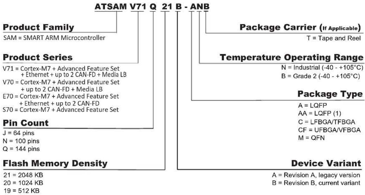
2. Ordering Information
other
| Product Family | Flash Memory Density | Package Carrier (If Applicable) | Temperature Operating Range | | --- | --- | --- | --- | | SAM | 21 | - | T = Tape and Reel | | V71 | 2048 | - | N = Industrial (-40 - +105°C) | | V70 | 1024 | - | B = Grade 2 (-40 - +105°C) | | E70 | 19 | - | - | | S70 | 144 | - | - | | J | 64 | - | - | | N | 100 | - | - | | Q | 144 | - | - | ATSAM V71 Q 21 B - ANB Temperature Operating Range Package Type A = LQFP AA = LQFP (1) C = LFBGA/TFBGA CF = UFBGA/VFBGA M = QFN Device Variant A = Revision A, legacy version B = Revision B, current variantNote:
- LQFP package type for Grade 2 variants.
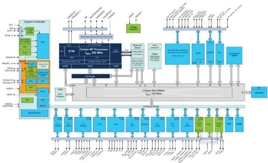
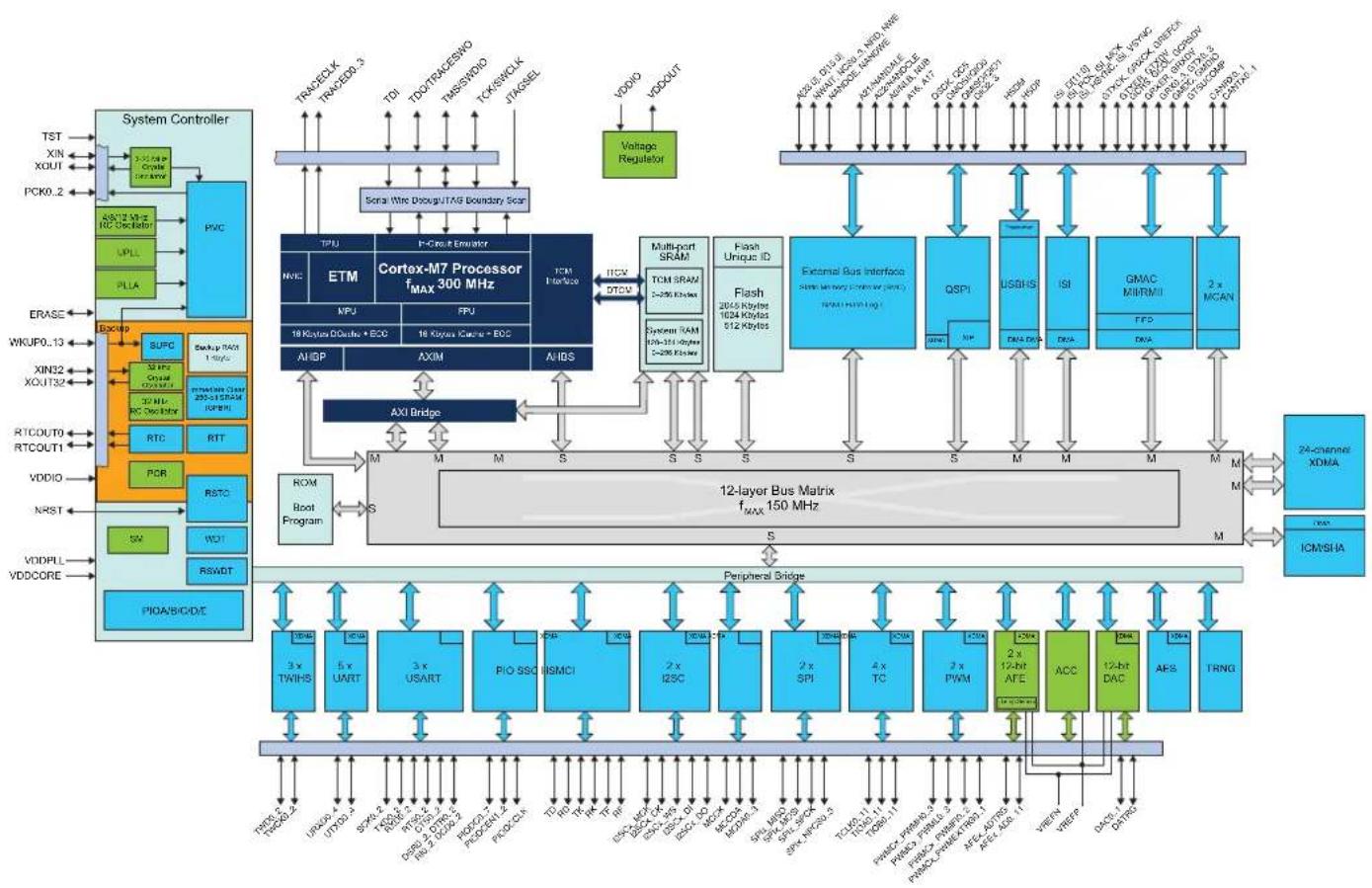
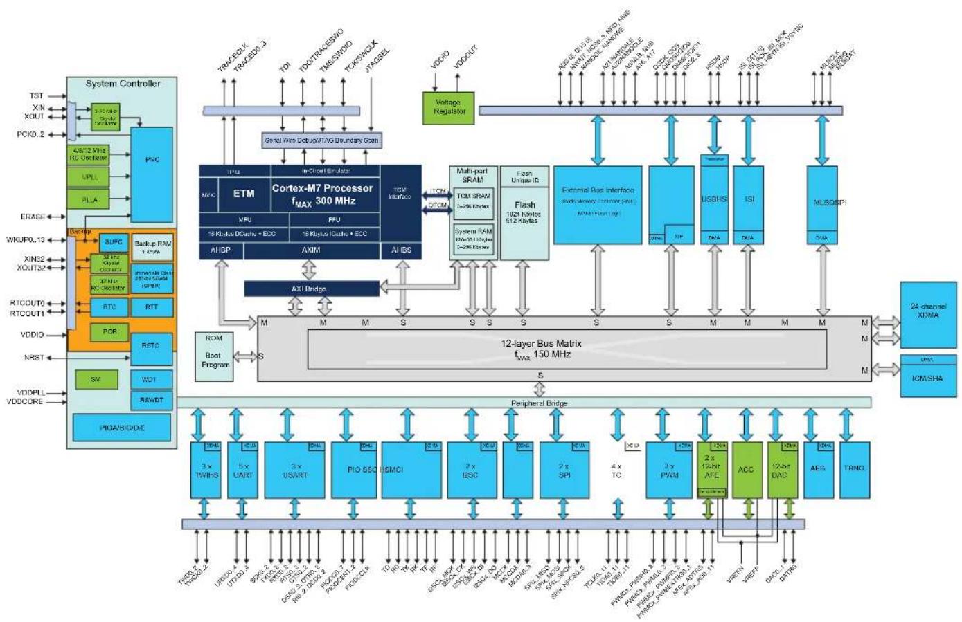
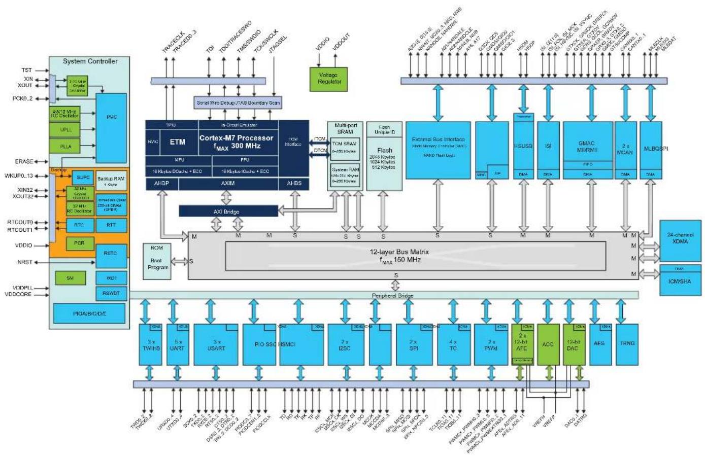
3. Block Diagram
Refer to the table 1. Configuration Summary for detailed configurations of memory size, package and features of the SAM E70/S70/V70/V71 devices.
Figure 3-1. SAM S70 144-pin Block Diagram
flowchart
graph TD
    subgraph System_Controller
        A["TST"] --> B["3x TBI"]
        C["XIN"] --> D["3x UART"]
        E["XOUT"] --> F["3x USART"]
        G["PCK0.2"] --> H["4xT2 MW RL Rectifier"]
        I["LPLL"] --> J["PLA"]
        K["PLA"] --> L["PLA"]
        M["ERASE"] --> N["5x TBI"]
        O["WKUPE.13"] --> P["5x UART"]
        Q["XN32 XOUT32"] --> R["5x USART"]
        S["RTCOUT0 RTCOUT1"] --> T["RTC"]
        U["VDDIO"] --> V["RSF"]
        W["NRST"] --> X["RSF"]
        Y["VDDPLL VDCORE"] --> Z["SM"]
        AA["PIGA/B/C/D/E"] --> AB["PGA/B/C/D/E"]
    end

    subgraph Cortex_M7Processor
        AC["Cortex-M7 Processor fMAX 300 MHz"] --> AD["TMP"]
        AD --> AE["ETM"]
        AE --> AF["MPU"]
        AF --> AG["AHSP"]
        AG --> AH["AUX Bridge"]
    end

    subgraph 12-layer_Bus_Matrix
        AI["12-layer Bus Matrix fMAX 150 MHz"] --> AJ["RAM"]
        AJ --> AK["S"]
        AK --> AL["M"]
        AL --> AM["S"]
        AM --> AN["S"]
        AN --> AO["S"]
        AO --> AP["S"]
        AP --> AQ["S"]
        AQ --> AR["S"]
        AR --> AS["S"]
        AS --> AT["S"]
        AT --> AU["S"]
        AU --> AV["S"]
        AV --> AW["S"]
        AW --> AX["S"]
        AX --> AY["S"]
        AY --> AZ["S"]
        AZ --> BA["S"]
        BA --> BB["S"]
        BB --> BC["S"]
        BC --> BD["S"]
        BD --> BE["S"]
        BE --> BF["S"]
        BF --> BG["S"]
        BG --> BH["S"]
        BH --> BI["S"]
        BI --> BJ["S"]
        BJ --> BK["S"]
        BK --> BL["S"]
        BL --> BM["S"]
        BM --> BN["S"]
        BN --> BO["S"]
        BO --> BP["S"]
        BP --> BQ["S"]
        BQ --> BR["S"]
        BR --> BS["S"]
        BS --> BT["S"]
        BT --> BU["S"]
        BU --> BV["S"]
        BV --> BW["S"]
        BW --> BX["S"]
        BX --> BY["S"]
        BY --> BZ["S"]
        BZ --> CA["S"]
        CA --> CB["S"]
        CB --> CC["S"]
        CC --> CD["S"]
        CD --> CE["S"]
        CE --> CF["S"]
        CF --> CG["S"]
        CG --> CH["S"]
        CH --> CI["S"]
        CI --> CJ["S"]
        CJ --> CK["S"]
        CK --> CL["S"]
        CL --> CM["S"]
        CM --> CN["S"]
        CN --> CO["S"]
        CO --> CP["S"]
        CP --> CQ["S"]
        CQ --> CR["S"]
        CR --> CS["S"]
        CS --> CT["S"]
        CT --> CU["S"]
        CU --> CV["S"]
        CV --> CW["S"]
        CW --> CX["S"]
        CX --> CY["S"]
        CY --> CZ["S"]
        CZ --> DA["S"]
    end

    subgraph Peripheral_Bridge
        AE["Peripheral Bridge"] --> AF["3 x TH/HSI 3x UART 3x USART PID SBC 2x SPI HIMO 2x USC 4x TC 2x PWM 2x 13.4A AFE ACC 13.4A DAC AES TRNG"]

    subgraph System_Controller
        AC
        AD
        AE
        AF
        AG
        AH
    end

    subgraph Peripheral_Bridge
        AI
        AE
    end
Figure 3-2. SAM E70 144-pin Block Diagram
flowchart
graph TD
    subgraph System_Controller
        A["TST"] --> B["XIN"]
        C["XOUT"] --> D["PCK0.2"]
        E["ERASE"] --> F["KWUP0.13"]
        G["XIN32"] --> H["XOUT32"]
        I["RTCOUT0"] --> J["RTCOUT1"]
        K["VDDIO"] --> L["NRST"]
        M["VDDPLL"] --> N["VDDCORE"]
        O["PUCL"] --> P["PLL"]
        Q["PLLX"] --> R["PLLX"]
        S["TTRCK"] --> T["TTRCK"]
        U["TRAGEDD.5"] --> V["TDI"]
        W["TOO/TRACEWSO"] --> X["TROSS/WDIO"]
        Y["TCK/SWCLK"] --> Z["JTAGSEL"]
        AA["TCMS"] --> AB["TCMS"]
        AC["TCMS"] --> AD["TCMS"]
        AE["TCMS"] --> AF["TCMS"]
        AG["TCMS"] --> AH["TCMS"]
        AI["TCMS"] --> AJ["TCMS"]
        AK["TCMS"] --> AL["TCMS"]
        AM["TCMS"] --> AN["TCMS"]
        AO["TCMS"] --> AP["TCMS"]
        AQ["TCMS"] --> AR["TCMS"]
        AS["TCMS"] --> AT["TCMS"]
    end

    subgraph System_Controller
        AU["TRACELCK"] --> AV["TRI"]
        AW["TRAGEDD.5"] --> AX["TDI"]
        AY["TDI"] --> AZ["TROSS/WDIO"]
        BA["TROSS/WDIO"] --> BB["TCK/SWCLK"]
        BC["TCK/SWCLK"] --> BD["JTAGSEL"]
        BE["TCMS"] --> BF["TRI"]
        BG["TRI"] --> BH["TRI"]
        BI["TRI"] --> BJ["TRI"]
        BK["TRI"] --> BL["TRI"]
        BM["TRI"] --> BN["TRI"]
        BO["TRI"] --> BP["TRI"]
        BQ["TRI"] --> BR["TRI"]
        BS["TRI"] --> BT["TRI"]
        BU["TRI"] --> BV["TRI"]
        BW["TRI"] --> BX["TRI"]
        BY["TRI"] --> BZ["TRI"]
        CA["TRI"] --> CB["TRI"]
        CC["TRI"] --> CD["TRI"]
        DD["TRI"] --> DE["TRI"]
        FD["TRI"] --> FDZ["TRI"]
        GD["TRI"] --> GDZ["TRI"]
        HD["TRI"] --> HDZ["TRI"]
        ID["TRI"] --> IDZ["TRI"]
        IDZ --> IDZ
        IDZ --> IDZ
    end

    subgraph System_Controller
        AJ["DVDO"] --> AK["DVDCUT"]
        AL["VDDOUT"] --> AM
        AM --> AM
        AN["VDDOUT"] --> AO
        AP["VDDOUT"] --> AQ
    end

    subgraph System_Controller
        AO["DVDCUT"] --> AP
    end

    subgraph System_Controller
        AQ["DVDCUT"] --> AR["DVDCUT"]
    end

    subgraph System_Controller
        AS["DVDCUT"] --> AT["DVDCUT"]

    subgraph System_Controller
        AU["DVDCUT"] --> AU1["DVDCUT"]

    subgraph System_Controller
        AU1["DVDCUT"] --> AU2["DVDCUT"]

    subgraph System_Controller
        AU2["DVDCUT"] --> AU3["DVDCUT"]

    subgraph System_Controller
        AU3["DVDCUT"] --> AU4["DVDCUT"]

    subgraph System_Controller
        AU4["DVDCUT"] --> AU5["DVDCUT"]

    subgraph System_Controller
        AU5["DVDCUT"] --> AU6["DVDCUT"]

    subgraph System_Controller
        AU6["DVDCUT"] --> AU7["DVDCUT"]

    subgraph System_Controller
        AU7["DVDCUT"] --> AU8["DVDCUT"]

    subgraph System_Controller
        AU8["DVDCUT"] --> AU9["DVDCUT"]

    subgraph System_Controller
        AU9["DVDCUT"] --> AU10["DVDCUT"]

    subgraph System_Controller
        AU10["DVDCUT"] --> AU11["DVDCUT"]

    subgraph System_Controller
        AU11["DVDCUT"] --> AU12["DVDCUT"]

    subgraph System_Controller
        AU12["DVDCUT"] --> AU13["DVDCUT"]

    subgraph System_Controller
        AU13["DVDCUT"] --> AU14["DVDCUT"]

    subgraph System_Controller
        AU14["DVDCUT"] --> AU15["DVDCUT"]

    subgraph System_Controller
        AU15["DVDCUT"] --> AU16["DVDCUT"]

    subgraph System_Controller
        AU16["DVDCUT"] --> AU17["DVDCUT"]

    subgraph System_Controller
        AU17["DVDCUT"] --> AU18["DVDCUT"]

    subgraph System_Controller
        AU18["DVDCUT"] --> AU19["DVDCUT"]

    subgraph System_Controller
        AU19["DVDCUT"] --> AU20["DVDCUT"]

    subgraph System_Controller
        AU20["DVDCUT"] --> AU21["DVDCUT"]

    subgraph System_Controller
        AU21["DVDCUT"] --> AU22["DVDCUT"]

    subgraph System_Controller
        AU22["DVDCUT"] --> AU23["DVDCUT"]

    subgraph System_Controller
        AU23["DVDCUT"] --> AU24["DVDCUT"]

    subgraph System_Controller
        AU24["DVDCUT"] --> AU25["DVDCUT"]

    subgraph System_Controller
        AU25["DVDCUT"] --> AU26["DVDCUT"]

    subgraph System_Controller
        AU26["DVDCUT"] --> AU27["DVDCUT"]

    subgraph System_Controller
        AU27["DVDCUT"] --> AU28["DVDCUT"]

    subgraph System_Controller
        AU28["DVDCUT"] --> AU29["DVDCUT"]

    subgraph System_Controller
        AU29["DVDCUT"] --> AU30["DVDCUT"]

    subgraph System_Controller
        AU30["DVDCUT"] --> AU31["DVDCUT"]

    subgraph System_Controller
        AU31["DVDCUT"] --> AU32["DVDCUT"]

    subgraph System_Controller
        AU32["DVDCUT"] --> AU33["DVDCUT"]

    subgraph System_Controller
        AU33["DVDCUT"] --> AU34["DVDCUT"]

    subgraph System_Controller
        AU34["DVDCUT"] --> AU35["DVDCUT"]

    subgraph System_Controller
        AU35["DVDCUT"] --> AU36["DVDCUT"]

    subgraph System_Controller
        AU36["DVDCUT"] --> AU37["DVDCUT"]

    subgraph System_Controller
        AU37["DVDCUT"] --> AU38["DVDCUT"]

    subgraph System_Controller
        AU38["DVDCUT"] --> AU39["DVDCUT"]

    subgraph System_Controller
        AU39["DVDCUT"] --> AU40["DVDCUT"]

    subgraph System_Controller
        AU40["DVDCUT"] --> AU41["DVDCUT"]

    subgraph System_Controller
        AU41["DVDCUT"] --> AU42["DVDCUT"]

    subgraph System_Controller
        AU42["DVDCUT"] --> AU43["DVDCUT"]

    subgraph System_Controller
        AU43["DVDCUT"] --> AU44["DVDCUT"]

    subgraph System_Controller
        AU44["DVDCUT"] --> AU45["DVDCUT"]

    subgraph System_Controller
        AU45["DVDCUT"] --> AU46["DVDCUT"]

    subgraph System_Controller
        AU46["DVDCUT"] --> AU47["DVDCUT"]

    subgraph System_Controller
        AU47["DVDCUT"] --> AU48["DVDCUT"]

    subgraph System_Controller
        AU48["DVDCUT"] --> AU49["DVDCUT"]

    subgraph System_Controller
        AU49["DVDCUT"] --> AU50["DVDCUT"]

    subgraph System_Controller
        AU50["DVDCUT"] --> AU51["DVDCUT"]

    subgraph System_Controller
        AU51["DVDCUT"] --> AU52["DVDCUT"]

    subgraph System_Controller
        AU52["DVDCUT"] --> AU53["DVDCUT"]

    subgraph System_Controller
        AU53["DVDCUT"] --> AU54["DVDCUT"]

    subgraph System_Controller
        AU54["DVDCUT"] --> AU55["DVDCUT"]

    subgraph System_Controller
        AU55["DVDCUT"] --> AU56["DVDCUT"]

    subgraph System_Controller
        AU56["DVDCUT"] --> AU57["DVDCUT"]

    subgraph System_Controller
        AU57["DVDCUT"] --> AU58["DVDCUT"]

    subgraph System_Controller
        AU58["DVDCUT"] --> AU59["DVDCUT"]

    subgraph System_Controller
        AU59["DVDCUT"] --> AU60["DVDCUT"]

    subgraph System_Controller
        AU60["DVDCUT"] --> AU61["DVDCUT"]

    subgraph System_Controller
        AU61["DVDCUT"] --> AU62["DVDCUT"]

    subgraph System_Controller
        AU62["DVDCUT"] --> AU63["DVDCUT"]

    subgraph System_Controller
        AU63["DVDCUT"] --> AU64["DVDCUT"]

    subgraph System_Controller
        AU64["DVDCUT"] --> AU65["DVDCUT"]

    subgraph System_Controller
        AU65["DVDCUT"] --> AU66["DVDCUT"]

    subgraph System_Controller
        AU66["DVDCUT"] --> AU67["DVDCUT"]

    subgraph System_Controller
        AU67["DVDCUT"] --> AU68["DVDCUT"]

    subgraph System_Controller
        AU68["DVDCUT"] --> AU69["DVDCUT"]

    subgraph System_Controller
        AU69["DVDCUT"] --> AU70["DVDCUT"]

    subgraph System_Controller
        AU70["DVDCUT"] --> AU71["DVDCUT"]

    subgraph System_Controller
        AU71["DVDCUT"] --> AU72["DVDCUT"]

    subgraph System_Controller
        AU72["DVDCUT"] --> AU73["DVDCUT"]

    subgraph System_Controller
        AU73["DVDCUT"] --> AU74["DVDCUT"]

    subgraph System_Controller
        AU74["DVDCUT"] --> AU75["DVDCUT"]

    subgraph System_Controller
        AU75["DVDCUT"] --> AU76["DVDCUT"]

    subgraph System_Controller
        AU76["DVDCUT"] --> AU77["DVDCUT"]

    subgraph System_Controller
        AU77["DVDCUT"] --> AU78["DVDCUT"]

    subgraph System_Controller
        AU78["DVDCUT"] --> AU79["DVDCUT"]

    subgraph System_Controller
        AU79["DVDCUT"] --> AU80["DVDCUT"]

    subgraph System_Controller
        AU80["DVDCUT"] --> AU81["DVDCUT"]

    end

    style A fill:#f9f,stroke:#333,stroke-width:2px

    style B fill:#f9f,stroke:#333,stroke-width:2px

    style C fill:#f9f,stroke:#333,stroke-width:2px

    style D fill:#f9f,stroke:#333,stroke-width:2px

    style E fill:#f9f,stroke:#333,stroke-width:2px

    style F fill:#f9f,stroke:#333,stroke-width:2px

    style G fill:#f9f,stroke:#333,stroke-width:2px

    style H fill:#f9f,stroke:#333,stroke-width:2px

    style I fill:#f9f,stroke:#333,stroke-width:2px

    style J fill:#f9f,stroke:#333,stroke-width:2px

    style K fill:#f9f,stroke:#333,stroke-width:2px

    style L fill:#f9f,stroke:#333,stroke-width:2px

    style M fill:#f9f,stroke:#333,stroke-width:2px

    style N fill:#f9f,stroke:#333,stroke-width:2px

    style O fill:#f9f,stroke:#333,stroke-width:2px

    style P fill:#f9f,stroke:#333,stroke-width:2px

    style Q fill:#f9f,stroke:#333,stroke-width:2px

    style R fill:#f9f,stroke:#333,stroke-width:2px

    style S fill:#f9f,stroke:#333,stroke-width:2px

    style T fill:#f9f,stroke:#333,stroke-width:2px

    style U fill:#f9f,stroke:#333,stroke-width:2px

    style V fill:#f9f,stroke:#333,stroke-width:2px

    style W fill:#f9f,stroke:#333,stroke-width:2px

    style X fill:#f9f,stroke:#333,stroke-width:2px

    style Y fill:#f9f,stroke:#333,stroke-width:2px

    style Z fill:#f9f,stroke:#333,stroke-width:2px

    style AA fill:#f9f,stroke:#333,stroke-width:2px

    style AB fill:#f9f,stroke:#333,stroke-width:2px

    style AC fill:#f9f,stroke:#333,stroke-width:2px

    style AD fill:#f9f,stroke:#333,stroke-width:2px

    style AE fill:#f9f,stroke:#333,stroke-width:2px

    style AF fill:#f9f,stroke:#333,stroke-width:2px

    style AG fill:#f9f,stroke:#333,stroke-width:2px

    style AH fill:#f9f,stroke:#333,stroke-width:2px

    style AI fill:#f9f,stroke:#333,stroke-width:2px

    style AJ fill:#f9f,stroke:#333,stroke-width:2px

    style AK fill:#f9f,stroke:#333,stroke-width:2px

    style AL fill:#f9f,stroke:#333,stroke-width:2px

    style AM fill:#f9f,stroke:#333,stroke-width:2px

    style AN fill:#f9f,stroke:#333,stroke-width:2px

    style AO fill:#f9f,stroke:#333,stroke-width:2px

    style AP fill:#f9f,stroke:#333,stroke-width:2px

    style AQ fill:#f9f,stroke:#333,stroke-width:2px

    style AR fill:#f9f,stroke:#333,stroke-width:2px

    style AS fill:#f9f,stroke:#333,stroke-width:2px

    style AT fill:#f9f,stroke:#333,stroke-width:2px

    style AV fill:#f9f,stroke:#333,stroke-width:2px

    style AW fill:#f9f,stroke:#333,stroke-width:2px

    style AX fill:#f9f,stroke:#333,stroke-width:2px

    style AY fill:#ccf,stroke:#ff0000
Figure 3-3. SAM V70 144-pin Block Diagram
flowchart
graph TD
    subgraph System_Controller
        A["TST"] --> B["3.5V/4V Core Control"]
        C["XIN"] --> D["45V/12 MHz RC Oscillator"]
        E["XOUT"] --> F["LPLL"]
        G["PCK0..2"] --> H["PLLX"]
        I["TRAE"] --> J["ERASE"]
        K["WKUP0..13"] --> L["DCDCRP"]
        M["XIN32"] --> N["6.8 Hz Array"]
        O["XOUT32"] --> P["3.6 MHz RC Oscillator"]
        Q["RTCOUT0"] --> R["RTC"]
        S["RTCOUT1"] --> T["RTC"]
        U["VDDIO"] --> V["PCR"]
        W["NRST"] --> X["RSSTC"]
        Y["VDDPLL"] --> Z["SVM"]
        AA["VDDCORE"] --> AB["RSWDT"]
        AC["PIGA/B/C/D/E"] --> AD["RAM/Boot Program"]
    end

    subgraph Cortex_M7_Processer
        AE["ETM"] --> AF["Cortex-M7 Processor fMAX 300 MHz"]
        AG["MPU"] --> AH["Multi-port SRAM"]
        AI["PFU"] --> AJ["External Bus Interface"]
        AK["AFI"] --> AL["1824 Keybird 612 Keylas"]
        AM["AXIM"] --> AN["1824 Keybird 612 Keylas"]
        AO["AXI Bridge"] --> AP["1824 Keybird 612 Keylas"]
    end

    subgraph Peripheral_Bridge
        AQ["3x TWIHS"] --> AR["Peripheral Bridge"]
        AS["5x UART"] --> AR
        AT["3x USART"] --> AR
        AU["PIO SSC"] --> AV["Peripheral Bridge"]
        AW["ISMCI"] --> AX["Peripheral Bridge"]
        AY["2x IZSC"] --> AZ["Peripheral Bridge"]
        BA["2x SPI"] --> BB["Peripheral Bridge"]
        BC["2x PWM"] --> BD["Peripheral Bridge"]
        BE["ACC"] --> BF["Peripheral Bridge"]
    end

    subgraph Control_Scale
        BG["TRAECK"] --> BH["TRACECK 3"]
        BI["TRDQ"] --> BJ["TDI"]
        BK["TOOITRACESNO"] --> BL["MOSW/OID"]
        BM["TAGSWEICK"] --> BN["JTAGSEL"]
        BO["VDDIO"] --> BP["VDDOUT"]
        BQ["Voltage Regulator"] --> BR["Voltage Regulator"]
        BS["KSS-RL1B"] --> BT["KSS-RL1B WITH MODE 2 AND WIRE"]
        BU["KSS-RL1B WITH MODE 2 AND WIRE"] --> BV["KSS-RL1B WITH MODE 2 AND WIRE"]
        BW["KSS-RL1B WITH MODE 2 AND WIRE"] --> BX["KSS-RL1B WITH MODE 2 AND WIRE"]
        BY["KSS-RL1B WITH MODE 2 AND WIRE"] --> BZ["KSS-RL1B WITH MODE 2 AND WIRE"]
    end

    subgraph Memory_Circuit
        CA["TMU"] --> CB["TMU Debug/UTANS Regulatory Scan"]
        CC["MVC"] --> CD["MVC Controller"]
        DD["MTM"] --> DE["TMT Controller"]
        EF["MPU"] --> GF["MPU Controller"]
        GH["16 Keyless DCuts + ECO"] --> HF["16 Keyless DCuts + ECO"]
        ID["MSP"] --> IE["MSP Controller"]
    end

    subgraph Control_Scale
        AF["Cortex-M7 Processor fMAX 300 MHz"]
        AH["TCM Interface"] --> AI["Cortex-M7 Processor fMAX 300 MHz"]
        AJ["ATM IGS"] --> AK["AKT IGS Controller"]
        AL["MUSB"] --> AM["MUSB Controller"]
    end

    subgraph Memory_Circuit
        AN["MOMI"] --> AO["MOMI Controller"]
        AP["MOSI"] --> AQ["MOSI Controller"]
    end

    subgraph Control_Scale
        AR["Multi-port SRAM"] --> AS["Multi-port SRAM Controller"]
        AT["MOSI"] --> AU["MOSI Controller"]
        AV["MUSB"] --> AW["MUSB Controller"]
    end

    subgraph Memory_Circuit
        AX["Flash Unique ID"] --> AY["Flash Unique ID Controller"]
        AZ["External Bus Interface"] --> BA["External Bus Interface Controller"]
    end

    subgraph Control_Scale
        ARM["External Bus Interface Controller"] --> ASM["External Bus Interface Controller"]
        AZM["External Bus Interface Controller"] --> AZM_1["External Bus Interface Controller"]
    end

    subgraph Memory_Circuit
        BAM["External Bus Interface Controller"] --> AZM_2["External Bus Interface Controller"]
    end

    subgraph Control_Scale
        BAM_1 & BA_2 & BZM_1 & BZM_2 & BZM_3 & BZM_4 & BZM_5 & BZM_6 & BZM_7 & BZM_8 & BZM_9 & BZM_10 & BZM_11 & BZM_12 & BZM_13 & BZM_14 & BZM_15 & BZM_16 & BZM_17 & BZM_18 & BZM_19 & BZM_20 & BZM_21 & BZM_22 & BZM_23 & BZM_24 & BZM_25 & BZM_26 & BZM_27 & BZM_28 & BZM_29 & BZM_30 & BZM_31 & BZM_32 & BZM_33 & BZM_34 & BZM_35 & BZM_36 & BZM_37 & BZM_38 & BZM_39 & BZM_40 & BZM_41 & BZM_42 & BZM_43 & BZM_44 & BZM_45 & BZM_46 & BZM_47 & BZM_48 & BZM_49 & BZM_50 & BZM_51 & BZM_52 & BZM_53 & BZM_54 & BZM_55 & BZM_56 & BZM_57 & BZM_58 & BZM_59 & BZM_60 & BZM_61 & BZM_62 & BZM_63 & BZM_64 & BZM_65 & BZM_66 & BZM_67 & BZM_68 & BZM_69 & BZM_70 & BZM_71 & BZM_72 & BZM_73 & BZM_74 & BZM_75 & BZM_76 & BZM_77 & BZM_78 & BZM_79 & BZM_80 & BZM_81 & BZM_82 & BZM_83 & BZM_84 & BZM_85 & BZM_86 & BZM_87 & BZM_88 & BZM_89 & BZM_90 & BZM_91 & BZM_92 & BZM_93 & BZM_94 & BZM_95 & BZM_96 & BZM_97 & BZM_98 & BZM_99 & BZM_AE_DACD
    end

    subgraph Control_Scale
        AC["RAM/Boot Program"] <--> AD["RROM Boot Program"]
    end

    subgraph Memory_Circuit
        AE --> AE
        AF --> AF
        AH --> AH
        AI --> AI
        AJ --> AJ
        AK --> AK
        AL --> AL
        AM --> AL
        AN --> AN
        AO --> AO
        AP --> AP
        AQ --> AQ
        AR --> AR
        AS --> AS
        AT --> AT
        AU --> AU
        AV --> AV
    end

    subgraph Memory_Circuit
        AH --> AH
        AI --> AI
        AJ --> AJ
        AK --> AJ
        AL --> AL
        AM --> AM
    end

    subgraph Memory_Circuit
        AH --> AH
        AI --> AH
        AJ --> AH
    end

    subgraph Control_Scale
        AO --> AO
        AP --> AP
        AQ --> AQ
    end
Figure 3-4. SAM V71 144-pin Block Diagram
flowchart
graph TD
    subgraph System_Controller
        A["TST"] --> B["XIN"]
        C["XOUT"] --> D["PCK0.2"]
        E["ERASE"] --> F["WKUP0.13"]
        G["XIN32"] --> H["XOUT32"]
        I["RTCOUT0"] --> J["RTCOUT1"]
        K["VDDIO"] --> L["NRST"]
        M["VDDPLL"] --> N["VDDCORE"]
        O["SW"] --> P["PICA/B/C/D/E"]
        Q["SUPC"] --> R["Backup RAW 1.0GHz"]
        S["PCI"] --> T["RTC"]
        U["RSTC"] --> V["PCR"]
        W["RSW"] --> X["MOT"]
        Y["RAM"] --> Z["RSWDT"]
        AA["PUCL"] --> AB["LPLL"]
        AC["PLLA"] --> AD["PLLX"]
        AE["SPIC"] --> AF["SPIC/SPIC/SPIC"]
        AG["ADC"] --> AH["ACO"]
    end

    subgraph Cortex_M7_Processer
        AI["Cortex-M7 Processor f_MAX 300 MHz"] --> AJ["ETM"]
        AK["Multi-port SRAM"] --> AL["FXI"]
        AM["Flash Unique ID"] --> AN["External Bus Interface"]
    end

    subgraph Peripheral_Bridge
        AO["Peripheral Bridge"] --> AP["3x TWIHS"]
        AO --> AQ["5x UART"]
        AO --> AR["3x USART"]
        AO --> AS["PIO SSC IISMCI"]
        AO --> AT["2x IZSC"]
        AO --> AU["2x SPI"]
        AO --> AV["4x TC"]
        AO --> AW["2x PWM"]
        AO --> AX["2x 12-bit AFE"]
        AO --> AY["ACC"]
        AO --> AZ["12-bit DAC"]
        AO --> BA["AES"]
        AO --> BB["TRNG"]

    subgraph Control_Regulator
        BC["Voltage Regulator"] --> BD["Serial Wire Debug 07/6 Boundary Scan"]
        BE["Signal Generator"] --> BF["TCU Interface"]
        BG["External Bus Interface"] --> BH["External Memory Controller (INTC)"]
    end

    subgraph System_Controller
        BI["TRACELCK PROCED 3"] --> BJ["TDI"]
        BI --> BK["TDO/TRACESNO"]
        BI --> BL["TMS/SW/OI"]
        BI --> BM["TCM/SW/CLK"]
        BI --> BN["J/TASSEL"]
        BI --> BO["VDD/O"]
        BI --> BP["VDD/OUT"]
    end

    subgraph Cortex_M7_Processer
        BQ["Cortex-M7 Processor f_MAX 300 MHz"] --> BR["TPU"]
        BQ --> BS["In-Circuit Simulator"]
        BQ --> BT["MTU"]
        BQ --> BU["MPU"]
        BQ --> BV["FPU"]
        BQ --> BW["18 Kbits/DCbits + ECO"]
        BQ --> BX["18 Kbits/DCbits + ECO"]
        BQ --> BY["AI/SP"]
        BQ --> BZ["AXIM"]
        BQ --> CA["AXI Bridge"]
    end

    subgraph Peripheral_Bridge
        CB["Cable 12-layer Bus Matrix f_MAX 150 MHz"] --> CC["12-layer Bus Interface"]
    end

    subgraph Control_Regulator
        DD["24-channel XDMA"] --> DD
    end

    subgraph System_Controller
        DE["Cable 12-layer Bus Interface"] --> DE
    end

    subgraph Cortex_M7_Processer
        DE --> DE1["TCU Interface"]
        DE --> DE2["ATC Interface"]
    end

    subgraph Control_Regulator
        DE1 --> DE2
    end

    subgraph System_Controller
        DE2 --> DE3["TCU Interface"]
        DE2 --> DE4["ATC Interface"]
    end

    subgraph Cortex_M7_Processer
        DE3 --> DE4
    end

    subgraph Control_Regulator
        DE4 --> DE5["TCU Interface"]
        DE4 --> DE6["ATC Interface"]
    end

    subgraph System_Controller
        DE5 --> DE6
    end

    subgraph Cortex_M7_Processer
        DE6 --> DE7
    end

    subgraph Control_Regulator
        DE7 --> DE8
    end

    subgraph System_Controller
        DE8 --> DE9
    end

    subgraph Cortex_M7_Processer
        DE9 --> DE10
    end

    subgraph Control_Regulator
        DE10 --> DE11
    end

    subgraph System_Controller
        DE11 --> DE12
    end

    subgraph Cortex_M7_Processer
        DE12 --> DE13
    end

    subgraph Control_Regulator
        DE13 --> DE14
    end

    subgraph System_Controller
        DE14 --> DE15
    end

    subgraph Cortex_M7_Processer
        DE15 --> DE16
    end

    subgraph Control_Regulator
        DE16 --> DE17
    end

    subgraph System_Controller
        DE17 --> DE18
    end

    subgraph Cortex_M7_Processer
        DE18 --> DE19
    end

    subgraph Control_Regulator
        DE19 --> DE20
    end

    subgraph System_Controller
        DE20 --> DE21
    end

    subgraph Cortex_M7_Processer
        DE21 --> DE22
    end

    subgraph Control_Regulator
        DE22 --> DE23
    end

    subgraph System_Controller
        DE23 --> DE24
    end

    subgraph Cortex_M7_Processer
        DE24 --> DE25
    end

    subgraph Control_Regulator
        DE25 --> DE26
    end

    subgraph System_Controller
        DE26 --> DE27
    end

    subgraph Cortex_M7_Processer
        DE27 --> DE28
    end

    subgraph Control_Regulator
        DE28 --> DE29
    end

    subgraph System_Controller
        DE29 --> DE30
    end

    subgraph Cortex_M7_Processer
        DE30 --> DE31
    end

    subgraph Control_Regulator
        DE31 --> DE32
    end

    subgraph System_Controller
        DE32 --> DE33
    end

    subgraph Cortex_M7_Processer
        DE33 --> DE34
    end

    subgraph Control_Regulator
        DE34 --> DE35
    end

    subgraph System_Controller
        DE35 --> DE36
    end

    subgraph Cortex_M7_Processer
        DE36 --> DE37
    end

    subgraph Control_Regulator
        DE37 --> DE38
    end

    subgraph System_Controller
        DE38 --> DE39
    end

    subgraph Cortex_M7_Processer
        DE39 --> DE40
    end

    subgraph Control_Regulator
        DE40 --> DE41
    end

    subgraph System_Controller
        DE41 --> DE42
    end

    subgraph Cortex_M7_Processer
        DE42 --> DE43
    end

    subgraph Control_Regulator
        DE43 --> DE44
    end

    subgraph System_Controller
        DE44 --> DE45
    end

    subgraph Cortex_M7_Processer
        DE45 --> DE46
    end

    subgraph Control_Regulator
        DE46 --> DE47
    end

    subgraph System_Controller
        DE47 --> DE48
    end

    subgraph Cortex_M7_Processer
        DE48 --> DE49
    end

    subgraph Control_Regulator
        DE49 --> DE50
    end

    subgraph System_Controller
        DE50 --> DE51
    end

    subgraph Cortex_M7_Processer
        DE51 --> DE52
    end

    subgraph Control_Regulator
        DE52 --> DE53
    end

    subgraph System_Controller
        DE53 --> DE54
    end

    subgraph Cortex_M7_Processer
        DE54 --> DE55
    end

    subgraph Control_Regulator
        DE55 --> DE56
    end

    subgraph System_Controller
        DE56 --> DE57
    end

    subgraph Cortex_M7_Processer
        DE57 --> DE58
    end

    subgraph Control_Regulator
        DE58 --> DE59
    end

    subgraph System_Controller
        DE59 --> DE60
    end

    subgraph Cortex_M7_Processer
        DE60 --> DE61
    end

    subgraph Control_Regulator
        DE61 --> DE62
    end

    subgraph System_Controller
        DE62 --> DE63
    end

    subgraph Cortex_M7_Processer
        DE63 --> DE64
    end

    subgraph Control_Regulator
        DE64 --> DE65
    end

    subgraph System_Controller
        DE65 --> DE66
    end
4. Signal Description
The following table provides details on signal names classified by peripherals.
Table 4-1. Signal Description List
| Signal Name Function Type Active Level | Voltage Reference | Comments | |||
| Power Supplies | |||||
| VDDIO | Peripherals I/O Lines Power Supply | Power - - - | |||
| VDDIN | Voltage Regulator Input, AFE, DAC, and Analog Comparator Power Supply(1) | Power - - - | |||
| VDDOUT Voltage Regulator Output Power - - - | |||||
| VDDPLL PLLA Power Supply Power - - - | |||||
| VDDPLLUSB | USB PLL and Oscillator Power Supply | Power - - - | |||
| VDDCORE | Powers the core, the embedded memories and the peripherals | Power - - - | |||
| GND, GNDPLL, GNDPLLUSB, GNDANA, GNDUTMI | Ground Ground - - - | ||||
| VDDUTMII | USB Transceiver Power Supply | Power - - - | |||
| VDDUTMIC USB Core Power Supply Power - - - | |||||
| GNDUTMI | USB Ground | Ground - - - | |||
| Clocks, Oscillators, and PLLs | |||||
| XIN | Main Oscillator Input | Input | - | VDDIO | If any signal is not used, its PIO pin should be setup as an output, driven low, and attached to a dedicated trace on the board in order to reduce current consumption. |
| XOUT | Main Oscillator Output Output | - | |||
| XIN32 | Slow Clock Oscillator Input Input | - | |||
| XOUT32 | Slow Clock Oscillator Output | Output | - | ||
| PCK0-PCK2 | Programmable Clock Output | Output | - | - | |
| Real Time Clock | |||||
| RTCOUTO | Programmable RTC Waveform Output | Output | - | VDDIO | - |
| RTCOUT1 | Programmable RTC Waveform Output | Output | - | - | |
| Serial Wire Debug/JTAG Boundary Scan | |||||
| SWCLK/TCK | Serial Wire Clock/Test Clock (Boundary scan mode only) | Input | - | VDDIO | - |
| TDI | Test Data In (Boundary scan mode only) | Input | - | - | |
| TDO/TRACESWO | Test Data Out (Boundary scan mode only) | Output | - | - | |
| SWDIO/TMS | Serial Wire Input/Output / Test Mode Select (Boundary scan mode only) | I/O / Input | - | - | |
| JTAGSEL JTAG Selection Input | High | - | |||
| Trace Debug Port | |||||
| TRACECLK Trace Clock Output - | VDDIO | PCK3 is used for ETM | |||
| TRACED0-TRACED3 Trace Data Output -- | |||||
| Flash Memory | |||||
| ERASE | Flash and NVM Configuration Bits Erase Command | Input High VDDIO - | |||
| Reset/Test | |||||
| NRST | Synchronous Microcontroller Reset | I/O Low | VDDIO | - | |
| TST Test Select Input -- | |||||
| Universal Asynchronous Receiver Transceiver - UART(x=[0:4]) | |||||
| URXDx | UART Receive Data | Input | - | - | PCK4 can be used to generate the baud rate |
| UTXDx | UART Transmit Data | Output - | - | ||
| PIO Controller - PIOA - PIOB - PIOC - PIOD - PIOE | |||||
| PA0-PA31 | Parallel I/O Controller A | I/O | - | VDDIO | - |
| PB0-PB9, PB12-PB13 | Parallel I/O Controller B | I/O | -- | ||
| PC0- PC31 | Parallel I/O Controller C | I/O | - | - | |
| PD0-PD31 | Parallel I/O Controller D | I/O | - | - | - |
| PE0-PE5 | Parallel I/O Controller E | I/O | - | - | - |
| PIO Controller - Parallel Capture Mode | |||||
| PIODC0-PIODC7 Parallel Capture Mode Data | Input | - | VDDIO | - | |
| PIODCCLK | Parallel Capture Mode Clock | Input | - | - | |
| PIODCEN1- PIODCEN2 | Parallel Capture Mode Enable | Input | -- | ||
| External Bus Interface | |||||
| D[15:0] | Data Bus | I/O | - | - | - |
| A[23:0] | Address Bus | Output | - | - | - |
| NWAIT | External Wait Signal | Input | Low | - | - |
| Static Memory Controller (SMC) | |||||
| NCS0-NCS3 | Chip Select Lines | Output | Low | - | - |
| NRD | Read Signal | Output | Low | - | - |
| NWE | Write Enable | Output | Low | - | - |
| NWR0-NWR1 | Write Signal | Output | Low | - | - |
| NBS0-NBS1 | Byte Mask Signal | Output | Low | - | - |
| NAND Flash Logic | |||||
| NANDOE | NAND Flash Output Enable | Output | Low | - | - |
| NANDWE | NAND Flash Write Enable | Output | Low | - | - |
| High-Speed Multimedia Card Interface (HSMCI) | |||||
| MCCK | Multimedia Card Clock | O | - | - | - |
| MCCDA | Multimedia Card Slot A Command | I/O | - | - | - |
| MCDA0-MCDA3 | Multimedia Card Slot A Data | I/O | - | - | - |
| Universal Synchronous Asynchronous Receiver Transmitter (USART(x=[0:2])) | |||||
| SCKx USARTx Serial Clock I/O -- | PCK4 can be used to generate the baud rate | ||||
| TXDx USARTx Transmit Data I/O -- | |||||
| RXDx USARTx Receive Data Input -- | |||||
| RTSx USARTx Request To Send Output | -- | ||||
| CTSx | USARTx Clear To Send | Input -- | |||
| DTRx | USARTx Data Terminal Ready | Output | - | - | |
| DSRx | USARTx Data Set Ready | Input -- | |||
| DCDx USARTx Data Carrier Detect Input -- | |||||
| Rlx | USARTx Ring Indicator | Input -- | |||
| LONCOL1 | LON Collision Detection | Input -- | |||
| Synchronous Serial Controller (SSC) | |||||
| TD | SSC Transmit Data | Output | - | - | - |
| RD | SSC Receive Data | Input -- | - | ||
| TK | SSC Transmit Clock | I/O -- | - | ||
| RK | SSC Receive Clock | I/O -- | - | ||
| TF SSC Transmit Frame Sync I/O -- | - | ||||
| RF SSC Receive Frame Sync I/O -- | - | ||||
| Inter-IC Sound Controller (I2SC[1..0]) | |||||
| I2SCx_MCK | Host Clock | Output | - | VDDIO | GCLK[PID] can be used to generate the baud rate |
| I2SCx_CK | Serial Clock | I/O - | VDDIO | ||
| I2SCx_WS I | ^2 S Word Select | I/O - | VDDIO | ||
| I2SCx_DI | Serial Data Input | Input | - | VDDIO | |
| I2SCx_DO | Serial Data Output | Output | - | VDDIO | |
| Image Sensor Interface (ISI) | |||||
| ISI_D0-ISI_D11 | Image Sensor Data | Input | - | - | - |
| ISI_MCK | Image sensor Reference clock.No dedicated signal, PCK1 can be used. | Output | -- | - | |
| ISI_HSYNC | Image Sensor Horizontal Synchro | Input -- | - | ||
| ISI_VSYNC | Image Sensor Vertical Synchro | Input -- | - | ||
| ISI_PCK | Image Sensor Data clock | Input | - | - | - |
| Timer Counter (TC(x=[0:11])) | |||||
| TCLKx | TC Channel x External Clock Input | Input -- | PCK6 can be used as an input clock | ||
| TIOAx | TC Channel x I/O Line A I/O -- | PCK7 can be used as an input clock for TC0.Ch0 only | |||
| TIOBx | TC Channel x I/O Line B I/O -- | ||||
| Pulse-Width Modulation Controller (PWMc(x=[0..1])) | |||||
| PWMc_PWMH0-PWMCx_PWMH3 | Waveform Output High for Channel 0-3 | Output | -- | - | |
| PWMc_PWML0-PWMCx_PWML3 | Waveform Output Low for Channel 0-3 | Output | -- | Only output in complementary mode when dead time insertion is enabled. | |
| PWMCx_PWMFI0-PWMCx_PWMFI2 | Fault Input Input - - - | ||||
| PWMCx_PWMEXTR G0-PWMCx_PWMEXTR G1 | External Trigger Input Input - - - | ||||
| Serial Peripheral Interface (SPI(x=[0..1])) | |||||
| SPIx_MISO Host In Client Out I/O - - - | |||||
| SPIx_MOSI Host Out Client In I/O - - - | |||||
| SPIx_SPCK SPI Serial Clock I/O - - - | |||||
| SPIx_NPCS0 | SPI Peripheral Chip Select 0 | I/O | Low | - | - |
| SPIx_NPCS1-SPIx_NPCS3 | SPI Peripheral Chip Select | Output | Low | - | - |
| Quad I/O SPI (QSPI) | |||||
| QSCK QSPI Serial Clock Output | - - - | ||||
| QCS | QSPI Chip Select | Output | - - - | ||
| QIO0-QIO3 | QSPI I/OQIO0 is QMOSI Host OutClient InQIO1 is QMISO Host In ClientOut | I/O - - - | |||
| Two-Wire Interface (TWIHS (x=0..2)) | |||||
| TWDx | TWIx Two-wire Serial Data | I/O - - - | |||
| TWCKx | TWIx Two-wire Serial Clock | I/O - - - | |||
| Analog | |||||
| VREFP | ADC, DAC and AnalogComparator PositiveReference | Analog | - - - | ||
| VREFN | ADC, DAC and AnalogComparator NegativeReference Must beconnected to GND orGNDANA. | Analog | - - - | ||
| 12-bit Analog Front End - (x=[0..1]) | |||||
| AFEx_AD0-AFEx_AD11(2) | Analog Inputs | Analog,Digital | - - - | ||
| AFEx_ADTRG | ADC Trigger | Input | - | VDDIO | - |
| 12-bit Digital-to-Analog Converter (DAC) | |||||
| DAC0-DAC1 | Analog Output | Analog,Digital | - - - | ||
| DATRG | DAC Trigger | Input | - | VDDIO | - |
| Fast Flash Programming Interface (FFPI) | |||||
| PGMEN0-PGMEN1 | Programming Enabling | Input | - | VDDIO | - |
| PGMM0-PGMM3 | Programming Mode | Input - | VDDIO | - | |
| PGMD0-PGMD15 | Programming Data | I/O - | - | ||
| PGMRDY | Programming Ready | Output | High | - | |
| PGMNVALID | Data Direction | Output | Low | - | |
| PGMNOE | Programming Read | Input | Low | - | |
| PGMNCMD | Programming Command | Input | Low | - | |
| USB High Speed (USBHS) | |||||
| HSDM USB High -Speed Data - | Analog, Digital | - | VDDUTMII | - | |
| HSDP USB High-Speed Data + -- | |||||
| VBG | Bias Voltage Reference for USB | Analog -- -- | |||
| Ethernet MAC 10/100 - GMAC | |||||
| GREFCK Reference Clock Input -- RMII only | |||||
| GTXCK Transmit Clock Input -- | MII only | ||||
| GRXCK | Receive Clock | Input -- | MII only | ||
| GTXEN | Transmit Enable Output -- -- | ||||
| GTX0 - GTX3 | Transmit Data | Output | - | - | GTX0-GTX1 only in RMII |
| GTXER | Transmit Coding Error | Output | - | - | MII only |
| GRXDV | Receive Data Valid | Input | - | - | MII only |
| GRX0 - GRX3 | Receive Data | Input | - | - | GRX0-GRX1 only in RMII |
| GRXER | Receive Error | Input -- -- | |||
| GCRS | Carrier Sense | Input -- | MII only | ||
| GCOL Collision Detected Input -- | MII only | ||||
| GMDC | Management Data Clock | Output | --- | ||
| GMDIO | Management Data Input/ Output | I/O | --- | ||
| GTSUCOMP | TSU timer comparison valid | Output | - | - | Active Low |
| Controller Area Network - MCAN (x=[0:1]) | |||||
| CANRXx | CAN Receive | Input -- | CANRX1 is available on PD28 for 100-pin onlyCANRX1 is available on PC12 for 144-pin only | ||
| CANTXx | CAN Transmit | Output | -- | PCK5 can be used for CAN clockPCK6 and PCK7 can be used for CAN timestamping | |
| MediaLB - (MLB) | |||||
| MLBCLK | MLB Clock | input -- -- | |||
| MLBSIG | MLB Signal I/O | --- | |||
| MLBDAT | MLB Data | I/O | --- | ||
Notes:
- Refer to the Active Mode section in the Power Considerations chapter for restrictions on the voltage range of analog cells.
- AFE0_AD11 is not an actual pin but is connected to a temperature sensor.
5. Automotive Quality Grade
The SAM V70 and SAM V71 devices are developed and manufactured according to the most stringent requirements of the international standard ISO-TS-16949. This data sheet contains limited values extracted from the results of extensive characterization (temperature and voltage).
The quality and reliability of the SAM V70 and SAM V71 has been verified during regular product qualification as per AEC-Q100 grade 2 ( -40^ to +105^ ).
Table 5-1. Temperature Grade Identification for Automotive Products
| Temperature (°C) Temperature Identifier Comments | |
| -40°C to +105°C B AEC-Q100 Grade 2 |
6. Package and Pinout
In the tables that follow, the column "Reset State" indicates the reset state of the line with mnemonics.
- "PIO""/"signal
Indicates whether the PIO Line resets in I/O mode or in peripheral mode. If "PIO" is mentioned, the PIO line is maintained in a static state as soon as the reset is released. As a result, the bit corresponding to the PIO line in the register PIO_PSR (Peripheral Status Register) resets low.
If a signal name is mentioned in the "Reset State" column, the PIO line is assigned to this function and the corresponding bit in PIO_PSR resets high. This is the case of pins controlling memories, in particular the address lines, which require the pin to be driven as soon as the reset is released.
• "I" / "O"
Indicates whether the signal is input or output state.
• "PU" / "PD"
Indicates whether pullup, pulldown, or nothing is enabled.
• "ST"
Indicates if Schmitt Trigger is enabled.
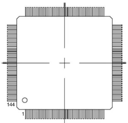
6.1 144-lead Packages
6.1.1 144-pin LQFP Package Outline
Figure 6-1. Orientation of the 144-pin LQFP Package
natural_image
Pure mechanical part diagram with no text, numbers, or symbols6.1.2 144-ball LFBGA/TFBGA Package Outline
Figure 6-2. Orientation of the 144-ball LFBGA/TFBGA Package

text_image
PIN A1 CORNER TOP VIEW6.1.3 144-ball UFBGA Package Outline
Figure 6-3. Orientation of the 144-ball UFBGA Package

text_image
TOP VIEW PIN A1 CORNER6.2 144-lead Package Pinout
Table 6-1. 144-lead Package Pinout
| LQFP Pin | LFBGA/TFBGA Ball | UFBGA Ball | Power Rail | I/O Type | Primary Alternate PIO | Periphera I A | PIO Periphera I B | PIO Periphera I C | PIO Periphera I D | Reset State | ||||||
| Signal Dir | Signal Dir Signal | Signal Dir Signal | Dir Signal | Dir Signal, | Dir, PU, PD, HiZ, ST | |||||||||||
| 102 C11 E11 | VDDIO GPIO_AD PA0 I/O WKUP0 | " " | IPWMCO_ PWMH0 | O TIOA0 | I/O A17 O I2SC0_M | CK | O PIO, I, PU, ST | |||||||||
| 99 | D12 | F11 | VDDIO GPIO_AD PA1 I/O WKUP1 | " " | IPWMCO_ PWML0 | O TIQB0 I/O A18 O I2SC0_C K | I/O PIO, I, PU, | ST | ||||||||
| 93 | E12 G12 | VDDIO GPIO | PA2 I/O WKUP2 | " " | IPWMCO_ PWMH1 | O | - | - | DATRG | I | - | - | PIO, I, PU, ST | |||
| LQFP Pin | UFBGA/TFBGA Ball | UFBGA Ball | Power Rail | I/O Type | Primary Alternate PIO | Peripheral IA | Dir Signal | Dir Signal, | PIO Peripheral IB | PIO Peripheral IC | PIO Peripheral ID | Reset State | |||||
| Signal Dir | Signal Dir | Signal Dir | Signal Dir | Signal Dir | Dir Signal | Dir Signal, | Dir, PU, PD, HIZ, ST | ||||||||||
| 91 F12 G11 | VDDIO GPIO_AD PA3 I/O PIODO | " | I TWO0 I/O | LONCOL | 1 | I | PCK2 | O | - | - | PIO, I, PU, ST | ||||||
| 77 K12 L12 | VDDIO GPIO | PA4 | I/O WKUP3/P | IODC1 " | I | TWCK0 | O | TCLK0 | I | UTXD1 | O | - | - | PIO, I, PU, ST | |||
| 73 | M11 | N13 | VDDIO | GPIO_AD | PA5 | I/O | WKUP4/PIODC2 " | IPWMC1_PWML3 | O | ISI_D4 | I | URXD1 | I | - | - | - | PIO, I, PU, ST |
| 114 | B9 | B11 | VDDIO | GPIO_AD | PA6 | I/O | - | - | - | - | PCK0 | O | UTXD1 | O | - | - | PIO, I, PU, ST |
| 35 | L2 | N1 | VDDIO | CLOCK | PA7 | I/O | XIN32* | I - | - | PWMCO_PWMH3 | O | - | - | - | - | - | PIO, HIZ |
| 36 M2 N2 | VDDIO CLOCK | PA8 I/O XOUT32 | " | O | PWMCI_PWMH3 | O | AFE0_ADTRG | I | - | - | - | - | PIO, HIZ | ||||
| 75 M12 | L11 VDDIO GPIO_AD PA9 | I/O WKUP6/P | IODC3 " | I URXD0 | I ISI_D3 I PWMCO_ | PWMFI0 | I - | - | PIO, I, PU, ST | ||||||||
| 66 | L9 | M10 | VDDIO | GPIO_AD | PA10 | I/O | PIODC4 " | I UTXD0 | O | PWMCO_PWMEXTRG0 | IRD | I - | - | - | PIO, I, PU, | ST | |
| 64 | J9 | N10 | VDDIO | GPIO_AD | PA11 | I/O | WKUP7/PIODCS " | IQCS | O | PWMCO_PWMH0 | O | PWMCI_PWMLO | O | - | - | - | PIO, I, PU, ST |
| 68 L10 N11 | VDDIO | GPIO_AD PA12 | I/O PIODO6 | " | IQIO1 | I/O PWMCO_ | PWMHI | O | PWMCI_PWMH0 | O | - | - | PIO, I, PU, ST | ||||
| 42 M3 M4 | VDDIO GPIO_AD PA13 | I/O | PIODO7 | " | IQIO0 | I/O PWMCO_ | PWMH2 | O | PWMCI_PWMIL1 | O | - | - | PIO, I, PU, ST | ||||
| 51 K6 | MG VDDIO GPIO_CL | K | PA14 | I/O | WKUP8/PIODCENT " | IQSCK | O | PWMCO_PWMH3 | O | PWMCI_PWMH1 | O | - | - | - | PIO, I, PU, ST | ||
| 49 | L5 | N6 | VDDIO | GPIO_AD | PA15 | I/O | - | - | D14 | I/O | TIOA1 | I/O | PWMCO_PWMIL3 | O | I2SC0_WS | I/O PIO, I, PU, ST | |
| 45 | K5 | L4 | VDDIO | GPIO_AD | PA16 | I/O | - | - | D15 | I/O | TIOB1 | I/O | PWMCO_PWMIL2 | O | I2SC0_DI | PIO, I, PU, ST | |
| 25 | J1 | J4 | VDDIO | GPIO_AD | PA17 | I/O | AFE0_AD6 * | IQIO2 | I/O PCK1 | O | PWMCO_PWMH3 | O | PWMH3 | O | - | - | PIO, I, PU, ST |
| 24 | H2 | J3 | VDDIO | GPIO_AD | PA18 | I/O | AFE0_AD7 * | IPWMC1_PWMEXTRG1 | I | PCK2 | O | A14 | O | - | - | - | PIO, I, PU, ST |
| 23 | H1 | J2 | VDDIO | GPIO_AD | PA19 | I/O | AFE0_AD8 /WKUP9 " | I - | - | PWMCO_PWMLO | O | A15 O | I2SC1_MCK | O | - | - | PIO, I, PU, ST |
| 22 | H3 | J1 | VDDIO | GPIO_AD | PA20 | I/O | AFE0_AD9 /WKUP10 " | I - | - | PWMCO_PWMIL1 | O | A16 O | I2SC1_CK | I/O PIO, I, PU, | ST | ||
| 32 | K2 | M1 | VDDIO | GPIO_AD | PA21 | I/O | AFE0_AD1 /PIODCEN ≥ | I RXD1 | I PCK1 | O | PWMCI_ | PWMFI0 | I - | - | - | PIO, I, PU, ST | |
| 37 K3 | M2 VDDIO GPIO_AD PA22 | I/O | PIODCCL | R* | IRK | I/O PWMCO_ | PWMEXTRG1 | I | NCS2 | O | - | - | PIO, I, PU, ST | ||||
| 46 | L4 | N5 | VDDIO | GPIO_AD | PA23 | I/O | - | - | SCK1 | I/O | PWMCO_PWMH0 | O | A19 O | PWMCI_PWMIL2 | O | - | PIO, I, PU, ST |
| LQFP Pin | LFBGA/TFBGA Ball | UFBGA Ball | Power Rail | I/O Type | Primary Alternate PIO | Peripheral A | PIO Peripheral B | PIO Peripheral C | PIO Peripheral D | Reset State | |||||||
| Signal Dir | Signal Dir Signal | Signal Dir Signal | Dir Signal | Dir Signal, | Dir, PU, PD, HIZ, ST | ||||||||||||
| 56 L7 N8 | VDDIO GPIO AD | PA24 I/O -- RTS1 O | PWMCO_ | PWMH1 | O | A20 | O | ISI PCK | I | PIO, I, PU, ST | |||||||
| 59 K8 L8 | VDDIO GPIO_AD | PA25 I/O -- CTS1 I | PWMCO_ | PWMH2 | O | A23 | O | MCCK | O | PIO, I, PU, ST | |||||||
| 62 | J8 | M9 | VDDIO | GPIO | PA26 | I/O | - | - | DCD1 | I | TIOA2 | O | MCDA2 | I/O | PWMCI_PWMFI1 | I | PIO, I, PU, ST |
| 70 | J10 | N12 | VDDIO | GPIO_AD | PA27 | I/O | - | - | DTR1 | O | TIOB2 | I/O | MCDA3 | I/O | ISLD7 | I | PIO, I, PU, ST |
| 112 | C9 | C11 | VDDIO | GPIO | PA28 | I/O | - | - | DSR1 | I | TCLK1 | I | MCCDA | I/O | PWMCI_PWMFI2 | I | PIO, I, PU, ST |
| 129 | A6 | A7 | VDDIO | GPIO | PA29 | I/O | - | - | RI1 | I | TCLK2 | I | - | - | - | - | PIO, I, PU, ST |
| 116 | A10 | A11 | VDDIO | GPIO | PA30 | I/O | WKUP11* | I | PWMCO_PWMML2 | O | PWMCI_PWMEXTRG0 | I | MCDA0 | I/O I25CO_D | O | O | PIO, I, PU, ST |
| 118 | C8 | C10 | VDDIO | GPIO_AD | PA31 | I/O | - | - | SPI0_NPCS1 | I/O PCK2 O | MCDA1 | I/O | PWMCI_PWMH2 | O | PIO, I, PU, ST | ||
| 21 H4 H2 | VDDIO GPIO PB0 | I/O AFE0_AD1 | 0/RTCOUTOn | I | PWMCO_PWMH0 | O | - | - | RXD0 | I | TF | I/O | PIO, I, PU, ST | ||||
| 20 G3 H1 | VDDIO GPIO PB1 | I/O AFE1_AD0 | / RTCOUTOn | I | PWMCO_PWMH1 | O | GTSUCOMP | O | TXD0 | I/O TX I/O | PIO, I, PU, | ST | |||||
| 26 | J2 | K1 | VDDIO | GPIO | PB2 | I/O | AFE0_AD5On | I | CANTX0 | O | - | - | CTS0 | I | SPI0_NPCS0 | I/O PIO, I, PU, ST | |
| 31 J3 | L1 VDDIO GPIO_AD PB3 | I/O | AFE0_AD2 | / WKUP12* | I | CANRX0 | I | PCK2 | O | RTS0 | O | ISLD2 | I | PIO, I, PU, ST | |||
| 105 | A12 | C13 | VDDIO GPIO_MLB | PB4 | I/O | TDI* | I | TWD1 | I/O PWMCO_PWMH2 | O | MLBCLK | I | TXD1 | I/O | PIO, I, PU, ST | ||
| 109 | C10 | C12 | VDDIO GPIO_MLB | PB5 | I/O | TDO/TRACESWO/WKUP13* | O | TWCK1 | O | PWMCO_PWMIL0 | O | MLBDAT | I/O | TD | O | O, PU | |
| 79 J11 K11 | VDDIO GPIO | PB6 | I/O SWIO/T | MS* | I | - | - | - | - | - | - | - | - | PIO,I,ST | |||
| 89 F9 H13 | VDDIO GPIO | PB7 | I/O SWCLK | TCK* | I | - | - | - | - | - | - | - | - | PIO,I,ST | |||
| 141 | A3 | B2 | VDDIO | CLOCK | PB8 | I/O | XOUT* | O | - | - | - | - | - | - | - | PIO, HZ | |
| 142 | A2 | A2 | VDDIO | CLOCK | PB9 | I/O | XIN* | I | - | - | - | - | - | - | - | PIO, HZ | |
| 87 G12 | J10 VDDIO GPIO PB12 I/O ERASE | * | I | PWMCO_PWMIL1 | O | GTSUCOMP | O | - | - | PCK0 | O | PIO, I, PD, ST | |||||
| 144 | B2 | A1 | VDDIO GPIO_AD PB13 I/O DAC0 | * | O | PWMCO_PWMIL2 | O | PCK0 | O | SCK0 I/O -- PIO, I, PU, | ST | ||||||
| 11 E4 F2 VDDIO GPIO_AD PC0 | I/O AFE1_AD9 | * | I | D0 I/O PWMCI_PWMIL0 | PWMIL0 | O | - | --- PIO, I, PU, | ST | ||||||||
| 38 | J4 | M3 | VDDIO | GPIO_AD | PC1 | I/O | - | - | D1 | I/O | PWMCO_PWMIL1 | O | - | --- PIO, I, PU, | ST | ||
| LQFP Pin | UFBGA/TFBGA Ball | UFBGA Ball | Power Rail | I/O Type | Primary Alternate PIO | Periphera IA | PIO Periphera IB | PIO Peripheral IC | PIO Peripheral ID | Reset State | ||||||
| Signal Dir Signal Dir Signal Dir Signal Dir Signal | Dir Signal Dir Signal, | Dir, PU, PD, HIZ, ST | ||||||||||||||
| 39 K4 N3 | VDDIO GPIO AD PC2 I/O -- D2 I/O PWMCO_ | PWML2 | O ---- PIO, I, PU, | ST | ||||||||||||
| 40 L3 | N4 VDDIO GPIO_AD PC3 I/O -- D3 I/O PWMCO_ | PWML3 | O ---- PIO, I, PU, | ST | ||||||||||||
| 41 | J5 | L3 | VDDIO | GPIO_AD | PC4 | I/O | - | - | D4 | I/O | - | - | - | - | - | PIO, I, PU, ST |
| 58 | L8 | M8 | VDDIO | GPIO_AD | PC5 | I/O | - | - | D5 | I/O | TIOA6 | I/O | - | - | - | PIO, I, PU, ST |
| 54 K7 L7 | VDDIO GPIO_AD PC6 I/O -- D6 | I/O TIOB6 | I/O ---- PIO, I, PU, | ST | ||||||||||||
| 48 | M4 | L5 | VDDIO | GPIO_AD | PC7 | I/O | - | - | D7 | I/O | TCLK6 | I | - | - | - | PIO, I, PU, ST |
| 82 J12 K13 | VDDIO GPIO_AD PC8 I/O -- NWR0/N | WE | O TIOA7 | I/O --- PIO, I, PU, | ST | |||||||||||
| 86 | G11 | J11 | VDDIO | GPIO_AD | PC9 | I/O | - | - | NANDOE | O | TIOB7 | I/O | - | - | - | PIO, I, PU, ST |
| 90 | F10 | H12 | VDDIO | GPIO_AD | PC10 | I/O | - | - | NANDWE | O | TCLK7 | I | - | - | - | PIO, I, PU, ST |
| 94 | F11 | F13 | VDDIO | GPIO_AD | PC11 | I/O | - | - | NRD | O | TIOA8 | I/O | - | - | - | PIO, I, PU, ST |
| 17 | F4 | G2 | VDDIO | GPIO_AD | PC12 | I/O | AFE1_AD3 * | I | NCS3 | O | TIOB8 | I/O | CANRX1 | I | - | PIO, I, PU, ST |
| 19 | G2 | H3 | VDDIO | GPIO_AD | PC13 | I/O | AFE1_AD1 * | I | NWAIT I | PWMCO_PWMH3 | O - O - PIO, I, PU, | ST | ||||
| 97 | E10 | F12 | VDDIO | GPIO_AD | PC14 | I/O | - | - | NCS0 | O | TCLK8 | I | CANTX1 | O | - | PIO, I, PU, ST |
| 18 | G1 | H4 | VDDIO | GPIO_AD | PC15 | I/O | AFE1_AD2 * | I | NCS1/SDCS | O PWMCO_PWMH3 | O ---- PIO, I, PU, | ST | ||||
| 100 | D11 | E12 | VDDIO | GPIO_AD | PC16 | I/O | - | - | A21/NANDALE | O ---- PIO, I, PU, | ST | |||||
| 103 | B12 | E10 | VDDIO | GPIO_AD | PC17 | I/O | - | - | A22/NANDCLE | O ---- PIO, I, PU, | ST | |||||
| 111 | B10 | B12 | VDDIO | GPIO_AD | PC18 | I/O | - | - | A0/NBSO | O | PWMCO_PWMH1 | O ---- PIO, I, PU, | ST | |||
| 117 | D8 | B10 | VDDIO | GPIO_AD | PC19 | I/O | - | - | A1 | O | PWMCO_PWMH2 | O ---- PIO, I, PU, | ST | |||
| 120 | A9 | C9 | VDDIO | GPIO_AD | PC20 | I/O | - | - | A2 | O | PWMCO_PWMH2 | O ---- PIO, I, PU, | ST | |||
| 122 | A7 | A9 | VDDIO | GPIO_AD | PC21 | I/O | - | - | A3 | O | PWMCO_PWMH3 | O ---- PIO, I, PU, | ST | |||
| 124 | C7 | A8 | VDDIO | GPIO_AD | PC22 | I/O | - | - | A4 | O | PWMCO_PWMH3 | O ---- PIO, I, PU, | ST | |||
| 127 | C6 | C7 | VDDIO | GPIO_AD | PC23 | I/O | - | - | A5 | O | TIOA3 | I/O | - | - | - | PIO, I, PU, ST |
| 130 | B6 | D7 | VDDIO | GPIO_AD | PC24 | I/O | - | - | A6 | O | TIOB3 | I/O | SPI1_SPCK | O -- PIO, I, PU, | ST | |
| 133 | C5 | C6 | VDDIO | GPIO_AD | PC25 | I/O | - | - | A7 | O | TCLK3 | I | SPI1_NPCS0 | I/O -- PIO, I, PU, | ST | |
| 13 F2 F4 VDDIO GPIO_AD PC26 I/O AFE1_AD7 | < | IA8 O TIOA4 | I/O SPI1_MIS | O | I- | - | PIO, I, PU, ST | |||||||||
| 12 E2 F3 VDDIO GPIO_AD PC27 I/O AFE1_AD8 | * | IA9 O TIOB4 I/O | SPI1_MO | SI | O- | - | PIO, I, PU, ST | |||||||||
| 76 | L12 | L13 | VDDIO | GPIO_AD | PC28 | I/O | - | - | A10 | O | TCLK4 | I | SPI1_NPCS1 | I/O - | - | PIO, I, PU, ST |
| 16 F3 G1 | VDDIO GPIO_AD PC29 I/O AFE1_AD4 | * | IA11 | O TIOA5 I/O | SPI1_NP | CS2 | O- | - | PIO, I, PU, ST | |||||||
| 15 F1 G3 | VDDIO GPIO_AD PC30 I/O AFE1_AD5 | * | IA12 | O TIOB5 I/O SPI1_NP | CS3 | O- | - | PIO, I, PU, ST | ||||||||
| 14 E1 G4 | VDDIO GPIO_AD PC31 I/O AFE1_AD6 | * | I | A13 | O | TCLK5 | I | - | - | - | PIO, I, PU, ST | |||||
| 1 | D4 | B1 VDDIO GPIO_AD PD0 | I/O DAC1 | ** | IGTXCK I PWMCI_ | PWMLO | O SPI1_NPCS1 | I/O DCD0 | I PIO, I, PU, | ST | ||||||
| 132 | B5 | B6 | VDDIO | GPIO | PD1 | I/O | - | - | GTXEN | O | PWMCI_PWMH0 | O SPI1_NPCS2 | I/O DTR0 | O PIO, I, PU, | ST | |
| 131 | A5 | A6 | VDDIO | GPIO | PD2 | I/O | - | - | GTX0 | O | PWMCI_PWMIL1 | O SPI1_NPCS3 | I/O DSR0 | I PIO, I, PU, | ST | |
| 128 | B7 | B7 | VDDIO | GPIO | PD3 | I/O | - | - | GTX1 | O | PWMCI_PWMH1 | O UTXD4 O RIO | I PIO, I, PU, | ST | ||
| 126 | D6 | C8 VDDIO GPIO_CL | K | PD4 | I/O | - | - | GRXDV | I | PWMCI_PWMIL2 | O TRACED 0 | O DCD2 | I PIO, I, PU, | ST | ||
| 125 | D7 | B8 VDDIO GPIO_CL | K | PD5 | I/O | - | - | GRX0 | I | PWMCI_PWMH2 | O TRACED 1 | O DTR2 | O PIO, I, PU, | ST | ||
| 121 | A8 B9 VDDIO GPIO_CL | K | PD6 | I/O | - | - | GRX1 | I | PWMCI_PWMIL3 | O TRACED 2 | O DSR2 | I PIO, I, PU, | ST | |||
| 119 | B8 A10 | VDDIO GPIO_CL | K | PD7 | I/O - | - | GRXER I PWMCI_ | PWMH3 | O TRACED 3 | O RI2 | I PIO, I, PU, | ST | ||||
| 113 | E9 A12 | VDDIO GPIO_CL | K | PD8 | I/O | - | - | GMDC | O | PWMCI_PWMFI1 | I- | - | TRACEC | O PIO, I, PU, ST | ||
| 110 | D9 | A13 | VDDIO GPIO_CL | PD9 | I/O | - | - | GMDIO | I/O | PWMCI_PWMFI2 | IAFE1_ADTRG | I- | - | PIO, I, PU, ST | ||
| 101 | C12 | D13 | VDDIO GPIO_MLB | PD10 | I/O | - | - | GCRS | I | PWMCI_PWMIL0 | O TD | O MLBSIG | I/O PIO, I, PD, | ST | ||
| 98 | E11 | E13 | VDDIO | GPIO_AD | PD11 | I/O | - | - | GRX2 | I | PWMCI_PWMH0 | O GTSUCOMP | O ISI_DS I PIO, I, PU, | ST | ||
| 92 | G10 | G13 | VDDIO | GPIO_AD | PD12 | I/O | - | - | GRX3 | I | CANTX1 | O | SPIO_NPCS2 | O ISI_DS I PIO, I, PU, | ST | |
| B8 G9 | H11 | VDDIO GPIO_CL | K | PD13 | I/O | - | - | GCOL | I | - | - | O | - | - | PIO, I, PU, ST | |
| 84 | H10 | J12 | VDDIO | GPIO_AD | PD14 | I/O | - | - | GRXCK | I | - | - | O | - | - | PIO, I, PU, ST |
| 105 | A11 | D11 | VDDIO | GPIO_AD | PD15 | I/O | - | - | GTX2 | O | RXD2 | I | NWR1/NBS1 | O- | - | PIO, I, PU, ST |
| 78 | K11 | K10 | VDDIO | GPIO_AD | PD16 | I/O | - | - | GTX3 | O | TXD2 | I/O | - | O | - | PIO, I, PU, ST |
| 74 | L11 | M13 | VDDIO | GPIO_AD | PD17 | I/O | - | - | GTXER | O | SCK2 | I/O | - | O | - | PIO, I, PU, ST |
| LQFP Pin | LEBGA/TFBGA Ball | UFBGA Ball | Power Rail | I/O Type | Primary Alternate PIO | Periphera I A | PIO Peripheral I B | PIO Peripheral I C | PIO Peripheral I D | Reset State | |||||||
| Signal Dir | Signal Dir Signal | Signal Dir Signal | Dir Signal | Dir Signal, | Dir, PU, PD, HIZ, ST | ||||||||||||
| 69 M10 M1 | VDDIO GPIO_AD PD18 | I/O -- NCS1/SD | CS | O RTS2 O URXD4 | I | -- PIO, I, PU, | ST | ||||||||||
| 67 | M9 | L10 | VDDIO | GPIO_AD | PD19 | I/O | - | - | NCS3 | O | CTS2 | I | UTXD4 | O | - | - | PIO, I, PU, ST |
| 65 K9 K9 | VDDIO GPIO | PD20 I/O -- PWMCO_ | PWMH0 | O SPI0_MIS O | I/O GTSUCO MP | O -- PIO, I, PU, | ST | ||||||||||
| 63 H9 | L9 | VDDIO GPIO_AD PD21 | I/O -- PWMCO_ | PWMH1 | O SPI0_MO SI | I/O TIOA11 | I/O ISI_D1 I | PIO, I, PU, | ST | ||||||||
| 60 M8 N9 | VDDIO GPIO_AD PD22 | I/O -- PWMCO_ | PWMH2 | O SPI0_SP CK | O TIOB11 | I/O ISI_D0 I | PIO, I, PU, | ST | |||||||||
| 57 M7 N7 | VDDIO GPIO_CL | PD23 I/O -- PWMCO_ | PWMH3 | O --- | O - | - PIO, I, PU, | ST | ||||||||||
| 55 M6 K7 | VDDIO GPIO_AD PD24 I/O -- | PWMCO_ | PWML0 | O RF I/O TCLK11 | I | ISI_HSYN | C | I | PIO, I, PU, ST | ||||||||
| 52 M5 L6 VDDIO GPIO_AD PD25 I/O -- PWMCO_ | PWML1 | O SPI0_NP CS1 | I/O URXD2 | I | ISI_VSYN C | I | PIO, I, PU, ST | ||||||||||
| 53 L6 | M7 VDDIO GPIO PD26 I/O -- PWMCO_ | PWML2 | O TD | O UTXD2 | O UTXD1 O PIO, I, PU, | ST | |||||||||||
| 47 J6 | M5 VDDIO GPIO_AD PD27 I/O -- PWMCO_ | PWML3 | O SPI0_NP CS3 | O TWD2 | O ISI_D8 I | PIO, I, PU, | ST | ||||||||||
| 71 K10 | M12 VDDIO GPIO_AD PD28 I/O WKUPS | " | I | URXD3 | I | - | I | TWCK2 | O | ISI_D9 | I | PIO, I, PU, ST | |||||
| 108 | D10 | B13 | VDDIO | GPIO_AD | PD29 | I/O | - | - | - | - | - | - | O | - | - | PIO, I, PU, ST | |
| 34 M1 L2 VDDIO GPIO_AD PD30 I/O AFE0_AD | 0s | I | UTXD3 | O | - | - | - | ISI_D10 | I | PIO, I, PU, ST | |||||||
| 2 | D3 | C3 | VDDIO | GPIO_AD | PD31 | I/O | - | - | QIO3 | I/O | UTXD3 | O | PCK2 | O | ISI_D11 | I | PIO, I, PU, ST |
| 4 | C2 | C2 | VDDIO | GPIO_AD | PE0 | I/O | AFE1_AD 11# | I | D8 | I/O TIOA9 | I/O I2SC1_W S | I/O -- | S | I/O -- | PIO, I, PU, | ST | |
| 6 | A1 | D2 | VDDIO | GPIO_AD | PE1 | I/O | - | - | D9 | I/O | TIOB9 | I/O | I2SC1_D O | O - | - PIO, I, PU, | ST | |
| 7 | B1 | D1 | VDDIO | GPIO_AD | PE2 | I/O | - | - | D10 | I/O | TCLK9 | I | I2SC1_DI | I | - | - | PIO, I, PU, ST |
| 10 E3 F1 | VDDIO GPIO_AD PE3 | I/O AFE1_AD | 10# | I | D11 | I/O | TIOA10 | I/O | - | - | - | - | PIO, I, PU, ST | ||||
| 27 K1 | K2 VDDIO GPIO_AD PE4 | I/O AFE0_AD | 4s | I | D12 | I/O | TIOB10 | I/O | - | - | - | PIO, I, PU, ST | |||||
| 28 L1 | K3 | VDDIO GPIO_AD PE5 | I/O AFE0_AD | 3s | I | D13 | I/O | TCLK10 | I/O | - | - | - | PIO, I, PU, ST | ||||
| 3 | C3 | E4 | VDDOUT | Power | VDDOUT | - | - | - | - | - | - | - | - | - | - | - | |
| 5 | C1 | C1 | VDDIN | Power | VDDIN | - | - | - | - | - | - | - | - | - | - | - | |
| 8 | D2 | E2 | GND | Reference | VREFN | I | - | - | - | - | - | - | - | - | - | - | |
| 9 | D1 | E1 | VDDIO | Reference | VREFP | I | - | - | - | - | - | - | - | - | - | - | |
| 83 | H12 | K12 | VDDIO | RST | NRST | I/O | - | - | - | - | - | - | - | - | - | I, PU | |
| 85 | H11 | J13 | VDDIO | TEST | TST | I | - | - | - | - | - | - | - | - | - | I, PD | |
| LQFP Pin LFBGA/TFBGA Ball | UFBGA Ball | Power Rail | I/O Type Primary Alternate PIO | Periphera I A | PIO Peripheral I B | PIO Peripheral I C | PIO Peripheral I D | Reset State | |||||||||
| Signal Dir | Signal Dir Signal Dir Signal Dir Signal Dir Signal Dir Signal Dir Signal, | Dir, PU, PD, HIZ, ST | |||||||||||||||
| 30,43,72,80,96 | G8,H6,H7 | D6,F10,K6 VDDIO Power VDDIO - - - - - - - - - - - - - - - - - - - - - - - - - - - - - - - - - - - - - - - - - - - - - - - - - - - - - - - - - - - - - - - - - - - - - - - - - - - - - - - - - - - - - - - - - - - - - - - - - - - - | |||||||||||||||
| 104 | B11 | D12 | VDDIO | TEST | JTAGSEL | I | - | - | - | - | - | - | - | - | - | I, PD | |
| 29,33,50,81,107 | E8,H5,H8 | D5, G10,K5 | VDDCOR E | Power VDDCOR E | - - - - - - - - - - - - - - - - - - - - - - - - - - - - - - - - - - - - - - - - - - - - - - - - - - - - - - - - - - - - - - - - - - - - - - - - - - - - - - - - - - - - - - - - - - - - - - - - - - - - | ||||||||||||
| 123 | J7 | D8 | VDDPLL | Power | VDDPLL | - | - | - | - | - | - | - | - | - | - | - | |
| 134 E7 | B4 | VDDUTMI I | Power VDDUTMI I | - - - - - - - - - - - - - - - - - - - - - - - - - - - - - - - - - - - - - - - - - - - - - - - - - - - - - - - - - - - - - - - - - - - - - - - - - - - - - - - - - - - - - - - - - - - - - - - - - - | |||||||||||||
| 136 B4 | A5 | VDDUTMI I | USBHS | HSDM I/O | - - - - - - - - - - - - - - - - - - - - - - - - - - - - - - - - - - - - - - - - - - - - - - - - - - - - - - - - - - - - - - - - - - - - - - - - - - - - - - - - - - - - - - - - - - - - - - - - - - | - | |||||||||||
| 137 A4 | A4 | VDDUTMI I | USBHS | HSDP | I/O - - - - - - - - - - - - - - - - - - - - - - - - - - - - - - - - - - - - - - - - - - - - - - - - - - - - - - - - - - - - - - - - - - - - - - - - - - - - - - - - - - - - - - - - - - - - - - - - - - - | - | - | - | - | - | - | - | - | - | - | - | |
| 44,61,95,115,135,138 | F5, F6, G4,G5, G6,G7 | C3, D3,D10, H10,K4, K8 | GND | Ground | GND | - - - - - - - - - - - - - - - - - - - - - - - - - - - - - - - - - - - - - - - - - - - - - - - - - - - - - - - - - - - - - - - - - - - - - - - - - - - - - - - - - - - - - - - - - - - - - - - - - - | |||||||||||
| - | D5 | E3 | GNDANA | Ground | GNDANA | - | - | - | - | - | - | - | - | - | - | - | |
| - | E5 | B5 | GNDUTMI | Ground | GNDUTMI | - - - - - - - - - - - - - - - - - - - - - - - - - - - - - - - - - - - - - - - - - - - - - - - - - - - - - - - - - - - - - - - - - - - - - - - - - - - - - - - - - - - - - - - - - - - - | - | - | |||||||||
| - | F6 | B3 | GNDPLL USB | Ground | GNDPLL USB | - - - - - - - - - - - - - - - - - - - - - - - - - - - - - - - - - - - - - - - - - - - - - - - - - - - - - - - - - - - - - - - - - - - - - - - - - - - - - - - - - - - - - - - - - - - - - - - - - - | |||||||||||
| - | F7 | D9 | GNDPLL | Ground | GNDPLL | - | - | - | - | - | - | - | - | - | - | - | |
| 139 B3 | C4 | VDDUTMI C | Power VDDUTMI C | - - - - - - - - - - - - - - - - - - - - - - - - - - - - - - - - - - - - - - - - - - - - - - - - - - - - - - - - - - - - - - - - - - - - - - - - - - - - - - - - - - - - - - - - - - | |||||||||||||
| 140 | C4 | A3 | - | VBG | VBG | I | - | - | - | - | - | - | - | - | - | - | |
| 143 F8 | D4 | VDDPLL USB | Power VDDPLL USB | - - - - - - - - - - - - - - - - - - - - - - - - - - - - - - - - - - - - - - - - - - - - - - - - - - - - - - - - - - - - - - | |||||||||||||
Notes:
- WKUPx can be used if the PIO Controller defines the I/O line as "input".
- To select this extra function, refer to the 32.5.14. Parallel Capture Mode section in the Parallel Input/Output Controller (PIO) chapter.
- PIODCEN1/PIODCx has priority over WKUPx. Refer to the 32.5.14. Parallel Capture Mode section in the PIO chapter.
- Refer to the 23.4.2. Slow Clock Generator section in the Supply Controller (SUPC) chapter.
- To select this extra function, refer to the 33.5.2.1. I/O Lines section in the External Bus Interface (EBI) chapter. This selection is independent of the PIO line configuration. PIO lines must be configured according to required settings (PU or PD).
- Analog input has priority over WKUPx pin. To select the analog input, refer to the 33.5.2.1. I/O Lines section in the EBI chapter. WKUPx can be used if the PIO controller defines the I/O line as "input".
-
Analog input has priority over RTCOUTx pin. To select the analog input, refer to the 33.5.2.1. I/O Lines section in the EBI chapter. Refer to the 27.5.8. Waveform Generation section in the Real-Time Clock (RTC) chapter to select RTCOUTx.
-
Analog input has priority over WKUPx pin. To select the analog input, refer to the 33.5.2.1. I/O Lines section in the EBI chapter. To select PIODCEN2, refer to the 32.5.14. Parallel Capture Mode in the PIO chapter.
- Refer to the System I/O Configuration Register (19.4.7. CCFG_SYSIO) in the Bus Matrix (MATRIX) chapter.
- Refer to the 30.5.3. Main Crystal Oscillator section in the Clock Generator chapter. This selection is independent of the PIO line configuration. PIO lines must be configured according to XINxx (I) and XOUTxx (O).
- DAC0 is selected when DACC_CHER.CH0 is set. DAC1 is selected when DACC_CHER.CH1 is set. Refer to the DACC Channel Enable Register in the Digital-to-Analog Converter Controller (DACC) chapter.
6.3 100-lead Packages
6.3.1 100-pin LQFP Package Outline
Figure 6-4. Orientation of the 100-lead LQFP Package
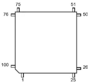
text_image
75 51 76 50 100 26 1 256.3.2 100-ball TFBGA Package Outline
The 100-ball TFBGA package has a 0.8 mm ball pitch and respects Green standards. Its dimensions are 9 x 9 x 1.1 mm. The figure below shows the orientation of the 100-ball TFBGA Package.
Figure 6-5. Orientation of the 100-ball TFBGA Package
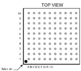
text_image
TOP VIEW 10 9 8 7 6 5 4 3 2 1 BALL A1 ABCDFGHJK6.3.3 100-ball VFBGA Package Outline
100-ball VFBGA Package Outline
The 100-ball VFBGA package has a 0.65 mm ball pitch and respects Green standards. The dimensions are 7mm x 7mm x 1.0 mm.
The following figure shows the orientation of the 100-ball VFBGA Package.
Figure 6-6. 100-ball VFBGA Package Outline

text_image
PIN A1 CORNER 1 2 3 4 5 6 7 8 9 10 A B C D E F G H J K6.4 100-lead Package Pinout
Table 6-2. 100-lead Package Pinout
| LQFP Pin | VFBGA Ball | TFBGA Ball | Power Rail | I/O Type Primary Alternate PI0 Peripheral A PIO Peripheral B PIO Peripheral C PIO Peripheral D Reset State | |||||||||||
| 72 | D8 | D8 | VDDIO | GPIO_AD | PA0 | I/O | WKUP0* | I | PWMCO_PWMH0 | O | TIOA0 | I/O | A17 | O | I2SC0_MCK |
| 70 | C10 | C10 | VDDIO | GPIO_AD | PA1 | I/O | WKUP1* | I | PWMCO_PWML0 | O | TIOB0 | I/O | A18 | O | I2SC0_CK |
| 66 D10 | D10 | VDDIO GPIO | PA2 | I/O WKUP2 | " | I | PWMCO_PWMH1 | O | - | - | DATRG | I | - | ||
| 64 | F9 | F9 | VDDIO | GPIO_AD | PA3 | I/O | PIODC0* | I | TWD0 | I/O | LONCOL1 | I | PCK2 | O | - |
| 55 | H10 | H10 | VDDIO | GPIO | PA4 | I/O | WKUP3/PIODC1* | I | TWCK0 | O | TCLK0 | I | UTXD1 | O | - |
| 52 | H9 | H9 | VDDIO | GPIO_AD | PA5 | I/O | WKUP4/PIODC2* | I | PWMCI_PWM L3 | O | ISI_D4 | I | URXD1 | I | - |
| 24 | J2 | J2 | VDDIO | CLOCK | PA7 | I/O | XIN32* | I | - | - | PWMCO_PWM H3 | - | - | - | - |
| 25 | K2 | K2 | VDDIO | CLOCK | PA8 | I/O | XOUT32* | O | PWMCI_PWM H3 | O | AFE0_ADTRG | I | - | - | - |
| 54 | J9 | J9 | VDDIO | GPIO_AD | PA9 | I/O | WKUP6/PIODC3* | I | URXD0 | I | ISI_D3 | I | PWMCO_PWMH0 | I | - |
| 46 | K9 | K9 | VDDIO | GPIO_AD | PA10 | I/O | PIODC4* | I | UTXD0 | O | PWMCO_PWMEXTRGO | I | RD | I | - |
| 44 | J8 | J8 | VDDIO | GPIO_AD | PA11 | I/O | WKUP7/PIODC5* | I | QCS | O | PWMCO_PWMH0 | O | PWMCI_PWMLO | O | - |
| 48 | K10 | K10 | VDDIO | GPIO_AD | PA12 | I/O | PIODC6* | I | QIO1 | I/O | PWMCO_PWMH1 | O | PWMCI_PWMH0 | O | - |
| 27 | G5 | G5 | VDDIO | GPIO_AD | PA13 | I/O | PIODC7* | I | QIO0 | I/O | PWMCO_PWMH2 | O | PWMCI_PWM L1 | O | - |
| 34 | H6 | H6 | VDDIO | GPIO_CLK | PA14 | I/O | WKUP8/PIODCEN1* | I | QSCK | O | PWMCO_PWMH3 | O | PWMCI_PWMH1 | O | - |
| 33 | J6 | J6 | VDDIO | GPIO_AD | PA15 | I/O | - | I | D14 | I/O | TIOA1 | I/O | PWMCO_PWM L3 | O | I2SC0_WS |
| 30 | J5 | J5 | VDDIO | GPIO_AD | PA16 | I/O | - | I | D15 | I/O | TIOB1 | I/O | PWMCO_PWM L2 | O | I2SC0_DI |
| 16 | G1 | G1 | VDDIO | GPIO_AD | PA17 | I/O | AFE0_AD6* | I | QIO2 | I/O | PCK1 | O | PWMCO_PWM H3 | O | - |
| 15 | G2 | G2 | VDDIO | GPIO_AD | PA18 | I/O | AFE0_AD7* | I | PWMCI_PWMEXTRG1 | I | PCK2 | O | A14 | O | - |
| 14 | F1 | F1 | VDDIO | GPIO_AD | PA19 | I/O | AFE0_AD8/WKUP9* | I | - | - | PWMCO_PWMLO | O | A15 | O | I2SC1_MCK |
| 13 | F2 | F2 | VDDIO | GPIO_AD | PA20 | I/O | AFE0_AD9/WKUP10* | I | - | - | PWMCO_PWM L1 | O | A16 | O | I2SC1_CK |
| 21 | J1 | J1 | VDDIO | GPIO_AD | PA21 | I/O | AFE0_AD1/PIODCEN2* | I | RXD1 | I | PCK1 | O | PWMCI_PWMH0 | I | - |
| LQFP Pin | VFBGA Ball | TFBGA Ball | Power Rail I/O Type Primary Alternate PIO Peripheral A PIO Peripheral B PIO Peripheral C PIO Peripheral D Reset State | ||||||||||||
| 26 | J3 | J3 | VDDIO | GPIO_AD | PA22 | I/O | PIODCCLK* | I | RK | I/O | PWM0_PWMEXTRG1 | I | NCS2 | O | - |
| 31 | K5 | K5 | VDDIO | GPIO_AD | PA23 | I/O | - | - | SCK1 | I/O | PWM0_PWMH0 | O | A19 | O | PWM1_PWM2 |
| 38 | K7 | K7 | VDDIO | GPIO_AD | PA24 | I/O | - | - | RTS1 | O | PWM0_PWMH1 | O | A20 | O | ISLPCK |
| 40 | H7 | H7 | VDDIO | GPIO_AD | PA25 | I/O | - | - | CTS1 | I | PWM0_PWMH2 | O | A23 | O | MCCK |
| 42 | K8 | K8 | VDDIO | GPIO | PA26 | I/O | - | - | DCD1 | I | TIOA2 | O | MCDA2 | I/O | PWM1_PWMFI1 |
| 50 | H8 | H8 | VDDIO | GPIO_AD | PA27 | I/O | - | - | DTR1 | O | TIOB2 | I/O | MCDA3 | I/O | ISLD7 |
| 79 | A9 | A9 | VDDIO | GPIO | PA28 | I/O | - | - | DSR1 | I | TCLK1 | I | MCCDA | I/O | PWM1_PWMFI2 |
| 82 | C7 | C7 | VDDIO | GPIO | PA30 | I/O | WKUP11* | I | PWM0_PWM2 | O | PWM1_PWMEXTRG0 | I | MCDA0 | I/O | I2SC0_D0 |
| 83 | A7 | A7 | VDDIO | GPIO_AD | PA31 | I/O | - | - | SP10_NPCS1 | I/O | PCK2 | O | MCDA1 | I/O | PWM1_PWMH2 |
| 12 | E1 | E1 | VDDIO | GPIO | PB0 | I/O | AFE0_AD10/RTCOUT0* | I | PWM0_PWMH0 | O | - | - | RXD0 | I | TF |
| 11 | E2 | E2 | VDDIO | GPIO | PB1 | I/O | AFE1_AD0/RTCOUT1* | I | PWM0_PWMH1 | O | GTSUCOMP | O | TXD0 | I/O | TK |
| 17 | H1 | H1 | VDDIO | GPIO | PB2 | I/O | AFE0_AD5* | I | CANTX0- | O- | - | - | CT50 | I | SP10_NPCS0 |
| 20 | H2 | H2 | VDDIO | GPIO_AD | PB3 | I/O | AFE0_AD2/WKUP12* | I | CANRX0- | I- | PCK2 | O | RTS0 | O | ISID2 |
| 74 | B9 | B9 | VDDIO | GPIO_MLB | PB4 | I/O | TD1* | I | TWD1 | I/O | PWM0_PWMH2 | O | MLBCLK- | I- | TXD1 |
| 77 | C8 | C8 | VDDIO | GPIO_MLB | PB5 | I/O | TDO/TRACESWO/WKUP13* | O | TWCK1 | O | PWM0_PWMLO | O | MLBDAT- | I/O- | TD |
| 57 | G8 | G8 | VDDIO | GPIO | PB6 | I/O | SWDIO/TMS* | I | - | - | - | - | - | - | - |
| 63 | E9 | E9 | VDDIO | GPIO | PB7 | I/O | SWCLK/TCK* | I | - | - | - | - | - | - | - |
| 98 | A2 | A2 | VDDIOP | CLOCK | PB8 | I/O | XOUT* | O | - | - | - | - | - | - | - |
| 99 | A1 | A1 | VDDIOP | CLOCK | PB9 | I/O | XIN* | I | - | - | - | - | - | - | - |
| 61 | F8 | F8 | VDDIO | GPIO | PB12 | I/O | ERASE* | I | PWM0_PWM1 | O | GTSUCOMP | O | - | - | PCK0 |
| 100 | B2 | B2 | VDDIO | GPIO_AD | PB13 | I/O | DAC0** | O | PWM0_PWM2 | O | PCK0 | O | SCK0 | I/O | - |
| 1 | B1 | C1 | VDDIO | GPIO_AD | PD0 | I/O | DAC1** | I | GTXCK | I | PWM1_PWMLO | O | SP11_NPCS1 | DCD0 | |
| 92 | D3 | D2 | VDDIO | GPIO | PD1 | I/O | - | - | GTXEN | O | PWM1_PWMH0 | O | SP11_NPCS2 | I/O | DTR0 |
| 91 | E3 | E3 | VDDIO | GPIO | PD2 | I/O | - | - | GTX0 | O | PWM1_PWM1 | O | SP11_NPCS3 | I/O | DSR0 |
| 89 | B5 | B5 | VDDIO | GPIO | PD3 | I/O | - | - | GTX1 | O | PWM1_PWMH1 | O | UTXD4 | O | RIO |
| 88 | A5 | A5 | VDDIO | GPIO_CLK | PD4 | I/O | - | - | GRXDV | I | PWM1_PWM2 | O | TRACED0 | O | DCD2 |
| 87 | D5 | D5 | VDDIO | GPIO_CLK | PD5 | I/O | - | - | GRX0 | I | PWM1_PWMH2 | O | TRACED1 | O | DTR2 |
| 85 | B6 | B6 | VDDIO | GPIO_CLK | PD6 | I/O | - | - | GRX1 | I | PWM1_PWM3 | O | TRACED2 | O | DSR2 |
| 84 | A8 | A6 | VDDIO | GPIO_CLK | PD7 | I/O | - | - | GRXER | I | PWM1_PWMH3 | O | TRACED3 | O | RI2 |
| 80 | B7 | B7 | VDDIO | GPIO_CLK | PD8 | I/O | - | - | GMDC | O | PWM0_PWMFI1 | I | - | - | TRACECLK |
| 78 | B8 | B8 | VDDIO | GPIO_CLK | PD9 | I/O | - | - | GMDIO | I/O | PWM0_PWMFI2 | AFE1_ADTRG | I | - | |
| 71 | C9 | C9 | VDDIO | GPIO_MLB | PD10 | I/O | - | - | GCR5 | I | PWM0_PWMLO | O | TD | O | MLBSIG- |
| 69 | D9 | D9 | VDDIO | GPIO_AD | PD11 | I/O | - | - | GRX2 | I | PWM0_PWMH0 | O | GTSUCOMP | O | ISID5 |
| 65 | E10 | E10 | VDDIO | GPIO_AD | PD12 | I/O | - | - | GRX3 | I | CANTX1- | O- | SP10_NPCS2 | O | ISID6 |
| 62 | E8 | E8 | VDDIO | GPIO_AD | PD13 | I/O | - | - | GCOL | I | - | - | - | O | - |
| 59 | F10 | F10 | VDDIO | GPIO_AD | PD14 | I/O | - | - | GRXCK | I | - | - | - | O | - |
| 75 | B10 | B10 | VDDIO | GPIO_AD | PD15 | I/O | - | - | GTX2 | O | RXD2 | I | NWR1/NBS1 | O | - |
| 56 | G9 | G9 | VDDIO | GPIO_AD | PD16 | I/O | - | - | GTX3 | O | TXD2 | I/O | - | O | - |
| 53 | J10 | J10 | VDDIO | GPIO_AD | PD17 | I/O | - | - | GTXER | SCK2 | I/O | - | O | - | |
| LQFP Pin | VFBGA Ball | TFBGA Ball | Power Rail | I/O Type Primary | Primary Alternate PIO Peripheral A PIO | Peripheral B PIO Peripheral C PIO Peripheral D Reset State | |||||||||||
| Signal Dir | Signal | Dir Signal Dir | Signal | Dir Signal Dir | Signal Dir | Signal, Dir, | PU, PD, HIZ, ST | ||||||||||
| 49 | K6 | K6 | VDDIO | GPIO_AD | PD18 | I/O | - | - | NCS1 | O | RTS2 | O | URXD4 | I | - | - | PIO, I, PU, ST |
| 47 | K4 | K4 | VDDIO | GPIO_AD | PD19 | I/O | - | - | NCS3 | O | CTS2 | I | UTXD4 | O | - | - | PIO, I, PU, ST |
| 45 | K3 | K3 | VDDIO | GPIO | PD20 | I/O | - | - | PWMCO_PWMH0 | O | SPI0_MISO | I/O | GTSUCOMP | O | - | - | PIO, I, PU, ST |
| 43 | H5 | H5 | VDDIO | GPIO_AD | PD21 | I/O | - | - | PWMCO_PWMH1 | O | SPI0_MOSI | I/O | TIOA11 | I/O | ISI_D1 | I | PIO, I, PU, ST |
| 41 | J4 | J4 | VDDIO | GPIO_AD | PD22 | I/O | - | - | PWMCO_PWMH2 | O | SPI0_SPCK | O | TIOB11 | I/O | ISI_D0 | I | PIO, I, PU, ST |
| 37 | G4 | G4 | VDDIO | GPIO_AD | PD24 | I/O | - | - | PWMCO_PWMLO | O | RF | I/O | TCLK11 | I | ISI_HSYNC | I | PIO, I, PU, ST |
| 35 | H3 | H3 | VDDIO | GPIO_AD | PD25 | I/O | - | - | PWMCO_PWML1 | O | SPI0_NPCS1 | I/O | URXD2 | I | ISI_VSYNC | I | PIO, I, PU, ST |
| 36 | G3 | G3 | VDDIO | GPIO | PD26 | I/O | - | - | PWMCO_PWML2 | O | TD | O | UTXD2 | O | UTXD1 | O | PIO, I, PU, ST |
| 32 | H4 | H4 | VDDIO | GPIO_AD | PD27 | I/O | - | - | PWMCO_PWML3 | O | SPI0_NPCS3 | O | TWD2 | O | ISI_D8 | I | PIO, I, PU, ST |
| 51 | J7 | J7 | VDDIO | GPIO_AD | PD28 | I/O | WKUP5" | URXD3 | I | CANRX1 | I- | TWCK2 | O | ISI_D9 | I | PIO, I, PU, ST | |
| 23 | K1 | K1 | VDDIO | GPIO_AD | PD30 | I/O | AFFO_AD0" | I | UTXD3 | O | - | - | - | - | ISI_D10 | I | PIO, I, PU, ST |
| 2 | C1 | B1 | VDDIO | GPIO_AD | PD31 | I/O | - | - | QIO3 | I/O | UTXD3 | O | PCK2 | O | ISI_D11 | I | PIO, I, PU, ST |
| 4 | C3 | C3 | VDDOUT | Power | VDDOUT | I | - | - | - | - | - | - | - | - | - | - | - |
| 5 | C2 | C2 | VDDIN | Power | VDDIN | I | - | - | - | - | - | - | - | - | - | - | - |
| 6 | D2 | D3 | GND | Ground | VREFN | I | - | - | - | - | - | - | - | - | - | - | - |
| 9 | D1 | D1 | VDDIO | Power | VREFP | I | - | - | - | - | - | - | - | - | - | - | - |
| 58 | G10 | G10 | VDDIO | RST | NRST | I | - | - | - | - | - | - | - | - | - | - | PIO, I, PU |
| 60 | F7 | F7 | VDDIO | TEST | TST | I | - | - | - | - | - | - | - | - | - | - | I, PD |
| 19, 28, 68, 81 | C5, F3, G7 | C5, F3, G7 | VDDIO | Power | VDDIO | I | - | - | - | - | - | - | - | - | - | - | - |
| 73 | A10 | A10 | VDDIO | TEST | JTAGSEL | I | - | - | - | - | - | - | - | - | - | - | I, PD |
| 18, 22, 39, 76 | C6, D6, G6 | C6, D6, G6 | VDDCORE | Power | VDDCORE | I | - | - | - | - | - | - | - | - | - | - | - |
| 86 | D7 | D7 | VDDPLL | Power | VDDPLL | I | - | - | - | - | - | - | - | - | - | - | - |
| 93 | E5 | E5 | VDDUTMII | Power | VDDUTMII | I | - | - | - | - | - | - | - | - | - | - | - |
| 94 | A4 | A4 | VDDUTMII | USBHS | HSDM | I/O | - | - | - | - | - | - | - | - | - | - | - |
| 95 | B4 | B4 | VDDUTMII | USBHS | HSDP | I/O | - | - | - | - | - | - | - | - | - | - | - |
| 3, 7, 8, 10, 29, 67 | E7, F4, F5, F6 | E7, F4, F5, F6 | GND | Ground | GND | I | - | - | - | - | - | - | - | - | - | - | - |
| D4 | D4 | GNDANA | Ground | GNDANA | I | - | - | - | - | - | - | - | - | - | - | - | |
| A6 | A8 | GNDUTMI | Ground | GNDUTMI | I | - | - | - | - | - | - | - | - | - | - | - | |
| C4 | C4 | GNDPLLUSB | Ground | GNDPLLUSB | I | - | - | - | - | - | - | - | - | - | - | - | |
| E6 | E4 | GNDPLL | Ground | GNDPLL | I | - | - | - | - | - | - | - | - | - | - | - | |
| 96 B3 | B3 | VDDUTMIC | Power VDDUTMIC | I | - | - | - | - | - | - | - | - | - | - | - | - | - |
| 97 | A3 | A3 | VBG | VBG | I | - | - | - | - | - | - | - | - | - | - | - | - |
| 90 E4 | E6 | VDDPLLUSB | Power VDDPLLUSB | I | - | - | - | - | - | - | - | - | - | - | - | - | - |
Notes:
- WKUPx can be used if the PIO Controller defines the I/O line as "input".
- To select this extra function, refer to the 32.5.14. Parallel Capture Mode section in the "Parallel Input/Output Controller (PIO)" chapter.
- PIODCEN1/PIODCx has priority over WKUPx. Refer to the 32.5.14. Parallel Capture Mode section in the "PIO" chapter.
- Refer to the 23.4.2. Slow Clock Generator section in the "Supply Controller (SUPC)" chapter.
- To select this extra function, refer to the 33.5.2.1. I/O Lines section in the "External Bus Interface (EBI)" chapter. This selection is independent of the PIO line configuration. PIO lines must be configured according to required settings (PU or PD).
- Analog input has priority over WKUPx pin. To select the analog input, refer to the 33.5.2.1. I/O Lines section in the "EBI" chapter. WKUPx can be used if the PIO controller defines the I/O line as "input".
- Analog input has priority over RTCOUTx pin. To select the analog input, refer to the 33.5.2.1. I/O Lines section in the "EBI" chapter. Refer to the 27.5.8. Waveform Generation section in the "Real-Time Clock (RTC)" chapter to select RTCOUTx.
- Analog input has priority over WKUPx pin. To select the analog input, refer to the 33.5.2.1. I/O Lines section in the "EBI" chapter. To select PIODCEN2, refer to the 32.5.14. Parallel Capture Mode in the "PIO" chapter.
- Refer to the System I/O Configuration Register (19.4.7. CCFG_SYSIO) in the "Bus Matrix (MATRIX)" chapter.
- Refer to the 30.5.3. Main Crystal Oscillator section in the "Clock Generator" chapter. This selection is independent of the PIO line configuration. PIO lines must be configured according to XINxx (I) and XOUTxx (O).
- DAC0 is selected when DACC_CHER.CH0 is set. DAC1 is selected when DACC_CHER.CH1 is set. Refer to the DACC Channel Enable Register in the "Digital-to-Analog Converter Controller (DACC)" chapter.
6.5 64-lead Package
6.5.1 64-lead QFN Wettable Flanks Package Outline
Figure 6-7. Orientation of the 64-lead QFN Wettable Flanks Package
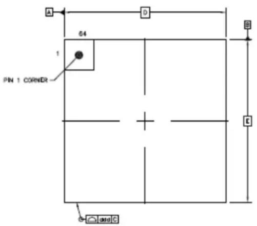
text_image
A 64 D B 1 PN 1 CORNER E C6.5.2 64-pin LQFP Package Outline
Figure 6-8. Orientation of the 64-pin LQFP Package

text_image
48 33 49 32 64 1 17 166.6 64-lead Package Pinout
Table 6-3. 64-lead Package Pinout
| LQFP Pin QFN Pin(11) | Power Rail I/O Type Primary Alternate PIO Peripheral A PIO Peripheral B PIO Peripheral CDir PIO Peripheral DDir Reset | State | ||||||||||||||
| Dir, PU,PD, HIZ, ST | ||||||||||||||||
| 40 40 VDDIO GPIO_AD | PA3 | I/O PIODC0 | " | I | TWD0* | I/O | LONCOL1 | I | PCK2 | O | - | - | PIO, I, PU,ST | |||
| 34 34 VDDIO GPIO | PA4 | I/O WKUP3/ | PIODC1* | I | TWCK0 | O | TCLK0 | I | UTXD1 | O | - | - | PIO, I, PU,ST | |||
| 32 32 VDDIO GPIO_AD | PA5 | I/O WKUP4/ | PIODC2* | I | PWMCI_PWML3 | O | ISI_D4 | I | URXD1 | I | - | - | PIO, I, PU,ST | |||
| 15 15 VDDIO CLOCK | PA7 | I/O XIN32 | " | I | - | - | PWMCO_PWMH3 | - | - | - | - | - | PIO, HIZ | |||
| 16 16 VDDIO CLOCK | PA8 | I/O XOUT32 | " | O | PWMCI_PWMH3 | O | AFE0_ADTRG | I | - | - | - | - | PIO, HIZ | |||
| 33 33 VDDIO GPIO_AD | PA9 | I/O WKUP6/ | PIODC3* | I | URXD0 | I | ISI_D3 | I | PWMCO_PWM FIO | I | - | - | PIO, I, PU,ST | |||
| 28 28 VDDIO GPIO_AD | PA10 | I/O | PIODC4 | " | I | UTXD0 | O | PWMCO_PWMEXTRG0 | I | RD | I | - | - | PIO, I, PU,ST | ||
| 27 27 VDDIO GPIO_AD | PA11 | I/O | WKUP7/ | PIODC5* | I | QCS O | PWMCO_PWMH0 | O | PWMCI_PWM L0 | O | - | - | - | PIO, I, PU,ST | ||
| 29 29 VDDIO GPIO_AD | PA12 | I/O | PIODC6 | " | I | QIO1 | I/O PWMCO_PWMH1 | O | PWMCI_PWM H0 | O | - | - | - | PIO, I, PU,ST | ||
| 18 18 VDDIO GPIO_AD | PA13 | I/O | PIODC7 | " | I | QIO0 | I/O PWMCO_PWMH2 | O | PWMCI_PWM L1 | O | - | - | - | PIO, I, PU,ST | ||
| 19 19 VDDIO GPIO_CLK | PA14 | I/O | WKUP8/ | PIODCEN1* | I | QSCX | O | PWMCO_PWMH3 | O | PWMCI_PWM H1 | O | - | - | PIO, I, PU,ST | ||
| 12 12 VDDIO GPIO_AD | PA21 | I/O | AFE0_AD1/ | PIODCEN2* | I | RXD1 | I | PCK1 | O | PWMCI_PWM FIO | I | - | - | PIO, I, PU,ST | ||
| 17 17 VDDIO GPIO_AD | PA22 | I/O PIODCCLK | " | I | RK | I/O PWMCO_PWMEXTRG1 | I | - | O | - | - | - | PIO, I, PU,ST | |||
| 23 | 23 | VDDIO | GPIO_AD | PA24 | I/O | - | - | RTS1 | O | PWMCO_PWMH1 | O | A20 | O | ISI_PCK | I | PIO, I, PU,ST |
| 30 | 30 | VDDIO | GPIO_AD | PA27 | I/O | - | - | DTR1 | O | TIOB2 | I/O | - | I/O | ISI_D7 | I | PIO, I, PU,ST |
| LQFP Pin QFN Pin(11) | Power Rail I/O Type Primary Alternate PIO Peripheral A PIO Peripheral B PIO Peripheral CDir PIO Peripheral DDir Reset | State | |||||||||||||
| Dir, PU,PD, HIZ, ST | |||||||||||||||
| 8 8 VDDIO GPIO PB0 I/O AFE0_AD1 | O/RTCOUT0* | I | PWMCO_PWMH0 | O | - | - | RXDO | I | TF | I/O | PIO, I, PU,ST | ||||
| 7 7 VDDIO GPIO PB1 I/O AFE1_AD0/ | RTCOUT1* | I | PWMCO_PWMH1 | O | GTSUCOMP | O | TXD0 I/O TK | I/O | PIO, I, PU, | ST | |||||
| 9 9 VDDIO GPIO PB2 I/O AFE0_AD5 | - | I | CANTX0 | O | - | - | CTSO | I | - | I/O | PIO, I, PU,ST | ||||
| 11 | 11 | VDDIO GPIO_AD PB3 I/O AFE0_AD2/ | WKUP 12* | I | CANRX0 | I | PCK2 | O | RT50 | O | ISI_D2 | I | PIO, I, PU,ST | ||
| 46 | 46 | VDDIO GPIO_MLB PB4 I/O TOI | " | I | TWD1 | I/O PWVC0_PWMH2 | O | MLBCLK | I | TXD1 I/O PIO, I, PD, | ST | ||||
| 47 | 47 | VDDIO GPIO_MLB PB5 I/O TOO/ | TRACESWO/WKUP13* | O | TWCK1 O | PWMCO_PWMLO | O | MLBDAT | I/O | TD | O | O, PU | |||
| 35 | 35 | VDDIO GPIO PB6 I/O SWDIO/ | TMS* | I | - | - | - | - | - | - | - | - | PIO,I,ST | ||
| 39 | 39 | VDDIO GPIO PB7 I/O SWCLK/ | TCK* | I | - | - | - | - | - | - | - | - | PIO,I,ST | ||
| 62 | 63 | VDDIO CLOCK PB8 I/O XOUT | " | O | - | - | - | - | - | - | - | - | PIO, HIZ | ||
| 63 | 64 | VDDIO CLOCK PB9 I/O XIN | < | I | - | - | - | - | - | - | - | - | PIO, HIZ | ||
| 38 | 38 | VDDIO GPIO PB12 I/O ERASE | " | I | PWMCO_PWMIL1 | O | GTSUCOMP | O | - | - | PCK0 | O | PIO, I, PD,ST | ||
| 1 2 VDDIO GPIO_AD PD0 I/O DAC1 | " | I | GTXCK1 | PWMCI_PWMLO | O | - | I/O | DCDO | I | PIO, I, PU,ST | |||||
| 57 | 57 | VDDIO GPIO PD1 I/O | - | - | GTXEN | O | PWMCI_PWMH0 | O | - | I/O | DTR0 | O | PIO, I, PU,ST | ||
| 56 | 56 | VDDIO GPIO PD2 I/O | - | - | GTX0 | O | PWMCI_PWMIL1 | O | - | I/O | DSR0 | I | PIO, I, PU,ST | ||
| 55 | 55 | VDDIO GPIO PD3 I/O | - | - | GTX1 | O | PWMCI_PWMH1 | O | UTXD4 | O | RIO | I | PIO, I, PU,ST | ||
| 54 | 54 | VDDIO GPIO_CLK PD4 I/O | - | - | GRXDV | I | PWMCI_PWMIL2 | O | TRACED0 O | -- | PIO, I, FU,ST | ||||
| 53 | 53 | VDDIO GPIO_CLK PD5 I/O | - | - | GRX0 | I | PWMCI_PWMH2 | O | TRACED1 O | -- | PIO, I, FU,ST | ||||
| 51 | 51 | VDDIO GPIO_CLK PD6 I/O | - | - | GRX1 | I | PWMCI_PWMIL3 | O | TRACED2 O | -- | PIO, I, FU,ST | ||||
| 50 | 50 | VDDIO GPIO_CLK PD7 I/O | - | - | GRXER | I | PWMCI_PWMH3 | O | TRACED3 O | -- | PIO, I, FU,ST | ||||
| 49 | 49 | VDDIO GPIO_CLK PD8 I/O | - | - | GMDC | O | PWMCO_PWMFI1 | I | - | - | TRACECLK | O | PIO, I, PU,ST | ||
| 48 | 48 | VDDIO GPIO_CLK PD9 I/O | - | - | GMDIO | I/O | PWMCO_PWMFI2 | I | AFE1_ADTRG | I | - | - | PIO, I, PU,ST | ||
| 44 | 44 | VDDIO GPIO_MLB PD10 I/O | - | - | GCRS | I | PWMCO_PWMLO | O | TD | O | MLBSIG | I/O | PIO, I, PD,ST | ||
| 43 | 43 | VDDIO GPIO_AD PD11 I/O | - | - | GRX2 | I | PWMCO_PWMH0 | O | GTSUCOMP | O | ISI_DS1 | PIO, I, PU,ST | |||
| 41 | 41 | VDDIO GPIO_AD PD12 I/O | - | - | GRX3 | I | - | O | - | O | ISI_DS1 | I | PIO, I, PU,ST | ||
| 26 26 VDDIO GPIO_AD PD21 I/O - | - | PWMCO_P | WMH1 | O | - | I/O | TIOA11 | I/O | ISI_D1 | I | PIO, I, PU,ST | ||||
| 25 25 VDDIO GPIO_AD PD22 I/O - | - | PWMCO_P | WMH2 | O | - | O | TIOB11 | I/O | ISI_D0 | I | PIO, I, PU,ST | ||||
| 22 22 VDDIO GPIO_AD PD24 I/O - | - | PWMCO_P | WML0 | O | RF | I/O | TCLK11 | I | ISI_HSYNC | I | PIO, I, PU,ST | ||||
| 20 20 VDDIO GPIO_AD PD25 I/O - | - | PWMCO_P | WML1 | O | - | I/O | URXD2 | I | ISI_VSYNC | I | PIO, I, PU,ST | ||||
| 21 21 VDDIO GPIO | PD26 I/O - | - | PWMCO_P | WML2 | O | TD | O | UTXD2 | O | UTXD1 | O | PIO, I, PU,ST | |||
| 2 | 3 | VDDIO | GPIO_AD | PD31 | I/O | - | QIO3 | I/O | UTXD3 | O | PCK2 | O | ISI_D11 | I | PIO, I, PU,ST |
| 3 | 4 | VDDOUT | Power | VDDOUT | - | - | - | - | - | - | - | - | - | - | |
| 4 | 5 | VDDIN | Power | VDDIN | - | - | - | - | - | - | - | - | - | - | |
| 5 | 6 | VDDIO | Reference | VREFP | I | - | - | - | - | - | - | - | - | - | |
| 36 | 36 | VDDIO | RST | NRST | I/O | - | - | - | - | - | - | - | - | PIO, I, PU | |
| 37 | 37 | VDDIO | TEST | TST | I | - | - | - | - | - | - | - | - | I, PD | |
| 10, 42, 58 | 10,42,58 | VDDIO | Power | VDDIO | - | - | - | - | - | - | - | - | - | - | |
| 45 | 45 | VDDIO | TEST | JTAGSEL | I | - | - | - | - | - | - | - | - | I, PD | |
| 13, 24, 61 | 13,24,61 | VDDCORE | Power | VDDCORE | - | - | - | - | - | - | - | - | - | - | |
| 52 | 52 | VDDPLL | Power | VDDPLL | - | - | - | - | - | - | - | - | - | - | |
| 59 | 59 | VDDUTMII | USBHS | DM | I/O | - | - | - | - | - | - | - | - | - | |
| 60 | 60 | VDDUTMII | USBHS | DP | I/O | - | - | - | - | - | - | - | - | - | |
| 14, 31 | 14,31 | GND | Ground | GND | - | - | - | - | - | - | - | - | - | - | |
| 6 | - | GND | Ground | GND | - | - | - | - | - | - | - | - | - | - | |
| 64 1 | VDDPLLUSB | Power | VDDPLLUSB | - | - | - | - | - | - | - | - | - | - | - | |
| - | 62 | - | VBG | VBG | I | - | - | - | - | - | - | - | - | - | |
Notes:
- To select this extra function, refer to the 32.5.14. Parallel Capture Mode section in the "Parallel Input/Output Controller (PIO)" chapter.
- PIODCEN1/PIODCx has priority over WKUPx. Refer to the 32.5.14. Parallel Capture Mode section in the "PIO" chapter.
- Refer to the 23.4.2. Slow Clock Generator section in the "Supply Controller (SUPC)" chapter.
- To select this extra function, refer to the 33.5.2.1. I/O Lines section in the "External Bus Interface (EBI)" chapter. This selection is independent of the PIO line configuration. PIO lines must be configured according to required settings (PU or PD).
- Analog input has priority over WKUPx pin. To select the analog input, refer to the 33.5.2.1. I/O Lines section in the "EBI" chapter. WKUPx can be used if the PIO controller defines the I/O line as "input".
-
Analog input has priority over RTCOUTx pin. To select the analog input, refer to the 33.5.2.1. I/O Lines section in the "EBI" chapter. Refer to the 27.5.8. Waveform Generation section in the "Real-Time Clock (RTC)" chapter to select RTCOUTx.
-
Analog input has priority over WKUPx pin. To select the analog input, refer to the 33.5.2.1. I/O Lines section in the "EBI" chapter. To select PIODCEN2, refer to the 32.5.14. Parallel Capture Mode in the "PIO" chapter.
- Refer to the System I/O Configuration Register (19.4.7. CCFG_SYSIO) in the "Bus Matrix (MATRIX)" chapter.
- Refer to the 30.5.3. Main Crystal Oscillator section in the Clock Generator chapter. This selection is independent of the PIO line configuration. PIO lines must be configured according to XINxx (I) and XOUTxx (O).
- DAC0 is selected when DACC_CHER.CH0 is set. DAC1 is selected when DACC_CHER.CH1 is set. Refer to the DACC Channel Enable Register in the "Digital-to-Analog Converter Controller (DACC)" chapter.
- The exposed pad of the QFN64 package MUST be connected to ground.
Note: Pinout limitations prevent full support of USART functionality. The following table lists which USART functions are available.
Table 6-4. USART Functions
| USART Pins Availability | ||||
| Function Description Pin Name USART0 USART1 | ||||
| SCK Serial Clock SCK n n | ||||
| TXD Transmit Data UTXDx y y | ||||
| RXD | Receive Data | URXDx | y | y |
| RTS | Request to Send | RTSx | y | y |
| CTS Clear To Send | CTSx | y | n | |
| DTR | Data Terminal Ready | DTRx | y | y |
| DSR | Data Set Ready | DSRx | y | n |
| DCD | Data Carrier Detect | DCDx y | n | |
| RI | Ring Indicator | RIx | y | n |
| LCOL | LON Collision Detection | LONCOLx | n | y |
7. Power Considerations
7.1 Power Supplies
The following table defines the power supply rails of the SAM E70/S70/V70/V71 .
Table 7-1. Power Supplies
| Name Associated Ground Powers | ||
| VDDCORE GND | Core, embedded memories and peripherals. | |
| VDDIO GND | Peripheral I/O lines (Input/Output Buffers), backup part, 1 Kbytes of backup SRAM, 32 kHz crystal oscillator, oscillator pads. For USB operations, VDDIO voltage range must be between 3.0V and 3.6V. | |
| VDDIN GND, GNDANA | Voltage regulator input. Supplies also the ADC, DAC, and analog voltage comparator. | |
| VDDPLL GND, GNDPLL PLLA and the fast RC oscillator. | ||
| VDDPLLUSB GND, GNDPLLUSB | UTMI PLL and 3 MHz to 20 MHz oscillator. | |
| VDDUTMII GNDUTMI | USB transceiver interface. Must be connected to VDDIO. | |
| VDDUTMIC GNDUTMI USB transceiver core. | ||
7.2 Power Constraints
The following power constraints are apply to SAM E70/S70/V70/V71 devices. Deviating from these constraints may lead to unpredictable results.
• VDDIN and VDDIO must have the same level
• VDDIN and VDDIO must always be higher than or equal to VDDCORE
• VDDCORE, VDDPLL and VDDUTMIC voltage levels must not vary by more than 0.6V
- For the USB to be operational, VDDUTMII, VDDPLLUSB, VDDIN and VDDIO must be higher than or equal to 3.0V
7.2.1 Powerup
VDDIO and VDDIN must rise simultaneously, prior to VDDCORE, VDDPLL and VDDUTMIC rising. This is respected if VDDCORE, VDDPLL and VDDUTMIC are supplied by the embedded voltage regulator.
If VDDCORE is powered by an external voltage regulator, VDDIO and VDDIN must reach their minimum operating voltage before VDDCORE has reached VDDCORE_min . The minimum slope for VDDCORE is defined by:
$$ \left(\mathrm{VDDCORE} _ {\min} - \mathrm{V} _ {\mathrm{T} + \min}\right) / \left(\mathrm{t} _ {\text {RESmin}}\right) $$
If VDDCORE rises at the same time as VDDIO and VDDIN, the minimum and maximum rising slopes of VDDIO and VDDIN must be respected. Refer to the section "DC Characteristics".
In order to prevent any overcurrent at powerup, it is required that VREFP rises simultaneously with VDDIO and VDDIN.
Figure 7-1. Powerup Sequence
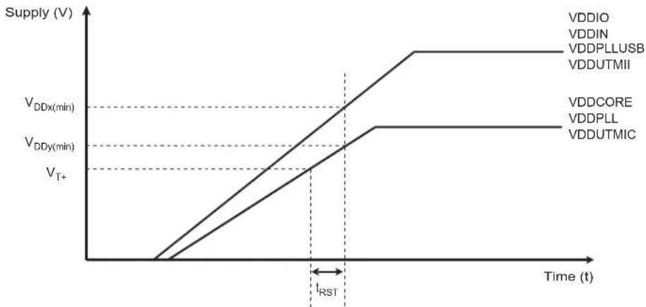
line
| Time (t) | Supply (V) - VDDIO | Supply (V) - VDDIN | Supply (V) - VDDPLLUSB | Supply (V) - VDDUTMII | |----------|--------------------|--------------------|------------------------|-----------------------| | 0 | 0 | 0 | 0 | 0 | | t_RST | V_DDIO | VDDIN | VDDPLLUSB | VDDUTMII | | | | | | | | | | | | | | | | | | | | | | | | | | | | | | | | | | | | | | | | | | | | | | | | | | | | | | | | | | | | |Related Links
57.2. DC Characteristics
23.4.6. Backup Power Supply Reset
23.4.6.1. Raising the Backup Power Supply
7.2.2 Powerdown
If VDDCORE, VDDPLL and VDDUTMIC are not supplied by the embedded voltage regulator, VDDIO, VDDIN, VDDPLLUSB and VDDUTMII should fall simultaneously, prior to VDDCORE, VDDPLL and VDDUTMIC falling. The VDDCORE falling slope must not be faster than 20V/ms.
In order to prevent any overcurrent at powerdown, it is required that VREFP falls simultaneously with VDDIO and VDDIN.
Figure 7-2. Powerdown Sequence

line
| Signal | Supply (V) | | ------------- | ---------- | | VDDIO | 1 | | VDDIN | 1 | | VDDPLLUSB | 1 | | VDDUTMII | 1 | | VDDtx(min) | 1 | | VDDCORE | 0 | | VDDPLL | 0 | | VDDUTMIC | 0 | | VDDy(min) | 0 |7.3 Voltage Regulator
The SAM E70/S70/V70/V71 embeds a voltage regulator that is managed by the Supply Controller.
For adequate input and output power supply decoupling/bypassing, refer to 57.2. DC Characteristics in the Electrical Characteristics chapter.
7.4 Backup SRAM Power Switch
The SAM E70/S70/V70/V71 embeds a power switch to supply the 1 Kbyte of backup SRAM. It is activated only when VDDCORE is switched off to ensure retention of the contents of the backup SRAM. When VDDCORE is switched on, the backup SRAM is powered with VDDCORE.
To save the power consumption of the backup SRAM, the user can disable the backup SRAM power switch by clearing the bit SRAMON in the Supply Controller Mode Register (SUPC_MR). By default, after VDDIO rises, the backup SRAM power switch is enabled.
7.5 Active Mode
Active mode is the normal running mode with the core clock running from the fast RC oscillator, the main crystal oscillator or the PLLA. The Power Management Controller can be used to adapt the core, bus and peripheral frequencies and to enable and/or disable the peripheral clocks.
7.6 Low-power Modes
The SAM E70/S70/V70/V71 features the following three Low-Power modes:
- Backup mode
- Wait mode
- Sleep mode
7.6.1 Backup Mode
The purpose of Backup mode is to achieve the lowest power consumption possible in a system which is performing periodic wakeups to perform tasks but not requiring fast startup time.
The Supply Controller, zero-power Power-On Reset (POR), RTT, RTC, backup SRAM, backup registers and 32 kHz oscillator (RC or crystal oscillator selected by software in the Supply Controller) are running. The regulator and the core supply are off.
Backup mode is based on the Cortex-M7 Deep-Sleep mode with the voltage regulator disabled.
Wakeup from Backup mode is done through WKUP0-13 pins, the supply monitor (SM), the RTT, or an RTC wakeup event.
Backup mode is entered by using the VROFFbit in the Supply Controller Control Register (SUPC_CR) and the SLEEPDEEP bit in the Cortex-M7 System Control Register set to 1. Refer to information on Power Management in the" ARM Cortex-M7 documentation", which is available for download at www.arm.com.
To enter Backup mode, follow these steps:
- Set the SLEEPDEEP bit of the Cortex-M7 processor.
- Set the VROFF bit of SUPC_CR.
Exit from Backup mode occurs as a result of one of the following enabled wakeup events:
- WKUP0-13 pins (level transition, configurable debouncing)
• Supply Monitor alarm - RTC alarm
- RTT alarm
Notes: If PLLA is enabled with the Main Crystal Oscillator as the clock source for Main Clock (MAINCK), the following sequence must be followed before entering into backup mode:
- Switch Main Clock (MAINCK) to Slow Clock (SLCK) by using PMC_MCKR.CSS.
- Disable the PLLA by writing MUL = 0 or DIV = 0.
- Disable the Main Crystal Oscillator.
- Add Wait time in the range of milliseconds.
- Enter backup mode.
7.6.2 Wait Mode
The purpose of Wait mode is to achieve very low-power consumption while maintaining the whole device in a powered state for a startup time of less than 10 s.
In Wait mode, the clocks of the core, peripherals and memories are stopped. However, the core, peripherals and memories power supplies are still powered.
Wait mode is entered when the WAITMODE bit is set in CKGR_MOR and the field FLPM is configured to 00 or 01 in the PMC Fast Startup Mode register (PMC_FSMR).
The Cortex-M is able to handle external events or internal events to wake up the core. This is done by configuring the external lines WKUP0-13 as fast startup wake-up pins (refer to the "Fast Startup" section). RTC or RTT alarms or USB wake-up events can be used to wake up the processor. Resume from Wait mode is also achieved when a debug request occurs and the bit CDBGPWRUPREQ is set in the processor.
To enter Wait mode, first, select the Main RC oscillator as Main Clock and perform the following steps:
- Configure the FLPM field in the PMC_FSMR.
- Set Flash Wait State at 0.
- Set HCLK = MCK by configuring MDIV to 0 in the PMC Host Clock register (PMC_MCKR).
- Set the WAITMODE bit in the PMC Clock Generator Main Oscillator register (CKGR_MOR).
- Wait for MCKRDY = 1 in the PMC Status register (PMC_SR).
Note: Internal main clock resynchronization cycles are necessary between writing the MOSCRCEN bit and the entry in Wait mode. Depending on the user application, waiting for the MOSCRCEN bit to be cleared is recommended to ensure that the core will not execute undesired instructions.
7.6.3 Sleep Mode
The purpose of Sleep mode is to optimize power consumption of the device versus response time. In this mode, only the core clock is stopped. The peripheral clocks can be enabled. The current consumption in this mode is application-dependent.
This mode is entered using the instruction Wait for Interrupt (WFI).
Processor wakeup is triggered by an interrupt if the WFI instruction of the Cortex-M processor is used.
7.6.4 Low-Power Mode Summary Table
The modes detailed above are the main low-power modes. Each part can be set to on or off separately and wake up sources can be individually configured. The following table provides a summary of the configurations of the low-power modes.
Table 7-2. Low-power Mode Configuration Summary
| Mode SUPC, 32 kHz Oscillator, RTC, RTT Backup SRAM (BRAM), Backup Registers (GPBR), POR (Backup Area) | Regulator Core Memory Peripherals | Mode Entry Configuration Potential Wakeup Sources | Core at Wakeup | PIO State while in Low-Power Mode | PIO State at Wakeup | Wakeup Time (see Note 2) |
| Backup Mode | ON OFF OFF(Not powered) | SUPC_CR.VROFF = 1SLEEPDEEP = 1 (see Note 1) | WKUP0-13 pins Supply MonitorRTC alarmRTT alarm | Reset Previous state maintained | PIOA, PIOB, PIOC, PIOD & PIOE inputs with pullups | < 2 ms |
| Wait Mode w/Flash in Deep Power-down Mode | ON ON Powered(Not clocked) | PMC_MCKR.MDIV = 0, CKGR_MOR.WAITMODE =1, SLEEPDEEP = 0, PMC_FSMR.LPM = 1, PMC_FSMR.FLPM = 1 (see Note 1) | WKUP0-13 pins RTCRTTUSBHSProcessor debug (see Note 6)GMAC Wake on LAN eventWakeup from CAN (see Note 7) | Clocked back (see Note 3) | Previous state maintained | Unchanged < 10 μs |
| Wait Mode w/Flash in Standby Mode | ON ON Powered(Not clocked) | PMC_MCKR.MDIV = 0, CKGR_MOR.WAITMODE =1, SLEEPDEEP = 0, PMC_FSMR.LPM = 1, PMC_FSMR.FLPM = 0 (see Note 1) | WKUP0-13 pins RTCRTTUSBHSProcessor debug (see Note 6)GMAC Wake on LAN Wakeup from CAN (see Note 7) | Clocked back (see Note 3) | Previous state maintained | Unchanged < 10 μs |
| Sleep Mode ON ON Powered(Not clocked)(see Note 4) | WFI SLEEPDEEP = 0PMC_FSMR.LPM = 0 (see Note 1) | Any enabled Interrupt Clocked back | Previous state maintained | Unchanged (see Note 5) | ||
Notes:
- The bit SLEEPDEEP is in the Cortex-M7 System Control Register.
- When considering wakeup time, the time required to start the PLL is not taken into account. Once started, the device works with the Main RC oscillator. The user has to add the PLL startup time if it is needed in the system. The wakeup time is defined as the time taken for wakeup until the first instruction is fetched.
- HCLK = MCK. The user may need to revert back to the previous clock configuration.
- Depends on MCK frequency.
- In this mode, the core is supplied and not clocked. Some peripherals can be clocked.
- Resume from Wait mode if a debug request occurs (CDBGPWRUPREQ is set in the processor).
- CAN wake-up requires the use of any WKUP0-13 pin.
7.7 Wakeup Sources
Wakeup events allow the device to exit Backup mode. When a wakeup event is detected, the Supply Controller performs a sequence which automatically reenables the core power supply and the SRAM power supply, if they are not already enabled.
7.8 Fast Startup
The SAM E70/S70/V70/V71 allows the processor to restart in a few microseconds while the processor is in Wait mode or in Sleep mode. A fast startup can occur upon detection of a low level on any of the following wake-up sources:
- WKUP0 to WKUP13 pins
- Supply Monitor
- RTC alarm
- RTT alarm
• USBHS interrupt line (WAKEUP) - Processor debug request (CDBGPWRUPREQ)
• GMAC wake on LAN event
Note: CAN wake-up requires the use of any WKUP0-13 pin.
The fast restart circuitry is fully asynchronous and provides a fast startup signal to the Power Management Controller. As soon as the fast startup signal is asserted, the PMC automatically restarts the Main RC oscillator, switches the Host clock on this clock and re-enables the processor clock.
8. Input/Output Lines
The SAM E70/S70/V70/V71 features both general purpose I/Os (GPIO) and system I/Os. GPIOs can have alternate functionality due to multiplexing capabilities of the PIO controllers. The same PIO line can be used, whether in I/O mode or by the multiplexed peripherals. System I/Os include pins such as test pins, oscillators, erase or analog inputs.
8.1 General-Purpose I/O Lines
General-purpose I/O (GPIO) lines are managed by PIO Controllers. All I/Os have several input or output modes, such as pull up or pull down, input Schmitt triggers, multi-drive (open-drain), glitch filters, debouncing or input change interrupt. Programming of these modes is performed independently for each I/O line through the PIO controller user interface. For additional information, refer to the 32. Parallel Input/Output Controller (PIO).
The input/output buffers of the PIO lines are supplied through VDDIO power supply rail.
The SAM E70/S70/V70/V71 devices embed high-speed pads capable of handling high-speed clocks for HSMCI, SPI and QSPI (MCK/2). Refer to the 57. Electrical Characteristics for SAM V70/V71 for additional information. Typical pull-up and pull-down value is 100 kΩ for all I/Os.
Each I/O line also embeds a R_SERIAL (On-die Serial Resistor), as shown in the following figure. It consists of an internal series resistor termination scheme for impedance matching between the driver output (SAM E70/S70/V70/V71) and the PCB trace impedance preventing signal reflection. The series resistor helps to reduce I/Os switching current (di/dt). thereby reducing in turn, EMI. It also decreases overshoot and undershoot (ringing) due to inductance of interconnect between devices or between boards. Finally, R_SERIAL helps diminish signal integrity issues. The following figure illustrates the On-Die Termination (ODT).
Note: Refer to the DC Characteristics tables in the Electrical Characteristics chapter.
Figure 8-1. On-Die Termination

text_image
On-die Serial Resistor Driver with ZOUT ~ 10 Ohms RSERIAL Z0 ~ ZOUT + ROUT PCB Trace Z0 ~ 50 Ohms Receiver8.2 System I/O Lines
System I/O lines are pins used by oscillators, Test mode, reset, JTAG and other features. The following table lists the SAM E70/S70/V70/V71 system I/O lines shared with PIO lines.
These pins are software-configurable as general-purpose I/Os or system pins. At startup, the default function of these pins is always used.
Table 8-1. System I/O Configuration Pin List
| CCFG_SYSIO Bit Number | Default Function After Reset | Other Function | Constraints for Normal Start | Configuration |
| 12 ERASE PB1 | Low Level at startup (see Note | 1) | In Matrix User Interface Registers(Refer to the 19.4.7. CCFG_SYSIO register) | |
| 7 TCK/SWCLK PB7 - | ||||
| 6 TMS/SWDIO PB6 - | ||||
| 5 TDO/TRACESWO PB5 - | ||||
| 4 TDI PB4 -- PA7 XIN32 | - (see Note 2 and 4) | |||
| - PA8 XOUT32 | - | |||
| - PB9 XIN | - (see Note 3 and 4) | |||
| - PB8 XOUT | - |
Notes:
- If the PB12 pin is used as PIO input in user applications, a low level must be ensured at start up to prevent Flash erase before the user application sets the PB12 pin into PIO mode.
- Refer to 23.4.2. Slow Clock Generator.
- Refer to 30.5.3. Main Crystal Oscillator.
- If not used then the corresponding PIO pin must be setup as an output and attached to a dedicated trace on the board to reduce current consumption.
8.2.1 Serial Wire Debug Port (SW-DP) Pins
The SW-DP pins, SWCLK and SWDIO, are commonly provided on a standard 20-pin JTAG connector defined by ARM. For additional information about voltage reference and reset state, refer to the Table 4-1.
At startup, the SW-DP pins are configured in SW-DP mode to allow connection with debugging probe. For more details, refer to 16. Debug and Test Features.
The SW-DP pins can be used as standard I/Os to provide users more general input/output pins when the debug port is not needed in the end application. Mode selection between SW-DP mode (System IO mode) and general IO mode is performed through the AHB Matrix Special Function Registers (MATRIX_SFR). Configuration of the pad for pull-up, triggers, debouncing and glitch filters is possible regardless of the mode.
The JTAGSEL pin is used to select the JTAG boundary scan when asserted at a high level. It integrates a permanent pulldown resistor of about 15 kΩ to GND, so that it can be left unconnected for normal operations.
The JTAG Debug Port TDI, TDO, TMS and TCK is inactive. It is provided for Boundary Scan Manufacturing Test purpose only.
8.2.2 Embedded Trace Module (ETM) Pins
The Embedded Trace Module (ETM) depends on the Trace Port Interface Unit (TPIU) to export data out of the system.
The TPUI features the following pins:
- TRACECLK is always exported to enable synchronization with the data.
- TRACED0-TRACED3 is the instruction trace stream.
8.3 NRST Pin
The NRST pin is bidirectional. It is handled by the on-chip Reset Controller (RSTC) and can be driven low to provide a reset signal to the external components or asserted low externally to reset the microcontroller. It resets the core and the peripherals, with the exception of the Backup area (RTC, RTT, Backup SRAM and Supply Controller). The NRST pin integrates a permanent pullup resistor to VDDIO of about 100 kΩ.
By default, the pin is configured as an input.
8.4 ERASE Pin
The ERASE pin is used to perform hardware erase of the on-chip Flash and the NVM bits including GPNVM bits, Lock bits and the Security Bit. The hardware erase sequence will first erase the entire Flash and afterwards the NVM bits in order to fully secure the content of the on-chip Flash. The ERASE pin integrates a pull-down resistor of about 100 kΩ to GND, hence it can be left unconnected for normal operations.
The ERASE pin is a system I/O pin that can be used as a standard I/O. At startup, this system I/O pin defaults to the ERASE function. This pin is debounced by SLCK to improve the glitch tolerance. To avoid unexpected erase at power-up due to glitches, a minimum ERASE pin assertion time is required. This time is defined in Table 57-49.
The erase operation cannot be performed when the system is in Wait mode.
If the ERASE pin is used as a standard I/O in Input or Output mode, note the following considerations and behavior:
- I/O Input mode: At startup of the device, the logic level of the pin must be low to prevent unwanted erasing until the user application has reconfigured this system I/O pin to a standard I/O pin.
- I/O Output mode: asserting the pin to low does not erase the Flash.
During software application development, a faulty software may put the device into a deadlock. This may be due to:
- Programming an incorrect clock switching sequence.
- Using this system I/O pin as a standard I/O pin.
- Entering Wait mode without any wakeup events programmed.
To recover normal behavior is to erase the Flash by following these steps:
- Apply a logic "1" level on the ERASE pin.
- Apply a logic "0" level on the NRST pin.
- Power down and then power up the device.
- Maintain the ERASE pin to logic "1" level for at least the minimum assertion time after releasing the NRST pin to logic "1" level.
9. Interconnect
The system architecture is based on the ARM Cortex-M7 processor connected to the main AHB Bus Matrix, the embedded Flash, the multi-port SRAM and the ROM.
The 32-bit AHBP interface is a single 32-bit wide interface that accesses the peripherals connected on the main Bus Matrix. It is used only for data access. Instruction fetches are never performed on the AHBP interface. The bus, AHBP or AXIM, accessing the peripheral memory area [0x40000000 to 0x60000000] is selected in the AHBP control register.
The 32-bit AHBS interface provides system access to the ITCM, D1TCM, and D0TCM. It is connected on the main Bus Matrix and allows the XDMA to transfer from memory or peripherals to the instruction or data TCMs.
The 64-bit AXIM interface is a single 64-bit wide interface connected through two ports of the AXI Bridge to the main AHB Bus Matrix and to two ports of the multi-port SRAM. The AXIM interface allows:
- Instruction fetches
• Data cache linefills and evictions - Non-cacheable normal-type memory data accesses
- Device and strongly-ordered type data accesses, generally to peripherals
The interleaved multi-port SRAM optimizes the Cortex-M7 accesses to the internal SRAM.
The interconnect of the other Hosts and Clients is described in 19. Bus Matrix (MATRIX).
The figure below shows the connections of the different Cortex-M7 ports.
Figure 9-1. Interconnect Block Diagram
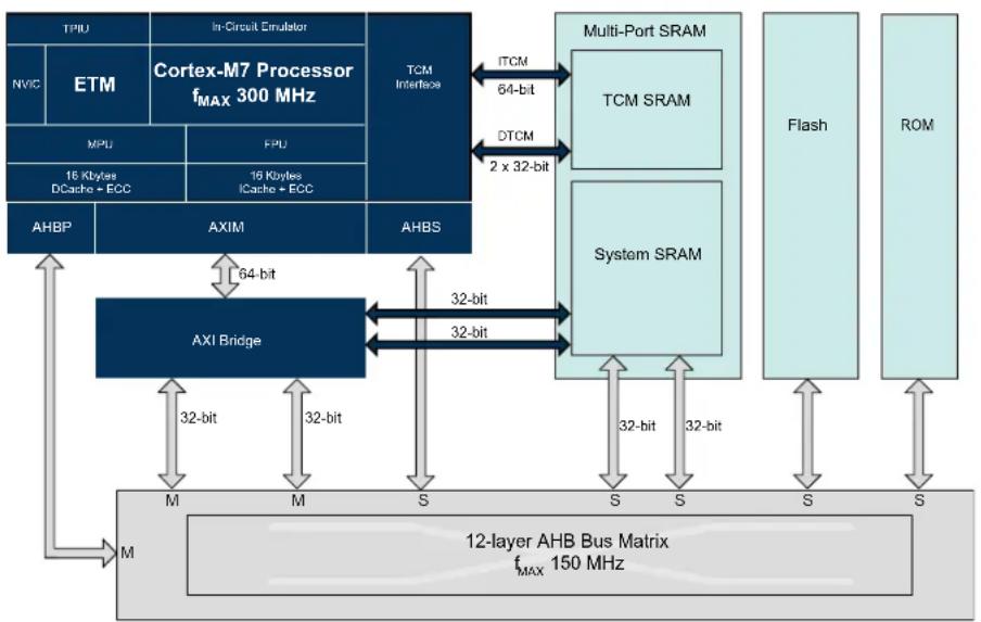
flowchart
graph TD
    A["TPIU"] --> B["In-Circuit Simulator"]
    C["NVIC"] --> D["Cortex-M7 Processor fMAX 300 MHz"]
    E["ETM"] --> D
    F["MPU"] --> G["16 Kbytes DCache + ECC"]
    H["FPU"] --> I["16 Kbytes ICache + ECC"]
    J["AHBP"] --> K["AXIM"]
    L["AHBS"] --> M["AXI Bridge"]
    N["Multi-Port SRAM"] --> O["TCM SRAM"]
    P["System SRAM"] --> Q["32-bit"]
    R["Flash"] --> S["S"]
    T["ROM"] --> U["S"]
    V["M"] --> W["12-layer AHB Bus Matrix fMAX 150 MHz"]
    X["M"] --> Y["32-bit"]
    Z["S"] --> AA["32-bit"]
    AB["S"] --> AC["32-bit"]
    AD["S"] --> AE["32-bit"]
    AF["S"] --> AG["32-bit"]
    AH["S"] --> AI["32-bit"]
    AJ["S"] --> AK["32-bit"]
    AL["S"] --> AM["32-bit"]
    AN["S"] --> AO["32-bit"]
    AP["ITCM"] --> AQ["64-bit"]
    AR["DTCM"] --> AS["2 x 32-bit"]
    AT["32-bit"] --> AU["32-bit"]
    AV["32-bit"] --> AW["32-bit"]
10. Product Mapping
Figure 10-1. SAM E70/S70/V70/V71 Product Mapping

11. Memories
11.1 Embedded Memories
11.1.1 Internal SRAM
SAM E70/S70/V70/V71 devices embed 384 Kbytes or 256 Kbytes of high-speed SRAM.
The SRAM is accessible over the system Cortex-M bus at address 0x2040 0000.
SAM E70/S70/V70/V71 devices embed a Multi-Port SRAM with four ports to optimize the bandwidth and latency. The priorities, defined in the Bus Matrix for each SRAM port Client are propagated, for each request, up to the SRAM Clients.
The Bus Matrix supports four priority levels: Normal, Bandwidth-sensitive, Latency-sensitive and Latency-critical in order to increase the overall processor performance while securing the high-priority latency-critical requests from the peripherals.
The SRAM controller manages interleaved addressing of SRAM blocks to minimize access latencies. It uses Bus Matrix priorities to give the priority to the most urgent request. The less urgent request is performed no later than the next cycle.
Two SRAM Client ports are dedicated to the Cortex-M7 while two ports are shared by the AHB Hosts.
11.1.2 Tightly Coupled Memory (TCM) Interface
SAM E70/S70/V70/V71 devices embed Tightly Coupled Memory (TCM) running at processor speed.
- ITCM is a single 64-bit interface, based at 0x0000 0000 (code region).
- DTCM is composed of dual 32-bit interfaces interleaved, based at 0x2000 0000 (data region).
ITCM and DTCM are enabled/disabled in the ITCMR and DTCMR registers in ARM SCB.
DTCM is enabled by default at reset. ITCM is disabled by default at reset.
There are four TCM configurations controlled by software. When enabled, ITCM is located at 0x0000 0000, overlapping ROM or Flash depending on the general-purpose NVM bit 1 (GPNVM). The configuration is done with GPNVM bits [8:7].
Table 11-1. TCM Configurations in Kbytes
| ITCM DTCM SRAM for 384K RAM-based SRAM for 256K RAM-based GPNVM Bits [8:7] | |
| 0 0 384 256 0 | |
| 32 32 320 192 1 | |
| 64 64 256 128 2 | |
| 128 128 128 0 3 | |
Accesses made to TCM regions when the relevant TCM is disabled and accesses made to the Code and SRAM region above the TCM size limit are performed on the AHB matrix, i.e., on internal Flash or on ROM depending on remap GPNVM bit.
Accesses made to the SRAM above the size limit will not generate aborts.
The Memory Protection Unit (MPU) can to be used to protect these areas.
11.1.3 Internal ROM
The SAM E70/S70/V70/V71 embeds an Internal ROM for the SAM Boot Assistant (SAM-BA ^® ), In Application Programming functions (IAP) and Fast Flash Programming Interface (FFPI).
At any time, the ROM is mapped at address 0x0080 0000.
The ROM may also be mapped at 0x00000000 depending on GPNVM bit setting and ITCM use.
11.1.4 Backup SRAM
The SAM E70/S70/V70/V71 embeds 1 Kbytes of backup SRAM located at 0x4007 4000.
The backup SRAM is accessible in 32-bit words only. Byte or half-word accesses are not supported.
The backup SRAM is supplied by VDDCORE in Normal mode.
In Backup mode, the backup SRAM supply is automatically switched to VDDIO through the backup SRAM power switch when VDDCORE falls. For more details, see the "Backup SRAM Power Switch" section.
11.1.5 Flash Memories
SAM E70/S70/V70/V71 devices embed 512 Kbytes, 1024 Kbytes, or 2084 Kbytes of internal Flash mapped at address 0x40 0000.
The devices feature a Quad SPI (QSPI) interface, mapped at address 0x80000000, that extends the Flash size by adding an external SPI or QSPI Flash.
When accessed by the Cortex-M7 processor for programming operations, the QSPI and internal Flash address spaces must be defined in the Cortex-M7 memory protection unit (MPU) with the attribute 'Device' or 'Strongly Ordered'. For fetch or read operations, the attribute 'Normal memory' must be set to benefit from the internal cache. For additional information, refer to the ARM Cortex-M7 Technical Reference Manual (ARM DDI 0489), which is available for download at www.arm.com.
Some precautions must be taken when the accesses are performed by the central DMA. Refer to the 22. Enhanced Embedded Flash Controller (EEFC) and 41. Quad Serial Peripheral Interface (QSPI).
11.1.5.1 Embedded Flash Overview
The memory is organized in sectors and each sector has a size of 128 Kbytes. The first sector is divided into three smaller sectors which are organized in two sectors of 8 Kbytes and one sector of 112 Kbytes, see figure below.
Figure 11-1. Global Flash Organization
text_image
Address Sector size Sector Name 0x000..... 8 Kbytes Small Sector 0 8 Kbytes Small Sector 1 Larger Sector 112 Kbytes Sector 0 128 Kbytes Sector 1 128 Kbytes Sector nEach sector is organized in pages of 512 bytes.
For sector 0:
• The smaller sector 0 has 16 pages of 512 bytes
• The smaller sector 1 has 16 pages of 512 bytes
• The larger sector has 224 pages of 512 bytes
The rest of the array is composed of 128-Kbyte sectors of 256 pages of 512 bytes each, see image below.
Figure 11-2. Flash Sector Organization

bar_stacked
Sector size is 128 Kbytes | Sector | Total (Kbytes) | Subsector | | :--- | :--- | :--- | | Sector 0 | 16 | Smaller sector 0 | | Sector 0 | 16 | Smaller sector 1 | | Sector 0 | 224 | Larger sector | | Sector n | 256 | Smaller sector 0 | | Sector n | 256 | Smaller sector 1 |The figure below illustrates the organization of the Flash depending on its size.
Figure 11-3. Flash Size
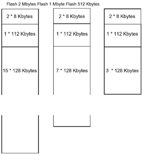
other
Flash 2 Mbytes Flash 1 Mbyte Flash 512 Kbytes | Block Size | Total (Mbytes) | Bytes (Kbytes) | | :--- | :--- | :--- | | 2 * 8 | 2 * 8 | 8 | | 1 * 112 | 1 * 112 | 12 | | 15 * 128 | 7 * 128 | 128 | | 3 * 128 | 3 * 128 | 128 | Flash 2: 2 Mbytes; Flash 1: 1 Mbyte; Flash 512: 512 KbytesErasing the memory can be performed:
- Chip Erase
- By block of 8 Kbytes
- By sector of 128 Kbytes
-
By 512-byte page
-
Erase memory by page is possible only in an 8 Kbyte sector
- EWP and EWPL commands can be only used in 8 Kbyte sectors
The memory has one additional reprogrammable page that can be used as page signature by the user. It is accessible through specific modes, for erase, write and read operations. Erase pin assertion will not erase the User Signature page.
11.1.5.2 Enhanced Embedded Flash Controller
Each Enhanced Embedded Flash Controller manages accesses performed by the hosts of the system. It enables reading the Flash and writing the write buffer. It also contains a User Interface, mapped on the APB.
The Enhanced Embedded Flash Controller ensures the interface of the Flash block.
It manages the programming, erasing, locking and unlocking sequences of the Flash using a full set of commands.
One of the commands returns the embedded Flash descriptor definition that informs the system about the Flash organization, thus making the software generic.
11.1.5.3 Flash Speed
The user must set the number of wait states depending on the system frequency.
For more details, refer to Embedded Flash Characteristics.
11.1.5.4 Lock Regions
Several lock bits are used to protect write and erase operations on lock regions. A lock region is composed of several consecutive pages, and each lock region has its associated lock bit.
Table 11-2. Flash Lock Bits
| Flash Size (Kbytes) Number of Lock Bits | Lock Region Size | |
| 2048 128 16 Kbytes | ||
| 1024 64 16 Kbytes | ||
| 512 32 16 Kbytes |
Asserting the ERASE pin clears the lock bits, thus unlocking the entire Flash.
11.1.5.5 Security Bit Feature
The SAM E70/S70/V70/V71 features a security bit based on the GPNVM bit 0. When security is enabled, any access to the Flash, SRAM, core registers and internal peripherals, either through the SW-DP, the ETM interface or the Fast Flash Programming Interface, is blocked. This ensures the confidentiality of the code programmed in the Flash.
This security bit can only be enabled through the command "Set General-purpose NVM Bit 0" of the EEFC User Interface. Disabling the security bit can only be achieved by asserting the ERASE pin at 1, and after a full Flash erase is performed. When the security bit is deactivated, all accesses to the Flash, SRAM, Core registers, Internal Peripherals are permitted.
The device contains a unique identifier of 2 pages of 512 bytes. These 2 pages are read-only and cannot be erased even by the ERASE pin.
The sequence to read the unique identifier area is described in 22.4.3.8. Unique Identifier Area.
The mapping is as follows:
- Bytes [0..15]: 128 bits for unique identifier
- Bytes[16..1023]: Reserved
11.1.5.7 User Signature
Each device contains a user signature of 512 bytes that is available to the user. The user signature can be used to store information such as trimming, keys, etc., that the user does not want to be erased by asserting the ERASE pin or by software ERASE command. Read, write and erase of this area is allowed.
11.1.5.8 Fast Flash Programming Interface (FFPI)
The Fast Flash Programming Interface (FFPI) allows programming the device through a multiplexed fully-handshaked parallel port. It allows gang programming with market-standard industrial programmers.
The FFPI supports read, page program, page erase, full erase, lock, unlock and protect commands.
The FFPI is enabled and the Fast Programming mode is entered when TST and PA3 and PA4 are tied low.
Table 11-3. FFPI on PIO Controller A (PIOA)
| I/O Line System Function | |
| PD10 PGMEN0 | |
| PD11 PGMEN1 | |
| PB0 PGMM0 | |
| PB1 PGMM1 | |
| PB2 PGMM2 | |
| PB3 PGMM3 | |
| PA3 PGMNCMD | |
| PA4 PGMRDY | |
| PA5 PGMNOE | |
| PA21 PGMNVALID | |
| PA7 PGMD0 | |
| PA8 PGMD1 | |
| PA9 PGMD2 | |
| PA10 PGMD3 | |
| PA11 PGMD4 | |
| PA12 PGMD5 | |
| PA13 PGMD6 | |
| PA14 PGMD7 | |
| PD0 PGMD8 | |
| PD1 PGMD9 | |
| PD2 PGMD10 | |
| PD3 PGMD11 | |
| PD4 PGMD12 | |
| PD5 PGMD13 | |
| PD6 PGMD14 | |
| PD7 PGMD15 |
11.1.5.9 SAM-BA Boot
The SAM-BA Boot is a default boot program which provides an easy way to program in-situ the on-chip Flash memory.
The SAM-BA Boot Assistant supports serial communication via the UART0 and USB.
The SAM-BA Boot provides an interface with SAM-BA computer application.
The SAM-BA Boot is in ROM at address 0x0 when the bit GPNVM1 is set to 0.
11.1.5.10 General-purpose NVM (GPNVM) Bits
All SAM E70/S70/V70/V71 devices feature nine general-purpose NVM (GPNVM) bits that can be cleared or set, through the "Clear GPNVM Bit" and "Set GPNVM Bit" commands of the EEFC User Interface.
The GPNVM0 bit is the security bit.
The GPNVM1bit is used to select the Boot mode (Boot always at 0x00) on ROM or Flash.
Table 11-4. General-purpose Non volatile Memory Bits
| GPNVM Bit Function | |
| 0 Security bit | |
| 1 Boot mode selection | 0: ROM (default)1: Flash |
| 5:2 Free | |
| 6 Reserved | |
| 8:7 TCM configuration | 00: 0 Kbytes DTCM + 0 Kbytes ITCM (default)01: 32 Kbytes DTCM + 32 Kbytes ITCM10: 64 Kbytes DTCM + 64 Kbytes ITCM11: 128 Kbytes DTCM + 128 Kbytes ITCMNote: After programming, reboot must be done. |
The system always boots at address 0x0. To ensure maximum boot possibilities, the memory layout can be changed using GPNVM bits.
A GPNVM bit is used to boot either on the ROM (default) or from the Flash.
The GPNVM bit can be cleared or set, respectively, through the commands "Clear General-purpose NVM Bit" and "Set General-purpose NVM Bit" of the EEFC User Interface.
Setting the bit GPNVM1 selects boot from the Flash. Clearing it selects boot from the ROM. Asserting ERASE resets the bit GPNVM1 and thus selects boot from ROM.
11.2 External Memories
The SAM E70/S70/V70/V71 features one External Bus Interface to provide an interface to a wide range of external memories and to any parallel peripheral.
12. Event System
The events generated by peripherals (source) are designed to be directly routed to peripherals (destination) using these events without processor intervention. The trigger source can be programmed in the destination peripheral.
12.1 Embedded Characteristics
- Timers, PWM, I/Os and peripherals generate event triggers which are directly routed to destination peripherals, such as AFEC or DACC to start measurement/conversion without processor intervention.
- UART, USART, QSPI, SPI, TWI, PWM, HSMCI, AES, AFEC, DACC, PIO, TC (Capture mode) also generate event triggers directly connected to the DMA Controller for data transfer without processor intervention.
- Parallel capture logic is directly embedded in the PIO and generates trigger events to the DMA Controller to capture data without processor intervention.
- PWM safety events (faults) are in combinational form and directly routed from event generators (AFEC, ACC, PMC, TC) to the PWM module.
- PWM output comparators (OCx) generate events directly connected to the TC.
- PMC safety event (clock failure detection) can be programmed to switch the MCK on reliable main RC internal clock without processor intervention.
12.2 Real-time Event Mapping
Table 12-1. Real-time Event Mapping List
| Function Application Description Event Source Event | Destination | |||
| Safety General-purpose | Automatic switch to reliable main RC oscillator in case of main crystal clock failure (see Note 1) | Power Management Controller (PMC) | PMC | |
| General-purpose, motor control, power factor correction (PFC) | Puts the PWM outputs in Safe mode in case of main crystal clock failure (see Notes 1, 2) | PMC Pulse Width | Modulation 0 and 1 (PWM0 and PWM1) | |
| Motor control, PFC | Puts the PWM outputs in Safe mode (overcurrent detection, etc.) (see Notes 2, 3) | Analog Comparator Controller (ACC) | PWM0 and PWM1 | |
| Motor control, PFC | Puts the PWM outputs in Safe mode (overspeed, overcurrent detection, etc.) (see Notes 2, 4) | Analog Front-End Controller (AFEC0) | PWM0 and PWM1 | |
| AFEC1 PWM0 and | PWM1 | |||
| Motor control Puts the PWM outputs in Safe mode (overspeed detection through timer quadrature decoder) (see Notes 2, 6) | TC0.Ch0 PWM0 | |||
| TC0.Ch1 PWM1 | ||||
| General-purpose, motor control, power factor correction (PFC) | Puts the PWM outputs in Safe mode (general-purpose fault inputs) (see Note 2) | PIO PA9, PD8, PD9 PWM0 | ||
| PIO PA21, PA26, PA28 PWM1 | ||||
| Security | General-purpose | Immediate GPBR clear (asynchronous) on tamper detection through WKUP0/1 IO pins (see Note 5) | PIO WKUP0/1 | GPBR |
| Measurement trigger | Power factor correction (DC-DC, lighting, etc.) | Duty cycle output waveform correction Trigger source selection in PWM (see Notes 7, 8) | ACC PWM0 | |
| PIO PA10, PA22 PWM0 | ||||
| ACC PWM1 | ||||
| PIO PA30, PA18 PWM1 | ||||
| General-purpose | Trigger source selection in AFEC (see Note 9) | PIO AFE0_ADTRG AFEC0 | ||
| TC0.Ch0 (TIOA0) AFEC0 | ||||
| TC0.Ch1 (TIOA1) AFEC0 | ||||
| TC0.Ch2 (TIOA2) AFEC0 | ||||
| ACC AFEC0 | ||||
| Motor control ADC-PWM synchronization (see Notes 12, 14) Trigger source selection in AFEC (see Note 9) | PWM0 Event Line 0 and 1 AFEC0 | |||
| General-purpose | Trigger source selection in AFEC (see Note 9) | PIO AFE1_ADTRG AFEC1 | ||
| TC1.Ch0 (TIOA3) AFEC1 | ||||
| TC1.Ch1 (TIOA4) AFEC1 | ||||
| TC1.Ch2 (TIOA5) AFEC1 | ||||
| ACC AFEC1 | ||||
| Motor control ADC-PWM synchronization (see Notes 12, 14) Trigger source selection in AFEC (see Note 9) | PWM1 Event Line 0 and 1 | AFEC1 | ||
| General-purpose | Temperature sensor Low-speed measurement (see Notes 10, 11) | RTC RTCOUT0 AFEC0 and | AFEC1 | |
| Conversion trigger | General-purpose | Trigger source selection in DACC (Digital-to-Analog Converter Controller) (see Note 13) | TC0.Ch0-2 (TIOA0, TIOA1, TIOA2) | DACC |
| PIO DATRG DACC | ||||
| PWM0 Event Line 0 and 1(14) | DACC | |||
| PWM1 Event Line 0 and 1(14) | DACC | |||
| Image capture Low-cost image sensor | Direct image transfer from sensor to system memory via DMA(15) | PIO PA3/4/5/9/10/11/12/13, PA22, PA14, PA21 | DMA | |
| Delay measurement | Motor control Propagation delay of external components (IOs, power transistor bridge driver, etc.) See Notes 16, 17) | PWM0 Comparator Output OC0 | TC0.Ch0 TIOA0 and TIOB0 | |
| PWM0 Comparator Output OC1 | TC0.Ch1 TIOA1 and TIOB1 | |||
| PWM0 Comparator Output OC2 | TC0.Ch2 TIOA2 and TIOB2 | |||
| PWM1 Comparator Output OC0 | TC1.Ch0 TIOA3 and TIOB3 | |||
| PWM1 Comparator Output OC1 | TC1.Ch1 TIOA4 and TIOB4 | |||
| PWM1 Comparator Output OC2 | TC1.Ch2 TIOA5 and TIOB5 | |||
| PWM0 Comparator Output OC0 | TC2.Ch0 TIOA6 and TIOB6 | |||
| PWM0 Comparator Output OC1 | TC2.Ch1 TIOA7 and TIOB7 | |||
| PWM0 Comparator Output OC2 | TC2.Ch2 TIOA8 and TIOB8 | |||
| PWM1 Comparator Output OC0 | TC3.Ch0 TIOA9 and TIOB9 | |||
| PWM1 Comparator Output OC1 | TC3.Ch1 TIOA10 and TIOB10 | |||
| Audio clock recovery from Ethernet | Audio GMAC GTSUCOMP signal adaptation via TC (TC3.TC_EMR.TRIGSRCB) in order to drive the clock reference of the external PLL for the audio clock | GMAC GTSUCOMP | TC3.Ch2 TIOB11 | |
| Direct Memory Access | General-purpose | Peripheral trigger event generation to transfer data to/from system memory (see Note 18) | USART, UART, TWIHS, SPI, QSPI, AFEC, TC (Capture), SSC, HSMCI, DAC, AES, PWM, PIO, I2SC | XDMA |
Notes:
- Refer to 31.15. Main Crystal Oscillator Failure Detection.
- Refer to 50.5.4. Fault Inputs and 50.6.2.7. Fault Protection.
- Refer to 53.6.4. Fault Mode.
- Refer to 53.5.4. Fault Output.
- Refer to 23.4.9.2. Low-power Tamper Detection and Anti-Tampering and 29.3.1. SYS_GPBRx.
- Refer to 49.6.18. Fault Mode.
- Refer to 50.7.49. PWM_ETRGx.
-
Refer to 50.6.5. PWM External Trigger Mode.
-
Refer to 51.6.6. Conversion Triggers and 51.7.2. AFEC_MR.
- Refer to 57.10. Temperature Sensor.
- Refer to 27.5.8. Waveform Generation.
- Refer to 50.7.36. PWM_CMPVx and 50.6.4. PWM Event Lines.
- Refer to 52.7.3. DACC_TRIGR.
- Refer to 50.6.3. PWM Comparison Units and 50.6.4. PWM Event Lines.
- Refer to 32.5.14. Parallel Capture Mode.
- Refer to 50.6.2.2. Comparator.
- Refer to 49.6.14. Synchronization with PWM.
- Refer to 35. DMA Controller (XDMAC).
13. System Controller
The System Controller is a set of peripherals that handles key elements of the system, such as power, resets, clocks, time, interrupts, watchdog, and so on..
13.1 System Controller and Peripherals Mapping
Refer to the "Product Mapping" section.
13.2 Power-on-Reset, Brownout and Supply Monitor
The SAM E70/S70/V70/V71 embeds three features to monitor, warn and/or reset the chip:
• Power-on-Reset (POR) on VDDIO
- POR on VDDCORE
- Brown-out-Detector (BOD) on VDDCORE
• Supply Monitor on VDDIO
13.2.1 Power-on-Reset
The Power-on-Reset (POR) monitors VDDIO and VDDCORE. It is always activated and monitors voltage at start up but also during power down. If VDDIO or VDDCORE goes below the threshold voltage, the entire chip is Reset. For more information, refer to 57. Electrical Characteristics for SAM V70/V71.
13.2.2 Brownout Detector on VDDCORE
The Brown-out-Detector(BOD) monitors VDDCORE. It is active by default. It can be deactivated by software through the Supply Controller (SUPC_MR). It is especially recommended to disable it during low-power modes, such as wait or sleep modes.
If VDDCORE goes below the threshold voltage, the reset of the core is asserted. For more information, refer to 23. Supply Controller (SUPC) and 57. Electrical Characteristics for SAM V70/V71.
13.2.3 Supply Monitor on VDDIO
The Supply Monitor monitors VDDIO. It is not active by default. It can be activated by software and is fully programmable with 16 steps for the threshold (between 1.6V to 3.4V). It is controlled by the Supply Controller (SUPC). A sample mode is possible, which allows the supply monitor power consumption to be divided by a factor of up to 2048. For more information, refer to 23. Supply Controller (SUPC) and 57. Electrical Characteristics for SAM V70/V71.
13.3 Reset Controller
The Reset Controller is based on two POR cells, one on VDDIO and one on VDDCORE, and a Supply Monitor on VDDIO.
The Reset Controller returns the source of the last reset to the software. This may be a general reset, a wakeup reset, a software reset, a user reset or a watchdog reset.
The Reset Controller controls the internal resets of the system and the pin input/output. It can shape a reset signal for the external devices, simplifying the connection of a push-button on the NRST pin to implement a manual reset.
The configuration of the Reset Controller is saved as supplied on VDDIO.
14. Peripherals
14.1 Peripheral Identifiers
The following table defines the peripheral identifiers of the SAM E70/S70/V70/V71 devices. A peripheral identifier is required for the control of the peripheral interrupt with the Nested Vectored Interrupt Controller and control of the peripheral clock with the Power Management Controller.
Table 14-1. Peripheral Identifiers
| Instance ID | Instance Name | NVIC Interrupt PMC Clock Control | Description | |
| 0 SUPC X - Supply Controller | ||||
| 1 RSTC X - Reset Controller | ||||
| 2 RTC X - Real Time Clock | ||||
| 3 RTT X - Real Time Timer | ||||
| 4 | WDT | X - Watchdog Timer | ||
| 5 | PMC | X - Power Management Controller | ||
| 6 | EFC X - Enhanced Embedded Flash Controller | |||
| 7 | UART0 | X | X | Universal Asynchronous Receiver/Transmitter |
| 8 | UART1 | X | X | Universal Asynchronous Receiver/Transmitter |
| 9 | SMC | - X | Static Memory Controller | |
| 10 | PIOA X | X | Parallel I/O Controller A | |
| 11 | PIOB X | X | Parallel I/O Controller B | |
| 12 | PIOC X | X | Parallel I/O Controller C | |
| 13 | USART0 | X | X | Universal Synchronous/Asynchronous Receiver/Transmitter |
| 14 | USART1 | X | X | Universal Synchronous/Asynchronous Receiver/Transmitter |
| 15 | USART2 | X | X | Universal Synchronous/Asynchronous Receiver/Transmitter |
| 16 | PIOD X | X | Parallel I/O Controller D | |
| 17 | PIOE | X | X | Parallel I/O Controller E |
| 18 | HSMCI | X | X | Multimedia Card Interface |
| 19 | TWIHS0 | X | X | Two-wire Interface ( I^2C -compatible) |
| 20 | TWIHS1 | X | X | Two-wire Interface ( I^2C -compatible) |
| 21 | SPI0 | X | X | Serial Peripheral Interface |
| 22 | SSC | X | X | Synchronous Serial Controller |
| 23 | TC0_CHANNEL0 | X | X | 16-bit Timer Counter 0, Channel 0 |
| 24 | TC0_CHANNEL1 | X | X | 16-bit Timer Counter 0, Channel 1 |
| 25 | TC0_CHANNEL2 | X | X | 16-bit Timer Counter 0, Channel 2 |
| 26 | TC1_CHANNEL0 | X | X | 16-bit Timer Counter 1, Channel 0 |
| 27 | TC1_CHANNEL1 | X | X | 16-bit Timer Counter 1, Channel 1 |
| 28 | TC1_CHANNEL2 | X | X | 16-bit Timer Counter 1, Channel 2 |
| 29 | AFEC0 | X | X | Analog Front-End Controller |
| 30 | DACC | X | X | Digital-to-Analog Converter |
| 31 | PWM0 | X | X | Pulse-Width Modulation Controller |
| 32 | ICM X | X | Integrity Check Monitor | |
| 33 | ACC | X | X | Analog Comparator Controller |
| 34 | USBHS | X | X | USB Host/Device Controller |
| 35 MCAN0 | X | X | CAN IRQ Line 0 | |
| 36 MCAN0 | INT1 | - CAN IRQ Line 1 | ||
| 37 MCAN1 X X CAN IRQ Line 0 | ||||
| 38 MCAN1 INT1 - CAN IRQ Line 1 | ||||
| 39 GMAC X X Ethernet MAC | ||||
| 40 AFEC1 X X Analog Front End Controller | ||||
| 41 TWIHS2 X X Two-wire Interface | ||||
| 42 SPI1 X X Serial Peripheral Interface | ||||
| 43 | QSPI | X X Quad I/O Serial Peripheral Interface | ||
| 44 | UART2 | X X Universal Asynchronous Receiver/Transmitter | ||
| 45 | UART3 | X X Universal Asynchronous Receiver/Transmitter | ||
| 46 | UART4 | X X Universal Asynchronous Receiver/Transmitter | ||
| 47 | TC2_CHANNEL0 | X X 16-bit Timer Counter 2, Channel 0 | ||
| 48 | TC2_CHANNEL1 | X X 16-bit Timer Counter 2, Channel 1 | ||
| 49 | TC2_CHANNEL2 | X X 16-bit Timer Counter 2, Channel 2 | ||
| 50 | TC3_CHANNEL0 | X X 16-bit Timer Counter 3, Channel 0 | ||
| 51 | TC3_CHANNEL1 | X X 16-bit Timer Counter 3, Channel 1 | ||
| 52 | TC3_CHANNEL2 | X X 16-bit Timer Counter 3, Channel 2 | ||
| 53 | MLB | X X MediaLB IRQ 0 | ||
| 54 | MLB | X - MediaLB IRQ 1 | ||
| 55 | - | X - Reserved | ||
| 56 | AES | X X Advanced Encryption Standard | ||
| 57 | TRNG | X X True Random Number Generator | ||
| 58 XDMAC X X DMA Controller | ||||
| 59 | ISI | X X Image Sensor Interface | ||
| 60 | PWM1 X X Pulse-Width Modulation Controller | |||
| 61 | ARM | FPU | - | Arm Floating Point Unit interrupt associated with OFC, UFC, IOC, DZC and IDC bits. |
| 62 | Reserved | - | -- | |
| 63 | RSWDT | X - Reinforced Safety Watchdog Timer | ||
| 64 | ARM CCW | - Arm Cache ECC Warning | ||
| 65 | ARM | CCF | - Arm Cache ECC Fault | |
| 66 GMAC Q1 | - GMAC Queue 1 Interrupt signal toggled on a DMA write to the first word of each DMA data buffer associated with queue 1. | |||
| 67 GMAC Q2 | - GMAC Queue 2 Interrupt signal toggled on a DMA write to the first word of each DMA data buffer associated with queue 2. | |||
| 68 | ARM IXC | - Floating Point Unit Interrupt IXC associated with FPU cumulative exception bit. | ||
| 69 | I2SC0 | X X Inter-IC Sound Controller | ||
| 70 | I2SC1 | X X Inter-IC Sound Controller | ||
| 71 GMAC Q3 | - GMAC Queue 3 Interrupt signal toggled on a DMA write to the first word of each DMA data buffer associated with queue 3 | |||
| 72 GMAC Q4 | - GMAC Queue 4 Interrupt signal toggled on a DMA write to the first word of each DMA data buffer associated with queue 4 | |||
| 73 GMAC Q5 | - GMAC Queue 5 Interrupt signal toggled on a DMA write to the first word of each DMA data buffer associated with queue 5 | |||
14.2 Peripheral Signal Multiplexing on I/O Lines
The SAM E70/S70/V70/V71 features
- Two PIO controllers on 64-pin versions (PIOA and PIOB)
- Three PIO controllers on the 100-pin version (PIOA, PIOB and PIOD)
- Five PIO controllers on the 144-pin version (PIOA, PIOB, PIOC, PIOD and PIOE), that multiplex the I/O lines of the peripheral set.
The SAM E70/S70/V70/V71 PIO Controllers control up to 32 lines and each line can be assigned to one of four peripheral functions: A, B, C or D.
For more information on multiplexed signals, refer to the "Package and Pinout" chapter.
15. Arm Cortex-M7
Refer to Arm reference documents Cortex-M7 Processor User Guide (ARM DUI 0644) and Cortex-M7 Technical Reference Manual (ARM DDI 0489), which are available for download at www.arm.com.
15.1 Arm Cortex-M7 Configuration
The following table provides the configuration for the Arm Cortex-M7 processor in SAM E70/S70/V70/V71 devices.
Table 15-1. Arm Cortex-M7 Configuration
| Features Configuration | |
| Debug | |
| Comparator set Full comparator set: 4 DWT and 8 FPB comparators | |
| ETM support Instruction ETM interface | |
| Internal Trace support (ITM) ITM and DWT trace functionality implemented | |
| CTI and WIC Not embedded | |
| TCM | |
| ITCM max size 128 KB | |
| DTCM max size 256 KB | |
| Cache | |
| Cache size 16 KB for instruction cache, 16 KB for data cache | |
| Number of sets 256 for instruction cache, 128 for data cache | |
| Number of ways 2 for instruction cache, 4 for data cache | |
| Number of words per cache line 8 words (32 bytes) | |
| ECC on Cache Embedded | |
| NVIC | |
| IRQ number | 74 |
| IRQ priority levels | 8 |
| MPU | |
| Number of regions | 16 |
| FPU | |
| FPU precision Single and double precision | |
| AHB Port | |
| AHBP addressing size | 512 MB |
16. Debug and Test Features
16.1 Description
The device features a number of complementary debug and test capabilities. The Serial Wire Debug Port (SW-DP) is used for standard debugging functions, such as downloading code and single-stepping through programs. It also embeds a serial wire trace.
16.2 Embedded Characteristics
- Debug access to all memory and registers in the system, including Cortex-M register bank, when the core is running, halted, or held in reset.
- Serial Wire Debug Port (SW-DP) debug access (ADlv5.1 with no multidrop mode support).
- Flash Patch and Breakpoint (FPB) unit for implementing breakpoints and code patches.
- Data Watchpoint and Trace (DWT) unit for implementing watchpoints, data tracing, and system profiling.
- Instrumentation Trace Macrocell (ITM) for support of printf style debugging.
- 6-pin Embedded Trace Macrocell (ETM) for instruction trace stream, including CoreSight™ Trace Port Interface Unit (TPIU).
- IEEE1149.1 JTAG Boundary scan on All Digital Pins.
16.3 Associated Documents
The SAM E70/S70/V70/V71 implements the standard Arm CoreSight macrocell. For information on CoreSight, the following reference documents are available from the Arm web site (www.arm.com):
- Cortex-M7 User Guide Reference Manual (ARM DUI 0644)
• Cortex-M7 Technical Reference Manual (ARM DDI 0489) - CoreSight Technology System Design Guide (ARM DGI 0012)
- CoreSight Components Technical Reference Manual (ARM DDI 0314)
• ARM Debug Interface v5 Architecture Specification (Doc. ARM IHI 0031)
• ARMv7-M Architecture Reference Manual (ARM DDI 0403)
16.4 Debug and Test Block Diagram
Figure 16-1. Debug and Test Block Diagram

flowchart
graph TD
    A["Cortex-M7"] --> B["Embedded Trace Macrocell"]
    B --> C["PICK3"]
    C --> D["Serial Wire Debug Port"]
    D --> E["Reset and Test"]
    E --> F["POR"]
    F --> G["TST"]
    D --> H["JTAGSEL"]
    D --> I["TDO/TRACESWO"]
    D --> J["TMS/SWDIO"]
    D --> K["TCK/SWCLK"]
    D --> L["TDI"]
    B --> M["PIO"]
    M --> N["TRACED0-3"]
    M --> O["TRACECLK"]
    A --> P["Boundary Test Access Port (TAP)"]
    P --> D
16.5 Debug and Test Pin Description
Table 16-1. Debug and Test Signal List
| Signal Name Function | Type Active Level | ||
| Reset/Test | |||
| NRST Microcontroller Reset Input/Output Low | |||
| TST Test Select Input - | |||
| Serial Wire Debug Port/JTAG Boundary Scan | |||
| TCK/SWCLK Test Clock/Serial Wire Clock Input - | |||
| TDI | Test Data In | Input - | |
| TDO/TRACESWO | Test Data Out/Trace Asynchronous Data Out | Output | - |
| TMS/SWDIO | Test Mode Select/Serial Wire Input/Output | Input - | |
| JTAGSEL | JTAG Selection | Input High | |
| Trace Debug Port | |||
| TRACECLK | Trace Clock | Output | - |
| TRACED0-3 | Trace Data | Output | - |
16.6 Application Examples
16.6.1 Debug Environment
The figure below shows a complete debug environment example. The SW-DP interface is used for standard debugging functions, such as downloading code and single-stepping through the program and viewing core and peripheral registers.
Figure 16-2. Application Debug Environment Example
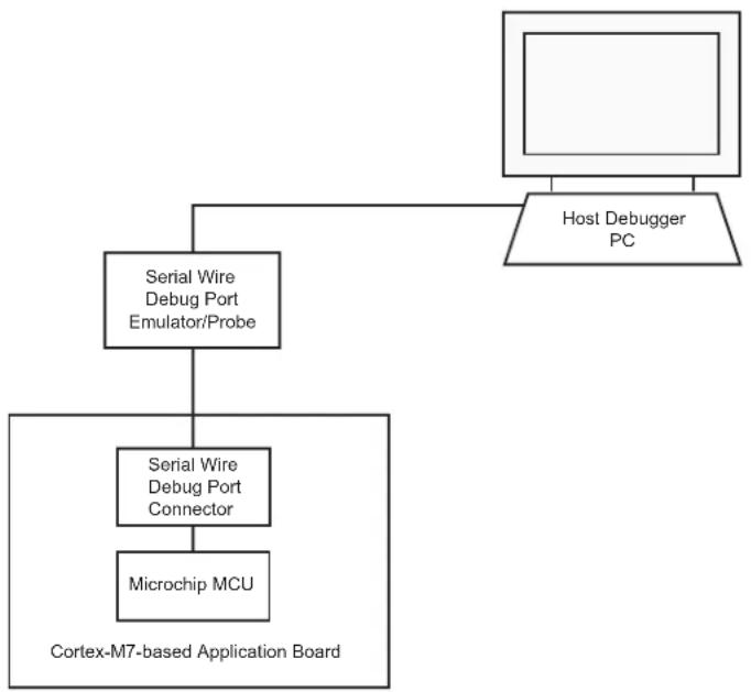
flowchart
graph TD
    A["Host Debugger PC"] --> B["Serial Wire Debug Port Emulator/Probe"]
    B --> C["Serial Wire Debug Port Connector"]
    C --> D["Microchip MCU"]
    style A fill:#f9f,stroke:#333
    style D fill:#ccf,stroke:#333
16.6.2 Test Environment
The figure below shows a test environment example (JTAG Boundary scan). Test vectors are sent and interpreted by the tester. In this example, the "board in test" is designed using a number of JTAG-compliant devices. These devices can be connected to form a single scan chain.
Figure 16-3. Application Test Environment Example

flowchart
graph TD
    A["JTAG Probe"] --> B["JTAG Connector"]
    B --> C["Chip n"]
    C -.-> D["Chip 2"]
    D --> E["Chip 1"]
    E --> F["Microchip MCU"]
    F --> B
    G["Tester"] --> A
    style A fill:#f9f,stroke:#333
    style B fill:#ccf,stroke:#333
    style C fill:#cfc,stroke:#333
    style D fill:#fcc,stroke:#333
    style E fill:#cff,stroke:#333
    style F fill:#ffc,stroke:#333
    style G fill:#fff,stroke:#333
16.7 Functional Description
16.7.1 Test Pin
The TST pin is used for JTAG Boundary Scan Manufacturing Test or Fast Flash Programming mode. The TST pin integrates a permanent pulldown resistor of about 15 kΩ to GND, so that it can be left unconnected for normal operations. To enable Fast Flash Programming mode, refer to 18. Fast Flash Programming Interface (FFPI).
16.7.2 Debug Architecture
Figure 16-4 shows the debug architecture used. The Cortex-M7 embeds six functional units for debug:
- Serial Wire Debug Port (SW-DP) debug access
• FPB (Flash Patch Breakpoint)
• DWT (Data Watchpoint and Trace)
• ITM (Instrumentation Trace Macrocell) - 6-pin Embedded Trace Macrocell (ETM) for instruction trace stream, including CoreSight Trace Port Interface Unit (TPIU)
- IEEE1149.1 JTAG Boundary scan on all digital pins
The debug architecture information that follows is mainly dedicated to developers of SW-DP Emulators/Probes and debugging tool vendors for Cortex-M7-based microcontrollers. For further details on SW-DP, see the Cortex - M7 Technical Reference Manual.
Figure 16-4. Debug Architecture
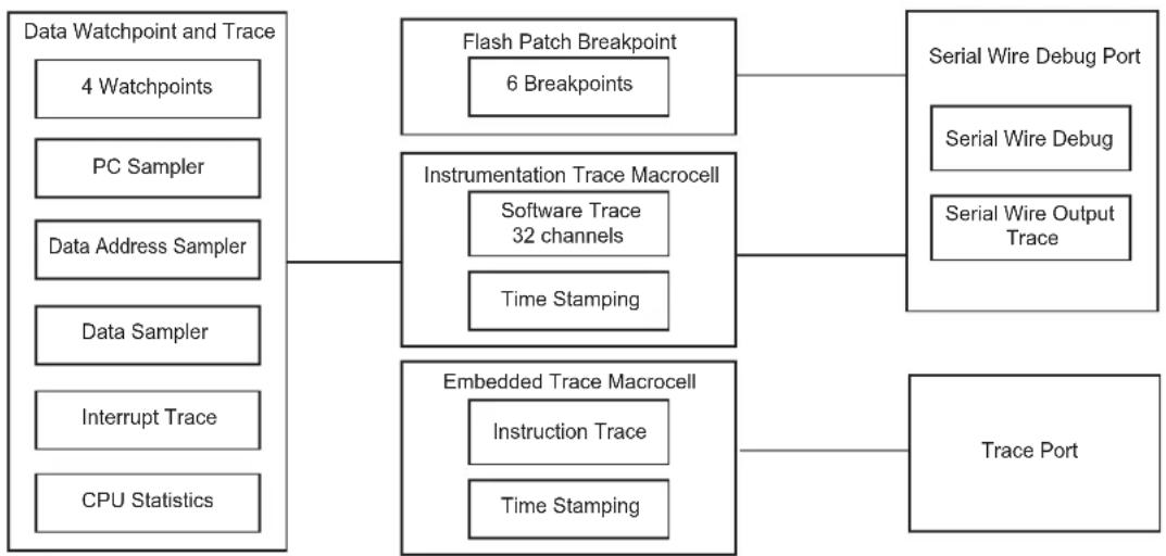
flowchart
graph LR
    A["Data Watchpoint and Trace"] --> B["4 Watchpoints"]
    A --> C["PC Sampler"]
    A --> D["Data Address Sampler"]
    A --> E["Data Sampler"]
    A --> F["Interrupt Trace"]
    A --> G["CPU Statistics"]
    H["Flash Patch Breakpoint"] --> I["6 Breakpoints"]
    J["Instrumentation Trace Macrocell"] --> K["Software Trace 32 channels"]
    J --> L["Time Stamping"]
    M["Embedded Trace Macrocell"] --> N["Instruction Trace"]
    M --> O["Time Stamping"]
    P["Serial Wire Debug Port"] --> Q["Serial Wire Debug"]
    P --> R["Serial Wire Output Trace"]
    S["Trace Port"] --> T["Serial Wire Debug"]
16.7.3 Serial Wire Debug Port (SW-DP) Pins
The SW-DP pins SWCLK and SWDIO are commonly provided on a standard 20-pin JTAG connector defined by ARM. For more details on voltage reference and reset state, refer to the "Signal Description" chapter.
At startup, SW-DP pins are configured in SW-DP mode to allow connection with debugging probe.
SW-DP pins can be used as standard I/Os to provide users more general input/output pins when the debug port is not needed in the end application. Mode selection between SW-DP mode (System I/O mode) and general I/O mode is performed through the AHB Matrix Chip Configuration registers
(CCFG_SYSIO). Configuration of the pad for pullup, triggers, debouncing and glitch filters is possible regardless of the mode.
The JTAGSEL pin is used to select the JTAG boundary scan when asserted at a high level. It integrates a permanent pulldown resistor of about 15 kΩ to GND, so that it can be left unconnected for normal operations.
The JTAG debug ports TDI, TDO, TMS and TCK are inactive. They are provided for Boundary Scan Manufacturing Test purposes only. By default the SW-DP is active; TDO/TRACESWO can be used for trace.
Table 16-2. SW-DP Pin List
| Pin Name JTAG Boundary Scan | Serial Wire Debug Port | |
| TMS/SWDIO TMS SWDIO | ||
| TCK/SWCLK TCK SWCLK | ||
| TDI TDI - | ||
| TDO/TRACESWO TDO TRACESWO (optional: trace) | ||
SW-DP is selected when JTAGSEL is low. It is not possible to switch directly between SW-DP and JTAG boundary scan operations. A chip reset must be performed after JTAGSEL is changed.
16.7.4 Embedded Trace Module (ETM) Pins
The Embedded Trace Module (ETM) uses the Trace Port Interface Unit (TPIU) to export data out of the system.
The TPUI features the pins:
- TRACECLK-always exported to enable synchronization back with the data. PCK3 is used internally.
- TRACED0-3-the instruction trace stream.
16.7.5 Flash Patch Breakpoint (FPB)
The FPB implements hardware breakpoints.
16.7.6 Data Watchpoint and Trace (DWT)
The DWT contains four comparators which can be configured to generate:
• PC sampling packets at set intervals
• PC or Data watchpoint packets
- Watchpoint event to halt core
The DWT contains counters for:
- Clock cycle (CYCCNT)
- Folded instructions
- Load Store Unit (LSU) operations
- Sleep cycles
• CPI (all instruction cycles except for the first cycle) - Interrupt overhead
16.7.7 Instrumentation Trace Macrocell (ITM)
The ITM is an application driven trace source that supports printf style debugging to trace Operating System (OS) and application events, and emits diagnostic system information. The ITM emits trace information as packets which can be generated by three different sources with several priority levels:
- Software trace: Software can write directly to ITM stimulus registers. This can be done using the printf function. For more information, refer to 16.7.5. Flash Patch Breakpoint (FPB).
- Hardware trace: The ITM emits packets generated by the DWT.
- Timestamping: Timestamps are emitted relative to packets. The ITM contains a 21-bit counter to generate the timestamp.
16.7.7.1 How to Configure the ITM
The following example describes how to output trace data in asynchronous trace mode.
Configure the TPIU for asynchronous trace mode. Refer to 16.7.7.3. How to Configure the TPIU.
- Enable the write accesses into the ITM registers by writing "0xC5ACCE55" into the Lock Access Register (Address: 0xE0000FB0)
-
Write 0x00010015 into the Trace Control register:
-
Enable ITM.
- Enable Synchronization packets.
- Enable SWO behavior.
-
Fix the ATB ID to 1.
-
Write 0x1 into the Trace Enable register:
- Enable the Stimulus port 0.
- Write 0x1 into the Trace Privilege register:
- Stimulus port 0 only accessed in privileged mode (Clearing a bit in this register will result in the corresponding stimulus port being accessible in user mode.)
- Write into the Stimulus port 0 register: TPIU (Trace Port Interface Unit)
The TPIU acts as a bridge between the on-chip trace data and the Instruction Trace Macrocell (ITM).
The TPIU formats and transmits trace data off-chip at frequencies asynchronous to the core.
16.7.7.2 Asynchronous Mode
The TPIU is configured in asynchronous mode, trace data are output using the single TRACESWO pin. The TRACESWO signal is multiplexed with the TDO signal. As a consequence, asynchronous trace mode is only available when the Serial Wire Debug mode is selected.
Two encoding formats are available for the single pin output:
- Manchester encoded stream. This is the reset value.
- NRZ_based UART byte structure
16.7.7.3 How to Configure the TPIU
This example only concerns the asynchronous trace mode.
Set the TRCENA bit to 1 into the Debug Exception and Monitor Register (0xE000EDFC) to enable the use of trace and debug blocks.
- Write 0x2 into the Selected Pin Protocol Register.
- Select the Serial Wire output - NRZ
-
Write 0x100 into the Formatter and Flush Control Register.
-
Set the suitable clock prescaler value into the Async Clock Prescaler Register to scale the baud rate of the asynchronous output (this can be done automatically by the debugging tool).
-
Write 0x100 into the Formatter and Flush Control Register.
- Set the suitable clock prescaler value into the Async Clock Prescaler Register to scale the baud rate of the asynchronous output (this can be done automatically by the debugging tool).
16.7.8 IEEE1149.1 JTAG Boundary Scan
IEEE1149.1 JTAG Boundary Scan allows pin-level access independent of the device packaging technology.
IEEE1149.1 JTAG Boundary Scan is enabled when TST is tied to high, PD0 tied to low, and JTAGSEL tied to high during powerup. These pins must be maintained in their respective states for the duration of the boundary scan operation. The SAMPLE, EXTEST and BYPASS functions are implemented. In Serial Wire Debug mode, the ARM processor responds with a non-JTAG chip ID that identifies the processor. This is not IEEE1149.1 JTAG-compliant.
It is not possible to switch directly between JTAG Boundary Scan and SWJ Debug Port operations. A chip reset must be performed after JTAGSEL is changed.
A Boundary Scan Descriptor Language (BSDL) file to set up the test is provided on www.microchip.com.
16.7.8.1 JTAG Boundary Scan Register
The Boundary Scan Register (BSR) contains a number of bits which correspond to active pins and associated control signals.
Each input/output pin corresponds to a 3-bit register in the BSR. The OUTPUT bit contains data that can be forced on the pad. The INPUT bit facilitates the observability of data applied to the pad. The CONTROL bit selects the direction of the pad.
For more information, refer to BDSL files available on www.microchip.com.
16.7.9 ID Code Register
Access: Read-only
| 31 30 29 28 27 26 25 24 | ||||||
| VERSION PART NUMBER | ||||||
| 23 22 21 20 19 18 17 16 | ||||||
| PART NUMBER | ||||||
| 15 14 13 12 11 10 9 8 | ||||||
| PART NUMBER MANUFACTURER IDENTITY | ||||||
| 7 6 5 4 3 2 1 0 | ||||||
| MANUFACTURER IDENTITY 1 | ||||||
- VERSION[31:28]: Product Version Number
Set to 0x0.
• PART NUMBER[27:12]: Product Part Number
Set to 0x0.
| PART NUMBER |
| 0x5B3D |
• MANUFACTURER IDENTITY[11:1]: Manufacturer ID
Set to 0x01F.
- Bit[0]: Required by IEEE Std. 1149.1
Set to 0x1.
| JTAG ID Code |
| 0x5B3D_D03F |
17. SAM-BA Boot Program
17.1 Description
The SAM-BA Boot Program integrates an array of programs permitting download and/or upload into the different memories of the product.
17.2 Embedded Characteristics
- Default Boot program
- Interface with SAM-BA graphic user interface (GUI)
- SAM-BA Boot
– Supports several communication media:
- Serial Communication on UART0
- USB device port communication up to 1Mbyte/s
- USB Requirements:
- External crystal or external clock with frequency of 12 MHz or 16 MHz
17.3 Hardware and Software Constraints
- SAM-BA Boot uses the first 2048 bytes of the SRAM for variables and stacks. The remaining available bytes can be used for the user code.
- USB requirements:
- External crystal or external clock (see Note below) with frequency of 12 MHz or 16 MHz
Note: Must be 2500 ppm and VDDIO square wave signal.
- UART0 requirements:
- None. If accurate external clock source is not available, the internal 12 MHz RC meets RS-232 standards at room temperature.
Table 17-1. Pins Driven during Boot Program Execution
| Peripheral Pin PIO Line | ||
| UART0 URXD0 PA9 | ||
| UART0 UTXD0 PA10 |
17.4 Flow Diagram
The boot program implements the algorithm below.
Figure 17-1. Boot Program Algorithm Flow Diagram
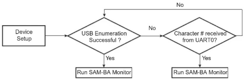
flowchart
graph TD
    A["Device Setup"] --> B{USB Enumeration Successful ?}
    B -->|Yes| C["Run SAM-BA Monitor"]
    B -->|No| D{Character # received from UART0?}
    D -->|Yes| E["Run SAM-BA Monitor"]
    D -->|No| F["End"]
The SAM-BA boot program looks for a source clock, either from the embedded main oscillator with external crystal (main oscillator enabled) or from a supported frequency signal applied to the XIN pin (Main oscillator in bypass mode).
If a clock is supplied by one of the two sources, the boot program checks that the frequency is one of the supported external frequencies. If the frequency is supported, USB activation is allowed. If no clock is supplied, or if a clock is supplied but the frequency is not a supported external frequency, the internal 12 MHz RC oscillator is used as the main clock. In this case, the USB is not activated due to the frequency drift of the 12 MHz RC oscillator.
17.5 Device Initialization
Initialization by the boot program follows the steps described below:
Stack setup.
- Embedded Flash Controller setup.
-
External clock (crystal or external clock on XIN) detection.
-
External crystal or clock with supported frequency supplied.
a. If yes, USB activation is allowed.
b. If no, USB activation is not allowed. The internal 12 MHz RC oscillator is used.
-
Host clock switch to main oscillator.
-
C variable initialization.
-
PLLA setup: PLLA is initialized to generate a 48 MHz clock.
-
Watchdog disable.
-
Initialization of UART0 (115200 bauds, 8, N, 1).
-
Initialization of the USB Device Port (only if USB activation is allowed; see Step 4.).
-
Wait for one of the following events:
a. Check if USB device enumeration has occurred.
b. Check if characters have been received in UART0. -
Jump to SAM-BA Monitor (refer to 17.6. SAM-BA Monitor)
17.6 SAM-BA Monitor
Once the communication interface is identified, the monitor runs in an infinite loop, waiting for different commands, as shown in the following table.
Table 17-2. Commands Available through the SAM-BA Boot
| Command Action | Arguments Example | ||
| N Set Normal mode | No argument N# | ||
| T Set Terminal mode | No argument T# | ||
| O Write a byte | Address, Value# O200001,CA# | ||
| o Read a byte | Address,# | o200001,# | |
| H Write a half word | Address, Value# | H200002,CAFE# | |
| h Read a half word | Address,# | h200002,# | |
| W | Write a word | Address, Value# W200000,CAFEDECA# | |
| w Read a word | Address,# | w200000,# | |
| S Send a file | Address,# | S200000,# | |
| R | Receive a file | Address, NbOfBytes# | R200000,1234# |
| G Go | Address# | G200200# | |
| V Display version | No argument V# | ||
- Mode commands:
- Normal mode configures SAM-BA Monitor to send/receive data in binary format
- Terminal mode configures SAM-BA Monitor to send/receive data in ASCII format
- Write commands: Write a byte (O), a halfword (H) or a word (W) to the target
- Address: Address in hexadecimal
- Value: Byte, halfword or word to write in hexadecimal
- Read commands: Read a byte (o), a halfword (h) or a word (w) from the target
- Address: Address in hexadecimal
- Output: The byte, halfword or word read in hexadecimal
- Send a file (S): Send a file to a specified address
- Address: Address in hexadecimal
Note: There is a timeout on this command which is reached when the prompt '>' appears before the end of the command execution.
- Receive a file (R): Receive data into a file from a specified address
- Address: Address in hexadecimal
- NbOfBytes: Number of bytes in hexadecimal to receive
- Go (G): Jump to a specified address and execute the code
- Address: Address to jump in hexadecimal
- Get Version (V): Return the SAM-BA boot version
Note: In Terminal mode, when the requested command is performed, SAM-BA Monitor adds the following prompt sequence to its answer:
17.6.1 UART0 Serial Port
Communication is performed through the UART0 initialized to 115200 Baud, 8, n, 1.
The Send and Receive File commands use the Xmodem protocol to communicate. Any terminal performing this protocol can be used to send the application file to the target. The size of the binary file to send depends on the SRAM size embedded in the product. In all cases, the size of the binary file must be smaller than the SRAM size because the Xmodem protocol requires some SRAM memory to work. Refer to the "Hardware and Software Constraints" section.
17.6.2 Xmodem Protocol
The Xmodem protocol supported is the 128-byte length block. This protocol uses a two-character CRC-16 to guarantee detection of a maximum bit error.
The Xmodem protocol with CRC is accurate if both sender and receiver report successful transmission. Each block of the transfer has the following format:
- < SOH > = 01 hex
= binary number, starts at 01, increments by 1, and wraps 0FFH to 00H (not to 01) - <255-blk #> = 1's complement of the blk#.
= 2 bytes CRC16
The figure below shows a transmission using this protocol.
Figure 17-2. Xmodem Transfer Example
flowchart
graph TD
    A["Host Device"] -->|C| B["SOH 01 FE Data[128"] CRC CRC]
    B -->|ACK| C["SOH 02 FD Data[128"] CRC CRC]
    C -->|ACK| D["SOH 03 FC Data[100"] CRC CRC]
    D -->|ACK| E["EOT"]
    E -->|ACK| F["End"]
17.6.3 USB Device Port
The device uses the USB communication device class (CDC) drivers to take advantage of the installed PC RS-232 software to talk over the USB. The CDC class is implemented in all releases of Windows ^® , beginning with Windows 98SE. The CDC document, available at www.usb.org, describes a way to implement devices such as ISDN modems and virtual COM ports.
The Vendor ID (VID) is the Atmel vendor ID 0x03EB. The product ID (PID) is 0x6124. These references are used by the host operating system to mount the correct driver. On Windows systems, the INF files contain the correspondence between vendor ID and product ID.
For more details on VID/PID for end product/systems, refer to the Vendor ID form available from the USB Implementers Forum found at http://www.usb.org/.

Unauthorized use of assigned or unassigned USB Vendor ID Numbers and associated Product ID Numbers is strictly prohibited.
17.6.3.1 Enumeration Process
The USB protocol is a Host/Client protocol. This is the host that starts the enumeration sending requests to the device through the control endpoint. The device handles standard requests as defined in the USB Specification.
Table 17-3. Handled Standard Requests
| Request Definition | |
| GET_DESCRIPTION Returns the current device configuration value. | |
| SET_ADDRESS Sets the device address for all future device access. | |
| SET_CONFIGURATION Sets the device configuration. | |
| GET_CONFIGURATION Returns the current device configuration value. | |
| GET_STATUS Returns status for the specified recipient. | |
| SET_FEATURE Set or Enable a specific feature. | |
| CLEAR_FEATURE Clear or Disable a specific feature. | |
The device also handles some class requests defined in the CDC class.
Table 17-4. Handled Class Requests
| Request Definition | |
| SET_LINE_CODING Configures DTE rate, stop bits, parity and number of character bits. | |
| GET_LINE_CODING Requests current DTE rate, stop bits, parity and number of character bits. | |
| SET_CONTROL_LINE_STATE RS-232 signal used to tell the DCE device the DTE device is now present. | |
Unhandled requests are STALLed.
17.6.3.2 Communication Endpoints
There are two communication endpoints. Endpoint 0 is used for the enumeration process. Endpoint 1 is a 64-byte Bulk OUT endpoint. Endpoint 2 is a 64-byte Bulk IN endpoint. SAM-BA Boot commands are sent by the host through endpoint 1. If required, the message is split by the host into several data payloads by the host driver.
If the command requires a response, the host can send IN transactions to pick up the response.
17.6.4 In Application Programming (IAP) Feature
The IAP feature is a function located in ROM that can be called by any software application.
When called, this function sends the desired FLASH command to the EEFC and waits for the Flash to be ready (looping while the FRDY bit is not set in the MC_FSR register).
Since this function is executed from ROM, this allows Flash programming (such as sector write) to be done by code running in Flash.
The IAP function entry point is retrieved by reading the NMI vector in ROM (0x00800008).
This function takes two arguments as parameters:
- the index of the Flash bank to be programmed: 0 for EEFC0, 1 for EEFC1. For devices with only one bank, this parameter has no effect and can be either 0 or 1, only EEFC0 will be accessed.
- the command to be sent to the EEFC Command register.
This function returns the value of the EEFC_FSR register.
An example of IAP software code follows:
// Example: How to write data in page 200 of the flash memory using ROM IAP function
flash_page_num = 200
flash_cmd = 0
flash_status = 0
eefc_index = 0 (0 for EEFC0, 1 for EEFC1)
// Initialize the function pointer (retrieve function address from NMI vector) */
iap_function_address = 0x00800008
// Fill the Flash page buffer at address 200 with the data to be written for i=0, i < page_size, i++ do
flash_sector_200_address[i] = your_data[i]
// Prepare the command to be sent to the EEFC Command register: key, page number and write command
flash_cmd = (0x5A << 24) | (flash_page_num << 8) | flash_write_command;
// Call the IAP function with the right parameters and retrieve the status in flash_status after completion
flash_status = iap_function (eefc_index, flash_cmd);
18. Fast Flash Programming Interface (FFPI)
18.1 Description
The Fast Flash Programming Interface (FFPI) provides parallel high-volume programming using a standard gang programmer. The parallel interface is fully handshaked and the device is considered to be a standard EEPROM. Additionally, the parallel protocol offers an optimized access to all the embedded Flash functionalities.
Although the Fast Flash Programming mode is a dedicated mode for high volume programming, this mode is not designed for in-situ programming.
18.2 Embedded Characteristics
- Programming Mode for High-volume Flash Programming Using Gang Programmer
- Offers Read and Write Access to the Flash Memory Plane
- Enables Control of Lock Bits and General-purpose NVM Bits
- Enables Security Bit Activation
- Disabled Once Security Bit is Set
- Parallel Fast Flash Programming Interface
- Provides a 16-bit Parallel Interface to Program the Embedded Flash
- Full Handshake Protocol
18.3 Parallel Fast Flash Programming
18.3.1 Device Configuration
In Fast Flash Programming mode, the device is in a specific test mode. Only a certain set of pins is significant. The rest of the PIOs are used as inputs with a pullup. The crystal oscillator is in Bypass mode, an external clock must be provided on the XIN pin.
Figure 18-1. 16-bit Parallel Programming Interface

text_image
VDDIO → TST VDDIO → PGMEN0 VDDIO → PGMEN1 NCMD → PGMNCMD RDY ← PGMRDY NOE → PGMNOE NVALID ← PGMVALID MODE[3:0] → PGMM[3:0] DATA[15:0] ← PGMD[15:0] External Clock → XIN ← VDDCORE ← VDDIO ← VDDPLL ← GNDTable 18-1. Signal Description List
| Signal Name | Function Type | Active Level Comments | |||
| Power | |||||
| VDDIO I/O Lines Power Supply Power -- | |||||
| ......continued | ||||
| Signal Name | Function Type Active Level Comments | |||
| VDDCORE Core Power Supply Power -- | ||||
| VDDPLL PLL Power Supply Power -- | ||||
| GND Ground Ground -- | ||||
| Clocks | ||||
| XIN Main | Clock Input | Input | -- | |
| Test | ||||
| TST | Test Mode Select | Input | High | Must be connected to VDDIO |
| PGMEN0 | Test Mode Select | Input | Low | Must be connected to VDDIO |
| PGMEN1 | Test Mode Select | Input | High | Must be connected to VDDIO |
| PIO | ||||
| PGMNCMD | Valid command available | Input | Low | Pulled-up input at reset |
| PGMRDY | 0: Device is busy1: Device is ready for a new command | Output | High | Pulled-up input at reset |
| PGMNOE | Output Enable (active high) | Input | Low | Pulled-up input at reset |
| PGMNVALID | 0: DATA[15:0] is in input mode1: DATA[15:0] is in output mode | Output | Low | Pulled-up input at reset |
| PGMM[3:0] | Specifies DATA type (see Table 18-2) | Input | - | Pulled-up input at reset |
| PGMD[15:0] | Bidirectional data bus | Input/Output | - | Pulled-up input at reset |
18.3.2 Signal Names
Depending on the MODE settings, DATA is latched in different internal registers.
Table 18-2. Mode Coding
| MODE[3:0] | Symbol | Data |
| 0000 | CMDE | Command Register |
| 0001 | ADDR0 Address Register LSBs | |
| 0010 | ADDR1 - | |
| 0011 | ADDR2 - | |
| 0100 | ADDR3 Address Register MSBs | |
| 0101 | DATA | Data Register |
| Default | IDLE | No register |
When MODE is equal to CMDE, then a new command (strobed on DATA[15:0] signals) is stored in the command register.
Table 18-3. Command Bit Coding
| DATA[15:0] | Symbol | Command Executed |
| 0x0011 | READ | Read Flash |
| 0x0012 | WP | Write Page Flash |
| 0x0022 | WPL | Write Page and Lock Flash |
| 0x0032 | EWP | Erase Page and Write Page |
| 0x0042 | EWPL | Erase Page and Write Page then Lock |
| 0x0013 | EA | Erase All |
| 0x0014 | SLB | Set Lock Bit |
| 0x0024 | CLB | Clear Lock Bit |
| 0x0015 | GLB | Get Lock Bit |
| 0x0034 | SGPB | Set General Purpose NVM bit |
| ......continued | ||
| DATA[15:0] Symbol Command Executed | ||
| 0x0044 CGPB Clear General Purpose NVM bit | ||
| 0x0025 GGPB Get General Purpose NVM bit | ||
| 0x0054 SSE Set Security Bit | ||
| 0x0035 GSE Get Security Bit | ||
| 0x001F WRAM Write Memory | ||
| 0x001E GVE Get Version | ||
18.3.3 Entering Parallel Programming Mode
The following algorithm puts the device in Parallel Programming mode:
- Apply the supplies as described in table Signal Description List.
- External clock is applied to the XIN pin within the VDDCORE POR reset time-out period, as defined in the section "Electrical Characteristics".
- Wait for the end of this reset period.
- Start a read or write handshaking.
18.3.4 Programmer Handshaking
A handshake is defined for read and write operations. When the device is ready to start a new operation (RDY signal set), the programmer starts the handshake by clearing the NCMD signal. The handshaking is completed once the NCMD signal is high and RDY is high.
18.3.4.1 Write Handshaking
For details on the write handshaking sequence, refer to the following figure and table.
Figure 18-2. Parallel Programming Timing, Write Sequence

text_image
NCMD RDY NOE NVALID DATA[15:0] MODE[3:0]Table 18-4. Write Handshake
| Step | Programmer Action Device Action | Data I/O | |
| 1 | Sets MODE and DATA signals | Waits for NCMD low | Input |
| 2 | Clears NCMD signal | Latches MODE and DATA | Input |
| 3 | Waits for RDY low | Clears RDY signal | Input |
| 4 | Releases MODE and DATA signals | Executes command and polls NCMD high | Input |
| 5 | Sets NCMD signal | Executes command and polls NCMD high | Input |
| 6 | Waits for RDY high | Sets RDY | Input |
18.3.4.2 Read Handshaking
For details on the read handshaking sequence, refer to the following figure and table.
Figure 18-3. Parallel Programming Timing, Read Sequence
flowchart
graph TD
    A["NCMD"] --> B["②"]
    B --> C["RDY"]
    C --> D["③"]
    D --> E["NOE"]
    E --> F["⑤"]
    F --> G["NVALID"]
    G --> H["⑦"]
    H --> I["DATA[15:0"] ④]
    I --> J["Address IN Z"]
    J --> K["Data OUT X IN"]
    K --> L["⑥"]
    L --> M["MODE[3:0"] ①]
    M --> N["ADDR"]
Table 18-5. Read Handshake
| Step | Programmer Action Device Action | DATA I/O | |
| 1 | Sets MODE and DATA signals Waits for NCMD low Input | ||
| 2 | Clears NCMD signal Latch MODE and DATA Input | ||
| 3 | Waits for RDY low Clears RDY signal Input | ||
| 4 | Sets DATA signal in tristate Waits for NOE Low Input | ||
| 5 | Clears NOE signal – | Tristate | |
| 6 | Waits for NVALID low | Sets DATA bus in output mode and outputs the flash contents. | Output |
| 7 – | Clears NVALID signal Output | ||
| 8 | Reads value on DATA Bus Waits for NOE high Output | ||
| 9 | Sets NOE signal – | Output | |
| 10 | Waits for NVALID high | Sets DATA bus in input mode | X |
| 11 | Sets DATA in output mode | Sets NVALID signal | Input |
| 12 | Sets NCMD signal Waits for NCMD high Input | ||
| 13 | Waits for RDY high | Sets RDY signal | Input |
18.3.5 Device Operations
Several commands on the Flash memory are available. These commands are summarized in table Command Bit Coding. Each command is driven by the programmer through the parallel interface running several read/write handshaking sequences.
When a new command is executed, the previous one is automatically achieved. Thus, chaining a read command after a write automatically flushes the load buffer in the Flash.
18.3.5.1 Flash Read Command
This command is used to read the contents of the Flash memory. The read command can start at any valid address in the memory plane and is optimized for consecutive reads. Read handshaking can be chained; an internal address buffer is automatically increased.
Table 18-6. Read Command
| Step | Handshake Sequence | MODE[3:0] | DATA[15:0] |
| 1 | Write handshaking | CMDE | READ |
| ......continued | |||
| Step Handshake Sequence MODE[3:0] DATA[15:0] | |||
| 2 Write handshaking ADDR0 Memory Address LSB | |||
| 3 Write handshaking ADDR1 Memory Address | |||
| 4 Read handshaking DATA *Memory Address++ | |||
| 5 Read handshaking DATA *Memory Address++ | |||
| ... ... ... ... | |||
| n Write handshaking ADDR0 Memory Address LSB | |||
| n+1 Write handshaking ADDR1 Memory Address | |||
| n+2 Read handshaking DATA *Memory Address++ | |||
| n+3 Read handshaking DATA *Memory Address++ | |||
| ... ... ... ... | |||
18.3.5.2 Flash Write Command
The Flash Write command is used to write the Flash contents.
The Flash memory plane is organized into several pages. Data to be written are stored in a load buffer that corresponds to a Flash memory page. The load buffer is automatically flushed to the Flash:
- Before access to any page other than the current one
- When a new command is validated (MODE = CMDE)
The Write Page command (WP) is optimized for consecutive writes. Write handshaking can be chained; an internal address buffer is automatically increased. An additional WP command must be executed if a full page is not written or if the write data starts from a non-zero page offset.
Table 18-7. Write Command
| Step | Handshake Sequence | MODE[3:0] | DATA[15:0] |
| 1 | Write handshaking | CMDE | WP or WPL or EWP or EWPL |
| 2 | Write handshaking | ADDR0 | Memory Address LSB |
| 3 | Write handshaking | ADDR1 | Memory Address |
| 4 | Write handshaking | DATA | *Memory Address++ |
| 5 | Write handshaking | DATA | *Memory Address++ |
| ... | ... | ... | ... |
| n | Write handshaking | ADDR0 | Memory Address LSB |
| n+1 | Write handshaking | ADDR1 | Memory Address |
| n+2 | Write handshaking | DATA | *Memory Address++ |
| n+3 | Write handshaking | DATA | *Memory Address++ |
| ... | ... | ... | ... |
The Flash command Write Page and Lock (WPL) is equivalent to the Flash Write Command. However, the lock bit is automatically set at the end of the Flash write operation. As a lock region is composed of several pages, the programmer writes to the first pages of the lock region using Flash write commands and writes to the last page of the lock region using a Flash write and lock command.
The Flash command Erase Page and Write (EWP) is equivalent to the Flash Write Command. However, before programming the load buffer, the page is erased.
The Flash command Erase Page and Write the Lock (EWPL) combines EWP and WPL commands.
18.3.5.3 Flash Full Erase Command
This command is used to erase the Flash memory planes.
All lock regions must be unlocked before the Full Erase command by using the CLB command. Otherwise, the erase command is aborted and no page is erased.
Table 18-8. Full Erase Command
| Step Handshake Sequence MODE[3:0] DATA[15:0] | ||
| 1 Write handshaking CMDE EA | ||
| 2 Write handshaking DATA 0 |
18.3.5.4 Flash Lock Commands
Lock bits can be set using WPL or EWPL commands. They can also be set by using the Set Lock command (SLB). With this command, several lock bits can be activated. A Bit Mask is provided as argument to the command. When bit 0 of the bit mask is set, then the first lock bit is activated.
In the same way, the Clear Lock command (CLB) is used to clear lock bits.
Table 18-9. Set and Clear Lock Bit Command
| Step Handshake Sequence MODE[3:0] DATA[15:0] | ||
| 1 Write handshaking CMDE SLB or CLB | ||
| 2 Write handshaking DATA Bit Mask |
Lock bits can be read using Get Lock Bit command (GLB). The n^th lock bit is active when the bit n of the bit mask is set.
Table 18-10. Get Lock Bit Command
| Step Handshake Sequence MODE[3:0] DATA[15:0] | |||
| 1 Write handshaking CMDE GLB | |||
| 2 Read handshaking DATA | Lock Bit Mask Status | 0 = Lock bit is cleared1 = Lock bit is set | |
18.3.5.5 Flash General-purpose NVM Commands
General-purpose NVM bits (GP NVM bits) can be set using the Set GPNVM command (SGPB). This command also activates GP NVM bits. A bit mask is provided as argument to the command. When bit 0 of the bit mask is set, then the first GP NVM bit is activated.
In the same way, the Clear GPNVM command (CGPB) is used to clear general-purpose NVM bits. The general-purpose NVM bit is deactivated when the corresponding bit in the pattern value is set to 1.
Table 18-11. Set/Clear GP NVM Command
| Step | Handshake Sequence | MODE[3:0] | DATA[15:0] |
| 1 | Write handshaking | CMDE | SGPB or CGPB |
| 2 | Write handshaking | DATA | GP NVM bit pattern value |
General-purpose NVM bits can be read using the Get GPNVM Bit command (GGPB). The n^th GP NVM bit is active when bit n of the bit mask is set.
Table 18-12. Get GP NVM Bit Command
| Step | Handshake Sequence | MODE[3:0] | DATA[15:0] |
| 1 | Write handshaking | CMDE | GGPB |
| 2 | Read handshaking | DATA | GP NVM Bit Mask Status0 = GP NVM bit is cleared1 = GP NVM bit is set |
18.3.5.6 Flash Security Bit Command
A security bit can be set using the Set Security Bit command (SSE). Once the security bit is active, the Fast Flash programming is disabled. No other command can be run. An event on the Erase signal can erase the security bit once the contents of the Flash have been erased.
Table 18-13. Set Security Bit Command
| Step Handshake Sequence MODE[3:0] DATA[15:0] | ||
| 1 Write handshaking CMDE SSE | ||
| 2 Write handshaking DATA 0 |
Once the security bit is set, it is not possible to access FFPI. The only way to erase the security bit is to erase the Flash.
To erase the Flash, perform the following steps:
- Power off the chip.
- Power on the chip with TST = 0.
- Assert the ERASE signal for at least the ERASE pin assertion time as defined in the section "Electrical Characteristics".
- Power off the chip.
Return to FFPI mode to check that the Flash is erased.
18.3.5.7 Memory Write Command
This command is used to perform a write access to any memory location.
The Memory Write command (WRAM) is optimized for consecutive writes. Write handshaking can be chained; an internal address buffer is automatically increased.
Table 18-14. Write Command
| Step Handshake Sequence MODE[3:0] DATA[15:0] | |||
| 1 Write handshaking CMDE WRAM | |||
| 2 Write handshaking ADDR0 | Memory Address LSB | ||
| 3 Write handshaking ADDR1 | Memory Address | ||
| 4 Write handshaking DATA | *Memory Address++ | ||
| 5 Write handshaking DATA | *Memory Address++ | ||
| ... | ... | ... | ... |
| n | Write handshaking ADDR0 | Memory Address LSB | |
| n+1 | Write handshaking ADDR1 | Memory Address | |
| n+2 | Write handshaking DATA | *Memory Address++ | |
| n+3 | Write handshaking DATA | *Memory Address++ | |
| ... | ... | ... | ... |
18.3.5.8 Get Version Command
The Get Version (GVE) command retrieves the version of the FFPI interface.
Table 18-15. Get Version Command
| Step Handshake Sequence MODE[3:0] DATA[15:0] | ||
| 1 Write handshaking CMDE GVE | ||
| 2 Read handshaking | DATA Version |
Note: GVE returned value is 0x29.
19. Bus Matrix (MATRIX)
19.1 Description
The Bus Matrix (MATRIX) implements a multi-layer AHB, based on the AHB-Lite protocol, that enables parallel access paths between multiple AHB Hosts and Clients in a system, thus increasing the overall bandwidth. The MATRIX interconnects 13 AHB Hosts to 9 AHB Clients. The normal latency to connect a Host to a Client is one cycle. The exception is the default Host of the accessed Client which is connected directly (zero cycle latency).
The MATRIX user interface is compliant with ARM Advanced Peripheral Bus.
19.2 Embedded Characteristics
• 13 Hosts
- 9 Clients
• One Decoder for Each Host
• Several Possible Boot Memories for Each Host before Remap
• One Remap Function for Each Host
• Support for Long Bursts of 32, 64, 128 and up to the 256-beat Word Burst AHB Limit
• Enhanced Programmable Mixed Arbitration for Each Client
- Round-Robin
- Fixed Priority
• Programmable Default Host for Each Client
- No Default Host
- Last Accessed Default Host
- Fixed Default Host
• Deterministic Maximum Access Latency for Hosts
• Zero or One Cycle Arbitration Latency for the First Access of a Burst
- Bus Lock Forwarding to Clients
- Host Number Forwarding to Clients
- Configurable Automatic Clock-off Mode for Power Reduction
• One Special Function Register for Each Client (not dedicated)
- Register Write Protection
19.2.1 Matrix Hosts
The MATRIX manages the Hosts listed in the following table. Each Host can perform an access to an available Client concurrently with other Hosts. lists the available Hosts.
Each Host has its own specifically-defined decoder. To simplify addressing, all the Hosts have the same decodings.
Table 19-1. Bus Matrix Hosts
| Host Index Name | |
| 0 Cortex-M7 | |
| 1 Cortex-M7 | |
| 2 Cortex-M7 Peripheral Port | |
| 3 Integrated Check Monitor | |
| ......continued | |
| Host Index Name | |
| 4, 5 XDMAC | |
| 6 ISI DMA | |
| 7 Media LB | |
| 8 USB DMA | |
| 9 Ethernet MAC DMA | |
| 10 CAN0 DMA | |
| 11 CAN1 DMA | |
| 12 Cortex-M7 | |
Note: Host 12 (Cortex-M7) is only on revision B.
19.2.2 Matrix Clients
The MATRIX manages the Clients listed in the following table. Each Client has its own arbiter, providing a different arbitration per Client.
Table 19-2. Bus Matrix Clients
| Client Index Name | |
| 0 Internal SRAM | |
| 1 Internal SRAM | |
| 2 Internal ROM | |
| 3 Internal Flash | |
| 4 USB High Speed Dual Port RAM (DPR) | |
| 5 External Bus Interface | |
| 6 QSPI | |
| 7 Peripheral Bridge | |
| 8 AHB Client |
19.2.3 Host to Client Access
The following table provides valid paths for Host to Client accesses. The paths shown as "-" are forbidden or not wired.
Table 19-3. Host to Client Access
| Hosts 0 1 2 3 4 5 | 6 7 8 9 | 10 | 11 | 12 | |||||||||||
| Clients | Cortex-M7 | Cortex-M7 | Cortex-M7 Peripheral Port | ICM | Central DMA IF0 | Central DMA IF1 | ISI DMA | MediaLB DMA | USB DMA | GMAC DMA | CAN0 DMA | CAN1 DMA | Cortex-M7 | ||
| 0 | Internal SRAM | - | - | - | X | X | - | - | - | - | - | - | - | - | |
| 1 | Internal SRAM | - | - | - | - | - | X | X | X | X | X | X | X | - | |
| 2 | Internal ROM | X | - | - | - | - | - | - | - | - | - | - | - | - | |
| 3 | Internal Flash | X | - | - | X | - | X | - | - | X | X | - | - | - | |
| 4 | USB HS Dual Port RAM | - | X | - | - | - | - | - | - | - | - | - | - | - | |
| 5 | External Bus Interface | - | X | - | X | X | X | X | X | X | X | X | X | - | |
| 6 | QSPI | - | - | - | X | - | X | - | - | X | X | - | - | X | |
| ....continued | ||||||||||||||||||||
| Hosts 0 1 2 3 | 4 | 5 | 6 | 7 | 8 | 9 | 10 | 11 | 12 | |||||||||||
| 7 Peripheral Bridge | - | XX | -- | X | ---- | - | - | |||||||||||||
| 8 Cortex-M7AHB Client(AHBS) (see Note) | --- | XX - XXXXX | X | - | ||||||||||||||||
Note: For the connection of the Cortex-M7 processor to the SRAM, refer to the sections "Interconnect" and "Memories", sub-section "Embedded Memories".
Related Links
11.1. Embedded Memories
19.3 Functional Description
The MATRIX provides one decoder for every AHB Host interface. The decoder offers each AHB Host several memory mappings. Each memory area may be assigned to several Clients. Thus booting at the same address while using different AHB Clients (i.e., external RAM, internal ROM or internal Flash, etc.) is possible.
The MATRIX user interface provides the Host Remap Control Register (MATRIX_MRCR) that performs remap action for every Host independently.
19.3.2 Special Bus Granting Mechanism
The MATRIX provides some speculative bus granting techniques in order to anticipate access requests from Hosts. This technique reduces latency at the first access of a burst, or for a single transfer, as long as the Client is free from any other Host access. Bus granting sets a different default Host for every Client.
At the end of the current access, if no other request is pending, the Client remains connected to its associated default Host. A Client can be associated with three kinds of default Hosts:
- No default Host
- Last access Host
- Fixed default Host
To change from one type of default Host to another, the MATRIX user interface provides the Client Configuration registers, one for every Client, that set a default Host for each Client. The Client Configuration register contains the fields DEFMSTR_TYPE and FIXED_DEFMSTR. The 2-bit DEFMSTR_TYPE field selects the default Host type (no default, last access Host, fixed default Host), whereas the 4-bit FIXED_DEFMSTR field selects a fixed default Host provided that DEFMSTR_TYPE is set to fixed default Host. Please refer to the "Bus Matrix Client Configuration Registers" section.
19.3.2.1 No Default Host
After the end of the current access, if no other request is pending, the Client is disconnected from all Hosts.
This configuration incurs one latency clock cycle for the first access of a burst after bus Idle. Arbitration without default Host may be used for Hosts that perform significant bursts or several transfers with no Idle in between, or if the Client bus bandwidth is widely used by one or more Hosts.
This configuration provides no benefit on access latency or bandwidth when reaching maximum Client bus throughput whatever the number of requesting Hosts.
19.3.2.2 Last Access Host
After the end of the current access, if no other request is pending, the Client remains connected to the last Host that performed an access request.
This allows the MATRIX to remove the one latency cycle for the last Host that accessed the Client. Other non privileged Hosts still get one latency clock cycle if they want to access the same Client. This technique is useful for Hosts that mainly perform single accesses or short bursts with some Idle cycles in between.
This configuration provides no benefit on access latency or bandwidth when reaching maximum Client bus throughput whatever is the number of requesting Hosts.
19.3.2.3 Fixed Default Host
At the end of the current access, if no other request is pending, the Client connects to its fixed default Host. Unlike the last access Host, the fixed default Host does not change unless the user modifies it by software (FIXED_DEFMSTR field of the related MATRIX_SCFG).
This allows the MATRIX arbiters to remove the one latency clock cycle for the fixed default Host of the Client. All requests attempted by the fixed default Host do not cause any arbitration latency, whereas other non-privileged Hosts will get one latency cycle. This technique is useful for a Host that mainly performs single accesses or short bursts with Idle cycles in between.
This configuration provides no benefit on access latency or bandwidth when reaching maximum Client bus throughput, regardless of the number of requesting Hosts.
19.3.3 Arbitration
The MATRIX provides an arbitration technique that reduces latency when conflicting cases occur; for example, when two or more Hosts try to access the same Client at the same time. One arbiter per AHB Client is provided, so that each Client is arbitrated differently.
The MATRIX provides the user with two arbitration types for each Client:
- Round-robin Arbitration (default)
- Fixed Priority Arbitration
Each algorithm may be complemented by selecting a default Host configuration for each Client.
When re-arbitration is required, specific conditions apply. Refer to the "Arbitration Rules" section.
19.3.3.1 Arbitration Rules
Each arbiter has the ability to arbitrate between requests from two or more Hosts. To avoid burst breaking and to provide maximum throughput for Client interfaces, arbitration should take place during the following cycles:
- Idle cycles: When a Client is not connected to any Host or is connected to a Host which is not currently accessing it
- Single cycles: When a Client is performing a single access
- End of Burst cycles: When the current cycle is the last cycle of a burst transfer. For a defined length burst, predicted end of burst matches the size of the transfer but is managed differently for undefined length burst. Refer to the "Undefined Length Burst Arbitration" section.
- Slot cycle limit: When the slot cycle counter has reached the limit value indicating that the current Host access is too long and must be broken. Refer to the "Slot Cycle Limit Arbitration" section.
19.3.3.1.1 Undefined Length Burst Arbitration
In order to prevent Client handling during undefined length bursts, the user can trigger the re-arbitration before the end of the incremental bursts. The re-arbitration period can be selected from the following Undefined Length Burst Type (ULBT) possibilities:
-
Unlimited: no predetermined end of burst is generated. This value enables 1-Kbyte burst lengths.
-
1-beat bursts: predetermined end of burst is generated at each single transfer during the INCR transfer.
- 4-beat bursts: predetermined end of burst is generated at the end of each 4-beat boundary during INCR transfer.
- 8-beat bursts: predetermined end of burst is generated at the end of each 8-beat boundary during INCR transfer.
- 16-beat bursts: predetermined end of burst is generated at the end of each 16-beat boundary during INCR transfer.
- 32-beat bursts: predetermined end of burst is generated at the end of each 32-beat boundary during INCR transfer.
- 64-beat bursts: predetermined end of burst is generated at the end of each 64-beat boundary during INCR transfer.
- 128-beat bursts: predetermined end of burst is generated at the end of each 128-beat boundary during INCR transfer.
The use of undefined length16-beat bursts, or less, is discouraged since this decreases the overall bus bandwidth due to arbitration and Client latencies at each first access of a burst.
If the Host does not permanently and continuously request the same Client or has an intrinsically limited average throughput, the ULBT should be left at its default unlimited value, knowing that the AHB specification natively limits all word bursts to 256 beats and double-word bursts to 128 beats because of its 1-Kbyte address boundaries.
Unless duly needed, the ULBT should be left at its default value of 0 for power saving.
This selection is made through the ULBT field of the Host Configuration Registers (MATRIX_MCFG).
19.3.3.1.2 Slot Cycle Limit Arbitration
The MATRIX contains specific logic to break long accesses, such as very long bursts on a very slow Client (e.g., an external low speed memory). At each arbitration time, a counter is loaded with the value previously written in the SLOT_CYCLE field of the related Client Configuration Register (MATRIX_SCFG) and decreased at each clock cycle. When the counter elapses, the arbiter has the ability to rearbitrate at the end of the current AHB bus access cycle.
Unless a Host has a very tight access latency constraint, which could lead to data overflow or underflow due to a badly undersized internal FIFO with respect to its throughput, the Slot Cycle Limit should be disabled (SLOT_CYCLE = 0) or set to its default maximum value in order not to inefficiently break long bursts performed by some bus Hosts.
In most cases, this feature is not needed and should be disabled for power saving.

This feature does not prevent a Client from locking its access indefinitely.
19.3.3.2 Arbitration Priority Scheme
The MATRIX arbitration scheme is organized in priority pools.
Round-robin priority is used in the highest and lowest priority pools, whereas fixed level priority is used between priority pools and in the intermediate priority pools.
For each Client, each Host is assigned to one of the Client priority pools through the priority registers for Clients (MxPR fields of MATRIX_PRAS and MATRIX_PRBS). When evaluating Host requests, this programmed priority level always takes precedence.
After reset, all the Hosts except those of the Cortex-M7 belong to the lowest priority pool (MxPR = 0) and are therefore granted bus access in a true round-robin order.
The highest priority pool must be specifically reserved for Hosts requiring very low access latency. If more than one Host belongs to this pool, they will be granted bus access in a biased round-robin manner which allows tight and deterministic maximum access latency from AHB bus requests. In the worst case, any currently occurring high-priority Host request will be granted after the current bus Host access has ended and other high priority pool Host requests, if any, have been granted once each.
The lowest priority pool shares the remaining bus bandwidth between AHB Hosts.
Intermediate priority pools allow fine priority tuning. Typically, a moderately latency-critical Host or a bandwidth-only critical Host will use such a priority level. The higher the priority level (MxPR value), the higher the Host priority.
All combinations of MxPR values are allowed for all Hosts and Clients. For example, some Hosts might be assigned the highest priority pool (round-robin), and remaining Hosts the lowest priority pool (round-robin), with no Host for intermediate fix priority levels.
If more than one Host requests the Client bus, regardless of the respective Hosts priorities, no Host will be granted the Client bus for two consecutive runs. A Host can only get back-to-back grants so long as it is the only requesting Host.
19.3.3.2.1 Fixed Priority Arbitration
The fixed priority arbitration algorithm is the first and only arbitration algorithm applied between Hosts from distinct priority pools. It is also used in priority pools other than the highest and lowest priority pools (intermediate priority pools).
Fixed priority arbitration is used by the MATRIX arbiters to dispatch the requests from different Hosts to the same Client by using the fixed priority defined by the user. If requests from two or more Hosts are active at the same time, the Host with the highest priority number is serviced first. If requests from two or more Hosts with the same priority are active at the same time, the Host with the highest number is serviced first.
For each Client, the priority of each Host is defined in the MxPR field in the Priority Registers, MATRIX_PRAS and MATRIX_PRBS.
19.3.3.2.2 Round-Robin Arbitration
Round-robin arbitration is only used in the highest and lowest priority pools. It allows the MATRIX arbiters to properly dispatch requests from different Hosts to the same Client. If two or more Host requests are active at the same time in the priority pool, they are serviced in a round-robin increasing Host number order.
19.3.4 System I/O Configuration
The System I/O Configuration register (CCFG_SYSIO) configures I/O lines in System I/O mode (such as JTAG, ERASE, USB, etc.) or as general purpose I/O lines. Enabling or disabling the corresponding I/O lines in peripheral mode or in PIO mode (PIO_PER or PIO_PDR registers) in the PIO controller as no effect. However, the direction (input or output), pull-up, pull-down and other mode control is still managed by the PIO controller.
19.3.5 SMC NAND Flash Chip Select Configuration
The SMC Nand Flash Chip Select Configuration Register (CCFG_SMCNFCS) manages the chip select signal (NCSx) and its assignment to NAND Flash.
Each NCSx may or may not be individually assigned to NAND Flash. When the NCSx is assigned to NAND Flash, the signals NANDOE and NANDWE are used for the NCSx signals selected.
19.3.6 Configuration of Automatic Clock-off Mode
To reduce power consumption, MATRIX, Bridge and EFC automatic clock gating can be enabled by writing a '1' to bits MATCKG, BRIDCKG and EFCCKG, respectively, in the Dynamic Clock Gating register (CCFG_DYNCKG).
19.3.7 Register Write Protection
To prevent any single software error from corrupting MATRIX behavior, certain registers in the address space can be write-protected by setting the WPEN bit in the Write Protection Mode Register (MATRIX_WPMR).
If a write access to a write-protected register is detected, the WPVS flag in the Write Protection Status Register (MATRIX_WPSR) is set and the field WPVSRC indicates the register in which the write access has been attempted.
The WPVS flag is reset by writing the Bus Matrix Write Protect Mode Register (MATRIX_WPMR) with the appropriate access key WPKEY.
The following registers can be write-protected:
- Bus Matrix Host Configuration Registers
- Bus Matrix Client Configuration Registers
- Bus Matrix Priority Registers A For Clients
- Bus Matrix Priority Registers B For Clients
- Bus Matrix Host Remap Control Register
19.4 Register Summary
| Offset | Name Bit Pos. 7 6 | 5 4 3 2 1 0 | |||||||
| 0x00 MATRIX_MCFG0 | 7:0 | ULBT[2:0] | |||||||
| 15:8 | |||||||||
| 23:16 | |||||||||
| 31:24 | |||||||||
| ... | |||||||||
| 0x30 MATRIX_MCFG12 | 7:0 | ULBT[2:0] | |||||||
| 15:8 | |||||||||
| 23:16 | |||||||||
| 31:24 | |||||||||
| 0x34 ... 0x3F | Reserved | ||||||||
| 0x40 | MATRIX_SCFG0 | 7:0 | SLOT_CYCLE[6:0] | ||||||
| 15:8 | SLOT_CYCLE[8:7] | ||||||||
| 23:16 | FIXED_DEFMSTR[3:0] | DEFMSTR_TYPE[1:0] | |||||||
| 31:24 | |||||||||
| 0x44 | MATRIX_SCFG1 | 7:0 | SLOT_CYCLE[6:0] | ||||||
| 15:8 | SLOT_CYCLE[8:7] | ||||||||
| 23:16 | FIXED_DEFMSTR[3:0] | DEFMSTR_TYPE[1:0] | |||||||
| 31:24 | |||||||||
| Ox48 | MATRIX_SCFG2 | 7:0 | SLOT_CYCLE[6:0] | ||||||
| 15:8 | SLOT_CYCLE[8:7] | ||||||||
| 23:16 | FIXED_DEFMSTR[3:0] | DEFMSTR_TYPE[1:0] | |||||||
| 31:24 | |||||||||
| oX4C | MATRIX_SCFG3 | 7:0 | SLOT_CYCLE[6:0] | ||||||
| 15:8 | SLOT_CYCLE[8:7] | ||||||||
| 23:16 | FIXED_DEFMSTR[3:0] | DEFMSTR_TYPE[1:0] | |||||||
| 31:24 | |||||||||
| ox50 | MATRIX_SCFG4 | 7:0 | SLOT_CYCLE[6:0] | ||||||
| 15:8 | SLOT_CYCLE[8:7] | ||||||||
| 23:16 | FIXED_DEFMSTR[3:0] | DEFMSTR_TYPE[1:0] | |||||||
| 31:24 | |||||||||
| OX54 | MATRIX_SCFG5 | 7:0 | SLOT_CYCLE[6:0] | ||||||
| 15:8 | SLOT_CYCLE[8:7] | ||||||||
| 23:16 | FIXED_DEFMSTR[3:0] | DEFMSTR_TYPE[1:0] | |||||||
| 31:24 | |||||||||
| OH58 | MATRIX_SCFG6 | 7:0 | SLOT_CYCLE[6:0] | ||||||
| 15:8 | SLOT_CYCLE[8:7] | ||||||||
| 23:16 | FIXED_DEFMSTR[3:0] | DEFMSTR_TYPE[1:0] | |||||||
| 31:24 | |||||||||
| ON5C | MATRIX_SCFG7 | 7:0 | SLOT_CYCLE[6:0] | ||||||
| 15:8 | SLOT_CYCLE[8:7] | ||||||||
| 23:16 | FIXED_DEFMSTR[3:0] | DEFMSTR_TYPE[1:0] | |||||||
| 31:24 | |||||||||
| On60 | MATRIX_SCFG8 | 7:0 | SLOT_CYCLE[6:0] | ||||||
| 15:8 | SLOT_CYCLE[8:7] | ||||||||
| 23:16 | FIXED_DEFMSTR[3:0] | DEFMSTR_TYPE[1:0] | |||||||
| 31:24 | |||||||||
| Oh64 ... 0x7F | Reserved | ||||||||
| 0x80 | MATRIX_PRAS0 | 7:0 | M1PR[1:0] | M0PR[1:0] | |||||
| 15:8 | M3PR[1:0] | M2PR[1:0] | |||||||
| 23:16 | M5PR[1:0] | M4PR[1:0] | |||||||
| 31:24 | M7PR[1:0] | M6PR[1:0] | |||||||
| 0x84 | MATRIX_PRBS0 | 7:0 | M9PR[1:0] | M8PR[1:0] | |||||
| 15:8 | M11PR[1:0] | M10PR[1:0] | |||||||
| 23:16 | M12PR[1:0] | ||||||||
| 31:24 | |||||||||
......continued
| Offset | Name Bit Pos. 7 6 5 4 3 2 1 0 | |||||||||
| 0x88 MATRIX_PRAS1 | 7:0 | M1PR[1:0] | M0PR[1:0] | |||||||
| 15:8 | M3PR[1:0] | M2PR[1:0] | ||||||||
| 23:16 | M5PR[1:0] | M4PR[1:0] | ||||||||
| 31:24 | M7PR[1:0] | M6PR[1:0] | ||||||||
| 0x8C MATRIX_PRBS1 | 7:0 | M9PR[1:0] | M8PR[1:0] | |||||||
| 15:8 | M11PR[1:0] | M10PR[1:0] | ||||||||
| 23:16 | M12PR[1:0] | |||||||||
| 31:24 | ||||||||||
| 0x90 MATRIX_PRAS2 | 7:0 | M1PR[1:0] | M0PR[1:0] | |||||||
| 15:8 | M3PR[1:0] | M2PR[1:0] | ||||||||
| 23:16 | M5PR[1:0] | M4PR[1:0] | ||||||||
| 31:24 | M7PR[1:0] | M6PR[1:0] | ||||||||
| 0x94 MATRIX_PRBS2 | 7:0 | M9PR[1:0] | M8PR[1:0] | |||||||
| 15:8 | M11PR[1:0] | M10PR[1:0] | ||||||||
| 23:16 | M12PR[1:0] | |||||||||
| 31: 24 | ||||||||||
| 0x98 MATRIX_PRAS3 | 7:0 | M1PR[1:0] | M0PR[1:0] | |||||||
| 15:8 | M3PR[1:0] | M2PR[1:0] | ||||||||
| 23:16 | M5PR[1:0] | M4PR[1:0] | ||||||||
| 31:24 | M7PR[1:0] | M6PR[1:0] | ||||||||
| 0x9C MATRIX_PRBS3 | 7:0 | M9PR[1:0] | M8PR[1:0] | |||||||
| 15:8 | M11PR[1:0] | M10PR[1:0] | ||||||||
| 23:16 | M12PR[1:0] | |||||||||
| 31:34 | ||||||||||
| 0xA0 MATRIX_PRAS4 | 7:0 | M1PR[1:0] | M0PR[1:0] | |||||||
| 15:8 | M3PR[1:0] | M2PR[1:0] | ||||||||
| 23:16 | M5PR[1:0] | M4PR[1:0] | ||||||||
| 31:24 | M7PR[1:0] | M6PR[1:0] | ||||||||
| 0xA4 MATRIX_PRBS4 | 7:0 | M9PR[1:0] | M8PR[1:0] | |||||||
| 15:8 | M11PR[1:0] | M10PR[1:0] | ||||||||
| 23:16 | M12PR[1:0] | |||||||||
| 31:44 | ||||||||||
| 0xA8 MATRIX_PRAS5 | 7:0 | M1PR[1:0] | M0PR[1:0] | |||||||
| 15:8 | M3PR[1:0] | M2PR[1:0] | ||||||||
| 23:16 | M5PR[1:0] | M4PR[1:0] | ||||||||
| 31:24 | M7PR[1:0] | M6PR[1:0] | ||||||||
| 0xAC MATRIX_PRBS5 | 7:0 | M9PR[1:0] | M8PR[1:0] | |||||||
| 15:8 | M11PR[1:0] | M10PR[1:0] | ||||||||
| 23:16 | M12PR[1:0] | |||||||||
| 31:54 | ||||||||||
| 0xB0 MATRIX_PRAS6 | 7:0 | M1PR[1:0] | M0PR[1:0] | |||||||
| 15:8 | M3PR[1:0] | M2PR[1:0] | ||||||||
| 23:16 | M5PR[1:0] | M4PR[1:0] | ||||||||
| 31:24 | M7PR[1:0] | M6PR[1:0] | ||||||||
| 0xB4 MATRIX_PRBS6 | 7:0 | M9PR[1:0] | M8PR[1:0] | |||||||
| 15:8 | M11PR[1:0] | M10PR[1:0] | ||||||||
| 23:16 | M12PR[1:0] | |||||||||
| 31:64 | ||||||||||
| 0xB8 MATRIX_PRAS7 | 7:0 | M1PR[1:0] | M0PR[1:0] | |||||||
| 15:8 | M3PR[1:0] | M2PR[1:0] | ||||||||
| 23:16 | M5PR[1:0] | M4PR[1:0] | ||||||||
| 31:24 | M7PR[1:0] | M6PR[1:0] | ||||||||
| 0xBC MATRIX_PRBS7 | 7:0 | M9PR[1:0] | M8PR[1:0] | |||||||
| 15:8 | M11PR[1:0] | M10PR[1:0] | ||||||||
| 23:16 | M12PR[1:0] | |||||||||
| 31:74 | ||||||||||
| 0xC0 MATRIX_PRAS8 | 7:0 | M1PR[1:0] | M0PR[1:0] | |||||||
| 15:8 | M3PR[1:0] | M2PR[1:0] | ||||||||
| 23:16 | M5PR[1:0] | M4PR[1:0] | ||||||||
| 31:24 | M7PR[1:0] | M6PR[1:0] | ||||||||
......continued
| Offset | Name Bit Pos. 76 | 543210 | ||||||||
| 0xC4 | MATRIX_PRBS8 | 7:0 | M9PR[1:0] | M8PR[1:0] | ||||||
| 15:8 | M11PR[1:0] | M10PR[1:0] | ||||||||
| 23:16 | M12PR[1:0] | |||||||||
| 31:24 | ||||||||||
| 0xC8...0xFF | Reserved | |||||||||
| 0x0100 | MATRIX_MRCR | 7:0 | RCB7 | RCB6 | RCB5 | RCB4 | RCB3 | RCB2 | RCB1 | RCB0 |
| 15:8 | RCB12 | RCB11 | RCB10 RCB9 | RCB8 | ||||||
| 23:16 | ||||||||||
| 31:24 | ||||||||||
| 0x0104...0x010F | Reserved | |||||||||
| 0x0110 | CCFG_CAN0 | 7:0 | Reserved[7:0] | |||||||
| 15:8 | Reserved[8] | |||||||||
| 23:16 | CAN0DMABA[7:0] | |||||||||
| 31:24 | CAN0DMABA[15:8] | |||||||||
| 0x0114 | CCFG_SYSIO | 7:0 SYSIO7 | SYSIO6 | SYSIO5 | SYSIO4 | |||||
| 15:8 | SYSIO12 | |||||||||
| 23:16 | CAN1DMABA[7:0] | |||||||||
| 31:24 | CAN1DMABA[15:8] | |||||||||
| 0x0118 | CCFG_PCCR | 7:0 | ||||||||
| 15:8 | ||||||||||
| 23:16 | I2SC1CC | I2SC0CC | TC0CC | |||||||
| 31:24 | ||||||||||
| 0x011C | CCFG_DYNCKG | 7:0 | EFCCKG | BRIDCKG | MATCKG | |||||
| 15:8 | ||||||||||
| 23:16 | ||||||||||
| 31:24 | ||||||||||
| 0x0120...0x0123 | Reserved | |||||||||
| 0x0124 | CCFG_SMCNFCS | 7:0 | SMC_NFCS3 | SMC_NFCS2 | SMC_NFCS1 | SMC_NFCS0 | ||||
| 15:8 | ||||||||||
| 23:16 | ||||||||||
| 31:24 | ||||||||||
| 0x0128...0x01E3 | Reserved | |||||||||
| 0x01E4 | MATRIX_WPMR | 7:0 | WPEN | |||||||
| 15:8 | WPKEY[7:0] | |||||||||
| 23:16 | WPKEY[15:8] | |||||||||
| 31:24 | WPKEY[23:16] | |||||||||
| 0x01E8 | MATRIX_WPSR | 7:0 | WPVS | |||||||
| 15:8 | WPVSR[7:0] | |||||||||
| 23:16 | WPVSR[15:8] | |||||||||
| 31:24 | ||||||||||
19.4.1 Bus Matrix Host Configuration Registers
Name: MATRIX_MCFGx
Offset: 0x00 + x*0x04 [x=0..12]
Reset: 0x00000004
Property: Read/Write
This register can only be written if the WPEN bit is cleared in the Write Protection Mode Register.
text_image
Bit 31 30 29 28 27 26 25 24 Access Reset Bit 23 22 21 20 19 18 17 16 Access Reset Bit 15 14 13 12 11 10 9 8 Access Reset Bit 7 6 5 4 3 2 1 0 Access Reset ULBT[20] R/W R/W R/W 1 0 0Bits 2:0 - ULBT[2:0] Undefined Length Burst Type
| Value | Name | Description |
| 0 | UNLTD_LENGTH | Unlimited Length Burst—No predicted end of burst is generated, therefore INCR bursts coming from this Host can only be broken if the Client Slot Cycle Limit is reached. If the Slot Cycle Limit is not reached, the burst is normally completed by the Host, at the latest, on the next AHB 1-Kbyte address boundary, allowing up to 256-beat word bursts or 128-beat double-word bursts.This value should not be used in the very particular case of a Host capable of performing back-to-back undefined length bursts on a single Client, since this could indefinitely freeze the Client arbitration and thus prevent another Host from accessing this Client. |
| 1 | SINGLE_ACCESS | Single Access—The undefined length burst is treated as a succession of single accesses, allowing re-arbitration at each beat of the INCR burst or bursts sequence. |
| 2 | 4BEAT_BURST | 4-beat Burst—The undefined length burst or bursts sequence is split into 4-beat bursts or less, allowing re-arbitration every 4 beats. |
| 3 | 8BEAT_BURST | 8-beat Burst—The undefined length burst or bursts sequence is split into 8-beat bursts or less, allowing re-arbitration every 8 beats. |
| 4 | 16BEAT_BURST | 16-beat Burst—The undefined length burst or bursts sequence is split into 16-beat bursts or less, allowing re-arbitration every 16 beats. |
| 5 | 32BEAT_BURST | 32-beat Burst —The undefined length burst or bursts sequence is split into 32-beat bursts or less, allowing re-arbitration every 32 beats. |
| 6 | 64BEAT_BURST | 64-beat Burst—The undefined length burst or bursts sequence is split into 64-beat bursts or less, allowing re-arbitration every 64 beats. |
| 7 | 128BEAT_BURST | 128-beat Burst—The undefined length burst or bursts sequence is split into 128-beat bursts or less, allowing re-arbitration every 128 beats.Note: Unless duly needed, the ULBT should be left at its default 0 value for power saving. |
19.4.2 Bus Matrix Client Configuration Registers
Name: MATRIX_SCFGx
Offset: 0x40 + x*0x04 [x=0..8]
Reset: 0x000201FE
Property: Read/Write
For Clients 2 and 3 (x = 2,3) the default value is 0x0002_01FF, making the default value of DEFMSTR_TYPE = 2 (FIXED).
This register can only be written if the WPEN bit is cleared in the Write Protection Mode Register.
text_image
Bit 31 30 29 28 27 26 25 24 Access Reset Bit 23 22 21 20 19 18 17 16 FIXED_DEFMSTR[3:0] DEFMSTR_TYPE[1:0] Access R/W R/W R/W R/W R/W R/W Reset 0 0 0 0 1 0 Bit 15 14 13 12 11 10 9 8 SLOT_CYCLE[8:7] Access R/W R/W Reset 0 1 Bit 7 6 5 4 3 2 1 0 SLOT_CYCLE[6:0] Access R/W R/W R/W R/W R/W R/W Reset 1 1 1 1 1 1 1Bits 21:18 - FIXED\_DEFMSTR[3:0] Fixed Default Host
Number of the Default Host for this Client. Only used if DEFMSTR_TYPE is 2. Specifying the number of a Host which is not connected to the selected Client is equivalent to setting DEFMSTR_TYPE to 0.
Bits 17:16 - DEFMSTR_TYPE[1:0] Default Host Type
| Value | Name | Description |
| 0 | NONE | No Default Host — At the end of the current Client access, if no other Host request is pending, the Client is disconnected from all Hosts.This results in a one clock cycle latency for the first access of a burst transfer or for a single access. |
| 1 | LAST | Last Default Host — At the end of the current Client access, if no other Host request is pending, the Client stays connected to the last Host having accessed it.This results in not having one clock cycle latency when the last Host tries to access the Client again. |
| 2 | FIXED | Fixed Default Host — At the end of the current Client access, if no other Host request is pending, the Client connects to the fixed Host the number that has been written in the FIXED_DEFMSTR field.This results in not having one clock cycle latency when the fixed Host tries to access the Client again. |
Bits 9:1 - SLOT\_CYCLE[8:0] Maximum Bus Grant Duration for Hosts
When SLOT_CYCLE AHB clock cycles have elapsed since the last arbitration, a new arbitration takes place to let another Host access this Client. If another Host is requesting the Client bus, then the current Host burst is broken.
If SLOT_CYCLE = 0, the slot cycle limit feature is disabled and bursts always complete unless broken according to the ULBT.
This limit has been placed in order to enforce arbitration so as to meet potential latency constraints of Hosts waiting for Client access.
This limit must not be too small. Unreasonably small values break every burst and the MATRIX arbitrates without performing any data transfer. The default maximum value is usually an optimal conservative choice.
In most cases, this feature is not needed and must be disabled for power saving, for additional information, refer to "Slot Cycle Limit Arbitration".
19.4.3 Bus Matrix Priority Registers A For Clients
Name: MATRIX_PRASx
Offset: 0x80 + x*0x08 [x=0..8]
Reset: 0x00000000
Property: Read/Write
This register can only be written if the WPE bit is cleared in the Write Protection Mode Register.
Bit 31 30 29 28 27 26 25 24
| M7PR[1:0] | M6PR[1:0] | ||||
| Access | R/W | ||||
| Reset 0 0 | 0 0 | ||||
Bit 23 22 21 20 19 18 17 16
| M5PR[1:0] | M4PR[1:0] | ||||
| Access | R/W | ||||
| Reset 0 0 | 0 0 | ||||
Bit 15 14 13 12 11 10 98
| M3PR[1:0] | M2PR[1:0] | ||||
| Access Reset 0 0 | R/W R/W R/W R/W | ||||
| 0 0 | |||||
Bit 76543210
| M1PR[1:0] | MOPR[1:0] | ||||
| Access Reset 0 0 | R/W R/W R/W R/W | ||||
| 0 0 | |||||
Bits 0:1, 4:5, 8:9, 12:13, 16:17, 20:21, 24:25, 28:29 - MxPR Host x Priority
Fixed priority of Host x for accessing the selected Client. The higher the number, the higher the priority.
All the Hosts programmed with the same MxPR value for the Client make up a priority pool.
Round-robin arbitration is used in the lowest (MxPR = 0) and highest (MxPR = 3) priority pools.
Fixed priority is used in intermediate priority pools (MxPR = 1) and (MxPR = 2).
See "Arbitration Priority Scheme" for details.
19.4.4 Bus Matrix Priority Registers B For Clients
Name: MATRIX_PRBSx
Offset: 0x84 + x*0x08 [x=0..8]
Reset: 0x00000000
Property: Read/Write
This register can only be written if the WPE bit is cleared in the Write Protection Mode Register.
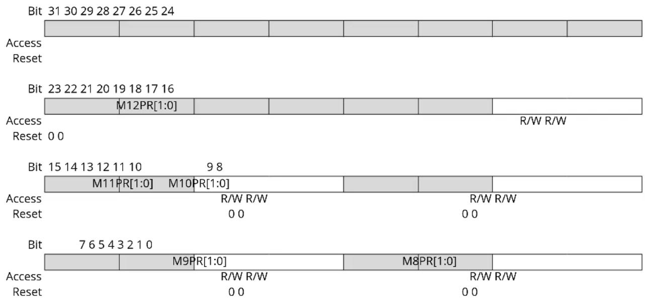
text_image
Bit 31 30 29 28 27 26 25 24 Access Reset Bit 23 22 21 20 19 18 17 16 M12PR[1:0] Access Reset 0 0 R/W R/W Bit 15 14 13 12 11 10 9 8 M11 PR[1:0] M10 PR[1:0] Access Reset R/W R/W R/W R/W 0 0 0 0 Bit 7 6 5 4 3 2 1 0 M9 PR[1:0] M8 PR[1:0] Access Reset R/W R/W R/W R/W 0 0 0 0Bits 0:1, 4:5, 8:9, 12:13, 16:17 - MxPR Host 8 Priority
Fixed priority of Host x for accessing the selected Client. The higher the number, the higher the priority.
All the Hosts programmed with the same MxPR value for the Client make up a priority pool.
Round-robin arbitration is used in the lowest (MxPR = 0) and highest (MxPR = 3) priority pools.
Fixed priority is used in intermediate priority pools (MxPR = 1) and (MxPR = 2).
See "Arbitration Priority Scheme" for details.
19.4.5 Bus Matrix Host Remap Control Register
Name: MATRIX_MRCR
Offset: 0x0100
Reset: 0x00000000
Property: Read/Write
This register can only be written if the WPEN bit is cleared in the Write Protection Mode Register.

bar_stacked
| Bit | RCB7 | RCB6 | RCB5 | RCB4 | RCB3 | RCB2 | RCB1 | RCB0 | |---|---|---|---|---|---|---|---|---| | Access Reset | 0 | 0 | 0 | 0 | 0 | 0 | 0 | 0 | | Bit 23 22 21 20 19 18 17 16 | 0 | 0 | 0 | 0 | 0 | 0 | 0 | 0 | | Access Reset | 0 | 0 | 0 | 0 | 0 | 0 | 0 | 0 | | Bit 15 14 13 12 11 10 9 8 | 0 | 0 | 0 | 0 | 0 | 0 | 0 | 0 | | Access Reset | R/W | R/W | R/W | R/W | R/W | R/W | R/W | R/W | | Bit 7 6 5 4 3 2 1 0 | 0 | 0 | 0 | 0 | 0 | 0 | 0 | 0 | | Access Reset | R/W | R/W | R/W | R/W | R/W | R/W | R/W | R/W | | Bit 0 | R/W | R/W | R/W | R/W | R/W | R/W | R/W | R/W | | Bit 15 | R/W | R/W | R/W | R/W | R/W | R/W | R/W | R/W | Note: The actual values for the bit bits are not provided in the image. The actual values may be calculated based on the input data and the number of bits. The actual output values for each bit are estimated based on the input data. There is no additional data series present in the image.Bits 0, 1, 2, 3, 4, 5, 6, 7, 8, 9, 10, 11, 12 - RCBx Remap Command Bit for Host x
| Value | Description |
| 0 | Disables remapped address decoding for the selected Host. |
| 1 | Enables remapped address decoding for the selected Host. |
19.4.6 CANO Configuration Register
Name: CCFG_CAN0
Offset: 0x0110
Reset: 0x2040019D
Property: Read/Write
| Bit 31 30 29 28 27 26 25 24 | ||||||
| CAN0DMABA[15:8] | ||||||
| Access Reset | R/W R/W R/W R/W R/W R/W R/W R/W | |||||
| 0 0 1 0 0 0 0 0 | ||||||
| Bit 23 22 21 20 19 18 17 16 | ||||||
| CAN0DMABA[7:0] | ||||||
| Access Reset | R/W R/W R/W R/W R/W R/W R/W R/W | |||||
| 0 1 0 0 0 0 0 0 | ||||||
| Bit 15 14 13 12 11 10 9 8 | ||||||
| Reserved[8] | ||||||
| Access Reset | R/W1 | |||||
| Bit 7 6 5 4 3 2 1 0 | ||||||
| Reserved[7:0] | ||||||
| Access Reset | R/W R/W R/W R/W R/W R/W R/W R/W | |||||
| 1 0 0 1 1 1 0 1 | ||||||
Bits 31:16 - CAN0DMABA[15:0] CAN0 DMA Base Address
Gives the 16-bit MSB of the CAN0 DMA base address. The 16-bit LSB must be programmed into CAN0 user interface.
Default address is 0x20400000.
Bits 8:0 - Reserved[8:0] Do not change the reset value
19.4.7 System I/O and CAN1 Configuration Register
Name: CCFG_SYSIO
Offset: 0x0114
Reset: 0x20400000
Property: Read/Write
Bit 31 30 29 28 27 26 25 24
| CAN1DMABA[15:8] |
Access R/W R/W R/W R/W R/W R/W R/W R/W
Reset 00100000
Bit 23 22 21 20 19 18 17 16
| CAN1 DMABA[7:0] |
Access R/W R/W R/W R/W R/W R/W R/W R/W
Reset 01000000
Bit 15 14 13 12 11 10 9 8
| SYSIO12 | |||||||
| Access | R/W | ||||||
Reset 0
Bit 76543210
| SYSIO7 | SYSIO6 | SYSIO5 | SYSIO4 |
Access R/W R/W R/W R/W
Reset 0000
Bits 31:16 - CAN1DMABA[15:0] CAN1 DMA Base Address
Give the 16-bit MSB of the CAN1 DMA base address. The 16-bit LSB must be programmed into CAN1 User interface.
Default address is 0x20400000.
Bit 12 - SYSIO12 PB12 or ERASE Assignment
| Value | Description |
| 0 | ERASE function selected. |
| 1 | PB12 function selected. |
Bit 7 - SYSIO7 PB7 or TCK/SWCLK Assignment
| Value | Description |
| 0 | TCK/SWCLK function selected. |
| 1 | PB7 function selected. |
Bit 6 - SYSIO6 PB6 or TMS/SWDIO Assignment
| Value | Description |
| 0 | TMS/SWDIO function selected. |
| 1 | PB6 function selected. |
Bit 5 - SYSIO5 PB5 or TDO/TRACESWO Assignment
| Value | Description |
| 0 | TDO/TRACESWO function selected. |
| 1 | PB5 function selected. |
Bit 4 - SYSIO4 PB4 or TDI Assignment
| Value Description | |
| 0 | TDI function selected. |
| 1 | PB4 function selected. |
19.4.8 Peripheral Clock Configuration Register
Name: CCFG_PCCR
Offset: 0x0118
Reset: 0x00022224
Property: Read/Write

text_image
Bit 31 30 29 28 27 26 25 24 Access Reset Bit 23 22 21 20 19 18 17 16 I2SC1 CC I2SC0CC TC0CC Access R/W R/W R/W Reset 0 0 0 Bit 15 14 13 12 11 10 9 8 Access Reset Bit 7 6 5 4 3 2 1 0 Access ResetBit 22 - I2SC1CC I2SC1 Clock Configuration
| Value | Description |
| 0 | Peripheral clock of I2SC1 is used. |
| 1 | GCLK is used. |
Bit 21 - I2SC0CC I2SC0 Clock Configuration
| Value | Description |
| 0 | Peripheral clock of I2SC0 is used. |
| 1 | GCLK is used. |
Bit 20 - TCOCC TC0 Clock Configuration
| Value | Description |
| 0 | PCK6 is used (default). |
| 1 | PCK7 is used. |
19.4.9 Dynamic Clock Gating Register
Name: CCFG_DYNCKG
Offset: 0x011C
Reset: 0x00000007
Property: Read/Write
Note: Clearing this register optimizes the power consumption of the system bus circuitry.

text_image
Bit 31 30 29 28 27 26 25 24 Access Reset Bit 23 22 21 20 19 18 17 16 Access Reset Bit 15 14 13 12 11 10 9 8 Access Reset Bit 7 6 5 4 3 2 1 0 Access Reset EFCCKG BRIDCKG MATCKG R/W R/W R/W 1 1 1Bit 2 - EFCCKG EFC Dynamic Clock Gating Enable
| Value | Description |
| 0 | EFC dynamic clock gating enabled. The Embedded Flash Controller circuitry is driven by the clock only when an access to the Flash memory is being performed. Power consumption is optimized. |
| 1 | EFC dynamic clock gating disabled. The Embedded Flash Controller is always driven by the clock in Active mode. |
Bit 1 - BRIDCKG Bridge Dynamic Clock Gating Enable
| Value | Description |
| 0 | Bridge dynamic clock gating enabled. The peripheral bridge circuitry is driven by the clock only when a transfer to/from any peripheral located on the APB bus is being performed. Power consumption is optimized. |
| 1 | Bridge dynamic clock gating disabled. The peripheral bridge circuitry is always driven by the clock in Active mode. |
Bit 0 - MATCKG MATRIX Dynamic Clock Gating
| Value | Description |
| 0 | MATRIX dynamic clock gating enabled. The MATRIX circuitry is driven by the clock only when a transfer to a peripheral is being performed. Power consumption is optimized. |
| 1 | MATRIX dynamic clock gating disabled. The MATRIX circuitry is always driven by the clock in Active mode. |
19.4.10 SMC NAND Flash Chip Select Configuration Register
Name: CCFG_SMCNFCS
Offset: 0x0124
Reset: 0x00000000
Property: Read/Write

text_image
Bit 31 30 29 28 27 26 25 24 Access Reset Bit 23 22 21 20 19 18 17 16 Access Reset Bit 15 14 13 12 11 10 9 8 Access Reset Bit 7 6 5 4 3 2 1 0 Access Reset SMC_NFCS3 SMC_NFCS2 SMC_NFCS1 SMC_NFCS0 R/W R/W R/W R/W 0 0 0 0Bit 3 - SMC_NFCS3 SMC NAND Flash Chip Select 3 Assignment
| Value | Description |
| 0 | NCS3 is not assigned to a NAND Flash (NANDOE and NANWE not used for NCS3). |
| 1 | NCS3 is assigned to a NAND Flash (NANDOE and NANWE used for NCS3). |
Bit 2 - SMC_NFCS2 SMC NAND Flash Chip Select 2 Assignment
| Value | Description |
| 0 | NCS2 is not assigned to a NAND Flash (NANDOE and NANWE not used for NCS2). |
| 1 | NCS2 is assigned to a NAND Flash (NANDOE and NANWE used for NCS2). |
Bit 1 - SMC_NFCS1 SMC NAND Flash Chip Select 1 Assignment
| Value | Description |
| 0 | NCS1 is not assigned to a NAND Flash (NANDOE and NANWE not used for NCS1). |
| 1 | NCS1 is assigned to a NAND Flash (NANDOE and NANWE used for NCS1). |
Bit 0 - SMC_NFCSO SMC NAND Flash Chip Select 0 Assignment
| Value | Description |
| 0 | NCS0 is not assigned to a NAND Flash (NANDOE and NANWE not used for NCS0). |
| 1 | NCS0 is assigned to a NAND Flash (NANDOE and NANWE used for NCS0). |
19.4.11 Write Protection Mode Register
Name: MATRIX_WPMR
Offset: 0x01E4
Reset: 0x00000000
Property: Read/Write
| Bit 31 30 29 28 27 26 25 24 | ||||||
| WPKEY[23:16] | ||||||
| Access Reset | R/W R/W R/W R/W R/W R/W R/W R/W | |||||
| 0 0 0 0 0 0 0 0 | ||||||
| Bit 23 22 21 20 19 18 17 16 | ||||||
| WPKEY[15:8] | ||||||
| Access Reset | R/W R/W R/W R/W R/W R/W R/W R/W | |||||
| 0 0 0 0 0 0 0 0 | ||||||
| Bit 15 14 13 12 11 10 9 8 | ||||||
| WPKEY[7:0] | ||||||
| Access Reset | R/W R/W R/W R/W R/W R/W R/W R/W | |||||
| 0 0 0 0 0 0 0 0 | ||||||
| Bit 7 6 5 4 3 2 1 0 | ||||||
| WPEN | ||||||
| Access Reset | R/W0 | |||||
Bits 31:8 - WPKEY[23:0] Write Protection Key
| Value | Name | Description |
| 0x4D4154 | PASSWD | Writing any other value in this field aborts the write operation of the WPEN bit.Always reads as 0. |
Bit 0 - WPEN Write Protection Enable
Refer to the "Register Write Protection" section for the list of registers that can be write-protected.
| Value | Description |
| 0 | Disables the write protection if WPKEY corresponds to 0x4D4154 ("MAT" in ASCII). |
| 1 | Enables the write protection if WPKEY corresponds to 0x4D4154 ("MAT" in ASCII). |
19.4.12 Write Protection Status Register
Name: MATRIX_WPSR
Offset: 0x01E8
Reset: 0x00000000
Property: Read-only

text_image
Bit 31 30 29 28 27 26 25 24 Access Reset Bit 23 22 21 20 19 18 17 16 WPVSRC[15:8] Access R R R R R R R R Reset 0 0 0 0 0 0 0 0 Bit 15 14 13 12 11 10 9 8 WPVSRC[7:0] Access R R R R R R R R R Reset 0 0 0 0 0 0 0 0 Bit 7 6 5 4 3 2 1 0 WPVS Access Reset R 0Bits 23:8 - WPVSRC[15:0] Write Protection Violation Source
When WPVS = 1, WPVSRC indicates the register address offset at which a write access has been attempted.
Bit 0 - WPVS Write Protection Violation Status
| Value | Description |
| 0 | No write protection violation has occurred since the last write of the MATRIX_WPMR. |
| 1 | A write protection violation has occurred since the last write of the MATRIX_WPMR. If this violation is an unauthorized attempt to write a protected register, the associated violation is reported into field WPVSRC. |
20. USB Transmitter Macrocell Interface (UTMI)
20.1 Description
The USB Transmitter Macrocell Interface (UTMI) registers manage specific aspects of the integrated USB transmitter macrocell functionality not controlled in USB sections.
20.2 Embedded Characteristics
• 32-bit UTMI Registers Control Product-specific Behavior
20.3 Register Summary
| Offset | Name Bit Pos. 7 | 6 | 5 | 4 | 3 | 2 | 1 | 0 | |||||||||
| 0x00...0x0F | Reserved | ||||||||||||||||
| 0x10 UTMI_OHCIICR | 7:0 APPSTART ARIE | RESx | |||||||||||||||
| 15:8 | |||||||||||||||||
| 23:16 UDPPUDIS | |||||||||||||||||
| 31:24 | |||||||||||||||||
| 0x14...0x2F | Reserved | ||||||||||||||||
| 0x30 | UTMI_CKTRIM | 7:0 | FREQ[1:0] | ||||||||||||||
| 15:8 | |||||||||||||||||
| 23:16 | |||||||||||||||||
| 31:24 | |||||||||||||||||
20.3.1 OHCI Interrupt Configuration Register
Name: UTMI_OHCIICR
Offset: 0x10
Reset: 0x0
Property: Read/Write

text_image
Bit 31 30 29 28 27 26 25 24 Access Reset Bit 23 22 21 20 19 18 17 16 UDPPUDIS Access R/W Reset 0 Bit 15 14 13 12 11 10 9 8 Access Reset Bit 7 6 5 4 3 2 1 0 Access R/W R/W RESx Reset 0 0 R/WBit 23 - UDPPUDIS USB Device Pull-up Disable
| Value | Description |
| 0 | USB device pull-up connection is enabled. |
| 1 | USB device pull-up connection is disabled. |
Bit 5 - APPSTART Reserved
| Value | Description |
| 0 | Must write 0. |
Bit 4 - ARIE OHCI Asynchronous Resume Interrupt Enable
| Value | Description |
| 0 | Interrupt disabled. |
| 1 | Interrupt enabled. |
Bit 0 - RESx USB PORTx Reset
| Value | Description |
| 0 | Resets USB port. |
| 1 | Usable USB port. |
20.3.2 UTMI Clock Trimming Register
Name: UTMI_CKTRIM
Offset: 0x30
Reset: 0x00010000
Property: Read/Write
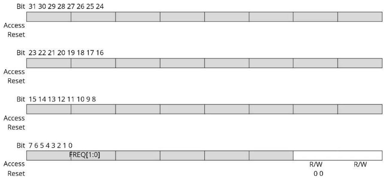
text_image
Bit 31 30 29 28 27 26 25 24 Access Reset Bit 23 22 21 20 19 18 17 16 Access Reset Bit 15 14 13 12 11 10 9 8 Access Reset Bit 7 6 5 4 3 2 1 0 FREQ[1:0] Access Reset R/W R/W 0 0Bits 1:0 - FREQ[1:0] UTMI Reference Clock Frequency
| Value | Name | Description |
| 0 | XTAL12 | 12 MHz reference clock |
| 1 | XTAL16 | 16 MHz reference clock |
21. Chip Identifier (CHIPID)
21.1 Description
Chip Identifier (CHIPID) registers are used to recognize the device and its revision. These registers provide the sizes and types of the on-chip memories, as well as the set of embedded peripherals.
Two CHIPID registers are embedded: Chip ID Register (CHIPID_CIDR) and Chip ID Extension Register (CHIPID_EXID). Both registers contain a hard-wired value that is read-only.
The CHIPID_CIDR register contains the following fields:
- VERSION: Identifies the revision of the silicon
- EPROC: Indicates the embedded ARM processor
- NVPTYP and NVPSIZ: Identify the type of embedded non-volatile memory and the size
- SRAMSIZ: Indicates the size of the embedded SRAM
- ARCH: Identifies the set of embedded peripherals
- EXT: Shows the use of the extension identifier register
The CHIPID_EXID register is device-dependent and reads 0 if CHIPID_CIDR.EXT = 0.
21.2 Embedded Characteristics
- Chip ID Registers
- Identification of the Device Revision, Sizes of the Embedded Memories, Set of Peripherals, Embedded Processor
Table 21-1. SAM S70/SAM E70/SAM V70/SAM V71 Chip ID Registers
| Chip Name CHIPID_CIDR | (see Notes 1 and 2) | CHIPID_EXID |
| SAME70Q21 0xA102_0E0x 0x00000002 | ||
| SAME70Q20 0xA102_0C0x 0x00000002 | ||
| SAME70Q19 0xA10D_0A0x 0x00000002 | ||
| SAME70N21 0xA102_0E0x 0x00000001 | ||
| SAME70N20 0xA102_0C0x 0x00000001 | ||
| SAME70N19 0xA10D_0A0x 0x00000001 | ||
| SAME70J21 0xA102_0E0x 0x00000000 | ||
| SAME70J20 0xA102_0C0x 0x00000000 | ||
| SAME70J19 0xA10D_0A0x 0x00000000 | ||
| SAMS70Q21 0xA112_0E0x 0x00000002 | ||
| SAMS70Q20 0xA112_0C0x 0x00000002 | ||
| SAMS70Q19 0xA11D_0A0x 0x00000002 | ||
| SAMS70N21 0xA112_0E0x 0x00000001 | ||
| SAMS70N20 0xA112_0C0x 0x00000001 | ||
| SAMS70N19 0xA11D_0A0x 0x00000001 | ||
| SAMS70J21 0xA112_0E0x 0x00000000 | ||
| SAMS70J20 0xA112_0C0x 0x00000000 | ||
| SAMS70J19 0xA11D_0A0x 0x00000000 | ||
| SAMV71Q21 0xA122_0E0x 0x00000002 | ||
| SAMV71Q20 0xA122_0C0x 0x00000002 | ||
| SAMV71Q19 0xA12D_0A0x 0x00000002 | ||
| ......continued | ||
| Chip Name CHIPID_CIDR | (see Notes 1 and 2) | CHIPID_EXID |
| SAMV71N21 0xA122_0E0x 0x00000001 | ||
| SAMV71N20 0xA122_0C0x 0x00000001 | ||
| SAMV71N19 0xA12D_0A0x 0x00000001 | ||
| SAMV71J21 0xA122_0E0x 0x00000000 | ||
| SAMV71J20 0xA122_0C0x 0x00000000 | ||
| SAMV71J19 0xA12D_0A0x 0x00000000 | ||
| SAMV70Q20 0xA132_0C0x 0x00000002 | ||
| SAMV70Q19 0xA13D_0A0x 0x00000002 | ||
| SAMV70N20 0xA132_0C0x 0x00000001 | ||
| SAMV70N19 0xA13D_0A0x 0x00000001 | ||
| SAMV70J20 0xA132_0C0x 0x00000000 | ||
| SAMV70J19 0xA13D_0A0x 0x00000000 | ||
- x = 0 for MRL A devices.
- x = 1 for MRL B devices.
21.3 Register Summary
| Offset | Name Bit Pos. 7 | 6 | 5 | 4 | 3 | 2 | 1 | 0 | ||||||||
| 0x00 CHIPID_CIDR | 7:0 EPROC[2:0] VERSION[4:0] | |||||||||||||||
| 15:8 NVPSIZ2[3:0] NVPSIZ[3:0] | ||||||||||||||||
| 23:16 ARCH[3:0] SRAMSIZ[3:0] | ||||||||||||||||
| 31:24 EXT NVPTYP[2:0] ARCH[7:4] | ||||||||||||||||
| 0x04 CHIPID_EXID | 7:0 | EXID[7:0] | ||||||||||||||
| 15:8 | EXID[15:8] | |||||||||||||||
| 23:16 | EXID[23:16] | |||||||||||||||
| 31:24 | EXID[31:24] | |||||||||||||||
21.3.1 Chip ID Register
Name: CHIPID_CIDR
Offset: 0x0
Reset: -
Property: Read-only
| Bit 31 30 29 28 27 26 25 24 | ||||||||
| EXT NVPTYP[2:0] ARCH[7:4] | ||||||||
| Access Reset | RR R R R R R R | |||||||
| Bit 23 22 21 20 19 18 17 16 | ||||||||
| ARCH[3:0] SRAMSIZ[3:0] | ||||||||
| Access Reset | RR R R R R R R | |||||||
| Bit 15 14 13 12 11 10 9 8 | ||||||||
| NVPSIZ2[3:0] | NVPSIZ[3:0] | |||||||
| Access Reset | RR R R R R R R | |||||||
| Bit | 7 | 6 | 5 | 4 | 3 | 2 | 1 | 0 |
| EPROC[2:0] | VERSION[4:0] | |||||||
| Access Reset | RR R R R R R R | |||||||
Bit 31 - EXT Extension Flag
| Value | Description |
| 0 | Chip ID has a single register definition without extension. |
| 1 | An extended Chip ID exists. |
Bits 30:28 - NVPTYP[2:0] Nonvolatile Program Memory Type
| Value | Name | Description |
| 0 | ROM | ROM |
| 1 | ROMLESS | ROMless or on-chip Flash |
| 2 | FLASH | Embedded Flash Memory |
| 3 | ROM_FLASH | ROM and Embedded Flash Memory- NVPSIZ is ROM size- NVPSIZ2 is Flash size |
| 4 | SRAM | SRAM emulating ROM |
Bits 27:20 - ARCH[7:0] Architecture Identifier
| Value | Name | Description |
| 0x10 | SAM E70 | SAM E70 |
| 0x11 | SAM S70 | SAM S70 |
| 0x12 | SAM V71 | SAM V71 |
| 0x13 | SAM V70 | SAM V70 |
Bits 19:16 - SRAMSIZ[3:0] Internal SRAM Size
| Value | Name | Description |
| 0 | 48K | 48 Kbytes |
| 1 | 192K | 192 Kbytes |
| 2 | 384K | 384 Kbytes |
| Value Name | Description | |
| 3 | 6K 6 Kbytes | |
| 4 | 24K 24 Kbytes | |
| 5 | 4K 4 Kbytes | |
| 6 | 80K 80 Kbytes | |
| 7 | 160K 160 Kbytes | |
| 8 | 8K 8 Kbytes | |
| 9 | 16K 16 Kbytes | |
| 10 | 32K 32 Kbytes | |
| 11 | 64K 64 Kbytes | |
| 12 | 128K 128 Kbytes | |
| 13 | 256K 256 Kbytes | |
| 14 | 96K 96 Kbytes | |
| 15 | 512K 512 Kbytes |
Bits 15:12 - NVPSIZ2[3:0] Second Nonvolatile Program Memory Size
| Value Name | Description | |
| 0 | NONE None | |
| 1 | 8K 8 Kbytes | |
| 2 | 16K 16 Kbytes | |
| 3 | 32K 32 Kbytes | |
| 4 | - Reserved | |
| 5 | 64K 64 Kbytes | |
| 6 | - Reserved | |
| 7 | 128K 128 Kbytes | |
| 8 | - Reserved | |
| 9 | 256K 256 Kbytes | |
| 10 | 512K 512 Kbytes | |
| 11 | - Reserved | |
| 12 | 1024K 1024 Kbytes | |
| 13 | - Reserved | |
| 14 | 2048K 2048 Kbytes | |
| 15 | - Reserved |
Bits 11:8 - NVPSIZ[3:0] Nonvolatile Program Memory Size
| Value Name | Description | |
| 0 | NONE None | |
| 1 | 8K 8 Kbytes | |
| 2 | 16K 16 Kbytes | |
| 3 | 32K 32 Kbytes | |
| 4 | - Reserved | |
| 5 | 64K 64 Kbytes | |
| 6 | - Reserved | |
| 7 | 128K 128 Kbytes | |
| 8 | 160K 160 Kbytes | |
| 9 | 256K 256 Kbytes | |
| 10 | 512K 512 Kbytes | |
| 11 | - Reserved | |
| 12 | 1024K 1024 Kbytes | |
| 13 | - Reserved | |
| 14 | 2048K 2048 Kbytes | |
| 15 | - Reserved |
Bits 7:5 - EPROC[2:0] Embedded Processor
| Value Name | Description | |
| 0 | SAM x7 Cortex-M7 | |
| Value Name | Description | |
| 1 | ARM946ES ARM946ES | |
| 2 | ARM7TDMI ARM7TDMI | |
| 3 | CM3 Cortex-M3 | |
| 4 | ARM920T ARM920T | |
| 5 | ARM926EJS ARM926EJS | |
| 6 | CA5 Cortex-A5 | |
| 7 | CM4 Cortex-M4 | |
Bits 4:0 - VERSION[4:0] Version of the Device
Current version of the device.
21.3.2 Chip ID Extension Register
Name: CHIPID_EXID
Offset: 0x4
Reset: -
Property: Read-only
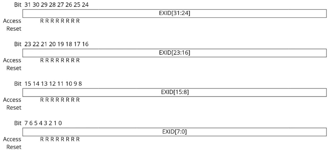
text_image
Bit 31 30 29 28 27 26 25 24 EXID[31:24] Access R R R R R R R R Reset Bit 23 22 21 20 19 18 17 16 EXID[23:16] Access R R R R R R R R Reset Bit 15 14 13 12 11 10 9 8 EXID[15:8] Access R R R R R R R R Reset Bit 7 6 5 4 3 2 1 0 EXID[7:0] Access R R R R R R R R ResetBits 31:0 - EXID[31:0] Chip ID Extension
This field is cleared if CHIPID_CIDR.EXT = 0.
| Value | Name | Description |
| 0xX | Reserved | Reserved |
22. Enhanced Embedded Flash Controller (EEFC)
22.1 Description
The Enhanced Embedded Flash Controller (EEFC) provides the interface of the Flash block with the 32-bit internal bus.
Its 128-bit wide memory interface increases performance. It also manages the programming, erasing, locking and unlocking sequences of the Flash using a full set of commands. One of the commands returns the embedded Flash descriptor definition that informs the system about the Flash organization, thus making the software generic.
22.2 Embedded Characteristics
- Increases Performance in Thumb-2 Mode with 128-bit-wide Memory Interface up to 150 MHz
• Code Loop Optimization
• 128 Lock Bits, Each Protecting a Lock Region
• 9 General-purpose GPNVM Bits
• One-by-one Lock Bit Programming - Commands Protected by a Keyword
- Erase the Entire Flash
- Erase by Sector
- Erase by Page
- Provides Unique Identifier
- Provides 512-byte User Signature Area
• Supports Erasing before Programming - Locking and Unlocking Operations
- ECC Single and Multiple Error Flags Report
• Supports Read of the Calibration Bits - Register Write Protection
22.3 Product Dependencies
22.3.1 Power Management
The Enhanced Embedded Flash Controller (EEFC) is continuously clocked. The Power Management Controller has no effect on its behavior.
22.3.2 Interrupt Sources
The EEFC interrupt line is connected to the interrupt controller. Using the EEFC interrupt requires the interrupt controller to be programmed first. The EEFC interrupt is generated only if the value of EEFC_FMR.FRDY is '1'.
22.4 Functional Description
22.4.1 Embedded Flash Organization
The embedded Flash interfaces with the internal bus. The embedded Flash is composed of the following:
- One memory plane organized in several pages of the same size for the code.
- A separate 2 x 512-byte memory area which includes the unique chip identifier.
• A separate 512-byte memory area for the user signature.
- Two 128-bit read buffers used for code read optimization.
• One 128-bit read buffer used for data read optimization.
- One write buffer that manages page programming. The write buffer size is equal to the page size. This buffer is write-only and accessible all along the entire flash address space, so that each word can be written to its final address.
- Several lock bits used to protect write/erase operation on several pages (lock region). A lock bit is associated with a lock region composed of several pages in the memory plane.
- Several bits that may be set and cleared through the EEFC interface, called general-purpose non-volatile memory bits (GPNVM bits).
The embedded Flash size, page size, organization of lock regions, and definition of GPNVM bits are specific to the device. The EEFC returns a descriptor of the Flash controller after a 'Get Flash Descriptor' command has been issued by the application, refer to the "Get Flash Descriptor Command".
Figure 22-1. Flash Memory Areas
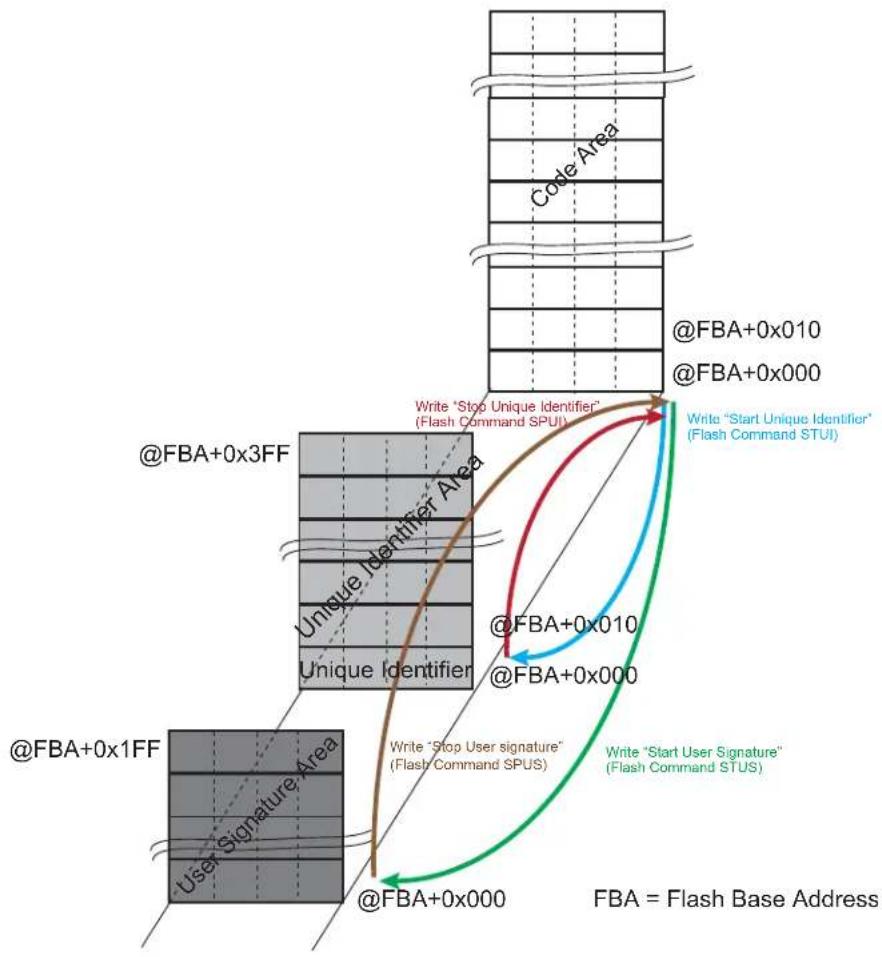
flowchart
graph TD
    A["@FBA+0x1FF"] --> B["User Signature Area"]
    B --> C["@FBA+0x3FF"]
    C --> D["Unique Identifier Area"]
    D --> E["@FBA+0x010"]
    E --> F["@FBA+0x000"]
    F --> G["Write "Stop User signature" (Flash Command SPUS)"]
    G --> H["Write "Start User Signature" (Flash Command STUS)"]
    H --> I["Write "Stop Unique Identifier" (Flash Command SPU)"]
    I --> J["@FBA+0x010"]
    J --> K["@FBA+0x000"]
    K --> L["Code Area"]
    style A fill:#f9f,stroke:#333
    style B fill:#ccf,stroke:#333
    style C fill:#cfc,stroke:#333
    style D fill:#fcc,stroke:#333
    style E fill:#cff,stroke:#333
    style F fill:#ffc,stroke:#333
    style G fill:#fcf,stroke:#333
    style H fill:#cff,stroke:#333
    style I fill:#ffc,stroke:#333
    style J fill:#cff,stroke:#333
    style K fill:#ffc,stroke:#333
    style L fill:#cff,stroke:#333
Figure 22-2. Organization of Embedded Flash for Code

text_image
Memory Plane Start Address Page 0 Lock Region 0 ← Lock Bit 0 Page (m-1) Lock Region 1 ← Lock Bit 1 ... Lock Region (n-1) ← Lock Bit (n-1) Start Address + Flash size -1 Page (n*m-1)22.4.2 Read Operations
An optimized controller manages embedded Flash reads, thus increasing performance when the processor is running in Thumb-2 mode by means of the 128-bit-wide memory interface.
The Flash memory is accessible through 8-, 16- and 32-bit reads.
As the Flash block size is smaller than the address space reserved for the internal memory area, the embedded Flash wraps around the address space and appears to be repeated within it.
The read operations can be performed with or without wait states. Wait states must be programmed in the field FWS in the Flash Mode register (EEFC_FMR). Defining FWS as 0 enables the single-cycle access of the embedded Flash. For more details, refer to the section "Electrical Characteristics" of this datasheet.
Related Links
-
Electrical Characteristics for SAM E70/S70
-
Electrical Characteristics for SAM V70/V71
22.4.2.1 Code Read Optimization
Code read optimization is enabled if the bit EEFC_FMR.SCOD is cleared.
A system of 2 × 128 -bit buffers is added in order to optimize sequential code fetch.
Note: Immediate consecutive code read accesses are not mandatory to benefit from this optimization.
The sequential code read optimization is enabled by default. If the bit EEFC_FMR.SCOD is set, these buffers are disabled and the sequential code read is no longer optimized.
Another system of 2 x 128-bit buffers is added in order to optimize loop code fetch. Refer to the "Code Loop Optimization" section for more details.
Figure 22-3. Code Read Optimization for FWS = 0
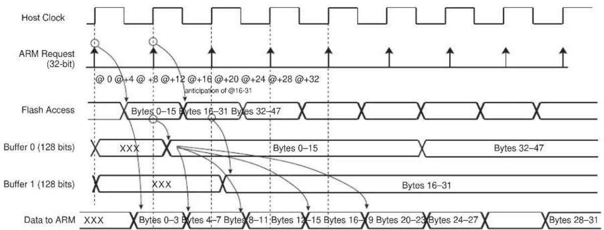
flowchart
graph TD
    A["Host Clock"] --> B["ARM Request (32-bit)"]
    B --> C["Flash Access"]
    C --> D["Buffer 0 (128 bits)"]
    D --> E["Buffer 1 (128 bits)"]
    E --> F["Data to ARM"]

    subgraph Flash Access
        G["Bytes 0-15 Bytes 16-31 Bytes 32-47"]
    end

    subgraph Buffer Access
        H["Bytes 0-15"]
        I["Bytes 32-47"]
    end

    subgraph Data to ARM
        J["Bytes 0-3 Bytes 4-7 Bytes 8-11 Bytes 12-15 Bytes 16-19 Bytes 20-23 Bytes 24-27"]
        K["Bytes 16-31"]
    end
Note: When FWS is equal to '0', all the accesses are performed in a single-cycle access.
Figure 22-4. Code Read Optimization for FWS = 3

flowchart
graph TD
    A["Host Clock"] --> B["@0"]
    B --> C["@+4 @+8 @+12 @+16 @+20 @+24 @+28 @+32 @+36 @+40 @+44 @+48 @+52"]
    C --> D["@0/4/8/12 are ready"]
    D --> E["@16/20/24/28 are ready"]
    E --> F["@32-47 anticipation of @32-47"]
    F --> G["@40"]
    G --> H["@44"]
    H --> I["@48"]
    I --> J["@52"]
    K["ARM Request (32-bit)"] --> L["@0"]
    L --> M["@+4 @+8 @+12 @+16 @+20 @+24 @+28 @+32 @+36 @+40 @+44 @+48 @+52"]
    M --> N["@0/4/8/12 are ready"]
    N --> O["@16/20/24/28 are ready"]
    O --> P["@32-47 anticipation of @32-47"]
    P --> Q["@40"]
    Q --> R["@44"]
    R --> S["@48"]
    S --> T["@52"]
    U["Flash Access"] --> V["Bytes 0-15"]
    V --> W["Bytes 16-31"]
    W --> X["Bytes 32-47"]
    X --> Y["Bytes 48-63"]
    Z["Buffer 0 (128 bits)"] --> AA["Bytes 0-15"]
    AB["Buffer 1 (128 bits)"] --> AC["Bytes 16-31"]
    AC --> AD["Bytes 32-47"]
    AD --> AE["Bytes 48-63"]
    AF["Data to ARM"] --> AG["XXX 0-3 4-7 8-11 12÷15 16-19 20-23 24-27 28-31 32-35 36-39 40-43 44-47 48-51"]
Note: When FWS is between 1 and 3, in case of sequential reads, the first access takes (FWS + 1) cycles. The following accesses take only one cycle.
22.4.2.2 Code Loop Optimization
Code loop optimization is enabled when the EEFC_FMR.CLOE bit is set.
When a backward jump is inserted in the code, the pipeline of the sequential optimization is broken and becomes inefficient. In this case, the loop code read optimization takes over from the sequential code read optimization to prevent the insertion of wait states. The loop code read optimization is enabled by default. In EEFC_FMR, if the bit CLOE is reset to 0 or the bit SCOD is set, these buffers are disabled and the loop code read is not optimized.
When code loop optimization is enabled, if inner loop body instructions L_0 to L_n are positioned from the 128-bit Flash memory cell M_b0 to the memory cell M_p1 , after recognition of a first backward branch, the first two Flash memory cells M_b0 and M_b1 targeted by this branch are cached for fast access from the processor at the next loop iteration.
Then by combining the sequential prefetch (described in the "Code Read Optimization" section) through the loop body with the fast read access to the loop entry cache, the entire loop can be iterated with no wait state.
The following figure illustrates code loop optimization.
Figure 22-5. Code Loop Optimization

flowchart
graph LR
    A["Flash Memory 128-bit words"] --> B["Backward address jump"]
    B --> C["2x128-bit loop entry cache"]
    C --> D["2x128-bit prefetch buffer"]
    D --> E["2x128-bit prefetch Buffer 0"]
    D --> F["2x128-bit prefetch Buffer 1"]
    style A fill:#f9f,stroke:#333
    style B fill:#ccf,stroke:#333
    style C fill:#cfc,stroke:#333
    style D fill:#fcc,stroke:#333
22.4.2.3 Data Read Optimization
The organization of the Flash in 128 bits is associated with two 128-bit prefetch buffers and one 128-bit data read buffer, thus providing maximum system performance. This buffer is added in order to store the requested data plus all the data contained in the 128-bit aligned data. This speeds up sequential data reads if, for example, FWS is equal to 1 (see Figure 22-6). The data read optimization is enabled by default. If the bit EEFC_FMR.SCOD is set, this buffer is disabled and the data read is no longer optimized.
Note: No consecutive data read accesses are mandatory to benefit from this optimization.
Figure 22-6. Data Read Optimization for FWS = 1

text_image
Host Clock ARM Request (32-bit) @Byte 0 @ 4 @ 8 @ 12 @ 16 @ 20 @ 24 @ 28 @ 32 @ 36 Flash Access XXX Bytes 0–15 Bytes 16–31 Bytes 32–47 Buffer (128 bits) XXX Bytes 0–15 Bytes 16–31 Data to ARM XXX Bytes 0–3 4–7 8–1 12–15 16–19 20–23 24–27 28–31 32–3522.4.3 Flash Commands
The EEFC offers a set of commands to manage programming the Flash memory, locking and unlocking lock regions, consecutive programming, locking and full Flash erasing, and so on.
The commands are listed in the following table.
Table 22-1. Set of Commands
| Command | Value | Mnemonic |
| Get Flash Descriptor | 0x00 | GETD |
| Write Page | 0x01 | WP |
| Write Page and Lock | 0x02 | WPL |
| Erase Page and Write Page | 0x03 | EWP |
| Erase Page and Write Page and then Lock | 0x04 | EWPL |
| Erase All | 0x05 | EA |
| ......continued | ||
| Command Value Mnemonic | ||
| Erase Pages 0x07 EPA | ||
| Set Lock Bit 0x08 SLB | ||
| Clear Lock Bit 0x09 CLB | ||
| Get Lock Bit 0x0A GLB | ||
| Set GPNVM Bit 0x0B SGPB | ||
| Clear GPNVM Bit 0x0C CGPB | ||
| Get GPNVM Bit 0x0D GGPB | ||
| Start Read Unique Identifier 0x0E STUI | ||
| Stop Read Unique Identifier 0x0F SPUI | ||
| Get CALIB Bit | 0x10 GCALB | |
| Erase Sector | 0x11 ES | |
| Write User Signature | 0x12 WUS | |
| Erase User Signature | 0x13 EUS | |
| Start Read User Signature | 0x14 STUS | |
| Stop Read User Signature | 0x15 SPUS | |
To execute one of these commands, select the required command using the FCMD field in the Flash Command register (EEFC_FCR). As soon as EEFC_FCR is written, the FRDY flag and the FVALUE field in the Flash Result register (EEFC_FRR) are automatically cleared. Once the current command has completed, the FRDY flag is automatically set. If an interrupt has been enabled by setting the bit EEFC_FMR.FRDY, the corresponding interrupt line of the interrupt controller is activated (This is true for all commands except for the STUI command. The FRDY flag is not set when the STUI command has completed).
All the commands are protected by the same keyword, which must be written in the eight highest bits of EEFC_FCR.
Writing EEFC_FCR with data that does not contain the correct key and/or with an invalid command has no effect on the whole memory plane, but the FCMDE flag is set in the Flash Status register (EEFC_FSR). This flag is automatically cleared by a read access to EEFC_FSR.
When the current command writes or erases a page in a locked region, the command has no effect on the whole memory plane, but the FLOCKE flag is set in EEFC_FSR. This flag is automatically cleared by a read access to EEFC_FSR.
Figure 22-7. Command State Chart
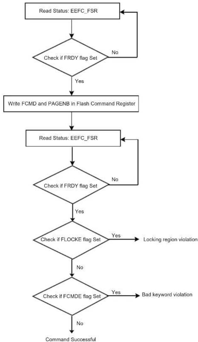
flowchart
graph TD
    A["Read Status: EEFC_FSR"] --> B{Check if FRDY flag Set}
    B -->|Yes| C["Write FCMD and PAGENB in Flash Command Register"]
    B -->|No| D["End"]
    C --> E["Read Status: EEFC_FSR"]
    E --> F{Check if FRDY flag Set}
    F -->|Yes| G{Check if FLOCKE flag Set}
    G -->|Yes| H["Locking region violation"]
    G -->|No| I["End"]
    F -->|No| J["End"]
    G -->|No| K["Command Successful"]
    H --> L["End"]
    I --> L
    J --> L
    K --> L
22.4.3.1 Get Flash Descriptor Command
This command provides the system with information on the Flash organization. The system can take full advantage of this information. For instance, a device could be replaced by one with more Flash capacity, and so the software is able to adapt itself to the new configuration.
To get the embedded Flash descriptor, the application writes the GETD command in EEFC_FCR. The first word of the descriptor can be read by the software application in EEFC_FRR as soon as the FRDY flag in EEFC_FSR rises. The next reads of EEFC_FRR provide the following word of the descriptor. If extra read operations to EEFC_FRR are done after the last word of the descriptor has been returned, the EEFC_FRR value is 0 until the next valid command.
Table 22-2. Flash Descriptor Definition
| Symbol Word | Index Description | |
| FL_ID 0 | Flash interface description | |
| FL_SIZE 1 | Flash size in bytes | |
| FL_PAGE_SIZE | 2 Page size in bytes |
......continued
Symbol Word Index Description
FL_NB_PLANE 3 Number of planes
FL_PLANE[0] 4 Number of bytes in the plane
FL_NB_LOCK 4 + FL_NB_PLANE Number of lock bits. A bit is associated with a lock region. A lock bit is used to prevent write or erase operations in the lock region.
FL_LOCK[0] 4 + FL_NB_PLANE + 1 Number of bytes in the first lock region
22.4.3.2 Write Commands
DMA write accesses must be 32-bit aligned. If a single byte has to be written in a 32-bit word, the rest of the word must be written with ones.
Several commands are used to program the Flash.
Only '0' values can be programmed using Flash technology; '1' is the erased value. In order to program words in a page, the page must first be erased. Commands are available to erase the entire Flash or a given number of pages. With the EWP and EWPL commands, a page erase is done automatically before a page programming.
After programming, the page (the entire lock region) can be locked to prevent miscellaneous write or erase sequences. The lock bit can be automatically set after page programming using WPL or EWPL commands.
Data to be programmed in the Flash must be written in an internal latch buffer before writing the programming command in EEFC_FCR. Data can be written at their final destination address, as the latch buffer is mapped into the Flash memory address space and wraps around within this Flash address space.
Byte and half-word AHB accesses to the latch buffer are not allowed. Only 32-bit word accesses are supported.
32-bit words must be written continuously in either ascending or descending order. Writing the latch buffer in a random order is not permitted. This prevents mapping a C-code structure to the latch buffer and accessing the data of the structure in any order. It is instead recommended to fill in a C-code structure in SRAM and copy it in the latch buffer in a continuous order.
Write operations in the latch buffer are performed with the number of wait states programmed for reading the Flash.
The latch buffer is automatically re-initialized, that is, written with logical '1', after execution of each programming command.
The programming sequence is as follows:
- Write the data to be programmed in the latch buffer.
- Write the programming command in EEFC_FCR. This automatically clears the EEFC_FSR.FRDY bit.
- When Flash programming is completed, the EEFC_FSR.FRDY bit rises. If an interrupt has been enabled by setting the EEFC_FMR.FRDY bit, the interrupt line of the EEFC is activated.
Three errors can be detected in EEFC_FSR after a programming sequence:
- Command Error: A bad keyword has been written in EEFC_FCR.
- Lock Error: The page to be programmed belongs to a locked region. A command must be run previously to unlock the corresponding region.
- Flash Error: When programming is completed, the WriteVerify test of the Flash memory has failed. After a first programming pulse, a Verify is applied. The memory is read, to compare both programmed and expected values. If that comparison fails, a second programming pulse is applied, and so on, until a maximum pulse number is reached. At this time, if the memory is still not containing what is expected, the FLERR flag is set high.
Only one page can be programmed at a time. It is possible to program all the bits of a page (full page programming) or only some of the bits of the page (partial page programming).
Depending on the number of bits to be programmed within the page, the EEFC adapts the write operations required to program the Flash.
When a 'Write Page' (WP) command is issued, the EEFC starts the programming sequence and all the bits written at '0' in the latch buffer are cleared in the Flash memory array.
During programming, that is, until EEFC_FSR.FDRY rises, access to the Flash is not allowed.
22.4.3.2.1 Full Page Programming
To program a full page, all the bits of the page must be erased before writing the latch buffer and issuing the WP command. The latch buffer must be written in ascending order, starting from the first address of the page. See Figure 22-8.
22.4.3.2.2 Partial Page Programming
To program only part of a page using the WP command, the following constraints must be respected:
- Data to be programmed must be contained in integer multiples of 128-bit address-aligned words.
- 128-bit words can be programmed only if all the corresponding bits in the Flash array are erased (at logical value '1').
See 22.4.3.2.4. Programming Bytes.
22.4.3.2.3 Optimized Partial Page Programming
The EEFC automatically detects the number of 128-bit words to be programmed. If only one 128-bit aligned word is to be programmed in the Flash array, the process is optimized to reduce the time needed for programming.
If several 128-bit words are to be programmed, a standard page programming operation is performed.
See Figure 22-10.
22.4.3.2.4 Programming Bytes
Individual bytes can be programmed using the Partial Page Programming mode.
In this case, an area of 128 bits must be reserved for each byte.
Refer to the Figure 22-11
Figure 22-8. Full Page Programming

text_image
32 bits wide CA FE CA FE CA FE CA FE 0xX1C CA FE CA FE 0xX18 CA FE CA FE 0xX14 CA FE CA FE 0xX10 CA FE CA FE 0xX0C CA FE CA FE 0xX08 CA FE CA FE 0xX04 CA FE CA FE 0xX00 address space for Page NBefore programming: Unerased page in Flash array

text_image
32 bits wide FF FF FF FF FF FF FF FF FF FF FF FF FF FF FF FF FF FF FF FF FF FF FF FF FF FF FF FF FF FF FF FF FF FF FF FF FF FF FF FF FF FF FF FF 0xX1C 0xX18 0xX14 0xX10 0xX0C 0xX08 0xX04 0xX00Step 1: Flash array after page erase
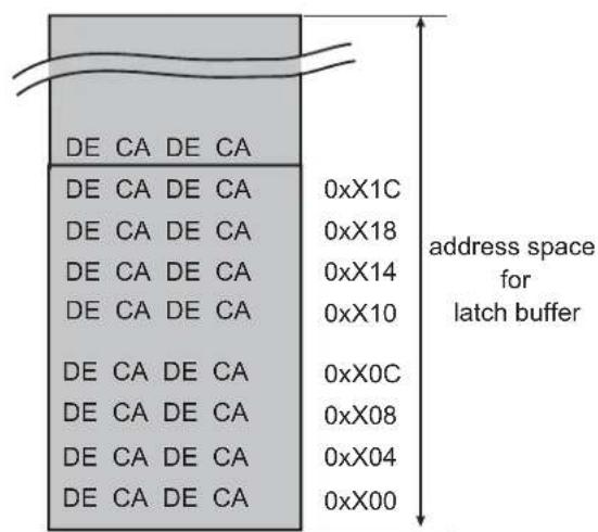
text_image
DE CA DE CA DE CA DE CA 0xX1C DE CA DE CA 0xX18 DE CA DE CA 0xX14 DE CA DE CA 0xX10 DE CA DE CA 0xX0C DE CA DE CA 0xX08 DE CA DE CA 0xX04 DE CA DE CA 0xX00 address space for latch bufferStep 2: Writing a page in the latch buffer

text_image
DE CA DE CA DE CA DE CA 0xX1C DE CA DE CA 0xX18 DE CA DE CA 0xX14 DE CA DE CA 0xX10 DE CA DE CA 0xX0C DE CA DE CA 0xX08 DE CA DE CA 0xX04 DE CA DE CA 0xX00 address space for Page NStep 3: Page in Flash array after issuing WP command and FRDY=1
Figure 22-9. Partial Page Programming
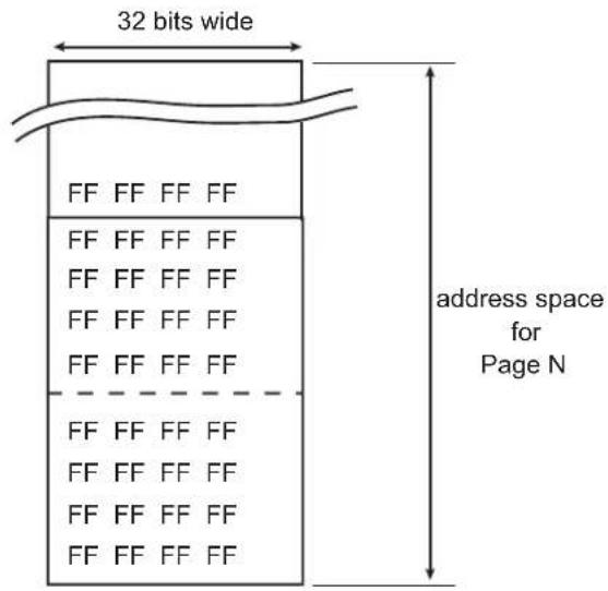
text_image
32 bits wide FF FF FF FF FF FF FF FF FF FF FF FF FF FF FF FF FF FF FF FF DD FF FF FF FF FF FF FF FF FF FF FF FF FF FF FF FF FF FF FF address space for Page NStep 1: Flash array after page erase

text_image
32 bits wide FF FF FF FF FF FF FF FF FF FF FF FF FF FF FF FF FF FF FF FF FF FF FF FF CA FE CA FE CA FE CA FE CA FE CA FE CA FE CA FE 0xX1C 0xX18 0xX14 0xX10 0xX0C 0xX08 0xX04 0xX00Step 2: Flash array after programming
128-bit at address 0xX00 (write latch buffer + WP)

text_image
32 bits wide FF FF FF FF CA FE CA FE 0xX1C CA FE CA FE 0xX18 CA FE CA FE 0xX14 CA FE CA FE 0xX10 CA FE CA FE 0xX0C CA FE CA FE 0xX08 CA FE CA FE 0xX04 CA FE CA FE 0xX00Step 3: Flash array after programming a second 128-bit data at address 0xX10 (write latch buffer + WP)
Figure 22-10. Optimized Partial Page Programming
text_image
32 bits wide 4 x 32 bits FF FF FF FF 0xX1C FF FF FF FF 0xX18 FF FF FF FF 0xX14 FF FF FF FF 0xX10 FF FF FF FF 0xX0C FF FF FF FF 0xX08 CA FE CA FE 0xX04 CA FE CA FE 0xX00Case 1: 2 x 32 bits modified, not crossing 128-bit boundary User programs WP, Flash Controller sends Write Word => Only 1 word programmed => programming period reduced
text_image
32 bits wide FF FF FF FF 0xX1C FF FF FF FF 0xX18 FF FF FF FF 0xX14 FF FF FF FF 0xX10 CA FE FF F F 0xX0C FF FF CA FE 0xX08 FF FF FF FF 0xX04 FF FF FF FF 0xX00Case 2: 2 x 32 bits modified, not crossing 128-bit boundary User programs WP, Flash Controller sends Write Word => Only 1 word programmed => programming period reduced
text_image
32 bits wide 4 x 32 bits FF FF FF FF 0xX1C FF FF FF FF 0xX18 CA FE CA FE 0xX14 CA FE CA FE 0xX10 CA FE CA FE 0xX0C CA FE CA FE 0xX08 FF FF FF FF 0xX04 FF FF FF FF 0xX00Case 3: 4 x 32 bits modified across 128-bit boundary User programs WP, Flash Controller sends WP => Whole page programmed
text_image
32 bits wide FF FF FF FF 0xX1C FF FF FF FF 0xX18 FF FF FF FF 0xX14 FF FF FF FF 0xX10 CA FE CA FE 0xX0C CA FE CA FE 0xX08 CA FE CA FE 0xX04 CA FE CA FE 0xX00Case 4: 4 x 32 bits modified, not crossing 128-bit boundary User programs WP, Flash Controller sends Write Word => Only 1 word programmed => programming period reduced
Figure 22-11. Programming Bytes in the Flash
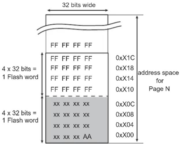
text_image
32 bits wide FF FF FF FF 4 x 32 bits = 1 Flash word FF FF FF FF 0xX1C FF FF FF FF 0xX18 FF FF FF FF 0xX14 FF FF FF FF 0xX10 xx xx xx xx 0xX0C xx xx xx xx 0xX08 xx xx xx xx 0xX04 xx xx xx AA 0xX00 address space for Page N 4 x 32 bits = 1 Flash wordStep 1: Flash array after programming first byte (0xAA)
128-bit used at address 0xX00 (write latch buffer + WP)

text_image
32 bits wide FF FF FF FF xx xx xx xx 0xX1C xx xx xx xx 0xX18 xx xx xx xx 0xX14 xx xx xx 55 0xX10 xx xx xx xx 0xX0C xx xx xx xx 0xX08 xx xx xx xx 0xX04 xx xx xx AA 0xX00Step 2: Flash array after programming second byte (0x55)
128-bit used at address 0xX10 (write latch buffer + WP)
Note: The byte location shown here is for example only, it can be any byte location within a 64-bit word
22.4.3.3 Erase Commands
Erase commands are allowed only on unlocked regions. Depending on the Flash memory, several commands can be used to erase the Flash:
- Erase All Memory (EA): All memory is erased. The processor must not fetch code from the Flash memory.
- Erase Pages (EPA): 4, 8, 16, or 32 pages are erased in the Flash sector selected. The first page to be erased is specified in the FARG[15:2] field of the EEFC_FCR. The first page number must be a multiple of 8, 16, or 32 depending on the number of pages to erase simultaneously.
- Erase Sector (ES): A full memory sector is erased. Sector size depends on the Flash memory. EEFC_FCR.FARG must be set with a page number that is in the sector to be erased.
Note: If one sub-sector is locked within the first sector, the Erase Sector (ES) command cannot be processed on non-locked sub-sectors of the first sector. All the lock bits of the first sector must be cleared prior to issuing an ES command on the first sector. After the ES command has been issued, the first sector lock bits must be reverted to the state before clearing them.
If the processor is fetching code from the Flash memory while the EPA or ES command is being executed, the processor accesses are stalled until the EPA command is completed. To avoid stalling the processor, the code can be run out of internal SRAM.
The following are the erase sequence:
- Erase starts immediately one of the erase commands and the FARG field are written in EEFC FCR.
For the EPA command, the two lowest bits of the FARG field define the number of pages to be erased (FARG[1:0]), see table below.
Table 22-3. EEFC_FCR.FARG Field for EPA Command
FARG[1:0] Number of pages to be erased with EPA command
0 4 pages (only valid for small 8-KB sectors)
......continued
FARG[1:0] Number of pages to be erased with EPA command
| 1 8 pages (only valid for small 8-KB sectors) | |
| 2 16 pages | |
| 3 32 pages (not valid for small 8-KB sectors) | |
- When erasing is completed, the EEFC_FSR.FRDY bit rises. If an interrupt has been enabled by setting the EEFC_FMR.FRDY bit, the interrupt line of the interrupt controller is activated.
Three errors can be detected in EEFC_FSR after an erasing sequence:
- Command Error: A bad keyword has been written in EEFC_FCR.
- Lock Error: At least one page to be erased belongs to a locked region. The erase command has been refused, no page has been erased. A command must be run previously to unlock the corresponding region.
- Flash Error: At the end of the erase period, the EraseVerify test of the Flash memory has failed. After a first programming pulse, a Verify is applied. The memory is read, to compare both programmed and expected values. If that comparison fails, a second programming pulse is applied, and so on, until a maximum pulse number is reached. At this time, if the memory is still not containing what is expected, the FLERR flag is set high.
22.4.3.4 Lock Bit Protection
Lock bits are associated with several pages in the embedded Flash memory plane. This defines lock regions in the embedded Flash memory plane. They prevent writing/erasing protected pages.
The following are lock sequence:
- Execute the 'Set Lock Bit' command by writing the EEFC_FCR.FCMD bit with the SLB command and EEFC_FCR.FARG with a page number to be protected.
- When the locking completes, the EEFC_FSR.FRDY bit rises. If an interrupt has been enabled by setting the bit EEFC_FMR.FRDY, the interrupt line of the interrupt controller is activated.
- The result of the SLB command can be checked running a 'Get Lock Bit' (GLB) command. Note: The value of the FARG argument passed together with SLB command must not exceed the higher lock bit index available in the product.
The following two errors can be detected in EEFC_FSR after a programming sequence:
- Command Error: A bad keyword has been written in EEFC_FCR.
- Flash Error: At the end of the programming, the EraseVerify or WriteVerify test of the Flash memory has failed. After a first programming pulse, a Verify is applied. The memory is read, to compare both programmed and expected values. If that comparison fails, a second programming pulse is applied, and so on, until a maximum pulse number is reached. At this time, if the memory is still not containing what is expected, the FLERR flag is set high.
It is possible to clear lock bits previously set. After the lock bits are cleared, the locked region can be erased or programmed. The unlock sequence is the following:
- Execute the 'Clear Lock Bit' command by writing the EEFC_FCR.FCMD bit with the CLB command and the EEFC_FCR.FARG bit with a page number to be unprotected.
- When the unlock completes, the EEFC_FSR.FRDY bit rises. If an interrupt has been enabled by setting the EEFC_FMR.FRDY bit, the interrupt line of the interrupt controller is activated. Note: The value of the FARG argument passed together with CLB command must not exceed the higher lock bit index available in the product.
Two errors can be detected in EEFC_FSR after a programming sequence:
- Command Error: A bad keyword has been written in EEFC_FCR.
- Flash Error: At the end of the programming, the EraseVerify or WriteVerify test of the Flash memory has failed. After a first programming pulse, a Verify is applied. The memory is read, to compare both programmed and expected values. If that comparison fails, a second programming pulse is applied, and so on, until a maximum pulse number is reached. At this time, if the memory is still not containing what is expected, the FLERR flag is set high.
The status of lock bits can be returned by the EEFC. The 'Get Lock Bit' sequence is the following:
- Execute the 'Get Lock Bit' command by writing EEFC_FCR.FCMD with the GLB command. Field EEFC_FCR.FARG is meaningless.
- Lock bits can be read by the software application in EEFC_FRR. The first word read corresponds to the 32 first lock bits, next reads providing the next 32 lock bits as long as it is meaningful. Extra reads to EEFC_FRR return 0.
For example, if the third bit of the first word read in EEFC_FRR is set, the third lock region is locked.
Two errors can be detected in EEFC_FSR after a programming sequence:
- Command Error: A bad keyword has been written in EEFC_FCR.
- Flash Error: At the end of the programming, the EraseVerify or WriteVerify test of the Flash memory has failed. After a first programming pulse, a Verify is applied. The memory is read, to compare both programmed and expected values. If that comparison fails, a second programming pulse is applied, and so on, until a maximum pulse number is reached. At this time, if the memory is still not containing what is expected, the FLERR flag is set high.
Note: Access to the Flash in read is permitted when a 'Set Lock Bit', 'Clear Lock Bit' or 'Get Lock Bit' command is executed.
22.4.3.5 GPNVM Bit
The GPNVM bits do not interfere with the embedded Flash memory plane. For more details, refer to the "Memories" chapter.
The 'Set GPNVM Bit' sequence is the following:
- Execute the 'Set GPNVM Bit' command by writing EEFC_FCR.FCMD with the SGPB command and EEFC_FCR.FARG with the number of GPNVM bits to be set.
- When the GPNVM bit is set, the bit EEFC_FSR.FRDY rises. If an interrupt was enabled by setting the bit EEFC_FMR.FRDY, the interrupt line of the interrupt controller is activated.
- The result of the SGPB command can be checked by running a 'Get GPNVM Bit' (GGPB) command.
Note: The value of the FARG argument passed together with SGPB command must not exceed the higher GPNVM index available in the product. Flash data content is not altered if FARG exceeds the limit. Command Error is detected only if FARG is greater than 8.
Two errors can be detected in EEFC_FSR after a programming sequence:
- Command Error: A bad keyword has been written in EEFC_FCR.
- Flash Error: At the end of the programming, the EraseVerify or WriteVerify test of the Flash memory has failed. After a first programming pulse, a Verify is applied. The memory is read, to compare both programmed and expected values. If that comparison fails, a second programming pulse is applied, and so on, until a maximum pulse number is reached. At this time, if the memory is still not containing what is expected, the FLERR flag is set high.
It is possible to clear GPNVM bits previously set. The 'Clear GPNVM Bit' sequence is the following:
- Execute the 'Clear GPNVM Bit' command by writing EEFC_FCR.FCMD with the CGPB command and EEFC_FCR.FARG with the number of GPNVM bits to be cleared.
- When the clear completes, the bit EEFC_FSR.FRDY rises. If an interrupt has been enabled by setting the bit EEFC_FMR.FRDY, the interrupt line of the interrupt controller is activated.
Note: The value of the FARG argument passed together with CGPB command must not exceed the higher GPNVM index available in the product. Flash data content is not altered if FARG exceeds the limit. Command Error is detected only if FARG is greater than 8.
Two errors can be detected in EEFC_FSR after a programming sequence:
- Command Error: A bad keyword has been written in EEFC_FCR.
- Flash Error: At the end of the programming, the EraseVerify or WriteVerify test of the Flash memory has failed. After a first programming pulse, a Verify is applied. The memory is read, to compare both programmed and expected values. If that comparison fails, a second programming pulse is applied, and so on, until a maximum pulse number is reached. At this time, if the memory is still not containing what is expected, the FLERR flag is set high.
The status of GPNVM bits can be returned by the EEFC. The sequence is the following:
-
Execute the 'Get GPNVM Bit' command by writing EEFC_FCR.FCMD with the GGPB command. Field EEFC_FCR.FARG is meaningless.
-
GPNVM bits can be read by the software application in EEFC_FRR. The first word read corresponds to the 32 first GPNVM bits, following reads provide the next 32 GPNVM bits as long as it is meaningful. Extra reads to EEFC_FRR return 0.
For example, if the third bit of the first word read in EEFC_FRR is set, the third GPNVM bit is active.
One error can be detected in EEFC_FSR after a programming sequence:
- Command Error: A bad keyword has been written in EEFC_FCR.
Note: Access to the Flash in read is permitted when a 'Set GPNVM Bit', 'Clear GPNVM Bit' or 'Get GPNVM Bit' command is executed.
Related Links
11. Memories
22.4.3.6 Calibration Bit
Calibration bits do not interfere with the embedded Flash memory plane.
The calibration bits cannot be modified.
The status of calibration bits are returned by the EEFC. The sequence is as follows:
- Execute the 'Get CALIB Bit' command by writing EEFC_FCR.FCMD with the GCALB command. Field EEFC_FCR.FARG is meaningless.
- Calibration bits can be read by the software application in EEFC_FRR. The first word read corresponds to the first 32 calibration bits. The following reads provide the next 32 calibration bits as long as it is meaningful. Extra reads to EEFC_FRR return 0.
The 8/12 MHz internal RC oscillator is calibrated in production. This calibration can be read through the GCALB command. Table 22-4 shows the bit implementation.
The RC calibration for the 4 MHz is set to '1000000'.
Table 22-4. Calibration Bit Indexes
| Description EEFC_FRR Bits | |
| 8 MHz RC calibration output [28–22] | |
| 12 MHz RC calibration output [38–32] |
22.4.3.7 Security Bit Protection
When the security bit is enabled, the Embedded Trace Macrocell (ETM) is disabled and access to the Flash through the SWD interface or through the Fast Flash Programming interface is forbidden. This ensures the confidentiality of the code programmed in the Flash.
The security bit is GPNVM0.
Disabling the security bit can only be achieved by asserting the ERASE signal at '1', and after a full Flash erase is performed. When the security bit is deactivated, all accesses to the Flash are permitted.
22.4.3.8 Unique Identifier Area
Each device is programmed with a 128-bit unique identifier area.
See "Flash Memory Areas".
The sequence to read the unique identifier area is the following:
- Execute the 'Start Read Unique Identifier' command by writing EEFC_FCR.FCMD with the STUI command. Field EEFC_FCR.FARG is meaningless.
- Wait until the bit EEFC_FSR.FRDY falls to read the unique identifier area. The unique identifier field is located in the first 128 bits of the Flash memory mapping. The 'Start Read Unique Identifier' command reuses some addresses of the memory plane for code, but the unique identifier area is physically different from the memory plane for code.
- To stop reading the unique identifier area, execute the 'Stop Read Unique Identifier' command by writing EEFC_FCR.FCMD with the SPUI command. Field EEFC_FCR.FARG is meaningless.
- When the SPUI command has been executed, the bit EEFC_FSR.FRDY rises. If an interrupt was enabled by setting the bit EEFC_FMR.FRDY, the interrupt line of the interrupt controller is activated.
Note: During the sequence, the software cannot be fetched from the Flash.
22.4.3.9 User Signature Area
Each product contains a user signature area of 512 bytes. It can be used for storage. Read, write, and erase of this area is allowed. Refer to "Flash Memory Areas".
The sequence to read the user signature area is as follows:
- Execute the 'Start Read User Signature' command by writing EEFC_FCR.FCMD with the STUS command. Field EEFC_FCR.FARG is meaningless.
- Wait until the EEFC_FSR.FRDY bit falls to read the user signature area. The user signature area is located in the first 512 bytes of the Flash memory mapping. The 'Start Read User Signature' command reuses some addresses of the memory plane but the user signature area is physically different from the memory plane
- To stop reading the user signature area, execute the 'Stop Read User Signature' command by writing EEFC_FCR.FCMD with the SPUS command. Field EEFC_FCR.FARG is meaningless.
- When the SPUI command has been executed, the bit EEFC_FSR.FRDY rises. If an interrupt was enabled by setting the bit EEFC_FMR.FRDY, the interrupt line of the interrupt controller is activated.
Note: During the sequence, the software cannot be fetched from the Flash or from the second plane in case of dual plane.
One error can be detected in EEFC_FSR after this sequence:
- Command Error: A bad keyword has been written in EEFC_FCR.
The sequence to write the user signature area is as follows:
- Write the full page, at any page address, within the internal memory area address space.
-
Execute the 'Write User Signature' command by writing EEFC_FCR.FCMD with the WUS command. Field EEFC_FCR.FARG is meaningless.
-
When programming is completed, the EEFC_FSR.FRDY bit rises. If an interrupt has been enabled by setting the EEFC_FMR.FRDY bit, the corresponding interrupt line of the interrupt controller is activated.
The following two errors can be detected in EEFC_FSR after this sequence:
- Command Error: A bad keyword has been written in EEFC_FCR.
- Flash Error: At the end of the programming, the WriteVerify test of the Flash memory has failed. After a first programming pulse, a Verify is applied. The memory is read, to compare what is programmed with what is expected. If that comparison fails, a second programming pulse is applied, and so on, until a maximum pulse number is reached. At this time, if the memory is still not containing what is expected, the FLERR flag is set high.
The sequence to erase the user signature area is as follows:
-
Execute the 'Erase User Signature' command by writing EEFC_FCR.FCMD with the EUS command. Field EEFC_FCR.FARG is meaningless.
-
When programming is completed, the EEFC_FSR.FRDY bit rises. If an interrupt has been enabled by setting the EEFC_FMR.FRDY bit, the corresponding interrupt line of the interrupt controller is activated.
Two errors can be detected in EEFC_FSR after this sequence:
- Command Error: A bad keyword has been written in EEFC_FCR.
- Flash Error: At the end of the programming, the EraseVerify test of the Flash memory has failed. After a first programming pulse, a Verify is applied. The memory is read, to compare what is programmed with what is expected. If that comparison fails, a second programming pulse is applied, and so on, until a maximum pulse number is reached. At this time, if the memory is still not containing what is expected, the FLERR flag is set high.
22.4.3.10 ECC Errors and Corrections
The Flash embeds an ECC module able to correct one unique error and able to detect two errors. The errors are detected while a read access is performed into memory array and stored in EEFC_FSR (see "EEFC Flash Status Register"). The error report is kept until EEFC_FSR is read.
There is one flag for a unique error on lower half part of the Flash word (64 LSB) and one flag for the upper half part (MSB). The multiple errors are reported in the same way.
Due to the anticipation technique to improve bandwidth throughput on instruction fetch, a reported error can be located in the next sequential Flash word compared to the location of the instruction being executed, which is located in the previously fetched Flash word.
If a software routine processes the error detection independently from the main software routine, the entire Flash located software must be rewritten because there is no storage of the error location.
If only a software routine is running to program and check pages by reading EEFC_FSR, the situation differs from the previous case. Performing a check for ECC unique errors just after page programming completion involves a read of the newly programmed page. This read sequence is viewed as data accesses and is not optimized by the Flash controller. Thus, in case of unique error, only the current page must be reprogrammed.
22.4.4 Register Write Protection
To prevent any single software error from corrupting EEFC behavior, certain registers in the address space can be write-protected by setting the WPEN bit in the "EEFC Write Protection Mode Register" (EEFC_WPMR).
The following register can be write-protected:
- "EEFC Flash Mode Register"
22.5 Register Summary
| Offset | Name Bit Pos. 7 | 6 | 5 | 4 | 3 | 2 | 1 | 0 | |||||||||||||||||||||||||||||||||||||||||||||||||||||||||||||||||||||||||||||||||||||||||||||||||||||||||||||||||||||||||||||||||||||||||||||||||||||||||||||||||||||||||||||||||||||||||||||||||||||||||||||||||||||||||||||||||||||||||||||||||||||||||||||||||||||||||||||||||||||||||||||||||||||||||||||||||||||||||||||||||||||||||||||||||||||||||||||||||||||||||||||||||||||||||||||||||||||||||||||||||||||||||||||||||||||||||||||||||||||||||||||||||||||||||||||||||||||||||||||||||||||||||||||||||||||||||||||||||||||||||||||||||||||||||||||||||||||||||||||||||||||||||||||||||||||||||||||||||||||||||||||||||||||||||||||||||
| 0x00 | EEFC_FMR | 7:0 | FRDY | 7:0 | FRDY | ||||||||||||||||||||||||||||||||||||||||||||||||||||||||||||||||||||||||||||||||||||||||||||||||||||||||||||||||||||||||||||||||||||||||||||||||||||||||||||||||||||||||||||||||||||||||||||||||||||||||||||||||||||||||||||||||||||||||||||||||||||||||||||||||||||||||||||||||||||||||||||||||||||||||||||||||||||||||||||||||||||||||||||||||||||||||||||||||||||||||||||||||||||||||||||||||||||||||||||||||||||||||||||||||||||||||||||||||||||||||||||||||||||||||||||||||||||||||||||||||||||||||||||||||||||||||||||||||||||||||||||||||||||||||||||||||||||||||||||||||||||||||||||||||||||||||||||||||||||||||||||||||||||||||||||||||||||
| 15:8 | FWS[3:0] | 23:16 | SCOD | 31:24 | CLOE | ||||||||||||||||||||||||||||||||||||||||||||||||||||||||||||||||||||||||||||||||||||||||||||||||||||||||||||||||||||||||||||||||||||||||||||||||||||||||||||||||||||||||||||||||||||||||||||||||||||||||||||||||||||||||||||||||||||||||||||||||||||||||||||||||||||||||||||||||||||||||||||||||||||||||||||||||||||||||||||||||||||||||||||||||||||||||||||||||||||||||||||||||||||||||||||||||||||||||||||||||||||||||||||||||||||||||||||||||||||||||||||||||||||||||||||||||||||||||||||||||||||||||||||||||||||||||||||||||||||||||||||||||||||||||||||||||||||||||||||||||||||||||||||||||||||||||||||||||||||||||||||||||||||||||||||||||||||
| 23:16 | SCOD | 31:24 | FKEY[7:0] | ||||||||||||||||||||||||||||||||||||||||||||||||||||||||||||||||||||||||||||||||||||||||||||||||||||||||||||||||||||||||||||||||||||||||||||||||||||||||||||||||||||||||||||||||||||||||||||||||||||||||||||||||||||||||||||||||||||||||||||||||||||||||||||||||||||||||||||||||||||||||||||||||||||||||||||||||||||||||||||||||||||||||||||||||||||||||||||||||||||||||||||||||||||||||||||||||||||||||||||||||||||||||||||||||||||||||||||||||||||||||||||||||||||||||||||||||||||||||||||||||||||||||||||||||||||||||||||||||||||||||||||||||||||||||||||||||||||||||||||||||||||||||||||||||||||||||||||||||||||||||||||||||||||||||||||||||||||||
| 0x04 | EEFC_FCR | 7:0 | FCMD[7:0] | 15:8 | FARG[7:0] | 23:16 | FARG[15:8] | FKEY[7:0] | 31:24 | FKEY[7:0] | FLERR | FLOCKE | FCMDE | FRDY | 0x08 | EEFC_FSR | 7:0 | FLERR | FLOCKE | FCMDE | FRDY | 0x08 | EEFC_FSR | 7:0 | FLERR | FLOCKE | FCMDE | FRDY | 0x08 | EEFC_FSR | 15:8 | FLERR | FLOCKE | FCMDE | FRDY | 0x08 | EEFC_FSR | 15:8 | FLERR | FLOCKE | FCMDE | FRDY | 0x08 | EEFC_FSR | 23:16 | MECCEMSB | UECCEMSB | MECCELSB | UECCELSB | 0x08 | EEFC_FSR | 31:24 | FVALUE[7:0] | FLERR | FLOCKE | FCMDE | FRDY | 0x08 | EEFC_FSR | 7:0 | FLERR | FVALUE[7:0] | FLERR | FLOCKE | FCMDE | FRDY | 0x08 | EEFC_FSR | 15:8 | FLERR | FVALUE[7:0] | FLERR | FLOCKE | FCMDE | FRDY | 0x08 | EEFC_FSR | 23:16 | FVALUE[7:0] | FLERR | FLOCKE | FCMDE | FRDY | 0x08 | EEFC_FSR | 31:24 | FVALUE[7:0] | FLERR | FLOCKE | FCMDE | FRDY | 0x08 | EEFC_FSR | 7:0 | FVALUE[7:0] | FLERR | FLOCKE | FCMDE | FRDY | 0x08 | EEFC_FSR | 15:8 | FVALUE[7:0] | FLERR | FLOCKE | FCMDE | FRDY | 0x08 | EEFC_FSR | 23:16 | FVALUE[7:0] | FLERR | FLOCKE | FCMDE | FRDY | 0x08 | EEFC_FSR | 31:24 | FVALUE[7:0] | FLERR | FLOCKE | FCMDE | FRDY | FVALUE[7:0] | FLERR | FLOCKE | FCMDE | FRDY | 0x10 | Reserved | 7:0 | WPEN | WPEN | WPEN | WPEN | WPEN | WPEN | WPEN | WPEN | WPEN | WPEN | WPEN | WPEN | WPEN | WPEN | WPEN | WPEN | WPEN | WPEN | WPEN | WPEN | WPEN | WPEN | WPEN | WPEN | WPEN | WPEN | WPEN | WPEN | WPEN | WPEN | WPEN | WPEN | WPEN | WPEN | ||||||||||||||||||||||||||||||||||||||||||||||||||||||||||||||||||||||||||||||||||||||||||||||||||||||||||||||||||||||||||||||||||||||||||||||||||||||||||||||||||||||||||||||||||||||||||||||||||||||||||||||||||||||||||||||||||||||||||||||||||||||||||||||||||||||||||||||||||||||||||||||||||||||||||||||||||||||||||||||||||||||||||||||||||||||||||||||||||||||||||||||||||||||||||||||||||||||||||||||||||||||||||||||||||||||||||||||||||||||||||||||||||||||||||||||||||||
| 23:16 | WPKEY[7:0] | WPKEY[7:0] | WPKEY[7:0] | WPKEY[7:0] | WPKEY[7:0] | WPKEY[7:0] | WPKEY[7:0] | WPKEY[7:0] | WPKEY[7:0] | WPKEY[7:0] | WPKEY[7:0] | WPKEY[7:0] | WPKEY[7:0] | WPKEY | WPKEY[7:0] | WPKEY[7:0] | WPKEY[7:0] | WPKEY[7:0] | WPKEY[7:0] | WPKEY[7:0] | WPKEY[7:0] | WPKEY[7:0] | WPKEY[7:0] | WPKEY[7:0] | WPKEY[7:0] | WPKEY[7:0] | WPKEY [7:0] | WPKEY[7:0] | WPKEY[7:0] | WPKEY[7:0] | WPKEY[7:0] | WPKEY[7:0] | WPKEY[7:0] | WPKEY[7:0] | WPKEY[7:0] | WPKEY[7:0] | WPKEY[7:0] | WPKEY[7:0] | WPKEY[7:0][7:0] | WPKEY[7:0] | WPKEY[7:0] | WPKEY[7:0] | WPKEY[7:0] | WPKEY[7:0] | WPKEY[7:0] | WPKEY[7:0] | WPKEY[7:0] | WPKEY[7:0] | WPKEY[7:0] | WPKEY[7:0] | WPKEY[7:0] WPKEY[7:0] | WPKEY[7:0] | WPKEY[7:0] | WPKEY[7:0] | WPKEY[7:0] | WPKEY[7:0] | WPKEY[7:0] | WPKEY[7:0] | WPKEY[7:0] | WPKEY[7:0] | WPKEY[7:0] | WPKEY[7:0] | WPKEY[6:0] | WPKEY[6:0] | WPKEY[6:0] | WPKEY[6:0] | WPKEY[6:0] | WPKEY[6:0] | WPKEY[6:0] | WPKEY[6:0] | WPKEY[6:0] | WPKEY[6:0] | WPKEY[6:0] | WPKEY[6:0] | WPKEY[6:0] | ||||||||||||||||||||||||||||||||||||||||||||||||||||||||||||||||||||||||||||||||||||||||||||||||||||||||||||||||||||||||||||||||||||||||||||||||||||||||||||||||||||||||||||||||||||||||||||||||||||||||||||||||||||||||||||||||||||||||||||||||||||||||||||||||||||||||||||||||||||||||||||||||||||||||||||||||||||||||||||||||||||||||||||||||||||||||||||||||||||||||||||||||||||||||||||||||||||||||||||||||||||||||||||||||||||||||||||||||||||||||||||||||||||||||||||||||||||||||||||||||||||||||||||||||||||||||||||||||||||||||||||||||||||||||||||||||||||||||||||||
| 23:16 | FVALUE[7:0] | FVALUE[7:0] | FVALUE[7:0] | FVALUE[7:0] | FVALUE[7:0] | FVALUE[7:0] | FVALUE[7:0] | FVALUE[7:0] | FVALUE[7:0] | FVALUE[7:0] | FVALUE[7:0] | FVALUE[7:0] | FVALUE[7:0] | FVALUE [7:0] | FVALUE[7:0] | FVALUE[7:0] | FVALUE[7:0] | FVALUE[7:0] | FVALUE[7:0] | FVALUE[7:0] | FVALUE[7:0] | FVALUE[7:0] | FVALUE[7:0] | FVALUE[7:0] | FVALUE[7:0] | FVALUE[7:0][7:0] | FVALUE[7:0] | FVALUE[7:0] | FVALUE[7:0] | FVALUE[7:0] | FVALUE[7:0] | FVALUE[7:0] | FVALUE[7:0] | FVALUE[7:0] | FVALUE[7:0] | FVALUE[7:0] | FVALUE[7:0] | FVALUE[7:0] FVALUE[7:0] | FVALUE[7:0] | FVALUE[7:0] | FVALUE[7:0] | FVALUE[7:0] | FVALUE[7:0] | FVALUE[7:0] | FVALUE[7:0] | FVALUE[7:0] | FVALUE[7:0] | FVALUE[7:0] | FVALUE[7:0] | FVALUE[6:0] | FVALUE[6:0] | FVALUE[6:0] | FVALUE[6:0] | FVALUE[6:0] | FVALUE[6:0] | FVALUE[6:0] | FVALUE[6:0] | FVALUE[6:0] | FVALUE[6:0] | FVALUE[6:0] | FVALUE[6:0] | FVALUE[6:0] | |||||||||||||||||||||||||||||||||||||||||||||||||||||||||||||||||||||||||||||||||||||||||||||||||||||||||||||||||||||||||||||||||||||||||||||||||||||||||||||||||||||||||||||||||||||||||||||||||||||||||||||||||||||||||||||||||||||||||||||||||||||||||||||||||||||||||||||||||||||||||||||||||||||||||||||||||||||||||||||||||||||||||||||||||||||||||||||||||||||||||||||||||||||||||||||||||||||||||||||||||||||||||||||||||||||||||||||||||||||||||||||||||||||||||||||||||||||||||||||||||||||||||||||||||||||||||||||||||||||||||||||||||||||||||||||||||||||||||||||||||||||||||||
22.5.1 EEFC Flash Mode Register
Name: EEFC_FMR
Offset: 0x00
Property: Read/Write
This register can only be written if the WPEN bit is cleared in the "EEFC Write Protection Mode Register".
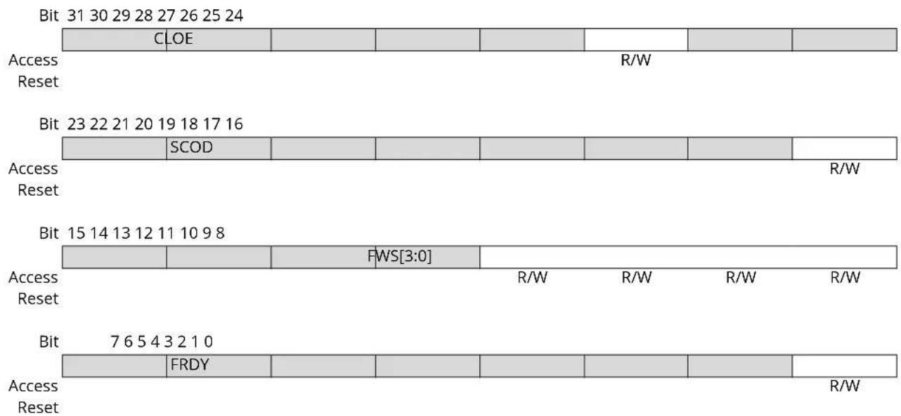
text_image
Bit 31 30 29 28 27 26 25 24 CLOE Access Reset R/W Bit 23 22 21 20 19 18 17 16 SCOD Access Reset R/W Bit 15 14 13 12 11 10 9 8 FWS[3:0] Access Reset R/W R/W R/W Bit 7 6 5 4 3 2 1 0 FRDY Access Reset R/WBit 26 - CLOE Code Loop Optimization Enable
No Flash read should be done during change of this field.
| Value | Description |
| 0 | The opcode loop optimization is disabled. |
| 1 | The opcode loop optimization is enabled. |
Bit 16 - SCOD Sequential Code Optimization Disable
No Flash read should be done during change of this field.
| Value | Description |
| 0 | The sequential code optimization is enabled. |
| 1 | The sequential code optimization is disabled. |
Bits 11:8 - FWS[3:0] Flash Wait State
This field defines the number of wait states for read and write operations:
FWS = Number of cycles for Read/Write operations - 1
Bit 0 - FRDY Flash Ready Interrupt Enable
| Value | Description |
| 0 | Flash ready does not generate an interrupt. |
| 1 | Flash ready (to accept a new command) generates an interrupt. |
22.5.2 EEFC Flash Command Register
Name: EEFC_FCR
Offset: 0x04
Reset: -
Property: Write-only
| Bit 31 30 29 28 27 26 25 24 | |
| FKEY[7:0] | |
| Access W W W W W W W W W | |
| Reset - - - - - - - - | |
| Bit 23 22 21 20 19 18 17 16 | |
| FARG[15:8] | |
| Access W W W W W W W W W W | |
| Reset - - - - - - - - | |
| Bit 15 14 13 12 11 10 9 8 | |
| FARG[7:0] | |
| Access W W W W W W W W W W | |
| Reset - - - - - - - - | |
| Bit 7 6 5 4 3 2 1 0 | |
| FCMD[7:0] | |
| Access W W W W W W W W W W | |
| Reset - - - - - - - - | |
Bits 31:24 - FKEY[7:0] Flash Write Protection Key
| Value | Name | Description |
| 0x5A | PASSWD | The 0x5A value enables the command defined by the bits of the register. If the field is written with a different value, the write is not performed and no action is started. |
Bits 23:8 - FARG[15:0] Flash Command Argument
| GETD, GLB, GGPB, STUI, SPUI, GCALB, WUS, EUS, STUS, SPUS, EA | Commands requiring no argument, including Erase all command | FARG is meaningless, must be written with 0 |
| ES | Erase sector command | FARG must be written with any page number within the sector to be erased |
| EPA | Erase pages command | FARG[1:0] defines the number of pages to be erasedThe start page must be written in FARG[15:2].FARG[1:0] = 0: Four pages to be erased. FARG[15:2] = Page_Number / 4FARG[1:0] = 1: Eight pages to be erased. FARG[15:3] = Page_Number / 8, FARG[2]=0FARG[1:0] = 2: Sixteen pages to be erased. FARG[15:4] = Page_Number / 16, FARG[3:2]=0FARG[1:0] = 3: Thirty-two pages to be erased. FARG[15:5] = Page_Number / 32, FARG[4:2]=0Refer to “EEFC_FCR.FARG Field for EPA Command”. |
| WP, WPL, EWP, EWPL | Programming commands | FARG must be written with the page number to be programmed |
| SLB, CLB | Lock bit commands | FARG defines the page number to be locked or unlocked |
| SGPB, CGPB | GPNVM commands | FARG defines the GPNVM number to be programmed |
Bits 7:0 - FCMD[7:0] Flash Command
| Value | Name | Description |
| 0x00 | GETD Get Flash descriptor | |
| 0x01 | WP Write page | |
| 0x02 | WPL Write page and lock | |
| 0x03 | EWP Erase page and write page | |
| 0x04 | EWPL Erase page and write page then lock | |
| 0x05 | EA Erase all | |
| 0x07 | EPA Erase pages | |
| 0x08 | SLB Set lock bit | |
| 0x09 | CLB Clear lock bit | |
| 0x0A | GLB Get lock bit | |
| 0x0B | SGPB Set GPNVM bit | |
| 0x0C | CGPB Clear GPNVM bit | |
| 0x0D | GGPB Get GPNVM bit | |
| 0x0E | STUI Start read unique identifier | |
| 0x0F | SPUI Stop read unique identifier | |
| 0x10 | GCALB Get CALIB bit | |
| 0x11 | ES Erase sector | |
| 0x12 | WUS Write user signature | |
| 0x13 | EUS Erase user signature | |
| 0x14 | STUS Start read user signature | |
| 0x15 | SPUS Stop read user signature |
22.5.3 EEFC Flash Status Register
Name: EEFC_FSR
Offset: 0x08
Property: Read-only

text_image
Bit 31 30 29 28 27 26 25 24 Access Reset Bit 23 22 21 20 19 18 17 16 MECCEMSB UECCEMSB MECCELSB UECCELSB Access Reset RR RR Bit 15 14 13 12 11 10 9 8 Access Reset Bit 7 6 5 4 3 2 1 0 Access Reset RR RR FLERR FLOCKE FCMDE FRDYBit 19 - MECCEMSB Multiple ECC Error on MSB Part of the Memory Flash Data Bus (cleared on read)
| Value | Description |
| 0 | No multiple error detected on 64 MSB part of the Flash memory data bus since the last read of EEFC_FSR. |
| 1 | Multiple errors detected and NOT corrected on 64 MSB part of the Flash memory data bus since the last read of EEFC_FSR. |
Bit 18 - UECCEMSB Unique ECC Error on MSB Part of the Memory Flash Data Bus (cleared on read)
| Value | Description |
| 0 | No unique error detected on 64 MSB data bus of the Flash memory since the last read of EEFC_FSR. |
| 1 | One unique error detected but corrected on 64 MSB data bus of the Flash memory since the last read of EEFC_FSR. |
Bit 17 - MECCELSB Multiple ECC Error on LSB Part of the Memory Flash Data Bus (cleared on read)
| Value | Description |
| 0 | No multiple error detected on 64 LSB part of the Flash memory data bus since the last read of EEFC_FSR. |
| 1 | Multiple errors detected and NOT corrected on 64 LSB part of the Flash memory data bus since the last read of EEFC_FSR. |
Bit 16 - UECCELSB Unique ECC Error on LSB Part of the Memory Flash Data Bus (cleared on read)
| Value | Description |
| 0 | No unique error detected on 64 LSB data bus of the Flash memory since the last read of EEFC_FSR. |
| 1 | One unique error detected but corrected on 64 LSB data bus of the Flash memory since the last read of EEFC_FSR. |
Bit 3 - FLERR Flash Error Status (cleared when a programming operation starts)
| Value | Description |
| 0 | No Flash memory error occurred at the end of programming (EraseVerify or WriteVerify test has passed). |
| 1 | A Flash memory error occurred at the end of programming (EraseVerify or WriteVerify test has failed). |
Bit 2 - FLOCKE Flash Lock Error Status (cleared on read)
This flag is automatically cleared when EEFC_FSR is read or EEFC_FCR is written.
| Value Description | |
| 0 | No programming/erase of at least one locked region has happened since the last read of EEFC_FSR. |
| 1 | Programming/erase of at least one locked region has happened since the last read of EEFC_FSR. |
Bit 1 - FCMDE Flash Command Error Status (cleared on read or by writing EEFC_FCR)
| Value Description | |
| 0 | No invalid commands and no bad keywords were written in EEFC_FMR. |
| 1 | An invalid command and/or a bad keyword was/were written in EEFC_FMR. |
Bit 0 - FRDY Flash Ready Status (cleared when Flash is busy)
When set, this flag triggers an interrupt if the FRDY flag is set in EEFC_FMR.
This flag is automatically cleared when the EEFC is busy.
| Value Description | |
| 0 | The EEFC is busy. |
| 1 | The EEFC is ready to start a new command. |
22.5.4 EEFC Flash Result Register
Name: EEFC_FRR
Offset: 0x0C
Property: Read-only

text_image
Bit 31 30 29 28 27 26 25 24 FVALUE[31:24] Access R R R R R R R R Reset Bit 23 22 21 20 19 18 17 16 FVALUE[23:16] Access R R R R R R R R Reset Bit 15 14 13 12 11 10 9 8 FVALUE[15:8] Access R R R R R R R R Reset Bit 7 6 5 4 3 2 1 0 FVALUE[7:0] Access R R R R R R R R ResetBits 31:0 - FVALUE[31:0] Flash Result Value
The result of a Flash command is returned in this register. If the size of the result is greater than 32 bits, the next resulting value is accessible at the next register read.
22.5.5 EEFC Write Protection Mode Register
Name: EEFC_WPMR
Offset: 0xE4
Property: Read/Write
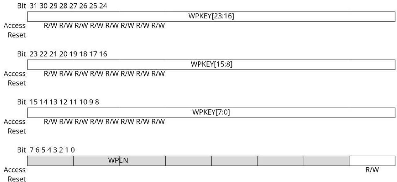
text_image
Bit 31 30 29 28 27 26 25 24 WPKEY[23:16] Access R/W R/W R/W R/W R/W R/W R/W Reset Bit 23 22 21 20 19 18 17 16 WPKEY[15:8] Access R/W R/W R/W R/W R/W R/W R/W Reset Bit 15 14 13 12 11 10 9 8 WPKEY[7:0] Access R/W R/W R/W R/W R/W R/W R/W Reset Bit 7 6 5 4 3 2 1 0 WPEN Access Reset R/WBits 31:8 - WPKEY[23:0] Write Protection Key
See "Register Write Protection" for the list of registers that can be protected.
| Value | Name | Description |
| 0x454643 | PASSWD | Writing any other value in this field aborts the write operation. Always reads as 0. |
Bit 0 - WPEN Write Protection Enable
See "Register Write Protection" for the list of registers that can be protected.
| Value | Description |
| 0 | Disables the write protection if WPKEY corresponds to 0x454643 (EFC in ASCII). |
| 1 | Enables the write protection if WPKEY corresponds to 0x454643 (EFC in ASCII). |
23. Supply Controller (SUPC)
23.1 Description
The Supply Controller (SUPC) controls the supply voltages of the system and manages the Backup mode. In this mode, current consumption is reduced to a few microamps for backup power retention. Exit from this mode is possible on multiple wakeup sources. The SUPC also generates the slow clock by selecting either the slow RC oscillator or the 32.768 kHz crystal oscillator.
23.2 Embedded Characteristics
- Management of the Core Power Supply VDDCORE and Backup Mode via the Embedded Voltage Regulator
• Supply Monitor Detection on VDDIO or a Brownout Detection on VDDCORE Triggers a Core Reset - Generates the Slow Clock SLCK by selecting either the 22-42 kHz Slow RC Oscillator or the 32.768 kHz Crystal Oscillator
- Backup SRAM
- Low-power Tamper Detection on Two Inputs
- Anti-tampering by Immediate Clear of the General-purpose Backup Registers
- Support of Multiple Wakeup Sources for Exit from Backup Mode
- 14 Wakeup Inputs with Programmable Debouncing
- Real-Time Clock Alarm
- Real-Time Timer Alarm
– Supply Monitor Detection on VDDIO, with Programmable Scan Period and Voltage Threshold
23.3 Block Diagram
Figure 23-1. Supply Controller Block Diagram
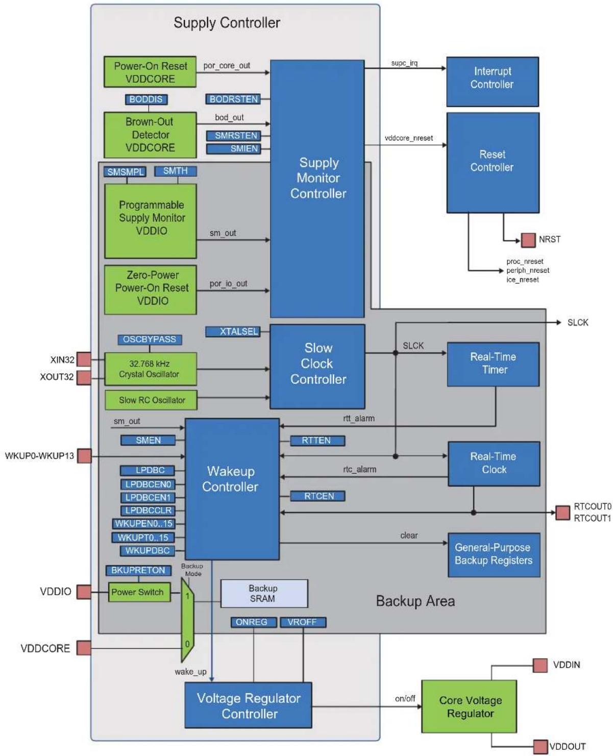
flowchart
graph TD
    A["Power-On Reset VDDCORE"] -->|por_core_out| B["Supply Monitor Controller"]
    C["BODDIS"] --> D["Brown-Out Detector VDDCORE"]
    D -->|bod_out| E["SMRSTEN"]
    D -->|SMIEN| F["SRMSTEN"]
    B --> G["vddcore_nreset"]
    B --> H["Interrupt Controller"]
    H --> I["Reset Controller"]
    I --> J["NRST"]
    J --> K["proc_nreset"]
    J --> L["periph_nreset"]
    J --> M["ice_nreset"]
    B --> N["Programmable Supply Monitor VDDIO"]
    N -->|sm_out| O["Slow Clock Controller"]
    O --> P["SLCK"]
    P --> Q["Real-Time Timer"]
    Q --> R["RLTEN"]
    R --> S["Wakeup Controller"]
    S --> T["RTCEN"]
    T --> U["Real-Time Clock"]
    U --> V["General-Purpose Backup Registers"]
    V --> W["RTCOUT0"]
    V --> X["RTCOUT1"]
    S --> Y["RTCOUT0.15"]
    S --> Z["WKUPD80.15"]
    S --> AA["WKUPDBC"]
    S --> AB["WKUPD80.15"]
    S --> AC["WKUPD80.15"]
    S --> AD["WKUPD80.15"]
    S --> AE["WKUPD80.15"]
    S --> AF["WKUPD80.15"]
    S --> AG["WKUPD80.15"]
    S --> AH["VDDIO"]
    AH --> AI["VDDCORE"]
    AI --> AJ["VDDCORE Regulator Controller"]
    AJ --> AK["Core Voltage Regulator"]
    AK --> AL["VDDIN"]
    AK --> AM["VDDOUT"]
    B --> AN["OSCBYPASS"]
    AN --> AO["32.768 kHz Crystal Oscillator"]
    AO --> AP["Slow RC Oscillator"]
    AP --> AQ["WTALSEL"]
    AQ --> AR["Slow Clock Controller"]
    AR --> AS["SLCK"]
    AS --> AT["SLCK"]
    AT --> AU["RLTEN"]
    AU --> AV["RTCEN"]
    AV --> AW["Wakeup Controller"]
    AW --> AX["RTCOUT0.15"]
    AW --> AY["WKUPD80.15"]
    AW --> AZ["WKUPD80.15"]
    AW --> BA["WKUPD80.15"]
    AW --> BB["KBUPRETON"]
    BB --> BC["Power Switch"]
    BC --> BD["Backup Mode 1"]
    BD --> BE["ONREG"]
    BE --> BF["VROFF"]
    BF --> BG["wake_up"]
    BG --> BH["Voltage Regulator Controller"]
    BH --> BI["on/off"]
    BI --> BJ["VDDIN"]
23.4 Functional Description
23.4.1 Overview
The device is divided into two power supply areas:
- VDDIO power supply: includes the Supply Controller, part of the Reset Controller, the slow clock switch, the general-purpose backup registers, the supply monitor and the clock which includes the Real-time Timer and the Real-time Clock.
- Core power supply: includes part of the Reset Controller, the Brownout Detector, the processor, the SRAM memory, the Flash memory and the peripherals.
The Supply Controller (SUPC) controls the supply voltage of the core power supply. The SUPC intervenes when the VDDIO power supply rises (when the system is starting) or when Backup mode is entered.
The SUPC also integrates the slow clock generator, which is based on a 32.768 kHz crystal oscillator, and a slow RC oscillator. The slow clock defaults to the slow RC oscillator, but the software can enable the 32.768 kHz crystal oscillator and select it as the slow clock source.
The SUPC and the VDDIO power supply have a reset circuitry based on a zero-power power-on reset cell. The zero-power power-on reset allows the SUPC to start correctly as soon as the VDDIO voltage becomes valid.
At startup of the system, once the backup voltage VDDIO is valid and the slow RC oscillator is stabilized, the SUPC starts up the core by sequentially enabling the internal voltage regulator. The SUPC waits until the core voltage VDDCORE is valid, then releases the reset signal of the core vddcore_nreset signal.
Once the system has started, the user should program a supply monitor and/or a brownout detector. If the supply monitor detects a voltage level on VDDIO that is too low, the SUPC asserts the reset signal of the core vddcore_nreset signal until VDDIO is valid. Likewise, if the brownout detector detects a core voltage level VDDCORE that is too low, the SUPC asserts the reset signal vddcore_nreset until VDDCORE is valid.
When Backup mode is entered, the SUPC sequentially asserts the reset signal of the core power supply vddcore_nreset and disables the voltage regulator, in order to supply only the VDDIO power supply. Current consumption is reduced to a few microamps for the backup part retention. Exit from this mode is possible on multiple wakeup sources including an event on WKUP pins, or a clock alarm. To exit this mode, the SUPC operates in the same way as system startup.
23.4.2 Slow Clock Generator
The SUPC embeds a slow clock generator that is supplied with the VDDIO power supply. As soon as the VDDIO is supplied, both the 32.768 kHz crystal oscillator and the slow RC oscillator are powered up, but only the slow RC oscillator is enabled. When the slow RC oscillator is selected as the slow clock source, the slow clock stabilizes more quickly than when the 32.768 kHz crystal oscillator is selected.
The user can select the 32.768 kHz crystal oscillator to be the source of the slow clock, as it provides a more accurate frequency than the slow RC oscillator. The 32.768 kHz crystal oscillator is selected by setting the XTALSEL bit in the SUPC Control register (SUPC_CR). The following sequence must be used to switch from the slow RC oscillator to the 32.768 kHz crystal oscillator:
- The PIO lines multiplexed with XIN32 and XOUT32 are configured to be driven by the oscillator.
- The 32.768 kHz crystal oscillator is enabled.
-
A number of slow RC oscillator clock periods is counted to cover the startup time of the 32.768 kHz crystal oscillator. Refer to the section "Electrical Characteristics" for information on the 32.768 kHz crystal oscillator startup time.
-
The slow clock is switched to the output of the 32.768 kHz crystal oscillator.
- The slow RC oscillator is disabled to save power.
The switching time may vary depending on the slow RC oscillator clock frequency range. The switch of the slow clock source is glitch-free. The OSCSEL bit of the SUPC Status register (SUPC_SR) indicates when the switch sequence is finished.
Reverting to the slow RC oscillator as a slow clock source is only possible by shutting down the VDDIO power supply.
If the user does not need the 32.768 kHz crystal oscillator, the XIN32 and XOUT32 pins should be left unconnected.
The user can also set the 32.768 kHz crystal oscillator in Bypass mode instead of connecting a crystal. In this case, the user has to provide the external clock signal on XIN32. The input characteristics of the XIN32 pin are given in the section "Electrical Characteristics". To enter Bypass mode, the OSCBYPASS bit in the Mode register (SUPC_MR) must be set before setting XTALSEL.
Related Links
- Electrical Characteristics for SAM V70/V71
- Electrical Characteristics for SAM E70/S70
23.4.3 Core Voltage Regulator Control/Backup Low-power Mode
The SUPC controls the embedded voltage regulator.
The voltage regulator automatically adapts its quiescent current depending on the required load current. Refer to the section "Electrical Characteristics".
The user can switch off the voltage regulator, and thus put the device in Backup mode, by writing a '1' to SUPC_CR.VROFF.
This asserts the vddcore_nreset signal after the write resynchronization time, which lasts two slow clock cycles (worst case). Once the vddcore_nreset signal is asserted, the processor and the peripherals are stopped one slow clock cycle before the core power supply shuts off.
When the internal voltage regulator is not used and VDDCORE is supplied by an external supply, the voltage regulator can be disabled by writing a '0' to SUPC_MR.ONREG.
Related Links
- Electrical Characteristics for SAM V70/V71
- Electrical Characteristics for SAM E70/S70
23.4.4 Using Backup Batteries/Backup Supply
When backup batteries or, more generally, a separate backup supply is used, only VDDIO is present in Backup mode. No other external supply is applied.
Figure 23-2. Separate Backup Supply Powering Scheme
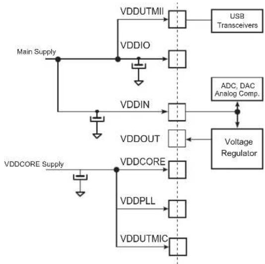
flowchart
graph TD
    A["Main Supply"] --> B["VDDOUTMII"]
    A --> C["VDDIO"]
    A --> D["VDDIN"]
    A --> E["VDDOUT"]
    F["VDDCORE Supply"] --> G["VDDCORE"]
    F --> H["VDDPLL"]
    F --> I["VDDUTMIC"]
    J["USB Transceivers"] --> K["Square Block"]
    L["ADC, DAC Analog Comp."] --> M["Square Block"]
    N["Voltage Regulator"] --> O["Square Block"]
    K --> P["Square Block"]
    M --> Q["Square Block"]
    O --> R["Square Block"]
Note: Restrictions
With main supply < 3.0V, USB is not usable.
With main supply < 2.7V, MediaLB is not usable.
With main supply < 2.0V, ADC, DAC and Analog comparator are not usable.
With main supply and VDDIN > 3V, all peripherals are usable.
When no separate backup supply for VDDIO is used, since the external voltage applied on VDDIO is kept, all of the I/O configurations (i.e., WKUP pin configuration) are maintained in Backup mode. When not using backup batteries, VDDIORDY is set so the user does not need to program it.
Figure 23-3. No Separate Backup Supply Powering Scheme
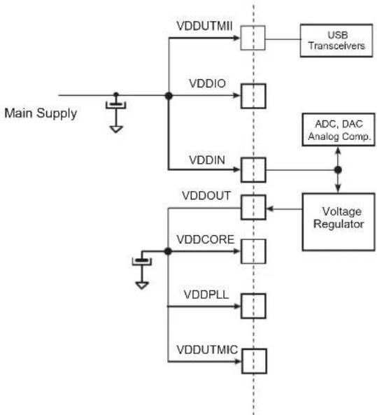
flowchart
graph TD
    A["Main Supply"] --> B["VDDUTMII"]
    A --> C["VDDIO"]
    A --> D["VDDIN"]
    B --> E["Square Block"]
    C --> F["Square Block"]
    D --> G["Square Block"]
    E --> H["USB Transceivers"]
    F --> I["Voltage Regulator"]
    G --> J["ADC, DAC Analog Comp."]
    K["VDDOUT"] --> L["Square Block"]
    M["VDDCORE"] --> N["Square Block"]
    O["VDDPLL"] --> P["Square Block"]
    Q["VDDUTMIC"] --> R["Square Block"]
Note: Restrictions
with main supply < 2.0 V, USB and ADC/DAC and analog comparator are not usable.
With main supply > 2.0V and < 3V, USB is not usable.
With main supply < 2.7V, MediaLB is not usable.
With main supply > 3V, all peripherals are usable.
The following figure illustrates an example of the powering scheme when using a backup battery. Since the PIO state is preserved when in Backup mode, any free PIO line can be used to switch off the external regulator by driving the PIO line at low level (PIO is input, pull-up enabled after backup reset). System wakeup can be performed using a wakeup pin (WKUPx). See the "Wakeup Sources" section for further details.
Figure 23-4. Battery Backup
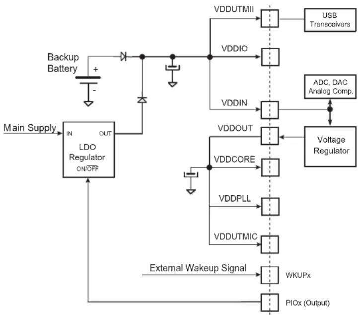
flowchart
graph TD
    A["Main Supply"] --> B["LDO Regulator ON/OFF"]
    B --> C["Backup Battery +"]
    C --> D["Ground"]
    D --> E["VDDUTMII"]
    E --> F["USB Transceivers"]
    B --> G["VDDIO"]
    G --> H["ADC, DAC Analog Comp."]
    B --> I["VDDIN"]
    I --> J["Voltage Regulator"]
    B --> K["VDDOUT"]
    K --> L["VDDCORE"]
    L --> M["VDDPLL"]
    M --> N["VDDUTMIC"]
    N --> O["External Wakeup Signal"]
    O --> P["WKUPx"]
    P --> Q["PLOx (Output)"]
    B --> R["OUT"]
    R --> S["Ground"]
Note: The two diodes provide a "switchover circuit" between the backup battery and the main supply when the system is put in Backup mode.
23.4.5 Supply Monitor
The SUPC embeds a supply monitor located in the VDDIO power supply and which monitors VDDIO power supply.
The supply monitor can be used to prevent the processor from falling into an unpredictable state if the main power supply drops below a certain level.
Note: The supply monitor is disabled by default.
The threshold of the supply monitor is programmable in the SMTH field of the Supply Monitor Mode register (SUPC_SMMR). Refer to the section "Electrical Characteristics".
The supply monitor can also be enabled during one slow clock period on every one of either 32, 256 or 2048 slow clock periods, depending on the user selection. This is configured in the SUPC_SMMR.SMSMPL.
Enabling the supply monitor for such reduced times divides the typical supply monitor power consumption by factors of 2, 16 and 128, respectively, if continuous monitoring of the VDDIO power supply is not required.
A supply monitor detection generates either a reset of the core power supply or a wakeup of the core power supply. Generating a core reset when a supply monitor detection occurs is enabled by setting SUPC_SMMR.SMRSTEN.
Waking up the core power supply when a supply monitor detection occurs can be enabled by setting the SMEN bit in the Wakeup Mode register (SUPC_WUMR).
The SUPC provides two status bits in the SUPC_SR for the supply monitor that determine whether the last wakeup was due to the supply monitor:
- SUPC_SR.SMOS provides real-time information, updated at each measurement cycle or updated at each slow clock cycle, if the measurement is continuous.
- SUPC_SR.SMS provides saved information and shows a supply monitor detection has occurred since the last read of SUPC_SR.
The SMS flag generates an interrupt if SUPC_SMMR.SMIEN is set.
Figure 23-5. Supply Monitor Status Bit and Associated Interrupt
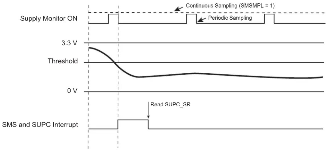
line
| Signal Type | Value | | ----------------------- | --------- | | Continuous Sampling | 1 | | Periodic Sampling | 1 | | Read SUPC_SR | SR |Related Links
- Electrical Characteristics for SAM V70/V71
- Electrical Characteristics for SAM E70/S70
23.4.6 Backup Power Supply Reset
23.4.6.1 Raising the Backup Power Supply
When the backup voltage VDDIO rises, the slow RC oscillator is powered up and the zero-power power-on reset cell maintains its output low as long as VDDIO has not reached its target voltage. During this period, the SUPC is reset. When the VDDIO voltage becomes valid and the zero-power power-on reset signal is released, a counter is started for five slow clock cycles. This is the time required for the slow RC oscillator to stabilize.
After this time, the voltage regulator is enabled. The core power supply rises and the brownout detector provides the bodcore_in signal as soon as the core voltage VDDCORE is valid. This results in releasing the vddcore_nreset signal to the Reset Controller after the bodcore_in signal has been confirmed as being valid for at least one slow clock cycle.
Figure 23-6. Raising the VDDIO Power Supply

other
| Signal Signal | Description | | ------------- | ----------- | | Backup Power Supply | Zero-Power POR | | Zero-Power Power-On Reset Cell output | (Not labeled) | | 22 - 42 kHz Slow RC Oscillator output | (Not labeled) | | vr_on | (Not labeled) | | Core Power Supply | (Not labeled) | | Fast RC Oscillator output | (Not labeled) | | bodcore_in | (Not labeled) | | vddcore_nreset | (Not labeled) | | NRST (no ext. drive assumed) | (Not labeled) | | periph_nreset | (Not labeled) | | proc_nreset | (Not labeled) |Note: After "proc_nreset" rising, the core starts fetching instructions from Flash.
23.4.7 Core Reset
The Supply Controller manages the vddcore_nreset signal to the Reset Controller, as described in the "Backup Power Supply Reset" section. The vddcore_nreset signal is normally asserted before shutting down the core power supply and released as soon as the core power supply is correctly regulated.
There are two additional sources which can be programmed to activate vddcore_nreset:
• a supply monitor detection
• a brownout detection
23.4.7.1 Supply Monitor Reset
The supply monitor is capable of generating a reset of the system. This is enabled by setting SUPC_SMMR.SMRSTEN.
If SUPC_SMMR.SMRSTEN is set and if a supply monitor detection occurs, the vddcore_nreset signal is immediately activated for a minimum of one slow clock cycle.
23.4.7.2 Brownout Detector Reset
The brownout detector provides the bodcore_in signal to the SUPC. This signal indicates that the voltage regulation is operating as programmed. If this signal is lost for longer than 1 slow clock period while the voltage regulator is enabled, the SUPC asserts vddcore_nreset if SUPC_MR.BODRSTEN is written to '1'.
If SUPC_MR.BODRSTEN is set and the voltage regulation is lost (output voltage of the regulator too low), the vddcore_nreset signal is asserted for a minimum of one slow clock cycle and then released if bodcore_in has been reactivated. SUPC_SR.BODRSTS indicates the source of the last reset.
Until bodcore_in is deactivated, the vddcore_nreset signal remains active.
23.4.8 Controlling the SRAM Power Supply
The SUPC can be used to switch on or off the power supply of the backup SRAM by opening or closing the SRAM power switch. This power switch is controlled by SUPC_MR.BKUPRETON. However, the battery backup SRAM is automatically switched on when the core power supply is enabled, as the processor requires the SRAM as data memory space.
- If SUPC_MR.BKUPRETON is written to '1', there is no immediate effect, but the SRAM will be left powered when the SUPC enters Backup mode, thus retaining its content.
- If SUPC_MR.BKUPRETON is written to '0', there is no immediate effect, but the SRAM will be switched off when the SUPC enters Backup mode. The SRAM is automatically switched on when Backup mode is exited.
23.4.9 Wakeup Sources
The wakeup events allow the device to exit Backup mode. When a wakeup event is detected, the SUPC performs a sequence that automatically reenables the core power supply.
Figure 23-7. Wakeup Sources
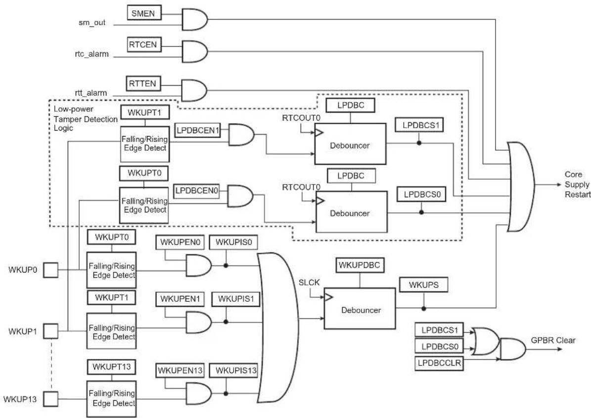
flowchart
graph TD
    subgraph Low-power Tamper Detection Logic
        A["SMEN"] --> B["AND"]
        C["RTCEN"] --> D["AND"]
        E["rtt_alarm"] --> F["AND"]
        G["Low-power Tamper Detection Logic"] --> H["WKUPT1"]
        H --> I["Falling/Rising Edge Detect"]
        I --> J["LPDBCEN1"]
        J --> K["AND"]
        L["LTTCOUT0"] --> M["Debouncer"]
        N["LTTCOUT0"] --> O["Debouncer"]
        P["LPDBC"] --> Q["LPDBCS1"]
        R["LPDBC"] --> S["LPDBCS0"]
    end

    subgraph Core Supply Restart
        T["Core Supply Restart"] --> U["Output"]
    end

    V["SWKUP0"] --> W["Falling/Rising Edge Detect"]
        W --> X["WKUPT0"]
        X --> Y["Falling/Rising Edge Detect"]
        Y --> Z["WKUPT1"]
        Z --> AA["Falling/Rising Edge Detect"]
        AA --> AB["WKUPT13"]
        AB --> AC["Falling/Rising Edge Detect"]
        AC --> AD["WKUPT13"]
    end

    subgraph GPBR Clear
        AE["GPBR Clear"] --> AF["Output"]
    end

    AG["SLCK"] --> AH["Debouncer"]
    AH --> AI["DEBouncer"]
    AI --> AJ["LPDBCS1"]
    AI --> AK["LPDBCS0"]
    AI --> AL["LPDBCCLR"]
    AJ --> AM["AND"]
    AK --> AN["AND"]
    AL --> AO["AND"]
    AP["RTTCOUT0"] --> AQ["Debouncer"]
    AQ --> AR["LPDBC"]
    AQ --> AS["LPDBCS0"]
    AQ --> AT["LPDBCS1"]
    AQ --> AU["LPDBCS0"]
    AQ --> AV["LPDBCCLR"]
    AW["SWKUP0"] --> AX["Falling/Rising Edge Detect"]
        AX --> AY["WKUPT0"]
        AY --> AZ["Falling/Rising Edge Detect"]
        AZ --> BA["WKUPT1"]
        BA --> BB["Falling/Rising Edge Detect"]
        BB --> BC["WKUPT13"]
        BC --> BD["Falling/Rising Edge Detect"]
        BD --> BE["WKUPT13"]
    end

    style Low-power Tamper Detection Logic fill:#f9f,stroke:#333
    style GPBR Clear fill:#ccf,stroke:#333
23.4.9.1 Wakeup Inputs
The wakeup inputs, WKUPx, can be programmed to perform a wakeup of the core power supply. Each input can be enabled by writing a '1' to the corresponding bit, WKUPENx, in the Wakeup Inputs register (SUPC_WUIR). The wakeup level can be selected with the corresponding polarity bit, WKUPTx, also located in SUPC_WUIR.
The resulting signals are wired-ORed to trigger a debounce counter, which is programmed with SUPC_WUMR.WKUPDBC. This field selects a debouncing period of 3, 32, 512, 4,096 or 32,768 slow clock cycles. The duration of these periods corresponds, respectively, to about 100 s, about 1 ms, about 16 ms, about 128 ms and about 1 second (for a typical slow clock frequency of 32 kHz). Programming SUPC_WUMR.WKUPDBC to 0 selects an immediate wakeup, i.e., an enabled WKUP pin must be active according to its polarity during a minimum of one slow clock period to wake up the core power supply.
If an enabled WKUP pin is asserted for a duration longer than the debouncing period, a wakeup of the core power supply is started and the signals, WKUP0 to WKUPx as shown in "Wakeup Sources", are latched in SUPC_SR. This allows the user to identify the source of the wakeup. However, if a new wakeup condition occurs, the primary information is lost. No new wakeup can be detected since the primary wakeup condition has disappeared.
Before instructing the system to enter Backup mode, if the field SUPC_WUMR.WKUPDBC > 0, it must be checked that none of the WKUPx pins that are enabled for a wakeup (exit from Backup mode) holds an active polarity. This is checked by reading the pin status in the PIO Controller. If SUPC_WUIR.WKUPENx=1 and the pin WKUPx holds an active polarity, the system must not be instructed to enter Backup mode.
Figure 23-8. Entering and Exiting Backup Mode with a WKUP Pin
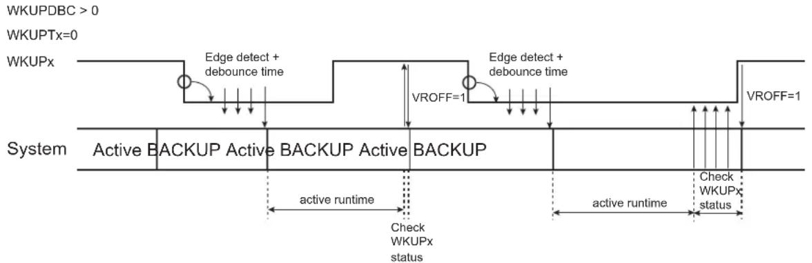
flowchart
graph TD
    A["WKUPDBC > 0"] --> B["WKUPTx=0"]
    B --> C["WKUPx"]
    C --> D["Edge detect + debounce time"]
    D --> E["VROFF=1"]
    E --> F["Edge detect + debounce time"]
    F --> G["VROFF=1"]
    G --> H["System"]
    H --> I["Active BACKUP Active BACKUP Active BACKUP"]
    I --> J["check WKUPx status"]
    J --> K["Active runtime"]
    K --> L["Check WKUPx status"]
    L --> M["Active runtime"]
    M --> N["Check WKUPx status"]
23.4.9.2 Low-power Tamper Detection and Anti-Tampering
Low-power debouncer inputs (WKUP0, WKUP1) can be used for tamper detection. If the tamper sensor is biased through a resistor and constantly driven by the power supply, this leads to power consumption as long as the tamper detection switch is in its active state. To prevent power consumption when the switch is in active state, the tamper sensor circuitry must be intermittently powered, and thus a specific waveform must be applied to the sensor circuitry.
The waveform is generated using RTCOUTx in all modes including Backup mode. Refer to the section "Real-Time Clock (RTC)" for waveform generation.
Separate debouncers are embedded, one for WKUP0 input, one for WKUP1 input.
The WKUP0 and/or WKUP1 inputs perform a system wakeup upon tamper detection. This is enabled by setting SUPC_WUMR.LPDBCEN0/1.
WKUP0 and/or WKUP1 inputs can also be used when VDDCORE is powered to detect a tamper.
When SUPC_WUMR.LPDBCENx is written to '1', WKUPx pins must not be configured to act as a debouncing source for the WKUPDBC counter (WKUPENx must be cleared in SUPC_WUIR).
Low-power tamper detection or debounce requires RTC output (RTCOUTx) to be configured to generate a duty cycle programmable pulse (i.e., OUT0 = 0x7 in RTC_MR) in order to create the sampling points of both debouncers. The sampling point is the falling edge of the RTCOUTx waveform.
The following figure shows an example of an application where two tamper switches are used. RTCOUTx powers the external pull-up used by the tamper sensor circuitry.
Figure 23-9. Low-power Debouncer (Push-to-Make Switch, Pull-up Resistors)

text_image
MCU RTCOUTx Pull-up Resistor WKUP0 Pull-up Resistor WKUP1 GND GNDFigure 23-10. Low-power Debouncer (Push-to-Break Switch, Pull-down Resistors)

text_image
MCU RTCOUTx WKUP0 WKUP1 GND Pull-down Resistors GND GNDThe debouncing period duration is configurable. The period is set for all debouncers (i.e., the duration cannot be adjusted for each debouncer). The number of successive identical samples to wake up the system can be configured from 2 up to 8 in SUPC_WUMR.LPDBC. The period of time between two samples can be configured by programming RTC_MR.TPERIOD. Power parameters can be adjusted by modifying the period of time in RTC_MR.THIGH.
The wakeup polarity of the inputs can be independently configured by writing SUPC_WUMR.WKUPT0 and/or SUPC_WUMR.WKUPT1.
In order to determine which wakeup/tamper pin triggers the system wakeup, a status flag is associated for each low-power debouncer. These flags are read in SUPC_SR.
A debounce event (tamper detection) can perform an immediate clear (0 delay) on the first half the general-purpose backup registers (GPBR). SUPC_WUMR.LPDBCCLR bit must be set.
Note that it is not mandatory to use the RTCOUTx pin when using the WKUP0/WKUP1 pins as tampering inputs in any mode. Using the RTCOUTx pin provides a "sampling mode" to further
reduce the power consumption of the tamper detection circuitry. If RTCOUTx is not used, the RTC must be configured to create an internal sampling point for the debouncer logic. The period of time between two samples can be configured by programming RTC_MR.TPERIOD.
The following figure illustrates the use of WKUPx without the RTCOUTx pin.
Figure 23-11. Using WKUP Pins Without RTCOUTx Pins
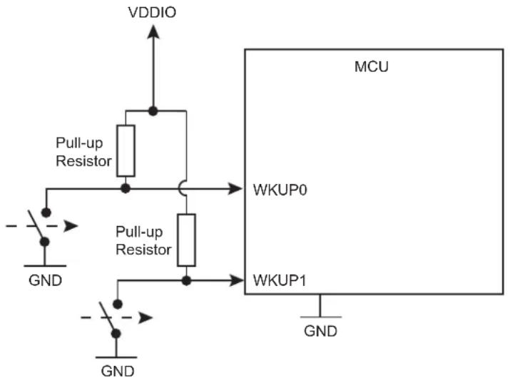
text_image
VDDIO Pull-up Resistor GND Pull-up Resistor MCU WKUP0 WKUP1 GNDRelated Links
27. Real-time Clock (RTC)
23.4.9.3 Clock Alarms
The RTC and the RTT alarms can generate a wakeup of the core power supply. This can be enabled by setting, respectively, SUPC_WUMR.RTCEN and SUPC_WUMR.RTTEN.
The Supply Controller does not provide any status as the information is available in the user interface of either the Real-Time Timer or the Real-Time Clock.
23.4.9.4 Supply Monitor Detection
The supply monitor can generate a wakeup of the core power supply. See "Supply Monitor".
23.4.10 Register Write Protection
To prevent any single software error from corrupting SYSC behavior, certain registers in the address space can be write-protected by setting the WPEN bit in the "System Controller Write Protection Mode Register" (SYSC_WPMR).
The following registers can be write-protected:
- RSTC Mode Register (1)
- RTT Mode Register (2)
- RTT Alarm Register (2)
- RTC Control Register (3)
- RTC Mode Register (3)
• RTC Time Alarm Register (3)
• RTC Calendar Alarm Register (3) - General Purpose Backup Registers (4)
• Supply Controller Control Register
• Supply Controller Supply Monitor Mode Register
• Supply Controller Mode Register
• Supply Controller Wakeup Mode Register
• Supply Controller Wakeup Inputs Register
Notes:
- See the section "Reset Controller (RSTC)".
- See the section "Real Time Timer (RTT)".
- See the section "Real Time Clock (RTC)".
- See the section "General Purpose Backup Registers (GPBR)".
23.4.11 Register Bits in Backup Domain (VDDIO)
The following configuration registers, or certain bits of the registers, are physically located in the product backup domain:
• RSTC Mode Register (all bits) (1)
• RTT Mode Register (all bits) ^(2)
• RTT Alarm Register (all bits) ^(2)
• RTC Control Register (all bits) ^(3)
• RTC Mode Register (all bits) ^(3)
- RTC Time Alarm Register (all bits) ^(3)
• RTC Calendar Alarm Register (all bits) ^(3)
- General Purpose Backup Registers (all bits) ^(4)
• Supply Controller Control Register (see register description for details)
• Supply Controller Supply Monitor Mode Register (all bits)
• Supply Controller Mode Register (see register description for details)
• Supply Controller Wakeup Mode Register (all bits)
• Supply Controller Wakeup Inputs Register (all bits)
• Supply Controller Status Register (all bits)
Notes:
- See the section "Reset Controller (RSTC)".
- See the section "Real Time Timer (RTT)".
- See the section "Real Time Clock (RTC)".
- See the section "General Purpose Backup Registers (GPBR)".
23.5 Register Summary
| Offset | Name Bit Pos. 7 | 6 | 5 | 4 | 3 | 2 | 1 | 0 | |||||||||||||||||||||||||||||||||||||||||||||||||||||||||||||||||||||||||||||||||||||||||||||||||||||||||||||||||||||||||||||||||||||||||||||||||||||||||||||||||||||||||||||||||||||||||||||||||||||||||||||||||||
| 0x00 | SUPC_CR | 7:0 | XTALSEL VROFF | 0x00 SUPC_SMMR | |||||||||||||||||||||||||||||||||||||||||||||||||||||||||||||||||||||||||||||||||||||||||||||||||||||||||||||||||||||||||||||||||||||||||||||||||||||||||||||||||||||||||||||||||||||||||||||||||||||||||||||||||||||||
| 15:8 | 0x04 SUPC_SMMR | ||||||||||||||||||||||||||||||||||||||||||||||||||||||||||||||||||||||||||||||||||||||||||||||||||||||||||||||||||||||||||||||||||||||||||||||||||||||||||||||||||||||||||||||||||||||||||||||||||||||||||||||||||||||||||
| 23:16 | 0x08 SUPC_MR | ||||||||||||||||||||||||||||||||||||||||||||||||||||||||||||||||||||||||||||||||||||||||||||||||||||||||||||||||||||||||||||||||||||||||||||||||||||||||||||||||||||||||||||||||||||||||||||||||||||||||||||||||||||||||||
| 31:24 KEY[7:0] | |||||||||||||||||||||||||||||||||||||||||||||||||||||||||||||||||||||||||||||||||||||||||||||||||||||||||||||||||||||||||||||||||||||||||||||||||||||||||||||||||||||||||||||||||||||||||||||||||||||||||||||||||||||||||||
| 0x004 | 7:0 | SMTH[3:0] | 0x004 SUPC_SMMR | ||||||||||||||||||||||||||||||||||||||||||||||||||||||||||||||||||||||||||||||||||||||||||||||||||||||||||||||||||||||||||||||||||||||||||||||||||||||||||||||||||||||||||||||||||||||||||||||||||||||||||||||||||||||||
| 15:8 | SMIEN SMRSTEN | SMSMPL[2:0] | |||||||||||||||||||||||||||||||||||||||||||||||||||||||||||||||||||||||||||||||||||||||||||||||||||||||||||||||||||||||||||||||||||||||||||||||||||||||||||||||||||||||||||||||||||||||||||||||||||||||||||||||||||||||||
| 23:16 | |||||||||||||||||||||||||||||||||||||||||||||||||||||||||||||||||||||||||||||||||||||||||||||||||||||||||||||||||||||||||||||||||||||||||||||||||||||||||||||||||||||||||||||||||||||||||||||||||||||||||||||||||||||||||||
| 31:24 | 0x004 SUPC_MR | ||||||||||||||||||||||||||||||||||||||||||||||||||||||||||||||||||||||||||||||||||||||||||||||||||||||||||||||||||||||||||||||||||||||||||||||||||||||||||||||||||||||||||||||||||||||||||||||||||||||||||||||||||||||||||
| 0x08 | 7:0 | ONREG BODDIS BODRSTEN | 0x004 SUPC_MR | ||||||||||||||||||||||||||||||||||||||||||||||||||||||||||||||||||||||||||||||||||||||||||||||||||||||||||||||||||||||||||||||||||||||||||||||||||||||||||||||||||||||||||||||||||||||||||||||||||||||||||||||||||||||||
| 15:8 | OSCBYPASS | BKUPRETON | |||||||||||||||||||||||||||||||||||||||||||||||||||||||||||||||||||||||||||||||||||||||||||||||||||||||||||||||||||||||||||||||||||||||||||||||||||||||||||||||||||||||||||||||||||||||||||||||||||||||||||||||||||||||||
| OSCBYPASS | BKUPRETON | ||||||||||||||||||||||||||||||||||||||||||||||||||||||||||||||||||||||||||||||||||||||||||||||||||||||||||||||||||||||||||||||||||||||||||||||||||||||||||||||||||||||||||||||||||||||||||||||||||||||||||||||||||||||||||
| 31:24 KEY[7:0] | |||||||||||||||||||||||||||||||||||||||||||||||||||||||||||||||||||||||||||||||||||||||||||||||||||||||||||||||||||||||||||||||||||||||||||||||||||||||||||||||||||||||||||||||||||||||||||||||||||||||||||||||||||||||||||
| 0x00C | SUPC_WUMR | 7:0 | LPDBCCLR | LPDBCEN1 | LPDBCENO | RTCEN | RTTEN | SMEN | 0x00C | ||||||||||||||||||||||||||||||||||||||||||||||||||||||||||||||||||||||||||||||||||||||||||||||||||||||||||||||||||||||||||||||||||||||||||||||||||||||||||||||||||||||||||||||||||||||||||||||||||||||||||||||||||
| 15:8 | WKUPDBC[2:0] | RTCEN | RTTEN | SMEN | 0x00C | ||||||||||||||||||||||||||||||||||||||||||||||||||||||||||||||||||||||||||||||||||||||||||||||||||||||||||||||||||||||||||||||||||||||||||||||||||||||||||||||||||||||||||||||||||||||||||||||||||||||||||||||||||||||
| 23:16 | LPDBC[2:0] | RTCEN | RTTEN | SMEN | 0x00C | ||||||||||||||||||||||||||||||||||||||||||||||||||||||||||||||||||||||||||||||||||||||||||||||||||||||||||||||||||||||||||||||||||||||||||||||||||||||||||||||||||||||||||||||||||||||||||||||||||||||||||||||||||||||
| 31:24 | WKUPEN[7:0] | RTTEN | SMEN | 0x10 | SUPC_WUIR | ||||||||||||||||||||||||||||||||||||||||||||||||||||||||||||||||||||||||||||||||||||||||||||||||||||||||||||||||||||||||||||||||||||||||||||||||||||||||||||||||||||||||||||||||||||||||||||||||||||||||||||||||||||||
| 0x10 | SUPC_WUIR | 7:0 | WKUPEN[7:0] | ||||||||||||||||||||||||||||||||||||||||||||||||||||||||||||||||||||||||||||||||||||||||||||||||||||||||||||||||||||||||||||||||||||||||||||||||||||||||||||||||||||||||||||||||||||||||||||||||||||||||||||||||||||||||
| 15:8 | WKUPEN[13:8] | ||||||||||||||||||||||||||||||||||||||||||||||||||||||||||||||||||||||||||||||||||||||||||||||||||||||||||||||||||||||||||||||||||||||||||||||||||||||||||||||||||||||||||||||||||||||||||||||||||||||||||||||||||||||||||
| 23:16 | WKUPT[7:0] | ||||||||||||||||||||||||||||||||||||||||||||||||||||||||||||||||||||||||||||||||||||||||||||||||||||||||||||||||||||||||||||||||||||||||||||||||||||||||||||||||||||||||||||||||||||||||||||||||||||||||||||||||||||||||||
| 31:24 | WKUPT[13:8] | ||||||||||||||||||||||||||||||||||||||||||||||||||||||||||||||||||||||||||||||||||||||||||||||||||||||||||||||||||||||||||||||||||||||||||||||||||||||||||||||||||||||||||||||||||||||||||||||||||||||||||||||||||||||||||
| 0x14 | SUPC_SR | 7:0 | OSCSEL | SMOS | SMS | SMRSTS | BODRSTS | SMWS | WKUPS | 0x14 | SUPC_SR | Reserved | |||||||||||||||||||||||||||||||||||||||||||||||||||||||||||||||||||||||||||||||||||||||||||||||||||||||||||||||||||||||||||||||||||||||||||||||||||||||||||||||||||||||||||||||||||||||||||||||||||||||||||||||
| 15:8 | LPDBCS1 | LPDBCS0 | WKUPIS[7:0] | WKUPIS[13:8] | WKUPIS[7:0] | WKUPIS[13:8] | WKUPIS[7:0] | WKUPIS[13:8] | WKUPIS[7:0] | WKUPIS[13:8] | WKUPIS[7:0] | WKUPIS[13:8] | WKUPIS[7:0] | WKUPIS[13:8] | WKUPIS | WKUPIS[7:0] | WKUPIS[13:8] | WKUPIS[7:0] | WKUPIS[13:8] | WKUPIS[7:0] | WKUPIS[13:8] | WKUPIS[7:0] | WKUPIS[13:8] | WKUPIS[7:0] | WKUPIS[13:8] | WKUPIS [7:0] | WKUPIS[13:8] | WKUPIS[13:8] | WKUPIS[13:8] | WKUPIS[13:8] | WKUPIS[13:8] | WKUPIS[13:8] | WKUPIS[13:8] | WKUPIS[13:8] | WKUPIS[13:8] | WKUPIS[13:8] | WKUPIS[13:18] | WKUPIS[13:8] | WKUPIS[13:8] | WKUPIS[13:8] | WKUPIS[13:8] | WKUPIS[13:8] | WKUPIS[13:8] | WKUPIS[13:8] | WKUPIS[13:8] | WKUPIS[13:8] | WKUPIS[13;8] | WKUPIS[13:8] | WKUPIS[13:8] | WKUPIS[13:8] | WKUPIS[13:8] | WKUPIS[13:8] | WKUPIS[13:8] | WKUPIS[13:8] | WKUPIS[13:8] | WKUPIS[13:8] | WKUPIS[13 :8] | WKUPIS[13:8] | WKUPIS[13:8] | WKUPIS[13:8] | WKUPIS[13:8] | WKUPIS[13:8] | WKUPIS[13:8] | WKUPIS[13:8] | WKUPIS[13:8] | WKUPIS[13:8] | WKUPIS[13 8] | WKUPIS[13:8] | WKUPIS[13:8] | WKUPIS[13:8] | WKUPIS[13:8] | WKUPIS[13:8] | WKUPIS[13:8] | WKUPIS[13:8] | WKUPIS[13:8] | WKUPIS[13:8] | WKUPIS[13.8] | WKUPIS[13:8] | WKUPIS[13:8] | WKUPIS[13:8] | WKUPIS[13:8] | WKUPIS[13:8] | WKUPIS[13:8] | WKUPIS[13:8] | WKUPIS[13:8] | WKUPIS[13:8] | WKUPIS[13-8] | WKUPIS[13:8] | WKUPIS[13:8] | WKUPIS[13:8] | WKUPIS[13:8] | WKUPIS[13:8] | WKUPIS[13:8] | WKUPIS[13:8] | WKUPIS[13:8] | WKUPIS[13:8] | WKUPIS[13/8] | WKUPIS[13:8] | WKUPIS[13:8] | WKUPIS[13:8] | WKUPIS[13:8] | WKUPIS[13:8] | WKUPIS[13:8] | WKUPIS[13:8] | WKUPIS[13:8] | WKUPIS[13:8] | WKUPIS[13 /8] | WKUPIS[13:8] | WKUPIS[13:8] | WKUPIS[13:8] | WKUPIS[13:8] | WKUPIS[13:8] | WKUPIS[13:8] | WKUPIS[13:8] | WKUPIS[13:8] | WKUPIS[13:8] | WKUPIS[13 -8] | WKUPIS[13:8] | WKUPIS[13:8] | WKUPIS[13:8] | WKUPIS[13:8] | WKUPIS[13:8] | WKUPIS[13:8] | WKUPIS[13:8] | WKUPIS[13:8] | WKUPIS[13:8] | WKUPIS[13,8] | WKUPIS[13:8] | WKUPIS[13:8] | WKUPIS[13:8] | WKUPIS[13:8] | WKUPIS[13:8] | WKUPIS[13:8] | WKUPIS[13:8] | WKUPIS[13:8] | WKUPIS[13:8] | WKUPIS[13(8)] | WKUPIS[13:8] | WKUPIS[13:8] | WKUPIS[13:8] | WKUPIS[13:8] | WKUPIS[13:8] | WKUPIS[13:8] | WKUPIS[13:8] | WKUPIS[13:8] | WKUPIS[13:8] | WKUPIS[13:8][13:8] | WKUPIS[13:8] | WKUPIS[13:8] | WKUPIS[13:8] | WKUPIS[13:8] | WKUPIS[13:8] | WKUPIS[13:8] | WKUPIS[13:8] | WKUPIS[13:8] | WKUPIS[13:8] | WKUPIS [13:8] | WKUPIS[13:8] | WKUPIS[13:8] | WKUPIS[13:8] | WKUPIS[13:8] | WKUPIS[13:8] | WKUPIS[13:8] | WKUPIS[13:8] | WKUPIS[13:8] | WKUPIS[13:8] | WKUPIS | WKUPIS[13:8] | WKUPIS[13:8] | WKUPIS[13:8] | WKUPIS[13:8] | WKUPIS[13:8] | WKUPIS[13:8] | WKUPIS[13:8] | WKUPIS[13:8] | WKUPIS[13:8] | WKUPIS[13:8 13:8] | WKUPIS[13:8] | WKUPIS[13:8] | WKUPIS[13:8] | WKUPIS[13:8] | WKUPIS[13:8] | WKUPIS[13:8] | WKUPIS[13:8] | WKUPIS[13:8] | WKUPIS[13:8] | WKUPIS 13:8 13:8] | WKUPIS[13:8] | WKUPIS[13:8] | WKUPIS[13:8] | WKUPIS[13:8] | WKUPIS[13:8] | WKUPIS[13:8] | WKUPIS[13:8] | WKUPIS[13:8] | WKUPIS[13:8 13:8 13:8] | WKUPIS[13:8] | WKUPIS[13:8] | WKUPIS[13:8] | WKUPIS[13:8] | WKUPIS[13:8] | WKUPIS[13:8] | WKUPIS[13:8] | WKUPIS[13:8] | WKUPIS[13: 13:8 13:8] | WKUPIS[13:8] | WKUPIS[13:8] | WKUPIS[13:8] | WKUPIS[13:8] | WKUPIS[13:8] | WKUPIS[13:8] | WKUPIS[13:8] | WKUPIS[13:8] | WKUPIS[13: | |||||
23.5.1 Supply Controller Control Register
Name: SUPC_CR
Offset: 0x00
Property: Write-only

text_image
Bit 31 30 29 28 27 26 25 24 KEY[7:0] Access W W W W W W W W Reset Bit 23 22 21 20 19 18 17 16 Access Reset Bit 15 14 13 12 11 10 9 8 Access Reset Bit 7 6 5 4 3 2 1 0 Access Reset XTALSEL VROFF W WBits 31:24 - KEY[7:0] Password
| Value | Name | Description |
| 0xA5 | PASSWD | Writing any other value in this field aborts the write operation. |
Bit 3 - XTALSEL Crystal Oscillator Select
Note: This bit is located in the VDDIO domain.
| Value | Description |
| 0 | (NO_EFFECT): No effect. |
| 1 | (CRYSTAL_SEL): If KEY is correct, XTALSEL switches the slow clock on the 32.768 kHz crystal oscillator output. |
Bit 2 - VROFF Voltage Regulator Off
Note: This bit is located in the VDDIO domain.
| Value | Description |
| 0 | (NO_EFFECT): No effect. |
| 1 | (STOP_VREG): If KEY is correct, VROFF asserts the vddcore_nreset and stops the voltage regulator. |
23.5.2 Supply Controller Supply Monitor Mode Register
Name: SUPC_SMMR
Offset: 0x04
Reset: 0x00000000
Property: Read/Write
This register is located in the VDDIO domain.

Bit 13 - SMIEN Supply Monitor Interrupt Enable
| Value | Description |
| 0 | (NOT_ENABLE): The SUPC interrupt signal is not affected when a supply monitor detection occurs. |
| 1 | (ENABLE): The SUPC interrupt signal is asserted when a supply monitor detection occurs. |
Bit 12 - SMRSTEN Supply Monitor Reset Enable
| Value | Description |
| 0 | (NOT_ENABLE): The core reset signal vddcore_nreset is not affected when a supply monitor detection occurs. |
| 1 | (ENABLE): The core reset signal, vddcore_nreset is asserted when a supply monitor detection occurs. |
Bits 10:8 - SMSMPL[2:0] Supply Monitor Sampling Period
| Value | Name | Description |
| 0x0 | SMD | Supply Monitor disabled |
| 0x1 | CSM | Continuous Supply Monitor |
| 0x2 | 32SLCK | Supply Monitor enabled one SLCK period every 32 SLCK periods |
| 0x3 | 256SLCK | Supply Monitor enabled one SLCK period every 256 SLCK periods |
| 0x4 | 2048SLCK | Supply Monitor enabled one SLCK period every 2,048 SLCK periods |
Bits 3:0 - SMTH[3:0] Supply Monitor Threshold
Selects the threshold voltage of the supply monitor. Refer to the section "Electrical Characteristics" for voltage values.
Related Links
- Electrical Characteristics for SAM V70/V71
23.5.3 Supply Controller Mode Register
Name: SUPC_MR
Offset: 0x08
Reset: 0x00005A00
Property: Read/Write

text_image
Bit 31 30 29 28 27 26 25 24 KEY[7:0] Access R/W R/W R/W R/W R/W R/W R/W Reset 0 0 0 0 0 0 0 0 Bit 23 22 21 20 19 18 17 16 OSC BYPASS BKUPRETON R/W R/W Access R/W Reset 0 0 Bit 15 14 13 12 11 10 9 8 Access ONREG BODDIS BODRSTEN R/W R/W R/W Reset 1 0 1 Bit 7 6 5 4 3 2 1 0 Access ResetBits 31:24 - KEY[7:0] Password Key
| Value | Name | Description |
| 0xA5 | PASSWD | Writing any other value in this field aborts the write operation. |
Bit 20 - OSCBYPASS Oscillator Bypass
Note: This bit is located in the VDDIO domain.
| Value | Description |
| 0 | (NO_EFFECT): No effect. Clock selection depends on the value of SUPC_CR.XTALSEL. |
| 1 | (BYPASS): The 32.768 kHz crystal oscillator is bypassed if SUPC_CR.XTALSEL is set. OSCBYPASS must be set prior to setting XTALSEL. |
Bit 17 - BKUPRETON SRAM On In Backup Mode
| Value | Description |
| 0 | SRAM (Backup) switched off in Backup mode. |
| 1 | SRAM (Backup) switched on in Backup mode.Note: This bit is located in the VDDIO domain. |
Bit 14 - ONREG Voltage Regulator Enable
Note: This bit is located in the VDDIO domain.
| Value | Description |
| 0 | (ONREG_UNUSED): Internal voltage regulator is not used (external power supply is used). |
| 1 | (ONREG_USED): Internal voltage regulator is used. |
| Value Description | |
| 0 | (ENABLE): The core brownout detector is enabled. |
| 1 | (DISABLE): The core brownout detector is disabled. |
Bit 13 - BODDIS Brownout Detector Disable
Note: This bit is located in the VDDIO domain.
Bit 12 - BODRSTEN Brownout Detector Reset Enable Note: This bit is located in the VDDIO domain.
| Value Description | |
| 0 | (NOT_ENABLE): The core reset signal vddcore_nreset is not affected when a brownout detection occurs. |
| 1 | (ENABLE): The core reset signal, vddcore_nreset is asserted when a brownout detection occurs. |
23.5.4 Supply Controller Wakeup Mode Register
Name: SUPC_WUMR
Offset: 0x0C
Reset: 0x00000000
Property: Read/Write
This register is located in the VDDIO domain.

text_image
Bit 31 30 29 28 27 26 25 24 Access Reset Bit 23 22 21 20 19 18 17 16 LPDBC[2:0] Access R/W R/W R/W Reset 0 0 0 Bit 15 14 13 12 11 10 9 8 WKUPDBC[2:0] Access R/W R/W R/W Reset 0 0 0 Bit 7 6 5 4 3 2 1 0 LPDBCCLR LPDBCEN1 LPDBCENO Access R/W R/W R/W R/W R/W R/W Reset 0 0 0 0 0 0 R/W R/W R/W RTCEN RTTEN SMENBits 18:16 - LPDBC[2:0] Low-power Debouncer Period
| Value | Name | Description |
| 0 | DISABLE | Disables the low-power debouncers. |
| 1 | 2_RTCOUT | WKUP0/1 in active state for at least 2 RTCOUTx clock periods |
| 2 | 3_RTCOUT | WKUP0/1 in active state for at least 3 RTCOUTx clock periods |
| 3 | 4_RTCOUT | WKUP0/1 in active state for at least 4 RTCOUTx clock periods |
| 4 | 5_RTCOUT | WKUP0/1 in active state for at least 5 RTCOUTx clock periods |
| 5 | 6_RTCOUT | WKUP0/1 in active state for at least 6 RTCOUTx clock periods |
| 6 | 7_RTCOUT | WKUP0/1 in active state for at least 7 RTCOUTx clock periods |
| 7 | 8_RTCOUT | WKUP0/1 in active state for at least 8 RTCOUTx clock periods |
Bits 14:12 - WKUPDBC[2:0] Wakeup Inputs Debouncer Period
| Value | Name | Description |
| 0 | IMMEDIATE | Immediate, no debouncing, detected active at least on one Slow Clock edge. |
| 1 | 3_SLCK | WKUPx shall be in its active state for at least 3 SLCK periods |
| 2 | 32_SLCK | WKUPx shall be in its active state for at least 32 SLCK periods |
| 3 | 512_SLCK | WKUPx shall be in its active state for at least 512 SLCK periods |
| 4 | 4096_SLCK | WKUPx shall be in its active state for at least 4,096 SLCK periods |
| 5 | 32768_SLCK | WKUPx shall be in its active state for at least 32,768 SLCK periods |
Bit 7 - LPDBCCLR Low-power Debouncer Clear
| Value | Description |
| 0 | (NOT_ENABLE): A low-power debounce event does not create an immediate clear on the first half of GPBR registers. |
| 1 | (ENABLE): A low-power debounce event on WKUP0 or WKUP1 generates an immediate clear on the first half of GPBR registers. |
Bit 6 - LPDBCEN1 Low-power Debouncer Enable WKUP1
| Value Description | |
| 0 | (NOT_ENABLE): The WKUP1 input pin is not connected to the low-power debouncer. |
| 1 | (ENABLE): The WKUP1 input pin is connected to the low-power debouncer and forces a system wakeup. |
Bit 5 - LPDBCENO Low-power Debouncer Enable WKUP0
| Value Description | |
| 0 | (NOT_ENABLE): The WKUP0 input pin is not connected to the low-power debouncer. |
| 1 | (ENABLE): The WKUP0 input pin is connected to the low-power debouncer and forces a system wakeup. |
Bit 3 - RTCEN Real-time Clock Wakeup Enable
| Value Description | |
| 0 | (NOT_ENABLE): The RTC alarm signal has no wakeup effect. |
| 1 | (ENABLE): The RTC alarm signal forces the wakeup of the core power supply. |
Bit 2 - RTTEN Real-time Timer Wakeup Enable
| Value Description | |
| 0 | (NOT_ENABLE): The RTT alarm signal has no wakeup effect. |
| 1 | (ENABLE): The RTT alarm signal forces the wakeup of the core power supply. |
Bit 1 - SMEN Supply Monitor Wakeup Enable
| Value Description | |
| 0 | (NOT_ENABLE): The supply monitor detection has no wakeup effect. |
| 1 | (ENABLE): The supply monitor detection forces the wakeup of the core power supply. |
23.5.5 Supply Controller Wakeup Inputs Register
Name: SUPC_WUIR
Offset: 0x10
Reset: 0x00000000
Property: Read/Write
This register is located in the VDDIO domain. This register can only be written if the WPEN bit is cleared in the System Controller Write Protection Mode Register (SYSC_WPMR).
| Bit 31 30 29 28 27 26 25 24 | ||
| WKUPT[13:8] | ||
| Access Reset | R/W R/W R/W R/W R/W R/W | |
| 0 0 0 0 0 0 | ||
| Bit 23 22 21 20 19 18 17 16 | ||
| WKUPT[7:0] | ||
| Access Reset | R/W R/W R/W R/W R/W R/W R/W | |
| 0 0 0 0 0 0 0 | - | |
| Bit 15 14 13 12 11 10 | 9 8 | |
| WKUPEN[13:8] | ||
| Access Reset | R/W R/W R/W R/W R/W R/W | |
| 0 0 0 0 0 0 | ||
| Bit 7 6 5 4 3 2 1 0 | ||
| WKUPEN[7:0] | ||
| Access Reset | R/W R/W R/W R/W R/W R/W R/W | |
| 0 0 0 0 0 0 0 | - | |
Bits 29:16 - WKUPT[13:0] Wakeup Input Type ('x' = 0-13)
| Value | Description |
| 0 | (LOW): A falling edge followed by a low level for a period defined by WKUPDBC on the corresponding wakeup input forces the wakeup of the core power supply. |
| 1 | (HIGH): A rising edge followed by a high level for a period defined by WKUPDBC on the corresponding wakeup input forces the wakeup of the core power supply. |
Bits 13:0 - WKUPEN[13:0] Wakeup Input Enablex ('x' = 0-13)
| Value | Description |
| 0 | (DISABLE): The corresponding wakeup input has no wakeup effect. |
| 1 | (ENABLE): The corresponding wakeup input is enabled for a wakeup of the core power supply. |
23.5.6 Supply Controller Status Register
Name: SUPC_SR
Offset: 0x14
Reset: 0x00000000
Property: Read-only
Note: Because of the asynchronism between the Slow Clock (SLCK) and the System Clock (MCK), the status register flag reset is taken into account only 2 slow clock cycles after the read of the SUPC_SR.
This register is located in the VDDIO domain.

text_image
Bit 31 30 29 28 27 26 25 24 WKUPIS[13:8] Access R R R R R R Reset 0 0 0 0 0 0 Bit 23 22 21 20 19 18 17 16 WKUPIS[7:0] Access R R R R R R R R Reset 0 0 0 0 0 0 0 0 Bit 15 14 13 12 11 10 9 8 LPDBCS1 LPDBCS0 R Access R R Reset 0 0 Bit 7 6 5 4 3 2 1 0 OSCSEL SMOS SMS SMRSTS BODRSTS SMWS WKUPS Access R R R R R R R Reset 0 0 0 0 0 0 0Bits 29:16 - WKUPIS[13:0] WKUPx ('x' = 0-13) Input Status (cleared on read)
| Value | Description |
| 0 | (DIS): The corresponding wakeup input is disabled, or was inactive at the time the debouncer triggered a wakeup event. |
| 1 | (EN): The corresponding wakeup input was active at the time the debouncer triggered a wakeup event since the last read of SUPC_SR. |
Bit 14 - LPDBCS1 Low-power Debouncer Wakeup Status on WKUP1 (cleared on read)
| Value | Description |
| 0 | (NO): No wakeup due to the assertion of the WKUP1 pin has occurred since the last read of SUPC_SR. |
| 1 | (PRESENT): At least one wakeup due to the assertion of the WKUP1 pin has occurred since the last read of SUPC_SR. |
Bit 13 - LPDBCS0 Low-power Debouncer Wakeup Status on WKUP0 (cleared on read)
| Value | Description |
| 0 | (NO): No wakeup due to the assertion of the WKUP0 pin has occurred since the last read of SUPC_SR. |
| 1 | (PRESENT): At least one wakeup due to the assertion of the WKUP0 pin has occurred since the last read of SUPC_SR. |
Bit 7 - OSCSEL 32-kHz Oscillator Selection Status
| Value | Description |
| 0 | (RC): The slow clock, SLCK, is generated by the slow RC oscillator. |
| 1 | (CRYST): The slow clock, SLCK, is generated by the 32.768 kHz crystal oscillator. |
Bit 6 - SMOS Supply Monitor Output Status
| Value Description | |
| 0 | (HIGH): The supply monitor detected VDDIO higher than its threshold at its last measurement. |
| 1 | (LOW): The supply monitor detected VDDIO lower than its threshold at its last measurement. |
Bit 5 - SMS Supply Monitor Status (cleared on read)
| Value Description | |
| 0 | (NO): No supply monitor detection since the last read of SUPC_SR. |
| 1 | (PRESENT): At least one supply monitor detection since the last read of SUPC_SR. |
Bit 4 – SMRSTS Supply Monitor Reset Status (cleared on read)
| Value Description | |
| 0 | (NO): No supply monitor detection has generated a core reset since the last read of the SUPC_SR. |
| 1 | (PRESENT): At least one supply monitor detection has generated a core reset since the last read of the SUPC_SR. |
Bit 3 - BODRSTS Brownout Detector Reset Status (cleared on read)
When the voltage remains below the defined threshold, there is no rising edge event at the output of the brownout detection cell. The rising edge event occurs only when there is a voltage transition below the threshold.
| Value Description | |
| 0 | (NO): No core brownout rising edge event has been detected since the last read of the SUPC_SR. |
| 1 | (PRESENT): At least one brownout output rising edge event has been detected since the last read of the SUPC_SR. |
Bit 2 - SMWS Supply Monitor Detection Wakeup Status (cleared on read)
| Value Description | |
| 0 | (NO): No wakeup due to a supply monitor detection has occurred since the last read of SUPC_SR. |
| 1 | (PRESENT): At least one wakeup due to a supply monitor detection has occurred since the last read of SUPC_SR. |
Bit 1 - WKUPS WKUP Wakeup Status (cleared on read)
| Value Description | |
| 0 | (NO): No wakeup due to the assertion of the WKUP pins has occurred since the last read of SUPC_SR. |
| 1 | (PRESENT): At least one wakeup due to the assertion of the WKUP pins has occurred since the last read of SUPC_SR. |
23.5.7 System Controller Write Protection Mode Register
Name: SYSC_WPMR
Offset: 0xD4
Reset: 0x00000000
Property: Read/Write
| Bit 31 30 29 28 27 26 25 24 | ||||||
| WPKEY[23:16] | ||||||
| Access Reset | R/W R/W R/W R/W R/W R/W R/W R/W | |||||
| 0 0 0 0 0 0 0 0 | ||||||
| Bit 23 22 21 20 19 18 17 16 | ||||||
| WPKEY[15:8] | ||||||
| Access Reset | R/W R/W R/W R/W R/W R/W R/W R/W | |||||
| 0 0 0 0 0 0 0 0 | ||||||
| Bit 15 14 13 12 11 10 9 8 | ||||||
| WPKEY[7:0] | ||||||
| Access Reset | R/W R/W R/W R/W R/W R/W R/W R/W | |||||
| 0 0 0 0 0 0 0 0 | ||||||
| Bit 7 6 5 4 3 2 1 0 | ||||||
| WPEN | ||||||
| Access Reset | R?W0 | |||||
Bits 31:8 - WPKEY[23:0] Write Protection Key.
| Value | Name | Description |
| 0x525443 | PASSWD | Writing any other value in this field aborts the write operation of the WPEN bit. Always reads as 0. |
Bit 0 - WPEN Write Protection Enable
See "Register Write Protection" for the list of registers that can be write-protected.
| Value | Description |
| 0 | Disables the write protection if WPKEY corresponds to 0x525443 ("RTC" in ASCII). |
| 1 | Enables the write protection if WPKEY corresponds to 0x525443 ("RTC" in ASCII). |
24. Watchdog Timer (WDT)
24.1 Description
The Watchdog Timer (WDT) is used to prevent system lock-up if the software becomes trapped in a deadlock. It features a 12-bit down counter that allows a watchdog period of up to 16 seconds (slow clock around 32kHz ). It can generate a general reset or a processor reset only. In addition, it can be stopped while the processor is in Debug mode or Sleep mode (Idle mode).
24.2 Embedded Characteristics
• 12-bit Key-protected Programmable Counter
- Watchdog Clock is Independent from Processor Clock
- Provides Reset or Interrupt Signals to the System
- Counter May Be Stopped while the Processor is in Debug State or in Idle Mode
24.3 Block Diagram
Figure 24-1. Watchdog Timer Block Diagram

flowchart
graph TD
    A["write WDT_MR"] --> B["WDRSTT"]
    B --> C["AND"]
    C --> D["1 0"]
    D --> E["12-bit Down Counter"]
    E --> F["Current Value"]
    F --> G["= 0"]
    G --> H["WDUNF"]
    H --> I["set"]
    I --> J["WDERR"]
    J --> K["reset"]
    K --> L["read WDT_SR or reset"]
    M["WDT_CR"] --> B
    N["WDT_MR"] --> O["WDV"]
    O --> D
    P["SLCK"] --> Q["1/128"]
    Q --> R["reload"]
    S["WDT_MR"] --> T["WDRSTEN"]
    T --> U["wdt_fault (to Reset Controller)"]
    V["WDT_MR"] --> W["WDFIEN"]
    W --> X["WDT_MR"]
    Y["read WDT_SR or reset"] --> J
    Z["reset"] --> H
24.4 Functional Description
The Watchdog Timer is used to prevent system lock-up if the software becomes trapped in a deadlock. It is supplied with VDDCORE. It restarts with initial values on processor reset.
The watchdog is built around a 12-bit down counter, which is loaded with the value defined in the field WDV of the Mode Register (WDT_MR). The Watchdog Timer uses the slow clock divided by 128
to establish the maximum watchdog period to be 16 seconds (with a typical slow clock of 32.768 kHz).
After a processor reset, the value of WDV is 0xFFFF, corresponding to the maximum value of the counter with the external reset generation enabled (field WDRSTEN at 1 after a backup reset). This means that a default watchdog is running at reset, i.e., at power-up. The user can either disable the WDT by setting bit WDT_MR.WDDIS or reprogram the WDT to meet the maximum watchdog period the application requires.
When setting the WDDIS bit, and while it is set, the fields WDV and WDD must not be modified.
If the watchdog is restarted by writing into the Control Register (WDT_CR), WDT_MR must not be programmed during a period of time of three slow clock periods following the WDT_CR write access. In any case, programming a new value in WDT_MR automatically initiates a restart instruction.
WDT_MR can be written only once. Only a processor reset resets it. Writing WDT_MR reloads the timer with the newly programmed mode parameters.
In normal operation, the user reloads the watchdog at regular intervals before the timer underflow occurs, by setting bit WDT_CR.WDRSTT. The watchdog counter is then immediately reloaded from WDT_MR and restarted, and the slow clock 128 divider is reset and restarted. WDT_CR is write-protected. As a result, writing WDT_CR without the correct hard-coded key has no effect. If an underflow does occur, the "wdt_fault" signal to the Reset Controller is asserted if bit WDT_MR.WDRSTEN is set. Moreover, the bit WDUNF is set in the Status Register (WDT_SR).
The reload of the watchdog must occur while the watchdog counter is within a window between 0 and WDD. WDD is defined in WDT_MR.
Any attempt to restart the watchdog while the watchdog counter is between WDV and WDD results in a watchdog error, even if the watchdog is disabled. The bit WDT_SR.WDERR is updated and the "wdt_fault" signal to the Reset Controller is asserted.
Note that this feature can be disabled by programming a WDD value greater than or equal to the WDV value. In such a configuration, restarting the Watchdog Timer is permitted in the whole range [0; WDV] and does not generate an error. This is the default configuration on reset (the WDD and WDV values are equal).
The status bits WDUNF (Watchdog Underflow) and WDERR (Watchdog Error) trigger an interrupt, provided the bit WDT_MR.WDFIEN is set. The signal "wdt_fault" to the Reset Controller causes a watchdog reset if the WDRSTEN bit is set as already explained in the Reset Controller documentation. In this case, the processor and the Watchdog Timer are reset, and the WDERR and WDUNF flags are reset.
If a reset is generated or if WDT_SR is read, the status bits are reset, the interrupt is cleared, and the "wdt_fault" signal to the reset controller is deasserted.
Writing WDT_MR reloads and restarts the down counter.
While the processor is in debug state or in Sleep mode, the counter may be stopped depending on the value programmed for the bits WDIDLEHLT and WDDBGHLT in WDT_MR.
Figure 24-2. Watchdog Behavior

flowchart
graph TD
    A["FFF"] --> B["WDV"]
    B --> C["Forbidden Window"]
    C --> D["WDD"]
    D --> E["Permitted Window"]
    E --> F["0"]
    G["Watchdog Fault"] --> H["Normal behavior"]
    H --> I["Watchdog Error"]
    I --> J["Watchdog Underflow"]
    J --> K["if WDRSTEN is 1"]
    J --> L["if WDRSTEN is 0"]
    M["WDT_CR.WDRSTT=1"] --> N["Central Point"]
    N --> O["End"]
24.5 Register Summary
| Offset | Name Bit Pos. 7 | 6 | 5 | 4 | 3 | 2 | 1 | 0 | |||||||||||||||||||||||||||||||||||||||||||||||||||||||||||||||||||||||||||||||||||||||||||||||||||||||||||||||||||||||||||||||||||||||||||||||||||||||||||||||||||||||||||||||||||||||||||||||||||||||||||||||||||||||||||||||||||||||||||||||||||||||||||||||||||||||||||||||||||||||||||||||||||||||||||||||||||||||||||||||||||||||||||||||||||||||||||||||||||||||||||||||||||||||||||||||||||||||||||
| 0x00 | WDT_CR | 7:0 | WDRSTT | 7:0 | WDRSTT | ||||||||||||||||||||||||||||||||||||||||||||||||||||||||||||||||||||||||||||||||||||||||||||||||||||||||||||||||||||||||||||||||||||||||||||||||||||||||||||||||||||||||||||||||||||||||||||||||||||||||||||||||||||||||||||||||||||||||||||||||||||||||||||||||||||||||||||||||||||||||||||||||||||||||||||||||||||||||||||||||||||||||||||||||||||||||||||||||||||||||||||||||||||||||||||||||||||||||||||||
| 15:8 | 23:16 | 31:24 | KEY[7:0] | ||||||||||||||||||||||||||||||||||||||||||||||||||||||||||||||||||||||||||||||||||||||||||||||||||||||||||||||||||||||||||||||||||||||||||||||||||||||||||||||||||||||||||||||||||||||||||||||||||||||||||||||||||||||||||||||||||||||||||||||||||||||||||||||||||||||||||||||||||||||||||||||||||||||||||||||||||||||||||||||||||||||||||||||||||||||||||||||||||||||||||||||||||||||||||||||||||||||||||||||||
| 23:16 | 31:24 | KEY[7:0] | 7:0 | WDV[7:0] | 7:0 | WDV[7:0] | |||||||||||||||||||||||||||||||||||||||||||||||||||||||||||||||||||||||||||||||||||||||||||||||||||||||||||||||||||||||||||||||||||||||||||||||||||||||||||||||||||||||||||||||||||||||||||||||||||||||||||||||||||||||||||||||||||||||||||||||||||||||||||||||||||||||||||||||||||||||||||||||||||||||||||||||||||||||||||||||||||||||||||||||||||||||||||||||||||||||||||||||||||||||||||||||||||||||||||||
| 0x04 | WDT_MR | 15:8 | WDDIS | WDRSTEN | WDFIEN | ||||||||||||||||||||||||||||||||||||||||||||||||||||||||||||||||||||||||||||||||||||||||||||||||||||||||||||||||||||||||||||||||||||||||||||||||||||||||||||||||||||||||||||||||||||||||||||||||||||||||||||||||||||||||||||||||||||||||||||||||||||||||||||||||||||||||||||||||||||||||||||||||||||||||||||||||||||||||||||||||||||||||||||||||||||||||||||||||||||||||||||||||||||||||||||||||||||||||||||||
| 23:16 | WDD[7:0] | ||||||||||||||||||||||||||||||||||||||||||||||||||||||||||||||||||||||||||||||||||||||||||||||||||||||||||||||||||||||||||||||||||||||||||||||||||||||||||||||||||||||||||||||||||||||||||||||||||||||||||||||||||||||||||||||||||||||||||||||||||||||||||||||||||||||||||||||||||||||||||||||||||||||||||||||||||||||||||||||||||||||||||||||||||||||||||||||||||||||||||||||||||||||||||||||||||||||||||||||||||
| 31:24 | WDIDLEHLT | WDDBGHLT | |||||||||||||||||||||||||||||||||||||||||||||||||||||||||||||||||||||||||||||||||||||||||||||||||||||||||||||||||||||||||||||||||||||||||||||||||||||||||||||||||||||||||||||||||||||||||||||||||||||||||||||||||||||||||||||||||||||||||||||||||||||||||||||||||||||||||||||||||||||||||||||||||||||||||||||||||||||||||||||||||||||||||||||||||||||||||||||||||||||||||||||||||||||||||||||||||||||||||||||||||
| 0x08 | WDT_SR | 7:0 | WDERR | WDUNF | |||||||||||||||||||||||||||||||||||||||||||||||||||||||||||||||||||||||||||||||||||||||||||||||||||||||||||||||||||||||||||||||||||||||||||||||||||||||||||||||||||||||||||||||||||||||||||||||||||||||||||||||||||||||||||||||||||||||||||||||||||||||||||||||||||||||||||||||||||||||||||||||||||||||||||||||||||||||||||||||||||||||||||||||||||||||||||||||||||||||||||||||||||||||||||||||||||||||||||||||
24.5.1 Watchdog Timer Control Register
Name: WDT_CR
Offset: 0x00
Reset: -
Property: Write-only
The WDT_CR register values must not be modified within three slow clock periods following a restart of the watchdog performed by a write access in WDT_CR. Any modification will cause the watchdog to trigger an end of period earlier than expected.
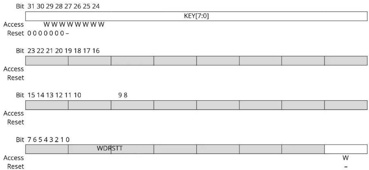
text_image
Bit 31 30 29 28 27 26 25 24 KEY[7:0] Access W W W W W W W W W Reset 0 0 0 0 0 0 0 - Bit 23 22 21 20 19 18 17 16 Access Reset Bit 15 14 13 12 11 10 9 8 Access Reset Bit 7 6 5 4 3 2 1 0 WDRSTT Access Reset W -Bits 31:24 - KEY[7:0] Password
| Value | Name | Description |
| 0xA5 | PASSWD | Writing any other value in this field aborts the write operation. |
Bit 0 - WDRSTT Watchdog Restart
| Value | Description |
| 0 | No effect. |
| 1 | Restarts the watchdog if KEY is written to 0xA5. |
24.5.2 Watchdog Timer Mode Register
Name: WDT_MR
Offset: 0x04
Reset: 0x3FFF2FFF
Property: Read/Write Once
The first write access prevents any further modification of the value of this register. Read accesses remain possible.
The WDT_MR register values must not be modified within three slow clock periods following a restart of the watchdog performed by a write access in WDT_CR. Any modification will cause the watchdog to trigger an end of period earlier than expected.
Bit 31 30 29 28 27 26 25 24
| WDID | LEHLT | WDDB | GHLT | WDD[11] | :8] | |||||
| Access Reset | R/W | R/W | R/W | R/W | R/W | R/W | ||||
| 1 | 1 | 1 | 1 |
Bit 23 22 21 20 19 18 17 16
| WDD[7:0] | ||||||||
| Access | R/W | R/W | R/W | R/W | R/W | R/W | R/W | R/W |
| Reset | 1 | 1 | 1 | 1 | ||||
Bit 15 14 13 12 11 10 9 8
| WDDIS | WDRSTEN WDFIEN | WDV[11:8] | ||||||
| Access Reset | R/W | R/W R/W R/W R/W R/W R/W | ||||||
| 0 | 1 | 0 | 1 | 1 | 1 | 1 | ||
| Bit | 7 | 6 | 5 | 4 | 3 | 2 | 1 | 0 |
| WDV[7:0] | ||||||||
| Access Reset | R/W R/W R/W R/W R/W R/W R/W | |||||||
| 1 | 1 | 1 | 1 | 1 | 1 | 1 | 1 | |
Bit 29 - WDIDLEHLT Watchdog Idle Halt
| Value | Description |
| 0 | The watchdog runs when the system is in idle state. |
| 1 | The watchdog stops when the system is in idle state. |
Bit 28 - WDDBGHLT Watchdog Debug Halt
| Value | Description |
| 0 | The watchdog runs when the processor is in debug state. |
| 1 | The watchdog stops when the processor is in debug state. |
Bits 27:16 - WDD[11:0] Watchdog Delta Value
Defines the permitted range for reloading the Watchdog Timer.
If the Watchdog Timer value is less than or equal to WDD, setting bit WDT_CR.WDRSTT restarts the timer.
If the Watchdog Timer value is greater than WDD, setting bit WDT_CR.WDRSTT causes a watchdog error.
Bit 15 - WDDIS Watchdog Disable
When setting the WDDIS bit, and while it is set, the fields WDV and WDD must not be modified.
| Value | Description |
| 0 | Enables the Watchdog Timer. |
Value Description
1 Disables the Watchdog Timer.
Bit 13 - WDRSTEN Watchdog Reset Enable
| Value Description | |
| 0 | A watchdog fault (underflow or error) has no effect on the resets. |
| 1 | A watchdog fault (underflow or error) triggers a watchdog reset. |
Bit 12 - WDFIEN Watchdog Fault Interrupt Enable
| Value Description | |
| 0 | A watchdog fault (underflow or error) has no effect on interrupt. |
| 1 | A watchdog fault (underflow or error) asserts interrupt. |
Bits 11:0 - WDV[11:0] Watchdog Counter Value
Defines the value loaded in the 12-bit watchdog counter.
24.5.3 Watchdog Timer Status Register
Name: WDT_SR
Offset: 0x08
Reset: 0x00000000
Property: Read-only

text_image
Bit 31 30 29 28 27 26 25 24 Access Reset Bit 23 22 21 20 19 18 17 16 Access Reset Bit 15 14 13 12 11 10 9 8 Access Reset Bit 7 6 5 4 3 2 1 0 Access Reset WDERR WDUNF R R 0 0Bit 1 - WDERR Watchdog Error (cleared on read)
| Value | Description |
| 0 | No watchdog error occurred since the last read of WDT_SR. |
| 1 | At least one watchdog error occurred since the last read of WDT_SR. |
Bit 0 - WDUNF Watchdog Underflow (cleared on read)
| Value | Description |
| 0 | No watchdog underflow occurred since the last read of WDT_SR. |
| 1 | At least one watchdog underflow occurred since the last read of WDT_SR. |
25. Reinforced Safety Watchdog Timer (RSWDT)
25.1 Description
The Reinforced Safety Watchdog Timer (RSWDT) works in parallel with the Watchdog Timer (WDT) to reinforce safe watchdog operations.
The RSWDT can be used to reinforce the safety level provided by the WDT in order to prevent system lock-up if the software becomes trapped in a deadlock. The RSWDT works in a fully operable mode, independent of the WDT. The RSWDT clock source is automatically selected from either the Slow RC oscillator clock, or from the Main RC oscillator divided clock to get an equivalent Slow RC oscillator clock. If the WDT clock source (for example, the 32 kHz crystal oscillator) fails, the system lock-up is no longer monitored by the WDT because the RSWDT performs the monitoring. Thus, there is no lack of safety regardless of the external operating conditions. The RSWDT shares the same features as the WDT (i.e., a 12-bit down counter that allows a watchdog period of up to 16 seconds with slow clock at 32.768 kHz). It can generate a general reset or a processor reset only. In addition, it can be stopped while the processor is in Debug mode or Idle mode.
25.2 Embedded Characteristics
• Automatically Selected Reliable RSWDT Clock Source (independent of WDT clock source)
• 12-bit Key-protected Programmable Counter
- Provides Reset or Interrupt Signals to the System
- Counter may be Stopped While Processor is in Debug State or Idle Mode
25.3 Block Diagram
Figure 25-1. Reinforced Safety Watchdog Timer Block Diagram

flowchart
graph TD
    A["write RSWDT_MR"] --> B["AND"]
    B --> C["1 0"]
    C --> D["12-bit Down Counter"]
    D --> E["Current Value"]
    E --> F["= 0"]
    F --> G["set"]
    G --> H["WDUNF"]
    H --> I["reset"]
    I --> J["read RSWDT_SR or reset"]

    K["main RC frequency"] --> L["divider"]
    M["main RC clock"] --> L
    L --> N["Automatic selection [CKGR_MOR.MOSCRCEN = 0 and (WDT_MR.WDDIS or SUPC_MR.XTALSEL = 1)"]
    N --> O["0"]
    O --> P["1/128"]
    P --> Q["reload"]
    Q --> E

    R["WDFIEN"] --> S["RSWDT_MR"]
    T["RSWDT_MR"] --> U["WDV"]
    U --> V["1 0"]
    V --> W["reload"]
    W --> X["1/128"]
    X --> Y["slow RC clock"]

    Z["read RSWDT_SR or reset"] --> H
25.4 Functional Description
The RSWDT is supplied by VDDCORE. The RSWDT is initialized with default values on processor reset or on a power-on sequence and is disabled (its default mode) under such conditions.
The RSWDT must not be enabled if the WDT is disabled.
The Main RC oscillator divided clock is selected if the Main RC oscillator is already enabled by the application (CKGR_MOR.MOSCRCEN = 1) or if the WDT is driven by the Slow RC oscillator.
The RSWDT is built around a 12-bit down counter, which is loaded with a slow clock value other than that of the slow clock in the WDT, defined in the WDV (Watchdog Counter Value) field of the Mode Register (RSWDT_MR). The RSWDT uses the slow clock divided by 128 to establish the maximum watchdog period to be 16 seconds (with a typical slow clock of 32.768 kHz).
After a processor reset, the value of the RSWDT_MR.WDV is 0xFFFF, corresponding to the maximum value of the counter with the external reset generation enabled (RSWDT_MR.WDRSTEN = 1 after a backup reset). This means that a default watchdog is running at reset, that is, at power up.
If the watchdog is restarted by writing into the Control Register (RSWDT_CR), the RSWDT_MR must not be programmed during a period of time of three slow clock periods following the RSWDT_CR write access. Programming a new value in the RSWDT_MR, automatically initiates a restart instruction.
The RSWDT_MR can be written only once. Only a processor reset resets it. Writing the RSWDT_MR reloads the timer with the newly programmed mode parameters.
In normal operation, the user reloads the watchdog at regular intervals before the timer underflow occurs, by setting the RSWDT_CR.WDRSTT bit. The watchdog counter is then immediately reloaded from the RSWDT_MR and restarted, and the slow clock 128 divider is reset and restarted. The RSWDT_CR is write-protected. As a result, writing the RSWDT_CR without the correct hard-coded key has no effect. If an underflow does occur, the "wdt_fault" signal to the Reset Controller is asserted if the RSWDT_MR.WDRSTEN is set. Moreover, Watchdog Underflow (WDUNF) is set in the Status Register (RSWDT_SR).
The status bits WDUNF and WDERR trigger an interrupt, provided the WDFIEN bit is set in the RSWDT_MR. The signal "wdt_fault" to the Reset Controller causes a Watchdog reset if the WDRSTEN bit. For additional information, refer to the section "Reset Controller (RSTC)". In this case, the processor and the RSWDT are reset, and the WDUNF and WDERR flags are reset.
If a reset is generated or if the RSWDT_SR is read, the status bits are reset, the interrupt is cleared, and the "wdt_fault" signal to the reset controller is deasserted
Writing the RSWDT_MR reloads and restarts the down counter.
The the RSWDT is disabled after any power-on sequence.
While the processor is in Debug state or in Idle mode, the counter may be stopped depending on the value programmed for the WDIDLEHLT and WDDBGHLT bits in the RSWDT_MR.

The RSWDT must not be enabled if the WDT is disabled.
Figure 25-2. Watchdog Behavior

flowchart
graph TD
    A["Watchdog Fault"] --> B{RSWDT_CR.WDRSTT = 1}
    B --> C{Normal behavior}
    C --> D["WDV"]
    D --> E{Watchdog Underflow}
    E --> F{if WDRSTEN is 0}
    F --> G["..."]
    G --> H["0"]
    H --> I["0xFFFF"]
    style A fill:#f9f,stroke:#333
    style I fill:#ccf,stroke:#333
Related Links
- Reset Controller (RSTC)
25.5 Register Summary
| Offset | Name Bit Pos. 7 | 6 | 5 | 4 | 3 | 2 | 1 | 0 | |||||||||||||||||||||||||||||||||||||||||||||||||||||||||||||||||||||||||||||||||||||||||||||||||||||||||||||||||||||||||||||||||||||||||||||||||||||||||||||||||||||||||||||||||||||||||||||||||||||||||||||||||||||||||||||||||||||||||||||||||||||||||||||||||||||||||||||||||||||||||||||||||||||||||||||||||||||||||||||||||||||||||||||||||||||||||||||||||||||||||||||||||||||||||||||||||||||||||||||||||||||||||||||||||||||||||||||||||||||||||||||||||||||||||||||||||||||||||||||||||||||||||||||||||||||||||||||||||||||||||||||||||||||||||||||||||||||||||||||||||||||||||||||||||||||||||||||||||||||||||||||||||||||||||||||||||||||||||||||||||||||||||||||||||||||||||||||||||||||||||||||||||||||||||||||||
| 0x00 RSWDT_CR | 7:0 WDRSTT | ||||||||||||||||||||||||||||||||||||||||||||||||||||||||||||||||||||||||||||||||||||||||||||||||||||||||||||||||||||||||||||||||||||||||||||||||||||||||||||||||||||||||||||||||||||||||||||||||||||||||||||||||||||||||||||||||||||||||||||||||||||||||||||||||||||||||||||||||||||||||||||||||||||||||||||||||||||||||||||||||||||||||||||||||||||||||||||||||||||||||||||||||||||||||||||||||||||||||||||||||||||||||||||||||||||||||||||||||||||||||||||||||||||||||||||||||||||||||||||||||||||||||||||||||||||||||||||||||||||||||||||||||||||||||||||||||||||||||||||||||||||||||||||||||||||||||||||||||||||||||||||||||||||||||||||||||||||||||||||||||||||||||||||||||||||||||||||||||||||||||||||||||||||||||||||||||||||||
| 15:8 | 23:16 | ||||||||||||||||||||||||||||||||||||||||||||||||||||||||||||||||||||||||||||||||||||||||||||||||||||||||||||||||||||||||||||||||||||||||||||||||||||||||||||||||||||||||||||||||||||||||||||||||||||||||||||||||||||||||||||||||||||||||||||||||||||||||||||||||||||||||||||||||||||||||||||||||||||||||||||||||||||||||||||||||||||||||||||||||||||||||||||||||||||||||||||||||||||||||||||||||||||||||||||||||||||||||||||||||||||||||||||||||||||||||||||||||||||||||||||||||||||||||||||||||||||||||||||||||||||||||||||||||||||||||||||||||||||||||||||||||||||||||||||||||||||||||||||||||||||||||||||||||||||||||||||||||||||||||||||||||||||||||||||||||||||||||||||||||||||||||||||||||||||||||||||||||||||||||||||||||||||||
| 23:16 | 31:24 KEY[7:0] | 31:24 KEY[7:0] | 31:24 KEY[7:0] | ||||||||||||||||||||||||||||||||||||||||||||||||||||||||||||||||||||||||||||||||||||||||||||||||||||||||||||||||||||||||||||||||||||||||||||||||||||||||||||||||||||||||||||||||||||||||||||||||||||||||||||||||||||||||||||||||||||||||||||||||||||||||||||||||||||||||||||||||||||||||||||||||||||||||||||||||||||||||||||||||||||||||||||||||||||||||||||||||||||||||||||||||||||||||||||||||||||||||||||||||||||||||||||||||||||||||||||||||||||||||||||||||||||||||||||||||||||||||||||||||||||||||||||||||||||||||||||||||||||||||||||||||||||||||||||||||||||||||||||||||||||||||||||||||||||||||||||||||||||||||||||||||||||||||||||||||||||||||||||||||||||||||||||||||||||||||||||||||||||||||||||||||||||||||||||||||||||
| 0x04 RSWDT_MR | 7:0 WDV[7:0] | 15:8 WDDIS WDRSTEN WDFIEN WDV[11:8]23:16 ALLONES[7:0]31:24 WDIDLEHLT WDDBGHLT ALLONES[11:8]31:24 WDUNF WDUNF 31:24 WDUNF WDUNF WDUNF WDUNF WDUNF WDUNF WDUNF WDUNF WDUNF WDUNF WDUNF WDUNF WDUNF WDUNF WDUNF WDUNF WDUNF WDUNF WDUNF WDUNF WDUNF WDUNF WDUNF WDUNF WDUNF WDUNF WDUNF WDUNF WDUNF WDUNF WDUNF WDUNF WDUNF WDUNF WTLDLEHLT WDDBGHLT ALLONES[11:8]31:24 WDUNF WDUNF WDUNF WDUNF WDUNF WDUNF WDUNF WDUNF WDUNF WDUNF WDUNF WDUNF WDUNF WDUNF WDUNF WDUNF WDUNF WDUNF WDUNF WDUNF WDUNF WDUNF WDUNF WDUNF WDUNF WDUNF WDUNF WDUNF WDUNF WDUNF WDUNF WDINF WDUNF WDUNF WDUNF WDUNF WDUNF WDUNF WDUNF WDUNF WDUNF WDUNF WDUNF WDUNF WDUNF WDUNF WDUNF WDUNF WDUNF WDUNF WDUNF WDUNF WDUNF WDUNF WDUNF WDUNF WDUNF WDUNF WDUNF WDUNF WDUNF WDUNF WDUNF WDUNF WDUN FWDUNF WDUNF WDUNF WDUNF WDUNF WDUNF WDUNF WDUNF WDUNF WDUNF WDUNF WDUNF WDUNF WDUNF WDUNF WDUNF WDUNF WDUNF WDUNF WDUNF WDUNF WDUNF WDUNF WDUNF WDUNF WDUNF WDUNF WDUNF WDUNF WDUNF WDUNF WDUNF WDUNF WD UNF WDUNF WDUNF WDUNF WDUNF WDUNF WDUNF WDUNF WDUNF WDUNF WDUNF WDUNF WDUNF WDUNF WDUNF WDUNF WDUNF WDUNF WDUNF WDUNF WDUNF WDUNF WDUNF WDUNF WDUNF WDUNF WDUNF WDUNF WDUNF WDUNF WDUNF WDUNF WDUNF WDUN | 7:0 | WDRSTT | 15:8 | 15:8 | 15:8 | 15:8 | 15:8 | 15:8 | 15:8 | 15:8 | 15:8 | 15:8 | 15:8 | 15:8 | 15:8 | 15:8 | 15:8 | 15:8 | 15:8 | 15:8 | 15:8 | 15:8 | 15:24 KEY[7:0] | 7:0 WDV[7:0] | 15:8 WDDIS WDRSTEN WDFIEN WDV[11:8]23:16 ALLONES[7:0]31:24 WDUNF WDUNF WDUNF WDUNF WDUNF WDUNF WDUNF WDUNF WDUNF WDUNF WDUNF WDUNF WDUNF WDUNF WDUNF WDUNF WDUNF WDUNF WDUNF WDUNF WDUNF WDUNF WDUNF WDUNF WDUNF WDUNF WDUNF WDUNF WDUNF WDUNF WDUNF WTLDLEHLT WDDBGHLT ALLONES[11:8]31:24 WDUNF WDUNF WDUNF WDUNF WDUNF WDUNF WDUNF WDUNF WDUNF WDUNF WDUNF WDUNF WDUNF WDUNF WDUNF WDUNF WDUNF WDUNF WDUNF WDUNF WDUNF WDUNF WDUNF WDUNF WDUNF WDUNF WDUNF WDUNF WDUN FWDUNF WDUNF WDUNF WDUNF WTLDLEHLT WDDBGHLT ALLONES[11:8]31:24 WDUNF WDUNF WDUNF WDUNF WDUNF WDUNF WDUNF WDUNF WDUNF WDUNF WDUNF WDUNF WDUNF WDUNF WDUNF WDUNF WDUNF WDUNF WDUNF WDUNF WDUNF WDUNF WD UNF WDUNF WDUNF WDUNF WDUNF WDUNF WDUNF WDUNF WDUNF WDUNF WDUNF WTLDLEHLT WDDBGHLT ALLONES[11:8]31:24 WDUNF WDUNF WDUNF WDUNF WDUNF WDUNF WDUNF WDUNF WDUNF WDUNF WDUNF WDUNF WDUNF WDUNF WDUNF WDUN FWDUNF WDUNF WDUNF WDUNF WDUNF WDUNF WDUNF WDUNF WDUNF WDUNF WDUNF WDUNF WDUNF WDUNF WDUNF WDUNF WDUNF WTLDLEHLT WTLDLEHLT WTLDLEHLT WTLDLEHLT WTLDLEHLT WTLDLEHLT WTLDLEHLT WTLDLEHLT WTLDLEHLT WTLDLEHLT WTLDLEHLT WTLDLEHLT WTLDLEHLT WTLDLEHLT WTLDLEHLT WTLDLEHLT WTLDLEHLT WTLDLEHLT WTLDLEHLT WTLDLEHLT WTLDLEHLT WTLDLEHLT WTLDLEHLT WTLDLEHLT WTLDLEHLT WTLDLEHLT WTLDLEHLT WTLDLEHLT WTLDLEHLT WTLDLEHLT WTLDLEHLT WTLDLEHLT WTLDLEHLT WTLDLEHLT WTLDLEHLT WTLDLEHLT WTLDLEHLT WTLDLEHLT WTLDLEHLT WTLDLEHLT WTLDLEHLT WTLDLEHLT WTLDLEHLT WTLDLEHLT WTLDLEHLT WTLDLEHLL TWTLDLEHLT WTLDLEHLT WTLDLEHLT WTLDLEHLT WTLDLEHLT WTLDLEHLT WTLDLEHLT WTLDLEHLT WTLDLEHLT WTLDLEHLT WTLDLEHLT WTLDLEHLT WTLDLEHLT WTLDLEHLT WTLDLEHLT WTLDLEHLT WTLDLEHLT WTLDLEHLT WTLDLEHLT WTLDLEHLT | 7:0 | WDRSTT | 15:8 | 15:8 | 15:8 | 15:8 | 15:8 | 15:8 | 15:8 | 15:8 | 15:8 | 15:8 | 15:8 | 15:8 | 15:8 | 15:8 | 15:8 | 15:8 | 15:8 | 15:8 | 31:24 | WTLDLEHLT | WTDDBGHLT | ALLONES[11:8] | 31:24 | WTUNF | WTUNF | WTUNF | WTUNF | WTUNF | WTUNF | WTUNF | WTUNF | WTUNF | WTUNF | WTUNF | WTUNF | WTUNF | WTUNF | WTUNF | WTUNF | WTUNF | WTUNF | WTUNF | WTUNF | WTUNF | WTUNF | WTUNF | WTUNF | WTUNF | WTUN FWDUNF | WTUNF | WTUNF | WTUNF | WTUNF | WTUNF | WTUNF | WTUNF | WTUNF | WTUNF | WTUNF | WTUNF | WTUNF | WTUNF | WTUNF | WTUNF | WTUNF | WTUNF | WTUNF | WTUNF | WTUNF | WTUNF | WTUNF | WTUNF | WTUNF | GTNDLEHLT | GTNDLEHLT | GTNDLEHLT | GTNDLEHLT | GTNDLEHLT | GTNDLEHLT | GTNDLEHLT | GTNDLEHLT | GTNDLEHLT | GTNDLEHLT | GTNDLEHLT | GTNDLEHLT | GTNDLEHLT | GTNDLEHLT | GTNDLEHLT | GTNDLEHLT | GTNDLEHLT | GTNDLES | GTNDLES | GTNDLES | GTNDLES | GTNDLES | GTNDLES | GTNDLES | GTNDLES | GTNDLES | GTNDLES | GTNDLES | GTNDLES | GTNDLES | GTNDLES | GTNDLES | GTNDLES | GTNDLES | GTNDLES | GTNDLES | GTNDLES | GTNDLES | GTNDLES | GTNDLES | GTNDLES | GTNDLES | GTNDS | GTNDS | GTNDS | GTNDS | GTNDS | GTNDS | GTNDS | GTNDS | GTNDS | GTNDS | GTNDS | GTNDS | GTNDS | GTNDS | GTNDS | GTNDS | GTNDS | GTNDS | GTNDS | GTNDS | GTNDS | GTNDS | GTNDS | GTNDS | GTNDS | GTND S | GTND S | GTND S | GTND S | GTND S | GTND S | GTND S | GTND S | GTND S | GTND S | GTND S | GTND S | GTND S | GTND S | GTND S | GTND S | GTND S | GTND S | GTND S | GTND S | GTND S | GTND S | GTND S | GTND S | GTND S | GTNDS | GTNDS | GTNDS | GTNDS | GTNDS | GTNDS | GTNDS | GTNDS | GTNDS | GTNDS | GTNDS | GTNDS | GTNDS | GTNDS | GTNDS | GTNDS | GTNDS | GTNDS | GTNDS | GTNDS | GTNDS | GTNDS | GTNDS | GTNDS | GTNDs | GTNDs | GTNDs | GTNDs | GTNDs | GTNDs | GTNDs | GTNDs | GTNDs | GTNDs | GTNDs | GTNDs | GTNDs | GTNDs | GTNDs | GTNDs | GTNDs | GTNDs | GTNDs | GTNDs | GTNDs | GTNDs | GTNDs | GTNDs | GTNDs | GTND s | GTNDs | GTNDs | GTNDs | GTNDs | GTNDs | GTNDs | GTNDs | GTNDs | GTNDs | GTNDs | GTNDs | GTNDs | GTNDs | GTNDs | GTNDs | GTNDs | GTNDs | GTNDs | GTNDs | GTNDs | GTNDs | GTNDs | GTNDs | GTNDs | GTNDS | GTNDs | GTNDs | GTNDs | GTNDs | GTNDs | GTNDs | GTNDs | GTNDs | GTNDs | GTNDs | GTNDs | GTNDs | GTNDs | GTNDs | GTNDs | GTNDs | GTNDs | GTNDs | GTNDs | GTNDs | GTNDs | GTNDs | GTNDs | GTND s | GTND s | GTND s | GTND s | GTND s | GTND s | GTND s | GTND s | GTND s | GTND s | GTND s | GTND s | GTND s | GTND s | GTND s | GTND s | GTND s | GTND s | GTND s | GTND s | GTND s | GTND s | GTND s | GTND s | GTND s | GTNDs | GTNDs | GTNDs | GTNDs | GTNDs | GTNDs | GTNDs | GTNDs | GTNDs | GTNDs | GTNDs | GTNDs | GTNDs | GTNDs | GTNDs | GTNDs | GTNDs | GTNDs | GTNDs | GTNDs | GTNDs | GTNDs | GTNDs | GTND s | GTND is | GTND is | GTND is | GTND is | GTND is | GTND is | GTND is | GTND is | GTND is | GTND is | GTND is | GTND is | GTND is | GTND is | GTND is | GTND is | GTND is | GTND is | GTND is | GTND is | GTND is | GTND is | GTND is | GTND is | GTND is | GTNDis | GTND is | GTND is | GTND is | GTND is | GTND is | GTND is | GTND is | GTND is | GTND is | GTND is | GTND is | GTND is | GTND is | GTND is | GTND is | GTND is | GTND is | GTND is | GTND is | GTND is | GTND is | GTND is | GTND is | GTND is | GTND i | GTND is | GTND is | GTND is | GTND is | GTND is | GTND is | GTND is | GTND is | GTND is | GTND is | GTND is | GTND is | GTND is | GTND is | GTND is | GTND is | GTND is | GTND is | GTND is | GTND is | GTND is | GTND is | GTND is | GTND is | GTNDi | GTND is | GTND is | GTND is | GTND is | GTND is | GTND is | GTND is | GTND is | GTND is | GTND is | GTND is | GTND is | GTND is | GTND is | GTND is | GTND is | GTND is | GTND is | GTND is | GTND is | GTND is | GTND is | GTND is | GTND is | GTND are | GTND is | GTND is | GTND is | GTND is | GTND is | GTND is | GTND is | GTND is | GTND is | GTND is | GTND is | GTND is | GTND is | GTND is | GTND is | GTND is | GTND is | GTND is | GTND is | GTND is | GTND is | GTND is | GTND is | GTND is | GTND in | GTND is | GTND is | GTND is | GTND is | GTND is | GTND is | GTND is | GTND is | GTND is | GTND is | GTND is | GTND is | GTND is | GTND is | GTND is | GTND is | GTND is | GTND is | GTND is | GTND is | GTND is | GTND is | GTND is | GTND is | GTND IS | GTND is | GTND is | GTND is | GTND is | GTND is | GTND is | GTND is | GTND is | GTND is | GTND is | GTND is | GTND is | GTND is | GTND is | GTND is | GTND is | GTND is | GTND is | GTND is | GTND is | GTND is | GTND is | GTND is | GTND is | GTND | ||||||||||||||||||||||||||||||||||||||||||||||||||||||||||||||||||||||||||||||||||||||||||||||||||||||||||||||||||||||||||||||||||||||||||||||||||||||||||||||||||||||||||||||||||||||||||||||||||
25.5.1 Reinforced Safety Watchdog Timer Control Register
Name: RSWDT_CR
Offset: 0x00
Property: Write-only
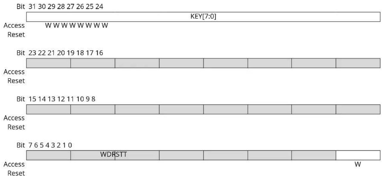
text_image
Bit 31 30 29 28 27 26 25 24 KEY[7:0] Access W W W W W W W W W Reset Bit 23 22 21 20 19 18 17 16 Access Reset Bit 15 14 13 12 11 10 9 8 Access Reset Bit 7 6 5 4 3 2 1 0 Access Reset WDRSTT WBits 31:24 - KEY[7:0] Password
| Value | Name | Description |
| 0xC4 | PASSWD | Writing any other value in this field aborts the write operation. |
Bit 0 - WDRSTT Watchdog Restart
| Value | Description |
| 0 | No effect. |
| 1 | Restarts the watchdog. |
25.5.2 Reinforced Safety Watchdog Timer Mode Register
Name: RSWDT_MR
Offset: 0x04
Reset: 0x3FFFAFFF
Property: Read/Write Once
Note: The first write access prevents any further modification of the value of this register; read accesses remain possible. The WDV value must not be modified within three slow clock periods following a restart of the watchdog performed by means of a write access in the RSWDT_CR, else the watchdog may trigger an end of period earlier than expected.
Bit 31 30 29 28 27 26 25 24
| WDIDLEHLT WDDBGHLT ALLONES[11:8] | ||||||
| Access Reset | 1 | 1 | 1 | 1 | 1 | 1 |
Bit 23 22 21 20 19 18 17 16
| ALLONES[7:0] | ||||||||
| Access Reset | 1 | 1 | 1 | 1 | 1 | 1 | 1 | 1 |
Bit 15 14 13 12 11 10 9 8
| WDDIS | WDRSTEN | WDFIEN | WDV[11:8] | |||||
| Access Reset | 1 | 1 | 0 | 1 | 1 | 1 | 1 | |
| Bit | 7 | 6 | 5 | 4 | 3 | 2 | 1 | 0 |
| WDV[7:0] | ||||||||
| Access Reset | 1 | 1 | 1 | 1 | 1 | 1 | 1 | 1 |
Bit 29 - WDIDLEHLT Watchdog Idle Halt
| Value | Description |
| 0 | The RSWDT runs when the system is in idle mode. |
| 1 | The RSWDT stops when the system is in idle state. |
Bit 28 - WDDBGHLT Watchdog Debug Halt
| Value | Description |
| 0 | The RSWDT runs when the processor is in debug state. |
| 1 | The RSWDT stops when the processor is in debug state. |
Bits 27:16 - ALLONES[11:0] Must Always Be Written with 0xFFFF
Bit 15 - WDDIS Watchdog Disable
| Value | Description |
| 0 | Enables the RSWDT. |
| 1 | Disables the RSWDT. |
Bit 13 - WDRSTEN Watchdog Reset Enable
| Value | Description |
| 0 | A Watchdog fault (underflow or error) has no effect on the resets. |
| 1 | A Watchdog fault (underflow or error) triggers a watchdog reset. |
Bit 12 - WDFIEN Watchdog Fault Interrupt Enable
| Value Description | |
| 0 | A Watchdog fault (underflow or error) has no effect on interrupt. |
| 1 | A Watchdog fault (underflow or error) asserts interrupt. |
Bits 11:0 - WDV[11:0] Watchdog Counter Value
Defines the value loaded in the 12-bit watchdog counter.
25.5.3 Reinforced Safety Watchdog Timer Status Register
Name: RSWDT_SR
Offset: 0x08
Reset: 0x00000000
Property: Read-only
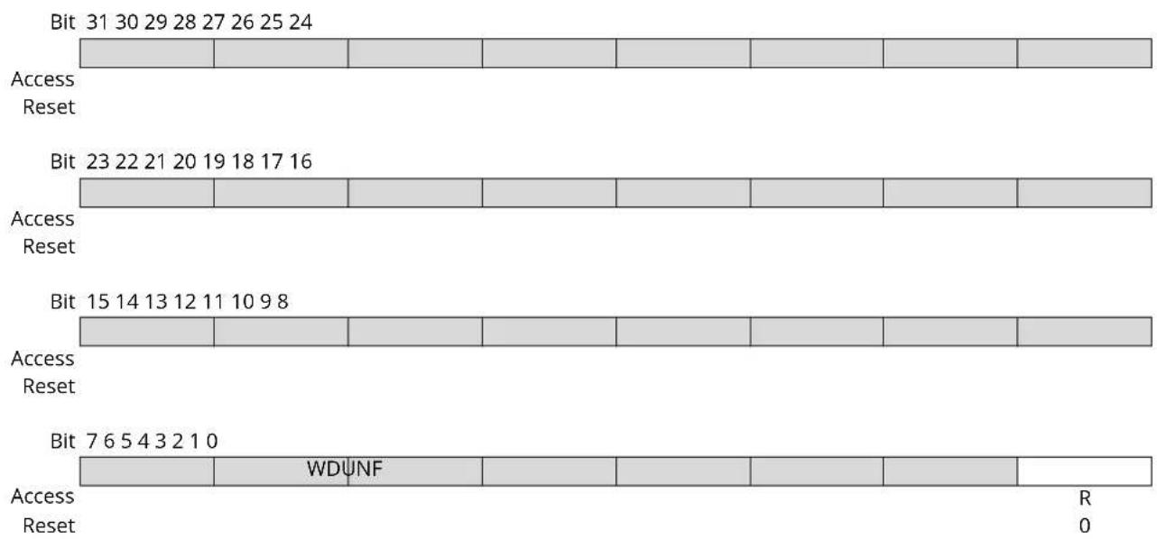
text_image
Bit 31 30 29 28 27 26 25 24 Access Reset Bit 23 22 21 20 19 18 17 16 Access Reset Bit 15 14 13 12 11 10 9 8 Access Reset Bit 7 6 5 4 3 2 1 0 Access Reset WDUNF R 0Bit 0 - WDUNF Watchdog Underflow
| Value | Description |
| 0 | No watchdog underflow occurred since the last read of RSWDT_SR. |
| 1 | At least one watchdog underflow occurred since the last read of RSWDT_SR. |
26. Reset Controller (RSTC)
26.1 Description
The Reset Controller (RSTC), driven by Power-On Reset (POR) cells, software, external reset pin and peripheral events, handles all the resets of the system without any external components. It reports which reset occurred last.
The RSTC also drives simultaneously the external reset and the peripheral and processor resets.
26.2 Embedded Characteristics
- Driven by embedded POR, software, external reset pin and peripheral events
-
Management of all system resets, including:
-
External devices through the NRST pin
- Processor
- Peripheral set
- Reset source status:
- Status of the last reset
- Either VDDCORE and VDDIO POR, Software Reset, User Reset, Watchdog Reset
• External reset signal control and shaping
26.3 Block Diagram
Figure 26-1. Reset Controller Block Diagram

flowchart
graph TD
    A["POR Backup"] --> B["SUPC"]
    C["SM Backup"] --> B
    D["POR VDDCORE"] --> B
    E["BOD VDDCORE"] --> B
    B --> F["VDDCORE reset"]
    F --> G["Reset Controller"]
    H["NRST Pin"] --> I["NRST Manager"]
    I --> J["user_reset"]
    I --> K["enter_nreset"]
    I --> L["nrst_out"]
    L --> I
    M["From watchdog"] --> N["wd_fault"]
    O["SLCK"] --> P["Reset State Manager"]
    Q["RSTC interrupt line"] --> G
    R["Processor and peripherals reset line"] --> G
    S["Backup area reset"] --> B
26.4 Functional Description
26.4.1 Overview
The RSTC is made up of an NRST manager and a reset state manager. It runs at SLCK frequency and generates the following reset signals:
- proc_nreset: Processor reset line (also resets the Watchdog Timer)
- periph_nreset: Affects the whole set of embedded peripherals
- nrst_out: Drives the NRST pin
Note: proc_nreset and periph_nreset are driven in the same way.
These reset signals are asserted by the RSTC, either on events generated by peripherals, events on the NRST pin, or on a software action. The reset state manager controls the generation of reset signals and provides a signal to the NRST manager when an assertion of the NRST pin is required.
The NRST manager shapes the NRST assertion during a programmable time, thus controlling external device resets.
The RSTC Mode register (RSTC_MR), used to configure the RSTC, is powered with VDDIO, so that its configuration is saved as long as VDDIO is on.
26.4.2 NRST Manager
The NRST manager samples the NRST input pin and drives this pin low when required by the reset state manager. The figure below shows the block diagram of the NRST manager.
Figure 26-2. NRST Manager
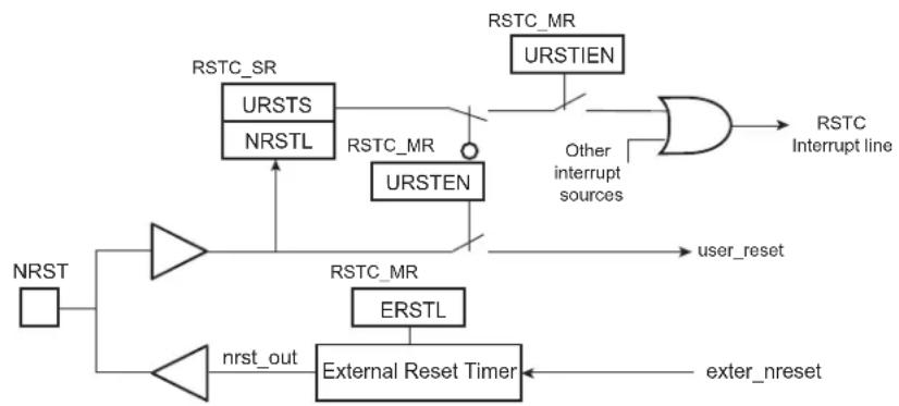
flowchart
graph TD
    A["NRST"] --> B["Δ"]
    B --> C["URSTS"]
    C --> D["URSTEN"]
    D --> E["URSTEN"]
    E --> F["URSTIEN"]
    F --> G["RSTC Interrupt line"]
    G --> H["Other interrupt sources"]
    H --> I["User_reset"]
    I --> J["ERSTL"]
    J --> K["External Reset Timer"]
    K --> L["nrst_out"]
    L --> M["Δ"]
    M --> N["User_reset"]
    N --> O["External Reset Timer"]
    O --> P["Outer_nreset"]
26.4.2.1 NRST Signal or Interrupt
The NRST manager samples the NRST pin at SLCK speed. When the NRST line is low for more than three clock cycles, a User Reset is reported to the reset state manager. The NRST pin must be asserted for at least 1 SLCK clock cycle to ensure execution of a user reset.
However, the NRST manager can be programmed to not trigger a reset when an assertion of NRST occurs. Writing a '0' to RSTC_MR.URSTEN disables the User Reset trigger.
The level of the pin NRST can be read at any time in the bit NRSTL in the RSTC Status Register (RSTC_SR). As soon as the NRST pin is asserted, RSTC_SR. URSTS is written to '1'. This bit is cleared only when the RSTC_SR is read.
The RSTC can also be programmed to generate an interrupt instead of generating a reset. To do so, RSTC_MR.URSTIEN must be set.
26.4.2.2 NRST External Reset Control
The reset state manager asserts the signal exter_nreset to assert the NRST pin. When this occurs, the "nrst_out" signal is driven low by the NRST manager for a time programmed by RSTC_MR.ERSTL.
This assertion duration, named External Reset Length, lasts 2^(ERSTL+1) SLCK cycles. This gives the approximate duration of an assertion between 60 s and 2 seconds. Note that ERSTL at '0' defines a two-cycle duration for the NRST pulse.
This feature allows the RSTC to shape the NRST pin level, and thus to guarantee that the NRST line is driven low for a time compliant with potential external devices connected on the system reset.
RSTC_MR is backed up, making it possible to use the value of ERSTL to shape the system powerup reset for devices requiring a longer startup time than that of the MCU.
26.4.3 Reset States
The reset state manager handles the different reset sources and generates the internal reset signals. It reports the reset status in RSTTYP of the Status Register (RSTC_SR). The update of RSTC_SR.RSTTYP is performed when the processor reset is released.
26.4.3.1 General Reset
A general reset occurs when a VDDIO POR is detected, a brown out or a voltage regulation loss is detected by the Supply Controller. The vddcore_nreset signal is asserted by the Supply Controller when a general reset occurs.
All the reset signals are released and RSTC_SR.RSTTYP reports a general reset. As the RSTC_MR is written to '0', the NRST line rises two cycles after the vddcore_nreset, as ERSTL defaults at value 0x0.
The figure below illustrates how the general reset affects the reset signals.
Figure 26-3. General Reset Timing Diagram
text_image
Power Supply Activation SLCK Main RC Oscillator MCK Any Freq. VDDIO POR Output 2 SLCK cycles 5 Main RC cycles Backup Logic Reset Active 5 SLCK cycles Inactive Regulator Startup VDDCORE POR Output Inactive 6.5 SLCK cycles + 2 Main RC cycles Processor and Peripherals Reset Line Active Inactive NRST (no ext.drive assumed) 3 SLCK cycles Inactive RSTTYP XXX 0x0 = General Reset XXX26.4.3.2 Backup Reset
A backup reset occurs when the chip exits from Backup mode. While exiting Backup mode, the vddcore_nreset signal is asserted by the Supply Controller.
Field RSTC_SR.RSTTYP is updated to report a backup reset.
26.4.3.3 Watchdog Reset
The watchdog reset is entered when a watchdog fault occurs. This reset lasts three SLCK cycles.
When in watchdog reset, the processor reset and the peripheral reset are asserted. The NRST line is also asserted, depending on the value of RSTC_MR.ERSTL. However, the resulting low level on NRST does not result in a user reset state.
The Watchdog Timer is reset by the proc_nreset signal. As the watchdog fault always causes a processor reset if WDT_MR.WDRSTEN is written to '1', the Watchdog Timer is always reset after a watchdog reset, and the Watchdog is enabled by default and with a period set to a maximum.
When WDT_MR.WDRSTEN is written to '0', the watchdog fault has no impact on the RSTC.
After a watchdog overflow occurs, the report on the RSTC_SR.RSTTYP may differ (either WDT_RST or USER_RST) depending on the external components driving the NRST pin. For example, if the NRST line is driven through a resistor and a capacitor (NRST pin debouncer), the reported value is USER_RST if the low to high transition is greater than one SLCK cycle.
Figure 26-4. Watchdog Reset Timing Diagram

text_image
SLCK WDT Fault Main RC Oscillator MCK Any Frequency. Any Frequency. 3 SLCK cycles + 2 MCK cycles RSTTYP XXX 0x2 = Watchdog Reset Processor and Peripherals Reset Line Inactive Active Inactive NRST (nrst_out) Inactive Active Inactive Min = 2 SLCK cycles if ERSTL=0 (e.g. 8 if ERSTL=2)26.4.3.4 Software Reset
The RSTC offers commands to assert the different reset signals. These commands are performed by writing the Control register (RSTC_CR) with the following bits at '1':
- RSTC_CR.PROCRST: Writing a '1' to PROCRST resets the processor and all the embedded peripherals, including the memory system and, in particular, the Remap Command.
- RSTC_CR.EXTRST: Writing a '1' to EXTRST asserts low the NRST pin during a time defined by the field RSTC_MR.ERSTL.
The software reset is entered if at least one of these bits is written to '1' by the software. All these commands can be performed independently or simultaneously. The software reset lasts three SLCK cycles.
The internal reset signals are asserted as soon as the register write is performed. This is detected on the Host Clock (MCK). They are released when the software reset has ended, i.e., synchronously to SLCK.
If EXTRST is written to '1', the nrst_out signal is asserted depending on the configuration of RSTC_MR.ERSTL. However, the resulting falling edge on NRST does not lead to a user reset.
If and only if the RSTC_CR.PROCRST is written to '1', the RSTC reports the software status in field RSTC_SR.RSTTYP. Other software resets are not reported in RSTTYP.
As soon as a software operation is detected, RSTC_SR.SRCMP is written to '1'. SRCMP is cleared at the end of the software reset. No other software reset can be performed while SRCMP is written to '1', and writing any value in the RSTC_CR has no effect.
Figure 26-5. Software Reset Timing Diagram

text_image
SLCK Up to 1 SLCK cycle Write RSTC_CR Main RC Oscillator MCK Any Frequency. 3 SLCK cycles + 2 MCK cycles Any Frequency. RSTTYP XXX 0x3 = Software Reset Processor and Peripherals Reset Line Inactive Active Inactive NRST (nrst_out) if EXTRST=1 Inactive Active Inactive RSTC_SR.SRCMP Min = 2 SLCK cycles if ERSTL=0 (e.g. 8 if ERSTL=2)26.4.3.5 User Reset
A user reset is generated when a low level is detected on the NRST pin and RSTC_MR.URSTEN is at '1'. The NRST input signal is resynchronized with SLCK to ensure proper behavior of the system. Thus, the NRST pin must be asserted for at least 1 SLCK clock cycle to ensure execution of a user reset.
The user reset is triggered 2 SLCK cycles after a low level is detected on NRST. The processor reset and the peripheral reset are asserted.
The user reset ends when NRST rises, after a two-cycle resynchronization time and a three-cycle processor startup. The processor clock is reenabled as soon as NRST is confirmed high.
When the processor reset signal is released, RSTC_SR.RSTTYP is loaded with the value '4', indicating a user reset.
The NRST manager guarantees that the NRST line is asserted for External Reset Length SLCK cycles, as configured in RSTC_MR.ERSTL. However, if NRST does not rise after External Reset Length because it is driven low externally, the internal reset lines remain asserted until NRST actually rises.
Figure 26-6. User Reset Timing Diagram

text_image
SLCK NRST pin 2 SLCK cycles Main RC Oscillator MCK Any Frequency. Any Frequency. RSTTYP XXX 0x4 = User Reset 6 SLCK cycles Processor and Peripherals Reset Line Inactive Active Inactive Min = 2 SLCK cycles if ERSTL=0 (e.g. 8 if ERSTL=2) NRST (nrst_out) Inactive Active Inactive26.4.4 Reset State Priorities
The reset state manager manages the priorities among the different reset sources. The resets are listed in order of priority as follows:
- General reset
- Backup reset
- Watchdog reset
- Software reset
- User reset
Specific cases are listed below:
- When in user reset:
- A watchdog event is impossible because the Watchdog Timer is being reset by the proc_nreset signal.
- A software reset is impossible, since the processor reset is being activated.
- When in software reset:
- A watchdog event has priority over the current state.
- The NRST has no effect.
- When in watchdog reset:
- The processor reset is active and so a software reset cannot be programmed.
- A user reset cannot be entered.
26.4.5 Register Summary
| Offset | Name Bit Pos. 7 | 6 | 5 | 4 | 3 | 2 | 1 | 0 | |||||||||||||||||||||||||||||||||||||||||||||||||||||||||||||||||||||||||||||||||||||||||||||||||||||||||||||||||||||||||||||||||||||||||||||||||||||||||||||||||||||||||||||||||||||||||||||||||||||||||||||||||||||||||||||||||||||||||||||||||||||||||||||||||||||||||||||||||||||||||||||||||||||||||||||||||||||||||||||||||||||||||||||||||||||||||||||||||||||||||||||||||||||||||||||||||||||||||||
| 0x00 | RSTC_CR | 7:0 | EXTRST | PROCRST | 7:0 | ||||||||||||||||||||||||||||||||||||||||||||||||||||||||||||||||||||||||||||||||||||||||||||||||||||||||||||||||||||||||||||||||||||||||||||||||||||||||||||||||||||||||||||||||||||||||||||||||||||||||||||||||||||||||||||||||||||||||||||||||||||||||||||||||||||||||||||||||||||||||||||||||||||||||||||||||||||||||||||||||||||||||||||||||||||||||||||||||||||||||||||||||||||||||||||||||||||||||||||||
| 15:8 | 23:16 | 31:24 KEY[7:0] | |||||||||||||||||||||||||||||||||||||||||||||||||||||||||||||||||||||||||||||||||||||||||||||||||||||||||||||||||||||||||||||||||||||||||||||||||||||||||||||||||||||||||||||||||||||||||||||||||||||||||||||||||||||||||||||||||||||||||||||||||||||||||||||||||||||||||||||||||||||||||||||||||||||||||||||||||||||||||||||||||||||||||||||||||||||||||||||||||||||||||||||||||||||||||||||||||||||||||||||||||
| 23:16 | |||||||||||||||||||||||||||||||||||||||||||||||||||||||||||||||||||||||||||||||||||||||||||||||||||||||||||||||||||||||||||||||||||||||||||||||||||||||||||||||||||||||||||||||||||||||||||||||||||||||||||||||||||||||||||||||||||||||||||||||||||||||||||||||||||||||||||||||||||||||||||||||||||||||||||||||||||||||||||||||||||||||||||||||||||||||||||||||||||||||||||||||||||||||||||||||||||||||||||||||||||
| 31:24 KEY[7:0] | |||||||||||||||||||||||||||||||||||||||||||||||||||||||||||||||||||||||||||||||||||||||||||||||||||||||||||||||||||||||||||||||||||||||||||||||||||||||||||||||||||||||||||||||||||||||||||||||||||||||||||||||||||||||||||||||||||||||||||||||||||||||||||||||||||||||||||||||||||||||||||||||||||||||||||||||||||||||||||||||||||||||||||||||||||||||||||||||||||||||||||||||||||||||||||||||||||||||||||||||||||
| 0x04 | RSTC_SR | 7:0 | URSTS | 23:16 | SRCMP | NRSTL | |||||||||||||||||||||||||||||||||||||||||||||||||||||||||||||||||||||||||||||||||||||||||||||||||||||||||||||||||||||||||||||||||||||||||||||||||||||||||||||||||||||||||||||||||||||||||||||||||||||||||||||||||||||||||||||||||||||||||||||||||||||||||||||||||||||||||||||||||||||||||||||||||||||||||||||||||||||||||||||||||||||||||||||||||||||||||||||||||||||||||||||||||||||||||||||||||||||||||||||
| 15:8 | RSTTYP[2:0] | ||||||||||||||||||||||||||||||||||||||||||||||||||||||||||||||||||||||||||||||||||||||||||||||||||||||||||||||||||||||||||||||||||||||||||||||||||||||||||||||||||||||||||||||||||||||||||||||||||||||||||||||||||||||||||||||||||||||||||||||||||||||||||||||||||||||||||||||||||||||||||||||||||||||||||||||||||||||||||||||||||||||||||||||||||||||||||||||||||||||||||||||||||||||||||||||||||||||||||||||||||
26.4.5.1 RSTC Control Register
Name: RSTC_CR
Offset: 0x00
Property: Write-only

text_image
Bit 31 30 29 28 27 26 25 24 KEY[7:0] Access W W W W W W W W Reset 0 0 0 0 0 0 0 - Bit 23 22 21 20 19 18 17 16 Access Reset Bit 15 14 13 12 11 10 9 8 Access Reset Bit 7 6 5 4 3 2 1 0 EXTRST PROCRST W W Access Reset - -Bits 31:24 - KEY[7:0] System Reset Key
| Value | Name | Description |
| 0xA5 | PASSWD | Writing any other value in this field aborts the write operation. |
Bit 3 - EXTRST External Reset
| Value | Description |
| 0 | No effect. |
| 1 | If KEY = 0xA5, asserts the NRST pin. |
Bit 0 - PROCRST Processor Reset
| Value | Description |
| 0 | No effect. |
| 1 | If KEY = 0xA5, resets the processor and all the embedded peripherals. |
26.4.5.2 RSTC Status Register
Name: RSTC_SR
Offset: 0x04
Reset: 0x00000000
Property: Read-only
The register reset value assumes that a general reset has been performed; it is subject to change if other types of reset are generated.
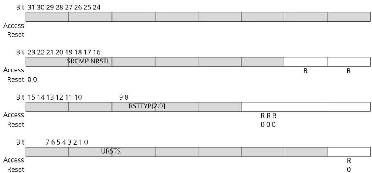
text_image
Bit 31 30 29 28 27 26 25 24 Access Reset Bit 23 22 21 20 19 18 17 16 $RCMP NRSTL Access Reset 0 0 Bit 15 14 13 12 11 10 9 8 Access Reset RRTTYP[2:0] RRR 0 0 0 Bit 7 6 5 4 3 2 1 0 Access Reset UR$TS R 0Bit 17 - SRCMP Software Reset Command in Progress
When set, this bit indicates that a software reset command is in progress and that no further software reset should be performed until the end of the current one. This bit is automatically cleared at the end of the current software reset.
| Value | Description |
| 0 | No software command is being performed by the RSTC. The RSTC is ready for a software command. |
| 1 | A software reset command is being performed by the RSTC. The RSTC is busy. |
Bit 16 - NRSTL NRST Pin Level
Registers the NRST pin level sampled on each MCK rising edge.
Bits 10:8 - RSTTYP[2:0] Reset Type
This field reports the cause of the last processor reset. Reading this RSTC_SR does not reset this field.
| Value | Name | Description |
| 0 | GENERAL_RST | First powerup reset |
| 1 | BACKUP_RST | Return from Backup mode |
| 2 | WDT_RST | Watchdog fault occurred |
| 3 | SOFT_RST | Processor reset required by the software |
| 4 | USER_RST | NRST pin detected low |
| 5 | - | Reserved |
| 6 | - | Reserved |
| 7 | - | Reserved |
Bit 0 - URSTS User Reset Status
A high-to-low transition of the NRST pin sets the URSTS. This transition is also detected on the MCK rising edge. If the user reset is disabled (URSTEN = 0 in RSTC_MR) and if the interrupt is enabled by RSTC_MR.URSTIEN, URSTS triggers an interrupt. Reading the RSTC_SR resets URSTS and clears the interrupt.
Value Description
| 0 | No high-to-low edge on NRST happened since the last read of RSTC_SR. |
| 1 | At least one high-to-low transition of NRST has been detected since the last read of RSTC_SR. |
26.4.5.3 RSTC Mode Register
Name: RSTC_MR
Offset: 0x08
Reset: 0x00000001
Property: Read/Write
This register can only be written if the WPEN bit is cleared in the System Controller Write Protection Mode Register (SYSC_WPMR).

text_image
Bit 31 30 29 28 27 26 25 24 KEY[7:0] Access W W W W W W W W Reset 0 0 0 0 0 0 0 0 Bit 23 22 21 20 19 18 17 16 Access Reset Bit 15 14 13 12 11 10 9 8 ERSTL[3:0] Access Reset R/W R/W R/W R/W 0 0 0 0 Bit 7 6 5 4 3 2 1 0 URSTIEN URSTEN Access R/W R/W Reset 0 1Bits 31:24 - KEY[7:0] Write Access Password
| Value | Name | Description |
| 0xA5 | PASSWD | Writing any other value in this field aborts the write operation. Always reads as 0. |
Bits 11:8 - ERSTL[3:0] External Reset Length
This field defines the external reset length. The external reset is asserted during a time of 2^(ERSTL+1) SLCK cycles. This allows assertion duration to be programmed between 60 s and 2 seconds. Note that synchronization cycles must also be considered when calculating the actual reset length as previously described.
Bit 4 - URSTIEN User Reset Interrupt Enable
| Value | Description |
| 0 | RSTC_SR.USRTS at '1' has no effect on the RSTC interrupt line. |
| 1 | RSTC_SR.USRTS at '1' asserts the RSTC interrupt line if URSTEN = 0. |
Bit 0 - URSTEN User Reset Enable
| Value | Description |
| 0 | The detection of a low level on the NRST pin does not generate a user reset. |
| 1 | The detection of a low level on the NRST pin triggers a user reset. |
27. Real-time Clock (RTC)
27.1 Description
The Real-time Clock (RTC) peripheral is designed for very low power consumption. For optimal functionality, the RTC requires an accurate external 32.768 kHz clock, which can be provided by a crystal oscillator.
It combines a complete time-of-day clock with alarm and a Gregorian or Persian calendar, complemented by a programmable periodic interrupt. The alarm and calendar registers are accessed by a 32-bit data bus.
The time and calendar values are coded in binary-coded decimal (BCD) format. The time format can be 24-hour mode or 12-hour mode with an AM/PM indicator.
Updating time and calendar fields and configuring the alarm fields are performed by a parallel capture on the 32-bit data bus. An entry control is performed to avoid loading registers with incompatible BCD format data or with an incompatible date according to the current month/year/ century.
A clock divider calibration circuitry can be used to compensate for crystal oscillator frequency variations.
An RTC output can be programmed to generate several waveforms, including a prescaled clock derived from 32.768 kHz.
27.2 Embedded Characteristics
• Full Asynchronous Design for Ultra Low Power Consumption
• Gregorian and Persian Modes Supported
- Programmable Periodic Interrupt
- Safety/security Features:
- Valid Time and Date Programming Check
-
On-The-Fly Time and Date Validity Check
-
Counters Calibration Circuitry to Compensate for Crystal Oscillator Variations
- Waveform Generation
- Register Write Protection
27.3 Block Diagram
Figure 27-1. Real-time Clock Block Diagram

flowchart
graph TD
    A["Slow Clock: SLCK"] --> B["32768 Divider"]
    B --> C["Clock Calibration"]
    C --> D["Time"]
    D --> E["Date"]
    E --> F["Wave Generator"]
    F --> G["RTCOUT0"]
    F --> H["RTCOUT1"]
    I["System Bus"] --> J["User Interface"]
    J --> K["Entry Control"]
    K --> L["Alarm"]
    L --> M["Interrupt Control"]
    M --> N["RTC Interrupt"]
    O["Clock Calibration"] <--> P["User Interface"]
    P <--> Q["Entry Control"]
    Q <--> R["Alarm"]
    R <--> S["Interrupt Control"]
    S <--> T["RTC Interrupt"]
    U["Time"] <--> V["Alarm"]
    V <--> W["Interrupt Control"]
    W <--> X["RTC Interrupt"]
27.4 Product Dependencies
27.4.1 Power Management
The Real-time Clock is continuously clocked at 32.768 kHz. The Power Management Controller has no effect on RTC behavior.
27.4.2 Interrupt
Within the System Controller, the RTC interrupt is OR-wired with all the other module interrupts.
Only one System Controller interrupt line is connected on one of the internal sources of the interrupt controller.
RTC interrupt requires the interrupt controller to be programmed first.
When a System Controller interrupt occurs, the service routine must first determine the cause of the interrupt. This is done by reading each status register of the System Controller peripherals successively.
27.5 Functional Description
The RTC provides a full binary-coded decimal (BCD) clock that includes century (19/20), year (with leap years), month, date, day, hours, minutes and seconds reported in RTC Time Register (RTC_TIMR).
The valid year range is up to 2099 in Gregorian mode (or 1300 to 1499 in Persian mode).
The RTC can operate in 24-hour mode or in 12-hour mode with an AM/PM indicator.
Corrections for leap years are included (all years divisible by 4 being leap years except 1900). This is correct up to the year 2099.
The RTC can generate configurable waveforms on RTCOUT0/1 outputs.
27.5.1 Reference Clock
The reference clock is the Slow Clock (SLCK) which can be driven internally or by an external 32.768 kHz crystal.
During low-power modes of the processor, the oscillator runs and power consumption is critical. The crystal selection must consider the current consumption for power saving and the frequency drift due to temperature effect on the circuit for time accuracy.
27.5.2 Timing
The RTC is updated in real time at one-second intervals in Normal mode for the counters of seconds, at one-minute intervals for the counter of minutes and so on.
Due to the asynchronous operation of the RTC with respect to the rest of the chip, to be certain that the value read in the RTC registers (century, year, month, date, day, hours, minutes, seconds) are valid and stable, it is necessary to read these registers twice. If the data is the same both times, then it is valid. Therefore, a minimum of two and a maximum of three accesses are required.
27.5.3 Alarm
The RTC has five programmable fields: month, date, hours, minutes and seconds.
Each of these fields can be enabled or disabled to match the alarm condition:
- If all the fields are enabled, an alarm flag is generated (the corresponding flag is asserted and an interrupt generated if enabled) at a given month, date, hour/minute/second.
- If only the "seconds" field is enabled, then an alarm is generated every minute.
Depending on the combination of fields enabled, a large number of possibilities are available to the user ranging from minutes to 365/366 days.
Hour, minute and second matching alarms (SECEN, MINEN, HOUREN) can be enabled independently of SEC, MIN, HOUR fields.
Note: To change one of the SEC, MIN, HOUR, DATE, MONTH fields, it is recommended to disable the field before changing the value and then re-enable it after the change has been made. This requires up to three accesses to the RTC_TIMALR or RTC_CALALR. The first access clears the enable corresponding to the field to change (SECEN, MINEN, HOUREN, DATEEN, MTHEN). If the field is already cleared, this access is not required. The second access performs the change of the value (SEC, MIN, HOUR, DATE, MONTH). The third access is required to re-enable the field by writing 1 in SECEN, MINEN, HOUREn, DATEEN, MTHEN fields.
27.5.4 Error Checking when Programming
Verification on user interface data is performed when accessing the century, year, month, date, day, hours, minutes, seconds and alarms. A check is performed on illegal BCD entries such as illegal date of the month with regard to the year and century configured.
If one of the time fields is not correct, the data is not loaded into the register/counter and a flag is set in the validity register. The user can not reset this flag. It is reset as soon as an acceptable value is programmed. This avoids any further side effects in the hardware. The same procedure is followed for the alarm.
The following checks are performed:
- Century (check if it is in range 19–20 or 13–14 in Persian mode)
- Year (BCD entry check)
- Date (check range 01–31)
- Month (check if it is in BCD range 01-12, check validity regarding "date")
- Day (check range 1–7)
- Hour (BCD checks: in 24-hour mode, check range 00–23 and check that AM/PM flag is not set if RTC is set in 24-hour mode; in 12-hour mode check range 01–12)
- Minute (check BCD and range 00–59)
- Second (check BCD and range 00–59)
Note: If the 12-hour mode is selected by means of the RTC Mode Register (RTC_MR), a 12-hour value can be programmed and the returned value on RTC_TIMR will be the corresponding 24-hour value. The entry control checks the value of the AM/PM indicator (bit 22 of RTC_TIMR) to determine the range to be checked.
27.5.5 RTC Internal Free Running Counter Error Checking
To improve the reliability and security of the RTC, a permanent check is performed on the internal free running counters to report non-BCD or invalid date/time values.
An error is reported by TDERR bit in the status register (RTC_SR) if an incorrect value has been detected. The flag can be cleared by setting the TDERRCLR bit in the Status Clear Command Register (RTC_SCCR).
The TDERR error flag will be set again if the source of the error has not been cleared before clearing the TDERR flag. The clearing of the source of such error can be done by reprogramming a correct value on RTC_CALR and/or RTC_TIMR.
The RTC internal free running counters may automatically clear the source of TDERR due to their roll-over (i.e., every 10 seconds for SECONDS[3:0] field in RTC_TIMR). In this case the TDERR is held high until a clear command is asserted by TDERRCLR bit in RTC_SCCR.
27.5.6 Updating Time/Calendar
27.5.6.1 Description
The update of the time/calendar must be synchronized on a second periodic event by either polling the RTC_SR.SEC status bit or by enabling the SECEN interrupt in the RTC_IER register.
Once the second event occurs, the user must stop the RTC by setting the corresponding field in the Control Register (RTC_CR). Bit UPDTIM must be set to update time fields (hour, minute, second) and bit UPDCAL must be set to update calendar fields (century, year, month, date, day).
The ACKUPD bit must then be read to 1 by either polling the RTC_SR or by enabling the ACKUPD interrupt in the RTC_IER. Once ACKUPD is read to 1, it is mandatory to clear this flag by writing the corresponding bit in the RTC_SCCR, after which the user can write to the Time Register, the Calendar Register, or both. Only the ACKUPD interrupt can be enabled while updating time/calendar, all others RTC interrupts must be disabled.
Once the update is finished, the user must write UPDTIM and/or UPDCAL to 0 in the RTC_CR.
The timing sequence of the time/calendar update is described in the figure below.
When entering the programming mode of the calendar fields, the time fields remain enabled and both the time and the calendar fields are stopped. This is due to the location of the calendar logical circuitry (downstream for low-power considerations). It is highly recommended to prepare all the fields to be updated before entering programming mode. In successive update operations, the user must wait for at least one second after resetting the UPDTIM/UPDCAL bit in the RTC_CR before setting these bits again. This is done by waiting for the SEC flag in the RTC_SR before setting the UPDTIM/UPDCAL bit. After resetting UPDTIM/UPDCAL, the SEC flag must also be cleared.
Figure 27-2. Time/Calendar Update Timing Diagram

flowchart
graph TD
    A["1Hz RTC Clock"] --> B["RTC_TIMR.SEC"]
    B --> C["20"]
    C --> D["(counter stopped)"]
    D --> E["15"]
    E --> F["16"]
    G["Software Time Line"] --> H["Update request from SW"]
    H --> I["1"]
    I --> J["2"]
    J --> K["Clear ACKUPD bit"]
    K --> L["3"]
    L --> M["Clear UPDTIM bit"]
    M --> N["4"]
    N --> O["Update RTC_TIMR.SEC to 15"]
    O --> P["RTC Back TO NORMAL MODE"]
    Q["RTC_CR.UPDTIM"] --> R["SEC Event Flag"]
    S["RTC_SR.ACKUPD"] --> T["RTC_CR.UPDTIM"]
    U["RTC_SR.ACKUPD"] --> V["RTC_CR.UPDTIM"]
Figure 27-3. Gregorian and Persian Modes Update Sequence

flowchart
graph TD
    A["Begin"] --> B["Prepare Time or Calendar Fields"]
    B --> C["Wait for second periodic event"]
    C --> D["Set UPDTIM and/or UPDCAL bit(s) in RTC_CR"]
    D --> E["Read RTC_SR"]
    E --> F{ACKUPD = 1?}
    F -->|No| E
    F -->|Yes| G["Clear ACKUPD bit in RTC_SCCR"]
    G --> H["Update Time and/or Calendar values in RTC_TIMR/RTC_CALR"]
    H --> I["Clear UPDTIM and/or UPDCAL bit in RTC_CR"]
    I --> J["End"]
    E --> K["Polling or IRQ (if enabled)"]
27.5.7 RTC Accurate Clock Calibration
The crystal oscillator that drives the RTC may not be as accurate as expected mainly due to temperature variation. The RTC is equipped with circuitry able to correct slow clock crystal drift.
To compensate for possible temperature variations over time, this accurate clock calibration circuitry can be programmed on-the-fly and also programmed during application manufacturing, in order to correct the crystal frequency accuracy at room temperature (20–25°C). The typical clock drift range at room temperature is ±20 ppm.
In the device operating temperature range, the 32.768 kHz crystal oscillator clock inaccuracy can be up to -200 ppm.
The RTC clock calibration circuitry allows positive or negative correction in a range of 1.5 ppm to 1950 ppm.
The calibration circuitry is fully digital. Thus, the configured correction is independent of temperature, voltage, process, etc., and no additional measurement is required to check that the correction is effective.
If the correction value configured in the calibration circuitry results from an accurate crystal frequency measure, the remaining accuracy is bounded by the values listed below:
- Below 1 ppm, for an initial crystal drift between 1.5 ppm up to 20 ppm, and from 30 ppm to 90 ppm
- Below 2 ppm, for an initial crystal drift between 20 ppm up to 30 ppm, and from 90 ppm to 130 ppm
- Below 5 ppm, for an initial crystal drift between 130 ppm up to 200 ppm
The calibration circuitry does not modify the 32.768 kHz crystal oscillator clock frequency but it acts by slightly modifying the 1 Hz clock period from time to time. The correction event occurs every 1 + [(20 - (19 x HIGHPPM)) x CORRECTION] seconds. When the period is modified, depending on the sign of the correction, the 1 Hz clock period increases or reduces by around 4 ms. Depending on the CORRECTION, NEGPPM and HIGHPPM values configured in RTC_MR, the period interval between two correction events differs.
Figure 27-4. Calibration Circuitry

flowchart
graph TD
    A["32.768 kHz"] --> B["Oscillator"]
    B --> C["32.768 kHz"]
    C --> D["RTC"]
    D --> E["Divider by 32768"]
    E --> F["1Hz"]
    F --> G["Time/Calendar"]
    D --> H["Integrator Comparator"]
    H --> I["Add Suppress"]
    H --> J["CORRECTION, HIGHPPM NEGPPM"]
    H --> K["Other Logic"]
Figure 27-5. Calibration Circuitry Waveforms

line
| Time Period | Condition | Value Label | |-------------|-------------------|-------------| | Start | Monotonic 1 Hz | 32.768 kHz +50 ppm | | End | Nominal | 32.768 kHz | | Start | Phase adjustment | ~4 ms | | End | Crystal frequency | 32.768 kHz -50 ppm | | Start | User configurable period | integer multiple of 1s or 20s | | End | Correction period | -50 ppm | | Start | Correction period | -25 ppm | | End | Correction period | -50 ppm |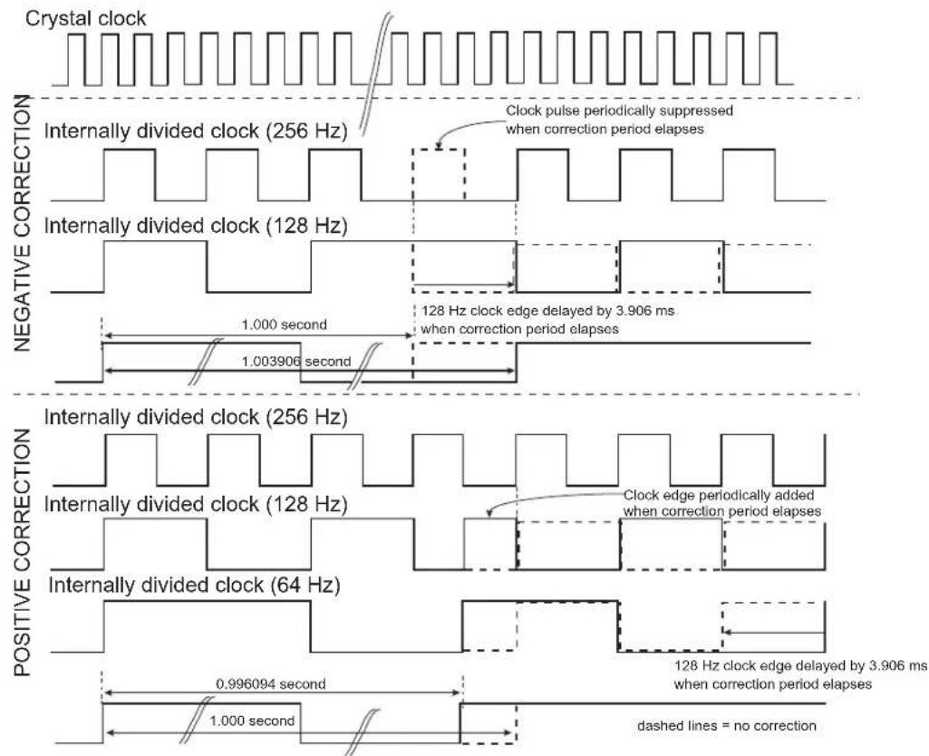
The inaccuracy of a crystal oscillator at typical room temperature ( ±20 ppm at 20–25 °C) can be compensated if a reference clock/signal is used to measure such inaccuracy. This kind of calibration operation can be set up during the final product manufacturing by means of measurement equipment embedding such a reference clock. The correction of value must be programmed into the (RTC_MR), and this value is kept as long as the circuitry is powered (backup area). Removing the backup power supply cancels this calibration. This room temperature calibration can be further processed by means of the networking capability of the target application.
To ease the comparison of the inherent crystal accuracy with the reference clock/signal during manufacturing, an internal prescaled 32.768 kHz clock derivative signal can be assigned to drive RTC output. To accommodate the measure, several clock frequencies can be selected among 1 Hz, 32 Hz, 64 Hz, 512 Hz.
The clock calibration correction drives the internal RTC counters but can also be observed in the RTC output when one of the following three frequencies 1 Hz, 32 Hz or 64 Hz is configured. The correction is not visible in the RTC output if 512 Hz frequency is configured.
Note: This adjustment does not consider the temperature variation.
The frequency drift (up to -200 ppm) due to temperature variation can be compensated using a reference time if the application can access such a reference. If a reference time cannot be used, a temperature sensor can be placed close to the crystal oscillator in order to get the operating temperature of the crystal oscillator. Once obtained, the temperature may be converted using a lookup table (describing the accuracy/temperature curve of the crystal oscillator used) and RTC_MR configured accordingly. The calibration can be performed on-the-fly. This adjustment method is not based on a measurement of the crystal frequency/drift and therefore can be improved by means of the networking capability of the target application.
If no crystal frequency adjustment has been done during manufacturing, it is still possible to do it. In the case where a reference time of the day can be obtained through LAN/WAN network, it is possible to calculate the drift of the application crystal oscillator by comparing the values read on RTC Time Register (RTC_TIMR) and programming the HIGHPPM and CORRECTION fields on RTC_MR according to the difference measured between the reference time and those of RTC_TIMR.
27.5.8 Waveform Generation
Waveforms can be generated in order to take advantage of the RTC inherent prescalers while the RTC is the only powered circuitry (Low-power mode of operation, Backup mode) or in any active mode. Entering Backup or Low-power operating modes does not affect the waveform generation outputs.
The outputs RTCOUT0 and RTCOUT1 can be configured to provide several types of waveforms. The figure below illustrates the different signals available to generate RTCOUT0 and RTCOUT1.
Figure 27-6. Waveform Generation
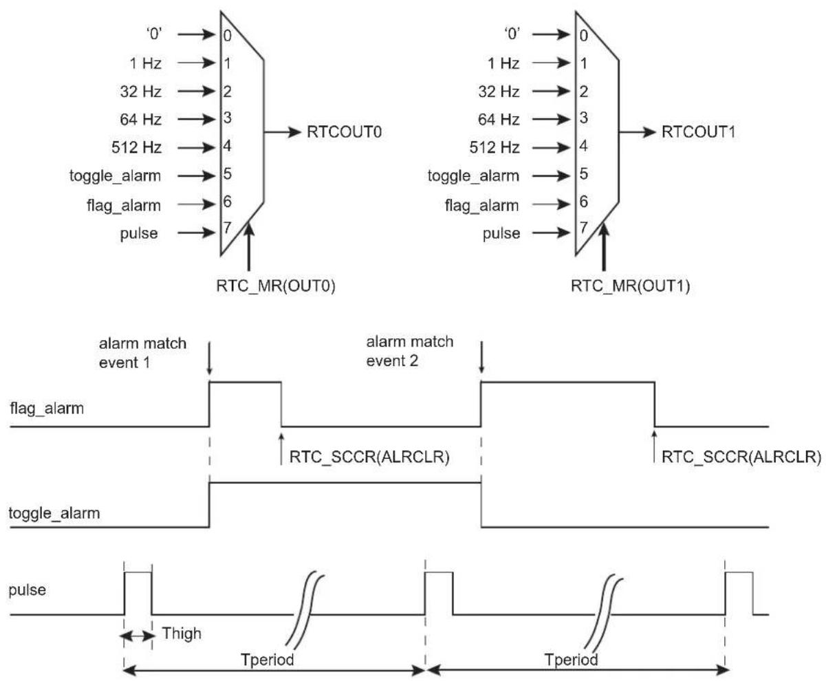
27.6 Register Summary
| Offset | Name Bit Pos. 7 | 6 | 5 | 4 | 3 | 2 | 1 | 0 | ||||||||||||||||||||||||||||||||||||||||||||||||||||||||||||||||||||||||||||||||||||||||||||||||||||||||||||||||||||||||||||||||||||||||||||||||||||||||||||||||||||||||||||||||||||||||||||||||||||||||||||||||||||||||||||||||||||||||||||||||||||||||||||||||||||||||||||||||||||||||||||||||||||||||||||||||||||||||||||||||||||||||||||||||||||||||||||||||||||||||||||||||||||||||||||||||||||||||||||||||||||||||||||||||||||||||||||||||||||||||||||||||||||||||||||||||||||||||||||||||||||||||||||||||||||||||||||||||||||||||||||||||||||||||||||||||||||||||
| 0x00 | RTC_CR | 7:0 | UPDCAL UPDTIM | 7:0 | UPDCAL UPDTIM | |||||||||||||||||||||||||||||||||||||||||||||||||||||||||||||||||||||||||||||||||||||||||||||||||||||||||||||||||||||||||||||||||||||||||||||||||||||||||||||||||||||||||||||||||||||||||||||||||||||||||||||||||||||||||||||||||||||||||||||||||||||||||||||||||||||||||||||||||||||||||||||||||||||||||||||||||||||||||||||||||||||||||||||||||||||||||||||||||||||||||||||||||||||||||||||||||||||||||||||||||||||||||||||||||||||||||||||||||||||||||||||||||||||||||||||||||||||||||||||||||||||||||||||||||||||||||||||||||||||||||||||||||||||||||||||||||||||||||||
| 15:8 | TIMEVSEL[1:0] | 23:16 | CALEVSEL[1:0] | 31:24 | ||||||||||||||||||||||||||||||||||||||||||||||||||||||||||||||||||||||||||||||||||||||||||||||||||||||||||||||||||||||||||||||||||||||||||||||||||||||||||||||||||||||||||||||||||||||||||||||||||||||||||||||||||||||||||||||||||||||||||||||||||||||||||||||||||||||||||||||||||||||||||||||||||||||||||||||||||||||||||||||||||||||||||||||||||||||||||||||||||||||||||||||||||||||||||||||||||||||||||||||||||||||||||||||||||||||||||||||||||||||||||||||||||||||||||||||||||||||||||||||||||||||||||||||||||||||||||||||||||||||||||||||||||||||||||||||||||||||||||||
| 23:16 | CALEVSEL[1:0] | THIGH[2:0] | OUT0[2:0] | OUT0[2;0] | OUT0 | OUT0[2;0] | OUT0[2;0] | OUT0[2;0] | OUT0[2;0] | OUT0[2;0] | OUT0[2;0] | OUT0[2;0] | OUT0[2;0] | OUT0[2;0] | OUT0[2;0] | OUT0[2;0] | OUT0[2;0] | OUT0[2;0] | OUT0[2;0] | OUT0 | OUT0[2;0] | OUT0[2;0] | OUT0[2;0] | OUT0[2;0] | OUT0[2;0] | OUT0[2;0] | OUT0[2;0] | OUT0[2;0] | OUT0[2;0] | OUT0[2;0] | OUT0[2;0] | OUT0[2;0] | OUT0 [2;0] | OUT0[2;0] | OUT0[2;0] | OUT0[2;0] | OUT0[2;0] | OUT0[2;0] | OUT0[2;0] | OUT0[2;0] | OUT0[2;0] | OUT0[2;0] | OUT0[2;0] | OUT0[2;0] | OUT0[2;0][2;0] | OUT0[2;0] | OUT0[2;0] | OUT0[2;0] | OUT0[2;0] | OUT0[2;0] | OUT0[2;0] | OUT0[2;0] | OUT0[2;0] | OUT0[2;0] | OUT0[2;0] | OUT0[2;0] | OUT0[2;0] OUT0[2;0] | OUT0[2;0] | OUT0[2;0] | OUT0[2;0] | OUT0[2;0] | OUT0[2;0] | OUT0[2;0] | OUT0[2;0] | OUT0[2;0] | OUT0[2;0] | OUT0[2;0] | OUT0[2;0] | OUT0[1;0] | OUT0[1;0] | OUT0[1;0] | OUT0[1;0] | OUT0[1;0] | OUT0[1;0] | OUT0[1;0] | OUT0[1;0] | OUT0[1;0] | OUT0[1;0] | OUT0[1;0] | OUT0[1;0] | OUT0[1;0] | |||||||||||||||||||||||||||||||||||||||||||||||||||||||||||||||||||||||||||||||||||||||||||||||||||||||||||||||||||||||||||||||||||||||||||||||||||||||||||||||||||||||||||||||||||||||||||||||||||||||||||||||||||||||||||||||||||||||||||||||||||||||||||||||||||||||||||||||||||||||||||||||||||||||||||||||||||||||||||||||||||||||||||||||||||||||||||||||||||||||||||||||||||||||||||||||||||||||||||||||||||||||||||||||||||||||||||||||||||||||||||||||||||||||||||||||||||||||||||||||
| 7:0 | HIGHPPM | CORRECTION[6:0] | ||||||||||||||||||||||||||||||||||||||||||||||||||||||||||||||||||||||||||||||||||||||||||||||||||||||||||||||||||||||||||||||||||||||||||||||||||||||||||||||||||||||||||||||||||||||||||||||||||||||||||||||||||||||||||||||||||||||||||||||||||||||||||||||||||||||||||||||||||||||||||||||||||||||||||||||||||||||||||||||||||||||||||||||||||||||||||||||||||||||||||||||||||||||||||||||||||||||||||||||||||||||||||||||||||||||||||||||||||||||||||||||||||||||||||||||||||||||||||||||||||||||||||||||||||||||||||||||||||||||||||||||||||||||||||||||||||||||||||||||
| HIGHPPM | 15:8 | MIN[6:0] | ||||||||||||||||||||||||||||||||||||||||||||||||||||||||||||||||||||||||||||||||||||||||||||||||||||||||||||||||||||||||||||||||||||||||||||||||||||||||||||||||||||||||||||||||||||||||||||||||||||||||||||||||||||||||||||||||||||||||||||||||||||||||||||||||||||||||||||||||||||||||||||||||||||||||||||||||||||||||||||||||||||||||||||||||||||||||||||||||||||||||||||||||||||||||||||||||||||||||||||||||||||||||||||||||||||||||||||||||||||||||||||||||||||||||||||||||||||||||||||||||||||||||||||||||||||||||||||||||||||||||||||||||||||||||||||||||||||||||||||||
| AMPM | 23:16 | CAPRIO[5:0] | THIGH[2:0] | OUT0[2:0] | OUT0[2;0] | OUT0[2;0] | OUT0[2;0] | OUT0[2;0] | OUT0[2;0] | OUT0[2;0] | OUT0[2;0] | OUT0[2;0] | OUT0[2;0] | OUT0[2;0] | OUT0[2;0] | OUT0[2;0] | INHIGR[2;0] | OUT0[2;0] | OUT0[2;0] | OUT0[2;0] | OUT0[2;0] | OUT0[2;0] | OUT0[2;0] | OUT0[2;0] | OUT0[2;0] | OUT0[2;0] | OUT0[2;0] | OUT0[2;0] | OUT0[2;1] | OUT0[2;1] | OUT0[2;1] | OUT0[2;1] | OUT0[2;1] | OUT0[2;1] | OUT0[2;1] | OUT0[2;1] | OUT0[2;1] | OUT0[2;1] | OUT0[2;1] | OUT0[2;1] | OUT0[2;1] | OUT1[2;0] | OUT1[2;0] | OUT1[2;0] | OUT1[2;0] | OUT1[2;0] | OUT1[2;0] | OUT1[2;0] | OUT1[2;0] | OUT1[2;0] | OUT1[2;0] | OUT1[2;0] | OUT1[2;0] | OUT1[2;0] | OUT2[2;0] | OUT2[2;0] | OUT2[2;0] | OUT2[2;0] | OUT2[2;0] | OUT2[2;0] | OUT2[2;0] | OUT2[2;0] | OUT2[2;0] | OUT2[2;0] | OUT2[2;0] | OUT2[2;0] | OUT2[2;1] | OUT2[2;1] | OUT2[2;1] | OUT2[2;1] | OUT2[2;1] | OUT2[2;1] | OUT2[2;1] | OUT2[2;1] | OUT2[2;1] | OUT2[2;1] | OUT2[2;1] | OUT2[2;1] | OUT2[2;1] | OUT3[2;0] | OUT3[2;0] | OUT3[2;0] | OUT3[2;0] | OUT3[2;0] | OUT3[2;0] | OUT3[2;0] | OUT3[2;0] | OUT3[2;0] | OUT3[2;0] | OUT3[2;0] | OUT3[2;0] | OUT3[2;0] | OUT4[2;0] | OUT4[2;0] | OUT4[2;0] | OUT4[2;0] | OUT4[2;0] | OUT4[2;0] | OUT4[2;0] | OUT4[2;0] | OUT4[2;0] | OUT4[2;0] | OUT4[2;0] | OUT4[2;0] | OUT4[2;1] | OUT4[2;1] | OUT4[2;1] | OUT4[2;1] | OUT4[2;1] | OUT4[2;1] | OUT4[2;1] | OUT4[2;1] | OUT4[2;1] | OUT4[2;1] | OUT4[2;1] | OUT4[2;1] | OUT4[2;1] | OUT5[2;0] | OUT5[2;0] | OUT5[2;0] | OUT5[2;0] | OUT5[2;0] | OUT5[2;0] | OUT5[2;0] | OUT5[2;0] | OUT5[2;0] | OUT5[2;0] | OUT5[2;0] | OUT5[2;0] | OUT5[2;0] | OUT6[2;0] | OUT6[2;0] | OUT6[2;0] | OUT6[2;0] | OUT6[2;0] | OUT6[2;0] | OUT6[2;0] | OUT6[2;0] | OUT6[2;0] | OUT6[2;0] | OUT6[2;0] | OUT6[2;0] | OUT6[2;1] | OUT6[2;1] | OUT6[2;1] | OUT6[2;1] | OUT6[2;1] | OUT6[2;1] | OUT6[2;1] | OUT6[2;1] | OUT6[2;1] | OUT6[2;1] | OUT6[2;1] | OUT6[2;1] | OUT6[2;1] | OUT7[2;0] | OUT7[2;0] | OUT7[2;0] | OUT7[2;0] | OUT7[2;0] | OUT7[2;0] | OUT7[2;0] | OUT7[2;0] | OUT7[2;0] | OUT7[2;0] | OUT7[2;0] | OUT7[2;0] | OUT7[2;0] | OUT8[2;0] | OUT8[2;0] | OUT8[2;0] | OUT8[2;0] | OUT8[2;0] | OUT8[2;0] | OUT8[2;0] | OUT8[2;0] | OUT8[2;0] | OUT8[2;0] | OUT8[2;0] | OUT8[2;0] | OUT8[2;1] | OUT8[2;1] | OUT8[2;1] | OUT8[2;1] | OUT8[2;1] | OUT8[2;1] | OUT8[2;1] | OUT8[2;1] | OUT8[2;1] | OUT8[2;1] | OUT8[2;1] | OUT8[2;1] | OUT8[2;1] | OUT9[2;0] | OUT9[2;0] | OUT9[2;0] | OUT9[2;0] | OUT9[2;0] | OUT9[2;0] | OUT9[2;0] | OUT9[2;0] | OUT9[2;0] | OUT9[2;0] | OUT9[2;0] | OUT9[2;0] | OUT9[2;0] | OUT10[2;0] | OUT10[2;0] | OUT10[2;0] | OUT10[2;0] | OUT10[2;0] | OUT10[2;0] | OUT10[2;0] | OUT10[2;0] | OUT10[2;0] | OUT10[2;0] | OUT10[2;0] | OUT10 [2;0] | OUT10[2;0] | OUT10[2;0] | OUT10[2;0] | OUT10[2;0] | OUT10[2;0] | OUT10[2;0] | OUT10[2;0] | OUT10[2;0] | OUT10[2;0] | OUT10[2;0] | OUT10[1;0] | OUT10[1;0] | OUT10[1;0] | OUT10[1;0] | OUT10[1;0] | OUT10[1;0] | OUT10[1;0] | OUT10[1;0] | OUT10[1;0] | OUT10[1;0] | OUT10[1;0] | OUT10[1,0] | OUT10[1;0] | OUT10[1;0] | OUT10[1;0] | OUT10[1;0] | OUT10[1;0] | OUT10[1;0] | OUT10[1;0] | OUT10[1;0] | OUT10[1;0] | OUT10[1;0] | OUT10[1;1] | OUT10[1;1] | OUT10[1;1] | OUT10[1;1] | OUT10[1;1] | OUT10[1;1] | OUT10[1;1] | OUT10[1;1] | OUT10[1;1] | OUT10[1;1] | OUT10[1;1] | OUT10[1;1][1;1] | OUT10[1;1] | OUT10[1;1] | OUT10[1;1] | OUT10[1;1] | OUT10[1;1] | OUT10[1;1] | OUT10[1;1] | OUT10[1;1] | OUT10[1;1] | OUT10[1;1] | OUT10[2;0] | OUT10[2;0] | OUT10[2;0] | OUT10[2;0] | OUT10[2;0] | OUT10[2;0] | OUT10[2;0] | OUT10[2;0] | OUT10[2;0] | OUT10[2;0] | OUT10[2;0][1;1] | OUT10[1;1] | OUT10[1;1] | OUT10[1;1] | OUT10[1;1] | OUT10[1;1] | OUT10[1;1] | OUT10[1;1] | OUT10[1;1] | OUT10[1;1] | OUT10[1;1] | OUT10(1;1) | OUT10[1;1] | OUT10[1;1] | OUT10[1;1] | OUT10[1;1] | OUT10[1;1] | OUT10[1;1] | OUT10[1;1] | OUT10[1;1] | OUT10[1;1] | OUT10[1;1] | OUT10[1;1] | |||||||||||||||||||||||||||||||||||||||||||||||||||||||||||||||||||||||||||||||||||||||||||||||||||||||||||||||||||||||||||||||||||||||||||||||||||||||||||||||||||||||||||||||||||||||||||||||||||||||||||||||||||||||||||||||||||||||||||||||||||||||||||||||
| 31:24 | DATEEN | 31:24 | 31:24 | DATEEN | DATEEEL | |||||||||||||||||||||||||||||||||||||||||||||||||||||||||||||||||||||||||||||||||||||||||||||||||||||||||||||||||||||||||||||||||||||||||||||||||||||||||||||||||||||||||||||||||||||||||||||||||||||||||||||||||||||||||||||||||||||||||||||||||||||||||||||||||||||||||||||||||||||||||||||||||||||||||||||||||||||||||||||||||||||||||||||||||||||||||||||||||||||||||||||||||||||||||||||||||||||||||||||||||||||||||||||||||||||||||||||||||||||||||||||||||||||||||||||||||||||||||||||||||||||||||||||||||||||||||||||||||||||||||||||||||||||||||||||||||||||||||||
| 0x18 RTC_SR | 7:0 | TDERR | 15:8 | TDERRCLR | ||||||||||||||||||||||||||||||||||||||||||||||||||||||||||||||||||||||||||||||||||||||||||||||||||||||||||||||||||||||||||||||||||||||||||||||||||||||||||||||||||||||||||||||||||||||||||||||||||||||||||||||||||||||||||||||||||||||||||||||||||||||||||||||||||||||||||||||||||||||||||||||||||||||||||||||||||||||||||||||||||||||||||||||||||||||||||||||||||||||||||||||||||||||||||||||||||||||||||||||||||||||||||||||||||||||||||||||||||||||||||||||||||||||||||||||||||||||||||||||||||||||||||||||||||||||||||||||||||||||||||||||||||||||||||||||||||||||||||||
| 23:16 | CALCLR | 31:24 | TDERRCLR | |||||||||||||||||||||||||||||||||||||||||||||||||||||||||||||||||||||||||||||||||||||||||||||||||||||||||||||||||||||||||||||||||||||||||||||||||||||||||||||||||||||||||||||||||||||||||||||||||||||||||||||||||||||||||||||||||||||||||||||||||||||||||||||||||||||||||||||||||||||||||||||||||||||||||||||||||||||||||||||||||||||||||||||||||||||||||||||||||||||||||||||||||||||||||||||||||||||||||||||||||||||||||||||||||||||||||||||||||||||||||||||||||||||||||||||||||||||||||||||||||||||||||||||||||||||||||||||||||||||||||||||||||||||||||||||||||||||||||||||
| 0x1C RTC_SCCR | 7:0 | TDERRCLR | 15:8 | TDERRCLR | ||||||||||||||||||||||||||||||||||||||||||||||||||||||||||||||||||||||||||||||||||||||||||||||||||||||||||||||||||||||||||||||||||||||||||||||||||||||||||||||||||||||||||||||||||||||||||||||||||||||||||||||||||||||||||||||||||||||||||||||||||||||||||||||||||||||||||||||||||||||||||||||||||||||||||||||||||||||||||||||||||||||||||||||||||||||||||||||||||||||||||||||||||||||||||||||||||||||||||||||||||||||||||||||||||||||||||||||||||||||||||||||||||||||||||||||||||||||||||||||||||||||||||||||||||||||||||||||||||||||||||||||||||||||||||||||||||||||||||||
| 23.16 | TDERRCLR | 31:24 | TDERRCLR | |||||||||||||||||||||||||||||||||||||||||||||||||||||||||||||||||||||||||||||||||||||||||||||||||||||||||||||||||||||||||||||||||||||||||||||||||||||||||||||||||||||||||||||||||||||||||||||||||||||||||||||||||||||||||||||||||||||||||||||||||||||||||||||||||||||||||||||||||||||||||||||||||||||||||||||||||||||||||||||||||||||||||||||||||||||||||||||||||||||||||||||||||||||||||||||||||||||||||||||||||||||||||||||||||||||||||||||||||||||||||||||||||||||||||||||||||||||||||||||||||||||||||||||||||||||||||||||||||||||||||||||||||||||||||||||||||||||||||||||
| 7:0 | TDERRCLR | 15:8 | TDERRCLR | |||||||||||||||||||||||||||||||||||||||||||||||||||||||||||||||||||||||||||||||||||||||||||||||||||||||||||||||||||||||||||||||||||||||||||||||||||||||||||||||||||||||||||||||||||||||||||||||||||||||||||||||||||||||||||||||||||||||||||||||||||||||||||||||||||||||||||||||||||||||||||||||||||||||||||||||||||||||||||||||||||||||||||||||||||||||||||||||||||||||||||||||||||||||||||||||||||||||||||||||||||||||||||||||||||||||||||||||||||||||||||||||||||||||||||||||||||||||||||||||||||||||||||||||||||||||||||||||||||||||||||||||||||||||||||||||||||||||||||||
| 23:16 | TDERRCLR | 31:24 | TDERRCLR | |||||||||||||||||||||||||||||||||||||||||||||||||||||||||||||||||||||||||||||||||||||||||||||||||||||||||||||||||||||||||||||||||||||||||||||||||||||||||||||||||||||||||||||||||||||||||||||||||||||||||||||||||||||||||||||||||||||||||||||||||||||||||||||||||||||||||||||||||||||||||||||||||||||||||||||||||||||||||||||||||||||||||||||||||||||||||||||||||||||||||||||||||||||||||||||||||||||||||||||||||||||||||||||||||||||||||||||||||||||||||||||||||||||||||||||||||||||||||||||||||||||||||||||||||||||||||||||||||||||||||||||||||||||||||||||||||||||||||||||
| 7:0 | TDERRCLR | 15:8 | TDERRCLR | 15:8 | TDERRCLR | |||||||||||||||||||||||||||||||||||||||||||||||||||||||||||||||||||||||||||||||||||||||||||||||||||||||||||||||||||||||||||||||||||||||||||||||||||||||||||||||||||||||||||||||||||||||||||||||||||||||||||||||||||||||||||||||||||||||||||||||||||||||||||||||||||||||||||||||||||||||||||||||||||||||||||||||||||||||||||||||||||||||||||||||||||||||||||||||||||||||||||||||||||||||||||||||||||||||||||||||||||||||||||||||||||||||||||||||||||||||||||||||||||||||||||||||||||||||||||||||||||||||||||||||||||||||||||||||||||||||||||||||||||||||||||||||||||||||||||
| 23:16 | TDERRCLR | 31:24 | TDERRCLR | TDERRCLR | TDERRCLR | TDERRCLR | TDERRCLR | TDERRCLR | TDERRCLR | TDERRCLR | TDERRCLR | TDERRCLR | TDERRCLR | TDERRCLR | TDERRCLR | TDERRCLR | TDERRCLR | TDERRCLR | TDERRCLR | TDERRCLR | TDERRCLR | TDERRCLR | TDERRCLR | TDERRCLR | TDERRCLR | TDERRCLR | TDERRCLR | TDERRCLR | TDERRCR | TDERRCLR | TDERRCLR | TDERRCLR | TDERRCLR | TDERRCLR | TDERRCLR | TDERRCLR | TDERRCLR | TDERRCLR | TDERRCLR | TDERRCLR | TDERRCLR | TDERRCLR | TDERRCLR | TDERRCLR | TDERRCLR | TDERRCLR | TDERRCLR | TDERRCLR | TDERRCLR | TDERRCLR | TDERRCLR | TDERRCLR | TDERRCLR | TDERRCL | TDERRCLR | TDERRCLR | TDERRCLR | TDERRCLR | TDERRCLR | TDERRCLR | TDERRCLR | TDERRCLR | TDERRCLR | TDERRCLR | TDERRCLR | TDERRCLR | TDERRCLR | TDERRCLR | TDERRCLR | TDERRCLR | TDERRCLR | TDERRCLR | TDERRCLR | TDERRCLR | TDERRCLR | TDERRCLR | TDERRCLR | TDERRCLR | TDERRC-1 | TDERRC-1 | TDERRC-1 | |||||||||||||||||||||||||||||||||||||||||||||||||||||||||||||||||||||||||||||||||||||||||||||||||||||||||||||||||||||||||||||||||||||||||||||||||||||||||||||||||||||||||||||||||||||||||||||||||||||||||||||||||||||||||||||||||||||||||||||||||||||||||||||||||||||||||||||||||||||||||||||||||||||||||||||||||||||||||||||||||||||||||||||||||||||||||||||||||||||||||||||||||||||||||||||||||||||||||||||||||||||||||||||||||||||||||||||||||||||||||||||||||||||||||||||||||||||||||||||||
27.6.1 RTC Control Register
Name: RTC_CR
Offset: 0x00
Reset: 0x00000000
Property: Read/Write
This register can only be written if the WPEN bit is cleared in the System Controller Write Protection Mode Register (SYSC_WPMR).
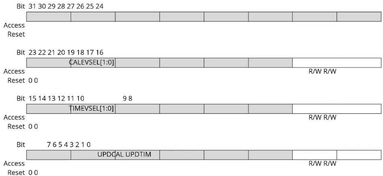
text_image
Bit 31 30 29 28 27 26 25 24 Access Reset Bit 23 22 21 20 19 18 17 16 CALEVSEL[1:0] Access Reset 0 0 R/W R/W Bit 15 14 13 12 11 10 9 8 TIMEVSEL[1:0] Access Reset 0 0 R/W R/W Bit 7 6 5 4 3 2 1 0 UPDCAL UPDTIM Access Reset 0 0 R/W R/WBits 17:16 - CALEVSEL[1:0] Calendar Event Selection
The event that generates the flag CALEV in RTC_SR depends on the value of CALEVSEL
| Value | Name | Description |
| 0 | WEEK | Week change (every Monday at time 00:00:00) |
| 1 | MONTH | Month change (every 01 of each month at time 00:00:00) |
| 2 | YEAR | Year change (every January 1 at time 00:00:00) |
| 3 | YEAR | Reserved |
Bits 9:8 - TIMEVSEL[1:0] Time Event Selection
The event that generates the flag TIMEV in RTC_SR depends on the value of TIMEVSEL.
| Value | Name | Description |
| 0 | MINUTE | Minute change |
| 1 | HOUR | Hour change |
| 2 | MIDNIGHT | Every day at midnight |
| 3 | NOON | Every day at noon |
Bit 1 - UPDCAL Update Request Calendar Register
Calendar counting consists of day, date, month, year and century counters. Calendar counters can be programmed once this bit is set and acknowledged by the bit ACKUPD of the RTC_SR.
| Value | Description |
| 0 | No effect or, if UPDCAL has been previously written to 1, stops the update procedure. |
| 1 | Stops the RTC calendar counting. |
Bit 0 - UPDTIM Update Request Time Register
Time counting consists of second, minute and hour counters. Time counters can be programmed once this bit is set and acknowledged by the bit ACKUPD of the RTC_SR.
| Value Description | |
| 0 | No effect or, if UPDTIM has been previously written to 1, stops the update procedure. |
| 1 | Stops the RTC time counting. |
27.6.2 RTC Mode Register
Name: RTC_MR
Offset: 0x04
Reset: 0x00000000
Property: Read/Write
This register can only be written if the WPEN bit is cleared in the System Controller Write Protection Mode Register (SYSC_WPMR).
Bit 31 30 29 28 27 26 25 24
| TPERIOD[1:0] THIGH[2:0] | |||||
| Access Reset | R/W 0 R/W 0 R/W R/W | ||||
Bit 23 22 21 20 19 18 17 16
| OUT1[2:0] | OUT0[2:0] | ||||||
| Access | R/W | R/W | R/W | R/W | R/W | R/W | R/W |
| Reset | 0 | 0 | 0 | 0 | |||
Bit 15 14 13 12 11 10 9 8
| HIGHPPM | CORRECTION[6:0] | |||||||
| Access Reset | R/W R/W | R/W | R/W | R/W | R/W | R/W | R/W | R/W |
| 0 | 0 | 0 | 0 | 0 | 0 | 0 | 0 | |
| Bit | 7 | 6 | 5 | 4 | 3 | 2 | 1 | 0 |
| NEGPPM | PERSIAN | HRMOD | ||||||
| Access Reset | R/W | R/W | R/W | |||||
| 0 | 0 | 0 | ||||||
Bits 29:28 - TPERIOD[1:0] Period of the Output Pulse
| Value | Name | Description |
| 0 | P_1S | 1 second |
| 1 | P_500MS | 500 ms |
| 2 | P_250MS | 250 ms |
| 3 | P_125MS | 125 ms |
Bits 26:24 - THIGH[2:0] High Duration of the Output Pulse
| Value | Name | Description |
| 0 | H_31MS | 31.2 ms |
| 1 | H_16MS | 15.6 ms |
| 2 | H_4MS | 3.91 ms |
| 3 | H_976US | 976 μs |
| 4 | H_488US | 488 μs |
| 5 | H_122US | 122 μs |
| 6 | H_30US | 30.5 μs |
| 7 | H_15US | 15.2 μs |
Bits 22:20 - OUT1[2:0] RTCOUT1 Output Source Selection
| Value | Name | Description |
| 0 | NO_WAVE | No waveform, stuck at '0' |
| 1 | FREQ1HZ | 1 Hz square wave |
| 2 | FREQ32HZ 32 Hz square wave | |
| 3 | FREQ64HZ 64 Hz square wave | |
| 4 | FREQ512HZ | 512 Hz square wave |
| Value Name | Description |
| 5 | ALARM_TOGGLE Output toggles when alarm flag rises |
| 6 | ALARM_FLAG Output is a copy of the alarm flag |
| 7 | PROG_PULSE Duty cycle programmable pulse |
Bits 18:16 - OUT0[2:0] RTCOUT0 Output Source Selection
| Value Name | Description | |
| 0 | NO_WAVE No waveform, stuck at '0' | |
| 1 | FREQ1HZ 1 Hz square wave | |
| 2 | FREQ32HZ 32 Hz square wave | |
| 3 | FREQ64HZ 64 Hz square wave | |
| 4 | FREQ512HZ 512 Hz square wave | |
| 5 | ALARM_TOGGLE Output toggles when alarm flag rises | |
| 6 | ALARM_FLAG Output is a copy of the alarm flag | |
| 7 | PROG_PULSE Duty cycle programmable pulse | |
Bit 15 - HIGHPPM HIGH PPM Correction
If the absolute value of the correction to be applied is lower than 30 ppm, it is recommended to clear HIGHPPM. HIGHPPM set to 1 is recommended for 30 ppm correction and above.
Formula:
If HIGHPPM = 0, then the clock frequency correction range is from 1.5 ppm up to 98 ppm. The RTC accuracy is less than 1 ppm for a range correction from 1.5 ppm up to 30 ppm.
The correction field must be programmed according to the required correction in ppm; the formula is as follows:
$$ \text { CORRECTION } = \frac {3 9 0 6}{2 0 \times \mathrm{ppm}} - 1 $$
The value obtained must be rounded to the nearest integer prior to being programmed into CORRECTION field.
If HIGHPPM = 1, then the clock frequency correction range is from 30.5 ppm up to 1950 ppm. The RTC accuracy is less than 1 ppm for a range correction from 30.5 ppm up to 90 ppm.
The correction field must be programmed according to the required correction in ppm; the formula is as follows:
$$ \text { CORRECTION } = \frac {3 9 0 6}{\mathrm{ppm}} - 1 $$
The value obtained must be rounded to the nearest integer prior to be programmed into CORRECTION field.
If NEGPPM is set to 1, the ppm correction is negative (used to correct crystals that are faster than the nominal 32.768 kHz).
| Value Description | |
| 0 | Lower range ppm correction with accurate correction. |
| 1 | Higher range ppm correction with accurate correction. |
Bits 14:8 - CORRECTION[6:0] Slow Clock Correction
| Value Description | |
| 0 | No correction |
| 1-127 | The slow clock will be corrected according to the formula given in HIGHPPM description. |
Bit 4 - NEGPPM Negative PPM Correction
See CORRECTION and HIGHPPM field descriptions.
NEGPPM must be cleared to correct a crystal slower than 32.768 kHz.
| Value Description | |
| 0 | Positive correction (the divider will be slightly higher than 32768). |
| 1 | Negative correction (the divider will be slightly lower than 32768). |
| 0 | Gregorian calendar. |
| 1 | Persian calendar. |
Bit 1 - PERSIAN PERSIAN Calendar
Bit 0 - HRMOD 12-/24-hour Mode
| Value Description | |
| 0 | 24-hour mode is selected. |
| 1 | 12-hour mode is selected. |
27.6.3 RTC Time Register
Name: RTC_TIMR
Offset: 0x08
Reset: 0x00000000
Property: Read/Write
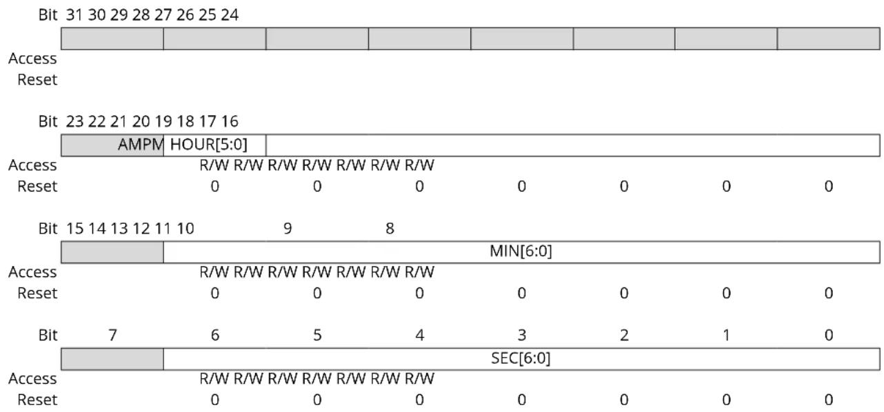
Bit 22 - AMPM Ante Meridiem Post Meridiem Indicator
This bit is the AM/PM indicator in 12-hour mode.
| Value | Description |
| 0 | AM. |
| 1 | PM. |
Bits 21:16 - HOUR[5:0] Current Hour
The range that can be set is 1–12 (BCD) in 12-hour mode or 0–23 (BCD) in 24-hour mode.
Bits 14:8 - MIN[6:0] Current Minute
The range that can be set is 0-59 (BCD).
The lowest four bits encode the units. The higher bits encode the tens.
Bits 6:0 - SEC[6:0] Current Second
The range that can be set is 0–59 (BCD).
The lowest four bits encode the units. The higher bits encode the tens.
27.6.4 RTC Calendar Register
Name: RTC_CALR
Offset: 0x0C
Reset: 0x01E11320
Property: Read/Write
| Bit 31 30 29 28 27 26 25 24 | ||
| DATE[5:0] | ||
| Access Reset | R/W R/W R/W R/W R/W R/W | |
| 0 0 0 0 0 1 | ||
| Bit 23 22 21 20 19 18 17 16 | ||
| DAY[2:0] | MONTH[4:0] | |
| Access Reset | R/W R/W R/W R/W R/W R/W R/W R/W | |
| 1 1 1 0 0 0 0 1 | ||
| Bit 15 14 13 12 11 10 | 9 8 | |
| YEAR[7:0] | ||
| Access Reset | R/W R/W R/W R/W R/W R/W R/W R/W | |
| 0 0 0 1 0 0 1 1 | ||
| Bit | 7 6 5 4 3 2 1 0 | |
| CENT[6:0] | ||
| Access Reset | R/W R/W R/W R/W R/W R/W R/W | |
| 0 1 0 0 0 0 0 | ||
Bits 29:24 - DATE[5:0] Current Day in Current Month
The range that can be set is 01-31 (BCD).
The lowest four bits encode the units. The higher bits encode the tens.
Bits 23:21 - DAY[2:0] Current Day in Current Week
The range that can be set is 1–7 (BCD).
The coding of the number (which number represents which day) is user-defined as it has no effect on the date counter.
Bits 20:16 - MONTH[4:0] Current Month
The range that can be set is 01–12 (BCD).
The lowest four bits encode the units. The higher bits encode the tens.
Bits 15:8 - YEAR[7:0] Current Year
The range that can be set is 00–99 (BCD).
The lowest four bits encode the units. The higher bits encode the tens.
Bits 6:0 - CENT[6:0] Current Century
The range that can be set is 19–20 (Gregorian) or 13–14 (Persian) (BCD).
The lowest four bits encode the units. The higher bits encode the tens.
27.6.5 RTC Time Alarm Register
Name: RTC_TIMALR
Offset: 0x10
Reset: 0x00000000
Property: Read/Write
This register can only be written if the WPEN bit is cleared in the System Controller Write Protection Mode Register (SYSC_WPMR).
To change one of the SEC, MIN, HOUR fields, it is recommended to disable the field before changing the value and then re-enable it after the change has been made. This requires up to three accesses to the RTC_TIMALR. The first access clears the enable corresponding to the field to change (SECEN, MINEN, HOUREN). If the field is already cleared, this access is not required. The second access performs the change of the value (SEC, MIN, HOUR). The third access is required to re-enable the field by writing 1 in SECEN, MINEN, HOUREN fields.
| Bit 31 30 29 28 27 26 25 24 | |||||||
| Access Reset | |||||||
| Bit 23 22 21 20 19 18 17 16 | |||||||
| HOURN AMPM HOUR[5:0] | |||||||
| Access Reset | R/W R/W R/W R/W R/W R/W R/W | ||||||
| 0 | 0 | 0 | 0 | 0 | 0 | 0 | |
| Bit 15 14 13 12 11 10 | 9 | 8 | |||||
| MINEN | MIN[6:0] | ||||||
| Access Reset | R/W R/W R/W R/W R/W R/W R/W | ||||||
| 0 | 0 | 0 | 0 | 0 | 0 | 0 | |
| Bit | 7 | 6 | 5 | 4 | 3 | 2 | 1 |
| SECEN | SEC[6:0] | ||||||
| Access Reset | R/W R/W R/W R/W R/W R/W R/W | ||||||
| 0 | 0 | 0 | 0 | 0 | 0 | 0 | |
Bit 23 - HOUREN Hour Alarm Enable
| Value | Description |
| 0 | The hour-matching alarm is disabled. |
| 1 | The hour-matching alarm is enabled. |
Bit 22 - AMPM AM/PM Indicator
This field is the alarm field corresponding to the BCD-coded hour counter.
Bits 21:16 - HOUR[5:0] Hour Alarm
This field is the alarm field corresponding to the BCD-coded hour counter.
Bit 15 - MINEN Minute Alarm Enable
| Value | Description |
| 0 | The minute-matching alarm is disabled. |
| 1 | The minute-matching alarm is enabled. |
Bits 14:8 - MIN[6:0] Minute Alarm
This field is the alarm field corresponding to the BCD-coded minute counter.
Bit 7 - SECEN Second Alarm Enable
| Value Description | |
| 0 | The second-matching alarm is disabled. |
| 1 | The second-matching alarm is enabled. |
Bits 6:0 - SEC[6:0] Second Alarm
This field is the alarm field corresponding to the BCD-coded second counter.
27.6.6 RTC Calendar Alarm Register
Name: RTC_CALALR
Offset: 0x14
Reset: 0x01010000
Property: Read/Write
This register can only be written if the WPEN bit is cleared in the System Controller Write Protection Mode Register (SYSC_WPMR).
To change one of the DATE, MONTH fields, it is recommended to disable the field before changing the value and then re-enable it after the change has been made. This requires up to three accesses to the RTC_CALALR. The first access clears the enable corresponding to the field to change (DATEEN, MTHEN). If the field is already cleared, this access is not required. The second access performs the change of the value (DATE, MONTH). The third access is required to re-enable the field by writing 1 in DATEEN, MTHEN fields.
| Bit 31 30 29 28 27 26 25 24 | |||||||
| DATEEN | DATE[5:0] | ||||||
| Access Reset | R/W | R/W | R/W | R/W | R/W | R/W | R/W |
| 0 | 0 | 0 | 0 | 0 | 1 | ||
| Bit 23 22 21 20 19 18 17 16 | |||||||
| MTHEN | MONTH[4:0] | ||||||
| Access Reset | R/W | R/W | R/W | R/W | R/W | ||
| 0 | 0 | 0 | 0 | 1 | |||
| Bit 15 14 13 12 11 10 | 9 | 8 | |||||
| Access Reset | |||||||
| Bit | 7 | 6 | 5 | 4 | 3 | 2 | 1 |
| Access Reset | |||||||
Bit 31 - DATEEN Date Alarm Enable
| Value | Description |
| 0 | The date-matching alarm is disabled. |
| 1 | The date-matching alarm is enabled. |
Bits 29:24 - DATE[5:0] Date Alarm
This field is the alarm field corresponding to the BCD-coded date counter.
Bit 23 - MTHEN Month Alarm Enable
| Value | Description |
| 0 | The month-matching alarm is disabled. |
| 1 | The month-matching alarm is enabled. |
Bits 20:16 - MONTH[4:0] Month Alarm
This field is the alarm field corresponding to the BCD-coded month counter.
27.6.7 RTC Status Register
Name: RTC_SR
Offset: 0x18
Reset: 0x00000000
Property: Read-only
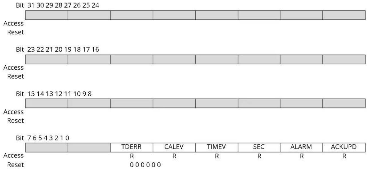
text_image
Bit 31 30 29 28 27 26 25 24 Access Reset Bit 23 22 21 20 19 18 17 16 Access Reset Bit 15 14 13 12 11 10 9 8 Access Reset Bit 7 6 5 4 3 2 1 0 Access Reset TDERR CALEV TIMEV SEC ALARM ACKUPD R R R R R 0 0 0 0 0 0Bit 5 - TDERR Time and/or Date Free Running Error
| Value | Name | Description |
| 0 | CORRECT | The internal free running counters are carrying valid values since the last read of the Status Register (RTC_SR). |
| 1 | ERR_TIMEDATE | The internal free running counters have been corrupted (invalid date or time, non-BCD values) since the last read and/or they are still invalid. |
Bit 4 - CALEV Calendar Event
The calendar event is selected in the CALEVSEL field in the Control Register (RTC_CR) and can be any one of the following events: week change, month change and year change.
| Value | Name | Description |
| 0 | NO_CALEVENT | No calendar event has occurred since the last clear. |
| 1 | CALEVENT | At least one calendar event has occurred since the last clear. |
Bit 3 - TIMEV Time Event
The time event is selected in the TIMEVSEL field in the Control Register (RTC_CR) and can be any one of the following events: minute change, hour change, noon, midnight (day change).
| Value | Name | Description |
| 0 | NO_TIMEVENT | No time event has occurred since the last clear. |
| 1 | TIMEVENT | At least one time event has occurred since the last clear. |
Bit 2 - SEC Second Event
| Value | Name | Description |
| 0 | NO_SECEVENT | No second event has occurred since the last clear. |
| 1 | SECEVENT | At least one second event has occurred since the last clear. |
Bit 1 - ALARM Alarm Flag
| Value Name | Description |
| 0 | NO_ALARMEVENT No alarm matching condition occurred. |
| 1 | ALARMEVENT An alarm matching condition has occurred. |
Bit 0 - ACKUPD Acknowledge for Update
| Value Name | Description | |
| 0 | FREERUN Time and calendar registers cannot be updated. | |
| 1 | UPDATE Time and calendar registers can be updated. | |
27.6.8 RTC Status Clear Command Register
Name: RTC_SCCR
Offset: 0x1C
Reset: -
Property: Write-only
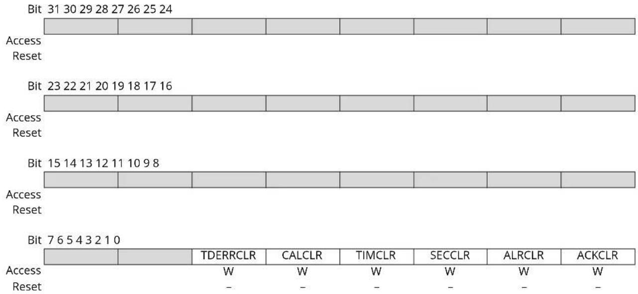
Bit 5 - TDERRCLR Time and/or Date Free Running Error Clear
| Value | Description |
| 0 | No effect. |
| 1 | Clears corresponding status flag in the Status Register (RTC_SR). |
Bit 4 - CALCLR Calendar Clear
| Value | Description |
| 0 | No effect. |
| 1 | Clears corresponding status flag in the Status Register (RTC_SR). |
Bit 3 - TIMCLR Time Clear
| Value | Description |
| 0 | No effect. |
| 1 | Clears corresponding status flag in the Status Register (RTC_SR). |
Bit 2 - SECCLR Second Clear
| Value | Description |
| 0 | No effect. |
| 1 | Clears corresponding status flag in the Status Register (RTC_SR). |
Bit 1 - ALRCLR Alarm Clear
| Value | Description |
| 0 | No effect. |
| 1 | Clears corresponding status flag in the Status Register (RTC_SR). |
Bit 0 - ACKCLR Acknowledge Clear
Value Description
| 0 | No effect. |
| 1 | Clears corresponding status flag in the Status Register (RTC_SR). |
27.6.9 RTC Interrupt Enable Register
Name: RTC_IER
Offset: 0x20
Reset: -
Property: Write-only
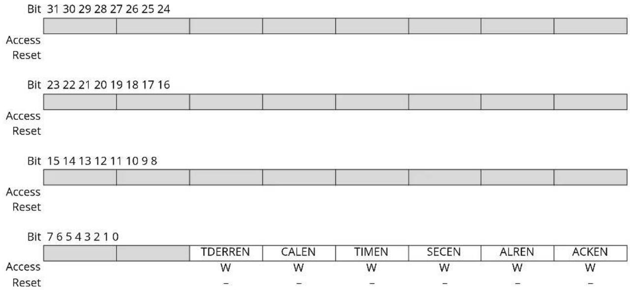
Bit 5 - TDERREN Time and/or Date Error Interrupt Enable
| Value | Description |
| 0 | No effect. |
| 1 | The time and date error interrupt is enabled. |
Bit 4 - CALEN Calendar Event Interrupt Enable
| Value | Description |
| 0 | No effect. |
| 1 | The selected calendar event interrupt is enabled. |
Bit 3 - TIMEN Time Event Interrupt Enable
| Value | Description |
| 0 | No effect. |
| 1 | The selected time event interrupt is enabled. |
Bit 2 - SECEN Second Event Interrupt Enable
| Value | Description |
| 0 | No effect. |
| 1 | The second periodic interrupt is enabled. |
Bit 1 - ALREN Alarm Interrupt Enable
| Value | Description |
| 0 | No effect. |
| 1 | The alarm interrupt is enabled. |
Bit 0 - ACKEN Acknowledge Update Interrupt Enable
Value Description
| 0 | No effect. |
| 1 | The acknowledge for update interrupt is enabled. |
27.6.10 RTC Interrupt Disable Register
Name: RTC_IDR
Offset: 0x24
Reset: -
Property: Write-only
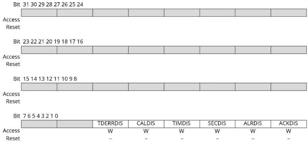
bar_stacked
| Bit | Access Reset | TDERRDIS | CALDIS | TIMDIS | SECDIS | ALRDIS | ACKDIS | |-----|--------------|----------|--------|--------|--------|--------|--------| | 31 | - | - | - | - | - | - | - | | 30 | - | - | - | - | - | - | - | | 29 | - | - | - | - | - | - | - | | 28 | - | - | - | - | - | - | - | | 27 | - | - | - | - | - | - | - | | 26 | - | - | - | - | - | - | - | | 25 | - | - | - | - | - | - | - | | 24 | - | - | - | - | - | - | - | | 23 | - | - | - | - | - | - | - | | 22 | - | - | - | - | - | - | - | | 21 | - | - | - | - | - | - | - | | 20 | - | - | - | - | - | - | - | | 19 | - | - | - | - | - | - | - | | 18 | - | - | - | - | - | - | - | | 17 | - | - | - | - | - | - | - | | 16 | - | - | - | - | - | - | - | | 15 | Access Reset | - | - | - | - | - | - | | 14 | Access Reset | - | - | - | - | - | - | | 13 | Access Reset | - | - | - | - | - | - | | 12 | Access Reset | - | - | - | - | - | - | | 11 | Access Reset | - | - | - | - | - | - | | 10 | Access Reset | - | - | - | - | - | - | | 9 | Access Reset | - | - | - | - | - | - | | 8 | Access Reset | - | - | - | - | - | - | | 7 | Access Reset | - | - | - | - | - | - | | 6 | Access Reset | TDERRDIS | CALDIS | TIMDIS | SECDIS | ALRDIS | ACKDIS | | 5 | Access Reset | W | W | W | W | W | W | | 4 | Access Reset | W | W | W | W | W | W | | 3 | Access Reset | W | W | W | W | W | W | | 2 | Access Reset | W | W | W | W | W | W | | 1 | Access Reset | W | W | W | W | W | W | | 0 | Access Reset | W | W | W | W | W | W | | The data is extracted from the image. The bit values are explicitly labeled on the bars. The 'Access' and 'Reset' labels are not present in the image. There are no additional data series or labels provided in the image.Bit 5 - TDERRDIS Time and/or Date Error Interrupt Disable
| Value | Description |
| 0 | No effect. |
| 1 | The time and date error interrupt is disabled. |
Bit 4 - CALDIS Calendar Event Interrupt Disable
| Value | Description |
| 0 | No effect. |
| 1 | The selected calendar event interrupt is disabled. |
Bit 3 - TIMDIS Time Event Interrupt Disable
| Value | Description |
| 0 | No effect. |
| 1 | The selected time event interrupt is disabled. |
Bit 2 - SECDIS Second Event Interrupt Disable
| Value | Description |
| 0 | No effect. |
| 1 | The second periodic interrupt is disabled. |
Bit 1 - ALRDIS Alarm Interrupt Disable
| Value | Description |
| 0 | No effect. |
| 1 | The alarm interrupt is disabled. |
Bit 0 - ACKDIS Acknowledge Update Interrupt Disable
Value Description
| 0 | No effect. |
| 1 | The acknowledge for update interrupt is disabled. |
27.6.11 RTC Interrupt Mask Register
Name: RTC_IMR
Offset: 0x28
Reset: 0x00000000
Property: Read-only

text_image
Bit 31 30 29 28 27 26 25 24 Access Reset Bit 23 22 21 20 19 18 17 16 Access Reset Bit 15 14 13 12 11 10 9 8 Access Reset Bit 7 6 5 4 3 2 1 0 Access Reset TDERR CAL TIM SEC ALR ACK R R R R R 0 0 0 0 0 0Bit 5 - TDERR Time and/or Date Error Mask
| Value | Description |
| 0 | The time and/or date error event is disabled. |
| 1 | The time and/or date error event is enabled. |
Bit 4 - CAL Calendar Event Interrupt Mask
| Value | Description |
| 0 | The selected calendar event interrupt is disabled. |
| 1 | The selected calendar event interrupt is enabled. |
Bit 3 - TIM Time Event Interrupt Mask
| Value | Description |
| 0 | The selected time event interrupt is disabled. |
| 1 | The selected time event interrupt is enabled. |
Bit 2 - SEC Second Event Interrupt Mask
| Value | Description |
| 0 | The second periodic interrupt is disabled. |
| 1 | The second periodic interrupt is enabled. |
Bit 1 - ALR Alarm Interrupt Mask
| Value | Description |
| 0 | The alarm interrupt is disabled. |
| 1 | The alarm interrupt is enabled. |
Bit 0 - ACK Acknowledge Update Interrupt Mask
Value Description
| 0 | The acknowledge for update interrupt is disabled. |
| 1 | The acknowledge for update interrupt is enabled. |
27.6.12 RTC Valid Entry Register
Name: RTC_VER
Offset: 0x2C
Reset: 0x00000000
Property: Read-only

text_image
Bit 31 30 29 28 27 26 25 24 Access Reset Bit 23 22 21 20 19 18 17 16 Access Reset Bit 15 14 13 12 11 10 9 8 Access Reset Bit 7 6 5 4 3 2 1 0 Access Reset NVCALALR NVTIMALR NVCAL NVTIM R R R R 0 0 0 0Bit 3 - NVCALALR Non-valid Calendar Alarm
| Value | Description |
| 0 | No invalid data has been detected in RTC_CALALR (Calendar Alarm Register). |
| 1 | RTC_CALALR has contained invalid data since it was last programmed. |
Bit 2 - NVTIMALR Non-valid Time Alarm
| Value | Description |
| 0 | No invalid data has been detected in RTC_TIMALR (Time Alarm Register). |
| 1 | RTC_TIMALR has contained invalid data since it was last programmed. |
Bit 1 - NVCAL Non-valid Calendar
| Value | Description |
| 0 | No invalid data has been detected in RTC_CALR (Calendar Register). |
| 1 | RTC_CALR has contained invalid data since it was last programmed. |
Bit 0 - NVTIM Non-valid Time
| Value | Description |
| 0 | No invalid data has been detected in RTC_TIMR (Time Register). |
| 1 | RTC_TIMR has contained invalid data since it was last programmed. |
28. Real-time Timer (RTT)
28.1 Description
The Real-time Timer (RTT) is built around a 32-bit counter used to count roll-over events of the programmable 16-bit prescaler driven from the 32-kHz slow clock source. It generates a periodic interrupt and/or triggers an alarm on a programmed value.
The RTT can also be configured to be driven by the 1Hz RTC signal, thus taking advantage of a calibrated 1Hz clock.
The slow clock source can be fully disabled to reduce power consumption when only an elapsed seconds count is required.
28.2 Embedded Characteristics
- 32-bit Free-running Counter on prescaled slow clock or RTC calibrated 1Hz clock
• 16-bit Configurable Prescaler - Interrupt on Alarm or Counter Increment
28.3 Block Diagram
Figure 28-1. Real-time Timer Block Diagram
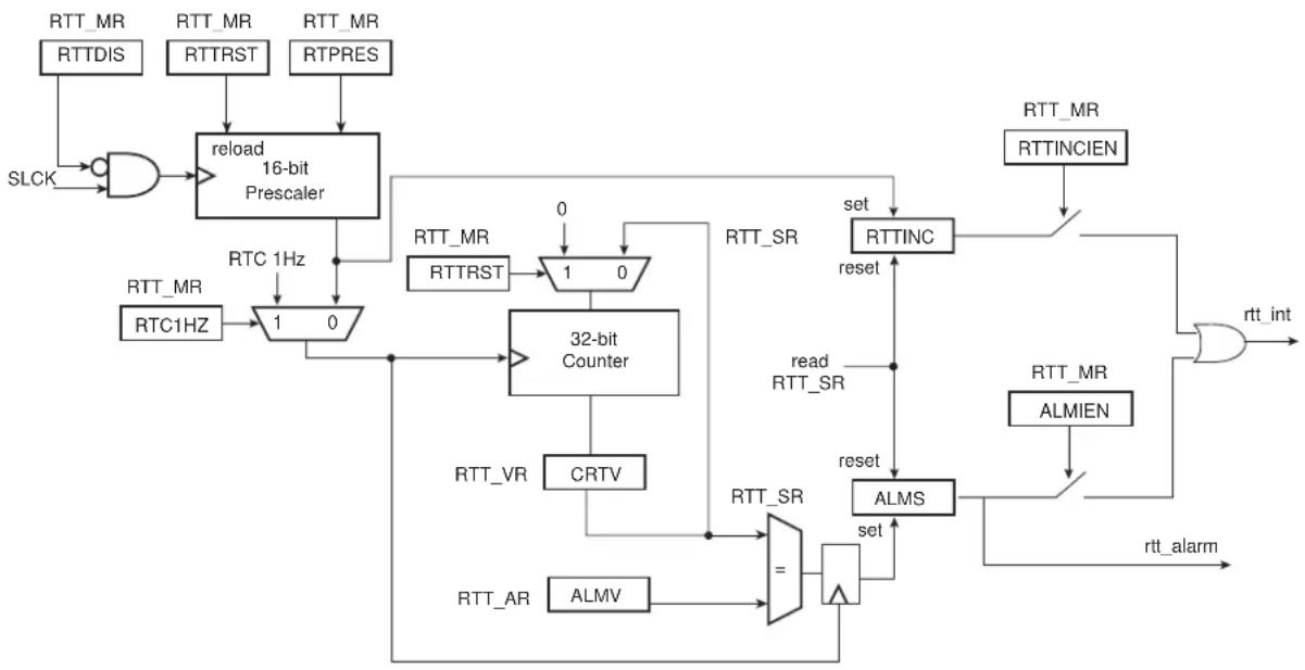
flowchart
graph TD
    A["RTT_MR"] --> B["RTTDIS"]
    C["RTTRST"] --> D["reload 16-bit Prescaler"]
    E["RTTPRES"] --> D
    F["SLCK"] --> G["AND Gate"]
    G --> H["reload"]
    H --> I["16-bit Prescaler"]
    I --> J["RTC 1Hz"]
    J --> K["1 0"]
    K --> L["32-bit Counter"]
    L --> M["RTTRST"]
    M --> N["1 0"]
    N --> O["RTT_SR"]
    P["RTT_MR"] --> Q["RTTC1HZ"]
    R["RTT_INCIEN"] --> S["RTTINC"]
    T["RTT_MR"] --> U["ALMIEN"]
    V["RTT_MR"] --> W["ALMS"]
    X["RTT_SR"] --> Y["="]
    Z["RTT_AR"] --> AA["ALMV"]
    AB["RTT_VR"] --> AC["CRTV"]
    AD["reset"] --> AE["reset"]
    AF["read RTT_SR"] --> AG["32-bit Counter"]
    AH["set"] --> AI["RTTINC"]
    AJ["rtt_int"] --> AK["AND Gate"]
    AL["rtt_alarm"] --> AM["ALMS"]
28.4 Functional Description
The programmable 16-bit prescaler value can be configured through the RTPRES field in the RTT Mode register (RTT_MR).
Configuring the RTPRES field value to 0x8000 (default value) corresponds to feeding the real-time counter with a 1Hz signal (if the slow clock is 32.768 kHz). The 32-bit counter can count up to 2^32 seconds, corresponding to more than 136 years, then roll over to 0. Bit RTTINC in the RTT Status Register (RTT_SR) is set each time there is a prescaler roll-over.
The real-time 32-bit counter can also be supplied by the 1Hz RTC clock. This mode is interesting when the RTC 1Hz is calibrated (CORRECTION field 0 in RTC_MR) in order to guaranty the synchronism between RTC and RTT counters.
Setting the RTC1HZ bit in the RTT_MR drives the 32-bit RTT counter from the 1Hz RTC clock. In this mode, the RTPRES field has no effect on the 32-bit counter.
The prescaler roll-over generates an increment of the real-time timer counter if RTC1HZ = 0. Otherwise, if RTC1HZ = 1, the RTT counter is incremented every second. The RTTINC bit is set independently from the 32-bit counter increment.
The RTT can also be used as a free-running timer with a lower time-base. The best accuracy is achieved by writing RTPRES to 3 in RTT_MR.
Programming RTPRES to 1 or 2 is forbidden.
If the RTT is configured to trigger an interrupt, the interrupt occurs two slow clock cycles after reading the RTT_SR. To prevent several executions of the interrupt handler, the interrupt must be disabled in the interrupt handler and re-enabled when the RTT_SR is cleared.
The CRTV field can be read at any time in the RTT Value register (RTT_VR). As this value can be updated asynchronously with the Host Clock, the CRTV field must be read twice at the same value to read a correct value.
The current value of the counter is compared with the value written in the RTT Alarm register (RTT_AR). If the counter value matches the alarm, the ALMS bit in the RTT_SR is set. The RTT_AR is set to its maximum value (0xFFFFFFF) after a reset.
The ALMS flag is always a source of the RTT alarm signal that may be used to exit the system from low power modes (see the Real-time Timer Block Diagram above).
The alarm interrupt must be disabled (ALMIEN must be cleared in RTT_MR) when writing a new ALMV value in the RTT_AR.
The RTTINC bit can be used to start a periodic interrupt, the period being one second when the RTPRES field value = 0x8000 and the slow clock = 32.768 kHz.
The RTTINCIEN bit must be cleared prior to writing a new RTPRES value in the RTT_MR.
Reading the RTT_SR automatically clears the RTTINC and ALMS bits.
Writing the RTTRST bit in the RTT_MR immediately reloads and restarts the clock divider with the new programmed value. This also resets the 32-bit counter.
When not used, the RTT can be disabled in order to suppress dynamic power consumption in this module. This can be achieved by setting the RTTDIS bit in the RTT_MR.
Figure 28-2. RTT Counting
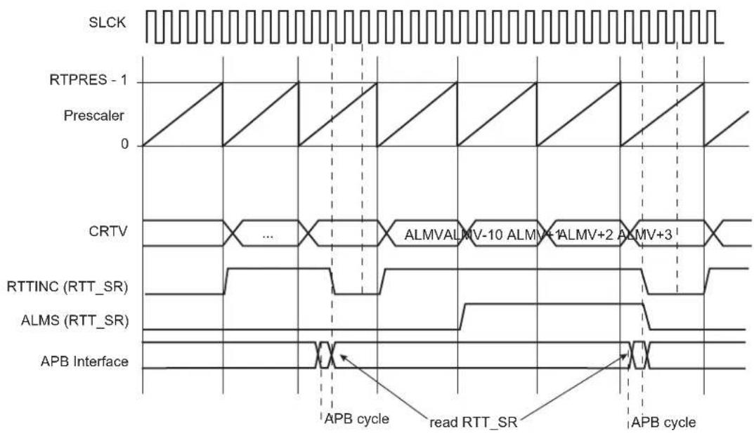
text_image
SLCK RTPRES - 1 Prescaler 0 CRTV ... ALMVALMV-10 ALMV+1ALMV+2 ALMV+3 RTTINC (RTT_SR) ALMS (RTT_SR) APB Interface APB cycle read RTT_SR APB cycle28.5 Register Summary
| Offset | Name Bit Pos. 7 | 6 | 5 | 4 | 3 | 2 | 1 | 0 | |||||||||||
| 0x00 | RTT_MR | 7:0 RTPRES[7:0] | |||||||||||||||||
| 15:8 RTPRES[15:8] | |||||||||||||||||||
| 23:16 | RTTDIS RTTRST RTTINCIEN ALMIEN | ||||||||||||||||||
| 31:24 | RTC1HZ | ||||||||||||||||||
| 0x04 | RTT_AR | 7:0 | ALMV[7:0] | ||||||||||||||||
| 15:8 | ALMV[15:8] | ||||||||||||||||||
| 23:16 | ALMV[23:16] | ||||||||||||||||||
| 31:24 | ALMV[31:24] | ||||||||||||||||||
| 0x08 | RTT_VR | 7:0 | CRTV[7:0] | ||||||||||||||||
| 15:8 CRTV[15:8] | |||||||||||||||||||
| 23:16 CRTV[23:16] | |||||||||||||||||||
| 31:24 CRTV[31:24] | |||||||||||||||||||
| 0x0C | RTT_SR | 7:0 | RTTINC ALMS | ||||||||||||||||
| 15:8 | |||||||||||||||||||
| 23:16 | |||||||||||||||||||
| 31:24 | |||||||||||||||||||
28.5.1 Real-time Timer Mode Register
Name: RTT_MR
Offset: 0x00
Reset: 0x00008000
Property: Read/Write
Bit 31 30 29 28 27 26 25 24
| RTC1HZ | |||||||
| Access Reset 0 | R/W | ||||||
Bit 23 22 21 20 19 18 17 16
| RTT | DIS | RTTRST | RTTINCIEN | ALMIEN | |||||
| Access | R/W | R/W | R/W | R/W | |||||
| Reset | 0 | 0 | 0 | 0 |
Bit 15 14 13 12 11 10 9 8
| RTPRES[15:8] | ||||||||
| Access | R/W | R/W | R/W | R/W | R/W | R/W | R/W | R/W |
| Reset | 1 | 0 | 0 | 0 | 0 | 0 | 0 | 0 |
| Bit | 7 | 6 | 5 | 4 | 3 | 2 | 1 | 0 |
| RTPRES[7:0] | ||||||||
| Access | R/W | R/W | R/W | R/W | R/W | R/W | R/W | R/W |
| Reset | 0 | 0 | 0 | 0 | 0 | 0 | 0 | 0 |
Bit 24 - RTC1HZ Real-Time Clock 1Hz Clock Selection
| Value | Description |
| 0 | The RTT 32-bit counter is driven by the 16-bit prescaler roll-over events. |
| 1 | The RTT 32-bit counter is driven by the 1Hz RTC clock. |
Bit 20 - RTTDIS Real-time Timer Disable
| Value | Description |
| 0 | The RTT is enabled. |
| 1 | The RTT is disabled (no dynamic power consumption). |
Bit 18 - RTTRST Real-time Timer Restart
| Value | Description |
| 0 | No effect. |
| 1 | Reloads and restarts the clock divider with the new programmed value. This also resets the 32-bit counter. |
Bit 17 - RTTINCIEN Real-time Timer Increment Interrupt Enable
| Value | Description |
| 0 | The bit RTTINC in RTT_SR has no effect on interrupt. |
| 1 | The bit RTTINC in RTT_SR asserts interrupt. |
Bit 16 - ALMIEN Alarm Interrupt Enable
| Value | Description |
| 0 | The bit ALMS in RTT_SR has no effect on interrupt. |
| 1 | The bit ALMS in RTT_SR asserts interrupt. |
Bits 15:0 - RTPRES[15:0] Real-time Timer Prescaler Value
Defines the number of SLCK periods required to increment the RTT. The RTTINCIEN bit must be cleared prior to writing a new RTPRES value.
RTPRES is defined as follows:
- RTPRES = 0: The prescaler period is equal to 2 ^16 * SLCK periods.
- RTPRES = 1 or 2: forbidden.
- RTPRES 0,1 or 2: The prescaler period is equal to RTPRES * SLCK periods.
28.5.2 Real-time Timer Alarm Register
Name: RTT_AR
Offset: 0x04
Reset: 0xFFFFFFF
Property: Read/Write
The alarm interrupt must be disabled (ALMIEN must be cleared in RTT_MR) when writing a new ALMV value.
Bit 31 30 29 28 27 26 25 24
ALMV[31:24]
Access R/W R/W R/W R/W R/W R/W R/W R/W
Reset 1 1 1 1 1 1 1 1
Bit 23 22 21 20 19 18 17 16
ALMV[23:16]
Access R/W R/W R/W R/W R/W R/W R/W R/W
Reset 1 1 1 1 1 1 1 1
Bit 15 14 13 12 11 10 9 8
ALMV[15:8]
Access R/W R/W R/W R/W R/W R/W R/W R/W
Reset 1 1 1 1 1 1 1 1
Bit 76543210
ALMV[7:0]
Access R/W R/W R/W R/W R/W R/W R/W R/W
Reset 1 1 1 1 1 1 1 1
Bits 31:0 - ALMV[31:0] Alarm Value
When the CRTV value in RTT_VR equals the ALMV field, the ALMS flag is set in RTT_SR. As soon as the ALMS flag rises, the CRTV value equals ALMV+1 (refer to the figure RTT Counting above).
28.5.3 Real-time Timer Value Register
Name: RTT_VR
Offset: 0x08
Reset: 0x00000000
Property: Read-only
| Bit 31 30 29 28 27 26 25 24 | |
| CRTV[31:24] | |
| Access R R R R R R R R | |
| Reset 0 0 0 0 0 0 0 0 | |
| Bit 23 22 21 20 19 18 17 16 | |
| CRTV[23:16] | |
| Access R R R R R R R R | |
| Reset 0 0 0 0 0 0 0 0 | |
| Bit 15 14 13 12 11 10 9 8 | |
| CRTV[15:8] | |
| Access R R R R R R R R | |
| Reset 0 0 0 0 0 0 0 0 | |
| Bit 7 6 5 4 3 2 1 0 | |
| CRTV[7:0] | |
| Access R R R R R R R R | |
| Reset 0 0 0 0 0 0 0 0 | |
Bits 31:0 - CRTV[31:0] Current Real-time Value
Returns the current value of the RTT.
As CRTV can be updated asynchronously, it must be read twice at the same value.
28.5.4 Real-time Timer Status Register
Name: RTT_SR
Offset: 0x0C
Reset: 0x00000000
Property: Read-only
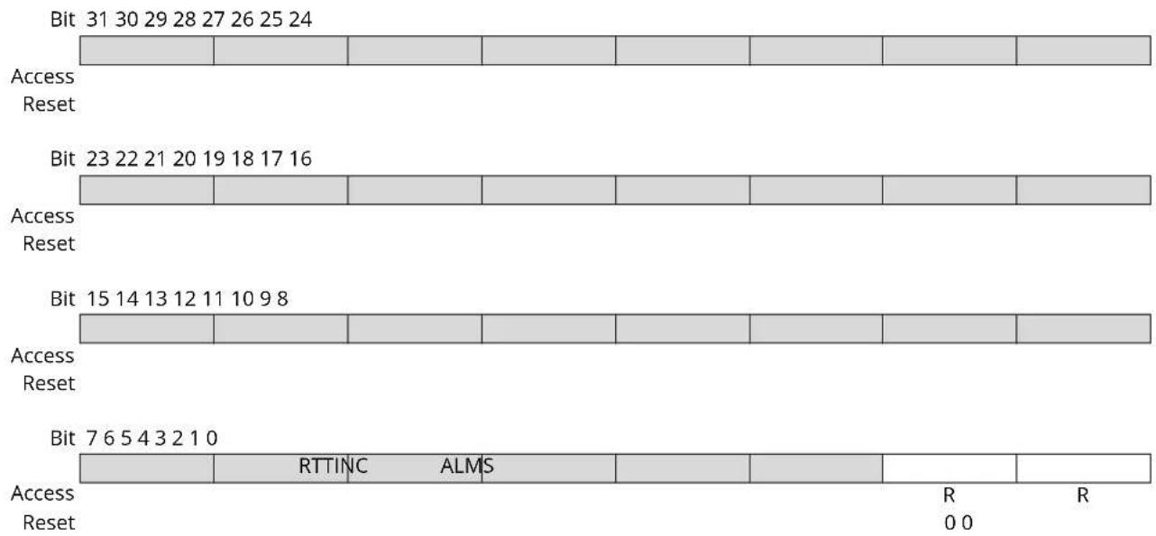
text_image
Bit 31 30 29 28 27 26 25 24 Access Reset Bit 23 22 21 20 19 18 17 16 Access Reset Bit 15 14 13 12 11 10 9 8 Access Reset Bit 7 6 5 4 3 2 1 0 Access Reset RTTINC ALMS R R 0 0Bit 1 - RTTINC Prescaler Roll-over Status (cleared on read)
| Value | Description |
| 0 | No prescaler roll-over occurred since the last read of the RTT_SR. |
| 1 | Prescaler roll-over occurred since the last read of the RTT_SR. |
Bit 0 - ALMS Real-time Alarm Status (cleared on read)
| Value | Description |
| 0 | The Real-time Alarm has not occurred since the last read of RTT_SR. |
| 1 | The Real-time Alarm occurred since the last read of RTT_SR. |
29. General Purpose Backup Registers (GPBR)
29.1 Description
The System Controller embeds 128 bits of General Purpose Backup registers organized as 8 32-bit registers.
It is possible to generate an immediate clear of the content of General Purpose Backup registers 0 to 3 (first half) if a Low-power Debounce event is detected on one of the wakeup pins, WKUP0 or WKUP1. The content of the other General Purpose Backup registers (second half) remains unchanged.
The Supply Controller module must be programmed accordingly. In the register SUPC_WUMR in the Supply Controller module, LPDBCCLR, LPDBCEN0 and/or LPDBCEN1 bit must be configured to 1 and LPDBC must be other than 0.
If a Tamper event has been detected, it is not possible to write to the General Purpose Backup registers while the LPDBCS0 or LPDBCS1 flags are not cleared in the Supply Controller Status Register (SUPC_SR).
29.2 Embedded Characteristics
• 128 bits of General Purpose Backup Registers
- Immediate Clear on Tamper Event
29.3 Register Summary
| Offset | Name Bit Pos. 7 | 6 | 5 | 4 | 3 | 2 | 1 | 0 | ||||||||
| 0x00 | SYS_GPBRx | 7:0 GPBR_VALUE[7:0] | ||||||||||||||
| 15:8 GPBR_VALUE[15:8] | ||||||||||||||||
| 23:16 GPBR_VALUE[23:16] | ||||||||||||||||
| 31:24 GPBR_VALUE[31:24] | ||||||||||||||||
29.3.1 General Purpose Backup Register x
Name: SYS_GPBRx
Offset: 0x00
Reset: 0
Property: R/W
These registers are reset at first power-up and on each loss of VDDIO.
Bit 31 30 29 28 27 26 25 24
| GPBR_VALUE[31:24] |
Access R/W R/W R/W R/W R/W R/W R/W R/W
Reset 00000000
Bit 23 22 21 20 19 18 17 16
| GPBR_VALUE[23:16] |
Access R/W R/W R/W R/W R/W R/W R/W R/W
Reset 00000000
Bit 15 14 13 12 11 10 9 8
| GPBR_VALUE[15:8] |
Access R/W R/W R/W R/W R/W R/W R/W R/W
Reset 00000000
Bit 76543210
| GPBR_VALUE[7:0] |
Access R/W R/W R/W R/W R/W R/W R/W R/W
Reset 00000000
Bits 31:0 - GPBR_VALUE[31:0] Value of GPBR x
If a Tamper event has been detected, it is not possible to write GPBR_VALUE as long as the LPDBCS0 or LPDBCS1 flag has not been cleared in the Supply Controller Status Register (SUPC_SR).
30. Clock Generator
30.1 Description
The Clock Generator user interface is embedded within the Power Management Controller and is described in Power Management Controller (PMC) User Interface. However, the Clock Generator registers are named CKGR_.
30.2 Embedded Characteristics
The Clock Generator is comprised of the following:
- A low-power 32.768 kHz crystal oscillator with Bypass mode
- A low-power Slow RC oscillator (32 kHz typical)
- A 3 to 20 MHz Main crystal oscillator with Bypass mode
- A Main RC oscillator. Three output frequencies can be selected: 4/8/12 MHz. By default 12 MHz is selected. 8 MHz and 12 MHz are factory-trimmed.
- A 480 MHz UTMI PLL, providing a clock for the USB high-speed controller
• A 160 to 500 MHz programmable PLL (input from 8 to 32 MHz)
It provides the following clocks:
- SLCK — Slow clock. The only permanent clock within the system
- MAINCK — output of the Main clock oscillator selection: either the Main crystal oscillator or Main RC oscillator
- PLLACK — output of the divider and 160 to 500 MHz programmable PLL (PLLA)
- UPLLCK — output of the 480 MHz UTMI PLL (UPLL)
30.3 Block Diagram
Figure 30-1. Clock Generator Block Diagram
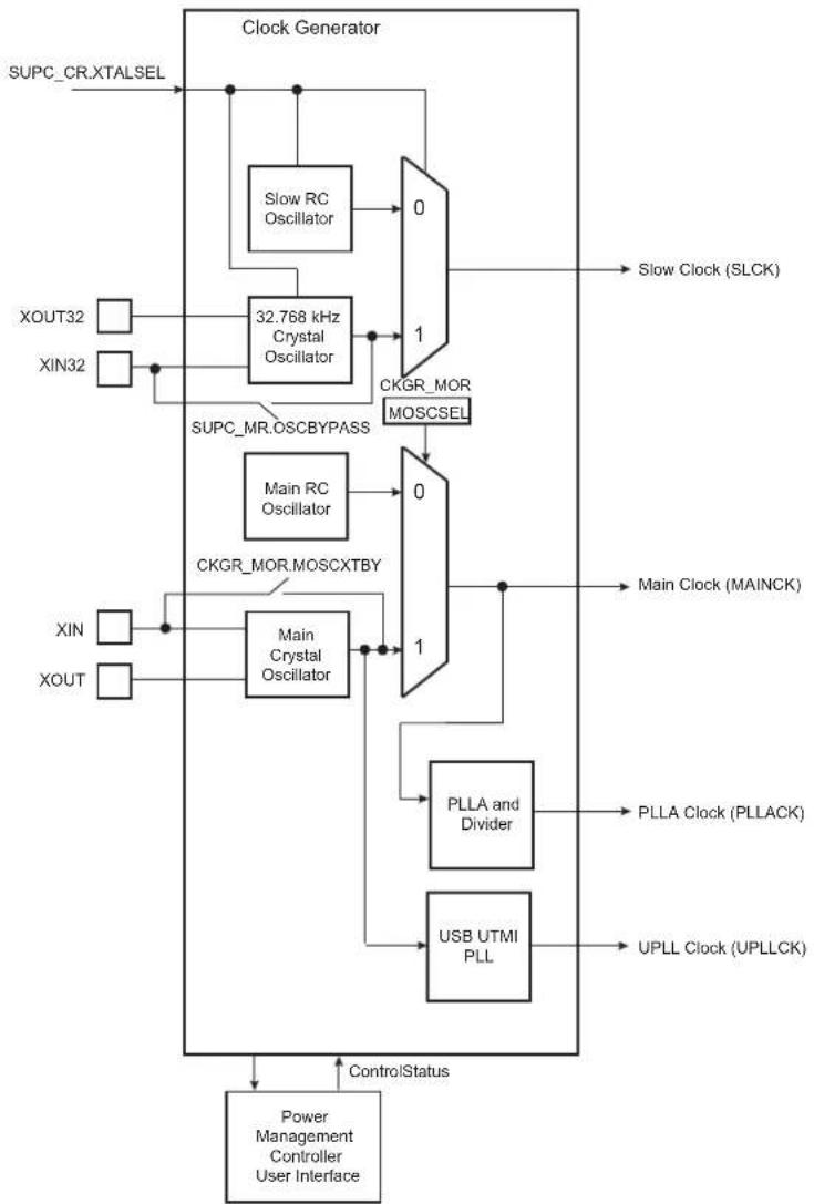
flowchart
graph TD
    A["XOUT32"] --> B["Slow RC Oscillator"]
    C["XIN32"] --> D["32.768 kHz Crystal Oscillator"]
    B --> E["0"]
    D --> F["1"]
    E --> G["Slow Clock (SLCK)"]
    F --> H["CKGR_MOR MOSCSEL"]
    I["XIN"] --> J["Main RC Oscillator"]
    K["XOUT"] --> L["Main Crystal Oscillator"]
    J --> M["0"]
    L --> N["1"]
    M --> O["Main Clock (MAINCK)"]
    N --> P["PLLAClock (PLLACK)"]
    N --> Q["USB UTMIPLL"]
    P --> R["UPLL Clock (UPLLCK)"]
    Q --> S["ControlStatus"]
    T["Power Management Controller User Interface"] --> U["ControlStatus"]
    style A fill:#f9f,stroke:#333
    style C fill:#f9f,stroke:#333
    style I fill:#f9f,stroke:#333
    style K fill:#f9f,stroke:#333
    style M fill:#f9f,stroke:#333
    style N fill:#f9f,stroke:#333
    style P fill:#f9f,stroke:#333
    style Q fill:#f9f,stroke:#333
    style S fill:#f9f,stroke:#333
30.4 Slow Clock
The Supply Controller embeds a slow clock generator that is supplied with the VDDIO power supply. As soon as VDDIO is supplied, both the 32.768 kHz crystal oscillator and the Slow RC oscillator are powered, but only the Slow RC oscillator is enabled. This allows the Slow clock (SLCK) to be valid in a short time (about 100 s).
SLCK is generated either by the 32.768 kHz crystal oscillator or by the Slow RC oscillator.
To select the clock source, the selection is made via the XTALSEL bit in the Supply Controller Control Register (SUPC_CR).
30.4.1 Slow RC Oscillator (32 kHz typical)
By default, the Slow RC oscillator is enabled and selected as a source of SLCK.
Compared to the 32.768 kHz crystal oscillator, this oscillator offers a faster startup time and is less exposed to the external environment, as it is fully integrated. However, its output frequency is
subject to larger variations with supply voltage, temperature and manufacturing process. Therefore, the user must take these variations into account when this oscillator is used as a time base (startup counter, frequency monitor, etc.). Refer to the section "Electrical Characteristics".
This oscillator is disabled by clearing the SUPC_CR.XTALSEL.
Related Links
-
Electrical Characteristics for SAM V70/V71
-
Electrical Characteristics for SAM E70/S70
30.4.2 32.768 kHz Crystal Oscillator
By default, the 32.768 kHz oscillator is disabled. To use this oscillator, the XIN32 and XOUT32 pins must be connected to a 32.768 kHz crystal or to a ceramic resonator. Refer to the section "Electrical Characteristics" for appropriate loading capacitors selection on XIN32 and XOUT32.
Note that the user is not obliged to use the 32.768 kHz crystal oscillator and can use the Slow RC oscillator instead. Using the 32.768 kHz crystal oscillator provides a more accurate frequency than the Slow RC oscillator.
To select the 32.768 kHz crystal oscillator as the source of SLCK, the bit SUPC_CR.XTALSEL must be set. This results in a sequence which first configures the PIO lines multiplexed with XIN32 and XOUT32 to be driven by the crystal oscillator, then enables the 32.768 kHz crystal oscillator and then disables the Slow RC oscillator to save power. The switch of SLCK source is glitch-free.
Reverting to the Slow RC oscillator is only possible by shutting down the VDDIO power supply. If the user does not need the 32.768 kHz crystal oscillator, the XIN32 and XOUT32 pins can be left unconnected since by default the XIN32 and XOUT32 system I/O pins are in PIO input mode with pullup after reset.
The user can also set the 32.768 kHz crystal oscillator in Bypass mode instead of connecting a crystal. In this case, the user must provide the external clock signal on XIN32. For input characteristics of the XIN32 pin, refer to the section "Electrical Characteristics". To enter Bypass mode, the OSCBYPASS bit of the Supply Controller Mode register (SUPC_MR) must be set prior to setting SUPC_CR.XTALSEL.
Related Links
-
Electrical Characteristics for SAM V70/V71
-
Electrical Characteristics for SAM E70/S70
30.5 Main Clock
The Main clock (MAINCK) has two sources:
- A Main RC oscillator (4/8/12 MHz) with a fast startup time and that is selected by default to start the system
- A Main crystal oscillator with Bypass mode
Figure 30-2. Main Clock (MAINCK) Block Diagram

flowchart
graph TD
    A["CKGR_MOR CKGR_MOR MOSCRCEN"] --> B["Main RC Oscillator"]
    C["MOSCRCF"] --> B
    B --> D["PMC_SR MOSCRCS"]
    E["CKGR_MOR MOSCSEL"] --> F["0"]
    G["PKC_SR MOSCSELS"] --> H["1"]
    I["XIN"] --> J["Main Crystal Oscillator"]
    K["XOUT"] --> J
    J --> L["MAINCK Main Clock"]
30.5.1 Main RC Oscillator
After reset, the Main RC oscillator is enabled with the 12 MHz frequency selected. This oscillator is selected as the source of MAINCK. MAINCK is the default clock selected to start the system.
Only the 8/12 MHz RC oscillator frequencies are calibrated in production. Refer to the section "Electrical Characteristics".
The software can disable or enable the Main RC oscillator with the MOSCRCEN bit in the Clock Generator Main Oscillator Register (CKGR_MOR).
The output frequency of the Main RC oscillator can be selected among 4, 8 or 12 MHz. Selection is done by configuring the field MOSCRCF in CKGR_MOR. When changing the frequency selection, the MOSCRCS bit in the Power Management Controller Status Register (PMC_SR) is automatically cleared and MAINCK is stopped until the oscillator is stabilized. Once the oscillator is stabilized, MAINCK restarts and PMC_SR.MOSCRCS is set. Note that enabling the Main RC oscillator (MOSCRCEN = 1) and changing its frequency (MOSCRCF) at the same time is not allowed.
This oscillator must be enabled first and its frequency changed in a second step.
When disabling the Main RC oscillator by clearing the CKGR_MOR.MOSCRCEN bit, the PMC_SR.MOSCRCS bit is automatically cleared, indicating that the oscillator is OFF.
Setting the MOSCRCS bit in the Power Management Controller Interrupt Enable Register (PMC_IER) triggers an interrupt to the processor.
Related Links
- Electrical Characteristics for SAM V70/V71
- Electrical Characteristics for SAM E70/S70
30.5.2 Main RC Oscillator Frequency Adjustment
The 8 MHz and 12 MHz frequencies are factory-centered to the typical values by using Flash calibration bits (refer to the "Electrical Characteristics" chapter).
The Flash calibration bits setting the Main RC oscillator frequency to 8 MHz and 12 MHz vary from device to device. To get a starting point when changing the CAL8 or CAL12 fields, it is recommended to first read their corresponding Flash calibration bits in the Flash Controller.
The user can adjust the value of the Main RC oscillator frequency by modifying the trimming values done in production on 8 MHz and 12 MHz. This may be used to compensate frequency drifts due to temperature or voltage. The values stored in the Flash cannot be erased by a Flash erase command
or by the ERASE signal. Values written by the user application in the Oscillator Calibration Register (PMC_OCR) are reset after each power-up or peripheral reset.
By default, SEL4/SEL8/SEL12 are cleared, so the Main RC oscillator is driven with the factory-programmed Flash calibration bits which are programmed during chip production.
Note: These factory-programmed calibration bitfields can be read through the EEFC using the Get CALIB bit command (GCALB).
In order to calibrate the oscillator lower frequency, SEL4 must be set to '1' and a valid frequency value must be configured in CAL4. Likewise, SEL8/12 must be set to '1' and a trim value must be configured in CAL8/12 in order to adjust the other frequencies of the oscillator.
It is possible to adjust the oscillator frequency while operating from this oscillator. For example, when running on lowest frequency, it is possible to change the CAL4 value if SEL4 is set in PMC_OCR.
At any time, the user can measure the main RC oscillator output frequency by means of the Main Frequency Counter (refer to "Main Frequency Counter"). Once the frequency measurement is done, the main RC oscillator calibration field (CALx) can be adjusted accordingly to correct this oscillator output frequency.
Related Links
-
Electrical Characteristics for SAM V70/V71
-
Electrical Characteristics for SAM E70/S70
30.5.3 Main Crystal Oscillator
After reset, the Main crystal oscillator is disabled and is not selected as the source of MAINCK.
As the source of MAINCK, the Main crystal oscillator provides a very precise frequency. The software enables or disables this oscillator in order to reduce power consumption through CKGR_MOR.MOSCXTEN.
When disabling this oscillator by clearing the CKGR_MOR.MOSCXTEN, PMC_SR.MOSCXTS is automatically cleared, indicating the oscillator is off.
When enabling this oscillator, the user must initiate the startup time counter. The startup time depends on the characteristics of the external device connected to this oscillator.
When CKGR_MOR.MOSCXTEN and CKGR_MOR.MOSCXTST are written to enable this oscillator, the PIO lines multiplexed with XIN and XOUT are driven by the Main crystal oscillator.
PMC_SR.MOSCXTS is cleared and the counter starts counting down on SLCK divided by 8 from the CKGR_MOR.MOSCXTST value. Because the CKGR_MOR.MOSCXTST value is coded with 8 bits, the startup time can be programmed up to 2048 SLCK periods, corresponding to about 62 ms when running at 32.768 kHz.
When the startup time counter reaches '0', PMC_SR.MOSCXTS is set, indicating that the oscillator is stabilized. Setting the MOSCXTS bit in the Interrupt Mask Register (PMC_IMR) can trigger an interrupt to the processor.
30.5.4 Main Clock Source Selection
The source of MAINCK can be selected from the following:
• The Main RC oscillator
• The Main crystal oscillator
- An external clock signal provided on the XIN input (Bypass mode of the Main crystal oscillator)
The advantage of the Main RC oscillator is its fast startup time. By default, this oscillator is selected to start the system and it must be selected prior to entering Wait mode.
The advantage of the Main crystal oscillator is its high level of accuracy.
The selection of the oscillator is made with bit CKGR_MOR.MOSCSEL. The switchover of the MAINCK source is glitch-free, so there is no need to run MCK out of SLCK, PLLACK or UPLLCK in order to change the selection. PMC_SR.MOSCSELS indicates when the switch sequence is done.
Setting PMC_IMR.MOSCSELS triggers an interrupt to the processor.
MAINCK Switching Sequence
When switching the Main Clock MAINCK source from the Main Crystal oscillator to the Main RC oscillator it is mandatory to follow the below steps:
- Start the Main RC oscillator and keep MAINCK on the Main Crystal Oscillator (this step is optional at startup as it is the default configuration)
- Switch MAINCK to the Main RC oscillator and keep the Main Crystal Oscillator on
- Switch off the Main Crystal Oscillator is a third separate step
30.5.5 Bypassing the Main Crystal Oscillator
Prior to bypassing the Main crystal oscillator, the external clock frequency provided on the XIN pin must be stable and within the values specified in the XIN Clock characteristics in the section "Electrical Characteristics".
The sequence is as follows:
- Ensure that an external clock is connected on XIN.
- Enable the bypass by setting CKGR_MOR.MOSCXTBY.
- Disable the Main crystal oscillator by clearing CKGR_MOR.MOSCXTEN.
30.5.6 Main Frequency Counter
The Main frequency counter measures the Main RC oscillator and the Main crystal oscillator against the SLCK and is managed by CKGR_MCFR.
During the measurement period, the Main frequency counter increments at the speed of the clock defined by the bit CKGR_MCFR.CCSS.
A measurement is started in the following cases:
- When CKGR_MCFR.RCMEAS is written to '1'.
- When the Main RC oscillator is selected as the source of MAINCK and when this oscillator is stable (i.e., when the MOSCRCS bit is set)
- When the Main crystal oscillator is selected as the source of MAINCK and when this oscillator is stable (i.e., when the MOSCXTS bit is set)
- When MAINCK source selection is modified
The measurement period ends at the 16th falling edge of SLCK, the MAINFRDY bit in CKGR_MCFR is set and the counter stops counting. Its value can be read in the MAINF field of CKGR_MCFR and gives the number of clock cycles during 16 periods of SLCK, so that the frequency of the Main RC oscillator or Main crystal oscillator can be determined.
If switching the source of MAINCK to the Main crystal oscillator from the Main RC oscillator, follow the programming sequence below to ensure that the oscillator is present and that its frequency is valid:
- Enable the Main crystal oscillator by setting CKGR_MOR.MOSCXTEN. Configure the CKGR_MOR.MOSCXTST field with the Main crystal oscillator startup time as defined in the section "Electrical Characteristics".
-
Wait for PMC_SR.MOSCXTS flag to rise, indicating the end of a startup period of the Main crystal oscillator.
-
Select the Main crystal oscillator as the source clock of the Main frequency counter by setting CKGR_MCFR.CCSS.
- Initiate a frequency measurement by setting CKGR_MCFR.RCMEAS.
- Read CKGR_MCFR.MAINFRDY until its value equals 1.
- Read CKGR_MCFR.MAINF and compute the value of the Main crystal frequency.
If the MAINF value is valid, software can switch MAINCK to the Main crystal oscillator. Refer to "Main Clock Source Selection".
Figure 30-3. Main Frequency Counter Block Diagram
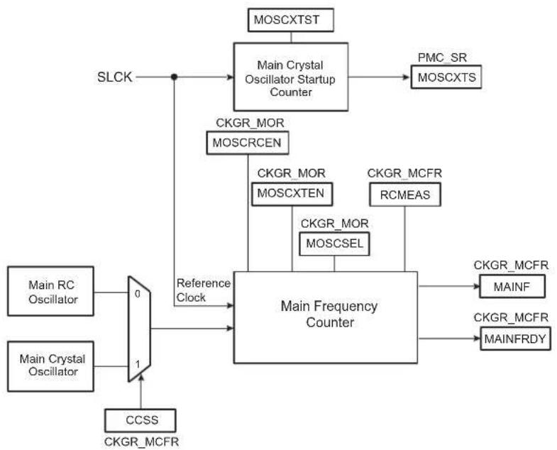
flowchart
graph TD
    A["Main Crystal Oscillator"] --> B["Main Frequency Counter"]
    C["Main RC Oscillator"] --> D["0"]
    E["Main Crystal Oscillator"] --> F["1"]
    G["CCSS"] --> H["0"]
    I["SLCK"] --> J["Main Crystal Oscillator Startup Counter"]
    K["CKGR_MOR MOSCRCEN"] --> L["Main Frequency Counter"]
    M["CKGR_MOR MOSCXTEN"] --> L
    N["CKGR_MOR MOSCSEL"] --> L
    O["CKGR_MCFR RCMEAS"] --> L
    P["CKGR_MCFR MAINF"] --> Q["Main Frequency Counter"]
    R["CKGR_MCFR MAINFRDY"] --> S["Main Frequency Counter"]
    T["MOSCXTST"] --> U["Main Crystal Oscillator Startup Counter"]
    V["PMC_SR MOSCXTS"] --> W["Main Frequency Counter"]
    X["Reference Clock"] --> Y["Main Frequency Counter"]
30.6 PLLA Clock
The PLLA clock (PLLACK) is generated from MAINCK by the PLLA and a predivider. This combination allows a wide range of frequencies to be selected on either MCK, HCLK or the PCKx outputs.
The following figure shows the block diagram of the dividers and PLLA blocks.
Figure 30-4. Divider and PLLA Block Diagram
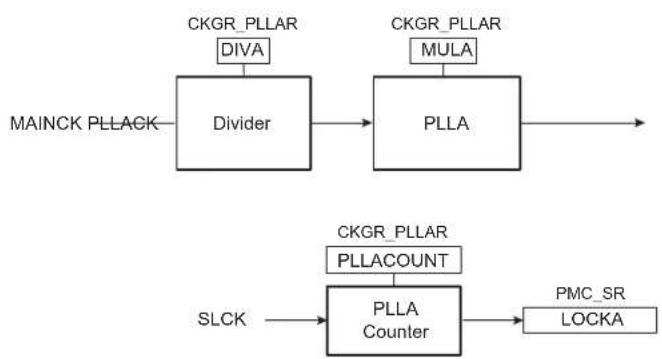
flowchart
graph LR
    A["MAINCK PLLAGK"] --> B["Divider"]
    B --> C["PLLA"]
    D["CKGR_PLLAR DIVA"] --> B
    E["CKGR_PLLAR MULA"] --> C
    F["SLCK"] --> G["PLLA Counter"]
    G --> H["PMC_SR LOCKA"]
    I["CKGR_PLLAR PLLACOUNT"] --> G
30.6.1 Divider and Phase Lock Loop Programming
The divider can be set between 1 and 255 in steps of 1. When a divider field (DIV) is cleared, the output of the corresponding divider and the PLL output is a continuous signal at level 0. On reset, each DIV field is cleared, thus the corresponding PLL input clock is stuck at '0'.
The PLL (PLLA) allows multiplication of the divider's outputs. The PLL clock signal has a frequency that depends on the respective source signal frequency and on the parameters DIV (DIVA) and MUL (MULA). The factor applied to the source signal frequency is (MUL + 1) / DIV . When MUL is written to '0' or DIV = 0 , the PLL is disabled and its power consumption is saved. Note that there is a delay of two SLCK clock cycles between the disable command and the real disable of the PLL. Re-enabling the PLL can be performed by writing a value higher than '0' in the MUL field and DIV higher than '0'.
Whenever the PLL is re-enabled or one of its parameters is changed, the LOCK (LOCKA) bit in PMC_SR is automatically cleared. The values written in the PLLCOUNT field (PLLACOUNT) in CKGR_PLLR (CKGR_PLLAR) are loaded in the PLL counter. The PLL counter then decrements at the speed of SLCK until it reaches '0'. At this time, PMC_SR.LOCK is set and can trigger an interrupt to the processor. The user has to load the number of SLCK cycles required to cover the PLL transient time into the PLLCOUNT field.
To avoid programming the PLL with a multiplication factor that is too high, the user can saturate the multiplication factor value sent to the PLL by setting the PLLA_MMAX field in the PLL Maximum Multiplier Value Register (PMC_PMMR).
It is forbidden to change the MAINCK characteristics (oscillator selection, frequency adjustment of the Main RC oscillator) when:
- MAINCK is selected as the PLLA clock source, and
• MCK is sourced from PLLA.
To change the MAINCK characteristics, the user must:
- Switch the MCK source to MAINCK by writing a '1' to PMC_MCKR.CSS.
- Change the Main RC oscillator frequency (MOSCRCF) or oscillator selection (MOSCSEL) in CKGR_MOR.
- Wait for MOSCRCS (if frequency changes) or MOSCSELS (if oscillator selection changes) in PMC_SR.
- Disable and then enable the PLL.
- Wait for the LOCK flag in PMC_SR.
- Switch back MCK to the PLLA by writing the appropriate value to PMC_MCKR.CSS.
30.7 UTMI PLL Clock
The source of the UTMI PLL (UPLL) is the Main Crystal oscillator. The UPLL provides the UTMI PLL Clock (UPLLCK) and UPLLCKDIV clock signals.
The UPLL has two possible multiplying factors: x40 and x30. To generate UPLLCK at 480 MHz (typical USB case), this leads to two possible crystal oscillator frequencies: 12 or 16 MHz. The crystal oscillator frequency (12 or 16 MHz) must be programmed in UTMI_CKTRIM.FREQ prior to enabling the UPLL.
When the UPLL is enabled by writing a '1' to bit UPLLEN in the UTMI Clock Register (CKGR_UCKR), the LOCKU bit in PMC_SR is automatically cleared. The values written in the PLLCOUNT field in CKGR_UCKR are loaded in the UTMI PLL counter. The UTMI PLL counter then decrements at the speed of SLCK divided by 8 until it reaches '0'. At this time, the LOCKU bit is set in PMC_SR and can trigger an interrupt to the processor. The user has to load the number of SLCK cycles required to cover the UTMI PLL transient time into the PLLCOUNT field.
Figure 30-5. UTMI PLL Block Diagram
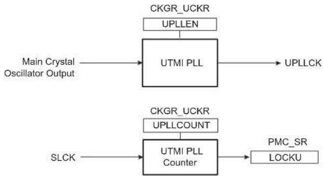
flowchart
graph TD
    A["Main Crystal Oscillator Output"] --> B["UTMI PLL"]
    C["CKGR_UCKR UPLLEN"] --> B
    B --> D["UPLLCK"]
    E["SLCK"] --> F["UTMI PLL Counter"]
    G["CKGR_UCKR UPLLCOUNT"] --> F
    F --> H["PMC_SR LOCKU"]
31. Power Management Controller (PMC)
31.1 Description
The Power Management Controller (PMC) optimizes power consumption by controlling all system and user peripheral clocks. The PMC enables/disables the clock inputs to many of the peripherals and the Cortex-M7 processor.
The Supply Controller selects either the Slow RC oscillator or the 32.768 kHz crystal oscillator as the source of SLCK. The unused oscillator is disabled automatically so that power consumption is optimized.
By default, at startup, the chip runs out of MCK using the Main RC oscillator running at 12 MHz.
31.2 Embedded Characteristics
The Power Management Controller provides the following clocks:
- Host Clock (MCK), programmable from a few hundred Hz to the maximum operating frequency of the device. It is available to the modules running permanently, such as the Enhanced Embedded Flash Controller
- Processor Clock (HCLK), automatically switched off when entering the processor in Sleep mode
• Free-running processor Clock (FCLK)
• The Cortex-M7 SysTick external clock - USB Clock (USB_48M), required by the USB peripheral
- Peripheral Clocks with independent ON/OFF control, provided to the peripherals
- Programmable Clock Outputs (PCKx), selected from the clock generator outputs to drive the device PCK pins
- Clock sources independent of MCK and HCLK, provided by internal PCKx for USART, UART, TC, Embedded Trace Macrocell (ETM) and CAN Clocks
- Generic Clock (GCLK) with controllable division and ON/OFF control, independent of MCK and HCLK. Provided to selected peripherals.
The Power Management Controller also provides the following features on clocks:
• A Main crystal oscillator failure detector
• A 32.768 kHz crystal oscillator frequency monitor
- A frequency counter on Main crystal oscillator or Main RC oscillator
- An on-the-fly adjustable Main RC oscillator frequency
31.3 Block Diagram
Figure 31-1. General Clock Distribution Block Diagram

flowchart
graph TD
    A["Clock Generator"] --> B["Slaw HC Detector"]
    B --> C["0"]
    C --> D["CKGR MOR MDR/CFI"]
    D --> E["Main Clock (MAINCK)"]
    E --> F["PLA"]
    F --> G["USB UTM PLL"]
    G --> H["Control/Status"]
    H --> I["Power Management Control User Interface"]
    J["Processor Clock Controller (PNC PCR)"] --> K["Programmable Clock Controller (PMC_PCK)"]
    K --> L["PACK: (to PC pins and peripherals)"]
    L --> M["USB FS Clock (USB_48M)"]
    N["Processor Clock Controller (HCLK)"] --> O["Processor Clock (HCLK)"]
    O --> P["SysTick External Clock"]
    P --> Q["Free Running Clock (FCLK)"]
    Q --> R["Host Clock (MCK)"]
    S["XIN32"] --> T["32.768 key Crystal Cochistor"]
    U["XOUT32"] --> V["Main RC Cochistor"]
    W["XIN"] --> X["Vain Crystal Cochistor"]
    Y["XOUT"] --> Z["Control/Status"]
    AA["Processor Control"] --> AB["Slaw HC Detector"]
    AC["XIN32"] --> AD["32.768 key Crystal Cochistor"]
    AE["XOUT32"] --> AF["Main RC Cochistor"]
    AG["XIN"] --> AH["Vain Crystal Cochistor"]
    AI["XOUT"] --> AJ["Control/Status"]
    AK["Processor Control"] --> AL["Slaw HC Detector"]
    AM["XIN32"] --> AN["32.768 key Crystal Cochistor"]
    AO["XOUT32"] --> AP["Main RC Cochistor"]
    AQ["XIN"] --> AR["Vain Crystal Cochistor"]
    AS["XOUT"] --> AT["Control/Status"]
    AU["Processor Control"] --> AV["Slaw HC Detector"]
    AW["XIN32"] --> AX["32.768 key Crystal Cochistor"]
    AY["XIN32"] --> AZ["Main RC Cochistor"]
    BA["XOUT"] --> BB["Vain Crystal Cochistor"]
    BC["XIN"] --> BD["Vain Crystal Cochistor"]
    BE["XOUT"] --> BF["Control/Status"]
    BG["XIN"] --> BH["Vain Crystal Cochistor"]
    BI["XOUT"] --> BJ["Control/Status"]
    BK["Processor Clock"] --> BL["Slaw HC Detector"]
    BM["XIN32"] --> BN["32.768 key Crystal Cochistor"]
    BO["XOUT"] --> BP["Vain Crystal Cochistor"]
    BQ["XIN"] --> BR["Vain Crystal Cochistor"]
    BS["XOUT"] --> BT["Vain Crystal Cochistor"]
    BU["XIN"] --> BV["Vain Crystal Cochistor"]
    BW["XOUT"] --> BX["Vain Crystal Cochistor"]
    BY["XIN"] --> BZ["Vain Crystal Cochistor"]
    CA["XOUT"] --> CB["Vain Crystal Cochistor"]
    CC["XIN"] --> CD["Vain Crystal Cochistor"]
    DD["XOUT"] --> DE["Vain Crystal Cochistor"]
    FD["XIN"] --> FDZ["Vain Crystal Cochistor"]
    FDX["VIN"] --> FDXV["Vain Crystal Cochistor"]
    FDY["VIN"] --> FDYV["Vain Crystal Cochistor"]
    FDZ["VIN"] --> FDZV["Vain Crystal Cochistor"]
    FDXV["VIN"] --> FDXW["Vain Crystal Cochistor"]
    FDXV["VIN"] --> FDXY["Vain Crystal Cochistor"]
31.4 Host Clock Controller
The Host Clock Controller provides the Host Clock (MCK) with the selection and division of the clock generator's output signals. MCK is the source clock of the peripheral clocks.
The clock to be selected between SLCK, MAINCK, PLLACK and UPLLCKDIV is configured in PMC_MCKR.CSS. The prescaler supports the 1, 2, 3, 4, 8, 16, 32, 64 division factors and is configured using PMC_MCKR.PRES.
Each time PMC_MCKR is configured to define a new MCK, the MCKRDY bit is cleared in PMC_SR. It reads '0' until MCK is established. Then, the MCKRDY bit is set and can trigger an interrupt to the processor. This feature is useful when switching from a high-speed clock to a lower one to inform the software when the change is completed.
Note: Users cannot modify MDIV and CSS at the same access. Each field must be modified separately with a wait for the MCKRDY flag between the first field modification and the second field modification.
31.5 Processor Clock Controller
The PMC features a Processor Clock (HCLK) Controller that implements the processor Sleep mode. HCLK can be disabled by executing the WFI (WaitForInterrupt) or the WFE (WaitForEvent) processor instruction while the LPM bit is at '0' in the PMC Fast Startup Mode register (PMC_FSMR).
HCLK is enabled after a reset and is automatically re-enabled by any enabled interrupt. The processor Sleep mode is entered by disabling HCLK, which is automatically re-enabled by any enabled fast or normal interrupt, or by the reset of the product.
When processor Sleep mode is entered, the current instruction is finished before the clock is stopped, but this does not prevent data transfers from other hosts of the system bus.
31.6 SysTick External Clock
When the processor selects the SysTick external clock, the calibration value is fixed to 150000. This allows the generation of a time base of 1 ms with the SysTick clock at the maximum frequency on HCLK divided by 2.
The SysTick counter may miss a number of counts if an external clock source is selected when entering the sleep mode.
Refer to the section "Arm Cortex-M7 Processor" for details on selecting the SysTick external clock.
Related Links
15. Arm Cortex-M7
31.7 USB Full-speed Clock Controller
The user can select the PLLA or the UPLL output as the USB FS clock (USB_48M) by writing a '1' to the USBS bit in the USB Clock Register (PMC_USB). The user then must program the corresponding PLL to generate an appropriate frequency depending on the USBDIV bit in PMC_USB.
When PMC_SR. LOCKA and PMC_SR. LOCKU are set to '1', the PLLA and UPLL are stable. Then, USB_48M can be enabled by setting the USBCLK bit in the System Clock Enable register (PMC_SCER). To save power on this peripheral when not used, the user can set the USBCLK bit in the System Clock Disable register (PMC_SCDR). The USBCLK bit in the System Clock Status register (PMC_SCSR) gives the status of this clock. The USB port requires both the USB clock signal and the peripheral clock. The USB peripheral clock is controlled by means of the Host Clock Controller.
31.8 Core and Bus Independent Clocks for Peripherals
The following table lists the peripherals that require a PCKx clock to operate while the core, bus and peripheral clock frequencies are modified, thus providing communications at a bit rate which is independent for the core/bus/peripheral clock. This mode of operation is possible by using the internally generated independent clock sources.
Internal clocks can be independently selected between SLCK, MAINCK, any available PLL clock, and MCK by configuring PMC_PCKx.CSS. The independent clock sources can be also divided by configuring PMC_PCKx.PRES.
Each internal clock signal (PCKx) can be enabled and disabled by writing a '1' to the corresponding PMC_SCER.PCKx and PMC_SCDR.PCKx, respectively. The status of the internal clocks are given in PMC_SCSR.PCKx.
The status flag PMC_SR.PCKRDYx indicates that the programmable internal clock has been programmed in the Programmable clock registers.
The independent clock source must also be selected in each peripheral in the Clock Assignments table to operate communications, timings, etc without influencing the frequency of the core/bus/peripherals (except frequency limitations listed in each peripheral).
Table 31-1. Clock Assignments
| Clock Name Peripheral | |
| PCK3 ETM | |
| PCK4 UARTx/USARTx | |
| PCK5 MCANx | |
| PCK6 TC0.Ch1...TC3.Ch2 | |
| PCK7 TC0.Ch0 |
Note: USB, GMAC and MLB do not require PCKx to operate independently of core and bus peripherals.
31.9 Peripheral and Generic Clock Controller
The PMC controls the clocks of the embedded peripherals by means of the Peripheral Control register (PMC_PCR). With this register, the user can enable and disable the different clocks used by the peripherals:
- Peripheral clocks (periph_clk[PID]), routed to every peripheral and derived from the Host clock (MCK), and
- Generic clocks (GCLK[PID]), routed to I2SC0 and I2SC1. These clocks are independent of the core and bus clocks (HCLK, MCK and periph_clk[PID]). They are generated by selection and division of the following sources: SLCK, MAINCK, UPLLCKDIV, PLLACK and MCK. Refer to the description of each peripheral for the limitation to be applied to GCLK[PID] compared to periph_clk[PID].
To configure a peripheral's clocks, PMC_PCR.CMD must be written to '1' and PMC_PCR.PID must be written with the index of the corresponding peripheral. All other configuration fields must be correctly set.
To read the current clock configuration of a peripheral, PMC_PCR.CMD must be written to '0' and PMC_PCR.PID must be written with the index of the corresponding peripheral regardless of the values of other fields. This write does not modify the configuration of the peripheral. The PMC_PCR can then be read to know the configuration status of the corresponding PID.
The user can also enable and disable these clocks by configuring the Peripheral Clock Enable (PMC_PCERx) and Peripheral Clock Disable (PMC_PCDRx) registers. The status of the peripheral clock activity can be read in the Peripheral Clock Status registers (PMC_PCSRx).
When a peripheral or a generic clock is disabled, it is immediately stopped. These clocks are disabled after a reset.
To stop a peripheral clock, it is recommended that the system software wait until the peripheral has executed its last programmed operation before disabling the clock. This is to avoid data corruption or erroneous behavior of the system.
The bit number in PMC_PCERx, PMC_PCDRx, and PMC_PCSRx is the Peripheral Identifier defined at the product level. The bit number corresponds to the interrupt source number assigned to the peripheral.
31.10 Asynchronous Partial Wakeup
31.10.1 Description
The asynchronous partial wakeup wakes up a peripheral in a fully asynchronous way when activity is detected on the communication line. The asynchronous partial wakeup function automatically manages the peripheral clock. It reduces overall power consumption of the system by clocking peripherals only when needed.
Asynchronous partial wakeup can be enabled in Wait mode (SleepWalking), or in Active mode.
Only the following peripherals can be configured with asynchronous partial wakeup: UARTx and TWIHSx.
The peripheral selected for asynchronous partial wakeup must first be configured so that its clock is enabled. To do so, write a '1' to the appropriate PIDx bit in PMC_PCER registers.
31.10.2 Asynchronous Partial Wakeup in Wait Mode (SleepWalking)
When the system is in Wait mode, all clocks of the system except SLCK are stopped. When an asynchronous clock request from a peripheral occurs, the PMC partially wakes up the system to feed the clock only to this peripheral. The rest of the system is not fed with the clock, thus optimizing power consumption. Finally, depending on user-configurable conditions, the peripheral either wakes up the whole system if these conditions are met or stops the peripheral clock until the next clock request. If a wakeup request occurs, SleepWalking is automatically disabled until the user instructs
the PMC to enable SleepWalking. This is done by writing a '1' to PIDx in the PMC SleepWalking Enable register (PMC_SLPWK_ER).
Figure 31-2. SleepWalking Waveforms

text_image
system_clock The system is in wait mode. No clock is fed to the system. peripheral_clock peripheral clock request peripheral wakeup request peripheral sleepwalking status The wakeup request wakes up the system and resets the sleepwalking status of the peripheral31.10.2.1 Configuration Procedure
Before configuring SleepWalking for a peripheral, check that the PIDx bit in PMC_PCSR is set. This ensures that the peripheral clock is enabled.
The steps to enable SleepWalking for a peripheral are the following:
- Check that the corresponding PIDx bit in the PMC SleepWalking Activity Status register (PMC_SLPWK_ASR) is set to '0'. This ensures that the peripheral has no activity in progress.
- Enable SleepWalking for the peripheral by writing a '1' to the corresponding PIDx bit in the PMC_SLPWK_ER.
- Check that the corresponding PIDx bit in PMC_SLPWK_ASR is set to '0'. This ensures that no activity has started during the enable phase.
- In the PMC_SLPWK_ASR, if the corresponding PIDx bit is set, SleepWalking must be immediately disabled by writing a '1' to the PIDx bit in the PMC SleepWalking Disable register (PMC_SLPWK_DR). Wait for the end of peripheral activity before reinitializing the procedure. If the corresponding PIDx bit is set to '0', then the peripheral clock is disabled and the system can then be placed in Wait mode.
Before entering Wait mode, check that the AIP bit in the PMC SleepWalking Activity In Progress Register (PMC_SLPWK_AIPR) is cleared. This ensures that none of the peripherals is currently active.
Note: When SleepWalking for a peripheral is enabled and the core is running (system not in Wait mode), the peripheral must not be accessed before a wakeup of the peripheral is performed.
31.10.3 Asynchronous Partial Wakeup in Active Mode
When the system is in Active mode, peripherals enabled for asynchronous partial wakeup have their respective clocks stopped until the peripherals request a clock. When a peripheral requests the clock, the PMC provides the clock without processor intervention.
The triggering of the peripheral clock request depends on conditions which can be configured for each peripheral. If these conditions are met, the peripheral asserts a request to the PMC. The PMC disables the Asynchronous Partial Wakeup mode of the peripheral and provides the clock to the peripheral until the user instructs the PMC to re-enable partial wakeup on the peripheral. This is done by setting PMC_SLPWK_ER.PIDx.
If the conditions are not met, the peripheral clears the clock request and the PMC stops the peripheral clock until the clock request is reasserted by the peripheral.
Note: Configuring Asynchronous Partial Wake-up mode requires the same registers as Sleep-Walking mode.
Figure 31-3. Asynchronous Partial Wake-up in Active Mode
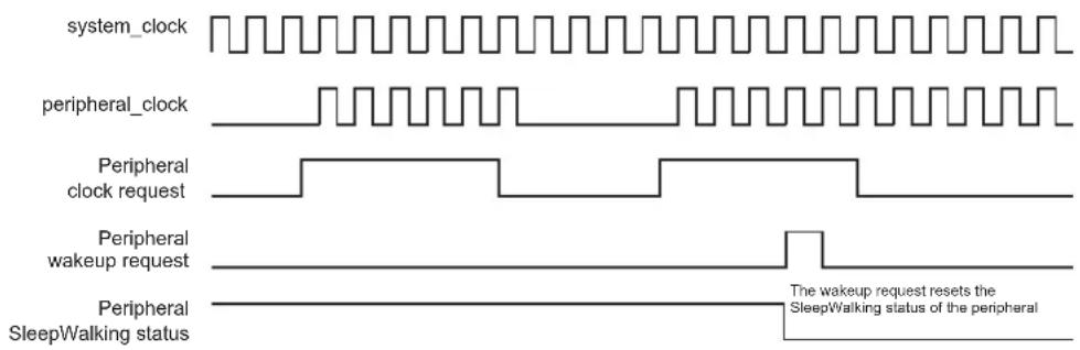
text_image
system_clock peripheral_clock Peripheral clock_request Peripheral wakeup_request Peripheral SleepWalking status The wakeup request resets the SleepWalking status of the peripheral31.10.3.1 Configuration Procedure
Before configuring the asynchronous partial wakeup function of a peripheral, check that the PIDx bit in PMC_PCSR is set. This ensures that the peripheral clock is enabled.
The steps to enable the asynchronous partial wakeup function of a peripheral are the following:
- Check that the corresponding PIDx bit in the PMC SleepWalking Activity Status register (PMC_SLPWK_ASR) is set to '0'. This ensures that the peripheral has no activity in progress.
- Enable the asynchronous partial wakeup function of the peripheral by writing a '1' to the corresponding PIDx bit in the PMC_SLPWK_ER.
- Check that the corresponding PIDx bit in PMC_SLPWK_ASR is set to '0'. This ensures that no activity has started during the enable phase.
If an activity has started during the enable phase, the asynchronous partial wakeup function must be immediately disabled by writing a '1' to the PIDx bit in the PMC SleepWalking Disable register (PMC_SLPWK_DR). Wait for the end of peripheral activity before reinitializing the procedure.
31.11 Free-running Processor Clock
The free-running Processor clock (FCLK) used for sampling interrupts and clocking debug blocks ensures that interrupts can be sampled, and sleep events can be traced, while the processor is sleeping.
31.12 Programmable Clock Output Controller
The PMC controls three signals to be output on the external pins PCKx. Each signal can be independently programmed via the Programmable Clock registers (PMC_PCKx).
PCKx can be independently selected between SLCK, MAINCK, PLLACK, UPLLCKDIV and MCK by configuring PMC_PCKx.CSS. Each output signal can also be divided by 1 to 256 by configuring PMC_PCKx.PRES.
Each output signal can be enabled and disabled by writing a '1' to the corresponding bits PMC_SCER.PCKx and PMC_SCDR.PCKx, respectively. The status of the active programmable output clocks is given in PMC_SCSR.PCKx.
The status flag PMC_SR.PCKRDYx indicates that PCKx is actually what has been programmed in registers PMC_PCKx.
As the Programmable Clock Controller does not manage with glitch prevention when switching clocks, it is strongly recommended to disable PCKx before any configuration change and to re-enable it after the change is performed.
31.13 Fast Startup
At exit from Wait mode, the device allows the processor to restart in several microseconds only if the C-code function that manages the Wait mode entry and exit is linked to and executed from on-chip SRAM.
The fast startup time cannot be achieved if the first instruction after an exit is located in the embedded Flash.
If fast startup is not required, or if the first instruction after exit from Wait mode is located in embedded Flash, see "Startup from Embedded Flash".
To instruct the device to enter Wait mode, refer to section "Power Considerations".
A fast startup occurs upon the detection of a programmed level on one of the 14 wakeup inputs (WKUP) or upon an active alarm from the RTC, RTT and USB Controller. The polarity of each of the 14 wakeup inputs is programmable in the PMC Fast Startup Polarity Register (PMC_FSPR).

The duration of the WKUPx pins active level must be greater than four MAINCK cycles.
The fast startup circuitry, as shown in the following figure, is fully asynchronous and provides a fast startup signal to the PMC. As soon as the fast startup signal is asserted, the Main RC oscillator restarts automatically.
When entering Wait mode, the embedded Flash can be placed in one of the low-power modes (Deep-powerdown or Standby mode) with PMC_FSMR.FLPM. FLPM can be configured at any time and its value will be applied to the next Wait mode period.
The power consumption reduction is optimal when PMC_FSMR.FLPM is configured to '1' (Deep-powerdown mode). If the field is configured to '0' (Standby mode), the power consumption is slightly higher than in Deep-powerdown mode.
When PMC_FSMR.FLPM is configured to '2', the Wait mode Flash power consumption is equivalent to that of the Active mode when there is no read access on the Flash.
Figure 31-4. Fast Startup Circuitry
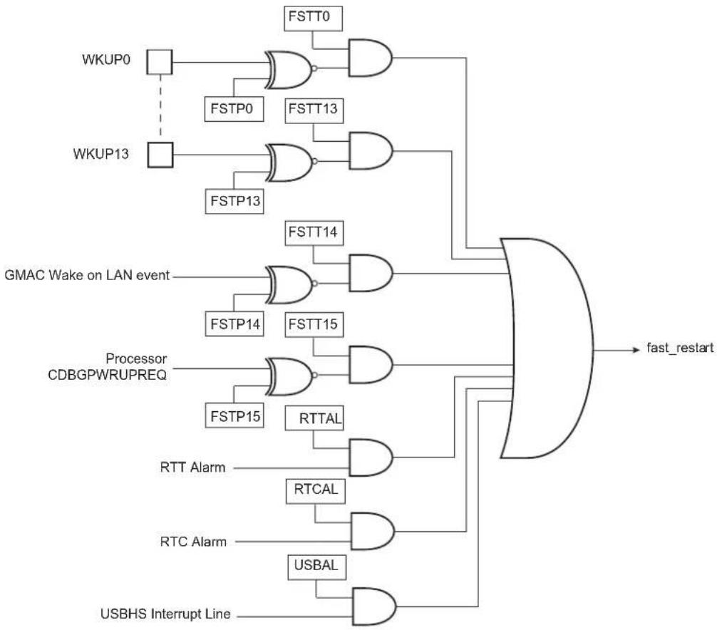
flowchart
graph TD
    A["WKUP0"] --> B["FSTT0"]
    C["WKUP13"] --> D["FSTP0"]
    C --> E["FSTT13"]
    B --> F["FSTT14"]
    D --> G["FSTP13"]
    H["GMAC Wake on LAN event"] --> I["FSTT14"]
    I --> J["FSTP14"]
    I --> K["FSTT15"]
    L["Processor CDBGPRUPREQ"] --> M["FSTP15"]
    L --> N["RTTAL"]
    O["RTT Alarm"] --> P["RTCAL"]
    Q["RTC Alarm"] --> R["USBAL"]
    S["USBHS Interrupt Line"] --> T["Fast_restart"]
    B --> T
    D --> T
    E --> T
    G --> T
    I --> T
    M --> T
    N --> T
    P --> T
    R --> T
    U["fast_restart"] --> T
Each wakeup input pin and alarm can be enabled to generate a fast startup event by setting the corresponding bit in PMC_FSMR.
The user interface does not provide any status for fast startup. The status can be read in the PIO Controller and the status registers of the RTC, RTT and USB Controller.
Related Links
7. Power Considerations
31.14 Startup from Embedded Flash
The inherent startup time of the embedded Flash cannot provide a fast startup of the system.
If system fast startup time is not required, the first instruction after a Wait mode exit can be located in the embedded Flash. Under these conditions, prior to entering Wait mode, the Flash controller must be programmed to perform access in 0 wait-state (refer to the embedded Flash controller section).
The procedure and conditions to enter Wait mode and the circuitry to exit Wait mode are strictly the same as fast startup (see "Fast Startup").
Related Links
- Enhanced Embedded Flash Controller (EEFC)
31.15 Main Crystal Oscillator Failure Detection
The Main crystal oscillator failure detector monitors the Main crystal oscillator against the Slow RC oscillator and provides an automatic switchover of the MAINCK source to the Main RC oscillator in case of failure detection.
The failure detector can be enabled or disabled by configuring the CKGR_MOR.CFDEN, and it can also be disabled in either of the following cases:
• After a VDDCORE reset
- When the Main crystal oscillator is disabled (MOSCXTEN = 0)
A failure is detected by means of a counter incrementing on the Main crystal oscillator output and detection logic is triggered by the Slow RC oscillator which is automatically enabled when CFDEN = 1.
The counter is cleared when the Slow RC oscillator clock signal is low and enabled when the signal is high. Thus, the failure detection time is one Slow RC oscillator period. If, during the high level period of the Slow RC oscillator clock signal, less than eight Main crystal oscillator clock periods have been counted, then a failure is reported. Note that when enabling the failure detector, up to two cycles of the Slow RC oscillator are needed to detect a failure of the Main crystal oscillator.
If a failure of Main crystal oscillator is detected, PMC_SR.CFDEV and PMC_SR.FOS both indicate a failure event. PMC_SR.CFDEV is cleared on read of PMC_SR, and PMC_SR.FOS is cleared by writing a '1' to the FOCLR bit in the PMC Fault Output Clear Register (PMC_FOCR).
Only PMC_SR.CFDEV can generate an interrupt if the corresponding interrupt source is enabled in PMC_IER. The current status of the clock failure detection can be read at any time from PMC_SR.CFDS.
Figure 31-5. Clock Failure Detection Example
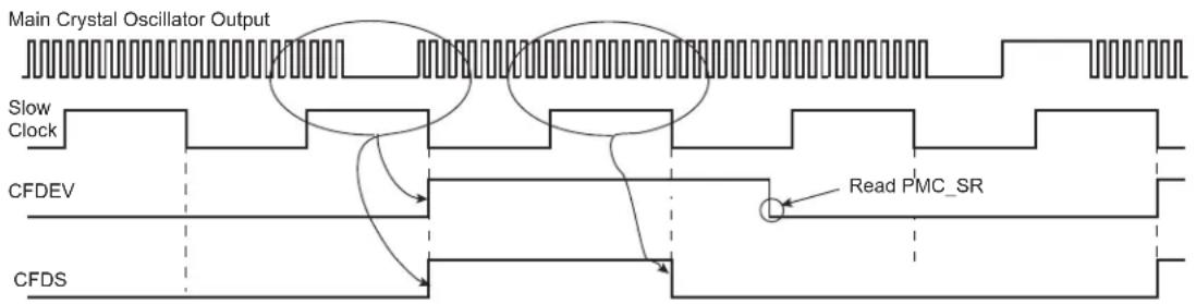
text_image
Main Crystal Oscillator Output Slow Clock CFDEV CFDS Read PMC_SRNote: Ratio of clock periods is for illustration purposes only.
If the Main crystal oscillator is selected as the source clock of MAINCK (CKGR_MOR.MOSCSEL = 1), and if the MCK source is PLLACK or UPLLCKDIV (CSS = 2 or 3), a clock failure detection automatically forces MAINCK to be the source clock for MCK. Then, regardless of the PMC configuration, a clock failure detection automatically forces the Main RC oscillator to be the source clock for MAINCK. If the Main RC oscillator is disabled when a clock failure detection occurs, it is automatically re-enabled by the clock failure detection mechanism.
Two Slow RC oscillator clock cycles are necessary to detect and switch from the Main crystal oscillator to the Main RC oscillator if the source of MCK is MAINCK, or three Slow RC oscillator clock cycles if the source of MCK is PLLACK or UPLLCKDIV.
A clock failure detection activates a fault output that is connected to the Pulse Width Modulator (PWM) Controller. With this connection, the PWM controller is able to force its outputs and to protect the driven device, if a clock failure is detected.
31.16 32.768 kHz Crystal Oscillator Frequency Monitor
The frequency of the 32.768 kHz crystal oscillator can be monitored by means of logic driven by the Main RC oscillator known as a reliable clock source. This function is enabled by configuring
the XT32KFME bit of CKGR_MOR. Prior to enabling this frequency monitor, the 32.768 kHz crystal oscillator must be started and its startup time be elapsed. Refer to details on the Slow clock generator in the section "Supply Controller (SUPC)".
An error flag (XT32KERR in PMC_SR) is asserted when the 32.768 kHz crystal oscillator frequency is out of the ±10% nominal frequency value (i.e., 32.768 kHz). The error flag can be cleared only if the frequency monitor is disabled.
When the Main RC oscillator frequency is set to 4 MHz, the accuracy of the measurement is ±40% as this frequency is not trimmed during production. Therefore, ±10% accuracy is obtained only if the Main RC oscillator frequency is configured for 8 or 12 MHz.
The monitored clock frequency is declared invalid if at least 4 consecutive clock period measurement results are over the nominal period ± 10% . Note that modifying the trimming values of the Main RC oscillator (PMC_OCR) may impact the monitor accuracy and lead to inappropriate failure detection.
Due to the possible frequency variation of the Main RC oscillator acting as reference clock for the monitor logic, any 32.768 kHz crystal frequency deviation over ±10% of the nominal frequency is systematically reported as an error by means of PMC_SR.XT32KERR. Between -1% and -10% and +1% and +10%, the error is not systematically reported.
Thus only a crystal running at 32.768 kHz frequency ensures that the error flag will not be asserted. The permitted drift of the crystal is 10000 ppm (1%), which allows any standard crystal to be used.
If the Main RC oscillator frequency range needs to be changed while the frequency monitor is operating, the monitoring must be stopped prior to change the Main RC oscillator frequency. Then it can be re-enabled as soon as PMC_SR.MOSCRCS is set.
The error flag can be defined as an interrupt source of the PMC by setting PMC_IER.XT32KERR. This flag is also routed to the RSTC and may generate a reset of the device.
Related Links
23. Supply Controller (SUPC)
31.17 Recommended Programming Sequence
Follow the steps below to program the PMC:
- If the Main crystal oscillator is not required, the PLL and divider can be directly configured (Step 6.) else this oscillator must be started (Step 2.).
-
Enable the Main crystal oscillator by setting CKGR_MOR.MOSCXTEN. The user can define a startup time. This can be done by configuring the appropriate value in CKGR_MOR.MOSCXTST. Once this register has been correctly configured, the user must wait for PMC_SR.MOSCXTS to be set. This can be done either by polling PMC_SR.MOSCXTS, or by waiting for the interrupt line to be raised if the associated interrupt source (MOSCXTS) has been enabled in PMC_IER.
-
Switch MAINCK to the Main crystal oscillator by setting CKGR_MOR.MOSCSEL.
-
Wait for PMC_SR.MOSCSELS to be set to ensure the switch is complete.
-
Check MAINCK frequency:
This frequency can be measured via CKGR_MCFR.
Read CKGR_MCFR until the MAINFRDY field is set, after which the user can read CKGR_MCFR.MAINF by performing an additional read. This provides the number of Main clock cycles that have been counted during a period of 16 SLCK cycles.
If MAINF = 0, switch MAINCK to the Main RC Oscillator by clearing CKGR_MOR.MOSCSEL. If MAINF ≠ 0, proceed to Step 6.
- Set PLLA and Divider (if not required, proceed to Step 7.):
All parameters needed to configure PLLA and the divider are located in CKGR_PLLAR.
CKGR_PLLAR.DIVA is used to control the divider. This parameter can be programmed between 0 and 127. Divider output is divider input divided by DIVA parameter. By default, DIVA field is cleared which means that the divider and PLLA are turned off.
CKGR_PLLAR.MULA is the PLLA multiplier factor. This parameter can be programmed between 0 and 62. If MULA is cleared, PLLA will be turned off, otherwise the PLLA output frequency is PLLA input frequency multiplied by (MULA + 1).
CKGR_PLLAR.PLLACOUNT specifies the number of SLCK cycles before PMC_SR. LOCKA is set after CKGR_PLLAR has been written.
Once CKGR_PLLAR has been written, the user must wait for PMC_SR. LOCKA to be set. This can be done either by polling PMC_SR. LOCKA or by waiting for the interrupt line to be raised if the associated interrupt source (LOCKA) has been enabled in PMC_IER. All fields in CKGR_PLLAR can be programmed in a single write operation. If MULA or DIVA is modified, the LOCKA bit goes low to indicate that PLLA is not yet ready. When PLLA is locked, LOCKA is set again. The user must wait for the LOCKA bit to be set before using the PLLA output clock.
7. Select MCK and HCLK:
MCK and HCLK are configurable via PMC_MCKR.
CSS is used to select the clock source of MCK and HCLK. By default, the selected clock source is MAINCK.
PRES is used to define the HCLK and MCK prescaler.s The user can choose between different values (1, 2, 3, 4, 8, 16, 32, 64). Prescaler output is the selected clock source frequency divided by the PRES value.
MDIV is used to define the MCK divider. It is possible to choose between different values (0, 1, 2, 3). MCK output is the HCLK frequency divided by 1, 2, 3 or 4, depending on the value programmed in MDIV.
By default, MDIV is cleared, which indicates that the HCLK is equal to MCK.
Once the PMC_MCKR has been written, the user must wait for PMC_SR.MCKRDY to be set. This can be done either by polling PMC_SR.MCKRDY or by waiting for the interrupt line to be raised if the associated interrupt source (MCKRDY) has been enabled in PMC_IER. PMC_MCKR must not be programmed in a single write operation. The programming sequence for PMC_MCKR is as follows:
If a new value for PMC_MCKR.CSS corresponds to any of the available PLL clocks:
a. Program PMC_MCKR.PRES.
b. Wait for PMC_SR.MCKRDY to be set.
c. Program PMC_MCKR.MDIV.
d. Wait for PMC_SR.MCKRDY to be set.
e. Program PMC_MCKR.CSS.
f. Wait for PMC_SR.MCKRDY to be set.
If a new value for PMC_MCKR.CSS corresponds to MAINCK or SLCK:
a. Program PMC_MCKR.CSS.
b. Wait for PMC_SR.MCKRDY to be set.
c. Program PMC_MCKR.PRES.
d. Wait for PMC_SR.MCKRDY to be set.
If CSS, MDIV or PRES are modified at any stage, the MCKRDY bit goes low to indicate that MCK and HCLK are not yet ready. The user must wait for MCKRDY bit to be set again before using MCK and HCLK.
Note: If PLLA clock was selected as MCK and the user decides to modify it by writing a new value into CKGR_PLLAR, the MCKRDY flag will go low while PLLA is unlocked. Once PLLA is locked again, LOCKA goes high and MCKRDY is set.
While PLLA is unlocked, MCK selection is automatically changed to SLCK for PLLA. For further information, see "Clock Switching Waveforms".
MCK is MAINCK divided by 2.
- Select the Programmable clocks (PCKx):
PCKx are controlled via registers PMC_SCER, PMC_SCDR and PMC_SCSR.
PCKx can be enabled and/or disabled via PMC_SCER and PMC_SCDR. Three PCKx can be used.
PMC_SCSR indicates which PCKx is enabled. By default all PCKx are disabled.
PMC_PCKx registers are used to configure PCKx.
PMC_PCKx.CSS is used to select the PCKx divider source. Several clock options are available:
- MAINCK
- SLCK
- MCK
- PLLACK
- UPLLCKDIV
SLCK is the default clock source.
PMC_PCKx.PRES is used to control the PCKx prescaler. It is possible to choose between different values (1 to 256). PCKx output is prescaler input divided by PRES. By default, the PRES value is cleared which means that PCKx is equal to Slow clock.
Once PMC_PCKx has been configured, the corresponding PCKx must be enabled and the user must wait for PMC_SR.PCKRDYx to be set. This can be done either by polling PMC_SR.PCKRDYx or by waiting for the interrupt line to be raised if the associated interrupt source (PCKRDYx) has been enabled in PMC_IER. All parameters in PMC_PCKx can be programmed in a single write operation.
If the PMC_PCKx.CSS and PMC_PCKx.PRES parameters are to be modified, the corresponding PCKx must be disabled first. The parameters can then be modified. Once this has been done, the user must re-enable PCKx and wait for the PCKRDYx bit to be set.
- Enable the peripheral clocks
Once all of the previous steps have been completed, the peripheral clocks can be enabled and/or disabled via registers PMC_PCERx and PMC_PCDRx.
31.18 Clock Switching Details
31.18.1 Host Clock Switching Timings
The following two tables, Clock Switching Timings (Worst Case) and Clock Switching Timings Between Two PLLs (Worst Case) give the worst case timings required for MCK to switch from one selected clock to another one. This is in the event that the prescaler is deactivated. When the prescaler is activated, an additional time of 64 clock cycles of the newly selected clock has to be added.
Table 31-2. Clock Switching Timings (Worst Case)
| From MAINCK SLCK PLL Clock | ||
| To | ||
| MAINCK - 4 x SLCK + | 2.5 x MAINCK | 3 x PLL Clock +4 x SLCK +1 x MAINCK |
| SLCK 0.5 x MAINCK +4.5 x SLCK | - 3 x PLL Clock + | 5 x SLCK |
| ......continued | |||
| From MAINCK SLCK PLL Clock | |||
| PLL Clock 0.5 x MAINCK +4 x SLCK +PLLCOUNT x SLCK +2.5 x PLL Clock | 2.5 x PLL Clock +5 x SLCK +PLLCOUNT x SLCK | See the following table. | |
Notes:
- PLL designates any available PLL of the Clock Generator.
- PLLCOUNT designates either PLLACOUNT or UPLLCOUNT.
Table 31-3. Clock Switching Timings Between Two PLLs (Worst Case)
| From PLLACK UPLL Clock | |||
| To | |||
| PLLACK - 3 x PLLACK + | 4 x SLCK +1.5 x PLLACK | ||
| UPLLCKDIV 3 x UPLLCKDIV + | 4 x SLCK +1.5 x UPLLCKDIV | - | |
31.18.2 Clock Switching Waveforms
Figure 31-6. Switch Host Clock (MCK) from Slow Clock to PLLx Clock
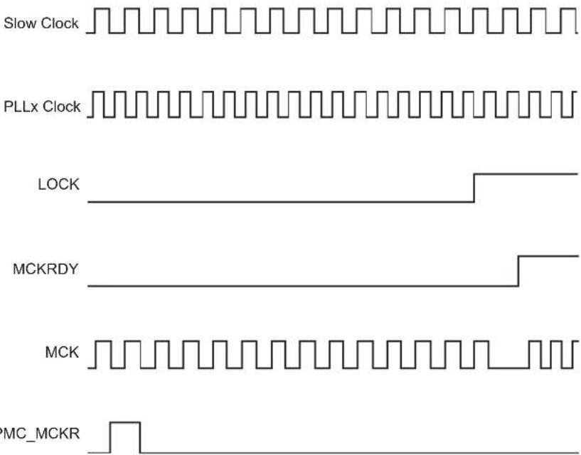
text_image
Slow Clock PLLx Clock LOCK MCKRDY MCK MC_MCKRFigure 31-7. Switch Host Clock (MCK) from Main Clock (MAINCK) to Slow Clock
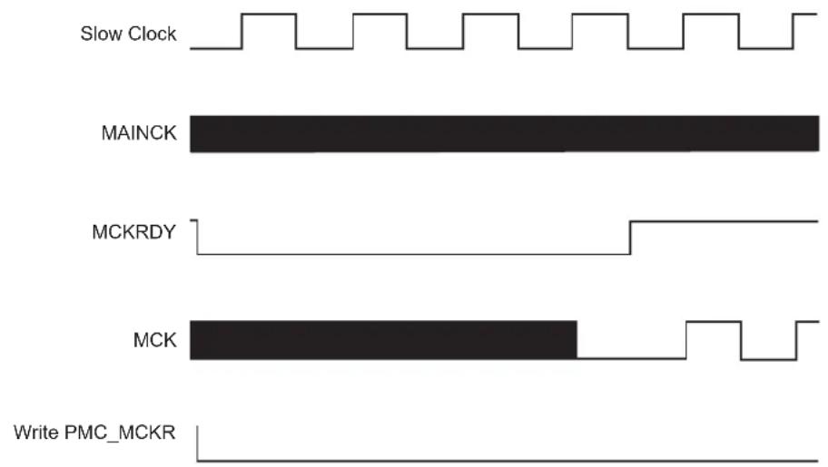
text_image
Slow Clock MAINCK MCKRDY MCK Write PMC_MCKRFigure 31-8. Change PLLA Programming
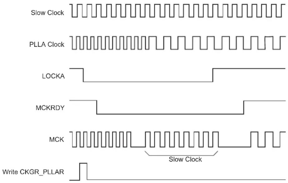
text_image
Slow Clock PLLA Clock LOCKA MCKRDY MCK Slow Clock Write CKGR_PLLARFigure 31-9. Programmable Clock Output Programming
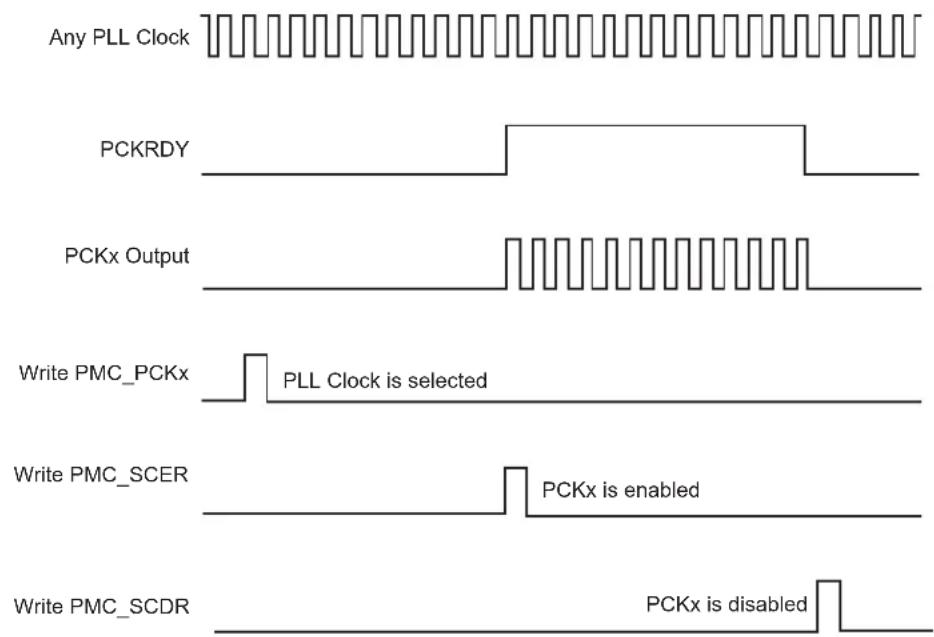
text_image
Any PLL Clock PCKRDY PCKx Output Write PMC_PCKx PLL Clock is selected Write PMC_SCER PCKx is enabled Write PMC_SCDR PCKx is disabled31.19 Register Write Protection
To prevent any single software error from corrupting PMC behavior, certain registers in the address space can be write-protected by setting the WPEN bit in the PMC Write Protection Mode Register (PMC_WPMR).
If a write access to a write-protected register is detected, the WPVS flag in the PMC Write Protection Status Register (PMC_WPSR) is set and the field WPVSRC indicates the register in which the write access has been attempted.
The WPVS bit is automatically cleared after reading the PMC_WPSR.
The following registers are write-protected when the WPEN bit is set in PMC_WPMR:
• PMC System Clock Disable Register
- PMC Peripheral Clock Enable Register 0
• PMC Peripheral Clock Disable Register 0
- PMC Clock Generator Main Oscillator Register
• PMC Clock Generator Main Clock Frequency Register
• PMC Clock Generator PLLA Register
- PMC UTMI Clock Configuration Register
• PMC Host Clock Register
- PMC USB Clock Register
• PMC Programmable Clock Register
• PMC Fast Startup Mode Register
• PMC Fast Startup Polarity Register
- PMC Peripheral Clock Enable Register1
• PMC Pheripheral Clock Disable Register1
• PMC Oscillator Calibration Register
• PMC SleepWalking Enable Register 0
• PMC SleepWalking Disable Register 0
- PLL Maximum Multiplier Value Register
• PMC SleepWalking Enable Register 1
• PMC SleepWalking Disable Register 1
31.20 Register Summary
| Offset | Name Bit Pos. 7 | 6 | 5 | 4 | 3 | 2 | 1 | 0 | ||||||||
| 0x00 PMC_SCER | 7:0 USBCLK | |||||||||||||||
| 15:8 PCK7 PCK6 PCK5 PCK4 PCK3 PCK2 PCK1 PCK0 | ||||||||||||||||
| 23:16 | ||||||||||||||||
| 31:24 | ||||||||||||||||
| 0x04 PMC_SCDR | 7:0 USBCLK | |||||||||||||||
| 15:8 PCK7 PCK6 PCK5 PCK4 PCK3 PCK2 PCK1 PCK0 | ||||||||||||||||
| 23:16 | ||||||||||||||||
| 32:24 | ||||||||||||||||
| 0x08 PMC_SCSR | 7:0 USBCLK HCLKS | |||||||||||||||
| 15:8 PCK7 PCK6 PCK5 PCK4 PCK3 PCK2 PCK1 PCK0 | ||||||||||||||||
| 23:16 | ||||||||||||||||
| 31:24 | ||||||||||||||||
| 0x0C ... 0x0F | Reserved | |||||||||||||||
| 0x10 | PMC_PCERO | 7:0 | PID7 | |||||||||||||
| 15:8 | PID15 | PID14 | PID13 | PID12 | PID11 | PID10 | PID9 | PID8 | ||||||||
| 23:16 | PID23 | PID22 | PID21 | PID20 | PID19 | PID18 | PID17 | PID16 | ||||||||
| 31:24 | PID31 | PID30 | PID29 | PID28 | PID27 | PID26 | PID25 | PID24 | ||||||||
| 0x14 | PMC_PCDRO | 7:0 | PID7 | |||||||||||||
| 15:8 | PID15 | PID14 | PID13 | PID12 | PID11 | PID10 | PID9 | PID8 | ||||||||
| 23:16 | PID23 | PID22 | PID21 | PID20 | PID19 | PID17 | PID16 | PID16 | ||||||||
| 31:24 | PID31 | PID30 | PID29 | PID28 | PID27 | PID26 | PID25 | PID24 | ||||||||
| 0x18 | PMC_PCSR0 | 7:0 | PID7 | |||||||||||||
| 15:8 | PID15 | PID14 | PID13 | PID12 | PID11 | PID10 | PID9 | PID8 | ||||||||
| 23:16 | PID23 | PID22 | PID21 | PID20 | PID19 | PID16 | PID17 | PID16 | ||||||||
| 31:24 | PID31 | PID30 | PID29 | PID28 | PID27 | PID26 | PID25 | PID24 | ||||||||
| 0x1C | CKGR_UCKR | 7:0 | ||||||||||||||
| 15:8 | ||||||||||||||||
| 23:16 | UPLLCOUNT[3:0] | UPLLEN | ||||||||||||||
| 31:24 | ||||||||||||||||
| 0x20 | CKGR_MOR | 7:0 | MOSCRCF[2:0] | MOSCRCEN | WAITMODE | MOSCXTBY | MOSCXTEN | |||||||||
| 15:8 | MOSCXTST[7:0] | |||||||||||||||
| 23:16 | KEY[7:0] | |||||||||||||||
| 31:24 | XT32KFME CFDEN MOSCSEL | |||||||||||||||
| 0x24 | CKGR_MCFR | 7:0 | MAINF[7:0] | |||||||||||||
| 15:8 | MAINF[15:8] | |||||||||||||||
| 23:16 | RCMEAS MAINFRDY | |||||||||||||||
| 31:24 | CCSS | |||||||||||||||
| 0x28 | CKGR_PLLAR | 7:0 | DIVA[7:0] | |||||||||||||
| 15:8 | PLLACOUNT[5:0] | |||||||||||||||
| 23:16 | MULA[7:0] | |||||||||||||||
| 31:24 | ONE | MULA[10:8] | ||||||||||||||
| 0x2C ... 0x2F | Reserved | |||||||||||||||
| 0x30 | PMC_MCKR | 7:0 | PRES[2:0] | CSS[1:0] | ||||||||||||
| 15:8 | UPLLDIV2 | MDIV[1:0] | ||||||||||||||
| 23:16 | ||||||||||||||||
| 31:24 | ||||||||||||||||
| 0x34 ... 0x37 | Reserved | |||||||||||||||
| 0x38 | PMC_USB | 7:0 | USBS | |||||||||||||
| 15:8 | USBDIV[3:0] | |||||||||||||||
| 23:16 | ||||||||||||||||
| 31:24 | ||||||||||||||||
......continued
| Offset | Name Bit Pos. 76543210 | ||||||||||
| 0x3C...0x3F | Reserved | ||||||||||
| 0x40 PMC_PCKx [x=0..] | 7:0 PRES[3:0] CSS[2:0] | ||||||||||
| 15:8 | PRES[7:4] | ||||||||||
| 23:16 | |||||||||||
| 31:24 | |||||||||||
| 0x44...0x5F | Reserved | ||||||||||
| 0x60 PMC_IER | 7:0 | LOCKU | MCKRDY | LOCKA | MOSCXTS | ||||||
| 15:8 | PCKRDY7 | PCKRDY6 | PCKRDYS | PCKRDY4 | PCKRDY3 | PCKRDY2 | PCKRDY1 | PCKRDY0 | |||
| 23:16 | XT32KERR | CFDEV | MOSCRCS | MOSCSELS | |||||||
| 31:24 | |||||||||||
| 0x64 | PMC_IDR | 7:0 | LOCKU | MCKRDY | LOCKA | MOSCXTS | |||||
| 15:8 | PCKRDY7 | PCKRDY6 | PCKRDY5 | PCKRDY4 | PCKRDY3 | PCKRDY2 | PCKRDY1 | PCKRDY0 | |||
| 23:16 | XT32KERR | CFDEV | MOSCRCS | MOSCSELS | |||||||
| 31:24 | |||||||||||
| 0x68 | PMC_SR | 7:0 | OSCSELS | LOCKU | MCKRDY | LOCKA | MOSCXTS | ||||
| 15:8 | PCKRDY7 | PCKRDY6 | PCKRDY5 | PCKRDY4 | PCKRDY3 | PCKRDY2 | PCKRDY1 | PCKRDY0 | |||
| 23:16 | XT32KERR | FOS | CFDS | CFDEV | MOSCRCs | MOSCSELS | |||||
| 31:24 | |||||||||||
| 0x6C PMC_IMR | 7:0 | LOCKU | MCKRDY | LOCKA | MOSCXTS | ||||||
| 15:8 | PCKRDY7 | PCKRDY6 | PCKRDY5 | PCKRDY4 | PCKRDY3 | PCKRDY2 | PCKRDY1 | PCKRDY0 | |||
| 23:16 | XT32KERR | CFDEV | MOSCRCS | MOSCSELS | |||||||
| 31:24 | |||||||||||
| 0x70 PMC_FSMR | 7:0 | FSTT7 | FSTT6 | FSTT5 | FSTT4 | FSTT3 | FSTT2 | FSTT1 | FSTT0 | ||
| 15:8 | FSTT15 | FSTT14 | FSTT13 | FSTT12 | FSTT11 | FSTT10 | FSTT9 | FSTT8 | |||
| 23:16 | FFLPM | FLPM[1:0] | LPM | USBAL | RTCAL | RTTAL | |||||
| 31:24 | |||||||||||
| 0x74 | PMC_FSPR | 7:0 | FSTP7 | FSTP6 | FSTP5 | FSTP4 | FSTP3 | FSTP2 | FSTP1 | FSTP0 | |
| 15:8 | FSTP15 | FSTP14 | FSTP13 | FSTP12 | FSTP11 | FSTP10 | FSTP9 | FSTP8 | |||
| 23:16 | |||||||||||
| 31:24 | |||||||||||
| 0x78 PMC_FOCR | 7:0 | FOCLR | |||||||||
| 15:8 | |||||||||||
| 23:16 | |||||||||||
| 31:24 | |||||||||||
| 0x7C...0xE3 | Reserved | ||||||||||
| 0xE4 | PMC_WPMR | 7:0 | WPEN | ||||||||
| 15:8 | WPKEY[7:0] | ||||||||||
| 23:16 | WPKEY[15:8] | ||||||||||
| 31:24 | WPKEY[23:16] | ||||||||||
| 0xE8 | PMC_WPSR | 7:0 | WPVS | ||||||||
| 15:8 | WPVSR[7:0] | ||||||||||
| 23:16 | WPVSR[15:8] | ||||||||||
| 31:24 | |||||||||||
| 0xEC...0xFF | Reserved | ||||||||||
| 0x0100 | PMC_PCER1 | 7:0 | PID39 | PID37 | PID35 | PID34 | PID33 | PID32 | |||
| 15:8 | PID47 | PID46 | PID45 | PID44 | PID43 | PID42 | PID41 | PID40 | |||
| 23:16 | PID53 | PID52 | PID51 | PID50 | PID49 | PID48 | |||||
| 31:24 | PID62 | PID60 | PID59 | PID58 | PID57 | PID56 | |||||
| 0x0104 | PMC_PCDR1 | 7:0 | PID39 | PID37 | PID35 | PID34 | PID33 | PID32 | |||
| 15:8 | PID47 | PID46 | PID45 | PID44 | PID43 | PID42 | PID41 | PID40 | |||
| 23:16 | PID53 | PID52 | PID51 | PID50 | PID49 | PID48 | |||||
| 31:24 | PID62 | PID60 | PID59 | PID58 | PID57 | PID56 | |||||
......continued
| Offset | Name Bit Pos. 7 | 6 | 5 | 4 | 3 | 2 | 1 | 0 | |||||||||
| 0x0108 | PMC_PCSR1 | 7:0 PID39 PID37 PID35 PID34 PID33 PID32 | |||||||||||||||
| 15:8 PID47 PID46 PID45 PID44 PID43 PID42 PID41 PID40 | |||||||||||||||||
| 23:16 PID53 PID52 PID51 PID50 PID49 PID48 | |||||||||||||||||
| 31:24 PID62 PID60 PID59 PID58 PID57 PID56 | |||||||||||||||||
| 0x010C | PMC_PCR | 7:0 PID[6:0] | |||||||||||||||
| 15:8 | CMD GCLKCSS[2:0] | ||||||||||||||||
| 23:16 | GCLKDIV[3:0] | ||||||||||||||||
| 31:24 | GCLKEN EN | GCLKDIV[7:4] | |||||||||||||||
| 0x0110 | PMC_OCR | 7:0 SEL4 | CAL4[6:0] | ||||||||||||||
| 15:8 SEL8 | CAL8[6:0] | ||||||||||||||||
| 23:16 SEL12 | CAL12[6:0] | ||||||||||||||||
| 31:24 | |||||||||||||||||
| 0x0114 | PMC_SLPWK_ER0 | 7:0 PID7 | |||||||||||||||
| 15:8 PID15 PID14 PID13 PID12 PID11 PID10 | PID9 | PID8 | |||||||||||||||
| 23:16 PID23 PID22 PID21 PID20 PID19 PID18 PID17 PID16 | |||||||||||||||||
| 31:24 PID31 PID30 PID29 PID28 PID27 PID26 PID25 PID24 | |||||||||||||||||
| 0x0118 | PMC_SLPWK_DRO | 7:0 PID7 | |||||||||||||||
| 15:8 PID15 PID14 PID13 PID12 PID11 PID10 | PID9 | PID8 | |||||||||||||||
| 23:16 PID23 PID22 PID21 PID20 PID19PID18 PID17 PID16 | |||||||||||||||||
| 31:24 PID31 PID30 PID29 PID28 PID27 PID26 PID25 PID24 | |||||||||||||||||
| 0x011C | PMC_SLPWK_SR0 | 7:0 PID7 | |||||||||||||||
| 15:8 PID15 PID14 PID13 PID12 PID11 PID10 | PID9 | PID8 | |||||||||||||||
| 23:16 PID23 PID22 PID21 PID20 PID18PID17PID16 | |||||||||||||||||
| 31:24 PID31 PID30 PID29 PID28 PID27 PID26 PID25 PID24 | |||||||||||||||||
| 0x0120 | PMC_SLPWK_ASRO | 7:0 PID7 | |||||||||||||||
| 15:8 PID15 PID14 PID13 PID12 PID11 PID10 | PID9 | PID8 | |||||||||||||||
| 23:16 PID23 PID22 PID21 PID20 PID18 PID17 PID16 | |||||||||||||||||
| 31:24 PID31 PID30 PID29 PID28 PID27 PID26 PID25 PID24 | |||||||||||||||||
| 0x0124 ... 0x012F | Reserved | ||||||||||||||||
| 7:0 PLLA_MMAX[7:0] | |||||||||||||||||
| 0x0130 | PMC_PMMR | 15:8 | PLLA_MMAX[10:8] | ||||||||||||||
| 23:16 | |||||||||||||||||
| 31:24 | |||||||||||||||||
| 0x0134 | PMC_SLPWK_ER1 | 7:0 PID39 PID37 | |||||||||||||||
| 15:8 PID47 PID46 PID45 PID44 PID43 PID42 PID41 PID40 | |||||||||||||||||
| 23:16 PID53 PID52 PID51 PID50 PID49 PID48 | |||||||||||||||||
| 31:24 PID63 PID62 PID60 PID59 PID58 PID57 PID56 | |||||||||||||||||
| 0x0138 | PMC_SLPWK_DR1 | 7:0 PID39 PID37 PID35 PID34 PID33 PID32 | |||||||||||||||
| 15:8 PID47 PID46 PID45 PID44 PID43 PID42 PID41 PID40 | |||||||||||||||||
| 23:16 PID53 PID52 PID51 PID50 PID49 PID48 | |||||||||||||||||
| 31:24 PID63 PID62 PID60 PID59 PID58 PID57 PID56 | |||||||||||||||||
| 0x013C | PMC_SLPWK_SR1 | 7:0 PID39 PID37 PID35 PID34 PID33 PID32 | |||||||||||||||
| 15:8 PID47 PID46 PID45 PID44 PID43 PID42 PID41 PID40 | |||||||||||||||||
| 28:16 PID53 PID52 PID51 PID50 PID49 PID48 | |||||||||||||||||
| 31:24 PID63 PID62 PID60 PID59 PID58 PID57 PID56 | |||||||||||||||||
| 0x0140 | PMC_SLPWK_ASR1 | 7:0 PID39 PID37 PID35 PID34 PID33 PID32 | |||||||||||||||
| 15:8 PID47 PID46 PID45 PID44 PID43 PID42 PID41 PID40 | |||||||||||||||||
| 25:16 PID53 PID52 PID51 PID50 PID49 PID48 | |||||||||||||||||
| 31:24 PID63 PID62 PID60 PID59 PID58 PID57 PID56 | |||||||||||||||||
| 0x0144 | PMC_SLPWK_AIPR | 7:0 AIP | |||||||||||||||
| 15:8 AIP | |||||||||||||||||
| 23:16 AIP | |||||||||||||||||
| 31:24 AIP | |||||||||||||||||
31.20.1 PMC System Clock Enable Register
Name: PMC_SCER
Offset: 0x0000
Property: Write-only
This register can only be written if the WPEN bit is cleared in the PMC Write Protection Mode Register.

text_image
Bit 31 30 29 28 27 26 25 24 Access Reset Bit 23 22 21 20 19 18 17 16 Access Reset Bit 15 14 13 12 11 10 9 8 PCK7 PCK6 PCK5 PCK4 PCK3 PCK2 PCK1 PCK0 Access Reset W W W W W W W W W Bit 7 6 5 4 3 2 1 0 Access Reset USBCLK WBits 8, 9, 10, 11, 12, 13, 14, 15 - PCK Programmable Clock x Output Enable
| Value | Description |
| 0 | No effect. |
| 1 | Enables the corresponding Programmable Clock output. |
Bit 5 - USBCLK Enable USB FS Clock
| Value | Description |
| 0 | No effect. |
| 1 | Enables USB FS clock. |
31.20.2 PMC System Clock Disable Register
Name: PMC_SCDR
Offset: 0x0004
Property: Write-only
This register can only be written if the WPEN bit is cleared in the PMC Write Protection Mode Register.
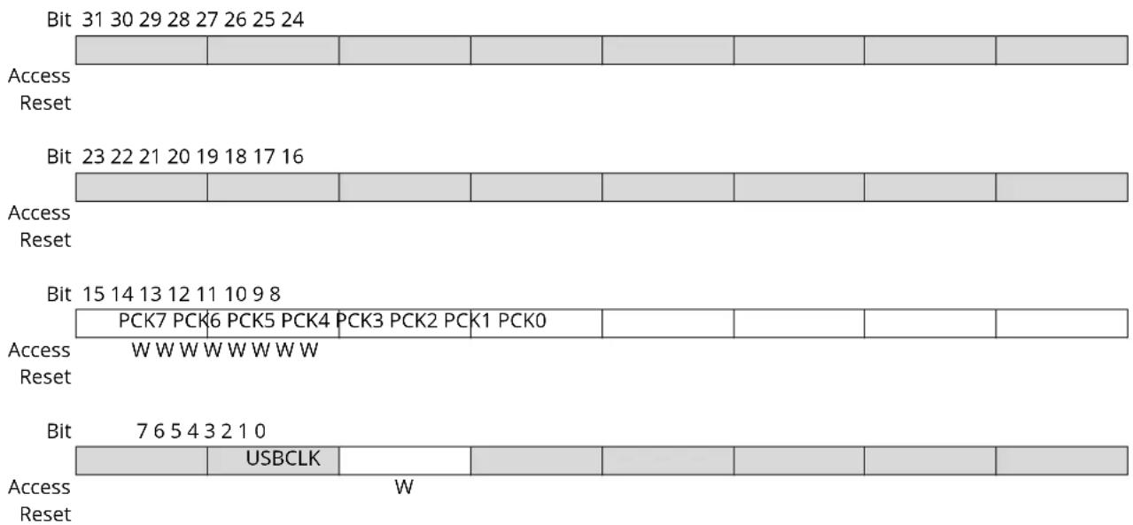
text_image
Bit 31 30 29 28 27 26 25 24 Access Reset Bit 23 22 21 20 19 18 17 16 Access Reset Bit 15 14 13 12 11 10 9 8 PCK7 PCK6 PCK5 PCK4 PCK3 PCK2 PCK1 PCK0 Access Reset W W W W W W W W W Bit 7 6 5 4 3 2 1 0 USBCLK W Access ResetBits 8, 9, 10, 11, 12, 13, 14, 15 - PCK Programmable Clock x Output Disable
| Value | Description |
| 0 | No effect. |
| 1 | Disables the corresponding Programmable Clock output. |
Bit 5 - USBCLK Disable USB FS Clock
| Value | Description |
| 0 | No effect. |
| 1 | Disables USB FS clock. |
31.20.3 PMC System Clock Status Register
Name: PMC_SCSR
Offset: 0x0008
Reset: 0x00000001
Property: Read-only

text_image
Bit 31 30 29 28 27 26 25 24 Access Reset Bit 23 22 21 20 19 18 17 16 Access Reset Bit 15 14 13 12 11 10 9 8 PCK7 PCK6 PCK5 PCK4 PCK3 PCK2 PC K1 PCK0 Access R R R R R R R Reset 0 0 0 0 0 0 0 Bit 7 6 5 4 3 2 1 0 USBCLK HCLK$ Access R Reset 0 R 1Bits 8, 9, 10, 11, 12, 13, 14, 15 - PCK Programmable Clock x Output Status
| Value | Description |
| 0 | The corresponding Programmable Clock output is disabled. |
| 1 | The corresponding Programmable Clock output is enabled. |
Bit 5 - USBCLK USB FS Clock Status
| Value | Description |
| 0 | The USB FS clock is disabled. |
| 1 | The USB FS clock is enabled. |
Bit 0 - HCLKS HCLK Status
| Value | Description |
| 0 | HCLK is disabled. |
| 1 | HCLK is enabled. |
31.20.4 PMC Peripheral Clock Enable Register 0
Name: PMC_PCERO
Offset: 0x0010
Property: Write-only
This register can only be written if the WPEN bit is cleared in the PMC Write Protection Mode Register.
| Bit 31 30 29 28 27 26 25 24 | |||||||
| PID31 PID | 30 PID29 PID2 | 8 PID27 PID26 | PID25 PID24 | ||||
| Access Reset | WWWWWWWW | ||||||
| Bit 23 22 21 20 19 18 17 16 | |||||||
| PID23 PID | 22 PID21 PID2 | 0 PID19 PID18 | PID17 PID16 | ||||
| Access Reset | WWWWWWWW | ||||||
| Bit 15 14 13 12 11 10 9 8 | |||||||
| PID15 PID | 14 PID13 PID1 | 2 PID11 PID10 | PID9 | PID8 | |||
| Access Reset | WWWWWWWW | ||||||
| Bit 7 6 5 4 3 2 1 0 | |||||||
| PID7 | |||||||
| Access Reset | W | ||||||
Bits 7, 8, 9, 10, 11, 12, 13, 14, 15, 16, 17, 18, 19, 20, 21, 22, 23, 24, 25, 26, 27, 28, 29, 30, 31 – PIDx Peripheral Clock x Enable
| Value | Description |
| 0 | No effect. |
| 1 | Enables the corresponding peripheral clock.Notes:1. PIDx refers to identifiers defined in the section “Peripheral Identifiers”. Other peripherals can be enabled in PMC_PCER1 (see 31.20.23. PMC_PCER1).2. Programming the control bits of the Peripheral ID that are not implemented has no effect on the behavior of the PMC. |
31.20.5 PMC Peripheral Clock Disable Register 0
Name: PMC_PCDRO
Offset: 0x0014
Property: Write-only
This register can only be written if the WPEN bit is cleared in the PMC Write Protection Mode Register.
| Bit 31 30 29 28 27 26 25 24 | |||||||
| PID31 PID | 30 PID29 PID2 | 8 PID27 PID26 | PID25 PID24 | ||||
| Access Reset | WWWWWWWW | ||||||
| Bit 23 22 21 20 19 18 17 16 | |||||||
| PID23 PID | 22 PID21 PID2 | 0 PID19 PID18 | PID17 PID16 | ||||
| Access Reset | WWWWWWWW | ||||||
| Bit 15 14 13 12 11 10 9 8 | |||||||
| PID15 PID | 14 PID13 PID1 | 2 PID11 PID10 | PID9 | PID8 | |||
| Access Reset | WWWWWWWW | ||||||
| Bit 7 6 5 4 3 2 1 0 | |||||||
| PID7 | |||||||
| Access Reset | W | ||||||
Bits 7, 8, 9, 10, 11, 12, 13, 14, 15, 16, 17, 18, 19, 20, 21, 22, 23, 24, 25, 26, 27, 28, 29, 30, 31 - PIDx Peripheral Clock x Disable
| Value | Description |
| 0 | No effect. |
| 1 | Disables the corresponding peripheral clock.Note: PIDx refers to identifiers defined in the section “Peripheral Identifiers”. Other peripherals can be disabled in PMC_PCDR1 (see 31.20.24. PMC_PCDR1). |
31.20.6 PMC Peripheral Clock Status Register 0
Name: PMC_PCSR0
Offset: 0x0018
Reset: 0x00000000
Property: Read-only
| Bit 31 30 29 28 27 26 25 24 | |||||||
| PID31 PID | 30 PID29 PID2 | 8 PID27 PID26 | PID25 PID24 | ||||
| Access | RR R R R R R R | ||||||
| Reset 0 0 0 0 0 0 0 0 | |||||||
| Bit 23 22 21 20 19 18 17 16 | |||||||
| PID23 PID | 22 PID21 PID2 | 0 PID19 PID18 | PID17 PID16 | ||||
| Access | RR R R R R R R | ||||||
| Reset 0 0 0 0 0 0 0 0 | |||||||
| Bit 15 14 13 12 11 10 9 8 | |||||||
| PID15 PID | 14 PID13 PID1 | 2 PID11 PID10 | PID9 | PID8 | |||
| Access | RR R R R R R R | ||||||
| Reset 0 0 0 0 0 0 0 0 | |||||||
| Bit 7 6 5 4 3 2 1 0 | |||||||
| PID7 | |||||||
| Access | R | ||||||
| Reset 0 | |||||||
Bits 7, 8, 9, 10, 11, 12, 13, 14, 15, 16, 17, 18, 19, 20, 21, 22, 23, 24, 25, 26, 27, 28, 29, 30, 31 – PIDx Peripheral Clock x Status
| Value | Description |
| 0 | The corresponding peripheral clock is disabled. |
| 1 | The corresponding peripheral clock is enabled.Note: PIDx refers to identifiers defined in the section “Peripheral Identifiers”. Other peripherals status can be read in PMC_PCSR1 (see PMC Peripheral Clock Status Register 1). |
31.20.7 PMC UTMI Clock Configuration Register
Name: CKGR_UCKR
Offset: 0x001C
Reset: 0x10200800
Property: Read/Write
This register can only be written if the WPEN bit is cleared in the PMC Write Protection Mode Register.
text_image
Bit 31 30 29 28 27 26 25 24 Access Reset Bit 23 22 21 20 19 18 17 16 UPLLCOUNT[3:0] UPLLEN Access R/W R/W R/W R/W R/W Reset 0 0 1 0 0 Bit 15 14 13 12 11 10 9 8 Access Reset Bit 7 6 5 4 3 2 1 0 Access ResetBits 23:20 - UPLLCOUNT[3:0] UTMI PLL Startup Time
Specifies the number of SLCK cycles multiplied by 8 for the UTMI PLL startup time.
Bit 16 - UPLLEN UTMI PLL Enable
When UPLLEN is set, the LOCKU flag is set once the UTMI PLL startup time is achieved.
| Value | Description |
| 0 | The UTMI PLL is disabled. |
| 1 | The UTMI PLL is enabled. |
31.20.8 PMC Clock Generator Main Oscillator Register
Name: CKGR_MOR
Offset: 0x0020
Reset: 0x00000008
Property: Read/Write
This register can only be written if the WPEN bit is cleared in the PMC Write Protection Mode Register.
Bit 31 30 29 28 27 26 25 24
| XT32KFME CFDEN MOSCSEL | ||||||
| Access Reset 0 0 0 | R/W R/W R/W | |||||
Bit 23 22 21 20 19 18 17 16
| KEY[7:0] | |
| Access | R/W R/W R/W R/W R/W R/W R/W R/W |
| Reset | 0 0 0 0 0 0 0 |
Bit 15 14 13 12 11 10 98
| MOSCXTST[7:0] | |
| Access | R/W R/W R/W R/W R/W R/W R/W R/W |
| Reset | 0 0 0 0 0 0 0 |
Bit 76543210
| MOSCRCF[2:0] | MOSCRCEN | WAITMODE | MOSCXTBY | MOSCXTEN | |
| Access | R/W R/W R/W R/W R/W R/W R/W | ||||
| Reset | 0 0 0 1 0 0 0 | ||||
Bit 26 - XT32KFME 32.768 kHz Crystal Oscillator Frequency Monitoring Enable
| Value | Description |
| 0 | The 32.768 kHz crystal oscillator frequency monitoring is disabled. |
| 1 | The 32.768 kHz crystal oscillator frequency monitoring is enabled. |
Bit 25 - CFDEN Clock Failure Detector Enable
| Value | Description |
| 0 | The clock failure detector is disabled. |
| 1 | The clock failure detector is enabled. |
Bit 24 - MOSCSEL Main Clock Oscillator Selection
| Value | Description |
| 0 | The Main RC oscillator is selected. |
| 1 | The Main crystal oscillator is selected. |
Bits 23:16 - KEY[7:0] Write Access Password
| Value | Name | Description |
| 0×37 | PASSWD | Writing any other value in this field aborts the write operation.Always reads as 0. |
Bits 15:8 - MOSCXTST[7:0] Main Crystal Oscillator Startup Time
Specifies the number of SLCK cycles multiplied by 8 for the main crystal oscillator startup time.
Bits 6:4 - MOSCRCF[2:0] Main RC Oscillator Frequency Selection
At startup, the Main RC oscillator frequency is 12 MHz.
| Value Name | Description |
| 0 | 4_MHz The RC oscillator frequency is at 4 MHz |
| 1 | 8_MHz The RC oscillator frequency is at 8 MHz |
| 2 | 12_MHz The RC oscillator frequency is at 12 MHzNote: MOSCRCF must be changed only if MOSCRCS is set in the PMC_SR. Therefore MOSCRCF and MOSCRCEN cannot be changed at the same time. |
Bit 3 - MOSCRCEN Main RC Oscillator Enable
When MOSCRCEN is set, the MOSCRCS flag is set once the Main RC oscillator startup time is achieved.
| Value Description | |
| 0 | The Main RC oscillator is disabled. |
| 1 | The Main RC oscillator is enabled. |
Bit 2 - WAITMODE Wait Mode Command (write-only)
| Value Description | |
| 0 | No effect. |
| 1 | Puts the device in Wait mode. |
Bit 1 - MOSCXTBY Main Crystal Oscillator Bypass
When MOSCXTBY is set, the MOSCXTS flag in PMC_SR is automatically set. Clearing MOSCXTEN and MOSCXTBY bits clears the MOSCXTS flag.
| Value Description | |
| 0 | No effect. |
| 1 | The Main crystal oscillator is bypassed. MOSCXTEN must be cleared. An external clock must be connected on XIN.Note: When the crystal oscillator bypass is disabled (MOSCXTBY = 0), the MOSCXTS flag must be read at '0' in PMC_SR before enabling the crystal oscillator (MOSCXTEN = 1). |
Bit 0 - MOSCXTEN Main Crystal Oscillator Enable
A crystal must be connected between XIN and XOUT.
When MOSCXTEN is set, the MOSCXTS flag is set once the Main crystal oscillator startup time is achieved.
| Value Description | |
| 0 | The Main crystal oscillator is disabled. |
| 1 | The Main crystal oscillator is enabled. MOSCXTBY must be cleared. |
31.20.9 PMC Clock Generator Main Clock Frequency Register
Name: CKGR_MCFR
Offset: 0x0024
Reset: 0x00000000
Property: Read/Write
This register can only be written if the WPEN bit is cleared in the PMC Write Protection Mode Register.
Bit 31 30 29 28 27 26 25 24
| CCSS | |||||||
| Access Reset 0 | R/W | ||||||
Bit 23 22 21 20 19 18 17 16
| RCMEAS | MAINFRDY | ||||||
| Access Reset | R/W 0 | R/W 0 |
Bit 15 14 13 12 11 10 9 8
| MAINF[15:8] | ||||||||
| Access | R/W | R/W | R/W | R/W | R/W | R/W | R/W | R/W |
| Reset | 0 | 0 | 0 | 0 | 0 | 0 | 0 | 0 |
| Bit | 7 | 6 | 5 | 4 | 3 | 2 | 1 | 0 |
| MAINF[7:0] | ||||||||
| Access | R/W | R/W | R/W | R/W | R/W | R/W | R/W | R/W |
| Reset | 0 | 0 | 0 | 0 | 0 | 0 | 0 | 0 |
Bit 24 - CCSS Counter Clock Source Selection
| Value | Description |
| 0 | The measured clock of the MAINF counter is the Main RC oscillator. |
| 1 | The measured clock of the MAINF counter is the Main crystal oscillator. |
Bit 20 - RCMEAS RC Oscillator Frequency Measure (write-only)
The measurement is performed on the main frequency (i.e., not limited to the Main RC oscillator only). If the source of MAINCK is the Main crystal oscillator, the restart of measurement may not be required because of the stability of crystal oscillators.
| Value | Description |
| 0 | No effect. |
| 1 | Restarts measuring of the frequency of MAINCK. MAINF carries the new frequency as soon as a low-to-high transition occurs on the MAINFRDY flag. |
Bit 16 - MAINFRDY Main Clock Frequency Measure Ready
| Value | Description |
| 0 | MAINF value is not valid or the measured oscillator is disabled or a measure has just been started by means of RCMEAS. |
| 1 | The measured oscillator has been enabled previously and MAINF value is available.Note: To ensure that a correct value is read on the MAINF field, the MAINFRDY flag must be read at ‘1’ then another read access must be performed on the register to get a stable value on the MAINF field. |
Bits 15:0 - MAINF[15:0] Main Clock Frequency
Gives the number of cycles of the clock selected by the bit CCSS within 16 SLCK periods. To calculate the frequency of the measured clock:
f_SELCLK = (MAINF × f_SLCK) / 16
where frequency is in MHz.
31.20.10 PMC Clock Generator PLLA Register
Name: CKGR_PLLAR
Offset: 0x0028
Reset: 0x00003F00
Property: Read/Write
Possible limitations on PLLA input frequencies and multiplier factors should be checked before using the PMC.

Bit 29 must always be set to '1' when programming the CKGR_PLLAR.
This register can only be written if the WPEN bit is cleared in the PMC Write Protection Mode Register.
Bit 31 30 29 28 27 26 25 24
| ONE | MULA[10:8] | |||||
| Access | R/W | R/W | R/W | R/W | ||
| Reset | 0 | 0 | 0 |
Bit 23 22 21 20 19 18 17 16
| MULA[7:0] | ||||||||
| Access | R/W | R/W | R/W | R/W | R/W | R/W | R/W | R/W |
| Reset | 0 | 0 | 0 | 0 | ||||
Bit 15 14 13 12 11 10 9 8
| PLLACOUNT[5:0] | |||||||
| Access Reset | R/W R/W R/W R/W R/W R/W | ||||||
| 1 | 1 | 1 | 1 | 1 | 1 | ||
| Bit | 7 | 6 | 5 | 4 | 3 | 2 | 0 |
| DIVA[7:0] | |||||||
| Access Reset | R/W R/W R/W R/W R/W R/W R/W | ||||||
| 0 | 0 | 0 | 0 | 0 | 0 | 0 | |
Bit 29 - ONE Must Be Set to 1
Bit 29 must always be set to '1' when programming the CKGR_PLLAR.
Bits 26:16 - MULA[10:0] PLLA Multiplier
1 up to 62 = PLLCK frequency is the PLLA input frequency multiplied by MULA + 1.
Unlisted values are forbidden.
| Value | Description |
| 0 | The PLLA is disabled (PLLA also disabled if DIVA = 0). |
Bits 13:8 - PLLACOUNT[5:0] PLLA Counter
Specifies the number of SLCK cycles before the LOCKA bit is set in PMC_SR after CKGR_PLLAR is written.
Bits 7:0 - DIVA[7:0] PLLA Front End Divider
| Value | Name | Description |
| 0 | 0 | PLLA is disabled. |
| 1 | BYPASS | Divider is bypassed (divide by 1) and PLLA is enabled. |
| 2-255 | Divider output is the selected clock divided by DIVA. | |
31.20.11 PMC Host Clock Register
Name: PMC_MCKR
Offset: 0x0030
Reset: 0x00000001
Property: Read/Write
This register can only be written if the WPEN bit is cleared in the PMC Write Protection Mode Register.

text_image
Bit 31 30 29 28 27 26 25 24 Access Reset Bit 23 22 21 20 19 18 17 16 Access Reset Bit 15 14 13 12 11 10 9 8 UPLL DIV2 MDIV[1:0] Access R/W R/W R/W Reset 0 0 0 Bit 7 6 5 4 3 2 1 0 Access PRES[2:0] CS$[1:0] Reset R/W R/W R/W R/W 0 0 0 0 1Bit 13 - UPLLDIV2 UPLL Divider by 2
| Value | Description |
| 0 | UPLLCK frequency is divided by 1. |
| 1 | UPLLCK frequency is divided by 2. |
Bits 9:8 - MDIV[1:0] Host Clock Division
| Value | Name | Description |
| 0 | EQ_PCK | MCK is FCLK divided by 1. |
| 1 | PCK_DIV2 | MCK is FCLK divided by 2. |
| 2 | PCK_DIV4 | MCK is FCLK divided by 4. |
| 3 | PCK_DIV3 | MCK is FCLK divided by 3. |
Bits 6:4 - PRES[2:0] Processor Clock Prescaler
| Value | Name | Description |
| 0 | CLK_1 | Selected clock |
| 1 | CLK_2 | Selected clock divided by 2 |
| 2 | CLK_4 | Selected clock divided by 4 |
| 3 | CLK_8 | Selected clock divided by 8 |
| 4 | CLK_16 | Selected clock divided by 16 |
| 5 | CLK_32 | Selected clock divided by 32 |
| 6 | CLK_64 | Selected clock divided by 64 |
| 7 | CLK_3 | Selected clock divided by 3 |
| Value Name | Description | |
| 0 | SLOW_CLK SLCK is selected | |
| 1 | MAIN_CLK MAINCK is selected | |
| 2 | PLLA_CLK PLLACK is selected | |
| 3 | UPLL_CLK UPPLLCKDIV is selected | |
Bits 1:0 - CSS[1:0] Host Clock Source Selection
31.20.12 PMC USB Clock Register
Name: PMC_USB
Offset: 0x0038
Reset: 0x00000000
Property: Read/Write
This register can only be written if the WPEN bit is cleared in the PMC Write Protection Mode Register.
text_image
Bit 31 30 29 28 27 26 25 24 Access Reset Bit 23 22 21 20 19 18 17 16 Access Reset Bit 15 14 13 12 11 10 9 8 USBDIV[3:0] Access R/W R/W R/W R/W Reset 0 0 0 0 Bit 7 6 5 4 3 2 1 0 Access Reset USBS R/W 0Bits 11:8 - USBDIV[3:0] Divider for USB_48M
USB_48M is input clock divided by USBDIV+1.
Bit 0 - USBS USB Input Clock Selection
| Value | Description |
| 0 | USB_48M input is PLLA. |
| 1 | USB_48M input is UPLL. |
31.20.13 PMC Programmable Clock Register
Name: PMC_PCKx [x=0..7]
Offset: 0x0040
Reset: 0
Property: Read/Write
This register can only be written if the WPEN bit is cleared in the PMC Write Protection Mode Register.
text_image
Bit 31 30 29 28 27 26 25 24 Access Reset Bit 23 22 21 20 19 18 17 16 Access Reset Bit 15 14 13 12 11 10 9 8 PRES[7:4] Access R/W R/W R/W R/W Reset 0 0 0 0 Bit 7 6 5 4 3 2 1 0 PRES[3:0] CSS[2:0] Access R/W R/W R/W R/W Reset 0 0 0 0 0 0 R/W R/W R/W R/WBits 11:4 - PRES[7:0] Programmable Clock Prescaler
| Value | Description |
| 0-255 | Selected clock is divided by PRES+1. |
Bits 2:0 - CSS[2:0] Programmable Clock Source Selection
| Value | Name | Description |
| 0 | SLOW_CLK | SLCK is selected |
| 1 | MAIN_CLK | MAINCK is selected |
| 2 | PLLA_CLK | PLLACK is selected |
| 3 | UPLL_CLK | UPLLCKDIV is selected |
| 4 | MCK | MCK is selected |
| 5 | AUDIO_CLK | AUDIOPLLCLK is selected |
31.20.14 PMC Interrupt Enable Register
Name: PMC_IER
Offset: 0x0060
Property: Write-only
The following configuration values are valid for all listed bit names of this register:
0: No effect.
1: Enables the corresponding interrupt.
Bit 31 30 29 28 27 26 25 24
| Access Reset |
Bit 23 22 21 20 19 18 17 16

text_image
XT32 KERR CFDEV MOSCRCS M∅SCSELS W W W W Access ResetBit 15 14 13 12 11 10 9 8
| PCKRDY7 | PCKRDY6 | PCKRDY5 | PCKRDY4 | PCKRDY3 | PCKRDY2 | PCKRDY1 | PCKRDY0 | |
| Access Reset | WWWWWWWW | |||||||

text_image
Bit 7 6 5 4 3 2 1 0 LOCKU MCKRDY LOCKA MOSCXTS Access W W W W ResetBit 21 - XT32KERR 32.768 kHz Crystal Oscillator Error Interrupt Enable
Bit 18 - CFDEV Clock Failure Detector Event Interrupt Enable
Bit 17 - MOSCRCS Main RC Oscillator Status Interrupt Enable
Bit 16 - MOSCSELS Main Clock Source Oscillator Selection Status Interrupt Enable
Bits 8, 9, 10, 11, 12, 13, 14, 15 – PCKRDY Programmable Clock Ready x Interrupt Enable
Bit 6 - LOCKU UTMI PLL Lock Interrupt Enable
Bit 3 - MCKRDY Host Clock Ready Interrupt Enable
Bit 1 - LOCKA PLLA Lock Interrupt Enable
Bit 0 - MOSCXTS Main Crystal Oscillator Status Interrupt Enable
31.20.15 PMC Interrupt Disable Register
Name: PMC_IDR
Offset: 0x0064
Property: Write-only
The following configuration values are valid for all listed bit names of this register:
0: No effect.
1: Disables the corresponding interrupt.
Bit 31 30 29 28 27 26 25 24
| Access Reset |
Bit 23 22 21 20 19 18 17 16

text_image
XT32 KERR CFDEV MOSCRCS M∅SCSELS Access Reset W W W WBit 15 14 13 12 11 10 9 8
| PCKRDY7 | PCKRDY6 | PCKRDY5 | PCKRDY4 | PCKRDY3 | PCKRDY2 | PCKRDY1 | PCKRDY0 | |
| Access Reset | WWWWWWWW | |||||||

text_image
Bit 7 6 5 4 3 2 1 0 LOCKU MCKRDY LOCKA MOSCXTS Access WW WW ResetBit 21 - XT32KERR 32.768 kHz Crystal Oscillator Error Interrupt Disable
Bit 18 - CFDEV Clock Failure Detector Event Interrupt Disable
Bit 17 - MOSCRCS Main RC Status Interrupt Disable
Bit 16 - MOSCSELS Main Clock Source Oscillator Selection Status Interrupt Disable
Bits 8, 9, 10, 11, 12, 13, 14, 15 – PCKRDY Programmable Clock Ready x Interrupt Disable
Bit 6 - LOCKU UTMI PLL Lock Interrupt Disable
Bit 3 - MCKRDY Host Clock Ready Interrupt Disable
Bit 1 - LOCKA PLLA Lock Interrupt Disable
Bit 0 - MOSCXTS Main Crystal Oscillator Status Interrupt Disable
31.20.16 PMC Status Register
Name: PMC_SR
Offset: 0x0068
Reset: 0x01030008
Property: Read-only
Bit 31 30 29 28 27 26 25 24
| Access Reset | |||||||
Bit 23 22 21 20 19 18 17 16
| XT32 | KERR FOS CFDS | CFDEV MOSC | CRCS MOSCSELS | ||||
| Access | R | R | R | R | R | R | |
| Reset | 0 | 0 | 0 | 0 | 1 | 1 |
Bit 15 14 13 12 11 10 9 8
| PCKRDY7 | PCKRDY6 | PCKRDY5 | PCKRDY4 | PCKRDY3 | PCKRDY2 | PCKRDY1 | PCKRDY0 | |
| Access | R | R | R | R | R | R | R | R |
| Reset | 0 | 0 | 0 | 0 | 0 | 0 | 0 | 0 |
Bit 7 6 5 4 3 2 1 0
| OSCSELS | LOCKU | MCKRDY | LOCKA | MOSCXTS | ||||
| Access | R | R | R | R | R | |||
| Reset | 0 | 0 | 1 | 0 | 0 |
Bit 21 - XT32KERR Slow Crystal Oscillator Error
| Value | Description |
| 0 | The frequency of the 32.768 kHz crystal oscillator is correct (32.768 kHz ±1%) or the monitoring is disabled. |
| 1 | The frequency of the 32.768 kHz crystal oscillator is incorrect or has been incorrect for an elapsed period of time since the monitoring has been enabled. |
Bit 20 - FOS Clock Failure Detector Fault Output Status
| Value | Description |
| 0 | The fault output of the clock failure detector is inactive. |
| 1 | The fault output of the clock failure detector is active. This status is cleared by writing a ‘1’ to FOCLR in PMC_FOCR. |
Bit 19 - CFDS Clock Failure Detector Status
| Value | Description |
| 0 | A clock failure of the Main crystal oscillator clock is not detected. |
| 1 | A clock failure of the Main crystal oscillator clock is detected. |
Bit 18 - CFDEV Clock Failure Detector Event
| Value | Description |
| 0 | No clock failure detection of the Main crystal oscillator clock has occurred since the last read of PMC_SR. |
| 1 | At least one clock failure detection of the Main crystal oscillator clock has occurred since the last read of PMC_SR. |
Bit 17 - MOSCRCS Main RC Oscillator Status
| Value | Description |
| 0 | Main RC oscillator is not stabilized. |
| 1 | Main RC oscillator is stabilized. |
Bit 16 - MOSCSELS Main Clock Source Oscillator Selection Status
| Value Description | |
| 0 | Selection is in progress. |
| 1 | Selection is done. |
Bits 8, 9, 10, 11, 12, 13, 14, 15 - PCKRDY Programmable Clock Ready Status
| Value Description | |
| 0 | Programmable Clock x is not ready. |
| 1 | Programmable Clock x is ready. |
Bit 7 - OSCSELS Slow Clock Source Oscillator Selection
| Value Description | |
| 0 | Slow RC oscillator is selected. |
| 1 | 32.768 kHz crystal oscillator is selected. |
Bit 6 - LOCKU UTMI PLL Lock Status
| Value Description | |
| 0 | UTMI PLL is not locked |
| 1 | UTMI PLL is locked. |
Bit 3 - MCKRDY Host Clock Status
| Value Description | |
| 0 | Host Clock is not ready. |
| 1 | Host Clock is ready. |
Bit 1 - LOCKA PLLA Lock Status
| Value Description | |
| 0 | PLLA is not locked |
| 1 | PLLA is locked. |
Bit 0 - MOSCXTS Main Crystal Oscillator Status
| Value Description | |
| 0 | Main crystal oscillator is not stabilized. |
| 1 | Main crystal oscillator is stabilized. |
31.20.17 PMC Interrupt Mask Register
Name: PMC_IMR
Offset: 0x006C
Reset: 0x00000000
Property: Read-only
The following configuration values are valid for all listed bit names of this register:
0: No effect.
1: Enables the corresponding interrupt.
Bit 31 30 29 28 27 26 25 24
| Access Reset | |||||||
Bit 23 22 21 20 19 18 17 16
| XT32 | KERR | CFDEV | MOSCRCS | MOSCSELS | |||||
| Access Reset | R | R | R | ||||||
| 0 | 0 | 0 | 0 |
Bit 15 14 13 12 11 10 9 8
| PCKRDY7 | PCKRDY6 | PCKRDY5 | PCKRDY4 | PCKRDY3 | PCKRDY2 | PCKRDY1 | PCKRDY0 | |
| Access | R R R R R R R | |||||||
| Reset | 0 | 0 | 0 | 0 | 0 | 0 | 0 | 0 |
| Bit | 7 | 6 | 5 | 4 | 3 | 2 | 1 | 0 |
| LOCKU | MCKRDY | LOCKA | MOSCXTS | |||||
| Access | R R | R R | ||||||
| Reset | 0 | 0 | 0 | 0 | ||||
Bit 21 - XT32KERR 32.768 kHz Crystal Oscillator Error Interrupt Mask
Bit 18 - CFDEV Clock Failure Detector Event Interrupt Mask
Bit 17 - MOSCRCS Main RC Status Interrupt Mask
Bit 16 - MOSCSELS Main Clock Source Oscillator Selection Status Interrupt Mask
Bits 8, 9, 10, 11, 12, 13, 14, 15 – PCKRDY Programmable Clock Ready x Interrupt Mask
Bit 6 - LOCKU UTMI PLL Lock Interrupt Mask
Bit 3 - MCKRDY Host Clock Ready Interrupt Mask
Bit 1 - LOCKA PLLA Lock Interrupt Mask
Bit 0 - MOSCXTS Main Crystal Oscillator Status Interrupt Mask
31.20.18 PMC Fast Startup Mode Register
Name: PMC_FSMR
Offset: 0x0070
Reset: 0x00000000
Property: Read/Write
This register can only be written if the WPEN bit is cleared in the PMC Write Protection Mode Register.
Bit 31 30 29 28 27 26 25 24
| Access Reset | |||||||
Bit 23 22 21 20 19 18 17 16
| FFLPM FLPM[1:0] LPM USBAL RTCAL RTTAL | ||||||||
| Access | R/W | R/W | R/W | R/W | R/W | R/W | R/W | |
| Reset | 0 | 0 | 0 | 0 | 0 | 0 | 0 | |
Bit 15 14 13 12 11 10 98
| FSTT15 | FSTT14 | FSTT13 | FSTT12 | FSTT11 | FSTT10 | FSTT9 | FSTT8 | |
| Access | R/W | R/W | R/W | R/W | R/W | R/W | R/W | R/W |
| Reset | 0 | 0 | 0 | 0 | 0 | 0 | 0 | 0 |
Bit 7 6 5 4 3 2 1 0
| FSTT7 | FSTT6 | FSTT5 | FSTT4 | FSTT3 | FSTT2 | FSTT1 | FSTT0 | |
| Access | R/W | R/W | R/W | R/W | R/W | R/W | R/W | R/W |
| Reset | 0 | 0 | 0 | 0 | 0 | 0 | 0 | 0 |
Bit 23 - FFLPM Force Flash Low-power Mode
| Value | Description |
| 0 | The Flash Low-power mode, defined in the FLPM field, is automatically applied when in Wait mode and released when going back to Active mode. |
| 1 | The Flash Low-power mode is user defined by the FLPM field and immediately applied. |
Bits 22:21 - FLPM[1:0] Flash Low-power Mode
| Value | Name | Description |
| 0 | FLASH_STANDBY | Flash is in Standby Mode when system enters Wait Mode |
| 1 | FLASH_DEEP_POWERDOWN | Flash is in Deep-powerdown mode when system enters Wait Mode |
| 2 | FLASH_IDLE | Idle mode |
Bit 20 - LPM Low-power Mode
| Value | Description |
| 0 | The WaitForInterrupt (WFI) or the WaitForEvent (WFE) instruction of the processor makes the processor enter Sleep mode. |
| 1 | The WaitForEvent (WFE) instruction of the processor makes the system enter Wait mode. |
Bit 18 - USBAL USB Alarm Enable
| Value | Description |
| 0 | The USB alarm has no effect on the PMC. |
| 1 | The USB alarm enables a fast restart signal to the PMC. |
Bit 17 - RTCAL RTC Alarm Enable
| Value | Description |
| 0 | The RTC alarm has no effect on the PMC. |
Value Description
1 The RTC alarm enables a fast restart signal to the PMC.
Bit 16 - RTTAL RTT Alarm Enable
| Value Description | |
| 0 | The RTT alarm has no effect on the PMC. |
| 1 | The RTT alarm enables a fast restart signal to the PMC. |
Bits 0, 1, 2, 3, 4, 5, 6, 7, 8, 9, 10, 11, 12, 13, 14, 15 - FSTT Fast Startup Input Enable
| Value Description | |
| 0 | The corresponding wake-up input has no effect on the PMC. |
| 1 | The corresponding wake-up input enables a fast restart signal to the PMC. |
31.20.19 PMC Fast Startup Polarity Register
Name: PMC_FSPR
Offset: 0x0074
Reset: 0x00000000
Property: Read/Write
This register can only be written if the WPEN bit is cleared in the PMC Write Protection Mode Register.
Bit 31 30 29 28 27 26 25 24
| Access Reset | |||||||
Bit 23 22 21 20 19 18 17 16
| Access Reset |
Bit 15 14 13 12 11 10 9 8
| FSTP15 FS | P14 FSTP13 F | FSTP12 FSTP11 | FSTP10 FSTP9 | FSTP8 | ||||
| Access | R/W | R/W | R/W | R/W | R/W | R/W | R/W | R/W |
| Reset | 0 0 0 0 0 0 0 0 | |||||||
Bit 76543210
| FSTP7 | FSTP6 | FSTP5 | FSTP4 | FSTP3 | FSTP2 | FSTP1 | FSTP0 | |
| Access | R/W | R/W | R/W | R/W | R/W | R/W | R/W | R/W |
| Reset | 0 0 0 0 0 0 0 0 | |||||||
Bits 0, 1, 2, 3, 4, 5, 6, 7, 8, 9, 10, 11, 12, 13, 14, 15 – FSTP Fast Startup Input Polarity x bits
Defines the active polarity of the corresponding wake-up input. If the corresponding wake-up input is enabled and at the FSTP level, it enables a fast restart signal.
31.20.20 PMC Fault Output Clear Register
Name: PMC_FOCR
Offset: 0x0078
Property: Write-only
text_image
Bit 31 30 29 28 27 26 25 24 Access Reset Bit 23 22 21 20 19 18 17 16 Access Reset Bit 15 14 13 12 11 10 9 8 Access Reset Bit 7 6 5 4 3 2 1 0 Access Reset FOCLR WBit 0 - FOCLR Fault Output Clear
Clears the clock failure detector fault output.
31.20.21 PMC Write Protection Mode Register
Name: PMC_WPMR
Offset: 0x00E4
Reset: 0x0
Property: Read/Write
| Bit 31 30 29 28 27 26 25 24 | |||||||
| WPKEY[23:16] | |||||||
| Access | R/W R/W R/W R/W R/W R/W R/W R/W | ||||||
| Reset | 0 0 0 0 0 0 0 0 | ||||||
| Bit 23 22 21 20 19 18 17 16 | |||||||
| WPKEY[15:8] | |||||||
| Access | R/W R/W R/W R/W R/W R/W R/W R/W | ||||||
| Reset | 0 0 0 0 0 0 0 0 | ||||||
| Bit 15 14 13 12 11 10 9 8 | |||||||
| WPKEY[7:0] | |||||||
| Access | R/W R/W R/W R/W R/W R/W R/W R/W | ||||||
| Reset | 0 0 0 0 0 0 0 0 | ||||||
| Bit 7 6 5 4 3 2 1 0 | |||||||
| WPEN | |||||||
| Access | R/W | ||||||
| Reset | 0 | ||||||
Bits 31:8 - WPKEY[23:0] Write Protection Key
| Value | Name | Description |
| 0x504D43 | PASSWD | Writing any other value in this field aborts the write operation of the WPEN bit. Always reads as 0. |
Bit 0 - WPEN Write Protection Enable
See "Register Write Protection" for the list of registers that can be write-protected.
| Value | Description |
| 0 | Disables the write protection if WPKEY corresponds to 0x504D43 ("PMC" in ASCII). |
| 1 | Enables the write protection if WPKEY corresponds to 0x504D43 ("PMC" In ASCII). |
31.20.22 PMC Write Protection Status Register
Name: PMC_WPSR
Offset: 0x00E8
Reset: 0x0
Property: Read-only

text_image
Bit 31 30 29 28 27 26 25 24 Access Reset Bit 23 22 21 20 19 18 17 16 WPVSRC[15:8] Access R R R R R R R R Reset 0 0 0 0 0 0 0 0 Bit 15 14 13 12 11 10 9 8 WPVSRC[7:0] Access R R R R R R R R R Reset 0 0 0 0 0 0 0 0 Bit 7 6 5 4 3 2 1 0 WPVS Access R Reset 0 R 0Bits 23:8 - WPVSRC[15:0] Write Protection Violation Source
When WPVS = 1, WPVSRC indicates the register address offset at which a write access has been attempted.
Bit 0 - WPVS Write Protection Violation Status
| Value | Description |
| 0 | No write protection violation has occurred since the last read of the PMC_WPSR. |
| 1 | A write protection violation has occurred since the last read of the PMC_WPSR. If this violation is an unauthorized attempt to write a protected register, the associated violation is reported into field WPVSRC. |
31.20.23 PMC Peripheral Clock Enable Register 1
Name: PMC_PCER1
Offset: 0x0100
Property: Write-only
This register can only be written if the WPEN bit is cleared in the PMC Write Protection Mode Register.
Bit 31 30 29 28 27 26 25 24
| PID62 | PID60 | PID59 | PID58 | PID57 | PID56 | |||||
| Access | WWWWWW | |||||||||
| Reset 000000 | ||||||||||
Bit 23 22 21 20 19 18 17 16
| PID53 | PID52 | PID51 | PID50 | PID49 | PID48 | ||||
| Access | WWWWWW | ||||||||
| Reset | 000000 | ||||||||
Bit 15 14 13 12 11 10 98
| PID47 PID46 PID45 PID44 PID43 PID42 PID41 PID40 | |||||
| Access | WWWWWWWW | ||||
| Reset | 0000000 | ||||
Bit 76543210
| PID39 PID37 PID35 PID34 PID33 PID32 | |||||
| Access | WWWWWW | ||||
| Reset | 000000 |
Bit 30 - PIDx Peripheral Clock x Enable
| Value | Description |
| 0 | No effect. |
| 1 | The corresponding peripheral clock is enabled.Note: “PIDx” refers to identifiers as defined in the section “Peripheral Identifiers”. |
Bits 24, 25, 26, 27, 28 - PIDx Peripheral Clock x Enable
| Value | Description |
| 0 | No effect. |
| 1 | The corresponding peripheral clock is enabled.Note: “PIDx” refers to identifiers as defined in the section “Peripheral Identifiers”. |
Bits 7, 8, 9, 10, 11, 12, 13, 14, 15, 16, 17, 18, 19, 20, 21 - PIDx Peripheral Clock x Enable
| Value | Description |
| 0 | No effect. |
| 1 | The corresponding peripheral clock is enabled.Note: “PIDx” refers to identifiers as defined in the section “Peripheral Identifiers”. |
Bit 5 - PIDx Peripheral Clock x Enable
| Value | Description |
| 0 | No effect. |
| 1 | The corresponding peripheral clock is enabled.Note: “PIDx” refers to identifiers as defined in the section “Peripheral Identifiers”. |
Bits 0, 1, 2, 3 - PIDx Peripheral Clock x Enable
Value Description
| 0 | No effect. |
| 1 | The corresponding peripheral clock is enabled.Note: "PIDx" refers to identifiers as defined in the section "Peripheral Identifiers". |
31.20.24 PMC Peripheral Clock Disable Register 1
Name: PMC_PCDR1
Offset: 0x104
Property: Write-only
This register can only be written if the WPEN bit is cleared in the PCM Write Protection Mode Register
Bit 31 30 29 28 27 26 25 24
| PID62 | PID60 | PID59 | PID58 | PID57 | PID56 | |||||
| Access | WWWWWW | |||||||||
| Reset 000000 | ||||||||||
Bit 23 22 21 20 19 18 17 16
| PID53 | PID52 | PID51 | PID50 | PID49 | PID48 | ||||
| Access | WWWWWW | ||||||||
| Reset | 000000 | ||||||||
Bit 15 14 13 12 11 10 98
| PID47 PID46 PID45 PID44 PID43 PID42 PID41 PID40 | |||||
| Access | WWWWWWWW | ||||
| Reset | 0000000 | ||||
Bit 76543210
| PID39 PID37 PID35 PID34 PID33 PID32 | |||||
| Access | WWWWWW | ||||
| Reset | 000000 |
Bit 30 - PIDx Peripheral Clock x Disable
| Value | Description |
| 0 | No effect. |
| 1 | The corresponding peripheral clock is disabled.Note: “PIDx” refers to identifiers as defined in the section “Peripheral Identifiers”. |
Bits 24, 25, 26, 27, 28 - PIDx Peripheral Clock x Disable
| Value | Description |
| 0 | No effect. |
| 1 | The corresponding peripheral clock is disabled.Note: “PIDx” refers to identifiers as defined in the section “Peripheral Identifiers”. |
Bits 7, 8, 9, 10, 11, 12, 13, 14, 15, 16, 17, 18, 19, 20, 21 - PIDx Peripheral Clock x Disable
| Value | Description |
| 0 | No effect. |
| 1 | The corresponding peripheral clock is disabled.Note: “PIDx” refers to identifiers as defined in the section “Peripheral Identifiers”. |
Bit 5 - PIDx Peripheral Clock x Disable
| Value | Description |
| 0 | No effect. |
| 1 | The corresponding peripheral clock is disabled.Note: “PIDx” refers to identifiers as defined in the section “Peripheral Identifiers”. |
Bits 0, 1, 2, 3 - PIDx Peripheral Clock x Disable
| Value Description | |
| 0 | No effect. |
| 1 | The corresponding peripheral clock is disabled.Note: "PIDx" refers to identifiers as defined in the section "Peripheral Identifiers". |
Note: "PIDx" refers to identifiers as defined in the section "Peripheral Identifiers".
31.20.25 PMC Peripheral Clock Status Register 1
Name: PMC_PCSR1
Offset: 0x0108
Reset: 0x00000000
Property: Read-only
| Bit 31 30 29 28 27 26 25 24 | |||||||
| PID62 | PID60 PID59 | PID58 PID57 PID56 | |||||
| Access | RR R R R R | ||||||
| Reset 0 0 0 0 0 0 | |||||||
| Bit 23 22 21 20 19 18 17 16 | |||||||
| PID53 | PID52 PID51 PID50 PID49 PID48 | ||||||
| Access | RR R R R R | ||||||
| Reset | 0 0 0 0 0 0 | ||||||
| Bit 15 14 13 12 11 10 9 8 | |||||||
| PID47 PID | 46 PID45 PID4 | 4 PID43 PID42 PID41 PID40 | |||||
| Access | RR R R R R R R | ||||||
| Reset | 0 0 0 0 0 0 0 0 | ||||||
| Bit | 7 6 5 4 3 2 1 0 | ||||||
| PID39 PID37 PID35 PID34 PID33 PID32 | |||||||
| Access | RR R R R R | ||||||
| Reset | 0 0 0 0 0 0 | ||||||
Bit 30 - PIDx Peripheral Clock x Status
| Value | Description |
| 0 | The corresponding peripheral clock is disabled. |
| 1 | The corresponding peripheral clock is enabled.Note: “PIDx” refers to identifiers as defined in the section “Peripheral Identifiers”. |
Bits 24, 25, 26, 27, 28 - PIDx Peripheral Clock x Status
| Value | Description |
| 0 | The corresponding peripheral clock is disabled. |
| 1 | The corresponding peripheral clock is enabled.Note: “PIDx” refers to identifiers as defined in the section “Peripheral Identifiers”. |
Bits 7, 8, 9, 10, 11, 12, 13, 14, 15, 16, 17, 18, 19, 20, 21 - PIDx Peripheral Clock x Status
| Value | Description |
| 0 | The corresponding peripheral clock is disabled. |
| 1 | The corresponding peripheral clock is enabled.Note: “PIDx” refers to identifiers as defined in the section “Peripheral Identifiers”. |
Bit 5 - PIDx Peripheral Clock x Status
| Value | Description |
| 0 | The corresponding peripheral clock is disabled. |
| 1 | The corresponding peripheral clock is enabled.Note: “PIDx” refers to identifiers as defined in the section “Peripheral Identifiers”. |
Bits 0, 1, 2, 3 - PIDx Peripheral Clock x Status
Value Description
| 0 | The corresponding peripheral clock is disabled. |
| 1 | The corresponding peripheral clock is enabled.Note: “PIDx” refers to identifiers as defined in the section “Peripheral Identifiers”. |
31.20.26 PMC Peripheral Control Register
Name: PMC_PCR
Offset: 0x010C
Reset: 0x00000000
Property: Read/Write
text_image
Bit 31 30 29 28 27 26 25 24 GCLKEN EN GCLKDIV[7:4] Access R/W R/W R/W R/W R/W R/W Reset 0 0 0 0 0 0 Bit 23 22 21 20 19 18 17 16 GCLKDIV[3:0] Access R/W R/W R/W R/W Reset 0 0 0 0 Bit 15 14 13 12 11 10 9 8 CMD GCLKCSS[2:0] Access R/W R/W R/W Reset 0 0 0 0 Bit 7 6 5 4 3 2 1 0 PID[6:0] Access R/W R/W R/W R/W R/W R/W Reset 0 0 0 0 0 0Bit 29 - GCLKEN Generic Clock Enable
| Value | Description |
| 0 | The selected generic clock is disabled. |
| 1 | The selected generic clock is enabled. |
Bit 28 - EN Enable
| Value | Description |
| 0 | Selected Peripheral clock is disabled. |
| 1 | Selected Peripheral clock is enabled. |
Bits 27:20 - GCLKDIV[7:0] Generic Clock Division Ratio
Generic clock is the selected clock period divided by GCLKDIV + 1.
GCLKDIV must not be changed while the peripheral selects GCLKx (e.g., bit rate, etc.).
Bit 12 - CMD Command
| Value | Description |
| 0 | Read mode. |
| 1 | Write mode. |
Bits 10:8 - GCLKCSS[2:0] Generic Clock Source Selection
| Value | Name | Description |
| 0 | SLOW_CLK | SLCK is selected |
| 1 | MAIN_CLK | MAINCK is selected |
| 2 | PLLA_CLK | PLLACK is selected |
| 3 | UPLL_CLK | UPLLCK is selected |
| 4 | MCK_CLK | MCK is selected |
| 5 | AUDIO_CLK | AUDIOPLLCLK is selected |
Bits 6:0 - PID[6:0] Peripheral ID
Peripheral ID selection from PID2 to PID127.
"PID2 to PID127" refers to identifiers as defined in section "Peripheral Identifiers".
31.20.27 PMC Oscillator Calibration Register
Name: PMC_OCR
Offset: 0x0110
Reset: 0x00404040
Property: Read/Write
This register can only be written if the WPEN bit is cleared in the PMC Write Protection Mode Register.
Bit 31 30 29 28 27 26 25 24
Access Reset
Bit 23 22 21 20 19 18 17 16
| SEL12 CAL12[6:0] |
Access R/W R/W R/W R/W R/W R/W R/W R/W
Reset 01000000
Bit 15 14 13 12 11 10 98
| SEL8 | CAL8[6:0] |
Access R/W R/W R/W R/W R/W R/W R/W R/W
Reset 01000000
Bit 76543210
| SEL4 | CAL4[6:0] |
Access R/W R/W R/W R/W R/W R/W R/W R/W
Reset 01000000
Bit 23 - SEL12 Selection of Main RC Oscillator Calibration Bits for 12 MHz
| Value | Description |
| 0 | Factory-determined value stored in Flash memory. |
| 1 | Value written by user in CAL12 field of this register. |
Bits 22:16 - CAL12[6:0] Main RC Oscillator Calibration Bits for 12 MHz
Calibration bits applied to the RC Oscillator when SEL12 is set.
Bit 15 - SEL8 Selection of Main RC Oscillator Calibration Bits for 8 MHz
| Value | Description |
| 0 | Factory-determined value stored in Flash memory. |
| 1 | Value written by user in CAL8 field of this register. |
Bits 14:8 - CAL8[6:0] Main RC Oscillator Calibration Bits for 8 MHz
Calibration bits applied to the RC Oscillator when SEL8 is set.
Bit 7 - SEL4 Selection of Main RC Oscillator Calibration Bits for 4 MHz
| Value | Description |
| 0 | Default value stored in Flash memory. |
| 1 | Value written by user in CAL4 field of this register. |
Bits 6:0 - CAL4[6:0] Main RC Oscillator Calibration Bits for 4 MHz
Calibration bits applied to the RC Oscillator when SEL4 is set.
31.20.28 PMC SleepWalking Enable Register 0
Name: PMC_SLPWK_ER0
Offset: 0x0114
Property: Write-only
This register can only be written if the WPEN bit is cleared in the PMC Write Protection Mode Register.
| Bit 31 30 29 28 27 26 25 24 | |||||||
| PID31 PID | 30 PID29 PID2 | 8 PID27 PID26 | PID25 PID24 | ||||
| Access Reset | WWWWWWWW | ||||||
| Bit 23 22 21 20 19 18 17 16 | |||||||
| PID23 PID | 22 PID21 PID2 | 0 PID19 PID18 | PID17 PID16 | ||||
| Access Reset | WWWWWWWW | ||||||
| Bit 15 14 13 12 11 10 9 8 | |||||||
| PID15 PID | 14 PID13 PID1 | 2 PID11 PID10 | PID9 PID8 | ||||
| Access Reset | WWWWWWWW | ||||||
| Bit 7 6 5 4 3 2 1 0 | |||||||
| PID7 | |||||||
| Access Reset | W | ||||||
Bits 7, 8, 9, 10, 11, 12, 13, 14, 15, 16, 17, 18, 19, 20, 21, 22, 23, 24, 25, 26, 27, 28, 29, 30, 31 – PIDx Peripheral x SleepWalking Enable
Not all PIDs can be configured with asynchronous partial wake-up.
Only the following PID can be configured with asynchronous partial wake-up: UARTx and TWIHSx. The clock of the peripheral must be enabled before using its asynchronous partial wake-up (SleepWalking) function (its associated PIDx field in PMC Peripheral Clock Status Register 0 or PMC Peripheral Clock Status Register 1 is set to '1').
| Value | Description |
| 0 | No effect. |
| 1 | The asynchronous partial wakeup (SleepWalking) function of the corresponding peripheral is enabled.Note: “PIDx” refers to identifiers as defined in the section “Peripheral Identifiers” |
31.20.29 PMC SleepWalking Enable Register 1
Name: PMC_SLPWK_ER1
Offset: 0x0134
Property: Write-only
This register can only be written if the WPEN bit is cleared in the PMC Write Protection Mode Register.
Bit 31 30 29 28 27 26 25 24
| PID63 PID62 | PID60 PID59 | PID58 | PID57 | PID56 | |||||
| Access | W W W W W W W | ||||||||
| Reset | 0 0 0 0 0 0 0 | ||||||||
Bit 23 22 21 20 19 18 17 16
| PID53 | PID52 | PID51 | PID50 | PID49 | PID48 | ||||
| Access | WWWWWW | ||||||||
| Reset | 000000 | ||||||||
Bit 15 14 13 12 11 10 98
| PID47 PID46 PID45 PID44 PID43 PID42 PID41 PID40 | |||||
| Access | WWWWWWWW | ||||
| Reset | 0000000 | ||||
Bit 76543210
| PID39 | PID37 | |||||||
| Access | W | W | ||||||
| Reset 0 0 | ||||||||
Bits 30, 31 - PIDx Peripheral SleepWalking x Enable
| Value | Description |
| 0 | No effect. |
| 1 | The asynchronous partial wakeup (SleepWalking) function of the corresponding peripheral is enabled.Note: "PIDx" refers to identifiers as defined in the section "Peripheral Identifiers" |
Bits 24, 25, 26, 27, 28 - PIDx Peripheral SleepWalking x Enable
| Value | Description |
| 0 | No effect. |
| 1 | The asynchronous partial wakeup (SleepWalking) function of the corresponding peripheral is enabled.Note: "PIDx" refers to identifiers as defined in the section "Peripheral Identifiers" |
Bits 7, 8, 9, 10, 11, 12, 13, 14, 15, 16, 17, 18, 19, 20, 21 - PIDx Peripheral SleepWalking x Enable
| Value | Description |
| 0 | No effect. |
| 1 | The asynchronous partial wakeup (SleepWalking) function of the corresponding peripheral is enabled.Note: "PIDx" refers to identifiers as defined in the section "Peripheral Identifiers" |
Bit 5 - PIDx Peripheral SleepWalking x Enable
| Value | Description |
| 0 | No effect. |
| 1 | The asynchronous partial wakeup (SleepWalking) function of the corresponding peripheral is enabled.Note: “PIDx” refers to identifiers as defined in the section “Peripheral Identifiers” |
31.20.30 PMC SleepWalking Disable Register 0
Name: PMC_SLPWK_DRO
Offset: 0x0118
Property: Write-only
This register can only be written if the WPEN bit is cleared in the PMC Write Protection Mode Register.
| Bit 31 30 29 28 27 26 25 24 | |||||||
| PID31 PID | 30 PID29 PID2 | 8 PID27 PID26 | PID25 PID24 | ||||
| Access Reset | WWWWWWWW | ||||||
| Bit 23 22 21 20 19 18 17 16 | |||||||
| PID23 PID | 22 PID21 PID2 | 0 PID19 PID18 | PID17 PID16 | ||||
| Access Reset | WWWWWWWW | ||||||
| Bit 15 14 13 12 11 10 9 8 | |||||||
| PID15 PID | 14 PID13 PID1 | 2 PID11 PID10 | PID9 PID8 | ||||
| Access Reset | WWWWWWWW | ||||||
| Bit 7 6 5 4 3 2 1 0 | |||||||
| PID7 | |||||||
| Access Reset | W | ||||||
Bits 7, 8, 9, 10, 11, 12, 13, 14, 15, 16, 17, 18, 19, 20, 21, 22, 23, 24, 25, 26, 27, 28, 29, 30, 31 – PIDx Peripheral x SleepWalking Disable
Not all PIDs can be configured with asynchronous partial wake-up.
Only the following PIDs can be configured with asynchronous partial wake-up: UARTx and TWIHSx.
| Value | Description |
| 0 | No effect. |
| 1 | The asynchronous partial wakeup (SleepWalking) function of the corresponding peripheral is disabled.Note: “PIDx” refers to identifiers as defined in the section “Peripheral Identifiers”. |
31.20.31 PMC SleepWalking Disable Register 1
Name: PMC_SLPWK_DR1
Offset: 0x0138
Property: Write-only
This register can only be written if the WPEN bit is cleared in the PMC Write Protection Mode Register.
Bit 31 30 29 28 27 26 25 24
| PID63 PID62 | PID60 PID59 | PID58 | PID57 | PID56 | |||||
| Access | WWWWWWWW | ||||||||
| Reset | 0000000 | ||||||||
Bit 23 22 21 20 19 18 17 16
| PID53 | PID52 | PID51 | PID50 | PID49 | PID48 | ||||
| Access | WWWWWW | ||||||||
| Reset | 000000 | ||||||||
Bit 15 14 13 12 11 10 98
| PID47 PID46 PID45 PID44 PID43 PID42 PID41 PID40 | |||||
| Access | WWWWWWWWW | ||||
| Reset | 00000000 | ||||
Bit 76543210
| PID39 | PID37 | PID35 | PID34 | PID33 | PID32 | |||||
| Access | WWWWWW | |||||||||
| Reset | 000000 | |||||||||
Bits 30, 31 - PIDx Peripheral SleepWalking x Disable
| Value | Description |
| 0 | No effect. |
| 1 | The asynchronous partial wakeup (SleepWalking) function of the corresponding peripheral is disabled.Note: “PIDx” refers to identifiers as defined in the section “Peripheral Identifiers”. |
Bits 24, 25, 26, 27, 28 - PIDx Peripheral SleepWalking x Disable
| Value | Description |
| 0 | No effect. |
| 1 | The asynchronous partial wakeup (SleepWalking) function of the corresponding peripheral is disabled.Note: “PIDx” refers to identifiers as defined in the section “Peripheral Identifiers”. |
Bits 7, 8, 9, 10, 11, 12, 13, 14, 15, 16, 17, 18, 19, 20, 21 - PIDx Peripheral SleepWalking x Disable
| Value | Description |
| 0 | No effect. |
| 1 | The asynchronous partial wakeup (SleepWalking) function of the corresponding peripheral is disabled.Note: “PIDx” refers to identifiers as defined in the section “Peripheral Identifiers”. |
Bit 5 - PIDx Peripheral SleepWalking x Disable
| Value | Description |
| 0 | No effect. |
| 1 | The asynchronous partial wakeup (SleepWalking) function of the corresponding peripheral is disabled.Note: “PIDx” refers to identifiers as defined in the section “Peripheral Identifiers”. |
Bits 0, 1, 2, 3 - PIDx Peripheral SleepWalking x Disable
Value Description
| 0 | No effect. |
| 1 | The asynchronous partial wakeup (SleepWalking) function of the corresponding peripheral is disabled.Note: “PIDx” refers to identifiers as defined in the section “Peripheral Identifiers”. |
31.20.32 PMC SleepWalking Status Register 0
Name: PMC_SLPWK_SRO
Offset: 0x011C
Reset: 0x00000000
Property: Read-only
| Bit 31 30 29 28 27 26 25 24 | |||||||
| PID31 PID | 30 PID29 PID2 | 8 PID27 PID26 | PID25 PID24 | ||||
| Access | RR R R R R R R | ||||||
| Reset 0 0 0 0 0 0 0 0 | |||||||
| Bit 23 22 21 20 19 18 17 16 | |||||||
| PID23 PID | 22 PID21 PID2 | 0 PID19 PID18 | PID17 PID16 | ||||
| Access | RR R R R R R R | ||||||
| Reset 0 0 0 0 0 0 0 0 | |||||||
| Bit 15 14 13 12 11 10 9 8 | |||||||
| PID15 PID | 14 PID13 PID1 | 2 PID11 PID10 | PID9 | PID8 | |||
| Access | RR R R R R R R | ||||||
| Reset 0 0 0 0 0 0 0 0 | |||||||
| Bit 7 6 5 4 3 2 1 0 | |||||||
| PID7 | |||||||
| Access | R | ||||||
| Reset 0 | |||||||
Bits 7, 8, 9, 10, 11, 12, 13, 14, 15, 16, 17, 18, 19, 20, 21, 22, 23, 24, 25, 26, 27, 28, 29, 30, 31 – PIDx Peripheral x SleepWalking Status
Not all PIDs can be configured with asynchronous partial wake-up.
Only the following PIDs can be configured with asynchronous partial wake-up: UARTx and TWIHSx.
| Value | Description |
| 0 | The asynchronous partial wake-up (SleepWalking) function of the peripheral is currently disabled or the peripheral enabled for asynchronous partial wake-up (SleepWalking) cleared the PIDn bit upon detection of a wake-up condition. |
| 1 | The asynchronous partial wake-up (SleepWalking) function of the peripheral is currently enabled.Note: “PIDx” refers to identifiers as defined in the section “Peripheral Identifiers”. |
31.20.33 PMC SleepWalking Status Register 1
Name: PMC_SLPWK_SR1
Offset: 0x013C
Reset: 0x00000000
Property: Read-only
Bit 31 30 29 28 27 26 25 24
| PID63 PID | 62 | PID60 PID | 59 | PID58 | PID57 | PID56 |
Access R R R R R R
Reset 0000000
Bit 23 22 21 20 19 18 17 16
| PID53 | PID52 | PID51 | PID50 | PID49 | PID48 |
| Access | RRRRRR |
| Reset | 000000 |
Bit 15 14 13 12 11 10 98
| PID47 PID | 46 PID45 PID4 | 44 PID43 PID42 | PID41 PID40 |
Access RRRRRRRR
Reset 00000000
Bit 76543210
| PID39 PID37 PID35 PID34 PID33 PID32 |
Access R R R R R
Reset 000000
Bits 30, 31 - PIDx Peripheral SleepWalking x Status
| Value | Description |
| 0 | The asynchronous partial wake-up (SleepWalking) function of the peripheral is currently disabled or the peripheral enabled for asynchronous partial wake-up (SleepWalking) cleared the PIDn bit upon detection of a wake-up condition. |
| 1 | The asynchronous partial wake-up (SleepWalking) function of the peripheral is currently enabled.Note: “PIDx” refers to identifiers as defined in the section “Peripheral Identifiers”. |
Bits 24, 25, 26, 27, 28 - PIDx Peripheral SleepWalking x Status
| Value | Description |
| 0 | The asynchronous partial wake-up (SleepWalking) function of the peripheral is currently disabled or the peripheral enabled for asynchronous partial wake-up (SleepWalking) cleared the PIDn bit upon detection of a wake-up condition. |
| 1 | The asynchronous partial wake-up (SleepWalking) function of the peripheral is currently enabled.Note: “PIDx” refers to identifiers as defined in the section “Peripheral Identifiers”. |
Bits 7, 8, 9, 10, 11, 12, 13, 14, 15, 16, 17, 18, 19, 20, 21 - PIDx Peripheral SleepWalking x Status
| Value | Description |
| 0 | The asynchronous partial wake-up (SleepWalking) function of the peripheral is currently disabled or the peripheral enabled for asynchronous partial wake-up (SleepWalking) cleared the PIDn bit upon detection of a wake-up condition. |
| 1 | The asynchronous partial wake-up (SleepWalking) function of the peripheral is currently enabled.Note: “PIDx” refers to identifiers as defined in the section “Peripheral Identifiers”. |
Bit 5 - PIDx Peripheral SleepWalking x Status
| Value Description | |
| 0 | The asynchronous partial wake-up (SleepWalking) function of the peripheral is currently disabled or the peripheral enabled for asynchronous partial wake-up (SleepWalking) cleared the PIDn bit upon detection of a wake-up condition. |
| 1 | The asynchronous partial wake-up (SleepWalking) function of the peripheral is currently enabled.Note: “PIDx” refers to identifiers as defined in the section “Peripheral Identifiers”. |
Bits 0, 1, 2, 3 - PIDx Peripheral SleepWalking x Status
| Value Description | |
| 0 | The asynchronous partial wake-up (SleepWalking) function of the peripheral is currently disabled or the peripheral enabled for asynchronous partial wake-up (SleepWalking) cleared the PIDn bit upon detection of a wake-up condition. |
| 1 | The asynchronous partial wake-up (SleepWalking) function of the peripheral is currently enabled.Note: “PIDx” refers to identifiers as defined in the section “Peripheral Identifiers”. |
31.20.34 PMC SleepWalking Activity Status Register 0
Name: PMC_SLPWK_ASRO
Offset: 0x0120
Reset: 0x00000000
Property: Read-only
| Bit 31 30 29 28 27 26 25 24 | |||||||
| PID31 PID | 30 PID29 PID2 | 8 PID27 PID26 | PID25 PID24 | ||||
| Access | RR R R R R R R | ||||||
| Reset 0 0 0 0 0 0 0 0 | |||||||
| Bit 23 22 21 20 19 18 17 16 | |||||||
| PID23 PID | 22 PID21 PID2 | 0 PID19 PID18 | PID17 PID16 | ||||
| Access | RR R R R R R R | ||||||
| Reset 0 0 0 0 0 0 0 0 | |||||||
| Bit 15 14 13 12 11 10 9 8 | |||||||
| PID15 PID | 14 PID13 PID1 | 2 PID11 PID10 | PID9 | PID8 | |||
| Access | RR R R R R R R | ||||||
| Reset 0 0 0 0 0 0 0 0 | |||||||
| Bit 7 6 5 4 3 2 1 0 | |||||||
| PID7 | |||||||
| Access | R | ||||||
| Reset 0 | |||||||
Bits 7, 8, 9, 10, 11, 12, 13, 14, 15, 16, 17, 18, 19, 20, 21, 22, 23, 24, 25, 26, 27, 28, 29, 30, 31 - PIDx Peripheral x Activity Status
Only the following PIDs can be configured with asynchronous partial wake-up: UARTx and TWIHSx. All other PIDs are always read at '0'.
| Value | Description |
| 0 | The peripheral x is not currently active. The asynchronous partial wake-up (SleepWalking) function can be activated. |
| 1 | The peripheral x is currently active. The asynchronous partial wake-up (SleepWalking) function must not be activated.Note: “PIDX” refers to identifiers as defined in the section “Peripheral Identifiers”. |
31.20.35 PLL Maximum Multiplier Value Register
Name: PMC_PMMR
Offset: 0x0130
Reset: 0x000007FF
Property: Read/Write
This register can only be written if the WPEN bit is cleared in the PMC Write Protection Mode Register.

text_image
Bit 31 30 29 28 27 26 25 24 Access Reset Bit 23 22 21 20 19 18 17 16 Access Reset Bit 15 14 13 12 11 10 9 8 PLLA_MMAX[10:8] Access R/W R/W R/W R/W R/W R/W R/W R/W R/W R/W R/W R/W R/W R/W R/W R/W R/W R/W R/W R/W R/W R/W R/W R/W R/W R/W R/W R/W R/W R/W R/W R/W R/W R/W R/W R/W R/W R/W R/W R/W R/W R/W R/W R/W R/W Access R/W R/W R/W R/W R/W R/W R/W R/W R/W R/W R/W R/W R/W R/W R/W R/W R/W R/W R/W R/W R/W R/W R/W R/W R/W R/W R/W R/W R/W R/W R/W R/W R/W R/W R/W R/W R/W R/W R/W R/W R/W R/W R/W R/W R/W R/W R/W R/W R/W R/W R/W R/W R/W R/W R/W R/W R/W R/W R/W R/W R/W R/W R/W R/W R/W R/W R/W R/W R/W R/W Access R/WR/WR/WR/WR/WR/WR/WR/WR/WR/WR/WR/WR/WR/WR/WR/WR/WR/WR/WR/WR/WR/WR/WR/WR/WR/WR/WR/WR/WR/WR/WR/WR/WR/WR/WR/WR/WR/WR/WR/WR/WR/WR/WR/WR/WR/WR/WR/WR/WR/WR/RR/RR/RR/RR/RR/RR/RR/RR/RR/RR/RR/RR/RR/RR/RR/RR/RR/RR/RR/RR/RR/RR/RR/RR/RR/RR/RR/RR/RR/RR/RR/RR/RR/RR/RR/RR/RR/RR/RR/RR/RR/RR/RR/RR/RR/RR/RR/RW/RW/RW/RW/RW/RW/RW/RW/RW/RW/RW/RW/RW/RW/RW/RW/RW/RW/RW/RW/RW/RW/RW/RW/RW/RW/RW/RW/RW/RW/RW/RW/RW/RW/RW/RW/RW/RW/RW/RW/RW/RW/RW/RW/RW/RW/RW/RW/RW/RW/Rw/Rw/Rw/Rw/Rw/Rw/Rw/Rw/Rw/Rw/Rw/Rw/Rw/Rw/Rw/Rw/Rw/Rw/Rw/Rw/Rw/Rw/Rw/Rw/Rw/Rw/Rw/Rw/Rw/Rw/Rw/Rw/Rw/Rw/Rw/Rw/Rw/Rw/Rw/Rw/Rw/Rw/Rw/Rw/Rw/Rw/Rw/Rw/Rw/Rw/Rr/BR/BR/BR/BR/BR/BR/BR/BR/BR/BR/BR/BR/BR/BR/BR/BR/BR/BR/BR/BR/BR/BR/BR/BR/BR/BR/BR/BR/BR/BR/BR/BR/BR/BR/BR/BR/BR/BR/BR/BR/BR/BR/BR/BR/BR/BR/BR/BR/BR/BR/BBRLBRLBRLBRLBRLBRLBRLBRLBRLBRLBRLBRLBRLBRLBRLBRLBRLBRLBRLBRLBRLBRLBRLBRLBRLBRLBRLBRLBRLBRLBRLBRLBRLBRLBRLBRLBRLBRLBRLBRLBRLBRLBRLBRLBRLBRLBRLBRLBRLBRLBRSBLBRSBLBRSBLBRSBLBRSBLBRSBLBRSBLBRSBLBRSBLBRSBLBRSBLBRSBLBRSBLBRSBLBRSBLBRSBLBRSBLBRSBLBRSBLBRSBLBRSBLBRSBLBRSBLBRSBLBRSBLBRSBLBRSBLBRSBLBRSBLBRSBLBRSBLBRSBLBRSBLBRSBLCRLBCRLBCRLBCRLBCRLBCRLBCRLBCRLBCRLBCRLBCRLBCRLBCRLBCRLBCRLBCRLBCRLBCRLBCRLBCRLBCRLBCRLBCRLBCRLBCRLBCRLBCRLBCRLBCRLBCRLBCRLBCRLBCRLBCRLBCRLBCRLBCRLBCRLBCRLBCRLBCRLBCRLBCRLBCRLBCRLBCRLBCRLBCRLBCRLBCRLBCRLCRLBCRLBCRLBCRLBCRLBCRLBCRLBCRLBCRLBCRLBCRLBCRLBCRLBCRLBCRLBCRLBCRLBCRLBCRLBCRLBCRLBCRLBCRLBCRLBCRLBCRLBCRLBCRLBCRLBCRLBCRLBCRLBCRLBCRLBCRLBCRLBCRLBCRLBCRLBCRLBCRLBCRLBCRLBCRLBCRLBCRLBCRLBCRLBCRLBCMLCMLCMLCMLCMLCMLCMLCMLCMLCMLCMLCMLCMLCMLCMLCMLCMLCMLCMLCMLCMLCMLCMLCMLCMLCMLCMLCMLCMLCMLCMLCMLCMLCMLCMLCMLCMLCMLCMLCMLCMLCMLCMLCMLCMLCMLCMLCMLCMLCMLCMLCAMLCAMLCAMLCAMLCAMLCAMLCAMLCAMLCAMLCAMLCAMLCAMLCAMLCAMLCAMLCAMLCAMLCAMLCAMLCAMLCAMLCAMLCAMLCAMLCAMLCAMLCAMLCAMLCAMLCAMLCAMLCAMLCAMLCAMLCAMLCAMLCAMLCAMLCAMLCAMLCAMLCAMLCAMLCAMLCAMLCAMLCAMLCAMLCAMLCAMLCATLLABLLABLLABLLABLLABLLABLLABLLABLLABLLABLLABLLABLLABLLABLLABLLABLLABLLABLLABLLABLLABLLABLLABLLABLLABLLABLLABLLABLLABLLABLLABLLABLLABLLABLLABLLABLLABLLABLLABLLABLLABLLABLLABLLABLLABLLABLLABLLABLLABLLABLLA B L B L B L B L B L B L B L B L B L B L B L B L B L B L B L B L B L B L B L B L B L B L B L B L B L B L B L B L B L B L B L B L B L B L B L B L B L B L B L B L B L B L B L B L B L B L B L B L B L B L B l A b a b a b a b a b a b a b a b a b a b a b a b a b a b a b a b a b a b a b a b a b a b a b a b a b a b a b a b a b a b a b a b a b a b a b a b a b a b a b a b a b a b a b a b a b a b a b a b a b a b a b b a b a b a b a b a b a b a b a b a b a b a b a b a b a b a b a b a b a b a b a b a b a b a b a b a b a b a b a b a b a b a b a b a b a b a b a b a b a b a b a b a b a b a b a b a b a b a b a b a b A c l A c l A c l A c l A c l A c l A c l A c l A c l A c l A c l A c l A c l A c l A c l A c l A c l A c l A c l A c l A c l A c l A c l A c l A c l A c l A c l A c l A c l A c l A c l A c l A c l A c lA C r BLA MMAX[7:0] Access Reset R / W / W / W / W / W / W / W / W / W / W / W / W / W / W / W / W / W / W / W / W / W / W / W / W / W / W / W / W / W / W / W / W / W / W / W / W / W / W / W / W / W / W / W / W / W / W / W / W / W / W / N BLA MMAX[7:0] Access Reset R / W / W / W / W / W / W / W / W / W / W / W / W / W / W / W / W / W / W / W / W / W / W / W / W / W / W / W / W / W / W / W / W / W / W / W / W / W / W / W / W / W / N BLA MMAX[7:0] Access Reset R / WR / WR / WR / WR / WR / WR / WR / WR / WR / WR / WR / WR / WR / WR / WR / WR / WR / WR / WR / WR / WR / WR / WR / WR / WR / WR / WR / WR / WR / WR / WR / WR / WR / WR / WR / WR / WR / WR / WR / WR / WR / WR / WR / WR / WR / WRBits 10:0 - PLLA\_MMAX[10:0] PLLA Maximum Allowed Multiplier Value
Defines the maximum value of multiplication factor that can be sent to PLLA. Any value of the MULA field (see PMC Clock Generator PLLA Register) above PLLA_MMAX is saturated to PLLA_MMAX. PLLA_MMAX write operation is cancelled in the following cases:
- The value of MULA is currently saturated by PLLA_MMAX
- The user is trying to write a value of PLLA_MMAX that is smaller than the current value of MULA
31.20.36 PMC SleepWalking Activity Status Register 1
Name: PMC_SLPWK_ASR1
Offset: 0x0140
Reset: 0x00000000
Property: Read-only
Bit 31 30 29 28 27 26 25 24
| PID63 PID | 62 | PID60 PID | 59 | PID58 | PID57 | PID56 |
Access R R R R R R
Reset 0000000
Bit 23 22 21 20 19 18 17 16
| PID53 | PID52 | PID51 | PID50 | PID49 | PID48 |
| Access | RRRRRR |
| Reset | 000000 |
Bit 15 14 13 12 11 10 98
| PID47 PID | 46 PID45 PID4 | 44 PID43 PID42 | PID41 PID40 |
Access RRRRRRRR
Reset 00000000
Bit 76543210
| PID39 PID37 PID35 PID34 PID33 PID32 |
Access R R R R R
Reset 000000
Bits 30, 31 - PIDx Peripheral Activity x Status
| Value | Description |
| 0 | The peripheral x is not currently active. The asynchronous partial wake-up (SleepWalking) function can be activated. |
| 1 | The peripheral x is currently active. The asynchronous partial wake-up (SleepWalking) function must not be activated.Note: “PIDx” refers to identifiers as defined in the section “Peripheral Identifiers”. |
Bits 24, 25, 26, 27, 28 - PIDx Peripheral Activity x Status
| Value | Description |
| 0 | The peripheral x is not currently active. The asynchronous partial wake-up (SleepWalking) function can be activated. |
| 1 | The peripheral x is currently active. The asynchronous partial wake-up (SleepWalking) function must not be activated.Note: “PIDx” refers to identifiers as defined in the section “Peripheral Identifiers”. |
Bits 7, 8, 9, 10, 11, 12, 13, 14, 15, 16, 17, 18, 19, 20, 21 - PIDx Peripheral Activity x Status
| Value | Description |
| 0 | The peripheral x is not currently active. The asynchronous partial wake-up (SleepWalking) function can be activated. |
| 1 | The peripheral x is currently active. The asynchronous partial wake-up (SleepWalking) function must not be activated.Note: “PIDx” refers to identifiers as defined in the section “Peripheral Identifiers”. |
Bit 5 - PIDx Peripheral Activity x Status
| Value | Description |
| 0 | The peripheral x is not currently active. The asynchronous partial wake-up (SleepWalking) function can be activated. |
| Value Description | |
| 1 | The peripheral x is currently active. The asynchronous partial wake-up (SleepWalking) function must not be activated.Note: “PIDx” refers to identifiers as defined in the section “Peripheral Identifiers”. |
Bits 0, 1, 2, 3 - PIDx Peripheral Activity x Status
| Value Description | |
| 0 | The peripheral x is not currently active. The asynchronous partial wake-up (SleepWalking) function can be activated. |
| 1 | The peripheral x is currently active. The asynchronous partial wake-up (SleepWalking) function must not be activated.Note: “PIDx” refers to identifiers as defined in the section “Peripheral Identifiers”. |
31.20.37 PMC SleepWalking Activity In Progress Register
Name: PMC_SLPWK_AIPR
Offset: 0x0144
Property: Read-only

text_image
Bit 31 30 29 28 27 26 25 24 Access Reset Bit 23 22 21 20 19 18 17 16 Access Reset Bit 15 14 13 12 11 10 9 8 Access Reset Bit 7 6 5 4 3 2 1 0 Access Reset AIP RBit 0 - AIP Activity In Progress
Only the following PIDs can be configured with asynchronous partial wakeup: UARTx and TWIHSx.
| Value Description | |
| 0 | There is no activity on peripherals. The asynchronous partial wakeup (SleepWalking) function can be activated on one or more peripherals. The device can enter Wait mode. |
| 1 | One or more peripherals are currently active. The device must not enter Wait mode if the asynchronous partial wakeup is enabled for one of the following PIDs: UARTx and TWIHSx. |
32. Parallel Input/Output Controller (PIO)
32.1 Description
The Parallel Input/Output Controller (PIO) manages up to fully programmable input/output lines. Each I/O line may be dedicated as a general-purpose I/O or be assigned to a function of an embedded peripheral. This ensures effective optimization of the pins of the product.
Each I/O line is associated with a bit number in all of the 32-bit registers of the 32-bit wide user interface.
Each I/O line of the PIO Controller features the following:
- An input change interrupt enabling level change detection on any I/O line
• Additional Interrupt modes enabling rising edge, falling edge, low-level or high-level detection on any I/O line - A glitch filter providing rejection of glitches lower than one-half of peripheral clock cycle
- A debouncing filter providing rejection of unwanted pulses from key or push button operations
- Multi-drive capability similar to an open drain I/O line
• Control of the I/O line pullup and pulldown - Input visibility and output control
The PIO Controller also features a synchronous output providing up to bits of data output in a single write operation.
An 8-bit Parallel Capture mode is also available which can be used to interface a CMOS digital image sensor, an ADC, a DSP synchronous port in Synchronous mode, etc.
32.2 Embedded Characteristics
- Up to Programmable I/O Lines
- Fully Programmable through Set/Clear Registers
- Multiplexing of Four Peripheral Functions per I/O Line
- For each I/O Line (Whether Assigned to a Peripheral or Used as General Purpose I/O)
- Input Change Interrupt
- Programmable Glitch Filter
- Programmable Debouncing Filter
- Multi-drive Option Enables Driving in Open Drain
- Programmable Pullup on Each I/O Line
- Pin Data Status Register, Supplies Visibility of the Level on the Pin at Any Time
- Additional Interrupt Modes on a Programmable Event: Rising Edge, Falling Edge, Low-Level or High-Level
- Lock of the Configuration by the Connected Peripheral
- Synchronous Output, Provides Set and Clear of Several I/O Lines in a Single Write
- Register Write Protection
- Programmable Schmitt Trigger Inputs
- Programmable I/O Drive
- Parallel Capture Mode
- Can Be Used to Interface a CMOS Digital Image Sensor, an ADC, etc.
- One Clock, 8-bit Parallel Data and Two Data Enable on I/O Lines
– Data Can be Sampled Every Other Time (For Chrominance Sampling Only) - Supports Connection of One DMA Controller Channel Which Offers Buffer Reception Without Processor Intervention
32.3 Block Diagram
Figure 32-1. Block Diagram

flowchart
graph TD
    A["DMA"] -->|Data Events| B["Parallel Capture Mode"]
    C["Interrupt Controller"] -->|PIO Interrupt| B
    D["PMC"] -->|Peripheral Clock| B
    E["Embedded Peripheral"] -->|Data, Enable| B
    F["Embedded Peripheral"] -->|Data, Enable| B
    B --> G["POI Controller"]
    G --> H["Up to x peripheral IOs"]
    G --> I["Up to x peripheral IOs"]
    H --> J["PIODCCLK"]
    H --> K["PIODC[7:0"]]
    H --> L["PIODCEN1"]
    H --> M["PIODCEN2"]
    I --> N["PIN 0"]
    I --> O["PIN 1"]
    I --> P["PIN x-1"]
    G --> Q["APB"]
    style G fill:#f9f,stroke:#333
    style H fill:#ccf,stroke:#333
    style I fill:#ccf,stroke:#333
Table 32-1. Signal Description
| Signal Name Signal Description Signal Type | |
| PIODCCLK Parallel Capture Mode Clock Input | |
| PIODC[7:0] Parallel Capture Mode Data Input | |
| PIODCEN1 Parallel Capture Mode Data Enable 1 Input | |
| PIODCEN2 Parallel Capture Mode Data Enable 2 Input |
32.4 Product Dependencies
32.4.1 Pin Multiplexing
Each pin is configurable, depending on the product, as either a general-purpose I/O line only, or as an I/O line multiplexed with one or two peripheral I/Os. As the multiplexing is hardware defined and thus product-dependent, the hardware designer and programmer must carefully determine the configuration of the PIO Controllers required by their application. When an I/O line is general-purpose only, i.e., not multiplexed with any peripheral I/O, programming of the PIO Controller regarding the assignment to a peripheral has no effect and only the PIO Controller can control how the pin is driven by the product.
32.4.2 External Interrupt Lines
When the WKUPx input pins must be used as external interrupt lines, the PIO Controller must be configured to disable the peripheral control on these IOs, and the corresponding IO lines must be set to Input mode.
32.4.3 Power Management
The Power Management Controller controls the peripheral clock in order to save power. Writing any of the registers of the user interface does not require the peripheral clock to be enabled. This means that the configuration of the I/O lines does not require the peripheral clock to be enabled.
However, when the clock is disabled, not all of the features of the PIO Controller are available, including glitch filtering. Note that the input change interrupt, the interrupt modes on a programmable event and the read of the pin level require the clock to be validated.
After a hardware reset, the peripheral clock is disabled by default.
The user must configure the Power Management Controller before any access to the input line information.
32.4.4 Interrupt Sources
For interrupt handling, the PIO Controllers are considered as user peripherals. This means that the PIO Controller interrupt lines are connected among the interrupt sources. Refer to the PIO Controller peripheral identifier in the Peripheral Identifiers table to identify the interrupt sources dedicated to the PIO Controllers. Using the PIO Controller requires the Interrupt Controller to be programmed first.
The PIO Controller interrupt can be generated only if the peripheral clock is enabled.
32.5 Functional Description
The PIO Controller features up to fully-programmable I/O lines. Most of the control logic associated to each I/O is represented in the following figure. In this description each signal shown represents one of up to possible indexes.
Figure 32-2. Port n I/O Line Control Logic

flowchart
graph TD
    A["Clock Divider"] -->|0 div_rock| B["Programmable Glitch or Debouncing Filter"]
    C["Slow Clock"] --> B
    D["Peripheral Clock"] --> B
    E["Peripheral Clock"] --> F["Plio_SCDR"]
    F --> G["Plio_IFSCER[n"]]
    G --> H["Plio_IFSCSR[n"]]
    H --> I["Plio_IFSCDR[n"]]
    I --> J["Plio_IFDR[n"]]
    J --> K["Plio_IFSR[n"]]
    K --> L["Plio_PDFR[n"]]
    L --> M["Plio_PDDR[n"]]
    M --> N["Plio_PPSR[n"]]
    N --> O["Plio_PER[n"]]
    O --> P["Plio_A Output Enable"]
    O --> Q["Plio_A Output Enable"]
    O --> R["Plio_A Output Enable"]
    O --> S["Plio_A Output Enable"]
    O --> T["Plio_A Output Enable"]
    U["Plio_OER[n"]] --> V["PIO_ODR[n"]]
    W["PIO_OER[n"]] --> X["PIO_OSR[n"]]
    Y["PIO_OER[n"]] --> Z["PIO_PUDR[n"]]
    AA["PIO_PUDR[n"]] --> AB["PIO_PUSR[n"]]
    AC["PIO_PUSR[n"]] --> AD["PIO_PUER[n"]]
    AE["PIO_PUER[n"]] --> AF["PIO_PUDR[n"]]
    AG["VDD"] --> AH["Integrated Pull Up Resistor"]
    AI["PAD"] --> AJ["Pad"]
    AK["Plio_MDDR[n"]] --> AL["PIO_MDR[n"]]
    AM["Plio_MDDR[n"]] --> AN["PIO_PPSR[n"]]
    AO["Plio_PPSR[n"]] --> AP["PIO_PUDR[n"]]
    AQ["Plio_PUDR[n"]] --> AR["PIO_PUER[n"]]
    AS["Plio_PPDAR[n"]] --> AT["PIO_PPDSR[n"]]
    AU["Plio_PPDSR[n"]] --> AV["PIO_PPDDR[n"]]
    AW["GND"] --> AX["Integrated Pull-Down Resistor"]
    AY["Plio_PPPDER[n"]] --> AZ["PIO_PPDDR[n"]]
    BA["Plio_PPDDR[n"]] --> BB["GND"]
    BC["Peripheral A Input"] --> BD["Peripheral B Input"]
    BE["Peripheral B Input"] --> BF["Peripheral C Input"]
    BG["Peripheral C Input"] --> BH["Peripheral D Input"]
    BI["(Up to 32 possible inputs)"] --> BJ["PIO Interrupt"]
    BK["PIO_PDSR[n"]] --> BL["Event Detector"]
    BL --> BM["PIO_ISR[n"]]
    BN["PIO_PDSR[n"]] --> BO["Peripheral Clock Resynchronization Stage"]
    BP["PIO_PDSR[n"]] --> BQ["PIO_PPSR[n"]]
    BR["PIO_PPSR[n"]] --> BS["PIO_PUDR[n"]]
    BT["PIO_PUDR[n"]] --> BU["PIO_PUER[n"]]
    BV["PIO_PUDR[n"]] --> BW["PIO_PUER[n"]]
    BX["PIO_PUDR[n"]] --> BY["PIO_PUER[n"]]
    BZ["PIO_PPSR[n"]] --> CA["PIO_PUDR[n"]]
    CB["PIO_PUDR[n"]] --> CC["PIO_PUER[n"]]
    DD["PIO_PUDR[n"]] --> DE["PIO_PUER[n"]]
32.5.1 Pullup and Pulldown Resistor Control
Each I/O line is designed with an embedded pullup resistor and an embedded pulldown resistor. The pullup resistor can be enabled or disabled by writing to the Pull-Up Enable Register (PIO_PUER) or Pull-Up Disable Register (PIO_PUDR), respectively. Writing to these registers results in setting or clearing the corresponding bit in the Pull-Up Status Register (PIO_PUSR). Reading a one in PIO_PUSR means the pullup is disabled and reading a zero means the pullup is enabled. The pulldown resistor can be enabled or disabled by writing the Pull-Down Enable Register (PIO_PPDER) or the Pull-Down Disable Register (PIO_PPDDR), respectively. Writing in these registers results in setting or clearing the corresponding bit in the Pull-Down Status Register (PIO_PPDSR). Reading a one in PIO_PPDSR means the pullup is disabled and reading a zero means the pulldown is enabled.
Enabling the pulldown resistor while the pullup resistor is still enabled is not possible. In this case, the write of PIO_PPDER for the relevant I/O line is discarded. Likewise, enabling the pullup resistor while the pulldown resistor is still enabled is not possible. In this case, the write of PIO_PUER for the relevant I/O line is discarded.
Control of the pullup resistor is possible regardless of the configuration of the I/O line.
After reset, depending on the I/O, pullup or pulldown can be set.
32.5.2 I/O Line or Peripheral Function Selection
When a pin is multiplexed with one or two peripheral functions, the selection is controlled with the Enable Register (PIO_PER) and the Disable Register (PIO_PDR). The Status Register (PIO_PSR) is the result of the set and clear registers and indicates whether the pin is controlled by the corresponding peripheral or by the PIO Controller. A value of zero indicates that the pin is controlled by the corresponding on-chip peripheral selected in the Peripheral ABCD Select registers (PIO_ABCDSR0 and PIO_ABCDSR1). A value of one indicates the pin is controlled by the PIO Controller.
If a pin is used as a general-purpose I/O line (not multiplexed with an on-chip peripheral), the PIO_PER and PIO_PDR have no effect and the PIO_PSR returns a one for the corresponding bit.
After reset, the I/O lines are controlled by the PIO Controller, that is, the PIO_PSR resets at one. However, in some events, it is important that PIO lines are controlled by the peripheral (as in the case of memory chip select lines that must be driven inactive after reset, or for address lines that must be driven low for booting out of an external memory). Thus, the reset value of the PIO_PSR is defined at the product level and depends on the multiplexing of the device.
32.5.3 Peripheral A or B or C or D Selection
The PIO Controller provides multiplexing of up to four peripheral functions on a single pin. The selection is performed by writing the PIO_ABCDSR0 and PIO_ABCDSR1.
For each pin:
- The corresponding bit at level zero in the PIO_ABCDSR0 and the corresponding bit at level zero in the PIO_ABCDSR1 means peripheral A is selected.
- The corresponding bit at level one in the PIO_ABCDSR0 and the corresponding bit at level zero in the PIO_ABCDSR1 means peripheral B is selected.
- The corresponding bit at level zero in the PIO_ABCDSR0 and the corresponding bit at level one in the PIO_ABCDSR1 means peripheral C is selected.
- The corresponding bit at level one in the PIO_ABCDSR0 and the corresponding bit at level one in the PIO_ABCDSR1 means peripheral D is selected.
Multiplexing of peripheral lines A, B, C and D only affects the output line. The peripheral input lines are always connected to the pin input, for additional information, refer to Figure 32-2. "Port n I/O Line Control Logic".
Writing in the PIO_ABCDSR0 and PIO_ABCDSR1 manages the multiplexing regardless of the configuration of the pin. However, assignment of a pin to a peripheral function requires a write in the PIO_ABCDSR0 and PIO_ABCDSR1 in addition to a write in the PIO_PDR.
After reset, the PIO_ABCDSR0 and PIO_ABCDSR1 are zero, thus indicating that all the PIO lines are configured on peripheral A. However, peripheral A generally does not drive the pin as the PIO Controller resets in I/O Line mode.
If the software selects a peripheral A, B, C or D which does not exist for a pin, no alternate functions are enabled for this pin and the selection is taken into account. The PIO Controller does not carry out checks to prevent selection of a peripheral which does not exist.
32.5.4 Output Control
When the I/O line is assigned to a peripheral function, that is, the corresponding bit in the PIO_PSR is at zero, the drive of the I/O line is controlled by the peripheral. Peripheral A or B, or C or D depending on the value in the PIO_ABCDSR0 and PIO_ABCDSR1 determines whether the pin is driven or not.
When the I/O line is controlled by the PIO Controller, the pin can be configured to be driven. This is done by writing the Output Enable Register (PIO_OER) and Output Disable Register (PIO_ODR). The results of these write operations are detected in the Output Status Register (PIO_OSR). When a bit in
this register is at zero, the corresponding I/O line is used as an input only. When the bit is at one, the corresponding I/O line is driven by the PIO Controller.
The level driven on an I/O line can be determined by writing in the Set Output Data Register (PIO_SODR) and the Clear Output Data Register (PIO_CODR). These write operations, respectively, set and clear the Output Data Status Register (PIO_ODSR), which represents the data driven on the I/O lines. Writing in the PIO_OER and PIO_ODR manages the PIO_OSR whether the pin is configured to be controlled by the PIO Controller or assigned to a peripheral function. This enables configuration of the I/O line prior to setting it to be managed by the PIO Controller.
Similarly, writing in the PIO_SODR and PIO_CODR affects the PIO_ODSR. This is important as it defines the first level driven on the I/O line.
32.5.5 Synchronous Data Output
Clearing one or more PIO line(s) and setting another one or more PIO line(s) synchronously cannot be done by using PIO_SODR and PIO_CODR. It requires two successive write operations into two different registers. To overcome this, the PIO Controller offers a direct control of PIO outputs by single write access to PIO_ODSR. Only bits unmasked by the Output Write Status Register (PIO_OWSR) are written. The mask bits in PIO_OWSR are set by writing to the Output Write Enable Register (PIO_OWER) and cleared by writing to the Output Write Disable Register (PIO_OWDR).
After reset, the synchronous data output is disabled on all the I/O lines as PIO_OWSR resets at 0x0.
32.5.6 Multi-Drive Control (Open Drain)
Each I/O can be independently programmed in open drain by using the multi-drive feature. This feature permits several drivers to be connected on the I/O line which is driven low only by each device. An external pullup resistor (or enabling of the internal one) is generally required to guarantee a high level on the line.
The multi-drive feature is controlled by the Multi-driver Enable Register (PIO_MDER) and the Multi-driver Disable Register (PIO_MDDR). The multi-drive can be selected whether the I/O line is controlled by the PIO Controller or assigned to a peripheral function. The Multi-driver Status Register (PIO_MDSR) indicates the pins that are configured to support external drivers.
After reset, the multi-drive feature is disabled on all pins, i.e., PIO_MDSR resets at value 0x0.
32.5.7 Output Line Timings
The following figure shows how the outputs are driven either by writing PIO_SODR or PIO_CODR, or by directly writing PIO_ODSR. This last case is valid only if the corresponding bit in PIO_OWSR is set. The Output Line Timings figure also shows when the feedback in the Pin Data Status Register (PIO_PDSR) is available.
Figure 32-3. Output Line Timings

text_image
Peripheral clock Write PIO_SODR Write PIO_ODSR at 1 APB Access Write PIO_CODR Write PIO_ODSR at 0 APB Access PIO_ODSR 2 cycles 2 cycles PIO_PDSR32.5.8 Inputs
The level on each I/O line can be read through PIO_PDSR. This register indicates the level of the I/O lines regardless of their configuration, whether uniquely as an input, or driven by the PIO Controller, or driven by a peripheral.
Reading the I/O line levels requires the clock of the PIO Controller to be enabled, otherwise PIO_PDSR reads the levels present on the I/O line at the time the clock was disabled.
32.5.9 Input Glitch and Debouncing Filters
Optional input glitch and debouncing filters are independently programmable on each I/O line.
The glitch filter can filter a glitch with a duration of less than 1/2 peripheral clock and the debouncing filter can filter a pulse of less than 1/2 period of a programmable divided slow clock.
The selection between glitch filtering or debounce filtering is done by writing in the PIO Input Filter Slow Clock Disable Register (PIO_IFSCDR) and the PIO Input Filter Slow Clock Enable Register (PIO_IFSCER). Writing PIO_IFSCDR and PIO_IFSCER, respectively, sets and clears bits in the Input Filter Slow Clock Status Register (PIO_IFSCSR).
The current selection status can be checked by reading the PIO_IFSCSR.
- If PIO_IFSCSR[i] = 0: The glitch filter can filter a glitch with a duration of less than 1/2 Host clock period.
- If PIO_IFSCSR[i] = 1: The debouncing filter can filter a pulse with a duration of less than 1/2 programmable divided slow clock period.
For the debouncing filter, the period of the divided slow clock is defined by writing in the DIV field of the Slow Clock Divider Debouncing Register (PIO_SCDR):
$$ t _ {\text { div_slck }} = ((D | V + 1) \times 2) \times t _ {\text { slck }} $$
When the glitch or debouncing filter is enabled, a glitch or pulse with a duration of less than 1/2 selected clock cycle (selected clock represents peripheral clock or divided slow clock depending on PIO_IFSCDR and PIO_IFSCER programming) is automatically rejected, while a pulse with a duration of one selected clock (peripheral clock or divided slow clock) cycle or more is accepted. For pulse durations between 1/2 selected clock cycle and one selected clock cycle, the pulse may or may not be taken into account, depending on the precise timing of its occurrence. Thus for a pulse to be visible, it must exceed one selected clock cycle, whereas for a glitch to be reliably filtered out, its duration must not exceed 1/2 selected clock cycle.
The filters also introduce some latencies, illustrated in the following two figures.
The glitch filters are controlled by the Input Filter Enable Register (PIO_IFER), the Input Filter Disable Register (PIO_IFDR) and the Input Filter Status Register (PIO_IFSR). Writing PIO_IFER and PIO_IFDR respectively sets and clears bits in PIO_IFSR. This last register enables the glitch filter on the I/O lines.
When the glitch and/or debouncing filter is enabled, it does not modify the behavior of the inputs on the peripherals. It acts only on the value read in PIO_PDSR and on the input change interrupt detection. The glitch and debouncing filters require that the peripheral clock is enabled.
Figure 32-4. Input Glitch Filter Timing
text_image
PIO_IFCSR = 0 Peripheral clock Pin Level 1 cycle 1 cycle 1 cycle PIO_PDSR if PIO_IFSR = 0 PIO_PDSR if PIO_IFSR = 1 up to 1.5 cycles 1 cycle 2 cycles up to 2.5 cycles up to 2 cyclesFigure 32-5. Input Debouncing Filter Timing
text_image
PIO_IFCSR = 1 Divided Slow Clock (div_slick) Pin Level up to 2 cycles t_peripheral clock up to 2 cycles t_pargnamental clock PIO_PDSR if PIO_IFSR = 0 PIO_PDSR if PIO_IFSR = 1 1 cycle t_dry_sick up to 1.5 cycles t_dry_sick up to 2 cycles t_pargnamental clock 1 cycle t_dry_sick up to 1.5 cycles t_dry_sick up to 2 cycles t_pargnamental clock32.5.10 Input Edge/Level Interrupt
The PIO Controller can be programmed to generate an interrupt when it detects an edge or a level on an I/O line. The Input Edge/Level interrupt is controlled by writing the Interrupt Enable Register (PIO_IER) and the Interrupt Disable Register (PIO_IDR), which enable and disable the input change interrupt respectively by setting and clearing the corresponding bit in the Interrupt Mask Register (PIO_IMR). As input change detection is possible only by comparing two successive samplings of the input of the I/O line, the peripheral clock must be enabled. The Input Change interrupt is available regardless of the configuration of the I/O line, i.e., configured as an input only, controlled by the PIO Controller or assigned to a peripheral function.
By default, the interrupt can be generated at any time an edge is detected on the input.
Some additional interrupt modes can be enabled/disabled by writing in the Additional Interrupt Modes Enable Register (PIO_AIMER) and Additional Interrupt Modes Disable Register (PIO_AIMDR). The current state of this selection can be read through the Additional Interrupt Modes Mask Register (PIO_AIMMR).
These additional modes are:
- Rising edge detection
- Falling edge detection
- Low-level detection
• High-level detection
In order to select an additional interrupt mode:
- The type of event detection (edge or level) must be selected by writing in the Edge Select Register (PIO_ESR) and Level Select Register (PIO_LSR) which select, respectively, the edge and level detection. The current status of this selection is accessible through the Edge/Level Status Register (PIO_ELSR).
- The polarity of the event detection (rising/falling edge or high/low-level) must be selected by writing in the Falling Edge/Low-Level Select Register (PIO_FELLSR) and Rising Edge/High-Level Select Register (PIO_REHLSR) which allow to select falling or rising edge (if edge is selected in PIO_ELSR) edge or high- or low-level detection (if level is selected in PIO_ELSR). The current status of this selection is accessible through the Fall/Rise - Low/High Status Register (PIO_FRLHSR).
When an input edge or level is detected on an I/O line, the corresponding bit in the Interrupt Status Register (PIO_ISR) is set. If the corresponding bit in PIO_IMR is set, the PIO Controller interrupt line is asserted. The interrupt signals of the channels are ORed-wired together to generate a single interrupt signal to the interrupt controller.
When the software reads PIO_ISR, all the interrupts are automatically cleared. This signifies that all the interrupts that are pending when PIO_ISR is read must be handled. When an Interrupt is enabled on a "level", the interrupt is generated as long as the interrupt source is not cleared, even if some read accesses in PIO_ISR are performed.
Figure 32-6. Event Detector on Input Lines (Figure Represents Line 0)
flowchart
graph TD
    A["Resynchronized input on line 0"] --> B["Rising Edge Detector"]
    A --> C["Falling Edge Detector"]
    A --> D["PIO_REHLSR[0"]]
    A --> E["PIO_FRLHSR[0"]]
    A --> F["PIO_FELLSR[0"]]
    A --> G["High Level Detector"]
    A --> H["Low Level Detector"]
    A --> I["Edge Detector"]
    B --> J["1"]
    C --> K["0"]
    D --> L["1"]
    E --> M["0"]
    F --> N["1"]
    G --> O["1"]
    H --> P["0"]
    I --> Q["1"]
    J --> R["0"]
    K --> S["1"]
    L --> T["1"]
    M --> U["1"]
    N --> V["1"]
    O --> W["1"]
    P --> X["1"]
    Q --> Y["1"]
    R --> Z["Event detection on line 0"]
    S --> AA["Event detection on line 0"]
    T --> AB["Event detection on line 0"]
    U --> AC["Event detection on line 0"]
    V --> AD["Event detection on line 0"]
    W --> AE["Event detection on line 0"]
    X --> AF["Event detection on line 0"]
    Y --> AG["Event detection on line 0"]
    Z --> AH["Event detection on line 0"]
Example of interrupt generation on following lines:
- Rising edge on PIO line 0
- Falling edge on PIO line 1
• Rising edge on PIO line 2 - Low-level on PIO line 3
• High-level on PIO line 4
• High-level on PIO line 5 - Falling edge on PIO line 6
• Rising edge on PIO line 7 - Any edge on the other lines
The following table provides the required configuration for this example.
Table 32-2. Configuration for Example Interrupt Generation
| Configuration Description | |
| Interrupt Mode All the interrupt sources are enabled by writing 32'hFFFF_FFFF in PIO_IER.Then the additional Interrupt mode is enabled for lines 0 to 7 by writing 32'h0000_00FF in PIO_AIMER. | |
| Edge or Level Detection | Lines 3, 4 and 5 are configured in level detection by writing 32'h0000_0038 in PIO_LSR.The other lines are configured in edge detection by default, if they have not been previously configured. Otherwise, lines 0, 1, 2, 6 and 7 must be configured in edge detection by writing 32'h0000_00C7 in PIO_ESR. |
| Falling/Rising Edge or Low/High-Level Detection | Lines 0, 2, 4, 5 and 7 are configured in rising edge or high-level detection by writing 32'h0000_00B5 in PIO_REHLSR.The other lines are configured in falling edge or low-level detection by default if they have not been previously configured. Otherwise, lines 1, 3 and 6 must be configured in falling edge/low-level detection by writing 32'h0000_004A in PIO_FELLSR. |
Figure 32-7. Input Change Interrupt Timings When No Additional Interrupt Modes
text_image
Peripheral clock Pin Level PIO_ISR Read PIO_ISR APB Access APB Access32.5.11 I/O Lines Lock
When an I/O line is controlled by a peripheral (particularly the Pulse-Width Modulation (PWM) Controller), it can become locked by the action of this peripheral through an input of the PIO Controller. When an I/O line is locked, the write of the corresponding bit in the PIO_PER, PIO_PDR, PIO_MDER, PIO_MDDR, PIO_PUDR, PIO_PUER, PIO_ABCDSR0 and PIO_ABCDSR1 is discarded to lock its configuration. The user can know at any time which I/O line is locked by reading the PIO Lock Status Register (PIO_LOCKSR). Once an I/O line is locked, the only way to unlock it is to apply a hardware reset to the PIO Controller.
32.5.12 Programmable I/O Drive
It is possible to configure the I/O drive for pads. Refer to the section "Electrical Characteristics".
32.5.13 Programmable Schmitt Trigger
It is possible to configure each input for the Schmitt trigger. By default the Schmitt trigger is active. Disabling the Schmitt trigger is requested when using the QTouch ^® Library.
32.5.14 Parallel Capture Mode
32.5.14.1 Overview
The PIO Controller integrates an interface able to read data from a CMOS digital image sensor, a high-speed parallel ADC, a DSP synchronous port in Synchronous mode, etc. For better understanding and to ease reading, the following description uses an example with a CMOS digital image sensor.
32.5.14.2 Functional Description
The CMOS digital image sensor provides a sensor clock, an 8-bit data synchronous with the sensor clock and two data enables which are also synchronous with the sensor clock.
Figure 32-8. PIO Controller Connection with CMOS Digital Image Sensor

flowchart
graph LR
    DMA -->|Data| PIN["PIO Controller"]
    PIN -->|Events| DMA
    PIN -->|PCLK| CMOS["CMOS Digital Image Sensor"]
    PIN -->|DATA["7:0"]| CMOS
    PIN -->|VSYNC| CMOS
    PIN -->|HSYNC| CMOS
    PIN -->|PIODCCLK| PIN
    PIN -->|PIODCEN1| PIN
    PIN -->|PIODCEN2| PIN
Figure 32-9. PIO Controller Connection with CMOS Digital Image Sensor

flowchart
graph LR
    PDC["Power Supply"] -->|Data| PINController["PIO Controller"]
    PINController -->|Status| PINController
    PINController -->|Events| PINController
    PINController -->|PIODCCLK| PINController
    PINController -->|PIODC["7:0"]| PINController
    PINController -->|PIODCEN1| PINController
    PINController -->|PIODCEN2| PINController
    PINController -->|PCLK| CMOSDigital["CMOS Digital Image Sensor"]
    CMOSDigital -->|DATA["7:0"]| PINController
    CMOSDigital -->|VSYNC| PINController
    CMOSDigital -->|HSYNC| PINController
As soon as the Parallel Capture mode is enabled by writing a one to the PCEN bit in PIO_PCMR, the I/O lines connected to the sensor clock (PIODCCLK), the sensor data (PIODC[7:0]) and the sensor data enable signals (PIODCEN1 and PIODCEN2) are configured automatically as inputs. To know which I/O lines are associated with the sensor clock, the sensor data and the sensor data enable signals, refer to the I/O multiplexing table(s) in the section "Package and Pinout".
Once enabled, the Parallel Capture mode samples the data at rising edge of the sensor clock and resynchronizes it with the peripheral clock domain.
The size of the data which can be read in PIO_PCRHR can be programmed using the DSIZE field in PIO_PCMR. If this data size is larger than 8 bits, then the Parallel Capture mode samples several sensor data to form a concatenated data of size defined by DSIZE. Then this data is stored in PIO_PCRHR and the flag DRDY is set to one in PIO_PCISR.
The Parallel Capture mode can be associated with a reception channel of the DMA Controller. This performs reception transfer from Parallel Capture mode to a memory buffer without any intervention from the CPU.
The Parallel Capture mode can be associated with a reception channel of the Peripheral DMA Controller (PDC). This performs reception transfer from Parallel Capture mode to a memory buffer without any intervention from the CPU. Transfer status signals from PDC are available in PIO_PCISR through the flags ENDRX and RXBUFF.
The Parallel Capture mode can take into account the sensor data enable signals or not. If the bit ALWYS is set to zero in PIO_PCMR, the Parallel Capture mode samples the sensor data at the rising edge of the sensor clock only if both data enable signals are active (at one). If the bit ALWYS is set to one, the Parallel Capture mode samples the sensor data at the rising edge of the sensor clock whichever the data enable signals are.
The Parallel Capture mode can sample the sensor data only one time out of two. This is particularly useful when the user wants only to sample the luminance Y of a CMOS digital image sensor which outputs a YUV422 data stream. If the HALFS bit is set to zero in PIO_PCMR, the Parallel Capture mode samples the sensor data in the conditions described above. If the HALFS bit is set to one in PIO_PCMR, the Parallel Capture mode samples the sensor data in the conditions described above, but only one time out of two. Depending on the FRSTS bit in PIO_PCMR, the sensor can either sample the even or odd sensor data. If sensor data are numbered in the order that they are received with an index from zero to n, if FRSTS equals zero then only data with an even index are sampled. If FRSTS equals one, then only data with an odd index are sampled. If data is ready in PIO_PCRHR and it is not read before a new data is stored in PIO_PCRHR, then an overrun error occurs. The previous data is lost and the OVRE flag in PIO_PCISR is set to one. This flag is automatically reset when PIO_PCISR is read (reset after read).
The flags DRDY and OVRE can be a source of the PIO interrupt.
The flags DRDY, OVRE, ENDRX and RXBUFF can be a source of the PIO interrupt.
Figure 32-10. Parallel Capture Mode Waveforms (DSIZE = 2, ALWYS = 0, HALFS = 0)
text_image
MCK PIODCLK PIODC[7:0] 0x01 0x23 0x3 0x450x12 0x56 0x67 0x78 0x89 PIODCEN1 PIODCEN2 DRDY (PIO_PCISR) Read of PIO_PCISR RDATA (PIO_PCRHR) 0x5645_3423Figure 32-11. Parallel Capture Mode Waveforms (DSIZE = 2, ALWYS = 1, HALFS = 0)

text_image
MCK PIODCLK PIODC[7:0] 0x01 0x23 0x38 0x450x12 0x56 0x67 0x78 0x89 PIODCEN1 PIODCEN2 DRDY (PIO_PCISR) Read of PIO_PCISR RDATA (PIO_PCRHR) 0x3423_1201 0x7867_5645Figure 32-12. Parallel Capture Mode Waveforms (DSIZE = 2, ALWYS = 0, HALFS = 1, FRSTS = 0)

text_image
MCK PIODCLK PIODC[7:0] 0x01 0x23 0x34 0x450x12 0x56 0x67 0x78 0x89 PIODCEN1 PIODCEN2 DRDY (PIO_PCISR) Read of PIO_PCISR RDATA (PIO_PCRHR) 0x6745_2301Figure 32-13. Parallel Capture Mode Waveforms (DSIZE = 2, ALWYS = 0, HALFS = 1, FRSTS = 1)
text_image
MCK PIODCLK PIODC[7:0] 0x01 0x23 0x34 0x450x12 0x56 0x67 0x78 0x89 PIODCEN1 PIODCEN2 DRDY (PIO_PCISR) Read of PIO_PCISR RDATA (PIO_PCRHR) 0x7856_341232.5.14.3 Restrictions
- Configuration fields DSIZE, ALWYS, HALFS and FRSTS in PIO_PCMR can be changed ONLY if the Parallel Capture mode is disabled at this time (PCEN = 0 in PIO_PCMR).
- The frequency of peripheral clock must be strictly superior to two times the frequency of the clock of the device which generates the parallel data.
32.5.14.4 Programming Sequence
32.5.14.4.1 Without DMA
- Write PIO_PCIDR and PIO_PCIER in order to configure the Parallel Capture mode interrupt mask.
- Write PIO_PCMR to set the fields DSIZE, ALWYS, HALFS and FRSTS in order to configure the Parallel Capture mode WITHOUT enabling the Parallel Capture mode.
- Write PIO_PCMR to set the PCEN bit to one in order to enable the Parallel Capture mode WITHOUT changing the previous configuration.
- Wait for a data ready by polling the DRDY flag in PIO_PCISR or by waiting for the corresponding interrupt.
- Check OVRE flag in PIO PCISR.
- Read the data in PIO PCRHR.
-
If new data are expected, go to step 4.
-
Write PIO_PCMR to set the PCEN bit to zero in order to disable the Parallel Capture mode WITHOUT changing the previous configuration.
32.5.14.4.2 With DMA
- Write PIO_PCIDR and PIO_PCIER in order to configure the Parallel Capture mode interrupt mask.
- Configure DMA transfer in DMA registers.
- Write PIO_PCMR to set the fields DSIZE, ALWYS, HALFS and FRSTS in order to configure the Parallel Capture mode WITHOUT enabling the Parallel Capture mode.
- Write PIO_PCMR to set PCEN bit to one in order to enable the Parallel Capture mode WITHOUT changing the previous configuration.
- Wait for the DMA status flag to indicate that the buffer transfer is complete.
- Check OVRE flag in PIO_PCISR.
- If a new buffer transfer is expected, go to step 5.
- Write PIO_PCMR to set the PCEN bit to zero in order to disable the Parallel Capture mode WITHOUT changing the previous configuration.
32.5.15 I/O Lines Programming Example
The programming example shown in the following table is used to obtain the following configuration:
- 4-bit output port on I/O lines 0 to 3 (should be written in a single write operation), open-drain, with pullup resistor
- Four output signals on I/O lines 4 to 7 (to drive LEDs for example), driven high and low, no pullup resistor, no pulldown resistor
- Four input signals on I/O lines 8 to 11 (to read push-button states for example), with pullup resistors, glitch filters and input change interrupts
- Four input signals on I/O line 12 to 15 to read an external device status (polled, thus no input change interrupt), no pullup resistor, no glitch filter
- I/O lines 16 to 19 assigned to peripheral A functions with pullup resistor
- I/O lines 20 to 23 assigned to peripheral B functions with pulldown resistor
- I/O lines 24 to 27 assigned to peripheral C with input change interrupt, no pullup resistor and no pulldown resistor
- I/O lines 28 to 31 assigned to peripheral D, no pullup resistor and no pulldown resistor
Table 32-3. Programming Example
| Register Value to be Written | |
| PIO_PER 0x0000_FFFF | |
| PIO_PDR 0xFFFF_0000 | |
| PIO_OER 0x0000_00FF | |
| PIO_ODR 0xFFFF_FF00 | |
| PIO_IFER 0x0000_0F00 | |
| PIO_IFDR 0xFFFF_F0FF | |
| PIO_SODR 0x0000_0000 | |
| PIO_CODR 0x0FFF_FFFF | |
| PIO_IER 0x0F00_0F00 | |
| PIO_IDR 0xF0FF_F0FF | |
| PIO_MDER 0x0000_000F | |
| PIO_MDDR 0xFFFF_FFF0 | |
| PIO_PUDR 0xFFFF0_00F0 | |
| PIO_PUER 0x000F_FF0F | |
| PIO_PPDDR 0xFF0F_FFFF | |
| PIO_PPDER 0x00F0_0000 | |
| PIO_ABCDSR0 0xF0F0_0000 | |
| PIO_ABCDSR1 0xFF00_0000 | |
| PIO_OWNER 0x0000_000F | |
| PIO_OWDR 0x0FFF_FFF0 |
32.5.16 Register Write Protection
To prevent any single software error from corrupting PIO behavior, certain registers in the address space can be write-protected by setting the WPEN bit in the PIO Write Protection Mode Register (PIO_WPMR).
If a write access to a write-protected register is detected, the WPVS flag in the PIO Write Protection Status Register (PIO_WPSR) is set and the field WPVSRC indicates the register in which the write access has been attempted.
The WPVS bit is automatically cleared after reading the PIO_WPSR.
The following registers can be write-protected:
- PIO Enable Register
- PIO Disable Register
- PIO Output Enable Register
• PIO Output Disable Register - PIO Input Filter Enable Register
• PIO Input Filter Disable Register
• PIO Multi-driver Enable Register
• PIO Multi-driver Disable Register
• PIO Pull-Up Disable Register
• PIO Pull-Up Enable Register
• PIO Peripheral ABCD Select Register 1
• PIO Peripheral ABCD Select Register 2
• PIO Output Write Enable Register
• PIO Output Write Disable Register
• PIO Pad Pull-Down Disable Register
• PIO Pad Pull-Down Enable Register
• PIO Parallel Capture Mode Register
32.6 Register Summary
Each I/O line controlled by the PIO Controller is associated with a bit in each of the PIO Controller User Interface registers. Each register is 32 bits wide. If a parallel I/O line is not defined, writing to the corresponding bits has no effect. Undefined bits read zero. If the I/O line is not multiplexed with any peripheral, the I/O line is controlled by the PIO Controller and PIO_PSR returns one systematically.
| Offset | Name Bit Pos. 76543210 | ||||||||
| 0x00 PIO_PER | 7:0 P7 P6 P5 P4 P3 P2 P1 P0 | ||||||||
| 15:8 P15 P14 P13 P12 P11 P10 P9 P8 | |||||||||
| 23:16 P23 P22 P21 P20 P19 P18 P17 P16 | |||||||||
| 31:24 P31 P30 P29 P28 P27 P26 P25 P24 | |||||||||
| 0x04 PIO_PDR | 7:0 P7 P6 P5 P4 P3 P2 P1 P0 | ||||||||
| 15:8 P15 P14 P13 P12 P11 P10 P9 P8 | |||||||||
| 23:16 P23 P22 P21 P20 P19 P18 P17 P15 | |||||||||
| 31:24 P31 P30 P29 P28 P27 P26 P25 P24 | |||||||||
| 0x08 PIO_PSR | 7:0 P7 P6 P5 P4 P3 P2 P1 P0 | ||||||||
| 15:8 P15 P14 P13 P12 P11 P10 P9 P8 | |||||||||
| 23:16 P23 P22 P21 P20 P19 P18 P17 P14 | |||||||||
| 31:24 P31 P30 P29 P28 P27 P26 P25 P24 | |||||||||
| 0x0C ... 0x0F | Reserved | ||||||||
| 0x10 PIO_OER | 7:0 P7 P6 P5 P4 P3 P2 P1 P0 | ||||||||
| 15:8 P15 P14 P13 P12 P11 P10 P9 P8 | |||||||||
| 23:16 P23 P22 P21 P20 P19 P18 P17 P13 | |||||||||
| 31:24 P31 P30 P29 P28 P27 P26 P25 P24 | |||||||||
| 0x14 | PIO_ODR | 7:0 P7 P6 P5 P4 P3 P2 P1 P0 | |||||||
| 15:8 P15 P14 P13 P12 P11 P10 P9 P8 | |||||||||
| 23:16 P23 P22 P21 P20 P19 P18 P17 P16 | |||||||||
| 31:24 P31 P30 P29 P28 P27 P26 P25 P24 | |||||||||
| 0x18 PIO_OSR | 7:0 P7 P6 P5 P4 P3 P2 P1 P0 | ||||||||
| 15:8 P15 P14 P13 P12 P11 P10 P9 P8 | |||||||||
| 23:16 P23 P22 P21 P20 P19 P18 P17 P24 | |||||||||
| 31:24 P31 P30 P29 P28 P27 P26 P25 P24 | |||||||||
| 0x1C ... 0x1F | Reserved | ||||||||
| 0x20 PIO_IFER | 7:0 P7 P6 P5 P4 P3 P2 P1 P0 | ||||||||
| 15:8 P15 P14 P13 P12 P11 P10 P9 P8 | |||||||||
| 23:16 P23 P22 P21 P20 P19 P18 P17 P26 | |||||||||
| 31:24 P31 P30 P29 P28 P27 P26 P25 P24 | |||||||||
| 0x24 | PIO_IFDR | 7:0 P7 P6 P5 P4 P3 P2 P1 P0 | |||||||
| 15:8 P15 P14 P13 P12 P11 P10 P9 P8 | |||||||||
| 23:16 P23 P22 P21 P20 P19 P18 P17 P24 | |||||||||
| 31:24 P31 P30 P29 P28 P27 P26 P25 P24 | |||||||||
| 0x28 PIO_IFSR | 7:0 P7 P6 P5 P4 P3 P2 P1 P0 | ||||||||
| 15:8 P15 P14 P13 P12 P11 P10 P9 P8 | |||||||||
| 23:16 P23 P22 P21 P20 P19 P18 P17 P31 | |||||||||
| 31:24 P31 P30 P29 P28 P27 P26 P25 P24 | |||||||||
| 0x2C ... 0x2F | Reserved | ||||||||
| 0x30 | PIO_SODR | 7:0 P7 P6 P5 P4 P3 P2 P1 P0 | |||||||
| 15:8 P15 P14 P13 P12 P11 P10 P9 P8 | |||||||||
| 23:16 P23 P22 P21 P20 P19 P18 P17 P31 | |||||||||
| 31:24 P31 P30 P29 P28 P27 P26 P25 P24 | |||||||||
| 0x34 | PIO_CODR | 7:0 P7 P6 P5 P4 P3 P2 P1 P0 | |||||||
| 15:8 P15 P14 P13 P12 P11 P10 P9 P8 | |||||||||
| 23:16 P23 P22 P21 P20 P19 P18 P17 P32 | |||||||||
| 31:24 P31 P30 P29 P28 P27 P26 P25 P24 | |||||||||
......continued
| Offset | Name Bit Pos. 7 6 5 4 3 2 1 0 | |||||||
| 0x38 PIO_ODSR | 7:0 P7 P6 P5 P4 P3 P2 P1 P0 | |||||||
| 15:8 P15 P14 P13 P12 P11 P10 P9 P8 | ||||||||
| 23:16 P23 P22 P21 P20 P19 P18 P17 P16 | ||||||||
| 31:24 P31 P30 P29 P28 P27 P26 P25 P24 | ||||||||
| 0x3C PIO_PDSR | 7:0 P7 P6 P5 P4 P3 P2 P1 P0 | |||||||
| 15:8 P15 P14 P13 P12 P11 P10 P9 P8 | ||||||||
| 23:16 P23 P22 P21 P20 P19 P18 P17 P16 | P18 P17 P16 | |||||||
| 31:24 P31 P30 P29 P28 P27 P26 P25 P24 | ||||||||
| 0x40 PIO_IER | 7:0 P7 P6 P5 P4 P3 P2 P1 P0 | |||||||
| 15:8 P15 P14 P13 P12 P11 P10 P9 P8 | ||||||||
| 23:16 P23 P22 P21 P20 P19 P18 P17 P16 | ||||||||
| 31:24 P31 P30 P29 P28 P27 P26 P25 P24 | ||||||||
| 0x44 PIO_IDR | 7:0 P7 P6 P5 P4 P3 P2 P1 P0 | |||||||
| 15:8 P15 P14 P13 P12 P11 P10 P9 P8 | ||||||||
| 23:16 P23 P22 P21 P20 P19 P18 P17 P16 | ||||||||
| 31:24 P31 P30 P29 P28 P27 P26 P25 P24 | ||||||||
| 0x48 PIO_IMR | 7:0 P7 P6 P5 P4 P3 P2 P1 P0 | |||||||
| 15:8 P15 P14 P13 P12 P11 P10 P9 P8 | ||||||||
| 23:16 P23 P22 P21 P20 P19 P18 P17 P16 | P18 P17 P16 | |||||||
| 31:24 P31 P30 P29 P28 P27 P26 P25 P24 | ||||||||
| 0x4C PIO_ISR | 7:0 P7 P6 P5 P4 P3 P2 P1 P0 | |||||||
| 15:8 P15 P14 P13 P12 P11 P10 P9 P8 | ||||||||
| 23:16 P23 P22 P21 P20 P19 P18 P17 P16 | P18 P17 P16 | |||||||
| 31:24 P31 P30 P29 P28 P27 P26 P25 P24 | ||||||||
| 0x50 PIO_MDER | 7:0 P7 P6 P5 P4 P3 P2 P1 P0 | |||||||
| 15:8 P15 P14 P13 P12 P11 P10 P9 P8 | ||||||||
| 23:16 P23 P22 P21 P20 P19 P18 P17 P16 | ||||||||
| 31:24 P31 P30 P29 P28 P27 P26 P25 P24 | ||||||||
| 0x54 PIO_MDDR | 7:0 P7 P6 P5 P4 P3 P2 P1 P0 | |||||||
| 15:8 P15 P14 P13 P12 P11 P10 P9 P8 | ||||||||
| 23:16 P23 P22 P21 P20 P19 P18 P17 P16 | ||||||||
| 31:24 P31 P30 P29 P28 P27 P26 P25 P24 | ||||||||
| 0x58 PIO_MDSR | 7:0 P7 P6 P5 P4 P3 P2 P1 P0 | |||||||
| 15:8 P15 P14 P13 P12 P11 P10 P9 P8 | ||||||||
| 23:16 P23 P22 P21 P20 P19 P18 P17 P16 | ||||||||
| 31:24 P31 P30 P29 P28 P27 P26 P25 P24 | ||||||||
| 0x5C ... 0x5F | Reserved | |||||||
| 0x60 PIO_PUDR | 7:0 P7 P6 P5 P4 P3 P2 P1 P0 | |||||||
| 15:8 P15 P14 P13 P12 P11 P10 P9 P8 | ||||||||
| 23:16 P23 P22 P21 P20 P19 P18 P17 P16 | ||||||||
| 31:24 P31 P30 P29 P28 P27 P26 P25 P24 | ||||||||
| 0x64 | PIO_PUER | 7:0 P7 P6 P5 P4 P3 P2 P1 P0 | ||||||
| 15:8 P15 P14 P13 P12 P11 P10 P9 P8 | ||||||||
| 23:16 P23 P22 P21 P20 P19 P18 P17 P16 | ||||||||
| 31:24 P31 P30 P29 P28 P27 P26 P25 P24 | ||||||||
| 0x68 | PIO_PUSR | 7:0 P7 P6 P5 P4 P3 P2 P1 P0 | ||||||
| 15:8 P15 P14 P13 P12 P11 P10 P9 P8 | ||||||||
| 23:16 P23 P22 P21 P20 P19 P18 P17 P16 | ||||||||
| 31:24 P31 P30 P29 P28 P27 P26 P25 P24 | ||||||||
| 0x6C ... 0x6F | Reserved | |||||||
| 0x70 | PIO_ABCDSRO | 7:0 P7 P6 P5 P4 P3 P2 P1 P0 | ||||||
| 15:8 P15 P14 P13 P12 P11 P10 P9 P8 | ||||||||
| 23:16 P23 P22 P21 P20 P19 P18 P17 P16 | P18 P17 P16 | |||||||
| 31:24 P31 P30 P29 P28 P27 P26 P25 P24 | P28 P25 P24 | |||||||
......continued
| Offset | Name Bit Pos. 76543210 | |||||||||
| 0x74 PIO_ABCDSR1 | 7:0 P7 P6 P5 P4 P3 P2 P1 P0 | |||||||||
| 15:8 P15 P14 P13 P12 P11 P10 P9 P8 | ||||||||||
| 23:16 P23 P22 P21 P20 P19 P18 P17 P16 | ||||||||||
| 31:24 P31 P30 P29 P28 P27 P26 P25 P24 | ||||||||||
| 0x78 ... 0x7F | Reserved | |||||||||
| 0x80 PIO_IFSCDR | 7:0 P7 P6 P5 P4 P3 P2 P1 P0 | |||||||||
| 15:8 P15 P14 P13 P12 P11 P10 P9 P8 | ||||||||||
| 23:16 P23 P22 P21 P20 P19 P18 P17P16 | ||||||||||
| 31:24 P31 P30 P29 P28 P27 P26 P25 P24 | ||||||||||
| 0x84 | PIO_IFSCER | 7:0 P7 P6 P5 P4 P3 P2 P1 P0 | ||||||||
| 15:8 P15 P14 P13 P12 P11 P10 P9 P8 | ||||||||||
| 23:16 P23 P22 P21 P20 P19 P18 P17 P16 | ||||||||||
| 31:24 P31 P30 P29 P28 P27 P26 P25 P24 | ||||||||||
| 0x88 | PIO_IFSCSR | 7:0 P7 P6 P5 P4 P3 P2 P1 P0 | ||||||||
| 15:8 P15 P14 P13 P12 P11 P10 P9 P8 | ||||||||||
| 23:16 P23 P22 P21 P20 P19 P18 P17 P 16 | ||||||||||
| 31:24 P31 P30 P29 P28 P27 P26 P25 P24 | ||||||||||
| 0x8C PIO_SCDR | 7:0 DIV[7:0] | |||||||||
| 15:8 DIV[13:8] | ||||||||||
| 23:16 | ||||||||||
| 31:24 | ||||||||||
| 0x90 PIO_PPDDR | 7:0 P7 P6 P5 P4 P3 P2 P1 P0 | |||||||||
| 15:8 P15 P14 P13 P12 P11 P10 P9 P8 | ||||||||||
| 23:16 P23 P22 P21 P20 P19 P18 P17 16 | ||||||||||
| 31:24 P31 P30 P29 P28 P27 P26 P25 P24 | ||||||||||
| 0x94 | PIO_PPDER | 7:0 P7 P6 P5 P4 P3 P2 P1 P0 | ||||||||
| 15:8 P15 P14 P13 P12 P11 P10 P9 P8 | ||||||||||
| 23:16 P23 P22 P21 P20 P19 P18 P17 P.16 | ||||||||||
| 31:24 P31 P30 P29 P28 P27 P26 P25 P24 | ||||||||||
| 0x98 | PIO_PPDSR | 7:0 P7 P6 P5 P4 P3 P2 P1 P0 | ||||||||
| 15:8 P15 P14 P13 P12 P11 P10 P9 P8 | ||||||||||
| 23:16 P23 P22 P21 P20 P19 P18 P17 P .16 | ||||||||||
| 31:24 P31 P30 P29 P28 P27 P26 P25 P24 | ||||||||||
| 0x9C ... 0x9F | Reserved | |||||||||
| 0xA0 | PIO_OWER | 7:0 P7 P6 P5 P4 P3 P2 P1 P0 | ||||||||
| 15:8 P15 P14 P13 P12 P11 P10 P9 P8 | ||||||||||
| 23:16 P23 P22 P21 P20 P19 P18 P17 P..16 | ||||||||||
| 31:24 P31 P30 P29 P28 P27 P26 P25 P24 | ||||||||||
| 0xA4 | PIO_OWDR | 7:0 P7 P6 P5 P4 P3 P2 P1 P0 | ||||||||
| 15:8 P15 P14 P13 P12 P11 P10 P9 P8 | ||||||||||
| 23:16 P23 P22 P21 P20 P19 P18 P17 P ..16 | ||||||||||
| 31:24 P31 P30 P29 P28 P27 P26 P25 P24 | ||||||||||
| 0xA8 | PIO_OWSR | 7:0 P7 P6 P5 P4 P3 P2 P1 P0 | ||||||||
| 15:8 P15 P14 P13 P12 P11 P10 P9 P8 | ||||||||||
| 23:16 P23 P22 P21 P20 P19 P18 P17 16 | ||||||||||
| 31:24 P31 P30 P29 P28 P27 P26 P25 P24 | ||||||||||
| 0xAC ... 0xAF | Reserved | |||||||||
| 0xB0 PIO_AIMER | 7:0 P7 P6 P5 P4 P3 P2 P1 P0 | |||||||||
| 15:8 P15 P14 P13 P12 P11 P10 P9 P8 | ||||||||||
| 23:16 P23 P22 P21 P20 P19 P18 P17 .16 | ||||||||||
| 31:24 P31 P30 P29 P28 P27 P26 P25 P24 | ||||||||||
| 0xB4 | PIO AIMDR | 7:0 P7 P6 P5 P4 P3 P2 P1 P0 | ||||||||
| 15:8 P15 P14 P13 P12 P11 P10 P9 P8 | ||||||||||
| 23:16 P23 P22 P21 P20 P19 P18 P17 0.16 | ||||||||||
| 31:24 P31 P30 P29 P28 P27 P26 P25 P24 | ||||||||||
| 0xB8 PIO_AIMMR | 7:0 P7 P6 P5 P4 P3 P2 P1 P0 | |||||||||
| 15:8 P15 P14 P13 P12 P11 P10 P9 P8 | ||||||||||
| 23:16 P23 P22 P21 P20 P19 P18 P17 P16 | ||||||||||
| 31:24 P31 P30 P29 P28 P27 P26 P25 P24 | ||||||||||
| 0xBC...0xBF | Reserved | |||||||||
| 0xC0 PIO_ESR | 7:0 P7 P6 P5 P4 P3 P2 P1 P0 | |||||||||
| 15:8 P15 P14 P13 P12 P11 P10 P9 P8 | ||||||||||
| 23:16 P23 P22 P21 P20 P19 P18 P17 P24 | ||||||||||
| 31:24 P31 P30 P29 P28 P27 P26 P25 P24 | ||||||||||
| 0xC4 PIO_LSR | 7:0 P7 P6 P5 P4 P3 P2 P1 P0 | |||||||||
| 15:8 P15 P14 P13 P12 P11 P10 P9 P8 | ||||||||||
| 23:16 P23 P22 P21 P20 P19 P18 P17 P31:24 P31 P30 P29 P28 P27 P26 P25 P24 | ||||||||||
| 0xC8 PIO_ELSR | 7:0 P7 P6 P5 P4 P3 P2 P1 P0 | |||||||||
| 15:8 P15 P14 P13 P12 P11 P10 P9 P8 | ||||||||||
| 23:16 P23 P22 P21 P20 P19 P18 P17P16 | ||||||||||
| 31:24 P31 P30 P29 P28 P27 P26 P25 P24 | ||||||||||
| 0xCC...0xCF | Reserved | |||||||||
| 0xD0 PIO_FELLSR | 7:0 P7 P6 P5 P4 P3 P2 P1 P0 | |||||||||
| 15:8 P15 P14 P13 P12 P11 P10 P9 P8 | ||||||||||
| 23:16 P23 P22 P21 P20 P19 P18 P16 | ||||||||||
| 31:24 P31 P30 P29 P28 P27 P26 P25 P24 | ||||||||||
| 0xD4 | PIO_REHLSR | 7:0 P7 P6 P5 P4 P3 P2 P1 P0 | ||||||||
| 15:8 P15 P14 P13 P12 P11 P10 P9 P8 | ||||||||||
| 23:16 P23 P22 P21 P20 P19 P18 P17 P31:24 P31 P30 P29 P28 P27 P26 P25 P24 | ||||||||||
| 0xD8 | PIO_FRLHSR | 7:0 P7 P6 P5 P4 P3 P2 P1 P0 | ||||||||
| 15:8 P15 P14 P13 P12 P11 P10 P9 P8 | ||||||||||
| 23:16 P23 P22 P21 P20 P19 P18 P17P16 | ||||||||||
| 31:24 P31 P30 P29 P28 P27 P26 P25 P24 | ||||||||||
| 0xDC...0xDF | Reserved | |||||||||
| 0xE0 | PIO_LOCKSR | 7:0 P7 P6 P5 P4 P3 P2 P1 P0 | ||||||||
| 15:8 P15 P14 P13 P12 P11 P10 P9 P8 | ||||||||||
| 23:16 P23 P22 P21 P20 P19 P18 P17 P16 | ||||||||||
| 31:24 P31 P30 P29 P28 P27 P26 P25 P24 | ||||||||||
| 0xE4 PIO_WPMR | 7:0WPEN | |||||||||
| 15:8WPKEY[7:0] | ||||||||||
| 23:16WPKEY[15:8] | ||||||||||
| 31:24WPKEY[23:16] | ||||||||||
| 0xE8 | PIO_WPSR | 7:0WPVS | ||||||||
| 15:8WPVSRC[7:0] | ||||||||||
| 23:16WPVSRC[15:8] | ||||||||||
| 31:24WPVSRC[15:8] | ||||||||||
| 0xEC...0xFF | Reserved | |||||||||
| 0x0100 | PIO_SCHMITT | 7:0SCHMITT7SCHMITT6SCHMITT5SCHMITT4SCHMITT3SCHMITT2SCHMITT1SCHMITT0 | SCHMITT7 | SCHMITT6 | SCHMITT5 | SCHMITT4 | SCHMITT3 | SCHMITT2 | SCHMITT1 | SCHMITT0 |
| 15:8SCHMITT15SCHMITT14SCHMITT13SCHMITT12SCHMITT11SCHMITT10 | SCHMITT15 | SCHMITT14 | SCHMITT13 | SCHMITT12 | SCHMITT11 | SCHMITT10 | SCHMITT9 | SCHMITT8 | ||
| 23:16SCHMITT23SCHMITT22SCHMITT21SCHMITT20SCHMITT19SCHMITT18SCHMITT17SCHMITT16 | SCHMITT23 | SCHMITT22 | SCHMITT21 | SCHMITT20 | SCHMITT19 | SCHMITT18 | SCHMITT17 | SCHMITT16 | ||
| 31:24SCHMITT31SCHMITT30SCHMITT29SCHMITT28SCHMITT27SCHMITT26SCHMITT25SCHMITT24 | SCHMITT31 | SCHMITT30 | SCHMITT29 | SCHMITT28 | SCHMITT27 | SCHMITT26 | SCHMITT25 | SCHMITT24 | ||
| 0x0104...0x0117 | Reserved | |||||||||
......continued
| Offset | Name Bit Pos. 7 | 6 | 5 | 4 | 3 | 2 | 1 | 0 | ||||||||||||||||
| 0x0118 | PIO_DRIVER | 7:0 | LINE7 | LINE6 | LINE5 | LINE4 | LINE3 | LINE2 | LINE1 | LINE0 | ||||||||||||||
| 15:8 | LINE15 | LINE14 | LINE13 | LINE12 | LINE11 | LINE10 | LINE9 | LINE8 | ||||||||||||||||
| 23:16 | LINE23 | LINE22 | LINE21 | LINE20 | LINE19 | LINE18 | LINE17 | LINE16 | ||||||||||||||||
| 31:24 | LINE31 | LINE30 | LINE29 | LINE28 | LINE27 | LINE26 | LINE25 | LINE24 | ||||||||||||||||
| 0x011C ... 0x014F | Reserved | |||||||||||||||||||||||
| 0x0150 | PIO_PCMR | 7:0 | DSIZE[1:0] | PCEN | ||||||||||||||||||||
| 15:8 | FRSTS | HALFS ALWYS | ||||||||||||||||||||||
| 23:16 | ||||||||||||||||||||||||
| 31:24 | ||||||||||||||||||||||||
| 0x0154 | PIO_PCIER | 7:0 | RXBUFF | ENDRX | OVRE | DRDY | ||||||||||||||||||
| 15:8 | ||||||||||||||||||||||||
| 23:16 | ||||||||||||||||||||||||
| 31:24 | ||||||||||||||||||||||||
| 0x0158 | PIO_PCIDR | 7:0 | RXBUFF | ENDRX | OVRE | DRDY | ||||||||||||||||||
| 15:8 | ||||||||||||||||||||||||
| 23:16 | ||||||||||||||||||||||||
| 0x015C | PIO_PCMR | 31:24 | ||||||||||||||||||||||
| 7:0 | RXBUFF | ENDRX | OVRE | DRDY | ||||||||||||||||||||
| 15:8 | ||||||||||||||||||||||||
| 23:16 | ||||||||||||||||||||||||
| 31:24 | ||||||||||||||||||||||||
| 0x0160 | PIO_PCIISR | 7:0 | RXBUFF | ENDRX | OVRE | DRDY | ||||||||||||||||||
| 15:8 | ||||||||||||||||||||||||
| 23:16 | ||||||||||||||||||||||||
| 31:24 | ||||||||||||||||||||||||
| 0x0164 | PIO_PCRHR | 7:0 | RDATA[7:0] | |||||||||||||||||||||
| 15:8 | RDATA[15:8] | |||||||||||||||||||||||
| 23:16 | RDATA[23:16] | |||||||||||||||||||||||
| 31:24 | RDATA[31:24] | |||||||||||||||||||||||
32.6.1 PIO Enable Register
Name: PIO_PER
Offset: 0x0000
Property: Write-only
This register can only be written if the WPEN bit is cleared in the PIO Write Protection Mode Register.
Bit 31 30 29 28 27 26 25 24
| P31 P30 P29 P28 P27 P26 P25 P24 | ||||||
| Access Reset | WWWWWWWW | |||||
Bit 23 22 21 20 19 18 17 16
| P23 P22 P21 P20 P19 P18 P17 P16 | ||||||
| Access Reset | WWWWWWWW | |||||
Bit 15 14 13 12 11 10 9 8
| P15 P14 P13 P12 P11 P10 P9 | P8 | |||||
| Access Reset | WWWWWWWW | |||||
Bit 76543210
| P7 | P6 | P5 | P4 | P3 | P2 | P1 | P0 | |
| Access Reset | WWWWWWWW | |||||||
Bits 0, 1, 2, 3, 4, 5, 6, 7, 8, 9, 10, 11, 12, 13, 14, 15, 16, 17, 18, 19, 20, 21, 22, 23, 24, 25, 26, 27, 28, 29, 30, 31 - P PIO Enable
| Value | Description |
| 0 | No effect. |
| 1 | Enables the PIO to control the corresponding pin (disables peripheral control of the pin). |
32.6.2 PIO Disable Register
Name: PIO_PDR
Offset: 0x0004
Property: Write-only
This register can only be written if the WPEN bit is cleared in the PIO Write Protection Mode Register.
Bit 31 30 29 28 27 26 25 24
| P31 P30 P29 P28 P27 P26 P25 P24 | ||||||
| Access Reset | WWWWWWWW | |||||
Bit 23 22 21 20 19 18 17 16
| P23 P22 P21 P20 P19 P18 P17 P16 | ||||||
| Access Reset | WWWWWWWW | |||||
Bit 15 14 13 12 11 10 9 8
| P15 P14 P13 P12 P11 P10 P9 | P8 | |||||
| Access Reset | WWWWWWWW | |||||
Bit 76543210
| P7 | P6 | P5 | P4 | P3 | P2 | P1 | P0 | |
| Access Reset | WWWWWWWW | |||||||
Bits 0, 1, 2, 3, 4, 5, 6, 7, 8, 9, 10, 11, 12, 13, 14, 15, 16, 17, 18, 19, 20, 21, 22, 23, 24, 25, 26, 27, 28, 29, 30, 31 - P PIO Disable
| Value | Description |
| 0 | No effect. |
| 1 | Disables the PIO from controlling the corresponding pin (enables peripheral control of the pin). |
32.6.3 PIO Status Register
Name: PIO_PSR
Offset: 0x0008
Property: Read-only
| Bit 31 30 29 28 27 26 25 24 | ||||||||
| P31 P30 | P29 P28 P27 P26 P25 P24 | |||||||
| Access Reset | RR R R R R R R | |||||||
| Bit 23 22 21 20 19 18 17 16 | ||||||||
| P23 P22 | P21 P20 P19 P18 P17 P16 | |||||||
| Access Reset | RR R R R R R R | |||||||
| Bit 15 14 13 12 11 10 9 8 | ||||||||
| P15 P14 | P13 P12 P11 P10 P9 | P8 | ||||||
| Access Reset | RR R R R R R R | |||||||
| Bit 7 6 5 4 3 2 1 0 | ||||||||
| P7 | P6 | P5 | P4 | P3 | P2 | P1 | P0 | |
| Access Reset | RR R R R R R R | |||||||
Bits 0, 1, 2, 3, 4, 5, 6, 7, 8, 9, 10, 11, 12, 13, 14, 15, 16, 17, 18, 19, 20, 21, 22, 23, 24, 25, 26, 27, 28, 29, 30, 31 - P PIO Status
| Value | Description |
| 0 | PIO is inactive on the corresponding I/O line (peripheral is active). |
| 1 | PIO is active on the corresponding I/O line (peripheral is inactive). |
32.6.4 PIO Output Enable Register
Name: PIO_OER
Offset: 0x0010
Property: Write-only
This register can only be written if the WPEN bit is cleared in the PIO Write Protection Mode Register.
Bit 31 30 29 28 27 26 25 24
| P31 P30 | P29 P28 P27 P26 P25 P24 |
Access W W W W W W W W W
Reset
| Bit 23 22 21 20 19 18 17 16 | ||||||
| P23 P22 P21 P20 P19 P18 P17 P16 | ||||||
Access WWWWWW
Reset
| Bit 15 14 13 12 11 10 9 8 | |||||
| P15 P14 P13 P12 P11 P10 P9 | P8 | ||||
Access W W W W W W W W
Reset
| Bit 76543210 | |||||||
| P7 | P6 | P5 | P4 | P3 | P2 | P1 | P0 |
Access WWWWWW
Reset
Bits 0, 1, 2, 3, 4, 5, 6, 7, 8, 9, 10, 11, 12, 13, 14, 15, 16, 17, 18, 19, 20, 21, 22, 23, 24, 25, 26, 27, 28, 29, 30, 31 - P PIO Output Enable
| Value | Description |
| 0 | No effect. |
| 1 | Enables the output on the I/O line. |
32.6.5 PIO Output Disable Register
Name: PIO_ODR
Offset: 0x0014
Property: Write-only
This register can only be written if the WPEN bit is cleared in the PIO Write Protection Mode Register.
Bit 31 30 29 28 27 26 25 24
| P31 P30 | P29 P28 P27 P26 P25 P24 |
Access W W W W W W W W W
Reset
| Bit 23 22 21 20 19 18 17 16 | ||||||
| P23 P22 P21 P20 P19 P18 P17 P16 | ||||||
Access WWWWWW
Reset
| Bit 15 14 13 12 11 10 9 8 | |||||
| P15 P14 P13 P12 P11 P10 P9 | P8 | ||||
Access W W W W W W W W
Reset
| Bit 76543210 | |||||||
| P7 | P6 | P5 | P4 | P3 | P2 | P1 | P0 |
Access WWWWWW
Reset
Bits 0, 1, 2, 3, 4, 5, 6, 7, 8, 9, 10, 11, 12, 13, 14, 15, 16, 17, 18, 19, 20, 21, 22, 23, 24, 25, 26, 27, 28, 29, 30, 31 - P PIO Output Disable
| Value | Description |
| 0 | No effect. |
| 1 | Disables the output on the I/O line. |
32.6.6 PIO Output Status Register
Name: PIO_OSR
Offset: 0x0018
Reset: 0x00000000
Property: Read-only
Bit 31 30 29 28 27 26 25 24
| P31 P30 | P29 P28 P27 P | P26 P25 P24 |
Access R R R R R R R
Reset 00000000
| Bit 23 22 21 20 19 18 17 16 | |||||||
| P23 P22 | P21 P20 P19 P | 18 P17 P16 | |||||
Access RRRRRRRR
Reset 00000000
| Bit 15 14 13 12 11 10 9 8 | |||||||||||||||
| P15 | P14 | P13 | P12 | P11 | P10 | P9 | P8 | ||||||||
Access RRRRRRRR
Reset 00000000
Bits 0, 1, 2, 3, 4, 5, 6, 7, 8, 9, 10, 11, 12, 13, 14, 15, 16, 17, 18, 19, 20, 21, 22, 23, 24, 25, 26, 27, 28, 29, 30, 31 - P PIO Output Status
| Value | Description |
| 0 | The I/O line is a pure input. |
| 1 | The I/O line is enabled in output. |
32.6.7 PIO Input Filter Enable Register
Name: PIO_IFER
Offset: 0x0020
Property: Write-only
This register can only be written if the WPEN bit is cleared in the PIO Write Protection Mode Register.
Bit 31 30 29 28 27 26 25 24
| P31 P30 | P29 P28 P27 P26 P25 P24 |
Access W W W W W W W W W
Reset
| Bit 23 22 21 20 19 18 17 16 | ||||||
| P23 P22 P21 P20 P19 P18 P17 P16 | ||||||
Access WWWWWW
Reset
| Bit 15 14 13 12 11 10 9 8 | |||||
| P15 P14 P13 P12 P11 P10 P9 | P8 | ||||
Access W W W W W W W W
Reset
| Bit 76543210 | |||||||
| P7 | P6 | P5 | P4 | P3 | P2 | P1 | P0 |
Access W W W W W W W W
Reset
Bits 0, 1, 2, 3, 4, 5, 6, 7, 8, 9, 10, 11, 12, 13, 14, 15, 16, 17, 18, 19, 20, 21, 22, 23, 24, 25, 26, 27, 28, 29, 30, 31 - P PIO Input Filter Enable
| Value | Description |
| 0 | No effect. |
| 1 | Enables the input glitch filter on the I/O line. |
32.6.8 PIO Input Filter Disable Register
Name: PIO_IFDR
Offset: 0x0024
Property: Write-only
This register can only be written if the WPEN bit is cleared in the PIO Write Protection Mode Register.
Bit 31 30 29 28 27 26 25 24
| P31 P30 | P29 P28 P27 P26 P25 P24 |
Access W W W W W W W W W
Reset
| Bit 23 22 21 20 19 18 17 16 | ||||||
| P23 P22 P21 P20 P19 P18 P17 P16 | ||||||
Access WWWWWW
Reset
| Bit 15 14 13 12 11 10 9 8 | |||||
| P15 P14 P13 P12 P11 P10 P9 | P8 | ||||
Access W W W W W W W W
Reset
| Bit 76543210 | |||||||
| P7 | P6 | P5 | P4 | P3 | P2 | P1 | P0 |
Access W W W W W W W W
Reset
Bits 0, 1, 2, 3, 4, 5, 6, 7, 8, 9, 10, 11, 12, 13, 14, 15, 16, 17, 18, 19, 20, 21, 22, 23, 24, 25, 26, 27, 28, 29, 30, 31 - P PIO Input Filter Disable
| Value | Description |
| 0 | No effect. |
| 1 | Disables the input glitch filter on the I/O line. |
32.6.9 PIO Input Filter Status Register
Name: PIO_IFSR
Offset: 0x0028
Reset: 0x00000000
Property: Read-only
Bit 31 30 29 28 27 26 25 24
| P31 P30 | P29 P28 P27 P | P26 P25 P24 |
Access R R R R R R R
Reset 00000000
| Bit 23 22 21 20 19 18 17 16 | |||||||
| P23 P22 | P21 P20 P19 P | 18 P17 P16 | |||||
Access RRRRRRRR
Reset 00000000
| Bit 15 14 13 12 11 10 9 8 | |||||||||||||||
| P15 | P14 | P13 | P12 | P11 | P10 | P9 | P8 | ||||||||
Access RRRRRRRR
Reset 00000000
Bits 0, 1, 2, 3, 4, 5, 6, 7, 8, 9, 10, 11, 12, 13, 14, 15, 16, 17, 18, 19, 20, 21, 22, 23, 24, 25, 26, 27, 28, 29, 30, 31 - P PIO Input Filter Status
| Value | Description |
| 0 | The input glitch filter is disabled on the I/O line. |
| 1 | The input glitch filter is enabled on the I/O line. |
32.6.10 PIO Set Output Data Register
Name: PIO_SODR
Offset: 0x0030
Property: Write-only
| Bit 31 30 29 28 27 26 25 24 | ||||||||
| P31 P30 | P29 P28 P27 P26 P25 P24 | |||||||
| Access Reset | WWWWWWWW | |||||||
| Bit 23 22 21 20 19 18 17 16 | ||||||||
| P23 P22 | P21 P20 P19 P18 P17 P16 | |||||||
| Access Reset | WWWWWWWW | |||||||
| Bit 15 14 13 12 11 10 9 8 | ||||||||
| P15 P14 | P13 P12 P11 P10 P9 | P8 | ||||||
| Access Reset | WWWWWWWW | |||||||
| Bit 7 6 5 4 3 2 1 0 | ||||||||
| P7 | P6 | P5 | P4 | P3 | P2 | P1 | P0 | |
| Access Reset | WWWWWWWW | |||||||
Bits 0, 1, 2, 3, 4, 5, 6, 7, 8, 9, 10, 11, 12, 13, 14, 15, 16, 17, 18, 19, 20, 21, 22, 23, 24, 25, 26, 27, 28, 29, 30, 31 - P PIO Set Output Data
| Value | Description |
| 0 | No effect. |
| 1 | Sets the data to be driven on the I/O line. |
32.6.11 PIO Clear Output Data Register
Name: PIO_CODR
Offset: 0x0034
Property: Write-only
| Bit 31 30 29 28 27 26 25 24 | ||||||||
| P31 P30 | P29 P28 P27 P | 26 P25 P24 | ||||||
| Access Reset | WWWWWWWW | |||||||
| Bit 23 22 21 20 19 18 17 16 | ||||||||
| P23 P22 | P21 P20 P19 P | 18 P17 P16 | ||||||
| Access Reset | WWWWWWWW | |||||||
| Bit 15 14 13 12 11 10 9 8 | ||||||||
| P15 P14 | P13 P12 P11 P | 10 P9 | P8 | |||||
| Access Reset | WWWWWWWW | |||||||
| Bit 7 6 5 4 3 2 1 0 | ||||||||
| P7 | P6 | P5 | P4 | P3 | P2 | P1 | P0 | |
| Access Reset | WWWWWWWW | |||||||
Bits 0, 1, 2, 3, 4, 5, 6, 7, 8, 9, 10, 11, 12, 13, 14, 15, 16, 17, 18, 19, 20, 21, 22, 23, 24, 25, 26, 27, 28, 29, 30, 31 - P PIO Clear Output Data
| Value | Description |
| 0 | No effect. |
| 1 | Clears the data to be driven on the I/O line. |
32.6.12 PIO Output Data Status Register
Name: PIO_ODSR
Offset: 0x0038
Property: Read-only or Read/Write
| Bit 31 30 29 28 27 26 25 24 | |||||||
| P31 P30 | P29 P28 P27 P | 26 P25 P24 | |||||
| Access Reset | |||||||
| Bit 23 22 21 20 19 18 17 16 | |||||||
| P23 P22 | P21 P20 P19 P | 18 P17 P16 | |||||
| Access Reset | |||||||
| Bit 15 14 13 12 11 10 9 8 | |||||||
| P15 P14 | P13 P12 P11 P | 10 P9 P8 | |||||
| Access Reset | |||||||
| Bit 7 6 5 4 3 2 1 0 | |||||||
| P7 P6 P5 | P4 P3 P2 P1 P0 | ||||||
| Access Reset | |||||||
Bits 0, 1, 2, 3, 4, 5, 6, 7, 8, 9, 10, 11, 12, 13, 14, 15, 16, 17, 18, 19, 20, 21, 22, 23, 24, 25, 26, 27, 28, 29, 30, 31 - P PIO Output Data Status
| Value | Description |
| 0 | The data to be driven on the I/O line is 0. |
| 1 | The data to be driven on the I/O line is 1. |
32.6.13 PIO Pin Data Status Register
Name: PIO_PDSR
Offset: 0x003C
Property: Read-only
| Bit 31 30 29 28 27 26 25 24 | ||||||||
| P31 P30 | P29 P28 P27 P26 P25 P24 | |||||||
| Access Reset | RR R R R R R R | |||||||
| Bit 23 22 21 20 19 18 17 16 | ||||||||
| P23 P22 | P21 P20 P19 P18 P17 P16 | |||||||
| Access Reset | RR R R R R R R | |||||||
| Bit 15 14 13 12 11 10 9 8 | ||||||||
| P15 P14 | P13 P12 P11 P10 P9 | P8 | ||||||
| Access Reset | RR R R R R R R | |||||||
| Bit 7 6 5 4 3 2 1 0 | ||||||||
| P7 | P6 | P5 | P4 | P3 | P2 | P1 | P0 | |
| Access Reset | RR R R R R R R | |||||||
Bits 0, 1, 2, 3, 4, 5, 6, 7, 8, 9, 10, 11, 12, 13, 14, 15, 16, 17, 18, 19, 20, 21, 22, 23, 24, 25, 26, 27, 28, 29, 30, 31 - P PIO Output Data Status
| Value | Description |
| 0 | The I/O line is at level 0. |
| 1 | The I/O line is at level 1. |
32.6.14 PIO Interrupt Enable Register
Name: PIO_IER
Offset: 0x0040
Property: Write-only
| Bit 31 30 29 28 27 26 25 24 | ||||||||
| P31 P30 | P29 P28 P27 P26 P25 P24 | |||||||
| Access Reset | WWWWWWWW | |||||||
| Bit 23 22 21 20 19 18 17 16 | ||||||||
| P23 P22 | P21 P20 P19 P18 P17 P16 | |||||||
| Access Reset | WWWWWWWW | |||||||
| Bit 15 14 13 12 11 10 9 8 | ||||||||
| P15 P14 | P13 P12 P11 P10 P9 | P8 | ||||||
| Access Reset | WWWWWWWW | |||||||
| Bit 7 6 5 4 3 2 1 0 | ||||||||
| P7 | P6 | P5 | P4 | P3 | P2 | P1 | P0 | |
| Access Reset | WWWWWWWW | |||||||
Bits 0, 1, 2, 3, 4, 5, 6, 7, 8, 9, 10, 11, 12, 13, 14, 15, 16, 17, 18, 19, 20, 21, 22, 23, 24, 25, 26, 27, 28, 29, 30, 31 - P PIO Input Change Interrupt Enable
| Value | Description |
| 0 | No effect. |
| 1 | Enables the input change interrupt on the I/O line. |
32.6.15 PIO Interrupt Disable Register
Name: PIO_IDR
Offset: 0x0044
Property: Write-only
| Bit 31 30 29 28 27 26 25 24 | ||||||||
| P31 P30 | P29 P28 P27 P26 P25 P24 | |||||||
| Access Reset | WWWWWWWW | |||||||
| Bit 23 22 21 20 19 18 17 16 | ||||||||
| P23 P22 | P21 P20 P19 P18 P17 P16 | |||||||
| Access Reset | WWWWWWWW | |||||||
| Bit 15 14 13 12 11 10 9 8 | ||||||||
| P15 P14 | P13 P12 P11 P10 P9 | P8 | ||||||
| Access Reset | WWWWWWWW | |||||||
| Bit 7 6 5 4 3 2 1 0 | ||||||||
| P7 | P6 | P5 | P4 | P3 | P2 | P1 | P0 | |
| Access Reset | WWWWWWWW | |||||||
Bits 0, 1, 2, 3, 4, 5, 6, 7, 8, 9, 10, 11, 12, 13, 14, 15, 16, 17, 18, 19, 20, 21, 22, 23, 24, 25, 26, 27, 28, 29, 30, 31 - P PIO Input Change Interrupt Disable
| Value | Description |
| 0 | No effect. |
| 1 | Disables the input change interrupt on the I/O line. |
32.6.16 PIO Interrupt Mask Register
Name: PIO_IMR
Offset: 0x0048
Reset: 0x00000000
Property: Read-only
Bit 31 30 29 28 27 26 25 24
| P31 P30 | P29 P28 P27 P | P26 P25 P24 |
Access R R R R R R R
Reset 00000000
| Bit 23 22 21 20 19 18 17 16 | |||||||
| P23 P22 | P21 P20 P19 P | 18 P17 P16 | |||||
Access RRRRRRRR
Reset 00000000
| Bit 15 14 13 12 11 10 9 8 | |||||||||||||||
| P15 | P14 | P13 | P12 | P11 | P10 | P9 | P8 | ||||||||
Access RRRRRRRR
Reset 00000000
Bits 0, 1, 2, 3, 4, 5, 6, 7, 8, 9, 10, 11, 12, 13, 14, 15, 16, 17, 18, 19, 20, 21, 22, 23, 24, 25, 26, 27, 28, 29, 30, 31 - P PIO Input Change Interrupt Mask
| Value | Description |
| 0 | Input change interrupt is disabled on the I/O line. |
| 1 | Input change interrupt is enabled on the I/O line. |
32.6.17 PIO Interrupt Status Register
Name: PIO_ISR
Offset: 0x004C
Reset: 0x00000000
Property: Read-only
Bit 31 30 29 28 27 26 25 24
| P31 P30 | P29 P28 P27 P | P26 P25 P24 |
Access R R R R R R R
Reset 00000000
| Bit 23 22 21 20 19 18 17 16 | |||||||
| P23 P22 | P21 P20 P19 P | 18 P17 P16 | |||||
Access RRRRRRRR
Reset 00000000
| Bit 15 14 13 12 11 10 9 8 | |||||||||||||||
| P15 | P14 | P13 | P12 | P11 | P10 | P9 | P8 | ||||||||
Access RRRRRRRR
Reset 00000000
Bits 0, 1, 2, 3, 4, 5, 6, 7, 8, 9, 10, 11, 12, 13, 14, 15, 16, 17, 18, 19, 20, 21, 22, 23, 24, 25, 26, 27, 28, 29, 30, 31 - P PIO Input Change Interrupt Status
| Value | Description |
| 0 | No input change has been detected on the I/O line since PIO_ISR was last read or since reset. |
| 1 | At least one input change has been detected on the I/O line since PIO_ISR was last read or since reset. |
32.6.18 PIO Multi-driver Enable Register
Name: PIO_MDER
Offset: 0x0050
Property: Write-only
This register can only be written if the WPEN bit is cleared in the PIO Write Protection Mode Register.
Bit 31 30 29 28 27 26 25 24
| P31 P30 | P29 P28 P27 P26 P25 P24 |
Access W W W W W W W W W
Reset
| Bit 23 22 21 20 19 18 17 16 | ||||||
| P23 P22 P21 P20 P19 P18 P17 P16 | ||||||
Access WWWWWW
Reset
| Bit 15 14 13 12 11 10 9 8 | |||||
| P15 P14 P13 P12 P11 P10 P9 | P8 | ||||
Access W W W W W W W W
Reset
| Bit 76543210 | |||||||
| P7 | P6 | P5 | P4 | P3 | P2 | P1 | P0 |
Access WWWWWW
Reset
Bits 0, 1, 2, 3, 4, 5, 6, 7, 8, 9, 10, 11, 12, 13, 14, 15, 16, 17, 18, 19, 20, 21, 22, 23, 24, 25, 26, 27, 28, 29, 30, 31 - P PIO Multi-drive Enable
| Value | Description |
| 0 | No effect. |
| 1 | Enables multi-drive on the I/O line. |
32.6.19 PIO Multi-driver Disable Register
Name: PIO_MDDR
Offset: 0x0054
Property: Write-only
This register can only be written if the WPEN bit is cleared in the PIO Write Protection Mode Register.
Bit 31 30 29 28 27 26 25 24
| P31 P30 P29 P28 P27 P26 P25 P24 | ||||||
| Access Reset | WWWWWWWW | |||||
Bit 23 22 21 20 19 18 17 16
| P23 P22 P21 P20 P19 P18 P17 P16 | ||||||
| Access Reset | WWWWWWWW | |||||
Bit 15 14 13 12 11 10 9 8
| P15 P14 P13 P12 P11 P10 P9 | P8 | |||||
| Access Reset | WWWWWWWW | |||||
Bit 76543210
| P7 | P6 | P5 | P4 | P3 | P2 | P1 | P0 | |
| Access Reset | WWWWWWWW | |||||||
Bits 0, 1, 2, 3, 4, 5, 6, 7, 8, 9, 10, 11, 12, 13, 14, 15, 16, 17, 18, 19, 20, 21, 22, 23, 24, 25, 26, 27, 28, 29, 30, 31 - P PIO Multi-drive Disable
| Value | Description |
| 0 | No effect. |
| 1 | Disables multi-drive on the I/O line. |
32.6.20 PIO Multi-driver Status Register
Name: PIO_MDSR
Offset: 0x0058
Reset: 0x00000000
Property: Read-only
Bit 31 30 29 28 27 26 25 24
| P31 P30 | P29 P28 P27 P26 P25 P24 |
Access R R R R R R R
Reset 00000000
| Bit 23 22 21 20 19 18 17 16 | |||||||
| P23 P22 | P21 P20 P19 P | 18 P17 P16 | |||||
Access RRRRRRRR
Reset 00000000
| Bit 15 14 13 12 11 10 9 8 | |||||||||||||||
| P15 | P14 | P13 | P12 | P11 | P10 | P9 | P8 | ||||||||
Access RRRRRRRR
Reset 00000000
Bits 0, 1, 2, 3, 4, 5, 6, 7, 8, 9, 10, 11, 12, 13, 14, 15, 16, 17, 18, 19, 20, 21, 22, 23, 24, 25, 26, 27, 28, 29, 30, 31 - P PIO Multi-drive Status
| Value | Description |
| 0 | The multi-drive is disabled on the I/O line. The pin is driven at high- and low-level. |
| 1 | The multi-drive is enabled on the I/O line. The pin is driven at low-level only. |
32.6.21 PIO Pull-Up Disable Register
Name: PIO_PUDR
Offset: 0x0060
Property: Write-only
This register can only be written if the WPEN bit is cleared in the PIO Write Protection Mode Register.
Bit 31 30 29 28 27 26 25 24
| P31 P30 P29 P28 P27 P26 P25 P24 | ||||||
| Access Reset | WWWWWWWW | |||||
Bit 23 22 21 20 19 18 17 16
| P23 P22 P21 P20 P19 P18 P17 P16 | ||||||
| Access Reset | WWWWWWWW | |||||
Bit 15 14 13 12 11 10 9 8
| P15 P14 P13 P12 P11 P10 P9 | P8 | |||||
| Access Reset | WWWWWWWW | |||||
Bit 76543210
| P7 | P6 | P5 | P4 | P3 | P2 | P1 | P0 | |
| Access Reset | WWWWWWWW | |||||||
Bits 0, 1, 2, 3, 4, 5, 6, 7, 8, 9, 10, 11, 12, 13, 14, 15, 16, 17, 18, 19, 20, 21, 22, 23, 24, 25, 26, 27, 28, 29, 30, 31 - P PIO Pull-Up Disable
| Value | Description |
| 0 | No effect. |
| 1 | Disables the pullup resistor on the I/O line. |
32.6.22 PIO Pull-Up Enable Register
Name: PIO_PUER
Offset: 0x0064
Property: Write-only
This register can only be written if the WPEN bit is cleared in the PIO Write Protection Mode Register.
Bit 31 30 29 28 27 26 25 24
| P31 P30 P29 P28 P27 P26 P25 P24 | ||||||
| Access Reset | WWWWWWWW | |||||
Bit 23 22 21 20 19 18 17 16
| P23 P22 P21 P20 P19 P18 P17 P16 | ||||||
| Access Reset | WWWWWWWW | |||||
Bit 15 14 13 12 11 10 9 8
| P15 P14 P13 P12 P11 P10 P9 | P8 | |||||
| Access Reset | WWWWWWWW | |||||
Bit 76543210
| P7 | P6 | P5 | P4 | P3 | P2 | P1 | P0 | |
| Access Reset | WWWWWWWW | |||||||
Bits 0, 1, 2, 3, 4, 5, 6, 7, 8, 9, 10, 11, 12, 13, 14, 15, 16, 17, 18, 19, 20, 21, 22, 23, 24, 25, 26, 27, 28, 29, 30, 31 - P PIO Pull-Up Enable
| Value | Description |
| 0 | No effect. |
| 1 | Enables the pullup resistor on the I/O line. |
32.6.23 PIO Pull-Up Status Register
Name: PIO_PUSR
Offset: 0x0068
Property: Read-only
| Bit 31 30 29 28 27 26 25 24 | ||||||||
| P31 P30 | P29 P28 P27 P26 P25 P24 | |||||||
| Access Reset | RR R R R R R R | |||||||
| Bit 23 22 21 20 19 18 17 16 | ||||||||
| P23 P22 | P21 P20 P19 P18 P17 P16 | |||||||
| Access Reset | RR R R R R R R | |||||||
| Bit 15 14 13 12 11 10 9 8 | ||||||||
| P15 P14 | P13 P12 P11 P10 P9 | P8 | ||||||
| Access Reset | RR R R R R R R | |||||||
| Bit 7 6 5 4 3 2 1 0 | ||||||||
| P7 | P6 | P5 | P4 | P3 | P2 | P1 | P0 | |
| Access Reset | RR R R R R R R | |||||||
Bits 0, 1, 2, 3, 4, 5, 6, 7, 8, 9, 10, 11, 12, 13, 14, 15, 16, 17, 18, 19, 20, 21, 22, 23, 24, 25, 26, 27, 28, 29, 30, 31 - P PIO Pull-Up Status
| Value | Description |
| 0 | Pullup resistor is enabled on the I/O line. |
| 1 | Pullup resistor is disabled on the I/O line. |
32.6.24 PIO Peripheral ABCD Select Register 0
Name: PIO_ABCDSR0
Offset: 0x0070
Reset: 0x00000000
Property: Read/Write
This register can only be written if the WPEN bit is cleared in the PIO Write Protection Mode Register.
Bit 31 30 29 28 27 26 25 24
| P31 P30 | P29 P28 P27 P26 P25 P24 |
Access R/W R/W R/W R/W R/W R/W R/W R/W
Reset 00000000
Bit 23 22 21 20 19 18 17 16
| P23 P22 | P21 P20 P19 P18 P17 P16 |
Access R/W R/W R/W R/W R/W R/W R/W R/W
Reset 00000000
Bit 15 14 13 12 11 10 9 8
Bits 0, 1, 2, 3, 4, 5, 6, 7, 8, 9, 10, 11, 12, 13, 14, 15, 16, 17, 18, 19, 20, 21, 22, 23, 24, 25, 26, 27, 28, 29, 30, 31 – P PIO Peripheral Select
If the same bit is set to '0' in PIO_ABCDSR1:
0: Assigns the I/O line to the Peripheral A function.
1: Assigns the I/O line to the Peripheral B function.
If the same bit is set to '1' in PIO_ABCDSR1:
0: Assigns the I/O line to the Peripheral C function.
1: Assigns the I/O line to the Peripheral D function.
32.6.25 PIO Peripheral ABCD Select Register 1
Name: PIO_ABCDSR1
Offset: 0x0074
Reset: 0x00000000
Property: Read/Write
This register can only be written if the WPEN bit is cleared in the PIO Write Protection Mode Register.
Bit 31 30 29 28 27 26 25 24
| P31 P30 | P29 P28 P27 P26 P25 P24 |
Access R/W R/W R/W R/W R/W R/W R/W R/W
Reset 00000000
Bit 23 22 21 20 19 18 17 16
| P23 P22 | P21 P20 P19 P18 P17 P16 |
Access R/W R/W R/W R/W R/W R/W R/W R/W
Reset 00000000
Bit 15 14 13 12 11 10 9 8
Bits 0, 1, 2, 3, 4, 5, 6, 7, 8, 9, 10, 11, 12, 13, 14, 15, 16, 17, 18, 19, 20, 21, 22, 23, 24, 25, 26, 27, 28, 29, 30, 31 – P PIO Peripheral Select
If the same bit is set to '0' in PIO_ABCDSR0:
0: Assigns the I/O line to the Peripheral A function.
1: Assigns the I/O line to the Peripheral C function.
If the same bit is set to '1' in PIO_ABCDSR0:
0: Assigns the I/O line to the Peripheral B function.
1: Assigns the I/O line to the Peripheral D function.
32.6.26 PIO Input Filter Slow Clock Disable Register
Name: PIO_IFSCDR
Offset: 0x0080
Property: Write-only
| Bit 31 30 29 28 27 26 25 24 | ||||||||
| P31 P30 | P29 P28 P27 P26 P25 P24 | |||||||
| Access Reset | WWWWWWWW | |||||||
| Bit 23 22 21 20 19 18 17 16 | ||||||||
| P23 P22 | P21 P20 P19 P18 P17 P16 | |||||||
| Access Reset | WWWWWWWW | |||||||
| Bit 15 14 13 12 11 10 9 8 | ||||||||
| P15 P14 | P13 P12 P11 P10 P9 | P8 | ||||||
| Access Reset | WWWWWWWW | |||||||
| Bit 7 6 5 4 3 2 1 0 | ||||||||
| P7 | P6 | P5 | P4 | P3 | P2 | P1 | P0 | |
| Access Reset | WWWWWWWW | |||||||
Bits 0, 1, 2, 3, 4, 5, 6, 7, 8, 9, 10, 11, 12, 13, 14, 15, 16, 17, 18, 19, 20, 21, 22, 23, 24, 25, 26, 27, 28, 29, 30, 31 - P PIO Peripheral Clock Glitch Filtering Select
| Value | Description |
| 0 | No effect. |
| 1 | The glitch filter is able to filter glitches with a duration < t_peripheral clock/2 . |
32.6.27 PIO Input Filter Slow Clock Enable Register
Name: PIO_IFSCER
Offset: 0x0084
Property: Write-only
| Bit 31 30 29 28 27 26 25 24 | ||||||||
| P31 P30 | P29 P28 P27 P26 P25 P24 | |||||||
| Access Reset | WWWWWWWW | |||||||
| Bit 23 22 21 20 19 18 17 16 | ||||||||
| P23 P22 | P21 P20 P19 P18 P17 P16 | |||||||
| Access Reset | WWWWWWWW | |||||||
| Bit 15 14 13 12 11 10 9 8 | ||||||||
| P15 P14 | P13 P12 P11 P10 P9 | P8 | ||||||
| Access Reset | WWWWWWWW | |||||||
| Bit 7 6 5 4 3 2 1 0 | ||||||||
| P7 | P6 | P5 | P4 | P3 | P2 | P1 | P0 | |
| Access Reset | WWWWWWWW | |||||||
Bits 0, 1, 2, 3, 4, 5, 6, 7, 8, 9, 10, 11, 12, 13, 14, 15, 16, 17, 18, 19, 20, 21, 22, 23, 24, 25, 26, 27, 28, 29, 30, 31 – P PIO Slow Clock Debouncing Filtering Select
| Value | Description |
| 0 | No effect. |
| 1 | The debouncing filter is able to filter pulses with a duration < t_div\_slick /2. |
32.6.28 PIO Input Filter Slow Clock Status Register
Name: PIO_IFSCSR
Offset: 0x0088
Reset: 0x00000000
Property: Read-only
Bit 31 30 29 28 27 26 25 24
| P31 P30 | P29 P28 P27 P26 P25 P24 |
Access R R R R R R R
Reset 00000000
Bit 23 22 21 20 19 18 17 16
| P23 P22 | P21 P20 P19 P | 18 P17 P16 |
Access RRRRRRRR
Reset 00000000
Bit 15 14 13 12 11 10 9 8
Bits 0, 1, 2, 3, 4, 5, 6, 7, 8, 9, 10, 11, 12, 13, 14, 15, 16, 17, 18, 19, 20, 21, 22, 23, 24, 25, 26, 27, 28, 29, 30, 31 - P PIO Glitch or Debouncing Filter Selection Status
| Value | Description |
| 0 | The glitch filter is able to filter glitches with a duration < t_peripheral clock/2 . |
| 1 | The debouncing filter is able to filter pulses with a duration < t_div\_slick/2 . |
32.6.29 PIO Slow Clock Divider Debouncing Register
Name: PIO_SCDR
Offset: 0x008C
Reset: 0x00000000
Property: Read/Write
text_image
Bit 31 30 29 28 27 26 25 24 Access Reset Bit 23 22 21 20 19 18 17 16 Access Reset Bit 15 14 13 12 11 10 9 8 DIV[1]3:8 Access Reset R/W R/W R/W R/W R/W R/W 0 0 0 0 0 0 Bit 7 6 5 4 3 2 1 0 DIV[7:0] Access Reset R/W R/W R/W R/W R/W R/W R/W 0 0 0 0 0 0 0Bits 13:0 - DIV[13:0] Slow Clock Divider Selection for Debouncing
$$ t _ {\text { div_slck }} = ((\text { DIV } + 1) \times 2) \times t _ {\text { slck }} $$
32.6.30 PIO Pad Pull-Down Disable Register
Name: PIO_PPDDR
Offset: 0x0090
Property: Write-only
This register can only be written if the WPEN bit is cleared in the PIO Write Protection Mode Register.
Bit 31 30 29 28 27 26 25 24
| P31 P30 P29 P28 P27 P26 P25 P24 | ||||||
| Access Reset | WWWWWWWW | |||||
Bit 23 22 21 20 19 18 17 16
| P23 P22 P21 P20 P19 P18 P17 P16 | ||||||
| Access Reset | WWWWWWWW | |||||
Bit 15 14 13 12 11 10 9 8
| P15 P14 P13 P12 P11 P10 P9 | P8 | |||||
| Access Reset | WWWWWWWW | |||||
Bit 76543210
| P7 | P6 | P5 | P4 | P3 | P2 | P1 | P0 | |
| Access Reset | WWWWWWWW | |||||||
Bits 0, 1, 2, 3, 4, 5, 6, 7, 8, 9, 10, 11, 12, 13, 14, 15, 16, 17, 18, 19, 20, 21, 22, 23, 24, 25, 26, 27, 28, 29, 30, 31 - P PIO Pull-Down Disable
| Value | Description |
| 0 | No effect. |
| 1 | Disables the pull-down resistor on the I/O line. |
32.6.31 PIO Pad Pull-Down Enable Register
Name: PIO_PPDER
Offset: 0x0094
Property: Write-only
This register can only be written if the WPEN bit is cleared in the PIO Write Protection Mode Register.
Bit 31 30 29 28 27 26 25 24
| P31 P30 P29 P28 P27 P26 P25 P24 | ||||||
| Access Reset | WWWWWWWW | |||||
Bit 23 22 21 20 19 18 17 16
| P23 P22 P21 P20 P19 P18 P17 P16 | ||||||
| Access Reset | WWWWWWWW | |||||
Bit 15 14 13 12 11 10 9 8
| P15 P14 P13 P12 P11 P10 P9 | P8 | |||||
| Access Reset | WWWWWWWW | |||||
Bit 76543210
| P7 | P6 | P5 | P4 | P3 | P2 | P1 | P0 | |
| Access Reset | WWWWWWWW | |||||||
Bits 0, 1, 2, 3, 4, 5, 6, 7, 8, 9, 10, 11, 12, 13, 14, 15, 16, 17, 18, 19, 20, 21, 22, 23, 24, 25, 26, 27, 28, 29, 30, 31 - P PIO Pull-Down Enable
| Value | Description |
| 0 | No effect. |
| 1 | Enables the pull-down resistor on the I/O line. |
32.6.32 PIO Pad Pull-Down Status Register
Name: PIO_PPDSR
Offset: 0x0098
Property: Read-only
| Bit 31 30 29 28 27 26 25 24 | ||||||||
| P31 P30 | P29 P28 P27 P26 P25 P24 | |||||||
| Access Reset | RR R R R R R R | |||||||
| Bit 23 22 21 20 19 18 17 16 | ||||||||
| P23 P22 | P21 P20 P19 P18 P17 P16 | |||||||
| Access Reset | RR R R R R R R | |||||||
| Bit 15 14 13 12 11 10 9 8 | ||||||||
| P15 P14 | P13 P12 P11 P10 P9 | P8 | ||||||
| Access Reset | RR R R R R R R | |||||||
| Bit 7 6 5 4 3 2 1 0 | ||||||||
| P7 | P6 | P5 | P4 | P3 | P2 | P1 | P0 | |
| Access Reset | RR R R R R R R | |||||||
Bits 0, 1, 2, 3, 4, 5, 6, 7, 8, 9, 10, 11, 12, 13, 14, 15, 16, 17, 18, 19, 20, 21, 22, 23, 24, 25, 26, 27, 28, 29, 30, 31 - P PIO Pull-Down Status
| Value | Description |
| 0 | Pull-down resistor is enabled on the I/O line. |
| 1 | Pull-down resistor is disabled on the I/O line. |
32.6.33 PIO Output Write Enable Register
Name: PIO_OWNER
Offset: 0x00A0
Property: Write-only
This register can only be written if the WPEN bit is cleared in the PIO Write Protection Mode Register.
Bit 31 30 29 28 27 26 25 24
| P31 P30 P29 P28 P27 P26 P25 P24 | ||||||
| Access Reset | WWWWWWWW | |||||
Bit 23 22 21 20 19 18 17 16
| P23 P22 P21 P20 P19 P18 P17 P16 | ||||||
| Access Reset | WWWWWWWW | |||||
Bit 15 14 13 12 11 10 9 8
| P15 P14 P13 P12 P11 P10 P9 | P8 | |||||
| Access Reset | WWWWWWWW | |||||
Bit 76543210
| P7 | P6 | P5 | P4 | P3 | P2 | P1 | P0 | |
| Access Reset | WWWWWWWW | |||||||
Bits 0, 1, 2, 3, 4, 5, 6, 7, 8, 9, 10, 11, 12, 13, 14, 15, 16, 17, 18, 19, 20, 21, 22, 23, 24, 25, 26, 27, 28, 29, 30, 31 - P PIO Output Write Enable
| Value | Description |
| 0 | No effect. |
| 1 | Enables writing PIO_ODSR for the I/O line. |
32.6.34 PIO Output Write Disable Register
Name: PIO_OWDR
Offset: 0x00A4
Property: Write-only
This register can only be written if the WPEN bit is cleared in the PIO Write Protection Mode Register.
Bit 31 30 29 28 27 26 25 24
| P31 P30 | P29 P28 P27 P26 P25 P24 |
Access W W W W W W W W W
Reset
| Bit 23 22 21 20 19 18 17 16 | ||||||
| P23 P22 P21 P20 P19 P18 P17 P16 | ||||||
Access WWWWWW
Reset
| Bit 15 14 13 12 11 10 9 8 | |||||
| P15 P14 P13 P12 P11 P10 P9 | P8 | ||||
Access W W W W W W W W
Reset
| Bit 76543210 | |||||||
| P7 | P6 | P5 | P4 | P3 | P2 | P1 | P0 |
Access WWWWWW
Reset
Bits 0, 1, 2, 3, 4, 5, 6, 7, 8, 9, 10, 11, 12, 13, 14, 15, 16, 17, 18, 19, 20, 21, 22, 23, 24, 25, 26, 27, 28, 29, 30, 31 - P PIO Output Write Disable
| Value | Description |
| 0 | No effect. |
| 1 | Disables writing PIO_ODSR for the I/O line. |
32.6.35 PIO Output Write Status Register
Name: PIO_OWSR
Offset: 0x00A8
Reset: 0x00000000
Property: Read-only
Bit 31 30 29 28 27 26 25 24
| P31 P30 | P29 P28 P27 P26 P25 P24 |
Access R R R R R R R
Reset 00000000
Bit 23 22 21 20 19 18 17 16
| P23 P22 | P21 P20 P19 P | 18 P17 P16 |
Access RRRRRRRR
Reset 00000000
Bit 15 14 13 12 11 10 9 8
Bits 0, 1, 2, 3, 4, 5, 6, 7, 8, 9, 10, 11, 12, 13, 14, 15, 16, 17, 18, 19, 20, 21, 22, 23, 24, 25, 26, 27, 28, 29, 30, 31 - P PIO Output Write Status
| Value | Description |
| 0 | Writing PIO_ODSR does not affect the I/O line. |
| 1 | Writing PIO_ODSR affects the I/O line. |
32.6.36 PIO Additional Interrupt Modes Enable Register
Name: PIO_AIMER
Offset: 0x00B0
Property: Write-only
| Bit 31 30 29 28 27 26 25 24 | ||||||||
| P31 P30 | P29 P28 P27 P | 26 P25 P24 | ||||||
| Access Reset | WWWWWWWW | |||||||
| Bit 23 22 21 20 19 18 17 16 | ||||||||
| P23 P22 | P21 P20 P19 P | 18 P17 P16 | ||||||
| Access Reset | WWWWWWWW | |||||||
| Bit 15 14 13 12 11 10 9 8 | ||||||||
| P15 P14 | P13 P12 P11 P | 10 P9 | P8 | |||||
| Access Reset | WWWWWWWW | |||||||
| Bit 7 6 5 4 3 2 1 0 | ||||||||
| P7 | P6 | P5 | P4 | P3 | P2 | P1 | P0 | |
| Access Reset | WWWWWWWW | |||||||
Bits 0, 1, 2, 3, 4, 5, 6, 7, 8, 9, 10, 11, 12, 13, 14, 15, 16, 17, 18, 19, 20, 21, 22, 23, 24, 25, 26, 27, 28, 29, 30, 31 – P PIO Additional Interrupt Modes Enable
| Value | Description |
| 0 | No effect. |
| 1 | The interrupt source is the event described in PIO_ELSR and PIO_FRLHSR. |
32.6.37 PIO Additional Interrupt Modes Disable Register
Name: PIO_AIMDR
Offset: 0x00B4
Property: Write-only
| Bit 31 30 29 28 27 26 25 24 | ||||||||
| P31 P30 | P29 P28 P27 P26 P25 P24 | |||||||
| Access Reset | WWWWWWWW | |||||||
| Bit 23 22 21 20 19 18 17 16 | ||||||||
| P23 P22 | P21 P20 P19 P18 P17 P16 | |||||||
| Access Reset | WWWWWWWW | |||||||
| Bit 15 14 13 12 11 10 9 8 | ||||||||
| P15 P14 | P13 P12 P11 P10 P9 | P8 | ||||||
| Access Reset | WWWWWWWW | |||||||
| Bit 7 6 5 4 3 2 1 0 | ||||||||
| P7 | P6 | P5 | P4 | P3 | P2 | P1 | P0 | |
| Access Reset | WWWWWWWW | |||||||
Bits 0, 1, 2, 3, 4, 5, 6, 7, 8, 9, 10, 11, 12, 13, 14, 15, 16, 17, 18, 19, 20, 21, 22, 23, 24, 25, 26, 27, 28, 29, 30, 31 – P PIO Additional Interrupt Modes Disable
| Value | Description |
| 0 | No effect. |
| 1 | The Interrupt mode is set to the default Interrupt mode (Both-edge Detection). |
32.6.38 PIO Additional Interrupt Modes Mask Register
Name: PIO_AIMMR
Offset: 0x00B8
Reset: 0x00000000
Property: Read-only
Bit 31 30 29 28 27 26 25 24
| P31 P30 | P29 P28 P27 P | P26 P25 P24 |
Access R R R R R R R
Reset 00000000
| Bit 23 22 21 20 19 18 17 16 | |||||||
| P23 P22 | P21 P20 P19 P | 18 P17 P16 | |||||
Access RRRRRRRR
Reset 00000000
| Bit 15 14 13 12 11 10 9 8 | |||||||||||||||
| P15 | P14 | P13 | P12 | P11 | P10 | P9 | P8 | ||||||||
Access RRRRRRRR
Reset 00000000
Bits 0, 1, 2, 3, 4, 5, 6, 7, 8, 9, 10, 11, 12, 13, 14, 15, 16, 17, 18, 19, 20, 21, 22, 23, 24, 25, 26, 27, 28, 29, 30, 31 - P PIO I/O Line Index
Selects the I/O event type triggering an interrupt.
| Value | Description |
| 0 | The interrupt source is a both-edge detection event. |
| 1 | The interrupt source is described by the registers PIO_ELSR and PIO_FRLHSR. |
32.6.39 PIO Edge Select Register
Name: PIO_ESR
Offset: 0x00C0
Property: Write-only
| Bit 31 30 29 28 27 26 25 24 | ||||||||
| P31 P30 | P29 P28 P27 P26 P25 P24 | |||||||
| Access Reset | WWWWWWWW | |||||||
| Bit 23 22 21 20 19 18 17 16 | ||||||||
| P23 P22 | P21 P20 P19 P18 P17 P16 | |||||||
| Access Reset | WWWWWWWW | |||||||
| Bit 15 14 13 12 11 10 9 8 | ||||||||
| P15 P14 | P13 P12 P11 P10 P9 | P8 | ||||||
| Access Reset | WWWWWWWW | |||||||
| Bit 7 6 5 4 3 2 1 0 | ||||||||
| P7 | P6 | P5 | P4 | P3 | P2 | P1 | P0 | |
| Access Reset | WWWWWWWW | |||||||
Bits 0, 1, 2, 3, 4, 5, 6, 7, 8, 9, 10, 11, 12, 13, 14, 15, 16, 17, 18, 19, 20, 21, 22, 23, 24, 25, 26, 27, 28, 29, 30, 31 - P PIO Edge Interrupt Selection
| Value | Description |
| 0 | No effect. |
| 1 | The interrupt source is an edge-detection event. |
32.6.40 PIO Level Select Register
Name: PIO_LSR
Offset: 0x00C4
Property: Write-only
| Bit 31 30 29 28 27 26 25 24 | ||||||||
| P31 P30 | P29 P28 P27 P26 P25 P24 | |||||||
| Access Reset | WWWWWWWW | |||||||
| Bit 23 22 21 20 19 18 17 16 | ||||||||
| P23 P22 | P21 P20 P19 P18 P17 P16 | |||||||
| Access Reset | WWWWWWWW | |||||||
| Bit 15 14 13 12 11 10 9 8 | ||||||||
| P15 P14 | P13 P12 P11 P10 P9 | P8 | ||||||
| Access Reset | WWWWWWWW | |||||||
| Bit 7 6 5 4 3 2 1 0 | ||||||||
| P7 | P6 | P5 | P4 | P3 | P2 | P1 | P0 | |
| Access Reset | WWWWWWWW | |||||||
Bits 0, 1, 2, 3, 4, 5, 6, 7, 8, 9, 10, 11, 12, 13, 14, 15, 16, 17, 18, 19, 20, 21, 22, 23, 24, 25, 26, 27, 28, 29, 30, 31 - P PIO Level Interrupt Selection
| Value | Description |
| 0 | No effect. |
| 1 | The interrupt source is a level-detection event. |
32.6.41 PIO Edge/Level Status Register
Name: PIO_ELSR
Offset: 0x00C8
Reset: 0x00000000
Property: Read-only
Bit 31 30 29 28 27 26 25 24
| P31 P30 | P29 P28 P27 P | P26 P25 P24 |
Access R R R R R R R
Reset 00000000
| Bit 23 22 21 20 19 18 17 16 | |||||||
| P23 P22 | P21 P20 P19 P | 18 P17 P16 | |||||
Access RRRRRRRR
Reset 00000000
| Bit 15 14 13 12 11 10 9 8 | |||||||||||||||
| P15 | P14 | P13 | P12 | P11 | P10 | P9 | P8 | ||||||||
Access RRRRRRRR
Reset 00000000
Bits 0, 1, 2, 3, 4, 5, 6, 7, 8, 9, 10, 11, 12, 13, 14, 15, 16, 17, 18, 19, 20, 21, 22, 23, 24, 25, 26, 27, 28, 29, 30, 31 - P PIO Edge/Level Interrupt Source Selection
| Value | Description |
| 0 | The interrupt source is an edge-detection event. |
| 1 | The interrupt source is a level-detection event. |
32.6.42 PIO Falling Edge/Low-Level Select Register
Name: PIO_FELLSR
Offset: 0x00D0
Property: Write-only
| Bit 31 30 29 28 27 26 25 24 | ||||||||
| P31 P30 | P29 P28 P27 P26 P25 P24 | |||||||
| Access Reset | WWWWWWWW | |||||||
| Bit 23 22 21 20 19 18 17 16 | ||||||||
| P23 P22 | P21 P20 P19 P18 P17 P16 | |||||||
| Access Reset | WWWWWWWW | |||||||
| Bit 15 14 13 12 11 10 9 8 | ||||||||
| P15 P14 | P13 P12 P11 P10 P9 | P8 | ||||||
| Access Reset | WWWWWWWW | |||||||
| Bit 7 6 5 4 3 2 1 0 | ||||||||
| P7 | P6 | P5 | P4 | P3 | P2 | P1 | P0 | |
| Access Reset | WWWWWWWW | |||||||
Bits 0, 1, 2, 3, 4, 5, 6, 7, 8, 9, 10, 11, 12, 13, 14, 15, 16, 17, 18, 19, 20, 21, 22, 23, 24, 25, 26, 27, 28, 29, 30, 31 – P PIO Falling Edge/Low-Level Interrupt Selection
| Value | Description |
| 0 | No effect. |
| 1 | The interrupt source is set to a falling edge detection or low-level detection event, depending on PIO_ELSR. |
32.6.43 PIO Rising Edge/High-Level Select Register
Name: PIO_REHLSR
Offset: 0x00D4
Property: Write-only
| Bit 31 30 29 28 27 26 25 24 | ||||||||
| P31 P30 | P29 P28 P27 P26 P25 P24 | |||||||
| Access Reset | WWWWWWWW | |||||||
| Bit 23 22 21 20 19 18 17 16 | ||||||||
| P23 P22 | P21 P20 P19 P18 P17 P16 | |||||||
| Access Reset | WWWWWWWW | |||||||
| Bit 15 14 13 12 11 10 9 8 | ||||||||
| P15 P14 | P13 P12 P11 P10 P9 | P8 | ||||||
| Access Reset | WWWWWWWW | |||||||
| Bit 7 6 5 4 3 2 1 0 | ||||||||
| P7 | P6 | P5 | P4 | P3 | P2 | P1 | P0 | |
| Access Reset | WWWWWWWW | |||||||
Bits 0, 1, 2, 3, 4, 5, 6, 7, 8, 9, 10, 11, 12, 13, 14, 15, 16, 17, 18, 19, 20, 21, 22, 23, 24, 25, 26, 27, 28, 29, 30, 31 – P PIO Rising Edge/High-Level Interrupt Selection
| Value | Description |
| 0 | No effect. |
| 1 | The interrupt source is set to a rising edge detection or high-level detection event, depending on PIO_ELSR. |
32.6.44 PIO Fall/Rise - Low/High Status Register
Name: PIO_FRLHSR
Offset: 0x00D8
Reset: 0x00000000
Property: Read-only
Bit 31 30 29 28 27 26 25 24
| P31 P30 | P29 P28 P27 P26 P25 P24 |
Access R R R R R R R
Reset 00000000
Bit 23 22 21 20 19 18 17 16
| P23 P22 | P21 P20 P19 P18 P17 P16 |
Access RRRRRRRR
Reset 00000000
Bit 15 14 13 12 11 10 9 8
Bits 0, 1, 2, 3, 4, 5, 6, 7, 8, 9, 10, 11, 12, 13, 14, 15, 16, 17, 18, 19, 20, 21, 22, 23, 24, 25, 26, 27, 28, 29, 30, 31 – P PIO Edge/Level Interrupt Source Selection
| Value | Description |
| 0 | The interrupt source is a falling edge detection (if PIO_ELSR = 0) or low-level detection event (if PIO_ELSR = 1). |
| 1 | The interrupt source is a rising edge detection (if PIO_ELSR = 0) or high-level detection event (if PIO_ELSR = 1). |
32.6.45 PIO Lock Status Register
Name: PIO_LOCKSR
Offset: 0x00E0
Reset: 0x00000000
Property: Read-only
Bit 31 30 29 28 27 26 25 24
| P31 P30 | P29 P28 P27 P | P26 P25 P24 |
Access R R R R R R R
Reset 00000000
| Bit 23 22 21 20 19 18 17 16 | |||||||
| P23 P22 | P21 P20 P19 P | 18 P17 P16 | |||||
Access RRRRRRRR
Reset 00000000
| Bit 15 14 13 12 11 10 9 8 | |||||||||||||||
| P15 | P14 | P13 | P12 | P11 | P10 | P9 | P8 | ||||||||
Access RRRRRRRR
Reset 00000000
Bits 0, 1, 2, 3, 4, 5, 6, 7, 8, 9, 10, 11, 12, 13, 14, 15, 16, 17, 18, 19, 20, 21, 22, 23, 24, 25, 26, 27, 28, 29, 30, 31 - P PIO Lock Status
| Value | Description |
| 0 | The I/O line is not locked. |
| 1 | The I/O line is locked. |
32.6.46 PIO Write Protection Mode Register
Name: PIO_WPMR
Offset: 0x00E4
Reset: 0x00000000
Property: Read/Write
| Bit 31 30 29 28 27 26 25 24 | ||||||
| WPKEY[23:16] | ||||||
| Access Reset | R/W R/W R/W R/W R/W R/W R/W R/W | |||||
| 0 0 0 0 0 0 0 0 | ||||||
| Bit 23 22 21 20 19 18 17 16 | ||||||
| WPKEY[15:8] | ||||||
| Access Reset | R/W R/W R/W R/W R/W R/W R/W R/W | |||||
| 0 0 0 0 0 0 0 0 | ||||||
| Bit 15 14 13 12 11 10 9 8 | ||||||
| WPKEY[7:0] | ||||||
| Access Reset | R/W R/W R/W R/W R/W R/W R/W R/W | |||||
| 0 0 0 0 0 0 0 0 | ||||||
| Bit 7 6 5 4 3 2 1 0 | ||||||
| WPEN | ||||||
| Access Reset | R/W0 | |||||
Bits 31:8 - WPKEY[23:0] Write Protection Key
| Value | Name | Description |
| 0x50494F | PASSWD | Writing any other value in this field aborts the write operation of the WPEN bit. Always reads as 0. |
Bit 0 - WPEN Write Protection Enable
Refer to "Register Write Protection" for the list of registers that can be protected.
| Value | Description |
| 0 | Disables the write protection if WPKEY corresponds to 0x50494F ("PIO" in ASCII). |
| 1 | Enables the write protection if WPKEY corresponds to 0x50494F ("PIO" in ASCII). |
32.6.47 PIO Write Protection Status Register
Name: PIO_WPSR
Offset: 0x00E8
Reset: 0x00000000
Property: Read-only
text_image
Bit 31 30 29 28 27 26 25 24 Access Reset Bit 23 22 21 20 19 18 17 16 WPVSRC[15:8] Access R R R R R R R R Reset 0 0 0 0 0 0 0 0 Bit 15 14 13 12 11 10 9 8 WPVSRC[7:0] Access R R R R R R R R R Reset 0 0 0 0 0 0 0 0 Bit 7 6 5 4 3 2 1 0 WPVS Access R Reset 0Bits 23:8 - WPVSRC[15:0] Write Protection Violation Source
When WPVS = 1, WPVSRC indicates the register address offset at which a write access has been attempted.
Bit 0 - WPVS Write Protection Violation Status
| Value | Description |
| 0 | No write protection violation has occurred since the last read of the PIO_WPSR. |
| 1 | A write protection violation has occurred since the last read of the PIO_WPSR. If this violation is an unauthorized attempt to write a protected register, the associated violation is reported into field WPVSRC. |
32.6.48 PIO Schmitt Trigger Register
Name: PIO_SCHMITT
Offset: 0x0100
Reset: 0x00000000
Property: Read/Write
Bit 31 30 29 28 27 26 25 24
SCHMITT31 SCHMITT30 SCHMITT29 SCHMITT28 SCHMITT27 SCHMITT26 SCHMITT25 SCHMITT24
Access R/W R/W R/W R/W R/W R/W R/W R/W
Reset 00000000
Bit 23 22 21 20 19 18 17 16
SCHMITT23 \$CHMITT22 SCHMITT21 SCHMITT20 SCHMITT19 SCHMITT18 SCHMITT17 SCHMITT16
Access R/W R/W R/W R/W R/W R/W R/W R/W
Reset 00000000
Bit 15 14 13 12 11 10 9 8
SCHMITT15 | SCHMITT14 | SCHMITT13 | SCHMITT12 | SCHMITT11 | SCHMITT10 | SCHMITT9 | SCHMITT8
Access R/W R/W R/W R/W R/W R/W R/W R/W
Reset 00000000
Bit 76543210
SCHMITT7 | SCHMITT6 | SCHMITT5 | SCHMITT4 | SCHMITT3 | SCHMITT2 | SCHMITT1 | SCHMITT0
Access R/W R/W R/W R/W R/W R/W R/W R/W
Reset 00000000
Bits 0, 1, 2, 3, 4, 5, 6, 7, 8, 9, 10, 11, 12, 13, 14, 15, 16, 17, 18, 19, 20, 21, 22, 23, 24, 25, 26, 27, 28, 29, 30, 31 - SCHMITT PIO Schmitt Trigger Control
| Value | Description |
| 0 | Schmitt trigger is enabled. |
| 1 | Schmitt trigger is disabled. |
32.6.49 PIO I/O Drive Register
Name: PIO_DRIVER
Offset: 0x0118
Property: Read/Write
Register Reset value: 0x000000000xAAAAAAAA
Bit 31 30 29 28 27 26 25 24
Bits 0, 1, 2, 3, 4, 5, 6, 7, 8, 9, 10, 11, 12, 13, 14, 15, 16, 17, 18, 19, 20, 21, 22, 23, 24, 25, 26, 27, 28, 29, 30, 31 – LINE Drive of PIO Line
| Value | Name | Description |
| 0 | LOW_DRIVE | Lowest drive |
| 1 | HIGH_DRIVE | Highest drive |
32.6.50 PIO Parallel Capture Mode Register
Name: PIO_PCMR
Offset: 0x0150
Reset: 0x00000000
Property: Read/Write
This register can only be written if the WPEN bit is cleared in the PIO Write Protection Mode Register.

text_image
Bit 31 30 29 28 27 26 25 24 Access Reset Bit 23 22 21 20 19 18 17 16 Access Reset Bit 15 14 13 12 11 10 9 8 FRSTS HALFS ALWYS Access Reset R/W R/W R/W 0 0 0 Bit 7 6 5 4 3 2 1 0 DSIZE[1:0] Access Reset R/W R/W 0 0 PCEN R/W 0Bit 11 - FRSTS Parallel Capture Mode First Sample
This bit is useful only if the HALFS bit is set to 1. If data are numbered in the order that they are received with an index from 0 to n:
| Value | Description |
| 0 | Only data with an even index are sampled. |
| 1 | Only data with an odd index are sampled. |
Bit 10 - HALFS Parallel Capture Mode Half Sampling Independently from the ALWYS bit:
| Value | Description |
| 0 | The Parallel Capture mode samples all the data. |
| 1 | The Parallel Capture mode samples the data only every other time. |
Bit 9 - ALWYS Parallel Capture Mode Always Sampling
| Value | Description |
| 0 | The Parallel Capture mode samples the data when both data enables are active. |
| 1 | The Parallel Capture mode samples the data whatever the data enables are. |
Bits 5:4 - DSIZE[1:0] Parallel Capture Mode Data Size
| Value | Name | Description |
| 0 | BYTE | The reception data in the PIO_PCRHR is a byte (8-bit) |
| 1 | HALF-WORD | The reception data in the PIO_PCRHR is a half-word (16-bit) |
| 2 | WORD | The reception data in the PIO_PCRHR is a word (32-bit) |
| 3 | Reserved | Reserved |
Bit 0 - PCEN Parallel Capture Mode Enable
Value Description
| 0 | The Parallel Capture mode is disabled. |
| 1 | The Parallel Capture mode is enabled. |
32.6.51 PIO Parallel Capture Interrupt Enable Register
Name: PIO_PCIER
Offset: 0x0154
Property: Write-only
The following configuration values are valid for all listed bit names of this register:
0: No effect
1: Enables the corresponding interrupt
text_image
Bit 31 30 29 28 27 26 25 24 Access Reset Bit 23 22 21 20 19 18 17 16 Access Reset Bit 15 14 13 12 11 10 9 8 Access Reset Bit 7 6 5 4 3 2 1 0 Access Reset RX BUFF EN DRX OVRE DRDY W W W WBit 3 - RXBUFF Reception Buffer Full Interrupt Enable
Bit 2 - ENDRX End of Reception Transfer Interrupt Enable
Bit 1 - OVRE Parallel Capture Mode Overrun Error Interrupt Enable
Bit 0 - DRDY Parallel Capture Mode Data Ready Interrupt Enable
32.6.52 PIO Parallel Capture Interrupt Disable Register
Name: PIO_PCIDR
Offset: 0x0158
Property: Write-only
The following configuration values are valid for all listed bit names of this register:
0: No effect
1: Disables the corresponding interrupt

text_image
Bit 31 30 29 28 27 26 25 24 Access Reset Bit 23 22 21 20 19 18 17 16 Access Reset Bit 15 14 13 12 11 10 9 8 Access Reset Bit 7 6 5 4 3 2 1 0 Access Reset RX BUFF EN DRX OVRE DRDY W W W WBit 3 - RXBUFF Reception Buffer Full Interrupt Disable
Bit 2 - ENDRX End of Reception Transfer Interrupt Disable
Bit 1 - OVRE Parallel Capture Mode Overrun Error Interrupt Disable
Bit 0 - DRDY Parallel Capture Mode Data Ready Interrupt Disable
32.6.53 PIO Parallel Capture Interrupt Mask Register
Name: PIO_PCIMR
Offset: 0x015C
Reset: 0x00000000
Property: Read-only
The following configuration values are valid for all listed bit names of this register:
0: Corresponding interrupt is not enabled.
1: Corresponding interrupt is enabled.

text_image
Bit 31 30 29 28 27 26 25 24 Access Reset Bit 23 22 21 20 19 18 17 16 Access Reset Bit 15 14 13 12 11 10 9 8 Access Reset Bit 7 6 5 4 3 2 1 0 Access Reset RXBUFF ENDRX OVRE DRDY R R R 0 0 0 0Bit 3 - RXBUFF Reception Buffer Full Interrupt Mask
Bit 2 - ENDRX End of Reception Transfer Interrupt Mask
Bit 1 - OVRE Parallel Capture Mode Overrun Error Interrupt Mask
Bit 0 - DRDY Parallel Capture Mode Data Ready Interrupt Mask
32.6.54 PIO Parallel Capture Interrupt Status Register
Name: PIO_PCISR
Offset: 0x0160
Reset: 0x00000000
Property: Read-only
text_image
Bit 31 30 29 28 27 26 25 24 Access Reset Bit 23 22 21 20 19 18 17 16 Access Reset Bit 15 14 13 12 11 10 9 8 Access Reset Bit 7 6 5 4 3 2 1 0 Access Reset RXBUFF ENDRX OVRE DRDY R R R 0 0 0 0Bit 3 - RXBUFF Reception Buffer Full
| Value | Description |
| 0 | The signal Buffer Full from the reception PDC channel is inactive.1: The signal Buffer Full from the reception PDC channel is active. |
Bit 2 - ENDRX End of Reception Transfer
| Value | Description |
| 0 | The End of Transfer signal from the reception PDC channel is inactive. |
| 1 | The End of Transfer signal from the reception PDC channel is active. |
Bit 1 - OVRE Parallel Capture Mode Overrun Error
The OVRE flag is automatically reset when this register is read or when the Parallel Capture mode is disabled.
| Value | Description |
| 0 | No overrun error occurred since the last read of this register. |
| 1 | At least one overrun error occurred since the last read of this register. |
Bit 0 - DRDY Parallel Capture Mode Data Ready
The DRDY flag is automatically reset when PIO_PCRHR is read or when the Parallel Capture mode is disabled.
| Value | Description |
| 0 | No new data is ready to be read since the last read of PIO_PCRHR. |
| 1 | A new data is ready to be read since the last read of PIO_PCRHR. |
32.6.55 PIO Parallel Capture Reception Holding Register
Name: PIO_PCRHR
Offset: 0x0164
Reset: 0x00000000
Property: Read-only
| Bit 31 30 29 28 27 26 25 24 | |
| RDATA[31:24] | |
| Access R R R R R R R R | |
| Reset 0 0 0 0 0 0 0 0 | |
| Bit 23 22 21 20 19 18 17 16 | |
| RDATA[23:16] | |
| Access R R R R R R R R | |
| Reset 0 0 0 0 0 0 0 0 | |
| Bit 15 14 13 12 11 10 9 8 | |
| RDATA[15:8] | |
| Access R R R R R R R R | |
| Reset 0 0 0 0 0 0 0 0 | |
| Bit 7 6 5 4 3 2 1 0 | |
| RDATA[7:0] | |
| Access R R R R R R R R | |
| Reset 0 0 0 0 0 0 0 0 | |
Bits 31:0 - RDATA[31:0] Parallel Capture Mode Reception Data
If DSIZE = 0 in PIO_PCMR, only the 8 LSBs of RDATA are useful.
If DSIZE = 1 in PIO_PCMR, only the 16 LSBs of RDATA are useful.
33. External Bus Interface
33.1 Description
The External Bus Interface (EBI) is designed to ensure the successful data transfer between several external devices and the embedded Memory Controller of an Arm-based device.
The Static Memory is an external Memory Controller on the EBI. This external Memory Controller is capable of handling several types of external memory and peripheral devices, such as SRAM, PROM, EPROM, EEPROM, and Flash. The EBI operates with a 1.8V or 3.3V power supply.
Note: The SAMV7x devices operates at 3.3V only.
The EBI also supports the NAND Flash protocols through integrated circuitry that reduces the requirements for external components. Additionally, the EBI handles data transfers with up to six external devices, each assigned to six address spaces defined by the embedded Memory Controller. Data transfers are performed through a 16-bit or 32-bit data bus, an address bus of up to 24 bits, up to four chip select lines (NCS[3:0]) and several control pins that are generally multiplexed between the different external Memory Controllers.
33.2 Embedded Characteristics
• Integrates one External Memory Controller
- Static Memory Controller
• Integrates NAND Flash Logic
- Up to 24-bit Address Bus (up to 16 Mbytes linear per chip select)
- Up to four Chip Selects, Configurable Assignment
- Static Memory Controller on NCS0, NCS1, NCS2, NCS3
- NAND Flash support on NCS0, NCS1, NSCS2 and NCS3
33.3 EBI Block Diagram
Figure 33-1. Organization of the External Bus Interface
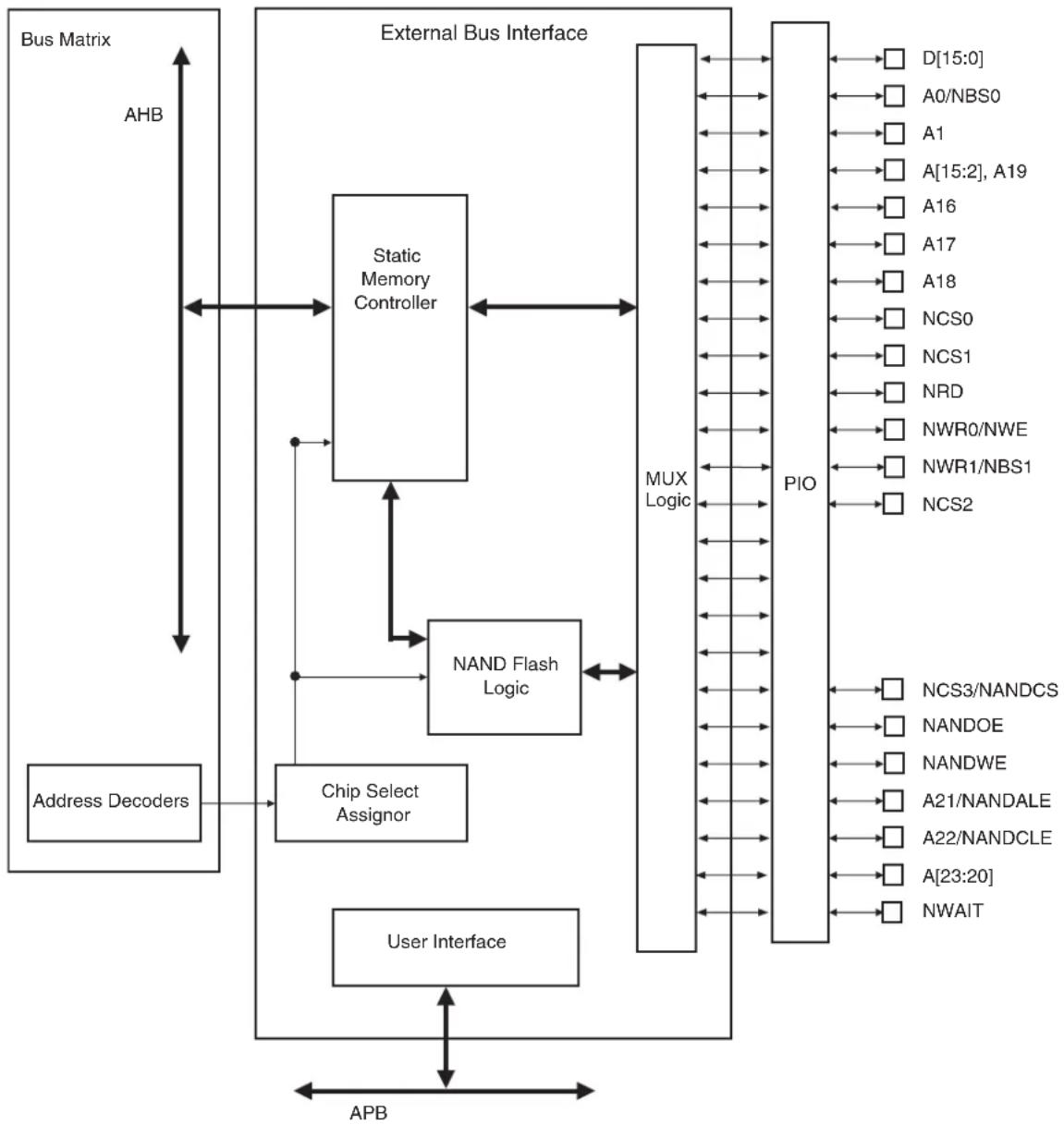
flowchart
graph TD
    A["Address Decoders"] --> B["Chip Select Assignor"]
    B --> C["Static Memory Controller"]
    C --> D["MUX Logic"]
    D --> E["PIO"]
    E --> F["D[15:0"]]
    E --> G["A0/NBS0"]
    E --> H["A1"]
    E --> I["A[15:2"], A19]
    E --> J["A16"]
    E --> K["A17"]
    E --> L["A18"]
    E --> M["NCS0"]
    E --> N["NCS1"]
    E --> O["NRD"]
    E --> P["NWR0/NWE"]
    E --> Q["NWR1/NBS1"]
    E --> R["NCS2"]
    B --> S["User Interface"]
    S --> T["APB"]
    T --> A
    style A fill:#f9f,stroke:#333
    style E fill:#ccf,stroke:#333
33.4 I/O Lines Description
Table 33-1. EBI I/O Lines Description
| Name Function Type Active Level | |||
| EBI | |||
| D0–D15 Data Bus I/O | |||
| A0–A23 Address Bus Output | |||
| NWAIT External Wait Signal Input Low | |||
| SMC | |||
| ......continued | |||
| Name Function Type Active Level | |||
| NCS0–EBI_NCS3 Chip Select Lines Output Low | |||
| NWR0–NWR1 Write Signals Output Low | |||
| NRD Read Signal Output Low | |||
| NWE Write Enable Output Low | |||
| NBS0–NBS1 Byte Mask Signals Output Low | |||
| EBI for NAND Flash Support | |||
| NANDCS | NAND Flash Chip Select Line | Output Low | |
| NANDOE | NAND Flash Output Enable Output Low | ||
| NANDWE | NAND Flash Write Enable | Output Low | |
The connection of some signals through the MUX logic is not direct and depends on the Memory Controller in use at the moment.
The following table details the connections between the SMC Memory Controller and the EBI pins.
Table 33-2. EBI Pins and Memory Controllers I/O Lines Connections
| EBIx Pins | SMC I/O Lines |
| NWR1/NBS1 | NWR1 |
| A0/NBS0 | SMC_A0 |
| A1 | SMC_A1 |
| A[11:2] | SMC_A[11:2] |
| A12 | SMC_A12 |
| A[15:13] | SMC_A[15:13] |
| A[25:16] | SMC_A[25:16] |
| D[15:0] | D[15:0] |
33.5 Application Example
33.5.1 Hardware Interface
The following table details the connections to be applied between the EBI pins and the external devices for each Memory Controller.
Table 33-3. EBI Pins and External Static Device Connections
| Signals: EBI_ | Pins of the Interfaced Device | ||
| 8-bit Static Device | 2 x 8-bit Static Devices | 16-bit Static Device | |
| Controller | SMC | ||
| D0-D7 D0-D7 | D0-D7 | D0-D7 | |
| D8-D15 | - | D8-D15 | D8-D15 |
| A0/NBS0 | A0 | - | NLB |
| A1 | A1 | A0 | A0 |
| A2-A23 | A[2:23] | A[1:22] | A[1:22] |
| NCS0 | CS | CS | CS |
| NCS1 | CS | CS | CS |
| NCS2 | CS | CS | CS |
| NCS3/NANDCS | CS | CS | CS |
| NRD | OE OE | OE | |
| NWR0/NWE | WE WE (see Note) | WE | |
| ......continued | |||
| Signals:EBI_ | Pins of the Interfaced Device | ||
| 8-bitStatic Device | 2 x 8-bitStatic Devices | 16-bitStatic Device | |
| Controller SMC | |||
| NWR1/NBS1 – WE (see Note) NUB | |||
Note: NWR1 enables upper byte writes. NWR0 enables lower byte writes.
Table 33-4. EBI Pins and External Device Connections
| Signals: EBI_ | Power supply Pins of the Interfaced Device | |
| NAND Flash | ||
| Controller NFC | ||
| D0-D15 VDDIO D0-D15 | ||
| A0/NBS0 VDDIO - | ||
| A1 VDDIO - | ||
| A2-A10 VDDIO - | ||
| A11 VDDIO - | ||
| A12 VDDIO - | ||
| A13-A14 VDDIO - | ||
| A15 VDDIO - | ||
| A16 VDDIO - | ||
| A17 VDDIO - | ||
| A18 VDDIO - | ||
| A19 VDDIO - | ||
| A20 VDDIO - | ||
| A21/NANDALE VDDIO ALE | ||
| A22/NANDCLE VDDIO CLE | ||
| A23 VDDIO - | ||
| NCS0 | VDDIO - | |
| NCS1 | VDDIO - | |
| NCS2 | VDDIO - | |
| NCS3/NANDCS | VDDIO CE | |
| NANDOE | VDDIO OE | |
| NANDWE | VDDIO WE | |
| NRD | VDDIO - | |
| NWR0/NWE | VDDIO - | |
| NWR1/NBS1 | VDDIO - | |
| Pxx | VDDIO CE | |
| Pxx | VDDIO RDY | |
33.5.2 Product Dependencies
33.5.2.1 I/O Lines
The pins used for interfacing the External Bus Interface may be multiplexed with the PIO lines. The programmer must first program the PIO controller to assign the External Bus Interface pins to their peripheral function. If I/O lines of the External Bus Interface are not used by the application, they can be used for other purposes by the PIO Controller.
33.5.3 Functional Description
The EBI transfers data between the internal AHB Bus (handled by the Bus Matrix) and the external memories or peripheral devices. It controls the waveforms and the parameters of the external address, data and control buses and is composed of the following elements:
• Static Memory Controller (SMC)
- A chip select assignment feature that assigns an AHB address space to the external devices
• A multiplex controller circuit that shares the pins between the different Memory Controllers
- Programmable NAND Flash support logic
33.5.3.1 Bus Multiplexing
The EBI offers a complete set of control signals that share the 16-bit data lines, the address lines of up to 24 bits and the control signals through a multiplex logic operating in function of the memory area requests.
Multiplexing is specifically organized in order to guarantee the maintenance of the address and output control lines at a stable state while no external access is being performed. Multiplexing is also designed to respect the data float times defined in the Memory Controllers.
33.5.3.2 Static Memory Controller
For information on the Static Memory Controller, refer to 34. Static Memory Controller (SMC)
33.5.3.3 NAND Flash Support
External Bus Interfaces integrate circuitry that interfaces to NAND Flash devices.
To ensure that the processor preserves transaction order and thus the correct NAND Flash behavior, the NAND Flash address space is to be declared in the Memory Protection Unit (MPU) as "Device" or "Strongly-ordered" memory. Refer to the ARM Cortex-M7 Technical Reference Manual (ARM DDI 0489) available on www.arm.com.
External Bus Interface
The NAND Flash Chip Select (NANDCS) is driven by the Static Memory Controller on the NCS0, NCS1, NCS2 or NCS3 address space depending on value of SMC_SMCSx bits. For example, programming the SMC_NFC3 field in the CCFG_SMCNFCS Register in the Chip Configuration User Interface to the appropriate value enables the NAND Flash logic. For details on this register, refer to 19. Bus Matrix (MATRIX). Access to an external NAND Flash device is then made by accessing the address space reserved to NCS3 (i.e., between 0x6300 0000 and 0x6FFF FFFF).
The NAND Flash logic drives the read and write command signals of the SMC on the NANDOE and NANDWE signals when the required SMC_NFCSx signal is active. NANDOE and NANDWE are invalidated as soon as the transfer address fails to lie in the selected NCSx address space. For details on these waveforms, refer to 34. Static Memory Controller (SMC).
NAND Flash Signals
The address latch enable and command latch enable signals on the NAND Flash device are driven by address bits A22 and A21 of the EBI address bus. The command, address or data words on the data bus of the NAND Flash device are distinguished by using their address within the NCSx address space. The chip enable (CE) signal of the device and the ready/busy (R/B) signals are connected to PIO lines. The CE signal then remains asserted even when NCSx is not selected, preventing the device from returning to standby mode.
34. Static Memory Controller (SMC)
34.1 Description
The External Bus Interface (EBI) is designed to ensure the successful data transfer between several external devices and the ARM-based microcontroller. The Static Memory Controller (SMC) is part of the EBI.
The SMC handles several types of external memory and peripheral devices, such as SRAM, PSRAM, PROM, EPROM, EEPROM, LCD Module, NOR Flash and NAND Flash.
The SMC generates the signals that control the access to the external memory devices or peripheral devices. It has 4 chip selects, a 24-bit address bus, and a configurable 8 or 16-bit data bus. Separate read and write control signals allow for direct memory and peripheral interfacing. Read and write signal waveforms are fully adjustable.
The SMC can manage wait requests from external devices to extend the current access. The SMC is provided with an automatic Slow clock mode. In Slow clock mode, it switches from user-programmed waveforms to slow-rate specific waveforms on read and write signals. The SMC supports asynchronous burst read in Page mode access for page sizes up to 32 bytes.
The external data bus can be scrambled/unscrambled by means of user keys.
34.2 Embedded Characteristics
• Four Chip Selects Available
• 16-Mbyte Address Space per Chip Select
• 8-bit or 16-bit Data Bus
• Zero Wait State Scrambling/Unscrambling Function with User Key
• Word, Halfword, Byte Transfers
- Byte Write or Byte Select Lines
- Programmable Setup, Pulse And Hold Time for Read Signals per Chip Select
- Programmable Setup, Pulse And Hold Time for Write Signals per Chip Select
- Programmable Data Float Time per Chip Select
- External Wait Request
• Automatic Switch to Slow Clock Mode
- Asynchronous Read in Page Mode Supported: Page Size Ranges from 4 to 32 Bytes
- Register Write Protection
34.3 I/O Lines Description
Table 34-1. I/O Line Description
| Name Description Type Active Level | |||
| NCS[3:0] Static Memory Controller Chip Select Lines Output Low | |||
| NRD Read Signal Output Low | |||
| NWR0/NWE Write 0/Write Enable Signal Output Low | |||
| NWR1/NBS1 Write 1/Byte 1 Select Signal Output Low | |||
| A0/NBS0 | Address Bit 0/Byte 0 Select Signal | Output Low | |
| A[23:1] | Address Bus | Output - | |
| D[15:0] | Data Bus | I/O | - |
| NWAIT | External Wait Signal | Input | Low |
| ......continued | |||
| Name Description Type Active Level | |||
| NANDCS NAND Flash Chip Select Line Output Low | |||
| NANDOE NAND Flash Output Enable Output Low | |||
| NANDWE NAND Flash Write Enable Output Low | |||
| NANDALE NAND Flash Address Latch Enable Output - | |||
| NANDCLE NAND Flash Command Latch Enable Output - | |||
34.4 Multiplexed Signals
Table 34-2. Static Memory Controller (SMC) Multiplexed Signals
| Multiplexed Signals | Related Function | |
| NWR0 | NWE | Byte-write or Byte-select access.See "Byte Write Access" and "Byte Select Access" |
| A0 | NBS0 | 8-bit or 16-bit data bus. See "Data Bus Width" |
| NWR1 | NBS1 | Byte-write or Byte-select access. See "Byte Write Access" and "Byte Select Access" |
| A22 | NANDCLE | NAND Flash Command Latch Enable |
| A21 | NANDALE | NAND Flash Address Latch Enable |
34.5 Product Dependencies
34.5.1 I/O Lines
The pins used for interfacing the SMC are multiplexed with the PIO lines. The programmer must first program the PIO controller to assign the SMC pins to their peripheral function. If I/O lines of the SMC are not used by the application, they can be used for other purposes by the PIO Controller.
34.5.2 Power Management
The SMC is clocked through the Power Management Controller (PMC), thus the programmer must first configure the PMC to enable the SMC clock.
34.6 External Memory Mapping
The SMC provides up to 24 address lines, A[23:0]. This allows each chip select line to address up to 16 Mbytes of memory.
If the physical memory device connected on one chip select is smaller than 16 Mbytes, it wraps around and appears to be repeated within this space. The SMC correctly handles any valid access to the memory device within the page (see the following figure).
Figure 34-1. Memory Connections for Four External Devices
flowchart
graph TD
    A["SMC"] --> B["NCS[0"] -_NCS["3"]]
    A --> C["NRD"]
    A --> D["NWE"]
    A --> E["A[23:0"]]
    A --> F["D[15:0"]]
    B --> G["NCS3"]
    C --> H["NRD"]
    D --> I["NWE"]
    E --> J["A[23:0"]]
    F --> K["D[15:0"]]
    G --> L["Memory Enable"]
    H --> L
    I --> L
    J --> L
    K --> L
    L --> M["Memory Enable"]
    L --> N["Output Enable"]
    L --> O["Write Enable"]
    L --> P["A[23:0"]]
    L --> Q["D[15:0"] or_D["7:0"]]
    M --> R["24"]
    N --> R
    O --> R
    P --> R
    Q --> R
34.7 Connection to External Devices
34.7.1 Data Bus Width
A data bus width of 8 or 16 bits can be selected for each chip select. This option is controlled by the bit DBW in the Mode register (SMC_MODE) for the corresponding chip select.
Figure 34-2 shows how to connect a 512-Kbyte × 8-bit memory on NCS2. Figure 34-3 shows how to connect a 512-Kbyte × 16-bit memory on NCS2.
Figure 34-2. Memory Connection for an 8-bit Data Bus
flowchart
graph LR
    A["SMC"] --> B["D[7:0"] D["7:0"]]
    A --> C["A[18:2"] A1 A0]
    A --> D["NWE NRD NCS[2"]]
    E["Memory Enable"] --> F["A[18:2"] A1 A0]
    E --> G["Write Enable Output Enable"]
Figure 34-3. Memory Connection for a 16-bit Data Bus
flowchart
graph LR
    A["SMC"] --> B["D[15:0"] D["15:0"]]
    A --> C["A[19:2"]]
    A --> D["NBS0"]
    A --> E["NBS1 High Byte Enable"]
    A --> F["NWE"]
    A --> G["NRD"]
    A --> H["NCS[2"]]
    I["A[18:1"]] --> J["A[0"]A1]
    I --> K["Low Byte Enable"]
    I --> L["Write Enable"]
    I --> M["Output Enable"]
    I --> N["Memory Enable"]
34.7.2 Byte Write or Byte Select Access
Each chip select with a 16-bit data bus can operate with one of two different types of write access: byte write or byte select. This is controlled by the BAT field of the SMC_MODE register for the corresponding chip select.
34.7.2.1 Byte Write Access
Byte write access is used to connect 2 × 8 -bit devices as a 16-bit memory, and supports one write signal per byte of the data bus and a single read signal.
Note that the SMC does not allow boot in Byte write access mode.
For 16-bit devices, the SMC provides NWR0 and NWR1 write signals for respectively Byte0 (lower byte) and Byte1 (upper byte) of a 16-bit bus. One single read signal (NRD) is provided.
Byte select access is used to connect one 16-bit device. In this mode, read/write operations can be enabled/disabled at byte level. One byte-select line per byte of the data bus is provided. One NRD and one NWE signal control read and write.
For 16-bit devices, the SMC provides NBS0 and NBS1 selection signals for respectively Byte0 (lower byte) and Byte1 (upper byte) of a 16-bit bus.
Figure 34-4. Connection of 2 × 8-bit Devices on a 16-bit Bus: Byte Write Option
flowchart
graph TD
    A["SMC"] --> B["D[7:0"] D["7:0"]]
    A --> C["D[15:8"]]
    A --> D["A[24:2"]]
    A --> E["A1"]
    A --> F["NWR0"]
    A --> G["NWR1"]
    A --> H["NRD"]
    A --> I["NCS[3"]]
    J["A[23:1"]] --> K["A[0"]]
    J --> L["Write Enable"]
    M["Read Enable"] --> N["Memory Enable"]
    O["D[15:8"]] --> P["A[23:1"]]
    O --> Q["A[0"]]
    R["Write Enable"] --> S["Read Enable"]
    T["Memory Enable"] --> U["Read Enable"]
34.7.2.3 Signal Multiplexing
Depending on the byte access type (BAT), only the byte write signals or the byte select signals are used. To save I/Os at the external bus interface, control signals at the SMC interface are multiplexed. The following table shows signal multiplexing depending on the data bus width and the byte access type.
For 16-bit devices, bit A0 of address is unused. When the Byte Select option is selected, NWR1 is unused. When the Byte Write option is selected, NBS0 is unused.
Table 34-3. SMC Multiplexed Signal Translation
| Device Type Signal Name | |||
| 16-bit Bus 8-bit Bus | |||
| 1 x 16-bit 2 x 8-bit 1 x 8-bit | |||
| Byte Access Type (BAT) Byte Select Byte Write - | |||
| NBS0_A0 NBS0 - A0 | |||
| NWE_NWR0 NWE NWRO NWE | |||
| NBS1_NWR1 NBS1 NWR1 - | |||
| A1 A1 A1 | A1 | ||
34.7.3 NAND Flash Support
The SMC integrates circuitry that interfaces to NAND Flash devices.
The NAND Flash logic is driven by the SMC. Configuration is done via the SMC_NFCSx field in the CCFG_SMCNFCS register in the Bus Matrix. For details on this register, refer to the section "Bus Matrix (MATRIX)" of this datasheet. The external NAND Flash device is accessed via the address space reserved for the chip select programmed.
The user can connect up to four NAND Flash devices with separate chip selects.
The NAND Flash logic drives the read and write command signals of the SMC on the NANDOE and NANDWE signals when the NCSx programmed is active. NANDOE and NANDWE are disabled as soon as the transfer address fails to lie in the NCSx programmed address space.
Figure 34-5. NAND Flash Signal Multiplexing on SMC Pins

flowchart
graph LR
    A["SMC"] --> B["NCSx"]
    A --> C["NRD"]
    A --> D["NWE"]
    B --> E["NAND Flash Logic"]
    C --> E
    D --> E
    E --> F["NANDOE"]
    E --> G["NANDWE"]
    F --> H["NANDOE"]
    G --> I["NANDWE"]
Note: 1. NCSx is active when CCFG_SMCNFCS.SMC_NFCSx=1.
Note: 2. When the NAND Flash logic is activated, (SMC_NFCSx=1), the NWE pin can be used only in Peripheral mode (NWE function). If the NWE function is not used for other external memories (SRAM, LCD), it must be configured in one of the following modes: PIO input with pull-up enabled (default state after reset) and PIO output set at level 1.
The address latch enable and command latch enable signals on the NAND Flash device are driven by address bits A22 and A21 of the address bus. Any bit of the address bus can also be used for this purpose. The command, address or data words on the data bus of the NAND Flash device use their own addresses within the NCSx address space (configured in the register CCFG_SMCNFCS in the Bus Matrixe). The chip enable (CE) signal of the device and the ready/busy (R/B) signals are connected to PIO lines. The CE signal then remains asserted even when NAND Flash chip select is not selected, preventing the device from returning to Standby mode. The NANDCS output signal should be used in accordance with the external NAND Flash device type.
Two types of CE behavior exist depending on the NAND Flash device:
- Standard NAND Flash devices require that the CE pin remains asserted low continuously during the read busy period to prevent the device from returning to Standby mode. Since the SMC asserts the NCSx signal high, it is necessary to connect the CE pin of the NAND Flash device to a GPIO line, in order to hold it low during the busy period preceding data read out.
- This restriction has been removed for "CE don't care" NAND Flash devices. The NCSx signal can be directly connected to the CE pin of the NAND Flash device.
The following figure illustrates both topologies: Standard and "CE don't care" NAND Flash.
Figure 34-6. Standard and "CE don't care" NAND Flash Application Examples
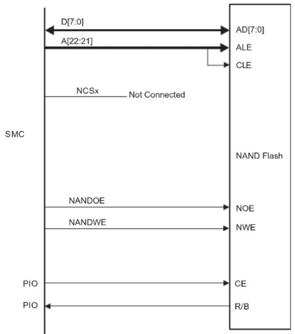
flowchart
graph TD
    A["SMC"] -->|D["7:0"]| B["AD[7:0"]]
    A -->|A["22:21"]| C["ALE"]
    A -->|NCSx Not Connected| D["CLE"]
    A -->|NANDOE| E["NAND Flash"]
    A -->|NANDWE| F["NOE"]
    A -->|PIO| G["NWE"]
    A -->|PIO| H["CE"]
    A -->|PIO| I["R/B"]
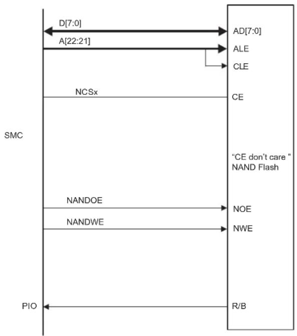
flowchart
graph TD
    A["SMC"] --> B["D[7:0"]]
    B --> C["A[22:21"]]
    C --> D["AD[7:0"]]
    D --> E["ALE"]
    E --> F["CLE"]
    F --> G["CE"]
    G --> H["CE don't care"]
    H --> I["NAND Flash"]
    I --> J["NOE"]
    J --> K["NWE"]
    K --> L["NANDWE"]
    L --> M["NANDOE"]
    M --> N["PIO"]
    N --> O["R/B"]
Related Links
19. Bus Matrix (MATRIX)
34.8 Application Example
34.8.1 Implementation Examples
Hardware configurations are given for illustration only. The user should refer to the manufacturer web site to check for memory device availability.
For hardware implementation examples, refer to the evaluation kit schematics for this microcontroller, which show examples of a connection to an LCD module and NAND Flash.
34.8.1.1 8-bit NAND Flash
Hardware Configuration
Figure 34-7. 8-bit NAND Flash
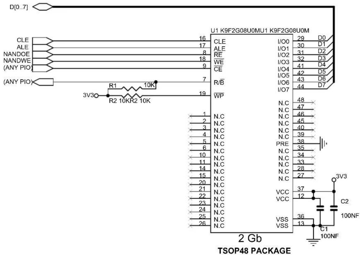
text_image
D[0..7] CLE ALE NANDOE NANDWE (ANY PIO) (ANY PIO) 3V3O R1 10K R2 10KR2 10K U1 K9F2G08U0MU1 K9F2G08U0M CLE I/O0 29 D0 ALE I/O1 30 D1 RE I/O2 31 D2 WE I/O3 32 D3 CE I/O4 41 D4 R/B I/O5 42 D5 I/O6 43 D6 I/O7 44 D7 WP N.C 48 N.C 47 N.C 46 N.C 45 N.C 40 N.C 39 N.C 38 PRE N.C 35 N.C 34 N.C 33 N.C 28 N.C 27 N.C VCC 37 VCC 12 VSS 36 VSS 13 C1 C2 100NF 1 N.C 2 N.C 3 N.C 4 N.C 5 N.C 6 N.C 7 N.C 8 N.C 9 N.C 10 N.C 11 N.C 12 N.C 13 N.C 14 N.C 15 N.C 16 N.C 17 N.C 18 N.C 19 N.C 20 N.C 21 N.C 22 N.C 23 N.C 24 N.C 25 N.C 26 N.C 2 Gb TSOP48 PACKAGESoftware Configuration
Perform the following configuration:
- Select the chip select used to drive the NAND Flash by setting the bit CCFG_SMCNFCS.SMC_NFCSx.
- Reserve A21 / A22 for ALE / CLE functions. Address and Command Latches are controlled by setting the address bits A21 and A22, respectively, during accesses.
- NANDOE and NANDWE signals are multiplexed with PIO lines. Thus, the dedicated PIOs must be programmed in Peripheral mode in the PIO controller.
- Configure a PIO line as an input to manage the Ready/Busy signal.
- Configure SMC CS3 Setup, Pulse, Cycle and Mode according to NAND Flash timings, the data bus width and the system bus frequency.
In this example, the NAND Flash is not addressed as a "CE don't care". To address it as a "CE don't care", connect NCS3 (if SMC_NFCS3 is set) to the NAND Flash CE.
34.8.1.2 NOR Flash
Hardware Configuration
Figure 34-8. NOR Flash

Configure the SMC CS0 Setup, Pulse, Cycle, and Mode, depending on Flash timings and system bus frequency.
34.9 Standard Read and Write Protocols
In the following sections, the byte access type is not considered. Byte select lines (NBS0 to NBS1) always have the same timing as the A address bus. NWE represents either the NWE signal in byte select access type or one of the byte write lines (NWR0 to NWR1) in byte write access type. NWR0 to NWR1 have the same timings and protocol as NWE. If D[15:8] are used, they have the same timing as D[7:0]. In the same way, NCS represents one of the NCS[0..3] chip select lines.
34.9.1 Read Waveforms
The read cycle is shown in the following figure.
The read cycle starts with the address setting on the memory address bus.
Figure 34-9. Standard Read Cycle
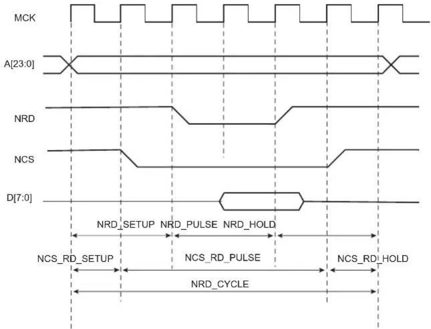
text_image
MCK A[23:0] NRD NCS D[7:0] NRD_SETUP NRD_PULSE NRD_HOLD NCS_RD_SETUP NCS_RD_PULSE NCS_RD_HOLD NRD_CYCLE34.9.1.1 NRD Waveform
The NRD signal is characterized by a setup timing, a pulse width and a hold timing.
- nrd_setup—NRD setup time is defined as the setup of address before the NRD falling edge;
- nrd_pulse—NRD pulse length is the time between NRD falling edge and NRD rising edge;
- nrd_hold—NRD hold time is defined as the hold time of address after the NRD rising edge.
34.9.1.2 NCS Waveform
The NCS signal can be divided into a setup time, pulse length and hold time:
- ncs_rd_setup—NCS setup time is defined as the setup time of address before the NCS falling edge.
- ncs_rd_pulse—NCS pulse length is the time between NCS falling edge and NCS rising edge;
- ncs_rd_hold—NCS hold time is defined as the hold time of address after the NCS rising edge.
34.9.1.3 Read Cycle
The NRD_CYCLE time is defined as the total duration of the read cycle, i.e., from the time where address is set on the address bus to the point where address may change. The total read cycle time is defined as:
$$ \text { NRD_CYCLE } = \text { NRD_SETUP } + \text { NRD_PULSE } + \text { NRD_HOLD }, $$
as well as
$$ \text { NRD_CYCLE } = \text { NCS_RD_SETUP } + \text { NCS_RD_PULSE } + \text { NCS_RD_HOLD } $$
All NRD and NCS timings are defined separately for each chip select as an integer number of Host Clock cycles. The NRD_CYCLE field is common to both the NRD and NCS signals, thus the timing period is of the same duration.
NRD_CYCLE, NRD_SETUP, and NRD_PULSE implicitly define the NRD_HOLD value as:
$$ \text { NRD_HOLD } = \text { NRD_CYCLE } - \text { NRD SETUP } - \text { NRD PULSE } $$
NRD_CYCLE, NCS_RD_SETUP, and NCS_RD_PULSE implicitly define the NCS_RD_HOLD value as:
NCS_RD_HOLD = NRD_CYCLE - NCS_RD_SETUP - NCS_RD_PULSE
34.9.1.4 Null Delay Setup and Hold
If null setup and hold parameters are programmed for NRD and/or NCS, NRD and NCS remain active continuously in case of consecutive read cycles in the same memory (see the following figure).
Figure 34-10. No Setup, No Hold on NRD and NCS Read Signals
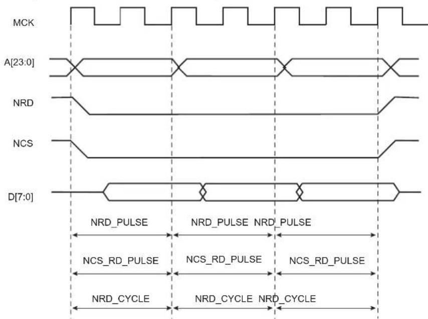
text_image
MCK A[23:0] NRD NCS D[7:0] NRD_PULSE NRD_PULSE NRD_PULSE NCS_RD_PULSE NCS_RD_PULSE NCS_RD_PULSE NRD_CYCLE NRD_CYCLE NRD_CYCLE34.9.1.5 Null Pulse
Programming a null pulse is not permitted. The pulse must be at least set to 1. A null value leads to unpredictable behavior.
34.9.2 Read Mode
As NCS and NRD waveforms are defined independently of one other, the SMC needs to know when the read data is available on the data bus. The SMC does not compare NCS and NRD timings to know which signal rises first. The READ_MODE bit in the SMC_MODE register of the corresponding chip select indicates which signal of NRD and NCS controls the read operation.
34.9.2.1 Read is Controlled by NRD (SMC\_MODE.READ\_MODE = 1):
The following figure shows the waveforms of a read operation of a typical asynchronous RAM. The read data is available t_PACC after the falling edge of NRD, and turns to 'Z' after the rising edge of NRD. In this case, SMC_MODE.READ_MODE must be set to 1 (read is controlled by NRD), to indicate that data is available with the rising edge of NRD. The SMC samples the read data internally on the rising edge of Host Clock that generates the rising edge of NRD, whatever the programmed waveform of NCS may be.
Figure 34-11. SMC_MODE.READ_MODE = 1: Data is sampled by SMC before the rising edge of NRD
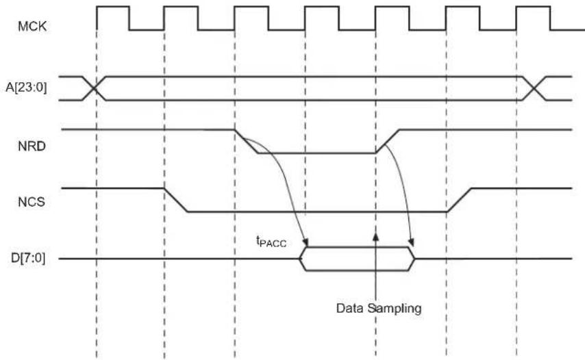
text_image
MCK A[23:0] NRD NCS D[7:0] tPACC Data Sampling34.9.2.2 Read is Controlled by NCS (SMC\_MODE.READ\_MODE = 0)
The following figure shows the typical read cycle of an LCD module. The read data is valid t_PACC after the falling edge of the NCS signal and remains valid until the rising edge of NCS. Data must be sampled when NCS is raised. In this case, the SMC_MODE.READ_MODE must be set to 0 (read is controlled by NCS): the SMC internally samples the data on the rising edge of Host Clock that generates the rising edge of NCS, whatever the programmed waveform of NRD may be.
Figure 34-12. SMC_MODE.READ_MODE = 0: Data is Sampled by SMC Before the Rising Edge of NCS
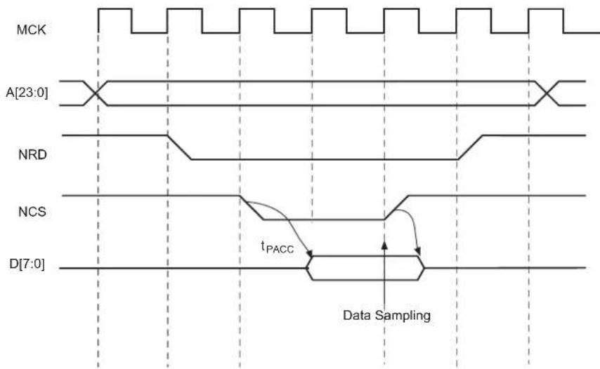
text_image
MCK A[23:0] NRD NCS D[7:0] tPACC Data Sampling34.9.3 Write Waveforms
The write protocol is similar to the read protocol. It is depicted in Figure 34-13. The write cycle starts with the address setting on the memory address bus.
34.9.3.1 NWE Waveforms
The NWE signal is characterized by a setup timing, a pulse width and a hold timing.
- NWE_SETUP—the NWE setup time is defined as the setup of address and data before the NWE falling edge;
- NWE_PULSE—the NWE pulse length is the time between NWE falling edge and NWE rising edge;
- NWE_HOLD—the NWE hold time is defined as the hold time of address and data after the NWE rising edge.
34.9.3.2 NCS Waveforms
The NCS signal waveforms in write operation are not the same that those applied in read operations, but are separately defined:
- ncs_wr_setup—the NCS setup time is defined as the setup time of address before the NCS falling edge.
- ncs_wr_pulse—the NCS pulse length is the time between NCS falling edge and NCS rising edge;
- ncs_wr_hold—the NCS hold time is defined as the hold time of address after the NCS rising edge.
Figure 34-13. Write Cycle
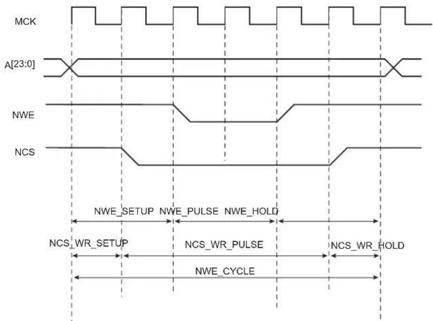
text_image
MCK A[23:0] NWE NCS NWE_SETUP NWE_PULSE NWE_HOLD NCS_WR_SETUP NCS_WR_PULSE NCS_WR_HOLD NWE_CYCLE34.9.3.3 Write Cycle
The write_cycle time is defined as the total duration of the write cycle; that is, from the time where address is set on the address bus to the point where address may change. The total write cycle time is defined as:
$$ \text { NWE_CYCLE } = \text { NWE_SETUP } + \text { NWE_PULSE } + \text { NWE_HOLD }, $$
as well as
$$ \text { NWE_CYCLE } = \text { NCS_WR_SETUP } + \text { NCS_WR_PULSE } + \text { NCS_WR_HOLD } $$
All NWE and NCS (write) timings are defined separately for each chip select as an integer number of Host Clock cycles. The NWE_CYCLE field is common to both the NWE and NCS signals, thus the timing period is of the same duration.
$$ \text { NWE_CYCLE, NWE_SETUP, and NWE_PULSE implicitly define the NWE_HOLD value as: } $$
$$ \text { NWE_HOLD } = \text { NWE_CYCLE } - \text { NWE_SETUP } - \text { NWE_PULSE } $$
$$ \text { NWE_CYCLE, NCS_WR_SETUP, and NCS_WR_PULSE implicitly define the NCS_WR_HOLD value as: } $$
$$ N C S _ W R _ H O L D = N W E _ C Y C L E - N C S _ W R _ S E T U P - N C S _ W R _ P U L S E $$
34.9.3.4 Null Delay Setup and Hold
If null setup parameters are programmed for NWE and/or NCS, NWE and/or NCS remain active continuously in case of consecutive write cycles in the same memory (see the following figure). However, for devices that perform write operations on the rising edge of NWE or NCS, such as SRAM, either a setup or a hold must be programmed.
Figure 34-14. Null Setup and Hold Values of NCS and NWE in Write Cycle
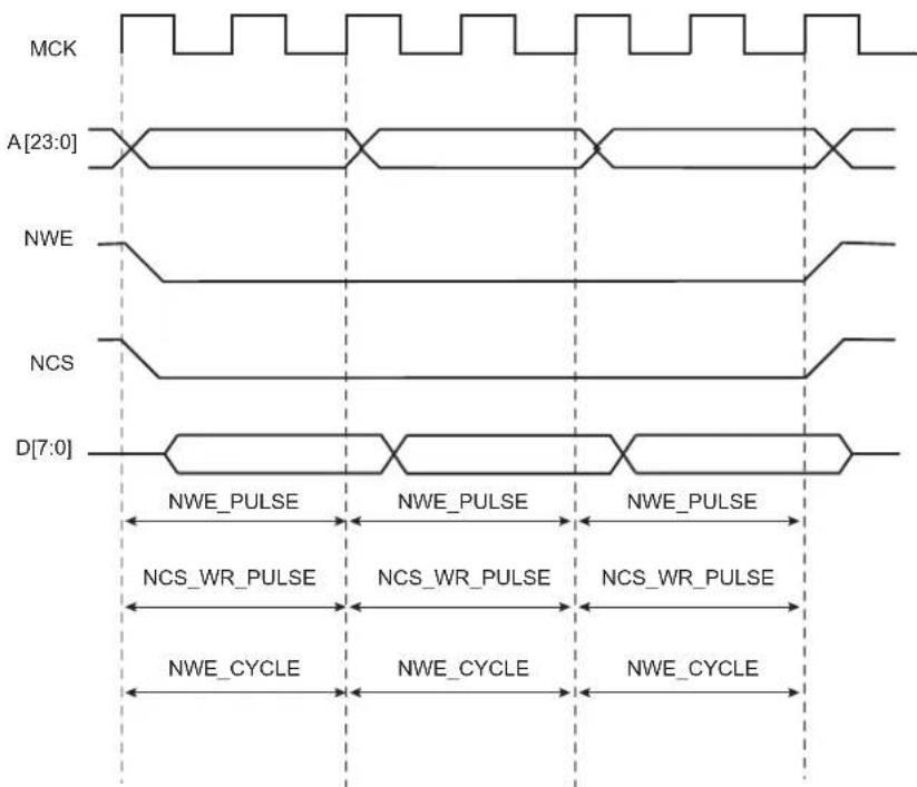
text_image
MCK A[23:0] NWE NCS D[7:0] NWE_PULSE NWE_PULSE NWE_PULSE NCS_WR_PULSE NCS_WR_PULSE NCS_WR_PULSE NWE_CYCLE NWE_CYCLE NWE_CYCLE34.9.3.5 Null Pulse
Programming null pulse is not permitted. Pulse must be at least set to 1. A null value leads to unpredictable behavior.
34.9.4 Write Mode
The bit WRITE_MODE in the SMC_MODE register of the corresponding chip select indicates which signal controls the write operation.
34.9.4.1 Write is Controlled by NWE (SMC.MODE.WRITE\_MODE = 1):
The following figure shows the waveforms of a write operation with SMC_MODE.WRITE_MODE set. The data is put on the bus during the pulse and hold steps of the NWE signal. The internal data buffers are switched to Output mode after the NWE_SETUP time, and until the end of the write cycle, regardless of the programmed waveform on NCS.
Figure 34-15. SMC_MODE.WRITE_MODE = 1. Write Operation is Controlled by NWE
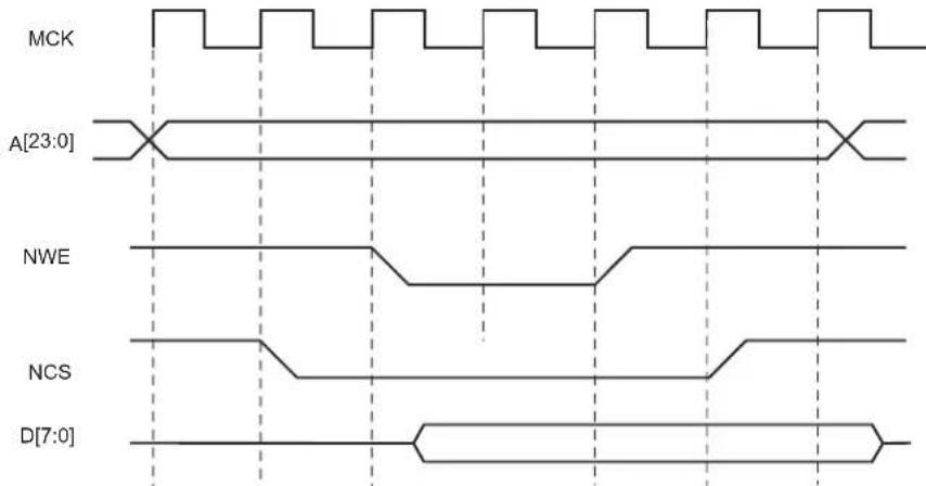
text_image
MCK A[23:0] NWE NCS D[7:0]34.9.4.2 Write is Controlled by NCS (SMC.MODE.WRITE\_MODE = 0)
The following figure shows the waveforms of a write operation with SMC_MODE.WRITE_MODE cleared. The data is put on the bus during the pulse and hold steps of the NCS signal. The internal data buffers are switched to Output mode after the NCS_WR_SETUP time, and until the end of the write cycle, regardless of the programmed waveform on NWE.
Figure 34-16. WRITE_MODE = 0. Write Operation is Controlled by NCS

text_image
MCK A[23:0] NWE NCS D[7:0]34.9.5 Register Write Protection
To prevent any single software error that may corrupt SMC behavior, the registers listed below can be write-protected by setting the WPEN bit in the SMC Write Protection Mode register (SMC_WPMR).
If a write access in a write-protected register is detected, the WPVS flag in the SMC Write Protection Status register (SMC_WPSR) is set and the field WPVSRC indicates in which register the write access has been attempted.
The WPVS flag is automatically cleared after reading the SSMC_WPSR.
The following registers can be write-protected:
- "SMC Setup Register"
- "SMC Pulse Register"
-
"SMC Cycle Register"
-
"SMC Mode Register"
- "SMC Off-chip Memory Scrambling Register"
34.9.6 Coding Timing Parameters
All timing parameters are defined for one chip select and are grouped together in one register according to their type.
The SMC_SETUP register groups the definition of all setup parameters:
- NRD_SETUP
- NCS_RD_SETUP
- NWE_SETUP
- NCS_WR_SETUP
The SMC_PULSE register groups the definition of all pulse parameters:
- NRD_PULSE
- NCS_RD_PULSE
- NWE_PULSE
- NCS_WR_PULSE
The SMC_CYCLE register groups the definition of all cycle parameters:
- NRD_CYCLE
- NWE_CYCLE
The following table shows how the timing parameters are coded and their permitted range.
Table 34-4. Coding and Range of Timing Parameters
| Coded Value Number of Bits Effective Value Permitted Range | ||||
| Coded Value Effective Value | ||||
| setup [5:0] 6 128 × setup[5] + setup[4:0] 0 ≤ 31 0 ≤ 128+31 | ||||
| pulse [6:0] 7 256 × pulse[6] + pulse[5:0] 0 ≤ 63 0 ≤ 256+63 | ||||
| cycle [8:0] 9 256 × cycle[8:7] + cycle[6:0] 0 ≤ 127 0 ≤ 256+127 | 0 ≤ 512+1270 ≤ 768+127 | |||
34.9.7 Reset Values of Timing Parameters
The following table provides the default value of timing parameters at reset.
Table 34-5. Reset Values of Timing Parameters
| Parameter | Reset Value | Definition |
| SMC_SETUP | 0x01010101 | All setup timings are set to 1. |
| SMC_PULSE | 0x01010101 | All pulse timings are set to 1. |
| SMC_CYCLE | 0x00030003 | The read and write operations continue for 3 Host Clock cycles and provide one hold cycle. |
| WRITE_MODE | 1 Write is controlled with NWE. | |
| READ_MODE 1 | Read is controlled with NRD. | |
34.9.8 Usage Restriction
The SMC does not check the validity of the user-programmed parameters. If the sum of SETUP and PULSE parameters is larger than the corresponding CYCLE parameter, this leads to unpredictable behavior of the SMC.
- For read operations:
Null but positive setup and hold of address and NRD and/or NCS can not be guaranteed at the memory interface because of the propagation delay of theses signals through external logic and pads. If positive setup and hold values must be verified, then it is strictly recommended to program non-null values so as to cover possible skews between address, NCS and NRD signals.
- For write operations:
If a null hold value is programmed on NWE, the SMC can guarantee a positive hold of address and NCS signal after the rising edge of NWE. This is true for SMC_MODE.WRITE_MODE = 1 only. See "Early Read Wait State".
- For read and write operations:
A null value for pulse parameters is forbidden and may lead to unpredictable behavior.
In read and write cycles, the setup and hold time parameters are defined in reference to the address bus. For external devices that require setup and hold time between NCS and NRD signals (read), or between NCS and NWE signals (write), these setup and hold times must be converted into setup and hold times in reference to the address bus.
34.10 Scrambling/Unscrambling Function
The external data bus can be scrambled to protect intellectual property data located in off-chip memories by means of data analysis at the package pin level of either the microcontroller or the memory device.
The scrambling and unscrambling are performed on-the-fly without additional wait states.
The scrambling/unscrambling function can be enabled or disabled by configuring the CSxSE bits in the SMC Off-Chip Memory Scrambling Register (SMC_OCMS).
When multiple chip selects are handled, the scrambling function per chip select is configurable using the CSxSE bits in the SMC_OCMS register.
The scrambling method depends on two user-configurable key registers, SMC_KEY1 and SMC_KEY2 plus a random value depending on device processing characteristics. These key registers cannot be read. They can be written once after a system reset.
The scrambling user key or the seed for key generation must be securely stored in a reliable non-volatile memory in order to recover data from the off-chip memory. Any data scrambled with a given key cannot be recovered if the key is lost.
34.11 Automatic Wait States
Under certain circumstances, the SMC automatically inserts idle cycles between accesses to avoid bus contention or operation conflict.
34.11.1 Chip Select Wait States
The SMC always inserts an idle cycle between two transfers on separate Chip Selects. This idle cycle ensures that there is no bus contention between the deactivation of one device and the activation of the next one.
During Chip Select Wait state, all control lines are turned inactive: NWR, NCS[0..3], NRD lines are all set to 1.
The following figure illustrates a Chip Select Wait state between access on Chip Select 0 and Chip Select 2.
Figure 34-17. Chip Select Wait State between a Read Access on NCS0 and a Write Access on NCS2
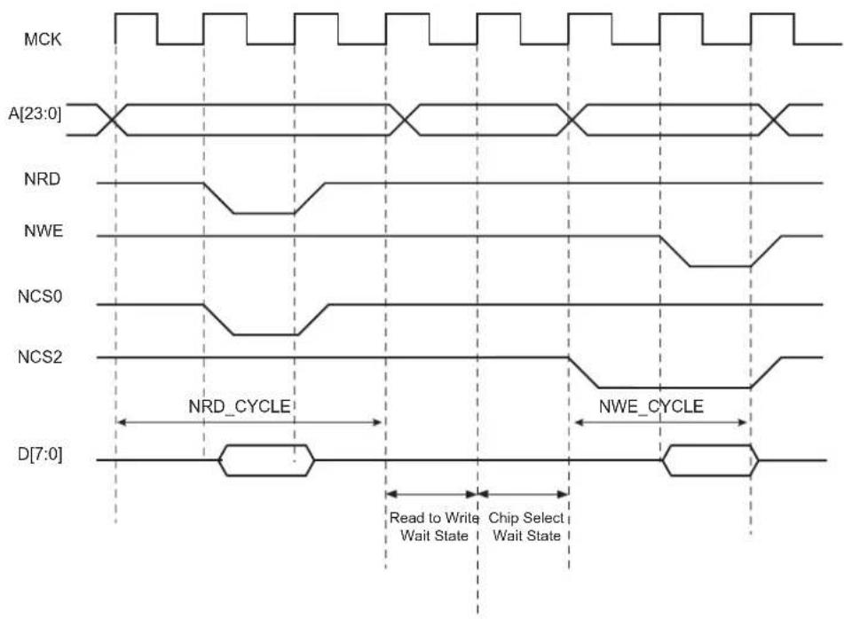
text_image
MCK A[23:0] NRD NWE NCS0 NCS2 D[7:0] NRD_CYCLE NWE_CYCLE Read to Write Chip Select Wait State Wait State34.11.2 Early Read Wait State
In some cases, the SMC inserts a wait state cycle between a write access and a read access to allow time for the write cycle to end before the subsequent read cycle begins. This wait state is not generated in addition to a chip select wait state. The early read cycle thus only occurs between a write and read access to the same memory device (same chip select).
An early read wait state is automatically inserted if at least one of the following conditions is valid:
- if the write controlling signal has no hold time and the read controlling signal has no setup time (Figure 34-18).
- in NCS Write controlled mode (SMC_MODE.WRITE_MODE = 0), if there is no hold timing on the NCS signal and the NCS_RD_SETUP parameter is set to 0, regardless of the Read mode (Figure 34-19). The write operation must end with a NCS rising edge. Without an Early Read Wait State, the write operation could not complete properly.
- in NWE controlled mode (SMC_MODE.WRITE_MODE = 1) and if there is no hold timing (NWE_HOLD = 0), the feedback of the write control signal is used to control address, data, and chip select lines. If the external write control signal is not inactivated as expected due to load capacitances, an Early Read Wait State is inserted and address, data and control signals are maintained one more cycle. See Figure 34-20.
Figure 34-18. Early Read Wait State: Write with No Hold Followed by Read with No Setup
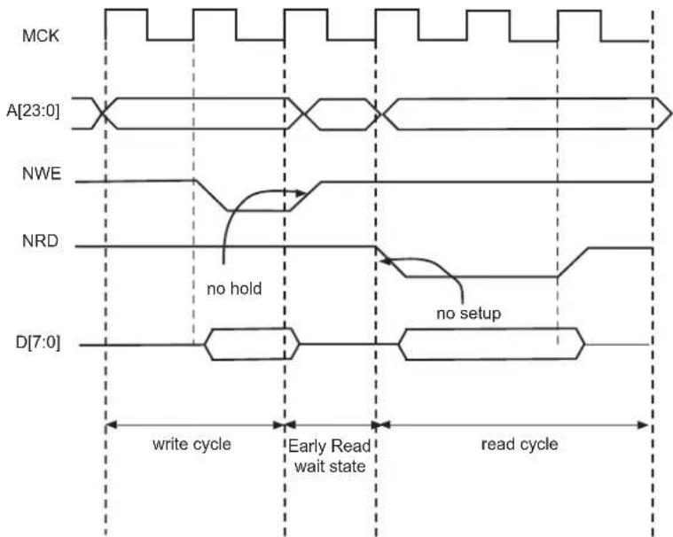
text_image
MCK A[23:0] NWE NRD no hold no setup D[7:0] write cycle Early Read wait state read cycleFigure 34-19. Early Read Wait State: NCS-controlled write with no hold followed by a read with no NCS setup
text_image
MCK A[23:0] NCS NRD D[7:0] no hold no setup write cycle (WRITE_MODE = 0) Early Read wait state (READ_MODE = 0 or READ_MODE = 1)Figure 34-20. Early Read Wait State: NWE-controlled write with no hold followed by a read with one set-up cycle
text_image
MCK A[25:2] internal write controlling signal external write controlling signal (NWE) no hold read setup = 1 NRD D[7:0] write cycle (WRITE_MODE = 1) Early Read wait state read cycle (READ_MODE = 0 or READ_MODE = 1)34.11.3 Reload User Configuration Wait State
The user may change any of the configuration parameters by writing the SMC user interface.
When detecting that a new user configuration has been written in the user interface, the SMC inserts a wait state before starting the next access. This "reload user configuration wait state" is used by the SMC to load the new set of parameters to apply to next accesses.
The reload configuration wait state is not applied in addition to the chip select wait state. If accesses before and after re-programming the user interface are made to different devices (chip selects), then one single chip select wait state is applied.
On the other hand, if accesses before and after writing the user interface are made to the same device, a reload configuration wait state is inserted, even if the change does not concern the current chip select.
34.11.3.1 User Procedure
To insert a reload configuration wait state, the SMC detects a write access to any SMC_MODE register of the user interface. If the user only modifies timing registers (SMC_SETUP, SMC_PULSE, SMC_CYCLE registers) in the user interface, he must validate the modification by writing the SMC_MODE, even if no change was made on the mode parameters.
The user must not change the configuration parameters of an SMC chip select (Setup, Pulse, Cycle, Mode) if accesses are performed on this CS during the modification. Any change of the chip select parameters, while fetching the code from a memory connected on this CS, may lead to unpredictable behavior. The instructions used to modify the parameters of an SMC chip select can be executed from the internal RAM or from a memory connected to another CS.
34.11.3.2 Slow Clock Mode Transition
A reload configuration wait state is also inserted when the Slow Clock mode is entered or exited, after the end of the current transfer (see "Slow Clock Mode").
34.11.4 Read to Write Wait State
Due to an internal mechanism, a wait cycle is always inserted between consecutive read and write SMC accesses.
This wait cycle is referred to as a read to write wait state in this document.
This wait cycle is applied in addition to chip select and reload user configuration wait states when they are to be inserted. See Figure 12-1.
34.12 Data Float Wait States
Some memory devices are slow to release the external bus. For such devices, it is necessary to add wait states (data float wait states) after a read access:
- before starting a read access to a different external memory
- before starting a write access to the same device or to a different external one.
The data float output time ( t_DF ) for each external memory device is programmed in the SMC_MODE.TDF_CYCLES field for the corresponding chip select. The value of SMC_MODE.TDF_CYCLES indicates the number of data float wait cycles (between 0 and 15) before the external device releases the bus, and represents the time allowed for the data output to go to high impedance after the memory is disabled.
Data float wait states do not delay internal memory accesses. Hence, a single access to an external memory with long t_DF will not slow down the execution of a program from internal memory.
The data float wait states management depends on SMC_MODE.READ_MODE and the SMC_MODE.TDF_MODE fields for the corresponding chip select.
34.12.1 SMC\_MODE.READ\_MODE
Setting SMC_MODE.READ_MODE to 1 indicates to the SMC that the NRD signal is responsible for turning off the tri-state buffers of the external memory device. The Data Float Period then begins after the rising edge of the NRD signal and lasts SMC_MODE.TDF_CYCLES MCK cycles.
When the read operation is controlled by the NCS signal (SMC_MODE.READ_MODE = 0), the TDF field gives the number of MCK cycles during which the data bus remains busy after the rising edge of NCS.
Figure 34-21 illustrates the Data Float Period in NRD-controlled mode (SMC_MODE.READ_MODE = 1), assuming a data float period of 2 cycles (SMC_MODE.TDF_CYCLES = 2). Figure 34-22 shows the read operation when controlled by NCS (SMC_MODE.READ_MODE = 0) and SMC_MODE.TDF_CYCLES = 3.
Figure 34-21. TDF Period in NRD Controlled Read Access (TDF = 2)
text_image
MCK A[23:0] NRD NCS D[7:0] tpacc TDF = 2 clock cycles NRD controlled read operationFigure 34-22. TDF Period in NCS Controlled Read Operation (TDF = 3)
text_image
MCK A[23:0] NWE NCS D[7:0]34.12.2 TDF Optimization Enabled (SMC\_MODE.TDF\_MODE = 1)
When SMC_MODE.TDF_MODE is set to 1 (TDF optimization is enabled), the SMC takes advantage of the setup period of the next access to optimize the number of wait states cycle to insert.
The following figure shows a read access controlled by NRD, followed by a write access controlled by NWE, on Chip Select 0. Chip Select 0 has been programmed with:
nrd_hold = 4; SMC_MODE.read_mode = 1 (NRD controlled)
nwe_setup = 3; SMC_MODE.write_mode = 1 (NWE controlled)
SMC_MODE.TDF_CYCLES = 6; SMC_MODE.TDF_MODE = 1 (optimization enabled).
Figure 34-23. TDF Optimization: No TDF wait states are inserted if the TDF period is over when the next access begins
other
| Signal | Description | |------------|--------------------------------| | MCK | Waveform with square pulses | | NRD | NRD HOLD = 4 (clock pulse) | | NWE | NRD HOLD = 4 (clock pulse) | | NCS0 | NRD HOLD = 4 (clock pulse) | | D[7:0] | TDF_CYCLES = 6 (clock pulse) | | Read access | read access on NCS0 (NRD controlled) | | Read to Write | Read to Write Wait State | | Write access | Write access on NCS0 (NWE controlled) |34.12.3 TDF Optimization Disabled (SMC\_MODE.TDF\_MODE = 0)
When optimization is disabled, TDF Wait states are inserted at the end of the read transfer, so that the data float period is ended when the second access begins. If the hold period of the read1 controlling signal overlaps the data float period, no additional TDF Wait states will be inserted.
Figure 34-24, Figure 34-25 and Figure 34-26 illustrate the cases:
- read access followed by a read access on another Chip Select,
- read access followed by a write access on another Chip Select,
- read access followed by a write access on the same Chip Select,
with no TDF optimization.
Figure 34-24. TDF Optimization Disabled (TDF Mode = 0): TDF wait states between 2 read accesses on different chip selects
text_image
MCK A[23:0] read1 controlling signal (NRD) read1 hold = 1 read2 controlling signal (NRD) TDF_CYCLES = 6 D[7:0] read1 cycle TDF_CYCLES = 6 Chip Select Wait State 5 TDF WAIT STATES read2 setup = 1 read 2cycle TDF_MODE = 0 (optimization disabled)Figure 34-25. TDF Mode = 0: TDF wait states between a read and a write access on different chip selects
text_image
MCK A[23:0] read1 controlling signal (NRD) read1 hold = 1 write2 controlling signal (NWE) TDF_CYCLES = 4 D[7:0] read1 cycle TDF_CYCLES = 4 2 TDF WAIT STATES Write2 cycle TDF_MODE = 0 (optimization disabled) Read to Write Chip Select Wait State Wait StateFigure 34-26. TDF Mode = 0: TDF wait states between read and write accesses on the same chip select

text_image
MCK A[23:0] read1 controlling signal (NRD) read1 hold = 1 write2 controlling signal (NWE) TDF_CYCLES = 5 write2 setup = 1 D[7:0] read1 cycle TDF_CYCLES = 5 Read to Write Wait State 4 TDF WAIT STATES write2 cycle TDF_MODE = 0 (optimization disabled)34.13 External Wait
Any access can be extended by an external device using the NWAIT input signal of the SMC. The SMC_MODE.EXNW_MODE field on the corresponding chip select must be set either to "10" (Frozen mode) or "11" (Ready mode). When SMC_MODE.EXNW_MODE is set to "00" (disabled), the NWAIT signal is simply ignored on the corresponding chip select. The NWAIT signal delays the read or write operation in regards to the read or write controlling signal, depending on the Read and Write modes of the corresponding chip select.
34.13.1 Restriction
When SMC_MODE.EXNW_MODE is enabled, it is mandatory to program at least one hold cycle for the read/write controlling signal. For that reason, the NWAIT signal cannot be used in Page mode (34.15. Asynchronous Page Mode), or in Slow clock mode ("Slow Clock Mode").
The NWAIT signal is assumed to be a response of the external device to the read/write request of the SMC. Then NWAIT is examined by the SMC only in the pulse state of the read or write controlling signal. The assertion of the NWAIT signal outside the expected period has no impact on SMC behavior.
34.13.2 Frozen Mode
When the external device asserts the NWAIT signal (active low), and after internal synchronization of this signal, the SMC state is frozen, i.e., SMC internal counters are frozen, and all control signals remain unchanged. When the resynchronized NWAIT signal is deasserted, the SMC completes the access, resuming the access from the point where it was stopped. See Figure 34-27. This mode must be selected when the external device uses the NWAIT signal to delay the access and to freeze the SMC.
The assertion of the NWAIT signal outside the expected period is ignored as illustrated in Figure 34-28.
Figure 34-27. Write Access with NWAIT Assertion in Frozen Mode (SMC_MODE.EXNW_MODE = 10)

other
| Signal State | Value | | ------------------ | ----- | | MCK | 0 | | A[23:0] | 0 | | NWE | 43211101 | | NCS | 4563222210 | | D[7:0] | 0 | | NWAIT | 0 | | internally synchronized | 0 | | NWAIT signal | 0 | | FROZEN STATE | 0 | | Write cycle | 0 | | EXNW_MODE = 10 (Frozen) | 0 | | WRITE_MODE = 1 (NWE_controlled) | 0 | | NWE_PULSE = 5 | 5 | | NCS_WR_PULSE = 7 | 7 |Figure 34-28. Read Access with NWAIT Assertion in Frozen Mode (SMC_MODE.EXNW_MODE = 10)

other
| Signal | Read Cycle | |-----------------|----------| | MCK | 0 | | A[23:0] | 0 | | NCS | 4 | | NCS | 3 | | NCS | 2 | | NCS | 2 | | NRD | 1 | | NRD | 0 | | NRD | 5 | | NRD | 5 | | NRD | 5 | | NRD | 5 | | NRD | 5 | | NRD | 5 | | NRD | 5 | | NRD | 5 | | NRD | 5 | | NRD | 5 | | NRD | 5 | | NRD | 5.5 | | NRD | 4 | | NRD | 3 | | NRD | 2 | | NRD | 2 | | NRD | 2 | | NRD | 2 | | NRD | 2 | | NRD | 2 | | NRD | 2 | | NRD | 2 | | NRD | 2 | | NRD | 2 | | NRD | 2 | | NRD | 2.5 | | NRD | 3 | | NRD | 3 | | NRD | 3 | | NRD | 3 | | NRD | 3 | | NRD | 3 | | NRD | 3 | | NRD | 3 | | NRD | 3 | | NRD | 3 | | NRD | 3 | | NRD | 3 |34.13.3 Ready Mode
In Ready mode (SMC_MODE.EXNW_MODE = 11), the SMC behaves differently. Normally, the SMC begins the access by down counting the setup and pulse counters of the read/write controlling signal. In the last cycle of the pulse phase, the resynchronized NWAIT signal is examined.
If asserted, the SMC suspends the access as shown in Figure 34-29 and Figure 34-30. After deassertion, the access is completed: the hold step of the access is performed.
This mode must be selected when the external device uses deassertion of the NWAIT signal to indicate its ability to complete the read or write operation.
If the NWAIT signal is deasserted before the end of the pulse, or asserted after the end of the pulse of the controlling read/write signal, it has no impact on the access length as shown in Figure 34-30.
Figure 34-29. NWAIT Assertion in Write Access: Ready Mode (SMC_MODE.EXNW_MODE = 11)
other
| Signal | Value | |-----------------|-------| | MCK | 0 | | A[23:0] | 0 | | NWE | 4321000 | | NCS | 456321110 | | D[7:0] | 0 | | NWAIT | 0 | | internally synchronized | 0 | | NWAIT signal | 0 | | Wait STATE | 0 | | Write cycle | 0 | | EXNW_MODE | 11 | | WRITE_MODE | 1 | | NWE_PULSE | 5 | | NCS_WR_PULSE | 7 |Figure 34-30. NWAIT Assertion in Read Access: Ready Mode (SMC_MODE.EXNW_MODE = 11)

other
| Signal | Read Cycle | |-----------------|----------| | MCK | 0 | | A[23:0] | 0 | | NCS | 456 3 2 0 0 | | NRD | 456 3 2 11 | | NWAIT | 0 | | internally synchronized NWAIT signal | 0 | | Wait STATE | 1 | | NRD_PULSE | 7 | | NCS_RD_PULSE | 7 |34.13.4 NWAIT Latency and Read/Write Timings
There may be a latency between the assertion of the read/write controlling signal and the assertion of the NWAIT signal by the device. The programmed pulse length of the read/write controlling signal must be at least equal to this latency plus the 2 cycles of resynchronization + one cycle. Otherwise, the SMC may enter the hold state of the access without detecting the NWAIT signal assertion. This is true in Frozen mode as well as in Ready mode. This is illustrated in the following figure.
When SMC_MODE.EXNW_MODE is enabled (ready or frozen), the user must program a pulse length of the read and write controlling signal of at least:
Minimal pulse length = NWAIT latency + 2 resynchronization cycles + 1 cycle
Figure 34-31. NWAIT Latency
other
| Signal State | Value | | ------------ | ----- | | MCK | 0 | | A[23:0] | 0 | | NRD | 4 | | NRD | 3 | | NRD | 21000 | | NWAIT | 0 | | NWAIT | 2 | | NWAIT | 1 | | INTENALLY Synchronized NWAIT signal | 0 | | INTENALLY Synchronized NWAIT signal | 2 | | INTENALLY Synchronized NWAIT signal | 1 | | READ_Cycle | 0 | | READ_MODE | 1 | | READ_MODE | 1 (NRD_controlled) | | READ_PULSE | 5 |34.14 Slow Clock Mode
The SMC is able to automatically apply a set of "Slow clock mode" read/write waveforms when an internal signal driven by the Power Management Controller is asserted because MCK has been turned to a very slow clock rate (typically 32kHz clock rate). In this mode, the user-programmed waveforms are ignored and the Slow clock mode waveforms are applied. This mode is provided so as to avoid reprogramming the User Interface with appropriate waveforms at a very slow clock rate. When activated, the Slow clock mode is active on all chip selects.
34.14.1 Slow Clock Mode Waveforms
Figure 34-32 illustrates the read and write operations in Slow Clock mode. They are valid on all Chip Selects. Table 34-6 indicates the value of read and write parameters in Slow Clock mode.
Figure 34-32. Read/Write Cycles in Slow Clock Mode

text_image
MCK A[23:0] NWE 1 NCS 1 1 NWE_CYCLE = 3 SLOW CLOCK MODE WRITE
text_image
MCK A[23:0] NRD NCS 1 1 NRD_CYCLE = 2 SLOW CLOCK MODE READTable 34-6. Read and Write Timing Parameters in Slow Clock Mode
| Read Parameters Duration (cycles) Write Parameters Duration (cycles) | |||
| NRD_SETUP 1 NWE_SETUP 1 | |||
| NRD_PULSE 1 NWE_PULSE 1 | |||
| NCS_RD_SETUP 0 NCS_WR_SETUP 0 | |||
| NCS_RD_PULSE 2 NCS_WR_PULSE 3 | |||
| NRD_CYCLE 2 NWE_CYCLE 3 | |||
34.14.2 Switching from (to) Slow Clock Mode to (from) Normal Mode
When switching from Slow clock mode to Normal mode, the current Slow clock mode transfer is completed at a high clock rate, with the set of Slow clock mode parameters (see Figure 34-33). The external device may not be fast enough to support such timings.
Figure 34-34 illustrates the recommended procedure to switch from one mode to the other.
Figure 34-33. Clock Rate Transition Occurs while the SMC is Performing a Write Operation
text_image
Slow Clock Mode internal signal from PMC MCK A[23:0] NWE NCS NWE_CYCLE = 3 SLOW CLOCK MODE WRITE SLOW CLOCK MODE WRITE NORMAL MODE WRITE This write cycle finishes with the slow clock mode set of parameters after the clock rate transition Slow clock mode transition is detected: Reload Configuration Wait StateFigure 34-34. Recommended Procedure to Switch from Slow Clock Mode to Normal Mode or from Normal Mode to Slow Clock Mode
text_image
Slow Clock Mode internal signal from PMC MCK A[23:0] NWE NCS SLOW CLOCK MODE WRITE NORMAL MODE WRITE/DLE STA Reload Conf guration Wait State34.15 Asynchronous Page Mode
The SMC supports asynchronous burst reads in Page mode, provided that the Page mode is enabled (SMC_MODE.PMEN = 1). The page size must be configured in the SMC_MODE register (PS field) to 4, 8, 16 or 32 bytes.
The page defines a set of consecutive bytes into memory. A 4-byte page (resp. 8-, 16-, 32-byte page) is always aligned to 4-byte boundaries (resp. 8-, 16-, 32-byte boundaries) of memory. The MSB of data address defines the address of the page in memory, the LSB of address define the address of the data in the page as detailed in the following table.
With Page mode memory devices, the first access to one page ( t_pa ) takes longer than the subsequent accesses to the page ( t_sa ) as shown in Page Mode Read Protocol. When in Page mode, the SMC enables the user to define different read timings for the first access within one page, and next accesses within the page.
Table 34-7. Page Address and Data Address within a Page
| Page Size Page Address (see Note) Data Address in the Page | |
| 4 bytes A[23:2] A[1:0] | |
| 8 bytes A[23:3] A[2:0] | |
| 16 bytes A[23:4] A[3:0] | |
| 32 bytes A[23:5] A[4:0] |
Note: "A" denotes the address bus of the memory device.
34.15.1 Protocol and Timings in Page Mode
The following figure shows the NRD and NCS timings in Page mode access.
Figure 34-35. Page Mode Read Protocol (Address MSB and LSB are defined in Table 34-7)
text_image
MCK A[MSB] A[LSB] NRD NCS tsatpa tsa D[7:0] NCS_RD_PULSE NRD_PULSE NRD_PULSEThe NRD and NCS signals are held low during all read transfers, whatever the programmed values of the setup and hold timings in the User Interface may be. Moreover, the NRD and NCS timings are identical. The pulse length of the first access to the page is defined with the NCS_RD_PULSE field of the SMC_PULSE register. The pulse length of subsequent accesses within the page are defined using the NRD_PULSE parameter.
In Page mode, the programming of the read timings is described in the following table:
Table 34-8. Programming of Read Timings in Page Mode
| Parameter Value Definition | ||
| READ_MODE 'x' No impact. | ||
| NCS_RD_SETUP 'x' No impact. | ||
| NCS_RD_PULSE t | pa | Access time of first access to the page. |
| NRD_SETUP 'x' No impact. | ||
| NRD_PULSE t | sa | Access time of subsequent accesses in the page. |
| NRD_CYCLE 'x' No impact. |
The SMC does not check the coherency of timings. It will always apply the NCS_RD_PULSE timings as page access timing ( t_pa ) and the NRD_PULSE for accesses to the page ( t_sa ), even if the programmed value for t_pa is shorter than the programmed value for t_sa .
34.15.2 Page Mode Restriction
The Page mode is not compatible with the use of the NWAIT signal. Using the Page mode and the NWAIT signal may lead to unpredictable behavior.
34.15.3 Sequential and Non-sequential Accesses
If the chip select and the MSB of addresses as defined in Table 34-7 are identical, then the current access lies in the same page as the previous one, and no page break occurs.
Using this information, all data within the same page, sequential or not sequential, are accessed with a minimum access time ( t_sa ). The following figure illustrates access to an 8-bit memory device in Page mode, with 8-byte pages. Access to D1 causes a page access with a long access time ( t_pa ). Accesses to D3 and D7, though they are not sequential accesses, only require a short access time ( t_sa ).
If the MSB of addresses are different, the SMC performs the access of a new page. In the same way, if the chip select is different from the previous access, a page break occurs. If two sequential accesses are made to the Page mode memory, but separated by an other internal or external peripheral access, a page break occurs on the second access because the chip select of the device was deasserted between both accesses.
Figure 34-36. Access to Non-Sequential Data within the Same Page
text_image
MCK A[23:3] Page address A[2], A1, A0 A1 A3 A7 NRD NCS D[7:0] D1 D3 D7 NCS_RD_PULSE NRD_PULSE NRD_PULSE34.16 Register Summary
| Offset | Name Bit Pos. 7 | 6 | 5 | 4 | 3 | 2 | 1 | 0 | |||||||||||
| 0x00 | SMC_SETUP0 | 7:0 | NWE_SETUP[5:0] | ||||||||||||||||
| 15:8 | NCS_WR_SETUP[5:0] | ||||||||||||||||||
| 23:16 | NRD_SETUP[5:0] | ||||||||||||||||||
| 31:24 | NCS_RD_SETUP[5:0] | ||||||||||||||||||
| 0x04 | SMC_PULSE0 | 7:0 | NWE_PULSE[6:0] | ||||||||||||||||
| 15:8 | NCS_WR_PULSE[6:0] | ||||||||||||||||||
| 23:16 | NRD_PULSE[6:0] | ||||||||||||||||||
| 31:24 | NCS_RD_PULSE[6:0] | ||||||||||||||||||
| 0x08 | SMC_CYCLE0 | 7:0 | NWE_CYCLE[7:0] | ||||||||||||||||
| 15:8 | NWE_CYCLE[8] | ||||||||||||||||||
| 23:16 | NRD_CYCLE[7:0] | ||||||||||||||||||
| 31:24 | NRD_CYCLE[8] | ||||||||||||||||||
| 0x0C | SMC_MODE0 | 7:0 | EXNW_MODE[1:0] | WRITE_MODE | READ_MODE | ||||||||||||||
| 15:8 | DBW | BAT | |||||||||||||||||
| 23:16 | TDF_MODE | TDF_CYCLES[3:0] | |||||||||||||||||
| 31:24 | PS[1:0] | PMEN | |||||||||||||||||
| 0x10 | SMC_SETUP1 | 7:0 | NWE_SETUP[5:0] | ||||||||||||||||
| 15:8 | NCS_WR_SETUP[5:0] | ||||||||||||||||||
| 23:16 | NRD_SETUP[5:0] | ||||||||||||||||||
| 0x14 SMC_PULSE1 | 7:0 | NWE_PULSE[6:0] | |||||||||||||||||
| 15:8 | NCS_WR_PULSE[6:0] | ||||||||||||||||||
| 23:16 | NRD_PULSE[6:0] | ||||||||||||||||||
| 31:24 | NCS_RD_PULSE[6:0] | ||||||||||||||||||
| 0x18 | SMC_CYCLE1 | 7:0 | NWE_CYCLE[7:0] | ||||||||||||||||
| 15:8 | NWE_CYCLE[8] | ||||||||||||||||||
| 23:16 | NRD_CYCLE[7:0] | ||||||||||||||||||
| 31:24 | NRD_CYCLE[8] | ||||||||||||||||||
| 0x1C | SMC_MODE1 | 7:0 | EXNW_MODE[1:0] | WRITE_MODE | READ_MODE | ||||||||||||||
| 15:8 | DBW | BAT | |||||||||||||||||
| 23:16 | TDF_MODE | TDF_CYCLES[3:0] | |||||||||||||||||
| 31:24 | PS[1:0] | PMEN | |||||||||||||||||
| 0x20 | SMC_SETUP2 | 7:0 | NWE_SETUP[5:0] | ||||||||||||||||
| 15:8 | NCS_WR_SETUP[5:0] | ||||||||||||||||||
| 23:16 | NRD_SETUP[5:0] | ||||||||||||||||||
| 31:24 | NCS_RD_SETUP[5:0] | ||||||||||||||||||
| 0x24 | SMC_PULSE2 | 7:0 | NWE_PULSE[6:0] | ||||||||||||||||
| 15:8 | NCS_WR_PULSE[6:0] | ||||||||||||||||||
| 23:16 | NRD_PULSE[6:0] | ||||||||||||||||||
| 31:24 | NCS_RD_PULSE[6:0] | ||||||||||||||||||
| 0x28 | SMC_CYCLE2 | 7:0 | NWE_CYCLE[7:0] | ||||||||||||||||
| 15:8 | NWE_CYCLE[8] | ||||||||||||||||||
| 23:16 | NRD_CYCLE[7:0] | ||||||||||||||||||
| 31:24 | NRD_CYCLE[8] | ||||||||||||||||||
| 0x2C | SMC_MODE2 | 7:0 | EXNW_MODE[1:0] | WRITE_MODE | READ_MODE | ||||||||||||||
| 15:8 | DBW | BAT | |||||||||||||||||
| 23:16 | TDF_MODE | TDF_CYCLES[3:0] | |||||||||||||||||
| 31:24 | PS[1:0] | PMEN | |||||||||||||||||
| 0x30 | SMC_SETUP3 | 7:0 | NWE_SETUP[5:0] | ||||||||||||||||
| 15:8 | NCS_WR_SETUP[5:0] | ||||||||||||||||||
| 23:16 | NRD_SETUP[5:0] | ||||||||||||||||||
| 0x31 | NCS_RD_SETUP[5:0] | ||||||||||||||||||
| Offset | Name Bit Pos. 7 | 6 | 5 | 4 | 3 | 2 | 1 | 0 | ||||||||||||||||||||||||||||||||||||||||||||||||||||||||||||||||||||||||||||||||||||||||||||||||||||||||||||||||||||||||||||||||||||||||||||||||||||||||||||||||||||||||||||||||||||||||||||||||||||||||||||||||||||||||||||||||||||||||||||||||||||||||||||||||||||||||||||||||||||||||||||||||||||||||||||||||||||||||||||||||||||||||||||||||||||||||||||||||||||||||||||||||||||||||||||||||||||||||||||||||||||||||||||||||||||||||||||||||||||||||||||||||||||||||||||||||||||||||||||||||||||||||||||||||||||||||||||||||||||||||||||||||||||||||||||||||||||||||||||||||||||||||||||||||||||||||||||||||||||||||||||||||||||||||||||||||||||||||||||||||||||||||||||||||||||||||||||||||||||||||||||||||||||||
| 0x34 | SMC_PULSE3 | 7:0 | NWE_PULSE[6:0] | |||||||||||||||||||||||||||||||||||||||||||||||||||||||||||||||||||||||||||||||||||||||||||||||||||||||||||||||||||||||||||||||||||||||||||||||||||||||||||||||||||||||||||||||||||||||||||||||||||||||||||||||||||||||||||||||||||||||||||||||||||||||||||||||||||||||||||||||||||||||||||||||||||||||||||||||||||||||||||||||||||||||||||||||||||||||||||||||||||||||||||||||||||||||||||||||||||||||||||||||||||||||||||||||||||||||||||||||||||||||||||||||||||||||||||||||||||||||||||||||||||||||||||||||||||||||||||||||||||||||||||||||||||||||||||||||||||||||||||||||||||||||||||||||||||||||||||||||||||||||||||||||||||||||||||||||||||||||||||||||||||||||||||||||||||||||||||||||||||||||||||||||||||||||||||
| 15:8 | NCS_WR_PULSE[6:0] | 0x38 | SMC_CYCLE3 | 7:0 | NWE_CYCLE[7:0] | NWE_CYCLE[8] | 23:16 | NRD_CYCLE[7:0] | 31:24 | |||||||||||||||||||||||||||||||||||||||||||||||||||||||||||||||||||||||||||||||||||||||||||||||||||||||||||||||||||||||||||||||||||||||||||||||||||||||||||||||||||||||||||||||||||||||||||||||||||||||||||||||||||||||||||||||||||||||||||||||||||||||||||||||||||||||||||||||||||||||||||||||||||||||||||||||||||||||||||||||||||||||||||||||||||||||||||||||||||||||||||||||||||||||||||||||||||||||||||||||||||||||||||||||||||||||||||||||||||||||||||||||||||||||||||||||||||||||||||||||||||||||||||||||||||||||||||||||||||||||||||||||||||||||||||||||||||||||||||||||||||||||||||||||||||||||||||||||||||||||||||||||||||||||||||||||||||||||||||||||||||||||||||||||||||||||||||||||||||||||||||||||||||||
| 0x38 | SMC_CYCLE3 | 7:0 | NWE_CYCLE[7:0] | 15:8 | ||||||||||||||||||||||||||||||||||||||||||||||||||||||||||||||||||||||||||||||||||||||||||||||||||||||||||||||||||||||||||||||||||||||||||||||||||||||||||||||||||||||||||||||||||||||||||||||||||||||||||||||||||||||||||||||||||||||||||||||||||||||||||||||||||||||||||||||||||||||||||||||||||||||||||||||||||||||||||||||||||||||||||||||||||||||||||||||||||||||||||||||||||||||||||||||||||||||||||||||||||||||||||||||||||||||||||||||||||||||||||||||||||||||||||||||||||||||||||||||||||||||||||||||||||||||||||||||||||||||||||||||||||||||||||||||||||||||||||||||||||||||||||||||||||||||||||||||||||||||||||||||||||||||||||||||||||||||||||||||||||||||||||||||||||||||||||||||||||||||||||||||||||||||||||
34.16.1 Static Memory Controller (SMC) User Interface
The SMC is programmed using the registers listed in the following table. For each Chip Select, a set of four registers is used to program the parameters of the external device connected on it. In the Register Summary, "CS_number" denotes the Chip Select number. 16 bytes (0x10) are required per Chip Select.
34.16.1.1 SMC Setup Register
Name: SMC_SETUP
Offset: 0x00 + n*0x10 [n=0..3]
Reset: 0x01010101
Property: R/W
This register can only be written if the WPEN bit is cleared in the "SMC Write Protection Mode Register".
Bit 31 30 29 28 27 26 25 24
| NCS_RD_SETUP[5:0] | |
| Access | R/W R/W R/W R/W R/W R/W |
| Reset 0 0 0 0 0 1 | |
Bit 23 22 21 20 19 18 17 16
| NRD_SETUP[5:0] | ||
| Access Reset 0 0 0 0 0 1 | R/W R/W R/W R/W R/W R/W | |
Bit 15 14 13 12 11 10 98
| NCS_WR_SETUP[5:0] | ||
| Access Reset 0 0 0 0 0 1 | R/W R/W R/W R/W R/W R/W | |
Bit 76543210
| NWE_SETUP[5:0] | ||
| Access Reset 0 0 0 0 0 1 | R/W R/W R/W R/W R/W R/W | |
Bits 29:24 - NCS_RD_SETUP[5:0] NCS Setup Length in READ Access
In read access, the NCS signal setup length is defined as:
NCS setup length = (128* NCS_RD_SETUP[5] + NCS_RD_SETUP[4:0]) clock cycles
Bits 21:16 - NRD_SETUP[5:0] NRD Setup Length
The NRD signal setup length is defined in clock cycles as:
NRD setup length = (128* NRD_SETUP[5] + NRD_SETUP[4:0]) clock cycles
Bits 13:8 - NCS_WR_SETUP[5:0] NCS Setup Length in WRITE Access
In write access, the NCS signal setup length is defined as:
NCS setup length = (128* NCS_WR_SETUP[5] + NCS_WR_SETUP[4:0]) clock cycles
Bits 5:0 - NWE_SETUP[5:0] NWE Setup Length
The NWE signal setup length is defined as:
NWE setup length = (128* NWE_SETUP[5] + NWE_SETUP[4:0]) clock cycles
34.16.1.2 SMC Pulse Register
Name: SMC_PULSE
Offset: 0x04 + n*0x10 [n=0..3]
Reset: 0x01010101
Property: R/W
This register can only be written if the WPEN bit is cleared in the "SMC Write Protection Mode Register".
text_image
Bit 31 30 29 28 27 26 25 24 NCS_RD_PULSE[6:0] Access R/W R/W R/W R/W R/W R/W R/W Reset 0 0 0 0 0 0 1 Bit 23 22 21 20 19 18 17 16 NRD_PULSE[6:0] Access R/W R/W R/W R/W R/W R/W R/W Reset 0 0 0 0 0 0 1 Bit 15 14 13 12 11 10 9 8 NCS_WR_PULSE[6:0] Access R/W R/W R/W R/W R/W R/W R/W Reset 0 0 0 0 0 0 1 Bit 7 6 5 4 3 2 1 0 NWE_PULSE[6:0] Access R/W R/W R/W R/W R/W R/W R/W Reset 0 0 0 0 0 0 1Bits 30:24 - NCS_RD_PULSE[6:0] NCS Pulse Length in READ Access
In standard read access, the NCS signal pulse length is defined as:
NCS pulse length = (256* NCS_RD_PULSE[6] + NCS_RD_PULSE[5:0]) clock cycles
The NCS pulse length must be at least 1 clock cycle.
In Page mode read access, the NCS_RD_PULSE parameter defines the duration of the first access to one page.
Bits 22:16 - NRD_PULSE[6:0] NRD Pulse Length
In standard read access, the NRD signal pulse length is defined in clock cycles as:
NRD pulse length = (256* NRD_PULSE[6] + NRD_PULSE[5:0]) clock cycles
The NRD pulse length must be at least 1 clock cycle.
In Page mode read access, the NRD_PULSE parameter defines the duration of the subsequent accesses in the page.
Bits 14:8 - NCS_WR_PULSE[6:0] NCS Pulse Length in WRITE Access
In write access, the NCS signal pulse length is defined as:
NCS pulse length = (256* NCS_WR_PULSE[6] + NCS_WR_PULSE[5:0]) clock cycles
The NCS pulse length must be at least 1 clock cycle.
Bits 6:0 - NWE_PULSE[6:0] NWE Pulse Length
The NWE signal pulse length is defined as:
NWE pulse length = (256* NWE_PULSE[6] + NWE_PULSE[5:0]) clock cycles
The NWE pulse length must be at least 1 clock cycle.
34.16.1.3 SMC Cycle Register
Name: SMC_CYCLE
Offset: 0x08 + n*0x10 [n=0..3]
Reset: 0x00030003
Property: R/W
This register can only be written if the WPEN bit is cleared in the "SMC Write Protection Mode Register".
Bit 31 30 29 28 27 26 25 24
| NRD_CYCLE[8] | ] | ||||||
| Access Reset 0 | R/W | ||||||
Bit 23 22 21 20 19 18 17 16
| NRD_CYCLE[7:0] | ||||||||
| Access | R/W | R/W | R/W | R/W | R/W | R/W | R/W | R/W |
| Reset | 0 | 0 | 0 | 0 | 1 | |||
Bit 15 14 13 12 11 10 9 8
| NWE_CYCLE[ | 8] | ||||||
| Access Reset 0 | R/W | ||||||
| Bit | 7 | 6 | 5 | 4 | 3 | 2 | 1 | 0 |
| NWE_CYCLE[7:0] | ||||||||
| Access | R/W | R/W | R/W | R/W | R/W | R/W | R/W | R/W |
| Reset | 0 | 0 | 0 | 0 | 0 | 0 | 1 | 1 |
Bits 24:16 - NRD\_CYCLE[8:0] Total Read Cycle Length
The total read cycle length is the total duration in clock cycles of the read cycle. It is equal to the sum of the setup, pulse and hold steps of the NRD and NCS signals. It is defined as:
Read cycle length = (NRD_CYCLE[8:7]*256 + NRD_CYCLE[6:0]) clock cycles
Bits 8:0 - NWE\_CYCLE[8:0] Total Write Cycle Length
The total write cycle length is the total duration in clock cycles of the write cycle. It is equal to the sum of the setup, pulse and hold steps of the NWE and NCS signals. It is defined as:
Write cycle length = (NWE_CYCLE[8:7]*256 + NWE_CYCLE[6:0]) clock cycles
34.16.1.4 SMC Mode Register
Name: SMC_MODE
Offset: 0x0C + n*0x10 [n=0..3]
Reset: 0x10001003
Property: R/W
This register can only be written if the WPEN bit is cleared in the "SMC Write Protection Mode Register".
The user must confirm the SMC configuration by writing any one of the SMC_MODE registers.

text_image
Bit 31 30 29 28 27 26 25 24 PS[1:0] PMEN Access R/W R/W R/W Reset Bit 23 22 21 20 19 18 17 16 TDF_MODE TDF_CYCLES[3:0] Access R/W R/W R/W R/W R/W Reset Bit 15 14 13 12 11 10 9 8 Access DBW BAT R/W R/W Access R/W R/W Reset Bit 7 6 5 4 3 2 1 0 Access EXNW_MODE[1:0] WRITE_MODE READ_MODE Reset R/W R/W R/W R/WBits 29:28 - PS[1:0] Page Size
If page mode is enabled, this field indicates the size of the page in bytes.
| Value | Name | Description |
| 0 | 4_BYTE | 4-byte page |
| 1 | 8_BYTE | 8-byte page |
| 2 | 16_BYTE | 16-byte page |
| 3 | 32_BYTE | 32-byte page |
Bit 24 - PMEN Page Mode Enabled
| Value | Description |
| 0 | Standard read is applied. |
| 1 | Asynchronous burst read in page mode is applied on the corresponding chip select. |
Bit 20 - TDF\_MODE TDF Optimization
| Value | Description |
| 0 | TDF optimization disabled-the number of TDF wait states is inserted before the next access begins. |
| 1 | TDF optimization enabled-the number of TDF wait states is optimized using the setup period of the next read/write access. |
Bits 19:16 - TDF\_CYCLES[3:0] Data Float Time
This field gives the integer number of clock cycles required by the external device to release the data after the rising edge of the read controlling signal. The SMC always provide one full cycle of bus turnaround after the TDF_CYCLES period. The external bus cannot be used by another chip select during TDF_CYCLES + 1 cycles. From 0 up to 15 TDF_CYCLES can be set.
Bit 12 - DBW Data Bus Width
| Value Name | Description | |
| 0 | 8_BIT 8-bit Data Bus | |
| 1 | 16_BIT 16-bit Data Bus |
Bit 8 - BAT Byte Access Type
This field is used only if DBW defines a 16-bit data bus.
| Value Name | Description | |
| 0 | BYTE_SELECT Byte select access type: | |
| 1 | BYTE_WRITE Byte write access type: | |
Bits 5:4 - EXNW\_MODE[1:0] NWAIT Mode
The NWAIT signal is used to extend the current read or write signal. It is only taken into account during the pulse phase of the read and write controlling signal. When the use of NWAIT is enabled, at least one cycle hold duration must be programmed for the read and write controlling signal.
| Value Name | Description |
| 0 | DISABLED Disabled-The NWAIT input signal is ignored on the corresponding chip select. |
| 1 | Reserved |
| 2 | FROZEN Frozen Mode-If asserted, the NWAIT signal freezes the current read or write cycle. After deassertion, the read/write cycle is resumed from the point where it was stopped. |
| 3 | READY Ready Mode-The NWAIT signal indicates the availability of the external device at the end of the pulse of the controlling read or write signal, to complete the access. If high, the access normally completes. If low, the access is extended until NWAIT returns high. |
Bit 1 - WRITE_MODE Write Mode
| Value Description | |
| 0 | The write operation is controlled by the NCS signal.- If TDF optimization is enabled (TDF_MODE =1), TDF wait states will be inserted after the setup of NCS. |
| 1 | The write operation is controlled by the NWE signal.- If TDF optimization is enabled (TDF_MODE =1), TDF wait states will be inserted after the setup of NWE. |
Bit 0 - READ_MODE Read Mode
| Value Description | |
| 0 | The read operation is controlled by the NCS signal.- If TDF cycles are programmed, the external bus is marked busy after the rising edge of NCS.- If TDF optimization is enabled (TDF_MODE =1), TDF wait states are inserted after the setup of NCS. |
| 1 | The read operation is controlled by the NRD signal.- If TDF cycles are programmed, the external bus is marked busy after the rising edge of NRD.- If TDF optimization is enabled (TDF_MODE =1), TDF wait states are inserted after the setup of NRD. |
34.16.1.5 SMC Off-Chip Memory Scrambling Register
Name: SMC_OCMS
Offset: 0x80
Reset: 0x00000000
Property: Read/Write
Note: This register can only be written if the WPEN bit is cleared in the SMC Write Protection Mode Register (34.16.1.8. SMC_WPMR).

text_image
Bit 31 30 29 28 27 26 25 24 Access Reset Bit 23 22 21 20 19 18 17 16 Access Reset Bit 15 14 13 12 11 10 9 8 CSBSE CS2SE CS1 SE CS0SE R/W R/W R/W 0 0 0 0 Access Reset Bit 7 6 5 4 3 2 1 0 SMSE Access Reset R/W 0Bits 8, 9, 10, 11 - CSSE Chip Select x Scrambling Enable
| Value | Description |
| 0 | Disable scrambling for CSx. |
| 1 | Enable scrambling for CSx. |
Bit 0 - SMSE Static Memory Controller Scrambling Enable
| Value | Description |
| 0 | Disable scrambling for SMC access. |
| 1 | Enable scrambling for SMC access. |
34.16.1.6 SMC Off-Chip Memory Scrambling Key1 Register
Name: SMC_KEY1
Offset: 0x84
Reset: 0x00000000
Property: Write-once
Note:
- 'Write-once' access indicates that the first write access after a system reset prevents any further modification of the value of this register.
| Bit 31 30 29 28 27 26 25 24 | |
| KEY1[31:24] | |
| Access Reset 0 0 0 0 0 0 0 0 | |
| Bit 23 22 21 20 19 18 17 16 | |
| KEY1[23:16] | |
| Access Reset 0 0 0 0 0 0 0 0 | |
| Bit 15 14 13 12 11 10 9 8 | |
| KEY1[15:8] | |
| Access Reset 0 0 0 0 0 0 0 0 | |
| Bit 7 6 5 4 3 2 1 0 | |
| KEY1[7:0] | |
| Access Reset 0 0 0 0 0 0 0 0 | |
Bits 31:0 - KEY1[31:0] Off-Chip Memory Scrambling (OCMS) Key Part 1
When off-chip memory scrambling is enabled, KEY1 and KEY2 values determine data scrambling.
34.16.1.7 SMC Off-Chip Memory Scrambling Key2 Register
Name: SMC_KEY2
Offset: 0x88
Reset: 0x00000000
Property: Write-once
Note: 'Write-once' access indicates that the first write access after a system reset prevents any further modification of the value of this register.
text_image
Bit 31 30 29 28 27 26 25 24 KEY2[31:24] Access Reset 0 0 0 0 0 0 0 0 Bit 23 22 21 20 19 18 17 16 KEY2[23:16] Access Reset 0 0 0 0 0 0 0 0 Bit 15 14 13 12 11 10 9 8 KEY2[15:8] Access Reset 0 0 0 0 0 0 0 0 Bit 7 6 5 4 3 2 1 0 KEY2[7:0] Access Reset 0 0 0 0 0 0 0 0Bits 31:0 - KEY2[31:0] Off-Chip Memory Scrambling (OCMS) Key Part 2
When off-chip memory scrambling is enabled, KEY1 and KEY2 values determine data scrambling.
34.16.1.8 SMC Write Protection Mode Register
Name: SMC_WPMR
Offset: 0xE4
Reset: 0x00000000
Property: Read/Write
| Bit 31 30 29 28 27 26 25 24 | |||||||
| WPKEY[23:16] | |||||||
| Access | R/W R/W R/W R/W R/W R/W R/W R/W | ||||||
| Reset | 0 0 0 0 0 0 0 0 | ||||||
| Bit 23 22 21 20 19 18 17 16 | |||||||
| WPKEY[15:8] | |||||||
| Access | R/W R/W R/W R/W R/W R/W R/W R/W | ||||||
| Reset | 0 0 0 0 0 0 0 0 | ||||||
| Bit 15 14 13 12 11 10 9 8 | |||||||
| WPKEY[7:0] | |||||||
| Access | R/W R/W R/W R/W R/W R/W R/W R/W | ||||||
| Reset | 0 0 0 0 0 0 0 0 | ||||||
| Bit 7 6 5 4 3 2 1 0 | |||||||
| WPEN | |||||||
| Access | R/W | ||||||
| Reset | 0 | ||||||
Bits 31:8 - WPKEY[23:0] Write Protection Key
| Value | Name | Description |
| 0x534D43 | PASSWD | Writing any other value in this field aborts the write operation of the WPEN bit. Always reads as 0. |
Bit 0 - WPEN Write Protect Enable
See "Register Write Protection" for the list of registers that can be write-protected.
| Value | Description |
| 0 | Disables the write protection if WPKEY corresponds to 0x534D43 ("SMC" in ASCII). |
| 1 | Enables the write protection if WPKEY corresponds to 0x534D43 ("SMC" in ASCII). |
34.16.1.9 SMC Write Protection Status Register
Name: SMC_WPSR
Offset: 0xE8
Reset: 0x00000000
Property: Read-only

text_image
Bit 31 30 29 28 27 26 25 24 Access Reset Bit 23 22 21 20 19 18 17 16 WPVSRC[15:8] Access R R R R R R R R Reset 0 0 0 0 0 0 0 0 Bit 15 14 13 12 11 10 9 8 WPVSRC[7:0] Access R R R R R R R R R Reset 0 0 0 0 0 0 0 0 Bit 7 6 5 4 3 2 1 0 WPVS Access Reset R 0Bits 23:8 - WPVSRC[15:0] Write Protection Violation Source
When WPVS = 1, WPVSRC indicates the register address offset at which a write access has been attempted.
Bit 0 - WPVS Write Protection Violation Status
| Value | Description |
| 0 | No write protection violation has occurred since the last read of the SMC_WPSR register. |
| 1 | A write protection violation has occurred since the last read of the SMC_WPSR register. If this violation is an unauthorized attempt to write a protected register, the associated violation is reported into field WPVSRC. |
35. DMA Controller (XDMAC)
35.1 Description
The DMA Controller (XDMAC) is a -protocol central direct memory access controller. It performs peripheral data transfer and memory move operations over one or two bus ports through the unidirectional communication channel. Each channel is fully programmable and provides both peripheral or memory-to-memory transfers. The channel features are configurable at implementation.
35.2 Embedded Characteristics
- Host Interfaces
- DMA Channels
- Hardware Requests
- Embedded FIFO
- Supports Peripheral-to-Memory, Memory-to-Peripheral, or Memory-to-Memory Transfer Operations
- Peripheral DMA Operation Runs on Bytes (8-bit), Half-Word (16-bit) and Word (32-bit)
• Memory DMA Operation Runs on Bytes (8 bit), Half-Word (16-bit) and Word (32-bit)
• Supports Hardware and Software Initiated Transfers
• Supports Linked List Operations
• Supports Incrementing or Fixed Addressing Mode
• Supports Programmable Independent Data Striding for Source and Destination
• Supports Programmable Independent Microblock Striding for Source and Destination - Configurable Priority Group and Arbitration Policy
• Programmable Burst Length - Configuration Interface Accessible through APB Interface
• XDMAC Architecture Includes Multiport FIFO
• Supports Multiple View Channel Descriptor
• Automatic Flush of Channel Trailing Bytes
• Automatic Coarse-Grain and Fine-Grain Clock Gating - Hardware Acceleration of Memset Pattern
35.3 Block Diagram
Figure 35-1. DMA Controller (XDMAC) Block Diagram
flowchart
graph TD
    A["Data FIFO"] --> B["Control and Data Steering"]
    C["Destination FSM"] --> D["Request Arbiter"]
    E["Source FSM"] --> D
    F["APB Interface"] --> G["Status Registers"]
    H["Configuration Registers"] --> G
    I["Hardware Request Interface"] --> J["Peripheral Hardware Requests"]
    K["DMA Interrupt"] --> L["DMA System Controller"]
    M["AMBA AHB Layer"] --> N["Dual Host AHB Interface"]
    O["AMBA AHB Layer"] --> N
    P["DMA Read/Write Datapath"] --> B
    Q["DMA Channel"] --> B
    R["Request Pool"] --> D
    S["APB Interface"] --> T["APB Interface"]
    U["Peripheral Hardware Requests"] --> J
    V["DMA Interrupt"] --> L
35.4 DMA Controller Peripheral Connections
Table 35-1. Peripheral Hardware Requests
| Peripheral Name Transfer Type HW Interface Number (XDMAC_CC.PERID) | ||
| HSMCI Transmit/Receive 0 | ||
| SPI0 Transmit 1 | ||
| SPI0 Receive 2 | ||
| SPI1 Transmit 3 | ||
| SPI1 Receive 4 | ||
| QSPI Transmit 5 | ||
| QSPI Receive 6 | ||
| USART0 Transmit 7 | ||
| USART0 Receive 8 | ||
| USART1 Transmit 9 | ||
| USART1 Receive 10 | ||
| USART2 Transmit | 11 | |
| USART2 Receive 12 | ||
| PWM0 | Transmit | 13 |
| TWIHS0 Transmit | 14 | |
| TWIHS0 Receive 15 | ||
| TWIHS1 Transmit | 16 | |
| TWIHS1 Receive 17 | ||
| TWIHS2 Transmit | 18 | |
| TWIHS2 Receive 19 | ||
| UART0 Transmit 20 | ||
| UART0 Receive 21 | ||
| UART1 Transmit 22 | ||
| UART1 Receive 23 | ||
| UART2 Transmit 24 | ||
| UART2 Receive 25 | ||
| UART3 Transmit 26 | ||
| UART3 Receive 27 | ||
| UART4 Transmit 28 | ||
| UART4 Receive 29 | ||
| DACC Transmit 30 | ||
| SSC Transmit 32 | ||
| SSC Receive 33 | ||
| PIOA Receive 34 | ||
| AFEC0 Receive 35 | ||
| AFEC1 Receive 36 | ||
| AES Transmit 37 | ||
| AES Receive 38 | ||
| PWM1 Transmit 39 | ||
| TC0.Ch0 Receive 40 | ||
| TC1.Ch0 Receive 41 | ||
| TC2.Ch0 Receive 42 | ||
| TC3.Ch0 Receive 43 | ||
| I2SC0 Transmit Left 44 | ||
| I2SC0 Receive Left | 45 | |
| I2SC1 Transmit Left 46 | ||
| I2SC1 Receive Left | 47 | |
| I2SC0 | Transmit Right | 48 |
| I2SC0 | Receive Right | 49 |
| I2SC1 | Transmit Right | 50 |
| I2SC1 | Receive Right | 51 |
35.5 Functional Description
35.5.1 Basic Definitions
Source Peripheral: Client device, memory mapped on the interconnection network, from where the XDMAC reads data. The source peripheral teams up with a destination peripheral to form a channel. A data read operation is scheduled when the peripheral transfer request is asserted.
Destination Peripheral: Client device, memory mapped on the interconnection network, to which the XDMAC writes. A write data operation is scheduled when the peripheral transfer request is asserted.
Channel: The data movement between source and destination creates a logical channel.
Transfer Type: The transfer is hardware-synchronized when it is paced by the peripheral hardware request, otherwise the transfer is self-triggered (memory to memory transfer).
35.5.2 Transfer Hierarchy Diagram
XDMAC Host Transfer: The Host Transfer is composed of a linked list of blocks. The channel address, control and configuration registers can be modified at the inter block boundary. The descriptor structure modifies the channel registers conditionally. Interrupts can be generated on a per block basis or when the end of linked list event occurs.
XDMAC Block: An XDMAC block is composed of a programmable number of microblocks. The channel configuration registers remain unchanged at the inter microblock boundary. The source and destination addresses are conditionally updated with a programmable signed number.
XDMAC Microblock: The microblock is composed of a programmable number of data. The channel configuration registers remain unchanged at the data boundary. The data address may be fixed (a FIFO location, a peripheral transmit or receive register), incrementing (a memory-mapped area) by a programmable signed number.
XDMAC Burst and Incomplete Burst: In order to improve the overall performance when accessing dynamic external memory, burst access is mandatory. Each data of the microblock is considered as a part of a memory burst. The programmable burst value indicates the largest memory burst allowed on a per channel basis. When the microblock length is not an integral multiple of the burst size, an incomplete burst is performed to read or write the last trailing bytes.
XDMAC Chunk and Incomplete Chunk: When a peripheral synchronized transfer is activated, the microblock splits into a number of data chunks. The chunk size is programmable. The larger the chunk is, the better the performance is. When the transfer size is not a multiple of the chunk size, the last chunk may be incomplete.
Figure 35-2. XDMAC Memory Transfer Hierarchy

flowchart
graph TD
    A["Host Transfer"] --> B["Block Level"]
    B --> C["BLK₀ BLK₁ BLK(N-1)"]
    C --> D["μBLK₀ μBLK₁ μBLK(M-1)"]
    D --> E["MB₀"]
    D --> F["MB(p-1) ...... iMB"]
    D --> G["......"]
    G --> H["Memory Burst Level"]
    style A fill:#f9f,stroke:#333
    style B fill:#ccf,stroke:#333
    style C fill:#cfc,stroke:#333
    style D fill:#fcc,stroke:#333
    style E fill:#cff,stroke:#333
    style F fill:#ffc,stroke:#333
    style G fill:#cfc,stroke:#333
    style H fill:#fcc,stroke:#333
Figure 35-3. XDAMC Peripheral Transfer Hierarchy

flowchart
graph TD
    A["Host Transfer"] --> B["Block Level"]
    B --> C["BLK₀ BLK₁ BLK(N-1)"]
    C --> D["μBLK₀ μBLK₁ μBLK(M-1)"]
    C --> E["......"]
    E --> F["CHK₀ CHK_(p-1) iCHK Chunk Level"]
    C -.-> G["......"]
    G --> H["Micro Block Level"]
35.5.3 Peripheral Synchronized Transfer
A peripheral hardware request interface is used to control the pace of the chunk transfer. When a peripheral is ready to transmit or receive a chunk of data, it asserts its request line and the DMA Controller transfers a data to or from the memory to the peripheral.
35.5.3.1 Software Triggered Synchronized Transfer
The Peripheral hardware request can be software controlled using the SWREQ field of the XDMAC Global Channel Software Request Register (XDMAC_GSWR). The peripheral synchronized transfer is paced using a processor write access in the XDMAC_GSWR. Each bit of that register triggers a transfer request. The XDMAC Global Channel Software Request Status Register (XDMAC_GSWS) indicates the status of the request; when set, the request is still pending.
35.5.4 XDMAC Transfer Software Operation
35.5.4.1 Single Block Transfer With Single Microblock
- Read the XDMAC Global Channel Status Register (XDMAC_GS) to select a free channel.
- Clear the pending Interrupt Status bit(s) by reading the selected XDMAC Channel x Interrupt Status Register (XDMAC_CISx).
- Write the XDMAC Channel x Source Address Register (XDMAC_CSAx) for channel x.
- Write the XDMAC Channel x Destination Address Register (XDMAC_CDAx) for channel x.
- Program field UBLEN in the XDMAC Channel x Microblock Control Register (XDMAC_CUBCx) with the number of data.
- Program the XDMAC Channel x Configuration Register (XDMAC_CCx):
a. Clear XDMAC_CCx.TYPE for a memory-to-memory transfer, otherwise set this bit.
b. Configure XDMAC_CCx.MBSIZE to the memory burst size used.
c. Configure XDMAC_CCx.SAM and DAM to Memory Addressing mode.
d. Configure XDMAC_CCx.DSYNC to select the peripheral transfer direction.
e. Configure XDMAC_CCx.CSIZE to configure the channel chunk size (only relevant for peripheral synchronized transfer).
f. Configure XDMAC_CCx.DWIDTH to configure the transfer data width.
g. Configure XDMAC_CCx.SIF, XDMAC_CCx.DIF to configure the Host interface used to read data and write data, respectively.
h. Configure XDMAC_CCx.PERID to select the active hardware request line (only relevant for a peripheral synchronized transfer).
i. Set XDMAC_CCx.SWREQ to use a software request (only relevant for a peripheral synchronized transfer).
-
Clear the following five registers:
-
XDMAC Channel x Next Descriptor Control Register (XDMAC_CNDCx)
- XDMAC Channel x Block Control Register (XDMAC_CBCx)
- XDMAC Channel x Data Stride Memory Set Pattern Register (XDMAC_CDS_MSPx)
- XDMAC Channel x Source Microblock Stride Register (XDMAC_CSUSx)
- XDMAC Channel x Destination Microblock Stride Register (XDMAC_CDUSx)
This indicates that the linked list is disabled, there is only one block and striding is disabled.
- Enable the Microblock interrupt by writing a '1' to bit BIE in the XDMAC Channel x Interrupt Enable Register (XDMAC_CIEx). Enable the Channel x Interrupt Enable bit by writing a '1' to bit IEx in the XDMAC Global Interrupt Enable Register (XDMAC_GIE).
- Enable channel x by writing a '1' to bit ENx in the XDMAC Global Channel Enable Register (XDMAC_GE). XDMAC_GS.STx (XDMAC Channel x Status bit) is set by hardware.
- Once completed, the DMA channel sets XDMAC_CISx.BIS (End of Block Interrupt Status bit) and generates an interrupt. XDMAC_GS.STx is cleared by hardware. The software can either wait for an interrupt or poll the channel status bit.
35.5.4.2 Single Block Transfer With Multiple Microblock
- Read the XDMAC_GS register to choose a free channel.
- Clear the pending Interrupt Status bit by reading the chosen XDMAC_CISx register.
- Write the XDMAC_CSAx register for channel x.
- Write the XDMAC_CDAx register for channel x.
- Program XDMAC_CUBCx.UBLEN with the number of data.
- Program XDMAC_CCx register (see "Single Block Transfer With Single Microblock").
- Program XDMAC_CBCx.BLEN with the number of microblocks of data.
-
Clear the following registers:
-
XDMAC_CNDCx
- XDMAC_CDS_MSPx
- XDMAC_CSUSx XDMAC_CDUSx
This indicates that the linked list is disabled and striding is disabled.
- Enable the Block interrupt by writing a '1' to XDMAC_CIEx.BIE, enable the Channel x Interrupt Enable bit by writing a '1' to XDMAC_GIEx.IEx.
- Enable channel x by writing a '1' to the XDMAC_GE.ENx. XDMAC_GS.STx is set by hardware.
- Once completed, the DMA channel sets XDMAC_CISx.BIS (End of Block Interrupt Status bit) and generates an interrupt. XDMAC_GS.STx is cleared by hardware. The software can either wait for an interrupt or poll the channel status bit.
35.5.4.3 Host Transfer
- Read the XDMAC_GS register to choose a free channel.
-
Clear the pending Interrupt Status bit by reading the chosen XDMAC_CISx register.
-
Build a linked list of transfer descriptors in memory. The descriptor view is programmable on a per descriptor basis. The linked list items structure must be word aligned. MBR_UBC.NDE must be configured to 0 in the last descriptor to terminate the list.
- Configure field NDA in the XDMAC Channel x Next Descriptor Address Register (XDMAC_CNDAX) with the first descriptor address and bit XDMAC_CNDAX.NDAIF with the Host interface identifier.
- Configure the XDMAC_CNDCx register:
a. Set XDMAC_CNDCx.NDE to enable the descriptor fetch.
b. Set XDMAC_CNDCx.NDSUP to update the source address at the descriptor fetch time, otherwise clear this bit.
c. Set XDMAC_CNDCx.NDDUP to update the destination address at the descriptor fetch time, otherwise clear this bit.
d. Configure XDMAC_CNDCx.NDVIEW to define the length of the first descriptor.
- Enable the End of Linked List interrupt by writing a '1' to XDMAC_CIEx.LIE.
- Enable channel x by writing a '1' to XDMAC_GE.ENx. XDMAC_GS.STx is set by hardware.
- Once completed, the DMA channel sets XDMAC_CISx.BIS (End of Block Interrupt Status bit) and generates an interrupt. XDMAC_GS.STx is cleared by hardware. The software can either wait for an interrupt or poll the channel status bit.
35.5.4.4 Disabling A Channel Before Transfer Completion
Under normal operation, the software enables a channel by writing a '1' to XDMAC_GE.ENx, then the hardware disables a channel on transfer completion by clearing bit XDMAC_GS.STx. To disable a channel, write a '1' to bit XDMAC_GD.Dlx and poll the XDMAC_GS register.
35.6 Linked List Descriptor Operation
35.6.1 Linked List Descriptor View
Table 35-2. Channel Next Descriptor View 0–3 Structures
| Channel Next Descriptor Offset | Structure member Name | ||
| View 0 Structure DSCR_ADDR+0x00 Next Descriptor Address Member MBR_NDA | |||
| DSCR_ADDR+0x04 Microblock Control Member MBR_UBC | |||
| DSCR_ADDR+0x08 Transfer Address Member MBR_TA | |||
| View 1 Structure DSCR_ADDR+0x00 Next Descriptor Address Member MBR_NDA | |||
| DSCR_ADDR+0x04 Microblock Control Member MBR_UBC | |||
| DSCR_ADDR+0x08 Source Address Member MBR_SA | |||
| DSCR_ADDR+0x0C | Destination Address Member | MBR_DA | |
| View 2 Structure DSCR_ADDR+0x00 Next Descriptor Address Member MBR_NDA | |||
| ......continued | |||
| Channel Next Descriptor Offset | Structure member Name | ||
| View 3 Structure DSCR_ADDR+0x00 Next Descriptor Address Member MBR_NDA | |||
35.6.2 Descriptor Structure Members Description
35.6.2.1 View 0 Descriptor
Next Descriptor Address Member (MBR_NDA)
Microblock Control Member (MBR_UBC)
Transfer Address Member (MBR_TA)
View0 is the simplest descriptor having just three members.
Next Descriptor Address Member (MBR\_NDA):
MBR_NDA is similar to XDMAC Channel Next Descriptor register (XDMAC_CNDAx). The XDMAC_CNDAx register is initialized to the address of the first descriptor of the linked list, whereas Next Descriptor Address Member (MBR_NDA) is initialized to the address of the subsequent descriptor to be fetched from the linked list. If there are no further descriptors present in the linked list, then MBR_NDA should be initialized with 0. When a descriptor is fetched, XDMAC_CNDAx register is updated with MBR_NDA value for the execution of the next descriptor (Block).
TransferAddress Member (MBR\_TA):
Transfer Address Member (MBR_TA) should be written with the destination address during Memory-to-Memory and Peripheral-to-Memory transfers. When the descriptor is fetched, the Channel Destination Address register (XDMAC_CDAx) is updated with the valued stored in Transfer Address member (MBR_TA) based on the previous descriptor's MBR_UBC.NDEN value.
Transfer Address Member (MBR_TA) should be written with the source address during Memory-to-Peripheral transfer. When the descriptor is fetched, the Channel Source Address register (XDMAC_CSAx) is updated with the values stored in Transfer Address member (MBR_TA) based on the previous descriptor's MBR_UBC.NSEN value.
Note: For the first descriptor of the linked list, XDMAC_CNDCx.NDSUP and XDMAC_CNDCx.NDDUP values should be directly initialized. These values decide whether to update the Channel Source/Destination Address registers with MBR_TA or not.
35.6.2.2 View 1 Descriptor
Next Descriptor Address Member (MBR_NDA)
Microblock Control Member (MBR_UBC)
Source Address Member (MBR_SA)
Destination Address Member (MBR_DA)
View 1 descriptor has two extra members in addition to View 0 descriptor.
Source Address Member (MBR\_SA):
It contains the source address value of the corresponding descriptor (BLOCK). The value of MBR_SA is copied to the Channel Source Address register (XDMAC_CSAx) based on the previous MBR_UBC.NSEN settings. Therefore, the source address can be changed between different descriptors (BLOCKS).
Note: For the first descriptor of the linked list, the XDMAC_CNDCx.NDSUP value should be directly initialized. This value decides whether to update Channel Source Address register (XDMAC_CSAx) with MBR_SA or not.
Destination Address Member (MBR\_DA):
It contains the destination address value of the corresponding descriptor (BLOCK). The value of MBR_DA is copied to the Channel Destination Address register (XDMAC_CDAx) based on the previous MBR_UBC. NDEN settings. Therefore, the destination address can be changed between different descriptors (BLOCKS).
Note: For the first descriptor of the linked list, the XDMAC_CNDCx.NDDUP value should be directly initialized. This value decides whether to update Channel Destination Address register (XDMAC_CDAx) with MBR_DA or not.
35.6.2.3 View 2 Descriptor
Next Descriptor Address Member (MBR_NDA)
Microblock Control Member (MBR_UBC)
Source Address Member (MBR_SA)
Destination Address Member (MBR_DA)
Configuration Member (MBR_CFG)
View2 descriptor has Configuration Member (MBR_CFG) in addition to View 1 descriptor.
ConfigurationMember (MBR\_CFG):
MBR_CFGis similar to the XDMAC_CCx register. During the descriptor fetch, the value of MBR_CFG is copied to the XDMAC_CCx register.
35.6.2.4 View 3 Descriptor
Next Descriptor Address Member (MBR_NDA)
Microblock Control Member (MBR_UBC)
Source Address Member (MBR_SA)
Destination Address Member (MBR_DA)
Configuration Member (MBR_CFG)
Block Control Member (MBR_BC)
Data Stride Member (MBR_DS)
Source Microblock Stride Member (MBR_SUS)
Destination Microblock Stride Member (MBR_DUS)
View3 descriptor has four extra members in addition to View 2 descriptor.
Block Control Member (MBR\_BC):
MBR_BC is similar to the Channel Block Control Register (XDMAC_CBCx). During the descriptor fetch, the value of MBR_BC is copied to the XDMAC_CBCx register.
Data Stride Member (MBR\_DS):
MBR_DS is similar to the Channel Data Stride Memory Set Pattern Register (XDMAC_CDS_MSPx). During the descriptor fetch, the value of MBR_DS is copied to the XDMAC_CDS_MSPx register.
Source Microblock Stride Member (MBR\_SUS):
MBR_SUS is similar to the Channel Source Microblock Stride Register (XDMAC_CSUSx). During the descriptor fetch, the value of MBR_SUS is copied to the XDMAC_CSUSx register.
Destination Microblock Stride Member (MBR\_DUS):
MBR_DUS is similar to the Channel Destination Microblock Stride Register (XDMAC_CDUSx). During the descriptor fetch, the value of MBR_DUS is copied to the XDMAC_CDUSx register.
35.6.2.5 Descriptor Structure Microblock Control Member
Name: MBR_UBC
Property: Read-only
| Bit 31 30 29 28 27 26 25 24 | ||||||
| NVIEW[1:0] NDEN | NSEN NDE | |||||
| Access Reset | RR R RR | |||||
| Bit 23 22 21 20 19 18 17 16 | ||||||
| UBLEN[23:16] | ||||||
| Access Reset | RR R R R R R R | |||||
| Bit 15 14 13 12 11 10 9 8 | ||||||
| UBLEN[15:8] | ||||||
| Access Reset | RR R R R R R R | |||||
| Bit 7 6 5 4 3 2 1 0 | ||||||
| UBLEN[7:0] | ||||||
| Access Reset | RR R R R R R R | |||||
Bits 28:27 - NVIEW[1:0] Next Descriptor View
| Value | Name | Description |
| 0 | NDV0 | Next Descriptor View 0 |
| 1 | NDV1 | Next Descriptor View 1 |
| 2 | NDV2 | Next Descriptor View 2 |
| 3 | NDV3 | Next Descriptor View 3 |
Bit 26 - NDEN Next Descriptor Destination Update
| Value | Description |
| 0 | Destination parameters remain unchanged. |
| 1 | Destination parameters are updated when the descriptor is retrieved. |
Bit 25 - NSEN Next Descriptor Source Update
| Value | Description |
| 0 | Source parameters remain unchanged. |
| 1 | Source parameters are updated when the descriptor is retrieved. |
Bit 24 - NDE Next Descriptor Enable
| Value | Description |
| 0 | Descriptor fetch is disabled. |
| 1 | Descriptor fetch is enabled. |
Bits 23:0 - UBLEN[23:0] Microblock Length
This field indicates the number of data in the microblock. The microblock contains UBLEN data.
35.7 XDMAC Maintenance Software Operations
35.7.1 Disabling a Channel
A disable channel request occurs when a write operation is performed in the XDMAC_GD register. If the channel is source peripheral synchronized (bit XDMAC_CCx.TYPE is set and bit XDMAC_CCx.DSYNC is cleared), then pending bytes (bytes located in the FIFO) are written to memory and bit XDMAC_CISx.DIS is set. If the channel is not source peripheral synchronized, the current channel transaction (read or write) is terminated and XDMAC_CISx.DIS is set. XDMAC_GS.STx is cleared by hardware when the current transfer is completed. The channel is no longer active and can be reused.
35.7.2 Suspending a Channel
A read request suspend command is issued by writing to the XDMAC_GRS register. A write request suspend command is issued by writing to the XDMAC_GWS register. A read write suspend channel is issued by writing to the XDMAC_GRWS register. These commands have an immediate effect on the scheduling of both read and write transactions. If a transaction is already in progress, it is terminated normally. The channel is not disabled. The FIFO content is preserved. The scheduling can resume normally, clearing the bit in the same registers. Pending bytes located in the FIFO are not written out to memory. The write suspend command does not affect read request operations, that is, read operations can still occur until the FIFO is full.
35.7.3 Flushing a Channel
A FIFO flush command is issued by writing to the XDMAC_SWF register. The content of the FIFO is written to memory. XDMAC_CISx.FIS (End of Flush Interrupt Status bit) is set when the last byte is successfully transferred to memory. The channel is not disabled. The flush operation is not blocking, meaning that read operation can be scheduled during the flush write operation. The flush operation is only relevant for peripheral to memory transfer where pending peripheral bytes are buffered into the channel FIFO.
35.7.4 Maintenance Operation Priority
35.7.4.1 Disable Operation Priority
- When a disable request occurs on a suspended channel, the XDMAC_GWS.WSx (Channel x Write Suspend bit) is cleared. If the transfer is source peripheral synchronized, the pending bytes are drained to memory. The bit XDMAC_CISx.DIS is set.
- When a disable request follows a flush request, if the flush last transaction is not yet scheduled, the flush request is discarded and the disable procedure is applied. Bit XDMAC_CISx.FIS is not set. Bit XDMAC_CISx.DIS is set when the disable request is completed. If the flush request transaction is already scheduled, the XDMAC_CISx.FIS is set. XDMAC_CISx.DIS is also set when the disable request is completed.
35.7.4.2 Flush Operation Priority
- When a flush request occurs on a suspended channel, if there are pending bytes in the FIFO, they are written out to memory, XDMAC_CISx.FIS is set. If the FIFO is empty, XDMAC_CISx.FIS is also set.
- If the flush operation is performed after a disable request, the flush command is ignored. XDMAC_CISx.FIS is not set.
35.7.4.3 Suspend Operation Priority
If the suspend operation is performed after a disable request, the write suspend operation is ignored.
35.8 XDMAC Software Requirements
- Write operations to channel registers are not be performed in an active channel after the channel is enabled. If any channel parameters must be reprogrammed, this can only be done after disabling the XDMAC channel.
- XDMAC_CSAx and XDMAC_CDAx channel registers are to be programmed with a byte, half-word or word aligned address depending on the Channel x Data Width field (DWIDTH) of the XDMAC Channel x Configuration Register.
- When XDMAC_CC.INITD is set to 0, XDMAC_CUBC.UBLEN and XDMAC_CNDA.NDA field values are unreliable when the descriptor is being updated. The following procedure applies to get the buffer descriptor identifier and the residual bytes:
Read XDMAC_CNDAx.NDA(nda0)
Read XDMAC_CCx.INITD(initd0)
Read XDMAC_CCx.INITD(initd0)
Read XDMAC_CUBCx.UBLEN(ublen)
Read XDMAC_CCx.INITD(initd1)
Read XDMA_CNDAx.NDA(ndal)
If (nda0 == ndal && initd0 == 1 && initd1 == 1).
Then the ublen is correct, the buffer id is nda.
Else retry
See the figure below.
Figure 35-4. INITD Timing Diagram
text_image
XDMAC_CUBCx.UBLEN buffer0buffer1buffer0buffer1buffer0 XDMAC_CCx.INITD XDMAC_CUBCx.UBLEN 0 buffer0buffer1ublen XDMAC_CNDAx.NDA buffer1ndabuffer0.nda35.9 Register Summary
| Offset | Name Bit Pos. 7 | 6 | 5 | 4 | 3 | 2 | 1 | 0 | |||||||||
| 0x00 | XDMAC_GTYPE | 7:0 FIFO_SZ[2:0] NB_CH[4:0] | |||||||||||||||
| 15:8 FIFO_SZ[10:3] | |||||||||||||||||
| 23:16 NB_REQ[6:0] | |||||||||||||||||
| 31:24 | |||||||||||||||||
| 0x04 | XDMAC_GCFG | 7:0 | |||||||||||||||
| 15:8 | BXKBEN | ||||||||||||||||
| 23:16 | |||||||||||||||||
| 31:24 | |||||||||||||||||
| 0x08 | XDMAC_GWAC | 7:0 | PW1[3:0] | PW0[3:0] | |||||||||||||
| 15:8 | PW3[3:0] | PW2[3:0] | |||||||||||||||
| 23:16 | |||||||||||||||||
| 31:24 | |||||||||||||||||
| 0x0C | XDMAC_GIE | 7:0 | IE6 | IE5 | IE4 | IE3 | IE2 | IE1 | IE0 | ||||||||
| 15:8 | |||||||||||||||||
| 23:16 | |||||||||||||||||
| 31:24 | |||||||||||||||||
| 0x10 | XDMAC_GID | 7:0 | ID6 | ID5 | ID4 | ID3 | ID2 | ID1 | ID0 | ||||||||
| 15:8 | |||||||||||||||||
| 23:16 | |||||||||||||||||
| 31:24 | |||||||||||||||||
| 0x14 | XDMAC_GIM | 7:0 | IM6 | IM5 | IM4 | IM3 | IM2 | IM1 | IM0 | ||||||||
| 15:8 | |||||||||||||||||
| 23:16 | |||||||||||||||||
| 31:24 | |||||||||||||||||
| 0x18 | XDMAC_GIS | 7:0 | IS6 | IS5 | IS4 | IS3 | IS2 | IS1 | IS0 | ||||||||
| 15:8 | |||||||||||||||||
| 23:16 | |||||||||||||||||
| 31:24 | |||||||||||||||||
| 0x1C | XDMAC_GE | 7:0 | EN6 | EN5 | EN4 | EN3 | EN2 | EN1 | ENO | ||||||||
| 15:8 | |||||||||||||||||
| 23:16 | |||||||||||||||||
| 31:24 | |||||||||||||||||
| 0x20 | XDMAC_GD | 7:0 | DI6 | DI5 | DI4 | DI3 | DI2 | DI1 | DI0 | ||||||||
| 15:8 | |||||||||||||||||
| 23:16 | |||||||||||||||||
| 31:24 | |||||||||||||||||
| 0x24 | XDMAC_GS | 7:0 | ST6 | ST5 | ST4 | ST3 | ST2 | ST1 | ST0 | ||||||||
| 15:8 | |||||||||||||||||
| 23:16 | |||||||||||||||||
| 31:24 | |||||||||||||||||
| 0x28 | XDMAC_GRS | 7:0 | RS6 | RS5 | RS4 | RS3 | RS2 | RS1 | RS0 | ||||||||
| 15:8 | |||||||||||||||||
| 23:16 | |||||||||||||||||
| 31:24 | |||||||||||||||||
| 0x2C | XDMAC_GWS | WS6 | WS5 | WS4 | WS3 | 7:0 | RWS6 | RWS5 | RWS4 | RWS3 | RWS2 | RWS1 | RWS0 | ||||
| 15:8 | 23:16 | ||||||||||||||||
| 23:16 | 31:24 | ||||||||||||||||
| 0x30 | XDMAC_GRWS | RWS6 | RWS5 | RWS4 | RWS3 | 7:0 | RWR6 | RWR5 | RWR4 | RWR3 | RWR2 | RWR1 | RWR0 | ||||
| 15:8 | 23:16 | ||||||||||||||||
| 23:16 | 31:24 | ||||||||||||||||
| 0x34 | XDMAC_GRWR | RWR6 | RWR5 | RWR4 | RWR3 | 7:0 | RWR6 | RWR5 | RWR4 | RWR3 | RWR2 | RWR1 | RWR0 | ||||
| 15:8 | 23:16 | ||||||||||||||||
| 23:16 | 31:24 | ||||||||||||||||
......continued
| Offset | Name Bit Pos. 76543210 | |||||||||
| 0x38 XDMAC_GSWR | 7:0 SWREQ6 SWREQ5 SWREQ4 SWREQ3 SWREQ2 SWREQ1 SWREQ0 | |||||||||
| 15:8 | ||||||||||
| 23:16 | ||||||||||
| 31:24 | ||||||||||
| 0x3C XDMAC_GSWS | 7:0 SWRS6 SWRS5 SWRS4 SWRS3 SWRS2 SWRS1 SWRS0 | |||||||||
| 15:8 | ||||||||||
| 23:16 | ||||||||||
| 31:24 | ||||||||||
| 0x40 XDMAC_GSWF | 7:0 | SWF6 | SWF5 | SWF4 | SWF3 | SWF2 | SWF1 | SWF0 | ||
| 15:8 | ||||||||||
| 23:16 | ||||||||||
| 31:24 | ||||||||||
| 0x44 ... 0x4F | Reserved | |||||||||
| 0x50 | XDMAC_CIE0 | 7:0 | ROIE | WBIE | RBIE FIE DIE LIE BIE | |||||
| 15:8 | ||||||||||
| 23:16 | ||||||||||
| 31:24 | ||||||||||
| 0x54 | XDMAC_CID0 | 7:0 | ROID | WBEID | RBEID | FID | DID | LID | BID | |
| 15:8 | ||||||||||
| 23:16 | ||||||||||
| 31:24 | ||||||||||
| 0x58 | XDMAC_CIMO | 7:0 | ROIM | WBEIM | RBEIM | FIM | DIM | LIM | BIM | |
| 15:8 | ||||||||||
| 23:16 | ||||||||||
| 31:24 | ||||||||||
| 0x5C | XDMAC_CISO | 7:0 | ROIS | WBEIS | RBEIS | FIS | DIS | LIS | BIS | |
| 15:8 | ||||||||||
| 23:16 | ||||||||||
| 31:24 | ||||||||||
| 0x60 | XDMAC_CSA0 | 7:0 | SA[7:0] | |||||||
| 15:8 | SA[15:8] | |||||||||
| 23:16 | SA[23:16] | |||||||||
| 31:24 | SA[31:24] | |||||||||
| 0x64 | XDMAC_CDA0 | 7:0 | DA[7:0] | |||||||
| 15:8 | DA[15:8] | |||||||||
| 23:16 | DA[23:16] | |||||||||
| 31:24 | DA[31:24] | |||||||||
| 0x68 | XDMAC_CNDA0 | 7:0 | NDA[5:0] | NDAIF | ||||||
| 15:8 | NDA[13:6] | |||||||||
| 23:16 | NDA[21:14] | |||||||||
| 31:24 | NDA[29:22] | |||||||||
| 0x6C | XDMAC_CNDC0 | 7:0 | NDVIEW[1:0] | NDDUP | NDSUP NDE | |||||
| 15:8 | ||||||||||
| 23:16 | ||||||||||
| 31:24 | ||||||||||
| 0x70 XDMAC_CUBCO | 7:0 | UBLEN[7:0] | ||||||||
| 15:8 | UBLEN[15:8] | |||||||||
| 23:16 | UBLEN[23:16] | |||||||||
| 31:24 | ||||||||||
| 0x74 | XDMAC_CBC0 | 7:0 | BLEN[7:0] | |||||||
| 15:8 | BLEN[11:8] | |||||||||
| 23:16 | ||||||||||
| 31:24 | ||||||||||
| 0x78 | XDMAC_CCO | 7:0 | MEMSET | SWREQ | DSYNC | MBSIZE[1:0] | TYPE | |||
| 15:8 | DIF SIF | DWIDTH[1:0] | CSIZE[2:0] | |||||||
| 23:16 | WRIP | RDIP | INITD | DAM[1:0] | SAM[1:0] | |||||
| 31:24 | PERID[6:0] | |||||||||
......continued
| Offset | Name Bit Pos. 76543210 | ||||||||
| 0x7C XDMAC_CDS_MSP0 | 7:0 SDS_MSP[7:0] | ||||||||
| 15:8 SDS_MSP[15:8] | |||||||||
| 23:16 DDS_MSP[7:0] | |||||||||
| 31:24 DDS_MSP[15:8] | |||||||||
| 0x80 XDMAC_CSUS0 | 7:0 SUBS[7:0] | ||||||||
| 15:8 SUBS[15:8] | |||||||||
| 23:16 SUBS[23:16] | |||||||||
| 31:24 | |||||||||
| 0x84 | XDMAC_CDUS0 | 7:0 | DUBS[7:0] | ||||||
| 15:8 | DUBS[15:8] | ||||||||
| 23:16 | DUBS[23:16] | ||||||||
| 31:24 | |||||||||
| 0x88 ... 0x8F | Reserved | ||||||||
| 0x90 | XDMAC_CIE1 | 7:0 | ROIE | WBIE | RBIE | FIE | DIE | LIE | BIE |
| 15:8 | |||||||||
| 23:16 | |||||||||
| 31:24 | |||||||||
| 0x94 | XDMAC_CID1 | 7:0 | ROID | WBEID | RBEID | FID | DID | LID | BID |
| 15:8 | |||||||||
| 23:16 | |||||||||
| 31:24 | |||||||||
| 0x98 | XDMAC CIM1 | 7:0 | ROIM | WBEIM | RBEIM | FIM | DIM | LIM | BIM |
| 15:8 | |||||||||
| 23:16 | |||||||||
| 31:24 | |||||||||
| 0x9C | XDMAC_CIS1 | 7:0 | ROIS | WBEIS | RBEIS | FIS | DIS | LIS | BIS |
| 15:8 | |||||||||
| 23:16 | |||||||||
| 31:24 | |||||||||
| 0xA0 | XDMAC CSA1 | 7:0 | SA[7:0] | ||||||
| 15:8 | SA[15:8] | ||||||||
| 23:16 | SA[23:16] | ||||||||
| 31:24 | SA[31:24] | ||||||||
| 0xA4 | XDMAC_CDA1 | 7:0 | DA[7:0] | ||||||
| 15:8 DA[15:8] | |||||||||
| 23:16 DA[23:16] | |||||||||
| 31:24 DA[31:24] | |||||||||
| 0xA8 | XDMAC_CNDA1 | 7:0 | NDA[5:0] | NDAIF | |||||
| 15:8 | NDA[13:6] | ||||||||
| 23:16 NDA[21:14] | |||||||||
| 31:24 NDA[29:22] | |||||||||
| 0xAC | XDMAC_CNDC1 | 7:0 | NDVIEW[1:0] | NDDUP | NDSUP | NDE | |||
| 15:8 | |||||||||
| 23:16 | |||||||||
| 31:24 | |||||||||
| 0xB0 | XDMAC_CUBC1 | 7:0 | UBLEN[7:0] | ||||||
| 15:8 UBLEN[15:8] | |||||||||
| 23:16 UBLEN[23:16] | |||||||||
| 31:24 | |||||||||
| 0xB4 | XDMAC_CBC1 | 7:0 BLEN[7:0] | |||||||
| 15:8 | BLEN[11:8] | ||||||||
| 23:16 | |||||||||
| 31:24 | |||||||||
| 0xB8 | XDMAC_CC1 | 7:0 | MEMSET | SWREQ | DSYNC | MBSIZE[1:0] | TYPE | ||
| 15:8 | DIF | SIF | DWIDTH[1:0] | CSIZE[2:0] | |||||
| 23:16 | WRIP | RDIP | INITD | DAM[1:0] | SAM[1:0] | ||||
| 31:24 | PERID[6:0] | ||||||||
| 0xBC XDMAC_CDS_MSP1 | 7:0 SDS_MSP[7:0] | ||||||||
| 15:8 SDS_MSP[15:8] | |||||||||
| 23:16 DDS_MSP[7:0] | |||||||||
| 31:24 DDS_MSP[15:8] | |||||||||
| 0xC0 XDMAC_CSUS1 | 7:0 SUBS[7:0] | ||||||||
| 15:8 SUBS[15:8] | |||||||||
| 23:16 SUBS[23:16] | |||||||||
| 31:24 | |||||||||
| 0xC4 | XDMAC_CDUS1 | 7:0 | DUBS[7:0] | ||||||
| 15:8 | DUBS[15:8] | ||||||||
| 23:16 | DUBS[23:16] | ||||||||
| 31:24 | |||||||||
| 0xC8 ... 0xCF | Reserved | ||||||||
| 0xD0 | XDMAC_CIE2 | 7:0 | ROIE | WBIE | RBIE | FIE | DIE | LIE | BIE |
| 15:8 | |||||||||
| 23:16 | |||||||||
| 31:24 | |||||||||
| 0xD4 | XDMAC_CID2 | 7:0 | ROID | WBEID | RBEID | FID | DID | LID | BID |
| 15:8 | |||||||||
| 23:16 | |||||||||
| 31:24 | |||||||||
| 0xD8 | XDMAC_CIM2 | 7:0 | ROIM | WBEIM | RBEIM | FIM | DIM | LIM | BIM |
| 15:8 | |||||||||
| 23:16 | |||||||||
| 31:24 | |||||||||
| 0xDC | XDMAC_CIS2 | 7:0 | ROIS | WBEIS | RBEIS | FIS | DIS | LIS | BIS |
| 15:8 | |||||||||
| 23:16 | |||||||||
| 31:24 | |||||||||
| 0xE0 | XDMAC_CSA2 | 7:0 | SA[7:0] | ||||||
| 15:8 | SA[15:8] | ||||||||
| 23:16 | SA[23:16] | ||||||||
| 31:24 | SA[31:24] | ||||||||
| 0xE4 | XDMAC_CDA2 | 7:0 | DA[7:0] | ||||||
| 15:8 DA[15:8] | |||||||||
| 23:16 DA[23:16] | |||||||||
| 31:24 DA[31:24] | |||||||||
| 0xE8 | XDMAC_CNDA2 | 7:0 | NDA[5:0] | NDAIF | |||||
| 15:8 | NDA[13:6] | ||||||||
| 23:16 NDA[21:14] | |||||||||
| 31:24 NDA[29:22] | |||||||||
| 0xEC | XDMAC_CNDC2 | 7:0 | NDVIEW[1:0] | NDDUP | NDSUP | NDE | |||
| 15:8 | |||||||||
| 23:16 | |||||||||
| 31:24 | |||||||||
| 0xF0 XDMAC_CUBC2 | 7:0 | UBLEN[7:0] | |||||||
| 15:8 UBLEN[15:8] | |||||||||
| 23:16 UBLEN[23:16] | |||||||||
| 31:24 | |||||||||
| 0xF4 | XDMAC_CBC2 | 7:0 BLEN[7:0] | |||||||
| 15:8 | BLEN[11:8] | ||||||||
| 23:16 | |||||||||
| 31:24 | |||||||||
| 0xF8 | XDMAC_CC2 | 7:0 | MEMSET | SWREQ | DSYNC | MBSIZE[1:0] | TYPE | ||
| 15:8 | DIF | SIF | DWIDTH[1:0] | CSIZE[2:0] | |||||
| 23:16 | WRIP | RDIP | INITD | DAM[1:0] | SAM[1:0] | ||||
| 31:24 | PERID[6:0] | ||||||||
| 0xFC XDMAC_CDS_MSP2 | 7:0 SDS_MSP[7:0] | ||||||||
| 15:8 SDS_MSP[15:8] | |||||||||
| 23:16 DDS_MSP[7:0] | |||||||||
| 31:24 DDS_MSP[15:8] | |||||||||
| 0x0100 XDMAC_CSUS2 | 7:0 SUBS[7:0] | ||||||||
| 15:8 SUBS[15:8] | |||||||||
| 23:16 SUBS[23:16] | |||||||||
| 31:24 | |||||||||
| 0x0104 | XDMAC_CDUS2 | 7:0 | DUBS[7:0] | ||||||
| 15:8 | DUBS[15:8] | ||||||||
| 23:16 | DUBS[23:16] | ||||||||
| 31:24 | |||||||||
| 0x0108 ... 0x010F | Reserved | ||||||||
| 0x0110 | XDMAC_CIE3 | 7:0 | ROIE | WBIE | RBIE | FIE | DIE | LIE | BIE |
| 15:8 | |||||||||
| 23:16 | |||||||||
| 31:24 | |||||||||
| 0x0114 | XDMAC_CID3 | 7:0 | ROID | WBEID | RBEID | FID | DID | LID | BID |
| 15:8 | |||||||||
| 23:16 | |||||||||
| 31:24 | |||||||||
| 0x0118 | XDMAC CIM3 | 7:0 | ROIM | WBEIM | RBEIM | FIM | DIM | LIM | BIM |
| 15:8 | |||||||||
| 23:16 | |||||||||
| 31:24 | |||||||||
| 0x011C | XDMAC_CIS3 | 7:0 | ROIS | WBEIS | RBEIS | FIS | DIS | LIS | BIS |
| 15:8 | |||||||||
| 23:16 | |||||||||
| 31:24 | |||||||||
| 0x0120 | XDMAC CSA3 | 7:0 | SA[7:0] | ||||||
| 15:8 | SA[15:8] | ||||||||
| 23:16 | SA[23:16] | ||||||||
| 31:24 | SA[31:24] | ||||||||
| 0x0124 | XDMAC_CDA3 | 7:0 | DA[7:0] | ||||||
| 15:8 DA[15:8] | |||||||||
| 23:16 DA[23:16] | |||||||||
| 31:24 DA[31:24] | |||||||||
| 0x0128 | XDMAC_CNDA3 | 7:0 | NDA[5:0] | NDAIF | |||||
| 15:8 | NDA[13:6] | ||||||||
| 23:16 NDA[21:14] | |||||||||
| 31:24 NDA[29:22] | |||||||||
| 0x012C | XDMAC_CNDC3 | 7:0 | NDVIEW[1:0] | NDDUP | NDSUP | NDE | |||
| 15:8 | |||||||||
| 23:16 | |||||||||
| 31:24 | |||||||||
| 0x0130 | XDMAC_CUBC3 | 7:0 | UBLEN[7:0] | ||||||
| 15:8 UBLEN[15:8] | |||||||||
| 23:16 UBLEN[23:16] | |||||||||
| 31:24 | |||||||||
| 0x0134 | XDMAC_CBC3 | 7:0 BLEN[7:0] | |||||||
| 15:8 | BLEN[11:8] | ||||||||
| 23:16 | |||||||||
| 31:24 | |||||||||
| 0x0138 | XDMAC_CC3 | 7:0 | MEMSET | SWREQ | DSYNC | MBSIZE[1:0] | TYPE | ||
| 15:8 | DIF | SIF | DWIDTH[1:0] | CSIZE[2:0] | |||||
| 23:16 | WRIP | RDIP | INITD | DAM[1:0] | SAM[1:0] | ||||
| 31:24 | PERID[6:0] | ||||||||
| 0x013C | XDMAC_CDS_MSP3 | 7:0 SDS_MSP[7:0] | |||||||
| 15:8 SDS_MSP[15:8] | |||||||||
| 23:16 DDS_MSP[7:0] | |||||||||
| 31:24 DDS_MSP[15:8] | |||||||||
| 0x0140 | XDMAC_CSUS3 | 7:0 SUBS[7:0] | |||||||
| 15:8 SUBS[15:8] | |||||||||
| 23:16 SUBS[23:16] | |||||||||
| 31:24 | |||||||||
| 0x0144 | XDMAC_CDUS3 | 7:0 | DUBS[7:0] | ||||||
| 15:8 | DUBS[15:8] | ||||||||
| 23:16 | DUBS[23:16] | ||||||||
| 31:24 | |||||||||
| 0x0148 ... 0x014F | Reserved | ||||||||
| 0x0150 | XDMAC_CIE4 | 7:0 | ROIE | WBIE | RBIE | FIE | DIE | LIE | BIE |
| 15:8 | |||||||||
| 23:16 | |||||||||
| 31:24 | |||||||||
| 0x0154 | XDMAC_CID4 | 7:0 | ROID | WBEID | RBEID | FID | DID | LID | BID |
| 15:8 | |||||||||
| 23:16 | |||||||||
| 31:24 | |||||||||
| 0x0158 | XDMAC_CIM4 | 7:0 | ROIM | WBEIM | RBEIM | FIM | DIM | LIM | BIM |
| 15:8 | |||||||||
| 23:16 | |||||||||
| 31:24 | |||||||||
| 0x015C | XDMAC_CIS4 | 7:0 | ROIS | WBEIS | RBEIS | FIS | DIS | LIS | BIS |
| 15:8 | |||||||||
| 23:16 | |||||||||
| 31:24 | |||||||||
| 0x0160 | XDMAC_CSA4 | 7:0 | SA[7:0] | ||||||
| 15:8 | SA[15:8] | ||||||||
| 23:16 | SA[23:16] | ||||||||
| 31:24 | SA[31:24] | ||||||||
| 0x0164 | XDMAC_CDA4 | 7:0 | DA[7:0] | ||||||
| 15:8 DA[15:8] | |||||||||
| 23:16 DA[23:16] | |||||||||
| 31:24 DA[31:24] | |||||||||
| 0x0168 | XDMAC_CNDA4 | 7:0 | NDA[5:0] | NDAIF | |||||
| 15:8 | NDA[13:6] | ||||||||
| 23:16 NDA[21:14] | |||||||||
| 31:24 NDA[29:22] | |||||||||
| 0x016C | XDMAC_CNDC4 | 7:0 | NDVIEW[1:0] | NDDUP | NDSUP | NDE | |||
| 15:8 | |||||||||
| 23:16 | |||||||||
| 31:24 | |||||||||
| 0x0170 | XDMAC_CUBC4 | 7:0 | UBLEN[7:0] | ||||||
| 15:8 UBLEN[15:8] | |||||||||
| 23:16 UBLEN[23:16] | |||||||||
| 31:24 | |||||||||
| 0x0174 | XDMAC_CBC4 | 7:0 BLEN[7:0] | |||||||
| 15:8 | BLEN[11:8] | ||||||||
| 23:16 | |||||||||
| 31:24 | |||||||||
| 0x0178 | XDMAC_CC4 | 7:0 | MEMSET | SWREQ | DSYNC | MBSIZE[1:0] | TYPE | ||
| 15:8 | DIF | SIF | DWIDTH[1:0] | CSIZE[2:0] | |||||
| 23:16 | WRIP | RDIP | INITD | DAM[1:0] | SAM[1:0] | ||||
| 31:24 | PERID[6:0] | ||||||||
| 0x017C | XDMAC_CDS_MSP4 | 7:0 SDS_MSP[7:0] | |||||||
| 15:8 SDS_MSP[15:8] | |||||||||
| 23:16 DDS_MSP[7:0] | |||||||||
| 31:24 DDS_MSP[15:8] | |||||||||
| 0x0180 | XDMAC_CSUS4 | 7:0 SUBS[7:0] | |||||||
| 15:8 SUBS[15:8] | |||||||||
| 23:16 SUBS[23:16] | |||||||||
| 31:24 | |||||||||
| 0x0184 | XDMAC_CDUS4 | 7:0 | DUBS[7:0] | ||||||
| 15:8 | DUBS[15:8] | ||||||||
| 23:16 | DUBS[23:16] | ||||||||
| 31:24 | |||||||||
| 0x0188 ... 0x018F | Reserved | ||||||||
| 0x0190 | XDMAC_CIE5 | 7:0 | ROIE | WBIE | RBIE | FIE | DIE | LIE | BIE |
| 15:8 | |||||||||
| 23:16 | |||||||||
| 31:24 | |||||||||
| 0x0194 | XDMAC_CIDS | 7:0 | ROID | WBEID | RBEID | FID | DID | LID | BID |
| 15:8 | |||||||||
| 23:16 | |||||||||
| 31:24 | |||||||||
| 0x0198 | XDMAC_CIM5 | 7:0 | ROIM | WBEIM | RBEIM | FIM | DIM | LIM | BIM |
| 15:8 | |||||||||
| 23:16 | |||||||||
| 31:24 | |||||||||
| 0x019C | XDMAC_CIS5 | 7:0 | ROIS | WBEIS | RBEIS | FIS | DIS | LIS | BIS |
| 15:8 | |||||||||
| 23:16 | |||||||||
| 31:24 | |||||||||
| 0x01A0 | XDMAC_CSA5 | 7:0 | SA[7:0] | ||||||
| 15:8 | SA[15:8] | ||||||||
| 23:16 | SA[23:16] | ||||||||
| 31:24 | SA[31:24] | ||||||||
| 0x01A4 | XDMAC_CDA5 | 7:0 | DA[7:0] | ||||||
| 15:8 DA[15:8] | |||||||||
| 23:16 DA[23:16] | |||||||||
| 31:24 DA[31:24] | |||||||||
| 0x01A8 | XDMAC_CNDA5 | 7:0 | NDA[5:0] | NDAIF | |||||
| 15:8 | NDA[13:6] | ||||||||
| 23:16 NDA[21:14] | |||||||||
| 31:24 NDA[29:22] | |||||||||
| 0x01AC | XDMAC_CNDC5 | 7:0 | NDVIEW[1:0] | NDDUP | NDSUP | NDE | |||
| 15:8 | |||||||||
| 23:16 | |||||||||
| 31:24 | |||||||||
| 0x01B0 | XDMAC_CUBC5 | 7:0 | UBLEN[7:0] | ||||||
| 15:8 UBLEN[15:8] | |||||||||
| 23:16 UBLEN[23:16] | |||||||||
| 31:24 | |||||||||
| 0x01B4 | XDMAC_CBC5 | 7:0 BLEN[7:0] | |||||||
| 15:8 | BLEN[11:8] | ||||||||
| 23:16 | |||||||||
| 31:24 | |||||||||
| 0x01B8 | XDMAC_CC5 | 7:0 | MEMSET | SWREQ | DSYNC | MBSIZE[1:0] | TYPE | ||
| 15:8 | DIF | SIF | DWIDTH[1:0] | CSIZE[2:0] | |||||
| 23:16 | WRIP | RDIP | INITD | DAM[1:0] | SAM[1:0] | ||||
| 31:24 | PERID[6:0] | ||||||||
| 0x01BC | XDMAC_CDS_MSP5 | 7:0 SDS_MSP[7:0] | |||||||
| 15:8 SDS_MSP[15:8] | |||||||||
| 23:16 DDS_MSP[7:0] | |||||||||
| 31:24 DDS_MSP[15:8] | |||||||||
| 0x01C0 | XDMAC_CSUS5 | 7:0 SUBS[7:0] | |||||||
| 15:8 SUBS[15:8] | |||||||||
| 23:16 SUBS[23:16] | |||||||||
| 31:24 | |||||||||
| 0x01C4 | XDMAC_CDUS5 | 7:0 | DUBS[7:0] | ||||||
| 15:8 | DUBS[15:8] | ||||||||
| 23:16 | DUBS[23:16] | ||||||||
| 31:24 | |||||||||
| 0x01C8 ... 0x01CF | Reserved | ||||||||
| 0x01D0 | XDMAC_CIE6 | 7:0 | ROIE | WBIE | RBIE | FIE | DIE | LIE | BIE |
| 15:8 | |||||||||
| 23:16 | |||||||||
| 31:24 | |||||||||
| 0x01D4 | XDMAC_CID6 | 7:0 | ROID | WBEID | RBEID | FID | DID | LID | BID |
| 15:8 | |||||||||
| 23:16 | |||||||||
| 31:24 | |||||||||
| 0x01D8 | XDMAC_CIM6 | 7:0 | ROIM | WBEIM | RBEIM | FIM | DIM | LIM | BIM |
| 15:8 | |||||||||
| 23:16 | |||||||||
| 31:24 | |||||||||
| 0x01DC | XDMAC_CIS6 | 7:0 | ROIS | WBEIS | RBEIS | FIS | DIS | LIS | BIS |
| 15:8 | |||||||||
| 23:16 | |||||||||
| 31:24 | |||||||||
| 0x01E0 | XDMAC_CSA6 | 7:0 | SA[7:0] | ||||||
| 15:8 | SA[15:8] | ||||||||
| 23:16 | SA[23:16] | ||||||||
| 31:24 | SA[31:24] | ||||||||
| 0x01E4 | XDMAC_CDA6 | 7:0 | DA[7:0] | ||||||
| 15:8 DA[15:8] | |||||||||
| 23:16 DA[23:16] | |||||||||
| 31:24 DA[31:24] | |||||||||
| 0x01E8 | XDMAC_CNDA6 | 7:0 | NDA[5:0] | NDAIF | |||||
| 15:8 | NDA[13:6] | ||||||||
| 23:16 NDA[21:14] | |||||||||
| 31:24 NDA[29:22] | |||||||||
| 0x01EC | XDMAC_CNDC6 | 7:0 | NDVIEW[1:0] | NDDUP | NDSUP | NDE | |||
| 15:8 | |||||||||
| 23:16 | |||||||||
| 31:24 | |||||||||
| 0x01F0 | XDMAC_CUBC6 | 7:0 | UBLEN[7:0] | ||||||
| 15:8 UBLEN[15:8] | |||||||||
| 23:16 UBLEN[23:16] | |||||||||
| 31:24 | |||||||||
| 0x01F4 | XDMAC_CBC6 | 7:0 BLEN[7:0] | |||||||
| 15:8 | BLEN[11:8] | ||||||||
| 23:16 | |||||||||
| 31:24 | |||||||||
| 0x01F8 | XDMAC_CC6 | 7:0 MEMSET | SWREQ | DSYNC | MBSIZE[1:0] | TYPE | |||
| 15:8 | DIF | SIF | DWIDTH[1:0] | CSIZE[2:0] | |||||
| 23:16 WRIP | RDIP | INITD | DAM[1:0] | SAM[1:0] | |||||
| 31:24 | PERID[6:0] | ||||||||
......continued
| Offset | Name Bit Pos. 7 | 6 | 5 | 4 | 3 | 2 | 1 | 0 | ||||||||||
| 0x01FC | XDMAC_CDS_MSP6 | 7:0 SDS_MSP[7:0] | ||||||||||||||||
| 15:8 SDS_MSP[15:8] | ||||||||||||||||||
| 23:16 DDS_MSP[7:0] | ||||||||||||||||||
| 31:24 DDS_MSP[15:8] | ||||||||||||||||||
| 0x0200 | XDMAC_CSUS6 | 7:0 SUBS[7:0] | ||||||||||||||||
| 15:8 SUBS[15:8] | ||||||||||||||||||
| 23:16 SUBS[23:16] | ||||||||||||||||||
| 31:24 | ||||||||||||||||||
| 0x0204 | XDMAC_CDUS6 | 7:0 | DUBS[7:0] | |||||||||||||||
| 15:8 | DUBS[15:8] | |||||||||||||||||
| 23:16 | DUBS[23:16] | |||||||||||||||||
| 31:24 | ||||||||||||||||||
35.9.1 XDMAC Global Type Register
Name: XDMAC_GTYPE
Offset: 0x00
Reset: 0x00000000
Property: Read-only

text_image
Bit 31 30 29 28 27 26 25 24 Access Reset Bit 23 22 21 20 19 18 17 16 NB_REQ[6:0] Access R R R R R R R Reset 0 0 0 0 0 0 0 Bit 15 14 13 12 11 10 9 8 FIFO_SZ[10:3] Access R R R R R R R R Reset 0 0 0 0 0 0 0 0 Bit 7 6 5 4 3 2 1 0 FIFO_SZ[2:0] NB_CH[4:0] Access R R R R R R R R Reset 0 0 0 0 0 0 0 0Bits 22:16 - NB_REQ[6:0] Number of Peripheral Requests Minus One
Bits 15:5 - FIFO_SZ[10:0] Number of Bytes
Bits 4:0 - NB_CH[4:0] Number of Channels Minus One
35.9.2 XDMAC Global Configuration Register
Name: XDMAC_GCFG
Offset: 0x04
Reset: 0x00000000
Property: Read/Write
text_image
Bit 31 30 29 28 27 26 25 24 Access Reset Bit 23 22 21 20 19 18 17 16 Access Reset Bit 15 14 13 12 11 10 9 8 Access Reset BXKBEN R/W 0 Bit 7 6 5 4 3 2 1 0 Access Reset CGDISIF CGDISFIFO CGDISPIPE CGDISREG R/W R/W R/W R/W 0 0 0 0Bit 8 - BXKBEN Boundary X Kilobyte Enable
| Value | Description |
| 0 | The 1 Kbyte boundary is used. |
| 1 | The controller does not meet the AHB specification. |
Bit 3 - CGDISIF Bus Interface Clock Gating Disable
| Value | Description |
| 0 | The automatic clock gating is enabled for the system bus interface. |
| 1 | The automatic clock gating is disabled for the system bus interface. |
Bit 2 - CGDISFIFO FIFO Clock Gating Disable
| Value | Description |
| 0 | The automatic clock gating is enabled for the main FIFO. |
| 1 | The automatic clock gating is disabled for the main FIFO. |
Bit 1 - CGDISPIPE Pipeline Clock Gating Disable
| Value | Description |
| 0 | The automatic clock gating is enabled for the main pipeline. |
| 1 | The automatic clock gating is disabled for the main pipeline. |
Bit 0 - CGDISREG Configuration Registers Clock Gating Disable
| Value | Description |
| 0 | The automatic clock gating is enabled for the configuration registers. |
| 1 | The automatic clock gating is disabled for the configuration registers. |
35.9.3 XDMAC Global Weighted Arbiter Configuration Register
Name: XDMAC_GWAC
Offset: 0x08
Reset: 0x00000000
Property: Read/Write
text_image
Bit 31 30 29 28 27 26 25 24 Access Reset Bit 23 22 21 20 19 18 17 16 Access Reset Bit 15 14 13 12 11 10 9 8 PW3[3:0] PW2[3:0] Access R/W R/W R/W R/W R/W R/W R/W R/W Reset 0 0 0 0 0 0 0 Bit 7 6 5 4 3 2 1 0 PW1[3:0] PW0[3:0] Access R/W R/W R/W R/W R/W R/W R/W R/W Reset 0 0 0 0 0 0 0Bits 15:12 - PW3[3:0] Pool Weight 3
This field indicates the weight of pool 3 in the arbitration scheme of the DMA scheduler.
Bits 11:8 - PW2[3:0] Pool Weight 2
This field indicates the weight of pool 2 in the arbitration scheme of the DMA scheduler.
Bits 7:4 - PW1[3:0] Pool Weight 1
This field indicates the weight of pool 1 in the arbitration scheme of the DMA scheduler.
Bits 3:0 - PW0[3:0] Pool Weight 0
This field indicates the weight of pool 0 in the arbitration scheme of the DMA scheduler.
35.9.4 XDMAC Global Interrupt Enable Register
Name: XDMAC_GIE
Offset: 0x0C
Reset: -
Property: Write-only

bar_stacked
| Bit | Access Reset | Bit 76543210 | | --- | --- | --- | | 31 | W | - | | 30 | W | - | | 29 | W | - | | 28 | W | - | | 27 | W | - | | 26 | W | - | | 25 | W | - | | 24 | W | - | | 23 | W | - | | 22 | W | - | | 21 | W | - | | 20 | W | - | | 19 | W | - | | 18 | W | - | | 17 | W | - | | 16 | W | - | | 15 | W | - | | 14 | W | - | | 13 | W | - | | 12 | W | - | | 11 | W | - | | 10 | W | - | | 9 | W | - | | 8 | W | - | | 7 | W | - | | 6 | W | - | | 5 | W | - | | 4 | W | - | | 3 | W | - | | 2 | W | - | | 1 | W | - | | 0 | W | - | The image contains only the actual data for the bit sequence. The bit sequence labels are not explicitly provided in the code. The 'IE' values represent the bit position of each bit.Bits 0, 1, 2, 3, 4, 5, 6 - IE XDMAC Channel x Interrupt Enable
| Value | Description |
| 0 | This bit has no effect. The Channel x Interrupt Mask bit (XDMAC_GIM.IMx) is not modified. |
| 1 | The corresponding mask bit is set. The XDMAC Channel x Interrupt Status register (XDMAC_GIS) can generate an interrupt. |
35.9.5 XDMAC Global Interrupt Disable Register
Name: XDMAC_GID
Offset: 0x10
Reset: -
Property: Write-only

Bits 0, 1, 2, 3, 4, 5, 6 - ID XDMAC Channel x Interrupt Disable
| Value | Description |
| 0 | This bit has no effect. The Channel x Interrupt Mask bit (XDMAC_GIM.IMx) is not modified. |
| 1 | The corresponding mask bit is reset. The Channel x Interrupt Status register interrupt (XDMAC_GIS) is masked. |
35.9.6 XDMAC Global Interrupt Mask Register
Name: XDMAC_GIM
Offset: 0x14
Reset: 0x00000000
Property: Read-only

text_image
Bit 31 30 29 28 27 26 25 24 Access Reset Bit 23 22 21 20 19 18 17 16 Access Reset Bit 15 14 13 12 11 10 9 8 Access Reset Bit 7 6 5 4 3 2 1 0 Access Reset IM6 IM5 IM4 IM3 IM2 IM1 IM0 R R R R R R 0 0 0 0 0 0Bits 0, 1, 2, 3, 4, 5, 6 - IM XDMAC Channel x Interrupt Mask
| Value | Description |
| 0 | This bit indicates that the channel x interrupt source is masked. The interrupt line is not raised. |
| 1 | This bit indicates that the channel x interrupt source is unmasked. |
35.9.7 XDMAC Global Interrupt Status Register
Name: XDMAC_GIS
Offset: 0x18
Reset: 0x00000000
Property: Read-only

text_image
Bit 31 30 29 28 27 26 25 24 Access Reset Bit 23 22 21 20 19 18 17 16 Access Reset Bit 15 14 13 12 11 10 9 8 Access Reset Bit 7 6 5 4 3 2 1 0 Access Reset IS6 IS5 IS4 IS3 IS2 IS1 IS0 R R R R R R 0 0 0 0 0 0Bits 0, 1, 2, 3, 4, 5, 6 - IS XDMAC Channel x Interrupt Status
| Value | Description |
| 0 | This bit indicates that either the interrupt source is masked at the channel level or no interrupt is pending for channel x. |
| 1 | This bit indicates that an interrupt is pending for the channel x. |
35.9.8 XDMAC Global Channel Enable Register
Name: XDMAC_GE
Offset: 0x1C
Reset: -
Property: Write-only

Bits 0, 1, 2, 3, 4, 5, 6 - EN XDMAC Channel x Enable
| Value | Description |
| 0 | This bit has no effect. |
| 1 | Enables channel n. This operation is permitted if the Channel x Status bit (XDMAC_GS.STx) was read as '0'. |
35.9.9 XDMAC Global Channel Disable Register
Name: XDMAC_GD
Offset: 0x20
Reset: -
Property: Write-only

bar_stacked
| Bit | Access | Reset | | --- | --- | --- | | 31 | 30 | 29 | | 28 | 28 | 27 | | 26 | 26 | 25 | | 24 | 25 | 24 | | 23 | 22 | 21 | | 20 | 19 | 18 | | 18 | 17 | 17 | | 16 | 16 | 16 | | 15 | 14 | 13 | | 12 | 12 | 11 | | 10 | 9 | 8 | | 9 | 8 | 8 | | 8 | 7 | 7 | | 7 | 6 | 5 | | 4 | 3 | 3 | | 3 | 2 | 2 | | 2 | 1 | 1 | | 1 | 0 | 0 | | 0 | - | - | | - | - | - | | - | - | - | | - | - | - | | - | - | - | | - | - | - | | - | - | - | | - | - | - | | - | - | - | | - | - | - | | - | - | - | | - | - | - | | - | - | - | | - | - | - | | - | - | - | | - | + | + | | - | + | + | | - | + | + | | - | + | + | | - | + | + | | - | + | + | | - | + | + | | - | + | + | | - | + | + | | - | + | + | | - | + | + | | - | + | + | | - | + | + | | - | + | + | | - | + | + | | | - | + | + | | - | + | + | | - | + | + | | - | + | + | | - | + | + | | - | + | + | | - | + | + | | - | + | + | | - | + | + | | - | + | + | | - | + | + | | - | + | + | | - | + | + | | - | + | + | | Note: The actual values for "Access" and "Bit" are not provided in the image. The actual values for "Access" and "Bit" are estimated based on the code execution.Bits 0, 1, 2, 3, 4, 5, 6 - DI XDMAC Channel x Disable
| Value | Description |
| 0 | This bit has no effect. |
| 1 | Disables channel x. |
35.9.10 XDMAC Global Channel Status Register
Name: XDMAC_GS
Offset: 0x24
Reset: 0x00000000
Property: Read-only

text_image
Bit 31 30 29 28 27 26 25 24 Access Reset Bit 23 22 21 20 19 18 17 16 Access Reset Bit 15 14 13 12 11 10 9 8 Access Reset Bit 7 6 5 4 3 2 1 0 Access Reset ST6 ST5 ST4 ST3 ST2 ST1 ST0 R R R R R R 0 0 0 0 0 0Bits 0, 1, 2, 3, 4, 5, 6 - ST XDMAC Channel x Status
| Value | Description |
| 0 | This bit indicates that the channel x is disabled. |
| 1 | This bit indicates that the channel x is enabled. If a channel disable request is issued, this bit remains asserted until pending transaction is completed. |
35.9.11 XDMAC Global Channel Read Suspend Register
Name: XDMAC_GRS
Offset: 0x28
Reset: 0x00000000
Property: Read/Write

text_image
Bit 31 30 29 28 27 26 25 24 Access Reset Bit 23 22 21 20 19 18 17 16 Access Reset Bit 15 14 13 12 11 10 9 8 Access Reset Bit 7 6 5 4 3 2 1 0 Access Reset RS6 RS5 RS4 RS3 RS2 RS1 RS0 R/W R/W R/W R/W R/W R/W R/W 0 0 0 0 0 0Bits 0, 1, 2, 3, 4, 5, 6 - RSx XDMAC Channel x Read Suspend
| Value | Description |
| 0 | The read channel is not suspended. |
| 1 | The source requests for channel n are no longer serviced by the system scheduler. |
35.9.12 XDMAC Global Channel Write Suspend Register
Name: XDMAC_GWS
Offset: 0x2C
Reset: 0x00000000
Property: Read/Write
text_image
Bit 31 30 29 28 27 26 25 24 Access Reset Bit 23 22 21 20 19 18 17 16 Access Reset Bit 15 14 13 12 11 10 9 8 Access Reset Bit 7 6 5 4 3 2 1 0 Access Reset WS6 WS5 WS4 WS3 WS2 WS1 WS0 R/W R/W R/W R/W R/W R/W R/W 0 0 0 0 0 0Bits 0, 1, 2, 3, 4, 5, 6 - WSx XDMAC Channel x Write Suspend
| Value | Description |
| 0 | The write channel is not suspended. |
| 1 | Destination requests are no longer routed to the scheduler. |
35.9.13 XDMAC Global Channel Read Write Suspend Register
Name: XDMAC_GRWS
Offset: 0x30
Reset: -
Property: Write-only
bar_stacked
| Bit | Access Reset | Bit 31 | 30 | 29 | 28 | 27 | 26 | 25 | 24 | | --- | --- | --- | --- | --- | --- | --- | --- | --- | --- | | 31 | W | RWS6 | RWS5 | W | W | W | W | - | - | | 30 | - | RWS6 | RWS5 | W | W | W | W | - | - | | 29 | - | RWS6 | RWS5 | W | W | W | W | - | - | | 28 | - | RWS6 | RWS5 | W | W | W | W | - | - | | 27 | - | RWS6 | RWS5 | W | W | W | W | - | - | | 26 | - | RWS6 | RWS5 | W | W | W | W | - | - | | 25 | - | RWS6 | RWS5 | W | W | W | W | - | - | | 24 | - | RWS6 | RWS5 | W | W | W | W | - | - | | 23 | - | RWS6 | RWS5 | W | W | W | W | - | - | | 22 | - | RWS6 | RWS5 | W | W | W | W | - | - | | 21 | - | RWS6 | RWS5 | W | W | W | W | - | - | | 20 | - | RWS6 | RWS5 | W | W | W | W | - | - | | 19 | - | RWS6 | RWS5 | W | W | W | W | - | - | | 18 | - | RWS6 | RWS5 | W | W | W | W | - | - | | 17 | - | RWS6 | RWS5 | W | W | W | W | - | - | | 16 | - | RWS6 | RWS5 | W | W | W | W | - | - | | 15 | - | RWS6 | RWS5 | W | W | W | W | - | - | | 14 | - | RWS6 | RWS5 | W | W | W | W | - | - | | 13 | - | RWS6 | RWS5 | W | W | W | W | - | - | | 12 | - | RWS6 | RWS5 | W | W | W | W | - | - | | 11 | - | RWS6 | RWS5 | W | W | W | W | - | - | | 10 & 9 & 8 = 10 & 9 & 8 = 10 & 9 & 8 = 10 & 9 & 8 = 10 & 9 & 8 = 10 & 9 & 8 = 10 & 9 & 8 = 10 & 9 & 8 = 10 & 9 & 8 = 10 & 9 & 8 = 10 & 9 & 8 & 8 = 10 & 9 & 8 & 8 = 10 & 9 & 8 & 8 = 10 & 9 & 8 & 8 = 10 & 9 & 8 & 8 = 10 & 9 & 8 & 8 = 10 & 9 & 8 & 8 = 10 & 9 & 8 & 8 = 10 &Bits 0, 1, 2, 3, 4, 5, 6 - RWSx XDMAC Channel x Read Write Suspend
| Value | Description |
| 0 | No effect. |
| 1 | Read and write requests are suspended. |
35.9.14 XDMAC Global Channel Read Write Resume Register
Name: XDMAC_GRWR
Offset: 0x34
Reset: -
Property: Write-only

bar_stacked
| Bit | Access Reset | Bit Reset | | --- | --- | --- | | 31 | 24 | - | | 29 | 16 | - | | 28 | 17 | - | | 27 | 17 | - | | 26 | 17 | - | | 25 | 16 | - | | 24 | - | - | | 23 | 16 | - | | 22 | 16 | - | | 21 | 16 | - | | 20 | 16 | - | | 19 | 16 | - | | 18 | 16 | - | | 17 | 16 | - | | 16 | 16 | - | | 15 | 8 | - | | 14 | 8 | - | | 13 | 8 | - | | 12 | 8 | - | | 11 | 8 | - | | 10 | 8 | - | | 9 | 8 | - | | 8 | 8 | - | | 7 | 8 | - | | 6 | 8 | - | | 5 | 8 | - | | 4 | 8 | - | | 3 | 8 | - | | 2 | 8 | - | | 1 | 8 | - | | 0 | 8 | - | | 16543210 | - | - | | RWR6 | W | - | | RWR5 | W | - | | RWR4 | W | - | | RWR3 | W | - | | RWR2 | W | - | | RWR1 | W | - | | RWR0 | W | - |Bits 0, 1, 2, 3, 4, 5, 6 - RWRx XDMAC Channel x Read Write Resume
| Value | Description |
| 0 | No effect. |
| 1 | Read and write requests are serviced. |
35.9.15 XDMAC Global Channel Software Request Register
Name: XDMAC_GSWR
Offset: 0x38
Reset: -
Property: Write-only
bar_stacked
| Bit | SWREQ6 | SWREQ5 | SWREQ4 | SWREQ3 | SWREQ2 | SWREQ1 | SWREQ0 | |----|--------|--------|--------|--------|--------|--------|--------| | 31 | | | | | | | | | 30 | | | | | | | | | 29 | | | | | | | | | 28 | | | | | | | | | 27 | | | | | | | | | 26 | | | | | | | | | 25 | | | | | | | | | 24 | | | | | | | | | 23 | | | | | | | | | 22 | | | | | | | | | 21 | | | | | | | | | 20 | | | | | | | | | 19 | | | | | | | | | 18 | | | | | | | | | 17 | | | | | | | | | 16 | | | | | | | | | 15 | | | | | | | | | 14 | | | | | | | | | 13 | | | | | | | | | 12 | | | | | | | | | 11 | | | | | | | | | 10 & 9 & 8 & 9 & 8 & 8 & 8 & 8 & 8 & 8 & 8 & 8 & 8 & 8 & 8 & 8 & 8 & 8 & 8 & 8 & 8 & 8 & 8 & 8 & 8 & 8 & 8 & 8 & 8 & 8 & 8 & 8 & 8 & 8 & 8 & 8 & 8 & 8& 8 & 8 & 8 & 8 & 8 & 8 & 8 & 8 & 8 & 8 & 8 & 8 & 8 & 8 & 8 & 8 & 8 & 8 & 8 & 8 & 8 & 8 & 8 & 8 & 8 & 8 & 8 & 8 & 8 & 8 & 8 & 8 & 8 &Bits 0, 1, 2, 3, 4, 5, 6 - SWREQ XDMAC Channel x Software Request
| Value | Description |
| 0 | No effect. |
| 1 | Requests a DMA transfer for channel x. |
35.9.16 XDMAC Global Channel Software Request Status Register
Name: XDMAC_GSWS
Offset: 0x3C
Reset: 0x00000000
Property: Read-only
text_image
Bit 31 30 29 28 27 26 25 24 Access Reset Bit 23 22 21 20 19 18 17 16 Access Reset Bit 15 14 13 12 11 10 9 8 Access Reset Bit 7 6 5 4 3 2 1 0 Access Reset SWRS6 SWRS5 SWRS4 SWRS3 SWRS2 SWRS1 SWRS0 R R R R R R 0 0 0 0 0 0Bits 0, 1, 2, 3, 4, 5, 6 - SWRS XDMAC Channel x Software Request Status
| Value | Description |
| 0 | Channel x source request is serviced. |
| 1 | Channel x source request is pending. |
35.9.17 XDMAC Global Channel Software Flush Request Register
Name: XDMAC_GSWF
Offset: 0x40
Reset: -
Property: Write-only

bar_stacked
| Bit | SWF6 | SWF5 | SWF4 | SWF3 | SWF2 | SWF1 | SWF0 | |----|------|------|------|------|------|------|------| | 31 | 0 | 0 | 0 | 0 | 0 | 0 | 0 | | 30 | 0 | 0 | 0 | 0 | 0 | 0 | 0 | | 29 | 0 | 0 | 0 | 0 | 0 | 0 | 0 | | 28 | 0 | 0 | 0 | 0 | 0 | 0 | 0 | | 27 | 0 | 0 | 0 | 0 | 0 | 0 | 0 | | 26 | 0 | 0 | 0 | 0 | 0 | 0 | 0 | | 25 | 0 | 0 | 0 | 0 | 0 | 0 | 0 | | 24 | 0 | 0 | 0 | 0 | 0 | 0 | 0 | | 23 | 0 | 0 | 0 | 0 | 0 | 0 | 0 | | 22 | 0 | 0 | 0 | 0 | 0 | 0 | 0 | | 21 | 0 | 0 | 0 | 0 | 0 | 0 | 0 | | 20 | 0 | 0 | 0 | 0 | 0 | 0 | 0 | | 19 | 0 | 0 | 0 | 0 | 0 | 0 | 0 | | 18 | 0 | 0 | 0 | 0 | 0 | 0 | 0 | | 17 | 0 | 0 | 0 | 0 | 0 | 0 | 0 | | 16 | 0 | 0 | 0 | 0 | 0 | 0 | 0 | | 15 | 0 | 0 | 0 | 0 | 0 | 0 | 0 | | 14 | 0 | 0 | 0 | 0 | 0 | 0 | - | | 13 | - | - | - | - | - | - | - | | 12 | - | - | - | - | - | - | - | | 11 | - | - | - | - | - | - | - | | 10 & 9 & 8 | - | - | - | - | - | - | - | | - | - | - | - | - | - | - | - | | - | - | - | - | - | - | - | - | | - | - | - | - | - | - | - | - | | - | - | - | - | - | - | - | - | | - | - | - | - | - | - | - | - | | - | - | - | - | - | - | - | - | | - | - | - | - | - | - | - | - | | - | - | - | - | - | - | - | - | | - | - | - | - | - | - | - | - | | - | - | - | - | - | - | - | - | | - | - | - | - | - | - | - | - | | - | - | - | - | - | - | - | - | | - (Bit=7) A: SWF6 B: SWF5 C: SWF4 D: SWF3 E: SWF2 F: SWF1 G: SWFO H: SWF6 I: SWF5 J: SWF4 K: SWF3 L: SWF2 M: SWF1 N: SWF4 O: SWF3 P: SWF2 Q: SWF1 R: SWF4 S: SWF3 T: SWF2 U: SWF3 V: SWF4 W: SWF5 X: SWF4 Y: SWF5 Z: SWF4 AA: SWF5 AB: SWF4 AC: SWF5 AD: SWF4 AE: SWF5 AF: SWF6 AG: SWF5 AH: SWF4 AI: SWF5 AJ: SWF6 AK: SWF5 AL: SWF4 AM: SWF5 AN: SWF6 AO: SWF5 AP: SWF6 AQ: SWF5 AR: SWF4 AS: SWF5 AT: SWF6 AU: SWF5 AV: SWF4 AW: SWF5 AX: SWF6 AY: SWF5 AZ: SWF4 BA: SWF5 BB: SWF6 BC: SWF5 BD: SWF4 BE: SWF6 BF: SWF5 BG: SWF4 BH: SWF5 BI: SWF6 BJ: SWF5 BK: SWF4 BL: SWF5 BM: SWF6 BN: SWF5 BO: SWF4 BP: SWF5 BQ: SWF6 CA: SWF5 CB: SWF4 CD: SWF5 CE: SWF6 CF: SWF5 CG: SWF4 CH: SWF5 CI: SWF6 D: SWF5 AE: SWF4 AF: SWF5 AG: SWF6 AH: SWF5 AI: SWF6 AJ: SWF5 AK: SWF4 AL: SWF5 AM: SWF6 AN: SWF5 AO: SWF6 AP: SWF6 AQ: SWF5 AR: SWF4 AS: SWF6 AZ: SWF5 BA: SWF6 BB: SWF5 BC: SWF4 BD: SWF6 BE: SWF5 BF: SWF6 BG: SWF5 BH: SWF4 BI: SWF6 BJ: SWF5 BK: SWF4 BL: SWF5 BKA: SWF6 BLA: SWF5 BAa: SWF6 BAb: SWF5 BAc: SWF4 BAd: SWF5 BAe: SWF6 BAf: SWF5 BAg: SWF4 BAh: SWF6 BAi: SWF6 BAj: SWF5 BAk: SWF4 BAl: SWF5 BAm: SWF6 BAnA: SWF6 BAo:A-SWFO B-A-SWFO A-A-SWFO B-A-SWFO C-A-SWFO D-A-SWFO E-A-SWFO F-A-SWFO G-A-SWFO H-A-SWFO I-A-SWFO J-A-SWFO K-A-SWFO L-A-SWFO M-A-SWFO N-A-SWFO O-A-SWFO P-A-SWFO Q-A-SWFO R-A-SWFO S-A-SWFO T-A-SWFO U-A-SWFO V-A-SWFO W-A-SWFO X-A-SWFO Y-A-SWFO Z-A-SWFO AA-A-SWFO AB-A-SWFO AC-A-SWFO AD-A-SWFO AE-A-SWFO AF-A-SWFO AG-A-SWFO AH-A-SWFO AI-A-SWFO AJ-A-SWFO AK-A-SWFO AL-A-SWFO AM-A-SWFO AN-A-SWFO AO-A-SWFO AP-A-SWFO AQ-A-SWFO BA-A-SWFO BAb-A-SWFO BAc-A-SWFO BAd-A-SWFO BAe-A-SWFO BAf-A-SWFO BAg-A-SWFO BAh-A-SWFO BAi-A-SWFO BAj-A-SWFO BAk-A-SWFO BAl-A-SWFO BAm-A-SWFO BAnB-A-SWFO B-B-SWFO B-C-SWFO B-D-SWFO B-E-SWFO B-F-SWFO B-G-SWFO B-H-SWFO B-I-SWFO B-J-SWFO B-K-SWFO B-L-SWFO B-M-SWFO B-N-SWFO B-O-SWFO B-P-SWFO B-Q-SWFO B-R-SWFO B-+SWFO B+SWFO B+SWFO B+SWFO B+SWFO B+SWFO B+SWFO B+SWFO B+SWFO B+SWFO B+SWFO B+SWFO B+SWFO B+SWFO B+SWFO B+SWFO B+SWFO B+SWFO B+SWFO B+SWFO B+SWFO A+SWFO A+SWFO A+SWFO A+SWFO A+SWFO A+SWFO A+SWFO A+SWFO A+SWFO A+SWFO A+SWFO A+SWFO A+SWFO A+SWFO A+SWFO A+SWFO A+SWFO A+SWFO A+SWFO A+SWFO B+SWFO B+SWFO B+SWFO B+SWFO B+SWFO B+SWFO B+SWFO B+SWFO B+SWFO B+SWFO B+SWFO B+SWFO B+SWFO B+SWFO B+SWFO B+SWFO B+SWFO B+SWFO B+SWFO C+SWFO A+SWFO A+SWFO A+SWFO A+SWFO A+SWFO A+SWFO A+SWFO A+SWFO A+SWFO A+SWFO A+SWFO A+SWFO A+SWFO A+SWFO A+SWFO A+SWEO A+SWEO A+SWEO A+SWEO A+SWEO A+SWEO A+SWEO A+SWEO A+SWEO A+SWEO A+SWEO A+SWEO A+SWEO A+SWEO A+SWEO A+SWEO A+SWEO A+SWEO A+SWEO A+SWEO A+SWED A+SWED A+SWED A+SWED A+SWED A+SWED A+SWED A+SWED A+SWED A+SWED A+SWED A+SWED A+SWED A+SWED A+SWED A+SWED A+SWED A+SWED A+SWED A+SWED A +SWED A +SWED A +SWED A +SWED A +SWED A +SWED A +SWED A +SWED A +SWED A +SWED A +SWED A +SWED A +SWED A +SWED A +SWED A +SWED A +SWED A +SWED A +SWED A +SWED A+B/SWF6 / SWF5 / SWF4 / SWF3 / SWF2 / SWF1 / SWFO / SWFOBits 0, 1, 2, 3, 4, 5, 6 - SWFx XDMAC Channel x Software Flush Request
| Value | Description |
| 0 | No effect. |
| 1 | Requests a DMA transfer flush for channel x. This bit is only relevant when the transfer is source peripheral synchronized. |
35.9.18 XDMAC Channel x Interrupt Enable Register [x=0..6]
Name: XDMAC_CIE
Offset: 0x50 + n*0x40 [n=0..6]
Reset: -
Property: Write-only
![Microchip ATSAMS70Q19 - XDMAC Channel x Interrupt Enable Register [x=0..6] - 1](/content/2026/06/1221740/images/c6466705bce048cf434545b4376a5c409c29122503ec935f64097ae24261aad0.jpg)
bar_stacked
| Bit | Access Reset | Bit 76543210 | | --- | --- | --- | | 31 | W | - | | 30 | W | - | | 29 | W | - | | 28 | W | - | | 27 | W | - | | 26 | W | - | | 25 | W | - | | 24 | W | - | | 23 | W | - | | 22 | W | - | | 21 | W | - | | 20 | W | - | | 19 | W | - | | 18 | W | - | | 17 | W | - | | 16 | W | - | | 15 | W | - | | 14 | W | - | | 13 | W | - | | 12 | W | - | | 11 | W | - | | 10 | W | - | | 9 | W | - | | 8 | W | - | | 7 | W | - | | 6 | W | - | | 5 | W | - | | 4 | W | - | | 3 | W | - | | 2 | W | - | | 1 | W | - | | 0 | W | - | Bit 76543210 Access Reset Bit 76543210 Access Reset Bit 76543210Bit 6 - ROIE Request Overflow Error Interrupt Enable Bit
| Value | Description |
| 0 | No effect. |
| 1 | Enables request overflow error interrupt. |
Bit 5 - WBIE Write Bus Error Interrupt Enable Bit
| Value | Description |
| 0 | No effect. |
| 1 | Enables write bus error interrupt. |
Bit 4 - RBIE Read Bus Error Interrupt Enable Bit
| Value | Description |
| 0 | No effect. |
| 1 | Enables read bus error interrupt. |
Bit 3 - FIE End of Flush Interrupt Enable Bit
| Value | Description |
| 0 | No effect. |
| 1 | Enables end of flush interrupt. |
Bit 2 - DIE End of Disable Interrupt Enable Bit
| Value | Description |
| 0 | No effect. |
| 1 | Enables end of disable interrupt. |
| Value Description | |
| 0 | No effect. |
| 1 | Enables end of linked list interrupt. |
Bit 1 - LIE End of Linked List Interrupt Enable Bit
Bit 0 - BIE End of Block Interrupt Enable Bit
| Value Description | |
| 0 | No effect. |
| 1 | Enables end of block interrupt. |
35.9.19 XDMAC Channel x Interrupt Disable Register [x = 0..6]
Name: XDMAC_CID
Offset: 0x54 + n*0x40 [n=0..6]
Reset: -
Property: Write-only
![Microchip ATSAMS70Q19 - XDMAC Channel x Interrupt Disable Register [x = 0..6] - 1](/content/2026/06/1221740/images/5c796aaec2f465b0efaea61ff2803ec57cabc469770788db85136dbbb2121b17.jpg)
bar_stacked
| Bit | Access Reset | Bit 76543210 | | --- | --- | --- | | 31 | W | - | | 30 | W | - | | 29 | W | - | | 28 | W | - | | 27 | W | - | | 26 | W | - | | 25 | W | - | | 24 | W | - | | 23 | W | - | | 22 | W | - | | 21 | W | - | | 20 | W | - | | 19 | W | - | | 18 | W | - | | 17 | W | - | | 16 | W | - | | 15 | W | - | | 14 | W | - | | 13 | W | - | | 12 | W | - | | 11 | W | - | | 10 | W | - | | 9 | W | - | | 8 | W | - | | 7 | W | - | | 6 | W | - | | 5 | W | - | | 4 | W | - | | 3 | W | - | | 2 | W | - | | 1 | W | - | | 0 | W | - | BID BID W W W W W W W W W W W W W W W W W W W W W W W W W W W W W W W W W W W W W W W W W W W W W W W W W W BIDBit 6 - ROID Request Overflow Error Interrupt Disable Bit
| Value | Description |
| 0 | No effect. |
| 1 | Disables request overflow error interrupt. |
Bit 5 - WBEID Write Bus Error Interrupt Disable Bit
| Value | Description |
| 0 | No effect. |
| 1 | Disables bus error interrupt. |
Bit 4 - RBEID Read Bus Error Interrupt Disable Bit
| Value | Description |
| 0 | No effect. |
| 1 | Disables bus error interrupt. |
Bit 3 - FID End of Flush Interrupt Disable Bit
| Value | Description |
| 0 | No effect. |
| 1 | Disables end of flush interrupt. |
Bit 2 - DID End of Disable Interrupt Disable Bit
| Value | Description |
| 0 | No effect. |
| 1 | Disables end of disable interrupt. |
Bit 1 - LID End of Linked List Interrupt Disable Bit
| Value Description | |
| 0 | No effect. |
| 1 | Disables end of linked list interrupt. |
Bit 0 - BID End of Block Interrupt Disable Bit
| Value Description | |
| 0 | No effect. |
| 1 | Disables end of block interrupt. |
35.9.20 XDMAC Channel x Interrupt Mask Register [x = 0..6]
Name: XDMAC_CIM
Offset: 0x58 + n*0x40 [n=0..6]
Reset: 0x00000000
Property: Read-only
![Microchip ATSAMS70Q19 - XDMAC Channel x Interrupt Mask Register [x = 0..6] - 1](/content/2026/06/1221740/images/75a4b93c24bb65b238bc7f6bb3587cfae7daa186712ed91a4796d1a75931c181.jpg)
text_image
Bit 31 30 29 28 27 26 25 24 Access Reset Bit 23 22 21 20 19 18 17 16 Access Reset Bit 15 14 13 12 11 10 9 8 Access Reset Bit 7 6 5 4 3 2 1 0 Access Reset ROIM WBEIM RBEIM FIM DIM LIM BIM R R R R R R R 0 0 0 0 0 0Bit 6 - ROIM Request Overflow Error Interrupt Mask Bit
| Value | Description |
| 0 | Request overflow interrupt is masked. |
| 1 | Request overflow interrupt is activated. |
Bit 5 - WBEIM Write Bus Error Interrupt Mask Bit
| Value | Description |
| 0 | Bus error interrupt is masked. |
| 1 | Bus error interrupt is activated. |
Bit 4 - RBEIM Read Bus Error Interrupt Mask Bit
| Value | Description |
| 0 | Bus error interrupt is masked. |
| 1 | Bus error interrupt is activated. |
Bit 3 - FIM End of Flush Interrupt Mask Bit
| Value | Description |
| 0 | End of flush interrupt is masked. |
| 1 | End of flush interrupt is activated. |
Bit 2 - DIM End of Disable Interrupt Mask Bit
| Value | Description |
| 0 | End of disable interrupt is masked. |
| 1 | End of disable interrupt is activated. |
Bit 1 - LIM End of Linked List Interrupt Mask Bit
| Value Description | |
| 0 | End of linked list interrupt is masked. |
| 1 | End of linked list interrupt is activated. |
Bit 0 - BIM End of Block Interrupt Mask Bit
| Value Description | |
| 0 | Block interrupt is masked. |
| 1 | Block interrupt is activated. |
35.9.21 XDMAC Channel x Interrupt Status Register [x = 0..6]
Name: XDMAC_CIS
Offset: 0x5C + n*0x40 [n=0..6]
Reset: 0x00000000
Property: Read-only
![Microchip ATSAMS70Q19 - XDMAC Channel x Interrupt Status Register [x = 0..6] - 1](/content/2026/06/1221740/images/f8284469b7c2a31c10a2544a55672a2a8bdfa85fb781e63241eaea16b3dca43f.jpg)
text_image
Bit 31 30 29 28 27 26 25 24 Access Reset Bit 23 22 21 20 19 18 17 16 Access Reset Bit 15 14 13 12 11 10 9 8 Access Reset Bit 7 6 5 4 3 2 1 0 Access Reset ROIS WBEIS RBEIS FIS DIS LIS BIS R R R R R R R 0 0 0 0 0 0Bit 6 - ROIS Request Overflow Error Interrupt Status Bit
| Value | Description |
| 0 | Overflow condition has not occurred. |
| 1 | Overflow condition has occurred at least once. (This information is only relevant for peripheral synchronized transfers.) |
Bit 5 - WBEIS Write Bus Error Interrupt Status Bit
| Value | Description |
| 0 | Write bus error condition has not occurred. |
| 1 | At least one bus error has been detected in a write access since the last read of the Status register. |
Bit 4 - RBEIS Read Bus Error Interrupt Status Bit
| Value | Description |
| 0 | Read bus error condition has not occurred. |
| 1 | At least one bus error has been detected in a read access since the last read of the Status register. |
Bit 3 - FIS End of Flush Interrupt Status Bit
| Value | Description |
| 0 | End of flush condition has not occurred. |
| 1 | End of flush condition has occurred since the last read of the Status register. |
Bit 2 - DIS End of Disable Interrupt Status Bit
| Value | Description |
| 0 | End of disable condition has not occurred. |
| 1 | End of disable condition has occurred since the last read of the Status register. |
Bit 1 - LIS End of Linked List Interrupt Status Bit
| Value Description | |
| 0 | End of linked list condition has not occurred. |
| 1 | End of linked list condition has occurred since the last read of the Status register. |
Bit 0 - BIS End of Block Interrupt Status Bit
| Value Description | |
| 0 | End of block interrupt has not occurred. |
| 1 | End of block interrupt has occurred since the last read of the Status register. |
35.9.22 XDMAC Channel x Source Address Register [x = 0..6]
Name: XDMAC_CSA
Offset: 0x60 + n*0x40 [n=0..6]
Reset: 0x00000000
Property: Read/Write
Bit 31 30 29 28 27 26 25 24
SA[31:24]
Access R/W R/W R/W R/W R/W R/W R/W R/W
Reset 00000000
Bit 23 22 21 20 19 18 17 16
SA[23:16]
Access R/W R/W R/W R/W R/W R/W R/W R/W
Reset 00000000
Bit 15 14 13 12 11 10 9 8
SA[15:8]
Access R/W R/W R/W R/W R/W R/W R/W R/W
Reset 00000000
Bit 76543210
SA[7:0]
Access R/W R/W R/W R/W R/W R/W R/W R/W
Reset 00000000
Bits 31:0 - SA[31:0] Channel x Source Address
Program this register with the source address of the DMA transfer.
A configuration error is generated when this address is not aligned with the transfer data size.
35.9.23 XDMAC Channel x Destination Address Register [x = 0..6]
Name: XDMAC_CDA
Offset: 0x64 + n*0x40 [n=0..6]
Reset: 0x00000000
Property: Read/Write
| Bit 31 30 29 28 27 26 25 24 | |
| DA[31:24] | |
| Access R/W R/W R/W R/W R/W R/W R/W R/W Reset 0 0 0 0 0 0 0 0 | |
| Bit 23 22 21 20 19 18 17 16 | |
| DA[23:16] | |
| Access R/W R/W R/W R/W R/W R/W R/W R/W Reset 0 0 0 0 0 0 0 0 | |
| Bit 15 14 13 12 11 10 9 8 | |
| DA[15:8] | |
| Access R/W R/W R/W R/W R/W R/W R/W R/W Reset 0 0 0 0 0 0 0 0 | |
| Bit 7 6 5 4 3 2 1 0 | |
| DA[7:0] | |
| Access R/W R/W R/W R/W R/W R/W R/W R/W Reset 0 0 0 0 0 0 0 0 | |
Bits 31:0 - DA[31:0] Channel x Destination Address
Program this register with the destination address of the DMA transfer.
A configuration error is generated when this address is not aligned with the transfer data size.
35.9.24 XDMAC Channel x Next Descriptor Address Register [x = 0..6]
Name: XDMAC_CNDA
Offset: 0x68 + n*0x40 [n=0..6]
Reset: 0x00000000
Property: Read/Write
| Bit 31 30 29 28 27 26 25 24 | ||||
| NDA[29:22] | ||||
| Access | R/W R/W R/W R/W R/W R/W R/W R/W | |||
| Reset | 0 0 0 0 0 0 0 0 | |||
| Bit 23 22 21 20 19 18 17 16 | ||||
| NDA[21:14] | ||||
| Access | R/W R/W R/W R/W R/W R/W R/W R/W | |||
| Reset | 0 0 0 0 0 0 0 0 | |||
| Bit 15 14 13 12 11 10 9 8 | ||||
| NDA[13:6] | ||||
| Access | R/W R/W R/W R/W R/W R/W R/W R/W | |||
| Reset | 0 0 0 0 0 0 0 0 | |||
| Bit 7 6 5 4 3 2 1 0 | ||||
| NDA[5:0] | NDAIF | |||
| Access | R/W R/W R/W R/W R/W R/W | R/W | ||
| Reset | 0 0 0 0 0 0 | 0 | ||
Bits 31:2 - NDA[29:0] Channel x Next Descriptor Address
The 30-bit width of the NDA field represents the next descriptor address range 31:2. The descriptor is word-aligned and the two least significant register bits 1:0 are ignored.
Bit 0 - NDAIF Channel x Next Descriptor Interface
| Value | Description |
| 0 | The channel descriptor is retrieved through system interface 0. |
| 1 | The channel descriptor is retrieved through system interface 1. |
35.9.25 XDMAC Channel x Next Descriptor Control Register [x = 0..6]
Name: XDMAC_CNDC
Offset: 0x6C + n*0x40 [n=0..6]
Reset: 0x00000000
Property: Read/Write
![Microchip ATSAMS70Q19 - XDMAC Channel x Next Descriptor Control Register [x = 0..6] - 1](/content/2026/06/1221740/images/e47dcb48df26f4d7742fb446db35461547ba077a1ced774ec5813381b1d51af6.jpg)
text_image
Bit 31 30 29 28 27 26 25 24 Access Reset Bit 23 22 21 20 19 18 17 16 Access Reset Bit 15 14 13 12 11 10 9 8 Access Reset Bit 7 6 5 4 3 2 1 0 Access Reset NDVIEW[1:0] R/W R/W R/W R/W 0 0 0 0 0 NDDUP NDSUP NDE R/W R/W R/WBits 4:3 - NDVIEW[1:0] Channel x Next Descriptor View
| Value | Name | Description |
| 0 | NDV0 | Next Descriptor View 0 |
| 1 | NDV1 | Next Descriptor View 1 |
| 2 | NDV2 | Next Descriptor View 2 |
| 3 | NDV3 | Next Descriptor View 3 |
Bit 2 - NDDUP Channel x Next Descriptor Destination Update
0 (DST_PARAMS_UNCHANGED): Destination parameters remain unchanged.
1 (DST_PARAMS_UPDATED): Destination parameters are updated when the descriptor is retrieved.
Bit 1 - NDSUP Channel x Next Descriptor Source Update
0 (SRC_PARAMS_UNCHANGED): Source parameters remain unchanged.
1 (SRC_PARAMS_UPDATED): Source parameters are updated when the descriptor is retrieved.
Bit 0 - NDE Channel x Next Descriptor Enable
0 (DSCR_FETCH_DIS): Descriptor fetch is disabled.
1 (DSCR_FETCH_EN): Descriptor fetch is enabled.
35.9.26 XDMAC Channel x Microblock Control Register [x = 0..6]
Name: XDMAC_CUBC
Offset: 0x70 + n*0x40 [n=0..6]
Reset: 0x00000000
Property: Read/Write
| Bit 31 30 29 28 27 26 25 24 | |||||||
| Access Reset | |||||||
| Bit 23 22 21 20 19 18 17 16 | |||||||
| UBLEN[23:16] | |||||||
| Access Reset | R/W R/W R/W R/W R/W R/W R/W R/W | ||||||
| 0 0 0 0 0 0 0 0 | |||||||
| Bit 15 14 13 12 11 10 9 8 | |||||||
| UBLEN[15:8] | |||||||
| Access Reset | R/W R/W R/W R/W R/W R/W R/W R/W | ||||||
| 0 0 0 0 0 0 0 0 | |||||||
| Bit 7 6 5 4 3 2 1 0 | |||||||
| UBLEN[7:0] | |||||||
| Access Reset | R/W R/W R/W R/W R/W R/W R/W R/W | ||||||
| 0 0 0 0 0 0 0 0 | |||||||
Bits 23:0 - UBLEN[23:0] Channel x Microblock Length
This field indicates the number of data in the microblock. The microblock contains UBLEN data.
35.9.27 XDMAC Channel x Block Control Register [x = 0..6]
Name: XDMAC_CBC
Offset: 0x74 + n*0x40 [n=0..6]
Reset: 0x00000000
Property: Read/Write
![Microchip ATSAMS70Q19 - XDMAC Channel x Block Control Register [x = 0..6] - 1](/content/2026/06/1221740/images/ed97736d6a5bd604e94998c1491ae73cb85bed12cf2722fc047916f984277adc.jpg)
text_image
Bit 31 30 29 28 27 26 25 24 Access Reset Bit 23 22 21 20 19 18 17 16 Access Reset Bit 15 14 13 12 11 10 9 8 BLEN[11:8] Access Reset R/W R/W R/W R/W 0 0 0 0 Bit 7 6 5 4 3 2 1 0 BLEN[7:0] Access Reset R/W R/W R/W R/W R/W R/W 0 0 0 0 0 0 0Bits 11:0 - BLEN[11:0] Channel x Block Length
The length of the block is (BLEN+1) microblocks.
35.9.28 XDMAC Channel x Configuration Register [x = 0..6]
Name: XDMAC_CC
Offset: 0x78 + n*0x40 [n=0..6]
Reset: 0x00000000
Property: Read/Write
Bit 31 30 29 28 27 26 25 24
| PERID[6:0] | |
| Access | R/W R/W R/W R/W R/W R/W R/W |
| Reset 0 0 0 0 0 0 0 | |
Bit 23 22 21 20 19 18 17 16
| WRIP | RDIP | INITD | DAM[1:0] | SAM[1:0] | ||
| Access | R/W R/W R/W | R/W R/W R/W R/W | ||||
| Reset | 0 0 0 | 0 0 0 0 | ||||
Bit 15 14 13 12 11 10 98
| DIF | SIF | DWIDTH[1:0] | CSIZE[2:0] | |
| Access | R/W R/W R/W R/W R/W R/W R/W | |||
| Reset 0 0 0 0 0 0 0 | ||||
Bit 76543210
| MEMSET | SWREQ | DSYNC | MBSIZE[1:0] | TYPE | |||
| Access | R/W R/W | R/W | R/W R/W R/W | ||||
| Reset | 0 0 | 0 | 0 0 0 | ||||
Bits 30:24 - PERID[6:0] Channel x Peripheral Hardware Request Line Identifier
This field contains the peripheral hardware request line identifier. PERID refers to identifiers defined in "DMA Controller Peripheral Connections".
Bit 23 - WRIP Write in Progress (this bit is read-only)
0 (DONE): No active write transaction on the bus.
1 (IN_PROGRESS): A write transaction is in progress.
Bit 22 - RDIP Read in Progress (this bit is read-only)
0 (DONE): No active read transaction on the bus.
1 (IN_PROGRESS): A read transaction is in progress.
Bit 21 - INITD Channel Initialization Done (this bit is read-only)
0 (IN_PROGRESS): Channel initialization is in progress.
1 (TERMINATED): Channel initialization is completed.
Note: When set to 0, XDMAC_CUBC.UBLEN and XDMAC_CNDA.NDA field values are unreliable each time a descriptor is being updated. See 35.8. XDMAC Software Requirements.
Bits 19:18 - DAM[1:0] Channel x Destination Addressing Mode
| Value | Name | Description |
| 0 | FIXED_AM | The address remains unchanged. |
| 1 | INCREMENTED_AM | The addressing mode is incremented (the increment size is set to the data size). |
| 2 | UBS_AM | The microblock stride is added at the microblock boundary. |
| 3 | UBS_DS_AM | The microblock stride is added at the microblock boundary; the data stride is added at the data boundary. |
Bits 17:16 - SAM[1:0] Channel x Source Addressing Mode
| Value Name | Description |
| 0 | FIXED_AM The address remains unchanged. |
| 1 | INCREMENTED_AM The addressing mode is incremented (the increment size is set to the data size). |
| 2 | UBS_AM The microblock stride is added at the microblock boundary. |
| 3 | UBS_DS_AM The microblock stride is added at the microblock boundary, the data stride is added at the data boundary. |
Bit 14 - DIF Channel x Destination Interface Identifier
0 (AHB_IF0): The data is written through system bus interface 0.
1 (AHB_IF1): The data is written though system bus interface 1.
Bit 13 - SIF Channel x Source Interface Identifier
0 (AHB_IF0): The data is read through system bus interface 0.
1 (AHB_IF1): The data is read through system bus interface 1.
Bits 12:11 - DWIDTH[1:0] Channel x Data Width
| Value Name | Description |
| 0 | BYTE The data size is set to 8 bits |
| 1 | HALFWORD The data size is set to 16 bits |
| 2 | WORD The data size is set to 32 bits |
Bits 10:8 - CSIZE[2:0] Channel x Chunk Size
| Value Name | Description | |
| 0 | CHK_1 1 data transferred | |
| 1 | CHK_2 2 data transferred | |
| 2 | CHK_4 4 data transferred | |
| 3 | CHK_8 8 data transferred | |
| 4 | CHK_16 16 data transferred | |
Bit 7 - MEMSET Channel x Fill Block of Memory
0 (NORMAL_MODE): Memset is not activated.
1 (HW_MODE): Sets the block of memory pointed by DA field to the specified value. This operation is performed on 8-, 16- or 32-bit basis.
Bit 6 - SWREQ Channel x Software Request Trigger
0 (HWR_CONNECTED): Hardware request line is connected to the peripheral request line.
1 (SWR_CONNECTED): Software request is connected to the peripheral request line.
Bit 4 - DSYNC Channel x Synchronization
0 (PER2MEM): Peripheral-to-memory transfer.
1 (MEM2PER): Memory-to-peripheral transfer.
Bits 2:1 - MBSIZE[1:0] Channel x Memory Burst Size
| Value Name | Description | |
| 0 | SINGLE The memory burst size is set to one. | |
| 1 | FOUR The memory burst size is set to four. | |
| 2 | EIGHT | The memory burst size is set to eight. |
| 3 | SIXTEEN | The memory burst size is set to sixteen. |
Bit 0 - TYPE Channel x Transfer Type
0 (MEM_TRAN): Self-triggered mode (memory-to-memory transfer).
1 (PER_TRAN): Synchronized mode (peripheral-to-memory or memory-to-peripheral transfer).
35.9.29 XDMAC Channel x Data Stride Memory Set Pattern Register [x = 0..6]
Name: XDMAC_CDS_MSP
Offset: 0x7C + n*0x40 [n=0..6]
Reset: 0x00000000
Property: Read/Write
| Bit 31 30 29 28 27 26 25 24 | |
| DDS_MSP[15:8] | |
| Access R/W R/W R/W R/W R/W R/W R/W R/W Reset 0 0 0 0 0 0 0 0 | |
| Bit 23 22 21 20 19 18 17 16 | |
| DDS_MSP[7:0] | |
| Access R/W R/W R/W R/W R/W R/W R/W R/W Reset 0 0 0 0 0 0 0 0 | |
| Bit 15 14 13 12 11 10 9 8 | |
| SDS_MSP[15:8] | |
| Access R/W R/W R/W R/W R/W R/W R/W R/W Reset 0 0 0 0 0 0 0 0 | |
| Bit 7 6 5 4 3 2 1 0 | |
| SDS_MSP[7:0] | |
| Access R/W R/W R/W R/W R/W R/W R/W R/W Reset 0 0 0 0 0 0 0 0 | |
Bits 31:16 - DDS_MSP[15:0] Channel x Destination Data Stride or Memory Set Pattern When XDMAC_CCx.MEMSET = 0, this field indicates the destination data stride. When XDMAC_CCx.MEMSET = 1, this field indicates the memory set pattern.
Bits 15:0 - SDS_MSP[15:0] Channel x Source Data stride or Memory Set Pattern When XDMAC_CCx.MEMSET = 0, this field indicates the source data stride. When XDMAC_CCx.MEMSET = 1, this field indicates the memory set pattern.
35.9.30 XDMAC Channel x Source Microblock Stride Register [x = 0..6]
Name: XDMAC_CSUS
Offset: 0x80 + n*0x40 [n=0..6]
Reset: 0x00000000
Property: Read/Write
| Bit 31 30 29 28 27 26 25 24 | |||||||
| Access Reset | |||||||
| Bit 23 22 21 20 19 18 17 16 | |||||||
| SUBS[23:16] | |||||||
| Access Reset | R/W R/W R/W R/W R/W R/W R/W R/W | ||||||
| 0 0 0 0 0 0 0 0 | |||||||
| Bit 15 14 13 12 11 10 9 8 | |||||||
| SUBS[15:8] | |||||||
| Access Reset | R/W R/W R/W R/W R/W R/W R/W R/W | ||||||
| 0 0 0 0 0 0 0 0 | |||||||
| Bit 7 6 5 4 3 2 1 0 | |||||||
| SUBS[7:0] | |||||||
| Access Reset | R/W R/W R/W R/W R/W R/W R/W R/W | ||||||
| 0 0 0 0 0 0 0 0 | |||||||
Bits 23:0 - SUBS[23:0] Channel x Source Microblock Stride Two's complement microblock stride for channel x.
35.9.31 XDMAC Channel x Destination Microblock Stride Register [x = 0..6]
Name: XDMAC_CDUS
Offset: 0x84 + n*0x40 [n=0..6]
Reset: 0x00000000
Property: Read/Write
| Bit 31 30 29 28 27 26 25 24 | |||||||
| Access Reset | |||||||
| Bit 23 22 21 20 19 18 17 16 | |||||||
| DUBS[23:16] | |||||||
| Access Reset | R/W R/W R/W R/W R/W R/W R/W R/W | ||||||
| 0 0 0 0 0 0 0 0 | |||||||
| Bit 15 14 13 12 11 10 9 8 | |||||||
| DUBS[15:8] | |||||||
| Access Reset | R/W R/W R/W R/W R/W R/W R/W R/W | ||||||
| 0 0 0 0 0 0 0 0 | |||||||
| Bit 7 6 5 4 3 2 1 0 | |||||||
| DUBS[7:0] | |||||||
| Access Reset | R/W R/W R/W R/W R/W R/W R/W R/W | ||||||
| 0 0 0 0 0 0 0 0 | |||||||
Bits 23:0 - DUBS[23:0] Channel x Destination Microblock Stride Two's complement microblock stride for channel x.
36. Image Sensor Interface
36.1 Description
The Image Sensor Interface (ISI) connects a CMOS-type image sensor to the processor and provides image capture in various formats. The ISI performs data conversion, if necessary, before the storage in memory through DMA.
The ISI supports color CMOS image sensor and grayscale image sensors with a reduced set of functionalities.
In Grayscale mode, the data stream is stored in memory without any processing, hence is not compatible with the LCD controller.
Internal FIFOs on the preview and codec paths are used to store the incoming data. The RGB output on the preview path is compatible with the LCD controller. This module outputs the data in RGB format (LCD compatible) and has scaling capabilities to make it compliant to the LCD display resolution, refer to the table RGB Format in Default Mode, RGB_CFG = 00, No Swap).
Several input formats, such as preprocessed RGB or YCbCr are supported through the data bus interface.
The ISI supports two synchronization modes:
- Hardware with ISI_VSYNC and ISI_HSYNC signals
• International Telecommunication Union Recommendation ITU-R BT.656-4 Start-of-Active-Video (SAV) and End-of-Active-Video (EAV) synchronization sequence
Using EAV/SAV for synchronization reduces the pin count (ISI_VSYNC, ISI_HSYNC not used). The polarity of the synchronization pulse is programmable to comply with the sensor signals.
Table 36-1. I/O Description
| Signal Direction Description | |
| ISI_VSYNC In Vertical Synchronization | |
| ISI_HSYNC In Horizontal Synchronization | |
| ISI_DATA[11..0] In Sensor Pixel Data | |
| ISI_MCK Out Host Clock provided to the Image Sensor. Refer to “Clocks”. | |
| ISI_PCK In Pixel Clock provided by the Image Sensor | |
Figure 36-1. ISI Connection Example
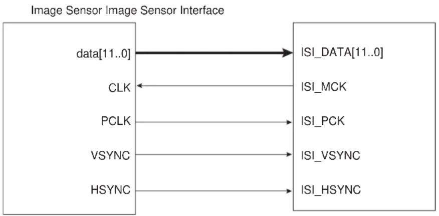
flowchart
graph LR
    A["data[11..0"]] --> B["ISI_DATA[11..0"]]
    C["CLK"] <--_D["ISI_MCK"]
    E["PCLK"] <--_F["ISI_PCK"]
    G["VSYNC"] <--_H["ISI_VSYNC"]
    I["HSYNC"] <--_J["ISI_HSYNC"]
36.2 Embedded Characteristics
- ITU-R BT. 601/656 8-bit Mode External Interface Support
• Supports up to 12-bit Grayscale CMOS Sensors - Support for ITU-R BT.656-4 SAV and EAV Synchronization
• Vertical and Horizontal Resolutions up to 2048 × 2048 - Preview Path up to 640 × 480 in RGB Mode
• Codec Path up to 2048 × 2048 - byte FIFO on Codec Path
- byte FIFO on Preview Path
- Support for Packed Data Formatting for YCbCr 4:2:2 Formats
- Preview Scaler to Generate Smaller Size image
- Programmable Frame Capture Rate
• VGA, QVGA, CIF, QCIF Formats Supported for LCD Preview - Custom Formats with Horizontal and Vertical Preview Size as Multiples of 16 Also Supported for LCD Preview
36.3 Block Diagram
Figure 36-2. ISI Block Diagram

flowchart
graph TD
    A["Hsync/Line enable Vsync/Frame enable"] --> B["Timing Signals Interface"]
    C["CMOS Sensor Pixel input up to 12 bits YCbCr 4:2:2 RGB 8:8:8 5:6:5"] --> D["CCIR-656 Embedded Timing Decoder(SAV/EAV)"]
    D --> E["Camera Interrupt Controller"]
    E --> F["Configuration Registers"]
    F --> G["APB Interface"]
    H["CMOS Sensor Pixel Clock input"] --> I["Pixel Sampling Module"]
    I --> J["Preview path"]
    J --> K["2-D Image Scaler"]
    K --> L["Pixel Formatter"]
    L --> M["Rx Direct Display FIFO"]
    M --> N["Core Video Arbiter"]
    N --> O["Camera AHB Host Interface Scatter Mode Support"]
    O --> P["AHB bus APB bus"]
    Q["From Rx buffers"] --> E
    R["Codec on"] --> S["Codec path"]
    T["Pixel Clock Domain"] --> U["2-D Image Scaler"]
    U --> V["Pixel Formatter"]
    V --> W["Rx Direct Display FIFO"]
    W --> X["Core Video Arbiter"]
    X --> O
    Y[" Cambodia Interrupt Request Line"] --> F
36.4 Product Dependencies
36.4.1 I/O Lines
The pins used for interfacing the compliant external devices can be multiplexed with PIO lines. The programmer must first program the PIO controllers to assign the ISI pins to their peripheral functions.
36.4.2 Power Management
The ISI can be clocked through the Power Management Controller (PMC), thus the programmer must first configure the PMC to enable the ISI clock.
36.4.3 Interrupt Sources
The ISI interface has an interrupt line connected to the interrupt controller. Handling the ISI interrupt requires programming the interrupt controller before configuring the ISI.
36.5 Functional Description
The Image Sensor Interface (ISI) supports direct connection to the ITU-R BT. 601/656 8-bit mode compliant sensors and up to 12-bit grayscale sensors. It receives the image data stream from the image sensor on the 12-bit data bus.
This module receives up to 12 bits for data, the horizontal and vertical synchronizations and the pixel clock. The reduced pin count alternative for synchronization is supported for sensors that embed SAV (start of active video) and EAV (end of active video) delimiters in the data stream.
The Image Sensor Interface interrupt line is connected to the Advanced Interrupt Controller and can trigger an interrupt at the beginning of each frame and at the end of a DMA frame transfer. If the SAV/EAV synchronization is used, an interrupt can be triggered on each delimiter event.
For 8-bit color sensors, the data stream received can be in several possible formats: YCbCr 4:2:2, RGB 8:8:8, RGB 5:6:5 and may be processed before the storage in memory. When the preview DMA channel is configured and enabled, the preview path is activated and an 'RGB frame' is moved to memory. The preview path frame rate is configured with the FRATE field of the ISI_CFG1 register. When the codec DMA channel is configured and enabled, the codec path is activated and a 'YCbCr 4:2:2 frame' is captured as soon as the ISI_CDC bit of the ISI Control Register (ISI_CR) is set.
When the FULL bit of the ISI_CFG1 register is set, both preview DMA channel and codec DMA channel can operate simultaneously. When a zero is written to the FULL bit of the ISI_CFG1 register, a hardware scheduler checks the FRATE field. If its value is zero, a preview frame is skipped and a codec frame is moved to memory instead. If its value is other than zero, at least one free frame slot is available. The scheduler postpones the codec frame to that free available frame slot.
The data stream may be sent on both preview path and codec path if the value of bit ISI_CDC in the ISI_CR is one. To optimize the bandwidth, the codec path should be enabled only when a capture is required.
In Grayscale mode, the input data stream is stored in memory without any processing. The 12-bit data, which represent the grayscale level for the pixel, is stored in memory one or two pixels per word, depending on the GS_MODE bit in the ISI_CFG2 register. The codec datapath is not available when grayscale image is selected.
A frame rate counter allows users to capture all frames or 1 out of every 2 to 8 frames.
36.5.1 Data Timing
36.5.1.1 VSYNC/HSYNC Data Timing
In the VSYNC/HSYNC synchronization, the valid data is captured with the active edge of the pixel clock (ISI_PCK), after SFD lines of vertical blanking and SLD pixel clock periods delay programmed in the ISI_CR.
The data timing using horizontal and vertical synchronization are shown in the following figure.
Figure 36-3. HSYNC and VSYNC Synchronization

text_image
Frame ISI_VSYNC 1 line ISI_HSYNC ISI_PCK Y06 Y07 Y08 Y09 Y10 Y11 ISI DATA[0]X_0X36.5.1.2 SAV/EAV Data Timing
The ITU-RBT.656-4 standard defines the functional timing for an 8-bit wide interface.
There are two timing reference signals, one at the beginning of each video data block SAV (0xFF000080) and one at the end of each video data block EAV (0xFF00009D). Only data sent between EAV and SAV is captured. Horizontal blanking and vertical blanking are ignored. Use of the SAV and EAV synchronization eliminates the ISI_VSYNC and ISI_HSYNC signals from the interface, thereby reducing the pin count. In order to retrieve both frame and line synchronization properly, at least one line of vertical blanking is mandatory.
The data timing using EAV/SAV sequence synchronization are shown in the following figure.
Figure 36-4. SAV and EAV Sequence Synchronization

text_image
ISII_PCK ISI_DATA[7..0] FF 0 00 80 Cb Y 00 D Cr Cb Cr Y C Y C FF 0 SAV EAVAActive Video36.5.2 Data Ordering
The RGB color space format is required for viewing images on a display screen preview, and the YCbCr color space format is required for encoding.
All the sensors do not output the YCbCr or RGB components in the same order. The ISI allows the user to program the same component order as the sensor, reducing software treatments to restore the right format.
Table 36-2. Data Ordering in YCbCr Mode
| Mode Byte 0 | Byte 1 | Byte 2 | Byte 3 | |
| Default | Cb(i) | Y(i) | Cr(i) | Y(i+1) |
| Mode 1 | Cr(i) | Y(i) | Cb(i) | Y(i+1) |
| Mode 2 | Y(i) | Cb(i) | Y(i+1) | Cr(i) |
| Mode 3 | Y(i) | Cr(i) | Y(i+1) | Cb(i) |
Table 36-3. RGB Format in Default Mode, RGB_CFG = 00, No Swap
| Mode Byte D7 | D6 | D5 | D4 | D3 | D2 | D1 | D0 | ||||||
| RGB 8:8:8 Byte | 0 | R7(i) | R6(i) | R5(i) | R4(i) | R3(i) | R2(i) | R1(i) | R0(i) | ||||
| Byte 1 | G7(i) | G6(i) | G5(i) | G4(i) | G3(i) | G2(i) | G1(i) | G0(i) | |||||
| Byte 2 | B7(i) | B6(i) | B5(i) | B4(i) | B3(i) | B2(i) | B1(i) | B0(i) | |||||
| Byte 3 | R7(i+1) | R6(i+1) | R5(i+1) | R4(i+1) | R3(i+1) | R2(i+1) | R1(i+1) | R0(i+1) | |||||
| RGB 5:6:5 Byte | 0 | R4(i) | R3(i) | R2(i) | R1(i) | R0(i) | G5(i) | G4(i) | G3(i) | ||||
| Byte 1 | G2(i) | G1(i) | G0(i) | B4(i) | B3(i) | B2(i) | B1(i) | B0(i) | |||||
| Byte 2 | R4(i+1) | R3(i+1) | R2(i+1) | R1(i+1) | R0(i+1) | G5(i+1) | G4(i+1) | G3(i+1) | |||||
| Byte 3 | G2(i+1) | G1(i+1) | G0(i+1) | B4(i+1) | B3(i+1) | B2(i+1) | B1(i+1) | B0(i+1) | |||||
Table 36-4. RGB Format, RGB_CFG = 10 (Mode 2), No Swap
| Mode Byte D7 | D6 | D5 | D4 | D3 | D2 | D1 | D0 | ||||||
| RGB 5:6:5 Byte | 0 | G2(i) | G1(i) | G0(i) | R4(i) | R3(i) | R2(i) | R1(i) | R0(i) | ||||
| Byte 1 | B4(i) | B3(i) | B2(i) | B1(i) | B0(i) | G5(i) | G4(i) | G3(i) | |||||
| Byte 2 | G2(i+1) | G1(i+1) | G0(i+1) | R4(i+1) | R3(i+1) | R2(i+1) | R1(i+1) | R0(i+1) | |||||
| Byte 3 | B4(i+1) | B3(i+1) | B2(i+1) | B1(i+1) | B0(i+1) | G5(i+1) | G4(i+1) | G3(i+1) | |||||
Table 36-5. RGB Format in Default Mode, RGB_CFG = 00, Swap Activated
| Mode Byte D7 | D6 | D5 | D4 | D3 | D2 | D1 | D0 | ||||||
| RGB 8:8:8 Byte | 0 | R0(i) | R1(i) | R2(i) | R3(i) | R4(i) | R5(i) | R6(i) | R7(i) | ||||
| Byte 1 | G0(i) | G1(i) | G2(i) | G3(i) | G4(i) | G5(i) | G6(i) | G7(i) | |||||
| Byte 2 | B0(i) | B1(i) | B2(i) | B3(i) | B4(i) | B5(i) | B6(i) | B7(i) | |||||
| Byte 3 | R0(i+1) | R1(i+1) | R2(i+1) | R3(i+1) | R4(i+1) | R5(i+1) | R6(i+1) | R7(i+1) | |||||
| RGB 5:6:5 Byte | 0 | G3(i) | G4(i) | G5(i) | R0(i) | R1(i) | R2(i) | R3(i) | R4(i) | ||||
| Byte 1 | B0(i) | B1(i) | B2(i) | B3(i) | B4(i) | G0(i) | G1(i) | G2(i) | |||||
| Byte 2 | G3(i+1) | G4(i+1) | G5(i+1) | R0(i+1) | R1(i+1) | R2(i+1) | R3(i+1) | R4(i+1) | |||||
| Byte 3 | B0(i+1) | B1(i+1) | B2(i+1) | B3(i+1) | B4(i+1) | G0(i+1) | G1(i+1) | G2(i+1) | |||||
The RGB 5:6:5 input format is processed to be displayed as RGB 5:6:5 format, compliant with the 16-bit mode of the LCD controller.
36.5.3 Clocks
The sensor Host clock (ISI_MCK) can be generated either by the Power Management Controller (PMC) through a Programmable Clock output (using PID=59) or by an external oscillator connected to the sensor.
None of the sensors embed a power management controller, so providing the clock by the APMC is a simple and efficient way to control power consumption of the system.
Care must be taken when programming the system clock. The ISI has two clock domains, the sensor Host clock and the pixel clock provided by sensor. The two clock domains are not synchronized, but the sensor Host clock must be faster than the pixel clock.
36.5.4 Preview Path
36.5.4.1 Scaling, Decimation (Subsampling)
This module resizes captured 8-bit color sensor images to fit the LCD display format. The resize module performs only downscaling. The same ratio is applied for both horizontal and vertical resize, then a fractional decimation algorithm is applied.
The decimation factor is a multiple of 1/16; values 0 to 15 are forbidden.
Table 36-6. Decimation Factor
| Decimation Value 0-15 16 17 18 19 ... 124 125 126 127 | ||||||
| Decimation Factor — 1 1.063 1.125 1.188 ... 7.750 7.813 7.875 7.938 | ||||||
Table 36-7. Decimation and Scaler Offset Values
| OUTPUT INPUT | 352 × 28 | 640 × 480 | 800 × 600 | 1280 × 1024 | 1600 × 1200 | 2048 × 1536 | ||
| VGA640 × 480 | F | — | 16 | 20 | 32 | 40 | 51 | |
| QVGA320 × 240 | F | 16 | 32 | 40 | 64 | 80 | 102 | |
| CIF352 × 288 | F | 16 | 26 | 33 | 56 | 66 | 85 | |
| QCIF176 × 144 | F | 32 | 53 | 66 | 113 | 133 | 170 |
Example:
Input 1280 × 1024 Output = 640 × 480
Hratio = 1280/640 = 2
Vratio = 1024/480 = 2.1333
The decimation factor is 2 so 32/16.
Figure 36-5. Resize Examples
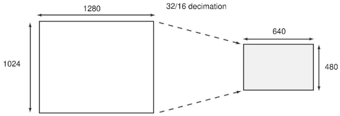
geo
| Dimension | Value | | ----------------- | ----- | | Base | 1024 | | 32/16 decimation | 1280 | | Total Height | 480 | | Height (Top) | 640 |
geo
| Dimension | Value | | ----------------- | ----- | | Upper Left Square | 1280 | | Lower Left Square | 1024 | | Middle Right Square | 352 | | Lower Right Square | 288 |36.5.4.2 Color Space Conversion
This module converts YCrCb or YUV pixels to RGB color space. Clipping is performed to ensure that the samples value do not exceed the allowable range. The conversion matrix is defined below and is fully programmable:
$$ \left[ \begin{array}{l} R \ G \ B \end{array} \right] = \left[ \begin{array}{c c c} C _ {0} & 0 C & 1 \ C _ {0} & - C _ {2} & - C _ {3} \ C _ {0} & C _ {4} & 0 \end{array} \right] \times \left[ \begin{array}{l} Y - Y _ {\text {off}} \ C _ {b} - C _ {\text {boff}} \ C _ {r} - C _ {\text {roff}} \end{array} \right] $$
Example of programmable value to convert YCrCb to RGB:
$$ \left{ \begin{array}{l l} R = 1. 1 6 4 \cdot Y - (1 6 + 1. 5) 9 6 \cdot C & \quad (r - 1 2 8) \ G = 1. 1 6 4 \cdot Y - (1 6 - 0. 8) 1 3 \cdot C & \quad (r - 1 2 8) 0. 3 9 2 \cdot C (b - 1 2 8) \ B = 1. 1 6 4 \cdot Y - (1 6 + 2. 1) 0 7 \cdot C & \quad (b - 1 2 8) \end{array} \right. $$
An example of programmable value to convert from YUV to RGB:
$$ \left{ \begin{array}{l} R = Y + 1. 5 9 6 \cdot V \ G = Y - 0. 3 9 4 \cdot U - 0. 4 3 6 \cdot V \ B = Y + 2. 0 3 2 \cdot U \end{array} \right. $$
36.5.4.3 Memory Interface
36.5.4.3.1 RGB Mode
The preview datapath contains a data formatter that converts 8:8:8 pixel to RGB 5:6:5 format compliant with the 16-bit format of the LCD controller. In general, when converting from a color channel with more bits to one with fewer bits, the formatter module discards the lower-order bits.
For example, converting from RGB 8:8:8 to RGB 5:6:5, the formatter module discards the three LSBs from the red and blue channels, and two LSBs from the green channel.
36.5.4.3.2 12-bit Grayscale Mode
ISI_DATA[11:0] is the physical interface to the ISI. These bits are sampled and written to memory.
When 12-bit Grayscale mode is enabled, two memory formats are supported:
ISI_CFG2.GS_MODE = 0: two pixels per word
ISI_CFG2.GS_MODE = 1: one pixel per word
The following tables illustrate the memory mapping for the two formats.
If ISI_CFG1.GRAYLE = 0, the pixels map as follows:
Table 36-8. Grayscale Memory Mapping Configuration for 12-bit Data (ISI_CFG2.GS_MODE = 0: two pixels per word)
| 31 30 29 28 27 26 25 24 | ||||||
| Pixel 0 [11:4] | ||||||
| 23 22 21 20 19 18 17 16 | ||||||
| Pixel 0 [3:0] - - - - | ||||||
| 15 14 13 12 11 10 9 8 | ||||||
| Pixel 1 [11:4] | ||||||
| 7 6 5 4 3 2 1 0 | ||||||
| Pixel 1 [3:0] - - - - | ||||||
If ISI_CFG1.GRAYLE=1, the pixels map as follows:
Table 36-9. Grayscale Memory Mapping Configuration for 12-bit Data (ISI_CFG2.GS_MODE = 0: two pixels per word)
| 31 30 29 28 27 26 25 24 | ||||||
| Pixel 1 [11:4] | ||||||
| 23 22 21 20 19 18 17 16 | ||||||
| Pixel 1 [3:0] - - - - | ||||||
| 15 14 13 12 11 10 9 8 | ||||||
| Pixel 0 [11:4] | ||||||
| 7 6 5 4 3 2 1 0 | ||||||
| Pixel 0 [3:0] - - - - | ||||||
Table 36-10. Grayscale Memory Mapping Configuration for 12-bit Data (ISI_CFG2.GS_MODE = 1: one pixel per word)
| 31 30 29 28 27 | 26 25 24 | ||||||
| Pixel 0 [11:4] | |||||||
| 23 22 21 20 19 | 18 17 16 | ||||||
| Pixel 0 [3:0] - - - - | |||||||
| 15 14 13 12 11 | 10 9 8 | ||||||
| - - - - - - - | |||||||
| 7 6 5 4 3 2 1 0 | |||||||
| - - - - - - - | |||||||
36.5.4.3.3 8-bit Grayscale Mode
For 8-bit Grayscale mode, ISI_DATA[7:0] on the 12-bit data bus is the physical interface to the ISI. These bits are sampled and written to memory.
To enable 8-bit Grayscale mode, configure ISI_CFG2 as follows:
- Clear ISI_CFG2.GRAYSCALE.
- Clear ISI_CFG2.RGB_SWAP.
- Clear ISI_CFG2.COL_SPACE.
- Configure the field ISI_CFG2.YCC_SWAP to value 0.
- Configure the field ISI_CFG2.IM_VSIZE with the vertical resolution of the image minus 1.
- Configure the field ISI_CFG2.IM_HSIZE with the horizontal resolution of the image divided by 2. The horizontal resolution must be a multiple of 2.
The codec datapath is used to capture the 8-bit grayscale image. Use the following configuration:
- Set ISI_DMA_C_CTRL.C_FETCH.
- Configure ISI_DMA_C_DSCR.C_DSCR with the descriptor address.
- Write a one to the bit ISI_DMA_CHER.C_CH_EN.
Table 36-11. Memory Mapping for 8-bit Grayscale Mode
| 31 30 29 28 27 | 26 25 24 | ||||||
| Pixel 3 | |||||||
| 23 22 21 20 19 | 18 17 16 | ||||||
| Pixel 2 | |||||||
| 15 14 13 12 11 | 10 9 8 | ||||||
Pixel 1
76543210
Pixel 0
36.5.4.4 FIFO and DMA Features
Both preview and codec datapaths contain FIFOs. These asynchronous buffers are used to safely transfer formatted pixels from the pixel clock domain to the AHB clock domain. A video arbiter is used to manage FIFO thresholds and triggers a relevant DMA request through the AHB Host interface. Thus, depending on the FIFO state, a specified length burst is asserted. Regarding AHB Host interface, it supports Scatter DMA mode through linked list operation. This mode of operation improves flexibility of image buffer location and allows the user to allocate two or more frame buffers. The destination frame buffers are defined by a series of Frame Buffer Descriptors (FBD). Each FBD controls the transfer of one entire frame and then optionally loads a further FBD to switch the DMA operation at another frame buffer address. The FBD is defined by a series of three words. The first word defines the current frame buffer address (named DMA_X_ADDR register), the second defines control information (named DMA_X_CTRL register) and the third defines the next descriptor address (named DMA_X_DSCR). DMA Transfer mode with linked list support is available for both codec and preview datapaths. The data to be transferred described by an FBD requires several burst accesses. In the following example, the use of two ping-pong frame buffers is described.
Example:
The first FBD, stored at address 0x00030000, defines the location of the first frame buffer. This address is programmed in the ISI user interface DMA_P_DSCR. To enable the descriptor fetch operation, the value 0x00000001 must be written to the DMA_P_CTRL register. LLI_0 and LLI_1 are the two descriptors of the linked list.
Destination address: frame buffer ID0 0x02A000 (LLI_0.DMA_P_ADDR)
Transfer 0 Control Information, fetch and writeback: 0x00000003 (LLI_0.DMA_P_CTRL)
Next FBD address: 0x00030010 (LLI_0.DMA_P_DSCR)
The second FBD, stored at address 0x00030010, defines the location of the second frame buffer.
Destination address: frame buffer ID1 0x0003A000 (LLI_1.DMA_P_ADDR)
Transfer 1 Control information fetch and writeback: 0x00000003 (LLI_1.DMA_P_CTRL)
The third FBD address: 0x00030000, wrapping to first FBD (LLI_1.DMA_P_DSCR)
Using this technique, several frame buffers can be configured through the linked list. The following figure illustrates a typical three-frame buffer application. Frame n is mapped to frame buffer 0, frame n+1 is mapped to frame buffer 1, frame n+2 is mapped to frame buffer 2 and further frames wrap. A codec request occurs, and the full-size 4:2:2 encoded frame is stored in a dedicated memory space.
Figure 36-6. Three Frame Buffers Application and Memory Mapping
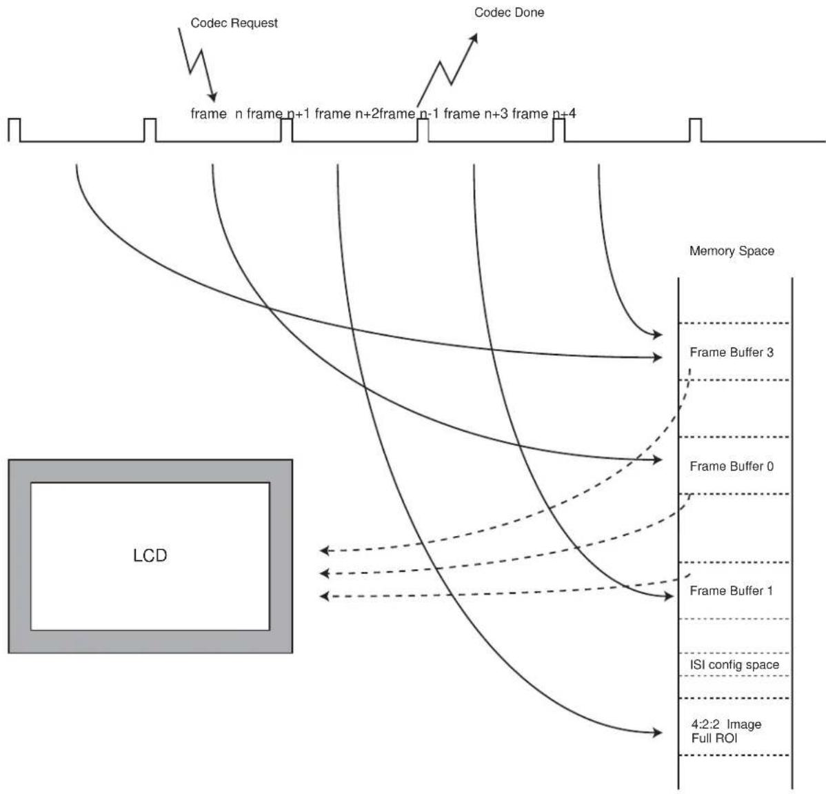
flowchart
graph TD
    A["Codec Request"] --> B["frame n frame n+1"]
    B --> C["frame n+2frame n-1"]
    C --> D["frame n+3 frame n+4"]
    E["Codec Done"] --> F["Frame Buffer 0"]
    F --> G["Frame Buffer 1"]
    G --> H["ISI config space"]
    H --> I["4:2:2 Image Full ROI"]
    J["Memory Space"] --> K["Frame Buffer 3"]
    K --> L["Frame Buffer 0"]
    L --> M["Frame Buffer 1"]
    M --> N["LCD"]
36.5.5 Codec Path
36.5.5.1 Color Space Conversion
Depending on user selection, this module can be bypassed so that input YCrCb stream is directly connected to the format converter module. If the RGB input stream is selected, this module converts RGB to YCrCb color space with the formulas given below:
$$ \left[ \begin{array}{l} Y \ C _ {r} \ C _ {b} \end{array} \right] = \left[ \begin{array}{c c c} C _ {0} & C _ {1} & C _ {2} \ C _ {3} & - C _ {4} & - C _ {5} \ - C _ {6} & - C _ {7} & C _ {8} \end{array} \right] \times \left[ \begin{array}{l} R \ G \ B \end{array} \right] + \left[ \begin{array}{l} Y _ {\text {off}} \ \mathrm{Cr} _ {\text {off}} \ \mathrm{Cb} _ {\text {off}} \end{array} \right] $$
An example of coefficients is given below:
$$ \left{ \begin{array}{l} Y = 0. 2 5 7 \cdot R + 0. 5 0 4 \cdot G + 0. 0 9 8 \cdot B + 1 6 \ C _ {r} = 0. 4 3 9 \cdot R - 0. 3 6 8 \cdot G - 0. 0 7 1 \cdot B + 1 2 8 \ C _ {b} = - 0. 1 4 8 \cdot R - 0. 2 9 1 \cdot G + 0. 4 3 9 \cdot B + 1 2 8 \end{array} \right. $$
36.5.5.2 Memory Interface
Dedicated FIFOs are used to support packed memory mapping. YCrCb pixel components are sent in a single 32-bit word in a contiguous space (packed). Data is stored in the order of natural scan lines. Planar mode is not supported.
36.5.5.3 DMA Features
Like preview datapath, codec datapath DMA mode uses linked list operation.
36.6 Register Summary
Note: Several parts of the ISI controller use the pixel clock provided by the image sensor (ISI_PCK). Thus the user must first program the image sensor to provide this clock (ISI_PCK) before programming the Image Sensor Controller.
| Offset | Name Bit Pos. 7 | 6 | 5 | 4 | 3 | 2 | 1 | 0 | ||||||||||||||||||||||||||||||||||||||||||||||||||||||||||||||||||||||||||||||||||||||||||||||||||||||||||||||||||||||||||||||||||||||||||||||||||||||||||||||||||||||||||||||||||||||||||||||||||||||||||||||||||||||||||||||||||||||||||||||||||||||||||||||||||||||||||||||||||||||||||||||||||||||||||||||||||||||||||||||||||||||||||||||||||||||||||||||||||||||||||||||||||||||||||||||||||||||||||||
| 0x00 ISI_CFG1 | 7:0 CRC_SYNC EMB_SYNC GRAYLE PIXCLK_POL VSYNC_POL HSYNC_POL | |||||||||||||||||||||||||||||||||||||||||||||||||||||||||||||||||||||||||||||||||||||||||||||||||||||||||||||||||||||||||||||||||||||||||||||||||||||||||||||||||||||||||||||||||||||||||||||||||||||||||||||||||||||||||||||||||||||||||||||||||||||||||||||||||||||||||||||||||||||||||||||||||||||||||||||||||||||||||||||||||||||||||||||||||||||||||||||||||||||||||||||||||||||||||||||||||||||||||||||||||||
| 15:8 THMASK[1:0] FULL DISCR | 0 | |||||||||||||||||||||||||||||||||||||||||||||||||||||||||||||||||||||||||||||||||||||||||||||||||||||||||||||||||||||||||||||||||||||||||||||||||||||||||||||||||||||||||||||||||||||||||||||||||||||||||||||||||||||||||||||||||||||||||||||||||||||||||||||||||||||||||||||||||||||||||||||||||||||||||||||||||||||||||||||||||||||||||||||||||||||||||||||||||||||||||||||||||||||||||||||||||||||||||||||||||||
| 23:16 SLD[7:0] | ||||||||||||||||||||||||||||||||||||||||||||||||||||||||||||||||||||||||||||||||||||||||||||||||||||||||||||||||||||||||||||||||||||||||||||||||||||||||||||||||||||||||||||||||||||||||||||||||||||||||||||||||||||||||||||||||||||||||||||||||||||||||||||||||||||||||||||||||||||||||||||||||||||||||||||||||||||||||||||||||||||||||||||||||||||||||||||||||||||||||||||||||||||||||||||||||||||||||||||||||||||
| 31:24 RGB_CFG[1:0] YCC_SWAP[1:0] IM_HSIZE[10:8] | ||||||||||||||||||||||||||||||||||||||||||||||||||||||||||||||||||||||||||||||||||||||||||||||||||||||||||||||||||||||||||||||||||||||||||||||||||||||||||||||||||||||||||||||||||||||||||||||||||||||||||||||||||||||||||||||||||||||||||||||||||||||||||||||||||||||||||||||||||||||||||||||||||||||||||||||||||||||||||||||||||||||||||||||||||||||||||||||||||||||||||||||||||||||||||||||||||||||||||||||||||||
......continued
| Offset | Name Bit Pos. 76543210 | |||||||||
| 0x34 ISI_IMR | 7:0 | SRST DIS_DONE | ||||||||
| 15:8 | VSYNC | |||||||||
| 23:16 | CXFR_DONE PXFR_DONE | |||||||||
| 31:24 | FR_OVR | CRC_ERR | C_OVR | P_OVR | ||||||
| 0x38 | ISI_DMA_CHER | 7:0 | C_CH_EN | P_CH_EN | ||||||
| 15:8 | ||||||||||
| 23:16 | ||||||||||
| 31:24 | ||||||||||
| 0x3C | ISI_DMA_CHDR | 7:0 | C_CH_DIS | P_CH_DIS | ||||||
| 15:8 | ||||||||||
| 23:16 | ||||||||||
| 31:24 | ||||||||||
| 0x40 | ISI_DMA_CHSR | 7:0 | C_CH_S | P_CH_S | ||||||
| 15:8 | ||||||||||
| 23:16 | ||||||||||
| 31:24 | ||||||||||
| 0x44 | ISI_DMA_P_ADDR | 7:0 | P_ADDR[5:0] | |||||||
| 15:8 | P_ADDR[13:6] | |||||||||
| 23:16 | P_ADDR[21:14] | |||||||||
| 31:24 | P_ADDR[29:22] | |||||||||
| 0x48 | ISI_DMA_P_CTRL | 7:0 | P_DONE | P_IEN | P_WB | P_FETCH | ||||
| 15:8 | ||||||||||
| 23:16 | ||||||||||
| 31:24 | ||||||||||
| 0x4C | ISI_DMA_P_DSCR | 7:0 | P_DSCR[5:0] | |||||||
| 15:8 | P_DSCR[13:6] | |||||||||
| 23:16 | P_DSCR[21:14] | |||||||||
| 31:24 | P_DSCR[29:22] | |||||||||
| 0x50 | ISI_DMA_C_ADDR | 7:0 | C_ADDR[5:0] | |||||||
| 15:8 | C_ADDR[13:6] | |||||||||
| 23:16 | C_ADDR[21:14] | |||||||||
| 31:24 | C_ADDR[29:22] | |||||||||
| 0x54 | ISI_DMA_C_CTRL | 7:0 | C_DONE | C_IEN | C_WB | C_FETCH | ||||
| 15:8 | ||||||||||
| 23:16 | ||||||||||
| 31:24 | ||||||||||
| 0x58 | ISI_DMA_C_DSCR | 7:0 | C_DSCR[5:0] | |||||||
| 15:8 | C_DSCR[13:6] | |||||||||
| 23:16 | C_DSCR[21:14] | |||||||||
| 31:24 | C_DSCR[29:22] | |||||||||
| 0x5C ... 0xE3 | Reserved | |||||||||
| 0xE4 | ISI_WPMR | 7:0 | WPEN | |||||||
| 15:8 | WPKEY[7:0] | |||||||||
| 23:16 | WPKEY[15:8] | |||||||||
| 31:24 | WPKEY[23:16] | |||||||||
| 0xE8 ISI_WPSR | 7:0 | WPVS | ||||||||
| 15:8 | WPVSRC[7:0] | |||||||||
| 23:16 | WPVSRC[15:8] | |||||||||
| 31:24 | ||||||||||
36.6.1 ISI Configuration 1 Register
Name: ISI_CFG1
Offset: 0x00
Reset: 0x00000000
Property: Read/Write
| Bit 31 30 29 28 27 26 25 24 | |||||||
| SFD[7:0] | |||||||
| Access R/W R/W R/W R/W R/W R/W R/W R/W Reset 0 0 0 0 0 0 0 0 | |||||||
| Bit 23 22 21 20 19 18 17 16 | |||||||
| SLD[7:0] | |||||||
| Access R/W R/W R/W R/W R/W R/W R/W R/W Reset 0 0 0 0 0 0 0 0 | |||||||
| Bit 15 14 13 12 11 10 9 8 | |||||||
| THMASK[1:0] FULL DISCR FRATE[2:0] | |||||||
| Access R/W R/W R/W R/W R/W R/W R/W R/W Reset 0 0 0 0 0 0 0 | |||||||
| Bit 7 6 5 4 3 2 1 0 | |||||||
| CRC_SYNC | EMB_SYNC | GRAYLE | PIXCLK_POL | VSYNC_POL | HSYNC_POL | ||
| Access R/W R/W R/W R/W R/W R/W Reset 0 0 0 0 0 0 | |||||||
Bits 31:24 - SFD[7:0] Start of Frame Delay
SFD lines are skipped at the beginning of the frame.
Bits 23:16 - SLD[7:0] Start of Line Delay
SLD pixel clock periods to wait before the beginning of a line.
Bits 14:13 - THMASK[1:0] Threshold Mask
| Value | Name | Description |
| 0 | BEATS_4 | Only 4 beats AHB burst allowed |
| 1 | BEATS_8 | Only 4 and 8 beats AHB burst allowed |
| 2 | BEATS_16 | 4, 8 and 16 beats AHB burst allowed |
Bit 12 - FULL Full Mode is Allowed
| Value | Description |
| 0 | The codec frame is transferred to memory when an available frame slot is detected. |
| 1 | Both preview and codec DMA channels are operating simultaneously. |
Bit 11 - DISCR Disable Codec Request
| Value | Description |
| 0 | Codec datapath DMA interface requires a request to restart. |
| 1 | Codec datapath DMA automatically restarts. |
Bits 10:8 - FRATE[2:0] Frame Rate [0..7]
| Value | Description |
| 0 | All the frames are captured, else one frame every FRATE + 1 is captured. |
Bit 7 - CRC_SYNC Embedded Synchronization Correction
| Value Description | |
| 0 | No CRC correction is performed on embedded synchronization. |
| 1 | CRC correction is performed. If the correction is not possible, the current frame is discarded and the CRC_ERR bit is set in the ISI_SR. |
Bit 6 - EMB_SYNC Embedded Synchronization
| Value Description | |
| 0 | Synchronization by HSYNC, VSYNC. |
| 1 | Synchronization by embedded synchronization sequence SAV/EAV. |
Bit 5 - GRAYLE Grayscale Little Endian
Refer to Table 36-8 and Table 36-9 for details.
| Value Description | |
| 0 | The two pixels are represented in big-endian format within a 32-bit register. |
| 1 | The two pixels are represented in little-endian format within a 32-bit register. |
Bit 4 - PIXCLK_POL Pixel Clock Polarity
| Value Description | |
| 0 | Data is sampled on rising edge of pixel clock. |
| 1 | Data is sampled on falling edge of pixel clock. |
Bit 3 - VSYNC_POL Vertical Synchronization Polarity
| Value Description | |
| 0 | VSYNC active high. |
| 1 | VSYNC active low. |
Bit 2 - HSYNC_POL Horizontal Synchronization Polarity
| Value Description | |
| 0 | HSYNC active high. |
| 1 | HSYNC active low. |
36.6.2 ISI Configuration 2 Register
Name: ISI_CFG2
Offset: 0x04
Reset: 0x00000000
Property: Read/Write
Bit 31 30 29 28 27 26 25 24
| RGB_CFG[1:0] YCC_SWAP[1:0] IM_HSIZE[10:8] | ||||||||
| Access | R/W | R/W | R/W | R/W R/W R/W R/W | ||||
| Reset | 0 | 0 | 0 | 0 | 0 | 0 | 0 | 0 |
Bit 23 22 21 20 19 18 17 16
| IM_HSIZE[7:0] | ||||||||
| Access | R/W | R/W | R/W | R/W | R/W | R/W | R/W | R/W |
| Reset | 0 | 0 | 0 | 0 | ||||
Bit 15 14 13 12 11 10 9 8
| COL_SPACE | RGB_SWAP | GRAYSCALE | RGB_MODE | GS_MODE | IM_VSIZE[10:8] | |||
| Access Reset | R/W R/W | R/W R/W | R/W R/W | R/W R/W | R/W | 0 | 0 | 0 |
| 0 | 0 | 0 | 0 | 0 | 0 | 0 | 0 | |
| Bit | 7 | 6 | 5 | 4 | 3 | 2 | 1 | 0 |
| IM_VSIZE[7:0] | ||||||||
| Access Reset | R/W R/W | R/W R/W | R/W R/W | R/W R/W | R/W | 0 | 0 | 0 |
| 0 | 0 | 0 | 0 | 0 | 0 | 0 | 0 | |
Bits 31:30 - RGB\_CFG[1:0] RGB Pixel Mapping Configuration
Defines RGB pattern when RGB_MODE is set to 1.
If RGB_MODE is set to RGB 8:8:8, then RGB_CFG = 0 implies RGB color sequence, else it implies BGR color sequence.
If 8-bit Grayscale mode is enabled, IM_HSIZE = (Horizontal size/2) - 1.
Else IM_HSIZE = Horizontal size - 1.
Bit 15 - COL_SPACE Color Space for the Image Data
| Value Description | |
| 0 | YCbCr. |
| 1 | RGB. |
Bit 14 - RGB_SWAP RGB Format Swap Mode
The RGB_SWAP has no effect when Grayscale mode is enabled.
| Value Description | |
| 0 | D7 → R7. |
| 1 | D0 → R7. |
Bit 13 - GRAYSCALE Grayscale Mode Format Enable
| Value Description | |
| 0 | Grayscale mode is disabled. |
| 1 | Input image is assumed to be grayscale-coded. |
Bit 12 - RGB_MODE RGB Input Mode
| Value Description | |
| 0 | RGB 8:8:8 24 bits. |
| 1 | RGB 5:6:5 16 bits. |
Bit 11 - GS_MODE Grayscale Pixel Format Mode
| Value Description | |
| 0 | 2 pixels per word. |
| 1 | 1 pixel per word. |
Bits 10:0 - IM_VSIZE[10:0] Vertical Size of the Image Sensor [0..2047]
IM_VSIZE = Vertical size - 1
36.6.3 ISI Preview Size Register
Name: ISI_PSIZE
Offset: 0x08
Reset: 0x00000000
Property: Read/Write

text_image
Bit 31 30 29 28 27 26 25 24 PREV_HSIZE[9:8] R/W R/W Access Reset 0 0 Bit 23 22 21 20 19 18 17 16 PREV_HSIZE[7:0] Access R/W R/W R/W R/W R/W R/W R/W Reset 0 0 0 0 0 0 0 0 Bit 15 14 13 12 11 10 9 8 PREV_VSIZE[9:8] R/W R/W Access Reset 0 0 Bit 7 6 5 4 3 2 1 0 PREV_VSIZE[7:0] Access R/W R/W R/W R/W R/W R/W R/W Reset 0 0 0 0 0 0 0 0Bits 25:16 - PREV_HSIZE[9:0] Horizontal Size for the Preview Path
PREV_HSIZE = Horizontal Preview size - 1 (640 max only in RGB mode).
Bits 9:0 - PREV_VSIZE[9:0] Vertical Size for the Preview Path
PREV_VSIZE = Vertical Preview size - 1 (480 max only in RGB mode).
36.6.4 ISI Preview Decimation Factor Register
Name: ISI_PDECF
Offset: 0x0C
Reset: 0x00000010
Property: Read/Write
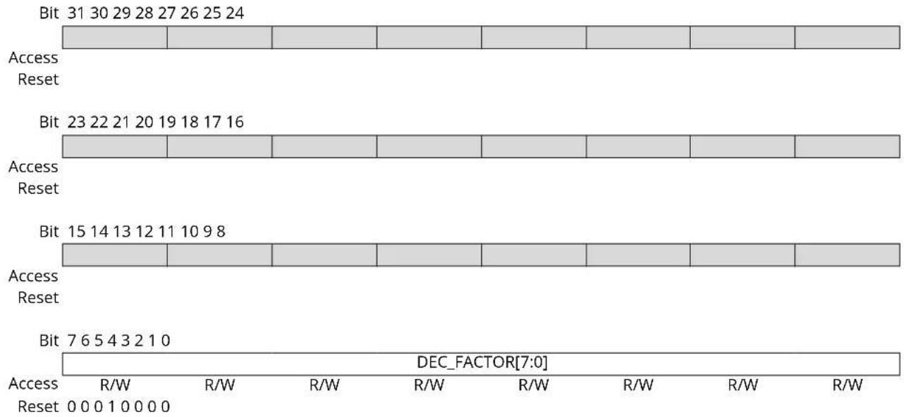
bar_stacked
| Bit | Access Reset | DEC_FACTOR[7:0] | | --- | --- | --- | | 31 | 0 | R/W | | 30 | 0 | R/W | | 29 | 0 | R/W | | 28 | 0 | R/W | | 27 | 0 | R/W | | 26 | 0 | R/W | | 25 | 0 | R/W | | 24 | 0 | R/W | | 23 | 0 | R/W | | 22 | 0 | R/W | | 21 | 0 | R/W | | 20 | 0 | R/W | | 19 | 0 | R/W | | 18 | 0 | R/W | | 17 | 0 | R/W | | 16 | 0 | R/W | | 15 | 0 | R/W | | 14 | 0 | R/W | | 13 | 0 | R/W | | 12 | 0 | R/W | | 11 | 0 | R/W | | 10 | 0 | R/W | | 9 | 0 | R/W | | 8 | 0 | R/W | | 7 | 0 | R/W | | 6 | 0 | R/W | | 5 | 0 | R/W | | 4 | 0 | R/W | | 3 | 0 | R/W | | 2 | 0 | R/W | | 1 | 0 | R/W | | 0 | 0 | R/W | | 1 | 0 | R/W | | 2 | 0 | R/W | | 3 | 0 | R/W | | 4 | 0 | R/W | | 5 | 0 | R/W | | 6 | 0 | R/W | | 7 | 0 | R/W | | 8 | 0 | R/W | | 9 | 0 | R/W | | 10 | 0 | R/W | | 11 | 0 | R/W | | 12 | 0 | R/W | | 13 | 0 | R/W | | 14 | 0 | R/W | | 15 | 0 | R/W | | 16 | 0 | R/W | | 17 | 0 | R/W | | 18 | 0 | R/W | | 19 | 0 | R/W | | 20 | 0 | R/W | | 21 | 0 | R/W | | 22 | 0 | R/W | | 23 | 0 | R/W | | 24 | 0 | R/W | | 25 | 0 | R/W | | 26 | 0 | R/W | | 27 | 0 | R/W | | 28 | 0 | R/W | | Note: The actual values for 'Access Reset' and 'DEC_FACTOR[7:0]' are not provided in the code. The actual values are not explicitly labeled on the chart.Bits 7:0 - DEC_FACTOR[7:0] Decimation Factor
DEC_FACTOR is 8-bit width, range is from 16 to 255. Values from 0 to 16 do not perform any decimation.
36.6.5 ISI Color Space Conversion YCrCb to RGB Set 0 Register
Name: ISI_Y2R_SET0
Offset: 0x10
Reset: 0x6832CC95
Property: Read/Write
| Bit 31 30 29 28 27 26 25 24 | |
| C3[7:0] | |
| Access R/W R/W R/W R/W R/W R/W R/W R/W Reset 0 1 1 0 1 0 0 0 | |
| Bit 23 22 21 20 19 18 17 16 | |
| C2[7:0] | |
| Access R/W R/W R/W R/W R/W R/W R/W R/W Reset 0 0 1 1 0 0 1 0 | |
| Bit 15 14 13 12 11 10 9 8 | |
| C1[7:0] | |
| Access R/W R/W R/W R/W R/W R/W R/W R/W Reset 1 1 0 0 1 1 0 0 | |
| Bit 7 6 5 4 3 2 1 0 | |
| C0[7:0] | |
| Access R/W R/W R/W R/W R/W R/W R/W R/W Reset 1 0 0 1 0 1 0 1 | |
Bits 31:24 - C3[7:0] Color Space Conversion Matrix Coefficient C3 C3 element default step is 1/128, ranges from 0 to 1.9921875.
Bits 23:16 - C2[7:0] Color Space Conversion Matrix Coefficient C2 C2 element default step is 1/128, ranges from 0 to 1.9921875.
Bits 15:8 - C1[7:0] Color Space Conversion Matrix Coefficient C1 C1 element default step is 1/128, ranges from 0 to 1.9921875.
Bits 7:0 - C0[7:0] Color Space Conversion Matrix Coefficient C0 C0 element default step is 1/128, ranges from 0 to 1.9921875.
36.6.6 ISI Color Space Conversion YCrCb to RGB Set 1 Register
Name: ISI_Y2R_SET1
Offset: 0x14
Reset: 0x00007102
Property: Read/Write

text_image
Bit 31 30 29 28 27 26 25 24 Access Reset Bit 23 22 21 20 19 18 17 16 Access Reset Bit 15 14 13 12 11 10 9 8 Access Reset Cboff Croff Yoff C4[8] R/W R/W R/W R/W R/W 1 Access Reset 1 1 1 Bit 7 6 5 4 3 2 1 0 C4[7:0] Access Reset R/W R/W R/W R/W R/W R/W R/W 0 0 0 0 0 0 1 0Bit 14 - Cboff Color Space Conversion Blue Chrominance Default Offset
| Value | Description |
| 0 | No offset. |
| 1 | Offset = 16. |
Bit 13 - Croff Color Space Conversion Red Chrominance Default Offset
| Value | Description |
| 0 | No offset. |
| 1 | Offset = 16. |
Bit 12 - Yoff Color Space Conversion Luminance Default Offset
| Value | Description |
| 0 | No offset. |
| 1 | Offset = 128. |
Bits 8:0 - C4[8:0] Color Space Conversion Matrix Coefficient C4
C4 element default step is 1/128, ranges from 0 to 3.9921875.
36.6.7 ISI Color Space Conversion RGB to YCrCb Set 0 Register
Name: ISI_R2Y_SET0
Offset: 0x18
Reset: 0x01324145
Property: Read/Write
| Bit 31 30 29 28 27 26 25 24 | |||||||
| Roff | |||||||
| Access Reset 1 | R/W | ||||||
| Bit 23 22 21 20 19 18 17 16 | |||||||
| C2[6:0] | |||||||
| Access Reset | R/W R/W R/W R/W R/W R/W R/W | ||||||
| 0 | 1 | 1 | 0 | 0 | 1 | 0 | |
| Bit 15 14 13 12 11 10 | 9 | 8 | |||||
| C1[6:0] | |||||||
| Access Reset | R/W R/W R/W R/W R/W R/W R/W | ||||||
| 1 | 0 | 0 | 0 | 0 | 0 | 1 | |
| Bit 7 | 6 | 5 | 4 | 3 | 2 | 1 | 0 |
| C0[6:0] | |||||||
| Access Reset | R/W R/W R/W R/W R/W R/W R/W | ||||||
| 1 | 0 | 0 | 0 | 1 | 0 | 1 | |
Bit 24 - Roff Color Space Conversion Red Component Offset
| Value | Description |
| 0 | No offset |
| 1 | Offset = 16 |
Bits 22:16 - C2[6:0] Color Space Conversion Matrix Coefficient C2 C2 element default step is 1/512, from 0 to 0.2480468875.
Bits 14:8 - C1[6:0] Color Space Conversion Matrix Coefficient C1 C1 element default step is 1/128, from 0 to 0.9921875.
Bits 6:0 - C0[6:0] Color Space Conversion Matrix Coefficient C0 C0 element default step is 1/256, from 0 to 0.49609375.
36.6.8 ISI Color Space Conversion RGB to YCrCb Set 1 Register
Name: ISI_R2Y_SET1
Offset: 0x1C
Reset: 0x01245E38
Property: Read/Write
| Bit 31 30 29 28 27 26 25 24 | |||||||
| Goff | |||||||
| Access Reset 1 | R/W | ||||||
| Bit 23 22 21 20 19 18 17 16 | |||||||
| C5[6:0] | |||||||
| Access Reset | R/W R/W R/W R/W R/W R/W R/W | ||||||
| 0 | 1 | 0 | 0 | 1 | 0 | 0 | |
| Bit 15 14 13 12 11 10 | 9 | 8 | |||||
| C4[6:0] | |||||||
| Access Reset | R/W R/W R/W R/W R/W R/W R/W | ||||||
| 1 | 0 | 1 | 1 | 1 | 1 | 0 | |
| Bit 7 | 6 | 5 | 4 | 3 | 2 | 1 | 0 |
| C3[6:0] | |||||||
| Access Reset | R/W R/W R/W R/W R/W R/W R/W | ||||||
| 0 | 1 | 1 | 1 | 0 | 0 | 0 | |
Bit 24 - Goff Color Space Conversion Green Component Offset
| Value | Description |
| 0 | No offset. |
| 1 | Offset = 128. |
Bits 22:16 - C5[6:0] Color Space Conversion Matrix Coefficient C5
C1 element default step is 1/512, ranges from 0 to 0.2480468875.
Bits 14:8 - C4[6:0] Color Space Conversion Matrix Coefficient C4
C1 element default step is 1/256, ranges from 0 to 0.49609375.
Bits 6:0 - C3[6:0] Color Space Conversion Matrix Coefficient C3
C0 element default step is 1/128, ranges from 0 to 0.9921875.
36.6.9 ISI Color Space Conversion RGB to YCrCb Set 2 Register
Name: ISI_R2Y_SET2
Offset: 0x20
Reset: 0x01384A4B
Property: Read/Write
| Bit 31 30 29 28 27 26 25 24 | |||||||
| Boff | |||||||
| Access Reset 1 | R/W | ||||||
| Bit 23 22 21 20 19 18 17 16 | |||||||
| C8[6:0] | |||||||
| Access Reset | R/W R/W R/W R/W R/W R/W R/W | ||||||
| 0 | 1 | 1 | 1 | 0 | 0 | 0 | |
| Bit 15 14 13 12 11 10 | 9 | 8 | |||||
| C7[6:0] | |||||||
| Access Reset | R/W R/W R/W R/W R/W R/W R/W | ||||||
| 1 | 0 | 0 | 1 | 0 | 1 | 0 | |
| Bit 7 | 6 | 5 | 4 | 3 | 2 | 1 | 0 |
| C6[6:0] | |||||||
| Access Reset | R/W R/W R/W R/W R/W R/W R/W | ||||||
| 1 | 0 | 0 | 1 | 0 | 1 | 1 | |
Bit 24 - Boff Color Space Conversion Blue Component Offset
| Value | Description |
| 0 | No offset. |
| 1 | Offset = 128. |
Bits 22:16 - C8[6:0] Color Space Conversion Matrix Coefficient C8
C8 element default step is 1/128, ranges from 0 to 0.9921875.
Bits 14:8 - C7[6:0] Color Space Conversion Matrix Coefficient C7
C7 element default step is 1/256, ranges from 0 to 0.49609375.
Bits 6:0 - C6[6:0] Color Space Conversion Matrix Coefficient C6
C6 element default step is 1/512, ranges from 0 to 0.2480468875.
36.6.10 ISI Control Register
Name: ISI_CR
Offset: 0x24
Reset: -
Property: Write-only
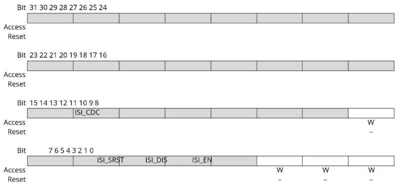
text_image
Bit 31 30 29 28 27 26 25 24 Access Reset Bit 23 22 21 20 19 18 17 16 Access Reset Bit 15 14 13 12 11 10 9 8 Access Reset W - Bit 7 6 5 4 3 2 1 0 Access Reset ISI_SRST ISI_DIS ISI_EN W W W - - -Bit 8 - ISI\_CDC ISI Codec Request
Write a one to this bit to enable the codec datapath and capture a full resolution frame. A new request cannot be taken into account while CDC_PND bit is active in the ISI_SR.
Bit 2 - ISI\_SRST ISI Software Reset Request
Write a one to this bit to request a software reset of the module. Software must poll the SRST bit in the ISI_SR to verify that the software request command has terminated.
Bit 1 - ISI\_DIS ISI Module Disable Request
Write a one to this bit to disable the module. If both ISI_EN and ISI_DIS are asserted at the same time, the disable request is not taken into account. Software must poll the DIS_DONE bit in the ISI_SR to verify that the command has successfully completed.
Bit 0 - ISI\_EN ISI Module Enable Request
Write a one to this bit to enable the module. Software must poll the ENABLE bit in the ISI_SR to verify that the command has successfully completed.
36.6.11 ISI Status Register
Name: ISI_SR
Offset: 0x28
Reset: 0x00000000
Property: Read-only
Bit 31 30 29 28 27 26 25 24
| FR_OVR CRC_ERR C_OVR P_OVR | |||||
| Access Reset | R R R R | ||||
| 0 | 0 | 0 | 0 | ||
Bit 23 22 21 20 19 18 17 16
| SIP | CXFR_DONE | PXFR_DONE | |||||
| Access | R | RR | |||||
| Reset | 0 | 0 | 0 |
Bit 15 14 13 12 11 10 9 8
| VSYNC | CDC_PND | ||||
| Access | R | R | |||
| Reset | 0 | 0 |
Bit 7 6 5 4 3 2 1 0
| SRST | DIS_DONE | ENABLE | ||||
| Access Reset | R R R0 | 0 | 0 |
Bit 27 - FR_OVR Frame Rate Overrun (cleared on read)
| Value | Description |
| 0 | No frame overrun |
| 1 | Frame overrun. The current frame is being skipped because a vsync signal has been detected while flushing FIFOs since the last read of ISI_SR. |
Bit 26 - CRC_ERR CRC Synchronization Error (cleared on read)
| Value | Description |
| 0 | No CRC error in the embedded synchronization frame (SAV/EAV) |
| 1 | Embedded Synchronization Correction is enabled (CRC_SYNC bit is set) In the ISI_CR and an error has been detected and not corrected since the last read of ISI_SR. The frame is discarded and the ISI waits for a new one. |
Bit 25 - C_OVR Codec Datapath Overflow (cleared on read)
| Value | Description |
| 0 | No overflow |
| 1 | An overrun condition has occurred in input FIFO on the codec path. The overrun happens when the FIFO is full and an attempt is made to write a new sample to the FIFO since the last read of ISI_SR. |
Bit 24 - P_OVR Preview Datapath Overflow (cleared on read)
| Value | Description |
| 0 | No overflow |
| 1 | An overrun condition has occurred in input FIFO on the preview path. The overrun happens when the FIFO is full and an attempt is made to write a new sample to the FIFO since the last read of ISI_SR. |
Bit 19 - SIP Synchronization in Progress
When the status of the preview or codec DMA channel is modified, a minimum amount of time is required to perform the clock domain synchronization.
| Value Description | |
| 0 | The clock domain synchronization process is terminated. |
| 1 | This bit is set when the clock domain synchronization operation occurs. No modification of the channel status is allowed when this bit is set, to guarantee data integrity. |
Bit 17 - CXFR_DONE Codec DMA Transfer has Terminated (cleared on read)
| Value Description | |
| 0 | Codec transfer done not detected. |
| 1 | Codec transfer done detected. When set, this bit indicates that the data transfer on the codec channel has completed since the last read of ISI_SR. |
Bit 16 - PXFR_DONE Preview DMA Transfer has Terminated (cleared on read)
| Value Description | |
| 0 | Preview transfer done not detected. |
| 1 | Preview transfer done detected. When set, this bit indicates that the data transfer on the preview channel has completed since the last read of ISI_SR. |
Bit 10 - VSYNC Vertical Synchronization (cleared on read)
| Value Description | |
| 0 | Indicates that the vertical synchronization has not been detected since the last read of the ISI_SR. |
| 1 | Indicates that a vertical synchronization has been detected since the last read of the ISI_SR. |
Bit 8 - CDC_PND Pending Codec Request
| Value Description | |
| 0 | Indicates that no codec request is pending |
| 1 | Indicates that the request has been taken into account but cannot be serviced within the current frame. The operation is postponed to the next frame. |
Bit 2 - SRST Module Software Reset Request has Terminated (cleared on read)
| Value Description | |
| 0 | Indicates that the request is not completed (if a request was issued). |
| 1 | Software reset request has completed. This flag is reset after a read operation. |
Bit 1 - DIS_DONE Module Disable Request has Terminated (cleared on read)
| Value Description | |
| 0 | Indicates that the request is not completed (if a request was issued). |
| 1 | Disable request has completed. This flag is reset after a read operation. |
Bit 0 - ENABLE Module Enable
| Value Description | |
| 0 | Module is disabled. |
| 1 | Module is enabled. |
36.6.12 ISI Interrupt Enable Register
Name: ISI_IER
Offset: 0x2C
Reset: -
Property: Write-only

text_image
Bit 31 30 29 28 27 26 25 24 Access Reset WRWW W W W - - - - Bit 23 22 21 20 19 18 17 16 Access Reset Bit 15 14 13 12 11 10 9 8 VSYNC Access Reset Bit 7 6 5 4 3 2 1 0 SRST DIS_DONE Access Reset W W W W W W - - -Bit 27 - FR\_OVR Frame Rate Overflow Interrupt Enable
| Value | Description |
| 0 | No effect. |
| 1 | Enables the corresponding interrupt. |
Bit 26 - CRC\_ERR Embedded Synchronization CRC Error Interrupt Enable
| Value | Description |
| 0 | No effect. |
| 1 | Enables the corresponding interrupt. |
Bit 25 - C\_OVR Codec Datapath Overflow Interrupt Enable
| Value | Description |
| 0 | No effect. |
| 1 | Enables the corresponding interrupt. |
Bit 24 - P\_OVR Preview Datapath Overflow Interrupt Enable
| Value | Description |
| 0 | No effect. |
| 1 | Enables the corresponding interrupt. |
Bit 17 - CXFR\_DONE Codec DMA Transfer Done Interrupt Enable
| Value | Description |
| 0 | No effect. |
| 1 | Enables the corresponding interrupt. |
Bit 16 - PXFR\_DONE Preview DMA Transfer Done Interrupt Enable
| Value Description | |
| 0 | No effect. |
| 1 | Enables the corresponding interrupt. |
Bit 10 - VSYNC Vertical Synchronization Interrupt Enable
| Value Description | |
| 0 | No effect. |
| 1 | Enables the corresponding interrupt. |
Bit 2 - SRST Software Reset Interrupt Enable
| Value Description | |
| 0 | No effect. |
| 1 | Enables the corresponding interrupt. |
Bit 1 - DIS_DONE Disable Done Interrupt Enable
| Value Description | |
| 0 | No effect. |
| 1 | Enables the corresponding interrupt. |
36.6.13 ISI Interrupt Disable Register
Name: ISI_IDR
Offset: 0x30
Reset: -
Property: Write-only
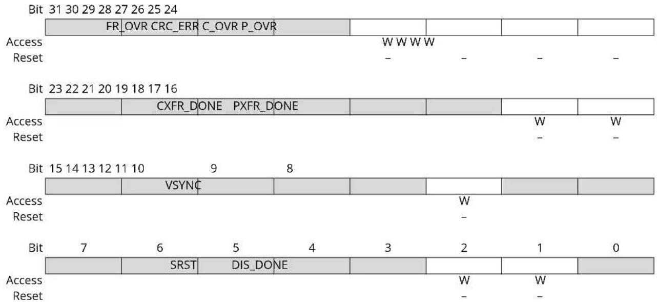
text_image
Bit 31 30 29 28 27 26 25 24 FR_OVR_CRC_ERR_C_OVR_P_OVR Access Reset W W W W - - - - Bit 23 22 21 20 19 18 17 16 CXFR_DONE PXFR_DONE Access Reset W W - - Bit 15 14 13 12 11 10 9 8 VSYNC Access Reset W - Bit 7 6 5 4 3 2 1 0 SRST DIS_DONE Access Reset W W - -Bit 27 - FR\_OVR Frame Rate Overflow Interrupt Disable
| Value | Description |
| 0 | No effect. |
| 1 | Disables the corresponding interrupt. |
Bit 26 - CRC\_ERR Embedded Synchronization CRC Error Interrupt Disable
| Value | Description |
| 0 | No effect. |
| 1 | Disables the corresponding interrupt. |
Bit 25 - C\_OVR Codec Datapath Overflow Interrupt Disable
| Value | Description |
| 0 | No effect. |
| 1 | Disables the corresponding interrupt. |
Bit 24 - P\_OVR Preview Datapath Overflow Interrupt Disable
| Value | Description |
| 0 | No effect. |
| 1 | Disables the corresponding interrupt. |
Bit 17 - CXFR\_DONE Codec DMA Transfer Done Interrupt Disable
| Value | Description |
| 0 | No effect. |
| 1 | Disables the corresponding interrupt. |
Bit 16 - PXFR\_DONE Preview DMA Transfer Done Interrupt Disable
| Value Description | |
| 0 | No effect. |
| 1 | Disables the corresponding interrupt. |
Bit 10 - VSYNC Vertical Synchronization Interrupt Disable
| Value Description | |
| 0 | No effect. |
| 1 | Disables the corresponding interrupt. |
Bit 2 - SRST Software Reset Interrupt Disable
| Value Description | |
| 0 | No effect. |
| 1 | Disables the corresponding interrupt. |
Bit 1 - DIS_DONE Disable Done Interrupt Disable
| Value Description | |
| 0 | No effect. |
| 1 | Disables the corresponding interrupt. |
36.6.14 ISI Interrupt Mask Register
Name: ISI_IMR
Offset: 0x34
Reset: 0x00000000
Property: Read-only
Bit 31 30 29 28 27 26 25 24
| FR_OVR CRC_ERR C_OVR P_OVR | |||||
| Access Reset | R R R R | ||||
| 0 | 0 | 0 | 0 | ||
Bit 23 22 21 20 19 18 17 16
| CXFR_DONE PXFR_DONE | |||||
| Access | R | R | |||
| Reset | 0 | 0 |
Bit 15 14 13 12 11 10 9 8
| VSYNC | ||||||
| Access | R | |||||
| Reset | 0 |
Bit 7 6 5 4 3 2 1 0
| SRST | DIS_DONE | |||||
| Access | R | R | ||||
| Reset | 0 | 0 |
Bit 27 - FR_OVR Frame Rate Overrun
| Value | Description |
| 0 | The Frame Rate Overrun interrupt is disabled. |
| 1 | The Frame Rate Overrun is enabled. |
Bit 26 - CRC_ERR CRC Synchronization Error
| Value | Description |
| 0 | The CRC Synchronization Error interrupt is disabled. |
| 1 | The CRC Synchronization Error interrupt is enabled. |
Bit 25 - C_OVR Codec FIFO Overflow
| Value | Description |
| 0 | The Codec FIFO Overflow interrupt is disabled. |
| 1 | The Codec FIFO Overflow interrupt is enabled. |
Bit 24 - P_OVR Preview FIFO Overflow
| Value | Description |
| 0 | The Preview FIFO Overflow interrupt is disabled. |
| 1 | The Preview FIFO Overflow Interrupt is enabled. |
Bit 17 - CXFR_DONE Codec DMA Transfer Completed
| Value | Description |
| 0 | The Codec DMA Transfer Completed interrupt is disabled. |
| 1 | The Codec DMA Transfer Completed interrupt is enabled. |
Bit 16 - PXFR_DONE Preview DMA Transfer Completed
| Value Description | |
| 0 | The Preview DMA Transfer Completed Interrupt is disabled. |
| 1 | The Preview DMA Transfer Completed interrupt is enabled. |
Bit 10 - VSYNC Vertical Synchronization
| Value Description | |
| 0 | The Vertical Synchronization interrupt is disabled. |
| 1 | The Vertical Synchronization interrupt is enabled. |
Bit 2 - SRST Software Reset Completed
| Value Description | |
| 0 | The Software Reset Completed interrupt is disabled. |
| 1 | The Software Reset Completed interrupt is enabled. |
Bit 1 - DIS_DONE Module Disable Operation Completed
| Value Description | |
| 0 | The Module Disable Operation Completed interrupt is disabled. |
| 1 | The Module Disable Operation Completed interrupt is enabled. |
36.6.15 DMA Channel Enable Register
Name: ISI_DMA_CHER
Offset: 0x38
Reset: -
Property: Write-only

text_image
Bit 31 30 29 28 27 26 25 24 Access Reset Bit 23 22 21 20 19 18 17 16 Access Reset Bit 15 14 13 12 11 10 9 8 Access Reset Bit 7 6 5 4 3 2 1 0 Access Reset C_CH_EN P_CH_EN W W -Bit 1 - C\_CH\_EN Codec Channel Enable
Write a one to this bit to enable the codec DMA channel.
Bit 0 - P\_CH\_EN Preview Channel Enable
Write a one to this bit to enable the preview DMA channel.
36.6.16 DMA Channel Disable Register
Name: ISI_DMA_CHDR
Offset: 0x3C
Reset: -
Property: Write-only
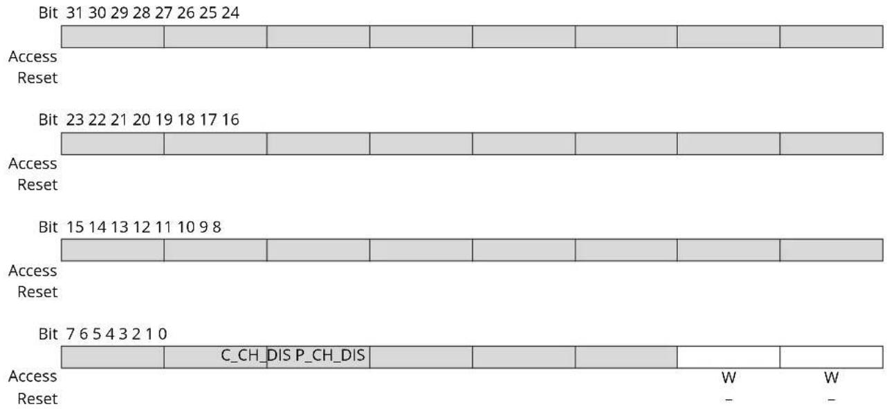
text_image
Bit 31 30 29 28 27 26 25 24 Access Reset Bit 23 22 21 20 19 18 17 16 Access Reset Bit 15 14 13 12 11 10 9 8 Access Reset Bit 7 6 5 4 3 2 1 0 Access Reset C_CH_DIS P_CH_DIS W W -Bit 1 - C_CH_DIS Codec Channel Disable Request
| Value | Description |
| 0 | No effect. |
| 1 | Disables the channel. Poll C_CH_S in DMA_CHSR to verify that the codec channel status has been successfully modified. |
Bit 0 - P_CH_DIS Preview Channel Disable Request
| Value | Description |
| 0 | No effect. |
| 1 | Disables the channel. Poll P_CH_S in DMA_CHSR to verify that the preview channel status has been successfully modified. |
36.6.17 DMA Channel Status Register
Name: ISI_DMA_CHSR
Offset: 0x40
Reset: 0x00000000
Property: Read-only
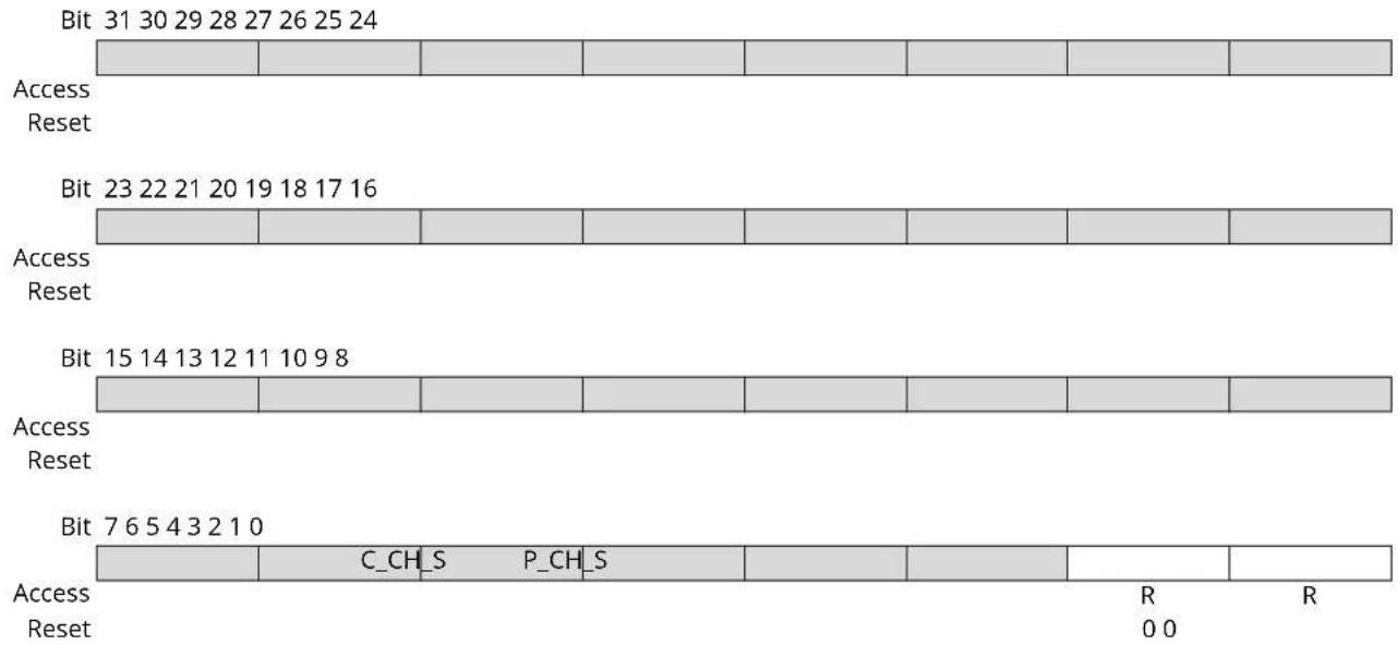
text_image
Bit 31 30 29 28 27 26 25 24 Access Reset Bit 23 22 21 20 19 18 17 16 Access Reset Bit 15 14 13 12 11 10 9 8 Access Reset Bit 7 6 5 4 3 2 1 0 Access Reset C_CH_S P_CH_S R R 0 0Bit 1 - C_CH_S Code DMA Channel Status
| Value | Description |
| 0 | Indicates that the Codec DMA channel is disabled. |
| 1 | Indicates that the Codec DMA channel is enabled. |
Bit 0 - P_CH_S Preview DMA Channel Status
| Value | Description |
| 0 | Indicates that the Preview DMA channel is disabled. |
| 1 | Indicates that the Preview DMA channel is enabled. |
36.6.18 DMA Preview Base Address Register
Name: ISI_DMA_P_ADDR
Offset: 0x44
Reset: 0x00000000
Property: Read/Write
| Bit 31 30 29 28 27 26 25 24 | |||
| P_ADDR[29:22] | |||
| Access | R/W R/W R/W R/W R/W R/W R/W R/W | ||
| Reset | 0 0 0 0 0 0 0 0 | ||
| Bit 23 22 21 20 19 18 17 16 | |||
| P_ADDR[21:14] | |||
| Access | R/W R/W R/W R/W R/W R/W R/W R/W | ||
| Reset | 0 0 0 0 0 0 0 0 | ||
| Bit 15 14 13 12 11 10 9 8 | |||
| P_ADDR[13:6] | |||
| Access | R/W R/W R/W R/W R/W R/W R/W R/W | ||
| Reset | 0 0 0 0 0 0 0 0 | ||
| Bit 7 6 5 4 3 2 1 0 | |||
| P_ADDR[5:0] | |||
| Access | R/W R/W R/W R/W R/W R/W R/W | ||
| Reset | 0 0 0 0 0 0 | ||
Bits 31:2 - P_ADDR[29:0] Preview Image Base Address This address is word-aligned.
36.6.19 DMA Preview Control Register
Name: ISI_DMA_P_CTRL
Offset: 0x48
Reset: 0x00000000
Property: Read/Write

text_image
Bit 31 30 29 28 27 26 25 24 Access Reset Bit 23 22 21 20 19 18 17 16 Access Reset Bit 15 14 13 12 11 10 9 8 Access Reset Bit 7 6 5 4 3 2 1 0 Access Reset P_DONE P_IEN P_WB P_FETCH R/W R/W R/W R/W 0 0 0 0Bit 3 - P\_DONE Preview Transfer Done
This bit is only updated in the memory.
| Value | Description |
| 0 | The transfer related to this descriptor has not been performed. |
| 1 | The transfer related to this descriptor has completed. This bit is updated in memory at the end of the transfer, when writeback operation is enabled. |
Bit 2 - P\_IEN Transfer Done Flag Control
| Value | Description |
| 0 | Preview transfer done flag generation is enabled. |
| 1 | Preview transfer done flag generation is disabled. |
Bit 1 - P\_WB Descriptor Writeback Control Bit
| Value | Description |
| 0 | Preview channel writeback operation is disabled. |
| 1 | Preview channel writeback operation is enabled. |
Bit 0 - P\_FETCH Descriptor Fetch Control Bit
| Value | Description |
| 0 | Preview channel fetch operation is disabled. |
| 1 | Preview channel fetch operation is enabled. |
36.6.20 DMA Preview Descriptor Address Register
Name: ISI_DMA_P_DSCR
Offset: 0x4C
Reset: 0x00000000
Property: Read/Write
| Bit 31 30 29 28 27 26 25 24 | |||
| P_DSCR[29:22] | |||
| Access | R/W R/W R/W R/W R/W R/W R/W R/W | ||
| Reset | 0 0 0 0 0 0 0 0 | ||
| Bit 23 22 21 20 19 18 17 16 | |||
| P_DSCR[21:14] | |||
| Access | R/W R/W R/W R/W R/W R/W R/W R/W | ||
| Reset | 0 0 0 0 0 0 0 0 | ||
| Bit 15 14 13 12 11 10 9 8 | |||
| P_DSCR[13:6] | |||
| Access | R/W R/W R/W R/W R/W R/W R/W R/W | ||
| Reset | 0 0 0 0 0 0 0 0 | ||
| Bit 7 6 5 4 3 2 1 0 | |||
| P_DSCR[5:0] | |||
| Access | R/W R/W R/W R/W R/W R/W R/W | ||
| Reset | 0 0 0 0 0 0 | ||
Bits 31:2 - P_DSCR[29:0] Preview Descriptor Base Address This address is word-aligned.
36.6.21 DMA Codec Base Address Register
Name: ISI_DMA_C_ADDR
Offset: 0x50
Reset: 0x00000000
Property: Read/Write
| Bit 31 30 29 28 27 26 25 24 | |||
| C_ADDR[29:22] | |||
| Access | R/W R/W R/W R/W R/W R/W R/W R/W | ||
| Reset | 0 0 0 0 0 0 0 0 | ||
| Bit 23 22 21 20 19 18 17 16 | |||
| C_ADDR[21:14] | |||
| Access | R/W R/W R/W R/W R/W R/W R/W R/W | ||
| Reset | 0 0 0 0 0 0 0 0 | ||
| Bit 15 14 13 12 11 10 9 8 | |||
| C_ADDR[13:6] | |||
| Access | R/W R/W R/W R/W R/W R/W R/W R/W | ||
| Reset | 0 0 0 0 0 0 0 0 | ||
| Bit 7 6 5 4 3 2 1 0 | |||
| C_ADDR[5:0] | |||
| Access | R/W R/W R/W R/W R/W R/W R/W | ||
| Reset | 0 0 0 0 0 0 | ||
Bits 31:2 - C_ADDR[29:0] Codec Image Base Address This address is word-aligned.
36.6.22 DMA Codec Control Register
Name: ISI_DMA_C_CTRL
Offset: 0x54
Reset: 0x00000000
Property: Read/Write
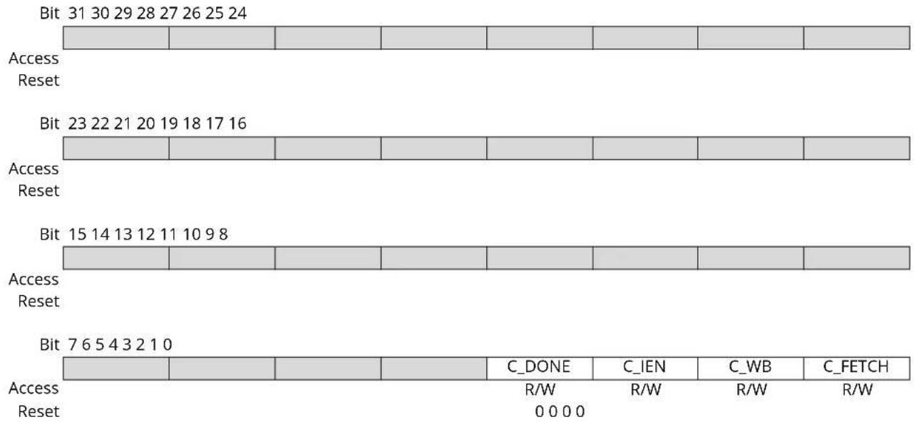
text_image
Bit 31 30 29 28 27 26 25 24 Access Reset Bit 23 22 21 20 19 18 17 16 Access Reset Bit 15 14 13 12 11 10 9 8 Access Reset Bit 7 6 5 4 3 2 1 0 Access Reset C_DONE C_IEN C_WB C_FETCH R/W R/W R/W R/W 0 0 0 0Bit 3 - C\_DONE Codec Transfer Done
This bit is only updated in the memory.
| Value | Description |
| 0 | The transfer related to this descriptor has not been performed. |
| 1 | The transfer related to this descriptor has completed. This bit is updated in memory at the end of the transfer when writeback operation is enabled. |
Bit 2 - C\_IEN Transfer Done Flag Control
| Value | Description |
| 0 | Codec transfer done flag generation is enabled. |
| 1 | Codec transfer done flag generation is disabled. |
Bit 1 - C\_WB Descriptor Writeback Control Bit
| Value | Description |
| 0 | Codec channel writeback operation is disabled. |
| 1 | Codec channel writeback operation is enabled. |
Bit 0 - C\_FETCH Descriptor Fetch Control Bit
| Value | Description |
| 0 | Codec channel fetch operation is disabled. |
| 1 | Codec channel fetch operation is enabled. |
36.6.23 DMA Codec Descriptor Address Register
Name: ISI_DMA_C_DSCR
Offset: 0x58
Reset: 0x00000000
Property: Read/Write
| Bit 31 30 29 28 27 26 25 24 | |||
| C_DSCR[29:22] | |||
| Access | R/W R/W R/W R/W R/W R/W R/W R/W | ||
| Reset | 0 0 0 0 0 0 0 | ||
| Bit 23 22 21 20 19 18 17 16 | |||
| C_DSCR[21:14] | |||
| Access | R/W R/W R/W R/W R/W R/W R/W R/W | ||
| Reset | 0 0 0 0 0 0 0 | ||
| Bit 15 14 13 12 11 10 9 8 | |||
| C_DSCR[13:6] | |||
| Access | R/W R/W R/W R/W R/W R/W R/W R/W | ||
| Reset | 0 0 0 0 0 0 0 | ||
| Bit 7 6 5 4 3 2 1 0 | |||
| C_DSCR[5:0] | |||
| Access | R/W R/W R/W R/W R/W R/W | ||
| Reset | 0 0 0 0 0 | ||
Bits 31:2 - C_DSCR[29:0] Codec Descriptor Base Address This address is word-aligned.
36.6.24 ISI Write Protection Mode Register
Name: ISI_WPMR
Offset: 0xE4
Reset: 0x00000000
Property: Read/Write
| Bit 31 30 29 28 27 26 25 24 | ||||||
| WPKEY[23:16] | ||||||
| Access | WWWWWWWWW | |||||
| Reset | 0 0 0 0 0 0 0 0 | |||||
| Bit 23 22 21 20 19 18 17 16 | ||||||
| WPKEY[15:8] | ||||||
| Access | WWWWWWWWW | |||||
| Reset | 0 0 0 0 0 0 0 0 | |||||
| Bit 15 14 13 12 11 10 9 8 | ||||||
| WPKEY[7:0] | ||||||
| Access | WWWWWWWWW | |||||
| Reset | 0 0 0 0 0 0 0 0 | |||||
| Bit 7 6 5 4 3 2 1 0 | ||||||
| WPEN | ||||||
| Access | R/W | |||||
| Reset | 0 | |||||
Bits 31:8 - WPKEY[23:0] Write Protection Key Password
| Value | Name | Description |
| 0x495349 | PASSWD | Writing any other value in this field aborts the write operation of the WPEN bit.Always reads as 0. |
Bit 0 - WPEN Write Protection Enable
| Value | Description |
| 0 | Disables the write protection if WPKEY corresponds to 0x495349 ("ISI" in ASCII). |
| 1 | Enables the write protection if WPKEY corresponds to 0x495349 ("ISI" in ASCII). |
36.6.25 ISI Write Protection Status Register
Name: ISI_WPSR
Offset: 0xE8
Reset: 0x00000000
Property: Read-only

text_image
Bit 31 30 29 28 27 26 25 24 Access Reset Bit 23 22 21 20 19 18 17 16 WPVSRC[15:8] Access R R R R R R R R Reset 0 0 0 0 0 0 0 0 Bit 15 14 13 12 11 10 9 8 WPVSRC[7:0] Access R R R R R R R R R Reset 0 0 0 0 0 0 0 0 Bit 7 6 5 4 3 2 1 0 WPVS Access R Reset R 0Bits 23:8 - WPVSRC[15:0] Write Protection Violation Source
| Value | Name |
| 0 | No Write Protection Violation occurred since the last read of this register (ISI_WPSR). |
| 1 | Write access in ISI_CFG1 while Write Protection was enabled (since the last read). |
| 2 | Write access in ISI_CFG2 while Write Protection was enabled (since the last read). |
| 3 | Write access in ISI_PSIZE while Write Protection was enabled (since the last read). |
| 4 | Write access in ISI_PDECF while Write Protection was enabled (since the last read). |
| 5 | Write access in ISI_Y2R_SET0 while Write Protection was enabled (since the last read). |
| 6 | Write access in ISI_Y2R_SET1 while Write Protection was enabled (since the last read). |
| 7 | Write access in ISI_R2Y_SET0 while Write Protection was enabled (since the last read). |
| 8 | Write access in ISI_R2Y_SET1 while Write Protection was enabled (since the last read). |
| 9 | Write access in ISI_R2Y_SET2 while Write Protection was enabled (since the last read). |
Bit 0 - WPVS Write Protection Violation Status
| Value | Name |
| 0 | No write protection violation occurred since the last read of ISI_WPSR. |
| 1 | A write protection violation has occurred since the last read of the ISI_WPSR. If this violation is an unauthorized attempt to write a protected register, the associated violation is reported into field WPVSRC. |
37. GMAC - Ethernet MAC
The description and registers of this peripheral are using the 'GMAC' designation although the device does not support Gigabit Ethernet functionality.
37.1 Description
The Ethernet Media Access Controller (GMAC) module implements a 10/100 Mbps Ethernet MAC, compatible with the IEEE 802.3 standard. The GMAC can operate in either half or full duplex mode at all supported speeds.
37.2 Embedded Characteristics
- Compatible with IEEE Standard 802.3
• 10, 100 Mbps operation
• Full and half duplex operation at all supported speeds of operation
• Statistics Counter Registers for RMON/MIB - MII/RMII interface to the physical layer
- Integrated physical coding
- Direct memory access (DMA) interface to external memory
• Support for priority queues in DMA - 8-KByte transmit RAM and 4-KByte receive RAM (refer to Table 37-4 for queue-specific sizes
- Programmable burst length and endianism for DMA
- Interrupt generation to signal receive and transmit completion, errors or other events
• Automatic pad and cyclic redundancy check (CRC) generation on transmitted frames
• Automatic discard of frames received with errors - Receive and transmit IP, TCP and UDP checksum offload. Both IPv4 and IPv6 packet types supported
- Address checking logic for four specific 48-bit addresses, four type IDs, promiscuous mode, hash matching of unicast and multicast destination addresses and Wake-on-LAN
- Management Data Input/Output (MDIO) interface for physical layer management
- Support for jumbo frames up to 10240 Bytes
- Full duplex flow control with recognition of incoming pause frames and hardware generation of transmitted pause frames
- Half duplex flow control by forcing collisions on incoming frames
• Support for 802.1Q VLAN tagging with recognition of incoming VLAN and priority tagged frames
• Support for 802.1Qbb priority-based flow control - Programmable Inter Packet Gap (IPG) Stretch
• Recognition of IEEE 1588 PTP frames
• IEEE 1588 time stamp unit (TSU) - Support for 802.1AS timing and synchronization
• Supports 802.1Qav traffic shaping on two highest priority queues
• Support for 802.3az Energy Efficient Ethernet
37.3 Block Diagram
Figure 37-1. Block Diagram

flowchart
graph TD
    APB --> RegisterInterface["Register Interface"]
    APB --> ControlRegisters["Control Registers"]
    APB --> AHB_DMAInterface["AHB DMA Interface"]
    APB --> PacketBufferMemories["Packet Buffer Memories"]
    RegisterInterface <--> Status&StatisticRegisters["Status & Statistic Registers"]
    ControlRegisters <--> MDIO["MDIO"]
    AHB_DMAInterface <--> FIFOInterface["FIFO Interface"]
    FIFOInterface --> MACTransmitter["MAC Transmitter"]
    MACTransmitter --> MediaInterface["Media Interface"]
    MediaInterface --> MACReceiver["MAC Receiver"]
    MACReceiver --> FrameFiltering["Frame Filtering"]
    ControlRegisters --> MACTransmitter
37.4 Signal Interface
The GMAC includes the following signal interfaces:
• MII, RMII to an external PHY
• MDIO interface for external PHY management
- Slave APB interface for accessing GMAC registers
- Master AHB interface for memory access
• GTSUCOMP signal for TSU timer count value comparison
Table 37-1. GMAC Connections in Different Modes
| Signal Name Function MII RMII | |||
| GTXCK ^(1) | Transmit Clock or Reference Clock TXCK REFCK | ||
| GTXEN Transmit Enable TXEN TXEN | |||
| GTX[3..0] Transmit Data TXD[3:0] TXD[1:0] | |||
| GTXER Transmit Coding Error TXER | Not Used | ||
| GRXCK Receive Clock | RXCK Not Used | ||
| GRXDV | Receive Data Valid | RXDV | CRSDV |
| GRX[3..0] | Receive Data | RXD[3:0] | RXD[1:0] |
| GRXER | Receive Error | RXER RXER | |
| GCRS | Carrier Sense and Data Valid | CRS | Not Used |
| GCOL | Collision Detect | COL | Not Used |
| GMDC | Management Data Clock | MDC | MDC |
| GMDIO | Management Data Input/Output | MDIO | MDIO |
Note:
- Input only. GTXCK must be provided with a 25 MHz / 50 MHz external crystal oscillator for MII / RMII interfaces, respectively.
37.5 Product Dependencies
37.5.1 I/O Lines
The pins used for interfacing the GMAC may be multiplexed with PIO lines. The programmer must first program the PIO Controller to assign the pins to their peripheral function. If I/O lines of the GMAC are not used by the application, they can be used for other purposes by the PIO Controller.
37.5.2 Power Management
The GMAC is not continuously clocked. The user must first enable the GMAC clock in the Power Management Controller before using it.
37.5.3 Interrupt Sources
The GMAC interrupt line is connected to one of the internal sources of the interrupt controller. Using the GMAC interrupt requires prior programming of the interrupt controller.
The GMAC features interrupt sources. Refer to the table "Peripheral Identifiers" in the section "Peripherals" for the interrupt numbers for GMAC priority queues.
37.6 Functional Description
37.6.1 Media Access Controller
The Transmit Block of the Media Access Controller (MAC) takes data from FIFO, adds preamble, checks and adds padding and frame check sequence (FCS). Both half duplex and full duplex Ethernet modes of operation are supported.
When operating in half duplex mode, the MAC Transmit Block generates data according to the Carrier Sense Multiple Access with Collision Detect (CSMA/CD) protocol. The start of transmission is deferred if Carrier Sense (CRS) is active. If Collision (COL) is detected during transmission, a jam sequence is asserted and the transmission is retried after a random back off. The CRS and COL signals have no effect in full duplex mode.
The Receive Block of the MAC checks for valid preamble, FCS, alignment and length, and presents received frames to the MAC address checking block and FIFO. Software can configure the GMAC to receive jumbo frames of up to 10240 Bytes. It can optionally strip CRC (Cyclic Redundancy Check) from the received frame before transferring it to FIFO.
The Address Checker recognizes four specific 48-bit addresses, can recognize four different types of ID values, and contains a 64-bit Hash register for matching multicast and unicast addresses as required. It can recognize the broadcast address all-'1' (0xFFFFFFFFFFF) and copy all frames. The MAC can also reject all frames that are not VLAN tagged, and recognize Wake on LAN events.
The MAC Receive Block supports offloading of IP, TCP and UDP checksum calculations (both IPv4 and IPv6 packet types supported), and can automatically discard bad checksum frames.
37.6.2 IEEE 1588 Time Stamp Unit
The IEEE 1588 time stamp unit (TSU) is implemented as a 94-bit timer.
- The 48 upper bits [93:46] of the timer count seconds and are accessible in the GMAC 1588 Timer Seconds High Register" (GMAC_TSH) and GMAC 1588 Timer Seconds Low Register (GMAC_TSL).
- The 30 lower bits [45:16] of the timer count nanoseconds and are accessible in the GMAC 1588 Timer Nanoseconds Register (GMAC_TN).
- The lowest 16 bits [15:0] of the timer count sub-nanoseconds.
The 46 lower bits roll over when they have counted to 1s. The timer increments by a programmable period (to approximately 15.2fs resolution) with each MCK period and can also be adjusted in 1ns resolution (incremented or decremented) through APB register accesses.
37.6.3 AHB Direct Memory Access Interface
The GMAC DMA controller is connected to the MAC FIFO interface and provides a scatter-gather type capability for packet data storage.
The DMA implements packet buffering where dual-port memories are used to buffer multiple frames.
37.6.3.1 Packet Buffer DMA
- Easier to guarantee maximum line rate due to the ability to store multiple frames in the packet buffer, where the number of frames is limited by the amount of packet buffer memory and Ethernet frame size
• Full store and forward, or partial store and forward programmable options (partial store will cater for shorter latency requirements) - Support for Transmit TCP/IP checksum offload
• Support for priority queuing - When a collision on the line occurs during transmission, the packet will be automatically replayed directly from the packet buffer memory rather than having to re-fetch through the AHB (full store and forward ONLY)
- Received erroneous packets are automatically dropped before any of the packet is presented to the AHB (full store and forward ONLY), thus reducing AHB activity
• Supports manual RX packet flush capabilities - Optional RX packet flush when there is lack of AHB resource
37.6.3.2 Partial Store and Forward Using Packet Buffer DMA
The DMA uses SRAM-based packet buffers, and can be programmed into a low latency mode, known as Partial Store and Forward. This mode allows for a reduced latency as the full packet is not buffered before forwarding.
Note: This option is only available when the device is configured for full duplex operation.
This feature is enabled via the programmable TX and RX Partial Store and Forward registers (GMAC_TPSF and GMAC_RPSF). When the transmit Partial Store and Forward mode is activated, the transmitter will only begin to forward the packet to the MAC when there is enough packet data stored in the packet buffer. Likewise, when the receive Partial Store and Forward mode is activated, the receiver will only begin to forward the packet to the AHB when enough packet data is stored in the packet buffer. The amount of packet data required to activate the forwarding process is programmable via watermark registers. These registers are located at the same address as the partial store and forward enable bits.
Note: The minimum operational value for the TX partial store and forward watermark is 20. There is no operational limit for the RX partial store and forward watermark.
Enabling Partial Store and Forward is a useful means to reduce latency, but there are performance implications. The GMAC DMA uses separate transmit and receive lists of buffer descriptors, with each descriptor describing a buffer area in memory. This allows Ethernet packets to be broken up and scattered around the AHB memory space.
37.6.3.3 Receive AHB Buffers
Received frames, optionally including FCS, are written to receive AHB buffers stored in memory. The receive buffer depth is programmable in the range of 64 Bytes to 16 KBytes through the DMA Configuration register (GMAC_DCFGR), with the default being 128 Bytes.
The start location for each receive AHB buffer is stored in memory in a list of receive buffer descriptors at an address location pointed to by the receive buffer queue pointer. The base address for the receive buffer queue pointer is configured in software using the Receive Buffer Queue Base Address register (GMAC_RBQB).
Each list entry consists of two words. The first is the address of the receive AHB buffer and the second the receive status.
If the length of a receive frame exceeds the AHB buffer length, the status word for the used buffer is written with zeroes except for the "Start of Frame" bit, which is always set for the first buffer in a frame.
Bit zero of the address field is written to 1 to show that the buffer has been used. The receive buffer manager then reads the location of the next receive AHB buffer and fills that with the next part of the received frame data. AHB buffers are filled until the frame is complete and the final buffer descriptor status word contains the complete frame status. See the following table for details of the receive buffer descriptor list.
Table 37-2. Receive Buffer Descriptor Entry
| Bit Function | |
| Word 0 | |
| 31:2 Address of beginning of buffer | |
| 1 Wrap—marks last descriptor in receive buffer descriptor list. | |
| 0 | Ownership—needs to be zero for the GMAC to write data to the receive buffer. The GMAC sets this to one once it has successfully written a frame to memory.Software has to clear this bit before the buffer can be used again. |
| Word 1 | |
| 31 Global all ones broadcast address detected | |
| 30 Multicast hash match | |
| 29 Unicast hash match | |
| 28 | - |
| 27 | Specific Address Register match found, bit 25 and bit 26 indicate which Specific Address Register causes the match. |
| 26:25 | Specific Address Register match. Encoded as follows:00: Specific Address Register 1 match01: Specific Address Register 2 match10: Specific Address Register 3 match11: Specific Address Register 4 matchIf more than one specific address is matched only one is indicated with priority 4 down to 1. |
| 24 | This bit has a different meaning depending on whether RX checksum offloading is enabled.With RX checksum offloading disabled: (bit 24 clear in Network Configuration Register)Type ID register match found, bit 22 and bit 23 indicate which type ID register causes the match.With RX checksum offloading enabled: (bit 24 set in Network Configuration Register)0: The frame was not SNAP encoded and/or had a VLAN tag with the Canonical Format Indicator (CFI) bit set.1: The frame was SNAP encoded and had either no VLAN tag or a VLAN tag with the CFI bit not set. |
| 23:22 | This bit has a different meaning depending on whether RX checksum offloading is enabled.With RX checksum offloading disabled: (bit 24 clear in Network Configuration)Type ID register match. Encoded as follows:00: Type ID register 1 match01: Type ID register 2 match10: Type ID register 3 match11: Type ID register 4 matchIf more than one Type ID is matched only one is indicated with priority 4 down to 1.With RX checksum offloading enabled: (bit 24 set in Network Configuration Register)00: Neither the IP header checksum nor the TCP/UDP checksum was checked.01: The IP header checksum was checked and was correct. Neither the TCP nor UDP checksum was checked.10: Both the IP header and TCP checksum were checked and were correct.11: Both the IP header and UDP checksum were checked and were correct. |
......continued
Bit Function
21 VLAN tag detected—type ID of 0x8100. For packets incorporating the stacked VLAN processing feature, this bit will be set if the second VLAN tag has a type ID of 0x8100
20 Priority tag detected—type ID of 0x8100 and null VLAN identifier. For packets incorporating the stacked VLAN processing feature, this bit will be set if the second VLAN tag has a type ID of 0x8100 and a null VLAN identifier.
19:17 VLAN priority—only valid if bit 21 is set.
16 Canonical format indicator (CFI) bit (only valid if bit 21 is set).
15 End of frame—when set the buffer contains the end of a frame. If end of frame is not set, then the only valid status bit is start of frame (bit 14).
14 Start of frame—when set the buffer contains the start of a frame. If both bits 15 and 14 are set, the buffer contains a whole frame.
13 This bit has a different meaning depending on whether jumbo frames and ignore FCS modes are enabled. If neither mode is enabled this bit will be zero.
With jumbo frame mode enabled: (bit 3 set in Network Configuration Register) Additional bit for length of frame (bit[13]), that is concatenated with bits[12:0]
With ignore FCS mode enabled and jumbo frames disabled: (bit 26 set in Network Configuration Register and bit 3 clear in Network Configuration Register) This indicates per frame FCS status as follows:
0: Frame had good FCS
1: Frame had bad FCS, but was copied to memory as ignore FCS enabled.
12:0 These bits represent the length of the received frame which may or may not include FCS depending on whether FCS discard mode is enabled.
With FCS discard mode disabled: (bit 17 clear in Network Configuration Register)
Least significant 12 bits for length of frame including FCS. If jumbo frames are enabled, these 12 bits are concatenated with bit[13] of the descriptor above.
With FCS discard mode enabled: (bit 17 set in Network Configuration Register)
Least significant 12 bits for length of frame excluding FCS. If jumbo frames are enabled, these 12 bits are concatenated with bit[13] of the descriptor above.
Each receive AHB buffer start location is a word address. The start of the first AHB buffer in a frame can be offset by up to three Bytes, depending on the value written to bits 14 and 15 of the Network Configuration register (GMAC_NCFGR). If the start location of the AHB buffer is offset, the available length of the first AHB buffer is reduced by the corresponding number of Bytes.
To receive frames, the AHB buffer descriptors must be initialized by writing an appropriate address to bits 31:2 in the first word of each list entry. Bit 0 must be written with zero. Bit 1 is the wrap bit and indicates the last entry in the buffer descriptor list.
The start location of the receive buffer descriptor list must be written with the receive buffer queue base address before reception is enabled (receive enable in the Network Control register GMAC_NCR). Once reception is enabled, any writes to the Receive Buffer Queue Base Address register (GMAC_RBQB) are ignored. When read, it will return the current pointer position in the descriptor list, though this is only valid and stable when receive is disabled.
If the filter block indicates that a frame should be copied to memory, the receive data DMA operation starts writing data into the receive buffer. If an error occurs, the buffer is recovered.
An internal counter within the GMAC represents the receive buffer queue pointer and it is not visible through the CPU interface. The receive buffer queue pointer increments by two words after each buffer has been used. It re-initializes to the receive buffer queue base address if any descriptor has its wrap bit set.
As receive AHB buffers are used, the receive AHB buffer manager sets bit zero of the first word of the descriptor to logic one indicating the AHB buffer has been used.
Software should search through the "used" bits in the AHB buffer descriptors to find out how many frames have been received, checking the start of frame and end of frame bits.
When the DMA is configured in the packet buffer Partial Store And Forward mode, received frames are written out to the AHB buffers as soon as enough frame data exists in the packet buffer. For both cases, this may mean several full AHB buffers are used before some error conditions can be detected. If a receive error is detected the receive buffer currently being written will be recovered. Previous buffers will not be recovered. As an example, when receiving frames with cyclic redundancy check (CRC) errors or excessive length, it is possible that a frame fragment might be stored in a sequence of AHB receive buffers. Software can detect this by looking for start of frame bit set in a buffer following a buffer with no end of frame bit set.
To function properly, a 10/100 Ethernet system should have no excessive length frames or frames greater than 128 Bytes with CRC errors. Collision fragments will be less than 128 Bytes long, therefore it will be a rare occurrence to find a frame fragment in a receive AHB buffer, when using the default value of 128 Bytes for the receive buffers size.
When in packet buffer full store and forward mode, only good received frames are written out of the DMA, so no fragments will exist in the AHB buffers due to MAC receiver errors. There is still the possibility of fragments due to DMA errors, for example used bit read on the second buffer of a multi-buffer frame.
If bit zero of the receive buffer descriptor is already set when the receive buffer manager reads the location of the receive AHB buffer, the buffer has been already used and cannot be used again until software has processed the frame and cleared bit zero. In this case, the "buffer not available" bit in the receive status register is set and an interrupt triggered. The receive resource error statistics register is also incremented.
When the DMA is configured in the packet buffer full store and forward mode, the user can optionally select whether received frames should be automatically discarded when no AHB buffer resource is available. This feature is selected via the DMA Discard Receive Packets bit in the DMA Configuration register (GMAC_DCFGR.DDRP). By default, the received frames are not automatically discarded. If this feature is off, then received packets will remain to be stored in the SRAM-based packet buffer until AHB buffer resource next becomes available. This may lead to an eventual packet buffer overflow if packets continue to be received when bit zero (used bit) of the receive buffer descriptor remains set.
Note: After a used bit has been read, the receive buffer manager will re-read the location of the receive buffer descriptor every time a new packet is received. When the DMA is not configured in the packet buffer full store and forward mode and a used bit is read, the frame currently being received will be automatically discarded.
When the DMA is configured in the packet buffer full store and forward mode, a receive overrun condition occurs when the receive SRAM-based packet buffer is full, or because HRESP was not OK. In all other modes, a receive overrun condition occurs when either the AHB bus was not granted quickly enough, or because HRESP was not OK, or because a new frame has been detected by the receive block, but the status update or write back for the previous frame has not yet finished. For a receive overrun condition, the receive overrun interrupt is asserted and the buffer currently being written is recovered. The next frame that is received whose address is recognized reuses the buffer.
In any packet buffer mode, writing a '1' to the Flush Next Package bit in the NCR register (GMAC_NCR.FNP) will force a packet from the external SRAM-based receive packet buffer to be flushed. This feature is only acted upon when the RX DMA is not currently writing packet data out to AHB, i.e., it is in an IDLE state. If the RX DMA is active, GMAC_NCR.FNP=1 is ignored.
37.6.3.4 Transmit AHB Buffers
Frames to transmit are stored in one or more transmit AHB buffers. Transmit frames can be between 1 and 16384 Bytes long, so it is possible to transmit frames longer than the maximum length specified in the IEEE 802.3 standard. It should be noted that zero length AHB buffers are allowed and that the maximum number of buffers permitted for each transmit frame is 128.
The start location for each transmit AHB buffer is stored in memory in a list of transmit buffer descriptors at a location pointed to by the transmit buffer queue pointer. The base address for this
queue pointer is set in software using the Transmit Buffer Queue Base Address register. Each list entry consists of two words. The first is the Byte address of the transmit buffer and the second containing the transmit control and status. For the packet buffer DMA, the start location for each AHB buffer is a Byte address, the bottom bits of the address being used to offset the start of the data from the data-word boundary (i.e., bits 2,1 and 0 are used to offset the address for 64-bit data paths). For the FIFO-based DMA configured with a 32-bit data path the address of the buffer is a Byte address.
For bus widths of 64 or 128-bits however, the address of the buffer must be aligned to the correct 64-bit or 128-bit boundary, plus an offset of less than 4 Bytes.
Note: This alignment restriction in FIFO-based DMA mode only should be sufficient for applications as the main purpose is to allow alignment of the encapsulated IP packet. Given the 14 Bytes of MAC encapsulation, an offset of 2 Bytes will always align the IP header to a 128-bit boundary.)
Frames can be transmitted with or without automatic Cyclic Redundancy Checksum (CRC) generation. If CRC is automatically generated, pad will also be automatically generated to take frames to a minimum length of 64 Bytes. When CRC is not automatically generated (as defined in word 1 of the transmit buffer descriptor), the frame is assumed to be at least 64 Bytes long and pad is not generated.
An entry in the transmit buffer descriptor list is described in this table:
Table 37-3. Transmit Buffer Descriptor Entry
| Bit Function | |
| Word 0 | |
| 31:0 Byte address of buffer | |
| Word 1 | |
| 31 | Used—must be zero for the GMAC to read data to the transmit buffer. The GMAC sets this to one for the first buffer of a frame once it has been successfully transmitted. Software must clear this bit before the buffer can be used again. |
| 30 | Wrap—marks last descriptor in transmit buffer descriptor list. This can be set for any buffer within the frame. |
| 29 Retry limit exceeded, transmit error detected | |
| 28 Transmit underrun—occurs when the start of packet data has been written into the FIFO and either HRESP is not OK, or the transmit data could not be fetched in time, or when buffers are exhausted. | |
| 27 Transmit frame corruption due to AHB error—set if an error occurs while midway through reading transmit frame from the AHB, including HRESP errors and buffers exhausted mid frame (if the buffers run out during transmission of a frame then transmission stops, FCS shall be bad and GTXER asserted).Also set if single frame is too large for configured packet buffer memory size. | |
| 26 Late collision, transmit error detected. Late collisions only force this status bit to be set in gigabit mode. | |
| 25:23 Reserved | |
| 22:20 Transmit IP/TCP/UDP checksum generation offload errors:000: No Error.001: The Packet was identified as a VLAN type, but the header was not fully complete, or had an error in it.010: The Packet was identified as a SNAP type, but the header was not fully complete, or had an error in it.011: The Packet was not of an IP type, or the IP packet was invalidly short, or the IP was not of type IPv4/IPv6.100: The Packet was not identified as VLAN, SNAP or IP.101: Non supported packet fragmentation occurred. For IPv4 packets, the IP checksum was generated and inserted.110: Packet type detected was not TCP or UDP. TCP/UDP checksum was therefore not generated. For IPv4 packets, the IP checksum was generated and inserted.111: A premature end of packet was detected and the TCP/UDP checksum could not be generated. | |
| 19:17 Reserved | |
.continued
Bit Function
| 16 | No CRC to be appended by MAC. When set, this implies that the data in the buffers already contains a valid CRC,hence no CRC or padding is to be appended to the current frame by the MAC.This control bit must be set for the first buffer in a frame and will be ignored for the subsequent buffers of a frame.Note that this bit must be clear when using the transmit IP/TCP/UDP checksum generation offload, otherwisechecksum generation and substitution will not occur. |
| 15 | Last buffer, when set this bit will indicate the last buffer in the current frame has been reached. |
| 14 Reserved |
| 13:0 Length of buffer |
To transmit frames, the buffer descriptors must be initialized by writing an appropriate Byte address to bits [31:0] of the first word of each descriptor list entry.
The second word of the transmit buffer descriptor is initialized with control information that indicates the length of the frame, whether or not the MAC is to append CRC and whether the buffer is the last buffer in the frame.
After transmission the status bits are written back to the second word of the first buffer along with the used bit. Bit 31 is the used bit which must be zero when the control word is read if transmission is to take place. It is written to '1' once the frame has been transmitted. Bits[29:20] indicate various transmit error conditions. Bit 30 is the wrap bit which can be set for any buffer within a frame. If no wrap bit is encountered the queue pointer continues to increment.
The Transmit Buffer Queue Base Address register can only be updated while transmission is disabled or halted; otherwise any attempted write will be ignored. When transmission is halted the transmit buffer queue pointer will maintain its value. Therefore when transmission is restarted the next descriptor read from the queue will be from immediately after the last successfully transmitted frame. As long as transmit is disabled by writing a '0' to the Transmit Enable bit in the Network Control register (GMAC_NCR.TXEN), the transmit buffer queue pointer resets to point to the address indicated by the Transmit Buffer Queue Base Address register (GMAC_TBQB).
Note: Disabling receive does not have the same effect on the receive buffer queue pointer.
Once the transmit queue is initialized, transmit is activated by writing a '1' to the Start Transmission bit of the Network Control register (GMAC_NCR.TSTART). Transmit is halted when a buffer descriptor with its used bit set is read, a transmit error occurs, or by writing to the Transmit Halt bit of the Network Control register (GMAC_NCR.THALT). Transmission is suspended if a pause frame is received while the Transmit Pause Frame bit is '1' in the Network Configuration register (GMAC_NCR.TXPF). Rewriting the Start bit (GMAC_NCR.TSTART) while transmission is active is allowed. This is implemented by the Transmit Go variable which is readable in the Transmit Status register (GMAC_TSR.TXGO). The TXGO variable is reset when:
- Transmit is disabled.
- A buffer descriptor with its ownership bit set is read.
- Bit 10, THALT, of the Network Control register is written.
- There is a transmit error such as too many retries, late collision (gigabit mode only) or a transmit underrun.
To set TXGO, write a '1' to GMAC_NCR.TSTART. Transmit halt does not take effect until any ongoing transmit finishes.
The DMA transmission will automatically restart from the first buffer of the frame.
If the DMA is configured for packet buffer Partial Store and Forward mode and a collision occurs during transmission of a multi-buffer frame, transmission will automatically restart from the first buffer of the frame. For packet buffer mode, the entire contents of the frame are read into the
transmit packet buffer memory, so the retry attempt will be replayed directly from the packet buffer memory rather than having to re-fetch through the AHB.
If a used bit is read midway through transmission of a multi-buffer frame, this is treated as a transmit error. Transmission stops, GTXER is asserted and the FCS will be bad.
If transmission stops due to a transmit error or a used bit being read, transmission restarts from the first buffer descriptor of the frame being transmitted when the transmit start bit is rewritten.
37.6.3.5 DMA Bursting on the AHB
The DMA will always use SINGLE, or INCR type AHB accesses for buffer management operations. When performing data transfers, the AHB burst length is selected by the Fixed Burst Length for DMA Data Operations bit field in the DMA Configuration register (GMAC_DCFGR.FBLDO) so that either SINGLE or fixed length incrementing bursts (INCR4, INCR8 or INCR16) are used where possible:
When there is enough space and enough data to be transferred, the programmed fixed length bursts will be used. If there is not enough data or space available, for example when at the beginning or the end of a buffer, SINGLE type accesses are used. Also SINGLE type accesses are used at 1024 Byte boundaries, so that the 1 KByte boundaries are not burst over as per AHB requirements.
The DMA will not terminate a fixed length burst early, unless an error condition occurs on the AHB or if receive or transmit are disabled in the Network Control register (GMAC_NCR).
37.6.3.6 DMA Packet Buffer
The DMA uses packet buffers for both transmit and receive paths. This mode allows multiple packets to be buffered in both transmit and receive directions. This allows the DMA to withstand far greater access latencies on the AHB and make more efficient use of the AHB bandwidth. There are two modes of operation—Full Store and Forward and Partial Store and Forward.
As described above, the DMA can be programmed into a low latency mode, known as Partial Store and Forward. For further details of this mode, see the related Links.
When the DMA is in full store and forward mode, full packets are buffered which provides the possibility to:
- Discard packets with error on the receive path before they are partially written out of the DMA, thus saving AHB bus bandwidth and driver processing overhead,
- Retry collided transmit frames from the buffer, thus saving AHB bus bandwidth,
- Implement transmit IP/TCP/UDP checksum generation offload.
With the packet buffers included, the structure of the GMAC data paths is shown in this image:
Figure 37-2. Data Paths with Packet Buffers Included

flowchart
graph TD
    A["APB"] --> B["Register Interface"]
    B --> C["Control Interface"]
    C --> D["MDIO"]
    D --> E["Status and Statistic Registers"]
    E --> F["TX Packet Buffer"]
    F --> G["MAC Transmitter"]
    G --> H["TX GMII"]
    F --> I["TX DMA"]
    I --> J["AHB DMA"]
    J --> K["AHB"]
    F --> L["RX DMA"]
    L --> M["AHB DMA"]
    M --> N["AHB"]
    F --> O["RX Packet Buffer"]
    O --> P["AHB DMA"]
    P --> Q["AHB"]
    F --> R["MAC Receiver"]
    R --> S["RX GMII"]
    S --> T["Frame Filtering"]
    T --> U["ARM"]
    U --> V["ARM"]
    V --> W["ARM"]
    style A fill:#f9f,stroke:#333
    style B fill:#ccf,stroke:#333
    style C fill:#cfc,stroke:#333
    style D fill:#fcc,stroke:#333
    style E fill:#cff,stroke:#333
    style F fill:#ffc,stroke:#333
    style G fill:#fcc,stroke:#333
    style H fill:#ffc,stroke:#333
    style I fill:#fcc,stroke:#333
    style J fill:#ffc,stroke:#333
    style K fill:#fcc,stroke:#333
    style L fill:#fcc,stroke:#333
    style M fill:#fcc,stroke:#333
    style N fill:#fcc,stroke:#333
    style O fill:#fcc,stroke:#333
    style P fill:#fcc,stroke:#333
    style Q fill:#fcc,stroke:#333
    style R fill:#fcc,stroke:#333
    style S fill:#fcc,stroke:#333
    style T fill:#fcc,stroke:#333
    style U fill:#fcc,stroke:#333
    style V fill:#fcc,stroke:#333
37.6.3.7 Transmit Packet Buffer
The transmitter packet buffer will continue attempting to fetch frame data from the AHB system memory until the packet buffer itself is full, at which point it will attempt to maintain its full level.
To accommodate the status and statistics associated with each frame, three words per packet (or two if the GMAC is configured in 64-bit data path mode) are reserved at the end of the packet data. If the packet is bad and requires to be dropped, the status and statistics are the only information held on that packet. Storing the status in the DPRAM is required in order to decouple the DMA interface of the buffer from the MAC interface, to update the MAC status/statistics and to generate interrupts in the order in which the packets that they represent were fetched from the AHB memory.
If any errors occur on the AHB while reading the transmit frame, the fetching of packet data from AHB memory is halted. The MAC transmitter will continue to fetch packet data, thereby emptying the packet buffer and allowing any good (non-erroneous) frames to be transmitted successfully. Once these have been fully transmitted, the status/statistics for the erroneous frame will be updated and software will be informed via an interrupt that an AHB error occurred. This way, the error is reported in the correct packet order.
The transmit packet buffer will only attempt to read more frame data from the AHB when space is available in the packet buffer memory. If space is not available it must wait until the a packet fetched by the MAC completes transmission and is subsequently removed from the packet buffer memory.
Note: If full store and forward mode is active and if a single frame is fetched that is too large for the packet buffer memory, the frame is flushed and the DMA halted with an error status. This is because a complete frame must be written into the packet buffer before transmission can begin, and therefore the minimum packet buffer memory size should be chosen to satisfy the maximum frame to be transmitted in the application.
In full store and forward mode, once the complete transmit frame is written into the packet buffer memory, a trigger is sent across to the MAC transmitter, which will then begin reading the frame from the packet buffer memory. Since the whole frame is present and stable in the packet buffer memory an underflow of the transmitter is not possible. The frame is kept in the packet buffer until notification is received from the MAC that the frame data has either been successfully transmitted or can no longer be retransmitted (too many retries in half duplex mode). When this notification is received the frame is flushed from memory to make room for a new frame to be fetched from AHB system memory.
In Partial Store and Forward mode, a trigger is sent across to the MAC transmitter as soon as sufficient packet data is available, which will then begin fetching the frame from the packet buffer memory. If, after this point, the MAC transmitter is able to fetch data from the packet buffer faster than the AHB DMA can fill it, an underflow of the transmitter is possible. In this case, the transmission is terminated early, and the packet buffer is completely flushed. Transmission can only be restarted by writing a '1' to the Transmit Start bit in the Network Control register (GMAC_NCR.TSTART).
In half duplex mode, the frame is kept in the packet buffer until notification is received from the MAC that the frame data has either been successfully transmitted or can no longer be retransmitted (too many retries in half duplex mode). When this notification is received the frame is flushed from memory to make room for a new frame to be fetched from AHB system memory.
In full duplex mode, the frame is removed from the packet buffer on the fly.
Other than underflow, the only MAC related errors that can occur are due to collisions during half duplex transmissions. When a collision occurs the frame still exists in the packet buffer memory so can be retried directly from there. After sixteen failed transmit attempts, the frame will be flushed from the packet buffer.
37.6.3.8 Receive Packet Buffer
The receive packet buffer stores frames from the MAC receiver along with their status and statistics. Frames with errors are flushed from the packet buffer memory, while good frames are pushed onto the DMA AHB interface.
The receiver packet buffer monitors the FIFO write interface from the MAC receiver and translates the FIFO pushes into packet buffer writes. At the end of the received frame the status and statistics are buffered so that the information can be used when the frame is read out. When programmed in full store and forward mode and the frame has an error, the frame data is immediately flushed from the packet buffer memory allowing subsequent frames to utilize the freed up space. The status and statistics for bad frames are still used to update the GMAC registers.
To accommodate the status and statistics associated with each frame, three words per packet (or two if configured in 64-bit datapath mode) are reserved at the end of the packet data. If the packet is bad and requires to be dropped, the status and statistics are the only information held on that packet.
The receiver packet buffer will also detect a full condition so that an overflow condition can be detected. If this occurs, subsequent packets are dropped and an RX overflow interrupt is raised.
For full store and forward, the DMA only begins packet fetches once the status and statistics for a frame are available. If the frame has a bad status due to a frame error, the status and statistics are passed on to the GMAC registers. If the frame has a good status, the information is used to read the frame from the packet buffer memory and burst onto the AHB using the DMA buffer management protocol. Once the last frame data has been transferred to the packet buffer, the status and statistics are updated to the GMAC registers.
If Partial Store and Forward mode is active, the DMA will begin fetching the packet data before the status is available. As soon as the status becomes available, the DMA will fetch this information as soon as possible before continuing to fetch the remainder of the frame. Once the last frame
data has been transferred to the packet buffer, the status and statistics are updated to the GMAC registers.
37.6.3.9 Priority Queuing in the DMA
The DMA by default uses a single transmit and receive queue. This means the list of transmit/receive buffer descriptors point to data buffers associated with a single transmit/receive data stream. The GMAC can select up to priority queues. Each queue has an independent list of buffer descriptors pointing to separate data streams.
The table below gives the DPRAM size associated with each queue.
Table 37-4. Queue Size
| Queue Number Queue Size | |
| 5 (highest priority) 1 KB | |
| 4 2 KB | |
| 3 2 KB | |
| 2 512 bytes | |
| 1 512 bytes | |
| 0 (lowest priority) 2 KB |
In the transmit direction, higher priority queues are always serviced before lower priority queues, with Q0 as lowest priority and Q as highest priority. This strict priority scheme requires the user to ensure that high priority traffic is constrained so that lower priority traffic will have required bandwidth. The GMAC DMA will determine the next queue to service by initiating a sequence of buffer descriptor reads interrogating the ownership bits of each. The buffer descriptor corresponding to the highest priority queue is read first.
As an example, if the ownership bit of this descriptor is set, the DMA will progress by reading the 2nd highest priority queue's descriptor. If that ownership bit read of this lower priority queue is set as well, the DMA will read the 3rd highest priority queue's descriptor. If all the descriptors return an ownership bit set, a resource error has occurred, so an interrupt is generated and transmission is automatically halted. Transmission can only be restarted by writing a '1' to the Transmission Start bit in the Network Control register (GMAC_NCR.TSTART). The GMAC DMA will need to identify the highest available queue to transmit from when the TSTART bit is written and the TX is in a halted state, or when the last word of any packet has been fetched from external AHB memory.
The GMAC transmit DMA maximizes the effectiveness of priority queuing by ensuring that high priority traffic be transmitted as early as possible after being fetched from AHB. High priority traffic fetched from AHB will be pushed to the MAC layer, depending on traffic shaping being enabled and the associated credit value for that queue, before any lower priority traffic that may pre-exist in the transmit SRAM-based packet buffer. This is achieved by separating the transmit SRAM-based packet buffer into regions, one region per queue. The size of each region determines the amount of SRAM space allocated per queue.
For each queue, there is an associated Transmit Buffer Queue Base Address register (GMAC_TBQB). For the lowest priority queue (or the only queue when only one queue is selected), the Transmit Buffer Queue Base Address is located at address 0x1C. For all other queues, the Transmit Buffer Queue Base Address registers are located at sequential addresses starting at address 0x440.
In the receive direction each packet is written to AHB data buffers in the order that it is received. For each queue, there is an independent set of receive AHB buffers for each queue. There is therefore a separate Receive Buffer Queue Base Address register for each queue (GMAC_RBQBAx). For the lowest priority queue (or the only queue when only one queue is selected), the Receive Buffer Queue Base Address is located at address 0x18. For all other queues, the Receive Buffer Queue Base Address registers are located at sequential addresses starting at address 0x480. Every received packet will pass through a programmable screening algorithm which will allocate a particular queue to that frame. The user interface to the screeners is through two types of programmable registers:
- Screening Type 1 registers: The module features Screening Type 1 registers. Screening Type 1 registers hold values to match against specific IP and UDP fields of the received frames. The fields matched against are DS (Differentiated Services field of IPv4 frames), TC (Traffic class field of IPv6 frames) and/or the UDP destination port.
-
Screening Type 2 registers: The module features Screening Type 2 registers GMAC_ST2RPQ. Screening Type 2 registers operate independently of Screening Type 1 registers and offer additional match capabilities. Screening Type 2 allows a screen to be configured that is the combination of all or any of the following comparisons:
-
An enable bit VLAN priority, VLANE. A VLAN priority match will be performed if the VLAN priority enable is set. The extracted priority field in the VLAN header is compared against VLANP in the GMAC_ST2RPQ itself.
- An enable bit EtherType, ETHE. The EtherType field I2ETH inside the GMAC_ST2RPQ maps to one of EtherType match registers, GMAC_ST2ER. The extracted EtherType is compared against GMAC_ST2ER designated by this EtherType field.
- An enable bit Compare A, COMPAE. This bit is associated with a Screening Type 2 Compare Word 0/1 register x, GMAC_ST2CW0/1.
- An enable bit Compare B, COMPBE. This bit is associated with a Screening Type 2 Compare Word 0/1 register x, GMAC_ST2CW0/1.
- An enable bit Compare C, COMPCE. This bit is associated with a Screening Type 2 Compare Word 0/1 register x, GMAC_ST2CW0/1.
Each screener type has an enable bit, a match pattern and a queue number. If a received frame matches on an enabled screening register, then the frame will be tagged with the queue value in the associated screening register, and forwarded onto the DMA and subsequently into the external memory associated with that queue. If two screeners are matched then the one which resides at the lowest register address will take priority so care must be taken on the selection of the screener location.
When the priority queuing feature is enabled, the number of interrupt outputs from the GMAC core is increased to match the number of supported queues. The number of Interrupt Status registers is increased by the same number. Only DMA related events are reported using the individual interrupt outputs, as the GMAC can relate these events to specific queues. All other events generated within the GMAC are reported in the interrupt associated with the lowest priority queue. For the lowest priority queue (or the only queue when only 1 queue is selected), the Interrupt Status register is located at address 0x24. For all other queues, the Interrupt Status register is located at sequential addresses starting at address 0x400.
Note: The address matching is the first level of filtering. If there is a match, the screeners are the next level of filtering for routing the data to the appropriate queue. See MAC Filtering Block for more details.
The additional screening done by the functions Compare A, B, and C each have an enable bit and compare register field. COMPA, COMPB and COMPC in GMAC_ST2RPQ are pointers to a configured offset (OFFSVAL), value (COMPVAL), and mask (MASKVAL). If enabled, the compare is true if the data at the offset into the frame, ANDed with MASKVAL, is equal to the value of COMPVAL ANDed with MASKVAL. A 16-bit word comparison is done. The byte at the offset number of bytes from the index start is compared to bits 7:0 of the configured COMPVAL and MASKVAL. The byte at the offset number of bytes + 1 from the index start is compared to bits 15:8 of the configured COMPVAL and MASKVAL.
The offset value in bytes, OFFSVAL, ranges from 0 to 127 bytes from either the start of the frame, the byte after the EtherType field, the byte after the IP header (IPv4 or IPv6) or the byte after the TCP/UDP header. Note the logic to decode the IP header or the TCP/UDP header is reused from the TCP/UDP/IP checksum offload logic and therefore has the same restrictions on use (the main
limitation is that IP fragmentation is not supported). Refer to the Checksum Offload for IP, TCP and UDP section of this documentation for further details.
Compare A, B, and C use a common set of GMAC_ST2CW0/1 registers, thus all COMPA, COMPB and COMPC fields in the registers GMAC_ST2RPQ point to a single pool of GMAC_ST2CW0/1 registers.
Note that Compare A, B and C together allow matching against an arbitrary 48 bits of data and so can be used to match against a MAC address.
All enabled comparisons are ANDed together to form the overall type 2 screening match.
37.6.4 MAC Transmit Block
The MAC transmitter can operate in either half duplex or full duplex mode and transmits frames in accordance with the Ethernet IEEE 802.3 standard. In half duplex mode, the CSMA/CD protocol of the IEEE 802.3 specification is followed.
A small input buffer receives data through the FIFO interface which will extract data in 32-bit form. All subsequent processing prior to the final output is performed in bytes.
Transmit data can be output using the MII interface.
Frame assembly starts by adding preamble and the start frame delimiter. Data is taken from the transmit FIFO interface a word at a time.
If necessary, padding is added to take the frame length to 60 bytes. CRC is calculated using an order 32-bit polynomial. This is inverted and appended to the end of the frame taking the frame length to a minimum of 64 bytes. If the no CRC bit is set in the second word of the last buffer descriptor of a transmit frame, neither pad nor CRC are appended. The no CRC bit can also be set through the FIFO interface.
In full duplex mode (at all data rates), frames are transmitted immediately. Back to back frames are transmitted at least 96 bit times apart to guarantee the interframe gap.
In half duplex mode, the transmitter checks carrier sense. If asserted, the transmitter waits for the signal to become inactive, and then starts transmission after the interframe gap of 96 bit times. If the collision signal is asserted during transmission, the transmitter will transmit a jam sequence of 32 bits taken from the data register and then retry transmission after the back off time has elapsed. If the collision occurs during either the preamble or Start Frame Delimiter (SFD), then these fields will be completed prior to generation of the jam sequence.
The back off time is based on an XOR of the 10 least significant bits of the data coming from the transmit FIFO interface and a 10-bit pseudo random number generator. The number of bits used depends on the number of collisions seen. After the first collision 1 bit is used, then the second 2 bits and so on up to the maximum of 10 bits. All 10 bits are used above ten collisions. An error will be indicated and no further attempts will be made if 16 consecutive attempts cause collision. This operation is compliant with the description in Clause 4.2.3.2.5 of the IEEE 802.3 standard which refers to the truncated binary exponential back off algorithm.
In 10/100 mode, both collisions and late collisions are treated identically, and back off and retry will be performed up to 16 times. This condition is reported in the transmit buffer descriptor word 1 (late collision, bit 26) and also in the Transmit Status register (late collision, bit 7). An interrupt can also be generated (if enabled) when this exception occurs, and bit 5 in the Interrupt Status register will be set.
In all modes of operation, if the transmit DMA underruns, a bad CRC is automatically appended using the same mechanism as jam insertion and the GTXER signal is asserted. For a properly configured system this should never happen and also it is impossible if configured to use the DMA with packet buffers, as the complete frame is buffered in local packet buffer memory.
By setting when bit 28 is set in the Network Configuration register, the Inter Packet Gap (IPG) may be stretched beyond 96 bits depending on the length of the previously transmitted frame and the
value written to the IPG Stretch register (GMAC_IPGS). The least significant 8 bits of the IPG Stretch register multiply the previous frame length (including preamble). The next significant 8 bits (+1 so as not to get a divide by zero) divide the frame length to generate the IPG. IPG stretch only works in full duplex mode and when bit 28 is set in the Network Configuration register. The IPG Stretch register cannot be used to shrink the IPG below 96 bits.
If the back pressure bit is set in the Network Control register, or if the HDFC configuration bit is set in the GMAC_UR register (10M or 100M half duplex mode), the transmit block transmits 64 bits of data, which can consist of 16 nibbles of 1011 or in bit rate mode 64 1s, whenever it sees an incoming frame to force a collision. This provides a way of implementing flow control in half duplex mode.
37.6.5 MAC Receive Block
All processing within the MAC receive block is implemented using a 16-bit data path. The MAC receive block checks for valid preamble, FCS, alignment and length, presents received frames to the FIFO interface and stores the frame destination address for use by the address checking block.
If, during the frame reception, the frame is found to be too long, a bad frame indication is sent to the FIFO interface. The receiver logic ceases to send data to memory as soon as this condition occurs.
At end of frame reception the receive block indicates to the DMA block whether the frame is good or bad. The DMA block will recover the current receive buffer if the frame was bad.
Ethernet frames are normally stored in DMA memory complete with the FCS. Setting the FCS remove bit in the network configuration (bit 17) causes frames to be stored without their corresponding FCS. The reported frame length field is reduced by four bytes to reflect this operation.
The receive block signals to the register block to increment the alignment, CRC (FCS), short frame, long frame, jabber or receive symbol errors when any of these exception conditions occur.
If bit 26 is set in the network configuration, CRC errors will be ignored and CRC errored frames will not be discarded, though the Frame Check Sequence Errors statistic register will still be incremented. Additionally, if not enabled for jumbo frames mode, then bit[13] of the receiver descriptor word 1 will be updated to indicate the FCS validity for the particular frame. This is useful for applications such as EtherCAT whereby individual frames with FCS errors must be identified.
Received frames can be checked for length field error by setting the length field error frame discard bit of the Network Configuration register (bit-16). When this bit is set, the receiver compares a frame's measured length with the length field (bytes 13 and 14) extracted from the frame. The frame is discarded if the measured length is shorter. This checking procedure is for received frames between 64 bytes and 1518 bytes in length.
Each discarded frame is counted in the 10-bit length field error statistics register. Frames where the length field is greater than or equal to 0x0600 hex will not be checked.
37.6.6 Checksum Offload for IP, TCP and UDP
The GMAC can be programmed to perform IP, TCP and UDP checksum offloading in both receive and transmit directions, which is enabled by setting bit 24 in the Network Configuration register for receive and bit 11 in the DMA Configuration register for transmit.
IPv4 packets contain a 16-bit checksum field, which is the 16-bit 1's complement of the 1's complement sum of all 16-bit words in the header. TCP and UDP packets contain a 16-bit checksum field, which is the 16-bit 1's complement of the 1's complement sum of all 16-bit words in the header, the data and a conceptual IP pseudo header.
To calculate these checksums in software requires each byte of the packet to be processed. For TCP and UDP this can use a large amount of processing power. Offloading the checksum calculation to hardware can result in significant performance improvements.
For IP, TCP or UDP checksum offload to be useful, the operating system containing the protocol stack must be aware that this offload is available so that it can make use of the fact that the hardware can either generate or verify the checksum.
37.6.6.1 Receiver Checksum Offload
When receive checksum offloading is enabled in the GMAC Network Configuration Register (NCFGR.RXCOEN), the IPv4 header checksum is checked as per RFC 791, where the packet meets the following criteria:
- If present, the VLAN header must be four octets long and the CFI bit must not be set.
- Encapsulation must be RFC 894 Ethernet Type Encoding or RFC 1042 SNAP Encoding.
- IPv4 packet
• IP header is of a valid length
The GMAC also checks the TCP checksum as per RFC 793, or the UDP checksum as per RFC 768, if the following criteria are met:
- IPv4 or IPv6 packet
• Good IP header checksum (if IPv4) - No IP fragmentation
- TCP or UDP packet
When an IP, TCP or UDP frame is received, the receive buffer descriptor gives an indication if the GMAC was able to verify the checksums. There is also an indication if the frame had SNAP encapsulation. These indication bits will replace the type ID match indication bits when the receive checksum offload is enabled. For details of these indication bits refer to "Receive Buffer Descriptor Entry".
If any of the checksums are verified as incorrect by the GMAC, the packet is discarded and the appropriate statistics counter incremented.
37.6.6.2 Transmitter Checksum Offload
The transmitter checksum offload is only available if the full store and forward mode is enabled. This is because the complete frame to be transmitted must be read into the packet buffer memory before the checksum can be calculated and written back into the headers at the beginning of the frame.
Transmitter checksum offload is enabled by setting bit [11] in the DMA Configuration register. When enabled, it will monitor the frame as it is written into the transmitter packet buffer memory to automatically detect the protocol of the frame. Protocol support is identical to the receiver checksum offload.
For transmit checksum generation and substitution to occur, the protocol of the frame must be recognized and the frame must be provided without the FCS field, by making sure that bit [16] of the transmit descriptor word 1 is clear. If the frame data already had the FCS field, this would be corrupted by the substitution of the new checksum fields.
If these conditions are met, the transmit checksum offload engine will calculate the IP, TCP and UDP checksums as appropriate. Once the full packet is completely written into packet buffer memory, the checksums will be valid and the relevant DPRAM locations will be updated for the new checksum fields as per standard IP/TCP and UDP packet structures.
If the transmitter checksum engine is prevented from generating the relevant checksums, bits [22:20] of the transmitter DMA writeback status will be updated to identify the reason for the error. Note that the frame will still be transmitted but without the checksum substitution, as typically the reason that the substitution did not occur was that the protocol was not recognized.
37.6.7 MAC Filtering Block
The filter block determines which frames should be written to the FIFO interface and on to the DMA.
Whether a frame is passed depends on what is enabled in the Network Configuration register, the state of the external matching pins, the contents of the specific address, type and Hash registers and the frame's destination address and type field.
If bit 25 of the Network Configuration register is not set, a frame will not be copied to memory if the GMAC is transmitting in half duplex mode at the time a destination address is received.
Ethernet frames are transmitted a byte at a time, least significant bit first. The first six bytes (48 bits) of an Ethernet frame make up the destination address. The first bit of the destination address, which is the LSB of the first byte of the frame, is the group or individual bit. This is one for multicast addresses and zero for unicast. The all ones address is the broadcast address and a special case of multicast.
The GMAC supports recognition of four specific addresses. Each specific address requires two registers, Specific Address register Bottom and Specific Address register Top. Specific Address register Bottom stores the first four bytes of the destination address and Specific Address register Top contains the last two bytes. The addresses stored can be specific, group, local or universal.
The destination address of received frames is compared against the data stored in the Specific Address registers once they have been activated. The addresses are deactivated at reset or when their corresponding Specific Address register Bottom is written. They are activated when Specific Address register Top is written. If a receive frame address matches an active address, the frame is written to the FIFO interface and on to DMA memory.
Frames may be filtered using the type ID field for matching. Four type ID registers exist in the register address space and each can be enabled for matching by writing a one to the MSB (bit 31) of the respective register. When a frame is received, the matching is implemented as an OR function of the various types of match.
The contents of each type ID register (when enabled) are compared against the length/type ID of the frame being received (e.g., bytes 13 and 14 in non-VLAN and non-SNAP encapsulated frames) and copied to memory if a match is found. The encoded type ID match bits (Word 0, Bit 22 and Bit 23) in the receive buffer descriptor status are set indicating which type ID register generated the match, if the receive checksum offload is disabled.
The reset state of the type ID registers is zero, hence each is initially disabled.
The following example illustrates the use of the address and type ID match registers for a MAC address of 21:43:65:87:A9:CB:
| Preamble 55 | |
| SFD D5 | |
| DA (Octet 0 - LSB) 21 | |
| DA (Octet 1) 43 | |
| DA (Octet 2) 65 | |
| DA (Octet 3) 87 | |
| DA (Octet 4) A9 | |
| DA (Octet 5 - MSB) CB | |
| SA (LSB) 00 (see Note) | |
| SA 00(see Note) | |
| SA 00(see Note) | |
| SA 00(see Note) | |
| SA 00(see Note) | |
| SA (MSB) 00(see Note) |
Type ID (MSB) 43
Type ID (LSB) 21
Note: Contains the address of the transmitting device.
The previous sequence shows the beginning of an Ethernet frame. Byte order of transmission is from top to bottom, as shown. For a successful match to specific address 1, the following address matching registers must be set up:
Specific Address 1 Bottom register (GMAC_SAB1) (Address 0x088) 0x87654321
Specific Address 1 Top register (GMAC_SAT1) (Address 0x08C) 0x0000CBA9
For a successful match to the type ID, the following Type ID Match 1 register must be set up:
Type ID Match 1 register (GMAC_TIDM1) (Address 0x0A8) 0x80004321
37.6.8 Broadcast Address
Frames with the broadcast address of 0xFFFFFFFFFFF are stored to memory only if the 'no broadcast' bit in the Network Configuration register is set to zero.
37.6.9 Hash Addressing
The hash address register is 64 bits long and takes up two locations in the memory map. The least significant bits are stored in Hash Register Bottom and the most significant bits in Hash Register Top.
The unicast hash enable and the multicast hash enable bits in the Network Configuration register enable the reception of hash matched frames. The destination address is reduced to a 6-bit index into the 64-bit Hash register using the following hash function: The hash function is an XOR of every sixth bit of the destination address.
hash_index[05] = da[05] ^ da[11] ^ da[17] ^ da[23] ^ da[29] ^ da[35] ^ da[41] ^ da[47]
hash_index[04] = da[04] ^ da[10] ^ da[16] ^ da[22] ^ da[28] ^ da[34] ^ da[40] ^ da[46]
hash_index[03] = da[03] ^ da[09] ^ da[15] ^ da[21] ^ da[27] ^ da[33] ^ da[39] ^ da[45]
hash_index[02] = da[02] ^ da[08] ^ da[14] ^ da[20] ^ da[26] ^ da[32] ^ da[38] ^ da[44]
hash_index[01] = da[01] ^ da[07] ^ da[13] ^ da[19] ^ da[25] ^ da[31] ^ da[37] ^ da[43]
hash_index[00] = da[00] ^ da[06] ^ da[12] ^ da[18] ^ da[24] ^ da[30] ^ da[36] ^ da[42]
da[0] represents the least significant bit of the first byte received, that is, the multicast/unicast indicator, and da[47] represents the most significant bit of the last byte received.
If the hash index points to a bit that is set in the Hash register then the frame will be matched according to whether the frame is multicast or unicast.
A multicast match will be signaled if the multicast hash enable bit is set, da[0] is logic 1 and the hash index points to a bit set in the Hash register.
A unicast match will be signaled if the unicast hash enable bit is set, da[0] is logic 0 and the hash index points to a bit set in the Hash register.
To receive all multicast frames, the Hash register should be set with all ones and the multicast hash enable bit should be set in the Network Configuration register.
37.6.10 Copy all Frames (Promiscuous Mode)
If the Copy All Frames bit is set in the Network Configuration register then all frames (except those that are too long, too short, have FCS errors or have GRXER asserted during reception) will be copied to memory. Frames with FCS errors will be copied if bit 26 is set in the Network Configuration register.
37.6.11 Disable Copy of Pause Frames
Pause frames can be prevented from being written to memory by setting the disable copying of pause frames control bit 23 in the Network Configuration register. When set, pause frames are not copied to memory regardless of the Copy All Frames bit, whether a hash match is found, a type ID match is identified or if a destination address match is found.
37.6.12 VLAN Support
The following table describes an Ethernet encoded 802.1Q VLAN tag.
Table 37-5. 802.1Q VLAN Tag
| TPID (Tag Protocol Identifier) 16 bits TCI (Tag Control Information) 16 bits 0x8100 First 3 bits priority, then CFI bit, last 12 bits VID |
The VLAN tag is inserted at the 13th byte of the frame adding an extra four bytes to the frame. To support these extra four bytes, the GMAC can accept frame lengths up to 1536 bytes by setting bit 8 in the Network Configuration register.
If the VID (VLAN identifier) is null (0x000) this indicates a priority-tagged frame.
The following bits in the receive buffer descriptor status word give information about VLAN tagged frames:-
- Bit 21 set if receive frame is VLAN tagged (i.e., type ID of 0x8100).
- Bit 20 set if receive frame is priority tagged (i.e., type ID of 0x8100 and null VID). (If bit 20 is set, bit 21 will be set also.)
- Bit 19, 18 and 17 set to priority if bit 21 is set.
- Bit 16 set to CFI if bit 21 is set.
The GMAC can be configured to reject all frames except VLAN tagged frames by setting the discard non-VLAN frames bit in the Network Configuration register.
37.6.13 Wake on LAN Support
The receive block supports Wake on LAN by detecting the following events on incoming receive frames:
- Magic packet
- Address Resolution Protocol (ARP) request to the device IP address
- Specific address 1 filter match
- Multicast hash filter match
These events can be individually enabled through bits [19:16] of the Wake on LAN register. Also, for Wake on LAN detection to occur, receive enable must be set in the Network Control register, however a receive buffer does not have to be available.
In case of an ARP request, specific address 1 or multicast filter events will occur even if the frame is errored. For magic packet events, the frame must be correctly formed and error free.
A magic packet event is detected if all of the following are true:
- Magic packet events are enabled through bit 16 of the Wake on LAN register
- The frame's destination address matches specific address 1
- The frame is correctly formed with no errors
- The frame contains at least 6 bytes of 0xFF for synchronization
- There are 16 repetitions of the contents of Specific Address 1 register immediately following the synchronization
An ARP request event is detected if all of the following are true:
- ARP request events are enabled through bit 17 of the Wake on LAN register
- Broadcasts are allowed by bit 5 in the Network Configuration register
- The frame has a broadcast destination address (bytes 1 to 6)
- The frame has a type ID field of 0x0806 (bytes 13 and 14)
- The frame has an ARP operation field of 0x0001 (bytes 21 and 22)
- The least significant 16 bits of the frame's ARP target protocol address (bytes 41 and 42) match the value programmed in bits[15:0] of the Wake on LAN register
The decoding of the ARP fields adjusts automatically if a VLAN tag is detected within the frame. The reserved value of 0x0000 for the Wake on LAN target address value will not cause an ARP request event, even if matched by the frame.
A specific address 1 filter match event will occur if all of the following are true:
- Specific address 1 events are enabled through bit 18 of the Wake on LAN register
- The frame's destination address matches the value programmed in the Specific Address 1 registers
A multicast filter match event will occur if all of the following are true:
- Multicast hash events are enabled through bit 19 of the Wake on LAN register
- Multicast hash filtering is enabled through bit 6 of the Network Configuration register
- The frame destination address matches against the multicast hash filter
- The frame destination address is not a broadcast
37.6.14 IEEE 1588 Support
IEEE 1588 is a standard for precision time synchronization in local area networks. It works with the exchange of special Precision Time Protocol (PTP) frames. The PTP messages can be transported over IEEE 802.3/Ethernet, over Internet Protocol Version 4 or over Internet Protocol Version 6 as described in the annex of IEEE P1588.D2.1.
The GMAC indicates the message time-stamp point (asserted on the start packet delimiter and de-asserted at end of frame) for all frames and the passage of PTP event frames (asserted when a PTP event frame is detected and de-asserted at end of frame).
IEEE 802.1AS is a subset of IEEE 1588. One difference is that IEEE 802.1AS uses the Ethernet multicast address 0180C200000E for sync frame recognition whereas IEEE 1588 does not. GMAC is designed to recognize sync frames with both IEEE 802.1AS and IEEE 1588 addresses and so can support both 1588 and 802.1AS frame recognition simultaneously.
Synchronization between master and slave clocks is a two stage process.
First, the offset between the master and slave clocks is corrected by the master sending a sync frame to the slave with a follow up frame containing the exact time the sync frame was sent. Hardware assist modules at the master and slave side detect exactly when the sync frame was sent by the master and received by the slave. The slave then corrects its clock to match the master clock.
Second, the transmission delay between the master and slave is corrected. The slave sends a delay request frame to the master which sends a delay response frame in reply. Hardware assist modules at the master and slave side detect exactly when the delay request frame was sent by the slave and received by the master. The slave will now have enough information to adjust its clock to account for delay. For example, if the slave was assuming zero delay, the actual delay will be half the difference between the transmit and receive time of the delay request frame (assuming equal transmit and receive times) because the slave clock will be lagging the master clock by the delay time already.
The time-stamp is taken when the message time-stamp point passes the clock time-stamp point. This can generate an interrupt if enabled (GMAC_IER). However, MAC Filtering configuration is needed to actually 'copy' the message to memory. For Ethernet, the message time-stamp point is the SFD and the clock time-stamp point is the MII interface. (The IEEE 1588 specification refers to sync and delay_req messages as event messages as these require time-stamping. These events are captured in the registers GMAC_EFTx and GMAC_EFRx, respectively. Follow up, delay response and management messages do not require time-stamping and are referred to as general messages.)
1588 version 2 defines two additional PTP event messages. These are the peer delay request (Pdelay_Req) and peer delay response (Pdelay_Resp) messages. These events are captured in the registers GMAC_PEFTx and GMAC_PEFRx, respectively. These messages are used to calculate the delay on a link. Nodes at both ends of a link send both types of frames (regardless of whether they contain a master or slave clock). The Pdelay_Resp message contains the time at which a Pdelay_Req was received and is itself an event message. The time at which a Pdelay_Resp message is received is returned in a Pdelay_Resp_Follow_Up message.
1588 version 2 introduces transparent clocks of which there are two kinds, peer-to-peer (P2P) and end-to-end (E2E). Transparent clocks measure the transit time of event messages through a bridge and amend a correction field within the message to allow for the transit time. P2P transparent clocks additionally correct for the delay in the receive path of the link using the information gathered from the peer delay frames. With P2P transparent clocks delay_req messages are not used to measure link delay. This simplifies the protocol and makes larger systems more stable.
The GMAC recognizes four different encapsulations for PTP event messages:
- 1588 version 1 (UDP/IPv4 multicast)
- 1588 version 2 (UDP/IPv4 multicast)
- 1588 version 2 (UDP/IPv6 multicast)
- 1588 version 2 (Ethernet multicast)
Table 37-6. Example of Sync Frame in 1588 Version 1 Format
| Frame Segment Value | |
| Preamble/SFD 5555555555555555D5 | |
| DA (Octets 0-5) — | |
| SA (Octets 6-11) — | |
| Type (Octets 12-13) 0800 | |
| IP stuff (Octets 14-22) — | |
| UDP (Octet 23) 11 | |
| IP stuff (Octets 24-29) — | |
| IP DA (Octets 30-32) E00001 | |
| IP DA (Octet 33) 81 or 82 or 83 or 84 | |
| Source IP port (Octets 34-35) — | |
| Dest IP port (Octets 36-37) 013F | |
| Other stuff (Octets 38-42) — | |
| Version PTP (Octet 43) | 01 |
| Other stuff (Octets 44-73) — | |
| Control (Octet 74) | 00 |
| Other stuff (Octets 75-168) | — |
Table 37-7. Example of Delay Request Frame in 1588 Version 1 Format
| Frame Segment Value | |
| Preamble/SFD 5555555555555555D5 | |
| DA (Octets 0-5) — | |
| ......continued | |
| Frame Segment Value | |
| SA (Octets 6-11) — | |
| Type (Octets 12-13) 0800 | |
| IP stuff (Octets 14-22) — | |
| UDP (Octet 23) 11 | |
| IP stuff (Octets 24-29) — | |
| IP DA (Octets 30-32) E00001 | |
| IP DA (Octet 33) 81 or 82 or 83 or 84 | |
| Source IP port (Octets 34-35) — | |
| Dest IP port (Octets 36-37) 013F | |
| Other stuff (Octets 38-42) — | |
| Version PTP (Octet 43) 01 | |
| Other stuff (Octets 44-73) — | |
| Control (Octet 74) 01 | |
| Other stuff (Octets 75-168) — | |
For 1588 version 1 messages, sync and delay request frames are indicated by the GMAC if the frame type field indicates TCP/IP, UDP protocol is indicated, the destination IP address is 224.0.1.129/130/131 or 132, the destination UDP port is 319 and the control field is correct.
The control field is 0x00 for sync frames and 0x01 for delay request frames.
For 1588 version 2 messages, the type of frame is determined by looking at the message type field in the first byte of the PTP frame. Whether a frame is version 1 or version 2 can be determined by looking at the version PTP field in the second byte of both version 1 and version 2 PTP frames.
In version 2 messages sync frames have a message type value of 0x0, delay_req have 0x1, Pdelay_Req have 0x2 and Pdelay_Resp have 0x3.
Table 37-8. Example of Sync Frame in 1588 Version 2 (UDP/IPv4) Format
| Frame Segment Value | |
| Preamble/SFD | 5555555555555555D5 |
| DA (Octets 0-5) | — |
| SA (Octets 6-11) — | |
| Type (Octets 12-13) 0800 | |
| IP stuff (Octets 14-22) — | |
| UDP (Octet 23) 11 | |
| IP stuff (Octets 24-29) — | |
| IP DA (Octets 30-33) E0000181 | |
| Source IP port (Octets 34-35) — | |
| Dest IP port (Octets 36-37) 013F | |
| Other stuff (Octets 38-41) — | |
| Message type (Octet 42) | 00 |
| Version PTP (Octet 43) 02 |
Table 37-9. Example of Pdelay_Req Frame in 1588 Version 2 (UDP/IPv4) Format
| Frame Segment Value | |
| Preamble/SFD | 555555555555555D5 |
| DA (Octets 0-5) | — |
| SA (Octets 6-11) — | |
| Type (Octets 12-13) 0800 | |
| IP stuff (Octets 14-22) — | |
| UDP (Octet 23) 11 | |
| IP stuff (Octets 24-29) — | |
| IP DA (Octets 30-33) E000006B | |
| Source IP port (Octets 34-35) — | |
| Dest IP port (Octets 36-37) 013F | |
| Other stuff (Octets 38-41) — | |
| Message type (Octet 42) 02 | |
| Version PTP (Octet 43) 02 |
Table 37-10. Example of Sync Frame in 1588 Version 2 (UDP/IPv6) Format
| Frame Segment Value | |
| Preamble/SFD 5555555555555555D5 | |
| DA (Octets 0-5) — | |
| SA (Octets 6-11) — | |
| Type (Octets 12-13) 86dd | |
| IP stuff (Octets 14-19) — | |
| UDP (Octet 20) 11 | |
| IP stuff (Octets 21-37) — | |
| IP DA (Octets 38-53) FFOX00000000018 | |
| Source IP port (Octets 54-55) — | |
| Dest IP port (Octets 56-57) 013F | |
| Other stuff (Octets 58-61) — | |
| Message type (Octet 62) 00 | |
| Other stuff (Octets 63-93) — | |
| Version PTP (Octet 94) 02 |
Table 37-11. Example of Pdelay_Resp Frame in 1588 Version 2 (UDP/IPv6) Format
| Frame Segment Value | |
| Preamble/SFD 5555555555555555D5 | |
| DA (Octets 0-5) — | |
| SA (Octets 6-11) — | |
| Type (Octets 12-13) 86dd | |
| IP stuff (Octets 14-19) — | |
| UDP (Octet 20) 11 | |
| IP stuff (Octets 21-37) — | |
| IP DA (Octets 38-53) FF0200000000006B | |
| Source IP port (Octets 54-55) — | |
| Dest IP port (Octets 56-57) 013F | |
| Other stuff (Octets 58-61) — | |
| Message type (Octet 62) 03 | |
| Other stuff (Octets 63-93) — | |
| Version PTP (Octet 94) 02 |
For the multicast address 011B19000000 sync and delay request frames are recognized depending on the message type field, 00 for sync and 01 for delay request.
Table 37-12. Example of Sync Frame in 1588 Version 2 (Ethernet Multicast) Format
| Frame Segment Value | |
| Preamble/SFD 555555555555555D5 | |
| DA (Octets 0-5) 011B19000000 | |
| SA (Octets 6-11) — | |
| Type (Octets 12-13) 88F7 | |
| Message type (Octet 14) 00 | |
| Version PTP (Octet 15) 02 |
Pdelay request frames need a special multicast address so they can pass through ports blocked by the spanning tree protocol. For the multicast address 0180C200000E sync, Pdelay_Req and Pdelay_Resp frames are recognized depending on the message type field, 00 for sync, 02 for pdelay request and 03 for pdelay response.
Table 37-13. Example of Pdelay_Req Frame in 1588 Version 2 (Ethernet Multicast) Format
| Frame Segment Value | |
| Preamble/SFD 555555555555555D5 | |
| DA (Octets 0-5) 0180C200000E | |
| SA (Octets 6-11) — | |
| Type (Octets 12-13) 88F7 | |
| Message type (Octet 14) 00 | |
| Version PTP (Octet 15) 02 |
37.6.15 Time Stamp Unit
Overview
The TSU consists of a timer and registers to capture the time at which PTP event frames cross the message timestamp point. An interrupt is issued when a capture register is updated.
The 1588 time stamp unit (TSU) is implemented as a 94-bit timer.
- The 48 upper bits [93:46] of the timer count seconds and are accessible in the GMAC 1588 Timer Seconds High Register" (GMAC_TSH) and GMAC 1588 Timer Seconds Low Register (GMACTL).
- The 30 lower bits [45:16] of the timer count nanoseconds and are accessible in the GMAC 1588 Timer Nanoseconds Register (GMAC TN).
• The lowest 16 bits [15:0] of the timer count sub-nanoseconds.
The 46 lower bits roll over when they have counted to 1s. An interrupt is generated when the seconds increment. The timer increments by a programmable period (to approximately 15.2fs resolution) with each MCK period. The timer value can be read, written and adjusted with 1ns resolution (incremented or decremented) through the APB interface.
Timer Adjustment
The amount by which the timer increments each clock cycle is controlled by the Timer Increment register (GMAC_TI). Bits [7:0] are the default increment value in nanoseconds. Additional 16 bits of sub-nanosecond resolution are available using the Timer Increment Sub-Nanoseconds register (GMAC_TISUBN). If the rest of the register is written with zero, the timer increments by the value in [7:0], plus the value of the GMAC_TISUBN for each clock cycle.
The GMAC_TISUBN allows a resolution of approximately 15fs.
Bits [15:8] of the increment register are the alternative increment value in nanoseconds, and bits [23:16] are the number of increments after which the alternative increment value is used. If [23:16] are zero the alternative increment value will never be used.
Taking the example of 10.2MHz, there are 102 cycles every 10 s or 51 cycles every 5 s. So a timer with a 10.2MHz clock source is constructed by incrementing by 98ns for fifty cycles and then incrementing by 100ns (98ns × 50 + 100ns = 5000ns). This is programmed by writing the value 0x00326462 to the Timer Increment register (GMAC_TI).
In a second example, a 49.8 MHz clock source requires 20ns for 248 cycles, followed by an increment of 40ns (20ns × 248 + 40ns = 5000ns). This is programmed by writing the value 0x00F82814 to the GMAC_TI register.
The Number of Increments bit field in the GMAC_TI register is 8 bit in size, so frequencies up to 50MHz are supported with 200kHz resolution.
Without the alternative increment field the period of the clock would be limited to an integer number of nanoseconds, resulting in supported clock frequencies of 8, 10, 20, 25, 40, 50, 100, 125, 200 and 250 MHz.
There are six additional 62-bit registerseight additional 80-bit registers that capture the time at which PTP event frames are transmitted and received. An interrupt is issued when these registers are updated. The TSU timer count value can be compared to a programmable comparison value. For the comparison, the 48 bits of the seconds value and the upper 22 bits of the nanoseconds value are used. A signal (GTSUCOMP) is output from the core to indicate when the TSU timer count value is equal to the comparison value stored in the TSU timer comparison value registers (GMAC_NSC, GMAC_SCL, and GMAC_SCH). The GTSUCOMP signal can be routed to the Timer peripheral to automatically toggle pin TIOA11/PD21. This can be used as the reference clock for an external PLL to regenerate the audio clock in Ethernet AVB. An interrupt can also be generated (if enabled) when the TSU timer count value and comparison value are equal, mapped to bit 29 of the interrupt status register.
37.6.16 MAC 802.3 Pause Frame Support
Note: Refer to the Clause 31, and Annex 31A and 31B of the IEEE standard 802.3 for a full description of MAC 802.3 pause operation.
The following table shows the start of a MAC 802.3 pause frame.
Table 37-14. Start of an 802.3 Pause Frame
| Address Type | (MAC Control Frame) | Pause | ||
| Destination Source Opcode Time | ||||
| 0x0180C2000001 6 bytes 0x8808 | 0x0001 2 bytes | |||
The GMAC supports both hardware controlled pause of the transmitter, upon reception of a pause frame, and hardware generated pause frame transmission.
37.6.16.1 802.3 Pause Frame Reception
Bit 13 of the Network Configuration register is the pause enable control for reception. If this bit is set, transmission will pause if a non zero pause quantum frame is received.
If a valid pause frame is received then the Pause Time register is updated with the new frame's pause time, regardless of whether a previous pause frame is active or not. An interrupt (either bit 12 or bit 13 of the Interrupt Status register) is triggered when a pause frame is received, but only if the interrupt has been enabled (bit 12 and bit 13 of the Interrupt Mask register). Pause frames received with non zero quantum are indicated through the interrupt bit 12 of the Interrupt Status register. Pause frames received with zero quantum are indicated on bit 13 of the Interrupt Status register.
Once the Pause Time register is loaded and the frame currently being transmitted has been sent, no new frames are transmitted until the pause time reaches zero. The loading of a new pause time, and hence the pausing of transmission, only occurs when the GMAC is configured for full duplex operation. If the GMAC is configured for half duplex there will be no transmission pause, but the pause frame received interrupt will still be triggered. A valid pause frame is defined as having a destination address that matches either the address stored in Specific Address register 1 or if it matches the reserved address of 0x0180C2000001. It must also have the MAC control frame type ID of 0x8808 and have the pause opcode of 0x0001.
Pause frames that have frame check sequence (FCS) or other errors will be treated as invalid and will be discarded. 802.3 Pause frames that are received after Priority-based Flow Control (PFC) has been negotiated will also be discarded. Valid pause frames received will increment the pause frames received statistic register.
The pause time register decrements every 512 bit times once transmission has stopped. For test purposes, the retry test bit can be set (bit 12 in the Network Configuration register) which causes the Pause Time register to decrement every GTXCK cycle once transmission has stopped.
The interrupt (bit 13 in the Interrupt Status register) is asserted whenever the Pause Time register decrements to zero (assuming it has been enabled by bit 13 in the Interrupt Mask register). This interrupt is also set when a zero quantum pause frame is received.
37.6.16.2 802.3 Pause Frame Transmission
Automatic transmission of pause frames is supported through the transmit pause frame bits of the Network Control register. If either bit 11 or bit 12 of the Network Control register is written with logic 1, an 802.3 pause frame will be transmitted, providing full duplex is selected in the Network Configuration register and the transmit block is enabled in the Network Control register.
Pause frame transmission will happen immediately if transmit is inactive or if transmit is active between the current frame and the next frame due to be transmitted.
Transmitted pause frames comprise the following:
• A destination address of 01-80-C2-00-00-01
- A source address taken from Specific Address register 1
• A type ID of 88-08 (MAC control frame)
• A pause opcode of 00-01
• A pause quantum register
- Fill of 00 to take the frame to minimum frame length
- Valid FCS
The pause quantum used in the generated frame will depend on the trigger source for the frame as follows:
- If bit 11 is written with a '1', the pause quantum will be taken from the Transmit Pause Quantum register. The Transmit Pause Quantum register resets to a value of 0xFFFF giving maximum pause quantum as default.
- If bit 12 is written with a '1', the pause quantum will be zero.
After transmission, a pause frame transmitted interrupt will be generated (bit 14 of the Interrupt Status register) and the only statistics register that will be incremented will be the Pause Frames Transmitted register.
Pause frames can also be transmitted by the MAC using normal frame transmission methods.
37.6.17 MAC PFC Priority-based Pause Frame Support
Note: Refer to the 802.1Qbb standard for a full description of priority-based pause operation.
The following table shows the start of a Priority-based Flow Control (PFC) pause frame.
Table 37-15. Start of a PFC Pause Frame
| Address Type | (Mac Control Frame) | Pause Opcode Priority Enable Vector Pause Time | ||
| Destination Source | ||||
| 0x0180C2000001 6 bytes 0x8808 0x1001 2 bytes 8 × 2 bytes | ||||
The GMAC supports PFC priority-based pause transmission and reception. Before PFC pause frames can be received, bit 16 of the Network Control register must be set.
37.6.17.1 PFC Pause Frame Reception
The ability to receive and decode priority-based pause frames is enabled by setting bit 16 of the Network Control register. When this bit is set, the GMAC will match either classic 802.3 pause frames or PFC priority-based pause frames. Once a priority-based pause frame has been received and matched, then from that moment on the GMAC will only match on priority-based pause frames (this is an 802.1Qbb requirement, known as PFC negotiation). Once priority-based pause has been negotiated, any received 802.3x format pause frames will not be acted upon.
If a valid priority-based pause frame is received then the GMAC will decode the frame and determine which, if any, of the eight priorities require to be paused. Up to eight Pause Time registers are then updated with the eight pause times extracted from the frame regardless of whether a previous pause operation is active or not. An interrupt (either bit 12 or bit 13 of the Interrupt Status register) is triggered when a pause frame is received, but only if the interrupt has been enabled (bit 12 and bit 13 of the Interrupt Mask register). Pause frames received with non zero quantum are indicated through the interrupt bit 12 of the Interrupt Status register. Pause frames received with zero quantum are indicated on bit 13 of the Interrupt Status register. The loading of a new pause time only occurs when the GMAC is configured for full duplex operation. If the GMAC is configured for half duplex, the pause time counters will not be loaded, but the pause frame received interrupt will still be triggered. A valid pause frame is defined as having a destination address that matches either the address stored in Specific Address register 1 or if it matches the reserved address of 0x0180C2000001. It must also have the MAC control frame type ID of 0x8808 and have the pause opcode of 0x0101.
Pause frames that have frame check sequence (FCS) or other errors will be treated as invalid and will be discarded. Valid pause frames received will increment the Pause Frames Received Statistic register.
The Pause Time registers decrement every 512 bit times immediately following the PFC frame reception. For test purposes, the retry test bit can be set (bit 12 in the Network Configuration register) which causes the Pause Time register to decrement every GRXCK cycle once transmission has stopped.
The interrupt (bit 13 in the Interrupt Status register) is asserted whenever the Pause Time register decrements to zero (assuming it has been enabled by bit 13 in the Interrupt Mask register). This interrupt is also set when a zero quantum pause frame is received.
37.6.17.2 PFC Pause Frame Transmission
Automatic transmission of pause frames is supported through the transmit priority-based pause frame bit of the Network Control register. If bit 17 of the Network Control register is written with logic 1, a PFC pause frame will be transmitted providing full duplex is selected in the Network Configuration register and the transmit block is enabled in the Network Control register. When bit 17 of the Network Control register is set, the fields of the priority-based pause frame will be built using the values stored in the Transmit PFC Pause register.
Pause frame transmission will happen immediately if transmit is inactive or if transmit is active between the current frame and the next frame due to be transmitted.
Transmitted pause frames comprise the following:
• A destination address of 01-80-C2-00-00-01
- A source address taken from Specific Address register 1
• A type ID of 88-08 (MAC control frame)
• A pause opcode of 01-01
- A priority enable vector taken from Transmit PFC Pause register
• 8 pause quantum registers
- Fill of 00 to take the frame to minimum frame length
- Valid FCS
The pause quantum registers used in the generated frame will depend on the trigger source for the frame as follows:
- If bit 17 of the Network Control register is written with a one, then the priority enable vector of the priority-based pause frame will be set equal to the value stored in the Transmit PFC Pause register [7:0]. For each entry equal to zero in the Transmit PFC Pause register [15:8], the pause quantum field of the pause frame associated with that entry will be taken from the transmit pause quantum register. For each entry equal to one in the Transmit PFC Pause register [15:8], the pause quantum associated with that entry will be zero.
- The Transmit Pause Quantum register resets to a value of 0xFFFF giving maximum pause quantum as default.
After transmission, a pause frame transmitted interrupt will be generated (bit 14 of the Interrupt Status register) and the only statistics register that will be incremented will be the Pause Frames Transmitted register.
PFC Pause frames can also be transmitted by the MAC using normal frame transmission methods.
37.6.18 Energy Efficient Ethernet Support
Features
• Energy Efficient Ethernet according to IEEE 802.3az
- A system's transmit path can enter a low power mode if there is nothing to transmit.
- A PHY can detect whether its link partner's transmit path is in low power mode, and configure its own receive path to enter low power mode.
- Link remains up during lower power mode and no frames are dropped.
- Asymmetric, one direction can be in low power mode while the other is transmitting normally.
- LPI (Low Power Idle) signaling is used to control entry and exit to and from low power modes.
Note: LPI signaling can only take place if both sides have indicated support for it through auto-negotiation.
Operation
- Low power control is done at the MII (reconciliation sublayer).
- As an architectural convenience in writing the 802.3az it is assumed that transmission is deferred by asserting carrier sense - in practice it will not be done this way. This system will know when it has nothing to transmit and only enter low power mode when it is not transmitting.
- LPI should not be requested unless the link has been up for at least one second.
- LPI is signaled on the MII transmit path by asserting 0x01 on txd with tx_en low and tx_er high.
- A PHY on seeing LPI requested on the MII will send the sleep signal before going quiet. After going quiet it will periodically emit refresh signals.
-
The sleep, quiet and refresh periods are defined in 802.3az, Table 78-2.
-
LPI mode ends by transmitting normal idle for the wake time. There is a default time for this but it can be adjusted in software using the Link Layer Discovery Protocol (LLDP) described in 802.3az, Clause 79.
- LPI is indicated at the receive side when sleep and refresh signaling has been detected.
37.6.19 802.1Qav Support - Credit-based Shaping
A credit-based shaping algorithm is available on the two highest priority queues and is defined in the standard 802.1Qav: Forwarding and Queuing Enhancements for Time-Sensitive Streams. This allows traffic on these queues to be limited and to allow other queues to transmit.
Traffic shaping is enabled via the CBS (Credit Based Shaping) Control register. This enables a counter which stores the amount of transmit 'credit', measured in bytes that a particular queue has. A queue may only transmit if it has non-negative credit. If a queue has data to send, but is held off from doing as another queue is transmitting, then credit will accumulate in the credit counter at the rate defined in the IdleSlope register (GMAC_CBSISQx) for that queue.
portTransmitRate is the transmission rate, in bits per second, that the underlying MAC service that supports transmission through the Port provides. The value of this parameter is determined by the operation of the MAC. IdleSlope is the rate of change of increasing credit when waiting to transmit and must be less than the value of the portTransmitRate.
IdleSlope is the rate of change of credit when waiting to transmit and must be less than the value of the portTransmitRate.
The max value of IdleSlope (or sendSlope) is (portTransmitRate / bits_per_MII_Clock).
In case of 100 Mbps, maximum IdleSlope = (100 Mbps / 4) = 0x17D7840.
When this queue is transmitting the credit counter is decremented at the rate of sendSlope which is defined as (portTransmitRate - IdleSlope). A queue can accumulate negative credit when transmitting which will hold off any other transfers from that queue until credit returns to a non-negative value. No transfers are halted when a queue's credit becomes negative; it will accumulate negative credit until the transfer completes.
The highest priority queue always has priority regardless of which queue has the most credit.
37.6.20 LPI Operation in the EMAC
It is best to use firmware to control LPI. LPI operation happens at the system level. Firmware gives maximum control and flexibility of operation. LPI operation is straightforward and firmware should be capable of responding within the required timeframes.
Autonegotiation:
- Indicate EEE capability using next page autonegotiation.
For the transmit path:
-
If the link has been up for 1 second and there is nothing being transmitted, write to the TXLPIEN bit in the Network Control register.
-
Wake up by clearing the TXLPIEN bit in the Network Control register.
For the receive path:
- Enable RXLPISBC bit in GMAC_IER. The bit RXLPIS is set in Network Status Register triggering an interrupt.
- Wait for an interrupt to indicate that LPI has been received.
- Disable relevant parts of the receive path if desired.
-
The RXLPIS bit in Network Status Register gets cleared to indicate that regular idle has been received. This triggers an interrupt.
-
Re-enable the receive path.
37.6.21 PHY Interface
Different PHY interfaces are supported by the Ethernet MAC:
• MII
• RMII
The MII interface is provided for 10/100 operation and uses txd[3:0] and rxd[3:0]. The RMII interface is provided for 10/100 operation and uses txd[1:0] and rxd[1:0].
37.6.22 10/100 Operation
The 10/100 Mbps speed bit in the Network Configuration register is used to select between 10 Mbps and 100 Mbps.
37.6.23 Jumbo Frames
The jumbo frames enable bit in the Network Configuration register allows the GMAC, in its default configuration, to receive jumbo frames up to 10240 bytes in size. This operation does not form part of the IEEE 802.3 specification and is normally disabled. When jumbo frames are enabled, frames received with a frame size greater than 10240 bytes are discarded.
37.7 Programming Interface
37.7.1 Initialization
37.7.1.1 Configuration
Initialization of the GMAC configuration (e.g., loop back mode, frequency ratios) must be done while the transmit and receive circuits are disabled. See the description of the Network Control register and Network Configuration register earlier in this document.
To change loop back mode, the following sequence of operations must be followed:
- Write to Network Control register to disable transmit and receive circuits.
- Write to Network Control register to change loop back mode.
- Write to Network Control register to re-enable transmit or receive circuits.
Note: These writes to the Network Control register cannot be combined in any way.
37.7.1.2 Receive Buffer List
Receive data is written to areas of data (i.e., buffers) in system memory. These buffers are listed in another data structure that also resides in main memory. This data structure (receive buffer queue) is a sequence of descriptor entries as defined in the table Receive Buffer Descriptor Entry.
The Receive Buffer Queue Pointer register points to this data structure.
Figure 37-3. Receive Buffer List
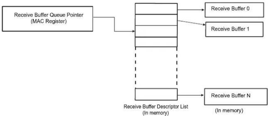
flowchart
graph TD
    A["Receive Buffer Queue Pointer (MAC Register)"] --> B["Receive Buffer Descriptor List (In memory)"]
    B --> C["Receive Buffer N (In memory)"]
    B --> D["Receive Buffer 0"]
    B --> E["Receive Buffer 1"]
To create the list of buffers:
- Allocate a number (N) of buffers of X bytes in system memory, where X is the DMA buffer length programmed in the DMA Configuration register.
- Allocate an area 8N bytes for the receive buffer descriptor list in system memory and create N entries in this list. Mark all entries in this list as owned by GMAC, i.e., bit 0 of word 0 set to 0.
- Mark the last descriptor in the queue with the wrap bit (bit 1 in word 0 set to 1).
- Write address of receive buffer descriptor list and control information to GMAC register receive buffer queue pointer
- The receive circuits can then be enabled by writing to the address recognition registers and the Network Control register.
Note: The queue pointers must be initialized and point to USED descriptors for all queues including those not intended for use.
37.7.1.3 Transmit Buffer List
Transmit data is read from areas of data (the buffers) in system memory. These buffers are listed in another data structure that also resides in main memory. This data structure (Transmit Buffer Queue) is a sequence of descriptor entries as defined in the table Transmit Buffer Descriptor Entry.
The Transmit Buffer Queue Pointer register points to this data structure.
To create this list of buffers:
- Allocate a number (N) of buffers of between 1 and 2047 bytes of data to be transmitted in system memory. Up to 128 buffers per frame are allowed.
- Allocate an area 8N bytes for the transmit buffer descriptor list in system memory and create N entries in this list. Mark all entries in this list as owned by GMAC, i.e., bit 31 of word 1 set to 0.
- Mark the last descriptor in the queue with the wrap bit (bit 30 in word 1 set to 1).
- Write address of transmit buffer descriptor list and control information to GMAC register transmit buffer queue pointer.
- The transmit circuits can then be enabled by writing to the Network Control register.
Note: The queue pointers must be initialized and point to USED descriptors for all queues including those not intended for use.
37.7.1.4 Address Matching
The GMAC Hash register pair and the four Specific Address register pairs must be written with the required values. Each register pair comprises of a bottom register and top register, with the bottom register being written first. The address matching is disabled for a particular register pair after the
bottom register has been written and re-enabled when the top register is written. Each register pair may be written at any time, regardless of whether the receive circuits are enabled or disabled.
As an example, to set Specific Address register 1 to recognize destination address 21:43:65:87:A9:CB, the following values are written to Specific Address register 1 bottom and Specific Address register 1 top:
- Specific Address register 1 bottom bits 31:0 (0x98): 0x8765_4321.
- Specific Address register 1 top bits 31:0 (0x9C): 0x0000_CBA9.
Note: The address matching is the first level of filtering. If there is a match, the screeners are the next level of filtering for routing the data to the appropriate queue. See Priority Queueing in the DMA for more details.
37.7.1.5 PHY Maintenance
The PHY Maintenance register is implemented as a shift register. Writing to the register starts a shift operation which is signalled as complete when bit two is set in the Network Status register (about 2000 MCK cycles later when bits 18:16 are set to 010 in the Network Configuration register). An interrupt is generated as this bit is set.
During this time, the MSB of the register is output on the MDIO pin and the LSB updated from the MDIO pin with each Management Data Clock (MDC) cycle. This causes the transmission of a PHY management frame on MDIO. See section 22.2.4.5 of the IEEE 802.3 standard.
Reading during the shift operation will return the current contents of the shift register. At the end of the management operation the bits will have shifted back to their original locations. For a read operation the data bits are updated with data read from the PHY. It is important to write the correct values to the register to ensure a valid PHY management frame is produced.
The Management Data Clock (MDC) should not toggle faster than 2.5 MHz (minimum period of 400 ns), as defined by the IEEE 802.3 standard. MDC is generated by dividing down MCK. Three bits in the Network Configuration register determine by how much MCK should be divided to produce MDC.
37.7.1.6 Interrupts
There are 18 interrupt conditions that are detected within the GMAC. The conditions are ORed to make multiple interrupts. Depending on the overall system design this may be passed through a further level of interrupt collection (interrupt controller). On receipt of the interrupt signal, the CPU enters the interrupt handler. Refer to the device interrupt controller documentation to identify that it is the GMAC that is generating the interrupt. To ascertain which interrupt, read the Interrupt Status register. Note that in the default configuration this register will clear itself after being read, though this may be configured to be write-one-to-clear if desired.
At reset all interrupts are disabled. To enable an interrupt, write to Interrupt Enable register with the pertinent interrupt bit set to 1. To disable an interrupt, write to Interrupt Disable register with the pertinent interrupt bit set to 1. To check whether an interrupt is enabled or disabled, read Interrupt Mask register. If the bit is set to 1, the interrupt is disabled.
37.7.1.7 Transmitting Frames
The procedure to set up a frame for transmission is the following:
- Enable transmit in the Network Control register.
- Allocate an area of system memory for transmit data. This does not have to be contiguous, varying byte lengths can be used if they conclude on byte borders.
- Set-up the transmit buffer list by writing buffer addresses to word zero of the transmit buffer descriptor entries and control and length to word one.
- Write data for transmission into the buffers pointed to by the descriptors.
- Write the address of the first buffer descriptor to transmit buffer descriptor queue pointer.
-
Enable appropriate interrupts.
-
Write to the transmit start bit (TSTART) in the Network Control register.
37.7.1.8 Receiving Frames
When a frame is received and the receive circuits are enabled, the GMAC checks the address and, in the following cases, the frame is written to system memory:
- If it matches one of the four Specific Address registers.
- If it matches one of the four type ID registers.
- If it matches the hash address function.
- If it is a broadcast address (0xFFFFFFFFFFF) and broadcasts are allowed.
- If the GMAC is configured to "copy all frames".
The register receive buffer queue pointer points to the next entry in the receive buffer descriptor list and the GMAC uses this as the address in system memory to write the frame to.
Once the frame has been completely and successfully received and written to system memory, the GMAC then updates the receive buffer descriptor entry (see Receive Buffer Descriptor Entry) with the reason for the address match and marks the area as being owned by software. Once this is complete, a receive complete interrupt is set. Software is then responsible for copying the data to the application area and releasing the buffer (by writing the ownership bit back to 0).
If the GMAC is unable to write the data at a rate to match the incoming frame, then a receive overrun interrupt is set. If there is no receive buffer available, i.e., the next buffer is still owned by software, a receive buffer not available interrupt is set. If the frame is not successfully received, a statistics register is incremented and the frame is discarded without informing software.
37.7.2 Statistics Registers
Statistics registers are described in the User Interface beginning with GMAC Octets Transmitted Low Register and ending with GMAC UDP Checksum Errors Register.
The statistics register block begins at 0x100 and runs to 0x1B0, and comprises the registers listed below.
| Octets Transmitted Low Register Broadcast Frames Received Register | |
| Octets Transmitted High Register Multicast Frames Received Register | |
| Frames Transmitted Register Pause Frames Received Register | |
| Broadcast Frames Transmitted Register 64 Byte Frames Received Register | |
| Multicast Frames Transmitted Register 65 to 127 Byte Frames Received Register | |
| Pause Frames Transmitted Register 128 to 255 Byte Frames Received Register | |
| 64 Byte Frames Transmitted Register 256 to 511 Byte Frames Received Register | |
| 65 to 127 Byte Frames Transmitted Register 512 to 1023 Byte Frames Received Register | |
| 128 to 255 Byte Frames Transmitted Register 1024 to 1518 Byte Frames Received Register | |
| 256 to 511 Byte Frames Transmitted Register 1519 to Maximum Byte Frames Received Register | |
| 512 to 1023 Byte Frames Transmitted Register Undersize Frames Received Register | |
| 1024 to 1518 Byte Frames Transmitted Register Oversize Frames Received Register | |
| Greater Than 1518 Byte Frames Transmitted Register | Jabbers Received Register |
| Transmit Underruns Register | Frame Check Sequence Errors Register |
| Single Collision Frames Register | Length Field Frame Errors Register |
| Multiple Collision Frames Register | Receive Symbol Errors Register |
| Excessive Collisions Register | Alignment Errors Register |
| Late Collisions Register | Receive Resource Errors Register |
| Deferred Transmission Frames Register | Receive Overrun Register |
| Carrier Sense Errors Register | IP Header Checksum Errors Register |
| Octets Received Low Register TCP Checksum Errors Register | |
| Octets Received High Register UDP Checksum Errors Register | |
| Frames Received Register | |
These registers reset to zero on a read and stick at all ones when they count to their maximum value. They should be read frequently enough to prevent loss of data.
The receive statistics registers are only incremented when the receive enable bit (RXEN) is set in the Network Control register.
Once a statistics register has been read, it is automatically cleared. When reading the Octets Transmitted and Octets Received registers, bits 31:0 should be read prior to bits 47:32 to ensure reliable operation.
37.8 Register Summary
| Offset | Name Bit Pos. 7 | 6 | 5 | 4 | 3 | 2 | 1 | 0 | |||||||
| 0x00 | GMAC_NCR | 7:0 | WESTAT INCSTAT | CLRSTAT MPE | TXEN RXEN LBL | ||||||||||
| 15:8 | SRTSM | TXZQPF | TXPF | THALT | TSTART | BP | |||||||||
| 23:16 | FNP | TXPBPF | ENPBPR | ||||||||||||
| 31:24 | |||||||||||||||
| 0x04 | GMAC_NCFGR | 7:0 | UNIHEN | MTIHEN | NBC | CAF | JFRAME | DNVLAN | FD | SPD | |||||
| 15:8 | RXBUFO[1:0] | PEN | RTY | GBE | MAXFS | ||||||||||
| 23:16 | DCPF | DBW[1:0] | CLK[2:0] | RFCS | LFERD | ||||||||||
| 31:24 | IRXER | RXBP | IPGSEN | IRXFCS | EFRHD | RXCOEN | |||||||||
| 0x08 | GMAC_NSR | 7:0 | IDLE | MDIO | |||||||||||
| 15:8 | |||||||||||||||
| 23:16 | |||||||||||||||
| 31:24 | |||||||||||||||
| 0x0C | GMAC_UR | 7:0 | MII | ||||||||||||
| 15:8 | |||||||||||||||
| 23:16 | |||||||||||||||
| 31:24 | |||||||||||||||
| 0x10 | GMAC_DCFGR | 7:0 | ESPA ESMA | FBLDO[4:0] | |||||||||||
| 15:8 | TXCOEN | TXPBMS | RXBMS[1:0] | ||||||||||||
| 23:16 | DRBS[7:0] | ||||||||||||||
| 31:24 | DDRP | ||||||||||||||
| 0x14 | GMAC_TSR | 7:0 | LCO | UND | TXCOMP | TFC | TXGO | RLE | COL | UBR | |||||
| 15:8 | HRESP | ||||||||||||||
| 23:16 | |||||||||||||||
| 31:24 | |||||||||||||||
| 0x18 | GMAC_RBQB | 7:0 | ADDR[5:0] | ||||||||||||
| 15:8 | ADDR[13:6] | ||||||||||||||
| 23:16 | ADDR[21:14] | ||||||||||||||
| 31:24 | ADDR[29:22] | ||||||||||||||
| 0x1C | GMAC_TBQB | 7:0 | ADDR[5:0] | ||||||||||||
| 15:8 | ADDR[13:6] | ||||||||||||||
| 23:16 | ADDR[21:14] | ||||||||||||||
| 31:24 | ADDR[28:22] | ||||||||||||||
| 0x20 | GMAC_RSR | 7:0 | HNO | RXOVR | REC | BNA | |||||||||
| 15:8 | |||||||||||||||
| 23:16 | |||||||||||||||
| 31:24 | |||||||||||||||
| 0x24 | GMAC_ISR | 7:0 | TCOMP | TFC | RLEX | TUR | TXUBR | RXUBR | RCOMP | MFS | |||||
| 15:8 | PFTR | PTZ | PFNZ | HRESP | ROVR | ||||||||||
| 23:16 | PDRSFR | PDRQFR | SFT | DRQFT | SFR | DRQFR | |||||||||
| 31:24 | TSUTIMCMP | WOL | RXLPISBC | SRI | PDRSFT | PDRQFT | |||||||||
| 0x28 | GMAC_IER | 7:0 | TCOMP | TFC | RLEX | TUR | TXUBR | RXUBR | RCOMP | MFS | |||||
| 15:8 | EXINT | PFTR | PTZ | PFNZ | HRESP | ROVR | |||||||||
| 23:16 | PDRSFR | PDRQFR | SFT | DRQFT | SFR | DRQFR | |||||||||
| 31:24 | TSUTIMCMP | WOL | RXLPISBC | SRI | PDRSFT | PDQFT | |||||||||
| 0x2C | GMAC_IDR | 7:0 | TCOMP | TFC | RLEX | TUR | TXUBR | RXUBR | RCOMP | MFS | |||||
| 15:8 | EXINT | PFTR | PTZ | PFNZ | HRESP | ROVR | |||||||||
| 23:16 | PDRSFR | PDRQFR | SFT | DRQFT | DRQFR | ||||||||||
| 31:24 | TSUTIMCMP | WOL | RXLPISBC | SRI | PDRSFT | PDRQFT | |||||||||
| 0x30 | GMAC_IMR | 7:0 | TCOMP | TFC | RLEX | TUR | TXUBR | RXUBR | RCOMP | MFS | |||||
| 15:8 | EXINT | PFTR | PTZ | PFNZ | HRESP | ROVR | |||||||||
| 23:16 | PDRSFR | PDRQFR | SFT | DRQTT | SFR | DRQFR | |||||||||
| 31:24 | TSUTIMCMP | WOL | RXLPISBC | SRI | PDRSFT | PDRQFT | |||||||||
| 0x34 | GMAC_MAN | 7:0 | DATA[7:0] | ||||||||||||
| 15:8 | DATA[15:8] | ||||||||||||||
| 23:16 | PHYA[0] | REGA[4:0] | WTN[1:0] | ||||||||||||
| 31:24 | WZO | CLTTO | OP[1:0] | PHYA[4:1] | |||||||||||
......continued
| Offset | Name Bit Pos. 76543210 | ||||||||
| 0x38 GMAC_RPQ | 7:0 RPQ[7:0] | ||||||||
| 15:8 RPQ[15:8] | |||||||||
| 23:16 | |||||||||
| 31:24 | |||||||||
| 0x3C GMAC_TPQ | 7:0 TPQ[7:0] | ||||||||
| 15:8 TPQ[15:8] | |||||||||
| 23:16 | |||||||||
| 31:24 | |||||||||
| 0x40 GMAC_TPSF | 7:0 TPB1ADR[7:0] | ||||||||
| 15:8 | TPB1ADR[11:8] | ||||||||
| 23:16 | |||||||||
| 31:24 ENTXP | |||||||||
| 0x44 GMAC_RPSF | 7:0 RPB1ADR[7:0] | ||||||||
| 15:8 | RPB1ADR[11:8] | ||||||||
| 23:16 | |||||||||
| 31:24 ENRXP | |||||||||
| 0x48 | GMAC_RJFML | 7:0 FML[7:0] | |||||||
| 15:8 | FML[13:8] | ||||||||
| 23:16 | |||||||||
| 31:24 | |||||||||
| 0x4C ... 0x7F | Reserved | ||||||||
| 0x80 GMAC_HRB | 7:0 | ADDR[7:0] | |||||||
| 15:8 | ADDR[15:8] | ||||||||
| 23:16 | ADDR[23:16] | ||||||||
| 31:24 | ADDR[31:24] | ||||||||
| 0x84 | GMAC_HRT | 7:0 | ADDR[7:0] | ||||||
| 15:8 | ADDR[15:8] | ||||||||
| 23:16 | ADDR[23:16] | ||||||||
| 31:24 | ADDR[31:24] | ||||||||
| 0x88 | GMAC_SAB1 | 7:0 | ADDR[7:0] | ||||||
| 15:8 | ADDR[15:8] | ||||||||
| 23:16 | ADDR[23:16] | ||||||||
| 31:24 | ADDR[31:24] | ||||||||
| 0x8C | GMAC_SAT1 | 7:0 | ADDR[7:0] | ||||||
| 15:8 | ADDR[15:8] | ||||||||
| 23:16 | |||||||||
| 31:24 | |||||||||
| 0x90 | GMAC_SAB2 | 7:0 | ADDR[7:0] | ||||||
| 15:8 | ADDR[15:8] | ||||||||
| 23:16 | ADDR[23:16] | ||||||||
| 31:24 | ADDR[31:24] | ||||||||
| 0x94 | GMAC_SAT2 | 7:0 | ADDR[7:0] | ||||||
| 15:8 | ADDR[15:8] | ||||||||
| 23:16 | |||||||||
| 31:24 | |||||||||
| 0x98 | GMAC_SAB3 | 7:0 | ADDR[7:0] | ||||||
| 15:8 | ADDR[15:8] | ||||||||
| 23:16 | ADDR[23:16] | ||||||||
| 31:24 | ADDR[31:24] | ||||||||
| 0x9C | GMAC_SAT3 | 7:0 | ADDR[7:0] | ||||||
| 15:8 | ADDR[15:8] | ||||||||
| 23:16 | |||||||||
| 31:24 | |||||||||
| 0xA0 | GMAC_SAB4 | 7:0 | ADDR[7:0] | ||||||
| 15:8 | ADDR[15:8] | ||||||||
| 23:16 | ADDR[23:16] | ||||||||
| 31:24 | ADDR[31:24] | ||||||||
| 0xA4 GMAC_SAT4 | 7:0 ADDR[7:0] | ||||||||
| 15:8 ADDR[15:8] | |||||||||
| 23:16 | |||||||||
| 31:24 | |||||||||
| 0xA8 GMAC_TIDM1 | 7:0 TID[7:0] | ||||||||
| 15:8 TID[15:8] | |||||||||
| 23:16 | |||||||||
| 31:24 ENIDn | |||||||||
| 0xAC GMAC_TIDM2 | 7:0 TID[7:0] | ||||||||
| 15:8 TID[15:8] | |||||||||
| 23:16 | |||||||||
| 31:24 ENIDn | |||||||||
| 0xB0 GMAC_TIDM3 | 7:0 TID[7:0] | ||||||||
| 15:8 TID[15:8] | |||||||||
| 23:16 | |||||||||
| 31:24 ENIDn | |||||||||
| 0xB4 GMAC_TIDM4 | 7:0 TID[7:0] | ||||||||
| 15:8 TID[15:8] | |||||||||
| 23:16 | |||||||||
| 31:24 ENIDn | |||||||||
| 0xB8 GMAC_WOL | 7:0 IP[7:0] | ||||||||
| 15:8 | IP[15:8] | ||||||||
| 23:16 | MTI | SA1 | ARP MAG | ||||||
| 31:24 | |||||||||
| 0xBC GMAC_IPGS | 7:0 | FL[7:0] | |||||||
| 15:8 | FL[15:8] | ||||||||
| 23:16 | |||||||||
| 31:24 | |||||||||
| 0xC0 GMAC_SVLAN | 7:0 | VLAN_TYPE[7:0] | |||||||
| 15:8 | VLAN_TYPE[15:8] | ||||||||
| 23:16 | |||||||||
| 31:24 ESVLAN | |||||||||
| 0xC4 | GMAC_TPFCP | 7:0 | PEV[7:0] | ||||||
| 15:8 | PQ[7:0] | ||||||||
| 23:16 | |||||||||
| 31:24 | |||||||||
| 0xC8 | GMAC_SAMB1 | 7:0 ADDR[7:0] | |||||||
| 15:8 ADDR[15:8] | |||||||||
| 23:16 | ADDR[23:16] | ||||||||
| 31:24 | ADDR[31:24] | ||||||||
| 0xCC | GMAC_SAMT1 | 7:0 ADDR[7:0] | |||||||
| 15:8 ADDR[15:8] | |||||||||
| 23:16 | |||||||||
| 31:24 | |||||||||
| 0xD0 ... 0xDB | Reserved | ||||||||
| 0xDC | GMAC_NSC | 7:0 | NANOSEC[7:0] | ||||||
| 15:8 | NANOSEC[15:8] | ||||||||
| 23:16 | NANOSEC[21:16] | ||||||||
| 31:24 | |||||||||
| 0xE0 | GMAC_SCL | 7:0 | SEC[7:0] | ||||||
| 15:8 | SEC[15:8] | ||||||||
| 23:16 | SEC[23:16] | ||||||||
| 31:24 | SEC[31:24] | ||||||||
| 0xE4 GMAC_SCH | 7:0 | SEC[7:0] | |||||||
| 15:8 | SEC[15:8] | ||||||||
| 23:16 | |||||||||
| 31:24 | |||||||||
| 0xE8 GMAC_EFTSH | 7:0 RUD[7:0] | ||||||||
| 15:8 RUD[15:8] | |||||||||
| 23:16 | |||||||||
| 31:24 | |||||||||
| 0xEC GMAC_EFRSH | 7:0 RUD[7:0] | ||||||||
| 15:8 RUD[15:8] | |||||||||
| 23:16 | |||||||||
| 31:24 | |||||||||
| 0xF0 GMAC_PEFTSH | 7:0 RUD[7:0] | ||||||||
| 15:8 RUD[15:8] | |||||||||
| 23:16 | |||||||||
| 31:24 | |||||||||
| 0xF4 GMAC_PEFRSH | 7:0 RUD[7:0] | ||||||||
| 15:8 RUD[15:8] | |||||||||
| 23:16 | |||||||||
| 31:24 | |||||||||
| 0xF8 ... 0xFF | Reserved | ||||||||
| 0x0100 | GMAC_OTLO | 7:0 TXO[7:0] | |||||||
| 15:8 | TXO[15:8] | ||||||||
| 23:16 | TXO[23:16] | ||||||||
| 31:24 | TXO[31:24] | ||||||||
| 0x0104 | GMAC_OTHI | 7:0 TXO[7:0] | |||||||
| 15:8 | TXO[15:8] | ||||||||
| 23:16 | |||||||||
| 31:24 | |||||||||
| 0x0108 | GMAC_FT | 7:0 | FTX[7:0] | ||||||
| 15:8 | FTX[15:8] | ||||||||
| 23:16 | FTX[23:16] | ||||||||
| 31:24 | FTX[31:24] | ||||||||
| 0x010C | GMAC_BCFT | 7:0 | BFTX[7:0] | ||||||
| 15:8 | BFTX[15:8] | ||||||||
| 23:16 | BFTX[23:16] | ||||||||
| 31:24 | BFTX[31:24] | ||||||||
| 0x0110 | GMAC_MFT | 7:0 | MFTX[7:0] | ||||||
| 15:8 | MFTX[15:8] | ||||||||
| 23:16 | MFTX[23:16] | ||||||||
| 31:24 | MFTX[31:24] | ||||||||
| 0x0114 | GMAC_PFT | 7:0 | PFTX[7:0] | ||||||
| 15:8 | PFTX[15:8] | ||||||||
| 23:16 | |||||||||
| 31:24 | |||||||||
| 0x0118 | GMAC_BFT64 | 7:0 | NFTX[7:0] | ||||||
| 15:8 | NFTX[15:8] | ||||||||
| 23:16 | NFTX[23:16] | ||||||||
| 31:24 | NFTX[31:24] | ||||||||
| 0x011C | GMAC_TBFT127 | 7:0 | NFTX[7:0] | ||||||
| 15:8 | NFTX[15:8] | ||||||||
| 23:16 | NFTX[23:16] | ||||||||
| 31:24 | NFTX[31:24] | ||||||||
| 0x0128 | GMAC_TBFT1023 | 7:0 NFTX[7:0] | |||||||
| 15:8 NFTX[15:8] | |||||||||
| 23:16 NFTX[23:16] | |||||||||
| 31:24 NFTX[31:24] | |||||||||
| 0x012C | GMAC_TBFT1518 | 7:0 NFTX[7:0] | |||||||
| 15:8 NFTX[15:8] | |||||||||
| 23:16 NFTX[23:16] | |||||||||
| 31:24 NFTX[31:24] | |||||||||
| 0x0130 | GMAC_GTBFT1518 | 7:0 NFTX[7:0] | |||||||
| 15:8 NFTX[15:8] | |||||||||
| 23:16 NFTX[23:16] | |||||||||
| 31:24 NFTX[31:24] | |||||||||
| 0x0134 | GMAC_TUR | 7:0 TXUNR[7:0] | |||||||
| 15:8 TXUNR[9:8] | |||||||||
| 23:16 | |||||||||
| 31:24 | |||||||||
| 0x0138 | GMAC_SCF | 7:0 SCOL[7:0] | |||||||
| 15:8 SCOL[15:8] | |||||||||
| 23:16 | SCOL[17:16] | ||||||||
| 31:24 | |||||||||
| 0x013C | GMAC_MCF | 7:0 | MCOL[7:0] | ||||||
| 15:8 | MCOL[15:8] | ||||||||
| 23:16 | MCOL[17:16] | ||||||||
| 31:24 | |||||||||
| 0x0140 | GMAC_EC | 7:0 XCOL[7:0] | |||||||
| 15:8 | XCOL[9:8] | ||||||||
| 23:16 | |||||||||
| 31:24 | |||||||||
| 0x0144 | GMAC_LC | 7:0 LCOL[7:0] | |||||||
| 15:8 | LCOL[9:8] | ||||||||
| 23:16 | |||||||||
| 31:24 | |||||||||
| 0x0148 | GMAC_DTF | 7:0 DEFT[7:0] | |||||||
| 15:8 DEFT[15:8] | |||||||||
| 23:16 | DEFT[17:16] | ||||||||
| 31:24 | |||||||||
| 0x014C | GMAC_CSE | 7:0 | CSR[7:0] | ||||||
| 15:8 | CSR[9:8] | ||||||||
| 23:16 | |||||||||
| 31:24 | |||||||||
| 0x0150 | GMAC_ORLO | 7:0 | RXO[7:0] | ||||||
| 15:8 | RXO[15:8] | ||||||||
| 23:16 | RXO[23:16] | ||||||||
| 31:24 | RXO[31:24] | ||||||||
| 0x0154 | GMAC_ORHI | 7:0 | RXO[7:0] | ||||||
| 15:8 | RXO[15:8] | ||||||||
| 23:16 | |||||||||
| 31:24 | |||||||||
| 0x0158 | GMAC_FR | 7:0 | FRX[7:0] | ||||||
| 15:8 | FRX[15:8] | ||||||||
| 23:16 | FRX[23:16] | ||||||||
| 31:24 | FRX[31:24] | ||||||||
| 0x015C | GMAC_BCFR | 7:0 BFRX[7:0] | |||||||
| 15:8 BFRX[15:8] | |||||||||
| 23:16 BFRX[23:16] | |||||||||
| 31:24 BFRX[31:24] | |||||||||
| 0x0160 | GMAC_MFR | 7:0 | MFRX[7:0] | ||||||
| 15:8 | MFRX[15:8] | ||||||||
| 23:16 | MFRX[23:16] | ||||||||
| 31:24 | MFRX[31:24] | ||||||||
| 0x0164 | GMAC_PFR | 7:0 PFRX[7:0] | |||||||
| 15:8 PFRX[15:8] | |||||||||
| 23:16 | |||||||||
| 31:24 | |||||||||
| 0x0168 | GMAC_BFR64 | 7:0 NFRX[7:0] | |||||||
| 15:8 NFRX[15:8] | |||||||||
| 23:16 NFRX[23:16] | |||||||||
| 31:24 NFRX[31:24] | |||||||||
| 0x016C | GMAC_TBFR127 | 7:0 NFRX[7:0] | |||||||
| 15:8 NFRX[15:8] | |||||||||
| 23:16 NFRX[23:16] | |||||||||
| 31:24 NFRX[31:24] | |||||||||
| 0x01A0 | GMAC_RRE | 7:0 RXRER[7:0] | |||||||
| 15:8 RXRER[15:8] | |||||||||
| 23:16 | RXRER[17:16] | ||||||||
| 31:24 | |||||||||
| 0x01A4 | GMAC_ROE | 7:0 RXOVR[7:0] | |||||||
| 15:8 | RXOVR[9:8] | ||||||||
| 23:16 | |||||||||
| 31:24 | |||||||||
| 0x01A8 | GMAC_IHCE | 7:0 HCKER[7:0] | |||||||
| 15:8 | |||||||||
| 23:16 | |||||||||
| 31:24 | |||||||||
| 0x01AC | GMAC_TCE | 7:0 TCKER[7:0] | |||||||
| 15:8 | |||||||||
| 23:16 | |||||||||
| 31:24 | |||||||||
| 0x01B0 | GMAC_UCE | 7:0 UCKER[7:0] | |||||||
| 15:8 | |||||||||
| 23:16 | |||||||||
| 31:24 | |||||||||
| 0x01B4 ... 0x01BB | Reserved | ||||||||
| 0x01BC | GMAC_TISUBN | 7:0 LSBTIR[7:0] | |||||||
| 15:8 | LSBTIR[15:8] | ||||||||
| 23:16 | |||||||||
| 31:24 | |||||||||
| 0x01C0 | GMAC_TSH | 7:0 | TCS[7:0] | ||||||
| 15:8 | TCS[15:8] | ||||||||
| 23:16 | |||||||||
| 31:24 | |||||||||
| 0x01C4 ... 0x01CF | Reserved | ||||||||
| 0x01D0 | GMAC_TSL | 7:0 | TCS[7:0] | ||||||
| 15:8 | TCS[15:8] | ||||||||
| 23:16 | TCS[23:16] | ||||||||
| 31:24 | TCS[31:24] | ||||||||
| 0x01D4 | GMAC_TN | 7:0 | TNS[7:0] | ||||||
| 15:8 TNS[15:8] | |||||||||
| 23:16 TNS[23:16] | |||||||||
| 31:24 | TNS[29:24] | ||||||||
| 0x01D8 | GMAC_TA | 7:0 | ITDT[7:0] | ||||||
| 15:8 | ITDT[15:8] | ||||||||
| 23:16 | ITDT[23:16] | ||||||||
| 31:24 | ADJ | ITDT[29:24] | |||||||
| 0x01DC | GMAC_TI | 7:0 | CNS[7:0] | ||||||
| 15:8 ACNS[7:0] | |||||||||
| 23:16 | NIT[7:0] | ||||||||
| 31:24 | |||||||||
| 0x01E0 | GMAC_EFTSL | 7:0 | RUD[7:0] | ||||||
| 15:8 | RUD[15:8] | ||||||||
| 23:16 | RUD[23:16] | ||||||||
| 31:24 | RUD[31:24] | ||||||||
| 0x01E4 | GMAC_EFTN | 7:0 | RUD[7:0] | ||||||
| 15:8 | RUD[15:8] | ||||||||
| 23:16 | RUD[23:16] | ||||||||
| 31:24 | RUD[29:24] | ||||||||
......continued
| Offset | Name Bit Pos. 76543210 | |||||||||
| 0x01E8 | GMAC_EFRSL | 7:0 RUD[7:0] | ||||||||
| 15:8 RUD[15:8] | ||||||||||
| 23:16 RUD[23:16] | ||||||||||
| 31:24 RUD[31:24] | ||||||||||
| 0x01EC | GMAC_EFRN | 7:0 RUD[7:0] | ||||||||
| 15:8 RUD[15:8] | ||||||||||
| 23:16 RUD[23:16] | ||||||||||
| 31:24 RUD[29:24] | ||||||||||
| 0x01F0 | GMAC_PEFTSL | 7:0 RUD[7:0] | ||||||||
| 15:8 RUD[15:8] | ||||||||||
| 23:16 RUD[23:16] | ||||||||||
| 31:24 RUD[31:24] | ||||||||||
| 0x01F4 | GMAC_PEFTN | 7:0 RUD[7:0] | ||||||||
| 15:8 RUD[15:8] | ||||||||||
| 23:16 RUD[23:16] | ||||||||||
| 31:24 RUD[29:24] | ||||||||||
| 0x01F8 | GMAC_PEFRSL | 7:0 RUD[7:0] | ||||||||
| 15:8 RUD[15:8] | ||||||||||
| 23:16 RUD[23:16] | ||||||||||
| 31:24 RUD[31:24] | ||||||||||
| 0x01FC | GMAC_PEFRN | 7:0 RUD[7:0] | ||||||||
| 15:8 RUD[15:8] | ||||||||||
| 23:16 RUD[23:16] | ||||||||||
| 31:24 RUD[29:24] | ||||||||||
| 0x0200 ... 0x026F | Reserved | |||||||||
| 0x0270 | GMAC_RXLPI | 7:0 | COUNT[7:0] | |||||||
| 15:8 | COUNT[15:8] | |||||||||
| 23:16 | ||||||||||
| 31:24 | ||||||||||
| 0x0274 | GMAC_RXLPITIME | 7:0 | LPITIME[7:0] | |||||||
| 15:8 | LPITIME[15:8] | |||||||||
| 23:16 | LPITIME[23:16] | |||||||||
| 31:24 | ||||||||||
| 0x0278 | GMAC_TXLPI | 7:0 | COUNT[7:0] | |||||||
| 15:8 | COUNT[15:8] | |||||||||
| 23:16 | COUNT[23:16] | |||||||||
| 31:24 | ||||||||||
| 0x027C | GMAC_TXLPITIME | 7:0 | LPITIME[7:0] | |||||||
| 15:8 | LPITIME[15:8] | |||||||||
| 23:16 | LPITIME[23:16] | |||||||||
| 31:24 | ||||||||||
| 0X0280 ... 0x03FF | Reserved | |||||||||
| 0x0400 | GMAC_ISRPQ1 | 7:0 | TCOMP | TFC | RLEX | RXUBR | RCOMP | |||
| 15:8 | HRESP | ROVR | ||||||||
| 23:16 | ||||||||||
| 31:24 | ||||||||||
| 0x0404 | GMAC_ISRPQ2 | 7:0 | TCOMP | TFC | RLEX | RXUBR | RCOMP | |||
| 15:8 | HRESP | ROVR | ||||||||
| 23:16 | ||||||||||
| 31:24 | ||||||||||
| 0x0408 ... 0x043F | Reserved | |||||||||
| 0x0440 | GMAC_TBQBAPQ1 | 7:0 | TXBQBA[5:0] | |||||||
| 15:8 | TXBQBA[13:6] | |||||||||
| 23:16 | TXBQBA[21:14] | |||||||||
| 31:24 | TXBQBA[29:22] | |||||||||
......continued
| Offset | Name Bit Pos. 76543210 | ||||||||
| 0x0444 | GMAC_TBQBAPQ2 | 7:0 TXBQBA[5:0] | |||||||
| 15:8 TXBQBA[13:6] | |||||||||
| 23:16 TXBQBA[21:14] | |||||||||
| 31:24 TXBQBA[29:22] | |||||||||
| 0x0448 ... 0x047F | Reserved | ||||||||
| 0x0480 | GMAC_RBQBAPQ1 | 7:0 RXBQBA[5:0] | |||||||
| 15:8 RXBQBA[13:6] | |||||||||
| 23:16 RXBQBA[21:14] | |||||||||
| 31:24 RXBQBA[29:22] | |||||||||
| 0x0484 | GMAC_RBQBAPQ2 | 7:0 RXBQBA[5:0] | |||||||
| 15:8 RXBQBA[13:6] | |||||||||
| 23:16 RXBQBA[21:14] | |||||||||
| 31:24 RXBQBA[29:22] | |||||||||
| 0x0488 ... 0x049F | Reserved | ||||||||
| 0x04A0 | GMAC_RBSRPQ1 | 7:0 RBS[7:0] | |||||||
| 15:8 RBS[15:8] | |||||||||
| 23:16 | |||||||||
| 31:24 | |||||||||
| 0x04A4 | GMAC_RBSRPQ2 | 7:0 RBS[7:0] | |||||||
| 15:8 RBS[15:8] | |||||||||
| 23:16 | |||||||||
| 31:24 | |||||||||
| 0x04A8 ... 0x04BB | Reserved | ||||||||
| 0x04BC | GMAC_CBSCR | 7:0 | QAE QBE | ||||||
| 15:8 | |||||||||
| 23:16 | |||||||||
| 31:24 | |||||||||
| 0x04C0 | GMAC_CBSISQA | 7:0 | IS[7:0] | ||||||
| 15:8 | IS[15:8] | ||||||||
| 23:16 | IS[23:16] | ||||||||
| 31:24 | IS[31:24] | ||||||||
| 0x04C4 | GMAC_CBSISQB | 7:0 | IS[7:0] | ||||||
| 15:8 | IS[15:8] | ||||||||
| 23:16 | IS[23:16] | ||||||||
| 31:24 | IS[31:24] | ||||||||
| 0x04C8 ... 0x04FF | Reserved | ||||||||
| 0x0500 | GMAC_ST1RPQ0 | 7:0 | DSTCM[3:0] | QNB[2:0] | |||||
| 15:8 | UDPM[3:0] | DSTCM[7:4] | |||||||
| 23:16 | UDPM[11:4] | ||||||||
| 31:24 | UDPE DSTCE | UDPM[15:12] | |||||||
| 0x0504 | GMAC_ST1RPQ1 | 7:0 | DSTCM[3:0] | QNB[2:0] | |||||
| 15:8 | UDPM[3:0] | DSTCM[7:4] | |||||||
| 23:16 | UDPM[11:4] | ||||||||
| 31:24 | UDPE DSTCE | UDPN[15:12] | |||||||
| 0x0508 ... 0x053F | Reserved | ||||||||
| 0x0540 | GMAC_ST2RPQ0 | 7:0 | VLANP[2:0] | QNB[2:0] | |||||
| 15:8 | COMPA[2:0] | ETHE | I2ETH[2:0] | VLANE | |||||
| 23:16 | COMPB[4:0] | COMPAE | COMPA[4:3] | ||||||
| 31:24 | COMPCE COMPC[4:0] | COMPBE | |||||||
......continued
| Offset | Name Bit Pos. 76543210 | |||||||||
| 0x0544 | GMAC_ST2RPQ1 | 7:0 VLANP[2:0] QNB[2:0] | ||||||||
| 15:8 COMPA[2:0] ETHE I2ETH[2:0] VLANE | ||||||||||
| 23:16 COMPB[4:0] COMPAE COMPA[4:3] | ||||||||||
| 31:24 | COMPCE COMPC[4:0] | COMPBE | ||||||||
| 0x0548 ... 0x05FF | Reserved | |||||||||
| 0x0600 | GMAC_IERPQ1 | 7:0 | TCOMP | TFC | RLEX | RXUBR | RCOMP | |||
| 15:8 | HRESP | ROVR | ||||||||
| 23:16 | ||||||||||
| 31:24 | ||||||||||
| 0x0604 | GMAC_IERPQ2 | 7:0 | TCOMP | TFC | RLEX | RXUBR | RCOMP | |||
| 15:8 | HRESP | ROVR | ||||||||
| 23:16 | ||||||||||
| 31:24 | ||||||||||
| 0x0608 ... 0x061F | Reserved | |||||||||
| 0x0620 | GMAC_IDRPQ1 | 7:0 | TCOMP | TFC | RLEX | RXUBR | RCOMP | |||
| 15:8 | HRESP | ROVR | ||||||||
| 23:16 | ||||||||||
| 31:24 | ||||||||||
| 0x0624 | GMAC_IDRPQ2 | 7:0 | TCOMP | TFC | RLEX | RXUBR | RCOMP | |||
| 15:8 | HRESP | ROVR | ||||||||
| 23:16 | ||||||||||
| 31:24 | ||||||||||
| 0x0628 ... 0x063F | Reserved | |||||||||
| 0x0640 | GMAC_IMRPQ1 | 7:0 | TCOMP | AHB | RLEX | RXUBR | RCOMP | |||
| 15:8 | HRESP | ROVR | ||||||||
| 23:16 | ||||||||||
| 31:24 | ||||||||||
| 0x0644 | GMAC_IMRPQ2 | 7:0 | TCOMP | AHB | RLEX | RXUBR | RCOMP | |||
| 15:8 | HRESP | ROVR | ||||||||
| 23:16 | ||||||||||
| 31:24 | ||||||||||
| 0x0648 ... 0x06DF | Reserved | |||||||||
| 0x06E0 | GMAC_ST2ER0 | 7:0 | COMPVAL[7:0] | |||||||
| 15:8 | COMPVAL[15:8] | |||||||||
| 23:16 | ||||||||||
| 31:24 | ||||||||||
| 0x06E4 | GMAC_ST2ER1 | 7:0 | COMPVAL[7:0] | |||||||
| 15:8 | COMPVAL[15:8] | |||||||||
| 23:16 | ||||||||||
| 31:24 | ||||||||||
| 0x06E8 | GMAC_ST2ER2 | 7:0 | COMPVAL[7:0] | |||||||
| 15:8 | COMPVAL[15:8] | |||||||||
| 23:16 | ||||||||||
| 31:24 | ||||||||||
| 0x06EC | GMAC_ST2ER3 | 7:0 | COMPVAL[7:0] | |||||||
| 15:8 | COMPVAL[15:8] | |||||||||
| 23:16 | ||||||||||
| 31:24 | ||||||||||
| 0x06F0 ... 0x06FF | Reserved | |||||||||
......continued
| Offset | Name Bit Pos. 7 | 6 | 5 | 4 | 3 | 2 | 1 | 0 | |||||||||||
| 0x0700 | GMAC_ST2CW00 | 7:0 MASKVAL[7:0] | |||||||||||||||||
| 15:8 MASKVAL[15:8] | |||||||||||||||||||
| 23:16 COMPVAL[7:0] | |||||||||||||||||||
| 31:24 COMPVAL[15:8] | |||||||||||||||||||
| 0x0704 | GMAC_ST2CW10 | 7:0 OFFSSTRT[0] OFFSVAL[6:0] | |||||||||||||||||
| 15:8 | OFFSSTRT[1] | ||||||||||||||||||
| 23:16 | |||||||||||||||||||
| 31:24 | |||||||||||||||||||
| 0x0708 | GMAC_ST2CW01 | 7:0 MASKVAL[7:0] | |||||||||||||||||
| 15:8 MASKVAL[15:8] | |||||||||||||||||||
| 23:16 COMPVAL[7:0] | |||||||||||||||||||
| GMAC_ST2CW11 | 31:24 COMPVAL[15:8] | ||||||||||||||||||
| 0x070C | 7:0 OFFSSTRT[0] OFFSVAL[6:0] | ||||||||||||||||||
| 15:8 | OFFSSTRT[1] | ||||||||||||||||||
| 23:16 | |||||||||||||||||||
| 31:24 | |||||||||||||||||||
37.8.1 GMAC Network Control Register
Name: GMAC_NCR
Offset: 0x000
Reset: 0x00000000
Property: Read/Write
| Bit 31 30 29 28 27 26 25 24 | |||||||
| Access Reset | |||||||
| Bit 23 22 21 20 19 18 17 16 | |||||||
| FNP TXPBPF EN PBPR | |||||||
| Access Reset | R/W R/W R/W | ||||||
| 0 | 0 | 0 | |||||
| Bit 15 14 13 12 11 10 | 9 | 8 | |||||
| SRTSM | TXZQPF | TXPF | THALT | TSTART | BP | ||
| Access Reset | R/W | R/W R/W R/W R/W R/W | |||||
| 0 | 0 | 0 | 0 | 0 | 0 | ||
| Bit | 7 | 6 | 5 | 4 | 3 | 2 | 1 |
| WESTAT | INCSTAT | CLRSTAT | MPE | TXEN | RXEN | LBL | |
| Access Reset | R/W R/W R/W R/W R/W R/W | ||||||
| 0 | 0 | 0 | 0 | 0 | 0 | ||
Bit 18 - FNP Flush Next Packet
Writing a '1' to this bit will flush the next packet from the external RX DPRAM. Flushing the next packet will only take effect if the DMA is not currently writing a packet already stored in the DPRAM to memory.
Bit 17 - TXPBPF Transmit PFC Priority-based Pause Frame
Takes the values stored in the Transmit PFC Pause Register.
Bit 16 - ENPBPR Enable PFC Priority-based Pause Reception
Writing a '1' to this bit enables PFC Priority Based Pause Reception capabilities, enabling PFC negotiation and recognition of priority-based pause frames.
| Value | Description |
| 0 | Normal operation |
| 1 | PFC Priority-based Pause frames are recognized. |
Bit 15 - SRTSM Store Receive Time Stamp to Memory
Writing a '1' to this bit causes the CRC of every received frame to be replaced with the value of the nanoseconds field of the 1588 timer that was captured as the receive frame passed the message time stamp point.
Note that bit RFCS in register GMAC_NCFGR may not be set to 1 when the timer should be captured.
| Value | Description |
| 0 | Normal operation |
| 1 | All received frames' CRC is replaced with a time stamp. |
Bit 12 - TXZQPF Transmit Zero Quantum Pause Frame
Writing a '1' to this bit causes a pause frame with zero quantum to be transmitted.
Writing a '0' to this bit has no effect.
Bit 11 - TXPF Transmit Pause Frame
Writing one to this bit causes a pause frame to be transmitted.
Writing a '0' to this bit has no effect.
Bit 10 - THALT Transmit Halt
Writing a '1' to this bit halts transmission as soon as any ongoing frame transmission ends.
Writing a '0' to this bit has no effect.
Bit 9 - TSTART Start Transmission
Writing a '1' to this bit starts transmission.
Writing a '0' to this bit has no effect.
Bit 8 - BP Back Pressure
In 10M or 100M half duplex mode, writing a '1' to this bit forces collisions on all received frames. Ignored in gigabit half duplex mode.
| Value Description | |
| 0 | Frame collisions are not forced. |
| 1 | Frame collisions are forced in 10M and 100M half duplex mode. |
Bit 7 - WESTAT Write Enable for Statistics Registers
Writing a '1' to this bit makes the statistics registers writable for functional test purposes.
| Value Description | |
| 0 | Statistics Registers are write-protected. |
| 1 | Statistics Registers are write-enabled. |
Bit 6 - INCSTAT Increment Statistics Registers
Writing a '1' to this bit increments all Statistics Registers by one for test purposes.
Writing a '0' to this bit has no effect.
This bit will always read '0'.
Bit 5 - CLRSTAT Clear Statistics Registers
Writing a '1' to this bit clears the Statistics Registers.
Writing a '0' to this bit has no effect.
This bit will always read '0'.
Bit 4 - MPE Management Port Enable
Writing a '1' to this bit enables the Management Port.
Writing a '0' to this bit disables the Management Port, and forces MDIO to high impedance state and MDC to low impedance.
| Value Description | |
| 0 | Management Port is disabled. |
| 1 | Management Port is enabled. |
Bit 3 - TXEN Transmit Enable
Writing a '1' to this bit enables the GMAC transmitter to send data.
Writing a '0' to this bit stops transmission immediately, the transmit pipeline and control registers is cleared, and the Transmit Queue Pointer Register will be set to point to the start of the transmit descriptor list.
| Value Description | |
| 0 | Transmit is disabled. |
| 1 | Transmit is enabled. |
Bit 2 - RXEN Receive Enable
Writing a '1' to this bit enables the GMAC to receive data.
Writing a '0' to this bit stops frame reception immediately, and the receive pipeline is cleared. The Receive Queue Pointer Register is not affected.
| Value Description | |
| 0 | Receive is disabled. |
| 1 | Receive is enabled. |
Bit 1 - LBL Loop Back Local
Writing '1' to this bit connects GTX to GRX, GTXEN to GRXDV, and forces full duplex mode. GRXCK and GTXCK may malfunction as the GMAC is switched into and out of internal loop back. It is important that receive and transmit circuits have already been disabled when making the switch into and out of internal loop back.
| Value Description | |
| 0 | Loop back local is disabled. |
| 1 | Loop back local is enabled. |
37.8.2 GMAC Network Configuration Register
Name: GMAC_NCFGR
Offset: 0x004
Reset: 0x00080000
Property: Read/Write
Bit 31 30 29 28 27 26 25 24
| IRXER | RXBP IPGSEN | IRXFCS EFRHD | RXCOEN | ||||
| Access | R/W | R/W | R/W | R/W | R/W | R/W | |
| Reset | 0 | 0 | 0 | 0 | 0 | 0 | |
Bit 23 22 21 20 19 18 17 16
| DCPF | DBW[1:0] | CLK[2:0] | RFCS | LFERD | ||||
| Access | R/W | R/W | R/W | R/W | R/W | R/W | R/W | R/W |
| Reset | 0 | 0 | 0 | 0 | 1 | 0 | 0 | 0 |
Bit 15 14 13 12 11 10 9 8
| RXBUFO[1:0] | PEN | RTY | GBE | MAXFS | ||||
| Access | R/W | R/W | R/W | R/W | R/W | R/W | ||
| Reset | 0 | 0 | 0 | 0 | 0 | 0 | ||
Bit 7 6 5 4 3 2 1 0
| UNIHEN | MTIHEN | NBC | CAF | JFRAME | DNVLAN | FD | SPD | |
| Access | R/W | R/W | R/W | R/W | R/W | R/W | R/W | R/W |
| Reset | 0 | 0 | 0 | 0 | 0 | 0 | 0 | 0 |
Bit 30 - IRXER Ignore IPG GRXER
When this bit is written to '1', the Receive Error signal (GRXER) has no effect on the GMAC operation when Receive Data Valid signal (GRXDV) is low.
Note: Write this bit to '1' when using the RMGII wrapper in half-duplex mode.
Bit 29 - RXBP Receive Bad Preamble
When written to '1', frames with non-standard preamble are not rejected.
Bit 28 - IPGSEN IP Stretch Enable
Writing a '1' to this bit allows the transmit IPG to increase above 96 bit times, depending on the previous frame length using the IPG Stretch Register.
Bit 26 - IRXFCS Ignore RX FCS
For normal operation this bit must be written to zero.
When this bit is written to '1', frames with FCS/CRC errors will not be rejected. FCS error statistics will still be collected for frames with bad FCS, and FCS status will be recorded in the DMA descriptor of the frame.
Bit 25 - EFRHD Enable Frames Received in half-duplex
Writing a '1' to this bit enables frames to be received in half-duplex mode while transmitting.
Bit 24 - RXCOEN Receive Checksum Offload Enable
Writing a '1' to this bit enables the receive checksum engine, and frames with bad IP, TCP or UDP checksums are discarded.
Bit 23 - DCPF Disable Copy of Pause Frames
Writing a '1' to this bit prevents valid pause frames from being copied to memory. Pause frames are not copied regardless of the state of the Copy All Frames (CAF) bit, whether a hash match is found or whether a type ID match is identified.
If a destination address match is found, the pause frame will be copied to memory. Note that valid pause frames received will still increment pause statistics and pause the transmission of frames, as required.
Bits 22:21 - DBW[1:0] Data Bus Width
Should always be written to '0'. The default value for this register is 64 bits. Should always be written to '1'.
| Value Name | Description | |
| 0 | DBW32 32-bit data bus width | |
| 1 | DBW64 64-bit data bus width |
Bits 20:18 - CLK[2:0] MDC Clock Division
These bits must be set according to MCK speed, and determine the number MCK will be divided by to generate Management Data Clock (MDC). For conformance with the 802.3 specification, MDC must not exceed 2.5MHz.
Note: MDC is only active during MDIO read and write operations.
| Value Name | Description |
| 0 | MCK_8 MCK divided by 8 (MCK up to 20MHz) |
| 1 | MCK_16 MCK divided by 16 (MCK up to 40MHz) |
| 2 | MCK_32 MCK divided by 32 (MCK up to 80MHz) |
| 3 | MCK_48 MCK divided by 48 (MCK up to 120MHz) |
| 4 | MCK_64 MCK divided by 64 (MCK up to 160MHz) |
| 5 | MCK_96 MCK divided by 96 (MCK up to 240MHz) |
Bit 17 - RFCS Remove FCS
Writing this bit to '1' will cause received frames to be written to memory without their frame check sequence (last 4 bytes). The indicated frame length will be reduced by four bytes in this mode.
Bit 16 - LFERD Length Field Error Frame Discard
Writing a '1' to this bit discards frames with a measured length shorter than the extracted length field (as indicated by bytes 13 and 14 in a non-VLAN tagged frame). This only applies to frames with a length field less than 0x0600.
Bits 15:14 - RXBUFO[1:0] Receive Buffer Offset
These bits determine the number of bytes by which the received data is offset from the start of the receive buffer.
Bit 13 - PEN Pause Enable
When written to '1', transmission will pause if a non-zero 802.3 classic pause frame is received and PFC has not been negotiated.
Bit 12 - RTY Retry Test
This bit must be written to '0' for normal operation.
When writing a '1' to this bit, the back-off between collisions will always be one slot time. This setting helps testing the too many retries condition. This setting is also useful for pause frame tests by reducing the pause counter's decrement time from "512 bit times" to "every GRXCK cycle".
Bit 10 - GBE Gigabit Mode Enable
Writing a '1' configures the GMAC for 1000 Mbps operation.
| Value Description | |
| 0 | 10/100 operation using MII interface. |
Value Description
Gigabit operation using GMII interface.
Bit 8 - MAXFS 1536 Maximum Frame Size
Writing a '1' to this bit increases the maximum accepted frame size to 1536 bytes in length. When written to '0', any frame above 1518 bytes in length is rejected.
Bit 7 - UNIHEN Unicast Hash Enable
When writing a '1' to this bit, unicast frames will be accepted when the 6-bit hash function of the destination address points to a bit that is set in the Hash Register.
Writing a '0' to this bit disables unicast hashing.
Bit 6 - MTIHEN Multicast Hash Enable
When writing a '1' to this bit, multicast frames will be accepted when the 6-bit hash function of the destination address points to a bit that is set in the Hash Register.
Writing a '0' to this bit disables multicast hashing.
Bit 5 - NBC No Broadcast
Writing a '1' to this bit will reject frames addressed to the broadcast address 0xFFFFFFFFFFF (all '1').
Writing a '0' to this bit allows broadcasting to 0xFFFFFFFFFFF.
Bit 4 - CAF Copy All Frames
When writing a '1' to this bit, all valid frames will be accepted.
Bit 3 - JFRAME Jumbo Frame Size
Writing a '1' to this bit enables jumbo frames of up to 10240 bytes to be accepted. The default length is 10240 bytes.
Bit 2 - DNVLAN Discard Non-VLAN Frames
Writing a '1' to this bit allows only VLAN-tagged frames to pass to the address matching logic. Writing a '0' to this bit allows both VLAN_tagged and untagged frames to pass to the address matching logic.
Bit 1 - FD Full Duplex
Writing a '1' enables full duplex operation, so the transmit block ignores the state of collision and carrier sense and allows receive while transmitting.
Writing a '0' disables full duplex operation.
Bit 0 - SPD Speed
Writing a '1' selects 100Mbps operation.
Writing a '0' to this bit selects 10Mbps operation.
37.8.3 GMAC Network Status Register
Name: GMAC_NSR
Offset: 0x008
Reset: 0x000001X0
Property: Read-only
text_image
Bit 31 30 29 28 27 26 25 24 Access Reset Bit 23 22 21 20 19 18 17 16 Access Reset Bit 15 14 13 12 11 10 9 8 Access Reset Bit 7 6 5 4 3 2 1 0 Access Reset IDLE MDIO R R 0 0Bit 2 - IDLE PHY Management Logic Idle
The PHY management logic is idle (i.e., has completed).
Bit 1 - MDIO MDIO Input Status
Returns status of the GMDIO pin.
37.8.4 GMAC User Register
Name: GMAC_UR
Offset: 0x00C
Reset: 0x00000000
Property: -

text_image
Bit 31 30 29 28 27 26 25 24 Access Reset Bit 23 22 21 20 19 18 17 16 Access Reset Bit 15 14 13 12 11 10 9 8 Access Reset Bit 7 6 5 4 3 2 1 0 Access Reset MII R/W 0Bit 0 - MII Reduced MII Mode
| Value | Description |
| 0 | RMII mode is selected |
| 1 | MII mode is selected |
37.8.5 GMAC DMA Configuration Register
Name: GMAC_DCFGR
Offset: 0x010
Reset: 0x00020704
Property: Read/Write
| Bit 31 30 29 28 27 26 25 24 | |||||||
| DDRP | |||||||
| Access Reset 0 | R/W | ||||||
| Bit 23 22 21 20 19 18 17 16 | |||||||
| DRBS[7:0] | |||||||
| Access Reset | R/W R/W R/W R/W R/W R/W R/W | ||||||
| 0 | 0 | 0 | 0 | 0 | 0 | 1 | |
| Bit 15 14 13 12 11 10 | 9 | 8 | |||||
| TXCOEN TXPBMS | RXBMS[1:0] | ||||||
| Access Reset | R/W R/W R/W R/W | ||||||
| 0 | 1 | 1 | |||||
| Bit | 7 | 6 | 5 | 4 | 3 | 2 | 1 |
| ESPA | ESMA | FBLDO[4:0] | |||||
| Access Reset | R/W R/W | R/W R/W R/W R/W | |||||
| 0 | 0 | 0 | 0 | 1 | 0 | ||
Bit 24 - DDRP DMA Discard Receive Packets
A write to this bit is ignored if the DMA is not configured in the packet buffer full store and forward mode.
| Value | Description |
| 0 | Received packets are stored in the SRAM based packet buffer until next AHB buffer resource becomes available. |
| 1 | Receive packets from the receiver packet buffer memory are automatically discarded when no AHB resource is available. |
Bits 23:16 - DRBS[7:0] DMA Receive Buffer Size
The values defined by these bits determines the size of buffer to use in main AHB system memory when writing received data.
The value is defined in multiples of 64 bytes, for example:
- 0x02: 128 bytes
• 0x18: 1536 bytes (1 × max length frame/buffer) - 0xA0: 10240 bytes (1 × 10K jumbo frame/buffer)
![Microchip ATSAMS70Q19 - Bits 23:16 - DRBS[7:0] DMA Receive Buffer Size - 1](/content/2026/06/1221740/images/47b94aa546c119ff00f435347b04efc8524dc02b7692188391d8f11652d286fc.jpg)
Do not write 0x00 to this bit field.
Bit 11 - TXCOEN Transmitter Checksum Generation Offload Enable
Transmitter IP, TCP and UDP checksum generation offload enable.
| Value | Description |
| 0 | Frame data is unaffected. |
Value Description
The transmitter checksum generation engine calculates and substitutes checksums for transmit frames.
Bit 10 - TXPBMS Transmitter Packet Buffer Memory Size Select
When written to zero, the amount of memory used for the transmit packet buffer is reduced by 50%. This reduces the amount of memory used by the GMAC.
It is important to write this bit to '1' if the full configured physical memory is available. The value in parentheses represents the size that would result for the default maximum configured memory size of 4KBytes.
Value Description
| 0 | Top address bits not used. (2KByte used.) |
| 1 | Full configured addressable space (4KBytes) used. |
Bits 9:8 - RXBMS[1:0] Receiver Packet Buffer Memory Size Select
The default receive packet buffer size is FULL= Kbytes. The table below shows how to configure this memory to FULL, HALF, QUARTER or EIGHTH of the default size.
Value Name Description
| 0 | EIGHTH /8 Kbyte Memory Size | |
| 1 | QUARTER /4 Kbytes Memory Size | |
| 2 | HALF /2 Kbytes Memory Size | |
| 3 | FULL Kbytes Memory Size |
Bit 7 - ESPA Endian Swap Mode Enable for Packet Data Accesses
Value Description
| 0 | Little endian mode for AHB transfers selected. |
| 1 | Big endian mode for AHB transfers selected. |
Bit 6 - ESMA Endian Swap Mode Enable for Management Descriptor Accesses
Value Description
| 0 | Little endian mode for AHB transfers selected. |
| 1 | Big endian mode for AHB transfers selected. |
Bits 4:0 - FBLDO[4:0] Fixed Burst Length for DMA Data Operations
Selects the burst length to attempt to use on the AHB when transferring frame data. Not used for DMA management operations and only used where space and data size allow. Otherwise SINGLE type AHB transfers are used.
One-hot priority encoding enforced automatically on register writes as follows. 'x' represents don't care.
| Value Name | Description | |
| 0 | - Reserved | |
| 1 | SINGLE 00001: Always use SINGLE AHB bursts | |
| 2 | - Reserved | |
| 4 | INCR4 001xx: Attempt to use INCR4 AHB bursts (Default) | |
| 8 | INCR8 01xxx: Attempt to use INCR8 AHB bursts | |
| 16 | INCR16 1xxxx: Attempt to use INCR16 AHB bursts | |
37.8.6 GMAC Transmit Status Register
Name: GMAC_TSR
Offset: 0x014
Reset: 0x00000000
Property: -
text_image
Bit 31 30 29 28 27 26 25 24 Access Reset Bit 23 22 21 20 19 18 17 16 Access Reset Bit 15 14 13 12 11 10 9 8 Access Reset HRESP R/W 0 Bit 7 6 5 4 3 2 1 0 LCO UND TXCOMP TFC TXGO RLE COL UBR Access R/W R/W R/W R/W R/W R/W Reset 0 0 0 0 0 0 0 0Bit 8 - HRESP HRESP Not OK
Set when the DMA block sees HRESP not OK.
This bit is cleared by writing a '1' to it.
Bit 7 - LCO Late Collision Occurred
This bit is set when a late collision occurred gigabit mode, where a retry is not attempted. This bit is cleared by writing a '1' to it.
Bit 6 - UND Transmit Underrun
This bit is set if the transmitter was forced to terminate the transmission of a frame due to further data being unavailable.
This bit is also set if a transmitter status write back has not completed when another status write back is attempted.
When using the DMA interface configured for internal FIFO mode, this bit is also set when the transmit DMA has written the SOP data into the FIFO and either the AHB bus was not granted in time for further data, or an AHB not OK response was returned, or a used bit was read.
This bit is cleared by writing a '1' to it.
Bit 5 - TXCOMP Transmit Complete
Set when a frame has been transmitted.
This bit is cleared by writing a '1' to it.
Bit 4 - TFC Transmit Frame Corruption Due to AHB Error
This bit is set when an error occurs during reading transmit frame from the AHB. Error causes include HRESP errors and buffers exhausted mid frame. (If the buffers run out during transmission of a frame then transmission stops, FCS shall be bad and GTXER asserted).
In DMA packet buffer mode, this bit is also set if a single frame is too large for the configured packet buffer memory size.
This bit is cleared by writing a '1' to it.
Bit 3 - TXGO Transmit Go
This bit is '1' when transmit is active. When using the DMA interface this bit represents the TXGO variable as specified in the transmit buffer description.
Bit 2 - RLE Retry Limit Exceeded
This bit is cleared by writing a '1' to it.
Bit 1 - COL Collision Occurred
When operating in 10/100Mbps mode, this bit is set by the assertion of either a collision or a late collision.
When operating in Gb mode, this bit is set by the assertion of a collision, but not of a late collision.
This bit is cleared by writing a '1' to it.
Bit 0 - UBR Used Bit Read
This bit is set when a transmit buffer descriptor is read with its used bit set.
This bit is cleared by writing a '1' to it.
37.8.7 GMAC Receive Buffer Queue Base Address Register
Name: GMAC_RBQB
Offset: 0x018
Reset: 0x00000000
Property: Read/Write
This register holds the start address of the receive buffer queue (receive buffers descriptor list). The receive buffer queue base address must be initialized before receive is enabled through bit 2 of the Network Control Register. Once reception is enabled, any write to the Receive Buffer Queue Base Address Register is ignored. Reading this register returns the location of the descriptor currently being accessed. This value increments as buffers are used. Software should not use this register for determining where to remove received frames from the queue as it constantly changes as new frames are received. Software should instead work its way through the buffer descriptor queue checking the "used" bits.
In terms of AMBA AHB operation, the descriptors are read from memory using a single 32-bit AHB access. When the datapath is configured at 64 bits, the descriptors should be aligned at 64-bit boundaries and each pair of 32-bit descriptors is written to by using a single AHB access. The descriptors should be aligned at 32-bit boundaries and the descriptors are written to using two individual non sequential accesses for 32-bit datapaths.
| Bit 31 30 29 28 27 26 25 24 | |||
| ADDR[29:22] | |||
| Access | R/W R/W R/W R/W R/W R/W R/W R/W | ||
| Reset | 0 0 0 0 0 0 0 0 | ||
| Bit | 23 22 21 20 19 18 17 16 | ||
| ADDR[21:14] | |||
| Access | R/W R/W R/W R/W R/W R/W R/W R/W | ||
| Reset | 0 0 0 0 0 0 0 0 | ||
| Bit | 15 14 13 12 11 10 9 8 | ||
| ADDR[13:6] | |||
| Access | R/W R/W R/W R/W R/W R/W R/W R/W | ||
| Reset | 0 0 0 0 0 0 0 0 | ||
| Bit | 7 6 5 4 3 2 1 0 | ||
| ADDR[5:0] | |||
| Access | R/W R/W R/W R/W R/W R/W | ||
| Reset | 0 0 0 0 0 0 | ||
Bits 31:2 - ADDR[29:0] Receive Buffer Queue Base Address Written with the address of the start of the receive queue.
37.8.8 GMAC Transmit Buffer Queue Base Address Register
Name: GMAC_TBQB
Offset: 0x01C
Reset: 0x00000000
Property: -
This register holds the start address of the transmit buffer queue (transmit buffers descriptor list). The Transmit Buffer Queue Base Address Register must be initialized before transmit is started through bit 9 of the Network Control Register. Once transmission has started, any write to the Transmit Buffer Queue Base Address Register is illegal and therefore ignored.
Note that due to clock boundary synchronization, it takes a maximum of four MCK cycles from the writing of the transmit start bit before the transmitter is active. Writing to the Transmit Buffer Queue Base Address Register during this time may produce unpredictable results.
Reading this register returns the location of the descriptor currently being accessed. Since the DMA handles two frames at once, this may not necessarily be pointing to the current frame being transmitted.
In terms of AMBA AHB operation, the descriptors are written to memory using a single 32-bit AHB access. When the datapath is configured at 64 bits, the descriptors should be aligned at 64-bit boundaries and each pair of 32-bit descriptors is read from memory using a single AHB access. The descriptors should be aligned at 32-bit boundaries and the descriptors are read from memory using two individual non sequential accesses for 32-bit datapaths.
Bit 31 30 29 28 27 26 25 24
ADDR[29:22]
Access R/W R/W R/W R/W R/W R/W R/W R/W
Reset 00000000
Bit 23 22 21 20 19 18 17 16
ADDR[21:14]
Access R/W R/W R/W R/W R/W R/W R/W R/W
Reset 00000000
Bit 15 14 13 12 11 10 9 8
ADDR[13:6]
Access R/W R/W R/W R/W R/W R/W R/W R/W
Reset 00000000
Bit 76543210
ADDR[5:0]
Access R/W R/W R/W R/W R/W R/W
Reset 000000
Bits 31:2 - ADDR[29:0] Transmit Buffer Queue Base Address
Written with the address of the start of the transmit queue.
37.8.9 GMAC Receive Status Register
Name: GMAC_RSR
Offset: 0x020
Reset: 0x00000000
Property: -
This register, when read, provides receive status details. Once read, individual bits may be cleared by writing a '1' to them. It is not possible to set a bit to '1' by writing to this register.
text_image
Bit 31 30 29 28 27 26 25 24 Access Reset Bit 23 22 21 20 19 18 17 16 Access Reset Bit 15 14 13 12 11 10 9 8 Access Reset Bit 7 6 5 4 3 2 1 0 Access Reset HNO RXOVR REC BNA R/W R/W R/W R/W 0 0 0 0Bit 3 - HNO HRESP Not OK
This bit is set when the DMA block sees HRESP not OK.
This bit is cleared by writing a '1' to it.
Bit 2 - RXOVR Receive Overrun
This bit is set if RX FIFO is not able to store the receive frame due to a FIFO overflow, or if the receive status was not taken at the end of the frame. This bit is also set if the packet buffer overflows. The buffer will be recovered if an overrun occurs.
This bit is cleared by writing a '1' to it.
Bit 1 - REC Frame Received
This bit is set to when one or more frames have been received and placed in memory.
This bit is cleared by writing a '1' to it.
Bit 0 - BNA Buffer Not Available
When this bit is set, an attempt was made to get a new buffer and the pointer indicated that it was owned by the processor. The DMA will re-read the pointer each time an end of frame is received until a valid pointer is found. This bit is set following each descriptor read attempt that fails, even if consecutive pointers are unsuccessful and software has in the mean time cleared the status flag.
This bit is cleared by writing a '1' to it.
37.8.10 GMAC Interrupt Status Register
Name: GMAC_ISR
Offset: 0x024
Reset: 0x00000000
Property: Read-only
This register indicates the source of the interrupt. An interrupt source must be enabled in the mask register first so the corresponding bits of this register will be set and the GMAC interrupt signal will be asserted in the system.
Bit 31 30 29 28 27 26 25 24
| TSUT | IMCMP WOL | RXLPISBC SRI P | DRSFT PDRQFT | |||||
| Access | R | R | R | R | R | R | ||
| Reset | 0 | 0 | 0 | 0 | 0 | 0 |
Bit 23 22 21 20 19 18 17 16
| PDRSFR | PDRQFR | SFT | DRQFT | SFR | DRQFR | |||
| Access | R | R | R | R | R | R | ||
| Reset | 0 | 0 | 0 | 0 | 0 | 0 |
Bit 15 14 13 12 11 10 9 8
| PFTR | PTZ | PFNZ | HRESP | ROVR | |||
| Access | R | R | R | R | R | ||
| Reset | 0 | 0 | 0 | 0 | 0 |
Bit 7 6 5 4 3 2 1 0
| TCOMP | TFC | RLEX | TUR | TXUBR | RXUBR | RCOMP | MFS | |
| Access | R | R | R | R | R | R | R | R |
| Reset | 0 | 0 | 0 | 0 | 0 | 0 | 0 | 0 |
Bit 29 - TSUTIMCMP TSU Timer Comparison
Indicates when TSU timer count value is equal to programmed value.
Cleared on read.
Bit 28 - WOL Wake On LAN
WOL interrupt. Indicates a WOL message has been received.
Bit 27 - RXLPISBC Receive LPI indication Status Bit Change
Receive LPI indication status bit change.
Cleared on read.
Bit 26 - SRI TSU Seconds Register Increment
Indicates the register has incremented.
Cleared on read.
Bit 25 - PDRSFT PDelay Response Frame Transmitted
Indicates a PTP pdelay_resp frame has been transmitted.
Cleared on read.
Bit 24 - PDRQFT PDelay Request Frame Transmitted
Indicates a PTP pdelay_req frame has been transmitted.
Cleared on read.
Bit 23 - PDRSFR PDelay Response Frame Received Indicates a PTP pdelay_resp frame has been received. Cleared on read.
Bit 22 - PDRQFR PDelay Request Frame Received Indicates a PTP pdelay_req frame has been received. Cleared on read.
Bit 21 - SFT PTP Sync Frame Transmitted Indicates a PTP sync frame has been transmitted. Cleared on read.
Bit 20 - DRQFT PTP Delay Request Frame Transmitted Indicates a PTP delay_req frame has been transmitted. Cleared on read.
Bit 19 - SFR PTP Sync Frame Received Indicates a PTP sync frame has been received. Cleared on read.
Bit 18 - DRQFR PTP Delay Request Frame Received Indicates a PTP delay_req frame has been received. Cleared on read.
Bit 14 - PFTR Pause Frame Transmitted Indicates a pause frame has been successfully transmitted after being initiated from the Network Control Register. Cleared on read.
Bit 13 - PTZ Pause Time Zero Set when either the Pause Time Register at address 0x38 decrements to zero, or when a valid pause frame is received with a zero pause quantum field. Cleared on read.
Bit 12 - PFNZ Pause Frame with Non-zero Pause Quantum Received Indicates a valid pause has been received that has a non-zero pause quantum field. Cleared on read.
Bit 11 - HRESP HRESP Not OK Set when the DMA block sees HRESP not OK. Cleared on read.
Bit 10 - ROVR Receive Overrun Set when the receive overrun status bit is set. Cleared on read.
Bit 7 - TCOMP Transmit Complete Set when a frame has been transmitted. Cleared on read.
Bit 6 - TFC Transmit Frame Corruption Due to AHB Error Transmit frame corruption due to AHB error. Set if an error occurs during reading a transmit frame from the AHB, including HRESP errors and buffers exhausted mid frame.
Bit 5 - RLEX Retry Limit Exceeded or Late Collision
Retry Limit Exceeded or Late Collision Transmit error. Late Collision will only cause this status bit to be set in gigabit mode, as a retry is not attempted.
Cleared on read.
Bit 4 - TUR Transmit Underrun
This interrupt is set if the transmitter was forced to terminate an ongoing frame transmission due to further data being unavailable.
This interrupt is also set if a transmitter status write back has not completed when another status write back is attempted.
This interrupt is also set when the transmit DMA has written the SOP data into the FIFO and either the AHB bus was not granted in time for further data, or because an AHB not OK response was returned, or because the used bit was read.
Bit 3 - TXUBR TX Used Bit Read
Set when a transmit buffer descriptor is read with its used bit set.
Cleared on read.
Bit 2 - RXUBR RX Used Bit Read
Set when a receive buffer descriptor is read with its used bit set.
Cleared on read.
Bit 1 - RCOMP Receive Complete
A frame has been stored in memory.
Cleared on read.
Bit 0 - MFS Management Frame Sent
The PHY Maintenance Register has completed its operation.
Cleared on read.
37.8.11 GMAC Interrupt Enable Register
Name: GMAC_IER
Offset: 0x028
Reset: -
Property: Write-only
This register is write-only and will always return zero.
The following values are valid for all listed bit names of this register:
0: No effect.
1: Enables the corresponding interrupt.
Bit 31 30 29 28 27 26 25 24
| TSUT | IMCMP | WOL | RXLPISBC | SRI | PDRSFT | PDRQFT | |||||
| Access | W | W | R | W | |||||||
| Reset | - | - | - | - |
Bit 23 22 21 20 19 18 17 16
| PDRSFR | PDRQFR | SFT | DRQFT | SFR | DRQFR | |||
| Access | W | W | W | W | W | W | ||
| Reset | - | - | - | - | - | - |
Bit 15 14 13 12 11 10 9 8
| EXINT | PFTR | PTZ | PFNZ | HRESP | ROVR | |||
| Access | W | W | W | W | W | W | ||
| Reset | - | - | - | - | - | - |
Bit 7 6 5 4 3 2 1 0
| TCOMP | TFC | RLEX | TUR | TXUBR | RXUBR | RCOMP | MFS | |
| Access | W | W | W | W | W | W | W | W |
| Reset | - | - | - | - | - | - | - | - |
Bit 29 - TSUTIMCMP TSU Timer Comparison
Bit 28 - WOL Wake On LAN
Bit 27 - RXLPISBC Receive LPI indication Status Bit Change
Receive LPI indication status bit change.
Cleared on read.
Bit 26 - SRI TSU Seconds Register Increment
Bit 25 - PDRSFT PDelay Response Frame Transmitted
Bit 24 - PDRQFT PDelay Request Frame Transmitted
Bit 23 - PDRSFR PDelay Response Frame Received
Bit 22 - PDRQFR PDelay Request Frame Received
Bit 21 - SFT PTP Sync Frame Transmitted
Bit 20 - DRQFT PTP Delay Request Frame Transmitted
Bit 19 - SFR PTP Sync Frame Received
Bit 18 - DRQFR PTP Delay Request Frame Received
Bit 15 - EXINT External Interrupt
Bit 14 - PFTR Pause Frame Transmitted
Bit 13 - PTZ Pause Time Zero
Bit 12 - PFNZ Pause Frame with Non-zero Pause Quantum Received
Bit 11 - HRESP HRESP Not OK
Bit 10 - ROVR Receive Overrun
Bit 7 - TCOMP Transmit Complete
Bit 6 - TFC Transmit Frame Corruption Due to AHB Error
Bit 5 - RLEX Retry Limit Exceeded or Late Collision
Bit 4 - TUR Transmit Underrun
Bit 3 - TXUBR TX Used Bit Read
Bit 2 - RXUBR RX Used Bit Read
Bit 1 - RCOMP Receive Complete
Bit 0 - MFS Management Frame Sent
37.8.12 GMAC Interrupt Disable Register
Name: GMAC_IDR
Offset: 0x02C
Reset: -
Property: Write-only
This register is write-only and will always return zero.
The following values are valid for all listed bit names of this register:
0: No effect.
1: Disables the corresponding interrupt.
Bit 31 30 29 28 27 26 25 24
| TSUT | IMCMP | WOL | RXLPISBC | SRI | PDRSFT | PDRQFT | |||||
| Access | W | W | R | W | |||||||
| Reset | - | - | - | - |
Bit 23 22 21 20 19 18 17 16
| PDRSFR | PDRQFR | SFT | DRQFT | SFR | DRQFR | |||
| Access | W | W | W | W | W | W | ||
| Reset | - | - | - | - | - | - |
Bit 15 14 13 12 11 10 9 8
| EXINT | PFTR | PTZ | PFNZ | HRESP | ROVR | |||
| Access | W | W | W | W | W | W | ||
| Reset | - | - | - | - | - | - |
Bit 7 6 5 4 3 2 1 0
| TCOMP | TFC | RLEX | TUR | TXUBR | RXUBR | RCOMP | MFS | |
| Access | W | W | W | W | W | W | W | W |
| Reset | - | - | - | - | - | - | - | - |
Bit 29 - TSUTIMCMP TSU Timer Comparison
Bit 28 - WOL Wake On LAN
Bit 27 - RXLPISBC Receive LPI indication Status Bit Change
Receive LPI indication status bit change.
Cleared on read.
Bit 26 - SRI TSU Seconds Register Increment
Bit 25 - PDRSFT PDelay Response Frame Transmitted
Bit 24 - PDRQFT PDelay Request Frame Transmitted
Bit 23 - PDRSFR PDelay Response Frame Received
Bit 22 - PDRQFR PDelay Request Frame Received
Bit 21 - SFT PTP Sync Frame Transmitted
Bit 20 - DRQFT PTP Delay Request Frame Transmitted
Bit 19 - SFR PTP Sync Frame Received
Bit 18 - DRQFR PTP Delay Request Frame Received
Bit 15 - EXINT External Interrupt
Bit 14 - PFTR Pause Frame Transmitted
Bit 13 - PTZ Pause Time Zero
Bit 12 - PFNZ Pause Frame with Non-zero Pause Quantum Received
Bit 11 - HRESP HRESP Not OK
Bit 10 - ROVR Receive Overrun
Bit 7 - TCOMP Transmit Complete
Bit 6 - TFC Transmit Frame Corruption Due to AHB Error
Bit 5 - RLEX Retry Limit Exceeded or Late Collision
Bit 4 - TUR Transmit Underrun
Bit 3 - TXUBR TX Used Bit Read
Bit 2 - RXUBR RX Used Bit Read
Bit 1 - RCOMP Receive Complete
Bit 0 - MFS Management Frame Sent
37.8.13 GMAC Interrupt Mask Register
Name: GMAC_IMR
Offset: 0x030
Reset: 0x07FFFFFFF
Property: Read/Write
This register is a read-only register indicating which interrupts are masked. All bits are set at Reset and can be reset individually by writing to the Interrupt Enable Register (GMAC_IER), or set individually by writing to the Interrupt Disable Register (GMAC_IDR).
For test purposes there is a write-only function to this register that allows the bits in the Interrupt Status Register to be set or cleared, regardless of the state of the mask register. A write to this register directly affects the state of the corresponding bit in the Interrupt Status Register, causing an interrupt to be generated if a 1 is written.
The following values are valid for all listed bit names of this register when read:
0: The corresponding interrupt is enabled.
1: The corresponding interrupt is not enabled.
Bit 31 30 29 28 27 26 25 24
| TSUT | IMCMP WOL | RXLPISBC SRI | PDRSFT PDRQFT | ||||
| Access | R/W | R/W | R/W | R/W | R/W | R/W | |
| Reset | 0 | 0 | 0 | 1 | 1 | 1 |
Bit 23 22 21 20 19 18 17 16
| PDRSFR | PDRQFR | SFT | DRQFT | SFR | DRQFR | |||
| Access | R/W | R/W | R/W | R/W | R/W | R/W | ||
| Reset | 1 | 1 | 1 | 1 | 1 | 1 |
Bit 15 14 13 12 11 10 9 8
| EXINT | PFTR | PTZ | PFNZ | HRESP | ROVR | |||
| Access | R/W | R/W | R/W | R/W | R/W | R/W | ||
| Reset | 1 | 1 | 1 | 1 | 1 | 1 |
Bit 7 6 5 4 3 2 1 0
| TCOMP | TFC | RLEX | TUR | TXUBR | RXUBR | RCOMP | MFS | |
| Access | R/W | R/W | R/W | R/W | R/W | R/W | R/W | R/W |
| Reset | 1 | 1 | 1 | 1 | 1 | 1 | 1 | 1 |
Bit 29 - TSUTIMCMP TSU Timer Comparison
Bit 28 - WOL Wake On LAN
Bit 27 - RXLPISBC Receive LPI indication Status Bit Change
Receive LPI indication status bit change.
Cleared on read.
Bit 26 - SRI TSU Seconds Register Increment
Bit 25 - PDRSFT PDelay Response Frame Transmitted
Bit 24 - PDRQFT PDelay Request Frame Transmitted
Bit 23 - PDRSFR PDelay Response Frame Received
Bit 22 - PDRQFR PDelay Request Frame Received
Bit 21 - SFT PTP Sync Frame Transmitted
Bit 20 - DRQFT PTP Delay Request Frame Transmitted
Bit 19 - SFR PTP Sync Frame Received
Bit 18 - DRQFR PTP Delay Request Frame Received
Bit 15 - EXINT External Interrupt
Bit 14 - PFTR Pause Frame Transmitted
Bit 13 - PTZ Pause Time Zero
Bit 12 - PFNZ Pause Frame with Non-zero Pause Quantum Received
Bit 11 - HRESP HRESP Not OK
Bit 10 - ROVR Receive Overrun
Bit 7 - TCOMP Transmit Complete
Bit 6 - TFC Transmit Frame Corruption Due to AHB Error
Bit 5 - RLEX Retry Limit Exceeded or Late Collision
Bit 4 - TUR Transmit Underrun
Bit 3 - TXUBR TX Used Bit Read
Bit 2 - RXUBR RX Used Bit Read
Bit 1 - RCOMP Receive Complete
Bit 0 - MFS Management Frame Sent
37.8.14 GMAC PHY Maintenance Register
Name: GMAC_MAN
Offset: 0x034
Reset: 0x00000000
Property: Read/Write
This register is a shift register. Writing to it starts a shift operation which is signaled completed when bit 2 is set in the Network Status Register (GMAC_NSR). It takes about 2000 MCK cycles to complete, when MDC is set for MCK divide by 32 in the Network Configuration Register. An interrupt is generated upon completion.
During this time, the MSB of the register is output on the MDIO pin and the LSB updated from the MDIO pin with each MDC cycle. This causes transmission of a PHY management frame on MDIO. Refer also to section 22.2.4.5 of the IEEE 802.3 standard.
Reading during the shift operation returns the current contents of the shift register. At the end of management operation, the bits will have shifted back to their original locations. For a read operation, the data bits are updated with data read from the PHY. It is important to write the correct values to the register to ensure a valid PHY management frame is produced.
The MDIO interface can read IEEE 802.3 clause 45 PHYs, as well as clause 22 PHYs. To read clause 45 PHYs, bit 30 should be written with a '0' rather than a '1'. To write clause 45 PHYs, bits 31:28 should be written as 0x1:
| PHY Access Bit Value | |||||
| WZO CLTTO | OP[1] OP[0] | ||||
| Clause 22 Read 0 1 1 | 0 | ||||
| Write | 0 1 0 | 1 | |||
| Clause 45 Read 0 0 1 | 1 | ||||
| Write | 0 0 0 | 1 | |||
| Read + Address | 0 0 1 | 0 | |||
For a description of MDC generation, see also the 'GMAC Network Configuration Register' (GMAC_NCR) description.
Bit 31 30 29 28 27 26 25 24
| WZO CLTTO OP[1:0] PHYA[4:1] |
Access R/W R/W R/W R/W R/W R/W R/W R/W
Reset 00000000
Bit 23 22 21 20 19 18 17 16
| PHYA[0] REGA[4:0] WTN[1:0] |
Access R/W R/W R/W R/W R/W R/W R/W R/W
Reset 00000000
Bit 15 14 13 12 11 10 9 8
DATA[15:8]
Access R/W R/W R/W R/W R/W R/W R/W R/W
Reset 00000000
Bit 76543210
DATA[7:0]
Access R/W R/W R/W R/W R/W R/W R/W R/W
Reset 00000000
Bit 31 - WZO Write ZERO
Must be written to '0'.
| Value Description | |
| 0 | Mandatory |
| 1 | Reserved |
Bit 30 - CLTTO Clause 22 Operation
| Value Description | |
| 0 | Clause 45 operation |
| 1 | Clause 22 operation |
Bits 29:28 - OP[1:0] Operation
| Value Description | |
| 01 | Write |
| 10 | Read |
| Other | Reseved |
Bits 27:23 - PHYA[4:0] PHY Address
Bits 22:18 - REGA[4:0] Register Address
Specifies the register in the PHY to access.
Bits 17:16 - WTN[1:0] Write Ten
Must be written to '10'.
| Value Description | |
| 10 | Mandatory |
| Other | Reserved |
Bits 15:0 - DATA[15:0] PHY Data
For a write operation, this field is written with the data to be written to the PHY.
After a read operation, this field contains the data read from the PHY.
37.8.15 GMAC Receive Pause Quantum Register
Name: GMAC_RPQ
Offset: 0x038
Reset: 0x00000000
Property: -
text_image
Bit 31 30 29 28 27 26 25 24 Access Reset Bit 23 22 21 20 19 18 17 16 Access Reset Bit 15 14 13 12 11 10 9 8 RPQ[15:8] Access R R R R R R R R Reset 0 0 0 0 0 0 0 0 Bit 7 6 5 4 3 2 1 0 RPQ[7:0] Access R R R R R R R R R Reset 0 0 0 0 0 0 0 0Bits 15:0 - RPQ[15:0] Received Pause Quantum
Stores the current value of the Receive Pause Quantum Register which is decremented every 512 bit times.
37.8.16 GMAC Transmit Pause Quantum Register
Name: GMAC_TPQ
Offset: 0x03C
Reset: 0x0000FFFF
Property: -
text_image
Bit 31 30 29 28 27 26 25 24 Access Reset Bit 23 22 21 20 19 18 17 16 Access Reset Bit 15 14 13 12 11 10 9 8 TPQ[15:8] Access R/W R/W R/W R/W R/W R/W R/W Reset 1 1 1 1 1 1 1 1 Bit 7 6 5 4 3 2 1 0 TPQ[7:0] Access R/W R/W R/W R/W R/W R/W R/W Reset 1 1 1 1 1 1 1 1Bits 15:0 - TPQ[15:0] Transmit Pause Quantum
Written with the pause quantum value for pause frame transmission.
37.8.17 GMAC TX Partial Store and Forward Register
Name: GMAC_TPSF
Offset: 0x040
Reset: 0x00000FFF
Property: -

Bit 31 - ENTXP Enable TX Partial Store and Forward Operation
Bits 11:0 – TPB1ADR[11:0] Transmit Partial Store and Forward Address Watermark value.
37.8.18 GMAC RX Partial Store and Forward Register
Name: GMAC_RPSF
Offset: 0x044
Reset: 0x00000FFF
Property: -
Bit 31 - ENRXP Enable RX Partial Store and Forward Operation
Bits 11:0 - RPB1ADR[11:0] Receive Partial Store and Forward Address Watermark value. Reset = 1.
37.8.19 GMAC RX Jumbo Frame Max Length Register
Name: GMAC_RJFML
Offset: 0x048
Reset: 0x00003FFF
Property: Read/Write
text_image
Bit 31 30 29 28 27 26 25 24 Access Reset Bit 23 22 21 20 19 18 17 16 Access Reset Bit 15 14 13 12 11 10 9 8 FML[13:8] Access Reset R/W R/W R/W R/W R/W R/W 1 1 1 1 1 1 Bit 7 6 5 4 3 2 1 0 FML[7:0] Access Reset R/W R/W R/W R/W R/W R/W R/W 1 1 1 1 1 1 1Bits 13:0 - FML[13:0] Frame Max Length
Rx jumbo frame maximum length.
37.8.20 GMAC Hash Register Bottom
Name: GMAC_HRB
Offset: 0x080
Reset: 0x00000000
Property: Read/Write
The unicast hash enable (UNIHEN) and the multicast hash enable (MITIHEN) bits in the Network Configuration Register (GMAC_NCFGR) enable the reception of hash matched frames.
Bit 31 30 29 28 27 26 25 24
ADDR[31:24]
Access R/W R/W R/W R/W R/W R/W R/W R/W
Reset 00000000
Bit 23 22 21 20 19 18 17 16
ADDR[23:16]
Access R/W R/W R/W R/W R/W R/W R/W R/W
Reset 00000000
Bit 15 14 13 12 11 10 9 8
ADDR[15:8]
Access R/W R/W R/W R/W R/W R/W R/W R/W
Reset 00000000
Bit 76543210
ADDR[7:0]
Access R/W R/W R/W R/W R/W R/W R/W R/W
Reset 00000000
Bits 31:0 - ADDR[31:0] Hash Address
The first 32 bits of the Hash Address Register.
37.8.21 GMAC Hash Register Top
Name: GMAC_HRT
Offset: 0x084
Reset: 0x00000000
Property: Read/Write
The Unicast Hash Enable (UNIHEN) and the Multicast Hash Enable (MITIHEN) bits in the Network Configuration Register (GMAC_NCFGR) enable the reception of hash matched frames.
Bit 31 30 29 28 27 26 25 24
ADDR[31:24]
Access R/W R/W R/W R/W R/W R/W R/W R/W
Reset 00000000
Bit 23 22 21 20 19 18 17 16
ADDR[23:16]
Access R/W R/W R/W R/W R/W R/W R/W R/W
Reset 00000000
Bit 15 14 13 12 11 10 9 8
ADDR[15:8]
Access R/W R/W R/W R/W R/W R/W R/W R/W
Reset 00000000
Bit 76543210
ADDR[7:0]
Access R/W R/W R/W R/W R/W R/W R/W R/W
Reset 00000000
Bits 31:0 - ADDR[31:0] Hash Address
Bits 63 to 32 of the Hash Address Register.
37.8.22 GMAC Specific Address n Bottom Register
Name: GMAC_SABx
Offset: 0x88 + (x-1)*0x08 [x=1..4]
Reset: 0x00000000
Property: Read/Write
The addresses stored in the Specific Address Registers are deactivated at reset or when their corresponding Specific Address Register Bottom is written. They are activated when Specific Address Register Top is written.
Bit 31 30 29 28 27 26 25 24
| ADDR[31:24] |
Access R/W R/W R/W R/W R/W R/W R/W R/W
Reset 00000000
Bit 23 22 21 20 19 18 17 16
| ADDR[23:16] |
Access R/W R/W R/W R/W R/W R/W R/W R/W
Reset 00000000
Bit 15 14 13 12 11 10 9 8
| ADDR[15:8] |
Access R/W R/W R/W R/W R/W R/W R/W R/W
Reset 00000000
Bit 76543210
| ADDR[7:0] |
Access R/W R/W R/W R/W R/W R/W R/W R/W
Reset 00000000
Bits 31:0 - ADDR[31:0] Specific Address n
Least significant 32 bits of the destination address, that is, bits 31:0. Bit zero indicates whether the address is multicast or unicast and corresponds to the least significant bit of the first byte received.
37.8.23 GMAC Specific Address n Top Register
Name: GMAC_SATx
Offset: 0x8C + (x-1)*0x08 [x=1..4]
Reset: 0x00000000
Property: Read/Write
The addresses stored in the Specific Address Registers are deactivated at reset or when their corresponding Specific Address Register Bottom is written. They are activated when Specific Address Register Top is written.
text_image
Bit 31 30 29 28 27 26 25 24 Access Reset Bit 23 22 21 20 19 18 17 16 Access Reset Bit 15 14 13 12 11 10 9 8 ADDR[15:8] Access R/W R/W R/W R/W R/W R/W R/W Reset 0 0 0 0 0 0 0 Bit 7 6 5 4 3 2 1 0 ADDR[7:0] Access R/W R/W R/W R/W R/W R/W R/W Reset 0 0 0 0 0 0 0Bits 15:0 - ADDR[15:0] Specific Address n
The most significant bits of the destination address, that is, bits 47:32.
37.8.24 GMAC Type ID Match n Register
Name: GMAC_TIDMx
Offset: 0xA8 + (x-1)*0x04 [x=1..4]
Reset: 0x00000000
Property: Read/Write

Bit 31 - ENIDn Enable Copying of TID Matched Frames
| Value | Description |
| 0 | TID n is not part of the comparison match. |
| 1 | TID n is processed for the comparison match. |
Bits 15:0 - TID[15:0] Type ID Match n
For use in comparisons with received frames type ID/length frames.
37.8.25 GMAC Wake on LAN Register
Name: GMAC_WOL
Offset: 0x0B8
Reset: 0x00000000
Property: -

other
| Bit | MTI SA1 ARP MAG | IP[15:8] | IP[7:0] | |---|---|---|---| | Bit 31 | 24 | 0 | 0 | | Bit 29 | 26 | 0 | 0 | | Bit 28 | 25 | 0 | 0 | | Bit 27 | 24 | 0 | 0 | | Bit 26 | 25 | 0 | 0 | | Bit 25 | 24 | 0 | 0 | | Bit 24 | 25 | 0 | 0 | | Bit 23 | 16 | 0 | 0 | | Bit 22 | 17 | 0 | 0 | | Bit 21 | 16 | 0 | 0 | | Bit 20 | 17 | 0 | 0 | | Bit 19 | 18 | 0 | 0 | | Bit 18 | 17 | 0 | 0 | | Bit 17 | 16 | 0 | 0 | | Bit 16 | 17 | 0 | 0 | | Bit 15 | 18 | 0 | 0 | | Bit 14 | 19 | 0 | 0 | | Bit 13 | 20 | 0 | 0 | | Bit 12 | 21 | 0 | 0 | | Bit 11 | 22 | 0 | 0 | | Bit 10 | 23 | 0 | 0 | MTI SA1 ARP MAG MTI SA1 ARP MAG MTI SA1 ARP MAG MTI SA1 ARP MAG MTI SA1 ARP MAG MTI SA1 ARP MAG MTI SA1 ARP MAG MTI SA1 ARP MAG MTI SA1 ARP MAG MTI SA1 ARP MAG MTI SA1 ARP MAG MTI SA1 ARP MAG MTI SA1 ARP MAG MTI SA1 ARP MAG MTI SA1 ARP MAG MTI SA1 ARP MAG MTI SA1 ARP MAG MTI SA1 ERP MAG MTI SA1 ERP MAG MTI SA1 ERP MAG MTI SA1 ERP MAG MTI SA1 ERP MAG MTI SA1 ERP MAG MTI SA1 ERP MAG MTI SA1 ERP MAG MTI SA1 ERP MAG MTI SA1 ERP MAG MTI SA1 ERP MAG MTI SA1 ERP MAG MTI SA1 ERP MAG MTI SA1 ERP MAG MTI SA1 ERP MAG MTI SA1 ERP MAG MTI SA1 ERP MAG MTI TAIP [R/W] [R/W] [R/W] [R/W] [R/W] [R/W] [R/W] [R/W] [R/W] [R/W] [R/W] [R/W] [R/W] [R/W] [R/W] [R/W] [R/W] [R/W] [R/W] [R/W] [R/W] [R/W] [R/W] [R/W] [R/W] [R/W] Access Reset Bit Access Reset Bit Access Reset Bit Access Reset Bit Access Reset Bit Access Reset Bit Access Reset Bit Access Reset Bit Access Reset Bit Access Reset Bit Access Reset Bit Access Reset Bit Access Reset Bit Access Reset Bit Access Reset Bit Access Reset Bit Access Reset Bit Access Reset Bit Access Reset Bit Access Reset Bit Access Reset BitBit 19 - MTI Multicast Hash Event Enable
| Value | Description |
| 0 | Wake on LAN multicast hash Event disabled |
| 1 | Wake on LAN multicast hash Event enabled |
Bit 18 - SA1 Specific Address Register 1 Event Enable
| Value | Description |
| 0 | Wake on Specific Address Register 1 Event disabled |
| 1 | Wake on Specific Address Register 1 Event enabled |
Bit 17 - ARP ARP Request Event Enable
| Value | Description |
| 0 | Wake on LAN ARP request Event disabled |
| 1 | Wake on LAN ARP request Event enabled |
Bit 16 - MAG Magic Packet Event Enable
| Value | Description |
| 0 | Wake on LAN magic packet Event disabled |
| 1 | Wake on LAN magic packet Event enabled |
Bits 15:0 - IP[15:0] ARP Request IP Address
Wake on LAN ARP request IP address. Written to define the 16 least significant bits of the target IP address that is matched to generate a Wake on LAN event.
| Value | Description |
| 0x0000 | No Event generated, even if matched by the received frame. |
| 0x0001-0x PFFF | Wake on LAN Event generated for matching LSB of the target IP address. |
37.8.26 GMAC IPG Stretch Register
Name: GMAC_IPGS
Offset: 0x0BC
Reset: 0x00000000
Property: -

text_image
Bit 31 30 29 28 27 26 25 24 Access Reset Bit 23 22 21 20 19 18 17 16 Access Reset Bit 15 14 13 12 11 10 9 8 FL[15:8] Access R/W R/W R/W R/W R/W R/W R/W R/W Reset 0 0 0 0 0 0 0 0 Bit 7 6 5 4 3 2 1 0 FL[7:0] Access R/W R/W R/W R/W R/W R/W R/W R/W Reset 0 0 0 0 0 0 0 0Bits 15:0 - FL[15:0] Frame Length
Bits FL[7:0] are multiplied with the previously transmitted frame length (including preamble), and divided by FL[15:8]+1 (adding 1 to prevent division by zero). RESULT = [7:0]F[15+8]+1
If RESULT > 96 and the IP Stretch Enable bit in the Network Configuration Register (GMAC_NCFGR.IPGSEN) is written to '1', RESULT is used for the transmit inter-packet-gap.
37.8.27 GMAC Stacked VLAN Register
Name: GMAC_SVLAN
Offset: 0x0C0
Reset: 0x00000000
Property: -
other
| Bit | VLAN_TYPE[15:8] | VLAN_TYPE[7:0] | |---|---|---| | 31 | 29 | 26 | | 29 | 28 | 25 | | 28 | 27 | 24 | | 26 | 26 | 25 | | 25 | 25 | 24 | | 24 | 24 | 25 | | 23 | 23 | 26 | | 22 | 22 | 27 | | 21 | 21 | 28 | | 20 | 20 | 29 | | 19 | 19 | 30 | | 18 | 18 | 31 | | 17 | 17 | 32 | | 16 | 16 | 33 | | 15 | 15 | 34 | | 14 | 14 | 35 | | 13 | 13 | 36 | | 12 | 12 | 37 | | 11 | 11 | 38 | | 10 | 10 | 39 | | 9 | 9 | 40 | | 8 | 8 | 41 | Access - Reset Access Reset Bit Access Reset Access Reset Access Reset VLAN_TYPE[15:8] R/W R/W R/W R/W R/W R/W R/W R/W R/W R/W R/W R/W R/W R/W R/W R/W R/W R/W R/W R/W R/W R/W R/W R/W R/W R/W R/W R/W R/W R/W R/W R/W R/W R/W R/W R/W R/W R/W R/W R/W R/W R/W R/W R/W R/W R/W R/W R/W R/W R/W R/WBit 31 - ESVLAN Enable Stacked VLAN Processing Mode
0: Disable the stacked VLAN processing mode
1: Enable the stacked VLAN processing mode
| Value | Description |
| 0 | Stacked VLAN Processing disabled |
| 1 | Stacked VLAN Processing enabled |
Bits 15:0 - VLAN\_TYPE[15:0] User Defined VLAN\_TYPE Field
When Stacked VLAN is enabled (ESVLAN=1), the first VLAN tag in a received frame will only be accepted if the VLAN type field is equal to this user defined VLAN_TYPE, OR equal to the standard VLAN type (0x8100).
Note: The second VLAN tag of a Stacked VLAN packet will only be matched correctly if its VLAN_TYPE field equals 0x8100.
37.8.28 GMAC Transmit PFC Pause Register
Name: GMAC_TPFCP
Offset: 0x0C4
Reset: 0x00000000
Property: -
text_image
Bit 31 30 29 28 27 26 25 24 Access Reset Bit 23 22 21 20 19 18 17 16 Access Reset Bit 15 14 13 12 11 10 9 8 PQ[7:0] Access R/W R/W R/W R/W R/W R/W R/W R/W Reset 0 0 0 0 0 0 0 0 Bit 7 6 5 4 3 2 1 0 PEV[7:0] Access R/W R/W R/W R/W R/W R/W R/W R/W Reset 0 0 0 0 0 0 0 0Bits 15:8 - PQ[7:0] Pause Quantum
When the Remove FCS bit in the GMAC Network Configuration register (GMAC_NCFGR.RFCS) is written to '1', and one or more bits in this bit field are written to '0', the associated PFC pause frame's pause quantum field value is taken from the Transmit Pause Quantum register (GMAC_TPQ). For each entry equal to '1' in this bit field, the pause quantum associated with that entry will be zero.
Bits 7:0 - PEV[7:0] Priority Enable Vector
When the Remove FCS bit in the GMAC Network Configuration register (GMAC_NCFGR.RFCS) is written to '1', the priority enable vector of the PFC priority-based pause frame is set to the value stored in this bit field.
37.8.29 GMAC Specific Address 1 Mask Bottom
Name: GMAC_SAMB1
Offset: 0x0C8
Reset: 0x00000000
Property: -
| Bit 31 30 29 28 27 26 25 24 | |
| ADDR[31:24] | |
| Access R/W R/W R/W R/W R/W R/W R/W R/W Reset 0 0 0 0 0 0 0 0 | |
| Bit 23 22 21 20 19 18 17 16 | |
| ADDR[23:16] | |
| Access R/W R/W R/W R/W R/W R/W R/W R/W Reset 0 0 0 0 0 0 0 0 | |
| Bit 15 14 13 12 11 10 9 8 | |
| ADDR[15:8] | |
| Access R/W R/W R/W R/W R/W R/W R/W R/W Reset 0 0 0 0 0 0 0 0 | |
| Bit 7 6 5 4 3 2 1 0 | |
| ADDR[7:0] | |
| Access R/W R/W R/W R/W R/W R/W R/W R/W Reset 0 0 0 0 0 0 0 0 | |
Bits 31:0 - ADDR[31:0] Specific Address 1 Mask
Setting a bit to '1' masks the corresponding bit in the Specific Address 1 Bottom register (GMAC_SAB1).
37.8.30 GMAC Specific Address Mask 1 Top
Name: GMAC_SAMT1
Offset: 0x0CC
Reset: 0x00000000
Property: -

text_image
Bit 31 30 29 28 27 26 25 24 Access Reset Bit 23 22 21 20 19 18 17 16 Access Reset Bit 15 14 13 12 11 10 9 8 ADDR[15:8] Access R/W R/W R/W R/W R/W R/W R/W Reset 0 0 0 0 0 0 0 Bit 7 6 5 4 3 2 1 0 ADDR[7:0] Access R/W R/W R/W R/W R/W R/W R/W Reset 0 0 0 0 0 0 0Bits 15:0 - ADDR[15:0] Specific Address 1 Mask
Setting a bit to '1' masks the corresponding bit in the Specific Address 1 register GMAC_SAT1.
37.8.31 GMAC 1588 Timer Nanosecond Comparison Register
Name: GMAC_NSC
Offset: 0x0DC
Reset: 0x00000000
Property: -
| Bit 31 30 29 28 27 26 25 24 | |||||||
| Access Reset | |||||||
| Bit 23 22 21 20 19 18 17 16 | |||||||
| NANOSEC[21:16] | |||||||
| Access Reset 0 0 0 0 0 0 | R/W R/W R/W R/W R/W R/W | ||||||
| Bit 15 14 13 12 11 10 | 9 8 | ||||||
| NANOSEC[15:8] | |||||||
| Access Reset | R/W R/W R/W R/W R/W R/W R/W R/W | ||||||
| 0 0 0 0 0 0 0 0 | |||||||
| Bit | 7 6 5 4 3 2 1 0 | ||||||
| NANOSEC[7:0] | |||||||
| Access Reset | R/W R/W R/W R/W R/W R/W R/W R/W | ||||||
| 0 0 0 0 0 0 0 0 | |||||||
Bits 21:0 - NANOSEC[21:0] 1588 Timer Nanosecond Comparison Value
Value is compared to the bits [45:24] of the TSU timer count value (upper 22 bits of nanosecond value).
37.8.32 GMAC 1588 Timer Second Comparison Low Register
Name: GMAC_SCL
Offset: 0x0E0
Reset: 0x00000000
Property: -
| Bit 31 30 29 28 27 26 25 24 | |
| SEC[31:24] | |
| Access R/W R/W R/W R/W R/W R/W R/W R/W Reset 0 0 0 0 0 0 0 0 | |
| Bit 23 22 21 20 19 18 17 16 | |
| SEC[23:16] | |
| Access R/W R/W R/W R/W R/W R/W R/W R/W Reset 0 0 0 0 0 0 0 0 | |
| Bit 15 14 13 12 11 10 9 8 | |
| SEC[15:8] | |
| Access R/W R/W R/W R/W R/W R/W R/W R/W Reset 0 0 0 0 0 0 0 0 | |
| Bit 7 6 5 4 3 2 1 0 | |
| SEC[7:0] | |
| Access R/W R/W R/W R/W R/W R/W R/W R/W Reset 0 0 0 0 0 0 0 0 | |
Bits 31:0 - SEC[31:0] 1588 Timer Second Comparison Value
Value is compared to seconds value bits [31:0] of the TSU timer count value.
37.8.33 GMAC 1588 Timer Second Comparison High Register
Name: GMAC_SCH
Offset: 0x0E4
Reset: 0x00000000
Property: -
text_image
Bit 31 30 29 28 27 26 25 24 Access Reset Bit 23 22 21 20 19 18 17 16 Access Reset Bit 15 14 13 12 11 10 9 8 SEC[15:8] Access R/W R/W R/W R/W R/W R/W R/W Reset 0 0 0 0 0 0 0 0 Bit 7 6 5 4 3 2 1 0 SEC[7:0] Access R/W R/W R/W R/W R/W R/W R/W Reset 0 0 0 0 0 0 0 0Bits 15:0 - SEC[15:0] 1588 Timer Second Comparison Value
Value is compared to the top 16 bits (most significant 16 bits [47:32] of seconds value) of the TSU timer count value.
37.8.34 GMAC PTP Event Frame Transmitted Seconds High Register
Name: GMAC_EFTSH
Offset: 0x0E8
Reset: 0x00000000
Property: Read-only

text_image
Bit 31 30 29 28 27 26 25 24 Access Reset Bit 23 22 21 20 19 18 17 16 Access Reset Bit 15 14 13 12 11 10 9 8 RUD[15:8] Access R R R R R R R R Reset 0 0 0 0 0 0 0 0 Bit 7 6 5 4 3 2 1 0 RUD[7:0] Access R R R R R R R R R Reset 0 0 0 0 0 0 0 0Bits 15:0 - RUD[15:0] Register Update
The register is updated with the value that the IEEE 1588 timer seconds register held when the SFD of a PTP transmit primary event crosses the MII interface. An interrupt is issued when the register is updated.
37.8.35 GMAC PTP Event Frame Received Seconds High Register
Name: GMAC_EFRSH
Offset: 0x0EC
Reset: 0x00000000
Property: Read-only

text_image
Bit 31 30 29 28 27 26 25 24 Access Reset Bit 23 22 21 20 19 18 17 16 Access Reset Bit 15 14 13 12 11 10 9 8 RUD[15:8] Access R R R R R R R R Reset 0 0 0 0 0 0 0 0 Bit 7 6 5 4 3 2 1 0 RUD[7:0] Access R R R R R R R R R Reset 0 0 0 0 0 0 0 0Bits 15:0 - RUD[15:0] Register Update
The register is updated with the value that the IEEE 1588 timer seconds register held when the SFD of a PTP transmit primary event crosses the MII interface. An interrupt is issued when the register is updated.
37.8.36 GMAC PTP Peer Event Frame Transmitted Seconds High Register
Name: GMAC_PEFTSH
Offset: 0x0F0
Reset: 0x00000000
Property: -

text_image
Bit 31 30 29 28 27 26 25 24 Access Reset Bit 23 22 21 20 19 18 17 16 Access Reset Bit 15 14 13 12 11 10 9 8 RUD[15:8] Access R R R R R R R R Reset 0 0 0 0 0 0 0 0 Bit 7 6 5 4 3 2 1 0 RUD[7:0] Access R R R R R R R R R Reset 0 0 0 0 0 0 0 0Bits 15:0 - RUD[15:0] Register Update
The register is updated with the value that the IEEE 1588 timer seconds register held when the SFD of a PTP transmit peer event crosses the MII interface. An interrupt is issued when the register is updated.
37.8.37 GMAC PTP Peer Event Frame Received Seconds High Register
Name: GMAC_PEFRSH
Offset: 0x0F4
Reset: 0x00000000
Property: -

text_image
Bit 31 30 29 28 27 26 25 24 Access Reset Bit 23 22 21 20 19 18 17 16 Access Reset Bit 15 14 13 12 11 10 9 8 RUD[15:8] Access R R R R R R R R Reset 0 0 0 0 0 0 0 0 Bit 7 6 5 4 3 2 1 0 RUD[7:0] Access R R R R R R R R R Reset 0 0 0 0 0 0 0 0Bits 15:0 - RUD[15:0] Register Update
The register is updated with the value that the 1588 timer seconds register held when the SFD of a PTP transmit peer event crosses the MII interface. An interrupt is issued when the register is updated.
37.8.38 GMAC Octets Transmitted Low Register
Name: GMAC_OTLO
Offset: 0x100
Reset: 0x00000000
Property: -
When reading the Octets Transmitted and Octets Received Registers, bits [31:0] should be read prior to bits [47:32] to ensure reliable operation.
| Bit 31 30 29 28 27 26 25 24 | |
| TXO[31:24] | |
| Access R R R R R R R R | |
| Reset 0 0 0 0 0 0 0 0 | |
| Bit 23 22 21 20 19 18 17 16 | |
| TXO[23:16] | |
| Access R R R R R R R R | |
| Reset 0 0 0 0 0 0 0 0 | |
| Bit 15 14 13 12 11 10 9 8 | |
| TXO[15:8] | |
| Access R R R R R R R R | |
| Reset 0 0 0 0 0 0 0 0 | |
| Bit 7 6 5 4 3 2 1 0 | |
| TXO[7:0] | |
| Access R R R R R R R R | |
| Reset 0 0 0 0 0 0 0 0 | |
Bits 31:0 - TXO[31:0] Transmitted Octets
Transmitted octets in valid frames of any type without errors, bits [31:0]. This counter is 48-bits, and is read through two registers. This count does not include octets from automatically generated pause frames.
37.8.39 GMAC Octets Transmitted High Register
Name: GMAC_OTHI
Offset: 0x104
Reset: 0x00000000
Property: -
When reading the Octets Transmitted and Octets Received Registers, bits [31:0] should be read prior to bits [47:32] to ensure reliable operation.

text_image
Bit 31 30 29 28 27 26 25 24 Access Reset Bit 23 22 21 20 19 18 17 16 Access Reset Bit 15 14 13 12 11 10 9 8 TXO[15:8] Access R R R R R R R R Reset 0 0 0 0 0 0 0 0 Bit 7 6 5 4 3 2 1 0 TXO[7:0] Access R R R R R R R R R Reset 0 0 0 0 0 0 0 0Bits 15:0 - TXO[15:0] Transmitted Octets
Transmitted octets in valid frames of any type without errors, bits [47:32]. This counter is 48-bits, and is read through two registers. This count does not include octets from automatically generated pause frames.
37.8.40 GMAC Frames Transmitted
Name: GMAC_FT
Offset: 0x108
Reset: 0x00000000
Property: Read-only
| Bit 31 30 29 28 27 26 25 24 | |
| FTX[31:24] | |
| Access R R R R R R R R | |
| Reset 0 0 0 0 0 0 0 0 | |
| Bit 23 22 21 20 19 18 17 16 | |
| FTX[23:16] | |
| Access R R R R R R R R | |
| Reset 0 0 0 0 0 0 0 0 | |
| Bit 15 14 13 12 11 10 9 8 | |
| FTX[15:8] | |
| Access R R R R R R R R | |
| Reset 0 0 0 0 0 0 0 0 | |
| Bit 7 6 5 4 3 2 1 0 | |
| FTX[7:0] | |
| Access R R R R R R R R | |
| Reset 0 0 0 0 0 0 0 0 | |
Bits 31:0 - FTX[31:0] Frames Transmitted without Error
Frames transmitted without error. This register counts the number of frames successfully transmitted, i.e., no underrun and not too many retries. Excludes pause frames.
37.8.41 GMAC Broadcast Frames Transmitted Register
Name: GMAC_BCFT
Offset: 0x10C
Reset: 0x00000000
Property: Read-only
| Bit 31 30 29 28 27 26 25 24 | |
| BFTX[31:24] | |
| Access R R R R R R R R Reset 0 0 0 0 0 0 0 0 | |
| Bit 23 22 21 20 19 18 17 16 | |
| BFTX[23:16] | |
| Access R R R R R R R R Reset 0 0 0 0 0 0 0 0 | |
| Bit 15 14 13 12 11 10 9 8 | |
| BFTX[15:8] | |
| Access R R R R R R R R R Reset 0 0 0 0 0 0 0 0 | |
| Bit 7 6 5 4 3 2 1 0 | |
| BFTX[7:0] | |
| Access R R R R R R R R R Reset 0 0 0 0 0 0 0 0 | |
Bits 31:0 - BFTX[31:0] Broadcast Frames Transmitted without Error
This register counts the number of broadcast frames successfully transmitted without error, i.e., no underrun and not too many retries. Excludes pause frames.
37.8.42 GMAC Multicast Frames Transmitted Register
Name: GMAC_MFT
Offset: 0x110
Reset: 0x00000000
Property: -
| Bit 31 30 29 28 27 26 25 24 | |
| MFTX[31:24] | |
| Access R R R R R R R R | |
| Reset 0 0 0 0 0 0 0 0 | |
| Bit 23 22 21 20 19 18 17 16 | |
| MFTX[23:16] | |
| Access R R R R R R R R | |
| Reset 0 0 0 0 0 0 0 0 | |
| Bit 15 14 13 12 11 10 9 8 | |
| MFTX[15:8] | |
| Access R R R R R R R R | |
| Reset 0 0 0 0 0 0 0 0 | |
| Bit 7 6 5 4 3 2 1 0 | |
| MFTX[7:0] | |
| Access R R R R R R R R | |
| Reset 0 0 0 0 0 0 0 0 | |
Bits 31:0 - MFTX[31:0] Multicast Frames Transmitted without Error
This register counts the number of multicast frames successfully transmitted without error, i.e., no underrun and not too many retries. Excludes pause frames.
37.8.43 GMAC Pause Frames Transmitted Register
Name: GMAC_PFT
Offset: 0x114
Reset: 0x00000000
Property: -

text_image
Bit 31 30 29 28 27 26 25 24 Access Reset Bit 23 22 21 20 19 18 17 16 Access Reset Bit 15 14 13 12 11 10 9 8 PFTX[15:8] Access R R R R R R R R Reset 0 0 0 0 0 0 0 0 Bit 7 6 5 4 3 2 1 0 PFTX[7:0] Access R R R R R R R R R Reset 0 0 0 0 0 0 0 0Bits 15:0 - PFTX[15:0] Pause Frames Transmitted Register
This register counts the number of pause frames transmitted. Only pause frames triggered by the register interface or through the external pause pins are counted as pause frames. Pause frames received through the FIFO interface are counted in the frames transmitted counter.
37.8.44 GMAC 64 Byte Frames Transmitted Register
Name: GMAC_BFT64
Offset: 0x118
Reset: 0x00000000
Property: Read-only
| Bit 31 30 29 28 27 26 25 24 | |
| NFTX[31:24] | |
| Access R R R R R R R R | |
| Reset 0 0 0 0 0 0 0 0 | |
| Bit 23 22 21 20 19 18 17 16 | |
| NFTX[23:16] | |
| Access R R R R R R R R | |
| Reset 0 0 0 0 0 0 0 0 | |
| Bit 15 14 13 12 11 10 9 8 | |
| NFTX[15:8] | |
| Access R R R R R R R R | |
| Reset 0 0 0 0 0 0 0 0 | |
| Bit 7 6 5 4 3 2 1 0 | |
| NFTX[7:0] | |
| Access R R R R R R R R | |
| Reset 0 0 0 0 0 0 0 0 | |
Bits 31:0 - NFTX[31:0] 64 Byte Frames Transmitted without Error
This register counts the number of 64 byte frames successfully transmitted without error, i.e., no underrun and not too many retries. Excludes pause frames.
37.8.45 GMAC 65 to 127 Byte Frames Transmitted Register
Name: GMAC_TBFT127
Offset: 0x11C
Reset: 0x00000000
Property: -
| Bit 31 30 29 28 27 26 25 24 | |
| NFTX[31:24] | |
| Access R R R R R R R R | |
| Reset 0 0 0 0 0 0 0 0 | |
| Bit 23 22 21 20 19 18 17 16 | |
| NFTX[23:16] | |
| Access R R R R R R R R | |
| Reset 0 0 0 0 0 0 0 0 | |
| Bit 15 14 13 12 11 10 9 8 | |
| NFTX[15:8] | |
| Access R R R R R R R R | |
| Reset 0 0 0 0 0 0 0 0 | |
| Bit 7 6 5 4 3 2 1 0 | |
| NFTX[7:0] | |
| Access R R R R R R R R | |
| Reset 0 0 0 0 0 0 0 0 | |
Bits 31:0 - NFTX[31:0] 65 to 127 Byte Frames Transmitted without Error
This register counts the number of 65 to 127 byte frames successfully transmitted without error, i.e., no underrun and not too many retries. Excludes pause frames.
37.8.46 GMAC 128 to 255 Byte Frames Transmitted Register
Name: GMAC_TBFT255
Offset: 0x120
Reset: 0x00000000
Property: -
| Bit 31 30 29 28 27 26 25 24 | |
| NFTX[31:24] | |
| Access R R R R R R R R | |
| Reset 0 0 0 0 0 0 0 0 | |
| Bit 23 22 21 20 19 18 17 16 | |
| NFTX[23:16] | |
| Access R R R R R R R R | |
| Reset 0 0 0 0 0 0 0 0 | |
| Bit 15 14 13 12 11 10 9 8 | |
| NFTX[15:8] | |
| Access R R R R R R R R | |
| Reset 0 0 0 0 0 0 0 0 | |
| Bit 7 6 5 4 3 2 1 0 | |
| NFTX[7:0] | |
| Access R R R R R R R R | |
| Reset 0 0 0 0 0 0 0 0 | |
Bits 31:0 - NFTX[31:0] 128 to 255 Byte Frames Transmitted without Error
This register counts the number of 128 to 255 byte frames successfully transmitted without error, i.e., no underrun and not too many retries.
37.8.47 GMAC 256 to 511 Byte Frames Transmitted Register
Name: GMAC_TBFT511
Offset: 0x124
Reset: 0x00000000
Property: -
| Bit 31 30 29 28 27 26 25 24 | |
| NFTX[31:24] | |
| Access R R R R R R R R | |
| Reset 0 0 0 0 0 0 0 0 | |
| Bit 23 22 21 20 19 18 17 16 | |
| NFTX[23:16] | |
| Access R R R R R R R R | |
| Reset 0 0 0 0 0 0 0 0 | |
| Bit 15 14 13 12 11 10 9 8 | |
| NFTX[15:8] | |
| Access R R R R R R R R | |
| Reset 0 0 0 0 0 0 0 0 | |
| Bit 7 6 5 4 3 2 1 0 | |
| NFTX[7:0] | |
| Access R R R R R R R R | |
| Reset 0 0 0 0 0 0 0 0 | |
Bits 31:0 - NFTX[31:0] 256 to 511 Byte Frames Transmitted without Error
This register counts the number of 256 to 511 byte frames successfully transmitted without error, i.e., no underrun and not too many retries.
37.8.48 GMAC 512 to 1023 Byte Frames Transmitted Register
Name: GMAC_TBFT1023
Offset: 0x128
Reset: 0x00000000
Property: -
| Bit 31 30 29 28 27 26 25 24 | |
| NFTX[31:24] | |
| Access R R R R R R R R | |
| Reset 0 0 0 0 0 0 0 0 | |
| Bit 23 22 21 20 19 18 17 16 | |
| NFTX[23:16] | |
| Access R R R R R R R R | |
| Reset 0 0 0 0 0 0 0 0 | |
| Bit 15 14 13 12 11 10 9 8 | |
| NFTX[15:8] | |
| Access R R R R R R R R | |
| Reset 0 0 0 0 0 0 0 0 | |
| Bit 7 6 5 4 3 2 1 0 | |
| NFTX[7:0] | |
| Access R R R R R R R R | |
| Reset 0 0 0 0 0 0 0 0 | |
Bits 31:0 - NFTX[31:0] 512 to 1023 Byte Frames Transmitted without Error
This register counts the number of 512 to 1023 byte frames successfully transmitted without error, i.e., no underrun and not too many retries.
37.8.49 GMAC 1024 to 1518 Byte Frames Transmitted Register
Name: GMAC_TBFT1518
Offset: 0x12C
Reset: 0x00000000
Property: -
| Bit 31 30 29 28 27 26 25 24 | |
| NFTX[31:24] | |
| Access R R R R R R R R | |
| Reset 0 0 0 0 0 0 0 0 | |
| Bit 23 22 21 20 19 18 17 16 | |
| NFTX[23:16] | |
| Access R R R R R R R R | |
| Reset 0 0 0 0 0 0 0 0 | |
| Bit 15 14 13 12 11 10 9 8 | |
| NFTX[15:8] | |
| Access R R R R R R R R | |
| Reset 0 0 0 0 0 0 0 0 | |
| Bit 7 6 5 4 3 2 1 0 | |
| NFTX[7:0] | |
| Access R R R R R R R R | |
| Reset 0 0 0 0 0 0 0 0 | |
Bits 31:0 - NFTX[31:0] 1024 to 1518 Byte Frames Transmitted without Error
This register counts the number of 1024 to 1518 byte frames successfully transmitted without error, i.e., no underrun and not too many retries.
37.8.50 GMAC Greater Than 1518 Byte Frames Transmitted Register
Name: GMAC_GTBFT1518
Offset: 0x130
Reset: 0x00000000
Property: Read-only
| Bit 31 30 29 28 27 26 25 24 | |
| NFTX[31:24] | |
| Access R R R R R R R R | |
| Reset 0 0 0 0 0 0 0 0 | |
| Bit 23 22 21 20 19 18 17 16 | |
| NFTX[23:16] | |
| Access R R R R R R R R | |
| Reset 0 0 0 0 0 0 0 0 | |
| Bit 15 14 13 12 11 10 9 8 | |
| NFTX[15:8] | |
| Access R R R R R R R R | |
| Reset 0 0 0 0 0 0 0 0 | |
| Bit 7 6 5 4 3 2 1 0 | |
| NFTX[7:0] | |
| Access R R R R R R R R | |
| Reset 0 0 0 0 0 0 0 0 | |
Bits 31:0 - NFTX[31:0] Greater than 1518 Byte Frames Transmitted without Error
This register counts the number of 1518 or above byte frames successfully transmitted without error i.e., no underrun and not too many retries.
37.8.51 GMAC Transmit Underruns Register
Name: GMAC_TUR
Offset: 0x134
Reset: 0x00000000
Property: -

text_image
Bit 31 30 29 28 27 26 25 24 Access Reset Bit 23 22 21 20 19 18 17 16 Access Reset Bit 15 14 13 12 11 10 9 8 TXUNR[9:8] Access Reset R R 0 0 Bit 7 6 5 4 3 2 1 0 TXUNR[7:0] Access R R R R R R Reset 0 0 0 0 0 0 0Bits 9:0 - TXUNR[9:0] Transmit Underruns
This register counts the number of frames not transmitted due to a transmit underrun. If this register is incremented then no other statistics register is incremented.
37.8.52 GMAC Single Collision Frames Register
Name: GMAC_SCF
Offset: 0x138
Reset: 0x00000000
Property: -
text_image
Bit 31 30 29 28 27 26 25 24 Access Reset Bit 23 22 21 20 19 18 17 16 $COL[17:16] Access Reset 0 0 R R Bit 15 14 13 12 11 10 9 8 SCOL[15:8] Access R R R R R R R R Reset 0 0 0 0 0 0 0 0 Bit 7 6 5 4 3 2 1 0 SCOL[7:0] Access R R R R R R R R R Reset 0 0 0 0 0 0 0 0Bits 17:0 - SCOL[17:0] Single Collision
This register counts the number of frames experiencing a single collision before being successfully transmitted i.e., no underrun.
37.8.53 GMAC Multiple Collision Frames Register
Name: GMAC_MCF
Offset: 0x13C
Reset: 0x00000000
Property: -

text_image
Bit 31 30 29 28 27 26 25 24 Access Reset Bit 23 22 21 20 19 18 17 16 MCOL[17:16] Access Reset 0 0 R R Bit 15 14 13 12 11 10 9 8 MCOL[15:8] Access R R R R R R R R Reset 0 0 0 0 0 0 0 0 Bit 7 6 5 4 3 2 1 0 MCOL[7:0] Access R R R R R R R R R Reset 0 0 0 0 0 0 0 0Bits 17:0 - MCOL[17:0] Multiple Collision
This register counts the number of frames experiencing between two and fifteen collisions prior to being successfully transmitted, i.e., no underrun and not too many retries.
37.8.54 GMAC Excessive Collisions Register
Name: GMAC_EC
Offset: 0x140
Reset: 0x00000000
Property: Read-only
text_image
Bit 31 30 29 28 27 26 25 24 Access Reset Bit 23 22 21 20 19 18 17 16 Access Reset Bit 15 14 13 12 11 10 9 8 XCOL[9:8] Access Reset R R 0 0 Bit 7 6 5 4 3 2 1 0 XCOL[7:0] Access Reset R R R R R R 0 0 0 0 0 0 0Bits 9:0 - XCOL[9:0] Excessive Collisions
This register counts the number of frames that failed to be transmitted because they experienced 16 collisions.
37.8.55 GMAC Late Collisions Register
Name: GMAC_LC
Offset: 0x144
Reset: 0x00000000
Property: -

text_image
Bit 31 30 29 28 27 26 25 24 Access Reset Bit 23 22 21 20 19 18 17 16 Access Reset Bit 15 14 13 12 11 10 9 8 LCOL[9:8] Access Reset R R 0 0 Bit 7 6 5 4 3 2 1 0 LCOL[7:0] Access R R R R R R Reset 0 0 0 0 0 0 0Bits 9:0 - LCOL[9:0] Late Collisions
This register counts the number of late collisions occurring after the slot time (512 bits) has expired. In 10/100 mode, late collisions are counted twice i.e., both as a collision and a late collision. In gigabit mode, a late collision causes the transmission to be aborted, thus the single and multi collision registers are not updated.
37.8.56 GMAC Deferred Transmission Frames Register
Name: GMAC_DTF
Offset: 0x148
Reset: 0x00000000
Property: Read-only

text_image
Bit 31 30 29 28 27 26 25 24 Access Reset Bit 23 22 21 20 19 18 17 16 DEFT[17:16] Access Reset 0 0 R R Bit 15 14 13 12 11 10 9 8 DEFT[15:8] Access R R R R R R R R Reset 0 0 0 0 0 0 0 0 Bit 7 6 5 4 3 2 1 0 DEFT[7:0] Access R R R R R R R R R Reset 0 0 0 0 0 0 0 0Bits 17:0 - DEFT[17:0] Deferred Transmission
This register counts the number of frames experiencing deferral due to carrier sense being active on their first attempt at transmission. Frames involved in any collision are not counted nor are frames that experienced a transmit underrun.
37.8.57 GMAC Carrier Sense Errors Register
Name: GMAC_CSE
Offset: 0x14C
Reset: 0x00000000
Property: Read-only

text_image
Bit 31 30 29 28 27 26 25 24 Access Reset Bit 23 22 21 20 19 18 17 16 Access Reset Bit 15 14 13 12 11 10 9 8 CSR[9:8] Access Reset R R 0 0 Bit 7 6 5 4 3 2 1 0 CSR[7:0] Access R R R R R R Reset 0 0 0 0 0 0 0Bits 9:0 - CSR[9:0] Carrier Sense Error
This register counts the number of frames transmitted with carrier sense was not seen during transmission or where carrier sense was deasserted after being asserted in a transmit frame without collision (no underrun). Only incremented in half duplex mode. The only effect of a carrier sense error is to increment this register. The behavior of the other statistics registers is unaffected by the detection of a carrier sense error.
37.8.58 GMAC Octets Received Low Register
Name: GMAC_ORLO
Offset: 0x150
Reset: 0x00000000
Property: -
When reading the Octets Transmitted and Octets Received Registers, bits [31:0] should be read prior to bits [47:32] to ensure reliable operation.
| Bit 31 30 29 28 27 26 25 24 | |
| RXO[31:24] | |
| Access R R R R R R R R | |
| Reset 0 0 0 0 0 0 0 0 | |
| Bit 23 22 21 20 19 18 17 16 | |
| RXO[23:16] | |
| Access R R R R R R R R | |
| Reset 0 0 0 0 0 0 0 0 | |
| Bit 15 14 13 12 11 10 9 8 | |
| RXO[15:8] | |
| Access R R R R R R R R | |
| Reset 0 0 0 0 0 0 0 0 | |
| Bit 7 6 5 4 3 2 1 0 | |
| RXO[7:0] | |
| Access R R R R R R R R | |
| Reset 0 0 0 0 0 0 0 0 | |
Bits 31:0 - RXO[31:0] Received Octets
Received octets in frame without errors [31:0]. The number of octets received in valid frames of any type. This counter is 48-bits and is read through two registers. This count does not include octets from pause frames, and is only incremented if the frame is successfully filtered and copied to memory.
37.8.59 GMAC Octets Received High Register
Name: GMAC_ORHI
Offset: 0x154
Reset: 0x00000000
Property: -
When reading the Octets Transmitted and Octets Received Registers, bits 31:0 should be read prior to bits 47:32 to ensure reliable operation.

text_image
Bit 31 30 29 28 27 26 25 24 Access Reset Bit 23 22 21 20 19 18 17 16 Access Reset Bit 15 14 13 12 11 10 9 8 RXO[15:8] Access R R R R R R R R Reset 0 0 0 0 0 0 0 0 Bit 7 6 5 4 3 2 1 0 RXO[7:0] Access R R R R R R R R R Reset 0 0 0 0 0 0 0 0Bits 15:0 - RXO[15:0] Received Octets
Received octets in frame without errors [47:32]. The number of octets received in valid frames of any type. This counter is 48-bits and is read through two registers. This count does not include octets from pause frames, and is only incremented if the frame is successfully filtered and copied to memory.
37.8.60 GMAC Frames Received Register
Name: GMAC_FR
Offset: 0x158
Reset: 0x00000000
Property: Read-only
| Bit 31 30 29 28 27 26 25 24 | |
| FRX[31:24] | |
| Access R R R R R R R R Reset 0 0 0 0 0 0 0 0 | |
| Bit 23 22 21 20 19 18 17 16 | |
| FRX[23:16] | |
| Access R R R R R R R R Reset 0 0 0 0 0 0 0 0 | |
| Bit 15 14 13 12 11 10 9 8 | |
| FRX[15:8] | |
| Access R R R R R R R R Reset 0 0 0 0 0 0 0 0 | |
| Bit 7 6 5 4 3 2 1 0 | |
| FRX[7:0] | |
| Access R R R R R R R R R Reset 0 0 0 0 0 0 0 0 | |
Bits 31:0 - FRX[31:0] Frames Received without Error
This bit field counts the number of frames successfully received, excluding pause frames. It is only incremented if the frame is successfully filtered and copied to memory.
37.8.61 GMAC Broadcast Frames Received Register
Name: GMAC_BCFR
Offset: 0x15C
Reset: 0x00000000
Property: Read-only
| Bit 31 30 29 28 27 26 25 24 | |
| BFRX[31:24] | |
| Access R R R R R R R R | |
| Reset 0 0 0 0 0 0 0 0 | |
| Bit 23 22 21 20 19 18 17 16 | |
| BFRX[23:16] | |
| Access R R R R R R R R | |
| Reset 0 0 0 0 0 0 0 0 | |
| Bit 15 14 13 12 11 10 9 8 | |
| BFRX[15:8] | |
| Access R R R R R R R R | |
| Reset 0 0 0 0 0 0 0 0 | |
| Bit 7 6 5 4 3 2 1 0 | |
| BFRX[7:0] | |
| Access R R R R R R R R | |
| Reset 0 0 0 0 0 0 0 0 | |
Bits 31:0 - BFRX[31:0] Broadcast Frames Received without Error
Broadcast frames received without error. This bit field counts the number of broadcast frames successfully received. This excludes pause frames, and is only incremented if the frame is successfully filtered and copied to memory.
37.8.62 GMAC Multicast Frames Received Register
Name: GMAC_MFR
Offset: 0x160
Reset: 0x00000000
Property: -
| Bit 31 30 29 28 27 26 25 24 | |
| MFRX[31:24] | |
| Access R R R R R R R R | |
| Reset 0 0 0 0 0 0 0 0 | |
| Bit 23 22 21 20 19 18 17 16 | |
| MFRX[23:16] | |
| Access R R R R R R R R | |
| Reset 0 0 0 0 0 0 0 0 | |
| Bit 15 14 13 12 11 10 9 8 | |
| MFRX[15:8] | |
| Access R R R R R R R R | |
| Reset 0 0 0 0 0 0 0 0 | |
| Bit 7 6 5 4 3 2 1 0 | |
| MFRX[7:0] | |
| Access R R R R R R R R | |
| Reset 0 0 0 0 0 0 0 0 | |
Bits 31:0 - MFRX[31:0] Multicast Frames Received without Error
This register counts the number of multicast frames successfully received without error, excluding pause frames, and is only incremented if the frame is successfully filtered and copied to memory.
37.8.63 GMAC Pause Frames Received Register
Name: GMAC_PFR
Offset: 0x164
Reset: 0x00000000
Property: -

text_image
Bit 31 30 29 28 27 26 25 24 Access Reset Bit 23 22 21 20 19 18 17 16 Access Reset Bit 15 14 13 12 11 10 9 8 PFRX[15:8] Access R R R R R R R R Reset 0 0 0 0 0 0 0 0 Bit 7 6 5 4 3 2 1 0 PFRX[7:0] Access R R R R R R R R R Reset 0 0 0 0 0 0 0 0Bits 15:0 - PFRX[15:0] Pause Frames Received Register
This register counts the number of pause frames received without error.
37.8.64 GMAC 64 Byte Frames Received Register
Name: GMAC_BFR64
Offset: 0x168
Reset: 0x00000000
Property: Read-only
| Bit 31 30 29 28 27 26 25 24 | |
| NFRX[31:24] | |
| Access R R R R R R R R | |
| Reset 0 0 0 0 0 0 0 0 | |
| Bit 23 22 21 20 19 18 17 16 | |
| NFRX[23:16] | |
| Access R R R R R R R R | |
| Reset 0 0 0 0 0 0 0 0 | |
| Bit 15 14 13 12 11 10 9 8 | |
| NFRX[15:8] | |
| Access R R R R R R R R | |
| Reset 0 0 0 0 0 0 0 0 | |
| Bit 7 6 5 4 3 2 1 0 | |
| NFRX[7:0] | |
| Access R R R R R R R R | |
| Reset 0 0 0 0 0 0 0 0 | |
Bits 31:0 - NFRX[31:0] 64 Byte Frames Received without Error
This bit field counts the number of 64 byte frames successfully received without error. Excludes pause frames, and is only incremented if the frame is successfully filtered and copied to memory.
37.8.65 GMAC 65 to 127 Byte Frames Received Register
Name: GMAC_TBFR127
Offset: 0x16C
Reset: 0x00000000
Property: -
| Bit 31 30 29 28 27 26 25 24 | |
| NFRX[31:24] | |
| Access R R R R R R R R | |
| Reset 0 0 0 0 0 0 0 0 | |
| Bit 23 22 21 20 19 18 17 16 | |
| NFRX[23:16] | |
| Access R R R R R R R R | |
| Reset 0 0 0 0 0 0 0 0 | |
| Bit 15 14 13 12 11 10 9 8 | |
| NFRX[15:8] | |
| Access R R R R R R R R | |
| Reset 0 0 0 0 0 0 0 0 | |
| Bit 7 6 5 4 3 2 1 0 | |
| NFRX[7:0] | |
| Access R R R R R R R R | |
| Reset 0 0 0 0 0 0 0 0 | |
Bits 31:0 - NFRX[31:0] 65 to 127 Byte Frames Received without Error
This bit field counts the number of 65 to 127 byte frames successfully received without error.
Excludes pause frames, and is only incremented if the frame is successfully filtered and copied to memory.
37.8.66 GMAC 128 to 255 Byte Frames Received Register
Name: GMAC_TBFR255
Offset: 0x170
Reset: 0x00000000
Property: -
| Bit 31 30 29 28 27 26 25 24 | |
| NFRX[31:24] | |
| Access R R R R R R R R | |
| Reset 0 0 0 0 0 0 0 0 | |
| Bit 23 22 21 20 19 18 17 16 | |
| NFRX[23:16] | |
| Access R R R R R R R R | |
| Reset 0 0 0 0 0 0 0 0 | |
| Bit 15 14 13 12 11 10 9 8 | |
| NFRX[15:8] | |
| Access R R R R R R R R | |
| Reset 0 0 0 0 0 0 0 0 | |
| Bit 7 6 5 4 3 2 1 0 | |
| NFRX[7:0] | |
| Access R R R R R R R R | |
| Reset 0 0 0 0 0 0 0 0 | |
Bits 31:0 - NFRX[31:0] 128 to 255 Byte Frames Received without Error
This bit field counts the number of 128 to 255 byte frames successfully received without error. Excludes pause frames, and is only incremented if the frame is successfully filtered and copied to memory.
37.8.67 GMAC 256 to 511 Byte Frames Received Register
Name: GMAC_TBFR511
Offset: 0x174
Reset: 0x00000000
Property: -
| Bit 31 30 29 28 27 26 25 24 | |
| NFRX[31:24] | |
| Access R R R R R R R R | |
| Reset 0 0 0 0 0 0 0 0 | |
| Bit 23 22 21 20 19 18 17 16 | |
| NFRX[23:16] | |
| Access R R R R R R R R | |
| Reset 0 0 0 0 0 0 0 0 | |
| Bit 15 14 13 12 11 10 9 8 | |
| NFRX[15:8] | |
| Access R R R R R R R R | |
| Reset 0 0 0 0 0 0 0 0 | |
| Bit 7 6 5 4 3 2 1 0 | |
| NFRX[7:0] | |
| Access R R R R R R R R | |
| Reset 0 0 0 0 0 0 0 0 | |
Bits 31:0 - NFRX[31:0] 256 to 511 Byte Frames Received without Error
This bit fields counts the number of 256 to 511 byte frames successfully received without error. Excludes pause frames, and is only incremented if the frame is successfully filtered and copied to memory.
37.8.68 GMAC 512 to 1023 Byte Frames Received Register
Name: GMAC_TBFR1023
Offset: 0x178
Reset: 0x00000000
Property: -
| Bit 31 30 29 28 27 26 25 24 | |
| NFRX[31:24] | |
| Access R R R R R R R R | |
| Reset 0 0 0 0 0 0 0 0 | |
| Bit 23 22 21 20 19 18 17 16 | |
| NFRX[23:16] | |
| Access R R R R R R R R | |
| Reset 0 0 0 0 0 0 0 0 | |
| Bit 15 14 13 12 11 10 9 8 | |
| NFRX[15:8] | |
| Access R R R R R R R R | |
| Reset 0 0 0 0 0 0 0 0 | |
| Bit 7 6 5 4 3 2 1 0 | |
| NFRX[7:0] | |
| Access R R R R R R R R | |
| Reset 0 0 0 0 0 0 0 0 | |
Bits 31:0 - NFRX[31:0] 512 to 1023 Byte Frames Received without Error
This bit field counts the number of 512 to 1023 byte frames successfully received without error. Excludes pause frames, and is only incremented if the frame is successfully filtered and copied to memory.
37.8.69 GMAC 1024 to 1518 Byte Frames Received Register
Name: GMAC_TBFR1518
Offset: 0x17C
Reset: 0x00000000
Property: -
| Bit 31 30 29 28 27 26 25 24 | |
| NFRX[31:24] | |
| Access R R R R R R R R | |
| Reset 0 0 0 0 0 0 0 0 | |
| Bit 23 22 21 20 19 18 17 16 | |
| NFRX[23:16] | |
| Access R R R R R R R R | |
| Reset 0 0 0 0 0 0 0 0 | |
| Bit 15 14 13 12 11 10 9 8 | |
| NFRX[15:8] | |
| Access R R R R R R R R | |
| Reset 0 0 0 0 0 0 0 0 | |
| Bit 7 6 5 4 3 2 1 0 | |
| NFRX[7:0] | |
| Access R R R R R R R R | |
| Reset 0 0 0 0 0 0 0 0 | |
Bits 31:0 - NFRX[31:0] 1024 to 1518 Byte Frames Received without Error
This bit field counts the number of 1024 to 1518 byte frames successfully received without error, i.e., no underrun and not too many retries.
37.8.70 GMAC 1519 to Maximum Byte Frames Received Register
Name: GMAC_TMXBFR
Offset: 0x180
Reset: 0x00000000
Property: -
| Bit 31 30 29 28 27 26 25 24 | |
| NFRX[31:24] | |
| Access R R R R R R R R | |
| Reset 0 0 0 0 0 0 0 0 | |
| Bit 23 22 21 20 19 18 17 16 | |
| NFRX[23:16] | |
| Access R R R R R R R R | |
| Reset 0 0 0 0 0 0 0 0 | |
| Bit 15 14 13 12 11 10 9 8 | |
| NFRX[15:8] | |
| Access R R R R R R R R | |
| Reset 0 0 0 0 0 0 0 0 | |
| Bit 7 6 5 4 3 2 1 0 | |
| NFRX[7:0] | |
| Access R R R R R R R R | |
| Reset 0 0 0 0 0 0 0 0 | |
Bits 31:0 - NFRX[31:0] 1519 to Maximum Byte Frames Received without Error
This bit field counts the number of 1519 Byte or above frames successfully received without error. Maximum frame size is determined by the Maximum Frame Size bit (MAXFS, 1536 Bytes) or Jumbo Frame Size bit (JFRAME, 10240 Bytes) in the Network Configuration Register (GMAC_NCFGR). Excludes pause frames, and is only incremented if the frame is successfully filtered and copied to memory.
37.8.71 GMAC Undersized Frames Received Register
Name: GMAC_UFR
Offset: 0x184
Reset: 0x00000000
Property: -

text_image
Bit 31 30 29 28 27 26 25 24 Access Reset Bit 23 22 21 20 19 18 17 16 Access Reset Bit 15 14 13 12 11 10 9 8 UFRX[9:8] Access Reset R R 0 0 Bit 7 6 5 4 3 2 1 0 UFRX[7:0] Access R R R R R R Reset 0 0 0 0 0 0 0Bits 9:0 - UFRX[9:0] Undersize Frames Received
This bit field counts the number of frames received less than 64 bytes in length (10/100 mode or gigabit mode, full duplex) that do not have either a CRC error or an alignment error. In gigabit mode, half duplex, this bit field counts either frames not conforming to the minimum slot time of 512 bytes or frames not conforming to the minimum frame size once bursting is active.
37.8.72 GMAC Oversized Frames Received Register
Name: GMAC_OFR
Offset: 0x188
Reset: 0x00000000
Property: -

text_image
Bit 31 30 29 28 27 26 25 24 Access Reset Bit 23 22 21 20 19 18 17 16 Access Reset Bit 15 14 13 12 11 10 9 8 OFRX[9:8] Access Reset R R 0 0 Bit 7 6 5 4 3 2 1 0 OFRX[7:0] Access R R R R R R Reset 0 0 0 0 0 0 0Bits 9:0 - OFRX[9:0] Oversized Frames Received
This pit field counts the number of frames received exceeding 1518 Bytes in length (1536 Bytes if GMAC_NCFGR.MAXFS is written to '1', 10240 Bytes if GMAC_NCFGR.JFRAME=1) but do not have either a CRC error, an alignment error, nor a receive symbol error.
37.8.73 GMAC Jabbers Received Register
Name: GMAC_JR
Offset: 0x18C
Reset: 0x00000000
Property: -

text_image
Bit 31 30 29 28 27 26 25 24 Access Reset Bit 23 22 21 20 19 18 17 16 Access Reset Bit 15 14 13 12 11 10 9 8 JRX[9:8] Access Reset R R 0 0 Bit 7 6 5 4 3 2 1 0 JRX[7:0] Access Reset R R R R R R 0 0 0 0 0 0 0Bits 9:0 - JRX[9:0] Jabbers Received
This bit field counts the number of frames received exceeding 1518 Bytes in length (1536 Bytes if GMAC_NCFGR.MAXFS is written to '1', 10240 Bytes if GMAC_NCFGR.JFRAME=1) and have either a CRC error, an alignment error or a receive symbol error.
37.8.74 GMAC Frame Check Sequence Errors Register
Name: GMAC_FCSE
Offset: 0x190
Reset: 0x00000000
Property: Read-only

text_image
Bit 31 30 29 28 27 26 25 24 Access Reset Bit 23 22 21 20 19 18 17 16 Access Reset Bit 15 14 13 12 11 10 9 8 FCKR[9:8] Access Reset R R 0 0 Bit 7 6 5 4 3 2 1 0 FCKR[7:0] Access R R R R R R Reset 0 0 0 0 0 0 0Bits 9:0 - FCKR[9:0] Frame Check Sequence Errors
The register counts frames that are an integral number of bytes, have bad CRC and are between 64 and 1518 bytes in length (1536 Bytes if GMAC_NCFGR.MAXFS is written to '1', 10240 Bytes if GMAC_NCFGR.JFRAME=1). This register is also incremented if a symbol error is detected and the frame is of valid length and has an integral number of bytes.
This register is incremented for a frame with bad FCS, regardless of whether it is copied to memory due to ignore FCS mode (enabled by writing GMAC_NCFGR.IRXFCS=1).
37.8.75 GMAC Length Field Frame Errors Register
Name: GMAC_LFFE
Offset: 0x194
Reset: 0x00000000
Property: -

text_image
Bit 31 30 29 28 27 26 25 24 Access Reset Bit 23 22 21 20 19 18 17 16 Access Reset Bit 15 14 13 12 11 10 9 8 LFER[9:8] Access Reset R R 0 0 Bit 7 6 5 4 3 2 1 0 LFER[7:0] Access R R R R R R Reset 0 0 0 0 0 0 0Bits 9:0 - LFER[9:0] Length Field Frame Errors
This bit field counts the number of frames received that have a measured length shorter than that extracted from the length field (Bytes 13 and 14). This condition is only counted if the value of the length field is less than 0x0600, the frame is not of excessive length and checking is enabled by writing a '1' to the Length Field Error Frame Discard bit in the Network Configuration Register (GMAC_NCFGR.LFERD).
37.8.76 GMAC Receive Symbol Errors Register
Name: GMAC_RSE
Offset: 0x198
Reset: 0x00000000
Property: Read-only

text_image
Bit 31 30 29 28 27 26 25 24 Access Reset Bit 23 22 21 20 19 18 17 16 Access Reset Bit 15 14 13 12 11 10 9 8 RXSE[9:8] Access Reset R R 0 0 Bit 7 6 5 4 3 2 1 0 RXSE[7:0] Access R R R R R R Reset 0 0 0 0 0 0 0Bits 9:0 - RXSE[9:0] Receive Symbol Errors
This bit field counts the number of frames that had GRXER asserted during reception. For 10/100 mode symbol errors are counted regardless of frame length checks. For gigabit mode the frame must satisfy slot time requirements in order to count a symbol error. Additionally, in gigabit half duplex mode, carrier extension errors are also recorded. Receive symbol errors will also be counted as an FCS or alignment error if the frame is between 64 and 1518 Bytes (1536 Bytes if GMAC_NCFGR.MAXFS=1, 10240 Bytes if GMAC_NCFGR.JFRAME=1). If the frame is larger it will be recorded as a jabber error.
37.8.77 GMAC Alignment Errors Register
Name: GMAC_AE
Offset: 0x19C
Reset: 0x00000000
Property: Read-only
text_image
Bit 31 30 29 28 27 26 25 24 Access Reset Bit 23 22 21 20 19 18 17 16 Access Reset Bit 15 14 13 12 11 10 9 8 AER[9:8] Access Reset R R 0 0 Bit 7 6 5 4 3 2 1 0 AER[7:0] Access R R R R R R Reset 0 0 0 0 0 0 0Bits 9:0 - AER[9:0] Alignment Errors
This bit field counts the frames that are not an integral number of bytes long and have bad CRC when their length is truncated to an integral number of Bytes and are between 64 and 1518 Bytes in length (1536 if GMAC_NCFGR.MAXFS=1, 10240 Bytes if GMAC_NCFGR.JFRAME=1). This register is also incremented if a symbol error is detected and the frame is of valid length and does not have an integral number of bytes.
37.8.78 GMAC Receive Resource Errors Register
Name: GMAC_RRE
Offset: 0x1A0
Reset: 0x00000000
Property: -

text_image
Bit 31 30 29 28 27 26 25 24 Access Reset Bit 23 22 21 20 19 18 17 16 RXRER[17:16] R R Access Reset 0 0 Bit 15 14 13 12 11 10 9 8 RXRER[15:8] Access R R R R R R R R Reset 0 0 0 0 0 0 0 0 Bit 7 6 5 4 3 2 1 0 RXRER[7:0] Access R R R R R R R R R Reset 0 0 0 0 0 0 0 0Bits 17:0 - RXRER[17:0] Receive Resource Errors
This bit field counts frames that are not an integral number of bytes long and have bad CRC when their length is truncated to an integral number of Bytes and are between 64 and 1518 Bytes in length (1536 if GMAC_NCFGR.MAXFS=1, 10240 Bytes if GMAC_NCFGR.JFRAME=1). This bit field is also incremented if a symbol error is detected and the frame is of valid length and does not have an integral number of Bytes.
37.8.79 GMAC Receive Overruns Register
Name: GMAC_ROE
Offset: 0x1A4
Reset: 0x00000000
Property: -
text_image
Bit 31 30 29 28 27 26 25 24 Access Reset Bit 23 22 21 20 19 18 17 16 Access Reset Bit 15 14 13 12 11 10 9 8 RXOVR[9:8] Access Reset R R 0 0 Bit 7 6 5 4 3 2 1 0 RXOVR[7:0] Access R R R R R R Reset 0 0 0 0 0 0 0Bits 9:0 - RXOVR[9:0] Receive Overruns
This bit field counts the number of frames that are address recognized but were not copied to memory due to a receive overrun.
37.8.80 GMAC IP Header Checksum Errors Register
Name: GMAC_IHCE
Offset: 0x1A8
Reset: 0x00000000
Property: -

bar_stacked
| Bit | Access Reset | HCKER[7:0] | | --- | --- | --- | | 31 | R | R | | 30 | R | R | | 29 | R | R | | 28 | R | R | | 27 | R | R | | 26 | R | R | | 25 | R | R | | 24 | R | R | | 23 | R | R | | 22 | R | R | | 21 | R | R | | 20 | R | R | | 19 | R | R | | 18 | R | R | | 17 | R | R | | 16 | R | R | | 15 | R | R | | 14 | R | R | | 13 | R | R | | 12 | R | R | | 11 | R | R | | 10 | R | R | | 9 | R | R | | 8 | R | R | | 7 | R | R | | 6 | R | R | | 5 | R | R | | 4 | R | R | | 3 | R | R | | 2 | R | R | | 1 | R | R | | 0 | R | R | | 1 | R | R | | 2 | R | R | | 3 | R | R | | 4 | R | R | | 5 | R | R | | 6 | R | R | | 7 | R | R | | 8 | R | R | | 9 | R | R | | 10 | R | R | | 11 | R | R | | 12 | R | R | | 13 | R | R | | 14 | R | R | | 15 | R | R | | 16 | R | R | | 17 | R | R | | 18 | R | R | | 19 | R | R | | 20 | R | R | | 21 | R | R | | 22 | R | R | | 23 | R | R | | 24 | R | R | | 25 | R | R | | 26 | R | R | | 27 | R | R | | 28 | R | R | | 29 | R | R | | 30 | R | R | | 31 | R | R | HCKER[7:0]Bits 7:0 - HCKER[7:0] IP Header Checksum Errors
This register counts the number of frames discarded due to an incorrect IP header checksum, but are between 64 and 1518 Bytes (1536 Bytes if GMAC_NCFGR.MAXFS=1 or 10240 Bytes if GMAC_NCFGR.JFRAME=1) and do not have a CRC error, an alignment error, nor a symbol error.
37.8.81 GMAC TCP Checksum Errors Register
Name: GMAC_TCE
Offset: 0x1AC
Reset: 0x00000000
Property: -
bar_stacked
| Bit | Access Reset | TCKER[7:0] | | --- | --- | --- | | 31 | 25 | 0 | | 30 | 24 | 0 | | 29 | 23 | 0 | | 28 | 22 | 0 | | 27 | 21 | 0 | | 26 | 20 | 0 | | 25 | 19 | 0 | | 24 | 18 | 0 | | 23 | 17 | 0 | | 22 | 16 | 0 | | 21 | 15 | 0 | | 20 | 14 | 0 | | 19 | 13 | 0 | | 18 | 12 | 0 | | 17 | 11 | 0 | | 16 | 10 | 0 | | 15 | 9 | 0 | | 14 | 8 | 0 | | 13 | 7 | 0 | | 12 | 6 | 0 | | 11 | 5 | 0 | | 10 | 4 | 0 | | 9 | 3 | 0 | | 8 | 2 | 0 | | 7 | 1 | 0 | | 6 | 0 | 0 | | 5 | R | R | | 4 | R | R | | 3 | R | R | | 2 | R | R | | 1 | R | R | | R | R | R | | TCKER[7:0] = TCKER[7:0] Access Reset = R Reset = R TCKER[7:0] = TCKER[7:0]Bits 7:0 - TCKER[7:0] TCP Checksum Errors
This register counts the number of frames discarded due to an incorrect TCP checksum, but are between 64 and 1518 Bytes (1536 Bytes if GMAC_NCFGR.MAXFS=1 or 10240 Bytes if GMAC_NCFGR.JFRAME=1) and do not have a CRC error, an alignment error, nor a symbol error.
37.8.82 GMAC UDP Checksum Errors Register
Name: GMAC_UCE
Offset: 0x1B0
Reset: 0x00000000
Property: -

text_image
Bit 31 30 29 28 27 26 25 24 Access Reset Bit 23 22 21 20 19 18 17 16 Access Reset Bit 15 14 13 12 11 10 9 8 Access Reset Bit 7 6 5 4 3 2 1 0 UCKER[7:0] Access R R R R R R R Reset 0 0 0 0 0 0 0Bits 7:0 - UCKER[7:0] UDP Checksum Errors
This register counts the number of frames discarded due to an incorrect UDP checksum, but are between 64 and 1518 Bytes (1536 Bytes if GMAC_NCFGR.MAXFS=1 or 10240 Bytes if GMAC_NCFGR.JFRAME=1) and do not have a CRC error, an alignment error, nor a symbol error.
37.8.83 GMAC 1588 Timer Increment Sub-nanoseconds Register
Name: GMAC_TISUBN
Offset: 0x1BC
Reset: 0x00000000
Property: -

text_image
Bit 31 30 29 28 27 26 25 24 Access Reset Bit 23 22 21 20 19 18 17 16 Access Reset Bit 15 14 13 12 11 10 9 8 LSBTIR[15:8] Access R/W R/W R/W R/W R/W R/W R/W R/W Reset 0 0 0 0 0 0 0 0 Bit 7 6 5 4 3 2 1 0 LSBTIR[7:0] Access R/W R/W R/W R/W R/W R/W R/W R/W Reset 0 0 0 0 0 0 0 0Bits 15:0 - LSBTIR[15:0] Lower Significant Bits of Timer Increment Register
Lower significant bits of Timer Increment Register [15:0], giving a 24-bit timer_increment counter. These bits are the sub-ns value which the 1588 timer will be incremented each clock cycle. Bit n = 2^(n - 16) ns giving a resolution of approximately 15.2E^-15 sec.
37.8.84 GMAC 1588 Timer Seconds High Register
Name: GMAC_TSH
Offset: 0x1C0
Reset: 0x00000000
Property: -

text_image
Bit 31 30 29 28 27 26 25 24 Access Reset Bit 23 22 21 20 19 18 17 16 Access Reset Bit 15 14 13 12 11 10 9 8 TCS[15:8] Access R/W R/W R/W R/W R/W R/W R/W R/W Reset 0 0 0 0 0 0 0 0 Bit 7 6 5 4 3 2 1 0 TCS[7:0] Access R/W R/W R/W R/W R/W R/W R/W R/W Reset 0 0 0 0 0 0 0 0Bits 15:0 - TCS[15:0] Timer Count in Seconds
This register is writable. It increments by 1 when the IEEE 1588 nanoseconds counter counts to one second. It may also be incremented when the Timer Adjust Register is written.
37.8.85 GMAC 1588 Timer Seconds Low Register
Name: GMAC_TSL
Offset: 0x1D0
Reset: 0x00000000
Property: -
| Bit 31 30 29 28 27 26 25 24 | |
| TCS[31:24] | |
| Access R/W R/W R/W R/W R/W R/W R/W R/W Reset 0 0 0 0 0 0 0 0 | |
| Bit 23 22 21 20 19 18 17 16 | |
| TCS[23:16] | |
| Access R/W R/W R/W R/W R/W R/W R/W R/W Reset 0 0 0 0 0 0 0 0 | |
| Bit 15 14 13 12 11 10 9 8 | |
| TCS[15:8] | |
| Access R/W R/W R/W R/W R/W R/W R/W R/W Reset 0 0 0 0 0 0 0 0 | |
| Bit 7 6 5 4 3 2 1 0 | |
| TCS[7:0] | |
| Access R/W R/W R/W R/W R/W R/W R/W R/W Reset 0 0 0 0 0 0 0 0 | |
Bits 31:0 - TCS[31:0] Timer Count in Seconds
This register is writable. It increments by 1 when the IEEE 1588 nanoseconds counter counts to one second. It may also be incremented when the Timer Adjust Register is written.
37.8.86 GMAC 1588 Timer Nanoseconds Register
Name: GMAC_TN
Offset: 0x1D4
Reset: 0x00000000
Property: -
Bit 31 30 29 28 27 26 25 24
TNS[29:24]
Access
R/W R/W R/W R/W R/W R/W
Reset 000000
Bit 23 22 21 20 19 18 17 16
TNS[23:16]
Access
R/W R/W R/W R/W R/W R/W R/W R/W
Reset
00000000
Bit 15 14 13 12 11 10
98
TNS[15:8]
Access
R/W R/W R/W R/W R/W R/W R/W R/W
Reset
00000000
Bit 76543210
TNS[7:0]
Access
R/W R/W R/W R/W R/W R/W R/W
Reset
00000000
Bits 29:0 - TNS[29:0] Timer Count in Nanoseconds
This register is writable. It can also be adjusted by writes to the IEEE 1588 Timer Adjust Register. It increments by the value of the IEEE 1588 Timer Increment Register each clock cycle.
37.8.87 GMAC 1588 Timer Adjust Register
Name: GMAC_TA
Offset: 0x1D8
Reset: 0x00000000
Property: -
| Bit 31 30 29 28 27 26 25 24 | |||||||
| ADJ ITDT[29:24] | |||||||
| Access Reset | WWWWWWWW | ||||||
| 0 | 0 | 0 | 0 | 0 | 0 | ||
| Bit 23 22 21 20 19 18 17 16 | |||||||
| ITDT[23:16] | |||||||
| Access Reset | WWWWWWWW | ||||||
| 0 | 0 | 0 | 0 | 0 | 0 | 0 | |
| Bit 15 14 13 12 11 10 | 9 | 8 | |||||
| ITDT[15:8] | |||||||
| Access Reset | WWWWWWWW | ||||||
| 0 | 0 | 0 | 0 | 0 | 0 | 0 | |
| Bit | 7 | 6 | 5 | 4 | 3 | 2 | 1 |
| ITDT[7:0] | |||||||
| Access Reset | WWWWWWWW | ||||||
| 0 | 0 | 0 | 0 | 0 | 0 | 0 | |
Bit 31 - ADJ Adjust 1588 Timer
Write as '1' to subtract from the 1588 timer. Write as '0' to add to it.
Bits 29:0 - ITDT[29:0] Increment/Decrement
The number of nanoseconds to increment or decrement the IEEE 1588 Timer Nanoseconds Register. If necessary, the IEEE 1588 Seconds Register will be incremented or decremented.
37.8.88 GMAC IEEE 1588 Timer Increment Register
Name: GMAC_TI
Offset: 0x1DC
Reset: 0x00000000
Property: -
| Bit 31 30 29 28 27 26 25 24 | |||||||
| Access Reset | |||||||
| Bit 23 22 21 20 19 18 17 16 | |||||||
| NIT[7:0] | |||||||
| Access Reset | R/W R/W R/W R/W R/W R/W R/W R/W | ||||||
| 0 0 0 0 0 0 0 0 | |||||||
| Bit 15 14 13 12 11 10 9 8 | |||||||
| ACNS[7:0] | |||||||
| Access Reset | R/W R/W R/W R/W R/W R/W R/W R/W | ||||||
| 0 0 0 0 0 0 0 0 | |||||||
| Bit 7 6 5 4 3 2 1 0 | |||||||
| CNS[7:0] | |||||||
| Access Reset | R/W R/W R/W R/W R/W R/W R/W R/W | ||||||
| 0 0 0 0 0 0 0 0 | |||||||
Bits 23:16 - NIT[7:0] Number of Increments
The number of increments after which the alternative increment is used.
Bits 15:8 - ACNS[7:0] Alternative Count Nanoseconds
Alternative count of nanoseconds by which the 1588 Timer Nanoseconds Register will be incremented each clock cycle.
Bits 7:0 - CNS[7:0] Count Nanoseconds
A count of nanoseconds by which the IEEE 1588 Timer Nanoseconds Register will be incremented each clock cycle.
37.8.89 GMAC PTP Event Frame Transmitted Seconds Low Register
Name: GMAC_EFTSL
Offset: 0x1E0
Reset: 0x00000000
Property: Read-only
| Bit 31 30 29 28 27 26 25 24 | |
| RUD[31:24] | |
| Access R R R R R R R R Reset 0 0 0 0 0 0 0 0 | |
| Bit 23 22 21 20 19 18 17 16 | |
| RUD[23:16] | |
| Access R R R R R R R R Reset 0 0 0 0 0 0 0 0 | |
| Bit 15 14 13 12 11 10 9 8 | |
| RUD[15:8] | |
| Access R R R R R R R R Reset 0 0 0 0 0 0 0 0 | |
| Bit 7 6 5 4 3 2 1 0 | |
| RUD[7:0] | |
| Access R R R R R R R R R Reset 0 0 0 0 0 0 0 0 | |
Bits 31:0 - RUD[31:0] Register Update
The register is updated with the value that the IEEE 1588 Timer Seconds Register holds when the SFD of a PTP transmit primary event crosses the MII interface. An interrupt is issued when the register is updated.
37.8.90 GMAC PTP Event Frame Transmitted Nanoseconds Register
Name: GMAC_EFTN
Offset: 0x1E4
Reset: 0x00000000
Property: Read-only
| Bit 31 30 29 28 27 26 25 24 | |
| RUD[29:24] | |
| Access | RR R R RR |
| Reset 0 0 0 0 0 0 | |
| Bit 23 22 21 20 19 18 17 16 | |
| RUD[23:16] | |
| Access | RR R R R R R R |
| Reset | 0 0 0 0 0 0 0 0 |
| Bit 15 14 13 12 11 10 | 9 8 |
| RUD[15:8] | |
| Access | RR R R R R R R R |
| Reset | 0 0 0 0 0 0 0 0 |
| Bit | 7 6 5 4 3 2 1 0 |
| RUD[7:0] | |
| Access | RR R R R R R R R |
| Reset | 0 0 0 0 0 0 0 0 |
Bits 29:0 - RUD[29:0] Register Update
The register is updated with the value that the IEEE 1588 Timer Nanoseconds Register holds when the SFD of a PTP transmit primary event crosses the MII interface. An interrupt is issued when the bit field is updated.
37.8.91 GMAC PTP Event Frame Received Seconds Low Register
Name: GMAC_EFRSL
Offset: 0x1E8
Reset: 0x00000000
Property: Read-only
| Bit 31 30 29 28 27 26 25 24 | |
| RUD[31:24] | |
| Access R R R R R R R R | |
| Reset 0 0 0 0 0 0 0 0 | |
| Bit 23 22 21 20 19 18 17 16 | |
| RUD[23:16] | |
| Access R R R R R R R R | |
| Reset 0 0 0 0 0 0 0 0 | |
| Bit 15 14 13 12 11 10 9 8 | |
| RUD[15:8] | |
| Access R R R R R R R R | |
| Reset 0 0 0 0 0 0 0 0 | |
| Bit 7 6 5 4 3 2 1 0 | |
| RUD[7:0] | |
| Access R R R R R R R R | |
| Reset 0 0 0 0 0 0 0 0 | |
Bits 31:0 - RUD[31:0] Register Update
The register is updated with the value that the IEEE 1588 Timer Seconds Register holds when the SFD of a PTP receive primary event crosses the MII interface. An interrupt is issued when the register is updated.
37.8.92 GMAC PTP Event Frame Received Nanoseconds Register
Name: GMAC_EFRN
Offset: 0x1EC
Reset: 0x00000000
Property: Read-only
| Bit 31 30 29 28 27 26 25 24 | |
| RUD[29:24] | |
| Access | RR R R RR |
| Reset 0 0 0 0 0 0 | |
| Bit 23 22 21 20 19 18 17 16 | |
| RUD[23:16] | |
| Access | RR R R R R R R |
| Reset | 0 0 0 0 0 0 0 0 |
| Bit 15 14 13 12 11 10 | 9 8 |
| RUD[15:8] | |
| Access | RR R R R R R R |
| Reset | 0 0 0 0 0 0 0 0 |
| Bit | 7 6 5 4 3 2 1 0 |
| RUD[7:0] | |
| Access | RR R R R R R R |
| Reset | 0 0 0 0 0 0 0 0 |
Bits 29:0 - RUD[29:0] Register Update
The register is updated with the value that the IEEE 1588 Timer Nanoseconds Register holds when the SFD of a PTP receive primary event crosses the MII interface. An interrupt is issued when the register is updated.
37.8.93 GMAC PTP Peer Event Frame Transmitted Seconds Low Register
Name: GMAC_PEFTSL
Offset: 0x1F0
Reset: 0x00000000
Property: -
| Bit 31 30 29 28 27 26 25 24 | |
| RUD[31:24] | |
| Access R R R R R R R R Reset 0 0 0 0 0 0 0 0 | |
| Bit 23 22 21 20 19 18 17 16 | |
| RUD[23:16] | |
| Access R R R R R R R R Reset 0 0 0 0 0 0 0 0 | |
| Bit 15 14 13 12 11 10 9 8 | |
| RUD[15:8] | |
| Access R R R R R R R R Reset 0 0 0 0 0 0 0 0 | |
| Bit 7 6 5 4 3 2 1 0 | |
| RUD[7:0] | |
| Access R R R R R R R R R Reset 0 0 0 0 0 0 0 0 | |
Bits 31:0 - RUD[31:0] Register Update
The register is updated with the value that the IEEE 1588 Timer Seconds Register holds when the SFD of a PTP transmit peer event crosses the MII interface. An interrupt is issued when the register is updated.
37.8.94 GMAC PTP Peer Event Frame Transmitted Nanoseconds Register
Name: GMAC_PEFTN
Offset: 0x1F4
Reset: 0x00000000
Property: -
| Bit 31 30 29 28 27 26 25 24 | |
| RUD[29:24] | |
| Access | RR R R RR |
| Reset 0 0 0 0 0 0 | |
| Bit 23 22 21 20 19 18 17 16 | |
| RUD[23:16] | |
| Access | RR R R R R R R |
| Reset | 0 0 0 0 0 0 0 0 |
| Bit 15 14 13 12 11 10 | 9 8 |
| RUD[15:8] | |
| Access | RR R R R R R R R |
| Reset | 0 0 0 0 0 0 0 0 |
| Bit | 7 6 5 4 3 2 1 0 |
| RUD[7:0] | |
| Access | RR R R R R R R R |
| Reset | 0 0 0 0 0 0 0 0 |
Bits 29:0 - RUD[29:0] Register Update
The register is updated with the value that the 1588 Timer Nanoseconds Register holds when the SFD of a PTP transmit peer event crosses the MII interface. An interrupt is issued when the register is updated.
37.8.95 GMAC PTP Peer Event Frame Received Seconds Low Register
Name: GMAC_PEFRSL
Offset: 0x1F8
Reset: 0x00000000
Property: -
| Bit 31 30 29 28 27 26 25 24 | |
| RUD[31:24] | |
| Access R R R R R R R R | |
| Reset 0 0 0 0 0 0 0 0 | |
| Bit 23 22 21 20 19 18 17 16 | |
| RUD[23:16] | |
| Access R R R R R R R R | |
| Reset 0 0 0 0 0 0 0 0 | |
| Bit 15 14 13 12 11 10 9 8 | |
| RUD[15:8] | |
| Access R R R R R R R R | |
| Reset 0 0 0 0 0 0 0 0 | |
| Bit 7 6 5 4 3 2 1 0 | |
| RUD[7:0] | |
| Access R R R R R R R R | |
| Reset 0 0 0 0 0 0 0 0 | |
Bits 31:0 - RUD[31:0] Register Update
The register is updated with the value that the IEEE 1588 Timer Seconds Register holds when the SFD of a PTP receive primary event crosses the MII interface. An interrupt is issued when the register is updated.
37.8.96 GMAC PTP Peer Event Frame Received Nanoseconds Register
Name: GMAC_PEFRN
Offset: 0x1FC
Reset: 0x00000000
Property: -
| Bit 31 30 29 28 27 26 25 24 | |
| RUD[29:24] | |
| Access | RR R R RR |
| Reset 0 0 0 0 0 0 | |
| Bit 23 22 21 20 19 18 17 16 | |
| RUD[23:16] | |
| Access | RR R R R R R R |
| Reset | 0 0 0 0 0 0 0 0 |
| Bit 15 14 13 12 11 10 | 9 8 |
| RUD[15:8] | |
| Access | RR R R R R R R |
| Reset | 0 0 0 0 0 0 0 0 |
| Bit | 7 6 5 4 3 2 1 0 |
| RUD[7:0] | |
| Access | RR R R R R R R |
| Reset | 0 0 0 0 0 0 0 0 |
Bits 29:0 - RUD[29:0] Register Update
The register is updated with the value that the IEEE 1588 Timer Nanoseconds Register holds when the SFD of a PTP receive primary event crosses the MII interface. An interrupt is issued when the register is updated.
37.8.97 GMAC Received LPI Transitions
Name: GMAC_RXLPI
Offset: 0x270
Reset: 0x00000000
Property: Read-only
text_image
Bit 31 30 29 28 27 26 25 24 Access Reset Bit 23 22 21 20 19 18 17 16 Access Reset Bit 15 14 13 12 11 10 9 8 COUNT[15:8] Access R R R R R R R R Reset 0 0 0 0 0 0 0 0 Bit 7 6 5 4 3 2 1 0 COUNT[7:0] Access R R R R R R R R R Reset 0 0 0 0 0 0 0 0Bits 15:0 - COUNT[15:0] Count of Received LPI Transitions
A count of the number of times there is a transition from receiving normal idle to receiving low power idle.
Cleared on read.
37.8.98 GMAC Received LPI Time
Name: GMAC_RXLPITIME
Offset: 0x274
Reset: 0x00000000
Property: Read-only
| Bit 31 30 29 28 27 26 25 24 | |||||||
| Access Reset | |||||||
| Bit 23 22 21 20 19 18 17 16 | |||||||
| LPITIME[23:16] | |||||||
| Access R R R R R R R R | |||||||
| Reset 0 0 0 0 0 0 0 0 | |||||||
| Bit 15 14 13 12 11 10 | 9 8 | ||||||
| LPITIME[15:8] | |||||||
| Access R R R R R R R R | |||||||
| Reset 0 0 0 0 0 0 0 0 | |||||||
| Bit 7 6 5 4 3 2 1 0 | |||||||
| LPITIME[7:0] | |||||||
| Access R R R R R R R R | |||||||
| Reset 0 0 0 0 0 0 0 0 | |||||||
Bits 23:0 - LPITIME[23:0] Time in LPI
This field increments once every 16 MCK cycles when the bit RXLPIS (LPI Indication (bit 7)) is set in the GMAC_NSR.
Cleared on read.
37.8.99 GMAC Transmit LPI Transitions
Name: GMAC_TXLPI
Offset: 0x278
Reset: 0x00000000
Property: Read-only
text_image
Bit 31 30 29 28 27 26 25 24 Access Reset Bit 23 22 21 20 19 18 17 16 COUNT[23:16] Access R R R R R R R R Reset 0 0 0 0 0 0 0 0 BIT 15 14 13 12 11 10 9 8 COUNT[15:8] Access R R R R R R R R Reset 0 0 0 0 0 0 0 0 BIT 7 6 5 4 3 2 1 0 COUNT[7:0] Access R R R R R R R R Reset 0 0 0 0 0 0 0 0Bits 23:0 - COUNT[23:0] Count of LIP Transitions
A count of the number of times the bit TXLPIEN (Enable LPI Transmission (bit 19)) goes from low to high in the GMAC_NCR.
Cleared on read.
37.8.100 GMAC Transmit LPI Time
Name: GMAC_TXLPITIME
Offset: 0x27C
Reset: 0x00000000
Property: Read-only
text_image
Bit 31 30 29 28 27 26 25 24 Access Reset Bit 23 22 21 20 19 18 17 16 LPITIME[23:16] Access R R R R R R R R Reset 0 0 0 0 0 0 0 0 Bit 15 14 13 12 11 10 9 8 LPITIME[15:8] Access R R R R R R R R Reset 0 0 0 0 0 0 0 0 Bit 7 6 5 4 3 2 1 0 LPITIME[7:0] Access R R R R R R R R Reset 0 0 0 0 0 0 0 0Bits 23:0 - LPITIME[23:0] Time in LPI
This field increments once every 16 MCK cycles when the bit TXLPIEN (Enable LPI Transmission (bit 19)) is set in GMAC_NCR.
Cleared on read.
37.8.101 GMAC Interrupt Status Register Priority Queue x
Name: GMAC_ISRPQx
Offset: 0x0400 + (x-1)*0x04 [x=1..2]
Reset: 0x00000000
Property: Read/Write
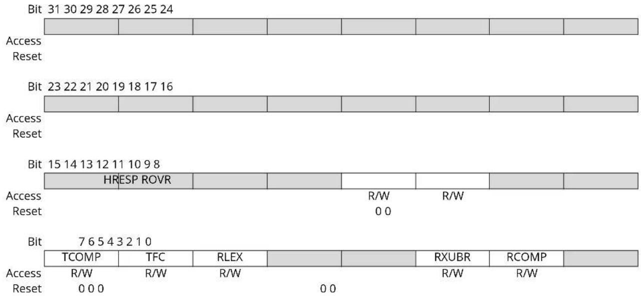
text_image
Bit 31 30 29 28 27 26 25 24 Access Reset Bit 23 22 21 20 19 18 17 16 Access Reset Bit 15 14 13 12 11 10 9 8 HRESP ROVR Access Reset R/W R/W 0 0 Bit 7 6 5 4 3 2 1 0 TCOMP TFC RLEX RXUBR RCOMP Access R/W R/W R/W R/W Reset 0 0 0 0 0Bit 11 - HRESP HRESP Not OK
Bit 10 - ROVR Receive Overrun
Bit 7 - TCOMP Transmit Complete
Bit 6 - TFC Transmit Frame Corruption Due to AHB Error Transmit frame corruption due to AHB error—set if an error occurs whilst midway through reading transmit frame from the AHB, including HRESP errors and buffers exhausted mid frame.
Bit 5 - RLEX Retry Limit Exceeded or Late Collision
Bit 2 - RXUBR RX Used Bit Read
Bit 1 - RCOMP Receive Complete
37.8.102 GMAC Transmit Buffer Queue Base Address Register Priority Queue x
Name: GMAC_TBQBAPQx
Offset: 0x0440 + (x-1)*0x04 [x=1..2]
Reset: 0x00000000
Property: Read/Write
These registers hold the start address of the transmit buffer queues (transmit buffers descriptor lists) for the additional queues and must be initialized to the address of valid descriptors, even if the priority queues are not used.
Bit 31 30 29 28 27 26 25 24
| TXBQBA[29:22] |
Access R/W R/W R/W R/W R/W R/W R/W R/W
Reset 00000000
Bit 23 22 21 20 19 18 17 16
| TXBQBA[21:14] |
Access R/W R/W R/W R/W R/W R/W R/W R/W
Reset 00000000
Bit 15 14 13 12 11 10 9 8
| TXBQBA[13:6] |
Access R/W R/W R/W R/W R/W R/W R/W R/W
Reset 00000000
Bit 76543210
| TXBQBA[5:0] |
Access R/W R/W R/W R/W R/W R/W
Reset 000000
Bits 31:2 - TXBQBA[29:0] Transmit Buffer Queue Base Address
Contains the address of the start of the transmit queue.
37.8.103 GMAC Receive Buffer Queue Base Address Register Priority Queue x
Name: GMAC_RBQBAPQx
Offset: 0x0480 + (x-1)*0x04 [x=1..2]
Reset: 0x00000000
Property: Read/Write
These registers hold the start address of the receive buffer queues (receive buffers descriptor lists) for the additional queues used when priority queues are employed.
Bit 31 30 29 28 27 26 25 24
RXBQBA[29:22]
Access R/W R/W R/W R/W R/W R/W R/W R/W
Reset 00000000
Bit 23 22 21 20 19 18 17 16
RXBQBA[21:14]
Access R/W R/W R/W R/W R/W R/W R/W R/W
Reset 00000000
Bit 15 14 13 12 11 10 9 8
RXBQBA[13:6]
Access R/W R/W R/W R/W R/W R/W R/W R/W
Reset 00000000
Bit 76543210
RXBQBA[5:0]
Access R/W R/W R/W R/W R/W R/W
Reset 000000
Bits 31:2 - RXBQBA[29:0] Receive Buffer Queue Base Address Holds the address of the start of the receive queue.
37.8.104 GMAC Receive Buffer Size Register Priority Queue x
Name: GMAC_RBSRPQx
Offset: 0x04A0 + (x-1)*0x04 [x=1..2]
Reset: 0x00000002
Property: Read/Write
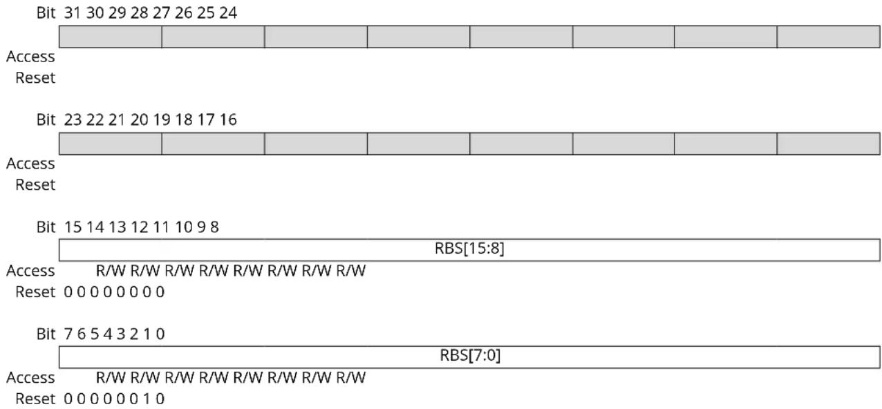
text_image
Bit 31 30 29 28 27 26 25 24 Access Reset Bit 23 22 21 20 19 18 17 16 Access Reset Bit 15 14 13 12 11 10 9 8 RBS[15:8] Access R/W R/W R/W R/W R/W R/W R/W R/W Reset 0 0 0 0 0 0 0 0 Bit 7 6 5 4 3 2 1 0 RBS[7:0] Access R/W R/W R/W R/W R/W R/W R/W R/W Reset 0 0 0 0 0 0 1 0Bits 15:0 - RBS[15:0] Receive Buffer Size
DMA receive buffer size in AHB system memory. The value defined by these bits determines the size of buffer to use in main AHB system memory when writing received data.
The value is defined in multiples of 64 Bytes such that a value of 0x01 corresponds to buffers of 64 Bytes, 0x02 corresponds to 128 Bytes etc.
Examples:
• 0x18: 1536 Bytes (1 × max length frame/buffer)
- 0xA0: 10240 Bytes (1 × 10K jumbo frame/buffer)
Note: This value should never be written as zero.
37.8.105 GMAC Credit-Based Shaping Control Register
Name: GMAC_CBSCR
Offset: 0x4BC
Reset: 0x00000000
Property: Read/Write
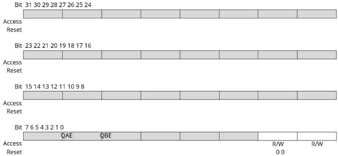
text_image
Bit 31 30 29 28 27 26 25 24 Access Reset Bit 23 22 21 20 19 18 17 16 Access Reset Bit 15 14 13 12 11 10 9 8 Access Reset Bit 7 6 5 4 3 2 1 0 QAE QBE Access Reset R/W R/W 0 0Bit 1 - QAE Queue A CBS Enable
| Value | Description |
| 0 | Credit-based shaping on the second highest priority queue (queue A) is disabled. |
| 1 | Credit-based shaping on the second highest priority queue (queue A) is enabled. |
Bit 0 - QBE Queue B CBS Enable
| Value | Description |
| 0 | Credit-based shaping on the highest priority queue (queue B) is disabled. |
| 1 | Credit-based shaping on the highest priority queue (queue B) is enabled. |
37.8.106 GMAC Credit-Based Shaping IdleSlope Register for Queue A
Name: GMAC_CBSISQA
Offset: 0x4C0
Reset: 0x00000000
Property: Read/Write
Credit-based shaping must be disabled in the GMAC_CBSCR before updating this register.
Bit 31 30 29 28 27 26 25 24
| IS[31:24] |
Access R/W R/W R/W R/W R/W R/W R/W R/W
Reset 00000000
Bit 23 22 21 20 19 18 17 16
| IS[23:16] |
Access R/W R/W R/W R/W R/W R/W R/W R/W
Reset 00000000
Bit 15 14 13 12 11 10 9 8
| IS[15:8] |
Access R/W R/W R/W R/W R/W R/W R/W R/W
Reset 00000000
Bit 76543210
| IS[7:0] |
Access R/W R/W R/W R/W R/W R/W R/W R/W
Reset 00000000
Bits 31:0 - IS[31:0] IdleSlope
IdleSlope value for queue A in Bytes per second.
The IdleSlope value is defined as the rate of change of credit when a packet is waiting to be sent.
This must not exceed the port transmit rate which is dependent on the speed of operation, e.g., 100
Mb/second = 32'h017D7840.
If 50% of bandwidth was to be allocated to a particular queue in 100 Mb/second mode, then the IdleSlope value for that queue would be calculated as 32'h017D7840 / 2.
37.8.107 GMAC Credit-Based Shaping IdleSlope Register for Queue B
Name: GMAC_CBSISQB
Offset: 0x4C4
Reset: 0x00000000
Property: Read/Write
Credit-based shaping must be disabled in the GMAC_CBSCR before updating this register.
Bit 31 30 29 28 27 26 25 24
| IS[31:24] |
Access R/W R/W R/W R/W R/W R/W R/W R/W
Reset 00000000
Bit 23 22 21 20 19 18 17 16
| IS[23:16] |
Access R/W R/W R/W R/W R/W R/W R/W R/W
Reset 00000000
Bit 15 14 13 12 11 10 9 8
| IS[15:8] |
Access R/W R/W R/W R/W R/W R/W R/W R/W
Reset 00000000
Bit 76543210
| IS[7:0] |
Access R/W R/W R/W R/W R/W R/W R/W R/W
Reset 00000000
Bits 31:0 - IS[31:0] IdleSlope
IdleSlope value for queue B in bytes/second.
The IdleSlope value is defined as the rate of change of credit when a packet is waiting to be sent.
This must not exceed the port transmit rate which is dependent on the speed of operation, e.g., 100
Mb/second = 32'h017D7840.
If 50% of bandwidth was to be allocated to a particular queue in 100 Mb/sec mode, then the
IdleSlope value for that queue would be calculated as 32'h017D7840 / 2
37.8.108 GMAC Screening Type 1 Register x Priority Queue
Name: GMAC_ST1RPQx
Offset: 0x0500 + x*0x04 [x=0..1]
Reset: 0x00000000
Property: Read/Write
Screening type 1 registers are used to allocate up to priority queues to received frames based on certain IP or UDP fields of incoming frames.
Bit 31 30 29 28 27 26 25 24
| UDP$ DSTCE UDPM[15:12] | |||
| Access | R/W R/W R/W R/W R/W R/W | ||
| Reset 0 0 0 0 0 0 | |||
Bit 23 22 21 20 19 18 17 16
| UDPM[11:4] | |
| Access | R/W R/W R/W R/W R/W R/W R/W R/W |
| Reset | 0 0 0 0 0 0 0 |
Bit 15 14 13 12 11 10 98
| UDPM[3:0] | DSTCM[7:4] | |
| Access | R/W R/W R/W R/W R/W R/W R/W R/W | |
| Reset | 0 0 0 0 0 0 0 | |
Bit 76543210
| DSTCM[3:0] | QNB[2:0] | |||
| Access | R/W R/W R/W R/W | R/W R/W R/W | ||
| Reset | 0 0 0 0 | 0 0 0 | ||
Bit 29 - UDPE UDP Port Match Enable
When this bit is written to '1', the UDP Destination Port of the received UDP frame is matched against the value stored in the bit field UDPM.
Bit 28 - DSTCE Differentiated Services or Traffic Class Match Enable
When this bit is written to '1', the DS (differentiated services) field of the received IPv4 header or TC field (traffic class) of IPv6 headers are matched against the value stored in bit field DSTCM.
Bits 27:12 - UDPM[15:0] UDP Port Match
When UDP port match enable is set (UDPME=1), the UDP Destination Port of the received UDP frame is matched against this bit field.
Bits 11:4 - DSTCM[7:0] Differentiated Services or Traffic Class Match
When DS/TC match enable is set (DSTCE), the DS (differentiated services) field of the received IPv4 header or TC field (traffic class) of IPv6 headers are matched against this bit field.
Bits 2:0 - QNB[2:0] Queue Number
If a match is successful, then the queue value programmed in this bit field is allocated to the frame.
37.8.109 GMAC Screening Type 2 Register x Priority Queue
Name: GMAC_ST2RPQx
Offset: 0x0540 + x*0x04 [x=0..1]
Reset: 0x00000000
Property: Read/Write
Screening type 2 registers are used to allocate up to 2 priority queues to received frames based on the VLAN priority field of received Ethernet frames.
Bit 31 30 29 28 27 26 25 24
| COMPCE COMPC[4:0] COMPBE | ||
| Access | R/W R/W R/W R/W R/W R/W R/W | |
| Reset 0 0 0 0 0 0 0 | ||
Bit 23 22 21 20 19 18 17 16
| COMPB[4:0] COMPAE COMPA[4:3] | |||
| Access | R/W R/W R/W R/W R/W R/W R/W R/W | ||
| Reset | 0 0 0 0 0 0 0 | ||
Bit 15 14 13 12 11 10 98
| COMPA[2:0] | ETHE | I2ETH[2:0] | VLANE | |
| Access | R/W R/W R/W R/W R/W R/W R/W R/W | |||
| Reset | 0 0 0 0 0 0 0 | |||
Bit 76543210
| VLANP[2:0] | QNB[2:0] | ||
| Access | R/W R/W R/W | R/W R/W R/W | |
| Reset 0 0 0 | 0 0 0 |
Bit 30 - COMPCE Compare C Enable
| Value | Description |
| 0 | Compare C is disabled. |
| 1 | Comparison via the register designated by index COMPC is enabled. |
Bits 29:25 - COMPC[4:0] Index of Screening Type 2 Compare Word 0/Word 1 register x
COMPC is a pointer to the compare registers GMAC_ST2CW0x and GMAC_ST2CW1x. When COMPCE=1, the compare is true if the data at the frame offset ANDed with the value MASKVAL is equal to the value of COMPVAL ANDed with the value of MASKVAL.
Bit 24 - COMPBE Compare B Enable
| Value | Description |
| 0 | Compare B is disabled. |
| 1 | Comparison via the register designated by index COMPB is enabled. |
Bits 23:19 - COMPB[4:0] Index of Screening Type 2 Compare Word 0/Word 1 register x
COMPB is a pointer to the compare registers GMAC_ST2CW0x and GMAC_ST2CW1x. When COMPBE=1, the compare is true if the data at the frame offset ANDed with the value MASKVAL is equal to the value of COMPVAL ANDed with the value of MASKVAL.
Bit 18 - COMPAE Compare A Enable
| Value | Description |
| 0 | Compare A is disabled. |
| 1 | Comparison via the register designated by index COMPA is enabled. |
Bits 17:13 - COMPA[4:0] Index of Screening Type 2 Compare Word 0/Word 1 register x COMPA is a pointer to the compare registers GMAC_ST2CW0x and GMAC_ST2CW1x. When COMPAE=1, the compare is true if the data at the frame offset ANDed with the value MASKVAL is equal to the value of COMPVAL ANDed with the value of MASKVAL.
Bit 12 - ETHE EtherType Enable
| Value Description | |
| 0 | EtherType match is disabled |
| 1 | EtherType match with bits [15:0] of the register designated by the value in I2ETH is enabled |
Bits 11:9 - I2ETH[2:0] Index of Screening Type 2 EtherType register x When EtherType is enabled (ETHE=1), the EtherType field (last EtherType in the header if the frame is VLAN-tagged) is compared with bits [15:0] in the register designated by the value of this bit field.
Bit 8 - VLANE VLAN Enable
| Value Description | |
| 0 | VLAN match disabled |
| 1 | VLAN match is enabled |
Bits 6:4 - VLANP[2:0] VLAN Priority When VLAN match is enabled (VLANE=1), the VLAN Priority field of the received frame is matched against the value of this bit field.
Bits 2:0 - QNB[2:0] Queue Number If a match is successful, then the queue value programmed in QNB is allocated to the frame.
37.8.110 GMAC Interrupt Enable Register Priority Queue x
Name: GMAC_IERPQx
Offset: 0x0600 + (x-1)*0x04 [x=1..2]
Reset: -
Property: Write-only
The following values are valid for all listed bit names of this register:
0: No effect.
1: Enables the corresponding interrupt.
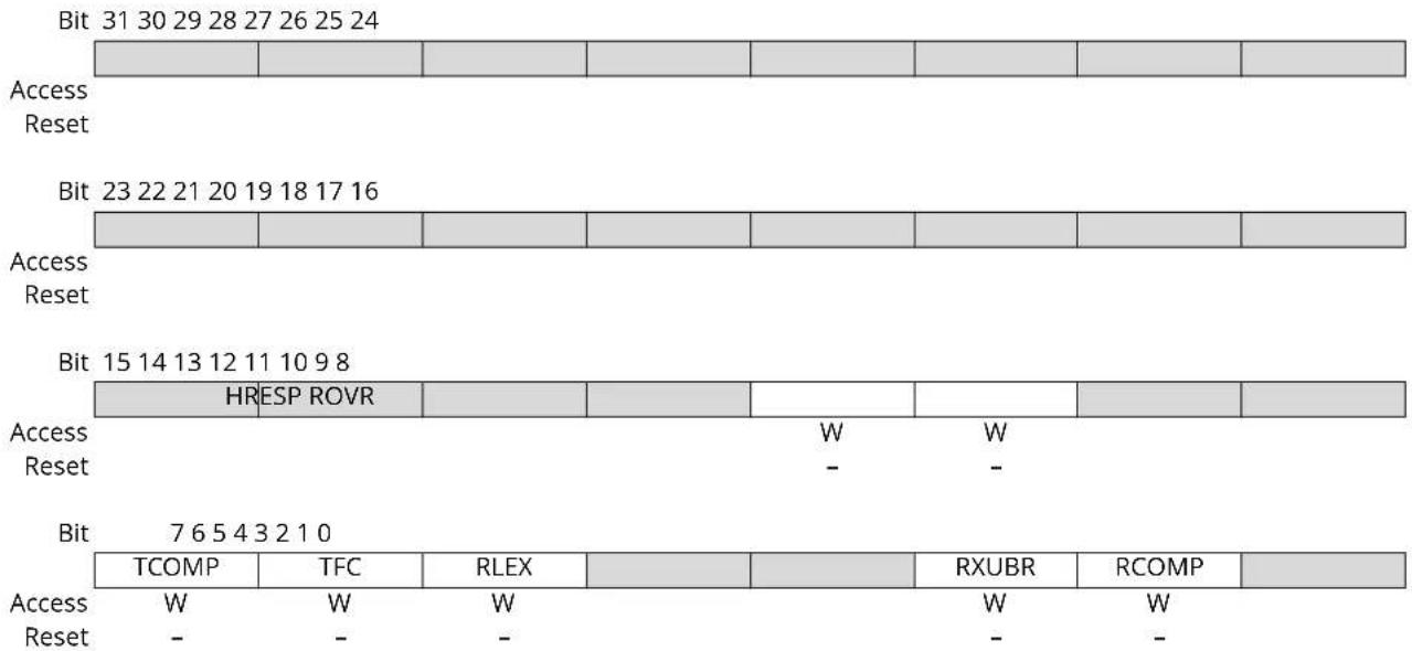
text_image
Bit 31 30 29 28 27 26 25 24 Access Reset Bit 23 22 21 20 19 18 17 16 Access Reset Bit 15 14 13 12 11 10 9 8 HRESP ROVR Access Reset W W - - Bit 7 6 5 4 3 2 1 0 TCOMP TFC RLEX RXUBR RCOMP Access W W W W Reset - - - - -Bit 11 - HRESP HRESP Not OK
Bit 10 - ROVR Receive Overrun
Bit 7 - TCOMP Transmit Complete
Bit 6 - TFC Transmit Frame Corruption Due to AHB Error
Bit 5 - RLEX Retry Limit Exceeded or Late Collision
Bit 2 - RXUBR RX Used Bit Read
Bit 1 - RCOMP Receive Complete
37.8.111 GMAC Interrupt Disable Register Priority Queue x
Name: GMAC_IDRPQx
Offset: 0x0620 + (x-1)*0x04 [x=1..2]
Reset: -
Property: Write-only
The following values are valid for all listed bit names of this register:
0: No effect.
1: Disables the corresponding interrupt.

text_image
Bit 31 30 29 28 27 26 25 24 Access Reset Bit 23 22 21 20 19 18 17 16 Access Reset Bit 15 14 13 12 11 10 9 8 HRESP ROVR Access Reset W W - - Bit 7 6 5 4 3 2 1 0 TCOMP TFC RLEX RXUBR RCOMP Access W W W W Reset - - - - -Bit 11 - HRESP HRESP Not OK
Bit 10 - ROVR Receive Overrun
Bit 7 - TCOMP Transmit Complete
Bit 6 - TFC Transmit Frame Corruption Due to AHB Error
Bit 5 - RLEX Retry Limit Exceeded or Late Collision
Bit 2 - RXUBR RX Used Bit Read
Bit 1 - RCOMP Receive Complete
37.8.112 GMAC Interrupt Mask Register Priority Queue x
Name: GMAC_IMRPQx
Offset: 0x0640 + (x-1)*0x04 [x=1..2]
Reset: 0x00000000
Property: Read/Write
A read of this register returns the value of the receive complete interrupt mask.
A write to this register directly affects the state of the corresponding bit in the Interrupt Status Register, causing an interrupt to be generated if a '1' is written.
The following values are valid for all listed bit names of this register:
0: Corresponding interrupt is enabled.
1: Corresponding interrupt is disabled.

text_image
Bit 31 30 29 28 27 26 25 24 Access Reset Bit 23 22 21 20 19 18 17 16 Access Reset Bit 15 14 13 12 11 10 9 8 HRESP ROVR Access Reset R/W R/W 0 0 Bit 7 6 5 4 3 2 1 0 TCOMP AHB RLEX RXUBR RCOMP Access R/W R/W R/W R/W Reset 0 0 0 0 0Bit 11 - HRESP HRESP Not OK
Bit 10 - ROVR Receive Overrun
Bit 7 - TCOMP Transmit Complete
Bit 6 - AHB AHB Error
Bit 5 - RLEX Retry Limit Exceeded or Late Collision
Bit 2 - RXUBR RX Used Bit Read
Bit 1 - RCOMP Receive Complete
37.8.113 GMAC Screening Type 2 EtherType Register x
Name: GMAC_ST2ERx
Offset: 0x06E0 + x*0x04 [x=0..3]
Reset: 0x00000000
Property: Read/Write

text_image
Bit 31 30 29 28 27 26 25 24 Access Reset Bit 23 22 21 20 19 18 17 16 Access Reset Bit 15 14 13 12 11 10 9 8 COMPVAL[15:8] Access R/W R/W R/W R/W R/W R/W R/W R/W Reset 0 0 0 0 0 0 0 0 Bit 7 6 5 4 3 2 1 0 COMPVAL[7:0] Access R/W R/W R/W R/W R/W R/W R/W R/W Reset 0 0 0 0 0 0 0 0Bits 15:0 - COMPVAL[15:0] EtherType Compare Value
When the bit GMAC_ST2RPQ.ETHE is written to '1', the EtherType (last EtherType in the header if the frame is VLAN tagged) is compared with bits [15:0] in the register designated by GMAC_ST2RPQ.I2ETH.
37.8.114 GMAC Screening Type 2 Compare Word 0 Register x
Name: GMAC_ST2CW0x
Offset: 0x0700 + x*0x08 [x=0..1]
Reset: 0x00000000
Property: Read/Write
Bit 31 30 29 28 27 26 25 24
| COMPVAL[15:8] |
Access R/W R/W R/W R/W R/W R/W R/W R/W
Reset 00000000
Bit 23 22 21 20 19 18 17 16
| COMPVAL[7:0] |
Access R/W R/W R/W R/W R/W R/W R/W R/W
Reset 00000000
Bit 15 14 13 12 11 10 9 8
| MASKVAL[15:8] |
Access R/W R/W R/W R/W R/W R/W R/W R/W
Reset 00000000
Bit 76543210
| MASKVAL[7:0] |
Access R/W R/W R/W R/W R/W R/W R/W R/W
Reset 00000000
Bits 31:16 - COMPVAL[15:0] Compare Value
The byte stored in bits [23:16] is compared against the first byte of the 2 bytes extracted from the frame.
The byte stored in bits [31:24] is compared against the second byte of the 2 bytes extracted from the frame.
Bits 15:0 - MASKVAL[15:0] Mask Value
The value of MASKVAL ANDed with the 2 bytes extracted from the frame is compared to the value of MASKVAL ANDed with the value of COMPVAL.
37.8.115 GMAC Screening Type 2 Compare Word 1 Register x
Name: GMAC_ST2CW1x
Offset: 0x0704 + x*0x08 [x=0..1]
Reset: 0x00000000
Property: Read/Write
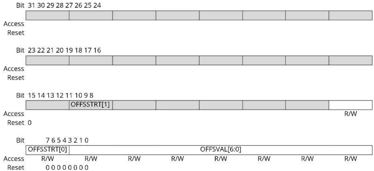
text_image
Bit 31 30 29 28 27 26 25 24 Access Reset Bit 23 22 21 20 19 18 17 16 Access Reset Bit 15 14 13 12 11 10 9 8 Access Reset 0 Bit 7 6 5 4 3 2 1 0 OFFSSTRT[0] OFFSVAL[6:0] Access R/W R/W R/W R/W R/W R/W R/W Reset 0 0 0 0 0 0 0 0Bits 8:7 - OFFSSTRT[1:0] Ethernet Frame Offset Start
| Value | Name | Description |
| 0 | FRAMESTART | Offset from the start of the frame |
| 1 | ETHERTYPE | Offset from the byte after the EtherType field |
| 2 | IP | Offset from the byte after the IP header field |
| 3 | TCP_UDP | Offset from the byte after the TCP/UDP header field |
Bits 6:0 - OFFSVAL[6:0] Offset Value in Bytes
The value of OFFSVAL ranges from 0 to 127 bytes, and is counted from either the start of the frame, the byte after the EtherType field (last EtherType in the header if the frame is VLAN tagged), the byte after the IP header (IPv4 or IPv6) or the byte after the TCP/UDP header.
38. USB High-Speed Interface (USBHS)
38.1 Description
The USB High-Speed Interface (USBHS) complies with the Universal Serial Bus (USB) 2.0 specification. (1)
Each pipe/endpoint can be configured in one of several USB transfer types. It can be associated with one, two or three banks of a DPRAM used to store the current data payload. If two or three banks are used, then one DPRAM bank is read or written by the CPU or the DMA, while the other is read or written by the USBHS core. This feature is mandatory for isochronous pipes/endpoints.
The following table describes the hardware configuration of the USB MCU device.
Table 38-1. Description of USB Pipes/Endpoints
| Pipe/Endpoint | Mnemonic | Max. Number Banks | DMA | High Band Width | Max. Pipe/ Endpoint Size | Type |
| 0 PEP_0 1 N N 64 Control | ||||||
| 1 PEP_1 3 Y Y 1024 Isochronous/Bulk/Interrupt/ | Control | |||||
| 2 PEP_2 3 Y Y 1024 Isochronous/Bulk/Interrupt/ | Control | |||||
| 3 PEP_3 2 Y Y 1024 Isochronous/Bulk/Interrupt/ | Control | |||||
| 4 PEP_4 2 Y Y 1024 Isochronous/Bulk/Interrupt/ | Control | |||||
| 5 PEP_5 2 Y Y 1024 Isochronous/Bulk/Interrupt/ | Control | |||||
| 6 PEP_6 2 Y Y 1024 Isochronous/Bulk/Interrupt/ | Control | |||||
| 7 PEP_7 2 Y Y 1024 Isochronous/Bulk/Interrupt/ | Control | |||||
| 8 PEP_8 2 N Y 1024 Isochronous/Bulk/Interrupt/ | Control | |||||
| 9 PEP_9 2 N Y 1024 Isochronous/Bulk/Interrupt/ | Control | |||||
Note:
- High-bandwidth isochronous transfers supported in device but not host mode.
38.2 Embedded Characteristics
- Compatible with the USB 2.0 Specification
• Supports High-Speed (480 Mbps), Full-Speed (12 Mbps) and Low-Speed (1.5 Mbps) Communication - 9 Pipes/Endpoints
• 4096 bytes of Embedded Dual-Port RAM (DPRAM) for Pipes/Endpoints - Up to 3 Memory Banks per Pipe/Endpoint (not for Control Pipe/Endpoint)
- Flexible Pipe/Endpoint Configuration and Management with Dedicated DMA Channels
- On-chip UTMI Transceiver including Pull-ups/Pull-downs
38.3 Block Diagram
The USBHS provides a hardware device to interface a USB link to a data flow stored in a dual-port RAM (DPRAM).
In normal operation (SPDCONF = 0), the UTMI transceiver requires the UTMI PLL (480 MHz). In case of full-speed or low-speed only, for a lower consumption (SPDCONF = 1), the UTMI transceiver only requires 48 MHz.
Figure 38-1. USBHS Block Diagram

flowchart
graph TD
    A["APB Bus"] --> B["APB Interface"]
    C["AHB Bus"] --> D["AHB1 DMA AHB0"]
    E["AHB Bus"] --> F["Host AHB Multiplexer Client"]
    G["PMC"] --> H["MCK"]
    H --> I["Local AHB Client interface"]
    I --> J["USB2.0 CORE"]
    J --> K["UTMI"]
    K --> L["HSDP/DP HSDM/DM"]
    J --> M["PEP Alloc"]
    M --> N["DPRAM"]
    N --> O["32 bits"]
    O --> P["USB_48M Clock (needed only when SPDCONF=1)"]
    O --> Q["USB_480M Clock (needed only when SPDCONF=0)"]
    J --> R["rd/Wr/Ready"]
    R --> J
    J --> S["ctrl status"]
    S --> J
    style J fill:#f9f,stroke:#333
    style K fill:#ccf,stroke:#333
    style L fill:#cfc,stroke:#333
    style M fill:#fcc,stroke:#333
    style N fill:#ffc,stroke:#333
    style O fill:#fcc,stroke:#333
    style P fill:#fcc,stroke:#333
    style Q fill:#fcc,stroke:#333
38.4 Signal Description
Table 38-2. Signal Description
| Name Description Type | ||
| HSDM/DM HS/FS Differential Data Line - Input/Output | ||
| HSDP/DP HS/FS Differential Data Line + Input/Output | ||
38.5 Product Dependencies
38.5.1 I/O Lines
A regular PIO line must be used to control VBUS. This is configured in the I/O Controller.
38.5.2 Clocks
The clock for the USBHS bus interface is generated by the Power Management Controller. This clock can be enabled or disabled in the Power Management Controller. It is recommended to disable the USBHS before disabling the clock, to avoid freezing the USBHS in an undefined state.
Before enabling the USB clock in the Power Management Controller, the USBHS must be enabled (by writing a one to the USBHS_CTRL.USBE bit and a zero to the USBHS_CTRL.FRZCLK bit).
The USBHS can work in two modes:
- Normal mode (SPDCONF = 0) where High speed, Full speed and Low speed are available.
- Low-power mode (SPDCONF = 1) where Full speed and Low speed are available.
To ensure successful startup, follow the sequences below:
- In Normal mode:
- Enable the USBHS peripheral clock. This is done via the register PMC_PCER.
- Enable the USBHS (UIMOD, USBE = 1, FRZCLK = 0).
- Enable the UPLL 480 MHz.
- Wait for the UPLL 480 MHz to be considered as locked by the PMC.
- In Low-power mode:
- As USB_48M must be set to 48 MHz (refer to the section "Power Management Controller (PMC)"), select either the PLLA or the UPLL (previously set to ON), and program the PMC_USB register (source selection and divider).
- Enable the USBHS peripheral clock (PMC_PCER).
- Put the USBHS in Low-power mode (SPDCONF = 1).
- Enable the USBHS (UIMOD, USBE = 1, FRZCLK = 0).
- Enable the USBCK bit (PMC_SCER).
Related Links
- Power Management Controller (PMC)
38.5.3 Interrupt Sources
The USBHS interrupt request line is connected to the interrupt controller. Using the USBHS interrupt requires the interrupt controller to be programmed first.
38.5.4 USB Pipe/Endpoint x FIFO Data Register (USBFIFOxDATA)
The application has access to each pipe/endpoint FIFO through its reserved 32 KB address space. The application can access a 64-KB buffer linearly or fixedly as the DPRAM address increment is fully handled by hardware. Byte, half-word and word accesses are supported. Data should be accessed in a big-endian way.
Disabling the USBHS (by writing a zero to the USBHS_CTRL.USBE bit) does not reset the DPRAM.
38.6 Functional Description
38.6.1 USB General Operation
38.6.1.1 Power-On and Reset
The following figure describes the USBHS general states.
Figure 38-2. General States

flowchart
graph TD
    A["Macro off: USBHS_CTRL.USBE = 0\nClock stopped: USBHS_CTRL.FRZCLK = 1"] --> B["Reset"]
    B --> C["Device"]
    B --> D["Host"]
    B --> E["HW RESET"]
    E --> F["<any other state>"]
    B --> G["USBHS_CTRL.USBE = 0\nUSBHS_CTRL.USBE = 1\nUSBHS_CTRL.UIMOD = 1"]
    B --> H["USBHS_CTRL.USBE = 0\nUSBHS_CTRL.USBE = 1\nUSBHS_CTRL.UIMOD = 0"]
    B --> I["USBHS_CTRL.USBE = 0\nUSBHS_CTRL.USBE = 0\nUSBHS_CTRL.USBE = 0"]
After a hardware reset, the USBHS is in Reset state. In this state:
- The USBHS is disabled. The USBHS Enable bit in the General Control register (USBHS_CTRL.USBE) is zero.
- The USBHS clock is stopped in order to minimize power consumption. The Freeze USB Clock bit (USBHS_CTRL.FRZCLK) is set.
• The UTMI is in Suspend mode. - The internal states and registers of the Device and Host modes are reset.
- The DPRAM is not cleared and is accessible.
After writing a one to USBHS_CTRL.USBE, the USBHS enters the Device or the Host mode in idle state.
The USBHS can be disabled at any time by writing a zero to USBHS_CTRL.USBE. This acts as a hardware reset, except that the USBHS_CTRL.FRZCLK, USBHS_CTRL.UIMOD and USBHS_DEVCTRL.LS bits are not reset.
38.6.1.2 Interrupts
One interrupt vector is assigned to the USB interface. The following figure shows the structure of the USB interrupt system.
Figure 38-3. Interrupt System
flowchart
graph TD
    A["USBHS_DEVEPTISRx.TXINI"] --> B["USBHS_DEVEPTIMRx.TXINE"]
    C["USBHS_DEVEPTISRx.RXOUTI"] --> D["USBHS_DEVEPTIMRx.RXOUTE"]
    E["USBHS_DEVEPTISRx.RXSTPI"] --> F["USBHS_DEVEPTIMRx.RXSTPE"]
    G["USBHS_DEVEPTISRx.UNDERFI"] --> H["USBHS_DEVEPTIMRx.UNDERFE"]
    I["USBHS_DEVEPTISRx.NAKOUTI"] --> J["USBHS_DEVEPTIMRx.NAKOUTE"]
    K["USBHS_DEVEPTISRx.HBISOINERRI"] --> L["USBHS_DEVEPTIMRx.HBISOINERRRE"]
    M["USBHS_DEVEPTISRx.NAKINI"] --> N["USBHS_DEVEPTIMRx.NAKINE"]
    O["USBHS_DEVEPTISRx.HBISOFLUSHI"] --> P["USBHS_DEVEPTIMRx.HBISOFLUSHE"]
    Q["USBHS_DEVEPTISRx.OVERFI"] --> R["USBHS_DEVEPTIMRx.OVERFE"]
    S["USBHS_DEVEPTISRx.STALLEDI"] --> T["USBHS_DEVEPTIMRx.STALLEDE"]
    U["USBHS_DEVEPTISRx.CRCERRI"] --> V["USBHS_DEVEPTIMRx.CRCERRE"]
    W["USBHS_DEVEPTISRx.SHORTPACKET"] --> X["USBHS_DEVEPTIMRx.SHORTPACKETE"]
    Y["USBHS_DEVEPTISRx.CTSEQ-MDATA & UESTAX RXOUTI"] --> Z["USBHS_DEVEPTIMRx.MDATAE"]
    AA["USBHS_DEVEPTISRx.CTSEQ-DATAX & UESTAX RXOUTI"] --> AB["USBHS_DEVEPTIMRx.DATAXE"]
    AC["USBHS_DEVEPTISRx.TRANSERR"] --> AD["USBHS_DEVEPTIMRx.TRANSERRE"]
    AE["USBHS_DEVEPTISRx.NBUSYBK"] --> AF["USBHS_DEVEPTIMRx.NBUSYBKE"]

    B --> AG["USB Device Endpoint X Interrupt"]
    D --> AG
    F --> AG
    H --> AG
    J --> AG
    L --> AG
    M --> AG
    N --> AG
    O --> AG
    P --> AG
    Q --> AG
    R --> AG
    S --> AG
    T --> AG
    U --> AG
    V --> AG
    W --> AG
    X --> AG
    Y --> AG
    Z --> AG
    AA --> AG
    AB --> AG
    AD --> AG
    AF --> AG
    AG --> AH["USB Device DMA Channel X Interrupt"]

    AI["USB Device Interrupt"] --> AJ["USB Device Interrupt"]

    AK["USB Device Interrupt"] --> AL["USB Device Interrupt"]

    AM["USB Device Interrupt"] --> AN["USB Device Interrupt"]

    AO["USB Device Interrupt"] --> AP["USB Device Interrupt"]

    AQ["USB Device Interrupt"] --> AR["USB Device Interrupt"]

    AS["USB Device Interrupt"] --> AT["USB Device Interrupt"]

    AU["USB Device Interrupt"] --> AV["USB Device Interrupt"]

    AW["USB Device Interrupt"] --> AX["USB Device Interrupt"]

    AY["USB Device Interrupt"] --> AZ["USB Device Interrupt"]

    BA["USB Device Interrupt"] --> BB["USB Device Interrupt"]

    BC["USB Device Interrupt"] --> BD["USB Device Interrupt"]

    BE["USB Device Interrupt"] --> BF["USB Device Interrupt"]

    BG["USB Device Interrupt"] --> BH["USB Device Interrupt"]

    BI["USB Device Interrupt"] --> BJ["USB Device Interrupt"]

    BK["USB Device Interrupt"] --> BL["USB Device Interrupt"]

    BM["USB Device Interrupt"] --> BN["USB Device Interrupt"]

    BO["USB Device Interrupt"] --> BP["USB Device Interrupt"]

    BQ["USB Device Interrupt"] --> BR["USB Device Interrupt"]

    BS["USB Device Interrupt"] --> BT["USB Device Interrupt"]

    BU["USB Device Interrupt"] --> BV["USB Device Interrupt"]

    BW["USB Device Interrupt"] --> BX["USB Device Interrupt"]

    BY["USB Device Interrupt"] --> BZ["USB Device Interrupt"]

    CA["USB Device Interrupt"] --> CB["USB Device Interrupt"]

    CC["USB Device Interrupt"] --> CD["USB Device Interrupt"]

    DE["USB Device Interrupt"] --> DF["USB Device Interrupt"]

    DG["USB Device Interrupt"] --> DH["USB Device Interrupt"]

    DI["USB Device Interrupt"] --> DJ["USB Device Interrupt"]

    BEQ["USB Device Interrupt"] --> BEQ
    BFQ["USB Device Interrupt"] --> BFQ

    BKQ["USHDSHEVDMASTATUSx.EOT_STA"] --> BKQ
    BKQ --> BKQ
    BKQ --> BKQ
    BKQ --> BKQ
    BKQ --> BKQ
    BKQ --> BKQ
    BKQ --> BKQ
    BKQ --> BKQ
    BKQ --> BKQ
    BKQ --> BKQ
    BKQ --> BKQ
    BKQ --> BKQ

    BLQ["USHDSHEVDMASTATUSx.EOCH_BUFF_STA"] --> BLQ
    BLQ --> BLQ
    BLQ --> BLQ
    BLQ --> BLQ
    BLQ --> BLQ
    BLQ --> BLQ
    BLQ --> BLQ

    BMQ["USHDSHEVDMASTATUSx.DESC_LD_STA"] --> BMQ
    BMQ --> BMQ
    BMQ --> BMQ
    BMQ --> BMQ

    BNQ["USHDSHEVDMASTATUSx.EOT_STA"] --> BNQ
    BNQ --> BNQ
    BNQ --> BNQ
    BNQ --> BNQ
    BNQ --> BNQ

    BOQ1["USHDSHEVDMASTATUSx.EOCH_BUFF_STA"] --> BOQ1
    BOQ1 --> BOQ1
    BOQ1 --> BOQ1
    BOQ1 --> BOQ1
    BOQ1 --> BOQ1

    BNQ2["USHDSHEVDMASTATUSx.DESC_LD_STA"] --> BNQ2
    BNQ2 --> BNQ2
    BNQ2 --> BNQ2

    BQ3["USHDSHEVDMASTATUSx.EOT_STA"] --> BQ3
    BQ3 --> BQ3
    BQ3 --> BQ3
    BQ3 --> BQ3

    BQ4["USHDSHEVDMASTATUSx.EOCH_BUFF_STA"] --> BQ4
    BQ4 --> BQ4
    BQ4 --> BQ4
    BQ4 --> BQ4

    BQ5["USHDSHEVDMASTATUSx.DESC_LD_STA"] --> BQ5
    BQ5 --> BQ5
    BQ5 --> BQ5

    BQ6["USHDSHEVDMASTATUSx.EOT_STA"] --> BQ6
    BQ6 --> BQ6
    BQ6 --> BQ6

    BQ7["USHDSHEVDMASTATUSx.EOCH_BUFF_STA"] --> BQ7
    BQ7 --> BQ7
    BQ7 --> BQ7

    BQ8["USHDSHEVDMASTATUSx.DESC_LD_STA"] --> BQ8
    BQ8 --> BQ8

    AC["USHDSHEVDMASTATUSx.EOT_STA"] --> AC
    AC --> AC
    AC --> AC
    AC --> AC

    AD["USHDSHEVDMASTATUSx.EOCH_BUFF_STA"] --> AD
    AD --> AD
    AD --> AD
    AD --> AD

    AE["USHDSHEVDMASTATUSx.DESC_LD_STA"] --> AE
    AE --> AE

    AF["USHDSHEVDMASTATUSx.EOT_STA"] --> AF
    AF --> AF
    AF --> AF

    AG["USHDSHEVDMASTATUSx.EOCH_BUFF_STA"] --> AG
    AG --> AG
    AG --> AG

    AH["USHDSHEVDMASTATUSx.DESC_LD_STA"] --> AH
See Interrupts in the Device Operation section and Interrupts in the Host Operation section for further details about device and host interrupts.
There are two kinds of general interrupts: processing, i.e., their generation is part of the normal processing, and exception, i.e., errors (not related to CPU exceptions).
38.6.1.3 MCU Power Modes
USB Suspend Mode
In Peripheral mode, the Suspend Interrupt bit in the Device Global Interrupt Status register (USBHS_DEVISR.SUSP) indicates that the USB line is in Suspend mode. In this case, the transceiver is automatically set in Suspend mode to reduce consumption.
Clock Frozen
The USBHS can be frozen when the USB line is in the Suspend mode, by writing a one to the USBHS_CTRL.FRZCLK bit, which reduces power consumption.
In this case, it is still possible to access the following:
- USBHS_CTRL.FRZCLK, USBHS_CTRL.USBE and USBHS_DEVCTRL.LS bits
Moreover, when USBHS_CTRL.FRZCLK = 1, only the asynchronous interrupt sources can trigger the USB interrupt:
- Wakeup Interrupt (USBHS_DEVISR.WAKEUP)
- Host Wakeup Interrupt (USBHS_HSTISR.HWUPI)
38.6.1.4 Speed Control
Device Mode
When the USB interface is in Device mode, the speed selection (Full-speed or High-speed) is performed automatically by the USBHS during the USB reset according to the host speed capability. At the end of the USB reset, the USBHS enables or disables high-speed terminations and pull-up.
It is possible to set the USBHS_DEVCTRL.SPDCONF.
Host Mode
When the USB interface is in Host mode, internal pull-down resistors are connected on both D+ and D- and the interface detects the speed of the connected device, which is reflected by the Speed Status (USBHS_SR.SPEED) field.
38.6.1.5 DPRAM Management
Pipes and endpoints can only be allocated in ascending order, from pipe/endpoint 0 to the last pipe/endpoint to be allocated. The user should therefore configure them in the same order.
The allocation of a pipe/endpoint x starts when the Endpoint Memory Allocate bit in the Endpoint x Configuration register (USBHS_DEVEPTCFGx.ALLOC) is written to one. Then, the hardware allocates a memory area in the DPRAM and inserts it between the x - 1 and x + 1 pipes/endpoints. The x + 1 pipe/endpoint memory window slides up and its data is lost. Note that the following pipe/endpoint memory windows (from x + 2) do not slide.
Disabling a pipe, by writing a zero to the Pipe x Enable bit in the Host Pipe register (USBHS_HSTPIP.PENx), or disabling an endpoint, by writing a zero to the Endpoint x Enable bit in the Device Endpoint register (USBHS_DEVEPT.EPENx), does not reset the USBHS_DEVEPTCFGx.ALLOC bit or the Pipe/Endpoint configuration:
- Pipe Configuration
- Pipe Banks (USBHS_HSTPIPCFGx.PBK)
- Pipe Size (USBHS_HSTPIPCFGx.PSIZE)
- Pipe Token (USBHS_HSTPIPCFGx.PTOKEN)
- Pipe Type (USBHS_HSTPIPCFGx.PTYPE)
- Pipe Endpoint Number (USBHS_HSTPIPCFGx.PEPNUM)
- Pipe Interrupt Request Frequency (USBHS_HSTPIPCFGx.INTFRQ)
- Endpoint Configuration
- Endpoint Banks (USBHS_DEVEPTCFGx.EPBK)
- Endpoint Size (USBHS_DEVEPTCFGx. EPSIZE)
- Endpoint Direction (USBHS_DEVEPTCFGx.EPDIR)
- Endpoint Type (USBHS_DEVEPTCFGx.EPTYPE)
To free endpoint memory, the user must write a zero to the USBHS_DEVEPTCFGx.ALLOC bit. The x+1 pipe/endpoint memory window then slides down and its data is lost. Note that the following pipe/endpoint memory windows (from x + 2) do not slide.
The following figure illustrates the allocation and reorganization of the DPRAM in a typical example.
Figure 38-4. Allocation and Reorganization of the DPRAM
flowchart
graph TD
    A["Free Memory"] --> B["PEP5"]
    B --> C["PEP4"]
    C --> D["PEP3"]
    D --> E["PEP2"]
    E --> F["PEP1"]
    F --> G["PEP0"]
    H["Device: USBHS_DEVEPT.EPENx = 1\nUSBHS_DEVEPTCFGx.ALLOC = 1"] --> A
    I["Host: USBHS_HSTPIP.EPENx = 1\nUSBHS_HSTPIPCFGx.ALLOC = 1"] --> A
    J["Pipe/Endpoints 0..5 Activated"] --> K["Free Memory"]
    K --> L["PEP5"]
    L --> M["PEP4"]
    M --> N["PEP3 (ALLOC stays at 1)"]
    N --> O["PEP2"]
    O --> P["PEP1"]
    P --> Q["PEP0"]
    R["Device: USBHS_DEVEPT.EPEN3 = 0\nHost: USBHS_HSTPIP.EPEN3 = 0"] --> S["Free Memory"]
    S --> T["PEP5"]
    T --> U["PEP4 Lost Memory"]
    U --> V["PEP4"]
    V --> W["PEP2"]
    W --> X["PEP1"]
    X --> Y["PEP0"]
    Z["Device: USBHS_DEVEPTCFG3.ALLOC = 0\nHost: USBHS_HSTPIPCFG3.ALLOC = 0"] --> S
    AA["Device: USBHS_DEVEPT.EPEN3 = 1\nUSBHS_DEVEPTCFG3.ALLOC = 1"] --> AB["Free Memory"]
    AC["Host: USBHS_HSTPIP.EPEN3 = 1\nUSBHS_HSTPIPCFG3.ALLOC = 1"] --> AC
    AD["Conflict"] --> AE["PEP4 (larger size)"]
    AE --> AF["PEP2"]
    AF --> AG["PEP1"]
    AG --> AH["PEP0"]
- Pipes/endpoints 0 to 5 are enabled, configured and allocated in ascending order. Each pipe/endpoint then owns a memory area in the DPRAM.
- Pipe/endpoint 3 is disabled, but its memory is kept allocated by the controller.
- In order to free its memory, its USBHS_DEVEPTCFGx.ALLOC bit is written to zero. The pipe/endpoint 4 memory window slides down, but pipe/endpoint 5 does not move.
- If the user chooses to reconfigure pipe/endpoint 3 with a larger size, the controller allocates a memory area after the pipe/endpoint 2 memory area and automatically slides up the pipe/endpoint 4 memory window. Pipe/endpoint 5 does not move and a memory conflict appears as the memory windows of pipes/endpoints 4 and 5 overlap. The data of these pipes/endpoints is potentially lost.
Note: 1. The data of pipe or endpoint 0 cannot be lost (except if it is de-allocated) as the memory allocation and de-allocation may affect only higher pipes/endpoints.
Note: 2. Deactivating then reactivating the same pipe/endpoint with the same configuration only modifies temporarily the controller DPRAM pointer and size for this pipe/endpoint. Nothing changes in the DPRAM. Higher endpoints seem not to have been moved and their data is preserved as long as nothing has been written or received into them while changing the allocation state of the first pipe/endpoint.
Note: 3. When the user writes a one to the USBHS_DEVEPTCFGx.ALLOC bit, the Configuration OK Status bit (USBHS_DEVEPTISRx.CFGOK) is set only if the configured size and number of banks are correct as compared to the endpoint maximum allowed values and to the maximum FIFO size (i.e., the DPRAM size). The USBHS_DEVEPTISRx.CFGOK value does not consider memory allocation conflicts.
38.6.1.6 Pad Suspend
Figure 38-5 shows the pad behavior.
Figure 38-5. Pad Behavior
| = Logical OR & = Logical AND

flowchart
graph TD
    A["Idle"] -->|USBHS_CTRL.USBE = 1 & USBHS_DEVCTRL.DETACH = 0 & Suspend| B["Active"]
    A -->|USBHS_CTRL.USBE = 0 | B
    B -->|USBHS_DEVCTRL.DETACH = 1 | B
- In Idle state, the pad is put in Low-power mode, i.e., the differential receiver of the USB pad is off, and internal pull-downs with a strong value (15 K) are set in HSDP/D and HSDM/DM to avoid floating lines.
• In Active state, the pad is working.
Figure 38-6 illustrates the pad events leading to a PAD state change.
Figure 38-6. Pad Events
flowchart
graph TD
    A["USBHS_DEVISR.SUSP"] --> B["Suspend detected Cleared on wakeup"]
    C["USBHS_DEVISR.WAKEUP"] --> D["Wakeup detected"]
    E["PAD State"] --> F["Active"]
    F --> G["Idle"]
    G --> H["Active"]
    I["Cleared by software to acknowledge the interrupt"] --> J["Wakeup detected"]
    J --> K["Idle"]
    K --> L["Active"]
The USBHS_DEVISR.SUSP bit is set and the Wakeup Interrupt (USBHS_DEVISR.WAKEUP) bit is cleared when a USB "Suspend" state has been detected on the USB bus. This event automatically puts the USB pad in Idle state. The detection of a non-idle event sets USBHS_DEVISR.WAKEUP, clears USBHS_DEVISR.SUSP and wakes up the USB pad.
The pad goes to the Idle state if the USBHS is disabled or if the USBHS_DEVCTRL.DETACH bit = 1. It returns to the Active state when USBHS_CTRL.USBE = 1 and USBHS_DEVCTRL.DETACH = 0.
38.6.2 USB Device Operation
38.6.2.1 Introduction
In Device mode, the USBHS supports high-, full- and low-speed data transfers.
In addition to the default control endpoint, 9 endpoints are provided, which can be configured with an isochronous, bulk or interrupt type, as described in Table 38-1.
As the Device mode starts in Idle state, the pad consumption is reduced to the minimum.
38.6.2.2 Power-On and Reset
The following figure describes the USBHS Device mode main states.
Figure 38-7. Device Mode Main States
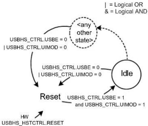
flowchart
graph TD
    A["<any other state>"] -->|USBHS_CTRL,USBE = 0 | B["Reset"]
    B -->|USBHS_CTRL,USBE = 1 and USBHS_CTRL,UIMOD = 1| C["Idle"]
    C -->|USBHS_CTRL,USBE = 0 | D["Reset"]
    D -->|USBHS_HSTCTRL_RESET| E["Reset"]
    E --> F["Reset"]
    F --> G["Reset"]
    G --> H["Reset"]
    H --> I["Reset"]
    I --> J["Reset"]
    J --> K["Reset"]
    K --> L["Reset"]
    L --> M["Reset"]
    M --> N["Reset"]
    N --> O["Reset"]
    O --> P["Reset"]
    P --> Q["Reset"]
    Q --> R["Reset"]
    R --> S["Reset"]
    S --> T["Reset"]
    T --> U["Reset"]
    U --> V["Reset"]
    V --> W["Reset"]
    W --> X["Reset"]
    X --> Y["Reset"]
    Y --> Z["Reset"]
    Z --> AA["Reset"]
    AA --> AB["Reset"]
    AB --> AC["Reset"]
    AC --> AD["Reset"]
    AD --> AE["Reset"]
    AE --> AF["Reset"]
    AF --> AG["Reset"]
    AG --> AH["Reset"]
    AH --> AI["Reset"]
    AI --> AJ["Reset"]
    AJ --> AK["Reset"]
    AK --> AL["Reset"]
    AL --> AM["Reset"]
    AM --> AN["Reset"]
    AN --> AO["Reset"]
    AO --> AP["Reset"]
    AP --> AQ["Reset"]
    AQ --> AR["Reset"]
    AR --> AS["Reset"]
    AS --> AT["Reset"]
    AT --> AU["Reset"]
    AU --> AV["Reset"]
    AV --> AW["Reset"]
    AW --> AX["Reset"]
    AX --> AY["Reset"]
    AY --> AZ["Reset"]
    AZ --> BA["Reset"]
    BA --> BB["Reset"]
    BB --> BC["Reset"]
    BC --> BD["Reset"]
    BD --> BE["Reset"]
    BE --> BF["Reset"]
    BF --> BG["Reset"]
    BG --> BH["Reset"]
    BH --> BI["Reset"]
    BI --> BJ["Reset"]
    BJ --> BK["Reset"]
    BK --> BL["Reset"]
    BL --> BM["Reset"]
    BM --> BN["Reset"]
    BN --> BO["Reset"]
    BO --> BP["Reset"]
    BP --> BQ["Reset"]
    BQ --> BR["Reset"]
    BR --> BS["Reset"]
    BS --> BT["Reset"]
    BT --> BU["Reset"]
    BU --> BV["Reset"]
    BV --> BW["Reset"]
    BW --> BX["Reset"]
    BX --> BY["Reset"]
    BY --> BZ["Reset"]
After a hardware reset, the USBHS Device mode is in Reset state. In this state:
- the USBHS clock is stopped to minimize power consumption (USBHS_CTRL.FRZCLK = 1),
- the internal registers of the Device mode are reset,
• the endpoint banks are de-allocated, - neither D+ nor D- is pulled up (USBHS_DEVCTRL.DETACH = 1).
D+ or D- is pulled up according to the selected speed as soon as the USBHS_DEVCTRL.DETACH bit is written to zero. See "Device Mode" for further details.
When the USBHS is enabled (USBHS_CTRL.USBE = 1) in Device mode (USBHS_CTRL.UIMOD = 1), its Device mode state enters Idle state with minimal power consumption. This does not require the USB clock to be activated.
The USBHS Device mode can be disabled and reset at any time by disabling the USBHS (by writing a zero to USBHS_CTRL.USBE) or when the Host mode is enabled (USBHS_CTRL.UIMOD = 0).
38.6.2.3 USB Reset
The USB bus reset is managed by hardware. It is initiated by a connected host.
When a USB reset is detected on the USB line, the following operations are performed by the controller:
- All endpoints are disabled, except the default control endpoint.
- The default control endpoint is reset (see 38.6.2.4. Endpoint Reset for more details).
- The data toggle sequence of the default control endpoint is cleared.
- At the end of the reset process, the End of Reset (USBHS_DEVISR.EORST) bit is set.
- During a reset, the USBHS automatically switches to High-speed mode if the host is High-speed-capable (the reset is called High-speed reset). The user should observe the USBHS_SR.SPEED field to know the speed running at the end of the reset (USBHS_DEVISR.EORST = 1).
38.6.2.4 Endpoint Reset
An endpoint can be reset at any time by writing a one to the Endpoint x Reset bit USBHS_DEVEPT.EPRSTx. This is recommended before using an endpoint upon hardware reset or when a USB bus reset has been received. This resets:
• the internal state machine of the endpoint,
• the receive and transmit bank FIFO counters,
- all registers of this endpoint (USBHS_DEVEPTCFGx, USBHS_DEVEPTISRx, the Endpoint x Control (USBHS_DEVEPTIMRx) register), except its configuration
(USBHS_DEVEPTCFGx.ALLOC, USBHS_DEVEPTCFGx.EPBK, USBHS_DEVEPTCFGx.EPSIZE, USBHS_DEVEPTCFGx.EPDIR, USBHS_DEVEPTCFGx.EPTYPE) and the Data Toggle Sequence (USBHS_DEVEPTISRx.DTSEQ) field.
Note: The interrupt sources located in USBHS_DEVEPTISRx are not cleared when a USB bus reset has been received.
The endpoint configuration remains active and the endpoint is still enabled.
The endpoint reset may be associated with a clear of the data toggle sequence as an answer to the CLEAR_FEATURE USB request. This can be achieved by writing a one to the Reset Data Toggle Set bit (RSTDTS) in the Device Endpoint x Control Set register (this sets the Reset Data Toggle bit USBHS_DEVEPTIMRx.RSTDT).
In the end, the user has to write a zero to the USBHS_DEVEPT.EPRSTx bit to complete the reset operation and to start using the FIFO.
38.6.2.5 Endpoint Activation
The endpoint is maintained inactive and reset (see "Endpoint Reset" for more information) as long as it is disabled (USBHS_DEVEPT.EPENx = 0). USBHS_DEVEPTISRx.DTSEQ is also reset.
The algorithm represented in the following figure must be followed to activate an endpoint.
Figure 38-8. Endpoint Activation Algorithm

flowchart
graph TD
    A["Endpoint Activation"] --> B["USBHs_DEVEPT.EPENx = 1"]
    B --> C["USBHs_DEVEPTCFGx<br>.EPTYPE<br>.EPDIR<br>.EPSIZE<br>.EPBK<br>.ALLOC"]
    C --> D{USBHs_HSTPIPISRx.CFCFGOK == 1?}
    D -->|Yes| E["Endpoint Activated"]
    D -->|No| F["ERROR"]
Enable the endpoint.
Configure the endpoint:
- type
- direction
- size
- number of banks
Allocate the configured DPRAM banks.
Test if the endpoint configuration is correct.
As long as the endpoint is not correctly configured (USBHS_HSTPIPISRx.CFGOK = 0), the controller does not acknowledge the packets sent by the host to this endpoint.
The USBHS_HSTPIPISRx.CFGOK bit is set provided that the configured size and number of banks are correct as compared to the endpoint maximal allowed values (see the Description of USB Pipes/Endpoints table) and to the maximal FIFO size (i.e., the DPRAM size).
See "DPRAM Management" for additional information.
38.6.2.6 Address Setup
The USB device address is set up according to the USB protocol.
• After all kinds of resets, the USB device address is 0.
- The host starts a SETUP transaction with a SET_ADDRESS (addr) request.
- The user writes this address to the USB Address (USBHS_DEVCTRL.UADD) field, and writes a zero to the Address Enable (USBHS_DEVCTRL.ADDEN) bit, so the actual address is still 0.
- The user sends a zero-length IN packet from the control endpoint.
- The user enables the recorded USB device address by writing a one to USBHS_DEVCTRL.ADDEN.
Once the USB device address is configured, the controller filters the packets to accept only those targeting the address stored in USBHS_DEVCTRL.UADD.
USBHS_DEVCTRL.UADD and USBHS_DEVCTRL.ADDEN must not be written all at once.
USBHS_DEVCTRL.UADD and USBHS_DEVCTRL.ADDEN are cleared:
- on a hardware reset,
- when the USBHS is disabled (USBHS_CTRL.USBE = 0),
- when a USB reset is detected.
When USBHS_DEVCTRL.UADD or USBHS_DEVCTRL.ADDEN is cleared, the default device address 0 is used.
38.6.2.7 Suspend and Wakeup
When an idle USB bus state has been detected for 3 ms, the controller sets the Suspend (USBHS_DEVISR.SUSP) interrupt bit. The user may then write a one to the USBHS_CTRL.FRZCLK bit to reduce power consumption.
To recover from the Suspend mode, the user should wait for the Wakeup (USBHS_DEVISR.WAKEUP) interrupt bit, which is set when a non-idle event is detected, then write a zero to USBHS_CTRL.FRZCLK.
As the USBHS_DEVISR.WAKEUP interrupt bit is set when a non-idle event is detected, it can occur whether the controller is in the Suspend mode or not. The USBHS_DEVISR.SUSP and USBHS_DEVISR.WAKEUP interrupts are thus independent, except that one bit is cleared when the other is set.
38.6.2.8 Detach
The reset value of the USBHS_DEVCTRL.DETACH bit is one.
It is possible to initiate a device re-enumeration by simply writing a one, and then a zero, to USBHS_DEVCTRL.DETACH.
USBHS_DEVCTRL.DETACH acts on the pull-up connections of the D+ and D- pads. See "Device Mode" for further details.
38.6.2.9 Remote Wakeup
The Remote Wakeup request (also known as Upstream Resume) is the only one the device may send without a host invitation, assuming a host command allowing the device to send such a request was previously issued. The sequence is the following:
- The USBHS must have detected a "Suspend" state on the bus, i.e., the Remote Wakeup request can only be sent after a USBHS_DEVISR.SUSP interrupt has been set.
- The user writes a one to the Remote Wakeup (USBHS_DEVCTRL.RMWKUP) bit to send an upstream resume to the host for a remote wakeup. This will automatically be done by the controller after 5 ms of inactivity on the USB bus.
- When the controller sends the upstream resume, the Upstream Resume (USBHS_DEVISR.UPRSM) interrupt is set and USBHS_DEVISR.SUSP is cleared.
- USBHS_DEVCTRL.RMWKUP is cleared at the end of the upstream resume.
- When the controller detects a valid "End of Resume" signal from the host, the End of Resume (USBHS_DEVISR.EORSM) interrupt is set.
38.6.2.10 STALL Request
For each endpoint, the STALL management is performed using:
- the STALL Request (USBHS_DEVEPTIMRx.STALLRQ) bit to initiate a STALL request,
- the STALLed Interrupt (USBHS_DEVEPTISRx.STALLEDI) bit, which is set when a STALL handshake has been sent.
To answer the next request with a STALL handshake, USBHS_DEVEPTIMRx.STALLRQ has to be set by writing a one to the STALL Request Set (USBHS_DEVEPTIERx.STALLRQS) bit. All following requests are discarded (USBHS_DEVEPTISRx.RXOUTI, etc. is not be set) and handshaked with a STALL until the USBHS_DEVEPTIMRx.STALLRQ bit is cleared, which is done when a new SETUP packet is received (for control endpoints) or when the STALL Request Clear (USBHS_DEVEPTIMRx.STALLRQC) bit is written to one.
Each time a STALL handshake is sent, the USBHS_DEVEPTISRx.STALLEDI bit is set by the USBHS and the PEP_x interrupt is set.
Special Considerations for Control Endpoints
If a SETUP packet is received into a control endpoint for which a STALL is requested, the Received SETUP Interrupt (USBHS_DEVEPTISRx.RXSTPI) bit is set and USBHS_DEVEPTIMRx.STALLRQ and USBHS_DEVEPTISRx.STALLEDI are cleared. The SETUP has to be ACKed.
This simplifies the enumeration process management. If a command is not supported or contains an error, the user requests a STALL and can return to the main task, waiting for the next SETUP request.
STALL Handshake and Retry Mechanism
The retry mechanism has priority over the STALL handshake. A STALL handshake is sent if the USBHS_DEVEPTIMRx.STALLRQ bit is set and if no retry is required.
38.6.2.11 Management of Control Endpoints
Overview
A SETUP request is always ACKed. When a new SETUP packet is received, the USBHS_DEVEPTISRx.RXSTPI is set; the Received OUT Data Interrupt (USBHS_DEVEPTISRx.RXOUTI) bit is not.
The FIFO Control (USBHS_DEVEPTIMRx.FIFOCON) bit and the Read/Write Allowed (USBHS_DEVEPTISRx.RWALL) bit are irrelevant for control endpoints. The user never uses them on these endpoints. When read, their values are always zero.
Control endpoints are managed using:
- the USBHS_DEVEPTISRx.RXSTPI bit, which is set when a new SETUP packet is received and which is cleared by firmware to acknowledge the packet and to free the bank;
- the USBHS_DEVEPTISRx.RXOUTI bit, which is set when a new OUT packet is received and which is cleared by firmware to acknowledge the packet and to free the bank;
- the Transmitted IN Data Interrupt (USBHS_DEVEPTISRx.TXINI) bit, which is set when the current bank is ready to accept a new IN packet and which is cleared by firmware to send the packet. Control Write
Figure 38-9 shows a control write transaction. During the status stage, the controller does not necessarily send a NAK on the first IN token:
- if the user knows the exact number of descriptor bytes that must be read, it can then anticipate the status stage and send a zero-length packet after the next IN token, or
- it can read the bytes and wait for the NAKed IN Interrupt (USBHS_DEVEPTISRx.NAKINI), which acknowledges that all the bytes have been sent by the host and that the transaction is now in the status stage.
Figure 38-9. Control Write

flowchart
graph TD
    A["USB Bus"] --> B["SETUP"]
    B --> C["HW SW"]
    C --> D["OUT"]
    D --> E["HW SW"]
    E --> F["OUT"]
    F --> G["HW SW"]
    G --> H["IN IN"]
    H --> I["NAK"]
    J["USBHS_DEVEPTISRx.RXSTPI"] --> K["Control Read"]
    L["USBHS_DEVEPTISRx.RXOUTI"] --> M["Control Read"]
    N["USBHS_DEVEPTISRx.TXINI"] --> O["Control Read"]
    P["SW"] --> Q["Control Read"]
Figure 38-10 shows a control read transaction. The USBHS has to manage the simultaneous write requests from the CPU and the USB host.
Figure 38-10. Control Read
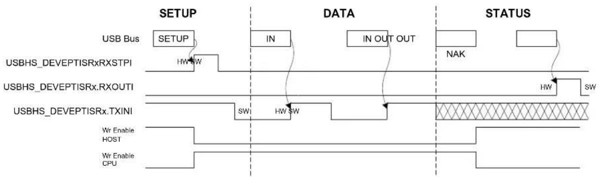
flowchart
graph LR
    A["USB Bus"] --> B["SETUP"]
    B --> C["HW SW"]
    C --> D["USBHS_DEVEPTISRxRXSTPI"]
    D --> E["DATA"]
    E --> F["IN"]
    F --> G["HW SW"]
    G --> H["IN OUT OUT"]
    H --> I["STATUS"]
    I --> J["NAK"]
    J --> K["HW SW"]
    K --> L["SW"]
    L --> M["USBHS_DEVEPTISRx.TXINI"]
    M --> N["SW"]
    N --> O["SW"]
    O --> P["SW"]
    P --> Q["SW"]
    Q --> R["SW"]
    R --> S["SW"]
    S --> T["SW"]
    T --> U["SW"]
    U --> V["SW"]
    V --> W["SW"]
    W --> X["SW"]
    X --> Y["SW"]
    Y --> Z["SW"]
    Z --> AA["SW"]
    AA --> AB["SW"]
    AB --> AC["SW"]
    AC --> AD["SW"]
    AD --> AE["SW"]
    AE --> AF["SW"]
    AF --> AG["SW"]
    AG --> AH["SW"]
    AH --> AI["SW"]
    AI --> AJ["SW"]
    AJ --> AK["SW"]
    AK --> AL["SW"]
    AL --> AM["SW"]
    AM --> AN["SW"]
    AN --> AO["SW"]
    AO --> AP["SW"]
    AP --> AQ["SW"]
    AQ --> AR["SW"]
    AR --> AS["SW"]
    AS --> AT["SW"]
    AT --> AU["SW"]
    AU --> AV["SW"]
    AV --> AW["SW"]
    AW --> AX["SW"]
    AX --> AY["SW"]
    AY --> AZ["SW"]
    AZ --> BA["SW"]
    BA --> BB["SW"]
    BB --> BC["SW"]
    BC --> BD["SW"]
    BD --> BE["SW"]
    BE --> BF["SW"]
    BF --> BG["SW"]
    BG --> BH["SW"]
    BH --> BI["SW"]
    BI --> BJ["SW"]
    BJ --> BK["SW"]
    BK --> BL["SW"]
    BL --> BM["SW"]
    BM --> BN["SW"]
    BN --> BO["SW"]
    BO --> BP["SW"]
    BP --> BQ["SW"]
    BQ --> BR["SW"]
    BR --> BS["SW"]
    BS --> BT["SW"]
    BT --> BU["SW"]
    BU --> BV["SW"]
    BV --> BW["SW"]
    BW --> BX["SW"]
    BX --> BY["SW"]
    BY --> BZ["SW"]
    BZ --> CA["SW"]
    CA --> CB["SW"]
    CB --> CC["SW"]
    CC --> CD["SW"]
    CD --> CE["SW"]
    CE --> CF["SW"]
    CF --> CG["SW"]
    CG --> CH["SW"]
    CH --> CI["SW"]
    CI --> CJ["SW"]
    CJ --> CK["SW"]
    CK --> CR["SW"]
    CR --> CS["SW"]
    CS --> CT["SW"]
    CT --> CU["SW"]
    CU --> CV["SW"]
    CV --> CW["SW"]
    CW --> CX["SW"]
    CX --> CY["SW"]
    CY --> CZ["SW"]
    CZ --> DA["SW"]
    DA --> DB["SW"]
    DB --> DC["SW"]
    DC --> DD["SW"]
    DD --> DE["SW"]
    DE --> DF["SW"]
    DF --> DG["SW"]
    DG --> DH["SW"]
    DH --> DI["SW"]
    DI --> DJ["SW"]
    DJ --> DK["SW"]
A NAK handshake is always generated on the first status stage command.
When the controller detects the status stage, all data written by the CPU is lost and clearing USBHS_DEVEPTISRx.TXINI has no effect.
The user checks if the transmission or the reception is complete.
The OUT retry is always ACKed. This reception sets USBHS_DEVEPTISRx.RXOUTI and USBHS_DEVEPTISRx.TXINI. Handle this with the following software algorithm:
set TXINI
wait for RXOUTI OR TXINI
if RXOUTI, then clear bit and return
if TXINI, then continue
Once the OUT status stage has been received, the USBHS waits for a SETUP request. The SETUP request has priority over any other request and has to be ACKed. This means that any other bit should be cleared and the FIFO reset when a SETUP is received.
The user has to consider that the byte counter is reset when a zero-length OUT packet is received.
38.6.2.12 Management of IN Endpoints
Overview
IN packets are sent by the USB device controller upon IN requests from the host. All data which acknowledges or not the bank can be written when it is full.
The endpoint must be configured first.
The USBHS_DEVEPTISRx.TXINI bit is set at the same time as USBHS_DEVEPTIMRx.FIFOCON when the current bank is free. This triggers a PEP_x interrupt if the Transmitted IN Data Interrupt Enable (USBHS_DEVEPTIMRx.TXINE) bit is one.
USBHS_DEVEPTISRx.TXINI is cleared by software (by writing a one to the Transmitted IN Data Interrupt Clear bit (USBHS_DEVEPTIDRx.TXINIC) to acknowledge the interrupt, which has no effect on the endpoint FIFO.
The user then writes into the FIFO and writes a one to the FIFO Control Clear (USBHS_DEVEPTIDRx.FIFOCONC) bit to clear the USBHS_DEVEPTIMRx.FIFOCON bit. This allows the USBHS to send the data. If the IN endpoint is composed of multiple banks, this also switches to the next bank. The USBHS_DEVEPTISRx.TXINI and USBHS_DEVEPTIMRx.FIFOCON bits are updated in accordance with the status of the next bank.
USBHS_DEVEPTISRx.TXINI is always cleared before clearing USBHS_DEVEPTIMRx.FIFOCON.
The USBHS_DEVEPTISRx.RWALL bit is set when the current bank is not full, i.e., when the software can write further data into the FIFO.
Figure 38-11. Example of an IN Endpoint with one Data Bank
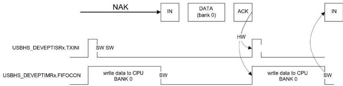
flowchart
graph TD
    A["NAK"] --> B["IN"]
    B --> C["DATA (bank 0)"]
    C --> D["ACK"]
    D --> E["HW"]
    E --> F["write data to CPU BANK 0"]
    F --> G["SW"]
    H["USBHS_DEVEPTISRx.TXINI"] --> I["SW SW"]
    I --> J["write data to CPU BANK 0"]
    J --> K["SW"]
    L["USBHS_DEVEPTIMRx.FIFOCON"] --> M["write data to CPU BANK 0"]
    M --> N["SW"]
    O["IN"] --> P["SW"]
    P --> Q["write data to CPU BANK 0"]
    Q --> R["SW"]
    S["HW"] --> T["write data to CPU BANK 0"]
    T --> U["SW"]
Figure 38-12. Example of an IN Endpoint with two Data Banks
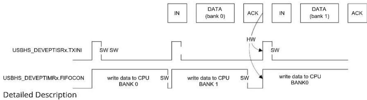
flowchart
graph TD
    A["USBHS_DEVEPTISRx.TXINI"] --> B["SW SW"]
    C["USBHS_DEVEPTIMRx.FIFOCON"] --> D["write data to CPU BANK 0"]
    D --> E["SW"]
    F["DATA (bank 0)"] --> G["HW"]
    H["DATA (bank 1)"] --> I["SW"]
    J["DATA (bank 0)"] --> K["ACK"]
    L["DATA (bank 1)"] --> M["ACK"]
    N["DATA (bank 0)"] --> O["ACK"]
    P["DATA (bank 1)"] --> Q["ACK"]
    R["DATA (bank 0)"] --> S["ACK"]
    T["DATA (bank 1)"] --> U["ACK"]
    V["DATA (bank 0)"] --> W["ACK"]
    X["DATA (bank 1)"] --> Y["ACK"]
    Z["DATA (bank 0)"] --> AA["ACK"]
    AB["DATA (bank 1)"] --> AC["ACK"]
    AD["DATA (bank 0)"] --> AE["ACK"]
    AF["DATA (bank 1)"] --> AG["ACK"]
    AH["DATA (bank 0)"] --> AI["ACK"]
    AJ["DATA (bank 1)"] --> AK["ACK"]
    AL["DATA (bank 0)"] --> AM["ACK"]
    AN["DATA (bank 1)"] --> AO["ACK"]
    AP["DATA (bank 0)"] --> AQ["ACK"]
    AR["DATA (bank 1)"] --> AS["ACK"]
    AT["DATA (bank 0)"] --> AU["ACK"]
    AV["DATA (bank 1)"] --> AW["ACK"]
    AX["DATA (bank 0)"] --> AY["ACK"]
    AZ["DATA (bank 1)"] --> BA["ACK"]
    BB["DATA (bank 0)"] --> BC["ACK"]
    BD["DATA (bank 1)"] --> BE["ACK"]
    BF["DATA (bank 0)"] --> BG["ACK"]
    BH["DATA (bank 1)"] --> BI["ACK"]
    BJ["DATA (bank 0)"] --> BK["ACK"]
    BL["DATA (bank 1)"] --> BLA["ACK"]
    BM["DATA (bank 0)"] --> BN["ACK"]
    BO["DATA (bank 1)"] --> BP["ACK"]
    BQ["DATA (bank 0)"] --> BR["ACK"]
    BS["DATA (bank 1)"] --> BT["ACK"]
    BU["DATA (bank 0)"] --> BV["ACK"]
    BW["DATA (bank 1)"] --> BX["ACK"]
    BY["DATA (bank 0)"] --> BYA["ACK"]
    BZ["DATA (bank 1)"] --> CA["ACK"]
    CB["DATA (bank 0)"] --> CBX["ACK"]
    CC["DATA (bank 1)"] --> CD["ACK"]
    CE["DATA (bank 0)"] --> CF["ACK"]
    CG["DATA (bank 1)"] --> CH["ACK"]
    CI["DATA (bank 0)"] --> CJ["ACK"]
    CK["DATA (bank 1)"] --> CL["ACK"]
    CM["DATA (bank 0)"] --> CN["ACK"]
    CO["DATA (bank 1)"] --> COX["ACK"]
    CP["DATA (bank 0)"] --> CPX["ACK"]
    CY["DATA (bank 1)"] --> CZ["ACK"]
    DA["DATA (bank 0)"] --> DAX["ACK"]
    DB["DATA (bank 1)"] --> DBX["ACK"]
    DC["DATA (bank 0)"] --> DCY["ACK"]
    DD["DATA (bank 1)"] --> DDX["ACK"]
    DX["DATA (bank 0)"] --> DXY["ACK"]
    DXZ["DATA (bank 1)"] --> DXZL["ACK"]
The data is written as follows:
- When the bank is empty, USBHS_DEVEPTISRx.TXINI and USBHS_DEVEPTIMRx.FIFOCON are set, which triggers a PEP_x interrupt if USBHS_DEVEPTIMRx.TXINE = 1.
- The user acknowledges the interrupt by clearing USBHS_DEVEPTISRx.TXINI.
- The user writes the data into the current bank by using the USB Pipe/Endpoint nFIFO Data (USBFIFOnDATA) register, until all the data frame is written or the bank is full (in which case USBHS_DEVEPTISRx.RWALL is cleared and the Byte Count (USBHS_DEVEPTISRx.BYCT) field reaches the endpoint size).
- The user allows the controller to send the bank and switches to the next bank (if any) by clearing USBHS_DEVEPTIMRx.FIFOCON.
If the endpoint uses several banks, the current one can be written while the previous one is being read by the host. Then, when the user clears USBHS_DEVEPTIMRx.FIFOCON, the following bank may already be free and USBHS_DEVEPTISRx.TXINI is set immediately.
An "Abort" stage can be produced when a zero-length OUT packet is received during an IN stage of a control or isochronous IN transaction. The Kill IN Bank (USBHS_DEVEPTIMRx.KILLBK) bit is used to kill the last written bank. The best way to manage this abort is to apply the algorithm represented in the following figure.
Figure 38-13. Abort Algorithm

flowchart
graph TD
    A["Endpoint Abort"] --> B["USBHS_DEVEPTIDRx.TXINEC = 1"]
    B --> C{USBHS_DEVEPTISRx.NBUSYBK == 0?}
    C -->|Yes| D["USBHS_DEVEPT. EPRSTx = 1"]
    C -->|No| E["USBHS_DEVEPTIERx.KILLBKS = 1"]
    D --> F{USBHS_DEVEPTIMRx.KILLBK == 1?}
    E --> F
    F -->|Yes| G["Abort Done"]
    F -->|No| H["Disable the USBHS_DEVEPTISRx.TXINI interrupt"]
    G --> I["Abort is based on the fact that no bank is busy, i.e., that nothing has to be sent"]
    H --> J["Wait for the end of the procedure"]
38.6.2.13 Management of OUT Endpoints
Overview
OUT packets are sent by the host. All data which acknowledges or not the bank can be read when it is empty.
The endpoint must be configured first.
The USBHS_DEVEPTISRx.RXOUTI bit is set at the same time as USBHS_DEVEPTIMRx.FIFOCON when the current bank is full. This triggers a PEP_x interrupt if the Received OUT Data Interrupt Enable (USBHS_DEVEPTIMRx.RXOUTE) bit is one.
USBHS_DEVEPTISRx.RXOUTI is cleared by software (by writing a one to the Received OUT Data Interrupt Clear (USBHS_DEVEPTICRx.RXOUTIC) bit to acknowledge the interrupt, which has no effect on the endpoint FIFO.
The user then reads from the FIFO and clears the USBHS_DEVEPTIMRx.FIFOCON bit to free the bank. If the OUT endpoint is composed of multiple banks, this also switches to the next bank. The USBHS_DEVEPTISRx.RXOUTI and USBHS_DEVEPTIMRx.FIFOCON bits are updated in accordance with the status of the next bank.
USBHS_DEVEPTISRx.RXOUTI is always cleared before clearing USBHS_DEVEPTIMRx.FIFOCON.
The USBHS_DEVEPTISRx.RWALL bit is set when the current bank is not empty, i.e., when the software can read further data from the FIFO.
Figure 38-14. Example of an OUT Endpoint with one Data Bank
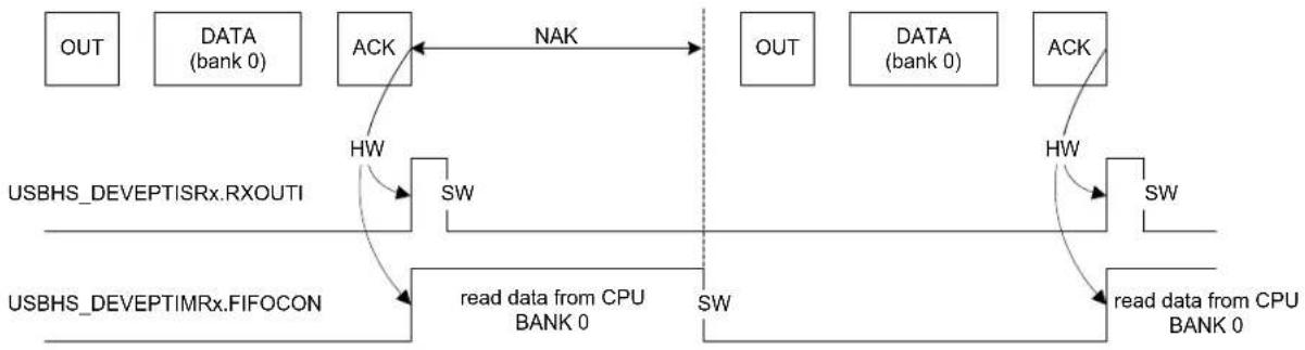
flowchart
graph TD
    A["OUT"] --> B["DATA (bank 0)"]
    B --> C["ACK"]
    C --> D["NAK"]
    D --> E["OUT"]
    E --> F["DATA (bank 0)"]
    F --> G["ACK"]
    G --> H["SW"]
    H --> I["read data from CPU BANK 0"]
    I --> J["read data from CPU BANK 0"]
    J --> K["SW"]
    K --> L["read data from CPU BANK 0"]
    L --> M["read data from CPU BANK 0"]
    M --> N["SW"]
    N --> O["read data from CPU BANK 0"]
    O --> P["read data from CPU BANK 0"]
    P --> Q["read data from CPU BANK 0"]
    Q --> R["read data from CPU BANK 0"]
    R --> S["read data from CPU BANK 0"]
    S --> T["read data from CPU BANK 0"]
    T --> U["read data from CPU BANK 0"]
    U --> V["read data from CPU BANK 0"]
    V --> W["read data from CPU BANK 0"]
    W --> X["read data from CPU BANK 0"]
    X --> Y["read data from CPU BANK 0"]
    Y --> Z["read data from CPU BANK 0"]
    Z --> AA["read data from CPU BANK 0"]
    AA --> AB["read data from CPU BANK 0"]
    AB --> AC["read data from CPU BANK 0"]
    AC --> AD["read data from CPU BANK 0"]
    AD --> AE["read data from CPU BANK 0"]
    AE --> AF["read data from CPU BANK 0"]
    AF --> AG["read data from CPU BANK 0"]
    AG --> AH["read data from CPU BANK 0"]
    AH --> AI["read data from CPU BANK 0"]
    AI --> AJ["read data from CPU BANK 0"]
    AJ --> AK["read data from CPU BANK 0"]
    AK --> AL["read data from CPU BANK 0"]
    AL --> AM["read data from CPU BANK 0"]
    AM --> AN["read data from CPU BANK 0"]
    AN --> AO["read data from CPU BANK 0"]
    AO --> AP["read data from CPU BANK 0"]
    AP --> AQ["read data from CPU BANK 0"]
    AQ --> AR["read data from CPU BANK 0"]
    AR --> AS["read data from CPU BANK 0"]
    AS --> AT["read data from CPU BANK 0"]
    AT --> AU["read data from CPU BANK 0"]
    AU --> AV["read data from CPU BANK 0"]
    AV --> AW["read data from CPU BANK 0"]
    AW --> AX["read data from CPU BANK 0"]
    AX --> AY["read data from CPU BANK 0"]
    AY --> AZ["read data from CPU BANK 0"]
    AZ --> BA["read data from CPU BANK 0"]
    BA --> BB["read data from CPU BANK 0"]
    BB --> BC["read data from CPU BANK 0"]
    BC --> BD["read data from CPU BANK 0"]
    BD --> BE["read data from CPU BANK 0"]
    BE --> BF["read data from CPU BANK 0"]
    BF --> BG["read data from CPU BANK 0"]
    BG --> BH["read data from CPU BANK 0"]
    BH --> BI["read data from CPU BANK 0"]
    BI --> BJ["read data from CPU BANK 0"]
    BJ --> BK["read data from CPU BANK 0"]
    BK --> BL["read data from CPU BANK 0"]
    BL --> BM["read data from CPU BANK 0"]
    BM --> BN["read data from CPU BANK 0"]
    BN --> BO["read data from CPU BANK 0"]
    BO --> BP["read data from CPU BANK 0"]
    BP --> BQ["read data from CPU BANK 0"]
    BQ --> BR["read data from CPU BANK 0"]
    BR --> BS["read data from CPU BANK 0"]
    BS --> BT["read data from CPU BANK 0"]
    BT --> BU["read data from CPU BANK 0"]
    BU --> BV["read data from CPU BANK 0"]
    BV --> BW["read data from CPU BANK 0"]
    BW --> BX["read data from CPU BANK 0"]
    BX --> BY["read data from CPU BANK 0"]
    BY --> BZ["read data from CPU BANK 0"]
    BZ --> CA["read data from CPU BANK 0"]
    CA --> CB["read data from CPU BANK 0"]
    CB --> CC["read data from CPU BANK 0"]
    CC --> CD["read data from CPU BANK 0"]
    CD --> CE["read data from CPU BANK 0"]
    CE --> CF["read data from CPU BANK 0"]
    CF --> CG["read data from CPU BANK 0"]
    CG --> CH["read data from CPU BANK 0"]
    CH --> CI["read data from CPU BANK 0"]
    CI --> CJ["read data from CPU BANK 0"]
    CJ --> CK["read data from CPU BANK 0"]
Figure 38-15. Example of an OUT Endpoint with two Data Banks
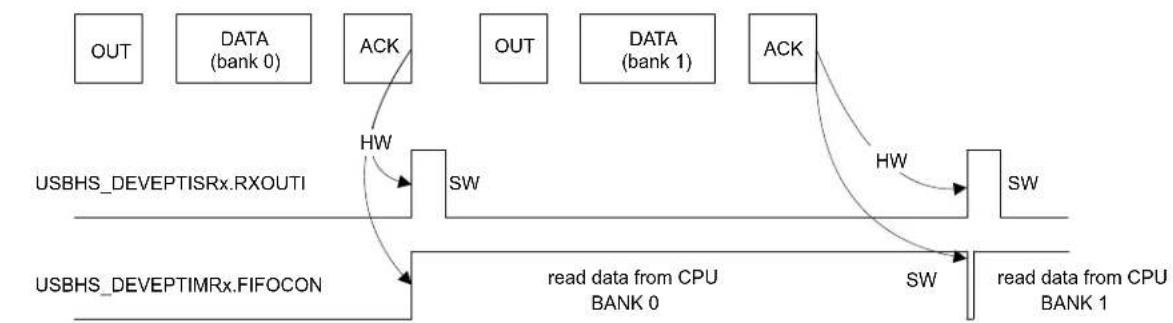
flowchart
graph TD
    A["OUT"] --> B["DATA (bank 0)"]
    B --> C["ACK"]
    C --> D["HW"]
    D --> E["SW"]
    E --> F["read data from CPU BANK 0"]
    F --> G["SW"]
    G --> H["read data from CPU BANK 1"]
    H --> I["ACK"]
    I --> J["HW"]
    J --> K["SW"]
    K --> L["read data from CPU BANK 0"]
    L --> M["read data from CPU BANK 1"]
    M --> N["USBHS_DEVEPTISRx.RXOUTI"]
    N --> O["USBHS_DEVEPTIMRx.FIFOCON"]
Detailed Description
The data is read as follows:
- When the bank is full, USBHS_DEVEPTISRx.RXOUTI and USBHS_DEVEPTIMRx.FIFOCON are set, which triggers a PEP_x interrupt if USBHS_DEVEPTIMRx.RXOUTE = 1.
- The user acknowledges the interrupt by writing a one to USBHS_DEVEPTICRx.RXOUTIC in order to clear USBHS_DEVEPTISRx.RXOUTI.
- The user can read the byte count of the current bank from USBHS_DEVEPTISRx.BYCT to know how many bytes to read, rather than polling USBHS_DEVEPTISRx.RWALL.
- The user reads the data from the current bank by using the USBFIFOnDATA register, until all the expected data frame is read or the bank is empty (in which case USBHS_DEVEPTISRx.RWALL is cleared and USBHS_DEVEPTISRx.BYCT reaches zero).
- The user frees the bank and switches to the next bank (if any) by clearing USBHS_DEVEPTIMRx.FIFOCON.
If the endpoint uses several banks, the current one can be read while the following one is being written by the host. Then, when the user clears USBHS_DEVEPTIMRx.FIFOCON, the following bank can already be read and USBHS_DEVEPTISRx.RXOUTI is set immediately.
In High-speed mode, the PING and NYET protocols are handled by the USBHS.
- For a single bank, a NYET handshake is always sent to the host (on Bulk-out transaction) to indicate that the current packet is acknowledged but there is no room for the next one.
- For a double bank, the USBHS responds to the OUT/DATA transaction with an ACK handshake when the endpoint accepted the data successfully and has room for another data payload (the second bank is free).
38.6.2.14 Underflow
This error only exists for isochronous IN/OUT endpoints. It sets the Underflow Interrupt (USBHS_DEVEPTISRx.UNDERFI) bit, which triggers a PEP_x interrupt if the Underflow Interrupt Enable (USBHS_DEVEPTIMRx.UNDERFE) bit is one.
- An underflow can occur during the IN stage if the host attempts to read from an empty bank. A zero-length packet is then automatically sent by the USBHS.
- An underflow cannot occur during the OUT stage on a CPU action, since the user may only read if the bank is not empty (USBHS_DEVEPTISRx.RXOUTI = 1 or USBHS_DEVEPTISRx.RWALL = 1).
- An underflow can also occur during the OUT stage if the host sends a packet while the bank is already full. Typically, the CPU is not fast enough. The packet is lost.
- An underflow cannot occur during the IN stage on a CPU action, since the user may only write if the bank is not full (USBHS_DEVEPTISRx.TXINI = 1 or USBHS_DEVEPTISRx.RWALL = 1).
38.6.2.15 Overflow
This error exists for all endpoint types. It sets the Overflow interrupt (USBHS_DEVEPTISRx.OVERFI) bit, which triggers a PEP_x interrupt if the Overflow Interrupt Enable (USBHS_DEVEPTIMRx.OVERFE) bit is one.
- An overflow can occur during the OUT stage if the host attempts to write into a bank which is too small for the packet. The packet is acknowledged and the USBHS_DEVEPTISRx.RXOUTI bit is set as if no overflow had occurred. The bank is filled with all the first bytes of the packet that fit in.
- An overflow cannot occur during the IN stage on a CPU action, since the user may only write if the bank is not full (USBHS_DEVEPTISRx.TXINI = 1 or USBHS_DEVEPTISRx.RWALL = 1).
38.6.2.16 HB IsoIn Error
This error only exists for high-bandwidth isochronous IN endpoints.
At the end of the microframe, if at least one packet has been sent to the host and fewer banks than expected have been validated (by clearing the USBHS_DEVEPTIMRx.USBHS_DEVEPTIMRx.FIFOCON) for this microframe, it sets the USBHS_DEVEPTISRx.HBISOINERRORI bit, which triggers a PEP_x interrupt if the High Bandwidth Isochronous IN Error Interrupt Enable (HBISOINERRORE) bit is one.
For example, if the Number of Transactions per MicroFrame for Isochronous Endpoint (NBTRANS) field in USBHS_DEVEPTCFGx is three (three transactions per microframe), only two banks are filled by the CPU (three expected) for the current microframe. Then, the HBISOINERRI interrupt is generated at the end of the microframe. Note that an UNDERFI interrupt is also generated (with an automatic zero-length-packet), except in the case of a missing IN token.
38.6.2.17 HB IsoFlush
This error only exists for high-bandwidth isochronous IN endpoints.
At the end of the microframe, if at least one packet has been sent to the host and there is a missing IN token during this microframe, the bank(s) destined to this microframe is/are flushed out to ensure a good data synchronization between the host and the device.
For example, if NBTRANS is three (three transactions per microframe) and if only the first IN token (among three) is well received by the USBHS, the last two banks are discarded.
38.6.2.18 CRC Error
This error only exists for isochronous OUT endpoints. It sets the CRC Error Interrupt (USBHS_DEVEPTISRx.CRCERRI) bit, which triggers a PEP_x interrupt if the CRC Error Interrupt Enable (USBHS_DEVEPTIMRx.CRCERRE) bit is one.
A CRC error can occur during the OUT stage if the USBHS detects a corrupted received packet. The OUT packet is stored in the bank as if no CRC error had occurred (USBHS_DEVEPTISRx.RXOUTI is set).
38.6.2.19 Interrupts
See the structure of the USB device interrupt system in Figure 38-3.
There are two kinds of device interrupts: processing, i.e., their generation is part of the normal processing, and exception, i.e., errors (not related to CPU exceptions).
Global Interrupts
The processing device global interrupts are:
- Suspend (USBHS_DEVISR.SUSP)
- Start of Frame (USBHS_DEVISR.SOF) interrupt with no frame number CRC error - the Frame Number CRC Error (USBHS_DEVFNUM.FNCERR) bit is zero.
- Micro Start of Frame (USBHS_DEVISR.MSOF) with no CRC error
• End of Reset (USBHS_DEVISR.EORST) - Wakeup (USBHS_DEVISR.WAKEUP)
• End of Resume (USBHS_DEVISR.EORSM) - Upstream Resume (USBHS_DEVISR.UPRSM)
- Endpoint x (USBHS_DEVISR.PEP_x)
• DMA Channel x (USBHS_DEVISR.DMA_x)
The exception device global interrupts are:
- Start of Frame (USBHS_DEVISR.SOF) with a frame number CRC error (USBHS_DEVFNUM.FNCERR = 1)
- Micro Start of Frame (USBHS_DEVFNUM.FNCERR.MSOF) with a CRC error Endpoint Interrupts
The processing device endpoint interrupts are:
- Transmitted IN Data (USBHS_DEVEPTISRx.TXINI)
- Received OUT Data (USBHS_DEVEPTISRx.RXOUTI)
- Received SETUP (USBHS_DEVEPTISRx.RXSTPI)
- Short Packet (USBHS_DEVEPTISRx.SHORTPACKET)
• Number of Busy Banks (USBHS_DEVEPTISRx.NBUSYBK) - Received OUT Isochronous Multiple Data (DTSEQ = MDATA & USBHS_DEVEPTISRx.RXOUTI)
- Received OUT Isochronous DataX (DTSEQ = DATAX & USBHS_DEVEPTISRx.RXOUTI)
The exception device endpoint interrupts are:
- Underflow (USBHS_DEVEPTISRx.UNDERFI)
- NAKed OUT (USBHS_DEVEPTISRx.NAKOUTI)
• High-Bandwidth Isochronous IN Error (USBHS_DEVEPTISRx.HBISOINERRI) - NAKed IN (USBHS_DEVEPTISRx.NAKINI)
- High-Bandwidth Isochronous IN Flush error (USBHS_DEVEPTISRx.HBISOFLUSHI)
• Overflow (USBHS_DEVEPTISRx.OVERFI) - STALLed (USBHS_DEVEPTISRx.STALLEDI)
- CRC Error (USBHS_DEVEPTISRx.CRCERRI)
- Transaction Error (USBHS_DEVEPTISRx.ERRORTRANS) DMA Interrupts
The processing device DMA interrupts are:
- End of USB Transfer Status (USBHS_DEVDMASTATUSx.END_TR_ST)
- End of Channel Buffer Status (USBHS_DEVDMASTATUSx.END_BF_ST)
- Descriptor Loaded Status (USBHS_DEVDMASTATUSx.DESC_LDST)
There is no exception device DMA interrupt.
38.6.2.20 Test Modes
When written to one, the USBHS_DEVCTRL.TSTPCKT bit switches the USB device controller to a "Test-packet" mode:
The transceiver repeatedly transmits the packet stored in the current bank.
USBHS_DEVCTRL.TSTPCKT must be written to zero to exit the Test-packet mode. The endpoint is reset by software after a Test-packet mode.
This enables the testing of rise and falling times, eye patterns, jitter, and any other dynamic waveform specifications.
The flow control used to send the packets is as follows:
- USBHS_DEVCTRL.TSTPCKT = 1;
- Store data in an endpoint bank
- Write a zero to the USBHS_DEVEPTIDRx.FIFOCON bit
To stop the Test-packet mode, write a zero to the USBHS_DEVCTRL.TSTPCKT bit.
38.6.3 USB Host Operation
38.6.3.1 Description of Pipes
For the USBHS in Host mode, the term "pipe" is used instead of "endpoint" (used in Device mode). A host pipe corresponds to a device endpoint, as described in Figure 38-16 (from the USB Specification).
Figure 38-16. USB Communication Flow

flowchart
graph TD
    A["Host"] --> B["Client Software"]
    B --> C["Buffers"]
    B --> D["Communication Flows"]
    B --> E["Endpoints"]
    F["Pipes"] --> B
    G["USB Logical Device"] --> H["Interface"]
    H --> B
    B --> I["Data Flow"]
    style A fill:#f9f,stroke:#333
    style B fill:#ccf,stroke:#333
    style F fill:#cfc,stroke:#333
    style G fill:#fcc,stroke:#333
    style H fill:#cff,stroke:#333
    style I fill:#ffc,stroke:#333
In Host mode, the USBHS associates a pipe to a device endpoint, considering the device configuration descriptors.
38.6.3.2 Power-On and Reset
The following figure describes the USBHS Host mode main states.
Figure 38-17. Host Mode Main States
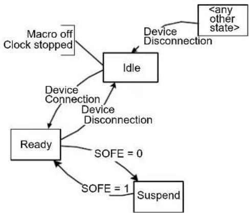
flowchart
graph TD
    A["Macro off Clock stopped"] --> B["Idle"]
    B --> C["Device Connection"]
    B --> D["Device Disconnection"]
    C --> E["Ready"]
    D --> E
    E --> F["Suspend"]
    G["<any other state>"] --> B
    H["SOFE = 0"] --> E
    I["SOFE = 1"] --> E
After a hardware reset, the USBHS Host mode is in the Reset state.
When the USBHS is enabled (USBHS_CTRL.USBE = 1) in Host mode (USBHS_CTRL.UIMOD = 0), it goes to the Idle state. In this state, the controller waits for a device connection with a minimal power consumption. The USB pad should be in the Idle state. Once a device is connected, the USBHS enters the Ready state, which does not require the USB clock to be activated.
The controller enters the Suspend state when the USB bus is in a "Suspend" state, i.e., when the Host mode does not generate the "Start of Frame (SOF)". In this state, the USB consumption is minimal. The Host mode exits the Suspend state when starting to generate the SOF over the USB line.
38.6.3.3 Device Detection
A device is detected by the USBHS Host mode when D+ or D- is no longer tied low, i.e., when the device D+ or D- pull-up resistor is connected. The bit USBHS_SFR.VBUSRQS must be set to '1' to enable this detection.
Note: The VBUS supply is not managed by the USBHS interface. It must be generated on-board.
The device disconnection is detected by the host controller when both D+ and D- are pulled down.
38.6.3.4 USB Reset
The USBHS sends a USB bus reset when the user writes a one to the Send USB Reset bit in the Host General Control register (USBHS_HSTCTRL.RESET). The USB Reset Sent Interrupt bit in the Host Global Interrupt Status register (USBHS_HSTISR.RSTI) is set when the USB reset has been sent. In this case, all pipes are disabled and de-allocated.
If the bus was previously in a "Suspend" state (the Start of Frame Generation Enable (USBHS_HSTCTRL.SOFE) bit is zero), the USBHS automatically switches to the "Resume" state, the Host Wakeup Interrupt (USBHS_HSTISR.HWUPI) bit is set and the USBHS_HSTCTRL.SOFE bit is set in order to generate SOFs or micro SOFs immediately after the USB reset.
At the end of the reset, the user should check the USBHS_SR.SPEED field to know the speed running according to the peripheral capability (LS.FS/HS).
38.6.3.5 Pipe Reset
A pipe can be reset at any time by writing a one to the Pipe x Reset (USBHS_HSTPIP.PRSTx) bit. This is recommended before using a pipe upon hardware reset or when a USB bus reset has been sent. This resets:
• the internal state machine of the pipe,
• the receive and transmit bank FIFO counters,
- all the registers of the pipe (USBHS_HSTPIPCFGx, USBHS_HSTPIPISRx, USBHS_HSTPIPIMRx), except its configuration (USBHS_HSTPIPCFGx.ALLOC, USBHS_HSTPIPCFGx.PBK, USBHS_HSTPIPCFGx.PSIZE, USBHS_HSTPIPCFGx.PTOKEN, USBHS_HSTPIPCFGx.PTYPE, USBHS_HSTPIPCFGx.PEPNUM, USBHS_HSTPIPCFGx.INTFRQ) and its Data Toggle Sequence field (USBHS_HSTPIPISRx.DTSEQ).
The pipe configuration remains active and the pipe is still enabled.
The pipe reset may be associated with a clear of the data toggle sequence. This can be achieved by setting the Reset Data Toggle bit in the Pipe x Control register (USBHS_HSTPIPIMRx.RSTDT) (by writing a one to the Reset Data Toggle Set bit in the Pipe x Control Set register (USBHS_HSTPIPIERx.RSTDTS)).
In the end, the user has to write a zero to the USBHS_HSTPIP.PRSTx bit to complete the reset operation and to start using the FIFO.
38.6.3.6 Pipe Activation
The pipe is maintained inactive and reset (see "Pipe Reset" for more details) as long as it is disabled (USBHS_HSTPIP.PENx = 0). The Data Toggle Sequence field (USBHS_HSTPIPISRx.DTSEQ) is also reset.
The algorithm represented in the following figure must be followed to activate a pipe.
Figure 38-18. Pipe Activation Algorithm

flowchart
graph TD
    A["Pipe Activation"] --> B["USBHS_HSTPIP.PENx = 1"]
    B --> C["USBHS_HSTPIPPCFGx .INTFRQ .PEPNUM .PTYPE .PTOKEN .PSIZE .PBK .ALLOC"]
    C --> D{USBHS_HSTPIPISRx.CFGOK == 1?}
    D -->|Yes| E["Pipe Activated"]
    D -->|No| F["ERROR"]
    E --> G["Test if the pipe configuration is correct."]
As long as the pipe is not correctly configured (USBHS_HSTPIPISRx.CFGOK = 0), the controller cannot send packets to the device through this pipe.
The USBHS_HSTPIPISRx.CFGOK bit is only set if the configured size and number of banks are correct as compared to their maximal allowed values for the pipe (see the Description of USB Pipes/Endpoints table) and to the maximal FIFO size (i.e., the DPRAM size).
See "DPRAM Management" for additional information.
Once the pipe is correctly configured (USBHS_HSTPIPISRx.CFGOK = 1), only the USBHS_HSTPIPCFGx.PTOKEN and USBHS_HSTPIPCFGx.INTFRQ fields can be written by software. USBHS_HSTPIPCFGx.INTFRQ is meaningless for non-interrupt pipes.
When starting an enumeration, the user gets the device descriptor by sending a GET_DESCRIPTION USB request. This descriptor contains the maximal packet size of the device default control endpoint (bMaxPacketSize0) and the user reconfigures the size of the default control pipe with this size parameter.
38.6.3.7 Address Setup
Once the device has answered the first host requests with the default device address 0, the host assigns a new address to the device. The host controller has to send a USB reset to the device and to send a SET_ADDRESS (addr) SETUP request with the new address to be used by the device. Once this SETUP transaction is over, the user writes the new address into the USB Host Address for Pipe x field in the USB Host Device Address register (HSTADDR.HSTADDRPx). All the following requests on all pipes are then performed using this new address.
When the host controller sends a USB reset, the HSTADDRPx field is reset by hardware and the following host requests are performed using the default device address 0.
38.6.3.8 Remote Wakeup
The controller Host mode enters the Suspend state when the USBHS_HSTCTRL.SOFE bit is written to zero. No more "Start of Frame" is sent on the USB bus and the USB device enters the Suspend state 3 ms later.
The device awakes the host by sending an Upstream Resume (Remote Wakeup feature). When the host controller detects a non-idle state on the USB bus, it sets the Host Wakeup interrupt (USBHS_HSTISR.HWUPI) bit. If the non-idle bus state corresponds to an Upstream Resume (K state), the Upstream Resume Received Interrupt (USBHS_HSTISR.RXRSMI) bit is set. The user has to generate a Downstream Resume within 1 ms and for at least 20 ms by writing a one to the Send USB Resume (USBHS_HSTCTRL.RESUME) bit. It is mandatory to write a one to USBHS_HSTCTRL.SOFE before writing a one to USBHS_HSTCTRL.RESUME to enter the Ready state, otherwise USBHS_HSTCTRL.RESUME has no effect.
38.6.3.9 Management of Control Pipes
A control transaction is composed of three stages:
- SETUP
- Data (IN or OUT)
- Status (OUT or IN)
The user has to change the pipe token according to each stage.
For the control pipe only, each token is assigned a specific initial data toggle sequence:
- SETUP: Data0
• IN: Data1 - OUT: Data1
38.6.3.10 Management of IN Pipes
IN packets are sent by the USB device controller upon IN requests from the host. All data which acknowledges or not the bank can be read when it is empty.
The pipe must be configured first.
When the host requires data from the device, the user has to first select the IN Request mode with the IN Request Mode bit in the Pipe x IN Request register (USBHS_HSTPIPINRQx.INMODE):
- When USBHS_HSTPIPINRQx.INMODE = 0, the USBHS performs (INRQ + 1) IN requests before freezing the pipe.
- When USBHS_HSTPIPINRQx.INMODE = 1, the USBHS performs IN requests endlessly when the pipe is not frozen by the user.
The generation of IN requests starts when the pipe is unfrozen (the Pipe Freeze (USBHS_HSTPIPIMRx.PFREEZE) field in USBHS_HSTPIPIMRx is zero).
The Received IN Data Interrupt (USBHS_HSTPIPISRx.RXINI) bit is set at the same time as the FIFO Control (USBHS_HSTPIPIMRx.FIFOCON) bit when the current bank is full. This triggers a PEP_x interrupt if the Received IN Data Interrupt Enable (USBHS_HSTPIPIMRx.RXINE) bit is one.
USBHS_HSTPIPISRx.RXINI is cleared by software (by writing a one to the Received IN Data Interrupt Clear bit in the Host Pipe x Clear register (USBHS_HSTPIPIDRx.RXINIC)) to acknowledge the interrupt, which has no effect on the pipe FIFO.
The user then reads from the FIFO and clears the USBHS_HSTPIPIMRx.FIFOCON bit (by writing a one to the FIFO Control Clear (USBHS_HSTPIPIDRx.FIFOCONC) bit) to free the bank. If the IN pipe is composed of multiple banks, this also switches to the next bank. The USBHS_HSTPIPISRx.RXINI and USBHS_HSTPIPIMRx.FIFOCON bits are updated in accordance with the status of the next bank.
USBHS_HSTPIPISRx.RXINI is always cleared before clearing USBHS_HSTPIPIMRx.FIFOCON.
The Read/Write Allowed (USBHS_HSTPIPISRx.RWALL) bit is set when the current bank is not empty, i.e., when the software can read further data from the FIFO.
Figure 38-19. Example of an IN Pipe with one Data Bank

flowchart
graph TD
    IN["IN"] -->|DATA (bank 0)| HW1["HW"]
    HW1 -->|SW| USBHS_HSTPIPISRx.RXINI["USBHS_HSTPIPISRx.RXINI"]
    HW1 -->|SW| USBHS_HSTPIPIMRx.FIFOCON["USBHS_HSTPIPIMRx.FIFOCON"]
    HW1 -->|SW| readData["read data from CPU BANK 0"]
    HW1 -->|SW| readData2["read data from CPU BANK 0"]
    HW1 -->|SW| readData3["read data from CPU BANK 0"]
    HW1 -->|SW| readData4["read data from CPU BANK 0"]
    HW1 -->|SW| readData5["read data from CPU BANK 0"]
    HW1 -->|SW| readData6["read data from CPU BANK 0"]
    HW1 -->|SW| readData7["read data from CPU BANK 0"]
    HW1 -->|SW| readData8["read data from CPU BANK 0"]
    HW1 -->|SW| readData9["read data from CPU BANK 0"]
    HW1 -->|SW| readData10["read data from CPU BANK 0"]
    HW1 -->|SW| readData11["read data from CPU BANK 0"]
    HW1 -->|SW| readData12["read data from CPU BANK 0"]
    HW1 -->|SW| readData13["read data from CPU BANK 0"]
    HW1 -->|SW| readData14["read data from CPU BANK 0"]
    HW1 -->|SW| readData15["read data from CPU BANK 0"]
    HW1 -->|SW| readData16["read data from CPU BANK 0"]
    HW1 -->|SW| readData17["read data from CPU BANK 0"]
    HW1 -->|SW| readData18["read data from CPU BANK 0"]
    HW1 -->|SW| readData19["read data from CPU BANK 0"]
    HW1 -->|SW| readData20["read data from CPU BANK 0"]
    HW1 -->|SW| readData21["read data from CPU BANK 0"]
    HW1 -->|SW| readData22["read data from CPU BANK 0"]
    HW1 -->|SW| readData23["read data from CPU BANK 0"]
    HW1 -->|SW| readData24["read data from CPU BANK 0"]
    HW1 -->|SW| readData25["read data from CPU BANK 0"]
    HW1 -->|SW| readData26["read data from CPU BANK 0"]
    HW1 -->|SW| readData27["read data from CPU BANK 0"]
    HW1 -->|SW| readData28["read data from CPU BANK 0"]
    HW1 -->|SW| readData29["read data from CPU BANK 0"]
    HW1 -->|SW| readData30["read data from CPU BANK 0"]
    HW1 -->|SW| readData31["read data from CPU BANK 0"]
    HW1 -->|SW| readData32["read data from CPU BANK 0"]
    HW1 -->|SW| readData33["read data from CPU BANK 0"]
    HW1 -->|SW| readData34["read data from CPU BANK 0"]
    HW1 -->|SW| readData35["read data from CPU BANK 0"]
    HW1 -->|SW| readData36["read data from CPU BANK 0"]
    HW1 -->|SW| readData37["read data from CPU BANK 0"]
    HW1 -->|SW| readData38["read data from CPU BANK 0"]
    HW1 -->|SW| readData39["read data from CPU BANK 0"]
    HW1 -->|SW| readData40["read data from CPU BANK 0"]
    HW1 -->|SW| readData41["read data from CPU BANK 0"]
    HW1 -->|SW| readData42["read data from CPU BANK 0"]
    HW1 -->|SW| readData43["read data from CPU BANK 0"]
    HW1 -->|SW| readData44["read data from CPU BANK 0"]
    HW1 -->|SW| readData45["read data from CPU BANK 0"]
    HW1 -->|SW| readData46["read data from CPU BANK 0"]
    HW1 -->|SW| readData47["read data from CPU BANK 0"]
    HW1 -->|SW| readData48["read data from CPU BANK 0"]
    HW1 -->|SW| readData49["read data from CPU BANK 0"]
    HW1 -->|SW| readData50["read data from CPU BANK 0"]
Figure 38-20. Example of an IN Pipe with two Data Banks
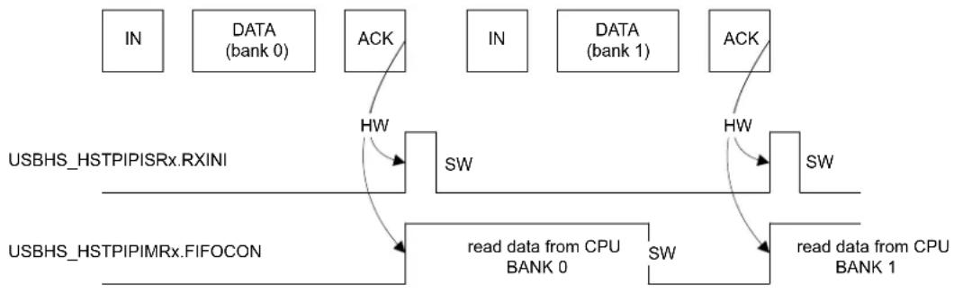
flowchart
graph TD
    IN["IN"] -->|DATA (bank 0)| HW1["HW"]
    HW1 -->|SW| USBHS_HSTPIPISRx.RXINI["USBHS_HSTPIPISRx.RXINI"]
    HW1 -->|SW| USBHS_HSTPIPIMRx.FIFOCON["USBHS_HSTPIPIMRx.FIFOCON"]
    HW1 -->|SW| readData["read data from CPU BANK 0"]
    HW1 -->|SW| readData["read data from CPU BANK 1"]
    HW1 -->|SW| readData["read data from CPU BANK 1"]
    HW1 -->|SW| readData["read data from CPU BANK 0"]
    HW1 -->|SW| readData["read data from CPU BANK 1"]
    HW1 -->|SW| readData["read data from CPU BANK 0"]
    HW1 -->|SW| readData["read data from CPU BANK 1"]
    HW1 -->|SW| readData["read data from CPU BANK 0"]
    HW1 -->|SW| readData["read data from CPU BANK 1"]
    HW1 -->|SW| readWater["SW"]
    HW1 -->|SW| readWater["SW"]
    HW1 -->|SW| readWater["SW"]
    HW1 -->|SW| readWater["SW"]
    HW1 -->|SW| readWater["SW"]
    HW1 -->|SW| readWater["SW"]
    HW1 -->|SW| readWater["SW"]
    HW1 -->|SW| readWater["SW"]
    HW1 -->|SW| readWater["SW"]
    HW2["IN"] -->|DATA (bank 0)| HW1
    HW2 -->|DATA (bank 0)| HW2
    HW2 -->|DATA (bank 0)| HW3
    HW2 -->|DATA (bank 0)| HW4
    HW2 -->|DATA (bank 0)| HW5
    HW2 -->|DATA (bank 0)| HW6
    HW2 -->|DATA (bank 0)| HW7
    HW2 -->|DATA (bank 0)| HW8
    HW2 -->|DATA (bank 0)| HW9
    HW2 -->|DATA (bank 0)| HW10
    HW2 -->|DATA (bank 0)| HW11
    HW2 -->|DATA (bank 0)| HW12
    HW2 -->|DATA (bank 0)| HW13
    HW2 -->|DATA (bank 0)| HW14
    HW2 -->|DATA (bank 0)| HW15
    HW2 -->|DATA (bank 0)| HW16
    HW2 -->|DATA (bank 0)| HW17
    HW2 -->|DATA (bank 0)| HW18
    HW2 -->|DATA (bank 0)| HW19
    HW2 -->|DATA (bank 0)| HW20
    HW2 -->|DATA (bank 0)| HW21
    HW2 -->|DATA (bank 0)| HW22
    HW2 -->|DATA (bank 0)| HW23
    HW2 -->|DATA (bank 0)| HW24
    HW2 -->|DATA (bank 0)| HW25
    HW2 -->|DATA (bank 0)| HW26
    HW2 -->|DATA (bank 0)| HW27
    HW2 -->|DATA (bank 0)| HW28
    HW2 -->|DATA (bank 0)| HW29
    HW2 -->|DATA (bank 0)| HW30
    HW2 -->|DATA (bank 0)| HW31
    HW2 -->|DATA (bank 0)| HW32
    HW2 -->|DATA (bank 0)| HW33
    HW2 -->|DATA (bank 0)| HW34
    HW2 -->|DATA (bank 0)| HW35
    HW2 -->|DATA (bank 0)| HW36
    HW2 -->|DATA (bank 0)| HW37
    HW2 -->|DATA (bank 0)| HW38
    HW2 -->|DATA (bank 0)| HW39
    HW2 -->|DATA (bank 0)| HW40
    HW2 -->|DATA (bank 0)| HW41
    HW2 -->|DATA (bank 0)| HW42
    HW2 -->|DATA (bank 0)| HW43
    HW2 -->|DATA (bank 0)| HW44
    HW2 -->|DATA (bank 0)| HW45
    HW2 -->|DATA (bank 0)| HW46
    HW2 -->|DATA (bank 0)| HW47
    HW2 -->|DATA (bank 0)| HW48
    HW2 -->|DATA (bank 0)| HW49
    HW2 -->|DATA (bank 0)| HW50
38.6.3.11 Management of OUT Pipes
OUT packets are sent by the host. All data which acknowledges or not the bank can be written when it is full.
The pipe must be configured and unfrozen first.
The Transmitted OUT Data Interrupt (USBHS_HSTPIPISRx.TXOUTI) bit is set at the same time as USBHS_HSTPIPIMRx.FIFOCON when the current bank is free. This triggers a PEP_x interrupt if the Transmitted OUT Data Interrupt Enable (USBHS_HSTPIPIMRx.TXOUTE) bit is one.
USBHS_HSTPIPISRx.TXOUTI is cleared by software (by writing a one to the Transmitted OUT Data Interrupt Clear (USBHS_HSTPIPIDRx.TXOUTIC) bit to acknowledge the interrupt, which has no effect on the pipe FIFO.
The user then writes into the FIFO and clears the USBHS_HSTPIPIDRx.FIFOCON bit to allow the USBHS to send the data. If the OUT pipe is composed of multiple banks, this also switches to the next bank. The USBHS_HSTPIPISRx.TXOUTI and USBHS_HSTPIPIMRx.FIFOCON bits are updated in accordance with the status of the next bank.
USBHS_HSTPIPISRx.TXOUTI is always cleared before clearing USBHS_HSTPIPIMRx.FIFOCON.
The USBHS_HSTPIPISRx.RWALL bit is set when the current bank is not full, i.e., when the software can write further data into the FIFO.
Notes:
- If the user decides to switch to the Suspend state (by writing a zero to the USBHS_HSTCTRL.SOFE bit) while a bank is ready to be sent, the USBHS automatically exits this state and the bank is sent.
- In High-speed operating mode, the host controller automatically manages the PING protocol to maximize the USB bandwidth. The user can tune the PING protocol by handling the Ping Enable (PINGEN) bit and the bInterval Parameter for the Bulk-Out/Ping Transaction (BINTERVAL) field in USBHS HSTPIPCFGx. See the Host Pipe x Configuration Register for additional information.
Figure 38-21. Example of an OUT Pipe with one Data Bank

flowchart
graph TD
    A["USBHS_HSTPIPISRx.TXOUTI"] -->|SW SW| B["write data to CPU BANK 0"]
    C["USBHS_HSTPIPIMRx.FIFOCON"] -->|SW| D["write data to CPU BANK 0"]
    B --> E["DATA (bank 0)"]
    D --> F["ACK"]
    E --> G["OUT"]
    F --> H["OUT"]
    G --> I["HW"]
    H --> I
    I --> J["Write Data to CPU BANK 0"]
Figure 38-22. Example of an OUT Pipe with two Data Banks and no Bank Switching Delay
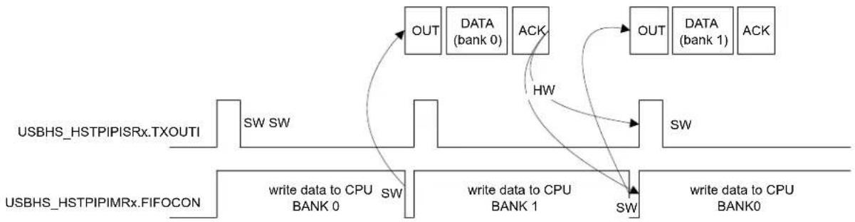
flowchart
graph TD
    A["USBHS_HSTPIPISRx.TXOUTI"] --> B["SW SW"]
    B --> C["OUT DATA (bank 0) ACK"]
    C --> D["HW"]
    D --> E["OUT DATA (bank 1) ACK"]
    E --> F["SW"]
    G["USBHS_HSTPIPIMRx.FIFOCON"] --> H["write data to CPU BANK 0 SW"]
    H --> I["write data to CPU BANK 1 SW"]
    I --> J["write data to CPU BANK0"]
Figure 38-23. Example of an OUT Pipe with two Data Banks and a Bank Switching Delay
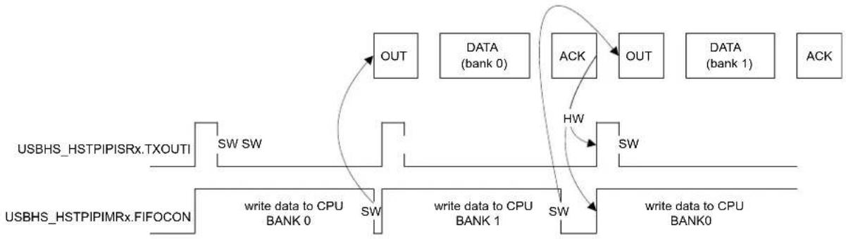
flowchart
graph TD
    A["USBHS_HSTPIPISRx.TXOUTI"] --> B["SW SW"]
    C["USBHS_HSTPIPIMRx.FIFOCON"] --> D["write data to CPU BANK 0"]
    D --> E["SW"]
    F["DATA (bank 0)"] --> G["OUT"]
    H["DATA (bank 1)"] --> I["ACK"]
    J["DATA (bank 0)"] --> K["HW"]
    L["DATA (bank 1)"] --> M["OUT"]
    N["DATA (bank 0)"] --> O["ACK"]
    P["Write data to CPU BANK 0"] --> Q["Write data to CPU BANK 1"]
    R["Write data to CPU BANK 1"] --> S["Write data to CPU BANK 2"]
    T["Write data to CPU BANK 2"] --> U["Write data to CPU BANK 3"]
    V["Write data to CPU BANK 3"] --> W["Write data to CPU BANK 4"]
    X["Write data to CPU BANK 4"] --> Y["Write data to CPU BANK 5"]
    Z["Write data to CPU BANK 5"] --> AA["Write data to CPU BANK 6"]
    AB["Write data to CPU BANK 6"] --> AC["Write data to CPU BANK 7"]
    AD["Write data to CPU BANK 7"] --> AE["Write data to CPU BANK 8"]
    AF["Write data to CPU BANK 8"] --> AG["Write data to CPU BANK 9"]
    AH["Write data to CPU BANK 9"] --> AI["Write data to CPU BANK 10"]
38.6.3.12 CRC Error
This error exists only for isochronous IN pipes. It sets the CRC Error Interrupt (USBHS_HSTPIPISRx.CRCERRI) bit, which triggers a PEP_x interrupt if then the CRC Error Interrupt Enable (USBHS_HSTPIPIMRx.CRCERRE) bit is one.
A CRC error can occur during IN stage if the USBHS detects a corrupted received packet. The IN packet is stored in the bank as if no CRC error had occurred (USBHS_HSTPIPISRx.RXINI is set).
38.6.3.13 Interrupts
See the structure of the USB host interrupt system on Figure 38-3.
There are two kinds of host interrupts: processing, i.e., their generation is part of the normal processing, and exception, i.e., errors (not related to CPU exceptions).
Global Interrupts
The processing host global interrupts are:
• Device Connection (USBHS_HSTISR.DCONNI)
• Device Disconnection (USBHS_HSTISR.DDISCI)
- USB Reset Sent (USBHS_HSTISR.RSTI)
- Downstream Resume Sent (USBHS_HSTISR.RSMEDI)
- Upstream Resume Received (USBHS_HSTISR.RXRSMI)
- Host Start of Frame (USBHS_HSTISR.HSOFI)
- Host Wakeup (USBHS_HSTISR.HWUPI)
- Pipe x (USBHS_HSTISR.PEP_x)
- DMA Channel x (USBHS_HSTISR.DMAxINT)
There is no exception host global interrupt.
Pipe Interrupts
The processing host pipe interrupts are:
- Received IN Data (USBHS_HSTPIPISRx.RXINI)
- Transmitted OUT Data (USBHS_HSTPIPISRx.TXOUTI)
- Transmitted SETUP (USBHS_HSTPIPISRx.TXSTPI)
- Short Packet (USBHS_HSTPIPISRx.SHORTPACKETI)
• Number of Busy Banks (USBHS_HSTPIPISRx.NBUSYBK)
The exception host pipe interrupts are:
- Underflow (USBHS_HSTPIPISRx.UNDERFI)
- Pipe Error (USBHS_HSTPIPISRx.PERRI)
- NAKed (USBHS_HSTPIPISRx.NAKEDI)
- Overflow (USBHS_HSTPIPISRx.OVERFI)
- Received STALLed (USBHS_HSTPIPISRx.RXSTALLDI)
- CRC Error (USBHS_HSTPIPISRx.CRCERRI) DMA Interrupts
The processing host DMA interrupts are:
- The End of USB Transfer Status (USBHS_HSTDMASTATUSx.END_TR_ST)
- The End of Channel Buffer Status (USBHS_HSTDMASTATUSx.END_BF_ST)
- The Descriptor Loaded Status (USBHS_HSTDMASTATUSx.DESC_LDST)
There is no exception host DMA interrupt.
38.6.4 USB DMA Operation
USB packets of any length may be transferred when required by the USBHS. These transfers always feature sequential addressing. Such characteristics mean that in case of high USBHS throughput, both AHB ports benefit from "incrementing burst of unspecified length" since the average access latency of AHB Clients can then be reduced.
The DMA uses word "incrementing burst of unspecified length" of up to 256 beats for both data transfers and channel descriptor loading. A burst may last on the AHB busses for the duration of a whole USB packet transfer, unless otherwise broken by the AHB arbitration or the AHB 1-Kbyte boundary crossing.
Packet data AHB bursts may be locked on a DMA buffer basis for drastic overall AHB bus bandwidth performance boost with paged memories. This prevents large AHB bursts from being broken in case of conflict with other AHB bus Hosts, thus avoiding access latencies due to memory row changes. This means up to 128 words single cycle unbroken AHB bursts for bulk pipes/endpoints and 256 words single cycle unbroken bursts for isochronous pipes/endpoints. This maximal burst length is then controlled by the lowest programmed USB Pipe/Endpoint Size (USBHS_HSTPIPCFGx.PSIZE / USBHS_DEVEPTCFGx.EPSIZE) and the Buffer Byte Length (USBHS_HSTDMACONTROLx.BUFF_LENGTH / USBHS_DEVDMACONTROLx.BUFF_LENGTH) fields.
The USBHS average throughput can reach nearly 480 Mbps. Its average access latency decreases as burst length increases due to the zero wait-state side effect of unchanged pipe/endpoint. Word access allows reducing the AHB bandwidth required for the USB by four, as compared to native byte access. If at least 0 wait-state word burst capability is also provided by the other DMA AHB bus Clients, each DMA AHB bus needs less than 60% bandwidth allocation for full USB bandwidth usage at 33 MHz, and less than 30% at 66 MHz.
Figure 38-24. Example of a DMA Chained List
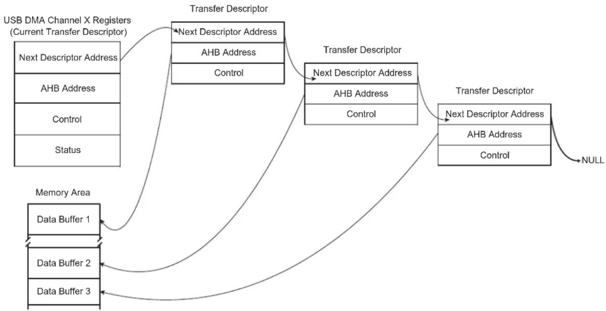
flowchart
graph TD
    A["USB DMA Channel X Registers (Current Transfer Descriptor)"] --> B["Next Descriptor Address"]
    B --> C["AHB Address"]
    C --> D["Control"]
    D --> E["Transfer Descriptor"]
    E --> F["Next Descriptor Address"]
    F --> G["AHB Address"]
    G --> H["Control"]
    H --> I["Transfer Descriptor"]
    I --> J["Next Descriptor Address"]
    J --> K["AHB Address"]
    K --> L["Control"]
    L --> M["NULL"]
    M --> N["Data Buffer 1"]
    M --> O["Data Buffer 2"]
    M --> P["Data Buffer 3"]
    N --> Q["Memory Area"]
    O --> Q
    P --> Q
38.6.5 USB DMA Channel Transfer Descriptor
The DMA channel transfer descriptor is loaded from the memory. The following structures apply:
Offset 0:
• The address must be aligned: 0xXXXX0
- Next Descriptor Address Register: USBHS_xxxDMANXTDSCx
Offset 4:
• The address must be aligned: 0xXXXX4
- DMA Channelx Address Register: USBHS_xxxDMAADDRESSx
Offset 8:
• The address must be aligned: 0xXXXX8
- DMA Channelx Control Register: USBHS_xxxDMACONTROLx
To use the DMA channel transfer descriptor, fill the structures with the correct values (as described in the following pages), then write directly in USBHS_xxxDMANXTDSCx the address of the descriptor to be used first.
Then write 1 in the USBHS_xxxDMACONTROLx.LDNXT_DSC bit (load next channel transfer descriptor). The descriptor is automatically loaded upon pipe x / endpoint x request for packet transfer.
38.7 Register Summary
| Offset | Name Bit Pos. 7 6 | 5 4 3 2 1 0 | |||||||
| 0x00 USBHS_DEVCTRL | 7:0 ADDEN UADD[6:0] | ||||||||
| 15:8 TSTPCKT TSTK TSTJ LS SPDCONF[1:0] RMWKUP DETACH | |||||||||
| 23:16 | OPMODE2 | ||||||||
| 31:24 | |||||||||
| 0x04 | USBHS_DEVISR | 7:0 | UPRSM | EORSM | WAKEUP | EORST | SOF | MSOF | |
| 15:8 | PEP_3 | PEP_2 | PEP_1 | PEP_0 | |||||
| 23:16 | PEP_9 | PEP_8 | PEP_7 | PEP_6 | PEP_5 | ||||
| 31:24 | DMA_6 | DMA_5 | DMA_4 | DMA_3 | DMA_2 | DMA_1 | DMA_0 | ||
| 0x08 | USBHS_DEVICR | 7:0 | UPRSMC | EORSMC | WAKEUPC | EORSTC | SOFC | MSOFC | |
| 15:8 | |||||||||
| 23:16 | |||||||||
| 31:24 | |||||||||
| 0x0C | USBHS_DEVIFR | 7:0 | UPRSMS | EORSMS | WAKEUPS | EORSTS | SOFS | MSOFS | |
| 15:8 | |||||||||
| 23:16 | |||||||||
| 31:24 | DMA_6 | DMA_5 | DMA_4 | DMA_3 | DMA_2 | DMA_1 | DMA_0 | ||
| 0x10 | USBHS_DEVIMR | 7:0 | UPRSME | EORSME | WAKEUPE | EORSTE | SOFE | MSOFE | |
| 15:8 | PEP_3 | PEP_2 | PEP_1 | PEP_0 | |||||
| 23:16 | PEP_9 | PEP_8 | PEP_7 | PEP_6 | PEP_5 | ||||
| 31:24 | DMA_6 | DMA_5 | DMA_4 | DMA_3 | DMA_2. | DMA_1 | DMA_0 | ||
| 0x14 USBHS_DEVIDR | 7:0 | UPRSMEC | EORSMEC | WAKEUPEC | EORSTEC | SOFEC | MSOFEC | ||
| 15:8 | PEP_3 | PEP_2 | PEP_1 | PEP_0 | |||||
| 23:16 | PEP_9 | PEP_8 | PEP_7 | PEP_6 | PEP_5 | ||||
| 31:24 | DMA_6 | DMA_5 | DMA_4 | DMA_3 | DMA_2 | DMA_1 | DMA_0 | ||
| 0x18 | USBHS_DEVIER | 7:0 | UPRSMES | EORSMES | WAKEUPES | EORSTES | SOFES | MSOFES | |
| 15:8 | PEP_3 | PEP_2 | PEP_1 | PEP_0 | |||||
| 23:16 | PEP_9 | PEP_8 | PEP_7 | PEP_6 | PEP_5 | ||||
| 31:24 | DMA_6 | DMA_5 | DMA_4 | DMA_3 | DMA_2, | DMA_1 | DMA_0 | ||
| 0x1C | USBHS_DEVEPT | 7:0 | EPEN7 | EPEN6 EPEN5 EPEN4 EPEN3 EPEN2 EPEN1 EPENO | |||||
| 15:8 | EPEN9 | ||||||||
| 23:16 | EPRST7 | EPRST6 | EPRST5 | EPRST4 | EPRST3 | EPRST2 | EPRST1 | ||
| 31:24 | EPRST9 | ||||||||
| 0x20 | USBHS_DEVFNUM | 7:0 | FNUM[4:0] | MFNUM[2:0] | |||||
| 15:8 | FNCERR | FNUM[10:5] | |||||||
| 23:16 | |||||||||
| 31:24 | |||||||||
| 0x24 ... 0xFF | Reserved | ||||||||
| 0x0100 | USBHS_DEVEPTCFG 0 | 7:0 | EPSIZE[2:0] | EPBK[1:0] | ALLOC | ||||
| 15:8 | NBTRANS[1:0] | EPTYPE[1:0] | AUTOSW | ||||||
| 23:16 | |||||||||
| 31:24 | |||||||||
| 0x0104 | USBHS_DEVEPTCFG 1 | 7:0 | EPSIZE[2:0] | EPBK[1:0] | ALLOC | ||||
| 15:8 | NBTRANS[1:0] | EPTYPE[1:0] | AUTOSW | ||||||
| 23:16 | |||||||||
| 31:24 | |||||||||
| 0x108 | USBHS_DEVEPTCFG 2 | 7:0 | EPSIZE[2:0] | EPBK[1:0] | ALLOC | ||||
| 15:8 | NBTRANS[1:0] | EPTYPE[1:0] | AUTOSW | ||||||
| 23:16 | |||||||||
| 31:24 | |||||||||
| 0xO10C | USBHS_DEVEPTCFG 3 | 7:0 | EPSIZE[2:0] | EPBK[1:0] | ALLOC | ||||
| 15:8 | NBTRANS[1:0] | EPTYPE[1:0] | AUTOSW | ||||||
| 23:16 | |||||||||
| 31:24 | |||||||||
| 0xD110 | USBHS_DEVEPTCFG 4 | 7:0 | EPSIZE[2:0] | EPBK[1:0] | ALLOC | ||||
| 15:8 | NBTRANS[1:0] | EPTYPE[1:0] | AUTOSW | ||||||
| 23:16 | |||||||||
| 31:24 | |||||||||
| Offset | Name Bit Pos. 7 6 5 4 3 2 1 0 | ||||||||
| 0x0114 | USBHS_DEVEPTCFG5 | 7:0 EPSIZE[2:0] EPBK[1:0] ALLOC | |||||||
| 15:8 NBTRANS[1:0] EPTYPE[1:0] AUTOSW EPDIR | |||||||||
| 23:16 | |||||||||
| 31:24 | |||||||||
| 0x0118 | USBHS_DEVEPTCFG6 | 7:0 EPSIZE[2:0] EPBK[1:0] ALLOC | |||||||
| 15:8 NBTRANS[1:0] EPTYPE[1:0] AUTOSW EPDIR | |||||||||
| 23:16 | |||||||||
| 31:24 | |||||||||
| 7:0 EPSIZE[2:0] EPBK[1:0] ALLOC | |||||||||
| 0x011C | USBHS_DEVEPTCFG7 | 15:8 NBTRANS[1:0] EPTYPE[1:0] AUTOSW EPDIR | |||||||
| 23:16 | |||||||||
| 31:24 | |||||||||
| 0x0120 | USBHS_DEVEPTCFG8 | 7:0 EPSIZE[2:0] EPBK[1:0] ALLOC | |||||||
| 15:8 NBTRANS[1:0] EPTYPE[1:0] AUTOSW EPDIR | |||||||||
| 23:16 | |||||||||
| 31:24 | |||||||||
| Reserved | |||||||||
| 0x0124...0x012F | |||||||||
| 0x0130 | USBHS_DEVEPTISR0 | 7:0 | SHORTPACKET | STALLEDI | OVERFI | NAKINI | NAKOUTI | RXSTPI | TXINI |
| 15:8 | CURRBK[1:0] | NBUSYBK[1:0] | DTSEQ[1:0] | ||||||
| 23:16 | BYCT[3:0] | CFGOK | CTRLDIR RWALL | ||||||
| 31:24 | BYCT[10:4] | ||||||||
| 0x0130 | USBHS_DEVEPTISR0 (ISOENPT) | 7:0 | SHORTPACKET | CRCERRI | OVERFI | HBISOFLUSHI | HBISOINERRI | UNDERFI | TXINI |
| 15:8 | CURRBK[1:0] | NBUSYBK[1:0] | ERRORTRANS | DTSEQ[1:0] | |||||
| 23:16 | BYCT[3:0] | CFGOK | |||||||
| 31:24 | BYCT[10:4] | ||||||||
| 0x0134 | USBHS_DEVEPTISR1 | 7:0 | SHORTPACKET | STALLEDI | OVERFI | NAKINI | NAKOUTI | RXSTPI | TXINI |
| 15:8 | CURRBK[1:0] | NBUSYBK[1:0] | DTSEQ[1:0] | ||||||
| 23:16 | BYCT[3:0] | CFGOK | CTRLDIRRWALL | ||||||
| 31:24 | BYCT[10:4] | ||||||||
| 0x0134 | USBHS_DEVEPTISR1 (ISOENPT) | 7:0 | SHORTPACKET | CRCERRI | OVERFI | HBISOFLUSHI | HBISOINERRI | UNDERFI | TXINI |
| 15:8 | CURRBK[1:0] | NBUSYBK[1:0] | ERRORTRANS | DTSEQ[1:0] | |||||
| 23:16 | BYCT[3:0] | CFGOK | |||||||
| 31:24 | BYCT[10:4] | ||||||||
| 0x0138 | USBHS_DEVEPTISR2 | 7:0 | SHORTPACKET | STALLEDI | OVERFI | NAKINI | NAKOUTI | RXSTPI | TXINI |
| 15:8 | CURRBK[1:0] | NBUSYBK[1:0] | DTSEQ[1:0] | ||||||
| 23:16 | BYCT[3:0] | CFGOK | CTRLDIR | ||||||
| 31:24 | BYCT[10:4] | ||||||||
| 0x0138 | USBHS_DEVEPTISR2 (ISOENPT) | 7:0 | SHORTPACKET | CRCERRI | OVERFI | HBISOFLUSHI | HBISOINERRI | UNDERFI | TXINI |
| 15:8 | CURRBK[1:0] | NBUSYBK[1:0] | ERRORTRANS | DTSEQ[1:0] | |||||
| 23:16 | BYCT[3:0] | BYCT[10:4] | CFGOK | ||||||
| 31:24 | BYCT[10:4] | ||||||||
| 0x013C | USBHS_DEVEPTISR3 | 7:0 | SHORTPACKET | STALLEDI | OVERFI | NAKINI | NAKOUTI | RXSTPI | TXINI |
| 15:8 | CURRBK[1:0] | NBUSYBK[1:0] | DTSEQ[1:0] | ||||||
| 23:16 | BYCT[3:0] | CFGOK | CTRLDIR R/WALL | ||||||
| 31:24 | BYCT[10:4] | ||||||||
| 0x013C | USBHS_DEVEPTISR3 (ISOENPT) | 7:0 | SHORTPACKET | CRCERRI | OVERFI | HBISOFLUSHI | HBISOINERRI | UNDERFI | TXINI |
| 15:8 | CURRBK[1:0] | NBUSYBK[1:0] | ERRORTRANS | DTSEQ[1:0] | |||||
| 23:16 | BYCT[3:0] | CFGOK | |||||||
| 31:24 | BYCT[10:4] | ||||||||
| 0x0140 | USBHS_DEVEPTISR4 | 7:0 | SHORTPACKET | STALLEDI OVERFI NAKINI NAKOUTI RXSTPI RXOUTI TXINI | |||||
| 15:8 CURRBK[1:0] NBUSYBK[1:0] DTSEQ[1:0] | |||||||||
| 23:16 BYCT[3:0] CFGOK CTRLDIR RWALL | |||||||||
| 31:24 | BYCT[10:4] | ||||||||
| 0x0140 | USBHS_DEVEPTISR4 (ISOENPT) | 7:0 | SHORTPACKET | CRCERRI | OVERFI | HBISOFLUSHI | HBISOINERRI | UNDERFI | RXOUTI |
| 15:8 CURRBK[1:0] NBUSYBK[1:0] | ERRORTRANS DTSEQ[1:0] | ||||||||
| 23:16 BYCT[3:0] CFGOK RWALL | |||||||||
| 31:24 | BYCT[10:4] | ||||||||
| 0x0144 | USBHS_DEVEPTISR5 | 7:0 | SHORTPACKET | STALLEDI OVERFI NAKINI NAKOUTI RXSTPI RXOUTI TXINI | |||||
| 15:8 CURRBK[1:0] NBUSYBK[1:0] DTSEQ[1:0] | |||||||||
| 23:16 BYCT[3:0] CFGOK CTRLDIR RWALL | |||||||||
| 31:24 | BYCT[10:4] | ||||||||
| 0x0144 | USBHS_DEVEPTISR5 (ISOENPT) | 7:0 | SHORTPACKET | CRCERRI | OVERFI | HBISOFLUSHI | HBISOINERRI | UNDERFI | RXOUTI |
| 15:8 CURRBK[1:0] NBUSYBK[1:0] | ERRORTRANS DTSEQ[1:0] | ||||||||
| 23:16 BYCT[3:0] CFGK RWALL | |||||||||
| 31:24 | BYCT[10:4] | ||||||||
| 0x0148 | USBHS_DEVEPTISR6 | 7:0 | SHORTPACKET | STALLEDI OVERFI NAKINI NAKOUTI RXSTPI RXOUTI TXINI | |||||
| 15:8 CURRBK[1:0] NBUSYBK[1:0] DTSEQ[1:0] | |||||||||
| 23:16 BYCT[3:0] CFGOK CTRLDIR RWALL | BYCT[10:4] | ||||||||
| 31:24 | BYCT[10:4] | ||||||||
| 0x0148 | USBHS_DEVEPTISR6 (ISOENPT) | 7:0 | SHORTPACKET | CRCERRI | OVERFI | HBISOFLUSHI | HBISOINERRI | UNDERFI | RXOUTI |
| 15:8 CURRBK[1:0] NBUSYBK[1:0] | ERRORTRANS DTSEQ[1:0] | ||||||||
| 23:16 BYCT[3:0] CFGKO RWALL | |||||||||
| 31:24 | BYCT[10:4] | ||||||||
| 0x014C | USBHS_DEVEPTISR7 | 7:0 | SHORTPACKET | STALLEDI OVERFI NAKINI NAKOUTI RXSTPI RXOUTI TXINI | |||||
| 15:8 CURRBK[1:0] NBUSYBK[1:0] DTSEQ[1:0] | |||||||||
| 23:16 BYCT[3:0] CFGOK CTRLDIR RWALL | |||||||||
| 31:24 | BYCT[10:4] | ||||||||
| 0x014C | USBHS_DEVEPTISR7 (ISOENPT) | 7:0 | SHORTPACKET | CRCERRI | OVERFI | HBISOFLUSHI | HBISOINERRI | UNDERFI | RXOUTI |
| 15:8 CURRBK[1:0] NBUSYBK[1:0] | ERRORTRANS DTSEQ[1:0] | ||||||||
| 23:16 BYCT[3:0] CFGO RWALL | |||||||||
| 31:24 | BYCT[10:4] | ||||||||
| 0x0150 | USBHS_DEVEPTISR8 | 7:0 | SHORTPACKET | STALLEDI OVERFI NAKINI NAKOUTI RXSTPI RXOUTI TXINI | |||||
| 15:8 CURRBK[1:0] NBUSYBK[1:0] DTSEQ[1:0] | |||||||||
| 23:16 BYCT[3:0] CFGOK CTRLDIR RWALL | |||||||||
| 31:24 | BYCT[10:4] | ||||||||
| 0x0150 | USBHS_DEVEPTISR8 (ISOENPT) | 7:0 | SHORTPACKET | CRCERRI | OVERFI | HBISOFLUSHI | HBISOINERRI | UNDERFI | RXOUTI |
| 15:8 CURRBK[1:0] NBUSYBK[1:0] | ERRORTRANS DTSEQ[1:0] | ||||||||
| 23:16 BYCT[3:0] CFGG RWALL | |||||||||
| 31:24 | BYCT[10:4] | ||||||||
| 0x0154...0x015F | Reserved | ||||||||
| 0x0160 | USBHS_DEVEPTICR0 | 7:0 | SHORTPACKETC | STALLEDIC | OVERFIC | NAKINIC | NAKOUTIC | RXSTPIC | RXOUTIC |
| 15:8 | |||||||||
| 23:16 | |||||||||
| 31:24 | |||||||||
| Offset | Name Bit Pos. 76 | 543210 | |||||||
| 0x0160 | USBHS_DEVEPTICR0 (ISOENPT) | 7:0 | SHORTPACKETC | CRCERRIC OVERFIC | HBISOFLUSHIC | HBISOINERRIC | UNDERFIC RXOUTIC TXINIC | ||
| 15:8 | |||||||||
| 23:16 | |||||||||
| 31:24 | |||||||||
| 0x0164 | USBHS_DEVEPTICR1 | 7:0 | SHORTPACKETC | STALLEDIC OVERFIC NAKINIC | NAKOUTIC | RXSTPIC RXOUTIC TXINIC | |||
| 15:8 | |||||||||
| 23:16 | |||||||||
| 31:24 | |||||||||
| 0x0164 | USBHS_DEVEPTICR1 (ISOENPT) | 7:0 | SHORTPACKETC | CRCERRIC OVERFIC | HBISOFLUSHIC | HBISOINERRIC | UNDERFIC RXOUTIC TXINIC | ||
| 15:8 | |||||||||
| 23:16 | |||||||||
| 31:24 | |||||||||
| 0X0168 | USBHS_DEVEPTICR2 | 7:0 | SHORTPACKETC | STALLEDIC OVERFIC NAKINIC | NAKOUTIC | RXSTPIC RXOUTIC TXINIC | |||
| 15:8 | |||||||||
| 23:16 | |||||||||
| 31:24 | |||||||||
| 0x0168 | USBHS_DEVEPTICR2 (ISOENPT) | 7:0 | SHORTPACKETC | CRCERRIC OVERFIC | HBISOFLUSHIC | HBISOINERRIC | UNDERFIC RXOUTIC TXINIC | ||
| 15:8 | |||||||||
| 23:16 | |||||||||
| 31:24 | |||||||||
| 00x016C | USBHS_DEVEPTICR3 | 7:0 | SHORTPACKETC | STALLEDIC OVERFIC NAKINIC | NAKOUTIC | RXSTPIC RXOUTIC TXINIC | |||
| 15:8 | |||||||||
| 23:16 | |||||||||
| 31:24 | |||||||||
| 0x016C | USBHS_DEVEPTICR3 (ISOENPT) | 7:0 | SHORTPACKETC | CRCERRIC OVERFIC | HBISOFLUSHIC | HBISOINERRIC | UNDERFIC RXOUTIC TXINIC | ||
| 15:8 | |||||||||
| 23:16 | |||||||||
| 31:24 | |||||||||
| 0 x0170 | USBHS_DEVEPTICR4 | 7:0 | SHORTPACKETC | STALLEDIC OVERFIC NAKINIC | NAKOUTIC | RXSTPIC RXOUTIC TXINIC | |||
| 15:8 | |||||||||
| 23:16 | |||||||||
| 31:24 | |||||||||
| 0x0170 | USBHS_DEVEPTICR4 (ISOENPT) | 7:0 | SHORTPACKETC | CRCERRIC OVERFIC | HBISOFLUSHIC | HBISOINERRIC | UNDERFIC RXOUTIC TXINIC | ||
| 15:8 | |||||||||
| 23:16 | |||||||||
| 31:24 | |||||||||
| 0×0174 | USBHS_DEVEPTICR5 | 7:0 | SHORTPACKETC | STALLEDIC OVERFIC NAKINIC | NAKOUTIC | RXSTPIC RXOUTIC TXINIC | |||
| 15:8 | |||||||||
| 23:16 | |||||||||
| 31:24 | |||||||||
| 0x0174 | USBHS_DEVEPTICR5 (ISOENPT) | 7:0 | SHORTPACKETC | CRCERRIC OVERFIC | HBISOFLUSHIC | HBISOINERRIC | UNDERFIC RXOUTIC TXINIC | ||
| 15:8 | |||||||||
| 23:16 | |||||||||
| 31:24 | |||||||||
| 0 ×0178 | USBHS_DEVEPTICR6 | 7:0 | SHORTPACKETC | STALLEDIC OVERFIC NAKINIC | NAKOUTIC | RXSTPIC RXOUTIC TXINIC | |||
| 15:8 | |||||||||
| 23:16 | |||||||||
| 31:24 | |||||||||
......continued
| Offset | Name Bit Pos. 7 | 6 | 5 | 4 | 3 | 2 | 1 | 0 | ||||||||
| 0x0178 | USBHS_DEVEPTICR6 (ISOENPT) | 7:0 | SHORTPACKETC | CRCERRIC OVERFIC | HBISOFLUSHIC | HBISOINERRIC | UNDERFIC RXOUTIC TXINIC | |||||||||
| 15:8 | ||||||||||||||||
| 23:16 | ||||||||||||||||
| 31:24 | ||||||||||||||||
| 0x017C | USBHS_DEVEPTICR7 | 7:0 | SHORTPACKETC | STALLEDIC OVERFIC NAKINIC | NAKOUTIC RXSTPIC RXOUTIC TXINIC | |||||||||||
| 15:8 | ||||||||||||||||
| 23:16 | ||||||||||||||||
| 31:24 | ||||||||||||||||
| 0x017C | USBHS_DEVEPTICR7 (ISOENPT) | 7:0 | SHORTPACKETC | CRCERRIC OVERFIC | HBISOFLUSHIC | HBISOINERRIC | UNDERFIC RXOUTIC TXINIC | |||||||||
| 15:8 | ||||||||||||||||
| 23:16 | ||||||||||||||||
| 31:24 | ||||||||||||||||
| 0x0180 | USBHS_DEVEPTICR8 | 7:0 | SHORTPACKETC | STALLEDIC OVERFIC NAKINIC | NAKOUTIC RXSTPIC RXOUTIC TXINIC | |||||||||||
| 15:8 | ||||||||||||||||
| 23:16 | ||||||||||||||||
| 31 :24 | ||||||||||||||||
| 0x0180 | USBHS_DEVEPTICR8 (ISOENPT) | 7:0 | SHORTPACKETC | CRCERRIC OVERFIC | HBISOFLUSHIC | HBISOINERRIC | UNDERFIC RXOUTIC TXINIC | |||||||||
| 15:8 | ||||||||||||||||
| 23:16 | ||||||||||||||||
| 31:24 | ||||||||||||||||
| 0x0184...0x018F | Reserved | |||||||||||||||
| 0x0190 | USBHS_DEVEPTIFR0 | 7:0 | SHORTPACKETS | STALLEDIS | OVERFIS | NAKINIS | NAKOUTIS | RXSTPIS | RXOUTIS | TXINIS | ||||||
| 15:8 | NBUSYBKS | |||||||||||||||
| 23:16 | ||||||||||||||||
| 31:24 | ||||||||||||||||
| 0x0190 | USBHS_DEVEPTIFR0 (ISOENPT) | 7:0 | SHORTPACKETS | CRCERRIS | OVERFIS | HBISOFLUSHIS | HBISOINERRIS | UNDERFIS RXOUTIS | TXINIS | |||||||
| 15:8 | NBUSYBKS | |||||||||||||||
| 23:16 | ||||||||||||||||
| 31:24 | ||||||||||||||||
| 0x0194 | USBHS_DEVEPTIFR1 | 7:0 | SHORTPACKETS | STALLEDIS | OVERFIS | NAKINIS | NAKOUTIS | RXSTPIS | RXOUTIS | TXINIS | ||||||
| 15:8 | NBUSYBKS | |||||||||||||||
| 23:16 | ||||||||||||||||
| 0x0194 | USBHS_DEVEPTIFR1 (ISOENPT) | 7:0 | SHORTPACKETS | CRCERRIS | OVERFIS | HBISOFLUSHIS | HBISOINERRIS | UNDERFIS RXOUTIS | TXINIS | |||||||
| 15:8 | NBUSYBKS | |||||||||||||||
| 23:16 | ||||||||||||||||
| 31:24 | ||||||||||||||||
| 0x0198 | USBHS_DEVEPTIFR2 | 7:0 | SHORTPACKETS | STALLEDIS | OVERFIS | NAKINIS | NAKOUTIS | RXSTPIS | RXOUTIS | TXINIS | ||||||
| 15:8 | NBUSYBKS | |||||||||||||||
| 23:16 | ||||||||||||||||
| 31:24 | ||||||||||||||||
| 0x0198 | USBHS_DEVEPTIFR2 (ISOENPT) | 7:0 | SHORTPACKETS | CRCERRIS | OVERFIS | HBISOFLUSHIS | HBISOINERRIS | UNDERFIS RXOUTIS | TXINIS | |||||||
| 15:8 | NBUSYBKS | |||||||||||||||
| 23:16 | ||||||||||||||||
| 31:24 | ||||||||||||||||
| Offset | Name Bit Pos. 7 6 | 5 4 3 2 1 0 | ||||||||||||||
| 0x019C | USBHS_DEVEPTIFR 3 | 7:0 | SHORTPACKETS | STALLEDIS OVERFIS NAKINIS NAKOUTIS RXSTPIS RXOUTIS TXINIS | ||||||||||||
| 15:8 | NBUSYBKS | |||||||||||||||
| 23:16 | ||||||||||||||||
| 31:24 | ||||||||||||||||
| 0x019C | USBHS_DEVEPTIFR 3 (ISOENPT) | 7:0 | SHORTPACKETS | CRCERRIS OVERFIS | HBISOFLUSHI S | HBISOINERRI S | UNDERFIS RXOUTIS TXINIS | |||||||||
| 15:8 | NBUSYBKS | |||||||||||||||
| 23:16 | ||||||||||||||||
| 31:24 | ||||||||||||||||
| 0x01A0 | USBHS_DEVEPTIFR 4 | 7:0 | SHORTPACKETS | STALLEDIS OVERFIS NAKINIS NAKOUTIS RXSTPIS RXOUTIS TXINIS | ||||||||||||
| 15:8 | NBUSYBKS | |||||||||||||||
| 23:16 | ||||||||||||||||
| 31:24 | ||||||||||||||||
| 0x001A0 | USBHS_DEVEPTIFR 4 (ISOENPT) | 7:0 | SHORTPACKETS | CRCERRIS OVERFIS | HBISOFLUSHI S | HBISOINERRI S | UNDERFIS RXOUTIS TXINIS | |||||||||
| 15:8 | NBUSYBKS | |||||||||||||||
| 23:16 | ||||||||||||||||
| 31:24 | ||||||||||||||||
| 0x01A4 | USBHS_DEVEPTIFR 5 | 7:0 | SHORTPACKETS | STALLEDIS OVERFIS NAKINIS NAKOUTIS RXSTPIS RXOUTIS TXINIS | ||||||||||||
| 15:8 | NBUSYBKS | |||||||||||||||
| 23:16 | ||||||||||||||||
| 31:24 | ||||||||||||||||
| 0x02A4 | USBHS_DEVEPTIFR 5 (ISOENPT) | 7:0 | SHORTPACKETS | CRCERRIS OVERFIS | HBISOFLUSHI S | HBISOINERRI S | UNDERFIS RXOUTIS TXINIS | |||||||||
| 15:8 | NBUSYBKS | |||||||||||||||
| 23:16 | ||||||||||||||||
| 31:24 | ||||||||||||||||
| 0x01A8 | USBHS_DEVEPTIFR 6 | 7:0 | SHORTPACKETS | STALLEDIS OVERFIS NAKINIS NAKOUTIS RXSTPIS RXOUTIS TXINIS | ||||||||||||
| 15:8 | NBUSYBKS | |||||||||||||||
| 23:16 | ||||||||||||||||
| 31:24 | ||||||||||||||||
| 0x03A8 | USBHS_DEVEPTIFR 6 (ISOENPT) | 7:0 | SHORTPACKETS | CRCERRIS OVERFIS | HBISOFLUSHI S | HBISOINERRI S | UNDERFIS RXOUTIS TXINIS | |||||||||
| 15:8 | NBUSYBKS | |||||||||||||||
| 23:16 | ||||||||||||||||
| 31:24 | UNDERFIS RXOUTIS TXINIS | |||||||||||||||
| 0x01AC | USBHS_DEVEPTIFR 7 | 7:0 | SHORTPACKETS | STALLEDIS OVERFIS NAKINIS NAKOUTIS RXSTPIS RXOUTIS TXINIS | ||||||||||||
| 15:8 | NBUSYBKS | |||||||||||||||
| 23:16 | ||||||||||||||||
| 31:24 | ||||||||||||||||
| 0x04AC | USBHS_DEVEPTIFR 7 (ISOENPT) | 7:0 | SHORTPACKETS | CRCERRIS OVERFIS | HBISOFLUSHI S | HBISOINERRI S | UNDERFIS RXOUTIS TXINIS | |||||||||
| 15:8 | NBUSYBKS | |||||||||||||||
| 23:16 | ||||||||||||||||
| 31:24 | ||||||||||||||||
| Offset | Name Bit Pos. 76543210 | |||||||||||||||
| 0x01B4...0x01BF | Reserved | |||||||||||||||
| 0x01C0 | USBHS_DEVEPTIMR0 | 7:0 | SHORTPACKETE | STALLEDE OVERFE NAKINE | NAKOUTE RXSTPE RXOUTE | TXINE | ||||||||||
| 15:8 | FIFOCON KILLBK | NBUSYBKE | ||||||||||||||
| 23:16 | STALLRQ | RSTDT | NYETDIS | EPDISHDMA | ||||||||||||
| 31:24 | ||||||||||||||||
| 0x01C0 | USBHS_DEVEPTIMR0 (ISOENPT) | 7:0 | SHORTPACKETE | CRCERRE | OVERFE | HBISOFLUSH E | HBISOINERRE | UNDERFE RXOUTE TXINE | ||||||||
| 15:8 | FIFOCON KILLBK | NBUSYBKE | ERRORTRANS E | DATAXE | MDATAE | |||||||||||
| 23:16 | RSTDT EPDISHDMA | |||||||||||||||
| 31:24 | ||||||||||||||||
| 0x01C4 | USBHS_DEVEPTIMR1 | 7:0 | SHORTPACKETE | STALLEDE OVERFE NAKINE | NAKOUTE RXSTPE RXOUTE | TXINE | ||||||||||
| 15:8 | FIFOCON KILLBK | NBUSYBKE | ||||||||||||||
| 23:16 | STALLRQ | RSTDT | NYETDIS | EPDISHDMA | ||||||||||||
| 31:24 | ||||||||||||||||
| 0x01C4 | USBHS_DEVEPTIMR1 (ISOENPT) | 7:0 | SHORTPACKETE | CRCERRE | OVERFE | HBISOFLUSH E | HBISOINERRE | UNDERFE RXOUTE TXINE | ||||||||
| 15:8 | FIFOCON KILLBK | NBUSYBKE | ERRORTRANS E | DATAXE | MDATAE | |||||||||||
| 23:16 | RSTDT EPDISHDMA | |||||||||||||||
| 31:24 | ||||||||||||||||
| 0x01C8 | USBHS_DEVEPTIMR2 | 7:0 | SHORTPACKETE | STALLEDE OVERFE NAKINE | NAKOUTE RXSTPE RXOUTE | TXINE | ||||||||||
| 15:8 | FIFOCON KILLBK | NBUSYBKE | ||||||||||||||
| 23:16 | STALLRQ | RSTDT | NYETDIS | EPDISHDMA | ||||||||||||
| 31:24 | ||||||||||||||||
| 0x01C8 | USBHS_DEVEPTIMR2 (ISOENPT) | 7:0 | SHORTPACKETE | CRCERRE | OVERFE | HBISOFLUSH E | HBISOINERRE | UNDERFE RXOUTE TXINE | ||||||||
| 15:8 | FIFOCON KILLBK | NBUSYBKE | ERRORTRANS E | DATAXE | MDATAE | |||||||||||
| 23:16 | RSTDT EPDISHDMA | |||||||||||||||
| 31:24 | ||||||||||||||||
| 0x01CC | USBHS_DEVEPTIMR3 | 7:0 | SHORTPACKETE | STALLEDE OVERFE NAKINE | NAKOUTE RXSTPE RXOUTE | TXINE | ||||||||||
| 15:8 | FIFOCON KILLBK | NBUSYBKE | ||||||||||||||
| 23:16 | STALLRQ | RSTDT | NYETDIS | EPDISHDMA | ||||||||||||
| 0x01CC | USBHS_DEVEPTIMR3 (ISOENPT) | 7:0 | SHORTPACKETE | CRCERRE | OVERFE | HBISOFLUSH E | HBISOINERRE | UNDERFE RXOUTE TXINE | ||||||||
| 15:8 | FIFOCON KILLBK | NBUSYBKE | ERRORTRANS E | DATAXE | MDATAE | |||||||||||
| 23:16 | RSTDT EPDISHDMA | |||||||||||||||
| 31:24 | ||||||||||||||||
| 0x01D0 | USBHS_DEVEPTIMR4 | 7:0 | SHORTPACKETE | STALLEDE OVERFE NAKINE | NAKOUTE RXSTPE RXOUTE | TXINE | ||||||||||
| 15:8 | FIFOCON KILLBK | NBUSYBKE | ||||||||||||||
| 23:16 | STALLRQ | RSTDT | NYETDIS | EPDISHDMA | ||||||||||||
| 0x01D0 | USBHS_DEVEPTIMR4 (ISOENPT) | 7:0 | SHORTPACKETE | CRCERRE | OVERFE | HBISOFLUSH E | HBISOINERRE | UNDERFE RXOUTE TXINE | ||||||||
| 15:8 | FIFOCON KILLBK | NBUSYBKE | ERRORTRANS E | DATAXE | MDATAE | |||||||||||
| 23:16 | RSTDT EPDISHDMA | |||||||||||||||
| 0x01D4 | USBHS_DEVEPTIMR5 | 7:0 | SHORTPACKETE | STALLEDE OVERFE NAKINE | NAKOUTE RXSTPE RXOUTE | TXINE | ||||||||||
| 15:8 | FIFOCON KILLBK | NBUSYBKE | ||||||||||||||
| 23:16 | STALLRQ RSTDT NYETDIS | EPDISHDMA | ||||||||||||||
| 31:24 | ||||||||||||||||
| 0x01D4 | USBHS_DEVEPTIMR5 (ISOENPT) | 7:0 | SHORTPACKETE | CRCERRE | OVERFE | HBISOFLUSH E | HBISOINERRE | UNDERFE RXOUTE TXINE | ||||||||
| 15:8 | FIFOCON KILLBK | NBUSYBKE | ERRORTRANS E | DATAXE | MDATAE | |||||||||||
| 23:16 | RSTDT | EPDISHDMA | ||||||||||||||
| 31:24 | ||||||||||||||||
| 0x01D8 | USBHS_DEVEPTIMR6 | 7:0 | SHORTPACKETE | STALLEDE OVERFE NAKINE | NAKOUTE RXSTPE RXOUTE | TXINE | ||||||||||
| 15:8 | FIFOCON KILLBK | NBUSYBKE | ||||||||||||||
| 23:16 | STALLRQ RSTDT NYETDIS | EPDISHDMA | ||||||||||||||
| 31:24 | ||||||||||||||||
| 0x01D8 | USBHS_DEVEPTIMR6 (ISOENPT) | 7:0 | SHORTPACKETE | CRCERRE | OVERFE | HBISOFLUSH E | HBISOINERRE | UNDERFE RXOUTE TXINE | ||||||||
| 15:8 | FIFOCON KILLBK | NBUSYBKE | ERRORTRANS E | DATAXE | MDATAE | |||||||||||
| 23:16 | RSTDT | EPDISHDMA | ||||||||||||||
| 31:24 | ||||||||||||||||
| 0x01DC | USBHS_DEVEPTIMR7 | 7:0 | SHORTPACKETE | STALLEDE OVERFE NAKINE | NAKOUTE RXSTPE RXOUTE | TXINE | ||||||||||
| 15:8 | FIFOCON KILLBK | NBUSYBKE | ||||||||||||||
| 23:16 | STALLRQ RSTDT NYETDIS | EPDISHDMA | ||||||||||||||
| 31:24 | ||||||||||||||||
| 0x01DC | USBHS_DEVEPTIMR7 (ISOENPT) | 7:0 | SHORTPACKETE | CRCERRE | OVERFE | HBISOFLUSH E | HBISOINERRE | UNDERFE RXOUTE TXINE | ||||||||
| 15:8 | FIFOCON KILLBK | NBUSYBKE | ERRORTRANS E | DATAXE | MDATAE | |||||||||||
| 23:16 | RSTDT | EPDISHDMA | ||||||||||||||
| 31:24 | ||||||||||||||||
| 0x01E0 | USBHS_DEVEPTIMR8 | 7:0 | SHORTPACKETE | STALLEDE OVERFE NAKINE | NAKOUTE RXSTPE RXOUTE | TXINE | ||||||||||
| 15:8 | FIFOCON KILLBK | NBUSYBKE | ||||||||||||||
| 23:16 | STALLRQ RSTDT NYETDIS | EPDISHDMA | ||||||||||||||
| 0x01E0 | USBHS_DEVEPTIMR8 (ISOENPT) | 7:0 | SHORTPACKETE | CRCERRE | OVERFE | HBISOFLUSH E | HBISOINERRE | UNDERFE RXOUTE TXINE | ||||||||
| 15:8 | FIFOCON KILLBK | NBUSYBKE | ERRORTRANS E | DATAXE | MDATAE | |||||||||||
| 23:16 | RSTDT | EPDISHDMA | ||||||||||||||
| 31:24 | ||||||||||||||||
| 0x01E4...0x01EF | Reserved | |||||||||||||||
| 0x01F0 | USBHS_DEVEPTIER0 | 7:0 | SHORTPACKETES | STALLEDES | OVERFES | NAKINES | NAKOUTES | RXSTPES | RXOUTES | TXINES | ||||||
| 15:8 | FIFOCONS | KILLBKS | NBUSYBKES | |||||||||||||
| 23:16 | STALLRQS RSTDTS | NYETDISS | EPDISHDMAS | |||||||||||||
| 31:24 | ||||||||||||||||
| 0x01F0 | USBHS_DEVEPTIER0 (ISOENPT) | 7:0 | SHORTPACKETES | CRCERRES | OVERFES | HBISOFLUSH ES | HBISOINERRE S | UNDERFES | RXOUTES | TXINES | ||||||
| 15:8 | FIFOCONS | KILLBKS | NBUSYBKES | ERRORTRANS ES | DATAXES | MDATAES | ||||||||||
| 23:16 | RSTDTS | EPDISHDMAS | ||||||||||||||
| 31:24 | ||||||||||||||||
| Offset | Name Bit Pos. 76 | 543210 | ||||||||||||||
| 0x01F4 | USBHS_DEVEPTIER 1 | 7:0 | SHORTPACKETES | STALLEDES OVERFES NAKINES NAKOUTES RXSTPES RXOUTES TXINES | ||||||||||||
| 15:8 | FIFOCONS KILLBKS NBUSYBKES | |||||||||||||||
| 23:16 | STALLRQS | RSTDTS | NYETDISS | EPDISHDMAS | ||||||||||||
| 31:24 | ||||||||||||||||
| 0x01F4 | USBHS_DEVEPTIER 1 (ISOENPT) | 7:0 | SHORTPACKETES | CRCERRES | OVERFES | HBISOFLUSHES | HBISOINERRES | UNDERFES RXOUTES TXINES | ||||||||
| 15:8 | FIFOCONS KILLBKS NBUSYBKES | ERRORTRANSES | DATAXES | MDATAES | ||||||||||||
| 23:16 | RSTDTS | EPDISHDMAS | ||||||||||||||
| 31:24 | ||||||||||||||||
| 0x01F8 | USBHS_DEVEPTIER 2 | 7:0 | SHORTPACKETES | STALLEDES OVERFES NAKINES NAKOUTES RXSTPES RXOUTES TXINES | ||||||||||||
| 15:8 | FIFOCONS KILLBKS NBUSYBKES | |||||||||||||||
| 23:16 | STALLRQS | RSTDTS | NYETDISS | EPDISHDMAS | ||||||||||||
| 0x01F8 | USBHS_DEVEPTIER 2 (ISOENPT) | 7:0 | SHORTPACKETES | CRCERRES | OVERFES | HBISOFLUSHES | HBISOINERRES | UNDERFES RXOUTES TXINES | ||||||||
| 15:8 | FIFOCONS KILLBKS NBUSYBKES | ERRORTRANSES | DATAXES | MDATAES | ||||||||||||
| 23:16 | RSTDTS | EPDISHDMASS | ||||||||||||||
| 31:24 | ||||||||||||||||
| 0x01FC | USBHS_DEVEPTIER 3 | 7:0 | SHORTPACKETES | STALLEDES OVERFES NAKINES NAKOUTES RXSTPES RXOUTES TXINES | ||||||||||||
| 15:8 | FIFOCONS KILLBKS NBUSYBKES | |||||||||||||||
| 23:16 | STALLRQS | RSTDTS | NYETDISS | EPDISHDMAS | ||||||||||||
| 31:24 | ||||||||||||||||
| 0x01FC | USBHS_DEVEPTIER 3 (ISOENPT) | 7:0 | SHORTPACKETES | CRCERRES | OVERFES | HBISOFLUSHES | HBISOINERRES | UNDERFES RXOUTES TXINES | ||||||||
| 15:8 | FIFOCONS KILLBKS NBUSYBKES | ERRORTRANSES | DATAXES | MDATAES | ||||||||||||
| 23:16 | RSTDTS | EPDISHDMS | ||||||||||||||
| 31:24 | ||||||||||||||||
| 0x0200 | USBHS_DEVEPTIER 4 | 7:0 | SHORTPACKETES | STALLEDES OVERFES NAKINES NAKOUTES RXSTPES RXOUTES TXINES | ||||||||||||
| 15:8 | FIFOCONS KILLBKS NBUSYBKES | |||||||||||||||
| 23:16 | STALLRQS | RSTDTS | NYETDISS | EPDISHDMAS | ||||||||||||
| Offset | Name Bit Pos. 76543210 | |||||||||||||||
| 0x0208 | USBHS_DEVEPTIER6 (ISOENPT) | 7:0 | SHORTPACKETES | CRCERRES OVERFES | HBISOFLUSHES | HBISOINERRES | UNDERFES RXOUTES TXINES | |||||||||
| 15:8 | FIFOCONS KILLBKS | NBUSYBKES | ERRORTRANSES | DATAXES MDATAES | ||||||||||||
| 23:16 | RSTDTS | EPDISHDMAS | ||||||||||||||
| 31:24 | ||||||||||||||||
| 0x020C | USBHS_DEVEPTIER7 | 7:0 | SHORTPACKETES | STALLEDES | OVERFES | NAKINES | NAKOUTES | RXSTPES | RXOUTES | TXINES | ||||||
| 15:8 | FIFOCONS KILLBKS | NBUSYBKES | ||||||||||||||
| 23:16 | STALLRQS | RSTDTS | NYETDISS | EPDISHDMAS | ||||||||||||
| 31:24 | ||||||||||||||||
| 0x020C | USBHS_DEVEPTIER7 (ISOENPT) | 7:0 | SHORTPACKETES | CRCERRES OVERFES | HBISOFLUSHES | HBISOINERRES | UNDERFES RXOUTES TXINES | |||||||||
| 15:8 | FIFOCONS KILLBKS | NBUSYBKES | ERRORTRANSES | DATAXES MDATAES | ||||||||||||
| 23:16 | RSTDTS | EPDISHDMAS | ||||||||||||||
| 31:24 | ||||||||||||||||
| 0x0210 | USBHS_DEVEPTIER8 | 7:0 | SHORTPACKETES | STALLEDES | OVERFES | NAKINES | NAKOUTES | RXSTPES | RXOUTES | TXINES | ||||||
| 15:8 | FIFOCONS KILLBKS | NBUSYBKES | ||||||||||||||
| 23:16 | STALLRQS | RSTDTS | NYETDISS | EPDISHDMASH | ||||||||||||
| 31:24 | ||||||||||||||||
| 0x0210 | USBHS_DEVEPTIER8 (ISOENPT) | 7:0 | SHORTPACKETES | CRCERRES OVERFES | HBISOFLUSHES | HBISOINERRES | UNDERFES RXOUTES TXINES | |||||||||
| 15:8 | FIFOCONS KILLBKS | NBUSYBKES | ERRORTRANSES | DATAXES MDATAES | ||||||||||||
| 23:16 | RSTDTS | EPDSHDMAS | ||||||||||||||
| 31:24 | ||||||||||||||||
| 0x0214...0x021F | Reserved | |||||||||||||||
| 0x0220 | USBHS_DEVEPTIDR0 | 7:0 | SHORTPACKETEC | STALLEDEC OVERFEC NAKINEC | NAKOUTEC RXSTPEC | RXOUTEC | TXINEC | |||||||||
| 15:8 | FIFOCONC | NBUSYBKEC | ||||||||||||||
| 23:16 | STALLRQC | NYETDISC EPDISHDMAC | ||||||||||||||
| 31:24 | ||||||||||||||||
| 0x0220 | USBHS_DEVEPTIDR0 (ISOENPT) | 7:0 | SHORTPACKETEC | CRCERREC | OVERFEC | HBISOFLUSHEC | HBISOINERREC | UNDERFEC | RXOUTEC | TXINEC | ||||||
| 15:8 | FIFOCONC | NBUSYBKEC | ERRORTRANSEC | DATAXEC | MDATEC | |||||||||||
| 23:16 | EPDISHDMAC | |||||||||||||||
| 31:24 | ||||||||||||||||
| 0x0224 | USBHS_DEVEPTIDR1 | 7:0 | SHORTPACKETEC | STALLEDEC OVERFEC NAKINEC | NAKOUTEC RXSTPEC | RXOUTEC | TXINEC | |||||||||
| 15:8 | FIFOCONC | NBUSYBKEC | ||||||||||||||
| 23:16 | STALLRQC | NYETDISC EPDISHDMAC | ||||||||||||||
| USBHS_DEVEPTIDR1 (ISOENPT) | 7:0 | SHORTPACKETEC | CRCERREC | OVERFEC | HBISOFLUSHEC | HBISOINERREC | UNDERFEC | RXOUTEC | TXINEC | |||||||
| 15:8 | FIFOCONC | NBUSYBKEC | ERRORTRANSEC | DATAXEC | MDATEC | |||||||||||
| 23:16 | EPDISHDMAC | |||||||||||||||
| 31:24 | ||||||||||||||||
| 0x0228 | USBHS_DEVEPTIDR2 | 7:0 | SHORTPACKETEC | STALLEDEC OVERFEC NAKINEC | NAKOUTEC RXSTPEC | RXOUTEC | TXINEC | |||||||||
| 15:8 | FIFOCONC | NBUSYBKEC | ||||||||||||||
| 23:16 | STALLRQC | NYETDISC EPDISHDMAC | ||||||||||||||
| 31:24 | ||||||||||||||||
| Offset | Name Bit Pos. 7 6 | 5 4 3 2 1 0 | ||||||||||||||
| 0x0228 | USBHS_DEVEPTIDR2 (ISOENPT) | 7:0 | SHORTPACKETEC | CRCERREC OVERFEC | HBISOFLUSHEC | HBISOINERREC | UNDERFEC RXOUTEC TXINEC | |||||||||
| 15:8 | FIFOCONC NBUSYBKEC | ERRORTRANSEC | DATAXEC MDATEC | |||||||||||||
| 23:16 | EPDISHDMAC | |||||||||||||||
| 31:24 | ||||||||||||||||
| 0x022C | USBHS_DEVEPTIDR3 | 7:0 | SHORTPACKETEC | STALLEDEC OVERFEC | NAKINEC NAKOUTEC RXSTPEC | RXOUTEC TXINEC | ||||||||||
| 15:8 | FIFOCONC NBUSYBKEC | |||||||||||||||
| 23:16 | STALLRQC | NYETDISC | EPDISHDMAC | |||||||||||||
| 31:24 | ||||||||||||||||
| 0x022C | USBHS_DEVEPTIDR3 (ISOENPT) | 7:0 | SHORTPACKETEC | CRCERREC OVERFEC | HBISOFLUSHEC | HBISOINERREC | UNDERFEC RXOUTEC TXINEC | |||||||||
| 15:8 | FIFOCONC NBUSYBKEC | ERRORTRANSEC | DATAXEC MDATEC | |||||||||||||
| 23:16 | EPDISHDMAC | |||||||||||||||
| 31:24 | ||||||||||||||||
| 0x0230 | USBHS_DEVEPTIDR4 | 7:0 | SHORTPACKETEC | STALLEDEC OVERFEC | NAKINEC NAKOUTEC RXSTPEC | RXOUTEC TXINEC | ||||||||||
| 15:8 | FIFOCONC NBUSYBKEC | |||||||||||||||
| 23:16 | STALLRQC | NYETDISC | EPDISHDMAC | |||||||||||||
| 32:24 | ||||||||||||||||
| 0x0230 | USBHS_DEVEPTIDR4 (ISOENPT) | 7:0 | SHORTPACKETEC | CRCERREC OVERFEC | HBISOFLUSHEC | HBISOINERREC | UNDERFEC RXOUTEC TXINEC | |||||||||
| 15:8 | FIFOCONC NBUSYBKEC | ERRORTRANSEC | DATAXEC MDATEC | |||||||||||||
| 23:16 | EPDISHDMAC | ERRORTRANSEC | DATAXEC MDATEC | |||||||||||||
| 31:24 | ||||||||||||||||
| 0x0234 | USBHS_DEVEPTIDR5 | 7:0 | SHORTPACKETEC | STALLEDEC OVERFEC | NAKINEC NAKOUTEC RXSTPEC | RXOUTEC TXINEC | ||||||||||
| 15:8 | FIFOCONC NBUSYBKEC | |||||||||||||||
| 23:16 | STALLRQC | NYETDISC | EPDISHDMAC | |||||||||||||
| 30:24 | ||||||||||||||||
| 0x0234 | USBHS_DEVEPTIDR5 (ISOENPT) | 7:0 | SHORTPACKETEC | CRCERREC OVERFEC | HBISOFLUSHEC | HBISOINERREC | UNDERFEC RXOUTEC TXINEC | |||||||||
| 15:8 | FIFOCONC NBUSYBKEC | ERRORTRANSEC | DATAXEC MDATEC | |||||||||||||
| 23:16 | EPDISHDMAC | |||||||||||||||
| 31:24 | ||||||||||||||||
| 0x0238 | USBHS_DEVEPTIDR6 | 7:0 | SHORTPACKETEC | STALLEDEC OVERFEC | NAKINEC NAKOUTEC RXSTPEC | RXOUTEC TXINEC | ||||||||||
| 15:8 | FIFOCONC NBUSYBKEC | |||||||||||||||
| 23:16 | STALLRQC | NYETDISC | EPDISHDMAC | |||||||||||||
| 33:24 | ||||||||||||||||
| 0x0238 | USBHS_DEVEPTIDR6 (ISOENPT) | 7:0 | SHORTPACKETEC | CRCERREC OVERFEC | HBISOFLUSHEC | HBISOINERREC | UNDERFEC RXOUTEC TXINEC | |||||||||
| 15:8 | FIFOCONC NBUSYBKEC | ERRORTRANSEC | DATAXEC MDATEC | |||||||||||||
| 23:16 | EPDISHDMAC | |||||||||||||||
| 31:24 | ||||||||||||||||
| 0x023C | USBHS_DEVEPTIDR7 | 7:0 | SHORTPACKETEC | STALLEDEC OVERFEC | NAKINEC NAKOUTEC RXSTPEC | RXOUTEC TXINEC | ||||||||||
| 15:8 | FIFOCONC NBUSYBKEC | |||||||||||||||
| 23:16 | STALLRQC | NYETDISC | EPDISHDMAC | |||||||||||||
| 34:24 | ||||||||||||||||
| 0x023C | USBHS_DEVEPTIDR7 (ISOENPT) | 7:0 | SHORTPACKETEC | CRCERREC OVERFEC | HBISOFLUSHEC | HBISOINERREC | UNDERFEC RXOUTEC TXINEC | |||||||||
| 15:8 | FIFOCONC NBUSYBKEC | ERRORTRANSEC | DATAXEC MDATEC | |||||||||||||
| 23:16 | EPDISHDMAC | |||||||||||||||
| 31:24 | ||||||||||||||||
......continued
| Offset | Name Bit Pos. 76 | 543210 | |||||||||
| 0x0240 | USBHS_DEVEPTIDR8 | 7:0 | SHORTPACKETEC | STALLEDEC OVERFEC NAKINEC NAKOUTEC RXSTPEC RXOUTEC TXINEC | |||||||
| 15:8 | FIFOCONC NBUSYBKEC | ||||||||||
| 23:16 | STALLRQC | NYETDISC EPDISHDMAC | |||||||||
| 31:24 | |||||||||||
| 0x0240 | USBHS_DEVEPTIDR8 (ISOENPT) | 7:0 | SHORTPACKETEC | CRCERREC | OVERFEC | HBISOFLUSHEC | HBISOINERREC | UNDERFEC RXOUTEC TXINEC | |||
| 15:8 | FIFOCONC NBUSYBKEC | ERRORTRANSEC | DATAXEC | MDATEC | |||||||
| 23:16 | EPDISHDMAC | ||||||||||
| 31:24 | |||||||||||
| 0x0244...0x02FF | Reserved | ||||||||||
| 0x0300 | USBHS_DEVDMANXTDSC1 | 7:0 | NXT_DSC_ADD[7:0] | ||||||||
| 15:8 | NXT_DSC_ADD[15:8] | ||||||||||
| 23:16 | NXT_DSC_ADD[23:16] | ||||||||||
| 31:24 | NXT_DSC_ADD[31:24] | ||||||||||
| 0x0304 | USBHS_DEVDMAADDRESS1 | 7:0 | BUFF_ADD[7:0] | ||||||||
| 15:8 | BUFF_ADD[15:8] | ||||||||||
| 23:16 | BUFF_ADD[23:16] | ||||||||||
| 31:24 | BUFF_ADD[31:24] | ||||||||||
| 0x0308 | USBHS_DEVDMACONTROL1 | 7:0 | BURST_LCK | DESC_LD_IT | END_BUFFIT | END_TR_IT | END_B_EN | END_TR_EN | LDNXT_DSC | CHANN_ENB | |
| 15:8 | |||||||||||
| 23:16 | BUFF_LENGTH[7:0] | ||||||||||
| 31:24 | BUFF_LENGTH[15:8] | ||||||||||
| 0x030C | USBHS_DEVDMASTATUS1 | 7:0 | DESC_LDST | END_BF_ST | END_TR_ST | CHANN_ACT | CHANN_ENB | ||||
| 15:8 | |||||||||||
| 23:16 | BUFF_COUNT[7:0] | ||||||||||
| 31:24 | BUFF_COUNT[15:8] | ||||||||||
| 0x0310 | USBHS_DEVDMANXTDSC2 | 7:0 | NXT_DSC_ADD[7:0] | ||||||||
| 15:8 | NXT_DSC_ADD[15:8] | ||||||||||
| 23:16 | NXT_DSC_ADD[23:16] | ||||||||||
| 31:24 | NXT_DSC_ADD(31:24) | ||||||||||
| 0x0314 | USBHS_DEVDMAADDRESS2 | 7:0 | BUFF_ADD[7:0] | ||||||||
| 15:8 | BUFF_ADD[15:8] | ||||||||||
| 23:16 | BUFF_ADD[23:16] | ||||||||||
| 31:24 | BUFF_ADD[31:24] | ||||||||||
| 0x0318 | USBHS_DEVDMACONTROL2 | 7:0 | BURST_LCK | DESC_LD_IT | END_BUFFIT | END_TR_IT | END_B_EN | END_TR_EN | LDNXT_DSC | CHANN_ENB | |
| 15:8 | |||||||||||
| 23:16 | BUFF_LENGTH[7:0] | ||||||||||
| 31:24 | BUFF_LENGTH[31:24] | ||||||||||
| 0x031C | USBHS_DEVDMASTATUS2 | 7:0 | DESC_LDST | END_BF_ST | END_TR_ST | CHANN_ACT | CHANN_ENB | ||||
| 15:8 | |||||||||||
| 23:16 | BUFF_COUNT[7:0] | ||||||||||
| 31:24 | BUFF_COUNT[15:8] | ||||||||||
| 0x0320 | USBHS_DEVDMANXTDSC3 | 7:0 | NXT_DSC_ADD[7:0] | ||||||||
| 15:8 | NXT_DSC_ADD[15:8] | ||||||||||
| 23:16 | NXT_DSC_ADD[23:16] | ||||||||||
| 31:24 | NXT_DSC_ADD [31:24] | ||||||||||
| 0x0324 | USBHS_DEVDMAADDRESS3 | 7:0 | BUFF_ADD[7:0] | ||||||||
| 15:8 | BUFF_ADD[15:8] | ||||||||||
| 23:16 | BUFF_ADD[23:16] | ||||||||||
| 31:24 | BUFF_ADD[31:24] | LDNXT_DSC | CHANN_ENB | ||||||||
| 0x0328 | USBHS_DEVDMACONTROL3 | 7:0 | BURST_LCK | DESC_LD_IT | END_BUFFIT | END_TR_IT | END_B_EN | END_TR_EN | LDNXT_DSC | CHANN_ENB | |
| 15:8 | |||||||||||
| 23:16 | BUFF_LENGTH[7:0] | ||||||||||
| 31:24 | BUFF_LENGTH[4:15:8] | ||||||||||
......continued
| Offset | Name Bit Pos. 7 6 | 5 4 3 2 1 0 | ||||||||
| 0x032C | USBHS_DEVDMASTATUS3 | 7:0 DESC_LDST END_BF_ST END_TR_ST CHANN_ACT CHANN_ENB | ||||||||
| 15:8 | ||||||||||
| 23:16 BUFF_COUNT[7:0] | ||||||||||
| 31:24 BUFF_COUNT[15:8] | ||||||||||
| 0x0330 | USBHS_DEVDMANXTDSC4 | 7:0 NXT_DSC_ADD[7:0] | ||||||||
| 15:8 NXT_DSC_ADD[15:8] | ||||||||||
| 23:16 NXT_DSC_ADD[23:16] | ||||||||||
| 31:24 NXT_DSC_ADD[31:24] | ||||||||||
| 0x0334 | USBHS_DEVDMAADDRESS4 | 7:0 BUFF_ADD[7:0] | ||||||||
| 15:8 BUFF_ADD[15:8] | ||||||||||
| 23:16 BUFF_ADD[23:16] | ||||||||||
| 31:24 BUFF_ADD[31:24] | ||||||||||
| 0x0338 | USBHS_DEVDMACONTROL4 | 7:0 BURST_LCK DESC_LD_IT END_BUFFIT END_TR_IT END_B_EN END_TR_EN LDNXT_DSC CHANN_ENB | ||||||||
| 15:8 | ||||||||||
| 23:16 BUFF_LENGTH[7:0] | ||||||||||
| 31:24 BUFF_LENGTH[15:8] | ||||||||||
| 0x033C | USBHS_DEVDMASTATUS4 | 7:0 DESC_LDST END_BF_ST END_TR_ST CHANN_ACT CHANN_ENB | ||||||||
| 15:8 | ||||||||||
| 23:16 BUFF_COUNT[7:0] | ||||||||||
| 31:24 BUFF_COUNT[15:8] | ||||||||||
| Offset | Name Bit Pos. 76 | 543210 | ||||||||
| 0x0368 | USBHS_DEVDMACONTROL7 | 7:0 BURST_LCK DESC_LD_IT END_BUFFIT END_TR_IT END_B_EN END_TR_EN LDNXT_DSC CHANN_ENB | ||||||||
| 15:8 | ||||||||||
| 23:16 BUFF_LENGTH[7:0] | ||||||||||
| 31:24 | BUFF_LENGTH[15:8] | |||||||||
| 0x036C | USBHS_DEVDMASTATUS7 | 7:0 | DESC_LDST | END_BF_ST | END_TR_ST | CHANN_ACT | CHANN_ENB | |||
| 15:8 | ||||||||||
| 23:16 | BUFF_COUNT[7:0] | |||||||||
| 31:24 | BUFF_COUNT[15:8] | |||||||||
| 0x0370...0x03FF | Reserved | |||||||||
| 0x0400 | USBHS_HSTCTRL | 7:0 | ||||||||
| 15:8 | SPDCONF[1:0] | RESUME | RESET | SOFE | ||||||
| 23:16 | ||||||||||
| 31:24 | ||||||||||
| 0x0404 | USBHS_HSTISR | 7:0 | HWUPI | HSOFI | RXRSMI | RSMEDI | RSTI | DDISCI | DCONNI | |
| 15:8 | PEP_7 | PEP_6 | PEP_5 | PEP_4 | PEP_3 | PEP_2 | PEP_1 | PEP_0 | ||
| 23:16 | PEP_9 | PEP_8 | ||||||||
| 31:24 | DMA_6 | DMA_5 | DMA_4 | DMA_3 | DMA_2 | DMA_1 | DMA_0 | |||
| 0x0408 | USBHS_HSTICR | 7:0 | HWUPIC | HSOFIC | RXRSMIC | RSMEDIC | RSTIC | DDISCIC | DCONNIC | |
| 15:8 | ||||||||||
| 23:16 | ||||||||||
| 31:24 | ||||||||||
| 0x040C | USBHS_HSTIFR | 7:0 | HWUPIS | HSOFIS | RXRSMIS | RSMEDIS | RSTIS | DDISCIS | DCONNIS | |
| 15:8 | ||||||||||
| 23:16 | ||||||||||
| 31:24 | DMA_6 | DMA_5 | DMA_4 | DMA_3 | DMA_2 | DMA_1 | DMA_0 | |||
| 0x0410 | USBHS_HSTIMR | 7:0 | HWUPIE | HSOFIE | RXRSMIE | RSMEDIE | RSTIE | DDISCIE | DCONNIE | |
| 15:8 | PEP_7 | PEP_6 | PEP_5 | PEP_4 | PEP_3 | PEP_2 | PEP_1 | PEP_0 | ||
| 23:16 | PEP_9 | PEP_8 | ||||||||
| 31:24 | DMA_6 | DMA_5 | DMA_4 | DMA 3 | DMA_2 | DMA_1 | DMA_0 | |||
| 0x0414 | USBHS_HSTIDR | 7:0 | HWUPIEC | HSOFIEC | RXRSMIEC | RSMEDIEC | RSTIEC | DDISCIEC | DCONNIEC | |
| 15:8 | PEP_7 | PEP_6 | PEP_5 | PEP_4 | PEP_3 | PEP_2 | PEP_1 | PEP_0 | ||
| 23:16 | PEP_9 | PEP_8 | ||||||||
| 31:24 | DMA_6 | DMA_5 | DMA_4 | DMA3 | DMA_2 | DMA_1 | DMA_0 | |||
| 0x0418 | USBHS_HSTIER | 7:0 | HWUPIES | HSOFIES | RXRSMIES | RSMEDIES | RSTIES | DDISCIES | DCONNIES | |
| 15:8 | PEP_7 | PEP_6 | PEP_5 | PEP_4 | PEP_3 | PEP_2 | PEP_1 | PEP_0 | ||
| 23:16 | PEP_9 | PEP_8 | ||||||||
| 31:24 | DMA_6 | DMA_5 | DMA_4 | DMA _3 | DMA_2 | DMA_1 | DMA_0 | |||
| 0x041C | USBHS_HSTPIP | 7:0 | PEN7 | PEN6 | PEN5 | PEN4 | PEN3 | PEN2 | PEN1 | PENO |
| 15:8 | PEN8 | |||||||||
| 23:16 | PRST7 | PRST6 | PRST5 | PRST4 | PRST3 | PRST2 | PRST1 | PRST0 | ||
| 31:24 | PRST8 | |||||||||
| 0x0420 | USBHS_HSTFNUM | 7:0 | FNUM[4:0] | MFNUM[2:0] | ||||||
| 15:8 | FNUM[10:5] | |||||||||
| 23:16 | FLENHIGH[7:0] | |||||||||
| 31:24 | ||||||||||
| 0x0424 | USBHS_HSTADDR1 | 7:0 | HSTADDRPO[6:0] | |||||||
| 15:8 | HSTADDRP1[6:0] | |||||||||
| 23:16 | HSTADDRP2[6:0] | |||||||||
| 31:24 | HSTADDRP3[6:0] | |||||||||
| 0x0428 | USBHS_HSTADDR2 | 7:0 | HSTADDRP4[6:0] | |||||||
| 15:8 | HSTADDRP5[6:0] | |||||||||
| 23:16 | HSTADDRP6[6:0] | |||||||||
| 31:24 | HSTADDRP7[6:0] | |||||||||
| 0x042C | USBHS_HSTADDR3 | 7:0 | HSTADDRP8[6:0] | |||||||
| 15:8 | HSTADDRP9[6:0] | |||||||||
| 23:16 | ||||||||||
| 31:24 | ||||||||||
......continued
| Offset | Name Bit Pos. 7 6 5 4 3 2 1 0 | ||||||||
| 0x0430 ... 0x04FF | Reserved | ||||||||
| 0x0500 | USBHS_HSTPIPCFG 0 | 7:0 PSIZE[2:0] PBK[1:0] ALLOC | |||||||
| 15:8 PTYPE[1:0] AUTOSW | PTOKEN[1:0] | ||||||||
| 23:16 | PEPNUM[3:0] | ||||||||
| 31:24 | INTFRQ[7:0] | ||||||||
| 0x0500 | USBHS_HSTPIPCFG 0 (HSBOHSCP) | 7:0 PSIZE[2:0] PBK[1:0] ALLOC | |||||||
| 15:8 PTYPE[1:0] AUTOSW | PTOKEN[1:0] | ||||||||
| 23:16 | PINGEN | PEPNUM[3:0] | |||||||
| 31:24 | BINTERVAL[7:0] | ||||||||
| 0x0504 | USBHS_HSTPIPCFG 1 | 7:0 PSIZE[2:0] PBK[1:0] ALLOC | |||||||
| 15:8 PTYPE[1:0] AUTOSW | PTOKEN[1:0] | ||||||||
| 23:16 | PEPNUM[3:0] | ||||||||
| 31:24 | INTFRQ[7:0] | ||||||||
| 0x0504 | USBHS_HSTPIPCFG 1 (HSBOHSCP) | 7:0 PSIZE[2:0] PBK[1:0] ALLOC | |||||||
| 15:8 PTYPE[1:0] AUTOSW | PTOKEN[1:0] | ||||||||
| 23:16 | PINGEN | PEPNUM[3:0] | |||||||
| 32:24 | BINTERVAL[7:0] | ||||||||
| 0x0508 | USBHS_HSTPIPCFG 2 | 7:0 PSIZE[2:0] PBK[1:0] ALLOC | |||||||
| 15:8 PTYPE[1:0] AUTOSW | PTOKEN[1:0] | ||||||||
| 23:16 | PEPNUM[3:0] | ||||||||
| 31:24 | INTFRQ [7:0] | ||||||||
| 0x0508 | USBHS_HSTPIPCFG 2 (HSBOHSCP) | 7:0 PSIZE[2:0] PBK[1:0] ALLOC | |||||||
| 15:8 PTYPE[1:0] AUTOSW | PTOKEN[1:0] | ||||||||
| 23:16 | PINGEN | PEPNUM[3:0] | |||||||
| 30:24 | BINTERVAL[7:0] | ||||||||
| 0x050C | USBHS_HSTPIPCFG 3 | 7:0 PSIZE[2:0] PBK[1:0] ALLOC | |||||||
| 15:8 PTYPE[1:0] AUTOSW | PTOKEN[1:0] | ||||||||
| 23:16 | PEPNUM[3:0] | ||||||||
| 31:24 | INTFRQ 7 : 0 | ||||||||
| 0x050C | USBHS_HSTPIPCFG 3 (HSBOHSCP) | 7:0 PSIZE[2:0] PBK[1:0] ALLOC | |||||||
| 15:8 PTYPE[1:0] AUTOSW | PTOKEN[1:0] | ||||||||
| 23:16 | PINGEN | PEPNUM[3:0] | |||||||
| 33:24 | BINTERVAL[7:0] | ||||||||
| 0x0510 | USBHS_HSTPIPCFG 4 | 7:0 PSIZE[2:0] PBK[1:0] ALLOC | |||||||
| 15:8 PTYPE[1:0] AUTOSW | PTOKEN[1:0] | ||||||||
| 23:16 | PEPNUM[3:0] | ||||||||
| 31:24 | INTFRQ 7 : 0 | ||||||||
| 0x0510 | USBHS_HSTPIPCFG 4 (HSBOHSCP) | 7:0 PSIZE[2:0] PBK[1:0] ALLOC | |||||||
| 15:8 PTYPE[1:0] AUTOSW | PTOKEN[1:0] | ||||||||
| 23:16 | PINGEN | PEPNUM[3:0] | |||||||
| 34:24 | BINTERVAL[7:0] | ||||||||
| 0x0514 | USBHS_HSTPIPCFG 5 | 7:0 PSIZE[2:0] PBK[1:0] ALLOC | |||||||
| 15:8 PTYPE[1:0] AUTOSW | PTOKEN[1:0] | ||||||||
| 23:16 | PEPNUM[3:0] | ||||||||
| 31:24 | INTFRQ 7 : 0 | ||||||||
| 0x0514 | USBHS_HSTPIPCFG 5 (HSBOHSCP) | 7:0 PSIZE[2:0] PBK[1:0] ALLOC | |||||||
| 15:8 PTYPE[1:0] AUTOSW | PTOKEN[1:0] | ||||||||
| 23:16 | PINGEN | PEPNUM[3:0] | |||||||
| 35:24 | BINTERVAL[7:0] | ||||||||
| 0x0518 | USBHS_HSTPIPCFG 6 | 7:0 PSIZE[2:0] PBK[1:0] ALLOC | |||||||
| 15:8 PTYPE[1:0] AUTOSW | PTOKEN[1:0] | ||||||||
| 23:16 | PINGEN | PEPNUM[3:0] | |||||||
| 36:24 | BINTERVAL[7:0] | ||||||||
| 0x0518 | USBHS_HSTPIPCFG 6 (HSBOHSCP) | 7:0 PSIZE[2:0] PBK[1:0] ALLOC | |||||||
| 15:8 PTYPE[1:0] AUTOSW | PTOKEN[1:0] | ||||||||
| 23:16 | PINGEN | PEPNUM[3:0] | |||||||
| 37:24 | BINTERVAL[7:0] | ||||||||
......continued
| Offset | Name Bit Pos. 7 6 5 4 3 2 1 0 | |||||||||
| 0x051C | USBHS_HSTPIPCFG7 | 7:0 PSIZE[2:0] PBK[1:0] ALLOC | ||||||||
| 15:8 PTYPE[1:0] AUTOSW PTOKEN[1:0] | ||||||||||
| 23:16 | PEPNUM[3:0] | |||||||||
| 31:24 | INTFRQ[7:0] | |||||||||
| 0x051C | USBHS_HSTPIPCFG7 (HSBOHSCP) | 7:0 PSIZE[2:0] PBK[1:0] ALLOC | ||||||||
| 15:8 PTYPE[1:0] AUTOSW PTOKEN[1:0] | ||||||||||
| 23:16 | PINGEN | PEPNUM[3:0] | ||||||||
| 31:24 | BINTERVAL[7:0] | |||||||||
| 0x0520 | USBHS_HSTPIPCFG8 | 7:0 PSIZE[2:0] PBK[1:0] ALLOC | ||||||||
| 15:8 PTYPE[1:0] AUTOSW PTOKEN[1:0] | ||||||||||
| 23:16 | PEPNUM[3:0] | |||||||||
| 31:24 | INTFRQ [7:0] | |||||||||
| 0x0520 | USBHS_HSTPIPCFG8 (HSBOHSCP) | 7:0 PSIZE[2:0] PBK[1:0] ALLOC | ||||||||
| 15:8 PTYPE[1:0] AUTOSW PTOKEN[1:0] | ||||||||||
| 23:16 | PINGEN | PEPNUM[3:0] | ||||||||
| 31:24 | BINTERVAL[7:0] | |||||||||
| 0x0524...0x052F | Reserved | |||||||||
| 0x0530 | USBHS_HSTPIPISR0 | 7:0 | SHORTPACKETI | RXSTALLDI | OVERFI | NAKEDI | PERRI | TXSTPI | TXOUTI | RXINI |
| 15:8 | CURRBK[1:0] | NBUSYBK[1:0] | DTSEQ[1:0] | |||||||
| 23:16 | PBYCT[3:0] | CFGOK | RWALL | |||||||
| 31:24 | PBYCT[10:4] | |||||||||
| 0x0530 | USBHS_HSTPIPISR0(INTPIPES) | 7:0 | SHORTPACKETI | RXSTALLDI | OVERFI | NAKEDI | PERRI | UNDERFI | TXOUTI | RXINI |
| 15:8 | CURRBK[1:0] | NBUSYBK[1:0] | DTSEQ[1:0] | |||||||
| 23:16 | PBYCT[3:0] | CFGOK | RWALL | |||||||
| 31:24 | PBYCT[10:4] | |||||||||
| 0x0530 | USBHS_HSTPIPISR0(ISOPIPES) | 7:0 | SHORTPACKETI | CRCERRI | OVERFI | NAKEDI | PERRI | UNDERFI | TXOUTI | RXINI |
| 15:8 | CURRBK[1:0] | NBUSYBK[1:0] | DTSEQ[1:0] | |||||||
| 23:16 | PBYCT[3:0] | CFGOK | RWALL | |||||||
| 31 :24 | PBYCT[10:4] | |||||||||
| 0x0534 | USBHS_HSTPIPISR1 | 7:0 | SHORTPACKETI | RXSTALLDI | OVERFI | NAKEDI | PERRI | TXSTPI | TXOUTI | RXINI |
| 15:8 | CURRBK[1:0] | NBUSYBK[1:0] | DTSEQ[1:0] | |||||||
| 23:16 | PBYCT[3:0] | CFGOK | RWALL | |||||||
| 31:24 | PBYCT[10:4] | |||||||||
| 0x0534 | USBHS_HSTPIPISR1(INTPIPES) | 7:0 | SHORTPACKETI | RXSTALLDI | OVERFI | NAKEDI | PERRI | UNDERFI | TXOUTI | RXINI |
| 15:8 | CURRBK[1:0] | NBUSYBK[1:0] | DTSEQ[1:0] | |||||||
| 23:16 | PBYCT[3:0] | CFGOK | RWALL | |||||||
| 31:24 | PBYCT[10:4] | |||||||||
| 0x0538 | USBHS_HSTPIPISR2 | 7:0 | SHORTPACKETI | RXSTALLDI | OVERFI | NAKEDI | PERRI | TXSTPI | TXOUTI | RXINI |
| 15:8 | CURRBK[1:0] | NBUSYBK[1:0] | DTSEQ[1:0] | |||||||
| 23:16 | PBYCT[3:0] | CGGOK | RWALL | |||||||
| 31:24 | PBYCT[10:4] | |||||||||
| 0x0538 | USBHS_HSTPIPISR2(INTPIPES) | 7:0 | SHORTPACKETI | RXSTALLDI | OVERFI | NAKEDI | PERRI | UNDERFI | TXOUTI | RXINI |
| 15:8 | CURRBK[1:0] | NBUSYBK[1:0] | DTSEQ[1:0] | |||||||
| 23:16 | PBYCT[3:0] | CFGOK | RWALL | |||||||
| 31:24 | PBYCT[10:4] | |||||||||
| Offset | Name Bit Pos. 7 6 | 5 4 3 2 1 0 | ||||||||
| 0x0538 | USBHS_HSTPIPISR2 (ISOPIPES) | 7:0 | SHORTPACKETI | CRCERRI OVERFI NAKEDI PERRI UNDERFI TXOUTI RXINI | ||||||
| 15:8 CURRBK[1:0] NBUSYBK[1:0] DTSEQ[1:0] | ||||||||||
| 23:16 | PBYCT[3:0] | CFGOK | RWALL | |||||||
| 31:24 | PBYCT[10:4] | |||||||||
| 0x053C | USBHS_HSTPIPISR3 | 7:0 | SHORTPACKETI | RXSTALLDI | OVERFI | NAKEDI | PERRI | TXSTPI | TXOUTI | RXINI |
| 15:8 CURRBK[1:0] NBUSYBK[1:0] DTSEQ[1:0] | ||||||||||
| 23:16 | PBYCT[3:0] | CFGOK | RWALL | |||||||
| 31:24 | PBYCT[10:4] | |||||||||
| 0X053C | USBHS_HSTPIPISR3 (INTPIPES) | 7:0 | SHORTPACKETI | RXSTALLDI | OVERFI NAKEDI PERRI UNDERFI TXOUTI RXINI | |||||
| 15:8 CURRBK[1:0] NBUSYBK[1:0] DTSEQ[1:0] | ||||||||||
| 23:16 | PBYCT[3:0] | CFGOK | RWALL | |||||||
| 31:24 | PBYCT[10:4] | |||||||||
| 7:0 | SHORTPACKETI | CRCERRI OVERFI NAKEDI PERRI UNDERFI TXOUTI RXINI | ||||||||
| 0x053C | USBHS_HSTPIPISR3 (ISOPIPES) | 15:8 CURRBK[1:0] NBUSYBK[1:0] DTSEQ[1:0] | ||||||||
| 23:16 | PBYCT[3:0] | CFGOK | RWALL | |||||||
| 31:24 | PBYCT[10:4] | |||||||||
| 0x0540 | USBHS_HSTPIPISR4 | 7:0 | SHORTPACKETI | RXSTALLDI | OVERFI | NAKEDI | PERRI | TXSTPI | TXOUTI | RXINI |
| 15:8 CURRBK[1:0] NBUSYBK[1:0] DTSEQ[1:0] | ||||||||||
| 23:16 | PBYCT[3:0] | CFGK | RWALL | |||||||
| 31:24 | PBYCT[10:4] | |||||||||
| 0x0540 | USBHS_HSTPIPISR4 (INTPIPES) | 7:0 | SHORTPACKETI | RXSTALLDI | OVERFI NAKEDI PERRI UNDERFI TXOUTI RXINI | |||||
| 15:8 CURRBK[1:0] NBUSYBK[1:0] DTSEQ[1:0] | ||||||||||
| 23:16 | PBYCT[3:0] | PBYCT[10:4] | ||||||||
| 31:24 | PBYCT[10:4] | |||||||||
| 0x0540 | USBHS_HSTPIPISR4 (ISOPIPES) | 7:0 | SHORTPACKETI | CRCERRI OVERFI NAKEDI PERRI UNDERFI TXOUTI RXINI | ||||||
| 15:8 CURRBK[1:0] NBUSYBK[1:0] DTSEQ[1:0] | ||||||||||
| 23:16 | PBYCT[3:0] | CFGK | RWALL | |||||||
| 31:24 | PBYCT[10:4] | |||||||||
| 0X0544 | USBHS_HSTPIPISR5 | 7:0 | SHORTPACKETI | RXSTALLDI | OVERFI | NAKEDI | PERRI | TXSTPI | TXOUTI | RXINI |
| 15:8 CURRBK[1:0] NBUSYBK[1:0] DTSEQ[1:0] | ||||||||||
| 23:16 | PBYCT[3:0] | CFGQ | RWALL | |||||||
| 31:24 | PBYCT[10:4] | |||||||||
| 0x0544 | USBHS_HSTPIPISR5 (INTPIPES) | 7:0 | SHORTPACKETI | RXSTALLDI | OVERFI NAKEDI PERRI UNDERFI TXOUTI RXINI | |||||
| 15:8 CURRBK[1:0] NBUSYBK[1:0] DTSEQ[1:0] | ||||||||||
| 23:16 | PBYCT[3:0] | CFGQ | RWALL | |||||||
| 31:24 | PBYCT[10:4] | |||||||||
| 0x0544 | USBHS_HSTPIPISR5 (ISOPIPES) | 7:0 | SHORTPACKETI | CRCERRI OVERFI NAKEDI PERRI UNDERFI TXOUTI RXINI | ||||||
| 15:8 CURRBK[1:0] NBUSYBK[1:0] DTSEQ[1:0] | ||||||||||
| 23:16 | PBYCT[3:0] | PBYCT[10:4] | ||||||||
| 31:24 | PBYCT[10:4] | |||||||||
| 0x0548 | USBHS_HSTPIPISR6 | 7:0 | SHORTPACKETI | RXSTALLDI | OVERFI | NAKEDI | PERRI | TXSTPI | TXOUTI | RXINI |
| 15:8 CURRBK[1:0] NBUSYBK[1:0] DTSEQ[1:0] | ||||||||||
| 23:16 | PBYCT[3:0] | CFGG | RWALL | |||||||
| 31:24 | PBYCT[10:4] | |||||||||
| 0x0548 | USBHS_HSTPIPISR6 (INTPIPES) | 7:0 | SHORTPACKETI | RXSTALLDI | OVERFI NAKEDI PERRI UNDERFI TXOUTI RXINI | |||||
| 15:8 CURRBK[1:0] NBUSYBK[1:0] DTSEQ[1:0] | ||||||||||
| 23:16 | PBYCT[3:0] | CFGG | RWALL | |||||||
| 31:24 | PBYCT[10:4] | |||||||||
| Offset | Name Bit Pos. 76543210 | |||||||||
| 0x0548 | USBHS_HSTPIPISR6(ISOPIPES) | 7:0 | SHORTPACKETI | CRCERRI OVERFI NAKEDI PERRI UNDERFI TXOUTI RXINI | ||||||
| 15:8 CURRBK[1:0] NBUSYBK[1:0] DTSEQ[1:0] | ||||||||||
| 23:16 | PBYCT[3:0] | CFGOK | RWALL | |||||||
| 31:24 | PBYCT[10:4] | |||||||||
| 0x054C | USBHS_HSTPIPISR7 | 7:0 | SHORTPACKETI | RXSTALLDI | OVERFI | NAKEDI | PERRI | TXSTPI | TXOUTI | RXINI |
| 15:8 CURRBK[1:0] NBUSYBK[1:0] DTSEQ[1:0] | ||||||||||
| 23:16 | PBYCT[3:0] | CFGOK | RWALL | |||||||
| 31:24 | PBYCT[10:4] | |||||||||
| Offset | Name Bit Pos. 7 6 | 5 4 3 2 1 0 | ||||||||
| 0x0564 | USBHS_HSTPIPICR1(INTPIPES) | 7:0 | SHORTPACKETIC | RXSTALLDIC OVERFIC NAKEDIC UNDERFICTXOUTIC RXINIC | ||||||
| 15:8 | ||||||||||
| 23:16 | ||||||||||
| 31:24 | ||||||||||
| 0x0564 | USBHS_HSTPIPICR1(ISOPIPES) | 7:0 | SHORTPACKETIC | CRCERRIC OVERFIC NAKEDIC UNDERFICTXOUTIC RXINIC | ||||||
| 15:8 | ||||||||||
| 23:16 | ||||||||||
| 31:24 | ||||||||||
| 0x0568 | USBHS_HSTPIPICR2 | 7:0 | SHORTPACKETIC | RXSTALLDIC OVERFIC NAKEDIC | TXSTPIC | TXOUTIC RXINIC | ||||
| 15:8 | ||||||||||
| 23:16 | ||||||||||
| 31:24 | ||||||||||
| 0x0568 | USBHS_HSTPIPICR2(INTPIPES) | 7:0 | SHORTPACKETIC | RXSTALLDIC OVERFIC NAKEDIC UNDERFICTXOUTIC RXINIC | ||||||
| 15:8 | ||||||||||
| 23:16 | ||||||||||
| 31:24 | ||||||||||
| 0x0568 | USBHS_HSTPIPICR2(ISOPIPES) | 7:0 | SHORTPACKETIC | CRCERRIC OVERFIC NAKEDIC UNDERFICTXOUTIC RXINIC | ||||||
| 15:8 | ||||||||||
| 23:16 | ||||||||||
| 31:24 | ||||||||||
| 0x056C | USBHS_HSTPIPICR3 | 7:0 | SHORTPACKETIC | RXSTALLDIC OVERFIC NAKEDIC | TXSTPIC | TXOUTIC RXINIC | ||||
| 15:8 | ||||||||||
| 23:16 | ||||||||||
| 31:24 | ||||||||||
| 0x056C | USBHS_HSTPIPICR3(INTPIPES) | 7:0 | SHORTPACKETIC | RXSTALLDIC OVERFIC NAKEDIC UNDERFICTXOUTIC RXINIC | ||||||
| 15:8 | ||||||||||
| 23:16 | ||||||||||
| 31:24 | ||||||||||
| 0x056C | USBHS_HSTPIPICR3(ISOPIPES) | 7:0 | SHORTPACKETIC | CRCERRIC OVERFIC NAKEDIC UNDERFICTXOUTIC RXINIC | ||||||
| 15:8 | ||||||||||
| 23:16 | ||||||||||
| 31:24 | ||||||||||
| 0x0570 | USBHS_HSTPIPICR4 | 7:0 | SHORTPACKETIC | RXSTALLDIC OVERFIC NAKEDIC | TXSTPIC | TXOUTIC RXINIC | ||||
| 15:8 | ||||||||||
| 23:16 | ||||||||||
| 31:24 | ||||||||||
| 0x0570 | USBHS_HSTPIPICR4(INTPIPES) | 7:0 | SHORTPACKETIC | RXSTALLDIC OVERFIC NAKEDIC UNDERFICTXOUTIC RXINIC | ||||||
| 15:8 | ||||||||||
| 23:16 | ||||||||||
| 31:24 | ||||||||||
| 0x0570 | USBHS_HSTPIPICR4(ISOPIPES) | 7:0 | SHORTPACKETIC | CRCERRIC OVERFIC NAKEDIC UNDERFICTXOUTIC RXINIC | ||||||
| 15:8 | ||||||||||
| 23:16 | ||||||||||
| 31:24 | ||||||||||
| 0x0574 | USBHS_HSTPIPICR5 | 7:0 | SHORTPACKETIC | RXSTALLDIC OVERFIC NAKEDIC | TXSTPIC | TXOUTIC RXINIC | ||||
| 15:8 | ||||||||||
| 23:16 | ||||||||||
| 31:24 | ||||||||||
| Offset | Name Bit Pos. 76543210 | |||||||||
| 0x0574 | USBHS_HSTPIPICR5(INTPIPES) | 7:0 | SHORTPACKETIC | RXSTALLDIC | OVERFIC NAKEDIC | UNDERFIC | TXOUTIC RXINIC | |||
| 15:8 | ||||||||||
| 23:16 | ||||||||||
| 31:24 | ||||||||||
| 0x0574 | USBHS_HSTPIPICR5(ISOPIPES) | 7:0 | SHORTPACKETIC | CRCERRIC | OVERFIC NAKEDIC | UNDERFIC | TXOUTIC RXINIC | |||
| 15:8 | ||||||||||
| 23:16 | ||||||||||
| 31:24 | ||||||||||
| 0x0578 | USBHS_HSTPIPICR6 | 7:0 | SHORTPACKETIC | RXSTALLDIC | OVERFIC NAKEDIC | TXSTPIC | TXOUTIC RXINIC | |||
| 15:8 | ||||||||||
| 23:16 | ||||||||||
| 31:24 | ||||||||||
| 0x0578 | USBHS_HSTPIPICR6(INTPIPES) | 7:0 | SHORTPACKETIC | RXSTALLDIC | OVERFIC NAKEDIC | UNDERFIC | TXOUTIC RXINIC | |||
| 15:8 | ||||||||||
| 23:16 | ||||||||||
| 31:24 | ||||||||||
| 0x0587 | USBHS_HSTPIPICR6(ISOPIPES) | 7:0 | SHORTPACKETIC | CRCERRIC | OVERFIC NAKEDIC | UNDERFIC | TXOUTIC RXINIC | |||
| 15:8 | ||||||||||
| 23:16 | ||||||||||
| 31:24 | ||||||||||
| 0x067C | USBHS_HSTPIPICR7 | 7:0 | SHORTPACKETIC | RXSTALLDIC | OVERFIC NAKEDIC | TXSTPIC | TXOUTIC RXINIC | |||
| 15:8 | ||||||||||
| 23:16 | ||||||||||
| 31:24 | ||||||||||
| 0x057C | USBHS_HSTPIPICR7(INTPIPES) | 7:0 | SHORTPACKETIC | RXSTALLDIC | OVERFIC NAKEDIC | UNDERFIC | TXOUTIC RXINIC | |||
| 15:8 | ||||||||||
| 23:16 | ||||||||||
| 31:24 | ||||||||||
| 0x059C | USBHS_HSTPIPICR7(ISOPIPES) | 7:0 | SHORTPACKETIC | CRCERRIC | OVERFIC NAKEDIC | UNDERFIC | TXOUTIC RXINIC | |||
| 15:8 | ||||||||||
| 23:16 | ||||||||||
| 31:24 | ||||||||||
| 0x080 | USBHS_HSTPIPICR8 | 7:0 | SHORTPACKETIC | RXSTALLDIC | OVERFIC NAKEDIC | TXSTPIC | TXOUTIC RXINIC | |||
| 15:8 | ||||||||||
| 23:16 | ||||||||||
| 31:24 | ||||||||||
| 0x0580 | USBHS_HSTPIPICR8(INTPIPES) | 7:0 | SHORTPACKETIC | RXSTALLDIC | OVERFIC NAKEDIC | UNDERFIC | TXOUTIC RXINIC | |||
| 15:8 | ||||||||||
| 23:16 | ||||||||||
| 31:24 | ||||||||||
| 0x0560 | USBHS_HSTPIPICR8(ISOPIPES) | 7:0 | SHORTPACKETIC | CRCERRIC | OVERFIC NAKEDIC | UNDERFIC | TXOUTIC RXINIC | |||
| 15:8 | ||||||||||
| 23:16 | ||||||||||
| 31:24 | ||||||||||
| 0x0480 | Reserved | Reserved | ||||||||
| Offset | Name Bit Pos. 7 6 | 5 4 3 2 1 0 | ||||||||
| 0x0590 | USBHS_HSTPIPIFRx | 7:0 | SHORTPACKETIS | RXSTALLDIS OVERFIS NAKEDIS PERRIS TXSTPIS TXOUTIS RXINIS | ||||||
| 15:8 | NBUSYBKS | |||||||||
| 23:16 | ||||||||||
| 31:24 | ||||||||||
| 0x0590 | USBHS_HSTPIPIFR0(INTPIPES) | 7:0 | SHORTPACKETIS | RXSTALLDIS OVERFIS NAKEDIS PERRIS UNDERFIS TXOUTIS RXINIS | ||||||
| 15:8 | NBUSYBKS | |||||||||
| 23:16 | ||||||||||
| 31:24 | ||||||||||
| 0x0590 | USBHS_HSTPIPIFR0(ISOPIPES) | 7:0 | SHORTPACKETIS | CRCERRIS | OVERFIS NAKEDIS PERRIS UNDERFIS TXOUTIS RXINIS | |||||
| 15:8 | NBUSYBKS | |||||||||
| 23:16 | ||||||||||
| 31:24 | ||||||||||
| 0x0594 | USBHS_HSTPIPIFR1(INTPIPES) | 7:0 | SHORTPACKETIS | RXSTALLDIS OVERFIS NAKEDIS PERRIS UNDERFIS TXOUTIS RXINIS | ||||||
| 15:8 | NBUSYBKS | |||||||||
| 23:16 | ||||||||||
| 31:24 | ||||||||||
| Ox0594 | USBHS_HSTPIPIFR1(ISOPIPES) | 7:0 | SHORTPACKETIS | CRCERRIS | OVERFIS NAKEDIS PERRIS UNDERFIS TXOUTIS RXINIS | |||||
| 15:8 | NBUSYBKS | |||||||||
| 23:16 | ||||||||||
| 31:24 | ||||||||||
| 7:0 | SHORTPACKETIS | RXSTALLDIS OVERFIS NAKEDIS PERRIS UNDERFIS TXOUTIS RXINIS | ||||||||
| 0x0598 | USBHS_HSTPIPIFR2(INTPIPES) | 15:8 | NBUSYBKS | |||||||
| 23:16 | ||||||||||
| 31:24 | ||||||||||
| 0x0598 | USBHS_HSTPIPIFR2(ISOPIPES) | 7:0 | SHORTPACKETIS | CRCERRIS | OVERFIS NAKEDIS PERRIS UNDERFIS TXOUTIS RXINIS | |||||
| 15:8 | NBUSYBKS | |||||||||
| 23:16 | ||||||||||
| 31:24 | ||||||||||
| USBHS_HSTPIPIFR3(INTPIPES) | 7:0 | SHORTPACKETIS | RXSTALLDIS OVERFIS NAKEDIS PERRIS UNDERFIS TXOUTIS RXINIS | |||||||
| 15:8 | NBUSYBKS | |||||||||
| 23:16 | ||||||||||
| 31:24 | ||||||||||
| X0x059C | USBHS_HSTPIPIFR3(ISOPIPES) | 7:0 | SHORTPACKETIS | CRCERRIS | OVERFIS NAKEDIS PERRIS UNDERFIS TXOUTIS RXINIS | |||||
| 15:8 | NBUSYBKS | |||||||||
| 23:16 | ||||||||||
| 31:24 | ||||||||||
| Offset | Name Bit Pos. 76543210 | |||||||||
| 0x05A4 | USBHS_HSTPIPIFR5(ISOPIPES) | 7:0 | SHORTPACKETIS | CRCERRIS OVERFIS NAKEDIS PERRIS UNDERFIS TXOUTIS RXINIS | ||||||
| 15:8 | NBUSYBKS | |||||||||
| 23:16 | ||||||||||
| 31:24 | ||||||||||
| 0x05A8 | USBHS_HSTPIPIFR6(INTPIPES) | 7:0 | SHORTPACKETIS | RXSTALLDIS OVERFIS NAKEDIS PERRIS UNDERFIS TXOUTIS RXINIS | ||||||
| 15:8 | NBUSYBKS | |||||||||
| 23:16 | ||||||||||
| 31:24 | ||||||||||
| 0x05A8 | USBHS_HSTPIPIIFR6(ISOPIPES) | 7:0 | SHORTPACKETIS | CRCERRIS OVERFIS NAKEDIS PERRIS UNDERFIS TXOUTIS RXINIS | ||||||
| 15:8 | NBUSYBKS | |||||||||
| 23:16 | ||||||||||
| 31:24 | ||||||||||
| 0x05AC | USBHS_HSTPIPIIFR7(INTPIPES) | 7:0 | SHORTPACKETIS | RXSTALLDIS OVERFIS NAKEDIS PERRIS UNDERFIS TXOUTIS RXINIS | ||||||
| 15:8 | NBUSYBKS | |||||||||
| 23:16 | ||||||||||
| 31:24 | ||||||||||
| 0x05AC | USBHS_HSTPIPIIFRT(ISOPIPES) | 7:0 | SHORTPACKETIS | CRCERRIS OVERFIS NAKEDIS PERRIS UNDERFIS TXOUTIS RXINIS | ||||||
| 15:8 | NBUSYBKS | |||||||||
| 23:16 | ||||||||||
| 31:24 | ||||||||||
| 0x05B0 | USBHS_HSTPIPIIFR8(INTPIPES) | 7:0 | SHORTPACKETIS | RXSTALLDIS OVERFIS NAKEDIS PERRIS UNDERFIS TXOUTIS RXINIS | ||||||
| 15:8 | NBUSYBKS | |||||||||
| 23:16 | ||||||||||
| 31:24 | ||||||||||
| 0x05B0 | USBHS_HSTPIPIIFR8(ISOPIPES) | 7:0 | SHORTPACKETIS | CRCERRIS OVERFIS NAKEDIS PERRIS UNDERFIS TXOUTIS RXINIS | ||||||
| 15:8 | NBUSYBKS | |||||||||
| 23:16 | ||||||||||
| 31:24 | ||||||||||
| 0x05B4...0x05BF | Reserved | |||||||||
| 0x05C0 | USBHS_HSTPIPIMR0 | 7:0 | SHORTPACKETIE | RXSTALLDE | OVERFIE | NAKEDE | PERRE | TXSTPE | TXOUTE | RXINE |
| 15:8 | FIFOCON | NBUSYBKE | ||||||||
| 23:16 | RSTDT | PFREEZE | PDISHDMA | |||||||
| 31:24 | ||||||||||
| 0x05C0 | USBHS_HSTPIPIMR0(INTPIPES) | 7:0 | SHORTPACKETIE | RXSTALLDE | OVERFIE | NAKEDE | PERRE | UNDERFIE | TXOUTE | RXINE |
| 15:8 | FIFOCON | NBUSYBKE | ||||||||
| 23:16 | RSTDT | PFREEZE | PDISHDMA | |||||||
| 31:24 | ||||||||||
| 0x05C0 | USBHS_HSTPIPIMR0(ISOPIPES) | 7:0 | SHORTPACKETIE | CRCERRE | OVERFIE | NAKEDE | PERRE | UNDERFIE | TXOUTE | RXINE |
| 15:8 | FIFOCON | NBUSYBKE | ||||||||
| 23:16 | RSTDT | PFREEZE | PDISHDMA | |||||||
| 31:24 | ||||||||||
| 0x05CA4 | USBHS_HSTPIPIMR1 | 7:0 | SHORTPACKETIE | RXSTALLDE | OVERFIE | NAKEDE | PERRE | TXSTPE | TXOUTE | RXINE |
| 15:8 | FIFOCON | NBUSYBKE | ||||||||
| 23:16 | RSTDT | PFREEZE | PDISHDMA | |||||||
| 31:24 | ||||||||||
......continued
| Offset | Name Bit Pos. 7 6 | 5 4 3 2 1 0 | |||||||
| 0x05C4 | USBHS_HSTPIPIMR 1 (INTPIPES) | 7:0 | SHORTPACKETIE | RXSTALLDE OVERFIE NAKEDE PERRE UNDERFIE TXOUTE RXINE | |||||
| 15:8 | FIFOCON NBUSYBKE | ||||||||
| 23:16 | RSTDT | PFREEZE | PDISHDMA | ||||||
| 31:24 | |||||||||
| 0x05C4 | USBHS_HSTPIPIMR 1 (ISOPIPES) | 7:0 | SHORTPACKETIE | CRCERRE | OVERFIE NAKEDE PERRE UNDERFIE TXOUTE RXINE | ||||
| 15:8 | FIFOCON NBUSYBKE | ||||||||
| 23:16 | RSTDT | PFREEZE | PDISHDMA | ||||||
| 31:24 | |||||||||
| 0x05C8 | USBHS_HSTPIPIMR 2 | 7:0 | SHORTPACKETIE | RXSTALLDE OVERFIE NAKEDE PERRE | TXSTPE | TXOUTE RXINE | |||
| 15:8 | FIFOCON NBUSYBKE | ||||||||
| 23:16 | RSTDT | PFREEZE | PDISHDMA | ||||||
| 31:24 | |||||||||
| 0x05C8 | USBHS_HSTPIPIMR 2 (INTPIPES) | 7:0 | SHORTPACKETIE | RXSTALLDE OVERFIE NAKEDE PERRE UNDERFIE TXOUTE RXINE | |||||
| 15:8 | FIFOCON NBUSYBKE | ||||||||
| 23:16 | RSTDT | PFREEZE | PDISHDMA | ||||||
| 31:24 | PFREEZE | PDISHDMA | |||||||
| 0x05C8 | USBHS_HSTPIPIMR 2 (ISOPIPES) | 7:0 | SHORTPACKETIE | CRCERRE | OVERFIE NAKEDE PERRE UNDERFIE TXOUTE RXINE | ||||
| 15:8 | FIFOCON NBUSYBKE | ||||||||
| 23:16 | RSTDT | PFREEZE | PDISHDMA | ||||||
| 31:22 | |||||||||
| 0x05CC | USBHS_HSTPIPIMR 3 | 7:0 | SHORTPACKETIE | RXSTALLDE OVERFIE NAKEDE PERRE | TXSTPE | TXOUTE RXINE | |||
| 15:8 | FIFOCON NBUSYBKE | ||||||||
| 23:16 | RSTDT | PFREEZE | PDISHDMA | ||||||
| 31:24 | |||||||||
| 0x05CC | USBHS_HSTPIPIMR 3 (INTPIPES) | 7:0 | SHORTPACKETIE | RXSTALLDE OVERFIE NAKEDE PERRE UNDERFIE TXOUTE RXINE | |||||
| 15:8 | FIFOCON NBUSYBKE | ||||||||
| 23:16 | RSTDT | PFREEZE | PDISHDMA | ||||||
| 31:24 | |||||||||
| 0x05CC | USBHS_HSTPIPIMR 3 (ISOPIPES) | 7:0 | SHORTPACKETIE | CRCERRE | OVERFIE NAKEDE PERRE UNDERFIE TXOUTE RXINE | ||||
| 15:8 | FIFOCON NBUSYBKE | ||||||||
| 23:16 | RSTDT | PFREEZE | PDISHDMA | ||||||
| 31:23 | |||||||||
| 0x05D0 | USBHS_HSTPIPIMR 4 | 7:0 | SHORTPACKETIE | RXSTALLDE OVERFIE NAKEDE PERRE | TXSTPE | TXOUTE RXINE | |||
| 15:8 | FIFOCON NBUSYBKE | ||||||||
| 23:16 | RSTDT | PFREEZE | PDISHDMA | ||||||
| 31:24 | |||||||||
| 0x05D0 | USBHS_HSTPIPIMR 4 (INTPIPES) | 7:0 | SHORTPACKETIE | RXSTALLDE OVERFIE NAKEDE PERRE UNDERFIE TXOUTE RXINE | |||||
| 15:8 | FIFOCON NBUSYBKE | ||||||||
| 23:16 | RSTDT | PFREEZE | PDISHDMA | ||||||
| 31:24 | |||||||||
| 0x05D0 | USBHS_HSTPIPIMR 4 (ISOPIPES) | 7:0 | SHORTPACKETIE | CRCERRE | OVERFIE NAKEDE PERRE UNDERFIE TXOUTE RXINE | ||||
| 15:8 | FIFOCON NBUSYBKE | ||||||||
| 23:16 | RSTDT | PFREEZE | PDISHDMA | ||||||
| 31:25 | |||||||||
| 0x05D4 | USBHS_HSTPIPIMR 5 | 7:0 | SHORTPACKETIE | RXSTALLDE OVERFIE NAKEDE PERRE | TXSTPE | TXOUTE RXINE | |||
| 15:8 | FIFOCON NBUSYBKE | ||||||||
| 23:16 | RSTDT | PFREEZE | PDISHDMA | ||||||
| 31:24 | TXOUTE RXINE | ||||||||
| Offset | Name Bit Pos. 76543210 | ||||||||
| 0x05D4 | USBHS_HSTPIPIMR5 (INTPIPES) | 7:0 | SHORTPACKETIE | RXSTALLDE OVERFIE NAKEDE PERRE UNDERFIE TXOUTERXINE | |||||
| 15:8 | FIFOCON NBUSYBKE | ||||||||
| 23:16 | RSTDT | PFREEZE | PDISHDMA | ||||||
| 31:24 | |||||||||
| 0x05D4 | USBHS_HSTPIPIMR5 (ISOPIPES) | 7:0 | SHORTPACKETIE | CRCERRE | OVERFIE NAKEDE PERRE UNDERFIE TXOUTERXINE | ||||
| 15:8 | FIFOCON NBUSYBKE | ||||||||
| 23:16 | RSTDT | PFREEZE | PDISHDMA | ||||||
| 31:24 | |||||||||
| 0x05D8 | USBHS_HSTPIPIMR6 | 7:0 | SHORTPACKETIE | RXSTALLDE OVERFIE NAKEDE PERRE | TXSTPE | TXOUTERXINE | |||
| 15:8 | FIFOCON NBUSYBKE | ||||||||
| 23:16 | RSTDT | PFREEZE | PDISHDMA | ||||||
| 31:24 | |||||||||
| 0x05D8 | USBHS_HSTPIPIMR6 (INTPIPES) | 7:0 | SHORTPACKETIE | RXSTALLDE OVERFIE NAKEDE PERRE UNDERFIE TXOUTERXINE | |||||
| 15:8 | FIFOCON NBUSYBKE | ||||||||
| 23:16 | RSTDT | PFREEZE | PDISHDMA | ||||||
| 31:24 | |||||||||
| 0x05D8 | USBHS_HSTPIPIMR6 (ISOPIPES) | 7:0 | SHORTPACKETIE | CRCERRE | OVERFIE NAKEDE PERRE UNDERFIE TXOUTERXINE | ||||
| 15:8 | FIFOCON NBUSYBKE | ||||||||
| 23:16 | RSTDT | PFREEZE | PDISHDMA | ||||||
| 31:23 | |||||||||
| 0x05DC | USBHS_HSTPIPIMR7 | 7:0 | SHORTPACKETIE | RXSTALLDE OVERFIE NAKEDE PERRE | TXSTPE | TXOUTERXINE | |||
| 15:8 | FIFOCON NBUSYBKE | ||||||||
| 23:16 | RSTDT | PFREEZE | PDISHDMA | ||||||
| 31:24 | |||||||||
| 0x05DC | USBHS_HSTPIPIMR7 (INTPIPES) | 7:0 | SHORTPACKETIE | RXSTALLDE OVERFIE NAKEDE PERRE UNDERFIE TXOUTERXINE | |||||
| 15:8 | FIFOCON NBUSYBKE | ||||||||
| 23:16 | RSTDT | PFREEZE | PDISHDMA | ||||||
| 31:24 | 31:24 | ||||||||
| 0x05DC | USBHS_HSTPIPIMR7 (ISOPIPES) | 7:0 | SHORTPACKETIE | CRCERRE | OVERFIE NAKEDE PERRE UNDERFIE TXOUTERXINE | ||||
| 15:8 | FIFOCON NBUSYBKE | ||||||||
| 23:16 | RSTDT | PFREEZE | PDISHDMA | ||||||
| 31:22 | |||||||||
| 0x05E0 | USBHS_HSTPIPIMR8 | 7:0 | SHORTPACKETIE | RXSTALLDE OVERFIE NAKEDE PERRE | TXSTPE | TXOUTERXINE | |||
| 15:8 | FIFOCON NBUSYBKE | ||||||||
| 23:16 | RSTDT | PFREEZE | PDISHDMA | ||||||
| 31:24 | 31:24 | ||||||||
| 0x05E0 | USBHS_HSTPIPIMR8 (INTPIPES) | 7:0 | SHORTPACKETIE | RXSTALLDE OVERFIE NAKEDE PERRE UNDERFIE TXOUTERXINE | |||||
| 15:8 | FIFOCON NBUSYBKE | ||||||||
| 23:16 | RSTDT | PFREEZE | PDISHDMA | ||||||
| 31:24 | |||||||||
| 0x05E0 | USBHS_HSTPIPIMR8 (ISOPIPES) | 7:0 | SHORTPACKETIE | CRCERRE | OVERFIE NAKEDE PERRE UNDERFIE TXOUTERXINE | ||||
| 15:8 | FIFOCON NBUSYBKE | ||||||||
| 23:16 | RSTDT | PFREEZE | PDISHDMA | ||||||
| 31:21 | |||||||||
| 0x05E4...0x05EF | Reserved | ||||||||
| Offset | Name Bit Pos. 76 | 543210 | |||||||
| 0x05F0 | USBHS_HSTPIPIERO | 7:0 | SHORTPACKETIES | RXSTALLDES OVERFIES NAKEDES PERRES TXSTPES TXOUTES RXINES | |||||
| 15:8 | NBUSYBKES | ||||||||
| 23:16 | RSTDTS | PFREEZES | PDISHDMAS | ||||||
| 31:24 | |||||||||
| 0x05F0 | USBHS_HSTPIPIERO(INTPIPES) | 7:0 | SHORTPACKETIES | RXSTALLDES OVERFIES NAKEDES PERRES UNDERFIES | TXOUTES RXINES | ||||
| 15:8 | NBUSYBKES | ||||||||
| 23:16 | RSTDTS | PFREEZES | PDISHDMAS | ||||||
| 31:24 | |||||||||
| 0x05F0 | USBHS_HSTPIPIERO(ISOPIPES) | 7:0 | SHORTPACKETIES | CRCERRES | OVERFIES NAKEDES PERRES UNDERFIES | TXOUTES RXINES | |||
| 15:8 | NBUSYBKES | ||||||||
| 23:16 | RSTDTS | PFREEZES | PDISHDMAS | ||||||
| 31:24 | |||||||||
| 0x05F4 | USBHS_HSTPIPIER1 | 7:0 | SHORTPACKETIES | RXSTALLDES OVERFIES NAKEDES PERRES TXSTPES TXOUTES RXINES | |||||
| 15:8 | NBUSYBKES | ||||||||
| 23:16 | RSTDTS | PFREEZES | PDISHDMAS | ||||||
| 31:24 | |||||||||
| 0x05F4 | USBHS_HSTPIPIER1(INTPIPES) | 7:0 | SHORTPACKETIES | RXSTALLDES OVERFIES NAKEDES PERRES UNDERFIES | TXOUTES RXINES | ||||
| 15:8 | NBUSYBKES | ||||||||
| 23:16 | RSTDTS | PFREEZES | PDISHDMAS | ||||||
| 31:24 | |||||||||
| 0x05F4 | USBHS_HSTPIPIER1(ISOPIPES) | 7:0 | SHORTPACKETIES | CRCERRES | OVERFIES NAKEDES PERRES UNDERFIES | TXOUTES RXINES | |||
| 15:8 | NBUSYBKES | ||||||||
| 23:16 | RSTDTS | PFREEZES | PDISHDMAS | ||||||
| 31:24 | |||||||||
| 0x05F8 | USBHS_HSTPIPIER2 | 7:0 | SHORTPACKETIES | RXSTALLDES OVERFIES NAKEDES PERRES TXSTPES TXOUTES RXINES | |||||
| 15:8 | NBUSYBKES | ||||||||
| 23:16 | RSTDTS | PFREEZES | PDISHDMAS | ||||||
| 31:24 | PFREEZES | ||||||||
| 0x05F8 | USBHS_HSTPIPIER2(INTPIPES) | 7:0 | SHORTPACKETIES | RXSTALLDES OVERFIES NAKEDES PERRES UNDERFIES | TXOUTES RXINES | ||||
| 15:8 | NBUSYBKES | ||||||||
| 23:16 | RSTDTS | PFREEZES | PDISHDMAS | ||||||
| 31:24 | |||||||||
| 0x05F8 | USBHS_HSTPIPIER2(ISOPIPES) | 7:0 | SHORTPACKETIES | CRCERRES | OVERFIES NAKEDES PERRES UNDERFIES | TXOUTES RXINES | |||
| 15:8 | NBUSYBKES | ||||||||
| 23:16 | RSTDTS | PFREEZES | PDISHDMAS | ||||||
| 31:24 | |||||||||
| 0x05FC | USBHS_HSTPIPIER3 | 7:0 | SHORTPACKETIES | RXSTALLDES OVERFIES NAKEDES PERRES TXSTPES TXOUTES RXINES | |||||
| 15:8 | NBUSYBKES | ||||||||
| 23:16 | RSTDTS | PFREEZES | PDISHDMAS | ||||||
| 31:24 | |||||||||
| 0x05FC | USBHS_HSTPIPIER3(INTPIPES) | 7:0 | SHORTPACKETIES | RXSTALLDES OVERFIES NAKEDES PERRES UNDERFIES | TXOUTES RXINES | ||||
| 15:8 | NBUSYBKES | ||||||||
| 23:16 | RSTDTS | PFREEZES | PDISHDMAS | ||||||
| 31:24 | |||||||||
| 0x05FC | USBHS_HSTPIPIER3(ISOPIPES) | 7:0 | SHORTPACKETIES | CRCERRES | OVERFIES NAKEDES PERRES UNDERFIES | TXOUTES RXINES | |||
| 15:8 | NBUSYBKES | ||||||||
| 23:16 | RSTDTS | PFREEZES | PDISHDMAS | ||||||
| 31:24 | RSTDTS | PFREEZES | PDISHDMAS | ||||||
| 0x0600 | USBHS_HSTPIPIER4 | 7:0 | SHORTPACKETIES | RXSTALLDES OVERFIES NAKEDES PERRES TXSTPES TXOUTES RXINES | |||||
| 15:8 | NBUSYBKES | ||||||||
| 23:16 | RSTDTS | PFREEZES | PDISHDMAS | ||||||
| 31:24 | |||||||||
| 0x0600 | USBHS_HSTPIPIER4(INTPIPES) | 7:0 | SHORTPACKETIES | RXSTALLDES OVERFIES NAKEDES PERRES UNDERFIES | TXOUTES RXINES | ||||
| 15:8 | NBUSYBKES | ||||||||
| 23:16 | RSTDTS | PFREEZES | PDISHDMAS | ||||||
| 31:24 | |||||||||
| 0x0600 | USBHS_HSTPIPIER4(ISOPIPES) | 7:0 | SHORTPACKETIES | CRCERRES | OVERFIES NAKEDES PERRES UNDERFIES | TXOUTES RXINES | |||
| 15:8 | NBUSYBKES | ||||||||
| 23:16 | RSTDTS | PFREEZES | PDISHDMAS | ||||||
| 31:24 | |||||||||
| 0x0604 | USBHS_HSTPIPIERS | 7:0 | SHORTPACKETIES | RXSTALLDES OVERFIES NAKEDES PERRES TXSTPES TXOUTES RXINES | |||||
| 15:8 | NBUSYBKES | ||||||||
| 23:16 | RSTDTS | PFREEZES | PDISHDMAS | ||||||
| 31:24 | |||||||||
| 0x0604 | USBHS_HSTPIPIER5(INTPIPES) | 7:0 | SHORTPACKETIES | RXSTALLDES OVERFIES NAKEDES PERRES UNDERFIES | TXOUTES RXINES | ||||
| 15:8 | NBUSYBKES | ||||||||
| 23:16 | RSTDTS | PFREEZES | PDISHDMAS | ||||||
| 31:24 | |||||||||
| 0x0604 | USBHS_HSTPIPIER5(ISOPIPES) | 7:0 | SHORTPACKETIES | CRCERRES | OVERFIES NAKEDES PERRES UNDERFIES | TXOUTES RXINES | |||
| 15:8 | NBUSYBKES | ||||||||
| 23:16 | RSTDTS | PFREEZES | PDISHDMAS | ||||||
| 31:24 | |||||||||
| 0x0608 | USBHS_HSTPIPIER6 | 7:0 | SHORTPACKETIES | RXSTALLDES OVERFIES NAKEDES PERRES TXSTPES TXOUTES RXINES | |||||
| 15:8 | NBUSYBKES | ||||||||
| 23:16 | RSTDTS | PFREEZES | PDISHDMAS | ||||||
| 31:24 | |||||||||
| 0x0608 | USBHS_HSTPIPIER6(INTPIPES) | 7:0 | SHORTPACKETIES | RXSTALLDES OVERFIES NAKEDES PERRES UNDERFIES | TXOUTES RXINES | ||||
| 15:8 | NBUSYBKES | ||||||||
| 23:16 | RSTDTS | PFREEZES | PDISHDMAS | ||||||
| 31:24 | |||||||||
| 0x0608 | USBHS_HSTPIPIER6(ISOPIPES) | 7:0 | SHORTPACKETIES | CRCERRES | OVERFIES NAKEDES PERRES UNDERFIES | TXOUTES RXINES | |||
| 15:8 | NBUSYBKES | ||||||||
| 23:16 | RSTDTS | PFREEZES | PDISHDMAS | ||||||
| 31:24 | |||||||||
| 0x060C | USBHS_HSTPIPIER7 | 7:0 | SHORTPACKETIES | RXSTALLDES OVERFIES NAKEDES PERRES TXSTPES TXOUTES RXINES | |||||
| 15:8 | NBUSYBKES | ||||||||
| 23:16 | RSTDTS | PFREEZES | PDISHDMAS | ||||||
| 31:24 | |||||||||
| 0x060C | USBHS_HSTPIPIER7(INTPIPES) | 7:0 | SHORTPACKETIES | RXSTALLDES OVERFIES NAKEDES PERRES UNDERFIES | TXOUTES RXINES | ||||
| 15:8 | NBUSYBKES | ||||||||
| 23:16 | RSTDTS | PFREEZES | PDISHDMAS | ||||||
| 31:24 | RSTDTS | PFREEZES | PDISHDMAS | ||||||
| 0x060C | USBHS_HSTPIPIER7(ISOPIPES) | 7:0 | SHORTPACKETIES | CRCERRES | OVERFIES NAKEDES PERRES UNDERFIES | TXOUTES RXINES | |||
| 15:8 | NBUSYBKES | ||||||||
| 23:16 | RSTDTS | PFREEZES | PDISHDMAS | ||||||
| 31:24 | RSTDTS | PFREEZES | PDISHDMAS | ||||||
......continued
| Offset | Name Bit Pos. 76543210 | |||||||||
| 0x0610 | USBHS_HSTPIPIER8 | 7:0 | SHORTPACKETIES | RXSTALLDES OVERFIES NAKEDES PERRES TXSTPES TXOUTES RXINES | ||||||
| 15:8 | NBUSYBKES | |||||||||
| 23:16 | RSTDTS | PFREEZES | PDISHDMAS | |||||||
| 31:24 | ||||||||||
| 0x0610 | USBHS_HSTPIPIER8(INTPIPES) | 7:0 | SHORTPACKETIES | RXSTALLDES OVERFIES NAKEDES PERRES UNDERFIES | TXOUTES RXINES | |||||
| 15:8 | NBUSYBKES | |||||||||
| 23:16 | RSTDTS | PFREEZES | PDISHDMAS | |||||||
| 31:24 | ||||||||||
| 0x0610 | USBHS_HSTPIPIER8(ISOPIPES) | 7:0 | SHORTPACKETIES | CRCERRES | OVERFIES NAKEDES PERRES UNDERFIES | TXOUTES RXINES | ||||
| 15:8 | NBUSYBKES | |||||||||
| 23:16 | RSTDTS | PFREEZES | PDISHDMAS | |||||||
| 31:24 | ||||||||||
| 0x0614...0x061F | Reserved | |||||||||
| 0x0620 | USBHS_HSTPIPIDRO | 7:0 | SHORTPACKETIEC | RXSTALLDEC | OVERFIEC | NAKEDEC | PERREC | TXSTPEC | TXOUTEC | RXINEC |
| 15:8 | FIFOCONC | NBUSYBKEC | ||||||||
| 23:16 | PFREEZEC PDISHDMAC | |||||||||
| 31:24 | ||||||||||
| 0x0620 | USBHS_HSTPIPIDRO(INTPIPES) | 7:0 | SHORTPACKETIEC | RXSTALLDEC | OVERFIEC | NAKEDEC | PERREC | UNDERFIEC | TXOUTEC | RXINEC |
| 15:8 | FIFOCONC | NBUSYBKEC | ||||||||
| 23:16 | PFREEZEC PDISHDMAC | |||||||||
| 31:24 | ||||||||||
| 0x0620 | USBHS_HSTPIPIDRO(ISOPIPES) | 7:0 | SHORTPACKETIEC | CRCERREC | OVERFIEC | NAKEDEC | PERREC | UNDERFIEC | TXOUTEC | RXINEC |
| 15:8 | FIFOCONC | NBUSYBKEC | ||||||||
| 23:16 | PFREEZEC PDISHDMAC | |||||||||
| 31:24 | ||||||||||
| X0x0624 | USBHS_HSTPIPIDR1 | 7:0 | SHORTPACKETIEC | RXSTALLDEC | OVERFIEC | NAKEDEC | PERREC | TXSTPEC | TXOUTEC | RXINEC |
| 15:8 | FIFOCONC | NBUSYBKEC | ||||||||
| 23:16 | PFREEZEC PDISHDMAC | |||||||||
| 31:124 | ||||||||||
| 0x0624 | USBHS_HSTPIPIDR1(INTPIPES) | 7:0 | SHORTPACKETIEC | RXSTALLDEC | OVERFIEC | NAKEDEC | PERREC | UNDERFIEC | TXOUTEC | RXINEC |
| 15:8 | FIFOCONC | NBUSYBKEC | ||||||||
| 23:16 | PFREEZEC PDISHDMAC | |||||||||
| USBHS_HSTPIPIDR1(ISOPIPES) | 7:0 | SHORTPACKETIEC | CRCERREC | OVERFIEC | NAKEDEC | PERREC | UNDERFIEC | TXOUTEC | RXINEC | |
| 15:8 | FIFOCONC | NBUSYBKEC | ||||||||
| 23:16 | PFREEZEC PDISHDMAC | |||||||||
| 0x0628 | USBHS_HSTPIPIDR2 | 7:0 | SHORTPACKETIEC | RXSTALLDEC | OVERFIEC | NAKEDEC | PERREC | TXSTPEC | TXOUTEC | RXINEC |
| 15:8 | FIFOCONC | NBUSYBKEC | ||||||||
| 23:16 | PFREEZEC PDISHDMAC | |||||||||
| 31:34 | ||||||||||
| 0x0628 | USBHS_HSTPIPIDR2(INTPIPES) | 7:0 | SHORTPACKETIEC | RXSTALLDEC | OVERFIEC | NAKEDEC | PERREC | UNDERFIEC | TXOUTEC | RXINEC |
| 15:8 | FIFOCONC | NBUSYBKEC | ||||||||
| 23:16 | PFREEZEC PDISHDMAC | |||||||||
| 31:24 | ||||||||||
| Offset | Name Bit Pos. 7 6 | 5 4 3 2 1 0 | ||||||||
| 0x0628 | USBHS_HSTPIPIDR2(ISOPIPES) | 7:0 | SHORTPACKETIEC | CRCERREC OVERFIEC NAKEDEC PERREC UNDERFIEC TXOUTEC RXINEC | ||||||
| 15:8 | FIFOCONC NBUSYBKEC | |||||||||
| 23:16 | PFREEZEC PDISHDMAC | |||||||||
| 31:24 | ||||||||||
| 0x062C | USBHS_HSTPIPIDR3 | 7:0 | SHORTPACKETIEC | RXSTALLDEC | OVERFIEC | NAKEDEC | PERREC | TXSTPEC | TXOUTEC | RXINEC |
| 15:8 | FIFOCONC NBUSYBKEC | |||||||||
| 23:16 | PFREEZEC PDISHDMAC | |||||||||
| 31:24 | ||||||||||
| 0x062C | USBHS_HSTPIPIDR3(INTPIPES) | 7:0 | SHORTPACKETIEC | RXSTALLDEC | OVERFIEC NAKEDEC PERREC UNDERFIEC TXOUTEC RXINEC | |||||
| 15:8 | FIFOCONC NBUSYBKEC | |||||||||
| 23:16 | PFREEZEC PDISHDMAC | |||||||||
| 31:24 | ||||||||||
| 0x062C | USBHS_HSTPIPIDR3(ISOPIPES) | 7:0 | SHORTPACKETIEC | CRCERREC OVERFIEC NAKEDEC PERREC UNDERFIEC TXOUTEC RXINEC | ||||||
| 15:8 | FIFOCONC NBUSYBKEC | |||||||||
| 23:16 | PFREEZEC PDISHDMAC | |||||||||
| 0x0630 | USBHS_HSTPIPIDR4 | 7:0 | SHORTPACKETIEC | RXSTALLDEC | OVERFIEC | NAKEDEC | PERREC | TXSTPEC | TXOUTEC | RXINEC |
| 15:8 | FIFOCONC NBUSYBKEC | |||||||||
| 23:16 | PFREEZEC PDISHDMAC | |||||||||
| 31: 24 | ||||||||||
| 0x0630 | USBHS_HSTPIPIDR4(INTPIPES) | 7:0 | SHORTPACKETIEC | RXSTALLDEC | OVERFIEC NAKEDEC PERREC UNDERFIEC TXOUTEC RXINEC | |||||
| 15:8 | FIFOCONC NBUSYBKEC | |||||||||
| 23:16 | PFREEZEC PDISHDMAC | |||||||||
| USBHS_HSTPIPIDR4(ISOPIPES) | 7:0 | SHORTPACKETIEC | CRCERREC OVERFIEC NAKEDEC PERREC UNDERFIEC TXOUTEC RXINEC | |||||||
| 15:8 | FIFOCONC NBUSYBKEC | |||||||||
| 23:16 | PFREEZEC PDISHDMAC | |||||||||
| 31:24 | ||||||||||
| 0x0634 | USBHS_HSTPIPIDR5 | 7:0 | SHORTPACKETIEC | RXSTALLDEC | OVERFIEC | NAKEDEC | PERREC | TXSTPEC | TXOUTEC | RXINEC |
| 15:8 | FIFOCONC NBUSYBKEC | |||||||||
| 23:16 | PFREEZEC PDISHDMAC | |||||||||
| 31:124 | ||||||||||
| 0x0634 | USBHS_HSTPIPIDR5(INTPIPES) | 7:0 | SHORTPACKETIEC | RXSTALLDEC | OVERFIEC NAKEDEC PERREC UNDERFIEC TXOUTEC RXINEC | |||||
| 15:8 | FIFOCONC NBUSYBKEC | |||||||||
| 23:16 | PFREEZEC PDISHDMAC | |||||||||
| 31:24 | ||||||||||
| 0x0634 | USBHS_HSTPIPIDR5(ISOPIPES) | 7:0 | SHORTPACKETIEC | CRCERREC OVERFIEC NAKEDEC PERREC UNDERFIEC TXOUTEC RXINEC | ||||||
| 15:8 | FIFOCONC NBUSYBKEC | |||||||||
| 23:16 | PFREEZEC PDISHDMAC | |||||||||
......continued
| Offset | Name Bit Pos. 76543210 | ||||||||||
| 0x0638 | USBHS_HSTPIPIDR6(ISOPIPES) | 7:0 | SHORTPACKETIEC | CRCERREC OVERFIEC NAKEDEC PERREC UNDERFIEC TXOUTEC RXINEC | |||||||
| 15:8 | FIFOCONC NBUSYBKEC | ||||||||||
| 23:16 | PFREEZEC PDISHDMAC | ||||||||||
| 31:24 | |||||||||||
| 0x063C | USBHS_HSTPIPIDR7 | 7:0 | SHORTPACKETIEC | RXSTALLDEC | OVERFIEC | NAKEDEC | PERREC | TXSTPEC | TXOUTEC | RXINEC | |
| 15:8 | FIFOCONC NBUSYBKEC | ||||||||||
| 23:16 | PFREEZEC PDISHDMAC | ||||||||||
| 31:24 | |||||||||||
| 0x063C | USBHS_HSTPIPIDR7(INTPIPES) | 7:0 | SHORTPACKETIEC | RXSTALLDEC | OVERFIEC | NAKEDEC PERREC UNDERFIEC TXOUTEC RXINEC | |||||
| 15:8 | FIFOCONC NBUSYBKEC | ||||||||||
| 23:16 | PFREEZEC PDISHDMAC | ||||||||||
| 31:24 | |||||||||||
| 0x063C | USBHS_HSTPIPIDR7(ISOPIPES) | 7:0 | SHORTPACKETIEC | CRCERREC OVERFIEC NAKEDEC PERREC UNDERFIEC TXOUTEC RXINEC | |||||||
| 15:8 | FIFOCONC NBUSYBKEC | ||||||||||
| 23:16 | PFREEZEC PDISHDMAC | ||||||||||
| 0x0640 | USBHS_HSTPIPIDR8 | 7:0 | SHORTPACKETIEC | RXSTALLDEC | OVERFIEC | NAKEDEC | PERREC | TXSTPEC | TXOUTEC | RXINEC | |
| 15:8 | FIFOCONC NBUSYBKEC | ||||||||||
| 23:16 | PFREEZEC PDISHDMAC | ||||||||||
| 31: 24 | |||||||||||
| 0x0640 | USBHS_HSTPIPIDR8(INTPIPES) | 7:0 | SHORTPACKETIEC | RXSTALLDEC | OVERFIEC NAKEDEC PERREC UNDERFIEC TXOUTEC RXINEC | ||||||
| 15:8 | FIFOCONC NBUSYBKEC | ||||||||||
| 23:16 | PFREEZEC PDISHDMAC | ||||||||||
| 31:24 | |||||||||||
| 0x0640 | USBHS_HSTPIPIDR8(ISOPIPES) | 7:0 | SHORTPACKETIEC | CRCERREC OVERFIEC NAKEDEC PERREC UNDERFIEC TXOUTEC RXINEC | |||||||
| 15:8 | FIFOCONC NBUSYBKEC | ||||||||||
| 23:16 | PFREEZEC PDISHDMAC | ||||||||||
| 31:24 | |||||||||||
| 0x0644...0x064F | Reserved | ||||||||||
| 0x0650 | USBHS_HSTPIPINRQ0 | 7:0 | INRQ[7:0] | ||||||||
| 15:8 | INMODE | ||||||||||
| 23:16 | |||||||||||
| 31:24 | |||||||||||
| 0x0654 | USBHS_HSTPIPINRQ1 | 7:0 | INRQ[7:0] | ||||||||
| 15:8 | INMODE | ||||||||||
| 23:16 | |||||||||||
| 31:24 | |||||||||||
| 0x0658 | USBHS_HSTPIPINRQ2 | 7:0 | INRQ[7:0] | ||||||||
| 15:8 | INMODE | ||||||||||
| 23:16 | |||||||||||
| 31:24 | |||||||||||
| 0x065C | USBHS_HSTPIPINRQ3 | 7:0 | INRQ[7:0] | ||||||||
| 15:8 | INMODE | ||||||||||
| 23:16 | |||||||||||
| 31:24 | |||||||||||
| 0x0660 | USBHS_HSTPIPINRQ4 | 7:0 | INRQ[7:0] | ||||||||
| 15:8 | INMODE | ||||||||||
| 23:16 | |||||||||||
| 31:24 | |||||||||||
| Offset | Name Bit Pos. 7 6 5 4 3 2 1 0 | ||||||||||
| 0x0664 | USBHS_HSTPIPINR Q5 | 7:0 INRQ[7:0] | |||||||||
| 15:8 | INMODE | ||||||||||
| 23:16 | |||||||||||
| 31:24 | |||||||||||
| 0x0668 | USBHS_HSTPIPINR Q6 | 7:0 INRQ[7:0] | |||||||||
| 15:8 | INMODE | ||||||||||
| 23:16 | |||||||||||
| 31:24 | |||||||||||
| 0x066C | USBHS_HSTPIPINR Q7 | 7:0 INRQ[7:0] | |||||||||
| 15:8 | INMODE | ||||||||||
| 23:16 | |||||||||||
| 31:24 | |||||||||||
| 0x0670 | USBHS_HSTPIPINR Q8 | 7:0 INRQ[7:0] | |||||||||
| 15:8 | INMODE | ||||||||||
| 23:16 | |||||||||||
| 31:24 | |||||||||||
| 0x0674 ... 0x067F | Reserved | ||||||||||
| 0x0680 | USBHS_HSTPIPERR 0 | 7:0 | COUNTER[1:0] | CRC16 | TIMEOUT | PID | DATAPID | DATATGL | |||
| 15:8 | |||||||||||
| 23:16 | |||||||||||
| 31:24 | |||||||||||
| 0x0684 | USBHS_HSTPIPERR 1 | 7:0 | COUNTER[1:0] | CRC16 | TIMEOUT | PID | DATAPID | DATATGL | |||
| 15:8 | |||||||||||
| 23:16 | |||||||||||
| 31:24 | |||||||||||
| 0x0688 | USBHS_HSTPIPERR 2 | 7:0 | COUNTER[1:0] | CRC16 | TIMEOUT | PID | DATAPID | DATATGL | |||
| 15:8 | |||||||||||
| 23:16 | |||||||||||
| 31:24 | |||||||||||
| 0x068C | USBHS_HSTPIPERR 3 | 7:0 | COUNTER[1:0] | CRC16 | TIMEOUT | PID | DATAPID | DATATGL | |||
| 15:8 | |||||||||||
| 23:16 | |||||||||||
| 31:24 | |||||||||||
| 0x0690 | USBHS_HSTPIPERR 4 | 7:0 | COUNTER[1:0] | CRC16 | TIMEOUT | PID | DATAPID | DATATGL | |||
| 15:8 | |||||||||||
| 23:16 | |||||||||||
| 31:24 | |||||||||||
| 0x0694 | USBHS_HSTPIPERR 5 | 7:0 | COUNTER[1:0] | CRC16 | TIMEOUT | PID | DATAPID | DATATGL | |||
| 15:8 | |||||||||||
| 23:16 | |||||||||||
| 31:24 | |||||||||||
| 0x0698 | USBHS_HSTPIPERR 6 | 7:0 | COUNTER[1:0] | CRC16 | TIMEOUT | PID | DATAPID | DATATGL | |||
| 15:8 | |||||||||||
| 23:16 | |||||||||||
| 31:24 | |||||||||||
| 0x069C | USBHS_HSTPIPERR 7 | 7:0 | COUNTER[1:0] | CRC16 | TIMEOUT | PID | DATAPID | DATATGL | |||
| 15:8 | |||||||||||
| 23:16 | |||||||||||
| 31:24 | |||||||||||
| 0x06A0 | USBHS_HSTPIPERR 8 | 7:0 | COUNTER[1:0] | CRC16 | TIMEOUT | PID | DATAPID | DATATGL | |||
| 15:8 | |||||||||||
| 23:16 | |||||||||||
| 31:24 | |||||||||||
| 0x06A4 ... 0x06FF | Reserved | ||||||||||
| Offset | Name Bit Pos. 76543210 | ||||||||||
| 0x0700 | USBHS_HSTDMANXTDSC1 | 7:0 NXT_DSC_ADD[7:0] | |||||||||
| 15:8 NXT_DSC_ADD[15:8] | |||||||||||
| 23:16 NXT_DSC_ADD[23:16] | |||||||||||
| 31:24 NXT_DSC_ADD[31:24] | |||||||||||
| 0x0704 | USBHS_HSTDMAADDRESSx | 7:0 BUFF_ADD[7:0] | |||||||||
| 15:8 BUFF_ADD[15:8] | |||||||||||
| 23:16 BUFF_ADD[23:16] | |||||||||||
| 31:24 BUFF_ADD[31:24] | |||||||||||
| 0x0708 | USBHS_HSTDMACONTROLx | 7:0 | BURST_LCK | DESC_LD_IT | END_BUFFIT | END_TR_IT | END_B_EN | END_TR_EN | LDNXT_DSC | CHANN_ENB | |
| 15:8 | |||||||||||
| 23:16 | BUFF_LENGTH[7:0] | ||||||||||
| 31:24 | BUFF_LENGTH[15:8] | ||||||||||
| 0x070C | USBHS_HSTDMASTATUSx | 7:0 | DESC_LDST | END_BF_ST | END_TR_ST | CHANN_ACT | CHANN_ENB | ||||
| 15:8 | |||||||||||
| 23:16 | BUFF_COUNT[7:0] | ||||||||||
| 31:24 | BUFF_COUNT[15:8] | ||||||||||
| 0x0710 | USBHS_HSTDMANXTDSC2 | 7:0 NXT_DSC_ADD[7:0] | |||||||||
| 15:8 NXT_DSC_ADD[15:8] | |||||||||||
| 23:16 NXT_DSC_ADD[23:16] | |||||||||||
| 31:24 NXT_DSC_ADD[31:24] | |||||||||||
| 0x0714 | USBHS_HSTDMAADDRESSx | 7:0 BUFF_ADD[7:0] | |||||||||
| 15:8 BUFF_ADD[15:8] | |||||||||||
| 23:16 BUFF_ADD[23:16] | |||||||||||
| 31:24 BUFF_ADD[31:24] ^1 | |||||||||||
| 0x0718 | USBHS_HSTDMACONTROLx | 7:0 | BURST_LCK | DESC_LD_IT | END_BUFFIT | END_TR_IT | END_B_EN | END_TR_EN | LDNXT_DSC | CHANN_ENB | |
| 15:8 | |||||||||||
| 23:16 | BUFF_LENGTH[7:0] | ||||||||||
| 32:24 | BUFF_LENGTH[15:8] | ||||||||||
| 0x071C | USBHS_HSTDMASTATUSx | 7:0 | DESC_LDST | END_BF_ST | END_TR_ST | CHANN_ACT | CHANN_ENB | ||||
| 15:8 | |||||||||||
| 23:16 | BUFF_COUNT[7:0] | ||||||||||
| 31:24 | BUFF_COUNT[15:8] ^1 | ||||||||||
| 0x0720 | USBHS_HSTDMANXTDSC3 | 7:0 NXT_DSC_ADD[7:0] | |||||||||
| 15:8 NXT_DSC_ADD[15:8] | |||||||||||
| 23:16 NXT_DSC_ADD[23:16] | |||||||||||
| 31:24 NXT_DSC_ADD[31:24] | ^1 BUFF_COUNT[7:0] | ||||||||||
| 0x0724 | USBHS_HSTDMAADDRESSx | 7:0 BUFF_ADD[7:0] | |||||||||
| 15:8 BUFF_ADD[15:8] | |||||||||||
| 23:16 BUFF_ADD[23:16] | |||||||||||
| 31:24 BUFF_ADD[31:24][31:24] | |||||||||||
| 0x0728 | USBHS_HSTDMACONTROLx | 7:0 | BURST_LCK | DESC_LD_IT | END_BUFFIT | END_TR_IT | END_B_EN | END_TR_EN | LDNXT_DSC | CHANN_ENB | |
| 15:8 | |||||||||||
| 23:16 | BUFF_LENGTH[7:0] | ||||||||||
| 30:24 | BUFF_LENGTH[15:8] | ||||||||||
| 0x072C | USBHS_HSTDMASTATUSx | 7:0 | DESC_LDST | END_BF_ST | END_TR_ST | CHANN_ACT | CHANN_ENB | ||||
| 15:8 | |||||||||||
| 23:16 | BUFF_COUNT[7:0] | ||||||||||
| 31:24 | BUFF_COUNT[15:8] ^1 | ||||||||||
| 0x0730 | USBHS_HSTDMANXTDSC4 | 7:0 NXT_DSC_ADD[7:0] | |||||||||
| 15:8 NXT_DSC_ADD[15:8] | |||||||||||
| 23:16 NXT_DSC_ADD[23:16] | |||||||||||
| 31:24 NXT_DSC_ADD[31:24] | |||||||||||
| 0x0734 | USBHS_HSTDMAADDRESSx | 7:0 BUFF_ADD[7:0] | |||||||||
| 15:8 BUFF_ADD[15:8] | |||||||||||
| 23:16 BUFF_ADD[23:16] | |||||||||||
| 31:24 BUFF_ADD[31:24](31:24] | |||||||||||
| 0x0738 | USBHS_HSTDMACONTROLx | 7:0 | BURST_LCK | DESC_LD_IT | END_BUFFIT | END_TR_IT | END_B_EN | END_TR_EN | LDNXT_DSC | CHANN_ENB | |
| 15:8 | |||||||||||
| 23:16 | BUFF_LENGTH[7:0] | ||||||||||
| 33:24 | BUFF_LENGTH[15:8] | ||||||||||
| 0x073C | USBHS_HSTDMASTATUSx | 7:0 DESC_LDST END_BF_ST END_TR_ST CHANN_ACT CHANN_ENB | |||||||||
| 15:8 | |||||||||||
| 23:16 BUFF_COUNT[7:0] | |||||||||||
| 31:24 BUFF_COUNT[15:8] | |||||||||||
| 0x0740 | USBHS_HSTDMANXTDSC5 | 7:0 NXT_DSC_ADD[7:0] | |||||||||
| 15:8 NXT_DSC_ADD[15:8] | |||||||||||
| 23:16 NXT_DSC_ADD[23:16] | |||||||||||
| 31:24 NXT_DSC_ADD[31:24] | |||||||||||
| 0x0744 | USBHS_HSTDMAADDRESSx | 7:0 BUFF_ADD[7:0] | |||||||||
| 15:8 BUFF_ADD[15:8] | |||||||||||
| 23:16 BUFF_ADD[23:16] | |||||||||||
| 31:24 BUFF_ADD[31:24] | |||||||||||
| 0x0748 | USBHS_HSTDMACONTROLx | 7:0 BURST_LCK DESC_LD_IT END_BUFFIT END_TR_IT END_B_EN END_TR_EN LDNXT_DSC CHANN_ENB | |||||||||
| 15:8 | |||||||||||
| 23:16 BUFF_LENGTH[7:0] | |||||||||||
| 31:24 BUFF_LENGTH[15:8] | |||||||||||
| 0x074C | USBHS_HSTDMASTATUSx | 7:0 DESC_LDST END_BF_ST END_TR_ST CHANN_ACT CHANN_ENB | |||||||||
| 15:8 | |||||||||||
| 23:16 BUFF_COUNT[7:0] | |||||||||||
| 31:24 BUFF_COUNT[15:8]) | |||||||||||
| 0x0750 | USBHS_HSTDMANXTDSC6 | 7:0 NXT_DSC_ADD[7:0] | |||||||||
| 15:8 NXT_DSC_ADD[15:8] | |||||||||||
| 23:16 NXT_DSC_ADD[23:16] | |||||||||||
| 31:24 NXT_DSC_ADD[31:24] | |||||||||||
| 0x0754 | USBHS_HSTDMAADDRESSx | 7:0 BUFF_ADD[7:0] | |||||||||
| 15:8 BUFF_ADD[15:8] | |||||||||||
| 23:16 BUFF_ADD[23:16] | |||||||||||
| 31:24 BUFF_ADD[31:24]) | |||||||||||
| 0x0758 | USBHS_HSTDMACONTROLx | 7:0 BURST_LCK DESC_LD_IT END_BUFFIT END_TR_IT END_B_EN END_TR_EN LDNXT_DSC CHANN_ENB | |||||||||
| 15:8 | |||||||||||
| 23:16 BUFF_COUNT[7:0] | |||||||||||
| 31:24 BUFF_COUNT[15:8]) | |||||||||||
| 0x075C | USBHS_HSTDMASTATUSx | 7:0 DESC_LDST END_BF_ST END_TR_ST CHANN_ACT CHANN_ENB | |||||||||
| 15:8 | |||||||||||
| 23:16 BUFF_COUNT[7:0] | |||||||||||
| 31:24 BUFF_COUNT[15:8]] | |||||||||||
| 0x0760 | USBHS_HSTDMANXTDSC7 | 7:0 NXT_DSC_ADD[7:0] | |||||||||
| 15:8 NXT_DSC_ADD[15:8] | |||||||||||
| 23:16 NXT_DSC_ADD[23:16] | |||||||||||
| 31:24 NXT_DSC_ADD[31:24]) | |||||||||||
| 0x0764 | USBHS_HSTDMAADDRESSx | 7:0 BUFF_ADD[7:0] | |||||||||
| 15:8 BUFF_ADD[15:8] | |||||||||||
| 23:16 BUFF_ADD[23:16] | |||||||||||
| 31:24 BUFF_ADD[31:24]] | |||||||||||
| 0x0768 | USBHS_HSTDMACONTROLx | 7:0 BURST_LCK DESC_LD_IT END_BUFFIT END_TR_IT END_B_EN END_TR_EN LDNXT_DSC CHANN_ENB | |||||||||
| 15:8 | |||||||||||
| 23:16 BUFF_LENGTH[7:0] | |||||||||||
| 23:16 BUFF_LENGTH[15:8] | |||||||||||
| 0x076C | USBHS_HSTDMASTATUSx | 7:0 DESC_LDST END_BF_ST END_TR_ST CHANN_ACT CHANN_ENB | |||||||||
| 15:8 | |||||||||||
| 23:16 BUFF_COUNT[7:0] | |||||||||||
| 31:24 BUFF_COUNT[15:8]} | |||||||||||
| 0x0770...0x07FF | Reserved | ||||||||||
| 0x0800 | USBHS_CTRL | 7:0 RDERRE | |||||||||
| 15:8 USBE FRZCLK | VBUSHWC | ||||||||||
| 23:16 | |||||||||||
| 31:24 UIMOD UID | |||||||||||
......continued
| Offset | Name Bit Pos. 7 | 6 | 5 | 4 | 3 | 2 | 1 | 0 | |||||||||||
| 0x0804 | USBHS_SR | 7:0 | RDERRI | ||||||||||||||||
| 15:8 | CLKUSABLE SPEED[1:0] | ||||||||||||||||||
| 23:16 | |||||||||||||||||||
| 31:24 | |||||||||||||||||||
| 0x0808 | USBHS_SCR | 7:0 | RDERRIC | ||||||||||||||||
| 15:8 | |||||||||||||||||||
| 23:16 | |||||||||||||||||||
| 31:24 | |||||||||||||||||||
| 0x080C | USBHS_SFR | 7:0 | RDERRIS | ||||||||||||||||
| 15:8 | VBUSRQS | ||||||||||||||||||
| 23:16 | |||||||||||||||||||
| 31:24 | |||||||||||||||||||
38.7.1 General Control Register
Name: USBHS_CTRL
Offset: 0x0800
Reset: 0x03004000
Property: Read/Write
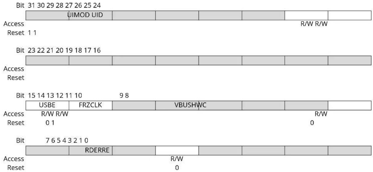
text_image
Bit 31 30 29 28 27 26 25 24 UIMOD UID Access R/W R/W Reset 1 1 Bit 23 22 21 20 19 18 17 16 Access Reset Bit 15 14 13 12 11 10 9 8 USBE FRZCLK VBUSHWC Access R/W R/W R/W Reset 0 1 0 Bit 7 6 5 4 3 2 1 0 Access R/W Reset 0Bit 25 - UIMOD USBHS Mode
0 (HOST): The module is in USB Host mode.
1 (DEVICE): The module is in USB Device mode.
This bit can be written even if USBE = 0 or FRZCLK = 1. Disabling the USBHS (by writing a zero to the USBE bit) does not reset this bit.
Bit 24 - UID UID Pin Enable
Must be set to '0'.
Bit 15 - USBE USBHS Enable
Writing a zero to this bit resets the USBHS, disables the USB transceiver, and disables the USBHS clock inputs. Unless explicitly stated, all registers then become read-only and are reset.
This bit can be written even if FRZCLK = 1
| Value | Description |
| 0 | The USBHS is disabled. |
| 1 | The USBHS is enabled. |
Bit 14 - FRZCLK Freeze USB Clock
This bit can be written even if USBE = 0. Disabling the USBHS (by writing a zero to the USBE bit) does not reset this bit, but it freezes the clock inputs whatever its value.
| Value | Description |
| 0 | The clock inputs are enabled. |
| 1 | The clock inputs are disabled (the resume detection is still active). This reduces the power consumption. Unless explicitly stated, all registers then become read-only. |
Bit 8 - VBUSHWC VBUS Hardware Control
Must be set to '1'.
| Value Description | |
| 0 | The hardware control over the VBOF output pin is enabled. The USBHS resets the VBOF output pin when a VBUS problem occurs. |
| 1 | The hardware control over the VBOF output pin is disabled. |
| 0 | The hardware control over the PIO line is enabled. The USBHS resets the PIO output pin when a VBUS problem occurs. |
| 1 | The hardware control over the PIO line is disabled. |
Bit 4 - RDERRE Remote Device Connection Error Interrupt Enable
| Value Description | |
| 0 | The Remote Device Connection Error Interrupt (USBHS_SR.RDERRI) is disabled. |
| 1 | The Remote Device Connection Error Interrupt (USBHS_SR.RDERRI) is enabled. |
38.7.2 General Status Register
Name: USBHS_SR
Offset: 0x0804
Reset: 0x00000400
Property: Read-only
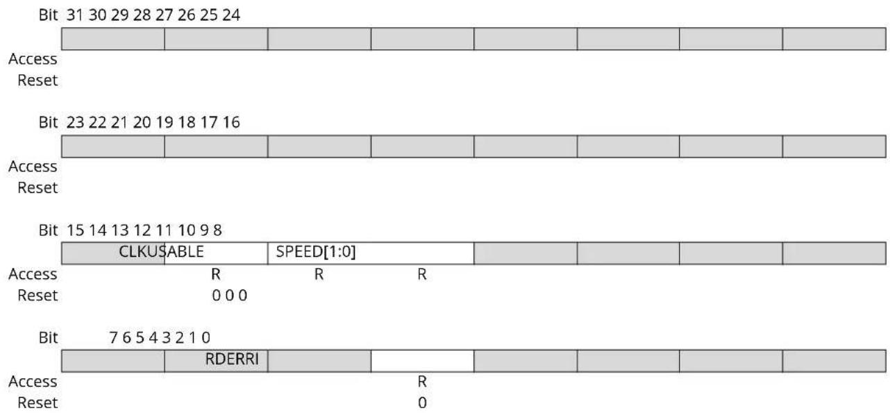
text_image
Bit 31 30 29 28 27 26 25 24 Access Reset Bit 23 22 21 20 19 18 17 16 Access Reset Bit 15 14 13 12 11 10 9 8 CLKUSABLE SPEED[1:0] R R Access R R Reset 0 0 0 Bit 7 6 5 4 3 2 1 0 Access RDERRI R Reset 0Bit 14 - CLKUSABLE UTMI Clock Usable
| Value | Description |
| 0 | Cleared when the UTMI 30 MHz is not usable. |
| 1 | Set when the UTMI 30 MHz is usable. |
Bits 13:12 - SPEED[1:0] Remote Device Speed Status
This field is set according to the connected device speed mode.
| Value | Name | Description |
| 0 | FULL_SPEED | Full-Speed mode |
| 1 | HIGH_SPEED | High-Speed mode |
| 2 | LOW_SPEED | Low-Speed mode |
| 3 | Reserved |
Bit 4 - RDERRI Remote Device Connection Error Interrupt (Host mode only)
| Value | Description |
| 0 | Cleared when USBHS_SCR.RDERRIC = 1. |
| 1 | Set when an error occurs during the remote device connection. This triggers a USB interrupt if USBHS_CTRL.RDERRE = 1. |
38.7.3 General Status Clear Register
Name: USBHS_SCR
Offset: 0x0808
Property: Write-only
This register always reads as zero.
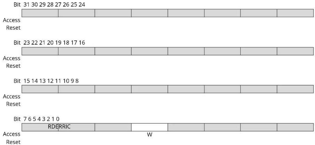
text_image
Bit 31 30 29 28 27 26 25 24 Access Reset Bit 23 22 21 20 19 18 17 16 Access Reset Bit 15 14 13 12 11 10 9 8 Access Reset Bit 7 6 5 4 3 2 1 0 Access Reset RDERRIC WBit 4 - RDERRIC Remote Device Connection Error Interrupt Clear
| Value | Description |
| 0 | No effect. |
| 1 | Clears the RDERRI bit in USBHS_SR. |
38.7.4 General Status Set Register
Name: USBHS_SFR
Offset: 0x080C
Property: Write-only
This register always reads as zero.

text_image
Bit 31 30 29 28 27 26 25 24 Access Reset Bit 23 22 21 20 19 18 17 16 Access Reset Bit 15 14 13 12 11 10 9 8 VBUSRQS W Access Reset Bit 7 6 5 4 3 2 1 0 Access Reset RDERRIS WBit 9 - VBUSRQS VBUS Request Set
Must be set to '1'.
| Value | Description |
| 0 | No effect. |
| 1 | Sets the VBUSRQ bit in USBHS_SR. |
Bit 4 - RDERRIS Remote Device Connection Error Interrupt Set
| Value | Description |
| 0 | No effect. |
| 1 | Sets the RDERRI bit in USBHS_SR, which may be useful for test or debug purposes. |
38.7.5 Device General Control Register
Name: USBHS_DEVCTRL
Offset: 0x0000
Reset: 0x00000100
Property: Read/Write
| Bit 31 30 29 28 27 26 25 24 | |||||||
| Access Reset | |||||||
| Bit 23 22 21 20 19 18 17 16 | |||||||
| OPMODE2 | |||||||
| Access Reset 0 | R/W | ||||||
| Bit 15 14 13 12 11 10 9 | 8 | ||||||
| TSTPCKT | TSTK | TSTJ | LS | SPDCONF[1:0] | RMWKUP | DETACH | |
| Access Reset | R/W0 | R/W0 | R/W0 | R/W0 | R/W0 | R/W0 | R/W1 |
| Bit | 7 | 6 | 5 | 4 | 3 | 2 | 1 |
| ADDEN | UADD[6:0] | ||||||
| Access Reset | R/W0 | R/W0 | R/W0 | R/W0 | R/W0 | R/W0 | R/W0 |
Bit 16 - OPMODE2 Specific Operational mode
| Value | Description |
| 0 | The UTMI transceiver is in Normal operating mode. |
| 1 | The UTMI transceiver is in the “Disable bit stuffing and NRZI encoding” operational mode for test purposes. |
Bit 15 - TSTPCKT Test packet mode
| Value | Description |
| 0 | The UTMI transceiver is in Normal operating mode. |
| 1 | The UTMI transceiver generates test packets for test purposes. |
Bit 14 - TSTK Test mode K
| Value | Description |
| 0 | The UTMI transceiver is in Normal operating mode. |
| 1 | The UTMI transceiver generates high-speed K state for test purposes. |
Bit 13 - TSTJ Test mode J
| Value | Description |
| 0 | The UTMI transceiver is in Normal operating mode. |
| 1 | The UTMI transceiver generates high-speed J state for test purposes. |
Bit 12 - LS Low-Speed Mode Force
This bit can be written even if USBHS_CTRL.USBE = 0 or USBHS_CTRL.FRZCLK = 1. Disabling the USBHS (by writing a zero to the USBHS_CTRL.USBE bit) does not reset this bit.
| Value | Description |
| 0 | The Full-speed mode is active. |
| 1 | The Low-speed mode is active. |
Bits 11:10 - SPDCONF[1:0] Mode Configuration
This field contains the peripheral speed:
| Value Name | Description |
| 0 | NORMAL The peripheral starts in Full-speed mode and performs a high-speed reset to switch to High-speed mode if the host is high-speed-capable. |
| 1 | LOW_POWER For a better consumption, if high speed is not needed. |
| 2 | HIGH_SPEED Forced high speed. |
| 3 | FORCED_FS The peripheral remains in Full-speed mode whatever the host speed capability. |
Bit 9 - RMWKUP Remote Wakeup
This bit is cleared when the USBHS receives a USB reset or once the upstream resume has been sent.
| Value Description | |
| 0 | No effect. |
| 1 | Sends an upstream resume to the host for a remote wakeup. |
Bit 8 - DETACH Detach
| Value Description | |
| 0 | Reconnects the device. |
| 1 | Physically detaches the device (disconnects the internal pull-up resistor from D+ and D-). |
Bit 7 - ADDEN Address Enable
This bit is cleared when a USB reset is received.
| Value Description | |
| 0 | No effect. |
| 1 | Activates the UADD field (USB address). |
Bits 6:0 - UADD[6:0] USB Address
This field contains the device address.
This field is cleared when a USB reset is received.
38.7.6 Device Global Interrupt Status Register
Name: USBHS_DEVISR
Offset: 0x0004
Reset: 0x00000000
Property: Read-only
Bit 31 30 29 28 27 26 25 24
| DMA_6 DMA_5 DMA_4 DMA_3 DMA_2 DMA_1 DMA_0 |
Access R R R R R R
Reset 0000000
Bit 23 22 21 20 19 18 17 16
| PEP_9 | PEP_8 | PEP_7 | PEP_6 | PEP_5 | PEP_4 | ||
| Access | RRRRRR | ||||||
| Reset | 000000 | ||||||
Bit 15 14 13 12 11 10 98
| PEP_3 | PEP_2 | PEP_1 | PEP_0 | |||||
| Access | R R R R | |||||||
Reset 0000
Bit 76543210
| UPRSM | EORSM | WAKEUP | EORST | SOF | MSOF | SUSP | |
| Access | RRRRRR | ||||||
| Reset | 0 0 0 0 0 0 | ||||||
Bits 25, 26, 27, 28, 29, 30, 31 - DMA_ DMA Channel x Interrupt
| Value | Description |
| 0 | Cleared when the USBHS_DEVDMASTATUSx interrupt source is cleared. |
| 1 | Set when an interrupt is triggered by the DMA channel x. This triggers a USB interrupt if DMA_x = 1. |
Bits 12, 13, 14, 15, 16, 17, 18, 19, 20, 21 - PEP_ Endpoint x Interrupt
| Value | Description |
| 0 | Cleared when the interrupt source is serviced. |
| 1 | Set when an interrupt is triggered by endpoint x (USBHS_DEVEPTISRx, USBHS_DEVEPTIMRx). This triggers a USB interrupt if USBHS_DEVIMR.PEP_x = 1. |
Bit 6 - UPRSM Upstream Resume Interrupt
| Value | Description |
| 0 | Cleared when the USBHS_DEVICR.UPRSMC bit is written to one to acknowledge the interrupt (USB clock inputs must be enabled before). |
| 1 | Set when the USBHS sends a resume signal called “Upstream Resume”. This triggers a USB interrupt if USBHS_DEVIMR.UPRSME = 1. |
Bit 5 - EORSM End of Resume Interrupt
| Value | Description |
| 0 | Cleared when the USBHS_DEVICR.EORSMC bit is written to one to acknowledge the interrupt. |
| 1 | Set when the USBHS detects a valid “End of Resume” signal initiated by the host. This triggers a USB interrupt if USBHS_DEVIMR.EORSME = 1. |
Bit 4 - WAKEUP Wakeup Interrupt
This interrupt is generated even if the clock is frozen by the USBHS_CTRL.FRZCLK bit.
| Value Description | |
| 0 | Cleared when the USBHS_DEVICR.WAKEUPC bit is written to one to acknowledge the interrupt (USB clock inputs must be enabled before), or when the Suspend (SUSP) interrupt bit is set. |
| 1 | Set when the USBHS is reactivated by a filtered non-idle signal from the lines (not by an upstream resume). This triggers an interrupt if USBHS_DEVIMR.WAKEUPE = 1. |
Bit 3 - EORST End of Reset Interrupt
| Value Description | |
| 0 | Cleared when the USBHS_DEVICR.EORSTC bit is written to one to acknowledge the interrupt. |
| 1 | Set when a USB “End of Reset” has been detected. This triggers a USB interrupt if USBHS_DEVIMR.EORSTE = 1. |
Bit 2 - SOF Start of Frame Interrupt
| Value Description | |
| 0 | Cleared when the USBHS_DEVICR.SOFC bit is written to one to acknowledge the interrupt. |
| 1 | Set when a USB “Start of Frame” PID (SOF) has been detected (every 1 ms). This triggers a USB interrupt if SOFE = 1. The FNUM field is updated. In High-speed mode, the MFNUM field is cleared. |
Bit 1 - MSOF Micro Start of Frame Interrupt
| Value Description | |
| 0 | Cleared when the USBHS_DEVICR.MSOFC bit is written to one to acknowledge the interrupt. |
| 1 | Set in High-speed mode when a USB “Micro Start of Frame” PID (SOF) has been detected (every 125 μs). This triggers a USB interrupt if MSOFE = 1. The MFNUM field is updated. The FNUM field is unchanged. |
Bit 0 - SUSP Suspend Interrupt
| Value Description | |
| 0 | Cleared when the USBHS_DEVICR.SUSPC bit is written to one to acknowledge the interrupt, or when the Wakeup (WAKEUP) interrupt bit is set. |
| 1 | Set when a USB “Suspend” idle bus state has been detected for 3 frame periods (J state for 3 ms). This triggers a USB interrupt if USBHS_DEVIMR.SUSPE = 1. |
38.7.7 Device Global Interrupt Clear Register
Name: USBHS_DEVICR
Offset: 0x0008
Property: Write-only
This register always reads as zero.
The following configuration values are valid for all listed bit names of this register:
0: No effect.
1: Clears the corresponding bit in USBHS_DEVISR.
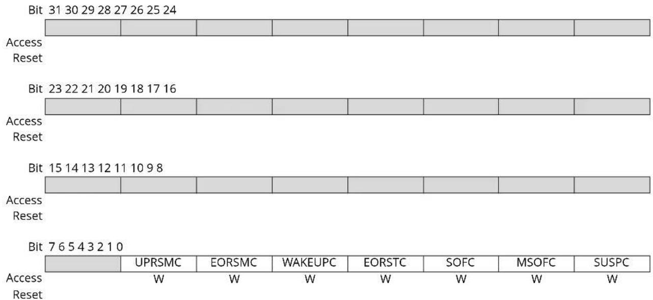
text_image
Bit 31 30 29 28 27 26 25 24 Access Reset Bit 23 22 21 20 19 18 17 16 Access Reset Bit 15 14 13 12 11 10 9 8 Access Reset Bit 7 6 5 4 3 2 1 0 Access Reset UPRSMC EORSMC WAKEUPC EORSTC SOFC MSOFC SUSPC W W W W W W WBit 6 - UPRSMC Upstream Resume Interrupt Clear
Bit 5 - EORSMC End of Resume Interrupt Clear
Bit 4 - WAKEUPC Wakeup Interrupt Clear
Bit 3 - EORSTC End of Reset Interrupt Clear
Bit 2 - SOFC Start of Frame Interrupt Clear
Bit 1 - MSOFC Micro Start of Frame Interrupt Clear
Bit 0 - SUSPC Suspend Interrupt Clear
38.7.8 Device Global Interrupt Set Register
Name: USBHS_DEVIFR
Offset: 0x000C
Property: Write-only
This register always reads as zero.
The following configuration values are valid for all listed bit names of this register:
0: No effect.
1: Sets the corresponding bit in USBHS_DEVISR.
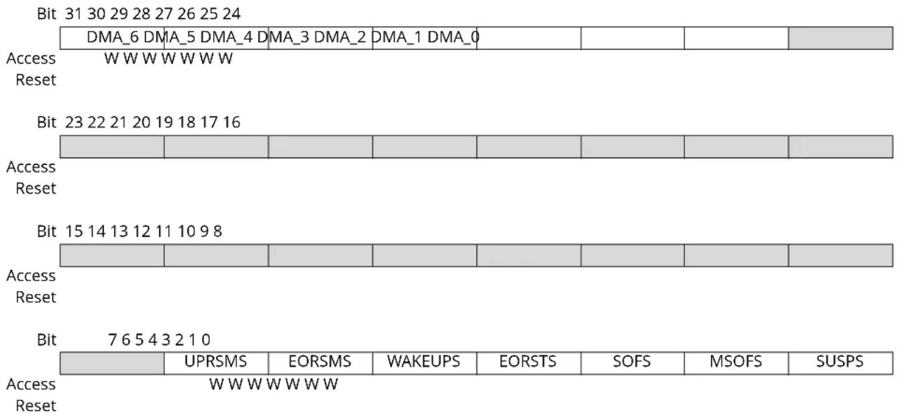
text_image
Bit 31 30 29 28 27 26 25 24 DMA_6 DMA_5 DMA_4 DMA_3 DMA_2 DMA_1 DMA_0 Access WWWWWWW Reset Bit 23 22 21 20 19 18 17 16 Access Reset Bit 15 14 13 12 11 10 9 8 Access Reset Bit 7 6 5 4 3 2 1 0 Access Reset UPRSMS EORSMS WAKEUPS EORSTS SOFS MSOFS SUSPS WWWWWWWBits 25, 26, 27, 28, 29, 30, 31 - DMA_ DMA Channel x Interrupt Set
Bit 6 - UPRSMS Upstream Resume Interrupt Set
Bit 5 - EORSMS End of Resume Interrupt Set
Bit 4 - WAKEUPS Wakeup Interrupt Set
Bit 3 - EORSTS End of Reset Interrupt Set
Bit 2 - SOFS Start of Frame Interrupt Set
Bit 1 - MSOFS Micro Start of Frame Interrupt Set
Bit 0 - SUSPS Suspend Interrupt Set
38.7.9 Device Global Interrupt Mask Register
Name: USBHS_DEVIMR
Offset: 0x0010
Reset: 0x00000000
Property: Read-only
The following configuration values are valid for all listed bit names of this register:
0: The corresponding interrupt is not enabled.
1: The corresponding interrupt is enabled.
Bit 31 30 29 28 27 26 25 24
| DMA_6 DMA_5 DMA_4 DMA_3 DMA_2 DMA_1 DMA_0 | ||||
| Access | RRRRRRR | |||
| Reset | 0 0 0 0 0 0 |
Bit 23 22 21 20 19 18 17 16
| PEP_9 | PEP_8 | PEP_7 | PEP_6 | PEP_5 | PEP_4 | ||
| Access | RRRRRR | ||||||
| Reset | 000000 | ||||||
Bit 15 14 13 12 11 10 98
| PEP_3 | PEP_2 | PEP_1 | PEP_0 | |||||
| Access | R R R R | |||||||
| Reset | 0 0 0 0 | |||||||
Bit 76543210
| UPRSME | EORSME | WAKEUPE | EORSTE | SOFE | MSOFE | SUSPE | |
| Access | RRRRRR | ||||||
| Reset | 0000000 | ||||||
Bits 25, 26, 27, 28, 29, 30, 31 - DMA_ DMA Channel x Interrupt Mask
Bits 12, 13, 14, 15, 16, 17, 18, 19, 20, 21 - PEP_ Endpoint x Interrupt Mask
Bit 6 - UPRSME Upstream Resume Interrupt Mask
Bit 5 - EORSME End of Resume Interrupt Mask
Bit 4 - WAKEUPE Wakeup Interrupt Mask
Bit 3 - EORSTE End of Reset Interrupt Mask
Bit 2 - SOFE Start of Frame Interrupt Mask
Bit 1 - MSOFE Micro Start of Frame Interrupt Mask
Bit 0 - SUSPE Suspend Interrupt Mask
38.7.10 Device Global Interrupt Disable Register
Name: USBHS_DEVIDR
Offset: 0x0014
Property: Write-only
This register always reads as zero.
The following configuration values are valid for all listed bit names of this register:
0: No effect.
1: Clears the corresponding bit in USBHS_DEVIMR.
bar_stacked
| Bit | DMA_6 DMA_5 DMA_4 DMA_3 DMA_2 DMA_1 DMA_0 | DMA_5 DMA_4 DMA_3 DMA_2 DMA_1 DMA_0 | DMA_4 DMA_3 DMA_2 DMA_1 DMA_0 | DMA_3 DMA_2 DMA_1 DMA_0 | DMA_2 DMA_3 DMA_2 DMA_1 DMA_0 | DMA_3 DMA_2 DMA_1 DMA_0 | DMA_2 DMA_3 DMA_2 DMA_1 DMA_0 | DMA_3 DMA_2 DMA_1 DMA_0 | DMA_2 DMA_3 DMA_2 DMA_1 DMA_0 | DMA_3 DMA_2 DMA_1 DMA_0 | DMA_2 DMA_3 DMA_2 DMA_1 DMA_0 | |---|---|---|---|---|---|---|---|---|---|---|---| | 31 | | | | | | | | | | | | | 29 | | | | | | | | | | | | | 28 | | | | | | | | | | | | | 27 | | | | | | | | | | | | | 26 | | | | | | | | | | | | | 25 | | | | | | | | | | | | | 24 | | | | | | | | | | | | | 23 | | | | | | | | | | | | | 22 | | | | | | | | | | | | | 21 | | | | | | | | | | | | | 20 | | | | | | | | | | | | | 19 | | | | | | | | | | | | | 18 | | | | | | | | | | | | | 17 | | | | | | | | | | | | | Note: The actual values for the bit allocation are not provided in the code. The actual values for the bit allocation of the bit allocation of the bit allocation of the bit allocation of the bit allocation of the bit allocation of the bit allocation of the bit allocation of the bit allocation of the bit allocation of the bit allocation of the bit allocation of the bit allocation of the bit allocation of the bit allocation of the bit allocation of the bit allocation of the bit allocation of the bit allocation of the bit allocation of the bit allocation of the bit allocation of the bit allocation of the bit allocation of the bit allocation of the bit allocation.Bits 25, 26, 27, 28, 29, 30, 31 - DMA_ DMA Channel x Interrupt Disable
Bits 12, 13, 14, 15, 16, 17, 18, 19, 20, 21 - PEP_ Endpoint x Interrupt Disable
Bit 6 - UPRSMEC Upstream Resume Interrupt Disable
Bit 5 - EORSMEC End of Resume Interrupt Disable
Bit 4 - WAKEUPEC Wakeup Interrupt Disable
Bit 3 - EORSTEC End of Reset Interrupt Disable
Bit 2 - SOFEC Start of Frame Interrupt Disable
Bit 1 - MSOFEC Micro Start of Frame Interrupt Disable
Bit 0 - SUSPEC Suspend Interrupt Disable
38.7.11 Device Global Interrupt Enable Register
Name: USBHS_DEVIER
Offset: 0x0018
Property: Write-only
This register always reads as zero.
The following configuration values are valid for all listed bit names of this register:
0: No effect.
1: Sets the corresponding bit in USBHS_DEVIMR.

bar_stacked
| Bit | DMA_6 DMA_5 DMA_4 DMA_3 DMA_2 DMA_1 DMA_0 | DMA_5 DMA_4 DMA_3 DMA_2 DMA_1 DMA_0 | DMA_4 DMA_3 DMA_2 DMA_1 DMA_0 | DMA_3 DMA_2 DMA_1 DMA_0 | DMA_2 DMA_3 DMA_2 DMA_1 DMA_0 | DMA_3 DMA_2 DMA_1 DMA_0 | DMA_2 DMA_3 DMA_2 DMA_1 DMA_0 | DMA_3 DMA_2 DMA_1 DMA_0 | DMA_2 DMA_3 DMA_2 DMA_1 DMA_0 | DMA_3 DMA_2 DMA_1 DMA_0 | DMA_2 DMA_3 DMA_2 DMA_1 DMA_0 | |---|---|---|---|---|---|---|---|---|---|---|---| | 31 | | | | | | | | | | | | | 29 | | | | | | | | | | | | | 28 | | | | | | | | | | | | | 27 | | | | | | | | | | | | | 26 | | | | | | | | | | | | | 25 | | | | | | | | | | | | | 24 | | | | | | | | | | | | | 23 | | | | | | | | | | | | | 22 | | | | | | | | | | | | | 21 | | | | | | | | | | | | | 20 | | | | | | | | | | | | | 19 | | | | | | | | | | | | | 18 | | | | | | | | | | | | | 17 | | | | | | | | | | | | | Note: The actual values for the bit allocation are not provided in the code. The actual values for the bit allocation of the bit allocation of the bit allocation of the bit allocation of the bit allocation of the bit allocation of the bit allocation of the bit allocation of the bit allocation of the bit allocation of the bit allocation of the bit allocation of the bit allocation of the bit allocation of the bit allocation of the bit allocation of the bit allocation of the bit allocation of the bit allocation of the bit allocation of the bit allocation of the bit allocation of the bit allocation of the bit allocation of the bit allocation of the bit allocation.Bits 25, 26, 27, 28, 29, 30, 31 - DMA_ DMA Channel x Interrupt Enable
Bits 12, 13, 14, 15, 16, 17, 18, 19, 20, 21 - PEP_ Endpoint x Interrupt Enable
Bit 6 - UPRSMES Upstream Resume Interrupt Enable
Bit 5 - EORSMES End of Resume Interrupt Enable
Bit 4 – WAKEUPES Wakeup Interrupt Enable
Bit 3 - EORSTES End of Reset Interrupt Enable
Bit 2 - SOFES Start of Frame Interrupt Enable
Bit 1 - MSOFES Micro Start of Frame Interrupt Enable
Bit 0 - SUSPES Suspend Interrupt Enable
38.7.12 Device Endpoint Register
Name: USBHS_DEVEPT
Offset: 0x001C
Reset: 0x00000000
Property: Read/Write
Bit 31 30 29 28 27 26 25 24
| EPRST9 EPRST8 | ||||||
| Access Reset 0 0 | R/W R/W | |||||
Bit 23 22 21 20 19 18 17 16
| EPRST7 EPRST6 EPRST5 EPRST4 EPRST3 EPRST2 EPRST1 EPRST0 | ||||
| Access | R/W R/W R/W R/W R/W R/W R/W R/W | |||
| Reset | 0 0 0 0 0 0 0 | |||
Bit 15 14 13 12 11 10 98
| EPEN9 | EPEN8 | |||||
| Access Reset 0 0 | R/W R/W | |||||
Bit 76543210
| EPEN7 | EPEN6 | EPEN5 | EPEN4 | EPEN3 | EPEN2 | EPEN1 | EPENO | |
| Access | R/W | R/W | R/W | R/W | R/W | R/W | R/W | R/W |
| Reset | 0 | 0 | 0 | 0 | 0 | 0 | 0 | 0 |
Bits 16, 17, 18, 19, 20, 21, 22, 23, 24, 25 - EPRST Endpoint x Reset
The whole endpoint mechanism (FIFO counter, reception, transmission, etc.) is reset apart from the Data Toggle Sequence field (USBHS_DEVEPTISRx.DTSEQ), which can be cleared by setting the USBHS_DEVEPTIMRx.RSTDT bit (by writing a one to the USBHS_DEVEPTIERx.RSTDTS bit).
The endpoint configuration remains active and the endpoint is still enabled.
This bit is cleared upon receiving a USB reset.
| Value | Description |
| 0 | Completes the reset operation and starts using the FIFO. |
| 1 | Resets the endpoint x FIFO prior to any other operation, upon hardware reset or when a USB bus reset has been received. This resets the endpoint x registers (USBHS_DEVEPTCFGx, USBHS_DEVEPTISRx, USBHS_DEVEPTIMRx) but not the endpoint configuration (USBHS_DEVEPTCFGx.ALLOC, USBHS_DEVEPTCFGx.EPBK, USBHS_DEVEPTCFGx.EPSIZE, USBHS_DEVEPTCFGx.EPDIR, USBHS_DEVEPTCFGx.EPTYPE). |
Bits 0, 1, 2, 3, 4, 5, 6, 7, 8, 9 - EPEN Endpoint x Enable
| Value | Description |
| 0 | Endpoint x is disabled, forcing the endpoint x state to inactive (no answer to USB requests) and resetting the endpoint x registers (USBHS_DEVEPTCFGx, USBHS_DEVEPTISRx, USBHS_DEVEPTIMRx) but not the endpoint configuration (USBHS_DEVEPTCFGx.ALLOC, USBHS_DEVEPTCFGx.EPBK, USBHS_DEVEPTCFGx.EPSIZE, USBHS_DEVEPTCFGx.EPDIR, USBHS_DEVEPTCFGx.EPTYPE). |
| 1 | Endpoint x is enabled. |
38.7.13 Device Frame Number Register
Name: USBHS_DEVFNUM
Offset: 0x0020
Reset: 0x00000000
Property: Read-only
text_image
Bit 31 30 29 28 27 26 25 24 Access Reset Bit 23 22 21 20 19 18 17 16 Access Reset Bit 15 14 13 12 11 10 9 8 FNCERR FNUM[10:5] Access R R R R R R Reset 0 0 0 0 0 0 0 Bit 7 6 5 4 3 2 1 0 FNUM[4:0] MFNUM[2:0] Access R R R R R R Reset 0 0 0 0 0 0 0 0Bit 15 - FNCERR Frame Number CRC Error
| Value | Description |
| 0 | Cleared upon receiving a USB reset. |
| 1 | Set when a corrupted frame number (or microframe number) is received. This bit and the SOF (or MSOF) interrupt bit are updated at the same time. |
Bits 13:3 - FNUM[10:0] Frame Number
This field contains the 11-bit frame number information. It is provided in the last received SOF packet.
This field is cleared upon receiving a USB reset.
FNUM is updated even if a corrupted SOF is received.
Bits 2:0 - MFNUM[2:0] Micro Frame Number
This field contains the 3-bit micro frame number information. It is provided in the last received MSOF packet.
This field is cleared at the beginning of each start of frame (SOF interrupt) or upon receiving a USB reset.
MFNUM is updated even if a corrupted MSOF is received.
38.7.14 Device Endpoint x Configuration Register
Name: USBHS_DEVEPTCFGx
Offset: 0x0100 + x*0x04 [x=0..8]
Reset: 0
Property: Read/Write
text_image
Bit 31 30 29 28 27 26 25 24 Access Reset Bit 23 22 21 20 19 18 17 16 Access Reset Bit 15 14 13 12 11 10 9 8 Access Reset NBTRANS[1:0] EPTYPE[1:0] AUTOSW EPDIR R/W R/W R/W R/W R/W 0 0 0 0 0 0 Bit 7 6 5 4 3 2 1 0 Access Reset EPSIZE[2:0] EPBK[1:0] ALLOC R/W R/W R/W R/W R/W 0 0 0 0 0Bits 14:13 - NBTRANS[1:0] Number of transactions per microframe for isochronous endpoint
This field should be written with the number of transactions per microframe to perform high-bandwidth isochronous transfer.
It can be written only for endpoints that have this capability (see USBHS_FEATURES.ENHBISOx bit). Otherwise, this field is 0.
This field is irrelevant for non-isochronous endpoints.
| Value | Name | Description |
| 0 | 0_TRANS | Reserved to endpoint that does not have the high-bandwidth isochronous capability. |
| 1 | 1_TRANS | Default value: one transaction per microframe. |
| 2 | 2_TRANS | Two transactions per microframe. This endpoint should be configured as double-bank. |
| 3 | 3_TRANS | Three transactions per microframe. This endpoint should be configured as triple-bank. |
Bits 12:11 - EPTYPE[1:0] Endpoint Type
This field should be written to select the endpoint type:
This field is cleared upon receiving a USB reset.
| Value | Name | Description |
| 0 | CTRL | Control |
| 1 | ISO | Isochronous |
| 2 | BLK | Bulk |
| 3 | INTRPT | Interrupt |
Bit 9 - AUTOSW Automatic Switch
This bit is cleared upon receiving a USB reset.
| Value | Description |
| 0 | The automatic bank switching is disabled. |
| 1 | The automatic bank switching is enabled. |
Bit 8 - EPDIR Endpoint Direction
This bit is cleared upon receiving a USB reset.
0 (OUT): The endpoint direction is OUT.
1 (IN): The endpoint direction is IN (nor for control endpoints).
Bits 6:4 - EPSIZE[2:0] Endpoint Size
This field should be written to select the size of each endpoint bank:
This field is cleared upon receiving a USB reset (except for endpoint 0).
| Value Name | Description | |
| 0 | 8_BYTE 8 bytes | |
| 1 | 16_BYTE 16 bytes | |
| 2 | 32_BYTE 32 bytes | |
| 3 | 64_BYTE 64 bytes | |
| 4 | 128_BYTE 128 bytes | |
| 5 | 256_BYTE 256 bytes | |
| 6 | 512_BYTE 512 bytes | |
| 7 | 1024_BYTE 1024 bytes |
Bits 3:2 - EPBK[1:0] Endpoint Banks
This field should be written to select the number of banks for the endpoint:
For control endpoints, a single-bank endpoint (0b00) should be selected.
This field is cleared upon receiving a USB reset (except for endpoint 0).
| Value Name | Description | |
| 0 | 1_BANK Single-bank endpoint | |
| 1 | 2_BANK Double-bank endpoint | |
| 2 | 3_BANK Triple-bank endpoint | |
| 3 | Reserved | |
Bit 1 - ALLOC Endpoint Memory Allocate
This bit is cleared upon receiving a USB reset (except for endpoint 0).
| Value Description | |
| 0 | Frees the endpoint memory. |
| 1 | Allocates the endpoint memory. The user should check the USBHS_DEVEPTISRx.CFGOK bit to know whether the allocation of this endpoint is correct. |
38.7.15 Device Endpoint Interrupt Status Register (Control, Bulk, Interrupt Endpoints)
Name: USBHS_DEVEPTISRx
Offset: 0x0130 + x*0x04 [x=0..8]
Reset: 0
Property: Read/Write
This register view is relevant only if EPTYPE = 0x0, 0x2, or 0x3 in the "Device Endpoint x Configuration Register".
Bit 31 30 29 28 27 26 25 24
| BYCT[10:4] | |
| Access | R/W R/W R/W R/W R/W R/W R/W |
| Reset 0 0 0 0 0 0 0 | |
Bit 23 22 21 20 19 18 17 16
| BYCT[3:0] | CFGOK | CTRLDIR | RWALL | |||
| Access | R/W R/W R/W R/W | R/W R/W R/W | ||||
| Reset | 0 0 0 0 | 0 0 0 | ||||
Bit 15 14 13 12 11 10 98
| CURRBK[1:0] | NBUSYBK[1:0] | DTSEQ[1:0] | |||
| Access | R/W R/W R/W R/W | R/W R/W | |||
| Reset | 0 0 0 0 | 0 0 | |||
Bit 76543210
| SHORTPACKET | STALLEDI | OVERFI | NAKINI | NAKOUTI | RXSTPI | RXOUTI | TXINI | |
| Access | R/W R/W | R/W R/W | R/W R/W | R/W R/W R/W | ||||
| Reset | 0 0 0 0 0 0 0 | |||||||
Bits 30:20 - BYCT[10:0] Byte Count
This field is set with the byte count of the FIFO.
For IN endpoints, the field is incremented after each byte written by the software into the endpoint and decremented after each byte sent to the host.
For OUT endpoints, the field is incremented after each byte received from the host and decremented after each byte read by the software from the endpoint.
This field may be updated one clock cycle after the RWALL bit changes, so the user should not poll this field as an interrupt bit.
Bit 18 - CFGOK Configuration OK Status
This bit is updated when USBHS_DEVEPTCFGx.ALLOC = 1.
This bit is set if the endpoint x number of banks (USBHS_DEVEPTCFGx.EPBK) and size
(USBHS_DEVEPTCFGx.EPSIZE) are correct compared to the maximal allowed number of banks and size for this endpoint and to the maximal FIFO size (i.e., the DPRAM size).
If this bit is cleared, the user should rewrite correct values to the USBHS_DEVEPTCFGx.EPBK and USBHS_DEVEPTCFGx.EPSIZE fields.
Bit 17 - CTRLDIR Control Direction
| Value | Description |
| 0 | Cleared after a SETUP packet to indicate that the following packet is an OUT packet. |
| 1 | Set after a SETUP packet to indicate that the following packet is an IN packet. |
Bit 16 - RWALL Read/Write Allowed
This bit is set for IN endpoints when the current bank is not full, i.e., the user can write further data into the FIFO.
This bit is set for OUT endpoints when the current bank is not empty, i.e., the user can read further data from the FIFO.
This bit is never set if USBHS_DEVEPTIMRx.STALLRQ = 1 or in case of error.
This bit is cleared otherwise.
This bit should not be used for control endpoints.
Bits 15:14 - CURRBK[1:0] Current Bank
This bit is set for non-control endpoints, to indicate the current bank:
This field may be updated one clock cycle after the RWALL bit changes, so the user should not poll this field as an interrupt bit.
| Value Name | Description | |
| 0 | BANK0 Current bank is bank0 | |
| 1 | BANK1 Current bank is bank1 | |
| 2 | BANK2 Current bank is bank2 | |
| 3 | Reserved | |
Bits 13:12 - NBUSYBK[1:0] Number of Busy Banks
This field is set to indicate the number of busy banks:
For IN endpoints, it indicates the number of banks filled by the user and ready for IN transfer. When all banks are free, this triggers a PEP_x interrupt if NBUSYBKE = 1.
For OUT endpoints, it indicates the number of banks filled by OUT transactions from the host. When all banks are busy, this triggers a PEP_x interrupt if NBUSYBKE = 1.
When the USBHS_DEVEPTIMRx.FIFOCON bit is cleared (by writing a one to the
USBHS_DEVEPTIMRx.FIFOCONC bit) to validate a new bank, this field is updated two or three clock cycles later to calculate the address of the next bank.
A PEP_x interrupt is triggered if:
| Value Name | Description |
| 0 | 0_BUSY 0 busy bank (all banks free) |
| 1 | 1_BUSY 1 busy bank |
| 2 | 2_BUSY 2 busy banks |
| 3 | 3_BUSY 3 busy banksfor IN endpoint, USBHS_DEVEPTIMRx.NBUSYBKE = 1 and all the banks are free;for OUT endpoint, USBHS_DEVEPTIMRx.NBUSYBKE = 1 and all the banks are busy. |
Bits 9:8 - DTSEQ[1:0] Data Toggle Sequence
This field is set to indicate the PID of the current bank:
For IN transfers, it indicates the data toggle sequence that should be used for the next packet to be sent. This is not relative to the current bank.
For OUT transfers, this value indicates the last data toggle sequence received on the current bank.
By default, DTSEQ is 0b01, as if the last data toggle sequence was Data1, so the next sent or expected data toggle sequence should be Data0.
| Value Name | Description |
| 0 | DATA0 Data0 toggle sequence |
| 1 | DATA1 Data1 toggle sequence |
| 2 | DATA2 Reserved for high-bandwidth isochronous endpoint |
| 3 | MDATA Reserved for high-bandwidth isochronous endpoint |
Bit 7 - SHORTPACKET Short Packet Interrupt
| Value Description | |
| 0 | Cleared when SHORTPACKETC = 1. This acknowledges the interrupt. |
| 1 | Set for non-control OUT endpoints, when a short packet has been received. This triggers a PEP_x interrupt if USBHS_DEVEPTIMRx.SHORTPACKETE = 1. |
Bit 6 - STALLEDI STALLed Interrupt
| Value Description | |
| 0 | Cleared when STALLEDIC = 1. This acknowledges the interrupt. |
| 1 | Set to signal that a STALL handshake has been sent. To do that, the software has to set the STALLRQ bit (by writing a one to the STALLRQS bit). This triggers a PEP_x interrupt if STALLEDE = 1. |
Bit 5 - OVERFI Overflow Interrupt
For all endpoint types, an overflow can occur during the OUT stage if the host attempts to write into a bank that is too small for the packet. The packet is acknowledged and the USBHS_DEVEPTISRx.RXOUTI bit is set as if no overflow had occurred. The bank is filled with all the first bytes of the packet that fit in.
| Value Description | |
| 0 | Cleared when the OVERFIC bit is written to one. This acknowledges the interrupt. |
| 1 | Set when an overflow error occurs. This triggers a PEP_x interrupt if OVERFE = 1. |
Bit 4 - NAKINI NAKed IN Interrupt
| Value Description | |
| 0 | Cleared when NAKINIC = 1. This acknowledges the interrupt. |
| 1 | Set when a NAK handshake has been sent in response to an IN request from the host. This triggers a PEP_x interrupt if NAKINE = 1. |
Bit 3 - NAKOUTI NAKed OUT Interrupt
| Value Description | |
| 0 | Cleared when NAKOUTIC = 1. This acknowledges the interrupt. |
| 1 | Set when a NAK handshake has been sent in response to an OUT request from the host. This triggers a PEP_x interrupt if NAKOUTE = 1. |
Bit 2 - RXSTPI Received SETUP Interrupt
This bit is set, for control endpoints, to signal that the current bank contains a new valid SETUP packet. This triggers a PEP_x interrupt if RXSTPE = 1. It is cleared by writing a one to the RXSTPIC bit. This acknowledges the interrupt and frees the bank. This bit is inactive (cleared) for bulk and interrupt IN/OUT endpoints.
Bit 1 - RXOUTI Received OUT Data Interrupt
For control endpoints:
0: Cleared by writing a one to the RXOUTIC bit. This acknowledges the interrupt and frees the bank. 1: Set when the current bank contains a bulk OUT packet (data or status stage). This triggers a PEP_x interrupt if USBHS_DEVEPTIMRx.RXOUTE = 1.
For bulk and interrupt OUT endpoints:
0: Cleared by writing a one to the RXOUTIC bit. This acknowledges the interrupt, which has no effect on the endpoint FIFO. USBHS_DEVEPTISRx.RXOUTI shall always be cleared before clearing USBHS_DEVEPTIMRx.FIFOCON.
1: Set at the same time as USBHS_DEVEPTIMRx.FIFOCON when the current bank is full. This triggers a PEP_x interrupt if USBHS_DEVEPTIMRx.RXOUTE = 1.
The user reads from the FIFO and clears the USBHS_DEVEPTIMRx.FIFOCON bit to free the bank. If the OUT endpoint is composed of multiple banks, this also switches to the next bank. The USBHS_DEVEPTISRx.RXOUTI and USBHS_DEVEPTIMRx.FIFOCON bits are set/cleared in accordance with the status of the next bank.
This bit is inactive (cleared) for bulk and interrupt IN endpoints.
Bit 0 - TXINI Transmitted IN Data Interrupt
For control endpoints:
0: Cleared when TXINIC = 1. This acknowledges the interrupt and sends the packet.
1: Set when the current bank is ready to accept a new IN packet. This triggers a PEP_x interrupt if TXINE = 1.
For bulk and interrupt IN endpoints:
0: Cleared when TXINIC = 1. This acknowledges the interrupt, which has no effect
on the endpoint FIFO. USBHS_DEVEPTISRx.TXINI shall always be cleared before clearing
USBHS DEVEPTIMRx.FIFOCON.
1: Set at the same time as USBHS_DEVEPTIMRx.FIFOCON when the current bank is free. This triggers a PEP_x interrupt if TXINE = 1.
The user writes into the FIFO and clears the USBHS_DEVEPTIMRx.FIFOCON bit to allow the USBHS to send the data. If the IN endpoint is composed of multiple banks, this also switches to the next bank. The USBHS_DEVEPTISRx.TXINI and USBHS_DEVEPTIMRx.FIFOCON bits are set/cleared in accordance with the status of the next bank.
This bit is inactive (cleared) for bulk and interrupt OUT endpoints.
38.7.16 Device Endpoint Interrupt Status Register (Isochronous Endpoints)
Name: USBHS_DEVEPTISRx (ISOENPT)
Offset: 0x0130 + x*0x04 [x=0..8]
Reset: 0
Property: Read/Write
This register view is relevant only if EPTYPE = 0x1 in the "Device Endpoint x Configuration Register".
Bit 31 30 29 28 27 26 25 24
| BYCT[10:4] | |
| Access | R/W R/W R/W R/W R/W R/W R/W |
| Reset 0000000 | |
Bit 23 22 21 20 19 18 17 16
| BYCT[3:0] | CFGOK | RWALL | ||||
| Access | R/W R/W R/W R/W | R/W | R/W | |||
| Reset | 0 0 0 0 | 0 | 0 | |||
Bit 15 14 13 12 11 10 98
| CURRBK[1:0] | NBUSYBK[1:0] | ERRORTRANS | DTSEQ[1:0] | ||
| Access | R/W R/W R/W R/W | R/W R/W R/W | |||
| Reset | 0 0 0 0 | 0 0 0 | |||
Bit 76543210
| SHORTPACKET | CRCERRI | OVERFI | HBISOFLUSHI | HBISOINERRI | UNDERFI | RXOUTI | TXINI | |
| Access | R/W R/W | R/W R/W | R/W R/W | R/W R/W R/W | ||||
| Reset | 0 0 0 0 0 0 0 0 | |||||||
Bits 30:20 - BYCT[10:0] Byte Count
This field is set with the byte count of the FIFO.
For IN endpoints, the field is incremented after each byte written by the software into the endpoint and decremented after each byte sent to the host.
For OUT endpoints, the field is incremented after each byte received from the host and decremented after each byte read by the software from the endpoint.
This field may be updated one clock cycle after the RWALL bit changes, so the user should not poll this field as an interrupt bit.
Bit 18 - CFGOK Configuration OK Status
This bit is updated when USBHS_DEVEPTCFGx.ALLOC = 1.
This bit is set if the endpoint x number of banks (USBHS_DEVEPTCFGx.EPBK) and size (USBHS_DEVEPTCFGx.EPSIZE) are correct compared to the maximal allowed number of banks and size for this endpoint and to the maximal FIFO size (i.e., the DPRAM size).
If this bit is cleared, the user should rewrite correct values to the USBHS_DEVEPTCFGx.EPBK and USBHS_DEVEPTCFGx.EPSIZE fields.
Bit 16 - RWALL Read/Write Allowed
This bit is set for IN endpoints when the current bank is not full, i.e., the user can write further data into the FIFO.
This bit is set for OUT endpoints when the current bank is not empty, i.e., the user can read further data from the FIFO.
This bit is never set in case of error.
This bit is cleared otherwise.
Bits 15:14 - CURRBK[1:0] Current Bank
This field is used to indicate the current bank. It may be updated one clock cycle after the RWALL bit changes, so the user should not poll this field as an interrupt bit.
| Value Name | Description | |
| 0 | BANK0 Current bank is bank0 | |
| 1 | BANK1 Current bank is bank1 | |
| 2 | BANK2 Current bank is bank2 | |
| 3 | Reserved | |
Bits 13:12 - NBUSYBK[1:0] Number of Busy Banks
This field is set to indicate the number of busy banks:
For IN endpoints, it indicates the number of banks filled by the user and ready for IN transfer. When all banks are free, this triggers a PEP_x interrupt if NBUSYBKE = 1.
For OUT endpoints, it indicates the number of banks filled by OUT transactions from the host. When all banks are busy, this triggers a PEP_x interrupt if NBUSYBKE = 1.
When the USBHS_DEVEPTIMRx.FIFOCON bit is cleared (by writing a one to the
USBHS_DEVEPTIMRx.FIFOCONC bit) to validate a new bank, this field is updated two or three clock cycles later to calculate the address of the next bank.
A PEP_x interrupt is triggered if:
| Value Name | Description |
| 0 | 0_BUSY 0 busy bank (all banks free) |
| 1 | 1_BUSY 1 busy bank |
| 2 | 2_BUSY 2 busy banks |
| 3 | 3_BUSY 3 busy banksFor IN endpoint, USBHS_DEVEPTIMRx.NBUSYBKE = 1 and all the banks are free.For OUT endpoint, USBHS_DEVEPTIMRx.NBUSYBKE = 1 and all the banks are busy. |
Bit 10 - ERRORTRANS High-bandwidth Isochronous OUT Endpoint Transaction Error Interrupt
This bit is set when a transaction error occurs during the current microframe (the data toggle sequencing is not compliant with the USB 2.0 standard). This triggers a PEP_x interrupt if USBHS_DEVEPTIMRx.ERRORTRANSE = 1.
This bit is set as long as the current bank (CURRBK) belongs to the bad n-transactions (n = 1, 2 or 3) transferred during the microframe. It is cleared by software by clearing (at least once) the USBHS_DEVEPTIMRx.FIFOCON bit to switch to the bank that belongs to the next n-transactions (next microframe).
Bits 9:8 - DTSEQ[1:0] Data Toggle Sequence
This field is set to indicate the PID of the current bank:
For IN transfers, it indicates the data toggle sequence that should be used for the next packet to be sent. This is not relative to the current bank.
For OUT transfers, this value indicates the last data toggle sequence received on the current bank. By default, DTSEQ is 0b01, as if the last data toggle sequence was Data1, so the next sent or expected data toggle sequence should be Data0.
For high-bandwidth isochronous endpoint, a PEP_x interrupt is triggered if:
| Value Name | Description |
| 0 | DATA0 Data0 toggle sequence |
| 1 | DATA1 Data1 toggle sequence |
| 2 | DATA2 Data2 toggle sequence (for high-bandwidth isochronous endpoint) |
| 3 | MDATA MData toggle sequence (for high-bandwidth isochronous endpoint) |
| • USBHS_DEVEPTIMRx.MDATAE = 1 and a MData packet has been received (DTSEQ = MData and USBHS_DEVEPTISRx.RXOUTI = 1). | |
| • USBHS_DEVEPTISRx.DATAXE = 1 and a Data0/1/2 packet has been received (DTSEQ = Data0/1/2 and USBHS_DEVEPTISRx.RXOUTI = 1). |
Bit 7 - SHORTPACKET Short Packet Interrupt
| Value Description | |
| 0 | Cleared when SHORTPACKETC = 1. This acknowledges the interrupt. |
| 1 | Set for non-control OUT endpoints, when a short packet has been received. This triggers a PEP_x interrupt if USBHS_DEVEPTIMRx.SHORTPACKETE = 1. |
Bit 6 - CRCERRI CRC Error Interrupt
| Value Description | |
| 0 | Cleared when CRCERRIC = 1. This acknowledges the interrupt. |
| 1 | Set to signal that a CRC error has been detected in an isochronous OUT endpoint. The OUT packet is stored in the bank as if no CRC error had occurred. This triggers a PEP_x interrupt if CRCERRE = 1. |
Bit 5 - OVERFI Overflow Interrupt
| Value Description | |
| 0 | Cleared when OVERFIC = 1. This acknowledges the interrupt. |
| 1 | Set when an overflow error occurs. This triggers a PEP_x interrupt if OVERFE = 1. For all endpoint types, an overflow can occur during OUT stage if the host attempts to write into a bank that is too small for the packet. The packet is acknowledged and the USBHS_DEVEPTISRx.RXOUTI bit is set as if no overflow had occurred. The bank is filled with all the first bytes of the packet that fit in. |
Bit 4 - HBISOFLUSHI High Bandwidth Isochronous IN Flush Interrupt
| Value Description | |
| 0 | Cleared when the HBISOFLUSHIC bit is written to one. This acknowledges the interrupt. |
| 1 | Set for High-bandwidth isochronous IN endpoint (with NBTRANS = 2 or 3) at the end of the microframe, if less than N transactions have been completed by the USBHS without underflow error. This may occur in case of a missing IN token. In this case, the banks are flushed out to ensure the data synchronization between the host and the device. This triggers a PEP_x interrupt if HBISOFLUSHE = 1. |
Bit 3 - HBISOINERRI High Bandwidth Isochronous IN Underflow Error Interrupt
| Value Description | |
| 0 | Cleared when the HBISOINERRIC bit is written to one. This acknowledges the interrupt. |
| 1 | Set for High-bandwidth isochronous IN endpoint (with NBTRANS = 2 or 3) at the end of the microframe, if less than N banks were written by the CPU within this microframe. This triggers a PEP_x interrupt if HBISOINERRE = 1. |
Bit 2 - UNDERFI Underflow Interrupt
This bit is set, for isochronous IN/OUT endpoints, when an underflow error occurs. This triggers a PEP_x interrupt if UNDERFE = 1.
An underflow can occur during IN stage if the host attempts to read from an empty bank. A zero-length packet is then automatically sent by the USBHS.
An underflow can also occur during OUT stage if the host sends a packet while the bank is already full. Typically, the CPU is not fast enough. The packet is lost.
It is cleared by writing a one to the UNDERFIC bit. This acknowledges the interrupt.
Bit 1 - RXOUTI Received OUT Data Interrupt
For control endpoints:
0: Cleared by writing a one to the RXOUTIC bit. This acknowledges the interrupt and frees the bank.
1: Set when the current bank contains a bulk OUT packet (data or status stage). This triggers a PEP_x interrupt if USBHS_DEVEPTIMRx.RXOUTE = 1.
For OUT endpoints:
0: Cleared by writing a one to the RXOUTIC bit. This acknowledges the interrupt, which has no effect on the endpoint FIFO. USBHS_DEVEPTISRx.RXOUTI shall always be cleared before clearing USBHS_DEVEPTIMRx.FIFOCON.
1: Set at the same time as USBHS_DEVEPTIMRx.FIFOCON when the current bank is full. This triggers a PEP_x interrupt if USBHS_DEVEPTIMRx.RXOUTE = 1.
The user reads from the FIFO and clears the USBHS_DEVEPTIMRx.FIFOCON bit to free the bank.
If the OUT endpoint is composed of multiple banks, this also switches to the next bank. The
USBHS_DEVEPTISRx.RXOUTI and USBHS_DEVEPTIMRx.FIFOCON bits are set/cleared in accordance with the status of the next bank.
This bit is inactive (cleared) for IN endpoints.
Bit 0 - TXINI Transmitted IN Data Interrupt
For control endpoints:
0: Cleared when TXINIC = 1. This acknowledges the interrupt and sends the packet.
1: Set when the current bank is ready to accept a new IN packet. This triggers a PEP_x interrupt if TXINE = 1.
For IN endpoints:
0: Cleared when TXINIC = 1. This acknowledges the interrupt, which has no effect on the endpoint FIFO. USBHS_DEVEPTISRx.TXINI shall always be cleared before clearing USBHS_DEVEPTIMRx.FIFOCON.
1: Set at the same time as USBHS_DEVEPTIMRx.FIFOCON when the current bank is free. This triggers a PEP_x interrupt if TXINE = 1.
The user writes into the FIFO and clears the USBHS_DEVEPTIMRx.FIFOCON bit to allow the USBHS to send the data. If the IN endpoint is composed of multiple banks, this also switches to the next bank. The USBHS_DEVEPTISRx.TXINI and USBHS_DEVEPTIMRx.FIFOCON bits are set/cleared in accordance with the status of the next bank.
This bit is inactive (cleared) for OUT endpoints.
38.7.17 Device Endpoint Interrupt Clear Register (Control, Bulk, Interrupt Endpoints)
Name: USBHS_DEVEPTICRx
Offset: 0x0160 + x*0x04 [x=0..8]
Reset: 0
Property: Read/Write
This register view is relevant only if EPTYPE = 0x0, 0x2, or 0x3 in the "Device Endpoint x Configuration Register".
For additional information, see "Device Endpoint x Status Register (Control, Bulk, Interrupt Endpoints)".
This register always reads as zero.
The following configuration values are valid for all listed bit names of this register:
0: No effect.
1: Clears the corresponding bit in USBHS_DEVEPTISRx.

text_image
Bit 31 30 29 28 27 26 25 24 Access Reset
text_image
Bit 23 22 21 20 19 18 17 16 Access Reset
text_image
Bit 15 14 13 12 11 10 9 8 Access Reset| Bit 76543210 | ||||||||
| SHORTPACKETC | STALLEDIC | OVERFIC | NAKINIC | NAKOUTIC | RXSTPIC | RXOUTIC | TXINIC | |
| Access Reset | R/W 0 0 0 0 0 0 0 | R/W | R/W | R/W | R/W | R/W | R/W | R/W |
Bit 7 - SHORTPACKETC Short Packet Interrupt Clear
Bit 6 - STALLEDIC STALLed Interrupt Clear
Bit 5 - OVERFIC Overflow Interrupt Clear
Bit 4 - NAKINIC NAKed IN Interrupt Clear
Bit 3 - NAKOUTIC NAKed OUT Interrupt Clear
Bit 2 - RXSTPIC Received SETUP Interrupt Clear
Bit 1 - RXOUTIC Received OUT Data Interrupt Clear
Bit 0 - TXINIC Transmitted IN Data Interrupt Clear
38.7.18 Device Endpoint Interrupt Clear Register (Isochronous Endpoints)
Name: USBHS_DEVEPTICRx (ISOENPT)
Offset: 0x0160 + x*0x04 [x=0..8]
Reset: 0
Property: Read/Write
This register view is relevant only if EPTYPE = 0x1 in "Device Endpoint x Configuration Register".
For additional information, see "Device Endpoint x Status Register (Isochronous Endpoints)".
This register always reads as zero.
The following configuration values are valid for all listed bit names of this register:
0: No effect.
1: Clears the corresponding bit in USBHS_DEVEPTISRx.

text_image
Bit 31 30 29 28 27 26 25 24 Access Reset Bit 23 22 21 20 19 18 17 16 Access Reset Bit 15 14 13 12 11 10 9 8 Access Reset Bit 7 6 5 4 3 2 1 0 SHORTPACKETC CRCERRIC OVERFIC HBISOFLUSHIC HBISOINERRIC UNDERFIC RXOUTIC TXINIC Access R/W R/W R/W R/W R/W R/W R/W R/W Reset 0 0 0 0 0 0 0Bit 7 - SHORTPACKETC Short Packet Interrupt Clear
Bit 6 - CRCERRIC CRC Error Interrupt Clear
Bit 5 - OVERFIC Overflow Interrupt Clear
Bit 4 - HBISOFLUSHIC High Bandwidth Isochronous IN Flush Interrupt Clear
Bit 3 - HBISOINERRIC High Bandwidth Isochronous IN Underflow Error Interrupt Clear
Bit 2 - UNDERFIC Underflow Interrupt Clear
Bit 1 - RXOUTIC Received OUT Data Interrupt Clear
Bit 0 - TXINIC Transmitted IN Data Interrupt Clear
38.7.19 Device Endpoint Interrupt Set Register (Control, Bulk, Interrupt Endpoints)
Name: USBHS_DEVEPTIFRx
Offset: 0x0190 + x*0x04 [x=0..8]
Reset: 0
Property: Read/Write
This register view is relevant only if EPTYPE = 0x0, 0x2, or 0x3 in "Device Endpoint x Configuration Register".
For additional information, see "Device Endpoint x Status Register (Control, Bulk, Interrupt Endpoints)". This register always reads as zero.
The following configuration values are valid for all listed bit names of this register:
0: No effect.
1: Sets the corresponding bit in USBHS_DEVEPTISRx, which may be useful for test or debug purposes.
text_image
Bit 31 30 29 28 27 26 25 24 Access Reset Bit 23 22 21 20 19 18 17 16 Access Reset Bit 15 14 13 12 11 10 9 8 Access Reset NBUSYBK$ R/W 0 Bit 7 6 5 4 3 2 1 0 SHORTPACKETS STALLEDIS OVERFIS NAKINIS NAKOUTIS RXSTPIS RXOUTIS TXINIS Access Reset R/W R/W R/W R/W R/W R/W R/W 0 0 0 0 0 0 0Bit 12 - NBUSYBKS Number of Busy Banks Interrupt Set
Bit 7 - SHORTPACKETS Short Packet Interrupt Set
Bit 6 - STALLEDIS STALLed Interrupt Set
Bit 5 - OVERFIS Overflow Interrupt Set
Bit 4 - NAKINIS NAKed IN Interrupt Set
Bit 3 - NAKOUTIS NAKed OUT Interrupt Set
Bit 2 - RXSTPIS Received SETUP Interrupt Set
Bit 1 - RXOUTIS Received OUT Data Interrupt Set
Bit 0 - TXINIS Transmitted IN Data Interrupt Set
38.7.20 Device Endpoint Interrupt Set Register (Isochronous Endpoints)
Name: USBHS_DEVEPTIFRx (ISOENPT)
Offset: 0x0190 + x*0x04 [x=0..8]
Reset: 0
Property: Read/Write
This register view is relevant only if EPTYPE = 0x1 in "Device Endpoint x Configuration Register".
For additional information, see "Device Endpoint x Status Register (Isochronous Endpoints)".
The following configuration values are valid for all listed bit names of this register:
0: No effect.
1: Sets the corresponding bit in USBHS_DEVEPTISRx, which may be useful for test or debug purposes.

text_image
Bit 31 30 29 28 27 26 25 24 Access Reset Bit 23 22 21 20 19 18 17 16 Access Reset Bit 15 14 13 12 11 10 9 8 NBUSYBKS Access R/W Reset 0 Bit 76543210 SHORTPACKETS CRCERRIS OVERFIS HBIS$OFLUSHI S HBISOINERRIS UNDERFIS RXOUTIS TXINIS Access R/W R/W R/W R/W R/W R/W R/W Reset 0 0 0 0 0 0 0Bit 12 - NBUSYBKS Number of Busy Banks Interrupt Set
Bit 7 - SHORTPACKETS Short Packet Interrupt Set
Bit 6 - CRCERRIS CRC Error Interrupt Set
Bit 5 - OVERFIS Overflow Interrupt Set
Bit 4 - HBISOFLUSHIS High Bandwidth Isochronous IN Flush Interrupt Set
Bit 3 - HBISOINERRIS High Bandwidth Isochronous IN Underflow Error Interrupt Set
Bit 2 - UNDERFIS Underflow Interrupt Set
Bit 1 - RXOUTIS Received OUT Data Interrupt Set
Bit 0 - TXINIS Transmitted IN Data Interrupt Set
38.7.21 Device Endpoint Interrupt Mask Register (Control, Bulk, Interrupt Endpoints)
Name: USBHS_DEVEPTIMRx
Offset: 0x01C0 + x*0x04 [x=0..8]
Reset: 0
Property: Read/Write
This register view is relevant only if EPTYPE = 0x0, 0x2, or 0x3 in "Device Endpoint x Configuration Register".
Bit 31 30 29 28 27 26 25 24
| Access Reset |
Bit 23 22 21 20 19 18 17 16
| STALLRQ RSTDT | NYETDIS | EP | DISHDMA | |||||
| Access | R/W | R/W | R/W | R/W | ||||
| Reset | 0 | 0 | 0 | 0 |
| Bit 15 14 13 12 11 10 | 9 | 8 | |||||
| FIFOCON | KILLBK | NBUSYBKE | |||||
| Access | R/W | R/W | R/W | ||||
| Reset | 0 | 0 | 0 | ||||
| Bit | 7 | 6 | 5 | 4 | 3 | 2 | 1 | 0 |
| SHORTPACKETE | STALLEDE | OVERFE | NAKINE | NAKOUTE | RXSTPE | RXOUTE | TXINE | |
| Access | R/W | R/W | R/W | R/W | R/W | R/W | R/W | R/W |
| Reset | 0 | 0 | 0 | 0 | 0 | 0 | 0 | 0 |
Bit 19 - STALLRQ STALL Request
| Value | Description |
| 0 | Cleared when a new SETUP packet is received or when USBHS_DEVEPTIDRx.STALLRQC = 0. |
| 1 | Set when USBHS_DEVEPTIERx.STALLRQS = 1. This requests to send a STALL handshake to the host. |
Bit 18 - RSTDT Reset Data Toggle
This bit is set when USBHS_DEVEPTIERx.RSTDTS = 1. This clears the data toggle sequence, i.e., sets to Data0 the data toggle sequence of the next sent (IN endpoints) or received (OUT endpoints) packet.
This bit is cleared instantaneously.
The user does not have to wait for this bit to be cleared.
Bit 17 - NYETDIS NYET Token Disable
| Value | Description |
| 0 | Cleared when USBHS_DEVEPTIDRx.NYETDISC = 1. This enables the USBHS to handle the high-speed handshake following the USB 2.0 standard. |
| 1 | Set when USBHS_DEVEPTIERx.NYETDISS = 1. This sends a ACK handshake instead of a NYET handshake in High-speed mode. |
Bit 16 - EPDISHDMA Endpoint Interrupts Disable HDMA Request
This bit is set when USBHS_DEVEPTIERx.EPDISHDMAS = 1. This pauses the on-going DMA channel x transfer on any Endpoint x interrupt (PEP_x), whatever the state of the Endpoint x Interrupt Enable bit (PEP_x).
The user then has to acknowledge or to disable the interrupt source (e.g.
USBHS_DEVEPTISRx.RXOUTI) or to clear the EPDISHDMA bit (by writing a one to the
USBHS_DEVEPTIDRx.EPDISHDMAC bit) in order to complete the DMA transfer.
In Ping-pong mode, if the interrupt is associated to a new system-bank packet (e.g. Bank1) and the current DMA transfer is running on the previous packet (Bank0), then the previous-packet DMA transfer completes normally, but the new-packet DMA transfer does not start (not requested).
If the interrupt is not associated to a new system-bank packet (USBHS_DEVEPTISRx.NAKINI,
NAKOUTI, etc.), then the request cancellation may occur at any time and may immediately pause the current DMA transfer.
This may be used for example to identify erroneous packets, to prevent them from being transferred into a buffer, to complete a DMA transfer by software after reception of a short packet, etc.
Bit 14 - FIFOCON FIFO Control
For control endpoints:
The FIFOCON and RWALL bits are irrelevant. Therefore, the software never uses them on these endpoints. When read, their value is always 0.
For IN endpoints:
0: Cleared (by writing a one to the USBHS_DEVEPTIDRx.FIFOCONC bit) to send the FIFO data and to switch to the next bank.
1: Set when the current bank is free, at the same time as USBHS_DEVEPTISRx.TXINI.
For OUT endpoints:
0: Cleared (by writing a one to the USBHS_DEVEPTIDRx.FIFOCONC bit) to free the current bank and to switch to the next bank.
1: Set when the current bank is full, at the same time as USBHS_DEVEPTISRx.RXOUTI.
Bit 13 - KILLBK Kill IN Bank
This bit is set when the USBHS_DEVEPTIERx.KILLBKS bit is written to one. This kills the last written bank.
This bit is cleared when the bank is killed.

The bank is really cleared when the "kill packet" procedure is accepted by the USBHS core. This bit is automatically cleared after the end of the procedure.
The bank is really killed: USBHS_DEVEPTISRx.NBUSYBK is decremented.
The bank is not cleared but sent (IN transfer): USBHS_DEVEPTISRx.NBUSYBK is decremented.
The bank is not cleared because it was empty.
The user should wait for this bit to be cleared before trying to kill another packet.
This kill request is refused if at the same time an IN token is coming and the last bank is the current one being sent on the USB line. If at least two banks are ready to be sent, there is no problem to kill a packet even if an IN token is coming. Indeed, in this case, the current bank is sent (IN transfer) while the last bank is killed.
Bit 12 - NBUSYBKE Number of Busy Banks Interrupt
| Value Description | |
| 0 | Cleared when USBHS_DEVEPTIDRx.NBUSYBKEC = 0. This disables the Number of Busy Banks interrupt (USBHS_DEVEPTISRx.NBUSYBK). |
| 1 | Set when the USBHS_DEVEPTIERx.NBUSYBKES = 1. This enables the Number of Busy Banks interrupt (USBHS_DEVEPTISRx.NBUSYBK). |
Bit 7 - SHORTPACKETE Short Packet Interrupt
If this bit is set for non-control IN endpoints, a short packet transmission is guaranteed upon ending a DMA transfer, thus signaling an end of isochronous frame or a bulk or interrupt end of transfer, provided that the End of DMA Buffer Output Enable (END_B_EN) bit and the Automatic Switch (AUTOSW) = 1.
| Value Description | |
| 0 | Cleared when USBHS_DEVEPTIDRx.SHORTPACKETEC = 1. This disables the Short Packet interrupt (USBHS_DEVEPTISRx.SHORTPACKET). |
| 1 | Set when USBHS_DEVEPTIERx.SHORTPACKETES = 1. This enables the Short Packet interrupt (USBHS_DEVEPTISRx.SHORTPACKET). |
Bit 6 - STALLEDE STALLed Interrupt
| Value Description | |
| 0 | Cleared when USBHS_DEVEPTIDRx.STALLEDEC = 1. This disables the STALLed interrupt (USBHS_DEVEPTISRx.STALLEDI). |
| 1 | Set when USBHS_DEVEPTIERx.STALLEDES = 1. This enables the STALLed interrupt (USBHS_DEVEPTISRx.STALLEDI). |
Bit 5 - OVERFE Overflow Interrupt
| Value Description | |
| 0 | Cleared when USBHS_DEVEPTIDRx.OVERFEC = 1. This disables the Overflow interrupt (USBHS_DEVEPTISRx.OVERFI). |
| 1 | Set when USBHS_DEVEPTIERx.OVERFES = 1. This enables the Overflow interrupt (USBHS_DEVEPTISRx.OVERFI). |
Bit 4 - NAKINE NAKed IN Interrupt
| Value Description | |
| 0 | Cleared when USBHS_DEVEPTIDRx.NAKINEC = 1. This disables the NAKed IN interrupt (USBHS_DEVEPTISRx.NAKINI). |
| 1 | Set when USBHS_DEVEPTIERx.NAKINES = 1. This enables the NAKed IN interrupt (USBHS_DEVEPTISRx.NAKINI). |
Bit 3 - NAKOUTE NAKed OUT Interrupt
| Value Description | |
| 0 | Cleared when USBHS_DEVEPTIDRx.NAKOUTEC = 1. This disables the NAKed OUT interrupt (USBHS_DEVEPTISRx.NAKOUTI). |
| 1 | Set when USBHS_DEVEPTIERx.NAKOUTES = 1. This enables the NAKed OUT interrupt (USBHS_DEVEPTISRx.NAKOUTI). |
Bit 2 - RXSTPE Received SETUP Interrupt
| Value Description | |
| 0 | Cleared when USBHS_DEVEPTIERx.RXSTPEC = 1. This disables the Received SETUP interrupt (USBHS_DEVEPTISRx.RXSTPI). |
| 1 | Set when USBHS_DEVEPTIERx.RXSTPES = 1. This enables the Received SETUP interrupt (USBHS_DEVEPTISRx.RXSTPI). |
Bit 1 - RXOUTE Received OUT Data Interrupt
| Value Description | |
| 0 | Cleared when USBHS_DEVEPTIDRx.RXOUTEC = 1. This disables the Received OUT Data interrupt (USBHS_DEVEPTISRx.RXOUTI). |
| 1 | Set when USBHS_DEVEPTIERx.RXOUTES = 1. This enables the Received OUT Data interrupt (USBHS_DEVEPTISRx.RXOUTI). |
Bit 0 - TXINE Transmitted IN Data Interrupt
| Value Description | |
| 0 | Cleared when USBHS_DEVEPTIDRx.TXINEC = 1. This disables the Transmitted IN Data interrupt (USBHS_DEVEPTISRx.TXINI). |
| 1 | Set when USBHS_DEVEPTIERx.TXINES = 1. This enables the Transmitted IN Data interrupt (USBHS_DEVEPTISRx.TXINI). |
38.7.22 Device Endpoint Interrupt Mask Register (Isochronous Endpoints)
Name: USBHS_DEVEPTIMRx (ISOENPT)
Offset: 0x01C0 + x*0x04 [x=0..8]
Reset: 0
Property: Read/Write
This register view is relevant only if EPTYPE = 0x1 in "Device Endpoint x Configuration Register".
| Bit 31 30 29 28 27 26 25 24 | |||||||
| Access Reset | |||||||
| Bit 23 22 21 20 19 18 17 16 | ||||||
| RSTDT | EPDISHDMA | |||||
| Access | R/W R/W | |||||
| Reset 0 | 0 | |||||
| Bit 15 14 13 12 11 10 | 9 | 8 | |||||
| FIFOCON | KILLBK | NBUSYBKE | ERRORTRANSE | DATAXE | MDATAE | ||
| Access | R/W | R/W | R/W | R/W | R/W | R/W | |
| Reset | 0 | 0 | 0 | 0 | 0 | 0 | |
| Bit | 7 | 6 | 5 | 4 | 3 | 2 | 1 | 0 |
| SHORTPACKETE | CRCERRE | OVERFE | HBISOFLUSHE | HBISOINERRE | UNDERFE | RXOUTE | TXINE | |
| Access | R/W | R/W | R/W | R/W | R/W | R/W | R/W | R/W |
| Reset | 0 | 0 | 0 | 0 | 0 | 0 | 0 | 0 |
Bit 18 - RSTDT Reset Data Toggle
This bit is set when USBHS_DEVEPTIERx.RSTDTS = 1. This clears the data toggle sequence, i.e., sets to Data0 the data toggle sequence of the next sent (IN endpoints) or received (OUT endpoints) packet. This bit is cleared instantaneously.
The user does not have to wait for this bit to be cleared.
Bit 16 - EPDISHDMA Endpoint Interrupts Disable HDMA Request
This bit is set when USBHS_DEVEPTIERx.EPDISHDMAS = 1. This pauses the on-going DMA channel x transfer on any Endpoint x interrupt (PEP_x), whatever the state of the Endpoint x Interrupt Enable bit (PEP_x).
The user then has to acknowledge or to disable the interrupt source (e.g.
USBHS_DEVEPTISRx.RXOUTI) or to clear the EPDISHDMA bit (by writing a one to the
USBHS_DEVEPTIDRx.EPDISHDMAC bit) in order to complete the DMA transfer.
In Ping-pong mode, if the interrupt is associated to a new system-bank packet (e.g. Bank1) and the current DMA transfer is running on the previous packet (Bank0), then the previous-packet DMA transfer completes normally, but the new-packet DMA transfer does not start (not requested).
If the interrupt is not associated to a new system-bank packet (USBHS_DEVEPTISRx.NAKINI,
NAKOUTI, etc.), then the request cancellation may occur at any time and may immediately pause the current DMA transfer.
This may be used for example to identify erroneous packets, to prevent them from being transferred into a buffer, to complete a DMA transfer by software after reception of a short packet, etc.
Bit 14 - FIFOCON FIFO Control
For control endpoints:
The FIFOCON and RWALL bits are irrelevant. Therefore, the software never uses them on these endpoints. When read, their value is always 0.
For IN endpoints:
0: Cleared (by writing a one to the USBHS_DEVEPTIDRx.FIFOCONC bit) to send the FIFO data and to switch to the next bank.
1: Set when the current bank is free, at the same time as USBHS_DEVEPTISRx.TXINI.
For OUT endpoints:
0: Cleared (by writing a one to the USBHS_DEVEPTIDRx.FIFOCONC bit) to free the current bank and to switch to the next bank.
1: Set when the current bank is full, at the same time as USBHS_DEVEPTISRx.RXOUTI.
Bit 13 - KILLBK Kill IN Bank

The bank is really cleared when the "kill packet" procedure is accepted by the USBHS core. This bit is automatically cleared after the end of the procedure.
The bank is really killed: USBHS_DEVEPTISRx.NBUSYBK is decremented.
The bank is not cleared but sent (IN transfer): USBHS_DEVEPTISRx.NBUSYBK is decremented.
The bank is not cleared because it was empty.
The user should wait for this bit to be cleared before trying to kill another packet.
This kill request is refused if at the same time an IN token is coming and the last bank is the current one being sent on the USB line. If at least two banks are ready to be sent, there is no problem to kill a packet even if an IN token is coming. Indeed, in this case, the current bank is sent (IN transfer) while the last bank is killed.
| Value Description | |
| 0 | Cleared when the bank is killed. |
| 1 | Set when USBHS_DEVEPTIERx.KILLBKS = 1. This kills the last written bank. |
Bit 12 - NBUSYBKE Number of Busy Banks Interrupt
| Value Description | |
| 0 | Cleared when USBHS_DEVEPTIDRx.NBUSYBKEC = 0. This disables the Number of Busy Banks interrupt (USBHS_DEVEPTISRx.NBUSYBK). |
| 1 | Set when USBHS_DEVEPTIERx.NBUSYBKES = 1. This enables the Number of Busy Banks interrupt (USBHS_DEVEPTISRx.NBUSYBK). |
Bit 10 - ERRORTRANSE Transaction Error Interrupt
| Value Description | |
| 0 | Cleared when USBHS_DEVEPTIDRx.ERRORTRANSEC = 1. This disables the transaction error interrupt (USBHS_DEVEPTISRx.ERRORTRANS). |
| 1 | Set when USBHS_DEVEPTIERx.ERRORTRANSES = 1. This enables the transaction error interrupt (USBHS_DEVEPTISRx.ERRORTRANS). |
Bit 9 - DATAXE DataX Interrupt
| Value Description | |
| 0 | Cleared when USBHS_DEVEPTIDRx.DATAXEC = 1. This disables the DATAX interrupt. |
| 1 | Set when the USBHS_DEVEPTIERx.DATAXES = 1. This enables the DATAX interrupt (see DTSEQ bits). |
Bit 8 - MDATAE MData Interrupt
| Value Description | |
| 0 | Cleared when USBHS_DEVEPTIDRx.MDATAEC = 1. This disables the Multiple DATA interrupt. |
| 1 | Set when the USBHS_DEVEPTIERx.MDATAES = 1. This enables the Multiple DATA interrupt (see DTSEQ bits). |
Bit 7 - SHORTPACKETE Short Packet Interrupt
If this bit is set for non-control IN endpoints, a short packet transmission is guaranteed upon ending a DMA transfer, thus signaling an end of isochronous frame or a bulk or interrupt end of transfer, provided that the End of DMA Buffer Output Enable (END_B_EN) bit and the Automatic Switch (AUTOSW) bit = 1.
| Value Description | |
| 0 | Cleared when USBHS_DEVEPTIDRx.SHORTPACKETEC = 1. This disables the Short Packet interrupt (USBHS_DEVEPTISRx.SHORTPACKET). |
| 1 | Set when USBHS_DEVEPTIERx.SHORTPACKETES = 1. This enables the Short Packet interrupt (USBHS_DEVEPTISRx.SHORTPACKET). |
Bit 6 - CRCERRE CRC Error Interrupt
| Value Description | |
| 0 | Cleared when USBHS_DEVEPTIDRx.CRCERREC = 1. This disables the CRC Error interrupt (USBHS_DEVEPTISRx.CRCERRI). |
| 1 | Set when USBHS_DEVEPTIERx.CRCERRES = 1. This enables the CRC Error interrupt (USBHS_DEVEPTISRx.CRCERRI). |
Bit 5 - OVERFE Overflow Interrupt
| Value Description | |
| 0 | Cleared when USBHS_DEVEPTIDRx.OVERFEC = 1. This disables the Overflow Interrupt (USBHS_DEVEPTISRx.OVERFI). |
| 1 | Set when USBHS_DEVEPTIERx.OVERFES = 1. This enables the Overflow interrupt (USBHS_DEVEPTISRx.OVERFI). |
Bit 4 - HBISOFLUSHE High Bandwidth Isochronous IN Flush Interrupt
| Value Description | |
| 0 | Cleared when the USBHS_DEVEPTIDRx.HBISOFLUSHEC bit disables the HBISOFLUSHI interrupt. |
| 1 | Set when USBHS_DEVEPTIERx.HBISOFLUSHES = 1. This enables the HBISOFLUSHI interrupt. |
Bit 3 - HBISOINERRE High Bandwidth Isochronous IN Error Interrupt
| Value Description | |
| 0 | Cleared when the USBHS_DEVEPTIDRx.HBISOINERREC bit disables the HBISOINERRI interrupt. |
| 1 | Set when USBHS_DEVEPTIERx.HBISOINERRES = 1. This enables the HBISOINERRI interrupt. |
Bit 2 - UNDERFE Underflow Interrupt
| Value Description | |
| 0 | Cleared when USBHS_DEVEPTIDRx.UNDERFEC = 1. This disables the Underflow interrupt (USBHS_DEVEPTISRx.UNDERFI). |
| 1 | Set when USBHS_DEVEPTIERx.UNDERFES = 1. This enables the Underflow interrupt (USBHS_DEVEPTISRx.UNDERFI). |
Bit 1 - RXOUTE Received OUT Data Interrupt
| Value Description | |
| 0 | Cleared when USBHS_DEVEPTIDRx.RXOUTEC = 1. This disables the Received OUT Data interrupt (USBHS_DEVEPTISRx.RXOUTI). |
| 1 | Set when USBHS_DEVEPTIERx.RXOUTES = 1. This enables the Received OUT Data interrupt (USBHS_DEVEPTISRx.RXOUTI). |
Bit 0 - TXINE Transmitted IN Data Interrupt
| Value Description | |
| 0 | Cleared when USBHS_DEVEPTIDRx.TXINEC = 1. This disables the Transmitted IN Data interrupt (USBHS_DEVEPTISRx.TXINI). |
| 1 | Set when USBHS_DEVEPTIERx.TXINES = 1. This enables the Transmitted IN Data interrupt (USBHS_DEVEPTISRx.TXINI). |
38.7.23 Device Endpoint Interrupt Disable Register (Control, Bulk, Interrupt Endpoints)
Name: USBHS_DEVEPTIDRx
Offset: 0x0220 + x*0x04 [x=0..8]
Reset: 0
Property: Read/Write
This register view is relevant only if EPTYPE = 0x0, 0x2, or 0x3 in "Device Endpoint x Configuration Register".
For additional information, see "Device Endpoint x Mask Register (Control, Bulk, Interrupt Endpoints)".
This register always reads as zero.
The following configuration values are valid for all listed bit names of this register:
0: No effect.
1: Clears the corresponding bit in USBHS_DEVEPTIMRx.
text_image
Bit 31 30 29 28 27 26 25 24 Access Reset| Bit 23 22 21 20 19 18 17 16 | ||||
| STALLRQC NYETDISC EPDISHDMAC | ||||
| Access | R/W | R/W | R/W | |
| Reset | 0 | 0 | 0 | |
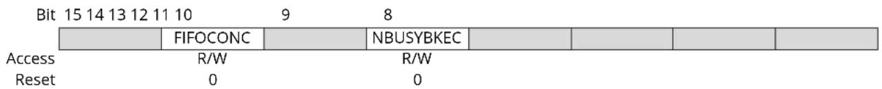
text_image
Bit 15 14 13 12 11 10 9 8 FIFOCONC NBUSYBKEC Access R/W R/W Reset 0 0| Bit | 7 | 6 | 5 | 4 | 3 | 2 | 1 | 0 |
| SHORTPACKETEC | STALLEDEC | OVERFEC | NAKINEC | NAKOUTEC | RXSTPEC | RXOUTEC | TXINEC | |
| Access | R/W | R/W | R/W | R/W | R/W | R/W | R/W | R/W |
| Reset | 0 | 0 | 0 | 0 | 0 | 0 | 0 | 0 |
Bit 19 - STALLRQC STALL Request Clear
Bit 17 - NYETDISC NYET Token Disable Clear
Bit 16 - EPDISHDMAC Endpoint Interrupts Disable HDMA Request Clear
Bit 14 - FIFOCONC FIFO Control Clear
Bit 12 - NBUSYBKEC Number of Busy Banks Interrupt Clear
Bit 7 - SHORTPACKETEC Shortpacket Interrupt Clear
Bit 6 - STALLEDEC STALLed Interrupt Clear
Bit 5 - OVERFEC Overflow Interrupt Clear
Bit 4 - NAKINEC NAKed IN Interrupt Clear
Bit 3 - NAKOUTEC NAKed OUT Interrupt Clear
Bit 2 - RXSTPEC Received SETUP Interrupt Clear
Bit 1 - RXOUTEC Received OUT Data Interrupt Clear
Bit 0 - TXINEC Transmitted IN Interrupt Clear
38.7.24 Device Endpoint Interrupt Disable Register (Isochronous Endpoints)
Name: USBHS_DEVEPTIDRx (ISOENPT)
Offset: 0x0220 + x*0x04 [x=0..8]
Reset: 0
Property: Read/Write
This register view is relevant only if EPTYPE = 0x1 in "Device Endpoint x Configuration Register".
For additional information, see "Device Endpoint x Mask Register (Isochronous Endpoints)".
This register always reads as zero.
The following configuration values are valid for all listed bit names of this register:
0: No effect.
1: Clears the corresponding bit in USBHS_DEVEPTIMRx.
text_image
Bit 31 30 29 28 27 26 25 24 Access Reset Bit 23 22 21 20 19 18 17 16 Access Reset 0 EPDISHDMAQ R/W| Bit 15 14 13 12 11 10 9 | 8 | |||||||
| FIFOCONC | NBUSYBKEC | ERRORTRANSE EC | DATAXEC | MDATEC | ||||
| Access Reset | R/W 0 | R/W 0 | R/W 0 | R/W 0 | R/W 0 | |||
| Bit | 7 | 6 | 5 | 4 | 3 | 2 | 1 | 0 |
| SHORTPACKETEC | CRCERREC O | VERFEC HB | SOFLUSH EC | HBISOINERRE C | UNDERFEC | RXOUTEC | TXINEC | |
| Access Reset | R/W 0 | R/W 0 | R/W 0 | R/W 0 | R/W 0 | R/W 0 | R/W 0 | R/W 0 |
Bit 16 - EPDISHDMAC Endpoint Interrupts Disable HDMA Request Clear
Bit 14 - FIFOCONC FIFO Control Clear
Bit 12 - NBUSYBKEC Number of Busy Banks Interrupt Clear
Bit 10 - ERRORTRANSEC Transaction Error Interrupt Clear
Bit 9 - DATAXEC DataX Interrupt Clear
Bit 8 - MDATEC MData Interrupt Clear
Bit 7 - SHORTPACKETEC Shortpacket Interrupt Clear
Bit 6 - CRCERREC CRC Error Interrupt Clear
Bit 5 - OVERFEC Overflow Interrupt Clear
Bit 4 – HBISOFLUSHEC High Bandwidth Isochronous IN Flush Interrupt Clear
Bit 3 - HBISOINERREC High Bandwidth Isochronous IN Error Interrupt Clear
Bit 2 - UNDERFEC Underflow Interrupt Clear
Bit 1 - RXOUTEC Received OUT Data Interrupt Clear
Bit 0 - TXINEC Transmitted IN Interrupt Clear
38.7.25 Device Endpoint Interrupt Enable Register (Control, Bulk, Interrupt Endpoints)
Name: USBHS_DEVEPTIERx
Offset: 0x01F0 + x*0x04 [x=0..8]
Reset: 0
Property: Read/Write
This register view is relevant only if EPTYPE = 0x0, 0x2, or 0x3 in "Device Endpoint x Configuration Register".
For additional information, see "Device Endpoint x Mask Register (Control, Bulk, Interrupt Endpoints)".
This register always reads as zero.
The following configuration values are valid for all listed bit names of this register:
0: No effect.
1: Sets the corresponding bit in USBHS_DEVEPTIMRx.
| Bit 31 30 29 28 27 26 25 24 | |||||||
| Access Reset | |||||||
| Bit 23 22 21 20 19 18 17 16 | ||||||
| STALLRQS RSTDTS NYETDISS | EPDISHDMAS | |||||
| Access | R/W | R/W | R/W | R/W | ||
| Reset | 0 | 0 | 0 | 0 | ||
| Bit 15 14 13 12 11 10 | 9 | 8 | |||||
| FIFOCONS | KILLBKS | NBUSYBKES | |||||
| Access | R/W | R/W | R/W | ||||
| Reset | 0 | 0 | 0 | ||||
| Bit | 7 | 6 | 5 | 4 | 3 | 2 | 1 | 0 |
| SHORTPACKETES | STALLEDES | OVERFES | NAKINES | NAKOUTES | RXSTPES | RXOUTES | TXINES | |
| Access | R/W | R/W | R/W | R/W | R/W | R/W | R/W | R/W |
| Reset | 0 | 0 | 0 | 0 | 0 | 0 | 0 | 0 |
Bit 19 - STALLRQS STALL Request Enable
Bit 18 - RSTDTS Reset Data Toggle Enable
Bit 17 - NYETDISS NYET Token Disable Enable
Bit 16 - EPDISHDMAS Endpoint Interrupts Disable HDMA Request Enable
Bit 14 - FIFOCONS FIFO Control
Bit 13 - KILLBKS Kill IN Bank
Bit 12 - NBUSYBKES Number of Busy Banks Interrupt Enable
Bit 7 - SHORTPACKETES Short Packet Interrupt Enable
Bit 6 - STALLEDES STALLed Interrupt Enable
Bit 5 - OVERFES Overflow Interrupt Enable
Bit 4 - NAKINES NAKed IN Interrupt Enable
Bit 3 - NAKOUTES NAKed OUT Interrupt Enable
Bit 2 - RXSTPES Received SETUP Interrupt Enable
Bit 1 - RXOUTES Received OUT Data Interrupt Enable
Bit 0 - TXINES Transmitted IN Data Interrupt Enable
38.7.26 Device Endpoint Interrupt Enable Register (Isochronous Endpoints)
Name: USBHS_DEVEPTIERx (ISOENPT)
Offset: 0x01F0 + x*0x04 [x=0..8]
Reset: 0
Property: Read/Write
This register view is relevant only if EPTYPE = 0x1 in "Device Endpoint x Configuration Register".
For additional information, see "Device Endpoint x Mask Register (Isochronous Endpoints)".
This register always reads as zero.
The following configuration values are valid for all listed bit names of this register:
0: No effect.
1: Clears the corresponding bit in USBHS_DEVEPTIMRx.
text_image
Bit 31 30 29 28 27 26 25 24 Access Reset Bit 23 22 21 20 19 18 17 16 RSTDTS EPDISH HDMAS Access Reset 0 0 R/W R/W| Bit 15 14 13 12 11 10 | 9 | 8 | ||||||
| FIFOCONS | KILLBKS | NBUSYBKES | ERRORTRANS ES | DATAXES M | DATAES | |||
| Access Reset | R/W R/W 0 | R/W R/W 0 | R/W R/W 0 | R/W R/W | ||||
| Bit | 7 | 6 | 5 | 4 | 3 | 2 | 1 | 0 |
| SHORTPACKETES | CRCERRES OVERFES HB | SOFLUSH ES | HBISOINERRE S | UNDERFES | RXOUTES TXINES | |||
| Access Reset | R/W 0 | R/W 0 | R/W 0 | R/W 0 | R/W 0 | R/W 0 | R/W 0 | R/W 0 |
Bit 18 - RSTDTS Reset Data Toggle Enable
Bit 16 - EPDISHDMAS Endpoint Interrupts Disable HDMA Request Enable
Bit 14 - FIFOCONS FIFO Control
Bit 13 - KILLBKS Kill IN Bank
Bit 12 - NBUSYBKES Number of Busy Banks Interrupt Enable
Bit 10 - ERRORTRANSES Transaction Error Interrupt Enable
Bit 9 - DATAXES DataX Interrupt Enable
Bit 8 - MDATAES MData Interrupt Enable
Bit 7 - SHORTPACKETES Short Packet Interrupt Enable
Bit 6 - CRCERRES CRC Error Interrupt Enable
Bit 5 - OVERFES Overflow Interrupt Enable
Bit 4 – HBISOFLUSHES High Bandwidth Isochronous IN Flush Interrupt Enable
Bit 3 - HBISOINERRES High Bandwidth Isochronous IN Error Interrupt Enable
Bit 2 - UNDERFES Underflow Interrupt Enable
Bit 1 - RXOUTES Received OUT Data Interrupt Enable
Bit 0 - TXINES Transmitted IN Data Interrupt Enable
38.7.27 Device DMA Channel x Next Descriptor Address Register
Name: USBHS_DEVDMANXTDSCx
Offset: 0x0300 + (x-1)*0x10 [x=1..7]
Reset: 0
Property: Read/Write
Bit 31 30 29 28 27 26 25 24
NXT_DSC_ADD[31:24]
Access R/W R/W R/W R/W R/W R/W R/W R/W
Reset 00000000
Bit 23 22 21 20 19 18 17 16
NXT_DSC_ADD[23:16]
Access R/W R/W R/W R/W R/W R/W R/W R/W
Reset 00000000
Bit 15 14 13 12 11 10 9 8
NXT_DSC_ADD[15:8]
Access R/W R/W R/W R/W R/W R/W R/W R/W
Reset 00000000
Bit 76543210
NXT_DSC_ADD[7:0]
Access R/W R/W R/W R/W R/W R/W R/W R/W
Reset 00000000
Bits 31:0 - NXT\_DSC\_ADD[31:0] Next Descriptor Address
This field points to the next channel descriptor to be processed. This channel descriptor must be aligned, so bits 0 to 3 of the address must be equal to zero.
38.7.28 Device DMA Channel x Address Register
Name: USBHS_DEVDMAADDRESSx
Offset: 0x0304 + (x-1)*0x10 [x=1..7]
Reset: 0
Property: Read/Write
Bit 31 30 29 28 27 26 25 24
BUFF_ADD[31:24]
Access R/W R/W R/W R/W R/W R/W R/W R/W
Reset 00000000
Bit 23 22 21 20 19 18 17 16
BUFF_ADD[23:16]
Access R/W R/W R/W R/W R/W R/W R/W R/W
Reset 00000000
Bit 15 14 13 12 11 10 9 8
BUFF_ADD[15:8]
Access R/W R/W R/W R/W R/W R/W R/W R/W
Reset 00000000
Bit 76543210
BUFF_ADD[7:0]
Access R/W R/W R/W R/W R/W R/W R/W R/W
Reset 00000000
Bits 31:0 - BUFF\_ADD[31:0] Buffer Address
This field determines the AHB bus starting address of a DMA channel transfer.
Channel start and end addresses may be aligned on any byte boundary.
The firmware can write this field only when the USBHS_DEVDMASTATUS.CHANN_ENB bit is clear.
This field is updated at the end of the address phase of the current access to the AHB bus. It is incremented by the access byte width. The access width is 4 bytes (or less) at packet start or end, if the start or end address is not aligned on a word boundary.
The packet start address is either the channel start address or the next channel address to be accessed in the channel buffer. The packet end address is either the channel end address or the latest channel address accessed in the channel buffer.
The channel start address is written by software or loaded from the descriptor. The channel end address is either determined by the end of buffer or the USB device, or by the USB end of transfer if the USBHS_DEVDMACONTROLx.END_TR_EN bit is set.
38.7.29 Device DMA Channel x Control Register
Name: USBHS_DEVDMACONTROLx
Offset: 0x0308 + (x-1)*0x10 [x=1..7]
Reset: 0
Property: Read/Write
Bit 31 30 29 28 27 26 25 24
| BUFF_LENGTH[15:8] |
Access R/W R/W R/W R/W R/W R/W R/W R/W
Reset 00000000
Bit 23 22 21 20 19 18 17 16
| BUFF_LENGTH[7:0] |
Access R/W R/W R/W R/W R/W R/W R/W R/W
Reset 00000000
Bit 15 14 13 12 11 10 9 8
Access
Reset
Bit 76543210
| BURST_LCK | DESC_LD_IT | END_BUFFIT | END_TR_IT | END_B_EN | END_TR_EN | LDNXT_DSC | CHANN_ENB |
Access R/W R/W R/W R/W R/W R/W R/W R/W
Reset 00000000
Bits 31:16 - BUFF\_LENGTH[15:0] Buffer Byte Length (Write-only)
This field determines the number of bytes to be transferred until end of buffer. The maximum channel transfer size (32 KBytes) is reached when this field is 0 (default value). If the transfer size is unknown, this field should be set to 0, but the transfer end may occur earlier under USB device control.
When this field is written, the USBHS_DEVDMASTATUSx.BUFF_COUNT field is updated with the write value.
Note: 1. Bits [31:2] are only writable when issuing a channel Control Command other than "Stop Now".
Note: 2. For reliability, it is recommended to wait for both the USBHS_DEVDMASTATUSx.CHAN_ACT and the USBHS_DEVDMASTATUSx.CHAN_ENB flags to be at 0, thus ensuring the channel has been stopped before issuing a command other than "Stop Now".
Bit 7 - BURST_LCK Burst Lock Enable
| Value | Description |
| 0 | The DMA never locks bus access. |
| 1 | USB packets AHB data bursts are locked for maximum optimization of the bus bandwidth usage and maximization of fly-by AHB burst duration. |
Bit 6 - DESC_LD_IT Descriptor Loaded Interrupt Enable
| Value | Description |
| 0 | USBHS_DEVDMASTATUSx.DESC_LDST rising does not trigger any interrupt. |
| 1 | An interrupt is generated when a descriptor has been loaded from the bus. |
Bit 5 - END_BUFFIT End of Buffer Interrupt Enable
| Value | Description |
| 0 | USBHS_DEVDMA_STATUSx.END_BF_ST rising does not trigger any interrupt. |
Value Description
1 An interrupt is generated when USBHS_HSTDMASTATUSx.BUFF_COUNT reaches zero.
Bit 4 - END\_TR\_IT End of Transfer Interrupt Enable
Use when the receive size is unknown.
Value Description
| 0 | USBHS device-initiated buffer transfer completion does not trigger any interrupt at USBHS_DEVDMASTATUSx.END_TR_ST rising. |
| 1 | An interrupt is sent after the buffer transfer is complete, if the USBHS device has ended the buffer transfer. |
Bit 3 - END\_B\_EN End of Buffer Enable Control
This is mainly for short packet IN validations initiated by the DMA reaching end of buffer, but can be used for OUT packet truncation (discarding of unwanted packet data) at the end of DMA buffer.
Value Description
| 0 | DMA Buffer End has no impact on USB packet transfer. |
| 1 | The endpoint can validate the packet (according to the values programmed in the USBHS_DEVEPTCFGx.AUTOSW and USBHS_DEVEPTIERx.SHORTPACKETES fields) at DMA Buffer End, i.e., when USBHS_DEVDMASTATUS.BUFF_COUNT reaches 0. |
Bit 2 - END\_TR\_EN End of Transfer Enable Control (OUT transfers only)
When set, a BULK or INTERRUPT short packet or the last packet of an ISOCHRONOUS (micro) frame (DATAX) closes the current buffer and the USBHS_DEVDMASTATUSx.END_TR_ST flag is raised.
This is intended for a USBHS non-prenegotiated end of transfer (BULK or INTERRUPT) or ISOCHRONOUS microframe data buffer closure.
Value Description
| 0 | The USB end of transfer is ignored. |
| 1 | The USBHS device can put an end to the current buffer transfer. |
Bit 1 - LDNXT\_DSC Load Next Channel Transfer Descriptor Enable Command
If the CHANN_ENB bit is cleared, the next descriptor is immediately loaded upon transfer request.
DMA Channel Control Command Summary:
| Value LDNXT_DSC Value CHANN_ENB Name Description | ||
| 0 0 STOP_NOW Stop now | ||
| 0 1 RUN_AND_STOP Run and stop at end of buffer | ||
| 1 0 LOAD_NEXT_DESC Load next descriptor now | ||
| 1 1 RUN_AND_LINK Run and link at end of buffer | ||
Value Description
| 0 | No channel register is loaded after the end of the channel transfer. |
| 1 | The channel controller loads the next descriptor after the end of the current transfer, i.e., when the USBHS_DEVDMASTATUS.CHANN_ENB bit is reset. |
Bit 0 - CHANN\_ENB Channel Enable Command
Value Description
| 0 | The DMA channel is disabled at end of transfer and no transfer occurs upon request. This bit is also cleared by hardware when the channel source bus is disabled at end of buffer.If the LDNXT_DSC bit has been cleared by descriptor loading, the firmware must set the corresponding CHANN_ENB bit to start the described transfer, if needed.If the LDNXT_DSC bit is cleared, the channel is frozen and the channel registers may then be read and/or written reliably as soon as both USBHS_DEVDMASTATUS.CHANN_ENB and CHANN_ACT flags read as 0.If a channel request is currently serviced when this bit is cleared, the DMA FIFO buffer is drained until it is empty, then the USBHS_DEVDMASTATUS.CHANN_ENB bit is cleared.If the LDNXT_DSC bit is set at or after this bit clearing, then the currently loaded descriptor is skipped (no data transfer occurs) and the next descriptor is immediately loaded. |
| 1 | The USBHS_DEVDMASTATUS.CHANN_ENB bit is set, thus enabling the DMA channel data transfer. Then, any pending request starts the transfer. This may be used to start or resume any requested transfer. |
38.7.30 Device DMA Channel x Status Register
Name: USBHS_DEVDMASTATUSx
Offset: 0x030C + (x-1)*0x10 [x=1..7]
Reset: 0
Property: Read/Write
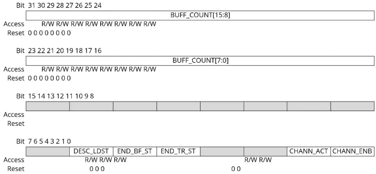
text_image
Bit 31 30 29 28 27 26 25 24 BUFF_COUNT[15:8] Access R/W R/W R/W R/W R/W R/W R/W Reset 0 0 0 0 0 0 0 0 Bit 23 22 21 20 19 18 17 16 BUFF_COUNT[7:0] Access R/W R/W R/W R/W R/W R/W R/W Reset 0 0 0 0 0 0 0 0 Bit 15 14 13 12 11 10 9 8 Access Reset Bit 7 6 5 4 3 2 1 0 DESC_LDST END_BF_ST END_TR_ST CHANN_ACT CHANN_ENB Access R/W R/W R/W R/W R/W R/W R/W Reset 0 0 0 0 0 0 0 R/W R/W 0 0 0 0 0 0Bits 31:16 - BUFF\_COUNT[15:0] Buffer Byte Count
This field determines the current number of bytes still to be transferred for this buffer.
This field is decremented from the AHB source bus access byte width at the end of this bus address phase.
The access byte width is 4 by default, or less, at DMA start or end, if the start or end address is not aligned on a word boundary.
At the end of buffer, the DMA accesses the USBHS device only for the number of bytes needed to complete it.
Note: For OUT endpoints, if the receive buffer byte length (BUFF_LENGTH) has been defaulted to zero because the USB transfer length is unknown, the actual buffer byte length received is 0x10000-BUFF_COUNT.
Bit 6 - DESC\_LDST Descriptor Loaded Status
Valid until the CHANN_ENB flag is cleared at the end of the next buffer transfer.
| Value | Description |
| 0 | Cleared automatically when read by software. |
| 1 | Set by hardware when a descriptor has been loaded from the system bus. |
Bit 5 - END\_BF\_ST End of Channel Buffer Status
Valid until the CHANN_ENB flag is cleared at the end of the next buffer transfer.
| Value | Description |
| 0 | Cleared automatically when read by software. |
| 1 | Set by hardware when the BUFF_COUNT count-down reaches zero. |
Bit 4 - END\_TR\_ST End of Channel Transfer Status
Valid until the CHANN_ENB flag is cleared at the end of the next buffer transfer.
| Value Description | |
| 0 | Cleared automatically when read by software. |
| 1 | Set by hardware when the last packet transfer is complete, if the USBHS device has ended the transfer. |
Bit 1 - CHANN\_ACT Channel Active Status
When a packet transfer is ended, this bit is automatically reset.
When a packet transfer cannot be completed due to an END_BF_ST, this flag stays set during the next channel descriptor load (if any) and potentially until completion of a USBHS packet transfer, if allowed by the new descriptor.
| Value Description | |
| 0 | The DMA channel is no longer trying to source the packet data. |
| 1 | The DMA channel is currently trying to source packet data, i.e., selected as the highest-priority requesting channel. |
Bit 0 - CHANN\_ENB Channel Enable Status
When any transfer is ended either due to an elapsed byte count or to completion of a USBHS device-initiated transfer, this bit is automatically reset.
This bit is normally set or cleared by writing into the USBHS_DEVDMACONTROLx.CHANN_ENB bit field either by software or descriptor loading.
If a channel request is currently serviced when the USBHS_DEVDMACONTROLx.CHANN_ENB bit is cleared, the DMA FIFO buffer is drained until it is empty, then this status bit is cleared.
| Value Description | |
| 0 | If cleared, the DMA channel no longer transfers data, and may load the next descriptor if the USBHS_DEVDMACONTROLx.LDNXT_DSC bit is set. |
| 1 | If set, the DMA channel is currently enabled and transfers data upon request. |
38.7.31 Host General Control Register
Name: USBHS_HSTCTRL
Offset: 0x0400
Reset: 0x00000000
Property: Read/Write
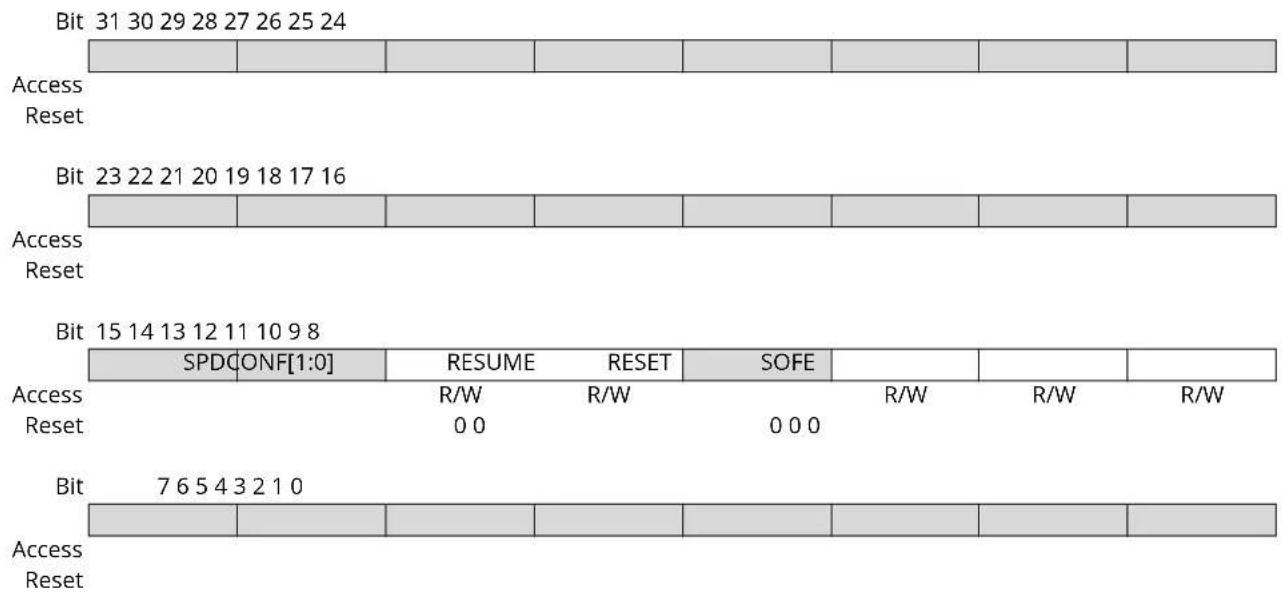
text_image
Bit 31 30 29 28 27 26 25 24 Access Reset Bit 23 22 21 20 19 18 17 16 Access Reset Bit 15 14 13 12 11 10 9 8 SPDCONF[1:0] RESUME RESET SOFE R/W R/W R/W R/W Access Reset 0 0 0 0 0 Bit 7 6 5 4 3 2 1 0 Access ResetBits 13:12 - SPDCONF[1:0] Mode Configuration
This field contains the host speed capability:.
| Value | Name | Description |
| 0 | NORMAL | The host starts in Full-speed mode and performs a high-speed reset to switch to High-speed mode if the downstream peripheral is high-speed capable. |
| 1 | LOW_POWER | For a better consumption, if high speed is not needed. |
| 2 | HIGH_SPEED | Forced high speed. |
| 3 | FORCED_FS | The host remains in Full-speed mode whatever the peripheral speed capability. |
Bit 10 - RESUME Send USB Resume
This bit is cleared when the USB Resume has been sent or when a USB reset is requested.
This bit should be written to one only when the start of frame generation is enabled (SOFE = 1).
| Value | Description |
| 0 | No effect. |
| 1 | Generates a USB Resume on the USB bus. |
Bit 9 - RESET Send USB Reset
This bit is cleared when the USB Reset has been sent.
It may be useful to write a zero to this bit when a device disconnection is detected (USBHS_HSTISR.DDISCI = 1) whereas a USB Reset is being sent.
| Value | Description |
| 0 | No effect. |
| 1 | Generates a USB Reset on the USB bus. |
Bit 8 - SOFE Start of Frame Generation Enable
This bit is set when a USB reset is requested or an upstream resume interrupt is detected (USBHS_HSTISR.TXRSMI).
Value Description
| 0 | Disables the SOF generation and leaves the USB bus in idle state. |
| 1 | Generates SOF on the USB bus in Full- or High-speed mode and sends “keep alive” signals in Low-speed mode. |
38.7.32 Host Global Interrupt Status Register
Name: USBHS_HSTISR
Offset: 0x0404
Reset: 0x00000000
Property: Read-only
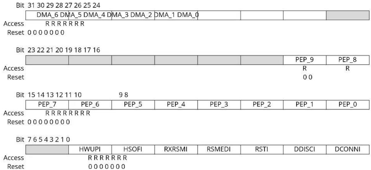
text_image
Bit 31 30 29 28 27 26 25 24 DMA_6 DMA_5 DMA_4 DMA_3 DMA_2 DMA_1 DMA_0 Access R R R R R R R Reset 0 0 0 0 0 0 0 Bit 23 22 21 20 19 18 17 16 Access R R R R R R R Reset 0 0 Bit 15 14 13 12 11 10 9 8 Access R R R R R R R R Reset 0 0 0 0 0 0 0 0 Bit 7 6 5 4 3 2 1 0 Access R R R R R R R Reset 0 0 0 0 0 0 0 RWUPI HSOFI RXRSMI RSMEDI RSTI DDISCI DCONNIBits 25, 26, 27, 28, 29, 30, 31 - DMA_ DMA Channel x Interrupt
| Value | Description |
| 0 | Cleared when the USBHS_HSTDMASTATUSx interrupt source is cleared. |
| 1 | Set when an interrupt is triggered by the DMA channel x. This triggers a USB interrupt if the corresponding bit in USBHS_HSTIMR = 1. |
Bits 8, 9, 10, 11, 12, 13, 14, 15, 16, 17 - PEP_ Pipe x Interrupt
| Value | Description |
| 0 | Cleared when the interrupt source is served. |
| 1 | Set when an interrupt is triggered by pipe x (USBHS_HSTPIPISRx). This triggers a USB interrupt if the corresponding bit in USBHS_HSTIMR = 1. |
Bit 6 - HWUPI Host Wakeup Interrupt
This bit is set when the host controller is in Suspend mode (SOFE = 0) and an upstream resume from the peripheral is detected.
This bit is set when the host controller is in Suspend mode (SOFE = 0) and a peripheral disconnection is detected.
This interrupt is generated even if the clock is frozen by the USBHS_CTRL.FRZCLK bit.
Bit 5 - HSOFI Host Start of Frame Interrupt
| Value | Description |
| 0 | Cleared when USBHS_HSTICR.HSOFIC = 1. |
| 1 | Set when a SOF is issued by the host controller. This triggers a USB interrupt when HSOFE = 1. When using the host controller in Low-speed mode, this bit is also set when a keep-alive is sent. |
Bit 4 - RXRSMI Upstream Resume Received Interrupt
| Value | Description |
| 0 | Cleared when USBHS_HSTICR.RXRSMIC = 1. |
Value Description
| 1 | Set when an Upstream Resume has been received from the device. |
Bit 3 - RSMEDI Downstream Resume Sent Interrupt
| Value Description | |
| 0 | Cleared when USBHS_HSTICR.RSMEDIC = 1. |
| 1 | Set when a Downstream Resume has been sent to the device. |
Bit 2 - RSTI USB Reset Sent Interrupt
| Value Description | |
| 0 | Cleared when USBHS_HSTICR.RSTIC = 1. |
| 1 | Set when a USB Reset has been sent to the device. |
Bit 1 - DDISCI Device Disconnection Interrupt
| Value Description | |
| 0 | Cleared when USBHS_HSTICR.DDISCIC = 1. |
| 1 | Set when the device has been removed from the USB bus. |
Bit 0 - DCONNl Device Connection Interrupt
| Value Description | |
| 0 | Cleared when USBHS_HSTICR.DCONNIC = 1. |
| 1 | Set when a new device has been connected to the USB bus. |
38.7.33 Host Global Interrupt Clear Register
Name: USBHS_HSTICR
Offset: 0x0408
Property: Write-only
This register always reads as zero.
The following configuration values are valid for all listed bit names of this register:
0: No effect.
1: Clears the corresponding bit in USBHS_HSTISR.
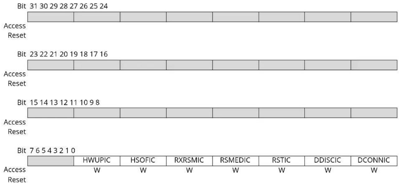
Bit 6 - HWUPIC Host Wakeup Interrupt Clear
Bit 5 - HSOFIC Host Start of Frame Interrupt Clear
Bit 4 - RXRSMIC Upstream Resume Received Interrupt Clear
Bit 3 - RSMEDIC Downstream Resume Sent Interrupt Clear
Bit 2 - RSTIC USB Reset Sent Interrupt Clear
Bit 1 - DDISCIC Device Disconnection Interrupt Clear
Bit 0 - DCONNIC Device Connection Interrupt Clear
38.7.34 Host Global Interrupt Set Register
Name: USBHS_HSTIFR
Offset: 0x040C
Property: Write-only
This register always reads as zero.
The following configuration values are valid for all listed bit names of this register:
0: No effect.
1: Sets the corresponding bit in USBHS_HSTISR, which may be useful for test or debug purposes.

text_image
Bit 31 30 29 28 27 26 25 24 DMA_6 DMA_5 DMA_4 DMA_3 DMA_2 DMA_1 DMA_0 Access W W W W W W W W Reset Bit 23 22 21 20 19 18 17 16 Access Reset Bit 15 14 13 12 11 10 9 8 Access Reset Bit 7 6 5 4 3 2 1 0 Access Reset HWUPIS HSOFIS RXRSMIS RSMEDIS RSTIS DDISCIS DCONNIS W W W W W W W WBits 25, 26, 27, 28, 29, 30, 31 - DMA_ DMA Channel x Interrupt Set
Bit 6 - HWUPIS Host Wakeup Interrupt Set
Bit 5 - HSOFIS Host Start of Frame Interrupt Set
Bit 4 - RXRSMIS Upstream Resume Received Interrupt Set
Bit 3 - RSMEDIS Downstream Resume Sent Interrupt Set
Bit 2 - RSTIS USB Reset Sent Interrupt Set
Bit 1 - DDISCIS Device Disconnection Interrupt Set
Bit 0 - DCONNIS Device Connection Interrupt Set
38.7.35 Host Global Interrupt Mask Register
Name: USBHS_HSTIMR
Offset: 0x0410
Reset: 0x00000000
Property: Read-only
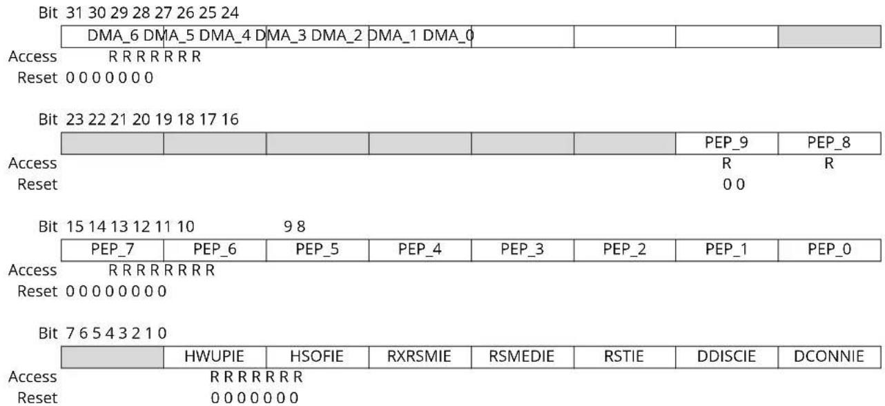
text_image
Bit 31 30 29 28 27 26 25 24 DMA_6 DMA_5 DMA_4 DMA_3 DMA_2 DMA_1 DMA_0 Access R R R R R R R Reset 0 0 0 0 0 0 0 Bit 23 22 21 20 19 18 17 16 Access R R R R R R R Reset 0 0 Bit 15 14 13 12 11 10 9 8 Access R R R R R R R R Reset 0 0 0 0 0 0 0 0 Bit 7 6 5 4 3 2 1 0 Access R R R R R R R R Reset 0 0 0 0 0 0 0 HWUPIE HSOFIE RXRSMIE RSMEDIE RSTIE DDISCIE DCONNIEBits 25, 26, 27, 28, 29, 30, 31 - DMA_ DMA Channel x Interrupt Enable
| Value | Description |
| 0 | Cleared when the corresponding bit in USBHS_HSTIDR = 1. This disables the DMA Channel x Interrupt (USBHS_HSTISR.DMA_x). |
| 1 | Set when the corresponding bit in USBHS_HSTIER = 1. This enables the DMA Channel x Interrupt (USBHS_HSTISR.DMA_x). |
Bits 8, 9, 10, 11, 12, 13, 14, 15, 16, 17 - PEP_ Pipe x Interrupt Enable
| Value | Description |
| 0 | Cleared when PEP_x = 1. This disables the Pipe x Interrupt (PEP_x). |
| 1 | Set when the corresponding bit in USBHS_HSTIER = 1. This enables the Pipe x Interrupt (USBHS_HSTISR.PEP_x). |
Bit 6 - HWUPIE Host Wakeup Interrupt Enable
| Value | Description |
| 0 | Cleared when USBHS_HSTIDR.HWUPIEC = 1. This disables the Host Wakeup Interrupt (USBHS_HSTISR.HWUPI). |
| 1 | Set when USBHS_HSTIER.HWUPIES = 1. This enables the Host Wakeup Interrupt (USBHS_HSTISR.HWUPI). |
Bit 5 - HSOFIE Host Start of Frame Interrupt Enable
| Value | Description |
| 0 | Cleared when USBHS_HSTIDR.HSOFIEC = 1. This disables the Host Start of Frame interrupt (USBHS_HSTISR.HSOFI). |
| 1 | Set when USBHS_HSTIER.HSOFIES= 1. This enables the Host Start of Frame interrupt (USBHS_HSTISR.HSOFI). |
Bit 4 - RXRSMIE Upstream Resume Received Interrupt Enable
| Value | Description |
| 0 | Cleared when USBHS_HSTIDR.RXRSMIEC= 1. This disables the Downstream Resume interrupt (USBHS_HSTISR.RXRSMI). |
Value Description
| 1 | Set when USBHS_HSTIER.RXRSMIES = 1. This enables the Upstream Resume Received interrupt (USBHS_HSTISR.RXRSMI). |
Bit 3 - RSMEDIE Downstream Resume Sent Interrupt Enable
| Value Description | |
| 0 | Cleared when USBHS_HSTIDR.RSMEDIEC = 1. This disables the Downstream Resume interrupt (USBHS_HSTISR.RSMEDI). |
| 1 | Set when USBHS_HSTIER.RSMEDIES = 1. This enables the Downstream Resume interrupt (USBHS_HSTISR.RSMEDI). |
Bit 2 - RSTIE USB Reset Sent Interrupt Enable
| Value Description | |
| 0 | Cleared when USBHS_HSTIDR.RSTIEC = 1. This disables the USB Reset Sent interrupt (USBHS_HSTISR.RSTI). |
| 1 | Set when USBHS_HSTIER.RSTIES = 1. This enables the USB Reset Sent interrupt (USBHS_HSTISR.RSTI). |
Bit 1 - DDISCIE Device Disconnection Interrupt Enable
| Value Description | |
| 0 | Cleared when USBHS_HSTIDR.DDISCIEC = 1. This disables the Device Disconnection interrupt (USBHS_HSTISR.DDISCI). |
| 1 | Set when USBHS_HSTIER.DDISCIES = 1. This enables the Device Disconnection interrupt (USBHS_HSTISR.DDISCI). |
Bit 0 - DCONNIE Device Connection Interrupt Enable
| Value Description | |
| 0 | Cleared when USBHS_HSTIDR.DCONNIEC = 1. This disables the Device Connection interrupt (USBHS_HSTISR.DCONNI). |
| 1 | Set when USBHS_HSTIER.DCONNIES = 1. This enables the Device Connection interrupt (USBHS_HSTISR.DCONNI). |
38.7.36 Host Global Interrupt Disable Register
Name: USBHS_HSTIDR
Offset: 0x0414
Property: Write-only
This register always reads as zero.
The following configuration values are valid for all listed bit names of this register:
0: No effect.
1: Clears the corresponding bit in USBHS_HSTIMR.
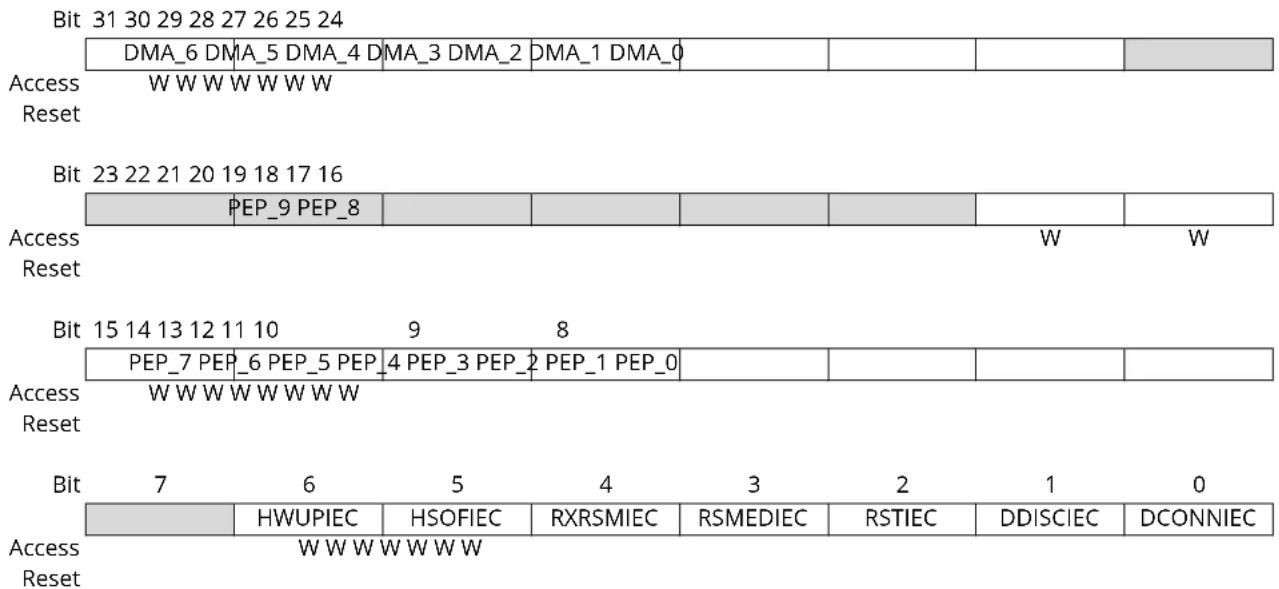
text_image
Bit 31 30 29 28 27 26 25 24 DMA_6 DMA_5 DMA_4 DMA_3 DMA_2 DMA_1 DMA_0 Access W W W W W W W Reset Bit 23 22 21 20 19 18 17 16 PEP_9 PEP_8 Access W W Reset Bit 15 14 13 12 11 10 9 8 Access W W W W W W W W Reset PEP_7 PEP_6 PEP_5 PEP_4 PEP_3 PEP_2 PEP_1 PEP_0 Access W W W W W W W W Bit 7 6 5 4 3 2 1 0 Access HWUPIEC HSOFIEC RXRSMIEC RSMEDIEC RSTIEC DDISCIEC DCONNIEC Reset W W W W W W W WBits 25, 26, 27, 28, 29, 30, 31 - DMA_ DMA Channel x Interrupt Disable
Bits 8, 9, 10, 11, 12, 13, 14, 15, 16, 17 - PEP_ Pipe x Interrupt Disable
Bit 6 - HWUPIEC Host Wakeup Interrupt Disable
Bit 5 - HSOFIEC Host Start of Frame Interrupt Disable
Bit 4 - RXRSMIEC Upstream Resume Received Interrupt Disable
Bit 3 - RSMEDIEC Downstream Resume Sent Interrupt Disable
Bit 2 - RSTIEC USB Reset Sent Interrupt Disable
Bit 1 - DDISCIEC Device Disconnection Interrupt Disable
Bit 0 - DCONNIEC Device Connection Interrupt Disable
38.7.37 Host Global Interrupt Enable Register
Name: USBHS_HSTIER
Offset: 0x0418
Property: Write-only
This register always reads as zero.
The following configuration values are valid for all listed bit names of this register:
0: No effect.
1: Sets the corresponding bit in USBHS_HSTISR.

Bits 25, 26, 27, 28, 29, 30, 31 - DMA_ DMA Channel x Interrupt Enable
Bits 8, 9, 10, 11, 12, 13, 14, 15, 16, 17 - PEP_ Pipe x Interrupt Enable
Bit 6 - HWUPIES Host Wakeup Interrupt Enable
Bit 5 - HSOFIES Host Start of Frame Interrupt Enable
Bit 4 - RXRSMIES Upstream Resume Received Interrupt Enable
Bit 3 - RSMEDIES Downstream Resume Sent Interrupt Enable
Bit 2 - RSTIES USB Reset Sent Interrupt Enable
Bit 1 - DDISCIES Device Disconnection Interrupt Enable
Bit 0 - DCONNIES Device Connection Interrupt Enable
38.7.38 Host Frame Number Register
Name: USBHS_HSTFNUM
Offset: 0x0420
Reset: 0x00000000
Property: Read/Write
| Bit 31 30 29 28 27 26 25 24 | |||||||
| Access Reset | |||||||
| Bit 23 22 21 20 19 18 17 16 | |||||||
| FLENHIGH[7:0] | |||||||
| Access Reset | R/W R/W R/W R/W R/W R/W R/W R/W | ||||||
| 0 0 0 0 0 0 0 0 | |||||||
| Bit 15 14 13 12 11 10 | 9 8 | ||||||
| FNUM[10:5] | |||||||
| Access Reset | R/W R/W R/W R/W R/W R/W | ||||||
| 0 0 0 0 0 0 | |||||||
| Bit 76543210 | ||
| FNUM[4:0] | MFNUM[2:0] | |
| Access | R/W R/W R/W R/W R/W R/W R/W R/W | |
| Reset | 0 0 0 0 0 0 0 | |
Bits 23:16 - FLENHIGH[7:0] Frame Length
In High-speed mode, this field contains the 8 high-order bits of the 16-bit internal frame counter (at 30 MHz, the counter length is 3750 to ensure a SOF generation every 125 s).
Bits 13:3 - FNUM[10:0] Frame Number
This field contains the current SOF number.
This field can be written. In this case, the MFNUM field is reset to zero.
Bits 2:0 - MFNUM[2:0] Micro Frame Number
This field contains the current microframe number (can vary from 0 to 7), updated every 125 s. When operating in Full-speed mode, this field is tied to zero.
38.7.39 Host Address 1 Register
Name: USBHS_HSTADDR1
Offset: 0x0424
Reset: 0x00000000
Property: Read/Write
| Bit | 31 30 29 28 27 26 25 24 |
| HSTADDRP3[6:0] | |
| Access | R/W R/W R/W R/W R/W R/W R/W |
| Reset | 0 0 0 0 0 0 0 |
| Bit | 23 22 21 20 19 18 17 16 |
| HSTADDRP2[6:0] | |
| Access | R/W R/W R/W R/W R/W R/W R/W |
| Reset | 0 0 0 0 0 0 0 |
| Bit | 15 14 13 12 11 10 9 8 |
| HSTADDRP1[6:0] | |
| Access | R/W R/W R/W R/W R/W R/W R/W |
| Reset | 0 0 0 0 0 0 0 |
| Bit | 7 6 5 4 3 2 1 0 |
| HSTADDRP0[6:0] | |
| Access | R/W R/W R/W R/W R/W R/W R/W |
| Reset | 0 0 0 0 0 0 0 |
Bits 30:24 - HSTADDRP3[6:0] USB Host Address
This field contains the address of the Pipe3 of the USB device.
This field is cleared when a USB reset is requested.
Bits 22:16 - HSTADDRP2[6:0] USB Host Address
This field contains the address of the Pipe2 of the USB device.
This field is cleared when a USB reset is requested.
Bits 14:8 - HSTADDRP1[6:0] USB Host Address
This field contains the address of the Pipe1 of the USB device.
This field is cleared when a USB reset is requested.
Bits 6:0 - HSTADDRP0[6:0] USB Host Address
This field contains the address of the Pipe0 of the USB device.
This field is cleared when a USB reset is requested.
38.7.40 Host Address 2 Register
Name: USBHS_HSTADDR2
Offset: 0x0428
Reset: 0x00000000
Property: Read/Write
| Bit | 31 30 29 28 27 26 25 24 |
| HSTADDRP7[6:0] | |
| Access | R/W R/W R/W R/W R/W R/W R/W |
| Reset | 0 0 0 0 0 0 0 |
| Bit | 23 22 21 20 19 18 17 16 |
| HSTADDRP6[6:0] | |
| Access | R/W R/W R/W R/W R/W R/W R/W |
| Reset | 0 0 0 0 0 0 0 |
| Bit | 15 14 13 12 11 10 9 8 |
| HSTADDRP5[6:0] | |
| Access | R/W R/W R/W R/W R/W R/W R/W |
| Reset | 0 0 0 0 0 0 0 |
| Bit | 7 6 5 4 3 2 1 0 |
| HSTADDRP4[6:0] | |
| Access | R/W R/W R/W R/W R/W R/W R/W |
| Reset | 0 0 0 0 0 0 0 |
Bits 30:24 - HSTADDRP7[6:0] USB Host Address
This field contains the address of the Pipe7 of the USB device.
This field is cleared when a USB reset is requested.
Bits 22:16 - HSTADDRP6[6:0] USB Host Address
This field contains the address of the Pipe6 of the USB device.
This field is cleared when a USB reset is requested.
Bits 14:8 - HSTADDRP5[6:0] USB Host Address
This field contains the address of the Pipe5 of the USB device.
This field is cleared when a USB reset is requested.
Bits 6:0 - HSTADDRP4[6:0] USB Host Address
This field contains the address of the Pipe4 of the USB device.
This field is cleared when a USB reset is requested.
38.7.41 Host Address 3 Register
Name: USBHS_HSTADDR3
Offset: 0x042C
Reset: 0x00000000
Property: Read/Write
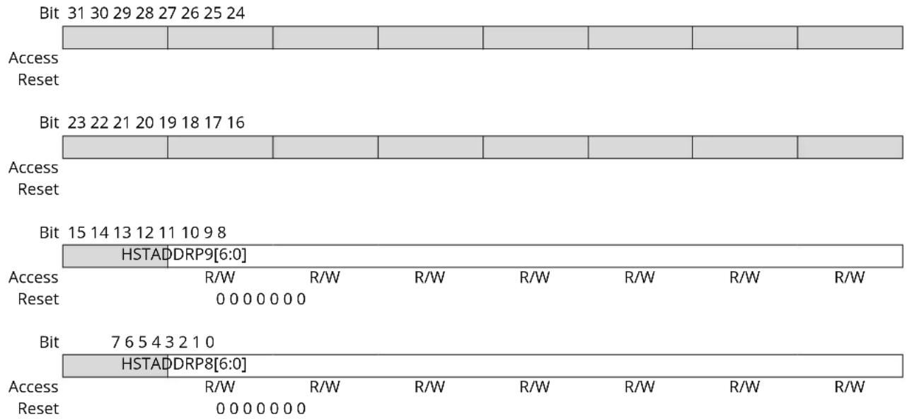
text_image
Bit 31 30 29 28 27 26 25 24 Access Reset Bit 23 22 21 20 19 18 17 16 Access Reset Bit 15 14 13 12 11 10 9 8 HSTADDRP9[6:0] Access R/W R/W R/W R/W R/W R/W R/W Reset 0 0 0 0 0 0 0 Bit 7 6 5 4 3 2 1 0 HSTADDRP8[6:0] Access R/W R/W R/W R/W R/W R/W R/W Reset 0 0 0 0 0 0 0Bits 14:8 - HSTADDRP9[6:0] USB Host Address
This field contains the address of the Pipe9 of the USB device.
This field is cleared when a USB reset is requested.
Bits 6:0 - HSTADDRP8[6:0] USB Host Address
This field contains the address of the Pipe8 of the USB device.
This field is cleared when a USB reset is requested.
38.7.42 Host Pipe Register
Name: USBHS_HSTPIP
Offset: 0x0041C
Reset: 0x00000000
Property: Read/Write
Bit 31 30 29 28 27 26 25 24
| PRST8 | |||||||
| Access Reset 0 | R/W | ||||||
Bit 23 22 21 20 19 18 17 16
| PRST7 PR$T6 PRST5 PRST4 PRST3 PRST2 PRST1 PRST0 | ||||||||
| Access | R/W | R/W | R/W | R/W | R/W | R/W | R/W | R/W |
| Reset | 0 | 0 | 0 | 0 | ||||
Bit 15 14 13 12 11 10 9 8
| PEN8 | ||||||
| Access Reset 0 | R/W | |||||
Bit 7 6 5 4 3 2 1 0
| PEN7 | PEN6 | PEN5 | PEN4 | PEN3 | PEN2 | PEN1 | PENO | |
| Access | R/W R/W | R/W R/W | R/W R/W | R/W R/W R/W | ||||
| Reset | 0 | 0 | 0 | 0 | 0 | 0 | 0 | 0 |
Bits 16, 17, 18, 19, 20, 21, 22, 23, 24 - PRST Pipe x Reset
| Value | Description |
| 0 | Completes the reset operation and allows to start using the FIFO. |
| 1 | Resets the Pipe x FIFO. This resets the pipe x registers (USBHS_HSTPIPCFGx, USBHS_HSTPIPISRx, USBHS_HSTPIPIMRx), but not the pipe configuration (ALLOC, PBK, PSIZE, PTOKEN, PTYPE, PEPNUM, INTFRQ). The whole pipe mechanism (FIFO counter, reception, transmission, etc.) is reset, apart from the Data Toggle management. The pipe configuration remains active and the pipe is still enabled. |
Bits 0, 1, 2, 3, 4, 5, 6, 7, 8 - PEN Pipe x Enable
| Value | Description |
| 0 | Disables Pipe x, which forces the Pipe x state to inactive and resets the pipe x registers (USBHS_HSTPIPCFGx, USBHS_HSTPIPISRx, USBHS_HSTPIPIMRx), but not the pipe configuration (USBHS_HSTPIPCFGx.ALLOC, USBHS_HSTPIPCFGx.PBK, USBHS_HSTPIPCFGx.PSIZE). |
| 1 | Enables Pipe x. |
38.7.43 Host Pipe x Configuration Register
Name: USBHS_HSTPIPCFGx
Offset: 0x0500 + x*0x04 [x=0..8]
Reset: 0
Property: Read/Write
For High-speed Bulk-out Pipe, see "Host Pipe x Configuration Register (High-speed Bulk-out or High-speed Control Pipe)".
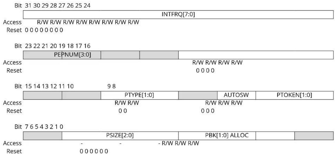
text_image
Bit 31 30 29 28 27 26 25 24 INTFRQ[7:0] Access R/W R/W R/W R/W R/W R/W R/W Reset 0 0 0 0 0 0 0 0 Bit 23 22 21 20 19 18 17 16 PEPNUM[3:0] R/W R/W R/W R/W R/W R/W R/W R/W Reset 0 0 0 0 Bit 15 14 13 12 11 10 9 8 PTYPE[1:0] AUTOSW PTOKEN[1:0] Access R/W R/W R/W Reset 0 0 0 0 0 Bit 7 6 5 4 3 2 1 0 PSIZE[2:0] PBK[1:0] ALLOCBits 31:24 - INTFRQ[7:0] Pipe Interrupt Request Frequency
This field contains the maximum value in milliseconds of the polling period for an Interrupt Pipe.
This value has no effect for a non-Interrupt Pipe.
This field is cleared upon sending a USB reset.
Bits 19:16 - PEPNUM[3:0] Pipe Endpoint Number
This field contains the number of the endpoint targeted by the pipe. This value is from 0 to 9.
This field is cleared upon sending a USB reset.
Bits 13:12 - PTYPE[1:0] Pipe Type
This field contains the pipe type.
This field is cleared upon sending a USB reset.
| Value | Name | Description |
| 0 | CTRL | Control |
| 1 | ISO | Isochronous |
| 2 | BLK | Bulk |
| 3 | INTRPT | Interrupt |
Bit 10 - AUTOSW Automatic Switch
This bit is cleared upon sending a USB reset.
| Value | Description |
| 0 | The automatic bank switching is disabled. |
| 1 | The automatic bank switching is enabled. |
Bits 9:8 - PTOKEN[1:0] Pipe Token
This field contains the pipe token.
| Value Name | Description | |
| 0 | SETUP SETUP | |
| 1 | IN IN | |
| 2 | OUT OUT | |
| 3 | - Reserved | |
Bits 6:4 - PSIZE[2:0] Pipe Size
This field contains the size of each pipe bank.
This field is cleared upon sending a USB reset.
| Value Name | Description | |
| 0 | 8_BYTE 8 bytes | |
| 1 | 16_BYTE 16 bytes | |
| 2 | 32_BYTE 32 bytes | |
| 3 | 64_BYTE 64 bytes | |
| 4 | 128_BYTE 128 bytes | |
| 5 | 256_BYTE 256 bytes | |
| 6 | 512_BYTE 512 bytes | |
| 7 | 1024_BYTE 1024 bytes | |
Bits 3:2 - PBK[1:0] Pipe Banks
This field contains the number of banks for the pipe.
For control pipes, a single-bank pipe (0b00) should be selected.
This field is cleared upon sending a USB reset.
| Value Name | Description | |
| 0 | 1_BANK Single-bank pipe | |
| 1 | 2_BANK Double-bank pipe | |
| 2 | 3_BANK Triple-bank pipe | |
| 3 | - Reserved |
Bit 1 - ALLOC Pipe Memory Allocate
This bit is cleared when a USB Reset is requested.
Refer to "DPRAM Management" for more details.
| Value Description | |
| 0 | Frees the pipe memory. |
| 1 | Allocates the pipe memory. |
38.7.44 Host Pipe x Configuration Register (High-speed Bulk-out or High-speed Control Pipe)
Name: USBHS_HSTPIPCFGx (HSBOHSCP)
Offset: 0x0500 + x*0x04 [x=0..8]
Reset: 0
Property: Read/Write
This configuration is relevant only if PTYPE = 0x0 or 0x2 in "Host Pipe x Configuration Register".
Bit 31 30 29 28 27 26 25 24
| BINTERVAL[7:0] | |
| Access | R/W R/W R/W R/W R/W R/W R/W R/W |
| Reset | 0 0 0 0 0 0 0 |
Bit 23 22 21 20 19 18 17 16
| PINGEN | PEPNUM[3:0] | ||
| Access | R/W R/W R/W R/W R/W | ||
| Reset | 0 0 0 0 0 | ||
Bit 15 14 13 12 11 10 98
| PTYPE[1:0] | AUTOSW | PTOKEN[1:0] | |||
| Access Reset | R/W R/W 0 0 | R/W R/W R/W 0 0 0 |
Bit 76543210
| PSIZE[2:0] | PBK[1:0] ALLOC | |||
| Access | R/W R/W R/W R/W R/W R/W | |||
| Reset | 0 0 0 0 0 0 | |||
Bits 31:24 - BINTERVAL[7:0] bInterval Parameter for the Bulk-Out/Ping Transaction
This field contains the Ping/Bulk-out period.
- If BINTERVAL > 0 and PINGEN = 1, one PING token is sent every blInterval microframe until it is ACKed by the peripheral.
- If BINTERVAL = 0 and PINGEN = 1, multiple consecutive PING tokens are sent in the same microframe until they are ACKed.
- If BINTERVAL > 0 and PINGEN = 0, one OUT token is sent every blinterval microframe until it is ACKed by the peripheral.
- If BINTERVAL = 0 and PINGEN = 0, multiple consecutive OUT tokens are sent in the same microframe until they are ACKed.
This value must be in the range from 0 to 255.
Bit 20 - PINGEN Ping Enable
This bit is relevant for High-speed Bulk-out transaction only (including the control data stage and the control status stage).
This bit is cleared upon sending a USB reset.
| Value | Description |
| 0 | Disables the ping protocol. |
| 1 | Enables the ping mechanism according to the USB 2.0 Standard. |
Bits 19:16 - PEPNUM[3:0] Pipe Endpoint Number
This field contains the number of the endpoint targeted by the pipe. This value is from 0 to 9. This field is cleared upon sending a USB reset.
Bits 13:12 - PTYPE[1:0] Pipe Type
This field contains the pipe type.
This field is cleared upon sending a USB reset.
| Value Name | Description | |
| 0 | CTRL Control | |
| 1 | Reserved | |
| 2 | BLK | Bulk |
| 3 | Reserved | |
Bit 10 - AUTOSW Automatic Switch
This bit is cleared upon sending a USB reset.
| Value Description | |
| 0 | The automatic bank switching is disabled. |
| 1 | The automatic bank switching is enabled. |
Bits 9:8 - PTOKEN[1:0] Pipe Token
This field contains the pipe token.
| Value Name | Description | |
| 0 | SETUP SETUP | |
| 1 | IN IN | |
| 2 | OUT OUT | |
| 3 | Reserved | |
Bits 6:4 - PSIZE[2:0] Pipe Size
This field contains the size of each pipe bank.
This field is cleared upon sending a USB reset.
| Value Name | Description | |
| 0 | 8_BYTE 8 bytes | |
| 1 | 16_BYTE 16 bytes | |
| 2 | 32_BYTE 32 bytes | |
| 3 | 64_BYTE 64 bytes | |
| 4 | 128_BYTE 128 bytes | |
| 5 | 256_BYTE 256 bytes | |
| 6 | 512_BYTE 512 bytes | |
| 7 | 1024_BYTE 1024 bytes |
Bits 3:2 - PBK[1:0] Pipe Banks
This field contains the number of banks for the pipe.
For control pipes, a single-bank pipe (0b00) should be selected.
This field is cleared upon sending a USB reset.
| Value Name | Description | |
| 0 | 1_BANK Single-bank pipe | |
| 1 | 2_BANK Double-bank pipe | |
| 2 | 3_BANK Triple-bank pipe | |
| 3 | Reserved | |
Bit 1 - ALLOC Pipe Memory Allocate
This bit is cleared when a USB Reset is requested.
Refer to "DPRAM Management" for more details.
| Value Description | |
| 0 | Frees the pipe memory. |
| 1 | Allocates the pipe memory. |
38.7.45 Host Pipe x Status Register (Control, Bulk Pipes)
Name: USBHS_HSTPIPISRx
Offset: 0x0530 + x*0x04 [x=0..8]
Reset: 0
Property: Read/Write
This register view is relevant only if PTYPE = 0x0 or 0x2 in "Host Pipe x Configuration Register".
Bit 31 30 29 28 27 26 25 24
| PBYCT[10:4] | |
| Access | R/W R/W R/W R/W R/W R/W R/W |
| Reset 0 0 0 0 0 0 | |
Bit 23 22 21 20 19 18 17 16
| PBYCT[3:0] | CFGOK | RWALL | ||||
| Access | R/W | R/W R/W | R/W | R/W | ||
| Reset | 0 | 0 | 0 | 0 | ||
Bit 15 14 13 12 11 10 98
| CURRBK[1:0] | NBUSYBK[1:0] | DTSEQ[1:0] | |||
| Access | R/W R/W R/W R/W | R/W R/W | |||
| Reset | 0 0 0 0 | 0 0 | |||
Bit 76543210
| SHORTPACKETI | RXSTALLDI | OVERFI | NAKEDI | PERRI | TXSTPI | TXOUTI | RXINI | |
| Access | R/W R/W | R/W R/W | R/W R/W | R/W R/W R/W | ||||
| Reset | 0 0 0 0 0 0 0 | |||||||
Bits 30:20 - PBYCT[10:0] Pipe Byte Count
This field contains the byte count of the FIFO.
For an OUT pipe, the field is incremented after each byte written by the user into the pipe and decremented after each byte sent to the peripheral.
For an IN pipe, the field is incremented after each byte received from the peripheral and decremented after each byte read by the user from the pipe.
This field may be updated 1 clock cycle after the RWALL bit changes, so the user should not poll this field as an interrupt bit.
Bit 18 - CFGOK Configuration OK Status
This bit is set/cleared when the USBHS_HSTPIPCFGx.ALLOC bit is set.
This bit is set if the pipe x number of banks (USBHS_HSTPIPCFGx.PBK) and size
(USBHS_HSTPIPCFGx.PSIZE) are correct compared to the maximal allowed number of banks and size for this pipe and to the maximal FIFO size (i.e., the DPRAM size).
If this bit is cleared, the user should rewrite correct values for the PBK and PSIZE fields in the USBHS_HSTPIPCFGx register.
Bit 16 - RWALL Read/Write Allowed
For an OUT pipe, this bit is set when the current bank is not full, i.e., the software can write further data into the FIFO.
For an IN pipe, this bit is set when the current bank is not empty, i.e., the software can read further data from the FIFO.
This bit is cleared otherwise.
This bit is also cleared when the RXSTALLDI or the PERRI bit = 1.
Bits 15:14 - CURRBK[1:0] Current Bank
For non-control pipe, this field indicates the number of the current bank.
This field may be updated 1 clock cycle after the RWALL bit changes, so the user should not poll it as an interrupt bit.
| Value Name | Description | |
| 0 | BANK0 Current bank is bank0 | |
| 1 | BANK1 Current bank is bank1 | |
| 2 | BANK2 Current bank is bank2 | |
| 3 | Reserved | |
Bits 13:12 - NBUSYBK[1:0] Number of Busy Banks
This field indicates the number of busy banks.
For an OUT pipe, this field indicates the number of busy banks, filled by the user, ready for OUT transfer. When all banks are busy, this triggers a PEP_x interrupt if USBHS_HSTPIPIMRx.NBUSYBKE = 1.
For an IN pipe, this field indicates the number of busy banks filled by IN transaction from the Device. When all banks are free, this triggers a PEP_x interrupt if USBHS_HSTPIPIMRx.NBUSYBKE = 1.
| Value Name | Description |
| 0 | 0_BUSY 0 busy bank (all banks free) |
| 1 | 1_BUSY 1 busy bank |
| 2 | 2_BUSY 2 busy banks |
| 3 | 3_BUSY 3 busy banks |
Bits 9:8 - DTSEQ[1:0] Data Toggle Sequence
This field indicates the data PID of the current bank.
For an OUT pipe, this field indicates the data toggle of the next packet that is to be sent.
For an IN pipe, this field indicates the data toggle of the received packet stored in the current bank.
| Value Name | Description | |
| 0 | DATA0 Data0 toggle sequence | |
| 1 | DATA1 Data1 toggle sequence | |
| 2 | Reserved | |
| 3 | Reserved | |
Bit 7 - SHORTPACKETI Short Packet Interrupt
| Value Description | |
| 0 | Cleared when USBHS_HSTPIPICR.SHORTPACKETIC = 1. |
| 1 | Set when a short packet is received by the host controller (packet length inferior to the PSIZE programmed field). |
Bit 6 - RXSTALLDI Received STALLed Interrupt
This bit is set when a STALL handshake has been received on the current bank of the pipe. The pipe is automatically frozen. This triggers an interrupt if USBHS_HSTPIPIMR.RXSTALLE = 1.
| Value Description | |
| 0 | Cleared when USBHS_HSTPIPICR.RXSTALLDIC = 1. |
Bit 5 - OVERFI Overflow Interrupt
| Value Description | |
| 0 | Cleared when USBHS_HSTPIPICR.OVERFIC = 1. |
| 1 | Set when the current pipe has received more data than the maximum length of the current pipe. An interrupt is triggered if USBHS_HSTPIPIMR.OVERFIE = 1. |
Bit 4 - NAKEDI NAKed Interrupt
| Value Description | |
| 0 | Cleared when USBHS_HSTPIPICR.NAKEDIC = 1. |
| 1 | Set when a NAK has been received on the current bank of the pipe. This triggers an interrupt if USBHS_HSTPIPIMR.NAKEDE = 1. |
Bit 3 - PERRI Pipe Error Interrupt
| Value Description | |
| 0 | Cleared when the error source bit is cleared. |
| 1 | Set when an error occurs on the current bank of the pipe. This triggers an interrupt if the USBHS_HSTPIPIMR.PERRE bit is set. Refer to the USBHS_HSTPIPERRx register to determine the source of the error. |
Bit 2 - TXSTPI Transmitted SETUP Interrupt
| Value Description | |
| 0 | Cleared when USBHS_HSTPIPICR.TXSTPIC = 1. |
| 1 | Set, for control pipes, when the current SETUP bank is free and can be filled. This triggers an interrupt if USBHS_HSTPIPIMR.TXSTPE = 1. |
Bit 1 - TXOUTI Transmitted OUT Data Interrupt
| Value Description | |
| 0 | Cleared when USBHS_HSTPIPICR.TXOUTIC = 1. |
| 1 | Set when the current OUT bank is free and can be filled. This triggers an interrupt if USBHS_HSTPIPIMR.TXOUTE = 1. |
Bit 0 - RXINI Received IN Data Interrupt
| Value Description | |
| 0 | Cleared when USBHS_HSTPIPICR.RXINIC = 1. |
| 1 | Set when a new USB message is stored in the current bank of the pipe. This triggers an interrupt if USBHS_HSTPIPIMR.RXINE = 1. |
38.7.46 Host Pipe x Status Register (Interrupt Pipes)
Name: USBHS_HSTPIPISRx (INTPIPES)
Offset: 0x0530 + x*0x04 [x=0..8]
Reset: 0
Property: Read/Write
This register view is relevant only if PTYPE = 0x3 in "Host Pipe x Configuration Register".
Bit 31 30 29 28 27 26 25 24
| PBYCT[10:4] | |
| Access | R/W R/W R/W R/W R/W R/W R/W |
| Reset 0 0 0 0 0 0 | |
Bit 23 22 21 20 19 18 17 16
| PBYCT[3:0] | CFGOK | RWALL | ||||
| Access | R/W | R/W | R/W | R/W | ||
| Reset | 0 | 0 | 0 | 0 | ||
Bit 15 14 13 12 11 10 98
| CURRBK[1:0] | NBUSYBK[1:0] | DTSEQ[1:0] | |||
| Access | R/W R/W R/W R/W | R/W R/W | |||
| Reset | 0 0 0 0 | 0 0 | |||
Bit 76543210
| SHORTPACKETI | RXSTALLDI | OVERFI | NAKEDI | PERRI | UNDERFI | TXOUTI | RXINI | |
| Access | R/W R/W | R/W R/W | R/W R/W | R/W R/W R/W | ||||
| Reset | 0 0 0 0 0 0 0 | |||||||
Bits 30:20 - PBYCT[10:0] Pipe Byte Count
This field contains the byte count of the FIFO.
For an OUT pipe, the field is incremented after each byte written by the user into the pipe and decremented after each byte sent to the peripheral.
For an IN pipe, the field is incremented after each byte received from the peripheral and decremented after each byte read by the user from the pipe.
This field may be updated 1 clock cycle after the RWALL bit changes, so the user should not poll this field as an interrupt bit.
Bit 18 - CFGOK Configuration OK Status
This bit is set/cleared when the USBHS_HSTPIPCFGx.ALLOC bit is set.
This bit is set if the pipe x number of banks (USBHS_HSTPIPCFGx.PBK) and size
(USBHS_HSTPIPCFGx.PSIZE) are correct compared to the maximal allowed number of banks and size for this pipe, and to the maximal FIFO size (i.e., the DPRAM size).
If this bit is cleared, the user should rewrite correct values for the PBK and PSIZE fields in the USBHS_HSTPIPCFGx register.
Bit 16 - RWALL Read/Write Allowed
For an OUT pipe, this bit is set when the current bank is not full, i.e., the software can write further data into the FIFO.
For an IN pipe, this bit is set when the current bank is not empty, i.e., the software can read further data from the FIFO.
This bit is cleared otherwise.
This bit is also cleared when RXSTALLDI or PERRI = 1.
Bits 15:14 - CURRBK[1:0] Current Bank
For a non-control pipe, this field indicates the number of the current bank.
This field may be updated 1 clock cycle after the RWALL bit changes, so the user should not poll it as an interrupt bit.
| Value Name | Description | |
| 0 | BANK0 Current bank is bank0 | |
| 1 | BANK1 Current bank is bank1 | |
| 2 | BANK2 Current bank is bank2 | |
| 3 | Reserved | |
Bits 13:12 - NBUSYBK[1:0] Number of Busy Banks
This field indicates the number of busy banks.
For an OUT pipe, this field indicates the number of busy banks, filled by the user, ready for an OUT transfer. When all banks are busy, this triggers a PEP_x interrupt if USBHS_HSTPIPIMRx.NBUSYBKE = 1.
For an IN pipe, this field indicates the number of busy banks filled by IN transaction from the device. When all banks are free, this triggers a PEP_x interrupt if USBHS_HSTPIPIMRx.NBUSYBKE = 1.
| Value Name | Description |
| 0 | 0_BUSY 0 busy bank (all banks free) |
| 1 | 1_BUSY 1 busy bank |
| 2 | 2_BUSY 2 busy banks |
| 3 | 3_BUSY 3 busy banks |
Bits 9:8 - DTSEQ[1:0] Data Toggle Sequence
This field indicates the data PID of the current bank.
For an OUT pipe, this field indicates the data toggle of the next packet that is to be sent.
For an IN pipe, this field indicates the data toggle of the received packet stored in the current bank.
| Value Name | Description | |
| 0 | DATA0 Data0 toggle sequence | |
| 1 | DATA1 Data1 toggle sequence | |
| 2 | Reserved | |
| 3 | Reserved | |
Bit 7 - SHORTPACKETI Short Packet Interrupt
| Value Description | |
| 0 | Cleared when USBHS_HSTPIPICR.SHORTPACKETIC = 1. |
| 1 | Set when a short packet is received by the host controller (packet length inferior to the PSIZE programmed field). |
Bit 6 - RXSTALLDI Received STALLed Interrupt
| Value Description | |
| 0 | Cleared when USBHS_HSTPIPICR.RXSTALLDIC = 1. |
| 1 | Set when a STALL handshake has been received on the current bank of the pipe. The pipe is automatically frozen. This triggers an interrupt if USBHS_HSTPIPIMR.RXSTALLE = 1. |
Bit 5 - OVERFI Overflow Interrupt
| Value Description | |
| 0 | Cleared when USBHS_HSTPIPICR.OVERFIC = 1. |
| 1 | Set when the current pipe has received more data than the maximum length of the current pipe. An interrupt is triggered if the USBHS_HSTPIPIMR.OVERFIE bit = 1. |
Bit 4 - NAKEDI NAKed Interrupt
| Value Description | |
| 0 | Cleared when USBHS_HSTPIPICR.NAKEDIC = 1. |
| 1 | Set when a NAK has been received on the current bank of the pipe. This triggers an interrupt if the USBHS_HSTPIPIMR.NAKEDE bit = 1. |
Bit 3 - PERRI Pipe Error Interrupt
| Value Description | |
| 0 | Cleared when the error source bit is cleared. |
| 1 | Set when an error occurs on the current bank of the pipe. This triggers an interrupt if the USBHS_HSTPIPIMR.PERRE bit is set. Refer to the USBHS_HSTPIPERRx register to determine the source of the error. |
Bit 2 - UNDERFI Underflow Interrupt
This bit is set, for an isochronous and interrupt IN/OUT pipe, when an error flow occurs. This triggers an interrupt if UNDERFIE = 1.
This bit is set, for an isochronous or interrupt OUT pipe, when a transaction underflow occurs in the current pipe (the pipe cannot send the OUT data packet in time because the current bank is not ready). A zero-length-packet (ZLP) is sent instead.
This bit is set, for an isochronous or interrupt IN pipe, when a transaction flow error occurs in the current pipe, i.e., the current bank of the pipe is not free while a new IN USB packet is received. This packet is not stored in the bank. For an interrupt pipe, the overflowed packet is ACKed to comply with the USB standard.
This bit is cleared when USBHS_HSTPIPICR.UNDERFIEC = 1.
Bit 1 - TXOUTI Transmitted OUT Data Interrupt
| Value Description | |
| 0 | Cleared when USBHS_HSTPIPICR.TXOUTIC = 1. |
| 1 | Set when the current OUT bank is free and can be filled. This triggers an interrupt if USBHS_HSTPIPIMR.TXOUTE = 1. |
Bit 0 - RXINI Received IN Data Interrupt
| Value Description | |
| 0 | Cleared when USBHS_HSTPIPICR.RXINIC = 1. |
| 1 | Set when a new USB message is stored in the current bank of the pipe. This triggers an interrupt if the USBHS_HSTPIPIMR.RXINE bit = 1. |
38.7.47 Host Pipe x Status Register (Isochronous Pipes)
Name: USBHS_HSTPIPISRx (ISOPIPES)
Offset: 0x0530 + x*0x04 [x=0..8]
Reset: 0
Property: Read/Write
This register view is relevant only if PTYPE = 0x1 in "Host Pipe x Configuration Register".
Bit 31 30 29 28 27 26 25 24
| PBYCT[10:4] | |
| Access | R/W R/W R/W R/W R/W R/W R/W |
| Reset 0 0 0 0 0 0 | |
Bit 23 22 21 20 19 18 17 16
| PBYCT[3:0] | CFGOK | RWALL | ||||
| Access | R/W | R/W | R/W | R/W | ||
| Reset | 0 | 0 | 0 | 0 | ||
Bit 15 14 13 12 11 10 98
| CURRBK[1:0] | NBUSYBK[1:0] | DTSEQ[1:0] | |||
| Access | R/W R/W R/W R/W | R/W R/W | |||
| Reset | 0 0 0 0 | 0 0 | |||
Bit 76543210
| SHORTPACKETI | CRCERRI | OVERFI | NAKEDI | PERRI | UNDERFI | TXOUTI | RXINI | |
| Access | R/W R/W | R/W R/W | R/W R/W | R/W R/W R/W | ||||
| Reset | 0 0 0 0 0 0 0 | |||||||
Bits 30:20 - PBYCT[10:0] Pipe Byte Count
This field contains the byte count of the FIFO.
For an OUT pipe, the field is incremented after each byte written by the user into the pipe and decremented after each byte sent to the peripheral.
For an IN pipe, the field is incremented after each byte received from the peripheral and decremented after each byte read by the user from the pipe.
This field may be updated 1 clock cycle after the RWALL bit changes, so the user should not poll this field as an interrupt bit.
Bit 18 - CFGOK Configuration OK Status
This bit is set/cleared when the USBHS_HSTPIPCFGx.ALLOC bit is set.
This bit is set if the pipe x number of banks (USBHS_HSTPIPCFGx.PBK) and size
(USBHS_HSTPIPCFGx.PSIZE) are correct compared to the maximal allowed number of banks and size for this pipe and to the maximal FIFO size (i.e., the DPRAM size).
If this bit is cleared, the user should rewrite correct values for the PBK and PSIZE fields in the USBHS_HSTPIPCFGx register.
Bit 16 - RWALL Read/Write Allowed
For an OUT pipe, this bit is set when the current bank is not full, i.e., the software can write further data into the FIFO.
For an IN pipe, this bit is set when the current bank is not empty, i.e., the software can read further data from the FIFO.
This bit is cleared otherwise.
This bit is also cleared when the RXSTALLDI or the PERRI bit = 1.
Bits 15:14 - CURRBK[1:0] Current Bank
For a non-control pipe, this field indicates the number of the current bank.
This field may be updated 1 clock cycle after the RWALL bit changes, so the user should not poll it as an interrupt bit.
| Value Name | Description | |
| 0 | BANK0 Current bank is bank0 | |
| 1 | BANK1 Current bank is bank1 | |
| 2 | BANK2 Current bank is bank2 | |
| 3 | Reserved | |
Bits 13:12 - NBUSYBK[1:0] Number of Busy Banks
This field indicates the number of busy banks.
For an OUT pipe, this field indicates the number of busy banks, filled by the user, ready for an OUT transfer. When all banks are busy, this triggers a PEP_x interrupt if USBHS_HSTPIPIMRx.NBUSYBKE = 1.
For an IN pipe, this field indicates the number of busy banks filled by IN transaction from the device. When all banks are free, this triggers a PEP_x interrupt if USBHS_HSTPIPIMRx.NBUSYBKE = 1.
| Value Name | Description |
| 0 | 0_BUSY 0 busy bank (all banks free) |
| 1 | 1_BUSY 1 busy bank |
| 2 | 2_BUSY 2 busy banks |
| 3 | 3_BUSY 3 busy banks |
Bits 9:8 - DTSEQ[1:0] Data Toggle Sequence
This field indicates the data PID of the current bank.
For an OUT pipe, this field indicates the data toggle of the next packet that is to be sent.
For an IN pipe, this field indicates the data toggle of the received packet stored in the current bank.
| Value Name | Description | |
| 0 | DATA0 Data0 toggle sequence | |
| 1 | DATA1 Data1 toggle sequence | |
| 2 | Reserved | |
| 3 | Reserved | |
Bit 7 - SHORTPACKETI Short Packet Interrupt
| Value Description | |
| 0 | Cleared when USBHS_HSTPIPICR.SHORTPACKETIC = 1. |
| 1 | Set when a short packet is received by the host controller (packet length inferior to the PSIZE programmed field). |
Bit 6 - CRCERRI CRC Error Interrupt
| Value Description | |
| 0 | Cleared when USBHS_HSTPIPICR.CRCERRIC = 1. |
| 1 | Set when a CRC error occurs on the current bank of the pipe. This triggers an interrupt if the USBHS_HSTPIPIMR.TXSTPE bit = 1. |
Bit 5 - OVERFI Overflow Interrupt
| Value Description | |
| 0 | Cleared when USBHS_HSTPIPICR.OVERFIC = 1. |
| 1 | Set when the current pipe has received more data than the maximum length of the current pipe. An interrupt is triggered if the USBHS_HSTPIPIMR.OVERFIE bit = 1. |
Bit 4 - NAKEDI NAKed Interrupt
| Value Description | |
| 0 | Cleared when USBHS_HSTPIPICR.NAKEDIC = 1. |
| 1 | Set when a NAK has been received on the current bank of the pipe. This triggers an interrupt if the USBHS_HSTPIPIMR.NAKEDE bit = 1. |
Bit 3 - PERRI Pipe Error Interrupt
| Value Description | |
| 0 | Cleared when the error source bit is cleared. |
| 1 | Set when an error occurs on the current bank of the pipe. This triggers an interrupt if the USBHS_HSTPIPIMR.PERRE bit is set. Refer to the USBHS_HSTPIPERRx register to determine the source of the error. |
Bit 2 - UNDERFI Underflow Interrupt
This bit is set, for an isochronous and interrupt IN/OUT pipe, when an error flow occurs. This triggers an interrupt if the UNDERFIE bit = 1.
This bit is set, for an isochronous or interrupt OUT pipe, when a transaction underflow occurs in the current pipe (the pipe cannot send the OUT data packet in time because the current bank is not ready). A zero-length-packet (ZLP) is sent instead.
This bit is set, for an isochronous or interrupt IN pipe, when a transaction flow error occurs in the current pipe, i.e., the current bank of the pipe is not free while a new IN USB packet is received. This packet is not stored in the bank. For an interrupt pipe, the overflowed packet is ACKed to comply with the USB standard.
This bit is cleared when USBHS_HSTPIPICR.UNDERFIEC = 1.
Bit 1 - TXOUTI Transmitted OUT Data Interrupt
| Value Description | |
| 0 | Cleared when USBHS_HSTPIPICR.TXOUTIC = 1. |
| 1 | Set when the current OUT bank is free and can be filled. This triggers an interrupt if USBHS_HSTPIPIMR.TXOUTE = 1. |
Bit 0 - RXINI Received IN Data Interrupt
| Value Description | |
| 0 | Cleared when USBHS_HSTPIPICR.RXINIC = 1. |
| 1 | Set when a new USB message is stored in the current bank of the pipe. This triggers an interrupt if USBHS_HSTPIPIMR.RXINE = 1. |
38.7.48 Host Pipe x Clear Register (Control, Bulk Pipes)
Name: USBHS_HSTPIPICRx
Offset: 0x0560 + x*0x04 [x=0..8]
Reset: 0
Property: Read/Write
This register view is relevant only if PTYPE = 0x0 or 0x2 in "Host Pipe x Configuration Register".
For additional information, see "Host Pipe x Status Register (Control, Bulk Pipes)".
This register always reads as zero.
The following configuration values are valid for all listed bit names of this register:
0: No effect.
1: Clears the corresponding bit in USBHS_HSTPIPISRx.

Bit 7 - SHORTPACKETIC Short Packet Interrupt Clear
Bit 6 - RXSTALLDIC Received STALLed Interrupt Clear
Bit 5 - OVERFIC Overflow Interrupt Clear
Bit 4 - NAKEDIC NAKed Interrupt Clear
Bit 2 - TXSTPIC Transmitted SETUP Interrupt Clear
Bit 1 - TXOUTIC Transmitted OUT Data Interrupt Clear
Bit 0 - RXINIC Received IN Data Interrupt Clear
38.7.49 Host Pipe x Clear Register (Interrupt Pipes)
Name: USBHS_HSTPIPICRx (INTPIPES)
Offset: 0x0560 + x*0x04 [x=0..8]
Reset: 0
Property: Read/Write
This register view is relevant only if PTYPE = 0x3 in "Host Pipe x Configuration Register".
For additional information, see "Host Pipe x Status Register (Interrupt Pipes)".
This register always reads as zero.
The following configuration values are valid for all listed bit names of this register:
0: No effect.
1: Clears the corresponding bit in USBHS_HSTPIPISRx.

Bit 7 - SHORTPACKETIC Short Packet Interrupt Clear
Bit 6 - RXSTALLDIC Received STALLed Interrupt Clear
Bit 5 - OVERFIC Overflow Interrupt Clear
Bit 4 - NAKEDIC NAKed Interrupt Clear
Bit 2 - UNDERFIC Underflow Interrupt Clear
Bit 1 - TXOUTIC Transmitted OUT Data Interrupt Clear
Bit 0 - RXINIC Received IN Data Interrupt Clear
38.7.50 Host Pipe x Clear Register (Isochronous Pipes)
Name: USBHS_HSTPIPICRx (ISOPIPES)
Offset: 0x0560 + x*0x04 [x=0..8]
Reset: 0
Property: Read/Write
This register view is relevant only if PTYPE = 0x1 in "Host Pipe x Configuration Register".
For additional information, see "Host Pipe x Status Register (Isochronous Pipes)".
This register always reads as zero.
The following configuration values are valid for all listed bit names of this register:
0: No effect.
1: Clears the corresponding bit in USBHS_HSTPIPISRx.

bar_stacked
| Bit | SHORTPACKETIC | CRCERRIC | OVERFIC | NAKEDIC | UNDERFIC | TXOUTIC | RXINIC | |-----|----------------|----------|---------|---------|-----------|---------|--------| | 31 | 0 | 0 | 0 | 0 | 0 | 0 | 0 | | 30 | 0 | 0 | 0 | 0 | 0 | 0 | 0 | | 29 | 0 | 0 | 0 | 0 | 0 | 0 | 0 | | 28 | 0 | 0 | 0 | 0 | 0 | 0 | 0 | | 27 | 0 | 0 | 0 | 0 | 0 | 0 | 0 | | 26 | 0 | 0 | 0 | 0 | 0 | 0 | 0 | | 25 | 0 | 0 | 0 | 0 | 0 | 0 | 0 | | 24 | 0 | 0 | 0 | 0 | 0 | 0 | 0 | | 23 | 0 | 0 | 0 | 0 | 0 | 0 | 0 | | 22 | 0 | 0 | 0 | 0 | 0 | 0 | 0 | | 21 | 0 | 0 | 0 | 0 | 0 | 0 | 0 | | 20 | 0 | 0 | 0 | 0 | 0 | 0 | 0 | | 19 | 0 | 0 | 0 | 0 | 0 | 0 | 0 | | 18 | 0 | 0 | 0 | 0 | 0 | 0 | 0 | | 17 | 0 | 0 | 0 | 0 | 0 | 0 | 0 | | 16 | 0 | 0 | 0 | 0 | 0 | 0 | 0 | | 15 | 0 | 0 | 0 | 0 | 0 | 0 | 0 | | 14 | 0 | 0 | 0 | 0 | 0 | 0 | 0 | | 13 | 0 | 0 | 0 | 0 | 0 | 0 | 0 | | 12 | 0 | 0 | 0 | 0 | 0 | 0 | 0 | | 11 | 0 | 0 | 0 | 0 | 0 | 0 | 0 | | 10 | 0 | 0 | 0 | 0 | 0 | 0 | 0 | | 9 | - | - | - | - | - | - | - | | - | - | - | - | - | - | - | - | | - | - | - | - | - | - | - | - | | - | - | - | - | - | - | - | - | | - | - | - | - | - | - | - | - | | + = ShortPACKETIC / OverFIC / NAKEDIC / UNDERFIC / TXOUTIC / RXINIC / ShortPACKETIC / OverFIC / NAKEDIC / UNDERFIC / TXOUTIC / RXINIC / ShortPACKETIC / OverFIC / NAKEDIC / UNDERFIC / TXOUTIC / RXINIC / ShortPACKETIC / OverFIC / NAKEDIC / UnderFIC / TXOUTIC / RXINIC / ShortPACKETIC / OverFIC / NAKEDIC / UnderFIC / TXOUTIC / RXINIC / ShortPACKETIC / OverFIC / NAKEDIC / UnderFIC / TXOUTIC / RXINIC / ShortPACKETIC / OverFIC / NAKEDIC / UnderFIC / TXOUTIC / RXINIC / ShortPACKETIC / OverFIC / NOK | | + = ShortPACKETIC / OverFIC / NAKEDIC / UNDERFIC / TXOUTIC / RXINIC / ShortPACKETIC / OverFIC / NAKEDIC / UNDERFIC / TXOUTIC / RXINIC / ShortPACKETIC / OverFIC / NAKEDIC / UnderFIC / TXOUTIC / RXINIC / ShortPACKETIC / OverFIC / NOK | | + = ShortPACKETIC / OverFIC / NAKEDIC / UNDERFIC / TXOUTIC / RXINIC / ShortPACKETIC / OverFIC / NAKEDIC / UNDERFIC / TX OUTC | | + = ShortPACKETIC / OverFIC / NAKEDIC / UNDERFIC / TXOUTC | | + = ShortPACKETIC / OverFIC / NAKEDIC / UNDERFIC / TXOUTC | | + = ShortPACKETIC / OverFIC / NAKEDIC / UNDERFIC / TXOUTC | | + = ShortPACKETIC / OverFIC / NAKEDIC / UNDERFIC / TXOUTC | | + = ShortPACKETIC / OverFIC / NAKESO/ NOKO/ RXOUTC | | + = ShortPACKETIC / OverFIC/ NOKO/ RXOUTC | | + = ShortPACKETIC/ OverFIC/ NOKO/ RXOUTC | | + = ShortPACKETIC/ OverFIC/ NOKO/ RXOUTC | | + = ShortPACKETI/C/ OverFIC/ NOKO/ RXOUTC | | + = ShortPACKETI/C/ OverFIC/ NOKO/ RXOUTC | | + = ShortPACKETI/C/ OverFIC/ NOKO/ RXOUTC | | + = ShortPACKETI/C/ OverFIC/ NOKO/ RXOUTC | | + = ShortPACKETI/C/ OverFIC/ NOKC/ RXOUTC | | + = ShortPACKETI/C/ OverFIC/ NOKC/ RXOUTC | | + = ShortPACKETI/C/ OverFIC/ NOKC/ RXOUTC | | + = ShortPACKETI/C/ OverFIC/ NOKC/ RXOUTC | | + = ShortPACKETI/C/ OverFIC/ NOKC/ RXOUTC | | - = ShortPACKETI/C/ OverFIC/ NOKC/ RXOUTC | | - = ShortPACKETI/C/ OverFIC/ NOKC/ RXOUTC | | - = ShortPACKETI/C/ OverFIC/ NOKC/ RXOUTC | | - = ShortPACKETI/C/ OverFIC/ NOKC/ RXOUTC | | - = ShortPACKETI/C/TICA/ OverFIC/ NOKC/ RXOUTC | | - = ShortPACKETI/C/TICA/ OverFIC/ NOKC/ RXOUTC | | - = ShortPACKETI/C/TICA/TICA/ OverFIC/ NOKC/TICA/ RXOUTC | | - = ShortPACKETI/C/TICA/TICA/TICA/TICA/TICA/TICA/TICA/TICA/TICA/TICA/TICA/TICA/TICA/TICA/TICA/TICA/TICA/TICA/TICA/TICA/TICA/TICA/TICA/TICA/TICA/TICA/TICA/TICA/TICA/TICA/TICA/TICA/TICA/TICA/TICA/TICA/TICA/TICA/TICA/TICA/TICA/TICA/TICA/TICA/TICA/TICA/TICA/TICA/TICA/TICA/TACABit 7 - SHORTPACKETIC Short Packet Interrupt Clear
Bit 6 - CRCERRIC CRC Error Interrupt Clear
Bit 5 - OVERFIC Overflow Interrupt Clear
Bit 4 - NAKEDIC NAKed Interrupt Clear
Bit 2 - UNDERFIC Underflow Interrupt Clear
Bit 1 - TXOUTIC Transmitted OUT Data Interrupt Clear
Bit 0 - RXINIC Received IN Data Interrupt Clear
38.7.51 Host Pipe x Set Register (Control, Bulk Pipes)
Name: USBHS_HSTPIPIFRx
Offset: 0x0590
Reset: 0
Property: Read/Write
This register view is relevant only if PTYPE = 0x0 or 0x2 in "Host Pipe x Configuration Register".
For additional information, see "Host Pipe x Status Register (Control, Bulk Pipes)".
This register always reads as zero.
The following configuration values are valid for all listed bit names of this register:
0: No effect.
1: Sets the corresponding bit in USBHS_HSTPIPISRx, which may be useful for test or debug purposes.
text_image
Bit 31 30 29 28 27 26 25 24 Access Reset Bit 23 22 21 20 19 18 17 16 Access Reset Bit 15 14 13 12 11 10 9 8 Access Reset NBUSYBK$ R/W 0 Bit 7 6 5 4 3 2 1 0 SHORTPACKETIS RXSTALLDIS OVERFIS NAKEDIS PERRIS TXSTPIS TXOUTIS RXINIS Access R/W R/W R/W R/W R/W R/W R/W Reset 0 0 0 0 0 0 0Bit 12 - NBUSYBKS Number of Busy Banks Set
Bit 7 - SHORTPACKETIS Short Packet Interrupt Set
Bit 6 - RXSTALLDIS Received STALLed Interrupt Set
Bit 5 - OVERFIS Overflow Interrupt Set
Bit 4 - NAKEDIS NAKed Interrupt Set
Bit 3 - PERRIS Pipe Error Interrupt Set
Bit 2 - TXSTPIS Transmitted SETUP Interrupt Set
Bit 1 - TXOUTIS Transmitted OUT Data Interrupt Set
Bit 0 - RXINIS Received IN Data Interrupt Set
38.7.52 Host Pipe x Set Register (Interrupt Pipes)
Name: USBHS_HSTPIPIFRx (INTPIPES)
Offset: 0x0590 + x*0x04 [x=0..8]
Reset: 0
Property: Read/Write
This register view is relevant only if PTYPE = 0x3 in "Host Pipe x Configuration Register".
For additional information, see "Host Pipe x Status Register (Interrupt Pipes)".
This register always reads as zero.
The following configuration values are valid for all listed bit names of this register:
0: No effect.
1: Sets the corresponding bit in USBHS_HSTPIPISRx, which may be useful for test or debug purposes.

text_image
Bit 31 30 29 28 27 26 25 24 Access Reset Bit 23 22 21 20 19 18 17 16 Access Reset Bit 15 14 13 12 11 10 9 8 Access Reset NBUSYBK$ R/W 0 Bit 7 6 5 4 3 2 1 0 SHORTPACKETIS RXSTALLDIS OVERFIS NAKEDIS PERRIS UNDERFIS TXOUTIS RXINIS Access R/W R/W R/W R/W R/W R/W R/W Reset 0 0 0 0 0 0 0Bit 12 - NBUSYBKS Number of Busy Banks Set
Bit 7 - SHORTPACKETIS Short Packet Interrupt Set
Bit 6 - RXSTALLDIS Received STALLed Interrupt Set
Bit 5 - OVERFIS Overflow Interrupt Set
Bit 4 - NAKEDIS NAKed Interrupt Set
Bit 3 - PERRIS Pipe Error Interrupt Set
Bit 2 - UNDERFIS Underflow Interrupt Set
Bit 1 - TXOUTIS Transmitted OUT Data Interrupt Set
Bit 0 - RXINIS Received IN Data Interrupt Set
38.7.53 Host Pipe x Set Register (Isochronous Pipes)
Name: USBHS_HSTPIPIFRx (ISOPIPES)
Offset: 0x0590 + x*0x04 [x=0..8]
Reset: 0
Property: Read/Write
This register view is relevant only if PTYPE = 0x1 in "Host Pipe x Configuration Register".
For additional information, see "Host Pipe x Status Register (Isochronous Pipes)".
This register always reads as zero.
The following configuration values are valid for all listed bit names of this register:
0: No effect.
1: Sets the corresponding bit in USBHS_HSTPIPISRx, which may be useful for test or debug purposes.

text_image
Bit 31 30 29 28 27 26 25 24 Access Reset Bit 23 22 21 20 19 18 17 16 Access Reset Bit 15 14 13 12 11 10 9 8 Access Reset NBUSYBK$ R/W 0 Bit 7 6 5 4 3 2 1 0 SHORTPACKETIS CRCERRIS OVERFIS NAKEDIS PERRIS UNDERFIS TXOUTIS RXINIS Access Reset R/W R/W R/W R/W R/W R/W R/W 0 0 0 0 0 0 0Bit 12 - NBUSYBKS Number of Busy Banks Set
Bit 7 - SHORTPACKETIS Short Packet Interrupt Set
Bit 6 - CRCERRIS CRC Error Interrupt Set
Bit 5 - OVERFIS Overflow Interrupt Set
Bit 4 - NAKEDIS NAKed Interrupt Set
Bit 3 - PERRIS Pipe Error Interrupt Set
Bit 2 - UNDERFIS Underflow Interrupt Set
Bit 1 - TXOUTIS Transmitted OUT Data Interrupt Set
Bit 0 - RXINIS Received IN Data Interrupt Set
38.7.54 Host Pipe x Mask Register (Control, Bulk Pipes)
Name: USBHS_HSTPIPIMRx
Offset: 0x05C0 + x*0x04 [x=0..8]
Reset: 0
Property: Read/Write
This register view is relevant only if PTYPE = 0x0 or 0x2 in "Host Pipe x Configuration Register".

Bit 18 - RSTDT Reset Data Toggle
| Value | Description |
| 0 | No reset of the Data Toggle is ongoing. |
| 0 | Set when USBHS_HSTPIPIER.RSTDTS = 1. This resets the Data Toggle to its initial value for the current pipe. |
Bit 17 - PFREEZE Pipe Freeze
This freezes the pipe request generation.
| Value | Description |
| 0 | Cleared when USBHS_HSTPIPIDR.PFREEZEC = 1. This enables the pipe request generation. |
| 1 | Set when one of the following conditions is met:• USBHS_HSTPIPIER.PFREEZES=• The pipe is not configured.• A STALL handshake has been received on the pipe.• An error has occurred on the pipe (USBHS_HSTPIPISR.PERRI = 1).• (INRQ+1) In requests have been processed.• A Pipe Reset (USBHS_HSTPIP.PRSTx rising) has occurred.• A Pipe Enable (USBHS_HSTPIP.PEN rising) has occurred. |
Bit 16 - PDISHDMA Pipe Interrupts Disable HDMA Request Enable
See the USBHS_DEVEPTIMR.EPDISHDMA bit description.
Bit 14 - FIFOCON FIFO Control
For OUT and SETUP pipes:
0: Cleared when USBHS_HSTPIPIDR.FIFOCONC = 1. This sends the FIFO data and switches the bank.
1: Set when the current bank is free, at the same time as USBHS_HSTPIPISR.TXOUTI or TXSTPI.
For an IN pipe:
0: Cleared when USBHS_HSTPIPIDR.FIFOCONC = 1. This frees the current bank and switches to the next bank.
1: Set when a new IN message is stored in the current bank, at the same time as
USBHS_HSTPIPISR.RXINI.
Bit 12 - NBUSYBKE Number of Busy Banks Interrupt Enable
| Value Description | |
| 0 | Cleared when USBHS_HSTPIPIDR.NBUSYBKEC = 1. This disables the Transmitted IN Data interrupt (USBHS_HSTPIPIMR.NBUSYBKE). |
| 1 | Set when USBHS_HSTPIPIER.NBUSYBKES = 1. This enables the Transmitted IN Data interrupt (USBHS_HSTPIPIMR.NBUSYBKE). |
Bit 7 - SHORTPACKETIE Short Packet Interrupt Enable
If this bit is set for non-control OUT pipes, a short packet transmission is guaranteed upon ending a DMA transfer, thus signaling an end of transfer, provided that End of DMA Buffer Output Enable (USBHS_HSTDMACONTROL.END_B_EN) and Automatic Switch (USBHS_HSTPIPCFG.AUTOSW) = 1.
| Value Description | |
| 0 | Cleared when USBHS_HSTPIPIDR.SHORTPACKETEC = 1. This disables the Transmitted IN Data IT (USBHS_HSTPIPIMR.SHORTPACKETE). |
| 1 | Set when USBHS_HSTPIPIER.SHORTPACKETIES = 1. This enables the Transmitted IN Data IT (USBHS_HSTPIPIMR.SHORTPACKETIE). |
Bit 6 - RXSTALLDE Received STALLed Interrupt Enable
| Value Description | |
| 0 | Cleared when USBHS_HSTPIPIDR.RXSTALLDEC = 1. This disables the Transmitted IN Data interrupt (USBHS_HSTPIPIMR.RXSTALLDE). |
| 1 | Set when USBHS_HSTPIPIER.RXSTALLDES = 1. This enables the Transmitted IN Data interrupt (USBHS_HSTPIPIMR.RXSTALLDE). |
Bit 5 - OVERFIE Overflow Interrupt Enable
| Value Description | |
| 0 | Cleared when USBHS_HSTPIPIDR.OVERFIEC = 1. This disables the Transmitted IN Data interrupt (USBHS_HSTPIPIMR.OVERFIE). |
| 1 | Set when USBHS_HSTPIPIER.OVERFIES = 1. This enables the Transmitted IN Data interrupt (USBHS_HSTPIPIMR.OVERFIE). |
Bit 4 - NAKEDE NAKed Interrupt Enable
| Value Description | |
| 0 | Cleared when USBHS_HSTPIPIDR.NAKEDEC = 1. This disables the Transmitted IN Data interrupt (USBHS_HSTPIPIMR.NAKEDE). |
| 1 | Set when USBHS_HSTPIPIER.NAKEDES = 1. This enables the Transmitted IN Data interrupt (USBHS_HSTPIPIMR.NAKEDE). |
Bit 3 - PERRE Pipe Error Interrupt Enable
| Value Description | |
| 0 | Cleared when USBHS_HSTPIPIDR.PERREC = 1. This disables the Transmitted IN Data interrupt (USBHS_HSTPIPIMR.PERRE). |
| 1 | Set when USBHS_HSTPIPIER.PERRES = 1. This enables the Transmitted IN Data interrupt (USBHS_HSTPIPIMR.PERRE). |
Bit 2 - TXSTPE Transmitted SETUP Interrupt Enable
| Value Description | |
| 0 | Cleared when USBHS_HSTPIPIDR.TXSTPEC = 1. This disables the Transmitted IN Data interrupt (USBHS_HSTPIPIMR.TXSTPE). |
| Value | Description |
| 1 | Set when USBHS_HSTPIPIER.TXSTPES = 1. This enables the Transmitted IN Data interrupt (USBHS_HSTPIPIMR.TXSTPE). |
Bit 1 - TXOUTE Transmitted OUT Data Interrupt Enable
| Value Description | |
| 0 | Cleared when USBHS_HSTPIPIDR.TXOUTEC = 1. This disables the Transmitted IN Data interrupt (USBHS_HSTPIPIMR.TXOUTE). |
| 1 | Set when USBHS_HSTPIPIER.TXOUTES = 1. This enables the Transmitted IN Data interrupt (USBHS_HSTPIPIMR.TXOUTE). |
Bit 0 - RXINE Received IN Data Interrupt Enable
| Value Description | |
| 0 | Cleared when USBHS_HSTPIPIDR.RXINEC = 1. This disables the Transmitted IN Data interrupt (USBHS_HSTPIPIMR.RXINE). |
| 1 | Set when USBHS_HSTPIPIER.RXINES = 1. This enables the Transmitted IN Data interrupt (USBHS_HSTPIPIMR.RXINE). |
38.7.55 Host Pipe x Mask Register (Interrupt Pipes)
Name: USBHS_HSTPIPIMRx (INTPIPES)
Offset: 0x05C0 + x*0x04 [x=0..8]
Reset: 0
Property: Read/Write
This register view is relevant only if PTYPE = 0x3 in "Host Pipe x Configuration Register".
Bit 31 30 29 28 27 26 25 24
| Access Reset | |||||||
Bit 23 22 21 20 19 18 17 16
| RSTDT PFREEZE | PDISHDMA | ||||||
| Access Reset | R/W | R/W | R/W | ||||
| 0 | 0 | 0 |
Bit 15 14 13 12 11 10 9 8
| FIFOCON | NBUSYBKE | ||||||
| Access | R/W | R/W | |||||
| Reset | 0 | 0 | |||||
Bit 7 6 5 4 3 2 1 0
| SHORTPACKETIE | RXSTALLDE | OVERFIE | NAKEDE | PERRE | UNDERFIE | TXOUTE | RXINE | |
| Access | R/W R/W | R/W R/W | R/W R/W | R/W R/W R/W | ||||
| Reset | 0 | 0 | 0 | 0 | 0 | 0 | 0 | 0 |
Bit 18 - RSTDT Reset Data Toggle
| Value | Description |
| 0 | 0: No reset of the Data Toggle is ongoing. |
| 1 | Set when USBHS_HSTPIPIER.RSTDTS = 1. This resets the Data Toggle to its initial value for the current pipe. |
Bit 17 - PFREEZE Pipe Freeze
This freezes the pipe request generation.
| Value | Description |
| 0 | Cleared when USBHS_HSTPIPIDR.PFREEZEC = 1. This enables the pipe request generation. |
| 1 | Set when one of the following conditions is met:• USBHS_HSTPIPIER.PFREEZES = 1• The pipe is not configured.• A STALL handshake has been received on the pipe.• An error has occurred on the pipe (USBHS_HSTPIPISR.PERRI = 1).• (INRQ+1) in requests have been processed.• A Pipe Reset (USBHS_HSTPIP.PRSTx rising) has occurred.• A Pipe Enable (USBHS_HSTPIP.PEN rising) has occurred. |
Bit 16 - PDISHDMA Pipe Interrupts Disable HDMA Request Enable
See the USBHS_DEVEPTIMR.EPDISHDMA bit description.
Bit 14 - FIFOCON FIFO Control
For OUT and SETUP pipes:
0: Cleared when USBHS_HSTPIPIDR.FIFOCONC = 1. This sends the FIFO data and switches the bank.
1: Set when the current bank is free, at the same time as USBHS_HSTPIPISR.TXOUTI or TXSTPI.
For IN pipes:
0: Cleared when USBHS_HSTPIPIDR.FIFOCONC = 1. This frees the current bank and switches to the next bank.
1: Set when a new IN message is stored in the current bank, at the same time as
USBHS_HSTPIPISR.RXINI.
Bit 12 - NBUSYBKE Number of Busy Banks Interrupt Enable
| Value Description | |
| 0 | Cleared when USBHS_HSTPIPIDR.NBUSYBKEC = 1. This disables the Transmitted IN Data interrupt (USBHS_HSTPIPIMR.NBUSYBKE). |
| 1 | Set when USBHS_HSTPIPIER.NBUSYBKES = 1. This enables the Transmitted IN Data interrupt (USBHS_HSTPIPIMR.NBUSYBKE). |
Bit 7 - SHORTPACKETIE Short Packet Interrupt Enable
If this bit is set for non-control OUT pipes, a short packet transmission is guaranteed upon ending a DMA transfer, thus signaling an end of transfer, provided that the End of DMA Buffer Output Enable (USBHS_HSTDMACONTROL.END_B_EN) bit and the Automatic Switch (USBHS_HSTPIPCFG.AUTOSW) bit = 1.
| Value Description | |
| 0 | Cleared when USBHS_HSTPIPIDR.SHORTPACKETEC = 1. This disables the Transmitted IN Data interrupt (USBHS_HSTPIPIMR.SHORTPACKETE). |
| 1 | Set when USBHS_HSTPIPIER.SHORTPACKETIES = 1. This enables the Transmitted IN Data interrupt (USBHS_HSTPIPIMR.SHORTPACKETIE). |
Bit 6 - RXSTALLDE Received STALLed Interrupt Enable
| Value Description | |
| 0 | Cleared when USBHS_HSTPIPIDR.RXSTALLDEC = 1. This disables the Transmitted IN Data interrupt (USBHS_HSTPIPIMR.RXSTALLDE). |
| 1 | Set when USBHS_HSTPIPIER.RXSTALLDES= 1. This enables the Transmitted IN Data interrupt (USBHS_HSTPIPIMR.RXSTALLDE). |
Bit 5 - OVERFIE Overflow Interrupt Enable
| Value Description | |
| 0 | Cleared when USBHS_HSTPIPIDR.OVERFIEC = 1. This disables the Transmitted IN Data interrupt (USBHS_HSTPIPIMR.OVERFIE). |
| 1 | Set when USBHS_HSTPIPIER.OVERFIES = 1. This enables the Transmitted IN Data interrupt (USBHS_HSTPIPIMR.OVERFIE). |
Bit 4 - NAKEDE NAKed Interrupt Enable
| Value Description | |
| 0 | Cleared when USBHS_HSTPIPIDR.NAKEDEC = 1. This disables the Transmitted IN Data interrupt (USBHS_HSTPIPIMR.NAKEDE). |
| 1 | Set when USBHS_HSTPIPIER.NAKEDES = 1. This enables the Transmitted IN Data interrupt (USBHS_HSTPIPIMR.NAKEDE). |
Bit 3 - PERRE Pipe Error Interrupt Enable
| Value Description | |
| 0 | Cleared when USBHS_HSTPIPIDR.PERREC = 1. This disables the Transmitted IN Data interrupt (USBHS_HSTPIPIMR.PERRE). |
| 1 | Set when USBHS_HSTPIPIER.PERRES = 1. This enables the Transmitted IN Data interrupt (USBHS_HSTPIPIMR.PERRE). |
Bit 2 - UNDERFIE Underflow Interrupt Enable
| Value Description | |
| 0 | Cleared when USBHS_HSTPIPIDR.UNDERFIEC= 1. This disables the Transmitted IN Data interrupt (USBHS_HSTPIPIMR.UNDERFIE). |
Value Description
| 1 | Set when USBHS_HSTPIPIER.UNDERFIES = 1. This enables the Transmitted IN Data interrupt (USBHS_HSTPIPIMR.UNDERFIE). |
Bit 1 - TXOUTE Transmitted OUT Data Interrupt Enable
Value Description
| 0 | Cleared when USBHS_HSTPIPIDR.TXOUTEC = 1. This disables the Transmitted IN Data interrupt (USBHS_HSTPIPIMR.TXOUTE). |
| 1 | Set when USBHS_HSTPIPIER.TXOUTES = 1. This enables the Transmitted IN Data interrupt (USBHS_HSTPIPIMR.TXOUTE). |
Bit 0 - RXINE Received IN Data Interrupt Enable
Value Description
| 0 | Cleared when USBHS_HSTPIPIDR.RXINEC = 1. This disables the Transmitted IN Data interrupt (USBHS_HSTPIPIMR.RXINE). |
| 1 | Set when USBHS_HSTPIPIER.RXINES= 1. This enables the Transmitted IN Data interrupt (USBHS_HSTPIPIMR.RXINE). |
38.7.56 Host Pipe x Mask Register (Isochronous Pipes)
Name: USBHS_HSTPIPIMRx (ISOPIPES)
Offset: 0x05C0 + x*0x04 [x=0..8]
Reset: 0
Property: Read/Write
This register view is relevant only if PTYPE = 0x1 in "Host Pipe x Configuration Register".
Bit 31 30 29 28 27 26 25 24
| Access Reset | |||||||
Bit 23 22 21 20 19 18 17 16
| RSTDT PFREEZE | PDISHDMA | ||||||
| Access Reset | R/W | R/W | R/W | ||||
| 0 | 0 | 0 |
Bit 15 14 13 12 11 10 9 8
| FIFOCON | NBUSYBKE | ||||||
| Access | R/W | R/W | |||||
| Reset | 0 | 0 | |||||
Bit 7 6 5 4 3 2 1 0
| SHORTPACKETIE | CRCERRE | OVERFIE | NAKEDE | PERRE | UNDERFIE | TXOUTE | RXINE | |
| Access | R/W R/W | R/W R/W | R/W R/W R/W | |||||
| Reset | 0 | 0 | 0 | 0 | 0 | 0 | 0 | 0 |
Bit 18 - RSTDT Reset Data Toggle
| Value | Description |
| 0 | No reset of the Data Toggle is ongoing. |
| 1 | Set when USBHS_HSTPIPIER.RSTDTS = 1. This resets the Data Toggle to its initial value for the current pipe. |
Bit 17 - PFREEZE Pipe Freeze
This freezes the pipe request generation.
| Value | Description |
| 0 | Cleared when USBHS_HSTPIPIDR.PFREEZEC = 1. This enables the pipe request generation. |
| 1 | Set when one of the following conditions is met:• USBHS_HSTPIPIER.PFREEZES = 1.• The pipe is not configured.• A STALL handshake has been received on the pipe.• An error has occurred on the pipe (USBHS_HSTPIPISR.PERRI = 1).• (INRQ+1) In requests have been processed.• A Pipe Reset (USBHS_HSTPIP.PRSTx rising) has occurred.• A Pipe Enable (USBHS_HSTPIP.PEN rising) has occurred. |
Bit 16 - PDISHDMA Pipe Interrupts Disable HDMA Request Enable
See the USBHS_DEVEPTIMR.EPDISHDMA bit description.
Bit 14 - FIFOCON FIFO Control
For OUT and SETUP pipes:
0: Cleared when USBHS_HSTPIPIDR.FIFOCONC = 1. This sends the FIFO data and switches the bank.
1: Set when the current bank is free, at the same time as USBHS_HSTPIPISR.TXOUTI or TXSTPI.
For IN pipes:
0: Cleared when USBHS_HSTPIPIDR.FIFOCONC = 1. This frees the current bank and switches to the next bank.
1: Set when a new IN message is stored in the current bank, at the same time as
USBHS_HSTPIPISR.RXINI.
Bit 12 - NBUSYBKE Number of Busy Banks Interrupt Enable
| Value Description | |
| 0 | Cleared when USBHS_HSTPIPIDR.NBUSYBKEC = 1. This disables the Transmitted IN Data interrupt (USBHS_HSTPIPIMR.NBUSYBKE). |
| 1 | Set when USBHS_HSTPIPIER.NBUSYBKES = 1. This enables the Transmitted IN Data interrupt (USBHS_HSTPIPIMR.NBUSYBKE). |
Bit 7 - SHORTPACKETIE Short Packet Interrupt Enable
If this bit is set for non-control OUT pipes, a short packet transmission is guaranteed upon ending a DMA transfer, thus signaling an end of transfer, provided that the End of DMA Buffer Output Enable (USBHS_HSTDMACONTROL.END_B_EN) bit and the Automatic Switch (USBHS_HSTPIPCFG.AUTOSW) bit = 1.
| Value Description | |
| 0 | Cleared when USBHS_HSTPIPIDR.SHORTPACKETEC = 1. This disables the Transmitted interrupt Data IT (USBHS_HSTPIPIMR.SHORTPACKETE). |
| 1 | Set when USBHS_HSTPIPIER.SHORTPACKETIES = 1. This enables the Transmitted IN Data interrupt (USBHS_HSTPIPIMR.SHORTPACKETIE). |
Bit 6 - CRCERRE CRC Error Interrupt Enable
| Value Description | |
| 0 | Cleared when USBHS_HSTPIPIDR.CRCERREC = 1. This disables the Transmitted IN Data interrupt (USBHS_HSTPIPIMR.CRCERRE). |
| 1 | Set when USBHS_HSTPIPIER.CRCERRES = 1. This enables the Transmitted IN Data interrupt (USBHS_HSTPIPIMR.CRCERRE). |
Bit 5 - OVERFIE Overflow Interrupt Enable
| Value Description | |
| 0 | Cleared when USBHS_HSTPIPIDR.OVERFIEC = 1. This disables the Transmitted IN Data interrupt (USBHS_HSTPIPIMR.OVERFIE). |
| 1 | Set when USBHS_HSTPIPIER.OVERFIES = 1. This enables the Transmitted IN Data interrupt (USBHS_HSTPIPIMR.OVERFIE). |
Bit 4 - NAKEDE NAKed Interrupt Enable
| Value Description | |
| 0 | Cleared when USBHS_HSTPIPIDR.NAKEDEC = 1. This disables the Transmitted IN Data interrupt (USBHS_HSTPIPIMR.NAKEDE). |
| 1 | Set when USBHS_HSTPIPIER.NAKEDES = 1. This enables the Transmitted IN Data interrupt (USBHS_HSTPIPIMR.NAKEDE). |
Bit 3 - PERRE Pipe Error Interrupt Enable
| Value Description | |
| 0 | Cleared when USBHS_HSTPIPIDR.PERREC = 1. This disables the Transmitted IN Data interrupt (USBHS_HSTPIPIMR.PERRE). |
| 1 | Set when USBHS_HSTPIPIER.PERRES = 1. This enables the Transmitted IN Data interrupt (USBHS_HSTPIPIMR.PERRE). |
Bit 2 - UNDERFIE Underflow Interrupt Enable
| Value Description | |
| 0 | Cleared when USBHS_HSTPIPIDR.UNDERFIEC = 1. This disables the Transmitted IN Data interrupt (USBHS_HSTPIPIMR.UNDERFIE). |
Value Description
| 1 | Set when USBHS_HSTPIPIER.UNDERFIES = 1. This enables the Transmitted IN Data interrupt (USBHS_HSTPIPIMR.UNDERFIE). |
Bit 1 - TXOUTE Transmitted OUT Data Interrupt Enable
Value Description
| 0 | Cleared when USBHS_HSTPIPIDR.TXOUTEC = 1. This disables the Transmitted IN Data interrupt (USBHS_HSTPIPIMR.TXOUTE). |
| 1 | Set when USBHS_HSTPIPIER.TXOUTES = 1. This enables the Transmitted IN Data interrupt (USBHS_HSTPIPIMR.TXOUTE). |
Bit 0 - RXINE Received IN Data Interrupt Enable
Value Description
| 0 | Cleared when USBHS_HSTPIPIDR.RXINEC = 1. This disables the Transmitted IN Data interrupt (USBHS_HSTPIPIMR.RXINE). |
| 1 | Set when USBHS_HSTPIPIER.RXINES = 1. This enables the Transmitted IN Data interrupt (USBHS_HSTPIPIMR.RXINE). |
38.7.57 Host Pipe x Disable Register (Control, Bulk Pipes)
Name: USBHS_HSTPIPIDRx
Offset: 0x0620 + x*0x04 [x=0..8]
Reset: 0
Property: Read/Write
This register view is relevant only if PTYPE = 0x0 or 0x2 in "Host Pipe x Configuration Register".
For additional information, see "Host Pipe x Mask Register (Control, Bulk Pipes)".
This register always reads as zero.
The following configuration values are valid for all listed bit names of this register:
0: No effect.
1: Clears the corresponding bit in USBHS_HSTPIPIMRx.
Bit 17 - PFREEZEC Pipe Freeze Disable
Bit 16 - PDISHDMAC Pipe Interrupts Disable HDMA Request Disable
Bit 14 - FIFOCONC FIFO Control Disable
Bit 12 - NBUSYBKEC Number of Busy Banks Disable
Bit 7 - SHORTPACKETIEC Short Packet Interrupt Disable
Bit 6 - RXSTALLDEC Received STALLed Interrupt Disable
Bit 5 - OVERFIEC Overflow Interrupt Disable
Bit 4 - NAKEDEC NAKed Interrupt Disable
Bit 3 - PERREC Pipe Error Interrupt Disable
Bit 2 - TXSTPEC Transmitted SETUP Interrupt Disable
Bit 1 - TXOUTEC Transmitted OUT Data Interrupt Disable
Bit 0 - RXINEC Received IN Data Interrupt Disable
38.7.58 Host Pipe x Disable Register (Interrupt Pipes)
Name: USBHS_HSTPIPIDRx (INTPIPES)
Offset: 0x0620 + x*0x04 [x=0..8]
Reset: 0
Property: Read/Write
This register view is relevant only if PTYPE = 0x3 in "Host Pipe x Configuration Register".
For additional information, see "Host Pipe x Mask Register (Interrupt Pipes)".
This register always reads as zero.
The following configuration values are valid for all listed bit names of this register:
0: No effect.
1: Clears the corresponding bit in USBHS_HSTPIPIMRx.
bar_stacked
| Bit Position | Bit Type | Bit Value | | :--- | :--- | :--- | | Bit 31 | Access Reset | 31 | | Bit 30 | Access Reset | 30 | | Bit 29 | Access Reset | 29 | | Bit 28 | Access Reset | 28 | | Bit 27 | Access Reset | 27 | | Bit 26 | Access Reset | 26 | | Bit 25 | Access Reset | 25 | | Bit 24 | Access Reset | 24 | | Bit 23 | Access Reset | 23 | | Bit 22 | Access Reset | 22 | | Bit 21 | Access Reset | 21 | | Bit 20 | Access Reset | 20 | | Bit 19 | Access Reset | 19 | | Bit 18 | Access Reset | 18 | | Bit 17 | Access Reset | 17 | | Bit 16 | Access Reset | 16 | | Bit 15 | Access Reset | 15 | | Bit 14 | Access Reset | 14 | | Bit 13 | Access Reset | 13 | | Bit 12 | Access Reset | 12 | | Bit 11 | Access Reset | 11 | | Bit 10 | Access Reset | 10 | | Bit 9 | Access Reset | 9 | | Bit 8 | Access Reset | 8 | | Bit 7 | Access Reset | 7 | | Bit 6 | Access Reset | 6 | | Bit 5 | Access Reset | 5 | | Bit 4 | Access Reset | 4 | | Bit 3 | Access Reset | 3 | | Bit 2 | Access Reset | 2 | | Bit 1 | Access Reset | 1 | | Bit 0 | Access Reset | 0 | PFREEZEC PDI$HDMAC R/W R/W 0 R/W R/W 0 FIFOCONC R/W 0 FIFOCONC R/W 0 FIFOCONC R/W 0 FIFOCONC R/W 0 FIFOCONC R/W 0 FIFOCONC R/W 0 FIFOCONC R/W 0 FIFOCONC R/W 0 FIFOCONC R/W 0 FIFOCONC R/W 0 FIFOCONC FIFOCONC R/W R/W R/W R/W R/W R/W R/W R/W R/W R/W R/W R/W R/W R/W R/W R/W R/W R/W R/W R/W R/W R/W R/W R/W R/W R/W R/W R/W R/W R/W R/W R/W R/W R/W R/W R/W R/W R/W R/W R/W R/W R/W R/W R/W R/W R/W R/W R/W R/W R/W R/W R/W R/W R/W R/W R/W R/W R/W R/W R/WBit 17 - PFREEZEC Pipe Freeze Disable
Bit 16 - PDISHDMAC Pipe Interrupts Disable HDMA Request Disable
Bit 14 - FIFOCONC FIFO Control Disable
Bit 12 - NBUSYBKEC Number of Busy Banks Disable
Bit 7 - SHORTPACKETIEC Short Packet Interrupt Disable
Bit 6 - RXSTALLDEC Received STALLed Interrupt Disable
Bit 5 - OVERFIEC Overflow Interrupt Disable
Bit 4 - NAKEDEC NAKed Interrupt Disable
Bit 3 - PERREC Pipe Error Interrupt Disable
Bit 2 - UNDERFIEC Underflow Interrupt Disable
Bit 1 - TXOUTEC Transmitted OUT Data Interrupt Disable
Bit 0 - RXINEC Received IN Data Interrupt Disable
38.7.59 Host Pipe x Disable Register (Isochronous Pipes)
Name: USBHS_HSTPIPIDRx (ISOPIPES)
Offset: 0x0620 + x*0x04 [x=0..8]
Reset: 0
Property: Read/Write
This register view is relevant only if PTYPE = 0x1 in "Host Pipe x Configuration Register".
For additional information, see "Host Pipe x Mask Register (Isochronous Pipes)".
This register always reads as zero.
The following configuration values are valid for all listed bit names of this register:
0: No effect.
1: Clears the corresponding bit in USBHS_HSTPIPIMRx.

Bit 17 - PFREEZEC Pipe Freeze Disable
Bit 16 - PDISHDMAC Pipe Interrupts Disable HDMA Request Disable
Bit 14 - FIFOCONC FIFO Control Disable
Bit 12 - NBUSYBKEC Number of Busy Banks Disable
Bit 7 - SHORTPACKETIEC Short Packet Interrupt Disable
Bit 6 - CRCERREC CRC Error Interrupt Disable
Bit 5 - OVERFIEC Overflow Interrupt Disable
Bit 4 - NAKEDEC NAKed Interrupt Disable
Bit 3 - PERREC Pipe Error Interrupt Disable
Bit 2 - UNDERFIEC Underflow Interrupt Disable
Bit 1 - TXOUTEC Transmitted OUT Data Interrupt Disable
Bit 0 - RXINEC Received IN Data Interrupt Disable
38.7.60 Host Pipe x Enable Register (Control, Bulk Pipes)
Name: USBHS_HSTPIPIERx
Offset: 0x05F0 + x*0x04 [x=0..8]
Reset: 0
Property: Read/Write
This register view is relevant only if PTYPE = 0x0 or 0x2 in "Host Pipe x Configuration Register".
For additional information, see "Host Pipe x Mask Register (Control, Bulk Pipes)".
This register always reads as zero.
The following configuration values are valid for all listed bit names of this register:
0: No effect.
1: Sets the corresponding bit in USBHS_HSTPIPIMRx.
bar_stacked
| Bit | ShortPacketTIES | RXSTALLDES | OVERFIES | NAKEDES | PERRES | TXSTPES | TXOUTES | RXINES | |---|---|---|---|---|---|---|---|---| | 7 | R/W | R/W | R/W | R/W | R/W | R/W | R/W | R/W | | 6 | 0 | 0 | 0 | 0 | 0 | 0 | 0 | 0 | | 5 | - | - | - | - | - | - | - | - | | 4 | - | - | - | - | - | - | - | - | | 3 | - | - | - | - | - | - | - | - | | 2 | - | - | - | - | - | - | - | - | | 1 | - | - | - | - | - | - | - | - | | 0 | - | - | - | - | - | - | - | - | | 9 | - | - | - | - | - | - | - | - | | 8 | - | - | - | - | - | - | - | - | | 10+15+20+21+22+23+24+25+26+27+28+29+30+31+32+33+34+35+36+37+38+39+40+41+42+43+44+45+46+47+48+49+50+51+52+53+54+55+56+57+58+59+60+61+62+63+64+65+66+67+68+69+70+71+72+73+74+75+76+77+78+79+80+81+82+83+84+85+86+87+88+89+90+91+92+93+94+95+96+97+98+99+100+101+102+103+104+105+106+107+108+109+110+111+112+113+114+115+116+117+118+119+120+121+122+123+124+125+126+127+128+129+130+131+132+133+134+135+136 + 137 + 138 + 139 + 140 + 141 + 142 + 143 + 144 + 145 + 146 + 147 + 148 + 149 + 150 + 151 + 152 + 153 + 154 + 155 + 156 + 157 + 158 + 159 + 160 + 161 + 162 + 163 + 164 + 165 + 166 + 167 + 168 + 169 + 170 + 171 + 172 + 173 + 174 + 175 + 176 + 177 + 178 + 179 + 180 + 181 + 182 + 183 + 184 + 185 + 186 + 187 + 188 + 189 + 190 + 191 + 192 + 193 + 194 + 195 + 196 + 197 + 198 + 199 + 200 + 201 + 202 + 203 + 204 + 205 + 206 + 207 + 208 + 209 + 210 + 211 + 212 + 213 + 214 + 215 + 216 + 217 + 218 + 219 + 220 + 221 + 222 + 223 + 224 + 225 + 226 + 227 + 228 + 229 + 230 + 231 + 232 + 233 + 234 + 235 + 236 + 237 + 238 + 239 + 240 + 241 + 242 + 243 + 244 + 245 + 246 + 247 + 248 + 249 + 250 + 251 + 252 + 253 + 254 + 255 + 256 + 257 + 258 + 259 + 260Bit 18 - RSTDTS Reset Data Toggle Enable
Bit 17 - PFREEZES Pipe Freeze Enable
Bit 16 - PDISHDMAS Pipe Interrupts Disable HDMA Request Enable
Bit 12 - NBUSYBKES Number of Busy Banks Enable
Bit 7 - SHORTPACKETIES Short Packet Interrupt Enable
Bit 6 - RXSTALLDES Received STALLed Interrupt Enable
Bit 5 - OVERFIES Overflow Interrupt Enable
Bit 4 - NAKEDES NAKed Interrupt Enable
Bit 3 - PERRES Pipe Error Interrupt Enable
Bit 2 - TXSTPES Transmitted SETUP Interrupt Enable
Bit 1 - TXOUTES Transmitted OUT Data Interrupt Enable
Bit 0 - RXINES Received IN Data Interrupt Enable
38.7.61 Host Pipe x Enable Register (Interrupt Pipes)
Name: USBHS_HSTPIPIERx (INTPIPES)
Offset: 0x05F0 + x*0x04 [x=0..8]
Reset: 0
Property: Read/Write
This register view is relevant only if PTYPE = 0x3 in "Host Pipe x Configuration Register".
For additional information, see "Host Pipe x Mask Register (Interrupt Pipes)".
This register always reads as zero.
The following configuration values are valid for all listed bit names of this register:
0: No effect.
1: Sets the corresponding bit in USBHS_HSTPIPIMRx.

bar_stacked
| Bit | Access Reset | Bit | Value | | :--- | :--- | :--- | :--- | | 1 | 0 | 23 | 0 | | 2 | 0 | 23 | 0 | | 3 | 0 | 23 | 0 | | 4 | 0 | 23 | 0 | | 5 | 0 | 23 | 0 | | 6 | 0 | 23 | 0 | | 7 | 0 | 23 | 0 | | 8 | 0 | 23 | 0 | | 9 | 0 | 23 | 0 | | 10 | 0 | 23 | 0 | | 11 | 0 | 23 | 0 | | 12 | 0 | 23 | 0 | | 13 | 0 | 23 | 0 | | 14 | 0 | 23 | 0 | | 15 | 0 | 23 | 0 | Note: The actual bit values are not explicitly provided in the image. The actual bit values are only available as placeholders.Bit 18 - RSTDTS Reset Data Toggle Enable
Bit 17 - PFREEZES Pipe Freeze Enable
Bit 16 - PDISHDMAS Pipe Interrupts Disable HDMA Request Enable
Bit 12 - NBUSYBKES Number of Busy Banks Enable
Bit 7 - SHORTPACKETIES Short Packet Interrupt Enable
Bit 6 - RXSTALLDES Received STALLed Interrupt Enable
Bit 5 - OVERFIES Overflow Interrupt Enable
Bit 4 - NAKEDES NAKed Interrupt Enable
Bit 3 - PERRES Pipe Error Interrupt Enable
Bit 2 - UNDERFIES Underflow Interrupt Enable
Bit 1 - TXOUTES Transmitted OUT Data Interrupt Enable
Bit 0 - RXINES Received IN Data Interrupt Enable
38.7.62 Host Pipe x Enable Register (Isochronous Pipes)
Name: USBHS_HSTPIPIERx (ISOPIPES)
Offset: 0x05F0 + x*0x04 [x=0..8]
Reset: 0
Property: Read/Write
This register view is relevant only if PTYPE = 0x1 in "Host Pipe x Configuration Register".
For additional information, see "Host Pipe x Mask Register (Isochronous Pipes)".
This register always reads as zero.
The following configuration values are valid for all listed bit names of this register:
0: No effect.
1: Sets the corresponding bit in USBHS_HSTPIPIMRx.
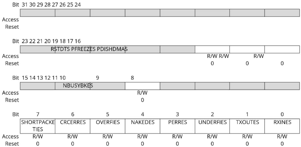
Bit 18 - RSTDTS Reset Data Toggle Enable
Bit 17 - PFREEZES Pipe Freeze Enable
Bit 16 - PDISHDMAS Pipe Interrupts Disable HDMA Request Enable
Bit 12 - NBUSYBKES Number of Busy Banks Enable
Bit 7 - SHORTPACKETIES Short Packet Interrupt Enable
Bit 6 - CRCERRES CRC Error Interrupt Enable
Bit 5 - OVERFIES Overflow Interrupt Enable
Bit 4 - NAKEDES NAKed Interrupt Enable
Bit 3 - PERRES Pipe Error Interrupt Enable
Bit 2 - UNDERFIES Underflow Interrupt Enable
Bit 1 - TXOUTES Transmitted OUT Data Interrupt Enable
Bit 0 - RXINES Received IN Data Interrupt Enable
38.7.63 Host Pipe x IN Request Register
Name: USBHS_HSTPIPINRQx
Offset: 0x0650 + x*0x04 [x=0..8]
Reset: 0
Property: Read/Write
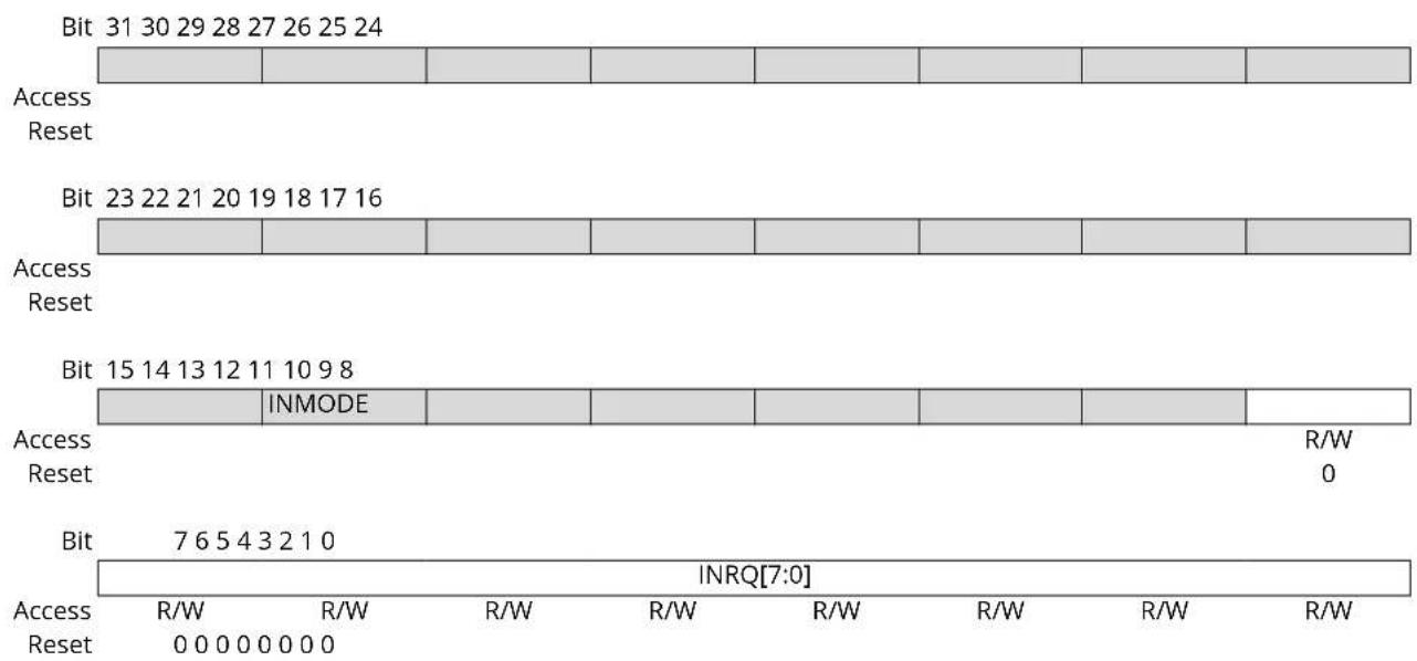
bar_stacked
| Bit | Access Reset | INMODE | R/W | | --- | --- | --- | --- | | 31 | 24 | 0 | 0 | | 30 | 25 | 0 | 0 | | 29 | 26 | 0 | 0 | | 28 | 27 | 0 | 0 | | 27 | 28 | 0 | 0 | | 26 | 29 | 0 | 0 | | 25 | 30 | 0 | 0 | | 31 | 31 | 0 | 0 | | 24 | 32 | 0 | 0 | | 23 | 33 | 0 | 0 | | 22 | 34 | 0 | 0 | | 21 | 35 | 0 | 0 | | 20 | 36 | 0 | 0 | | 19 | 37 | 0 | 0 | | 18 | 38 | 0 | 0 | | 17 | 39 | 0 | 0 | | 16 | 40 | 0 | 0 | | 15 | 41 | 0 | 0 | | 14 | 42 | INMODE | R/W = 0 | | 13 | 43 | INMODE | R/W = 0 | | 12 | 44 | INMODE | R/W = 0 | | 11 | 45 | INMODE | R/W = 0 | | 10 | 46 | INMODE | R/W = 0 | | 9 | 47 | INMODE | R/W = 0 | | 8 | 48 | INMODE | R/W = 0 | | 7 | 49 | INMODE | R/W = 0 | | 6 | 50 | INMODE | R/W = 0 | | 5 | 51 | INMODE | R/W = 0 | | 4 | 52 | INMODE | R/W = 0 | | 3 | 53 | INMODE | R/W = 0 | | 2 | 54 | INMODE | R/W = 0 | | 1 | 55 | INMODE | R/W = 0 | | All (Bit) vs. All (INRQ[7:0])Bit 8 - INMODE IN Request Mode
| Value | Description |
| 0 | Performs a pre-defined number of IN requests. This number is the INRQ field. |
| 1 | Enables the USBHS to perform infinite IN requests when the pipe is not frozen. |
Bits 7:0 - INRQ[7:0] IN Request Number before Freeze
This field contains the number of IN transactions before the USBHS freezes the pipe. The USBHS performs (INRQ+1) IN requests before freezing the pipe. This counter is automatically decreased by 1 each time an IN request has been successfully performed.
This register has no effect when INMODE = 1.
38.7.64 Host Pipe x Error Register
Name: USBHS_HSTPIPERRx
Offset: 0x0680 + x*0x04 [x=0..8]
Reset: 0
Property: Read/Write
Writing a zero in a bit/field in this register clears the bit/field. Writing a one has no effect.

text_image
Bit 31 30 29 28 27 26 25 24 Access Reset Bit 23 22 21 20 19 18 17 16 Access Reset Bit 15 14 13 12 11 10 9 8 Access Reset Bit 7 6 5 4 3 2 1 0 Access Reset COUNTER[1:0] CRC16 TIMEOUT PID DATAPID DATATGL R/W R/W R/W R/W R/W R/W R/W 0 0 0 0 0 0Bits 6:5 - COUNTER[1:0] Error Counter
This field is incremented each time an error occurs (CRC16, TIMEOUT, PID, DATAPID or DATATGL). This field is cleared when receiving a USB packet free of error.
When this field reaches 3 (i.e., 3 consecutive errors), this pipe is automatically frozen (USBHS_HSTPIPIMRx.PFREEZE is set).
Bit 4 - CRC16 CRC16 Error
| Value | Description |
| 0 | No CRC16 error occurred since last clear of this bit. |
| 1 | This bit is automatically set when a CRC16 error has been detected. |
Bit 3 - TIMEOUT Time-Out Error
| Value | Description |
| 0 | No Time-Out error occurred since last clear of this bit. |
| 1 | This bit is automatically set when a Time-Out error has been detected. |
Bit 2 - PID PID Error
| Value | Description |
| 0 | No PID error occurred since last clear of this bit. |
| 1 | This bit is automatically set when a PID error has been detected. |
Bit 1 - DATAPID Data PID Error
| Value | Description |
| 0 | No Data PID error occurred since last clear of this bit. |
| 1 | This bit is automatically set when a Data PID error has been detected. |
Bit 0 - DATATGL Data Toggle Error
| Value Description | |
| 0 | No Data Toggle error occurred since last clear of this bit. |
| 1 | This bit is automatically set when a Data Toggle error has been detected. |
38.7.65 Host DMA Channel x Next Descriptor Address Register
Name: USBHS_HSTDMANXTDSCx
Offset: 0x0700 + (x-1)*0x10 [x=1..7]
Reset: 0
Property: Read/Write
Bit 31 30 29 28 27 26 25 24
NXT_DSC_ADD[31:24]
Access R/W R/W R/W R/W R/W R/W R/W R/W
Reset 00000000
Bit 23 22 21 20 19 18 17 16
NXT_DSC_ADD[23:16]
Access R/W R/W R/W R/W R/W R/W R/W R/W
Reset 00000000
Bit 15 14 13 12 11 10 9 8
NXT_DSC_ADD[15:8]
Access R/W R/W R/W R/W R/W R/W R/W R/W
Reset 00000000
Bit 76543210
NXT_DSC_ADD[7:0]
Access R/W R/W R/W R/W R/W R/W R/W R/W
Reset 00000000
Bits 31:0 - NXT\_DSC\_ADD[31:0] Next Descriptor Address
This field points to the next channel descriptor to be processed. This channel descriptor must be aligned, so bits 0 to 3 of the address must be equal to zero.
38.7.66 Host DMA Channel x Address Register
Name: USBHS_HSTDMAADDRESSx
Offset: 0x0704 + x*0x10 [x=0..6]
Reset: 0
Property: Read/Write
Bit 31 30 29 28 27 26 25 24
BUFF_ADD[31:24]
Access R/W R/W R/W R/W R/W R/W R/W R/W
Reset 00000000
Bit 23 22 21 20 19 18 17 16
BUFF_ADD[23:16]
Access R/W R/W R/W R/W R/W R/W R/W R/W
Reset 00000000
Bit 15 14 13 12 11 10 9 8
BUFF_ADD[15:8]
Access R/W R/W R/W R/W R/W R/W R/W R/W
Reset 00000000
Bit 76543210
BUFF_ADD[7:0]
Access R/W R/W R/W R/W R/W R/W R/W R/W
Reset 00000000
Bits 31:0 - BUFF\_ADD[31:0] Buffer Address
This field determines the AHB bus starting address of a DMA channel transfer.
Channel start and end addresses may be aligned on any byte boundary.
The firmware can write this field only when the USBHS_HSTDMASTATUS.CHANN_ENB bit is cleared.
This field is updated at the end of the address phase of the current access to the AHB bus. It is incremented by the access byte width. The access width is 4 bytes (or less) at packet start or end, if the start or end address is not aligned on a word boundary.
The packet start address is either the channel start address or the next channel address to be accessed in the channel buffer.
The packet end address is either the channel end address or the latest channel address accessed in the channel buffer.
The channel start address is written by software or loaded from the descriptor. The channel end address is either determined by the end of buffer or the USB device, or by the USB end of transfer if the USBHS_HSTDMACONTROLx.END_TR_EN bit is set.
38.7.67 Host DMA Channel x Control Register
Name: USBHS_HSTDMACONTROLx
Offset: 0x0708 + x*0x10 [x=0..6]
Reset: 0
Property: Read/Write
Bit 31 30 29 28 27 26 25 24
| BUFF_LENGTH[15:8] |
Access R/W R/W R/W R/W R/W R/W R/W R/W
Reset 00000000
Bit 23 22 21 20 19 18 17 16
| BUFF_LENGTH[7:0] |
Access R/W R/W R/W R/W R/W R/W R/W R/W
Reset 00000000
Bit 15 14 13 12 11 10 9 8
Access
Reset
Bit 76543210
| BURST_LCK | DESC_LD_IT | END_BUFFIT | END_TR_IT | END_B_EN | END_TR_EN | LDNXT_DSC | CHANN_ENB |
Access R/W R/W R/W R/W R/W R/W R/W R/W
Reset 00000000
Bits 31:16 - BUFF\_LENGTH[15:0] Buffer Byte Length (Write-only)
This field determines the number of bytes to be transferred until end of buffer. The maximum channel transfer size (32 KBytes) is reached when this field is 0 (default value). If the transfer size is unknown, this field should be set to 0, but the transfer end may occur earlier under USB device control.
When this field is written, the USBHS_HSTDMASTATUSx.BUFF_COUNT field is updated with the write value.
Notes: 1. Bits [31:2] are only writable when issuing a channel Control Command other than "Stop Now".
- For reliability, it is highly recommended to wait for both the USBHS_HSTDMASTATUSx.CHAN_ACT and the CHAN_ENB flags to be at 0, thus ensuring the channel has been stopped before issuing a command other than "Stop Now".
Bit 7 - BURST\_LCK Burst Lock Enable
| Value | Description |
| 0 | The DMA never locks the bus access. |
| 1 | USB packets AHB data bursts are locked for maximum optimization of the bus bandwidth usage and maximization of fly-by AHB burst duration. |
Bit 6 - DESC\_LD\_IT Descriptor Loaded Interrupt Enable
| Value | Description |
| 0 | USBHS_HSTDMASTATUSx.DESC_LDST rising does not trigger any interrupt. |
| 1 | An interrupt is generated when a descriptor has been loaded from the bus. |
Bit 5 - END\_BUFFIT End of Buffer Interrupt Enable
| Value | Description |
| 0 | USBHS_HSTDMASTATUSx.END_BF_ST rising does not trigger any interrupt. |
Value Description
An interrupt is generated when USBHS_HSTDMASTATUSx.BUFF_COUNT reaches zero.
Bit 4 - END\_TR\_IT End of Transfer Interrupt Enable
Use when the receive size is unknown.
Value Description
| 0 | Completion of a USBHS device-initiated buffer transfer does not trigger any interrupt at USBHS_HSTDMASTATUSx.END_TR_ST rising. |
| 1 | An interrupt is sent after the buffer transfer is complete, if the USBHS device has ended the buffer transfer. |
Bit 3 - END\_B\_EN End of Buffer Enable Control
This is mainly for short packet OUT validations initiated by the DMA reaching the end of buffer, but could be used for IN packet truncation (discarding of unwanted packet data) at the end of DMA buffer.
Value Description
| 0 | DMA Buffer End has no impact on USB packet transfer. |
| 1 | The pipe can validate the packet (according to the values programmed in the USBHS_HSTPIPCFGx.AUTOSW and USBHS_HSTPIPIMRx.SHORTPACKETIE fields) at DMA Buffer End, i.e., when USBHS_HSTDMASTATUS.BUFF_COUNT reaches 0. |
Bit 2 - END\_TR\_EN End of Transfer Enable Control (OUT transfers only)
When set, a BULK or INTERRUPT short packet closes the current buffer and the USBHS_HSTDMASTATUSx.END_TR_ST flag is raised.
This is intended for a USBHS non-prenegotiated USB transfer size.
Value Description
| 0 | USB end of transfer is ignored. |
| 1 | The USBHS device can put an end to the current buffer transfer. |
Bit 1 - LDNXT\_DSC Load Next Channel Transfer Descriptor Enable Command
If the CHANN_ENB bit is cleared, the next descriptor is loaded immediately upon transfer request.
DMA Channel Control Command Summary:
| Value LDNXT_DSC Value CHANN_ENB Name Description | ||
| 0 0 STOP_NOW Stop now | ||
| 0 1 RUN_AND_STOP Run and stop at end of buffer | ||
| 1 0 LOAD_NEXT_DESC Load next descriptor now | ||
| 1 1 RUN_AND_LINK Run and link at end of buffer | ||
Value Description
| 0 | No channel register is loaded after the end of the channel transfer. |
| 1 | The channel controller loads the next descriptor after the end of the current transfer, i.e., when the USBHS_HSTDMASTATUS.CHANN_ENB bit is reset. |
Bit 0 - CHANN\_ENB Channel Enable Command
If the LDNXT_DSC bit has been cleared by descriptor loading, the firmware has to set the corresponding CHANN_ENB bit to start the described transfer, if needed.
If the LDNXT_DSC bit is cleared, the channel is frozen and the channel registers may then be read and/or written reliably as soon as both the USBHS_HSTDMASTATUS.CHANN_ENB and the CHANN_ACT flags read as 0.
If a channel request is currently serviced when this bit is cleared, the DMA FIFO buffer is drained until it is empty, then the USBHS_HSTDMASTATUS.CHANN_ENB bit is cleared.
If the LDNXT_DSC bit is set or after it has been cleared, the currently loaded descriptor is skipped (no data transfer occurs) and the next descriptor is immediately loaded.
Value Description
| 0 | The DMA channel is disabled and no transfer occurs upon request. This bit is also cleared by hardware when the channel source bus is disabled at the end of the buffer. |
| 1 | The USBHS_HSTDMASTATUS.CHANN_ENB bit is set, enabling DMA channel data transfer. Then, any pending request starts the transfer. This may be used to start or resume any requested transfer. |
38.7.68 Host DMA Channel x Status Register
Name: USBHS_HSTDMASTATUSx
Offset: 0x070C + x*0x10 [x=0..6]
Reset: 0
Property: Read/Write

text_image
Bit 31 30 29 28 27 26 25 24 BUFF_COUNT[15:8] Access R/W R/W R/W R/W R/W R/W R/W Reset 0 0 0 0 0 0 0 0 Bit 23 22 21 20 19 18 17 16 BUFF_COUNT[7:0] Access R/W R/W R/W R/W R/W R/W R/W Reset 0 0 0 0 0 0 0 0 Bit 15 14 13 12 11 10 9 8 Access Reset Bit 7 6 5 4 3 2 1 0 DESC_LDST END_BF_ST END_TR_ST CHANN_ACT CHANN_ENB Access R/W R/W R/W R/W R/W R/W R/W Reset 0 0 0 0 0 0 0 R/W R/W 0 0 0 0 0 0Bits 31:16 - BUFF\_COUNT[15:0] Buffer Byte Count
This field determines the current number of bytes still to be transferred for this buffer.
This field is decremented from the AHB source bus access byte width at the end of this bus address phase.
The access byte width is 4 by default, or less, at DMA start or end, if the start or end address is not aligned on a word boundary.
At the end of buffer, the DMA accesses the USBHS device only for the number of bytes needed to complete it.
Note: For IN pipes, if the receive buffer byte length (USBHS_HSTDMACONTROL.BUFF_LENGTH) has been defaulted to zero because the USB transfer length is unknown, the actual buffer byte length received is 0x10000-BUFF_COUNT.
Bit 6 - DESC\_LDST Descriptor Loaded Status
Valid until the CHANN_ENB flag is cleared at the end of the next buffer transfer.
| Value | Description |
| 0 | Cleared automatically when read by software. |
| 1 | Set by hardware when a descriptor has been loaded from the system bus. |
Bit 5 - END\_BF\_ST End of Channel Buffer Status
Valid until the CHANN_ENB flag is cleared at the end of the next buffer transfer.
| Value | Description |
| 0 | Cleared automatically when read by software. |
| 1 | Set by hardware when the BUFF_COUNT count-down reaches zero. |
Bit 4 - END\_TR\_ST End of Channel Transfer Status
Valid until the CHANN_ENB flag is cleared at the end of the next buffer transfer.
| Value Description | |
| 0 | Cleared automatically when read by software. |
| 1 | Set by hardware when the last packet transfer is complete, if the USBHS device has ended the transfer. |
Bit 1 - CHANN\_ACT Channel Active Status
When a packet transfer is ended, this bit is automatically reset.
When a packet transfer cannot be completed due to an END_BF_ST, this flag stays set during the next channel descriptor load (if any) and potentially until completion of a USBHS packet transfer, if allowed by the new descriptor.
| Value Description | |
| 0 | The DMA channel is no longer trying to source the packet data. |
| 1 | The DMA channel is currently trying to source packet data, i.e., selected as the highest-priority requesting channel. |
Bit 0 - CHANN\_ENB Channel Enable Status
When any transfer is ended either due to an elapsed byte count or to completion of a USBHS device-initiated transfer, this bit is automatically reset.
This bit is normally set or cleared by writing into the USBHS_HSTDMACONTROLx.CHANN_ENB bit field either by software or descriptor loading.
If a channel request is currently serviced when the USBHS_HSTDMACONTROLx.CHANN_ENB bit is cleared, the DMA FIFO buffer is drained until it is empty, then this status bit is cleared.
| Value Description | |
| 0 | If cleared, the DMA channel no longer transfers data, and may load the next descriptor if the USBHS_HSTDMACONTROLx.LDNXT_DSC bit is set. |
| 1 | If set, the DMA channel is currently enabled and transfers data upon request. |
39. High-Speed Multimedia Card Interface (HSMCI)
39.1 Description
The High Speed Multimedia Card Interface (HSMCI) supports the MultiMedia Card (MMC) Specification V4.3, the SD Memory Card Specification V2.0, the SDIO V2.0 specification and CE-ATA V1.1.
The HSMCI includes a command register, response registers, data registers, timeout counters and error detection logic that automatically handle the transmission of commands and, when required, the reception of the associated responses and data with a limited processor overhead.
The HSMCI operates at a rate of up to Host Clock divided by 2 and supports the interfacing of 1 slot(s). Each slot may be used to interface with a High Speed MultiMedia Card bus (up to 30 Cards) or with an SD Memory Card. A bit field in the SD Card Register performs this selection.
The SD Memory Card communication is based on a 9-pin interface (clock, command, four data and three power lines) and the High Speed MultiMedia Card on a 7-pin interface (clock, command, one data, three power lines and one reserved for future use).
The SD Memory Card interface also supports High Speed MultiMedia Card operations. The main differences between SD and High Speed MultiMedia Cards are the initialization process and the bus topology.
HSMCI fully supports CE-ATA Revision 1.1, built on the MMC System Specification v4.0. The module includes dedicated hardware to issue the command completion signal and capture the host command completion signal disable.
39.2 Embedded Characteristics
- Compatible with MultiMedia Card Specification Version 4.3
- Compatible with SD Memory Card Specification Version 2.0
- Compatible with SDIO Specification Version 2.0
- Compatible with CE-ATA Specification 1.1
- Cards Clock Rate Up to Host Clock Divided by 2
- Boot Operation Mode Support
• High Speed Mode Support - Embedded Power Management to Slow Down Clock Rate When Not Used
• Supports 1 Multiplexed Slot(s)
– Each Slot for either a High Speed MultiMedia Card Bus (Up to 30 Cards) or an SD Memory Card - Support for Stream, Block and Multi-block Data Read and Write
- Minimizes Processor Intervention for Large Buffer Transfers
• Built in FIFO (from 16 to 256 bytes) with Large Memory Aperture Supporting Incremental Access - Support for CE-ATA Completion Signal Disable Command
- Protection Against Unexpected Modification On-the-Fly of the Configuration Registers
39.3 Block Diagram
Figure 39-1. Block Diagram (4-bit configuration)
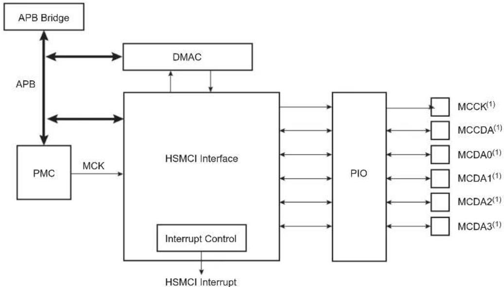
flowchart
graph TD
    A["APB Bridge"] <--> B["DMAC"]
    C["PMC"] -->|MCK| D["HSMCI Interface"]
    D --> E["PIO"]
    E --> F["MCCK(1)"]
    E --> G["MCCDA(1)"]
    E --> H["MCDA0(1)"]
    E --> I["MCDA1(1)"]
    E --> J["MCDA2(1)"]
    E --> K["MCDA3(1)"]
    D <--> L["Interrupt Control"]
    L --> M["HSMCI Interrupt"]
    M --> D
Note:
- When several HSMCI (x HSMCI) are embedded in a product, MCCK refers to HSMCIX_CK, MCCDA to HSMCIX_CDA, MCDAy to HSMCIX_DAy.
39.4 Application Block Diagram
Figure 39-2. Application Block Diagram
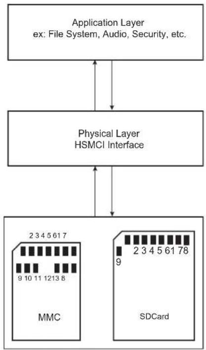
flowchart
graph TD
    A["Application Layer\nex: File System, Audio, Security, etc."] --> B["Physical Layer\nHSMCI Interface"]
    B --> C["MMC"]
    B --> D["SDCard"]
    C --> E["Pin 2 3 4 5 6 1 7"]
    C --> F["Pin 9 10 11 12 13 8"]
    D --> G["Pin 2 3 4 5 6 1 78"]
39.5 Pin Name List
Table 39-1. I/O Lines Description for 4-bit Configuration
| Pin Name(1) | Pin Description Type | (2) | Comments |
| MCCDA Command/response I/O/PP/OD CMD of an MMC or SDCard/SDIO | |||
| MCCK Clock O CLK of an MMC or SD Card/SDIO | |||
| MCDA0-MCDA3 Data 0..3 of Slot A I/O/PP DAT[0..3] of an MMC | DAT[0..3] of an SD Card/SDIO | ||
Note: 1. When several HSMCI (x HSMCI) are embedded in a product, MCCK refers to HSMClx_CK, MCCDA to HSMClx_CDA, MCDAy to HSMClx_DAy.
Note: 2. I: Input, O: Output, PP: Push/Pull, OD: Open Drain.
39.6 Product Dependencies
39.6.1 I/O Lines
The pins used for interfacing the High Speed MultiMedia Cards or SD Cards are multiplexed with PIO lines. The programmer must first program the PIO controllers to assign the peripheral functions to HSMCI pins.
39.6.2 Power Management
The HSMCI is clocked through the Power Management Controller (PMC), so the programmer must first configure the PMC to enable the HSMCI clock.
39.6.3 Interrupt Sources
The HSMCI has an interrupt line connected to the interrupt controller.
Handling the HSMCI interrupt requires programming the interrupt controller before configuring the HSMCI.
39.7 Bus Topology
Figure 39-3. High Speed MultiMedia Memory Card Bus Topology
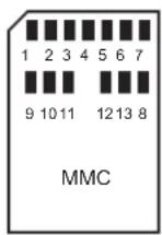
The High Speed MultiMedia Card communication is based on a 13-pin serial bus interface. It has three communication lines and four supply lines.
Table 39-2. Bus Topology
| Pin Number | Name | Type^(1) | Description | HSMCI Pin Name^(2) (Slot z) |
| 1 | DAT[3] | I/O/PP | Data | MCDz3 |
| 2 | CMD | I/O/PP/OD | Command/response | MCCDz |
| 3 | VSS1 | S | Supply voltage ground | VSS |
| 4 | VDD | S | Supply voltage | VDD |
| 5 | CLK | O | Clock | MCCK |
| Pin Number Name Type | (1) | Description HSMCI Pin Name | (2)(Slot z) |
| 6 VSS2 S Supply voltage ground VSS | |||
| 7 DAT[0] I/O/PP Data 0 MCDz0 | |||
| 8 DAT[1] I/O/PP Data 1 MCDz1 | |||
| 9 DAT[2] I/O/PP Data 2 MCDz2 | |||
Notes:
- I: Input, O: Output, PP: Push/Pull, OD: Open Drain, S: Supply
- When several HSMCI (x HSMCI) are embedded in a product, MCCK refers to HSMCIX_CK, MCCDA to HSMCIX_CDA, MCDAy to HSMCIX_DAy.
Figure 39-4. MMC Bus Connections (One Slot)

flowchart
graph TD
    A["HSMCI"] --> B["MCDA0"]
    A --> C["MCCDA"]
    A --> D["MCCK"]
    B --> E["MMC1"]
    C --> F["MMC2"]
    D --> G["MMC3"]
    E --> H["2 3 4 5 6 1 7"]
    E --> I["9 10 11 12 13 8"]
    F --> J["2 3 4 5 6 1 7"]
    F --> K["9 10 11 12 13 8"]
    G --> L["2 3 4 5 6 1 7"]
    G --> M["9 10 11 12 13 8"]
Note: When several HSMCI (x HSMCI) are embedded in a product, MCCK refers to HSMCIX_CK, MCCDA to HSMCIX_CDA MCDAy to HSMCIX_DAy.
Figure 39-5. SD Memory Card Bus Topology
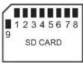
The SD Memory Card bus includes the signals listed in the table below.
Table 39-3. SD Memory Card Bus Signals
| Pin Number | Name | Type(1) | Description | HSMCI Pin Name(2)(Slot z) |
| 1 | CD/DAT[3] | I/O/PP | Card detect/ Data line Bit 3 | MCDz3 |
| 2 | CMD | PP Command/response | MCCDz | |
| 3 | VSS1 | S | Supply voltage ground | VSS |
| 4 | VDD | S | Supply voltage | VDD |
| 5 | CLK | O | Clock | MCCK |
| 6 | VSS2 | S | Supply voltage ground | VSS |
| 7 | DAT[0] | I/O/PP | Data line Bit 0 | MCDz0 |
| 8 | DAT[1] | I/O/PP | Data line Bit 1 or Interrupt | MCDz1 |
| ......continued | ||||
| Pin Number Name | Type | (1) | Description HSMCI Pin Name | (2)(Slot z) |
| 9 DAT[2] I/O/PP Data line Bit 2 MCDz2 | ||||
Notes:
- I: input, O: output, PP: Push Pull, OD: Open Drain.
- When several HSMCI (x HSMCI) are embedded in a product, MCCK refers to HSMCIX_CK, MCCDA to HSMCIX_CDA, MCDAy to HSMCIX_DAy.
Figure 39-6. SD Card Bus Connections with One Slot
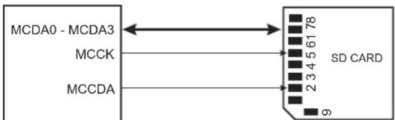
flowchart
graph LR
    A["MCDA0 - MCDA3"] <--> B["SD CARD"]
    C["MCCK"] --> B
    D["MCCDA"] --> B
    B --> E["Pin 78: 78"]
    B --> F["Pin 61: 61"]
    B --> G["Pin 5: 5"]
    B --> H["Pin 4: 4"]
    B --> I["Pin 3: 3"]
    B --> J["Pin 2: 2"]
    B --> K["Pin 1: 1"]
    B --> L["Pin 9: 9"]
Note: When several HSMCI (x HSMCI) are embedded in a product, MCCK refers to HSMCIX_CK, MCCDA to HSMCIX_CDA MCDAy to HSMCIX_DAy.
When the HSMCI is configured to operate with SD memory cards, the width of the data bus can be selected in the HSMCI_SDCR. Clearing the SDCBUS bit in this register means that the width is one bit; setting it means that the width is four bits. In the case of High Speed MultiMedia cards, only the data line 0 is used. The other data lines can be used as independent PIOs.
39.8 High-Speed Multimedia Card Operations
After a power-on reset, the cards are initialized by a special message-based High-Speed Multimedia Card bus protocol. Each message is represented by one of the following tokens:
- Command—A command is a token that starts an operation. A command is sent from the host either to a single card (addressed command) or to all connected cards (broadcast command). A command is transferred serially on the CMD line.
- Response—A response is a token which is sent from an addressed card or (synchronously) from all connected cards to the host as an answer to a previously received command. A response is transferred serially on the CMD line.
- Data—Data can be transferred from the card to the host or vice versa. Data is transferred via the data line.
Card addressing is implemented using a session address assigned during the initialization phase by the bus controller to all currently connected cards. Their unique CID number identifies individual cards.
The structure of commands, responses and data blocks is described in the High-Speed Multimedia Card System Specification. See Table 39-4 for additional information.
High-Speed Multimedia Card bus data transfers are composed of these tokens.
There are different types of operations. Addressed operations always contain a command and a response token. In addition, some operations have a data token; the others transfer their information directly within the command or response structure. In this case, no data token is present in an operation. The bits on the DAT and the CMD lines are transferred synchronous to the clock HSMCI clock.
Two types of data transfer commands are defined:
- Sequential commands—These commands initiate a continuous data stream. They are terminated only when a stop command follows on the CMD line. This mode reduces the command overhead to an absolute minimum.
- Block-oriented commands—These commands send a data block succeeded by CRC bits.
Both read and write operations allow either single or multiple block transmission. A multiple block transmission is terminated when a stop command follows on the CMD line similarly to the sequential read or when a multiple block transmission has a predefined block count (see "Data Transfer Operation").
The HSMCI provides a set of registers to perform the entire range of High-Speed Multimedia Card operations.
39.8.1 Command - Response Operation
After reset, the HSMCI is disabled and becomes valid after setting the MCIEN bit in the HSMCI_CR.
The PWSEN bit saves power by dividing the HSMCI clock by 2^PWSDIV + 1 when the bus is inactive.
The two bits, RDPROOF and WRPROOF in the HSMCI Mode Register (HSMCI_MR) allow stopping the HSMCI clock during read or write access if the internal FIFO is full. This will guarantee data integrity, not bandwidth.
All the timings for High Speed MultiMedia Card are defined in the High Speed MultiMedia Card System Specification.
The two bus modes (open drain and push/pull) needed to process all the operations are defined in the HSMCI Command Register (HSMCI_CMDR). The HSMCI_CMDR allows a command to be carried out.
For example, to perform an ALL_SEND_CID command:
| Host Command N | _ID Cycles Response High Impedance State | |||||||||||
| CMD S T | Content CRC E Z | ***** | Z S T | CID Content Z Z Z | ||||||||
The command ALL_SEND_CID and the fields and values for the HSMCI_CMDR are described in the following two tables.
Table 39-4. ALL_SEND_CID Command Description
| CMD Index | Type A | Argument Response | Abbreviation | Command | Description |
| CMD2 | bcr(1) | [31:0] stuff bits | R2 | ALL_SEND_CID | Asks all cards to send their CID numbers on the CMD line |
Note: 1. bcr means broadcast command with response.
Table 39-5. Fields and Values for HSMCI_CMDR
| Field | Value |
| CMDNB (command number) | 2 (CMD2) |
| RSPTYP (response type) | 2 (R2: 136 bits response) |
| SPCMD (special command) | 0 (not a special command) |
| OPCMD (open drain command) | 1 |
| MAXLAT (max latency for command to response) | 0 (NID cycles ==> 5 cycles) |
| TRCMD (transfer command) | 0 (No transfer) |
| TRDIR (transfer direction) | X (available only in transfer command) |
| TRTYP (transfer type) | X (available only in transfer command) |
| IOSPCMD (SDIO special command) | 0 (not a special command) |
The HSMCI_ARGR contains the argument field of the command.
To send a command, the user must perform the following steps:
-
Fill the argument register (HSMCI_ARGR) with the command argument.
-
Set the command register (HSMCI_CMDR).
The command is sent immediately after writing the command register.
While the card maintains a busy indication (at the end of a STOP_TRANSMISSION command CMD12, for example), a new command shall not be sent. The NOTBUSY flag in the Status Register (HSMCI_SR) is asserted when the card releases the busy indication.
If the command requires a response, it can be read in the HSMCI Response Register (HSMCI_RSPR). The response size can be from 48 bits up to 136 bits depending on the command. The HSMCI embeds an error detection to prevent any corrupted data during the transfer.
The following flowchart shows how to send a command to the card and read the response if needed. In this example, the status register bits are polled but setting the appropriate bits in the HSMCI Interrupt Enable Register (HSMCI_IER) allows using an interrupt method.
Figure 39-7. Command/Response Functional Flow Diagram
flowchart
graph TD
    A["Set the command argument HSMCI_ARGR = Argument(1)"] --> B["Set the command HSMCI_CMDR = Command"]
    B --> C["Read HSMCI_SR"]
    C --> D{CMDRDY}
    D -->|0| E["Return ERROR(1)"]
    D -->|1| F{Status error flags?}
    F -->|Yes| E
    F -->|No| G["Return OK"]
    G --> H["Read HSMCI_SR"]
    H --> I{NOTBUSY}
    I -->|0| E
    I -->|1| J["RETURN OK"]
    E --> K["Wait for command ready status flag"]
    K --> C
    F --> L["Check error bits in the status register(1)"]
    L --> F
Note: If the command is SEND_OP_COND, the CRC error flag is always present (refer to R3 response in the High Speed MultiMedia Card specification).
39.8.2 Data Transfer Operation
The High Speed MultiMedia Card allows several read/write operations (single block, multiple blocks, stream, etc.). These kinds of transfer can be selected setting the Transfer Type (TRTYP) field in the HSMCI Command Register (HSMCI_CMDR).
In all cases, the block length (BLKLEN field) must be defined either in the HSMCI Mode Register (HSMCI_MR) or in the HSMCI Block Register (HSMCI_BLKR). This field determines the size of the data block.
Consequent to MMC Specification 3.1, two types of multiple block read (or write) transactions are defined (the host can use either one at any time):
- Open-ended/Infinite Multiple block read (or write):
The number of blocks for the read (or write) multiple block operation is not defined. The card will continuously transfer (or program) data blocks until a stop transmission command is received. - Multiple block read (or write) with predefined block count (since version 3.1 and higher):
The card will transfer (or program) the requested number of data blocks and terminate the transaction. The stop command is not required at the end of this type of multiple block read (or write), unless terminated with an error. In order to start a multiple block read (or write) with predefined block count, the host must correctly program the HSMCI Block Register (HSMCI_BLKR). Otherwise the card will start an open-ended multiple block read. The BCNT field of the HSMCI_BLKR defines the number of blocks to transfer (from 1 to 65535 blocks). Programming the value 0 in the BCNT field corresponds to an infinite block transfer.
39.8.3 Read Operation
The following flowchart shows how to read a single block with or without use of DMAC facilities. In this example, a polling method is used to wait for the end of read. Similarly, the user can configure the HSMCI Interrupt Enable Register (HSMCI_IER) to trigger an interrupt at the end of read.
Figure 39-8. Read Functional Flow Diagram

flowchart
graph TD
    A["Send SELECT/DESELECT_CARD command¹ to select the card"] --> B["Send SET_BLOCKLEN command¹"]
    B --> C{Read with DMAC}
    C -->|YesNo| D["Set the DMAEN bit HSMCI_DMA |= DMAEN\nSet the block length (in bytes)\nHSMCI_BLKR |= (BlockLength<<16)"]
    D --> E["Send READ_SINGLE_BLOCK command¹"]
    E --> F["Number of words to read = BlockLength/4"]
    F --> G{Number of words to read = 0 ?}
    G -->|Yes| H["Read status register HSMCI_SR"]
    G -->|No| I["Read data = HSMCI_RDR\nNumber of words to read = Number of words to read -1"]
    H --> J{Poll the bit RXRDY = 0?}
    J -->|Yes| K["Write the bit XFRDONE = 0?"]
    J -->|No| L["Return"]
    K --> M["Read data = HSMCI_RDR\nNumber of words to read = Number of words to read -1"]
    L --> N["Return"]
Note 1: It is assumed that this command has been correctly sent (see the Command/Response Functional Flow Diagram).
39.8.4 Write Operation
In write operation, the HSMCI Mode Register (HSMCI_MR) is used to define the padding value when writing non-multiple block size. If the bit PADV is 0, then 0x00 value is used when padding data, otherwise 0xFF is used.
If set, the bit DMAEN in the HSMCI DMA Configuration Register (HSMCI_DMA) enables DMA transfer.
The flowchart, Write Functional Flow Diagram, shows how to write a single block with or without use of DMA facilities. Polling or interrupt method can be used to wait for the end of write according to the contents of the HSMCI Interrupt Mask Register (HSMCI_IMR).
Figure 39-9. Write Functional Flow Diagram
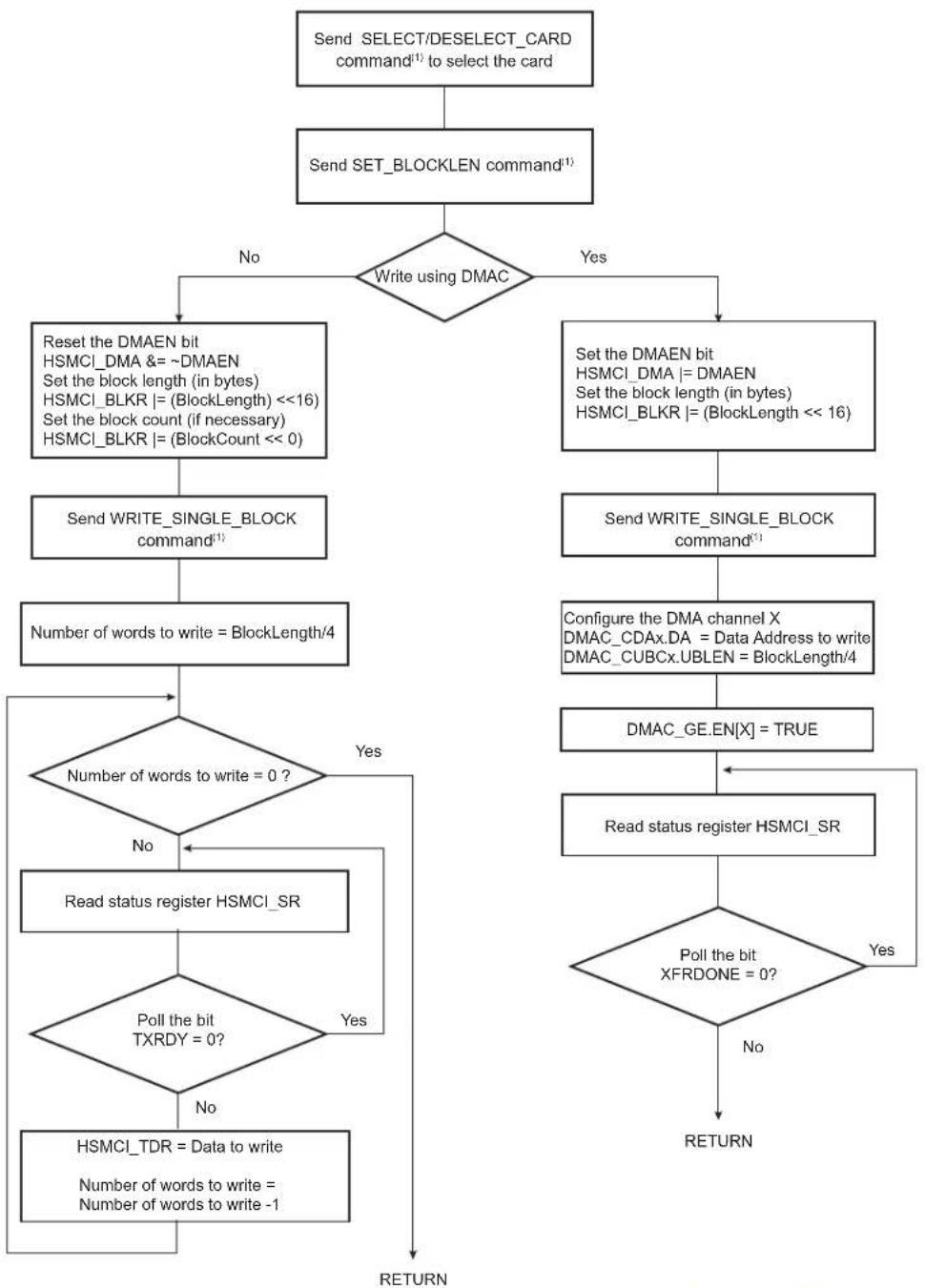
flowchart
graph TD
    A["Send SELECT/DESELECT_CARD command¹"] --> B["Send SET_BLOCKLEN command¹"]
    B --> C{Write using DMAC}
    C -->|No| D["Reset the DMAEN bit\nHSMCI_DMA &= ~DMAEN\nSet the block length (in bytes)\nHSMCI_BLKR |= (BlockLength) << 16\nSet the block count (if necessary)\nHSMCI_BLKR |= (BlockCount << 0)"]
    B -->|Yes| E["Set the DMAEN bit\nHSMCI_DMA |= DMAEN\nSet the block length (in bytes)\nHSMCI_BLKR |= (BlockLength << 16)"]
    E --> F["Send WRITE_SINGLE_BLOCK command¹"]
    F --> G["Number of words to write = BlockLength/4"]
    G --> H{Number of words to write = 0 ?}
    H -->|No| I["Read status register HSMCI_SR"]
    H -->|Yes| J{Poll the bit TXRDY = 0?}
    I --> K["HSMCI_TDR = Data to write\nNumber of words to write =\nNumber of words to write -1"]
    J -->|Yes| L["Read status register HSMCI_SR"]
    J -->|No| M["Return"]
    L --> N{Poll the bit XFRDONE = 0?}
    N -->|Yes| O["Read status register HSMCI_SR"]
    N -->|No| P["Return"]
    O --> Q["Return"]
Note: 1. It is assumed that this command has been correctly sent (see Command/Response Functional Flow Diagram).
The flowchart in Read and Write Multiple Block shows how to manage read multiple block and write multiple block transfers with the DMA Controller. Polling or interrupt method can be used to wait for the end of write according to the contents of the HSMCI_IMR.
Figure 39-10. Read and Write Multiple Block

flowchart
graph TD
    A["Send SELECT/DESELECT_CARD command¹"] --> B["Send SET_BLOCKLEN command¹"]
    B --> C{Write using DMAC}
    C -->|No| D["Reset the DMAEN bit\nHSMCI_DMA &= ~DMAEN\nSet the block length (in bytes)\nHSMCI_BLKR |= (BlockLength) << 16\nSet the block count (if necessary)\nHSMCI_BLKR |= (BlockCount << 0)"]
    B -->|Yes| E["Set the DMAEN bit\nHSMCI_DMA |= DMAEN\nSet the block length (in bytes)\nHSMCI_BLKR |= (BlockLength << 16)"]
    E --> F["Send WRITE_SINGLE_BLOCK command¹"]
    F --> G["Number of words to write = BlockLength/4"]
    G --> H{Number of words to write = 0 ?}
    H -->|No| I["Read status register HSMCI_SR"]
    H -->|Yes| J{Poll the bit TXRDY = 0?}
    I --> K["HSMCI_TDR = Data to write\nNumber of words to write =\nNumber of words to write -1"]
    J -->|Yes| L["Read status register HSMCI_SR"]
    J -->|No| M["Return"]
    L --> N{Poll the bit XFRDONE = 0?}
    N -->|Yes| O["Read status register HSMCI_SR"]
    N -->|No| P["Return"]
    O --> Q["Return"]
Notes: 1. It is assumed that this command has been correctly sent (see Command/Response Functional Flow Diagram).
2. Handle errors reported in HSMCI_SR.
39.8.5 WRITE\_SINGLE\_BLOCK/WRITE\_MULTIPLE\_BLOCK Operation using DMA Controller
- Wait until the current command execution has successfully terminated.
a. Check that CMDRDY and NOTBUSY fields are asserted in HSMCI_SR
-
Program the block length in the card. This value defines the value block_length.
-
Program the block length in the HSMCI Configuration Register with block_length value.
-
Configure the fields of the HSMCI_MR as follows:
a. Program FBYTE to one when the transfer is not multiple of 4, zero otherwise.
-
Issue a WRITE_SINGLE_BLOCK command writing HSMCI_ARGR then HSMCI_CMDR.
-
Program the DMA Controller.
a. Read the Channel Status Register to choose an available (disabled) channel.
b. Clear any pending interrupts on the channel from the previous DMAC transfer by reading the DMAC_CISx register.
c. Program the channel registers.
d. The DMAC_CSAx register for Channel x must be set to the location of the source data.
e. The DMAC_CDAx register for Channel x must be set with the starting address of the HSMCI_FIFO address.
f. Configure the fields of DMAC_CCx of Channel x as follows:
- DWIDTH is set to WORD when the transfer is multiple of 4, otherwise it is set to BYTE
- CSIZE must be set according to the value of HSMCI_DMA.CHKSIZE.
g. Configure the fields of DMAC_CUBCx for Channel x as follows:
- UBLEN is programmed with block_length/4 when the transfer length is multiple of 4, block_length otherwise.
h. Enable Channel x, writing one to DMAC_GE.EN[x]. The DMAC is ready and waiting for request.
- Wait for XFRDONE in the HSMCI_SR.
39.8.6 READ\_SINGLE\_BLOCK/READ\_MULTIPLE\_BLOCK Operation using DMA Controller
- Wait until the current command execution has successfully completed.
a. Check that CMDRDY and NOTBUSY are asserted in HSMCI_SR.
-
Program the block length in the card. This value defines the value block_length.
-
Program the block length in the HSMCI Configuration Register with block_length value.
-
Set RDPROOF bit in HSMCI_MR to avoid overflow.
-
Configure the fields of the HSMCI_MR as follows:
a. Program FBYTE to one when the transfer is not multiple of 4, zero otherwise.
-
Issue a READ_SINGLE_BLOCK/WRITE_MULTIPLE_BLOCK command.
-
Program the DMA controller.
a. Read the Channel Status Register to choose an available (disabled) channel.
b. Clear any pending interrupts on the channel from the previous DMA transfer by reading the DMAC_CISx register.
c. Program the channel registers.
d. The DMAC_CSAx register for Channel x must be set with the starting address of the HSMCI_FIFO address.
e. The DMAC_CDAx register for Channel x must be word aligned.
f. Configure the fields of DMAC_CCx for Channel x as follows:
- DWIDTH is set to WORD when the length is a multiple of 4, otherwise it is set to BYTE.
- CSIZE must be set according to the value of HSMCI_DMA.CHKSIZE.
g. Configure the fields of the DMAC_CUBCx register of Channel x as follows:
-
UBLEN is programmed with block_length/4 when the transfer length is multiple of 4, block_length otherwise.
h. Enable Channel x, writing one to DMAC_GE.EN[x]. The DMAC is ready and waiting for request. -
Wait for XFRDONE in the HSMCI_SR.
39.9 SD/SDIO Card Operation
The High Speed MultiMedia Card Interface allows processing of SD Memory (Secure Digital Memory Card) and SDIO (SD Input Output) Card commands.
SD/SDIO cards are based on the MultiMedia Card (MMC) format, but are physically slightly thicker and feature higher data transfer rates, a lock switch on the side to prevent accidental overwriting and security features. The physical form factor, pin assignment and data transfer protocol are forward-compatible with the High Speed MultiMedia Card with some additions. SD slots can actually be used for more than flash memory cards. Devices that support SDIO can use small devices designed for the SD form factor, such as GPS receivers, Wi-Fi or Bluetooth adapters, modems, barcode readers, IrDA adapters, FM radio tuners, RFID readers, digital cameras and more.
SD/SDIO is covered by numerous patents and trademarks, and licensing is only available through the Secure Digital Card Association.
The SD/SDIO Card communication is based on a 9-pin interface (Clock, Command, 4 x Data and 3 x Power lines). The communication protocol is defined as a part of this specification. The main difference between the SD/SDIO Card and the High Speed MultiMedia Card is the initialization process.
The SD/SDIO Card Register (HSMCI_SDCR) allows selection of the Card Slot and the data bus width.
The SD/SDIO Card bus allows dynamic configuration of the number of data lines. After power up, by default, the SD/SDIO Card uses only DAT0 for data transfer. After initialization, the host can change the bus width (number of active data lines).
39.9.1 SDIO Data Transfer Type
SDIO cards may transfer data in either a multi-byte (1 to 512 bytes) or an optional block format (1 to 511 blocks), while the SD memory cards are fixed in the block transfer mode. The TRTYP field in the HSMCI Command Register (HSMCI_CMDR) allows to choose between SDIO Byte or SDIO Block transfer.
The number of bytes/blocks to transfer is set through the BCNT field in the HSMCI Block Register (HSMCI_BLKR). In SDIO Block mode, the field BLKLEN must be set to the data block size while this field is not used in SDIO Byte mode.
An SDIO Card can have multiple I/O or combined I/O and memory (called Combo Card). Within a multi-function SDIO or a Combo card, there are multiple devices (I/O and memory) that share access to the SD bus. In order to allow the sharing of access to the host among multiple devices, SDIO and combo cards can implement the optional concept of suspend/resume (Refer to the SDIO Specification for more details). To send a suspend or a resume command, the host must set the SDIO Special Command field (IOSPCMD) in the HSMCI Command Register.
39.9.2 SDIO Interrupts
Each function within an SDIO or Combo card may implement interrupts (Refer to the SDIO Specification for more details). In order to allow the SDIO card to interrupt the host, an interrupt function is added to a pin on the DAT[1] line to signal the card's interrupt to the host. An SDIO interrupt on each slot can be enabled through the HSMCI Interrupt Enable Register. The SDIO interrupt is sampled regardless of the currently selected slot.
39.10 CE-ATA Operation
CE-ATA maps the streamlined ATA command set onto the MMC interface. The ATA task file is mapped onto MMC register space.
CE-ATA utilizes five MMC commands:
- GO_IDLE_STATE (CMD0): used for hard reset.
- STOP_TRANSMISSION (CMD12): causes the ATA command currently executing to be aborted.
- FAST_IO (CMD39): Used for single register access to the ATA taskfile registers, 8-bit access only.
- RW_MULTIPLE_REGISTER(SCMD60): used to issue an ATA command or to access the control/status registers.
- RW_MULTIPLE_BLOCK (CMD61): used to transfer data for an ATA command.
CE-ATA utilizes the same MMC command sequences for initialization as traditional MMC devices.
39.10.1 Executing an ATA Polling Command
- Issue READ_DMA_EXT with RW_MULTIPLE_REGISTER (CMD60) for 8 KB of DATA.
- Read the ATA status register until DRQ is set.
- Issue RW_MULTIPLE_BLOCK (CMD61) to transfer DATA.
- Read the ATA status register until DRQ && BSY are configured to 0.
39.10.2 Executing an ATA Interrupt Command
- Issue READ_DMA_EXT with RW_MULTIPLE_REGISTER (CMD60) for 8 KB of DATA with nIEN field set to zero to enable the command completion signal in the device.
- Issue RW_MULTIPLE_BLOCK (CMD61) to transfer DATA.
- Wait for Completion Signal Received Interrupt.
39.10.3 Aborting an ATA Command
If the host needs to abort an ATA command prior to the completion signal it must send a special command to avoid potential collision on the command line. The SPCMD field of the HSMCI_CMDR must be set to 3 to issue the CE-ATA completion Signal Disable Command.
39.10.4 CE-ATA Error Recovery
Several methods of ATA command failure may occur, including:
- No response to an MMC command, such as RW_MULTIPLE_REGISTER (CMD60).
- CRC is invalid for an MMC command or response.
- CRC16 is invalid for an MMC data packet.
- ATA Status register reflects an error by setting the ERR bit to one.
- The command completion signal does not arrive within a host specified time out period.
Error conditions are expected to happen infrequently. Thus, a robust error recovery mechanism may be used for each error event. The recommended error recovery procedure after a timeout is:
- Issue the command completion signal disable if nIEN was cleared to zero and the RW_MULTIPLE_BLOCK (CMD61) response has been received.
- Issue STOP_TRANSMISSION (CMD12) and successfully receive the R1 response.
- Issue a software reset to the CE-ATA device using FAST_IO (CMD39).
If STOP_TRANMISSION (CMD12) is successful, then the device is again ready for ATA commands. However, if the error recovery procedure does not work as expected or there is another timeout, the
next step is to issue GO_IDLE_STATE (CMD0) to the device. GO_IDLE_STATE (CMD0) is a hard reset to the device and completely resets all device states.
Note that after issuing GO_IDLE_STATE (CMD0), all device initialization needs to be completed again. If the CE-ATA device completes all MMC commands correctly but fails the ATA command with the ERR bit set in the ATA Status register, no error recovery action is required. The ATA command itself failed implying that the device could not complete the action requested, however, there was no communication or protocol failure. After the device signals an error by setting the ERR bit to one in the ATA Status register, the host may attempt to retry the command.
39.11 HSMCI Boot Operation Mode
In boot operation mode, the processor can read boot data from the Client (MMC device) by keeping the CMD line low after power-on before issuing CMD1. The data can be read from either the boot area or user area, depending on register setting.
39.11.1 Boot Procedure, Processor Mode
- Configure the HSMCI data bus width programming SDCBUS Field in the HSMCI_SDCR. The BOOT_BUS_WIDTH field located in the device Extended CSD register must be set accordingly.
- Set the byte count to 512 bytes and the block count to the desired number of blocks, writing BLKLEN and BCNT fields of the HSMCI_BLKR.
- Issue the Boot Operation Request command by writing to the HSMCI_CMDR with SPCMD field set to BOOTREQ, TRDIR set to READ and TRCMD set to "start data transfer".
- The BOOT_ACK field located in the HSMCI_CMDR must be set to one, if the BOOT_ACK field of the MMC device located in the Extended CSD register is set to one.
- Host processor can copy boot data sequentially as soon as the RXRDY flag is asserted.
- When Data transfer is completed, host processor shall terminate the boot stream by writing the HSMCI_CMDR with SPCMD field set to BOOTEND.
39.11.2 Boot Procedure DMA Mode
- Configure the HSMCI data bus width by programming SDCBUS Field in the HSMCI_SDCR. The BOOT_BUS_WIDTH field in the device Extended CSD register must be set accordingly.
- Set the byte count to 512 bytes and the block count to the desired number of blocks by writing BLKLEN and BCNT fields of the HSMCI_BLKR.
- Enable DMA transfer in the HSMCI_DMA register.
- Configure DMA controller, program the total amount of data to be transferred and enable the relevant channel.
- Issue the Boot Operation Request command by writing to the HSMCI_CMDR with SPCND set to BOOTREQ, TRDIR set to READ and TRCMD set to "start data transfer".
- DMA controller copies the boot partition to the memory.
- When DMA transfer is completed, host processor shall terminate the boot stream by writing the HSMCI_CMDR with SPCMD field set to BOOTEND.
39.12 HSMCI Transfer Done Timings
39.12.1 Definition
The XFRDONE flag in the HSMCI_SR indicates exactly when the read or write sequence is finished.
39.12.2 Read Access
During a read access, the XFRDONE flag behaves as shown in the following figure.
Figure 39-11. XFRDONE During a Read Access
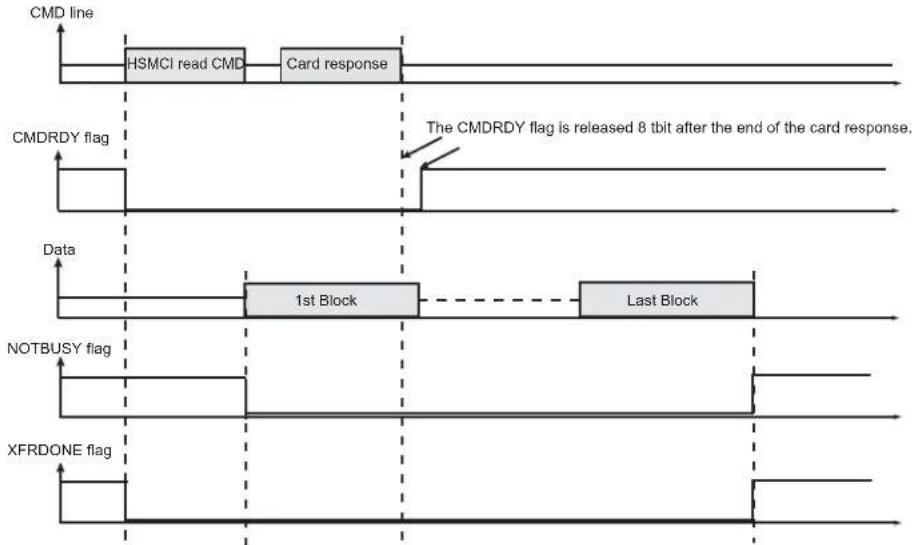
flowchart
graph TD
    A["CMD line"] --> B["HSMCI read CMD"]
    B --> C["Card response"]
    D["CMDRDY flag"] --> E["Data"]
    F["NOTBUSY flag"] --> G["XFRDONE flag"]
    H["1st Block"] --> I["Last Block"]
    J["The CMDRDY flag is released 8 tbit after the end of the card response."] --> K["End of card response"]
39.12.3 Write Access
During a write access, the XFRDONE flag behaves as shown in the following figure.
Figure 39-12. XFRDONE During a Write Access
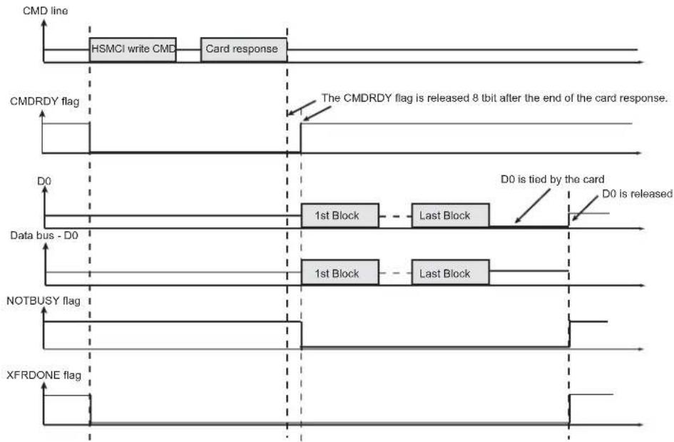
flowchart
graph TD
    A["CMD line"] --> B["HSMCI write CMD"]
    B --> C["Card response"]
    D["CMDRDY flag"] --> E["The CMDRDY flag is released 8 tbit after the end of the card response."]
    F["Data bus - D0"] --> G["1st Block"]
    G --> H["Last Block"]
    H --> I["D0 is tied by the card"]
    J["NOTBUSY flag"] --> K["1st Block"]
    K --> L["Last Block"]
    L --> M["D0 is released"]
    N["XFRDONE flag"] --> O["End"]
39.13 Register Write Protection
To prevent any single software error from corrupting HSMCI behavior, certain registers in the address space can be write-protected by setting the WPEN bit in the HSMCI Write Protection Mode Register (HSMCI_WPMR).
If a write access to a write-protected register is detected, the WPVS bit in the HSMCI Write Protection Status Register (HSMCI_WPSR) is set and the field WPVSRC indicates the register in which the write access has been attempted.
The WPVS bit is automatically cleared after reading the HSMCI_WPSR.
The following registers can be protected:
• HSMCI Mode Register
• HSMCI Data Timeout Register
• HSMCI SDCard/SDIO Register
• HSMCI Completion Signal Timeout Register
• HSMCI DMA Configuration Register
• HSMCI Configuration Register
39.14 Register Summary
| Offset | Name Bit Pos. 7 | 6 | 5 | 4 | 3 | 2 | 1 | 0 | ||||||||
| 0x00 | HSMCI_CR | 7:0 SWRST PWSDIS PWSEN MCIDIS MCIEN | ||||||||||||||
| 15:8 | ||||||||||||||||
| 23:16 | ||||||||||||||||
| 31:24 | ||||||||||||||||
| 0x04 | HSMCI_MR | 7:0 CLKDIV[7:0] | ||||||||||||||
| 15:8 | PADV | FBYTE | WRPROOF | RDPROOF | PWSDIV[2:0] | |||||||||||
| 23:16 | CLKODD | |||||||||||||||
| 31:24 | ||||||||||||||||
| 0x08 | HSMCI_DTOR | 7:0 DTOMUL[2:0] | DTOCYC[3:0] | |||||||||||||
| 15:8 | ||||||||||||||||
| 23:16 | ||||||||||||||||
| 31:24 | ||||||||||||||||
| 0x0C | HSMCI_SDCR | 7:0 SDCBUS[1:0] | SDCSEL[1:0] | |||||||||||||
| 15:8 | ||||||||||||||||
| 23:16 | ||||||||||||||||
| 31:24 | ||||||||||||||||
| 0x10 | HSMCI_ARGR | 7:0 ARG[7:0] | ||||||||||||||
| 15:8 | ARG[15:8] | |||||||||||||||
| 23:16 | ARG[23:16] | |||||||||||||||
| 31:24 | ARG[31:24] | |||||||||||||||
| 0x14 | HSMCI_CMDR | 7:0 RSPTYP[1:0] | CMDNB[5:0] | |||||||||||||
| 15:8 MAXLAT OPDCMD | SPCMD[2:0] | |||||||||||||||
| 23:16 TRTYP[2:0] | TRDIR | TRCMD[1:0] | ||||||||||||||
| 31:24 | BOOT_ACK | ATACS | IOSPCMD[1:0] | |||||||||||||
| 0x18 | HSMCI_BLKR | 7:0 BCNT[7:0] | ||||||||||||||
| 15:8 BCNT[15:8] | ||||||||||||||||
| 23:16 BLKLEN[7:0] | ||||||||||||||||
| 31:24 BLKLEN[15:8] | ||||||||||||||||
| 0x1C | HSMCI_CSTOR | 7:0 CSTOMUL[2:0] | CSTOCYC[3:0] | |||||||||||||
| 15:8 | ||||||||||||||||
| 23:16 | ||||||||||||||||
| 31:24 | ||||||||||||||||
| 0x20 | HSMCI_RSP[0..3] | 7:0 RSP[7:0] | ||||||||||||||
| 15:8 RSP[15:8] | ||||||||||||||||
| 23:16 RSP[23:16] | ||||||||||||||||
| 31:24 RSP[31:24] | ||||||||||||||||
| 0x24 ... 0x2F | Reserved | |||||||||||||||
| 0x30 | HSMCI_RDR | 7:0 DATA[7:0] | ||||||||||||||
| 15:8 DATA[15:8] | ||||||||||||||||
| 23:16 DATA[23:16] | ||||||||||||||||
| 31:24 DATA[31:24] | ||||||||||||||||
| 0x34 | HSMCI_TDR | 7:0 DATA[7:0] | ||||||||||||||
| 15:8 DATA[15:8] | ||||||||||||||||
| 23:16 DATA[23:16] | ||||||||||||||||
| 31:24 DATA [31:24] | ||||||||||||||||
| 0x38 ... 0x3F | Reserved | |||||||||||||||
| 0x40 | HSMCI_SR | 7:0 NOTBUSY DTIP BLKE TXRDY RXRDY CMDRDY | ||||||||||||||
| 15:8 CSRCV SDIOWAIT | SDIOIRQA | |||||||||||||||
| 23:16 CSTOE DTOE DCRCE RTOE RENDE RCRCE RDIRE RINDE | ||||||||||||||||
| 31:24 UNRE OVRE ACKRCVE ACKRCV XFRDONE FIFOEMPTY BLKOVRE | ||||||||||||||||
| 0x44 | HSMCI_IER | 7:0 NOTBUSY DTIP BLKE TXRDY RXRDY CMDRDY | ||||||||||||||
| 15:8 CSRCV SDIOWAIT | SDIOIRQA | |||||||||||||||
| 23:16 CSTOE DTOE DCRCE RTOE RENDE RCRCE RDIRE RINDE | ||||||||||||||||
| 31:24 UNRE OVRE ACKRCVE ACKRCW XFRDONE FIFOEMPTY BLKOVRE | ||||||||||||||||
| 0x48 | HSMCI_IDR | 7:0 | NOTBUSY DTIP BLKE TXRDY RXRDY CMDRDY | |||||||||||||
| 15:8 | CSRCV SDIOWAIT SDIOIRQA | |||||||||||||||
| 23:16 | CSTOE | DTOE | DCRCE | RTOE | RENDE | RCRCE | RDIRE | RINDE | ||||||||
| 31:24 | UNRE | OVRE | ACKRCVE | ACKRCV | XFRDONE | FIFOEMPTY | BLKOVRE | |||||||||
| 0x4C | HSMCI_IMR | 7:0 | NOTBUSY DTIP BLKE TXRDY RXRDY CMDRDY | |||||||||||||
| 15:8 | CSRCV SDIOWAIT SDIOIRQA | |||||||||||||||
| 23:16 | CSTOE | DTOE | DCRCE | RTOE | RENDE | CRRCE | RDIRE | RINDE | ||||||||
| 31:24 | UNRE | OVRE | ACKRCVE | ACKRCV | XFRDONE | FIFOEMPTY | BLKOVRE | |||||||||
| 0x50 | HSMCI_DMA | 7:0 | CHKSIZE[2:0] | |||||||||||||
| 15:8 | DMAEN | |||||||||||||||
| 23:16 | ||||||||||||||||
| 31:24 | ||||||||||||||||
| 0x54 | HSMCI_CFG | 7:0 | FERRCTRL FIFOMODE | |||||||||||||
| 15:8 | LSYNC HSMODE | |||||||||||||||
| 23:16 | ||||||||||||||||
| 31:24 | ||||||||||||||||
| 0x58 ... 0xE3 | Reserved | |||||||||||||||
| 0xE4 | HSMCI_WPMR | 7:0 | WPEN | |||||||||||||
| 15:8 | WPKEY[7:0] | |||||||||||||||
| 23:16 | WPKEY[15:8] | |||||||||||||||
| 31:24 | WPKEY[23:16] | |||||||||||||||
| 0xE8 | HSMCI_WPSR | 7:0 | WPVS | |||||||||||||
| 15:8 | WPVSRC[7:0] | |||||||||||||||
| 23:16 | WPVSRC[15:8] | |||||||||||||||
| 31:24 | ||||||||||||||||
| 0xEC ... 0x01FF | Reserved | |||||||||||||||
| 0x0200 | HSMCI_FIFOx [x=0..255] | 7:0 | DATA[7:0] | |||||||||||||
| 15:8 | DATA[15:8] | |||||||||||||||
| 23:16 | DATA[23:16] | |||||||||||||||
| 31:24 | DATA[31:24] | |||||||||||||||
39.14.1 HSMCI Control Register
Name: HSMCI_CR
Offset: 0x00
Property: Write-only
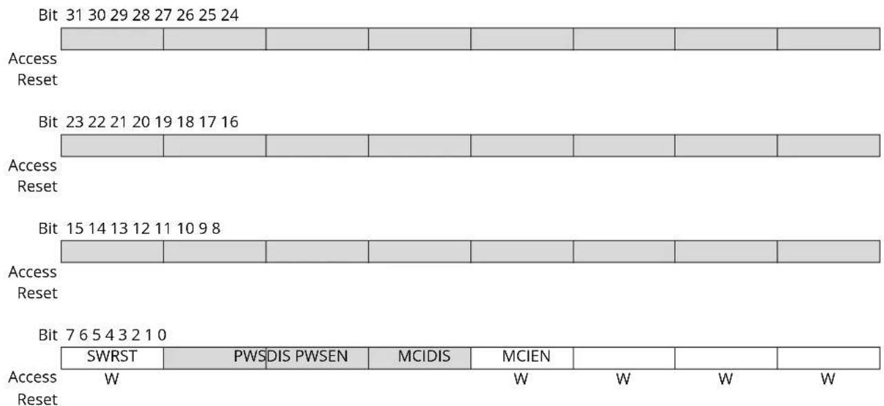
text_image
Bit 31 30 29 28 27 26 25 24 Access Reset Bit 23 22 21 20 19 18 17 16 Access Reset Bit 15 14 13 12 11 10 9 8 Access Reset Bit 7 6 5 4 3 2 1 0 SWRST PWS DIS PWSEN MCIDIS MCIEN W W W W Access Reset W W W WBit 7 - SWRST Software Reset
| Value | Description |
| 0 | No effect. |
| 1 | Resets the HSMCI. A software triggered hardware reset of the HSMCI is performed. |
Bit 3 - PWSDIS Power Save Mode Disable
| Value | Description |
| 0 | No effect. |
| 1 | Disables the Power Saving Mode. |
Bit 2 - PWSEN Power Save Mode Enable

Before enabling this mode, the user must set a value different from 0 in the PWSDIV field of the HSMCI_MR.
| Value | Description |
| 0 | No effect. |
| 1 | Enables the Power Saving Mode if PWSDIS is 0. |
Bit 1 - MCIDIS Multi-Media Interface Disable
| Value | Description |
| 0 | No effect. |
| 1 | Disables the Multi-Media Interface. |
Bit 0 - MCIEN Multi-Media Interface Enable
| Value | Description |
| 0 | No effect. |
Value Description
1 Enables the Multi-Media Interface if MCDIS is 0.
39.14.2 HSMCI Mode Register
Name: HSMCI_MR
Offset: 0x04
Reset: 0x0
Property: Read/Write
This register can only be written if the WPEN bit is cleared in the HSMCI Write Protection Mode Register.

text_image
Bit 31 30 29 28 27 26 25 24 Access Reset Bit 23 22 21 20 19 18 17 16 Access Reset 0 CLKODD R/W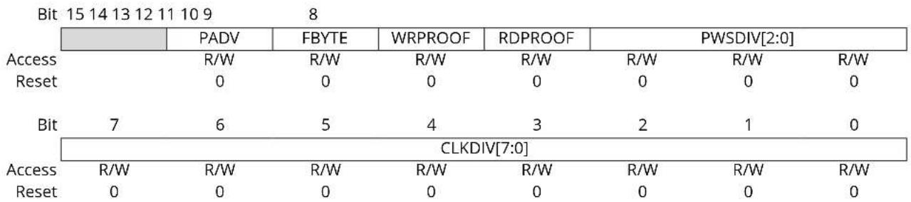
other
Bit 15 14 13 12 11 10 9 8 | Bit | PADV | FBYTE | WRPROOF | RDPROOF | PWSDIV[2:0] | Access Reset | R/W 0 | R/W 0 | R/W 0 | R/W 0 | R/W 0 | R/W 0 | | :--- | :--- | :--- | :--- | :--- | :--- | :--- | | Bit | 7 | 6 | 5 | 4 | 3 | 2 | | CLKDIV[7:0]Bit 16 - CLKODD Clock divider is odd
This bit is the least significant bit of the clock divider and indicates the clock divider parity.
Bit 14 - PADV Padding Value
PADV may be only in manual transfer.
| Value | Description |
| 0 | 0x00 value is used when padding data in write transfer. |
| 1 | 0xFF value is used when padding data in write transfer. |
Bit 13 - FBYTE Force Byte Transfer
Enabling Force Byte Transfer allow byte transfers, so that transfer of blocks with a size different from modulo 4 can be supported.

BLKLEN value depends on FBYTE.
| Value | Description |
| 0 | Disables Force Byte Transfer. |
| 1 | Enables Force Byte Transfer. |
Bit 12 - WRPROOF Write Proof Enable
Enabling Write Proof allows to stop the HSMCI Clock during write access if the internal FIFO is full. This will guarantee data integrity, not bandwidth.
| Value Description | |
| 0 | Disables Write Proof. |
| 1 | Enables Write Proof. |
Bit 11 - RDPROOF Read Proof Enable
Enabling Read Proof allows to stop the HSMCI Clock during read access if the internal FIFO is full. This will guarantee data integrity, not bandwidth.
| Value Description | |
| 0 | Disables Read Proof. |
| 1 | Enables Read Proof. |
Bits 10:8 - PWSDIV[2:0] Power Saving Divider
High Speed MultiMedia Card Interface clock is divided by 2^(PWSDIV) + 1 when entering Power Saving Mode.
![Microchip ATSAMS70Q19 - Bits 10:8 - PWSDIV[2:0] Power Saving Divider - 1](/content/2026/06/1221740/images/f076b4fab0a276b3e09c2e39c2cf70ffd1c9899c62a8b003c5a2ab64eb137841.jpg)
This value must be different from 0 before enabling the Power Save Mode in the HSMCI_CR (PWSEN bit).
Bits 7:0 - CLKDIV[7:0] Clock Divider
High Speed MultiMedia Card Interface clock (MCCK or HSMCI_CK) is Host Clock (MCK) divided by 2 × CLKDIV + CLKODD + 2.
39.14.3 HSMCI Data Timeout Register
Name: HSMCI_DTOR
Offset: 0x08
Reset: 0x0
Property: Read/Write
This register can only be written if the WPEN bit is cleared in the HSMCI Write Protection Mode Register.

text_image
Bit 31 30 29 28 27 26 25 24 Access Reset Bit 23 22 21 20 19 18 17 16 Access Reset Bit 15 14 13 12 11 10 9 8 Access Reset Bit 7 6 5 4 3 2 1 0 Access Reset DTOMUL[2:0] R/W R/W R/W R/W R/W R/W 0 0 0 0 0 0 0 DTOCYC[3:0]Bits 6:4 - DTOMUL[2:0] Data Timeout Multiplier
If the data time-out set by DTOCYC and DTOMUL has been exceeded, the Data Time-out Error flag (DTOE) in the HSMCI Status Register (HSMCI_SR) rises.
| Value | Name | Description |
| 0 | 1 | DTOCYC |
| 1 | 16 | DTOCYC x 16 |
| 2 | 128 | DTOCYC x 128 |
| 3 | 256 | DTOCYC x 256 |
| 4 | 1024 | DTOCYC x 1024 |
| 5 | 4096 | DTOCYC x 4096 |
| 6 | 65536 | DTOCYC x 65536 |
| 7 | 1048576 | DTOCYC x 1048576 |
Bits 3:0 - DTOCYC[3:0] Data Timeout Cycle Number
This field determines the maximum number of Host Clock cycles that the HSMCI waits between two data block transfers. It equals (DTOCYC x Multiplier).
39.14.4 HSMCI SDCard/SDIO Register
Name: HSMCI_SDCR
Offset: 0x0C
Reset: 0x0
Property: Read/Write
This register can only be written if the WPEN bit is cleared in the HSMCI Write Protection Mode Register.
bar_stacked
| Bit | Access Reset | SDCBUS[1:0] | SDCSEL[1:0] | | --- | --- | --- | --- | | 31 | 0 | R/W | 0 | | 30 | 0 | R/W | 0 | | 29 | 0 | R/W | 0 | | 28 | 0 | R/W | 0 | | 27 | 0 | R/W | 0 | | 26 | 0 | R/W | 0 | | 25 | 0 | R/W | 0 | | 24 | 0 | R/W | 0 | | 23 | 0 | R/W | 0 | | 22 | 0 | R/W | 0 | | 21 | 0 | R/W | 0 | | 20 | 0 | R/W | 0 | | 19 | 0 | R/W | 0 | | 18 | 0 | R/W | 0 | | 17 | 0 | R/W | 0 | | 16 | 0 | R/W | 0 | | 15 | 0 | R/W | 0 | | 14 | 0 | R/W | 0 | | 13 | 0 | R/W | 0 | | 12 | 0 | R/W | 0 | | 11 | 0 | R/W | 0 | | 10 | 0 | R/W | 0 | | 9 | 0 | R/W | 0 | | 8 | 0 | R/W | 0 | | 7 | 0 | R/W | 0 | | 6 | 0 | R/W | 0 | | 5 | 0 | R/W | 0 | | 4 | 0 | R/W | 0 | | 3 | 0 | R/W | 0 | | 2 | 0 | R/W | 0 | | 1 | 0 | R/W | 0 | | 0 | 0 | R/W | 0 | | Not applicable to SDCBUS[1:0] or SDCSEL[1:0].Bits 7:6 - SDCBUS[1:0] SDCard/SDIO Bus Width
| Value | Name | Description |
| 0 | 1 | 1 bit |
| 1 | Reserved | |
| 2 | 4 | 4 bits |
| 3 | 8 | 8 bits |
Bits 1:0 - SDCSEL[1:0] SDCard/SDIO Slot
| Value | Name | Description |
| 0 | SLOTA | Slot A is selected. |
| 1 | SLOTB | Reserved |
| 2 | SLOTC | Reserved |
| 3 | SLOTD | Reserved |
39.14.5 HSMCI Argument Register
Name: HSMCI_ARGR
Offset: 0x10
Reset: 0x0
Property: Read/Write
Bit 31 30 29 28 27 26 25 24
ARG[31:24]
Access R/W R/W R/W R/W R/W R/W R/W R/W
Reset 00000000
Bit 23 22 21 20 19 18 17 16
ARG[23:16]
Access R/W R/W R/W R/W R/W R/W R/W R/W
Reset 00000000
Bit 15 14 13 12 11 10 9 8
ARG[15:8]
Access R/W R/W R/W R/W R/W R/W R/W R/W
Reset 00000000
Bit 76543210
ARG[7:0]
Access R/W R/W R/W R/W R/W R/W R/W R/W
Reset 00000000
Bits 31:0 - ARG[31:0] Command Argument
39.14.6 HSMCI Command Register
Name: HSMCI_CMDR
Offset: 0x14
Property: Write-only
This register is write-protected while CMDRDY is 0 in HSMCI_SR. If an Interrupt command is sent, this register is only writable by an interrupt response (field SPCMD). This means that the current command execution cannot be interrupted or modified.
Bit 31 30 29 28 27 26 25 24
| BOOT_ACK ATACS IOSPCMD[1:0] | ||||
| Access Reset | WWWW | |||
Bit 23 22 21 20 19 18 17 16
| TRTYP[2:0] TRDIR TRCMD[1:0] | |||
| Access Reset | WWWWWW | ||
Bit 15 14 13 12 11 10 9 8
| MAXLAT | OPDCMD | SPCMD[2:0] | ||
| Access Reset | WWWWW | |||
| Bit | 7 | 6 | 5 | 4 | 3 | 2 | 1 | 0 |
| RSPTYP[1:0] | CMDNB[5:0] | |||||||
| Access | W | W | W | W | W | W | W | W |
| Reset |
Bit 27 - BOOT\_ACK Boot Operation Acknowledge
The Host can choose to receive the boot acknowledge from the Client when a Boot Request command is issued. When set to one this field indicates that a Boot acknowledge is expected within a programmable amount of time defined with DTOMUL and DTOCYC fields located in the HSMCI_DTOR. If the acknowledge pattern is not received then an acknowledge timeout error is raised. If the acknowledge pattern is corrupted then an acknowledge pattern error is set.
Bit 26 - ATACS ATA with Command Completion Signal
0 (NORMAL): Normal operation mode.
1 (COMPLETION): This bit indicates that a completion signal is expected within a programmed amount of time (HSMCI_CSTOR).
Bits 25:24 - IOSPCMD[1:0] SDIO Special Command
| Value | Name Description | |
| 0 | STD | Not an SDIO Special Command |
| 1 | SUSPEND | SDIO Suspend Command |
| 2 | RESUME | SDIO Resume Command |
Bits 21:19 - TRTYP[2:0] Transfer Type
| Value | Name | Description |
| 0 | SINGLE | MMC/SD Card Single Block |
| 1 | MULTIPLE | MMC/SD Card Multiple Block |
| 2 | STREAM | MMC Stream |
| 4 | BYTE | SDIO Byte |
| 5 | BLOCK | SDIO Block |
Bit 18 - TRDIR Transfer Direction
0 (WRITE): Write.
1 (READ): Read.
Bits 17:16 - TRCMD[1:0] Transfer Command
| Value Name | Description | |
| 0 | NO_DATA No data transfer | |
| 1 | START_DATA Start data transfer | |
| 2 | STOP_DATA Stop data transfer | |
| 3 | Reserved Reserved |
Bit 12 - MAXLAT Max Latency for Command to Response
0 (5): 5-cycle max latency.
1 (64): 64-cycle max latency.
Bit 11 - OPDCMD Open Drain Command
0 (PUSHPULL): Push pull command.
1 (OPENDRAIN): Open drain command.
Bits 10:8 - SPCMD[2:0] Special Command
| Value Name | Description |
| 0 | STD Not a special CMD. |
| 1 | INIT Initialization CMD:74 clock cycles for initialization sequence. |
| 2 | SYNC Synchronized CMD:Wait for the end of the current data block transfer before sending the pending command. |
| 3 | CE_ATA CE-ATA Completion Signal disable Command.The host cancels the ability for the device to return a command completion signal on the command line. |
| 4 | IT_CMD Interrupt command:Corresponds to the Interrupt Mode (CMD40). |
| 5 | IT_RESP Interrupt response:Corresponds to the Interrupt Mode (CMD40). |
| 6 | BOR Boot Operation Request.Start a boot operation mode, the host processor can read boot data from the MMC device directly. |
| 7 | EBO End Boot Operation.This command allows the host processor to terminate the boot operation mode. |
Bits 7:6 - RSPTYP[1:0] Response Type
| Value Name | Description | |
| 0 | NORESP | No response |
| 1 | 48_BIT | 48-bit response |
| 2 | 136_BIT | 136-bit response |
| 3 | R1B | R1b response type |
Bits 5:0 - CMDNB[5:0] Command Number
This is the command index.
39.14.7 HSMCI Block Register
Name: HSMCI_BLKR
Offset: 0x18
Reset: 0x0
Property: Read/Write
Bit 31 30 29 28 27 26 25 24
BLKLEN[15:8]
Access R/W R/W R/W R/W R/W R/W R/W R/W
Reset 00000000
Bit 23 22 21 20 19 18 17 16
BLKLEN[7:0]
Access R/W R/W R/W R/W R/W R/W R/W R/W
Reset 00000000
Bit 15 14 13 12 11 10 9 8
BCNT[15:8]
Access R/W R/W R/W R/W R/W R/W R/W R/W
Reset 00000000
Bit 76543210
BCNT[7:0]
Access R/W R/W R/W R/W R/W R/W R/W R/W
Reset 00000000
Bits 31:16 - BLKLEN[15:0] Data Block Length
This field determines the size of the data block.
Bits 16 and 17 must be configured to 0 if FBYTE is disabled.
Note: In SDIO Byte mode, BLKLEN field is not used.
Bits 15:0 - BCNT[15:0] MMC/SDIO Block Count - SDIO Byte Count
This field determines the number of data byte(s) or block(s) to transfer.
The transfer data type and the authorized values for BCNT field are determined by the TRTYP field in the HSMCI Command Register (HSMCI_CMDR).
When TRTYP = 1 (MMC/SDCARD Multiple Block), BCNT can be programmed from 1 to 65535, 0 corresponds to an infinite block transfer.
When TRTYP = 4 (SDIO Byte), BCNT can be programmed from 1 to 511, 0 corresponds to 512-byte transfer. Values in range 512 to 65536 are forbidden.
When TRTYP = 5 (SDIO Block), BCNT can be programmed from 1 to 511, 0 corresponds to an infinite block transfer. Values in range 512 to 65536 are forbidden.
![Microchip ATSAMS70Q19 - Bits 15:0 - BCNT[15:0] MMC/SDIO Block Count - SDIO Byte Count - 1](/content/2026/06/1221740/images/3226cf0f80b90628d73a06d989ad2fc217f1e57438c45f517b30f5c5703358df.jpg)
In SDIO Byte and Block modes (TRTYP = 4 or 5), writing the 7 last bits of BCNT field with a value which differs from 0 is forbidden and may lead to unpredictable results.
39.14.8 HSMCI Completion Signal Timeout Register
Name: HSMCI_CSTOR
Offset: 0x1C
Reset: 0x0
Property: Read/Write
This register can only be written if the WPEN bit is cleared in the HSMCI Write Protection Mode Register.

text_image
Bit 31 30 29 28 27 26 25 24 Access Reset Bit 23 22 21 20 19 18 17 16 Access Reset Bit 15 14 13 12 11 10 9 8 Access Reset Bit 7 6 5 4 3 2 1 0 Access Reset CSTOMUL[2:0] R/W R/W R/W R/W R/W R/W 0 0 0 0 0 0 0 CSTOCYC[3:0]Bits 6:4 - CSTOMUL[2:0] Completion Signal Timeout Multiplier
This field determines the maximum number of Host Clock cycles that the HSMCI waits between two data block transfers. Its value is calculated by (CSTOCYC x Multiplier).
These fields determine the maximum number of Host Clock cycles that the HSMCI waits between the end of the data transfer and the assertion of the completion signal. The data transfer comprises data phase and the optional busy phase. If a non-DATA ATA command is issued, the HSMCI starts waiting immediately after the end of the response until the completion signal.
Multiplier is defined by CSTOMUL as shown in the following table:
If the data time-out set by CSTOCYC and CSTOMUL has been exceeded, the Completion Signal Time-out Error flag (CSTOE) in the HSMCI Status Register (HSMCI_SR) rises.
| Value | Name | Description |
| 0 | 1 | CSTOCYC x 1 |
| 1 | 16 | CSTOCYC x 16 |
| 2 | 128 | CSTOCYC x 128 |
| 3 | 256 | CSTOCYC x 256 |
| 4 | 1024 | CSTOCYC x 1024 |
| 5 | 4096 | CSTOCYC x 4096 |
| 6 | 65536 | CSTOCYC x 65536 |
| 7 | 1048576 | CSTOCYC x 1048576 |
Bits 3:0 - CSTOCYC[3:0] Completion Signal Timeout Cycle Number
This field determines the maximum number of Host Clock cycles that the HSMCI waits between two data block transfers. Its value is calculated by (CSTOCYC x Multiplier).
39.14.9 HSMCI Response Register
Name: HSMCI_RSPR[0..3]
Offset: 0x20
Reset: 0x0
Property: Read-only
Note: The RSP data size can be up to 128 bit. According to the data size, RSP data is available at consecutive addresses (0x20, 0x24, 0x28, 0x2C).
| Bit 31 30 29 28 27 26 25 24 | |
| RSP[31:24] | |
| Access R R R R R R R R | |
| Reset 0 0 0 0 0 0 0 0 | |
| Bit 23 22 21 20 19 18 17 16 | |
| RSP[23:16] | |
| Access R R R R R R R R | |
| Reset 0 0 0 0 0 0 0 0 | |
| Bit 15 14 13 12 11 10 9 8 | |
| RSP[15:8] | |
| Access R R R R R R R R | |
| Reset 0 0 0 0 0 0 0 0 | |
| Bit 7 6 5 4 3 2 1 0 | |
| RSP[7:0] | |
| Access R R R R R R R R | |
| Reset 0 0 0 0 0 0 0 0 | |
Bits 31:0 - RSP[31:0] Response
39.14.10 HSMCI Receive Data Register
Name: HSMCI_RDR
Offset: 0x30
Reset: 0x0
Property: Read-only
| Bit 31 30 29 28 27 26 25 24 | |
| DATA[31:24] | |
| Access R R R R R R R R | |
| Reset 0 0 0 0 0 0 0 0 | |
| Bit 23 22 21 20 19 18 17 16 | |
| DATA[23:16] | |
| Access R R R R R R R R | |
| Reset 0 0 0 0 0 0 0 0 | |
| Bit 15 14 13 12 11 10 9 8 | |
| DATA[15:8] | |
| Access R R R R R R R R | |
| Reset 0 0 0 0 0 0 0 0 | |
| Bit 7 6 5 4 3 2 1 0 | |
| DATA[7:0] | |
| Access R R R R R R R R | |
| Reset 0 0 0 0 0 0 0 0 | |
Bits 31:0 - DATA[31:0] Data to Read
39.14.11 HSMCI Transmit Data Register
Name: HSMCI_TDR
Offset: 0x34
Property: Write-only
text_image
Bit 31 30 29 28 27 26 25 24 DATA[31:24] Access W W W W W W W W W Reset Bit 23 22 21 20 19 18 17 16 DATA[23:16] Access W W W W W W W W W Reset Bit 15 14 13 12 11 10 9 8 DATA[15:8] Access W W W W W W W W W Reset Bit 7 6 5 4 3 2 1 0 DATA[7:0] Access W W W W W W W W W ResetBits 31:0 - DATA[31:0] Data to Write
39.14.12 HSMCI Status Register
Name: HSMCI_SR
Offset: 0x40
Reset: 0xC0E5
Property: Read-only
Bit 31 30 29 28 27 26 25 24
| UNRE OVRE ACKRCVE ACKRCV XFRDONE FIFOEMPTY BLKOVRE | ||||||||
| Access | R | R | R | R | R | R | R | |
| Reset | 0 | 0 | 0 | 0 | 0 | 0 | 0 | |
Bit 23 22 21 20 19 18 17 16
| CSTOE | DTOE | DCRCE | RTOE | RENDE | RCRCE | RDIRE | RINDE | |
| Access | R | R | R | R | R | R | R | R |
| Reset | 0 | 0 | 0 | 0 | 0 | 0 | 0 | 0 |
Bit 15 14 13 12 11 10 9 8
| CSRCV | SDIOWAIT | SDIOIRQA | |||||
| Access | R | R | R | ||||
| Reset | 0 | 0 | 0 |
Bit 7 6 5 4 3 2 1 0
| NOTBUSY | DTIP | BLKE | TXRDY | RXRDY | CMDRDY | ||
| Access | R | R | R | R | R | R | |
| Reset | 1 | 0 | 0 | 1 | 0 | 1 |
Bit 31 - UNRE Underrun (if FERRCTRL = 1, cleared by writing in HSMCI_CMDR or cleared on read if FERRCTRL = 0)
If FERRCTRL = 1 in HSMCI_CFG, OVRE is cleared on read.
If FERRCTRL = 0 in HSMCI_CFG, OVRE is cleared by writing HSMCI_CMDR.
| Value | Description |
| 0 | No error. |
| 1 | At least one 8-bit data has been sent without valid information (not written). |
Bit 30 - OVRE Overrun (if FERRCTRL = 1, cleared by writing in HSMCI_CMDR or cleared on read if FERRCTRL = 0)
If FERRCTRL = 1 in HSMCI_CFG, OVRE is cleared on read.
If FERRCTRL = 0 in HSMCI_CFG, OVRE is cleared by writing HSMCI_CMDR.
| Value | Description |
| 0 | No error. |
| 1 | At least one 8-bit received data has been lost (not read). |
Bit 29 - ACKRCVE Boot Operation Acknowledge Error (cleared on read)
| Value | Description |
| 0 | No boot operation error since the last read of HSMCI_SR |
| 1 | Corrupted Boot Acknowledge signal received since the last read of HSMCI_SR. |
Bit 28 - ACKRCV Boot Operation Acknowledge Received (cleared on read)
| Value | Description |
| 0 | No Boot acknowledge received since the last read of the HSMCI_SR. |
| 1 | A Boot acknowledge signal has been received since the last read of HSMCI_SR. |
Bit 27 - XFRDONE Transfer Done flag
| Value Description | |
| 0 | A transfer is in progress. |
| 1 | Command Register is ready to operate and the data bus is in the idle state. |
Bit 26 - FIFOEMPTY FIFO empty flag
| Value Description | |
| 0 | FIFO contains at least one byte. |
| 1 | FIFO is empty. |
Bit 24 - BLKOVRE DMA Block Overrun Error (cleared on read)
| Value Description | |
| 0 | No error. |
| 1 | A new block of data is received and the DMA controller has not started to move the current pending block, a block overrun is raised. |
Bit 23 - CSTOE Completion Signal Time-out Error (cleared on read)
| Value Description | |
| 0 | No error. |
| 1 | The completion signal time-out set by CSTOCYC and CSTOMUL in HSMCI_CSTOR has been exceeded. |
Bit 22 - DTOE Data Time-out Error (cleared on read)
| Value Description | |
| 0 | No error. |
| 1 | The data time-out set by DTOCYC and DTOMUL in HSMCI_DTOR has been exceeded. |
Bit 21 - DCRCE Data CRC Error (cleared on read)
| Value Description | |
| 0 | No error. |
| 1 | A CRC16 error has been detected in the last data block. |
Bit 20 - RTOE Response Time-out Error (cleared by writing in HSMCI_CMDR)
| Value Description | |
| 0 | No error. |
| 1 | The response time-out set by MAXLAT in the HSMCI_CMDR has been exceeded. |
Bit 19 - RENDE Response End Bit Error (cleared by writing in HSMCI_CMDR)
| Value Description | |
| 0 | No error. |
| 1 | The end bit of the response has not been detected. |
Bit 18 - RCRCE Response CRC Error (cleared by writing in HSMCI_CMDR)
| Value Description | |
| 0 | No error. |
| 1 | A CRC7 error has been detected in the response. |
Bit 17 - RDIRE Response Direction Error (cleared by writing in HSMCI_CMDR)
| Value Description | |
| 0 | No error. |
| 1 | The direction bit from card to host in the response has not been detected. |
Bit 16 - RINDE Response Index Error (cleared by writing in HSMCI_CMDR)
| Value Description | |
| 0 | No error. |
| 1 | A mismatch is detected between the command index sent and the response index received. |
Bit 13 - CSRCV CE-ATA Completion Signal Received (cleared on read)
| Value Description | |
| 0 | No completion signal received since last status read operation. |
| 1 | The device has issued a command completion signal on the command line. |
Bit 12 - SDIOWAIT SDIO Read Wait Operation Status
| Value Description | |
| 0 | Normal Bus operation. |
| 1 | The data bus has entered IO wait state. |
Bit 8 - SDIOIRQA SDIO Interrupt for Slot A (cleared on read)
| Value Description | |
| 0 | No interrupt detected on SDIO Slot A. |
| 1 | An SDIO Interrupt on Slot A occurred. |
Bit 5 - NOTBUSY HSMCI Not Busy
A block write operation uses a simple busy signalling of the write operation duration on the data (DAT0) line: during a data transfer block, if the card does not have a free data receive buffer, the card indicates this condition by pulling down the data line (DAT0) to LOW. The card stops pulling down the data line as soon as at least one receive buffer for the defined data transfer block length becomes free.
Refer to the MMC or SD Specification for more details concerning the busy behavior.
For all the read operations, the NOTBUSY flag is cleared at the end of the host command.
For the Infinite Read Multiple Blocks, the NOTBUSY flag is set at the end of the STOP_TRANSMISSION host command (CMD12).
For the Single Block Reads, the NOTBUSY flag is set at the end of the data read block.
For the Multiple Block Reads with predefined block count, the NOTBUSY flag is set at the end of the last received data block.
The NOTBUSY flag allows to deal with these different states.
| Value Description | |
| 0 | The HSMCI is not ready for new data transfer. Cleared at the end of the card response. |
| 1 | The HSMCI is ready for new data transfer. Set when the busy state on the data line has ended. This corresponds to a free internal data receive buffer of the card. |
Bit 4 - DTIP Data Transfer in Progress (cleared at the end of CRC16 calculation)
| Value Description | |
| 0 | No data transfer in progress. |
| 1 | The current data transfer is still in progress, including CRC16 calculation. |
Bit 3 - BLKE Data Block Ended (cleared on read)
This flag must be used only for Write Operations.
Refer to the MMC or SD Specification for more details concerning the CRC Status.
| Value Description | |
| 0 | A data block transfer is not yet finished. |
| 1 | A data block transfer has ended, including the CRC16 Status transmission. The flag is set for each transmitted CRC Status. |
Bit 2 - TXRDY Transmit Ready (cleared by writing in HSMCI_TDR)
| Value Description | |
| 0 | The last data written in HSMCI_TDR has not yet been transferred in the Shift Register. |
| 1 | The last data written in HSMCI_TDR has been transferred in the Shift Register. |
Bit 1 - RXRDY Receiver Ready (cleared by reading HSMCI_RDR)
| Value Description | |
| 0 | Data has not yet been received since the last read of HSMCI_RDR. |
| 1 | Data has been received since the last read of HSMCI_RDR. |
Bit 0 - CMDRDY Command Ready (cleared by writing in HSMCI_CMDR)
Value Description
| 0 | A command is in progress. |
| 1 | The last command has been sent. |
39.14.13 HSMCI Interrupt Enable Register
Name: HSMCI_IER
Offset: 0x44
Property: Write-only
The following configuration values are valid for all listed bit names of this register:
0: No effect.
1: Enables the corresponding interrupt.
Bit 31 30 29 28 27 26 25 24
| UNRE OVRE ACKRCVE ACKRCV XFRDONE FIFOEMPTY BLKOVRE | ||||
| Access Reset | WWWWWWW W |
Bit 23 22 21 20 19 18 17 16
| CSTOE | DTOE | DCRCE | RTOE | RENDE | RCRCE | RDIRE | RINDE | |
| Access Reset | WWWWWWWW | |||||||
Bit 15 14 13 12 11 10 9 8
| CSRCV | SDIOWAIT | SDIOIRQA | |||||
| Access Reset | WW | W | |||||
Bit 7 6 5 4 3 2 1 0
| NOTBUSY | DTIP | BLKE | TXRDY | RXRDY | CMDRDY | ||
| Access Reset | WWWWWW | ||||||
Bit 31 - UNRE Underrun Interrupt Enable
Bit 30 - OVRE Overrun Interrupt Enable
Bit 29 - ACKRCVE Boot Acknowledge Error Interrupt Enable
Bit 28 - ACKRCV Boot Acknowledge Interrupt Enable
Bit 27 - XFRDONE Transfer Done Interrupt enable
Bit 26 - FIFOEMPTY FIFO empty Interrupt enable
Bit 24 - BLKOVRE DMA Block Overrun Error Interrupt Enable
Bit 23 - CSTOE Completion Signal Timeout Error Interrupt Enable
Bit 22 - DTOE Data Time-out Error Interrupt Enable
Bit 21 - DCRCE Data CRC Error Interrupt Enable
Bit 20 - RTOE Response Time-out Error Interrupt Enable
Bit 19 - RENDE Response End Bit Error Interrupt Enable
Bit 18 - RCRCE Response CRC Error Interrupt Enable
Bit 17 - RDIRE Response Direction Error Interrupt Enable
Bit 16 - RINDE Response Index Error Interrupt Enable
Bit 13 - CSRCV Completion Signal Received Interrupt Enable
Bit 12 - SDIOWAIT SDIO Read Wait Operation Status Interrupt Enable
Bit 8 - SDIOIRQA SDIO Interrupt for Slot A Interrupt Enable
Bit 5 - NOTBUSY Data Not Busy Interrupt Enable
Bit 4 - DTIP Data Transfer in Progress Interrupt Enable
Bit 3 - BLKE Data Block Ended Interrupt Enable
Bit 2 - TXRDY Transmit Ready Interrupt Enable
Bit 1 - RXRDY Receiver Ready Interrupt Enable
Bit 0 - CMDRDY Command Ready Interrupt Enable
39.14.14 HSMCI Interrupt Disable Register
Name: HSMCI_IDR
Offset: 0x48
Property: Write-only
The following configuration values are valid for all listed bit names of this register:
0: No effect.
1: Disables the corresponding interrupt.
Bit 31 30 29 28 27 26 25 24
| UNRE OVRE ACKRCVE ACKRCV XFRDONE FIFOEMPTY BLKOVRE | ||||
| Access Reset | WWWWWWW W |
Bit 23 22 21 20 19 18 17 16
| CSTOE | DTOE | DCRCE | RTOE | RENDE | RCRCE | RDIRE | RINDE | |
| Access Reset | WWWWWWWW | |||||||
Bit 15 14 13 12 11 10 9 8
| CSRCV | SDIOWAIT | SDIOIRQA | |||||
| Access Reset | WW | W | |||||
Bit 7 6 5 4 3 2 1 0
| NOTBUSY | DTIP | BLKE | TXRDY | RXRDY | CMDRDY | ||
| Access Reset | WWWWWW | ||||||
Bit 31 - UNRE Underrun Interrupt Disable
Bit 30 - OVRE Overrun Interrupt Disable
Bit 29 - ACKRCVE Boot Acknowledge Error Interrupt Disable
Bit 28 - ACKRCV Boot Acknowledge Interrupt Disable
Bit 27 - XFRDONE Transfer Done Interrupt Disable
Bit 26 - FIFOEMPTY FIFO empty Interrupt Disable
Bit 24 - BLKOVRE DMA Block Overrun Error Interrupt Disable
Bit 23 - CSTOE Completion Signal Time out Error Interrupt Disable
Bit 22 - DTOE Data Time-out Error Interrupt Disable
Bit 21 - DCRCE Data CRC Error Interrupt Disable
Bit 20 - RTOE Response Time-out Error Interrupt Disable
Bit 19 - RENDE Response End Bit Error Interrupt Disable
Bit 18 - RCRCE Response CRC Error Interrupt Disable
Bit 17 - RDIRE Response Direction Error Interrupt Disable
Bit 16 - RINDE Response Index Error Interrupt Disable
Bit 13 - CSRCV Completion Signal received interrupt Disable
Bit 12 - SDIOWAIT SDIO Read Wait Operation Status Interrupt Disable
Bit 8 - SDIOIRQA SDIO Interrupt for Slot A Interrupt Disable
Bit 5 - NOTBUSY Data Not Busy Interrupt Disable
Bit 4 - DTIP Data Transfer in Progress Interrupt Disable
Bit 3 - BLKE Data Block Ended Interrupt Disable
Bit 2 - TXRDY Transmit Ready Interrupt Disable
Bit 1 - RXRDY Receiver Ready Interrupt Disable
Bit 0 - CMDRDY Command Ready Interrupt Disable
39.14.15 HSMCI Interrupt Mask Register
Name: HSMCI_IMR
Offset: 0x4C
Reset: 0x0
Property: Read-only
The following configuration values are valid for all listed bit names of this register:
0: The corresponding interrupt is not enabled.
1: The corresponding interrupt is enabled.
Bit 31 30 29 28 27 26 25 24
| UNRE OVRE ACKRCVE ACKRCV XFRDONE FIFOEMPTY BLKOVRE | ||||||||
| Access | R | R | R | R | R | R | R | R |
| Reset | 0 | 0 | 0 | 0 | 0 | 0 | 0 | 0 |
Bit 23 22 21 20 19 18 17 16
| CSTOE | DTOE | DCRCE | RTOE | RENDE | RCRCE | RDIRE | RINDE | |
| Access | R | R | R | R | R | R | R | R |
| Reset | 0 | 0 | 0 | 0 | 0 | 0 | 0 | 0 |
Bit 15 14 13 12 11 10 9 8
| CSRCV | SDIOWAIT | SDIOIRQA | |||||
| Access | R | R | R | ||||
| Reset | 0 | 0 | 0 |
Bit 7 6 5 4 3 2 1 0
| NOTBUSY | DTIP | BLKE | TXRDY | RXRDY | CMDRDY | ||
| Access | R | R | R | R | R | R | |
| Reset | 0 | 0 | 0 | 0 | 0 | 0 |
Bit 31 - UNRE Underrun Interrupt Mask
Bit 30 - OVRE Overrun Interrupt Mask
Bit 29 - ACKRCVE Boot Operation Acknowledge Error Interrupt Mask
Bit 28 - ACKRCV Boot Operation Acknowledge Received Interrupt Mask
Bit 27 - XFRDONE Transfer Done Interrupt Mask
Bit 26 - FIFOEMPTY FIFO Empty Interrupt Mask
Bit 24 - BLKOVRE DMA Block Overrun Error Interrupt Mask
Bit 23 - CSTOE Completion Signal Time-out Error Interrupt Mask
Bit 22 - DTOE Data Time-out Error Interrupt Mask
Bit 21 - DCRCE Data CRC Error Interrupt Mask
Bit 20 - RTOE Response Time-out Error Interrupt Mask
Bit 19 - RENDE Response End Bit Error Interrupt Mask
Bit 18 - RCRCE Response CRC Error Interrupt Mask
Bit 17 - RDIRE Response Direction Error Interrupt Mask
Bit 16 - RINDE Response Index Error Interrupt Mask
Bit 13 - CSRCV Completion Signal Received Interrupt Mask
Bit 12 - SDIOWAIT SDIO Read Wait Operation Status Interrupt Mask
Bit 8 - SDIOIRQA SDIO Interrupt for Slot A Interrupt Mask
Bit 5 - NOTBUSY Data Not Busy Interrupt Mask
Bit 4 - DTIP Data Transfer in Progress Interrupt Mask
Bit 3 - BLKE Data Block Ended Interrupt Mask
Bit 2 - TXRDY Transmit Ready Interrupt Mask
Bit 1 - RXRDY Receiver Ready Interrupt Mask
Bit 0 - CMDRDY Command Ready Interrupt Mask
39.14.16 HSMCI DMA Configuration Register
Name: HSMCI_DMA
Offset: 0x50
Reset: 0x0
Property: Read/Write
This register can only be written if the WPEN bit is cleared in the HSMCI Write Protection Mode Register.

text_image
Bit 31 30 29 28 27 26 25 24 Access Reset Bit 23 22 21 20 19 18 17 16 Access Reset Bit 15 14 13 12 11 10 9 8 Access Reset 0 R/W Bit 7 6 5 4 3 2 1 0 CHKSIZE[2:0] Access R/W R/W R/W Reset 0 0 0Bit 8 - DMAEN DMA Hardware Handshaking Enable
| Value | Description |
| 0 | DMA interface is disabled. |
| 1 | DMA Interface is enabled.Note: To avoid unpredictable behavior, DMA hardware handshaking must be disabled when CPU transfers are performed. |
Bits 324:4 - CHKSIZE[320:0] DMA Channel Read and Write Chunk Size
The CHKSIZE field indicates the number of data available when the DMA chunk transfer request is asserted.
| Value | Name | Description |
| 0 | 1 | 1 data available |
| 1 | 2 | 2 data available |
| 2 | 4 | 4 data available |
| 3 | 8 | 8 data available |
| 4 | 16 | 16 data available |
39.14.17 HSMCI Configuration Register
Name: HSMCI_CFG
Offset: 0x54
Reset: 0x0
Property: Read/Write
This register can only be written if the WPEN bit is cleared in the HSMCI Write Protection Mode Register.
text_image
Bit 31 30 29 28 27 26 25 24 Access Reset Bit 23 22 21 20 19 18 17 16 Access Reset Bit 15 14 13 12 11 10 9 8 LSYNC HSMODE Access R/W R/W Reset 0 0 Bit 7 6 5 4 3 2 1 0 Access FERRCTRL FIFOMODE R/W R/W Reset 0 0Bit 12 - LSYNC Synchronize on the last block
| Value | Description |
| 0 | The pending command is sent at the end of the current data block. |
| 1 | The pending command is sent at the end of the block transfer when the transfer length is not infinite (block count shall be different from zero). |
Bit 8 - HSMODE High Speed Mode
| Value | Description |
| 0 | Default bus timing mode. |
| 1 | If set to one, the host controller outputs command line and data lines on the rising edge of the card clock. The Host driver shall check the high speed support in the card registers. |
Bit 4 - FERRCTRL Flow Error flag reset control mode
| Value | Description |
| 0 | When an underflow/overflow condition flag is set, a new Write/Read command is needed to reset the flag. |
| 1 | When an underflow/overflow condition flag is set, a read status resets the flag. |
Bit 0 - FIFOMODE HSMCI Internal FIFO control mode
When the block length is greater than or equal to 3/4 of the HSMCI internal FIFO size, then the write transfer starts as soon as half the FIFO is filled. When the block length is greater than or equal to half the internal FIFO size, then the write transfer starts as soon as one quarter of the FIFO is filled. In other cases, the transfer starts as soon as the total amount of data is written in the internal FIFO.
| Value | Description |
| 0 | A write transfer starts when a sufficient amount of data is written into the FIFO. |
| 1 | A write transfer starts as soon as one data is written into the FIFO. |
39.14.18 HSMCI Write Protection Mode Register
Name: HSMCI_WPMR
Offset: 0xE4
Reset: 0x0
Property: Read/Write
| Bit 31 30 29 28 27 26 25 24 | |||||||
| WPKEY[23:16] | |||||||
| Access | R/W R/W R/W R/W R/W R/W R/W R/W | ||||||
| Reset | 0 0 0 0 0 0 0 0 | ||||||
| Bit 23 22 21 20 19 18 17 16 | |||||||
| WPKEY[15:8] | |||||||
| Access | R/W R/W R/W R/W R/W R/W R/W R/W | ||||||
| Reset | 0 0 0 0 0 0 0 0 | ||||||
| Bit 15 14 13 12 11 10 9 8 | |||||||
| WPKEY[7:0] | |||||||
| Access | R/W R/W R/W R/W R/W R/W R/W R/W | ||||||
| Reset | 0 0 0 0 0 0 0 0 | ||||||
| Bit 7 6 5 4 3 2 1 0 | |||||||
| WPEN | |||||||
| Access | R/W | ||||||
| Reset | 0 | ||||||
Bits 31:8 - WPKEY[23:0] Write Protect Key
| Value | Name | Description |
| 0x4D4349 | PASSWD | Writing any other value in this field aborts the write operation of the WPEN bit. Always reads as 0. |
Bit 0 - WPEN Write Protect Enable
See "Register Write Protection" for the list of registers that can be write-protected.
| Value | Description |
| 0 | Disables the Write Protection if WPKEY corresponds to 0x4D4349 ("MCI" in ASCII). |
| 1 | Enables the Write Protection if WPKEY corresponds to 0x4D4349 ("MCI" in ASCII). |
39.14.19 HSMCI Write Protection Status Register
Name: HSMCI_WPSR
Offset: 0xE8
Reset: 0x0
Property: Read-only

text_image
Bit 31 30 29 28 27 26 25 24 Access Reset Bit 23 22 21 20 19 18 17 16 WPVSRC[15:8] Access R R R R R R R R Reset 0 0 0 0 0 0 0 0 Bit 15 14 13 12 11 10 9 8 WPVSRC[7:0] Access R R R R R R R R R Reset 0 0 0 0 0 0 0 0 Bit 7 6 5 4 3 2 1 0 WPVS Access R Reset 0 R 0Bits 23:8 - WPVSRC[15:0] Write Protection Violation Source
When WPVS = 1, WPVSRC indicates the register address offset at which a write access has been attempted.
Bit 0 - WPVS Write Protection Violation Status
| Value | Description |
| 0 | No write protection violation has occurred since the last read of the HSMCI_WPSR. |
| 1 | A write protection violation has occurred since the last read of the HSMCI_WPSR. If this violation is an unauthorized attempt to write a protected register, the associated violation is reported into field WPVSRC. |
39.14.20 HSMCI FIFOx Memory Aperture
Name: HSMCI_FIFOx [x=0..255]
Offset: 0x200
Reset: 0
Property: R/W
| Bit 31 30 29 28 27 26 25 24 | |
| DATA[31:24] | |
| Access R/W R/W R/W R/W R/W R/W R/W R/W Reset 0 0 0 0 0 0 0 0 | |
| Bit 23 22 21 20 19 18 17 16 | |
| DATA[23:16] | |
| Access R/W R/W R/W R/W R/W R/W R/W R/W Reset 0 0 0 0 0 0 0 0 | |
| Bit 15 14 13 12 11 10 9 8 | |
| DATA[15:8] | |
| Access R/W R/W R/W R/W R/W R/W R/W R/W Reset 0 0 0 0 0 0 0 0 | |
| Bit 7 6 5 4 3 2 1 0 | |
| DATA[7:0] | |
| Access R/W R/W R/W R/W R/W R/W R/W R/W Reset 0 0 0 0 0 0 0 0 | |
Bits 31:0 - DATA[31:0] Data to Read or Data to Write
40. Serial Peripheral Interface (SPI)
40.1 Description
The Serial Peripheral Interface (SPI) circuit is a synchronous serial data link that provides communication with external devices in Host or Client mode. It also enables communication between processors if an external processor is connected to the system.
The Serial Peripheral Interface is essentially a shift register that serially transmits data bits to other SPIs. During a data transfer, one SPI system acts as the "Host" which controls the data flow, while the other devices act as "Clients" which have data shifted into and out by the Host. Different CPUs can take turn being Hosts (multiple Host protocol, contrary to single Host protocol where one CPU is always the Host while all of the others are always Clients). One Host can simultaneously shift data into multiple Clients. However, only one Client can drive its output to write data back to the Host at any given time.
A Client device is selected when the Host asserts its NSS signal. If multiple Client devices exist, the Host generates a separate Client select signal for each Client (NPCS).
The SPI system consists of two data lines and two control lines:
- Host Out Client In (MOSI)—This data line supplies the output data from the Host shifted into the input(s) of the Client(s).
- Host In Client Out (MISO)—This data line supplies the output data from a Client to the input of the Host. There may be no more than one Client transmitting data during any particular transfer.
- Serial Clock (SPCK)—This control line is driven by the Host and regulates the flow of the data bits. The Host can transmit data at a variety of baud rates; there is one SPCK pulse for each bit that is transmitted.
- Client Select (NSS)—This control line allows Clients to be turned on and off by hardware.
40.2 Embedded Characteristics
- Host or Client Serial Peripheral Bus Interface
- 8-bit to 16-bit programmable data length per chip select
- Programmable phase and polarity per chip select
- Programmable transfer delay between consecutive transfers and delay before SPI clock per chip select
- Programmable delay between chip selects
-
Selectable mode fault detection
-
Host Mode can Drive SPCK up to Peripheral Clock
- Host Mode Bit Rate can be Independent of the Processor/Peripheral Clock
- Client Mode Operates on SPCK, Asynchronously with Core and Bus Clock
- Four Chip Selects with External Decoder Support Allow Communication with up to 15 Peripherals
- Communication with Serial External Devices Supported
- Serial memories, such as DataFlash and 3-wire EEPROMs
- Serial peripherals, such as ADCs, DACs, LCD controllers, CAN controllers and sensors
- External coprocessors
- Connection to DMA Channel Capabilities, Optimizing Data Transfers
- One channel for the receiver
- One channel for the transmitter
- Register Write Protection
40.3 Block Diagram
Figure 40-1. Block Diagram
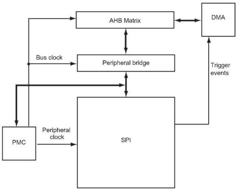
flowchart
graph TD
    A["PMC"] -->|Bus clock| B["Peripheral bridge"]
    B --> C["AHB Matrix"]
    C --> D["DMA"]
    D -->|Trigger events| E["SPI"]
    E --> F["Peripheral clock"]
    F --> A
    B <--> C
40.4 Application Block Diagram
Figure 40-2. Application Block Diagram: Single Host/Multiple Client Implementation
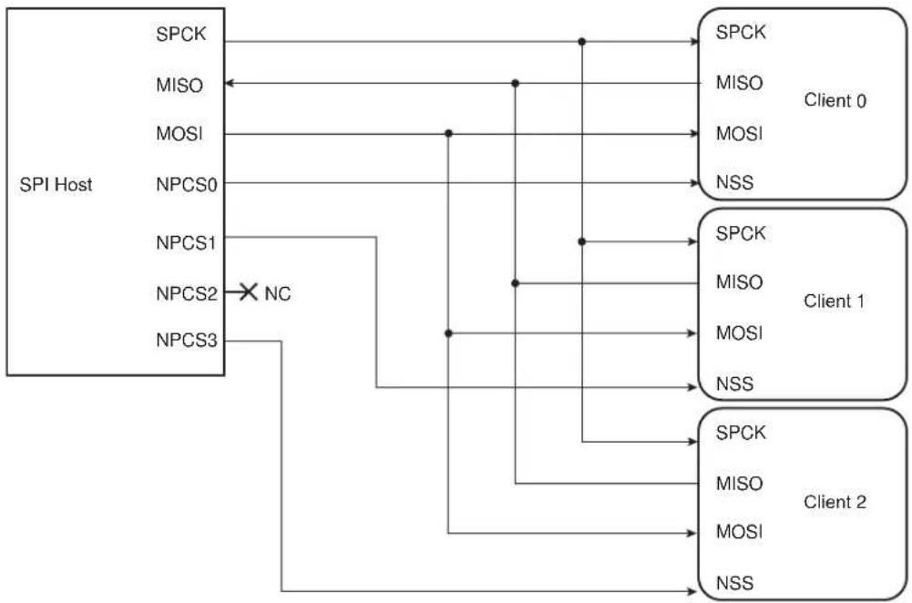
flowchart
graph TD
    A["SPI Host"] --> B["SPCK"]
    A --> C["MISO"]
    A --> D["MOSI"]
    A --> E["NPCS0"]
    A --> F["NPCS1"]
    A --> G["NPCS2"]
    A --> H["NPCS3"]
    B --> I["SPCK Client 0"]
    C --> J["MISO Client 0"]
    D --> K["MOSI Client 0"]
    E --> L["NSS Client 0"]
    F --> M["NPCS1 Client 1"]
    G --> N["NPCS2 Client 1"]
    H --> O["NPCS3 Client 1"]
    I --> P["SPCK Client 2"]
    J --> Q["MISO Client 2"]
    K --> R["MOSI Client 2"]
    L --> S["NSS Client 2"]
    M --> T["NCCN"]
    N --> U["NC"]
40.5 Signal Description
Table 40-1. Signal Description
| Pin Name Pin Description Type | ||
| Host Client | ||
| MISO Host In Client Out Input Output | ||
| MOSI Host Out Client In Output Input | ||
| SPCK Serial Clock Output Input | ||
| NPCS1-NPCS3 Peripheral Chip Selects Output Unused | ||
| NPCS0/NSS Peripheral Chip Select/Client Select Output Input | ||
40.6 Product Dependencies
40.6.1 I/O Lines
The pins used for interfacing the compliant external devices can be multiplexed with PIO lines. The programmer must first program the PIO controllers to assign the SPI pins to their peripheral functions.
40.6.2 Power Management
The SPI can be clocked through the Power Management Controller (PMC), thus the programmer must first configure the PMC to enable the SPI clock.
40.6.3 Interrupt
The SPI interface has an interrupt line connected to the interrupt controller. Handling the SPI interrupt requires programming the interrupt controller before configuring the SPI.
40.6.4 Direct Memory Access Controller (DMAC)
The SPI interface can be used in conjunction with the DMAC in order to reduce processor overhead. For a full description of the DMAC, refer to the relevant section.
40.7 Functional Description
40.7.1 Modes of Operation
The SPI operates in Host mode or in Client mode.
- The SPI operates in Host mode by setting the MSTR bit in the SPI Mode Register (SPI_MR):
- Pins NPCS0 to NPCS3 are all configured as outputs
- The SPCK pin is driven
- The MISO line is wired on the receiver input
- The MOSI line is driven as an output by the transmitter.
- The SPI operates in Client mode if the MSTR bit in SPI_MR is written to '0':
- The MISO line is driven by the transmitter output
- The MOSI line is wired on the receiver input
- The SPCK pin is driven by the transmitter to synchronize the receiver.
- The NPCS0 pin becomes an input, and is used as a Client select signal (NSS)
- The NPCS1 to NPCS3 pins are not driven and can be used for other purposes.
The data transfers are identically programmable for both modes of operation. The baud rate generator is activated only in Host mode.
40.7.2 Data Transfer
Four combinations of polarity and phase are available for data transfers. The clock polarity is programmed with the CPOL bit in the SPI Chip Select registers (SPI_CSRx). The clock phase is programmed with the NCPHA bit. These two parameters determine the edges of the clock signal on which data is driven and sampled. Each of the two parameters has two possible states, resulting in four possible combinations that are incompatible with one another. Consequently, a Host/Client pair must use the same parameter pair values to communicate. If multiple Clients are connected and require different configurations, the Host must reconfigure itself each time it needs to communicate with a different Client.
The table below shows the four modes and corresponding parameter settings.
Table 40-2. SPI Bus Protocol Modes
| SPI Mode CPOL | NCPHA | Shift SPCK Edge | Capture SPCK Edge | SPCK Inactive Level | |
| 0 0 1 | Falling Rising Low | ||||
| 1 0 0 | Rising Falling Low | ||||
| 2 1 1 | Rising Falling High | ||||
| 3 1 0 | Falling Rising High |
The following figures show examples of data transfers.
Figure 40-3. SPI Transfer Format (NCPHA = 1, 8 bits per transfer)

other
| Signal Type | Time Step 1 | Time Step 2 | Time Step 3 | Time Step 4 | Time Step 5 | Time Step 6 | Time Step 7 | Time Step 8 | |-----------------------|-------------|-------------|-------------|-------------|-------------|-------------|-------------|-------------| | SPCK (CPOL = 0) | Not defined | Not defined | Not defined | Not defined | Not defined | Not defined | Not defined | Not defined | | SPCK (CPOL = 1) | Not defined | Not defined | Not defined | Not defined | Not defined | Not defined | Not defined | Not defined | | MOSI (from host) | MSB | 6 | 5 | 4 | 3 | 2 | 1 | LSB | | MISO (from client) | MSB | 6 | 5 | 4 | 3 | 2 | 1 | LSB * | | NSS (to client) | Not defined | Not defined | Not defined | Not defined | Not defined | Not defined | Not defined | Not defined | * Not defined *Figure 40-4. SPI Transfer Format (NCPHA = 0, 8 bits per transfer)
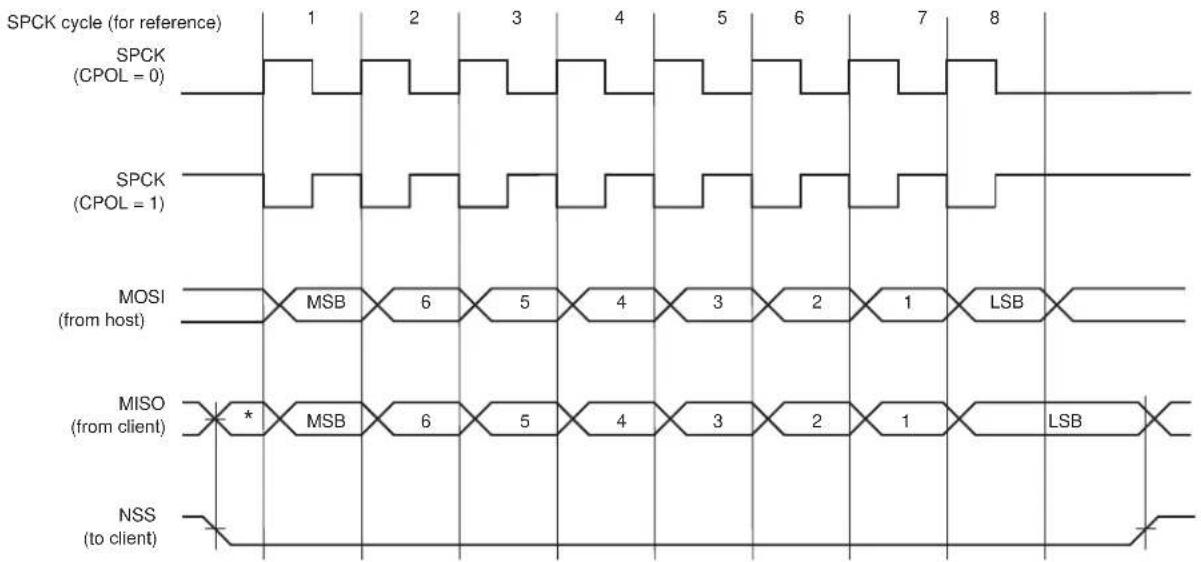
text_image
SPCK cycle (for reference) 1 2 3 4 5 6 7 8 SPCK (CPOL = 0) SPCK (CPOL = 1) MOSI (from host) MSB 6 5 4 3 2 1 LSB MISO (from client) * MSB 6 5 4 3 2 1 LSB NSS (to client)* Not defined.
40.7.3 Host Mode Operations
When configured in Host mode, the SPI operates on the clock generated by the internal programmable baud rate generator. It fully controls the data transfers to and from the Client(s) connected to the SPI bus. The SPI drives the chip select line to the Client and the serial clock signal (SPCK).
The SPI features two holding registers, the Transmit Data Register (SPI_TDR) and the Receive Data Register (SPI_RDR), and a single shift register. The holding registers maintain the data flow at a constant rate.
After enabling the SPI, a data transfer starts when the processor writes to SPI_TDR. The written data is immediately transferred into the internal shift register and the transfer on the SPI bus starts. While the data in the shift register is shifted on the MOSI line, the MISO line is sampled and shifted into the shift register. Data cannot be loaded in SPI_RDR without transmitting data. If there is no data to transmit, dummy data can be used (SPI_TDR filled with ones). If SPI_MR.WDRBT is set, transmission can occur only if SPI_RDR has been read. If Receiving mode is not required, for example when communicating with a Client receiver only (such as an LCD), the receive status flags in the SPI Status register (SPI_SR) can be discarded.
Before writing SPI_TDR, SPI_MR.PCS must be set in order to select a Client.
If new data is written in SPI_TDR during the transfer, it is kept in SPI_TDR until the current transfer is completed. Then, the received data is transferred from the shift register to SPI_RDR, the data in SPI_TDR is loaded in the shift register and a new transfer starts.
As soon as SPI_TDR is written, the Transmit Data Register Empty (TDRE) flag in SPI_SR is cleared. When the data written in SPI_TDR is loaded into the shift register, TDRE in SPI_SR is set. The TDRE flag is used to trigger the Transmit DMA channel.
See the figure below.
The end of transfer is indicated by the TXEMPTY flag in SPI_SR. If a transfer delay (DLYBCT) is greater than 0 for the last transfer, TXEMPTY is set after the completion of this delay. The peripheral clock can be switched off at this time.
Note: When the SPI is enabled, the TDRE and TXEMPTY flags are set.
Figure 40-5. TDRE and TXEMPTY Flag Behavior
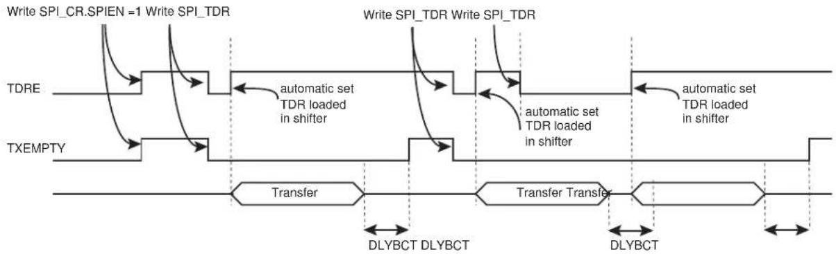
flowchart
graph LR
    A["Write SPI_CR.SPIEN =1 Write SPI_TDR"] --> B["TDRE"]
    B --> C["TXEMPTY"]
    C --> D["Transfer"]
    D --> E["DLYBCT"]
    E --> F["Transfer Transfer"]
    F --> G["DLYBCT"]
    G --> H["Automatic Set TDR Loaded in Shifter"]
    H --> I["Write SPI_TDR Write SPI_TDR"]
    I --> J["Automatic Set TDR Loaded in Shifter"]
    J --> K["Write SPI_TDR Write SPI_TDR"]
    K --> L["Automatic Set TDR Loaded in Shifter"]
    L --> M["Write SPI_TDR Write SPI_TDR"]
The transfer of received data from the internal shift register to SPI_RDR is indicated by the Receive Data Register Full (RDRF) bit in SPI_SR. When the received data is read, SPI_SR.RDRF is cleared.
If SPI_RDR has not been read before new data is received, the Overrun Error (OVRES) flag in SPI_SR is set. As long as this flag is set, data is loaded in SPI_RDR. The user has to read SPI_SR to clear OVRES.
The following figures show, respectively, a block diagram of the SPI when operating in Host mode and a flow chart describing how transfers are handled.
40.7.3.1 Host Mode Block Diagram
Figure 40-6. Host Mode Block Diagram
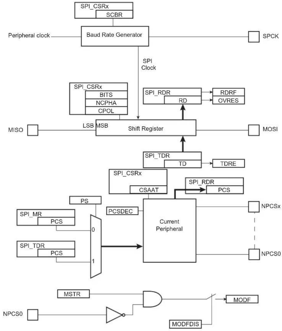
flowchart
graph TD
    A["Peripheral clock"] --> B["Baud Rate Generator"]
    B --> C["SPCK"]
    B --> D["Shift Register"]
    D --> E["MISO"]
    D --> F["MSB"]
    D --> G["LSB"]
    D --> H["MSB"]
    D --> I["Shift Register"]
    I --> J["MOSI"]
    I --> K["Current Peripheral"]
    K --> L["NPCS0"]
    K --> M["NPCS1"]
    K --> N["NPCS2"]
    K --> O["NPCS3"]
    K --> P["NPCS4"]
    K --> Q["NPCS5"]
    K --> R["NPCS6"]
    K --> S["NPCS7"]
    K --> T["NPCS8"]
    K --> U["NPCS9"]
    K --> V["NPCS10"]
    K --> W["NPCS11"]
    K --> X["NPCS12"]
    K --> Y["NPCS13"]
    K --> Z["NPCS14"]
    K --> AA["NPCS15"]
    K --> AB["NPCS16"]
    K --> AC["NPCS17"]
    K --> AD["NPCS18"]
    K --> AE["NPCS19"]
    K --> AF["NPCS20"]
    K --> AG["NPCS21"]
    K --> AH["NPCS22"]
    K --> AI["NPCS23"]
    K --> AJ["NPCS24"]
    K --> AK["NPCS25"]
    K --> AL["NPCS26"]
    K --> AM["NPCS27"]
    K --> AN["NPCS28"]
    K --> AO["NPCS29"]
    K --> AP["NPCS30"]
    K --> AQ["NPCS31"]
    K --> AR["NPCS32"]
    K --> AS["NPCS33"]
    K --> AT["NPCS34"]
    K --> AU["NPCS35"]
    K --> AV["NPCS36"]
    K --> AW["NPCS37"]
    K --> AX["NPCS38"]
    K --> AY["NPCS39"]
    K --> AZ["NPCS40"]
    K --> BA["NPCS41"]
    K --> BB["NPCS42"]
    K --> BC["NPCS43"]
    K --> BD["NPCS44"]
    K --> BE["NPCS45"]
    K --> BF["NPCS46"]
    K --> BG["NPCS47"]
    K --> BH["NPCS48"]
    K --> BI["NPCS49"]
    K --> BJ["NPCS50"]
    K --> BK["NPCS51"]
    K --> BL["NPCS52"]
    K --> BM["NPCS53"]
    K --> BN["NPCS54"]
    K --> BO["NPCS55"]
    K --> BP["NPCS56"]
    K --> BQ["NPCS57"]
    K --> BR["NPCS58"]
    K --> BS["NPCS59"]
    K --> BT["NPCS60"]
40.7.3.2 Host Mode Flow Diagram
Figure 40-7. Host Mode Flow Diagram
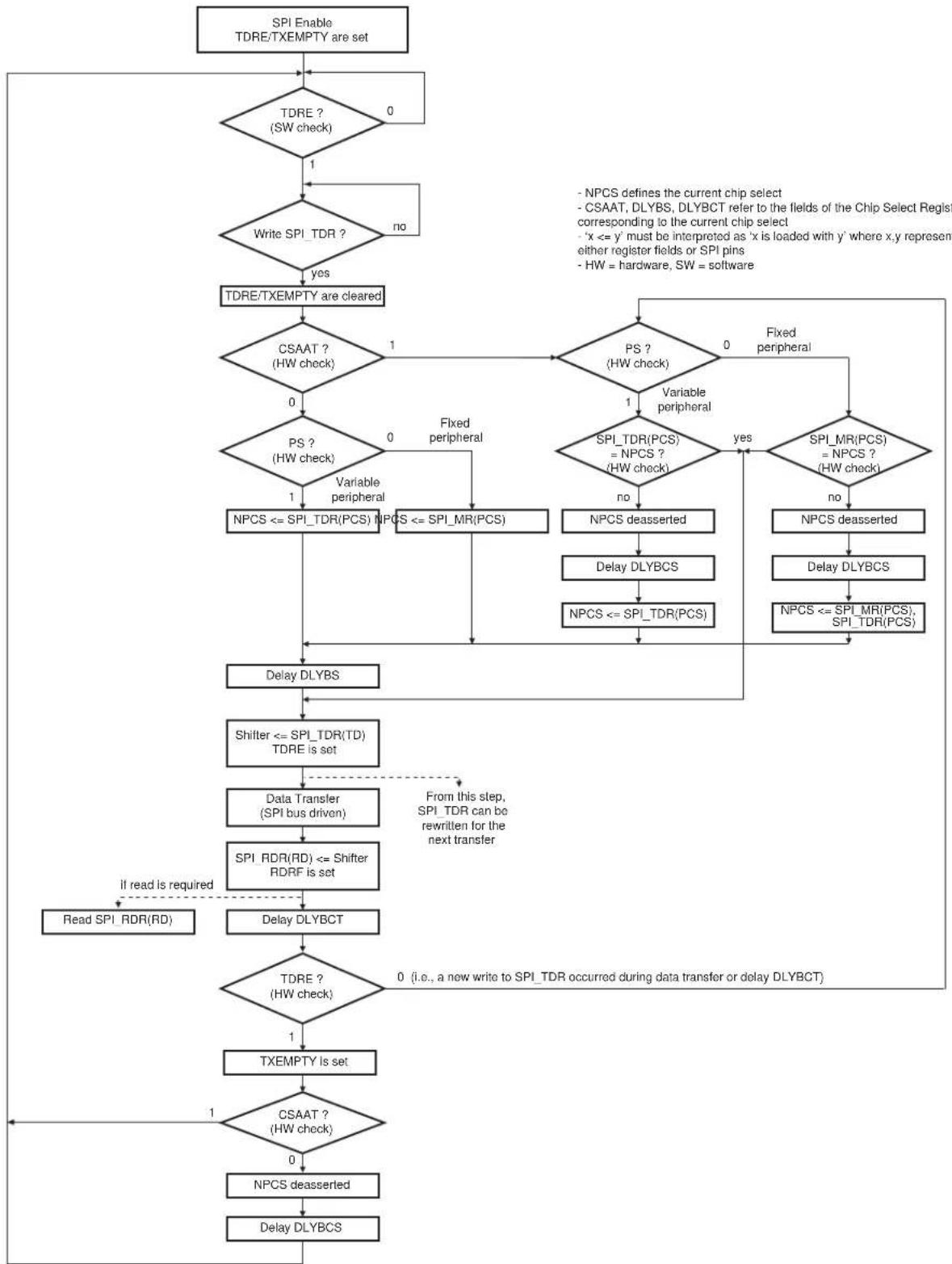
flowchart
graph TD
    A["SPI Enable<br>TDRE/TXEMPTY are set"] --> B{TDRE ? (SW check)}
    B -->|0| C["Write SPI_TDR ?"]
    B -->|1| D{CSAAT ? (HW check)}
    D -->|1| E{PS ? (HW check)}
    D -->|0| F{PS ? (HW check)}
    F -->|1| G["NPCS <= SPI_TDR(PCS) NPCS <= SPI_MR(PCS)"]
    F -->|0| H{Variable peripheral}
    H -->|0| I["Fixed peripheral"]
    H -->|1| J{SPI_TDR(PCS) = NPCS ? (HW check)}
    J -->|yes| K{SPI_MR(PCS) = NPCS ? (HW check)}
    J -->|no| L["NPCS deasserted"]
    J -->|yes| M{SPI_TDR(PCS) = NPCS ? (HW check)}
    M -->|yes| N{SPI_MR(PCS) = NPCS ? (HW check)}
    M -->|no| O["NPCS deasserted"]
    O --> P["Delay DLYBCS"]
    P --> Q["NPCS <= SPI_TDR(PCS)"]
    Q --> R["Delay DLYBCS"]
    R --> S{SPI_TDR(PCS) = NPCS ? (HW check)}
    S -->|yes| T{SPI_MR(PCS) = NPCS ? (HW check)}
    S -->|no| U["NPCS deasserted"]
    U --> V["Delay DLYBCS"]
    V --> W{SPI_TDR(PCS) = NPCS ? (HW check)}
    W -->|yes| X{SPI_MR(PCS) = NPCS ? (HW check)}
    X -->|yes| Y["SPICMR(PCS) = NPCS ? (HW check)"]
    X -->|no| Z["NPCS deasserted"]
    Z --> AA["Delay DLYBCS"]
    AA --> AB{SPI_TDR(PCS) = NPCS ? (HW check)}
    AB -->|yes| AC{SPI_TDR(PCS) = NPCS ? (HW check)}
    AC -->|yes| AD{SPI_MR(PCS) = NPCS ? (HW check)}
    AD -->|yes| AE["SPICMR(PCS) = NPCS ? (HW check)"]
    AD -->|no| AF["SPICMR(PCS) = NPCS ? (HW check)"]
    AF --> AG{SPI_TDR(PCS) = NPCS ? (HW check)}
    AG -->|yes| AH["SPICMR(PCS) = NPCS ? (HW check)"]
    AG -->|no| AI["SPICMR(PCS) = NPCS ? (HW check)"]
    AI --> AJ{SPI_TDR(PCS) = NPCS ? (HW check)}
    AJ -->|yes| AK["SPICMR(PCS) = NPCS ? (HW check)"]
    AJ -->|no| AL["SPICMR(PCS) = NPCS ? (HW check)"]
    AL --> AM{SPI_TDR(PCS) = NPCS ? (HW check)}
    AM -->|yes| AN["SPICMR(PCS) = NPCS ? (HW check)"]
    AM -->|no| AO["SPICMR(PCS) = NPCS ? (HW check)"]
    AO --> AP["SPICMR(PCS) = NPCS ? (HW check)"]
    AP --> AQ["SPICMR(PCS) = NPCS ? (HW check)"]
    AQ --> AR{SPI_TDR(PCS) = NPCS ? (HW check)}
    AR -->|yes| AS["SPICMR(PCS) = NPCS ? (HW check)"]
    AR -->|no| AT["SPICMR(PCS) = NPCS ? (HW check)"]
    AT --> AU["SPICMR(PCS) = NPCS ? (HW check)"]
    AU --> AV["SPICMR(PCS) = NPCS ? (HW check)"]
    AV --> AW["SPICMR(PCS) = NPCS ? (HW check)"]
    AW --> AX["SPICMR(PCS) = NPCS ? (HW check)"]
    AX --> AY["SPICMR(PCS) = NPCS ? (HW check)"]
    AY --> AZ["SPICMR(PCS) = NPCS ? (HW check)"]
    AZ --> BA["SPICMR(PCS) = NPCS ? (HW check)"]
    BA --> BB["SPICMR(PCS) = NPCS ? (HW check)"]
    BB --> BC["SPICMR(PCS) = NPCS ? (HW check)"]
    BC --> BD["SPICMR(PCS) = NPCS ? (HW check)"]
    BD --> BE["SPICMR(PCS) = NPCS ? (HW check)"]
    BE --> BF["SPICMR(PCS) = NPCS ? (HW check)"]
    BF --> BG["SPICMR(PCS) = NPCS ? (HW check)"]
    BG --> BH["SPICMR(PCS) = NPCS ? (HW check)"]
    BH --> BI["SPICMR(PCS) = NPCS ? (HW check)"]
    BI --> BJ["SPICMR(PCS) = NPCS ? (HW check)"]
    BJ --> BK["SPICMR(PCS) = NPCS ? (HW check)"]
    BK --> BL["SPICMR(PCS) = NPCS ? (HW check)"]
    BL --> BM["SPICMR(PCS) = NPCS ? (HW check)"]
    BM --> BN["SPICMR(PCS) = NPCS ? (HW check)"]
    BN --> BO["SPICMR(PCS) = NPCS ? (HW check)"]
    BO --> BP["SPICMR(PCS) = NPCS ? (HW check)"]
    BP --> BQ["SPICMR(PCS) = NPCS ? (HW check)"]
    BQ --> BR["SPICMR(PCS) = NPCS ? (HW check)"]
    BR --> BS["SPICMR(PCS) = NPCS ? (HW check)"]
    BS --> BT["SPICMR(PCS) = NPCS ? (HW check)"]
    BT --> BU["SPICMR(PCS) = NPCS ? (HW check)"]
    BU --> BV["SPICMR(PCS) = NPCS ? (HW check)"]
    BV --> BW["SPICMR(PCS) = NPCS ? (HW check)"]
    BW --> BX["SPICMR(PCS) = NPCS ? (HW check)"]
    BX --> BY["SPICMR(PCS) = NPCS ? (HW check)"]
    BY --> BZ["SPICMR(PCS) = NPCS ? (HW check)"]
    BZ --> CA["SPICMR(PCS) = NPCS ? (HW check)"]
    CA --> CB["SPICMR(PCS) = NPCS ? (HW check)"]
    CB --> CC["SPICMR(PCS) = NPCS ? (HW check)"]
    CC --> CD["SPICMR(PCS) = NPCS ? (HW check)"]
    CD --> CE["SPICMR(PCS) = NPCS ? (HW check)"]
    CE --> CF["SPICMR(PCS) = NPCS ? (HW check)"]
    CF --> CG["SPICMR(PCS) = NPCS ? (HW check)"]
    CG --> CH["SPICMR(PCS) = NPCS ? (HW check)"]
    CH --> CI["SPICMR(PCS) = NPCS ? (HW check)"]
    CI --> CJ["SPICMR(PCS) = NPCS ? (HW check)"]
    CJ --> CK["SPICMR(PCS) = NPCS ? (HW check)"]
    CK --> CL["SPICMR(PCS) = NPCS ? (HW check)"]
    CL --> CM["SPICMR(PCS) = NPCS ? (HW check)"]
    CM --> CN["SPICMR(PCS) = NPCS ? (HW check)"]
    CN --> CO["SPICMR(PCS) = NPCS ? (HW check)"]
    CO --> CP["SPICMR(PCS) = NPCS ? (HW check)"]
    CP --> CQ["SPICMR(PCS) = NPCS ? (HW check)"]
The figure below shows the behavior of Transmit Data Register Empty (TDRE), Receive Data Register (RDRF) and Transmission Register Empty (TXEMPTY) status flags within SPI_SR during an 8-bit data transfer in Fixed mode without the DMA involved.
Figure 40-8. Status Register Flags Behavior
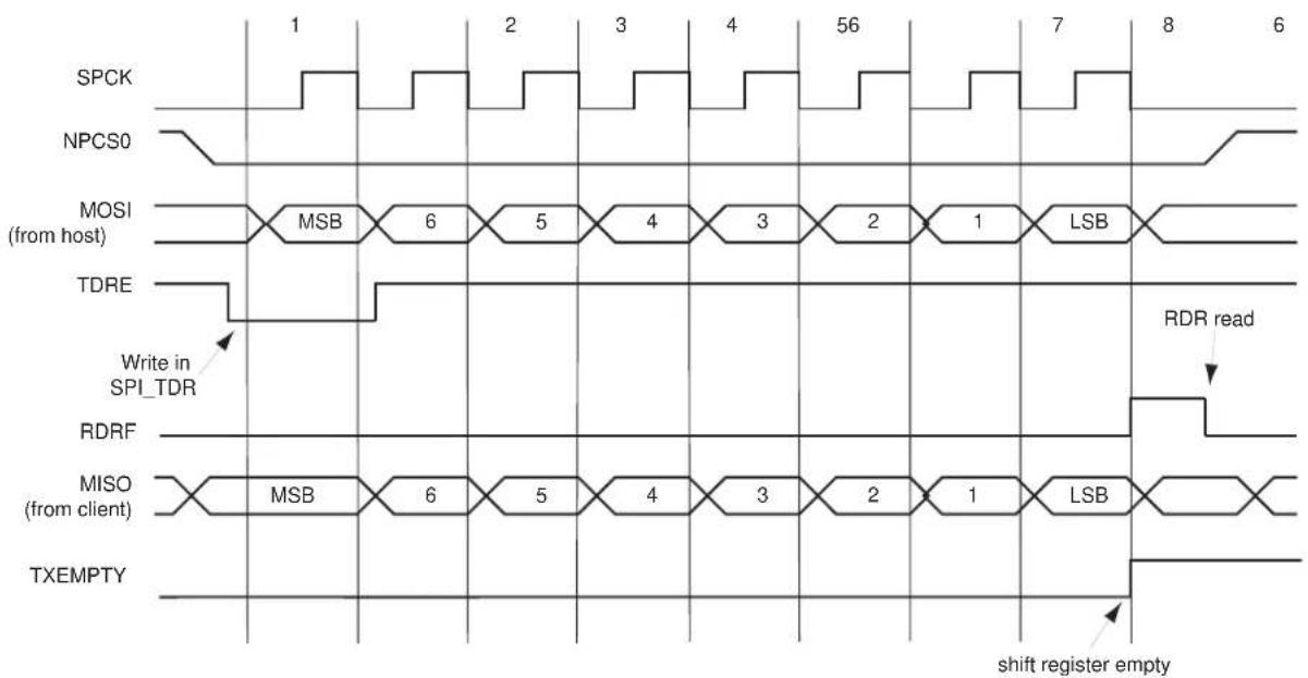
text_image
SPCK NPCS0 MOSI (from host) TDRE Write in SPI_TDR RDRF MISO (from client) TXEMPTY 1 2 3 4 56 7 8 6 MSB 6 5 4 3 2 1 LSB MSB 6 5 4 3 2 1 LSB RDR read shift register empty40.7.3.3 Clock Generation
The SPI Baud rate clock is generated by dividing the peripheral clock by a value between 1 and 255.
If SPI_CSRx.SCBR is programmed to 1, the operating baud rate is peripheral clock (refer to the section "Electrical Characteristics" for the SPCK maximum frequency). Triggering a transfer while SPI_CSRx.SCBR is at 0 can lead to unpredictable results.
At reset, SPI_CSRx.SCBR=0 and the user has to program it to a valid value before performing the first transfer.
The divisor can be defined independently for each chip select, as it has to be programmed in SPI_CSRx.SCBR. This allows the SPI to automatically adapt the baud rate for each interfaced peripheral without reprogramming.
40.7.3.4 Transfer Delays
The following figure shows a chip select transfer change and consecutive transfers on the same chip select. Three delays can be programmed to modify the transfer waveforms:
- Delay between the chip selects—programmable only once for all chip selects by writing field SPI_MR.DLYBCS. The SPI Client device deactivation delay is managed through DLYBCS. If there is only one SPI Client device connected to the Host, DLYBCS does not need to be configured. If several Client devices are connected to a Host, DLYBCS must be configured depending on the highest deactivation delay. Refer to details on the SPI Client device in the section "Electrical Characteristics".
- Delay before SPCK—independently programmable for each chip select by writing SPI_CSRx.DLYBS. The SPI Client device activation delay is managed through DLYBS. Refer to details on the SPI Client device in the section "Electrical Characteristics" to define DLYBS.
- Delay between consecutive transfers—independently programmable for each chip select by writing SPI_CSRx.DLYBCT. The time required by the SPI Client device to process received data is managed through DLYBCT. This time depends on the SPI Client system activity.
These delays allow the SPI to be adapted to the interfaced peripherals and their speed and bus release time.
Figure 40-9. Programmable Delays

text_image
Chip Select 1 Chip Select 2 SPCK DLYBCS DLYBS DLYBCT-DLYBCT40.7.3.5 Peripheral Selection
The serial peripherals are selected through the assertion of the NPCS0 to NPCS3 signals. By default, all NPCS signals are high before and after each transfer.
- Fixed Peripheral Select Mode: SPI exchanges data with only one peripheral.
Fixed Peripheral Select mode is enabled by clearing SPI_MR.PS. In this case, the current peripheral is defined by SPI_MR.PCS. SPI_TDR.PCS has no effect. - Variable Peripheral Select Mode: Data can be exchanged with more than one peripheral without having to reprogram SPI_MR.PCS.
Variable Peripheral Select mode is enabled by setting SPI_MR.PS. SPI_TDR.PCS is used to select the current peripheral. This means that the peripheral selection can be defined for each new data. The value must be written in a single access to SPI_TDR in the following format: [xxxxxxx(7-bit) + LASTXFER(1-bit)^(1) + xxxx(4-bit) + PCS(4-bit) + TD(8- to 16-bit data)]
with LASTXFER at 0 or 1 depending on the CSAAT bit, and PCS equal to the chip select to assert, as defined in section SPI Transmit Data Register.
Note:
1. Optional
For details on CSAAT, LASTXFER and CSNAAT, see section Peripheral Deselection with another DMA or PDC.
If LASTXFER is used, the command must be issued after writing the last character. Instead of LASTXFER, the user can use the SPIDIS command. After the end of the DMA transfer, it is necessary to wait for the TXEMPTY flag and then write SPIDIS into the SPI Control Register (SPI_CR). This does not change the configuration register values). The NPCS is disabled after the last character transfer. Then, another DMA transfer can be started if SPI_CR.SPIEN has previously been written.
40.7.3.6 SPI Direct Access Memory Controller (DMAC)
In both Fixed and Variable modes, the Direct Memory Access Controller (DMAC) can be used to reduce processor overhead.
The fixed peripheral selection allows buffer transfers with a single peripheral. Using the DMAC is an optimal means, as the size of the data transfer between the memory and the SPI is either 8 bits or 16 bits. However, if the peripheral selection is modified, SPI_MR must be reprogrammed.
The variable peripheral selection allows buffer transfers with multiple peripherals without reprogramming SPI_MR. Data written in SPI_TDR is 32 bits wide and defines the real data to be transmitted and the destination peripheral. Using the DMAC in this mode requires 32-bit wide
buffers, with the data in the LSBs and the PCS and LASTXFER fields in the MSBs. However, the SPI still controls the number of bits (8 to 16) to be transferred through MISO and MOSI lines with the chip select configuration registers. This is not the optimal means in terms of memory size for the buffers, but it provides a very effective means to exchange data with several peripherals without any intervention of the processor.
40.7.3.7 Peripheral Chip Select Decoding
The user can program the SPI to operate with up to 15 Client peripherals by decoding the four chip select lines, NPCS0 to NPCS3 with an external decoder/demultiplexer (see figure below). This can be enabled by setting SPI_MR.PCSDEC.
When operating without decoding, the SPI makes sure that in any case only one chip select line is activated, i.e., one NPCS line driven low at a time. If two bits are defined low in a PCS field, only the lowest numbered chip select is driven low.
When operating with decoding, the SPI directly outputs the value defined by the PCS field on the NPCS lines of either SPI_MR or SPI_TDR (depending on PS).
As the SPI sets a default value of 0xF on the chip select lines (i.e., all chip select lines at 1) when not processing any transfer, only 15 peripherals can be decoded.
The SPI has four chip select registers (SPI_CSR0...SPI_CSR3). As a result, when external decoding is activated, each NPCS chip select defines the characteristics of up to four peripherals. As an example, SPI_CRS0 defines the characteristics of the externally decoded peripherals 0 to 3, corresponding to the PCS values 0x0 to 0x3. Consequently, the user has to make sure to connect compatible peripherals on the decoded chip select lines 0 to 3, 4 to 7, 8 to 11 and 12 to 14. The following figure shows this type of implementation.
If SPI_CSRx.CSAAT bit is used, with or without the DMAC, the Mode Fault detection for NPCS0 line must be disabled. This is not needed for all other chip select lines since Mode Fault detection is only on NPCS0.
Figure 40-10. Chip Select Decoding Application Block Diagram: Single Host/Multiple Client Implementation
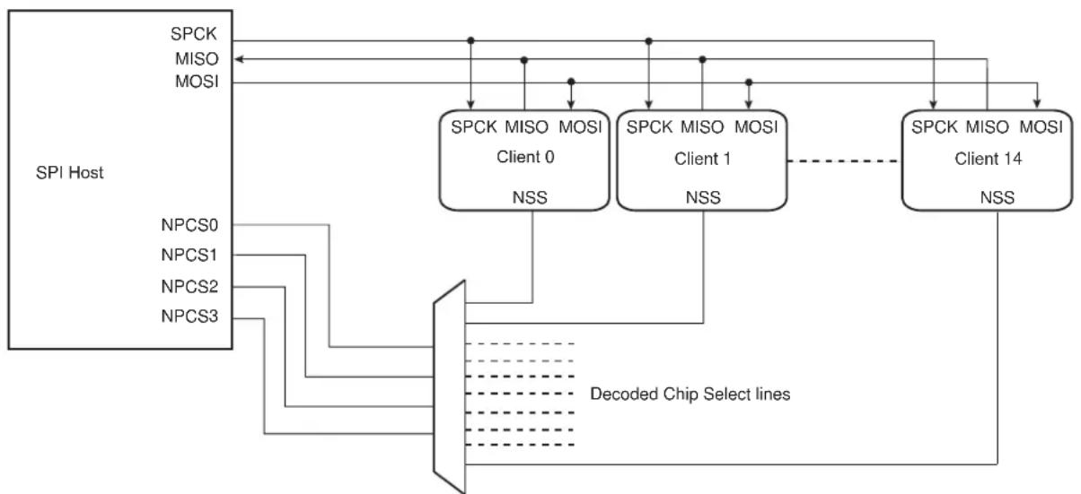
flowchart
graph TD
    A["SPI Host"] -->|SPCK MISO MOSI| B["Client 0"]
    A -->|SPCK MISO MOSI| C["Client 1"]
    A -->|SPCK MISO MOSI| D["Client 14"]
    B -->|NSS| E["Decoded Chip Select lines"]
    C -->|NSS| E
    D -->|NSS| E
    F["NPCS0"] --> E
    G["NPCS1"] --> E
    H["NPCS2"] --> E
    I["NPCS3"] --> E
    E --> J["Output"]
External 1-of-n Decoder/Demultiplexer
40.7.3.8 Peripheral Deselection without DMA
During a transfer of more than one unit of data on a chip select without the DMA, SPI_TDR is loaded by the processor, the TDRE flag rises as soon as the content of SPI_TDR is transferred into the internal shift register. When this flag is detected high, SPI_TDR can be reloaded. If this reload by
the processor occurs before the end of the current transfer and if the next transfer is performed on the same chip select as the current transfer, the chip select is not deasserted between the two transfers. But depending on the application software handling the SPI status register flags (by interrupt or polling method) or servicing other interrupts or other tasks, the processor may not reload SPI_TDR in time to keep the chip select active (low). A null DLYBCT value (delay between consecutive transfers) in SPI_CSR, gives even less time for the processor to reload SPI_TDR. With some SPI Client peripherals, if the chip select line must remain active (low) during a full set of transfers, communication errors can occur.
To facilitate interfacing with such devices, the chip select registers [SPI_CSR0...SPI_CSR3] can be programmed with the Chip Select Active After Transfer (CSAAT) bit at 1. This allows the chip select lines to remain in their current state (low = active) until a transfer to another chip select is required. Even if SPI_TDR is not reloaded, the chip select remains active. To deassert the chip select line at the end of the transfer, the Last Transfer (LASTXFER) bit in SPI_CR must be set after writing the last data to transmit into SPI_TDR.
40.7.3.9 Peripheral Deselection with DMA
DMA provides faster reloads of SPI_TDR compared to software. However, depending on the system activity, it is not guaranteed that SPI_TDR is written with the next data before the end of the current transfer. Consequently, data can be lost by the deassertion of the NPCS line for SPI Client peripherals requiring the chip select line to remain active between two transfers. The only way to guarantee a safe transfer in this case is the use of the CSAAT and LASTXFER bits.
When the CSAAT bit is configured to 0, the NPCS does not rise in all cases between two transfers on the same peripheral. During a transfer on a chip select, the TDRE flag rises as soon as the content of SPI_TDR is transferred into the internal shift register. When this flag is detected, SPI_TDR can be reloaded. If this reload occurs before the end of the current transfer and if the next transfer is performed on the same chip select as the current transfer, the chip select is not deasserted between the two transfers. This can lead to difficulties to interface with some serial peripherals requiring the chip select to be deasserted after each transfer. To facilitate interfacing with such devices, SPI_CSR can be programmed with the Chip Select Not Active After Transfer (CSNAAT) bit at 1. This allows the chip select lines to be deasserted systematically during a time "DLYBCS" (the value of the CSNAAT bit is processed only if the CSAAT bit is configured to 0 for the same chip select).
The following figure shows different peripheral deselection cases and the effect of the CSAAT and CSNAAT bits.
Figure 40-11. Peripheral Deselection

40.7.3.10 Mode Fault Detection
The SPI has the capability to operate in multihost environment. Consequently, the NPCS0/NSS line must be monitored. If one of the Hosts on the SPI bus is currently transmitting, the NPCS0/NSS line is low and the SPI must not transmit any data. A mode fault is detected when the SPI is programmed in Host mode and a low level is driven by an external Host on the NPCS0/NSS signal. In multihost environment, NPCS0, MOSI, MISO and SPCK pins must be configured in open drain (through the PIO controller). When a mode fault is detected, SPI_SR.MODF bit is set until SPI_SR is read and the SPI is automatically disabled until it is reenabled by setting SPI_CR.SPIEN bit.
By default, the mode fault detection is enabled. The user can disable it by setting SPI_MR.MODFDIS bit.
40.7.4 SPI Client Mode
When operating in Client mode, the SPI processes data bits on the clock provided on the SPI clock pin (SPCK).
The SPI waits until NSS goes active before receiving the serial clock from an external Host. When NSS falls, the clock is validated and the data is loaded in SPI_RDR depending on the configuration of SPI_CSR0.BITS. These bits are processed following a phase and a polarity defined respectively by the NCPHA and CPOL bits in SPI_CSR0. Note that the fields BITS, CPOL and NCPHA of the other chip select registers (SPI_CSR1...SPI_CSR3) have no effect when the SPI is programmed in Client mode.
The bits are shifted out on the MISO line and sampled on the MOSI line.
Note: For more information on SPI_CSRx.BITS, see the note in section SPI Chip Select Register.
When all bits are processed, the received data is transferred in SPI_RDR and the RDRF bit rises. If SPI_RDR has not been read before new data is received, the Overrun Error Status (OVRES) bit in SPI_SR is set. As long as this flag is set, data is loaded in SPI_RDR. The user must read SPI_SR to clear the OVRES bit.
When a transfer starts, the data shifted out is the data present in the internal shift register. If no data has been written in SPI_TDR, the last data received is transferred. If no data has been received since the last reset, all bits are transmitted low, as the internal shift register resets to 0.
When a first data is written in SPI_TDR, it is transferred immediately in the internal shift register and the TDRE flag rises. If new data is written, it remains in SPI_TDR until a transfer occurs, i.e., NSS falls and there is a valid clock on the SPCK pin. When the transfer occurs, the last data written in SPI_TDR is transferred in the internal shift register and the TDRE flag rises. This enables frequent updates of critical variables with single transfers.
Then, new data is loaded in the internal shift register from SPI_TDR. If no character is ready to be transmitted, i.e., no character has been written in SPI_TDR since the last load from SPI_TDR to the internal shift register, SPI_TDR is retransmitted. In this case the Underrun Error Status Flag (UNDES) is set in SPI_SR.
In Client mode, if the NSS line rises and the received character length does not match the configuration defined in SPI_CSR0.BITS the flag SFERR is set in SPI_SR.
The following figure shows a block diagram of the SPI when operating in Client mode.
Figure 40-12. Client Mode Functional Block Diagram

flowchart
graph TD
    A["MISO"] --> B["Shift Register"]
    B --> C["SPI_CSR0"]
    C --> D["SPIEN"]
    D --> E["SPIENS"]
    E --> F["SPI Clock"]
    F --> G["SPI_RDR"]
    G --> H["RDF"]
    H --> I["OVRES"]
    B --> J["LSB"]
    B --> K["MSB"]
    B --> L["MISO"]
    B --> M["TD"]
    M --> N["TDRE"]
    B --> O["SPI_TDR"]
    O --> P["SDIFF"]
    style B fill:#f9f,stroke:#333
    style C fill:#ccf,stroke:#333
    style D fill:#cfc,stroke:#333
    style E fill:#fcc,stroke:#333
    style F fill:#ffc,stroke:#333
    style G fill:#cff,stroke:#333
    style H fill:#ffc,stroke:#333
    style I fill:#ffc,stroke:#333
    style J fill:#cfc,stroke:#333
    style K fill:#cfc,stroke:#333
    style L fill:#cfc,stroke:#333
    style M fill:#cfc,stroke:#333
40.7.5 Register Write Protection
To prevent any single software error from corrupting SPI behavior, certain registers in the address space can be write-protected in the SPI Write Protection Mode Register (SPI_WPMR).
If a write access to a write-protected register is detected, the WPVS flag in the SPI Write Protection Status Register (SPI_WPSR) is set and the WPVSRC field indicates the register in which the write access has been attempted.
The WPVS bit is automatically cleared after reading SPI_WPSR.
The following registers are write-protected when WPEN is set in SPI_WPMR:
- SPI Mode Register
- SPI Chip Select Register
The following register is write-protected when WPCREN is set in SPI_WPMR:
- SPI Control Register
The following registers are write-protected when WPITEN is set in SPI_WPMR:
• SPI Interrupt Enable Register
• SPI Interrupt Disable Register
40.8 Register Summary
| Offset | Name Bit Pos. 7 | 6 | 5 | 4 | 3 | 2 | 1 | 0 | |||||||||
| 0x00 | SPI_CR | 7:0 SWRST SPIDIS SPIEN | |||||||||||||||
| 15:8 | REQCLR | ||||||||||||||||
| 23:16 | |||||||||||||||||
| 31:24 | LASTXFER | ||||||||||||||||
| 0x04 | SPI_MR | 7:0 | LLB | WDRBT | MODFDIS | PCSDEC | PS | MSTR | |||||||||
| 15:8 | |||||||||||||||||
| 23:16 | PCS[3:0] | ||||||||||||||||
| 31:24 | DLYBCS[7:0] | ||||||||||||||||
| 0x08 | SPI_RDR | 7:0 | RD[7:0] | ||||||||||||||
| 15:8 | RD[15:8] | ||||||||||||||||
| 23:16 | PCS[3:0] | ||||||||||||||||
| 31:24 | |||||||||||||||||
| 0x0C | SPI_TDR | 7:0 | TD[7:0] | ||||||||||||||
| 15:8 | TD[15:8] | ||||||||||||||||
| 23:16 | PCS[3:0] | ||||||||||||||||
| 31:24 | LASTXFER | ||||||||||||||||
| 0x10 | SPI_SR | 7:0 | OVRES MODF TDRE | RDRF | |||||||||||||
| 15:8 | SFERR | UNDES | TXEMPTY | NSSR | |||||||||||||
| 23:16 | SPIENS | ||||||||||||||||
| 31:24 | |||||||||||||||||
| 0x14 | SPI_IER | 7:0 | OVRES MODF TDRE | RDRF | |||||||||||||
| 15:8 | UNDES | TXEMPTY | NSSR | ||||||||||||||
| 23:16 | |||||||||||||||||
| 31:24 | |||||||||||||||||
| 0x18 | SPI_IDR | 7:0 | OVRES MODF TDRE | RDRF | |||||||||||||
| 15:8 | UNDES | TXEMPTY | NSSR | ||||||||||||||
| 23:16 | |||||||||||||||||
| 31:24 | NSSR | ||||||||||||||||
| 0x1C | SPI_IMR | 7:0 | OVRES MODF TDRE | RDRF | |||||||||||||
| 15:8 | UNDES | TXEMPTY | NSSR | ||||||||||||||
| 23:16 | |||||||||||||||||
| 31:24 | NSSR | ||||||||||||||||
| 0x20 ... 0x2F | Reserved | ||||||||||||||||
| 7:0 | BITS[3:0] | CSAAT | CSNAAT | NCPHA | CPOL | ||||||||||||
| 0x30 | SPI_CSR0 | 15:8 | SCBR[7:0] | ||||||||||||||
| 23:16 | DLYBS[7:0] | ||||||||||||||||
| 31:24 | DLYBCT[7:0] | ||||||||||||||||
| 0x34 | SPI_CSR1 | 7:0 | BITS[3:0] | CSAAT | CSNAAT | NCPHA | CPOL | ||||||||||
| 15:8 | SCBR[7:0] | ||||||||||||||||
| 23:16 | DLYBS[7:0] | ||||||||||||||||
| 31:24 | DLYBCT[7:0] | ||||||||||||||||
| 0x38 | SPI_CSR2 | 7:0 | BITS[3:0] | CSAAT | CSNAAT | NCPHA | CPOL | ||||||||||
| 15:8 | SCBR[7:0] | ||||||||||||||||
| 23:16 | DLYBS[7:0] | ||||||||||||||||
| ......continued | ||||||||||
| Offset | Name | Bit | Pos. 7 | 6 | 5 | 4 | 3 | 2 | 1 | 0 |
| 0xE8 | SPI_WPSR | 7:0 | WPVS | |||||||
| 15:8 | WPVSR[7:0] | |||||||||
| 23:16 | ||||||||||
| 31:24 | ||||||||||
40.8.1 SPI Control Register
Name: SPI_CR
Offset: 0x00
Reset: -
Property: Write-only
This register can only be written if the WPCREN bit is cleared in the SPI Write Protection Mode Register.

text_image
Bit 31 30 29 28 27 26 25 24 Access Reset - Bit 23 22 21 20 19 18 17 16 Access Reset Bit 15 14 13 12 11 10 9 8 Access Reset W - Bit 7 6 5 4 3 2 1 0 SWRST SPIDI$ SPIEN W W Access W W W Reset - - - -Bit 24 - LASTXFER Last Transfer
Refer to section Peripheral Selection for more details.
| Value | Description |
| 0 | No effect. |
| 1 | The current NPCS is deasserted after the character written in TD has been transferred. When SPI_CSRx.CSAAT is set, the communication with the current serial peripheral can be closed by raising the corresponding NPCS line as soon as TD transfer is completed. |
Bit 12 - REQCLR Request to Clear the Comparison Trigger
0: No effect.
1: Restarts the comparison trigger to enable SPI_RDR loading.
Bit 7 - SWRST SPI Software Reset
The SPI is in Client mode after software reset.
| Value | Description |
| 0 | No effect. |
| 1 | Reset the SPI. A software-triggered hardware reset of the SPI interface is performed. |
Bit 1 - SPIDIS SPI Disable
Disable SPI operation after current transmission is over.
If a transfer is in progress when SPIDIS is set, the SPI completes the transmission of the shifter register and does not start any new transfer, even if SPI_THR is loaded.
If both SPIEN and SPIDIS are equal to one when SPI_CR is written, the SPI is disabled.
| Value | Description |
| 0 | No effect. |
Value Description
| 1 | Disables the SPI. |
| Value Description | |
| 0 | No effect. |
| 1 | Enables the SPI to transfer and receive data. |
40.8.2 SPI Mode Register
Name: SPI_MR
Offset: 0x04
Reset: 0x0
Property: Read/Write
This register can only be written if the WPEN bit is cleared in the SPI Write Protection Mode Register.

text_image
Bit 31 30 29 28 27 26 25 24 DLYBCS[7:0] Access R/W R/W R/W R/W R/W R/W R/W Reset 0 0 0 0 0 0 0 0 Bit 23 22 21 20 19 18 17 16 PC[S[3:0] ] R/W R/W R/W R/W R/W R/W R/W R/W Reset 0 0 0 0 Bit 15 14 13 12 11 10 9 8 Access Reset Bit 7 6 5 4 3 2 1 0 LLB WDRBT MODFDIS PCSDEC PS MSTR Access R/W R/W R/W R/W R/W Reset 0 0 0 0 0 0Bits 31:24 - DLYBCS[7:0] Delay Between Chip Selects
This field defines the delay between the inactivation and the activation of NPCS. The DLYBCS time guarantees nonoverlapping chip selects and solves bus contentions in case of peripherals having long data float times.
If DLYBCS is lower than 6, six peripheral clock periods are inserted by default.
Otherwise, the following equation determines the delay:
Delay Between Chip Selects = _peripheral clock
Bits 19:16 - PCS[3:0] Peripheral Chip Select
This field is only used if fixed peripheral select is active (PS = 0).
If SPI_MR.PCSDEC = 0:
PCS = xxx0 NPCS[3:0] = 1110
PCS = xx01 NPCS[3:0] = 1101
PCS = x011 NPCS[3:0] = 1011
PCS = 0111 NPCS[3:0] = 0111
PCS = 1111 forbidden (no peripheral is selected)
(x = don't care)
If SPI_MR.PCSDEC = 1:
NPCS[3:0] output signals = PCS.
Bit 7 - LLB Local Loopback Enable
LLB controls the local loopback on the data shift register for testing in Host mode only (MISO is internally connected on MOSI).
| Value | Description |
| 0 | Local loopback path disabled. |
Value Description
1 Local loopback path enabled.
Bit 5 - WDRBT Wait Data Read Before Transfer
| Value Description | |
| 0 | No Effect. In Host mode, a transfer can be initiated regardless of SPI_RDR state. |
| 1 | In Host mode, a transfer can start only if SPI_RDR is empty, i.e., does not contain any unread data. This mode prevents overrun error in reception. |
Bit 4 - MODFDIS Mode Fault Detection
| Value Description | |
| 0 | Mode fault detection enabled |
| 1 | Mode fault detection disabled |
Bit 2 - PCSDEC Chip Select Decode
When PCSDEC = 1, up to 15 chip select signals can be generated with the four NPCS lines using an external 4-bit to 16-bit decoder. The chip select registers define the characteristics of the 15 chip selects, with the following rules:
SPI_CSR0 defines peripheral chip select signals 0 to 3.
SPI_CSR1 defines peripheral chip select signals 4 to 7.
SPI_CSR2 defines peripheral chip select signals 8 to 11.
SPI_CSR3 defines peripheral chip select signals 12 to 14.
Value Description
| 0 | The chip select lines are directly connected to a peripheral device. |
| 1 | The four NPCS chip select lines are connected to a 4-bit to 16-bit decoder. |
Bit 1 - PS Peripheral Select
| Value Description | |
| 0 | Fixed Peripheral Select |
| 1 | Variable Peripheral Select |
Bit 0 - MSTR Host/Client Mode
| Value Description | |
| 0 | SPI is in Client mode |
| 1 | SPI is in Host mode |
40.8.3 SPI Receive Data Register
Name: SPI_RDR
Offset: 0x08
Reset: 0x0
Property: Read-only
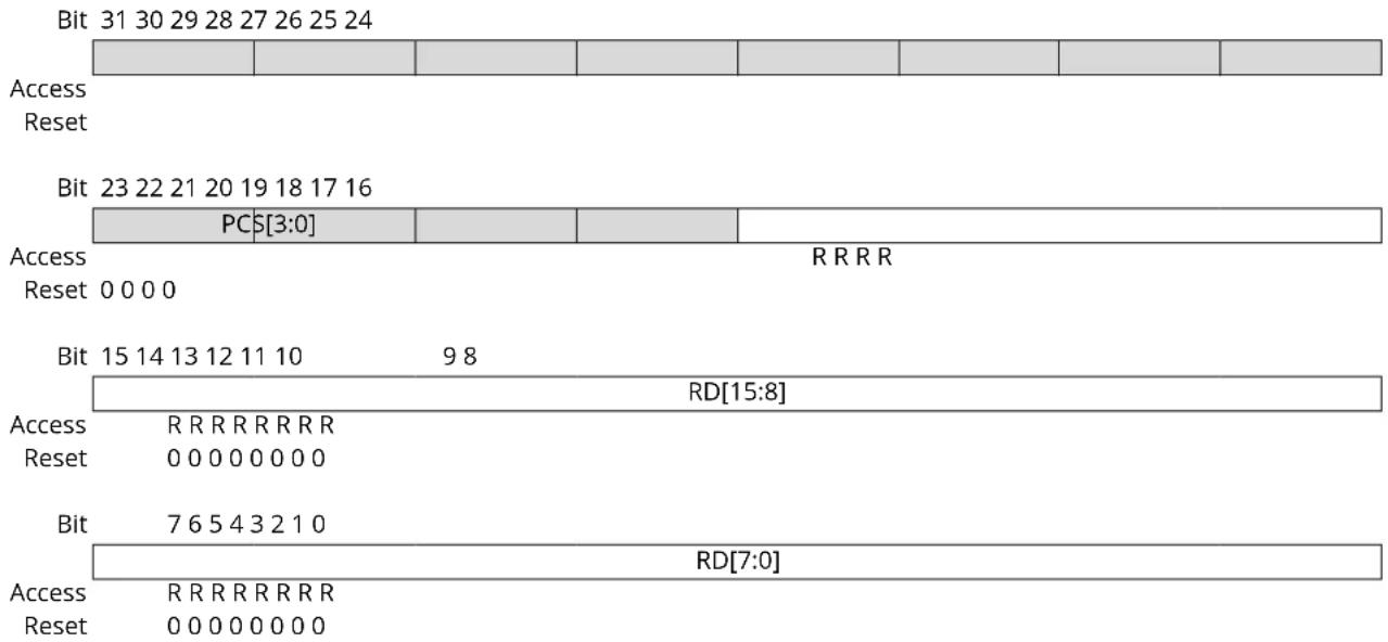
text_image
Bit 31 30 29 28 27 26 25 24 Access Reset Bit 23 22 21 20 19 18 17 16 PC5[3:0] Access R R R R Reset 0 0 0 0 Bit 15 14 13 12 11 10 9 8 RD[15:8] Access R R R R R R R R Reset 0 0 0 0 0 0 0 0 Bit 7 6 5 4 3 2 1 0 RD[7:0] Access R R R R R R R R R Reset 0 0 0 0 0 0 0 0Bits 19:16 - PCS[3:0] Peripheral Chip Select
In Host mode only, these bits indicate the value on the NPCS pins at the end of a transfer.
Otherwise, these bits are read as zero.
When using Variable Peripheral Select mode (PS = 1 in SPI_MR), it is mandatory to set SPI_MR.WDRBT bit if the PCS field must be processed in SPI_RDR.
Bits 15:0 - RD[15:0] Receive Data
Data received by the SPI Interface is stored in this register in a right-justified format. Unused bits are read as zero.
40.8.4 SPI Transmit Data Register
Name: SPI_TDR
Offset: 0x0C
Reset: -
Property: Write-only
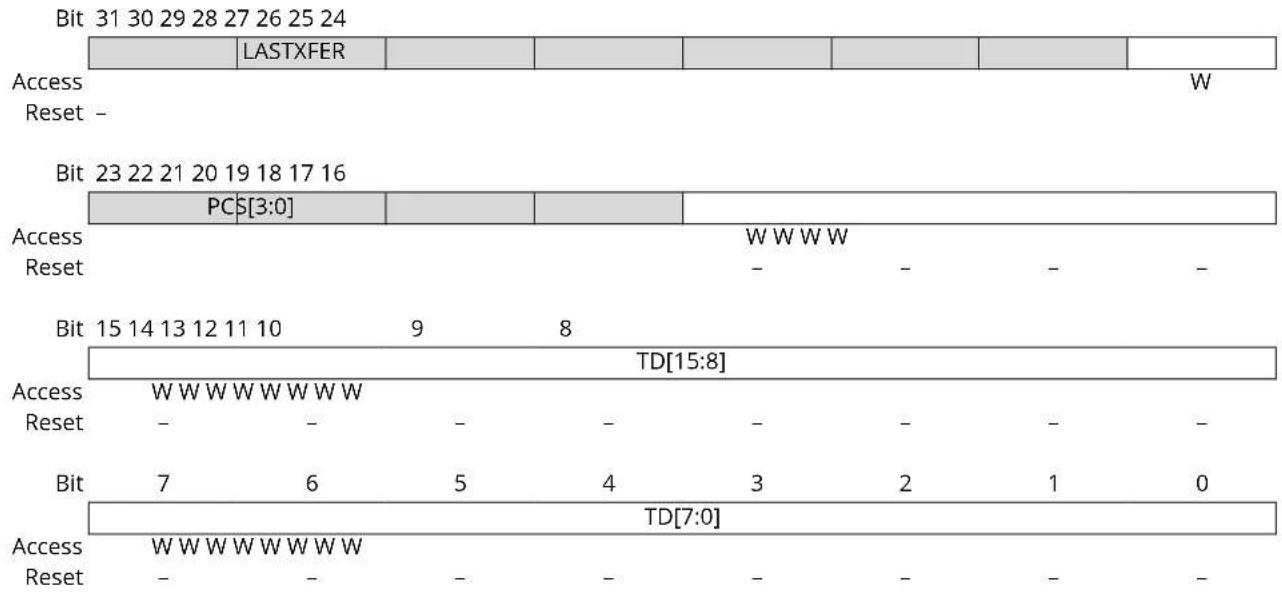
bar_stacked
| Bit | LastXFER | W WWW - | W WWW - | W WWW - | W WWW - | W WWW - | W WWW - | W WWW - | W WWW - | W WWW - | W WWW - | W WWW - | W WWW - | W WWW - | W WWW - | W WWW - | W WWW - | W WWW - | W WWW - | W WWW - | W WWW - | W WWW - | W WWW - | W WWW - | W WWW - | W WWW - | W WWW- | |---|---|---|---|---|---|---|---|---|---|---|---|---|---|---|---|---|---|---|---|---|---|---|---|---|---|---|---| | 31 30 29 28 27 26 25 24Bit 24 - LASTXFER Last Transfer
This field is only used if variable peripheral select is active (SPI_MR.PS = 1).
| Value | Description |
| 0 | No effect |
| 1 | The current NPCS is deasserted after the transfer of the character written in TD. When SPI_CSRx.CSAAT is set, the communication with the current serial peripheral can be closed by raising the corresponding NPCS line as soon as TD transfer is completed. |
Bits 19:16 - PCS[3:0] Peripheral Chip Select
This field is only used if variable peripheral select is active (SPI_MR.PS = 1).
If SPI MR.PCSDEC = 0:
PCS = xxx0 NPCS[3:0] = 1110
PCS = xx01 NPCS[3:0] = 1101
PCS = x011 NPCS[3:0] = 1011
PCS = 0111 NPCS[3:0] = 0111
PCS = 1111 forbidden (no peripheral is selected)
(x = don't care)
If SPI_MR.PCSDEC = 1:
NPCS[3:0] output signals = PCS.
Bits 15:0 - TD[15:0] Transmit Data
Data to be transmitted by the SPI interface is stored in this register. Information to be transmitted must be written to this register in a right-justified format.
40.8.5 SPI Status Register
Name: SPI_SR
Offset: 0x10
Reset: 0x00000000
Property: Read-only
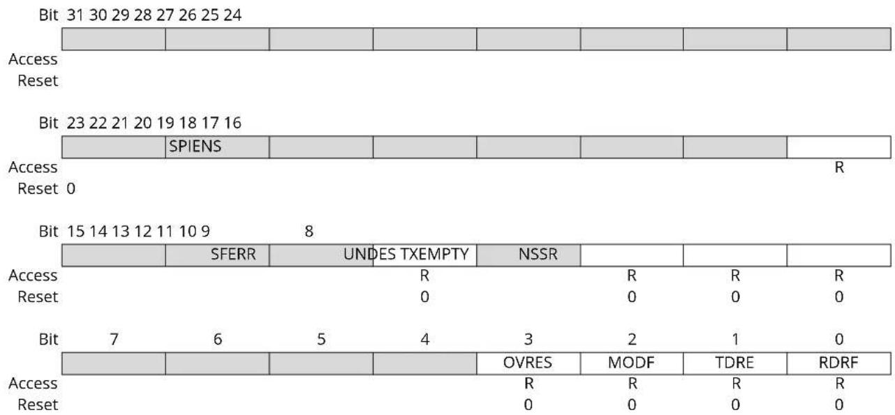
text_image
Bit 31 30 29 28 27 26 25 24 Access Reset Bit 23 22 21 20 19 18 17 16 Access Reset 0 Bit 15 14 13 12 11 10 9 8 SFERR UNDES TXEMPTY NSSR R R R Reset 0 0 0 0 Access Reset Bit 7 6 5 4 3 2 1 0 Reset Reset Reset Reset Reset Reset Reset Reset Reset Reset Reset Reset Reset Reset Reset Reset Reset Reset Reset Reset Reset Reset Reset Reset Reset Reset Reset Reset Reset Reset Reset Reset Reset Reset| Value | Description |
| 0 | SPI is disabled. |
| 1 | SPI is enabled. |
Bit 12 - SFERR Client Frame Error (cleared on read)
| Value | Description |
| 0 | There is no frame error detected for a Client access since the last read of SPI_SR. |
| 1 | In Client mode, the Chip Select raised while the character defined in SPI_CSR0.BITS was not complete. |
Bit 10 - UNDES Underrun Error Status (Client mode only) (cleared on read)
| Value | Description |
| 0 | No underrun has been detected since the last read of SPI_SR. |
| 1 | A transfer starts whereas no data has been loaded in SPI_TDR. |
Bit 9 - TXEMPTY Transmission Registers Empty (cleared by writing SPI_TDR)
| Value | Description |
| 0 | As soon as data is written in SPI_TDR. |
| 1 | SPI_TDR and internal shift register are empty. If a transfer delay has been defined, TXEMPTY is set after the end of this delay. |
Bit 8 - NSSR NSS Rising (cleared on read)
| Value | Description |
| 0 | No rising edge detected on NSS pin since the last read of SPI_SR. |
| 1 | A rising edge occurred on NSS pin since the last read of SPI_SR. |
Bit 3 - OVRES Overrun Error Status (cleared on read)
An overrun occurs when SPI_RDR is loaded at least twice from the internal shift register since the last read of SPI_RDR.
| Value Description | |
| 0 | No overrun has been detected since the last read of SPI_SR. |
| 1 | An overrun has occurred since the last read of SPI_SR. |
Bit 2 - MODF Mode Fault Error (cleared on read)
| Value Description | |
| 0 | No mode fault has been detected since the last read of SPI_SR. |
| 1 | A mode fault occurred since the last read of SPI_SR. |
Bit 1 - TDRE Transmit Data Register Empty (cleared by writing SPI_TDR)
0: Data has been written to SPI_TDR and not yet transferred to the internal shift register.
1: The last data written in SPI_TDR has been transferred to the internal shift register.
TDRE is cleared when the SPI is disabled or at reset. Enabling the SPI sets the TDRE flag.
Bit 0 - RDRF Receive Data Register Full (cleared by reading SPI_RDR)
0: No data has been received since the last read of SPI_RDR.
1: Data has been received and the received data has been transferred from the internal shift register to SPI_RDR since the last read of SPI_RDR.
40.8.6 SPI Interrupt Enable Register
Name: SPI_IER
Offset: 0x14
Reset: -
Property: Write-only
This register can only be written if the WPITEN bit is cleared in the SPI Write Protection Mode Register.
The following configuration values are valid for all listed bit names of this register:
0: No effect.
1: Enables the corresponding interrupt.
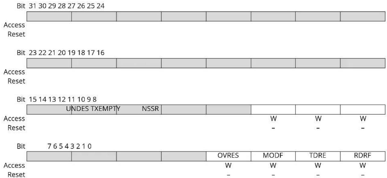
text_image
Bit 31 30 29 28 27 26 25 24 Access Reset Bit 23 22 21 20 19 18 17 16 Access Reset Bit 15 14 13 12 11 10 9 8 UNDES TXEMPTY NSSR Access Reset W W W - - - Bit 7 6 5 4 3 2 1 0 Access Reset W W W - - - -Bit 10 - UNDES Underrun Error Interrupt Enable
Bit 9 - TXEMPTY Transmission Registers Empty Enable
Bit 8 - NSSR NSS Rising Interrupt Enable
Bit 3 - OVRES Overrun Error Interrupt Enable
Bit 2 - MODF Mode Fault Error Interrupt Enable
Bit 1 - TDRE SPI Transmit Data Register Empty Interrupt Enable
Bit 0 - RDRF Receive Data Register Full Interrupt Enable
40.8.7 SPI Interrupt Disable Register
Name: SPI_IDR
Offset: 0x18
Reset: -
Property: Write-only
This register can only be written if the WPITEN bit is cleared in the SPI Write Protection Mode Register.
The following configuration values are valid for all listed bit names of this register:
0: No effect.
1: Disables the corresponding interrupt.

text_image
Bit 31 30 29 28 27 26 25 24 Access Reset Bit 23 22 21 20 19 18 17 16 Access Reset Bit 15 14 13 12 11 10 9 8 UNDES TXEMPTY NSSR Access Reset W W W - - - Bit 7 6 5 4 3 2 1 0 Access Reset W W W - - - -Bit 10 - UNDES Underrun Error Interrupt Disable
Bit 9 - TXEMPTY Transmission Registers Empty Disable
Bit 8 - NSSR NSS Rising Interrupt Disable
Bit 3 - OVRES Overrun Error Interrupt Disable
Bit 2 - MODF Mode Fault Error Interrupt Disable
Bit 1 - TDRE SPI Transmit Data Register Empty Interrupt Disable
Bit 0 - RDRF Receive Data Register Full Interrupt Disable
40.8.8 SPI Interrupt Mask Register
Name: SPI_IMR
Offset: 0x1C
Reset: 0x0
Property: Read-only
The following configuration values are valid for all listed bit names of this register:
0: The corresponding interrupt is not enabled.
1: The corresponding interrupt is enabled.
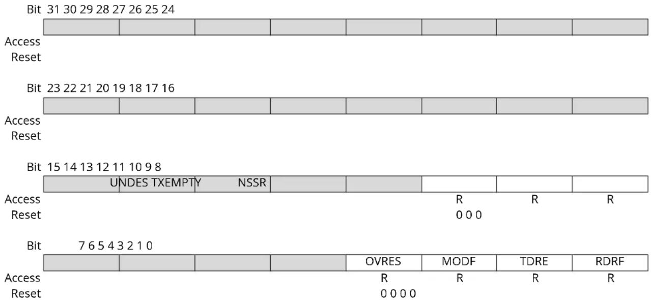
text_image
Bit 31 30 29 28 27 26 25 24 Access Reset Bit 23 22 21 20 19 18 17 16 Access Reset Bit 15 14 13 12 11 10 9 8 UNDES TXEMPTY NSSR Access Reset R R R 0 0 0 Bit 7 6 5 4 3 2 1 0 Access Reset R R R 0 0 0 0Bit 10 - UNDES Underrun Error Interrupt Mask
Bit 9 - TXEMPTY Transmission Registers Empty Mask
Bit 8 - NSSR NSS Rising Interrupt Mask
Bit 3 - OVRES Overrun Error Interrupt Mask
Bit 2 - MODF Mode Fault Error Interrupt Mask
Bit 1 - TDRE SPI Transmit Data Register Empty Interrupt Mask
Bit 0 - RDRF Receive Data Register Full Interrupt Mask
40.8.9 SPI Chip Select Register
Name: SPI_CSRx
Offset: 0x30 + x*0x04 [x=0..3]
Reset: 0
Property: R/W
This register can only be written if the WPEN bit is cleared in the SPI Write Protection Mode Register.
SPI_CSRx must be written even if the user wants to use the default reset values. The BITS field is not updated with the translated value unless the register is written.
| Bit 31 30 29 28 27 26 25 24 | ||||||
| DLYBCT[7:0] | ||||||
| Access | R/W R/W R/W R/W R/W R/W R/W R/W | |||||
| Reset | 0 0 0 0 0 0 0 0 | |||||
| Bit 23 22 21 20 19 18 17 16 | ||||||
| DLYBS[7:0] | ||||||
| Access | R/W R/W R/W R/W R/W R/W R/W R/W | |||||
| Reset | 0 0 0 0 0 0 0 0 | |||||
| Bit 15 14 13 12 11 10 9 8 | ||||||
| SCBR[7:0] | ||||||
| Access | R/W R/W R/W R/W R/W R/W R/W R/W | |||||
| Reset | 0 0 0 0 0 0 0 0 | |||||
| Bit 7 6 5 4 3 2 1 0 | ||||||
| BITS[3:0] CSAAT | CSNAAT | NCPHA | CPOL | |||
| Access | R/W R/W R/W R/W R/W R/W R/W R/W | |||||
| Reset | 0 0 0 0 0 0 0 0 | |||||
Bits 31:24 - DLYBCT[7:0] Delay Between Consecutive Transfers
This field defines the delay between two consecutive transfers with the same peripheral without removing the chip select. The delay is always inserted after each transfer and before removing the chip select if needed.
When DLYBCT = 0, no delay between consecutive transfers is inserted and the clock keeps its duty cycle over the character transfers.
Otherwise, the following equation determines the delay:
DLYBCT = Delay Between Consecutive Transfers × f_peripheral clock / 32
Bits 23:16 - DLYBS[7:0] Delay Before SPCK
This field defines the delay from NPCS falling edge (activation) to the first valid SPCK transition.
When DLYBS = 0, the delay is half the SPCK clock period.
Otherwise, the following equation determines the delay:
DLYBS = Delay Before SPCK × f_peripheral clock
Bits 15:8 - SCBR[7:0] Serial Clock Bit Rate
In Host mode, the SPI Interface uses a modulus counter to derive the SPCK bit rate from the peripheral clock. The bit rate is selected by writing a value from 1 to 255 in the SCBR field. The following equation determines the SPCK bit rate:
SCBR = f _peripheral clock / SPCK Bit Rate
Programming the SCBR field to 0 is forbidden. Triggering a transfer while SCBR is at 0 can lead to unpredictable results.
At reset, SCBR is 0 and the user has to program it at a valid value before performing the first transfer.
Note: If one of the SCBR fields in SPI_CSRx is set to 1, the other SCBR fields in SPI_CSRx must be set to 1 as well, if they are used to process transfers. If they are not used to transfer data, they can be set at any value.
Bits 7:4 - BITS[3:0] Bits Per Transfer
(See Note under the register table in SPI Chip Select Register.)
The BITS field determines the number of data bits transferred. Reserved values should not be used.
| Value Name | Description | |
| 0 | 8_BIT 8 bits for transfer | |
| 1 | 9_BIT 9 bits for transfer | |
| 2 | 10_BIT 10 bits for transfer | |
| 3 | 11_BIT 11 bits for transfer | |
| 4 | 12_BIT 12 bits for transfer | |
| 5 | 13_BIT 13 bits for transfer | |
| 6 | 14_BIT 14 bits for transfer | |
| 7 | 15_BIT 15 bits for transfer | |
| 8 | 16_BIT 16 bits for transfer | |
| 9 | - Reserved | |
| 10 | - Reserved | |
| 11 | - Reserved | |
| 12 | - Reserved | |
| 13 | - Reserved | |
| 14 | - Reserved | |
| 15 | - Reserved |
Bit 3 - CSAAT Chip Select Active After Transfer
| Value Description | |
| 0 | The Peripheral Chip Select Line rises as soon as the last transfer is achieved. |
| 1 | The Peripheral Chip Select Line does not rise after the last transfer is achieved. It remains active until a new transfer is requested on a different chip select. |
Bit 2 - CSNAAT Chip Select Not Active After Transfer (ignored if CSAAT = 1)
| Value Description | |
| 0 | The Peripheral Chip Select Line does not rise between two transfers if SPI_TDR is reloaded before the end of the first transfer and if the two transfers occur on the same chip select. |
| 1 | The Peripheral Chip Select Line rises systematically after each transfer performed on the same Client. It remains inactive after the end of transfer for a minimal duration of: 'peripheral clock (If field DLYBCS is lower than 6, a minimum of six periods is introduced.) |
Bit 1 - NCPHA Clock Phase
NCPHA determines which edge of SPCK causes data to change and which edge causes data to be captured. NCPHA is used with CPOL to produce the required clock/data relationship between Host and Client devices.
| Value Description | |
| 0 | Data is changed on the leading edge of SPCK and captured on the following edge of SPCK. |
| 1 | Data is captured on the leading edge of SPCK and changed on the following edge of SPCK. |
Bit 0 - CPOL Clock Polarity
CPOL is used to determine the inactive state value of the serial clock (SPCK). It is used with NCPHA to produce the required clock/data relationship between Host and Client devices.
| Value Description | |
| 0 | The inactive state value of SPCK is logic level zero. |
| 1 | The inactive state value of SPCK is logic level one. |
40.8.10 SPI Write Protection Mode Register
Name: SPI_WPMR
Offset: 0xE4
Reset: 0x0
Property: Read/Write
See section Register Write Protection for the list of registers that can be write-protected.
Bit 31 30 29 28 27 26 25 24
| WPKEY[23:16] | |
| Access | R/W R/W R/W R/W R/W R/W R/W R/W |
| Reset | 0 0 0 0 0 0 0 |
Bit 23 22 21 20 19 18 17 16
| WPKEY[15:8] | |
| Access | R/W R/W R/W R/W R/W R/W R/W R/W |
| Reset | 0 0 0 0 0 0 0 |
Bit 15 14 13 12 11 10 9 8
| WPKEY[7:0] | |
| Access | R/W R/W R/W R/W R/W R/W R/W R/W |
| Reset | 0 0 0 0 0 0 0 |
Bit 76543210
| WPCREN | WPITEN | WPEN | ||||
| Access | R/W | R/W | R/W | |||
| Reset | 0 | 0 | 0 |
Bits 31:8 - WPKEY[23:0] Write Protection Key
| Value | Name | Description |
| 0x535049 | PASSWD | Writing any other value in this field aborts the write operation of the WPEN bit.Always reads as 0. |
Bit 2 - WPCREN Write Protection Control Register Enable
| Value | Description |
| 0 | Disables the write protection on the Control register if WPKEY corresponds to 0x535049. |
| 1 | Enables the write protection on the Control register if WPKEY corresponds to 0x535049. |
Bit 1 - WPITEN Write Protection Interrupt Enable
| Value | Description |
| 0 | Disables the write protection on Interrupt registers if WPKEY corresponds to 0x535049. |
| 1 | Enables the write protection on Interrupt registers if WPKEY corresponds to 0x535049. |
Bit 0 - WPEN Write Protection Enable
| Value | Description |
| 0 | Disables the write protection if WPKEY corresponds to 0x535049 ("SPI" in ASCII) |
| 1 | Enables the write protection if WPKEY corresponds to 0x535049 ("SPI" in ASCII) |
40.8.11 SPI Write Protection Status Register
Name: SPI_WPSR
Offset: 0xE8
Reset: 0x0
Property: Read-only

text_image
Bit 31 30 29 28 27 26 25 24 Access Reset Bit 23 22 21 20 19 18 17 16 Access Reset Bit 15 14 13 12 11 10 9 8 WPVSRC[7:0] Access R R R R R R R R Reset 0 0 0 0 0 0 0 0 Bit 7 6 5 4 3 2 1 0 WPVS Access Reset R 0Bits 15:8 - WPVSRC[7:0] Write Protection Violation Source
When WPVS = 1, WPVSRC indicates the register address offset at which a write access has been attempted.
Bit 0 - WPVS Write Protection Violation Status
| Value | Description |
| 0 | No write protection violation has occurred since the last read of SPI_WPSR. |
| 1 | A write protection violation has occurred since the last read of SPI_WPSR. If this violation is an unauthorized attempt to write a protected register, the associated violation is reported into field WPVSRC. |
41. Quad Serial Peripheral Interface (QSPI)
41.1 Description
The Quad Serial Peripheral Interface (QSPI) is a synchronous serial data link that provides communication with external devices in Host mode.
The QSPI can be used in SPI Host Mode to interface to serial peripherals, such as ADCs, DACs, LCD controllers, CAN controllers and sensors, or in Serial Memory mode to interface to serial Flash memories.
The QSPI allows the system to execute code directly from a serial Flash memory (XIP) without code shadowing to RAM. The serial Flash memory mapping is seen in the system as other memories, such as ROM, SRAM, DRAM, embedded Flash memory, and so on.
With the support of the Quad SPI protocol, the QSPI allows the system to use high-performance serial Flash memories which are small and inexpensive, in place of larger and more expensive parallel Flash memories.
Note: Stacked devices with a rollover in the memory address space at each die boundary are not supported.
41.2 Embedded Characteristics
- SPI Mode: Host SPI Interface
- Programmable clock phase and clock polarity
-
Programmable transfer delays between consecutive transfers, between clock and data, between deactivation and activation of chip select
-
Interface to serial peripherals such as ADCs, DACs, LCD controllers, CAN controllers and sensors
- 8-bit/16-bit programmable data length
-
Serial Memory Mode
-
Interface to serial Flash memories operating in Single-bit SPI, Dual SPI and Quad SPI
- Interface to serial Flash Memories operating in Single Data Rate or Double Data Rate Modes
- Supports "Execute In Place" (XIP)—code execution by the system directly from a serial Flash memory
- Flexible instruction register for compatibility with all serial Flash memories
- 32-bit address mode (default is 24-bit address) to support serial Flash memories larger than 128 Mbits
- Continuous read mode
- Scrambling/unscrambling "On-The-Fly"
- Connection to DMA Channel Capabilities Optimizes Data Transfers
- One channel for the receiver, one channel for the transmitter
- Register Write Protection
41.3 Block Diagram
Figure 41-1. Block Diagram

flowchart
graph LR
    A["CPU"] --> B["AHB MATRIX"]
    C["DMA"] --> B
    B --> D["Peripheral Bridge"]
    D --> E["QSPI"]
    E --> F["QSPI Interrupt"]
    G["PMC"] --> H(peripheral clock]
    I["Interrupt Control"] --> J["QSPI Interrupt"]
    K["PIO"] --> L["QSCI"]
    K --> M["MOSI/QIO0"]
    K --> N["MISO/QIO1"]
    K --> O["QIO2"]
    K --> P["QIO3"]
    K --> Q["QCS"]
41.4 Signal Description
Table 41-1. Signal Description
| Pin Name Pin Description Type | ||
| QSCK Serial Clock Output | ||
| MOSI (QIO0) (1)(2) | Data Output (Data Input Output 0) Output (Input/Output) | |
| MISO (QIO1) (1)(2) | Data Input (Data Input Output 1) Input (Input/Output) | |
| QIO2 (3) | Data Input Output 2 Input/Output | |
| QIO3 (3) | Data Input Output 3 Input/Output | |
| QCS Peripheral Chip Select Output | ||
Notes:
- MOSI and MISO are used for single-bit SPI operation.
- QIO0-QIO1 are used for Dual SPI operation.
- QIO0-QIO3 are used for Quad SPI operation.
41.5 Product Dependencies
41.5.1 I/O Lines
The pins used for interfacing the compliant external devices may be multiplexed with PIO lines. The programmer must first program the PIO controllers to assign the QSPI pins to their peripheral functions.
41.5.2 Power Management
The QSPI may be clocked through the Power Management Controller (PMC), thus the programmer must first configure the PMC to enable the QSPI clock.
41.5.3 Interrupt Sources
The QSPI has an interrupt line connected to the Interrupt Controller. Handling the QSPI interrupt requires programming the interrupt controller before configuring the QSPI.
41.5.4 Direct Memory Access Controller (DMA)
The QSPI can be used in conjunction with the Direct Memory Access Controller (DMA) in order to reduce processor overhead. For a full description of the DMA, refer to the section "DMA Controller (XDMAC)".
Note: DMA write accesses must be 32-bit aligned. If a single byte is to be written in a 32-bit word, the rest of the word must be filled with ones.
41.6 Functional Description
41.6.1 Serial Clock Baud Rate
The QSPI baud rate clock is generated by dividing the peripheral clock by a value between 1 and 256.
41.6.2 Serial Clock Phase and Polarity
Four combinations of polarity and phase are available for data transfers. The clock polarity is programmed with the CPOL bit in the QSPI Serial Clock register (QSPI_SCR). The CPHA bit in the QSPI_SCR programs the clock phase. These two parameters determine the edges of the clock signal on which data is driven and sampled. Each of the two parameters has two possible states, resulting in four possible combinations that are incompatible with one another. Thus, the interfaced Client must use the same parameter values to communicate.
The table below shows the four modes and corresponding parameter settings.
Table 41-2. QSPI Bus Clock Modes
| QSPI Clock Mode QSPI_SCR.CPOL QSPI_SCR.CPHA Shift QSCK | Capture QSCK Edge QSCK Inactive Level | |||
| Edge | ||||
| 0 0 0 Falling Rising Low | ||||
| 1 0 1 Rising Falling Low | ||||
| 2 1 0 Rising Falling High | ||||
| 3 1 1 Falling Rising High | ||||
The following figures show examples of data transfers.
Figure 41-2. QSPI Transfer Format (QSPI_SCR.CPHA = 0, 8 bits per transfer)
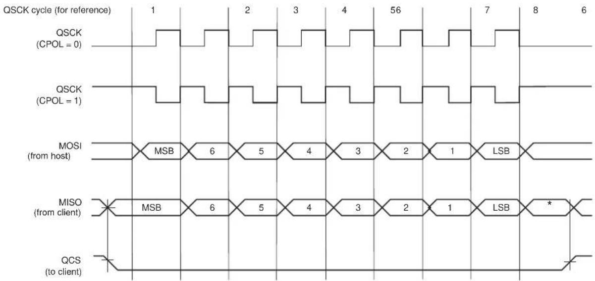
text_image
QSCK cycle (for reference) 1 2 3 4 56 7 8 6 QSCK (CPOL = 0) QSCK (CPOL = 1) MOSI (from host) MSB 6 5 4 3 2 1 LSB MISO (from client) MSB 6 5 4 3 2 1 LSB * QCS (to client)* Not defined, but normally MSB of previous character received.
Figure 41-3. QSPI Transfer Format (QSPI_SCR.CPHA = 1, 8 bits per transfer)
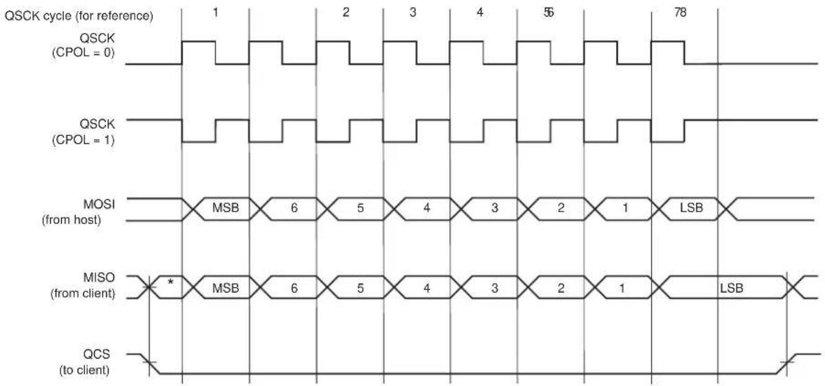
text_image
QSCK cycle (for reference) 1 2 3 4 5 6 7 8 QSCK (CPOL = 0) QSCK (CPOL = 1) MOSI (from host) MSB 6 5 4 3 2 1 LSB MISO (from client) * MSB 6 5 4 3 2 1 LSB QCS (to client)* Not defined but normally LSB of previous character transmitted.
41.6.3 Transfer Delays
The figure below shows several consecutive transfers while the chip select is active. Three delays can be programmed to modify the transfer waveforms:
- The delay between the deactivation and the activation of QCS, programmed by writing QSPI_MR.DLYCS. Allows to adjust the minimum time of QCS at high level.
- The delay before QSCK, programmed by writing QSPI_SR.DLYBS. Allows the start of QSCK to be delayed after the chip select has been asserted.
- The delay between consecutive transfers, programmed by writing QSPI_MR.DLYBCT. Allows insertion of a delay between two consecutive transfers. In Serial Memory mode, this delay is not programmable and DLYBCT is ignored. In this mode, DLYBCT must be written to '0'.
These delays allow the QSPI to be adapted to the interfaced peripherals and their speed and bus release time.
Figure 41-4. Programmable Delays

text_image
QCS QSCK DLYCS DLYBSDLYBCTDLYBET41.6.4 QSPI SPI Mode
In SPI mode, the QSPI acts as a standard SPI Host.
To activate this mode, QSPI_MR.SMM must be written to '0' in QSPI_MR.
41.6.4.1 SPI Mode Operations
The QSPI in standard SPI mode operates on the clock generated by the internal programmable baud rate generator. It fully controls the data transfers to and from the Client connected to the SPI bus. The QSPI drives the chip select line to the Client (QCS) and the serial clock signal (QSCK).
The QSPI features two holding registers, the Transmit Data register (QSPI_TDR) and the Receive Data register (QSPI_RDR), and a single internal shift register. The holding registers maintain the data flow at a constant rate.
After enabling the QSPI, a data transfer begins when the processor writes to the QSPI_TDR. The written data is immediately transferred to the internal shift register and transfer on the SPI bus starts. While the data in the internal shift register is shifted on the MOSI line, the MISO line is sampled and shifted to the internal shift register. Receiving data cannot occur without transmitting data. If receiving mode is not needed, for example when communicating with a Client receiver only (such as an LCD), the receive status flags in the Status register (QSPI_SR) can be discarded.
If new data is written in QSPI_TDR during the transfer, it is retained there until the current transfer is completed. Then, the received data is transferred from the internal shift register to the QSPI_RDR, the data in QSPI_TDR is loaded in the internal shift register and a new transfer starts.
The transfer of a data written in QSPI_TDR in the internal shift register is indicated by the Transmit Data Register Empty (TDRE) bit in the QSPI_SR. When new data is written in QSPI_TDR, this bit is cleared. QSPI_SR.TDRE is used to trigger the Transmit DMA channel.
The end of transfer is indicated by the TXEMPTY flag in the QSPI_SR. If a transfer delay (DLYBCT) is greater than 0 for the last transfer, QSPI_SR.TXEMPTY is set after the completion of this delay. The peripheral clock can be switched off at this time.
The transfer of received data from the internal shift register in QSPI_RDR is indicated by the Receive Data Register Full (RDRF) bit in the QSPI_SR. When the received data is read, QSPI_SR.RDRF bit is cleared.
If the QSPI_RDR has not been read before new data is received, the Overrun Error Status (OVRES) bit in QSPI_SR is set. As long as this flag is set, data is loaded in QSPI_RDR. The user must read the QSPI_SR to clear the OVRES bit.
The following figures show, respectively, a block diagram of the SPI when operating in Host mode, and a flow chart describing how transfers are handled.
41.6.4.2 SPI Mode Block Diagram
Figure 41-5. SPI Mode Block Diagram

flowchart
graph TD
    A["QSPI_SCR"] --> B["Baud Rate Generator"]
    C["SCBR"] --> B
    D["QSPI_SCR"] --> E["LSB MSB"]
    F["CPHA"] --> E
    G["CPOL"] --> E
    H["QSPI_RDR"] --> I["Shift Register"]
    J["RDF"] --> I
    K["OVRES"] --> I
    L["MISO"] --> I
    M["QSPI_MR"] --> N["NBBITS"]
    O["QSPI_TDR"] --> P["Shift Register"]
    Q["TDRE"] --> P
    R["Chip Select Controller"] --> S["QCS"]
    T["QSPI_MR"] --> U["CSMODE"]
    V["QSPI SCR"] --> W["QA"]
    X["QSPI SCR"] --> Y["QA"]
    Z["QSPI SCR"] --> AA["QA"]
    AB["QSPI SCR"] --> AC["QA"]
    AD["QSPI SCR"] --> AE["QA"]
    AF["QSPI SCR"] --> AG["QA"]
    AH["QSPI SCR"] --> AI["QA"]
    AJ["QSPI SCR"] --> AK["QA"]
    AL["QSPI SCR"] --> AM["QA"]
    AN["QSPI SCR"] --> AO["QA"]
    AP["QSPI SCR"] --> AQ["QA"]
    AR["QSPI SCR"] --> AS["QA"]
    AT["QSPI SCR"] --> AU["QA"]
    AV["QSPI SCR"] --> AW["QA"]
    AX["QSPI SCR"] --> AY["QA"]
    AZ["QSPI SCR"] --> BA["QA"]
    BB["QSPI SCR"] --> BC["QA"]
    BD["QSPI SCR"] --> BE["QA"]
    BF["QSPI SCR"] --> BG["QA"]
    BH["QSPI SCR"] --> BI["QA"]
    BJ["QSPI SCR"] --> BK["QA"]
    BL["QSPI SCR"] --> BM["QA"]
    BN["QSPI SCR"] --> BO["QA"]
    BP["QSPI SCR"] --> BQ["QA"]
    BR["QSPI SCR"] --> BS["QA"]
    BT["QSPI SCR"] --> BU["QA"]
    BV["QSPI SCR"] --> BW["QA"]
    BX["QSPI SCR"] --> BY["QA"]
    BZ["QSPI SCR"] --> CA["QA"]
    CB["QSPI SCR"] --> CC["QA"]
    DD["QSPI SCR"] --> DE["QA"]
    DF["QSPI SCR"] --> DG["QA"]
    DH["QSPI SCR"] --> DI["QA"]
    DJ["QSPI SCR"] --> DK["QA"]
    DL["QSPI SCR"] --> DM["QA"]
    DN["QSPI SCR"] --> DO
    DO --> DO
    DO --> DO
41.6.4.3 SPI Mode Flow Diagram
Figure 41-6. SPI Mode Flow Diagram
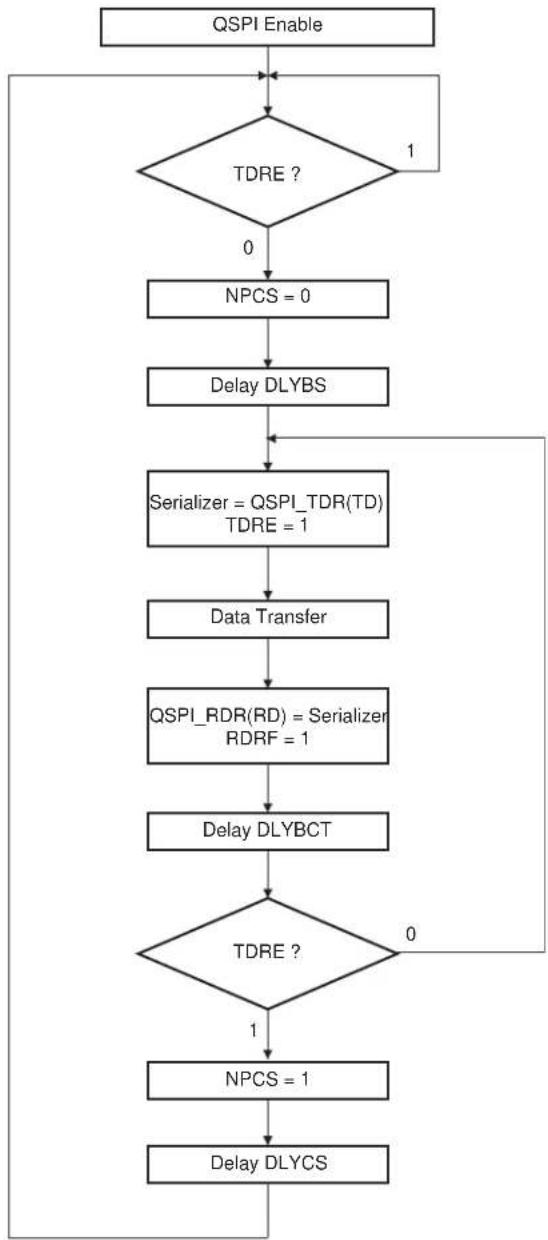
flowchart
graph TD
    A["QSPI Enable"] --> B{TDRE ?}
    B -->|0| C["NPCS = 0"]
    C --> D["Delay DLYBS"]
    D --> E["Serializer = QSPI_TDR(TD) TDRE = 1"]
    E --> F["Data Transfer"]
    F --> G["QSPI_RDR(RD) = Serializer RDRF = 1"]
    G --> H["Delay DLYBCT"]
    H --> I{TDRE ?}
    I -->|0| J["NPCS = 1"]
    J --> K["Delay DLYCS"]
    K --> B
    I -->|1| L["End"]
The figure below shows Transmit Data Register Empty (TDRE), Receive Data Register Full (RDRF) and Transmission Register Empty (TXEMPTY) status flags behavior within the QSPI_SR during an 8-bit data transfer in Fixed mode, without DMA.
Figure 41-7. Status Register Flags Behavior
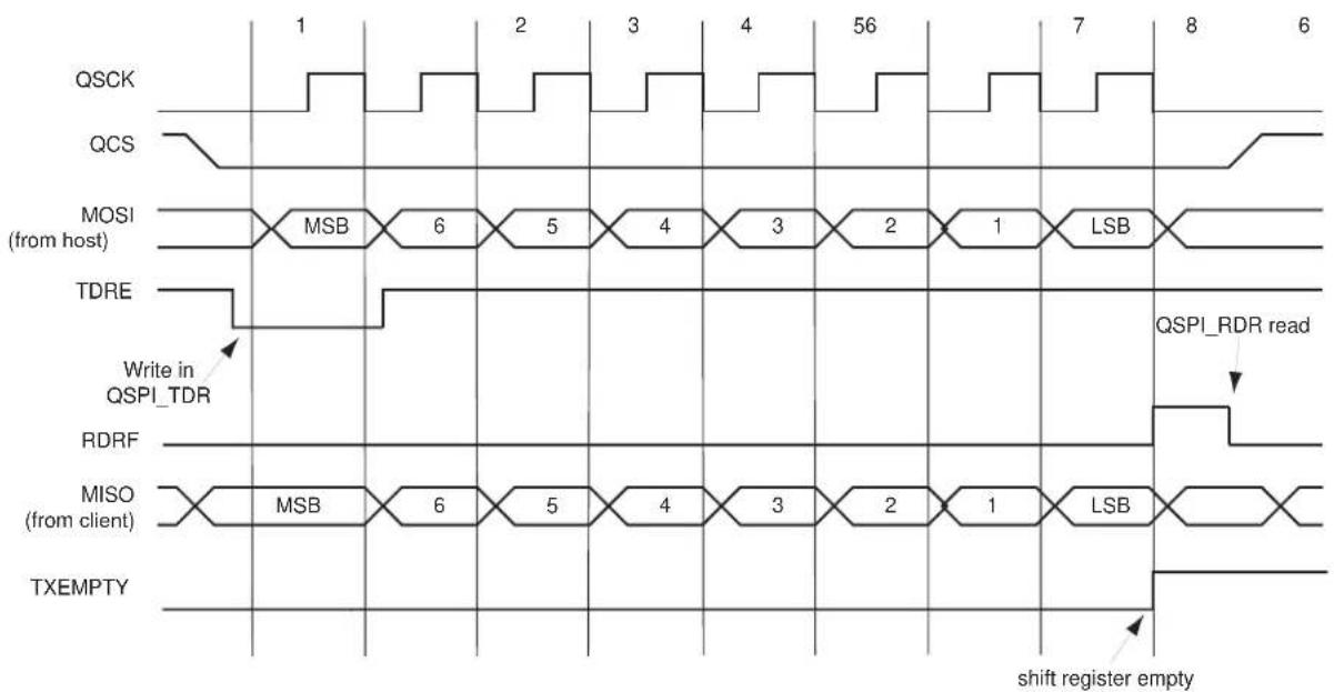
text_image
QSCK QCS MOSI (from host) TDRE Write in QSPI_TDR RDRF MISO (from client) TXEMPTY 1 2 3 4 56 7 8 6 MSB 6 5 4 3 2 1 LSB MSB 6 5 4 3 2 1 LSB QSPI_RDR read shift register empty41.6.4.4 Peripheral Deselection without DMA
During a transfer of more than one data on a Chip Select without the DMA, the QSPI_TDR is loaded by the processor and the flag TDRE rises as soon as the content of the QSPI_TDR is transferred into the internal shift register. When this flag is detected high, the QSPI_TDR can be reloaded. If this reload by the processor occurs before the end of the current transfer, the Chip Select is not deasserted between the two transfers. Depending on the application software handling the QSPI_SR flags (by interrupt or polling method) or servicing other interrupts or other tasks, the processor may not reload the QSPI_TDR in time to keep the chip select active (low). A null Delay Between Consecutive Transfer (DLYBCT) value in the QSPI_MR gives even less time for the processor to reload the QSPI_TDR. With some SPI Client peripherals, requiring the chip select line to remain active (low) during a full set of transfers may lead to communication errors.
To facilitate interfacing with such devices, QSPI_MR.CSMODE may be configured to '1'. This allows the chip select lines to remain in their current state (low = active) until the end of transfer is indicated by the Last Transfer (LASTXFER) bit in the Control register (QSPI_CR). Even if the QSPI_TDR is not reloaded, the chip select remains active. To have the chip select line rise at the end of the last data transfer, QSPI_CR.LASTXFER must be written to '1' at the same time or after writing the last data to transmit into the QSPI_TDR.
41.6.4.5 Peripheral Deselection with DMA
When the DMA Controller is used, the Chip Select line remains low during the transfer since the TDRE flag is managed by the DMA itself. Reloading the QSPI_TDR by the DMA is done as soon as the TDRE flag is set. In this case, writing QSPI_MR.CSMODE to '1' may not be needed. However, when other DMA channels connected to other peripherals are also in use, the QSPI DMA could be delayed by another DMA with a higher priority on the bus. Having DMA buffers in slower memories like Flash memory compared to fast internal SRAM, may lengthen the reload time of the QSPI_TDR by the DMA as well. This means that the QSPI_TDR might not be reloaded in time to keep the chip select line low. In this case, the chip select line may toggle between data transfer and according to some SPI Client devices, the communication might get lost. It may be necessary to configure QSPI_MR.CSMODE to '1'.
When QSPI_MR.CSMODE is configured to '0', the QCS does not rise in all cases between two transfers on the same peripheral. During a transfer on a Chip Select, the flag TDRE rises as soon as the content of the QSPI_TDR is transferred into the internal shifter. When this flag is detected, the QSPI_TDR can be reloaded. If this reload occurs before the end of the current transfer, the Chip
Select is not deasserted between the two transfers. This might lead to difficulties for interfacing with some serial peripherals requiring the chip select to be deasserted after each transfer. To facilitate interfacing with such devices, the QSPI_MR may be configured with QSPI_MR.CSMODE at '2'.
41.6.5 QSPI Serial Memory Mode
In Serial Memory mode, the QSPI acts as a serial Flash memory controller. The QSPI can be used to read data from the serial Flash memory allowing the CPU to execute code from it (XIP execute in place). The QSPI can also be used to control the serial Flash memory (Program, Erase, Lock, etc.) by sending specific commands. In this mode, the QSPI is compatible with single-bit SPI, Dual SPI and Quad SPI protocols.
To activate this mode, QSPI_MR.SMM must be written to '1'.
In Serial Memory mode, data is transferred only by writing or reading the QSPI memory space (0x80000000).
41.6.5.1 Instruction Frame
In order to control serial Flash memories, the QSPI is able to send instructions via the SPI bus (ex: READ, PROGRAM, ERASE, LOCK, etc.). Because the instruction set implemented in serial Flash memories is memory vendor-dependent, the QSPI includes a complete Instruction Frame register (QSPI_IFR), which makes it very flexible and compatible with all serial Flash memories.
An instruction frame includes:
- An instruction code (size: 8 bits). The instruction is optional in some cases (see section Continuous Read mode).
- An address (size: 24 bits or 32 bits). The address is optional but is required by instructions such as READ, PROGRAM, ERASE, LOCK. By default the address is 24 bits long, but it can be 32 bits long to support serial Flash memories larger than 128 Mbits (16 Mbytes).
- An option code (size: 1/2/4/8 bits). The option code is not required, but it is useful to activate the XIP mode or the Continuous Read mode (see section Continuous Read mode) for READ instructions, in some serial Flash memory devices. These modes improve the data read latency.
- Dummy cycles. Dummy cycles are optional but required by some READ instructions.
- Data bytes are optional. Data bytes are present for data transfer instructions such as READ or PROGRAM.
The instruction code, the address/option and the data can be sent with Single-bit SPI, Dual SPI or Quad SPI protocols.
Figure 41-8. Instruction Frame

flowchart
graph LR
    subgraph QCS
        A1["A20"] --> B1["A16"] --> C1["A12"] --> D1["A8"] --> E1["A4"] --> F1["A0"] --> G1["O4"] --> H1["O0"] --> I1["D4"] --> J1["D0"] --> K1["......"]
    end
    subgraph QSCK
        L1["A21"] --> M1["A17"] --> N1["A13"] --> O1["A9"] --> P1["A5"] --> Q1["A1"] --> R1["O5"] --> S1["O1"] --> T1["D5"] --> U1["......"]
    end
    subgraph QIO0
        V1["A22"] --> W1["A18"] --> X1["A14"] --> Y1["A10"] --> Z1["A6"] --> AA1["A2"] --> AB1["O6"] --> AC1["O2"] --> AD1["D6"] --> AE["......"]
    end
    subgraph QIO1
        F1["A23"] --> G1["A19"] --> H1["A15"] --> I1["A11"] --> J1["A7"] --> K1["A3"] --> L1["O7"] --> M1["O3"] --> N1["O7"] --> O1["O3"]
    end
    subgraph QIO2
        M1["A24"] --> N1["A18"] --> O1["A14"] --> P1["A10"] --> Q1["A6"] --> R1["O6"] --> S1["O2"] --> T1["O6"] --> U1["O2"]
    end
    subgraph QIO3
        N1["A25"] --> O1["A23"] --> P1["A20"] --> Q1["A19"] --> R1["Address Option"]
        R1["A20"] --> S1["S1"]
        S1["S1"] --> T1["T1"]
        T1["T1"] --> U1["T1"]
        U1["T1"] --> V1["V2"]
        V1["V2"] --> W1["W2"]
        W1["W2"] --> X1["W2"]
        X1["W2"] --> Y1["W2"]
        Y1["W2"] --> Z1["Z3"]
        Z1["Z3"] --> AA1["Z3"]
        AA1["Z3"] --> AB1["Z3"]
        AB1["Z3"] --> AC1["Z3"]
        AC1["Z3"] --> U1["Z3"]
        U1["Z3"] --> V1["V2"]
        V1["V2"] --> W1["V2"]
        W1["V2"] --> X1["V2"]
        X1["V2"] --> Y1["V2"]
        Y1["V2"] --> Z1["Z3"]
        Z1["Z3"] --> AA2["Z3"]
        AA2["Z3"] --> AB2["Z3"]
        AB2["Z3"] --> AC2["Z3"]
        AC2["Z3"] --> U2["U2"]
        U2["U2"] --> V2["U2"]
        V2["U2"] --> W2["U2"]
        W2["U2"] --> X2["U2"]
        X2["U2"] --> Y2["U2"]
        Y2["U2"] --> Z2["Z3"]
        Z2["Z3"] --> AA3["Z3"]
        AA3["Z3"] --> AB3["Z3"]
        AB3["Z3"] --> AC3["Z3"]
        AC3["Z3"] --> U3["U3"]
        U3["U3"] --> V3["U3"]
        V3["U3"] --> W3["U3"]
        W3["U3"] --> X3["U3"]
        X3["U3"] --> Y3["U3"]
        Y3["U3"] --> Z3["Z3"]
41.6.5.2 Instruction Frame Transmission
To send an instruction frame, the user must first configure the address to send by writing the field ADDR in the Instruction Address register (QSPI_IAR). This step is required if the instruction frame
includes an address and no data. When data is present, the address of the instruction is defined by the address of the data accesses in the QSPI memory space, not by QSPI_IAR.
If the instruction frame includes the instruction code and/or the option code, the user must configure the instruction code and/or the option code to send by writing the fields INST and OPT in the Instruction Code register (QSPI_ICR).
Then, the user must write QSPI_IFR to configure the instruction frame depending on which instruction must be sent. If the instruction frame does not include data, writing in this register triggers the send of the instruction frame in the QSPI. If the instruction frame includes data, the send of the instruction frame is triggered by the first data access in the QSPI memory space.
The instruction frame is configured by the following bits and fields of QSPI_IFR:
- WIDTH field—used to configure which data lanes are used to send the instruction code, the address, the option code and to transfer the data. It is possible to use two unidirectional data lanes (MISO-MOSI Single-bit SPI), two bidirectional data lanes (QIO0-QIO1 Dual SPI) or four bidirectional data lanes (QIO0-QIO3 Quad SPI).
- INSTEN bit—used to enable the send of an instruction code.
- ADDREN bit—used to enable the send of an address after the instruction code.
- OPTEN bit—used to enable the send of an option code after the address.
- DATAEN bit—used to enable the transfer of data (READ or PROGRAM instruction).
- OPTL field—used to configure the option code length. The value written in OPTL must be consistent with the value written in the field WIDTH. For example: OPTL = 0 (1-bit option code) is not consistent with WIDTH = 6 (option code sent with QuadSPI protocol, thus the minimum length of the option code is 4 bits).
- ADDRL bit—used to configure the address length.
- TFRTYP field—used to define which type of data transfer must be performed.
- NBDUM field—used to configure the number of dummy cycles when reading data from the serial Flash memory. Between the address/option and the data, with some instructions, dummy cycles are inserted by the serial Flash memory.
Refer to 41.6.5.2. Instruction Frame Transmission.
If data transfer is enabled, the user can access the serial memory by reading or writing the QSPI memory space:
- To read in the serial memory, but not a memory data, for example a JEDEC-ID or the QSPI_SR, QSPI_IFR.TFRTYP must be written to '0'.
- To read in the serial memory, and particularly a memory data, TFRTYP must be written to '1'.
- To write in the serial memory, but not a memory data, for example writing the configuration or the QSPI_SR, TFRTYP must be written to '2'.
- If the user wants to write in the serial memory in particular to program a memory data, TFRTYP must be written to '3'.
If QSPI_IFR.TFRTYP has a value other than '1', the address sent in the instruction frame is the address of the first system bus accesses. The addresses of the next accesses are not used by the QSPI. At each system bus access, an SPI transfer is performed with the same size. For example, a halfword system bus access leads to a 16-bit SPI transfer, and a byte system bus access leads to an 8-bit SPI transfer.
If TFRTYP = 1, the address of the first instruction frame is the one of the first read access in the QSPI memory space. Each time the read accesses become nonsequential (addresses are not consecutive), a new instruction frame is sent with the last system bus access address. In this way, the system can
read data at a random location in the serial memory. The size of the SPI transfers may differ from the size of the system bus read accesses.
When data transfer is not enabled, the end of the instruction frame is indicated when QSPI_SR.INSTRE rises. (The QSPI_SR.CSR flag indicates when chip select rises. A delay between these flags may exist in case of high clock division or a high DLYBCT value).
When data transfer is enabled, the user must indicate when the data transfer is completed in the QSPI memory space by setting QSPI_CR.LASTXFR. The end of the instruction frame is indicated when QSPI_SR.INSTRE rises.
The following figure illustrates instruction transmission management.
Figure 41-9. Instruction Transmission Flow Diagram
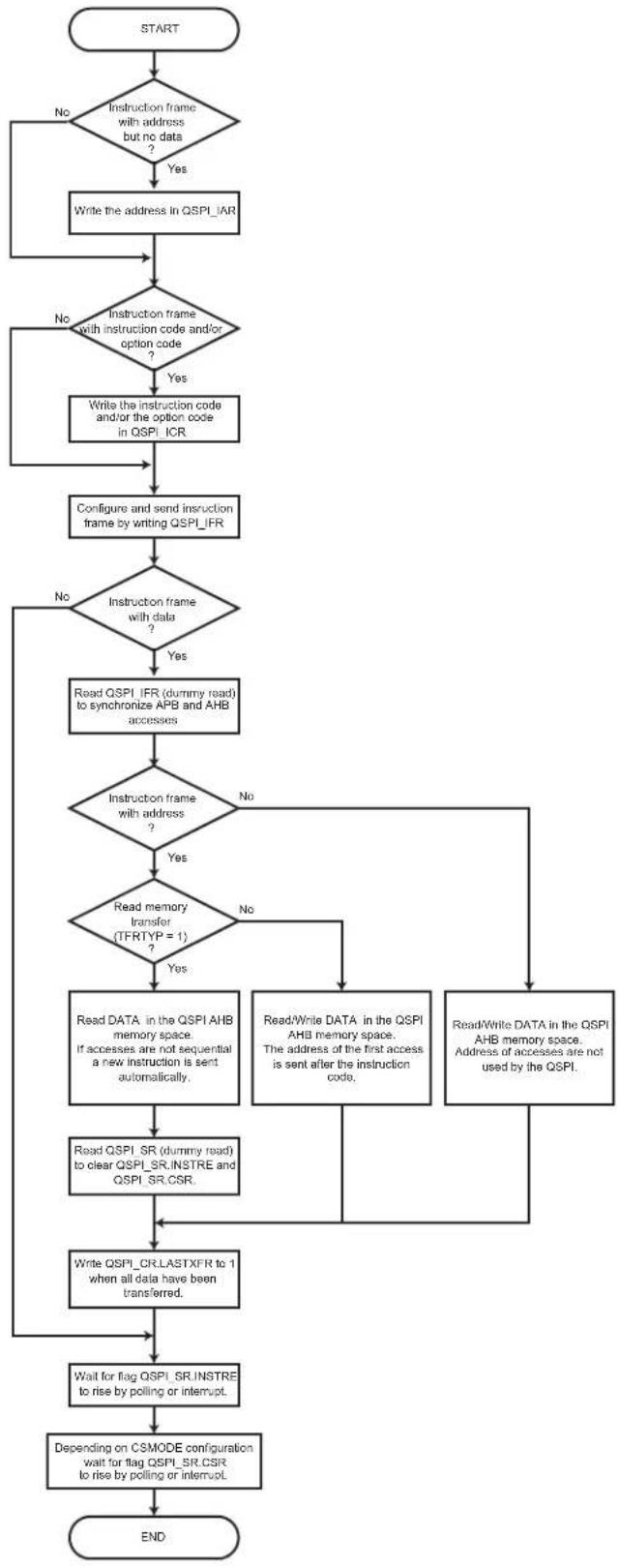
flowchart
graph TD
    A["START"] --> B{Instruction frame with address but no data?}
    B -->|No| C["Write the address in QSPI_IAR"]
    B -->|Yes| D["Write the instruction code and/or option code?"]
    C --> E{Instruction frame with instruction code and/or option code?}
    D --> F["Write the instruction code and/or option code in QSPI_ICR"]
    E --> G["Configure and send instruction frame by writing QSPI_IFR"]
    F --> G
    G --> H{Instruction frame with data?}
    H -->|No| I["Read QSPI_IFR (dummy read) to synchronize APB and AHB accesses"]
    H -->|Yes| J["Read data in the QSPI.AHB memory space. If accesses are not sequential a new instruction is sent automatically."]
    J --> K{Instruction frame with address?}
    K -->|No| L["Read/write DATA in the QSPI.AHB memory space. The address of the first access is sent after the instruction code."]
    K -->|Yes| M{Read memory transfer (TFRTYP = 1)?}
    M -->|No| N["Read/Write DATA in the QSPI.AHB memory space. Address of accesses are not used by the QSPI."]
    M -->|Yes| O["Read data in the QSPI.AHB memory space. If accesses are not sequentially a new instruction is sent automatically."]
    O --> P["Read QSPI_SR (dummy read) to clear QSPI_SR.INSTRE and QSPI_SR.CSR."]
    P --> Q["Write QSPI_CR.LASTXFR to 1 when all data have been transferred."]
    Q --> R["Wait for flag QSPI_SR.INSTRE to rise by polling or interrupt."]
    R --> S["Depending on CSMODE configuration wait for flag QSPI_SR.CSR to rise by polling or interrupt."]
    S --> T["END"]
41.6.5.3 Read Memory Transfer
The user can access the data of the serial memory by sending an instruction with QSPI_IFR.DATAEN = 1 and QSPI_IFR.TFRTYP = 1.
In this mode, the QSPI is able to read data at random address into the serial Flash memory, allowing the CPU to execute code directly from it (XIP execute-in-place).
In order to fetch data, the user must first configure the instruction frame by writing the QSPI_IFR. Then data can be read at any address in the QSPI address space mapping. The address of the system bus read accesses match the address of the data inside the serial Flash memory.
When Fetch mode is enabled, several instruction frames can be sent before writing QSPI_CR.LASTXFR. Each time the system bus read accesses become nonsequential (addresses are not consecutive), a new instruction frame is sent with the corresponding address.
41.6.5.4 Continuous Read Mode
The QSPI is compatible with the Continuous Read mode which is implemented in some serial Flash memories.
In Continuous Read mode, the instruction overhead is reduced by excluding the instruction code from the instruction frame. When the Continuous Read mode is activated in a serial Flash memory by a specific option code, the instruction code is stored in the memory. For the next instruction frames, the instruction code is not required as the memory uses the stored one.
In the QSPI, Continuous Read mode is used when reading data from the memory (QSPI_IFR.TFRTYP = 1). The addresses of the system bus read accesses are often nonsequential and this leads to many instruction frames that have the same instruction code. By disabling the send of the instruction code, the Continuous Read mode reduces the access time of the data.
To be functional, this mode must be enabled in both the QSPI and the serial Flash memory. The Continuous Read mode is enabled in the QSPI by writing CRM to '1' in the QSPI_IFR (TFRTYP must equal 1). The Continuous Read mode is enabled in the serial Flash memory by sending a specific option code.

If the Continuous Read mode is not supported by the serial Flash memory or disabled, CRM bit must not be written to '1', otherwise data read out of the serial Flash memory is unpredictable.
Figure 41-10. Continuous Read Mode

text_image
QCS QSCK QIO0 QIO1 QIO2 QIO3 Instruction Address Option to activate the Continuous Read Mode in the serial flash memory D4 D0 ...... D4 D6 A22 A16 A12 A8 A4 A0 O5 O0 D5 U1 ...... U5 D1 A22 A17 A15 A9 A5 A1 O5 O1 D5 D2 ...... U5 D2 A22 A18 A16 A8 A2 O5 O2 D7 D3 ...... D7 D3 Address Option Data Instruction code is not required D4 D0 ...... D4 D6 A22 A16 A12 A8 A4 A0 O5 O0 D5 U1 ...... U5 D1 A22 A17 A15 A9 A5 A1 O5 O1 D5 D2 ...... U5 D2 ...... D7 D3 ...... Data41.6.5.5 Instruction Frame Transmission Examples
All waveforms in the following examples describe SPI transfers in SPI Clock mode 0 (QSPI_SCR.CPOL = 0 and QSPI_SCR.CPHA = 0; see section Serial Clock Phase and Polarity).
All system bus accesses described below refer to the system bus address phase. System bus wait cycles and system bus data phases are not shown.
Example 1:
Instruction in Single-bit SPI, without address, without option, without data.
Command: CHIP ERASE (C7h).
- Write 0x0000_00C7 in QSPI_ICR.
- Write 0x0000_00C7 in QSPI_WICR.
- Write 0x0000_0010 in QSPI_IFR.
- Wait for QSPI_SR.INSTRE to rise.
Figure 41-11. Instruction Transmission Waveform 1
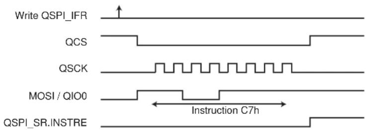
text_image
Write QSPI_IFR QCS QSCK MOSI / QIO0 QSPI_SR.INSTRE Instruction C7hExample 2:
Instruction in Quad SPI, without address, without option, without data.
Command: POWER DOWN (B9h)
- Write 0x0000_00B9 in QSPI_ICR.
- Write 0x0000_00B9 in QSPI_WICR.
- Write 0x0000_0016 in QSPI_IFR.
- Wait for QSPI_SR.INSTRE to rise.
Figure 41-12. Instruction Transmission Waveform 2
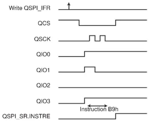
text_image
Write QSPI_IFR QCS QSCK QIO0 QIO1 QIO2 QIO3 QSPI_SR.INSTRE Instruction B9hExample 3:
Instruction in Single-bit SPI, with address in Single-bit SPI, without option, without data.
Command: BLOCK ERASE (20h)
- Write the address (of the block to erase) in QSPI_AR.
- Write 0x0000_0020 in QSPI_ICR.
-
Write 0x0000_0020 in QSPI_WICR.
-
Write 0x0000_0030 in QSPI_IFR.
- Wait for QSPI_SR.INSTRE to rise.
Figure 41-13. Instruction Transmission Waveform 3

text_image
Write QSPI_IAR Write QSPI_IFR QCS QSCK MOSI / QIO0 Instruction 20h A23 A22 A21 A20 A9-A2 A7 A0 Address QSPI_SR.INSTREExample 4:
Instruction in Single-bit SPI, without address, without option, with data write in Single-bit SPI.
Command: SET BURST (77h)
- Write 0x0000_0077 in QSPI_ICR.
- Write 0x0000_0077 in QSPI_WICR.
- Write 0x0000_2090 in QSPI_IFR.
- Write 0x0000_0090 in QSPI_IFR.
- Read QSPI_IFR (dummy read) to synchronize system bus accesses.
- Write data in the system bus memory space (0x80000000). The address of system bus write accesses is not used.
- Write a '1' to QSPI_CR.LASTXFR.
- Wait for QSPI_SR.INSTRE to rise.
Figure 41-14. Instruction Transmission Waveform 4

text_image
Write QSPI_IFR QCS QSCK MOSI / QIO0 Instruction 77h D7 D6 D5 D4 D3 D2 D1 D0 Data QSPI_SR.INSTRE Write AHB Set QSPI_CR.LASTXFRExample 5:
Instruction in Single-bit SPI, with address in Dual SPI, without option, with data write in Dual SPI.
Command: BYTE/PAGE PROGRAM (02h)
- Write 0x0000_0002 in QSPI_ICR.
- Write 0x0000_0002 in QSPI_WICR.
- Write 0x0000_30B3 in QSPI_IFR.
-
Write 0x0000_10B3 in QSPI_IFR.
-
Read QSPI_IFR (dummy read) to synchronize system bus accesses.
- Write data in the QSPI system bus memory space (0x80000000).
The address of the first system bus write access is sent in the instruction frame.
The address of the next system bus write accesses is not used.
- Write a '1' to QSPI_CR.LASTXFR.
- Wait for QSPI_SR.INSTRE to rise.
Figure 41-15. Instruction Transmission Waveform 5

text_image
Write QSPI_IFR QCS QSCK QIO0 A22 A20 A18 A16 A14 A12 A10 A8 A6 A4 A2 A0 D6 D4 D2 D0 X06 D4 D2 D0 QIO1 A23 A21 A19 A17 A15 A13 A11 A9 A7 A5 A3 A1 D7 D5 D3 D1 X07 D5 D3 D1 Instruction 02h Address Data QSPI_SR.INSTRE Write AHB Set QSPI_CR.LASTXFRExample 6:
Instruction in Single-bit SPI, with address in Single-bit SPI, without option, with data read in Quad SPI, with eight dummy cycles.
Command: QUAD_OUTPUT READ ARRAY (6Bh)
- Write 0x0000_006B in QSPI_ICR.
- Write 0x0008_10B2 in QSPI_IFR.
- Read QSPI_IR (dummy read) to synchronize system bus accesses.
- Read data in the QSPI system bus memory space (0x80000000).
The address of the first system bus read access is sent in the instruction frame.
The address of the next system bus read accesses is not used.
- Write a '1' to QSPI_CR.LASTXFR.
- Wait for QSPI_SR.INSTRE to rise.
Figure 41-16. Instruction Transmission Waveform 6
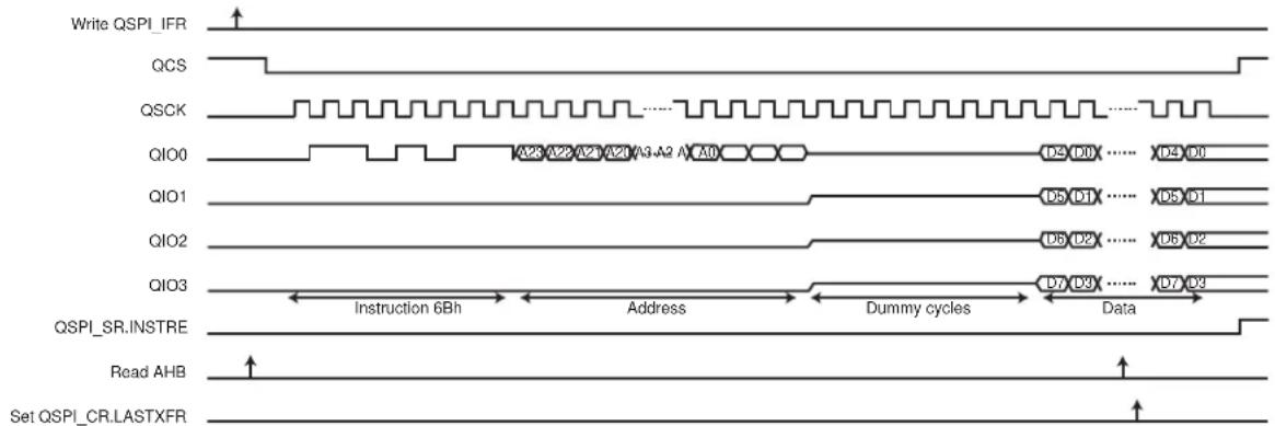
text_image
Write QSPI_IFR QCS QSCK QIO0 A26 A22 A21 A20 A3 A2 A1 A0 D4 D0 ...... D4 D0 QIO1 D5 D1 ...... D5 D1 QIO2 D6 D2 ...... D6 D2 QIO3 D7 D9 ...... D7 D9 QSPI_SR.INSTRE Instruction 6Bh Address Dummy cycles Data Read AHB Set QSPI_CR.LASTXFRExample 7:
Instruction in Single-bit SPI, with address and option in Quad SPI, with data read in Quad SPI, with four dummy cycles, with fetch and continuous read.
Command: FAST READ QUAD I/O (EBh) - 8-BIT OPTION (0x30h)
- Write 0x0030_00EB in QSPI_ICR.
- Write 0x0030_00EB in QSPI_RICR.
- Write 0x0004_33F4 in QSPI_IFR.
- Read QSPI_IFR (dummy read) to synchronize system bus accesses.
- Read data in the QSPI system bus memory space (0x80000000).
Fetch is enabled, the address of the system bus read accesses is always used.
- Write a '1' to QSPI_CR.LASTXFR.
- Wait for QSPI_SR.INSTRE to rise.
Figure 41-17. Instruction Transmission Waveform 7
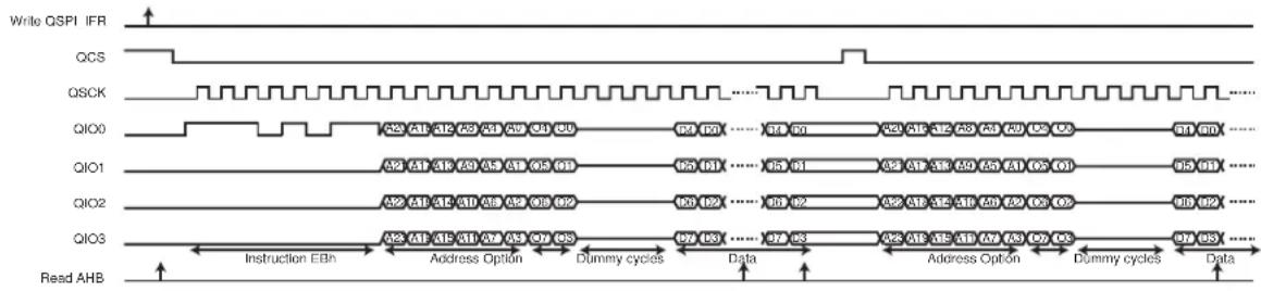
text_image
Write QSPI IFR QCS QSCK QIO0 A2 A1 A2 A3 A4 A5 A6 ... 94 90 ... 94 91 ... 93 A1 B A2 B A3 A4 B5 C6 ... 91 90 ... QIO1 A2 A1 A2 A3 A4 A5 A6 ... 95 91 ... 95 91 ... 95 A1 B A3 A4 B5 A6 A7 C6 ... 95 91 ... QIO2 A2 A1 A2 A3 A4 A5 A6 ... 98 92 ... 98 92 ... 98 A1 B A3 A4 B5 A6 C6 ... 98 92 ... QIO3 A2 A1 A2 A3 A4 A5 C7 C8 ... 97 93 ... 97 93 ... 97 A1 B A3 A4 B5 C7 C8 ... 97 93 ... Instruction EBn Address Option Dummy cycles Data Address Option Dummy cycles Data Read AHBExample 8:
Instruction in Quad SPI, with address in Quad SPI, without option, with data read in Quad SPI, with two dummy cycles, with fetch.
Command: HIGH-SPEED READ (0Bh)
- Write 0x0000_000B in QSPI_ICR.
- Write 0x0000_000B in QSPI_RICR.
- Write 0x0002_20B6 in QSPI_IFR.
- Read QSPI_IFR (dummy read) to synchronize system bus accesses.
- Read data in the QSPI system bus memory space (0x80000000).
Fetch is enabled, the address of the system bus read accesses is always used.
- Write a '1' to QSPI_CR.LASTXFR.
- Wait for QSPI_SR.INSTRE to rise.
Figure 41-18. Instruction Transmission Waveform 8

text_image
Write QSPI_IFR QCS QSCK QIO0 A20 A16 A12 A8 A4 A0 D4 D0 D4 D0 A20 A16 A12 A8 A4 A0 D4 D0 QIO1 A21 A17 A13 A9 A5 A1 D5 D1 D5 D1 A21 A17 A13 A9 A5 A1 D5 D1 QIO2 A22 A18 A14 A10 A6 A2 D6 D2 D6 D2 A22 A18 A14 A10 A6 A2 D6 D2 QIO3 A23 A19 A15 A11 A7 A3 D7 D3 D7 D3 A23 A19 A15 A11 A7 A3 D7 D3 Read AHB Instruction 0Bh Address Dummy cycles Data Instruction 0Bh Address Dummy cycles DataExample 9:
Instruction in Quad SPI, without address, without option, with data read in Quad SPI, without dummy cycles, without fetch.
Command: HIGH-SPEED READ (05h)
- Write 0x0000_0005 in QSPI_ICR.
- Write 0x0000_0005 in QSPI_RICR.
- Write 0x0000_0096 in QSPI_IFR.
- Read QSPI_IFR (dummy read) to synchronize system bus accesses.
- Read data in the QSPI system bus memory space (0x80000000). Fetch is disabled.
- Write a '1' to QSPI_CR.LASTXFR.
- Wait for QSPI_SR.INSTRE to rise.
Figure 41-19. Instruction Transmission Waveform 9
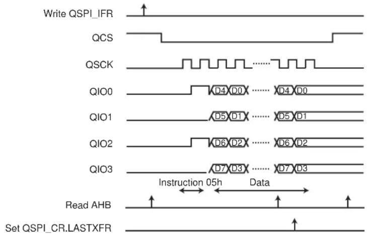
text_image
Write QSPI_IFR QCS QSCK QIO0 D4 D0 ....... D4 D0 QIO1 D5 D1 ....... D5 D1 QIO2 D6 D2 ....... D6 D2 QIO3 D7 D3 ....... D7 D3 Read AHB Set QSPI_CR.LASTXFR Instruction 05h Data41.6.6 Scrambling/Unscrambling Function
The scrambling/unscrambling function cannot be performed on devices other than memories. Data is scrambled when written to memory and unscrambled when data is read.
The external data lines can be scrambled in order to prevent intellectual property data located in off-chip memories from being easily recovered by analyzing data at the package pin level of either the microcontroller or the QSPI Client device (e.g., memory).
The scrambling/unscrambling function can be enabled by writing a '1' to the SCREEN bit in the QSPI Scrambling Mode Register (QSPI_SMR).
The scrambling and unscrambling are performed on-the-fly without impacting the throughput.
The scrambling method depends on the user-configurable user scrambling key (field USRK) in the QSPI Scrambling Key Register (QSPI_SKR). QSPI_SKR is only accessible in Write mode.
When QSPI_SMR.SCRKL has been written once to '1', QSPI_SKR.USRK cannot be written again until the next reset.
If QSPI_SMR.RVDIS is written to '0', the scrambling/unscrambling algorithm includes the user scrambling key plus a random value depending on device processing characteristics. Data scrambled by a given microcontroller cannot be unscrambled by another.
If QSPI_SMR.RVDIS is written to '1', the scrambling/unscrambling algorithm includes only the user scrambling key. No random value is part of the key.
The user scrambling key or the seed for key generation must be securely stored in a reliable nonvolatile memory in order to recover data from the off-chip memory. Any data scrambled with a given key cannot be recovered if the key is lost.
41.6.7 Register Write Protection
To prevent any single software error from corrupting QSPI behavior, certain registers in the address space can be write-protected by setting the WPEN bit in the QSPI Write Protection Mode Register (QSPI_WPMR).
If a write access to a write-protected register is detected, the WPVS flag in the QSPI Write Protection Status Register (QSPI_WPSR) is set and the field WPVSRC indicates the register in which the write access has been attempted.
The WPVS bit is automatically cleared after reading the QSPI_WPSR.
The following registers can be write-protected when WPEN is set in QSPI_WPMR:
- QSPI Mode Register
• QSPI Serial Clock Register
• QSPI Scrambling Mode Register
• QSPI Scrambling Key Register
41.7 Register Summary
| Offset | Name Bit Pos. 7 | 6 | 5 | 4 | 3 | 2 | 1 | 0 | |||||||||
| 0x00 | QSPI_CR | 7:0 SWRST QSPIDIS QSPIEN | |||||||||||||||
| 15:8 | |||||||||||||||||
| 23:16 | |||||||||||||||||
| 31:24 | LASTXFER | ||||||||||||||||
| 0x04 | QSPI_MR | 7:0 | TAMPCLR | CSMODE[1:0] | WDRBT | LLB | SMM | ||||||||||
| 15:8 | NBBITS[3:0] | ||||||||||||||||
| 23:16 | DLYBCT[7:0] | ||||||||||||||||
| 31:24 | DLYCS[7:0] | ||||||||||||||||
| 0x08 | QSPI_RDR | 7:0 | RD[7:0] | ||||||||||||||
| 15:8 | RD[15:8] | ||||||||||||||||
| 23:16 | |||||||||||||||||
| 31:24 | |||||||||||||||||
| 0x0C | QSPI_TDR | 7:0 | TD[7:0] | ||||||||||||||
| 15:8 | TD[15:8] | ||||||||||||||||
| 23:16 | |||||||||||||||||
| 31:24 | |||||||||||||||||
| 0x10 | QSPI_SR | 7:0 | OVRES | TXEMPTY | TDRE | RDRF | |||||||||||
| 15:8 | INSTRE CSS CSR | ||||||||||||||||
| 23:16 | |||||||||||||||||
| 31:24 | QSPIENS | ||||||||||||||||
| 0x14 | QSPI_IER | 7:0 | OVRES | TXEMPTY | TDRE | RDRF | |||||||||||
| 15:8 | INSTRE CSS CSR | ||||||||||||||||
| 23:16 | |||||||||||||||||
| 31:24 | |||||||||||||||||
| 0x18 | QSPI_IDR | 7:0 | OVRES | TXEMPTY | TDRE | RDRF | |||||||||||
| 15:8 | INSTRE CSS CSR | ||||||||||||||||
| 23:16 | |||||||||||||||||
| 31:24 | CPOL | ||||||||||||||||
| 0x1C | QSPI_IMR | 7:0 | OVRES | TXEMPTY | TDRE | RDRF | |||||||||||
| 15:8 | INSTRE CSS CSR | ||||||||||||||||
| 23:16 | |||||||||||||||||
| 31:24 | ADDR[31:24] | ||||||||||||||||
| 0x20 | QSPI_SCR | 7:0 | |||||||||||||||
| 15:8 | SCBR[7:0] | ||||||||||||||||
| 23:16 | DLYBS[7:0] | ||||||||||||||||
| 31:24 | |||||||||||||||||
| 0x24...0x2F | Reserved | ||||||||||||||||
| 0x30 | QSPI_IAR | 7:0 | ADDR[7:0] | ||||||||||||||
| 15:8 | ADDR[15:8] | ||||||||||||||||
| 23:16 | ADDR[23:16] | ||||||||||||||||
| 31:24 | ADDR[31:24] | ||||||||||||||||
| 0x34 | QSPI_ICR | 7:0 | INST[7:0] | ||||||||||||||
| 15:8 | |||||||||||||||||
| 23:16 | OPT[7:0] | ||||||||||||||||
| 31:24 | |||||||||||||||||
| 0x38 | QSPI_IFR | 7:0 | DATAEN | OPTEN | ADDREN | INSTEN | WIDTH[2:0] | ||||||||||
| 15:8 | DDREN | CRM | TFRTYP[1:0] | ADDRL | OPTL[1:0] | ||||||||||||
| 23:16 | NBDUM[4:0] | ||||||||||||||||
| 31:24 | DDRCMDEN | APBTFRTYP | |||||||||||||||
| 0x3C...0x3F | Reserved | ||||||||||||||||
| 0x40 | QSPI_SMR | 7:0 | RVDIS SCREEN | ||||||||||||||
| 15:8 | |||||||||||||||||
| 23:16 | |||||||||||||||||
| 31:24 | |||||||||||||||||
......continued
| Offset | Name Bit Pos. 7 | 6 | 5 | 4 | 3 | 2 | 1 | 0 | ||||||||||
| 0x44 | QSPI_SKR | 7:0 | USRK[7:0] | |||||||||||||||
| 15:8 | USRK[15:8] | |||||||||||||||||
| 23:16 | USRK[23:16] | |||||||||||||||||
| 31:24 | USRK[31:24] | |||||||||||||||||
| 0x48 ... 0xE3 | Reserved | |||||||||||||||||
| 0xE4 | QSPI_WPMR | 7:0 | WPEN | |||||||||||||||
| 15:8 | WPKEY[7:0] | |||||||||||||||||
| 23:16 | WPKEY[15:8] | |||||||||||||||||
| 31:24 | WPKEY[23:16] | |||||||||||||||||
| 0xE8 | QSPI_WPSR | 7:0 | WPVS | |||||||||||||||
| 15:8 | WPVSRC[7:0] | |||||||||||||||||
| 23:16 | ||||||||||||||||||
| 31:24 | ||||||||||||||||||