ATSAML22G17A - Electronic component Microchip - Free user manual and instructions
Find the device manual for free ATSAML22G17A Microchip in PDF.

User questions about ATSAML22G17A Microchip
0 question about this device. Answer the ones you know or ask your own.
Ask a new question about this device
Download the instructions for your Electronic component in PDF format for free! Find your manual ATSAML22G17A - Microchip and take your electronic device back in hand. On this page are published all the documents necessary for the use of your device. ATSAML22G17A by Microchip.
USER MANUAL ATSAML22G17A Microchip
32-bit ARM Cortex-M0+ Ultra-Low-Power MCU family with Peripheral Touch Controller (PTC), Segment LCD Controller, Advanced Analog, USB and AES
SAM L22 Family
Features
Operating Conditions
- 1.62V - 3.63V, -40°C to +85°C, DC up to 32 MHz
Core: 32 MHz ARM ^® Cortex ^® -M0+
- Single-cycle hardware multiplier
- Micro Trace Buffer
• Memory Protection Unit (MPU)
Memories
• 64/128/256 KB in-system self-programmable Flash
• 2/4/8 KB Flash Read-While-Write section
• 8/16/32 KB SRAM main memory
System
- Power-on Reset (POR) and programmable Brown-out Detection (BOD)
- Internal and external clock options
- External Interrupt Controller (EIC)
- 16 external interrupts that can use any I/O pin
- One Non-maskable Interrupt (NMI) on one I/O pin
• 2-pin Serial Wire Debug (SWD)
Low-Power
- Idle, Standby, Backup, and Off Sleep modes
- SleepWalking peripherals
- Battery backup support
- Two runtime selectable power/performance levels
- Embedded Buck/LDO regulator supporting on-the-fly selection
• Active mode: < 50 μA/MHz - Standby with full retention, RTC and LCD = 3.47 μA
- 2.1 μs wake-up time
- Standby with full retention and RTC: 1.87 A -2.1 s wake-up time
- Ultra low-power Backup mode with RTC: 490 nA
- 90 µs wake-up time
Peripherals
- Segment LCD controller - Up to 8 (4) common and 40 (44) segment terminals to drive 320 (176) segments
- Static, one-half, one-third, and one-fourth bias
- Internal charge pump able to generate VLCD higher than VDDIO
• 16-channel Direct Memory Access Controller (DMAC)
• 8-channel Event System
- Up to four 16-bit Timer/Counters (TC), each configurable as:
- 16-bit TC with two compare/capture channels
- 8-bit TC with two compare/capture channels
- 32-bit TC with two compare/capture channels, by using two TCs
- One 24-bit Timer/Counters for Control (TCC), with extended functions:
- Four compare channels with optional complementary output
- Generation of synchronized pulse width modulation (PWM) pattern across port pins
- Deterministic fault protection, fast decay and configurable dead-time between complementary output
- Dithering that increase resolution with up to 5-bit and reduce quantization error
- PWM Channels using TC and TCC peripherals:
- Up to four PWM channels on each 24-bit TCC
- Up to two PWM channels on each 16-bit TC
- Frequency Meter
• 32-bit Real-Time Counter (RTC) with Clock/Calendar function
- 8x32-bit Backup Register
- Tamper Detection
- Watchdog Timer (WDT)
- CRC-32 generator
• One Full-Speed (12 Mbps) Universal Serial Bus (USB) 2.0 Device
- Eight endpoints
- Crystal less operation
- Up to six Serial Communication Interfaces (SERCOM), each configurable as:
- USART with full-duplex and single-wire half-duplex configuration
- ISO7816
- I^2C up to 3.4 MHz (maximum of 1 High-Speed mode and maximum of 3 Fast mode I^2C )
- SPI
• One AES encryption engine
• One True Random Generator (TRNG)
• One Configurable Custom Logic (CCL)
• One 12-bit, 1 Msps Analog-to-Digital Converter (ADC) with up to 20 channels
– Differential and single-ended input
- Oversampling and decimation in hardware to support 13-bit, 14-bit, 15-bit, or 16-bit resolution
- Two Analog Comparators (AC) with Window Compare function
• Peripheral Touch Controller (PTC)
- Up to 256-Channel capacitive touch sensing
• Maximum Mutual-Cap up to 16x16 channels
• Maximum Self-Cap up to 24 channels
- Wake-up on touch in Standby mode
Oscillators
• 32.768 kHz crystal oscillator (XOSC32K)
• 0.4-32 MHz crystal oscillator (XOSC)
• 32.768 kHz ultra-low-power internal oscillator (OSCULP32K)
• 16/12/8/4 MHz high-accuracy internal oscillator (OSC16M)
• 48 MHz Digital Frequency Locked Loop (DFLL48M)
• 96 MHz Fractional Digital Phased Locked Loop (FDPLL96M)
I/O
- Up to 82 programmable I/O pins
- Up to 52 segment LCD pins can be used as GPIO/GPI
- Up to five wake-up pins with optional debouncing
- Up to five tamper input pins
• One tamper output pin
Packages
• 100-pin TQFP
- 64-pin TQFP, QFN
• 49-pin WLCSP
• 48-pin TQFP, QFN
Table of Contents
Features 1
- Configuration Summary......14
- Ordering Information.... 16
2.1. SAM L22N....16
2.2. SAM L22J.... 16
2.3. SAM L22G....17
2.4. Device Identification....17
- Block Diagram....18
- Pinout....20
4.1. SAM L22G....20
4.2. SAM L22J.... 22
4.3. SAM L22N....23
- Signal Descriptions List ....25
- I/O Multiplexing and Considerations....27
6.1. Multiplexed Signals....27
6.2. Other Functions.... 29
- Power Supply and Start-Up Considerations....32
7.1. Power Domain Overview.... 32
7.2. Power Supply Considerations.... 32
7.3. Power-Up....35
7.4. Power-On Reset and Brown-Out Detector....35
7.5. Performance Level Overview....36
- Product Mapping....37
- Memories....38
9.1. Embedded Memories....38
9.2. Physical Memory Map....38
9.3. NVM User Row Mapping.... 38
9.4. NVM Software Calibration Area Mapping....39
9.5. Serial Number....39
- Processor and Architecture....40
10.1. Cortex M0+ Processor....40
10.2. Nested Vector Interrupt Controller....41
10.3. Micro Trace Buffer 42
10.4. High-Speed Bus System.... 43
- PAC - Peripheral Access Controller....46
11.1. Overview....46
11.2. Features.... 46
11.3. Block Diagram....46
11.4. Product Dependencies....46
11.5. Functional Description....47
11.6. Register Summary.... 51
11.7. Register Description....51
-
Peripherals Configuration Summary....67
-
DSU - Device Service Unit....70
13.1. Overview....70
13.2. Features....70
13.3. Block Diagram....70
13.4. Signal Description....71
13.5. Product Dependencies....71
13.6. Debug Operation....72
13.7. Chip Erase....73
13.8. Programming....74
13.9. Intellectual Property Protection....74
13.10. Device Identification....76
13.11. Functional Description....77
13.12. Register Summary....82
13.13. Register Description....83
- Clock System....106
14.1. Clock Distribution.... 106
14.2. Synchronous and Asynchronous Clocks....107
14.3. Register Synchronization.... 108
14.4. Enabling a Peripheral.... 110
14.5. On Demand Clock Requests....110
14.6. Power Consumption vs. Speed.... 111
14.7. Clocks after Reset.... 111
- GCLK - Generic Clock Controller....112
15.1. Overview.... 112
15.2. Features.... 112
15.3. Block Diagram.... 112
15.4. Signal Description....113
15.5. Product Dependencies....113
15.6. Functional Description.... 114
15.7. Additional Features.... 117
15.8. Sleep Mode Operation....118
15.9. Synchronization.... 118
15.10. Register Summary.... 120
15.11. Register Description....120
- MCLK - Main Clock....128
16.1. Overview.... 128
16.2. Features.... 128
16.3. Block Diagram....128
16.4. Signal Description.... 128
16.5. Product Dependencies....128
16.6. Functional Description.... 130
16.7. Register Summary.... 134
16.8. Register Description.... 134
17. FREQM - Frequency Meter.... 147
17.1. Overview.... 147
17.2. Features.... 147
17.3. Block Diagram.... 147
17.4. Signal Description.... 147
17.5. Product Dependencies....147
17.6. Functional Description.... 148
17.7. Register Summary.... 151
17.8. Register Description.... 151
18. RSTC - Reset Controller....161
18.1. Overview.... 161
18.2. Features.... 161
18.3. Block Diagram.... 161
18.4. Signal Description.... 161
18.5. Product Dependencies....161
18.6. Functional Description.... 162
18.7. Register Summary.... 164
18.8. Register Description.... 164
19. PM - Power Manager 167
19.1. Overview.... 167
19.2. Features.... 167
19.3. Block Diagram.... 167
19.4. Signal Description.... 167
19.5. Product Dependencies....167
19.6. Functional Description.... 168
19.7. Register Summary.... 178
19.8. Register Description.... 178
20. OSCCTRL - Oscillators Controller....186
20.1. Overview.... 186
20.2. Features....186
20.3. Block Diagram....187
20.4. Signal Description....187
20.5. Product Dependencies....187
20.6. Functional Description.... 188
20.7. Register Summary.... 200
20.8. Register Description.... 201
21. OSC32KCTRL - 32.768 kHz Oscillators Controller.... 231
21.1. Overview.... 231
21.2. Features.... 231
21.3. Block Diagram....231
21.4. Signal Description....231
21.5. Product Dependencies....231
21.6. Functional Description.... 232
21.7. Register Summary.... 237
21.8. Register Description.... 237
- SUPC - Supply Controller 249
22.1. Overview.... 249
22.2. Features.... 249
22.3. Block Diagram.... 250
22.4. Signal Description....250
22.5. Product Dependencies....250
22.6. Functional Description.... 251
22.7. Register Summary.... 259
22.8. Register Description.... 259
- WDT - Watchdog Timer....278
23.1. Overview.... 278
23.2. Features....278
23.3. Block Diagram....278
23.4. Signal Description....279
23.5. Product Dependencies....279
23.6. Functional Description.... 280
23.7. Register Summary.... 286
23.8. Register Description.... 286
- RTC - Real-Time Counter....295
24.1. Overview.... 295
24.2. Features.... 295
24.3. Block Diagram....296
24.4. Signal Description....297
24.5. Product Dependencies....297
24.6. Functional Description.... 299
24.7. Register Summary - COUNT32....309
24.8. Register Description - COUNT32....310
24.9. Register Summary - COUNT16....330
24.10. Register Description - COUNT16.... 331
24.11. Register Summary - CLOCK 352
24.12. Register Description - CLOCK....353
- DMAC - Direct Memory Access Controller 375
25.1. Overview....375
25.2. Features....375
25.3. Block Diagram.... 377
25.4. Signal Description....377
25.5. Product Dependencies....377
25.6. Functional Description.... 378
25.7. Register Summary.... 399
25.8. Register Description....400
25.9. Register Summary - SRAM 430
25.10. Register Description - SRAM 430
- EIC – External Interrupt Controller....437
26.1. Overview....437
26.2. Features....437
26.3. Block Diagram....437
26.4. Signal Description....437
26.5. Product Dependencies....438
26.6. Functional Description....439
26.7. Register Summary...... 444
26.8. Register Description....444
27. NVMCTRL - Non-Volatile Memory Controller 455
27.1. Overview....455
27.2. Features....455
27.3. Block Diagram....455
27.4. Signal Description....456
27.5. Product Dependencies....456
27.6. Functional Description....457
27.7. Register Summary...... 464
27.8. Register Description....464
28. PORT - I/O Pin Controller....477
28.1. Overview....477
28.2. Features....477
28.3. Block Diagram....478
28.4. Signal Description....478
28.5. Product Dependencies....478
28.6. Functional Description....480
28.7. Register Summary...... 486
28.8. Register Description....487
29. EVSYS - Event System....505
29.1. Overview....505
29.2. Features....505
29.3. Block Diagram....505
29.4. Signal Description....505
29.5. Product Dependencies....506
29.6. Functional Description.... 507
29.7. Register Summary.... 512
29.8. Register Description....513
30. SERCOM - Serial Communication Interface....525
30.1. Overview....525
30.2. Features....525
30.3. Block Diagram....525
30.4. Signal Description....525
30.5. Product Dependencies....526
30.6. Functional Description....527
31. SERCOM USART – SERCOM Universal Synchronous and Asynchronous Receiver and Transmitter......532
31.1. Overview....532
31.2. USART Features....532
31.3. Block Diagram....533
31.4. Signal Description....533
31.5. Product Dependencies....533
31.6. Functional Description....535
31.7. Register Summary.... 549
31.8. Register Description....549
32. SERCOM SPI - SERCOM Serial Peripheral Interface....572
32.1. Overview....572
32.2. Features....572
32.3. Block Diagram....573
32.4. Signal Description....573
32.5. Product Dependencies....573
32.6. Functional Description....575
32.7. Register Summary.... 583
32.8. Register Description....583
33. SERCOM I²C – SERCOM Inter-Integrated Circuit....598
33.1. Overview....598
33.2. Features....598
33.3. Block Diagram....599
33.4. Signal Description....599
33.5. Product Dependencies....599
33.6. Functional Description....601
33.7. Register Summary - I2C Client....619
33.8. Register Description - I 2C Client....619
33.9. Register Summary - I2C Host 633
33.10. Register Description - I ^2 C Host 633
34. TC - Timer/Counter....651
34.1. Overview....651
34.2. Features....651
34.3. Block Diagram....652
34.4. Signal Description....652
34.5. Product Dependencies....652
34.6. Functional Description.... 654
34.7. Register Description....668
34.8. Register Summary - 8-bit Mode....669
34.9. Register Summary - 16-bit Mode....691
34.10. Register Summary - 32-bit Mode....711
35. TCC - Timer/Counter for Control Applications....731
35.1. Overview....731
35.2. Features....731
35.3. Block Diagram....732
35.4. Signal Description....732
35.5. Product Dependencies....732
35.6. Functional Description....734
35.7. Register Summary.... 766
35.8. Register Description....768
36. TRNG - True Random Number Generator....806
36.1. Overview....806
36.2. Features....806
36.3. Block Diagram....806
36.4. Signal Description....806
36.5. Product Dependencies....806
36.6. Functional Description....807
36.7. Register Summary....809
36.8. Register Description....809
37. AES - Advanced Encryption Standard....816
37.1. Overview....816
37.2. Features....816
37.3. Block Diagram....817
37.4. Signal Description....817
37.5. Product Dependencies....817
37.6. Functional Description....819
37.7. Register Summary....827
37.8. Register Description....829
38. USB - Universal Serial Bus....845
38.1. Overview....845
38.2. Features....845
38.3. USB Block Diagram....845
38.4. Signal Description....845
38.5. Product Dependencies....846
38.6. Functional Description....847
38.7. Communication Device Host Register Summary....856
38.8. Communication Device Host Register Description....856
38.9. Device Registers - Common -Register Summary.... 863
38.10. Device Registers - Common 863
38.11. Device Endpoint Register Summary......876
38.12. Device Endpoint Register Description.... 876
38.13. Endpoint Descriptor Structure....885
38.14. Device Endpoint RAM Register Summary......886
38.15. Device Endpoint RAM Register Description.... 886
39. CCL - Configurable Custom Logic 892
39.1. Overview....892
39.2. Features....892
39.3. Block Diagram....893
39.4. Signal Description....893
39.5. Product Dependencies....893
39.6. Functional Description....894
39.7. Register Summary.... 904
39.8. Register Description....904
40. ADC - Analog-to-Digital Converter....909
40.1. Overview....909
40.2. Features....909
40.3. Block Diagram....910
40.4. Signal Description....910
40.5. Product Dependencies....910
40.6. Functional Description....911
40.7. Register Summary....921
40.8. Register Description....921
41. AC - Analog Comparators....948
41.1. Overview....948
41.2. Features....948
41.3. Block Diagram....949
41.4. Signal Description....949
41.5. Product Dependencies....949
41.6. Functional Description....950
41.7. Register Summary....960
41.8. Register Description....960
42. SLCD - Segment Liquid Crystal Display Controller 976
42.1. Overview....976
42.2. Features....976
42.3. Block Diagram....977
42.4. Signal Description....977
42.5. Product Dependencies....977
42.6. Functional Description....979
42.7. Register Summary.... 1003
42.8. Register Description....1005
43. PTC - Peripheral Touch Controller....1051
43.1. Overview....1051
43.2. Features....1051
43.3. Block Diagram....1052
43.4. Signal Description....1053
43.5. Product Dependencies....1053
43.6. Functional Description....1054
44. Electrical Characteristics.... 1056
44.1. Disclaimer....1056
44.2. Absolute Maximum Ratings 1056
44.3. General Operating Ratings 1056
44.4. Supply Characteristics ....1057
44.5. Maximum Clock Frequencies 1057
44.6. Power Consumption 1058
44.7. Wake-up Timing....1061
44.8. IO Pin Characteristics.... 1062
44.9. Injection Current....1063
44.10. Analog Characteristics.... 1064
44.11. NVM Characteristics....1072
44.12. Oscillators Characteristics....1073
44.13. USB Characteristics....1078
44.14. SLCD Characteristics.... 1079
44.15. External Reset Pin.... 1081
- Typical Characteristics....1082
45.1. Power Consumption over Temperature in Sleep Modes....1082
- Packaging Information....1083
46.1. Thermal Considerations.... 1083
46.2. Package Drawings....1083
46.3. Soldering Profile.... 1090
- Schematic Checklist....1091
47.1. Introduction....1091
47.2. Power Supply.... 1091
47.3. External Analog Reference Connections....1094
47.4. External Reset Circuit....1095
47.5. Unused or Unconnected Pins.... 1096
47.6. Clocks and Crystal Oscillators.... 1096
47.7. Programming and Debug Ports....1099
47.8. USB Interface.... 1102
47.9. LCD 1103
47.10. SERCOM I ^2 C Pins.... 1104
47.11. Pin Characteristics....1104
47.12. Reference Schematic.... 1104
- Conventions....1105
48.1. Numerical Notation....1105
48.2. Memory Size and Type....1105
48.3. Frequency and Time....1105
48.4. Registers and Bits....1105
-
Acronyms and Abbreviations....1107
-
Datasheet Revision History....1109
50.1. Rev. D - 08/2023....1109
50.2. Rev. C - 06/2023.... 1109
50.3. Rev. B - 11/2021.... 1110
50.4. Rev.A - 03/2017.... 1113
50.5. Rev.E - 07/2016....1115
50.6. Rev.D - 05/2016....1115
50.7. Rev.C - 01/2016....1117
50.8. Rev.B - 11/2015.... 1119
50.9. Rev A - 08/2015.... 1120
Microchip Information....1121
The Microchip Website....1121
Product Change Notification Service....1121
Customer Support.... 1121
Product Identification System....1122
Microchip Devices Code Protection Feature....1122
Legal Notice....1122
Trademarks....1123
Quality Management System.... 1124
Worldwide Sales and Service....1125
- Configuration Summary
| SAM L22N SAM L22J SAM L22G | |||
| Pins 100 64 48 (QFN and TQFP) | 49 (WLCSP) | ||
| General Purpose I/O-pins (GPIOs) ^(1) | 82 50 36 | ||
| Flash 256/128/64KB 256/128/64KB 256/128/64KB | |||
| Flash RWW section 8/4/2KB 8/4/2KB 8/4/2KB | |||
| System SRAM 32/16/8KB 32/16/8KB | 32/16/8KB | ||
| Segment LCD (SLCD) Pins ^(1) | 48 selectable from 52 | 31 23 | |
| Timer Counter (TC) instances | 4 | 4 | 4 |
| Waveform/PWM output or Capture input channels per TC Instance | 2 | 2 | 2 |
| Timer Counter for Control (TCC) instances | 1 | 1 | 1 |
| Waveform/PWM output or Capture input channels per TCC instance | 4 | 4 | 4 |
| DMA channels 16 16 16 | |||
| USB Interface 1 | 1 | 1 | |
| AES engine | 1 | 1 | 1 |
| Configurable Custom Logic (CCL) (LUTs) | 4 | 4 | 4 |
| True Random Generator (TRNG) | 1 | 1 | 1 |
| Serial Communication Interface (SERCOM) instances | 6 | 4^(2) | 4^(2) |
| Analog-to-Digital Converter (ADC) channels | 20 16 10 | ||
| Two Analog Comparators (AC) with number of external input channels | 4 | 4 | 2 |
| Tamper Input Pins | 5 | 3 | 2 |
| Wake-up Pins with debouncing | 5 | 3 | 2 |
| Real-Time Counter (RTC) | Yes | Yes | Yes |
| RTC alarms | 1 | 1 | 1 |
| RTC compare values | One 32-bit value or two 16-bit values | One 32-bit value or two 16-bit values | One 32-bit value or two 16-bit values |
| External Interrupt lines | 16 16 16 | ||
| Peripheral Touch Controller (PTC) channels (X- x Y-lines) for mutual capacitance ^(3) | 256 (16x16) | 182 (13x14) | 132 (11x12) |
| Peripheral Touch Controller (PTC) channels for self capacitance (Y-lines only) ^(4) | 24 19 15 | ||
| Maximum CPU frequency | 32MHz | 32MHz | 32MHz |
| Packages TQFP | UFBGA | QFN | QFN |
| TQFP | TQFP | ||
| WLCSP | |||
| Oscillators 32.768 kHz crystal oscillator (XOSC32K) | |||
| 0.4-32MHz crystal oscillator (XOSC) | |||
| 32.768 kHz ultra-low-power internal oscillator (OSCULP32K) | |||
| 16/12/8/4MHz high-accuracy internal oscillator (OSC16M) | |||
| 48MHz Digital Frequency Locked Loop (DFLL48M) | |||
| 96MHz Fractional Digital Phased Locked Loop (FDPLL96M) | |||
| Event System channels 8 8 8 | |||
| SW Debug Interface Yes Yes Yes | |||
| Watchdog Timer (WDT) Yes Yes Yes | |||
Notes:
- L22J, L22G: All SLCD Pins can be configured also as GPIOs. L22N: 44 SLCD Pins can be configured as GPIOs, 8 SLCD Pins can be used as GP input.
- SAM L22N: SERCOM[5:0]. L22G, L22J: SERCOM[3:0].
- The number of X- and Y-lines depends on the configuration of the device, as some I/O lines can be configured as either X-lines or Y-lines.
- The number of Y-lines depends on the configuration of the device, as some I/O lines can be configured as either X-lines or Y-lines. The number given here is the maximum number of Y-lines that can be obtained.
2. Ordering Information
other
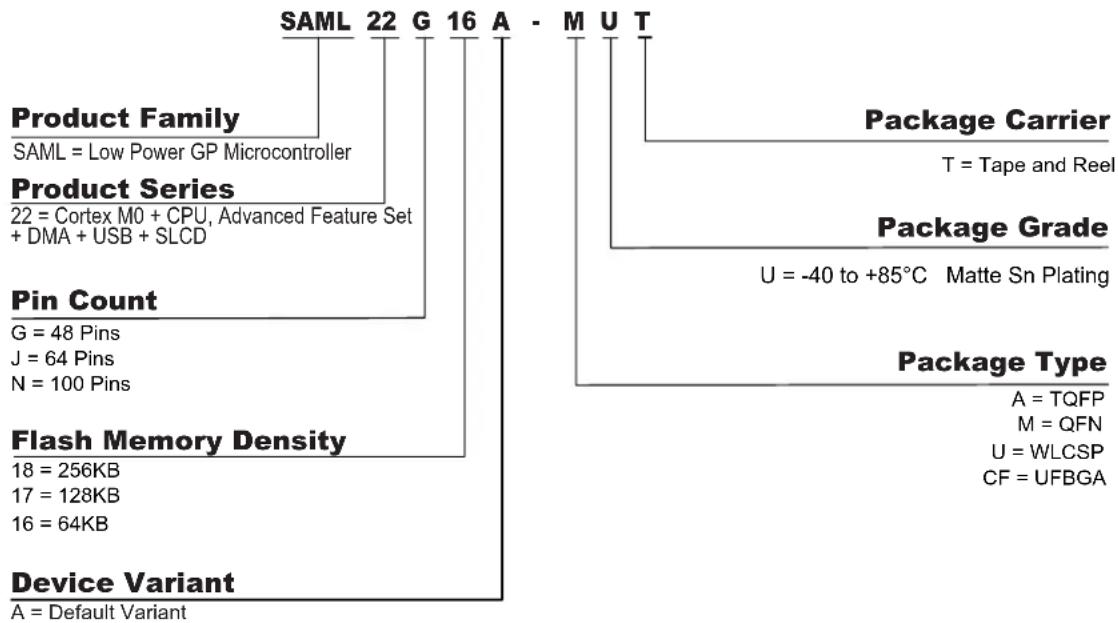
| Component | Label | Value | |-----------------------|---------------------------|-----------| | Product Family | SAML | 22 | | Product Family | G | 16 | | Product Family | A - M U T | - | | Product Family | T | - | | Product Series | SAML | Low Power GP Microcontroller | | Product Series | 22 | Cortex M0 + CPU, Advanced Feature Set + DMA + USB + SLCD | | Pin Count | G | 48 Pins | | Pin Count | J | 64 Pins | | Pin Count | N | 100 Pins | | Flash Memory Density | 18 | 256KB | | Flash Memory Density | 17 | 128KB | | Flash Memory Density | 16 | 64KB | | Device Variant | A = Default Variant | - | | Package Carrier | T = Tape and Reel | - | | Package Grade | U = -40 to +85°C | - | | Package Type | A = TQFP | - | | Package Type | M = QFN | - | | Package Type | U = WLCSP | - | | Package Type | CF = UFBGA | - |Note: The device variant (last letter of the ordering number) is independent of the die revision (DSU.DID.REVISION): The device variant denotes functional differences, whereas the die revision marks evolution of the die.
2.1 SAM L22N
Table 2-1. SAM L22N Ordering Codes
| Ordering Code FLASH (bytes) SRAM (bytes) Package Carrier Type | ||||
| ATSAML22N16A-AUT 64K 8K TQFP100 Tape & Reel | ||||
| ATSAML22N16A-CFUT UFBGA100 | ||||
| ATSAML22N17A-AUT 128K | 16K | TQFP100 Tape & Reel | ||
| ATSAML22N17A-CFUT UFBGA100 | ||||
| ATSAML22N18A-AUT 256K | 32K | TQFP100 Tape & Reel | ||
| ATSAML22N18A-CFUT UFBGA100 | ||||
2.2 SAM L22J
Table 2-2. SAM L22J Ordering Codes
| Ordering Code FLASH (bytes) SRAM (bytes) Package Carrier Type | ||||
| ATSAML22J16A-AUT | 64K | 8K | TQFP64 | Tape & Reel |
| ATSAML22J16A-MUT | QFN64 | |||
| ATSAML22J17A-AUT 128K | 16K TQFP64 | Tape & Reel | ||
| ATSAML22J17A-MUT | QFN64 | |||
| ATSAML22J18A-AUT 256K | 32K TQFP64 | Tape & Reel | ||
| ATSAML22J18A-MUT | QFN64 | |||
2.3 SAM L22G
Table 2-3. SAM L22G Ordering Codes
| Ordering Code FLASH (bytes) SRAM (bytes) Package Carrier Type | |||
| ATSAML22G16A-AUT 64K 8K TQFP48 Tape & Reel | |||
| ATSAML22G16A-MUT QFN48 | |||
| ATSAML22G17A-AUT 128K 16K TQFP48 Tape & Reel | |||
| ATSAML22G17A-MUT QFN48 | |||
| ATSAML22G17A-UUT WLCSP49 | |||
| ATSAML22G18A-AUT 256K 32K TQFP48 Tape & Reel | |||
| ATSAML22G18A-MUT QFN48 | |||
| ATSAML22G18A-UUT WLCSP49 | |||
2.4 Device Identification
The DSU - Device Service Unit peripheral provides the Device Selection bits in the Device Identification register (DID.DEVSEL) in order to identify the device by software. The SAM L22 variants have a reset value of DID=0x10820xxx, with the last digits identifying the variant:
Table 2-4. SAM L22 Device Identification Values
| DSU DID.DEVSEL | Device |
| 0x0 | L22N18 |
| 0x1 | L22N17 |
| 0x2 | L22N16 |
| 0x3-0x4 | Reserved |
| 0x5 | L22J18 |
| 0x6 | L22J17 |
| 0x7 | L22J16 |
| 0x8-0x9 | Reserved |
| 0xA | L22G18 |
| 0xB | L22G17 |
| 0xC | L22G16 |
| 0xD-0xFF | Reserved |
Note: The device variant (last letter of the ordering number) is independent of the die revision (DSU.DID.REVISION): The device variant denotes functional differences, whereas the die revision marks evolution of the die.
- Block Diagram
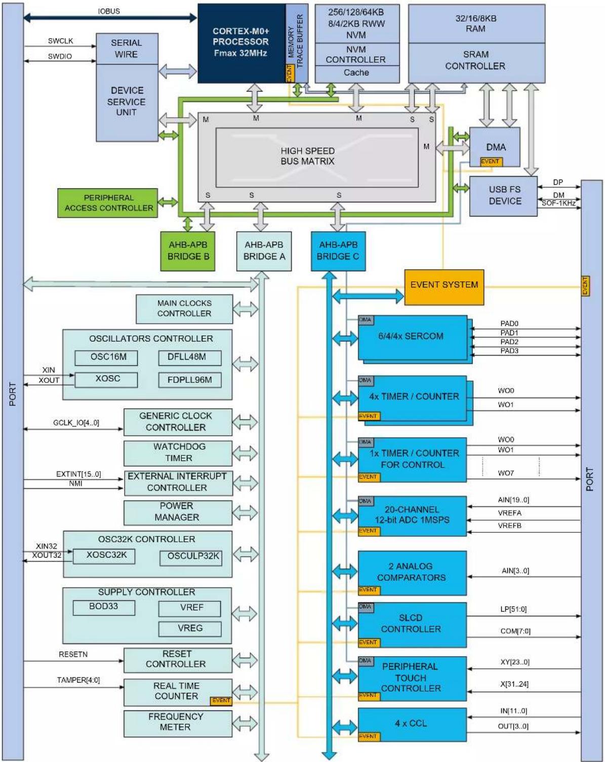
flowchart
graph TD
    subgraph CPU Architecture
        A["10BUS"] --> B["SERIAL WIRE"]
        B --> C["DEVICE SERVICE UNIT"]
        C --> D["Cortex-M0+ PROCESSOR Fmax 32MHz"]
        D --> E["MEMORY TRACE BUFFER"]
        E --> F["256/128/64KB 8/4/2KB RWW NVM"]
        E --> G["NVM CONTROLLER Cache"]
        E --> H["SRAM CONTROLLER"]
        I["PERIPHERAL ACCESS CONTROLLER"] --> J["AHB-APB BRIDGE B"]
        K["AHB-APB BRIDGE A"] --> L["AHB-APB BRIDGE C"]
        M["HIGH SPEED BUS MATRIX"] --> N["6/4/4x SERCOM"]
        N --> O["6/4/4x SERCOM"]
        P["MAIN CLOCKS CONTROLLER"] --> Q["OSCILLATORS CONTROLLER"]
        Q --> R["XIN XOUT"]
        Q --> S["XOSC"]
        T["PORT"] --> U["GCLK_IO[4..0"]]
        U --> V["GENERIC CLOCK CONTROLLER"]
        V --> W["WATCHDOG TIMER"]
        W --> X["EXTERNAL INTERRUPT CONTROLLER"]
        X --> Y["POWER MANAGER"]
        Y --> Z["XIN32 XOUT32"]
        Z --> AA["OSC32K CONTROLLER"]
        AA --> AB["XOSC32K"]
        AA --> AC["OSCULP32K"]
        AD["PORT"] --> AE["SUPPLY CONTROLLER"]
        AE --> AF["BOD33"]
        AE --> AG["VREF"]
        AE --> AH["VREG"]
        AI["RESETN"] --> AJ["RESET CONTROLLER"]
        AJ --> AK["TAMPER[4:0"]]
        AL["REAL TIME COUNTER"] --> AM["FREQUENCY METER"]
        AN["DATA"] --> AO["DMA EVENT"]
        AP["USB FS DEVICE"] --> AQ["DP DM SOF-1KHz"]
        AR["EVENT SYSTEM"] --> AS["6/4/4x SERCOM"]
        AS --> AT["PAD0 PAD1 PAD2 PAD3"]
        AU["1x TIMER / COUNTER FOR CONTROL"] --> AV["WO0 WO1"]
        AW["20-CHANNEL 12-bit ADC 1MSPS"] --> AX["AIN[19..0"] VREFA VREFB]
        AY["2 ANALOG COMPARATORS"] --> AZ["AIN[3..0"]]
        BA["SLCD CONTROLLER"] --> BB["LP[51:0"] COM["7:0"]]
        BC["PERIPHERAL TOUCH CONTROLLER"] --> BD["XY[23..0"] X["31..24"]]
        BE["4 x CCL"] --> BF["IN[11..0"] OUT["3..0"]]
    end
    subgraph Port Interface
        AG["OUTPUT"] --> AH
    end
Note:
- Some device configurations have different number of SERCOM instances, Timer/Counter instances, PTC signals and ADC signals. The number of PTC X and Y signals is configurable.
4. Pinout
4.1 SAM L22G
Figure 4-1. 48-Pin QFN, TQFP
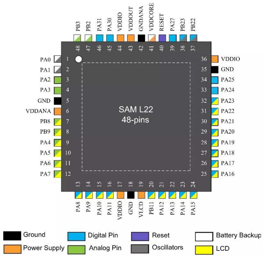
bar_stacked
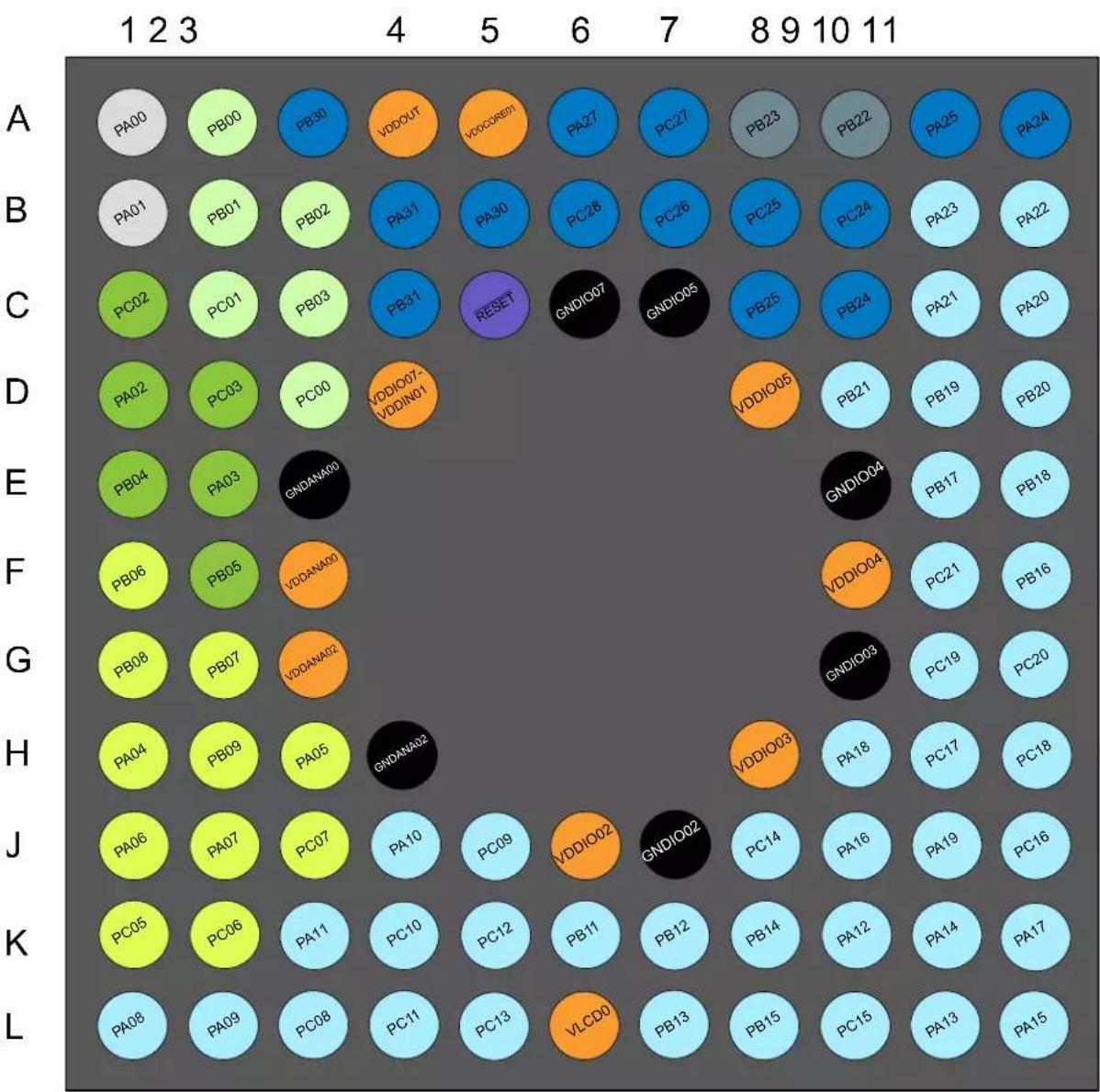
| Pin | Ground | Digital Pin | Power Supply | Analog Pin | Reset | Oscillators | Battery Backup | LCD | |-----|--------|-------------|--------------|------------|-------|-------------|----------------|-----| | PA0 | 1 | 48 | - | - | - | - | - | - | | PA1 | 2 | - | - | - | - | - | - | - | | PA2 | 3 | - | - | - | - | - | - | - | | PA3 | 4 | - | - | - | - | - | - | - | | GND | 5 | - | - | - | - | - | - | - | | VDDANA | 6 | - | - | - | - | - | - | - | | PB8 | 7 | - | - | - | - | - | - | - | | PB9 | 8 | - | - | - | - | - | - | - | | PA4 | 9 | - | - | - | - | - | - | - | | PA5 | 10 | - | - | - | - | - | - | - | | PA6 | 11 | - | - | - | - | - | - | - | | PA7 | 12 | - | - | - | - | - | - | - | | GND | 18 | - | - | - | - | - | - | - | | VLCD | 19 | - | - | - | - | - | - | - | | PB11 | 20 | - | - | - | - | - | - | - | | PA12 | 21 | - | - | - | - | - | - | - | | PA13 | 22 | - | - | - | - | - | - | - | | PA14 | 23 | - | - | - | - | - | - | - | | PA15 | 24 | - | - | - | - | - | - | - | | VDDIO, VCCORE, RESET, PA27, PB23, PB22, VDDIO, GND, VLD, Digital Pin, Analog Pin, Power Supply, LCD, Battery BackupFigure 4-2. 49-Pin WLCSP
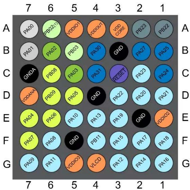
heatmap
| | 7 | 6 | 5 | 4 | 3 | 2 | 1 | |---|---|---|---|---|---|---|---| | A | PA00 | PB02(1) | VDDIO1 | VDDOUT | VDD CORE | PB23 | PB22 | | B | PA01 | PA02 | PB03 | PA30 | GND | PA27 | PA25 | | C | GNDA | PB08 | PA03 | PA31 | RESET | PA23 | PA24 | | D | VDDNAI | PB09 | PA05 | GND | PA22 | PA20 | PA21 | | E | PA04 | PA06 | PA10 | PA13 | PA19 | GND | VDDIO2 | | F | PA07 | PA08 | GND | PB11 | PA15 | PA17 | PA18 | | G | PA09 | PA11 | VDDIO3 | VLCD | PA12 | PA14 | PA16 | The chart displays a 5x5 grid where rows and columns are indexed from 1 to 7. The color values represent the specific elements of the cell in each cell.(BOTTOM VIEW)

Ground

Power Supply

Digital Pin

Digital/LCD


Reset

Battery Backup/Oscillators

Analog Pin

Analog/LCD

Analog/Battery Backup
Note:
- PB02 has an internal connection to PB00. PB00 is not available on any other pin of the device and is only enabled with PS_OK function. The connection between PB02 and PB00 is only available on ASTAML22G17A-UUTA2. ATSAML22G17A-UUTA0/1 have the same pin function as standard product ATSAML22G17A-UUT.
4.2 SAM L22J

heatmap
SAM L22 64-pins | Pin | Ground | Digital Pin | Power Supply | Analog Pin | Reset | Oscillators | Battery Backup | LCD | |---|---|---|---|---|---|---|---|---| | PB3 | 64 | 63 | 1 | 61 | 60 | 59 | 58 | 57 | | PB2 | 63 | 62 | 2 | 60 | 59 | 58 | 57 | 56 | | PB1 | 62 | 61 | 3 | 59 | 58 | 57 | 56 | 55 | | PB0 | 61 | 60 | 4 | 58 | 57 | 56 | 55 | 54 | | PB31 | 60 | 59 | 5 | 57 | 56 | 55 | 54 | 53 | | PB30 | 59 | 58 | 6 | 55 | 54 | 53 | 52 | 51 | | PA31 | 58 | 57 | 7 | 52 | 51 | 50 | 49 | | | PA30 | 57 | 56 | 8 | 49 | VDDIO | GND | VDDIO | GND | | VDDIO | 48 | VDDIO | GND | GND | VDDIO OUT | GND | VDDCORE | RESET | | GNDANANA | 7 | VDDANA | GNDIA | GNDANA | VDDANA OUT | GNDANA | VDDANA OUT | GNDANA | | VDDA | 8 | VDDA | GNDIA | GNDIA | VDDA OUT | GNDIA | VDDA OUT | GNDIA | | PB6 | 9 | PB6 | GNDIA | GNDIA | PB6 OUT | GNDIA | GNDIA | GNDIA | | PB7 | 10 | PB7 | GNDIA | GNDIA | PB7 OUT | GNDIA | GNDIA | GNDIA | | PB8 | 11 | PB8 | GNDIA | GNDIA | PB8 OUT | GNDIA | GNDIA | GNDIA | | PB9 | 12 | PB9 | GNDIA | GNDIA | PB9 OUT | GNDIA | GNDIA | GNDIA | | PA4 | 13 | PA4 | GNDIA | GNDIA | PA4 OUT | GNDIA | GNDIA | GNDIA | | PA5 | 14 | PA5 | GNDIA | GNDIA | PA5 OUT | GNDIA | GNDIA | GNDIA | | PA6 | 15 | PA6 | GNDIA | GNDIA | PA6 OUT | GNDIA | GNDIA | GNDIA | | PA7 | 16 | PA7 | GNDIA | GNDIA | PA7 OUT | GNDIA | GNDIA | GNDIA | | VDDIOI/OLED (VDDIO) - Ground, Digital Pin, Power Supply, Analog Pin, Reset, Oscillators, Battery Backup, LCD, etc. The diagram shows a single rectangular block with color-coded pins: black for Ground, blue for Digital Pin, purple for Power Supply, orange for Analog Pin, gray for Oscillators, white for Battery Backup, and yellow for LCD. The central label 'SAM L22' indicates the chip's physical structure.4.3 SAM L22N
Figure 4-3. TQFP100
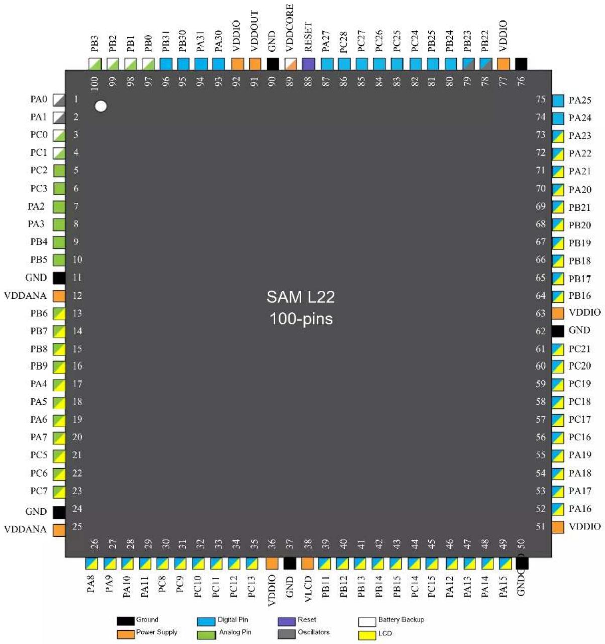
Figure 4-4. UFBGA100
(TOP VIEW)

text_image
Ground Power Supply Digital Pin Digital/LCD Digital/Oscillators Reset Battery Backup/Oscillators Analog Pin Analog/LCD Analog/Battery Backup5. Signal Descriptions List
The following table gives details on signal names classified by peripheral.
Table 5-1. Signal Descriptions List
| Signal Name Function Type | Active Level | ||
| Analog Comparators - AC | |||
| AIN[3:0] AC Analog Inputs Analog | |||
| CMP[1:0] AC Analog Output Analog | |||
| Analog Digital Converter - ADC | |||
| AIN[19:0] ADC Analog Inputs Analog | |||
| VREFA ADC Voltage External Reference A Analog | |||
| VREFB ADC Voltage External Reference B Analog | |||
| External Interrupt Controller - EIC | |||
| EXTINT[15:0] External Interrupts inputs Digital | |||
| NMI | External Non-Maskable Interrupt input | Digital | |
| Generic Clock Generator - GCLK | |||
| GCLK_IO[4:0] | Generic Clock (source clock inputs or generic clock generator output) | Digital | |
| Custom Control Logic - CCL | |||
| IN[11:0] | Logic Inputs | Digital | |
| OUT[3:0] | Logic Outputs | Digital | |
| Supply Controller - SUPC | |||
| VBAT | External battery supply Inputs | Analog | |
| PSOK | Main Power Supply OK input | Digital | |
| OUT[1:0] | Logic Outputs | Digital | |
| Power Manager - PM | |||
| RESETN | Reset input | Digital Low | |
| Serial Communication Interface - SERCOMx | |||
| PAD[3:0] | SERCOM Inputs/Outputs Pads | Digital | |
| Oscillators Control - OSCCTRL | |||
| XIN | Crystal or external clock Input | Analog/Digital | |
| XOUT | Crystal Output | Analog | |
| 32KHz Oscillators Control - OSC32KCTRL | |||
| XIN32 | 32KHz Crystal or external clock Input | Analog/Digital | |
| XOUT32 | 32KHz Crystal Output | Analog | |
| Timer Counter - TCx | |||
| WO[1:0] | Waveform/PWM outputs or Capture Inputs | Digital | |
| Timer Counter - TCCx | |||
| WO[7:0] | Waveform/PWM outputs or Capture Inputs | Digital | |
| Peripheral Touch Controller - PTC | |||
| X[7:0] | PTC Input/Output | Analog | |
| Y[23:0] | PTC Input/Output | Analog | |
| X[31:24] | PTC Output | Analog | |
| General Purpose I/O - PORT | |||
| PA25 - PA00 | Parallel I/O Controller I/O Port A | Digital | |
| PA27 Parallel I/O Controller I/O Port A Digital | |||
| PA31 - PA30 Parallel I/O Controller I/O Port A Digital | |||
| PB09 - PB00 Parallel I/O Controller I/O Port B Digital | |||
| PB25 - PB11 Parallel I/O Controller I/O Port B Digital | |||
| PB31 - PB30 Parallel I/O Controller I/O Port B Digital | |||
| PC03 - PC00 Parallel I/O Controller I/O Port C Digital | |||
| PC07 - PC05 Parallel I/O Controller I/O Port C Digital | |||
| PC17 - PC12 Parallel I/O Controller I/O Port C Digital | |||
| PC28 - PC24 Parallel I/O Controller I/O Port C Digital | |||
| General Purpose input - PORT | |||
| PC11 - PC08 Parallel I/O Controller input Port C Digital | |||
| PC21 - PC18 Parallel I/O Controller input Port C Digital | |||
| Segment LCD | |||
| SLCD51 - SLCD00 Segment | LCD Analog | ||
| VLCD Bias Voltage Analog | |||
| Universal Serial Bus - USB | |||
| DP DP for USB | Digital | ||
| DM | DM for USB | Digital | |
| SOF 1kHz | USB Start of Frame Digital | ||
| Real Timer Clock - RTC | |||
| RTC_IN[4:0] | Tamper or external wake-up pins | Digital | |
| RTC_OUT | Tamper output | Digital | |
6. I/O Multiplexing and Considerations
6.1 Multiplexed Signals
Each pin is by default controlled by the PORT as a general purpose I/O and alternatively it can be assigned a different peripheral functions. To enable a peripheral function on a pin, the Peripheral Multiplexer Enable bit in the Pin Configuration register corresponding to that pin (PINCFGn.PMUXEN, n = 0-31) in the PORT must be written to '1'. The selection of peripheral function A to I is done by writing to the Peripheral Multiplexing Odd and Even bits in the Peripheral Multiplexing register (PMUXn.PMUXE/O) of the PORT.
This table describes the peripheral signals multiplexed to the PORT I/O pins.
Table 6-1. PORT Function Multiplexing
| Function - A B C D E F G H I | |||||||||||||||||
| Type L22G | * | L22J | L22N Pad Name | EIC ANAREF ADC | AC PTC | SLCD | SERCOM | * | SERCOM* | TC/TCC | TCC/RTC | COM/RTC | AC/GCLK | CCL | |||
| Battery backup | 1 | 1 | PA00 | EIC/EXTINT[0] | SERCOM1/PAD[0] | ||||||||||||
| 2 | 2 | PA01 | EIC/EXTINT[1] | SERCOM1/PAD[1] | |||||||||||||
| 3 | PC00 | EIC/EXTINT[8] | ADC/AIN[16] | RTC/IN[3] | |||||||||||||
| 4 | PC01 | EIC/EXTINT[9] | ADC/AIN[17] | RTC/IN[4] | |||||||||||||
| 5 | PC02 | EIC/EXTINT[10] | ADC/AIN[18] | PTC/XY[6] | |||||||||||||
| 6 | PC03 | EIC/EXTINT[11] | ADC/AIN[19] | PTC/XY[7] | |||||||||||||
| 3 | 7 | PA02 | EIC/EXTINT[2] | ADC/VREFB | ADC/AIN[0] | AC/AIN[0] | PTC/XY[8] | RTC/IN[2] | |||||||||
| 4 | 8 | PA03 | EIC/EXTINT[3] | ADC/VREFA | ADC/AIN[1] | AC/AIN[1] | PTC/XY[9] | ||||||||||
| 9 | PB04 | EIC/EXTINT[4] | ADC/AIN[12] | AC/AIN[2] | PTC/XY[10] | ||||||||||||
| 10 | PB05 | EIC/EXTINT[5] | ADC/AIN[13] | AC/AIN[3] | PTC/XY[11] | ||||||||||||
| 13 | PB06 | EIC/EXTINT[6] | ADC/AIN[14] | PTC/XY[12] | SLCD/LP[0] | CCL/IN[6] | |||||||||||
| 14 | PB07 | EIC/EXTINT[7] | ADC/AIN[15] | PTC/XY[13] | SLCD/LP[1] | CCL/IN[7] | |||||||||||
| 7 | 15 | PB08 | EIC/EXTINT[8] | ADC/AIN[2] | PTC/XY[14] | SLCD/LP[2] | SERCOM3/PAD[0] | TC/0/WO[0] | CCL/IN[8] | ||||||||
| 8 | 16 | PB09 | EIC/EXTINT[9] | ADC/AIN[3] | PTC/XY[15] | SLCD/LP[3] | SERCOM3/PAD[1] | TC/0/WO[1] | CCL/OUT[2] | ||||||||
| 9 | 17 | PA04 | EIC/EXTINT[4] | ADC/AIN[4] | PTC/X[24] | SLCD/LP[4] | SERCOM0/PAD[0] | TCC/WO[0] | CCL/IN[0] | ||||||||
| 10 | 18 | PA05 | EIC/EXTINT[5] | ADC/AIN[5] | PTC/X[25] | SLCD/LP[5] | SERCOM0/PAD[1] | TCC/WO[1] | CCL/IN[1] | ||||||||
| 11 | 19 | PA06 | EIC/EXTINT[6] | ADC/AIN[6] | PTC/X[26] | SLCD/LP[6] | SERCOM0/PAD[2] | CCL/IN[2] | |||||||||
| 12 | 20 | PA07 | EIC/EXTINT[7] | ADC/AIN[7] | PTC/X[27] | SLCD/LP[7] | SERCOM0/PAD[3] | CCL/OUT[0] | |||||||||
| 21 | PC05 | EIC/EXTINT[13] | PTC/XY[4] | SLCD/LP[8] | |||||||||||||
| 22 | PC06 | EIC/EXTINT[14] | PTC/XY[5] | SLCD/LP[9] | |||||||||||||
| 23 | PC07 | EIC/EXTINT[15] | SLCD/LP[10] | ||||||||||||||
| 13 | 26 | PA08 | EIC/NMI | PTC/XY[3] | SLCD/LP[11] | SERCOM0/PAD[0] | SERCOM4/PAD[0] | TCC/WO[0] | CCL/IN[3] | ||||||||
| 14 | 27 | PA09 | EIC/EXTINT[9] | PTC/XY[2] | SLCD/LP[12] | SERCOM0/PAD[1] | SERCOM4/PAD[1] | TCC/WO[1] | CCL/IN[4] | ||||||||
| 15 | 28 | PA10 | EIC/EXTINT[10] | PTC/XY[1] | SLCD/LP[13] | SERCOM0/PAD[2] | SERCOM4/PAD[2] | TCC/WO[2] | GCLK/IO[4] | CCL/IN[5] | |||||||
| 16 | 29 | PA11 | EIC/EXTINT[11] | PTC/XY[0] | SLCD/LP[14] | SERCOM0/PAD[3] | SERCOM4/PAD[3] | TCC/WO[3] | CCL/OUT[1] | ||||||||
| 30 | PC08 | EIC/EXTINT[0] | SLCD/LP[15] | ||||||||||||||
| 31 | PC09 | EIC/EXTINT[1] | SLCD/LP[16] | ||||||||||||||
| 32 | PC10 | EIC/EXTINT[2] | SLCD/LP[17] | SERCOM1/PAD[2] | |||||||||||||
| 33 | PC11 | EIC/EXTINT[3] | SLCD/LP[18] | SERCOM1/PAD[3] | |||||||||||||
| 34 | PC12 | EIC/EXTINT[4] | SLCD/LP[19] | SERCOM1/PAD[0] | |||||||||||||
| 35 | PC13 | EIC/EXTINT[5] | SLCD/LP[20] | SERCOM1/PAD[1] | |||||||||||||
| 19 | 38 | VLCD | |||||||||||||||
| 20 | 39 | PB11 | EIC/EXTINT[11] | SLCD/LP[21] | SERCOM3/PAD[3] | TC/1/WO[1] | TCC/WO[5] | CCL/OUT[1] | |||||||||
continued
| Function - A B C D E F G H I | ||||||||||||||||
| Type L22G | L22I | L22N | Pad Name | EIC ANAREF ADC | AC PTC | SLCD | SERCOM | SERCOM* | TC/TCC | TCC/RTC | COM/RTC | AC/GCLK | CCL | |||
| I2C: full Fm+,Limited currentsfor Sm, Fm | 25 | 40 | PB12 | EIC/EXTINT[12] | SLCD/LP[22] | SERCOM3/PAD[0] | TC/0/WO[0] | TCC/WO[6] | ||||||||
| 26 | 41 | PB13 | EIC/EXTINT[13] | SLCD/LP[23] | SERCOM3/PAD[1] | TC/0/WO[1] | TCC/WO[7] | |||||||||
| 27 | 42 | PB14 | EIC/EXTINT[14] | SLCD/LP[24] | SERCOM3/PAD[2] | TC/1/WO[0] | GCLK/IO[0] | CCL/IN[9] | ||||||||
| 28 | 43 | PB15 | EIC/EXTINT[15] | SLCD/LP[25] | SERCOM3/PAD[3] | TC/1/WO[1] | GCLK/IO[1] | CCL/IN[10] | ||||||||
| 44 | PC14 | EIC/EXTINT[6] | SLCD/LP[26] | |||||||||||||
| 45 | PC15 | EIC/EXTINT[7] | SLCD/LP[27] | |||||||||||||
| I2C: Sm, Fm, Fm+ | 21 | 29 | 46 | PA12 | EIC/EXTINT[12] | SLCD/LP[28] | SERCOM4/PAD[0] | SERCOM3/PAD[0] | TCC/WO[6] | AC/CMP[0] | ||||||
| 22 | 30 | 47 | PA13 | EIC/EXTINT[13] | SLCD/LP[29] | SERCOM4/PAD[1] | SERCOM3/PAD[1] | TCC/WO[7] | AC/CMP[1] | |||||||
| 23 | 31 | 48 | PA14 | EIC/EXTINT[14] | SLCD/LP[30] | SERCOM4/PAD[2] | SERCOM3/PAD[2] | TCC/WO[4] | GCLK/IO[0] | |||||||
| 24 | 32 | 49 | PA15 | EIC/EXTINT[15] | SLCD/LP[31] | SERCOM4/PAD[3] | SERCOM3/PAD[3] | TCC/WO[5] | GCLK/IO[1] | |||||||
| 25 | 35 | 52 | PA16 | EIC/EXTINT[0] | PTC/X[28] | SLCD/LP[32] | SERCOM1/PAD[0] | SERCOM2/PAD[0] | TCC/WO[6] | GCLK/IO[2] | CCL/IN[0] | |||||
| 26 | 36 | 53 | PA17 | EIC/EXTINT[1] | PTC/X[29] | SLCD/LP[33] | SERCOM1/PAD[1] | SERCOM2/PAD[1] | TCC/WO[7] | GCLK/IO[3] | CCL/IN[1] | |||||
| 27 | 37 | 54 | PA18 | EIC/EXTINT[2] | PTC/X[30] | SLCD/LP[34] | SERCOM1/PAD[2] | SERCOM2/PAD[2] | TCC/WO[2] | AC/CMP[0] | CCL/IN[2] | |||||
| 28 | 38 | 55 | PA19 | EIC/EXTINT[3] | PTC/X[31] | SLCD/LP[35] | SERCOM1/PAD[3] | SERCOM2/PAD[3] | TCC/WO[3] | AC/CMP[1] | CCL/OUT[0] | |||||
| 56 | PC16 | EIC/EXTINT[8] | SLCD/LP[36] | |||||||||||||
| 57 | PC17 | EIC/EXTINT[9] | SLCD/LP[37] | |||||||||||||
| 58 | PC18 | EIC/EXTINT[10] | SLCD/LP[38] | |||||||||||||
| 59 | PC19 | EIC/EXTINT[11] | SLCD/LP[39] | |||||||||||||
| 60 | PC20 | EIC/EXTINT[12] | SLCD/LP[40] | CCL/IN[9] | ||||||||||||
| 61 | PC21 | EIC/EXTINT[13] | SLCD/LP[41] | CCL/IN[10] | ||||||||||||
| 39 | 64 | PB16 | EIC/EXTINT[0] | SLCD/LP[42] | SERCOM5/PAD[0] | TC/2/WO[0] | TCC/WO[4] | GCLK/IO[2] | CCL/IN[11] | |||||||
| 40 | 65 | PB17 | EIC/EXTINT[1] | SLCD/LP[43] | SERCOM5/PAD[1] | TC/2/WO[1] | TCC/WO[5] | GCLK/IO[3] | CCL/OUT[3] | |||||||
| 66 | PB18 | EIC/EXTINT[2] | SLCD/LP[44] | SERCOM5/PAD[2] | SERCOM3/PAD[2] | TCC/WO[0] | ||||||||||
| 67 | PB19 | EIC/EXTINT[3] | SLCD/LP[45] | SERCOM5/PAD[3] | SERCOM3/PAD[3] | TCC/WO[1] | ||||||||||
| 68 | PB20 | EIC/EXTINT[4] | SLCD/LP[46] | SERCOM3/PAD[0] | SERCOM5/PAD[0] | TCC/WO[2] | ||||||||||
| 69 | PB21 | EIC/EXTINT[5] | SLCD/LP[47] | SERCOM3/PAD[1] | SERCOM5/PAD[1] | TCC/WO[3] | ||||||||||
| 29 | 41 | 70 | PA20 | EIC/EXTINT[4] | PTC/XY[16] | SLCD/LP[48] | SERCOM0/PAD[0] | SERCOM2/PAD[2] | TC/3/WO[0] | TCC/WO[6] | GCLK/IO[4] | |||||
| 30 | 42 | 71 | PA21 | EIC/EXTINT[5] | PTC/XY[17] | SLCD/LP[49] | SERCOM0/PAD[1] | SERCOM2/PAD[3] | TC/3/WO[1] | TCC/WO[7] | ||||||
| I2C: Sm, Fm, Fm+ | 31 | 43 | 72 | PA22 | EIC/EXTINT[6] | PTC/XY[18] | SLCD/LP[50] | SERCOM0/PAD[2] | SERCOM2/PAD[0] | TC/0/WO[0] | TCC/WO[4] | CCL/IN[6] | ||||
| 32 | 44 | 73 | PA23 | EIC/EXTINT[7] | PTC/XY[19] | SLCD/LP[51] | SERCOM0/PAD[3] | SERCOM2/PAD[1] | TC/0/WO[1] | TCC/WO[5] | USB/SOF_1KHZ | CCL/IN[7] | ||||
| 33 | 45 | 74 | PA24 | EIC/EXTINT[12] | SERCOM2/PAD[2] | SERCOM5/PAD[0] | TC/1/WO[0] | TCC/WO[0] | USB/DM | CCL/IN[8] | ||||||
| 34 | 46 | 75 | PA25 | EIC/EXTINT[13] | SERCOM2/PAD[3] | SERCOM5/PAD[1] | TC/1/WO[1] | TCC/WO[1] | USB/DP | CCL/OUT[2] | ||||||
| 37 | 49 | 78 | PB22 | EIC/EXTINT[6] | SERCOM0/PAD[2] | SERCOM5/PAD[2] | TC/3/WO[0] | TCC/WO[2] | USB/SOF_1KHZ | GCLK/IO[0] | CCL/IN[0] | |||||
| 38 | 50 | 79 | PB23 | EIC/EXTINT[7] | SERCOM0/PAD[3] | SERCOM5/PAD[3] | TC/3/WO[1] | TCC/WO[3] | GCLK/IO[1] | CCL/OUT[0] | ||||||
| 80 | PB24 | EIC/EXTINT[8] | SERCOM0/PAD[0] | SERCOM4/PAD[0] | TCC/WO[6] | AC/CMP[0] | ||||||||||
| 81 | PB25 | EIC/EXTINT[9] | SERCOM0/PAD[1] | SERCOM4/PAD[1] | TCC/WO[7] | AC/CMP[1] | ||||||||||
| 82 | PC24 | EIC/EXTINT[0] | SERCOM0/PAD[2] | SERCOM4/PAD[2] | TC/2/WO[0] | TCC/WO[0] | ||||||||||
| 83 | PC25 | EIC/EXTINT[1] | SERCOM0/PAD[3] | SERCOM4/PAD[3] | TC/2/WO[1] | TCC/WO[1] | ||||||||||
| 84 | PC26 | EIC/EXTINT[2] | TC/3/WO[0] | TCC/WO[2] | ||||||||||||
| 85 | PC27 | EIC/EXTINT[3] | SERCOM1/PAD[0] | TC/2/WO[1] | TCC/WO[3] | CCL/IN[4] | ||||||||||
| 86 | PC28 | EIC/EXTINT[4] | PTC/XY[20] | SERCOM1/PAD[1] | TCC/WO[4] | CCL/IN[5] | ||||||||||
| recommended forGCLK IO | 39 | 51 | 87 | PA27 | EIC/EXTINT[15] | PTC/XY[21] | TCC/WO[5] | GCLK/IO[0] | ||||||||
| 40 | 52 | 88 | RESET_N | |||||||||||||
| 45 | 57 | 93 | PA30 | EIC/EXTINT[10] | PTC/XY[22] | SERCOM1/PAD[2] | CORTEX_MOP/SWCLK | GCLK/IO[0] | CCL/IN[3] | |||||||
| Function - A B C D E F G H I | ||||||||||||||||
| Type L22G | * | L22J | L22N | Pad Name | EIC ANAREF ADC | AC PTC | SLCD | SERCOM | - | SERCOM* | TC/TCC | TCC/RTC | COM/RTC | AC/GCLK | CCL | |
| 46 | 58 | 94 | PA31 | EIC/EXTINT[11] | PTC/XY[23] | SERCOM1/PAD[3] | SWDIO | CCL/OUT[1] | ||||||||
| I2C: Sm, Fm, Fm+, Hs | 59 | 95 | PB30 | EIC/EXTINT[14] | SERCOM1/PAD[0] | SERCOM5/PAD[0] | TCC/WO[0] | |||||||||
| 60 | 96 | PB31 | EIC/EXTINT[15] | SERCOM1/PAD[1] | SERCOM5/PAD[1] | TCC/WO[1] | ||||||||||
| Battery backup | 61 | 97 | PB00 | EIC/EXTINT[0] | ADC/AIN[8] | SERCOM3/PAD[2] | SERCOM5/PAD[2] | TC/3/WO[0] | RTC/IN[0] | CCL/IN[1] | ||||||
| 62 | 98 | PB01 | EIC/EXTINT[1] | ADC/AIN[9] | SERCOM3/PAD[3] | SERCOM5/PAD[3] | TC/3/WO[1] | RTC/IN[2] | RTC/OUT | CCL/IN[2] | ||||||
| 47 | 63 | 99 | PB02 | EIC/EXTINT[2] | ADC/AIN[10] | SERCOM3/PAD[0] | SERCOM5/PAD[0] | TC/2/WO[0] | RTC/IN[1] | CCL/OUT[0] | ||||||
| 48 | 64 | 100 | PB03 | EIC/EXTINT[3] | ADC/AIN[11] | SERCOM3/PAD[1] | SERCOM5/PAD[1] | TC/2/WO[1] | ||||||||
Notes:
-
All analog pin functions are on peripheral function B. Peripheral function B must be selected to disable the digital control of the pin.
-
Only some pins can be used in SERCOM I²C mode. See the Type column for supported I²C modes.
-
Sm: Standard mode, up to 100kHz
- Fm: Fast mode, up to 400kHz
- Fm+: Fast mode Plus, up to 1MHz
-
Hs: High-speed mode, up to 3.4MHz
-
These pins are High Sink pins and have different properties than regular pins: PA12, PA13, PA22, PA23, PA27, PA31, PB30, PB31.
- Clusters of multiple GPIO pins are sharing the same supply pin.
- The 49^th pin of the WLCSP49 package is an additional GND pin.
- SAM L22N: SERCOM[0:5]. SAM L22G, L22I: SERCOM[0:3].
6.2 Other Functions
6.2.1 Oscillator Pinout
The oscillators are not mapped to the normal PORT functions and their multiplexing is controlled by registers in the Oscillators Controller (OSCCTRL) and in the 32K Oscillators Controller (OSC32KCTRL).
Table 6-2. Oscillator Pinout
| Oscillator | Supply | Signal | I/O pin |
| XOSC | VDDIO | XIN | PB22 |
| XOUT | PB23 | ||
| XOSC32K | VSWOUT | XIN32 | PA00 |
| XOUT32 | PA01 |
Note: In order to minimize the cycle-to-cycle jitter of the external oscillator, keep the neighboring pins as steady as possible. For neighboring pin details, refer to the Oscillator Pinout section.
Table 6-3. XOSC32K Jitter Minimization
| Package | Steady Signal Recommended |
| L22N | PB00, PB01, PB02, PB03, PC00, PC01 |
| L22J | PB00, PB01, PB02, PB03, PA02, PA03 |
| L22G | PB02, PB03, PA02, PA03 |
6.2.2 Serial Wire Debug Interface Pinout
Only the SWCLK pin is mapped to the normal PORT functions. A debugger cold-plugging or hot-plugging detection will automatically switch the SWDIO port to the SWDIO function.
Table 6-4. Serial Wire Debug Interface Pinout
| Signal Supply I/O pin | ||
| SWCLK VDDIO PA30 | ||
| SWDIO VDDIO PA31 |
6.2.3 SERCOM USART and I ^2 C Configurations
The SAM L22 has up to six instances of the serial communication interface (SERCOM) peripheral. The following table lists the supported communication protocols for each SERCOM instance.
Table 6-5. SERCOM USART and I²C Protocols
| SERCOM Instance | |||||
| Protocol SERCOM0 | SERCOM1 | SERCOM2 | SERCOM3 | SERCOM4 | SERCOM5 |
| I^2C no yes yes yes yes yes | |||||
| I^2C at 3.4MHz no yes no no no yes | |||||
| USARTincluding RS485and ISO 7816 | yes yes yes yes yes yes | ||||
| SPI yes yes yes yes yes yes | |||||
Note: Not all available I²C pins support I²C mode at 3.4MHz.
6.2.4 GPIO Pin Clusters
Table 6-6. GPIO Clusters
| Package | Cluster | GPIO | Supplies Pin connected to the cluster | |
| 100 pins | 1 | PA02, PA03, PB04, PB05, PC02, PC03 | V_DDANA pin12 | GNDANA pin11 |
| 2 | PA04, PA05, PA06, PA07, PB06, PB07, PB08, PB09, PC05, PC06, PC07 | V_DDANA pin12, V_DDANA pin25 | GNDANA pin11, GNDANA pin24 | |
| 3 | PA08, PA09, PA10, PA11, PC08, PC09, PC10, PC11, PC12, PC13 | V_DDO pin36 | GND pin37 | |
| 4 | PA12, PA13, PA14, PA15, PB11, PB12, PB13, PB14, PB15, PC14, PC15 | V_DDO pin36, V_DDIC pin51 | GND pin37, GND pin50 | |
| 5 | PA16, PA17, PA18, PA19, PC16, PC17, PC18, PC19, PC20, PC21 | V_DDO pin51, V_DDIC pin63 | GND pin50, GND pin62 | |
| 6 | PA20, PA21, PA22, PA23, PA24, PA25, PB16, PB17, PB18, PB19, PB20, PB21 | V_DDO pin63, V_DDIC pin77 | GND pin62, GND pin76 | |
| 7 | PA27, PB22, PB23, PB24, PB25, PC24, PC25, PC26, PC27, PC28 | V_DDO pin77, V_DDIC pin92 | GND pin76, GND pin90 | |
| 8 | PA00, PA01, PA30, PA31, PB00, PB01, PB02, PB03, PB30, PB31, PC00, PC01 | V_DDO pin92 | GND pin90 | |
| 64 pins | 1 | PA02, PA03, PA04, PA05, PA06, PA07, PB04, PB05, PB06, PB07, PB08, PB09 | V_DDANA pin8 | GNDANA pin7 |
| 2 | PA08, PA09, PA10, PA11 | V_DDO pin21 | GND pin22 | |
| 3 | PA12, PA13, PA14, PA15, PB11, PB12, PB13, PB14, PB15 | V_DDO pin21, V_DDIC pin34 | GND pin22, GND pin33 | |
| 4 | PA16, PA17, PA18, PA19, PA20, PA21, PA22, PA23, PA24, PA25, PB16, PB17 | V_DDO pin34, V_DDIC pin48 | GND pin33, GND pin47 | |
| 5 | PA27, PB22, PB23 | V_DDO pin48, V_DDIC pin56 | GND pin47, GND pin54 | |
| 6 | PA00, PA01, PA30, PA31, PB00, PB01, PB02, PB03, PB30, PB31 | V_DDO pin56 | GND pin54 | |
| 48 pins | 1 | PA02, PA03, PA04, PA05, PA06, PA07, PB08, PB09 | V_DDANA pin6 | GNDANA pin5 |
| 2 | PA08, PA09, PA10, PA11 | V_DDO pin17 | GND pin18 | |
| 3 | PA12, PA13, PA14, PA15, PA16, PA17, PA18, PA19, PA20, PA21, PA22, PA23, PA24, PA25, PB11 | V_DDO pin17, V_DDIC pin36 | GND pin18, GND pin35 | |
| 4 | PA27, PB22, PB23 | V_DDO pin36, V_DDIC pin44 | GND pin35, GND pin42 | |
| 5 | PA00, PA01, PA30, PA31, PB02, PB03 | V_DDO pin44 | GND pin42 | |
| Package | Cluster | GPIO Supplies Pin connected to the cluster | ||
| 49 pins 1 | PA02, PA03, PA04, PA05, PA06, PA07, PB08, PB09 V | V_DOMA pin D7 GNDANA pin C7 | ||
| 2 PA08, | PA09, PA10, PA11 V | V_DOMA pin G5 GND pin F5 | ||
| 3 PA12, | PA13, PA14, PA15, PA16, PA17, PA18, PA19, PB11 V | V_DOMA pin G5, V_DOMA pin E1 GND pin F5, GND pin E2 | ||
| 4 PA20, | PA21, PA22, PA23, PA24, PA25 V | V_DOMA pin E1, V_DOMA pin A5 GND pin E2, GND pin D4 | ||
| 4 PA27, | PB22, PB23 V | V_DOMA pin E1, V_DOMA pin A5 GND pin D4, GND pin B3 | ||
| 5 PA00, | PA01, PA30, PA31, PB02, PB03 V | V_DOMA pin A5 | GND pin B3 | |
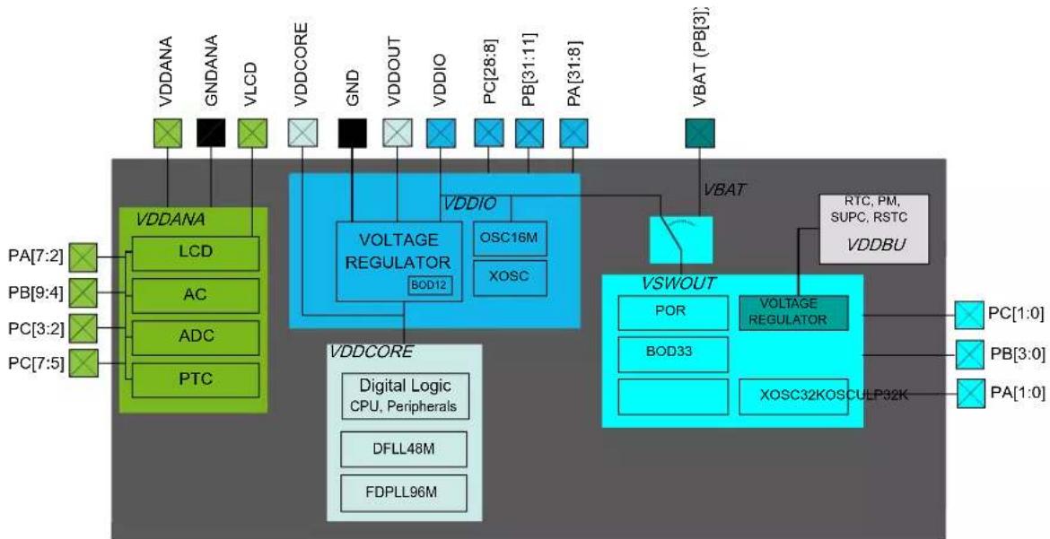
7. Power Supply and Start-Up Considerations
7.1 Power Domain Overview
flowchart
graph TD
    subgraph VDDANA
        A["VDDANA"] --> B["LCD"]
        C["GNDANA"] --> D["AC"]
        E["VLCD"] --> F["ADC"]
        G["PC[7:2"]] --> H["PTC"]
        I["PC[9:4"]] --> J["AC"]
        K["PC[3:2"]] --> L["ADC"]
        M["PC[7:5"]] --> N["PTC"]
    end

    subgraph VDDCORE
        O["VDDCORE"] --> P["VOLTAGE REGULATOR BOD12"]
        Q["GND"] --> R["VDDOUT"]
        S["PC[28:8"]] --> T["VDDIO"]
        U["PC[31:11"]] --> V["PC16M OSC16"]
        W["PA[31:8"]] --> X["PA16M XOSC"]
    end

    subgraph VSWOUT
        Y["VSWOUT"] --> Z["POR"]
        AA["VSWOUT"] --> AB["BOD33"]
        AC["VSWOUT"] --> AD["XOSC32KOSCULP32K"]
    end

    subgraph VBAT
        AE["VBAT (PB[3"])] --> AF["VBAT"]
    end

    subgraph VSWOUT
        AG["RTC, PM, SUPC, RSTC, VDDBU"] --> AH["PC[1:0"]]
        AI["PC[3:0"]] --> AJ["PB[3:0"]]
        AK["PA[1:0"]] --> AL["PA[1:0"]]
    end

    subgraph VDDCORE
        AM["VDDCORE"] --> AN["Digital Logic CPU, Peripherals"]
        AO["DFLL48M"] --> AP["FDPLL96M"]
    end
The SAM L22 power domains are not independent of each other:
• VDDCORE and VDDIO share GND, whereas VDDANA refers to GNDANA.
• VDDCORE serves as the internal voltage regulator output.
• VSWOUT and VDDBU are internal power domains.
7.2 Power Supply Considerations
7.2.1 Power Supplies
The SAM L22 has several different power supply pins:
- VDDIO powers I/O lines and OSC16M, XOSC, the internal regulator for VDDCORE and the Automatic Power Switch. Voltage is 1.62V to 3.63V
• VDDANA powers I/O lines and the ADC, AC, LCD and PTC. Voltage is 1.62V to 3.63V
• VLCD has two alternative functions:
- Output of the LCD voltage pump when VLCD is generated internally. Output voltage is 2.5V to 3.5V.
- Supply input for the bias generator when VLCD is provided externally by the application. Input voltage is 2.4 to 3.6V.
• VBAT powers the Automatic Power Switch. Voltage is 1.62V to 3.63V
- VDDCORE serves as the internal voltage regulator output. It powers the core, memories, peripherals, DFLL48M and FDPLL96M. Voltage is 0.9V to 1.2V typical.
- The Automatic Power Switch is a configurable switch that selects between VDDIO and VBAT as supply for the internal output VSWOUT, see the figure in 7.1. Power Domain Overview.
The same voltage must be applied to both VDDIO and VDDANA. This common voltage is referred to as VDD in the datasheet.
The ground pins, GND, are common to VDDCORE, and VDDIO. The ground pin for VDDANA is GNDANA.
For decoupling recommendations for the different power supplies, refer to the schematic checklist.
7.2.2 Voltage Regulator
The SAM L22 internal Voltage Regulator has four different modes:
- Linear mode: This is the default mode when CPU and peripherals are running. It does not require an external inductor.
- Switching mode. This is the most efficient mode when the CPU and peripherals are running. This mode can be selected by software on the fly.
- Low Power (LP) mode. This is the default mode used when the chip is in standby mode.
- Shutdown mode. When the chip is in backup mode, the internal regulator is off.
Note that the Voltage Regulator modes are controlled by the Power Manager.
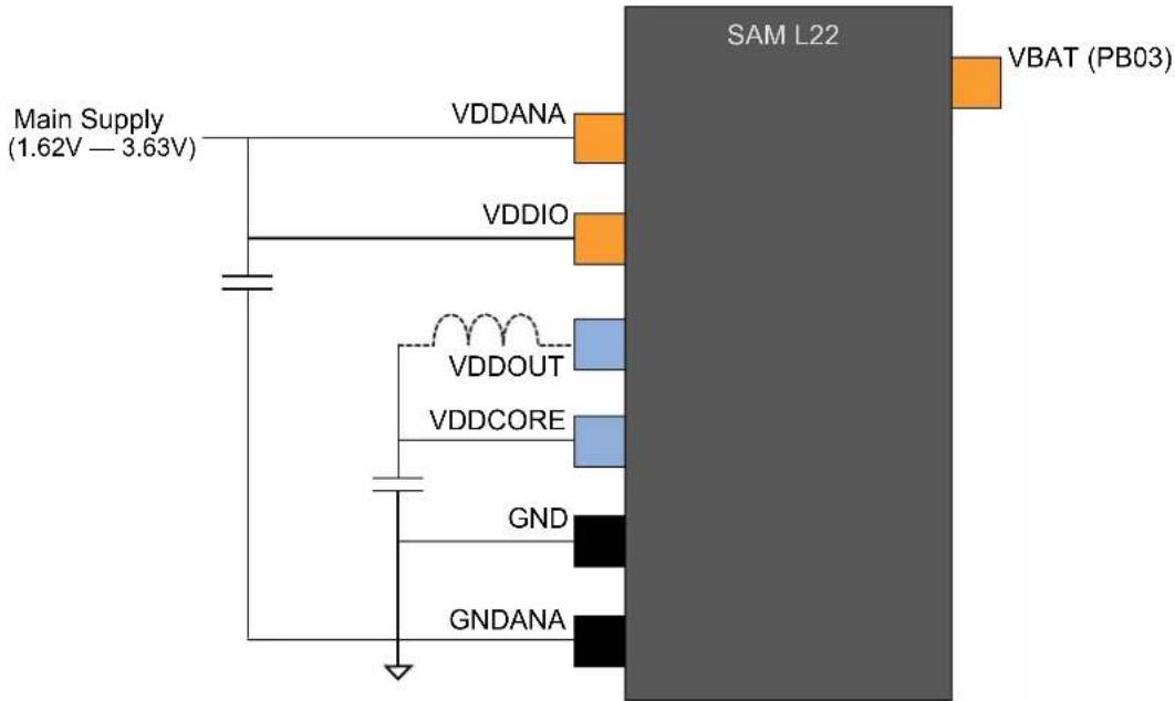
7.2.3 Typical Powering Schematic
SAM L22 uses a single supply from 1.62V to 3.63V.
The following figure shows the recommended power supply connection.
Figure 7-1. Power Supply Connection for Linear Mode Only
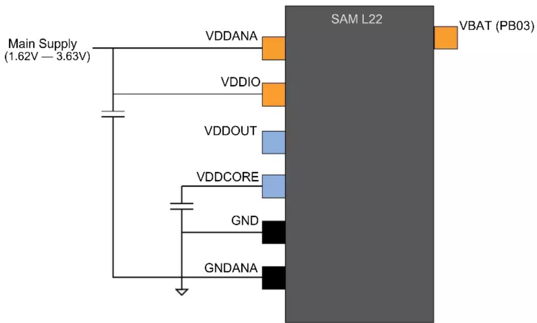
text_image
Main Supply (1.62V — 3.63V) VDDANA VDDIO VDDOUT VDDCORE GND GNDANA SAM L22 VBAT (PB03)Note: Refer to the Schematic Checklist chapter for additional information.
Figure 7-2. Power Supply Connection for Switching/Linear Mode
text_image
SAM L22 VBAT (PB03) Main Supply (1.62V — 3.63V) VDDANA VDDIO VDDOUT VDDCORE GND GNDANANote: Refer to the Schematic Checklist chapter for additional information.
Figure 7-3. Power Supply Connection for Battery Backup

text_image
SAM L22 VDDANA VDDIO VDDOUT VDDCORE GND GNDANA VBAT (PB03) Main Supply (1.62V — 3.63V)Note: Refer to the Schematic Checklist chapter for additional information.
7.2.4 Power-Up Sequence
7.2.4.1 Supply Order
VDDIO and VDDANA must have the same supply sequence. Ideally, they must be connected together.
7.2.4.2 Minimum Rise Rate
One integrated power-on reset (POR) circuits monitoring VDDIO requires a minimum rise rate.
7.2.4.3 Maximum Rise Rate
The rise rate of the power supplies must not exceed the values described in Electrical Characteristics.
7.3 Power-Up
This section summarizes the power-up sequence of the SAM L22. The behavior after power-up is controlled by the Power Manager.
7.3.1 Starting of Internal Regulator
After power-up, the device is set to its initial state and kept in Reset, until the power has stabilized throughout the device. The default performance level after power-up is PL0.
The internal regulator provides the internal VDDCORE corresponding to this performance level. Once the external voltage VDDIO and the internal VDDCORE reach a stable value, the internal Reset is released.
7.3.2 Starting of Clocks
Once the power has stabilized and the internal Reset is released, the device will use a 4MHz clock by default. The clock source for this clock signal is OSC16M, which is enabled and configured at 4MHz after a reset by default. This is also the default time base for Generic Clock Generator 0. In turn, Generator 0 provides the main clock GCLK_MAIN which is used by the Power Manager (PM).
Some synchronous system clocks are active after Start-Up, allowing software execution. Refer to the "Clock Mask Register" section in the PM-Power Manager documentation for the list of clocks that are running by default. Synchronous system clocks that are running receive the 4MHz clock from Generic Clock Generator 0. Other generic clocks are disabled.
7.3.3 I/O Pins
After power-up, the I/O pins are tri-stated except PA30, which is pull-up enabled and configured as input.
7.3.4 Fetching of Initial Instructions
After Reset has been released, the CPU starts fetching PC and SP values from the Reset address, 0x00000000. This points to the first executable address in the internal Flash memory. The code read from the internal Flash can be used to configure the clock system and clock sources. See the related peripheral documentation for details. Refer to the ARM Architecture Reference Manual for more information on CPU startup (www.arm.com).
7.4 Power-On Reset and Brown-Out Detector
The SAM L22 embeds three features to monitor, warn and/or reset the device:
- POR: Power-on Reset on VSWOUT and VDDIO
• BOD33: Brown-out detector on VSWOUT/VBAT - Brown-out detector internal to the voltage regulator for VDDCORE. BOD12 is calibrated in production and its calibration parameters are stored in the NVM User Row. This data should not be changed if the User Row is written to in order to assure correct behavior.
7.4.1 Power-On Reset on VSWOUT
VSWOUT is monitored by POR. Monitoring is always activated, including startup and all sleep modes. If VSWOUT goes below the threshold voltage, the entire chip is reset.
7.4.2 Power-On Reset on VDDIO
VDDIO is monitored by POR. Monitoring is always activated, including startup and all sleep modes. If VDDIO goes below the threshold voltage, all I/Os supplied by VDDIO are reset.
7.4.3 Brown-Out Detector on VSWOUT/VBAT
BOD33 monitors VSWOUT or VBAT depending on configuration.
7.4.4 Brown-Out Detector on VDDCORE
Once the device has started up, BOD12 monitors the internal VDDCORE.
7.5 Performance Level Overview
By default, the device will start in Performance Level 0. This PLO is aiming for the lowest power consumption by limiting logic speeds and the CPU frequency. As a consequence, all GCLK will have limited capabilities, and some peripherals and clock sources will not work or with limited capabilities:
List of peripherals/clock sources not available in PLO:
• USB (limited by logic frequency)
- DFLL48M
List of peripherals/clock sources with limited capabilities in PLO:
- All AHB/APB peripherals are limited by CPU frequency
- DPLL96M: may be able to generate 48MHz internally, but the output cannot be used by logic
- GCLK: the maximum frequency is by factor 4 compared to PL2
- SW interface: the maximum frequency is by factor 4 compared to PL2
- TC: the maximum frequency is by factor 4 compared to PL2
- TCC: the maximum frequency is by factor 4 compared to PL2
- SERCOM: the maximum frequency is by factor 4 compared to PL2
List of peripherals/clock sources with full capabilities in PLO:
- AC
• ADC
• EIC
• OPAMP - OSC16M
- PTC
- All 32KHz clock sources and peripherals
Full functionality and capability will be ensured in PL2. When transitioning between performance levels, the Supply Controller (SUPC) will provide a configurable smooth voltage scaling transition.
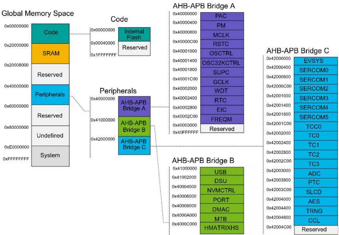
8. Product Mapping
Figure 8-1. SAM L22 Product Mapping
flowchart
graph TD
    A["Global Memory Space"] --> B["Code"]
    B --> C["Internal Flash"]
    B --> D["Reserved"]
    E["Peripherals"] --> F["AHB-APB Bridge A"]
    E --> G["AHB-APB Bridge B"]
    E --> H["AHB-APB Bridge C"]
    I["AHB-APB Bridge A"] --> J["PAC"]
    I --> K["PM"]
    I --> L["MCLK"]
    I --> M["RSTC"]
    I --> N["OSCTRL"]
    I --> O["OSC32KCTRL"]
    I --> P["SUPC"]
    I --> Q["GCLK"]
    I --> R["WDT"]
    I --> S["RTC"]
    I --> T["EIC"]
    I --> U["FREQM"]
    I --> V["Reserved"]
    W["AHB-APB Bridge C"] --> X["EVSYS"]
    W --> Y["SERCOM0"]
    W --> Z["SERCOM1"]
    W --> AA["SERCOM2"]
    W --> AB["SERCOM3"]
    W --> AC["SERCOM4"]
    W --> AD["SERCOM5"]
    W --> AE["TCC0"]
    W --> AF["TC0"]
    W --> AG["TC1"]
    W --> AH["TC2"]
    W --> AI["TC3"]
    W --> AJ["ADC"]
    W --> AK["PTC"]
    W --> AL["SLCD"]
    W --> AM["AES"]
    W --> AN["TRNG"]
    W --> AO["CCL"]
    W --> AP["Reserved"]
9. Memories
9.1 Embedded Memories
- Internal high-speed Flash with Read-While-Write (RWW) capability on a section of the array
- Internal high-speed RAM, single-cycle access at full speed
9.2 Physical Memory Map
The high-speed bus is implemented as a bus matrix. All high-speed bus addresses are fixed, and they are never remapped in any way, even during boot. The 32-bit physical address space is mapped as follows:
Table 9-1. SAM L22 Physical Memory Map
| Memory Start address Size [KB] | ||||
| SAML22x18(1) | SAML22x17(1) | SAML22x16(1) | ||
| Embedded Flash 0x00000000 256 128 64 | ||||
| Embedded RWW section 0x00400000 8 4 2 | ||||
| Embedded SRAM 0x20000000 32 16 8 | ||||
| Peripheral Bridge A 0x40000000 64 64 64 | ||||
| Peripheral Bridge B 0x41000000 64 64 64 | ||||
| Peripheral Bridge C 0x42000000 64 64 64 | ||||
| IOBUS 0x60000000 0.5 | 0.5 | 0.5 | ||
Note: 1. x = G, J , or N.
Table 9-2. Flash Memory Parameters
| Device Flash size [KB] | Number of pages | Page size [Bytes] | |
| SAML22x18(1) | 256 | 4096 | 64 |
| SAML22x17(1) | 128 | 2048 | 64 |
| SAML22x16(1) | 64 | 1024 | 64 |
Note: 1. x = G, J , or N.
Table 9-3. RWW Section Parameters ^(1)
| Device Flash size [KB] | Number of pages | Page size [Bytes] | |
| SAML22x18(1) | 8 | 128 | 64 |
| SAML22x17(1) | 4 | 64 | 64 |
| SAML22x16(1) | 2 | 32 | 64 |
Note: 1. x = G, J , or N.
The Non Volatile Memory (NVM) User Row contains calibration data that are automatically read at device power-on.
The NVM User Row can be read at address 0x00804000.
To write the NVM User Row, refer to the Chapter 27. NVMCTRL - Non-Volatile Memory Controller.
Note: When writing to the User Row, the new values do not get loaded by the other peripherals on the device until a device Reset occurs.
Table 9-4. NVM User Row Mapping
| Bit Pos. | Name Usage Factory Setting Related Peripheral | Register | ||
| 2:0 BOOTPROT Used to select one of eight different bootloader sizes. 0x7 NVMCTRL | ||||
| 3 Reserved — 0x1 — | ||||
| 6:4 EEPROM Used to select one of eight different EEPROM sizes. 0x7 NVMCTRL | ||||
| 7 Reserved — 0x1 — | ||||
| 13:8 | BOD33 Level | BOD33 threshold level at power-on. | 0x06 | SUPC.BOD33 |
| 14 | BOD33 Disable | BOD33 Disable at power-on. | 0x0 | SUPC.BOD33 |
| 16:15 | BOD33 Action | BOD33 Action at power-on. | 0x1 | SUPC.BOD33 |
| 25:17 | Reserved | Factory settings - do not change. | 0x08F | - |
| 26 | WDT Enable | WDT Enable at power-on. | 0x0 | WDT.CTRLA |
| 27 | WDT Always-On | WDT Always-On at power-on. | 0x0 | WDT.CTRLA |
| 31:28 | WDT Period | WDT Period at power-on. | 0xB | WDT.CONFIG |
| 35:32 | WDT Window | WDT Window mode time-out at power-on. | 0xB | WDT.CONFIG |
| 39:36 | WDT EWOFFSET | WDT Early Warning Interrupt Time Offset at power-on. | 0xB | WDT.EWCTRL |
| 40 | WDT WEN | WDT Timer Window Mode Enable at power-on. | 0x0 | WDT.CTRLA |
| 41 | BOD33 Hysteresis | BOD33 Hysteresis configuration at power-on. | 0x0 | SUPC.BOD33 |
| 47:42 | Reserved | Factory settings - do not change. | 0x3E | — |
| 63:48 | LOCK | NVM Region Lock Bits. | 0xFFFF | NVMCTRL |
9.4 NVM Software Calibration Area Mapping
The NVM Software Calibration Area contains calibration data that are determined and written during production test. These calibration values should be read by the application software and written back to the corresponding register.
The NVM Software Calibration Area can be read at address 0x00806020.
The NVM Software Calibration Area can not be written.
Table 9-5. NVM Software Calibration Area Mapping
| Bit Position | Name | Description |
| 2:0 | ADC BIASREFBUF | ADC Bias Reference Buffer Scaling. Must be written to ADC CALIB.BIASREFBUF. |
| 5:3 | ADC BIASCOMP | ADC Bias Comparator Scaling. Must be written to ADC CALIB.BIASCOMP. |
| 12:6 Reserved | Reserved for future use. | |
| 17:13 | USB TRANSN | USB TRANSN calibration value. Should be written to the USB PADCAL register. |
| 22:18 | USB TRANSP | USB TRANSP calibration value. Should be written to the USB PADCAL register. |
| 25:23 | USB TRIM | USB TRIM calibration value. Should be written to the USB PADCAL register. |
| 31:26 | DFLL48M COARSE CAL | DFLL48M Coarse calibration value. Should be written to the OSCCTRL DFLLVAL register. |
9.5 Serial Number
Each device has a unique 128-bit serial number which is a concatenation of four 32-bit words contained at the following addresses:
Word 0: 0x0080A00C
Word 1: 0x0080A040
Word 2: 0x0080A044
Word 3: 0x0080A048
The uniqueness of the serial number is guaranteed only when using all 128 bits.
10. Processor and Architecture
10.1 Cortex M0+ Processor
The SAM L22 devices implement the Arm ^ Cortex ^ -M0+ processor, based on the ARMv6 Architecture and Thumb ^ -2 ISA. The Cortex M0+ is 100% instruction set compatible with its predecessor, the Cortex-M0 core, and upward compatible to Cortex-M3 and M4 cores. The implemented Arm Cortex-M0+ is revision r0p1. For additional information, refer to www.arm.com.
10.1.1 Cortex M0+ Configuration
Table 10-1. Cortex M0+ Configuration
| Features Cortex-M0+ options SAM L22 configuration | ||
| Interrupts External interrupts 0-32 27 | ||
| Data endianness Little-endian or big-endian Little-endian | ||
| SysTick timer Present or absent Present | ||
| Number of watchpoint comparators 0, 1, 2 2 | ||
| Number of breakpoint comparators 0, 1, 2, 3, 4 | 4 | |
| Halting debug support | Present or absent Present | |
| Multiplier | Fast or small | Fast (single cycle) |
| Single-cycle I/O port | Present or absent Present | |
| Wake-up interrupt controller Supported or not supported | Not supported | |
| Vector Table Offset Register | Present or absent Present | |
| Unprivileged/Privileged support | Present or absent Present | |
| Memory Protection Unit | Not present or 8-region | 8-region |
| Reset all registers | Present or absent Absent | |
| Instruction fetch width | 16-bit only or mostly 32-bit | 32-bit |
The Arm Cortex-M0+ core has the following bus interfaces:
- Single 32-bit AMBA-3 AHB-Lite system interface that provides connections to peripherals and all system memory, which includes Flash and RAM.
- Single 32-bit I/O port bus interfacing to the PORT and DIVAS with 1-cycle loads and stores.
10.1.2 Cortex M0+ Peripherals
• System Control Space (SCS)
- The processor provides debug through registers in the SCS. Refer to the Cortex-M0+ Technical Reference Manual for details (www.arm.com)
- Nested Vectored Interrupt Controller (NVIC)
- External interrupt signals connect to the NVIC, and the NVIC prioritizes the interrupts. Software can set the priority of each interrupt. The NVIC and the Cortex-M0+ processor core are closely coupled, providing low latency interrupt processing and efficient processing of late arriving interrupts. Refer to NVIC-Nested Vector Interrupt Controller and the Cortex-M0+ Technical Reference Manual for details (www.arm.com).
Note: When the CPU frequency is much higher than the APB frequency it is recommended to insert a memory read barrier after each CPU write to registers mapped on the APB. Failing to do so in such conditions may lead to unexpected behavior such as e.g. re-entering a peripheral interrupt handler just after leaving it.
• System Timer (SysTick)
- The System Timer is a 24-bit timer clocked by CLK_CPU that extends the functionality of both the processor and the NVIC. Refer to the Cortex-M0+ Technical Reference Manual for details (www.arm.com).
• System Control Block (SCB)
- The System Control Block provides system implementation information, and system control. This includes configuration, control, and reporting of the system exceptions. Refer to the Cortex-M0+ Devices Generic User Guide for details (www.arm.com).
- Micro Trace Buffer (MTB)
- The CoreSight MTB-M0+ (MTB) provides a simple execution trace capability to the Cortex-M0+ processor. Refer to section MTB-Micro Trace Buffer and the CoreSight MTB-M0+ Technical Reference Manual for details (www.arm.com).
• Memory Protection Unit (MPU)
- The Memory Protection Unit divides the memory map into a number of regions, and defines the location, size, access permissions and memory attributes of each region. Refer to the Cortex-M0+ Devices Generic User Guide for details (www.arm.com)
10.1.3 Cortex M0+ Address Map
Table 10-2. Cortex-M0+ Address Map
| Address Peripheral | |
| 0xE000E000 System Control Space (SCS) | |
| 0xE000E010 System Timer (SysTick) | |
| 0xE000E100 Nested Vectored Interrupt Controller (NVIC) | |
| 0xE000ED00 System Control Block (SCB) | |
| 0xE000ED90 Memory Protection Unit (MPU) | |
| 0x41006000 Micro Trace Buffer (MTB) |
10.1.4 I/O Interface
The device allows direct access to PORT registers. Accesses to the AMBA ^® AHB-Lite ^™ and the single cycle I/O interface can be made concurrently, so the Cortex M0+ processor can fetch the next instructions while accessing the I/Os. This enables single cycle I/O access to be sustained for as long as necessary.
10.2 Nested Vector Interrupt Controller
10.2.1 Overview
The Nested Vectored Interrupt Controller (NVIC) in the SAM L22 supports 32 interrupts with four different priority levels. For more details, refer to the Cortex-M0+ Technical Reference Manual (www.arm.com).
10.2.2 Interrupt Line Mapping
Each of the interrupt lines is connected to one peripheral instance, as shown in the table below. Each peripheral can have one or more interrupt flags, located in the peripheral's Interrupt Flag Status and Clear (INTFLAG) register.
An interrupt flag is set when the interrupt condition occurs. Each interrupt in the peripheral can be individually enabled by writing a '1' to the corresponding bit in the peripheral's Interrupt Enable Set (INTENSET) register, and disabled by writing '1' to the corresponding bit in the peripheral's Interrupt Enable Clear (INTENCLR) register.
An interrupt request is generated from the peripheral when the interrupt flag is set and the corresponding interrupt is enabled.
The interrupt requests for one peripheral are ORed together on system level, generating one interrupt request for each peripheral. An interrupt request will set the corresponding interrupt pending bit in the NVIC interrupt pending registers (SETPEND/CLRPEND bits in ISPR/ICPR).
For the NVIC to activate the interrupt, it must be enabled in the NVIC interrupt enable register (SETENA/CLRENA bits in ISER/ICER). The NVIC interrupt priority registers IPR0-IPR7 provide a priority field for each interrupt.
Table 10-3. Interrupt Line Mapping
| Peripheral source NVIC line | |
| EIC NMI - External Interrupt Controller NMI | |
| PM - Power Manager | 0 |
| MCLK - Main Clock | |
| OSCCTRL - Oscillators Controller | |
| OSC32KCTRL - 32KHz Oscillators Controller | |
| PAC - Peripheral Access Controller | |
| SUPC - Supply Controller | |
| WDT - Watchdog Timer 1 | |
| RTC - Real Time Counter 2 | |
| EIC - External Interrupt Controller 3 | |
| FREQM - Frequency Meter 4 | |
| USB - Universal Serial Bus 5 | |
| NVMCTRL - Non-Volatile Memory Controller 6 | |
| DMAC - Direct Memory Access Controller 7 | |
| EVSYS - Event System 8 | |
| SERCOM0 - Serial Communication Interface 0 9 | |
| SERCOM1 - Serial Communication Interface 1 10 | |
| SERCOM2 - Serial Communication Interface 2 11 | |
| SERCOM3 - Serial Communication Interface 3 12 | |
| SERCOM4 - Serial Communication Interface 4 13 | |
| SERCOM5 - Serial Communication Interface 5 14 | |
| TCC0 - Timer Counter for Control 0 15 | |
| TC0 - Timer Counter 0 16 | |
| TC1 - Timer Counter 1 17 | |
| TC2 - Timer Counter 2 18 | |
| TC3 - Timer Counter 3 19 | |
| ADC - Analog-to-Digital Converter 20 | |
| AC - Analog Comparator | 21 |
| PTC - Peripheral Touch Controller | 22 |
| SLCD - Segmented LCD Controller | 23 |
| AES - Advanced Encryption Standard module | 24 |
| TRNG - True Random Number Generator 25 |
10.3 Micro Trace Buffer
10.3.1 Features
• Program flow tracing for the Cortex-M0+ processor
- MTB SRAM can be used for both trace and general purpose storage by the processor
- The position and size of the trace buffer in SRAM is configurable by software
- CoreSight compliant
10.3.2 Overview
When enabled, the MTB records the changes in program flow that are reported by the Cortex-M0+ processor over the execution trace interface. This interface is shared between the Cortex-M0+ processor and the CoreSight MTB-M0+. The information is stored by the MTB in the SRAM as trace packets. An off-chip debugger can extract the trace information using the Debug Access Port to read the trace information from the SRAM. The debugger can then reconstruct the program flow from this information.
The MTB stores trace information into the SRAM and gives the processor access to the SRAM simultaneously. The MTB ensures that trace write accesses have priority over processor accesses.
An execution trace packet consists of a pair of 32-bit words that the MTB generates when it detects a non-sequential change of the program counter (PC) value. A non-sequential PC change can occur during branch instructions or during exception entry. See the CoreSight MTB-M0+ Technical Reference Manual for more details on the MTB execution trace packet format.
Tracing is enabled when the MASTER.EN bit in the Host Trace Control Register is 1. There are various ways to set the bit to 1 to start tracing, or to 0 to stop tracing. See the CoreSight Cortex-M0+ Technical Reference Manual for more details on the Trace start and stop and for a detailed description of the MTB's MASTER register. The MTB can be programmed to stop tracing automatically when the memory fills to a specified watermark level or to start or stop tracing by writing directly to the MASTER.EN bit. If the watermark mechanism is not being used and the trace buffer overflows, then the buffer wraps around overwriting previous trace packets.
The base address of the MTB registers is 0x41006000; this address is also written in the CoreSight ROM Table. The offset of each register from the base address is fixed and as defined by the CoreSight MTB-M0+ Technical Reference Manual. The MTB has four programmable registers to control the behavior of the trace features:
- POSITION: Contains the trace write pointer and the wrap bit
- MASTER: Contains the main trace enable bit and other trace control fields
- FLOW: Contains the WATERMARK address and the AUTOSTOP and AUTOHALT control bits
- BASE: Indicates where the SRAM is located in the processor memory map. This register is provided to enable auto discovery of the MTB SRAM location by a debug agent
See the CoreSight MTB-M0+ Technical Reference Manual for a detailed description of these registers.
10.4 High-Speed Bus System
10.4.1 Overview
10.4.2 Features
High-Speed Bus Matrix has the following features:
- Symmetric crossbar bus switch implementation
- Allows concurrent accesses from different Hosts to different Clients
- 32-bit data bus
• Operation at a one-to-one clock frequency with the bus Hosts
10.4.3 Configuration
Figure 10-1. Host-Client Relations High-Speed Bus Matrix
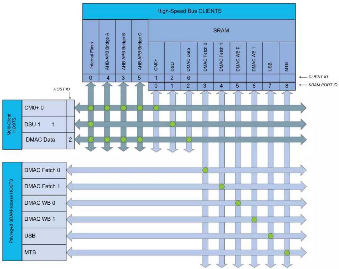
flowchart
graph TD
    A["High-Speed Bus CLIENTS"] --> B["Internal Flash"]
    A --> C["AHB-APB Bridge A"]
    A --> D["AHB-APB Bridge B"]
    A --> E["AHB-APB Bridge C"]
    A --> F["SRAM"]
    F --> G["CM0+"]
    F --> H["DSU"]
    F --> I["DMAC Data"]
    F --> J["DMAC Fetch 0"]
    F --> K["DMAC Fetch 1"]
    F --> L["DMAC WB 0"]
    F --> M["DMAC WB 1"]
    F --> N["USB"]
    F --> O["MTB"]

    P["Multi-Client HOSTS"] --> Q["CM0+ 0"]
    P --> R["DSU 1 1"]
    P --> S["DMAC Data 2"]

    T["Privileged SRAM-access HOSTS"] --> U["DMAC Fetch 0"]
    T --> V["DMAC Fetch 1"]
    T --> W["DMAC WB 0"]
    T --> X["DMAC WB 1"]
    T --> Y["USB"]
    T --> Z["MTB"]

    style A fill:#4A90E2,stroke:#333
    style P fill:#4A90E2,stroke:#333
Table 10-4. High Speed Bus Matrix Hosts
| High-Speed Bus Matrix Hosts Host ID | |
| CM0+ - Cortex M0+ Processor 0 | |
| DSU - Device Service Unit 1 | |
| DMAC - Direct Memory Access Controller / Data Access 2 |
Table 10-5. High-Speed Bus Matrix Clients
| High-Speed Bus Matrix Clients Client ID | |
| Internal Flash Memory 0 | |
| SRAM Port 0 - CM0+ Access 1 | |
| SRAM Port 1 - DSU Access 2 | |
| AHB-APB Bridge B 3 | |
| AHB-APB Bridge A 4 | |
| AHB-APB Bridge C 5 | |
| SRAM Port 2 - DMAC Data Access | 6 |
10.4.4 SRAM Quality of Service
To ensure that Hosts with latency requirements get sufficient priority when accessing RAM, priority levels can be assigned to the Hosts for different types of access.
The Quality of Service (QoS) level is independently selected for each Host accessing the RAM. For any access to the RAM, the RAM also receives the QoS level. The QoS levels and their corresponding bit values for the QoS level configuration is shown in the table below.
Table 10-6. Quality of Service
| Value Name Description | ||
| 0x0 DISABLE Background (no sensitive operation) | ||
| 0x1 LOW Sensitive Bandwidth | ||
| 0x2 MEDIUM Sensitive Latency | ||
| 0x3 HIGH Critical Latency |
If a Host is configured with QoS level DISABLE (0x0) or LOW (0x1) there will be a minimum latency of one cycle for the RAM access.
The priority order for concurrent accesses are decided by two factors. First, the QoS level for the Host and second, a static priority given by the port ID. The lowest port ID has the highest static priority. See the tables below for details.
The MTB has a fixed QoS level HIGH (0x3).
The CPU QoS level can be written/read, using 32-bit access only, at address 0x4100C114, bits [1:0]. Its reset value is 0x3.
Refer to different Host QOSCTRL registers for configuring QoS for the other Hosts (USB, DMAC).
Table 10-7. SRAM Port Connections QoS
| SRAM Port Connection | Port ID Connection Type | QoS default QoS | ||
| CM0+ - Cortex M0+ Processor | 0 Bus Matrix 0x4100C114, bits[1:0] | (1) | 0x3 | |
| DSU - Device Service Unit | 1 Bus Matrix 0x4100201C, bits[1:0] | (1) | 0x2 | |
| DMAC - Direct Memory Access Controller - Data Access | 2 Bus Matrix IP-QOSCTRL.DQOS | 0x2 | ||
| DMAC - Direct Memory Access Controller - Fetch Access | 3, 4 | Direct | IP-QOSCTRL.FQOS | 0x2 |
| DMAC - Direct Memory Access Controller - Write-Back Access | 5, 6 | Direct | IP-QOSCTRL.WRBQOS | 0x2 |
| USB - Universal Serial Bus | 7 Direct | IP-QOSCTRL | 0x3 | |
| MTB - Micro Trace Buffer | 8 Direct | STATIC-3 | 0x3 | |
Note: 1. Using 32-bit access only.
11. PAC - Peripheral Access Controller
11.1 Overview
The Peripheral Access Controller provides an interface for the locking and unlocking of peripheral registers within the device. It reports all violations that could happen when accessing a peripheral: write protected access, illegal access, enable protected access, access when clock synchronization or software reset is on-going. These errors are reported in a unique interrupt flag for a peripheral. The PAC module also reports errors occurring at the client bus level, when an access to a non-existing address is detected.
11.2 Features
- Manages write protection access and reports access errors for the peripheral modules or bridges
11.3 Block Diagram
Figure 11-1. PAC Block Diagram
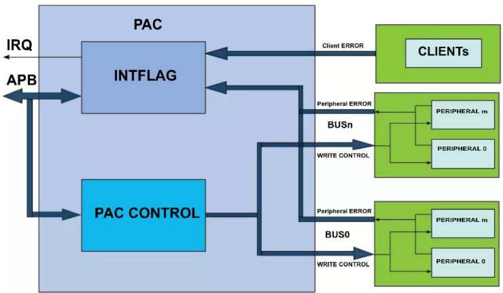
flowchart
graph TD
    A["PAC"] --> B["INTFLAG"]
    B --> C["Client ERROR"]
    C --> D["CLIENTs"]
    A --> E["PAC CONTROL"]
    E --> F["Peripheral ERROR"]
    F --> G["BUSn"]
    G --> H["WRITE CONTROL"]
    H --> I["Peripheral ERROR"]
    I --> J["BUS0"]
    J --> K["WRITE CONTROL"]
    K --> L["Peripheral ERROR"]
    L --> M["BUSn"]
    M --> N["PERIPHERAL m"]
    M --> O["PERIPHERAL 0"]
    N --> P["PERIPHERAL m"]
    N --> Q["PERIPHERAL 0"]
    style A fill:#cce5ff,stroke:#333
    style B fill:#cce5ff,stroke:#333
    style E fill:#cce5ff,stroke:#333
    style F fill:#cce5ff,stroke:#333
    style G fill:#cce5ff,stroke:#333
    style H fill:#cce5ff,stroke:#333
    style I fill:#cce5ff,stroke:#333
    style J fill:#cce5ff,stroke:#333
    style K fill:#cce5ff,stroke:#333
    style L fill:#cce5ff,stroke:#333
    style M fill:#cce5ff,stroke:#333
    style N fill:#cce5ff,stroke:#333
    style O fill:#cce5ff,stroke:#333
11.4 Product Dependencies
In order to use this peripheral, other parts of the system must be configured correctly, as described below.
11.4.1 I/O Lines
Not applicable.
11.4.2 Power Management
The PAC can continue to operate in any sleep mode where the selected source clock is running. The PAC interrupts can be used to wake up the device from sleep modes. The events can trigger other operations in the system without exiting sleep modes.
References:
PM - Power Manager
11.4.3 Clocks
The PAC bus clock (CLK_PAC_APB) can be enabled and disabled in the Main Clock module. The default state of CLK_PAC_APB can be found in the referenced links.
References:
MCLK - Main Clock
Peripheral Clock Masking
11.4.4 DMA
Not applicable.
11.4.5 Interrupts
The interrupt request line is connected to the Interrupt Controller. Using the PAC interrupt requires the Interrupt Controller to be configured first. Refer to the Nested Vector Interrupt Controller for more details.
Table 11-1. Interrupt Lines
| Instances NVIC Line | |
| PAC PACERR |
11.4.6 Events
The events are connected to the Event System, which may need configuration.
References:
- EVSYS – Event System
11.4.7 Debug Operation
When the CPU is halted in debug mode, write protection of all peripherals is disabled and the PAC continues normal operation.
11.4.8 Register Access Protection
All registers with write-access can be write-protected optionally by the Peripheral Access Controller (PAC), except for the following registers:
- Write Control (WRCTRL) register
- AHB Client Bus Interrupt Flag Status and Clear (INTFLAGAHB) register
- Peripheral Interrupt Flag Status and Clear n (INTFLAG A/B/C...) registers
Optional write-protection by the Peripheral Access Controller (PAC) is denoted by the "PAC Write-Protection" property in each individual register description.
PAC write-protection does not apply to accesses through an external debugger.
11.5 Functional Description
11.5.1 Principle of Operation
The Peripheral Access Control module allows the user to set a write protection on peripheral modules and generate an interrupt in case of a peripheral access violation. The peripheral's protection can be set, cleared or locked at the user discretion. A set of Interrupt Flag and Status registers informs the user on the status of the violation in the peripherals. In addition, clients bus errors can be also reported in the cases where reserved area is accessed by the application.
11.5.2 Basic Operation
11.5.2.1 Initialization
After reset, the PAC is enabled.
11.5.2.2 Enabling and Resetting
The PAC is always enabled after reset.
Only a hardware reset will reset the PAC module.
11.5.2.3 Operations
The PAC module allows the user to set, clear or lock the write protection status of all peripherals on all Peripheral Bridges.
If a peripheral register violation occurs, the Peripheral Interrupt Flag n registers (INTFLAGn) are updated to inform the user on the status of the violation in the peripherals connected to the Peripheral Bridge n (n = A,B,C ...). The corresponding Peripheral Write Control Status n register (STATUSn) gives the state of the write protection for all peripherals connected to the corresponding Peripheral Bridge n. Refer to the 11.5.2.4. Peripheral Access Errors for details.
The PAC module also reports the errors occurring at client bus level when an access to reserved area is detected. AHB Client Bus Interrupt Flag register (INTFLAGAHB) informs the user on the status of the violation in the corresponding client. Refer to the 11.5.2.7. AHB Client Bus Errors for details.
11.5.2.4 Peripheral Access Errors
The following events will generate a Peripheral Access Error:
- Protected write: To avoid unexpected writes to a peripheral's registers, each peripheral can be write protected. Only the registers denoted as "PAC Write-Protection" in the module's data sheet can be protected. If a peripheral is not write protected, write data accesses are performed normally. If a peripheral is write protected and if a write access is attempted, data will not be written and peripheral returns an access error. The corresponding interrupt flag bit in the INTFLAGn register will be set.
- Illegal access: Access to an unimplemented register within the module.
- Synchronized write error: For write-synchronized registers an error will be reported if the register is written while a synchronization is ongoing.
When any of the INTFLAGn registers bit are set, an interrupt will be requested if the PAC interrupt enable bit is set.
References:
Register Synchronization
11.5.2.5 Write Access Protection Management
Peripheral access control can be enabled or disabled by writing to the WRCTRL register.
The data written to the WRCTRL register is composed of two fields; WRCTRL.PERID and WRCTRL.KEY. The WRCTRL.PERID is an unique identifier corresponding to a peripheral. The WRCTRL.KEY is a key value that defines the operation to be done on the control access bit. These operations can be "clear protection", "set protection" and "set and lock protection bit".
The “clear protection” operation will remove the write access protection for the peripheral selected by WRCTRL.PERID. Write accesses are allowed for the registers in this peripheral.
The “set protection” operation will set the write access protection for the peripheral selected by WRCTRL.PERID. Write accesses are not allowed for the registers with write protection property in this peripheral.
The "set and lock protection" operation will permanently set the write access protection for the peripheral selected by WRCTRL.PERID. The write access protection will only be cleared by a hardware reset.
The peripheral access control status can be read from the corresponding STATUSn register.
11.5.2.6 Write Access Protection Management Errors
Only word-wise writes to the WRCTRL register will effectively change the access protection. Other type of accesses will have no effect and will cause a PAC write access error. This error is reported in the INTFLAGn.PAC bit corresponding to the PAC module.
PAC also offers an additional safety feature for correct program execution with an interrupt generated on double write clear protection or double write set protection. If a peripheral is write protected and a subsequent set protection operation is detected then the PAC returns an error, and similarly for a double clear protection operation.
In addition, an error is generated when writing a “set and lock” protection to a write-protected peripheral or when a write access is done to a locked set protection. This can be used to ensure that the application follows the intended program flow by always following a write protect with an unprotect and conversely. However in applications where a write protected peripheral is used in several contexts, e.g. interrupt, care should be taken so that either the interrupt can not happen while the main application or other interrupt levels manipulates the write protection status or when the interrupt handler needs to unprotect the peripheral based on the current protection status by reading the STATUS register.
The errors generated while accessing the PAC module registers (eg. key error, double protect error...) will set the INTFLAGn.PAC flag.
11.5.2.7 AHB Client Bus Errors
The PAC module reports errors occurring at the AHB Client bus level. These errors are generated when an access is performed at an address where no Client (bridge or peripheral) is mapped. These errors are reported in the corresponding bits of the INTFLAGAHB register.
11.5.2.8 Generating Events
The PAC module can also generate an event when any of the Interrupt Flag registers bit are set. To enable the PAC event generation, the control bit EVCTRL.ERREO must be set to '1'.
11.5.3 DMA Operation
Not applicable.
11.5.4 Interrupts
The PAC has the following interrupt source:
- Error (ERR): Indicates that a peripheral access violation occurred in one of the peripherals controlled by the PAC module, or a bridge error occurred in one of the bridges reported by the PAC
- This interrupt is a synchronous wake-up source.
Each interrupt source has an interrupt flag associated with it. The interrupt flag in the Interrupt Flag Status and Clear (INTFLAGAHB and INTFLAGn) registers is set when the interrupt condition occurs. Each interrupt can be individually enabled by writing a '1' to the corresponding bit in the Interrupt Enable Set (INTENSET) register, and disabled by writing a '1' to the corresponding bit in the Interrupt Enable Clear (INTENCLR) register. An interrupt request is generated when the interrupt flag is set and the corresponding interrupt is enabled. The interrupt request remains active until the interrupt flag is cleared, the interrupt is disabled, or the PAC is reset. All interrupt requests from the peripheral are ORed together on system level to generate one combined interrupt request to the NVIC. The user must read the INTFLAGAHB and INTFLAGn registers to determine which interrupt condition is present.
Note that interrupts must be globally enabled for interrupt requests to be generated.
References:
Sleep Mode Controller
Nested Vector Interrupt Controller
11.5.5 Events
The PAC can generate the following output event:
- Error (ERR): Generated when one of the interrupt flag registers bits is set
Writing a '1' to an Event Output bit in the Event Control Register (EVCTRL.ERREO) enables the corresponding output event. Writing a '0' to this bit disables the corresponding output event.
References:
- EVSYS – Event System
11.5.6 Sleep Mode Operation
In Sleep mode, the PAC is kept enabled if an available host (CPU, DMA) is running. The PAC will continue to catch access errors from the module and generate interrupts or events.
11.5.7 Synchronization
Not applicable.
11.6 Register Summary
| Offset | Name Bit Pos. 76543210 | ||||||||||
| 0x00 WRCTRL | 7:0 PERID[7:0] | ||||||||||
| 15:8 PERID[15:8] | |||||||||||
| 23:16 KEY[7:0] | |||||||||||
| 31:24 | |||||||||||
| 0x04 EVCTRL 7:0 ERREO | |||||||||||
| 0x05 ... 0x07 | Reserved | ||||||||||
| 0x08 | INTENCLR 7:0 | ERR | |||||||||
| 0x09 | INTENSET | 7:0 | ERR | ||||||||
| 0x0A ... 0x0F | Reserved | ||||||||||
| 0x10 | INTFLAGAHB | 7:0 | HSRAMDMAC | HPB2 | HPB0 | HPB1 | HSRAMDSU | HSRAMCMOP | FLASH | ||
| 15:8 | |||||||||||
| 23:16 | |||||||||||
| 31:24 | |||||||||||
| 0x14 | INTFLAGA | 7:0 | GCLK | SUPC | OSC32KCTRL | OSCCTRL | RSTC | MCLK | PM | PAC | |
| 15:8 | FREQM | EIC | RTC | WDT | |||||||
| 23:16 | |||||||||||
| 31:24 | |||||||||||
| 0x18 | INTFLAGB | 7:0 | MTB | DMAC | PORT | NVMCTRL | DSU | USB | |||
| 15:8 | |||||||||||
| 23:16 | |||||||||||
| 31:24 | |||||||||||
| 0x1C | INTFLAGC | 7:0 | TCC0 | SERCOM5 | SERCOM4 | SERCOM3 | SERCOM2 | SERCOM1 | SERCOM0 | EVSYS | |
| 15:8 | SLCD | PTC | AC | ADC | TC3 | TC2 | TC1 | TC0 | |||
| 23:16 | CCL | TRNG | AES | ||||||||
| 31:24 | |||||||||||
| 0x20 ... 0x33 | Reserved | ||||||||||
| 0x34 | STATUSA | 7:0 | GCLK | SUPC | OSC32KCTRL | OSCCTRL | RSTC | MCLK | PM | PAC | |
| 15:8 | FREQM | EIC | RTC | WDT | |||||||
| 23:16 | |||||||||||
| 31:24 | |||||||||||
| 7:0 | MTB | DMAC | PORT | NVMCTRL | DSU | USB | |||||
| 0x38 | STATUSB | 7:0 | |||||||||
| 15:8 | |||||||||||
| 23:16 | |||||||||||
| 31:24 | |||||||||||
| 0x3C | STATUSC | 7:0 | TCC0 | SERCOM5 | SERCOM4 | SERCOM3 | SERCOM2 | SERCOM1 | SERCOM0 | EVSYS | |
| 15:8 | SLCD | PTC | AC | ADC | TC3 | TC2 | TC1 | TC0 | |||
| 23:16 | CCL | TRNG | AES | ||||||||
| 3 1:24 | |||||||||||
11.7 Register Description
Registers can be 8, 16, or 32 bits wide. Atomic 8-, 16- and 32-bit accesses are supported. In addition, the 8-bit quarters and 16-bit halves of a 32-bit register, and the 8-bit halves of a 16-bit register can be accessed directly.
Some registers are optionally write-protected by the Peripheral Access Controller (PAC). Optional PAC write-protection is denoted by the "PAC Write-Protection" property in each individual register description. For details, refer to the Register Synchronization chapter.
11.7.1 Write Control
Name: WRCTRL
Offset: 0x00
Reset: 0x00000000
Property: -
| Bit 31 30 29 28 27 26 25 24 | |||||||
| Access Reset | |||||||
| Bit 23 22 21 20 19 18 17 16 | |||||||
| KEY[7:0] | |||||||
| Access Reset | R/W R/W R/W R/W R/W R/W R/W R/W | ||||||
| 0 0 0 0 0 0 0 0 | |||||||
| Bit 15 14 13 12 11 10 9 8 | |||||||
| PERID[15:8] | |||||||
| Access Reset | R/W R/W R/W R/W R/W R/W R/W R/W | ||||||
| 0 0 0 0 0 0 0 0 | |||||||
| Bit 7 6 5 4 3 2 1 0 | |||||||
| PERID[7:0] | |||||||
| Access Reset | R/W R/W R/W R/W R/W R/W R/W R/W | ||||||
| 0 0 0 0 0 0 0 0 | |||||||
Bits 23:16 - KEY[7:0] Peripheral Access Control Key
These bits define the peripheral access control key:
| Value | Name | Description |
| 0x0 | OFF | No action |
| 0x1 | CLR | Clear the peripheral write control |
| 0x2 | SET | Set the peripheral write control |
| 0x3 | SETLCK Set and lock the peripheral write control until the next hardware reset | |
Bits 15:0 - PERID[15:0] Peripheral Identifier
The PERID represents the peripheral whose control is changed using the WRCTRL.KEY. The Peripheral Identifier is calculated following formula:
$$ P E R I D = 3 2 ^ {*} \text { BridgeNumber } + N $$
Where BridgeNumber represents the Peripheral Bridge Number (0 for Peripheral Bridge A, 1 for Peripheral Bridge B, etc). N represents the peripheral index from the respective Bridge Number:
Table 11-2. PERID Values
| Periph. Bridge Name | BridgeNumber | PERID Values |
| A | 0 | 0+N |
| B | 1 | 32+N |
| C | 2 | 64+N |
| D | 3 | 96+N |
| E | 4 | 128+N |
11.7.2 Event Control
Name: EVCTRL
Offset: 0x04
Reset: 0x00
Property: -
Bit 76543210
| ERREO | |||||||
| Access Reset 0 | R/W | ||||||
Bit 0 - ERREO Peripheral Access Error Event Output
This bit indicates if the Peripheral Access Error Event Output is enabled or disabled. When enabled, an event will be generated when one of the interrupt flag registers bits (INTFLAGAHB, INTFLAGn) is set:
| Value Description | |
| 0 | Peripheral Access Error Event Output is disabled. |
| 1 | Peripheral Access Error Event Output is enabled. |
11.7.3 Interrupt Enable Clear
Name: INTENCLR
Offset: 0x08
Reset: 0x00
Property: PAC Write-Protection
This register allows the user to disable an interrupt without doing a read-modify-write operation. Changes in this register will also be reflected in the Interrupt Enable Set register (INTENSET).
Bit 76543210
| ERR | |||||||
| Access Reset 0 | R/W | ||||||
Bit 0 - ERR Peripheral Access Error Interrupt Disable
This bit indicates that the Peripheral Access Error Interrupt is disabled and an interrupt request will be generated when one of the interrupt flag registers bits (INTFLAGAHB, INTFLAGn) is set:
Writing a '0' to this bit has no effect.
Writing a '1' to this bit will clear the Peripheral Access Error interrupt Enable bit and disables the corresponding interrupt request.
Value Description
| 0 | Peripheral Access Error interrupt is disabled. |
| 1 | Peripheral Access Error interrupt is enabled. |
11.7.4 Interrupt Enable Set
Name: INTENSET
Offset: 0x09
Reset: 0x00
Property: PAC Write-Protection
This register allows the user to enable an interrupt without doing a read-modify-write operation. Changes in this register will also be reflected in the Interrupt Enable Set register (INTENCLR).
Bit 76543210
| ERR | |||||||
| Access Reset 0 | R/W | ||||||
Bit 0 - ERR Peripheral Access Error Interrupt Enable
This bit indicates that the Peripheral Access Error Interrupt is enabled and an interrupt request will be generated when one of the interrupt flag registers bits (INTFLAGAHB, INTFLAGn) is set:
Writing a '0' to this bit has no effect.
Writing a '1' to this bit will set the Peripheral Access Error interrupt Enable bit and enables the corresponding interrupt request.
Value Description
| 0 | Peripheral Access Error interrupt is disabled. |
| 1 | Peripheral Access Error interrupt is enabled. |
11.7.5 AHB Client Bus Interrupt Flag Status and Clear
Name: INTFLAGAHB
Offset: 0x10
Reset: 0x00000000
Property: -
This flag is cleared by writing a '1' to the flag.
This flag is set when an access error is detected by the CLIENT n, and will generate an interrupt request if INTENCLR/SET.ERR is '1'.
Writing a '0' to this bit has no effect.
Writing a '1' to this bit will clear the corresponding INTFLAGAHB interrupt flag.
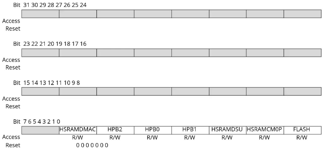
text_image
Bit 31 30 29 28 27 26 25 24 Access Reset Bit 23 22 21 20 19 18 17 16 Access Reset Bit 15 14 13 12 11 10 9 8 Access Reset Bit 7 6 5 4 3 2 1 0 Access Reset HSRAMDMAC HPB2 HPB0 HPB1 HSRAMDSU HSRAMCMOP FLASH R/W R/W R/W R/W R/W R/W R/W 0 0 0 0 0 0Bit 6 - HSRAMDMAC Interrupt Flag for CLIENT HSRAMDMAC
Bit 5 - HPB2 Interrupt Flag for CLIENT HPB2
Bit 4 - HPB0 Interrupt Flag for CLIENT HPB0
Bit 3 - HPB1 Interrupt Flag for CLIENT HPB1
Bit 2 - HSRAMDSU Interrupt Flag for CLIENT HSRAMDSU
Bit 1 - HSRAMCMOP Interrupt Flag for CLIENT HSRAMCMOP
Bit 0 - FLASH Interrupt Flag for CLIENT FLASH
11.7.6 Peripheral Interrupt Flag Status and Clear A
Name: INTFLAGA
Offset: 0x14
Reset: 0x00000000
Property: -
This flag is cleared by writing a one to the flag.
This flag is set when a Peripheral Access Error occurs while accessing the peripheral associated with the respective INTFLAGA bit, and will generate an interrupt request if INTENCLR/SET.ERR is one.
Writing a zero to this bit has no effect.
Writing a one to this bit will clear the corresponding INTFLAGA interrupt flag.
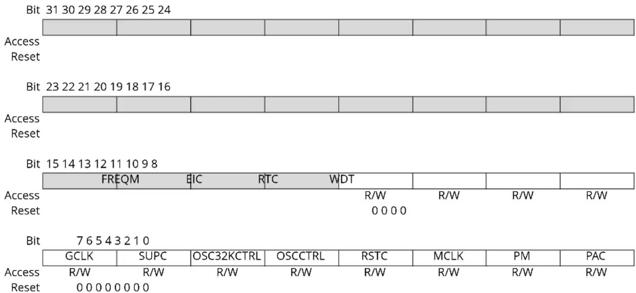
text_image
Bit 31 30 29 28 27 26 25 24 Access Reset Bit 23 22 21 20 19 18 17 16 Access Reset Bit 15 14 13 12 11 10 9 8 FREQM EIC RTC WDT R/W R/W R/W R/W Access Reset R/W R/W R/W R/W R/W R/W R/W 0 0 0 0 Bit 7 6 5 4 3 2 1 0 GCLK SUPC OSC32KCTRL OSCCTRL RSTC MCLK PM PAC Access R/W R/W R/W R/W R/W R/W R/W Reset 0 0 0 0 0 0 0Bit 11 - FREQM Interrupt Flag for FREQM
Bit 10 - EIC Interrupt Flag for EIC
Bit 9 - RTC Interrupt Flag for RTC
Bit 8 - WDT Interrupt Flag for WDT
Bit 7 - GCLK Interrupt Flag for GCLK
Bit 6 - SUPC Interrupt Flag for SUPC
Bit 5 - OSC32KCTRL Interrupt Flag for OSC32KCTRL
Bit 4 - OSCCTRL Interrupt Flag for OSCCTRL
Bit 3 - RSTC Interrupt Flag for RSTC
Bit 2 - MCLK Interrupt Flag for MCLK
Bit 1 - PM Interrupt Flag for PM
Bit 0 - PAC Interrupt Flag for PAC
11.7.7 Peripheral Interrupt Flag Status and Clear B
Name: INTFLAGB
Offset: 0x18
Reset: 0x00000000
Property: -
This flag is cleared by writing a '1' to the flag.
This flag is set when a Peripheral Access Error occurs while accessing the peripheral associated with the respective INTFLAGB bit, and will generate an interrupt request if INTENCLR/SET.ERR is '1'.
Writing a '0' to this bit has no effect.
Writing a '1' to this bit will clear the corresponding INTFLAGB interrupt flag.
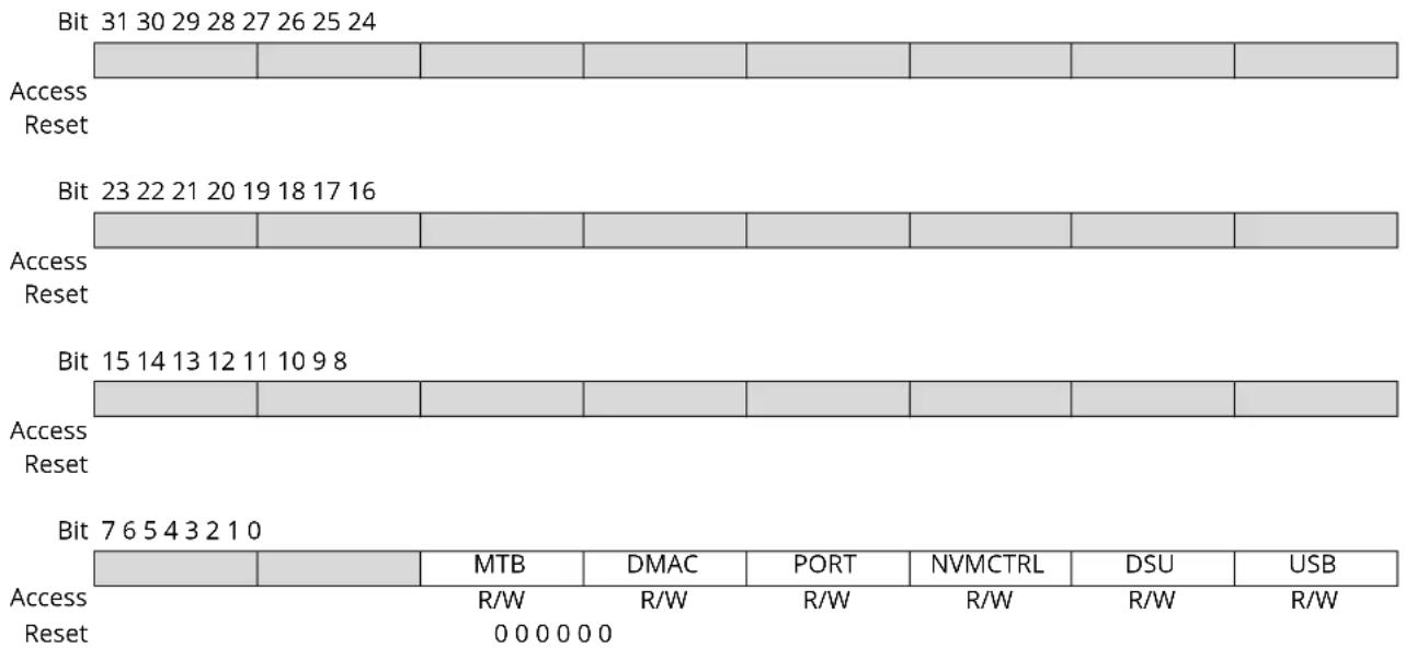
text_image
Bit 31 30 29 28 27 26 25 24 Access Reset Bit 23 22 21 20 19 18 17 16 Access Reset Bit 15 14 13 12 11 10 9 8 Access Reset Bit 7 6 5 4 3 2 1 0 Access Reset MTB DMAC PORT NVMCTRL DSU USB R/W R/W R/W R/W R/W R/W 0 0 0 0 0 0Bit 5 - MTB Interrupt Flag for MTB
Bit 4 - DMAC Interrupt Flag for DMAC
Bit 3 - PORT Interrupt Flag for PORT
Bit 2 - NVMCTRL Interrupt Flag for NVMCTRL
Bit 1 - DSU Interrupt Flag for DSU
Bit 0 - USB Interrupt Flag for USB
11.7.8 Peripheral Interrupt Flag Status and Clear C
Name: INTFLAGC
Offset: 0x1C
Reset: 0x00000000
Property: -
This flag is cleared by writing a one to the flag.
This flag is set when a Peripheral Access Error occurs while accessing the peripheral associated with the respective INTFLAGC bit, and will generate an interrupt request if INTENCLR/SET.ERR is one.
Writing a zero to this bit has no effect.
Writing a one to this bit will clear the corresponding INTFLAGC interrupt flag.
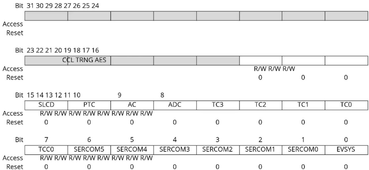
other
Bit 31 30 29 28 27 26 25 24 Access Reset Bit 23 22 21 20 19 18 17 16 CCL TRNG AES Access Reset R/W R/W R/W R/W R/W 0 0 0 Bit 15 14 13 12 11 10 9 8 SLCD PTC AC ADC TC3 TC2 TC1 TC0 Access Reset R/W R/W R/W R/W R/W R/W R/W 0 0 0 0 0 0 0 Bit 7 6 5 4 3 2 1 0 TCC0 SERCOM5 SERCOM4 SERCOM3 SERCOM2 SERCOM1 SERCOM0 EVSYS Access Reset R/W R/W R/W R/W R/W R/W R/W 0 0 0 0 0 0 0 Bit: 15 14 13 12 11 10 9 8Bit 18 - CCL Interrupt Flag for CCL
Bit 17 - TRNG Interrupt Flag for TRNG
Bit 16 - AES Interrupt Flag for AES
Bit 15 - SLCD Interrupt Flag for SLCD
Bit 14 - PTC Interrupt Flag for PTC
Bit 13 - AC Interrupt Flag for AC
Bit 12 - ADC Interrupt Flag for ADC
Bits 8, 9, 10, 11 - TC Interrupt Flag for TCn [n = 3..0]
Bit 7 - TCC0 Interrupt Flag for TCC0
Bits 1, 2, 3, 4, 5, 6 - SERCOM Interrupt Flag for SERCOMn [n = 5..0]
Bit 0 - EVSYS Interrupt Flag for EVSYS
11.7.9 Peripheral Write Protection Status A
Name: STATUSA
Offset: 0x34
Reset: 0x00000000
Property: -
Writing to this register has no effect.
Reading STATUS register returns peripheral write protection status:
| Value Description | |||||||
| 0 Peripheral is not write protected. | |||||||
| 1 Peripheral is write protected. | |||||||
| Bit 31 30 29 28 27 26 25 24 | |||||||
| Access Reset | |||||||
| Bit 23 22 21 20 19 18 17 16 | |||||||
| Access Reset | |||||||
| Bit 15 14 13 12 11 10 9 8 | |||||||
| Access Reset | FREQM | EIC | RTC | WDT | |||
| Access Reset | R | R | R | R | |||
| Bit 7 6 5 4 3 2 1 0 | |||||||
| GCLK | SUPC | OSC32KCTRL | OSCCTRL | RSTC | MCLK | PM | PAC |
| Access Reset | R | R | R | R | R | R | R |
Bit 11 - FREQM Peripheral FREQM Write Protection Status
Bit 10 - EIC Peripheral EIC Write Protection Status
Bit 9 - RTC Peripheral RTC Write Protection Status
Bit 8 - WDT Peripheral WDT Write Protection Status
Bit 7 - GCLK Peripheral GCLK Write Protection Status
Bit 6 - SUPC Peripheral SUPC Write Protection Status
Bit 5 - OSC32KCTRL Peripheral OSC32KCTRL Write Protection Status
Bit 4 - OSCCTRL Peripheral OSCCTRL Write Protection Status
Bit 3 - RSTC Peripheral RSTC Write Protection Status
Bit 2 - MCLK Peripheral MCLK Write Protection Status
Bit 1 - PM Peripheral PM Write Protection Status
Bit 0 - PAC Peripheral PAC Write Protection Status
11.7.10 Peripheral Write Protection Status B
Name: STATUSB
Offset: 0x38
Reset: 0x00000002
Property: -
Writing to this register has no effect.
Reading the STATUS register returns peripheral write protection status:
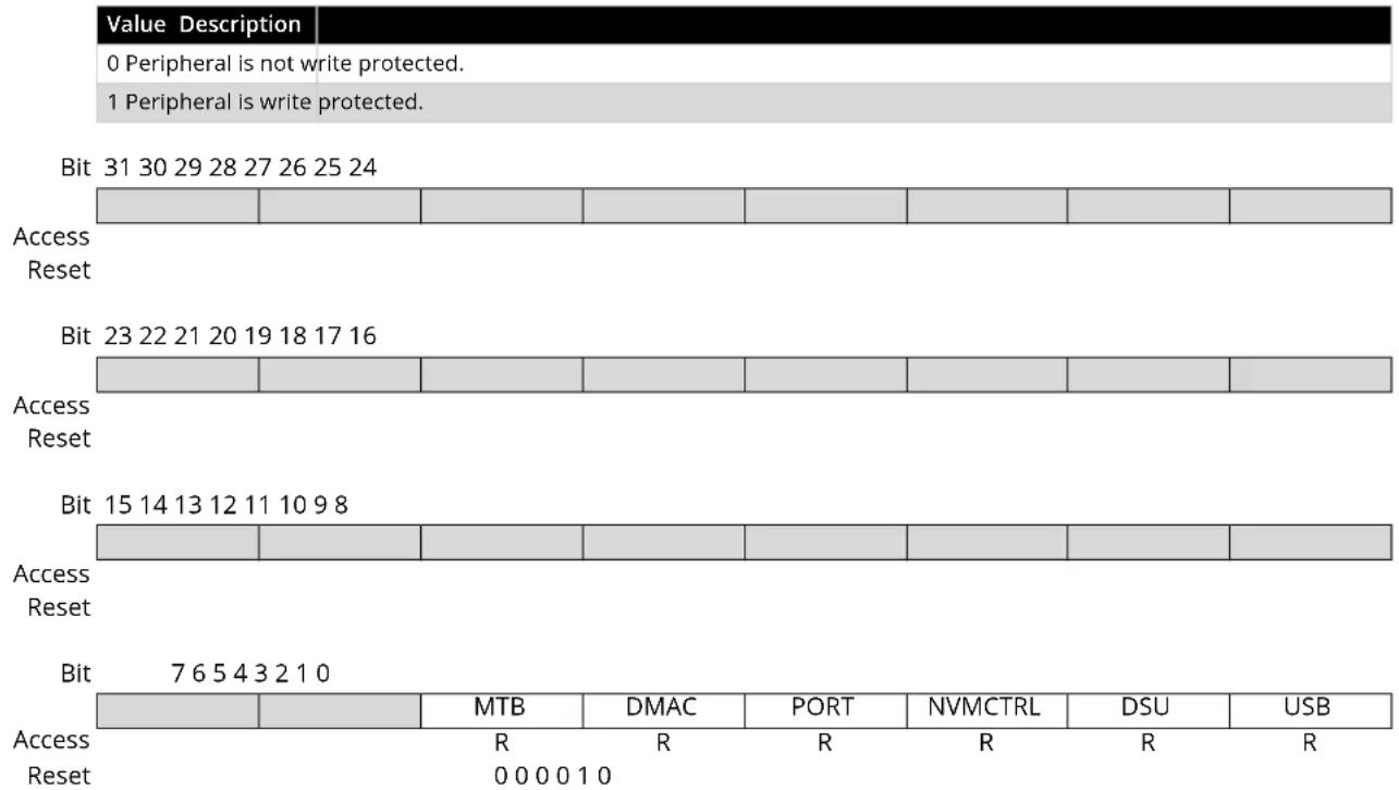
text_image
Value Description 0 Peripheral is not write protected. 1 Peripheral is write protected. Bit 31 30 29 28 27 26 25 24 Access Reset Bit 23 22 21 20 19 18 17 16 Access Reset Bit 15 14 13 12 11 10 9 8 Access Reset Bit 7 6 5 4 3 2 1 0 Access Reset MTB DMAC PORT NVMCTRL DSU USB R R R R R 0 0 0 0 1 0Bit 5 - MTB Peripheral MTB Write Protection Status
Bit 4 - DMAC Peripheral DMAC Write Protection Status
Bit 3 - PORT Peripheral PORT Write Protection Status
Bit 2 - NVMCTRL Peripheral NVMCTRL Write Protection Status
Bit 1 - DSU Peripheral DSU Write Protection Status
Bit 0 - USB Peripheral USB Write Protection Status
11.7.11 Peripheral Write Protection Status C
Name: STATUSC
Offset: 0x3C
Reset: 0x00000000
Property: -
Writing to this register has no effect.
Reading STATUS register returns peripheral write protection status:
| Value Description | ||||||||
| 0 Peripheral is not write protected. | ||||||||
| 1 Peripheral is write protected. | ||||||||
| Bit 31 30 29 28 27 26 25 24 | ||||||||
| Access Reset | ||||||||
| Bit 23 22 21 20 19 18 17 16 | ||||||||
| CCL TRNG | AES | |||||||
| Access Reset | R | R | R | |||||
| 0 | 0 | 0 | ||||||
| Bit 15 14 13 12 11 10 | 9 | 8 | ||||||
| SLCD | PTC | AC | ADC | TC3 | TC2 | TC1 | TC0 | |
| Access Reset | R | R | R | R | R | R | R | R |
| 0 | 0 | 0 | 0 | 0 | 0 | 0 | 0 | |
| Bit | 7 | 6 | 5 | 4 | 3 | 2 | 1 | 0 |
| TCC0 | SERCOM5 | SERCOM4 | SERCOM3 | SERCOM2 | SERCOM1 | SERCOM0 | EVSYS | |
| Access Reset | R | R | R | R | R | R | R | R |
| 0 | 0 | 0 | 0 | 0 | 0 | 0 | 0 | |
Bit 18 - CCL Peripheral CCL Write Protection Status
Bit 17 - TRNG Peripheral TRNG Write Protection Status
Bit 16 - AES Peripheral AES Write Protection Status
Bit 15 - SLCD Peripheral SLCD Write Protection Status
Bit 14 - PTC Peripheral PTC Write Protection Status
Bit 13 - AC Peripheral ADC Write Protection Status
Bit 12 - ADC Peripheral ADC Write Protection Status
Bits 8, 9, 10, 11 - TC Peripheral TCn Write Protection Status [n = 3..0]
Bit 7 - TCC0 Peripheral TCC0 Write Protection Status
Bits 1, 2, 3, 4, 5, 6 - SERCOM Peripheral SERCOMn Write Protection Status [n = 5..0]
Bit 0 - EVSYS Peripheral EVSYS Write Protection Status
12. Peripherals Configuration Summary
Table 12-1. Peripherals Configuration Summary
| Peripheral name | Base address | IRQ line | AHB clock | APB clock | Bus Clock Domain | Generic Clock | PAC Events | DMA | Power domain | ||||||
| Index | Enabled at Reset | Index | Enabled at Reset | Name | Index | Index | Prot at Reset | User | Generator | Index | Sleep Walking | Name | |||
| AHB-APB Bridge A | 0x40000000 — 0 | Y — — CPU — | — — | — — | — — | N/A | PDTOP | ||||||||
| PAC | 0x40000000 | 0 | 7 | Y | 0 | Y | CPU | — | 0 | — | — | 69 : ACCERR | — | N/A | PDTOP |
| PM | 0x40000400 | 0 | — | — | 1 | Y | Backup | — | 1 | N | — | — | — | N/A | PDBACKUP |
| MCLK | 0x40000800 | 0 | — | — | 2 | Y | CPU | — | 2 | N | — | — | — | Y | PDTOP |
| RSTC | 0x40000C00 | — | — | — | 3 | Y | Backup | — | 3 | N | — | — | — | N/A | PDBACKUP |
| OSCCTRL | 0x40001000 | 0 | — | — | 4 | Y | CPU | 0: DFLL48M reference1: FDPLL96M clk source2: FDPLL96M 32kHz | 4 | N | — | 0: CFD | — | Y | PDTOP |
| OSC32KCTRL | 0x40001400 | 0 | — | — | 5 | Y | Backup | — | 5 | N | — | 1: CFD | — | — | PDBACKUP |
| SUPC | 0x40001800 | 0 | — | — | 6 | Y | Backup | — | 6 | N | — | — | — | N/A | PDBACKUP |
| GCLK | 0x40001C00 | — | — | — | 7 | Y | CPU | — | 7 | N | — | — | — | N/A | PDTOP |
| WDT | 0x40002000 | 1 | — | — | 8 | Y | CPU | — | 8 | N | — | — | — | Y | PDTOP |
| RTC | 0x40002400 | 2 | — | — | 9 | Y | Backup | — | 9 | N | 0: TAMPEVT | 2: CMP0/ ALARMO3: CMP1 4: TAMPER5: OVF6-13: PER0-7 | 1: TIMESTAMP | Y PDBACKUP | |
| EIC | 0x40002800 | 3, NMI | — | — | 10 | Y | CPU | 3 | 10 | N | — | 14 29: EXTINTO-15 | — Y | PDTOP | |
| FREQM | 0x40002C00 | 4 | — | — | 11 | Y | CPU | 4: FREQM_MSR5: FREQM_REF | 11 N | — | 4: DONE — | Y PDTOP | |||
| AHB-APB Bridge B | 0x41000000 — 1 | Y — — CPU — — — — — — — — — — — — — — — — — — — — — — — — — — — — — — — — — — — — — — — — — — — — — — — — — — — — — — — — — — — — — — — — — — — — — — — — — — — — — — — — — — — — — — — — — — — — — — — — — — — — | |||||||||||||
| USB | 0x41000000 | 5 | 4 | Y | 0 | Y | CPU | 6 | 0 | N | — | — | — | Y | PDTOP |
| DSU | 0x41002000 | — | 5 | Y | 1 | Y | CPU | — | 1 | Y | — | — | — | N/A | PDTOP |
| NVMCTRL | 0x41004000 | 6 | 8 | Y | 2 | Y | CPU | — | 2 | N | — | — | — | Y | PDTOP |
| PORT | 0x41006000 | — | — | — | 10 | Y | CPU | — | 3 | N | 1-4 : EV0-3 | — | — | Y | PDTOP |
| DMAC | 0x41008000 | 7 | 4 | Y | — | — | CPU | — | 4 | — | 5-8: CH0-4 | 30-33: CH0-4 | — | Y | PDTOP |
| MTB | 0x410A0000 | — | — | — | — | — | CPU | — | — | — | — | — | — | N/A | PDTOP |
| AHB-APB Bridge C | 0x42000000 — 2 | Y — — CPU — — — — — — — — — — — — — — — — — — — — — — — — — — — — — — — — — — — — — — — — — — — — — — — — — — — — — — — — — — — — — — — — — — — — — — — — — — — — — — — — — — — — — — — — — — — — — — | N/A PDTOP | ||||||||||||
| EVSYS | 0x42000000 | 8 | — | — | 0 | Y | CPU | 7-14: one per CHANNEL | 0 | N | — — — — | Y PDTOP | |||
| Peripheral name | Base address | IRQ line | AHB clock | APB clock | Bus clock Domain | Generic Clock | PAC Events | DMA | Power domain | ||||||
| Index | Enabled at Reset | Index | Enabled at Reset | Name | Index | Index | Prot at Reset | User | Generator | Index | Sleep Walking | Name | |||
| SERCOM0 0x42000400 9 — — 1 Y CPU 16: CORE | 15: SLOW | 1 N — — 2: RX | 3: TX | Y PDTOP | |||||||||||
| SERCOM1 0x42000800 10 — — 2 Y CPU 17: CORE | 15: SLOW | 2 N — — 4: RX | 5: TX | Y PDTOP | |||||||||||
| SERCOM2 0x42000A00 11 — — 3 Y CPU 18: CORE | 15: SLOW | 3 N — — 6: RX | 7: TX | Y PDTOP | |||||||||||
| SERCOM3 0x42001000 12 — — 4 Y CPU 19: CORE | 15: SLOW | 4 N — — 8: RX | 9: TX | Y PDTOP | |||||||||||
| SERCOM4 0x42001400 13 — — 5 Y CPU 20: CORE | 15: SLOW | 5 N — — 10: RX | 11: TX | Y PDTOP | |||||||||||
| SERCOM5 0x42001800 14 — — 6 Y CPU 21: CORE | 15: SLOW | 6 N — — 12: RX | 13: TX | Y PDTOP | |||||||||||
| TCC0 0x42001C00 15 — — 7 Y CPU 22 | 7 N 9-10: EV0-1 | 11-14: MC0-3 | 34: OVF35: TRG36: CNT37-40: MC0-3 | 14: OVF15-18: MC0-3 | Y PDTOP | ||||||||||
| TC0 | 0x42002000 | 16 | — | — | 8 | Y | CPU | 23 | 8 | N | 15: EVU | 41: OVF42-43: MC0-1 | 19: OVF20-21: MC0-1 | Y PDTOP | |
| TC1 | 0x42002400 | 17 | — | — | 9 | Y | CPU | 23 | 9 | N | 16: EVU | 44: OVF45-46: MC0-1 | 22: OVF23-24: MC0-1 | Y PDTOP | |
| TC2 | 0x42002800 | 18 | — | — | 10 | Y | CPU | 24 | 10 | N | 17: EVU | 47: OVF48-49: MC0-1 | 25: OVF26-27: MC0-1 | Y PDTOP | |
| TC3 | 0x42002C00 | 19 | — | — | 11 | Y | CPU | 24 | 11 | N | 18: EVU | 50: OVF51-52: MC0-1 | 28: OVF29-30: MC0-1 | Y PDTOP | |
| ADC | 0x42003000 20 — — 12 Y CPU 25 | 12 N 19: START | 20: SYNC | 53: RESRDY54: WINMON | 31: RESRDY Y PDTOP | ||||||||||
| AC | 0x42003400 21 — — 13 Y CPU 26 | 13 N 21-22: | SOC0-1 | 55-56:COMP0-157: WIN0 | — Y PDTOP | ||||||||||
| PTC 0x42003800 22 — — 14 Y CPU 27 | 14 N 23: STCONV 58: EOC | 59: WCOMP | — — PDTOP | ||||||||||||
| SLCD 0x42003C00 | 23 — — 15 Y CPU — | 15 N — 60-62: FC0-2 | 63: DT | 32: DMU33: ACMDRDY34: ABMRDY | — PDTOP | ||||||||||
| AES | 0x42004000 24 — — 16 Y CPU — | 16 N — — 35 : WR | 36 : RD | Y PDTOP | |||||||||||
| TRNG | 0x42004400 | 25 | — | — | 17 | Y | CPU | — | 17 | N | — | 64 : READY | — | Y | PDTOP |
| Peripheral name | Base address | IRQ line | AHB clock | APB clock | Bus Clock Domain | Generic Clock | PAC Events | DMA | Power domain | ||||||
| Index | Enabled at Reset | Index | Enabled at Reset | Name | Index | Index | Prot at Reset | User | Generator | Index | Sleep Walking | Name | |||
| CCL 0x42004800 | — — — 18 Y CPU | 28 18 N 24 : LUTIN0 | 65 : LUTOUT0 | — Y PDTOP | |||||||||||
| 25 : LUTIN1 | 66 : LUTOUT1 | ||||||||||||||
| 26: LUTIN2 | 67: LUTOUT2 | ||||||||||||||
| 27: LUTIN3 | 68: LUTOUT3 | ||||||||||||||
13. DSU - Device Service Unit
13.1 Overview
The Device Service Unit (DSU) provides a means of detecting debugger probes. It enables the ARM Debug Access Port (DAP) to have control over multiplexed debug pads and CPU reset. The DSU also provides system-level services to debug adapters in an ARM debug system. It implements a CoreSight Debug ROM that provides device identification as well as identification of other debug components within the system. Hence, it complies with the ARM Peripheral Identification specification. The DSU also provides system services to applications that need memory testing, as required for IEC60730 Class B compliance, for example. The DSU can be accessed simultaneously by a debugger and the CPU, as it is connected on the High-Speed Bus Matrix. For security reasons, some of the DSU features will be limited or unavailable when the device is protected by the NVMCTRL security bit.
References:
- NVMCTRL - Non-Volatile Memory Controller
27.6.6. Security Bit
13.2 Features
- CPU reset extension
- Debugger probe detection (Cold- and Hot-Plugging)
• Chip-Erase command and status
• 32-bit cyclic redundancy check (CRC32) of any memory accessible through the bus matrix
- ARM ^ CoreSight ^TM compliant device identification
- Two debug communications channels
- Debug access port security filter
- Onboard memory built-in self-test (MBIST)
13.3 Block Diagram
Figure 13-1. DSU Block Diagram
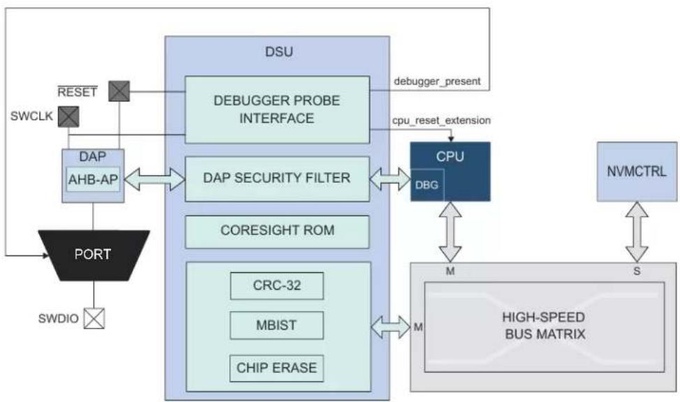
flowchart
graph TD
    A["DSU"] --> B["DEBUGGER PROBE INTERFACE"]
    B --> C["CPU"]
    C --> D["NVMCTRL"]
    D --> E["S"]
    F["PORT"] --> G["DAP AHB-AP"]
    G --> H["SWCLK"]
    I["SWIO"] --> J["RESET"]
    K["CORESIGHT ROM"] --> L["DAP SECURITY FILTER"]
    M["CRC-32"] --> N["MBIST"]
    O["CHIP ERASE"] --> P["High-Speed BUS MATRIX"]
    Q["CPU"] <--> R["DBG"]
    S["CPU"] <--> T["CPU"]
    U["CPU"] <--> V["CPU"]
    W["CPU"] <--> X["CPU"]
    Y["CPU"] <--> Z["CPU"]
    AA["CPU"] <--> AB["CPU"]
    AC["CPU"] <--> AD["CPU"]
    AE["CPU"] <--> AF["CPU"]
    AG["CPU"] <--> AH["CPU"]
    AI["CPU"] <--> AJ["CPU"]
    AK["CPU"] <--> AL["CPU"]
    AM["CPU"] <--> AN["CPU"]
    AO["CPU"] <--> AP["CPU"]
    AQ["CPU"] <--> AR["CPU"]
    AS["CPU"] <--> AT["CPU"]
    AU["CPU"] <--> AV["CPU"]
    AW["CPU"] <--> AX["CPU"]
    AY["DSU"] --> AZ["DEBUGGER PROBE INTERFACE"]
    style DSU fill:#d4edda,stroke:#333
    style CPU fill:#e6f7ff,stroke:#333
    style CPU fill:#e6f7ff,stroke:#333
    style CPU fill:#e6f7ff,stroke:#333
    style CPU fill:#e6f7ff,stroke:#333
    style CPU fill:#e6f7ff,stroke:#333
    style CPU fill:#e6f7ff,stroke:#333
    style CPU fill:#e6ff66,stroke:#333
    style CPU fill:#e6ff66,stroke:#333
    style CPU fill:#e6ff66,stroke:#333
    style CPU fill:#e6ff66,stroke:#333
    style CPU fill:#e6ff66,stroke:#333
    style CPU fill:#e6ff66,stroke:#333
    style CPU fill:#e6ef66,stroke:#333
    style CPU fill:#e6ef66,stroke:#333
    style CPU fill:#e6ef66,stroke:#333
    style CPU fill:#e6ef66,stroke:#333
    style CPU fill:#e6ef66,stroke:#333
    style CPU fill:#e6ef66,stroke:#333
    style CPU fill:#d4edda,stroke:#333
13.4 Signal Description
The DSU uses three signals to function.
| Signal Name Type Description | ||
| RESET Digital Input External reset | ||
| SWCLK Digital Input SW clock | ||
| SWDIO Digital I/O SW bidirectional data pin |
References:
I/O Multiplexing and Considerations
13.5 Product Dependencies
In order to use this peripheral, other parts of the system must be configured correctly, as described below.
13.5.1 IO Lines
The SWCLK pin is by default assigned to the DSU module to allow debugger probe detection and to stretch the CPU reset phase. For more information, refer to 13.6.3. Debugger Probe Detection. The Hot-Plugging feature depends on the PORT configuration. If the SWCLK pin function is changed in the PORT or if the PORT_MUX is disabled, the Hot-Plugging feature is disabled until a power-reset or an external reset.
13.5.2 Power Management
The DSU will continue to operate in any sleep mode where the selected source clock is running.
References:
PM - Power Manager
13.5.3 Clocks
The DSU bus clocks (CLK_DSU_APB and CLK_DSU_AHB) can be enabled and disabled by the Main Clock Controller
References:
-
PM - Power Manager
-
MCLK - Main Clock
16.6.2.6. Peripheral Clock Masking
13.5.4 Interrupts
Not applicable.
13.5.5 Events
Not applicable.
13.5.6 Register Access Protection
Registers with write-access can be optionally write-protected by the 11. PAC - Peripheral Access Controller, except for the following:
- Debug Communication Channel 0 register (DCC0)
- Debug Communication Channel 1 register (DCC1)
Note: Optional write-protection is indicated by the "PAC Write-Protection" property in the register description.
When the CPU is halted in debug mode, all write-protection is automatically disabled. Write-protection does not apply for accesses through an external debugger.
13.5.7 Analog Connections
Not applicable.
13.6 Debug Operation
13.6.1 Principle of Operation
The DSU provides basic services to allow on-chip debug using the ARM Debug Access Port and the ARM processor debug resources:
- CPU reset extension
- Debugger probe detection
For more details on the ARM debug components, refer to the ARM Debug Interface v5 Architecture Specification.
13.6.2 CPU Reset Extension
"CPU reset extension" refers to the extension of the reset phase of the CPU core after the external reset is released. This ensures that the CPU is not executing code at startup while a debugger connects to the system. The debugger is detected on a RESET release event when SWCLK is low. At startup, SWCLK is internally pulled up to avoid false detection of a debugger if the SWCLK pin is left unconnected. When the CPU is held in the reset extension phase, the CPU Reset Extension bit of the Status A register (STATUS.CRSTEXT) is set. To release the CPU, write a '1' to STATUSA.CRSTEXT. STATUSA.CRSTEXT will then be set to '0'. Writing a '0' to STATUSA.CRSTEXT has no effect. For security reasons, it is not possible to release the CPU reset extension when the device is protected by the NVMCTRL security bit. Trying to do so sets the Protection Error bit (PERR) of the Status A register (STATUS.PERR).
Figure 13-2. Typical CPU Reset Extension Set and Clear Timing Diagram

text_image
SWCLK RESET DSU CRSTEXT Clear CPU reset extension CPU_STATE reset runningReferences:
27.6.6. Security Bit
27. NVMCTRL - Non-Volatile Memory Controller
13.6.3 Debugger Probe Detection
13.6.3.1 Cold Plugging
Cold-Plugging is the detection of a debugger when the system is in reset. Cold-Plugging is detected when the CPU reset extension is requested, as described above.
13.6.3.2 Hot Plugging
Hot-Plugging is the detection of a debugger probe when the system is not in reset. Hot-Plugging is not possible under reset because the detector is reset when POR or RESET are asserted. Hot-Plugging is active when a SWCLK falling edge is detected. The SWCLK pad is multiplexed with other functions and the user must ensure that its default function is assigned to the debug system. If the SWCLK function is changed, the Hot-Plugging feature is disabled until a power-reset or external reset occurs. Availability of the Hot-Plugging feature can be read from the Hot-Plugging Enable bit of the Status B register (STATUSB.HPE).
Figure 13-3. Hot-Plugging Detection Timing Diagram
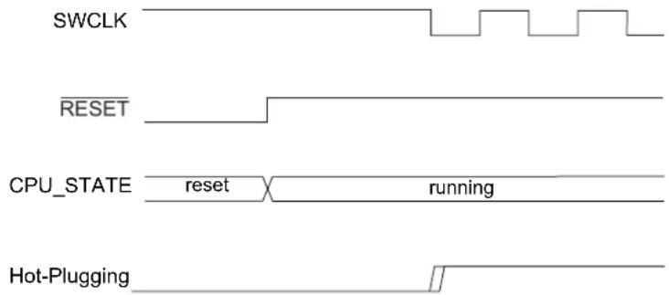
text_image
SWCLK RESET CPU_STATE reset running Hot-PluggingThe presence of a debugger probe is detected when either Hot-Plugging or Cold-Plugging is detected. Once detected, the Debugger Present bit of the Status B register (STATUSB.DBGPRES) is set. For security reasons, Hot-Plugging is not available when the device is protected by the NVMCTRL security bit.
This detection requires that pads are correctly powered. Thus, at cold startup, this detection cannot be done until POR is released. If the device is protected, Cold-Plugging is the only way to detect a debugger probe, and so the external reset timing must be longer than the POR timing. If external reset is deasserted before POR release, the user must retry the procedure above until it gets connected to the device.
References:
- NVMCTRL - Non-Volatile Memory Controller
27.6.6. Security Bit
13.7 Chip Erase
Chip-Erase consists of removing all sensitive information stored in the chip and clearing the NVMCTRL security bit. Therefore, all volatile memories and the Flash memory (including the EEPROM emulation area) will be erased. The Flash auxiliary rows, including the user row, will not be erased.
When the device is protected, the debugger must reset the device in order to be detected. This ensures that internal registers are reset after the protected state is removed. The Chip-Erase operation is triggered by writing a '1' to the Chip-Erase bit in the Control register (CTRL.CE). This command will be discarded if the DSU is protected by the Peripheral Access Controller (PAC). Once issued, the module clears volatile memories prior to erasing the Flash array. To ensure that the Chip-Erase operation is completed, check the Done bit of the Status A register (STATUSA.DONE).
The Chip-Erase operation depends on clocks and power management features that can be altered by the CPU. For that reason, it is recommended to issue a Chip-Erase after a Cold-Plugging procedure to ensure that the device is in a known and safe state.
The recommended sequence is as follows:
- Issue the Cold-Plugging procedure (refer to 13.6.3.1. Cold Plugging). The device then:
a. Detects the debugger probe.
b. Holds the CPU in reset.
- Issue the Chip-Erase command by writing a '1' to CTRL.CE. The device then:
a. Clears the system volatile memories.
b. Erases the whole Flash array (including the EEPROM emulation area, not including auxiliary rows).
c. Erases the lock row, removing the NVMCTRL security bit protection.
-
Check for completion by polling STATUSA.DONE (read as '1' when completed).
-
Reset the device to let the NVMCTRL update the fuses.
13.8 Programming
Programming the Flash or RAM memories is only possible when the device is not protected by the NVMCTRL security bit. The programming procedure is as follows:
- At power up, RESET is driven low by a debugger. The on-chip regulator holds the system in a POR state until the input supply is above the POR threshold (refer to Power-On Reset (POR) Characteristics). The system continues to be held in this static state until the internally regulated supplies have reached a safe operating state.
- The PM starts, clocks are switched to the slow clock (Core Clock, System Clock, Flash Clock and any Bus Clocks that do not have clock gate control). Internal resets are maintained due to the external reset.
- The debugger maintains a low level on SWCLK. RESET is released, resulting in a debugger Cold-Plugging procedure.
- The debugger generates a clock signal on the SWCLK pin, the Debug Access Port (DAP) receives a clock.
- The CPU remains in Reset due to the Cold-Plugging procedure; meanwhile, the rest of the system is released.
- A Chip-Erase is issued to ensure that the Flash is fully erased prior to programming.
- Programming is available through the AHB-AP.
- After the operation is completed, the chip can be restarted either by asserting RESET, toggling power, or writing a '1' to the Status A register CPU Reset Phase Extension bit (STATUS.ACRSTEXT). Make sure that the SWCLK pin is high when releasing RESET to prevent extending the CPU reset.
References:
Electrical Characteristics
NVMCTRL
Security Bit
13.9 Intellectual Property Protection
Intellectual property protection consists of restricting access to internal memories from external tools when the device is protected, and this is accomplished by setting the NVMCTRL security bit. This protected state can be removed by issuing a Chip-Erase (refer to 13.7. Chip Erase). When the device is protected, read/write accesses using the AHB-AP are limited to the DSU address range
and DSU commands are restricted. When issuing a Chip-Erase, sensitive information is erased from volatile memory and Flash.
The DSU implements a security filter that monitors the AHB transactions generated by the ARM AHB-AP inside the DAP. If the device is protected, then AHB-AP read/write accesses outside the DSU external address range are discarded, causing an error response that sets the ARM AHB-AP sticky error bits (refer to the ARM Debug Interface v5 Architecture Specification on www.arm.com).
The DSU is intended to be accessed either:
- Internally from the CPU, without any limitation, even when the device is protected
- Externally from a debug adapter, with some restrictions when the device is protected
For security reasons, DSU features have limitations when used from a debug adapter. To differentiate external accesses from internal ones, the first 0x100 bytes of the DSU register map has been replicated at offset 0x100:
- The first 0x100 bytes form the internal address range
- The next 0x100 bytes form the external address range
When the device is protected, the DAP can only issue MEM-AP accesses in the DSU address range limited to the 0x100 - 0x2000 offset range.
The DSU operating registers are located in the 0x0000-0x00FF area and remapped in 0x0100-0x01FF to differentiate accesses coming from a debugger and the CPU. If the device is protected and an access is issued in the region 0x0100-0x01FF, it is subject to security restrictions. For more information, refer to the Feature Availability Under Protection table.
Figure 13-4. APB Memory Mapping
| 0x0000 | DSU operating registers | Internal address range (cannot be accessed from debug tools when the device is protected by the NVMCTRL security bit) |
| 0x00FC | ||
| 0x0100 | Replicated DSU operating registers | External address range (can be accessed from debug tools with some restrictions) |
| 0x01FD | ||
| 0x1000 | Empty | |
| DSU CoreSight ROM | ||
| 0x1FFC |
Some features not activated by APB transactions are not available when the device is protected:
Table 13-1. Feature Availability Under Protection
| Features Availability when the device is protected | |
| CPU Reset Extension Yes | |
| Clear CPU Reset Extension No | |
| Debugger Cold-Plugging Yes | |
| Debugger Hot-Plugging No |
References:
27. NVMCTRL - Non-Volatile Memory Controller
Security Bit
13.10 Device Identification
Device identification relies on the ARM CoreSight component identification scheme, which allows the chip to be identified as a SAM device implementing a DSU. The DSU contains identification registers to differentiate the device.
13.10.1 CoreSight Identification
A system-level ARM CoreSight ROM table is present in the device to identify the vendor and the chip identification method. Its address is provided in the MEM-AP BASE register inside the ARM Debug Access Port. The CoreSight ROM implements a 64-bit conceptual ID composed as follows from the PID0 to PID7 CoreSight ROM Table registers:
Figure 13-5. Conceptual 64-bit Peripheral ID
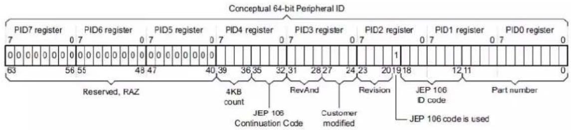
text_image
Conceptual 64-bit Peripheral ID PID7 register 7 0 0 0 0 0 0 0 0 0 0 0 0 0 0 0 0 0 0 0 0 0 0 0 0 63 56 55 48 47 40 39 36 35 32 31 28 27 24 23 20 19 18 12 11 0 PID6 register 7 0 7 PID5 register 7 0 7 PID4 register 7 0 7 PID3 register 7 0 7 PID2 register 7 0 7 PID1 register 7 0 7 PID0 register 0 Reserved, RAZ 4KB count RevAnd Revision JEP 106 Continuation Code Customer modified JEP 106 code is used Part numberTable 13-2. Conceptual 64-Bit Peripheral ID Bit Descriptions
| Field Size Description | Location | ||
| JEP-106 CC code 4 Continuation code: 0x0 PID4 | |||
| JEP-106 ID code 7 Device ID: 0x1F | PID1+PID2 | ||
| 4KB count | 4 | Indicates that the CoreSight component is a ROM: 0x0 | PID4 |
| RevAnd | 4 Not used; read as 0 | PID3 | |
| CUSMOD | 4 Not used; read as 0 | PID3 | |
| PARTNUM | 12 | Contains 0xCD0 to indicate that DSU is present | PID0+PID1 |
| REVISION | 4 | DSU revision (starts at 0x0 and increments by 1 at both major and minor revisions). Identifies DSU identification method variants. If 0x0, this indicates that device identification can be completed by reading the Device Identification register (DID) | PID3 |
For more information, refer to the ARM Debug Interface Version 5 Architecture Specification.
13.10.2 Chip Identification Method
The DSU DID register identifies the device by implementing the following information:
- Processor identification
• Product family identification
• Product series identification
- Device select
13.11 Functional Description
13.11.1 Principle of Operation
The DSU provides memory services such as CRC32 or MBIST that require almost the same interface. Hence, the Address, Length and Data registers (ADDR, LENGTH, DATA) are shared. These shared registers must be configured first; then a command can be issued by writing the Control register. When a command is ongoing, other commands are discarded until the current operation is completed. Hence, the user must wait for the STATUSA.DONE bit to be set prior to issuing another one.
13.11.2 Basic Operation
13.11.2.1 Initialization
The module is enabled by enabling its clocks. For more details, refer to Clocks. The DSU registers can be PAC write-protected.
References:
- PAC - Peripheral Access Controller
13.11.2.2 Operation From a Debug Adapter
Debug adapters should access the DSU registers in the external address range 0x100 - 0x2000. If the device is protected by the NVMCTRL security bit, accessing the first 0x100 bytes causes the system to return an error. Refer to 13.9. Intellectual Property Protection.
References:
- NVMCTRL - Non-Volatile Memory Controller
Security Bit
13.11.2.3 Operation From the CPU
There are no restrictions when accessing DSU registers from the CPU. However, the user should access DSU registers in the internal address range (0x0 - 0x100) to avoid external security restrictions. Refer to 13.9. Intellectual Property Protection.
13.11.3 32-bit Cyclic Redundancy Check CRC32
The DSU unit provides support for calculating a cyclic redundancy check (CRC32) value for a memory area (including Flash and AHB RAM).
When the CRC32 command is issued from:
- The internal range, the CRC32 can be operated at any memory location
- The external range, the CRC32 operation is restricted; DATA, ADDR, and LENGTH values are forced (see below)
Table 13-3. AMOD Bit Descriptions when Operating CRC32
| AMOD[1:0] | Short name | External range restrictions |
| 0 ARRAY CRC32 is restricted to the full Flash array area (EEPROM emulation area not included) DATA forced to 0xFFFFFFF before calculation (no seed) | ||
| 1 EEPROM CRC32 of the whole EEPROM emulation area DATA forced to 0xFFFFFFF before calculation (no seed) | ||
| 2-3 Reserved | ||
The algorithm employed is the industry standard CRC32 algorithm using the generator polynomial 0xEDB88320 (reversed representation).
13.11.3.1 Starting CRC32 Calculation
CRC32 calculation for a memory range is started after writing the start address into the Address register (ADDR) and the size of the memory range into the Length register (LENGTH). Both must be word-aligned.
The initial value used for the CRC32 calculation must be written to the Data register (DATA). This value will usually be 0xFFFFFFF, but can be, for example, the result of a previous CRC32 calculation if generating a common CRC32 of separate memory blocks.
Once completed, the calculated CRC32 value can be read out of the Data register. The read value must be complemented to match standard CRC32 implementations or kept non-inverted if used as starting point for subsequent CRC32 calculations.
If the device is in protected state by the NVMCTRL security bit, it is only possible to calculate the CRC32 of the whole flash array when operated from the external address space. In most cases, this area will be the entire onboard non-volatile memory. The Address, Length and Data registers will be forced to predefined values once the CRC32 operation is started, and values written by the user are ignored. This allows the user to verify the contents of a protected device.
The actual test is started by writing a '1' in the 32-bit Cyclic Redundancy Check bit of the Control register (CTRL.CRC). A running CRC32 operation can be canceled by resetting the module (writing '1' to CTRL.SWRST).
References:
27. NVMCTRL - Non-Volatile Memory Controller
Security Bit
13.11.3.2 Interpreting the Results
The user should monitor the Status A register. When the operation is completed, STATUSA.DONE is set. Then the Bus Error bit of the Status A register (STATUSA.BERR) must be read to ensure that no bus error occurred.
13.11.4 Debug Communication Channels
The Debug Communication Channels (DCCO and DCC1) consist of a pair of registers with associated handshake logic, accessible by both CPU and debugger even if the device is protected by the NVMCTRL security bit. The registers can be used to exchange data between the CPU and the debugger, during run time as well as in debug mode. This enables the user to build a custom debug protocol using only these registers.
The DCC0 and DCC1 registers are accessible when the protected state is active. When the device is protected, however, it is not possible to connect a debugger while the CPU is running (STATUS.CRSTEXT is not writable and the CPU is held under Reset).
Two Debug Communication Channel status bits in the Status B registers (STATUS.DCCDx) indicate whether a new value has been written in DCC0 or DCC1. These bits, DCC0D and DCC1D, are located in the STATUSB registers. They are automatically set on write and cleared on read.
Note: The DCC0 and DCC1 registers are shared with the on-board memory testing logic (MBIST). Accordingly, DCC0 and DCC1 must not be used while performing MBIST operations.
References:
NVMCTRL
27.6.6. Security Bit
13.11.5 Testing of On-Board Memories MBIST
The DSU implements a feature for automatic testing of memory also known as MBIST (memory built-in self test). This is primarily intended for production test of on-board memories. MBIST cannot be operated from the external address range when the device is protected by the NVMCTRL security bit. If an MBIST command is issued when the device is protected, a protection error is reported in the Protection Error bit in the Status A register (STATUS.PERR).
1. Algorithm
The algorithm used for testing is a type of March algorithm called "March LR". This algorithm is able to detect a wide range of memory defects, while still keeping a linear run time. The algorithm is:
a. Write entire memory to '0', in any order.
b. Bit for bit read '0', write '1', in descending order.
c. Bit for bit read '1', write '0', read '0', write '1', in ascending order.
d. Bit for bit read '1', write '0', in ascending order.
e. Bit for bit read '0', write '1', read '1', write '0', in ascending order.
f. Read '0' from entire memory, in ascending order.
The specific implementation used has a run time which depends on the CPU clock frequency and the number of bytes tested in the RAM. The detected faults are:
- Address decoder faults
- Stuck-at faults
- Transition faults
- Coupling faults
- Linked Coupling faults
2. Starting MBIST
To test a memory, you need to write the start address of the memory to the ADDR.ADDR bit field, and the size of the memory into the Length register.
For best test coverage, an entire physical memory block should be tested at once. It is possible to test only a subset of a memory, but the test coverage will then be somewhat lower.
The actual test is started by writing a '1' to CTRL.MBIST. A running MBIST operation can be canceled by writing a '1' to CTRL.SWRST.
3. Interpreting the Results
The tester should monitor the STATUSA register. When the operation is completed, STATUSA.DONE is set. There are two different modes:
- ADDR.AMOD=0: exit-on-error (default)
In this mode, the algorithm terminates either when a fault is detected or on successful completion. In both cases, STATUSA.DONE is set. If an error was detected, STATUSA.FAIL will be set. User then can read the DATA and ADDR registers to locate the fault. - ADDR.AMOD=1: pause-on-error
In this mode, the MBIST algorithm is paused when an error is detected. In such a situation, only STATUS.FAIL is asserted. The state machine waits for user to clear STATUS.FAIL by writing a '1' in STATUS.FAIL to resume. Prior to resuming, user can read the DATA and ADDR registers to locate the fault.
4. Locating Faults
If the test stops with STATUSA.FAIL set, one or more bits failed the test. The test stops at the first detected error. The position of the failing bit can be found by reading the following registers:
- ADDR: Address of the word containing the failing bit
- DATA: contains data to identify which bit failed, and during which phase of the test it failed. The DATA register will in this case contains the following bit groups:
Figure 13-6. DATA bits Description When MBIST Operation Returns an Error

bar_stacked
| Bit | 31 | 30 | 29 | 28 | 27 | 26 | 25 | 24 | | --- | --- | --- | --- | --- | --- | --- | --- | --- | | Bit 1 | 23 | 22 | 21 | 20 | 19 | 18 | 17 | 16 | | Bit 2 | 15 | 14 | 13 | 12 | 11 | 10 | 9 | 8 | | Bit 3 | 7 | 6 | 5 | 4 | 3 | 2 | 1 | 0 | | Bit 4 | 0 | 0 | 0 | 0 | 0 | 0 | 0 | 0 |- bit_index: contains the bit number of the failing bit
- phase: indicates which phase of the test failed and the cause of the error, as listed in the following table.
Table 13-4. MBIST Operation Phases
| Phase Test actions | |
| 0 Write all bits to zero. This phase cannot fail. | |
| 1 Read '0', write '1', increment address | |
| 2 Read '1', write '0' | |
| 3 Read '0', write '1', decrement address | |
| 4 Read '1', write '0', decrement address | |
| 5 Read '0', write '1' | |
| 6 Read '1', write '0', decrement address | |
| 7 Read all zeros. bit_index is not used |
Table 13-5. AMOD Bit Descriptions for MBIST
| AMOD[1:0] Description | |
| 0x0 Exit on Error | |
| 0x1 Pause on Error | |
| 0x2, 0x3 | Reserved |
References:
NVMCTRL
Security Bit
13.11.6 System Services Availability when Accessed Externally
External access: Access performed in the DSU address offset 0x200-0x1FFF range.
Internal access: Access performed in the DSU address offset 0x0-0x100 range.
Table 13-6. Available Features when Operated From The External Address Range and Device is Protected
| Features Availability From The External Address Range and Device is Protected | |
| Chip-Erase command and status Yes | |
| CRC32 Yes, only full array or full EEPROM | |
| CoreSight Compliant Device identification Yes | |
| Debug communication channels Yes | |
| Testing of onboard memories (MBIST) No | |
| STATUS.CRSTEXT clearing No (STATUS.PERR is set when attempting to do so) | |
13.12 Register Summary
| Offset | Name Bit Pos. 76543210 | |||||||||
| 0x00 CTRL 7:0 CE MBIST CRC SWRST | ||||||||||
| 0x01 | STATUS | 7:0 | PERR | FAIL | BERR | CRSTEXT | DONE | |||
| 0x02 | STATUS | 7:0 | HPE | DCCD1 | DCCD0 | DBG PRES | PROT | |||
| 0x03 | Reserved | |||||||||
| 0x04 | ADDR | 7:0 | ADDR[5:0] | AMOD[1:0] | ||||||
| 15:8 | ADDR[13:6] | |||||||||
| 23:16 | ADDR[21:14] | |||||||||
| 31:24 | ADDR[29:22] | |||||||||
| 0x08 LENGTH | 7:0 | LENGTH[5:0] | ||||||||
| 15:8 | LENGTH[13:6] | |||||||||
| 23:16 | LENGTH[21:14] | |||||||||
| 31:24 | LENGTH[29:22] | |||||||||
| 0x0C | DATA | 7:0 | DATA[7:0] | |||||||
| 15:8 | DATA[15:8] | |||||||||
| 23:16 | DATA[23:16] | |||||||||
| 31:24 | DATA[31:24] | |||||||||
| 0x10 DCC0 | 7:0 | DATA[7:0] | ||||||||
| 15:8 | DATA[15:8] | |||||||||
| 23:16 | DATA[23:16] | |||||||||
| 31:24 | DATA[31:24] | |||||||||
| 0x14 DCC1 | 7:0 | DATA[7:0] | ||||||||
| 15:8 | DATA[15:8] | |||||||||
| 23:16 | DATA[23:16] | |||||||||
| 31:24 | DATA[31:24] | |||||||||
| 0X18 | DID | 7:0 | DEVSEL[7:0] | |||||||
| 15:8 | DIE[3:0] | Revision[3:0] | ||||||||
| 23:16 | FAMILY[0] | SERIES[5:0] | ||||||||
| 31:24 | PROCESSOR[3:0] | FAMILY[4:1] | ||||||||
| 0x1C ... 0x0FFF | Reserved | |||||||||
| 0x1000 | ENTRY0 | 7:0 | FMT EPRES | |||||||
| 15:8 | ADDOFF[3:0] | |||||||||
| 23:16 | ADDOFF[11:4] | |||||||||
| 31:24 | ADDOFF[19:12] | |||||||||
| 0x1004 | ENTRY1 | 7:0 | FMT EPRES | |||||||
| 15:8 | ADDOFF[3:0] | |||||||||
| 23:16 | ADDOFF[11:4] | |||||||||
| 31:24 | ADDOFF[19:12] | |||||||||
| 0x1008 END | 7:0 | END[7:0] | ||||||||
| 15:8 | END[15:8] | |||||||||
| 23:16 | END[23:16] | |||||||||
| 31:24 | END[31:24] | |||||||||
| 0x100C ... 0x1FCB | Reserved | |||||||||
| 0x1FCC | MEMTYPE | 7:0 | SMEMP | |||||||
| 15:8 | ||||||||||
| 23:16 | ||||||||||
| 31:24 | ||||||||||
| 0x1FD0 | PID4 | 7:0 | FKBC[3:0] | JEPCC[3:0] | ||||||
| 15:8 | ||||||||||
| 23:16 | ||||||||||
| 31:24 | ||||||||||
| 0x1FD4 ... 0x1FDF | Reserved | |||||||||
| Offset | Name Bit Pos. 7 6 5 4 3 2 1 0 | ||||||||
| 0x1FE0 PID0 | 7:0 PARTNBL[7:0] | ||||||||
| 15:8 | |||||||||
| 23:16 | |||||||||
| 31:24 | |||||||||
| 0x1FE4 PID1 | 7:0 JEPIDCL[3:0] PARTNBH[3:0] | ||||||||
| 15:8 | |||||||||
| 23:16 | |||||||||
| 31:24 | |||||||||
| 0x1FE8 PID2 | 7:0 REVISION[3:0] JEPU JEPIDCH[2:0] | ||||||||
| 15:8 | |||||||||
| 23:16 | |||||||||
| 31:24 | |||||||||
| 0x1FEC PID3 | 7:0 REVAND[3:0] CUSMOD[3:0] | ||||||||
| 15:8 | |||||||||
| 23:16 | |||||||||
| 31:24 | |||||||||
| 0x1FF0 CID0 | 7:0 PREAMBLEB0[7:0] | ||||||||
| 15:8 | |||||||||
| 23:16 | |||||||||
| 31:24 | |||||||||
| 0x1FF4 CID1 | 7:0 | CCLASS[3:0] | PREAMBLE[3:0] | ||||||
| 15:8 | |||||||||
| 23:16 | |||||||||
| 31:24 | |||||||||
| 0x1FF8 CID2 | 7:0 PREAMBLEB2[7:0] | ||||||||
| 15:8 | |||||||||
| 23:16 | |||||||||
| 31:24 | |||||||||
| 0x1FFC CID3 | 7:0 PREAMBLEB3[7:0] | ||||||||
| 15:8 | |||||||||
| 23:16 | |||||||||
| 31:24 | |||||||||
13.13 Register Description
Registers can be 8, 16, or 32 bits wide. Atomic 8-, 16- and 32-bit accesses are supported. In addition, the 8-bit quarters and 16-bit halves of a 32-bit register, and the 8-bit halves of a 16-bit register can be accessed directly.
Some registers are optionally write-protected by the Peripheral Access Controller (PAC). Optional PAC write-protection is denoted by the "PAC Write-Protection" property in each individual register description. For details, refer to 13.5.6. Register Access Protection.
13.13.1 Control
Name: CTRL
Offset: 0x0000
Reset: 0x00
Property: PAC Write Protection
Bit 76543210
| CE MBIST CRC SW/RST | ||||||
| Access Reset | W | W | W | W | ||
| 0 0 0 | 0 |
Bit 4 - CE Chip Erase
Writing a '0' to this bit has no effect.
Writing a '1' to this bit starts the chip erase operation.
Bit 3 - MBIST Memory Built-In Self-Test
Writing a '0' to this bit has no effect.
Writing a '1' to this bit starts the memory BIST algorithm.
Bit 2 - CRC 32-Bit Cyclic Redundancy Check
Writing a '0' to this bit has no effect.
Writing a '1' to this bit starts the cyclic redundancy check algorithm.
Bit 0 - SWRST Software Reset
Writing a '0' to this bit has no effect.
Writing a '1' to this bit resets the module.
13.13.2 Status A
Name: STATUSA
Offset: 0x0001
Reset: 0x00
Property: PAC Write-Protection
Bit 76543210
| PERR FAIL BERR CRSTEXT DONE | ||||||
| Access Reset | R/W0 0 0 0 0 | R/W | R/W | R/W | R/W |
Bit 4 - PERR Protection Error
Writing a '0' to this bit has no effect.
Writing a '1' to this bit clears the Protection Error bit.
This bit is set when a command that is not allowed in protected state is issued.
Bit 3 - FAIL Failure
Writing a '0' to this bit has no effect.
Writing a '1' to this bit clears the Failure bit.
This bit is set when a DSU operation failure is detected.
Bit 2 - BERR Bus Error
Writing a '0' to this bit has no effect.
Writing a '1' to this bit clears the Bus Error bit.
This bit is set when a bus error is detected.
Bit 1 - CRSTEXT CPU Reset Phase Extension
Writing a '0' to this bit has no effect.
Writing a '1' to this bit clears the CPU Reset Phase Extension bit.
This bit is set when a debug adapter Cold-Plugging is detected, which extends the CPU reset phase.
Bit 0 - DONE Done
Writing a '0' to this bit has no effect.
Writing a '1' to this bit clears the Done bit.
This bit is set when a DSU operation is completed.
13.13.3 Status B
Name: STATUSB
Offset: 0x0002
Reset: 0x10000
Property: PAC Write Protection
Bit 76543210
| HPE | DCCD1 | DCCD0 | DBGPRES | PROT | ||||||
| Access Reset | R | R | R | |||||||
| 1 | 0 | 0 | 0 |
Bit 4 - HPE Hot-Plugging Enable
Writing a '0' to this bit has no effect.
Writing a '1' to this bit has no effect.
This bit is set when Hot-Plugging is enabled.
This bit is cleared when Hot-Plugging is disabled. This is the case when the SWCLK function is changed. Only a power Reset or a external Reset can set it again.
Bits 2, 3 - DCCDx Debug Communication Channel x Dirty [x=1..0]
Writing a '0' to this bit has no effect.
Writing a '1' to this bit has no effect.
This bit is set when DCCx is written.
This bit is cleared when DCCx is read.
Bit 1 - DBGPRES Debugger Present
Writing a '0' to this bit has no effect.
Writing a '1' to this bit has no effect.
This bit is set when a debugger probe is detected.
This bit is never cleared.
Bit 0 - PROT Protected
Writing a '0' to this bit has no effect.
Writing a '1' to this bit has no effect.
This bit is set at power-up when the device is protected.
This bit is never cleared.
13.13.4 Address
Name: ADDR
Offset: 0x0004
Reset: 0x00000000
Property: PAC Write-Protection
Bit 31 30 29 28 27 26 25 24
| ADDR[29:22] |
Access R/W R/W R/W R/W R/W R/W R/W R/W
Reset 00000000
Bit 23 22 21 20 19 18 17 16
| ADDR[21:14] |
Access R/W R/W R/W R/W R/W R/W R/W R/W
Reset 00000000
Bit 15 14 13 12 11 10 9 8
| ADDR[13:6] |
Access R/W R/W R/W R/W R/W R/W R/W R/W
Reset 00000000
Bit 76543210
| ADDR[5:0] AMOD[1:0] |
Access R/W R/W R/W R/W R/W R/W R/W R/W
Reset 00000000
Bits 31:2 - ADDR[29:0] Address
Initial word start address needed for memory operations.
Bits 1:0 - AMOD[1:0] Access Mode
The functionality of these bits is dependent on the operation mode.
Bit description when operating CRC32: refer to 13.11.3. 32-bit Cyclic Redundancy Check CRC32
Bit description when testing onboard memories (MBIST): refer to 13.11.5. Testing of On-Board Memories MBIST
13.13.5 Length
Name: LENGTH
Offset: 0x0008
Reset: 0x00000000
Property: PAC Write-Protection
Bit 31 30 29 28 27 26 25 24
| LENGTH[29:22] |
Access R/W R/W R/W R/W R/W R/W R/W R/W
Reset 00000000
Bit 23 22 21 20 19 18 17 16
| LENGTH[21:14] |
Access R/W R/W R/W R/W R/W R/W R/W R/W
Reset 00000000
Bit 15 14 13 12 11 10 9 8
| LENGTH[13:6] |
Access R/W R/W R/W R/W R/W R/W R/W R/W
Reset 00000000
Bit 76543210
| LENGTH[5:0] |
Access R/W R/W R/W R/W R/W R/W
Reset 000000
Bits 31:2 - LENGTH[29:0] Length
Length in words needed for memory operations.
13.13.6 Data
Name: DATA
Offset: 0x000C
Reset: 0x00000000
Property: PAC Write-Protection
Bit 31 30 29 28 27 26 25 24
DATA[31:24]
Access R/W R/W R/W R/W R/W R/W R/W R/W
Reset 00000000
Bit 23 22 21 20 19 18 17 16
DATA[23:16]
Access R/W R/W R/W R/W R/W R/W R/W R/W
Reset 00000000
Bit 15 14 13 12 11 10 9 8
DATA[15:8]
Access R/W R/W R/W R/W R/W R/W R/W R/W
Reset 00000000
Bit 76543210
DATA[7:0]
Access R/W R/W R/W R/W R/W R/W R/W R/W
Reset 00000000
Bits 31:0 - DATA[31:0] Data
Memory operation initial value or result value.
13.13.7 Debug Communication Channel 0
Name: DCC0
Offset: 0x0010
Reset: 0x00000000
Property: -
Bit 31 30 29 28 27 26 25 24
DATA[31:24]
Access R/W R/W R/W R/W R/W R/W R/W R/W
Reset 00000000
Bit 23 22 21 20 19 18 17 16
DATA[23:16]
Access R/W R/W R/W R/W R/W R/W R/W R/W
Reset 00000000
Bit 15 14 13 12 11 10 9 8
DATA[15:8]
Access R/W R/W R/W R/W R/W R/W R/W R/W
Reset 00000000
Bit 76543210
DATA[7:0]
Access R/W R/W R/W R/W R/W R/W R/W R/W
Reset 00000000
Bits 31:0 - DATA[31:0] Data
Data register.
13.13.8 Debug Communication Channel 1
Name: DCC1
Offset: 0x0014
Reset: 0x00000000
Property: -
Bit 31 30 29 28 27 26 25 24
DATA[31:24]
Access R/W R/W R/W R/W R/W R/W R/W R/W
Reset 00000000
Bit 23 22 21 20 19 18 17 16
DATA[23:16]
Access R/W R/W R/W R/W R/W R/W R/W R/W
Reset 00000000
Bit 15 14 13 12 11 10 9 8
DATA[15:8]
Access R/W R/W R/W R/W R/W R/W R/W R/W
Reset 00000000
Bit 76543210
DATA[7:0]
Access R/W R/W R/W R/W R/W R/W R/W R/W
Reset 00000000
Bits 31:0 - DATA[31:0] Data
Data register.
13.13.9 Device Identification
Name: DID
Offset: 0x0018
Reset: See References below
Property: PAC Write-Protection
The information in this register is related to the Ordering Information.
Bit 31 30 29 28 27 26 25 24
| PROCESSOR[3:0] FAMILY[4:1] | ||
| Access | RRRRRRRR | |
| Reset | pp pffff |
Bit 23 22 21 20 19 18 17 16
| FAMILY[0] | SERIES[5:0] | |||||||
| Access | R | RRRRRR | ||||||
| Reset | f | S | S | S | S | S | S | |
Bit 15 14 13 12 11 10 9 8
| DIE[3:0] | Revision[3:0] | |||||||
| Access Reset | R R R R R R R R d | |||||||
| Bit | 7 | 6 | 5 | 4 | 3 | 2 | 1 | 0 |
| DEVSEL[7:0] | ||||||||
| Access Reset | R R R R R R R R x | x | x | x | x | x | x | x |
Bits 31:28 - PROCESSOR[3:0] Processor
The value of this field defines the processor used on the device.
Bits 27:23 - FAMILY[4:0] Product Family
The value of this field corresponds to the Product Family part of the ordering code.
Bits 21:16 - SERIES[5:0] Product Series
The value of this field corresponds to the Product Series part of the ordering code.
Bits 15:12 - DIE[3:0] Die Number
Identifies the die family.
Bits 11:8 - REVISION[3:0] Revision Number
Identifies the die revision number. 0x0=rev.A, 0x1=rev.B etc.
Note: The device variant (last letter of the ordering number) is independent of the die revision (DSU.DID.REVISION): The device variant denotes functional differences, whereas the die revision marks evolution of the die.
Bits 7:0 - DEVSEL[7:0] Device Selection
This bit field identifies a device within a product family and product series. Refer to the Ordering Information for device configurations and corresponding values for Flash memory density, pin count and device variant. For further information, refer to Device Identification.
13.13.10 CoreSight ROM Table Entry 0
Name: ENTRY0
Offset: 0x1000
Reset: 0xXXXXX00X
Property: PAC Write-Protection
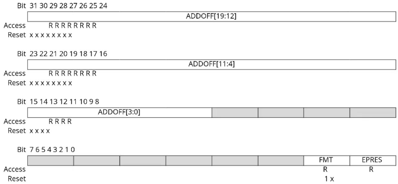
text_image
Bit 31 30 29 28 27 26 25 24 ADDOFF[19:12] Access R R R R R R R R Reset x x x x x x x x x Bit 23 22 21 20 19 18 17 16 ADDOFF[11:4] Access R R R R R R R R R Reset x x x x x x x x x Bit 15 14 13 12 11 10 9 8 ADDOFF[3:0] Access R R R R Reset x x x x Bit 7 6 5 4 3 2 1 0 FMT EPRES Access R Reset 1 xBits 31:12 - ADDOFF[19:0] Address Offset
The base address of the component, relative to the base address of this ROM table.
Bit 1 - FMT Format
Always reads as '1', indicating a 32-bit ROM table.
Bit 0 - EPRES Entry Present
This bit indicates whether an entry is present at this location in the ROM table.
This bit is set at power-up if the device is not protected indicating that the entry is not present.
This bit is cleared at power-up if the device is not protected indicating that the entry is present.
13.13.11 CoreSight ROM Table Entry 1
Name: ENTRY1
Offset: 0x1004
Reset: 0xXXXXX00X
Property: PAC Write-Protection

text_image
Bit 31 30 29 28 27 26 25 24 ADDOFF[19:12] Access R R R R R R R R Reset x x x x x x x x x Bit 23 22 21 20 19 18 17 16 ADDOFF[11:4] Access R R R R R R R R R Reset x x x x x x x x x Bit 15 14 13 12 11 10 9 8 ADDOFF[3:0] Access R R R R Reset x x x x Bit 7 6 5 4 3 2 1 0 FMT EPRES Access R R Reset 1 xBits 31:12 - ADDOFF[19:0] Address Offset
The base address of the component, relative to the base address of this ROM table.
Bit 1 - FMT Format
Always read as '1', indicating a 32-bit ROM table.
Bit 0 - EPRES Entry Present
This bit indicates whether an entry is present at this location in the ROM table.
This bit is set at power-up if the device is not protected indicating that the entry is not present.
This bit is cleared at power-up if the device is not protected indicating that the entry is present.
13.13.12 CoreSight ROM Table End
Name: END
Offset: 0x1008
Reset: 0x00000000
Property: -
| Bit 31 30 29 28 27 26 25 24 | |
| END[31:24] | |
| Access R R R R R R R R Reset 0 0 0 0 0 0 0 0 | |
| Bit 23 22 21 20 19 18 17 16 | |
| END[23:16] | |
| Access R R R R R R R R Reset 0 0 0 0 0 0 0 0 | |
| Bit 15 14 13 12 11 10 9 8 | |
| END[15:8] | |
| Access R R R R R R R R Reset 0 0 0 0 0 0 0 0 | |
| Bit 7 6 5 4 3 2 1 0 | |
| END[7:0] | |
| Access R R R R R R R R Reset 0 0 0 0 0 0 0 0 | |
Bits 31:0 - END[31:0] End Marker
Indicates the end of the CoreSight ROM table entries.
13.13.13 CoreSight ROM Table Memory Type
Name: MEMTYPE
Offset: 0x1FCC
Reset: 0x0000000X
Property: -
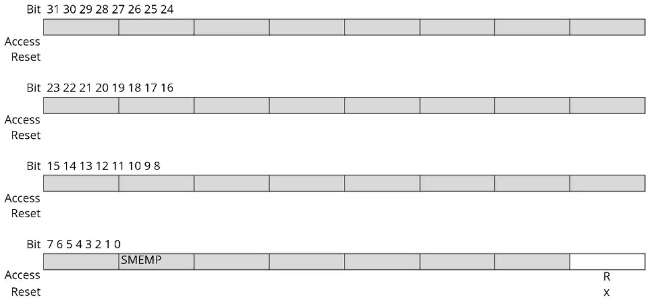
text_image
Bit 31 30 29 28 27 26 25 24 Access Reset Bit 23 22 21 20 19 18 17 16 Access Reset Bit 15 14 13 12 11 10 9 8 Access Reset Bit 7 6 5 4 3 2 1 0 Access Reset SMEMP R XBit 0 - SMEMP System Memory Present
This bit indicates whether system memory is present on the bus that connects to the ROM table. This bit is set at power-up if the device is not protected, indicating that the system memory is accessible from a debug adapter.
This bit is cleared at power-up if the device is protected, indicating that the system memory is not accessible from a debug adapter.
13.13.14 Peripheral Identification 4
Name: PID4
Offset: 0x1FD0
Reset: 0x00000000
Property: -
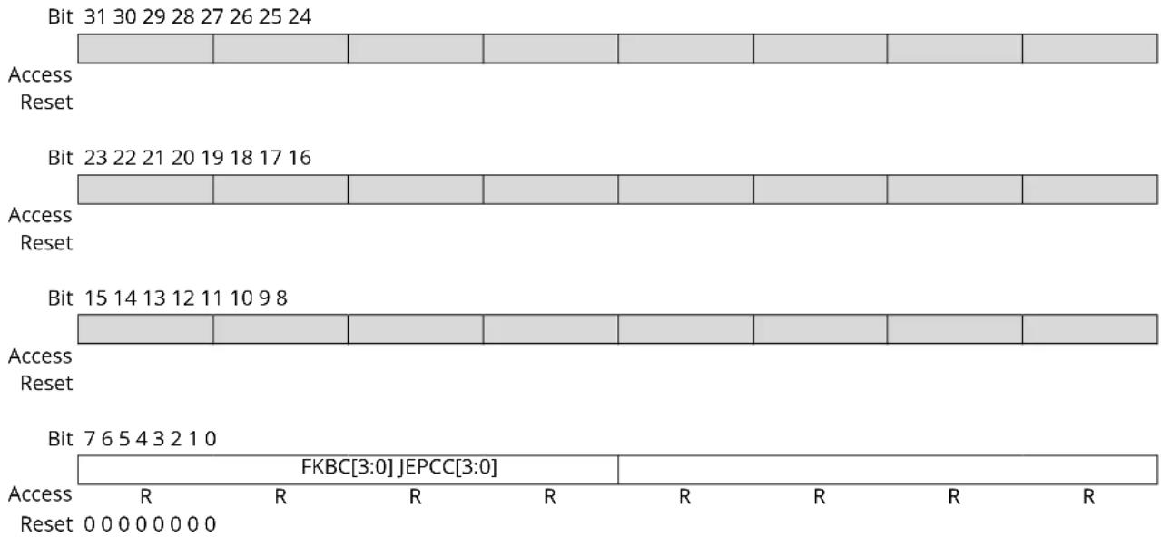
text_image
Bit 31 30 29 28 27 26 25 24 Access Reset Bit 23 22 21 20 19 18 17 16 Access Reset Bit 15 14 13 12 11 10 9 8 Access Reset Bit 7 6 5 4 3 2 1 0 FKBC[3:0] JEPCC[3:0] Access R R R R R R R Reset 0 0 0 0 0 0 0Bits 7:4 - FKBC[3:0] 4KB Count
These bits will always return zero when read, indicating that this debug component occupies one 4KB block.
Bits 3:0 - JEPCC[3:0] JEP-106 Continuation Code
These bits will always return zero when read.
13.13.15 Peripheral Identification 0
Name: PID0
Offset: 0x1FE0
Reset: 0x000000D0
Property: -
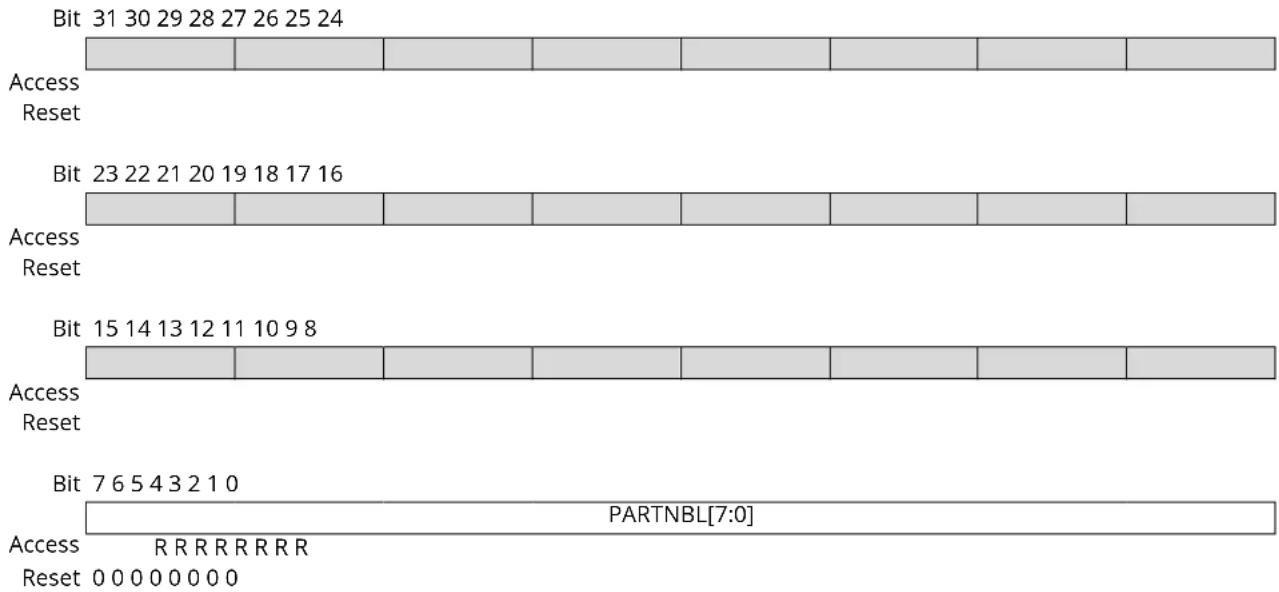
text_image
Bit 31 30 29 28 27 26 25 24 Access Reset Bit 23 22 21 20 19 18 17 16 Access Reset Bit 15 14 13 12 11 10 9 8 Access Reset Bit 7 6 5 4 3 2 1 0 PARTNBL[7:0] Access R R R R R R R R Reset 0 0 0 0 0 0 0Bits 7:0 - PARTNBL[7:0] Part Number Low
These bits will always return 0xD0 when read, indicating that this device implements a DSU module instance.
13.13.16 Peripheral Identification 1
Name: PID1
Offset: 0x1FE4
Reset: 0x000000FC
Property: -
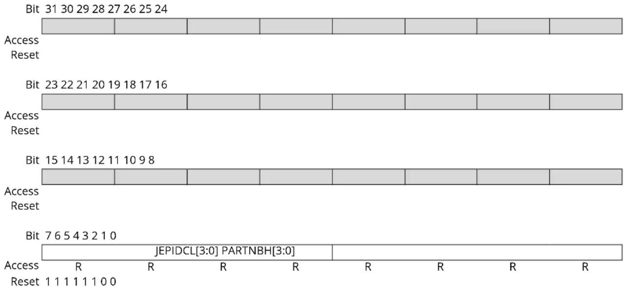
text_image
Bit 31 30 29 28 27 26 25 24 Access Reset Bit 23 22 21 20 19 18 17 16 Access Reset Bit 15 14 13 12 11 10 9 8 Access Reset Bit 7 6 5 4 3 2 1 0 JEPIDCL[3:0] PARTNBH[3:0] Access R R R R R R Reset 1 1 1 1 1 1 0 0Bits 7:4 - JEPIDCL[3:0] Low part of the JEP-106 Identity Code
These bits will always return 0xF when read (JEP-106 identity code is 0x1F).
Bits 3:0 - PARTNBH[3:0] Part Number High
These bits will always return 0xC when read, indicating that this device implements a DSU module instance.
13.13.17 Peripheral Identification 2
Name: PID2
Offset: 0x1FE8
Reset: 0x00000009
Property: -

text_image
Bit 31 30 29 28 27 26 25 24 Access Reset Bit 23 22 21 20 19 18 17 16 Access Reset Bit 15 14 13 12 11 10 9 8 Access Reset Bit 7 6 5 4 3 2 1 0 REVISION[3:0] JEPU JEPIDCH[2:0] Access R R R R R R R Reset 0 0 0 0 1 0 0 1Bits 7:4 - REVISION[3:0] Revision Number
Revision of the peripheral. Starts at 0x0 and increments by one at both major and minor revisions.
Bit 3 - JEPU JEP-106 Identity Code is used
This bit will always return one when read, indicating that JEP-106 code is used.
Bits 2:0 - JEPIDCH[2:0] JEP-106 Identity Code High
These bits will always return 0x1 when read (JEP-106 identity code is 0x1F).
13.13.18 Peripheral Identification 3
Name: PID3
Offset: 0x1FEC
Reset: 0x00000000
Property: -
text_image
Bit 31 30 29 28 27 26 25 24 Access Reset Bit 23 22 21 20 19 18 17 16 Access Reset Bit 15 14 13 12 11 10 9 8 Access Reset Bit 7 6 5 4 3 2 1 0 REVAND[3:0] CUSMOD[3:0] Access R R R R R R R Reset 0 0 0 0 0 0 0Bits 7:4 - REVAND[3:0] Revision Number
These bits will always return 0x0 when read.
These bits will always return 0x0 when read.
Bits 3:0 - CUSMOD[3:0] ARM CUSMOD
13.13.19 Component Identification 0
Name: CID0
Offset: 0x1FF0
Reset: 0x0000000D
Property: -

text_image
Bit 31 30 29 28 27 26 25 24 Access Reset Bit 23 22 21 20 19 18 17 16 Access Reset Bit 15 14 13 12 11 10 9 8 Access Reset Bit 7 6 5 4 3 2 1 0 PREAMBLEBO[7:0] Access R R R R R R R R Reset 0 0 0 0 1 1 0 1Bits 7:0 - PREAMBLEB0[7:0] Preamble Byte 0
These bits will always return 0x0000000D when read.
13.13.20 Component Identification 1
Name: CID1
Offset: 0x1FF4
Reset: 0x00000010
Property: -

text_image
Bit 31 30 29 28 27 26 25 24 Access Reset Bit 23 22 21 20 19 18 17 16 Access Reset Bit 15 14 13 12 11 10 9 8 Access Reset Bit 7 6 5 4 3 2 1 0 CCLASS[3:0] PREAMBLE[3:0] Access R R R R R R R Reset 0 0 0 1 0 0 0 0Bits 7:4 - CCLASS[3:0] Component Class
These bits will always return 0x1 when read indicating that this ARM CoreSight component is ROM table (refer to the ARM Debug Interface v5 Architecture Specification at http://www.arm.com).
Bits 3:0 - PREAMBLE[3:0] Preamble
These bits will always return 0x00 when read.
13.13.21 Component Identification 2
Name: CID2
Offset: 0x1FF8
Reset: 0x00000005
Property: -

text_image
Bit 31 30 29 28 27 26 25 24 Access Reset Bit 23 22 21 20 19 18 17 16 Access Reset Bit 15 14 13 12 11 10 9 8 Access Reset Bit 7 6 5 4 3 2 1 0 PREAMBLEB2[7:0] Access R R R R R R R R Reset 0 0 0 0 0 1 0 1Bits 7:0 - PREAMBLEB2[7:0] Preamble Byte 2
These bits will always return 0x00000005 when read.
13.13.22 Component Identification 3
Name: CID3
Offset: 0x1FFC
Reset: 0x000000B1
Property: -

text_image
Bit 31 30 29 28 27 26 25 24 Access Reset Bit 23 22 21 20 19 18 17 16 Access Reset Bit 15 14 13 12 11 10 9 8 Access Reset Bit 7 6 5 4 3 2 1 0 PREAMBLEB3[7:0] Access R R R R R R R R Reset 1 0 1 1 0 0 0 1Bits 7:0 - PREAMBLEB3[7:0] Preamble Byte 3
These bits will always return 0x000000B1 when read.
14. Clock System
This chapter summarizes the clock distribution and terminology in the SAM L22 device. It does not explain every detail of its configuration. For in-depth documentation, see the respective peripherals descriptions and the Generic Clock documentation.
14.1 Clock Distribution
Figure 14-1. Clock Distribution

flowchart
graph TD
    subgraph OSC_CTRL
        XOSC["XOSC"] --> GCLK_GCLK["&GCLK_DFL48M_REF"]
        OSC16M["OSC16M"] --> GCLK_GCLK
        DFLL48M["DFLL48M"] --> GCLK_GCLK
        FDPLL96M["FDPLL96M"] --> GCLK_GCLK
    end

    subgraph OSC32CTRL
        XOSC32K["XOSC32K"] --> GCLK_GCLK
        OSCULP32K["OSCULP32K"] --> GCLK_GCLK
    end

    GCLK_GCLK --> GCLK_MAIN["GCLK_MAIN"]
    GCLK_GCLK --> MCLK["MCLK"]
    GCLK_GCLK --> Syncronos_Clock["Syncronous Clock Controller"]
    GCLK_GCLK --> AHB/APB_System_Clocks["AHB/APB System Clocks"]

    subgraph CLK_ULP32K
        XOSC32K --> GCLK_GCLK
        OSCULP32K --> GCLK_GCLK
    end

    GCLK_GCLK --> GCLK_FDPLL_32K["GCLK_FDPLL_32K"]
    GCLK_GCLK --> GCLK_FDPLL
    GCLK_GCLK --> GCLK_FDPLL
    GCLK_GCLK --> GCLK_FDPLL_0["Peripheral 0 (DFLL48M Reference)"]
    GCLK_GCLK --> GCLK_FDPLL_1["Peripheral 1 (FDPLL96M Reference)"]
    GCLK_GCLK --> GCLK_FDPLL_2["Peripheral 2 (FDPLL96M Reference)"]
    GCLK_GCLK --> GCLK_FDPLL_3["Peripheral 3"]
    GCLK_GCLK --> GCLK_FDPLL_4["Peripheral 4"]
    GCLK_GCLK --> GCLK_FDPLL_5["Peripheral 5"]
    GCLK_GCLK --> GCLK_FDPLL_6["Peripheral 6"]
    GCLK_GCLK --> GCLK_FDPLL_7["Peripheral 7"]
    GCLK_GCLK --> GCLK_FDPLL_8["Peripheral 8"]
    GCLK_GCLK --> GCLK_FDPLL_9["Peripheral 9"]
    GCLK_GCLK --> GCLK_FDPLL_10["Peripheral 10"]
    GCLK_GCLK --> GCLK_FDPLL_11["Peripheral 11"]
    GCLK_GCLK --> GCLK_FDPLL_12["Peripheral 12"]
    GCLK_GCLK --> GCLK_FDPLL_13["Peripheral 13"]
    GCLK_GCLK --> GCLK_FDPLL_14["Peripheral 14"]
    GCLK_GCLK --> GCLK_FDPLL_15["Peripheral 15"]
    GCLK_GCLK --> GCLK_FDPLL_16["Peripheral 16"]
    GCLK_GCLK --> GCLK_FDPLL_17["Peripheral 17"]
    GCLK_GCLK --> GCLK_FDPLL_18["Peripheral 18"]
    GCLK_GCLK --> GCLK_FDPLL_19["Peripheral 19"]
    GCLK_GCLK --> GCLK_FDPLL_20["Peripheral 20"]
    GCLK_GCLK --> GCLK_FDPLL_21["Peripheral 21"]
    GCLK_GCLK --> GCLK_FDPLL_22["Peripheral 22"]
    GCLK_GCLK --> GCLK_FDPLL_23["Peripheral 23"]
    GCLK_GCLK --> GCLK_FDPLL_24["Peripheral 24"]
    GCLK_GCLK --> GCLK_FDPLL_25["Peripheral 25"]
    GCLK_GCLK --> GCLK_FDPLL_26["Peripheral 26"]
    GCLK_GCLK --> GCLK_FDPLL_27["Peripheral 27"]
    GCLK_GCLK --> GCLK_FDPLL_28["Peripheral 28"]
    GCLK_GCLK --> GCLK_FDPLL_29["Peripheral 29"]
    GCLK_GCLK --> GCLK_FDPLL_30["Peripheral 30"]
    GCLK_GCLK --> GCLK_FDPLL_31["Peripheral 31"]
    GCLK_GCLK --> GCLK_FDPLL_32["Peripheral 32"]
    GCLK_GCLK --> GCLK_FDPLL_33["Peripheral 33"]
    GCLK_GCLK --> GCLK_FDPLL_34["Peripheral 34"]
    GCLK_GCLK --> GCLK_FDPLL_35["Peripheral 35"]
    GCLK_GCLK --> GCLK_FDPLL_36["Peripheral 36"]
    GCLK_GCLK --> GCLK_FDPLL_37["Peripheral 37"]
    GCLK_GCLK --> GCLK_FDPLL_38["Peripheral 38"]
    GCLK_GCLK --> GCLK_FDPLL_39["Peripheral 39"]
    GCLK_GCLK --> GCLK_FDPLL_40["Peripheral 40"]
    GCLK_FDPLL_40 --> GCK_FDPLL_32
    style OSC_CTRL fill:#f9f,stroke:#333
    style OSC_POLP32K fill:#ccf,stroke:#333
    style OSC_CSTR fill:#cfc,stroke:#333
    style OSC_FDLLL96M fill:#fcc,stroke:#333
    style OSC_CSTR fill:#ffc,stroke:#333
The SAM L22 clock system consists of:
- Clock sources, that is oscillators controlled by OSCCTRL and OSC32KCTRL
- A clock source provides a time base that is used by other components, such as Generic Clock Generators. Example clock sources include the internal 16 MHz oscillator (OSC16M), external crystal oscillator (XOSC0) and the Digital Frequency Locked Loop (DFLL48M).
- Generic Clock Controller (GCLK), which generates, controls, and distributes the asynchronous clocks consisting of the following:
- Generic Clock Generators: These are programmable prescalers that can use any of the system clock sources as a time base. The Generic Clock Generator 0 generates the clock signal GCLK_MAIN, which is used by the Power Manager and the Main Clock (MCLK) module, which in turn generates synchronous clocks.
- Generic Clocks: These are clock signals generated by Generic Clock Generators and output by the Peripheral Channels, and serve as clocks for the peripherals of the system. Multiple instances of a peripheral will typically have a separate Generic Clock for each instance. Generic Clock 0 serves as the clock source for the DFLL48M clock input (when multiplying another clock source).
• Main Clock Controller (MCLK)
- The MCLK generates and controls the synchronous clocks on the system. This includes the CPU, bus clocks (APB, AHB), and the synchronous (to the CPU) user interfaces of the peripherals. It contains clock masks that can turn on/off the user interface of a peripheral and prescalers for the CPU and bus clocks.
The figure below illustrates where SERCOM0 is clocked by the DFLL48M in open loop mode. The DFLL48M is enabled, the Generic Clock Generator 1 uses the DFLL48M as its clock source and feeds into Peripheral Channel 16. The Generic Clock 16, also called GCLK_SERCOM0_CORE, is connected to SERCOM0. The SERCOM0 interface, clocked by CLK_SERCOM0_APB, has been unmasked in the APBC Mask register in the MCLK.
Figure 14-2. Example of SERCOM Clock

flowchart
graph TD
    A["OSCCTRL\nDFLL48M"] --> B["GCLK"]
    B --> C["Generic Clock Generator 1"]
    B --> D["Peripheral Channel 16"]
    D --> E["GCLK_SERCOM0_CORE"]
    F["MCLK\nSynchronous Clock Controller"] --> G["SERCOM 0"]
    G --> H["CLK_SERCOM0_APB"]
To customize the clock distribution, refer to these registers and bit fields:
- The source oscillator for a Generic Clock Generator n is selected by writing to the Source bit field in the Generator Control n register (GCLK.GENCTRLn.SRC).
- A Peripheral Channel m can be configured to use a specific Generic Clock Generator by writing to the Generic Clock Generator bit field in the respective Peripheral Channel m register (GCLK.PCHCTRLm.GEN)
- The Peripheral Channel number, m , is fixed for a given peripheral. See the PCHCTRLm Mapping table in the description of GCLK.PCHCTRLm.
- The AHB clocks are enabled and disabled by writing to the respective bit in the AHB Mask register (MCLK.AHBMASK).
- The APB clocks are enabled and disabled by writing to the respective bit in the APB x Mask registers (MCLK.APBxMASK).
14.2 Synchronous and Asynchronous Clocks
As the CPU and the peripherals can be in different clock domains, that is they are clocked from different clock sources and with different clock speeds, some peripheral accesses by the CPU need to be synchronized. In this case the peripheral includes a Synchronization Busy (SYNCBUSY) register that can be used to check if a sync operation is in progress.
For a general description, refer to 14.3. Register Synchronization. Some peripherals have specific properties described in their individual sub-chapter "Synchronization".
In the data sheet, references to Synchronous Clocks are referring to the CPU and bus clocks (MCLK), while asynchronous clocks are generated by the Generic Clock Controller (GCLK).
14.3 Register Synchronization
14.3.1 Overview
All peripherals are composed of one digital bus interface connected to the APB or AHB bus and running from a corresponding clock in the Main Clock domain, and one peripheral core running from the peripheral Generic Clock (GCLK).
Communication between these clock domains must be synchronized. This mechanism is implemented in hardware, so the synchronization process takes place even if the peripheral generic clock is running from the same clock source and on the same frequency as the bus interface.
All registers in the bus interface are accessible without synchronization.
All registers in the peripheral core are synchronized when written. Some registers in the peripheral core are synchronized when read.
Each individual register description will have the properties "Read-Synchronized" and/or "Write-Synchronized" if a register is synchronized.
As shown in the figure below, each register that requires synchronization has its individual synchronizer and its individual synchronization status bit in the Synchronization Busy register (SYNCBUSY).
Note: For registers requiring both read- and write-synchronization, the corresponding bit in SYNCBUSY is shared.
Figure 14-3. Register Synchronization Overview

flowchart
graph TD
    A["Non Sync'd reg"] --> B["Sync"]
    C["SYNCBUSY"] --> B
    B --> D["Write-Sync'd reg"]
    B --> E["Read-Sync'd reg"]
    B --> F["R/W register"]
    B --> G["Write-Sync'd reg"]
    B --> H["Non Sync'd reg"]
    I["INTFLAG"] --> J["Sync"]
    J --> K["Write-only register"]
    J --> L["Read-only register"]
    J --> M["R/W register"]
    J --> N["Write-Sync'd reg"]
    J --> O["Non Sync'd reg"]
    style A fill:#90EE90,stroke:#333
    style C fill:#90EE90,stroke:#333
    style I fill:#90EE90,stroke:#333
    style B fill:#FFA500,stroke:#333
    style D fill:#FFA500,stroke:#333
    style E fill:#FFA500,stroke:#333
    style F fill:#FFA500,stroke:#333
    style G fill:#FFA500,stroke:#333
    style H fill:#FFA500,stroke:#333
    style J fill:#FFA500,stroke:#333
    style K fill:#FFA500,stroke:#333
    style L fill:#FFA500,stroke:#333
    style M fill:#FFA500,stroke:#333
    style N fill:#FFA500,stroke:#333
    style O fill:#FFA500,stroke:#333
14.3.2 General Write Synchronization
Write-Synchronization is triggered by writing to a register in the peripheral clock domain. The respective bit in the Synchronization Busy register (SYNCBUSY) will be set when the write-synchronization starts and cleared when the write-synchronization is complete. Refer to 14.3.7. Synchronization Delay.
When write-synchronization is ongoing for a register, any subsequent write attempts to this register will be discarded, and an error will be reported through the Peripheral Access Controller (PAC).
Example:
REGA, REGB are 8-bit core registers. REGC is a 16-bit core register.
| Offset Register | |
| 0x00 REGA | |
| 0x01 REGB | |
| 0x02 REGC | |
| 0x03 |
Synchronization is per register, so multiple registers can be synchronized in parallel. Consequently, after REGA (8-bit access) was written, REGB (8-bit access) can be written immediately without error.
REGC (16-bit access) can be written without affecting REGA or REGB. If REGC is written to in two consecutive 8-bit accesses without waiting for synchronization, the second write attempt will be discarded and an error is generated through the PAC.
A 32-bit access to offset 0x00 will write all three registers. Note that REGA, REGB and REGC can be updated at different times because of independent write synchronization.
14.3.3 General Read Synchronization
Read-synchronized registers are synchronized each time the register value is updated but the corresponding SYNCBUSY bits are not set. Reading a read-synchronized register does not start a new synchronization, it returns the last synchronized value.
Note: The corresponding bits in SYNCBUSY will automatically be set when the device wakes up from sleep because read-synchronized registers need to be synchronized. Therefore reading a read-synchronized register before its corresponding SYNCBUSY bit is cleared will return the last synchronized value before sleep mode.
Moreover, if a register is also write-synchronized, any write access while the SYNCBUSY bit is set will be discarded and generate an error.
14.3.4 Completion of Synchronization
In order to check if synchronization is complete, the user can either poll the relevant bits in SYNCBUSY or use the Synchronisation Ready interrupt (if available). The Synchronization Ready interrupt flag will be set when all ongoing synchronizations are complete, i.e. when all bits in SYNCBUSY are '0'.
14.3.5 Write Synchronization for CTRLA.ENABLE
Setting the Enable bit in a module's Control A register (CTRLA.ENABLE) will trigger write-synchronization and set SYNCBUSY.ENABLE.
CTRLA. ENABLE will read its new value immediately after being written.
SYNCBUSY. ENABLE will be cleared by hardware when the operation is complete.
The Synchronization Ready interrupt (if available) cannot be used to enable write-synchronization.
14.3.6 Write-Synchronization for Software Reset Bit
Setting the Software Reset bit in CTRLA (CTRLA.SWRST=1) will trigger write-synchronization and set SYNCBUSY.SWRST. When writing a '1' to the CTRLA.SWRST bit it will immediately read as '1'.
CTRL.SWRST and SYNCBUSY.SWRST will be cleared by hardware when the peripheral has been reset.
Writing a '0' to the CTRL.SWRST bit has no effect.
The Ready interrupt (if available) cannot be used for Software Reset write-synchronization.
Note: Not all peripherals have the SWRST bit in the respective CTRLA register.
14.3.7 Synchronization Delay
The synchronization will delay write and read accesses by a certain amount. This delay D is within the range of:
$$ 5 \times P _ {G C L K} + 2 \times P _ {A P B} < D < 6 \times P _ {G C L K} + 3 \times P _ {A P B} $$
Where P_GCLK is the period of the generic clock and P_APB is the period of the peripheral bus clock. A normal peripheral bus register access duration is 2 × P_APB .
14.4 Enabling a Peripheral
In order to enable a peripheral that is clocked by a Generic Clock, the following parts of the system needs to be configured:
• A running Clock Source
- A clock from the Generic Clock Generator must be configured to use one of the running Clock Sources, and the Generator must be enabled.
- The Peripheral Channel that provides the Generic Clock signal to the peripheral must be configured to use a running Generic Clock Generator, and the Generic Clock must be enabled.
- The user interface of the peripheral needs to be unmasked in the PM. If this is not done the peripheral registers will read all 0's and any writing attempts to the peripheral will be discarded.
14.5 On Demand Clock Requests
Figure 14-4. Clock Request Routing
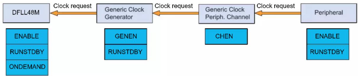
flowchart
graph LR
    A["DFLL48M"] -->|Clock request| B["Generic Clock Generator"]
    B -->|Clock request| C["Generic Clock Periph. Channel"]
    C -->|Clock request| D["Peripheral"]
    E["ENABLE"] --> F["RUNSTDBY"]
    F --> G["ONDEMAND"]
    H["GENEN"] --> I["RUNSTDBY"]
    I --> J["CHEN"]
    K["ENABLE"] --> L["RUNSTDBY"]
    L --> M["Peripheral"]
All clock sources in the system can be run in an on-demand mode: the clock source is in a stopped state unless a peripheral is requesting the clock source. Clock requests propagate from the peripheral, via the GCLK, to the clock source. If one or more peripheral is using a clock source, the clock source will be started/kept running. As soon as the clock source is no longer needed and no peripheral has an active request, the clock source will be stopped until requested again.
The clock request can reach the clock source only if the peripheral, the generic clock and the clock from the Generic Clock Generator in-between are enabled. The time taken from a clock request being asserted to the clock source being ready is dependent on the clock source startup time, clock source frequency as well as the divider used in the Generic Clock Generator. The total startup time T_start from a clock request until the clock is available for the peripheral is between:
T_start_max = Clock source startup time + 2 × clock source periods + 2 × divided clock source periods
T_start_min = Clock source startup time + 1 × clock source period + 1 × divided clock source period
The time between the last active clock request stopped and the clock is shut down, T_stop , is between:
T_stop_min = 1 × divided clock source period + 1 × clock source period
T_stop_max = 2 × divided clock source periods + 2 × clock source periods
The On-Demand function can be disabled individually for each clock source by clearing the ONDEMAND bit located in each clock source controller. Consequently, the clock will always run whatever the clock request status is. This has the effect of removing the clock source startup time at the cost of power consumption.
The clock request mechanism can be configured to work in standby mode by setting the RUNSDTBY bits of the modules, see Figure 14-4.
14.6 Power Consumption vs. Speed
When targeting for either a low-power or a fast acting system, some considerations have to be taken into account due to the nature of the asynchronous clocking of the peripherals:
If clocking a peripheral with a very low clock, the active power consumption of the peripheral will be lower. At the same time the synchronization to the synchronous (CPU) clock domain is dependent on the peripheral clock speed, and will take longer with a slower peripheral clock. This will cause worse response times and longer synchronization delays.
14.7 Clocks after Reset
On any Reset the synchronous clocks start to their initial state:
- OSC16M is enabled and configured to run at 4MHz
- Generic Generator 0 uses OSC16M as source and generates GCLK_MAIN
• CPU and BUS clocks are undivided
On a Power-on Reset, the 32KHz clock sources are reset and the GCLK module starts to its initial state:
- All Generic Clock Generators are disabled except
- Generator 0 is using OSC16M at 4MHz as source and generates GCLK_MAIN
- All Peripheral Channels in GCLK are disabled
On a User Reset the GCLK module starts to its initial state, except for:
- Generic Clocks that are write-locked, i.e., the according WRTLOCK is set to 1 prior to Reset
References:
RSTC - Reset Controller
15. GCLK - Generic Clock Controller
15.1 Overview
Depending on the application, peripherals may require specific clock frequencies to operate correctly. The Generic Clock controller (GCLK) provides five Generic Clock Generators that can provide a wide range of clock frequencies.
Generators can be set to use different external and internal oscillators as source. The clock of each Generator can be divided. The outputs from the Generators are used as sources for the Peripheral Channels, which provide the Generic Clock (GCLK_PERIPH) to the peripheral modules, as shown in Figure 15-2. The number of Peripheral Clocks depends on how many peripherals the device has.
Note: The Generator 0 is always the direct source of the GCLK_MAIN signal.
15.2 Features
- Provides a device-defined, configurable number of Peripheral Channel clocks
- Wide frequency range
15.3 Block Diagram
The generation of Peripheral Clock signals (GCLK_PERIPH) and the Main Clock (GCLK_MAIN) can be seen in Device Clocking Diagram.
Figure 15-1. Device Clocking Diagram
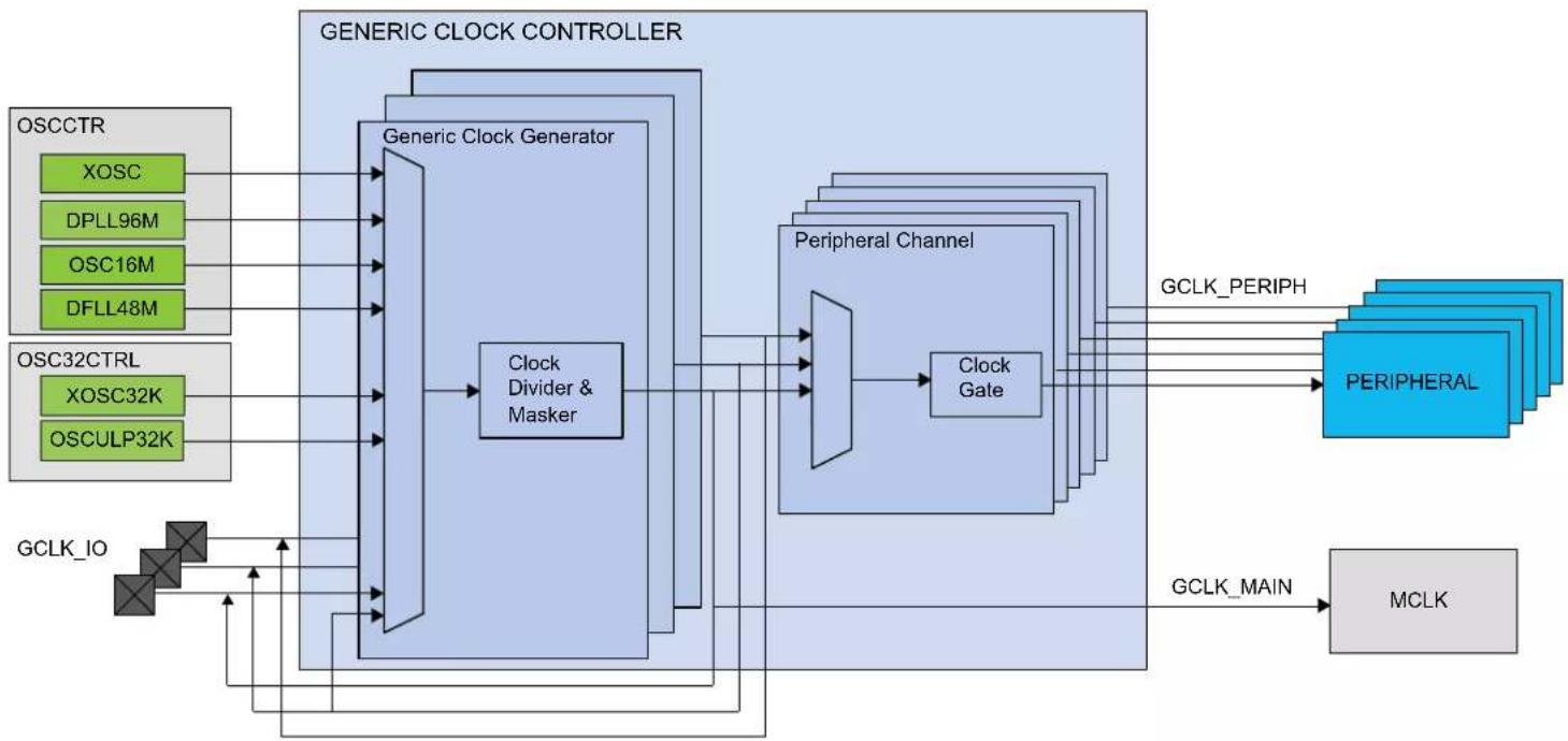
flowchart
graph TD
    subgraph "GENERIC CLOCK CONTROLLER"
        OSC_CTR["XOSC"] --> Generator["Generic Clock Generator"]
        DPLL96M["DPLL96M"] --> Generator
        OSC16M["OSC16M"] --> Generator
        DFLL48M["DFLL48M"] --> Generator
        OSC32CTRL["XOSC32K"] --> Generator
        OSCULP32K["OSCULP32K"] --> Generator
    end

    subgraph "GCLK_IO"
        GCLK_IO["GCLK_IO"] --> GCLKMain["GCLK_MAIN"]
    end

    subgraph "GCLK_PERIPH"
        Peripheral_Channel["Peripheral Channel"] --> Gate["Clock Gate"]
    end

    subgraph "MCLK"
        PeripheralRAL["PERIPHERAL"] --> Gate
    end

    XOSC["XOSC"] --> Generator
    DPLL96M["DPLL96M"] --> Generator
    OSC16M["OSC16M"] --> Generator
    DFLL48M["DFLL48M"] --> Generator
    OSC32CTRL["XOSC32K"] --> Generator
    OSCULP32K["OSCULP32K"] --> Generator
    GCLK_IO --> GCLKMain
    GCLKMain --> PeripheralChannel
    PeripheralChannel --> Gate
    GCLK_PERIPH --> PeripheralRAL
The GCLK block diagram is shown below:
Figure 15-2. Generic Clock Controller Block Diagram
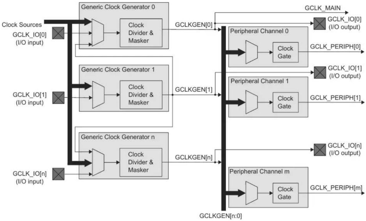
flowchart
graph TD
    A["Clock Sources"] --> B["GCLK_IO[0"] (I/O input)]
    B --> C["Generic Clock Generator 0"]
    C --> D["GCLKGEN[0"]]
    D --> E["Peripheral Channel 0"]
    E --> F["GCLK_MAIN"]
    A --> G["GCLK_IO[1"] (I/O input)]
    G --> H["Generic Clock Generator 1"]
    H --> I["GCLKGEN[1"]]
    I --> J["Peripheral Channel 1"]
    J --> K["GCLK_MAIN"]
    A --> L["GCLK_IO[n"] (I/O input)]
    L --> M["Generic Clock Generator n"]
    M --> N["GCLKGEN[n"]]
    N --> O["Peripheral Channel m"]
    O --> P["GCLK_MAIN"]
    E --> Q["GCLK_IO[0"] (I/O output)]
    Q --> R["GCLK_PERIPH[0"]]
    J --> S["GCLK_IO[1"] (I/O output)]
    S --> T["GCLK_PERIPH[1"]]
    O --> U["GCLK_IO[n"] (I/O output)]
    U --> V["GCLK_PERIPH[m"]]
15.4 Signal Description
Table 15-1. GCLK Signal Description
| Signal Name Type Description | ||
| GCLK_IO[4:0] Digital I/O Clock source for Generators when input | Generic Clock signal when output | |
Note: One signal can be mapped on several pins.
References:
I/O Multiplexing and Considerations
15.5 Product Dependencies
In order to use this peripheral, other parts of the system must be configured correctly, as described below.
15.5.1 I/O Lines
Using the GCLK I/O lines requires the I/O pins to be configured.
References:
- PORT - I/O Pin Controller
15.5.2 Power Management
The GCLK can operate in all sleep modes, if required.
References:
PM- Power Manager
15.5.3 Clocks
The GCLK bus clock (CLK_GCLK_APB) can be enabled and disabled in the Main Clock Controller.
References:
Peripheral Clock Masking
OSC32KCTRL - 32kHz Oscillators Controller
15.5.4 DMA
Not applicable.
15.5.5 Interrupts
Not applicable.
15.5.6 Events
Not applicable.
15.5.7 Debug Operation
When the CPU is halted in debug mode the GCLK continues normal operation. If the GCLK is configured in a way that requires it to be periodically serviced by the CPU through interrupts or similar, improper operation or data loss may result during debugging.
15.5.8 Register Access Protection
All registers with write-access can be optionally write-protected by the Peripheral Access Controller (PAC).
Note: Optional write-protection is indicated by the "PAC Write-Protection" property in the register description.
When the CPU is halted in debug mode, all write-protection is automatically disabled. Write-protection does not apply for accesses through an external debugger.
References:
- PAC - Peripheral Access Controller
15.5.9 Analog Connections
Not applicable.
15.6 Functional Description
15.6.1 Principle of Operation
The GCLK module is comprised of five Generic Clock Generators (Generators) sourcing up to 64 Peripheral Channels and the Main Clock signal GCLK_MAIN.
A clock source selected as input to a Generator can either be used directly, or it can be prescaled in the Generator. A generator output is used by one or more Peripheral Channels to provide a peripheral generic clock signal (GCLK_PERIPH) to the peripherals.
15.6.1.1 Basic Operation
15.6.1.1.1 Initialization
Before a Generator is enabled, the corresponding clock source should be enabled. The Peripheral clock must be configured as outlined by the following steps:
-
The Generator must be enabled (GENCTRLn.GENEN=1) and the division factor must be set (GENTRLn.DIVSEL and GENCTRLn.DIV) by performing a single 32-bit write to the Generator Control register (GENCTRLn).
-
The Generic Clock for a peripheral must be configured by writing to the respective Peripheral Channel Control register (PCHCTRLm). The Generator used as the source for the Peripheral Clock must be written to the GEN bit field in the Peripheral Channel Control register (PCHCTRLm.GEN).
Note: Each Generator n is configured by one dedicated register GENCTRLn.
Note: Each Peripheral Channel m is configured by one dedicated register PCHCTRLm.
15.6.1.1.2 Enabling, Disabling, and Resetting
The GCLK module has no enable/disable bit to enable or disable the whole module.
The GCLK is reset by setting the Software Reset bit in the Control A register (CTRLA.SWRST) to 1. All registers in the GCLK will be reset to their initial state, except for Peripheral Channels and associated Generators that have their Write Lock bit set to 1 (PCHCTRLm.WRTLOCK). For further details, refer to 15.6.2.4. Configuration Lock.
15.6.1.1.3 Generic Clock Generator
Each Generator (GCLK_GEN) can be set to run from one of nine different clock sources except GCLK_GEN[1], which can be set to run from one of eight sources. GCLK_GEN[1] is the only Generator that can be selected as source to others Generators.
Each generator GCLK_GEN[x] can be connected to one specific pin (GCLK_IO[y]). The GCLK_IO[y] can be set to act as source to GCLK_GEN[x] or to output the clock signal generated by GCLK_GEN[x].
The selected source can be divided. Each Generator can be enabled or disabled independently.
Each GCLK_GEN clock signal can then be used as clock source for Peripheral Channels. Each Generator output is allocated to one or several Peripherals.
GCLK_GEN[0] is used as GCLK_MAIN for the synchronous clock controller inside the Main Clock Controller. Refer to the Main Clock Controller description for details on the synchronous clock generation.
Figure 15-3. Generic Clock Generator
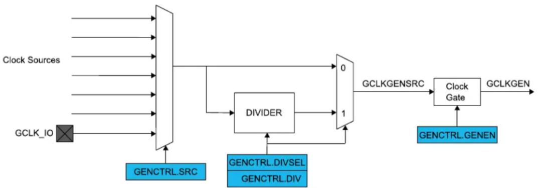
flowchart
graph LR
    A["Clock Sources"] --> B["DIVIDER"]
    C["GCLK_IO"] --> B
    B --> D["0"]
    B --> E["1"]
    D --> F["GCLKGENSRC"]
    E --> G["GCLKGEN"]
    H["GENCTRL.SRC"] --> B
    I["GENCTRL.DIVSEL"] --> B
    J["GENCTRL.DIV"] --> B
    K["GENCTRL.GENEN"] --> L["Clock Gate"]
    L --> M["GCLKGEN"]
15.6.1.1.4 Enabling a Generator
A Generator is enabled by writing a '1' to the Generator Enable bit in the Generator Control register (GENCTRLn.GENEN=1).
15.6.1.1.5 Disabling a Generator
A Generator is disabled by writing a '0' to GENCTRLn.GENEN. When GENCTRLn.GENEN=0, the GCLK_GEN[n] clock is disabled and gated.
15.6.1.1.6 Selecting a Clock Source for the Generator
Each Generator can individually select a clock source by setting the Source Select bit group in the Generator Control register (GENCTRLn.SRC).
Changing from one clock source, for example A, to another clock source, B, can be done on the fly: If clock source B is not ready, the Generator will continue using clock source A. As soon as source B is ready, the Generator will switch to it. During the switching operation, the Generator maintains clock requests to both clock sources A and B, and will release source A as soon as the switch is done. The according bit in SYNCBUSY register (SYNCBUSY.GENCTRLn) will remain '1' until the switch operation is completed.
The available clock sources are device dependent (usually the oscillators, RC oscillators, DPLL, and DFLL). Only Generator 1 can be used as a common source for all other generators.
15.6.1.1.7 Changing the Clock Frequency
The selected source for a Generator can be divided by writing a division value in the Division Factor bit field of the Generator Control register (GENCTRLn.DIV). How the actual division factor is calculated is depending on the Divide Selection bit (GENCTRLn.DIVSEL).
If GENCTRLn.DIVSEL=0 and GENCTRLn.DIV is either 0 or 1, the output clock will be undivided.
Note: The number of DIV bits for each Generator is device dependent.
When dividing a clock with an odd division factor, the duty-cycle will not be 50/50. Setting the Improve Duty Cycle bit of the Generator Control register (GENCTRLn.IDC) will result in a 50/50 duty cycle.
15.6.1.1.9 External Clock
The output clock (GCLK_GEN) of each Generator can be sent to I/O pins (GCLK_IO).
If the Output Enable bit in the Generator Control register is set (GENCTRLn.OE = 1) and the generator is enabled (GENCTRLn.GENEN=1), the Generator requests its clock source and the GCLK_GEN clock is output to an I/O pin.
If GENCTRLn.OE is 0, the according I/O pin is set to an Output Off Value, which is selected by GENCTRLn.OOV: If GENCTRLn.OOV is '0', the output clock will be low when turned off. If this bit is '1', the output clock will be high when turned off.
In Standby mode, if the clock is output (GENCTRLn.OE=1), the clock on the I/O pin is frozen to the OOV value if the Run In Standby bit of the Generic Control register (GENCTRLn.RUNSTDBY) is zero. If GENCTRLn.RUNSTDBY is '1', the GCLKGEN clock is kept running and output to the I/O pin.
15.6.2 Peripheral Clock
Figure 15-4. Peripheral Clock

flowchart
graph TD
    A["GCLKGEN[0"]] --> B((Block))
    C["GCLKGEN[1"]] --> B
    D["GCLKGEN[2"]] --> B
    E["GCLKGEN[n"]] --> B
    B --> F["Clock Gate"]
    F --> G["GCLK_PERIPH"]
    H["PCHCTRL.CHEN"] --> F
    I["PCHCTRL.GEN"] --> B
15.6.2.1 Enabling a Peripheral Clock
Before a Peripheral Clock is enabled, one of the Generators must be enabled (GENCTRLn.GENEN) and selected as source for the Peripheral Channel by setting the Generator Selection bits in the
Peripheral Channel Control register (PCHCTRL.GEN). Any available Generator can be selected as clock source for each Peripheral Channel.
When a Generator has been selected, the peripheral clock is enabled by setting the Channel Enable bit in the Peripheral Channel Control register, PCHCTRLm.CHEN = 1. The PCHCTRLm.CHEN bit must be synchronized to the generic clock domain. PCHCTRLm.CHEN will continue to read as its previous state until the synchronization is complete.
15.6.2.2 Disabling a Peripheral Clock
A Peripheral Clock is disabled by writing PCHCTRLm.CHEN=0. The PCHCTRLm.CHEN bit must be synchronized to the Generic Clock domain. PCHCTRLm.CHEN will stay in its previous state until the synchronization is complete. The Peripheral Clock is gated when disabled.
15.6.2.3 Selecting the Clock Source for a Peripheral
When changing a peripheral clock source by writing to PCHCTRLm.GEN, the peripheral clock must be disabled before re-enabling it with the new clock source setting. This prevents glitches during the transition:
- Disable the Peripheral Channel by writing PCHCTRLm.CHEN=0.
- Assert that PCHCTRLm.CHEN reads '0'.
- Change the source of the Peripheral Channel by writing PCHCTRLm.GEN.
- Re-enable the Peripheral Channel by writing PCHCTRLm.CHEN=1.
References:
Peripheral Channel Control
15.6.2.4 Configuration Lock
The peripheral clock configuration can be locked for further write accesses by setting the Write Lock bit in the Peripheral Channel Control register PCHCTRLm.WRTLOCK=1). All writing to the PCHCTRLm register will be ignored. It can only be unlocked by a Power Reset.
The Generator source of a locked Peripheral Channel will be locked, too: The corresponding GENCTRLn register is locked, and can be unlocked only by a Power Reset.
There is one exception concerning the Generator 0. As it is used as GCLK_MAIN, it cannot be locked. It is reset by any Reset and will start up in a known configuration. The software reset (CTRLA.SWRST) can not unlock the registers.
In case of an external Reset, the Generator source will be disabled. Even if the WRTLOCK bit is written to '1' the peripheral channels are disabled (PCHCTRLm.CHEN set to '0') until the Generator source is enabled again. Then, the PCHCTRLm.CHEN are set to '1' again.
References:
Peripheral Channel Control
CTRLA
15.7 Additional Features
15.7.1 Peripheral Clock Enable after Reset
The Generic Clock Controller must be able to provide a generic clock to some specific peripherals after a Reset. That means that the configuration of the Generators and Peripheral Channels after Reset is device-dependent.
Refer to GENCTRLn.SRC for details on GENCTRLn reset.
Refer to PCHCTRLm.SRC for details on PCHCTRLm reset.
15.8 Sleep Mode Operation
15.8.1 SleepWalking
The GCLK module supports the SleepWalking feature.
If the system is in a sleep mode where the Generic Clocks are stopped, a peripheral that needs its clock in order to execute a process must request it from the Generic Clock Controller.
The Generic Clock Controller receives this request, determines which Generic Clock Generator is involved and which clock source needs to be awakened. It then wakes up the respective clock source, enables the Generator and Peripheral Channel stages successively, and delivers the clock to the peripheral.
The RUNSTDBY bit in the Generator Control register controls clock output to pin during standby sleep mode. If the bit is cleared, the Generator output is not available on pin. When set, the GCLK can continuously output the generator output to GCLK_IO. Refer to 15.6.1.1.9. External Clock for details.
References:
PM - Power Manager
15.8.2 Minimize Power Consumption in Standby
The following table identifies when a Clock Generator is off in Standby Mode, minimizing the power consumption:
Table 15-2. Clock Generator n Activity in Standby Mode
| Request for Clock n present GENCTRLn.RUNSTDBY GENCTRLn.OE Clock Generator n | |||
| yes -- active | |||
| no 1 1 active | |||
| no 1 0 OFF | |||
| no 0 1 OFF | |||
| no 0 0 OFF | |||
15.8.3 Entering Standby Mode
There may occur a delay when the device is put into Standby, until the power is turned off. This delay is caused by running Clock Generators: if the Run in Standby bit in the Generator Control register (GENCTRLn.RUNSTDBY) is '0', GCLK must verify that the clock is turned of properly. The duration of this verification is frequency-dependent.
References:
PM - Power Manager
15.9 Synchronization
Due to asynchronicity between the main clock domain and the peripheral clock domains, some registers need to be synchronized when written or read.
An exception is the Channel Enable bit in the Peripheral Channel Control registers (PCHCTRLm.CHEN). When changing this bit, the bit value must be read-back to ensure the synchronization is complete and to assert glitch free internal operation. Note that changing the bit value under ongoing synchronization will not generate an error.
The following registers are synchronized when written:
- Generic Clock Generator Control register (GENCTRLn)
• Control A register (CTRLA)
Required write-synchronization is denoted by the "Write-Synchronized" property in the register description.
References:
Peripheral Channel Control
CTRLA
15.10 Register Summary
| Offset | Name Bit Pos. 76543210 | |||||||||
| 0x00 CTRLA 7:0 SWRST | ||||||||||
| 0x01 ... 0x03 | Reserved | |||||||||
| 0x04 SYNCBUSY | 7:0 GENCTRL4 GENCTRL3 GENCTRL2 GENCTRL1 GENCTRL0 | SWRST | ||||||||
| 15:8 | ||||||||||
| 23:16 | ||||||||||
| 31:24 | ||||||||||
| 0x08 ... 0x1F | Reserved | |||||||||
| 0x20 GENCTRL0 | 7:0 | SRC[3:0] | ||||||||
| 15:8 | RUNSTDBY | DIVSEL | OE | OOV | IDC | GENEN | ||||
| 23:16 | DIV[7:0] | |||||||||
| 31:24 | DIV[15:8] | |||||||||
| 0x24 GENCTRL1 | 7:0 | SRC[3:0] | ||||||||
| 15:8 | RUNSTDBY | DIVSEL | OE | OOV | IDC | GENEN | ||||
| 23:16 | DIV[7:0] | |||||||||
| 31:24 | DIV[15:8] | |||||||||
| 0x28 GENCTRL2 | 7:0 | SRC[3:0] | ||||||||
| 15:8 | RUNSTDBY | DIVSEL | OE | OOV | IDC | GENEN | ||||
| 23:16 | DIV[7:0] | |||||||||
| 31:24 | DIV[15:8] | |||||||||
| 0x2C GENCTRL3 | 7:0 | SRC[3:0] | ||||||||
| 15:8 | RUNSTDBY | DIVSEL | OE | OOV | IDC | GENEN | ||||
| 23:16 | DIV[7:0] | |||||||||
| 31:24 | DIV[15:8] | |||||||||
15.11 Register Description
Registers can be 8, 16, or 32 bits wide. Atomic 8-, 16- and 32-bit accesses are supported. In addition, the 8-bit quarters and 16-bit halves of a 32-bit register, and the 8-bit halves of a 16-bit register can be accessed directly.
Some registers are optionally write-protected by the Peripheral Access Controller (PAC). Optional PAC write-protection is denoted by the "PAC Write-Protection" property in each individual register description. For details, refer to 15.5.8. Register Access Protection.
Some registers are synchronized when read and/or written. Synchronization is denoted by the "Write-Synchronized" or the "Read-Synchronized" property in each individual register description. For details, refer to 15.9. Synchronization.
15.11.1 Control A
Name: CTRLA
Offset: 0x00
Reset: 0x00
Property: PAC Write-Protection, Write-Synchronized
Bit 76543210
| SWRST | |||||||
| Access Reset 0 | R/W | ||||||
Bit 0 - SWRST Software Reset
Writing a zero to this bit has no effect.
Setting this bit to 1 will reset all registers in the GCLK to their initial state after a Power Reset, except for generic clocks and associated Generators that have their WRTLOCK bit in PCHCTRLm set to 1.
Refer to GENCTRL Reset Value for details on GENCTRL register reset.
Refer to PCHCTRL Reset Value for details on PCHCTRL register reset.
Due to synchronization, there is a waiting period between setting CTRLA.SWRST and a completed Reset. CTRLA.SWRST and SYNCBUSY.SWRST will both be cleared when the reset is complete.
Value Description
| 0 | There is no Reset operation ongoing. |
| 1 | A Reset operation is ongoing. |
15.11.2 Synchronization Busy
Name: SYNCBUSY
Offset: 0x04
Reset: 0x00000000
Property: -

text_image
Bit 31 30 29 28 27 26 25 24 Access Reset Bit 23 22 21 20 19 18 17 16 Access Reset Bit 15 14 13 12 11 10 9 8 Access Reset Bit 7 6 5 4 3 2 1 0 Access R GENCTRL4 GENCTRL3 GENCTRL2 GENCTRL1 GENCTRL0 SWRST Reset 0 0 0 0 0 0Bits 2, 3, 4, 5, 6 - GENCTRLn Generator Control n Synchronization Busy
This bit is cleared when the synchronization of the Generator Control n register (GENCTRLn) between clock domains is complete, or when clock switching operation is complete.
This bit is set when the synchronization of the Generator Control n register (GENCTRLn) between clock domains is started.
Bit 0 - SWRST Software Reset Synchronization Busy
This bit is cleared when the synchronization of the CTRLA.SWRST register bit between clock domains is complete.
This bit is set when the synchronization of the CTRLA.SWRST register bit between clock domains is started.
15.11.3 Generator Control
Name: GENCTRLn
Offset: 0x20 + n*0x04 [n=0..4]
Reset: 0x00010005 for Generator n=0, else 0x00000000
Property: PAC Write-Protection, Write-Synchronized
GENCTRLn controls the settings of Generic Generator n (n=0..4).
Bit 31 30 29 28 27 26 25 24
| DIV[15:8] | |
| Access | R/W R/W R/W R/W R/W R/W R/W R/W |
| Reset | 0 0 0 0 0 0 0 |
Bit 23 22 21 20 19 18 17 16
| DIV[7:0] | |
| Access | R/W R/W R/W R/W R/W R/W R/W R/W |
| Reset | 0 0 0 0 0 0 0 |
Bit 15 14 13 12 11 10 9 8
| RUNSTDBY | DIVSEL | OE | OOV | IDC | GENEN | ||
| Access Reset | R/W R/W R/W R/W R/W R/W | ||||||
| 0 0 0 0 0 x | |||||||
Bit 76543210
| SRC[3:0] | ||||||
| Access Reset | R/W | R/W | R/W | R/W | ||
| X | X | X | ||||
Bits 31:16 - DIV[15:0] Division Factor
These bits represent a division value for the corresponding Generator. The actual division factor is dependent on the state of DIVSEL. The number of relevant DIV bits for each Generator can be seen in this table. Written bits outside of the specified range will be ignored.
Table 15-3. Division Factor Bits
| Generic Clock Generator | Division Factor Bits |
| Generator 0 | 8 division factor bits - DIV[7:0] |
| Generator 1 | 16 division factor bits - DIV[15:0] |
| Generator 2 - 4 | 8 division factor bits - DIV[7:0] |
Bit 13 - RUNSTDBY Run in Standby
This bit is used to keep the Generator running in Standby as long as it is configured to output to a dedicated GCLK_IO pin. If GENCTRLn.OE is zero, this bit has no effect and the generator will only be running if a peripheral requires the clock.
| Value | Description |
| 0 | The Generator is stopped in Standby and the GCLK_IO pin state (one or zero) will be dependent on the setting in GENCTRL.OOV. |
| 1 | The Generator is kept running and output to its dedicated GCLK_IO pin during Standby mode. |
Bit 12 - DIVSEL Divide Selection
This bit determines how the division factor of the clock source of the Generator will be calculated from DIV. If the clock source should not be divided, DIVSEL must be 0 and the GENCTRLn.DIV value must be either 0 or 1.
| Value | Description |
| 0 | The Generator clock frequency equals the clock source frequency divided by GENCTRLn.DIV. |
Value Description
1 The Generator clock frequency equals the clock source frequency divided by 2^(GENCTRLnDIV+1).
Bit 11 - OE Output Enable
This bit is used to output the Generator clock output to the corresponding pin (GCLK_IO), as long as GCLK_IO is not defined as the Generator source in the GENCTRLn.SRC bit field.
Value Description
| 0 | No Generator clock signal on pin GCLK_IO. |
| 1 | The Generator clock signal is output on the corresponding GCLK_IO, unless GCLK_IO is selected as a generator source in the GENCTRLn.SRC bit field. |
Bit 10 - OOV Output Off Value
This bit is used to control the clock output value on pin (GCLK_IO) when the Generator is turned off or the OE bit is zero, as long as GCLK_IO is not defined as the Generator source in the GENCTRLn.SRC bit field.
Value Description
| 0 | The GCLK_IO will be LOW when generator is turned off or when the OE bit is zero. |
| 1 | The GCLK_IO will be HIGH when generator is turned off or when the OE bit is zero. |
Bit 9 - IDC Improve Duty Cycle
This bit is used to improve the duty cycle of the Generator output to 50/50 for odd division factors.
Value Description
| 0 | Generator output clock duty cycle is not balanced to 50/50 for odd division factors. |
| 1 | Generator output clock duty cycle is 50/50. |
Bit 8 - GENEN Generator Enable
This bit is used to enable and disable the Generator.
Value Description
| 0 | Generator is disabled. |
| 1 | Generator is enabled. |
Bits 3:0 - SRC[3:0] Generator Clock Source Selection
These bits select the Generator clock source, as shown in this table.
Table 15-4. Generator Clock Source Selection
| Value Name Description | |
| 0x0 XOSC XOSC oscillator output | |
| 0x1 GCLK_IN Generator input pad (GCLK_IO) | |
| 0x2 GCLK_GEN1 Generic clock generator 1 output | |
| 0x3 OSCULP32K OSCULP32K oscillator output | |
| 0x4 XOSC32K XOSC32K oscillator output | |
| 0x5 OSC16M OSC16M oscillator output | |
| 0x6 DFLL48M DFLL48M output | |
| 0x7 DPLL96M DPLL96M output | |
| 0x8-0xF Reserved Reserved for future use |
A Power Reset will reset all GENCTRLn registers. the Reset values of the GENCTRLn registers are shown in table below.
Table 15-5. GENCTRLn Reset Value after a Power Reset
| GCLK Generator Reset Value after a Power Reset | |
| 0 0x00010005 | |
| others | 0x00000000 |
A User Reset will reset the associated GENCTRL register unless the Generator is the source of a locked Peripheral Channel (PCHCTRLm.WRTLOCK=1). The reset values of the GENCTRL register are as shown in the table below.
Table 15-6. GENCTRLn Reset Value after a User Reset
| GCLK Generator Reset Value after a User Reset |
| 0 0x00000105 |
| others No change if the generator is used by a Peripheral Channel m with PCHCTRLm.WRTLOCK=1 else 0x00000000 |
15.11.4 Peripheral Channel Control
Name: PCHCTRLm
Offset: 0x80 + m*0x04 [m=0..28]
Reset: 0x00000000
Property: PAC Write-Protection
PCHTRLm controls the settings of Peripheral Channel number m (m = 0..28).

bar_stacked
| Bit | Access Reset | WRTLOCK CHEN | GEN[3:0] | | --- | --- | --- | --- | | 31 | 24 | 0 | 0 | | 29 | 16 | 0 | 0 | | 28 | 16 | 0 | 0 | | 27 | 16 | 0 | 0 | | 26 | 16 | 0 | 0 | | 25 | 16 | 0 | 0 | | 24 | 16 | 0 | 0 | | 23 | 16 | 0 | 0 | | 22 | 16 | 0 | 0 | | 21 | 16 | 0 | 0 | | 20 | 16 | 0 | 0 | | 19 | 16 | 0 | 0 | | 18 | 16 | 0 | 0 | | 17 | 16 | 0 | 0 | | 16 | 16 | 0 | 0 | | 15 | 8 | 0 | 0 | | 14 | 8 | 0 | 0 | | 13 | 8 | 0 | 0 | | 12 | 8 | 0 | 0 | | 11 | 8 | 0 | 0 | | 10 | 8 | 0 | 0 | | 9 | 8 | 0 | 0 | | 8 | 8 | 0 | 0 | | 7 | 8 | 0 | 0 | | 6 | 8 | 0 | 0 | | 5 | 8 | 0 | 0 | | 4 | 8 | 0 | 0 | | 3 | 8 | 0 | 0 | | 2 | 8 | 0 | 0 | | 1 | 8 | 0 | 0 | | WRTLOCK CHEN | R/W | R/W | GEN[3:0] | | R/W | R/W | R/W | R/W | | R/W | R/W | R/W | R/W | | R/W | R/W | R/W | R/W | | R/W | R/W | R/W | R/W | | R/W = 0.0, R/W = 0.0, R/W = 0.0, R/W = ...Bit 7 - WRTLOCK Write Lock
After this bit is set to '1', further writes to the PCHCTRLm register will be discarded. The control register of the corresponding Generator n (GENCTRLn), as assigned in PCHCTRLm.GEN, will also be locked. It can only be unlocked by a Power Reset.
Note that Generator 0 cannot be locked.
| Value | Description |
| 0 | The Peripheral Channel register and the associated Generator register are not locked |
| 1 | The Peripheral Channel register and the associated Generator register are locked |
Bit 6 - CHEN Channel Enable
This bit is used to enable and disable a Peripheral Channel.
| Value | Description |
| 0 | The Peripheral Channel is disabled |
| 1 | The Peripheral Channel is enabled |
Bits 3:0 - GEN[3:0] Generator Selection
This bit field selects the Generator to be used as the source of a peripheral clock, as shown in the table below:
Table 15-7. Generator Selection
| Value | Description |
| 0x0 | Generic Clock Generator 0 |
| 0x1 | Generic Clock Generator 1 |
| 0x2 | Generic Clock Generator 2 |
| 0x3 | Generic Clock Generator 3 |
| 0x4 | Generic Clock Generator 4 |
| Value Description | |
| 0x5 - 0xF Reserved |
Table 15-8. Reset Value after a User Reset or a Power Reset
| Reset PCHCTRLm.GEN PCHCTRLm.CHEN PCHCTRLm.WRTLOCK | |||
| Power Reset 0x0 0x0 0x0 | |||
| User Reset If WRTLOCK = 0: 0x0If WRTLOCK = 1: no change | If WRTLOCK = 0: 0x0If WRTLOCK = 1: no change | No change | |
A Power Reset will reset all the PCHCTRLm registers.
A User Reset will reset a PCHCTRL if WRTLOCK = 0, or else, the content of that PCHCTRL remains unchanged.
The PCHCTRL register Reset values are shown in the table PCHCTRLm Mapping.
Table 15-9. PCHCTRLm Mapping
| index(m) | Name | Description | |
| 0 | GCLK_DFLL48M_REF | DFLL48M Reference | |
| 1 | GCLK_FDPLL | FDPLL96M input clock source for reference | |
| 2 | GCLK_FDPLL_32K | FDPLL96M 32kHz clock for FDPLL96M internal lock timer | |
| 3 | GCLK_EIC | EIC | |
| 4 | GCLK_FREQM_MSR | FREQM Measure | |
| 5 | GCLK_FREQM_REF | FREQM Reference | |
| 6 | GLCK_USB | USB | |
| 7 | GCLK_EVSYS_CHANNEL_0 | EVSYS_CHANNEL_0 | |
| 8 | GCLK_EVSYS_CHANNEL_1 | EVSYS_CHANNEL_1 | |
| 9 | GCLK_EVSYS_CHANNEL_2 | EVSYS_CHANNEL_2 | |
| 10 | GCLK_EVSYS_CHANNEL_3 | EVSYS_CHANNEL_3 | |
| 11 | GCLK_EVSYS_CHANNEL_4 | EVSYS_CHANNEL_4 | |
| 12 | GCLK_EVSYS_CHANNEL_5 | EVSYS_CHANNEL_5 | |
| 13 | GCLK_EVSYS_CHANNEL_6 | EVSYS_CHANNEL_6 | |
| 14 | GCLK_EVSYS_CHANNEL_7 | EVSYS_CHANNEL_7 | |
| 15 | GCLK_SERCOM[0,1,2,3,4,5]_SLOW | SERCOM[0,1,2,3,4,5]_SLOW | |
| 16 | GCLK_SERCOM0_CORE | SERCOM0_CORE | |
| 17 | GCLK_SERCOM1_CORE | SERCOM1_CORE | |
| 18 | GCLK_SERCOM2_CORE | SERCOM2_CORE | |
| 19 | GCLK_SERCOM3_CORE | SERCOM3_CORE | |
| 20 | GCLK_SERCOM4_CORE | SERCOM4_CORE | |
| 21 | GCLK_SERCOM5_CORE | SERCOM5_CORE | |
| 22 | GCLK_TCC0 | TCC0 | |
| 23 | GCLK_TC0, GCLK_TC1 | TC0, TC1 | |
| 24 | GCLK_TC2, GCLK_TC3 | TC2, TC3 | |
| 25 | GCLK_ADC | ADC | |
| 26 | GCLK_AC | AC | |
| 27 | GCLK_PTC | PTC | |
| 28 | GCLK_CCL | CCL | |
16. MCLK - Main Clock
16.1 Overview
The Main Clock (MCLK) controls the synchronous clock generation of the device.
Using a clock provided by the Generic Clock Module (GCLK_MAIN), the Main Clock Controller provides synchronous system clocks to the CPU and the modules connected to the AHBx and the APBx buses. The synchronous system clocks are divided into a number of clock domains. Each clock domain can run at different frequencies, enabling the user to save power by running peripherals at a relatively low clock frequency, while maintaining high CPU performance or vice versa. In addition, the clock can be masked for individual modules, enabling the user to minimize power consumption.
16.2 Features
- Generates CPU, AHB, and APB system clocks
- Clock source and division factor from GCLK
- Clock prescaler with 1x to 128x division
- Safe run-time clock switching from GCLK
- Module-level clock gating through maskable peripheral clocks
16.3 Block Diagram
Figure 16-1. MCLK Block Diagram
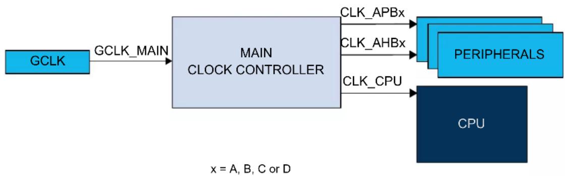
flowchart
graph LR
    A["GCLK"] -->|GCLK_MAIN| B["MAIN CLOCK CONTROLLER"]
    B --> C["CLK_APBx"]
    B --> D["CLK_AHBx"]
    B --> E["CLK_CPU"]
    C --> F["PERIPHERALS"]
    D --> F
    E --> F
    F --> G["CPU"]
16.4 Signal Description
Not applicable.
16.5 Product Dependencies
In order to use this peripheral, other parts of the system must be configured correctly, as described below.
16.5.1 I/O Lines
Not applicable.
16.5.2 Power Management
The MCLK will operate in all sleep modes if a synchronous clock is required in these modes.
16.5.3 Clocks
The MCLK bus clock (CLK_MCLK_APB) can be enabled and disabled in the Main Clock module, and the default state of CLK_MCLK_APB can be found in the Peripheral Clock Masking section. If this clock is disabled, it can only be re-enabled by a reset.
The Generic Clock GCLK_MAIN is required to generate the Main Clocks. GCLK_MAIN is configured in the Generic Clock Controller, and can be re-configured by the user if needed.
16.5.3.1 Main Clock
The main clock CLK_MAIN is the common source for the synchronous clocks. This is fed into the common 8-bit prescaler that is used to generate synchronous clocks to the CPU, AHBx, and APBx modules.
16.5.3.2 CPU Clock
The CPU clock (CLK_CPU) is routed to the CPU. Halting the CPU clock inhibits the CPU from executing instructions.
16.5.3.3 APBx and AHBx Clock
The APBx clocks (CLK_APBx) and the AHBx clocks (CLK_AHBx) are the root clock sources used by modules requiring a clock on the APBx and the AHBx buses. These clocks are always synchronous to the CPU clock, and can run even when the CPU clock is turned off in sleep mode. A clock gater is inserted after the common APB clock to gate any APBx clock of a module on APBx bus, as well as the AHBx clock serving that module.
16.5.3.4 Clock Domains
The device has these synchronous clock domains:
- High-Speed synchronous clock domain (HS Clock Domain). Frequency is f_HS .
- CPU synchronous clock domain (CPU Clock Domain). Frequency is f_CPU
- Backup synchronous clock domain. (BUP Clock Domain). Frequency is f_BUP .
See also the related links for the clock domain partitioning.
16.5.4 DMA
Not applicable.
16.5.5 Interrupts
The interrupt request line is connected to the Interrupt Controller. Using the MCLK interrupt requires the Interrupt Controller to be configured first.
16.5.6 Events
Not applicable.
16.5.7 Debug Operation
When the CPU is halted in debug mode, the MCLK continues normal operation. In sleep mode, the clocks generated from the MCLK are kept running to allow the debugger accessing any module. As a consequence, power measurements are incorrect in debug mode.
16.5.8 Register Access Protection
All registers with write access can be write-protected optionally by the Peripheral Access Controller (PAC), except for the following registers:
- Interrupt Flag register (INTFLAG)
Optional write protection by the Peripheral Access Controller (PAC) is denoted by the "PAC Write Protection" property in each individual register description.
PAC write protection does not apply to accesses through an external debugger.
16.5.9 Analog Connections
Not applicable.
16.6 Functional Description
16.6.1 Principle of Operation
The GCLK_MAIN clock signal from the GCLK module is the source for the main clock, which in turn is the common root for the synchronous clocks for the CPU, APBx, and AHBx modules. The GCLK_MAIN is divided by an 8-bit prescaler. Each of the derived clocks can run from any divided or undivided main clock, ensuring synchronous clock sources for each clock domain. Each clock domain (CPU, BUP) can be changed on the fly to respond to variable load in the application as long as f_CPU ≥ f_BUP . The clocks for each module in a clock domain can be masked individually to avoid power consumption in inactive modules. Depending on the sleep mode, some clock domains can be turned off.
16.6.2 Basic Operation
16.6.2.1 Initialization
After a Reset, the default clock source of the CLK_MAIN clock (GCLK_MAIN) is started and calibrated before the CPU starts running. The GCLK_MAIN clock is selected as the main clock without any prescaler division.
By default, only the necessary clocks are enabled.
16.6.2.2 Enabling, Disabling, and Resetting
The MCLK module is always enabled and cannot be reset.
16.6.2.3 Selecting the Main Clock Source
Refer to the Generic Clock Controller description for details on how to configure the clock source of the GCLK_MAIN clock.
16.6.2.4 Selecting the Synchronous Clock Division Ratio
The main clock CLK_MAIN feeds an 8-bit prescaler, which can be used to generate the synchronous clocks. By default, the synchronous clocks run on the undivided main clock. The user can select a prescaler division for the CPU clock domain by writing the Division (DIV) bits in the CPU Clock Division register CPUDIV, resulting in a CPU clock domain frequency determined by this equation:
$$ f _ {C P U} = \frac {f _ {m a i n}}{C P U D I V} $$
Similarly, the clock for the Backup Clock Domain can be divided by writing the BUPDIV register. To ensure correct operation, frequencies must be selected so that f_CPU ≥ f_BUP . Also, frequencies must never exceed the specified maximum frequency for each clock domain given in the electrical characteristics specifications.
If the application attempts to write forbidden values in CPUDIV or BUPDIV registers, registers are written but these bad values are not used and a violation is reported to the PAC module.
Division bits (DIV) can be written without halting or disabling peripheral modules. Writing DIV bits allows a new clock setting to be written to all synchronous clocks belonging to the corresponding clock domain at the same time. Each clock domain can be changed without changing others. This way, it is possible to, for example, scale the CPU clock domain speed according to the required performance, while keeping the Backup Clock Domain frequency constant.
Figure 16-2. Synchronous Clock Selection and Prescaler

flowchart
graph TD
    A["GCLK"] -->|GCLK_MAIN| B["Prescaler"]
    B --> C["BUPDIV"]
    C --> D["Clock gate"]
    D --> E["Clock APBx"]
    E --> F["Clock gate"]
    F --> G["clk_apb_ipn"]
    F --> H["clk_apb_ip1"]
    F --> I["clk_apb_ip0"]
    C --> J["Clock gate"]
    J --> K["Clock APB_HS"]
    K --> L["Clock gate"]
    L --> M["clk_apb_ipn"]
    L --> N["clk_apb_ip1"]
    L --> O["clk_apb_ip0"]
    C --> P["Clock gate"]
    P --> Q["Clock APB_HS"]
    Q --> R["Clock gate"]
    R --> S["clk_abh_ipn"]
    R --> T["clk_abh_ip1"]
    R --> U["clk_abh_ip0"]
    C --> V["Clock gate"]
    V --> W["Clock APB_HS"]
    W --> X["Clock gate"]
    X --> Y["clk_abh_ipn"]
    X --> Z["clk_abh_ip1"]
    X --> AA["clk_abh_ip0"]
    C --> AB["CPUDIV"]
    AB --> AC["Clock gate"]
    AC --> AD["CLK_CPU"]
    AD --> AE["CPU"]

    subgraph Backup Clock Domain: fBUP
        AF["PERIPHERALS"]
    end

    subgraph CPU Clock Domain: fCPU
        AG["PERIPHERALS"]
        AH["CPU"]
    end
16.6.2.5 Clock Ready Flag
There is a slight delay between writing to CPUDIV and BUPDIV until the new clock settings become effective.
During this interval, the Clock Ready flag in the Interrupt Flag Status and Clear register (INTFLAG.CKRDY) will return zero when read. If CKRDY in the INTENSET register is set to '1', the Clock Ready interrupt will be triggered when the new clock settings are effective. The clock settings (CPUDIV, BUPDIV) must not be re-written while INTFLAG.CKRDY reads '0'. The system may become unstable or hang, and a violation is reported to the PAC module.
16.6.2.6 Peripheral Clock Masking
The user can disable or enable the AHB or APB clock for a peripheral by writing the corresponding bit in the Clock Mask registers (APBxMASK) to '0' or '1'. The default state of the peripheral clocks is given in the table below:
Table 16-1. Peripheral Clock Default State
| CPU Clock Domain | |
| Peripheral Clock Default State | |
| CLK_AC_APB Enabled | |
| CLK_ADC_APB Enabled | |
| CLK_AES_APB Enabled | |
| CLK_BRIDGE_A_AHB Enabled | |
| CLK_BRIDGE_B_AHB Enabled | |
| CLK_BRIDGE_C_AHB Enabled | |
| CLK_CCL_APB Enabled | |
| CLK_DMAC_AHB Enabled | |
| CLK_DSU_AHB Enabled | |
| CLK_EIC_APB Enabled | |
| CLK_EVSYS_APB Enabled | |
| CLK_FREQM_APB Enabled | |
| CLK_GCLK_APB Enabled | |
| CLK_MCLK_APB Enabled | |
| CLK_NVMCTRL_AHB Enabled | |
| CLK_NVMCTRL_APB Enabled | |
| CLK_OSCCTRL_APB Enabled | |
| CLK_PAC_AHB Enabled | |
| CLK_PAC_APB Enabled | |
| CLK_PORT_APB Enabled | |
| CLK_PTC_APB Enabled | |
| CLK_SERCOM0_APB Enabled | |
| CLK_SERCOM1_APB Enabled | |
| CLK_SERCOM2_APB Enabled | |
| CLK_SERCOM3_APB Enabled | |
| CLK_SERCOM4_APB Enabled | |
| CLK_SERCOM5_APB Enabled | |
| CLK_SLCD_APB Enabled | |
| CLK_TC0_APB Enabled | |
| CLK_TC1_APB Enabled | |
| CLK_TC2_APB Enabled | |
| CLK_TC3_APB Enabled | |
| CLK_TCC0_APB Enabled | |
| CLK_TRNG_APB Enabled | |
| CLK_USB_AHB | Enabled |
| CLK_USB_APB | Enabled |
| CLK_WDT_APB | Enabled |
Table 16-2. Backup Clock Domain
| Backup Clock Domain | |
| Peripheral Clock Default State | |
| CLK_OSC32KCTRL_APB | Enabled |
| CLK_PM_APB | Enabled |
| CLK_SUPC_APB | Enabled |
| CLK_RSTC_APB | Enabled |
| CLK_RTC_APB | Enabled |
When the APB clock is not provided to a module, its registers cannot be read or written. The module can be re-enabled later by writing the corresponding mask bit to '1'.
A module may be connected to several clock domains (for example, AHB and APB), in which case it will have several mask bits.
The clocks should only be switched off if it is certain that the module will not be used: Switching off the clock for the NVM Controller (NVMCTRL) will cause a problem if the CPU needs to read from the Flash memory. Switching off the clock to the MCLK module (which contains the mask registers) or the corresponding APBx bridge, will make it impossible to write the mask registers again. In this case, they can only be re-enabled by a system reset.
16.6.3 DMA Operation
Not applicable.
16.6.4 Interrupts
The peripheral has the following interrupt sources:
- Clock Ready (CKRDY): indicates that CPU and BUP clocks are ready. This interrupt is a synchronous wake-up source.
Each interrupt source has an interrupt flag associated with it. The interrupt flag in the Interrupt Flag Status and Clear (INTFLAG) register is set when the interrupt condition occurs. Each interrupt can be enabled individually by writing a '1' to the corresponding enabling bit in the Interrupt Enable Set (INTENSET) register, and disabled by writing a '1' to the corresponding clearing bit in the Interrupt Enable Clear (INTENCLR) register. The status of enabled interrupts can be read from either INTENSET or INTENCLR.
An interrupt request is generated when the interrupt flag is set and the corresponding interrupt is enabled. The interrupt request remains active until the interrupt flag is cleared, the interrupt is disabled or the peripheral is reset. An interrupt flag is cleared by writing a '1' to the corresponding bit in the INTFLAG register. Each peripheral can have one interrupt request line per interrupt source or one common interrupt request line for all the interrupt sources. If the peripheral has one common interrupt request line for all the interrupt sources, the user must read the INTFLAG register to determine which interrupt condition is present.
16.6.5 Events
Not applicable.
16.6.6 Sleep Mode Operation
In IDLE sleep mode, the MCLK is still running on the selected main clock.
In STANDBY sleep mode, the MCLK is frozen if no synchronous clock is required.
16.7 Register Summary
| Offset | Name Bit Pos. 7 | 6 | 5 | 4 | 3 | 2 | 1 | 0 | ||||||||
| 0x00 Reserved | ||||||||||||||||
| 0x01 INTENCLR 7:0 | CKRDY | |||||||||||||||
| 0x02 INTENSET 7:0 | CKRDY | |||||||||||||||
| 0x03 | INTFLAG | 7:0 | CKRDY | |||||||||||||
| 0x04 | CPUDIV | 7:0 | CPUDIV[7:0] | |||||||||||||
| 0x05 Reserved | ||||||||||||||||
| 0x06 | BUPDIV | 7:0 | BUPDIV[7:0] | |||||||||||||
| 0x07 ... 0x0F | Reserved | |||||||||||||||
| 0x10 AHBMASK | 7:0 | PAC | Reserved | DSU | USB | DMAC | APBC | APBB | APBA | |||||||
| 15:8 | Reserved | Reserved | NVMCTRL | |||||||||||||
| 23:16 | ||||||||||||||||
| 31:24 | ||||||||||||||||
| 0x14 APBAMASK | 7:0 | GCLK | SUPC | OSC32KCTRL | OSCCTRL | RSTC | MCLK | PM | PAC | |||||||
| 15:8 | FREQM | EIC | RTC | WDT | ||||||||||||
| 23:16 | ||||||||||||||||
| 31:24 | ||||||||||||||||
| 0x18 | APBBMASK | 7:0 | PORT | NVMCTRL | DSU | USB | ||||||||||
| 15:8 | ||||||||||||||||
| 23:16 | ||||||||||||||||
| 31:24 | ||||||||||||||||
| 0x1C | APBCMASK | 7:0 | TCC0 | SERCOM5 | SERCOM4 | SERCOM3 | SERCOM2 | SERCOM1 | SERCOM0 | EVSYS | ||||||
| 15:8 | SLCD | PTC | AC | ADC | TC3 | TC2 | TC1 | TC0 | ||||||||
| 23:16 | CCL | TRNG | AES | |||||||||||||
| 31:24 | ||||||||||||||||
16.8 Register Description
Registers can be 8, 16, or 32 bits wide. Atomic 8-, 16-, and 32-bit accesses are supported. In addition, the 8-bit quarters and 16-bit halves of a 32-bit register, and the 8-bit halves of a 16-bit register can be accessed directly.
Some registers can be write-protected optionally by the Peripheral Access Controller (PAC). This is denoted by the property "PAC Write-Protection" in each individual register description. Refer to the 16.5.8. Register Access Protection for details.
16.8.1 Interrupt Enable Clear
Name: INTENCLR
Offset: 0x01
Reset: 0x00
Property: PAC Write-Protection
This register allows the user to disable an interrupt without doing a read-modify-write operation. Changes in this register will also be reflected in the Interrupt Enable Set (INTENSET) register.
Bit 76543210
| CKRDY | |||||||
| Access Reset 0 | R/W | ||||||
Bit 0 - CKRDY Clock Ready Interrupt Enable
Writing a '0' to this bit has no effect.
Writing a '1' to this bit will clear the Clock Ready Interrupt Enable bit and the corresponding interrupt request.
| Value Description | |
| 0 | The Clock Ready interrupt is disabled. |
| 1 | The Clock Ready interrupt is enabled and will generate an interrupt request when the Clock Ready Interrupt Flag is set. |
16.8.2 Interrupt Enable Set
Name: INTENSET
Offset: 0x02
Reset: 0x00
Property: PAC Write-Protection
This register allows the user to enable an interrupt without doing a read-modify-write operation. Changes in this register will also be reflected in the Interrupt Enable Clear (INTENCLR) register.
Bit 76543210
| CKRDY | |||||||
| Access Reset 0 | R/W | ||||||
Bit 0 - CKRDY Clock Ready Interrupt Enable
Writing a '0' to this bit has no effect.
Writing a '1' to this bit will set the Clock Ready Interrupt Enable bit and enable the Clock Ready interrupt.
| Value Description | |
| 0 | The Clock Ready interrupt is disabled. |
| 1 | The Clock Ready interrupt is enabled. |
16.8.3 Interrupt Flag Status and Clear
Name: INTFLAG
Offset: 0x03
Reset: 0x01
Property: -
Bit 76543210
| CKRDY | |||||||
| Access Reset 1 | R/W | ||||||
Bit 0 - CKRDY Clock Ready
This flag is cleared by writing a '1' to the flag.
This flag is set when the synchronous CPU, APBx, and AHBx clocks are stable and will generate an
interrupt if INTENCLR/SET.CKRDY is '1'.
Writing a '0' to this bit has no effect.
Writing a '1' to this bit clears the Clock Ready interrupt flag.
16.8.4 CPU Clock Division
Name: CPUDIV
Offset: 0x04
Reset: 0x01
Property: PAC Write-Protection
Bit 76543210
CPUDIV[7:0]
Access R/W R/W R/W R/W R/W R/W R/W R/W
Reset 00000001
Bits 7:0 - CPUDIV[7:0] CPU Clock Division Factor
These bits define the division ratio of the main clock prescaler related to the CPU clock domain. To ensure correct operation, frequencies must be selected so that F_CPU ≥ F_BUP (i.e., BUPDIV ≥ CPUDIV).
Frequencies must never exceed the specified maximum frequency for each clock domain.
| Value Name | Description | |
| 0x01 | DIV1 Divide by 1 | |
| 0x02 | DIV2 Divide by 2 | |
| 0x04 | DIV4 Divide by 4 | |
| 0x08 | DIV8 Divide by 8 | |
| 0x10 | DIV16 Divide by 16 | |
| 0x20 | DIV32 Divide by 32 | |
| 0x40 | DIV64 Divide by 64 | |
| 0x80 | DIV128 Divide by 128 | |
| others | - | Reserved |
16.8.5 Backup Clock Division
Name: BUPDIV
Offset: 0x06
Reset: 0x01
Property: PAC Write-Protection
Bit 76543210
BUPDIV[7:0]
Access R/W R/W R/W R/W R/W R/W R/W R/W
Reset 00000000
Bits 7:0 - BUPDIV[7:0] Backup Clock Division Factor
These bits define the division ratio of the main clock prescaler ( 2^n ) related to the Backup clock domain. To ensure correct operation, frequencies must be selected so that F_CPU ≥ F_BUP (i.e. BUPDIV ≥ CPUDIV). Also, frequencies must never exceed the specified maximum frequency for each clock domain.
Refer to the Maximum Clock Frequencies in the Electrical Characterization section for maximum frequencies in each performance level.
| Value Name | Description | |
| 0x01 | DIV1 Divide by 1 | |
| 0x02 | DIV2 Divide by 2 | |
| 0x04 | DIV4 Divide by 4 | |
| 0x08 | DIV8 Divide by 8 | |
| 0x10 | DIV16 Divide by 16 | |
| 0x20 | DIV32 Divide by 32 | |
| 0x40 | DIV64 Divide by 64 | |
| 0x80 | DIV128 Divide by 128 | |
| others | - | Reserved |
16.8.6 AHB Mask
Name: AHBMASK
Offset: 0x10
Reset: 0x000007FF
Property: PAC Write-Protection
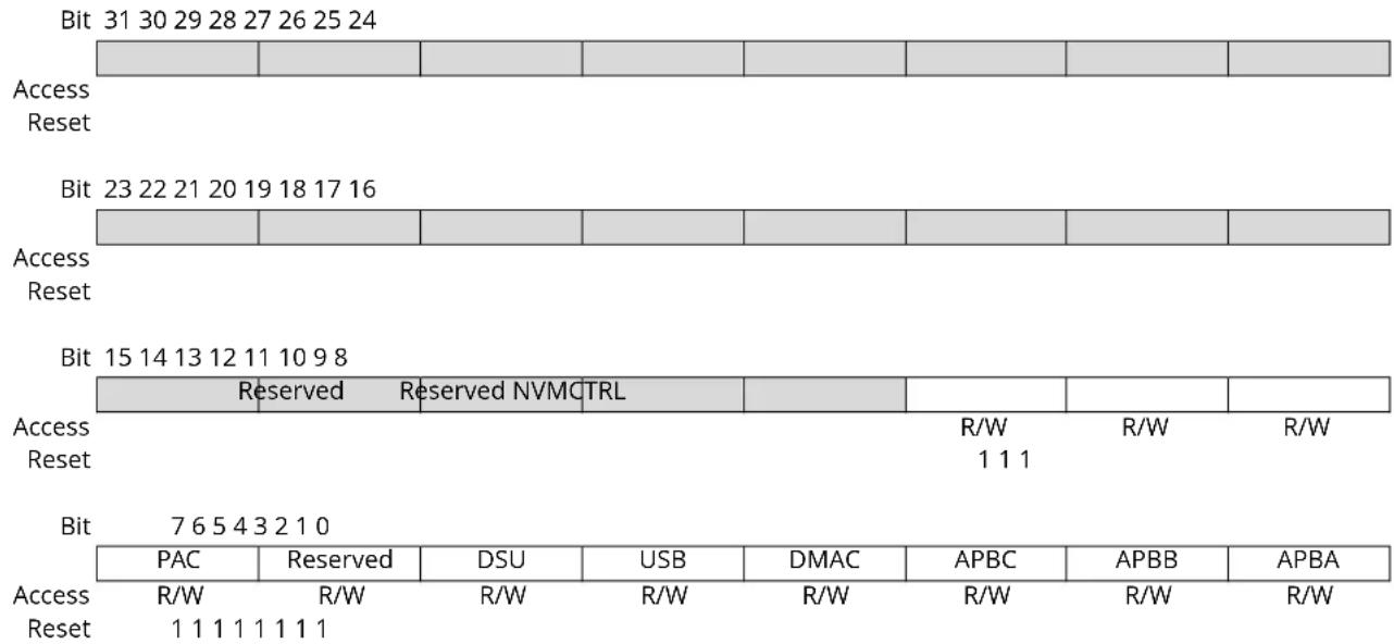
bar_stacked
| Bit | Total | | --- | --- | | Bit 31 | 31 | | Bit 29 | 29 | | Bit 28 | 28 | | Bit 27 | 27 | | Bit 26 | 26 | | Bit 25 | 25 | | Bit 24 | 24 | | Bit 23 | 23 | | Bit 22 | 22 | | Bit 21 | 21 | | Bit 19 | 19 | | Bit 18 | 18 | | Bit 17 | 17 | | Bit 16 | 16 | | Bit 15 | 15 | | Bit 14 | 14 | | Bit 13 | 13 | | Bit 12 | 12 | | Bit 11 | 11 | | Bit 9 | 9 | | Bit 8 | 8 | | Bit 7 | 7 | | Bit 6 | 6 | | Bit 5 | 5 | | Bit 4 | 4 | | Bit 3 | 3 | | Bit 2 | 2 | | Bit 1 | 1 | | Bit 0 | 0 | | Base | Reserved | | Base | NVMCTRL | | Base | R/W R/W R/W R/W R/W R/W R/W R/W R/W R/W R/W R/W R/W R/W R/W R/W R/W R/W R/W R/W R/W R/W R/W R/W R/W R/W R/W R/W R/W R/W R/W R/W R/W R/W R/BA Access Reset Access Reset Bit: PAC Access Reset: R/W R/W R/W R/W R/W R/W R/W R/W R/W R/W R/W R/W R/W R/W R/W R/W R/W R/W R/W R/W R/W R/W R/W R/W R/W R/W nan |Bits 10,9,6 - Reserved Reserved bits
Reserved bits are unused and reserved for future use. For compatibility with future devices, always write reserved bits to their reset value. If no reset value is given, write 0.
Bit 8 - NVMCTRL NVMCTRL AHB Clock Enable
| Value | Description |
| 0 | The AHB clock for the NVMCTRL is stopped |
| 1 | The AHB clock for the NVMCTRL is enabled |
Bit 7 - PAC PAC AHB Clock Enable
| Value | Description |
| 0 | The AHB clock for the PAC is stopped. |
| 1 | The AHB clock for the PAC is enabled. |
Bit 5 - DSU DSU AHB Clock Enable
| Value | Description |
| 0 | The AHB clock for the DSU is stopped. |
| 1 | The AHB clock for the DSU is enabled. |
Bit 4 - USB USB AHB Clock Enable
| Value | Description |
| 0 | The AHB clock for the USB is stopped. |
| 1 | The AHB clock for the USB is enabled. |
Bit 3 - DMAC DMAC AHB Clock Enable
| Value | Description |
| 0 | The AHB clock for the DMAC is stopped. |
Value Description
| 1 | The AHB clock for the DMAC is enabled. |
Bit 2 - APBC APBC AHB Clock Enable
Value Description
| 0 | The AHB clock for the APBC is stopped. |
| 1 | The AHB clock for the APBC is enabled |
Bit 1 - APBB APBB AHB Clock Enable
Value Description
| 0 | The AHB clock for the APBB is stopped. |
| 1 | The AHB clock for the APBB is enabled. |
Bit 0 - APBA APBA AHB Clock Enable
Value Description
| 0 | The AHB clock for the APBA is stopped. |
| 1 | The AHB clock for the APBA is enabled. |
16.8.7 APBA Mask
Name: APBAMASK
Offset: 0x14
Reset: 0x00000FFF
Property: PAC Write-Protection

other
| Bit | Access Reset | Bit 15 14 13 12 11 10 9 8 | |---|---|---| | 31 | | | | 29 | | | | 28 | | | | 27 | | | | 26 | | | | 25 | | | | 24 | | | FREQM EIC RTC WDT R/W R/W R/W R/W Reset 1 1 1 1 Access Reset Bit 7 6 5 4 3 2 1 0 GCLK SUPC OSC32KCTRL OSCCTRL RSTC MCLK PM PAC Access Reset R/W R/W R/W R/W R/W R/W R/W 1 1 1 1 1 1 1 1Bit 11 - FREQM FREQM APBA Clock Enable
| Value | Description |
| 0 | The APBA clock for the FREQM is stopped. |
| 1 | The APBA clock for the FREQM is enabled. |
Bit 10 - EIC EIC APBA Clock Enable
| Value | Description |
| 0 | The APBA clock for the EIC is stopped. |
| 1 | The APBA clock for the EIC is enabled. |
Bit 9 - RTC RTC APBA Clock Enable
| Value | Description |
| 0 | The APBA clock for the RTC is stopped. |
| 1 | The APBA clock for the RTC is enabled. |
Bit 8 - WDT WDT APBA Clock Enable
| Value | Description |
| 0 | The APBA clock for the WDT is stopped. |
| 1 | The APBA clock for the WDT is enabled. |
Bit 7 - GCLK GCLK APBA Clock Enable
| Value | Description |
| 0 | The APBA clock for the GCLK is stopped. |
| 1 | The APBA clock for the GCLK is enabled. |
Bit 6 - SUPC SUPC APBA Clock Enable
| Value Description | |
| 0 | The APBA clock for the SUPC is stopped. |
| 1 | The APBA clock for the SUPC is enabled. |
Bit 5 - OSC32KCTRL OSC32KCTRL APBA Clock Enable
| Value Description | |
| 0 | The APBA clock for the OSC32KCTRL is stopped. |
| 1 | The APBA clock for the OSC32KCTRL is enabled. |
Bit 4 - OSCCTRL OSCCTRL APBA Clock Enable
| Value Description | |
| 0 | The APBA clock for the OSCCTRL is stopped. |
| 1 | The APBA clock for the OSCCTRL is enabled. |
Bit 3 - RSTC RSTC APBA Clock Enable
| Value Description | |
| 0 | The APBA clock for the RSTC is stopped. |
| 1 | The APBA clock for the RSTC is enabled. |
Bit 2 - MCLK MCLK APBA Clock Enable
| Value Description | |
| 0 | The APBA clock for the MCLK is stopped. |
| 1 | The APBA clock for the MCLK is enabled. |
Bit 1 - PM PM APBA Clock Enable
| Value Description | |
| 0 | The APBA clock for the PM is stopped. |
| 1 | The APBA clock for the PM is enabled. |
Bit 0 - PAC PAC APBA Clock Enable
| Value Description | |
| 0 | The APBA clock for the PAC is stopped. |
| 1 | The APBA clock for the PAC is enabled. |
16.8.8 APBB Mask
Name: APBBMASK
Offset: 0x18
Reset: 0x0000004F
Property: PAC Write-Protection
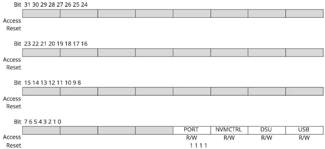
text_image
Bit 31 30 29 28 27 26 25 24 Access Reset Bit 23 22 21 20 19 18 17 16 Access Reset Bit 15 14 13 12 11 10 9 8 Access Reset Bit 7 6 5 4 3 2 1 0 Access Reset PORT NVMCTRL DSU USB R/W R/W R/W R/W 1 1 1 1Bit 3 - PORT PORT APBB Clock Enable
| Value | Description |
| 0 | The APBB clock for the PORT is stopped. |
| 1 | The APBB clock for the PORT is enabled. |
Bit 2 - NVMCTRL NVMCTRL APBB Clock Enable
| Value | Description |
| 0 | The APBB clock for the NVMCTRL is stopped |
| 1 | The APBB clock for the NVMCTRL is enabled |
Bit 1 - DSU DSU APBB Clock Enable
| Value | Description |
| 0 | The APBB clock for the DSU is stopped |
| 1 | The APBB clock for the DSU is enabled |
Bit 0 - USB USB APBB Clock Enable
| Value | Description |
| 0 | The APBB clock for the USB is stopped |
| 1 | The APBB clock for the USB is enabled |
Reserved bits are unused and reserved for future use. For compatibility with future devices, always write reserved bits to their reset value. If no reset value is given, write 0.
16.8.9 APBC Mask
Name: APBCMASK
Offset: 0x1C
Reset: 0x0007FFFF
Property: PAC Write-Protection
Bit 31 30 29 28 27 26 25 24
| Access Reset |
Bit 23 22 21 20 19 18 17 16
| CCL TRNG AES | |||||||
| Access Reset | R/W R/W R/W | ||||||
| 1 | 1 | 1 | |||||
Bit 15 14 13 12 11 10 9 8
| SLCD | PTC | AC | ADC | TC3 | TC2 | TC1 | TC0 | |
| Access | R/W | R/W | R/W | R/W | R/W | R/W | R/W | R/W |
| Reset | 1 | 1 | 1 | 1 | 1 | 1 | 1 | 1 |
Bit 7 6 5 4 3 2 1 0
| TCC0 | SERCOM5 | SERCOM4 | SERCOM3 | SERCOM2 | SERCOM1 | SERCOM0 | EVSYS | |
| Access | R/W R/W | R/W R/W | R/W R/W | R/W R/W | R/W R/W | |||
| Reset | 1 | 1 | 1 | 1 | 1 | 1 | 1 | 1 |
Bit 18 - CCL CCL APBC Mask Clock Enable
| Value | Description |
| 0 | The APBC clock for the CCL is stopped. |
| 1 | The APBC clock for the CCL is enabled. |
Bit 17 - TRNG TRNG APBC Mask Clock Enable
| Value | Description |
| 0 | The APBC clock for the TRNG is stopped. |
| 1 | The APBC clock for the TRNG is enabled. |
Bit 16 - AES AES APBC Mask Clock Enable
| Value | Description |
| 0 | The APBC clock for the AES is stopped. |
| 1 | The APBC clock for the AES is enabled. |
Bit 15 - SLCD SLCD
| Value | Description |
| 0 | The APBC clock for the SLCD is stopped. |
| 1 | The APBC clock for the SLCD is enabled. |
Bit 14 - PTC PTC APBC Mask Clock Enable
| Value | Description |
| 0 | The APBC clock for the PTC is stopped. |
| 1 | The APBC clock for the PTC is enabled. |
| Value Description | |
| 0 | The APBC clock for the AC is stopped. |
| 1 | The APBC clock for the AC is enabled. |
Bit 13 - AC AC APBC Mask Clock Enable
Bit 12 - ADC ADC APBC Mask Clock Enable
| Value Description | |
| 0 | The APBC clock for the ADC is stopped. |
| 1 | The APBC clock for the ADC is enabled. |
Bits 8, 9, 10, 11 - TCx TCx APBC Mask Clock Enable
| Value Description | |
| 0 | The APBC clock for the TCx is stopped. |
| 1 | The APBC clock for the TCx is enabled. |
Bit 7 - TCC0 TCC0 APBC Mask Clock Enable
| Value Description | |
| 0 | The APBC clock for the TCC0 is stopped. |
| 1 | The APBC clock for the TCC0 is enabled. |
Bits 1, 2, 3, 4, 5, 6 - SERCOMx SERCOMx APBC Mask Clock Enable
| Value Description | |
| 0 | The APBC clock for the SERCOMx is stopped. |
| 1 | The APBC clock for the SERCOMx is enabled. |
Bit 0 - EVSYS EVSYS APBC Clock Enable
| Value Description | |
| 0 | The APBC clock for the EVSYS is stopped. |
| 1 | The APBC clock for the EVSYS is enabled. |
17. FREQM - Frequency Meter
17.1 Overview
The Frequency Meter (FREQM) can be used to accurately measure the frequency of a clock by comparing it to a known reference clock.
17.2 Features
• Accurately measures a clock frequency
- A selectable reference clock from GCLK_FREQM_REF sources
- A selectable clock from GCLK_FREQM_MSR sources can be measured
• Ratio can be measured with 24-bit accuracy
17.3 Block Diagram
Figure 17-1. FREQM Block Diagram
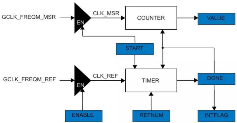
flowchart
graph TD
    A["GCLK_FREQM_MSR"] --> B["EN"]
    B --> C["CLK_MSR"]
    C --> D["COUNTER"]
    D --> E["VALUE"]
    F["GCLK_FREQM_REF"] --> G["EN"]
    G --> H["CLK_REF"]
    H --> I["TIMER"]
    I --> J["DONE"]
    J --> K["INTFLAG"]
    L["ENABLE"] --> G
    M["REFNUM"] --> I
    N["START"] --> I
    O["EN"] --> P["START"]
    Q["START"] --> R["TIMER"]
17.4 Signal Description
Not applicable.
17.5 Product Dependencies
In order to use this peripheral, other parts of the system must be configured correctly, as described below.
17.5.1 I/O Lines
Not applicable.
17.5.2 Power Management
The FREQM will continue to operate in idle sleep mode where the selected source clock is running. The FREQM's interrupts can be used to wake up the device from idle sleep mode. Refer to the 19. PM - Power Manager chapter for details on the different sleep modes.
17.5.3 Clocks
The clock for the FREQM bus interface (CLK_APB_FREQM) is enabled and disabled by the Main Clock Controller, the default state of CLK_APB_FREQM can be found in the 16.6.2.6. Peripheral Clock Masking section.
Two generic clocks are used by the FREQM(GCLK_FREQM_REF and GCLK_FREQM_MSR). The reference clock (GCLK_FREQM_REF) is required to clock the internal reference timer while operating as a frequency reference, while the measurement clock (GCLK_FREQM_MSR) is required to clock a ripple counter for frequency measurement. These clocks must be configured and enabled in the Generic Clock Controller before using the FREQM.
17.5.4 DMA
Not applicable.
17.5.5 Interrupts
The interrupt request line is connected to the Nested Vector Interrupt Controller. Using FREQM interrupt requires the interrupt controller to be configured first.
17.5.6 Events
Not applicable.
17.5.7 Debug Operation
When the CPU is halted in debug mode the FREQM continues its normal operation. The FREQM cannot be halted when the CPU is halted in debug mode. If the FREQM is configured in a way that requires it to be periodically serviced by the CPU, improper operation or data loss may result during debugging.
17.5.8 Register Access Protection
All registers with write access can be write-protected optionally by the Peripheral Access Controller (PAC), except the following registers:
• Control B register (CTRLB)
- Interrupt Flag Status and Clear register (INTFLAG)
- Status register (STATUS)
Optional write protection by the Peripheral Access Controller (PAC) is denoted by the "PAC Write Protection" property in each individual register description.
Write-protection does not apply to accesses through an external debugger.
17.6 Functional Description
17.6.1 Principle of Operation
During a period of REFNUM/ f_CLK_REF , the FREQM is counting the number of periods of the clock to be measured, VALUE. Here, REFNUM is the Number of Reference Clock Cycles selected in the Configuration A register (CFGA.REFNUM), VALUE is the Measurement result stored to the Value register (VALUE.VALUE), and f_CLK_REF is the frequency of the reference clock.
The frequency of the measured clock, f_CLK_MSR , is calculated by
$$ f _ {\mathrm {CLK_MSR}} = \left(\frac {\mathrm{VALUE}}{\mathrm{REFNUM}}\right) f _ {\mathrm {CLK_REF}} $$
17.6.2 Basic Operation
17.6.2.1 Initialization
Before enabling FREQM, the device and peripheral must be configured:
• Each of the generic clocks (GCLK_FREQM_REF and GCLK_FREQM_MSR) should be configured and enabled. Note that the reference clock should be slower than the measurement clock.
- The Number of Reference Clock Cycles value in the Configuration A register (CFGA.REFNUM) must be written to a value greater than 0x00.
The following register is enable-protected, meaning that it can only be written when the FREQM is disabled (CTRLA. ENABLE is zero):
- Configuration A register (CFGA)
Enable-protection is denoted by the "Enable-Protected" property in the register description.
For further information, refer to the GCLK.
17.6.2.2 Enabling, Disabling and Resetting
The FREQM is enabled by writing a '1' to the Enable bit in the Control A register (CTRLA.ENABLE). The peripheral is disabled by writing CTRLA.ENABLE=0.
The FREQM is reset by writing a '1' to the Software Reset bit in the Control A register (CTRLA.SWRST). On software reset, all registers in the FREQM will be reset to their initial state, and the FREQM will be disabled.
Then ENABLE and SWRST bits are write-synchronized.
For more information, refer to Synchronization.
17.6.2.3 Measurement
In the Configuration A register, the Number of Reference Clock Cycles field (CFGA.REFNUM) selects the duration of the measurement. The measurement is given in number of GCLK_FREQM_REF periods.
Note: The REFNUM field must be written before the FREQM is enabled.
After the FREQM is enabled, writing a '1' to the START bit in the Control B register (CTRLB.START) starts the measurement. The BUSY bit in Status register (STATUS.BUSY) is cleared when the measurement is done.
There is also an interrupt request for Measurement Done: When the Measurement Done bit in Interrupt Enable Set register (INTENSET.DONE) is '1' and a measurement is finished, the Measurement Done bit in the Interrupt Flag Status and Clear register (INTFLAG.DONE) will be set and an interrupt request is generated.
The result of the measurement can be read from the Value register (VALUE.VALUE). The frequency of the measured clock GCLK_FREQM_MSR is then:
$$ f _ {\mathrm {CLK_MSR}} = \left(\frac {\mathrm{VALUE}}{\mathrm{REFNUM}}\right) f _ {\mathrm {CLK_REF}} $$
Note: In order to make sure the measurement result (VALUE.VALUE[23:0]) is valid, the overflow status (STATUS.OVF) should be checked.
In case an overflow condition occurred, indicated by the Overflow bit in the STATUS register (STATUS.OVF), either the number of reference clock cycles must be reduced (CFGA.REFNUM), or a faster reference clock must be configured. Once the configuration is adjusted, clear the overflow status by writing a '1' to STATUS.OVF. Then another measurement can be started by writing a '1' to CTRLB.START.
17.6.3 DMA Operation
Not applicable.
17.6.4 Interrupts
The FREQM has one interrupt source:
• DONE: A frequency measurement is done
Each interrupt source has an interrupt flag associated with it. The interrupt flag in the Interrupt Flag Status and Clear (INTFLAG) register is set when the interrupt condition occurs. Each interrupt can be individually enabled by writing a '1' to the corresponding bit in the Interrupt Enable Set (INTENSET) register, and disabled by writing a '1' to the corresponding bit in the Interrupt Enable Clear (INTENCLR) register.
An interrupt request is generated when the interrupt flag is set and the corresponding interrupt is enabled. The interrupt request remains active until the interrupt flag is cleared, the interrupt is disabled, or the FREQM is reset. See INTFLAG for details on how to clear interrupt flags. All interrupt requests from the peripheral are ORed together on system level to generate one combined interrupt request to the NVIC. The user must read the INTFLAG register to determine which interrupt condition is present.
Note that interrupts must be globally enabled for interrupt requests to be generated.
17.6.5 Events
Not applicable.
17.6.6 Sleep Mode Operation
The FREQM will continue to operate in idle sleep modes where the selected source clock is running. The FREQM's interrupts can be used to wake up the device from idle sleep modes.
For lowest chip power consumption in sleep modes, FREQM should be disabled before entering a sleep mode.
For further information, refer to the Power Manager.
17.6.7 Synchronization
Due to asynchronicity between the main clock domain and the peripheral clock domains, some registers need to be synchronized when written or read.
The following bits and registers are write-synchronized:
- Software Reset bit in Control A register (CTRLA.SWRST)
- Enable bit in Control A register (CTRLA.ENABLE)
Required write synchronization is denoted by the "Write-Synchronized" property in the register description.
For more information refer to Register Synchronization.
17.7 Register Summary
| Offset | Name Bit Pos. 76543210 | |||||||||
| 0x00 CTRLA 7:0 ENABLE SWRST | ||||||||||
| 0x01 CTRLB 7:0 START | ||||||||||
| 0x02 CFGA | 7:0 REFNUM[7:0] | |||||||||
| 15:8 | ||||||||||
| 0x04 ... 0x07 | Reserved | |||||||||
| 0x08 | INTENCLR | 7:0 | DONE | |||||||
| 0x09 | INTENSET | 7:0 | DONE | |||||||
| 0x0A | INTFLAG | 7:0 | DONE | |||||||
| 0x0B | STATUS | 7:0 | OVF | BUSY | ||||||
| 0x0C | SYNCBUSY | 7:0 | ENABLE SWRST | |||||||
| 15:8 | ||||||||||
| 23:16 | ||||||||||
| 31:24 | ||||||||||
| 0x10 VALUE | 7:0 | VALUE[7:0] | ||||||||
| 15:8 VALUE[15:8] | ||||||||||
| 23:16 | VALUE[23:16] | |||||||||
| 31:24 | ||||||||||
17.8 Register Description
Registers can be 8, 16, or 32 bits wide. Atomic 8-, 16-, and 32-bit accesses are supported. In addition, the 8-bit quarters and 16-bit halves of a 32-bit register, and the 8-bit halves of a 16-bit register can be accessed directly.
Some registers require synchronization when read and/or written. Synchronization is denoted by the "Read-Synchronized" and/or "Write-Synchronized" property in each individual register description.
Some registers are enable-protected, meaning they can only be written when the module is disabled. Enable protection is denoted by the "Enable-Protected" property in each individual register description.
Some registers are optionally write-protected by the Peripheral Access Controller (PAC). Optional PAC write protection is denoted by the "PAC Write-Protection" property in each individual register description.
17.8.1 Control A
Name: CTRLA
Offset: 0x00
Reset: 0x00
Property: PAC Write-Protection
Bit 76543210
| ENABLE SWRST | ||||||
| Access Reset 0 0 | R/W R/W | |||||
Bit 1 - ENABLE Enable
Due to synchronization there is delay from writing CTRLA. ENABLE until the peripheral is enabled or disabled. The value written to CTRLA. ENABLE will read back immediately and the ENABLE bit in the Synchronization Busy register (SYNCBUSY. ENABLE) will be set. SYNCBUSY. ENABLE will be cleared when the operation is complete.
| Value Description | |
| 0 | The peripheral is disabled. |
| 1 | The peripheral is enabled. |
Bit 0 - SWRST Software Reset
Writing a '0' to this bit has no effect.
Writing a '1' to this bit resets all registers in the FREQM to their initial state, and the FREQM will be disabled. Writing a '1' to this bit will always take precedence, meaning that all other writes in the same write-operation will be discarded.
Due to synchronization there is a delay from writing CTRLA.SWRST until the Reset is complete.
CTRLA.SWRST and SYNCBUSY.SWRST will be cleared when the Reset is complete.
| Value Description | |
| 0 | There is no ongoing Reset operation. |
| 1 | The Reset operation is ongoing. |
17.8.2 Control B
Name: CTRLB
Offset: 0x01
Reset: 0x00
Property: -
Bit 76543210
| START | |||||||
| Access Reset 0 | W | ||||||
Bit 0 - START Start Measurement
| Value Description | |
| 0 | Writing a '0' has no effect. |
| 1 | Writing a '1' starts a measurement. |
17.8.3 Configuration A
Name: CFGA
Offset: 0x02
Reset: 0x0000
Property: PAC Write-Protection, Enable-protected
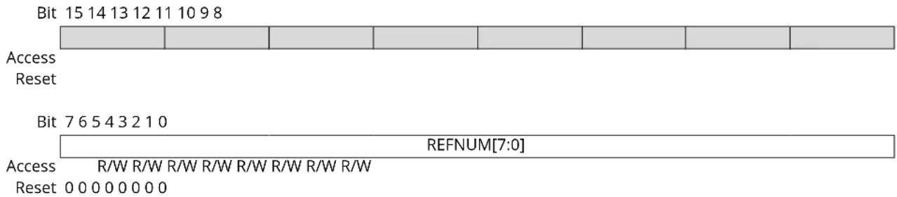
text_image
Bit 15 14 13 12 11 10 9 8 Access Reset Bit 7 6 5 4 3 2 1 0 REFNUM[7:0] Access R/W R/W R/W R/W R/W R/W R/W Reset 0 0 0 0 0 0 0 0Bits 7:0 - REFNUM[7:0] Number of Reference Clock Cycles
Selects the duration of a measurement in number of CLK_FREQM_REF cycles. This must be a non-zero value, i.e. 0x01 (one cycle) to 0xFF (255 cycles).
17.8.4 Interrupt Enable Clear
Name: INTENCLR
Offset: 0x08
Reset: 0x00
Property: PAC Write-Protection
Bit 76543210
| DONE | |||||||
| Access Reset 0 | R/W | ||||||
Bit 0 - DONE Measurement Done Interrupt Enable
Writing a '0' to this bit has no effect.
Writing a '1' to this bit will clear the Measurement Done Interrupt Enable bit, which disables the Measurement Done interrupt.
| Value Description | |
| 0 | The Measurement Done interrupt is disabled. |
| 1 | The Measurement Done interrupt is enabled. |
17.8.5 Interrupt Enable Set
Name: INTENSET
Offset: 0x09
Reset: 0x00
Property: PAC Write-Protection
Bit 76543210
| DONE | |||||||
| Access Reset 0 | R/W | ||||||
Bit 0 - DONE Measurement Done Interrupt Enable
Writing a '0' to this bit has no effect.
Writing a '1' to this bit will set the Measurement Done Interrupt Enable bit, which enables the Measurement Done interrupt.
| Value Description | |
| 0 | The Measurement Done interrupt is disabled. |
| 1 | The Measurement Done interrupt is enabled. |
17.8.6 Interrupt Flag Status and Clear
Name: INTFLAG
Offset: 0x0A
Reset: 0x00
Property: -
Bit 76543210
| DONE | |||||||
| Access Reset 0 | R/W | ||||||
Bit 0 - DONE Mesurement Done
This flag is cleared by writing a '1' to it.
This flag is set when the STATUS.BUSY bit has a one-to-zero transition.
Writing a '0' to this bit has no effect.
Writing a '1' to this bit will clear the DONE interrupt flag.
17.8.7 Status
Name: STATUS
Offset: 0x0B
Reset: 0x00
Property: -
Bit 76543210
| VF BUSY | |||||||
| Access Reset 0 0 | R/W R | ||||||
Bit 1 - OVF Sticky Count Value Overflow
This bit is cleared by writing a '1' to it.
This bit is set when an overflow condition occurs to the value counter.
Writing a '0' to this bit has no effect.
Writing a '1' to this bit will clear the OVF status.
Bit 0 - BUSY FREQM Status
| Value Description | |
| 0 | No ongoing frequency measurement. |
| 1 | Frequency measurement is ongoing. |
17.8.8 Synchronization Busy
Name: SYNCBUSY
Offset: 0x0C
Reset: 0x00000000
Property: -
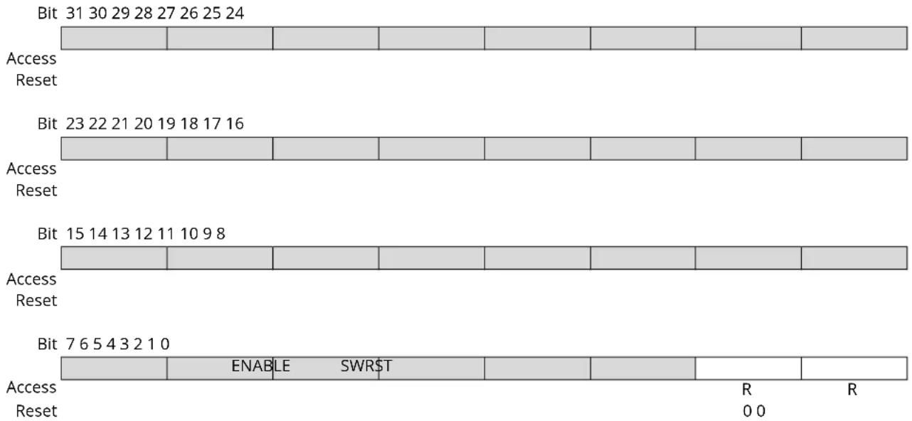
text_image
Bit 31 30 29 28 27 26 25 24 Access Reset Bit 23 22 21 20 19 18 17 16 Access Reset Bit 15 14 13 12 11 10 9 8 Access Reset Bit 7 6 5 4 3 2 1 0 Access Reset ENABLE SWR$T R R 0 0Bit 1 - ENABLE Enable
This bit is cleared when the synchronization of CTRLA. ENABLE is complete.
This bit is set when the synchronization of CTRLA. ENABLE is started.
Bit 0 - SWRST Synchronization Busy
This bit is cleared when the synchronization of CTRLA.SWRST is complete.
This bit is set when the synchronization of CTRLA.SWRST is started.
17.8.9 Value
Name: VALUE
Offset: 0x10
Reset: 0x00000000
Property: -
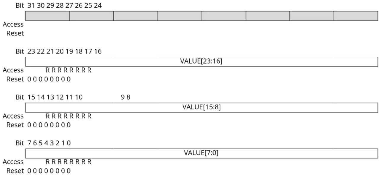
text_image
Bit 31 30 29 28 27 26 25 24 Access Reset Bit 23 22 21 20 19 18 17 16 VALUE[23:16] Access R R R R R R R R Reset 0 0 0 0 0 0 0 0 Bit 15 14 13 12 11 10 9 8 VALUE[15:8] Access R R R R R R R R Reset 0 0 0 0 0 0 0 0 Bit 7 6 5 4 3 2 1 0 VALUE[7:0] Access R R R R R R R R Reset 0 0 0 0 0 0 0 0Bits 23:0 - VALUE[23:0] Measurement Value Result from measurement.
18. RSTC – Reset Controller
18.1 Overview
The Reset Controller (RSTC) manages the reset of the microcontroller. It issues a microcontroller reset, sets the device to its initial state and allows the reset source to be identified by software.
18.2 Features
- Reset the microcontroller and set it to an initial state according to the reset source
- Reset cause register for reading the reset source from the application code
-
Multiple reset sources
-
Power supply reset sources: POR, BOD12, BOD33
- User reset sources: External reset (RESETN pin), Watchdog reset, and System Reset Request
- Backup exit sources: Real-Time Counter (RTC) and Battery Backup Power Switch (BBPS)
18.3 Block Diagram
Figure 18-1. Reset System
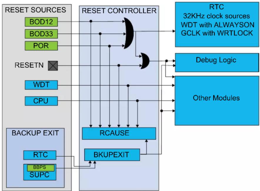
flowchart
graph TD
    A["RESET SOURCES"] --> B["BOD12"]
    A --> C["BOD33"]
    A --> D["POR"]
    E["RESETN"] --> F["WDT"]
    E --> G["CPU"]
    H["BACKUP EXIT"] --> I["RTC"]
    H --> J["BBPS"]
    H --> K["SUPC"]
    L["RESET CONTROLLER"] --> M["RCAUSE"]
    L --> N["BKUPEXIT"]
    O["RTC 32KHz clock sources WDT with ALWAYSON GCLK with WRTLOCK"] --> P["Debug Logic"]
    Q["Other Modules"] --> R["Other Modules"]
    S["RESET"] --> T["RESETN"]
    U["BUCKUP"] --> V["RCAUSE"]
    W["BUCKUP"] --> X["BKUPEXIT"]
18.4 Signal Description
| Signal Name Type Description | ||
| RESETN Digital Input External reset pin |
One signal can be mapped on several pins.
18.5 Product Dependencies
In order to use this peripheral, other parts of the system must be configured correctly, as described below.
18.5.1 I/O Lines
Not applicable.
18.5.2 Power Management
The Reset Controller module is always on.
18.5.3 Clocks
The RSTC bus clock (CLK_RSTC_APB) can be enabled and disabled in the Main Clock Controller.
18.5.4 DMA
Not applicable.
18.5.5 Interrupts
Not applicable.
18.5.6 Events
Not applicable.
18.5.7 Debug Operation
When the CPU is halted in debug mode, the RSTC continues normal operation.
18.5.8 Register Access Protection
All registers with write access can be optionally write-protected by the Peripheral Access Controller (PAC).
Note: Optional write protection is indicated by the "PAC Write Protection" property in the register description.
When the CPU is halted in debug mode, all write protection is automatically disabled. Write protection does not apply for accesses through an external debugger.
18.5.9 Analog Connections
Not applicable.
18.6 Functional Description
18.6.1 Principle of Operation
The Reset Controller collects the various Reset sources and generates Reset for the device.
18.6.2 Basic Operation
18.6.2.1 Initialization
After a power-on Reset, the RSTC is enabled and the Reset Cause (RCAUSE) register indicates the POR source.
18.6.2.2 Enabling, Disabling, and Resetting
The RSTC module is always enabled.
18.6.2.3 Reset Causes and Effects
The latest Reset cause is available in RCAUSE register, and can be read during the application boot sequence in order to determine proper action.
These are the groups of Reset sources:
- Power supply Reset: Resets caused by an electrical issue. It covers POR and BODs Resets
- User Reset: Resets caused by the application. It covers external Resets, system Reset requests and watchdog Resets
- Backup reset: Resets caused by a Backup Mode exit condition
The following table lists the parts of the device that are reset, depending on the Reset type.
Table 18-1. Effects of the Different Reset Causes
| Power Supply Reset | User Reset Backup Reset | ||||
| POR, BOD33 | BOD12 | External Reset W | WDT Reset, System Reset Request | RTC, BBPS | |
| RTC, OSC32KCTRL, RSTC, CTRLA.IORET bit of PM | Y N N N N | ||||
| GCLK with WRTLOCK Y Y N N Y | |||||
| Debug logic Y Y Y N Y | |||||
| Others Y Y Y Y Y | |||||
The external Reset is generated when pulling the RESET pin low.
The POR, BOD12, and BOD33 Reset sources are generated by their corresponding module in the Supply Controller Interface (SUPC).
The WDT Reset is generated by the Watchdog Timer.
The System Reset Request is a Reset generated by the CPU when asserting the SYSRESETREQ bit located in the Reset Control register of the CPU (for details refer to the ARM® Cortex™ Technical Reference Manual on http://www.arm.com).
From Backup Mode, the chip can be waken-up upon these conditions:
- Battery Backup Power Switch (BBPS): generated by the SUPC controller when the 3.3V VDDIO is restored.
• Real-Time Counter interrupt. For details refer to the applicable INTFLAG in the RTC for details.
If one of these conditions is triggered in Backup Mode, the RCAUSE.BACKUP bit is set and the Backup Exit Register (BKUPEXIT) is updated.
18.6.3 Additional Features
Not applicable.
18.6.4 DMA Operation
Not applicable.
18.6.5 Interrupts
Not applicable.
18.6.6 Events
Not applicable.
18.6.7 Sleep Mode Operation
The RSTC module is active in all sleep modes.
18.7 Register Summary
| Offset | Name Bit Pos. 7 | 6 | 5 | 4 | 3 | 2 | 1 | 0 | ||||||||||||||||||||||||||||||||||||||||||||||||||||||||||||||||||||||||||||||||||||||||||||||||||||||||||||||||||||||||||||||||||||||||||||||||||||||||||||||||||||||||||||||||||||||||||||||||||||||||||||||||||||||||||||||||||||||||||||||||||||||||||||||||||||||||||||||||||||||||||||||||||||||||||||||||||||||||||||||||||||||||||||||||||||||||||||||||||||||||||||||||||||||||||||||||||||||||||||||||||||||||||||||||||||||||||||||||||||||||||||||||||||||||||||||||||||||||||||||||||||||||||||||||||||||||||||||||||||||||||||||||||||||||||||||||||||||||||||||||||||||||||||||||||||||||||
| 0x00 | RCAUSE | 7:0 | BACKUP | SYST | WDT | EXT | BOD33 | BOD12 | POR | 0x01 | Reserved | |||||||||||||||||||||||||||||||||||||||||||||||||||||||||||||||||||||||||||||||||||||||||||||||||||||||||||||||||||||||||||||||||||||||||||||||||||||||||||||||||||||||||||||||||||||||||||||||||||||||||||||||||||||||||||||||||||||||||||||||||||||||||||||||||||||||||||||||||||||||||||||||||||||||||||||||||||||||||||||||||||||||||||||||||||||||||||||||||||||||||||||||||||||||||||||||||||||||||||||||||||||||||||||||||||||||||||||||||||||||||||||||||||||||||||||||||||||||||||||||||||||||||||||||||||||||||||||||||||||||||||||||||||||||||||||||||||||||||||||||||||||||||||||||||||||||
| 0x01 | Reserved | 0x02 | BKUPEXIT | 7:0 | 0x02 | BKUPEXIT | 7:0 | BBPS | RTC | 0x02 | BKUPEXIT | 7:0 | ||||||||||||||||||||||||||||||||||||||||||||||||||||||||||||||||||||||||||||||||||||||||||||||||||||||||||||||||||||||||||||||||||||||||||||||||||||||||||||||||||||||||||||||||||||||||||||||||||||||||||||||||||||||||||||||||||||||||||||||||||||||||||||||||||||||||||||||||||||||||||||||||||||||||||||||||||||||||||||||||||||||||||||||||||||||||||||||||||||||||||||||||||||||||||||||||||||||||||||||||||||||||||||||||||||||||||||||||||||||||||||||||||||||||||||||||||||||||||||||||||||||||||||||||||||||||||||||||||||||||||||||||||||||||||||||||||||||||||||||||||||||||||||||||||||||
18.8 Register Description
Registers can be 8, 16, or 32 bits wide. Atomic 8-, 16- and 32-bit accesses are supported. In addition, the 8-bit quarters and 16-bit halves of a 32-bit register, and the 8-bit halves of a 16-bit register can be accessed directly.
Some registers are optionally write-protected by the Peripheral Access Controller (PAC). Optional PAC write-protection is denoted by the "PAC Write-Protection" property in each individual register description. For details, refer to Register Access Protection.
18.8.1 Reset Cause
Name: RCAUSE
Offset: 0x00
Reset: Latest Reset Source
Property: -
When a Reset occurs, the bit corresponding to the Reset source is set to '1' and all other bits are written to '0'.
Bit 76543210
| BACKUP SYST WDT EXT | BOD33 BOD12 | POR | ||||||
| Access | R | R | R | R | R | R | R | |
| Reset | x | x | x | x | x | x | x | |
Bit 7 - BACKUP Backup Reset
This bit is set if a Backup Reset has occurred. Refer to BKUPEXIT register to identify the source of the Backup Reset.
Bit 6 - SYST System Reset Request
This bit is set if a System Reset Request has occurred. Refer to the Cortex processor documentation for more details.
Bit 5 - WDT Watchdog Reset
This bit is set if a Watchdog Timer Reset has occurred.
Bit 4 - EXT External Reset
This bit is set if an external Reset has occurred.
Bit 2 - BOD33 Brown Out 33 Detector Reset
This bit is set if a BOD33 Reset has occurred.
Bit 1 - BOD12 Brown Out 12 Detector Reset
This bit is set if a BOD12 Reset has occurred.
Bit 0 - POR Power On Reset
This bit is set if a POR has occurred.
18.8.2 Backup Exit Source
Name: BKUPEXIT
Offset: 0x02
Reset: Latest Backup Exit Source
Property: -
When a Backup Reset occurs, the bit corresponding to the exit condition is set to '1', the other bits are written to '0'.
In some specific cases, the RTC and BBPS bits can be set together, e.g. when the device leaves the battery Backup Mode caused by a BBPS condition, and a RTC event was generated during the Battery Backup Mode period.
Bit 76543210
| BBPS RTC | |||||||
| Access Reset x | x | R | R |
Bit 2 - BBPS Battery Backup Power Switch
This bit is set if the Battery Backup Power Switch of the Supply Controller changes back from battery mode to main power mode.
Bit 1 - RTC Real Timer Counter Interrupt
This bit is set if an RTC interrupt flag is set in Backup Mode. For more information, refer to the 24. RTC - Real-Time Counter.
19. PM - Power Manager
19.1 Overview
The Power Manager (PM) controls the sleep modes of the device.
Various sleep modes are provided in order to fit power consumption requirements. This enables the PM to stop unused modules in order to save power. In active mode, the CPU is executing application code. When the device enters a sleep mode, program execution is stopped and some modules and clock domains are automatically switched off by the PM according to the sleep mode. The application code decides which sleep mode to enter and when. Interrupts from enabled peripherals and all enabled reset sources can restore the device from a sleep mode to active mode.
Performance level technique consists of adjusting the regulator output voltage to reduce power consumption. The user can select on the fly the performance level configuration which best suits the application.
In backup mode, the PM allows retaining the state of the I/O lines, preventing I/O lines from toggling during wake-up.
19.2 Features
• Power management control
- Sleep modes: Idle, Standby, Backup, and Off
- Performance levels: PL0 and PL2
– SleepWalking available in Standby mode. - I/O lines retention in Backup mode
19.3 Block Diagram
Figure 19-1. PM Block Diagram
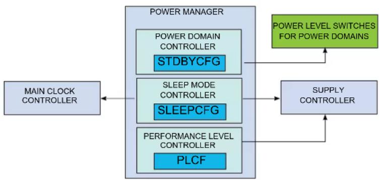
flowchart
graph TD
    A["MAIN CLOCK CONTROLLER"] --> B["POWER MANAGER"]
    B --> C["POWER DOMAIN CONTROLLER STDBYCFG"]
    B --> D["SLEEP MODE CONTROLLER SLEEPCFG"]
    B --> E["PERFORMANCE LEVEL CONTROLLER PLCF"]
    C --> F["POWER LEVEL SWITCHES FOR POWER DOMAINS"]
    D --> F
    E --> F
    F --> G["SUPPLY CONTROLLER"]
19.4 Signal Description
Not applicable.
19.5 Product Dependencies
In order to use this peripheral, other parts of the system must be configured correctly, as described below.
19.5.1 I/O Lines
Not applicable.
19.5.2 Clocks
The PM bus clock (CLK_PM_APB) can be enabled and disabled in the Main Clock module. If this clock is disabled, it can only be re-enabled by a system reset.
19.5.3 DMA
Not applicable.
19.5.4 Interrupts
The interrupt request line is connected to the interrupt controller. Using the PM interrupt requires the interrupt controller to be configured first.
19.5.5 Events
Not applicable.
19.5.6 Debug Operation
When the CPU is halted in debug mode, the PM continues normal operation. If standby sleep mode is requested by the system while in debug mode, the power domains are not turned off. As a consequence, power measurements while in debug mode are not relevant.
If Backup sleep mode is requested by the system while in debug mode, the core domains are kept on, and the debug modules are kept running to allow the debugger to access internal registers. When exiting the backup mode upon a reset condition, the core domains are reset except the debug logic, allowing users to keep using their current debug session.
Hot plugging in standby mode is supported.
Cold or Hot plugging in OFF or Backup mode is not supported.
19.5.7 Register Access Protection
Registers with write access can be write-protected optionally by the Peripheral Access Controller (PAC).
PAC write protection is not available for the following registers:
- Interrupt Flag register (INTFLAG).
Optional PAC write protection is denoted by the "PAC Write-Protection" property in each individual register description.
Write-protection does not apply to accesses through an external debugger.
19.5.8 Analog Connections
Not applicable.
19.6 Functional Description
19.6.1 Terminology
The following is a list of terms used to describe the Power Management features of this microcontroller.
19.6.1.1 Performance Levels
To help balance between performance and power consumption, the device has two performance levels. Each of the performance levels has a maximum operating frequency and a corresponding maximum consumption in A/MHz.
It is the application's responsibility to configure the appropriate PL depending on the application activity level. When the application selects a new PL, the voltage applied on the full logic area
moves from one value to another. This voltage scaling technique allows to reduce the active power consumption while decreasing the maximum frequency of the device.
19.6.1.1.1 PLO
Performance Level 0 (PL0) provides the maximum energy efficiency configuration.
Refer to the Electrical Characteristics chapters for details on energy consumption and maximum operating frequency.
19.6.1.1.2 PL2
Performance Level 2 (PL2) provides the maximum operating frequency.
Refer to the Electrical Characteristics chapters for details on energy consumption and maximum operating frequency.
19.6.1.2 Power Domains
In addition to the supply domains, such as VDDIO and VDDANA, the device provides these power domains:
- PDTOP
- PDBACKUP
19.6.1.2.1 PDTOP
PDTOP contains all controllers located in the core domain. It is powered when in Active, Idle or Standby mode. When in Backup or Off mode, this domain is completely powered down.
19.6.1.2.2 PDBACKUP
The Backup Power Domain (PDBACKUP) is always on, except in the off sleep mode. It contains the 32KHz oscillator sources, the Supply Controller, the Reset Controller, the Real Time Counter, and the Power Manager itself.
19.6.1.3 Sleep Modes
The device can be set in a sleep mode. In sleep mode, the CPU is stopped and the peripherals are either active or idle, according to the sleep mode depth:
- Idle sleep mode: The CPU is stopped. Synchronous clocks are stopped except when requested. The logic is retained.
- Standby sleep mode: The CPU is stopped as well as the peripherals.
- Backup sleep mode: Only the backup domain is kept powered to allow few features to run (RTC, 32KHz clock sources, and wake-up from external pins).
- Off sleep mode: The entire device is powered off.
19.6.2 Principle of Operation
In active mode, all clock domains and power domains are active, allowing software execution and peripheral operation. The PM Sleep Mode Controller allows to save power by choosing between different sleep modes depending on application requirements, see 19.6.3.3. Sleep Mode Controller.
The PM Performance Level Controller allows to optimize either for low power consumption or high performance.
The PM Power Domain Controller allows to reduce the power consumption in standby mode even further.
19.6.3 Basic Operation
19.6.3.1 Initialization
After a Power-on Reset (POR), the PM is enabled, the device is in Active mode, the performance level is PLO (the lowest power consumption) and all the power domains are in active state.
19.6.3.2 Enabling, Disabling and Resetting
The PM is always enabled and can not be reset.
19.6.3.3 Sleep Mode Controller
Sleep mode is entered by executing the Wait For Interrupt instruction (WFI). The Sleep Mode bits in the Sleep Configuration register (SLEEPCFG.SLEEPMODE) select the level of the sleep mode.
Note: A small latency happens between the store instruction and actual writing of the SLEEPCFG register due to bridges. Software must ensure that the SLEEPCFG register reads the desired value before issuing a WFI instruction.
Table 19-1. Sleep Mode Entry and Exit Table
| Mode Mode Entry Wake-Up Sources | |
| IDLE SLEEPCFG.SLEEPMODE = IDLE Synchronous | (2) (APB, AHB), asynchronous (1) |
| STANDBY SLEEPCFG.SLEEPMODE = STANDBY Synchronous | (3), Asynchronous |
| BACKUP SLEEPCFG.SLEEPMODE = BACKUP Backup reset detected by the RSTC | |
| OFF SLEEPCFG.SLEEPMODE = OFF External Reset |
Notes:
- Asynchronous: interrupt generated on generic clock, external clock, or external event.
- Synchronous: interrupt generated on the APB clock.
- Synchronous interrupt only for peripherals configured to run in standby.
Note: The type of wake-up sources (synchronous or asynchronous) is given in each module interrupt section.
The sleep modes (idle, standby, backup, and off) and their effect on the clocks activity, the regulator and the NVM state are described in the table and the sections below.
Table 19-2. Sleep Mode Overview
| Mode Main | clock | CPU AHBx and APBx clock | GCLK clocks | Oscillators Regulator NVM | ||||
| ONDEMAND = 0 | ONDEMAND = 1 | |||||||
| Active | Run | Run | Run | Run^(3) | Run | Run if requested | MAINVREG | active |
| IDLE | Run | Stop | Stop^(1) | Run^(3) | Run | Run if requested | MAINVREG | active |
| STANDBY | Stop^(1) | Stop | Stop^(1) | Stop^(1) | Run if requested or RUNSTDBY=1 | Run if requested | MAINVREG in low power mode | Ultra Low- power |
| BACKUP | Stop | Stop | Stop | Stop | Stop | Stop | Backup regulator ( LPVREG) | OFF |
| OFF | Stop | Stop | Stop | OFF | OFF | OFF | OFF | OFF |
Notes:
- Running if requested by peripheral during SleepWalking.
- Running during SleepWalking.
- Following On-Demand Clock Request principle.
19.6.3.3.1 IDLE Mode
IDLE mode allows power optimization with the fastest wake-up time.
The CPU is stopped, and peripherals are still working. As in Active mode, the AHBx and APBx clocks for peripheral are still provided if requested. As the main clock source is still running, wake-up time is very fast.
- Entering Idle mode: The Idle mode is entered by executing the WFI instruction. Additionally, if the SLEEPONEXIT bit in the Cortex System Control register (SCR) is set, the Idle mode will be entered
when the CPU exits the lowest priority ISR (Interrupt Service Routine, refer to the ARM Cortex documentation for details). This mechanism can be useful for applications that only require the processor to run when an interrupt occurs. Before entering the Idle mode, the user must select the Idle Sleep mode in the Sleep Configuration register (SLEEPCFG.SLEEPMODE=IDLE).
- Exiting Idle mode: The processor wakes the system up when it detects any non-masked interrupt with sufficient priority to cause exception entry. The system goes back to the Active mode. The CPU and affected modules are restarted.
GCLK clocks, regulators and RAM are not affected by the Idle Sleep mode and operate in normal mode.
19.6.3.3.2 STANDBY Mode
The Standby mode is the lowest power configuration while keeping the state of the logic and the content of the RAM.
In this mode, all clocks are stopped except those configured to be running sleepwalking tasks. The clocks can also be active on request or at all times, depending on their on-demand and run-in-standby settings. Either synchronous (CLK_APBx or CLK_AHBx) or generic (GCLK_x) clocks or both can be involved in sleepwalking tasks. This is the case when for example the SERCOM RUNSTDBY bit is written to '1'.
- Entering Standby mode: This mode is entered by executing the WFI instruction after writing the Sleep Mode bit in the Sleep Configuration register (SLEEPCFG.SLEEPMODE=STANDBY). The SLEEPONEXIT feature is also available as in Idle mode.
- Exiting Standby mode: Any peripheral able to generate an asynchronous interrupt can wake up the system. For example, a peripheral running on a GCLK clock can trigger an interrupt. When the enabled asynchronous wake-up event occurs and the system is woken up, the device will either execute the interrupt service routine or continue the normal program execution according to the Priority Mask Register (PRIMASK) configuration of the CPU.
Refer to the "Regulators, RAMs, and NVM State in Sleep Mode" for the RAM state.
The regulator operates in Low-Power mode by default and switches automatically to the normal mode in case of a sleepwalking task requiring more power. It returns automatically to low power mode when the sleepwalking task is completed.
19.6.3.3.3 BACKUP Mode
The BACKUP mode allows achieving the lowest power consumption aside from OFF. The device is entirely powered off except for the backup domain. All peripherals in backup domain are allowed to run, e.g. the RTC can be clocked by a 32.768kHz oscillator. All PM registers are reset except the CTRLA.IORET bit.
- Entering Backup mode: This mode is entered by executing the WFI instruction after selecting the Backup mode by writing the Sleep Mode bits in the Sleep Configuration register (SLEEPCFG.SLEEPMODE=BACKUP).
- Exiting Backup mode: is triggered when a Backup Reset is detected by the Reset Controller (RSTC).
19.6.3.3.4 OFF Mode
In Off mode, the device is entirely powered-off.
- Entering Off mode: This mode is entered by selecting the Off mode in the Sleep Configuration register by writing the Sleep Mode bits (SLEEPCFG.SLEEPMODE=OFF), and subsequent execution of the WFI instruction.
- Exiting Off mode: This mode is left by pulling the RESET pin low, or when a power Reset is done.
19.6.3.4 I/O Lines Retention in BACKUP Mode
When entering BACKUP mode, the PORT is powered off but the pin configuration is retained. When the device exits the BACKUP mode, the I/O line configuration can either be released or stretched, based on the I/O Retention bit in the CTRLA register (CTRLA.IORET).
- If IORET=0 when exiting BACKUP mode, the I/O lines configuration is released and driven by the reset value of the PORT.
- If the IORET=1 when exiting BACKUP mode, the configuration of the I/O lines is retained until the IORET bit is written to 0. It allows the I/O lines to be retained until the application has programmed the PORT.
19.6.3.5 Performance Level
The application can change the performance level on the fly writing to the by Performance Level Select bit in the Performance Level Configuration register (PLCFG.PLSEL).
When changing to a lower performance level, the bus frequency must be reduced before writing PLCFG.PLSEL in order to avoid exceeding the limit of the target performance level.
When changing to a higher performance level, the bus frequency can be increased only after the Performance Level Ready flag in the Interrupt Flag Status and Clear (INTFLAG.PLRDY) bit set to '1', indicating that the performance level transition is complete.
After a reset, the device starts in the lowest PL (lowest power consumption and lowest max frequency). The application can then switch to another PL at anytime without any stop in the code execution. As shown in Figure 19-2, performance level transition is possible only when the device is in active mode.
The Performance Level Disable bit in the Performance Level Configuration register (PLCFG.PLDIS) can be used to freeze the performance level to PL0. This disables the performance level hardware mechanism in order to reduce both the power consumption and the wake-up startup time from standby sleep mode.
Note: This bit PLCFG.PLDIS must be changed only when the current performance level is PLO.
Any attempt to modify this bit while the performance level is not PL0 is discarded and a violation is reported to the PAC module. Any attempt to change the performance level to PLn (with n>0) while PLCFG.PLDIS=1 is discarded and a violation is reported to the PAC module.
Figure 19-2. Sleep Modes and Performance Level Transitions
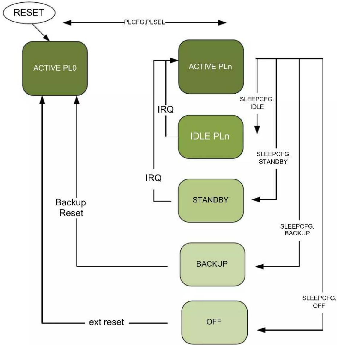
flowchart
graph TD
    A["RESET"] --> B["ACTIVE PL0"]
    B --> C["Active PLn"]
    C --> D["IDLE PLn"]
    D --> E["STANDBY"]
    E --> F["BACKUP"]
    F --> G["OFF"]
    G --> H["SLEEPCFG. OFF"]
    C --> I["SLEEPCFG. IDLE"]
    I --> J["SLEEPCFG. STANDBY"]
    J --> K["SLEEPCFG. BACKUP"]
    K --> L["SLEEPCFG. IDLE"]
    L --> M["IDLE PLn"]
    M --> N["ACTIVE PLn"]
    N --> O["OUTPUT"]
    style A fill:#d4edda,stroke:#333
    style B fill:#d4edda,stroke:#333
    style C fill:#d4edda,stroke:#333
    style D fill:#d4edda,stroke:#333
    style E fill:#d4edda,stroke:#333
    style F fill:#d4edda,stroke:#333
    style G fill:#d4edda,stroke:#333
    style H fill:#d4edda,stroke:#333
    style I fill:#d4edda,stroke:#333
    style J fill:#d4edda,stroke:#333
    style K fill:#d4edda,stroke:#333
    style L fill:#d4edda,stroke:#333
    style M fill:#d4edda,stroke:#333
    style N fill:#d4edda,stroke:#333
    style O fill:#d4edda,stroke:#333
    style P fill:#d4edda,stroke:#333
    style Q fill:#d4edda,stroke:#333
    style R fill:#d4edda,stroke:#333
    style S fill:#d4edda,stroke:#333
    style T fill:#d4edda,stroke:#333
    style U fill:#d4edda,stroke:#333
    style V fill:#d4edda,stroke:#333
    style W fill:#d4edda,stroke:#333
    style X fill:#d4edda,stroke:#333
    style Y fill:#d4edda,stroke:#333
    style Z fill:#d4edda,stroke:#333
19.6.3.6 Regulators, RAMs, and NVM State in Sleep Mode
By default, in Standby Sleep mode and backup sleep mode, the RAMs, NVM, and regulators are automatically set in Low-Power mode to reduce power consumption:
- The RAM is in Low-Power mode if the device is in standby mode. Refer to RAM Automatic Low Power Mode for details.
• Non-Volatile Memory - the NVM is automatically set in low power mode in these conditions:
- When the device is in Standby Sleep mode and the NVM is not accessed. This behavior can be changed by software by configuring the SLEEPPRM bit group of the CTRLB register in the NVMCTRL peripheral.
- When the device is in Idle Sleep mode and the NVM is not accessed. This behavior can be changed by software by configuring the SLEEPPRM bit group of the CTRLB register in the NVMCTRL peripheral.
- Regulators: by default, in Standby Sleep mode, the PM analyzes the device activity to use either the main or the low-power voltage regulator to supply the VDDCORE.
GCLK clocks, regulators and RAM are not affected in Idle Sleep mode and will operate as normal.
Table 19-3. Regulators, RAMs, and NVM state in Sleep Mode
| Sleep Mode | SRAM Mode^(1) | NVM | Regulators | ||
| VDDCORE | VDDBU | ||||
| main ULP | |||||
| Active normal normal on on on | |||||
| Idle auto | (2) | on on on on | |||
| Standby - case 1 normal auto | (2) | auto^(3) | on on | ||
| Standby - case 2 low power low power auto | (3) | on on | |||
| Standby - case 3 low power low power auto | (3) | on on | |||
| Standby - case 4 | low power | low power | off | on | on |
| Backup | off | off | off | off | on |
| Off | off | off | off | off | off |
Notes:
- RAMs mode by default: STDBYCFG.BBIAS bits are set to their default value.
- auto: by default, NVM is in low-power mode if not accessed.
- auto: by default, the main voltage regulator is on if GCLK, APBx, or AHBx clock is running during SleepWalking.
Related Links:
RAM Automatic Low Power Mode
Regulator Automatic Low Power Mode
19.6.4 Advanced Features
19.6.4.1 RAM Automatic Low Power Mode
The RAM is by default put in low power mode (back-biased) if the device is in standby sleep mode.
This behavior can be changed by configuring the Back Bias bit groups in the Standby Configuration register (STDBYCFG.BBIASxx), refer to the table below for details.
Note: In standby sleep mode, the RAM is put in low-power mode by default. This means that the RAM is back-biased, and the DMAC cannot access it. The DMAC can only access the RAM when it is not back biased (PM.STDBYCFG.BBIASxx=0x0).
Table 19-4. RAM Back-Biasing Mode
| STBYCDFG.BBIASxx config | RAM | |
| 0x0 | No Back Biasing mode | No Back Biasing in Standby mode |
| 0x1 | Standby Back Biasing mode | RAM is back-biased if the device is in standby sleep mode |
| 0x2 | Standby OFF mode | RAM is OFF if the device is in standby sleep mode |
| 0x3 | Always OFF mode | RAM is OFF if its power domain is in retention state |
19.6.4.2 Regulator Automatic Low-Power Mode
In Standby mode, the PM selects either the main or the low-power voltage regulator to supply the VDDCORE.
If a sleepwalking task is working on either asynchronous clocks (generic clocks) or synchronous clock (APB/AHB clocks), the main voltage regulator is used. This behavior can be changed by writing the
Voltage Regulator Standby Mode bits in the Standby Configuration register (STDBYCFG.VREGSMOD). Refer to the following table for details.
Table 19-5. Regulator State in Sleep Mode
| Sleep Modes | STDBYCFG. VREGSMOD | SleepWalking^(1) | Regulator state for VDDCORE |
| Active -- main voltage regulator | |||
| Idle -- main voltage regulator | |||
| Standby 0x0: AUTO NO low-power regulator | |||
| YES main voltage regulator | |||
| 0x1: PERFORMANCE - main voltage regulator | |||
| 0x2: LP^(2) | -(2) low-power regulator | ||
Notes:
- SleepWalking is running on GCLK clock or synchronous clock. This is not related to XOSC32K or OSCULP32K clocks.
- Must only be used when SleepWalking is running on GCLK with 32.768 kHz source.
19.6.4.3 SleepWalking and Performance Level
SleepWalking is the capability for a device to temporarily wake up clocks for a peripheral to perform a task without waking up the CPU from STANDBY sleep mode. At the end of the sleepwalking task, the device can either be woken up by an interrupt (from a peripheral involved in SleepWalking) or enter again into STANDBY sleep mode. In this device, SleepWalking is supported only on GCLK clocks by using the on-demand clock principle of the clock sources.
In standby mode, when SleepWalking is ongoing, the performance level used to execute the sleepwalking task is the current configured performance level (used in active mode), and the main voltage regulator used to execute the SleepWalking task is the selected regulator used in active mode (LDO or Buck converter).
These are illustrated in the figure below.
Figure 19-3. Operating Conditions and SleepWalking

flowchart
graph TD
    subgraph Sleep Mode
        A["ACTIVE"] --> B["ACTIVE ACTIVE"]
        C["IDLE"] --> B
        D["SleepWalking PL0"] --> E["SleepWalking PL2"]
        F["STANDBY"] --> G["STANDBY"]
        H["BACKUP"] --> I["BACKUP"]
    end

    subgraph Regulator Modes
        J["RESET"] --> K["LDO"]
        K --> L["LDO"]
        L --> M["LP VREG"]
        M --> N["BUCK"]
        N --> O["BUCK"]
        O --> P["SUPC. VREG.SEL"]
        P --> Q["BUCK"]
        Q --> R["MAIN VREG OFF"]
    end

    B <--> I
    C <--> D
    E <--> F
    G <--> H
    I <--> J
    style Sleep Mode fill:#f9f,stroke:#333
    style Regulator Modes fill:#bbf,stroke:#333
19.6.4.4 Wake-Up Time
The total wake-up time depends on the following:
- Latency due to Performance Level and Regulator effect: Performance Level has to be taken into account for the global wake-up time. As example, if PL2 is selected and the device is in Standby Sleep mode, the voltage level supplied by the ULP voltage regulator is lower than the one used in Active mode. When the device wakes up, it takes a certain amount of time for the main regulator to transition to the voltage level corresponding to PL2, causing additional wake-up time.
• Latency due to the CPU clock source wake-up time.
• Latency due to the NVM memory access. - Latency due to Switchable Power Domain back-bias wake-up time: If back-bias is enabled, and the device wakes up from retention, it takes a certain amount of time for the regulator to settle.
19.6.5 DMA Operation
Not applicable.
19.6.6 Interrupts
The peripheral has the following interrupt sources:
• Performance Level Ready (PLRDY)
This interrupt is a synchronous wake-up source. See Table 19-1 for details.
Each interrupt source has an interrupt flag associated with it. The interrupt flag in the Interrupt Flag Status and Clear (INTFLAG) register is set when the interrupt condition occurs. Each interrupt
can be individually enabled by writing a '1' to the corresponding bit in the Interrupt Enable Set (INTENSET) register, and disabled by writing a '1' to the corresponding bit in the Interrupt Enable Clear (INTENCLR) register.
An interrupt request is generated when the interrupt flag is set and the corresponding interrupt is enabled. The interrupt request remains active until the interrupt flag is cleared, the interrupt is disabled or the peripheral is reset.
An interrupt flag is cleared by writing a '1' to the corresponding bit in the INTFLAG register. Each peripheral can have one interrupt request line per interrupt source or one common interrupt request line for all the interrupt sources. Refer to the Nested Vector Interrupt Controller (NVIC) for details. If the peripheral has one common interrupt request line for all the interrupt sources, the user must read the INTFLAG register to determine which interrupt condition is present.
19.6.7 Events
Not applicable.
19.6.8 Sleep Mode Operation
The Power Manager is always active.
19.7 Register Summary
| Offset | Name Bit Pos. 7 | 6 | 5 | 4 | 3 | 2 | 1 | 0 | ||||||||||||||||||||||||||||||||||||||||||||||||||||||||||||||||||||||||||||||||||||||||||||||||||||||||||||||||||||||
| 0x00 | CTRLA | 7:0 | IORET | 10RET | ||||||||||||||||||||||||||||||||||||||||||||||||||||||||||||||||||||||||||||||||||||||||||||||||||||||||||||||||||||||||||
| 0x01 | SLEEPCFG | 7:0 | SLEEPMODE[2:0] | 10 | ||||||||||||||||||||||||||||||||||||||||||||||||||||||||||||||||||||||||||||||||||||||||||||||||||||||||||||||||||||||||||
| 0x02 | PLCFG | 7:0 | PLDIS | PLSEL[1:0] | 10 | |||||||||||||||||||||||||||||||||||||||||||||||||||||||||||||||||||||||||||||||||||||||||||||||||||||||||||||||||||||||||
| 0X03 | Reserved | 10 | ||||||||||||||||||||||||||||||||||||||||||||||||||||||||||||||||||||||||||||||||||||||||||||||||||||||||||||||||||||||||||||
| 0x04 | INTENCLR | 7:0 | PLRDY | 10 | ||||||||||||||||||||||||||||||||||||||||||||||||||||||||||||||||||||||||||||||||||||||||||||||||||||||||||||||||||||||||||
| 0x05 | INTENSET | 7:0 | ||||||||||||||||||||||||||||||||||||||||||||||||||||||||||||||||||||||||||||||||||||||||||||||||||||||||||||||||||||||||||||
| 0x06 | INTFLAG | 7:0 | 10 | |||||||||||||||||||||||||||||||||||||||||||||||||||||||||||||||||||||||||||||||||||||||||||||||||||||||||||||||||||||||||||
| 0x07 | Reserved | |||||||||||||||||||||||||||||||||||||||||||||||||||||||||||||||||||||||||||||||||||||||||||||||||||||||||||||||||||||||||||||
| 0x08 | STDBYCFG | 7:0 | VREGSMOD[1:0] | |||||||||||||||||||||||||||||||||||||||||||||||||||||||||||||||||||||||||||||||||||||||||||||||||||||||||||||||||||||||||||
| 15:8 | BBIASHS[1:0] | |||||||||||||||||||||||||||||||||||||||||||||||||||||||||||||||||||||||||||||||||||||||||||||||||||||||||||||||||||||||||||||
19.8 Register Description
Registers can be 8, 16, or 32 bits wide. Atomic 8-, 16- and 32-bit accesses are supported. In addition, the 8-bit quarters and 16-bit halves of a 32-bit register, and the 8-bit halves of a 16-bit register can be accessed directly.
Some registers are optionally write-protected by the Peripheral Access Controller (PAC). Optional PAC write protection is denoted by the "PAC Write-Protection" property in each individual register description. For details, refer to 19.5.7. Register Access Protection.
19.8.1 Control A
Name: CTRLA
Offset: 0x00
Reset: 0x00
Property: PAC Write-Protection
Bit 76543210
| IORET | |||||||
| Access Reset 0 | R/W | ||||||
Bit 2 - IORET I/O Retention
Note: This bit is not reset by a backup reset.
| Value Description | |
| 0 | After waking up from Backup mode, I/O lines are not held. |
| 1 | After waking up from Backup mode, I/O lines are held until IORET is written to 0. |
19.8.2 Sleep Configuration
Name: SLEEPCFG
Offset: 0x01
Reset: 0x02
Property: PAC Write-Protection
Bit 76543210
| SLEEPMODE[2:0] | ||||
| Access Reset 0 0 0 | R/W R/W R/W | |||
Bits 2:0 - SLEEPMODE[2:0] Sleep Mode
Note: A small latency happens between the store instruction and actual writing of the SLEEPCFG register due to bridges. Software has to make sure the SLEEPCFG register reads the wanted value before issuing WFI instruction.
| Value Name Definition | ||
| 0x0 | Reserved Reserved | |
| 0x1 | Reserved Reserved | |
| 0x2 | IDLE | CPU, AHBx, and APBx clocks are OFF |
| 0x3 | Reserved Reserved | |
| 0x4 | STANDBY | ALL clocks are OFF, unless requested by sleepwalking peripheral |
| 0x5 | BACKUP | Only Backup domain is powered ON |
| 0x6 | OFF | All power domains are powered OFF |
| 0x7 | Reserved Reserved | |
19.8.3 Performance Level Configuration
Name: PLCFG
Offset: 0x02
Reset: 0x00
Property: PAC Write-Protection
Bit 76543210
| PLDIS | PLSEL[1:0] | ||||||
| Access | R/W | R/W | R/W | ||||
| Reset | 0 | 0 | 0 |
Bit 7 - PLDIS Performance Level Disable
Disabling the PL selection forces the device to run in PL0, reducing the power consumption, and the wake-up time from Standby Sleep mode.
Changing this bit when the current performance level is not PLO is discarded, and a violation is reported to the PAC module.
| Value | Description |
| 0 | The Performance Level mechanism is enabled. |
| 1 | The Performance Level mechanism is disabled. |
Bits 1:0 - PLSEL[1:0] Performance Level Select
| Value | Name | Definition |
| 0x0 | PL0 | Performance Level 0 |
| 0x1 | Reserved | Reserved |
| 0x2 | PL2 | Performance Level 2 |
| 0x3 | Reserved | Reserved |
19.8.4 Interrupt Enable Clear
Name: INTENCLR
Offset: 0x04
Reset: 0x00
Property: PAC Write-Protection
This register allows the user to disable an interrupt without doing a read-modify-write operation. Changes in this register will also be reflected in the Interrupt Enable Set (INTENSET) register.
Bit 76543210
| PLRDY | |||||||
| Access Reset 0 | R/W | ||||||
Bit 0 - PLRDY Performance Level Interrupt Enable
Writing a '0' to this bit has no effect.
Writing a '1' to this bit will clear the Performance Ready Interrupt Enable bit and the corresponding interrupt request.
| Value Description | |
| 0 | The Performance Ready interrupt is disabled. |
| 1 | The Performance Ready interrupt is enabled and will generate an interrupt request when the Performance Ready Interrupt Flag is set. |
19.8.5 Interrupt Enable Set
Name: INTENSET
Offset: 0x05
Reset: 0x00
Property: PAC Write-Protection
This register allows the user to enable an interrupt without doing a read-modify-write operation. Changes in this register will also be reflected in the Interrupt Enable Clear (INTENCLR) register.
Bit 76543210
| PLRDY | |||||||
| Access Reset 0 | R/W | ||||||
Bit 0 - PLRDY Performance Level Ready Interrupt Enable
Writing a '0' to this bit has no effect.
Writing a '1' to this bit will set the Performance Ready Interrupt Enable bit and enable the Performance Ready interrupt.
| Value Description | |
| 0 | The Performance Ready interrupt is disabled. |
| 1 | The Performance Ready interrupt is enabled. |
19.8.6 Interrupt Flag Status and Clear
Name: INTFLAG
Offset: 0x06
Reset: 0x00
Property: -
Bit 76543210
| PLRDY | |||||||
| Access Reset 0 | R/W | ||||||
Bit 0 - PLRDY Performance Level Ready
This flag is set when the performance level is ready and will generate an interrupt if INTENCLR/SET.PLRDY is '1'.
Writing a '0' to this bit has no effect.
Writing a '1' to this bit clears the Performance Ready interrupt flag.
19.8.7 Standby Configuration
Name: STDBYCFG
Offset: 0x08
Reset: 0x0400
Property: PAC Write-Protection
| Bit 15 14 13 12 11 10 9 8 | ||||||
| BB|ASHS[1:0] | ||||||
| Access Reset 0 0 | R | R | ||||
| Bit 7 6 5 4 3 2 1 0 | ||||||
| VREGSMOD[1:0] | ||||||
| Access Reset 0 0 | R | R | ||||
| 0 0 | ||||||
Bits 11:10 - BBIASHS[1:0] Back Bias for HMCRAMCHS
Refer to Table 19-4 for details.
| Value | Description |
| 0 | No Back Biasing in Standby mode |
| 1 | Back Biasing in Standby mode |
| 2 | Standby OFF mode |
| 3 | Always OFF mode |
Bits 7:6 - VREGSMOD[1:0] VREG Switching Mode
Refer to 19.6.4.2. Regulator Automatic Low-Power Mode for details.
| Value | Name | Description |
| 0x0 | AUTO | Automatic Mode |
| 0x1 | PERFORMANCE | Performance oriented |
| 0x2 | LP | Low Power consumption oriented |
20. OSCCTRL – Oscillators Controller
20.1 Overview
The Oscillators Controller (OSCCTRL) provides a user interface to the XOSC, OSC16M, DFLL48M and FDPLL96M.
Through the interface registers, it is possible to enable, disable, calibrate, and monitor the OSCCTRL sub-peripherals.
All sub-peripheral statuses are collected in the Status register (STATUS). They can additionally trigger interrupts upon status changes via the INTENSET, INTENCLR, and INTFLAG registers.
20.2 Features
The following are key features of the OSCCTRL module.
• 0.4-32 MHz Crystal Oscillator (XOSC)
- Tunable gain control
- Programmable start-up time
- Crystal or external input clock on XIN I/O
- Clock failure detection with safe clock switch
- Clock failure event output
• 16 MHz Internal Oscillator (OSC16M)
- Fast startup
- 4/8/12/16 MHz output frequencies available
• Digital Frequency Locked Loop (DFLL48M)
- Internal oscillator with no external components
- 48 MHz output frequency
- Operates stand-alone as a high-frequency programmable oscillator in open loop mode
- Operates as an accurate frequency multiplier against a known frequency in closed loop mode
• Fractional Digital Phase Locked Loop (FDPLL96M)
- 48 MHz to 96 MHz output frequency
- 32 kHz to 2 MHz reference clock
- A selection of sources for the reference clock
- Adjustable proportional integral controller
– Fractional part used to achieve 1/16th of reference clock step
20.3 Block Diagram
Figure 20-1. OSCCTRL Block Diagram
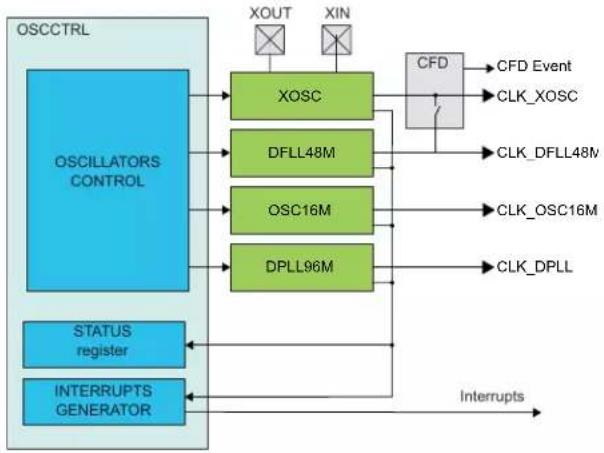
flowchart
graph TD
    A["OSCCTRL"] --> B["OSCILLATORS CONTROL"]
    B --> C["XOSC"]
    B --> D["DFLL48M"]
    B --> E["OSC16M"]
    B --> F["DPLL96M"]
    C --> G["CFD"]
    D --> G
    E --> G
    F --> G
    G --> H["CFD Event"]
    G --> I["CLK_XOSC"]
    G --> J["CLK_DFL48M"]
    G --> K["CLK_OSC16M"]
    G --> L["CLK_DPLL"]
    M["STATUS register"] --> B
    N["INTERRUPTS GENERATOR"] --> B
    O["Interrupts"] --> B
20.4 Signal Description
| Signal Description Type | |
| XIN Multipurpose Crystal Oscillator or external clock generator input Analog input | |
| XOUT Multipurpose Crystal Oscillator output Analog output |
The I/O lines are automatically selected when XOSC is enabled.
20.5 Product Dependencies
In order to use this peripheral, other parts of the system must be configured correctly, as described below.
20.5.1 I/O Lines
I/O lines are configured by OSCCTRL when XOSC is enabled, and need no user configuration.
20.5.2 Power Management
The OSCCTRL can continue to operate in any sleep mode where the selected source clock is running. The OSCCTRL interrupts can be used to wake up the device from sleep modes. The events can trigger other operations in the system without exiting sleep modes.
References:
- PM - Power Manager
20.5.3 Clocks
The OSCCTRL gathers controls for all device oscillators and provides clock sources to the Generic Clock Controller (GCLK). The available clock sources are: XOSC, OSC16M, DFLL48M, and FDPLL96M.
The OSCCTRL bus clock (CLK_OSCCTRL_APB) can be enabled and disabled in the Main Clock module (MCLK).
The DFLL48M control logic uses the DFLL oscillator output, which is also asynchronous to the user interface clock (CLK_OSCCTRL_APB). Due to this asynchronicity, writes to certain registers will require synchronization between the clock domains. Refer to Synchronization for further details.
References:
MCLK
Peripheral Clock Masking
20.5.4 DMA
Not applicable.
20.5.5 Interrupts
The interrupt request line is connected to the Interrupt Controller. Using the OSCCTRL interrupts requires the interrupt controller to be configured first.
20.5.6 Events
The events of this peripheral are connected to the Event System.
20.5.7 Debug Operation
When the CPU is halted in debug mode the OSCCTRL continues normal operation. If the OSCCTRL is configured in a way that requires it to be periodically serviced by the CPU through interrupts or similar, improper operation or data loss may result during debugging.
20.5.8 Register Access Protection
All registers with write-access can be write-protected optionally by the Peripheral Access Controller (PAC), except for the following registers:
- Interrupt Flag Status and Clear register (INTFLAG)
Note: Optional write-protection is indicated by the "PAC Write-Protection" property in the register description.
When the CPU is halted in debug mode, all write-protection is automatically disabled. Write-protection does not apply for accesses through an external debugger.
References:
Peripheral Access Controller
20.5.9 Analog Connections
The 0.4-32MHz crystal must be connected between the XIN and XOUT pins, along with any required load capacitors.
20.6 Functional Description
20.6.1 Principle of Operation
XOSC, OSC16M, DFLL48M, and FDPLL96M are configured via OSCCTRL control registers. Through this interface, the sub-peripherals are enabled, disabled, or have their calibration values updated.
The Status register gathers different status signals coming from the sub-peripherals controlled by the OSCCTRL. The status signals can be used to generate system interrupts, and in some cases wake up the system from standby mode, provided the corresponding interrupt is enabled.
20.6.2 External Multipurpose Crystal Oscillator (XOSC) Operation
The XOSC can operate in two different modes:
- External clock, with an external clock signal connected to the XIN pin
• Crystal oscillator, with an external 0.4-32MHz crystal
The XOSC can be used as a clock source for generic clock generators. This is configured by the Generic Clock Controller.
At reset, the XOSC is disabled, and the XIN/XOUT pins can be used as General Purpose I/O (GPIO) pins or by other peripherals in the system. When XOSC is enabled, the operating mode determines
the GPIO usage. When in crystal oscillator mode, the XIN and XOUT pins are controlled by the OSCCTRL, and GPIO functions are overridden on both pins. When in external clock mode, only the XIN pin will be overridden and controlled by the OSCCTRL, while the XOUT pin can still be used as a GPIO pin.
The XOSC is enabled by writing a '1' to the Enable bit in the External Multipurpose Crystal Oscillator Control register (XOSCCTRL.ENABLE).
To enable XOSC as an external crystal oscillator, the XTAL Enable bit (XOSCCTRL.XTALEN) must written to '1'. If XOSCCTRL.XTALEN is zero, the external clock input on XIN will be enabled.
When in crystal oscillator mode (XOSCCTRL.XTALEN=1), the External Multipurpose Crystal Oscillator Gain (XOSCCTRL.GAIN) must be set to match the external crystal oscillator frequency. If the External Multipurpose Crystal Oscillator Automatic Amplitude Gain Control (XOSCCTRL.AMPGC) is '1', the oscillator amplitude will be automatically adjusted, and in most cases result in a lower power consumption.
The XOSC will behave differently in different sleep modes, based on the settings of XOSCCTRL.RUNSTDBY, XOSCCTRL.ONDEMAND, and XOSCCTRL. ENABLE. If XOSCCTRL. ENABLE=0, the XOSC will be always stopped. For XOSCCTRL. ENABLE=1, this table is valid:
Table 20-1. XOSC Sleep Behavior
| CPU Mode XOSCCTRL.RUN | STDBY XOSCCTRL.ONDEMAND Sleep Behavior | |
| Active or Idle - 0 Always run | ||
| Active or Idle - 1 Run if requested by peripheral | ||
| Standby 1 0 Always run | ||
| Standby 1 1 Run if requested by peripheral | ||
| Standby 0 - Run if requested by peripheral |
After a hard reset, or when waking up from a sleep mode where the XOSC was disabled, the XOSC will need a certain amount of time to stabilize on the correct frequency. This start-up time can be configured by changing the Oscillator Start-Up Time bit group (XOSCCTRL.STARTUP) in the External Multipurpose Crystal Oscillator Control register. During the start-up time, the oscillator output is masked to ensure that no unstable clock propagates to the digital logic.
The External Multipurpose Crystal Oscillator Ready bit in the Status register (STATUS.XOSCRDY) is set once the external clock or crystal oscillator is stable and ready to be used as a clock source. An interrupt is generated on a zero-to-one transition on STATUS.XOSCRDY if the External Multipurpose Crystal Oscillator Ready bit in the Interrupt Enable Set register (INTENSET.XOSCRDY) is set.
References:
GCLK
20.6.3 Clock Failure Detection Operation
The Clock Failure Detector (CFD) allows the user to monitor the external clock or crystal oscillator signal provided by the external oscillator (XOSC). The CFD detects failing operation of the XOSC clock with reduced latency, and allows to switch to a safe clock source in case of clock failure. The user can also switch from the safe clock back to XOSC in case of recovery. The safe clock is derived from the OSC16M oscillator with a configurable prescaler. This allows to configure the safe clock in order to fulfill the operative conditions of the microcontroller.
In sleep modes, CFD operation is automatically disabled when the external oscillator is not requested to run by a peripheral. See the Sleep Behavior table above when this is the case.
The user interface registers allow to enable, disable, and configure the CFD. The Status register provides status flags on failure and clock switch conditions. The CFD can optionally trigger an interrupt or an event when a failure is detected.
Clock Failure Detection
The CFD is reset only at power-on (POR). The CFD does not monitor the XOSC clock when the oscillator is disabled (XOSCCTRL.ENABLE=0).
Before starting CFD operation, the user must start and enable the safe clock source (OSC16M oscillator).
CFD operation is started by writing a '1' to the CFD Enable bit in the External Oscillator Control register (XOCCTRL.CFDEN). After starting or restarting the XOSC, the CFD does not detect failure until the start-up time has elapsed. The start-up time is configured by the Oscillator Start-Up Time in the External Multipurpose Crystal Oscillator Control register (XOSCCTRL.STARTUP). Once the XOSC Start-Up Time is elapsed, the XOSC clock is constantly monitored.
During a period of 4 safe clocks (monitor period), the CFD watches for a clock activity from the XOSC. There must be at least one rising and one falling XOSC clock edge during 4 safe clock periods to meet non-failure conditions. If no or insufficient activity is detected, the failure status is asserted: The Clock Failure Detector status bit in the Status register (STATUS.CLKFAIL) and the Clock Failure Detector interrupt flag bit in the Interrupt Flag register (INTFLAG.CLKFAIL) are set. If the CLKFAIL bit in the Interrupt Enable Set register (INTENSET.CLKFAIL) is set, an interrupt is generated as well. If the Event Output enable bit in the Event Control register (EVCTRL.CFDEO) is set, an output event is generated, too.
After a clock failure was issued the monitoring of the XOSC clock is continued, and the Clock Failure Detector status bit in the Status register (STATUS.CLKFAIL) reflects the current XOSC activity.
Clock Switch
When a clock failure is detected, the XOSC clock is replaced by the safe clock in order to maintain an active clock during the XOSC clock failure. The safe clock source is the OSC16M oscillator clock. The safe clock source can be scaled down by a configurable prescaler to ensure that the safe clock frequency does not exceed the operating conditions selected by the application. When the XOSC clock is switched to the safe clock, the Clock Switch bit in the Status register (STATUS.CLKSW) is set.
When the CFD has switched to the safe clock, the XOSC is not disabled. If desired, the application must take the necessary actions to disable the oscillator. The application must also take the necessary actions to configure the system clocks to continue normal operations.
In the case the application can recover the XOSC, the application can switch back to the XOSC clock by writing a '1' to Switch Back Enable bit in the Clock Failure Control register (XOSCCTRL.SWBACK). Once the XOSC clock is switched back, the Switch Back bit (XOSCCTRL.SWBACK) is cleared by hardware.
Prescaler
The CFD has an internal configurable prescaler to generate the safe clock from the OSC16M oscillator. The prescaler size allows to scale down the OSC16M oscillator so the safe clock frequency is not higher than the XOSC clock frequency monitored by the CFD. The division factor is 2^P , with P being the value of the CFD Prescaler bits in the CFD Prescaler Register (CFDPRESC.CFDPRESC).
Example 20-1.
For an external crystal oscillator at 0.4MHz and the OSC16M frequency at 16MHz, the CFDPRESC.CFDPRESC value should be set scale down by more than factor 16/0.4=80, e.g. to 128, for a safe clock of adequate frequency.
Event
If the Event Output Enable bit in the Event Control register (EVCTRL.CFDEO) is set, the CFD clock failure will be output on the Event Output. When the CFD is switched to the safe clock, the CFD clock failure will not be output on the Event Output.
Sleep Mode
The CFD is halted depending on configuration of the XOSC and the peripheral clock request. For further details, refer to the Sleep Behavior table above. The CFD interrupt can be used to wake up the device from sleep modes.
20.6.4 16MHz Internal Oscillator (OSC16M) Operation
The OSC16M is an internal oscillator operating in open-loop mode and generating 4, 8, 12, or 16MHz frequency. The OSC16M frequency is selected by writing to the Frequency Select field in the OSC16M register (OSC16MCTRL.FSEL). OSC16M is enabled by writing '1' to the Oscillator Enable bit in the OSC16M Control register (OSC16MCTRL.ENABLE), and disabled by writing a '0' to this bit. Frequency selection must be done when OSC16M is disabled.
After enabling OSC16M, the OSC16M clock is output as soon as the oscillator is ready (STATUS.OSC16MRDY=1). User must ensure that the OSC16M is fully disabled before enabling it by reading STATUS.OSC16MRDY=0.
After reset, OSC16M is enabled and serves as the default clock source at 4MHz.
OSC16M will behave differently in different sleep modes based on the settings of OSC16MCTRL.RUNSTDBY, OSC16MCTRL.ONDEMAND, and OSC16MCTRL.ENABLE. If OSC16MCTRL.ENABLE=0, the OSC16M will be always stopped. For OSC16MCTRL.ENABLE=1, this table is valid:
Table 20-2. OSC16M Sleep Behavior
| CPU Mode OSC16MCTRL.RUNSTDBY OSC16MCTRL.ONDEMAN D | Sleep Behavior | |
| Active or Idle - 0 Always run | ||
| Active or Idle - 1 Run if requested by peripheral | ||
| Standby 1 0 Always run | ||
| Standby 1 1 Run if requested by peripheral | ||
| Standby 0 - Run if requested by peripheral | ||
OSC16M is used as a clock source for the generic clock generators. This is configured by the Generic Clock Generator Controller.
References:
GCLK
20.6.5 Digital Frequency Locked Loop (DFLL48M) Operation
The DFLL48M can operate in both open-loop mode and closed-loop mode. In closed-loop mode, a low-frequency clock with high accuracy should be used as the DFLL48M reference clock to get high accuracy on the output clock (CLK_DFLL48M).
The DFLL48M's output can be used as a source for the generic clock generators (GCLK.GENCTRLn.SRC = DFLL).
20.6.5.1 Basic Operation
20.6.5.1.1 Open-Loop Operation
After any reset, the open-loop mode is selected. When operating in open-loop mode, the output frequency of the DFLL48M clock, CLK_DFLL48M, will be determined by the values written to the DFLL Coarse Value bit group and the DFLL Fine Value bit group (DFLLVAL.COARSE and DFLLVAL.FINE) in the DFLL Value register. Using "DFLL48M COARSE CAL" value from the Non Volatile Memory Software Calibration Area in DFLL.COARSE helps to output a frequency close to 48MHz.
It is possible to change the values of DFLLVAL.COARSE and DFLLVAL.FINE while the DFLL48M is enabled and in use, and thereby to adjust the output frequency of CLK_DFLL48M.
20.6.5.1.2 Closed-Loop Operation
In closed-loop operation, the DFLL48M output frequency is continuously regulated against a precise reference clock of relatively low frequency. This will improve the accuracy and stability of the CLK_DFLL48M clock in comparison to the open-loop (free-running) configuration.
Before closed-loop operation can be enabled, the DFLL48M must be enabled and configured in the following way:
- Enable and select a reference clock (CLK_DFLL48M_REF). CLK_DFLL48M_REF is Generic Clock Channel 0 (DFLL48M_Reference).
- Select the maximum step size allowed for finding the Coarse and Fine values by writing the appropriate values to the DFLL Coarse Maximum Step and DFLL Fine Maximum Step bit groups (DFLLMUL.CSTEP and DFLLMUL.FSTEP) in the DFLL Multiplier register.
A small step size will ensure low overshoot on the output frequency, but it will typically take longer until locking is achieved. A high value might give a large overshoot, but will typically provide faster locking.
DFLLMUL.CSTEP and DFLLMUL.FSTEP should not be higher than 50% of the maximum value of DFLLVAL.COARSE and DFLLVAL.FINE, respectively. - Select the multiplication factor in the DFLL Multiply Factor bit group (DFLLMUL.MUL) in the DFLL Multiplier register.
Note: When choosing DFLLMUL.MUL, the output frequency must not exceed the maximum frequency of the device.
If the target frequency is below the minimum frequency of the DFLL48M, the output frequency will be equal to the DFLL minimum frequency. - Start the closed loop mode by writing '1' to the DFLL Mode Selection bit in the DFLL Control register (DFLLCTRL.MODE). See 20.6.5.1.3. Frequency Locking for details.
The frequency of CLK_DFLL48M ( F_clkdfll48m ) is given by:
$$ F _ {\mathrm{clkdfll48m}} = \text {DFLLMUL} \cdot \text {MUL} \times F \quad \text {clkdfll48m_ref} $$
where F_clkdfll48m_ref is the frequency of the reference clock (CLK_DFLL48M_REF).
20.6.5.1.3 Frequency Locking
After enabling closed-loop operation by writing DFLLCTRL.MODE=1, the Coarse Value and the Fine Value bit fields in the DFLL48M Value register (DFLLVAL.COARSE and DFLLVAL.FINE) are used as starting parameters for the locking procedure.
Note: DFLLVAL.COARSE and DFLLVAL.FINE are read-only in closed-loop mode, and are controlled by the frequency tuner to meet user specified frequency.
The frequency locking is divided into two stages: coarse and fine lock.
Coarse Lock. Starting from the original DFLLVAL.COARSE and DFLLVAL.FINE, the control logic quickly finds the correct value for DFLLVAL.COARSE and sets the output frequency to a value close to the correct frequency. On coarse lock, the DFLL Locked on Coarse Value bit (STATUS.DFLLLCKC) in the Status register will be set.
Fine Lock. In this stage, the control logic tunes the value in DFLLVAL.FINE so that the output frequency is very close to the desired frequency. On fine lock, the DFLL Locked on Fine Value bit (STATUS.DFLLLCKF) in the Status register will be set.
Interrupts are generated by STATUS.DFLLLCKC and STATUS.DFLLLCKF, if INTENSET.DFLLLCKC or INTENSET.DFLLLCKF, respectively, are written to '1'.
The accuracy of the output frequency depends on which locks are set.
Note: Writing DFLLVAL.COARSE to a value close to the final value before entering closed-loop mode will reduce the time needed to get a lock on Coarse.
For a DFLL48M output frequency of 48MHz, the bit field "DFLL48M COARSE CAL" in the NVM Software Calibration Area provides a matching value for DFLL.COARSE, and will start DFLL with a frequency close to 48MHz.
This procedure will reduce the locking time to only the DFLL Fine Lock time:
- Load the "DFLL48M COARSE CAL" value from the NVM Software Calibration Area into the DFLL.COARSE bit field.
- Enable the Bypass Coarse Lock (DFLLCTRL.BPLCKC=1).
- Start DFLL close loop (DFLLCTRL.MODE=1).
20.6.5.1.4 Frequency Error Measurement
The ratio between CLK_DFLL48M_REF and CLK48M_DFLL is measured automatically when the DFLL48M is in closed-loop mode. The difference between this ratio and the value in DFLLMUL.MUL is stored in the DFLL Multiplication Ratio Difference bit group (DFLLVAL.DIFF) in the DFLL Value register.
The relative error of CLK_DFLL48M with respect to the target frequency is calculated as follows:
$$ E R R O R = \frac {\text { D F L L V A L . D I F F }}{\text { D F L L M U L . M U L }} $$
20.6.5.1.5 Drift Compensation
If the Stable DFLL Frequency bit (DFLLCTRL.STABLE) in the DFLL Control register is '0', the frequency tuner will automatically compensate for drift in the CLK_DFLL48M without losing either of the locks.
Note: This means that DFLLVAL.FINE can change after every measurement of CLK_DFLL48M.
The DFLLVAL.FINE value may overflow or underflow in closed-loop mode due to large drift/instability of the clock source reference, and the DFLL Out Of Bounds bit (STATUS.DFLLOOB) in the Status register will be set. After an Out of Bounds error condition, the user must rewrite DFLLMUL.MUL to ensure correct CLK_DFLL48M frequency.
A zero-to-one transition of STATUS.DFLLOOB will generate an interrupt, if the DFLL Out Of Bounds bit in the Interrupt Enable Set register (INTENSET.DFLLOOB) is '1'. This interrupt will also be set if the tuner is not able to lock on the correct Coarse value.
To avoid this out-of-bounds error, the reference clock must be stable; an external oscillator XOSC32K is recommended.
20.6.5.1.6 Reference Clock Stop Detection
If CLK_DFLL48M_REF stops or is running at a very low frequency (slower than CLK_DFLL48M/(2 * MULMAX)), the DFLL Reference Clock Stopped bit in the Status register (STATUS.DFLLRCS) will be set.
Detecting a stopped reference clock can take a long time, in the order of 217 CLK_DFLL48M cycles.
When the reference clock is stopped, the DFLL48M will operate as if in open-loop mode. Closed-loop mode operation will automatically resume when the CLK_DFLL48M_REF is restarted.
A zero-to-one transition of the DFLL Reference Clock Stopped bit in the Status register (STATUS.DFLLRCS) will generate an interrupt, if the DFLL Reference Clock Stopped bit in the Interrupt Enable Set register (INTENSET.DFLLRCS) is '1'.
20.6.5.2 Additional Features
20.6.5.2.1 Dealing with Settling Time in Closed-Loop Mode
The time from selecting a new CLK_DFLL48M output frequency until this frequency is output by the DFLL48M can be up to several microseconds. A small value in DFLLMUL.MUL can lead to instability in the DFLL48M locking mechanism, which can prevent the DFLL48M from achieving locks.
To avoid this, a chill cycle can be enabled, during which the CLK_DFLL48M frequency is not measured. The chill cycle is enabled by default, but can be disabled by writing '1' to the DFLL Chill
Cycle Disable bit in the DFLL Control register (DFLLCTRL.CCDIS). Enabling chill cycles might double the lock time.
Another solution to this problem is using less strict lock requirements. This is called Quick Lock (QL). QL is enabled by default as well, but it can be disabled by writing '1' to the Quick Lock Disable bit in the DFLL Control register (DFLLCTRL.QLDIS). The Quick Lock might lead to a larger spread in the output frequency than chill cycles, but the average output frequency is the same.
20.6.5.2.2 USB Clock Recovery Mode
USB Clock Recovery mode can be used to create the 48MHz USB clock from the USB Start Of Frame (SOF). This mode is enabled by writing a '1' to both the USB Clock Recovery Mode bit and the Mode bit in DFLL Control register (DFLLCTRL.USBCRM and DFLLCTRL.MODE).
Note: In USB Clock Recovery mode, the status bits of the DFLL in OSCCTRL.STATUS are determined by the USB bus activity, and have no valid meaning.
The SOF signal from USB device will be used as reference clock (CLK_DFLL_REF), ignoring the selected generic clock reference. When the USB device is connected, a SOF will be sent every 1ms, thus DFLLVAL.MUX bits should be written to 0xBB80 to obtain a 48MHz clock.
In USB clock recovery mode, the DFLLCTRL.BPLCKC bit state is ignored, and the value stored in the DFLLVAL.COARSE will be used as final Coarse Value. The COARSE calibration value can be loaded from NVM OTP row by software. The locking procedure will also go instantaneously to the fine lock search.
The DFLLCTRL.QLDIS bit must be cleared and DFLLCTRL.CCDIS should be set to speed up the lock phase. The DFLLCTRL.STABLE bit state is ignored, an auto jitter reduction mechanism is used instead.
20.6.5.2.3 Wake from Sleep Modes
DFLL48M can optionally reset its lock bits when it is disabled. This is configured by the Lose Lock After Wake bit in the DFLL Control register (DFLLCTRL.LLAW).
If DFLLCTRL.LLAW is zero, the DFLL48M will be re-enabled and start running with the same configuration as before being disabled, even if the reference clock is not available. The locks will not be lost. After the reference clock has restarted, the fine lock tracking will quickly compensate for any frequency drift during sleep if DFLLCTRL.STABLE is zero.
If DFLLCTRL.LLAW is '1' when disabling the DFLL48M, the DFLL48M will lose all its locks, and needs to regain these through the full lock sequence.
20.6.5.2.4 Accuracy
There are three main factors that determine the accuracy of F_clkdfll48m . These can be tuned to obtain maximum accuracy when fine lock is achieved.
- Fine resolution. The frequency step between two Fine values. This is relatively smaller for higher output frequencies.
- Resolution of the measurement: If the resolution of the measured F_clkdfll48m is low, i.e., the ratio between the CLK_DFLL48M frequency and the CLK_DFLL48M_REF frequency is small, the DFLL48M might lock at a frequency that is lower than the targeted frequency. It is recommended to use a reference clock frequency of 32KHz or lower to avoid this issue for low target frequencies.
• The accuracy of the reference clock.
20.6.6 Digital Phase Locked Loop (DPLL) Operation
The task of the DPLL is to maintain coherence between the input (reference) signal and the respective output frequency, CLK_DPLL, via phase comparison. The DPLL controller supports three independent sources of reference clocks:
• XOSC32K: this clock is provided by the 32K External Crystal Oscillator (XOSC32K).
- XOSC: this clock is provided by the External Multipurpose Crystal Oscillator (XOSC).
• GCLK: this clock is provided by the Generic Clock Controller.
When the controller is enabled, the relationship between the reference clock frequency and the output clock frequency is:
$$ f _ {\mathrm{CK}} = f _ {\mathrm{CKR}} \times \mathrm{L} (\mathrm{DR} + 1 + \frac {\mathrm{LDRFRAC}}{1 6}) \times \frac {1}{2 ^ {\mathrm{PRESC}}} $$
Where f_CK is the frequency of the DPLL output clock, LDR is the loop divider ratio integer part, LDRFRAC is the loop divider ratio fractional part, f_CKR is the frequency of the selected reference clock, and PRESC is the output prescaler value.
Figure 20-2. DPLL Block Diagram
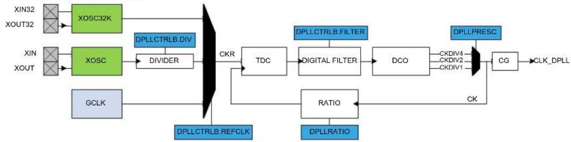
flowchart
graph LR
    A["XIN32"] --> B["XOSC32K"]
    C["XOUT32"] --> B
    D["XIN"] --> E["XOSC"]
    F["XOUT"] --> E
    G["GCLK"] --> H["DIVIDER"]
    H --> I["CKR"]
    I --> J["TDC"]
    J --> K["DIGITAL FILTER"]
    K --> L["DCO"]
    L --> M["DPLLPRESC"]
    M --> N["CG"]
    N --> O["CLK_DPLL"]
    P["DPLLCTRLB.REFCLK"] --> H
    Q["DPLLCTRLB.FILTER"] --> K
    R["RATIO"] --> S["DPLL RATIO"]
    T["CK"] --> M
When the controller is disabled, the output clock is low. If the Loop Divider Ratio Fractional part bit field in the DPLL Ratio register (DPLLRATIO.LDRFRAC) is zero, the DPLL works in integer mode. Otherwise, the fractional mode is activated. Note that the fractional part has a negative impact on the jitter of the DPLL.
Example (integer mode only): assuming F_CKR = 32kHz and F_CK = 48MHz , the multiplication ratio is 1500. It means that LDR shall be set to 1499.
Example (fractional mode): assuming F_CKR = 32kHz and F_CK = 48.006MHz , the multiplication ratio is 1500.1875 (1500 + 3/16). Thus LDR is set to 1499 and LDRFRAC to 3.
References:
-
GCLK - Generic Clock Controller
-
OSC32KCTRL - 32.768 kHz Oscillators Controller
20.6.6.1 Basic Operation
20.6.6.1.1 Initialization, Enabling, Disabling, and Resetting
The DPLLC is enabled by writing a '1' to the Enable bit in the DPLL Control A register (DPLLCTRLA.ENABLE). The DPLLC is disabled by writing a zero to this bit.
The DPLLSYNCBUSY. ENABLE is set when the DPLLCTRLA. ENABLE bit is modified. It is cleared when the DPLL output clock CK has sampled the bit at the high level after enabling the DPLL. When disabling the DPLL, DPLLSYNCBUSY. ENABLE is cleared when the output clock is no longer running.
Figure 20-3. Enable Synchronization Busy Operation
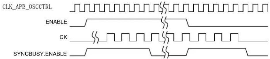
text_image
CLK_APB_OSCCTRL ENABLE CK SYNCBUSY.ENABLEThe frequency of the DPLL output clock CK is stable when the module is enabled and when the Lock bit in the DPLL Status register is set (DPLLSTATUS.LOCK).
When the Lock Time bit field in the DPLL Control B register (DPLLCTRLB.LTIME) is non-zero, a user defined lock time is used to validate the lock operation. In this case the lock time is constant. If DPLLCTRLB.LTIME = 0, the lock signal is linked with the status bit of the DPLL, and the lock time varies depending on the filter selection and the final target frequency.
Note: GCLK_FDPLL_32K is responsible for counting the user defined lock time (LTIME different from 0x0), hence must be enabled.
When the Wake Up Fast bit (DPLLCTRLB.WUF) is set, the wake up fast mode is activated. In this mode, the clock gating cell is enabled at the end of the startup time. At this time the final frequency is not stable, as it is still during the acquisition period, but it allows to save several milliseconds.
After first acquisition, the clock gater (CG) generating the output clock CLK_DPLL is gated by the LOCK signal when the Lock Bypass bit (DPLLCTRLB.LBYPASS) is cleared or is not gated and delivers the output clock CLK_DPLL immediately when DPLLCTRLB.LBYPASS is set.
Table 20-3. CLK_DPLL Behavior from Startup to First Edge Detection
| WUF LTIME CLK_DPLL Behavior |
| 0 0 Normal Mode: First Edge when lock is asserted |
| 0 Not Equal To Zero Lock Timer Timeout mode: First Edge when the timer down-counts to 0. |
| 1 X Wake Up Fast Mode: First Edge when CK is active (startup time) |
Table 20-4. CLK_DPLL Behavior after First Edge Detection
| LBYPASS CLK_DPLL Behavior |
| 0 Normal Mode: the CLK_DPLL is turned off when lock signal is low. |
| 1 Lock Bypass Mode: the CLK_DPLL is always running, lock is irrelevant. |
Figure 20-4. CK and CLK_DPLL Output from DPLL Off Mode to Running Mode

text_image
CKR ENABLE CK CLK_DPLL LOCK CK STABLEtstartug20.6.6.1.2 Reference Clock Switching
When a software operation requires reference clock switching, the recommended procedure is to turn the DPLL into the standby mode, modify the DPLLCTRLB.REFCLK to select the desired reference source, and activate the DPLL again.
20.6.6.1.3 Output Clock Prescaler
The DPLL controller includes an output prescaler. This prescaler provides three selectable output clocks CK, CKDIV2 and CKDIV4. The Prescaler bit field in the DPLL Prescaler register (DPLLPRESC.PRESC) is used to select a new output clock prescaler. When the prescaler field is modified, the DPLLSYNCBUSY.DPLLPRESC bit is set. It will be cleared by hardware when the synchronization is over.
Figure 20-5. Output Clock Switching Operation

text_image
CKR PRESC 0 1 CK CKDIV2 CLK_DPLL SYNCBUSY. PRESC DPLL_LOCK CK STABLECK S120.6.6.1.4 Loop Divider Ratio Updates
The DPLL Controller supports on-the-fly update of the DPLL Ratio Control (DPLLRATIO) register, allowing to modify the loop divider ratio and the loop divider ratio fractional part when the DPLL is enabled.
STATUS.DPLLLDRTO is set when the DPLLRATIO register has been modified and the DPLL analog cell has successfully sampled the updated value. At that time the DPLLSTATUS.LOCK bit is cleared and set again by hardware when the output frequency reached a stable state.
Figure 20-6. RATIOCTRL register update operation
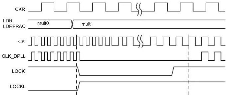
text_image
CKR LDR LDRFRAC mult0 mult1 CK CLK_DPLL LOCK LOCKL20.6.6.1.5 Digital Filter Selection
The PLL digital filter (PI controller) is automatically adjusted in order to provide a good compromise between stability and jitter. Nevertheless a software operation can override the filter setting using the Filter bit field in the DPLL Control B register (DPLLCTRLB.FILTER). The Low Power Enable bit (DPLLCTRLB.LPEN) can be used to bypass the Time to Digital Converter (TDC) module.
20.6.7 DMA Operation
Not applicable.
20.6.8 Interrupts
The OSCCTRL has the following interrupt sources:
- XOSCRDY - Multipurpose Crystal Oscillator Ready: A 0-to-1 transition on the STATUS.XOSCRDY bit is detected
- CLKFAIL - Clock Failure. A 0-to-1 transition on the STATUS.CLKFAIL bit is detected
- OSC16MRDY - 16MHz Internal Oscillator Ready: A 0-to-1 transition on the STATUS.OSC16MRDY bit is detected
- DFLL-related:
- DFLLRDY - DFLL48M Ready: A 0-to-1 transition of the STATUS.DFLLRDY bit is detected
- DFLLOOB - DFLL48M Out Of Boundaries: A 0-to-1 transition of the STATUS.DFLLOOB bit is detected
- DFLLLOCKF - DFLL48M Fine Lock: A 0-to-1 transition of the STATUS.DFLLLOCKF bit is detected
- DFLLLOCKC - DFLL48M Coarse Lock: A 0-to-1 transition of the STATUS.DFLLLOCKC bit is detected
- DFLLRCS - DFLL48M Reference Clock has Stopped: A 0-to-1 transition of the STATUS.DFLLRCS bit is detected
- DPLL-related:
- DPLLLOCKR - DPLL Lock Rise: A 0-to-1 transition of the STATUS.DPLLLOCKR bit is detected
- DPLLLOCKF - DPLL Lock Fall: A 0-to-1 transition of the STATUS.DPLLLOCKF bit is detected
- DPLLLTTO - DPLL Lock Timer Time-out: A 0-to-1 transition of the STATUS.DPLLLTTO bit is detected
- DPLLLDRTO - DPLL Loop Divider Ratio Update Complete. A 0-to-1 transition of the STATUS.DPLLLDRTO bit is detected
All these interrupts are synchronous wake-up source.
Each interrupt source has an interrupt flag associated with it. The interrupt flag in the Interrupt Flag Status and Clear register (INTFLAG) is set when the interrupt condition occurs.
Each interrupt can be individually enabled by writing a '1' to the corresponding bit in the Interrupt Enable Set register (INTENSET), and disabled by writing a '1' to the corresponding bit in the Interrupt Enable Clear register (INTENCLR).
An interrupt request is generated when the interrupt flag is set and the corresponding interrupt is enabled. The interrupt request remains active until the interrupt flag is cleared, the interrupt is disabled, or the OSCCTRL is reset. See the INTFLAG register for details on how to clear interrupt flags.
The OSCCTRL has one common interrupt request line for all the interrupt sources. The user must read the INTFLAG register to determine which interrupt condition is present. Refer to the INTFLAG register for details.
Note: The interrupts must be globally enabled for interrupt requests to be generated.
20.6.9 Events
The CFD can generate the following output event:
- Clock Failure (CLKFAIL): Generated when the Clock Failure status bit is set in the Status register (STATUS.CLKFAIL). The CFD event is not generated when the Clock Switch bit (STATUS.CLKSW) in the Status register is set.
Writing a '1' to an Event Output bit in the Event Control register (EVCTRL.CFDEO) enables the CFD output event. Writing a '0' to this bit disables the CFD output event. Refer to the Event System chapter for details on configuring the event system.
20.6.10 Synchronization
DFLL48M
Due to the multiple clock domains, values in the DFLL48M control registers need to be synchronized to other clock domains.
Once the DFLL is enabled, any read and write operation requires the DFLL Ready bit in the Status register (STATUS.DFLLRDY) to read '1'.
Note: Once the DFLL48M is enabled in on-demand mode (DFLLCTRL.ONDEMAND=1), the STATUS.DFLLRDY bit will keep to '0' until the DFLL48M is requested by a peripheral.
Before writing to any of the DFLL48M control registers, the user must check that the DFLL Ready bit (STATUS.DFLLRDY) is set to '1'. When this bit is set, the DFLL48M can be configured and CLK_DFLL48M is ready to be used. Any write to any of the DFLL48M control registers while DFLLRDY is '0' will be ignored.
In order to read from the DFLLVAL register in closed loop mode, the user must request a read synchronization by writing a '1' to the Read Request bit in the DFLL Synchronization register (DFLLSYNC.READREQ). This is required because the DFLL controller may change the content of the DFLLVAL register any time. If a read operation is issued while the DFLL controller is updating the DFLLVAL content, a zero will be returned.
Note: Issuing a read on any register while a write-synchronization is still on-going will return a zero.
Read-Synchronized registers using DFLLSYNC.READREQ:
• DFLL48M Value register (DFLLVAL)
Write-Synchronized registers:
- DFLL48M Control register (DFLLCTRL)
• DFLL48M Value register (DFLLVAL)
- DFLL48M Multiplier register (DFLLMUL)
DPLL96M
Due to the multiple clock domains, some registers in the DPLL96M must be synchronized when accessed.
When executing an operation that requires synchronization, the relevant synchronization bit in the Synchronization Busy register (DPLLSYNCBUSY) will be set immediately, and cleared when synchronization is complete.
The following bits need synchronization when written:
- Enable bit in control register A (DPLLCTRLA.ENABLE)
• DPLL Ratio register (DPLLRATIO)
• DPLL Prescaler register (DPLLPRESC)
20.7 Register Summary
| Offset | Name Bit Pos. 7 | 6 | 5 | 4 | 3 | 2 | 1 | 0 | ||||||||
| 0x00 | INTENCLR | 7:0 | OSC16MRDY | XOSCFAIL XOSCRDY | ||||||||||||
| 15:8 | DFLLRCS DFLLLCKC DFLLLCKF DFLLOOB DFLLRDY | |||||||||||||||
| 23:16 | DPLLLDRTO | DPLLTO | DPLLCKF | DPLLCKR | ||||||||||||
| 31:24 | ||||||||||||||||
| 0x04 | INTENSET | 7:0 | OSC16MRDY | XOSCFAIL XOSCRDY | ||||||||||||
| 15:8 | DFLLRCS DFLLLCKC DFLLLCKF DFLLOOB DFLLRDY | |||||||||||||||
| 23:16 | DPLLLDRTO | DPLLLTO | DPLLCKF | DPLLCKR | ||||||||||||
| 31:24 | ||||||||||||||||
| 0x08 | INTFLAG | 7:0 | OSC16MRDY | XOSCFAIL XOSCRDY | ||||||||||||
| 15:8 | DFLLRCS DFLLLCKC DFLLLCKF DFLLOOB DFLLRDY | |||||||||||||||
| 23:16 | DPLLLDRTO | DWLLTO | DWLLCKF | DWLLCKR | ||||||||||||
| 31:24 | ||||||||||||||||
| 0x0C | STATUS | 7:0 | OSC16MRDY | XOSCCKSW | XOSCFAIL XOSCRDY | |||||||||||
| 15:8 | DFLLRCS DFLLLCKC DFLLLCKF DFLLOOB DFLLRDY | |||||||||||||||
| 23:16 | DPLLLDRTO | DPLLTO | DWLLCKF | DWLLCKR | ||||||||||||
| 31:24 | ||||||||||||||||
| 0x10 | XOSCCTRL | 7:0 | ONDEMAND | RUNSTDBY | SWBEN | CFDEN | XTALEN | ENABLE | ||||||||
| 15:8 | STARTUP[3:0] | AMPGC | GAIN[2:0] | |||||||||||||
| 0x12 | CFDPRESC | 7:0 | CFDPRESC[2:0] | |||||||||||||
| 0x13 | EVCTRL 7:0 CFDEO | |||||||||||||||
| 0x14 | OSC16MCTRL | 7:0 | ONDEMAND | RUNSTDBY | FSEL[1:0] | ENABLE | ||||||||||
| 0x15...0x17 | Reserved | |||||||||||||||
| 0x18 | DFLLCTRL | 7:0 | ONDEMAND | RUNSTDBY | USBCRM | LLAW | STABLE | MODE | ENABLE | |||||||
| 15:8 | WAITLOCK | BPLCKC | QLDIS | CCDIS | ||||||||||||
| 0x1A...0x1B | Reserved | |||||||||||||||
| 0x1C | DFLLVAL | 7:0 | FINE[7:0] | |||||||||||||
| 15:8 | COARSE[5:0] | FINE[9:8] | ||||||||||||||
| 23:16 | DIFF[7:0] | |||||||||||||||
| 31:24 | DIFF[15:8] | |||||||||||||||
| 0x20 | DFLLMUL | 7:0 | MUL[7:0] | |||||||||||||
| 15:8 | MUL[15:8] | |||||||||||||||
| 23:16 | FSTEP[7:0] | |||||||||||||||
| 31:24 | CSTEP[5:0] | FSTEP[9:8] | ||||||||||||||
| 0x24 | DFLLSYNC | 7:0 | READREQ | |||||||||||||
| 0x25...0x27 | Reserved | |||||||||||||||
| 0x28 | DPLLCTRLA | 7:0 | ONDEMAND | RUNSTDBY | ENABLE | |||||||||||
| 0x29...0x2B | Reserved | |||||||||||||||
| 0x2C | DPLLRATIO | 7:0 | LDR[7:0] | |||||||||||||
| 15:8 | LDR[11:8] | |||||||||||||||
| 23:16 | LDRFRAC[3:0] | |||||||||||||||
| 31:24 | ||||||||||||||||
| 0x30 | DPLLCTRLB | 7:0 | REFCLK[1:0] | WUF | LPEN | FILTER[1:0] | ||||||||||
| 15:8 | LBYPASS | LTIME[2:0] | ||||||||||||||
| 23:16 | DIV[7:0] | |||||||||||||||
| 31:24 | DIV[10:8] | |||||||||||||||
| 0x34 | DPLLPRESC 7:0 | PRESC[1:0] | ||||||||||||||
| 0x35...0x37 | Reserved | |||||||||||||||
| 0x38 | DPLLSYNCBUSY | 7:0 | DPLLPRESSC | DPLLRATIO | ENABLE | |||||||||||
| ......continued | |||||||||
| Offset | Name Bit Pos. 76 | 543210 | |||||||
| 0x39...0x3B | Reserved | ||||||||
| 0x3C DPLLSTATUS 7:0 | CLKRDY LOCK | ||||||||
20.8 Register Description
Registers can be 8, 16, or 32 bits wide. Atomic 8-, 16-, and 32-bit accesses are supported. In addition, the 8-bit quarters and 16-bit halves of a 32-bit register and the 8-bit halves of a 16-bit register can be accessed directly.
Some registers are optionally write-protected by the Peripheral Access Controller (PAC). Write-protection is denoted by the "PAC Write-Protection" property in each individual register description. Refer to the 20.5.8. Register Access Protection section and the 11. PAC - Peripheral Access Controller chapter for details.
Some registers require synchronization when read and/or written. Synchronization is denoted by the "Read-Synchronized" or "Write.Synchronized" property in each individual register description. Refer to Synchronization section for details.
20.8.1 Interrupt Enable Clear
Name: INTENCLR
Offset: 0x00
Reset: 0x00000000
Property: PAC Write-Protection
This register allows the user to disable an interrupt without doing a read-modify-write operation. Changes in this register will also be reflected in the Interrupt Enable Set register (INTENSET).
| Bit 31 30 29 28 27 26 25 24 | |||||||
| Access Reset | |||||||
| Bit 23 22 21 20 19 18 17 16 | |||||||
| DPLL LDRTO DPLL LTO DPLLCKF DPLLCKR | |||||||
| Access Reset | R/W | R/W | R/W | R/W | |||
| 0 | 0 | 0 | 0 | ||||
| Bit 15 14 13 12 11 10 | 9 | 8 | |||||
| DFLLRCS | DFLLLCKC | DFLLLCKF | DFLLOOB | DFLLRDY | |||
| Access Reset | R/W | R/W | R/W | R/W | R/W | ||
| 0 | 0 | 0 | 0 | 0 | |||
| Bit 7 | 6 | 5 | 4 | 3 | 2 | 1 | 0 |
| OSC16MRDY | XOSCFAIL XOSCRDY | ||||||
| Access Reset | R/W | R/W | R/W | ||||
| 0 | 0 | 0 | |||||
Bit 19 - DPLLLDRTO DPLL Loop Divider Ratio Update Complete Interrupt Enable
Writing '0' to this bit has no effect.
Writing '1' to this bit will clear the DPLL Loop Divider Ratio Update Complete Interrupt Enable bit, which disables the DPLL Loop Divider Ratio Update Complete interrupt.
| Value | Description |
| 0 | The DPLL Loop Divider Ratio Update Complete interrupt is disabled. |
| 1 | The DPLL Loop Divider Ratio Update Complete interrupt is enabled, and an interrupt request will be generated when the DPLL Loop Divider Ratio Update Complete Interrupt flag is set. |
Bit 18 - DPLLTO DPLL Lock Timeout Interrupt Enable
Writing '0' to this bit has no effect.
Writing '1' to this bit will clear the DPLL Lock Timeout Interrupt Enable bit, which disables the DPLL Lock Timeout interrupt.
| Value | Description |
| 0 | The DPLL Lock Timeout interrupt is disabled. |
| 1 | The DPLL Lock Timeout interrupt is enabled, and an interrupt request will be generated when the DPLL Lock Timeout Interrupt flag is set. |
Bit 17 - DPLLLCKF DPLL Lock Fall Interrupt Enable
Writing '0' to this bit has no effect.
Writing '1' to this bit will clear the DPLL Lock Fall Interrupt Enable bit, which disables the DPLL Lock Fall interrupt.
| Value | Description |
| 0 | The DPLL Lock Fall interrupt is disabled. |
Value Description
| 1 | The DPLL Lock Fall interrupt is enabled, and an interrupt request will be generated when the DPLL Lock Fall Interrupt flag is set. |
Bit 16 - DPLLLCKR DPLL Lock Rise Interrupt Enable
Writing '0' to this bit has no effect.
Writing '1' to this bit will clear the DPLL Lock Rise Interrupt Enable bit, which disables the DPLL Lock Rise interrupt.
Value Description
| 0 | The DPLL Lock Rise interrupt is disabled. |
| 1 | The DPLL Lock Rise interrupt is enabled, and an interrupt request will be generated when the DPLL Lock Rise Interrupt flag is set. |
Bit 12 - DFLLRCS DFLL Reference Clock Stopped Interrupt Enable
Writing '0' to this bit has no effect.
Writing '1' to this bit will clear the DFLL Reference Clock Stopped Interrupt Enable bit, which disables the DFLL Reference Clock Stopped interrupt.
Value Description
| 0 | The DFLL Reference Clock Stopped interrupt is disabled. |
| 1 | The DFLL Reference Clock Stopped interrupt is enabled, and an interrupt request will be generated when the DFLL Reference Clock Stopped Interrupt flag is set. |
Bit 11 - DFLLLCKC DFLL Lock Coarse Interrupt Enable
Writing '0' to this bit has no effect.
Writing '1' to this bit will clear the DFLL Lock Coarse Interrupt Enable bit, which disables the DFLL Lock Coarse interrupt.
Value Description
| 0 | The DFLL Lock Coarse interrupt is disabled. |
| 1 | The DFLL Lock Coarse interrupt is enabled, and an interrupt request will be generated when the DFLL Lock Coarse Interrupt flag is set. |
Bit 10 - DFLLLCKF DFLL Lock Fine Interrupt Enable
Writing '0' to this bit has no effect.
Writing '1' to this bit will clear the DFLL Lock Fine Interrupt Enable bit, which disables the DFLL Lock Fine interrupt.
Value Description
| 0 | The DFLL Lock Fine interrupt is disabled. |
| 1 | The DFLL Lock Fine interrupt is enabled, and an interrupt request will be generated when the DFLL Lock Fine Interrupt flag is set. |
Bit 9 - DFLLOOB DFLL Out Of Bounds Interrupt Enable
Writing '0' to this bit has no effect.
Writing '1' to this bit will clear the DFLL Out Of Bounds Interrupt Enable bit, which disables the DFLL Out Of Bounds interrupt.
Value Description
| 0 | The DFLL Out Of Bounds interrupt is disabled. |
| 1 | The DFLL Out Of Bounds interrupt is enabled, and an interrupt request will be generated when the DFLL Out Of Bounds Interrupt flag is set. |
Bit 8 - DFLLRDY DFLL Ready Interrupt Enable
Writing '0' to this bit has no effect.
Writing '1' to this bit will clear the DFLL Ready Interrupt Enable bit, which disables the DFLL Ready interrupt.
Value Description
| 0 | The DFLL Ready interrupt is disabled. |
| 1 | The DFLL Ready interrupt is enabled, and an interrupt request will be generated when the DFLL Ready Interrupt flag is set. |
Bit 4 - OSC16MRDY OSC16M Ready Interrupt Enable
Writing '0' to this bit has no effect.
Writing '1' to this bit will clear the OSC16M Ready Interrupt Enable bit, which disables the OSC16M Ready interrupt.
| Value Description | |
| 0 | The OSC16M Ready interrupt is disabled. |
| 1 | The OSC16M Ready interrupt is enabled, and an interrupt request will be generated when the OSC16M Ready Interrupt flag is set. |
Bit 1 - XOSCFAIL Clock Failure Interrupt Enable
Writing '0' to this bit has no effect.
Writing '1' to this bit will clear the XOSC Clock Failure Interrupt Enable bit, which disables the XOSC Clock Failure interrupt.
| Value Description | |
| 0 | The XOSC Clock Failure interrupt is disabled. |
| 1 | The XOSC Clock Failure interrupt is enabled, and an interrupt request will be generated when the XOSC Clock Failure Interrupt flag is set. |
Bit 0 - XOSCRDY XOSC Ready Interrupt Enable
Writing '0' to this bit has no effect.
Writing '1' to this bit will clear the XOSC Ready Interrupt Enable bit, which disables the XOSC Ready interrupt.
| Value Description | |
| 0 | The XOSC Ready interrupt is disabled. |
| 1 | The XOSC Ready interrupt is enabled, and an interrupt request will be generated when the XOSC Ready Interrupt flag is set. |
20.8.2 Interrupt Enable Set
Name: INTENSET
Offset: 0x04
Reset: 0x00000000
Property: PAC Write-Protection
This register allows the user to disable an interrupt without doing a read-modify-write operation. Changes in this register will also be reflected in the Interrupt Enable Clear register (INTENCLR).
Bit 31 30 29 28 27 26 25 24
| Access Reset |
Bit 23 22 21 20 19 18 17 16
| DPLL LDRTO DPLL LTO DPLL CKF DPLL CKR | ||||||
| Access | R/W | R/W | R/W | R/W | ||
| Reset | 0 | 0 | 0 | 0 | ||
Bit 15 14 13 12 11 10 9 8
| DFLLRCS | DFLLLCKC | DFLLLCKF | DFLLOOB | DFLLRDY | |||
| Access | R/W | R/W | R/W | R/W | R/W | ||
| Reset | 0 | 0 | 0 | 0 | 0 |
Bit 7 6 5 4 3 2 1 0
| OSC16MRDY | XOSCFAIL XOSCRDY | ||||
| Access | R/W | R/W | R/W | ||
| Reset | 0 | 0 | 0 |
Bit 19 - DPLLLDRTO DPLL Loop Divider Ratio Update Complete Interrupt Enable
Writing '0' to this bit has no effect.
Writing '1' to this bit will set the DPLL Loop Ratio Update Complete Interrupt Enable bit, which enables the DPLL Loop Ratio Update Complete interrupt.
| Value | Description |
| 0 | The DPLL Loop Divider Ratio Update Complete interrupt is disabled. |
| 1 | The DPLL Loop Ratio Update Complete interrupt is enabled, and an interrupt request will be generated when the DPLL Loop Ratio Update Complete Interrupt flag is set. |
Bit 18 - DPLLTO DPLL Lock Timeout Interrupt Enable
Writing '0' to this bit has no effect.
Writing '1' to this bit will set the DPLL Lock Timeout Interrupt Enable bit, which enables the DPLL Lock Timeout interrupt.
| Value | Description |
| 0 | The DPLL Lock Timeout interrupt is disabled. |
| 1 | The DPLL Lock Timeout interrupt is enabled, and an interrupt request will be generated when the DPLL Lock Timeout Interrupt flag is set. |
Bit 17 - DPLLLCKF DPLL Lock Fall Interrupt Enable
Writing '0' to this bit has no effect.
Writing '1' to this bit will set the DPLL Lock Fall Interrupt Enable bit, which enables the DPLL Lock Fall interrupt.
| Value | Description |
| 0 | The DPLL Lock Fall interrupt is disabled. |
Value Description
| 1 | The DPLL Lock Fall interrupt is enabled, and an interrupt request will be generated when the DPLL Lock Fall Interrupt flag is set. |
Bit 16 - DPLLLCKR DPLL Lock Rise Interrupt Enable
Writing '0' to this bit has no effect.
Writing '1' to this bit will set the DPLL Lock Rise Interrupt Enable bit, which enables the DPLL Lock Rise interrupt.
Value Description
| 0 | The DPLL Lock Rise interrupt is disabled. |
| 1 | The DPLL Lock Rise interrupt is enabled, and an interrupt request will be generated when the DPLL Lock Rise Interrupt flag is set. |
Bit 12 - DFLLRCS DFLL Reference Clock Stopped Interrupt Enable
Writing '0' to this bit has no effect.
Writing '1' to this bit will set the DFLL Reference Clock Stopped Interrupt Enable bit, which enables the DFLL Reference Clock Stopped interrupt.
Value Description
| 0 | The DFLL Reference Clock Stopped interrupt is disabled. |
| 1 | The DFLL Reference Clock Stopped interrupt is enabled, and an interrupt request will be generated when the DFLL Reference Clock Stopped Interrupt flag is set. |
Bit 11 - DFLLLCKC DFLL Lock Coarse Interrupt Enable
Writing '0' to this bit has no effect.
Writing '1' to this bit will set the DFLL Lock Coarse Interrupt Enable bit, which enables the DFLL Lock Coarse interrupt.
Value Description
| 0 | The DFLL Lock Coarse interrupt is disabled. |
| 1 | The DFLL Lock Coarse interrupt is enabled, and an interrupt request will be generated when the DFLL Lock Coarse Interrupt flag is set. |
Bit 10 - DFLLLCKF DFLL Lock Fine Interrupt Enable
Writing '0' to this bit has no effect.
Writing '1' to this bit will set the DFLL Lock Fine Interrupt Disable/Enable bit, disable the DFLL Lock Fine interrupt and set the corresponding interrupt request.
Value Description
| 0 | The DFLL Lock Fine interrupt is disabled. |
| 1 | The DFLL Lock Fine interrupt is enabled, and an interrupt request will be generated when the DFLL Lock Fine Interrupt flag is set. |
Bit 9 - DFLLOOB DFLL Out Of Bounds Interrupt Enable
Writing '0' to this bit has no effect.
Writing '1' to this bit will set the DFLL Out Of Bounds Interrupt Enable bit, which enables the DFLL Out Of Bounds interrupt.
Value Description
| 0 | The DFLL Out Of Bounds interrupt is disabled. |
| 1 | The DFLL Out Of Bounds interrupt is enabled, and an interrupt request will be generated when the DFLL Out Of Bounds Interrupt flag is set. |
Bit 8 - DFLLRDY DFLL Ready Interrupt Enable
Writing '0' to this bit has no effect.
Writing '1' to this bit will set the DFLL Ready Interrupt Enable bit, which enables the DFLL Ready interrupt and set the corresponding interrupt request.
Value Description
| 0 | The DFLL Ready interrupt is disabled. |
| 1 | The DFLL Ready interrupt is enabled, and an interrupt request will be generated when the DFLL Ready Interrupt flag is set. |
Bit 4 - OSC16MRDY OSC16M Ready Interrupt Enable
Writing '0' to this bit has no effect.
Writing '1' to this bit will set the OSC16M Ready Interrupt Enable bit, which enables the OSC16M Ready interrupt.
| Value Description | |
| 0 | The OSC16M Ready interrupt is disabled. |
| 1 | The OSC16M Ready interrupt is enabled, and an interrupt request will be generated when the OSC16M Ready Interrupt flag is set. |
Bit 1 - XOSCFAIL XOSC Clock Failure Interrupt Enable
Writing '0' to this bit has no effect.
Writing '1' to this bit will set the XOSC Clock Failure Interrupt Enable bit, which enables the XOSC Clock Failure Interrupt.
| Value Description | |
| 0 | The XOSC Clock Failure Interrupt is disabled. |
| 1 | The XOSC Clock Failure Interrupt is enabled, and an interrupt request will be generated when the XOSC Clock Failure Interrupt flag is set. |
Bit 0 - XOSCRDY XOSC Ready Interrupt Enable
Writing '0' to this bit has no effect.
Writing '1' to this bit will set the XOSC Ready Interrupt Enable bit, which enables the XOSC Ready interrupt.
| Value Description | |
| 0 | The XOSC Ready interrupt is disabled. |
| 1 | The XOSC Ready interrupt is enabled, and an interrupt request will be generated when the XOSC Ready Interrupt flag is set. |
20.8.3 Interrupt Flag Status and Clear
Name: INTFLAG
Offset: 0x08
Reset: 0x00000000
Property: -
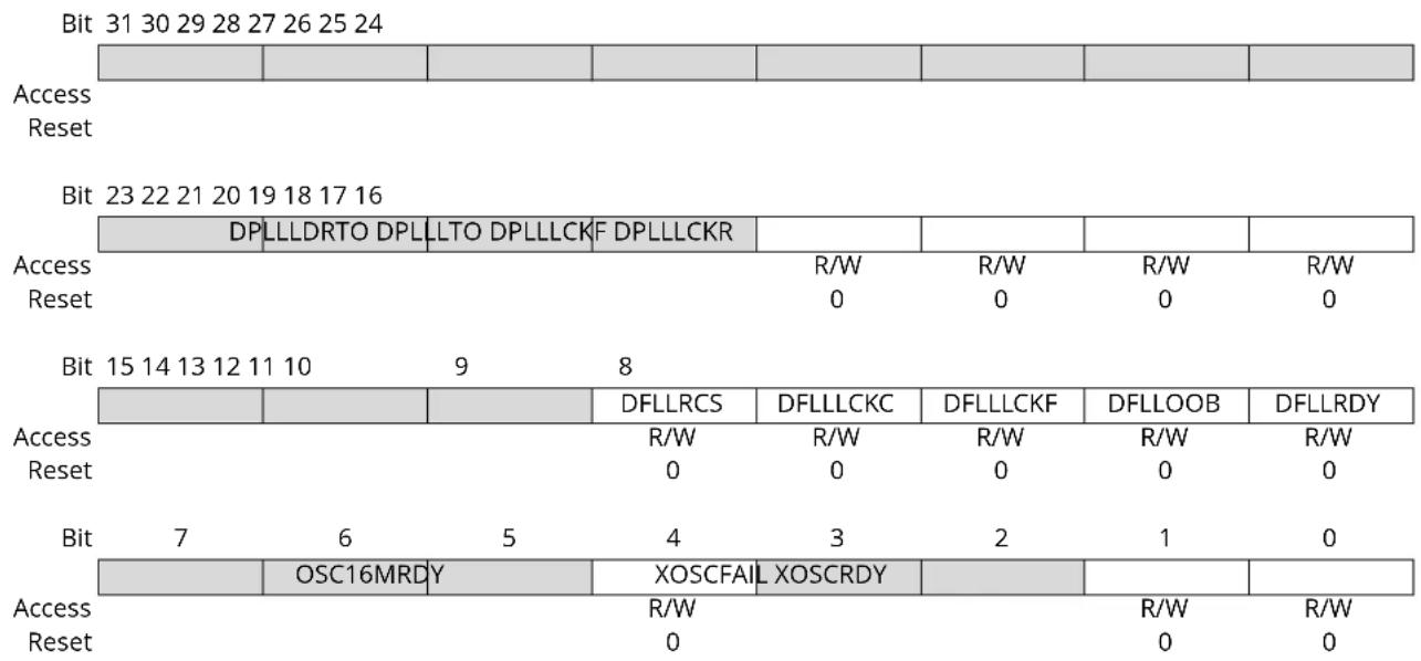
text_image
Bit 31 30 29 28 27 26 25 24 Access Reset Bit 23 22 21 20 19 18 17 16 DPLL LDRTO DPLL LTO DPLL LCKF DPLL LCKR Access Reset R/W R/W R/W R/W 0 0 0 0 Bit 15 14 13 12 11 10 9 8 Access Reset R/W R/W R/W R/W 0 0 0 0 0 Bit 7 6 5 4 3 2 1 0 OSC16MRDY XOSCFAIL XOSCRDY Access Reset R/W R/W R/W R/W 0 0 0 0 0Bit 19 - DPLLLDRTO DPLL Loop Divider Ratio Update Complete
This flag is cleared by writing '1' to it.
This flag is set on 0-to-1 transition of the DPLL Loop Divider Ratio Update Complete bit in the Status register (STATUS.DPLLLDRTO) and will generate an interrupt request if INTENSET.DPLLLDRTO is '1'.
Writing '0' to this bit has no effect.
Writing '1' to this bit clears the DPLL Loop Divider Ratio Update Complete interrupt flag.
Bit 18 - DPLLTO DPLL Lock Timeout
This flag is cleared by writing '1' to it.
This flag is set on 0-to-1 transition of the DPLL Lock Timeout bit in the Status register
(STATUS.DPLLLTO) and will generate an interrupt request if INTENSET.DPLLLTO is '1'.
Writing '0' to this bit has no effect.
Writing '1' to this bit clears the DPLL Lock Timeout interrupt flag.
Bit 17 - DPLLLCKF DPLL Lock Fall
This flag is cleared by writing '1' to it.
This flag is set on 0-to-1 transition of the DPLL Lock Fall bit in the Status register (STATUS.DPLLLCKF)
and will generate an interrupt request if INTENSET.DPLLLCKF is '1'.
Writing '0' to this bit has no effect.
Writing '1' to this bit clears the DPLL Lock Fall interrupt flag.
Bit 16 - DPLLLCKR DPLL Lock Rise
This flag is cleared by writing '1' to it.
This flag is set on 0-to-1 transition of the DPLL Lock Rise bit in the Status register (STATUS.DPLLLCKR) and will generate an interrupt request if INTENSET.DPLLLCKR is '1'.
Writing '0' to this bit has no effect.
Writing '1' to this bit clears the DPLL Lock Rise interrupt flag.
Bit 12 - DFLLRCS DFLL Reference Clock Stopped
This flag is cleared by writing '1' to it.
This flag is set on 0-to-1 transition of the DFLL Reference Clock Stopped bit in the Status register (STATUS.DFLLRCS) and will generate an interrupt request if INTENSET.DFLLRCS is '1'.
Writing '0' to this bit has no effect.
Writing '1' to this bit clears the DFLL Reference Clock Stopped interrupt flag.
Bit 11 - DFLLLCKC DFLL Lock Coarse
This flag is cleared by writing '1' to it.
This flag is set on 0-to-1 transition of the DFLL Lock Coarse bit in the Status register (STATUS.DFLLLCKC) and will generate an interrupt request if INTENSET.DFLLLCKC is '1'.
Writing '0' to this bit has no effect.
Writing '1' to this bit clears the DFLL Lock Coarse interrupt flag.
Bit 10 - DFLLLCKF DFLL Lock Fine
This flag is cleared by writing '1' to it.
This flag is set on 0-to-1 transition of the DFLL Lock Fine bit in the Status register (STATUS.DFLLLCKF) and will generate an interrupt request if INTENSET.DFLLLCKF is '1'.
Writing '0' to this bit has no effect.
Writing '1' to this bit clears the DFLL Lock Fine interrupt flag.
Bit 9 - DFLLOOB DFLL Out Of Bounds
This flag is cleared by writing '1' to it.
This flag is set on 0-to-1 transition of the DFLL Out Of Bounds bit in the Status register (STATUS.DFLLOOB) and will generate an interrupt request if INTENSET.DFLLOOB is '1'.
Writing '0' to this bit has no effect.
Writing '1' to this bit clears the DFLL Out Of Bounds interrupt flag.
Bit 8 - DFLLRDY DFLL Ready
This flag is cleared by writing '1' to it.
This flag is set on 0-to-1 transition of the DFLL Ready bit in the Status register (STATUS.DFLLRDY) and will generate an interrupt request if INTENSET.DFLLRDY is '1'.
Writing '0' to this bit has no effect.
Writing '1' to this bit clears the DFLL Ready interrupt flag.
Bit 4 - OSC16MRDY OSC16M Ready
This flag is cleared by writing '1' to it.
This flag is set on 0-to-1 transition of the OSC16M Ready bit in the Status register (STATUS.OSC16MRDY) and will generate an interrupt request if INTENSET.OSC16MRDY is '1'.
Writing '0' to this bit has no effect.
Writing '1' to this bit clears the OSC16M Ready interrupt flag.
Bit 1 - XOSCFAIL XOSC Failure Detection
This flag is cleared by writing '1' to it.
This flag is set on a 0-to-1 transition of the XOSC Clock Failure bit in the Status register (STATUS.XOSCFAIL) and will generate an interrupt request if INTENSET.XOSCFAIL is '1'.
Writing '0' to this bit has no effect.
Writing '1' to this bit clears the XOSC Clock Fail interrupt flag.
Bit 0 - XOSCRDY XOSC Ready
This flag is cleared by writing '1' to it.
This flag is set on a 0-to-1 transition of the XOSC Ready bit in the Status register (STATUS.XOSCRDY) and will generate an interrupt request if INTENSET.XOSCRDY is '1'.
Writing '0' to this bit has no effect.
Writing '1' to this bit clears the XOSC Ready interrupt flag.
20.8.4 Status
Name: STATUS
Offset: 0x0C
Reset: 0x00000100
Property: -
| Bit 31 30 29 28 27 26 25 24 | |||||||
| Access Reset | |||||||
| Bit 23 22 21 20 19 18 17 16 | |||||||
| DPLL LDRTO DPLL TO DPLL LCKF | DPLL LCKR | ||||||
| Access Reset | R | R | R | R | |||
| 0 | 0 | 0 | 0 | ||||
| Bit 15 14 13 12 11 10 | 9 | 8 | |||||
| DFLLRCS | DFLLLCKC | DFLLLCKF | DFLLOOB | DFLLRDY | |||
| Access Reset | R | R | R | R | R | ||
| 0 | 0 | 0 | 0 | 1 | |||
| Bit | 7 | 6 | 5 | 4 | 3 | 2 | 1 |
| OSC16MRDY | XOSCCKSW | XOSCFAIL | XOSCRDY | ||||
| Access Reset | R | R | R | R | |||
| 0 | 0 | 0 | 0 | ||||
Bit 19 - DPLLLDRTO DPLL Loop Divider Ratio Update Complete
| Value | Description |
| 0 | DPLL Loop Divider Ratio Update Complete not detected. |
| 1 | DPLL Loop Divider Ratio Update Complete detected. |
Bit 18 - DPLLTO DPLL Lock Timeout
| Value | Description |
| 0 | DPLL Lock time-out not detected. |
| 1 | DPLL Lock time-out detected. |
Bit 17 - DPLLLCKF DPLL Lock Fall
| Value | Description |
| 0 | DPLL Lock fall edge not detected. |
| 1 | DPLL Lock fall edge detected. |
Bit 16 - DPLLLCKR DPLL Lock Rise
| Value | Description |
| 0 | DPLL Lock rise edge not detected. |
| 1 | DPLL Lock fall edge detected. |
Bit 12 - DFLLRCS DFLL Reference Clock Stopped
| Value | Description |
| 0 | DFLL reference clock is running. |
| 1 | DFLL reference clock has stopped. |
| Value Description | |
| 0 | No DFLL coarse lock detected. |
| 1 | DFLL coarse lock detected. |
Bit 11 - DFLLLCKC DFLL Lock Coarse
Bit 10 - DFLLLCKF DFLL Lock Fine
| Value Description | |
| 0 | No DFLL fine lock detected. |
| 1 | DFLL fine lock detected. |
Bit 9 - DFLLOOB DFLL Out Of Bounds
| Value Description | |
| 0 | No DFLL Out Of Bounds detected. |
| 1 | DFLL Out Of Bounds detected. |
Bit 8 - DFLLRDY DFLL Ready
| Value Description | |
| 0 | DFLL registers update is ongoing. Registers update is requested through DFLLSYNC.READREQ, or after a write access in DFLLCTRL, DFLLVAL or DFLLMUL register. |
| 1 | DFLL registers are stable and ready for read/write access. |
Bit 4 - OSC16MRDY OSC16M Ready
| Value Description | |
| 0 | OSC16M is not ready. |
| 1 | OSC16M is stable and ready to be used as a clock source. |
Bit 2 - XOSCCKSW XOSC Clock Switch
| Value Description | |
| 0 | XOSC is not switched and provides the external clock or crystal oscillator clock. |
| 1 | XOSC is switched and provides the safe clock. |
Bit 1 - XOSCFAIL XOSC Clock Failure
| Value Description | |
| 0 | No XOSC failure detected. |
| 1 | A XOSC failure was detected. |
Bit 0 - XOSCRDY XOSC Ready
| Value Description | |
| 0 | XOSC is not ready. |
| 1 | XOSC is stable and ready to be used as a clock source. |
20.8.5 Clock Failure Detector Prescaler
Name: CFDPRESC
Offset: 0x12
Reset: 0x00
Property: PAC Write-Protection
Bit 76543210
| CFDPRESC[2:0] | |||||
| Access Reset 0 0 0 | R/W R/W R/W | ||||
Bits 2:0 - CFDPRESC[2:0] Clock Failure Detector Prescaler
These bits select the prescaler for the clock failure detector.
The OSC16M oscillator is used to clock the CFD prescaler. The CFD safe clock frequency is the OSC16M frequency divided by 2^CFDPRESC.
20.8.6 Event Control
Name: EVCTRL
Offset: 0x13
Reset: 0x00
Property: PAC Write-Protection
Bit 76543210
| CFDEO | |||||||
| Access Reset 0 | R/W | ||||||
Bit 0 - CFDEO Clock Failure Detector Event Output Enable
This bit indicates whether the Clock Failure detector event output is enabled or not and an output event will be generated when the Clock Failure detector detects a clock failure
| Value Description | |
| 0 | Clock Failure detector event output is disabled and no event will be generated. |
| 1 | Clock Failure detector event output is enabled and an event will be generated. |
20.8.7 16MHz Internal Oscillator (OSC16M) Control
Name: OSC16MCTRL
Offset: 0x14
Reset: 0x82
Property: PAC Write-Protection
Bit 76543210
| ONDEMAND RUNSTDBY | FSEL[1:0] ENABLE | ||||
| Access | R/W R/W | R/W R/W R/W | |||
| Reset | 1 0 | 0 0 1 | |||
Bit 7 - ONDEMAND On Demand Control
The On Demand operation mode allows the oscillator to be enabled or disabled depending on peripheral clock requests.
If the ONDEMAND bit has been previously written to '1', the oscillator will only be running when requested by a peripheral. If there is no peripheral requesting the oscillator's clock source, the oscillator will be in a disabled state.
If On Demand is disabled the oscillator will always be running when enabled.
In standby sleep mode, the On Demand operation is still active.
| Value | Description |
| 0 | The oscillator is always on, if enabled. |
| 1 | The oscillator is enabled when a peripheral is requesting the oscillator to be used as a clock source. The oscillator is disabled if no peripheral is requesting the clock source. |
Bit 6 - RUNSTDBY Run in Standby
This bit controls how the OSC16M behaves during standby sleep mode.
| Value | Description |
| 0 | The OSC16M is disabled in standby sleep mode if no peripheral requests the clock. |
| 1 | The OSC16M is not stopped in standby sleep mode. If ONDEMAND=1, the OSC16M will be running when a peripheral is requesting the clock. If ONDEMAND=0, the clock source will always be running in standby sleep mode. |
Bits 3:2 - FSEL[1:0] Oscillator Frequency Selection
These bits control the oscillator frequency range.
| Value | Name | Description |
| 0x0 | 4 | 4MHz |
| 0x1 | 8 | 8MHz |
| 0x2 | 12 | 12MHz |
| 0x3 | 16 | 16MHz |
Bit 1 - ENABLE Oscillator Enable
| Value | Description |
| 0 | The oscillator is disabled. |
| 1 | The oscillator is enabled. |
20.8.8 External Multipurpose Crystal Oscillator (XOSC) Control
Name: XOSCCTRL
Offset: 0x10
Reset: 0x0080
Property: PAC Write-Protection
Bit 15 14 13 12 11 10 9 8
| STARTUP[3:0] AMPGC GAIN[2:0] |
Access R/W R/W R/W R/W R/W R/W R/W R/W
Reset 00000000
Bit 76543210
| ONDEMAND | RUNSTDBY | SWBEN | CFDEN | XTALEN | ENABLE |
Access R/W R/W R/W R/W R/W R/W
Reset 10 0000
Bits 15:12 - STARTUP[3:0] Start-Up Time
These bits select start-up time for the oscillator.
The OSCULP32K oscillator is used to clock the start-up counter.
Table 20-5. Start-Up Time for External Multipurpose Crystal Oscillator
| STARTUP[3:0] | Number of OSCULP32K Clock Cycles | Number of XOSC Clock Cycles | Approximate Equivalent Time [μs] |
| 0x0 | 1 | 3 | 31 |
| 0x1 | 2 | 3 | 61 |
| 0x2 | 4 | 3 | 122 |
| 0x3 | 8 | 3 | 244 |
| 0x4 | 16 | 3 | 488 |
| 0x5 | 32 | 3 | 977 |
| 0x6 | 64 | 3 | 1953 |
| 0x7 | 128 | 3 | 3906 |
| 0x8 | 256 | 3 | 7813 |
| 0x9 | 512 | 3 | 15625 |
| 0xA | 1024 | 3 | 31250 |
| 0xB | 2048 | 3 | 62500μs |
| 0xC | 4096 | 3 | 125000 |
| 0xD | 8192 | 3 | 250000 |
| 0xE | 16384 | 3 | 500000 |
| 0xF | 32768 | 3 | 1000000 |
Notes:
- Actual startup time is 1 OSCULP32K cycle + 3 XOSC cycles.
- The given time neglects the three XOSC cycles before OSCULP32K cycle.
Bit 11 - AMPGC Automatic Amplitude Gain Control
Note: The configuration of the oscillator gain is mandatory even if AMPGC feature is enabled at startup.
| Value | Description |
| 0 | The automatic amplitude gain control is disabled. |
| 1 | The automatic amplitude gain control is enabled. Amplitude gain will be automatically adjusted during Crystal Oscillator operation. |
Bits 10:8 - GAIN[2:0] Oscillator Gain
These bits select the gain for the oscillator. The listed maximum frequencies are recommendations, and might vary based on capacitive load and crystal characteristics. The Gain bits must be properly configured even when the Automatic Amplitude Gain Control is active.
| Value Recommended | Max Frequency [MHz] |
| 0x0 2 | |
| 0x1 4 | |
| 0x2 8 | |
| 0x3 16 | |
| 0x4 30 | |
| 0x5-0x7 Reserved |
Bit 7 - ONDEMAND On Demand Control
The On Demand operation mode allows the oscillator to be enabled or disabled, depending on peripheral clock requests.
If the ONDEMAND bit has been previously written to '1', the oscillator will be running only when requested by a peripheral. If there is no peripheral requesting the oscillator's clock source, the oscillator will be in a disabled state.
If On Demand is disabled, the oscillator will always be running when enabled.
In standby sleep mode, the On Demand operation is still active.
| Value Description | |
| 0 | The oscillator is always on, if enabled. |
| 1 | The oscillator is enabled when a peripheral is requesting the oscillator to be used as a clock source. The oscillator is disabled if no peripheral is requesting the clock source. |
Bit 6 - RUNSTDBY Run in Standby
This bit controls how the XOSC behaves during standby sleep mode, together with the ONDEMAND bit:
| Value Description | |
| 0 | The XOSC is not running in Standby sleep mode if no peripheral requests the clock. |
| 1 | The XOSC is running in Standby sleep mode. If ONDEMAND=1, the XOSC will be running when a peripheral is requesting the clock. If ONDEMAND=0, the clock source will always be running in Standby sleep mode. |
Bit 4 - SWBEN Clock Switch Back
This bit controls the XOSC output switch back to the external clock or crystal oscillator in case of clock recovery:
| Value Description | |
| 0 | The clock switch back is disabled. |
| 1 | The clock switch back is enabled. This bit is reset once the XOSC output clock is switched back to the external clock or crystal oscillator. |
Bit 3 - CFDEN Clock Failure Detector Enable
This bit controls the clock failure detector:
| Value Description | |
| 0 | The Clock Failure Detector is disabled. |
| 1 | the Clock Failure Detector is enabled. |
Bit 2 - XTALEN Crystal Oscillator Enable
This bit controls the connections between the I/O pads and the external clock or crystal oscillator:
| Value Description | |
| 0 | External clock connected on XIN. XOUT can be used as general-purpose I/O. |
| 1 | Crystal connected to XIN/XOUT. |
Bit 1 - ENABLE Oscillator Enable
| Value Description | |
| 0 | The oscillator is disabled. |
Value Description
1 The oscillator is enabled.
20.8.9 DFLL48M Control
Name: DFLLCTRL
Offset: 0x18
Reset: 0x0080
Property: PAC Write-Protection, Write-Synchronized using STATUS.DFLLRDY=1
Bit 15 14 13 12 11 10 9 8
| WAITLOCK BPLCKC QLDIS | CCDIS | |||||
| Access Reset | R/W0 0 0 0 | R/W | R/W | R/W |
Bit 76543210
| ONDEMAND | RUNSTDBY | USBCRM | LLAW | STABLE | MODE | ENABLE | ||
| Access | R/W | R/W | R/W | R/W | R/W | R/W | R/W | |
| Reset | 1 0 0 0 0 0 0 | |||||||
Bit 11 - WAITLOCK Wait Lock
This bit controls the DFLL output clock, depending on lock status.
| Value | Description |
| 0 | Output clock before the DFLL is locked. |
| 1 | Output clock when DFLL is locked. |
Bit 10 - BPLCKC Bypass Coarse Lock
This bit controls the coarse lock procedure.
| Value | Description |
| 0 | Bypass coarse lock is disabled. |
| 1 | Bypass coarse lock is enabled. |
Bit 9 - QLDIS Quick Lock Disable
| Value | Description |
| 0 | Quick Lock is enabled. |
| 1 | Quick Lock is disabled. |
Bit 8 - CCDIS Chill Cycle Disable
| Value | Description |
| 0 | Chill Cycle is enabled. |
| 1 | Chill Cycle is disabled. |
Bit 7 - ONDEMAND On Demand Control
The On Demand operation mode allows the DFLL to be enabled or disabled depending on peripheral clock requests.
If the ONDEMAND bit has been previously written to '1', the DFLL will only be running when requested by a peripheral. If there is no peripheral requesting the DFLL clock source, the DFLL will be in a disabled state.
If On Demand is disabled, the DFLL will always be running when enabled.
In standby sleep mode, the On Demand operation is still active.
| Value | Description |
| 0 | The DFLL is always on, if enabled. |
| 1 | The DFLL is enabled when a peripheral is requesting the DFLL to be used as a clock source. The DFLL is disabled if no peripheral is requesting the clock source. |
Bit 6 - RUNSTDBY Run in Standby
This bit controls how the DFLL behaves during standby sleep mode:
| Value Description | |
| 0 | The DFLL is disabled in standby sleep mode if no peripheral requests the clock. |
| 1 | The DFLL is not stopped in standby sleep mode. If ONDEMAND is one, the DFLL will be running when a peripheral is requesting the clock. If ONDEMAND is zero, the clock source will always be running in standby sleep mode. |
Bit 5 - USBCRM USB Clock Recovery Mode
| Value Description | |
| 0 | USB Clock Recovery Mode is disabled. |
| 1 | USB Clock Recovery Mode is enabled. |
Bit 4 - LLAW Lose Lock After Wake
| Value Description | |
| 0 | Locks will not be lost after waking up from sleep modes if the DFLL clock has been stopped. |
| 1 | Locks will be lost after waking up from sleep modes if the DFLL clock has been stopped. |
Bit 3 - STABLE Stable DFLL Frequency
| Value Description | |
| 0 | FINE calibration tracks changes in output frequency. |
| 1 | FINE calibration register value will be fixed after a fine lock. |
Bit 2 - MODE Operating Mode Selection
| Value Description | |
| 0 | The DFLL operates in open-loop operation. |
| 1 | The DFLL operates in closed-loop operation. |
Bit 1 - ENABLE DFLL Enable
Due to synchronization, there is delay from updating the register until the peripheral is enabled/disabled. The value written to DFLLCTRL. ENABLE will read back immediately after written.
| Value Description | |
| 0 | The DFLL oscillator is disabled. |
| 1 | The DFLL oscillator is enabled. |
20.8.10 DFLL48M Value
Name: DFLLVAL
Offset: 0x1C
Reset: 0x00000000
Property: PAC Write-Protection, Read-Synchronized using DFLLSYNC.READREQ, Write-Synchronized using STATUS.DFLLRDY=1
Bit 31 30 29 28 27 26 25 24
| DIFF[15:8] |
Access R/W R/W R/W R/W R/W R/W R/W R/W
Reset 00000000
Bit 23 22 21 20 19 18 17 16
| DIFF[7:0] |
Access R/W R/W R/W R/W R/W R/W R/W R/W
Reset 00000000
Bit 15 14 13 12 11 10 9 8
| COARSE[5:0] FINE[9:8] |
Access R R R R R R R/W R/W
Reset 00000000
Bit 76543210
| FINE[7:0] |
Access R/W R/W R/W R/W R/W R/W R/W R/W
Reset 00000000
Bits 31:16 - DIFF[15:0] Multiplication Ratio Difference
In closed-loop mode (DFLLCTRL.MODE=1), this bit group indicates the difference between the ideal number of DFLL cycles and the counted number of cycles. In open-loop mode, this value is not updated and hence, invalid.
Bits 15:10 - COARSE[5:0] Coarse Value
Set the value of the Coarse Calibration register. In closed-loop mode, this field is read-only.
Bits 9:0 - FINE[9:0] Fine Value
Set the value of the Fine Calibration register. In closed-loop mode, this field is read-only.
20.8.11 DFLL48M Multiplier
Name: DFLLMUL
Offset: 0x20
Reset: 0x00000000
Property: PAC Write-Protection, Write-Synchronized using STATUS.DFLLRDY=1
Bit 31 30 29 28 27 26 25 24
| CSTEP[5:0] FSTEP[9:8] |
Access R R R R R R R/R/W R/W
Reset 00000000
Bit 23 22 21 20 19 18 17 16
| FSTEP[7:0] |
Access R/W R/W R/W R/W R/W R/W R/W R/W
Reset 00000000
Bit 15 14 13 12 11 10 98
| MUL[15:8] |
Access R/W R/W R/W R/W R/W R/W R/W R/W
Reset 00000000
Bit 76543210
| MUL[7:0] |
Access R/W R/W R/W R/W R/W R/W R/W R/W
Reset 00000000
Bits 31:26 - CSTEP[5:0] Coarse Maximum Step
This bit group indicates the maximum step size allowed during coarse adjustment in closed-loop mode. When adjusting to a new frequency, the expected output frequency overshoot depends on this step size.
Bits 25:16 - FSTEP[9:0] Fine Maximum Step
This bit group indicates the maximum step size allowed during fine adjustment in closed-loop mode. When adjusting to a new frequency, the expected output frequency overshoot depends on this step size.
Bits 15:0 - MUL[15:0] DFLL Multiply Factor
This field determines the ratio of the CLK_DFLL output frequency to the CLK_DFLL_REF input frequency. Writing to the MUL bits will cause locks to be lost and the fine calibration value to be reset to its midpoint.
20.8.12 DFLL48M Synchronization
Name: DFLLSYNC
Offset: 0x24
Reset: 0x00
Property: PAC Write-Protection
Bit 76543210
| READREQ | ||||||||
| Access | W | |||||||
| Reset | 0 |
Bit 7 - READREQ Read Request
To be able to read the current value of the DFLLVAL register in closed-loop mode, this bit must be written to '1'.
20.8.13 DPLL Control A
Name: DPLLCTRLA
Offset: 0x28
Reset: 0x80
Property: PAC Write-Protection, Write-Synchronized (ENABLE)
Bit 76543210
| ONDEMAND RUNSTDBY | ENABLE | ||||||
| Access | R/W R/W R/W | ||||||
| Reset 10 | 0 | ||||||
Bit 7 - ONDEMAND On Demand Clock Activation
The On Demand operation mode allows the DPLL to be enabled or disabled depending on peripheral clock requests.
If the ONDEMAND bit has been previously written to '1', the DPLL will only be running when requested by a peripheral. If there is no peripheral requesting the DPLL's clock source, the DPLL will be in a disabled state.
If On Demand is disabled the DPLL will always be running when enabled.
In standby sleep mode, the On Demand operation is still active.
| Value | Description |
| 0 | The DPLL is always on, if enabled. |
| 1 | The DPLL is enabled when a peripheral is requesting the DPLL to be used as a clock source. The DPLL is disabled if no peripheral is requesting the clock source. |
Bit 6 - RUNSTDBY Run in Standby
This bit controls how the DPLL behaves during standby sleep mode:
| Value | Description |
| 0 | The DPLL is disabled in standby sleep mode if no peripheral requests the clock. |
| 1 | The DPLL is not stopped in standby sleep mode. If ONDEMAND=1, the DPLL will be running when a peripheral is requesting the clock. If ONDEMAND=0, the clock source will always be running in standby sleep mode. |
Bit 1 - ENABLE DPLL Enable
The software operation of enabling or disabling the DPLL takes a few clock cycles, so the DPLLSYNCBUSY. ENABLE status bit indicates when the DPLL is successfully enabled or disabled.
| Value | Description |
| 0 | The DPLL is disabled. |
| 1 | The DPLL is enabled. |
20.8.14 DPLL Ratio Control
Name: DPLLRATIO
Offset: 0x2C
Reset: 0x00000000
Property: PAC Write-Protection, Write-Synchronized
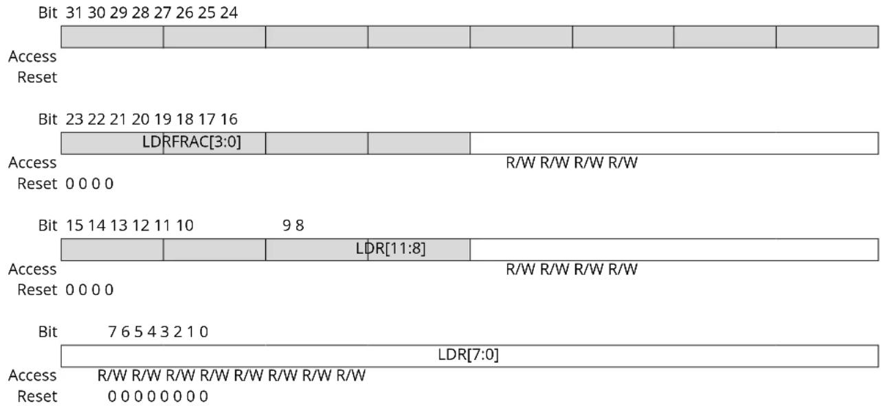
text_image
Bit 31 30 29 28 27 26 25 24 Access Reset Bit 23 22 21 20 19 18 17 16 LDRFRAC[3:0] Access R/W R/W R/W R/W Reset 0 0 0 0 Bit 15 14 13 12 11 10 9 8 Access R/W R/W R/W R/W Reset 0 0 0 0 Bit 7 6 5 4 3 2 1 0 LDR[7:0] Access R/W R/W R/W R/W R/W R/W R/W Reset 0 0 0 0 0 0 0Bits 19:16 - LDRFRAC[3:0] Loop Divider Ratio Fractional Part
Writing these bits selects the fractional part of the frequency multiplier. Due to synchronization there is a delay between writing these bits and the effect on the DPLL output clock. The value written will read back immediately and the DPLLRATIO bit in the DPLL Synchronization Busy register (DPLLSYNCBUSY.DPLLRATIO) will be set. DPLLSYNCBUSY.DPLLRATIO will be cleared when the operation is completed.
Bits 11:0 - LDR[11:0] Loop Divider Ratio
Writing these bits selects the integer part of the frequency multiplier. The value written to these bits will read back immediately, and the DPLL RATIO bit in the DPLL Synchronization busy register (DPLLSYNCBUSY.DPLLRATIO), will be set. DPLLSYNCBUSY.DPLLRATIO will be cleared when the operation is completed.
20.8.15 DPLL Control B
Name: DPLLCTRLB
Offset: 0x30
Reset: 0x00000000
Property: PAC Write-Protection, Enable-Protected
| Bit 31 30 29 28 27 26 25 24 | ||||||
| D\V[10:8] | ||||||
| Access Reset | R/W R/W R/W | |||||
| 0 0 0 | ||||||
| Bit 23 22 21 20 19 18 17 16 | ||||||
| DIV[7:0] | ||||||
| Access Reset | R/W R/W R/W R/W R/W R/W R/W | |||||
| 0 0 0 0 0 0 0 0 | ||||||
| Bit 15 14 13 12 11 10 | 9 8 | |||||
| LBYPASS | LTIME[2:0] | |||||
| Access Reset | R/W 0 | R/W R/W R/W 0 0 0 | ||||
| Bit | 7 6 5 4 3 2 1 0 | |||||
| REFCLK[1:0] | WUF | LPEN | FILTER[1:0] | |||
| Access Reset | R/W R/W R/W R/W R/W R/W 0 0 0 0 0 0 | R/W R/W R/W R/W 0 0 0 | ||||
Bits 26:16 - DIV[10:0] Clock Divider
These bits set the XOSC clock division factor and can be calculated with following formula:
$$ \mathrm{f} _ {D I V} = \frac {f _ {X O S C}}{2 x (D I V + 1)} $$
Bit 12 - LBYPASS Lock Bypass
| Value | Description |
| 0 | DPLL Lock signal drives the DPLL controller internal logic. |
| 1 | DPLL Lock signal is always asserted. |
Bits 10:8 - LTIME[2:0] Lock Time
These bits select the lock time-out value:
| Value | Name | Description |
| 0x0 | Default | No time-out. Automatic lock. |
| 0x1 | Reserved | |
| 0x2 | Reserved | |
| 0x3 | Reserved | |
| 0x4 | 8MS | Time-out if no lock within 8ms |
| 0x5 | 9MS | Time-out if no lock within 9ms |
| 0x6 | 10MS | Time-out if no lock within 10ms |
| 0x7 | 11MS | Time-out if no lock within 11ms |
Bits 5:4 - REFCLK[1:0] Reference Clock Selection
Write these bits to select the DPLL clock reference:
| Value | Name | Description |
| 0x0 | XOSC32K | XOSC32K clock reference |
| 0x1 | XOSC | XOSC clock reference |
| Value Name | Description | |
| 0x2 | GCLK GCLK clock reference | |
| 0x3 | Reserved Reserved |
Bit 3 - WUF Wake Up Fast
| Value Description | |
| 0 | DPLL clock is output after startup and lock time. |
| 1 | DPLL clock is output after startup time. |
Bit 2 - LPEN Low-Power Enable
| Value Description | |
| 0 | The low-power mode is disabled. Time to Digital Converter is enabled. |
| 1 | The low-power mode is enabled. Time to Digital Converter is disabled. This will improve power consumption but increase the output jitter. |
Bits 1:0 - FILTER[1:0] Proportional Integral Filter Selection
These bits select the DPLL filter type:
| Value Name | Description | |
| 0x0 | DEFAULT Default filter mode | |
| 0x1 | LBFILT Low bandwidth filter | |
| 0x2 | HBFILT High bandwidth filter | |
| 0x3 | HDFILT High damping filter |
20.8.16 DPLL Prescaler
Name: DPLLPRESC
Offset: 0x34
Reset: 0x00
Property: PAC Write-Protection, Write-Synchronized
Bit 76543210
| PRESC[1:0] | ||||||
| Access Reset 0 0 | R/W R/W | |||||
Bits 1:0 - PRESC[1:0] Output Clock Prescaler
These bits define the output clock prescaler setting.
| Value Name | Description | |
| 0x0 | DIV1 | DPLL output is divided by 1 |
| 0x1 | DIV2 | DPLL output is divided by 2 |
| 0x2 | DIV4 | DPLL output is divided by 4 |
| 0x3 | Reserved |
20.8.17 DPLL Synchronization Busy
Name: DPLLSYNCBUSY
Offset: 0x38
Reset: 0x00
Property: -
Bit 76543210
| DPLLPRESC DPLL | RATIO ENABLE | |||||
| Access Reset | RRR0 0 0 |
Bit 3 - DPLLPRESC DPLL Prescaler Synchronization Status
| Value | Description |
| 0 | The DPLLRESC register has been synchronized. |
| 1 | The DPLLRESC register value has changed and its synchronization is in progress. |
Bit 2 - DPLLRATIO DPLL Loop Divider Ratio Synchronization Status
| Value | Description |
| 0 | The DPLLATIO register has been synchronized. |
| 1 | The DPLLATIO register value has changed and its synchronization is in progress. |
Bit 1 - ENABLE DPLL Enable Synchronization Status
| Value | Description |
| 0 | The DPLLCTRLA.ENABLE bit has been synchronized. |
| 1 | The DPLLCTRLA.ENABLE bit value has changed and its synchronization is in progress. |
20.8.18 DPLL Status
Name: DPLLSTATUS
Offset: 0x3C
Reset: 0x00
Property: -
Bit 76543210
| CLKRDY LOCK | |||||||
| Access Reset 0 0 | R | R | |||||
Bit 1 - CLKRDY DPLL Clock Ready
| Value Description | |
| 0 | The DPLL output clock is off. |
| 1 | The DPLL output clock in on. |
Bit 0 - LOCK DPLL Lock
| Value Description | |
| 0 | The DPLL Lock signal is cleared, when the DPLL is disabled or when the DPLL is trying to reach the target frequency. |
| 1 | The DPLL Lock signal is asserted when the desired frequency is reached. |
21. OSC32KCTRL - 32.768 kHz Oscillators Controller
21.1 Overview
The 32.768 kHz Oscillators Controller (OSC32KCTRL) provides a user interface to the 32.768 kHz oscillators:
• A 32.768 kHz crystal oscillator (XOSC32K)
• A 32.768 kHz ultra low-power internal RC oscillator (OSCULP32K)
21.2 Features
• 32.768 kHz Crystal Oscillator (XOSC32K)
- Programmable start-up time
- Crystal or external input clock on XIN32 I/O
- Clock failure detection with safe clock switch
- Clock failure event output
- 32.768 kHz Ultra Low-Power Internal Oscillator (OSCULP32K)
- Ultra low-power, always-on oscillator
- Frequency fine tuning
• 1.024 kHz clock outputs available
21.3 Block Diagram
Figure 21-1. OSC32KCTRL Block Diagram
21.4 Signal Description
Signal Description Type
XIN32 Analog Input 32.768 kHz Crystal Oscillator or external clock input
XOUT32 Analog Output 32.768 kHz Crystal Oscillator output
The I/O lines are automatically selected when XOSC32K is enabled.
Note: The signal of the external crystal oscillator may affect the jitter of neighboring pads.
21.5 Product Dependencies
In order to use this peripheral, other parts of the system must be configured correctly, as described below.
21.5.1 I/O Lines
I/O lines are configured by OSC32KCTRL when XOSC32K is enabled and need no user configuration.
21.5.2 Power Management
The OSC32KCTRL will continue to operate in any sleep mode where a 32.768 kHz oscillator is running as source clock. The OSC32KCTRL interrupts can be used to wake up the device from sleep modes.
21.5.3 Clocks
The OSC32KCTRL gathers controls for both 32.768 kHz oscillators and provides clock sources to the Generic Clock Controller (GCLK), Real-Time Counter (RTC), Segment Liquid Crystal Controller (SLCD) and Watchdog Timer (WDT).
The available clock sources are: XOSC32K and OSCULP32K.
The OSC32KCTRL bus clock (CLK_OSC32KCTRL_APB) can be enabled and disabled in the Main Clock module (MCLK).
21.5.4 Interrupts
The interrupt request lines are connected to the interrupt controller. Using the OSC32KCTRL interrupts requires the interrupt controller to be configured first.
21.5.5 Events
The events of this peripheral are connected to the Event System.
21.5.6 Debug Operation
When the CPU is halted in debug mode, OSC32KCTRL will continue normal operation. If OSC32KCTRL is configured in a way that requires it to be periodically serviced by the CPU through interrupts or similar, improper operation or data loss may result during debugging.
21.5.7 Register Access Protection
All registers with write access can be write-protected optionally by the Peripheral Access Controller (PAC), except for the following registers:
- Interrupt Flag Status and Clear (INTFLAG) register
Optional write protection by the Peripheral Access Controller (PAC) is denoted by the "PAC Write Protection" property in each individual register description.
PAC write protection does not apply to accesses through an external debugger.
21.5.8 Analog Connections
The external 32.768 kHz crystal must be connected between the XIN32 and XOUT32 pins, along with any required load capacitors. For details on recommended oscillator characteristics and capacitor load, refer to the related links.
21.6 Functional Description
21.6.1 Principle of Operation
XOSC32K and OSCULP32K are configured via OSC32KCTRL control registers. Through this interface, the sub-peripherals are enabled, disabled.
The STATUS register gathers different status signals coming from the sub-peripherals of OSC32KCTRL. The status signals can be used to generate system interrupts, and in some cases wake up the system from standby mode, provided the corresponding interrupt is enabled.
21.6.2 32.768 kHz External Crystal Oscillator (XOSC32K) Operation
The XOSC32K can operate in the following two modes:
- External clock, with an external clock signal connected to XIN32
- Crystal oscillator, with an external 32.768 kHz crystal connected between XIN32 and XOUT32
At reset, the XOSC32K is disabled, and the XIN32/XOUT32 pins can either be used as General Purpose I/O (GPIO) pins or by other peripherals in the system.
When XOSC32K is enabled, the operating mode determines the GPIO usage. When in crystal oscillator mode, the XIN32 and XOUT32 pins are controlled by the OSC32KCTRL, and GPIO functions are overridden on both pins. When in external clock mode, the only XIN32 pin will be overridden and controlled by the OSC32KCTRL, while the XOUT32 pin can still be used as a GPIO pin.
The XOSC32K is enabled by writing a '1' to the Enable bit in the 32.768 kHz External Crystal Oscillator Control register (XOSC32K. ENABLE = 1). The XOSC32K is disabled by writing a '0' to the Enable bit in the 32.768 kHz External Crystal Oscillator Control register (XOSC32K. ENABLE = 0).
To enable the XOSC32K as a crystal oscillator, the XTALEN bit in the 32.768 kHz External Crystal Oscillator Control register must be set (XOSC32K.XTALEN = 1). If XOSC32K.XTALEN is '0', the external clock input will be enabled.
The XOSC32K 32.768 kHz output is enabled by setting the 32.768 kHz Output Enable bit in the 32.768 kHz External Crystal Oscillator Control register (XOSC32K.EN32K = 1). The XOSC32K also has a 1.024 kHz clock output, which can only be used by the RTC. This clock output is enabled by setting the 1.024 kHz Output Enable bit in the 32.768 kHz External Crystal Oscillator Control register (XOSC32K.EN1K = 1).
It is also possible to lock the XOSC32K configuration by setting the Write Lock bit in the 32.768 kHz External Crystal Oscillator Control register (XOSC32K.WRTLOCK = 1). If set, the XOSC32K configuration is locked until a Power-On Reset (POR) is detected.
The XOSC32K will behave differently in different sleep modes based on the settings of XOSC32K.RUNSTDBY, XOSC32K.ONDEMAND, and XOSC32K. ENABLE. If XOSC32KCTRL. ENABLE = 0, the XOSC32K will be always stopped. For XOSC32KCTRL. ENABLE = 1, the following table is valid:
Table 21-1. XOSC32K Sleep Behavior
| CPU Mode XOSC32K. | RUNSTDBY | XOSC32K.ONDEMAND | Sleep Behavior of XOSC32K and CFD |
| Active or Idle - 0 Always run | |||
| Active or Idle - 1 Run if requested by peripheral | |||
| Standby 1 0 Always run | |||
| Standby 1 1 Run if requested by peripheral | |||
| Standby 0 - Run if requested by peripheral |
As a crystal oscillator usually requires a very long start-up time, the 32.768 kHz External Crystal Oscillator will keep running across resets when XOSC32K.ONDEMAND = 0, except for Power-on Reset (POR). After a reset or when waking up from a Sleep mode where the XOSC32K was disabled, the XOSC32K will need a certain amount time to stabilize on the correct frequency. This stabilization time can be configured by changing the Oscillator Start-Up Time bit group (XOSC32K.STARTUP) in the 32.768 kHz External Crystal Oscillator Control register. During the start-up time, the oscillator output is masked to ensure that no unstable clock propagates to the digital logic.
Once the external clock or crystal oscillator is stable and ready to be used as a clock source, the XOSC32K Ready bit in the Status register is set (STATUS.XOSC32KRDY = 1). The transition of STATUS.XOSC32KRDY from '0' to '1' generates an interrupt if the XOSC32K Ready bit in the Interrupt Enable Set register is set (INTENSET.XOSC32KRDY = 1).

Important: The right XOSC32K.STARTUP stabilization time must be selected by considering the Crystal Start-up Time parameter given in the "XOSC32K Electrical Specification" section of the "Electrical Characteristics" chapter.
The XOSC32K can be used as a source for Generic Clock Generators (GCLK) or for the Real-Time Counter (RTC). Before enabling the GCLK or the RTC module, the corresponding oscillator output must be enabled (XOSC32K.EN32K or XOSC32K.EN1K) in order to ensure proper operation. In the same way, the GCLK or RTC modules must be disabled before the clock selection is changed. For additional information on RTC clock configuration, refer to 21.6.6. Real-Time Counter Clock Selection.
21.6.3 Clock Failure Detection Operation
The Clock Failure Detector (CFD) allows the user to monitor the external clock or crystal oscillator signal provided by the external oscillator (XOSC32K). The CFD detects failing operation of the XOSC32K clock with reduced latency, and allows to switch to a safe clock source in case of clock failure. The user can also switch from the safe clock back to XOSC32K in case of recovery. The safe clock is derived from the OSCULP32K oscillator with a configurable prescaler. This allows to configure the safe clock in order to fulfill the operative conditions of the microcontroller.
In sleep modes, CFD operation is automatically disabled when the external oscillator is not requested to run by a peripheral, see XOSC32K Sleep Behavior for additional information.
The user interface registers allow to enable, disable, and configure the CFD. The Status register provides status flags on failure and clock switch conditions. The CFD can optionally trigger an interrupt or an event when a failure is detected.
Clock Failure Detection
The CFD is reset only at Power-on Reset (POR). The CFD does not monitor the XOSC32K clock when the oscillator is disabled (XOSC32K. ENABLE = 0).
Before starting CFD operation, the user must start and enable the safe clock source (OSCULP32K oscillator).
CFD operation is started by writing a '1' to the CFD Enable bit in the External Oscillator Control register (CFDCTRL.CFDEN).
After starting or restarting the XOSC32K, the CFD does not detect failure until the crystal oscillator stabilization time has elapsed (XOSC32K.STARTUP). Once this stabilization time is elapsed, the XOSC32K clock is constantly monitored.

Important: The right XOSC32K.STARTUP stabilization time must be selected by considering the Crystal Start-up Time parameter given in the "XOSC32K Electrical Specification" section of the "Electrical Characteristics" chapter.
During a period of 4 safe clocks (monitor period), the CFD watches for a clock activity from the XOSC32K. There must be at least one rising and one falling XOSC32K clock edge during 4 safe clock periods to meet non-failure conditions. If no or insufficient activity is detected, the failure status is asserted: The Clock Failure Detector status bit in the Status register (STATUS.CLKFAIL) and the Clock Failure Detector interrupt flag bit in the Interrupt Flag register (INTFLAG.CLKFAIL) are set. If the CLKFAIL bit in the Interrupt Enable Set register (INTENSET.CLKFAIL) is set, an interrupt is generated as well. If the Event Output enable bit in the Event Control register (EVCTRL.CFDEO) is set, an output event is generated, too.
After a clock failure was issued the monitoring of the XOSC32K clock is continued, and the Clock Failure Detector status bit in the Status register (STATUS.CLKFAIL) reflects the current XOSC32K activity.
Clock Switch
When a clock failure is detected, the XOSC32K clock is replaced by the safe clock in order to maintain an active clock during the XOSC32K clock failure. The safe clock source is the OSCULP32K oscillator clock. Both 32.768 kHz and 1.024 kHz outputs of the XOSC32K are replaced by the respective OSCULP32K 32.768 kHz and 1.024 kHz outputs. The safe clock source can be scaled down by a configurable prescaler to ensure that the safe clock frequency does not exceed the operating conditions selected by the application. When the XOSC32K clock is switched to the safe clock, the Clock Switch bit in the Status register (STATUS.CLKSW) is set.
When the CFD has switched to the safe clock, the XOSC32K is not disabled. If desired, the application must take the necessary actions to disable the oscillator. The application must also take the necessary actions to configure the system clocks to continue normal operations. In the case the
application can recover the XOSC32K, the application can switch back to the XOSC32K clock by writing a '1' to Switch Back Enable bit in the Clock Failure Control register (CFDCTRL.SWBACK). Once the XOSC32K clock is switched back, the Switch Back bit (CFDCTRL.SWBACK) is cleared by hardware.
Prescaler
The CFD has an internal configurable prescaler to generate the safe clock from the OSCULP32K oscillator. The prescaler size allows to scale down the OSCULP32K oscillator so the safe clock frequency is not higher than the XOSC32K clock frequency monitored by the CFD. The maximum division factor is 2.
The prescaler is applied on both outputs (32.768 kHz and 1.024 kHz) of the safe clock.
Example 21-1.
For an external crystal oscillator at 32.768 kHz and the OSCULP32K frequency is 32.768 kHz, the XOSC32K.CFDPRESC should be set to '0' for a safe clock of equal frequency.
Event
If the Event Output Enable bit in the Event Control register (EVCTRL.CFDEO) is set, the CFD clock failure will be output on the Event Output. When the CFD is switched to the safe clock, the CFD clock failure will not be output on the Event Output.
Sleep Mode
The CFD is halted depending on configuration of the XOSC32K and the peripheral clock request. For additional information, refer to the Sleep Behavior table above. The CFD interrupt can be used to wake up the device from sleep modes.
21.6.4 32.768 kHz Ultra Low-Power Internal Oscillator (OSCULP32K) Operation
The OSCULP32K provides a tunable, low-speed, and ultra low-power clock source.
Note: The OSCULP32K is factory-calibrated under typical voltage and temperature conditions.
The OSCULP32K is enabled by default after a Power-on Reset (POR), and will always run except during POR.
Users can lock the OSCULP32K configuration by setting the Write Lock bit in the 32.768 kHz Ultra Low-Power Internal Oscillator Control register (OSCULP32K.WRTLOCK = 1). If set, the OSCULP32K configuration is locked until POR is detected.
The OSCULP32K can be used as a source for Generic Clock Generators (GCLK) or for the Real-Time Counter (RTC). To ensure proper operation, the GCLK or RTC modules must be disabled before the clock selection is changed.
21.6.5 Watchdog Timer Clock Selection
The Watchdog Timer (WDT) uses the internal 1.024 kHz OSCULP32K output clock. This clock is running all the time and internally enabled when requested by the WDT module.
21.6.6 Real-Time Counter Clock Selection
Before enabling the RTC module, the RTC clock must be selected first. All oscillator outputs are valid as RTC clock. The selection is done in the RTC Control register (RTCCTRL). To ensure a proper operation, it is highly recommended to disable the RTC module first, before the RTC clock source selection is changed.
21.6.7 SLCD Clock Selection
Before enabling the SLCD module, the SLCD clock must be selected first. the 32.768kHz outputs of OSCULP32K and XOSC32K are valid as SLCD clock. The selection is done by the SLCD Selection bit in the SLCD Control register (SLCDCTRL.SLCDSEL).
To ensure proper operation, it is highly recommended to first disable the SLCD module before the SLCD clock source is selected.
changed.
21.6.8 Interrupts
The OSC32KCTRL has the following interrupt sources:
- XOSC32KRDY - 32.768 kHz Crystal Oscillator Ready: A 0-to-1 transition on the STATUS.XOSC32KRDY bit is detected
- CLKFAIL - Clock Failure Detector: A 0-to-1 transition on the STATUS.CLKFAIL bit is detected
All these interrupts are synchronous wake-up source.
Each interrupt source has an interrupt flag associated with it. The interrupt flag in the Interrupt Flag Status and Clear register (INTFLAG) is set when the interrupt condition occurs. Each interrupt can be enabled individually by setting the corresponding bit in the Interrupt Enable Set register (INTENSET), and disabled by setting the corresponding bit in the Interrupt Enable Clear register (INTENCLR). The status of enabled interrupts can be read from either INTENSET or INTENCLR.
An interrupt request is generated when the interrupt flag is set and the corresponding interrupt is enabled. The interrupt request remains active until the interrupt flag is cleared, the interrupt is disabled or the OSC32KCTRL is reset. See the INTFLAG register for details on how to clear interrupt flags.
The OSC32KCTRL has one common interrupt request line for all the interrupt sources. The user must read the INTFLAG register to determine which interrupt condition is present. Refer to the INTFLAG register for details.
Note: Interrupts must be globally enabled for interrupt requests to be generated.
21.6.9 Events
The CFD can generate the following output event:
- Clock Failure Detector (CFDEO): Generated when the Clock Failure Detector status bit is set in the Status register (STATUS.CLKFAIL). The CFD event is not generated when the Clock Switch bit (STATUS.SWBACK) in the Status register is set.
Writing a '1' to an Event Output bit in the Event Control register (EVCTRL.CFDEO) enables the CFD output event. Writing a '0' to this bit disables the CFD output event. Refer to the Event System chapter for details on configuring the event system.
21.7 Register Summary
| Offset | Name Bit Pos. 7 | 6 | 5 | 4 | 3 | 2 | 1 | 0 | |||||||||||
| 0x00 | INTENCLR | 7:0 | CLKFAIL | XOSC32KRDY | |||||||||||||||
| 15:8 | |||||||||||||||||||
| 23:16 | |||||||||||||||||||
| 31:24 | |||||||||||||||||||
| 0x04 | INTENSET | 7:0 | CLKFAIL | XOSC32KRDY | |||||||||||||||
| 15:8 | |||||||||||||||||||
| 23:16 | |||||||||||||||||||
| 31:23 | |||||||||||||||||||
| 0x08 | INTFLAG | 7:0 | CLKFAIL | XOSC32KRDY | |||||||||||||||
| 15:8 | |||||||||||||||||||
| 23:16 | |||||||||||||||||||
| 31:22 | |||||||||||||||||||
| 0x0C | STATUS | 7:0 | CLKSW | CLKFAIL | XOSC32KRDY | ||||||||||||||
| 15:8 | |||||||||||||||||||
| 23:16 | |||||||||||||||||||
| 31:24 | |||||||||||||||||||
| 0x10 | RTCCTRL | 7:0 | |||||||||||||||||
| 0x11 | SLCDCTRL 7:0 | SLCDSEL | |||||||||||||||||
| 0x12...0x13 | Reserved | ||||||||||||||||||
| 0x14 | XOSC32K | 7:0 | ONDEMAND | RUNSTDBY | STARTUP[2:0] | EN1K | EN32K | XTALEN | ENABLE | ||||||||||
| 15:8 | WRTLOCK | ||||||||||||||||||
| 0x16 | CFDCTRL | 7:0 | CFDPRESC | SWBACK | CFDEN | ||||||||||||||
| 0x17 | EVCTRL 7:0 | CFDEO | |||||||||||||||||
| 0x18...0x1B | Reserved | ||||||||||||||||||
| 0x1C | OSCULP32K | 7:0 | |||||||||||||||||
| 15:8 | WRTLOCK | CALIB[4:0] | |||||||||||||||||
| 23:16 | |||||||||||||||||||
| 31:24 | |||||||||||||||||||
21.8 Register Description
Registers can be 8, 16, or 32 bits wide. Atomic 8-, 16-, and 32-bit accesses are supported. In addition, the 8-bit quarters and 16-bit halves of a 32-bit register and the 8-bit halves of a 16-bit register can be accessed directly.
All registers with write-access can be write-protected optionally by the peripheral access controller (PAC). Optional Write-Protection by the Peripheral Access Controller (PAC) is denoted by the "PAC Write-Protection" property in the register description. Write-protection does not apply to accesses through an external debugger.
21.8.1 Interrupt Enable Clear
Name: INTENCLR
Offset: 0x00
Reset: 0x00000000
Property: PAC Write-Protection
This register allows the user to disable an interrupt without doing a read-modify-write operation. Changes in this register will also be reflected in the Interrupt Enable Set register (INTENSET).

text_image
Bit 31 30 29 28 27 26 25 24 Access Reset Bit 23 22 21 20 19 18 17 16 Access Reset Bit 15 14 13 12 11 10 9 8 Access Reset Bit 7 6 5 4 3 2 1 0 Access Reset CLKFAIL XOSC32KRDY R/W 0 R/W 0Bit 2 - CLKFAIL XOSC32K Clock Failure Detection Interrupt Enable
Writing a '0' to this bit has no effect.
Writing a '1' to this bit will clear the XOSC32K Clock Failure Interrupt Enable bit, which disables the XOSC32K Clock Failure interrupt.
| Value | Description |
| 0 | The XOSC32K Clock Failure Detection is disabled. |
| 1 | The XOSC32K Clock Failure Detection is enabled. An interrupt request will be generated when the XOSC32K Clock Failure Detection interrupt flag is set. |
Bit 0 - XOSC32KRDY XOSC32K Ready Interrupt Enable
Writing a '0' to this bit has no effect.
Writing a '1' to this bit will clear the XOSC32K Ready Interrupt Enable bit, which disables the XOSC32K Ready interrupt.
| Value | Description |
| 0 | The XOSC32K Ready interrupt is disabled. |
| 1 | The XOSC32K Ready interrupt is enabled. |
21.8.2 Interrupt Enable Set
Name: INTENSET
Offset: 0x04
Reset: 0x00000000
Property: PAC Write-Protection
This register allows the user to disable an interrupt without doing a read-modify-write operation. Changes in this register will also be reflected in the Interrupt Enable Clear register (INTENCLR).
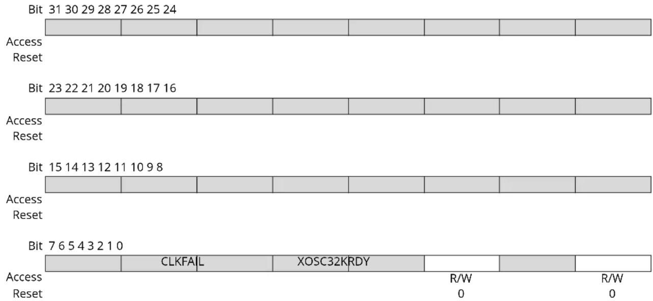
text_image
Bit 31 30 29 28 27 26 25 24 Access Reset Bit 23 22 21 20 19 18 17 16 Access Reset Bit 15 14 13 12 11 10 9 8 Access Reset Bit 7 6 5 4 3 2 1 0 Access Reset CLKFAIL XOSC32KRDY R/W 0 R/W 0Bit 2 - CLKFAIL XOSC32K Clock Failure Detection Interrupt Enable
Writing a '0' to this bit has no effect.
Writing a '1' to this bit will set the XOSC32K Clock Failure Interrupt Enable bit, which enables the XOSC32K Clock Failure interrupt.
| Value | Description |
| 0 | The XOSC32K Clock Failure Detection is disabled. |
| 1 | The XOSC32K Clock Failure Detection is enabled. An interrupt request will be generated when the XOSC32K Clock Failure Detection interrupt flag is set. |
Bit 0 - XOSC32KRDY XOSC32K Ready Interrupt Enable
Writing a '0' to this bit has no effect.
Writing a '1' to this bit will set the XOSC32K Ready Interrupt Enable bit, which enables the XOSC32K Ready interrupt.
| Value | Description |
| 0 | The XOSC32K Ready interrupt is disabled. |
| 1 | The XOSC32K Ready interrupt is enabled. |
21.8.3 Interrupt Flag Status and Clear
Name: INTFLAG
Offset: 0x08
Reset: 0x00000000
Property: -
text_image
Bit 31 30 29 28 27 26 25 24 Access Reset Bit 23 22 21 20 19 18 17 16 Access Reset Bit 15 14 13 12 11 10 9 8 Access Reset Bit 7 6 5 4 3 2 1 0 Access Reset CLKFAIL XOSC32KRDY R/W 0 R/W 0Bit 2 - CLKFAIL XOSC32K Clock Failure Detection
This flag is cleared by writing a '1' to it.
This flag is set on a zero-to-one transition of the XOSC32K Clock Failure Detection bit in the Status register (STATUS.CLKFAIL) and will generate an interrupt request if INTENSET.CLKFAIL is '1'.
Writing a '0' to this bit has no effect.
Writing a '1' to this bit will clear the XOSC32K Clock Failure Detection flag.
Bit 0 - XOSC32KRDY XOSC32K Ready
This flag is cleared by writing a '1' to it.
This flag is set by a zero-to-one transition of the XOSC32K Ready bit in the Status register
(STATUS.XOSC32KRDY), and will generate an interrupt request if INTENSET.XOSC32KRDY=1.
Writing a '0' to this bit has no effect.
Writing a '1' to this bit clears the XOSC32K Ready interrupt flag.
21.8.4 Status
Name: STATUS
Offset: 0x0C
Reset: 0x00000000
Property: -

text_image
Bit 31 30 29 28 27 26 25 24 Access Reset Bit 23 22 21 20 19 18 17 16 Access Reset Bit 15 14 13 12 11 10 9 8 Access Reset Bit 7 6 5 4 3 2 1 0 Access Reset R R R 0 0 0Bit 3 - CLKSW XOSC32K Clock Switch
| Value | Description |
| 0 | XOSC32K is not switched and provided the crystal oscillator. |
| 1 | XOSC32K is switched to be provided by the safe clock. |
Bit 2 - CLKFAIL XOSC32K Clock Failure Detector
| Value | Description |
| 0 | No XOSC32K failure is detected. |
| 1 | A XOSC32K failure is detected. |
Bit 0 - XOSC32KRDY XOSC32K Ready
| Value | Description |
| 0 | XOSC32K is not ready. |
| 1 | XOSC32K is stable and ready to be used as a clock source. |
21.8.5 RTC Clock Selection Control
Name: RTCCTRL
Offset: 0x10
Reset: 0x00
Property: PAC Write-Protection
Bit 76543210
| RTCSEL[2:0] | |||||
| Access Reset 0 0 0 | R/W R/W R/W | ||||
Bits 2:0 - RTCSEL[2:0] RTC Clock Selection
These bits select the source for the RTC.
| Value Name Description | ||
| 0x0 | ULP1K | 1.024 kHz from 32.768 kHz internal ULP oscillator |
| 0x1 | ULP32K | 32.768 kHz from 32.768 kHz internal ULP oscillator |
| 0x2, 0x3 | Reserved | - |
| 0x4 | XOSC1K | 1.024 kHz from 32.768 kHz external oscillator |
| 0x5 | XOSC32K | 32.768 kHz from 32.768 kHz external crystal oscillator |
| 0x6 | Reserved | - |
| 0x7 | Reserved | - |
21.8.6 SLCD Clock Selection Control
Name: SLCDCTRL
Offset: 0x11
Reset: 0x00
Property: PAC Write-Protection
Bit 76543210
| SLCDSEL | |||||||
| Access Reset 0 | R/W | ||||||
Bit 0 - SLCDSEL SLCD Clock Source Selection
This bit selects the clock source for the SLCD
| Value Description | |
| 0 | 32.768 kHz from 32.768 kHz internal ULP oscillator |
| 1 | 32.768 kHz from external oscillator |
21.8.7 32.768 kHz External Crystal Oscillator (XOSC32K) Control
Name: XOSC32K
Offset: 0x14
Reset: 0x00000080
Property: PAC Write-Protection
Bit 15 14 13 12 11 10 9 8
| WRTLOCK STARTUP[2:0] | ||||
| Access Reset | R/W R/W 0 | R/W | R/W 0 0 0 |
Bit 76543210
| ONDEMAND | RUNSTDBY | EN1K | EN32K | XTALEN | ENABLE | |||
| Access | R/W | R/W | R/W | R/W | R/W | R/W | ||
| Reset | 10 | 0 0 0 0 |
Bit 12 - WRTLOCK Write Lock
This bit locks the XOSC32K register for future writes, effectively freezing the XOSC32K configuration.
| Value | Description |
| 0 | The XOSC32K configuration is not locked. |
| 1 | The XOSC32K configuration is locked. |
Bits 10:8 - STARTUP[2:0] Oscillator Start-Up Time
This bit field selects the XOSC32K crystal oscillator stabilization time.
![Microchip ATSAML22G17A - Bits 10:8 - STARTUP[2:0] Oscillator Start-Up Time - 1](/content/2026/06/1221739/images/29a7966b76113fb0fc7f5f182ac8232df694f06f0c48d97e20b38f7cf13e5b4f.jpg)
Important: This stabilization time is for guidance only. A major component of crystal start-up time is based on the second party crystal MFG parasitics that are outside the scope of this specification. If this is a major concern, the customer would need to characterize this based on their design choices.
Table 21-2. Stabilization Time for 32.768 kHz External Crystal Oscillator (1)
| STARTUP[2:0] | Number of OSCULP32K Clock Cycles | Approximate Equivalent Time (2)[s] |
| 0x0 | 2048 | 0.06 |
| 0x1 | 4096 | 0.13 |
| 0x2 | 16384 | 0.5 |
| 0x3 | 32768 | 1 |
| 0x4 | 65536 | 2 |
| 0x5 | 131072 | 4 |
| 0x6 | 262144 | 8 |
| 0x7 | Reserved | Reserved |
Notes:
- The OSCULP32K oscillator is used to clock the start-up counter.
- Actual Start-Up time is the number of selected OSCULP32K cycles + 3 XOSC32K cycles.
Bit 7 - ONDEMAND On Demand Control
This bit controls how the XOSC32K behaves when a peripheral clock request is detected. For details, refer to XOSC32K Sleep Behavior.
Bit 6 - RUNSTDBY Run in Standby
This bit controls how the XOSC32K behaves during Standby sleep mode. For details, refer to XOSC32K Sleep Behavior.
Bit 4 - EN1K 1.024 kHz Output Enable
| Value Description | |
| 0 | The 1.024 kHz output is disabled. |
| 1 | The 1.024 kHz output is enabled. |
Bit 3 - EN32K 32.768 kHz Output Enable
| Value Description | |
| 0 | The 32.768 kHz output is disabled. |
| 1 | The 32.768 kHz output is enabled. |
Bit 2 - XTALEN Crystal Oscillator Enable
This bit controls the connections between the I/O pads and the external clock or crystal oscillator.
| Value Description | |
| 0 | External clock connected on XIN32. XOUT32 can be used as general-purpose I/O. |
| 1 | Crystal connected to XIN32/XOUT32. |
Bit 1 - ENABLE Oscillator Enable
| Value Description | |
| 0 | The oscillator is disabled. |
| 1 | The oscillator is enabled. |
21.8.8 Clock Failure Detector Control
Name: CFDCTRL
Offset: 0x16
Reset: 0x00
Property: PAC Write-Protection
Bit 76543210
Access
Reset 000
| CFDPRESC SWBACK CFDEN |
R/W R/W R/W
Bit 2 - CFDPRESC Clock Failure Detector Prescaler
This bit selects the prescaler for the Clock Failure Detector.
| Value | Description |
| 0 | The CFD safe clock frequency is the OSCULP32K frequency |
| 1 | The CFD safe clock frequency is the OSCULP32K frequency divided by 2 |
Bit 1 - SWBACK Clock Switch Back
This bit clontrols the XOSC32K output switch back to the external clock or crystal scillator in case of clock recovery.
| Value | Description |
| 0 | The clock switch is disabled. |
| 1 | The clock switch is enabled. This bit is reset when the XOSC32K output is switched back to the external clock or crystal oscillator. |
Bit 0 - CFDEN Clock Failure Detector Enable
This bit selects the Clock Failure Detector state.
| Value | Description |
| 0 | The CFD is disabled. |
| 1 | The CFD is enabled. |
21.8.9 Event Control
Name: EVCTRL
Offset: 0x17
Reset: 0x00
Property: PAC Write-Protection
Bit 76543210
| CFDEO | |||||||
| Access Reset 0 | R/W | ||||||
Bit 0 - CFDEO Clock Failure Detector Event Out Enable
This bit controls whether the Clock Failure Detector event output is enabled and an event will be generated when the CFD detects a clock failure.
| Value Description | |
| 0 | Clock Failure Detector Event output is disabled, no event will be generated. |
| 1 | Clock Failure Detector Event output is enabled, an event will be generated. |
21.8.10 32.768 kHz Ultra Low-Power Internal Oscillator (OSCULP32K) Control
Name: OSCULP32K
Offset: 0x1C
Reset: 0x0000XX00
Property: PAC Write-Protection
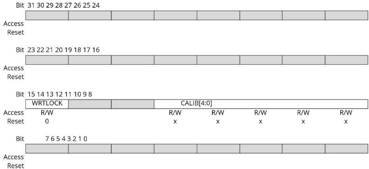
text_image
Bit 31 30 29 28 27 26 25 24 Access Reset Bit 23 22 21 20 19 18 17 16 Access Reset Bit 15 14 13 12 11 10 9 8 WRTLOCK CALIB[4:0] Access R/W R/W R/W R/W R/W R/W Reset 0 x x x x Bit 7 6 5 4 3 2 1 0 Access ResetBit 15 - WRTLOCK Write Lock
This bit locks the OSCULP32K register for future writes to fix the OSCULP32K configuration.
| Value | Description |
| 0 | The OSCULP32K configuration is not locked. |
| 1 | The OSCULP32K configuration is locked. |
Bits 12:8 - CALIB[4:0] Oscillator Calibration
These bits control the oscillator calibration.
These bits are loaded from Flash Calibration at startup.
22. SUPC – Supply Controller
22.1 Overview
The Supply Controller (SUPC) manages the voltage reference, power supply, and supply monitoring of the device. It is also able to control two output pins.
The SUPC controls the voltage regulators for the core (VDDCORE) and backup (VDDBU) domains. It sets the voltage regulators according to the sleep modes, or the user configuration. In active mode, the voltage regulators can be selected on the fly between LDO (low-dropout) type regulator or Buck converter.
The SUPC supports connection of a battery backup to the VBAT power pin. It includes functionality that enables automatic power switching between main power and battery backup power. This ensures power to the backup domain when the main battery or power source is unavailable.
The SUPC embeds two Brown-Out Detectors. BOD33 monitors the voltage applied to the device (VDD or VBAT) and BOD12 monitors the internal voltage to the core (VDDCORE). The BOD can monitor the supply voltage continuously (continuous mode) or periodically (sampling mode).
The SUPC generates also a selectable reference voltage which can be used by analog modules like the ADC.
22.2 Features
• Voltage Regulator System
- Main voltage regulator: LDO or Buck Converter in active mode (MAINVREG)
– Low Power voltage regulator in standby mode (LPVREG) - Backup voltage regulator for backup domains
- Adjustable VDDCORE to the sleep mode or the performance level
- Controlled VDDCORE voltage slope when changing VDDCORE
- Battery Backup Power Switch
- Automatic switching from main power to battery backup power
• Automatic entry to backup mode when switched to battery backup power - Automatic switching from battery backup power to main power
- Automatic exit from backup mode when switched back to main power
- Stay in backup mode when switched back to main power
- Main power request upon wake-up sources from backup mode
• Voltage Reference System
– Reference voltage for ADC
• 3.3V Brown-Out Detector (BOD33)
- Programmable threshold
- Threshold value loaded from NVM User Row at startup
- Triggers resets, interrupts, or Battery Backup Power Switch. Action loaded from NVM User Row
- Operating modes:
- Continuous mode
- Sampled mode for low power applications with programmable sample frequency
- Hysteresis value from Flash User Calibration
-
Monitor VDD or VBAT
-
1.2V Brown-Out Detector (BOD12)
- Internal non-configurable Brown-Out Detector
- Output pins
- Pin toggling on RTC event
22.3 Block Diagram
Figure 22-1. SUPC Block Diagram

flowchart
graph TD
    A["VDD"] --> B["Battery Backup Power Switch"]
    C["VBAT"] --> B
    B --> D["Automatic Power Switch"]
    D --> E["BOD33"]
    E --> F["Backup VREG"]
    F --> G["VDDBU"]
    G --> H["Backup domain"]
    I["Wakeup from RTC"] --> J["BKOUT"]
    J --> K["OUT[1:0"]]
    L["BBPS"] --> M["PSOK"]
    N["BODY Backup Power Switch"] --> O["Main VREG"]
    P["VREG"] --> Q["LDO"]
    R["PM"] --> S["Buck Converter"]
    T["DP"] --> U["LP VREG"]
    V["VREF"] --> W["DETREF"]
    X["VDDCORE"] --> Y["BOD12"]
    Z["Core domain"] --> AA["Core domain"]
    AB["performance level"] --> AC["LDO"]
    AD["sleep mode"] --> AE["LP VREG"]
    AF["reference voltages"] --> AG["DETREF"]
22.4 Signal Description
| Signal Name Type Description | ||
| OUT[1:0] Digital Output SUPC Outputs | ||
| PSOK Digital Input Main Power Supply OK | ||
One signal can be mapped on several pins.
22.5 Product Dependencies
In order to use this peripheral, other parts of the system must be configured correctly, as described below.
22.5.1 I/O Lines
I/O lines are configured by SUPC either when the SUPC output (signal OUT) is enabled or when the PSOK input is enabled. The I/O lines need no user configuration.
22.5.2 Power Management
The SUPC can operate in all sleep modes except backup sleep mode. BOD33 and Battery backup Power Switch can operate in backup mode.
22.5.3 Clocks
The SUPC bus clock (CLK_SUPC_APB) can be enabled and disabled in the Main Clock module.
A 32KHz clock, asynchronous to the user interface clock (CLK_SUPC_APB), is required to run BOD33 and BOD12 in sampled mode. Due to this asynchronicity, writing to certain registers will require synchronization between the clock domains. Refer to 22.6.7. Synchronization for further details.
References:
32KHz Oscillators Controller - OSC32KCTRL
Peripheral Clock Masking
22.5.4 DMA
Not applicable.
22.5.5 Interrupts
The interrupt request lines are connected to the Nested Vector Interrupt Controller. Using the SUPC interrupts requires the interrupt controller to be configured first.
22.5.6 Events
Not applicable.
22.5.7 Debug Operation
When the CPU is halted in debug mode, the SUPC continues normal operation. If the SUPC is configured in a way that requires it to be periodically serviced by the CPU through interrupts or similar, improper operation or data loss may result during debugging.
If debugger cold-plugging is detected by the system, BOD33 and BOD12 resets will be masked. The BOD resets keep running under hot-plugging. This allows to correct a BOD33 user level too high for the available supply.
22.5.8 Register Access Protection
Registers with write-access can be write-protected optionally by the peripheral access controller (PAC).
Note: Not all registers with write-access can be write-protected.
PAC Write-Protection is not available for the following registers:
- Interrupt Flag Status and Clear register (INTFLAG)
Optional PAC Write-Protection is denoted by the "PAC Write-Protection" property in each individual register description.
22.5.9 Analog Connections
Not applicable.
22.6 Functional Description
22.6.1 Voltage Regulator System Operation
22.6.1.1 Enabling, Disabling, and Resetting
The LDO main voltage regulator is enabled after any Reset. The main voltage regulator (MAINVREG) can not be disabled, therefore the Enable bit in the VREG register (VREG.ENABLE) must be set to one. The main voltage regulator output supply level is automatically defined by the sleep mode selected in the 19. PM - Power Manager module.
References:
Power Manager
22.6.1.2 Initialization
After a Reset, the LDO voltage regulator supplying VDDCORE is enabled.
22.6.1.3 Selecting a Voltage Regulator
In active mode, the type of the main voltage regulator supplying VDDCORE can be switched on the fly. The two alternatives are a LDO regulator and a Buck converter.
The main voltage regulator switching sequence:
- The user changes the value of the Voltage Regulator Selection bit in the Voltage Regulator System Control register (VREG.SEL)
- The start of the switching sequence is indicated by clearing the Voltage Regulator Ready bit in the STATUS register (STATUS.VREGRDY=0)
- Once the switching sequence is completed, STATUS.VREGRDY will read '1'
The Voltage Regulator Ready (VREGRDY) interrupt can also be used to detect a zero-to-one transition of the STATUS.VREGRDY bit.
22.6.1.4 Voltage Scaling Control
The VDDCORE supply will change under certain circumstances:
- When a new performance level (PL) is set
- When the standby sleep mode is entered or left
- When a sleepwalking task is requested in standby sleep mode
To prevent high peak current on the main power supply and to have a smooth transition of VDDCORE, both the voltage scaling step size and the voltage scaling frequency can be controlled: VDDCORE is changed by the selected step size of the selected period until the target voltage is reached.
The Voltage Scaling Voltage Step field is in the VREG register, VREG.VSVSTEP. The Voltage Scaling Period field is VREG.VSPER.
The following waveform shows an example of changing performance level from PL0 to PL2.
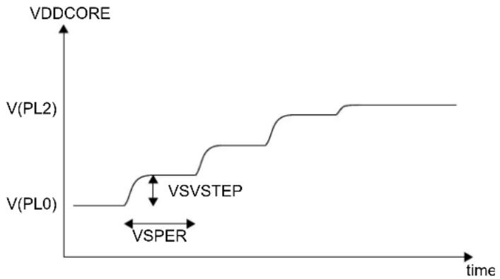
line
| time | V(PL0) | V(VSSTEP) | |------|--------|-----------| | 0 | V(PL0) | - | | V | V(PL2) | - | | >V | - | - |Setting VREG.VSVSTEP to the maximum value allows to transition in one voltage step.
The STATUS.VCORERDY bit is set to '1' as soon as the VDDCORE voltage has reached the target voltage. During voltage transition, STATUS.VCORERDY will read '0'. The Voltage Ready interrupt (VCORERDY) can be used to detect a 0-to-1 transition of STATUS.VCORERDY, see also 22.6.6. Interrupts.
When entering the standby sleep mode and when no sleepwalking task is requested, the VDDCORE Voltage scaling control is not used.
22.6.1.5 Sleep Mode Operation
In Standby mode, the low-power voltage regulator (LPVREG) is used to supply VDDCORE.
When the Run in Standby bit in the VREG register (VREG.RUNSTDBY) is written to '1', VDDCORE is supplied by the main voltage regulator. Depending on the Standby in PL0 bit in the Voltage Regulator register (VREG.STDBYPL0), the VDDCORE level is either set to the PL0 voltage level, or remains in the current performance level.
Table 22-1. VDDCORE Level in Standby Mode
| VREG.RUNSTDBY VREG.STDBY | PL0 VDDCORE Supply in Standby Mode | |
| 0 - LPVREG | ||
| 1 0 MAINVREG in current performance level | (1) | |
| 1 1 MAINVREG in PL0 | ||
Note:
- When the device is in PL0 but VREG.STDBYPL0 = 0, the MAINVREG is operating in normal power mode. To minimize power consumption, operate MAINVREG in PL0 mode by selecting VREG.STDBYPL0 = 1.
By writing the Low-Power mode Efficiency bit in the VREG register (VREG.LPEFF) to '1', the efficiency of the regulator in LPVREG can be improved when the application uses a limited VDD range (2.5 to 3.6V). It is also possible to use the BOD33 to monitor the VDD and change this LPEFF value on the fly according to VDD level.
References:
19.6.3.3 Sleep Mode Controller
22.6.2 Voltage Reference System Operation
The reference voltages are generated by a functional block DETREF inside of the SUPC. DETREF is providing a fixed-voltage source, BANDGAP = 1.1V, and a variable voltage, INTREF.
22.6.2.1 Initialization
The voltage reference output is disabled after any Reset.
22.6.2.2 Enabling, Disabling, and Resetting
The voltage reference output is enabled or disabled by setting or clearing the Voltage Reference Output Enable bit in the Voltage Reference register (VREF.VREFOE).
22.6.2.3 Selecting a Voltage Reference
The Voltage Reference Selection bit field in the VREF register (VREF.SEL) selects the voltage of INTREF to be applied to analog modules, for example the ADC.
22.6.2.4 Sleep Mode Operation
The Voltage Reference output behavior during Sleep mode can be configured using the Run in Standby bit and the On Demand bit in the Voltage Reference register (VREF.RUNSTDBY, VREF.ONDEMAND), see the following table:
Table 22-2. VREF Sleep Mode Operation
| VREF.ONDEMAND | VREF.RUNSTDBY | Voltage Reference Sleep behavior |
| -- Disable | ||
| 0 0 Always run in all sleep modes except Standby Sleep mode | ||
| 0 1 Always run in all sleep modes including Standby Sleep mode | ||
| 1 0 Only run if requested by the ADC, in all sleep modes except Standby sleep mode | ||
| 1 1 Only run if requested by the ADC, in all sleep modes including Standby sleep mode | ||
22.6.3 Battery Backup Power Switch
22.6.3.1 Initialization
The Battery Backup Power Switch (BBPS) is disabled at power-up, and the backup domain is supplied by main power.
22.6.3.2 Forced Battery Backup Power Switch
The Backup domain is always supplied by the VBAT supply pin when the Configuration bit field in the Battery Backup Power Switch Control register (BBPS.CONF) is written to 0x2 (FORCED).
22.6.3.3 Automatic Battery Backup Power Switch
The supply of the backup domain can be switched automatically to VBAT supply pin by the Automatic Power Switch or by using the BOD33.
The supply of the backup domain can be switched automatically to VDD supply pin either by the Automatic Power Switch or the Main Power Pin when VDD and VDDCORE are restored.
Automatic Power Switch (APWS)
When the Configuration bit field in the Battery Backup Power Switch register (BBPS.CONF) is selecting the APWS, the Automatic Power Switch will function as Battery Backup Power Switch.
The Automatic Power switch allows to switch the supply of the backup domain from VDD to VBAT power and vice-versa.
When the Automatic Power Switch configuration is selected, the Automatic Power Switch Ready bit in the Status register (STATUS.APWSRDY) is set when the Automatic Power Switch is ready to operate. The Automatic Power Switch Ready bit in the Interrupt Flag Status and Clear (INTFLAG.APSWRDY) will be set at the same time.
BOD33 Power Switch
When the Configuration bit field in the Battery Backup Power Switch register (BBPS.CONF) are selecting the BOD33, BOD33 will function as Battery Backup Power Switch. In this case, when the VDD voltage is below the BOD33 threshold, the backup domain supply is switched to VBAT.
Main Power Supply OK (PSOK) Pin Enable
The state of the Main Power VDD can be used to switch between supply sources as long as the Battery Backup Power Switch is not configured as Automatic Power Switch (i.e., BBPS.CONF not set to APWS): when the Main Power Supply OK Pin Enable bit in the BBPS register is written to '1' (BBPS.PSOKEN), restoring VDD will form a low-to-high transition on the PSOK pin. This low-to-high transition will switch the Backup Power Supply back to VDD.
Note: With BBPS.PSOKEN=0 and BBPS.CONF not configured to APWS, the device can not be restarted.
Backup Battery Power Switch Status
The Battery Backup Power Switch bit in the Status register (STATUS.BBPS) indicates whether the backup domain is currently powered by VDD or VBAT.
22.6.3.4 Sleep Mode Operation
The Battery Backup Power Switch is not stopped in any sleep mode.
Entering Battery Backup Mode
Entering backup mode can be triggered by either:
- Wait-for-interrupt (WFI) instruction.
- Automatic Power Switch (BBPS.CONF=APWS). When the Automatic Power Switch detects loss of Main Power, the Backup Domain will be powered by battery and the device will enter the backup mode.
- BOD33 detection: When the BOD33 detects loss of Main Power, the Backup Domain will be powered by battery and the device will enter the backup mode. For this trigger, the
following register configuration is required: BOD33.ACTION=BKUP, BOD33.VMON=VDD, and BBPS.CONF=BOD33.
Leaving Battery Backup Mode
Leaving backup mode can be triggered by either:
- RTC requests and externally triggered RSTC requests, under one of these conditions:
- The Backup Domain is supplied by Main Power, and the Battery Backup Power Switch is not forced (BBPS.CONF not set to FORCED)
- The Battery Backup Power Switch is forced (BBPS.CONF is FORCED)
The device is kept in battery-powered backup mode until Main Power is restored to supply the device. Then, the backup domain will be powered by Main Power.
- Automatic Power Switch. Leaving backup mode will happen when Main Power is restored and the Battery Backup Power Switch configuration (BBPS.CONF) is set to APWS: When BBPS.WAKEEN=1, the device will leave backup mode and wake up.
When BBPS.WAKEEN=0, the backup domain will be powered by Main Power, but the device will stay in backup mode.
- PSOK pin. A low-to-high transition on PSOK will wake up the device if BBPS.PSOKEN=1, BBPS.WAKEEN=1, and the Battery Backup Power Switch is different from APWS (BBPS.CONF is not APWS).
When BBPS.WAKEEN=0, the backup domain will be powered by Main Power, but the device will stay in backup mode.
22.6.4 Output Pins
The SUPC can drive two outputs. By writing a '1' to the corresponding Output Enable bit in the Backup Output Control register (BKOUT.EN), the OUTx pin is driven by the SUPC.
The OUT pin can be set by writing a '1' to the corresponding Set Output bit in the Backup Output Control register (BKOUT.SETx).
The OUT pin can be cleared by writing a '1' to the corresponding CLR bit (BKOUT.CLRx).
If a RTC Toggle Enable bit is written to '1' (BKOUT.RTCTGLx), the corresponding OUTx pin will toggle when an RTC event occurs.
22.6.5 Brown-Out Detectors
22.6.5.1 Initialization
Before a Brown-Out Detector (BOD33) is enabled, it must be configured, as outlined by the following:
- Set the BOD threshold level (BOD33.LEVEL)
- Set the configuration in active, standby, backup modes (BOD33.ACTCDG, BOD33.STDBYCFG, BODVDD.BKUP)
- Set the prescaling value if the BOD will run in sampling mode (BOD33.PSEL)
- Set the action and hysteresis (BOD33.ACTION and BOD33.HYST)
The BOD33 register is Enable-Protected, meaning that they can only be written when the BOD is disabled (BOD33.ENABLE=0 and SYNCBUSY.BOD33EN=0). As long as the Enable bit is '1', any writes to Enable-Protected registers will be discarded, and an APB error will be generated. The Enable bits are not Enable-Protected.
22.6.5.2 Enabling, Disabling, and Resetting
After power or user reset, the BOD33 and BOD12 register values are loaded from the NVM User Row.
The BODVDD is enabled by writing a '1' to the Enable bit in the BOD control register (BOD33.ENABLE). The BOD is disabled by writing a '0' to the BODVDD.ENABLE.
References:
The 3.3V Brown-Out Detector (BOD33) is able to monitor either the VDD or the VBAT supply.
The Voltage Monitored bit in the BOD33 Control register (BOD33.VMON) selects which supply is monitored in active and standby mode. In backup mode, BOD33 will always monitor the supply of the backup domain, i.e. either VDD or VBAT.
If VDD is monitored, the BOD33 compares the voltage with the brown-out threshold level. This level is set in the BOD33 Level field in the BOD33 register (BOD33.LEVEL). This level is used in all modes except the backup sleep modes. In backup sleep modes, a different voltage reference is used, which is configured by the BOD33.BKUPLEVEL bits.
When VDD crosses below the brown-out threshold level, the BOD33 can generate either an interrupt, a Reset, or an Automatic Battery Backup Power Switch, depending on the BOD33 Action bit field (BOD33.ACTION).
If VBAT is monitored, the BOD33 compares the voltage with the brown-out threshold level set in the BOD33 Backup Level field in the BOD33 register (BOD33.BKUPLEVEL).
When VBAT crosses below the backup brown-out threshold level, the BOD33 can generate either an interrupt or a Reset.
The BOD33 detection status can be read from the BOD33 Detection bit in the Status register (STATUS.BOD33DET).
At start-up or at Power-On Reset (POR), the BOD33 register values are loaded from the NVM User Row.
References:
The BOD12 is calibrated in production and its calibration configuration is stored in the NVM User Row. This configuration must not be changed to assure the correct behavior of the BOD12. The BOD12 generates a reset when 1.2V crosses below the preset brown-out level. The BODCORE is always disabled in standby sleep mode.
References:
22.6.5.5 Continuous Mode
Continuous mode is the default mode for BOD33.
The BOD33 is continuously monitoring the supply voltage (VDD or VBAT, depending on BOD33.VMON) if it is enabled (BOD33.ENABLE=1) and if the BOD33 Configuration bit in the BOD33 register is cleared (BOD33.ACTCFG=0 for active mode, BOD33.STDBYCFG=0 for standby mode).
22.6.5.6 Sampling Mode
The Sampling Mode is a low-power mode where the BOD33 is being repeatedly enabled on a sampling clock's ticks. The BOD33 will monitor the supply voltage for a short period of time and then go to a low-power disabled state until the next sampling clock tick.
Sampling mode is enabled in Active mode for BOD33 by writing the ACTCFG bit (BOD33.ACTCFG=1). Sampling mode is enabled in Standby mode by writing to the STDBYCFG bit (BOD33.STBYCFG=1). The frequency of the clock ticks ( F_clksampling ) is controlled by the Prescaler Select bit groups in the BOD33 register (BOD33.PSEL).
$$ F _ {c l k s a m p l i n g} = \frac {F _ {c l k p r e s c a l e r}}{2 ^ {\left(\mathrm{PSEL} + 1\right)}} $$
The prescaler signal ( F_clkprescaler ) is a 1KHz clock, output by the 32KHz Ultra Low Power Oscillator OSCULP32K.
As the sampling clock is different from the APB clock domain, synchronization among the clocks is necessary. See also 22.6.7. Synchronization.
22.6.5.7 Hysteresis
A hysteresis on the trigger threshold of a BOD will reduce the sensitivity to ripples on the monitored voltage: instead of switching RESET at each crossing of V_BOD , the thresholds for switching RESET on and off are separated ( V_BOD- and V_BOD+ , respectively).
Figure 22-2. BOD Hysteresis Principle
Hysteresis OFF:
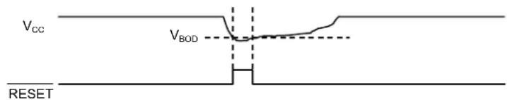
text_image
Vcc VBOD RESETHysteresis ON:
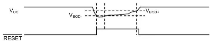
text_image
VCC VBOD- VBOD+ RESETEnabling the BOD33 hysteresis by writing the Hysteresis bit in the BOD33 register (BOD33.HYST) to '1' will add hysteresis to the BOD33 threshold level.
The hysteresis functionality can be used in both Continuous and Sampling Mode.
22.6.5.8 Sleep Mode Operation
22.6.5.8.1 Standby Mode
The BOD33 can be used in standby mode if the BOD is enabled and the corresponding Run in Standby bit is written to '1' (BOD33.RUNSTDBY).
The BOD33 can be configured to work in either Continuous or Sampling Mode by writing a '1' to the Configuration in Standby Sleep Mode bit (BOD33.STDBYCFG).
22.6.5.8.2 Backup Mode
In Backup mode, the BOD12 is automatically disabled.
If the BOD33 is enabled and the Run in Backup sleep mode bit in the BOD33 register (BOD33.RUNBKUP) is written to '1', the BOD33 will operate in Sampling mode. In this state, the voltage monitored by BOD33 is always the supply of the backup domain, i.e. VDD or VBAT.
22.6.6 Interrupts
The SUPC has the following interrupt sources, which are either synchronous or asynchronous wake-up sources:
• VDDCORE Voltage Ready (VCORERDY), asynchronous
• Automatic Power Switch Ready Ready (APSWRDY), asynchronous
• Voltage Regulator Ready (VREGRDY) asynchronous
• BOD33 Ready (BOD33RDY), synchronous
• BOD33 Detection (BOD33DET), asynchronous
• BOD33 Synchronization Ready (B33SRDY), synchronous
Each interrupt source has an interrupt flag associated with it. The interrupt flag in the Interrupt Flag Status and Clear register (INTFLAG) is set when the interrupt condition occurs.
Each interrupt can be individually enabled by writing a '1' to the corresponding bit in the Interrupt Enable Set register (INTENSET), and disabled by writing a '1' to the corresponding bit in the Interrupt Enable Clear register (INTENCLR).
An interrupt request is generated when the interrupt flag is set and the corresponding interrupt is enabled. The interrupt request remains active until either the interrupt flag is cleared, the interrupt is disabled, or the SUPC is reset. See the INTFLAG register for details on how to clear interrupt flags. The SUPC has one common interrupt request line for all the interrupt sources. The user must read the INTFLAG register to determine which interrupt condition is present.
Note: Interrupts must be globally enabled for interrupt requests to be generated.
References:
Nested Vector Interrupt Controller
Sleep Mode Controller
22.6.7 Synchronization
The prescaler counters that are used to trigger brown-out detections operate asynchronously from the peripheral bus. As a consequence, the BOD33 Enable bit (BOD33.ENABLE) need synchronization when written.
The Write-Synchronization of the Enable bit is triggered by writing a '1' to the Enable bit of the BOD33 Control register. The Synchronization Ready bit (STATUS.B33SRDY) in the STATUS register will be cleared when the Write-Synchronization starts, and set again when the Write-Synchronization is complete. Writing to the same register while the Write-Synchronization is ongoing (STATUS.B33SRDY is '0') will generate an error without stalling the APB bus.
22.7 Register Summary
| Offset | Name Bit Pos. 7 | 6 | 5 | 4 | 3 | 2 | 1 | 0 | ||||||||||||||||||||||||||||||||||||||||||||||||||||||||||||||||||||||||||||||||||||||||||||||||||||||||||||||||||||||||||||||||||||||||||||||||||||||||||||||||||||||||||||||||||||||||||||||||||||||||||||||||||||||||||||||||||||||||||||||||||||||||||||||||||||||||||||||||||||||||||||||||||||||||||||||||||||||||
| 0x00 | INTENCLR | 7:0 | B33SRDY BOD33DET BOD33RDY | 0x00 | INTENCLR | |||||||||||||||||||||||||||||||||||||||||||||||||||||||||||||||||||||||||||||||||||||||||||||||||||||||||||||||||||||||||||||||||||||||||||||||||||||||||||||||||||||||||||||||||||||||||||||||||||||||||||||||||||||||||||||||||||||||||||||||||||||||||||||||||||||||||||||||||||||||||||||||||||||||||||||||||||||||||||
| 15:8 | VCORERDY APWSRDY VREGRDY | 0x04 | INTENSET | 0x04 | INTENSET | |||||||||||||||||||||||||||||||||||||||||||||||||||||||||||||||||||||||||||||||||||||||||||||||||||||||||||||||||||||||||||||||||||||||||||||||||||||||||||||||||||||||||||||||||||||||||||||||||||||||||||||||||||||||||||||||||||||||||||||||||||||||||||||||||||||||||||||||||||||||||||||||||||||||||||||||||||||||||||
| 23:16 | 0x08 | INTFLAG | ||||||||||||||||||||||||||||||||||||||||||||||||||||||||||||||||||||||||||||||||||||||||||||||||||||||||||||||||||||||||||||||||||||||||||||||||||||||||||||||||||||||||||||||||||||||||||||||||||||||||||||||||||||||||||||||||||||||||||||||||||||||||||||||||||||||||||||||||||||||||||||||||||||||||||||||||||||||||||||||
| 31:24 | 0x0C | STATUS | 7:0 | B33SRDY BOD33DET BOD33RDY | 0x08 | INTFLAG | 7:0 | B33SRDY BOD33DET BOD33RDY | ||||||||||||||||||||||||||||||||||||||||||||||||||||||||||||||||||||||||||||||||||||||||||||||||||||||||||||||||||||||||||||||||||||||||||||||||||||||||||||||||||||||||||||||||||||||||||||||||||||||||||||||||||||||||||||||||||||||||||||||||||||||||||||||||||||||||||||||||||||||||||||||||||||||||||||||||||||||||
| 15:8 | VCORERDY APWSRDY VREGRDY | 15:8 | VCORERDY APWSRDY VREGRDY | 23:16 | 31:24 | |||||||||||||||||||||||||||||||||||||||||||||||||||||||||||||||||||||||||||||||||||||||||||||||||||||||||||||||||||||||||||||||||||||||||||||||||||||||||||||||||||||||||||||||||||||||||||||||||||||||||||||||||||||||||||||||||||||||||||||||||||||||||||||||||||||||||||||||||||||||||||||||||||||||||||||||||||||||||||
| 0x00 | STATUS | 7:0 | B33SRDY BOD33DET BOD33RDY | 0x0C | STATUS | 7:0 | B33SRDY BOD33DET BOD33RDY | 15:8 | BBPS | VCORERDY APWSRDY VREGRDY | ||||||||||||||||||||||||||||||||||||||||||||||||||||||||||||||||||||||||||||||||||||||||||||||||||||||||||||||||||||||||||||||||||||||||||||||||||||||||||||||||||||||||||||||||||||||||||||||||||||||||||||||||||||||||||||||||||||||||||||||||||||||||||||||||||||||||||||||||||||||||||||||||||||||||||||||||||||||
| 15:8 | BBPS | VCORERDY APWSRDY VREGRDY | 23:16 | 23:16 | 31:24 | 31:24 | 31:24 | 31:24 | 31:24 | 31:24 | 31:24 | 31:24 | 31:24 | 31:24 | 31:24 | 31:24 | 31:24 | 31:24 | 31:24 | 31:24 | 31:24 | 31;24 | 31:24 | 31:24 | 31:24 | 31:24 | 31:24 | 31:24 | 31:24 | 31:24 | 31:24 | 31:24 | 31:24 | 31:24 | 31:24 | 31:24 | 31:24 | 31:24 | 31:24 | 31:24 | 31:24 | 31:24 | 31:24 | 31:24 | 31:24 | 31:24 | 31:24 | 31:24 | 31:24 | 31:24 | 31:24 | 31:24 | 31:24 | 31:24 | 31 :24 | VSPER[7:0] | ||||||||||||||||||||||||||||||||||||||||||||||||||||||||||||||||||||||||||||||||||||||||||||||||||||||||||||||||||||||||||||||||||||||||||||||||||||||||||||||||||||||||||||||||||||||||||||||||||||||||||||||||||||||||||||||||||||||||||||||||||||||||||||||||||||||||
| 0x10 | BOD | 7:0 | RUNBKUP | RUNSTDBY | STDBYCFG | ACTION[1:0] | HYST | ENABLE | 0x10 | Reserved | Reserved | Reserved | Reserved | Reserved | Reserved | Reserved | Reserved | Reserved | Reserved | Reserved | Reserved | Reserved | Reserved | Reserved | Reserved | Reserved | Reserved | Reserved | Reserved | Reserved | Reserved | Reserved | Reserved | Reserved | Reserved | Reserved | Reserved | Reserved | Reserved | Reserved | Reserved | Reserved | Reserved | Reserved | Reserved | Reserved | Reserved | Reserved | Reserved | Reserved | Reserved | Reserved | Reserved | Reserved | Reserved | Reserved | Reserved | Reserved | Reserved | No | Reserved | Reserved | Reserved | Reserved | Reserved | Reserved | Reserved | Reserved | Reserved | Reserved | Reserved | Reserved | Reserved | Reserved | Reserved | Reserved | Reserved | Reserved | Reserved | Reserved | Reserved | Reserved | Reserved | Reserved | Reserved | Reserved | Reserved | Reserved | Reserved | Reserved | Reserved | Reserved | Reserved | Reserved | Reserved | Reserved | Reserved | Reserved | Reserved | Reserved | Reserved | Reserved | Reserved | Reserved | Reserved | Reserved | Reserved | Reserved | Reserved | Not | Reserved | Reserved | Reserved | Reserved | Reserved | Reserved | Reserved | Reserved | Reserved | Reserved | Reserved | Reserved | Reserved | Reserved | Reserved | Reserved | Reserved | Reserved | Reserved | Reserved | Reserved | Reserved | Reserved | Reserved | Reserved | Reserved | Reserved | Reserved | Reserved | Reserved | Reserved | Reserved | Reserved | Reserved | Reserved | Reserved | Reserved | Reserved | Reserved | Reserved | Reserved | Reserved | Reserved | Reserved | Reserved | Reserved | Reserved | Reserved | Reserved | Lower | Reserved | Reserved | Reserved | Reserved | Reserved | Reserved | Reserved | Reserved | Reserved | Reserved | Reserved | Reserved | Reserved | Reserved | Reserved | Reserved | Reserved | Reserved | Reserved | Reserved | Reserved | Reserved | Reserved | Reserved | Reserved | Reserved | Reserved | Reserved | Reserved | Reserved | Reserved | Reserved | Reserved | Reserved | Reserved | Reserved | Reserved | Reserved | Reserved | Reserved | Reserved | Reserved | Reserved | Reserved | Reserved | Reserved | Reserved | Reserved | Reserved | Yes | Reserved | Reserved | Reserved | Reserved | Reserved | Reserved | Reserved | Reserved | Reserved | Reserved | Reserved | Reserved | Reserved | Reserved | Reserved | Reserved | Reserved | Reserved | Reserved | Reserved | Reserved | Reserved | Reserved | Reserved | Reserved | Reserved | Reserved | Reserved | Reserved | Reserved | Reserved | Reserved | Reserved | Reserved | Reserved | Reserved | Reserved | Reserved | Reserved | Reserved | Reserved | Reserved | Reserved | Reserved | Reserved | Reserved | Reserved | Reserved | Reserved | None | Reserved | Reserved | Reserved | Reserved | Reserved | Reserved | Reserved | Reserved | Reserved | Reserved | Reserved | Reserved | Reserved | Reserved | Reserved | Reserved | Reserved | Reserved | Reserved | Reserved | Reserved | Reserved | Reserved | Reserved | Reserved | Reserved | Reserved | Reserved | Reserved | Reserved | Reserved | Reserved | Reserved | Reserved | Reserved | Reserved | Reserved | Reserved | Reserved | Reserved | Reserved | Reserved | Reserved | Reserved | Reserved | Reserved | Reserved | Reserved | Reserved | |||||||||||
22.8 Register Description
Registers can be 8, 16, or 32 bits wide. Atomic 8-, 16-, and 32-bit accesses are supported. In addition, the 8-bit quarters and 16-bit halves of a 32-bit register, and the 8-bit halves of a 16-bit register can be accessed directly.
Some registers are optionally write-protected by the Peripheral Access Controller (PAC). PAC Write-protection is denoted by the "PAC Write-Protection" property in each individual register description. Refer to 22.5.8. Register Access Protection for details.
Some registers require synchronization when read and/or written. Synchronization is denoted by the "Write-Synchronized" or the "Read-Synchronized" property in each individual register description. Refer to 22.6.7. Synchronization for details.
22.8.1 Interrupt Enable Clear
Name: INTENCLR
Offset: 0x00
Reset: 0x00000000
Property: PAC Write-Protection
This register allows the user to disable an interrupt without doing a read-modify-write operation. Changes in this register will also be reflected in the Interrupt Enable Set register (INTENSET).
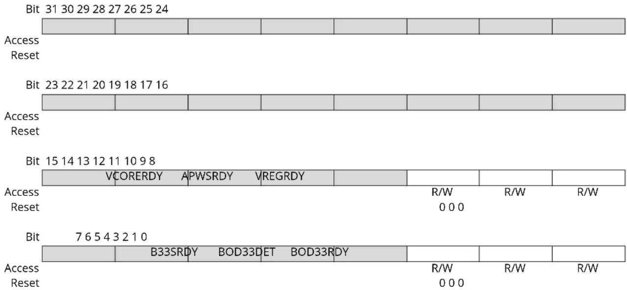
text_image
Bit 31 30 29 28 27 26 25 24 Access Reset Bit 23 22 21 20 19 18 17 16 Access Reset Bit 15 14 13 12 11 10 9 8 VCORERDY APWSRDY VREGRDY Access R/W R/W R/W Reset 0 0 0 Bit 7 6 5 4 3 2 1 0 B33SRDY BOD33DET BOD33RDY Access R/W R/W R/W Reset 0 0 0Bit 10 - VCORERDY VDDCORE Voltage Ready Interrupt Enable
Writing a '0' to this bit has no effect.
Writing a '1' to this bit will clear the VDDCORE Ready Interrupt Enable bit, which disables the VDDCORE Ready interrupt.
| Value | Description |
| 0 | The VDDCORE Ready interrupt is disabled. |
| 1 | The VDDCORE Ready interrupt is enabled and an interrupt request will be generated when the VCORERDY Interrupt Flag is set. |
Bit 9 - APWSRDY Automatic Power Switch Ready Interrupt Enable
Writing a '0' to this bit has no effect.
Writing a '1' to this bit will clear the Automatic Power Switch Ready Interrupt Enable bit, which disables the Automatic Power Switch Ready interrupt.
| Value | Description |
| 0 | The Automatic Power Switch Ready interrupt is disabled. |
| 1 | The Automatic Power Switch Ready interrupt is enabled and an interrupt request will be generated when the APWSRDY Interrupt Flag is set. |
Bit 8 - VREGRDY Voltage Regulator Ready Interrupt Enable
Writing a '0' to this bit has no effect.
Writing a '1' to this bit will clear the Voltage Regulator Ready Interrupt Enable bit, which disables the Voltage Regulator Ready interrupt.
| Value | Description |
| 0 | The Voltage Regulator Ready interrupt is disabled. |
Value Description
| 1 | The Voltage Regulator Ready interrupt is enabled and an interrupt request will be generated when the Voltage Regulator Ready Interrupt Flag is set. |
Bit 2 - B33SRDY BOD33 Synchronization Ready Interrupt Enable
Writing a '0' to this bit has no effect.
Writing a '1' to this bit will clear the BOD33 Synchronization Ready Interrupt Enable bit, which disables the BOD33 Synchronization Ready interrupt.
Value Description
| 0 | The BOD33 Synchronization Ready interrupt is disabled. |
| 1 | The BOD33 Synchronization Ready interrupt is enabled, and an interrupt request will be generated when the BOD33 Synchronization Ready Interrupt flag is set. |
Bit 1 - BOD33DET BOD33 Detection Interrupt Enable
Writing a '0' to this bit has no effect.
Writing a '1' to this bit will clear the BOD33 Detection Interrupt Enable bit, which disables the BOD33 Detection interrupt.
Value Description
| 0 | The BOD33 Detection interrupt is disabled. |
| 1 | The BOD33 Detection interrupt is enabled, and an interrupt request will be generated when the BOD33 Detection Interrupt flag is set. |
Bit 0 - BOD33RDY BOD33 Ready Interrupt Enable
Writing a '0' to this bit has no effect.
Writing a '1' to this bit will clear the BOD33 Ready Interrupt Enable bit, which disables the BOD33 Ready interrupt.
Value Description
| 0 | The BOD33 Ready interrupt is disabled. |
| 1 | The BOD33 Ready interrupt is enabled, and an interrupt request will be generated when the BOD33 Ready Interrupt flag is set. |
22.8.2 Interrupt Enable Set
Name: INTENSET
Offset: 0x04
Reset: 0x00000000
Property: PAC Write-Protection
This register allows the user to disable an interrupt without doing a read-modify-write operation. Changes in this register will also be reflected in the Interrupt Enable Clear register (INTENCLR).

text_image
Bit 31 30 29 28 27 26 25 24 Access Reset Bit 23 22 21 20 19 18 17 16 Access Reset Bit 15 14 13 12 11 10 9 8 VCORERDY APWSRDY VREGRDY Access Reset R/W R/W R/W 0 0 0 Bit 7 6 5 4 3 2 1 0 B33SRDY BOD33DET BOD33RDY Access Reset R/W R/W R/W 0 0 0Bit 10 - VCORERDY VDDCORE Voltage Ready Interrupt Enable
Writing a '0' to this bit has no effect.
Writing a '1' to this bit will set the VDDCORE Ready Interrupt Enable bit, which enables the VDDCORE Ready interrupt.
| Value | Description |
| 0 | The VDDCORE Ready interrupt is disabled. |
| 1 | The VDDCORE Ready interrupt is enabled and an interrupt request will be generated when the VCORERDY Interrupt Flag is set. |
Bit 9 - APWSRDY Automatic Power Switch Ready Interrupt Enable
Writing a '0' to this bit has no effect.
Writing a '1' to this bit will set the Automatic Power Switch Ready Interrupt Enable bit, which enables the Automatic Power Switch Ready interrupt.
| Value | Description |
| 0 | The Automatic Power Switch Ready interrupt is disabled. |
| 1 | The Automatic Power Switch Ready interrupt is enabled and an interrupt request will be generated when the Automatic Power Switch Ready Interrupt Flag is set. |
Bit 8 - VREGRDY Voltage Regulator Ready Interrupt Enable
Writing a '0' to this bit has no effect.
Writing a '1' to this bit will set the Voltage Regulator Ready Interrupt Enable bit, which enables the Voltage Regulator Ready interrupt.
| Value | Description |
| 0 | The Voltage Regulator Ready interrupt is disabled. |
Value Description
| 1 | The Voltage Regulator Ready interrupt is enabled and an interrupt request will be generated when the Voltage Regulator Ready Interrupt Flag is set. |
Bit 2 - B33SRDY BOD33 Synchronization Ready Interrupt Enable
Writing a '0' to this bit has no effect.
Writing a '1' to this bit will set the BOD33 Synchronization Ready Interrupt Enable bit, which enables the BOD33 Synchronization Ready interrupt.
Value Description
| 0 | The BOD33 Synchronization Ready interrupt is disabled. |
| 1 | The BOD33 Synchronization Ready interrupt is enabled, and an interrupt request will be generated when the BOD33 Synchronization Ready Interrupt flag is set. |
Bit 1 - BOD33DET BOD33 Detection Interrupt Enable
Writing a '0' to this bit has no effect.
Writing a '1' to this bit will set the BOD33 Detection Interrupt Enable bit, which enables the BOD33 Detection interrupt.
Value Description
| 0 | The BOD33 Detection interrupt is disabled. |
| 1 | The BOD33 Detection interrupt is enabled, and an interrupt request will be generated when the BOD33 Detection Interrupt flag is set. |
Bit 0 - BOD33RDY BOD33 Ready Interrupt Enable
Writing a '0' to this bit has no effect.
Writing a '1' to this bit will set the BOD33 Ready Interrupt Enable bit, which enables the BOD33 Ready interrupt.
Value Description
| 0 | The BOD33 Ready interrupt is disabled. |
| 1 | The BOD33 Ready interrupt is enabled, and an interrupt request will be generated when the BOD33 Ready Interrupt flag is set. |
22.8.3 Interrupt Flag Status and Clear
Name: INTFLAG
Offset: 0x08
Reset: 0x0000010x - x initially determined from NVM User Row after Reset
Property: -
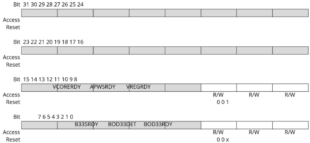
text_image
Bit 31 30 29 28 27 26 25 24 Access Reset Bit 23 22 21 20 19 18 17 16 Access Reset Bit 15 14 13 12 11 10 9 8 VCORERDY APWSRDY VREGRDY Access Reset R/W R/W R/W 0 0 1 Bit 7 6 5 4 3 2 1 0 B33SRDY BOD33DET BOD33RDY Access Reset R/W R/W R/W 0 0 xBit 10 - VCORERDY VDDCORE Voltage Ready
This flag is cleared by writing a '1 to it.
This flag is set on a zero-to-one transition of the VDDCORE Ready bit in the Status register (STATUS.VCORERDY) and will generate an interrupt request if INTENSET.VCORERDY = 1.
Writing a '0' to this bit has no effect.
Writing a '1' to this bit clears the VCORERDY interrupt flag.
Bit 9 - APWSRDY Automatic Power Switch Ready
This flag is cleared by writing a '1' to it.
This flag is set on a zero-to-one transition of the Automatic Power Switch Ready bit in the Status register (STATUS.APWSRDY) and will generate an interrupt request if INTENSET.APWSRDY = 1.
Writing a '0' to this bit has no effect.
Writing a '1' to this bit clears the APWSRDY interrupt flag.
Bit 8 - VREGRDY Voltage Regulator Ready
This flag is cleared by writing a '1' to it.
This flag is set on a zero-to-one transition of the Voltage Regulator Ready bit in the Status register (STATUS.VREGRDY) and will generate an interrupt request if INTENSET.VREGRDY = 1.
Writing a '0' to this bit has no effect.
Writing a '1' to this bit clears the VREGRDY interrupt flag.
Bit 2 - B33SRDY BOD33 Synchronization Ready
This flag is cleared by writing a '1' to it.
This flag is set on a zero-to-one transition of the BOD33 Synchronization Ready bit in the Status register (STATUS.B33SRDY) and will generate an interrupt request if INTENSET.B33SRDY = 1.
Writing a '0' to this bit has no effect.
Writing a '1' to this bit clears the BOD33 Synchronization Ready interrupt flag.
Bit 1 - BOD33DET BOD33 Detection
This flag is cleared by writing a '1' to it.
This flag is set on a zero-to-one transition of the BOD33 Detection bit in the Status register (STATUS.BOD33DET) and will generate an interrupt request if INTENSET.BOD33DET = 1. Writing a '0' to this bit has no effect. Writing a '1' to this bit clears the BOD33 Detection interrupt flag.
Bit 0 - BOD33RDY BOD33 Ready
This flag is cleared by writing a '1' to it.
This flag is set on a zero-to-one transition of the BOD33 Ready bit in the Status register (STATUS.BOD33RDY) and will generate an interrupt request if INTENSET.BOD33RDY = 1. Writing a '0' to this bit has no effect.
Writing a '1' to this bit clears the BOD33 Ready interrupt flag.
The BOD33 can be enabled.
References:
Reset: x initially determined from NVM User Row after Reset
Property: -

text_image
Bit 31 30 29 28 27 26 25 24 Access Reset Bit 23 22 21 20 19 18 17 16 Access Reset Bit 15 14 13 12 11 10 9 8 BBPS VCORRDY APW$RDY VREGRDY Access Reset R R R R 0 1 0 1 Bit 7 6 5 4 3 2 1 0 B33SRDY BOD33DET BOD33RDY Access Reset R R R 0 0 xBit 11 - BBPS Battery Backup Power Switch
| Value | Description |
| 0 | The backup domain is supplied by VDD. |
| 1 | The backup domain is supplied by VBAT. |
Bit 10 - VCORERDY VDDCORE Voltage Ready
| Value | Description |
| 0 | The VDDCORE voltage is not as expected. |
| 1 | The VDDCORE voltage is the target voltage. |
Bit 9 - APWSRDY Automatic Power Switch Ready
| Value | Description |
| 0 | The Automatic Power Switch is not ready. |
| 1 | The Automatic Power Switch is ready. |
Bit 8 - VREGRDY Voltage Regulator Ready
| Value | Description |
| 0 | The selected voltage regulator in VREG.SEL is not ready. |
| 1 | The voltage regulator selected in VREG.SEL is ready and the core domain is supplied by this voltage regulator. |
Bit 2 - B33SRDY BOD33 Synchronization Ready
| Value | Description |
| 0 | BOD33 synchronization is ongoing. |
| 1 | BOD33 synchronization is complete. |
Bit 1 - BOD33DET BOD33 Detection
Value Description
| 0 | No BOD33 detection. |
| 1 | BOD33 has detected that the I/O power supply is going below the BOD33 reference value. |
Bit 0 - BOD33RDY BOD33 Ready
The BOD33 can be enabled at start-up from the NVM User Row. The state of this bit is only applicable in BODVDD continuous mode. In sampling mode, this bit is never set.
References:
| Value Description | |
| 0 | BOD33 is not ready. |
| 1 | BOD33 is ready. |
22.8.5 Brown-Out Detector (BOD33) Control
Name: BOD33
Offset: 0x10
Reset: Determined from NVM User Row
Property: PAC Write-Protection, Enable-Protected bits, Write-Synchronized bits
| Bit 31 30 29 28 27 26 25 24 | |||||||
| BKUPLEVEL[5:0] | |||||||
| Access Reset | R/W R/W R/W R/W R/W R/W | ||||||
| 0 0 0 0 0 0 | |||||||
| Bit 23 22 21 20 19 18 17 16 | |||||||
| LEVEL[5:0] | |||||||
| Access Reset | R/W R/W R/W R/W R/W R/W | ||||||
| x | x | x | x | x | |||
| Bit 15 14 13 12 11 10 | 9 8 | ||||||
| PSEL[3:0] | VMON | ACTCFG | |||||
| Access Reset | R/W R/W R/W R/W | R/W | R/W | ||||
| 0 0 0 0 | 0 | 0 | |||||
| Bit 7 6 5 4 3 2 1 0 | |||||||
| RUNBKUP | RUNSTDBY | STDBYCFG | ACTION[1:0] | HYST | ENABLE | ||
| Access Reset | R/W R/W R/W R/W R/W R/W | ||||||
| 0 | 0 | 0 | y | y | 0 | z | |
Bits 29:24 - BKUPLEVEL[5:0] BOD33 Threshold Level on VBAT or in Backup Sleep Mode
These bits set the triggering voltage threshold for the BOD33 when the BOD33 monitors VBAT or in backup sleep mode.
Note: This bit field is enable-protected. This bit field is not write-synchronized.
Bits 21:16 - LEVEL[5:0] BOD33 Threshold Level on VDD
These bits set the triggering voltage threshold for the BOD33 when the BOD33 monitors the VDD except in backup sleep mode.
These bits are loaded from NVM User Row at start-up.
Note: This bit field is enable-protected. This bit field is not write-synchronized.
Bits 15:12 - PSEL[3:0] Prescaler Select
Selects the prescaler divide-by output for the BOD33 sampling mode. The input clock comes from the OSCULP32K 1.024 kHz output.
Note: This bit field is enable-protected. This bit field is not write-synchronized.
| Value | Name | Description |
| 0x0 | DIV2 | Divide clock by 2 |
| 0x1 | DIV4 | Divide clock by 4 |
| 0x2 | DIV8 | Divide clock by 8 |
| 0x3 | DIV16 | Divide clock by 16 |
| 0x4 | DIV32 | Divide clock by 32 |
| 0x5 | DIV64 | Divide clock by 64 |
| 0x6 | DIV128 | Divide clock by 128 |
| 0x7 | DIV256 | Divide clock by 256 |
| 0x8 | DIV512 | Divide clock by 512 |
| 0x9 | DIV1024 | Divide clock by 1024 |
| Value Name | Description | |
| 0xA | DIV2048 Divide clock by 2048 | |
| 0xB | DIV4096 Divide clock by 4096 | |
| 0xC | DIV8192 Divide clock by 8192 | |
| 0xD | DIV16384 Divide clock by 16384 | |
| 0xE | DIV32768 Divide clock by 32768 | |
| 0xF | DIV65536 Divide clock by 65536 | |
Bit 10 - VMON Voltage Monitored in Active and Standby Mode
Note: This bit is enable-protected. This bit is not write-synchronized.
| Value Description | |
| 0 | The BOD33 monitors the VDD power pin in active and standby mode. |
| 1 | The BOD33 monitors the VBAT power pin in active and standby mode. |
Bit 8 - ACTCFG BOD33 Configuration in Active Sleep Mode
Note: This bit is enable-protected. This bit is not write-synchronized.
| Value Description | |
| 0 | In active mode, the BOD33 operates in continuous mode. |
| 1 | In active mode, the BOD33 operates in sampling mode. |
Bit 7 - RUNBKUP BOD33 Configuration in Backup Sleep Mode
Note: This bit is enable-protected. This bit is not write-synchronized.
| Value Description | |
| 0 | In backup sleep mode, the BOD33 is disabled. |
| 1 | In backup sleep mode, the BOD33 is enabled and configured in sampling mode. |
Bit 6 - RUNSTDBY Run in Standby
Note: This bit is enable-protected. This bit is not write-synchronized.
| Value Description | |
| 0 | In standby sleep mode, the BOD33 is disabled. |
| 1 | In standby sleep mode, the BOD33 is enabled. |
Bit 5 - STDBYCFG BOD33 Configuration in Standby Sleep Mode
If the RUNSTDBY bit is set to '1', the STDBYCFG bit sets the BOD33 configuration in standby sleep mode.
Note: This bit is enable-protected. This bit is not write-synchronized.
| Value Description | |
| 0 | In standby sleep mode, the BOD33 is enabled and configured in continuous mode. |
| 1 | In standby sleep mode, the BOD33 is enabled and configured in sampling mode. |
Bits 4:3 - ACTION[1:0] BOD33 Action
These bits are used to select the BOD33 action when the supply voltage crosses below the BOD33 threshold.
These bits are loaded from NVM User Row at start-up.
Note: This bit field is enable-protected. This bit field is not write-synchronized.
| Value Name Description |
| 0x0 NONE No action |
| 0x1 RESET The BOD33 generates a reset |
| 0x2 INT The BOD33 generates an interrupt |
| 0x3 BKUP The BOD33 puts the device in backup sleep mode if VMON=0. |
| No action if VMON=1. |
Bit 2 - HYST Hysteresis
This bit indicates whether hysteresis is enabled for the BOD33 threshold voltage.
This bit is loaded from NVM User Row at start-up.
Note: This bit is enable-protected. This bit is not write-synchronized.
| Value Description | |
| 0 | No hysteresis. |
| 1 | Hysteresis enabled. |
Bit 1 - ENABLE Enable
This bit is loaded from NVM User Row at start-up.
Notes:
• This bit is not enable-protected
- This bit is write-synchronized: STATUS.B33SRDY must be checked to ensure the BOD33.ENABLE synchronization is complete
| Value Description | |
| 0 | BOD33 is disabled. |
| 1 | BOD33 is enabled. |
22.8.6 Voltage Regulator System (VREG) Control
Name: VREG
Offset: 0x18
Reset: 0x00000002
Property: PAC Write-Protection
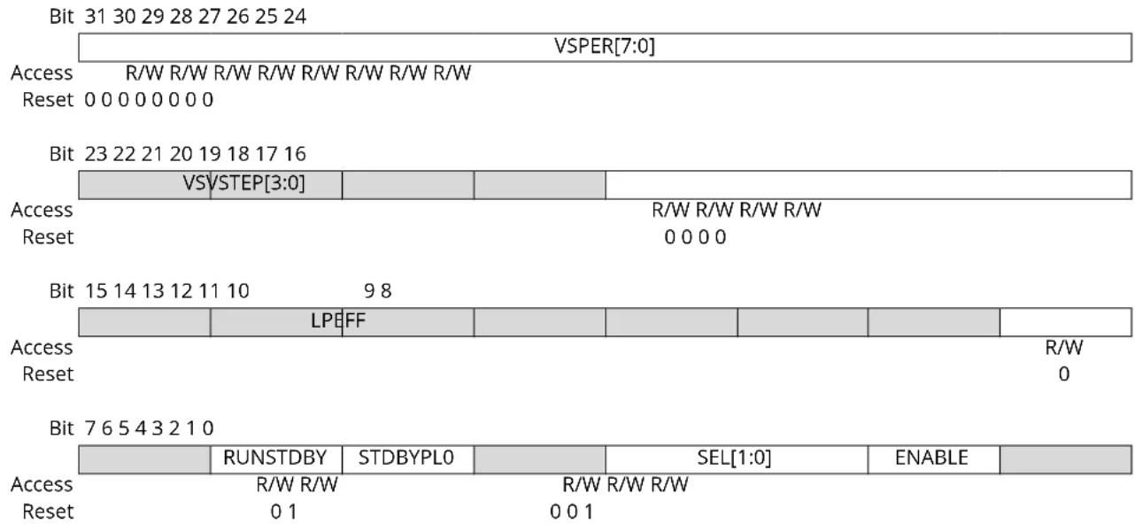
text_image
Bit 31 30 29 28 27 26 25 24 VSPER[7:0] Access R/W R/W R/W R/W R/W R/W R/W Reset 0 0 0 0 0 0 0 0 Bit 23 22 21 20 19 18 17 16 VS/STEP[3:0] R/W R/W R/W R/W R/W R/W R/W R/W Reset 0 0 0 0 Bit 15 14 13 12 11 10 9 8 LPEFF R/W Reset 0 Bit 7 6 5 4 3 2 1 0 RUNSTDBY STDBYPL0 SEL[1:0] ENABLE Access R/W R/W R/W R/W R/W Reset 0 1 0 0 1Bits 31:24 - VSPER[7:0] Voltage Scaling Period
This bitfield sets the period between the voltage steps when the VDDCORE voltage is changing in s. If VSPER=0, the period between two voltage steps is 1 s.
Bits 19:16 - VSVSTEP[3:0] Voltage Scaling Voltage Step
This field sets the voltage step height when the VDDCORE voltage is changing to reach the target VDDCORE voltage.
The voltage step is equal to 2^VSVSTEP * min_step.
See the Electrical Characteristics chapter for the min_step voltage level.
Bit 8 - LPEFF Low power Mode Efficiency
| Value | Description |
| 0 | The voltage regulator in Low power mode has the default efficiency and supports the whole VDD range (1.62V to 3.6V). |
| 1 | The voltage regulator in Low power mode has the highest efficiency and supports a limited VDD range (2.5V to 3.6V). |
Bit 6 - RUNSTDBY Run in Standby
| Value | Description |
| 0 | The voltage regulator is in low power mode in Standby sleep mode. |
| 1 | The voltage regulator is in normal mode in Standby sleep mode. |
Bit 5 - STDBYPL0 Standby in PLO
This bit selects the performance level (PL) of the main voltage regulator for the Standby sleep mode. This bit is only considered when RUNSTDBY=1.
| Value | Description |
| 0 | In Standby sleep mode, the voltage regulator remains in the current performance level. |
Value Description
In Standby sleep mode, the voltage regulator is used in PLO.
Bits 3:2 - SEL[1:0] Voltage Regulator Selection
This bit is loaded from NVM User Row at start-up.
Value Name Description
0 LDO The voltage regulator in active mode is a LDO voltage regulator.
1 BUCK The voltage regulator in active mode is a buck converter.
2-3 Reserved Reserved
Bit 1 - ENABLE Enable
Must be set to 1.
22.8.7 Voltage References System (VREF) Control
Name: VREF
Offset: 0x1C
Reset: 0x00000000
Property: PAC Write-Protection
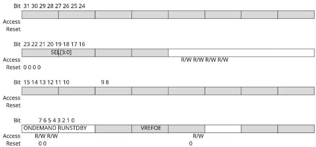
text_image
Bit 31 30 29 28 27 26 25 24 Access Reset Bit 23 22 21 20 19 18 17 16 SEL[3:0] Access R/W R/W R/W R/W Reset 0 0 0 0 Bit 15 14 13 12 11 10 9 8 Access Reset Bit 7 6 5 4 3 2 1 0 ONDEMAND RUNSTDBY Access R/W R/W R/W Reset 0 0 VREFOE 0Bits 19:16 - SEL[3:0] Voltage Reference Selection
These bits select the Voltage Reference for the ADC.
| Value | Name | Description |
| 0x0 | 1V0 | 1.0V voltage reference typical value |
| 0x1 | 1V1 | 1.1V voltage reference typical value |
| 0x2 | 1V2 | 1.2V voltage reference typical value |
| 0x3 | 1V25 | 1.25V voltage reference typical value |
| 0x4 | 2V0 | 2.0V voltage reference typical value |
| 0x5 | 2V2 | 2.2V voltage reference typical value |
| 0x6 | 2V4 | 2.4V voltage reference typical value |
| 0x7 | 2V5 | 2.5V voltage reference typical value |
| Others | Reserved | Reserved |
Note:
- 2.0V to 2.5V can be used when the supply voltage(VDDANA) is higher than 2.7V
Bit 7 - ONDEMAND On Demand Control
The On Demand operation mode allows to enable or disable the voltage reference depending on peripheral requests.
| Value | Description |
| 0 | The voltage reference is always on, if enabled. |
| 1 | The voltage reference is enabled when a peripheral is requesting it. The voltage reference is disabled if no peripheral is requesting it. |
Bit 6 - RUNSTDBY Run In Standby
The bit controls how the voltage reference behaves during standby sleep mode.
| Value Description | |
| 0 | The voltage reference is halted during standby sleep mode. |
| 1 | The voltage reference is not stopped in standby sleep mode. If VREF.ONDEMAND=1, the voltage reference will be running when a peripheral is requesting it. If VREF.ONDEMAND=0, the voltage reference will always be running in standby sleep mode. |
Bit 2 - VREFOE Voltage Reference Output Enable
| Value Description | |
| 0 | The Voltage Reference output is not available as an ADC input channel. |
| 1 | The Voltage Reference output is routed to an ADC input channel. |
22.8.8 Battery Backup Power Switch (BBPS) Control
Name: BBPS
Offset: 0x20
Reset: 0x00000000
Property: PAC Write-Protection
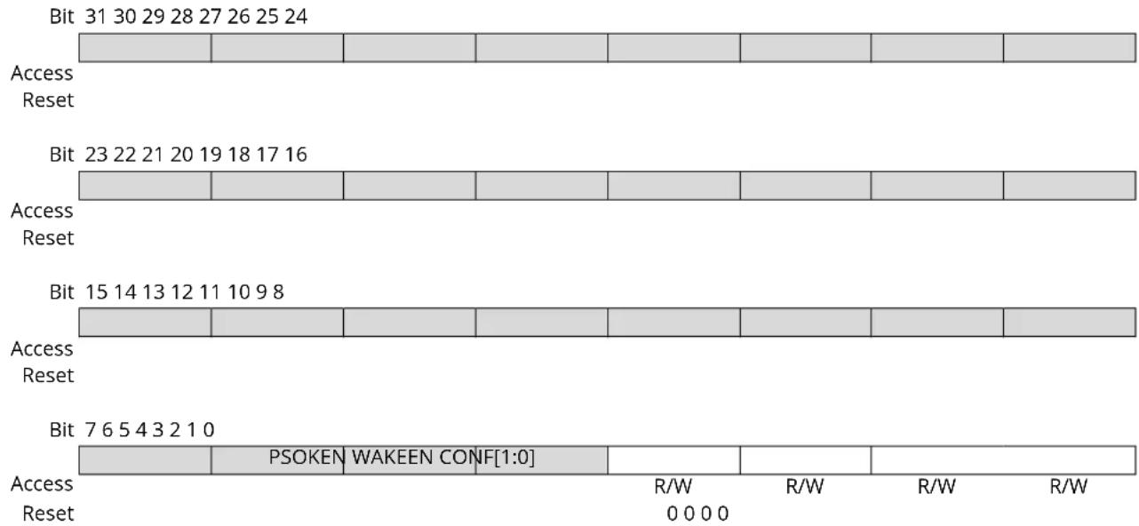
text_image
Bit 31 30 29 28 27 26 25 24 Access Reset Bit 23 22 21 20 19 18 17 16 Access Reset Bit 15 14 13 12 11 10 9 8 Access Reset Bit 7 6 5 4 3 2 1 0 Access Reset PSOKEN WAKEEN CONF[1:0] R/W R/W R/W R/W 0 0 0 0Bit 3 - PSOKEN Power Supply OK Enable
| Value | Description |
| 0 | The PSOK pin is not used. |
| 1 | The PSOK pin is used to determine the status of the Main Power Supply. |
Bit 2 - WAKEEN Wake Enable
| Value | Description |
| 0 | The device is not woken up when switched from battery backup power to Main Power. |
| 1 | The device is woken up when switched from battery backup power to Main Power. |
Bits 1:0 - CONF[1:0] Battery Backup Power Switch Configuration
| Value | Name | Description |
| 0x0 | NONE | The backup domain is always supplied by Main Power. |
| 0x1 | APWS | The power switch is handled by the Automatic Power Switch. |
| 0x2 | FORCED | The backup domain is always supplied by Battery Backup Power. |
| 0x3 | BOD33 | The power switch is handled by the BOD33. |
22.8.9 Backup Output (BKOUT) Control
Name: BKOUT
Offset: 0x24
Reset: 0x00000000
Property: PAC Write-Protection
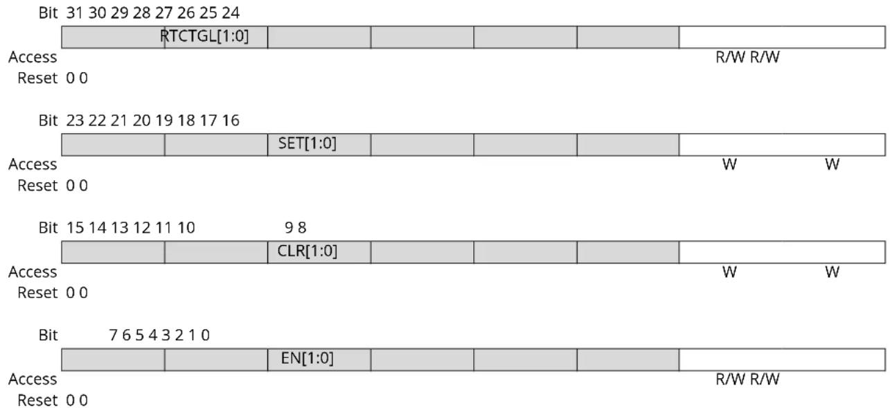
text_image
Bit 31 30 29 28 27 26 25 24 RTCTGL[1:0] Access Reset 0 0 R/W R/W Bit 23 22 21 20 19 18 17 16 Access Reset 0 0 SET[1:0] W W Bit 15 14 13 12 11 10 9 8 Access Reset 0 0 CLR[1:0] W W Bit 7 6 5 4 3 2 1 0 Access Reset 0 0 EN[1:0] R/W R/WBits 25:24 - RTCTGL[1:0] RTC Toggle Output
| Value | Description |
| 0 | The output will not toggle on RTC event. |
| 1 | The output will toggle on RTC event. |
Bits 17:16 - SET[1:0] Set Output
Writing a '0' to a bit has no effect.
Writing a '1' to a bit will set the corresponding output.
Reading this bit returns '0'.
Bits 9:8 - CLR[1:0] Clear Output
Writing a '0' to a bit has no effect.
Writing a '1' to a bit will clear the corresponding output.
Reading this bit returns '0'.
Bits 1:0 - EN[1:0] Enable Output
| Value | Description |
| 0 | The output is not enabled. |
| 1 | The output is enabled and driven by the SUPC. |
22.8.10 Backup Input (BKIN) Value
Name: BKIN
Offset: 0x28
Reset: 0x00000000
Property: -
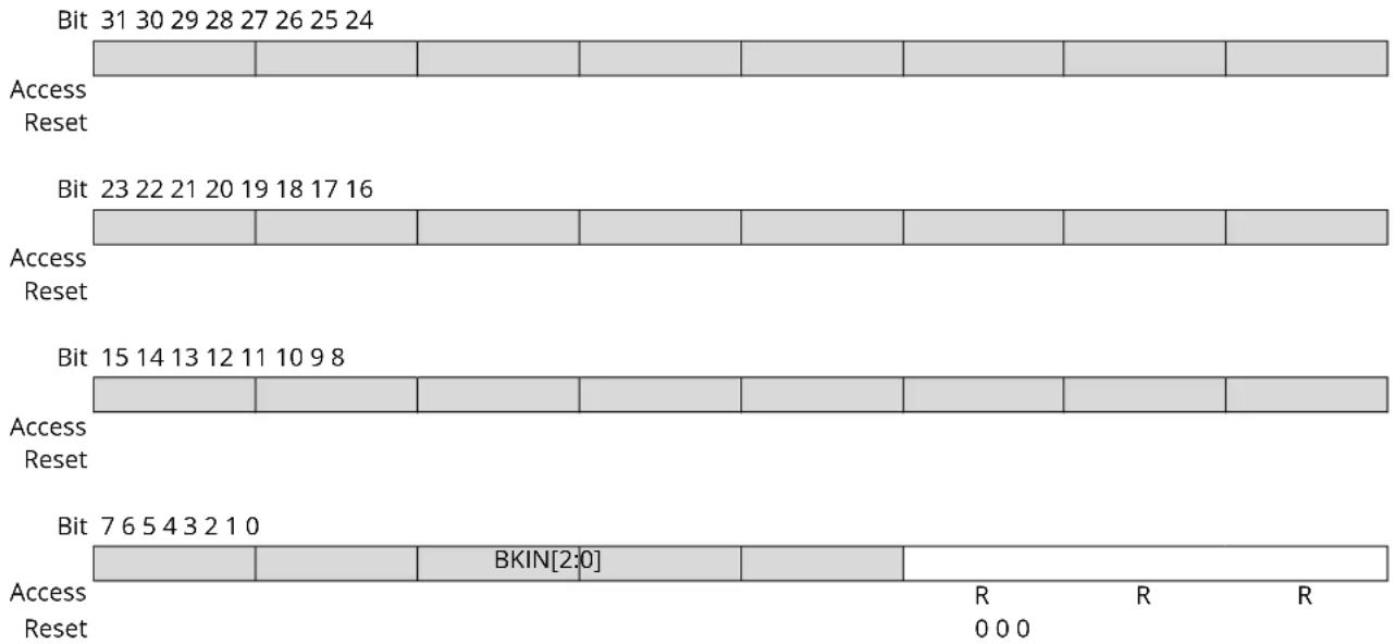
text_image
Bit 31 30 29 28 27 26 25 24 Access Reset Bit 23 22 21 20 19 18 17 16 Access Reset Bit 15 14 13 12 11 10 9 8 Access Reset Bit 7 6 5 4 3 2 1 0 Access Reset BKIN[2:0] R R R 0 0 0Bits 2:0 - BKIN[2:0] Backup I/O Data Input Value
These bits are cleared when the corresponding backup I/O pin detects a logical low level on the input pin or when the backup I/O is not enabled.
These bits are set when the corresponding backup I/O pin detects a logical high level on the input pin when the backup I/O is enabled.
| BKIN[2:0] | PAD | Description |
| BKIN[0] | PSOK | If BBPS.PSOKEN=1, BKIN[0] will give the input value of the PSOK pin |
| BKIN[1] | OUT[0] | If BKOUT.EN[0]=1, BKIN[1] will give the input value of the OUT[0] pin |
| BKIN[2] | OUT[1] | If BKOUT.EN[1]=1, BKIN[2] will give the input value of the OUT[1] pin |
23. WDT – Watchdog Timer
23.1 Overview
The Watchdog Timer (WDT) is a system function for monitoring correct program operation. It makes it possible to recover from error situations such as runaway or deadlocked code. The WDT is configured to a predefined time-out period, and is constantly running when enabled. If the WDT is not cleared within the time-out period, it will issue a system reset. An early-warning interrupt is available to indicate an upcoming watchdog time-out condition.
The window mode makes it possible to define a time slot (or window) inside the total time-out period during which the WDT must be cleared. If the WDT is cleared outside this window, either too early or too late, a system reset will be issued. Compared to the normal mode, this can also catch situations where a code error causes the WDT to be cleared frequently.
When enabled, the WDT will run in active mode and all sleep modes. It is asynchronous and runs from a CPU-independent clock source. The WDT will continue operation and issue a system reset or interrupt even if the main clocks fail.
23.2 Features
- Issues a system reset if the Watchdog Timer is not cleared before its time-out period
- Early Warning interrupt generation
- Asynchronous operation from dedicated oscillator
-
Two types of operation
-
Normal
- Window mode
- Selectable time-out periods
- From 8 cycles to 16,384 cycles in Normal mode
- From 16 cycles to 32,768 cycles in Window mode
• Always-On capability
23.3 Block Diagram
Figure 23-1. WDT Block Diagram

flowchart
graph TD
    A["0xA5"] --> B["CLEAR"]
    B --> C["0"]
    D["OSC32KCTRL"] --> E["CLK_WDT_OSC"]
    E --> F["COUNT"]
    F --> G["PER/WINDOWS/EWOFFSET"]
    G --> H["Early Warning Interrupt"]
    G --> I["Reset"]
23.4 Signal Description
Not applicable.
23.5 Product Dependencies
In order to use this peripheral, other parts of the system must be configured correctly, as described below.
23.5.1 I/O Lines
Not applicable.
23.5.2 Power Management
The WDT can continue to operate in any sleep mode where the selected source clock is running. The WDT interrupts can be used to wake up the device from sleep modes. The events can trigger other operations in the system without exiting sleep modes.
References:
PM - Power Manager
23.5.3 Clocks
The WDT bus clock (CLK_WDT_APB) can be enabled and disabled (masked) in the Main Clock module (MCLK).
A 1KHz oscillator clock (CLK_WDT_OSC) is required to clock the WDT internal counter. This clock must be configured and enabled in the 32KHz Oscillator Controller (OSC32KCTRL) before using the WDT.
CLK_WDT_OSC is normally sourced from the clock of the internal ultra-low-power oscillator, OSCULP32K. Due to the ultra-low-power design, the oscillator is not very accurate, and so the exact time-out period may vary from device to device. This variation must be kept in mind when designing software that uses the WDT to ensure that the time-out periods used are valid for all devices.
The counter clock CLK_WDT_OSC is asynchronous to the bus clock (CLK_WDT_APB). Due to this asynchronicity, writing to certain registers will require synchronization between the clock domains. Refer to Synchronization for further details.
References:
Peripheral Clock Masking
OSC32KCTRL- 32.768 kHz Oscillators Controller
Electrical Characteristics
23.5.4 DMA
Not applicable.
23.5.5 Interrupts
The interrupt request line is connected to the interrupt controller. Using the WDT interrupt(s) requires the interrupt controller to be configured first.
References:
Nested Vector Interrupt Controller
23.5.6 Events
Not applicable.
23.5.7 Debug Operation
When the CPU is halted in debug mode the WDT will halt normal operation.
23.5.8 Register Access Protection
All registers with write-access can be write-protected optionally by the Peripheral Access Controller (PAC), except for the following registers:
- Interrupt Flag Status and Clear (INTFLAG) register
Optional write-protection by the Peripheral Access Controller (PAC) is denoted by the "PAC Write-Protection" property in each individual register description.
PAC write-protection does not apply to accesses through an external debugger.
23.5.9 Analog Connections
Not applicable.
23.6 Functional Description
23.6.1 Principle of Operation
The Watchdog Timer (WDT) is a system for monitoring correct program operation, making it possible to recover from error situations such as runaway code, by issuing a Reset. When enabled, the WDT is a constantly running timer that is configured to a predefined time-out period. Before the end of the time-out period, the WDT should be set back, or else, a system Reset is issued.
The WDT has two modes of operation, Normal mode and Window mode. Both modes offer the option of Early Warning interrupt generation. The description for each of the basic modes is given below. The settings in the Control A register (CTRLA) and the Interrupt Enable register (handled by INTENCLR/INTENSET) determine the mode of operation:
Table 23-1. WDT Operating Modes
| CTRLA.ENABLE CTRLA.WEN Interrupt Enable Mode | |||
| 0 x x Stopped | |||
| 1 0 0 Normal mode | |||
| 1 0 1 Normal mode with Early Warning interrupt | |||
| 1 1 0 Window mode | |||
| 1 1 1 Window mode with Early Warning interrupt | |||
23.6.2 Basic Operation
23.6.2.1 Initialization
The following bits are enable-protected, meaning that they can only be written when the WDT is disabled (CTRLA.ENABLE=0):
- Control A register (CTRLA), except the Enable bit (CTRLA.ENABLE)
- Configuration register (CONFIG)
- Early Warning Interrupt Control register (EWCTRL)
Enable-protected bits in the CTRLA register can be written at the same time as CTRLA. ENABLE is written to '1', but not at the same time as CTRLA. ENABLE is written to '0'.
The WDT can be configured only while the WDT is disabled. The WDT is configured by defining the required Time-Out Period bits in the Configuration register (CONFIG.PER). If Window mode operation is desired, the Window Enable bit in the Control A register must be set (CTRLA.WEN=1) and the Window Period bits in the Configuration register (CONFIG.WINDOW) must be defined.
Enable-protection is denoted by the "Enable-Protected" property in the register description.
23.6.2.2 Configurable Reset Values
After a Power-on Reset, some registers will be loaded with initial values from the NVM User Row.
This includes the following bits and bit groups:
- Enable bit in the Control A register, CTRLA.ENABLE
- Always-On bit in the Control A register, CTRLA.ALWAYSON
- Watchdog Timer Windows Mode Enable bit in the Control A register, CTRLA.WEN
- Watchdog Timer Windows Mode Time-Out Period bits in the Configuration register, CONFIG.WINDOW
- Time-Out Period bits in the Configuration register, CONFIG.PER
- Early Warning Interrupt Time Offset bits in the Early Warning Interrupt Control register, EWCTRL.EWOFFSET
References:
23.6.2.3 Enabling, Disabling, and Resetting
The WDT is enabled by writing a '1' to the Enable bit in the Control A register (CTRLA.ENABLE). The WDT is disabled by writing a '0' to CTRLA.ENABLE.
The WDT can be disabled only if the Always-On bit in the Control A register (CTRLA.ALWAYSON) is '0'.
23.6.2.4 Normal Mode
In Normal mode operation, the length of a time-out period is configured in CONFIG.PER. The WDT is enabled by writing a '1' to the Enable bit in the Control A register (CTRLA.ENABLE). Once enabled, the WDT will issue a system reset if a time-out occurs. This can be prevented by clearing the WDT at any time during the time-out period.
The WDT is cleared and a new WDT time-out period is started by writing 0xA5 to the Clear register (CLEAR). Writing any other value than 0xA5 to CLEAR will issue an immediate system reset.
There are 12 possible WDT time-out (TO _WDT ) periods, selectable from 8ms to 16s.
By default, the early warning interrupt is disabled. If it is desired, the Early Warning Interrupt Enable bit in the Interrupt Enable register (INTENSET.EW) must be written to '1'. The Early Warning Interrupt is disabled again by writing a '1' to the Early Warning Interrupt bit in the Interrupt Enable Clear register (INTENCLR.EW).
If the Early Warning Interrupt is enabled, an interrupt is generated prior to a WDT time-out condition. In Normal mode, the Early Warning Offset bits in the Early Warning Interrupt Control register, EWCTRL.EWOFFSET, define the time when the early warning interrupt occurs. The Normal mode operation is illustrated in the figure Normal-Mode Operation.
Figure 23-2. Normal-Mode Operation

line
| Time [ms] | WDT Count | | --------- | --------- | | 15 | 0 | | 35 | 1 |23.6.2.5 Window Mode
In Window mode operation, the WDT uses two different time specifications: the WDT can only be cleared by writing 0xA5 to the CLEAR register after the closed window time-out period (TO _WDTW ),
during the subsequent Normal time-out period ( TO_WDT ). If the WDT is cleared before the time window opens (before TO_WDTW is over), the WDT will issue a system reset.
Both parameters TO_WDTW and TO_WDT are periods in a range from 8ms to 16s, so the total duration of the WDT time-out period is the sum of the two parameters.
The closed window period is defined by the Window Period bits in the Configuration register (CONFIG.WINDOW), and the open window period is defined by the Period bits in the Configuration register (CONFIG.PER).
By default, the Early Warning interrupt is disabled. If it is desired, the Early Warning Interrupt Enable bit in the Interrupt Enable register (INTENSET.EW) must be written to '1'. The Early Warning Interrupt is disabled again by writing a '1' to the Early Warning Interrupt bit in the Interrupt Enable Clear (INTENCLR.EW) register.
If the Early Warning interrupt is enabled in Window mode, the interrupt is generated at the start of the open window period, i.e. after TO_WDTW . The Window mode operation is illustrated in figure Window-Mode Operation.
Figure 23-3. Window-Mode Operation
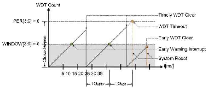
line
| Time (ms) | WDT Count | | --------- | --------- | | 0 | Closed Open | | 10 | 0 | | 15 | 0 | | 20 | 0 | | 25 | 0 | | 30 | 0 | | 35 | 0 | | 40 | 0 | | 45 | 0 | | 50 | 0 | | 55 | 0 | | 60 | 0 | | 65 | 0 | | 70 | 0 | | 75 | 0 | | 80 | 0 | | 85 | 0 | | 90 | 0 | | 95 | 0 | | 100 | 0 |23.6.3 DMA Operation
Not applicable.
23.6.4 Interrupts
The WDT has the following interrupt source:
- Early Warning (EW): Indicates that the counter is approaching the time-out condition.
- This interrupt is an asynchronous wake-up source.
Each interrupt source has an interrupt flag associated with it. The interrupt flag in the Interrupt Flag Status and Clear (INTFLAG) register is set when the interrupt condition occurs.
Each interrupt can be individually enabled by writing a '1' to the corresponding bit in the Interrupt Enable Set (INTENSET) register, and disabled by writing a '1' to the corresponding bit in the Interrupt Enable Clear (INTENCLR) register.
An interrupt request is generated when the interrupt flag is set and the corresponding interrupt is enabled. The interrupt request remains active until the interrupt flag is cleared, the interrupt is disabled, or the WDT is reset. See the 23.8.6. INTFLAG register description for details on how to clear interrupt flags. All interrupt requests from the peripheral are ORed together on system level to generate one combined interrupt request to the NVIC. The user must read the INTFLAG register to determine which interrupt condition is present.
Note: Interrupts must be globally enabled for interrupt requests to be generated.
References:
Sleep Mode Controller
Interrupt Line Mapping
PM - Power Manager
23.6.5 Events
Not applicable.
23.6.6 Sleep Mode Operation
The WDT will continue to operate in any sleep mode where the source clock is active except backup mode. The WDT interrupts can be used to wake up the device from a sleep mode. An interrupt request will be generated after the wake-up if the Interrupt Controller is configured accordingly. Otherwise the CPU will wake up directly, without triggering an interrupt. In this case, the CPU will continue executing from the instruction following the entry into sleep.
References:
CTRLA
23.6.7 Synchronization
Due to asynchronicity between the main clock domain and the peripheral clock domains, some registers need to be synchronized when written or read.
The following registers are synchronized when written:
- Enable bit in Control A register (CTRLA.ENABLE)
- Window Enable bit in Control A register (CTRLA.WEN)
• Always-On bit in control Control A (CTRLA.ALWAYSON)
The following registers are synchronized when read:
- Watchdog Clear register (CLEAR)
Required write-synchronization is denoted by the "Write-Synchronized" property in the register description.
Required read-synchronization is denoted by the "Read-Synchronized" property in the register description.
23.6.8 Additional Features
23.6.8.1 Always-On Mode
The Always-On mode is enabled by setting the Always-On bit in the Control A register (CTRLA.ALWAYSON=1). When the Always-On mode is enabled, the WDT runs continuously, regardless of the state of CTRLA.ENABLE. Once written, the Always-On bit can only be cleared by a power-on reset. The Configuration (CONFIG) and Early Warning Control (EWCTRL) registers are read-only registers while the CTRLA.ALWAYSON bit is set. Thus, the time period configuration bits (CONFIG.PER, CONFIG.WINDOW, EWCTRL.EWOFFSET) of the WDT cannot be changed.
Enabling or disabling Window mode operation by writing the Window Enable bit (CTRLA.WEN) is allowed while in Always-On mode, but note that CONFIG.PER cannot be changed.
The Interrupt Clear and Interrupt Set registers are accessible in the Always-On mode. The Early Warning interrupt can still be enabled or disabled while in the Always-On mode, but note that EWCTRL.EWOFFSET cannot be changed.
Table WDT Operating Modes With Always-On shows the operation of the WDT for CTRLA.ALWAYSON=1.
Table 23-2. WDT Operating Modes With Always-On
| WEN Interrupt Enable Mode | |
| 0 0 Always-on and normal mode | |
| 0 1 Always-on and normal mode with Early Warning interrupt | |
| 1 0 Always-on and window mode | |
| 1 1 Always-on and window mode with Early Warning interrupt | |
23.6.8.2 Early Warning
The Early Warning interrupt notifies that the WDT is approaching its time-out condition. The Early Warning interrupt behaves differently in Normal mode and in Window mode.
In Normal mode, the Early Warning interrupt generation is defined by the Early Warning Offset in the Early Warning Control register (EWCTRL.EWOFFSET). The Early Warning Offset bits define the number of CLK_WDT_OSC clocks before the interrupt is generated, relative to the start of the watchdog time-out period.
The user must take caution when programming the Early Warning Offset bits. If these bits define an Early Warning interrupt generation time greater than the watchdog time-out period, the watchdog time-out system reset is generated prior to the Early Warning interrupt. Consequently, the Early Warning interrupt will never be generated.
In window mode, the Early Warning interrupt is generated at the start of the open window period. In a typical application where the system is in sleep mode, the Early Warning interrupt can be used to wake up and clear the Watchdog Timer, after which the system can perform other tasks or return to sleep mode.
If the WDT is operating in Normal mode with CONFIG.PER = 0x2 and EWCTRL.EWOFFSET = 0x1, the Early Warning interrupt is generated 16 CLK_WDT_OSC clock cycles after the start of the time-out period. The time-out system reset is generated 32 CLK_WDT_OSC clock cycles after the start of the watchdog time-out period.
23.7 Register Summary
| Offset | Name Bit Pos. 7 | 6 | 5 | 4 | 3 | 2 | 1 | 0 | |||||||||||||||||||||||||||||||||||||||||||||||||||||||||||||||||||||||||||||||||||||||||||||||||||||||||||||||||||||||||||||||||||||||||||||||||||||||||||||||||||||||||||||||||||||||||||||||||||||||||||||||||||||||||||||||||||||||||||||||||||||||||||||||||||||||||||||||||||||||||||||||||||||||||||||||||||||||||||||||||||||||||||||||||||||||||||||||||||||||||||||||||||||||||||||||||||||||||||||||||||||||||||||||||||||||||||||||||||||||||||||||||||||||||||||||||||||||||||||||||||||||||||||||||
| 0x00 | CTRLA | 7:0 | ALWAYSON | WEN ENABLE | 0x01 | CONFIG | 7:0 | WINDOW[3:0] | |||||||||||||||||||||||||||||||||||||||||||||||||||||||||||||||||||||||||||||||||||||||||||||||||||||||||||||||||||||||||||||||||||||||||||||||||||||||||||||||||||||||||||||||||||||||||||||||||||||||||||||||||||||||||||||||||||||||||||||||||||||||||||||||||||||||||||||||||||||||||||||||||||||||||||||||||||||||||||||||||||||||||||||||||||||||||||||||||||||||||||||||||||||||||||||||||||||||||||||||||||||||||||||||||||||||||||||||||||||||||||||||||||||||||||||||||||||||||||||||||||||||||||||||||
| 0x02 | EWCTRL | 7:0 | EWOFFSET[3:0] | 0x03 | Reserved | ||||||||||||||||||||||||||||||||||||||||||||||||||||||||||||||||||||||||||||||||||||||||||||||||||||||||||||||||||||||||||||||||||||||||||||||||||||||||||||||||||||||||||||||||||||||||||||||||||||||||||||||||||||||||||||||||||||||||||||||||||||||||||||||||||||||||||||||||||||||||||||||||||||||||||||||||||||||||||||||||||||||||||||||||||||||||||||||||||||||||||||||||||||||||||||||||||||||||||||||||||||||||||||||||||||||||||||||||||||||||||||||||||||||||||||||||||||||||||||||||||||||||||||||||||||
| 0x04 | INTENCLR | 7:0 | EW | EW | EW | ||||||||||||||||||||||||||||||||||||||||||||||||||||||||||||||||||||||||||||||||||||||||||||||||||||||||||||||||||||||||||||||||||||||||||||||||||||||||||||||||||||||||||||||||||||||||||||||||||||||||||||||||||||||||||||||||||||||||||||||||||||||||||||||||||||||||||||||||||||||||||||||||||||||||||||||||||||||||||||||||||||||||||||||||||||||||||||||||||||||||||||||||||||||||||||||||||||||||||||||||||||||||||||||||||||||||||||||||||||||||||||||||||||||||||||||||||||||||||||||||||||||||||||||||||||
| EW | INTENSET | 7:0 | |||||||||||||||||||||||||||||||||||||||||||||||||||||||||||||||||||||||||||||||||||||||||||||||||||||||||||||||||||||||||||||||||||||||||||||||||||||||||||||||||||||||||||||||||||||||||||||||||||||||||||||||||||||||||||||||||||||||||||||||||||||||||||||||||||||||||||||||||||||||||||||||||||||||||||||||||||||||||||||||||||||||||||||||||||||||||||||||||||||||||||||||||||||||||||||||||||||||||||||||||||||||||||||||||||||||||||||||||||||||||||||||||||||||||||||||||||||||||||||||||||||||||||||||||||||||
| 0x06 | INTFLAG | 7:0 | EW | Reserved | 0X07 | Reserved | |||||||||||||||||||||||||||||||||||||||||||||||||||||||||||||||||||||||||||||||||||||||||||||||||||||||||||||||||||||||||||||||||||||||||||||||||||||||||||||||||||||||||||||||||||||||||||||||||||||||||||||||||||||||||||||||||||||||||||||||||||||||||||||||||||||||||||||||||||||||||||||||||||||||||||||||||||||||||||||||||||||||||||||||||||||||||||||||||||||||||||||||||||||||||||||||||||||||||||||||||||||||||||||||||||||||||||||||||||||||||||||||||||||||||||||||||||||||||||||||||||||||||||||||||||
23.8 Register Description
Registers can be 8, 16, or 32 bits wide. Atomic 8-, 16- and 32-bit accesses are supported. In addition, the 8-bit quarters and 16-bit halves of a 32-bit register, and the 8-bit halves of a 16-bit register can be accessed directly.
Some registers are optionally write-protected by the Peripheral Access Controller (PAC). Optional PAC write-protection is denoted by the "PAC Write-Protection" property in each individual register description. For details, refer to 23.5.8. Register Access Protection.
Some registers are synchronized when read and/or written. Synchronization is denoted by the "Write-Synchronized" or the "Read-Synchronized" property in each individual register description. For details refer to 23.6.7. Synchronization.
Some registers are enable-protected, meaning they can only be written when the peripheral is disabled. Enable-protection is denoted by the "Enable-Protected" property in each individual register description.
23.8.1 Control A
Name: CTRLA
Offset: 0x00
Reset: x initially determined from NVM User Row after reset
Property: PAC Write-Protection, Write-Synchronized
Bit 76543210
| ALWAYSON | WEN ENABLE | ||||||
| Access | R/W R/W | R/W | |||||
| Reset x | x | x |
Bit 7 - ALWAYSON Always-On
This bit allows the WDT to run continuously. After being set, this bit cannot be written to '0', and the WDT will remain enabled until a power-on Reset is received. When this bit is '1', the Control A register (CTRLA), the Configuration register (CONFIG) and the Early Warning Control register (EWCTRL) will be read-only, and any writes to these registers are not allowed.
Writing a '0' to this bit has no effect.
This bit is not Enable-Protected.
This bit is loaded from NVM User Row at start-up. Refer to NVM User Row Mapping.
| Value | Description |
| 0 | The WDT is enabled and disabled through the ENABLE bit. |
| 1 | The WDT is enabled and can only be disabled by a power-on reset (POR). |
Bit 2 - WEN Watchdog Timer Window Mode Enable
This bit enables Window mode. It can only be written if the peripheral is disabled unless CTRLA.ALWAYSON = 1. The initial value of this bit is loaded from Flash Calibration.
This bit is loaded from NVM User Row at startup. Refer to NVM User Row Mapping.
| Value | Description |
| 0 | Window mode is disabled (normal operation). |
| 1 | Window mode is enabled. |
Bit 1 - ENABLE Enable
This bit enables or disables the WDT. It can only be written if CTRLA.ALWAYSON = 0.
Due to synchronization, there is delay between writing CTRLA. ENABLE until the peripheral is enabled or disabled. The value written to CTRLA. ENABLE will read back immediately, and the Enable bit in the Synchronization Busy register (SYNCBUSY. ENABLE) will be set. SYNCBUSY. ENABLE will be cleared when the operation is complete.
This bit is not Enable-Protected.
This bit is loaded from NVM User Row at startup. Refer to NVM User Row Mapping.
| Value | Description |
| 0 | The WDT is disabled. |
| 1 | The WDT is enabled. |
23.8.2 Configuration
Name: CONFIG
Offset: 0x01
Reset: x initially determined from NVM User Row after reset
Property: PAC Write-Protection
Bit 76543210
| WINDOW[3:0] PER[3:0] | ||
| Access | R/W R/W R/W R/W R/W R/W R/W R/W | |
| Reset | xxxxxxx | |
Bits 7:4 - WINDOW[3:0] Window Mode Time-Out Period
In Window mode, these bits determine the watchdog closed window period as a number of cycles of the 1.024 kHz CLK_WDT_OSC clock.
These bits are loaded from NVM User Row at start-up. Refer to NVM User Row Mapping.
| Value Name | Description | |
| 0x0 | CYC8 8 clock cycles | |
| 0x1 | CYC16 | 16 clock cycles |
| 0x2 | CYC32 | 32 clock cycles |
| 0x3 | CYC64 | 64 clock cycles |
| 0x4 | CYC128 | 128 clock cycles |
| 0x5 | CYC256 | 256 clock cycles |
| 0x6 | CYC512 | 512 clock cycles |
| 0x7 | CYC1024 | 1024 clock cycles |
| 0x8 | CYC2048 | 2048 clock cycles |
| 0x9 | CYC4096 | 4096 clock cycles |
| 0xA | CYC8192 | 8192 clock cycles |
| 0xB | CYC16384 | 16384 clock cycles |
| 0xC - 0xF | - | Reserved |
Bits 3:0 - PER[3:0] Time-Out Period
These bits determine the watchdog time-out period as a number of 1.024 kHz CLK_WDTOSC clock cycles. In Window mode operation, these bits define the open window period.
These bits are loaded from NVM User Row at startup. Refer to NVM User Row Mapping.
| Value Name | Description | |
| 0x0 | CYC8 8 clock cycles | |
| 0x1 | CYC16 | 16 clock cycles |
| 0x2 | CYC32 | 32 clock cycles |
| 0x3 | CYC64 | 64 clock cycles |
| 0x4 | CYC128 | 128 clock cycles |
| 0x5 | CYC256 | 256 clock cycles |
| 0x6 | CYC512 | 512 clock cycles |
| 0x7 | CYC1024 | 1024 clock cycles |
| 0x8 | CYC2048 | 2048 clock cycles |
| 0x9 | CYC4096 | 4096 clock cycles |
| 0xA | CYC8192 | 8192 clock cycles |
| 0xB | CYC16384 | 16384 clock cycles |
| 0xC - 0xF | - | Reserved |
23.8.3 Early Warning Control
Name: EWCTRL
Offset: 0x02
Reset: x initially determined from NVM User Row after reset
Property: PAC Write-Protection
The Register reset value is loaded from the NVM User Row at start-up.
Bit 76543210
| EWOFFSET[3:0] | ||||
| Access Reset x x x x | R/W R/W R/W R/W | |||
Bits 3:0 - EWOFFSET[3:0] Early Warning Interrupt Time Offset
These bits determine the number of GCLK_WDT clock cycles between the start of the watchdog time-out period and the generation of the Early Warning interrupt. These bits are loaded from NVM User Row at start-up. Refer to NVM User Row Mapping.
| Value Name | Description | |
| 0x0 | CYC8 | 8 clock cycles |
| 0x1 | CYC16 | 16 clock cycles |
| 0x2 | CYC32 | 32 clock cycles |
| 0x3 | CYC64 | 64 clock cycles |
| 0x4 | CYC128 | 128 clock cycles |
| 0x5 | CYC256 | 256 clock cycles |
| 0x6 | CYC512 | 512 clock cycles |
| 0x7 | CYC1024 | 1024 clock cycles |
| 0x8 | CYC2048 | 2048 clock cycles |
| 0x9 | CYC4096 | 4096 clock cycles |
| 0xA | CYC8192 | 8192 clock cycles |
| 0xB | CYC16384 | 16384 clock cycles |
| 0xC - 0xF | - | Reserved |
23.8.4 Interrupt Enable Clear
Name: INTENCLR
Offset: 0x04
Reset: 0x00
Property: PAC Write-Protection
This register allows the user to disable an interrupt without doing a read-modify-write operation. Changes in this register will also be reflected in the Interrupt Enable Set (INTENSET) register.
Bit 76543210
Writing a '0' to this bit has no effect.
Writing a '1' to this bit clears the Early Warning Interrupt Enable bit, which disables the Early Warning interrupt.
| Value Description | |
| 0 | The Early Warning interrupt is disabled. |
| 1 | The Early Warning interrupt is enabled. |
23.8.5 Interrupt Enable Set
Name: INTENSET
Offset: 0x05
Reset: 0x00
Property: PAC Write-Protection
This register allows the user to enable an interrupt without doing a read-modify-write operation. Changes in this register will also be reflected in the Interrupt Enable Clear (INTENCLR) register.
Bit 76543210
Writing a '0' to this bit has no effect.
Writing a '1' to this bit sets the Early Warning Interrupt Enable bit, which enables the Early Warning interrupt.
| Value Description | |
| 0 | The Early Warning interrupt is disabled. |
| 1 | The Early Warning interrupt is enabled. |
23.8.6 Interrupt Flag Status and Clear
Name: INTFLAG
Offset: 0x06
Reset: 0x00
Property: N/A
Bit 76543210
This flag is cleared by writing a '1' to it.
This flag is set when an Early Warning interrupt occurs, as defined by the EWOFFSET bit group in EWCTRL.
Writing a '0' to this bit has no effect.
Writing a '1' to this bit clears the Early Warning interrupt flag.
23.8.7 Synchronization Busy
Name: SYNCBUSY
Offset: 0x08
Reset: 0x00000000
Property: -
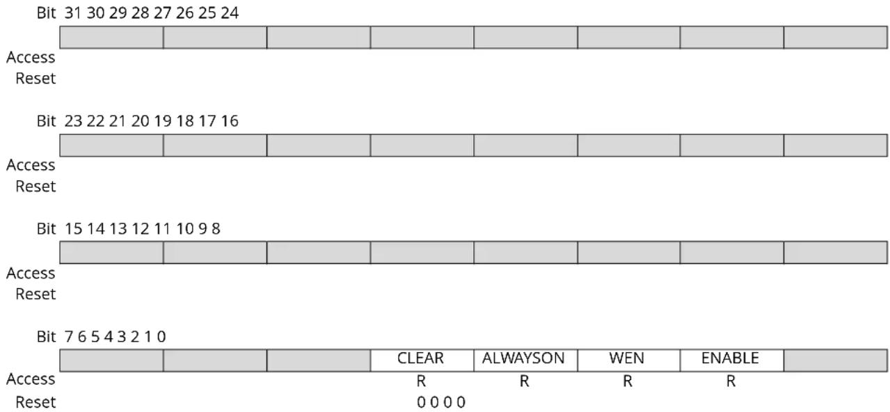
text_image
Bit 31 30 29 28 27 26 25 24 Access Reset Bit 23 22 21 20 19 18 17 16 Access Reset Bit 15 14 13 12 11 10 9 8 Access Reset Bit 7 6 5 4 3 2 1 0 Access Reset CLEAR ALWAYSON WEN ENABLE R R R 0 0 0 0Bit 4 - CLEAR Clear Synchronization Busy
| Value | Description |
| 0 | Write synchronization of the CLEAR register is complete. |
| 1 | Write synchronization of the CLEAR register is ongoing. |
Bit 3 - ALWAYSON Always-On Synchronization Busy
| Value | Description |
| 0 | Write synchronization of the CTRLA.ALWAYSON bit is complete. |
| 1 | Write synchronization of the CTRLA.ALWAYSON bit is ongoing. |
Bit 2 - WEN Window Enable Synchronization Busy
| Value | Description |
| 0 | Write synchronization of the CTRLA.WEN bit is complete. |
| 1 | Write synchronization of the CTRLA.WEN bit is ongoing. |
Bit 1 - ENABLE Enable Synchronization Busy
| Value | Description |
| 0 | Write synchronization of the CTRLA.ENABLE bit is complete. |
| 1 | Write synchronization of the CTRLA.ENABLE bit is ongoing. |
23.8.8 Clear
Name: CLEAR
Offset: 0x0C
Reset: 0x00
Property: Write-Synchronized
Bit 76543210
CLEAR[7:0]
Access WWWWWW
Reset 00000000
Bits 7:0 - CLEAR[7:0] Watchdog Clear
In Normal mode, writing 0xA5 to this register during the watchdog time-out period will clear the Watchdog Timer and the watchdog time-out period is restarted.
In Window mode, any writing attempt to this register before the time-out period started (i.e., during TO_WDTW ) will issue an immediate system Reset. Writing 0xA5 during the time-out period TO_WDT will clear the Watchdog Timer and the complete time-out sequence (first TO_WDTW then TO_WDT ) is restarted.
In both modes, writing any other value than 0xA5 will issue an immediate system Reset.
24. RTC – Real-Time Counter
24.1 Overview
The Real-Time Counter (RTC) is a 32-bit counter with a 10-bit programmable prescaler that typically runs continuously to keep track of time. The RTC can wake up the device from sleep modes using the alarm/compare wake up, periodic wake up, or overflow wake up mechanisms, or from the wake up inputs.
The RTC can generate periodic peripheral events from outputs of the prescaler, as well as alarm/compare interrupts and peripheral events, which can trigger at any counter value. Additionally, the timer can trigger an overflow interrupt and peripheral event, and can be reset on the occurrence of an alarm/compare match. This allows periodic interrupts and peripheral events at very long and accurate intervals.
The 10-bit programmable prescaler can scale down the clock source. By this, a wide range of resolutions and time-out periods can be configured. With a 32.768 kHz clock source, the minimum counter tick interval is 30.5 s, and time-out periods can range up to 36 hours. For a counter tick interval of 1s, the maximum time-out period is more than 136 years.
24.2 Features
The following are key features of the RTC module:
• 32-bit counter with 10-bit prescaler
- Multiple clock sources
• 32-bit or 16-bit counter mode
• One 32-bit or two 16-bit compare values
- Clock/Calendar mode
– Time in seconds, minutes, and hours (12/24)
- Date in day of month, month, and year
- Leap year correction
- Digital prescaler correction/tuning for increased accuracy
• Overflow, alarm/compare match and prescaler interrupts and events
- Optional clear on alarm/compare match
- 8 backup registers with retention capability
-
Tamper Detection
-
Timestamp on event or up to 5 inputs with debouncing
- Active layer protection
24.3 Block Diagram
Figure 24-1. RTC Block Diagram (Mode 0 — 32-Bit Counter)
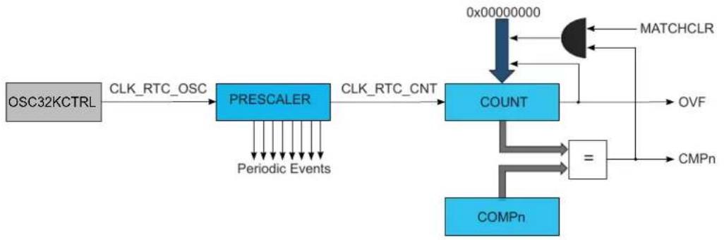
flowchart
graph LR
    A["OSC32KCTRL"] --> B["CLK_RTC_OSC"]
    B --> C["PREScaler"]
    C --> D["CLK_RTC_CNT"]
    D --> E["COUNT"]
    E --> F["0x00000000"]
    F --> G["MATCHCLR"]
    G --> H["OVF"]
    E --> I["="]
    I --> J["CMPn"]
    E --> K["COMPn"]
    C --> L["Periodic Events"]
Figure 24-2. RTC Block Diagram (Mode 1 — 16-Bit Counter)
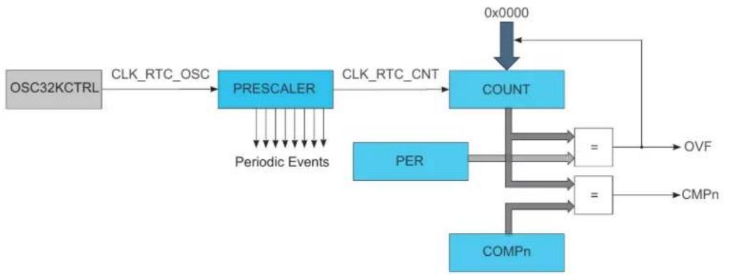
flowchart
graph TD
    A["OSC32KCTRL"] -->|CLK_RTC_OSC| B["PREScaler"]
    B -->|CLK_RTC_CNT| C["COUNT"]
    C --> D["0x0000"]
    D --> E["OVF"]
    C --> F["PER"]
    F --> G["="]
    F --> H["="]
    C --> I["COMPn"]
    I --> J["CMPn"]
    B --> K["Periodic Events"]
Figure 24-3. RTC Block Diagram (Mode 2 — Clock/Calendar)
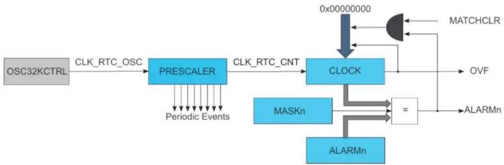
flowchart
graph LR
    A["OSC32KCTRL"] --> B["CLK_RTC_OSC"]
    B --> C["PREScaler"]
    C --> D["CLK_RTC_CNT"]
    D --> E["CLOCK"]
    E --> F["0x00000000"]
    F --> G["MATCHCLR"]
    G --> H["OVF"]
    E --> I["ALARMn"]
    I --> J["="]
    J --> K["ALARMn"]
    L["MASKn"] --> M["Periodic Events"]
    M --> C
Figure 24-4. RTC Block Diagram (Tamper Detection)

flowchart
graph TD
    A["TAMPEVT"] --> B["TIMESTAMP CAPTURE"]
    B --> C["Clock"]
    C --> D["="]
    D --> E["ALARM"]
    F["TAMPER"] --> B
    G["CLOCK"] --> C
    H["FREQCORR"] --> I["PREScaler"]
    I --> J["OUT"]
    K["IN0"] --> L["Tamper Input [0..n"]]
    M["IN1"] --> L
    N["IN2"] --> L
    O["IN3"] --> L
    P["IN4"] --> L
    Q["IN5"] --> L
    R["IN6"] --> L
    S["IN7"] --> L
    T["IN8"] --> L
    U["IN9"] --> L
    V["IN10"] --> L
    W["IN11"] --> L
    X["IN12"] --> L
    Y["IN13"] --> L
    Z["IN14"] --> L
    AA["IN15"] --> L
    AB["IN16"] --> L
    AC["IN17"] --> L
    AD["IN18"] --> L
    AE["IN19"] --> L
    AF["IN20"] --> L
    AG["IN21"] --> L
    AH["IN22"] --> L
    AI["IN23"] --> L
    AJ["IN24"] --> L
    AK["IN25"] --> L
    AL["IN26"] --> L
    AM["IN27"] --> L
    AN["IN28"] --> L
    AO["IN29"] --> L
    AP["IN30"] --> L
    AQ["IN31"] --> L
    AR["IN32"] --> L
    AS["IN33"] --> L
    AT["IN34"] --> L
    AU["IN35"] --> L
    AV["IN36"] --> L
    AW["IN37"] --> L
    AX["IN38"] --> L
    AY["IN39"] --> L
    AZ["IN40"] --> L
    BA["IN41"] --> L
    BB["IN42"] --> L
    BC["IN43"] --> L
    BD["IN44"] --> L
    BE["IN45"] --> L
    BF["IN46"] --> L
    BG["IN47"] --> L
    BH["IN48"] --> L
    BI["IN49"] --> L
    BJ["IN50"] --> L
    BK["IN51"] --> L
    BL["IN52"] --> L
    BM["IN53"] --> L
    BN["IN54"] --> L
    BO["IN55"] --> L
    BP["IN56"] --> L
    BQ["TAMPER"] --> BQ
24.4 Signal Description
Table 24-1. Signal Description
| Signal Description Type | |
| INn [n=0..4] Tamper / Wake / Active layer input Digital input | |
| OUT Active layer protection output Digital output |
One signal can be mapped to one of several pins.
24.5 Product Dependencies
In order to use this peripheral, other parts of the system must be configured correctly, as described below.
24.5.1 I/O Lines
Not applicable.
24.5.2 Power Management
The RTC will continue to operate in any sleep mode where the selected source clock is running. The RTC interrupts can be used to wake up the device from sleep modes. Events connected to the event system can trigger other operations in the system without exiting sleep modes. Refer to the Power Manager for details on the different sleep modes.
The RTC will be reset only at power-on (POR) or by setting the Software Reset bit in the Control A register (CTRLA.SWRST=1).
References:
PM - Power Manager
24.5.3 Clocks
The RTC bus clock (CLK_RTC_APB) can be enabled and disabled in the Main Clock module MCLK, and the default state of CLK_RTC_APB can be found in Peripheral Clock Masking section.
A 32KHz or 1KHz oscillator clock (CLK_RTC_OSC) is required to clock the RTC. This clock must be configured and enabled in the 32KHz oscillator controller (OSC32KCTRL) before using the RTC.
This oscillator clock is asynchronous to the bus clock (CLK_RTC_APB). Due to this asynchronicity, writing to certain registers will require synchronization between the clock domains. Refer to Synchronization for further details.
References:
Peripheral Clock Masking
OSC32KCTRL
24.5.4 DMA
The DMA request lines (or line if only one request) are connected to the DMA Controller (DMAC). Using the RTC DMA requests requires the DMA Controller to be configured first.
References:
DMAC - Direct Memory Access Controller
24.5.5 Interrupts
The interrupt request line is connected to the Interrupt Controller. Using the RTC interrupt requires the Interrupt Controller to be configured first.
References:
Nested Vector Interrupt Controller
24.5.6 Events
The events are connected to the Event System.
References:
EVSYS - Event System
24.5.7 Debug Operation
When the CPU is halted in debug mode the RTC will halt normal operation. The RTC can be forced to continue operation during debugging. Refer to 24.8.7. DBGCTRL for details.
24.5.8 Register Access Protection
All registers with write-access are optionally write-protected by the peripheral access controller (PAC), except the following registers:
- Interrupt Flag Status and Clear (INTFLAG) register
- General Purpose (GPx) registers
Write-protection is denoted by the "PAC Write-Protection" property in the register description.
Write-protection does not apply to accesses through an external debugger. Refer to the PAC Peripheral Access Controller for details.
24.5.9 Analog Connections
A 32.768kHz crystal can be connected to the XIN32 and XOUT32 pins, along with any required load capacitors. See Electrical Characteristics for details on recommended crystal characteristics and load capacitors.
References:
Electrical Characteristics
24.6 Functional Description
24.6.1 Principle of Operation
The RTC keeps track of time in the system and enables periodic events, as well as interrupts and events at a specified time. The RTC consists of a 10-bit prescaler that feeds a 32-bit counter. The actual format of the 32-bit counter depends on the RTC operating mode.
The RTC can function in one of these modes:
- Mode 0 - COUNT32: RTC serves as 32-bit counter
- Mode 1 - COUNT16: RTC serves as 16-bit counter
- Mode 2 - CLOCK: RTC serves as clock/calendar with alarm functionality
24.6.2 Basic Operation
24.6.2.1 Initialization
The following bits are enable-protected, meaning that they can only be written when the RTC is disabled (CTRLA.ENABLE=0):
- Operating Mode bits in the Control A register (CTRLA.MODE)
- Prescaler bits in the Control A register (CTRLA.PRESCALER)
- Clear on Match bit in the Control A register (CTRLA.MATCHCLR)
- Clock Representation bit in the Control A register (CTRLA.CLKREP)
The following registers are enable-protected:
• Event Control register (EVCTRL)
• Tamper Control register (TAMPCTRL)
• Control B register (CTRLB)
Enable-protected bits and registers can be changed only when the RTC is disabled (CTRLA.ENABLE=0). If the RTC is enabled (CTRLA.ENABLE=1), these operations are necessary: first write CTRLA.ENABLE=0 and check whether the write synchronization has finished, then change the desired bit field value. Enable-protected bits in can be written at the same time as CTRLA.ENABLE is written to '1', but not at the same time as CTRLA.ENABLE is written to '0'.
Enable-protection is denoted by the "Enable-Protected" property in the register description.
The RTC prescaler divides the source clock for the RTC counter.
Note: In Clock/Calendar mode, the prescaler must be configured to provide a 1Hz clock to the counter for correct operation.
The frequency of the RTC clock (CLK_RTC_CNT) is given by the following formula:
$$ f _ {\mathrm {CLK_RTC_CNT}} = \frac {f _ {\mathrm {CLK_RTC_OSC}}}{2 ^ {\text { PRESCALER }}} $$
The frequency of the oscillator clock, CLK_RTC_OSC, is given by f_CLK_RTC_OSC , and f_CLK_RTC_CNT is the frequency of the internal prescaled RTC clock, CLK_RTC_CNT.
24.6.2.2 Enabling, Disabling, and Resetting
The RTC is enabled by setting the Enable bit in the Control A register (CTRLA.ENABLE=1). The RTC is disabled by writing CTRLA.ENABLE=0.
The RTC is reset by setting the Software Reset bit in the Control A register (CTRLA.SWRST=1). All registers in the RTC, except DEBUG, will be reset to their initial state, and the RTC will be disabled. The RTC must be disabled before resetting it.
24.6.2.3 32-Bit Counter (Mode 0)
When the RTC Operating Mode bits in the Control A register (CTRLA.MODE) are written to 0x0, the counter operates in 32-bit Counter mode. The block diagram of this mode is shown in RTC Block Diagram (Mode 0 - 32-Bit Counter). When the RTC is enabled, the counter will increment on every 0-to-1 transition of CLK_RTC_CNT. The counter will increment until it reaches the top value of 0xFFFFFFF, and then wrap to 0x00000000. This sets the Overflow Interrupt flag in the Interrupt Flag Status and Clear register (INTFLAG.OVF).
The RTC counter value can be read from or written to the Counter Value register (COUNT) in 32-bit format.
The counter value is continuously compared with the 32-bit Compare register (COMP). When a compare match occurs, the Compare0 Interrupt flag in the Interrupt Flag Status and Clear register (INTFLAG.CMP0) is set on the next 0-to-1 transition of CLK_RTC_CNT.
If the Clear on Match bit in the Control A register (CTRLA.MATCHCLR) is '1', the counter is cleared on the next counter cycle when a compare match with COMP occurs. This allows the RTC to generate periodic interrupts or events with longer periods than the prescaler events. Note that when CTRLA.MATCHCLR is '1', INTFLAG.CMP0 and INTFLAG.OVF will both be set simultaneously on a compare match with COMP.
24.6.2.4 16-Bit Counter (Mode 1)
When the RTC Operating Mode bits in the Control A register (CTRLA.MODE) are written to 0x1, the counter operates in 16-bit Counter mode as shown in RTC Block Diagram (Mode 1 - 16-Bit Counter). When the RTC is enabled, the counter will increment on every 0-to-1 transition of CLK_RTC_CNT. In 16-bit Counter mode, the 16-bit Period register (PER) holds the maximum value of the counter. The counter will increment until it reaches the PER value, and then wrap to 0x0000. This sets the Overflow Interrupt flag in the Interrupt Flag Status and Clear register (INTFLAG.OVF).
The RTC counter value can be read from or written to the Counter Value register (COUNT) in 16-bit format.
The counter value is continuously compared with the 16-bit Compare registers (COMPn, n=0..1). When a compare match occurs, the Compare n Interrupt flag in the Interrupt Flag Status and Clear register (INTFLAG.CMPn, n=0..1) is set on the next 0-to-1 transition of CLK_RTC_CNT.
24.6.2.5 Clock/Calendar (Mode 2)
When the RTC Operating Mode bits in the Control A register (CTRLA.MODE) are written to 0x2, the counter operates in Clock/Calendar mode, as shown in RTC Block Diagram (Mode 2 - Clock/ Calendar). When the RTC is enabled, the counter will increment on every 0-to-1 transition of CLK_RTC_CNT. The selected clock source and RTC prescaler must be configured to provide a 1Hz clock to the counter for correct operation in this mode.
The time and date can be read from or written to the Clock Value register (CLOCK) in a 32-bit time/date format. Time is represented as:
- Seconds
- Minutes
- Hours
Hours can be represented in either 12- or 24-hour format, selected by the Clock Representation bit in the Control A register (CTRLA.CLKREP). This bit can be changed only while the RTC is disabled.
The date is represented in this form:
• Day as the numeric day of the month (starting at 1)
- Month as the numeric month of the year (1 = January, 2 = February, etc.)
- Year as a value from 0x00 to 0x3F. This value must be added to a user-defined reference year. The reference year must be a leap year (2016, 2020 etc). Example: the year value 0x2D, added to a reference year 2016, represents the year 2061.
The RTC will increment until it reaches the top value of 23:59:59 December 31 of year value 0x3F, and then wrap to 00:00:00 January 1 of year value 0x00. This will set the Overflow Interrupt flag in the Interrupt Flag Status and Clear registers (INTFLAG.OVF).
The clock value is continuously compared with the 32-bit Alarm register (ALARM). When an alarm match occurs, the Alarm 0 Interrupt flag in the Interrupt Flag Status and Clear registers (INTFLAG.ALARM0) is set on the next 0-to-1 transition of CLK_RTC_CNT. E.g. For a 1Hz clock counter, it means the Alarm 0 Interrupt flag is set with a delay of 1s after the occurrence of alarm match.
A valid alarm match depends on the setting of the Alarm Mask Selection bits in the Alarm Mask register (MASK.SEL). These bits determine which time/date fields of the clock and alarm values are valid for comparison and which are ignored.
If the Clear on Match bit in the Control A register (CTRLA.MATCHCLR) is set, the counter is cleared on the next counter cycle when an alarm match with ALARM 0 occurs. This allows the RTC to generate periodic interrupts or events with longer periods than it would be possible with the prescaler events only (see 24.6.8.1. Periodic Intervals).
Note: When CTRLA.MATCHCLR is 1, INTFLAG.ALARM0 and INTFLAG.OVF will both be set simultaneously on an alarm match with ALARM0.
24.6.3 DMA Operation
The RTC generates the following DMA request:
- Tamper (TAMPER): The request is set on capture of the timestamp. The request is cleared when the Timestamp register is read.
If the CPU accesses the registers which are the source for the DMA request set/clear condition, the DMA request can be lost or the DMA transfer can be corrupted, if enabled.
24.6.4 Interrupts
The RTC has the following interrupt sources:
• Overflow (OVF): Indicates that the counter has reached its top value and wrapped to zero.
- Compare (CMPn): Indicates a match between the counter value and the compare register.
- Alarm (ALARM0): Indicates a match between the clock value and the alarm register.
- Period n (PERn): The corresponding bit in the prescaler has toggled. Refer to Periodic Intervals for details.
- Tamper (TAMPER): Indicates detection of a valid signal on a tamper input pin, or tamper event input.
Each interrupt source has an interrupt flag associated with it. The interrupt flag in the Interrupt Flag Status and Clear (INTFLAG) register is set when the interrupt condition occurs. Each interrupt can be individually enabled by setting the corresponding bit in the Interrupt Enable Set register (INTENSET = 1), and disabled by setting the corresponding bit in the Interrupt Enable Clear register (INTENCLR = 1).
An interrupt request is generated when the interrupt flag is raised and the corresponding interrupt is enabled. The interrupt request remains active until either the interrupt flag is cleared, the interrupt is disabled or the RTC is reset. See the description of the INTFLAG registers for details on how to clear interrupt flags.
All interrupt requests from the peripheral are ORed together on system level to generate one combined interrupt request to the NVIC. Refer to the Nested Vector Interrupt Controller for
additional information. The user must read the INTFLAG register to determine which interrupt condition is present.
Note: Interrupts must be globally enabled for interrupt requests to be generated. Refer to the Nested Vector Interrupt Controller for details.
24.6.5 Events
The RTC can generate the following output events:
• Overflow (OVF): Generated when the counter has reached its top value and wrapped to zero.
- Compare (CMPn): Indicates a match between the counter value and the compare register.
- Alarm (ALARM0): Indicates a match between the clock value and the alarm register.
- Period n (PERn): The corresponding bit in the prescaler has toggled. Refer to Periodic Intervals for details.
- Tamper (TAMPER): Generated on detection of a valid signal on a tamper input pin, or tamper event input.
Setting the Event Output bit in the Event Control Register (EVCTRL.xxxEO = 1) enables the corresponding output event. Writing a zero to this bit disables the corresponding output event. Refer to the EVSYS - Event System for details on configuring the event system.
The RTC can take the following actions on an input event:
- Tamper (TAMPEV): Capture the RTC counter to the timestamp register. See 24.6.8.5. Tamper Detection.
Writing a one to an Event Input bit into the Event Control register (EVCTRL.xxxEI) enables the corresponding action on input event. Writing a zero to this bit disables the corresponding action on input event.
References:
- EVSYS - Event System
24.6.6 Sleep Mode Operation
The RTC will continue to operate in any sleep mode where the source clock is active. The RTC interrupts can be used to wake up the device from a sleep mode. RTC events can trigger other operations in the system without exiting the sleep mode.
An interrupt request will be generated after the wake-up if the Interrupt Controller is configured accordingly. Otherwise the CPU will wake up, without triggering any interrupt. In this case, the CPU will continue executing right from the first instruction that followed the entry into sleep.
The periodic events also may wake-up the CPU through the interrupt function of the Event System. In this case, the event must be enabled and connected to an event channel with its interrupt enabled. Refer to the EVSYS - Event System for more information
24.6.7 Synchronization
Due to asynchronicity between the main clock domain and the peripheral clock domains, some registers need to be synchronized when written or read.
The following bits are synchronized when written:
- Software Reset bit in Control A register, CTRLA.SWRST
- Enable bit in Control A register, CTRLA.ENABLE
- Count Read Synchronization bit in Control A register (CTRLA.COUNTSYNC)
The following registers are synchronized when written:
• Counter Value register, COUNT
- Clock Value register, CLOCK
• Counter Period register, PER
• Compare n Value registers, COMPn
• Alarm 0 Value register, ALARM
• Frequency Correction register, FREQCORR
- Alarm 0 Mask register, MASK
• The General Purpose n registers (GPn)
The following registers are synchronized when read:
- The Counter Value register, COUNT, if the Counter Read Sync Enable bit in CTRLA (CTRLA.COUNTSYNC) is '1'
- The Clock Value register, CLOCK, if the Clock Read Sync Enable bit in CTRLA (CTRLA.CLOCKSYNC) is '1'
• The Timestamp Value register (TIMESTAMP)
Required write-synchronization is denoted by the "Write-Synchronized" property in the register description.
Required read-synchronization is denoted by the "Read-Synchronized" property in the register description.
References:
14.3. Register Synchronization
24.6.8 Additional Features
24.6.8.1 Periodic Intervals
The RTC prescaler can generate interrupts and events at periodic intervals, allowing flexible system tick creation. Any of the upper eight bits of the prescaler (bits 2 to 9) can be the source of an interrupt/event. When one of the eight Periodic Event Output bits in the Event Control register (EVCTRL.PEREO[n=0..7]) is '1', an event is generated on the 0-to-1 transition of the related bit in the prescaler, resulting in a periodic event frequency of:
$$ f _ {\text { PERIODIC(n) }} = \frac {f _ {\mathrm {CLK_RTC_OSC}}}{2 ^ {n + 3}} $$
f_CLK_RTC_OSC is the frequency of the internal prescaler clock CLK_RTC_OSC, and n is the position of the EVCTRL.PEREOn bit. For example, PER0 will generate an event every eight CLK_RTC_OSC cycles, PER1 every 16 cycles, etc. This is shown in the figure below.
Periodic events are independent of the prescaler setting used by the RTC counter, except if CTRLA.PRESCALER is zero. Then, no periodic events will be generated.
Figure 24-5. Example Periodic Events

text_image
CLK_RTC_OSC PER0 PER1 PER2 PER324.6.8.2 Frequency Correction
The RTC Frequency Correction module employs periodic counter corrections to compensate for a too-slow or too-fast oscillator. Frequency correction requires that CTRLA.PRESCALER is greater than 1.
The digital correction circuit adds or subtracts cycles from the RTC prescaler to adjust the frequency in approximately 1ppm steps. Digital correction is achieved by adding or skipping a single count in the prescaler once every 8192 CLK_RTC_OSC cycles. The Value bit group in the Frequency Correction register (FREQCORR.VALUE) determines the number of times the adjustment is applied over 128 of these periods. The resulting correction is as follows:
$$ \text { Correction in ppm } = \frac {\text { FREQCORR.VALUE }}{8 1 9 2 \cdot 1 2 8} \cdot 1 0 ^ {6} \text { ppm } $$
This results in a resolution of 0.95367 ppm.
The Sign bit in the Frequency Correction register (FREQCORR.SIGN) determines the direction of the correction. A positive value will add counts and increase the period (reducing the frequency), and a negative value will reduce counts per period (speeding up the frequency).
Digital correction also affects the generation of the periodic events from the prescaler. When the correction is applied at the end of the correction cycle period, the interval between the previous periodic event and the next occurrence may also be shortened or lengthened depending on the correction value.
24.6.8.3 Backup Registers
The RTC includes eight Backup registers (BKUPn). These registers maintain their content in Backup sleep mode. They can be used to store user-defined values.
If more user-defined data must be stored than the eight Backup registers can hold, the General Purpose registers (GPn) can be used.
24.6.8.4 General Purpose Registers
The RTC includes two General Purpose registers (GPn). These registers are reset only when the RTC is reset or when tamper detection occurs while CTRLA.GPTRST=1, and remain powered while the RTC is powered. They can be used to store user-defined values while other parts of the system are powered off.
It is recommended to use the eight Backup registers (BKUPn) first to store user-defined values, and use the GPn only when the user-defined values exceed the capacity of the provided BKUPn.
An example procedure to write the general purpose registers GP0 and GP1 is:
- Wait for any ongoing write to COMP0 to complete (SYNCBUSY.COMP0 = 0). If the RTC is operating in Mode 1, wait for any ongoing write to COMP1 to complete as well (SYNCBUSY.COMP1 = 0).
- Write CTRLB.GPOEN = 1 if GP0 is needed.
- Write GP0 if needed.
- Wait for any ongoing write to GP0 to complete (SYNCBUSY.GP0 = 0). Note that GP1 will also show as busy when GP0 is busy.
- Write GP1 if needed.
Table 24-2. General Purpose Registers vs Compare/Alarm Registers
| Register Mode 0 Mode 1 Mode 2 Write Before | |||
| GP0 COMP0 COMP0 / COMP1 ALARM0 GP1 | |||
| GP1 COMP0 COMP0 / COMP1 ALARM0 - |
The GPn registers share internal resources with the compare/alarm features. Each pair of 32-bit GPn are associated with one 32-bit compare/alarm or a pair of 16-bit compare registers as shown in the table above. Before using an even GPn, the associated compare/alarm feature must be disabled by
writing a '1' to the General Purpose Enable bit in the Control B register (CTRLB.GPnEN). To re-enable the compare/alarm, CTRLB.GPnEN must be written to zero and the associated COMPn/ALARM0 must be written with the correct value. Each even GPn must also be written prior to writing the odd GPn if both will be used. Odd GPn can be used without affecting the compare/alarm functions; however, any writes to the associated COMPn/ALARM0 register must be completed before writing the odd GPn.
24.6.8.5 Tamper Detection
The RTC provides up to five selectable polarity external inputs (INn) that can be used for tamper detection. The RTC also supports an input event (TAMPEVT) for generating a tamper condition from within the Event System.
A single interrupt request (TAMPER) is available for all tamper sources. The polarity for each input is selected with the Tamper Level bits in the Tamper Control register (TAMPCTRL.TAMPLVLn). The tamper input event is enabled by the Tamper Input Event Enable in the Event Control register (EVCTRL.TAMPEVIE). The action of each input pin is configured using the Input n Action bits in the Tamper Control register (TAMPCTRL.INnACT). Tamper inputs support the following actions:
- Off: Detection for INn is disabled.
- Wake: A transition on INn matching TAMPCTRL.TAMPLVLn will be detected and the tamper interrupt flag (INTFLAG.TAMPER) will be set. The RTC value will not be captured in the TIMESTAMP register
- Capture: A transition on INn matching TAMPCTRL.TAMPLVLn will be detected and the tamper interrupt flag (INTFLAG.TAMPER) will be set. The RTC value will be captured in the TIMESTAMP register.
- Active Layer Protection: A mismatch between INn and OUT will be detected and the tamper interrupt flag (INTFLAG.TAMPER) will be set. The RTC value will be captured in the TIMESTAMP register.
In order to determine which tamper source caused a tamper event, the Tamper ID register (TAMPID) provides the detection status of each input pin and the input event. These bits remain active until cleared by software. Separate debouncers are embedded for each external input. The debouncer for each input is enabled/disabled with the Debounce Enable bits in the Tamper Control register (TAMPCTRL.DEBNCn). The debouncer configuration is fixed for all inputs as set by the Control B register (CTRLB). The debouncing period duration is configurable using the Debounce Frequency field in the Control B register (CTRLB.DEBF). The period is set for all debouncers (i.e., the duration cannot be adjusted separately for each debouncer).
When TAMPCTRL.DEBNCn = 0, INn is detected asynchronously. See Figure 24-6 for an example.
When TAMPCTRL.DEBNCn = 1, the detection time depends on whether the debouncer operates synchronously or asynchronously, and whether majority detection is enabled or not. Refer to the table below for more details. Synchronous versus asynchronous stability debouncing is configured by the Debounce Asynchronous Enable bit in the Control B register (CTRLB.DEBASYNC):
- Synchronous (CTRLB.DEBASYNC = 0): INn is synchronized in two CLK_RTC periods and then must remain stable for four CLK_RTC_DEB periods before a valid detection occurs. See Figure 24-7 for an example.
- Asynchronous (CTRLB.DEBASYNC = 1): The first edge on INn is detected. Further detection is blanked until INn remains stable for four CLK_RTC_DEB periods. See Figure 24-8 for an example.
Majority debouncing is configured by the Debounce Majority Enable bit in the Control B register (CTRLB.DEBMAJ). INn must be valid for two out of three CLK_RTC_DEB periods. See Figure 24-9 for an example.
Table 24-3. Debouncer Configuration
| TAMPCTRL. DEBNCn | CTRLB. DEBMA J CTRLB. DEBASYNC | Description | |
| 0 X X Detect edge on INn with no debouncing. Every edge detected is immediately triggered. | |||
| 1 0 0 Detect edge on INn with synchronous stability debouncing. Edge detected is only triggered when INn is stable for 4 consecutive CLK_RTC_DEB periods. | |||
| 1 0 1 Detect edge on INn with asynchronous stability debouncing. | First detected edge is triggered immediately. All subsequent detected edges are ignored until INn is stable for 4 consecutive CLK_RTC_DEB periods. | ||
| 1 1 X Detect edge on INn with majority debouncing. Pin INn is sampled for 3 consecutive CLK_RTC_DEB periods. Signal level is determined by majority-rule (LLL, LLH, LHL, HLL = '0' and LHH, HLH, HHL, HHH = '1'). | |||
Figure 24-6. Edge Detection with Debouncer Disabled

text_image
CLK_RTC CLK_RTC_DEB IN NE PE NE PE NE PE OUT TAMLVL=0 CLK_RTC CLK_RTC_DEB IN NE PE NE PE NE PE OUT TAMLVL=1Figure 24-7. Edge Detection with Synchronous Stability Debouncing
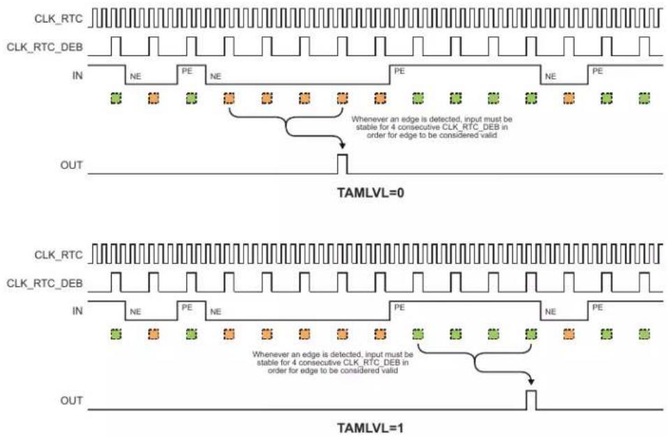
text_image
CLK_RTC CLK_RTC_DEB IN NE PE NE PE NE PE OUT Whenever an edge is detected, input must be stable for 4 consecutive CLK_RTC_DEB in order for edge to be considered valid TAMLVL=0 CLK_RTC CLK_RTC_DEB IN NE PE NE PE NE PE OUT Whenever an edge is detected, input must be stable for 4 consecutive CLK_RTC_DEB in order for edge to be considered valid TAMLVL=1Figure 24-8. Edge Detection with Asynchronous Stability Debouncing
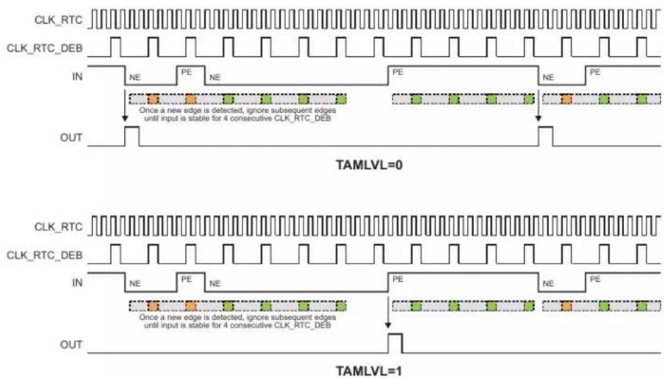
text_image
CLK_RTC CLK_RTC_DEB IN NE PE NE PE NE PE Once a new edge is detected, ignore subsequent edges until input is stable for 4 consecutive CLK_RTC_DEB OUT TAMLVL=0 CLK_RTC CLK_RTC_DEB IN NE PE NE PE NE PE Once a new edge is detected, ignore subsequent edges until input is stable for 4 consecutive CLK_RTC_DEB OUT TAMLVL=1Figure 24-9. Edge Detection with Majority Debouncing
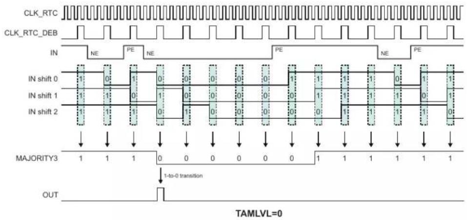
text_image
CLK_RTC CLK_RTC_DEB IN NE PE NE PE NE PE IN shift 0 1 0 1 0 0 0 0 1 1 1 1 0 1 1 IN shift 1 1 1 0 1 0 0 0 0 0 1 1 1 1 0 1 IN shift 2 1 1 1 0 1 0 0 0 0 0 0 1 1 1 1 1 1 MAJORITY3 1 1 1 0 0 0 0 0 0 1 1 1 1 1 1 OUT TAMLVL=0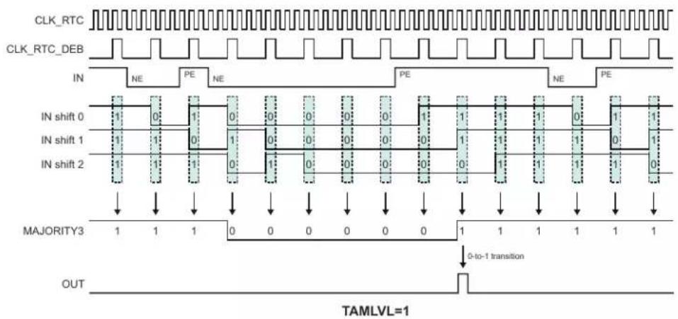
text_image
CLK_RTC CLK_RTC_DEB IN NE PE NE PE NE PE IN shift 0 1 0 1 0 0 0 0 1 1 1 1 0 1 1 IN shift 1 1 1 0 1 0 0 0 0 0 1 1 1 1 1 0 1 IN shift 2 1 1 1 0 1 0 0 0 0 0 0 1 1 1 1 1 1 0 MAJORITY3 1 1 1 0 0 0 0 0 0 1 1 1 1 1 1 1 OUT TAMLVL=124.6.8.6 Active Layer Protection
The RTC provides a means of detecting broken traces on the PCB, also known as Active Layer Protection. In this mode an RTC output signal is routed over critical components on the board and fed back to one of the RTC inputs. The input and output signals are compared and a tamper condition is detected when they do not match.
Enabling active layer protection requires the following steps:
- Enable the RTC prescaler output by writing a one to the RTC Out bit in the Control B register (CTRLB.RTCOUT). The I/O pins must also be configured to correctly route the signal to the external pins.
- Select the frequency of the output signal by configuring the RTC Active Layer Frequency field in the Control B register (CTRLB.ACTF).
$$ \mathrm {GCLK_RTC_OUT} = \frac {\mathrm {CLK_RTC}}{2 ^ {\mathrm{CTRLB.ACTF} + 1}} $$
- Enable one of the tamper inputs (INn) in active layer mode by writing 3 to the corresponding Input Action field in the Tamper Control register (TAMPCTRL.INnACT). When active layer protection is enabled, the value of INn is sampled on the falling edge of CLK_RTC and compared to the expected value of OUT. Therefore up to one half of a CLK_RTC period is available for propagation delay through the trace.
24.7 Register Summary - COUNT32
| Offset | Name Bit Pos. 7 | 6 | 5 | 4 | 3 | 2 | 1 | 0 | |||||||||||||||
| 0x00 | CTRLA | 7:0 MATCHCLR MODE[1:0] ENABLE SWRST | |||||||||||||||||||||
| 15:8 COUNTSYNC GPTRST BKTRST | PRESCALER[3:0] | ||||||||||||||||||||||
| 0x02 | CTRLB | 7:0 | DMAEN | RTCOUT | DEBASYNC | DEBMAJ | |||||||||||||||||
| 15:8 | ACTF[2:0] | ||||||||||||||||||||||
| 0x04 | EVCTRL | 7:0 | PEREO7 | PEREO6 | PEREO5 | PEREO4 | PEREO3 | PEREO2 | PEREO1 | PEREO0 | |||||||||||||
| 15:8 | OVFEO | TAMPEREO | CMPEO0 | ||||||||||||||||||||
| 23:16 | TAMPEVEI | ||||||||||||||||||||||
| 31:24 | |||||||||||||||||||||||
| 0x08 | INTENCLR | 7:0 | PER7 | PER6 | PER5 | PER4 | PER3 | PER2 | PER1 | PER0 | |||||||||||||
| 15:8 | OVF | TAMPER | CMP0 | ||||||||||||||||||||
| 0x0A | INTENSET | 7:0 | PER7 | PER6 | PER5 | PER4 | PER3 | PER2 | PER1 | PER0 | |||||||||||||
| 15:8 | OVF | TAMPER | CMP0 | ||||||||||||||||||||
| 0x0C | INTFLAG | 7:0 | PER7 | PER6 | PER5 | PER4 | PER3 | PER2 | PER1 | PER0 | |||||||||||||
| 15:8 | OVF | TAMPER | CMP0 | ||||||||||||||||||||
| 0x0E | DBGCTRL | 7:0 | DBGRUN | ||||||||||||||||||||
| 0x0F | Reserved | ||||||||||||||||||||||
| 0x10 | SYNCBUSY | 7:0 | COMPO | COUNT | FREQCORR | ENABLE | SWRST | ||||||||||||||||
| 15:8 COUNTSYNC | |||||||||||||||||||||||
| 23:16 | GP1 GP0 | ||||||||||||||||||||||
| 31:24 | |||||||||||||||||||||||
| 0x14 | FREQCORR | 7:0 | SIGN | VALUE[6:0] | |||||||||||||||||||
| 0x15 ... 0x17 | Reserved | ||||||||||||||||||||||
| 0x18 | COUNT | 7:0 | COUNT[7:0] | ||||||||||||||||||||
| 15:8 | COUNT[15:8] | ||||||||||||||||||||||
| 23:16 | COUNT[23:16] | ||||||||||||||||||||||
| 31:24 | COUNT[31:24] | ||||||||||||||||||||||
| 0x1C ... 0x1F | Reserved | ||||||||||||||||||||||
| 0x20 | COMPO | 7:0 | COMP[7:0] | ||||||||||||||||||||
| 15:8 | COMP[15:8] | ||||||||||||||||||||||
| 23:16 | COMP[23:16] | ||||||||||||||||||||||
| 31:24 | COMP[31:24] | ||||||||||||||||||||||
| 0x24 ... 0x3F | Reserved | ||||||||||||||||||||||
| 0x40 | GP0 | 7:0 | GP[7:0] | ||||||||||||||||||||
| 15:8 | GP[15:8] | ||||||||||||||||||||||
| 23:16 | GP[23:16] | ||||||||||||||||||||||
| 31:24 | GP[31:24] | ||||||||||||||||||||||
| 0x44 | GP1 | 7:0 | GP[7:0] | ||||||||||||||||||||
| 15:8 | GP[15:8] | ||||||||||||||||||||||
| 23:16 | GP[23:16] | ||||||||||||||||||||||
| 31:24 | GP[31:24] | ||||||||||||||||||||||
| 0x48 ... 0x5F | Reserved | ||||||||||||||||||||||
| 0x60 | TAMPCTRL | 7:0 | IN3ACT[1:0] | IN2ACT[1:0] | IN1ACT[1:0] | IN0ACT[1:0] | |||||||||||||||||
| 15:8 | IN4ACT[1:0] | ||||||||||||||||||||||
| 23:16 | TAMLVL4 | TAMLVL3 | TAMLVL2 | TAMLVL1 | TAMLVL0 | ||||||||||||||||||
| 31:24 | DEBNC4 | DEBNC3 | DEBNC2 | DEBNC1 | DEBNC0 | ||||||||||||||||||
| 0x64 | TIMESTAMP | 7:0 | COUNT[7:0] | ||||||||||||||||||||
| 15:8 | COUNT[15:8] | ||||||||||||||||||||||
| 23:16 | COUNT[23:16] | ||||||||||||||||||||||
| 31:24 | COUNT[31:24] | ||||||||||||||||||||||
| Offset | Name Bit Pos. 7 | 6 | 5 | 4 | 3 | 2 | 1 | 0 | |||||||||||||||||||||||||||||||||||||||||||||||||||||||||||||||||||||||||||||||||||||||||||||||||||||||||||||||||||||||||||||||||||||||||||||||||||||||||||||||||||||||||||||||||||||||||||||||||||||||||||||||||||||||||||||||||||||||||||||||||||||||||||||||||||||||||||||||||||||||||||||||||||||||||||||||||||||||||||||||||||||||||||||||||||||||||||||||||||||||||||||||||||||||||||||||||||||
| 0x68 TAMPID | 7:0 TAMPID4 TAMPID3 TAMPID2 TAMPID1 TAMPID0 | ||||||||||||||||||||||||||||||||||||||||||||||||||||||||||||||||||||||||||||||||||||||||||||||||||||||||||||||||||||||||||||||||||||||||||||||||||||||||||||||||||||||||||||||||||||||||||||||||||||||||||||||||||||||||||||||||||||||||||||||||||||||||||||||||||||||||||||||||||||||||||||||||||||||||||||||||||||||||||||||||||||||||||||||||||||||||||||||||||||||||||||||||||||||||||||||||||||||||||||
| 15:8 | 0x68 TAMPID | ||||||||||||||||||||||||||||||||||||||||||||||||||||||||||||||||||||||||||||||||||||||||||||||||||||||||||||||||||||||||||||||||||||||||||||||||||||||||||||||||||||||||||||||||||||||||||||||||||||||||||||||||||||||||||||||||||||||||||||||||||||||||||||||||||||||||||||||||||||||||||||||||||||||||||||||||||||||||||||||||||||||||||||||||||||||||||||||||||||||||||||||||||||||||||||||||||||||||||||
| 23:16 | 0X6C ... 0x7F | Reserved | 31:24 TAMPEVT | ||||||||||||||||||||||||||||||||||||||||||||||||||||||||||||||||||||||||||||||||||||||||||||||||||||||||||||||||||||||||||||||||||||||||||||||||||||||||||||||||||||||||||||||||||||||||||||||||||||||||||||||||||||||||||||||||||||||||||||||||||||||||||||||||||||||||||||||||||||||||||||||||||||||||||||||||||||||||||||||||||||||||||||||||||||||||||||||||||||||||||||||||||||||||||||||||||||||||||
| 0x80 BKUP0 | 7:0 BKUP[7:0] | 0x80 BKUP0 | 15:8 | BKUP[15:8] | 15:8 | BKUP[15:8] | |||||||||||||||||||||||||||||||||||||||||||||||||||||||||||||||||||||||||||||||||||||||||||||||||||||||||||||||||||||||||||||||||||||||||||||||||||||||||||||||||||||||||||||||||||||||||||||||||||||||||||||||||||||||||||||||||||||||||||||||||||||||||||||||||||||||||||||||||||||||||||||||||||||||||||||||||||||||||||||||||||||||||||||||||||||||||||||||||||||||||||||||||||||||||||||||||||||||
| 23:16 | |||||||||||||||||||||||||||||||||||||||||||||||||||||||||||||||||||||||||||||||||||||||||||||||||||||||||||||||||||||||||||||||||||||||||||||||||||||||||||||||||||||||||||||||||||||||||||||||||||||||||||||||||||||||||||||||||||||||||||||||||||||||||||||||||||||||||||||||||||||||||||||||||||||||||||||||||||||||||||||||||||||||||||||||||||||||||||||||||||||||||||||||||||||||||||||||||||||||||||||
| 31:24 | |||||||||||||||||||||||||||||||||||||||||||||||||||||||||||||||||||||||||||||||||||||||||||||||||||||||||||||||||||||||||||||||||||||||||||||||||||||||||||||||||||||||||||||||||||||||||||||||||||||||||||||||||||||||||||||||||||||||||||||||||||||||||||||||||||||||||||||||||||||||||||||||||||||||||||||||||||||||||||||||||||||||||||||||||||||||||||||||||||||||||||||||||||||||||||||||||||||||||||||
| 0x84 BKUP1 | 7:0 BKUP[7:0] | ||||||||||||||||||||||||||||||||||||||||||||||||||||||||||||||||||||||||||||||||||||||||||||||||||||||||||||||||||||||||||||||||||||||||||||||||||||||||||||||||||||||||||||||||||||||||||||||||||||||||||||||||||||||||||||||||||||||||||||||||||||||||||||||||||||||||||||||||||||||||||||||||||||||||||||||||||||||||||||||||||||||||||||||||||||||||||||||||||||||||||||||||||||||||||||||||||||||||||||
| BKUP[15:8] | |||||||||||||||||||||||||||||||||||||||||||||||||||||||||||||||||||||||||||||||||||||||||||||||||||||||||||||||||||||||||||||||||||||||||||||||||||||||||||||||||||||||||||||||||||||||||||||||||||||||||||||||||||||||||||||||||||||||||||||||||||||||||||||||||||||||||||||||||||||||||||||||||||||||||||||||||||||||||||||||||||||||||||||||||||||||||||||||||||||||||||||||||||||||||||||||||||||||||||||
| 15:8 | BKUP[15:8] | ||||||||||||||||||||||||||||||||||||||||||||||||||||||||||||||||||||||||||||||||||||||||||||||||||||||||||||||||||||||||||||||||||||||||||||||||||||||||||||||||||||||||||||||||||||||||||||||||||||||||||||||||||||||||||||||||||||||||||||||||||||||||||||||||||||||||||||||||||||||||||||||||||||||||||||||||||||||||||||||||||||||||||||||||||||||||||||||||||||||||||||||||||||||||||||||||||||||||||||
| Reserved | |||||||||||||||||||||||||||||||||||||||||||||||||||||||||||||||||||||||||||||||||||||||||||||||||||||||||||||||||||||||||||||||||||||||||||||||||||||||||||||||||||||||||||||||||||||||||||||||||||||||||||||||||||||||||||||||||||||||||||||||||||||||||||||||||||||||||||||||||||||||||||||||||||||||||||||||||||||||||||||||||||||||||||||||||||||||||||||||||||||||||||||||||||||||||||||||||||||||||||||
| 0x88 BKUP2 | 7:0 BKUP[7:0] | ||||||||||||||||||||||||||||||||||||||||||||||||||||||||||||||||||||||||||||||||||||||||||||||||||||||||||||||||||||||||||||||||||||||||||||||||||||||||||||||||||||||||||||||||||||||||||||||||||||||||||||||||||||||||||||||||||||||||||||||||||||||||||||||||||||||||||||||||||||||||||||||||||||||||||||||||||||||||||||||||||||||||||||||||||||||||||||||||||||||||||||||||||||||||||||||||||||||||||||
| 15:8 | BKUP[15:8] | ||||||||||||||||||||||||||||||||||||||||||||||||||||||||||||||||||||||||||||||||||||||||||||||||||||||||||||||||||||||||||||||||||||||||||||||||||||||||||||||||||||||||||||||||||||||||||||||||||||||||||||||||||||||||||||||||||||||||||||||||||||||||||||||||||||||||||||||||||||||||||||||||||||||||||||||||||||||||||||||||||||||||||||||||||||||||||||||||||||||||||||||||||||||||||||||||||||||||||||
| 23;16 | BKUP[23:16] | ||||||||||||||||||||||||||||||||||||||||||||||||||||||||||||||||||||||||||||||||||||||||||||||||||||||||||||||||||||||||||||||||||||||||||||||||||||||||||||||||||||||||||||||||||||||||||||||||||||||||||||||||||||||||||||||||||||||||||||||||||||||||||||||||||||||||||||||||||||||||||||||||||||||||||||||||||||||||||||||||||||||||||||||||||||||||||||||||||||||||||||||||||||||||||||||||||||||||||||
| 31:24 | BKUP[31:24] | ||||||||||||||||||||||||||||||||||||||||||||||||||||||||||||||||||||||||||||||||||||||||||||||||||||||||||||||||||||||||||||||||||||||||||||||||||||||||||||||||||||||||||||||||||||||||||||||||||||||||||||||||||||||||||||||||||||||||||||||||||||||||||||||||||||||||||||||||||||||||||||||||||||||||||||||||||||||||||||||||||||||||||||||||||||||||||||||||||||||||||||||||||||||||||||||||||||||||||||
| 0x8C BKUP3 | 7:0 BKUP[7:0] | ||||||||||||||||||||||||||||||||||||||||||||||||||||||||||||||||||||||||||||||||||||||||||||||||||||||||||||||||||||||||||||||||||||||||||||||||||||||||||||||||||||||||||||||||||||||||||||||||||||||||||||||||||||||||||||||||||||||||||||||||||||||||||||||||||||||||||||||||||||||||||||||||||||||||||||||||||||||||||||||||||||||||||||||||||||||||||||||||||||||||||||||||||||||||||||||||||||||||||||
| 15:8 | BKUP[15:8] | ||||||||||||||||||||||||||||||||||||||||||||||||||||||||||||||||||||||||||||||||||||||||||||||||||||||||||||||||||||||||||||||||||||||||||||||||||||||||||||||||||||||||||||||||||||||||||||||||||||||||||||||||||||||||||||||||||||||||||||||||||||||||||||||||||||||||||||||||||||||||||||||||||||||||||||||||||||||||||||||||||||||||||||||||||||||||||||||||||||||||||||||||||||||||||||||||||||||||||||
| 23;16 | BKUP[23:16] | ||||||||||||||||||||||||||||||||||||||||||||||||||||||||||||||||||||||||||||||||||||||||||||||||||||||||||||||||||||||||||||||||||||||||||||||||||||||||||||||||||||||||||||||||||||||||||||||||||||||||||||||||||||||||||||||||||||||||||||||||||||||||||||||||||||||||||||||||||||||||||||||||||||||||||||||||||||||||||||||||||||||||||||||||||||||||||||||||||||||||||||||||||||||||||||||||||||||||||||
| 31:24 | BKUP[31:24] | ||||||||||||||||||||||||||||||||||||||||||||||||||||||||||||||||||||||||||||||||||||||||||||||||||||||||||||||||||||||||||||||||||||||||||||||||||||||||||||||||||||||||||||||||||||||||||||||||||||||||||||||||||||||||||||||||||||||||||||||||||||||||||||||||||||||||||||||||||||||||||||||||||||||||||||||||||||||||||||||||||||||||||||||||||||||||||||||||||||||||||||||||||||||||||||||||||||||||||||
| 0x90 BKUP4 | 7:0 BKUP[7:0] | ||||||||||||||||||||||||||||||||||||||||||||||||||||||||||||||||||||||||||||||||||||||||||||||||||||||||||||||||||||||||||||||||||||||||||||||||||||||||||||||||||||||||||||||||||||||||||||||||||||||||||||||||||||||||||||||||||||||||||||||||||||||||||||||||||||||||||||||||||||||||||||||||||||||||||||||||||||||||||||||||||||||||||||||||||||||||||||||||||||||||||||||||||||||||||||||||||||||||||||
| 15:8 | BKUP[15:8] | ||||||||||||||||||||||||||||||||||||||||||||||||||||||||||||||||||||||||||||||||||||||||||||||||||||||||||||||||||||||||||||||||||||||||||||||||||||||||||||||||||||||||||||||||||||||||||||||||||||||||||||||||||||||||||||||||||||||||||||||||||||||||||||||||||||||||||||||||||||||||||||||||||||||||||||||||||||||||||||||||||||||||||||||||||||||||||||||||||||||||||||||||||||||||||||||||||||||||||||
| 23;16 | BKUP[23:16] | ||||||||||||||||||||||||||||||||||||||||||||||||||||||||||||||||||||||||||||||||||||||||||||||||||||||||||||||||||||||||||||||||||||||||||||||||||||||||||||||||||||||||||||||||||||||||||||||||||||||||||||||||||||||||||||||||||||||||||||||||||||||||||||||||||||||||||||||||||||||||||||||||||||||||||||||||||||||||||||||||||||||||||||||||||||||||||||||||||||||||||||||||||||||||||||||||||||||||||||
| 31:24 | BKUP[31:24] | ||||||||||||||||||||||||||||||||||||||||||||||||||||||||||||||||||||||||||||||||||||||||||||||||||||||||||||||||||||||||||||||||||||||||||||||||||||||||||||||||||||||||||||||||||||||||||||||||||||||||||||||||||||||||||||||||||||||||||||||||||||||||||||||||||||||||||||||||||||||||||||||||||||||||||||||||||||||||||||||||||||||||||||||||||||||||||||||||||||||||||||||||||||||||||||||||||||||||||||
| 0x94 BKUP5 | 7:0 BKUP[7:0] | ||||||||||||||||||||||||||||||||||||||||||||||||||||||||||||||||||||||||||||||||||||||||||||||||||||||||||||||||||||||||||||||||||||||||||||||||||||||||||||||||||||||||||||||||||||||||||||||||||||||||||||||||||||||||||||||||||||||||||||||||||||||||||||||||||||||||||||||||||||||||||||||||||||||||||||||||||||||||||||||||||||||||||||||||||||||||||||||||||||||||||||||||||||||||||||||||||||||||||||
| 15:8 | BKUP[15:8] | ||||||||||||||||||||||||||||||||||||||||||||||||||||||||||||||||||||||||||||||||||||||||||||||||||||||||||||||||||||||||||||||||||||||||||||||||||||||||||||||||||||||||||||||||||||||||||||||||||||||||||||||||||||||||||||||||||||||||||||||||||||||||||||||||||||||||||||||||||||||||||||||||||||||||||||||||||||||||||||||||||||||||||||||||||||||||||||||||||||||||||||||||||||||||||||||||||||||||||||
| 23;16 | BKUP[23:16] | ||||||||||||||||||||||||||||||||||||||||||||||||||||||||||||||||||||||||||||||||||||||||||||||||||||||||||||||||||||||||||||||||||||||||||||||||||||||||||||||||||||||||||||||||||||||||||||||||||||||||||||||||||||||||||||||||||||||||||||||||||||||||||||||||||||||||||||||||||||||||||||||||||||||||||||||||||||||||||||||||||||||||||||||||||||||||||||||||||||||||||||||||||||||||||||||||||||||||||||
| 31:24 | BKUP[31:24] | ||||||||||||||||||||||||||||||||||||||||||||||||||||||||||||||||||||||||||||||||||||||||||||||||||||||||||||||||||||||||||||||||||||||||||||||||||||||||||||||||||||||||||||||||||||||||||||||||||||||||||||||||||||||||||||||||||||||||||||||||||||||||||||||||||||||||||||||||||||||||||||||||||||||||||||||||||||||||||||||||||||||||||||||||||||||||||||||||||||||||||||||||||||||||||||||||||||||||||||
| 0x98 BKUP6 | 7:0 BKUP[7:0] | ||||||||||||||||||||||||||||||||||||||||||||||||||||||||||||||||||||||||||||||||||||||||||||||||||||||||||||||||||||||||||||||||||||||||||||||||||||||||||||||||||||||||||||||||||||||||||||||||||||||||||||||||||||||||||||||||||||||||||||||||||||||||||||||||||||||||||||||||||||||||||||||||||||||||||||||||||||||||||||||||||||||||||||||||||||||||||||||||||||||||||||||||||||||||||||||||||||||||||||
| 15:8 | BKUP[15:8] | ||||||||||||||||||||||||||||||||||||||||||||||||||||||||||||||||||||||||||||||||||||||||||||||||||||||||||||||||||||||||||||||||||||||||||||||||||||||||||||||||||||||||||||||||||||||||||||||||||||||||||||||||||||||||||||||||||||||||||||||||||||||||||||||||||||||||||||||||||||||||||||||||||||||||||||||||||||||||||||||||||||||||||||||||||||||||||||||||||||||||||||||||||||||||||||||||||||||||||||
| 23;16 | BKUP[23:16] | ||||||||||||||||||||||||||||||||||||||||||||||||||||||||||||||||||||||||||||||||||||||||||||||||||||||||||||||||||||||||||||||||||||||||||||||||||||||||||||||||||||||||||||||||||||||||||||||||||||||||||||||||||||||||||||||||||||||||||||||||||||||||||||||||||||||||||||||||||||||||||||||||||||||||||||||||||||||||||||||||||||||||||||||||||||||||||||||||||||||||||||||||||||||||||||||||||||||||||||
| 31: 24 | BKUP[31:24] | ||||||||||||||||||||||||||||||||||||||||||||||||||||||||||||||||||||||||||||||||||||||||||||||||||||||||||||||||||||||||||||||||||||||||||||||||||||||||||||||||||||||||||||||||||||||||||||||||||||||||||||||||||||||||||||||||||||||||||||||||||||||||||||||||||||||||||||||||||||||||||||||||||||||||||||||||||||||||||||||||||||||||||||||||||||||||||||||||||||||||||||||||||||||||||||||||||||||||||||
| 0x9C BKUP7 | 7:0 BKUP[7:0] | ||||||||||||||||||||||||||||||||||||||||||||||||||||||||||||||||||||||||||||||||||||||||||||||||||||||||||||||||||||||||||||||||||||||||||||||||||||||||||||||||||||||||||||||||||||||||||||||||||||||||||||||||||||||||||||||||||||||||||||||||||||||||||||||||||||||||||||||||||||||||||||||||||||||||||||||||||||||||||||||||||||||||||||||||||||||||||||||||||||||||||||||||||||||||||||||||||||||||||||
| 15:8 | BKUP[15:8] | ||||||||||||||||||||||||||||||||||||||||||||||||||||||||||||||||||||||||||||||||||||||||||||||||||||||||||||||||||||||||||||||||||||||||||||||||||||||||||||||||||||||||||||||||||||||||||||||||||||||||||||||||||||||||||||||||||||||||||||||||||||||||||||||||||||||||||||||||||||||||||||||||||||||||||||||||||||||||||||||||||||||||||||||||||||||||||||||||||||||||||||||||||||||||||||||||||||||||||||
| 23;16 | BKUP[23:16] | ||||||||||||||||||||||||||||||||||||||||||||||||||||||||||||||||||||||||||||||||||||||||||||||||||||||||||||||||||||||||||||||||||||||||||||||||||||||||||||||||||||||||||||||||||||||||||||||||||||||||||||||||||||||||||||||||||||||||||||||||||||||||||||||||||||||||||||||||||||||||||||||||||||||||||||||||||||||||||||||||||||||||||||||||||||||||||||||||||||||||||||||||||||||||||||||||||||||||||||
| 31:24 | BKUP[ 31:24] | ||||||||||||||||||||||||||||||||||||||||||||||||||||||||||||||||||||||||||||||||||||||||||||||||||||||||||||||||||||||||||||||||||||||||||||||||||||||||||||||||||||||||||||||||||||||||||||||||||||||||||||||||||||||||||||||||||||||||||||||||||||||||||||||||||||||||||||||||||||||||||||||||||||||||||||||||||||||||||||||||||||||||||||||||||||||||||||||||||||||||||||||||||||||||||||||||||||||||||||
24.8 Register Description - COUNT32
This Register Description section is valid if the RTC is in COUNT32 mode (CTRLA.MODE=0).
Registers can be 8, 16, or 32 bits wide. Atomic 8-, 16-, and 32-bit accesses are supported. In addition, the 8-bit quarters and 16-bit halves of a 32-bit register, and the 8-bit halves of a 16-bit register can be accessed directly.
Some registers require synchronization when read and/or written. Synchronization is denoted by the "Read-Synchronized" and/or "Write-Synchronized" property in each individual register description.
Optional write-protection by the Peripheral Access Controller (PAC) is denoted by the "PAC Write-Protection" property in each individual register description.
Some registers are enable-protected, meaning they can only be written when the module is disabled. Enable-protection is denoted by the "Enable-Protected" property in each individual register description.
24.8.1 Control A in COUNT32 mode (CTRLA.MODE=0)
Name: CTRLA
Offset: 0x00
Reset: 0x0000
Property: PAC Write-Protection, Write-Synchronized Bits, Enable-Protected Bits
Bit 15 14 13 12 11 10 9 8
| COUNTSYNC | GPTRST | BKTR$T | PRESCALER[3:0] | ||
| Access | R/W | R/W | R/W | R/W | R/W |
| Reset | 0 | 0 | 0 | 0 | 0 |
Bit 76543210
| MATCHCLR | MODE[1:0] | ENABLE | SWRST | |||||
| Access | R/W | R/W | R/W R/W R/W | |||||
| Reset | 0 | 0 0 0 0 | ||||||
Bit 15 - COUNTSYNC COUNT Read Synchronization Enable
The COUNT register requires synchronization when reading. Disabling the synchronization will prevent reading valid values from the COUNT register.
This bit is not enable-protected.
| Value | Description |
| 0 | COUNT read synchronization is disabled |
| 1 | COUNT read synchronization is enabled |
Bit 14 - GPTRST GP Registers Reset On Tamper Enable
Only GP registers enabled by the CTRLB.GPnEN bits are affected. This bit can be written only when the peripheral is disabled.
This bit is not synchronized.
Bit 13 - BKTRST GP Registers Reset On Tamper Enable
All BKUPn registers are affected. This bit can be written only when the peripheral is disabled.
This bit is not synchronized.
| Value | Description |
| 0 | BKUPn registers will not reset when a tamper condition occurs. |
| 1 | BKUPn registers will reset when a tamper condition occurs. |
Bits 11:8 - PRESCALER[3:0] Prescaler
These bits define the prescaling factor for the RTC clock source (GCLK_RTC) to generate the counter clock (CLK_RTC_CNT). Periodic events and interrupts are not available when the prescaler is off.
These bits are not synchronized.
| Value | Name | Description |
| 0x0 | OFF | CLK_RTC_CNT = GCLK_RTC/1 |
| 0x1 | DIV1 | CLK_RTC_CNT = GCLK_RTC/1 |
| 0x2 | DIV2 | CLK_RTC_CNT = GCLK_RTC/2 |
| 0x3 | DIV4 | CLK_RTC_CNT = GCLK_RTC/4 |
| 0x4 | DIV8 | CLK_RTC_CNT = GCLK_RTC/8 |
| 0x5 | DIV16 | CLK_RTC_CNT = GCLK_RTC/16 |
| 0x6 | DIV32 | CLK_RTC_CNT = GCLK_RTC/32 |
| 0x7 | DIV64 | CLK_RTC_CNT = GCLK_RTC/64 |
| 0x8 | DIV128 | CLK_RTC_CNT = GCLK_RTC/128 |
| 0x9 | DIV256 | CLK_RTC_CNT = GCLK_RTC/256 |
| 0xA | DIV512 | CLK_RTC_CNT = GCLK_RTC/512 |
| 0xB | DIV1024 | CLK_RTC_CNT = GCLK_RTC/1024 |
| Value Name | Description | |
| 0xC-0xF | - Reserved | |
Bit 7 - MATCHCLR Clear on Match
This bit defines if the counter is cleared or not on a match.
This bit is not synchronized.
| Value Description | |
| 0 | The counter is not cleared on a Compare/Alarm 0 match |
| 1 | The counter is cleared on a Compare/Alarm 0 match |
Bits 3:2 - MODE[1:0] Operating Mode
This bit group defines the operating mode of the RTC.
This bit is not synchronized.
| Value Name | Description | |
| 0x0 | COUNT32 Mode 0: 32-bit counter | |
| 0x1 | COUNT16 Mode 1: 16-bit counter | |
| 0x2 | CLOCK Mode 2: Clock/calendar | |
| 0x3 | - Reserved |
Bit 1 - ENABLE Enable
Due to synchronization there is a delay between writing CTRLA. ENABLE and until the peripheral is enabled/disabled. The value written to CTRLA. ENABLE will read back immediately and the Enable bit in the Synchronization Busy register (SYNCBUSY. ENABLE) will be set. SYNCBUSY. ENABLE will be cleared when the operation is complete.
| Value Description | |
| 0 | The peripheral is disabled |
| 1 | The peripheral is enabled |
Bit 0 - SWRST Software Reset
Writing a '0' to this bit has no effect.
Writing a '1' to this bit resets all registers in the RTC (except DBGCTRL) to their initial state, and the RTC will be disabled.
Writing a '1' to CTRLA.SWRST will always take precedence, meaning that all other writes in the same write-operation will be discarded.
Due to synchronization there is a delay between writing CTRLA.SWRST and until the reset is complete. CTRLA.SWRST will be cleared when the reset is complete.
| Value Description | |
| 0 | There is not reset operation ongoing |
| 1 | The reset operation is ongoing |
24.8.2 Control B in COUNT32 mode (CTRLA.MODE=0)
Name: CTRLB
Offset: 0x02
Reset: 0x0000
Property: PAC Write-Protection, Enable-Protected
Bit 15 14 13 12 11 10 9 8
| ACTF[2:0] | DEBF[2:0] | |||
| Access | R/W | R/W | R/W | R/W R/W |
| Reset | 0 0 0 | 0 0 0 | ||
Bit 76543210
| DMAEN | RTCOUT | DEBASYNC | DEBMAJ | GPOEN | ||||
| Access | R/W | R/W | R/W | R/W | ||||
| Reset | 0 | 0 | 0 | 0 | ||||
Bits 14:12 - ACTF[2:0] Active Layer Frequency
These bits define the prescaling factor for the RTC clock output (OUT) used during active layer protection in terms of the CLK_RTC.
| Value | Name | Description |
| 0x0 | DIV2 | CLK_RTC_OUT = CLK_RTC / 2 |
| 0x1 | DIV4 | CLK_RTC_OUT = CLK_RTC / 4 |
| 0x2 | DIV8 | CLK_RTC_OUT = CLK_RTC / 8 |
| 0x3 | DIV16 | CLK_RTC_OUT = CLK_RTC / 16 |
| 0x4 | DIV32 | CLK_RTC_OUT = CLK_RTC / 32 |
| 0x5 | DIV64 | CLK_RTC_OUT = CLK_RTC / 64 |
| 0x6 | DIV128 | CLK_RTC_OUT = CLK_RTC / 128 |
| 0x7 | DIV256 | CLK_RTC_OUT = CLK_RTC / 256 |
Bits 10:8 - DEBF[2:0] Debounce Frequency
These bits define the prescaling factor for the input debouncers in terms of the CLK_RTC.
| Value | Name | Description |
| 0x0 | DIV2 | CLK_RTC_DEB = CLK_RTC / 2 |
| 0x1 | DIV4 | CLK_RTC_DEB = CLK_RTC / 4 |
| 0x2 | DIV8 | CLK_RTC_DEB = CLK_RTC / 8 |
| 0x3 | DIV16 | CLK_RTC_DEB = CLK_RTC / 16 |
| 0x4 | DIV32 | CLK_RTC_DEB = CLK_RTC / 32 |
| 0x5 | DIV64 | CLK_RTC_DEB = CLK_RTC / 64 |
| 0x6 | DIV128 | CLK_RTC_DEB = CLK_RTC / 128 |
| 0x7 | DIV256 | CLK_RTC_DEB = CLK_RTC / 256 |
Bit 7 - DMAEN DMA Enable
The RTC can trigger a DMA request when the timestamp is ready in the TIMESTAMP register.
| Value | Description |
| 0 | Tamper DMA request is disabled. Reading TIMESTAMP has no effect on INTFLAG.TAMPER. |
| 1 | Tamper DMA request is enabled. Reading TIMESTAMP will clear INTFLAG.TAMPER. |
Bit 6 - RTCOUT RTC Output Enable
| Value | Description |
| 0 | The RTC active layer output is disabled. |
| 1 | The RTC active layer output is enabled. |
Bit 5 - DEBASYNC Debouncer Asynchronous Enable
| Value Description | |
| 0 | The tamper input debouncers operate synchronously. |
| 1 | The tamper input debouncers operate asynchronously. |
Bit 4 - DEBMAJ Debouncer Majority Enable
| Value Description | |
| 0 | The tamper input debouncers match three equal values. |
| 1 | The tamper input debouncers match majority two of three values. |
Bit 0 - GPOEN General Purpose 0 Enable
| Value Description | |
| 0 | COMP0 compare function enabled. GP0/GP1 disabled. |
| 1 | COMP0 compare function disabled. GP0/GP1 enabled. |
24.8.3 Event Control in COUNT32 mode (CTRLA.MODE=0)
Name: EVCTRL
Offset: 0x04
Reset: 0x00000000
Property: PAC Write-Protection, Enable-Protected
| Bit 31 30 29 28 27 26 25 24 | |||||||
| Access Reset | |||||||
| Bit 23 22 21 20 19 18 17 16 | |||||||
| TAMPEVEI | |||||||
| Access Reset 0 | R/W | ||||||
| Bit 15 14 13 12 11 10 9 | 8 | ||||||
| OVFEO | TAMPEREO | CMPEΦ0 | |||||
| Access Reset | R/W | R/W | R/W | ||||
| 0 | 0 | 0 | |||||
| Bit | 7 | 6 | 5 | 4 | 3 | 2 | 1 |
| PEREO7 | PEREO6 | PEREO5 | PEREO4 | PEREO3 | PEREO2 | PEREO1 | |
| Access Reset | R/W | R/W | R/W | R/W | R/W | R/W | R/W |
| 0 | 0 | 0 | 0 | 0 | 0 | 0 | |
Bit 16 - TAMPEVEI Tamper Event Input Enable
| Value | Description |
| 0 | Tamper event input is disabled and incoming events will be ignored. |
| 1 | Tamper event input is enabled and incoming events will capture the COUNT value. |
Bit 15 - OVFEO Overflow Event Output Enable
| Value | Description |
| 0 | Overflow event is disabled and will not be generated. |
| 1 | Overflow event is enabled and will be generated for every overflow. |
Bit 14 - TAMPEREO Tamper Event Output Enable
| Value | Description |
| 0 | Tamper event output is disabled and will not be generated. |
| 1 | Tamper event output is enabled and will be generated for every tamper input. |
Bit 8 - CMPEO0 Compare 0 Event Output Enable
| Value | Description |
| 0 | Compare 0 event is disabled and will not be generated. |
| 1 | Compare 0 event is enabled and will be generated for every compare match. |
Bits 0, 1, 2, 3, 4, 5, 6, 7 - PEREOn Periodic Interval n Event Output Enable [n = 0..7]
| Value | Description |
| 0 | Periodic Interval n event is disabled and will not be generated. |
| 1 | Periodic Interval n event is enabled and will be generated. |
24.8.4 Interrupt Enable Clear in COUNT32 mode (CTRLA.MODE=0)
Name: INTENCLR
Offset: 0x08
Reset: 0x0000
Property: PAC Write-Protection
This register allows the user to disable an interrupt without doing a read-modify-write operation. Changes in this register will also be reflected in the Interrupt Enable Set (INTENSET) register.
Bit 15 14 13 12 11 10 9 8
| OVF TAMPER | CMP0 | |||||||
| Access | R/W | R/W | R/W | |||||
| Reset | 0 0 | 0 | ||||||
Bit 76543210
| PER7 | PER6 | PER5 | PER4 | PER3 | PER2 | PER1 | PER0 | |
| Access | R/W | R/W | R/W | R/W | R/W | R/W | R/W | R/W |
| Reset | 0 0 0 0 0 0 0 0 | |||||||
Bit 15 - OVF Overflow Interrupt Enable
Writing a '0' to this bit has no effect.
Writing a '1' to this bit will clear the Overflow Interrupt Enable bit, which disables the Overflow interrupt.
| Value | Description |
| 0 | The Overflow interrupt is disabled. |
| 1 | The Overflow interrupt is enabled. |
Bit 14 - TAMPER Tamper Interrupt Enable
Writing a '0' to this bit has no effect.
Writing a '1' to this but will clear the Tamper Interrupt Enable bit, which disables the Tamper interrupt.
| Value | Description |
| 0 | The Tamper interrupt is disabled. |
| 1 | The Tamper interrupt is enabled. |
Bit 8 - CMP0 Compare 0 Interrupt Enable
Writing a '0' to this bit has no effect.
Writing a '1' to this bit will clear the Compare 0 Interrupt Enable bit, which disables the Compare 0 interrupt.
| Value | Description |
| 0 | The Compare 0 interrupt is disabled. |
| 1 | The Compare 0 interrupt is enabled. |
Bits 0, 1, 2, 3, 4, 5, 6, 7 - PERn Periodic Interval n Interrupt Enable [n = 0..7]
Writing a '0' to this bit has no effect.
Writing a '1' to this bit will clear the Periodic Interval n Interrupt Enable bit, which disables the Periodic Interval n interrupt.
| Value | Description |
| 0 | Periodic Interval n interrupt is disabled. |
| 1 | Periodic Interval n interrupt is enabled. |
24.8.5 Interrupt Enable Set in COUNT32 mode (CTRLA.MODE=0)
Name: INTENSET
Offset: 0x0A
Reset: 0x0000
Property: PAC Write-Protection
This register allows the user to enable an interrupt without doing a read-modify-write operation. Changes in this register will also be reflected in the Interrupt Enable Clear (INTENCLR) register.
Bit 15 14 13 12 11 10 9 8
| OVF TAMPER | CMP0 | |||||||
| Access | R/W | R/W | R/W | |||||
| Reset | 0 0 | 0 | ||||||
Bit 76543210
| PER7 | PER6 | PER5 | PER4 | PER3 | PER2 | PER1 | PER0 | |
| Access | R/W | R/W | R/W | R/W | R/W | R/W | R/W | R/W |
| Reset | 0 0 0 0 0 0 0 0 | |||||||
Bit 15 - OVF Overflow Interrupt Enable
Writing a '0' to this bit has no effect.
Writing a '1' to this bit will set the Overflow Interrupt Enable bit, which enables the Overflow interrupt.
| Value | Description |
| 0 | The Overflow interrupt is disabled. |
| 1 | The Overflow interrupt is enabled. |
Bit 14 - TAMPER Tamper Interrupt Enable
Writing a '0' to this bit has no effect.
Writing a '1' to this bit will set the Tamper Interrupt Enable bit, which enables the Tamper interrupt.
| Value | Description |
| 0 | The Tamper interrupt is disabled. |
| 1 | The Tamper interrupt is enabled. |
Bit 8 - CMP0 Compare 0 Interrupt Enable
Writing a '0' to this bit has no effect.
Writing a '1' to this bit will set the Compare 0 Interrupt Enable bit, which enables the Compare 0 interrupt.
| Value | Description |
| 0 | The Compare 0 interrupt is disabled. |
| 1 | The Compare 0 interrupt is enabled. |
Bits 0, 1, 2, 3, 4, 5, 6, 7 - PERn Periodic Interval n Interrupt Enable [n = 0..7]
Writing a '0' to this bit has no effect.
Writing a '1' to this bit will set the Periodic Interval n Interrupt Enable bit, which enables the Periodic Interval n interrupt.
| Value | Description |
| 0 | Periodic Interval n interrupt is disabled. |
| 1 | Periodic Interval n interrupt is enabled. |
24.8.6 Interrupt Flag Status and Clear in COUNT32 mode (CTRLA.MODE=0)
Name: INTFLAG
Offset: 0x0C
Reset: 0x0000
Property: -
Bit 15 14 13 12 11 10 9 8
| OVF TAMPER | CMP0 | |||||||
| Access | R/W | R/W | R/W | |||||
| Reset | 0 0 | 0 | ||||||
Bit 76543210
| PER7 | PER6 | PER5 | PER4 | PER3 | PER2 | PER1 | PER0 | |
| Access | R/W | R/W | R/W | R/W | R/W | R/W | R/W | R/W |
| Reset | 0 0 0 0 0 0 0 0 | |||||||
Bit 15 - OVF Overflow
This flag is cleared by writing a '1' to the flag.
This flag is set on the next CLK_RTC_CNT cycle after an overflow condition occurs, and an interrupt request will be generated if INTENCLR/SET.OVF is '1'.
Writing a '0' to this bit has no effect.
Writing a '1' to this bit clears the Overflow interrupt flag.
Bit 14 - TAMPER Tamper event
This flag is set after a damper condition occurs, and an interrupt request will be generated if INTENCLR.TAMPER/INTENSET.TAMPER is '1'. Writing a '0' to this bit has no effect. Writing a '1' to this bit clears the Tamper interrupt flag.
Bit 8 - CMP0 Compare 0
This flag is cleared by writing a '1' to the flag.
This flag is set on the next CLK_RTC_CNT cycle after a match with the compare condition, and an interrupt request will be generated if INTENCLR/SET.COMP0 is one.
Writing a '0' to this bit has no effect.
Writing a '1' to this bit clears the Compare 0 interrupt flag.
Bits 0, 1, 2, 3, 4, 5, 6, 7 - PERn Periodic Interval n [n = 0..7]
This flag is cleared by writing a '1' to the flag.
This flag is set on the 0-to-1 transition of prescaler bit [n+2] , and an interrupt request will be generated if INTENCLR/SET.PERn is one.
Writing a '0' to this bit has no effect.
Writing a '1' to this bit clears the Periodic Interval n interrupt flag.
24.8.7 Debug Control
Name: DBGCTRL
Offset: 0x0E
Reset: 0x00
Property: PAC Write-Protection
Bit 76543210
| DBGRUN | |||||||
| Access Reset 0 | R/W | ||||||
Bit 0 - DBGRUN Debug Run
This bit is not reset by a software reset.
This bit controls the functionality when the CPU is halted by an external debugger.
| Value Description | |
| 0 | The RTC is halted when the CPU is halted by an external debugger. |
| 1 | The RTC continues normal operation when the CPU is halted by an external debugger. |
24.8.8 Synchronization Busy in COUNT32 mode (CTRLA.MODE=0)
Name: SYNCBUSY
Offset: 0x10
Reset: 0x00000000
Property: -
| Bit 31 30 29 28 27 26 25 24 | ||||||||
| Access Reset | ||||||||
| Bit 23 22 21 20 19 18 17 16 | ||||||||
| GP1 GP0 | ||||||||
| Access Reset | 0 | 0 | R | R | ||||
| Bit 15 14 13 12 11 10 | 9 | 8 | ||||||
| COUNTSYNC | ||||||||
| Access Reset | R | |||||||
| 0 | ||||||||
| Bit | 7 | 6 | 5 | 4 | 3 | 2 | 1 | 0 |
| COMPO | COUNT | FREQCORR | ENABLE | SWRST | ||||
| Access Reset | R | RRRR | ||||||
| 0 | 0 | 0 | 0 | 0 | ||||
Bits 16, 17 - GPn General Purpose n Synchronization Busy Status
| Value | Description |
| 0 | Write synchronization for GPn register is complete. |
| 1 | Write synchronization for GPn register is ongoing. |
Bit 15 - COUNTSYNC Count Read Sync Enable Synchronization Busy Status
| Value | Description |
| 0 | Write synchronization for CTRLA.COUNTSYNC bit is complete. |
| 1 | Write synchronization for CTRLA.COUNTSYNC bit is ongoing. |
Bit 5 - COMPO Compare 0 Synchronization Busy Status
| Value | Description |
| 0 | Write synchronization for COMP0 register is complete. |
| 1 | Write synchronization for COMP0 register is ongoing. |
Bit 3 - COUNT Count Value Synchronization Busy Status
| Value | Description |
| 0 | Read/write synchronization for COUNT register is complete. |
| 1 | Read/write synchronization for COUNT register is ongoing. |
Bit 2 - FREQCORR Frequency Correction Synchronization Busy Status
| Value | Description |
| 0 | Read/write synchronization for FREQCORR register is complete. |
| 1 | Read/write synchronization for FREQCORR register is ongoing. |
| Value Description | |
| 0 | Read/write synchronization for CTRLA.ENABLE bit is complete. |
| 1 | Read/write synchronization for CTRLA.ENABLE bit is ongoing. |
Bit 1 - ENABLE Enable Synchronization Busy Status
Bit 0 - SWRST Software Reset Synchronization Busy Status
| Value Description | |
| 0 | Read/write synchronization for CTRLA.SWRST bit is complete. |
| 1 | Read/write synchronization for CTRLA.SWRST bit is ongoing. |
24.8.9 Frequency Correlation
Name: FREQCORR
Offset: 0x14
Reset: 0x00
Property: PAC Write-Protection, Write-Synchronized
Bit 76543210
SIGN VALUE[6:0]
Access R/W R/W R/W R/W R/W R/W R/W R/W
Reset 00000000
Bit 7 - SIGN Correction Sign
| Value Description | |
| 0 | The correction value is positive, i.e., frequency will be decreased. |
| 1 | The correction value is negative, i.e., frequency will be increased. |
Bits 6:0 - VALUE[6:0] Correction Value
These bits define the amount of correction applied to the RTC prescaler.
| Value Description | |
| 0 | Correction is disabled and the RTC frequency is unchanged. |
| 1 - 127 | The RTC frequency is adjusted according to the value. |
24.8.10 Counter Value in COUNT32 mode (CTRLA.MODE=0)
Name: COUNT
Offset: 0x18
Reset: 0x00000000
Property: PAC Write-Protection, Write-Synchronized
Notes:
-
This register is write-synchronized: SYNCBUSY.COUNT must be checked to ensure the COUNT register synchronization is complete.
-
Prior to read access, this register must be synchronized by the user by writing CTRLA.COUNTSYNC = 1.
Bit 31 30 29 28 27 26 25 24
COUNT[31:24]
Access R/W R/W R/W R/W R/W R/W R/W R/W
Reset 00000000
Bit 23 22 21 20 19 18 17 16
COUNT[23:16]
Access R/W R/W R/W R/W R/W R/W R/W R/W
Reset 00000000
Bit 15 14 13 12 11 10 9 8
COUNT[15:8]
Access R/W R/W R/W R/W R/W R/W R/W R/W
Reset 00000000
Bit 76543210
COUNT[7:0]
Access R/W R/W R/W R/W R/W R/W R/W R/W
Reset 00000000
Bits 31:0 - COUNT[31:0] Counter Value
These bits define the value of the 32-bit RTC counter in mode 0.
24.8.11 Compare 0 Value in COUNT32 mode (CTRLA.MODE=0)
Name: COMP0
Offset: 0x20
Reset: 0x00000000
Property: PAC Write-Protection, Write-Synchronized
| Bit 31 30 29 28 27 26 25 24 | |
| COMP[31:24] | |
| Access R/W R/W R/W R/W R/W R/W R/W R/W Reset 0 0 0 0 0 0 0 0 | |
| Bit 23 22 21 20 19 18 17 16 | |
| COMP[23:16] | |
| Access R/W R/W R/W R/W R/W R/W R/W R/W Reset 0 0 0 0 0 0 0 0 | |
| Bit 15 14 13 12 11 10 9 8 | |
| COMP[15:8] | |
| Access R/W R/W R/W R/W R/W R/W R/W R/W Reset 0 0 0 0 0 0 0 0 | |
| Bit 7 6 5 4 3 2 1 0 | |
| COMP[7:0] | |
| Access R/W R/W R/W R/W R/W R/W R/W R/W Reset 0 0 0 0 0 0 0 0 | |
Bits 31:0 - COMP[31:0] Compare Value
The 32-bit value of COMP0 is continuously compared with the 32-bit COUNT value. When a match occurs, the Compare 0 interrupt flag in the Interrupt Flag Status and Clear register (INTFLAG.CMP0) is set on the next counter cycle, and the counter value is cleared if CTRLA.MATCHCLR is '1'.
24.8.12 General Purpose n
Name: GPn
Offset: 0x40 + n*0x04 [n=0..1]
Reset: 0x00000000
Property: -
| Bit 31 30 29 28 27 26 25 24 | |
| GP[31:24] | |
| Access R/W R/W R/W R/W R/W R/W R/W R/W Reset 0 0 0 0 0 0 0 0 | |
| Bit 23 22 21 20 19 18 17 16 | |
| GP[23:16] | |
| Access R/W R/W R/W R/W R/W R/W R/W R/W Reset 0 0 0 0 0 0 0 0 | |
| Bit 15 14 13 12 11 10 9 8 | |
| GP[15:8] | |
| Access R/W R/W R/W R/W R/W R/W R/W R/W Reset 0 0 0 0 0 0 0 0 | |
| Bit 7 6 5 4 3 2 1 0 | |
| GP[7:0] | |
| Access R/W R/W R/W R/W R/W R/W R/W R/W Reset 0 0 0 0 0 0 0 0 | |
Bits 31:0 - GP[31:0] General Purpose
These bits are for user-defined general purpose use, see 24.6.8.4. General Purpose Registers.
24.8.13 Tamper Control
Name: TAMPCTRL
Offset: 0x60
Reset: 0x00000000
Property: PAC Write-Protection, Enable-Protected
| Bit 31 30 29 28 27 26 25 24 | ||||||
| DEBNC4 DEBNC3 | DEBNC2 DEBNC1 DEBNC0 | |||||
| Access Reset 0 0 0 0 0 | R/W R/W R/W R/W R/W | |||||
| Bit 23 22 21 20 19 18 17 16 | ||||||
| TAMLVL4 | TAMLVL3 TAMLVL2 TAMLVL1 | TAMLVL0 | ||||
| Access Reset 0 0 0 0 0 | R/W R/W R/W R/W R/W | |||||
| Bit 15 14 13 12 11 10 | 9 8 | |||||
| IN4ACT[1:0] | ||||||
| Access Reset | R/W R/W0 0 | |||||
| Bit 7 6 5 4 3 2 1 0 | ||||||
| IN3ACT[1:0] | IN2ACT[1:0] | IN1ACT[1:0] | IN0ACT[1:0] | |||
| Access Reset | R/W R/W R/W R/W R/W R/W R/W | |||||
| 0 0 0 0 0 0 0 | ||||||
Bits 24, 25, 26, 27, 28 - DEBNCn Debounce Enable of Tamper Input INn [n=0..4]
Note: Debounce feature does not apply to the Active Layer Protection mode (TAMPCTRL.INACT = ACTL).
| Value | Description |
| 0 | Debouncing is disabled for Tamper input INn |
| 1 | Debouncing is enabled for Tamper input INn |
Bits 16, 17, 18, 19, 20 - TAMLVLn Tamper Level Select of Tamper Input INn [n=0..4]
Note: Tamper Level Select feature does not apply to the Active Layer Protection mode (TAMPCTRL.INACT = ACTL).
| Value | Description |
| 0 | A falling edge condition will be detected on Tamper input INn. |
| 1 | A rising edge condition will be detected on Tamper input INn. |
Bits 0:1, 2:3, 4:5, 6:7, 8:9 - INnACT Tamper Input n Action [n=0...4]
These bits determine the action taken by Tamper Input INn.
| Value | Name | Description |
| 0x0 | OFF | Off (Disabled) |
| 0x1 | WAKE Wake and set Tamper flag | |
| 0x2 | CAPTURE | Capture timestamp and set Tamper flag |
| 0x3 | ACTL Compare RTC signal routed between INn and OUT pins. When a mismatch occurs, capture timestamp and set Tamper flag | |
24.8.14 Timestamp
Name: TIMESTAMP
Offset: 0x64
Reset: 0x00000000
Property: -
| Bit 31 30 29 28 27 26 25 24 | |
| COUNT[31:24] | |
| Access R R R R R R R R Reset 0 0 0 0 0 0 0 0 | |
| Bit 23 22 21 20 19 18 17 16 | |
| COUNT[23:16] | |
| Access R R R R R R R R Reset 0 0 0 0 0 0 0 0 | |
| Bit 15 14 13 12 11 10 9 8 | |
| COUNT[15:8] | |
| Access R R R R R R R R Reset 0 0 0 0 0 0 0 0 | |
| Bit 7 6 5 4 3 2 1 0 | |
| COUNT[7:0] | |
| Access R R R R R R R R Reset 0 0 0 0 0 0 0 0 | |
Bits 31:0 - COUNT[31:0] Count Timestamp Value
The 32-bit value of COUNT is captured by the TIMESTAMP when a tamper condition occurs
24.8.15 Tamper ID
Name: TAMPID
Offset: 0x68
Reset: 0x00000000

text_image
Bit 31 30 29 28 27 26 25 24 TAMPEVT Access R/W Reset 0 Bit 23 22 21 20 19 18 17 16 Access Reset Bit 15 14 13 12 11 10 9 8 Access Reset Bit 7 6 5 4 3 2 1 0 TAMPID4 TAMPID3 TAMPID2 TAMPID1 TAMPID0 Access R/W R/W R/W R/W Reset 0 0 0 0 0Bit 31 - TAMPEVT Tamper Event Detected
Writing a '0' to this bit has no effect. Writing a '1' to this bit clears the tamper detection bit.
| Value | Description |
| 0 | A tamper input event has not been detected |
| 1 | A tamper input event has been detected |
Bits 0, 1, 2, 3, 4 - TAMPIDn Tamper on Channel n Detected [n=0..4]
Writing a '0' to this bit has no effect. Writing a '1' to this bit clears the tamper detection bit.
| Value | Description |
| 0 | A tamper condition has not been detected on Channel n |
| 1 | A tamper condition has been detected on Channel n |
24.8.16 Backup n
Name: BKUPn
Offset: 0x80 + n*0x04 [n=0..7]
Reset: 0x00000000
Property: PAC Write-Protection
| Bit 31 30 29 28 27 26 25 24 | |
| BKUP[31:24] | |
| Access R/W R/W R/W R/W R/W R/W R/W R/W Reset 0 0 0 0 0 0 0 0 | |
| Bit 23 22 21 20 19 18 17 16 | |
| BKUP[23:16] | |
| Access R/W R/W R/W R/W R/W R/W R/W R/W Reset 0 0 0 0 0 0 0 0 | |
| Bit 15 14 13 12 11 10 9 8 | |
| BKUP[15:8] | |
| Access R/W R/W R/W R/W R/W R/W R/W R/W Reset 0 0 0 0 0 0 0 0 | |
| Bit 7 6 5 4 3 2 1 0 | |
| BKUP[7:0] | |
| Access R/W R/W R/W R/W R/W R/W R/W R/W Reset 0 0 0 0 0 0 0 0 | |
Bits 31:0 - BKUP[31:0] Backup
These bits are user-defined for general purpose use in the Backup domain.
24.9 Register Summary - COUNT16
| Offset | Name Bit Pos. 7 | 6 | 5 | 4 | 3 | 2 | 1 | 0 | |||||||||
| 0x00 | CTRLA | 7:0 | MODE[1:0] ENABLE SWRST | ||||||||||||||
| 15:8 COUNTSYNC GPTRST BKTRST | PRESCALER[3:0] | ||||||||||||||||
| 0x02 | CTRLB | 7:0 | DMAEN | RTCOUT | DEBASYNC | DEBMAJ | |||||||||||
| 15:8 | ACTF[2:0] | DEBF[2:0] | |||||||||||||||
| 0x04 | EVCTRL | 7:0 | PEREO7 | PEREO6 | PEREO5 | PEREO4 | PEREO3 | PEREO2 | PEREO1 | PEREO0 | |||||||
| 15:8 | OVFEO | TAMPEREO | CMPEO1 | CMPEO0 | |||||||||||||
| 23:16 | TAMPEVEI | ||||||||||||||||
| 31:24 | |||||||||||||||||
| 0x08 | INTENCLR | 7:0 | PER7 | PER6 | PER5 | PER4 | PER3 | PER2 | PER1 | PER0 | |||||||
| 15:8 | OVF | TAMPER | CMP1 CMP0 | ||||||||||||||
| 0x0A | INTENSET | 7:0 | PER7 | PER6 | PER5 | PER4 | PER3 | PER2 | PER1 | PER0 | |||||||
| 15:8 | OVF | TAMPER | CMP1 CMP0 | ||||||||||||||
| 0x0C | INTFLAG | 7:0 | PER7 | PER6 | PER5 | PER4 | PER3 | PER2 | PER1 | PER0 | |||||||
| 15:8 | OVF | TAMPER | CMP1 CMP0 | ||||||||||||||
| 0x0E | DBGCTRL | 7:0 | DBGRUN | ||||||||||||||
| 0x0F | Reserved | ||||||||||||||||
| 0x10 | SYNCBUSY | 7:0 | COMP1 | COMP0 | PER | PER | COUNT | FREQCORR | ENABLE | SWRST | |||||||
| 15:8 COUNTSYNC | |||||||||||||||||
| 23:16 | GP1 | GP0 | |||||||||||||||
| 31:24 | |||||||||||||||||
| 0x14 | FREQCORR | 7:0 | SIGN | VALUE[6:0] | |||||||||||||
| 0x15...0x17 | Reserved | ||||||||||||||||
| 0x18 | COUNT | 7:0 | |||||||||||||||
| 15:8 | |||||||||||||||||
| 0x1A...0x1B | Reserved | ||||||||||||||||
| 0x1C | PER | 7:0 | PER[7:0] | ||||||||||||||
| 15:8 | PER[15:8] | ||||||||||||||||
| 0x1E...0x1F | Reserved | ||||||||||||||||
| 0x20 | COMP0 | 7:0 | COMP[7:0] | ||||||||||||||
| 15:8 | COMP[15:8] | ||||||||||||||||
| 0x22 | COMP1 | 7:0 | COMP[7:0] | ||||||||||||||
| 15:8 | COMP[15:8] | ||||||||||||||||
| 0x24...0x3F | Reserved | ||||||||||||||||
| 0x40 | GP0 | 7:0 | GP[7:0] | ||||||||||||||
| 15:8 | GP[15:8] | ||||||||||||||||
| 23:16 | GP[23:16] | ||||||||||||||||
| 31:24 | GP[31:24] | ||||||||||||||||
| 0x44 | GP1 | 7:0 | GP[7:0] | ||||||||||||||
| 15:8 | GP[15:8] | ||||||||||||||||
| 23:16 | GP[23:16] | ||||||||||||||||
| 31:24 | GP[31:24] | ||||||||||||||||
| 0x48...0x5F | Reserved | ||||||||||||||||
| 0x60 | TAMPCTRL | 7:0 | IN3ACT[1:0] | IN2ACT[1:0] | IN1ACT[1:0] | INOACT[1:0] | |||||||||||
| 15:8 | IN4ACT[1:0] | ||||||||||||||||
| 23:16 | TAMLVL4 | TAMLVL3 | TAMLVL2 | TAMLVL1 | TAMLVL0 | ||||||||||||
| 31:24 | DEBNC4 | DEBNC3 | DEBNC2 | DEBNC1 | DEBNC0 | ||||||||||||
| Offset | Name Bit Pos. 76 | 543210 | |||||||
| 0x64 TIMESTAMP | 7:0 COUNT[7:0] | ||||||||
| 15:8 COUNT[15:8] | |||||||||
| 23:16 | |||||||||
| 31:24 | |||||||||
| 0x68 TAMPID | 7:0 TAMPID4 TAMPID3 TAMPID2 TAMPID1 TAMPID0 | ||||||||
| 15:8 | |||||||||
| 23:16 | |||||||||
| 31:24 TAMPEVT | |||||||||
| 0x6C ... 0x7F | Reserved | ||||||||
| 0x80 BKUP0 | 7:0 | BKUP[7:0] | |||||||
| 15:8 | BKUP[15:8] | ||||||||
| 23:16 | BKUP[23:16] | ||||||||
| 31:24 | BKUP[31:24] | ||||||||
| 0x84 BKUP1 | 7:0 | BKUP[7:0] | |||||||
| 15:8 | BKUP[15:8] | ||||||||
| 23:16 | BKUP[23:16] | ||||||||
| 31:24 | BKUP[31:24] | ||||||||
| 0X88 BKUP2 | 7:0 | BKUP[7:0] | |||||||
| 15:8 | BKUP[15:8] | ||||||||
| 23:16 | BKUP[23:16] | ||||||||
| 31:24 | BKUP[31:24] | ||||||||
| 0xC BKUP3 | 7:0 | BKUP[7:0] | |||||||
| 15:8 | BKUP[15:8] | ||||||||
| 23:16 | BKUP[23:16] | ||||||||
| 31:24 | BKUP[31:24] | ||||||||
| 090 BKUP4 | 7:0 | BKUP[7:0] | |||||||
| 15:8 | BKUP[15:8] | ||||||||
| 23:16 | BKUP[23:16] | ||||||||
| 31:24 | BKUP[31:24] | ||||||||
| 0xF4 BKUP5 | 7:0 | BKUP[7:0] | |||||||
| 15:8 | BKUP[15:8] | ||||||||
| 23:16 | BKUP[23:16] | ||||||||
| 31:24 | BKUP[31:24] | ||||||||
| 0xBKUP6 | 7:0 | BKUP[7:0] | |||||||
| 15:8 | BKUP[15:8] | ||||||||
| 23:16 | BKUP[23:16] | ||||||||
| 31:24 | BKUP[31:24] | ||||||||
| 0XC BKUP7 | 7:0 | BKUP[7:0] | |||||||
| 15:8 | BKUP[15:8] | ||||||||
| 23:16 | BKUP[23:16] | ||||||||
| 31:24 | BKUP[31:24] | ||||||||
24.10 Register Description - COUNT16
This Register Description section is valid if the RTC is in COUNT16 mode (CTRLA.MODE=1).
Registers can be 8, 16, or 32 bits wide. Atomic 8-, 16-, and 32-bit accesses are supported. In addition, the 8-bit quarters and 16-bit halves of a 32-bit register, and the 8-bit halves of a 16-bit register can be accessed directly.
Some registers require synchronization when read and/or written. Synchronization is denoted by the "Read-Synchronized" and/or "Write-Synchronized" property in each individual register description.
Optional write-protection by the Peripheral Access Controller (PAC) is denoted by the "PAC Write-Protection" property in each individual register description.
Some registers are enable-protected, meaning they can only be written when the module is disabled. Enable-protection is denoted by the "Enable-Protected" property in each individual register description.
24.10.1 Control A in COUNT16 mode (CTRLA.MODE=1)
Name: CTRLA
Offset: 0x00
Reset: 0x0000
Property: PAC Write-Protection, Write-Synchronized Bits, Enable-Protected Bits
Bit 15 14 13 12 11 10 9 8
| COUNTSYNC | GPTRST | BKTR$T | PRESCALER[3:0] | |||||
| Access | R/W | R/W | R/W | R/W | ||||
| Reset | 0 | 0 | 0 | 0 | 0 | |||
| Bit | 7 | 6 | 5 | 4 | 3 | 2 | 1 | 0 |
| MODE[1:0] | ENABLE | SWRST | ||||||
| Access | R/W | R/W | R/W | |||||
| Reset | 0 | 0 | 0 | |||||
Bit 15 - COUNTSYNC COUNT Read Synchronization Enable
The COUNT register requires synchronization when reading. Disabling the synchronization will prevent reading valid values from the COUNT register.
This bit is not enable-protected.
| Value | Description |
| 0 | COUNT read synchronization is disabled |
| 1 | COUNT read synchronization is enabled |
Bit 14 - GPTRST GP Registers Reset On Tamper Enable
Only GP registers enabled by the CTRLB.GPnEN bits are affected. This bit can be written only when the peripheral is disabled.
This bit is not synchronized.
| Value | Description |
| 0 | GPn registers will not reset when a tamper condition occurs. |
| 1 | GPn registers will reset when a tamper condition occurs. |
Bit 13 - BKTRST BKUP Registers Reset On Tamper Enable
All BKUPn registers are affected. This bit can be written only when the peripheral is disabled.
This bit is not synchronized.
| Value | Description |
| 0 | BKUPn registers will not reset when a tamper condition occurs. |
| 1 | BKUPn registers will reset when a tamper condition occurs. |
Bits 11:8 - PRESCALER[3:0] Prescaler
These bits define the prescaling factor for the RTC clock source (GCLK_RTC) to generate the counter clock (CLK_RTC_CNT). Periodic events and interrupts are not available when the prescaler is off. These bits are not synchronized.
| Value | Name | Description |
| 0x0 | OFF | CLK_RTC_CNT = GCLK_RTC/1 |
| 0x1 | DIV1 | CLK_RTC_CNT = GCLK_RTC/1 |
| 0x2 | DIV2 | CLK_RTC_CNT = GCLK_RTC/2 |
| 0x3 | DIV4 | CLK_RTC_CNT = GCLK_RTC/4 |
| 0x4 | DIV8 | CLK_RTC_CNT = GCLK_RTC/8 |
| 0x5 | DIV16 | CLK_RTC_CNT = GCLK_RTC/16 |
| 0x6 | DIV32 | CLK_RTC_CNT = GCLK_RTC/32 |
| 0x7 | DIV64 | CLK_RTC_CNT = GCLK_RTC/64 |
| 0x8 | DIV128 | CLK_RTC_CNT = GCLK_RTC/128 |
| Value Name | Description | |
| 0x9 | DIV256 CLK_RTC_CNT = GCLK_RTC/256 | |
| 0xA | DIV512 CLK_RTC_CNT = GCLK_RTC/512 | |
| 0xB | DIV1024 CLK_RTC_CNT = GCLK_RTC/1024 | |
| 0xC-0xF | - Reserved | |
Bits 3:2 - MODE[1:0] Operating Mode
This field defines the operating mode of the RTC. This bit is not synchronized.
| Value Name | Description | |
| 0x0 | COUNT32 Mode 0: 32-bit counter | |
| 0x1 | COUNT16 Mode 1: 16-bit counter | |
| 0x2 | CLOCK Mode 2: Clock/calendar | |
| 0x3 | - Reserved |
Bit 1 - ENABLE Enable
Due to synchronization there is delay from writing CTRLA. ENABLE until the peripheral is enabled/ disabled. The value written to CTRLA. ENABLE will read back immediately and the Enable bit in the Synchronization Busy register (SYNCBUSY. ENABLE) will be set. SYNCBUSY. ENABLE will be cleared when the operation is complete.
| Value Description | |
| 0 | The peripheral is disabled |
| 1 | The peripheral is enabled |
Bit 0 - SWRST Software Reset
Writing a '0' to this bit has no effect.
Writing a '1' to this bit resets all registers in the RTC (except DBGCTRL) to their initial state, and the RTC will be disabled.
Writing a '1' to CTRLA.SWRST will always take precedence, meaning that all other writes in the same write-operation will be discarded.
Due to synchronization there is a delay from writing CTRLA.SWRST until the reset is complete.
CTRLA.SWRST will be cleared when the reset is complete.
| Value Description | |
| 0 | There is not reset operation ongoing |
| 1 | The reset operation is ongoing |
24.10.2 Control B in COUNT16 mode (CTRLA.MODE=0)
Name: CTRLB
Offset: 0x02
Reset: 0x0000
Property: PAC Write-Protection, Enable-Protected
Bit 15 14 13 12 11 10 9 8
| ACTF[2:0] | DEBF[2:0] | |||
| Access | R/W | R/W | R/W | R/W R/W |
| Reset | 0 0 0 | 0 0 0 | ||
Bit 76543210
| DMAEN | RTCOUT | DEBASYNC | DEBMAJ | GPOEN | ||||
| Access | R/W | R/W | R/W | R/W | ||||
| Reset | 0 | 0 | 0 | 0 | ||||
Bits 14:12 - ACTF[2:0] Active Layer Frequency
These bits define the prescaling factor for the RTC clock output (OUT) used during active layer protection in terms of the CLK_RTC.
| Value | Name | Description |
| 0x0 | DIV2 | CLK_RTC_OUT = CLK_RTC / 2 |
| 0x1 | DIV4 | CLK_RTC_OUT = CLK_RTC / 4 |
| 0x2 | DIV8 | CLK_RTC_OUT = CLK_RTC / 8 |
| 0x3 | DIV16 | CLK_RTC_OUT = CLK_RTC / 16 |
| 0x4 | DIV32 | CLK_RTC_OUT = CLK_RTC / 32 |
| 0x5 | DIV64 | CLK_RTC_OUT = CLK_RTC / 64 |
| 0x6 | DIV128 | CLK_RTC_OUT = CLK_RTC / 128 |
| 0x7 | DIV256 | CLK_RTC_OUT = CLK_RTC / 256 |
Bits 10:8 - DEBF[2:0] Debounce Frequency
These bits define the prescaling factor for the input debouncers in terms of the CLK_RTC.
| Value | Name | Description |
| 0x0 | DIV2 | CLK_RTC_DEB = CLK_RTC / 2 |
| 0x1 | DIV4 | CLK_RTC_DEB = CLK_RTC / 4 |
| 0x2 | DIV8 | CLK_RTC_DEB = CLK_RTC / 8 |
| 0x3 | DIV16 | CLK_RTC_DEB = CLK_RTC / 16 |
| 0x4 | DIV32 | CLK_RTC_DEB = CLK_RTC / 32 |
| 0x5 | DIV64 | CLK_RTC_DEB = CLK_RTC / 64 |
| 0x6 | DIV128 | CLK_RTC_DEB = CLK_RTC / 128 |
| 0x7 | DIV256 | CLK_RTC_DEB = CLK_RTC / 256 |
Bit 7 - DMAEN DMA Enable
The RTC can trigger a DMA request when the timestamp is ready in the TIMESTAMP register.
| Value | Description |
| 0 | Tamper DMA request is disabled. Reading TIMESTAMP has no effect on INTFLAG.TAMPER. |
| 1 | Tamper DMA request is enabled. Reading TIMESTAMP will clear INTFLAG.TAMPER. |
Bit 6 - RTCOUT RTC Output Enable
| Value | Description |
| 0 | The RTC active layer output is disabled. |
| 1 | The RTC active layer output is enabled. |
Bit 5 - DEBASYNC Debouncer Asynchronous Enable
| Value Description | |
| 0 | The tamper input debouncers operate synchronously. |
| 1 | The tamper input debouncers operate asynchronously. |
Bit 4 - DEBMAJ Debouncer Majority Enable
| Value Description | |
| 0 | The tamper input debouncers match three equal values. |
| 1 | The tamper input debouncers match majority two of three values. |
Bit 0 - GPOEN General Purpose 0 Enable
| Value Description | |
| 0 | COMP0 compare function enabled. GP0/GP1 disabled. |
| 1 | COMP0 compare function disabled. GP0/GP1 enabled. |
24.10.3 Event Control in COUNT16 mode (CTRLA.MODE=1)
Name: EVCTRL
Offset: 0x04
Reset: 0x00000000
Property: PAC Write-Protection, Enable-Protected
| Bit 31 30 29 28 27 26 25 24 | |||||||
| Access Reset | |||||||
| Bit 23 22 21 20 19 18 17 16 | |||||||
| TAMPEVEI | |||||||
| Access Reset 0 | R/W | ||||||
| Bit 15 14 13 12 11 10 9 | 8 | ||||||
| OVFEO | TAMPEREO | CMPEO1 | CMPEO0 | ||||
| Access Reset | R/W | R/W | R/W | R/W | |||
| 0 | 0 | 0 | 0 | ||||
| Bit | 7 | 6 | 5 | 4 | 3 | 2 | 1 |
| PEREO7 | PEREO6 | PEREO5 | PEREO4 | PEREO3 | PEREO2 | PEREO1 | PEREO0 |
| Access Reset | R/W | R/W | R/W | R/W | R/W | R/W | R/W |
| 0 | 0 | 0 | 0 | 0 | 0 | 0 | |
Bit 16 - TAMPEVEI Tamper Event Input Enable
| Value | Description |
| 0 | Tamper event input is disabled, and incoming events will be ignored |
| 1 | Tamper event input is enabled, and incoming events will capture the CLOCK value |
Bit 15 - OVFEO Overflow Event Output Enable
| Value | Description |
| 0 | Overflow event is disabled and will not be generated. |
| 1 | Overflow event is enabled and will be generated for every overflow. |
Bit 14 - TAMPEREO Tamper Event Output Enable
| Value | Description |
| 0 | Tamper event output is disabled, and will not be generated. |
| 1 | Tamper event output is enabled, and will be generated for every tamper input. |
Bits 8, 9 - CMPEOn Compare n Event Output Enable [n = 0..1]
| Value | Description |
| 0 | Compare n event is disabled and will not be generated. |
| 1 | Compare n event is enabled and will be generated for every compare match. |
Bits 0, 1, 2, 3, 4, 5, 6, 7 - PEREOn Periodic Interval n Event Output Enable [n = 0..7]
| Value | Description |
| 0 | Periodic Interval n event is disabled and will not be generated. [n = 0..7] |
| 1 | Periodic Interval n event is enabled and will be generated. [n = 0..7] |
24.10.4 Interrupt Enable Clear in COUNT16 mode (CTRLA.MODE=1)
Name: INTENCLR
Offset: 0x08
Reset: 0x0000
Property: PAC Write-Protection
This register allows the user to disable an interrupt without doing a read-modify-write operation. Changes in this register will also be reflected in the Interrupt Enable Set (INTENSET) register.
Bit 15 14 13 12 11 10 9 8
| OVF TAMPER | CMP1 | CMP0 | ||||||
| Access | R/W | R/W | R/W | R/W | ||||
| Reset | 0 0 | 0 0 | ||||||
Bit 76543210
| PER7 | PER6 | PER5 | PER4 | PER3 | PER2 | PER1 | PER0 | |
| Access | R/W | R/W | R/W | R/W | R/W | R/W | R/W | R/W |
| Reset | 0 0 0 0 0 0 0 0 | |||||||
Bit 15 - OVF Overflow Interrupt Enable
Writing a '0' to this bit has no effect. Writing a '1' to this bit will clear the Overflow Interrupt Enable bit, which disables the Overflow interrupt.
| Value | Description |
| 0 | The Overflow interrupt is disabled. |
| 1 | The Overflow interrupt is enabled. |
Bit 14 - TAMPER Tamper Interrupt Enable
Writing a '0' to this bit has no effect. Writing a '1' to this bit will clear the Tamper Interrupt Enable bit, which disables the Tamper interrupt.
| Value | Description |
| 0 | The Tamper interrupt is disabled. |
| 1 | The Tamper interrupt is enabled. |
Bits 8, 9 - CMPn Compare n Interrupt Enable [n = 0..1]
Writing a '0' to this bit has no effect. Writing a '1' to this bit will clear the Compare n Interrupt Enable bit, which disables the Compare n interrupt.
| Value | Description |
| 0 | The Compare n interrupt is disabled. |
| 1 | The Compare n interrupt is enabled. |
Bits 0, 1, 2, 3, 4, 5, 6, 7 - PERn Periodic Interval n Interrupt Enable [n = 0..7]
Writing a '0' to this bit has no effect. Writing a '1' to this bit will clear the Periodic Interval n Interrupt Enable bit, which disables the Periodic Interval n interrupt.
| Value | Description |
| 0 | Periodic Interval n interrupt is disabled. |
| 1 | Periodic Interval n interrupt is enabled. |
24.10.5 Interrupt Enable Set in COUNT16 mode (CTRLA.MODE=1)
Name: INTENSET
Offset: 0x0A
Reset: 0x0000
Property: PAC Write-Protection
This register allows the user to enable an interrupt without doing a read-modify-write operation. Changes in this register will also be reflected in the Interrupt Enable Clear (INTENCLR) register.
Bit 15 14 13 12 11 10 9 8
| OVF TAMPER | CMP1 | CMP0 | ||||||
| Access | R/W | R/W | R/W | R/W | ||||
| Reset | 0 0 | 0 0 | ||||||
Bit 76543210
| PER7 | PER6 | PER5 | PER4 | PER3 | PER2 | PER1 | PER0 | |
| Access | R/W | R/W | R/W | R/W | R/W | R/W | R/W | R/W |
| Reset | 0 0 0 0 0 0 0 0 | |||||||
Bit 15 - OVF Overflow Interrupt Enable
Writing a '0' to this bit has no effect. Writing a '1' to this bit will set the Overflow Interrupt Enable bit, which enables the Overflow interrupt.
| Value | Description |
| 0 | The Overflow interrupt is disabled. |
| 1 | The Overflow interrupt is enabled. |
Bit 14 - TAMPER Tamper Interrupt Enable
Writing a '0' to this bit has no effect. Writing a '1' to this bit will set the Tamper Interrupt Enable bit, which enables the Tamper interrupt.
| Value | Description |
| 0 | The Tamper interrupt is disabled. |
| 1 | The Tamper interrupt is enabled. |
Bits 8, 9 - CMPn Compare n Interrupt Enable [n = 0..1]
Writing a '0' to this bit has no effect. Writing a '1' to this bit will set the Compare n Interrupt Enable bit, which and enables the Compare n interrupt.
| Value | Description |
| 0 | The Compare n interrupt is disabled. |
| 1 | The Compare n interrupt is enabled. |
Bits 0, 1, 2, 3, 4, 5, 6, 7 - PERn Periodic Interval n Interrupt Enable [n = 0..7]
Writing a '0' to this bit has no effect. Writing a '1' to this bit will set the Periodic Interval n Interrupt Enable bit, which enables the Periodic Interval n interrupt.
| Value | Description |
| 0 | Periodic Interval n interrupt is disabled. |
| 1 | Periodic Interval n interrupt is enabled. |
24.10.6 Interrupt Flag Status and Clear in COUNT16 mode (CTRLA.MODE=1)
Name: INTFLAG
Offset: 0x0C
Reset: 0x0000
Property: -
Bit 15 14 13 12 11 10 9 8
| OVF TAMPER | CMP1 | CMP0 | |||||
| Access | R/W | R/W | R/W | R/W | |||
| Reset | 0 0 | 0 0 |
Bit 76543210
| PER7 | PER6 | PER5 | PER4 | PER3 | PER2 | PER1 | PER0 | |
| Access | R/W | R/W | R/W | R/W | R/W | R/W | R/W | R/W |
| Reset | 0 0 0 0 0 0 0 0 | |||||||
Bit 15 - OVF Overflow
This flag is cleared by writing a '1' to the flag.
This flag is set on the next CLK_RTC_CNT cycle after an overflow condition occurs, and an interrupt request will be generated if INTENCLR/SET.OVF is '1'.
Writing a '0' to this bit has no effect.
Writing a '1' to this bit clears the Overflow interrupt flag.
Bit 14 - TAMPER Tamper
This flag is set after a tamper condition occurs, and an interrupt request will be generated if INTENCLR.TAMPER/ INTENSET.TAMPER is one.
Writing a '0' to this bit has no effect.
Writing a one to this bit clears the Tamper interrupt flag.
Bits 8, 9 - CMPn Compare n [n = 0..1]
This flag is cleared by writing a '1' to the flag.
This flag is set on the next CLK_RTC_CNT cycle after a match with the compare condition, and an interrupt request will be generated if INTENCLR/SET.COMPn is one.
Writing a '0' to this bit has no effect.
Writing a '1' to this bit clears the Compare n interrupt flag.
Bits 0, 1, 2, 3, 4, 5, 6, 7 - PERn Periodic Interval n [n = 0..7]
This flag is cleared by writing a '1' to the flag.
This flag is set on the 0-to-1 transition of prescaler bit [n+2] , and an interrupt request will be generated if INTENCLR/SET.PERx is one.
Writing a '0' to this bit has no effect.
Writing a '1' to this bit clears the Periodic Interval n interrupt flag.
24.10.7 Debug Control
Name: DBGCTRL
Offset: 0x0E
Reset: 0x00
Property: PAC Write-Protection
Bit 76543210
| DBGRUN | |||||||
| Access Reset 0 | R/W | ||||||
Bit 0 - DBGRUN Debug Run
This bit is not reset by a software reset.
This bit controls the functionality when the CPU is halted by an external debugger.
| Value Description | |
| 0 | The RTC is halted when the CPU is halted by an external debugger. |
| 1 | The RTC continues normal operation when the CPU is halted by an external debugger. |
24.10.8 Synchronization Busy in COUNT16 mode (CTRLA.MODE=1)
Name: SYNCBUSY
Offset: 0x10
Reset: 0x00000000
Property: -

bar_stacked
| Bit Position | Access Reset | Count | | ------------ | ------------ | ----- | | 31 | 30 | 29 | | 29 | 28 | 28 | | 27 | 26 | 26 | | 26 | 25 | 25 | | 24 | - | - | | 23 | 22 | 21 | | 20 | 19 | 18 | | 18 | 18 | 17 | | 17 | 16 | - | | 16 | - | - | | 15 | - | - | | 14 | - | - | | 13 | - | - | | 12 | - | - | | 11 | - | - | | 10 | - | - | | 9 | - | - | | 8 | - | - | | 7 | - | - | | 6 | - | - | | 5 | - | - | | 4 | - | - | | 3 | - | - | | 2 | - | - | | 1 | - | - | | 0 | - | - | | - | - | - | | - | - | - | | - | - | - | | - | - | - | | - | - | - | | - | - | - | | - | - | - | | - | - | - | | - | - | - | | - | - | - | | R/W | R/W | R/W | | R/W | R/W | R/W | | R/W | R/W | R/W | | R/W | R/W | R/W | | R/W | R/W | R/W | | R/W | R/W | R/W | | R/W | R/W | R/W | | R/W | R/W | R/W | | R/W | R/W | R/W | | R/W | R/W | R/W | | R/W | R/W | R/W | | R/W | R/W | R/W | | R/W | R/W | R/W | | R/W | R/W | R/W | | R/W | R/W | R/W | | R/W | R/W | R/W | | R/W | R/W | R/W | | R/W | R/W | R/W | | R/W | R/W | R/W | | R/W | R/W | R/W | | R/W | R/W | R/W | | R/W | R/W | R/W | | R/W | R/W | R/W | | R/W | R/W | R/W |Bits 16, 17 - GPn General Purpose n Synchronization Busy Status
| Value | Description |
| 0 | Write synchronization for GPn register is complete. |
| 1 | Write synchronization for GPn register is ongoing. |
Bit 15 - COUNTSYNC Count Read Sync Enable Synchronization Busy Status
| Value | Description |
| 0 | Write synchronization for CTRLA.COUNTSYNC bit is complete. |
| 1 | Write synchronization for CTRLA.COUNTSYNC bit is ongoing. |
Bits 5, 6 - COMPn Compare n Synchronization Busy Status [n = 1..0]
| Value | Description |
| 0 | Write synchronization for COMPn register is complete. |
| 1 | Write synchronization for COMPn register is ongoing. |
Bit 4 - PER Period Synchronization Busy Status
| Value | Description |
| 0 | Write synchronization for PER register is complete. |
| 1 | Write synchronization for PER register is ongoing. |
Bit 3 - COUNT Count Value Synchronization Busy Status
| Value | Description |
| 0 | Read/write synchronization for COUNT register is complete. |
| 1 | Read/write synchronization for COUNT register is ongoing. |
| Value Description | |
| 0 | Write synchronization for FREQCORR register is complete. |
| 1 | Write synchronization for FREQCORR register is ongoing. |
Bit 2 - FREQCORR Frequency Correction Synchronization Busy Status
Bit 1 - ENABLE Enable Synchronization Busy Status
| Value Description | |
| 0 | Write synchronization for CTRLA.ENABLE bit is complete. |
| 1 | Write synchronization for CTRLA.ENABLE bit is ongoing. |
Bit 0 - SWRST Software Reset Synchronization Busy Status
| Value Description | |
| 0 | Write synchronization for CTRLA.SWRST bit is complete. |
| 1 | Write synchronization for CTRLA.SWRST bit is ongoing. |
24.10.9 Frequency Correlation
Name: FREQCORR
Offset: 0x14
Reset: 0x00
Property: PAC Write-Protection, Write-Synchronized
Bit 76543210
SIGN VALUE[6:0]
Access R/W R/W R/W R/W R/W R/W R/W R/W
Reset 00000000
Bit 7 - SIGN Correction Sign
| Value Description | |
| 0 | The correction value is positive, i.e., frequency will be decreased. |
| 1 | The correction value is negative, i.e., frequency will be increased. |
Bits 6:0 - VALUE[6:0] Correction Value
These bits define the amount of correction applied to the RTC prescaler.
| Value Description | |
| 0 | Correction is disabled and the RTC frequency is unchanged. |
| 1 - 127 | The RTC frequency is adjusted according to the value. |
24.10.10 Counter Value in COUNT16 mode (CTRLA.MODE=1)
Name: COUNT
Offset: 0x18
Reset: 0x0000
Property: PAC Write-Protection, Write-Synchronized
Notes:
-
This register is write-synchronized: SYNCBUSY.COUNT must be checked to ensure the COUNT register synchronization is complete.
-
Prior to read access, this register must be synchronized by the user by writing CTRLA.COUNTSYNC = 1.
Bit 15 14 13 12 11 10 9 8
COUNT[15:8]
Access R/W R/W R/W R/W R/W R/W R/W R/W
Reset 00000000
Bit 76543210
COUNT[7:0]
Access R/W R/W R/W R/W R/W R/W R/W R/W
Reset 00000000
Bits 15:0 - COUNT[15:0] Counter Value
These bits define the value of the 16-bit RTC counter in COUNT16 mode (CTRLA.MODE = 1).
24.10.11 Counter Period in COUNT16 mode (CTRLA.MODE=1)
Name: PER
Offset: 0x1C
Reset: 0x0000
Property: PAC Write-Protection, Write-Synchronized
Bit 15 14 13 12 11 10 9 8
PER[15:8]
Access R/W R/W R/W R/W R/W R/W R/W R/W
Reset 00000000
Bit 76543210
PER[7:0]
Access R/W R/W R/W R/W R/W R/W R/W R/W
Reset 00000000
Bits 15:0 - PER[15:0] Counter Period
These bits define the value of the 16-bit RTC period in COUNT16 mode (CTRLA.MODE=1).
24.10.12 Compare n Value in COUNT16 mode (CTRLA.MODE=1)
Name: COMPn
Offset: 0x20 + n*0x02 [n=0..1]
Reset: 0x0000
Property: PAC Write-Protection, Write-Synchronized
Bit 15 14 13 12 11 10 9 8
COMP[15:8]
Access R/W R/W R/W R/W R/W R/W R/W R/W
Reset 00000000
Bit 76543210
COMP[7:0]
Access R/W R/W R/W R/W R/W R/W R/W R/W
Reset 00000000
Bits 15:0 - COMP[15:0] Compare Value
The 16-bit value of COMPn is continuously compared with the 16-bit COUNT value. When a match occurs, the Compare n interrupt flag in the Interrupt Flag Status and Clear register (INTFLAG.CMPn) is set on the next counter cycle.
24.10.13 General Purpose n
Name: GPn
Offset: 0x40 + n*0x04 [n=0..1]
Reset: 0x00000000
Property: -
| Bit 31 30 29 28 27 26 25 24 | |
| GP[31:24] | |
| Access R/W R/W R/W R/W R/W R/W R/W R/W Reset 0 0 0 0 0 0 0 0 | |
| Bit 23 22 21 20 19 18 17 16 | |
| GP[23:16] | |
| Access R/W R/W R/W R/W R/W R/W R/W R/W Reset 0 0 0 0 0 0 0 0 | |
| Bit 15 14 13 12 11 10 9 8 | |
| GP[15:8] | |
| Access R/W R/W R/W R/W R/W R/W R/W R/W Reset 0 0 0 0 0 0 0 0 | |
| Bit 7 6 5 4 3 2 1 0 | |
| GP[7:0] | |
| Access R/W R/W R/W R/W R/W R/W R/W R/W Reset 0 0 0 0 0 0 0 0 | |
Bits 31:0 - GP[31:0] General Purpose
These bits are for user-defined general purpose use, see 24.6.8.4. General Purpose Registers.
24.10.14 Tamper Control
Name: TAMPCTRL
Offset: 0x60
Reset: 0x00000000
Property: PAC Write-Protection, Enable-Protected
| Bit 31 30 29 28 27 26 25 24 | ||||||
| DEBNC4 DEBNC3 | DEBNC2 DEBNC1 DEBNC0 | |||||
| Access Reset 0 0 0 0 0 | R/W R/W R/W R/W R/W | |||||
| Bit 23 22 21 20 19 18 17 16 | ||||||
| TAMLVL4 | TAMLVL3 TAMLVL2 TAMLVL1 | TAMLVL0 | ||||
| Access Reset 0 0 0 0 0 | R/W R/W R/W R/W R/W | |||||
| Bit 15 14 13 12 11 10 | 9 8 | |||||
| IN4ACT[1:0] | ||||||
| Access Reset | R/W R/W0 0 | |||||
| Bit 7 6 5 4 3 2 1 0 | ||||||
| IN3ACT[1:0] | IN2ACT[1:0] | IN1ACT[1:0] | IN0ACT[1:0] | |||
| Access Reset | R/W R/W R/W R/W R/W R/W R/W | |||||
| 0 0 0 0 0 0 0 | ||||||
Bits 24, 25, 26, 27, 28 - DEBNCn Debounce Enable of Tamper Input INn [n=0..3]
Note: Debounce feature does not apply to the Active Layer Protection mode (TAMPCTRL.INACT = ACTL).
| Value | Description |
| 0 | Debouncing is disabled for Tamper input INn |
| 1 | Debouncing is enabled for Tamper input INn |
Bits 16, 17, 18, 19, 20 - TAMLVLn Tamper Level Select of Tamper Input INn [n=0..3]
Note: Tamper Level feature does not apply to the Active Layer Protection mode (TAMPCTRL.INACT = ACTL).
| Value | Description |
| 0 | A falling edge condition will be detected on Tamper input INn. |
| 1 | A rising edge condition will be detected on Tamper input INn. |
Bits 0:1, 2:3, 4:5, 6:7, 8:9 - INnACT Tamper Channel n Action [n=0..4]
These bits determine the action taken by Tamper Channel n.
| Value | Name | Description |
| 0x0 | OFF | Off (Disabled) |
| 0x1 | WAKE Wake and set Tamper flag | |
| 0x2 | CAPTURE | Capture timestamp and set Tamper flag |
| 0x3 | ACTL Compare RTC signal routed between INn and OUT pins. When a mismatch occurs, capture timestamp and set Tamper flag | |
24.10.15 Timestamp
Name: TIMESTAMP
Offset: 0x64
Reset: 0x00000000
Property: -

text_image
Bit 31 30 29 28 27 26 25 24 Access Reset Bit 23 22 21 20 19 18 17 16 Access Reset Bit 15 14 13 12 11 10 9 8 COUNT[15:8] Access R R R R R R R R Reset 0 0 0 0 0 0 0 Bit 7 6 5 4 3 2 1 0 COUNT[7:0] Access R R R R R R R R Reset 0 0 0 0 0 0 0Bits 15:0 - COUNT[15:0] Count Timestamp Value
The 16-bit value of COUNT is captured by the TIMESTAMP when a tamper condition occurs.
24.10.16 Tamper ID
Name: TAMPID
Offset: 0x68
Reset: 0x00000000
Property: -

text_image
Bit 31 30 29 28 27 26 25 24 TAMPEVT Access R/W Reset 0 Bit 23 22 21 20 19 18 17 16 Access Reset Bit 15 14 13 12 11 10 9 8 Access Reset Bit 7 6 5 4 3 2 1 0 TAMPID4 TAMPID3 TAMPID2 TAMPID1 TAMPID0 Access R/W R/W R/W R/W R/W Reset 0 0 0 0 0Bit 31 - TAMPEVT Tamper Event Detected
Writing a '0' to this bit has no effect. Writing a '1' to this bit clears the tamper detection bit.
| Value | Description |
| 0 | A tamper input event has not been detected |
| 1 | A tamper input event has been detected |
Bits 0, 1, 2, 3, 4 - TAMPIDn Tamper on Channel n Detected [n=0..3]
Writing a '0' to this bit has no effect. Writing a '1' to this bit clears the tamper detection bit.
| Value | Description |
| 0 | A tamper condition has not been detected on Channel n |
| 1 | A tamper condition has been detected on Channel n |
24.10.17 Backup n
Name: BKUPn
Offset: 0x80 + n*0x04 [n=0..7]
Reset: 0x00000000
Property: PAC Write-Protection
| Bit 31 30 29 28 27 26 25 24 | |
| BKUP[31:24] | |
| Access R/W R/W R/W R/W R/W R/W R/W R/W Reset 0 0 0 0 0 0 0 0 | |
| Bit 23 22 21 20 19 18 17 16 | |
| BKUP[23:16] | |
| Access R/W R/W R/W R/W R/W R/W R/W R/W Reset 0 0 0 0 0 0 0 0 | |
| Bit 15 14 13 12 11 10 9 8 | |
| BKUP[15:8] | |
| Access R/W R/W R/W R/W R/W R/W R/W R/W Reset 0 0 0 0 0 0 0 0 | |
| Bit 7 6 5 4 3 2 1 0 | |
| BKUP[7:0] | |
| Access R/W R/W R/W R/W R/W R/W R/W R/W Reset 0 0 0 0 0 0 0 0 | |
Bits 31:0 - BKUP[31:0] Backup
These bits are user-defined for general purpose use in the Backup domain.
24.11 Register Summary - CLOCK
| Offset | Name Bit Pos. 7 | 6 | 5 | 4 | 3 | 2 | 1 | 0 | |||||||
| 0x00 | CTRLA | 7:0 MATCHCLR CLKREP MODE[1:0] ENABLE SWRST | |||||||||||||
| 15:8 CLOCKSYNC GPTRST BKTRST | PRESCALER[3:0] | ||||||||||||||
| 0x02 | CTRLB | 7:0 | DMAEN | RTCOUT | DEBASYNC | DEBMAJ | GPOEN | ||||||||
| 15:8 | ACTF[2:0] | DEBF[2:0] | |||||||||||||
| 0x04 | EVCTRL | 7:0 | PEREO7 | PEREO6 | PEREO5 | PEREO4 | PEREO3 | PEREO2 | PEREO1 | ||||||
| 15:8 | OVFEO | TAMPEREO | ALARMEO0 | ||||||||||||
| 23:16 | TAMPEVEI | ||||||||||||||
| 31:24 | |||||||||||||||
| 0x08 | INTENCLR | 7:0 | PER7 | PER6 | PER5 | PER4 | PER3 | PER2 | PER1 | ||||||
| 15:8 | OVF | TAMPER | |||||||||||||
| 0x0A | INTENSET | 7:0 | PER7 | PER6 | PER5 | PER4 | PER3 | PER2 | PER1 | ||||||
| 15:8 | OVF | TAMPER | |||||||||||||
| 0x0C | INTFLAG | 7:0 | PER7 | PER6 | PER5 | PER4 | PER3 | PER2 | PER1 | ||||||
| 15:8 | OVF | TAMPER | |||||||||||||
| 0x0E | DBGCTRL | 7:0 | |||||||||||||
| 0x0F | Reserved | ||||||||||||||
| 0x10 | SYNCBUSY | 7:0 | ALARM0 | CLOCK | FREQCORR | ENABLE | |||||||||
| 15:8 | CLOCKSYNC | MASK0 | |||||||||||||
| 23:16 | GP1 | ||||||||||||||
| 31:24 | |||||||||||||||
| 0x14 | FREQCORR | 7:0 | SIGN | VALUE[6:0] | |||||||||||
| 0x15...0x17 | Reserved | ||||||||||||||
| 0x18 | CLOCK | 7:0 | MINUTE[1:0] | SECOND[5:0] | |||||||||||
| 15:8 | HOUR[3:0] | MINUTE[5:2] | |||||||||||||
| 23:16 | MONTH[1:0] | DAY[4:0] | HOUR[4] | ||||||||||||
| 31:24 | YEAR[5:0] | MONTH[3:2] | |||||||||||||
| 0x1C...0x1F | Reserved | ||||||||||||||
| 0x20 | ALARM | 7:0 | MINUTE[1:0] | SECOND[5:0] | |||||||||||
| 15:8 | HOUR[3:0] | MINUTE[5:2] | |||||||||||||
| 23:16 | MONTH[1:0] | DAY[4:0] | |||||||||||||
| 31:24 | YEAR[5:0] | MONTH[3:2] | |||||||||||||
| 0x24 | MASK | 7:0 | SEL[2:0] | ||||||||||||
| 0x25...0x3F | Reserved | ||||||||||||||
| 0x40 | GP0 | 7:0 | GP[7:0] | ||||||||||||
| 15:8 | GP[15:8] | ||||||||||||||
| 23:16 | GP[23:16] | ||||||||||||||
| 31:24 | GP[31:24] | ||||||||||||||
| 0x44 | GP1 | 7:0 | GP[7:0] | ||||||||||||
| 15:8 | GP[15:8] | ||||||||||||||
| 23:16 | GP[23:16] | ||||||||||||||
| 31:24 | DP[31:24] | ||||||||||||||
| 0x48...0x5F | Reserved | ||||||||||||||
| 0x60 | TAMPCTRL | 7:0 | IN3ACT[1:0] | IN2ACT[1:0] | IN1ACT[1:0] | IN0ACT[1:0] | |||||||||
| 15:8 | IN4ACT[1:0] | ||||||||||||||
| 23:16 | TAMLVL4 | TAMLVL3 | TAMLVL2 | TAMLVL1 | TAMLVL0 | ||||||||||
| 31:24 | DEBNC4 | DEBNC3 | DEBNC2 | DEBNC1 | DEBNC0 | ||||||||||
| 0x64 | TIMESTAMP | 7:0 | MINUTE[1:0] | SECOND[5:0] | |||||||||||
| 15:8 | HOUR[3:0] | MINUTE[5:2] | |||||||||||||
| 23:16 | MONTH[1:0] | DAY[4:0] | |||||||||||||
| 31:24 | YEAR[5:0] | MONTH[3:2] | |||||||||||||
| Offset | Name Bit Pos. 7 | 6 | 5 | 4 | 3 | 2 | 1 | 0 | |||||||||||||||||||||||||||||||||||||||||||||||||||||||||||||||||||||||||||||||||||||||||||||||||||||||||||||||||||||||||||||||||||||||||||||||||||||||||||||||||||||||||||||||||||||||||||||||||||||||||||||||||||||||||||||||||||||||||||||||||||||||||||||||||||||||||||||||||||||||||||||||||||||||||||||||||||||||||||||||||||||||||||||||||||||||||||||||||||||||||||||||||||||||||||||||||||||
| 0x68 TAMPID | 7:0 TAMPID4 TAMPID3 TAMPID2 TAMPID1 TAMPID0 | ||||||||||||||||||||||||||||||||||||||||||||||||||||||||||||||||||||||||||||||||||||||||||||||||||||||||||||||||||||||||||||||||||||||||||||||||||||||||||||||||||||||||||||||||||||||||||||||||||||||||||||||||||||||||||||||||||||||||||||||||||||||||||||||||||||||||||||||||||||||||||||||||||||||||||||||||||||||||||||||||||||||||||||||||||||||||||||||||||||||||||||||||||||||||||||||||||||||||||||
| 15:8 | 0x68 TAMPID | ||||||||||||||||||||||||||||||||||||||||||||||||||||||||||||||||||||||||||||||||||||||||||||||||||||||||||||||||||||||||||||||||||||||||||||||||||||||||||||||||||||||||||||||||||||||||||||||||||||||||||||||||||||||||||||||||||||||||||||||||||||||||||||||||||||||||||||||||||||||||||||||||||||||||||||||||||||||||||||||||||||||||||||||||||||||||||||||||||||||||||||||||||||||||||||||||||||||||||||
| 23:16 | 0X6C ... 0x7F | Reserved | 31:24 TAMPEVT | ||||||||||||||||||||||||||||||||||||||||||||||||||||||||||||||||||||||||||||||||||||||||||||||||||||||||||||||||||||||||||||||||||||||||||||||||||||||||||||||||||||||||||||||||||||||||||||||||||||||||||||||||||||||||||||||||||||||||||||||||||||||||||||||||||||||||||||||||||||||||||||||||||||||||||||||||||||||||||||||||||||||||||||||||||||||||||||||||||||||||||||||||||||||||||||||||||||||||||
| 0x80 BKUP0 | 7:0 BKUP[7:0] | 0x80 BKUP0 | 15:8 | BKUP[15:8] | 15:8 | BKUP[15:8] | |||||||||||||||||||||||||||||||||||||||||||||||||||||||||||||||||||||||||||||||||||||||||||||||||||||||||||||||||||||||||||||||||||||||||||||||||||||||||||||||||||||||||||||||||||||||||||||||||||||||||||||||||||||||||||||||||||||||||||||||||||||||||||||||||||||||||||||||||||||||||||||||||||||||||||||||||||||||||||||||||||||||||||||||||||||||||||||||||||||||||||||||||||||||||||||||||||||||
| 23:16 | |||||||||||||||||||||||||||||||||||||||||||||||||||||||||||||||||||||||||||||||||||||||||||||||||||||||||||||||||||||||||||||||||||||||||||||||||||||||||||||||||||||||||||||||||||||||||||||||||||||||||||||||||||||||||||||||||||||||||||||||||||||||||||||||||||||||||||||||||||||||||||||||||||||||||||||||||||||||||||||||||||||||||||||||||||||||||||||||||||||||||||||||||||||||||||||||||||||||||||||
| 31:24 | |||||||||||||||||||||||||||||||||||||||||||||||||||||||||||||||||||||||||||||||||||||||||||||||||||||||||||||||||||||||||||||||||||||||||||||||||||||||||||||||||||||||||||||||||||||||||||||||||||||||||||||||||||||||||||||||||||||||||||||||||||||||||||||||||||||||||||||||||||||||||||||||||||||||||||||||||||||||||||||||||||||||||||||||||||||||||||||||||||||||||||||||||||||||||||||||||||||||||||||
| 0x84 BKUP1 | 7:0 BKUP[7:0] | ||||||||||||||||||||||||||||||||||||||||||||||||||||||||||||||||||||||||||||||||||||||||||||||||||||||||||||||||||||||||||||||||||||||||||||||||||||||||||||||||||||||||||||||||||||||||||||||||||||||||||||||||||||||||||||||||||||||||||||||||||||||||||||||||||||||||||||||||||||||||||||||||||||||||||||||||||||||||||||||||||||||||||||||||||||||||||||||||||||||||||||||||||||||||||||||||||||||||||||
| BKUP[15:8] | |||||||||||||||||||||||||||||||||||||||||||||||||||||||||||||||||||||||||||||||||||||||||||||||||||||||||||||||||||||||||||||||||||||||||||||||||||||||||||||||||||||||||||||||||||||||||||||||||||||||||||||||||||||||||||||||||||||||||||||||||||||||||||||||||||||||||||||||||||||||||||||||||||||||||||||||||||||||||||||||||||||||||||||||||||||||||||||||||||||||||||||||||||||||||||||||||||||||||||||
| 15:8 | BKUP[15:8] | ||||||||||||||||||||||||||||||||||||||||||||||||||||||||||||||||||||||||||||||||||||||||||||||||||||||||||||||||||||||||||||||||||||||||||||||||||||||||||||||||||||||||||||||||||||||||||||||||||||||||||||||||||||||||||||||||||||||||||||||||||||||||||||||||||||||||||||||||||||||||||||||||||||||||||||||||||||||||||||||||||||||||||||||||||||||||||||||||||||||||||||||||||||||||||||||||||||||||||||
| Reserved | |||||||||||||||||||||||||||||||||||||||||||||||||||||||||||||||||||||||||||||||||||||||||||||||||||||||||||||||||||||||||||||||||||||||||||||||||||||||||||||||||||||||||||||||||||||||||||||||||||||||||||||||||||||||||||||||||||||||||||||||||||||||||||||||||||||||||||||||||||||||||||||||||||||||||||||||||||||||||||||||||||||||||||||||||||||||||||||||||||||||||||||||||||||||||||||||||||||||||||||
| 0x88 BKUP2 | 7:0 BKUP[7:0] | ||||||||||||||||||||||||||||||||||||||||||||||||||||||||||||||||||||||||||||||||||||||||||||||||||||||||||||||||||||||||||||||||||||||||||||||||||||||||||||||||||||||||||||||||||||||||||||||||||||||||||||||||||||||||||||||||||||||||||||||||||||||||||||||||||||||||||||||||||||||||||||||||||||||||||||||||||||||||||||||||||||||||||||||||||||||||||||||||||||||||||||||||||||||||||||||||||||||||||||
| 15:8 | BKUP[15:8] | ||||||||||||||||||||||||||||||||||||||||||||||||||||||||||||||||||||||||||||||||||||||||||||||||||||||||||||||||||||||||||||||||||||||||||||||||||||||||||||||||||||||||||||||||||||||||||||||||||||||||||||||||||||||||||||||||||||||||||||||||||||||||||||||||||||||||||||||||||||||||||||||||||||||||||||||||||||||||||||||||||||||||||||||||||||||||||||||||||||||||||||||||||||||||||||||||||||||||||||
| 23;16 | BKUP[23:16] | ||||||||||||||||||||||||||||||||||||||||||||||||||||||||||||||||||||||||||||||||||||||||||||||||||||||||||||||||||||||||||||||||||||||||||||||||||||||||||||||||||||||||||||||||||||||||||||||||||||||||||||||||||||||||||||||||||||||||||||||||||||||||||||||||||||||||||||||||||||||||||||||||||||||||||||||||||||||||||||||||||||||||||||||||||||||||||||||||||||||||||||||||||||||||||||||||||||||||||||
| 31:24 | BKUP[31:24] | ||||||||||||||||||||||||||||||||||||||||||||||||||||||||||||||||||||||||||||||||||||||||||||||||||||||||||||||||||||||||||||||||||||||||||||||||||||||||||||||||||||||||||||||||||||||||||||||||||||||||||||||||||||||||||||||||||||||||||||||||||||||||||||||||||||||||||||||||||||||||||||||||||||||||||||||||||||||||||||||||||||||||||||||||||||||||||||||||||||||||||||||||||||||||||||||||||||||||||||
| 0x8C BKUP3 | 7:0 BKUP[7:0] | ||||||||||||||||||||||||||||||||||||||||||||||||||||||||||||||||||||||||||||||||||||||||||||||||||||||||||||||||||||||||||||||||||||||||||||||||||||||||||||||||||||||||||||||||||||||||||||||||||||||||||||||||||||||||||||||||||||||||||||||||||||||||||||||||||||||||||||||||||||||||||||||||||||||||||||||||||||||||||||||||||||||||||||||||||||||||||||||||||||||||||||||||||||||||||||||||||||||||||||
| 15:8 | BKUP[15:8] | ||||||||||||||||||||||||||||||||||||||||||||||||||||||||||||||||||||||||||||||||||||||||||||||||||||||||||||||||||||||||||||||||||||||||||||||||||||||||||||||||||||||||||||||||||||||||||||||||||||||||||||||||||||||||||||||||||||||||||||||||||||||||||||||||||||||||||||||||||||||||||||||||||||||||||||||||||||||||||||||||||||||||||||||||||||||||||||||||||||||||||||||||||||||||||||||||||||||||||||
| 23;16 | BKUP[23:16] | ||||||||||||||||||||||||||||||||||||||||||||||||||||||||||||||||||||||||||||||||||||||||||||||||||||||||||||||||||||||||||||||||||||||||||||||||||||||||||||||||||||||||||||||||||||||||||||||||||||||||||||||||||||||||||||||||||||||||||||||||||||||||||||||||||||||||||||||||||||||||||||||||||||||||||||||||||||||||||||||||||||||||||||||||||||||||||||||||||||||||||||||||||||||||||||||||||||||||||||
| 31:24 | BKUP[31:24] | ||||||||||||||||||||||||||||||||||||||||||||||||||||||||||||||||||||||||||||||||||||||||||||||||||||||||||||||||||||||||||||||||||||||||||||||||||||||||||||||||||||||||||||||||||||||||||||||||||||||||||||||||||||||||||||||||||||||||||||||||||||||||||||||||||||||||||||||||||||||||||||||||||||||||||||||||||||||||||||||||||||||||||||||||||||||||||||||||||||||||||||||||||||||||||||||||||||||||||||
| 0x90 BKUP4 | 7:0 BKUP[7:0] | ||||||||||||||||||||||||||||||||||||||||||||||||||||||||||||||||||||||||||||||||||||||||||||||||||||||||||||||||||||||||||||||||||||||||||||||||||||||||||||||||||||||||||||||||||||||||||||||||||||||||||||||||||||||||||||||||||||||||||||||||||||||||||||||||||||||||||||||||||||||||||||||||||||||||||||||||||||||||||||||||||||||||||||||||||||||||||||||||||||||||||||||||||||||||||||||||||||||||||||
| 15:8 | BKUP[15:8] | ||||||||||||||||||||||||||||||||||||||||||||||||||||||||||||||||||||||||||||||||||||||||||||||||||||||||||||||||||||||||||||||||||||||||||||||||||||||||||||||||||||||||||||||||||||||||||||||||||||||||||||||||||||||||||||||||||||||||||||||||||||||||||||||||||||||||||||||||||||||||||||||||||||||||||||||||||||||||||||||||||||||||||||||||||||||||||||||||||||||||||||||||||||||||||||||||||||||||||||
| 23;16 | BKUP[23:16] | ||||||||||||||||||||||||||||||||||||||||||||||||||||||||||||||||||||||||||||||||||||||||||||||||||||||||||||||||||||||||||||||||||||||||||||||||||||||||||||||||||||||||||||||||||||||||||||||||||||||||||||||||||||||||||||||||||||||||||||||||||||||||||||||||||||||||||||||||||||||||||||||||||||||||||||||||||||||||||||||||||||||||||||||||||||||||||||||||||||||||||||||||||||||||||||||||||||||||||||
| 31:24 | BKUP[31:24] | ||||||||||||||||||||||||||||||||||||||||||||||||||||||||||||||||||||||||||||||||||||||||||||||||||||||||||||||||||||||||||||||||||||||||||||||||||||||||||||||||||||||||||||||||||||||||||||||||||||||||||||||||||||||||||||||||||||||||||||||||||||||||||||||||||||||||||||||||||||||||||||||||||||||||||||||||||||||||||||||||||||||||||||||||||||||||||||||||||||||||||||||||||||||||||||||||||||||||||||
| 0x94 BKUP5 | 7:0 BKUP[7:0] | ||||||||||||||||||||||||||||||||||||||||||||||||||||||||||||||||||||||||||||||||||||||||||||||||||||||||||||||||||||||||||||||||||||||||||||||||||||||||||||||||||||||||||||||||||||||||||||||||||||||||||||||||||||||||||||||||||||||||||||||||||||||||||||||||||||||||||||||||||||||||||||||||||||||||||||||||||||||||||||||||||||||||||||||||||||||||||||||||||||||||||||||||||||||||||||||||||||||||||||
| 15:8 | BKUP[15:8] | ||||||||||||||||||||||||||||||||||||||||||||||||||||||||||||||||||||||||||||||||||||||||||||||||||||||||||||||||||||||||||||||||||||||||||||||||||||||||||||||||||||||||||||||||||||||||||||||||||||||||||||||||||||||||||||||||||||||||||||||||||||||||||||||||||||||||||||||||||||||||||||||||||||||||||||||||||||||||||||||||||||||||||||||||||||||||||||||||||||||||||||||||||||||||||||||||||||||||||||
| 23;16 | BKUP[23:16] | ||||||||||||||||||||||||||||||||||||||||||||||||||||||||||||||||||||||||||||||||||||||||||||||||||||||||||||||||||||||||||||||||||||||||||||||||||||||||||||||||||||||||||||||||||||||||||||||||||||||||||||||||||||||||||||||||||||||||||||||||||||||||||||||||||||||||||||||||||||||||||||||||||||||||||||||||||||||||||||||||||||||||||||||||||||||||||||||||||||||||||||||||||||||||||||||||||||||||||||
| 31:24 | BKUP[31:24] | ||||||||||||||||||||||||||||||||||||||||||||||||||||||||||||||||||||||||||||||||||||||||||||||||||||||||||||||||||||||||||||||||||||||||||||||||||||||||||||||||||||||||||||||||||||||||||||||||||||||||||||||||||||||||||||||||||||||||||||||||||||||||||||||||||||||||||||||||||||||||||||||||||||||||||||||||||||||||||||||||||||||||||||||||||||||||||||||||||||||||||||||||||||||||||||||||||||||||||||
| 0x98 BKUP6 | 7:0 BKUP[7:0] | ||||||||||||||||||||||||||||||||||||||||||||||||||||||||||||||||||||||||||||||||||||||||||||||||||||||||||||||||||||||||||||||||||||||||||||||||||||||||||||||||||||||||||||||||||||||||||||||||||||||||||||||||||||||||||||||||||||||||||||||||||||||||||||||||||||||||||||||||||||||||||||||||||||||||||||||||||||||||||||||||||||||||||||||||||||||||||||||||||||||||||||||||||||||||||||||||||||||||||||
| 15:8 | BKUP[15:8] | ||||||||||||||||||||||||||||||||||||||||||||||||||||||||||||||||||||||||||||||||||||||||||||||||||||||||||||||||||||||||||||||||||||||||||||||||||||||||||||||||||||||||||||||||||||||||||||||||||||||||||||||||||||||||||||||||||||||||||||||||||||||||||||||||||||||||||||||||||||||||||||||||||||||||||||||||||||||||||||||||||||||||||||||||||||||||||||||||||||||||||||||||||||||||||||||||||||||||||||
| 23;16 | BKUP[23:16] | ||||||||||||||||||||||||||||||||||||||||||||||||||||||||||||||||||||||||||||||||||||||||||||||||||||||||||||||||||||||||||||||||||||||||||||||||||||||||||||||||||||||||||||||||||||||||||||||||||||||||||||||||||||||||||||||||||||||||||||||||||||||||||||||||||||||||||||||||||||||||||||||||||||||||||||||||||||||||||||||||||||||||||||||||||||||||||||||||||||||||||||||||||||||||||||||||||||||||||||
| 31:24 | BKUP[31:24] | ||||||||||||||||||||||||||||||||||||||||||||||||||||||||||||||||||||||||||||||||||||||||||||||||||||||||||||||||||||||||||||||||||||||||||||||||||||||||||||||||||||||||||||||||||||||||||||||||||||||||||||||||||||||||||||||||||||||||||||||||||||||||||||||||||||||||||||||||||||||||||||||||||||||||||||||||||||||||||||||||||||||||||||||||||||||||||||||||||||||||||||||||||||||||||||||||||||||||||||
| 0x9C BKUP7 | 7:0 BKUP[7:0] | ||||||||||||||||||||||||||||||||||||||||||||||||||||||||||||||||||||||||||||||||||||||||||||||||||||||||||||||||||||||||||||||||||||||||||||||||||||||||||||||||||||||||||||||||||||||||||||||||||||||||||||||||||||||||||||||||||||||||||||||||||||||||||||||||||||||||||||||||||||||||||||||||||||||||||||||||||||||||||||||||||||||||||||||||||||||||||||||||||||||||||||||||||||||||||||||||||||||||||||
| 15:8 | BKUP[15:8] | ||||||||||||||||||||||||||||||||||||||||||||||||||||||||||||||||||||||||||||||||||||||||||||||||||||||||||||||||||||||||||||||||||||||||||||||||||||||||||||||||||||||||||||||||||||||||||||||||||||||||||||||||||||||||||||||||||||||||||||||||||||||||||||||||||||||||||||||||||||||||||||||||||||||||||||||||||||||||||||||||||||||||||||||||||||||||||||||||||||||||||||||||||||||||||||||||||||||||||||
| 23;16 | BKUP[23:16] | ||||||||||||||||||||||||||||||||||||||||||||||||||||||||||||||||||||||||||||||||||||||||||||||||||||||||||||||||||||||||||||||||||||||||||||||||||||||||||||||||||||||||||||||||||||||||||||||||||||||||||||||||||||||||||||||||||||||||||||||||||||||||||||||||||||||||||||||||||||||||||||||||||||||||||||||||||||||||||||||||||||||||||||||||||||||||||||||||||||||||||||||||||||||||||||||||||||||||||||
| 31:24 | BKUP[31:24] | ||||||||||||||||||||||||||||||||||||||||||||||||||||||||||||||||||||||||||||||||||||||||||||||||||||||||||||||||||||||||||||||||||||||||||||||||||||||||||||||||||||||||||||||||||||||||||||||||||||||||||||||||||||||||||||||||||||||||||||||||||||||||||||||||||||||||||||||||||||||||||||||||||||||||||||||||||||||||||||||||||||||||||||||||||||||||||||||||||||||||||||||||||||||||||||||||||||||||||||
24.12 Register Description - CLOCK
This Register Description section is valid if the RTC is in Clock/Calendar mode (CTRLA.MODE=2).
Registers can be 8, 16, or 32 bits wide. Atomic 8-, 16-, and 32-bit accesses are supported. In addition, the 8-bit quarters and 16-bit halves of a 32-bit register, and the 8-bit halves of a 16-bit register can be accessed directly.
Some registers require synchronization when read and/or written. Synchronization is denoted by the "Read-Synchronized" and/or "Write-Synchronized" property in each individual register description.
Optional write-protection by the Peripheral Access Controller (PAC) is denoted by the "PAC Write-Protection" property in each individual register description.
Some registers are enable-protected, meaning they can only be written when the module is disabled. Enable-protection is denoted by the "Enable-Protected" property in each individual register description.
24.12.1 Control A in Clock/Calendar mode (CTRLA.MODE=2)
Name: CTRLA
Offset: 0x00
Reset: 0x0000
Property: PAC Write-Protection, Write-Synchronized Bits, Enable-Protected Bits
Bit 15 14 13 12 11 10 9 8
| CLOCKSYNC | GPTRST | BKTRST | PRESCALER[3:0] | ||
| Access | R/W | R/W | R/W | R/W | R/W |
| Reset | 0 0 0 | 0 0 0 0 | |||
Bit 76543210
| MATCHCLR | CLKREP | MODE[1:0] | ENABLE | SWRST | ||||
| Access | R/W | R/W | R/W | R/W R/W R/W | ||||
| Reset | 0 0 | 0 0 0 0 | ||||||
Bit 15 - CLOCKSYNC CLOCK Read Synchronization Enable
The CLOCK register requires synchronization when reading. Disabling the synchronization will prevent reading valid values from the CLOCK register.
This bit is not enable-protected.
| Value | Description |
| 0 | CLOCK read synchronization is disabled |
| 1 | CLOCK read synchronization is enabled |
Bit 14 - GPTRST GP Registers Reset On Tamper Enable
Only GP registers enabled by the CTRLB.GPnEN bits are affected. This bit can be written only when the peripheral is disabled.
This bit is not synchronized.
Bit 13 - BKTRST BKUP Registers Reset On Tamper Enable
All BKUPn registers are affected. This bit can be written only when the peripheral is disabled.
This bit is not synchronized.
| Value | Description |
| 0 | BKUPn registers will not reset when a tamper condition occurs. |
| 1 | BKUPn registers will reset when a tamper condition occurs. |
Bits 11:8 - PRESCALER[3:0] Prescaler
These bits define the prescaling factor for the RTC clock source (GCLK_RTC) to generate the counter clock (CLK_RTC_CNT). Periodic events and interrupts are not available when the prescaler is off.
These bits are not synchronized.
| Value | Name | Description |
| 0x0 | OFF | CLK_RTC_CNT = GCLK_RTC/1 |
| 0x1 | DIV1 | CLK_RTC_CNT = GCLK_RTC/1 |
| 0x2 | DIV2 | CLK_RTC_CNT = GCLK_RTC/2 |
| 0x3 | DIV4 | CLK_RTC_CNT = GCLK_RTC/4 |
| 0x4 | DIV8 | CLK_RTC_CNT = GCLK_RTC/8 |
| 0x5 | DIV16 | CLK_RTC_CNT = GCLK_RTC/16 |
| 0x6 | DIV32 | CLK_RTC_CNT = GCLK_RTC/32 |
| 0x7 | DIV64 | CLK_RTC_CNT = GCLK_RTC/64 |
| 0x8 | DIV128 | CLK_RTC_CNT = GCLK_RTC/128 |
| 0x9 | DIV256 | CLK_RTC_CNT = GCLK_RTC/256 |
| 0xA | DIV512 | CLK_RTC_CNT = GCLK_RTC/512 |
| 0xB | DIV1024 | CLK_RTC_CNT = GCLK_RTC/1024 |
Value Name Description
| 0xC-0xF | - Reserved |
Bit 7 - MATCHCLR Clear on Match
This bit is valid only in Mode 0 (COUNT32) and Mode 2 (CLOCK). This bit can be written only when the peripheral is disabled. This bit is not synchronized.
| Value Description | |
| 0 | The counter is not cleared on a Compare/Alarm 0 match |
| 1 | The counter is cleared on a Compare/Alarm 0 match |
Bit 6 - CLKREP Clock Representation
This bit is valid only in Mode 2 and determines how the hours are represented in the Clock Value (CLOCK) register. This bit can be written only when the peripheral is disabled. This bit is not synchronized.
| Value Description | |
| 0 | 24 Hour |
| 1 | 12 Hour (AM/PM) |
Bits 3:2 - MODE[1:0] Operating Mode
This field defines the operating mode of the RTC. This bit is not synchronized.
| Value Name | Description | |
| 0x0 | COUNT32 Mode 0: 32-bit counter | |
| 0x1 | COUNT16 Mode 1: 16-bit counter | |
| 0x2 | CLOCK Mode 2: Clock/calendar | |
| 0x3 | - Reserved |
Bit 1 - ENABLE Enable
Due to synchronization there is delay from writing CTRLA. ENABLE until the peripheral is enabled/ disabled. The value written to CTRLA. ENABLE will read back immediately and the Enable bit in the Synchronization Busy register (SYNCBUSY. ENABLE) will be set. SYNCBUSY. ENABLE will be cleared when the operation is complete.
| Value Description | |
| 0 | The peripheral is disabled |
| 1 | The peripheral is enabled |
Bit 0 - SWRST Software Reset
Writing a '0' to this bit has no effect.
Writing a '1' to this bit resets all registers in the RTC, except DBGCTRL, to their initial state, and the RTC will be disabled.
Writing a '1' to CTRLA.SWRST will always take precedence, meaning that all other writes in the same write-operation will be discarded.
Due to synchronization there is a delay from writing CTRLA.SWRST until the reset is complete.
CTRLA.SWRST will be cleared when the reset is complete.
| Value Description | |
| 0 | There is not reset operation ongoing |
| 1 | The reset operation is ongoing |
24.12.2 Control B in Clock/Calendar mode (CTRLA.MODE=2)
Name: CTRLB
Offset: 0x2
Reset: 0x0000
Property: PAC Write-Protection, Enable-Protected
Bit 15 14 13 12 11 10 9 8
| ACTF[2:0] | DEBF[2:0] | |||
| Access | R/W | R/W R/W | R/W | R/W R/W |
| Reset | 0 0 0 | 0 0 0 | ||
Bit 76543210
| DMAEN | RTCOUT | DEBASYNC | DEBMAJ | GPOEN | ||||
| Access | R/W | R/W | R/W | R/W | ||||
| Reset | 0 | 0 | 0 | 0 | ||||
Bits 14:12 - ACTF[2:0] Active Layer Frequency
These bits define the prescaling factor for the RTC clock output (OUT) used during active layer protection in terms of the CLK_RTC.
| Value | Name | Description |
| 0x0 | DIV2 | CLK_RTC_OUT = CLK_RTC / 2 |
| 0x1 | DIV4 | CLK_RTC_OUT = CLK_RTC / 4 |
| 0x2 | DIV8 | CLK_RTC_OUT = CLK_RTC / 8 |
| 0x3 | DIV16 | CLK_RTC_OUT = CLK_RTC / 16 |
| 0x4 | DIV32 | CLK_RTC_OUT = CLK_RTC / 32 |
| 0x5 | DIV64 | CLK_RTC_OUT = CLK_RTC / 64 |
| 0x6 | DIV128 | CLK_RTC_OUT = CLK_RTC / 128 |
| 0x7 | DIV256 | CLK_RTC_OUT = CLK_RTC / 256 |
Bits 10:8 - DEBF[2:0] Debounce Frequency
These bits define the prescaling factor for the input debouncers in terms of the CLK_RTC.
| Value | Name | Description |
| 0x0 | DIV2 | CLK_RTC_DEB = CLK_RTC / 2 |
| 0x1 | DIV4 | CLK_RTC_DEB = CLK_RTC / 4 |
| 0x2 | DIV8 | CLK_RTC_DEB = CLK_RTC / 8 |
| 0x3 | DIV16 | CLK_RTC_DEB = CLK_RTC / 16 |
| 0x4 | DIV32 | CLK_RTC_DEB = CLK_RTC / 32 |
| 0x5 | DIV64 | CLK_RTC_DEB = CLK_RTC / 64 |
| 0x6 | DIV128 | CLK_RTC_DEB = CLK_RTC / 128 |
| 0x7 | DIV256 | CLK_RTC_DEB = CLK_RTC / 256 |
Bit 7 - DMAEN DMA Enable
The RTC can trigger a DMA request when the timestamp is ready in the TIMESTAMP register.
| Value | Description |
| 0 | Tamper DMA request is disabled. Reading TIMESTAMP has no effect on INTFLAG.TAMPER. |
| 1 | Tamper DMA request is enabled. Reading TIMESTAMP will clear INTFLAG.TAMPER. |
Bit 6 - RTCOUT RTC Out Enable
| Value | Description |
| 0 | The RTC active layer output is disabled. |
| 1 | The RTC active layer output is enabled. |
Bit 5 - DEBASYNC Debouncer Asynchronous Enable
| Value Description | |
| 0 | The tamper input debouncers operate synchronously. |
| 1 | The tamper input debouncers operate asynchronously. |
Bit 4 - DEBMAJ Debouncer Majority Enable
| Value Description | |
| 0 | The tamper input debouncers match three equal values. |
| 1 | The tamper input debouncers match majority two of three values. |
Bit 0 - GPOEN General Purpose 0 Enable
| Value Description | |
| 0 | COMP0 compare function enabled. GP0 disabled. |
| 1 | COMP0 compare function disabled. GP0 enabled. |
24.12.3 Event Control in Clock/Calendar mode (CTRLA.MODE=2)
Name: EVCTRL
Offset: 0x04
Reset: 0x00000000
Property: PAC Write-Protection, Enable-Protected
| Bit 31 30 29 28 27 26 25 24 | |||||||
| Access Reset | |||||||
| Bit 23 22 21 20 19 18 17 16 | |||||||
| TAMPEVEI | |||||||
| Access Reset 0 | R/W | ||||||
| Bit 15 14 13 12 11 10 9 8 | |||||||
| OVFEO | TAMPEREO | ALARME00 | |||||
| Access Reset | R/W | R/W | R/W | ||||
| 0 | 0 | 0 | |||||
| Bit | 7 | 6 | 5 | 4 | 3 | 2 | 1 |
| PEREO7 | PEREO6 | PEREO5 | PEREO4 | PEREO3 | PEREO2 | PEREO1 | |
| Access Reset | R/W | R/W | R/W | R/W | R/W | R/W | R/W |
| 0 | 0 | 0 | 0 | 0 | 0 | 0 | |
Bit 16 - TAMPEVEI Tamper Event Input Enable
| Value | Description |
| 0 | Tamper event input is disabled, and incoming events will be ignored. |
| 1 | Tamper event input is enabled, and all incoming events will capture the CLOCK value. |
Bit 15 - OVFEO Overflow Event Output Enable
| Value | Description |
| 0 | Overflow event is disabled and will not be generated. |
| 1 | Overflow event is enabled and will be generated for every overflow. |
Bit 14 - TAMPEREO Tamper Event Output Enable
| Value | Description |
| 0 | Tamper event output is disabled, and will not be generated |
| 1 | Tamper event output is enabled, and will be generated for every tamper input. |
Bit 8 - ALARMEO0 Alarm 0 Event Output Enable
| Value | Description |
| 0 | Alarm 0 event is disabled and will not be generated. |
| 1 | Alarm 0 event is enabled and will be generated for every compare match. |
Bits 0, 1, 2, 3, 4, 5, 6, 7 - PEREOn Periodic Interval n Event Output Enable [n = 0..7]
| Value | Description |
| 0 | Periodic Interval n event is disabled and will not be generated. |
| 1 | Periodic Interval n event is enabled and will be generated. |
24.12.4 Interrupt Enable Clear in Clock/Calendar mode (CTRLA.MODE=2)
Name: INTENCLR
Offset: 0x08
Reset: 0x0000
Property: PAC Write-Protection
This register allows the user to disable an interrupt without doing a read-modify-write operation. Changes in this register will also be reflected in the Interrupt Enable Set (INTENSET) register.
Bit 15 14 13 12 11 10 9 8
| OVF TAMPER ALARM0 | |||||||
| Access | R/W | R/W | R/W | ||||
| Reset | 0 0 | 0 | |||||
Bit 76543210
| PER7 | PER6 | PER5 | PER4 | PER3 | PER2 | PER1 | PER0 | |
| Access | R/W | R/W | R/W | R/W | R/W | R/W | R/W | R/W |
| Reset | 0 0 0 0 0 0 0 0 | |||||||
Bit 15 - OVF Overflow Interrupt Enable
Writing a '0' to this bit has no effect. Writing a '1' to this bit will clear the Overflow Interrupt Enable bit, which disables the Overflow interrupt.
| Value | Description |
| 0 | The Overflow interrupt is disabled. |
| 1 | The Overflow interrupt is enabled. |
Bit 14 - TAMPER Tamper Interrupt Enable
Bit 8 - ALARM0 Alarm 0 Interrupt Enable
Writing a '0' to this bit has no effect. Writing a '1' to this bit will clear the Alarm 0 Interrupt Enable bit, which disables the Alarm interrupt.
| Value | Description |
| 0 | The Alarm 0 interrupt is disabled. |
| 1 | The Alarm 0 interrupt is enabled. |
Bits 0, 1, 2, 3, 4, 5, 6, 7 - PERn Periodic Interval n Interrupt Enable [n = 0..7]
Writing a '0' to this bit has no effect. Writing a '1' to this bit will clear the Periodic Interval n Interrupt Enable bit, which disables the Periodic Interval n interrupt.
| Value | Description |
| 0 | Periodic Interval n interrupt is disabled. |
| 1 | Periodic Interval n interrupt is enabled. |
24.12.5 Interrupt Enable Set in Clock/Calendar mode (CTRLA.MODE=2)
Name: INTENSET
Offset: 0x0A
Reset: 0x0000
Property: PAC Write-Protection
This register allows the user to enable an interrupt without doing a read-modify-write operation. Changes in this register will also be reflected in the Interrupt Enable Clear (INTENCLR) register.
Bit 15 14 13 12 11 10 9 8
| OVF TAMPER ALARM0 | |||||||
| Access | R/W | R/W | R/W | ||||
| Reset | 0 0 | 0 | |||||
Bit 76543210
| PER7 | PER6 | PER5 | PER4 | PER3 | PER2 | PER1 | PER0 | |
| Access | R/W | R/W | R/W | R/W | R/W | R/W | R/W | R/W |
| Reset | 0 0 0 0 0 0 0 0 | |||||||
Bit 15 - OVF Overflow Interrupt Enable
Writing a '0' to this bit has no effect. Writing a '1' to this bit will set the Overflow Interrupt Enable bit, which enables the Overflow interrupt.
| Value | Description |
| 0 | The Overflow interrupt is disabled. |
| 1 | The Overflow interrupt is enabled. |
Bit 14 - TAMPER Tamper Interrupt Enable
Writing a '0' to this bit has no effect. Writing a '1' to this bit will set the Tamper Interrupt Enable bit, which enables the Tamper interrupt.
| Value | Description |
| 0 | The Tamper interrupt it disabled. |
| 1 | The Tamper interrupt is enabled. |
Bit 8 - ALARM0 Alarm 0 Interrupt Enable
Writing a '0' to this bit has no effect. Writing a '1' to this bit will set the Alarm 0 Interrupt Enable bit, which enables the Alarm 0 interrupt.
| Value | Description |
| 0 | The Alarm 0 interrupt is disabled. |
| 1 | The Alarm 0 interrupt is enabled. |
Bits 0, 1, 2, 3, 4, 5, 6, 7 - PERn Periodic Interval n Interrupt Enable [n = 0..7]
Writing a '0' to this bit has no effect. Writing a '1' to this bit will set the Periodic Interval n Interrupt Enable bit, which enables the Periodic Interval n interrupt.
| Value | Description |
| 0 | Periodic Interval n interrupt is disabled. |
| 1 | Periodic Interval n interrupt is enabled. |
24.12.6 Interrupt Flag Status and Clear in Clock/Calendar mode (CTRLA.MODE=2)
Name: INTFLAG
Offset: 0x0C
Reset: 0x0000
Property: -
Bit 15 14 13 12 11 10 9 8
| OVF TAMPER ALARM0 | |||||||
| Access | R/W | R/W | R/W | ||||
| Reset | 0 0 | 0 | |||||
Bit 76543210
| PER7 | PER6 | PER5 | PER4 | PER3 | PER2 | PER1 | PER0 | |
| Access | R/W | R/W | R/W | R/W | R/W | R/W | R/W | R/W |
| Reset | 0 0 0 0 0 0 0 0 | |||||||
Bit 15 - OVF Overflow
This flag is cleared by writing a '1' to the flag.
This flag is set on the next CLK_RTC_CNT cycle after an overflow condition occurs, and an interrupt request will be generated if INTENCLR/SET.OVF is '1'.
Writing a '0' to this bit has no effect.
Writing a '1' to this bit clears the Overflow interrupt flag.
Bit 14 - TAMPER Tamper
This flag is set after a tamper condition occurs, and an interrupt request will be generated if INTENCLR.TAMPER/INTENSET.TAMPER is '1'. Writing a '0' to this bit has no effect. Writing a '1' to this bit clears the Tamper interrupt flag.
Bit 8 - ALARM0 Alarm 0
This flag is cleared by writing a '1' to the flag.
This flag is set on the next CLK_RTC_CNT cycle after a match with the compare condition, and an interrupt request will be generated if INTENCLR/SET.ALARM0 is one.
Writing a '0' to this bit has no effect.
Writing a '1' to this bit clears the Alarm 0 interrupt flag.
Bits 0, 1, 2, 3, 4, 5, 6, 7 - PERn Periodic Interval n [n = 0..7]
This flag is cleared by writing a '1' to the flag.
This flag is set on the 0-to-1 transition of prescaler bit [n+2] , and an interrupt request will be generated if INTENCLR/SET.PERx is '1'.
Writing a '0' to this bit has no effect.
Writing a '1' to this bit clears the Periodic Interval n interrupt flag.
24.12.7 Debug Control
Name: DBGCTRL
Offset: 0x0E
Reset: 0x00
Property: PAC Write-Protection
Bit 76543210
| DBGRUN | |||||||
| Access Reset 0 | R/W | ||||||
Bit 0 - DBGRUN Debug Run
This bit is not reset by a software reset.
This bit controls the functionality when the CPU is halted by an external debugger.
| Value Description | |
| 0 | The RTC is halted when the CPU is halted by an external debugger. |
| 1 | The RTC continues normal operation when the CPU is halted by an external debugger. |
24.12.8 Synchronization Busy in Clock/Calendar mode (CTRLA.MODE=2)
Name: SYNCBUSY
Offset: 0x10
Reset: 0x00000000
Property: -

text_image
Bit 31 30 29 28 27 26 25 24 Access Reset Bit 23 22 21 20 19 18 17 16 GP1 GP0 Access Reset 0 0 Bit 15 14 13 12 11 10 9 8 CLOCKSYNC R Reset 0 Access R R Reset 0 Bit 7 6 5 4 3 2 1 0 ALARM0 R R R R Reset 0 CLOCK FREQCORR ENABLE SWRST R R R R 0 0 0 0Bits 16, 17 - GPn General Purpose n Synchronization Busy Status
| Value | Description |
| 0 | Write synchronization for GPn register is complete. |
| 1 | Write synchronization for GPn register is ongoing. |
Bit 15 - CLOCKSYNC Clock Read Sync Enable Synchronization Busy Status
| Value | Description |
| 0 | Write synchronization for CTRLA.CLOCKSYNC bit is complete. |
| 1 | Write synchronization for CTRLA.CLOCKSYNC bit is ongoing. |
Bit 11 - MASK0 Mask 0 Synchronization Busy Status
| Value | Description |
| 0 | Write synchronization for MASK0 register is complete. |
| 1 | Write synchronization for MASK0 register is ongoing. |
Bit 5 - ALARM0 Alarm 0 Synchronization Busy Status
| Value | Description |
| 0 | Write synchronization for ALARM0 register is complete. |
| 1 | Write synchronization for ALARM0 register is ongoing. |
Bit 3 - CLOCK Clock Register Synchronization Busy Status
| Value | Description |
| 0 | Read/write synchronization for CLOCK register is complete. |
| 1 | Read/write synchronization for CLOCK register is ongoing. |
Bit 2 - FREQCORR Frequency Correction Synchronization Busy Status
| Value Description | |
| 0 | Write synchronization for FREQCORR register is complete. |
| 1 | Write synchronization for FREQCORR register is ongoing. |
Bit 1 - ENABLE Enable Synchronization Busy Status
| Value Description | |
| 0 | Write synchronization for CTRLA.ENABLE bit is complete. |
| 1 | Write synchronization for CTRLA.ENABLE bit is ongoing. |
Bit 0 - SWRST Software Reset Synchronization Busy Status
| Value Description | |
| 0 | Write synchronization for CTRLA.SWRST bit is complete. |
| 1 | Write synchronization for CTRLA.SWRST bit is ongoing. |
24.12.9 Frequency Correlation
Name: FREQCORR
Offset: 0x14
Reset: 0x00
Property: PAC Write-Protection, Write-Synchronized
Bit 76543210
| SIGN VALUE[6:0] |
Access R/W R/W R/W R/W R/W R/W R/W R/W
Reset 00000000
Bit 7 - SIGN Correction Sign
| Value Description | |
| 0 | The correction value is positive, i.e., frequency will be decreased. |
| 1 | The correction value is negative, i.e., frequency will be increased. |
Bits 6:0 - VALUE[6:0] Correction Value
These bits define the amount of correction applied to the RTC prescaler.
| Value Description | |
| 0 | Correction is disabled and the RTC frequency is unchanged. |
| 1 - 127 | The RTC frequency is adjusted according to the value. |
24.12.10 Clock Value in Clock/Calendar mode (CTRLA.MODE = 2)
Name: CLOCK
Offset: 0x18
Reset: 0x00000000
Property: PAC Write-Protection, Write-Synchronized
Notes:
-
Prior to any read access, this register must be synchronized by the user by writing CTRLA.CLOCKSYNC = 1.
-
This register is write-synchronized: SYNCBUSY.CLOCK must be checked to ensure the CLOCK register synchronization is complete.
Bit 31 30 29 28 27 26 25 24
| YEAR[5:0] MONTH[3:2] | ||
| Access | R/W R/W R/W R/W R/W R/W R/W R/W | |
| Reset | 0 0 0 0 0 0 0 | |
Bit 23 22 21 20 19 18 17 16
| MONTH[1:0] DAY[4:0] | HOUR[4] | ||
| Access | R/W R/W R/W R/W R/W R/W R/W R/W | ||
| Reset | 0 0 0 0 0 0 0 | ||
Bit 15 14 13 12 11 10 98
| HOUR[3:0] | MINUTE[5:2] | |
| Access | R/W R/W R/W R/W R/W R/W R/W R/W | |
| Reset | 0 0 0 0 0 0 0 | |
Bit 76543210
| MINUTE[1:0] | SECOND[5:0] | |
| Access | R/W R/W R/W R/W R/W R/W R/W R/W | |
| Reset | 0 0 0 0 0 0 0 | |
Bits 31:26 - YEAR[5:0] Year
The year offset with respect to the reference year (defined in software). The year is considered a leap year if YEAR[1:0] is zero.
Bits 25:22 - MONTH[3:0] Month
1 - January 2 - February
... 12 - December
Bits 21:17 - DAY[4:0] Day
Day starts at 1 and ends at 28, 29, 30, or 31, depending on the month and year.
Bits 16:12 - HOUR[4:0] Hour
When CTRLA.CLKREP = 0, the Hour bit group is in 24-hour format, with values 0-23. When CTRLA.CLKREP = 1, HOUR[3:0] has values 1-12, and HOUR[4] represents AM (0) or PM (1).
Bits 11:6 - MINUTE[5:0] Minute
0 - 59
Bits 5:0 - SECOND[5:0] Second 0 - 59
24.12.11 Alarm Value in Clock/Calendar mode (CTRLA.MODE=2)
Name: ALARM
Offset: 0x20
Reset: 0x00000000
Property: PAC Write-Protection, Write-Synchronized
The 32-bit value of ALARM is continuously compared with the 32-bit CLOCK value, based on the masking set by MASK.SEL. When a match occurs, the Alarm n interrupt flag in the Interrupt Flag Status and Clear register (INTFLAG.ALARM) is set on the next counter cycle, and the counter is cleared if CTRLA.MATCHCLR is '1'.
Bit 31 30 29 28 27 26 25 24
| YEAR[5:0] MONTH[3:2] |
Access R/W R/W R/W R/W R/W R/W R/W R/W
Reset 00000000
Bit 23 22 21 20 19 18 17 16
| MONTH[1:0] DAY[4:0] HOUR[4] |
Access R/W R/W R/W R/W R/W R/W R/W R/W
Reset 00000000
Bit 15 14 13 12 11 10 98
| HOUR[3:0] | MINUTE[5:2] |
Access R/W R/W R/W R/W R/W R/W R/W R/W
Reset 00000000
Bit 76543210
| MINUTE[1:0] | SECOND[5:0] |
Access R/W R/W R/W R/W R/W R/W R/W R/W
Reset 00000000
Bits 31:26 - YEAR[5:0] Year
The alarm year. Years are only matched if MASK.SEL is 6
Bits 25:22 - MONTH[3:0] Month
The alarm month. Months are matched only if MASK.SEL is greater than 4.
Bits 21:17 - DAY[4:0] Day
The alarm day. Days are matched only if MASK.SEL is greater than 3.
Bits 16:12 - HOUR[4:0] Hour
The alarm hour. Hours are matched only if MASK.SEL is greater than 2.
Bits 11:6 - MINUTE[5:0] Minute
The alarm minute. Minutes are matched only if MASK.SEL is greater than 1.
Bits 5:0 - SECOND[5:0] Second
The alarm second. Seconds are matched only if MASK.SEL is greater than 0.
24.12.12 Alarm Mask in Clock/Calendar mode (CTRLA.MODE=2)
Name: MASK
Offset: 0x24
Reset: 0x00
Property: PAC Write-Protection, Write-Synchronized
Bit 76543210
| SEL[2:0] | |||||
| Access Reset 0 0 0 | R/W R/W R/W | ||||
Bits 2:0 - SEL[2:0] Alarm Mask Selection
These bits define which bit groups of ALARM are valid.
| Value Name Description | ||
| 0x0 | OFF Alarm Disabled | |
| 0x1 | SS | Match seconds only |
| 0x2 | MMSS Match seconds and minutes only | |
| 0x3 | HHMMSS | Match seconds, minutes, and hours only |
| 0x4 | DDHHMMSS | Match seconds, minutes, hours, and days only |
| 0x5 | MMDDHHMMSS | Match seconds, minutes, hours, days, and months only |
| 0x6 | YYMMDDHHMMSS | Match seconds, minutes, hours, days, months, and years |
| 0x7 | - | Reserved |
24.12.13 General Purpose n
Name: GPn
Offset: 0x40 + n*0x04 [n=0..1]
Reset: 0x00000000
Property: -
| Bit 31 30 29 28 27 26 25 24 | |
| GP[31:24] | |
| Access R/W R/W R/W R/W R/W R/W R/W R/W Reset 0 0 0 0 0 0 0 0 | |
| Bit 23 22 21 20 19 18 17 16 | |
| GP[23:16] | |
| Access R/W R/W R/W R/W R/W R/W R/W R/W Reset 0 0 0 0 0 0 0 0 | |
| Bit 15 14 13 12 11 10 9 8 | |
| GP[15:8] | |
| Access R/W R/W R/W R/W R/W R/W R/W R/W Reset 0 0 0 0 0 0 0 0 | |
| Bit 7 6 5 4 3 2 1 0 | |
| GP[7:0] | |
| Access R/W R/W R/W R/W R/W R/W R/W R/W Reset 0 0 0 0 0 0 0 0 | |
Bits 31:0 - GP[31:0] General Purpose
These bits are for user-defined general purpose use, see General Purpose Registers.
24.12.14 Tamper Control
Name: TAMPCTRL
Offset: 0x60
Reset: 0x00000000
Property: PAC Write-Protection, Enable-Protected
text_image
Bit 31 30 29 28 27 26 25 24 DEBNC4 DEBNC3 DEBNC2 DEBNC1 DEBNC0 Access R/W R/W R/W R/W R/W Reset 0 0 0 0 0 Bit 23 22 21 20 19 18 17 16 TAMLVL4 TAMLVL3 TAM LVL2 TAMLVL1 TAMLVL0 Access R/W R/W R/W R/W R/W Reset 0 0 0 0 0 Bit 15 14 13 12 11 10 9 8 IN4ACT[1:0] Access R/W R/W Reset 0 0 Bit 7 6 5 4 3 2 1 0 IN3ACT[1:0] IN2ACT[1:0] IN1ACT[1:0] IN0ACT[1:0] Access R/W R/W R/W R/W R/W R/W R/W Reset 0 0 0 0 0 0 0Bits 24, 25, 26, 27, 28 - DEBNCn Debounce Enable of Tamper Input INn [n=0..4]
Note: Debounce feature does not apply to the Active Layer Protection mode (TAMPCTRL.INACT = ACTL).
| Value | Description |
| 0 | Debouncing is disabled for Tamper input INn |
| 1 | Debouncing is enabled for Tamper input INn |
Bits 16, 17, 18, 19, 20 - TAMLVLn Tamper Level Select of Tamper Input INn [n=0..4]
Note: Tamper Level Select feature does not apply to the Active Layer Protection mode (TAMPCTRL.INACT = ACTL).
| Value | Description |
| 0 | A falling edge condition will be detected on Tamper input INn. |
| 1 | A rising edge condition will be detected on Tamper input INn. |
Bits 0:1, 2:3, 4:5, 6:7, 8:9 - INnACT Tamper Input n Action [n=0...4]
These bits determine the action taken by Tamper Input INn.
| Value | Name | Description |
| 0x0 | OFF | Off (Disabled) |
| 0x1 | WAKE Wake and set Tamper flag | |
| 0x2 | CAPTURE | Capture timestamp and set Tamper flag |
| 0x3 | ACTL Compare RTC signal routed between INn and OUT pins. When a mismatch occurs, capture timestamp and set Tamper flag | |
24.12.15 Timestamp Value
Name: TIMESTAMP
Offset: 0x64
Reset: 0x00000000
Property: -
| Bit 31 30 29 28 27 26 25 24 | |||
| YEAR[5:0] MONTH[3:2] | |||
| Access | RR R R R R R R | ||
| Reset | 0 0 0 0 0 0 0 0 | ||
| Bit 23 22 21 20 19 18 17 16 | |||
| MONTH[1:0] DAY[4:0] HOUR[4] | |||
| Access | RR R R R R R R | ||
| Reset | 0 0 0 0 0 0 0 0 | ||
| Bit 15 14 13 12 11 10 | 9 8 | ||
| HOUR[3:0] | MINUTE[5:2] | ||
| Access | RR R R R R R R | ||
| Reset | 0 0 0 0 0 0 0 0 | ||
| Bit 7 6 5 4 3 2 1 0 | |||
| MINUTE[1:0] | SECOND[5:0] | ||
| Access | RR R R R R R R | ||
| Reset | 0 0 0 0 0 0 0 0 | ||
Bits 31:26 - YEAR[5:0] Year
The year value is captured by the TIMESTAMP when a tamper condition occurs.
Bits 25:22 - MONTH[3:0] Month
The month value is captured by the TIMESTAMP when a tamper condition occurs.
Bits 21:17 - DAY[4:0] Day
The day value is captured by the TIMESTAMP when a tamper condition occurs.
Bits 16:12 - HOUR[4:0] Hour
The hour value is captured by the TIMESTAMP when a tamper condition occurs.
Bits 11:6 - MINUTE[5:0] Minute
The minute value is captured by the TIMESTAMP when a tamper condition occurs.
Bits 5:0 - SECOND[5:0] Second
The second value is captured by the TIMESTAMP when a tamper condition occurs.
24.12.16 Tamper ID
Name: TAMPID
Offset: 0x68
Reset: 0x00000000
Property: -
text_image
Bit 31 30 29 28 27 26 25 24 TAMPEVT Access R/W Reset 0 Bit 23 22 21 20 19 18 17 16 Access Reset Bit 15 14 13 12 11 10 9 8 Access Reset Bit 7 6 5 4 3 2 1 0 TAMPID4 TAMPID3 TAMPID2 TAMPID1 TAMPID0 Access R/W R/W R/W R/W R/W Reset 0 0 0 0 0Bit 31 - TAMPEVT Tamper Event Detected
Writing a '0' to this bit has no effect. Writing a '1' to this bit clears the tamper detection bit.
| Value | Description |
| 0 | A tamper input event has not been detected |
| 1 | A tamper input event has been detected |
Bits 0, 1, 2, 3, 4 - TAMPIDn Tamper on Channel n Detected [n=0..4]
Writing a '0' to this bit has no effect. Writing a '1' to this bit clears the tamper detection bit.
| Value | Description |
| 0 | A tamper condition has not been detected on Channel n |
| 1 | A tamper condition has been detected on Channel n |
24.12.17 Backup n
Name: BKUPn
Offset: 0x80 + n*0x04 [n=0..7]
Reset: 0x00000000
Property: PAC Write-Protection
| Bit 31 30 29 28 27 26 25 24 | |
| BKUP[31:24] | |
| Access R/W R/W R/W R/W R/W R/W R/W R/W Reset 0 0 0 0 0 0 0 0 | |
| Bit 23 22 21 20 19 18 17 16 | |
| BKUP[23:16] | |
| Access R/W R/W R/W R/W R/W R/W R/W R/W Reset 0 0 0 0 0 0 0 0 | |
| Bit 15 14 13 12 11 10 9 8 | |
| BKUP[15:8] | |
| Access R/W R/W R/W R/W R/W R/W R/W R/W Reset 0 0 0 0 0 0 0 0 | |
| Bit 7 6 5 4 3 2 1 0 | |
| BKUP[7:0] | |
| Access R/W R/W R/W R/W R/W R/W R/W R/W Reset 0 0 0 0 0 0 0 0 | |
Bits 31:0 - BKUP[31:0] Backup
These bits are user-defined for general purpose use in the Backup domain.
25. DMAC – Direct Memory Access Controller
25.1 Overview
The Direct Memory Access Controller (DMAC) contains both a Direct Memory Access (DMA) engine and a Cyclic Redundancy Check (CRC) engine. The DMAC can transfer data between memories and peripherals and therefore, off-load these tasks from the CPU. It enables high data transfer rates with minimum CPU intervention, and frees up CPU time. With access to all peripherals, the DMAC can handle automatic transfer of data between communication modules.
The DMA part of the DMAC has several DMA channels, which can receive different types of transfer triggers and generate transfer requests from the DMA channels to the arbiter, refer to the block diagram. The arbiter will grant one DMA channel at a time to act as the active channel. When an active channel has been granted, the fetch engine of the DMAC will fetch a transfer descriptor from the SRAM and store it in the internal memory of the active channel, which will then execute the data transmission.
An ongoing data transfer of an active channel can be interrupted by a higher prioritized DMA channel. The DMAC will write back the updated transfer descriptor from the internal memory of the active channel to SRAM, and grant the higher prioritized channel a start transfer as the new active channel. Once a DMA channel is done with its transfer, interrupts and events can be generated optionally.
The DMAC has four bus interfaces:
- The data transfer bus is used for performing the actual DMA transfer.
• The AHB/APB Bridge bus is used when writing and reading the I/O registers of the DMAC. - The descriptor fetch bus is used by the fetch engine to fetch transfer descriptors before data transfer can be started or continued.
- The write-back bus is used to write the transfer descriptor back to SRAM.
All buses are AHB host interfaces except the AHB/APB Bridge bus, which is an APB client interface.
The CRC engine can be used by software to detect an accidental error in the transferred data and to take corrective action, such as requesting the data to be sent again or simply not using the incorrect data.
25.2 Features
• Data Transfer From:
- Peripheral-to-peripheral
- Peripheral-to-memory
- Memory-to-peripheral
- Memory-to-memory
- Transfer Trigger Sources:
- Software
- Events from Event System
– Dedicated requests from peripherals
• SRAM-based Transfer Descriptors:
– Single transfer using one descriptor
- Multi-buffer or Circular Buffer modes by linking multiple descriptors
- Up to 16 Channels:
- Enable 16 independent transfers
- Automatic descriptor fetch for each channel
- Suspend/resume operation support for each channel
• Flexible Arbitration Scheme:
- 4 configurable priority levels for each channel
- Fixed or round-robin priority scheme within each priority level
- From 1 to 256KB Data Transfer in a Single Block Transfer
- Multiple Addressing Modes:
- Static
- Configurable increment scheme
- Optional Interrupt Generation:
- On block transfer complete
- On error detection
- On channel suspend
• 4 Event Inputs:
- One event input for each of the 4 least significant DMA channels
- Can be selected to trigger normal transfers, periodic transfers or conditional transfers
- Can be selected to suspend or resume channel operation
• 4 Event Outputs:
- One output event for each of the 4 least significant DMA channels
- Selectable generation on AHB, block, or transaction transfer complete
- Error Management Supported by Write-back Function:
– Dedicated write-back memory section for each channel to store ongoing descriptor transfer
- CRC Polynomial Software Selectable to:
- CRC-16 (CRC-CCITT)
- CRC-32 (IEEE ^® 802.3)
25.3 Block Diagram
Figure 25-1. DMAC Block Diagram
flowchart
graph TD
    CPU["CPU"] <--> M["HIGH SPEED BUS MATRIX"]
    M --> S1["S"]
    M --> S2["S"]
    S1 --> AHBAPB["Bridge"]
    S2 --> AHBAPB_Bridge
    AHBAPB_Bridge <--> DMAC["DMAC"]
    DMAC --> n["n"]
    n --> DMAChannels["DMA Channels"]
    DMAChannels --> Channel0["Channel 0"]
    Channel0 --> Arbiter["Arbiter"]
    Arbiter <--> ActiveChannel["Active Channel"]
    ActiveChannel <--> Host["HOST"]
    Host --> FetchEngine["Fetch Engine"]
    HashMont["Data Transfer"] --> SRAM["SRAM"]
    SRAM <--> DescriptorFetch["Descriptor Fetch"]
    SRAM <--> WriteBack["Write-back"]
    HashMont --> InterruptEvents["Interrupt / Events"]
    HashMont --> CRCEngine["CRC Engine"]
    TransportTrans["Transfer Triggers"] --> n
    n --> Channel1["Channel 1"]
    Channel1 --> Arbiter
    Arbiter <--> ActiveChannel
    ActiveChannel <--> Host
    Host --> InterruptEvents
    InterruptEvents --> CRCEngine
    Interrupt Events --> CRCEngine
25.4 Signal Description
Not applicable.
25.5 Product Dependencies
In order to use this peripheral, other parts of the system must be configured correctly, as described below.
25.5.1 I/O Lines
Not applicable.
25.5.2 Power Management
The DMAC will continue to operate in any sleep mode where the selected source clock is running. The DMAC's interrupts can be used to wake-up the device from Sleep modes. Events connected to the event system can trigger other operations in the system without exiting Sleep modes. On hardware or software Reset, all registers are set to their Reset value.
25.5.3 Clocks
The DMAC bus clock (CLK_DMAC_APB) must be configured and enabled in the Main Clock module before using the DMAC.
This bus clock (CLK_DMAC_APB) is always synchronous to the module clock (CLK_DMAC_AHB), but can be divided by a prescaler and may run even when the module clock is turned off.
25.5.4 DMA
Not applicable.
25.5.5 Interrupts
The interrupt request line is connected to the interrupt controller. Using the DMAC interrupt requires the interrupt controller to be configured first.
References:
Nested Vector Interrupt Controller
25.5.6 Events
Not applicable.
25.5.7 Debug Operation
When the CPU is halted in Debug mode the DMAC will halt normal operation. The DMAC can be forced to continue operation during debugging. Refer to 25.8.6. DBGCTRL for details.
25.5.8 Register Access Protection
All registers with write access can be write-protected optionally by the Peripheral Access Controller (PAC), except for the following registers:
- Interrupt Pending register (INTPEND)
• Channel ID register (CHID) - Channel Interrupt Flag Status and Clear register (CHINTFLAG)
Optional write protection by the Peripheral Access Controller (PAC) is denoted by the "PAC Write Protection" property in each individual register description.
PAC write protection does not apply to accesses through an external debugger.
25.5.9 Analog Connections
Not applicable.
25.6 Functional Description
25.6.1 Principle of Operation
The DMAC consists of a DMA module and a CRC module.
25.6.1.1 DMA
The DMAC can transfer data between memories and peripherals without interaction from the CPU. The data transferred by the DMAC are called transactions, and these transactions can be split into smaller data transfers. The following figure shows the relationship between the different transfer sizes:
Figure 25-2. DMA Transfer Sizes
flowchart
graph LR
    A["Beat transfer"] --> B["Burst transfer"]
    B --> C["Block transfer"]
    C --> D["Linked Enabled"]
    D --> E["Linked EnabledLink Enabled"]
    style A fill:#f9f,stroke:#333
    style B fill:#f9f,stroke:#333
    style C fill:#f9f,stroke:#333
    style D fill:#f9f,stroke:#333
    style E fill:#f9f,stroke:#333
-
Beat transfer: The size of one data transfer bus access, and the size is selected by writing the Beat Size bit group in the Block Transfer Control register (BTCTRL.BEATSIZE)
-
Block transfer: The amount of data one transfer descriptor can transfer, and the amount can range from 1 to 64k beats. A block transfer can be interrupted.
- Burst transfer: Back-to-back beat transfers without CPU interference.
- Transaction: The DMAC can link several transfer descriptors by having the first descriptor pointing to the second and so forth, as shown in the figure above. A DMA transaction is the complete transfer of all blocks within a linked list.
A transfer descriptor describes how a block transfer should be carried out by the DMAC, and it must remain in SRAM. For further details on the transfer descriptor refer to 25.6.2.3. Transfer Descriptors.
The previous figure shows several block transfers linked together, which are called linked descriptors. For further information about linked descriptors, refer to 25.6.3.1. Linked Descriptors.
A DMA transfer is initiated by an incoming transfer trigger on one of the DMA channels. This trigger can be configured to be either a software trigger, an event trigger, or one of the dedicated peripheral triggers. The transfer trigger will result in a DMA transfer request from the specific channel to the arbiter. If there are several DMA channels with pending transfer requests, the arbiter chooses which channel is granted access to become the active channel. The DMA channel granted access as the active channel will carry out the transaction as configured in the transfer descriptor. A current transaction can be interrupted by a higher prioritized channel, but will resume the block transfer when the according DMA channel is granted access as the active channel again.
For each beat transfer, an optional output event can be generated. For each block transfer, optional interrupts and an optional output event can be generated. When a transaction is completed, dependent on the configuration, the DMA channel will either be suspended or disabled.
25.6.1.2 CRC
The internal CRC engine supports two commonly used CRC polynomials: CRC-16 (CRC-CCITT) and CRC-32 (IEEE 802.3). It can be used on a selectable DMA channel, or on the I/O interface. Refer to 25.6.3.7. CRC Operation for details.
25.6.2 Basic Operation
25.6.2.1 Initialization
The following DMAC registers are enable-protected, meaning that they can only be written when the DMAC is disabled (CTRL.DMAENABLE=0):
- Descriptor Base Memory Address register (BASEADDR)
- Write-Back Memory Base Address register (WRBADDR)
The following DMAC bit is enable-protected, meaning that it can only be written when both the DMAC and CRC are disabled (CTRL.DMAENABLE=0 and CTRL.CRCENABLE=0):
- Software Reset bit in Control register (CTRL.SWRST)
The following DMA channel register is enable-protected, meaning that it can only be written when the corresponding DMA channel is disabled (CHCTRLA.ENABLE=0):
- Channel Control B (CHCTRLB) register, except the Command bit (CHCTRLB.CMD) and the Channel Arbitration Level bit (CHCTRLB.LVL)
The following DMA channel bit is enable-protected, meaning that it can only be written when the corresponding DMA channel is disabled:
- Channel Software Reset bit in Channel Control A register (CHCTRLA.SWRST)
The following CRC registers are enable-protected, meaning that they can only be written when the CRC is disabled (CTRL.CRCENABLE=0):
• CRC Control register (CRCCTRL)
• CRC Checksum register (CRCCHKSUM)
Enable-protection is denoted by the "Enable-Protected" property in the register description.
Before the DMAC is enabled it must be configured, as outlined by the following steps:
- The SRAM address of where the descriptor memory section is located must be written to the Description Base Address (BASEADDR) register
- The SRAM address of where the write-back section should be located must be written to the Write-Back Memory Base Address (WRBADDR) register
- Priority level x of the arbiter can be enabled by setting the Priority Level x Enable bit in the Control register (CTRL.LVLENx=1)
Before a DMA channel is enabled, the DMA channel and the corresponding first transfer descriptor must be configured, as outlined by the following steps:
• DMA channel configurations
- The channel number of the DMA channel to configure must be written to the Channel ID (CHID) register
- Trigger action must be selected by writing the Trigger Action bit group in the Channel Control B register (CHCTRLB.TRIGACT)
- Trigger source must be selected by writing the Trigger Source bit group in the Channel Control B register (CHCTRLB.TRIGSRC)
- Transfer Descriptor
- The size of each access of the data transfer bus must be selected by writing the Beat Size bit group in the Block Transfer Control register (BTCTRL.BEATSIZE)
- The transfer descriptor must be made valid by writing a one to the Valid bit in the Block Transfer Control register (BTCTRLVALID)
- Number of beats in the block transfer must be selected by writing the Block Transfer Count (BTCNT) register
- Source address for the block transfer must be selected by writing the Block Transfer Source Address (SRCADDR) register
- Destination address for the block transfer must be selected by writing the Block Transfer Destination Address (DSTADDR) register
If CRC calculation is needed, the CRC engine must be configured before it is enabled, as outlined by the following steps:
- The CRC input source must be selected by writing the CRC Input Source bit group in the CRC Control register (CRCCTRL.CRCSRC)
- The type of CRC calculation must be selected by writing the CRC Polynomial Type bit group in the CRC Control register (CRCCTRL.CRCPOLY)
- If I/O is selected as input source, the beat size must be selected by writing the CRC Beat Size bit group in the CRC Control register (CRCCTRL.CRCBEATSIZE)
25.6.2.2 Enabling, Disabling, and Resetting
The DMAC is enabled by writing the DMA Enable bit in the Control register (CTRL.DMAENABLE) to '1'. The DMAC is disabled by writing a '0' to the CTRL.DMAENABLE bit.
A DMA channel is enabled by writing the Enable bit in the Channel Control A register (CHCTRLA.ENABLE) to '1', after the corresponding channel ID to the channel is configured. A DMA channel is disabled by writing a '0' to CHCTRLAn.ENABLE.
The CRC is enabled by writing a '1' to the CRC Enable bit in the Control register (CTRL.CRCENABLE). The CRC is disabled by writing a '0' to CTRL.CRCENABLE.
The DMAC is reset by writing a '1' to the Software Reset bit in the Control register (CTRL.SWRST) while the DMAC and CRC are disabled. All registers in the DMAC except DBGCTRL will be reset to their initial state.
A DMA channel is reset by writing a '1' to the Software Reset bit in the Channel Control A register (CHCTRLAn.SWRST), after writing the corresponding channel ID to the Channel ID bit group in the Channel ID register (CHID.ID). The channel registers will be reset to their initial state. The corresponding DMA channel must be disabled in order for the Reset to take effect.
25.6.2.3 Transfer Descriptors
The transfer descriptors, together with the channel configurations, decide how a block transfer should be executed. Before a DMA channel is enabled (CHCTRLA.ENABLE is written to one) and receives a transfer trigger, its first transfer descriptor must be initialized and valid (BTCTRLVALID). The first transfer descriptor describes the first block transfer of a transaction.
All transfer descriptors must reside in SRAM. The addresses stored in the Descriptor Memory Section Base Address (BASEADDR) and Write-Back Memory Section Base Address (WRBADDR) registers tell the DMAC where to find the descriptor memory section and the write-back memory section.
The descriptor memory section is where the DMAC expects to find the first transfer descriptors for all DMA channels. As BASEADDR points only to the first transfer descriptor of channel 0 (see figure below). All first transfer descriptors must be stored in a contiguous memory section, where the transfer descriptors must be ordered according to their channel number. For further details on linked descriptors, refer to 25.6.3.1. Linked Descriptors.
The write-back memory section is where the DMAC stores the transfer descriptors for the ongoing block transfers. WRBADDR points to the ongoing transfer descriptor of channel 0. All ongoing transfer descriptors are stored in a contiguous memory section where the transfer descriptors are ordered according to their channel number. The following figure shows an example of linked descriptors on DMA channel 0. For additional information on linked descriptors, refer to the 25.6.3.1. Linked Descriptors.
Figure 25-3. Memory Sections

flowchart
graph TD
    A["DESCADDR"] --> B["Channel 0 – Last Descriptor"]
    B --> C["0x00000000"]
    B --> D["DSTADDR"]
    B --> E["SRCADDR"]
    B --> F["BTCNT"]
    B --> G["BTCTRL"]
    H["DESCADDR"] --> I["Channel 0 – Descriptor n-1"]
    I --> J["DESCADDR"]
    I --> K["DSTADDR"]
    I --> L["SRCADDR"]
    I --> M["BTCNT"]
    I --> N["BTCTRL"]
    O["BASEADDR"] --> P["Descriptor Section"]
    P --> Q["DESCADDR"]
    P --> R["DSTADDR"]
    P --> S["SRCADDR"]
    P --> T["BTCNT"]
    P --> U["BTCTRL"]
    V["WRBADDR Channel"] --> W["Write-Back Section"]
    W --> X["Undefined"]
    W --> Y["Undefined"]
    W --> Z["Undefined"]
    W --> AA["Undefined"]
    W --> AB["Undefined"]
    W --> AC["Undefined"]
    AD["Device Memory Space"] --> AE["Device Memory Space"]
The size of the descriptor and write-back memory sections are dependent on the number of the most significant enabled DMA channel m, as shown below:
$$ \text { Size } = 1 2 8 \text { bits } \cdot m + 1 \tag {1} $$
For memory optimization, it is recommended to use the less significant DMA channels, if not all channels are required.
The descriptor and write-back memory sections can either be two separate memory sections, or they can share a memory section (BASEADDR=WRBADDR). The benefit of having them in two separate sections, is that the same transaction for a channel can be repeated without having to modify the first transfer descriptor. The benefit of having descriptor memory and write-back memory in the same section is that it requires less SRAM.
25.6.2.4 Arbitration
If a DMA channel is enabled and not suspended when it receives a transfer trigger, it will send a transfer request to the arbiter. When the arbiter receives the transfer request it will include the DMA channel in the queue of channels having pending transfers, and the corresponding Pending
Channel x bit in the Pending Channels registers (PENDCH.PENDCHx) will be set. Depending on the arbitration scheme, the arbiter will choose which DMA channel will be the next active channel. The active channel is the DMA channel being granted access to perform its next transfer. When the arbiter has granted a DMA channel access to the DMAC, the corresponding bit PENDCH.PENDCHx will be cleared. See also the following figure.
If the upcoming transfer is the first for the transfer request, the corresponding Busy Channel x bit in the Busy Channels register will be set (BUSYCH.BUSYCHx=1), and it will remain '1' for the subsequent granted transfers.
When the channel has performed its granted transfer(s) it will be either fed into the queue of channels with pending transfers, set to be waiting for a new transfer trigger, suspended, or disabled. This depends on the channel and block transfer configuration. If the DMA channel is fed into the queue of channels with pending transfers, the corresponding BUSYCH.BUSYCHx will remain '1'. If the DMA channel is set to wait for a new transfer trigger, suspended, or disabled, the corresponding BUSYCH.BUSYCHx will be cleared.
If a DMA channel is suspended while it has a pending transfer, it will be removed from the queue of pending channels, but the corresponding PENDCH.PENDCHx will remain set. When the same DMA channel is resumed, it will be added to the queue of pending channels again.
If a DMA channel gets disabled (CHCTRLA.ENABLE=0) while it has a pending transfer, it will be removed from the queue of pending channels, and the corresponding PENDCH.PENDCHx will be cleared.
Figure 25-4. Arbiter Overview

flowchart
graph LR
    subgraph Channel 0
        A["Channel Pending"] --> B["AND"]
        C["Channel Suspend"] --> B
        D["Channel Priority Level"] --> B
        E["Channel Burst Done"] --> B
    end

    subgraph Channel N
        F["Channel Pending"] --> G["AND"]
        H["Channel Suspend"] --> G
        I["Channel Priority Level"] --> G
        J["Channel Burst Done"] --> G
        K["CTRL.LVLENx"] --> L["Level Enable"]
    end

    M["Priority decoder"] --> N["Active.LVLEXx PRICTRLx.LVLPRI"]
    N --> O["Above"]
    O --> P["Active Channel"]
    style M fill:#f9f,stroke:#333
    style N fill:#bbf,stroke:#333
Priority Levels
When a channel level is pending or the channel is transferring data, the corresponding Level Executing bit is set in the Active Channel and Levels register (ACTIVE.LVLEXx).
Each DMA channel supports a 4-level priority scheme. The priority level for a channel is configured by writing to the Channel Arbitration Level bit group in the Channel Control B register (CHCTRLB.LVL). As long as all priority levels are enabled, a channel with a higher priority level number will have priority over a channel with a lower priority level number. Each priority level x is enabled by setting the corresponding Priority Level x Enable bit in the Control register (CTRL.LVLENx=1).
Within each priority level the DMAC's arbiter can be configured to prioritize statically or dynamically:
Static Arbitration within a priority level is selected by writing a '0' to the Level x Round-Robin Scheduling Enable bit in the Priority Control 0 register (PRICTRL0.RRLVLENx).
When static arbitration is selected, the arbiter will prioritize a low channel number over a high channel number as shown in the figure below. When using the static arbitration there is a risk of high channel numbers never being granted access as the active channel. This can be avoided using a dynamic arbitration scheme.
Figure 25-5. Static Priority Scheduling
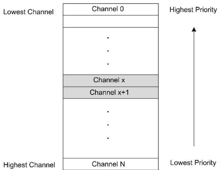
flowchart
graph TD
    A["Channel 0"] --> B["Channel x"]
    B --> C["Channel x+1"]
    C --> D["..."]
    D --> E["Channel N"]
    style A fill:#f9f,stroke:#333
    style B fill:#ccf,stroke:#333
    style C fill:#cfc,stroke:#333
    style D fill:#fcc,stroke:#333
    style E fill:#ffc,stroke:#333
Dynamic Arbitration within a priority level is selected by writing a '1' to PRICTRL0.RRLVLENx.
The dynamic arbitration scheme in the DMAC is round-robin. With the round-robin scheme, the channel number of the last channel being granted access will have the lowest priority the next time the arbiter has to grant access to a channel within the same priority level, as shown in Figure 25-6. The channel number of the last channel being granted access as the active channel is stored in the Level x Channel Priority Number bit group in the Priority Control 0 register (PRICTRL0.LVLPRIx) for the corresponding priority level.
Figure 25-6. Dynamic (Round-Robin) Priority Scheduling
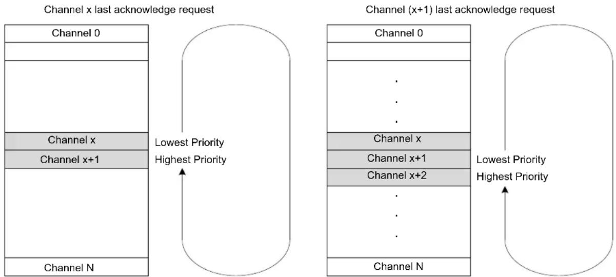
flowchart
graph TD
    subgraph "Channel x last acknowledge request"
        A["Channel 0"] --> B["Channel x"]
        B --> C["Channel x+1"]
        C --> D["..."]
        D --> E["Channel N"]
    end

    subgraph "Channel (x+1) last acknowledge request"
        F["Channel 0"] --> G["..."]
        G --> H["Channel x"]
        H --> I["Channel x+1"]
        I --> J["..."]
        J --> K["Channel N"]
    end

    style A fill:#f9f,stroke:#333
    style B fill:#f9f,stroke:#333
    style C fill:#f9f,stroke:#333
    style D fill:#f9f,stroke:#333
    style E fill:#f9f,stroke:#333
    style F fill:#f9f,stroke:#333
    style G fill:#f9f,stroke:#333
    style H fill:#f9f,stroke:#333
    style I fill:#f9f,stroke:#333
    style J fill:#f9f,stroke:#333
    style K fill:#f9f,stroke:#333
    note1["Lowest Priority Highest Priority"]
    note2["Lowest Priority Highest Priority"]
25.6.2.5 Data Transmission
Before the DMAC can perform a data transmission, a DMA channel has to be configured and enabled, its corresponding transfer descriptor has to be initialized, and the arbiter has to grant the DMA channel access as the active channel.
Once the arbiter has granted a DMA channel access as the active channel (refer to DMA Block Diagram section) the transfer descriptor for the DMA channel will be fetched from SRAM using the fetch bus, and stored in the internal memory for the active channel. For a new block transfer, the transfer descriptor will be fetched from the descriptor memory section (BASEADDR); For an ongoing block transfer, the descriptor will be fetched from the write-back memory section (WRBADDR). By using the data transfer bus, the DMAC will read the data from the current source address and write it to the current destination address. For further details on how the current source and destination addresses are calculated, refer to the section on Addressing.
The arbitration procedure is performed after each transfer. If the current DMA channel is granted access again, the block transfer counter (BTCNT) of the internal transfer descriptor will be decremented by the number of beats in a transfer, the optional output event Beat will be generated if configured and enabled, and the active channel will perform a new transfer. If a different DMA channel than the current active channel is granted access, the block transfer counter value will be written to the write-back section before the transfer descriptor of the newly granted DMA channel is fetched into the internal memory of the active channel.
When a block transfer has come to its end (BTCNT is zero), the Valid bit in the Block Transfer Control register will be cleared (BTCTRLVALID=0) before the entire transfer descriptor is written to the write-back memory. The optional interrupts, Channel Transfer Complete and Channel Suspend, and the optional output event Block, will be generated if configured and enabled. After the last block transfer in a transaction, the Next Descriptor Address register (DESCADDR) will hold the value 0x00000000, and the DMA channel will either be suspended or disabled, depending on the configuration in the Block Action bit group in the Block Transfer Control register (BTCTRL.BLOCKACT). If the transaction has further block transfers pending, DESCADDR will hold the SRAM address to the next transfer descriptor to be fetched. The DMAC will fetch the next descriptor into the internal memory of the active channel and write its content to the write-back section for the channel, before the arbiter gets to choose the next active channel.
25.6.2.6 Transfer Triggers and Actions
A DMA transfer through a DMA channel can be started only when a DMA transfer request is detected, and the DMA channel has been granted access to the DMA. A transfer request can be triggered from software, from a peripheral, or from an event. There are dedicated Trigger Source selections for each DMA Channel Control B (CHCTRLB.TRIGSRC).
The trigger actions are available in the Trigger Action bit group in the Channel Control B register (CHCTRLB.TRIGACT). By default, a trigger generates a request for a block transfer operation. If a single descriptor is defined for a channel, the channel is automatically disabled when a block transfer has been completed. If a list of linked descriptors is defined for a channel, the channel is automatically disabled when the last descriptor in the list is executed. If the list still has descriptors to execute, the channel will be waiting for the next block transfer trigger. When enabled again, the channel will wait for the next block transfer trigger. The trigger actions can also be configured to generate a request for a beat transfer (CHCTRLB.TRIGACT=0x2) or transaction transfer (CHCTRLB.TRIGACT=0x3) instead of a block transfer (CHCTRLB.TRIGACT=0x0).
Figure 25-7 shows an example where triggers are used with two linked block descriptors.
Figure 25-7. Trigger Action and Transfers
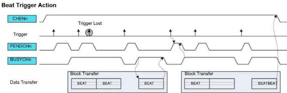
flowchart
graph TD
    A["CHENn"] --> B["Trigger Lost"]
    C["PENDCHn"] --> D["Trigger Lost"]
    E["BUSYCHn"] --> F["Trigger Lost"]
    G["Data Transfer"] --> H["Block Transfer"]
    H --> I["BEAT"]
    H --> J["BEAT"]
    H --> K["BEAT"]
    L["Block Transfer"] --> M["BEAT"]
    L --> N["BEAT"]
    L --> O["BEAT"]

flowchart
graph TD
    A["CHENn"] --> B["Trigger Lost"]
    C["PENDCHn"] --> B
    D["BUSYCHn"] --> B
    B --> E["Data Transfer"]
    E --> F["Block Transfer"]
    F --> G["BEAT"]
    F --> H["BEAT"]
    F --> I["BEAT"]
    F --> J["BEAT"]
    F --> K["BEAT"]
    F --> L["BEAT"]
    style A fill:#4CAF50,stroke:#388E3C
    style C fill:#4CAF50,stroke:#388E3C
    style D fill:#4CAF50,stroke:#388E3C
    style E fill:#FFA500,stroke:#388E3C
    style F fill:#FFA500,stroke:#388E3C
    style G fill:#FFA500,stroke:#388E3C
    style H fill:#FFA500,stroke:#388E3C
    style I fill:#FFA500,stroke:#388E3C
    style J fill:#FFA500,stroke:#388E3C
    style K fill:#FFA500,stroke:#388E3C
    style L fill:#FFA500,stroke:#388E3C
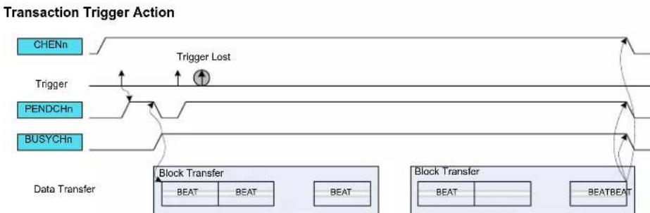
flowchart
graph TD
    A["CHENn"] --> B["Trigger Lost"]
    C["PENDCHn"] --> B
    D["BUSYCHn"] --> B
    B --> E["Data Transfer"]
    E --> F["Block Transfer"]
    F --> G["BEAT"]
    F --> H["BEAT"]
    F --> I["BEAT"]
    F --> J["BEAT"]
    F --> K["BEAT"]
    F --> L["BEAT"]
    style A fill:#e6f3ff,stroke:#333
    style C fill:#e6f3ff,stroke:#333
    style D fill:#e6f3ff,stroke:#333
    style E fill:#fff,stroke:#333
    style F fill:#fff,stroke:#333
    style G fill:#fff,stroke:#333
    style H fill:#fff,stroke:#333
    style I fill:#fff,stroke:#333
    style J fill:#fff,stroke:#333
    style K fill:#fff,stroke:#333
    style L fill:#fff,stroke:#333
If the trigger source generates a transfer request for a channel during an ongoing transfer, the new transfer request will be kept pending (CHSTATUS.PEND=1), and the new transfer can start after the ongoing one is done. Only one pending transfer can be kept per channel. If the trigger source
generates more transfer requests while one is already pending, the additional ones will be lost. All channels pending status flags are also available in the Pending Channels register (PENDCH).
When the transfer starts, the corresponding Channel Busy status flag is set in Channel Status register (CHSTATUS.BUSY). When the trigger action is complete, the Channel Busy status flag is cleared. All Channel Busy status flags are also available in the Busy Channels register (BUSYCH) in DMAC.
25.6.2.7 Addressing
Each block transfer needs to have both a source address and a destination address defined. The source address is set by writing the Transfer Source Address (SRCADDR)) register, the destination address is set by writing the Transfer Destination Address (DSTADDR) register.
The addressing of this DMAC module can be static or incremental, for either source or destination of a block transfer, or both.
Incrementation for the source address of a block transfer is enabled by writing the Source Address Incrementation Enable bit in the Block Transfer Control register (BTCTRL.SRCINC=1). The step size of the incrementation is configurable and can be chosen by writing the Step Selection bit in the Block Transfer Control register (BTCTRL.STEPSEL=1) and writing the desired step size in the Address Increment Step Size bit group in the Block Transfer Control register (BTCTRL.STEPSIZE). If BTCTRL.STEPSSEL=0, the step size for the source incrementation will be the size of one beat.
When source address incrementation is configured (BTCTRL.SRCINC=1), SRCADDR is calculated as follows:
If BTCTRL.STEPSEL= 1:
$$ \text { SRCADDR } = \text { SRCADDR } _ {\text { START }} + B T C N T \cdot B (\text { EATSIZE } + 1 \cdot 2) ^ {\text { STEPSIZE }} $$
If BTCTRL.STEPSEL=0:
$$ \text { SRCADDR } = \text { SRCADDR } _ {\text { START }} + B T C N T \cdot B E A T S I Z E + 1 \quad) $$
- SRCADDR START is the source address of the first beat transfer in the block transfer
- BTCNT is the initial number of beats remaining in the block transfer
- BEATSIZE is the configured number of bytes in a beat
- STEPSIZE is the configured number of beats for each incrementation
The following figure shows an example where DMA channel 0 is configured to increment the source address by one beat after each beat transfer (BTCTRL.SRCINC=1), and DMA channel 1 is configured to increment the source address by two beats (BTCTRL.SRCINC=1, BTCTRL.STEPSEL=1, and BTCTRL.STEPSIZE=0×1). As the destination address for both channels are peripherals, destination incrementation is disabled (BTCTRL.DSTINC=0).
Figure 25-8. Source Address Increment
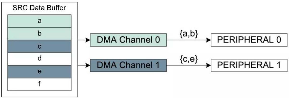
flowchart
graph LR
    A["SRC Data Buffer"] --> B["DMA Channel 0"]
    A --> C["DMA Channel 1"]
    B --> D["PERIPHERAL 0"]
    C --> E["PERIPHERAL 1"]
Incrementation for the destination address of a block transfer is enabled by setting the Destination Address Incrementation Enable bit in the Block Transfer Control register (BTCTRL.DSTINC=1). The step size of the incrementation is configurable by clearing BTCTRL.STEPSEL=0 and writing BTCTRL.STEPSIZE to the desired step size. If BTCTRL.STEPSEL=1, the step size for the destination incrementation will be the size of one beat.
When the destination address incrementation is configured (BTCTRL.DSTINC=1), DSTADDR must be set and calculated as follows:
| DSTADDR=DSTADDR START+BTCNT•BEATSIZE+1•2 ) STEPSIZE | where BTCTRL.STEPSEL is zero |
| DSTADDR=DSTADDR START+BTCNT•BEATSIZE+1 ) | where BTCTRL.STEPSEL is one |
- DSTADDR START is the destination address of the first beat transfer in the block transfer
- BTCNT is the initial number of beats remaining in the block transfer
- BEATSIZE is the configured number of bytes in a beat
- STEPSIZE is the configured number of beats for each incrementation
The following figure shows an example where DMA channel 0 is configured to increment destination address by one beat (BTCTRL.DSTINC=1) and DMA channel 1 is configured to increment destination address by two beats (BTCTRL.DSTINC=1, BTCTRL.STEPSEL=0, and BTCTRL.STEPSIZE=0x1). As the source address for both channels are peripherals, source incrementation is disabled (BTCTRL.SRCINC=0).
Figure 25-9. Destination Address Increment

flowchart
graph LR
    A["PERIPHERAL 0"] -->|{a,b}| B["DMA Channel 0"]
    C["PERIPHERAL 1"] -->|{c,d}| D["DMA Channel 1"]
    B --> E["DST Data Buffer"]
    D --> E
25.6.2.8 Error Handling
If a bus error is received from an AHB client during a DMA data transfer, the corresponding active channel is disabled and the corresponding Channel Transfer Error Interrupt flag in the Channel Interrupt Status and Clear register (CHINTFLAG.TERR) is set. If enabled, the optional transfer error interrupt is generated. The transfer counter will not be decremented and its current value is written-back in the write-back memory section before the channel is disabled.
When the DMAC fetches an invalid descriptor (BTCTRLVALID=0) or when the channel is resumed and the DMA fetches the next descriptor with null address (DESCADDR=0x00000000), the corresponding channel operation is suspended, the Channel Suspend Interrupt Flag in the Channel Interrupt Flag Status and Clear register (CHINTFLAG.SUSP) is set, and the Channel Fetch Error bit in the Channel Status register (CHSTATUS.FERR) is set. If enabled, the optional suspend interrupt is generated.
25.6.3 Additional Features
25.6.3.1 Linked Descriptors
A transaction can consist of either a single block transfer or of several block transfers. When a transaction consists of several block transfers it is done with the help of linked descriptors.
Figure 25-3 illustrates how linked descriptors work. When the first block transfer is completed on DMA channel 0, the DMAC fetches the next transfer descriptor, which is pointed to by the value stored in the Next Descriptor Address (DESCADDR) register of the first transfer descriptor. Fetching the next transfer descriptor (DESCADDR) is continued until the last transfer descriptor. When the block transfer for the last transfer descriptor is executed and DESCADDR=0x00000000, the transaction is terminated. For further details on how the next descriptor is fetched from SRAM, refer to section 25.6.2.5. Data Transmission.
25.6.3.1.1 Adding Descriptor to the End of a List
To add a new descriptor at the end of the descriptor list, create the descriptor in SRAM, with DESCADDR=0x00000000 indicating that it is the new last descriptor in the list, and modify the DESCADDR value of the current last descriptor to the address of the newly created descriptor.
25.6.3.1.2 Modifying a Descriptor in a List
In order to add descriptors to a linked list, the following actions must be performed:
- Enable the Suspend interrupt for the DMA channel.
- Enable the DMA channel.
- Reserve memory space in SRAM to configure a new descriptor.
- Configure the new descriptor:
- Set the next descriptor address (DESCADDR)
- Set the destination address (25.10.4. DSTADDR)
- Set the source address (25.10.3. SRCADDR)
- Configure the block transfer control (BTCTRL) including
- Optionally enable the suspend block action
-
Set the descriptor VALID bit
-
Clear the VALID bit for the existing list and for the descriptor which has to be updated.
-
Read DESCADDR from the write-back memory.
- If the DMA has not already fetched the descriptor that requires changes (i.e., DESCADDR is wrong):
- Update the DESCADDR location of the descriptor from the list
- Optionally clear the suspend block action
- Set the descriptor VALID bit to '1'
- Optionally enable the Resume Software command
- If the DMA is executing the same descriptor as the one that requires changes:
- Set the Channel Suspend Software command and wait for the suspend interrupt
- Update the next descriptor address (DESCRADDR) in the write-back memory
- Clear the interrupt sources and set the Resume Software command
- Update the DESCADDR location of the descriptor from the list
- Optionally clear the suspend block action
-
Set the descriptor VALID bit to '1'
-
Go to step 4 if needed.
25.6.3.1.3 Adding a Descriptor Between Existing Descriptors
To insert a new descriptor 'C' between two existing descriptors ('A' and 'B'), the descriptor currently executed by the DMA must be identified.
- If DMA is executing descriptor B, descriptor C cannot be inserted.
- If DMA has not started to execute descriptor A, follow the steps:
a. Set the descriptor A VALID bit to '0'.
b. Set the DESCADDR value of descriptor A to point to descriptor C instead of descriptor B.
c. Set the DESCADDR value of descriptor C to point to descriptor B.
d. Set the descriptor A VALID bit to '1'.
- If DMA is executing descriptor A:
a. Apply the software suspend command to the channel and
b. Perform steps 2.1 through 2.4.
c. Apply the software resume command to the channel.
25.6.3.2 Channel Suspend
The channel operation can be suspended at any time by software by writing a '1' to the Suspend command in the Command bit field of Channel Control B register (CHCTRLB.CMD). After the ongoing burst transfer is completed, the channel operation is suspended and the suspend command is automatically cleared.
When suspended, the Channel Suspend Interrupt flag in the Channel Interrupt Status and Clear register is set (CHINTFLAG.SUSP=1) and the optional suspend interrupt is generated.
By configuring the block action to suspend by writing Block Action bit group in the Block Transfer Control register (BTCTRL.BLOCKACT is 0x2 or 0x3), the DMA channel will be suspended after it has completed a block transfer. The DMA channel will be kept enabled and will be able to receive transfer triggers, but it will be removed from the arbitration scheme.
If an invalid transfer descriptor (BTCTRLVALID=0) is fetched from SRAM, the DMA channel will be suspended, and the Channel Fetch Error bit in the Channel Status register(CHASTATUS.FERR) will be set.
Note: Only enabled DMA channels can be suspended. If a channel is disabled when it is attempted to be suspended, the internal suspend command will be ignored.
For more details on transfer descriptors, refer to section 25.6.2.3. Transfer Descriptors.
25.6.3.3 Channel Resume and Next Suspend Skip
A channel operation can be resumed by software by setting the Resume command in the Command bit field of the Channel Control B register (CHCTRLB.CMD). If the channel is already suspended, the channel operation resumes from where it previously stopped when the Resume command is
detected. When the Resume command is issued before the channel is suspended, the next suspend action is skipped and the channel continues the normal operation.
Figure 25-10. Channel Suspend/Resume Operation
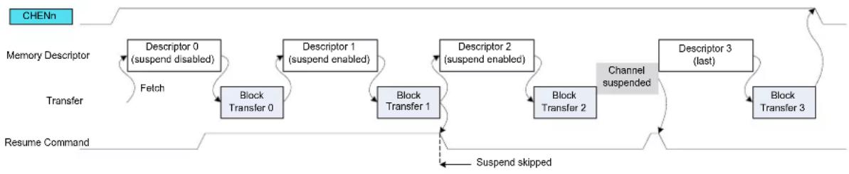
flowchart
graph TD
    A["CHENn"] --> B["Memory Descriptor"]
    B --> C["Transfer"]
    C --> D["Resume Command"]
    D --> E["Block Transfer 0"]
    E --> F["Descriptor 0 (suspend disabled)"]
    F --> G["Fetch"]
    G --> H["Block Transfer 1"]
    H --> I["Descriptor 1 (suspend enabled)"]
    I --> J["Block Transfer 2"]
    J --> K["Descriptor 2 (suspend enabled)"]
    K --> L["Block Transfer 3"]
    L --> M["Descriptor 3 (last)"]
    M --> N["Channel suspended"]
    N --> O["Block Transfer 2"]
    O --> P["Suspend skipped"]
    P --> Q["Block Transfer 3"]
    Q --> R["Descriptor 3"]
25.6.3.4 Event Input Actions
The event input actions are available only on the least significant DMA channels. For details on channels with event input support, refer to the in the Event system documentation.
Before using event input actions, the event controller must be configured first according to the following table, and the Channel Event Input Enable bit in the Channel Control B register (CHCTRLB.EVIE) must be written to '1'. Refer also to 25.6.6. Events.
Table 25-1. Event Input Action
| Action CHCTRLB.EVACT CHCTRLB.TRGSRC | |
| None NOACT - | |
| Normal Transfer TRIG DISABLE | |
| Conditional Transfer on Strobe TRIG any peripheral | |
| Conditional Transfer CTRIG | |
| Conditional Block Transfer CBLOCK | |
| Channel Suspend SUSPEND | |
| Channel Resume RESUME | |
| Skip Next Block Suspend SSKIP |
Normal Transfer
The event input is used to trigger a beat or burst transfer on peripherals.
The event is acknowledged as soon as the event is received. When received, both the Channel Pending Status bit in the Channel Status register (CHSTATUS.PEND) and the corresponding Channel n bit in the Pending Channels register (25.8.13. PENDCH.PENDCHn) are set. If the event is received while the channel is pending, the event trigger is lost.
The figure below shows an example where beat transfers are enabled by internal events.
Figure 25-11. Beat Event Trigger Action
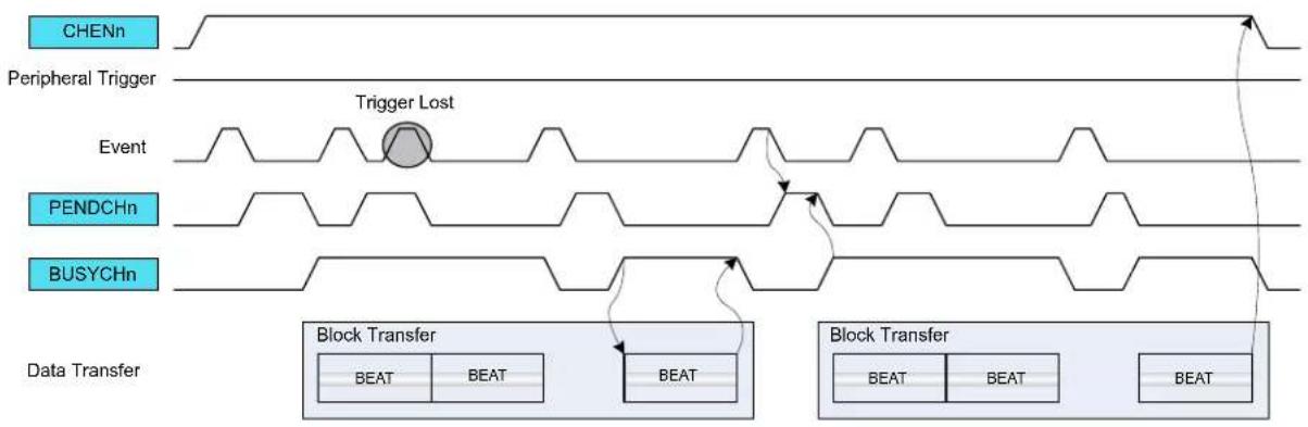
flowchart
graph TD
    A["CHENn"] --> B["Peripheral Trigger"]
    B --> C["Event"]
    C --> D["PENDCHn"]
    D --> E["BUSYCHn"]
    E --> F["Data Transfer"]
    F --> G["Trigger Lost"]
    G --> H["Block Transfer"]
    H --> I["BEAT"]
    H --> J["BEAT"]
    H --> K["BEAT"]
    H --> L["BEAT"]
    H --> M["BEAT"]
    H --> N["BEAT"]
Conditional Transfer on Strobe
The event input is used to trigger a transfer on peripherals with pending transfer requests. This event action is intended to be used with peripheral triggers (e.g., for timed communication protocols or periodic transfers between peripherals) only when the peripheral trigger coincides with the occurrence of a (possibly cyclic) event the transfer is issued.
The event is acknowledged as soon as the event is received. The peripheral trigger request is stored internally when the previous trigger action is completed (i.e., the channel is not pending) and when an active event is received. If the peripheral trigger is active, the DMA will wait for an event before the peripheral trigger is internally registered. When both event and peripheral transfer trigger are active, both CHSTATUS.PEND and 25.8.13. PENDCH.PENDCHn are set. A software trigger will now trigger a transfer.
The figure below shows an example where the peripheral beat transfer is started by a conditional strobe event action.
Figure 25-12. Periodic Event with Beat Peripheral Triggers
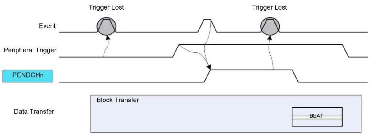
flowchart
graph TD
    A["Event"] --> B["Trigger Lost"]
    C["Peripheral Trigger"] --> D["Trigger Lost"]
    E["PENDCHn"] --> F["Trigger Lost"]
    G["Data Transfer"] --> H["Block Transfer"]
    I["BEAT"] --> J["Output"]
Conditional Transfer
The event input is used to trigger a conditional transfer on peripherals with pending transfer requests. For example, this type of event can be used for peripheral-to-peripheral transfers, where one peripheral is the source of event and the second peripheral is the source of the trigger.
Each peripheral trigger is stored internally when the event is received. When the peripheral trigger is stored internally, the Channel Pending Status bit is set (CHSTATUS.PEND), the respective Pending Channel n Bit in the Pending Channels register is set (25.8.13. PENDCH.PENDCHn), and the event is acknowledged. A software trigger will now trigger a transfer.
The figure below shows an example where conditional event is enabled with peripheral beat trigger requests.
Figure 25-13. Conditional Event with Beat Peripheral Triggers
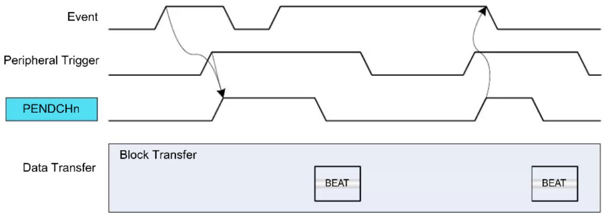
flowchart
graph TD
    A["Event"] --> B["Peripheral Trigger"]
    B --> C["PENDCHn"]
    C --> D["Data Transfer"]
    D --> E["Block Transfer"]
    E --> F["BEAT"]
    E --> G["BEAT"]
Conditional Block Transfer
The event input is used to trigger a conditional block transfer on peripherals.
Before starting transfers within a block, an event must be received. When received, the event is acknowledged when the block transfer is completed. A software trigger will trigger a transfer.
The figure below shows an example where conditional event block transfer is started with peripheral beat trigger requests.
Figure 25-14. Conditional Block Transfer with Beat Peripheral Triggers
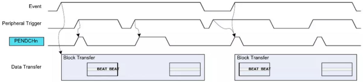
flowchart
graph TD
    A["Event"] --> B["Peripheral Trigger"]
    B --> C["PENDCHn"]
    C --> D["Data Transfer"]
    D --> E["Block Transfer"]
    E --> F["BEAT BEAT"]
    E --> G["Block Transfer"]
    G --> H["BEAT BEAT"]
Channel Suspend
The event input is used to suspend an ongoing channel operation. The event is acknowledged when the current AHB access is completed. For further details on Channel Suspend, refer to 25.6.3.2. Channel Suspend.
Channel Resume
The event input is used to resume a suspended channel operation. The event is acknowledged as soon as the event is received and the Channel Suspend Interrupt Flag (CHINTFLAG.SUSP) is cleared. For further details refer to 25.6.3.2. Channel Suspend.
Skip Next Block Suspend
This event can be used to skip the next block suspend action. If the channel is suspended before the event rises, the channel operation is resumed and the event is acknowledged. If the event rises before a suspend block action is detected, the event is kept until the next block suspend detection. When the block transfer is completed, the channel continues the operation (not suspended) and the event is acknowledged.
25.6.3.5 Event Output Selection
Event output selection is available only for the Least Significant DMA channels. The pulse width of an event output from a channel is one AHB clock cycle.
The output of channel events is enabled by writing a '1' to the Channel Event Output Enable bit in the Control B register (CHCTRLB.EVOE). The event output cause is selected by writing to the Event Output Selection bits in the Block Transfer Control register (BTCTRL.EVOSEL). It is possible to generate events after each block transfer (BTCTRL.EVOSEL=0x1) or beat transfer (BTCTRL.EVOSEL=0x3). To enable an event being generated when a transaction is complete, the block event selection must be set in the last transfer descriptor only.
Figure 25-15 shows an example where the event output generation is enabled in the first block transfer, and disabled in the second block.
Figure 25-15. Event Output Generation
Beat Event Output
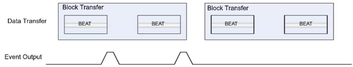
flowchart
graph LR
    A["Data Transfer"] --> B["Block Transfer"]
    B --> C["Event Output"]
    D["Block Transfer"] --> E["Event Output"]
    F["Event Output"] --> G["Event Output"]
Block Event Output

flowchart
graph LR
    A["Event Output"] --> B["Block Transfer"]
    B --> C["Data Transfer"]
    C --> D["Block Transfer"]
    D --> E["Event Output"]
25.6.3.6 Aborting Transfers
Transfers on any channel can be aborted gracefully by software by disabling the corresponding DMA channel. It is also possible to abort all ongoing or pending transfers by disabling the DMAC.
When a DMA channel disable request or DMAC disable request is detected:
- Ongoing transfers of the active channel will be disabled when the ongoing beat transfer is completed and the write-back memory section is updated. This prevents transfer corruption before the channel is disabled.
- All other enabled channels will be disabled in the next clock cycle.
The corresponding Channel Enable bit in the Channel Control A register is cleared (CHCTRLA.ENABLE=0) when the channel is disabled.
The corresponding DMAC Enable bit in the Control register is cleared (CTRL.DMAENABLE=0) when the entire DMAC module is disabled.
25.6.3.7 CRC Operation
A Cyclic Redundancy Check (CRC) is an error detection technique used to find errors in data. It is commonly used to determine whether the data during a transmission, or data present in data and
program memories has been corrupted or not. A CRC takes a data stream or a block of data as input and generates a 16- or 32-bit output that can be appended to the data and used as a checksum.
When the data is received, the device or application repeats the calculation using the DSU's CRC engine. If the new CRC result does not match the one calculated earlier, the block contains a data error. The application will then detect this and may take a corrective action, such as requesting the data to be sent again or simply not using the incorrect data.
The CRC engine in DMAC supports two commonly used CRC polynomials: CRC-16 (CRC-CCITT) and CRC-32 (IEEE 802.3). Typically, applying CRC-n (CRC-16 or CRC-32) to a data block of arbitrary length will detect any single alteration that is ≤n bits in length, and will detect the fraction 1-2-n of all longer error bursts.
• CRC-16:
- Polynomial: x^16 + x^12 + x^5 + 1
- Hex value: 0x1021
• CRC-32:
- Polynomial: x^32 + x^26 + x^23 + x^22 + x^16 + x^12 + x^11 + x^10 + x^8 + x^7 + x^5 + x^4 + x^2 + x + 1
- Hex value: 0x04C11DB7
The data source for the CRC engine can either be one of the DMA channels or the APB bus interface, and must be selected by writing to the CRC Input Source bits in the CRC Control register (CRCCTRL.CRCSRC). The CRC engine then takes data input from the selected source and generates a checksum based on these data. The checksum is available in the CRC Checksum register (CRCCHKSUM). When CRC-32 polynomial is used, the final checksum read is bit reversed and complemented, as shown in CRC Generator Block Diagram.
The CRC polynomial is selected by writing to the CRC Polynomial Type bit in the CRC Control register (CRCCTRL.CRCPOLY), the default is CRC-16. The CRC engine operates on byte only. When the DMA is used as data source for the CRC engine, the DMA channel beat size setting will be used. When used with APB bus interface, the application must select the CRC Beat Size bit field of CRC Control register (CRCCTRL.CRCBEATSIZE). 8-, 16-, or 32-bit bus transfer access type is supported. The corresponding number of bytes will be written in the CRCDATAIN register and the CRC engine will operate on the input data in a byte by byte manner.
Figure 25-16. CRC Generator Block Diagram
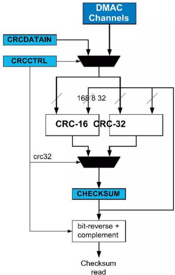
flowchart
graph TD
    A["DMAC Channels"] --> B["CRCDATAIN"]
    A --> C["CRCCTRL"]
    B --> D["CRC-16 CRC-32"]
    C --> D
    D --> E["CRC-16 CRC-32"]
    E --> F["csrc32"]
    F --> G["CHECKSUM"]
    G --> H["bit-reverse + complement"]
    H --> I["Checksum read"]
    D --> J["168 8 32"]
    J --> D
CRC on DMA data CRC-16 or CRC-32 calculations can be performed on data passing through any DMA channel. Once a DMA channel is selected as the source, the CRC engine will continuously generate the CRC on the data passing through the DMA channel. The checksum is available for readout once the DMA transaction is completed or aborted. A CRC can also be generated on SRAM, Flash, or I/O memory by passing these data through a DMA channel. If the latter is done, the destination register for the DMA data can be the data input (CRCDATAIN) register in the CRC engine.
CRC using the I/O interface Before using the CRC engine with the I/O interface, the application must set the CRC Beat Size bits in the CRC Control register (CRCCTRL.CRCBEATSIZE). 8/16/32-bit bus transfer type can be selected.
CRC can be performed on any data by loading them into the CRC engine using the CPU and writing the data to the CRCDATAIN register. Using this method, an arbitrary number of bytes can be written to the register by the CPU, and CRC is done continuously for each byte. This means if a 32-bit data is written to the CRCDATAIN register the CRC engine takes four cycles to calculate the CRC. The CRC complete is signaled by a set CRCBUSY bit in the CRCSTATUS register. New data can be written only when CRCBUSY flag is not set.
25.6.4 DMA Operation
Not applicable.
25.6.5 Interrupts
The DMAC channels have the following interrupt sources:
- Transfer Complete (TCMPL): Indicates that a block transfer is completed on the corresponding channel. Refer to 25.6.2.5. Data Transmission for details.
- Transfer Error (TERR): Indicates that a bus error has occurred during a burst transfer, or that an invalid descriptor has been fetched. Refer to 25.6.2.8. Error Handling for details.
- Channel Suspend (SUSP): Indicates that the corresponding channel has been suspended. Refer to 25.6.3.2. Channel Suspend and 25.6.2.5. Data Transmission for details.
Each interrupt source has an Interrupt flag associated with it. The Interrupt flag in the Channel Interrupt Flag Status and Clear (CHINTFLAG) register is set when the Interrupt condition occurs. Each interrupt can be individually enabled by setting the corresponding bit in the Channel Interrupt Enable Set register (CHINTENSET=1), and disabled by setting the corresponding bit in the Channel Interrupt Enable Clear register (CHINTENCLR=1). The status of enabled interrupts can be read from either INTENSET or INTENCLR.
An interrupt request is generated when the Interrupt flag is set and the corresponding interrupt is enabled. The interrupt request remains active until the Interrupt flag is cleared, the interrupt is disabled, the DMAC is reset or the corresponding DMA channel is reset. See CHINTFLAG for details on how to clear Interrupt flags. All interrupt requests are ORed together on system level to generate one combined interrupt request to the NVIC.
The user must read the Channel Interrupt Status (INTSTATUS) register to identify the channels with pending interrupts and must read the Channel Interrupt Flag Status and Clear (CHINTFLAG) register to determine which Interrupt condition is present for the corresponding channel. It is also possible to read the Interrupt Pending register (INTPEND), which provides the lowest channel number with pending interrupt and the respective Interrupt flags.
Note: Interrupts must be globally enabled for interrupt requests to be generated.
References:
Nested Vector Interrupt Controller
25.6.6 Events
The DMAC can generate the following output events:
- Channel (CH): Generated when a block transfer for a given channel has been completed, or when a beat transfer within a block transfer for a given channel has been completed. Refer to Event Output Selection for details.
Setting the Channel Control B Event Output Enable bit (CHCTRLB.EVOE=1) enables the corresponding output event configured in the Event Output Selection bit group in the Block Transfer Control register (BTCTRL.EVOSEL).
Clearing CHCTRLB.EVOE=0 disables the corresponding output event.
The DMAC can take the following actions on an input event:
- Transfer and Periodic Transfer Trigger (TRIG): normal transfer or periodic transfers on peripherals are enabled
- Conditional Transfer Trigger (CTRIG): conditional transfers on peripherals are enabled
- Conditional Block Transfer Trigger (CBLOCK): conditional block transfers on peripherals are enabled
- Channel Suspend Operation (SUSPEND): suspend a channel operation
- Channel Resume Operation (RESUME): resume a suspended channel operation
- Skip Next Block Suspend Action (SSKIP): skip the next block suspend transfer condition
- Increase Priority (INCPRI): increase channel priority
Setting the Channel Control B Event Input Enable bit (CHCTRLB.EVIE=1) enables the corresponding action on input event. Clearing this bit disables the corresponding action on input event. Note that several actions can be enabled for incoming events. If several events are connected to the peripheral, any enabled action will be taken for any of the incoming events. For further details on event input actions, refer to Event Input Actions.
Note: Event input and outputs are not available for every channel. Refer to the Features section for more information.
25.6.7 Sleep Mode Operation
Each DMA channel can be configured to operate in any sleep mode. To be able to run in standby, the RUNSTDBY bit in Channel Control A register (CHCTRLA.RUNSTDBY) must be written to '1'. The DMAC can wake up the device using interrupts from any sleep mode or perform actions through the Event System.
For channels with CHCTRLA.RUNSTDBY = 0, it is up to software to stop DMA transfers on these channels and wait for completion before going to standby mode using the following sequence:
- Suspend the DMAC channels for which CHCTRLA.RUNSTDBY = 0.
- Check the SYNCBUSY bits of registers accessed by the DMAC channels being suspended.
- Go to sleep.
- When the device wakes up, resume the suspended channels.
Note: In Stand-by Sleep mode, the DMAC can only access RAM when it is not back biased (PM.STDBYCFG.BBIASxx = 0x0)
Note: In Stand-by Sleep mode, the DMAC can access the SRAM only when the power domain PD1 is not in retention and PM.STDBYCFG.BBIASLP=0x0. The DMAC can access the SRAM in Stand-by Sleep mode only when the power domain PD2 is not in retention and PM.STDBYCFG.BBIASHS = 0x0.
25.6.8 Synchronization
Not applicable.
25.7 Register Summary
| Offset | Name Bit Pos. 7 6 | 5 4 3 2 1 | 0 | ||||||||
| 0x00 CTRL | 7:0 | CRCENABLE DMAENABLE SWRST | |||||||||
| 15:8 | LVLEN3 LVLEN2 LVLEN1 LVLEN0 | ||||||||||
| 0x02 CRCCTRL | 7:0 | CRCPOLY[1:0] | CRCBEATSIZE[1:0] | ||||||||
| 15:8 | CRCSRC[5:0] | ||||||||||
| 0x04 | CRCDATAIN | 7:0 | CRCDATAIN[7:0] | ||||||||
| 15:8 | CRCDATAIN[15:8] | ||||||||||
| 23:16 | CRCDATAIN[23:16] | ||||||||||
| 31:24 | CRCDATAIN[31:24] | ||||||||||
| 0x08 | CRCCHKSUM | 7:0 | CRCCHKSUM[7:0] | ||||||||
| 15:8 | CRCCHKSUM[15:8] | ||||||||||
| 23:16 | CRCCHKSUM[23:16] | ||||||||||
| 31:24 | CRCCHKSUM[31:24] | ||||||||||
| 0x0C | CRCSTATUS | 7:0 | CRCZERO | CRCBUSY | |||||||
| 0x0D | DBGCTRL | 7:0 | DBGRUN | ||||||||
| 0x0E | QOSCTRL | 7:0 | DQOS[1:0] | FQOS[1:0] | WRBQOS[1:0] | ||||||
| 0x0F Reserved | |||||||||||
| 0x10 | SWTRIGCTRL | 7:0 | SWTRIG7 | SWTRIG6 | SWTRIG5 | SWTRIG4 | SWTRIG3 | SWTRIG2 | SWTRIG1 | SWTRIG0 | |
| 15:8 | SWTRIG15 | SWTRIG14 | SWTRIG13 | SWTRIG12 | SWTRIG11 | SWTRIG10 | SWTRIG9 | SWTRIG8 | |||
| 23:16 | |||||||||||
| 31:24 | |||||||||||
| 0x14 PRICTRL0 | 7:0 | RRLVLEN0 | LVLPRIO[3:0] | ||||||||
| 15:8 | RRLVLEN1 | LVLPRI1[3:0] | |||||||||
| 23:16 | RRLVLEN2 | LVLPRI2[3:0] | |||||||||
| 31:24 | RRLVLEN3 | LVLPRI3[3:0] | |||||||||
| 0x18 ... 0x1F | Reserved | ||||||||||
| 0x20 INTPEND | 7:0 | ID[3:0] | |||||||||
| 15:8 | PEND | BUSY | FERR | SUSP | TCMPL | TERR | |||||
| 0x22 ... 0x23 | Reserved | ||||||||||
| 0x24 | INTSTATUS | 7:0 | CHINT7 | CHINT6 | CHINT5 | CHINT4 | CHINT3 | CHINT2 | CHINT1 | CHINT0 | |
| 15:8 | CHINT15 | CHINT14 | CHINT13 | CHINT12 | CHINT11 | CHINT10 | CHINT9 | CHINT8 | |||
| 23:16 | |||||||||||
| 31:24 | |||||||||||
| 0x28 | BUSYCH | 7:0 | BUSYCH7 | BUSYCH6 | BUSYCH5 | BUSYCH4 | BUSYCH3 | BUSYCH2 | BUSYCH1 | BUSYCH0 | |
| 15:8 | BUSYCH15 | BUSYCH14 | BUSYCH13 | BUSYCH12 | BUSYCH11 | BUSYCH10 | BUSYCH9 | BUSYCH8 | |||
| 23:16 | |||||||||||
| 31:24 | |||||||||||
| 0x2C | PENDCH | 7:0 | PENDCH7 | PENDCH6 | PENDCH5 | PENDCH4 | PENDCH3 | PENDCH2 | PENDCH1 | PENDCH0 | |
| 15:8 | PENDCH15 | PENDCH14 | PENDCH13 | PENDCH12 | PENDCH11 | PENDCH10 | PENDCH9 | PENDCH8 | |||
| 23:16 | |||||||||||
| 31:24 | |||||||||||
| 0x30 | ACTIVE | 7:0 | LVLEX3 | LVLEX2 | LVLEX1 | LVLEX0 | |||||
| 15:8 | ABUSY | ID[4:0] | |||||||||
| 23:16 | BTCNT[7:0] | ||||||||||
| 31:24 | BTCNT[15:8] | ||||||||||
| 0x34 | BASEADDR | 7:0 | BASEADDR[7:0] | ||||||||
| 15:8 | BASEADDR[15:8] | ||||||||||
| 23:16 | BASEADDR[23:16] | ||||||||||
| 31:24 | BASEADDR[31:24] | ||||||||||
| 0x38 WRBADDR | 7:0 | WRBADDR[7:0] | |||||||||
| 15:8 | WRBADDR[15:8] | ||||||||||
| 23:16 | WRBADDR[23:16] | ||||||||||
| 31:24 | WRBADDR[31:24] | ||||||||||
| 0x3C ... 0x3E | Reserved | ||||||||||
| ......continued | ||||||||||
| Offset | Name Bit Pos. 76543210 | |||||||||
| 0x3F CHID 7:0 ID[3:0] | ||||||||||
| 0x40 CHCTRLA 7:0 RUNSTDBY ENABLE SWRST | ||||||||||
| 0x41 ... 0x43 | Reserved | |||||||||
| 0x44 CHCTRLB | 7:0 | LVL[1:0] | EVOE | EVIE | EVACT[2:0] | |||||
| 15:8 | TRIGSRC[5:0] | |||||||||
| 23:16 TRIGACT[1:0] | ||||||||||
| 31:24 | CMD[1:0] | |||||||||
| 0x48 ... 0x4B | Reserved | |||||||||
| 0x4C | CHINTENCLR | 7:0 | SUSP | TCMPL | TERR | |||||
| 0x4D | CHINTENSET | 7:0 | SUSP | TCMPL | TERR | |||||
| 0x4E | CHINTFLAG | 7:0 | SUSP | TCMPL | TERR | |||||
| 0x4F | CHSTATUS | 7:0 | FERR | BUSY | PEND | |||||
25.8 Register Description
Registers can be 8, 16, or 32 bits wide. Atomic 8-, 16- and 32-bit accesses are supported. In addition, the 8-bit quarters and 16-bit halves of a 32-bit register, and the 8-bit halves of a 16-bit register can be accessed directly.
Some registers are optionally write-protected by the Peripheral Access Controller (PAC). Optional PAC write protection is denoted by the "PAC Write-Protection" property in each individual register description. For details, refer to 25.5.8. Register Access Protection.
Some registers are enable-protected, meaning they can only be written when the peripheral is disabled. Enable-protection is denoted by the "Enable-Protected" property in each individual register description.
25.8.1 Control
Name: CTRL
Offset: 0x00
Reset: 0x00X0
Property: PAC Write-Protection, Enable-Protected
Bit 15 14 13 12 11 10 9 8
| LVLEN3 LVLEN2 LVLEN1 LVLEND | |||||
| Access Reset | R/W R/W R/W R/W0 0 0 0 | ||||
Bit 76543210
| CRCENABLE DMAENABLE SWRST | |||||
| Access Reset | R/W R/W R/W0 0 0 | ||||
Bits 8, 9, 10, 11 - LVLENx Priority Level x Enable [x=0..3]
When this bit is set, all requests with the corresponding level will be fed into the arbiter block. When cleared, all requests with the corresponding level will be ignored.
For details on arbitration schemes, refer to the Arbitration section.
These bits are not enable-protected.
| Value | Description |
| 0 | Transfer requests for Priority level x will not be handled |
| 1 | Transfer requests for Priority level x will be handled |
Bit 2 - CRCENABLE CRC Enable
Writing a '0' to this bit will disable the CRC calculation when the CRC Status Busy flag is cleared (CRCSTATUS. CRCBUSY). The bit is zero when the CRC is disabled.
Writing a '1' to this bit will enable the CRC calculation.
This bit is not enable-protected.
| Value | Description |
| 0 | The CRC calculation is disabled |
| 1 | The CRC calculation is enabled |
Bit 1 - DMAENABLE DMA Enable
Setting this bit will enable the DMA module.
Writing a '0' to this bit will disable the DMA module. When writing a '0' during an ongoing transfer, the bit will not be cleared until the internal data transfer buffer is empty and the DMA transfer is aborted. The internal data transfer buffer will be empty once the ongoing burst transfer is completed.
This bit is not enable-protected.
| Value | Description |
| 0 | The peripheral is disabled |
| 1 | The peripheral is enabled |
Bit 0 - SWRST Software Reset
Writing a '0' to this bit has no effect.
Writing a '1' to this bit when both the DMAC and the CRC module are disabled (DMAENABLE and CRCENABLE are '0') resets all registers in the DMAC (except DBGCTRL) to their initial state. If either the DMAC or CRC module is enabled, the Reset request will be ignored and the DMAC will return an access error.
| Value | Description |
| 0 | There is no Reset operation ongoing |
Value Description
1 A Reset operation is ongoing
25.8.2 CRC Control
Name: CRCCTRL
Offset: 0x02
Reset: 0x0000
Property: PAC Write-Protection, Enable-Protected
| Bit 15 14 13 12 11 10 9 8 | |||
| CRCSRC[5:0] | |||
| Access Reset 0 0 0 0 0 0 | R/W R/W R/W R/W R/W R/W | ||
| Bit 7 6 5 4 3 2 1 0 | |||
| CRCPOLY[1:0] | CRCBEATSIZE[1:0] | ||
| Access Reset | R/W R/W R/W R/W | ||
| 0 0 0 0 | |||
Bits 13:8 - CRCSRC[5:0] CRC Input Source
These bits select the input source for generating the CRC, as shown in the table below. The selected source is locked until either the CRC generation is completed or the CRC module is disabled. This means the CRCSRC cannot be modified when the CRC operation is ongoing. The lock is signaled by the CRCBUSY Status bit. CRC generation complete is generated and signaled from the selected source when used with the DMA channel.
| Value | Name | Description |
| 0x00 | NOACT | No action |
| 0x01 | IO | I/O interface |
| 0x02-0x1F | - | Reserved |
| 0x20 | CH0 | DMA channel 0 |
| 0x21 | CH1 | DMA channel 1 |
| 0x22 | CH2 | DMA channel 2 |
| 0x23 | CH3 | DMA channel 3 |
| 0x24 | CH4 | DMA channel 4 |
| 0x25 | CH5 | DMA channel 5 |
| 0x26 | CH6 | DMA channel 6 |
| 0x27 | CH7 | DMA channel 7 |
| 0x28 | CH8 | DMA channel 8 |
| 0x29 | CH9 | DMA channel 9 |
| 0x2A | CH10 | DMA channel 10 |
| 0x2B | CH11 | DMA channel 11 |
Bits 3:2 - CRCPOLY[1:0] CRC Polynomial Type
These bits define the size of the data transfer for each bus access when the CRC is used with I/O interface, as shown in the table below.
| Value | Name | Description |
| 0x0 | CRC16 | CRC-16 (CRC-CCITT) |
| 0x1 | CRC32 | CRC32 (IEEE 802.3) |
| 0x2-0x3 | Reserved |
Bits 1:0 - CRCBEATSIZE[1:0] CRC Beat Size
These bits define the size of the data transfer for each bus access when the CRC is used with I/O interface.
| Value | Name | Description |
| 0x0 | BYTE | 8-bit bus transfer |
| 0x1 | HWORD | 16-bit bus transfer |
| Value Name | Description | |
| 0x2 | WORD 32-bit bus transfer | |
| 0x3 | Reserved | |
25.8.3 CRC Data Input
Name: CRCDATAIN
Offset: 0x04
Reset: 0x00000000
Property: PAC Write Protection
Bit 31 30 29 28 27 26 25 24
CRCDATAIN[31:24]
Access R/W R/W R/W R/W R/W R/W R/W R/W
Reset 00000000
Bit 23 22 21 20 19 18 17 16
CRCDATAIN[23:16]
Access R/W R/W R/W R/W R/W R/W R/W R/W
Reset 00000000
Bit 15 14 13 12 11 10 9 8
CRCDATAIN[15:8]
Access R/W R/W R/W R/W R/W R/W R/W R/W
Reset 00000000
Bit 76543210
CRCDATAIN[7:0]
Access R/W R/W R/W R/W R/W R/W R/W R/W
Reset 00000000
Bits 31:0 - CRCDATAIN[31:0] CRC Data Input
These bits store the data for which the CRC checksum is computed. A new CRC checksum is ready (CRCBEAT+ 1) clock cycles after the CRCDATAIN register is written.
25.8.4 CRC Checksum
Name: CRCCHKSUM
Offset: 0x08
Reset: 0x00000000
Property: PAC Write Protection, Enable-Protected
The CRCCHKSUM represents the 16- or 32-bit checksum value and the generated CRC. The register is reset to zero by default, but it is possible to reset all bits to one by writing the CRCCHKSUM register directly. It is possible to write this register only when the CRC module is disabled. If CRC-32 is selected and the CRC Status Busy flag is cleared (i.e., CRC generation is completed or aborted), the bit reversed (bit 31 is swapped with bit 0, bit 30 with bit 1, etc.) and complemented result will be read from CRCCHKSUM. If CRC-16 is selected or the CRC Status Busy flag is set (i.e., CRC generation is ongoing), CRCCHKSUM will contain the actual content.
Bit 31 30 29 28 27 26 25 24
| CRCCHKSUM[31:24] | |
| Access R/W R/W R/W R/W R/W R/W R/W R/W Reset 0 0 0 0 0 0 0 0 | |
| Bit 23 22 21 20 19 18 17 16 | |
| CRCCHKSUM[23:16] | |
| Access R/W R/W R/W R/W R/W R/W R/W R/W Reset 0 0 0 0 0 0 0 0 | |
| Bit 15 14 13 12 11 10 9 8 | |
| CRCCHKSUM[15:8] | |
| Access R/W R/W R/W R/W R/W R/W R/W R/W Reset 0 0 0 0 0 0 0 0 | |
| Bit 7 6 5 4 3 2 1 0 | |
| CRCCHKSUM[7:0] | |
| Access R/W R/W R/W R/W R/W R/W R/W R/W Reset 0 0 0 0 0 0 0 0 | |
Bits 31:0 - CRCCHKSUM[31:0] CRC Checksum
These bits store the generated CRC result. The 16 MSB bits are always read zero when CRC-16 is enabled.
25.8.5 CRC Status
Name: CRCSTATUS
Offset: 0x0C
Reset: 0x00
Property: PAC Write Protection
Bit 76543210
| CRCZERO CRCBUSY | ||||||
| Access Reset 0 0 | R R/W | |||||
Bit 1 - CRCZERO CRC Zero
This bit is cleared when a new CRC source is selected.
This bit is set when the CRC generation is complete and the CRC checksum is zero.
When running CRC-32 and appending the checksum at the end of the packet (as little endian), the final checksum should be 0x2144df1c, and not zero. However, if the checksum is complemented before it is appended (as little endian) to the data, the final result in the checksum register will be zero. See the description of CRCCHKSUM to read out different versions of the checksum.
Bit 0 - CRCBUSY CRC Module Busy
This flag is cleared by writing a one to it when used with I/O interface. When used with a DMA channel, the bit is set when the corresponding DMA channel is enabled, and cleared when the corresponding DMA channel is disabled. This register bit cannot be cleared by the application when the CRC is used with a DMA channel.
This bit is set when a source configuration is selected and as long as the source is using the CRC module.
25.8.6 Debug Control
Name: DBGCTRL
Offset: 0x0D
Reset: 0x00
Property: PAC Write Protection
Bit 76543210
| DBGRUN | |||||||
| Access Reset 0 | R/W | ||||||
Bit 0 - DBGRUN Debug Run
This bit is not reset by a Software Reset.
This bit controls the functionality when the CPU is halted by an external debugger.
| Value Description | |
| 0 | The DMAC is halted when the CPU is halted by an external debugger. |
| 1 | The DMAC continues normal operation when the CPU is halted by an external debugger. |
25.8.7 Quality of Service Control
Name: QOSCTRL
Offset: 0x0E
Reset: 0x2A
Property: PAC Write Protection
Bit 76543210
| DQOS[1:0] FQOS[1:0] WRBQOS[1:0] | |||
| Access | R/W R/W R/W R/W R/W R/W | ||
| Reset 1 0 1 0 1 0 | |||
These bits define the memory priority access during the data transfer operation.
| DQOS[1:0] | Name | Description |
| 0x0 | DISABLE | Background (no sensitive operation) |
| 0x1 | LOW | Sensitive Bandwidth |
| 0x2 | MEDIUM | Sensitive Latency |
| 0x3 | HIGH | Critical Latency |
Bits 3:2 - FQOS[1:0] Fetch Quality of Service
These bits define the memory priority access during the fetch operation.
| FQOS[1:0] | Name | Description |
| 0x0 | DISABLE | Background (no sensitive operation) |
| 0x1 | LOW | Sensitive Bandwidth |
| 0x2 | MEDIUM | Sensitive Latency |
| 0x3 | HIGH | Critical Latency |
Bits 1:0 - WRBQOS[1:0] Write-Back Quality of Service
These bits define the memory priority access during the write-back operation.
| WRBQOS[1:0] | Name | Description |
| 0x0 | DISABLE | Background (no sensitive operation) |
| 0x1 | LOW | Sensitive Bandwidth |
| 0x2 | MEDIUM | Sensitive Latency |
| 0x3 | HIGH | Critical Latency |
25.8.8 Software Trigger Control
Name: SWTRIGCTRL
Offset: 0x10
Reset: 0x00000000
Property: PAC Write Protection
| Bit 31 30 29 28 27 26 25 24 | |||||||
| Access Reset | |||||||
| Bit 23 22 21 20 19 18 17 16 | |||||||
| Access Reset | |||||||
| Bit 15 14 13 12 11 10 9 8 | |||||||
| Access Reset | SWTRIG15 R/W 0 0 0 0 0 0 0 | SWTRIG14 R/W | R/W | R/W | R/W | R/W | R/W |
| Bit 7 6 5 4 3 2 1 0 | |||||||
| Access Reset | SWTRIG7 R/W 0 0 0 0 0 0 0 | SWTRIG6 R/W | SWTRIG5 R/W | SWTRIG4 R/W | SWTRIG3 R/W | SWTRIG2 R/W | SWTRIG1 R/W |
Bits 0, 1, 2, 3, 4, 5, 6, 7, 8, 9, 10, 11, 12, 13, 14, 15 - SWTRIGn Channel n Software Trigger [n = 0..15]
This bit is cleared when the Channel Pending bit in the Channel Status register (CHSTATUS.PEND) for the corresponding channel is either set, or by writing a '1' to it.
This bit is set if CHSTATUS.PEND is already '1' when writing a '1' to that bit.
Writing a '0' to this bit will clear the bit.
Writing a '1' to this bit will generate a DMA software trigger on channel x, if CHSTATUS.PEND=0 for channel x. CHSTATUS.PEND will be set and SWTRIGn will remain cleared.
25.8.9 Priority Control 0
Name: PRICTRL0
Offset: 0x14
Reset: 0x00000000
Property: PAC Write Protection
| Bit 31 30 29 28 27 26 25 24 | ||||||
| RRLVLEN3 | LVLPR13[3:0] | |||||
| Access Reset | R/W R/W R/W R/W R/W 0 | 0 | 0 | 0 | ||
| Bit 23 22 21 20 19 18 17 16 | ||||||
| RRLVLEN2 | LVLPR12[3:0] | |||||
| Access Reset | R/W R/W R/W R/W R/W 0 | 0 | 0 | 0 | ||
| Bit 15 14 13 12 11 10 | 9 | 8 | ||||
| RRLVLEN1 | LVLPR11[3:0] | |||||
| Access Reset | R/W R/W R/W R/W R/W 0 | 0 | 0 | 0 | ||
| Bit | 7 | 6 | 5 | 4 | 3 | 2 |
| RRLVLEN0 | LVLPR10[3:0] | |||||
| Access Reset | R/W R/W R/W R/W R/W 0 | 0 | 0 | 0 | ||
Bit 31 - RRLVLEN3 Level 3 Round-Robin Arbitration Enable
This bit controls which arbitration scheme is selected for DMA channels with priority level 3. For details on arbitration schemes, refer to 25.6.2.4. Arbitration.
| Value | Description |
| 0 | Static arbitration scheme for channels with level 3 priority |
| 1 | Round-robin arbitration scheme for channels with level 3 priority |
Bits 27:24 - LVLPRI3[3:0] Level 3 Channel Priority Number
When round-robin arbitration is enabled (PRICTRL0.RRLVLEN3=1) for priority level 3, this register holds the channel number of the last DMA channel being granted access as the active channel with priority level 3.
When static arbitration is enabled (PRICTRL0.RRLVLEN3=0) for priority level 3, and the value of this bit group is non-zero, it will not affect the static priority scheme.
This bit group is not reset when round-robin arbitration gets disabled (PRICTRL0.RRLVLEN3 written to '0').
Bit 23 - RRLVLEN2 Level 2 Round-Robin Arbitration Enable
This bit controls which arbitration scheme is selected for DMA channels with priority level 2. For details on arbitration schemes, refer to 25.6.2.4. Arbitration.
| Value | Description |
| 0 | Static arbitration scheme for channels with level 2 priority |
| 1 | Round-robin arbitration scheme for channels with level 2 priority |
Bits 19:16 - LVLPRI2[3:0] Level 2 Channel Priority Number
When round-robin arbitration is enabled (PRICTRL0.RRLVLEN2=1) for priority level 2, this register holds the channel number of the last DMA channel being granted access as the active channel with priority level 2.
When static arbitration is enabled (PRICTRL0.RRLVLEN2=0) for priority level 2, and the value of this bit group is non-zero, it will not affect the static priority scheme.
This bit group is not reset when round-robin arbitration gets disabled (PRICTRL0.RRLVLEN2 written to '0').
Bit 15 - RRLVLEN1 Level 1 Round-Robin Scheduling Enable
For details on arbitration schemes, refer to 25.6.2.4. Arbitration.
Value Description
| 0 | Static arbitration scheme for channels with level 1 priority |
| 1 | Round-robin arbitration scheme for channels with level 1 priority |
Bits 11:8 - LVLPRI1[3:0] Level 1 Channel Priority Number
When round-robin arbitration is enabled (PRICTRL0.RRLVLEN1=1) for priority level 1, this register holds the channel number of the last DMA channel being granted access as the active channel with priority level 1.
When static arbitration is enabled (PRICTRL0.RRLVLEN1=0) for priority level 1, and the value of this bit group is non-zero, it will not affect the static priority scheme.
This bit group is not reset when round-robin arbitration gets disabled (PRICTRL0.RRLVLEN1 written to '0').
Bit 7 - RRLVLENO Level 0 Round-Robin Scheduling Enable
For details on arbitration schemes, refer to 25.6.2.4. Arbitration.
Value Description
| 0 | Static arbitration scheme for channels with level 0 priority |
| 1 | Round-robin arbitration scheme for channels with level 0 priority |
Bits 3:0 - LVLPR10[3:0] Level 0 Channel Priority Number
When round-robin arbitration is enabled (PRICTRL0.RRLVLEN0=1) for priority level 0, this register holds the channel number of the last DMA channel being granted access as the active channel with priority level 0.
When static arbitration is enabled (PRICTRL0.RRLVLEN0=0) for priority level 0, and the value of this bit group is non-zero, it will not affect the static priority scheme.
This bit group is not reset when round-robin arbitration gets disabled (PRICTRL0.RRLVLEN0 written to '0').
25.8.10 Interrupt Pending
Name: INTPEND
Offset: 0x20
Reset: 0x0000
Property: -
This register allows the user to identify the lowest DMA channel with pending interrupt.
Bit 15 14 13 12 11 10 9 8
| PEND BU$Y FERR | SUSP | TCMPL | TERR | |||||
| Access | R | R | R | R/W | R/W | R/W | ||
| Reset | 0 0 0 | 0 0 0 | ||||||
Bit 76543210
| ID[3:0] | ||||||
| Access Reset | R/W | R/W | R/W | R/W | ||
| 0 0 0 0 | ||||||
Bit 15 - PEND Pending
This bit will read '1' when the channel selected by Channel ID field (ID) is pending.
Bit 14 - BUSY Busy
This bit will read '1' when the channel selected by Channel ID field (ID) is busy.
Bit 13 - FERR Fetch Error
This bit will read '1' when the channel selected by Channel ID field (ID) fetched an invalid descriptor.
Bit 10 - SUSP Channel Suspend
This bit will read '1' when the channel selected by Channel ID field (ID) has pending Suspend interrupt.
Writing a '0' to this bit has no effect.
Writing a '1' to this bit will clear the Channel ID (ID) Suspend Interrupt flag.
Bit 9 - TCMPL Transfer Complete
This bit will read '1' when the channel selected by Channel ID field (ID) has pending Transfer Complete interrupt.
Writing a '0' to this bit has no effect.
Writing a '1' to this bit will clear the Channel ID (ID) Transfer Complete Interrupt flag.
Bit 8 - TERR Transfer Error
This bit is read one when the channel selected by Channel ID field (ID) has pending Transfer Error interrupt.
Writing a '0' to this bit has no effect.
Writing a '1' to this bit will clear the Channel ID (ID) Transfer Error Interrupt flag.
Bits 3:0 - ID[3:0] Channel ID
These bits store the lowest channel number with pending interrupts. The number is valid if Suspend (SUSP), Transfer Complete (TCMPL) or Transfer Error (TERR) bits are set. The Channel ID field is refreshed when a new channel (with channel number less than the current one) with pending interrupts is detected, or when the application clears the corresponding channel interrupt sources. When no pending channels interrupts are available, these bits will always return zero value when read.
When the bits are written, indirect access to the corresponding Channel Interrupt Flag register is enabled.
25.8.11 Interrupt Status
Name: INTSTATUS
Offset: 0x24
Reset: 0x00000000
Property: -
| Bit 31 30 29 28 27 26 25 24 | |||||||
| Access Reset | |||||||
| Bit 23 22 21 20 19 18 17 16 | |||||||
| Access Reset | |||||||
| Bit 15 14 13 12 11 10 9 8 | |||||||
| CHINT15 CHINT14 CHINT13 CHINT12 CHINT11 CHINT10 CHINT9 | CHINT8 | ||||||
| Access Reset | R | R | R | R | R | R | R |
| 0 0 0 0 0 0 0 0 | |||||||
| Bit | 7 6 5 4 3 2 1 0 | ||||||
| CHINT7 | CHINT6 | CHINT5 | CHINT4 | CHINT3 | CHINT2 | CHINT1 | CHINT0 |
| Access Reset | R | R | R | R | R | R | R |
| 0 0 0 0 0 0 0 0 | |||||||
Bits 0, 1, 2, 3, 4, 5, 6, 7, 8, 9, 10, 11, 12, 13, 14, 15 - CHINTn Channel n Pending Interrupt [n=0..15]
This bit is set when Channel n has a pending interrupt/the interrupt request is received.
This bit is cleared when the corresponding Channel n interrupts are disabled or the interrupts sources are cleared.
25.8.12 Busy Channels
Name: BUSYCH
Offset: 0x28
Reset: 0x00000000
Property: -
| Bit 31 30 29 28 27 26 25 24 | |||||||
| Access Reset | |||||||
| Bit 23 22 21 20 19 18 17 16 | |||||||
| Access Reset | |||||||
| Bit 15 14 13 12 11 10 9 8 | |||||||
| BUSYCH15 | BUSYCH14 | BUSYCH13 | BUSYCH12 | BUSYCH11 | BUSYCH10 | BUSYCH9 | BUSYCH8 |
| Access Reset | R R R0 0 0 0 0 0 0 0 | R | R | R | R | R | R |
| Bit 7 6 5 4 3 2 1 0 | |||||||
| BUSYCH7 | BUSYCH6 | BUSYCH5 | BUSYCH4 | BUSYCH3 | BUSYCH2 | BUSYCH1 | BUSYCH0 |
| Access Reset | R R R0 0 0 0 0 0 0 0 | R | R | R | R | R | R |
Bits 0, 1, 2, 3, 4, 5, 6, 7, 8, 9, 10, 11, 12, 13, 14, 15 - BUSYCHn Busy Channel n [x=0..15]
This bit is cleared when the channel trigger action for DMA channel n is complete, when a bus error for DMA channel n is detected, or when DMA channel n is disabled.
This bit is set when DMA channel n starts a DMA transfer.
25.8.13 Pending Channels
Name: PENDCH
Offset: 0x2C
Reset: 0x00000000
Property: -
| Bit 31 30 29 28 27 26 25 24 | |||||||
| Access Reset | |||||||
| Bit 23 22 21 20 19 18 17 16 | |||||||
| Access Reset | |||||||
| Bit 15 14 13 12 11 10 9 8 | |||||||
| PENDCH15 PENDCH14 PENDCH13 PENDCH12 PENDCH11 PENDCH10 PENDCH9 PENDCH8 | |||||||
| Access Reset | R | R | R | R | R | R | R |
| 0 0 0 0 0 0 0 0 | |||||||
| Bit | 7 6 5 4 3 2 1 0 | ||||||
| PENDCH7 | PENDCH6 | PENDCH5 | PENDCH4 | PENDCH3 | PENDCH2 | PENDCH1 | PENDCH0 |
| Access Reset | R | R | R | R | R | R | R |
| 0 0 0 0 0 0 0 0 | |||||||
Bits 0, 1, 2, 3, 4, 5, 6, 7, 8, 9, 10, 11, 12, 13, 14, 15 - PENDCHn Pending Channel n [n=0..15]
This bit is cleared when trigger execution defined by channel trigger action settings for DMA channel n is started, when a bus error for DMA channel n is detected or when DMA channel n is disabled. For details on trigger action settings, refer to CHCTRLB.TRIGACT.
This bit is set when a transfer is pending on DMA channel n.
25.8.14 Active Channel and Levels
Name: ACTIVE
Offset: 0x30
Reset: 0x00000000
Property: -

text_image
Bit 31 30 29 28 27 26 25 24 BTCNT[15:8] Access R R R R R R R R Reset 0 0 0 0 0 0 0 0 Bit 23 22 21 20 19 18 17 16 BTCNT[7:0] Access R R R R R R R R Reset 0 0 0 0 0 0 0 0 Bit 15 14 13 12 11 10 9 8 ABUSY ID[4:0] Access R R R R R R Reset 0 0 0 0 0 0 BIT 7 6 5 4 3 2 1 0 LVLEX3 LVLEX2 LVLEX1 LVLEX0 Access R R R R Reset 0 0 0 0Bits 31:16 - BTCNT[15:0] Active Channel Block Transfer Count
These bits hold the 16-bit block transfer count of the ongoing transfer. This value is stored in the active channel and written back in the corresponding Write-Back channel memory location when the arbiter grants a new channel access. The value is valid only when the active channel Active Busy flag (ABUSY) is set.
Bit 15 - ABUSY Active Channel Busy
This bit is cleared when the active transfer count is written back in the write-back memory section.
This bit is set when the next descriptor transfer count is read from the write-back memory section.
Bits 12:8 - ID[4:0] Active Channel ID
These bits hold the channel index currently stored in the active channel registers. The value is updated each time the arbiter grants a new channel transfer access request.
Bits 0, 1, 2, 3 - LVLEXx Level x Channel Trigger Request Executing [x=0..3]
This bit is set when a level-x channel trigger request is executing or pending.
This bit is cleared when no request is pending or being executed.
25.8.15 Descriptor Memory Section Base Address
Name: BASEADDR
Offset: 0x34
Reset: 0x00000000
Property: PAC Write-Protection, Enable-Protected
| Bit 31 30 29 28 27 26 25 24 | |
| BASEADDR[31:24] | |
| Access R/W R/W R/W R/W R/W R/W R/W R/W Reset 0 0 0 0 0 0 0 0 | |
| Bit 23 22 21 20 19 18 17 16 | |
| BASEADDR[23:16] | |
| Access R/W R/W R/W R/W R/W R/W R/W R/W Reset 0 0 0 0 0 0 0 0 | |
| Bit 15 14 13 12 11 10 9 8 | |
| BASEADDR[15:8] | |
| Access R/W R/W R/W R/W R/W R/W R/W R/W Reset 0 0 0 0 0 0 0 0 | |
| Bit 7 6 5 4 3 2 1 0 | |
| BASEADDR[7:0] | |
| Access R/W R/W R/W R/W R/W R/W R/W R/W Reset 0 0 0 0 0 0 0 0 | |
Bits 31:0 - BASEADDR[31:0] Descriptor Memory Base Address
These bits store the Descriptor memory section base address. The value must be 64-bit aligned.
25.8.16 Write-Back Memory Section Base Address
Name: WRBADDR
Offset: 0x38
Reset: 0x00000000
Property: PAC Write-Protection, Enable-Protected
Bit 31 30 29 28 27 26 25 24
| WRBADDR[31:24] |
Access R/W R/W R/W R/W R/W R/W R/W R/W
Reset 00000000
Bit 23 22 21 20 19 18 17 16
| WRBADDR[23:16] |
Access R/W R/W R/W R/W R/W R/W R/W R/W
Reset 00000000
Bit 15 14 13 12 11 10 9 8
| WRBADDR[15:8] |
Access R/W R/W R/W R/W R/W R/W R/W R/W
Reset 00000000
Bit 76543210
| WRBADDR[7:0] |
Access R/W R/W R/W R/W R/W R/W R/W R/W
Reset 00000000
Bits 31:0 - WRBADDR[31:0] Write-Back Memory Base Address
These bits store the Write-Back memory base address. The value must be 64-bit aligned.
25.8.17 Channel ID
Name: CHID
Offset: 0x3F
Reset: 0x00
Property: -
Bit 76543210
| ID[3:0] | ||||
| Access Reset 0 0 0 0 | R/W R/W R/W R/W | |||
Bits 3:0 - ID[3:0] Channel ID
These bits define the channel number that will be affected by the channel registers (CH*). Before reading or writing a channel register, the channel ID bit group must be written first.
25.8.18 Channel Control A
Name: CHCTRLA
Offset: 0x40
Reset: 0x00
Property: PAC Write Protection, Enable-Protected
This register affects the DMA channel that is selected in the Channel ID register (CHID.ID).
Bit 76543210
| RUNSTDBY ENABLE SWRST | |||||
| Access | RR/W R R R R/R/W R/W | ||||
| Reset | 0 0 0 0 0 0 0 |
Bit 6 - RUNSTDBY Channel run in standby
This bit is used to keep the DMAC channel running in Standby mode.
This bit is not enable-protected.
| Value Description | |
| 0 | The DMAC channel is halted in standby. |
| 1 | The DMAC channel continues to run in standby. |
Bit 1 - ENABLE Channel Enable
Writing a '0' to this bit during an ongoing transfer, the bit will not be cleared until the internal data transfer buffer is empty and the DMA transfer is aborted. The internal data transfer buffer will be empty once the ongoing burst transfer is completed.
Writing a '1' to this bit will enable the DMA channel.
This bit is not enable-protected.
| Value Description | |
| 0 | DMA channel is disabled |
| 1 | DMA channel is enabled |
Bit 0 - SWRST Channel Software Reset
Writing a '0' to this bit has no effect.
Writing a '1' to this bit resets the Channel registers to their initial state. The bit can be set when the channel is disabled (ENABLE=0). Writing a '1' to this bit will be ignored as long as ENABLE=1. This bit is automatically cleared when the Reset is completed.
| Value Description | |
| 0 | There is no Reset operation ongoing |
| 1 | The Reset operation is ongoing |
25.8.19 Channel Control B
Name: CHCTRLB
Offset: 0x44
Reset: 0x00000000
Property: PAC Write Protection, Enable-Protected
This register affects the DMA channel that is selected in the Channel ID register (CHID.ID).

text_image
Bit 31 30 29 28 27 26 25 24 Access Reset 0 0 Bit 23 22 21 20 19 18 17 16 Access Reset 0 0 Bit 15 14 13 12 11 10 9 8 Access Reset Bit 7 6 5 4 3 2 1 0 Access Reset LVL[1:0] EVOE EVIE EVACT[2:0] R/W R/W TRIGACT[1:0] R/W R/W R/W R/W R/W R/W R/W R/W R/W R/W R/W R/W R/W R/W R/W R/W R/W R/W R/W R/W R/W R/W R/W R/W R/W R/W R/W R/W R/W R/W R/W R/W R/W R/W R/W R/W R/W R/W R/W R/W R/W R/WBits 25:24 - CMD[1:0] Software Command
These bits define the software commands. Refer to 25.6.3.2. Channel Suspend and 25.6.3.3. Channel Resume and Next Suspend Skip.
These bits are not enable-protected.
| CMD[1:0] | Name | Description |
| 0x0 | NOACT | No action |
| 0x1 | SUSPEND | Channel suspend operation |
| 0x2 | RESUME | Channel resume operation |
| 0x3 | - | Reserved |
Bits 23:22 - TRIGACT[1:0] Trigger Action
These bits define the trigger action used for a transfer.
| TRIGACT[1:0] | Name | Description |
| 0x0 | BLOCK | One trigger required for each block transfer |
| 0x1 | - | Reserved |
| 0x2 | BEAT | One trigger required for each beat transfer |
| 0x3 | TRANSACTION | One trigger required for each transaction |
Bits 13:8 - TRIGSRC[5:0] Trigger Source
These bits define the peripheral trigger which is source of the transfer. For details on trigger selection and trigger modes, refer to Transfer Triggers and Actions and CHCTRLB.TRIGACT.
| Value | Name | Description |
| 0x00 | DISABLE | Only software/event triggers |
| 0x01 | RTC TIMESTAMP | RTC Timestamp Trigger |
| 0x02 | SERCOM0 RX SERCOM0 RX Trigger | |
| 0x03 | SERCOM0 TX SERCOM0 TX Trigger | |
| 0x04 | SERCOM1 RX SERCOM1 RX Trigger | |
| 0x05 | SERCOM1 TX SERCOM1 TX Trigger | |
| 0x06 | SERCOM2 RX SERCOM2 RX Trigger | |
| 0x07 | SERCOM2 TX SERCOM2 TX Trigger | |
| 0x08 | SERCOM3 RX SERCOM3 RX Trigger | |
| 0x09 | SERCOM3 TX SERCOM3 TX Trigger | |
| 0x0A | SERCOM4 RX SERCOM4 RX Trigger | |
| 0x0B | SERCOM4 TX SERCOM4 TX Trigger | |
| 0c0C | SERCOM5 RX SERCOM5 RX Trigger | |
| 0x0D | SERCOM5 TX SERCOM5 TX Trigger | |
| 0x0E | TCC0 OVF TCC0 Overflow Trigger | |
| 0x0F | TCC0 MC0 TCC0 Match/Compare 0 Trigger | |
| 0x10 | TCC0 MC1 TCC0 Match/Compare 1 Trigger | |
| 0x11 | TCC0 MC2 TCC0 Match/Compare 2 Trigger | |
| 0x12 | TCC0 MC3 TCC0 Match/Compare 3 Trigger | |
| 0x13 | TC0 OVF TC0 Overflow Trigger | |
| 0x14 | TC0 MC0 TC0 Match/Compare 0 Trigger | |
| 0x15 | TC0 MC1 TC0 Match/Compare 1 Trigger | |
| 0x16 | TC1 OVF TC1 Overflow Trigger | |
| 0x17 | TC1 MC0 TC1 Match/Compare 0 Trigger | |
| 0x18 | TC1 MC1 TC1 Match/Compare 1 Trigger | |
| 0x19 | TC2 OVF TC2 Overflow Trigger | |
| 0x1A | TC2 MC0 TC2 Match/Compare 0 Trigger | |
| 0x1B | TC2 MC1 TC2 Match/Compare 1 Trigger | |
| 0x1C | TC3 OVF TC3 Overflow Trigger | |
| 0x1D | TC3 MC0 TC3 Match/Compare 0 Trigger | |
| 0x1E | TC3 MC1 TC3 Match/Compare 1 Trigger | |
| 0x1F | ADC RESRDY ADC Result Ready Trigger | |
| 0x20 | SLCD DMU SLCD Display Memory Update Trigger | |
| 0x21 | SLCD ACMDRDY SLCD Automated Character Mapping Data Ready Trigger | |
| 0x22 | SLCD ABMDRDY SLCD Automated Bit Mapping Data Ready Trigger | |
| 0x23 | AES WR AES Write Trigger | |
| 0x24 | AES RD AES Read Trigger | |
| 0x25 | PTC EOC PTC End of Conversion Trigger | |
| 0x26 | PTC SEQ PTC Sequence Trigger | |
| 0x27 | PTC WCOMP PTC Window Comparator Trigger |
Bits 6:5 - LVL[1:0] Channel Arbitration Level
These bits define the arbitration level used for the DMA channel, where a high level has priority over a low level. For further details on arbitration schemes, refer to 25.6.2.4. Arbitration.
These bits are not enable-protected.
| TRIGACT[1:0] | Name | Description |
| 0x0 | LVL0 | Channel Priority Level 0 |
| 0x1 | LVL1 | Channel Priority Level 1 |
| 0x2 | LVL2 | Channel Priority Level 2 |
| 0x3 | LVL3 | Channel Priority Level 3 |
Bit 4 - EVOE Channel Event Output Enable
This bit indicates if the Channel event generation is enabled. The event will be generated for every condition defined in the descriptor Event Output Selection (BTCTRL.EVOSEL).
This bit is available only for the Least Significant DMA channels. Refer to table: User Multiplexer Selection and Event Generator Selection of the Event System for details.
| Value Description | |
| 0 | Channel event generation is disabled |
| 1 | Channel event generation is enabled |
Bit 3 - EVIE Channel Event Input Enable
This bit is available only for the Least Significant DMA channels. Refer to table: User Multiplexer Selection and Event Generator Selection of the Event System for details.
| Value Description | |
| 0 | Channel event action will not be executed on any incoming event |
| 1 | Channel event action will be executed on any incoming event |
Bits 2:0 - EVACT[2:0] Event Input Action
These bits define the event input action, as shown below. The action is executed only if the corresponding EVIE bit in CHCTRLB register of the channel is set.
These bits are available only for the Least Significant DMA channels. Refer to table: User Multiplexer Selection and Event Generator Selection of the Event System for details.
| EVACT[2:0] Name Description | |
| 0x0 NOACT No action | |
| 0x1 TRIG Normal Transfer and Conditional Transfer on Strobe trigger | |
| 0x2 CTRIG Conditional transfer trigger | |
| 0x3 CBLOCK Conditional block transfer | |
| 0x4 SUSPEND Channel suspend operation | |
| 0x5 RESUME Channel resume operation | |
| 0x6 SSKIP Skip next block suspend action | |
| 0x7 - Reserved | |
25.8.20 Channel Interrupt Enable Clear
Name: CHINTENCLR
Offset: 0x4C
Reset: 0x00
Property: PAC Write Protection
This register allows the user to disable an interrupt without doing a read-modify-write operation. Changes in this register will also be reflected in the Channel Interrupt Enable Set (CHINTENSET) register.
This register affects the DMA channel that is selected in the Channel ID register (CHID.ID).
Bit 76543210
| SUSP TCMPL TERR | ||||||
| Access Reset 0 0 0 | R/W R/W R/W | |||||
Bit 2 - SUSP Channel Suspend Interrupt Enable
Writing a '0' to this bit has no effect.
Writing a '1' to this bit will clear the Channel Suspend Interrupt Enable bit, which disables the Channel Suspend interrupt.
| Value Description | |
| 0 | The Channel Suspend interrupt is disabled |
| 1 | The Channel Suspend interrupt is enabled |
Bit 1 - TCMPL Channel Transfer Complete Interrupt Enable
Writing a '0' to this bit has no effect.
Writing a '1' to this bit will clear the Channel Transfer Complete Interrupt Enable bit, which disables the Channel Transfer Complete interrupt.
| Value Description | |
| 0 | The Channel Transfer Complete interrupt is disabled. When block action is set to none, the TCMPL flag will not be set when a block transfer is completed. |
| 1 | The Channel Transfer Complete interrupt is enabled |
Bit 0 - TERR Channel Transfer Error Interrupt Enable
Writing a '0' to this bit has no effect.
Writing a '1' to this bit will clear the Channel Transfer Error Interrupt Enable bit, which disables the Channel Transfer Error interrupt.
| Value Description | |
| 0 | The Channel Transfer Error interrupt is disabled |
| 1 | The Channel Transfer Error interrupt is enabled |
25.8.21 Channel Interrupt Enable Set
Name: CHINTENSET
Offset: 0x4D
Reset: 0x00
Property: PAC Write Protection
This register allows the user to enable an interrupt without doing a read-modify-write operation. Changes in this register will also be reflected in the Channel Interrupt Enable Clear (CHINTENCLR) register.
This register affects the DMA channel that is selected in the Channel ID register (CHID.ID).
Bit 76543210
| SUSP TCMPL TERR | ||||||
| Access Reset 0 0 0 | R/W R/W R/W | |||||
Bit 2 - SUSP Channel Suspend Interrupt Enable
Writing a '0' to this bit has no effect.
Writing a '1' to this bit will set the Channel Suspend Interrupt Enable bit, which enables the Channel Suspend interrupt.
Value Description
| 0 | The Channel Suspend interrupt is disabled |
| 1 | The Channel Suspend interrupt is enabled |
Bit 1 - TCMPL Channel Transfer Complete Interrupt Enable
Writing a '0' to this bit has no effect.
Writing a '1' to this bit will set the Channel Transfer Complete Interrupt Enable bit, which enables the Channel Transfer Complete interrupt.
Value Description
| 0 | The Channel Transfer Complete interrupt is disabled |
| 1 | The Channel Transfer Complete interrupt is enabled |
Bit 0 - TERR Channel Transfer Error Interrupt Enable
Writing a '0' to this bit has no effect.
Writing a '1' to this bit will set the Channel Transfer Error Interrupt Enable bit, which enables the Channel Transfer Error interrupt.
Value Description
| 0 | The Channel Transfer Error interrupt is disabled |
| 1 | The Channel Transfer Error interrupt is enabled |
25.8.22 Channel Interrupt Flag Status and Clear
Name: CHINTFLAG
Offset: 0x4E
Reset: 0x00
Property: -
This register affects the DMA channel that is selected in the Channel ID register (CHID.ID).
Bit 76543210
| SUSP TCMPL TERR | ||||||
| Access Reset 0 0 0 | R/W R/W R/W | |||||
Bit 2 - SUSP Channel Suspend
This flag is cleared by writing a '1' to it.
This flag is set when a block transfer with suspend block action is completed, when a software suspend command is executed, when a suspend event is received or when an invalid descriptor is fetched by the DMA.
Writing a '0' to this bit has no effect.
Writing a '1' to this bit will clear the Channel Suspend Interrupt flag for the corresponding channel.
For details on available software commands, refer to CHCTRLB.CMD.
For details on available event input actions, refer to CHCTRLB.EVACT.
For details on available block actions, refer to BTCTRL.BLOCKACT.
Bit 1 - TCMPL Channel Transfer Complete
This flag is cleared by writing a '1' to it.
This flag is set when a block transfer is completed and the corresponding interrupt block action is enabled.
Writing a '0' to this bit has no effect.
Writing a '1' to this bit will clear the Transfer Complete Interrupt flag for the corresponding channel.
Bit 0 - TERR Channel Transfer Error
This flag is cleared by writing a '1' to it.
This flag is set when a bus error is detected during a beat transfer or when the DMAC fetches an invalid descriptor.
Writing a '0' to this bit has no effect.
Writing a '1' to this bit will clear the Transfer Error Interrupt flag for the corresponding channel.
25.8.23 Channel Status
Name: CHSTATUS
Offset: 0x4F
Reset: 0x00
Property: -
This register affects the DMA channel that is selected in the Channel ID register (CHID.ID).
Bit 76543210
| FERR BUSY PEND | ||||||
| Access Reset 0 0 0 | RRR | |||||
Bit 2 - FERR Channel Fetch Error
This bit is cleared when a Software Resume command is executed.
This bit is set when an invalid descriptor is fetched.
Bit 1 - BUSY Channel Busy
This bit is cleared when the channel trigger action is completed, when a bus error is detected or when the channel is disabled.
This bit is set when the DMA channel starts a DMA transfer.
Bit 0 - PEND Channel Pending
This bit is cleared when the channel trigger action is started, when a bus error is detected or when the channel is disabled. For details on trigger action settings, refer to CHCTRLB.TRIGACT.
This bit is set when a transfer is pending on the DMA channel, as soon as the transfer request is received.
25.9 Register Summary - SRAM
| Offset | Name Bit Pos. 7 6 | 5 4 3 2 1 0 | |||||||
| 0x00 BTCTRL | 7:0 | BLOCKACT[1:0] EVOSEL[1:0] VALID | |||||||
| 15:8 | STEPSIZE[2:0] STEPSEL DSTINC SRCINC | BEATSIZE[1:0] | |||||||
| 0x02 | BTCNT | 7:0 | BTCNT[7:0] | ||||||
| 15:8 | BTCNT[15:8] | ||||||||
| 0x04 SRCADDR | 7:0 | SRCADDR[7:0] | |||||||
| 15:8 | SRCADDR[15:8] | ||||||||
| 23:16 | SRCADDR[23:16] | ||||||||
| 31:24 | SRCADDR[31:24] | ||||||||
| 0x08 DSTADDR | 7:0 | DSTADDR[7:0] | |||||||
| 15:8 | DSTADDR[15:8] | ||||||||
| 23:16 | DSTADDR[23:16] | ||||||||
| 31:24 | DSTADDR[31:24] | ||||||||
| 0x0C | DESCADDR | 7:0 | DESCADDR[7:0] | ||||||
| 15:8 | DESCADDR[15:8] | ||||||||
| 23:16 | DESCADDR[23:16] | ||||||||
| 31:24 | DESCADDR[31:24] | ||||||||
25.10 Register Description - SRAM
Registers can be 8, 16, or 32 bits wide. Atomic 8-, 16- and 32-bit accesses are supported. In addition, the 8-bit quarters and 16-bit halves of a 32-bit register, and the 8-bit halves of a 16-bit register can be accessed directly.
Some registers are optionally write-protected by the Peripheral Access Controller (PAC). Optional PAC write protection is denoted by the "PAC Write-Protection" property in each individual register description. For details, refer to 25.5.8. Register Access Protection.
Some registers are enable-protected, meaning they can only be written when the peripheral is disabled. Enable-protection is denoted by the "Enable-Protected" property in each individual register description.
25.10.1 Block Transfer Control
Name: BTCTRL
Offset: 0x00
Reset: 0x0000
Property: -
The BTCTRL register offset is relative to (BASEADDR or WRBADDR) + Channel Number * 0x10
Bit 15 14 13 12 11 10 9 8
| STEPSIZE[2:0] | STEPSEL DSTINC SRCINC BEATSIZE[1:0] | |||||||
| Access | R/W | R/W | R/W | R/W | R/W | R/W | R/W | R/W |
| Reset | 0 0 0 0 0 0 0 0 | |||||||
| Bit | 7 6 5 4 3 2 1 0 | |||||||
| BLOCKACT[1:0] | EVOSEL[1:0] | VALID | ||||||
| Access | R/W | R/W | R/W | R/W | R/W | |||
| Reset | 0 0 0 0 0 | |||||||
Bits 15:13 - STEPSIZE[2:0] Address Increment Step Size
These bits select the address increment step size. The setting apply to source or destination address, depending on STEPSEL setting.
| Value | Name | Description |
| 0x0 | X1 | Next ADDR = ADDR + (Beat size in byte) * 1 |
| 0x1 | X2 | Next ADDR = ADDR + (Beat size in byte) * 2 |
| 0x2 | X4 | Next ADDR = ADDR + (Beat size in byte) * 4 |
| 0x3 | X8 | Next ADDR = ADDR + (Beat size in byte) * 8 |
| 0x4 | X16 | Next ADDR = ADDR + (Beat size in byte) * 16 |
| 0x5 | X32 | Next ADDR = ADDR + (Beat size in byte) * 32 |
| 0x6 | X64 | Next ADDR = ADDR + (Beat size in byte) * 64 |
| 0x7 | X128 | Next ADDR = ADDR + (Beat size in byte) * 128 |
Bit 12 - STEPSEL Step Selection
This bit selects if source or destination addresses are using the step size settings.
| Value | Name | Description |
| 0x0 | DST | Step size settings apply to the destination address |
| 0x1 | SRC | Step size settings apply to the source address |
Bit 11 - DSTINC Destination Address Increment Enable
Writing a '0' to this bit will disable the destination address incrementation. The address will be kept fixed during the data transfer.
Writing a '1' to this bit will enable the destination address incrementation. By default, the destination address is incremented by 1. If the STEPSEL bit is cleared, flexible step-size settings are available in the STEPSIZE register.
| Value | Description |
| 0 | The Destination Address Increment is disabled |
| 1 | The Destination Address Increment is enabled |
Bit 10 - SRCINC Source Address Increment Enable
Writing a '0' to this bit will disable the source address incrementation. The address will be kept fixed during the data transfer.
Writing a '1' to this bit will enable the source address incrementation. By default, the source address is incremented by 1. If the STEPSEL bit is set, flexible step-size settings are available in the STEPSIZE register.
| Value Description | |
| 0 | The Source Address Increment is disabled |
| 1 | The Source Address Increment is enabled |
Bits 9:8 - BEATSIZE[1:0] Beat Size
These bits define the size of one beat. A beat is the size of one data transfer bus access, and the setting apply to both read and write accesses.
| Value Name | Description | |
| 0x0 | BYTE 8-bit bus transfer | |
| 0x1 | HWORD 16-bit bus transfer | |
| 0x2 | WORD 32-bit bus transfer | |
| other | Reserved | |
Bits 4:3 - BLOCKACT[1:0] Block Action
These bits define what actions the DMAC should take after a block transfer has completed.
| BLOCKACT[1:0] | Name | Description |
| 0x0 NOACT Channel will be disabled if it is the last block transfer in the transaction | ||
| 0x1 INT Channel will be disabled if it is the last block transfer in the transaction and block interrupt | ||
| 0x2 SUSPEND Channel suspend operation is completed | ||
| 0x3 BOTH Both channel suspend operation and block interrupt | ||
Bits 2:1 - EVOSEL[1:0] Event Output Selection
These bits define the event output selection.
| EVOSEL[1:0] Name Description | ||
| 0x0 | DISABLE | Event generation disabled |
| 0x1 | BLOCK | Event strobe when block transfer complete |
| 0x2 | Reserved | |
| 0x3 | BEAT | Event strobe when beat transfer complete |
Bit 0 - VALID Descriptor Valid
Writing a '0' to this bit in the Descriptor or Write-Back memory will suspend the DMA channel operation when fetching the corresponding descriptor.
The bit is automatically cleared in the Write-Back memory section when channel is aborted, when an error is detected during the block transfer, or when the block transfer is completed.
| Value Description | |
| 0 | The descriptor is not valid |
| 1 | The descriptor is valid |
25.10.2 Block Transfer Count
Name: BTCNT
Offset: 0x02
Property: -
The BTCNT register offset is relative to (BASEADDR or WRBADDR) + Channel Number * 0x10
Bit 15 14 13 12 11 10 9 8
BTCNT[15:8]
Access R/W R/W R/W R/W R/W R/W R/W R/W
Reset 00000000
Bit 76543210
BTCNT[7:0]
Access R/W R/W R/W R/W R/W R/W R/W R/W
Reset 00000000
Bits 15:0 - BTCNT[15:0] Block Transfer Count
This bit group holds the 16-bit block transfer count.
During a transfer, the internal counter value is decremented by one after each beat transfer. The internal counter is written to the corresponding write-back memory section for the DMA channel when the DMA channel loses priority, is suspended or gets disabled. The DMA channel can be disabled by a complete transfer, a transfer error or by software.
25.10.3 Block Transfer Source Address
Name: SRCADDR
Offset: 0x04
Property: -
The SRCADDR register offset is relative to (BASEADDR or WRBADDR) + Channel Number * 0x10
Bit 31 30 29 28 27 26 25 24
| SRCADDR[31:24] |
Access R/W R/W R/W R/W R/W R/W R/W R/W
Reset 00000000
Bit 23 22 21 20 19 18 17 16
| SRCADDR[23:16] |
Access R/W R/W R/W R/W R/W R/W R/W R/W
Reset 00000000
Bit 15 14 13 12 11 10 9 8
| SRCADDR[15:8] |
Access R/W R/W R/W R/W R/W R/W R/W R/W
Reset 00000000
Bit 76543210
| SRCADDR[7:0] |
Access R/W R/W R/W R/W R/W R/W R/W R/W
Reset 00000000
Bits 31:0 - SRCADDR[31:0] Transfer Source Address
This bit field holds the block transfer source address.
When source address incrementation is disabled (BTCTRL.SRCINC = 0), SRCADDR corresponds to the last beat transfer address in the block transfer.
When source address incrementation is enabled (BTCTRL.SRCINC = 1), SRCADDR is calculated as follows:
If BTCTRL.STEPSEL = 1:
$$ \text { SRCADDR } = \text { SRCADDR } _ {\text { START }} + B T C N T \cdot (\text { BEATSIZE } + 1) \cdot 2 ^ {\text { STEPSIZE }} $$
If BTCTRL.STEPSEL=0:
SRCADDR=SRCADDR START +BTCNT·BEATSIZE+1
- SRCADDR _START is the source address of the first beat transfer in the block transfer.
- BTCNT is the initial number of beats remaining in the block transfer.
- BEATSIZE is the configured number of bytes in a beat.
- STEPSIZE is the configured number of beats for each incrementation.
25.10.4 Block Transfer Destination Address
Name: DSTADDR
Offset: 0x08
Reset: 0x00000000
Property: -
The DSTADDR register offset is relative to (BASEADDR or WRBADDR) + Channel Number * 0x10
Bit 31 30 29 28 27 26 25 24
| DSTADDR[31:24] |
Access R/W R/W R/W R/W R/W R/W R/W R/W
Reset 00000000
Bit 23 22 21 20 19 18 17 16
| DSTADDR[23:16] |
Access R/W R/W R/W R/W R/W R/W R/W R/W
Reset 00000000
Bit 15 14 13 12 11 10 9 8
| DSTADDR[15:8] |
Access R/W R/W R/W R/W R/W R/W R/W R/W
Reset 00000000
Bit 76543210
| DSTADDR[7:0] |
Access R/W R/W R/W R/W R/W R/W R/W R/W
Reset 00000000
Bits 31:0 - DSTADDR[31:0] Transfer Destination Address
This bit field holds the block transfer destination address.
When destination address incrementation is disabled (BTCTRL.DSTINC = 0), DSTADDR corresponds to the last beat transfer address in the block transfer.
When destination address incrementation is enabled (BTCTRL.DSTINC = 1), DSTADDR is calculated as follows:
If BTCTRL.STEPSEL = 1:
DSTADDR=DSTADDR START + BTCNT • (BEATSIZE + 1)
If BTCTRL.STEPSEL = 0:
DSTADDR=DSTADDR START + BTCNT • (BEATSIZE + 1) • 2 ^STEPSIZE
- DSTADDR _START is the destination address of the first beat transfer in the block transfer.
- BTCNT is the initial number of beats remaining in the block transfer.
- BEATSIZE is the configured number of bytes in a beat.
- STEPSIZE is the configured number of beats for each incrementation.
25.10.5 Next Descriptor Address
Name: DESCADDR
Offset: 0x0C
Reset: 0x00000000
Property: -
The DESCADDR register offset is relative to (BASEADDR or WRBADDR) + Channel Number * 0x10
Bit 31 30 29 28 27 26 25 24
DESCADDR[31:24]
Access R/W R/W R/W R/W R/W R/W R/W R/W
Reset 00000000
Bit 23 22 21 20 19 18 17 16
DESCADDR[23:16]
Access R/W R/W R/W R/W R/W R/W R/W R/W
Reset 00000000
Bit 15 14 13 12 11 10 9 8
DESCADDR[15:8]
Access R/W R/W R/W R/W R/W R/W R/W R/W
Reset 00000000
Bit 76543210
DESCADDR[7:0]
Access R/W R/W R/W R/W R/W R/W R/W R/W
Reset 00000000
Bits 31:0 - DESCADDR[31:0] Next Descriptor Address
This bit group holds the SRAM address of the next descriptor. The value must be 64-bit aligned. If the value of this SRAM register is 0x00000000, the transaction will be terminated when the DMAC tries to load the next transfer descriptor.
26. EIC – External Interrupt Controller
26.1 Overview
The External Interrupt Controller (EIC) allows external pins to be configured as interrupt lines. Each interrupt line can be individually masked and can generate an interrupt on rising, falling, or both edges, or on high or low levels. Each external pin has a configurable filter to remove spikes. Each external pin can also be configured to be asynchronous in order to wake up the device from sleep modes where all clocks have been disabled. External pins can also generate an event.
A separate non-maskable interrupt (NMI) is also supported. It has properties similar to the other external interrupts, but is connected to the NMI request of the CPU, enabling it to interrupt any other interrupt mode.
26.2 Features
- Up to 16 external pins, plus one non-maskable pin
• Dedicated, individually maskable interrupt for each pin - Interrupt on rising, falling, or both edges
- Synchronous or asynchronous edge detection mode
- Interrupt on high or low levels
- Asynchronous interrupts for sleep modes without clock
• Filtering of external pins - Event generation
26.3 Block Diagram
Figure 26-1. EIC Block Diagram
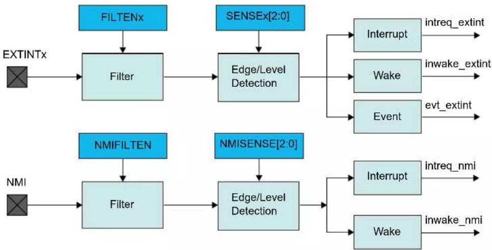
flowchart
graph TD
    A["EXTINTx"] --> B["Filter"]
    C["NMI"] --> D["Filter"]
    B --> E["Edge/Level Detection"]
    D --> F["Edge/Level Detection"]
    E --> G["Interrupt intreq_extint"]
    E --> H["Wake inwake_extint"]
    E --> I["Event evt_extint"]
    F --> J["Interrupt intreq_nmi"]
    F --> K["Wake inwake_nmi"]
26.4 Signal Description
| Signal Name Type Description | ||
| EXTINT[15..0] Digital Input External interrupt pin | ||
| NMI Digital Input Non-maskable interrupt pin | ||
One signal can be mapped on several pins.
References:
I/O Multiplexing and Considerations
26.5 Product Dependencies
In order to use this peripheral, other parts of the system must be configured correctly, as described below.
26.5.1 I/O Lines
Using the EIC's I/O lines requires the I/O pins to be configured.
References:
- PORT - I/O Pin Controller
26.5.2 Power Management
All interrupts are available in all sleep modes, but the EIC can be configured to automatically mask some interrupts in order to prevent device wake-up.
The EIC will continue to operate in any sleep mode where the selected source clock is running. The EIC's interrupts can be used to wake up the device from sleep modes. Events connected to the Event System can trigger other operations in the system without exiting sleep modes.
References:
PM - Power Manager
26.5.3 Clocks
The EIC bus clock (CLK_EIC_APB) can be enabled and disabled by the Main Clock Controller, the default state of CLK_EIC_APB can be found in the Peripheral Clock Masking section.
Some optional functions need a peripheral clock, which can either be a generic clock (GCLK_EIC, for wider frequency selection) or a Ultra Low Power 32.768 kHz clock (CLK_ULP32K, for highest power efficiency). One of the clock sources must be configured and enabled before using the peripheral:
GCLK_EIC is configured and enabled in the Generic Clock Controller.
CLK_ULP32K is provided by the internal ultra-low-power (OSCULP32K) oscillator in the OSC32KCTRL module.
Both GCLK_EIC and CLK_ULP32K are asynchronous to the user interface clock (CLK_EIC_APB). Due to this asynchronicity, writes to certain registers will require synchronization between the clock domains. Refer to Synchronization for further details.
References:
- MCLK - Main Clock
16.6.2.6. Peripheral Clock Masking
-
GCLK - Generic Clock Controller
-
OSC32KCTRL - 32.768 kHz Oscillators Controller
26.5.4 DMA
Not applicable.
26.5.5 Interrupts
There are two interrupt request lines, one for the external interrupts (EXTINT) and one for non-maskable interrupt (NMI).
The EXTINT interrupt request line is connected to the interrupt controller. Using the EIC interrupt requires the interrupt controller to be configured first.
The NMI interrupt request line is also connected to the interrupt controller, but does not require the interrupt to be configured.
References:
Nested Vector Interrupt Controller
26.5.6 Events
The events are connected to the Event System. Using the events requires the Event System to be configured first.
References:
- EVSYS – Event System
26.5.7 Debug Operation
When the CPU is halted in debug mode, the EIC continues normal operation. If the EIC is configured in a way that requires it to be periodically serviced by the CPU through interrupts or similar, improper operation or data loss may result during debugging.
26.5.8 Register Access Protection
All registers with write-access can be write-protected optionally by the Peripheral Access Controller (PAC), except for the following registers:
- Interrupt Flag Status and Clear register (INTFLAG)
• Non-Maskable Interrupt Flag Status and Clear register (NMIFLAG)
Optional write-protection by the Peripheral Access Controller (PAC) is denoted by the "PAC Write-Protection" property in each individual register description.
PAC write-protection does not apply to accesses through an external debugger.
References:
PAC
26.5.9 Analog Connections
Not applicable.
26.6 Functional Description
26.6.1 Principle of Operation
The EIC detects edge or level condition to generate interrupts to the CPU interrupt controller or events to the Event System. Each external interrupt pin (EXTINT) can be filtered using majority vote filtering, clocked by GCLK_EIC or by CLK_ULP32K.
26.6.2 Basic Operation
26.6.2.1 Initialization
The EIC must be initialized in the following order:
- Enable CLK_EIC_APB
- If required, configure the NMI by writing the Non-Maskable Interrupt Control register (NMICTRL)
- When the NMI is used or synchronous edge detection or filtering are required, enable GCLK_EIC or CLK_ULP32K.
GCLK_EIC is used when a frequency higher than 32.768 kHz is required for filtering, CLK_ULP32K is recommended when power consumption is the priority. For CLK_ULP32K write a '1' to the Clock Selection bit in the Control A register (CTRLA.CKSEL). Optionally, enable the asynchronous mode.
-
Configure the EIC input sense and filtering by writing the Configuration n register (CONFIGn).
-
Enable the EIC.
The following bits are enable-protected, meaning that it can only be written when the EIC is disabled (CTRLA.ENABLE=0):
- Clock Selection bit in Control A register (CTRLA.CKSEL)
The following registers are enable-protected:
• Event Control register (EVCTRL)
- Configuration n register (CONFIGn)
- External Interrupt Asynchronous Mode register (ASYNCH)
Enable-protected bits in the CTRLA register can be written at the same time when setting CTRLA. ENABLE to '1', but not at the same time as CTRLA. ENABLE is being cleared.
Enable-protection is denoted by the "Enable-Protected" property in the register description.
26.6.2.2 Enabling, Disabling, and Resetting
The EIC is enabled by writing a '1' the Enable bit in the Control A register (CTRLA.ENABLE). The EIC is disabled by writing CTRLA.ENABLE to '0'.
The EIC is reset by setting the Software Reset bit in the Control register (CTRLA.SWRST). All registers in the EIC will be reset to their initial state, and the EIC will be disabled.
Refer to the CTRLA register description for details.
26.6.3 External Pin Processing
Each external pin can be configured to generate an interrupt/event on edge detection (rising, falling or both edges) or level detection (high or low). The sense of external interrupt pins is configured by writing the Input Sense x bits in the Config n register (CONFIGn.SENSEx). The corresponding interrupt flag (INTFLAG.EXTINT[x]) in the Interrupt Flag Status and Clear register (INTFLAG) is set when the interrupt condition is met.
When the interrupt flag has been cleared in edge-sensitive mode, INTFLAG.EXTINT[x] will only be set if a new interrupt condition is met. In level-sensitive mode, when interrupt has been cleared, INTFLAG.EXTINT[x] will be set immediately if the EXTINTx pin still matches the interrupt condition.
Each external pin can be filtered by a majority vote filtering, clocked by GCLK_EIC or CLK_ULP32K. Filtering is enabled if bit Filter Enable x in the Configuration n register (CONFIGn.FILTENx) is written to '1'. The majority vote filter samples the external pin three times with GCLK_EIC or CLK_ULP32K and outputs the value when two or more samples are equal.
Table 26-1. Majority Vote Filter
| Samples [0, 1, 2] Filter Output | |
| [0,0,0] 0 | |
| [0,0,1] 0 | |
| [0,1,0] 0 | |
| [0,1,1] 1 | |
| [1,0,0] 0 | |
| [1,0,1] 1 | |
| [1,1,0] 1 | |
| [1,1,1] 1 |
When an external interrupt is configured for level detection and when filtering is disabled, detection is done asynchronously. Asynchronous detection does not require GCLK_EIC or CLK_ULP32K, but interrupt and events can still be generated.
If filtering or edge detection is enabled, the EIC automatically requests GCLK_EIC or CLK_ULP32K to operate. The selection between these two clocks is done by writing the Clock Selection bits in the Control A register (CTRLA.CKSEL). GCLK_EIC must be enabled in the GCLK module.
Figure 26-2. Interrupt Detections

text_image
GCLK_EIC CLK_EIC_APB EXTINTx intreq_extint[x] (level detection / no filter) intreq_extint[x] (level detection / filter) intreq_extint[x] (edge detection / no filter) intreq_extint[x] (edge detection / filter) No interrupt No interrupt clear INTFLAG.EXTINT[x]The detection delay depends on the detection mode.
Table 26-2. Interrupt Latency
| Detection mode Latency (worst case) | |
| Level without filter Five CLK_EIC_APB periods | |
| Level with filter | Four GCLK_EIC/CLK_ULP32K periods + five CLK_EIC_APB periods |
| Edge without filter | Four GCLK_EIC/CLK_ULP32K periods + five CLK_EIC_APB periods |
| Edge with filter | Six GCLK_EIC/CLK_ULP32K periods + five CLK_EIC_APB periods |
References:
GCLK
26.6.4 Additional Features
26.6.4.1 Non-Maskable Interrupt (NMI)
The non-maskable interrupt pin can also generate an interrupt on edge or level detection, but it is configured with the dedicated NMI Control register (NMICTRL). To select the sense for NMI, write to the NMISENSE bit group in the NMI Control register (NMICTRL.NMISENSE). NMI filtering is enabled by writing a '1' to the NMI Filter Enable bit (NMICTRL.NMIFILTEN).
If edge detection or filtering is required, enable GCLK_EIC or CLK_ULP32K.
NMI detection is enabled only by the NMICTRL.NMISENSE value, and the EIC is not required to be enabled.
After reset, NMI is configured to no detection mode.
When an NMI is detected, the non-maskable interrupt flag in the NMI Flag Status and Clear register is set (NMIFLAG.NMI). NMI interrupt generation is always enabled, and NMIFLAG.NMI generates an interrupt request when set.
26.6.4.2 Asynchronous Edge Detection Mode (No Debouncing)
The EXTINT edge detection can be operated synchronously or asynchronously, selected by the Asynchronous Control Mode bit for external pin x in the External Interrupt Asynchronous Mode register (ASYNCH.ASYNCH[x]). The EIC edge detection is operated synchronously when the Asynchronous Control Mode bit (ASYNCH.ASYNCH[x]) is '0' (default value). It is operated asynchronously when ASYNCH.ASYNCH[x] is written to '1'.
In Synchronous Edge Detection Mode, the external interrupt (EXTINT) or the non-maskable interrupt (NMI) pins are sampled using the EIC clock as defined by the Clock Selection bit in the Control A register (CTRLA.CKSEL). The External Interrupt flag (INTFLAG.EXTINT[x]) or Non-Maskable Interrupt flag (NMIFLAG.NMI) is set when the last sampled state of the pin differs from the previously sampled state. In this mode, the EIC clock is required.
In Asynchronous Edge Detection Mode, the external interrupt (EXTINT) pins or the non-maskable interrupt (NMI) pins set the External Interrupt flag or Non-Maskable Interrupt flag (INTFLAG.EXTINT[x] or NMIFLAG) directly. In this mode, the EIC clock is not requested.
The asynchronous edge detection mode can be used in all sleep modes.
26.6.5 DMA Operation
Not applicable.
26.6.6 Interrupts
The EIC has the following interrupt sources:
- External interrupt pins (EXTINTx). See 26.6.2. Basic Operation.
- Non-maskable interrupt pin (NMI). See 26.6.4. Additional Features.
Each interrupt source has an associated interrupt flag. The interrupt flag in the Interrupt Flag Status and Clear register (INTFLAG) is set when an interrupt condition occurs (NMIFLAG for NMI). Each interrupt, except NMI, can be individually enabled by setting the corresponding bit in the Interrupt Enable Set register (INTENSET=1), and disabled by setting the corresponding bit in the Interrupt Enable Clear register (INTENCLR=1).
An interrupt request is generated when the interrupt flag is set and the corresponding interrupt is enabled. The interrupt request remains active until the interrupt flag is cleared, the interrupt is disabled, or the EIC is reset. See the INTFLAG register for details on how to clear interrupt flags. The EIC has one common interrupt request line for all the interrupt sources, and one interrupt request line for the NMI. The user must read the INTFLAG (or NMIFLAG) register to determine which interrupt condition is present.
Note: Interrupts must be globally enabled for interrupt requests to be generated.
Note: If an external interrupts (EXTINT) is common on two or more I/O pins, only one will be active (the first one programmed).
References:
I/O Multiplexing and Considerations
26.6.7 Events
The EIC can generate the following output events:
- External event from pin (EXTINTx).
Setting an Event Output Control register (EVCTRL.EXTINTEO) enables the corresponding output event. Clearing this bit disables the corresponding output event. Refer to Event System for details on configuring the Event System.
When the condition on pin EXTINTx matches the configuration in the CONFIGn register, the corresponding event is generated, if enabled.
References:
- EVSYS – Event System
26.6.8 Sleep Mode Operation
In sleep modes, an EXTINTx pin can wake up the device if the corresponding condition matches the configuration in CONFIGn register, and the corresponding bit in the Interrupt Enable Set register (INTENSET) is written to '1'.
Figure 26-3. Wake-up Operation Example (High-Level Detection, No Filter, Interrupt Enable Set)
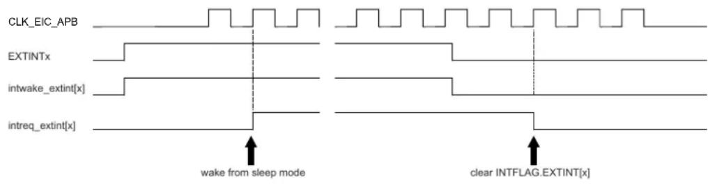
text_image
CLK_EIC_APB EXTINTx intwake_extint[x] intreq_extint[x] wake from sleep mode clear INTFLAG.EXTINT[x]26.6.9 Synchronization
Due to asynchronicity between the main clock domain and the peripheral clock domains, some registers need to be synchronized when written or read.
The following bits are synchronized when written:
- Software Reset bit in control register (CTRLA.SWRST)
- Enable bit in control register (CTRLA.ENABLE)
Required write-synchronization is denoted by the "Write-Synchronized" property in the register description.
26.7 Register Summary
| Offset | Name Bit Pos. 7 | 6 | 5 | 4 | 3 | 2 | 1 | 0 | ||||||||||||||||||||||||||||||||||||||||||||||||||||||||||||||||||||||||||||||||||||||||||||||||||||||||||||||||||||||||||||||||||||||||||||||||||||||||||||||||||||||||||||||||||||||||||||||||||||||||||||||||||||||||||||||||||||||||||||||||||||||||||||||||||||||||||||||||||||||||||||||||||||||||||||||||||||
| 0x00 | CTRLA | 7:0 | CKSEL | ENABLE SWRST | 0x01 | NMICTRL | 7:0 | NMIASYNCH NMIFILTEN NMISENSE[2:0] | ||||||||||||||||||||||||||||||||||||||||||||||||||||||||||||||||||||||||||||||||||||||||||||||||||||||||||||||||||||||||||||||||||||||||||||||||||||||||||||||||||||||||||||||||||||||||||||||||||||||||||||||||||||||||||||||||||||||||||||||||||||||||||||||||||||||||||||||||||||||||||||||||||||||||||||||||||||
| 0x02 | NMIFLAG | 7:0 | NMI | SYNCBUSY | 0x08 | EVCTRL | ||||||||||||||||||||||||||||||||||||||||||||||||||||||||||||||||||||||||||||||||||||||||||||||||||||||||||||||||||||||||||||||||||||||||||||||||||||||||||||||||||||||||||||||||||||||||||||||||||||||||||||||||||||||||||||||||||||||||||||||||||||||||||||||||||||||||||||||||||||||||||||||||||||||||||||||||||||||
| 15:8 | SYNCBUSY | 7:0 | ENABLE SWRST | 15:8 | EXTINTEO[7:0] | |||||||||||||||||||||||||||||||||||||||||||||||||||||||||||||||||||||||||||||||||||||||||||||||||||||||||||||||||||||||||||||||||||||||||||||||||||||||||||||||||||||||||||||||||||||||||||||||||||||||||||||||||||||||||||||||||||||||||||||||||||||||||||||||||||||||||||||||||||||||||||||||||||||||||||||||||||||||
| 15:8 | ENABLE SWRST | SYNCBUSY | 15:8 | EXTINTEO[15:8] | ||||||||||||||||||||||||||||||||||||||||||||||||||||||||||||||||||||||||||||||||||||||||||||||||||||||||||||||||||||||||||||||||||||||||||||||||||||||||||||||||||||||||||||||||||||||||||||||||||||||||||||||||||||||||||||||||||||||||||||||||||||||||||||||||||||||||||||||||||||||||||||||||||||||||||||||||||||||||
| 23:16 | 31:24 | 31:24 | 31:24 | 31:24 | 31:24 | 31:24 | 31:24 | 31:24 | 31:24 | 31:24 | 31:24 | 31:24 | 31:24 | 31:24 | 31:24 | 31:24 | 31:24 | 31;24 | 31:24 | 31:24 | 31:24 | 31:24 | 31:24 | 31:24 | 31:24 | 31:24 | 31:24 | 31:24 | 31:24 | 31:24 | 31:24 | 31:24 | 31:24 | 31:24 | 31:24 | 31:24 | 31:24 | 31:24 | 31:24 | 31:24 | 31:24 | 31:24 | 31:24 | 31:24 | 31:24 | 31:24 | 31:24 | 31:24 | 31:24 | 31:24 | 31 :24 | 31 :24 | 31 :24 | 31 :24 | 31 :24 | 31 :24 | 31 :24 | 31 :24 | 31 :24 | 31 :24 | 31 :24 | 31 :24 | 31 :24 | 31 :24 | 31 :24 | 31 :24 | 31 :24 | 31 :24 | 31 :24 | 31 :24 | 31 :24 | 31 :24 | 31 :24 | 31 :24 | 31 :24 | 31 :24 | 31 :24 | 31 :24 | 31 :24 | 31 :24 | 31 :24 | 31 :24 | 31 :24 | 31:24 | 31:24 | 31:24 | 31:24 | 31:24 | 31:24 | 31:24 | 31:24 | 31:24 | 31:24 | 31:24 | 31:24 | 31:24 | 31:24 | 31:24 | 31:24 | |||||||||||||||||||||||||||||||||||||||||||||||||||||||||||||||||||||||||||||||||||||||||||||||||||||||||||||||||||||||||||||||||||||||||||||||||||||||||||||||||||||||||||||||||||||||||||||||||||||||||||||||||||||||||
| 7:0 | EXTINT[7:0] | |||||||||||||||||||||||||||||||||||||||||||||||||||||||||||||||||||||||||||||||||||||||||||||||||||||||||||||||||||||||||||||||||||||||||||||||||||||||||||||||||||||||||||||||||||||||||||||||||||||||||||||||||||||||||||||||||||||||||||||||||||||||||||||||||||||||||||||||||||||||||||||||||||||||||||||||||||||||||||
| 15:8 | EXTINT[15:8] | SYNCBUSY | 15:9 | EXTINT[15:8] | ||||||||||||||||||||||||||||||||||||||||||||||||||||||||||||||||||||||||||||||||||||||||||||||||||||||||||||||||||||||||||||||||||||||||||||||||||||||||||||||||||||||||||||||||||||||||||||||||||||||||||||||||||||||||||||||||||||||||||||||||||||||||||||||||||||||||||||||||||||||||||||||||||||||||||||||||||||||||
| 23:16 | EXTINT[7:0] | SYNCBUSY | 15:9 | EXTINT[15;8] | ||||||||||||||||||||||||||||||||||||||||||||||||||||||||||||||||||||||||||||||||||||||||||||||||||||||||||||||||||||||||||||||||||||||||||||||||||||||||||||||||||||||||||||||||||||||||||||||||||||||||||||||||||||||||||||||||||||||||||||||||||||||||||||||||||||||||||||||||||||||||||||||||||||||||||||||||||||||||
| 23:16 | EXTINT[7:0] | SYNCBUSY | 15:9 | EXTINT[15:8] | 15:8 | EXTINT[7:0] | ||||||||||||||||||||||||||||||||||||||||||||||||||||||||||||||||||||||||||||||||||||||||||||||||||||||||||||||||||||||||||||||||||||||||||||||||||||||||||||||||||||||||||||||||||||||||||||||||||||||||||||||||||||||||||||||||||||||||||||||||||||||||||||||||||||||||||||||||||||||||||||||||||||||||||||||||||||||
| 23:16 | EXTINT[7:0] | |||||||||||||||||||||||||||||||||||||||||||||||||||||||||||||||||||||||||||||||||||||||||||||||||||||||||||||||||||||||||||||||||||||||||||||||||||||||||||||||||||||||||||||||||||||||||||||||||||||||||||||||||||||||||||||||||||||||||||||||||||||||||||||||||||||||||||||||||||||||||||||||||||||||||||||||||||||||||||
| 31:24 | EXTINT[15:8] | SYNCBUSY | 15:9 | EXTINT[15:8] | 15:8 | EXTINT[7:0] | ESTINT[15:8] | ESTINT[7:0] | ESTINT[7:0] | ESTINT[7:0] | ESTINT[7:0] | ESTINT[7:0] | ||||||||||||||||||||||||||||||||||||||||||||||||||||||||||||||||||||||||||||||||||||||||||||||||||||||||||||||||||||||||||||||||||||||||||||||||||||||||||||||||||||||||||||||||||||||||||||||||||||||||||||||||||||||||||||||||||||||||||||||||||||||||||||||||||||||||||||||||||||||||||||||||||||||||||||||||
| 23:16 | EXTINT[7:0] | |||||||||||||||||||||||||||||||||||||||||||||||||||||||||||||||||||||||||||||||||||||||||||||||||||||||||||||||||||||||||||||||||||||||||||||||||||||||||||||||||||||||||||||||||||||||||||||||||||||||||||||||||||||||||||||||||||||||||||||||||||||||||||||||||||||||||||||||||||||||||||||||||||||||||||||||||||||||||||
| 31:24 | EXTINT[15:8] | |||||||||||||||||||||||||||||||||||||||||||||||||||||||||||||||||||||||||||||||||||||||||||||||||||||||||||||||||||||||||||||||||||||||||||||||||||||||||||||||||||||||||||||||||||||||||||||||||||||||||||||||||||||||||||||||||||||||||||||||||||||||||||||||||||||||||||||||||||||||||||||||||||||||||||||||||||||||||||
| 31:24 | EXTINT[7:0] | |||||||||||||||||||||||||||||||||||||||||||||||||||||||||||||||||||||||||||||||||||||||||||||||||||||||||||||||||||||||||||||||||||||||||||||||||||||||||||||||||||||||||||||||||||||||||||||||||||||||||||||||||||||||||||||||||||||||||||||||||||||||||||||||||||||||||||||||||||||||||||||||||||||||||||||||||||||||||||
| 31:24 | EXTINT[7:0] | |||||||||||||||||||||||||||||||||||||||||||||||||||||||||||||||||||||||||||||||||||||||||||||||||||||||||||||||||||||||||||||||||||||||||||||||||||||||||||||||||||||||||||||||||||||||||||||||||||||||||||||||||||||||||||||||||||||||||||||||||||||||||||||||||||||||||||||||||||||||||||||||||||||||||||||||||||||||||||
| 31:24 | EXTINT[7:0] | |||||||||||||||||||||||||||||||||||||||||||||||||||||||||||||||||||||||||||||||||||||||||||||||||||||||||||||||||||||||||||||||||||||||||||||||||||||||||||||||||||||||||||||||||||||||||||||||||||||||||||||||||||||||||||||||||||||||||||||||||||||||||||||||||||||||||||||||||||||||||||||||||||||||||||||||||||||||||||
| 31:24 | EXTINT[7:0] | |||||||||||||||||||||||||||||||||||||||||||||||||||||||||||||||||||||||||||||||||||||||||||||||||||||||||||||||||||||||||||||||||||||||||||||||||||||||||||||||||||||||||||||||||||||||||||||||||||||||||||||||||||||||||||||||||||||||||||||||||||||||||||||||||||||||||||||||||||||||||||||||||||||||||||||||||||||||||||
| 31:24 | EXTINT[7:0] | |||||||||||||||||||||||||||||||||||||||||||||||||||||||||||||||||||||||||||||||||||||||||||||||||||||||||||||||||||||||||||||||||||||||||||||||||||||||||||||||||||||||||||||||||||||||||||||||||||||||||||||||||||||||||||||||||||||||||||||||||||||||||||||||||||||||||||||||||||||||||||||||||||||||||||||||||||||||||||
| 31:24 | EXTINT[7:0] | |||||||||||||||||||||||||||||||||||||||||||||||||||||||||||||||||||||||||||||||||||||||||||||||||||||||||||||||||||||||||||||||||||||||||||||||||||||||||||||||||||||||||||||||||||||||||||||||||||||||||||||||||||||||||||||||||||||||||||||||||||||||||||||||||||||||||||||||||||||||||||||||||||||||||||||||||||||||||||
| 31 :24 | EXTINT[7:0] | |||||||||||||||||||||||||||||||||||||||||||||||||||||||||||||||||||||||||||||||||||||||||||||||||||||||||||||||||||||||||||||||||||||||||||||||||||||||||||||||||||||||||||||||||||||||||||||||||||||||||||||||||||||||||||||||||||||||||||||||||||||||||||||||||||||||||||||||||||||||||||||||||||||||||||||||||||||||||||
| 31 :24 | EXTINT[7:0] | |||||||||||||||||||||||||||||||||||||||||||||||||||||||||||||||||||||||||||||||||||||||||||||||||||||||||||||||||||||||||||||||||||||||||||||||||||||||||||||||||||||||||||||||||||||||||||||||||||||||||||||||||||||||||||||||||||||||||||||||||||||||||||||||||||||||||||||||||||||||||||||||||||||||||||||||||||||||||||
| 31 :24 | EXTINT[7:0] | |||||||||||||||||||||||||||||||||||||||||||||||||||||||||||||||||||||||||||||||||||||||||||||||||||||||||||||||||||||||||||||||||||||||||||||||||||||||||||||||||||||||||||||||||||||||||||||||||||||||||||||||||||||||||||||||||||||||||||||||||||||||||||||||||||||||||||||||||||||||||||||||||||||||||||||||||||||||||||
| 31 :24 | EXTINT[7:0] | |||||||||||||||||||||||||||||||||||||||||||||||||||||||||||||||||||||||||||||||||||||||||||||||||||||||||||||||||||||||||||||||||||||||||||||||||||||||||||||||||||||||||||||||||||||||||||||||||||||||||||||||||||||||||||||||||||||||||||||||||||||||||||||||||||||||||||||||||||||||||||||||||||||||||||||||||||||||||||
| 31 :24 | EXTINT[7:0] | EXTINT[7:0] | ||||||||||||||||||||||||||||||||||||||||||||||||||||||||||||||||||||||||||||||||||||||||||||||||||||||||||||||||||||||||||||||||||||||||||||||||||||||||||||||||||||||||||||||||||||||||||||||||||||||||||||||||||||||||||||||||||||||||||||||||||||||||||||||||||||||||||||||||||||||||||||||||||||||||||||||||||||||||||
| 31 :24 | EXTINT[7:0] | |||||||||||||||||||||||||||||||||||||||||||||||||||||||||||||||||||||||||||||||||||||||||||||||||||||||||||||||||||||||||||||||||||||||||||||||||||||||||||||||||||||||||||||||||||||||||||||||||||||||||||||||||||||||||||||||||||||||||||||||||||||||||||||||||||||||||||||||||||||||||||||||||||||||||||||||||||||||||||
| 31 :24 | EXTINT[7:0] | |||||||||||||||||||||||||||||||||||||||||||||||||||||||||||||||||||||||||||||||||||||||||||||||||||||||||||||||||||||||||||||||||||||||||||||||||||||||||||||||||||||||||||||||||||||||||||||||||||||||||||||||||||||||||||||||||||||||||||||||||||||||||||||||||||||||||||||||||||||||||||||||||||||||||||||||||||||||||||
| 31 :24 | EXTINT[7:0] | |||||||||||||||||||||||||||||||||||||||||||||||||||||||||||||||||||||||||||||||||||||||||||||||||||||||||||||||||||||||||||||||||||||||||||||||||||||||||||||||||||||||||||||||||||||||||||||||||||||||||||||||||||||||||||||||||||||||||||||||||||||||||||||||||||||||||||||||||||||||||||||||||||||||||||||||||||||||||||
| 31 :24 | EXTINT[7: 0] | |||||||||||||||||||||||||||||||||||||||||||||||||||||||||||||||||||||||||||||||||||||||||||||||||||||||||||||||||||||||||||||||||||||||||||||||||||||||||||||||||||||||||||||||||||||||||||||||||||||||||||||||||||||||||||||||||||||||||||||||||||||||||||||||||||||||||||||||||||||||||||||||||||||||||||||||||||||||||||
| 31 :24 | EXTINT[7:0] | |||||||||||||||||||||||||||||||||||||||||||||||||||||||||||||||||||||||||||||||||||||||||||||||||||||||||||||||||||||||||||||||||||||||||||||||||||||||||||||||||||||||||||||||||||||||||||||||||||||||||||||||||||||||||||||||||||||||||||||||||||||||||||||||||||||||||||||||||||||||||||||||||||||||||||||||||||||||||||
| 31 :24 | EXTINT[7:0] | |||||||||||||||||||||||||||||||||||||||||||||||||||||||||||||||||||||||||||||||||||||||||||||||||||||||||||||||||||||||||||||||||||||||||||||||||||||||||||||||||||||||||||||||||||||||||||||||||||||||||||||||||||||||||||||||||||||||||||||||||||||||||||||||||||||||||||||||||||||||||||||||||||||||||||||||||||||||||||
| 31 :24 | EXTINT[7:0] | |||||||||||||||||||||||||||||||||||||||||||||||||||||||||||||||||||||||||||||||||||||||||||||||||||||||||||||||||||||||||||||||||||||||||||||||||||||||||||||||||||||||||||||||||||||||||||||||||||||||||||||||||||||||||||||||||||||||||||||||||||||||||||||||||||||||||||||||||||||||||||||||||||||||||||||||||||||||||||
| 31 :24 | EXTINT[7:0] | |||||||||||||||||||||||||||||||||||||||||||||||||||||||||||||||||||||||||||||||||||||||||||||||||||||||||||||||||||||||||||||||||||||||||||||||||||||||||||||||||||||||||||||||||||||||||||||||||||||||||||||||||||||||||||||||||||||||||||||||||||||||||||||||||||||||||||||||||||||||||||||||||||||||||||||||||||||||||||
| EXTINT[7:0] | ||||||||||||||||||||||||||||||||||||||||||||||||||||||||||||||||||||||||||||||||||||||||||||||||||||||||||||||||||||||||||||||||||||||||||||||||||||||||||||||||||||||||||||||||||||||||||||||||||||||||||||||||||||||||||||||||||||||||||||||||||||||||||||||||||||||||||||||||||||||||||||||||||||||||||||||||||||||||||||
| 31 :24 | EXTINT[7:0] | |||||||||||||||||||||||||||||||||||||||||||||||||||||||||||||||||||||||||||||||||||||||||||||||||||||||||||||||||||||||||||||||||||||||||||||||||||||||||||||||||||||||||||||||||||||||||||||||||||||||||||||||||||||||||||||||||||||||||||||||||||||||||||||||||||||||||||||||||||||||||||||||||||||||||||||||||||||||||||
| 31 :24 | EXTINT[7:0] | |||||||||||||||||||||||||||||||||||||||||||||||||||||||||||||||||||||||||||||||||||||||||||||||||||||||||||||||||||||||||||||||||||||||||||||||||||||||||||||||||||||||||||||||||||||||||||||||||||||||||||||||||||||||||||||||||||||||||||||||||||||||||||||||||||||||||||||||||||||||||||||||||||||||||||||||||||||||||||
| 31 :24 | EXTINT[7:0] | |||||||||||||||||||||||||||||||||||||||||||||||||||||||||||||||||||||||||||||||||||||||||||||||||||||||||||||||||||||||||||||||||||||||||||||||||||||||||||||||||||||||||||||||||||||||||||||||||||||||||||||||||||||||||||||||||||||||||||||||||||||||||||||||||||||||||||||||||||||||||||||||||||||||||||||||||||||||||||
| 31 :24 | EXTINT[7:0] | |||||||||||||||||||||||||||||||||||||||||||||||||||||||||||||||||||||||||||||||||||||||||||||||||||||||||||||||||||||||||||||||||||||||||||||||||||||||||||||||||||||||||||||||||||||||||||||||||||||||||||||||||||||||||||||||||||||||||||||||||||||||||||||||||||||||||||||||||||||||||||||||||||||||||||||||||||||||||||
26.8 Register Description
Registers can be 8, 16, or 32 bits wide. Atomic 8-, 16-, and 32-bit accesses are supported. In addition, the 8-bit quarters and 16-bit halves of a 32-bit register, and the 8-bit halves of a 16-bit register can be accessed directly.
Some registers require synchronization when read and/or written. Synchronization is denoted by the "Read-Synchronized" and/or "Write-Synchronized" property in each individual register description.
Some registers are enable-protected, meaning they can only be written when the module is disabled. Enable-protection is denoted by the "Enable-Protected" property in each individual register description.
26.8.1 Control A
Name: CTRLA
Offset: 0x00
Reset: 0x00
Property: PAC Write-Protection
Bit 76543210
| CKSEL ENABLE $WRST | ||||||
| Access Reset | R/W R/W W | |||||
| 0 | 0 0 | |||||
Bit 4 - CKSEL Clock Selection
The EIC can be clocked either by GCLK_EIC (when a frequency higher than 32KHz is required for filtering) or by CLK_ULP32K (when power consumption is the priority).
This bit is not Write-Synchronized.
| Value | Description |
| 0 | The EIC is clocked by GCLK_EIC. |
| 1 | The EIC is clocked by CLK_ULP32K. |
Bit 1 - ENABLE Enable
Due to synchronization there is a delay between writing to CTRLA. ENABLE until the peripheral is enabled/disabled. The value written to CTRLA. ENABLE will read back immediately and the Enable bit in the Synchronization Busy register will be set (SYNCBUSY. ENABLE=1). SYNCBUSY. ENABLE will be cleared when the operation is complete.
This bit is not Enable-Protected.
| Value | Description |
| 0 | The EIC is disabled. |
| 1 | The EIC is enabled. |
Bit 0 - SWRST Software Reset
Writing a '0' to this bit has no effect.
Writing a '1' to this bit resets all registers in the EIC to their initial state, and the EIC will be disabled. Writing a '1' to CTRLA.SWRST will always take precedence, meaning that all other writes in the same write operation will be discarded.
Due to synchronization there is a delay from writing CTRLA.SWRST until the Reset is complete. CTRLA.SWRST and SYNCBUSY.SWRST will both be cleared when the Reset is complete.
This bit is not Enable-Protected.
| Value | Description |
| 0 | There is no ongoing reset operation. |
| 1 | The reset operation is ongoing. |
26.8.2 Non-Maskable Interrupt Control
Name: NMICTRL
Offset: 0x01
Reset: 0x00
Property: PAC Write-Protection
Bit 76543210
| NM|ASYNCH NMIFILTEN NMISENSE[2:0] | |||
| Access | R/W R/W R/W R/W R/W | ||
| Reset 00000 | |||
Bit 4 - NMIASYNCH Asynchronous Edge Detection Mode
The NMI edge detection can be operated synchronously or asynchronously to the EIC clock.
| Value | Description |
| 0 | The NMI edge detection is synchronously operated. |
| 1 | The NMI edge detection is asynchronously operated. |
Bit 3 - NMIFILTEN Non-Maskable Interrupt Filter Enable
| Value | Description |
| 0 | NMI filter is disabled. |
| 1 | NMI filter is enabled. |
Bits 2:0 - NMISENSE[2:0] Non-Maskable Interrupt Sense Configuration
These bits define on which edge or level the NMI triggers.
| Value | Name | Description |
| 0x0 | NONE | No detection |
| 0x1 | RISE | Rising-edge detection |
| 0x2 | FALL | Falling-edge detection |
| 0x3 | BOTH | Both-edge detection |
| 0x4 | HIGH | High-level detection |
| 0x5 | LOW | Low-level detection |
| 0x6 - 0x7 | - | Reserved |
26.8.3 Non-Maskable Interrupt Flag Status and Clear
Name: NMIFLAG
Offset: 0x02
Reset: 0x0000
Property: -
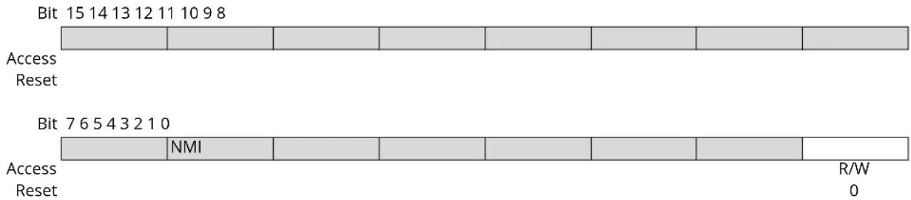
text_image
Bit 15 14 13 12 11 10 9 8 Access Reset Bit 7 6 5 4 3 2 1 0 Access Reset NMI R/W 0Bit 0 - NMI Non-Maskable Interrupt
This flag is cleared by writing a '1' to it.
This flag is set when the NMI pin matches the NMI sense configuration, and will generate an interrupt request.
Writing a '0' to this bit has no effect.
Writing a '1' to this bit clears the non-maskable interrupt flag.
26.8.4 Synchronization Busy
Name: SYNCBUSY
Offset: 0x04
Reset: 0x00000000
Property: -

text_image
Bit 31 30 29 28 27 26 25 24 Access Reset Bit 23 22 21 20 19 18 17 16 Access Reset Bit 15 14 13 12 11 10 9 8 Access Reset Bit 7 6 5 4 3 2 1 0 Access Reset ENABLE SWR$T R R 0 0Bit 1 - ENABLE Enable Synchronization Busy Status
| Value | Description |
| 0 | Write synchronization for CTRLA.ENABLE bit is complete. |
| 1 | Write synchronization for CTRLA.ENABLE bit is ongoing. |
Bit 0 - SWRST Software Reset Synchronization Busy Status
| Value | Description |
| 0 | Write synchronization forCTRLA.SWRST bit is complete. |
| 1 | Write synchronization forCTRLA.SWRST bit is ongoing. |
26.8.5 Event Control
Name: EVCTRL
Offset: 0x08
Reset: 0x00000000
Property: PAC Write-Protection, Enable-Protected

text_image
Bit 31 30 29 28 27 26 25 24 Access Reset Bit 23 22 21 20 19 18 17 16 Access Reset Bit 15 14 13 12 11 10 9 8 EXTINTEO[15:8] Access R/W R/W R/W R/W R/W R/W R/W R/W Reset 0 0 0 0 0 0 0 0 Bit 7 6 5 4 3 2 1 0 EXTINTEO[7:0] Access R/W R/W R/W R/W R/W R/W R/W R/W Reset 0 0 0 0 0 0 0 0Bits 15:0 - EXTINTEO[15:0] External Interrupt Event Output Enable
The bit x of EXTINTEO enables the event associated with the EXTINTx pin.
| Value | Description |
| 0 | Event from pin EXTINTx is disabled. |
| 1 | Event from pin EXTINTx is enabled and will be generated when EXTINTx pin matches the external interrupt sensing configuration. |
26.8.6 Interrupt Enable Clear
Name: INTENCLR
Offset: 0x0C
Reset: 0x00000000
Property: PAC Write-Protection
This register allows the user to disable an interrupt without doing a read-modify-write operation. Changes in this register will also be reflected in the Interrupt Enable Set register (INTENSET).

text_image
Bit 31 30 29 28 27 26 25 24 Access Reset Bit 23 22 21 20 19 18 17 16 Access Reset Bit 15 14 13 12 11 10 9 8 EXTINT[15:8] Access R/W R/W R/W R/W R/W R/W R/W R/W Reset 0 0 0 0 0 0 0 0 Bit 7 6 5 4 3 2 1 0 EXTINT[7:0] Access R/W R/W R/W R/W R/W R/W R/W R/W Reset 0 0 0 0 0 0 0 0Bits 15:0 - EXTINT[15:0] External Interrupt Enable
The bit x of EXTINT enables the interrupt associated with the EXTINTx pin.
Writing a '0' to bit x has no effect.
Writing a '1' to bit x will clear the External Interrupt x Enable bit, which disables the external interrupt EXTINTx.
| Value | Description |
| 0 | The external interrupt x is disabled. |
| 1 | The external interrupt x is enabled. |
26.8.7 Interrupt Enable Set
Name: INTENSET
Offset: 0x10
Reset: 0x00000000
Property: PAC Write-Protection
This register allows the user to enable an interrupt without doing a read-modify-write operation. Changes in this register will also be reflected in the Interrupt Enable Clear (INTENCLR) register.
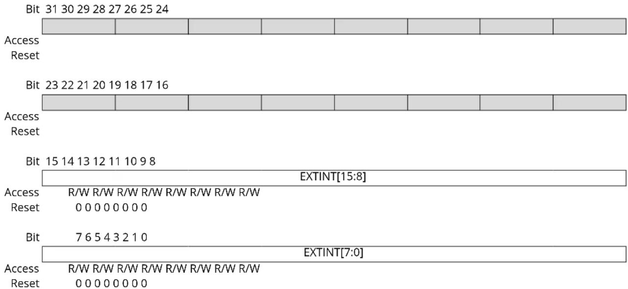
text_image
Bit 31 30 29 28 27 26 25 24 Access Reset Bit 23 22 21 20 19 18 17 16 Access Reset Bit 15 14 13 12 11 10 9 8 EXTINT[15:8] Access R/W R/W R/W R/W R/W R/W R/W R/W Reset 0 0 0 0 0 0 0 0 Bit 7 6 5 4 3 2 1 0 EXTINT[7:0] Access R/W R/W R/W R/W R/W R/W R/W R/W Reset 0 0 0 0 0 0 0 0Bits 15:0 - EXTINT[15:0] External Interrupt Enable
The bit x of EXTINT enables the interrupt associated with the EXTINTx pin.
Writing a '0' to bit x has no effect.
Writing a '1' to bit x will set the External Interrupt x Enable bit, which enables the external interrupt EXTINTx.
| Value | Description |
| 0 | The external interrupt x is disabled. |
| 1 | The external interrupt x is enabled. |
26.8.8 Interrupt Flag Status and Clear
Name: INTFLAG
Offset: 0x14
Reset: 0x00000000
Property: -
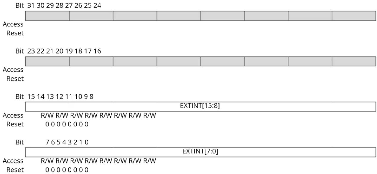
text_image
Bit 31 30 29 28 27 26 25 24 Access Reset Bit 23 22 21 20 19 18 17 16 Access Reset Bit 15 14 13 12 11 10 9 8 EXTINT[15:8] Access R/W R/W R/W R/W R/W R/W R/W R/W Reset 0 0 0 0 0 0 0 0 Bit 7 6 5 4 3 2 1 0 EXTINT[7:0] Access R/W R/W R/W R/W R/W R/W R/W R/W Reset 0 0 0 0 0 0 0 0Bits 15:0 - EXTINT[15:0] External Interrupt
The flag bit x is cleared by writing a '1' to it.
This flag is set when EXTINTx pin matches the external interrupt sense configuration and will generate an interrupt request if INTENCLR/SET.EXTINT[x] is '1'.
Writing a '0' to this bit has no effect.
Writing a '1' to this bit clears the External Interrupt x flag.
26.8.9 External Interrupt Asynchronous Mode
Name: ASYNCH
Offset: 0x18
Reset: 0x00000000
Property: PAC Write-Protection, Enable-Protected
| Bit 31 30 29 28 27 26 25 24 | |||||||
| Access Reset | |||||||
| Bit 23 22 21 20 19 18 17 16 | |||||||
| Access Reset | |||||||
| Bit 15 14 13 12 11 10 9 8 | |||||||
| ASYNCH[15:8] | |||||||
| Access Reset | R/W R/W R/W R/W R/W R/W R/W R/W | ||||||
| 0 0 0 0 0 0 0 0 | |||||||
| Bit | 7 6 5 4 3 2 1 0 | ||||||
| ASYNCH[7:0] | |||||||
| Access Reset | R/W R/W R/W R/W R/W R/W R/W R/W | ||||||
| 0 0 0 0 0 0 0 0 | |||||||
Bits 15:0 - ASYNCH[15:0] Asynchronous Edge Detection Mode
The bit x of ASYNCH set the Asynchronous Edge Detection Mode for the interrupt associated with the EXTINTx pin.
| Value | Description |
| 0 | The EXTINT x edge detection is synchronously operated. |
| 1 | The EXTINT x edge detection is asynchronously operated. |
26.8.10 External Interrupt Sense Configuration n
Name: CONFIGn
Offset: 0x1C + n*0x04 [n=0..1]
Reset: 0x00000000
Property: PAC Write-Protection, Enable-Protected
Bit 31 30 29 28 27 26 25 24
| FILTEN7 SENSE7[2:0] FILTEN6 SENSE6[2:0] |
Access RW RW RW RW RW RW RW
Reset 00000000
Bit 23 22 21 20 19 18 17 16
| FILTEN5 SENSE5[2:0] FILTEN4 SENSE4[2:0] |
Access RW RW RW RW RW RW RW
Reset 00000000
Bit 15 14 13 12 11 10 9 8
| FILTEN3 SENSE3[2:0] FILTEN2 SENSE2[2:0] |
Access RW RW RW RW RW RW RW
Reset 00000000
Bit 76543210
| FILTEN1 SENSE1[2:0] FILTENO SENSE0[2:0] |
Access RW RW RW RW RW RW RW
Reset 00000000
Bits 3, 7, 11, 15, 19, 23, 27, 31 - FILTENx Filter Enable x [x = 0..7]
Note: The filter must be disabled if the asynchronous detection is enabled.
| Value | Description |
| 0 | Filter is disabled for EXTINT[n*8+x] input. |
| 1 | Filter is enabled for EXTINT[n*8+x] input. |
Bits 0:2, 4:6, 8:10, 12:14, 16:18, 20:22, 24:26, 28:30 - SENSEx Input Sense Configuration x [x = 0..7]
These bits define on which edge or level the interrupt or event for EXTINT[n*8+x] will be generated.
| Value | Name | Description |
| 0x0 | NONE | No detection |
| 0x1 | RISE | Rising-edge detection |
| 0x2 | FALL | Falling-edge detection |
| 0x3 | BOTH | Both-edge detection |
| 0x4 | HIGH | High-level detection |
| 0x5 | LOW | Low-level detection |
| 0x6 - 0x7 | - | Reserved |
27. NVMCTRL – Non-Volatile Memory Controller
27.1 Overview
Non-Volatile Memory (NVM) is a reprogrammable Flash memory that retains program and data storage even with power off. It embeds a main array and a separate smaller array intended for EEPROM emulation (RWWEE, standing for Read (the main array) While Write (the EEPROM)) that can be programmed while reading the main array. The NVM Controller (NVMCTRL) connects to the AHB and APB bus interfaces for system access to the NVM block. The AHB interface is used for reads and writes to the NVM block, while the APB interface is used for commands and configuration.
27.2 Features
• 32-bit AHB interface for reads and writes
- Read While Write EEPROM emulation area
- All NVM sections are memory mapped to the AHB, including calibration and system configuration
• 32-bit APB interface for commands and control
- Programmable wait states for read optimization
- 16 regions can be individually protected or unprotected
• Additional protection for boot loader
• Supports device protection through a security bit
- Interface to Power Manager for power-down of Flash blocks in sleep modes
- Can optionally wake up on exit from sleep or on first access
- Direct-mapped cache
Note: A register with property "Enable-Protected" may contain bits that are not enable-protected.
27.3 Block Diagram
Figure 27-1. NVMCTRL Block Diagram
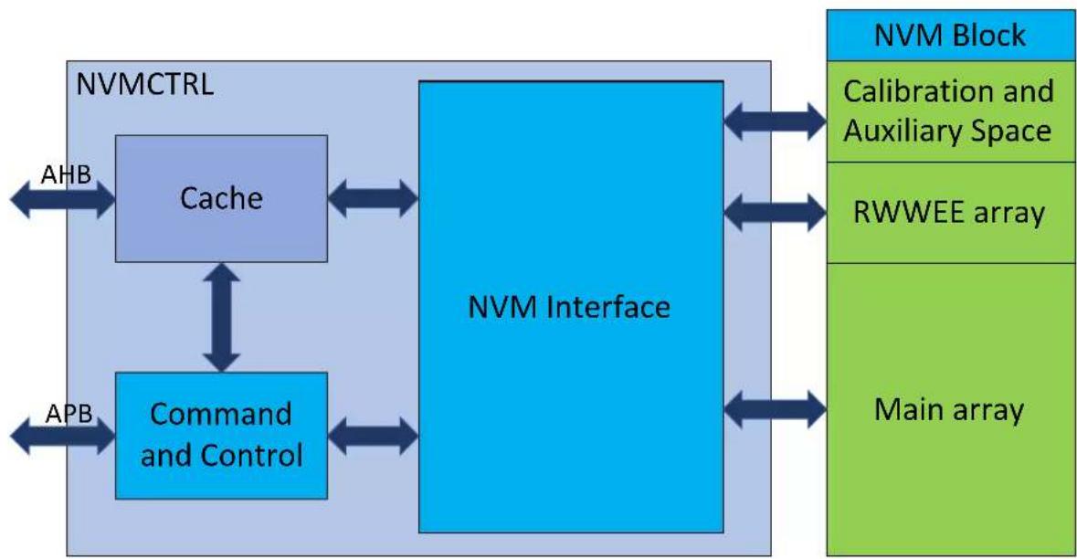
flowchart
graph LR
    A["NVM CTRL"] -->|AHB| B["Cache"]
    A -->|APB| C["Command and Control"]
    B <--> D["NVM Interface"]
    C <--> D
    D <--> E["NVM Block"]
    D --> F["Main array"]
    D --> G["RWWEE array"]
    D --> H["Calibration and Auxiliary Space"]
27.4 Signal Description
Not applicable.
27.5 Product Dependencies
In order to use this module, other parts of the system must be configured correctly, as described below.
27.5.1 Power Management
The NVMCTRL will continue to operate in any Sleep mode where the selected source clock is running. The NVMCTRL interrupts can be used to wake up the device from sleep modes.
The Power Manager will automatically put the NVM block into a low-power state when entering Sleep mode. This is based on the Control B register (CTRLB) SLEEPPRM bit setting. Refer to the CTRLB.SLEEPPRM register description for more details.
References:
PM-Power Manager
27.5.2 Clocks
Two synchronous clocks are used by the NVMCTRL. One is provided by the AHB bus (CLK_NVMCTRL_AHB) and the other is provided by the APB bus (CLK_NVMCTRL_APB). For higher system frequencies, a programmable number of wait states can be used to optimize performance. When changing the AHB bus frequency, the user must ensure that the NVM Controller is configured with the proper number of wait states. Refer to the Electrical Characteristics for the exact number of wait states to be used for a particular frequency range.
References:
Electrical Characteristics
27.5.3 Interrupts
The NVM Controller interrupt request line is connected to the interrupt controller. Using the NVMCTRL interrupt requires the interrupt controller to be programmed first.
27.5.4 Debug Operation
When an external debugger forces the CPU into debug mode, the peripheral continues normal operation.
Access to the NVM block can be protected by the security bit. In this case, the NVM block will not be accessible. See the section on the NVMCTRL 27.6.6. Security Bit for details.
27.5.5 Register Access Protection
All registers with write-access are optionally write-protected by the Peripheral Access Controller (PAC), except the following registers:
- Interrupt Flag Status and Clear register (INTFLAG)
- Status register (STATUS)
Optional write-protection by the Peripheral Access Controller (PAC) is denoted by the "PAC Write-Protection" property in each individual register description.
PAC Write-Protection does not apply to accesses through an external debugger. Refer to the PAC Peripheral Access Controller
References:
PAC-Peripheral Access Controller
27.5.6 Analog Connections
Not applicable.
27.6 Functional Description
27.6.1 Principle of Operation
The NVM Controller is a client on the AHB and APB buses. It responds to commands, read requests and write requests, based on user configuration.
27.6.1.1 Initialization
After power up, the NVM Controller goes through a power-up sequence. During this time, access to the NVM Controller from the AHB bus is halted. Upon power-up completion, the NVM Controller is operational without any need for user configuration.
27.6.2 Memory Organization
Refer to the Physical Memory Map for memory sizes and addresses for each device.
The NVM is organized into rows, where each row contains four pages, as shown in the NVM Row Organization figure. The NVM has a row-erase granularity, while the write granularity is by page. In other words, a single row erase will erase all four pages in the row, while four write operations are used to write the complete row.
Figure 27-2. NVM Row Organization
| Page (n*4) + 3 Page (n*4) + 2 Page (n*4) + 1 Page (n*4) + 0 Row n |
The NVM block contains a calibration and auxiliary space, a RWWEE section, and main array that are memory mapped. Refer to the NVM Organization figure below for details.
The calibration and auxiliary space contains factory calibration and system configuration information. These spaces can be read from the AHB bus in the same way as the main NVM main address space.
In addition, a boot loader section can be allocated at the beginning of the main array, and an EEPROM Emulation section can be allocated at the end of the NVM main address space.
Figure 27-3. NVM Memory Organization

text_image
Calibration and Auxiliary Space NVM Base Address + 0x00800000 RWWEE Address Space NVM Base Address + 0x00400000 NVM Base Address + NVM Size NVM Main Address Space NVM Base AddressThe lower rows in the NVM main address space can be allocated as a boot loader section by using the NVM User Row BOOTPROT fuses, and the upper rows can be allocated to EEPROM Emulation section by using the NVM User Row EEPROM fuses, as shown in the following figure.
The boot loader section is protected by the Lock bit(s) corresponding to this address space and by the BOOTPROT[2:0] fuse. The EEPROM Emulation rows can be written regardless of the region lock status.
The number of rows protected by BOOTPROT is given in Boot Loader Size, the number of rows allocated to the EEPROM Emulation area are given in EEPROM Size.
Figure 27-4. EEPROM and Boot Loader Allocation
| EEPROM Emulation allocation | NVM Base Address + NVM size |
| Program allocation | NVM Base Address + NVM size - EEPROM size |
| BOOT allocation | NVM Base Address + BOOTPROT size |
| NVM Base Address |
References:
Physical Memory Map
27.6.3 Region Lock Bits
The NVM block is grouped into 16 equally sized regions. The region size is dependent on the Flash memory size, and is given in the table below. Each region has a dedicated lock bit preventing writing and erasing pages in the region. After production, all regions will be unlocked.
Table 27-1. Region Size
| Memory Size [KB] Region Size [KB] | |
| 256 16 | |
| 128 8 | |
| 64 | 4 |
| 32 | 2 |
To lock or unlock a region, the Lock Region and Unlock Region commands are provided. Writing one of these commands will temporarily lock/unlock the region containing the address loaded in the ADDR register. ADDR can be written by software, or the automatically loaded value from a write operation can be used. The new setting will stay in effect until the next Reset, or until the setting is changed again using the Lock and Unlock commands. The current status of the lock can be determined by reading the LOCK register.
To change the default lock/unlock setting for a region, the user configuration section of the auxiliary space must be written using the Write Auxiliary Page command. Writing to the auxiliary space will take effect after the next Reset. Therefore, a boot of the device is needed for changes in the lock/unlock setting to take effect. Refer to the Physical Memory Map for calibration and auxiliary space address mapping.
References:
Physical Memory Map
27.6.4 Command and Data Interface
The NVM Controller is addressable from the APB bus, while the NVM main address space is addressable from the AHB bus. Read and automatic page write operations are performed by addressing the NVM main address space or the RWWEE address space directly, while other operations such as manual page writes and row erases must be performed by issuing commands through the NVM Controller.
To issue a command, the CTRLA.CMD bits must be written along with the CTRLA.CMDEX value. When a command is issued, INTFLAG.READY will be cleared until the command has completed. Any commands written while INTFLAG.READY is low will be ignored.
Read the CTRLA register description for more details.
The CTRLB register must be used to control the power reduction mode, read wait states, and the write mode.
27.6.4.1 NVM Read
Reading from the NVM main address space is performed via the AHB bus by addressing the NVM main address space or auxiliary address space directly. Read data is available after the configured number of read wait states (CTRLB.RWS) set in the NVM Controller.
The number of cycles data are delayed to the AHB bus is determined by the read wait states. Examples of using zero and one wait states are shown in the following figure.
Reading the NVM main address space while a programming or erase operation is ongoing on the NVM main array results in an AHB bus stall until the end of the operation. Reading the NVM main array does not stall the bus when the RWWEE array is being programmed or erased.
Figure 27-5. Read Wait State Examples
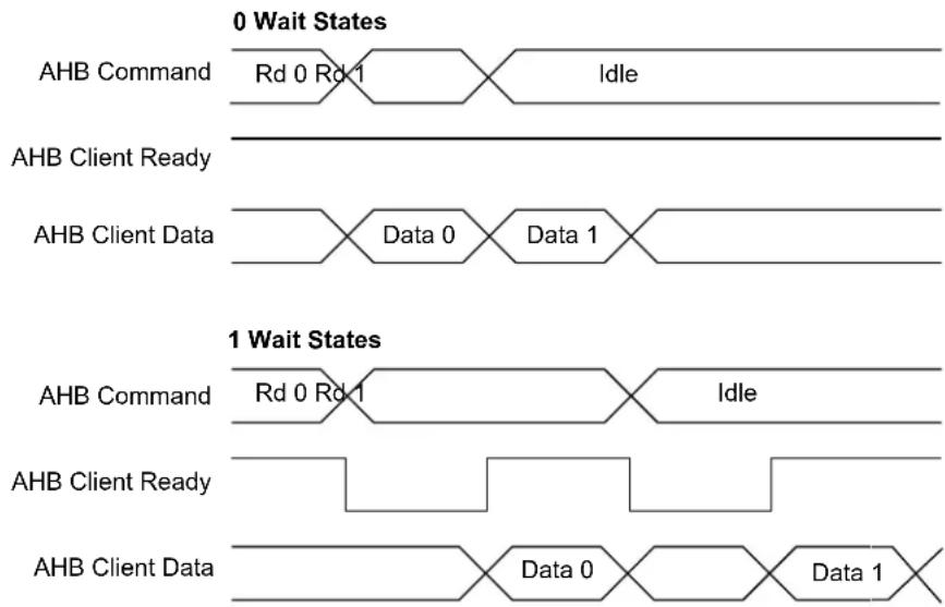
flowchart
graph TD
    subgraph "0 Wait States"
        A["AHB Command"] --> B["Rd 0 Rd 1"]
        B --> C["Idle"]
    end
    subgraph "1 Wait States"
        D["AHB Command"] --> E["Rd 0 Rd 1"]
        E --> F["Idle"]
        G["AHB Client Ready"] --> H["Data 0"]
        I["AHB Client Data"] --> J["Data 1"]
    end
    style A fill:#f9f,stroke:#333
    style D fill:#f9f,stroke:#333
    style G fill:#f9f,stroke:#333
    style B fill:#ccf,stroke:#333
    style E fill:#ccf,stroke:#333
    style F fill:#ccf,stroke:#333
    style J fill:#ccf,stroke:#333
27.6.4.2 RWWEE Read
Reading from the RWWEE address space is performed via the AHB bus by addressing the RWWEE address space directly. Refer to the figures in 27.6.2. Memory Organization for details.
Read timings are similar to regular NVM read timings when access size is Byte or half-Word. The AHB data phase is twice as long in case of full-Word-size access.
It is not possible to read the RWWEE area while the NVM main array is being written or erased, whereas the RWWEE area can be written or erased while the main array is being read.
The RWWEE address space is not cached, therefore it is recommended to limit access to this area for performance and power consumption considerations.
27.6.4.3 NVM Write
The NVM Controller requires that an erase must be done before programming. The entire NVM main address space and the RWWEE address space can be erased by a debugger Chip Erase command. Alternatively, rows can be individually erased by the Erase Row command or the RWWEE Erase Row command to erase the NVM main address space or the RWWEE address space, respectively.
After programming the NVM main array, the region that the page resides in can be locked to prevent spurious write or erase sequences. Locking is performed on a per-region basis, and so, locking a region will lock all pages inside the region.
Data to be written to the NVM block are first written to and stored in an internal buffer called the page buffer. The page buffer contains the same number of bytes as an NVM page. Writes to the page buffer must be 16 or 32 bits. 8-bit writes to the page buffer are not allowed and will cause a system exception.
Both the NVM main array and the RWWEE array share the same page buffer. Writing to the NVM block via the AHB bus is performed by a load operation to the page buffer. For each AHB bus write, the address is stored in the ADDR register. After the page buffer has been loaded with the required number of bytes, the page can be written to the NVM main array or the RWWEE array by setting CTRLA.CMD to 'Write Page' or 'RWWEE Write Page', respectively, and setting the key value to CMDEX. The LOAD bit in the STATUS register indicates whether the page buffer has been loaded or not. Before writing the page to memory, the accessed row must be erased.
Automatic page writes are enabled by writing the manual write bit to zero (CTRLB.MANW=0). This will trigger a write operation to the page addressed by ADDR when the last location of the page is written.
Because the address is automatically stored in ADDR during the I/O bus write operation, the last given address will be present in the ADDR register. There is no need to load the ADDR register manually, unless a different page in memory is to be written.
27.6.4.3.1 Procedure for Manual Page Writes (CTRLB.MANW=1)
The row to be written to must be erased before the write command is given.
- Write to the page buffer by addressing the NVM main address space directly
- Write the page buffer to memory: CTRL.CMD='Write Page' and CMDEX
- The READY bit in the INTFLAG register will be low while programming is in progress, and access through the AHB will be stalled
27.6.4.3.2 Procedure for Automatic Page Writes (CTRLB.MANW=0)
The row to be written to must be erased before the last write to the page buffer is performed.
Note that partially written pages must be written with a manual write.
- Write to the page buffer by addressing the NVM main address space directly.
When the last location in the page buffer is written, the page is automatically written to NVM main address space. - INTFLAG. READY will be zero while programming is in progress and access through the AHB will be stalled.
27.6.4.4 Page Buffer Clear
The page buffer is automatically set to all '1' after a page write is performed. If a partial page has been written and it is desired to clear the contents of the page buffer, the Page Buffer Clear command can be used.
27.6.4.5 Erase Row
Before a page can be written, the row containing that page must be erased. The Erase Row command can be used to erase the desired row in the NVM main address space. The RWWEE Erase Row can be used to erase the desired row in the RWWEE array. Erasing the row sets all bits to '1'. If the row resides in a region that is locked, the erase will not be performed and the Lock Error bit in the Status register (STATUS.LOCKE) will be set.
Procedure for Erase Row
- Write the address of the row to erase to ADDR. Any address within the row can be used.
- Issue an Erase Row command.
Note: The NVM Address bit field in the Address register (ADDR.ADDR) uses 16-bit addressing.
27.6.4.6 Lock and Unlock Region
These commands are used to lock and unlock regions as detailed in section 27.6.3. Region Lock Bits.
27.6.4.7 Set and Clear Power Reduction Mode
The NVM Controller and block can be taken in and out of power reduction mode through the Set and Clear Power Reduction Mode commands. When the NVM Controller and block are in power reduction mode, the Power Reduction Mode bit in the Status register (STATUS.PRM) is set.
27.6.5 NVM User Configuration
The NVM user configuration resides in the auxiliary space. Refer to the Physical Memory Map of the device for calibration and auxiliary space address mapping.
See NVM User Row Mapping for more information.
The bootloader resides in the main array starting at offset zero. The allocated boot loader section is write-protected.
Table 27-2. Boot Loader Size
| BOOTPROT [2:0] Rows Protected by BOOTPROT Boot Loader Size in Bytes | ||
| 0x7^(1) | None 0 | |
| 0x6 2 512 | ||
| 0x5 4 1024 | ||
| 0x4 8 2048 | ||
| 0x3 16 4096 | ||
| 0x2 32 8192 | ||
| 0x1 64 16384 | ||
| 0x0 128 32768 | ||
Note:
1. Default value is 0x7.
The EEPROM[2:0] bits indicate the EEPROM size, see the table below. The EEPROM resides in the upper rows of the NVM main address space and is writable, regardless of the region lock status.
Table 27-3. EEPROM Emulation Size
| EEPROM[2:0] Rows Allocated to EEPROM EEPROM Size in Bytes | ||
| 7 None 0 | ||
| 6 1 | 256 | |
| 5 2 | 512 | |
| 4 4 | 1024 | |
| 3 8 | 2048 | |
| ......continued | ||
| EEPROM[2:0] Rows Allocated to EEPROM EEPROM Size in Bytes | ||
| 2 16 4096 | ||
| 1 32 8192 | ||
| 0 64 16384 | ||
References:
Physical Memory Map
27.6.6 Security Bit
The security bit allows the entire chip to be locked from external access for code security. The security bit can be written by a dedicated command, Set Security Bit (SSB). Once set, the only way to clear the security bit is through a debugger Chip Erase command. After issuing the SSB command, the PROGE error bit can be checked.
In order to increase the security level it is recommended to enable the internal BOD33 when the security bit is set.
References:
DSU
27.6.7 Cache
The NVM Controller cache reduces the device power consumption and improves system performance when wait states are required. Only the NVM main array address space is cached. It is a direct-mapped cache that implements 8 lines of 64 bits (i.e., 64 Bytes). NVM Controller cache can be enabled by writing a '0' to the Cache Disable bit in the Control B register (CTRLB.CACHEDIS).
The cache can be configured to three different modes using the Read Mode bit group in the Control B register (CTRLB.READMODE).
The INVALL command can be issued using the Command bits in the Control A register to invalidate all cache lines (CTRLA.CMD=INVALL). Commands affecting NVM content automatically invalidate cache lines.
27.7 Register Summary
| Offset | Name Bit Pos. 76 | 543210 | |||||||
| 0x00 CTRLA | 7:0 CMD[6:0] | ||||||||
| 15:8 CMDEX[7:0] | |||||||||
| 0x02 ... 0x03 | Reserved | ||||||||
| 0x04 CTRLB | 7:0 MANW RWS[3:0] | ||||||||
| 15:8 FWUP SLEEPPRM[1:0] | |||||||||
| 23:16 CACHEDIS READMODE[1:0] | |||||||||
| 31:24 | |||||||||
| 0x08 | PARAM | 7:0 NVMP[7:0] | |||||||
| 15:8 NVMP[15:8] | |||||||||
| 23:16 RWWEEP[3:0] | PSZ[2:0] | ||||||||
| 31:24 RWWEEP[11:4] | |||||||||
| 0x0C | INTENCLR | 7:0 | ERROR | READY | |||||
| 0x0D ... 0x0F | Reserved | ||||||||
| 0x10 | INTENSET | 7:0 | ERROR | READY | |||||
| 0x11 ... 0x13 | Reserved | ||||||||
| 0x14 | INTFLAG | 7:0 | ERROR | READY | |||||
| 0x15 ... 0x17 | Reserved | ||||||||
| 0x18 | STATUS | 7:0 NVME LOCKE PROGE LOAD PRM | |||||||
| 15:8 SB | |||||||||
| 0x1A ... 0x1B | Reserved | ||||||||
| 0x1C | ADDR | 7:0 ADDR[7:0] | |||||||
| 15:8 ADDR[15:8] | |||||||||
| 23:16 ADDR[21:16] | |||||||||
| 31:24 | |||||||||
| 0x20 LOCK | 7:0 LOCK[7:0] | ||||||||
| 15:8 LOCK[15:8] | |||||||||
27.8 Register Description
Registers can be 8, 16, or 32 bits wide. Atomic 8-, 16-, and 32-bit accesses are supported. In addition, the 8-bit quarters and 16-bit halves of a 32-bit register, and the 8-bit halves of a 16-bit register can be accessed directly.
Some registers require synchronization when read and/or written. Synchronization is denoted by the "Read-Synchronized" and/or "Write-Synchronized" property in each individual register description.
Some registers are enable-protected, meaning they can only be written when the module is disabled. Enable-protection is denoted by the "Enable-Protected" property in each individual register description.
27.8.1 Control A
Name: CTRLA
Offset: 0x00
Reset: 0x0000
Property: PAC Write-Protection
Bit 15 14 13 12 11 10 9 8
CMDEX[7:0]
Access R/W R/W R/W R/W R/W R/W R/W R/W
Reset 00000000
Bit 76543210
CMD[6:0]
Access R/W R/W R/W R/W R/W R/W R/W
Reset 0000000
Bits 15:8 - CMDEX[7:0] Command Execution
When this bit group is written to the key value 0xA5, the command written to CMD will be executed. If a value different from the key value is tried, the write will not be performed and the Programming Error bit in the Status register (STATUS.PROGE) will be set. PROGE is also set if a previously written command is not completed yet.
The key value must be written at the same time as CMD. If a command is issued through the APB bus on the same cycle as an AHB bus access, the AHB bus access will be given priority. The command will then be executed when the NVM block and the AHB bus are idle.
INTFLAG. READY must be '1' when the command is issued.
Bit 0 of the CMDEX bit group will read back as '1' until the command is issued.
Note: The NVM Address bit field in the Address register (ADDR.ADDR) uses 16-bit addressing.
Bits 6:0 - CMD[6:0] Command
These bits define the command to be executed when the CMDEX key is written.
| CMD[6:0] | Group Configuration | Description |
| 0x00-0x01 | - | Reserved |
| 0x02 | ER | Erase Row - Erases the row addressed by the ADDR register in the NVM main array. |
| 0x03 | - | Reserved |
| 0x04 | WP | Write Page - Writes the contents of the page buffer to the page addressed by the ADDR register. |
| 0x05 | EAR | Erase Auxiliary Row - Erases the auxiliary row addressed by the ADDR register. This command can be given only when the security bit is not set and only to the User Configuration Row. |
| 0x06 | WAP | Write Auxiliary Page - Writes the contents of the page buffer to the page addressed by the ADDR register. This command can be given only when the security bit is not set and only to the User Configuration Row. |
| 0x07-0x0E | - | Reserved |
| 0x1A-0x19 | - | Reserved |
| 0x1A | RWWEEER | RWWEE Erase Row - Erases the row addressed by the ADDR register in the RWWEE array. |
| 0x1B | - | Reserved |
| 0x1C | RWWEEWP | RWWEE Write Page - Writes the contents of the page buffer to the page addressed by the ADDR register in the RWWEE array. |
| 0x1D-0x3F | - | Reserved |
| 0x40 | LR | Lock Region - Locks the region containing the address location in the ADDR register. |
| 0x41 | UR | Unlock Region - Unlocks the region containing the address location in the ADDR register. |
| 0x42 | SPRM | Sets the Power Reduction Mode. |
| 0x43 | CPRM | Clears the Power Reduction Mode. |
......continued
CMD[6:0] Group Configuration Description
0x44 PBC Page Buffer Clear - Clears the page buffer.
0x45 SSB Set Security Bit - Locks device from external access for code security.
0x46 INVALL Invalidates all cache lines.
27.8.2 Control B
Name: CTRLB
Offset: 0x04
Reset: 0x00000080
Property: PAC Write-Protection
| Bit 31 30 29 28 27 26 25 24 | |||||||
| Access Reset | |||||||
| Bit 23 22 21 20 19 18 17 16 | |||||||
| CACHEDIS READ MODE[1:0] | |||||||
| Access Reset 0 | 0 | 0 | R/W R/W R/W | ||||
| Bit 15 14 13 12 11 10 | 9 | 8 | |||||
| FWUP | SLEEPPRM[1:0] | ||||||
| Access Reset | R/W | R/W R/W | |||||
| 0 | 0 | 0 | |||||
| Bit | 7 | 6 | 5 | 4 | 3 | 2 | 1 |
| MANW | RWS[3:0] | ||||||
| Access Reset | R/W | R/W R/W R/W R/W | |||||
| 1 | 0 | 0 | 0 | 0 | |||
Bit 18 - CACHEDIS Cache Disable
These bits are used to enable/disable the cache.
| Value | Description |
| 0 | The cache is enabled |
| 1 | The cache is disabled |
Bits 17:16 - READMODE[1:0] NVMCTRL Read Mode
| Value | Name | Description |
| 0x0 | NO_MISS_PENALTY | The NVM Controller (cache system) does not insert wait states on a cache miss. Gives the best system performance. |
| 0x1 | LOW_POWER | Reduces power consumption of the cache system, but inserts a wait state each time there is a cache miss. This mode may not be relevant if CPU performance is required, as the application will be stalled and may lead to increased run time. |
| 0x2 | DETERMINISTIC | The cache system ensures that a cache hit or miss takes the same amount of time, determined by the number of programmed Flash wait states. This mode can be used for real-time applications that require deterministic execution timings. |
| 0x3 | Reserved |
Bit 11 - FWUP Fast Wake-Up
| Value | Description |
| 0 | Fast wake-up is turned off |
| 1 | Fast wake-up is turned on |
Bits 9:8 - SLEEPPRM[1:0] Power Reduction Mode during Sleep
Indicates the Power Reduction Mode during sleep.
| Value | Name | Description |
| 0x0 | WAKEONACCESS | NVM block enters low-power mode when entering sleep.NVM block exits low-power mode upon first access. |
| Value Name | Description | |
| 0x1 | WAKEUPINSTANT NVM block enters low-power mode when entering sleep. | |
| NVM block exits low-power mode when exiting sleep. | ||
| 0x2 | Reserved | |
| 0x3 | DISABLED Auto power reduction disabled. | |
Bit 7 - MANW Manual Write
Note that reset value of this bit is '1'.
| Value Description | |
| 0 | Writing to the last word in the page buffer will initiate a write operation to the page addressed by the last write operation. This includes writes to memory and auxiliary rows. |
| 1 | Write commands must be issued through the CTRLA.CMD register. |
Bits 4:1 - RWS[3:0] NVM Read Wait States
These bits control the number of wait states for a read operation. '0' indicates zero wait states, '1' indicates one wait state and so on, up to 15 wait states.
This register is initialized to 0 wait states. Software can change this value based on the NVM access time and system frequency.
27.8.3 NVM Parameter
Name: PARAM
Offset: 0x08
Reset: 0x000XXXXX - x initially determined from NVM User Row after Reset
Property: PAC Write-Protection
| Bit 31 30 29 28 27 26 25 24 | |||||||
| RWWEEP[11:4] | |||||||
| Access | RR R R R R R R | ||||||
| Reset | 0 0 0 0 0 0 0 0 | ||||||
| Bit 23 22 21 20 19 18 17 16 | |||||||
| RWWEEP[3:0] | PSZ[2:0] | ||||||
| Access | RR R R | RR R | |||||
| Reset | 0 0 0 0 | x | x | x | |||
| Bit 15 14 13 12 11 10 | 9 8 | ||||||
| NVMP[15:8] | |||||||
| Access | RR R R R R R R | ||||||
| Reset | x | x | x | x | x | x | x |
| Bit 7 6 5 4 3 2 1 0 | |||||||
| NVMP[7:0] | |||||||
| Access | RR R R R R R R | ||||||
| Reset | x | x | x | x | x | x | x |
Bits 31:20 - RWWEEP[11:0] RWWEE Pages
Indicates the number of pages in the RWWEE address space.
Bits 18:16 - PSZ[2:0] Page Size
Indicates the page size. Not all devices of the device families will provide all the page sizes indicated in the table.
| Value | Name | Description |
| 0x0 | 8 | 8 bytes |
| 0x1 | 16 | 16 bytes |
| 0x2 | 32 | 32 bytes |
| 0x3 | 64 | 64 bytes |
| 0x4 | 128 | 128 bytes |
| 0x5 | 256 | 256 bytes |
| 0x6 | 512 | 512 bytes |
| 0x7 | 1024 | 1024 bytes |
Bits 15:0 - NVMP[15:0] NVM Pages
Indicates the number of pages in the NVM main address space.
27.8.4 Interrupt Enable Clear
Name: INTENCLR
Offset: 0x0C
Reset: 0x00
Property: PAC Write-Protection
This register allows the user to disable an interrupt without doing a read-modify-write operation. Changes in this register will also be reflected in the Interrupt Enable Set register (INTENSET).
Bit 76543210
| ERROR READY | |||||||
| Access Reset 0 0 | R/W R/W | ||||||
Bit 1 - ERROR Error Interrupt Enable
Writing a '0' to this bit has no effect.
Writing a '1' to this bit clears the ERROR interrupt enable.
This bit will read as the current value of the ERROR interrupt enable.
Bit 0 - READY NVM Ready Interrupt Enable
Writing a '0' to this bit has no effect.
Writing a '1' to this bit clears the READY interrupt enable.
This bit will read as the current value of the READY interrupt enable.
27.8.5 Interrupt Enable Set
Name: INTENSET
Offset: 0x10
Reset: 0x00
Property: PAC Write-Protection
This register allows the user to enable an interrupt without doing a read-modify-write operation. Changes in this register will also be reflected in the Interrupt Enable Clear register (INTENCLR).
Bit 76543210
| ERROR READY | |||||||
| Access Reset 0 0 | R/W R/W | ||||||
Bit 1 - ERROR Error Interrupt Enable
Writing a '0' to this bit has no effect.
Writing a '1' to this bit sets the ERROR interrupt enable.
This bit will read as the current value of the ERROR interrupt enable.
Bit 0 - READY NVM Ready Interrupt Enable
Writing a '0' to this bit has no effect.
Writing a '1' to this bit sets the READY interrupt enable.
This bit will read as the current value of the READY interrupt enable.
27.8.6 Interrupt Flag Status and Clear
Name: INTFLAG
Offset: 0x14
Reset: 0x00
Property: -
Bit 76543210
| ERROR READY | |||||||
| Access Reset 0 0 | R/W R | ||||||
Bit 1 - ERROR Error
This flag is set on the occurrence of an NVME, LOCKE or PROGE error.
This bit can be cleared by writing a '1' to its bit location.
| Value Description | |
| 0 | No errors have been received since the last clear. |
| 1 | At least one error has occurred since the last clear. |
Bit 0 - READY NVM Ready
| Value Description | |
| 0 | The NVM controller is busy programming or erasing. |
| 1 | The NVM controller is ready to accept a new command. |
27.8.7 Status
Name: STATUS
Offset: 0x18
Reset: 0x0X00 - X initially determined from NVM User Row after Reset
Property: -
Bit 15 14 13 12 11 10 9 8
| SB | |||||||
| Access Reset x | R |
Bit 76543210
| NVME | LOCKE | PROGE | LOAD | PRM | |||
| Access Reset | R/W | R/W | R/W | R/W | R | ||
| 0 0 0 0 0 |
Bit 8 - SB Security Bit Status
| Value | Description |
| 0 | The Security bit is inactive. |
| 1 | The Security bit is active. |
Bit 4 - NVME NVM Error
This bit can be cleared by writing a '1' to its bit location.
| Value | Description |
| 0 | No programming or erase errors have been received from the NVM controller since this bit was last cleared. |
| 1 | At least one error has been registered from the NVM Controller since this bit was last cleared. |
Bit 3 - LOCKE Lock Error Status
This bit can be cleared by writing a '1' to its bit location.
| Value | Description |
| 0 | No programming of any locked lock region has happened since this bit was last cleared. |
| 1 | Programming of at least one locked lock region has happened since this bit was last cleared. |
Bit 2 - PROGE Programming Error Status
This bit can be cleared by writing a '1' to its bit location.
| Value | Description |
| 0 | No invalid commands or bad keywords were written in the NVM Command register since this bit was last cleared. |
| 1 | An invalid command and/or a bad keyword was/were written in the NVM Command register since this bit was last cleared. |
Bit 1 - LOAD NVM Page Buffer Active Loading
This bit indicates that the NVM page buffer has been loaded with one or more words. Immediately after an NVM load has been performed, this flag is set. It remains set until a page write or a page buffer clear (PBCLR) command is given.
This bit can be cleared by writing a '1' to its bit location.
Bit 0 - PRM Power Reduction Mode
This bit indicates the current NVM power reduction state. The NVM block can be set in power reduction mode in two ways: through the command interface or automatically when entering sleep with SLEEPPRM set accordingly.
PRM can be cleared in three ways: through AHB access to the NVM block, through the command interface (SPRM and CPRM) or when exiting sleep with SLEEPPRM set accordingly.
Value Description
| 0 | NVM is not in power reduction mode. |
| 1 | NVM is in power reduction mode. |
27.8.8 Address
Name: ADDR
Offset: 0x1C
Reset: 0x00000000
Property: PAC Write-Protection
| Bit 31 30 29 28 27 26 25 24 | |||||||
| Access Reset | |||||||
| Bit 23 22 21 20 19 18 17 16 | |||||||
| ADDR[21:16] | |||||||
| Access Reset 0 0 0 0 0 0 | R/W R/W R/W R/W R/W R/W | ||||||
| Bit 15 14 13 12 11 10 | 9 8 | ||||||
| ADDR[15:8] | |||||||
| Access Reset | R/W R/W R/W R/W R/W R/W R/W R/W | ||||||
| 0 0 0 0 0 0 0 0 | |||||||
| Bit | 7 6 5 4 3 2 1 0 | ||||||
| ADDR[7:0] | |||||||
| Access Reset | R/W R/W R/W R/W R/W R/W R/W R/W | ||||||
| 0 0 0 0 0 0 0 0 | |||||||
Bits 21:0 - ADDR[21:0] NVM Address
ADDR drives the hardware half-word offset from the start address of the corresponding NVM section when a command is executed using CMDEX. The effective address for the operation is start address of the SECTION_ADDRESS + 2*ADDR. This register is also automatically updated when writing to the page buffer.
Example:
For erasing the 3rd row in the Flash memory - spanning from 0x00000200 to 0x000002FF - ADDR must be written with the half-word offset address of any half-word within this range, that is any value between 0x100 and 0x17F
Refer to the Physical Memory Map for more information.
27.8.9 Lock Section
Name: LOCK
Offset: 0x20
Reset: 0xXXXX - X determined at start-up from NVM User Row
Property: -
Bit 15 14 13 12 11 10 9 8
LOCK[15:8]
Access RRRRRRRR
Reset xxxxxxxx
Bit 76543210
LOCK[7:0]
Access RRRRRRRR
Reset xxxxxxxx
Bits 15:0 - LOCK[15:0] Region Lock Bits
In order to set or clear these bits, the CMD register must be used.
Default state after erase will be unlocked (0xFFFF).
| Value Description | |
| 0 | The corresponding lock region is locked. |
| 1 | The corresponding lock region is not locked. |
28. PORT - I/O Pin Controller
28.1 Overview
The IO Pin Controller (PORT) controls the I/O pins of the device. The I/O pins are organized in a series of groups, collectively referred to as a PORT group. Each PORT group can have up to 32 pins that can be configured and controlled individually or as a group. The number of PORT groups on a device may depend on the package/number of pins. Each pin may either be used for general-purpose I/O under direct application control or be assigned to an embedded device peripheral. When used for general-purpose I/O, each pin can be configured as input or output, with highly configurable driver and pull settings.
All I/O pins have true read-modify-write functionality when used for general-purpose I/O; the direction or the output value of one or more pins may be changed (set, reset or toggled) explicitly without unintentionally changing the state of any other pins in the same port group by a single, atomic 8-, 16- or 32-bit write.
The PORT is connected to the high-speed bus matrix through an AHB/APB bridge. The Pin Direction, Data Output Value and Data Input Value registers may also be accessed using the low-latency CPU local bus (IOBUS; ARM ^® single-cycle I/O port).
28.2 Features
- Selectable input and output configuration for each individual pin
- Software-controlled multiplexing of peripheral functions on I/O pins
- Flexible pin configuration through a dedicated Pin Configuration register
-
Configurable output driver and pull settings:
-
Totem-pole (push-pull)
- Pull configuration
- Driver strength
- Configurable input buffer and pull settings:
- Internal pull-up or pull-down
- Input sampling criteria
- Input buffer can be disabled if not needed for lower power consumption
- Input event:
- Up to four input event pins for each PORT group
- SET/CLEAR/TOGGLE event actions for each event input on output value of a pin
- Can be output to pin
• Power saving using STANDBY mode
- No access to configuration registers
- Possible access to data registers (DIR, OUT or IN)
28.3 Block Diagram
Figure 28-1. PORT Block Diagram

flowchart
graph TD
    A["PORT"] -->|Peripheral Mux Select| B["Control and Status"]
    B -->|Port Line Bundles| C["IP Line Bundles"]
    C --> D["PORTMUX"]
    D -->|Pad Line Bundles| E["I/O PADS"]
    E --> F["Analog Blocks"]
    F --> G["Analog Pad Connections"]
    G --> H["Digital Controls of Analog Blocks"]
    H --> I["PERIPHERALS"]
    I --> A
28.4 Signal Description
Table 28-1. Signal description for PORT
| Signal name Type Description | |
| Pxy Digital I/O General-purpose I/O pin y in group x | |
Refer to the I/O Multiplexing and Considerations for details on the pin mapping for this peripheral. One signal can be mapped on several pins.
References:
I/O Multiplexing and Considerations
28.5 Product Dependencies
In order to use this peripheral, other parts of the system must be configured correctly as following.
28.5.1 I/O Lines
The I/O lines of the PORT are mapped to pins of the physical device. The following naming scheme is used:
Each line bundle with up to 32 lines is assigned an identifier 'xy', with letter x=A, B, C... and two-digit number y=00, 01, ...31. Examples: A24, C03.
PORT pins are labeled 'Pxy' accordingly, for example PA24, PC03. This identifies each pin in the device uniquely.
Each pin may be controlled by one or more peripheral multiplexer settings, which allow the pad to be routed internally to a dedicated peripheral function. When the setting is enabled, the selected peripheral has control over the output state of the pad, as well as the ability to read the current physical pad state. Refer to I/O Multiplexing and Considerations for details.
Each pin may be secured or non-secured, with secured pins only accessible by secure accesses.
Device-specific configurations may cause some lines (and the corresponding Pxy pin) not to be implemented.
References:
I/O Multiplexing and Considerations
28.5.2 Power Management
During Reset, all PORT lines are configured as inputs with input buffers, output buffers and pull disabled.
When the device is set to the BACKUP sleep mode, even if the PORT configuration registers and input synchronizers will lose their contents (these will not be restored when PORT is powered up again), the latches in the pads will keep their current configuration, such as the output value and pull settings. Refer to the Power Manager documentation for more features related to the I/O lines configuration in and out of BACKUP mode.
The PORT peripheral will continue operating in any sleep mode where its source clock is running.
28.5.3 Clocks
The PORT bus clock (CLK_PORT_APB) can be enabled and disabled in the Main Clock module, and the default state of CLK_PORT_APB can be found in the Peripheral Clock Masking section in the MCLK - Main Clock.
The PORT is fed by two different clocks: a CPU main clock, which allows the CPU to access the PORT through the low latency CPU local bus (IOBUS); an APB clock, which is a divided clock of the CPU main clock and allows the CPU to access the registers of PORT through the high-speed matrix and the AHB/APB bridge.
The priority of IOBUS accesses is higher than event accesses and APB accesses. The EVSYS and APB will insert wait states in the event of concurrent PORT accesses.
The PORT input synchronizers use the CPU main clock so that the resynchronization delay is minimized with respect to the APB clock.
References:
Peripheral Clock Masking
MCLK - Main Clock
28.5.4 DMA
Not applicable.
28.5.5 Interrupts
Not applicable.
28.5.6 Events
The events of this peripheral are connected to the Event System.
References:
- EVSYS – Event System
28.5.7 Debug Operation
When the CPU is halted in debug mode, this peripheral will continue normal operation. If the peripheral is configured to require periodical service by the CPU through interrupts or similar, improper operation or data loss may result during debugging. This peripheral can be forced to halt operation during debugging - refer to the Debug Control (DBGCTRL) register for details.
28.5.8 Register Access Protection
All registers with write-access can be optionally write-protected by the Peripheral Access Controller (PAC).
Note: Optional write-protection is indicated by the "PAC Write-Protection" property in the register description.
When the CPU is halted in debug mode, all write-protection is automatically disabled. Write-protection does not apply for accesses through an external debugger.
28.5.9 Analog Connections
Analog functions are connected directly between the analog blocks and the I/O pads using analog buses. However, selecting an analog peripheral function for a given pin will disable the corresponding digital features of the pad.
28.6 Functional Description
Figure 28-2. Overview of the PORT
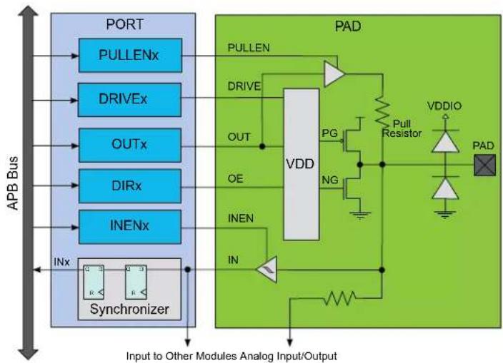
flowchart
graph TD
    A["APB Bus"] --> B["PORT"]
    B --> C["PULLENx"]
    B --> D["DRIVEx"]
    B --> E["OUTx"]
    B --> F["DIRx"]
    B --> G["INENx"]
    B --> H["INx"]
    H --> I["Synchronizer"]
    I --> J["VDD"]
    J --> K["PULLEN"]
    J --> L["DRIVE"]
    J --> M["OUT"]
    J --> N["OE"]
    J --> O["INEN"]
    J --> P["IN"]
    J --> Q["VDDIO"]
    Q --> R["PAD Resistor"]
    R --> S["Pull Resistor"]
    S --> T["PG"]
    T --> J
    J --> U["NG"]
    U --> V["Ground"]
    style A fill:#f9f,stroke:#333
    style B fill:#bbf,stroke:#333
    style I fill:#dfd,stroke:#333
    style J fill:#dfd,stroke:#333
    style K fill:#dfd,stroke:#333
    style L fill:#dfd,stroke:#333
    style M fill:#dfd,stroke:#333
    style N fill:#dfd,stroke:#333
    style O fill:#dfd,stroke:#333
    style P fill:#dfd,stroke:#333
    style Q fill:#dfd,stroke:#333
    style R fill:#dfd,stroke:#333
    style S fill:#dfd,stroke:#333
    style T fill:#dfd,stroke:#333
    style U fill:#dfd,stroke:#333
Note: The ESD diode connected to VDDIO is not plugged for the Back-up I/Os. For these specific pins, only the ESD diode connected to ground is implemented.
28.6.1 Principle of Operation
Each PORT group of up to 32 pins is controlled by the registers in PORT, as described in the figure. These registers in PORT are duplicated for each PORT group, with increasing base addresses. The number of PORT groups may depend on the package/number of pins.
Figure 28-3. Overview of the peripheral functions multiplexing
flowchart
graph TD
    A["Port bit y"] --> B["Port y PINCFG PMUXEN"]
    A --> C["Port y Data+Config"]
    A --> D["Port y PMUX[3:0"]]
    B --> E["Port y Peripheral Mux Enable"]
    C --> F["Port y Line Bundle"]
    D --> G["Port y PMUX Select"]
    H["Periph Signal 0"] --> I["0"]
    J["Periph Signal 1"] --> K["1"]
    L["Peripheral Signals to be muxed to Pad y"] --> M["15"]
    N["Periph Signal 15"] --> M
    I <--> K
    M <--> K
    O["0"] --> P["PORTMUX"]
    Q["1"] --> P
    P --> R["Pad y"]
    P --> S["Line Bundle"]
    T["Pad y"] --> U["PAD y"]
The I/O pins of the device are controlled by PORT peripheral registers. Each port pin has a corresponding bit in the Data Direction (DIR) and Data Output Value (OUT) registers to enable that pin as an output and to define the output state.
The direction of each pin in a PORT group is configured by the DIR register. If a bit in DIR is set to '1', the corresponding pin is configured as an output pin. If a bit in DIR is set to '0', the corresponding pin is configured as an input pin.
When the direction is set as output, the corresponding bit in the OUT register will set the level of the pin. If bit y in OUT is written to '1', pin y is driven HIGH. If bit y in OUT is written to '0', pin y is driven LOW. Pin configuration can be set by Pin Configuration (PINCFGy) registers, with y=00, 01, ..31 representing the bit position.
The Data Input Value (IN) is set as the input value of a port pin with resynchronization to the PORT clock. To reduce power consumption, these input synchronizers are clocked only when system requires reading the input value. The value of the pin can always be read, whether the pin is configured as input or output. If the Input Enable bit in the Pin Configuration registers (PINCFGy.INEN) is '0', the input value will not be sampled.
In PORT, the Peripheral Multiplexer Enable bit in the PINCFGy register (PINCFGy.PMUXEN) can be written to '1' to enable the connection between peripheral functions and individual I/O pins. The Peripheral Multiplexing n (PMUXn) registers select the peripheral function for the corresponding pin. This will override the connection between the PORT and that I/O pin, and connect the selected peripheral signal to the particular I/O pin instead of the PORT line bundle.
28.6.2 Basic Operation
28.6.2.1 Initialization
After reset, all standard function device I/O pads are connected to the PORT with outputs tri-stated and input buffers disabled, even if there is no clock running.
However, specific pins, such as those used for connection to a debugger, may be configured differently, as required by their special function.
28.6.2.2 Operation
Each I/O pin y can be controlled by the registers in PORT. Each PORT group has its own set of PORT registers, the base address of the register set for pin y is at byte address PORT + ([y] * 0x4). The index within that register set is [y].
To use pin number y as an output, write bit y of the DIR register to '1'. This can also be done by writing bit y in the DIRSET register to '1' - this will avoid disturbing the configuration of other pins in that group. The y bit in the OUT register must be written to the desired output value.
Similarly, writing an OUTSET bit to '1' will set the corresponding bit in the OUT register to '1'. Writing a bit in OUTCLR to '1' will set that bit in OUT to zero. Writing a bit in OUTTGL to '1' will toggle that bit in OUT.
To use pin y as an input, bit y in the DIR register must be written to '0'. This can also be done by writing bit y in the DIRCLR register to '1' - this will avoid disturbing the configuration of other pins in that group. The input value can be read from bit y in register IN as soon as the INEN bit in the Pin Configuration register (PINCFGy.INEN) is written to '1'.
Refer to I/O Multiplexing and Considerations for details on pin configuration and PORT groups.
By default, the input synchronizer is clocked only when an input read is requested. This will delay the read operation by two CLK_PORT cycles. To remove the delay, the input synchronizers for each PORT group of eight pins can be configured to be always active, but this will increase power consumption. This is enabled by writing '1' to the corresponding SAMPLINGn bit field of the CTRL register, see CTRL.SAMPLING for details.
To use pin y as one of the available peripheral functions, the corresponding PMUXEN bit of the PINCFGy register must be '1'. The PINCFGy register for pin y is at byte offset (PINCFG0 + [y]).
The peripheral function can be selected by setting the PMUXO or PMUXE in the PMUXn register. The PMUXO/PMUXE is at byte offset PMUX0 + (y/2). The chosen peripheral must also be configured and enabled.
References:
I/O Multiplexing and Considerations
28.6.3 I/O Pin Configuration
The Pin Configuration register (PINCFGy) is used for additional I/O pin configuration. A pin can be set in a totem-pole, or pull configuration.
As pull configuration is done through the Pin Configuration register, all intermediate PORT states during switching of pin direction and pin values are avoided.
The I/O pin configurations are described further in this chapter, and summarized in Table 28-2.
28.6.3.1 Pin Configurations Summary
Table 28-2. Pin Configurations Summary
| DIR INEN PULLEN OUT Configuration | |||
| 0 0 0 X Reset or analog I/O: all digital disabled | |||
| 0 0 1 0 Pull-down; input disabled | |||
| 0 0 1 1 Pull-up; input disabled | |||
| 0 1 0 X Input | |||
| 0 1 1 0 Input with pull-down | |||
| 0 1 1 1 Input with pull-up | |||
| 1 0 X X Output; input disabled | |||
| 1 1 X X Output; input enabled |
28.6.3.2 Input Configuration
Figure 28-4. I/O configuration - Standard Input

flowchart
graph TD
    A["PULLEN"] --> B["Comparator"]
    C["DIR"] --> B
    D["OUT"] --> B
    E["IN"] --> B
    F["INEN"] --> B
    B --> G["Summing Junction"]
    style B fill:#f9f,stroke:#333
    style G fill:#ccf,stroke:#333
Figure 28-5. I/O Configuration - Input with Pull
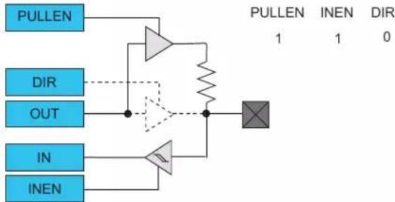
flowchart
graph TD
    A["PULLEN"] --> B["NOT"]
    C["DIR"] --> B
    D["OUT"] --> B
    E["IN"] --> F["NOT"]
    G["INEN"] --> F
    B --> H["Comparator"]
    F --> H
    H --> I["PULLEN 1 INEN DIR 0"]
Note: When pull is enabled, the pull value is defined by the OUT value.
28.6.3.3 Totem-Pole Output
When configured for totem-pole (push-pull) output, the pin is driven low or high according to the corresponding bit setting in the OUT register. In this configuration there is no current limitation for sink or source other than what the pin is capable of. If the pin is configured for input, the pin will float if no external pull is connected.
Note: Enabling the output driver will automatically disable pull.
Figure 28-6. I/O Configuration - Totem-Pole Output with Disabled Input
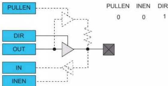
flowchart
graph LR
    A["PULLEN"] --> B["OUT"]
    C["DIR"] --> B
    D["IN"] --> E["INEN"]
    F["NOT"] --> G["Comparator Block"]
    H["0"] --> G
    I["0"] --> G
    J["1"] --> G
Figure 28-7. I/O Configuration - Totem-Pole Output with Enabled Input
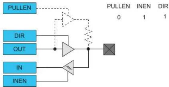
flowchart
graph TD
    A["PULLEN"] --> B["AND"]
    C["DIR"] --> B
    D["OUT"] --> B
    E["IN"] --> F["NOT"]
    G["INEN"] --> F
    B --> H["OR"]
    F --> H
    H --> I["Summing Junction"]
    style H fill:#cccccc,stroke:#333
Figure 28-8. I/O Configuration - Output with Pull
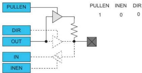
flowchart
graph TD
    A["PULLEN"] --> B["Adder"]
    C["DIR"] --> B
    D["OUT"] --> B
    E["IN"] --> F["Comparator"]
    G["INEN"] --> F
    B --> H["Output"]
    F --> H
28.6.3.4 Digital Functionality Disabled
Neither Input nor Output functionality are enabled.
Figure 28-9. I/O Configuration - Reset or Analog I/O: Digital Output, Input and Pull Disabled
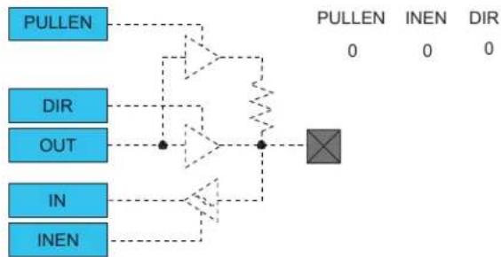
flowchart
graph TD
    A["PULLEN"] --> B["AND"]
    C["DIR"] --> B
    D["OUT"] --> B
    E["IN"] --> F["NOT"]
    G["INEN"] --> F
    B --> H["OR"]
    F --> H
    H --> I["PULLEN 0"]
    H --> J["INEN 0"]
    H --> K["DIR 0"]
28.6.4 Events
The PORT allows input events to control individual I/O pins. These input events are generated by the EVSYS module and can originate from a different clock domain than the PORT module.
The PORT can perform the following actions:
- Output (OUT): I/O pin will be set when the incoming event has a high level ('1') and cleared when the incoming event has a low-level ('0').
- Set (SET): I/O pin will be set when an incoming event is detected.
- Clear (CLR): I/O pin will be cleared when an incoming event is detected.
- Toggle (TGL): I/O pin will toggle when an incoming event is detected.
The event is output to pin without any internal latency. For SET, CLEAR and TOGGLE event actions, the action will be executed up to three clock cycles after a rising edge.
Note: In Standby mode, only the OUT operation is possible and SET, CLEAR and TOGGLE operations are not possible.
The event actions can be configured with the Event Action m bit group in the Event Input Control register( EVCTRL.EVACTm). Writing a '1' to a PORT Event Enable Input m of the Event Control register (EVCTRL.PORTEIm) enables the corresponding action on input event. Writing '0' to this bit disables the corresponding action on input event. Note that several actions can be enabled for incoming events. If several events are connected to the peripheral, any enabled action will be taken for any of the incoming events. Refer to EVSYS. for details on configuring the Event System.
Each event input can address one and only one I/O pin at a time. The selection of the pin is indicated by the PORT Event Pin Identifier of the Event Input Control register (EVCTR.PIDn). On the other hand, one I/O pin can be addressed by up to four different input events. To avoid action conflict on the output value of the register (OUT) of this particular I/O pin, only one action is performed according to the table below.
Note that this truth table can be applied to any SET/CLR/TGL configuration from two to four active input events.
Table 28-3. Priority on Simultaneous SET/CLR/TGL Event Actions
| EVACT0 EVACT1 EVACT2 EVACT3 Executed Event Action | |||
| SET SET SET SET SET | |||
| CLR CLR CLR CLR CLR | |||
| All Other Combinations TGL | |||
Be careful when the event is output to pin. Due to the fact the events are received asynchronously, the I/O pin may have unpredictable levels, depending on the timing of when the events are received. When several events are output to the same pin, the lowest event line will get the access. All other events will be ignored.
References:
EVSYS
28.6.5 PORT Access Priority
The PORT is accessed by different systems:
- The ARM ^ CPU through the ARM ^ single-cycle I/O port (IOBUS)
- The ARM ^ CPU through the high-speed matrix and the AHB/APB bridge (APB)
- EVSYS through four asynchronous input events
The following priority is adopted:
- ARM ^® CPU IOBUS (No wait tolerated)
- APB
- EVSYS input events
For input events that require different actions on the same I/O pin, refer to 28.6.4. Events.
28.7 Register Summary
| Offset | Name Bit Pos. 76543210 | |||||||||
| 0x00 DIR | 7:0 DIR[7:0] | |||||||||
| 15:8 DIR[15:8] | ||||||||||
| 23:16 DIR[23:16] | ||||||||||
| 31:24 DIR[31:24] | ||||||||||
| 0x04 DIRCLR | 7:0 DIRCLR[7:0] | |||||||||
| 15:8 DIRCLR[15:8] | ||||||||||
| 23:16 DIRCLR[23:16] | ||||||||||
| 31:24 DIRCLR[31:24] | ||||||||||
| 0x08 DIRSET | 7:0 DIRSET[7:0] | |||||||||
| 15:8 | DIRSET[15:8] | |||||||||
| 23:16 | DIRSET[23:16] | |||||||||
| 31:24 | DIRSET[31:24] | |||||||||
| 0x0C DIRTGL | 7:0 DIRTGL[7:0] | |||||||||
| 15:8 DIRTGL[15:8] | ||||||||||
| 23:16 DIRTGL[23:16] | ||||||||||
| 31:24 DIRTGL[31:24] | ||||||||||
| 0x10 | OUT | 7:0 | OUT[7:0] | |||||||
| 15:8 | OUT[15:8] | |||||||||
| 23:16 | OUT[23:16] | |||||||||
| 31:24 | OUT[31:24] | |||||||||
| 0x14 | OUTCLR | 7:0 | OUTCLR[7:0] | |||||||
| 15:8 | OUTCLR[15:8] | |||||||||
| 23:16 | OUTCLR[23:16] | |||||||||
| 31:24 | OUTCLR[31:24] | |||||||||
| 0x18 | OUTSET | 7:0 | OUTSET[7:0] | |||||||
| 15:8 | OUTSET[15:8] | |||||||||
| 23:16 | OUTSET[23:16] | |||||||||
| 31:24 | OUTSET[31:24] | |||||||||
| 0x1C | OUTTGL | 7:0 OUTTGL[7:0] | ||||||||
| 15:8 | OUTTGL[15:8] | |||||||||
| 23:16 | OUTTGL[23:16] | |||||||||
| 31:24 | OUTTGL[31:24] | |||||||||
| 0x20 | IN | 7:0 | IN[7:0] | |||||||
| 15:8 | IN[15:8] | |||||||||
| 23:16 IN[23:16] | ||||||||||
| 31:24 IN[31:24] | ||||||||||
| 0x24 | CTRL | 7:0 | SAMPLING[7:0] | |||||||
| 15:8 | SAMPLING[15:8] | |||||||||
| 23:16 | SAMPLING[23:16] | |||||||||
| 31:24 | SAMPLING[31:24] | |||||||||
| 0x28 WRCONFIG | 7:0 | PINMASK[7:0] | ||||||||
| 15:8 | PINMASK[15:8] | |||||||||
| 23:16 | DRVSTR | PULLEN | INEN | PMUXEN | ||||||
| 31:24 | HWSEL | WRPINCFG | WRPMUX | PMUX[3:0] | ||||||
| 0x2C | EVCTRL | 7:0 | PORTEI0 | EVACT0[1:0] | PID0[4:0] | |||||
| 15:8 | PORTEI1 | EVACT1[1:0] | PID1[4:0] | |||||||
| 23:16 | PORTEI2 | EVACT2[1:0] | PID2[4:0] | |||||||
| 31:24 | PORTEI3 | EVACT3[1:0] | PID3[4:0] | |||||||
| 0x30 | PMUXO | 7:0 | PMUXO[3:0] | PMUXE[3:0] | ||||||
| ... | ||||||||||
| 0x3F | PMUX15 | 7:0 | PMUXO[3:0] | PMUXE[3:0] | ||||||
| 0x40 | PINCFG0 | 7:0 | DRVSTR | PULLEN | INEN | PMUXEN | ||||
| ... | ||||||||||
| 0x5F | PINCFG31 | 7:0 | DRVSTR | PULLEN | INEN | PMUXEN | ||||
28.8 Register Description
Registers can be 8, 16, or 32 bits wide. Atomic 8-, 16- and 32-bit accesses are supported. In addition, the 8-bit quarters and 16-bit halves of a 32-bit register, and the 8-bit halves of a 16-bit register can be accessed directly.
Some registers are optionally write-protected by the Peripheral Access Controller (PAC). Optional PAC write-protection is denoted by the "PAC Write-Protection" property in each individual register description. For details, refer to 28.5.8. Register Access Protection.

Tip: The I/O pins are assembled in pin groups ("PORT groups") with up to 32 pins. Group 0 consists of the PA pins, group 1 is for the PB pins, etc. Each pin group has its own PORT registers. For example, the register address offset for the Data Direction (DIR) register for group 0 (PA00 to PA31) is 0x00, and the register address offset for the DIR register for group 1 (PB00 to PB31) is 0x80.
28.8.1 Data Direction
Name: DIR
Offset: 0x00
Reset: 0x00000000
Property: PAC Write-Protection
This register allows the user to configure one or more I/O pins as an input or output. This register can be manipulated without doing a read-modify-write operation by using the Data Direction Toggle (DIRTGL), Data Direction Clear (DIRCLR) and Data Direction Set (DIRSET) registers.

Tip: The I/O pins are assembled in pin groups ("PORT groups") with up to 32 pins. Group 0 consists of the PA pins, group 1 is for the PB pins, and so on. Each pin group has its own PORT registers, with a 0x80 address spacing. For example, the register address offset for the Data Direction (DIR) register for group 0 (PA00 to PA31) is 0x00, and the register address offset for the DIR register for group 1 (PB00 to PB31) is 0x80.
| Bit 31 30 29 28 27 26 25 24 | |
| DIR[31:24] | |
| Access R/W R/W R/W R/W R/W R/W R/W R/W Reset 0 0 0 0 0 0 0 0 | |
| Bit 23 22 21 20 19 18 17 16 | |
| DIR[23:16] | |
| Access R/W R/W R/W R/W R/W R/W R/W R/W Reset 0 0 0 0 0 0 0 0 | |
| Bit 15 14 13 12 11 10 9 8 | |
| DIR[15:8] | |
| Access R/W R/W R/W R/W R/W R/W R/W R/W Reset 0 0 0 0 0 0 0 0 | |
| Bit 7 6 5 4 3 2 1 0 | |
| DIR[7:0] | |
| Access R/W R/W R/W R/W R/W R/W R/W R/W Reset 0 0 0 0 0 0 0 0 | |
Bits 31:0 - DIR[31:0] Port Data Direction
These bits set the data direction for the individual I/O pins in the PORT group.
| Value Description | |
| 0 | The corresponding I/O pin in the PORT group is configured as an input. |
| 1 | The corresponding I/O pin in the PORT group is configured as an output. |
28.8.2 Data Direction Clear
Name: DIRCLR
Offset: 0x04
Reset: 0x00000000
Property: PAC Write-Protection
This register allows the user to set one or more I/O pins as an input, without doing a read-modify-write operation. Changes in this register will also be reflected in the Data Direction (DIR), Data Direction Toggle (DIRTGL) and Data Direction Set (DIRSET) registers.

Tip: The I/O pins are assembled in pin groups ("PORT groups") with up to 32 pins. Group 0 consists of the PA pins, group 1 is for the PB pins, and so on. Each pin group has its own PORT registers, with a 0x80 address spacing. For example, the register address offset for the Data Direction (DIR) register for group 0 (PA00 to PA31) is 0x00, and the register address offset for the DIR register for group 1 (PB00 to PB31) is 0x80.
| Bit 31 30 29 28 27 26 25 24 | |
| DIRCLR[31:24] | |
| Access R/W R/W R/W R/W R/W R/W R/W R/W Reset 0 0 0 0 0 0 0 0 | |
| Bit 23 22 21 20 19 18 17 16 | |
| DIRCLR[23:16] | |
| Access R/W R/W R/W R/W R/W R/W R/W R/W Reset 0 0 0 0 0 0 0 0 | |
| Bit 15 14 13 12 11 10 9 8 | |
| DIRCLR[15:8] | |
| Access R/W R/W R/W R/W R/W R/W R/W R/W Reset 0 0 0 0 0 0 0 0 | |
| Bit 7 6 5 4 3 2 1 0 | |
| DIRCLR[7:0] | |
| Access R/W R/W R/W R/W R/W R/W R/W R/W Reset 0 0 0 0 0 0 0 0 | |
Bits 31:0 - DIRCLR[31:0] Port Data Direction Clear
Writing a '0' to a bit has no effect.
Writing a '1' to a bit will clear the corresponding bit in the DIR register, which configures the I/O pin as an input.
| Value Description | |
| 0 | The corresponding I/O pin in the PORT group will keep its configuration. |
| 1 | The corresponding I/O pin in the PORT group is configured as input. |
28.8.3 Data Direction Set
Name: DIRSET
Offset: 0x08
Reset: 0x00000000
Property: PAC Write-Protection
This register allows the user to set one or more I/O pins as an output, without doing a read-modify-write operation. Changes in this register will also be reflected in the Data Direction (DIR), Data Direction Toggle (DIRTGL) and Data Direction Clear (DIRCLR) registers.

Tip: The I/O pins are assembled in pin groups ("PORT groups") with up to 32 pins. Group 0 consists of the PA pins, group 1 is for the PB pins, and so on. Each pin group has its own PORT registers, with a 0x80 address spacing. For example, the register address offset for the Data Direction (DIR) register for group 0 (PA00 to PA31) is 0x00, and the register address offset for the DIR register for group 1 (PB00 to PB31) is 0x80.
| Bit 31 30 29 28 27 26 25 24 | |
| DIRSET[31:24] | |
| Access R/W R/W R/W R/W R/W R/W R/W R/W Reset 0 0 0 0 0 0 0 0 | |
| Bit 23 22 21 20 19 18 17 16 | |
| DIRSET[23:16] | |
| Access R/W R/W R/W R/W R/W R/W R/W R/W Reset 0 0 0 0 0 0 0 0 | |
| Bit 15 14 13 12 11 10 9 8 | |
| DIRSET[15:8] | |
| Access R/W R/W R/W R/W R/W R/W R/W R/W Reset 0 0 0 0 0 0 0 0 | |
| Bit 7 6 5 4 3 2 1 0 | |
| DIRSET[7:0] | |
| Access R/W R/W R/W R/W R/W R/W R/W R/W Reset 0 0 0 0 0 0 0 0 | |
Bits 31:0 - DIRSET[31:0] Port Data Direction Set
Writing '0' to a bit has no effect.
Writing '1' to a bit will set the corresponding bit in the DIR register, which configures the I/O pin as an output.
| Value Description | |
| 0 | The corresponding I/O pin in the PORT group will keep its configuration. |
| 1 | The corresponding I/O pin in the PORT group is configured as an output. |
28.8.4 Data Direction Toggle
Name:DIRTGL
Offset: 0x0C
Reset: 0x00000000
Property: PAC Write-Protection
This register allows the user to toggle the direction of one or more I/O pins, without doing a read-modify-write operation. Changes in this register will also be reflected in the Data Direction (DIR), Data Direction Set (DIRSET) and Data Direction Clear (DIRCLR) registers.

Tip: The I/O pins are assembled in pin groups ("PORT groups") with up to 32 pins. Group 0 consists of the PA pins, group 1 is for the PB pins, and so on. Each pin group has its own PORT registers, with a 0x80 address spacing. For example, the register address offset for the Data Direction (DIR) register for group 0 (PA00 to PA31) is 0x00, and the register address offset for the DIR register for group 1 (PB00 to PB31) is 0x80.
| Bit 31 30 29 28 27 26 25 24 | |
| DIRTGL[31:24] | |
| Access R/W R/W R/W R/W R/W R/W R/W R/W Reset 0 0 0 0 0 0 0 0 | |
| Bit 23 22 21 20 19 18 17 16 | |
| DIRTGL[23:16] | |
| Access R/W R/W R/W R/W R/W R/W R/W R/W Reset 0 0 0 0 0 0 0 0 | |
| Bit 15 14 13 12 11 10 9 8 | |
| DIRTGL[15:8] | |
| Access R/W R/W R/W R/W R/W R/W R/W R/W Reset 0 0 0 0 0 0 0 0 | |
| Bit 7 6 5 4 3 2 1 0 | |
| DIRTGL[7:0] | |
| Access R/W R/W R/W R/W R/W R/W R/W R/W Reset 0 0 0 0 0 0 0 0 | |
Bits 31:0 -DIRTGL[31:0] Port Data Direction Toggle
Writing '0' to a bit has no effect.
Writing '1' to a bit will toggle the corresponding bit in the DIR register, which reverses the direction of the I/O pin.
| Value | Description |
| 0 | The corresponding I/O pin in the PORT group will keep its configuration. |
| 1 | The direction of the corresponding I/O pin is toggled. |
28.8.5 Data Output Value
Name: OUT
Offset: 0x10
Reset: 0x00000000
Property: PAC Write-Protection
This register sets the data output drive value for the individual I/O pins in the PORT.
This register can be manipulated without doing a read-modify-write operation by using the Data Output Value Clear (OUTCLR), Data Output Value Set (OUTSET), and Data Output Value Toggle (OUTTGL) registers.

Tip: The I/O pins are assembled in pin groups ("PORT groups") with up to 32 pins. Group 0 consists of the PA pins, group 1 is for the PB pins, and so on. Each pin group has its own PORT registers, with a 0x80 address spacing. For example, the register address offset for the Data Direction (DIR) register for group 0 (PA00 to PA31) is 0x00, and the register address offset for the DIR register for group 1 (PB00 to PB31) is 0x80.
| Bit 31 30 29 28 27 26 25 24 | |
| OUT[31:24] | |
| Access R/W R/W R/W R/W R/W R/W R/W R/W Reset 0 0 0 0 0 0 0 0 | |
| Bit 23 22 21 20 19 18 17 16 | |
| OUT[23:16] | |
| Access R/W R/W R/W R/W R/W R/W R/W R/W Reset 0 0 0 0 0 0 0 0 | |
| Bit 15 14 13 12 11 10 9 8 | |
| OUT[15:8] | |
| Access R/W R/W R/W R/W R/W R/W R/W R/W Reset 0 0 0 0 0 0 0 0 | |
| Bit 7 6 5 4 3 2 1 0 | |
| OUT[7:0] | |
| Access R/W R/W R/W R/W R/W R/W R/W R/W Reset 0 0 0 0 0 0 0 0 | |
Bits 31:0 - OUT[31:0] PORT Data Output Value
For pins configured as outputs via the Data Direction register (DIR), these bits set the logical output drive level.
For pins configured as inputs via the Data Direction register (DIR) and with pull enabled via the Pull Enable bit in the Pin Configuration register (PINCFG.PULLEN), these bits will set the input pull direction.
| Value Description | |
| 0 | The I/O pin output is driven low, or the input is connected to an internal pull-down. |
| 1 | The I/O pin output is driven high, or the input is connected to an internal pull-up. |
28.8.6 Data Output Value Clear
Name: OUTCLR
Offset: 0x14
Reset: 0x00000000
Property: PAC Write-Protection
This register allows the user to set one or more output I/O pin drive levels low, without doing a read-modify-write operation. Changes in this register will also be reflected in the Data Output Value (OUT), Data Output Value Toggle (OUTTGL) and Data Output Value Set (OUTSET) registers.

Tip: The I/O pins are assembled in pin groups ("PORT groups") with up to 32 pins. Group 0 consists of the PA pins, group 1 is for the PB pins, and so on. Each pin group has its own PORT registers, with a 0x80 address spacing. For example, the register address offset for the Data Direction (DIR) register for group 0 (PA00 to PA31) is 0x00, and the register address offset for the DIR register for group 1 (PB00 to PB31) is 0x80.
| Bit 31 30 29 28 27 26 25 24 | |
| OUTCLR[31:24] | |
| Access R/W R/W R/W R/W R/W R/W R/W R/W Reset 0 0 0 0 0 0 0 0 | |
| Bit 23 22 21 20 19 18 17 16 | |
| OUTCLR[23:16] | |
| Access R/W R/W R/W R/W R/W R/W R/W R/W Reset 0 0 0 0 0 0 0 0 | |
| Bit 15 14 13 12 11 10 9 8 | |
| OUTCLR[15:8] | |
| Access R/W R/W R/W R/W R/W R/W R/W R/W Reset 0 0 0 0 0 0 0 0 | |
| Bit 7 6 5 4 3 2 1 0 | |
| OUTCLR[7:0] | |
| Access R/W R/W R/W R/W R/W R/W R/W R/W Reset 0 0 0 0 0 0 0 0 | |
Bits 31:0 - OUTCLR[31:0] PORT Data Output Value Clear
Writing '0' to a bit has no effect.
Writing '1' to a bit will clear the corresponding bit in the OUT register. Pins configured as outputs through the Data Direction register (DIR) will be set to low-output drive level. Pins configured as inputs through DIR and with pull enabled through the Pull Enable bit in the Pin Configuration register (PINCFG.PULLEN) will set the input pull direction to an internal pull-down.
| Value Description | |
| 0 | The corresponding I/O pin in the PORT group will keep its configuration. |
| 1 | The corresponding I/O pin output is driven low, or the input is connected to an internal pull-down. |
28.8.7 Data Output Value Set
Name: OUTSET
Offset: 0x18
Reset: 0x00000000
Property: PAC Write-Protection
This register allows the user to set one or more output I/O pin drive levels high, without doing a read-modify-write operation. Changes in this register will also be reflected in the Data Output Value (OUT), Data Output Value Toggle (OUTTGL) and Data Output Value Clear (OUTCLR) registers.

Tip: The I/O pins are assembled in pin groups ("PORT groups") with up to 32 pins. Group 0 consists of the PA pins, group 1 is for the PB pins, and so on. Each pin group has its own PORT registers, with a 0x80 address spacing. For example, the register address offset for the Data Direction (DIR) register for group 0 (PA00 to PA31) is 0x00, and the register address offset for the DIR register for group 1 (PB00 to PB31) is 0x80.
| Bit 31 30 29 28 27 26 25 24 | |
| OUTSET[31:24] | |
| Access R/W R/W R/W R/W R/W R/W R/W R/W Reset 0 0 0 0 0 0 0 0 | |
| Bit 23 22 21 20 19 18 17 16 | |
| OUTSET[23:16] | |
| Access R/W R/W R/W R/W R/W R/W R/W R/W Reset 0 0 0 0 0 0 0 0 | |
| Bit 15 14 13 12 11 10 9 8 | |
| OUTSET[15:8] | |
| Access R/W R/W R/W R/W R/W R/W R/W R/W Reset 0 0 0 0 0 0 0 0 | |
| Bit 7 6 5 4 3 2 1 0 | |
| OUTSET[7:0] | |
| Access R/W R/W R/W R/W R/W R/W R/W R/W Reset 0 0 0 0 0 0 0 0 | |
Bits 31:0 - OUTSET[31:0] PORT Data Output Value Set
Writing '0' to a bit has no effect.
Writing '1' to a bit will set the corresponding bit in the OUT register, which sets the output drive level high for I/O pins configured as outputs via the Data Direction register (DIR). For pins configured as inputs via Data Direction register (DIR) with pull enabled via the Pull Enable register (PULLEN), these bits will set the input pull direction to an internal pull-up.
Value Description
| 0 | The corresponding I/O pin in the group will keep its configuration. |
| 1 | The corresponding I/O pin output is driven high, or the input is connected to an internal pull-up. |
28.8.8 Data Output Value Toggle
Name: OUTTGL
Offset: 0x1C
Reset: 0x00000000
Property: PAC Write-Protection
This register allows the user to toggle the drive level of one or more output I/O pins, without doing a read-modify-write operation. Changes in this register will also be reflected in the Data Output Value (OUT), Data Output Value Set (OUTSET) and Data Output Value Clear (OUTCLR) registers.

Tip: The I/O pins are assembled in pin groups ("PORT groups") with up to 32 pins. Group 0 consists of the PA pins, group 1 is for the PB pins, and so on. Each pin group has its own PORT registers, with a 0x80 address spacing. For example, the register address offset for the Data Direction (DIR) register for group 0 (PA00 to PA31) is 0x00, and the register address offset for the DIR register for group 1 (PB00 to PB31) is 0x80.
| Bit 31 30 29 28 27 26 25 24 | |
| OUTTGL[31:24] | |
| Access R/W R/W R/W R/W R/W R/W R/W R/W Reset 0 0 0 0 0 0 0 0 | |
| Bit 23 22 21 20 19 18 17 16 | |
| OUTTGL[23:16] | |
| Access R/W R/W R/W R/W R/W R/W R/W R/W Reset 0 0 0 0 0 0 0 0 | |
| Bit 15 14 13 12 11 10 9 8 | |
| OUTTGL[15:8] | |
| Access R/W R/W R/W R/W R/W R/W R/W R/W Reset 0 0 0 0 0 0 0 0 | |
| Bit 7 6 5 4 3 2 1 0 | |
| OUTTGL[7:0] | |
| Access R/W R/W R/W R/W R/W R/W R/W R/W Reset 0 0 0 0 0 0 0 0 | |
Bits 31:0 - OUTTGL[31:0] PORT Data Output Value Toggle
Writing '0' to a bit has no effect.
Writing '1' to a bit will toggle the corresponding bit in the OUT register, which inverts the output drive level for I/O pins configured as outputs through the Data Direction register (DIR). For pins configured as inputs through Data Direction register (DIR) with pull enabled through the Pull Enable register (PULLEN), these bits will toggle the input pull direction.
| Value | Description |
| 0 | The corresponding I/O pin in the PORT group will keep its configuration. |
| 1 | The corresponding OUT bit value is toggled. |
28.8.9 Data Input Value
Name: IN
Offset: 0x20
Reset: 0x00000000
Property: -

Tip: The I/O pins are assembled in pin groups ("PORT groups") with up to 32 pins. Group 0 consists of the PA pins, group 1 is for the PB pins, and so on. Each pin group has its own PORT registers, with a 0x80 address spacing. For example, the register address offset for the Data Direction (DIR) register for group 0 (PA00 to PA31) is 0x00, and the register address offset for the DIR register for group 1 (PB00 to PB31) is 0x80.
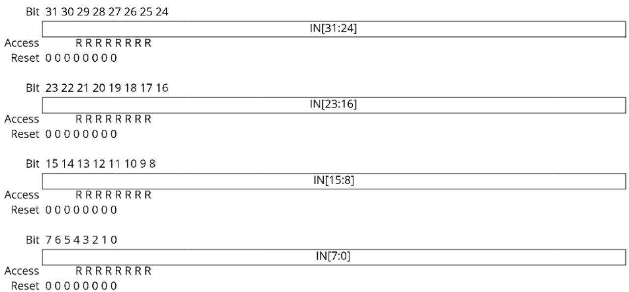
text_image
Bit 31 30 29 28 27 26 25 24 IN[31:24] Access R R R R R R R R Reset 0 0 0 0 0 0 0 0 Bit 23 22 21 20 19 18 17 16 IN[23:16] Access R R R R R R R R Reset 0 0 0 0 0 0 0 0 Bit 15 14 13 12 11 10 9 8 IN[15:8] Access R R R R R R R R Reset 0 0 0 0 0 0 0 0 Bit 7 6 5 4 3 2 1 0 IN[7:0] Access R R R R R R R R Reset 0 0 0 0 0 0 0 0Bits 31:0 - IN[31:0] PORT Data Input Value
These bits are cleared when the corresponding I/O pin input sampler detects a logical low level on the input pin.
These bits are set when the corresponding I/O pin input sampler detects a logical high level on the input pin.
28.8.10 Control
Name: CTRL
Offset: 0x24
Reset: 0x00000000
Property: PAC Write-Protection

Tip: The I/O pins are assembled in pin groups ("PORT groups") with up to 32 pins. Group 0 consists of the PA pins, group 1 is for the PB pins, and so on. Each pin group has its own PORT registers, with a 0x80 address spacing. For example, the register address offset for the Data Direction (DIR) register for group 0 (PA00 to PA31) is 0x00, and the register address offset for the DIR register for group 1 (PB00 to PB31) is 0x80.
| Bit 31 30 29 28 27 26 25 24 | |
| SAMPLING[31:24] | |
| AccessWWWWWWWW | |
| Reset 0 0 0 0 0 0 0 0 | |
| Bit 23 22 21 20 19 18 17 16 | |
| SAMPLING[23:16] | |
| AccessWWWWWWWW | |
| Reset 0 0 0 0 0 0 0 0 | |
| Bit 15 14 13 12 11 10 9 8 | |
| SAMPLING[15:8] | |
| AccessWWWWWWWW | |
| Reset 0 0 0 0 0 0 0 0 | |
| Bit 7 6 5 4 3 2 1 0 | |
| SAMPLING[7:0] | |
| AccessWWWWWWWW | |
| Reset 0 0 0 0 0 0 0 0 | |
Bits 31:0 - SAMPLING[31:0] Input Sampling Mode
Configures the input sampling functionality of the I/O pin input samplers, for pins configured as inputs through the Data Direction register (DIR).
The input samplers are enabled and disabled in sub-groups of eight. Thus if any pins within a byte request continuous sampling, all pins in that eight pin sub-group will be continuously sampled.
| Value Description | |
| 0 | The I/O pin input synchronizer is disabled. |
| 1 | The I/O pin input synchronizer is enabled. |
28.8.11 Write Configuration
Name: WRCONFIG
Offset: 0x28
Reset: 0x00000000
Property: PAC Write-Protection
This write-only register is used to configure several pins simultaneously with the same configuration and peripheral multiplexing.
To avoid side effect of non-atomic access, 8-bit or 16-bit writes to this register will have no effect. Reading this register always returns zero.

Tip: The I/O pins are assembled in pin groups ("PORT groups") with up to 32 pins. Group 0 consists of the PA pins, group 1 is for the PB pins, and so on. Each pin group has its own PORT registers, with a 0x80 address spacing. For example, the register address offset for the Data Direction (DIR) register for group 0 (PA00 to PA31) is 0x00, and the register address offset for the DIR register for group 1 (PB00 to PB31) is 0x80.
Bit 31 30 29 28 27 26 25 24
| HWSEL WRPINCFG WRP MUX PMUX[3;0] | |||||||
| Access | WWWWWWW | ||||||
| Reset | 0 | 0 | 0 | 0 | 0 | 0 | 0 |
Bit 23 22 21 20 19 18 17 16
| DRVSTR | PULLEN | INEN | PMUXEN | ||||
| Access | W | WWW | |||||
| Reset | 0 | 0 | 0 | 0 |
Bit 15 14 13 12 11 10 9 8
| PINMASK[15:8] | ||||||||
| Access Reset | WWWWWWWW | |||||||
| 0 | 0 | 0 | 0 | 0 | 0 | 0 | 0 | |
| Bit | 7 | 6 | 5 | 4 | 3 | 2 | 1 | 0 |
| PINMASK[7:0] | ||||||||
| Access Reset | WWWWWWWW | |||||||
| 0 | 0 | 0 | 0 | 0 | 0 | 0 | 0 | |
Bit 31 - HWSEL Half-Word Select
This bit selects the half-word field of a 32-PORT group to be reconfigured in the atomic write operation.
This bit will always read as zero.
| Value | Description |
| 0 | The lower 16 pins of the PORT group will be configured. |
| 1 | The upper 16 pins of the PORT group will be configured. |
Bit 30 - WRPINCFG Write PINCFG
This bit determines whether the atomic write operation will update the Pin Configuration register (PINCFGy) or not for all pins selected by the WRCONFIG.PINMASK and WRCONFIG.HWSEL bits. Writing '0' to this bit has no effect.
Writing '1' to this bit updates the configuration of the selected pins with the written WRCONFIG.DRVSTR, WRCONFIG.PULLEN, WRCONFIG.INEN, WRCONFIG.PMUXEN and WRCONFIG.PINMASK values.
This bit will always read as zero.
| Value Description | |
| 0 | The PINCFGy registers of the selected pins will not be updated. |
| 1 | The PINCFGy registers of the selected pins will be updated. |
Bit 28 - WRPMUX Write PMUX
This bit determines whether the atomic write operation will update the Peripheral Multiplexing register (PMUXn) or not for all pins selected by the WRCONFIG.PINMASK and WRCONFIG.HWSEL bits. Writing '0' to this bit has no effect.
Writing '1' to this bit updates the pin multiplexer configuration of the selected pins with the written WRCONFIG. PMUX value.
This bit will always read as zero.
| Value Description | |
| 0 | The PMUXn registers of the selected pins will not be updated. |
| 1 | The PMUXn registers of the selected pins will be updated. |
Bits 27:24 - PMUX[3:0] Peripheral Multiplexing
These bits determine the new value written to the Peripheral Multiplexing register (PMUXn) for all pins selected by the WRCONFIG.PINMASK and WRCONFIG.HWSEL bits, when the WRCONFIG.WRPMUX bit is set.
These bits will always read as zero.
Bit 22 - DRVSTR Output Driver Strength Selection
This bit determines the new value written to PINCFGy.DRVSTR for all pins selected by the WRCONFIG.PINMASK and WRCONFIG.HWSEL bits, when the WRCONFIG.WRPINCFG bit is set. This bit will always read as zero.
Bit 18 - PULLEN Pull Enable
This bit determines the new value written to PINCFGy.PULLEN for all pins selected by the WRCONFIG.PINMASK and WRCONFIG.HWSEL bits, when the WRCONFIG.WRPINCFG bit is set. This bit will always read as zero.
Bit 17 - INEN Input Enable
This bit determines the new value written to PINCFGy.INEN for all pins selected by the WRCONFIG.PINMASK and WRCONFIG.HWSEL bits, when the WRCONFIG.WRPINCFG bit is set. This bit will always read as zero.
Bit 16 - PMUXEN Peripheral Multiplexer Enable
This bit determines the new value written to PINCFGy.PMUXEN for all pins selected by the WRCONFIG.PINMASK and WRCONFIG.HWSEL bits, when the WRCONFIG.WRPINCFG bit is set. This bit will always read as zero.
Bits 15:0 - PINMASK[15:0] Pin Mask for Multiple Pin Configuration
These bits select the pins to be configured within the half-word group selected by the WRCONFIG.HWSEL bit.
These bits will always read as zero.
| Value Description | |
| 0 | The configuration of the corresponding I/O pin in the half-word group will be left unchanged. |
| 1 | The configuration of the corresponding I/O pin in the half-word PORT group will be updated. |
28.8.12 Event Input Control
Name: EVCTRL
Offset: 0x2C
Reset: 0x00000000
Property: PAC Write-Protection, Secure

Tip: The I/O pins are assembled in pin groups ("PORT groups") with up to 32 pins. Group 0 consists of the PA pins, group 1 is for the PB pins, and so on. Each pin group has its own PORT registers, with a 0x80 address spacing. For example, the register address offset for the Data Direction (DIR) register for group 0 (PA00 to PA31) is 0x00, and the register address offset for the DIR register for group 1 (PB00 to PB31) is 0x80.
There are up to four input event pins for each PORT group. Each byte of this register addresses one Event input pin.
Bit 31 30 29 28 27 26 25 24
| PORTEI3 EVACT3[1:0] PID3[4:0] | ||
| Access | RW/--/RW RW/--/RW RW/--/RW RW/--/RW RW/--/RW RW/--/RW RW/--/RW | |
| Reset | 0 0 0 0 0 0 0 | |
Bit 23 22 21 20 19 18 17 16
| PORTEI2 EVACT2[1:0] PID2[4:0] | ||
| Access | RW/-/RW RW/-/RW RW/-/RW RW/-/RW RW/-/RW RW/-/RW RW/-/RW | |
| Reset | 0 0 0 0 0 0 0 | |
Bit 15 14 13 12 11 10 98
| PORTEI1 EVACT1[1:0] PID1[4:0] | ||
| Access | RW/-/RW RW/-/RW RW/-/RW RW/-/RW RW/-/RW RW/-/RW RW/-/RW | |
| Reset | 0 0 0 0 0 0 0 | |
Bit 76543210
| PORTEIO EVACT0[1:0] PID0[4:0] | ||
| Access | RW/-/RW RW/-/RW RW/-/RW RW/-/RW RW/-/RW RW/-/RW RW/-/RW | |
| Reset | 0 0 0 0 0 0 0 | |
Bits 7, 15, 23, 31 - PORTEIx PORT Event Input Enable x [x = 3..0]
| Value | Description |
| 0 | The event action x (EVACTx) will not be triggered on any incoming event. |
| 1 | The event action x (EVACTx) will be triggered on any incoming event. |
Bits 5:6, 13:14, 21:22, 29:30 - EVACTx PORT Event Action x [x = 3..0]
These bits define the event action the PORT will perform on event input x. Refer to the PORT Event x Action (x = [3..0]) table in the PIDx bit field.
Bits 0:4, 8:12, 16:20, 24:28 - PIDx PORT Event Pin Identifier x [x = 3..0]
These bits define the I/O pin on which the event action will be performed, according to the following table.
Table 28-4. PORT Event x Action (x = [3..0])
| Value | Name | Description |
| 0x0 | OUT | Output register of pin will be set to level of event. |
| Value Name Description | ||
| 0x1 SET Set output register of pin on event. | ||
| 0x2 CLR Clear output register of pin on event. | ||
| 0x3 TGL Toggle output register of pin on event. | ||
Table 28-5. PORT Event x Pin Identifier (x = [3..0])
| Value Name Description | ||
| 0x0 PIN0 Event action to be executed on PIN 0. | ||
| 0x1 PIN1 Event action to be executed on PIN 1. | ||
| ... ... ... | ||
| 0x31 PIN31 Event action to be executed on PIN 31. |
28.8.13 Peripheral Multiplexing n
Name: PMUXn
Offset: 0x30 + n*0x01 [n=0..15]
Reset: 0x00
Property: PAC Write-Protection

Tip: The I/O pins are assembled in pin groups ("PORT groups") with up to 32 pins. Group 0 consists of the PA pins, group 1 is for the PB pins, and so on Each pin group has its own PORT registers, with a 0x80 address spacing. For example, the register address offset for the Data Direction (DIR) register for group 0 (PA00 to PA31) is 0x00, and the register address offset for the DIR register for group 1 (PB00 to PB31) is 0x80.
There are up to 16 Peripheral Multiplexing registers in each group, one for every set of two subsequent I/O lines. The 'n' denotes the number of the set of I/O lines.
Bit 76543210
| PMUXO[3:0] PMUXE[3:0] |
Access R/W R/W R/W R/W R/W R/W R/W R/W
Reset 00000000
Bits 7:4 - PMUXO[3:0] Peripheral Multiplexing for Odd-Numbered Pin
These bits select the peripheral function for odd-numbered pins (2*n + 1) of a PORT group, if the corresponding PINCFGy.PMUXEN bit is '1'.
Not all possible values for this selection may be valid. For additional information, refer to I/O Multiplexing and Considerations.
| PMUXO[3:0] Name Description | ||
| 0x0 A Peripheral function A selected | ||
| 0x1 B Peripheral function B selected | ||
| 0x2 C Peripheral function C selected | ||
| 0x3 | D | Peripheral function D selected |
| 0x4 | E | Peripheral function E selected |
| 0x5 | F | Peripheral function F selected |
| 0x6 | G | Peripheral function G selected |
| 0x7 | H | Peripheral function H selected |
| 0x8 | I | Peripheral function I selected |
| 0x9-0xF | - | Reserved |
Bits 3:0 - PMUXE[3:0] Peripheral Multiplexing for Even-Numbered Pin
These bits select the peripheral function for even-numbered pins (2*n) of a PORT group, if the corresponding PINCFGy.PMUXEN bit is '1'.
Not all possible values for this selection may be valid. For additional information, refer to the I/O Multiplexing and Considerations.
| PMUXE[3:0] Name Description | ||
| 0x0 | A | Peripheral function A selected |
| 0x1 | B Peripheral function B selected | |
| 0x2 | C | Peripheral function C selected |
| 0x3 | D Peripheral function D selected | |
| 0x4 | E | Peripheral function E selected |
| 0x5 | F | Peripheral function F selected |
| 0x6 | G Peripheral function G selected | |
| ......continued | ||
| PMUXE[3:0] Name Description | ||
| 0x7 H Peripheral function H selected | ||
| 0x8 I Peripheral function I selected | ||
| 0x9-0xF - Reserved | ||
28.8.14 Pin Configuration n
Name: PINCFGn
Offset: 0x40 + n*0x01 [n=0..31]
Reset: 0x00
Property: PAC Write-Protection
Bit 76543210
| DRVSTR | PULLEN | INEN PMUXEN | |||||
| Access Reset | R/W | R/W | R/W | R/W | |||
| 0 | 0 0 0 |
Bit 6 - DRVSTR Output Driver Strength Selection
This bit controls the output driver strength of an I/O pin configured as an output.
| Value | Description |
| 0 | Pin drive strength is set to normal drive strength. |
| 1 | Pin drive strength is set to stronger drive strength. |
Bit 2 - PULLEN Pull Enable
This bit enables the internal pull-up or pull-down resistor of an I/O pin configured as an input.
| Value | Description |
| 0 | Internal pull resistor is disabled, and the input is in a high-impedance configuration. |
| 1 | Internal pull resistor is enabled, and the input is driven to a defined logic level in the absence of external input. |
Bit 1 - INEN Input Enable
This bit controls the input buffer of an I/O pin configured as either an input or output.
Writing a zero to this bit disables the input buffer completely, preventing read-back of the physical pin state when the pin is configured as either an input or output.
| Value | Description |
| 0 | Input buffer for the I/O pin is disabled, and the input value will not be sampled. |
| 1 | Input buffer for the I/O pin is enabled, and the input value will be sampled when required. |
Bit 0 - PMUXEN Peripheral Multiplexer Enable
This bit enables or disables the peripheral multiplexer selection set in the Peripheral Multiplexing register (PMUXn) to enable or disable alternative peripheral control over an I/O pin direction and output drive value.
Writing a zero to this bit allows the PORT to control the pad direction via the Data Direction register (DIR) and output drive value via the Data Output Value register (OUT). The peripheral multiplexer value in PMUXn is ignored. Writing '1' to this bit enables the peripheral selection in PMUXn to control the pad. In this configuration, the physical pin state may still be read from the Data Input Value register (IN) if PINCFGn.INEN is set.
| Value | Description |
| 0 | The peripheral multiplexer selection is disabled, and the PORT registers control the direction and output drive value. |
| 1 | The peripheral multiplexer selection is enabled, and the selected peripheral function controls the direction and output drive value. |
29. EVSYS – Event System
29.1 Overview
The Event System (EVSYS) allows autonomous, low-latency and configurable communication between peripherals.
Several peripherals can be configured to generate and/or respond to signals known as events. The exact condition to generate an event, or the action taken upon receiving an event, is specific to each peripheral. Peripherals that respond to events are called event users. Peripherals that generate events are called event generators. A peripheral can have one or more event generators and can have one or more event users.
Communication is made without CPU intervention and without consuming system resources such as bus or RAM bandwidth. This reduces the load on the CPU and other system resources, compared to a traditional interrupt-based system.
29.2 Features
The following are key feature of the Event System:
- 8 configurable event channels, where each channel can:
- Be connected to any event generator
- Provide a pure asynchronous, resynchronized, or synchronous path
• 69 event generators
• 31 event users
- Configurable edge detector
- Peripherals can be event generators, event users, or both
- SleepWalking and interrupt for operation in sleep modes
- Software event generation
• Each event user can choose which channel to respond to and several event users can share the same channel and thus answer to the same event
29.3 Block Diagram
Figure 29-1. Event System Block Diagram
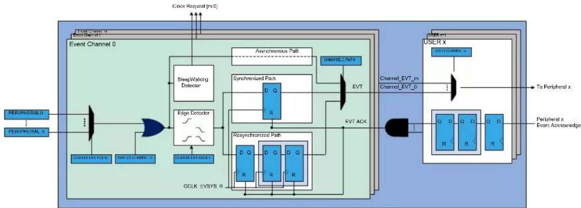
flowchart
graph TD
    subgraph_Event_Channel_0["Event Channel 0"]
        A["PERIPHERAL 0"] --> B["..."]
        C["PERIPHERAL n"] --> D["..."]
        B --> E["Sleep/Walking Detector"]
        D --> F["Edge Detector"]
        E --> G["Synchronized Path"]
        F --> H["Resynchronized Path"]
        G --> I["EVT"]
        H --> J["EVT ACK"]
    end

    subgraph_GCLK_EVSYS_0["GCLK EVSYS 0"]
        K["CHANNEL_LOGS"] --> L["SWST_LOGS"]
        M["CHANNEL_LOGS"] --> N["SWST_LOGS"]
        L --> O["Synchronized Path"]
        N --> P["Synchronized Path"]
        Q["SWST_LOGS"] --> R["SR"]
        S["SWST_LOGS"] --> T["SR"]
        U["SWST_LOGS"] --> V["SR"]
        W["SWST_LOGS"] --> X["SR"]
    end

    subgraph_User_x["USER x"]
        Y["IDENTIFIER x"] --> Z["Channel_EVT_m"]
        Z --> AA["Channel_EVT_0"]
        AB["User x"] --> AC["Q D Q D Q D"]
        AD["User x"] --> AE["Q D Q D Q D"]
        AF["User x"] --> AG["Q D Q D Q D"]
        AH["User x"] --> AI["Q D Q D Q D"]
        AJ["User x"] --> AK["Q D Q D Q D"]
        AL["User x"] --> AM["Q D Q D Q D"]
        AN["User x"] --> AO["Q D Q D Q D"]
        AP["User x"] --> AQ["Q D Q D Q D"]
        AR["User x"] --> AS["Q D Q D Q D"]
        AT["User x"] --> AU["Q D Q D Q D"]
        AV["User x"] --> AW["Q D Q D Q D"]
        AX["User x"] --> AY["Q D Q D Q D"]
        AZ["User x"] --> BA["Q D Q D Q D"]
        BB["User x"] --> BC["Q D Q D Q D"]
        BD["User x"] --> BE["Q D Q D Q D"]
        BF["User x"] --> BG["Q D Q D Q D"]
        BH["User x"] --> BI["Q D Q D Q D"]
        BJ["User x"] --> BK["Q D Q D Q D"]
        BL["User x"] --> BM["Q D Q D Q D"]
        BN["User x"] --> BO["Q D Q D Q D"]
        BP["User x"] --> BQ["Q D Q D Q D"]
        BR["User x"] --> BS["Q D Q D Q D"]
        BT["User x"] --> BU["Q D Q D Q D"]
        BV["User x"] --> BW["Q D Q D Q D"]
        BX["User x"] --> BY["Q D Q D Q D"]
        BZ["User x"] --> CA["Q D Q D Q D"]
        CB["User x"] --> CD["Q D Q D Q D"]
        DD["User x"] --> DJ["Q D Q D Q D"]
        DK["User x"] --> DL["Q D Q D Q D"]
        DV["User x"] --> DW["Q D Q D Q D"]
        DX["User x"] --> DXB["Q D Q D Q D"]
        DXC["User x"] --> DXD["Q D Q D Q D"]
    end

    subgraph_Peripheral_x["Peripheral_x Event Acknowledge"]
        DB["To Peripheral x"] --> AC
        AE["To Peripheral x"] --> AC
        AF["To Peripheral x"] --> AC
        AG["To Peripheral x"] --> AC
    end
29.4 Signal Description
Not applicable.
29.5 Product Dependencies
In order to use this peripheral, other parts of the system must be configured correctly, as described below.
29.5.1 I/O Lines
Not applicable.
29.5.2 Power Management
The EVSYS can be used to wake up the CPU from all sleep modes, even if the clock used by the EVSYS channel and the EVSYS bus clock are disabled. Refer to the PM - Power Manager for details on the different sleep modes.
In all sleep modes, although the clock for the EVSYS is stopped, the device still can wake up the EVSYS clock. Some event generators can generate an event when their clocks are stopped. The generic clock for the channel (GCLK_EVSYS_CHANNEL_n) will be restarted if that channel uses a synchronized path or a resynchronized path. It does not need to wake the system from sleep.
References:
PM - Power Manager
29.5.3 Clocks
The EVSYS bus clock (CLK_EVSYS_APB) can be enabled and disabled in the Main Clock module, and the default state of CLK_EVSYS_APB can be found in Peripheral Clock Masking.
Each EVSYS channel has a dedicated generic clock (GCLK_EVSYS_CHANNEL_n). These are used for event detection and propagation for each channel. These clocks must be configured and enabled in the generic clock controller before using the EVSYS. Refer to GCLK for details.
References:
Peripheral Clock Masking
GCLK
29.5.4 DMA
Not applicable.
29.5.5 Interrupts
The interrupt request line is connected to the Interrupt Controller. Using the EVSYS interrupts requires the interrupt controller to be configured first. Refer to Nested Vector Interrupt Controller for details.
29.5.6 Events
Not applicable.
29.5.7 Debug Operation
When the CPU is halted in debug mode, this peripheral will continue normal operation. If the peripheral is configured to require periodical service by the CPU through interrupts or similar, improper operation or data loss may result during debugging. This peripheral can be forced to halt operation during debugging - refer to the Debug Control (DBGCTRL) register for details.
29.5.8 Register Access Protection
Registers with write-access can be optionally write-protected by the Peripheral Access Controller (PAC), except for the following:
• Channel Status (CHSTATUS)
- Interrupt Flag Status and Clear register (INTFLAG)
Note: Optional write-protection is indicated by the "PAC Write-Protection" property in the register description.
When the CPU is halted in debug mode, all write-protection is automatically disabled. Write-protection does not apply for accesses through an external debugger.
29.5.9 Analog Connections
Not applicable.
29.6 Functional Description
29.6.1 Principle of Operation
The Event System consists of several channels which route the internal events from peripherals (generators) to other internal peripherals or IO pins (users). Each event generator can be selected as source for multiple channels, but a channel cannot be set to use multiple event generators at the same time.
A channel path can be configured in asynchronous, synchronous or re-synchronized mode of operation. The mode of operation must be selected based on the requirements of the application.
When using synchronous or resynchronized path, the Event System includes options to transfer events to users when rising, falling or both edges are detected on event generators.
For further details, refer to Channel Path section of this chapter.
29.6.2 Basic Operation
29.6.2.1 Initialization
Before enabling event routing within the system, the Event Users Multiplexer and Event Channels must be selected in the Event System (EVSYS), and the two peripherals that generate and use the event have to be configured. The recommended sequence is:
- In the event generator peripheral, enable output of event by writing a '1' to the respective Event Output Enable bit ("EO") in the peripheral's Event Control register (e.g., TCC.EVCTRL.MCEO1, AC.EVCTRL.WINEO0, RTC.EVCTRL.OVFEO).
- Configure the EVSYS:
a. Configure the Event User multiplexer by writing the respective EVSYS.USERm register, see also 29.6.2.3. User Multiplexer Setup.
b. Configure the Event Channel by writing the respective EVSYS.CHANNELn register, see also 29.6.2.4. Event System Channel.
- Configure the action to be executed by the event user peripheral by writing to the Event Action bits (EVACT) in the respective Event Control register (e.g., TC.EVCTRL.EVACT, PDEC.EVCTRL.EVACT).
Note: Not all peripherals require this step.
- In the event user peripheral, enable event input by writing a '1' to the respective Event Input Enable bit ("EI") in the peripheral's Event Control register (e.g., AC.EVCTRL.IVEI0, ADC.EVCTRL.STARTEI).
29.6.2.2 Enabling, Disabling, and Resetting
The EVSYS is always enabled.
The EVSYS is reset by writing a '1' to the Software Reset bit in the Control A register (CTRLA.SWRST). All registers in the EVSYS will be reset to their initial state and all ongoing events will be canceled.
Refer to the CTRLA.SWRST register for details.
29.6.2.3 User Multiplexer Setup
The user multiplexer defines the channel to be connected to which event user. Each user multiplexer is dedicated to one event user. A user multiplexer receives all event channels output and must be configured to select one of these channels, as shown in Block Diagram section. The channel is selected with the Channel bit group in the User register (USERm.CHANNEL).
The user multiplexer must always be configured before the channel. A list of all user multiplexers is found in the User (USERm) register description.
References:
USERm
29.6.2.4 Event System Channel
An event channel can select one event from a list of event generators. Depending on configuration, the selected event could be synchronized, resynchronized or asynchronously sent to the users. When synchronization or resynchronization is required, the channel includes an internal edge detector, allowing the Event System to generate internal events when rising, falling or both edges are detected on the selected event generator.
An event channel is able to generate internal events for the specific software commands. A channel block diagram is shown in Block Diagram section.
29.6.2.5 Event Generators
Each event channel can receive the events form all event generators. All event generators are listed in the Event Generator bit field in the Channel n register (CHANNELn.EVGEN). For details on event generation, refer to the corresponding module chapter. The channel event generator is selected by the Event Generator bit group in the Channel register (CHANNELn.EVGEN). By default, the channels are not connected to any event generators (ie, CHANNELn.EVGEN = 0)
29.6.2.6 Channel Path
There are three different ways to propagate the event from an event generator:
- Asynchronous path
- Synchronous path
- Resynchronized path
The path is decided by writing to the Path Selection bit group of the Channel register (CHANNELn.PATH).
Asynchronous Path
When using the asynchronous path, the events are propagated from the event generator to the event user without intervention from the Event System. The GCLK for this channel (GCLK_EVSYS_CHANNEL_n) is not mandatory, meaning that an event will be propagated to the user without any clock latency.
When the asynchronous path is selected, the channel cannot generate any interrupts, and the Channel Status register (CHSTATUS) is always zero. The edge detection is not required and must be disabled by software. Each peripheral event user has to select which event edge must trigger internal actions. For further details, refer to each peripheral chapter description.
Synchronous Path
The synchronous path should be used when the event generator and the event channel share the same generator for the generic clock. If they do not share the same clock, a logic change from the event generator to the event channel might not be detected in the channel, which means that the event will not be propagated to the event user. For details on generic clock generators, refer to GCLK - Generic Clock Controller.
When using the synchronous path, the channel is able to generate interrupts. The channel busy n bit in the Channel Status register (CHSTATUS.CHBUSYn) are also updated and available for use.
Resynchronized Path
The resynchronized path are used when the event generator and the event channel do not share the same generator for the generic clock. When the resynchronized path is used, resynchronization of the event from the event generator is done in the channel. For details on generic clock generators, refer to GCLK - Generic Clock Controller.
When the resynchronized path is used, the channel is able to generate interrupts. The channel busy n bits in the Channel Status register (CHSTATUS.CHBUSYn) are also updated and available for use.
29.6.2.7 Edge Detection
When synchronous or resynchronized paths are used, edge detection must be enabled. The event system can execute edge detection in three different ways:
- Generate an event only on the rising edge
- Generate an event only on the falling edge
- Generate an event on rising and falling edges.
Edge detection is selected by writing to the Edge Selection bit group of the Channel register (CHANNELn.EDGSEL).
29.6.2.8 Event Latency
An event from an event generator is propagated to an event user with different latency, depending on event channel configuration.
- Asynchronous Path: The maximum routing latency of an external event is related to the internal signal routing and it is device dependent.
- Synchronous Path: The maximum routing latency of an external event is one GCLK_EVSYS_CHANNEL_n clock cycle.
- Resynchronized Path: The maximum routing latency of an external event is three GCLK_EVSYS_CHANNEL_n clock cycles.
The maximum propagation latency of a user event to the peripheral clock core domain is three peripheral clock cycles.
The event generators, event channel and event user clocks ratio must be selected in relation with the internal event latency constraints. Events propagation or event actions in peripherals may be lost if the clock setup violates the internal latencies.
29.6.2.9 The Overrun Channel n Interrupt
The Overrun Channel n interrupt flag in the Interrupt Flag Status and Clear register (INTFLAG.OVRn) will be set, and the optional interrupt will be generated in the following cases:
- One or more event users on channel n is not ready when there is a new event.
- An event occurs when the previous event on channel m has not been handled by all event users connected to that channel.
The flag will only be set when using synchronous or resynchronized paths. In the case of asynchronous path, the INTFLAG.OVRn is always read as zero.
29.6.2.10 The Event Detected Channel n Interrupt
The Event Detected Channel n interrupt flag in the Interrupt Flag Status and Clear register (INTFLAG.EVDn) is set when an event coming from the event generator configured on channel n is detected.
The flag will only be set when using a synchronous or resynchronized path. In the case of asynchronous path, the INTFLAG.EVDn is always zero.
29.6.2.11 Channel Status
The Channel Status register (CHSTATUS) shows the status of the channels when using a synchronous or resynchronized path. There are two different status bits in CHSTATUS for each of the available channels:
- The CHSTATUS.CHBUSYn bit will be set when an event on the corresponding channel n has not been handled by all event users connected to that channel.
- The CHSTATUS.USRRDYn bit will be set when all event users connected to the corresponding channel are ready to handle incoming events on that channel.
29.6.2.12 Software Event
A software event can be initiated on a channel by setting the Channel n bit in the Software Event register (SWEVT.CHANNELn) to '1'. Then the software event can be serviced as any event generator; i.e., when the bit is set to '1', an event will be generated on the respective channel.
29.6.3 Interrupts
The EVSYS has the following interrupt sources:
- Overrun Channel n interrupt (OVRn): for details, refer to 29.6.2.9. The Overrun Channel n Interrupt.
- Event Detected Channel n interrupt (EVDn): for details, refer to 29.6.2.10. The Event Detected Channel n Interrupt.
These interrupts events are asynchronous wake-up sources. See 19.6.3.3. Sleep Mode Controller. Each interrupt source has an interrupt flag which is in the Interrupt Flag Status and Clear (INTFLAG) register. The flag is set when the interrupt is issued. Each interrupt event can be individually enabled by setting a '1' to the corresponding bit in the Interrupt Enable Set (INTENSET) register, and disabled by setting a '1' to the corresponding bit in the Interrupt Enable Clear (INTENCLR) register. An interrupt event is generated when the interrupt flag is set and the corresponding interrupt is enabled. The interrupt event works until the interrupt flag is cleared, the interrupt is disabled, or the Event System is reset. See INTFLAG for details on how to clear interrupt flags.
All interrupt events from the peripheral are ORed together on system level to generate one combined interrupt request to the NVIC. Refer to the Nested Vector Interrupt Controller for details. The event user must read the INTFLAG register to determine what the interrupt condition is.
Note that interrupts must be globally enabled for interrupt requests to be generated. Refer to Nested Vector Interrupt Controller for details.
29.6.4 Sleep Mode Operation
The EVSYS can generate interrupts to wake up the device from any sleep mode.
To be able to run in standby, the Run in Standby bit in the Channel register (CHANNELn.RUNSTDBY) must be set to '1'. When the Generic Clock On Demand bit in Channel register (CHANNELn.ONDEMAND) is set to '1' and the event generator is detected, the event channel will request its clock (GCLK_EVSYS_CHANNEL_n). The event latency for a resynchronized channel path will increase by two GCLK_EVSYS_CHANNEL_n clock (i.e., up to five GCLK_EVSYS_CHANNEL_n clock cycles).
A channel will behave differently in different sleep modes regarding to CHANNELn.RUNSTDBY and CHANNELn.ONDEMAND, as shown in the table below:
Table 29-1. Event Channel Sleep Behavior
| CHANNELn.PATH CHAN | NELn.ONDEMAN D | CHANNELn.RUNSTDBY | Sleep Behavior |
| ASYNC 0 0 Only run in IDLE sleep modes if an event | must be propagated. Disabled in STANDBY sleep mode. | ||
| SYNC/RESYNC 0 0 N/A. Works only in Active mode. | |||
| SYNC/RESYNC 0 1 Always run in IDLE and STANDBY sleep modes. | |||
| SYNC/RESYNC 1 0 Only run in IDLE sleep modes if an event | must be propagated. Disabled in STANDBY sleep mode. Two GCLK_EVSYS_n latency added in RESYNC path before the event is propagated internally. | ||
| SYNC/RESYNC 1 1 Always run in IDLE and STANDBY sleep modes. | Two GCLK_EVSYS_n latency added in RESYNC path before the event is propagated internally. | ||
Note: The ONDEMAND and RUNSTDBY bits have no effect for channels when the asynchronous path is selected.
29.7 Register Summary
| Offset | Name Bit Pos. 7 6 5 4 3 2 1 0 | ||||||||||
| 0x00 | CTRLA 7:0 SWRST | ||||||||||
| 0x01 ... 0x0B | Reserved | ||||||||||
| 0x0C | CHSTATUS | 7:0 USRRDY7 USRRDY6 USRRDY5 USRRDY4 USRRDY3 USRRDY2 USRRDY1 USRRDY0 | |||||||||
| 15:8 | |||||||||||
| 23:16 | CHBUSY7 | CHBUSY6 | CHBUSY5 | CHBUSY4 | CHBUSY3 | CHBUSY2 | CHBUSY1 | CHBUSY0 | |||
| 31:24 | |||||||||||
| 0x10 | INTENCLR | 7:0 | OVR7 | OVR6 | OVR5 | OVR4 | OVR3 | OVR2 | OVR1 | OVR0 | |
| 15:8 | |||||||||||
| 23:16 | EVD7 | EVD6 | EVD5 | EVD4 | EVD3 | EVD2 | EVD1 | EVD0 | |||
| 31:24 | |||||||||||
| 0x14 | INTENSET | 7:0 | OVR7 | OVR6 | OVR5 | OVR4 | OVR3 | OVR2 | OVR1 | OVR0 | |
| 15:8 | |||||||||||
| 23:16 | EVD7 | EVD6 | EVD5 | EVD4 | EVD3 | EVD2 | EVD1 | EVD0 | |||
| ......continued | ||||||||||
| Offset | Name Bit Pos. 7 | 6 | 5 | 4 | 3 | 2 | 1 | 0 | ||
| 0x80 USER0 | 7:0 | CHANNEL[3:0] | ||||||||
| 15:8 | ||||||||||
| 23:16 | ||||||||||
| 31:24 | ||||||||||
| ... | ||||||||||
| 0xF8 USER30 | 7:0 | CHANNEL[3:0] | ||||||||
| 15:8 | ||||||||||
| 23:16 | ||||||||||
| 31:24 | ||||||||||
29.8 Register Description
Registers can be 8, 16, or 32 bits wide. Atomic 8-, 16-, and 32-bit accesses are supported. In addition, the 8-bit quarters and 16-bit halves of a 32-bit register, and the 8-bit halves of a 16-bit register can be accessed directly.
Optional write protection by the Peripheral Access Controller (PAC) is denoted by the "PAC Write Protection" property in each individual register description.
Refer to Register Access Protection and PAC - Peripheral Access Controller.
29.8.1 Control A
Name: CTRLA
Offset: 0x00
Reset: 0x00
Property: PAC Write-Protection
Bit 76543210
| SWRST | |||||||
| Access Reset 0 | W | ||||||
Bit 0 - SWRST Software Reset
Writing '0' to this bit has no effect.
Writing '1' to this bit resets all registers in the EVSYS to their initial state.
Note: Before applying a Software Reset it is recommended to disable the event generators.
29.8.2 Channel Status
Name: CHSTATUS
Offset: 0x0C
Reset: 0x00000000
Property: -
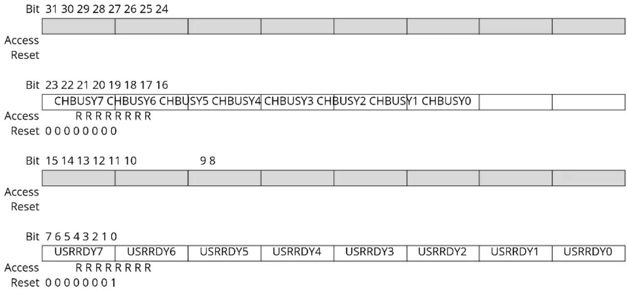
text_image
Bit 31 30 29 28 27 26 25 24 Access Reset Bit 23 22 21 20 19 18 17 16 CHBUSY7 C HBUSY6 CHBU SY5 CHBUSY4 CHBUSY3 CHBUSY2 CHBUSY1 CHBUSY0 Access R R R R R R R R Reset 0 0 0 0 0 0 0 0 Bit 15 14 13 12 11 10 9 8 Access Reset Bit 7 6 5 4 3 2 1 0 USRRDY7 USRRDY6 USRRDY5 USRRDY4 USRRDY3 USRRDY2 USRRDY1 USRRDY0 Access R R R R R R R R Reset 0 0 0 0 0 0 0 1Bits 16, 17, 18, 19, 20, 21, 22, 23 - CHBUSYn Channel Busy n [n = 0..7]
This bit is cleared when channel n is idle.
This bit is set if an event on channel n has not been handled by all event users connected to channel n.
Bits 0, 1, 2, 3, 4, 5, 6, 7 - USRRDYn User Ready for Channel n [n = 0..7]
This bit is cleared when at least one of the event users connected to the channel is not ready.
This bit is set when all event users connected to channel n are ready to handle incoming events on channel n.
29.8.3 Interrupt Enable Clear
Name: INTENCLR
Offset: 0x10
Reset: 0x00000000
Property: PAC Write-Protection
This register allows the user to disable an interrupt without doing a read-modify-write operation. Changes in this register will also be reflected in the Interrupt Enable Set register (INTENSET).
Bit 31 30 29 28 27 26 25 24
| Access Reset |
Bit 23 22 21 20 19 18 17 16
| EVD7 EVD6 EVD5 EVD4 EVD3 EVD2 EVD1 EVD0 | |||||
| Access | R/W R/W R/W R/W R/W R/W R/W R/W | ||||
| Reset | 0 0 0 0 0 0 0 | ||||
Bit 15 14 13 12 11 10 98
| Access Reset |
Bit 76543210
| OVR7 | OVR6 | OVR5 | OVR4 | OVR3 | OVR2 | OVR1 | OVR0 | |
| Access | R/W | R/W | R/W | R/W | R/W | R/W | R/W | R/W |
| Reset | 0 | 0 | 0 | 0 | 0 | 0 | 0 | 0 |
Bits 16, 17, 18, 19, 20, 21, 22, 23 - EVDn Event Detected Channel n Interrupt Enable [n = 0..7]
Writing '0' to this bit has no effect.
Writing '1' to this bit will clear the Event Detected Channel n Interrupt Enable bit, which disables the Event Detected Channel n interrupt.
| Value | Description |
| 0 | The Event Detected Channel n interrupt is disabled. |
| 1 | The Event Detected Channel n interrupt is enabled. |
Bits 0, 1, 2, 3, 4, 5, 6, 7 - OVRn Overrun Channel n Interrupt Enable[n = 0..7]
Writing '0' to this bit has no effect.
Writing '1' to this bit will clear the Overrun Channel n Interrupt Enable bit, which disables the Overrun Channel n interrupt.
| Value | Description |
| 0 | The Overrun Channel n interrupt is disabled. |
| 1 | The Overrun Channel n interrupt is enabled. |
29.8.4 Interrupt Enable Set
Name: INTENSET
Offset: 0x14
Reset: 0x00000000
Property: PAC Write-Protection
This register allows the user to enable an interrupt without doing a read-modify-write operation. Changes in this register will also be reflected in the Interrupt Enable Clear register (INTENCLR).
Bit 31 30 29 28 27 26 25 24
| Access Reset |
Bit 23 22 21 20 19 18 17 16
| EVD7 EVD6 EVD5 EVD4 EVD3 EVD2 EVD1 EVD0 | |||||
| Access | R/W R/W R/W R/W R/W R/W R/W R/W | ||||
| Reset | 0 0 0 0 0 0 0 | ||||
Bit 15 14 13 12 11 10 98
| Access Reset |
Bit 76543210
| OVR7 | OVR6 | OVR5 | OVR4 | OVR3 | OVR2 | OVR1 | OVR0 | |
| Access Reset | R/W R/W R/W R/W R/W R/W R/W R/W | |||||||
| 0 0 0 0 0 0 0 0 | ||||||||
Bits 16, 17, 18, 19, 20, 21, 22, 23 - EVDn Event Detected Channel n Interrupt Enable [n = 0..7]
Writing '0' to this bit has no effect.
Writing '1' to this bit will set the Event Detected Channel n Interrupt Enable bit, which enables the Event Detected Channel n interrupt.
| Value | Description |
| 0 | The Event Detected Channel n interrupt is disabled. |
| 1 | The Event Detected Channel n interrupt is enabled. |
Bits 0, 1, 2, 3, 4, 5, 6, 7 - OVRn Overrun Channel n Interrupt Enable [n = 0..7]
Writing '0' to this bit has no effect.
Writing '1' to this bit will set the Overrun Channel n Interrupt Enable bit, which disables the Overrun Channel n interrupt.
| Value | Description |
| 0 | The Overrun Channel n interrupt is disabled. |
| 1 | The Overrun Channel n interrupt is enabled. |
29.8.5 Interrupt Flag Status and Clear
Name: INTFLAG
Offset: 0x18
Reset: 0x00000000
Property: -
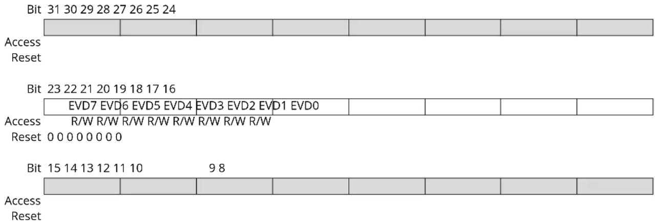
text_image
Bit 31 30 29 28 27 26 25 24 Access Reset Bit 23 22 21 20 19 18 17 16 EVD7 EVD6 EVD5 EVD4 EVD3 EVD2 EVD1 EVD0 Access R/W R/W R/W R/W R/W R/W R/W R/W Reset 0 0 0 0 0 0 0 0 Bit 15 14 13 12 11 10 9 8 Access Reset| Bit 76543210 | ||||||||
| OVR7 | OVR6 | OVR5 | OVR4 | OVR3 | OVR2 | OVR1 | OVR0 | |
| Access Reset 0 0 0 0 0 0 0 | ||||||||
Bits 16, 17, 18, 19, 20, 21, 22, 23 - EVDn Event Detected Channel n [n=0..7]
This flag is set on the next CLK_EVSYS_APB cycle when an event is being propagated through the channel, and an interrupt request will be generated if INTENCLR/SET.EVDn is '1'.
When the event channel path is asynchronous, the EVDn interrupt flag will not be set.
Writing '0' to this bit has no effect.
Writing '1' to this bit will clear the Event Detected Channel n interrupt flag.
Bits 0, 1, 2, 3, 4, 5, 6, 7 - OVRn Overrun Channel n [n=0..7]
This flag is set on the next CLK_EVSYS_APB cycle when an event is being propagated through the channel, and an interrupt request will be generated if INTENCLR/SET.OVRn is '1'.
There are two possible overrun channel conditions:
• One or more of the event users on channel n are not ready when a new event occurs.
- An event happens when the previous event on channel n has not yet been handled by all event users.
When the event channel path is asynchronous, the OVRn interrupt flag will not be set.
Writing '0' to this bit has no effect.
Writing '1' to this bit will clear the Overrun Detected Channel n interrupt flag.
29.8.6 Software Event
Name: SWEVT
Offset: 0x1C
Reset: 0x00000000
Property: PAC Write-Protection
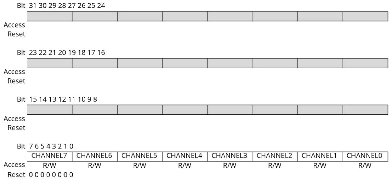
text_image
Bit 31 30 29 28 27 26 25 24 Access Reset Bit 23 22 21 20 19 18 17 16 Access Reset Bit 15 14 13 12 11 10 9 8 Access Reset Bit 7 6 5 4 3 2 1 0 CHANNEL7 CHANNEL6 CHANNEL5 CHANNEL4 CHANNEL3 CHANNEL2 CHANNEL1 CHANNEL0 Access R/W R/W R/W R/W R/W R/W R/W R/W Reset 0 0 0 0 0 0 0Bits 0, 1, 2, 3, 4, 5, 6, 7 - CHANNELn Channel n Software [n=0..7] Selection
Writing '0' to this bit has no effect.
Writing '1' to this bit will trigger a software event for the channel n.
These bits will always return zero when read.
29.8.7 Channel n
Name: CHANNELn
Offset: 0x20 + n*0x04 [n=0..7]
Reset: 0x00000000
Property: PAC Write-Protection
This register allows the user to configure channel n. To write to this register, do a single, 32-bit write of all the configuration data.

text_image
Bit 31 30 29 28 27 26 25 24 Access Reset
text_image
Bit 23 22 21 20 19 18 17 16 Access Reset
text_image
Bit 15 14 13 12 11 10 9 8 ONDEMAND RUNSTDBY EDGSEL[1:0] PATH[1:0] Access R/W R/W R/W R/W R/W Reset 0 0 0 0 0 0 0 0
text_image
Bit 7 6 5 4 3 2 1 0 EVGEN[6:0] Access R/W R/W R/W R/W R/W R/W R/W Reset 0 0 0 0 0 0 0Bit 15 - ONDEMAND Generic Clock On Demand
| Value | Description |
| 0 | Generic clock for a channel is always on, if the channel is configured and generic clock source is enabled. |
| 1 | Generic clock is requested on demand while an event is handled |
Bit 14 - RUNSTDBY Run in Standby
This bit is used to define the behavior during standby sleep mode.
| Value | Description |
| 0 | The channel is disabled in standby sleep mode. |
| 1 | The channel is not stopped in standby sleep mode and depends on the CHANNEL.ONDEMAND |
Bits 11:10 - EDGSEL[1:0] Edge Detection Selection
These bits set the type of edge detection to be used on the channel.
These bits must be written to zero when using the asynchronous path.
| Value | Name | Description |
| 0x0 | NO_EVT_OUTPUT | No event output when using the resynchronized or synchronous path |
| 0x1 | RISING_EDGE | Event detection only on the rising edge of the signal from the event generator |
| 0x2 | FALLING_EDGE | Event detection only on the falling edge of the signal from the event generator |
| 0x3 | BOTH_EDGES | Event detection on rising and falling edges of the signal from the event generator |
Bits 9:8 - PATH[1:0] Path Selection
These bits are used to choose which path will be used by the selected channel.
The path choice can be limited by the channel source, see the table in 29.8.8. USERm.
| Value | Name | Description |
| 0x0 | SYNCHRONOUS | Synchronous path |
| Value Name | Description | |
| 0x1 | RESYNCHRONIZED Resynchronized path | |
| 0x2 | ASYNCHRONOUS Asynchronous path | |
| 0x3 | - Reserved |
Bits 6:0 - EVGEN[6:0] Event Generator
These bits are used to choose the event generator to connect to the selected channel.
| Value Event Generator Description | ||
| 0x00 NONE No event generator selected | ||
| 0x01 OSCCTRL_CFD Clock Failure Detection | ||
| 0x02 OSC32KCTRL_CFD Clock Failure Detection | ||
| 0x03 RTC CMP0 Compare 0 (mode 0 and 1) or Alarm 0 | (mode 2) | |
| 0x04 RTC CMP1 Compare 1 | ||
| 0x05 RTC_TAMPER Tamper Detection | ||
| 0x06 RTC OVF Overflow | ||
| 0x07 RTC PER0 | Period 0 | |
| 0x08 RTC PER1 | Period 1 | |
| 0x09 RTC PER2 | Period 2 | |
| 0x0A | RTC PER3 | Period 3 |
| 0x0B | RTC PER4 | Period 4 |
| 0x0C | RTC PER5 | Period 5 |
| 0x0D | RTC PER6 | Period 6 |
| 0x0E RTC PER7 | Period 7 | |
| 0x0F | EIC EXTINT0 | External Interrupt 0 |
| 0x10 EIC EXTINT1 | External Interrupt 1 | |
| 0x11 EIC EXTINT2 | External Interrupt 2 | |
| 0x12 EIC EXTINT3 | External Interrupt 3 | |
| 0x13 EIC EXTINT4 | External Interrupt 4 | |
| 0x14 EIC EXTINT5 | External Interrupt 5 | |
| 0x15 EIC EXTINT6 | External Interrupt 6 | |
| 0x16 EIC EXTINT7 | External Interrupt 7 | |
| 0x17 EIC EXTINT8 | External Interrupt 8 | |
| 0x18 EIC EXTINT9 | External Interrupt 9 | |
| 0x19 EIC EXTINT10 | External Interrupt 10 | |
| 0x1A | EIC EXTINT11 | External Interrupt 11 |
| 0x1B | EIC EXTINT12 | External Interrupt 12 |
| 0x1C | EIC EXTINT13 | External Interrupt 13 |
| 0x1D | EIC EXTINT14 | External Interrupt 14 |
| 0x1E EIC EXTINT15 | External Interrupt 15 | |
| 0x1F | DMAC CH0 | Channel 0 |
| 0x20 DMAC CH1 | Channel 1 | |
| 0x21 DMAC CH2 | Channel 2 | |
| 0x22 DMAC CH3 | Channel 3 | |
| 0x23 TCCO_OVF | Overflow | |
| 0x24 TCCO_TRG | Trig | |
| 0x25 TCCO_CNT | Counter | |
| 0x26 TCCO_MCO | Match/Capture 0 | |
| 0x27 TCCO_MCO | Match/Capture 1 | |
| 0x28 TCCO_MCO | Match/Capture 2 | |
| 0x29 TCCO_MCO | Match/Capture 3 | |
| 0x2A | TCO OVF | Overflow/Underflow |
| 0x2B | TCO MCO | Match/Capture 0 |
| 0x2C | TCO MCO | Match/Capture 1 |
| 0x2D | TCI OVF | Overflow/Underflow |
| 0x2E TC1 MC0 Match/Capture 0 | ||
| 0x2F TC1 MC0 Match/Capture 1 | ||
| 0x30 TC2 OVF Overflow/Underflow | ||
| 0x31 TC2 MC0 Match/Capture 0 | ||
| 0x32 TC2 MC0 Match/Capture 1 | ||
| 0x33 TC3 OVF Overflow/Underflow | ||
| 0x34 TC3 MC0 Match/Capture 0 | ||
| 0x35 TC3 MC0 Match/Capture 1 | ||
| 0x36 ADC RESRDY Result Ready | ||
| 0x37 ADC WINMON Window Monitor | ||
| 0x38 AC COMP0 Comparator 0 | ||
| 0x39 AC COMP1 Comparator 1 | ||
| 0x3A AC WIN0 Window 0 | ||
| 0x3B PTC EOC End of Conversion | ||
| 0x3C PTC WCOMP Window Comparator | ||
| 0x3D SLCD_FC0 | Frame Counter 0 overflow | |
| 0x3E SCLD_FC1 | Frame Counter 1 overflow | |
| 0x3F SLCD_FC2 | Frame Counter 2 overflow | |
| 0x41 TRNG READY | Data Ready | |
| 0x42 CCL LUTOUT0 | CCL output | |
| 0x43 CCL LUTOUT1 | CCL output | |
| 0x44 CCL LUTOUT2 | CCL output | |
| 0x45 CCL LUTOUT3 | CCL output | |
| 0x46 PAC ACCERR | Access Error | |
| 0x47-0x7F | Reserved |
29.8.8 Event User m
Name: USERm
Offset: 0x80 + m*0x04 [m=0..30]
Reset: 0x00000000
Property: PAC Write-Protection
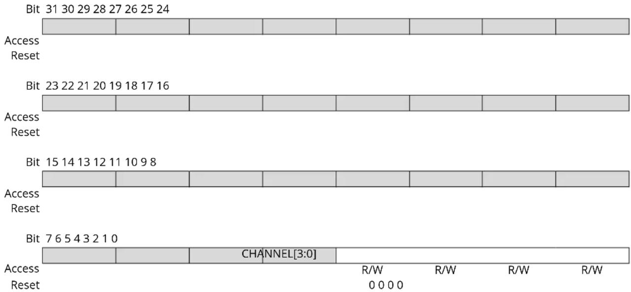
text_image
Bit 31 30 29 28 27 26 25 24 Access Reset Bit 23 22 21 20 19 18 17 16 Access Reset Bit 15 14 13 12 11 10 9 8 Access Reset Bit 7 6 5 4 3 2 1 0 Access Reset CHANNEL[3:0] R/W R/W R/W R/W 0 0 0 0Bits 3:0 - CHANNEL[3:0] Channel Event Selection
These bits are used to select the channel to connect to the event user.
Note that to select channel m, the value (m+1) must be written to the USER.CHANNEL bit group.
| Value | Channel Number |
| 0x00 | No channel output selected |
| 0x01 | 0 |
| 0x02 | 1 |
| 0x03 | 2 |
| 0x04 | 3 |
| 0x05 | 4 |
| 0x06 | 5 |
| 0x07 | 6 |
| 0x08 | 7 |
| 0x09-0xFF | Reserved |
Table 29-2. User Multiplexer Number
| USERm | User Multiplexer | Description | Path Type |
| m = 0 | RTC TAMPEVT | Tamper Event | Asynchronous, synchronous, and resynchronized paths |
| m = 1 | PORT EV0 | Event 0 | Asynchronous, synchronous, and resynchronized paths |
| m = 2 | PORT EV1 | Event 1 | Asynchronous, synchronous, and resynchronized paths |
| m = 3 | PORT EV2 | Event 2 | Asynchronous, synchronous, and resynchronized paths |
| m = 4 | PORT EV3 | Event 3 | Asynchronous, synchronous, and resynchronized paths |
| USERm User Multiplexer Description Path Type | |||
| m = 5 DMAC CH0 Channel 0 Synchronous, and | resynchronized paths | ||
| m = 6 DMAC CH1 Channel 1 Synchronous, and | resynchronized paths | ||
| m = 7 DMAC CH2 Channel 2 Synchronous, and | resynchronized paths | ||
| m = 8 DMAC CH3 Channel 3 Synchronous, and | resynchronized paths | ||
| m = 9 TCC0 EV0 - Asynchronous, synchronous, | and resynchronized paths | ||
| m = 10 TCC0 EV1 - Asynchronous, synchronous, | and resynchronized paths | ||
| m = 11 TCC0 MC0 Match/Capture 0 Asynchronous, synchronous, | and resynchronized paths | ||
| m = 12 TCC0 MC1 Match/Capture 1 Asynchronous, synchronous, | and resynchronized paths | ||
| m = 13 TCC0 MC2 Match/Capture 2 Asynchronous, synchronous, | and resynchronized paths | ||
| m = 14 TCC0 MC3 Match/Capture 3 Asynchronous, synchronous, | and resynchronized paths | ||
| m = 15 TC0 - Asynchronous, synchronous, | and resynchronized paths | ||
| m = 16 TC1 - Asynchronous, synchronous, | and resynchronized paths | ||
| m = 17 TC2 - Asynchronous, synchronous, | and resynchronized paths | ||
| m = 18 TC3 - Asynchronous, synchronous, | and resynchronized paths | ||
| m = 19 ADC START ADC start conversion Asynchronous, synchronous, | and resynchronized paths | ||
| m = 20 ADC SYNC Flush ADC Asynchronous, synchronous, | and resynchronized paths | ||
| m = 21 AC COMP0 | Start comparator 0 | Asynchronous, synchronous,and resynchronized paths | |
| m = 22 AC COMP1 | Start comparator 1 | Asynchronous, synchronous,and resynchronized paths | |
| m = 23 PTC STCONV | PTC start conversion | Asynchronous, synchronous,and resynchronized paths | |
| m = 24 CCL LUTIN 0 | CCL input | Asynchronous, synchronous,and resynchronized paths | |
| m = 25 CCL LUTIN 1 | CCL input | Asynchronous, synchronous,and resynchronized paths | |
| m = 26 CCL LUTIN 2 | CCL input | Asynchronous, synchronous,and resynchronized paths | |
| m = 27 CCL LUTIN 3 | CCL input | Asynchronous, synchronous,and resynchronized paths | |
| m = 29 MTB START | Tracing start | Asynchronous, synchronous,and resynchronized paths | |
| m = 30 MTB STOP | Tracing stop | Asynchronous, synchronous,and resynchronized paths | |
30. SERCOM – Serial Communication Interface
30.1 Overview
There are up to six instances of the Serial Communication interface (SERCOM) peripheral.
A SERCOM can be configured to support a number of modes: I2C, SPI, and USART. When an instance of SERCOM is configured and enabled, all of the resources of that SERCOM instance will be dedicated to the selected mode.
The SERCOM serial engine consists of a transmitter and receiver, baud-rate generator and address matching functionality. It can use the internal generic clock or an external clock. Using an external clock allows the SERCOM to be operated in all Sleep modes.
30.2 Features
- Interface for Configuring into one of the following (selected by CTRLA.MODE[2:0]):
- Inter-Integrated Circuit (I ^2 C) two-wire serial interface
- System Management Bus (SMBus ^TM ) compatible
- Serial Peripheral Interface (SPI)
-
Universal Synchronous/Asynchronous Receiver/Transmitter (USART)
-
Single Transmit Buffer and Double Receive Buffer
- Baud-rate Generator
- Address Match/mask Logic
- Operational in all Sleep modes with an External Clock Source
- Can be used with DMA
See the Related Links for full feature lists of the interface configurations.
30.3 Block Diagram
Figure 30-1. SERCOM Block Diagram
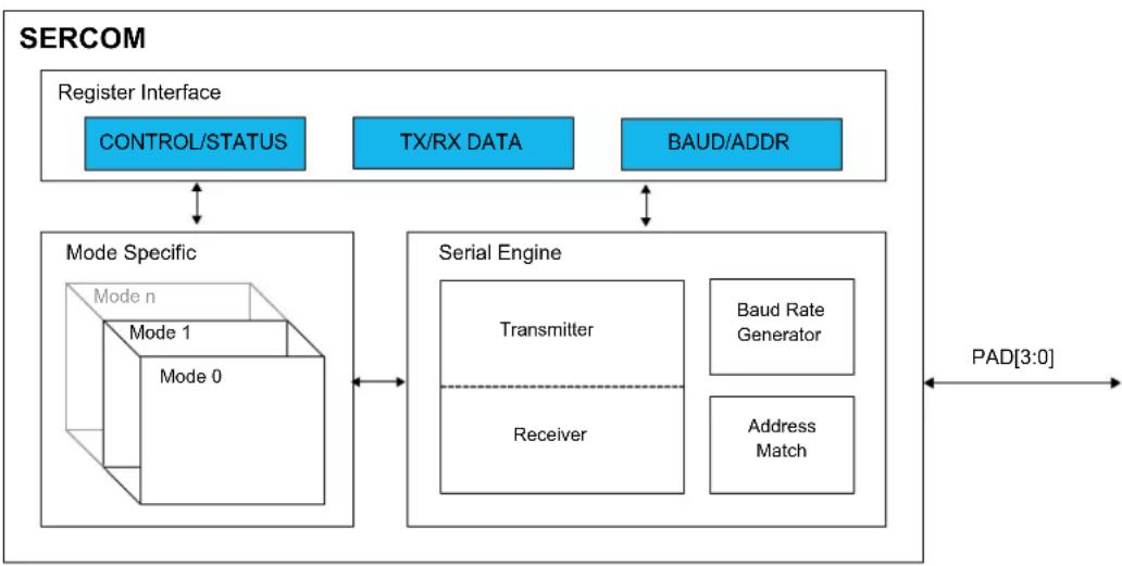
flowchart
graph TD
    A["Register Interface"] --> B["CONTROL/STATUS"]
    C["TX/RX DATA"] --> D["Mode Specific"]
    E["BAUD/ADDR"] --> F["Serial Engine"]
    B <--> F
    D <--> F
    F --> G["Transmitter"]
    F --> H["Receiver"]
    F --> I["Baud Rate Generator"]
    F --> J["Address Match"]
    G <--> K["PAD[3:0"]]
    H <--> K
    I <--> K
    J <--> K
30.4 Signal Description
See the respective SERCOM mode chapters for details.
30.5 Product Dependencies
In order to use this peripheral, other parts of the system must be configured correctly, as described below.
30.5.1 I/O Lines
Using the SERCOM I/O lines requires the I/O pins to be configured using port configuration (PORT).
The PORT Control bit (PINCFGn.DRVSTR) is still effective for the SERCOM output pins. The PORT Control bit (PINCFGn.PULLEN) is still effective on the SERCOM input pins, but is limited to the enabling or disabling of a pull down only (it is not possible to enable or disable a pull up)
The SERCOM has four internal pads, PAD[3:0], and the signals from I²C, SPI, and USART are routed through these SERCOM pads, through a multiplexer. The configuration of the multiplexer is available from the different SERCOM modes. Refer to the mode-specific chapters for additional information.
30.5.2 Power Management
The SERCOM can operate in any Sleep mode provided the selected clock source is running. SERCOM interrupts can be configured to wake the device from sleep modes.
30.5.3 Clocks
The SERCOM bus clock (CLK_SERCOMx_APB) can be enabled and disabled in the Main Clock Controller. Refer to Peripheral Clock Masking for details and default status of this clock.
The SERCOM uses two generic clocks: GCLK_SERCOMx_CORE and GCLK_SERCOMx_SLOW. The core clock (GCLK_SERCOMx_CORE) is required to clock the SERCOM while working as a host. The slow clock (GCLK_SERCOMx_SLOW) is only required for certain functions. See specific mode chapters for details.
These clocks must be configured and enabled in the Generic Clock Controller (GCLK) before using the SERCOM.
The generic clocks are asynchronous to the user interface clock (CLK_SERCOMx_APB). Due to this asynchronicity, writing to certain registers will require synchronization between the clock domains. Refer to 30.6.8. Synchronization for details.
30.5.4 DMA
The DMA request lines are connected to the DMA Controller (DMAC). The DMAC must be configured before the SERCOM DMA requests are used.
30.5.5 Interrupts
The interrupt request line is connected to the Interrupt Controller (NVIC). The NVIC must be configured before the SERCOM interrupts are used.
30.5.6 Events
Not applicable.
30.5.7 Debug Operation
When the CPU is halted in Debug mode, this peripheral will continue normal operation. If the peripheral is configured to require periodical service by the CPU through interrupts or similar, improper operation or data loss may result during debugging. This peripheral can be forced to halt operation during debugging - refer to the Debug Control (DBGCTRL) register for details.
30.5.8 Register Access Protection
Registers with write-access can be write-protected optionally by the Peripheral Access Controller (PAC).
Optional write protection by the Peripheral Access Controller (PAC) is denoted by the "PAC Write Protection" property in each individual register description.
PAC write protection does not apply to accesses through an external debugger.
30.5.9 Analog Connections
Not applicable.
30.6 Functional Description
30.6.1 Principle of Operation
The basic structure of the SERCOM serial engine is shown in SERCOM Serial Engine. Labels in capital letters are synchronous to the system clock and accessible by the CPU; labels in lowercase letters can be configured to run on the GCLK_SERCOMx_CORE clock or an external clock.
Figure 30-2. SERCOM Serial Engine
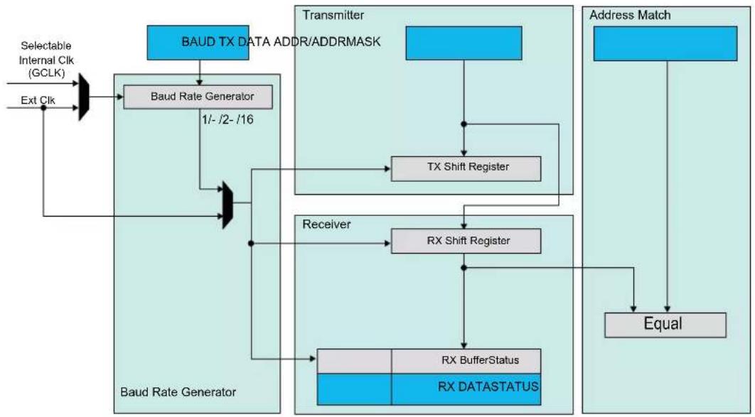
flowchart
graph TD
    A["Selectable Internal Clk (GCLK)"] --> B["BAUD TX DATA ADDR/ADDRMASK"]
    C["Ext Clk"] --> B
    B --> D["Baud Rate Generator"]
    D --> E["1/- /2- /16"]
    E --> F["BAUD TX DATA ADDR/ADDRMASK"]
    F --> G["TX Shift Register"]
    G --> H["Receiver"]
    H --> I["RX Shift Register"]
    I --> J["RX BufferStatus"]
    I --> K["RX DATASTATUS"]
    L["Address Match"] --> M["Equal"]
    M --> J
    M --> K
The transmitter consists of a single write buffer and a Shift register.
The receiver consists of a one-level (I²C), or two-level (USART, SPI) receive buffer and a Shift register.
The baud-rate generator is capable of running on the GCLK_SERCOMx_CORE clock or an external clock.
Address matching logic is included for SPI and I²C operation.
30.6.2 Basic Operation
30.6.2.1 Initialization
The SERCOM must be configured to the desired mode by writing the Operating Mode bits in the Control A register (CTRLA.MODE) as shown in the table below.
Table 30-1. SERCOM Modes
| CTRLA.MODE Description | |
| 0x0 USART with external clock | |
| 0x1 USART with Internal clock | |
| ......continued | |
| CTRLA.MODE Description | |
| 0x2 SPI in client operation | |
| 0x3 SPI in host operation | |
| 0x4 I | ^2C client operation |
| 0x5 I | ^2C host operation |
| 0x6-0x7 Reserved | |
For further initialization information, see the respective SERCOM mode chapters:
30.6.2.2 Enabling, Disabling, and Resetting
This peripheral is enabled by writing '1' to the Enable bit in the Control A register (CTRLA.ENABLE), and disabled by writing '0' to it.
Writing '1' to the Software Reset bit in the Control A register (CTRLA.SWRST) will reset all registers of this peripheral to their initial states, except the DBGCTRL register, and the peripheral is disabled.
Refer to the CTRLA register description for details.
30.6.2.3 Clock Generation - Baud-Rate Generator
The baud-rate generator, as shown in the following figure, generates internal clocks for asynchronous and synchronous communication. The output frequency ( f_BAUD ) is determined by the Baud register (BAUD) setting and the baud reference frequency ( f_ref ). The baud reference clock is the serial engine clock, and it can be internal or external.
For asynchronous communication, the /16 (divide-by-16) output is used when transmitting, whereas the /1 (divide-by-1) output is used while receiving.
For synchronous communication, the /2 (divide-by-2) output is used.
This functionality is automatically configured, depending on the selected operating mode.
Figure 30-3. Baud Rate Generator
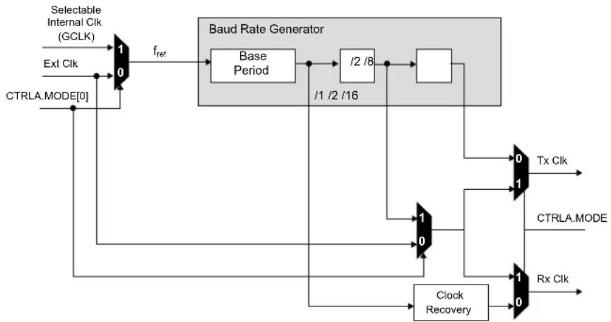
flowchart
graph TD
    A["Selectable Internal Cik (GCLK)"] --> B["1"]
    C["Ext Cik"] --> D["0"]
    E["CTRLA.MODE[0"]] --> D
    D --> F["f_ref"]
    F --> G["Base Period"]
    G --> H["/2 /8"]
    H --> I["/1 /2 /16"]
    I --> J["Square Block"]
    J --> K["Tx Cik"]
    L["Clock Recovery"] --> M["1"]
    M --> N["0"]
    O["CTRLA.MODE"] --> P["1"]
    P --> Q["Tx Cik"]
    R["Rx Cik"] --> S["1"]
    S --> T["0"]
    U["Baud Rate Generator"] --> V["/1 /2 /16"]
    V --> W["/2 /8"]
    W --> X["/1 /2 /16"]
    X --> Y["Square Block"]
    Y --> Z["Tx Cik"]
    AA["Clock Recovery"] --> AB["1"]
    AB --> AC["Tx Cik"]
The following table contains equations for the baud rate (in bits per second) and the BAUD register value for each operating mode.
For asynchronous operation, there are two modes:
- Arithmetic mode: the BAUD register value is 16 bits (0 to 65,535)
- Fractional mode: the BAUD register value is 13 bits, while the fractional adjustment is 3 bits. In this mode the BAUD setting must be greater than or equal to 1.
For synchronous operation, the BAUD register value is 8 bits (0 to 255).
Table 30-2. Baud Rate Equations
| Operating Mode Condition Baud Rate (Bits Per Second) BAUD Register Value Calculation | |||
| Asynchronous Arithmetic | f_BAUD ≤ _ref16 | f_BAUD = _ref16 ( 1 - 65536 ) | BAUD = 65536 · 1 - ( S · _BAUDf_ref ) |
| Asynchronous Fractional | f_BAUD ≤ _refS | f_BAUD = _refS · ( BAUD + 8 ) | BAUD = _refS · f_BAUD - 8 |
| Synchronous | f_BAUD ≤ _ref2 | f_BAUD = _ref2 · B(AUD+1) | BAUD = _ref2 · f_BAUD - 1 |
S - Number of samples per bit, which can be 16, 8, or 3.
The Asynchronous Fractional option is used for auto-baud detection.
The baud rate error is represented by the following formula:
$$ \text { Error } = 1 - \left(\frac {\text { ExpectedBaudRate }}{\text { ActualBaudRate }}\right) $$
30.6.2.3.1 Asynchronous Arithmetic Mode BAUD Value Selection
The formula given for f_BAUD calculates the average frequency over 65536 f_ref cycles. Although the BAUD register can be set to any value between 0 and 65536, the actual average frequency of f_BAUD over a single frame is more granular. The BAUD register values that will affect the average frequency over a single frame lead to an integer increase in the cycles per frame (CPF)
$$ C P F = \frac {f _ {r e f}}{f _ {B A U D}} (D + S) $$
where
• D represent the data bits per frame
- S represent the sum of start and first stop bits, if present.
The following table shows the BAUD register value versus baud frequency f_BAUD at a serial engine frequency of 48 MHz. This assumes a D value of 8 bits and an S value of 2 bits (10 bits, including start and stop bits).
Table 30-3. BAUD Register Value vs. Baud Frequency
| BAUD Register Value Serial Engine CPF f | _BAUD at 100MHz Serial Engine Frequency ( f_REF ) | |
| 0 – 406 161 6.211 MHz | ||
| 407 – 808 | 162 6.211 MHz | |
| 809 – 1205 | 163 6.173 MHz | |
| ... | ... | ... |
| 65206 | 31775 | 31.47 kHz |
| 65207 | 31872 | 31.38 kHz |
| 65208 | 31969 | 31.28 kHz |
30.6.3 Additional Features
30.6.3.1 Address Match and Mask
The SERCOM address match and mask feature is capable of matching either one address, two unique addresses, or a range of addresses with a mask, based on the mode selected. The match uses seven or eight bits, depending on the mode.
30.6.3.1.1 Address With Mask
An address written to the Address bits in the Address register (ADDR.ADDR), and a mask written to the Address Mask bits in the Address register (ADDR.ADDRMASK) will yield an address match. All bits that are masked are not included in the match. Note that writing the ADDR.ADDRMASK to 'all zeros' will match a single unique address, while writing ADDR.ADDRMASK to 'all ones' will result in all addresses being accepted.
Figure 30-4. Address With Mask
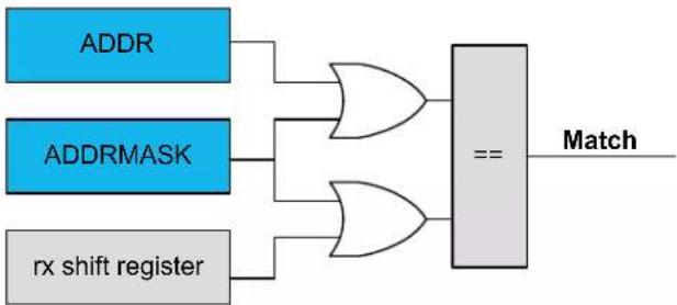
flowchart
graph LR
    A["ADDR"] --> C["AND"]
    B["ADDRMASK"] --> C
    D["rx shift register"] --> E["AND"]
    C --> F["=="]
    E --> F
    F --> G["Match"]
30.6.3.1.2 Two Unique Addresses
The two addresses written to ADDR and ADDRMASK will cause a match.
Figure 30-5. Two Unique Addresses
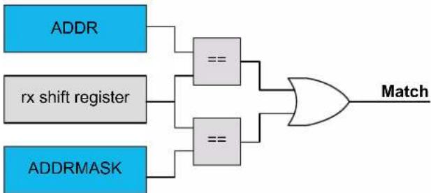
flowchart
graph LR
    A["ADDR"] --> B["=="]
    C["rx shift register"] --> D["=="]
    E["ADDRMASK"] --> F["=="]
    B --> G["OR"]
    D --> G
    F --> G
    G --> H["Match"]
30.6.3.1.3 Address Range
The range of addresses between and including ADDR.ADDR and ADDR.ADDRMASK will cause a match. ADDR.ADDR and ADDR.ADDRMASK can be set to any two addresses, with ADDR.ADDR acting as the upper limit and ADDR.ADDRMASK acting as the lower limit.
Figure 30-6. Address Range

text_image
ADDRMASK rx shift register ADDR == Match30.6.4 DMA Operation
The available DMA interrupts and their depend on the operation mode of the SERCOM peripheral. Refer to the Functional Description sections of the respective SERCOM mode.
30.6.5 Interrupts
Interrupt sources are mode specific. See the respective SERCOM mode chapters for details.
Each interrupt source has its own Interrupt flag.
The Interrupt flag in the Interrupt Flag Status and Clear register (INTFLAG) will be set when the Interrupt condition is met.
Each interrupt can be individually enabled by writing '1' to the corresponding bit in the Interrupt Enable Set register (INTENSET), and disabled by writing '1' to the corresponding bit in the Interrupt Enable Clear register (INTENCLR).
An interrupt request is generated when the Interrupt flag is set and the corresponding interrupt is enabled. The interrupt request remains active until either the Interrupt flag is cleared, the interrupt is disabled, or the SERCOM is reset. For details on clearing Interrupt flags, refer to the INTFLAG register description.
The value of INTFLAG indicates which Interrupt condition occurred. The user must read the INTFLAG register to determine which Interrupt condition is present.
Note: Interrupts must be globally enabled for interrupt requests to be generated.
30.6.6 Events
Not applicable.
30.6.7 Sleep Mode Operation
The peripheral can operate in any Sleep mode where the selected serial clock is running. This clock can be external or generated by the internal baud-rate generator.
The SERCOM interrupts can be used to wake-up the device from Sleep modes. Refer to the different SERCOM mode chapters for details.
30.6.8 Synchronization
Due to asynchronicity between the main clock domain and the peripheral clock domains, some registers need to be synchronized when written or read.
Required write synchronization is denoted by the "Write-Synchronized" property in the register description.
Required read synchronization is denoted by the "Read-Synchronized" property in the register description.
31. SERCOM USART – SERCOM Universal Synchronous and Asynchronous Receiver and Transmitter
31.1 Overview
The Universal Synchronous and Asynchronous Receiver and Transmitter (USART) is one of the available modes in the Serial Communication Interface (SERCOM).
The USART uses the SERCOM transmitter and receiver, see 31.3. Block Diagram. Labels in uppercase letters are synchronous to CLK_SERCOMx_APB and accessible for CPU. Labels in lowercase letters can be programmed to run on the internal generic clock or an external clock.
The transmitter consists of a single write buffer, a shift register, and control logic for different frame formats. The write buffer support data transmission without any delay between frames. The receiver consists of a two-level receive buffer and a shift register. Status information of the received data is available for error checking. Data and clock recovery units ensure robust synchronization and noise filtering during asynchronous data reception.
References:
SERCOM - Serial Communication Interface
SERCOM USART and I²C Configurations
31.2 USART Features
• Full-duplex operation
- Asynchronous (with clock reconstruction) or synchronous operation
- Internal or external clock source for asynchronous and synchronous operation
- Baud-rate generator
- Supports serial frames with 5, 6, 7, 8 or 9 data bits and 1 or 2 stop bits
- Odd or even parity generation and parity check
- Selectable LSB- or MSB-first data transfer
- Buffer overflow and frame error detection
- Noise filtering, including false start-bit detection and digital low-pass filter
- Collision detection
- Can operate in all sleep modes
- Operation at speeds up to half the system clock for internally generated clocks
- Operation at speeds up to the system clock for externally generated clocks
• RTS and CTS flow control
- IrDA modulation and demodulation up to 115.2kbps
- Start-of-frame detection
- Can work with DMA
References:
Features
31.3 Block Diagram
Figure 31-1. USART Block Diagram

flowchart
graph TD
    A["GCLK (internal)"] --> B["baud rate generator"]
    B --> C["/1 - /2 - /16"]
    D["XCK"] --> E["->"]
    E --> F["tx shift register"]
    F --> G["TxD"]
    F --> H["RxD"]
    I["status"] --> J["rx buffer"]
    K["STATUS"] --> L["RX DATA"]
    M["BAUD"] --> N["->"]
    O["TX DATA"] --> P["->"]
    Q["->"] --> R["->"]
    S["->"] --> T["->"]
31.4 Signal Description
Table 31-1. SERCOM USART Signals
| Signal Name Type Description | ||
| PAD[3:0] Digital I/O General SERCOM pins | ||
One signal can be mapped to one of several pins.
References:
I/O Multiplexing and Considerations
31.5 Product Dependencies
In order to use this peripheral, other parts of the system must be configured correctly, as described below.
31.5.1 I/O Lines
Using the USART's I/O lines requires the I/O pins to be configured using the I/O Pin Controller (PORT).
When the SERCOM is used in USART mode, the SERCOM controls the direction and value of the I/O pins according to the table below. PORT Control bit PINCFGn.DRVSTR is still effective for the SERCOM output pins. PORT Control bit PINCFGn.PULLEN is still effective on the SERCOM input pins, but is limited to the enabling/disabling of a pull down only (it is not possible to enable/disable a pull up). If the receiver or transmitter is disabled, these pins can be used for other purposes.
Table 31-2. USART Pin Configuration
| Pin Pin Configuration | |
| TxD Output | |
| RxD Input | |
| XCK Output or input |
The combined configuration of PORT and the Transmit Data Pinout and Receive Data Pinout bit fields in the Control A register (CTRLA.TXPO and CTRLA.RXPO, respectively) will define the physical position of the USART signals in the previous table USART Pin Configuration.
References:
- PORT - I/O Pin Controller
31.5.2 Power Management
This peripheral can continue to operate in any sleep mode where its source clock is running. The interrupts can wake up the device from sleep modes.
References:
PM - Power Manager
31.5.3 Clocks
The SERCOM bus clock (CLK_SERCOMx_APB) is enabled by default, and can be disabled and enabled in the Main Clock Controller. Refer to Peripheral Clock Masking for details.
A generic clock (GCLK_SERCOMx_CORE) is required to clock the SERCOMx_CORE. This clock must be configured and enabled in the Generic Clock Controller before using the SERCOMx_CORE. Refer to 15. GCLK - Generic Clock Controller for details.
This generic clock is asynchronous to the bus clock (CLK_SERCOMx_APB). Therefore, writing to certain registers will require synchronization to the clock domains. Refer to 32.6.6. Synchronization for further details.
31.5.4 DMA
The DMA request lines are connected to the DMA Controller (DMAC). In order to use DMA requests with this peripheral the DMAC must be configured first. Refer to the DMAC - Direct Memory Access Controller for details.
31.5.5 Interrupts
The interrupt request line is connected to the Interrupt Controller. In order to use interrupt requests of this peripheral, the Interrupt Controller (NVIC) must be configured first. Refer to the Nested Vector Interrupt Controller for details.
31.5.6 Events
Not applicable.
31.5.7 Debug Operation
When the CPU is halted in debug mode, this peripheral will continue normal operation. If the peripheral is configured to require periodical service by the CPU through interrupts or similar, improper operation or data loss may result during debugging. This peripheral can be forced to halt operation during debugging - refer to the Debug Control (DBGCTRL) register for details.
31.5.8 Register Access Protection
Registers with write-access can be write-protected optionally by the Peripheral Access Controller (PAC).
PAC Write-Protection is not available for the following registers:
- Interrupt Flag Clear and Status register (INTFLAG)
- Status register (STATUS)
- Data register (DATA)
Optional PAC Write-Protection is denoted by the "PAC Write-Protection" property in each individual register description.
Write-protection does not apply to accesses through an external debugger.
References:
PAC
31.5.9 Analog Connections
Not applicable.
31.6 Functional Description
31.6.1 Principle of Operation
The USART uses the following lines for data transfer:
- RxD for receiving
- TxD for transmitting
- XCK for the transmission clock in synchronous operation
USART data transfer is frame based. A serial frame consists of:
- 1 start bit
• From 5 to 9 data bits (MSB or LSB first)
• No, even or odd parity bit - 1 or 2 stop bits
A frame starts with the start bit followed by one character of data bits. If enabled, the parity bit is inserted after the data bits and before the first stop bit. After the stop bit(s) of a frame, either the next frame can follow immediately, or the communication line can return to the idle (high) state. The figure below illustrates the possible frame formats. Brackets denote optional bits.
Figure 31-2. Frame Formats
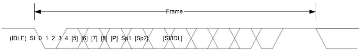
text_image
(IDLE) St 0 1 2 3 4 [5] [6] [7] [8] [P] Sp1 [Sp2] [St/IDL]St Start bit. Signal is always low.
n, [n] Data bits. 0 to [5..9]
[P] Parity bit. Either odd or even.
Sp, [Sp] Stop bit. Signal is always high.
IDLE No frame is transferred on the communication line. Signal is always high in this state.
31.6.2 Basic Operation
31.6.2.1 Initialization
The following registers are enable-protected, meaning they can only be written when the USART is disabled (CTRL.ENABLE=0):
- Control A register (CTRLA), except the Enable (ENABLE) and Software Reset (SWRST) bits.
- Control B register (CTRLB), except the Receiver Enable (RXEN) and Transmitter Enable (TXEN) bits.
- Baud register (BAUD)
When the USART is enabled or is being enabled (CTRLA.ENABLE=1), any writing attempt to these registers will be discarded. If the peripheral is being disabled, writing to these registers will be executed after disabling is completed. Enable-protection is denoted by the "Enable-Protection" property in the register description.
Before the USART is enabled, it must be configured by these steps:
- Select either external (0x0) or internal clock (0x1) by writing the Operating Mode value in the CTRLA register (CTRLA.MODE).
- Select either asynchronous (0) or or synchronous (1) communication mode by writing the Communication Mode bit in the CTRLA register (CTRLA.CMODE).
- Select pin for receive data by writing the Receive Data Pinout value in the CTRLA register (CTRLA.RXPO).
- Select pads for the transmitter and external clock by writing the Transmit Data Pinout bit in the CTRLA register (CTRLA.TXPO).
- Configure the Character Size field in the CTRLB register (CTRLB.CHSIZE) for character size.
- Set the Data Order bit in the CTRLA register (CTRLA.DORD) to determine MSB- or LSB-first data transmission.
- To use parity mode:
a. Enable parity mode by writing 0x1 to the Frame Format field in the CTRLA register (CTRLA.FORM).
b. Configure the Parity Mode bit in the CTRLB register (CTRLB.PMODE) for even or odd parity. - Configure the number of stop bits in the Stop Bit Mode bit in the CTRLB register (CTRLB.SBMODE).
- When using an internal clock, write the Baud register (BAUD) to generate the desired baud rate.
- Enable the transmitter and receiver by writing '1' to the Receiver Enable and Transmitter Enable bits in the CTRLB register (CTRLB.RXEN and CTRLB.TXEN).
31.6.2.2 Enabling, Disabling, and Resetting
This peripheral is enabled by writing '1' to the Enable bit in the Control A register (CTRLA.ENABLE), and disabled by writing '0' to it.
Writing '1' to the Software Reset bit in the Control A register (CTRLA.SWRST) will reset all registers of this peripheral to their initial states, except the DBGCTRL register, and the peripheral is disabled.
Refer to the CTRLA register description for details.
31.6.2.3 Clock Generation and Selection
For both synchronous and asynchronous modes, the clock used for shifting and sampling data can be generated internally by the SERCOM baud-rate generator or supplied externally through the XCK line.
The synchronous mode is selected by writing a '1' to the Communication Mode bit in the Control A register (CTRLA.CMODE), the asynchronous mode is selected by writing a zero to CTRLA.CMODE.
The internal clock source is selected by writing 0x1 to the Operation Mode bit field in the Control A register (CTRLA.MODE), the external clock source is selected by writing 0x0 to CTRLA.MODE.
The SERCOM baud-rate generator is configured as shown in the following figure.
In asynchronous mode (CTRLA.CMODE=0), the 16-bit Baud register value is used.
In synchronous mode (CTRLA.CMODE=1), the eight LSBs of the Baud register are used. Refer to Clock Generation - Baud Rate Generator for details on configuring the baud rate.
Figure 31-3. Clock Generation

flowchart
graph TD
    A["XCK"] --> B["CTRL.MODE[0"]]
    B --> C["1/0"]
    C --> D["Baud Rate Generator"]
    D --> E["Base Period"]
    E --> F["/2"]
    F --> G["/8"]
    G --> H["/2 /8/1"]
    H --> I["1"]
    I --> J["Tx Clk"]
    I --> K["CTRL.CMODE"]
    I --> L["Rx Clk"]
    M["XCKInternal Clk (GCLK)"] --> N["1/0"]
    N --> O["1"]
    O --> P["Tx Clk"]
    O --> Q["CTRL.CMODE"]
    O --> R["Rx Clk"]
References:
Clock Generation - Baud Rate Generator
Asynchronous Arithmetic Mode BAUD Value Selection
Synchronous Clock Operation
In synchronous mode, the CTRLA.MODE bit field determines whether the transmission clock line (XCK) serves either as input or output. The dependency between clock edges, data sampling, and data change is the same for internal and external clocks. Data input on the RxD pin is sampled at the opposite XCK clock edge when data is driven on the TxD pin.
The Clock Polarity bit in the Control A register (CTRLA.CPOL) selects which XCK clock edge is used for RxD sampling, and which is used for TxD change:
When CTRLA.CPOL is '0', the data will be changed on the rising edge of XCK, and sampled on the falling edge of XCK.
When CTRLA.CPOL is '1', the data will be changed on the falling edge of XCK, and sampled on the rising edge of XCK.
Figure 31-4. Synchronous Mode XCK Timing
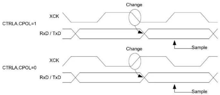
text_image
CTRLA.CPOL=1 XCK RxD / TxD Change Sample CTRLA.CPOL=0 XCK RxD / TxD Change SampleWhen the clock is provided through XCK (CTRLA.MODE=0x0), the shift registers operate directly on the XCK clock. This means that XCK is not synchronized with the system clock and, therefore, can operate at frequencies up to the system frequency.
31.6.2.4 Data Register
The USART Transmit Data register (TxDATA) and USART Receive Data register (RxDATA) share the same I/O address, referred to as the Data register (DATA). Writing the DATA register will update the TxDATA register. Reading the DATA register will return the contents of the RxDATA register.
31.6.2.5 Data Transmission
Data transmission is initiated by writing the data to be sent into the DATA register. Then, the data in TxDATA will be moved to the shift register when the shift register is empty and ready to send a new frame. After the shift register is loaded with data, the data frame will be transmitted.
When the entire data frame including stop bit(s) has been transmitted and no new data was written to DATA, the Transmit Complete interrupt flag in the Interrupt Flag Status and Clear register (INTFLAG.TXC) will be set, and the optional interrupt will be generated.
The Data Register Empty flag in the Interrupt Flag Status and Clear register (INTFLAG.DRE) indicates that the register is empty and ready for new data. The DATA register should only be written to when INTFLAG.DRE is set.
Disabling the Transmitter
The transmitter is disabled by writing '0' to the Transmitter Enable bit in the CTRLB register (CTRLB.TXEN).
Disabling the transmitter will complete only after any ongoing and pending transmissions are completed, i.e., there is no data in the transmit shift register and TxDATA to transmit.
31.6.2.6 Data Reception
The receiver accepts data when a valid start bit is detected. Each bit following the start bit will be sampled according to the baud rate or XCK clock, and shifted into the receive shift register until the first stop bit of a frame is received. The second stop bit will be ignored by the receiver.
When the first stop bit is received and a complete serial frame is present in the receive shift register, the contents of the shift register will be moved into the two-level receive buffer. Then, the Receive Complete interrupt flag in the Interrupt Flag Status and Clear register (INTFLAG.RXC) will be set, and the optional interrupt will be generated.
The received data can be read from the DATA register when the Receive Complete interrupt flag is set.
Disabling the Receiver
Writing '0' to the Receiver Enable bit in the CTRLB register (CTRLB.RXEN) will disable the receiver, flush the two-level receive buffer, and data from ongoing receptions will be lost.
Error Bits
The USART receiver has three error bits in the Status (STATUS) register: Frame Error (FERR), Buffer Overflow (BUFOVF), and Parity Error (PERR). Once an error happens, the corresponding error bit will be set until it is cleared by writing '1' to it. These bits are also cleared automatically when the receiver is disabled.
There are two methods for buffer overflow notification, selected by the Immediate Buffer Overflow Notification bit in the Control A register (CTRLA.IBON):
When CTRLA.IBON=1, STATUS.BUFOVF is raised immediately upon buffer overflow. Software can then empty the receive FIFO by reading RxDATA, until the receiver complete interrupt flag (INTFLAG.RXC) is cleared.
When CTRLA.IBON=0, the buffer overflow condition is attending data through the receive FIFO. After the received data is read, STATUS.BUFOVF will be set along with INTFLAG.RXC.
Asynchronous Data Reception
The USART includes a clock recovery and data recovery unit for handling asynchronous data reception.
The clock recovery logic can synchronize the incoming asynchronous serial frames at the RxD pin to the internally generated baud-rate clock.
The data recovery logic samples and applies a low-pass filter to each incoming bit, thereby improving the noise immunity of the receiver.
Asynchronous Operational Range
The operational range of the asynchronous reception depends on the accuracy of the internal baud-rate clock, the rate of the incoming frames, and the frame size (in number of bits). In addition, the operational range of the receiver is depending on the difference between the received bit rate and the internally generated baud rate. If the baud rate of an external transmitter is too high or too low compared to the internally generated baud rate, the receiver will not be able to synchronize the frames to the start bit.
There are two possible sources for a mismatch in baud rate: First, the reference clock will always have some minor instability. Second, the baud-rate generator cannot always do an exact division of the reference clock frequency to get the baud rate desired. In this case, the BAUD register value should be set to give the lowest possible error. Refer to Clock Generation - Baud-Rate Generator for details.
Recommended maximum receiver baud-rate errors for various character sizes are shown in the table below.
Table 31-3. Asynchronous Receiver Error for 16-fold Oversampling
| D(Data bits+Parity) | RSLOW [%] R | FAST [%] Max. total error [%] Recommended max. Rx error [%] | |
| 5 94.12 107.69 +5.88/-7.69 ±2.5 | |||
| 6 94.92 106.67 +5.08/-6.67 ±2.0 | |||
| 7 95.52 105.88 +4.48/-5.88 ±2.0 | |||
| 8 96.00 105.26 +4.00/-5.26 ±2.0 | |||
| 9 96.39 104.76 +3.61/-4.76 ±1.5 | |||
| 10 96.70 104.35 +3.30/-4.35 ±1.5 | |||
The following equations calculate the ratio of the incoming data rate and internal receiver baud rate:
$$ R _ {\mathrm{SLOW}} = \frac {(D + 1 S)}{S - 1 + D \cdot S + S} \quad_ {F}, R _ {\mathrm{FAST}} = \frac {(D + 2 S)}{(D + 1 S) + S} \quad_ {M} $$
- R_SLOW is the ratio of the slowest incoming data rate that can be accepted in relation to the receiver baud rate
- R_FAST is the ratio of the fastest incoming data rate that can be accepted in relation to the receiver baud rate
- D is the sum of character size and parity size ( D = 5 to 10 bits)
- S is the number of samples per bit ( S = 16, 8 or 3)
- S_F is the first sample number used for majority voting ( S_F = 7, 3 , or 2) when CTRLA.SAMPA=0.
- S_M is the middle sample number used for majority voting ( S_M = 8, 4, or 2 ) when CTRLA.SAMPA=0.
The recommended maximum Rx Error assumes that the receiver and transmitter equally divide the maximum total error. Its connection to the SERCOM Receiver error acceptance is depicted in this figure:
Figure 31-5. USART Rx Error Calculation

other
| Metric | Description | |--------|-------------| | Error Max (%) | Baud Generator offset error depends on BAUD register value | | Baud Rate | Clock source error | | Error Min (%) | Recommended max. Rx Error (%) |The recommendation values in the table above accommodate errors of the clock source and the baud generator. The following figure gives an example for a baud rate of 3Mbps:
Figure 31-6. USART Rx Error Calculation Example
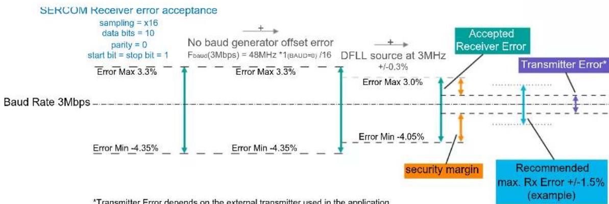
other
| Parameter | Value | | --- | --- | | No baud generator offset error | Fbaud(3Mbps) = 48MHz *1(BAUD=0) /16 | | Baud Rate | 3Mbps | | Error Max | 3.3% | | Error Min | -4.35% | | FDLL source at 3MHz | +/-0.3% | | Error Max | 3.3% | | Error Min | -4.35% | | Security margin | -4.05% | | Transmitter Error* | - | | Recommended max. Rx Error +/-1.5% (example) | - |*Transmitter Error depends on the external transmitter used in the application. It is advised that it is within the Recommended max. Rx Error (+/-1.5% in this example). Larger Transmitter Errors are acceptable but must lie within the Accepted Receiver Error.
References:
Clock Generation - Baud-Rate Generator
Asynchronous Arithmetic Mode BAUD Value Selection
31.6.3 Additional Features
31.6.3.1 Parity
Even or odd parity can be selected for error checking by writing 0x1 to the Frame Format bit field in the Control A register (CTRLA.FORM).
If even parity is selected (CTRLB.PMODE=0), the parity bit of an outgoing frame is '1' if the data contains an odd number of bits that are '1', making the total number of '1' even.
If odd parity is selected (CTRLB.PMODE=1), the parity bit of an outgoing frame is '1' if the data contains an even number of bits that are '0', making the total number of '1' odd.
When parity checking is enabled, the parity checker calculates the parity of the data bits in incoming frames and compares the result with the parity bit of the corresponding frame. If a parity error is detected, the Parity Error bit in the Status register (STATUS.PERR) is set.
31.6.3.2 Hardware Handshaking
The USART features an out-of-band hardware handshaking flow control mechanism, implemented by connecting the RTS and CTS pins with the remote device, as shown in the figure below.
Figure 31-7. Connection with a Remote Device for Hardware Handshaking
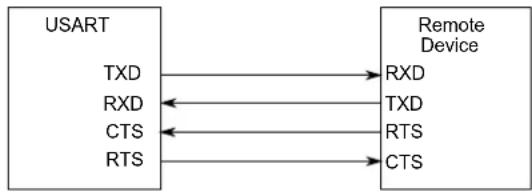
flowchart
graph LR
    A["USART"] -->|TXD| B["Remote Device"]
    A -->|RXD| B
    A -->|CTS| B
    A -->|RTS| B
    B -->|RXD| A
    B -->|TXD| A
    B -->|RTS| A
    B -->|CTS| A
Hardware handshaking is only available in the following configuration:
- USART with internal clock (CTRLA.MODE=1),
- Asynchronous mode (CTRLA.CMODE=0),
• and Flow control pinout (CTRLA.TXPO=2).
When the receiver is disabled or the receive FIFO is full, the receiver will drive the RTS pin high. This notifies the remote device to stop transfer after the ongoing transmission. Enabling and disabling the receiver by writing to CTRLB.RXEN will set/clear the RTS pin after a synchronization delay. When the receive FIFO goes full, RTS will be set immediately and the frame being received will be stored in the shift register until the receive FIFO is no longer full.
Figure 31-8. Receiver Behavior when Operating with Hardware Handshaking
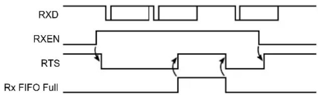
text_image
RXD RXEN RTS Rx FIFO FullThe current CTS Status is in the STATUS register (STATUS.CTS). Character transmission will start only if STATUS.CTS=0. When CTS is set, the transmitter will complete the ongoing transmission and stop transmitting.
Figure 31-9. Transmitter Behavior when Operating with Hardware Handshaking
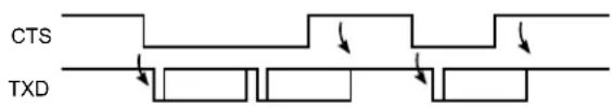
text_image
CTS TXD31.6.3.3 IrDA Modulation and Demodulation
Transmission and reception can be encoded IrDA compliant up to 115.2 kb/s. IrDA modulation and demodulation work in the following configuration:
- IrDA encoding enabled (CTRLB.ENC=1),
- Asynchronous mode (CTRLA.CMODE=0),
• and 16x sample rate (CTRLA.SAMPR[0]=0).
During transmission, each low bit is transmitted as a high pulse. The pulse width is 3/16 of the baud rate period, as illustrated in the figure below.
Figure 31-10. IrDA Transmit Encoding
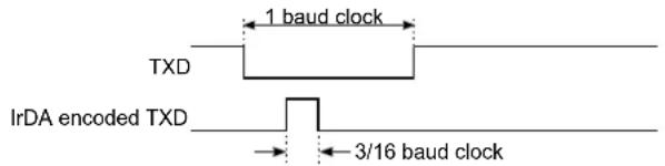
text_image
1 baud clock TXD IrDA encoded TXD 3/16 baud clockThe reception decoder has two main functions.
The first is to synchronize the incoming data to the IrDA baud rate counter. Synchronization is performed at the start of each zero pulse.
The second main function is to decode incoming Rx data. If a pulse width meets the minimum length set by configuration (RXPL.RXPL), it is accepted. When the baud rate counter reaches its middle value (1/2 bit length), it is transferred to the receiver.
Note: Note that the polarity of the transmitter and receiver are opposite: During transmission, a '0' bit is transmitted as a '1' pulse. During reception, an accepted '0' pulse is received as a '0' bit.
Example: The figure below illustrates reception where RXPL.RXPL is set to 19. This indicates that the pulse width should be at least 20 SE clock cycles. When using BAUD=0xE666 or 160 SE cycles per bit, this corresponds to 2/16 baud clock as minimum pulse width required. In this case the first bit is accepted as a '0', the second bit is a '1', and the third bit is also a '1'. A low pulse is rejected since it does not meet the minimum requirement of 2/16 baud clock.
Figure 31-11. IrDA Receive Decoding

text_image
Baud clock 0 0.5 1 1.5 2 2.5 IrDA encoded RXD RXD 20 SE clock cycles31.6.3.4 Break Character Detection and Auto-Baud
Break character detection and auto-baud are available in this configuration:
- Auto-baud frame format (CTRLA.FORM = 0x04 or 0x05),
- Asynchronous mode (CTRLA.CMODE = 0),
- and 16x sample rate using fractional baud rate generation (CTRLA.SAMPR = 1).
The auto-baud follows the LIN format. All LIN Frames start with a Break Field followed by a Sync Field. The USART uses a break detection threshold of greater than 11 nominal bit times at the configured baud rate. At any time, if more than 11 consecutive dominant bits are detected on the bus, the USART detects a Break Field. When a Break Field has been detected, the Receive Break interrupt flag (INTFLAG.RXBRK) is set and the USART expects the Sync Field character to be 0x55. This field is used to update the actual baud rate in order to stay synchronized. If the received Sync character is not 0x55, then the Inconsistent Sync Field error flag (STATUS.ISF) is set along with the Error interrupt flag (INTFLAG.ERROR), and the baud rate is unchanged.
Figure 31-12. LIN Break and Sync Fields

text_image
Break Field Sync Field 8 bit timesAfter a break field is detected and the start bit of the Sync Field is detected, a counter is started. The counter is then incremented for the next 8 bit times of the Sync Field. At the end of these 8 bit times, the counter is stopped. At this moment, the 13 most significant bits of the counter (value divided by 8) give the new clock divider (BAUD.BAUD), and the 3 least significant bits of this value (the remainder) give the new Fractional Part (BAUD.FP).
When the Sync Field has been received, the clock divider (BAUD.BAUD) and the Fractional Part (BAUD.FP) are updated after a synchronization delay. After the Break and Sync Fields are received, multiple characters of data can be received.
31.6.3.5 RS485
RS485 is available with the following configuration:
- USART frame format (CTRLA.FORM = 0x00 or 0x01)
• RS485 pinout (CTRLA.TXPO=0x3).
The RS485 feature enables control of an external line driver as shown in the figure below. While operating in RS485 mode, the transmit enable pin (TE) is driven high when the transmitter is active.
Figure 31-13. RS485 Bus Connection

text_image
USART RXD TXD TE Differential BusThe TE pin will remain high for the complete frame including stop bit(s). If a Guard Time is programmed in the Control C register (CTRLC.GTIME), the line will remain driven after the last character completion. The following figure shows a transfer with one stop bit and CTRLC.GTIME=3.
Figure 31-14. Example of TE Drive with Guard Time

text_image
Start StopData GTIME=3 TXD TEThe Transmit Complete interrupt flag (INTFLAG.TXC) will be raised after the guard time is complete and TE goes low.
31.6.3.6 ISO 7816 for Smart Card Interfacing
The SERCOM USART features an ISO/IEC 7816-compatible operating mode. This mode permits interfacing with smart cards and Security Access Modules (SAM) communicating through an ISO 7816 link. Both T=0 and T=1 protocols defined by the ISO 7816 specification are supported.
ISO 7816 is available with the following configuration:
• ISO 7816 format (CTRLA.FORM = 0x07)
- Inverse transmission and reception (CTRLA.RXINV=1 and CTRLA.TXINV=1)
- Single bidirectional data line (CTRLA.TXPO and CTRLA.RXPO configured to use the same data pin)
• Even parity (CTRLB.PMODE=0)
- 8-bit character size (CTRLB.CHSIZE=0)
• T=0 (CTRLA.CMODE=1) or T=1 (CTRLA.CMODE=0)
ISO 7816 is a half duplex communication on a single bidirectional line. The USART connects to a smart card as shown below. The output is only driven when the USART is transmitting. The USART is considered as the host of the communication as it generates the clock.
Figure 31-15. Connection of a Smart Card to the SERCOM USART

flowchart
graph LR
    A["SERCOM USART"] -->|CLK| B["Smart Card"]
    C["SCK"] -->|I/O| B
    D["TXD/RXD"] -->|I/O| B
ISO 7816 characters are specified as 8 bits with even parity. The USART must be configured accordingly.
The USART cannot operate concurrently in both receiver and transmitter modes as the communication is unidirectional. It has to be configured according to the required mode by enabling or disabling either the receiver or the transmitter as desired. Enabling both the receiver and the transmitter at the same time in ISO 7816 mode may lead to unpredictable results.
The ISO 7816 specification defines an inverse transmission format. Data bits of the character must be transmitted on the I/O line at their negative value (CTRLA.RXINV=1 and CTRLA.TXINV=1).
Protocol T=0
In T=0 protocol, a character is made up of:
- one start bit,
- eight data bits,
- one parity bit
• and one guard time, which lasts two bit times.
The transfer is synchronous (CTRLA.CMODE=1). The transmitter shifts out the bits and does not drive the I/O line during the guard time. Additional guard time can be added by programming the Guard Time (CTRLC.GTIME).
If no parity error is detected, the I/O line remains during the guard time and the transmitter can continue with the transmission of the next character, as shown in the following figure.
Figure 31-16. T=0 Protocol without Parity Error

text_image
SCK I/O Start Bit D0 D1 D2 D3 D4 D5 D6 D7 P Guard Guard Next Time1 Time2 Start BitIf a parity error is detected by the receiver, it drives the I/O line to 0 during the guard time, as shown in the next figure. This error bit is also named NACK, for Non Acknowledge. In this case, the character lasts 1 bit time more, as the guard time length is the same and is added to the error bit time, which lasts 1 bit time.
Figure 31-17. T=0 Protocol with Parity Error
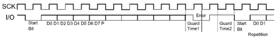
text_image
SCK I/O Start Bit D0 D1 D2 D3 D4 D5 D6 D7 P Error Guard Time1 Guard Time2 Start Bit D0 D1 RepetitionWhen the USART is the receiver and it detects a parity error, the parity error bit in the Status Register (STATUS.PERR) is set and the character is not written to the receive FIFO.
Receive Error Counter
The receiver also records the total number of errors (receiver parity errors and NACKs from the remote transmitter) up to a maximum of 255. This can be read in the Receive Error Count (RXERRCNT) register. RXERRCNT is automatically cleared on read.
Receive NACK Inhibit
The receiver can also be configured to inhibit error generation. This can be achieved by setting the Inhibit Not Acknowledge (CTRLC.INACK) bit. If CTRLC.INACK is 1, no error signal is driven on the I/O line even if a parity error is detected. Moreover, if CTRLC.INACK is set, the erroneous received character is stored in the receive FIFO, and the STATUS.PERR bit is set. Inhibit not acknowledge (CTRLC.INACK) takes priority over disable successive receive NACK (CTRLC.DSNACK).
Transmit Character Repetition
When the USART is transmitting a character and gets a NACK, it can automatically repeat the character before moving on to the next character. Repetition is enabled by writing the Maximum Iterations register (CTRLC.MAXITER) to a non-zero value. The USART repeats the character the number of times specified in CTRLC.MAXITER.
When the USART repetition number reaches the programmed value in CTRLC.MAXITER, the STATUS.ITER bit is set and the internal iteration counter is reset. If the repetition of the character is acknowledged by the receiver before the maximum iteration is reached, the repetitions are stopped and the iteration counter is cleared.
Disable Successive Receive NACK
The receiver can limit the number of successive NACKs sent back to the remote transmitter. This is programmed by setting the Disable Successive NACK bit (CTRLC.DSNACK). The maximum number of NACKs transmitted is programmed in the CTRLC.MAXITER field. As soon as the maximum is reached, the character is considered as correct, an acknowledge is sent on the line, the STATUS.ITER bit is set and the internal iteration counter is reset.
Protocol T=1
When operating in ISO7816 protocol T=1, the transmission is asynchronous (CTRL1.CMODE=0) with one or two stop bits. After the stop bits are sent, the transmitter does not drive the I/O line.
Parity is generated when transmitting and checked when receiving. Parity error detection sets the STATUS.PERR bit, and the erroneous character is written to the receive FIFO. When using T=1 protocol, the receiver does not signal errors on the I/O line and the transmitter does not retransmit.
31.6.3.7 Collision Detection
When the receiver and transmitter are connected either through pin configuration or externally, transmit collision can be detected after selecting the Collision Detection Enable bit in the CTRLB register (CTRLB.COLDEN=1). To detect collision, the receiver and transmitter must be enabled (CTRLB.RXEN=1 and CTRLB.TXEN=1).
Collision detection is performed for each bit transmitted by comparing the received value with the transmit value, as shown in the figure below. While the transmitter is idle (no transmission in progress), characters can be received on RxD without triggering a collision.
Figure 31-18. Collision Checking

text_image
8-bit character, single stop bit TXD RXD Collision checkedThe next figure shows the conditions for a collision detection. In this case, the start bit and the first data bit are received with the same value as transmitted. The second received data bit is found to be different than the transmitted bit at the detection point, which indicates a collision.
Figure 31-19. Collision Detected

text_image
Collision checked and ok TXD RXD TXEN Tri-state Collision detectedWhen a collision is detected, the USART follows this sequence:
- Abort the current transfer.
- Flush the transmit buffer.
-
Disable transmitter (CTRLB.TXEN=0)
-
This is done after a synchronization delay. The CTRLB Synchronization Busy bit (SYNCBUSY.CTRLB) will be set until this is complete.
-
After disabling, the TxD pin will be tri-stated.
-
Set the Collision Detected bit (STATUS.COLL) along with the Error interrupt flag (INTFLAG.ERROR).
- Set the Transmit Complete interrupt flag (INTFLAG.TXC), since the transmit buffer no longer contains data.
After a collision, software must manually enable the transmitter again before continuing, after assuring that the CTRLB Synchronization Busy bit (SYNCBUSY.CTRLB) is not set.
31.6.3.8 Loop-Back Mode
For loop-back mode, configure the Receive Data Pinout (CTRLA.RXPO) and Transmit Data Pinout (CTRLA.TXPO) to use the same data pins for transmit and receive. The loop-back is through the pad, so the signal is also available externally.
31.6.3.9 Start-of-Frame Detection
The USART start-of-frame detector can wake up the CPU when it detects a start bit. In standby sleep mode, the internal fast startup oscillator must be selected as the GCLK_SERCOMx_CORE source.
When a 1-to-0 transition is detected on RxD, the 8MHz Internal Oscillator is powered up and the USART clock is enabled. After startup, the rest of the data frame can be received, provided that the baud rate is slow enough in relation to the fast startup internal oscillator start-up time. Refer to the Electrical Characteristics for details. The start-up time of this oscillator varies with supply voltage and temperature.
The USART start-of-frame detection works both in asynchronous and synchronous modes. It is enabled by writing '1' to the Start of Frame Detection Enable bit in the Control B register (CTRLB.SFDE).
If the Receive Start Interrupt Enable bit in the Interrupt Enable Set register (INTENSET.RXS) is set, the Receive Start interrupt is generated immediately when a start is detected.
When using start-of-frame detection without the Receive Start interrupt, start detection will force the 8MHz Internal Oscillator and USART clock active while the frame is being received. In this case, the CPU will not wake up until the Receive Complete interrupt is generated.
31.6.3.10 Sample Adjustment
In asynchronous mode (CTRLA.CMODE=0), three samples in the middle are used to determine the value based on majority voting. The three samples used for voting can be selected using the Sample Adjustment bit field in Control A register (CTRLA.SAMPA). When CTRLA.SAMPA=0, samples 7-8-9 are used for 16x oversampling, and samples 3-4-5 are used for 8x oversampling.
31.6.4 DMA, Interrupts and Events
Table 31-4. Module Request for SERCOM USART
| Condition Request | |||
| DMA Interrupt Event | |||
| Data Register Empty (DRE) Yes | (request cleared when data is written) | Yes NA | |
| Receive Complete (RXC) Yes | (request cleared when data is read) | Yes | |
| Transmit Complete (TXC) NA Yes | |||
| Receive Start (RXS) NA Yes | |||
| Clear to Send Input Change (CTSIC) NA Yes | |||
| Receive Break (RXBRK) NA Yes | |||
| Error (ERROR) NA Yes | |||
31.6.4.1 DMA Operation
The USART generates the following DMA requests:
- Data received (RX): The request is set when data is available in the receive FIFO. The request is cleared when DATA is read.
- Data transmit (TX): The request is set when the transmit buffer (TX DATA) is empty. The request is cleared when DATA is written.
31.6.4.2 Interrupts
The USART has the following interrupt sources. These are asynchronous interrupts, and can wake up the device from any sleep mode:
• Data Register Empty (DRE)
- Receive Complete (RXC)
• Transmit Complete (TXC)
- Receive Start (RXS)
- Clear to Send Input Change (CTSIC)
• Received Break (RXBRK)
- Error (ERROR)
Each interrupt source has its own interrupt flag. The interrupt flag in the Interrupt Flag Status and Clear register (INTFLAG) will be set when the interrupt condition is met. Each interrupt can
be individually enabled by writing '1' to the corresponding bit in the Interrupt Enable Set register (INTENSET), and disabled by writing '1' to the corresponding bit in the Interrupt Enable Clear register (INTENCLR).
An interrupt request is generated when the interrupt flag is set and if the corresponding interrupt is enabled. The interrupt request remains active until either the interrupt flag is cleared, the interrupt is disabled, or the USART is reset. For details on clearing interrupt flags, refer to the INTFLAG register description.
The USART has one common interrupt request line for all the interrupt sources. The value of INTFLAG indicates which interrupt is executed. Note that interrupts must be globally enabled for interrupt requests. Refer to the Nested Vector Interrupt Controller for details.
31.6.4.3 Events
Not applicable.
31.6.5 Sleep Mode Operation
The behavior in sleep mode is depending on the clock source and the Run In Standby bit in the Control A register (CTRLA.RUNSTDBY):
- Internal clocking, CTRLA.RUNSTDBY=1: GCLK_SERCOMx_CORE can be enabled in all sleep modes. Any interrupt can wake up the device.
- External clocking, CTRLA.RUNSTDBY=1: The Receive Start and the Receive Complete interrupt(s) can wake up the device.
- Internal clocking, CTRLA.RUNSTDBY=0: Internal clock will be disabled, after any ongoing transfer was completed. The Receive Start and the Receive Complete interrupt(s) can wake up the device.
- External clocking, CTRLA.RUNSTDBY=0: External clock will be disconnected, after any ongoing transfer was completed. All reception will be dropped.
31.6.6 Synchronization
Due to asynchronicity between the main clock domain and the peripheral clock domains, some registers need to be synchronized when written or read.
The following bits are synchronized when written:
- Software Reset bit in the CTRLA register (CTRLA.SWRST)
- Enable bit in the CTRLA register (CTRLA.ENABLE)
- Receiver Enable bit in the CTRLB register (CTRLB.RXEN)
- Transmitter Enable bit in the Control B register (CTRLB.TXEN)
Note: CTRLB.RXEN is write-synchronized somewhat differently. See also 31.8.2. CTRLB for details.
Required write-synchronization is denoted by the "Write-Synchronized" property in the register description.
31.7 Register Summary
| Offset | Name Bit Pos. 76543210 | |||||||||
| 0x00 CTRLA | 7:0 RUNSTDBY MODE[2:0] ENABLE SWRST | |||||||||
| 15:8 SAMPR[2:0] RXINV TXINV IBON | ||||||||||
| 23:16 | SAMPA[1:0] | RXPO[1:0] | TXPO[1:0] | |||||||
| 31:24 | DORD | CPOL | CMODE | FORM[3:0] | ||||||
| 0x04 CTRLB | 7:0 | SBMODE | CHSIZE[2:0] | |||||||
| 15:8 | PMODE | ENC | SFDE | COLDEN | ||||||
| 23:16 | RXEN | TXEN | ||||||||
| 31:24 | ||||||||||
| 0x08 CTRLC | 7:0 | GTIME[2:0] | ||||||||
| 15:8 | ||||||||||
| 23:16 | MAXITER[2:0] | DSNACK | INACK | |||||||
| 31:24 | ||||||||||
| 0x0C | BAUD | 7:0 | BAUD[7:0] | |||||||
| 15:8 | BAUD[15:8] | |||||||||
| 0x0E | RXPL | 7:0 | RXPL[7:0] | |||||||
| 0x0F ... 0x13 | Reserved | |||||||||
| 0x14 | INTENCLR | 7:0 | ERROR | RXBRK | CTSIC | RXS | RXC | TXC | DRE | |
| 0x15 | Reserved | |||||||||
| 0x16 | INTENSET | 7:0 | ERROR | RXBRK | CTSIC | RXS | RXC | TXC | DRE | |
| 0x17 | Reserved | |||||||||
| 0x18 | INTFLAG | 7:0 | ERROR | RXBRK | CTSIC | RXS | RXC | TXC | DRE | |
| 0x19 | Reserved | |||||||||
| 0x1A | STATUS | 7:0 | ITER | COLL | ISF | CTS | BUFOVF | FERR | PERR | |
| 15:8 | ||||||||||
| 0x1C | SYNCBUSY | 7:0 | RXERRCNT CTRLB ENABLE SWRST | |||||||
| 15:8 | ||||||||||
| 23:16 | ||||||||||
| 31:24 | ||||||||||
| 0x20 | RXERRCNT | 7:0 | RXERRCNT[7:0] | |||||||
| 0x21 ... 0x27 | Reserved | |||||||||
| 0x28 | DATA | 7:0 | DATA[7:0] | |||||||
| 15:8 | DATA[8] | |||||||||
| 0x2A ... 0x2F | Reserved | |||||||||
| 0x30 | DBGCTRL | 7:0 | DBGSTOP | |||||||
31.8 Register Description
Registers can be 8, 16, or 32 bits wide. Atomic 8-, 16-, and 32-bit accesses are supported. In addition, the 8-bit quarters and 16-bit halves of a 32-bit register, and the 8-bit halves of a 16-bit register can be accessed directly.
Some registers require synchronization when read and/or written. Synchronization is denoted by the "Read-Synchronized" and/or "Write-Synchronized" property in each individual register description.
Optional write-protection by the Peripheral Access Controller (PAC) is denoted by the "PAC Write-Protection" property in each individual register description.
Some registers are enable-protected, meaning they can only be written when the module is disabled. Enable-protection is denoted by the "Enable-Protected" property in each individual register description.
31.8.1 Control A
Name: CTRLA
Offset: 0x00
Reset: 0x00000000
Property: PAC Write-Protection, Enable-Protected, Write-Synchronized
Bit 31 30 29 28 27 26 25 24
| DORD | CPOL | CMODE | FORM[3:0] | |||||
| Access Reset | R/W 0 | R/W 0 | R/W 0 | R/W 0 | ||||
Bit 23 22 21 20 19 18 17 16
| SAMPA[1:0] | RXPO[1:0] | TXPO[1:0] | ||||||
| Access | R/W | R/W | R/W | R/W | R/W | R/W | ||
| Reset | 0 | 0 | 0 | 0 | 0 | 0 | ||
Bit 15 14 13 12 11 10 9 8
| SAMPR[2:0] | RXINV | TXINV | IBON | |||||
| Access | R/W | R/W | R/W | R/W | R | |||
| Reset | 0 | 0 | 0 | 0 | 0 | 0 | ||
Bit 7 6 5 4 3 2 1 0
| RUNSTDBY | MODE[2:0] | ENABLE | SWRST | |||||
| Access | R/W | R/W | R/W | R/W R/W R/W | ||||
| Reset | 0 | 0 | 0 | 0 | 0 | |||
Bit 30 - DORD Data Order
This bit selects the data order when a character is shifted out from the Data register.
This bit is not synchronized.
| Value | Description |
| 0 | MSB is transmitted first. |
| 1 | LSB is transmitted first. |
Bit 29 - CPOL Clock Polarity
This bit selects the relationship between data output change and data input sampling in synchronous mode.
This bit is not synchronized.
| CPOL | TxD Change | RxD Sample |
| 0x0 | Rising XCK edge | Falling XCK edge |
| 0x1 | Falling XCK edge | Rising XCK edge |
Bit 28 - CMODE Communication Mode
This bit selects asynchronous or synchronous communication.
This bit is not synchronized.
| Value | Description |
| 0 | Asynchronous communication. |
| 1 | Synchronous communication. |
Bits 27:24 - FORM[3:0] Frame Format
These bits define the frame format.
These bits are not synchronized.
| FORM[3:0] Description | |
| 0x0 USART frame | |
| 0x1 USART frame with parity | |
| 0x4 Auto-baud - break detection and auto-baud | |
| 0x5 Auto-baud - break detection and auto-baud with parity | |
| 0x6-0xF Reserved | |
Bits 23:22 - SAMPA[1:0] Sample Adjustment
These bits define the sample adjustment.
These bits are not synchronized.
| SAMPA[1:0] 16x Over-sampling (CTRLA.SAMPR=0 or 1) 8x Over-sampling (CTRLA.SAMPR=2 or 3) | |
| 0x0 7-8-9 3-4-5 | |
| 0x1 9-10-11 4-5-6 | |
| 0x2 11-12-13 5-6-7 | |
| 0x3 13-14-15 6-7-8 | |
Bits 21:20 - RXPO[1:0] Receive Data Pinout
These bits define the receive data (RxD) pin configuration.
These bits are not synchronized.
| RXPO[1:0] Name Description | |
| 0x0 PAD[0] SERCOM PAD[0] is used for data reception | |
| 0x1 PAD[1] SERCOM PAD[1] is used for data reception | |
| 0x2 PAD[2] SERCOM PAD[2] is used for data reception | |
| 0x3 PAD[3] SERCOM PAD[3] is used for data reception | |
Bits 17:16 - TXPO[1:0] Transmit Data Pinout
These bits define the transmit data (TxD) and XCK pin configurations.
This bit is not synchronized.
| TXPO TxD Pin Location XCK Pin | Location (When Applicable) RTS | CTS | ||
| 0x0 | SERCOM PAD[0] | SERCOM PAD[1] | N/A | N/A |
| 0x1 | SERCOM PAD[2] | SERCOM PAD[3] | N/A | N/A |
| 0x2 | SERCOM PAD[0] | N/A | SERCOM PAD[2] | SERCOM PAD[3] |
| 0x3 | SERCOM_PAD[0] | SERCOM_PAD[1] | SERCOM_PAD[2] | N/A |
Bits 15:13 - SAMPR[2:0] Sample Rate
These bits select the sample rate.
These bits are not synchronized.
| SAMPR[2:0] | Description |
| 0x0 | 16x over-sampling using arithmetic baud rate generation. |
| 0x1 | 16x over-sampling using fractional baud rate generation. |
| 0x2 | 8x over-sampling using arithmetic baud rate generation. |
| 0x3 | 8x over-sampling using fractional baud rate generation. |
| 0x4 | 3x over-sampling using arithmetic baud rate generation. |
| 0x5-0x7 | Reserved |
Bit 10 - RXINV Receive Data Invert
This bit controls whether the receive data (RxD) is inverted or not.
Note: Start, parity and stop bit(s) are unchanged. When enabled, parity is calculated on the inverted data.
| Value | Description |
| 0 | RxD is not inverted. |
| 1 | RxD is inverted. |
Bit 9 - TXINV Transmit Data Invert
This bit controls whether the transmit data (TxD) is inverted or not.
Note: Start, parity and stop bit(s) are unchanged. When enabled, parity is calculated on the inverted data.
| Value Description | |
| 0 | TxD is not inverted. |
| 1 | TxD is inverted. |
Bit 8 - IBON Immediate Buffer Overflow Notification
This bit controls when the buffer overflow status bit (STATUS.BUFOVF) is asserted when a buffer overflow occurs.
| Value Description | |
| 0 | STATUS.BUFOVF is asserted when it occurs in the data stream. |
| 1 | STATUS.BUFOVF is asserted immediately upon buffer overflow. |
Bit 7 - RUNSTDBY Run In Standby
This bit defines the functionality in standby sleep mode.
This bit is not synchronized.
| RUNSTDBY | External Clock Internal Clock | |
| 0x0 External clock is disconnected when ongoing transfer is finished. All reception is dropped. | Generic clock is disabled when ongoing transfer is finished. The device can wake up on Transfer Complete interrupt. | |
| 0x1 Wake on Receive Complete interrupt. Generic clock is enabled in all sleep modes. Any interrupt can wake up the device. | ||
Bits 4:2 - MODE[2:0] Operating Mode
These bits select the USART serial communication interface of the SERCOM.
These bits are not synchronized.
| Value Description | |
| 0x0 | USART with external clock |
| 0x1 | USART with internal clock |
Bit 1 - ENABLE Enable
Due to synchronization, there is delay from writing CTRLA. ENABLE until the peripheral is enabled/disabled. The value written to CTRLA. ENABLE will read back immediately and the Enable Synchronization Busy bit in the Synchronization Busy register (SYNCBUSY. ENABLE) will be set. SYNCBUSY. ENABLE is cleared when the operation is complete.
This bit is not enable-protected.
| Value Description | |
| 0 | The peripheral is disabled or being disabled. |
| 1 | The peripheral is enabled or being enabled. |
Bit 0 - SWRST Software Reset
Writing '0' to this bit has no effect.
Writing '1' to this bit resets all registers in the SERCOM, except DBGCTRL, to their initial state, and the SERCOM will be disabled.
Writing '1' to CTRLA.SWRST will always take precedence, meaning that all other writes in the same write-operation will be discarded. Any register write access during the ongoing reset will result in an APB error. Reading any register will return the reset value of the register.
Due to synchronization, there is a delay from writing CTRLA.SWRST until the reset is complete.
CTRLA.SWRST and SYNCBUSY.SWRST will both be cleared when the reset is complete.
This bit is not enable-protected.
| Value Description | |
| 0 | There is no reset operation ongoing. |
| 1 | The reset operation is ongoing. |
31.8.2 Control B
Name: CTRLB
Offset: 0x04
Reset: 0x00000000
Property: PAC Write-Protection, Enable-Protected, Write-Synchronized
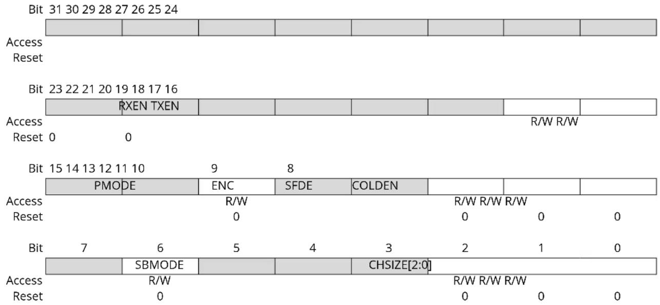
text_image
Bit 31 30 29 28 27 26 25 24 Access Reset Bit 23 22 21 20 19 18 17 16 RXEN TXEN Access Reset 0 0 R/W R/W Bit 15 14 13 12 11 10 9 8 PMODE ENC SFDE GOLDEN Access Reset R/W R/W R/W R/W 0 0 0 Bit 7 6 5 4 3 2 1 0 SBMODE CHSIZE[2:0] Access Reset R/W R/W R/W R/W 0 0 0 0Bit 17 - RXEN Receiver Enable
Writing '0' to this bit will disable the USART receiver. Disabling the receiver will flush the receive buffer and clear the FERR, PERR and BUFOVF bits in the STATUS register.
Writing '1' to CTRLB.RXEN when the USART is disabled will set CTRLB.RXEN immediately. When the USART is enabled, CTRLB.RXEN will be cleared, and SYNCBUSY.CTRLB will be set and remain set until the receiver is enabled. When the receiver is enabled, CTRLB.RXEN will read back as '1'.
Writing '1' to CTRLB.RXEN when the USART is enabled will set SYNCBUSY.CTRLB, which will remain set until the receiver is enabled, and CTRLB.RXEN will read back as '1'.
This bit is not enable-protected.
| Value | Description |
| 0 | The receiver is disabled or being enabled. |
| 1 | The receiver is enabled or will be enabled when the USART is enabled. |
Bit 16 - TXEN Transmitter Enable
Writing '0' to this bit will disable the USART transmitter. Disabling the transmitter will not become effective until ongoing and pending transmissions are completed.
Writing '1' to CTRLB.TXEN when the USART is disabled will set CTRLB.TXEN immediately. When the USART is enabled, CTRLB.TXEN will be cleared, and SYNCBUSY.CTRLB will be set and remain set until the transmitter is enabled. When the transmitter is enabled, CTRLB.TXEN will read back as '1'.
Writing '1' to CTRLB.TXEN when the USART is enabled will set SYNCBUSY.CTRLB, which will remain set until the receiver is enabled, and CTRLB.TXEN will read back as '1'.
This bit is not enable-protected.
| Value | Description |
| 0 | The transmitter is disabled or being enabled. |
| 1 | The transmitter is enabled or will be enabled when the USART is enabled. |
Bit 13 - PMODE Parity Mode
This bit selects the type of parity used when parity is enabled (CTRLA.FORM is '1'). The transmitter will automatically generate and send the parity of the transmitted data bits within each frame. The receiver will generate a parity value for the incoming data and parity bit, compare it to the parity mode and, if a mismatch is detected, STATUS.PERR will be set.
This bit is not synchronized.
| Value Description | |
| 0 | Even parity. |
| 1 | Odd parity. |
Bit 10 - ENC Encoding Format
This bit selects the data encoding format.
This bit is not synchronized.
| Value Description | |
| 0 | Data is not encoded. |
| 1 | Data is IrDA encoded. |
Bit 9 - SFDE Start of Frame Detection Enable
This bit controls whether the start-of-frame detector will wake up the device when a start bit is detected on the RxD line.
This bit is not synchronized.
| SFDE | INTENSET.RXS | INTENSET.RXC | Description |
| 0 X X | Start-of-frame detection disabled. | ||
| 1 0 0 | Reserved | ||
| 1 0 1 | Start-of-frame detection enabled. RXC wakes up the device from all sleep modes. | ||
| 1 1 0 | Start-of-frame detection enabled. RXS wakes up the device from all sleep modes. | ||
| 1 1 1 | Start-of-frame detection enabled. Both RXC and RXS wake up the device from all sleep modes. | ||
Bit 8 - GOLDEN Collision Detection Enable
This bit enables collision detection.
This bit is not synchronized.
| Value Description | |
| 0 | Collision detection is not enabled. |
| 1 | Collision detection is enabled. |
Bit 6 - SBMODE Stop Bit Mode
This bit selects the number of stop bits transmitted.
This bit is not synchronized.
| Value Description | |
| 0 | One stop bit. |
| 1 | Two stop bits. |
Bits 2:0 - CHSIZE[2:0] Character Size
These bits select the number of bits in a character.
These bits are not synchronized.
| CHSIZE[2:0] Description | |
| 0x0 8 bits | |
| 0x1 9 bits | |
| 0x2-0x4 Reserved | |
| 0x5 5 bits | |
| 0x6 6 bits | |
| 0x7 7 bits |
31.8.3 Control C
Name: CTRLC
Offset: 0x08
Reset: 0x00000000
Property: PAC Write-Protection, Enable-Protected
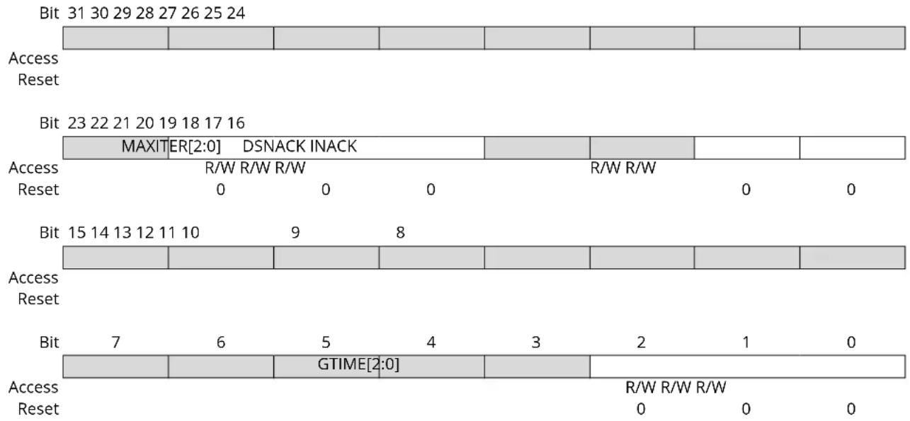
text_image
Bit 31 30 29 28 27 26 25 24 Access Reset Bit 23 22 21 20 19 18 17 16 MAXITER[2:0] DSNACK INACK Access R/W R/W R/W R/W R/W Reset 0 0 0 0 0 Bit 15 14 13 12 11 10 9 8 Access Reset Bit 7 6 5 4 3 2 1 0 GTIME[2:0] Access R/W R/W R/W Reset 0 0 0Bits 22:20 - MAXITER[2:0] Maximum Iterations
These bits define the maximum number of retransmit iterations.
These bits also define the successive NACKs sent to the remote transmitter when CTRLC.DSNACK is set.
This field is only valid when using ISO7816 T=0 mode (CTRLA.MODE=0x7).
Bit 17 - DSNACK Disable Successive Not Acknowledge
This bit controls how many times NACK will be sent on parity error reception.
This bit is only valid in ISO7816 T=0 mode and when CTRLC.INACK=0.
| Value | Description |
| 0 | NACK is sent on the ISO line for every parity error received. |
| 1 | Successive parity errors are counted up to the value specified in CTRLC.MAXITER. These parity errors generate a NACK on the ISO line. As soon as this value is reached, no additional NACK is sent on the ISO line. |
Bit 16 - INACK Inhibit Not Acknowledge
This bit controls whether a NACK is transmitted when a parity error is received.
This bit is only valid in ISO7816 T=0 mode.
| Value | Description |
| 0 | NACK is transmitted when a parity error is received. |
| 1 | NACK is not transmitted when a parity error is received. |
Bits 2:0 - GTIME[2:0] Guard Time
These bits define the guard time when using RS485 mode (CTRLA.FORM=0x0 or CTRLA.FORM=0x1, and CTRLA.TXPO=0x3) or ISO7816 mode (CTRLA.FORM=0x7).
For RS485 mode, the guard time is programmable from 0-7 bit times and defines the time that the transmit enable pin (TE) remains high after the last stop bit is transmitted and there is no remaining data to be transmitted.
For ISO7816 T=0 mode, the guard time is programmable from 2-9 bit times and defines the guard time between each transmitted byte.
31.8.4 Baud
Name: BAUD
Offset: 0x0C
Reset: 0x0000
Property: Enable-Protected, PAC Write-Protection
Bit 15 14 13 12 11 10 9 8
BAUD[15:8]
Access R/W R/W R/W R/W R/W R/W R/W R/W
Reset 00000000
Bit 76543210
BAUD[7:0]
Access R/W R/W R/W R/W R/W R/W R/W R/W
Reset 00000000
Bits 15:0 - BAUD[15:0] Baud Value
Arithmetic Baud Rate Generation (CTRLA.SAMPR[0]=0):
These bits control the clock generation, as described in the SERCOM Baud Rate section.
If Fractional Baud Rate Generation (CTRLA.SAMPR[0]=1) bit positions 15 to 13 are replaced by FP[2:0] Fractional Part:
For more information on an Arithmetic Baud Rate Generation, refer to Asynchronous Arithmetic Mode BAUD Value Selection.
- Bits 15:13 - FP[2:0]: Fractional Part
These bits control the clock generation, as described in the Clock Generation - Baud-Rate Generator section.
- Bits 12:0 - BAUD[21:0]: Baud Value
These bits control the clock generation, as described in the Clock Generation - Baud-Rate Generator section.
31.8.5 Receive Pulse Length Register
Name: RXPL
Offset: 0x0E
Reset: 0x00
Property: PAC Write-Protection
Bit 76543210
RXPL[7:0]
Access R/W R/W R/W R/W R/W R/W R/W R/W
Reset 00000000
Bits 7:0 - RXPL[7:0] Receive Pulse Length
When the encoding format is set to IrDA (CTRLB.ENC=1), these bits control the minimum pulse length that is required for a pulse to be accepted by the IrDA receiver with regards to the serial engine clock period SE_per .
$$ P U L S E \geq R X (P L + 2 \cdot S E) \quad p e r $$
31.8.6 Interrupt Enable Clear
Name: INTENCLR
Offset: 0x14
Reset: 0x00
Property: PAC Write-Protection
This register allows the user to disable an interrupt without doing a read-modify-write operation. Changes in this register will also be reflected in the Interrupt Enable Set register (INTENSET).
Bit 76543210
| ERROR | RXBRK | CTSIC | RXS | RXC | TXC | DRE | ||||||
| Access | R/W | R/W | R/W | R/W | R/W | R/W | R/W | |||||
| Reset | 0 | 0 | 0 | 0 | 0 | 0 | ||||||
Bit 7 - ERROR Error Interrupt Enable
Writing '0' to this bit has no effect.
Writing '1' to this bit will clear the Error Interrupt Enable bit, which disables the Error interrupt.
| Value | Description |
| 0 | Error interrupt is disabled. |
| 1 | Error interrupt is enabled. |
Bit 5 - RXBRK Receive Break Interrupt Enable
Writing '0' to this bit has no effect.
Writing '1' to this bit will clear the Receive Break Interrupt Enable bit, which disables the Receive Break interrupt.
| Value | Description |
| 0 | Receive Break interrupt is disabled. |
| 1 | Receive Break interrupt is enabled. |
Bit 4 - CTSIC Clear to Send Input Change Interrupt Enable
Writing '0' to this bit has no effect.
Writing '1' to this bit will clear the Clear To Send Input Change Interrupt Enable bit, which disables the Clear To Send Input Change interrupt.
| Value | Description |
| 0 | Clear To Send Input Change interrupt is disabled. |
| 1 | Clear To Send Input Change interrupt is enabled. |
Bit 3 - RXS Receive Start Interrupt Enable
Writing '0' to this bit has no effect.
Writing '1' to this bit will clear the Receive Start Interrupt Enable bit, which disables the Receive Start interrupt.
| Value | Description |
| 0 | Receive Start interrupt is disabled. |
| 1 | Receive Start interrupt is enabled. |
Bit 2 - RXC Receive Complete Interrupt Enable
Writing '0' to this bit has no effect.
Writing '1' to this bit will clear the Receive Complete Interrupt Enable bit, which disables the Receive Complete interrupt.
| Value | Description |
| 0 | Receive Complete interrupt is disabled. |
| 1 | Receive Complete interrupt is enabled. |
Bit 1 - TXC Transmit Complete Interrupt Enable
Writing '0' to this bit has no effect.
Writing '1' to this bit will clear the Transmit Complete Interrupt Enable bit, which disables the Receive Complete interrupt.
| Value Description | |
| 0 | Transmit Complete interrupt is disabled. |
| 1 | Transmit Complete interrupt is enabled. |
Bit 0 - DRE Data Register Empty Interrupt Enable
Writing '0' to this bit has no effect.
Writing '1' to this bit will clear the Data Register Empty Interrupt Enable bit, which disables the Data Register Empty interrupt.
| Value Description | |
| 0 | Data Register Empty interrupt is disabled. |
| 1 | Data Register Empty interrupt is enabled. |
31.8.7 Interrupt Enable Set
Name: INTENSET
Offset: 0x16
Reset: 0x00
Property: PAC Write-Protection
This register allows the user to enable an interrupt without read-modify-write operation. Changes in this register will also be reflected in the Interrupt Enable Clear register (INTENCLR).
This register allows the user to disable an interrupt without doing a read-modify-write operation. Changes in this register will also be reflected in the Interrupt Enable Clear register (INTENCLR).
Bit 76543210
| ERROR | RXBRK | CTSIC | RXS | RXC | TXC | DRE | ||||||
| Access | R/W | R/W | R/W | R/W | R/W | R/W | ||||||
| Reset | 0 | 0 0 0 0 0 0 | ||||||||||
Bit 7 - ERROR Error Interrupt Enable
Writing '0' to this bit has no effect.
Writing '1' to this bit will set the Error Interrupt Enable bit, which enables the Error interrupt.
| Value | Description |
| 0 | Error interrupt is disabled. |
| 1 | Error interrupt is enabled. |
Bit 5 - RXBRK Receive Break Interrupt Enable
Writing '0' to this bit has no effect.
Writing '1' to this bit will set the Receive Break Interrupt Enable bit, which enables the Receive Break interrupt.
| Value | Description |
| 0 | Receive Break interrupt is disabled. |
| 1 | Receive Break interrupt is enabled. |
Bit 4 - CTSIC Clear to Send Input Change Interrupt Enable
Writing '0' to this bit has no effect.
Writing '1' to this bit will set the Clear To Send Input Change Interrupt Enable bit, which enables the Clear To Send Input Change interrupt.
| Value | Description |
| 0 | Clear To Send Input Change interrupt is disabled. |
| 1 | Clear To Send Input Change interrupt is enabled. |
Bit 3 - RXS Receive Start Interrupt Enable
Writing '0' to this bit has no effect.
Writing '1' to this bit will set the Receive Start Interrupt Enable bit, which enables the Receive Start interrupt.
| Value | Description |
| 0 | Receive Start interrupt is disabled. |
| 1 | Receive Start interrupt is enabled. |
Bit 2 - RXC Receive Complete Interrupt Enable
Writing '0' to this bit has no effect.
Writing '1' to this bit will set the Receive Complete Interrupt Enable bit, which enables the Receive Complete interrupt.
| Value | Description |
| 0 | Receive Complete interrupt is disabled. |
| 1 | Receive Complete interrupt is enabled. |
Bit 1 - TXC Transmit Complete Interrupt Enable
Writing '0' to this bit has no effect.
Writing '1' to this bit will set the Transmit Complete Interrupt Enable bit, which enables the Transmit Complete interrupt.
| Value Description | |
| 0 | Transmit Complete interrupt is disabled. |
| 1 | Transmit Complete interrupt is enabled. |
Bit 0 - DRE Data Register Empty Interrupt Enable
Writing '0' to this bit has no effect.
Writing '1' to this bit will set the Data Register Empty Interrupt Enable bit, which enables the Data Register Empty interrupt.
| Value Description | |
| 0 | Data Register Empty interrupt is disabled. |
| 1 | Data Register Empty interrupt is enabled. |
31.8.8 Interrupt Flag Status and Clear
Name: INTFLAG
Offset: 0x18
Reset: 0x00
Property: -
Bit 76543210
| ERROR | RXBRK | CTSIC | RXS | RXC | TXC | DRE | ||||||
| Access | R/W | R/W | R/W | R/W | R | |||||||
| Reset | 0 | 0 0 0 0 0 0 | ||||||||||
Bit 7 - ERROR Error
This flag is cleared by writing '1' to it.
This bit is set when any error is detected. Errors that will set this flag have corresponding status flags in the STATUS register. Errors that will set this flag are COLL, ISF, BUFOVF, FERR, and PERR. Writing '0' to this bit has no effect.
Writing '1' to this bit will clear the flag.
Bit 5 - RXBRK Receive Break
This flag is cleared by writing '1' to it.
This flag is set when auto-baud is enabled (CTRLA.FORM) and a break character is received.
Writing '0' to this bit has no effect.
Writing '1' to this bit will clear the flag.
Bit 4 - CTSIC Clear to Send Input Change
This flag is cleared by writing a '1' to it.
This flag is set when a change is detected on the CTS pin.
Writing '0' to this bit has no effect.
Writing '1' to this bit will clear the flag.
Bit 3 - RXS Receive Start
This flag is cleared by writing '1' to it.
This flag is set when a start condition is detected on the RxD line and start-of-frame detection is enabled (CTRLB.SFDE is '1').
Writing '0' to this bit has no effect.
Writing '1' to this bit will clear the Receive Start interrupt flag.
Bit 2 - RXC Receive Complete
This flag is cleared by reading the Data register (DATA) or by disabling the receiver.
This flag is set when there are unread data in DATA.
Writing '0' to this bit has no effect.
Writing '1' to this bit has no effect.
Bit 1 - TXC Transmit Complete
This flag is cleared by writing '1' to it or by writing new data to DATA.
This flag is set when the entire frame in the transmit shift register has been shifted out and there are no new data in DATA.
Writing '0' to this bit has no effect.
Writing '1' to this bit will clear the flag.
Bit 0 - DRE Data Register Empty
This flag is cleared by writing new data to DATA.
This flag is set when DATA is empty and ready to be written.
Writing '0' to this bit has no effect.
Writing '1' to this bit has no effect.
31.8.9 Status
Name: STATUS
Offset: 0x1A
Reset: 0x0000
Property: -
Bit 15 14 13 12 11 10 9 8
| Access Reset |
Bit 76543210
| ITER | COLL | ISF | CTS | BUFOVF | FERR | PERR | ||
| Access | R/W | R/W | R/W | R | R/W | R/W | R/W | |
| Reset 0 | 0 0 0 0 0 0 |
Bit 7 - ITER Maximum Number of Repetitions Reached
This bit is set when the maximum number of NACK repetitions or retransmissions is met in ISO7816 T=0 mode.
Writing '0' to this bit has no effect.
Writing '1' to this bit will clear it.
Bit 5 - COLL Collision Detected
This bit is cleared by writing '1' to the bit or by disabling the receiver.
This bit is set when collision detection is enabled (CTRLB.COLDEN) and a collision is detected.
Writing '0' to this bit has no effect.
Writing '1' to this bit will clear it.
Bit 4 - ISF Inconsistent Sync Field
This bit is cleared by writing '1' to the bit or by disabling the receiver.
This bit is set when the frame format is set to auto-baud (CTRLA.FORM) and a sync field not equal to 0x55 is received.
Writing '0' to this bit has no effect.
Writing '1' to this bit will clear it.
Bit 3 - CTS Clear to Send
This bit indicates the current level of the CTS pin when flow control is enabled (CTRLA.TXPO).
Writing '0' to this bit has no effect.
Writing '1' to this bit has no effect.
Bit 2 - BUFOVF Buffer Overflow
Reading this bit before reading the Data register will indicate the error status of the next character to be read.
This bit is cleared by writing '1' to the bit or by disabling the receiver.
This bit is set when a buffer overflow condition is detected. A buffer overflow occurs when the receive buffer is full, there is a new character waiting in the receive shift register and a new start bit is detected.
Writing '0' to this bit has no effect.
Writing '1' to this bit will clear it.
Bit 1 - FERR Frame Error
Reading this bit before reading the Data register will indicate the error status of the next character to be read.
This bit is cleared by writing '1' to the bit or by disabling the receiver.
This bit is set if the received character had a frame error, i.e., when the first stop bit is zero.
Writing '0' to this bit has no effect.
Writing '1' to this bit will clear it.
Bit 0 - PERR Parity Error
Reading this bit before reading the Data register will indicate the error status of the next character to be read.
This bit is cleared by writing '1' to the bit or by disabling the receiver.
This bit is set if parity checking is enabled (CTRLA.FORM is 0x1, 0x5, or 0x7) and a parity error is detected.
Writing '0' to this bit has no effect.
Writing '1' to this bit will clear it.
31.8.10 Synchronization Busy
Name: SYNCBUSY
Offset: 0x1C
Reset: 0x00000000
Property: -

text_image
Bit 31 30 29 28 27 26 25 24 Access Reset Bit 23 22 21 20 19 18 17 16 Access Reset Bit 15 14 13 12 11 10 9 8 Access Reset Bit 7 6 5 4 3 2 1 0 Access Reset RXERRCN T CTRLB ENABLE SWRST R R R 0 0 0 0Bit 3 - RXERRCNT Receive Error Count Synchronization Busy
The RXERRCNT register is automatically synchronized to the APB domain upon error. When returning from sleep, this bit will be raised until the new value is available to be read.
| Value | Description |
| 0 | RXERRCNT synchronization is not busy. |
| 1 | RXERRCNT synchronization is busy. |
Bit 2 - CTRLB CTRLB Synchronization Busy
Writing to the CTRLB register when the SERCOM is enabled requires synchronization. When writing to CTRLB the SYNCBUSY.CTRLB bit will be set until synchronization is complete. If CTRLB is written while SYNCBUSY.CTRLB is asserted, an APB error will be generated.
| Value | Description |
| 0 | CTRLB synchronization is not busy. |
| 1 | CTRLB synchronization is busy. |
Bit 1 - ENABLE SERCOM Enable Synchronization Busy
Enabling and disabling the SERCOM (CTRLA. ENABLE) requires synchronization. When written, the SYNCBUSY. ENABLE bit will be set until synchronization is complete.
| Value | Description |
| 0 | Enable synchronization is not busy. |
| 1 | Enable synchronization is busy. |
Bit 0 - SWRST Software Reset Synchronization Busy
Resetting the SERCOM (CTRLA.SWRST) requires synchronization. When written, the SYNCBUSY.SWRST bit will be set until synchronization is complete.
| Value | Description |
| 0 | SWRST synchronization is not busy. |
Value Description
1 SWRST synchronization is busy.
31.8.11 Receive Error Count
Name: RXERRCNT
Offset: 0x20
Reset: 0x00
Bits 7:0 - RXERRCNT[7:0] Receive Error Count
This register records the total number of parity errors and NACK errors combined in ISO7816 mode (CTRLA.FORM=0x7).
This register is automatically cleared on read.
31.8.12 Data
Name: DATA
Offset: 0x28
Reset: 0x0000
Property: -
Bit 15 14 13 12 11 10 9 8
| DATA[8] | |||||||
| Access Reset 0 | R/W | ||||||
Bit 76543210

text_image
DATA[7:0] Access R/W R/W R/W R/W R/W R/W R/W Reset 0 0 0 0 0 0 0Bits 8:0 - DATA[8:0] Data
Reading these bits will return the contents of the Receive Data register. The register should be read only when the Receive Complete Interrupt Flag bit in the Interrupt Flag Status and Clear register (INTFLAG.RXC) is set. The status bits in STATUS should be read before reading the DATA value in order to get any corresponding error.
Writing these bits will write the Transmit Data register. This register should be written only when the Data Register Empty Interrupt Flag bit in the Interrupt Flag Status and Clear register (INTFLAG.DRE) is set.
31.8.13 Debug Control
Name: DBGCTRL
Offset: 0x30
Reset: 0x00
Property: PAC Write-Protection
Bit 76543210
| DBGSTOP | |||||||
| Access Reset 0 | R/W | ||||||
Bit 0 - DBGSTOP Debug Stop Mode
This bit controls the baud-rate generator functionality when the CPU is halted by an external debugger.
| Value Description | |
| 0 | The baud-rate generator continues normal operation when the CPU is halted by an external debugger. |
| 1 | The baud-rate generator is halted when the CPU is halted by an external debugger. |
32. SERCOM SPI – SERCOM Serial Peripheral Interface
32.1 Overview
The serial peripheral interface (SPI) is one of the available modes in the Serial Communication Interface (SERCOM).
The SPI uses the SERCOM transmitter and receiver configured as shown in 32.3. Block Diagram. Each side, Host and Client, depicts a separate SPI containing a shift register, a transmit buffer and two receive buffers. In addition, the SPI Host uses the SERCOM baud-rate generator, while the SPI Client can use the SERCOM address match logic. Labels in capital letters are synchronous to CLK_SERCOMx_APB and accessible by the CPU, while labels in lowercase letters are synchronous to the SCK clock.
32.2 Features
SERCOM SPI includes the following features:
• Full-duplex, four-wire interface (MISO, MOSI, SCK, SS)
- Single-buffered transmitter, double-buffered receiver
• Supports all four SPI modes of operation
- Single data direction operation allows alternate function on MISO or MOSI pin
- Selectable LSB or MSB-first data transfer
- Can be used with DMA
- Host operation:
- Serial clock speed, f_SCK = 1 / t_SCK^(1)
- 8-bit clock generator
- Hardware controlled SS
- Client operation:
- Serial clock speed, f_SCK = 1 / t_SSCK^(1)
- Optional 8-bit address match operation
- Operation in all sleep modes
-
Wake on SS transition
-
For t_SCK and t_SSCK values, refer to SPI Timing Characteristics.
References:
SERCOM
SERCOM - Features
32.3 Block Diagram
Figure 32-1. Full-Duplex SPI Host Client Interconnection
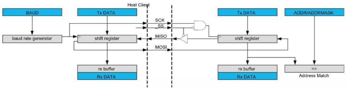
flowchart
graph TD
    A["BAUD"] --> B["baud rate generator"]
    B --> C["shift register"]
    C --> D["rx buffer"]
    C --> E["Rx DATA"]
    F["Tx DATA"] --> G["Host Client"]
    G --> H["SCK SS"]
    H --> I["MISO"]
    I --> J["MOSI"]
    J --> K["Shift register"]
    K --> L["Tx DATA"]
    M["ADDR/ADDRMASK"] --> N["Address Match"]
    N --> O["=="]
    O --> K
    style A fill:#4A90E2,stroke:#333
    style F fill:#4A90E2,stroke:#333
    style M fill:#4A90E2,stroke:#333
    style B fill:#4A90E2,stroke:#333
    style C fill:#4A90E2,stroke:#333
    style D fill:#4A90E2,stroke:#333
    style E fill:#4A90E2,stroke:#333
    style F fill:#4A90E2,stroke:#333
    style G fill:#4A90E2,stroke:#333
    style H fill:#4A90E2,stroke:#333
    style I fill:#4A90E2,stroke:#333
    style J fill:#4A90E2,stroke:#333
    style K fill:#4A90E2,stroke:#333
    style L fill:#4A90E2,stroke:#333
    style M fill:#4A90E2,stroke:#333
    style N fill:#4A90E2,stroke:#333
32.4 Signal Description
Table 32-1. SERCOM SPI Signals
| Signal Name Type Description | ||
| PAD[3:0] Digital I/O General SERCOM pins | ||
One signal can be mapped to one of several pins.
References:
I/O Multiplexing and Considerations
32.5 Product Dependencies
In order to use this peripheral, other parts of the system must be configured correctly, as described below.
32.5.1 I/O Lines
In order to use the SERCOM's I/O lines, the I/O pins must be configured using the 28. PORT - I/O Pin Controller.
When the SERCOM is configured for SPI operation, the SERCOM controls the direction and value of the I/O pins according to the table below. PORT Control bit PINCFGn.DRVSTR is still effective for the SERCOM output pins. PORT Control bit PINCFGn.PULLEN is still effective on the SERCOM input pins, but is limited to the enabling/disabling of a pull down only (it is not possible to enable/disable a pull up). If the receiver is disabled, the data input pin can be used for other purposes. In Host mode, the SPI select line (SS) is hardware controlled when the Host SPI Select Enable bit in the Control B register (CTRLB.MSSEN) is '1'.
Table 32-2. SPI Pin Configuration
| Pin Host SPI Client SPI | ||
| MOSI Output Input | ||
| MISO Input Output | ||
| SCK Output Input | ||
| SS Output (CTRLB.MSSEN=1) | Input | |
The combined configuration of PORT, the Data In Pinout and the Data Out Pinout bit groups in the Control A register (CTRLA.DIPO and CTRLA.DOPO) define the physical position of the SPI signals in the table above.
32.5.2 Power Management
This peripheral can continue to operate in any sleep mode where its source clock is running. The interrupts can wake up the device from sleep modes.
References:
PM - Power Manager
32.5.3 Clocks
The SERCOM bus clock (CLK_SERCOMx_APB) is enabled by default, and can be enabled and disabled in the Main Clock.
A generic clock (GCLK_SERCOMx_CORE) is required to clock the SPI. This clock must be configured and enabled in the Generic Clock Controller before using the SPI.
This generic clock is asynchronous to the bus clock (CLK_SERCOMx_APB). Therefore, writes to certain registers will require synchronization to the clock domains.
References:
- GCLK - Generic Clock Controller
16.6.2.6. Peripheral Clock Masking
SERCOM - Synchronization
32.5.4 DMA
The DMA request lines are connected to the DMA Controller (DMAC). In order to use DMA requests with this peripheral the DMAC must be configured first. Refer to the DMAC - Direct Memory Access Controller for details.
32.5.5 Interrupts
The interrupt request line is connected to the Interrupt Controller. In order to use interrupt requests of this peripheral, the Interrupt Controller (NVIC) must be configured first. Refer to the Nested Vector Interrupt Controller for details.
32.5.6 Events
Not applicable.
32.5.7 Debug Operation
When the CPU is halted in debug mode, this peripheral will continue normal operation. If the peripheral is configured to require periodical service by the CPU through interrupts or similar, improper operation or data loss may result during debugging. This peripheral can be forced to halt operation during debugging - refer to the Debug Control (DBGCTRL) register for details.
32.5.8 Register Access Protection
Registers with write-access can be write-protected optionally by the 11. PAC - Peripheral Access Controller.
PAC Write-Protection is not available for the following registers:
- Interrupt Flag Clear and Status register (INTFLAG)
- Status register (STATUS)
• Data register (DATA)
Optional PAC Write-Protection is denoted by the "PAC Write-Protection" property in each individual register description.
Write-protection does not apply to accesses through an external debugger.
32.5.9 Analog Connections
Not applicable.
32.6 Functional Description
32.6.1 Principle of Operation
The SPI is a high-speed synchronous data transfer interface It allows high-speed communication between the device and peripheral devices.
The SPI can operate as Host or Client. As Host, the SPI initiates and controls all data transactions. The SPI is single buffered for transmitting and double buffered for receiving.
When transmitting data, the Data register can be loaded with the next character to be transmitted during the current transmission.
When receiving, the data is transferred to the two-level receive buffer, and the receiver is ready for a new character.
The SPI transaction format is shown in SPI Transaction Format. Each transaction can contain one or more characters. The character size is configurable, and can be either 8 or 9 bits.
Figure 32-2. SPI Transaction Format
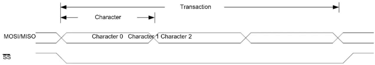
flowchart
graph LR
    A["MOSI/MISO"] --> B["Character 0"]
    B --> C["Character 1"]
    C --> D["Character 2"]
    D --> E["Transaction"]
    style A fill:#f9f,stroke:#333
    style E fill:#bbf,stroke:#333
The SPI Host must pull the SPI Select line (SS) of the desired Client low to initiate a transaction. The Host and Client prepare data to send via their respective shift registers, and the Host generates the serial clock on the SCK line.
Data are always shifted from Host to Client on the Host Output Client Input line (MOSI); data is shifted from Client to Host on the Host Input Client Output line (MISO).
Each time character is shifted out from the Host, a character will be shifted out from the Client simultaneously. To signal the end of a transaction, the Host will pull the SS line high
32.6.2 Basic Operation
32.6.2.1 Initialization
The following registers are enable-protected, meaning that they can only be written when the SPI is disabled (CTRL.ENABLE=0):
- Control A register (CTRLA), except Enable (CTRLA.ENABLE) and Software Reset (CTRLA.SWRST)
- Control B register (CTRLB), except Receiver Enable (CTRLB.RXEN)
• Baud register (BAUD) - Address register (ADDR)
When the SPI is enabled or is being enabled (CTRLA.ENABLE=1), any writing to these registers will be discarded.
when the SPI is being disabled, writing to these registers will be completed after the disabling.
Enable-protection is denoted by the Enable-Protection property in the register description.
Initialize the SPI by following these steps:
- Select SPI mode in Host / Client operation in the Operating Mode bit group in the CTRLA register (CTRLA.MODE=0x2 or 0x3).
- Select transfer mode for the Clock Polarity bit and the Clock Phase bit in the CTRLA register (CTRLA.CPOL and CTRLA.CPHA) if desired.
- Select the Frame Format value in the CTRLA register (CTRLA.FORM).
- Configure the Data In Pinout field in the Control A register (CTRLA.DIPO) for SERCOM pads of the receiver.
- Configure the Data Out Pinout bit group in the Control A register (CTRLA.DOPO) for SERCOM pads of the transmitter.
- Select the Character Size value in the CTRLB register (CTRLB.CHSIZE).
- Write the Data Order bit in the CTRLA register (CTRLA.DORD) for data direction.
- If the SPI is used in Host mode:
a. Select the desired baud rate by writing to the Baud register (BAUD).
b. If Hardware SS control is required, write '1' to the Host SPI Select Enable bit in CTRLB register (CTRLB.MSSEN). - Enable the receiver by writing the Receiver Enable bit in the CTRLB register (CTRLB.RXEN=1).
32.6.2.2 Enabling, Disabling, and Resetting
This peripheral is enabled by writing '1' to the Enable bit in the Control A register (CTRLA.ENABLE), and disabled by writing '0' to it.
Writing '1' to the Software Reset bit in the Control A register (CTRLA.SWRST) will reset all registers of this peripheral to their initial states, except the DBGCTRL register, and the peripheral is disabled.
Refer to the CTRLA register description for details.
32.6.2.3 Clock Generation
In SPI Host operation (CTRLA.MODE=0x3), the serial clock (SCK) is generated internally by the SERCOM baud-rate generator.
In SPI mode, the baud-rate generator is set to synchronous mode. The 8-bit Baud register (BAUD) value is used for generating SCK and clocking the shift register. Refer to Clock Generation - Baud-Rate Generator for more details.
In SPI Client operation (CTRLA.MODE is 0x2), the clock is provided by an external Host on the SCK pin. This clock is used to directly clock the SPI shift register.
References:
Clock Generation - Baud-Rate Generator
Asynchronous Arithmetic Mode BAUD Value Selection
32.6.2.4 Data Register
The SPI Transmit Data register (TxDATA) and SPI Receive Data register (RxDATA) share the same I/O address, referred to as the SPI Data register (DATA). Writing DATA register will update the Transmit Data register. Reading the DATA register will return the contents of the Receive Data register.
32.6.2.5 SPI Transfer Modes
There are four combinations of SCK phase and polarity to transfer serial data. The SPI data transfer modes are shown in SPI Transfer Modes (Table) and SPI Transfer Modes (Figure).
SCK phase is configured by the Clock Phase bit in the CTRLA register (CTRLA.CPHA). SCK polarity is programmed by the Clock Polarity bit in the CTRLA register (CTRLA.CPOL). Data bits are shifted out and latched in on opposite edges of the SCK signal. This ensures sufficient time for the data signals to stabilize.
Table 32-3. SPI Transfer Modes
| Mode CPOL CPHA Leading Edge Trailing Edge | ||
| 0 0 0 Rising, sample Falling, setup | ||
| 1 0 1 Rising, setup Falling, sample | ||
| 2 1 0 Falling, sample Rising, setup | ||
| 3 1 1 Falling, setup Rising, sample |
Note:
Leading edge is the first clock edge in a clock cycle.
Trailing edge is the second clock edge in a clock cycle.
Figure 32-3. SPI Transfer Modes
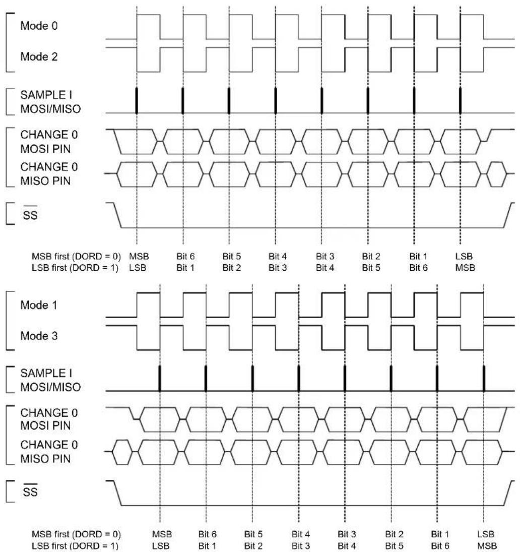
text_image
Mode 0 Mode 2 SAMPLE I MOSI/MISO CHANGE 0 MOSI PIN CHANGE 0 MISO PIN SS MSB first (DORD = 0) MSB Bit 6 Bit 5 Bit 4 Bit 3 Bit 2 Bit 1 LSB LSB first (DORD = 1) LSB Bit 1 Bit 2 Bit 3 Bit 4 Bit 5 Bit 6 MSB Mode 1 Mode 3 SAMPLE I MOSI/MISO CHANGE 0 MOSI PIN CHANGE 0 MISO PIN SS MSB first (DORD = 0) MSB Bit 6 Bit 5 Bit 4 Bit 3 Bit 2 Bit 1 LSB LSB first (DORD = 1) LSB Bit 1 Bit 2 Bit 3 Bit 4 Bit 5 Bit 6 MSB32.6.2.6 Transferring Data
Host
In Host mode (CTRLA.MODE=0x3), when Host Client Enable Select (CTRLB.MSSEN) is '1', hardware will control the SS line.
When Host SPI Select Enable (CTRLB.MSSEN) is '0', the line must be configured as an output. can be assigned to any general purpose I/O pin. When the SPI is ready for a data transaction, software must pull the line low.
When writing a character to the Data register (DATA), the character will be transferred to the shift register. Once the content of TxDATA has been transferred to the shift register, the Data Register Empty flag in the Interrupt Flag Status and Clear register (INTFLAG.DRE) will be set. And a new character can be written to DATA.
Each time one character is shifted out from the Host, another character will be shifted in from the Client simultaneously. If the receiver is enabled (CTRLA.RXEN=1), the contents of the shift register will be transferred to the two-level receive buffer. The transfer takes place in the same clock cycle as the last data bit is shifted in. And the Receive Complete Interrupt flag in the Interrupt Flag Status and Clear register (INTFLAG.RXC) will be set. The received data can be retrieved by reading DATA.
When the last character has been transmitted and there is no valid data in DATA, the Transmit Complete Interrupt flag in the Interrupt Flag Status and Clear register (INTFLAG.TXC) will be set. When the transaction is finished, the Host must pull the line high to notify the Client. If Host SPI Select Enable (CTRLB.MSSEN) is set to '0', the software must pull the line high.
Client
In Client mode (CTRLA.MODE=0x2), the SPI interface will remain inactive with the MISO line tri-stated as long as the SS pin is pulled high. Software may update the contents of DATA at any time as long as the Data Register Empty flag in the Interrupt Status and Clear register (INTFLAG.DRE) is set.
When is pulled low and SCK is running, the Client will sample and shift out data according to the transaction mode set. When the content of TxDATA has been loaded into the shift register, INTFLAG.DRE will be set, and new data can be written to DATA.
Similar to the Host, the Client will receive one character for each character transmitted. A character will be transferred into the two-level receive buffer within the same clock cycle its last data bit is received. The received character can be retrieved from DATA when the Receive Complete interrupt flag (INTFLAG.RXC) is set.
When the Host pulls the SS line high, the transaction is done and the Transmit Complete Interrupt flag in the Interrupt Flag Status and Clear register (INTFLAG.TXC) will be set.
After DATA is written it takes up to three SCK clock cycles until the content of DATA is ready to be loaded into the shift register on the next character boundary. As a consequence, the first character transferred in a SPI transaction will not be the content of DATA. This can be avoided by using the preloading feature. Refer to 32.6.3.2. Preloading of the Client Shift Register.
When transmitting several characters in one SPI transaction, the data has to be written into DATA register with at least three SCK clock cycles left in the current character transmission. If this criteria is not met, the previously received character will be transmitted.
Once the DATA register is empty, it takes three CLK_SERCOM_APB cycles for INTFLAG.DRE to be set.
32.6.2.7 Receiver Error Bit
The SPI receiver has one error bit: the Buffer Overflow bit (BUFOVF), which can be read from the Status register (STATUS). Once an error happens, the bit will stay set until it is cleared by writing '1' to it. The bit is also automatically cleared when the receiver is disabled.
There are two methods for buffer overflow notification, selected by the immediate buffer overflow notification bit in the Control A register (CTRLA.IBON):
If CTRLA.IBON=1, STATUS.BUFOVF is raised immediately upon buffer overflow. Software can then empty the receive FIFO by reading RxDATA until the receiver complete interrupt flag in the Interrupt Flag Status and Clear register (INTFLAG.RXC) goes low.
If CTRLA.IBON=0, the buffer overflow condition travels with data through the receive FIFO. After the received data is read, STATUS.BUFOVF and INTFLAG.ERROR will be set along with INTFLAG.RXC, and RxDATA will be zero.
32.6.3 Additional Features
32.6.3.1 Address Recognition
When the SPI is configured for Client operation (CTRLA.MODE=0x2) with address recognition (CTRLA.FORM is 0x2), the SERCOM address recognition logic is enabled: the first character in a transaction is checked for an address match.
If there is a match, the Receive Complete Interrupt flag in the Interrupt Flag Status and Clear register (INTFLAG.RXC) is set, the MISO output is enabled, and the transaction is processed. If the device is in sleep mode, an address match can wake up the device in order to process the transaction.
If there is no match, the complete transaction is ignored.
If a 9-bit frame format is selected, only the lower 8 bits of the shift register are checked against the Address register (ADDR).
Preload must be disabled (CTRLB.PLOADEN=0) in order to use this mode.
References:
Address Match and Mask
32.6.3.2 Preloading of the Client Shift Register
When starting a transaction, the Client will first transmit the contents of the shift register before loading new data from DATA. The first character sent can be either the reset value of the shift register (if this is the first transmission since the last reset) or the last character in the previous transmission.
Preloading can be used to preload data into the shift register while is high: this eliminates sending a dummy character when starting a transaction. If the shift register is not preloaded, the current contents of the shift register will be shifted out.
Only one data character will be preloaded into the shift register while the synchronized signal is high. If the next character is written to DATA before is pulled low, the second character will be stored in DATA until transfer begins.
For proper preloading, sufficient time must elapse between SS going low and the first SCK sampling edge, as in Timing Using Preloading. See the Electrical Characteristics for timing details.
Preloading is enabled by writing '1' to the Client Data Preload Enable bit in the CTRLB register (CTRLB.PLOADEN).
Figure 32-4. Timing Using Preloading

flowchart
graph LR
    A["SS"] --> B["Required SS-to-SCK time using PRELOADEN"]
    C["SS synchronized to system domain"] --> B
    D["SCK"] --> E["Synchronization to system domain"]
    E --> F["MISO to SCK setup time"]
32.6.3.3 Host with Several Clients
Host with multiple Clients in parallel is only available when Host SPI Select Enable (CTRLB.MSSEN) is set to zero and hardware control is disabled. If the bus consists of several SPI Clients, an SPI Host can use general purpose I/O pins to control the line to each of the Clients on the bus, as shown in Multiple Clients in Parallel. In this configuration, the single selected SPI Client will drive the tri-state MISO line.
Figure 32-5. Multiple Clients in Parallel
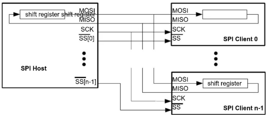
flowchart
graph TD
    A["SPI Host"] --> B["shift register"]
    B --> C["MOSI"]
    B --> D["MISO"]
    B --> E["SCK"]
    B --> F["SS[0"]]
    B --> G["..."]
    B --> H["SS[n-1"]]
    I["SPI Client 0"] --> J["MOSI"]
    I --> K["MISO"]
    I --> L["SCK"]
    I --> M["SS"]
    I --> N["..."]
    I --> O["..."]
    I --> P["..."]
    I --> Q["..."]
    I --> R["..."]
    I --> S["..."]
    I --> T["..."]
    I --> U["..."]
    I --> V["..."]
    I --> W["..."]
    I --> X["..."]
    I --> Y["..."]
    I --> Z["..."]
    I --> AA["..."]
    I --> AB["..."]
    I --> AC["..."]
    I --> AD["..."]
    I --> AE["..."]
    I --> AF["..."]
    I --> AG["..."]
    I --> AH["..."]
    I --> AI["..."]
    I --> AJ["..."]
    I --> AK["..."]
    I --> AL["..."]
    I --> AM["..."]
    I --> AN["..."]
    I --> AO["..."]
    I --> AP["..."]
    I --> AQ["..."]
    I --> AR["..."]
    I --> AS["..."]
    I --> AT["..."]
    I --> AU["..."]
    I --> AV["..."]
    I --> AW["..."]
    I --> AX["..."]
    I --> AY["..."]
    I --> AZ["..."]
    I --> BA["..."]
    I --> BB["..."]
    I --> BC["..."]
    I --> BD["..."]
    I --> BE["..."]
    I --> BF["..."]
    I --> BG["..."]
    I --> BH["..."]
    I --> BI["..."]
    I --> BJ["..."]
    I --> BK["..."]
    I --> BL["..."]
    I --> BM["..."]
    I --> BN["..."]
    I --> BO["..."]
    I --> BP["..."]
    I --> BQ["..."]
    I --> BR["..."]
    I --> BS["..."]
    I --> BT["..."]
    I --> BU["..."]
    I --> BV["..."]
    I --> BW["..."]
    I --> BX["..."]
    I --> BY["..."]
    I --> BZ["..."]
    I --> CA["..."]
    I --> CB["..."]
    I --> CC["..."]
    I --> CD["..."]
    I --> CE["..."]
    I --> CF["..."]
    I --> CG["..."]
    I --> CH["..."]
    I --> CI["..."]
    I --> CJ["..."]
    I --> CK["..."]
    I --> CL["..."]
    I --> CM["..."]
    I --> CN["..."]
    I --> CO["..."]
    I --> CP["..."]
    I --> CQ["..."]
    I --> CR["..."]
    I --> CS["..."]
    I --> CT["..."]
    I --> CU["..."]
    I --> CV["..."]
    I --> CW["..."]
    I --> CX["..."]
    I --> CY["..."]
    I --> CZ["..."]
    I --> DA["..."]
    I --> DB["..."]
    I --> DC["..."]
Another configuration is multiple Clients in series, as in Multiple Clients in Series. In this configuration, all n attached Clients are connected in series. A common SS line is provided to all Clients, enabling them simultaneously. The Host must shift n characters for a complete transaction. Depending on the Host SPI Select Enable bit (CTRLB.MSSEN), the SS line can be controlled either by hardware or user software and normal GPIO.
Figure 32-6. Multiple Clients in Series

flowchart
graph TD
    A["SPI Host"] -->|shift register shift register| B["SPI Client 0"]
    B -->|MOSI MISO| C["..."]
    A -->|MISO MISO| D["SPI Client n-1"]
    D -->|shift register MISO| E["..."]
    A -->|SCK SS| F["..."]
    A -->|SS| G["..."]
    A -->|MOSI MISO| H["..."]
    A -->|SCK SS| I["..."]
32.6.3.4 Loop-Back Mode
For loop-back mode, configure the Data In Pinout (CTRLA.DIPO) and Data Out Pinout (CTRLA.DOPO) to use the same data pins for transmit and receive. The loop-back is through the pad, so the signal is also available externally.
32.6.3.5 Hardware Controlled SS
In Host mode, a single SS chip select can be controlled by hardware by writing the Host SPI Select Enable (CTRLB.MSSEN) bit to '1'. In this mode, the SS pin is driven low for a minimum of one baud cycle before transmission begins, and stays low for a minimum of one baud cycle after transmission completes. If back-to-back frames are transmitted, the SS pin will always be driven high for a minimum of one baud cycle between frames.
In Hardware Controlled SS, the time T is between one and two baud cycles depending on the SPI transfer mode.
Figure 32-7. Hardware Controlled SS

text_image
SS SCK T T T T TT = 1 to 2 baud cycles
When CTRLB.MSSEN=0, the SS pin(s) is/are controlled by user software and normal GPIO.
32.6.3.6 SPI Select Low Detection
In Client mode, the SPI can wake the CPU when the SPI Select (SS) goes low. When the SPI Select Low Detect is enabled (CTRLB.SSDE=1), a high-to-low transition will set the SPI Select Low interrupt flag (INTFLAG.SSL) and the device will wake up if applicable.
32.6.4 DMA, Interrupts, and Events
Table 32-4. Module Request for SERCOM SPI
| Condition Request | |||
| DMA Interrupt Event | |||
| Data Register Empty (DRE) Yes | (request cleared when data is written) | Yes NA | |
| Receive Complete (RXC) Yes | (request cleared when data is read) | Yes | |
| Transmit Complete (TXC) NA Yes | |||
| Client Select low (SSL) NA Yes | |||
| Error (ERROR) NA Yes | |||
32.6.4.1 DMA Operation
The SPI generates the following DMA requests:
- Data received (RX): The request is set when data is available in the receive FIFO. The request is cleared when DATA is read
- Data transmit (TX): The request is set when the transmit buffer (TX DATA) is empty. The request is cleared when DATA is written.
32.6.4.2 Interrupts
The SPI has the following interrupt sources. These are asynchronous interrupts, and can wake up the device from any sleep mode:
• Data Register Empty (DRE)
• Receive Complete (RXC)
• Transmit Complete (TXC)
- Client Select Low (SSL)
- Error (ERROR)
Each interrupt source has its own interrupt flag. The interrupt flag in the Interrupt Flag Status and Clear register (INTFLAG) will be set when the interrupt condition is met. Each interrupt can be individually enabled by writing '1' to the corresponding bit in the Interrupt Enable Set register
(INTENSET), and disabled by writing '1' to the corresponding bit in the Interrupt Enable Clear register (INTENCLR).
An interrupt request is generated when the interrupt flag is set and if the corresponding interrupt is enabled. The interrupt request remains active until either the interrupt flag is cleared, the interrupt is disabled, or the SPI is reset. For details on clearing interrupt flags, refer to the INTFLAG register description.
The SPI has one common interrupt request line for all the interrupt sources. The value of INTFLAG indicates which interrupt is executed. Note that interrupts must be globally enabled for interrupt requests. Refer to the Nested Vector Interrupt Controller for details.
32.6.4.3 Events
Not applicable.
32.6.5 Sleep Mode Operation
The behavior in sleep mode is depending on the Host/Client configuration and the Run In Standby bit in the Control A register (CTRLA.RUNSTDBY):
- Host operation, CTRLA.RUNSTDBY=1: The peripheral clock GCLK_SERCOM_CORE will continue to run in idle sleep mode and in standby sleep mode. Any interrupt can wake up the device.
- Host operation, CTRLA.RUNSTDBY=0: GLK_SERCOMx_CORE will be disabled after the ongoing transaction is finished. Any interrupt can wake up the device.
- Client operation, CTRLA.RUNSTDBY=1: The Receive Complete interrupt can wake up the device.
- Client operation, CTRLA.RUNSTDBY=0: All reception will be dropped, including the ongoing transaction.
32.6.6 Synchronization
Due to asynchronicity between the main clock domain and the peripheral clock domains, some registers need to be synchronized when written or read.
The following bits are synchronized when written:
- Software Reset bit in the CTRLA register (CTRLA.SWRST)
- Enable bit in the CTRLA register (CTRLA.ENABLE)
- Receiver Enable bit in the CTRLB register (CTRLB.RXEN)
Note: CTRLB.RXEN is write-synchronized somewhat differently. See also 32.8.2. CTRLB register for details.
Required write-synchronization is denoted by the "Write-Synchronized" property in the register description.
32.7 Register Summary
| Offset | Name Bit Pos. 76543210 | |||||||||
| 0x00 CTRLA | 7:0 RUNSTDBY MODE[2:0] ENABLE SWRST | |||||||||
| 15:8 | IBON | |||||||||
| 23:16 | DIPO[1:0] | DOPO[1:0] | ||||||||
| 31:24 | DORD CPOL | CPHA | FORM[3:0] | |||||||
| 0x04 CTRLB | 7:0 | PLOADEN | CHSIZE[2:0] | |||||||
| 15:8 | AMODE[1:0] | MSSEN | SSDE | |||||||
| 23:16 | RXEN | |||||||||
| 31:24 | ||||||||||
| 0x08 ... 0x0B | Reserved | |||||||||
| 0x0C | BAUD | 7:0 | BAUD[7:0] | |||||||
| 0x0D ... 0x13 | Reserved | |||||||||
| 0x14 | INTENCLR | 7:0 | ERROR | SSL | RXC | TXC | DRE | |||
| 0x15 | Reserved | |||||||||
| 0x16 | INTENSET | 7:0 | ERROR | SSL | RXC | TXC | DRE | |||
| 0x17 | Reserved | |||||||||
| 0x18 | INTFLAG | 7:0 | ERROR | SSL | RXC | TXC | DRE | |||
| 0x19 | Reserved | |||||||||
| 0x1A | STATUS | 7:0 | BUFOVF | |||||||
| 15:8 | ||||||||||
| 0x1C | SYNCBUSY | 7:0 | CTRLB ENABLE SWRST | |||||||
| 15:8 | ||||||||||
| 23:16 | ||||||||||
| 31:24 | ||||||||||
| 0x20 ... 0x23 | Reserved | |||||||||
| 0x24 | ADDR | 7:0 | ADDR[7:0] | |||||||
| 15:8 | ||||||||||
| 23:16 | ADDRMASK[7:0] | |||||||||
| 31:24 | ||||||||||
| 0x28 | DATA | 7:0 | DATA[7:0] | |||||||
| 15:8 | DATA[8] | |||||||||
| 0x2A ... 0x2F | Reserved | |||||||||
| 0x30 | DBGCTRL | 7:0 | DBGSTOP | |||||||
32.8 Register Description
Registers can be 8, 16, or 32 bits wide. Atomic 8-, 16-, and 32-bit accesses are supported. In addition, the 8-bit quarters and 16-bit halves of a 32-bit register, and the 8-bit halves of a 16-bit register can be accessed directly.
Some registers require synchronization when read and/or written. Synchronization is denoted by the "Read-Synchronized" and/or "Write-Synchronized" property in each individual register description. Refer to 32.6.6. Synchronization.
Some registers are enable-protected, meaning they can only be written when the module is disabled. Enable-protection is denoted by the "Enable-Protected" property in each individual register description.
Optional write-protection by the Peripheral Access Controller (PAC) is denoted by the "PAC Write-Protection" property in each individual register description. Refer to 32.5.8. Register Access Protection.
32.8.1 Control A
Name: CTRLA
Offset: 0x00
Reset: 0x00000000
Property: PAC Write-Protection, Enable-Protected, Write-Synchronized
Bit 31 30 29 28 27 26 25 24
| DORD | CPOL | CPHA | FORM[3:0] | |||||
| Access | R/W | R/W | R/W | R/W | R/W | R/W | R/W | R/W |
| Reset | 0 | 0 | 0 | 0 | 0 | |||
Bit 23 22 21 20 19 18 17 16
| DIPO[1:0] | DOPO[1:0] | ||||
| Access Reset | R/W R/W | R/W R/W | |||
| 0 | 0 | 0 |
Bit 15 14 13 12 11 10 9 8
| IBON | |||||||
| Access | R/W | ||||||
| Reset | 0 |
Bit 7 6 5 4 3 2 1 0
| RUNSTDBY | MODE[2:0] | ENABLE | SWRST | |||||
| Access | R/W | R/W | R/W | R/W R/W R/W | ||||
| Reset | 0 | 0 | 0 | 0 | 0 | |||
Bit 30 - DORD Data Order
This bit selects the data order when a character is shifted out from the shift register.
This bit is not synchronized.
| Value | Description |
| 0 | MSB is transferred first. |
| 1 | LSB is transferred first. |
Bit 29 - CPOL Clock Polarity
In combination with the Clock Phase bit (CPHA), this bit determines the SPI transfer mode.
This bit is not synchronized.
| Value | Description |
| 0 | SCK is low when idle. The leading edge of a clock cycle is a rising edge, while the trailing edge is a falling edge. |
| 1 | SCK is high when idle. The leading edge of a clock cycle is a falling edge, while the trailing edge is a rising edge. |
Bit 28 - CPHA Clock Phase
In combination with the Clock Polarity bit (CPOL), this bit determines the SPI transfer mode.
This bit is not synchronized.
| Mode | CPOL | CPHA | Leading Edge | Trailing Edge |
| 0x0 | 0 | 0 | Rising, sample | Falling, change |
| 0x1 | 0 | 1 | Rising, change | Falling, sample |
| 0x2 | 1 | 0 | Falling, sample | Rising, change |
| 0x3 | 1 | 1 | Falling, change | Rising, sample |
Value Description
| 0 | The data is sampled on a leading SCK edge and changed on a trailing SCK edge. |
| 1 | The data is sampled on a trailing SCK edge and changed on a leading SCK edge. |
Bits 27:24 - FORM[3:0] Frame Format
This bit field selects the various frame formats supported by the SPI in Client mode. When the 'SPI frame with address' format is selected, the first byte received is checked against the ADDR register.
| FORM[3:0] Name Description | ||
| 0x0 SPI SPI frame | ||
| 0x1 - Reserved | ||
| 0x2 SPI_ADDR SPI frame with address | ||
| 0x3-0xF - Reserved |
Bits 21:20 - DIPO[1:0] Data In Pinout
These bits define the data in (DI) pad configurations.
In Host operation, DI is MISO.
In Client operation, DI is MOSI.
These bits are not synchronized.
| DIPO[1:0] Name Description | |
| 0x0 PAD[0] SERCOM PAD[0] is used as data input | |
| 0x1 PAD[1] SERCOM PAD[1] is used as data input | |
| 0x2 PAD[2] SERCOM PAD[2] is used as data input | |
| 0x3 PAD[3] SERCOM PAD[3] is used as data input |
Bits 17:16 - DOPO[1:0] Data Out Pinout
This bit defines the available pad configurations for data out (DO) and the serial clock (SCK). In Client operation, the Client select line ( ) is controlled by DOPO, while in Host operation the line is controlled by the port configuration.
In Host operation, DO is MOSI.
In Client operation, DO is MISO.
These bits are not synchronized.
| DOPO DO SCK Client SS | Host SS | — | — | |
| 0x0 | PAD[0] | PAD[1] | PAD[2] | System configuration |
| 0x1 | PAD[2] | PAD[3] | PAD[1] | System configuration |
| 0x2 | PAD[3] | PAD[1] | PAD[2] | System configuration |
| 0x3 | PAD[0] | PAD[3] | PAD[1] | System configuration |
Bit 8 - IBON Immediate Buffer Overflow Notification
This bit controls when the buffer overflow status bit (STATUS.BUFOVF) is set when a buffer overflow occurs.
This bit is not synchronized.
| Value | Description |
| 0 | STATUS.BUFOVF is set when it occurs in the data stream. |
| 1 | STATUS.BUFOVF is set immediately upon buffer overflow. |
Bit 7 - RUNSTDBY Run In Standby
This bit defines the functionality in standby sleep mode.
These bits are not synchronized.
| RUNSTDBY | Client | Host |
| 0x0 | Disabled. All reception is dropped, including the ongoing transaction. | Generic clock is disabled when ongoing transaction is finished. All interrupts can wake up the device. |
| 0x1 | Ongoing transaction continues, wake on Receive Complete interrupt. | Generic clock is enabled while in sleep modes. All interrupts can wake up the device. |
Bits 4:2 - MODE[2:0] Operating Mode
These bits must be written to 0x2 or 0x3 to select the SPI serial communication interface of the SERCOM.
0x2: SPI Client operation
0x3: SPI Host operation
These bits are not synchronized.
Bit 1 - ENABLE Enable
Due to synchronization, there is delay from writing CTRLA. ENABLE until the peripheral is enabled/disabled. The value written to CTRL. ENABLE will read back immediately and the Synchronization Enable Busy bit in the Synchronization Busy register (SYNCBUSY. ENABLE) will be set. SYNCBUSY. ENABLE is cleared when the operation is complete.
This bit is not enable-protected.
| Value Description | |
| 0 | The peripheral is disabled or being disabled. |
| 1 | The peripheral is enabled or being enabled. |
Bit 0 - SWRST Software Reset
Writing '0' to this bit has no effect.
Writing '1' to this bit resets all registers in the SERCOM, except DBGCTRL, to their initial state, and the SERCOM will be disabled.
Writing "1" to CTRL.SWRST will always take precedence, meaning that all other writes in the same write-operation will be discarded. Any register write access during the ongoing reset will result in an APB error. Reading any register will return the reset value of the register.
Due to synchronization, there is a delay from writing CTRLA.SWRST until the reset is complete.
CTRLA.SWRST and SYNCBUSY. SWRST will both be cleared when the reset is complete.
This bit is not enable-protected.
| Value Description | |
| 0 | There is no reset operation ongoing. |
| 1 | The reset operation is ongoing. |
32.8.2 Control B
Name: CTRLB
Offset: 0x04
Reset: 0x00000000
Property: PAC Write-Protection, Enable-Protected

other
| Bit | Access Reset | RXEN | R/W | Reset 0 | Bit | AMODE[1:0] | MSSEN | CHSIZE[2:0] | |---|---|---|---|---|---|---|---|---| | 31 | 29 | 28 | 27 | 26 | 25 | 24 | 24 | 24 | | 23 | 21 | 20 | 19 | 18 | 17 | 16 | 16 | 16 | | 15 | 13 | 12 | 11 | 10 | 9 | 8 | 8 | 8 | | 7 | 0 | 0 | 0 | 0 | 0 | 0 | 0 | 0 | | 6 | 0 | 0 | 0 | 0 | 0 | 0 | 0 | 0 | | 5 | 0 | 0 | 0 | 0 | 0 | 0 | 0 | 0 | | 4 | 0 | 0 | 0 | 0 | 0 | 0 | 0 | 0 | | 3 | 0 | 0 | 0 | 0 | 0 | 0 | 0 | 0 | | 2 | 0 | 0 | 0 | 0 | 0 | 0 | 0 | 0 | | 1 | 0 | 0 | 0 | 0 | 0 | 0 | 0 | 0 | | nanorated bits (Bit) are not provided in the image. The table is extracted from the image file.Bit 17 - RXEN Receiver Enable
Writing '0' to this bit will disable the SPI receiver immediately. The receive buffer will be flushed, data from ongoing receptions will be lost and STATUS.BUFOVF will be cleared.
Writing '1' to CTRLB.RXEN when the SPI is disabled will set CTRLB.RXEN immediately. When the SPI is enabled, CTRLB.RXEN will be cleared, SYNCBUSY.CTRLB will be set and remain set until the receiver is enabled. When the receiver is enabled CTRLB.RXEN will read back as '1'.
Writing '1' to CTRLB.RXEN when the SPI is enabled will set SYNCBUSY.CTRLB, which will remain set until the receiver is enabled, and CTRLB.RXEN will read back as '1'.
This bit is not enable-protected.
| Value | Description |
| 0 | The receiver is disabled or being enabled. |
| 1 | The receiver is enabled or it will be enabled when SPI is enabled. |
Bits 15:14 - AMODE[1:0] Address Mode
These bits set the Client addressing mode when the frame format (CTRLA.FORM) with address is used. They are unused in Host mode.
| AMODE[1:0] | Name | Description |
| 0x0 | MASK ADDRMASK is used as a mask to the ADDR register | |
| 0x1 | 2_ADDRS | The Client responds to the two unique addresses in ADDR and ADDRMASK |
| 0x2 | RANGE | The Client responds to the range of addresses between and including ADDR and ADDRMASK. ADDR is the upper limit |
| 0x3 | - | Reserved |
Bit 13 - MSSEN Host Client Select Enable
This bit enables hardware Client select (SS) control.
| Value Description | |
| 0 | Hardware SS control is disabled. |
| 1 | Hardware SS control is enabled. |
Bit 9 - SSDE Client Select Low Detect Enable
This bit enables wake up when the Client select (SS) pin transitions from high to low.
| Value Description | |
| 0 | SS low detector is disabled. |
| 1 | SS low detector is enabled. |
Bit 6 - PLOADEN Client Data Preload Enable
Setting this bit will enable preloading of the Client shift register when there is no transfer in progress. If the line is high when DATA is written, it will be transferred immediately to the shift register.
Bits 2:0 - CHSIZE[2:0] Character Size
| CHSIZE[2:0] Name Description | ||
| 0x0 8BIT 8 bits | ||
| 0x1 9BIT 9 bits | ||
| 0x2-0x7 - Reserved |
32.8.3 Baud Rate
Name: BAUD
Offset: 0x0C
Reset: 0x00
Property: PAC Write-Protection, Enable-Protected
Bit 76543210
BAUD[7:0]
Access R/W R/W R/W R/W R/W R/W R/W R/W
Reset 00000000
Bits 7:0 - BAUD[7:0] Baud Register
These bits control the clock generation, as described in the Clock Generation - Baud-Rate Generator. For further information, refer to Asynchronous Arithmetic Mode BAUD Value Selection.
32.8.4 Interrupt Enable Clear
Name: INTENCLR
Offset: 0x14
Reset: 0x00
Property: PAC Write-Protection
This register allows the user to disable an interrupt without read-modify-write operation. Changes in this register will also be reflected in the Interrupt Enable Set register (INTENSET).
Bit 76543210
| ERROR | SSL RXC TXC DRE | |||||||
| Access | R/W R/W | R/W | R/W | R/W | ||||
| Reset 0 | 0 0 0 0 | |||||||
Bit 7 - ERROR Error Interrupt Enable
Writing '0' to this bit has no effect.
Writing '1' to this bit will clear the Error Interrupt Enable bit, which disables the Error interrupt.
| Value | Description |
| 0 | Error interrupt is disabled. |
| 1 | Error interrupt is enabled. |
Bit 3 - SSL Client Select Low Interrupt Enable
Writing '0' to this bit has no effect.
Writing '1' to this bit will clear the Client Select Low Interrupt Enable bit, which disables the Client Select Low interrupt.
| Value | Description |
| 0 | Client Select Low interrupt is disabled. |
| 1 | Client Select Low interrupt is enabled. |
Bit 2 - RXC Receive Complete Interrupt Enable
Writing '0' to this bit has no effect.
Writing '1' to this bit will clear the Receive Complete Interrupt Enable bit, which disables the Receive Complete interrupt.
| Value | Description |
| 0 | Receive Complete interrupt is disabled. |
| 1 | Receive Complete interrupt is enabled. |
Bit 1 - TXC Transmit Complete Interrupt Enable
Writing '0' to this bit has no effect.
Writing '1' to this bit will clear the Transmit Complete Interrupt Enable bit, which disable the Transmit Complete interrupt.
| Value | Description |
| 0 | Transmit Complete interrupt is disabled. |
| 1 | Transmit Complete interrupt is enabled. |
Bit 0 - DRE Data Register Empty Interrupt Enable
Writing '0' to this bit has no effect.
Writing '1' to this bit will clear the Data Register Empty Interrupt Enable bit, which disables the Data Register Empty interrupt.
| Value | Description |
| 0 | Data Register Empty interrupt is disabled. |
| 1 | Data Register Empty interrupt is enabled. |
32.8.5 Interrupt Enable Set
Name: INTENSET
Offset: 0x16
Reset: 0x00
Property: PAC Write-Protection
This register allows the user to disable an interrupt without read-modify-write operation. Changes in this register will also be reflected in the Interrupt Enable Clear register (INTENCLR).
Bit 76543210
| ERROR | SSL RXC TXC DRE | |||||||
| Access | R/W R/W | R/W | R/W | R/W | ||||
| Reset 0 | 0 0 0 0 | |||||||
Bit 7 - ERROR Error Interrupt Enable
Writing '0' to this bit has no effect.
Writing '1' to this bit will set the Error Interrupt Enable bit, which enables the Error interrupt.
| Value | Description |
| 0 | Error interrupt is disabled. |
| 1 | Error interrupt is enabled. |
Bit 3 - SSL Client Select Low Interrupt Enable
Writing '0' to this bit has no effect.
Writing '1' to this bit will set the Client Select Low Interrupt Enable bit, which enables the Client Select Low interrupt.
| Value | Description |
| 0 | Client Select Low interrupt is disabled. |
| 1 | Client Select Low interrupt is enabled. |
Bit 2 - RXC Receive Complete Interrupt Enable
Writing '0' to this bit has no effect.
Writing '1' to this bit will set the Receive Complete Interrupt Enable bit, which enables the Receive Complete interrupt.
| Value | Description |
| 0 | Receive Complete interrupt is disabled. |
| 1 | Receive Complete interrupt is enabled. |
Bit 1 - TXC Transmit Complete Interrupt Enable
Writing '0' to this bit has no effect.
Writing '1' to this bit will set the Transmit Complete Interrupt Enable bit, which enables the Transmit Complete interrupt.
| Value | Description |
| 0 | Transmit Complete interrupt is disabled. |
| 1 | Transmit Complete interrupt is enabled. |
Bit 0 - DRE Data Register Empty Interrupt Enable
Writing '0' to this bit has no effect.
Writing '1' to this bit will set the Data Register Empty Interrupt Enable bit, which enables the Data Register Empty interrupt.
| Value | Description |
| 0 | Data Register Empty interrupt is disabled. |
| 1 | Data Register Empty interrupt is enabled. |
32.8.6 Interrupt Flag Status and Clear
Name: INTFLAG
Offset: 0x18
Reset: 0x00
Property: -
Bit 76543210
| ERROR | SSL RXC TXC DRE | |||||||
| Access | R/W R/W | R | R/W | R | ||||
| Reset 0 | 0 0 0 0 | |||||||
Bit 7 - ERROR Error
This flag is cleared by writing '1' to it.
This bit is set when any error is detected. Errors that will set this flag have corresponding status flags in the STATUS register. The BUFOVF error will set this interrupt flag.
Writing '0' to this bit has no effect.
Writing '1' to this bit will clear the flag.
Bit 3 - SSL Client Select Low
This flag is cleared by writing '1' to it.
This bit is set when a high to low transition is detected on the pin in Client mode and Client Select Low Detect (CTRLB.SSDE) is enabled.
Writing '0' to this bit has no effect.
Writing '1' to this bit will clear the flag.
Bit 2 - RXC Receive Complete
This flag is cleared by reading the Data (DATA) register or by disabling the receiver.
This flag is set when there are unread data in the receive buffer. If address matching is enabled, the first data received in a transaction will be an address.
Writing '0' to this bit has no effect.
Writing '1' to this bit has no effect.
Bit 1 - TXC Transmit Complete
This flag is cleared by writing '1' to it or by writing new data to DATA.
In Host mode, this flag is set when the data have been shifted out and there are no new data in DATA.
In Client mode, this flag is set when the pin is pulled high. If address matching is enabled, this flag is only set if the transaction was initiated with an address match.
Writing '0' to this bit has no effect.
Writing '1' to this bit will clear the flag.
Bit 0 - DRE Data Register Empty
This flag is cleared by writing new data to DATA.
This flag is set when DATA is empty and ready for new data to transmit.
Writing '0' to this bit has no effect.
Writing '1' to this bit has no effect.
32.8.7 Status
Name: STATUS
Offset: 0x1A
Reset: 0x0000
Property: -

text_image
Bit 15 14 13 12 11 10 9 8 Access Reset Bit 7 6 5 4 3 2 1 0 BUFOVF Access R/W Reset 0Bit 2 - BUFOVF Buffer Overflow
Reading this bit before reading DATA will indicate the error status of the next character to be read. This bit is cleared by writing '1' to the bit or by disabling the receiver.
This bit is set when a buffer overflow condition is detected. See also CTRLA.IBON for overflow handling.
When set, the corresponding RxDATA will be zero.
Writing '0' to this bit has no effect.
Writing '1' to this bit will clear it.
| Value | Description |
| 0 | No Buffer Overflow has occurred. |
| 1 | A Buffer Overflow has occurred. |
32.8.8 Synchronization Busy
Name: SYNCBUSY
Offset: 0x1C
Reset: 0x00000000
Property: -
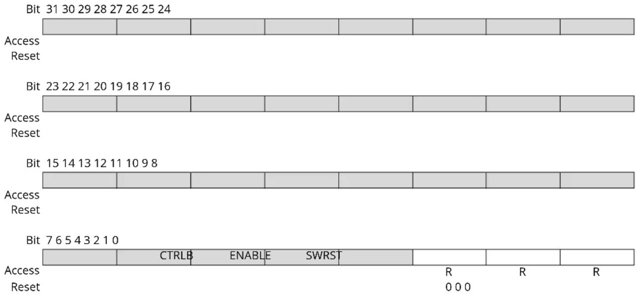
text_image
Bit 31 30 29 28 27 26 25 24 Access Reset Bit 23 22 21 20 19 18 17 16 Access Reset Bit 15 14 13 12 11 10 9 8 Access Reset Bit 7 6 5 4 3 2 1 0 Access Reset CTRLB ENABLE SWRST R R R 0 0 0Bit 2 - CTRLB CTRLB Synchronization Busy
Writing to the CTRLB when the SERCOM is enabled requires synchronization. Ongoing synchronization is indicated by SYNCBUSY.CTRLB=1 until synchronization is complete. If CTRLB is written while SYNCBUSY.CTRLB=1, an APB error will be generated.
| Value | Description |
| 0 | CTRLB synchronization is not busy. |
| 1 | CTRLB synchronization is busy. |
Bit 1 - ENABLE SERCOM Enable Synchronization Busy
Enabling and disabling the SERCOM (CTRLA.ENABLE) requires synchronization. Ongoing synchronization is indicated by SYNCBUSY.ENABLE=1 until synchronization is complete. Writes to any register (except for CTRLA.SWRST) while enable synchronization is on-going will be discarded and an APB error will be generated.
| Value | Description |
| 0 | Enable synchronization is not busy. |
| 1 | Enable synchronization is busy. |
Bit 0 - SWRST Software Reset Synchronization Busy
Resetting the SERCOM (CTRLA.SWRST) requires synchronization. Ongoing synchronization is indicated by SYNCBUSY.SWRST=1 until synchronization is complete. Writes to any register while synchronization is on-going will be discarded and an APB error will be generated.
| Value | Description |
| 0 | SWRST synchronization is not busy. |
| 1 | SWRST synchronization is busy. |
32.8.9 Address
Name: ADDR
Offset: 0x24
Reset: 0x00000000
Property: PAC Write-Protection, Enable-Protected

text_image
Bit 31 30 29 28 27 26 25 24 Access Reset Bit 23 22 21 20 19 18 17 16 ADDRMASK[7:0] Access R/W R/W R/W R/W R/W R/W R/W R/W Reset 0 0 0 0 0 0 0 0 Bit 15 14 13 12 11 10 9 8 Access Reset Bit 7 6 5 4 3 2 1 0 ADDR[7:0] Access R/W R/W R/W R/W R/W R/W R/W R/W Reset 0 0 0 0 0 0 0 0Bits 23:16 - ADDRMASK[7:0] Address Mask
These bits hold the address mask when the transaction format with address is used (CTRLA.FORM, CTRLB.AMODE).
Bits 7:0 - ADDR[7:0] Address
These bits hold the address when the transaction format with address is used (CTRLA.FORM, CTRLB.AMODE).
32.8.10 Data
Name: DATA
Offset: 0x28
Reset: 0x0000
Property: -
Bit 15 14 13 12 11 10 9 8
| DATA[8] | |||||||
| Access Reset 0 | R/W | ||||||
Bit 76543210

text_image
DATA[7:0] Access R/W R/W R/W R/W R/W R/W R/W Reset 0 0 0 0 0 0 0Bits 8:0 - DATA[8:0] Data
Reading these bits will return the contents of the receive data buffer. The register should be read only when the Receive Complete Interrupt Flag bit in the Interrupt Flag Status and Clear register (INTFLAG.RXC) is set.
Writing these bits will write the transmit data buffer. This register should be written only when the Data Register Empty Interrupt Flag bit in the Interrupt Flag Status and Clear register (INTFLAG.DRE) is set.
32.8.11 Debug Control
Name: DBGCTRL
Offset: 0x30
Reset: 0x00
Property: PAC Write-Protection
Bit 76543210
| DBGSTOP | |||||||
| Access Reset 0 | R/W | ||||||
Bit 0 - DBGSTOP Debug Stop Mode
This bit controls the functionality when the CPU is halted by an external debugger.
| Value Description | |
| 0 | The baud-rate generator continues normal operation when the CPU is halted by an external debugger. |
| 1 | The baud-rate generator is halted when the CPU is halted by an external debugger. |
33. SERCOM I ^2 C – SERCOM Inter-Integrated Circuit
33.1 Overview
The inter-integrated circuit (I²C) interface is one of the available modes in the SERCOM - Serial Communication Interface.
The I ^2 C interface uses the SERCOM transmitter and receiver configured as shown in Figure 33-1. Labels in capital letters are registers accessible by the CPU, while lowercase labels are internal to the SERCOM. Each Host and Client have a separate I ^2 C interface containing a shift register, a transmit buffer and a receive buffer. In addition, the I ^2 C Host uses the SERCOM baud-rate generator, while the I ^2 C Client uses the SERCOM address match logic.
33.2 Features
SERCOM I ^2 C includes the following features:
- Host or Client operation
- Can be used with DMA
• Philips I ^2 C compatible - SMBus™ compatible
- PMBus compatible
- Support of 100kHz and 400kHz, 1MHz and 3.4MHz I ^2 C mode low system clock frequencies
• Physical interface includes:
- Slew-rate limited outputs
- Filtered inputs
- Client operation:
- Operation in all sleep modes
- Wake-up on address match
-
7-bit and 10-bit Address match in hardware for:
-
Unique address and/or 7-bit general call address
- Address range
- Two unique addresses can be used with DMA
References:
Features
33.3 Block Diagram
Figure 33-1. I²C Single-Host Single-Client Interconnection

flowchart
graph TD
    A["BAUD TxDATA"] --> B["baud rate generator"]
    B --> C["shift register"]
    C --> D["RxDATA"]
    E["Host Client"] --> F["SCL hold low"]
    F --> G["0"]
    G --> H["×"]
    H --> I["SCL"]
    I --> J["×"]
    J --> K["0"]
    K --> L["SCL hold low"]
    L --> M["shift register"]
    M --> N["0"]
    N --> O["×"]
    O --> P["SDA"]
    P --> Q["0"]
    Q --> R["×"]
    R --> S["0"]
    S --> T["shift register"]
    T --> U["RxDATA"]
    V["TxDATA"] --> W["shift register"]
    X["ADDR/ADDRMASK"] --> Y["=="]
    Y --> Z["->"]
33.4 Signal Description
| Signal Name Type Description | ||
| PAD[0] Digital I/O SDA | ||
| PAD[1] Digital I/O SCL | ||
| PAD[2] Digital I/O SDA_OUT (4-wire) | ||
| PAD[3] Digital I/O SDC_OUT (4-wire) |
One signal can be mapped on several pins.
Not all the pins are I ^2 C pins. Refer to SERCOM USART and I ^2 C Configurations for additional information
References:
I/O Multiplexing and Considerations
33.5 Product Dependencies
In order to use this peripheral, other parts of the system must be configured correctly, as described below.
33.5.1 I/O Lines
In order to use the I/O lines of this peripheral, the I/O pins must be configured using the I/O Pin Controller (PORT).
When the SERCOM is used in I²C mode, the SERCOM controls the direction and value of the I/O pins. PORT Control bit PINCFGn.DRVSTR is still effective for the SERCOM output pins. PORT Control bit PINCFGn.PULLEN is still effective on the SERCOM input pins, but is limited to the enabling/disabling of a pull down only (it is not possible to enable/disable a pull up). If the receiver or transmitter is disabled, these pins can be used for other purposes.
33.5.2 Power Management
This peripheral can continue to operate in any sleep mode where its source clock is running. The interrupts can wake up the device from sleep modes.
References:
PM - Power Manager
33.5.3 Clocks
The SERCOM bus clock (CLK_SERCOMx_APB) is enabled by default, and can be enabled and disabled in the Main Clock Controller and the Power Manager.
Two generic clocks are used by SERCOM, GCLK_SERCOMx_CORE and GCLK_SERCOM_SLOW. The core clock (GCLK_SERCOMx_CORE) can clock the I²C when working as a Host. The slow clock (GCLK_SERCOM_SLOW) is required only for certain functions, e.g. SMBus timing. These clocks must be configured and enabled in the Generic Clock Controller (GCLK) before using the I²C.
These generic clocks are asynchronous to the bus clock (CLK_SERCOMx_APB). Due to this asynchronicity, writes to certain registers will require synchronization between the clock domains. Refer to 33.6.6. Synchronization for further details.
References:
GCLK - Generic Clock Controller
Peripheral Clock Masking
PM - Power Manager
33.5.4 DMA
The DMA request lines are connected to the DMA Controller (DMAC). In order to use DMA requests with this peripheral the DMAC must be configured first. Refer to the DMAC - Direct Memory Access Controller for details.
33.5.5 Interrupts
The interrupt request line is connected to the Interrupt Controller. In order to use interrupt requests of this peripheral, the Interrupt Controller (NVIC) must be configured first. Refer to the Nested Vector Interrupt Controller for details.
33.5.6 Events
Not applicable.
33.5.7 Debug Operation
When the CPU is halted in debug mode, this peripheral will continue normal operation. If the peripheral is configured to require periodical service by the CPU through interrupts or similar, improper operation or data loss may result during debugging. This peripheral can be forced to halt operation during debugging - refer to the Debug Control (DBGCTRL) register for details.
33.5.8 Register Access Protection
Registers with write-access can be write-protected optionally by the 11. PAC - Peripheral Access Controller.
PAC Write-Protection is not available for the following registers:
- Interrupt Flag Clear and Status register (INTFLAG)
- Status register (STATUS)
• Data register (DATA) - Address register (ADDR)
Optional PAC Write-Protection is denoted by the "PAC Write-Protection" property in each individual register description.
Write-protection does not apply to accesses through an external debugger.
33.5.9 Analog Connections
Not applicable.
33.6 Functional Description
33.6.1 Principle of Operation
The I²C interface uses two physical lines for communication:
- Serial Data Line (SDA) for packet transfer
- Serial Clock Line (SCL) for the bus clock
A transaction starts with the I²C Host sending the start condition, followed by a 7-bit address and a direction bit (read or write to/from the Client).
The addressed I ^2 C Client will then acknowledge (ACK) the address, and data packet transactions can begin. Every 9-bit data packet consists of 8 data bits followed by a one-bit reply indicating whether the data was acknowledged or not.
If a data packet is not acknowledged (NACK), whether by the I²C Client or Host, the I²C Host takes action by either terminating the transaction by sending the stop condition, or by sending a repeated start to transfer more data.
The following figure illustrates the possible transaction formats and Transaction Diagram Symbols explains the transaction symbols. These symbols will be used in the following descriptions.
Figure 33-2. Basic I²C Transaction Diagram

text_image
SDA SCL 6..0 7..0 7..0 ADDRESS R/W ACK DATA ACK DATA ACK/NACK S P S ADDRESS R/W A DATA A DATA A/A P Direction Address Packet Data Packet #0 Data Packet #1 TransactionTransaction Diagram Symbols Bus Driver Special Bus Conditions

Host driving bus

START condition

Client driving bus

repeated START condition

Either Host or Client driving bus

STOP condition
Data Package Direction Acknowledge

Host Read

Acknowledge (ACK)

Host Write

Not Acknowledge (NACK)
33.6.2 Basic Operation
33.6.2.1 Initialization
The following registers are enable-protected, meaning they can be written only when the I²C interface is disabled (CTRLA. ENABLE is '0'):
• Control A register (CTRLA), except Enable (CTRLA.ENABLE) and Software Reset (CTRLA.SWRST) bits
- Control B register (CTRLB), except Acknowledge Action (CTRLB.ACKACT) and Command (CTRLB.CMD) bits
• Baud register (BAUD)
- Address register (ADDR) in Client operation.
When the I ^2 C is enabled or is being enabled (CTRLA.ENABLE=1), writing to these registers will be discarded. If the I ^2 C is being disabled, writing to these registers will be completed after the disabling.
Enable-protection is denoted by the "Enable-Protection" property in the register description.
Before the I ^2 C is enabled it must be configured as outlined by the following steps:
- Select I ^2 C Host or Client mode by writing 0x4 or 0x5 to the Operating Mode bits in the CTRLA register (CTRLA.MODE).
- If desired, select the SDA Hold Time value in the CTRLA register (CTRLA.SDAHOLD).
- If desired, enable smart operation by setting the Smart Mode Enable bit in the CTRLB register (CTRLB.SMEN).
-
If desired, enable SCL low time-out by setting the SCL Low Time-Out bit in the Control A register (CTRLA.LOWTOUT).
-
In Host mode:
a. Select the inactive bus time-out in the Inactive Time-Out bit group in the CTRLA register (CTRLA.INACTOUT).
b. Write the Baud Rate register (BAUD) to generate the desired baud rate.
In Client mode:
a. Configure the address match configuration by writing the Address Mode value in the CTRLB register (CTRLB.AMODE).
b. Set the Address and Address Mask value in the Address register (ADDR.ADDR and ADDR.ADDRMASK) according to the address configuration.
33.6.2.2 Enabling, Disabling, and Resetting
This peripheral is enabled by writing '1' to the Enable bit in the Control A register (CTRLA.ENABLE), and disabled by writing '0' to it.
Refer to 33.10.1. CTRLA for details.
33.6.2.3 I²C Bus State Logic
The bus state logic includes several logic blocks that continuously monitor the activity on the I²C bus lines in all sleep modes. The start and stop detectors and the bit counter are all essential in the process of determining the current bus state. The bus state is determined according to Bus State Diagram. Software can get the current bus state by reading the Host Bus State bits in the Status register (STATUS.BUSSTATE). The value of STATUS.BUSSTATE in the figure is shown in binary.
Figure 33-3. Bus State Diagram
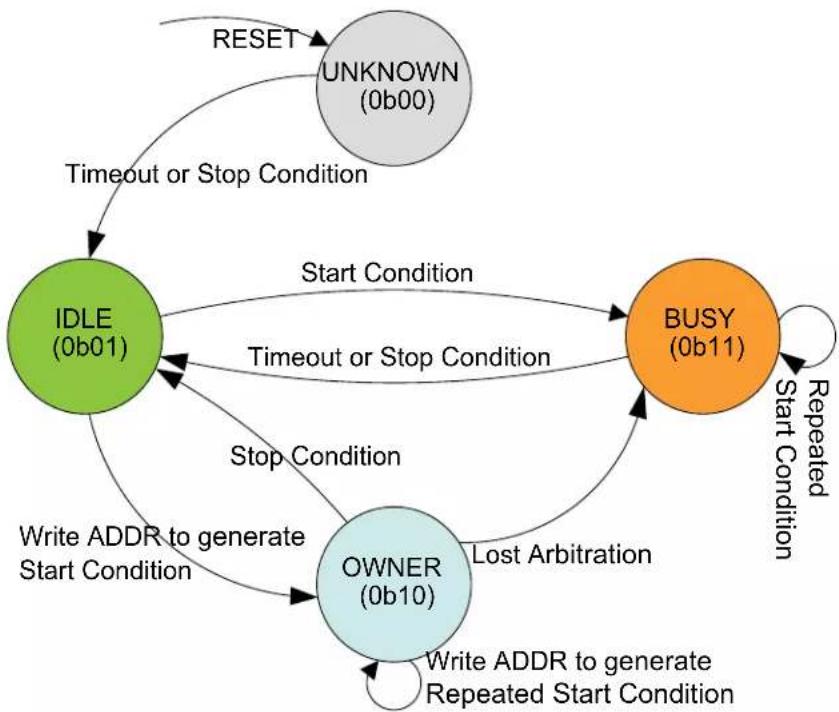
flowchart
graph TD
    A["IDLE (0b01)"] -->|Timeout or Stop Condition| B["UNKNOWN (0b00)"]
    A -->|Start Condition| C["BUSY (0b11)"]
    A -->|Stop Condition| D["OWNER (0b10)"]
    D -->|Write ADDR to generate Start Condition| A
    D -->|Write ADDR to generate Repeated Start Condition| A
    B -->|Repeated Start Condition| C
    C -->|Lost Arbitration| D
    D -->|Write ADDR to generate Stop Condition| A
    E["RESET"] --> A
The bus state machine is active when the I ^2 C Host is enabled.
After the I ^2 C Host has been enabled, the bus state is UNKNOWN (0b00). From the UNKNOWN state, the bus will transition to IDLE (0b01) by either:
- Forcing by by writing 0b01 to STATUS.BUSSTATE
• A stop condition is detected on the bus - If the inactive bus time-out is configured for SMBus compatibility (CTRLA.INACTOUT) and a time-out occurs.
Note: Once a known bus state is established, the bus state logic will not re-enter the UNKNOWN state.
When the bus is IDLE it is ready for a new transaction. If a start condition is issued on the bus by another I^2C Host in a multi-Host setup, the bus becomes BUSY (0b11). The bus will re-enter IDLE either when a stop condition is detected, or when a time-out occurs (inactive bus time-out needs to be configured).
If a start condition is generated internally by writing the Address bit group in the Address register (ADDR.ADDR) while IDLE, the OWNER state (0b10) is entered. If the complete transaction was performed without interference, i.e., arbitration was not lost, the I ^2 C Host can issue a stop condition, which will change the bus state back to IDLE.
However, if a packet collision is detected while in OWNER state, the arbitration is assumed lost and the bus state becomes BUSY until a stop condition is detected. A repeated start condition will change the bus state only if arbitration is lost while issuing a repeated start.
Regardless of winning or losing arbitration, the entire address will be sent. If arbitration is lost, only 'ones' are transmitted from the point of losing arbitration and the rest of the address length.
Note: Violating the protocol may cause the I ^2 C to hang. If this happens it is possible to recover from this state by a software reset (CTRLA.SWRST='1').
References:
Host CTRLA Register
33.6.2.4 I²C Host Operation
The I ^2 C Host is byte-oriented and interrupt based. The number of interrupts generated is kept at a minimum by automatic handling of most events. The software driver complexity and code size are reduced by auto-triggering of operations, and a special smart mode, which can be enabled by the Smart Mode Enable bit in the Control A register (CTRLA.SMEN).
The I ^2 C Host has two interrupt strategies.
When SCL Stretch Mode (CTRLA.SCLSM) is '0', SCL is stretched before or after the acknowledge bit. In this mode the I ^2 C Host operates according to Host Behavioral Diagram (SCLSM=0). The circles labelled "Mn" (M1, M2..) indicate the nodes the bus logic can jump to, based on software or hardware interaction.
This diagram is used as reference for the description of the I ^2 C Host operation throughout the document.
Figure 33-4. I²C Host Behavioral Diagram (SCLSM=0)
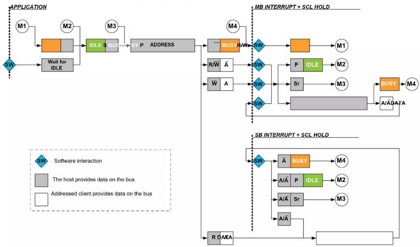
flowchart
graph TD
    A["APPLICATION"] --> B["M1"]
    B --> C["Wait for IDLE"]
    C --> D["IDLE S BUS"]
    D --> E["SY P ADDRESS"]
    E --> F["— BUSY RAW"]
    F --> G["SW"]
    G --> H[" "] --> I["M1"]
    F --> J["R/W A̅"]
    J --> K["SW"]
    K --> L["P IDLE"] --> M["M2"]
    K --> N["Sr"] --> O["M3"]
    K --> P[" "] --> Q["A/ĀDATA"]
    F --> R[" "] --> S["BUSY"] --> T["M4"]
    U["SB INTERRUPT + SCL HOLD"] --> V["SW"]
    V --> W["Ā BUSY"] --> X["M4"]
    V --> Y["A/Ā P IDLE"] --> Z["M2"]
    V --> AA["A/Ā Sr"] --> AB["M3"]
    V --> AC["A/Ā"]
    V --> AD["R DATA"]
    AD --> AE[" "]
    AF["Software interaction"] --> AG["The host provides data on the bus"]
    AF --> AH["Addressed client provides data on the bus"]
In the second strategy (CTRLA.SCLSM=1), interrupts only occur after the ACK bit, as in Host Behavioral Diagram (SCLSM=1). This strategy can be used when it is not necessary to check DATA before acknowledging.
Note: I²C High-speed (Hs) mode requires CTRLA.SCLSM=1.
Figure 33-5. I²C Host Behavioral Diagram (SCLSM=1)
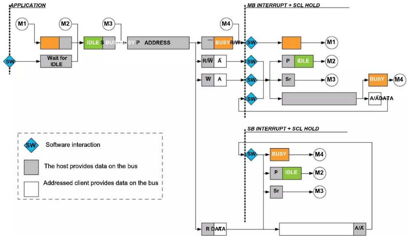
flowchart
graph TD
    A["APPLICATION"] --> B["M1"]
    B --> C["Wait for IDLE"]
    C --> D["IDLE S BUS"]
    D --> E["SY P ADDRESS"]
    E --> F["--BUSY R/W"]
    F --> G["SW"]
    G --> H["MB INTERRUPT + SCL HOLD"]
    H --> I["M1"]
    F --> J["R/W A"]
    J --> K["SW"]
    K --> L["P IDLE"]
    L --> M["M2"]
    K --> N["W A"]
    N --> O["SW"]
    O --> P["Sr"]
    P --> Q["M3"]
    O --> R["SW"]
    R --> S["SB INTERRUPT + SCL HOLD"]
    S --> T["M4"]
    T --> U["BUSY"]
    U --> V["M4"]
    S --> W["P IDLE"]
    W --> X["M2"]
    S --> Y["Sr"]
    Y --> Z["M3"]
    S --> AA["A/DATA"]
    AA --> AB["A/A"]
    S --> AC["R DATA"]
    AC --> AD["SB INTERRUPT + SCL HOLD"]
    AD --> AE["M4"]
    AE --> AF["P IDLE"]
    AF --> AG["M2"]
    AE --> AH["Sr"]
    AH --> AI["M3"]
Host Clock Generation
The SERCOM peripheral supports several I²C bi-directional modes:
• Standard mode (Sm) up to 100kHz
- Fast mode (Fm) up to 400kHz
- Fast mode Plus (Fm+) up to 1MHz
• High-speed mode (Hs) up to 3.4MHz
The Host clock configuration for Sm, Fm, and Fm+ are described in Clock Generation (Standard-Mode, Fast-Mode, and Fast-Mode Plus). For Hs, refer to Host Clock Generation (High-Speed Mode).
Clock Generation (Standard-Mode, Fast-Mode, and Fast-Mode Plus)
In I ^2 C Sm, Fm, and Fm+ mode, the Host clock (SCL) frequency is determined as described in this section:
The low ( T_LOW ) and high ( T_HIGH ) times are determined by the Baud Rate register (BAUD), while the rise ( T_RISE ) and fall ( T_FALL ) times are determined by the bus topology. Because of the wired-AND logic of the bus, T_FALL will be considered as part of T_LOW . Likewise, T_RISE will be in a state between T_LOW and T_HIGH until a high state has been detected.
Figure 33-6. SCL Timing
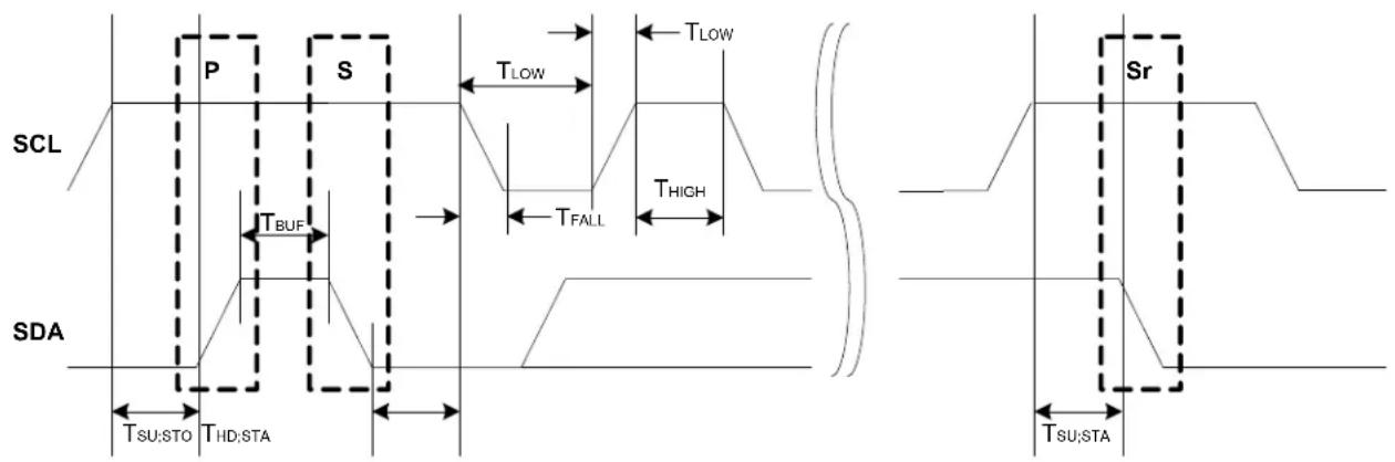
text_image
SCL P S TLOW TLOW TTHIGH TBUF TFAIL SDA TSU:STO THD:STA Sr TSU:STAThe following parameters are timed using the SCL low time period T_LOW . This comes from the Host Baud Rate Low bit group in the Baud Rate register (BAUD.BAUDLOW). When BAUD.BAUDLOW=0, or the Host Baud Rate bit group in the Baud Rate register (BAUD.BAUD) determines it.
- T_LOW - Low period of SCL clock
- T_SU;STO - Set-up time for stop condition
- T_BUF - Bus free time between stop and start conditions
- T_HD;STA - Hold time (repeated) start condition
- T_SU;STA - Set-up time for repeated start condition
- T_HIGH is timed using the SCL high time count from BAUD.BAUD
- T_RISE is determined by the bus impedance; for internal pull-ups. Refer to the Electrical Characteristics.
- T_FALL is determined by the open-drain current limit and bus impedance; can typically be regarded as zero. Refer to the Electrical Characteristics for details.
The SCL frequency is given by:
$$ f _ {\mathrm{SCL}} = \frac {1}{T _ {\mathrm{LOW}} + T _ {\mathrm{HIGH}} + T _ {\mathrm{RISE}}} $$
When BAUD.BAUDLOW is zero, the BAUD.BAUD value is used to time both SCL high and SCL low. In this case the following formula will give the SCL frequency:
$$ f _ {\mathrm{SCL}} = \frac {f _ {\mathrm{GCLK}}}{1 0 + 2 B A U D + f _ {\mathrm{GCLK}} \cdot T _ {\mathrm{RISE}}} $$
When BAUD.BAUDLOW is non-zero, the following formula determines the SCL frequency:
$$ f _ {\mathrm{SCL}} = \frac {f _ {\mathrm{GCLK}}}{1 0 + B A U D + B A U D L O W + f \quad_ {\mathrm{GCLK}} \cdot T _ {\mathrm{RISE}}} $$
The following formulas can determine the SCL T_LOW and T_HIGH times:
$$ T _ {\mathrm{LOW}} = \frac {B A U D L O W + 5}{f _ {\mathrm{GCLK}}} $$
$$ T _ {\mathrm{HIGH}} = \frac {B A U D + 5}{f _ {\mathrm{GCLK}}} $$
Note: The I²C standard Fm+ (Fast-mode plus) requires a nominal high to low SCL ratio of 1:2, and BAUD should be set accordingly. At a minimum, BAUD.BAUD and/or BAUD.BAUDLOW must be non-zero.
Startup Timing The minimum time between SDA transition and SCL rising edge is 6 APB cycles when the DATA register is written in smart mode. If a greater startup time is required due to long rise times, the time between DATA write and IF clear must be controlled by software.
Note: When timing is controlled by user, the Smart Mode cannot be enabled.
References:
Electrical Characteristics
Host Clock Generation (High-Speed Mode)
For I^2C Hs transfers, there is no SCL synchronization. Instead, the SCL frequency is determined by the GCLK_SERCOMx_CORE frequency ( f_GCLK ) and the High-Speed Baud setting in the Baud register (BAUD.HSBAUD). When BAUD.HSBAUDLOW=0, the HSBAUD value will determine both SCL high and SCL low. In this case the following formula determines the SCL frequency.
$$ f _ {\mathrm{SCL}} = \frac {f _ {\mathrm{GCLK}}}{2 + 2 \cdot H S B A U D} $$
When HSBAUDLOW is non-zero, the following formula determines the SCL frequency.
$$ f _ {\mathrm{SCL}} = \frac {f _ {\mathrm{GCLK}}}{2 + H S B A U D + H S B A U D L O W} $$
Note: The I²C standard Hs (High-speed) requires a nominal high to low SCL ratio of 1:2, and HSBAUD should be set accordingly. At a minimum, BAUD.HSBAUD and/or BAUD.HSBAUDLOW must be non-zero.
Transmitting Address Packets
The I ^2 C Host starts a bus transaction by writing the I ^2 C Client address to ADDR.ADDR and the direction bit, as described in 33.6.1. Principle of Operation. If the bus is busy, the I ^2 C Host will wait until the bus becomes idle before continuing the operation. When the bus is idle, the I ^2 C Host will issue a start condition on the bus. The I ^2 C Host will then transmit an address packet using the address written to ADDR.ADDR. After the address packet has been transmitted by the I ^2 C Host, one of four cases will arise according to arbitration and transfer direction.
Case 1: Arbitration lost or bus error during address packet transmission
If arbitration was lost during transmission of the address packet, the Host on Bus bit in the Interrupt Flag Status and Clear register (INTFLAG.MB) and the Arbitration Lost bit in the Status register (STATUS.ARBLOST) are both set. Serial data output to SDA is disabled, and the SCL is released, which disables clock stretching. In effect the I²C Host is no longer allowed to execute any operation on the bus until the bus is idle again. A bus error will behave similarly to the arbitration lost condition. In this case, the MB interrupt flag and Host Bus Error bit in the Status register (STATUS.BUSERR) are both set in addition to STATUS.ARBLOST.
The Host Received Not Acknowledge bit in the Status register (STATUS.RXNACK) will always contain the last successfully received acknowledge or not acknowledge indication.
In this case, software will typically inform the application code of the condition and then clear the interrupt flag before exiting the interrupt routine. No other flags have to be cleared at this moment, because all flags will be cleared automatically the next time the ADDR.ADDR register is written.
Case 2: Address packet transmit complete – No ACK received
If there is no I²C Client device responding to the address packet, then the INTFLAG.MB interrupt flag and STATUS.RXNACK will be set. The clock hold is active at this point, preventing further activity on the bus.
The missing ACK response can indicate that the I²C Client is busy with other tasks or sleeping. Therefore, it is not able to respond. In this event, the next step can be either issuing a stop condition (recommended) or resending the address packet by a repeated start condition. When using SMBus logic, the Client must ACK the address. If there is no response, it means that the Client is not available on the bus.
Case 3: Address packet transmit complete – Write packet, Host on Bus set
If the I ^2 C Host receives an acknowledge response from the I ^2 C Client, INTFLAG.MB will be set and STATUS.RXNACK will be cleared. The clock hold is active at this point, preventing further activity on the bus.
In this case, the software implementation becomes highly protocol dependent. Three possible actions can enable the I ^2 C operation to continue:
- Initiate a data transmit operation by writing the data byte to be transmitted into DATA.DATA.
- Transmit a new address packet by writing ADDR.ADDR. A repeated start condition will automatically be inserted before the address packet.
- Issue a stop condition, consequently terminating the transaction.
Case 4: Address packet transmit complete – Read packet, Client on Bus set
If the I ^2 C Host receives an ACK from the I ^2 C Client, the I ^2 C Host proceeds to receive the next byte of data from the I ^2 C Client. When the first data byte is received, the Client on Bus bit in the Interrupt Flag register (INTFLAG.SB) will be set and STATUS.RXNACK will be cleared. The clock hold is active at this point, preventing further activity on the bus.
In this case, the software implementation becomes highly protocol dependent. Three possible actions can enable the I ^2 C operation to continue:
- Let the I ^2 C Host continue to read data by acknowledging the data received. ACK can be sent by software, or automatically in smart mode.
- Transmit a new address packet.
- Terminate the transaction by issuing a stop condition.
Note: An ACK or NACK will be automatically transmitted if smart mode is enabled. The Acknowledge Action bit in the Control B register (CTRLB.ACKACT) determines whether ACK or NACK should be sent.
Transmitting Data Packets
When an address packet with direction Host Write (see Figure 33-2) was transmitted successfully, INTFLAG.MB will be set. The I²C Host will start transmitting data via the I²C bus by writing to DATA.DATA, and monitor continuously for packet collisions. I
If a collision is detected, the I ^2 C Host will lose arbitration and STATUS.ARBLOST will be set. If the transmit was successful, the I ^2 C Host will receive an ACK bit from the I ^2 C Client, and STATUS.RXNACK will be cleared. INTFLAG.MB will be set in both cases, regardless of arbitration outcome.
It is recommended to read STATUS.ARBLOST and handle the arbitration lost condition in the beginning of the I2C Host on Bus interrupt. This can be done as there is no difference between handling address and data packet arbitration.
STATUS.RXNACK must be checked for each data packet transmitted before the next data packet transmission can commence. The I²C Host is not allowed to continue transmitting data packets if a NACK is received from the I²C Client.
Receiving Data Packets (SCLSM=0)
When INTFLAG.SB is set, the I²C Host will already have received one data packet. The I²C Host must respond by sending either an ACK or NACK. Sending a NACK may be unsuccessful when arbitration is lost during the transmission. In this case, a lost arbitration will prevent setting INTFLAG.SB.
Instead, INTFLAG.MB will indicate a change in arbitration. Handling of lost arbitration is the same as for data bit transmission.
Receiving Data Packets (SCLSM=1)
When INTFLAG.SB is set, the I²C Host will already have received one data packet and transmitted an ACK or NACK, depending on CTRLB.ACKACT. At this point, CTRLB.ACKACT must be set to the correct value for the next ACK bit, and the transaction can continue by reading DATA and issuing a command if not in the smart mode.
High-Speed Mode
High-speed transfers are a multi-step process, see the following figure.
First, a Host code (0b00001nnn, where 'nnn' is a unique Host code) is transmitted in Full-speed mode, followed by a NACK since no Client should acknowledge. Arbitration is performed only during the Full-speed Host Code phase. The Host code is transmitted by writing the Host code to the address register (ADDR.ADDR) and writing the high-speed bit (ADDR.HS) to '0'.
After the Host code and NACK have been transmitted, the Host write interrupt will be asserted. In the meanwhile, the Client address can be written to the ADDR.ADDR register together with ADDR.HS=1. Now in High-speed mode, the Host will generate a repeated start, followed by the Client address with RW-direction. The bus will remain in High-speed mode until a stop is generated. If a repeated start is desired, the ADDR.HS bit must again be written to '1', along with the new address ADDR.ADDR to be transmitted.
Figure 33-7. High Speed Transfer

text_image
F/S-mode Hs-mode F/S-mode S Host Code ¯A Sr ADDRESS R/¯W A/¯A PA DATA N Data Packets Hs-mode continues Sr ADDRESSTransmitting in High-speed mode requires the I²C Host to be configured in High-speed mode (CTRLA.SPEED=0x2) and the SCL clock stretch mode (CTRLA.SCLSM) bit set to '1'.
10-Bit Addressing
When 10-bit addressing is enabled by the Ten Bit Addressing Enable bit in the Address register (ADDR.TENBITEN=1) and the Address bit field ADDR.ADDR is written, the two address bytes will be transmitted, see the following figure. The addressed Client acknowledges the two address bytes, and the transaction continues. Regardless of whether the transaction is a read or write, the Host must start by sending the 10-bit address with the direction bit (ADDR.ADDR[0]) being zero.
If the Host receives a NACK after the first byte, the write interrupt flag will be raised and the STATUS.RXNACK bit will be set. If the first byte is acknowledged by one or more Clients, then the Host will proceed to transmit the second address byte and the Host will first see the write interrupt flag after the second byte is transmitted. If the transaction direction is read-from-Client, the 10-bit address transmission must be followed by a repeated start and the first 7 bits of the address with the read/write bit equal to '1'.
Figure 33-8. 10-bit Address Transmission for a Read Transaction

flowchart
graph LR
    S["1110 addr[9:8"]] --> W["W̄"]
    W --> A["A"]
    A --> addr["7:0"]
    addr --> A2["A"]
    A2 --> S2["S W"]
    S2 --> Sr["SR AIR110 addr[9:8"]]
    Sr --> 1["1"]
    MB_INTERRUPT -.-> S2
This implies the following procedure for a 10-bit read operation:
-
Write the 10-bit address to ADDR.ADDR[10:1].ADDR.TENBITEN must be '1', the direction bit (ADDR.ADDR[0]) must be '0' (can be written simultaneously with ADDR).
-
Once the Host on Bus interrupt is asserted, Write ADDR[7:0] register to '11110 address [9:8] 1'. ADDR.TENBITEN must be cleared (can be written simultaneously with ADDR).
-
Proceed to transmit data.
33.6.2.5 I²C Client Operation
The I ^2 C Client is byte-oriented and interrupt-based. The number of interrupts generated is kept at a minimum by automatic handling of most events. The software driver complexity and code size are reduced by auto-triggering of operations, and a special smart mode, which can be enabled by the Smart Mode Enable bit in the Control A register (CTRLA.SMEN).
The I ^2 C Client has two interrupt strategies.
When SCL Stretch Mode bit (CTRLA.SCLSM) is '0', SCL is stretched before or after the acknowledge bit. In this mode, the I²C Client operates according to the following figure. The circles labelled "Sn" (S1, S2..) indicate the nodes the bus logic can jump to, based on software or hardware interaction.
This diagram is used as reference for the description of the I ^2 C Client operation throughout the document.
Figure 33-9. I²C Client Behavioral Diagram (SCLSM=0)
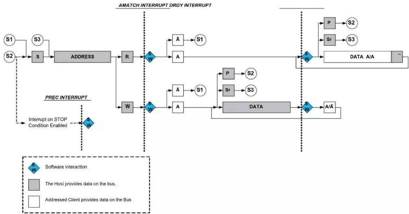
flowchart
graph TD
    subgraph AMATCH_INTERRUPT_DRDY_INTERRUPT
        S1["S1"] --> S2["S2"]
        S3["S3"] --> S4["S4"]
        S4 --> ADDRESS["ADDRESS"]
        S4 --> R["R"]
        R --> SW1["SW"]
        SW1 --> A["A"]
        A --> S1["S1"]
        SW1 --> W["W"]
        W --> SW2["SW"]
        SW2 --> A["A"]
        A --> S1["S1"]
        SW2 --> A["A"]
        A --> S3["S3"]
        S3 --> DATA["DATA A/A"]
        P["P"] --> S2["S2"]
        Sr["Sr"] --> S3["S3"]
        S2 --> DATA
        S3 --> DATA
    end

    PREC_INTERRUPT["PREC INTERRUPT\nInterrupt on STOP\nCondition Enabled"] --> SW2
    SW2 -->|S_W| S1
    SW2 -->|S_W| W
    SW2 -->|S_W| A
    SW2 -->|S_W| P
    SW2 -->|S_W| Sr
    SW2 -->|S_W| A
    SW2 -->|S_W| A
    SW2 -->|S_W| A
    SW2 -->|A/A| DATA
    style SW2 fill:#f9f,stroke:#333
    style S1 fill:#ccf,stroke:#333
    style S2 fill:#ccf,stroke:#333
    style S3 fill:#ccf,stroke:#333
    style S4 fill:#ccf,stroke:#333
    style R fill:#cfc,stroke:#333
    style W fill:#cfc,stroke:#333
    style A fill:#cfc,stroke:#333
    style S1 fill:#cfc,stroke:#333
    style S2 fill:#cfc,stroke:#333
    style S3 fill:#cfc,stroke:#333
    style S4 fill:#cfc,stroke:#333
    style S1 fill:#fcc,stroke:#333
    style S2 fill:#fcc,stroke:#333
    style S3 fill:#fcc,stroke:#333
    style S4 fill:#fcc,stroke:#333
    style S1 fill:#cff,stroke:#333
    style S2 fill:#cff,stroke:#333
    style S3 fill:#cff,stroke:#333
    style S4 fill:#cff,stroke:#333
    style S1 fill:#ffc,stroke:#333
    style S2 fill:#ffc,stroke:#333
    style S3 fill:#ffc,stroke:#333
    style S4 fill:#ffc,stroke:#333
    style S1 fill:#ffc,stroke:#333
    style S2 fill:#ffc,stroke:#333
    style S3 fill:#ffc,stroke:#333
    style S4 fill:#ffc,stroke:#333
In the second strategy (CTRLA.SCLSM=1), interrupts only occur after the ACK bit is sent as shown in the following figure. This strategy can be used when it is not necessary to check DATA before acknowledging. For Host reads, an address and data interrupt will be issued simultaneously after the address acknowledge. However, for Host writes, the first data interrupt will be seen after the first data byte has been received by the Client and the acknowledge bit has been sent to the Host.
Note: For I²C High-speed mode (Hs), SCLSM=1 is required.
Figure 33-10. I²C Client Behavioral Diagram (SCLSM=1)

flowchart
graph TD
    S1["S1"] --> S2["S2"]
    S2 --> S3["S3"]
    S3 --> ADDRESS["ADDRESS"]
    R["R"] --> S4["S_W"]
    S4 --> S5["S_W"]
    S5 --> W1["W"] --> A/A["A/A"]
    W1 --> S6["S_W"]
    S6 --> P["P"] --> S2["S2"]
    S6 --> Sr["S_r"] --> S3["S3"]
    S3 --> DATA["DATA A/A"]
    DATA --> S7["S_W"]
    S7 --> S8["S_W"]

    S1 -.-> S2
    S2 -.-> S3

    S1 -.-> S4
    S2 -.-> S5
    S3 -.-> S7

    S4 -.-> S9["S_W"]
    S5 -.-> S10["S_W"]
    S6 -.-> S11["S_W"]
    S7 -.-> S12["S_W"]

    S10 -.-> S13["S_W"]
    S11 -.-> S14["S_W"]
    S12 -.-> S15["S_W"]

    S13 -.-> S16["S_W"]
    S14 -.-> S17["S_W"]

    S15 -.-> S18["S_W"]
    S16 -.-> S19["S_W"]

    S17 -.-> S20["S_W"]
    S18 -.-> S21["S_W"]

    S20 -.-> P["P"] --> S22["S2"]
    S21 -.-> Sr["S_r"] --> S33["S3"]

    S22 -.-> DATA["DATA A/A"]
    S23 -.-> DATA
    S24 -.-> DATA
    S25 -.-> DATA
    S26 -.-> DATA
    S27 -.-> DATA
    S28 -.-> DATA
    S29 -.-> DATA
    S30 -.-> DATA
    S31 -.-> DATA
    S32 -.-> DATA
    S33 -.-> DATA
    S34 -.-> DATA
    S35 -.-> DATA
    S36 -.-> DATA
    S37 -.-> DATA
    S38 -.-> DATA
    S39 -.-> DATA
Receiving Address Packets (SCLSM=0)
When CTRLA.SCLSM=0, the I2C Client stretches the SCL line according to I^2C Client Behavioral Diagram (SCLSM=0). When the I^2C Client is properly configured, it will wait for a start condition.
When a start condition is detected, the successive address packet will be received and checked by the address match logic. If the received address is not a match, the packet will be rejected, and the I²C Client will wait for a new start condition. If the received address is a match, the Address Match bit in the Interrupt Flag register (INTFLAG.AMATCH) will be set.
SCL will be stretched until the I²C Client clears INTFLAG.AMATCH. As the I²C Client holds the clock by forcing SCL low, the software has unlimited time to respond.
The direction of a transaction is determined by reading the Read / Write Direction bit in the Status register (STATUS.DIR). This bit will be updated only when a valid address packet is received.
If the Transmit Collision bit in the Status register (STATUS.COLL) is set, this indicates that the last packet addressed to the I²C Client had a packet collision. A collision causes the SDA and SCL lines to be released without any notification to software. Therefore, the next AMATCH interrupt is the first indication of the previous packet's collision. Collisions are intended to follow the SMBus Address Resolution Protocol (ARP).
After the address packet has been received from the I²C Host, one of two cases will arise based on transfer direction.
Case 1: Address packet accepted - Read flag set
The STATUS.DIR bit is '1', indicating an I2C Host read operation. The SCL line is forced low, stretching the bus clock. If an ACK is sent, I2C Client hardware will set the Data Ready bit in the Interrupt Flag register (INTFLAG.DRDY), indicating data are needed for transmit. If a NACK is sent, the I2C Client will wait for a new start condition and address match.
Typically, software will immediately acknowledge the address packet by sending an ACK/NACK bit. The I²C Client Command bit field in the Control B register (CTRLB.CMD) can be written to '0x3' for both read and write operations as the command execution is dependent on the STATUS.DIR
bit. Writing '1' to INTFLAG.AMATCH will also cause an ACK/NACK to be sent corresponding to the CTRLB.ACKACT bit.
Case 2: Address packet accepted - Write flag set
The STATUS.DIR bit is cleared, indicating an I²C Host write operation. The SCL line is forced low, stretching the bus clock. If an ACK is sent, the I²C Client will wait for data to be received. Data, repeated start or stop can be received.
If a NACK is sent, the I²C Client will wait for a new start condition and address match. Typically, software will immediately acknowledge the address packet by sending an ACK/NACK. The I²C Client command CTRLB.CMD = 3 can be used for both read and write operation as the command execution is dependent on STATUS.DIR.
Writing '1' to INTFLAG.AMATCH will also cause an ACK/NACK to be sent corresponding to the CTRLB.ACKACT bit.
Receiving Address Packets (SCLSM=1)
When SCLSM=1, the I ^2 C Client will stretch the SCL line only after an ACK, see Client Behavioral Diagram (SCLSM=1). When the I ^2 C Client is properly configured, it will wait for a start condition to be detected.
When a start condition is detected, the successive address packet will be received and checked by the address match logic.
If the received address is not a match, the packet will be rejected and the I ^2 C Client will wait for a new start condition.
If the address matches, the acknowledge action as configured by the Acknowledge Action bit Control B register (CTRLB.ACKACT) will be sent and the Address Match bit in the Interrupt Flag register (INTFLAG.AMATCH) is set. SCL will be stretched until the I²C Client clears INTFLAG.AMATCH. As the I²C Client holds the clock by forcing SCL low, the software is given unlimited time to respond to the address.
The direction of a transaction is determined by reading the Read/Write Direction bit in the Status register (STATUS.DIR). This bit will be updated only when a valid address packet is received.
If the Transmit Collision bit in the Status register (STATUS.COLL) is set, the last packet addressed to the I²C Client had a packet collision. A collision causes the SDA and SCL lines to be released without any notification to software. The next AMATCH interrupt is, therefore, the first indication of the previous packet's collision. Collisions are intended to follow the SMBus Address Resolution Protocol (ARP).
After the address packet has been received from the I²C Host, INTFLAG.AMATCH be set to '1' to clear it.
Receiving and Transmitting Data Packets
After the I ^2 C Client has received an address packet, it will respond according to the direction either by waiting for the data packet to be received or by starting to send a data packet by writing to DATA.DATA. When a data packet is received or sent, INTFLAG.DRDY will be set. After receiving data, the I ^2 C Client will send an acknowledge according to CTRLB.ACKACT.
Case 1: Data received
INTFLAG.DRDY is set, and SCL is held low, pending for SW interaction.
Case 2: Data sent
When a byte transmission is successfully completed, the INTFLAG.DRDY interrupt flag is set. If NACK is received, indicated by STATUS.RXNACK=1, the I²C Client must expect a stop or a repeated start to be received. The I²C Client must release the data line to allow the I²C Host to generate a stop or repeated start. Upon detecting a stop condition, the Stop Received bit in the Interrupt Flag register (INTFLAG.PREC) will be set and the I²C Client will return to IDLE state.
High-Speed Mode
When the I ^2 C Client is configured in High-speed mode (Hs, CTRLA.SPEED=0x2) and CTRLA.SCLSM=1, switching between Full-speed and High-speed modes is automatic. When the Client recognizes a START followed by a Host code transmission and a NACK, it automatically switches to High-speed mode and sets the High-speed status bit (STATUS.HS). The Client will then remain in High-speed mode until a STOP is received.
10-Bit Addressing
When 10-bit addressing is enabled (ADDR.TENBITEN=1), the two address bytes following a START will be checked against the 10-bit Client address recognition. The first byte of the address will always be acknowledged, and the second byte will raise the address interrupt flag, see the following figure.
If the transaction is a write, then the 10-bit address will be followed by N data bytes.
If the operation is a read, the 10-bit address will be followed by a repeated START and reception of '11110 ADDR[9:8] 1', and the second address interrupt will be received with the DIR bit set. The Client matches on the second address as it it was addressed by the previous 10-bit address.
Figure 33-11. 10-bit Addressing

flowchart
graph LR
    S["11110 addr[9:8"]] --> W["\overline{W}"]
    W --> A["A"]
    A --> addr["7:0"]
    addr --> S2["S W"]
    S2 --> A2["A"]
    A2 --> Sr["Sr"]
    Sr --> 11110_addr["9:8"]
    R["R"] --> S3["S W"]
    S3 --> R
    style S fill:#f9f,stroke:#333
    style W fill:#bbf,stroke:#333
    style A fill:#bfb,stroke:#333
    style Sr fill:#ffb,stroke:#333
    style R fill:#fbb,stroke:#333
PMBus Group Command
When the PMBus Group Command bit in the CTRLB register is set (CTRLB.GCMD=1) and 7-bit addressing is used, INTFLAG.PREC will be set when a STOP condition is detected on the bus. When CTRLB.GCMD=0, a STOP condition without address match will not be set INTFLAG.PREC.
The group command protocol is used to send commands to more than one device. The commands are sent in one continuous transmission with a single STOP condition at the end. When the STOP condition is detected by the Clients addressed during the group command, they all begin executing the command they received.
The following figure shows an example where this Client, bearing ADDRESS 1, is addressed after a repeated START condition. There can be multiple Clients addressed before and after this Client. Eventually, at the end of the group command, a single STOP is generated by the Host. At this point a STOP interrupt is asserted.
Figure 33-12. PMBus Group Command Example
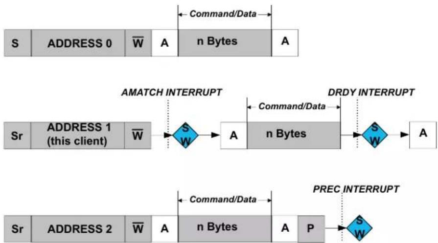
flowchart
graph TD
    A["S ADDRESS 0"] -->|Command/Data| B["n Bytes"]
    C["Sr ADDRESS 1 (this client)"] --> D["AMATCH INTERRUPT"]
    D --> E["S W"]
    E --> F["A n Bytes"]
    F --> G["DRDY INTERRUPT"]
    G --> H["S W"]
    H --> I["A"]
    J["Sr ADDRESS 2"] --> K[" commands/Data"]
    K --> L["n Bytes"]
    L --> M["A P"]
    M --> N["S W"]
    N --> O["PREC INTERRUPT"]
33.6.3 Additional Features
33.6.3.1 SMBus
The I ^2 C includes three hardware SCL low time-outs which allow a time-out to occur for SMBus SCL low time-out, Host extend time-out, and Client extend time-out. This allows for SMBus functionality These time-outs are driven by the GCLK_SERCOM_SLOW clock. The GCLK_SERCOM_SLOW clock is used to accurately time the time-out and must be configured to use a 32.768 kHz oscillator. The I ^2 C interface also allows for a SMBus compatible SDA hold time.
- T_TIMEOUT : SCL low time of 25..35ms – Measured for a single SCL low period. It is enabled by CTRLA.LOWTOUTEN.
- T_LOW:SEXT : Cumulative clock low extend time of 25 ms – Measured as the cumulative SCL low extend time by a Client device in a single message from the initial START to the STOP. It is enabled by CTRLA.SEXTTOEN.
- T_LOW:MEXT : Cumulative clock low extend time of 10 ms – Measured as the cumulative SCL low extend time by the Host device within a single byte from START-to-ACK, ACK-to-ACK, or ACK-to-STOP. It is enabled by CTRLA.MEXTTOEN.
33.6.3.2 Smart Mode
The I ^2 C interface has a smart mode that simplifies application code and minimizes the user interaction needed to adhere to the I ^2 C protocol. The smart mode accomplishes this by automatically issuing an ACK or NACK (based on the content of CTRLB.ACKACT) as soon as DATA.DATA is read.
33.6.3.3 4-Wire Mode
Writing a '1' to the Pin Usage bit in the Control A register (CTRLA.PINOUT) will enable 4-wire mode operation. In this mode, the internal I²C tri-state drivers are bypassed, and an external I²C compliant tri-state driver is needed when connecting to an I²C bus.
Figure 33-13. I²C Pad Interface
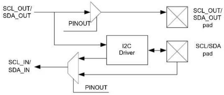
flowchart
graph TD
    A["SCL_OUT/SDA_OUT"] --> B["Pinout"]
    B --> C["I2C Driver"]
    C --> D["SCL_OUT/SDA_OUT pad"]
    C --> E["SCL/SDA pad"]
    F["SCL_IN/SDA_IN"] --> G["Pinout"]
    G --> H["I2C Driver"]
    H --> I["SCL_OUT/SDA_OUT pad"]
    H --> J["SCL/SDA pad"]
33.6.3.4 Quick Command
Setting the Quick Command Enable bit in the Control B register (CTRLB.QCEN) enables quick command. When quick command is enabled, the corresponding interrupt flag (INTFLAG.SB or INTFLAG.MB) is set immediately after the client acknowledges the address. At this point, the software can either issue a stop command or a repeated start by writing CTRLB.CMD or ADDR.ADDR.
33.6.4 DMA, Interrupts and Events
Table 33-1. Module Request for SERCOM I²C Client
| Condition Request | |||
| DMA Interrupt Event | |||
| Data needed for transmit (TX) (Client transmit mode) | Yes(request cleared when data is written) | NA | |
| Data received (RX) (Client receive mode) | Yes(request cleared when data is read) | ||
| Data Ready (DRDY) Yes | |||
| Address Match (AMATCH) Yes | |||
| Stop received (PREC) Yes | |||
| Error (ERROR) Yes | |||
Table 33-2. Module Request for SERCOM I²C Host
| Condition Request | |||
| DMA Interrupt Event | |||
| Data needed for transmit (TX) (Host transmit mode) | Yes (request cleared when data is written) | NA | |
| Data needed for transmit (RX) (Host transmit mode) | Yes (request cleared when data is read) | ||
| Host on Bus (MB) Yes | |||
| Stop received (SB) Yes | |||
| Error (ERROR) Yes | |||
33.6.4.1 DMA Operation
Smart mode must be enabled for DMA operation in the Control B register by writing CTRLB.SMEN=1.
Client DMA
When using the I ^2 C Client with DMA, an address match will cause the address interrupt flag (INTFLAG.ADDRMATCH) to be raised. After the interrupt has been serviced, data transfer will be performed through DMA.
The I ^2 C Client generates the following requests:
- Write data received (RX): The request is set when Host write data is received. The request is cleared when DATA is read.
- Read data needed for transmit (TX): The request is set when data is needed for a Host read operation. The request is cleared when DATA is written.
Host DMA
When using the I²C Host with DMA, the ADDR register must be written with the desired address (ADDR.ADDR), transaction length (ADDR.LEN), and transaction length enable (ADDR.LENEN). When ADDR.LENEN is written to 1 along with ADDR.ADDR, ADDR.LEN determines the number of data bytes in the transaction from 0 to 255. DMA is then used to transfer ADDR.LEN bytes followed by an automatically generated NACK (for Host reads) and a STOP.
If a NACK is received by the Client for a Host write transaction before ADDR.LEN bytes, a STOP will be automatically generated and the length error (STATUS.LENERR) will be raised along with the INTFLAG.ERROR interrupt.
The I ^2 C Host generates the following requests:
- Read data received (RX): The request is set when Host read data is received. The request is cleared when DATA is read.
- Write data needed for transmit (TX): The request is set when data is needed for a Host write operation. The request is cleared when DATA is written.
33.6.4.2 Interrupts
The I ^2 C Client has the following interrupt sources. These are asynchronous interrupts. They can wake-up the device from any sleep mode:
- Error (ERROR)
- Data Ready (DRDY)
- Address Match (AMATCH)
- Stop Received (PREC)
The I ^2 C Host has the following interrupt sources. These are asynchronous interrupts. They can wake-up the device from any sleep mode:
- Error (ERROR)
- Client on Bus (SB)
- Host on Bus (MB)
Each interrupt source has its own interrupt flag. The interrupt flag in the Interrupt Flag Status and Clear register (INTFLAG) will be set when the interrupt condition is meet. Each interrupt can be individually enabled by writing '1' to the corresponding bit in the Interrupt Enable Set register (INTENSET), and disabled by writing '1' to the corresponding bit in the Interrupt Enable Clear register (INTENCLR). An interrupt request is generated when the interrupt flag is set and the corresponding interrupt is enabled. The interrupt request active until the interrupt flag is cleared, the interrupt is disabled or the I²C is reset. See 33.10.6. INTFLAG register for details on how to clear interrupt flags.
The I ^2 C has one common interrupt request line for all the interrupt sources. The value of INTFLAG indicates which interrupt is executed. Note that interrupts must be globally enabled for interrupt requests. Refer to the Nested Vector Interrupt Controller for details.
33.6.4.3 Events
Not applicable.
33.6.5 Sleep Mode Operation
I²C Host Operation
The generic clock (GCLK_SERCOMx_CORE) will continue to run in idle sleep mode. If the Run In Standby bit in the Control A register (CTRLA.RUNSTDBY) is '1', the GLK_SERCOMx_CORE will also run in standby sleep mode. Any interrupt can wake up the device.
If CTRLA.RUNSTDBY=0, the GLK_SERCOMx_CORE will be disabled after any ongoing transaction is finished. Any interrupt can wake up the device.
I²C Client Operation
Writing CTRLA.RUNSTDBY=1 will allow the Address Match interrupt to wake up the device.
When CTRLA.RUNSTDBY=0, all receptions will be dropped.
33.6.6 Synchronization
Due to asynchronicity between the main clock domain and the peripheral clock domains, some registers need to be synchronized when written or read.
The following bits are synchronized when written:
- Software Reset bit in the CTRLA register (CTRLA.SWRST)
- Enable bit in the CTRLA register (CTRLA.ENABLE)
- Write to Bus State bits in the Status register (STATUS.BUSSTATE)
- Address bits in the Address register (ADDR.ADDR) when in Host operation.
The following registers are synchronized when written:
• Data (DATA) when in Host operation
Required write-synchronization is denoted by the "Write-Synchronized" property in the register description.
33.7 Register Summary - I2C Client
| Offset | Name Bit Pos. 76 | 543210 | ||||||||
| 0x00 CTRLA | 7:0 RUNSTDBY MODE[2:0] ENABLE SWRST | |||||||||
| 15:8 | ||||||||||
| 23:16 SEXTTOEN | SDAHOLD[1:0] PINOUT | |||||||||
| 31:24 | LOWTOUT | SCLSM | SPEED[1:0] | |||||||
| 0x04 CTRLB | 7:0 | |||||||||
| 15:8 | QCEN SMEN | |||||||||
| 23:16 | ACKACT CMD[1:0] | |||||||||
| 31:24 | ||||||||||
| 0x08 ... 0x13 | Reserved | |||||||||
| 0x14 | INTENCLR | 7:0 | ERROR | DRDY | AMATCH | PREC | ||||
| 0x15 | Reserved | |||||||||
| 0x16 | INTENSET | 7:0 | ERROR | DRDY | AMATCH | PREC | ||||
| 0x17 | Reserved | |||||||||
| 0x18 | INTFLAG | 7:0 | ERROR | DRDY | AMATCH | PREC | ||||
| 0x19 | Reserved | |||||||||
| 0x1A | STATUS | 7:0 | CLKHOLD | LOWTOUT | SR | DIR | RXNACK | COLL | BUSERR | |
| 15:8 | HS | SEXTTOUT | ||||||||
| 0x1C | SYNCBUSY | 7:0 | ENABLE SWRST | |||||||
| 15:8 | ||||||||||
| 23:16 | ||||||||||
| 31:24 | ||||||||||
| 0x20 ... 0x23 | Reserved | |||||||||
| 0x24 ADDR | 7:0 | ADDR[6:0] | GENCEN | |||||||
| 15:8 | TENBITEN | ADDR[9:7] | ||||||||
| 23:16 | ADDRMASK[6:0] | |||||||||
| 31:24 | ADDRMASK[9:7] | |||||||||
| 0x28 | DATA | 7:0 | DATA[7:0] | |||||||
| 15:8 | ||||||||||
33.8 Register Description - I ^2 C Client
Registers can be 8, 16, or 32 bits wide. Atomic 8-, 16- and 32-bit accesses are supported. In addition, the 8-bit quarters and 16-bit halves of a 32-bit register, and the 8-bit halves of a 16-bit register can be accessed directly.
Some registers are optionally write-protected by the Peripheral Access Controller (PAC). Optional PAC write-protection is denoted by the "PAC Write-Protection" property in each individual register description. For details, refer to 33.5.8. Register Access Protection.
Some registers are synchronized when read and/or written. Synchronization is denoted by the "Write-Synchronized" or the "Read-Synchronized" property in each individual register description. For details, refer to 33.6.6. Synchronization.
Some registers are enable-protected, meaning they can only be written when the peripheral is disabled. Enable-protection is denoted by the "Enable-Protected" property in each individual register description.
33.8.1 Control A
Name: CTRLA
Offset: 0x00
Reset: 0x00000000
Property: PAC Write-Protection, Enable-Protected, Write-Synchronized
Bit 31 30 29 28 27 26 25 24
| LOWTOUT | SCLSM | SPEED[1:0] | |||||
| Access | R/W | R/W | R/W | ||||
| Reset | 0 | 0 | 0 | 0 | |||
Bit 23 22 21 20 19 18 17 16
| SEXTTOEN | SDAHOLD[1:0] | PINOUT | ||||||
| Access | R/W | R/W | R/W | R/W | ||||
| Reset | 0 | 0 | 0 | 0 | ||||
Bit 15 14 13 12 11 10 9 8
| Access Reset |
Bit 7 6 5 4 3 2 1 0
| RUNSTDBY | MODE[2:0] | ENABLE | SWRST | |||||
| Access | R/W | R/W | R/W | R/W | R/W | R/W | ||
| Reset | 0 | 0 | 0 | 0 | 0 | 0 | ||
Bit 30 - LOWTOUT SCL Low Time-Out
This bit enables the SCL low time-out. If SCL is held low for 25ms-35ms, the Client will release its clock hold, if enabled, and reset the internal state machine. Any interrupt flags set at the time of time-out will remain set.
| Value | Description |
| 0 | Time-out disabled. |
| 1 | Time-out enabled. |
Bit 27 - SCLSM SCL Clock Stretch Mode
This bit controls when SCL will be stretched for software interaction.
This bit is not synchronized.
| Value | Description |
| 0 | SCL stretch according to Figure 33-9 |
| 1 | SCL stretch only after ACK bit according to Figure 33-10 |
Bits 25:24 - SPEED[1:0] Transfer Speed
These bits define bus speed.
These bits are not synchronized.
| Value | Description |
| 0x0 | Standard-mode (Sm) up to 100 kHz and Fast-mode (Fm) up to 400 kHz |
| 0x1 | Fast-mode Plus (Fm+) up to 1 MHz |
| 0x2 | High-speed mode (Hs-mode) up to 3.4 MHz |
| 0x3 | Reserved |
Bit 23 - SEXTTOEN Client SCL Low Extend Time-Out
This bit enables the Client SCL low extend time-out. If SCL is cumulatively held low for greater than 25ms from the initial START to a STOP, the Client will release its clock hold if enabled and reset the
internal state machine. Any interrupt flags set at the time of time-out will remain set. If the address was recognized, PREC will be set when a STOP is received.
This bit is not synchronized.
| Value Description | |
| 0 | Time-out disabled |
| 1 | Time-out enabled |
Bits 21:20 - SDAHOLD[1:0] SDA Hold Time
These bits define the SDA hold time with respect to the negative edge of SCL.
These bits are not synchronized.
| Value Name | Description | |
| 0x0 | DIS Disabled | |
| 0x1 | 75 50-100ns hold time | |
| 0x2 | 450 300-600ns hold time | |
| 0x3 | 600 400-800ns hold time | |
Bit 16 - PINOUT Pin Usage
This bit sets the pin usage to either two- or four-wire operation:
This bit is not synchronized.
| Value Description | |
| 0 | 4-wire operation disabled |
| 1 | 4-wire operation enabled |
Bit 7 - RUNSTDBY Run in Standby
This bit defines the functionality in standby sleep mode.
This bit is not synchronized.
| Value Description | |
| 0 | Disabled - All reception is dropped. |
| 1 | Wake on address match, if enabled. |
Bits 4:2 - MODE[2:0] Operating Mode
These bits must be written to 0x04 to select the I²C Client serial communication interface of the SERCOM.
These bits are not synchronized.
Bit 1 - ENABLE Enable
Due to synchronization, there is delay from writing CTRLA. ENABLE until the peripheral is enabled/disabled. The value written to CTRL. ENABLE will read back immediately and the Enable Synchronization Busy bit in the Synchronization Busy register (SYNCBUSY. ENABLE) will be set.
SYNCBUSY. ENABLE will be cleared when the operation is complete.
This bit is not enable-protected.
| Value Description | |
| 0 | The peripheral is disabled or being disabled. |
| 1 | The peripheral is enabled. |
Bit 0 - SWRST Software Reset
Writing '0' to this bit has no effect.
Writing '1' to this bit resets all registers in the SERCOM, except DBGCTRL, to their initial state, and the SERCOM will be disabled.
Writing '1' to CTRLA.SWRST will always take precedence, meaning that all other writes in the same write-operation will be discarded. Any register write access during the ongoing reset will result in an APB error. Reading any register will return the reset value of the register.
Due to synchronization, there is a delay from writing CTRLA.SWRST until the reset is complete.
CTRLA.SWRST and SYNCBUSY.SWRST will both be cleared when the reset is complete.
This bit is not enable-protected.
Value Description
| 0 | There is no reset operation ongoing. |
| 1 | The reset operation is ongoing. |
33.8.2 Control B
Name: CTRLB
Offset: 0x04
Reset: 0x00000000
Property: PAC Write-Protection, Enable-Protected, Write-Synchronized

text_image
Bit 31 30 29 28 27 26 25 24 Access Reset Bit 23 22 21 20 19 18 17 16 ACKACT CMD[1:0] Access Reset R/W W W 0 0 0 Bit 15 14 13 12 11 10 9 8 QCE N SMEN Access Reset R/W R/W 0 0 Bit 7 6 5 4 3 2 1 0 Access ResetBit 18 - ACKACT Acknowledge Action
This bit defines the Client's acknowledge behavior after an address or data byte is received from the Host. The acknowledge action is executed when a command is written to the CMD bits. If smart mode is enabled (CTRLB.SMEN=1), the acknowledge action is performed when the DATA register is read.
This bit is not enable-protected.
| Value | Description |
| 0 | Send ACK |
| 1 | Send NACK |
Bits 17:16 - CMD[1:0] Command
This bit field triggers the Client operation as the below. The CMD bits are strobe bits, and always read as zero. The operation is dependent on the Client interrupt flags, INTFLAG.DRDY and INTFLAG.AMATCH, in addition to STATUS.DIR.
All interrupt flags (INTFLAG.DRDY, INTFLAG.AMATCH and INTFLAG.PREC) are automatically cleared when a command is given.
This bit is not enable-protected.
Table 33-3. Command Description
| CMD[1:0] | DIR | Action |
| 0x0 | X | (No action) |
| 0x1 | X | (Reserved) |
| 0x2 | Used to complete a transaction in response to a data interrupt (DRDY) | |
| 0 (Host write) | Execute acknowledge action succeeded by waiting for any start (S/Sr) condition | |
| 1 (Host read) | Wait for any start (S/Sr) condition | |
| ......continued | ||
| CMD[1:0] | DIR Action | |
| 0x3 Used in response to an address interrupt (AMATCH) | ||
| 0 (Host write) Execute acknowledge action succeeded by reception of next byte | ||
| 1 (Host read) Execute acknowledge action succeeded by Client data interrupt | ||
| Used in response to a data interrupt (DRDY) | ||
| 0 (Host write) Execute acknowledge action succeeded by reception of next byte | ||
| 1 (Host read) Execute a byte read operation followed by ACK/NACK reception | ||
Bit 9 - QCEN Quick Command Enable
This bit is not write-synchronized.
| Value Description | |
| 0 | Quick Command is disabled. |
| 1 | Quick Command is enabled. |
Bit 8 - SMEN Smart Mode Enable
When smart mode is enabled, data is acknowledged automatically when DATA.DATA is read. This bit is not write-synchronized.
| Value Description | |
| 0 | Smart mode is disabled. |
| 1 | Smart mode is enabled. |
33.8.3 Interrupt Enable Clear
Name: INTENCLR
Offset: 0x14
Reset: 0x00
Property: PAC Write-Protection
This register allows the user to disable an interrupt without doing a read-modify-write operation. Changes in this register will also be reflected in the Interrupt Enable Set register (INTENSET).
Bit 76543210
| ERROR | DRDY AMATCH PREC | ||||||
| Access | R/W R/W | R/W | R/W | ||||
| Reset 0 | 0 0 0 |
Bit 7 - ERROR Error Interrupt Enable
Writing '0' to this bit has no effect.
Writing '1' to this bit will clear the Error Interrupt Enable bit, which disables the Error interrupt.
| Value | Description |
| 0 | Error interrupt is disabled. |
| 1 | Error interrupt is enabled. |
Bit 2 - DRDY Data Ready Interrupt Enable
Writing '0' to this bit has no effect.
Writing '1' to this bit will clear the Data Ready bit, which disables the Data Ready interrupt.
| Value | Description |
| 0 | The Data Ready interrupt is disabled. |
| 1 | The Data Ready interrupt is enabled. |
Bit 1 - AMATCH Address Match Interrupt Enable
Writing '0' to this bit has no effect.
Writing '1' to this bit will clear the Address Match Interrupt Enable bit, which disables the Address
Match interrupt.
| Value | Description |
| 0 | The Address Match interrupt is disabled. |
| 1 | The Address Match interrupt is enabled. |
Bit 0 - PREC Stop Received Interrupt Enable
Writing '0' to this bit has no effect.
Writing '1' to this bit will clear the Stop Received Interrupt Enable bit, which disables the Stop Received interrupt.
| Value | Description |
| 0 | The Stop Received interrupt is disabled. |
| 1 | The Stop Received interrupt is enabled. |
33.8.4 Interrupt Enable Set
Name: INTENSET
Offset: 0x16
Reset: 0x00
Property: PAC Write-Protection
This register allows the user to enable an interrupt without doing a read-modify-write operation.
Changes in this register will also be reflected in the Interrupt Enable Clear register (INTENCLR).
Bit 76543210
| ERROR | DRDY AMATCH PREC | ||||||
| Access | R/W R/W | R/W | R/W | ||||
| Reset 0 | 0 0 0 |
Bit 7 - ERROR Error Interrupt Enable
Writing '0' to this bit has no effect.
Writing '1' to this bit will set the Error Interrupt Enable bit, which enables the Error interrupt.
| Value | Description |
| 0 | Error interrupt is disabled. |
| 1 | Error interrupt is enabled. |
Bit 2 - DRDY Data Ready Interrupt Enable
Writing '0' to this bit has no effect.
Writing '1' to this bit will set the Data Ready bit, which enables the Data Ready interrupt.
| Value | Description |
| 0 | The Data Ready interrupt is disabled. |
| 1 | The Data Ready interrupt is enabled. |
Bit 1 - AMATCH Address Match Interrupt Enable
Writing '0' to this bit has no effect.
Writing '1' to this bit will set the Address Match Interrupt Enable bit, which enables the Address
Match interrupt.
| Value | Description |
| 0 | The Address Match interrupt is disabled. |
| 1 | The Address Match interrupt is enabled. |
Bit 0 - PREC Stop Received Interrupt Enable
Writing '0' to this bit has no effect.
Writing '1' to this bit will set the Stop Received Interrupt Enable bit, which enables the Stop Received interrupt.
| Value | Description |
| 0 | The Stop Received interrupt is disabled. |
| 1 | The Stop Received interrupt is enabled. |
33.8.5 Interrupt Flag Status and Clear
Name: INTFLAG
Offset: 0x18
Reset: 0x00
Property: -
Bit 76543210
| ERROR | DRDY AMATCH PREC | |||||||
| Access | R/W R/W | R/W | R/W | |||||
| Reset 0 | 0 0 0 | |||||||
Bit 7 - ERROR Error
This bit is set when any error is detected. Errors that will set this flag have corresponding status flags in the STATUS register. The corresponding bits in STATUS are LENERR, SEXTTOUT, LOWTOUT, COLL, and BUSERR.
Writing '0' to this bit has no effect.
Writing '1' to this bit will clear the flag.
Bit 2 - DRDY Data Ready
This flag is set when a I ^2 C Client byte transmission or reception is successfully completed.
The flag is cleared by hardware when either:
• Writing to the DATA register.
- Reading the DATA register with smart mode enabled.
- Writing a valid command to the CMD register.
Writing '0' to this bit has no effect.
Writing '1' to this bit will clear the Data Ready interrupt flag.
Bit 1 - AMATCH Address Match
This flag is set when the I ^2 C Client address match logic detects that a valid address has been received.
The flag is cleared by hardware when CTRL.CMD is written.
Writing '0' to this bit has no effect.
Writing '1' to this bit will clear the Address Match interrupt flag. When cleared, an ACK/NACK will be sent according to CTRLB.ACKACT.
Bit 0 - PREC Stop Received
This flag is set when a stop condition is detected for a transaction being processed. A stop condition detected between a bus Host and another Client will not set this flag, unless the PMBus Group Command is enabled in the Control B register (CTRLB.GCMD=1).
This flag is cleared by hardware after a command is issued on the next address match.
Writing '0' to this bit has no effect.
Writing '1' to this bit will clear the Stop Received interrupt flag.
33.8.6 Status
Name: STATUS
Offset: 0x1A
Reset: 0x0000
Property: -
Bit 15 14 13 12 11 10 9 8
| H$ SEXTTOUT | |||||||
| Access Reset | R/W0 0 | R/W |
Bit 76543210
| CLKHOLD | LOWTOUT | SR | DIR | RXNACK | COLL | BUSERR | ||
| Access | R | R/W | R | R | R | R/W | R/W | |
| Reset | 0 0 | 0 0 0 0 0 |
Bit 10 - HS High-speed
This bit is set if the Client detects a START followed by a Host Code transmission.
Writing a '0' to this bit has no effect.
Writing a '1' to this bit will clear the status. However, this flag is automatically cleared when a STOP is received.
Bit 9 - SEXTTOUT Client SCL Low Extend Time-Out
This bit is set if a Client SCL low extend time-out occurs.
This bit is cleared automatically if responding to a new start condition with ACK or NACK (write 3 to CTRLB.CMD) or when INTFLAG.AMATCH is cleared.
Writing a '0' to this bit has no effect.
Writing a '1' to this bit will clear the status.
| Value | Description |
| 0 | No SCL low extend time-out has occurred. |
| 1 | SCL low extend time-out has occurred. |
Bit 7 - CLKHOLD Clock Hold
The Client Clock Hold bit (STATUS.CLKHOLD) is set when the Client is holding the SCL line low, stretching the I2C clock. Software should consider this bit a read-only status flag that is set when INTFLAG.DRDY or INTFLAG.AMATCH is set.
This bit is automatically cleared when the corresponding interrupt is also cleared.
Bit 6 - LOWTOUT SCL Low Time-out
This bit is set if an SCL low time-out occurs.
This bit is cleared automatically if responding to a new start condition with ACK or NACK (write 3 to CTRLB.CMD) or when INTFLAG.AMATCH is cleared.
Writing a '0' to this bit has no effect.
Writing a '1' to this bit will clear the status.
| Value | Description |
| 0 | No SCL low time-out has occurred. |
| 1 | SCL low time-out has occurred. |
Bit 4 - SR Repeated Start
When INTFLAG.AMATCH is raised due to an address match, SR indicates a repeated start or start condition.
This flag is only valid while the INTFLAG.AMATCH flag is one.
| Value Description | |
| 0 | Start condition on last address match |
| 1 | Repeated start condition on last address match |
Bit 3 - DIR Read / Write Direction
The Read/Write Direction (STATUS.DIR) bit stores the direction of the last address packet received from a Host.
| Value Description | |
| 0 | Host write operation is in progress. |
| 1 | Host read operation is in progress. |
Bit 2 - RXNACK Received Not Acknowledge
This bit indicates whether the last data packet sent was acknowledged or not.
| Value Description | |
| 0 | Host responded with ACK. |
| 1 | Host responded with NACK. |
Bit 1 - COLL Transmit Collision
If set, the I2C Client was not able to transmit a high data or NACK bit, the I2C Client will immediately release the SDA and SCL lines and wait for the next packet addressed to it.
This flag is intended for the SMBus address resolution protocol (ARP). A detected collision in non-ARP situations indicates that there has been a protocol violation, and should be treated as a bus error.
Note that this status will not trigger any interrupt, and should be checked by software to verify that the data were sent correctly. This bit is cleared automatically if responding to an address match with an ACK or a NACK (writing 0x3 to CTRLB.CMD), or INTFLAG.AMATCH is cleared.
Writing a '0' to this bit has no effect.
Writing a '1' to this bit will clear the status.
| Value Description | |
| 0 | No collision detected on last data byte sent. |
| 1 | Collision detected on last data byte sent. |
Bit 0 - BUSERR Bus Error
The Bus Error bit (STATUS.BUSERR) indicates that an illegal bus condition has occurred on the bus, regardless of bus ownership. An illegal bus condition is detected if a protocol violating start, repeated start or stop is detected on the I2C bus lines. A start condition directly followed by a stop condition is one example of a protocol violation. If a time-out occurs during a frame, this is also considered a protocol violation, and will set STATUS.BUSERR.
This bit is cleared automatically if responding to an address match with an ACK or a NACK (writing 0x3 to CTRLB.CMD) or INTFLAG.AMATCH is cleared.
Writing a '1' to this bit will clear the status.
Writing a '0' to this bit has no effect.
| Value Description | |
| 0 | No bus error detected. |
| 1 | Bus error detected. |
33.8.7 Synchronization Busy
Name: SYNCBUSY
Offset: 0x1C
Reset: 0x00000000
Property: -
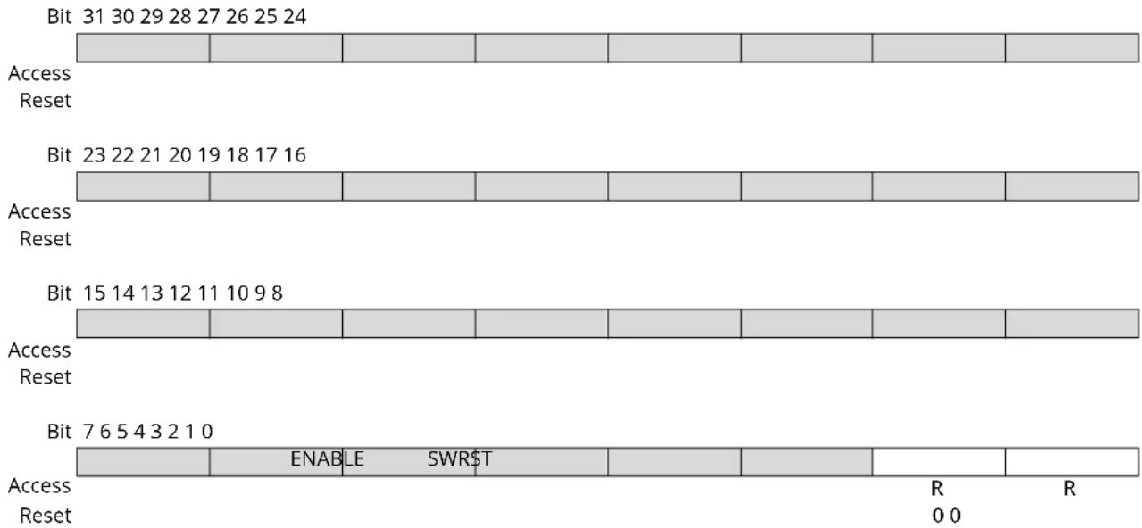
text_image
Bit 31 30 29 28 27 26 25 24 Access Reset Bit 23 22 21 20 19 18 17 16 Access Reset Bit 15 14 13 12 11 10 9 8 Access Reset Bit 7 6 5 4 3 2 1 0 Access Reset ENABLE SWR$T R R 0 0Bit 1 - ENABLE SERCOM Enable Synchronization Busy
Enabling and disabling the SERCOM (CTRLA. ENABLE) requires synchronization. When written, the SYNCBUSY. ENABLE bit will be set until synchronization is complete.
Writes to any register (except for CTRLA.SWRST) while enable synchronization is on-going will be discarded and an APB error will be generated.
| Value | Description |
| 0 | Enable synchronization is not busy. |
| 1 | Enable synchronization is busy. |
Bit 0 - SWRST Software Reset Synchronization Busy
Resetting the SERCOM (CTRLA.SWRST) requires synchronization. When written, the
SYNCBUSY.SWRST bit will be set until synchronization is complete.
Writes to any register while synchronization is on-going will be discarded and an APB error will be generated.
| Value | Description |
| 0 | SWRST synchronization is not busy. |
| 1 | SWRST synchronization is busy. |
33.8.8 Address
Name: ADDR
Offset: 0x24
Reset: 0x00000000
Property: PAC Write-Protection, Enable-Protected
Bit 31 30 29 28 27 26 25 24
| ADDRMASK[9:7] | |||||
| Access Reset 0 0 0 | R/W R/W R/W | ||||
Bit 23 22 21 20 19 18 17 16
| ADDRMASK[6:0] | ||
| Access | R/W R/W R/W R/W R/W R/W R/W | |
| Reset | 0 0 0 0 0 0 |
Bit 15 14 13 12 11 10 98
| TENBITEN | ADDR[9:7] | ||||
| Access | R/W | R/W R/W R/W | |||
| Reset | 0 | 0 0 0 |
Bit 76543210
| ADDR[6:0] | GENCEN | |
| Access | R/W R/W R/W R/W R/W R/W R/W R/W | |
| Reset | 0 0 0 0 0 0 0 |
Bits 26:17 - ADDRMASK[9:0] Address Mask
These bits act as a second address match register, an address mask register or the lower limit of an address range, depending on the CTRLB.AMODE setting.
Bit 15 - TENBITEN Ten Bit Addressing Enable
| Value | Description |
| 0 | 10-bit address recognition disabled. |
| 1 | 10-bit address recognition enabled. |
Bits 10:1 - ADDR[9:0] Address
These bits contain the I ^2 C Client address used by the Client address match logic to determine if a Host has addressed the Client.
When using 7-bit addressing, the Client address is represented by ADDR[6:0].
When using 10-bit addressing (ADDR.TENBITEN=1), the Client address is represented by ADDR[9:0]
When the address match logic detects a match, INTFLAG.AMATCH is set and STATUS.DIR is updated to indicate whether it is a read or a write transaction.
Bit 0 - GENCEN General Call Address Enable
A general call address is an address consisting of all-zeroes, including the direction bit (Host write).
| Value | Description |
| 0 | General call address recognition disabled. |
| 1 | General call address recognition enabled. |
33.8.9 Data
Name: DATA
Offset: 0x28
Reset: 0x0000
The Client data register I/O location (DATA.DATA) provides access to the Host transmit and receive data buffers. Reading valid data or writing data to be transmitted can be successfully done only when SCL is held low by the Client (STATUS.CLK HOLD is set). An exception occurs when reading the last data byte after the stop condition has been received.
Accessing DATA.DATA auto-triggers PC bus operations. The operation performed depends on the state of CTRLB.ACKACT, CTRLB.SMEN and the type of access (read/write).
Writing or reading DATA.DATA when not in smart mode does not require synchronization.
33.9 Register Summary - I2C Host
| Offset | Name Bit Pos. 76 | 543210 | ||||||||
| 0x00 CTRLA | 7:0 RUNSTDBY MODE[2:0] ENABLE SWRST | |||||||||
| 15:8 | ||||||||||
| 23:16 SEXTTOEN MEXTTOEN SDAHOLD[1:0] PINOUT | ||||||||||
| 31:24 | LOWTOUT | INACTOUT[1:0] | SCLSM | SPEED[1:0] | ||||||
| 0x04 CTRLB | 7:0 | |||||||||
| 15:8 | QCEN SMEN | |||||||||
| 23:16 | ACKACT CMD[1:0] | |||||||||
| 31:24 | ||||||||||
| 0x08 ... 0x0B | Reserved | |||||||||
| 0x0C | BAUD | 7:0 | BAUD[7:0] | |||||||
| 15:8 | BAUDLOW[7:0] | |||||||||
| 23:16 | HSBAUD[7:0] | |||||||||
| 31:24 | HSBAUDLOW[7:0] | |||||||||
| 0x10 ... 0x13 | Reserved | |||||||||
| 0x14 | INTENCLR | 7:0 | ERROR | SB | MB | |||||
| 0x15 | Reserved | |||||||||
| 0x16 | INTENSET | 7:0 | ERROR | SB | MB | |||||
| 0x17 | Reserved | |||||||||
| 0x18 | INTFLAG | 7:0 | ERROR | SB | MB | |||||
| 0x19 | Reserved | |||||||||
| 0x1A | STATUS | 7:0 | CLKHOLD | LOWTOUT | BUSSTATE[1:0] | RXNACK | ARBLOST | BUSERR | ||
| 15:8 | LENERR | SEXTTOUT MEXTTOUT | ||||||||
| 0x1C | SYNCBUSY | 7:0 | SYSOP ENABLE SWRST | |||||||
| 15:8 | ||||||||||
| 23:16 | ||||||||||
| 31:24 | ||||||||||
| 0x20 ... 0x23 | Reserved | |||||||||
| 0x24 | ADDR | 7:0 | ADDR[7:0] | |||||||
| 15:8 | TENBITEN | HS | LENEN | ADDR[10:8] | ||||||
| 23:16 | LEN[7:0] | |||||||||
| 31:24 | ||||||||||
| 0x28 | DATA | 7:0 | DATA[7:0] | |||||||
| 15:8 | ||||||||||
| 0x2A ... 0x2F | Reserved | |||||||||
| 0x30 | DBGCTRL | 7:0 | DBGSTOP | |||||||
33.10 Register Description - I²C Host
Registers can be 8, 16, or 32 bits wide. Atomic 8-, 16- and 32-bit accesses are supported. In addition, the 8-bit quarters and 16-bit halves of a 32-bit register, and the 8-bit halves of a 16-bit register can be accessed directly.
Some registers are optionally write-protected by the Peripheral Access Controller (PAC). Optional PAC write-protection is denoted by the "PAC Write-Protection" property in each individual register description. For details, refer to 33.5.8. Register Access Protection.
Some registers are synchronized when read and/or written. Synchronization is denoted by the "Write-Synchronized" or the "Read-Synchronized" property in each individual register description. For details, refer to 33.6.6. Synchronization.
Some registers are enable-protected, meaning they can only be written when the peripheral is disabled. Enable-protection is denoted by the "Enable-Protected" property in each individual register description.
33.10.1 Control A
Name: CTRLA
Offset: 0x00
Reset: 0x00000000
Property: PAC Write-Protection, Enable-Protected, Write-Synchronized
Bit 31 30 29 28 27 26 25 24
| LOWTOUT INACTOUT[1:0] SCLSM SPEED[1:0] | ||||||
| Access | R/W R/W R/W R/W | R/W R/W | ||||
| Reset | 0 | 0 | 0 | 0 | 0 | 0 |
Bit 23 22 21 20 19 18 17 16
| SEXTTOEN | MEXTTOEN | SDAHOLD[1:0] | PINOUT | ||||
| Access | R/W | R/W R/W | R/W | ||||
| Reset | 0 | 0 | 0 | 0 | 0 |
Bit 15 14 13 12 11 10 9 8
Reset
| Bit | 7 | 6 | 5 | 4 | 3 | 2 | 1 | 0 |
| RUNSTDBY | MODE[2:0] | ENABLE | SWRST | |||||
| Access | R/W | R/W R/W R/W R/W R/W | ||||||
| Reset | 0 | 0 | 0 | 0 | 0 | 0 | ||
Bit 30 - LOWTOUT SCL Low Time-Out
This bit enables the SCL low time-out. If SCL is held low for 25ms-35ms, the Host will release its clock hold, if enabled, and complete the current transaction. A stop condition will automatically be transmitted.
INTFLAG.SB or INTFLAG.MB will be set as normal, but the clock hold will be released. The STATUS.LOWTOUT and STATUS.BUSERR status bits will be set.
This bit is not synchronized.
| Value | Description |
| 0 | Time-out disabled. |
| 1 | Time-out enabled. |
Bits 29:28 - INACTOUT[1:0] Inactive Time-Out
If the inactive bus time-out is enabled and the bus is inactive for longer than the time-out setting, the bus state logic will be set to idle. An inactive bus arise when either an I²C Host or Client is holding the SCL low.
Enabling this option is necessary for SMBus compatibility, but can also be used in a non-SMBus set-up.
Calculated time-out periods are based on a 100kHz baud rate.
These bits are not synchronized.
| Value | Name | Description |
| 0x0 | DIS | Disabled |
| 0x1 | 55US | 5-6 SCL cycle time-out (50-60μs) |
| 0x2 | 105US | 10-11 SCL cycle time-out (100-110μs) |
| 0x3 | 205US | 20-21 SCL cycle time-out (200-210μs) |
Bit 27 - SCLSM SCL Clock Stretch Mode
This bit controls when SCL will be stretched for software interaction.
This bit is not synchronized.
| Value Description | |
| 0 | SCL stretch according to Figure 33-4. |
| 1 | SCL stretch only after ACK bit, Figure 33-5. |
Bits 25:24 - SPEED[1:0] Transfer Speed
These bits define bus speed.
These bits are not synchronized.
| Value Description | |
| 0x0 | Standard-mode (Sm) up to 100 kHz and Fast-mode (Fm) up to 400 kHz |
| 0x1 | Fast-mode Plus (Fm+) up to 1 MHz |
| 0x2 | High-speed mode (Hs-mode) up to 3.4 MHz |
| 0x3 | Reserved |
Bit 23 - SEXTTOEN Client SCL Low Extend Time-Out
This bit enables the Client SCL low extend time-out. If SCL is cumulatively held low for greater than 25ms from the initial START to a STOP, the Host will release its clock hold if enabled, and complete the current transaction. A STOP will automatically be transmitted.
SB or MB will be set as normal, but CLKHOLD will be release. The MEXTTOUT and BUSERR status bits will be set.
This bit is not synchronized.
| Value Description | |
| 0 | Time-out disabled |
| 1 | Time-out enabled |
Bit 22 - MEXTTOEN Host SCL Low Extend Time-Out
This bit enables the Host SCL low extend time-out. If SCL is cumulatively held low for greater than 10ms from START-to-ACK, ACK-to-ACK, or ACK-to-STOP the Host will release its clock hold if enabled, and complete the current transaction. A STOP will automatically be transmitted.
SB or MB will be set as normal, but CLKHOLD will be released. The MEXTTOUT and BUSERR status bits will be set.
This bit is not synchronized.
| Value Description | |
| 0 | Time-out disabled |
| 1 | Time-out enabled |
Bits 21:20 - SDAHOLD[1:0] SDA Hold Time
These bits define the SDA hold time with respect to the negative edge of SCL.
These bits are not synchronized.
| Value Name | Description | |
| 0x0 | DIS Disabled | |
| 0x1 | 75NS 50-100ns hold time | |
| 0x2 | 450NS 300-600ns hold time | |
| 0x3 | 600NS 400-800ns hold time | |
Bit 16 - PINOUT Pin Usage
This bit set the pin usage to either two- or four-wire operation:
This bit is not synchronized.
| Value Description | |
| 0 | 4-wire operation disabled. |
| 1 | 4-wire operation enabled. |
Bit 7 - RUNSTDBY Run in Standby
This bit defines the functionality in standby sleep mode.
This bit is not synchronized.
| Value Description | |
| 0 | GCLK_SERCOMx_CORE is disabled and the I^2C Host will not operate in standby sleep mode. |
| 1 | GCLK_SERCOMx_CORE is enabled in all sleep modes. |
Bits 4:2 - MODE[2:0] Operating Mode
These bits must be written to 0x5 to select the I ^2 C Host serial communication interface of the SERCOM.
These bits are not synchronized.
Bit 1 - ENABLE Enable
Due to synchronization, there is delay from writing CTRLA. ENABLE until the peripheral is enabled/disabled. The value written to CTRL. ENABLE will read back immediately and the Synchronization Enable Busy bit in the Synchronization Busy register (SYNCBUSY. ENABLE) will be set. SYNCBUSY. ENABLE will be cleared when the operation is complete.
This bit is not enable-protected.
| Value Description | |
| 0 | The peripheral is disabled or being disabled. |
| 1 | The peripheral is enabled. |
Bit 0 - SWRST Software Reset
Writing '0' to this bit has no effect.
Writing '1' to this bit resets all registers in the SERCOM, except DBGCTRL, to their initial state, and the SERCOM will be disabled.
Writing '1' to CTRLA.SWRST will always take precedence, meaning that all other writes in the same write-operation will be discarded. Any register write access during the ongoing reset will result in an APB error. Reading any register will return the reset value of the register.
Due to synchronization there is a delay from writing CTRLA.SWRST until the reset is complete.
CTRLA.SWRST and SYNCBUSY.SWRST will both be cleared when the reset is complete.
This bit is not enable-protected.
| Value Description | |
| 0 | There is no reset operation ongoing. |
| 1 | The reset operation is ongoing. |
33.10.2 Control B
Name: CTRLB
Offset: 0x04
Reset: 0x00000000
Property: PAC Write-Protection, Enable-Protected, Write-Synchronized
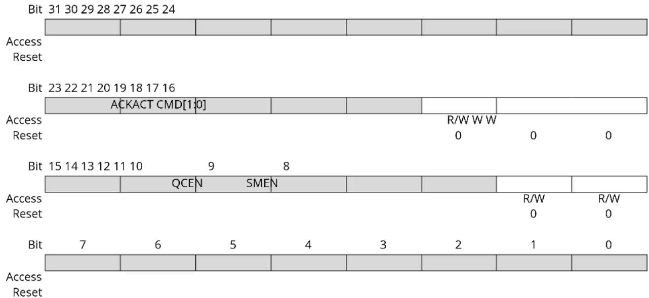
other
| Bit | Access Reset | Access CMD[1:0] | ACKACT CMD[1:0] | QCEN SMEN | R/W W W 0 | R/W 0 | R/W 0 | |-----|--------------|-----------------|-----------------|-----------|-----------|-------|-------| | 31 | 24 | 24 | 24 | 24 | 24 | 24 | 24 | | 29 | 24 | 24 | 24 | 24 | 24 | 24 | 24 | | 28 | 24 | 24 | 24 | 24 | 24 | 24 | 24 | | 27 | 24 | 24 | 24 | 24 | 24 | 24 | 24 | | 26 | 24 | 24 | 24 | 24 | 24 | 24 | 24 | | 25 | 24 | 24 | 24 | 24 | 24 | 24 | 24 | | 23 | 16 | 16 | 16 | 16 | 16 | 16 | 16 | | 22 | 16 | 16 | 16 | 16 | 16 | 16 | 16 | | 21 | 16 | 16 | 16 | 16 | 16 | 16 | 16 | | 20 | 16 | 16 | 16 | 16 | 16 | 16 | 16 | | 19 | 16 | 16 | 16 | 16 | 16 | 16 | 16 | | 18 | 16 | 16 | 16 | 16 | 16 | 16 | 16 | | 17 | 16 | 16 | 16 | 16 | 16 | 16 | 16 | | Note: The actual values for 'ACKACT CMD[1:0]' and 'QCEN SMEN' are not provided in the code. The actual values for 'ACKACT CMD[1:0]' and 'QCEN SMEN' are estimated based on the code execution. There is no label for the actual values.Bit 18 - ACKACT Acknowledge Action
This bit defines the I^2C Host's acknowledge behavior after a data byte is received from the I^2C Client. The acknowledge action is executed when a command is written to CTRLB.CMD, or if smart mode is enabled (CTRLB.SMEN is written to one), when DATA.DATA is read.
This bit is not enable-protected.
This bit is not write-synchronized.
| Value | Description |
| 0 | Send ACK. |
| 1 | Send NACK. |
Bits 17:16 - CMD[1:0] Command
Writing these bits triggers a Host operation as described below. The CMD bits are strobe bits, and always read as zero. The acknowledge action is only valid in Host read mode. In Host write mode, a command will only result in a repeated start or stop condition. The CTRLB.ACKACT bit and the CMD bits can be written at the same time, and then the acknowledge action will be updated before the command is triggered.
Commands can only be issued when either the Client on Bus interrupt flag (INTFLAG.SB) or Host on Bus interrupt flag (INTFLAG.MB) is '1'.
If CMD 0x1 is issued, a repeated start will be issued followed by the transmission of the current address in ADDR.ADDR. If another address is desired, ADDR.ADDR must be written instead of the CMD bits. This will trigger a repeated start followed by transmission of the new address.
Issuing a command will set the System Operation bit in the Synchronization Busy register (SYNCBUSY.SYSOP).
Table 33-4. Command Description
| CMD[1:0] | Direction Action | |
| 0x0 | X (No action) | |
| ......continued | ||
| CMD[1:0] Direction Action | ||
| 0x1 X Execute acknowledge action succeeded by repeated Start | ||
| 0x2 0 (Write) No operation | ||
| 1 (Read) Execute acknowledge action succeeded by a byte read operation | ||
| 0x3 X Execute acknowledge action succeeded by issuing a stop condition | ||
These bits are not enable-protected.
Bit 9 - QCEN Quick Command Enable
This bit is not write-synchronized.
| Value Description | |
| 0 | Quick Command is disabled. |
| 1 | Quick Command is enabled. |
Bit 8 - SMEN Smart Mode Enable
When smart mode is enabled, acknowledge action is sent when DATA.DATA is read.
This bit is not write-synchronized.
| Value Description | |
| 0 | Smart mode is disabled. |
| 1 | Smart mode is enabled. |
33.10.3 Baud Rate
Name: BAUD
Offset: 0x0C
Reset: 0x0000
Property: PAC Write-Protection, Enable-Protected
Bit 31 30 29 28 27 26 25 24
HSBAUDLOW[7:0]
Access R/W R/W R/W R/W R/W R/W R/W R/W
Reset 00000000
Bit 23 22 21 20 19 18 17 16
HSBAUD[7:0]
Access R/W R/W R/W R/W R/W R/W R/W R/W
Reset 00000000
Bit 15 14 13 12 11 10 9 8
BAUDLOW[7:0]
Access R/W R/W R/W R/W R/W R/W R/W R/W
Reset 00000000
Bit 76543210
BAUD[7:0]
Access R/W R/W R/W R/W R/W R/W R/W R/W
Reset 00000000
Bits 31:24 - HSBAUDLOW[7:0] High Speed Host Baud Rate Low
HSBAUDLOW non-zero: HSBAUDLOW indicates the SCL low time in High-speed mode according to HSBAUDLOW=f GCLK ·T LOW - 1
HSBAUDLOW equal to zero: The HSBAUD register is used to time T_LOW , T_HIGH , T_SU;STO , T_HD;STA and T_SU;STA . T_BUF is timed by the BAUD register.
Bits 23:16 - HSBAUD[7:0] High Speed Host Baud Rate
This bit field indicates the SCL high time in High-speed mode according to the following formula.
When HSBAUDLOW is zero, T_LOW , T_HIGH , T_SU;STO , T_HD;STA and T_SU;STA are derived using this formula. T_BUF is timed by the BAUD register.
HSBAUD=f GCLK·THIGH-1
Bits 15:8 - BAUDLOW[7:0] Host Baud Rate Low
If this bit field is non-zero, the SCL low time will be described by the value written.
For more information on how to calculate the frequency, see SERCOM Clock Generation - Baud-Rate Generator.
Bits 7:0 - BAUD[7:0] Host Baud Rate
This bit field is used to derive the SCL high time if BAUD.BAUDLOW is non-zero. If BAUD.BAUDLOW is zero, BAUD will be used to generate both high and low periods of the SCL.
For more information on how to calculate the frequency, see SERCOM SERCOM Clock Generation - Baud-Rate Generator..
33.10.4 Interrupt Enable Clear
Name: INTENCLR
Offset: 0x14
Reset: 0x00
Property: PAC Write-Protection
This register allows the user to disable an interrupt without doing a read-modify-write operation. Changes in this register will also be reflected in the Interrupt Enable Set register (INTENSET).
Bit 76543210
| ERROR | SB MB | |||||||
| Access | R/W | R/W | R/W | |||||
| Reset | 0 | 0 | 0 |
Bit 7 - ERROR Error Interrupt Enable
Writing '0' to this bit has no effect.
Writing '1' to this bit will clear the Error Interrupt Enable bit, which disables the Error interrupt.
| Value | Description |
| 0 | Error interrupt is disabled. |
| 1 | Error interrupt is enabled. |
Bit 1 - SB Client on Bus Interrupt Enable
Writing '0' to this bit has no effect.
Writing '1' to this bit will clear the Client on Bus Interrupt Enable bit, which disables the Client on Bus interrupt.
| Value | Description |
| 0 | The Client on Bus interrupt is disabled. |
| 1 | The Client on Bus interrupt is enabled. |
Bit 0 - MB Host on Bus Interrupt Enable
Writing '0' to this bit has no effect.
Writing '1' to this bit will clear the Host on Bus Interrupt Enable bit, which disables the Host on Bus interrupt.
| Value | Description |
| 0 | The Host on Bus interrupt is disabled. |
| 1 | The Host on Bus interrupt is enabled. |
33.10.5 Interrupt Enable Set
Name: INTENSET
Offset: 0x16
Reset: 0x00
Property: PAC Write-Protection
This register allows the user to enable an interrupt without doing a read-modify-write operation. Changes in this register will also be reflected in the Interrupt Enable Clear register (INTENCLR).
Bit 76543210
| ERROR | SB MB | |||||||
| Access | R/W | R/W | R/W | |||||
| Reset | 0 | 0 | 0 |
Bit 7 - ERROR Error Interrupt Enable
Writing '0' to this bit has no effect.
Writing '1' to this bit will set the Error Interrupt Enable bit, which enables the Error interrupt.
| Value | Description |
| 0 | Error interrupt is disabled. |
| 1 | Error interrupt is enabled. |
Bit 1 - SB Client on Bus Interrupt Enable
Writing '0' to this bit has no effect.
Writing '1' to this bit will set the Client on Bus Interrupt Enable bit, which enables the Client on Bus interrupt.
| Value | Description |
| 0 | The Client on Bus interrupt is disabled. |
| 1 | The Client on Bus interrupt is enabled. |
Bit 0 - MB Host on Bus Interrupt Enable
Writing '0' to this bit has no effect.
Writing '1' to this bit will set the Host on Bus Interrupt Enable bit, which enables the Host on Bus interrupt.
| Value | Description |
| 0 | The Host on Bus interrupt is disabled. |
| 1 | The Host on Bus interrupt is enabled. |
33.10.6 Interrupt Flag Status and Clear
Name: INTFLAG
Offset: 0x18
Reset: 0x00
Property: -
Bit 76543210
| ERROR | SB MB | |||||||
| Access | R/W | R/W | R/W | |||||
| Reset | 0 | 0 | 0 |
Bit 7 - ERROR Error
This flag is cleared by writing '1' to it.
This bit is set when any error is detected. Errors that will set this flag have corresponding status bits in the STATUS register. These status bits are LENERR, SEXTTOUT, MEXTTOUT, LOWTOUT, ARBLOST, and BUSERR.
Writing '0' to this bit has no effect.
Writing '1' to this bit will clear the flag.
Bit 1 - SB Client on Bus
The Client on Bus flag (SB) is set when a byte is successfully received in Host read mode, i.e., no arbitration lost or bus error occurred during the operation. When this flag is set, the Host forces the SCL line low, stretching the I²C clock period. The SCL line will be released and SB will be cleared on one of the following actions:
• Writing to ADDR.ADDR
• Writing to DATA.DATA
- Reading DATA.DATA when smart mode is enabled (CTRLB.SMEN)
• Writing a valid command to CTRLB.CMD
Writing '1' to this bit location will clear the SB flag. The transaction will not continue or be terminated until one of the above actions is performed.
Writing '0' to this bit has no effect.
Bit 0 - MB Host on Bus
This flag is set when a byte is transmitted in Host write mode. The flag is set regardless of the occurrence of a bus error or an arbitration lost condition. MB is also set when arbitration is lost during sending of NACK in Host read mode, or when issuing a start condition if the bus state is unknown. When this flag is set and arbitration is not lost, the Host forces the SCL line low, stretching the I^2C clock period. The SCL line will be released and MB will be cleared on one of the following actions:
• Writing to ADDR.ADDR
• Writing to DATA.DATA
- Reading DATA.DATA when smart mode is enabled (CTRLB.SMEN)
• Writing a valid command to CTRLB.CMD
Writing '1' to this bit location will clear the MB flag. The transaction will not continue or be terminated until one of the above actions is performed.
Writing '0' to this bit has no effect.
33.10.7 Status
Name: STATUS
Offset: 0x1A
Reset: 0x0000
Property: Write-Synchronized
Bit 15 14 13 12 11 10 9 8
| LENERR SEXTTOUT MEXTTOUT | |||||
| Access Reset | R/W R/W R/W0 0 0 | ||||
Bit 76543210
| CLKHOLD | LOWTOUT | BUSSTATE[1:0] | RXNACK | ARBLOST | BUSERR | ||
| Access | R | R/W | R | R | R | R/W | R/W |
| Reset | 0 0 0 0 | 0 0 0 |
Bit 10 - LENERR Transaction Length Error
This bit is set when automatic length is used for a DMA transaction and the Client sends a NACK before ADDR.LEN bytes have been written by the Host.
Writing '1' to this bit location will clear STATUS.LENERR. This flag is automatically cleared when writing to the ADDR register.
Writing '0' to this bit has no effect.
This bit is not write-synchronized.
Bit 9 - SEXTTOUT Client SCL Low Extend Time-Out
This bit is set if a Client SCL low extend time-out occurs.
This bit is automatically cleared when writing to the ADDR register.
Writing '1' to this bit location will clear SEXTTOUT. Normal use of the I²C interface does not require the SEXTTOUT flag to be cleared by this method.
Writing '0' to this bit has no effect.
This bit is not write-synchronized.
Bit 8 - MEXTTOUT Host SCL Low Extend Time-Out
This bit is set if a Host SCL low time-out occurs.
Writing '1' to this bit location will clear STATUS.MEXTTOUT. This flag is automatically cleared when writing to the ADDR register.
Writing '0' to this bit has no effect.
This bit is not write-synchronized.
Bit 7 - CLKHOLD Clock Hold
This bit is set when the Host is holding the SCL line low, stretching the I²C clock. Software should consider this bit when INTFLAG.SB or INTFLAG.MB is set.
This bit is cleared when the corresponding interrupt flag is cleared and the next operation is given.
Writing '0' to this bit has no effect.
Writing '1' to this bit has no effect.
This bit is not write-synchronized.
Bit 6 - LOWTOUT SCL Low Time-Out
This bit is set if an SCL low time-out occurs.
Writing '1' to this bit location will clear this bit. This flag is automatically cleared when writing to the ADDR register.
Writing '0' to this bit has no effect.
This bit is not write-synchronized.
Bits 5:4 - BUSSTATE[1:0] Bus State
These bits indicate the current I^2C bus state.
When in UNKNOWN state, writing 0x1 to BUSSTATE forces the bus state into the IDLE state. The bus state cannot be forced into any other state.
Writing BUSSTATE to idle will set SYNCBUSY.SYSOP.
| Value Name | Description |
| 0x0 | UNKNOWN The bus state is unknown to the I^2C Host and will wait for a stop condition to be detected or wait to be forced into an idle state by software |
| 0x1 | IDLE The bus state is waiting for a transaction to be initialized |
| 0x2 | OWNER The I^2C Host is the current owner of the bus |
| 0x3 | BUSY Some other I^2C Host owns the bus |
Bit 2 - RXNACK Received Not Acknowledge
This bit indicates whether the last address or data packet sent was acknowledged or not.
Writing '0' to this bit has no effect.
Writing '1' to this bit has no effect.
This bit is not write-synchronized.
| Value Description | |
| 0 | Client responded with ACK. |
| 1 | Client responded with NACK. |
Bit 1 - ARBLOST Arbitration Lost
This bit is set if arbitration is lost while transmitting a high data bit or a NACK bit, or while issuing a start or repeated start condition on the bus. The Host on Bus interrupt flag (INTFLAG.MB) will be set when STATUS.ARBLOST is set.
Writing the ADDR.ADDR register will automatically clear STATUS.ARBLOST.
Writing '0' to this bit has no effect.
Writing '1' to this bit will clear it.
This bit is not write-synchronized.
Bit 0 - BUSERR Bus Error
This bit indicates that an illegal bus condition has occurred on the bus, regardless of bus ownership. An illegal bus condition is detected if a protocol violating start, repeated start or stop is detected on the I^2C bus lines. A start condition directly followed by a stop condition is one example of a protocol violation. If a time-out occurs during a frame, this is also considered a protocol violation, and will set BUSERR.
If the I ^2 C Host is the bus owner at the time a bus error occurs, STATUS.ARBLOST and INTFLAG.MB will be set in addition to BUSERR.
Writing the ADDR.ADDR register will automatically clear the BUSERR flag.
Writing '0' to this bit has no effect.
Writing '1' to this bit will clear it.
This bit is not write-synchronized.
33.10.8 Synchronization Busy
Name: SYNCBUSY
Offset: 0x1C
Reset: 0x00000000
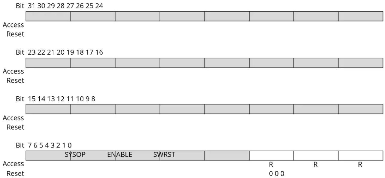
text_image
Bit 31 30 29 28 27 26 25 24 Access Reset Bit 23 22 21 20 19 18 17 16 Access Reset Bit 15 14 13 12 11 10 9 8 Access Reset Bit 7 6 5 4 3 2 1 0 SYSOP ENABLE SWRST R R R Access Reset 0 0 0Bit 2 - SYSOP System Operation Synchronization Busy
Writing CTRLB.CMD, STATUS.BUSSTATE, ADDR, or DATA when the SERCOM is enabled requires synchronization. When written, the SYNCBUSY.SYSOP bit will be set until synchronization is complete.
| Value | Description |
| 0 | System operation synchronization is not busy. |
| 1 | System operation synchronization is busy. |
Bit 1 - ENABLE SERCOM Enable Synchronization Busy
Enabling and disabling the SERCOM (CTRLA. ENABLE) requires synchronization. When written, the SYNCBUSY. ENABLE bit will be set until synchronization is complete.
Writes to any register (except for CTRLA.SWRST) while enable synchronization is on-going will be discarded and an APB error will be generated.
| Value | Description |
| 0 | Enable synchronization is not busy. |
| 1 | Enable synchronization is busy. |
Bit 0 - SWRST Software Reset Synchronization Busy
Resetting the SERCOM (CTRLA.SWRST) requires synchronization. When written, the SYNCBUSY.SWRST bit will be set until synchronization is complete.
Writes to any register while synchronization is on-going will be discarded and an APB error will be generated.
| Value | Description |
| 0 | SWRST synchronization is not busy. |
| 1 | SWRST synchronization is busy. |
33.10.9 Address
Name: ADDR
Offset: 0x24
Reset: 0x0000
Property: Write-Synchronized
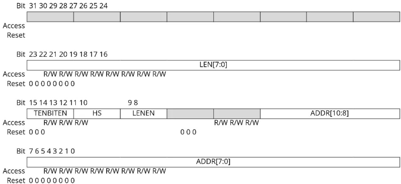
text_image
Bit 31 30 29 28 27 26 25 24 Access Reset Bit 23 22 21 20 19 18 17 16 LEN[7:0] Access R/W R/W R/W R/W R/W R/W R/W R/W Reset 0 0 0 0 0 0 0 0 Bit 15 14 13 12 11 10 9 8 TENBITEN HS LENEN ADDR[10:8] Access R/W R/W R/W R/W R/W R/W Reset 0 0 0 0 0 0 Bit 7 6 5 4 3 2 1 0 ADDR[7:0] Access R/W R/W R/W R/W R/W R/W R/W R/W Reset 0 0 0 0 0 0 0Bits 23:16 - LEN[7:0] Transaction Length
These bits define the transaction length of a DMA transaction from 0 to 255 bytes. The Transfer Length Enable (LENEN) bit must be written to '1' in order to use DMA.
Bit 15 - TENBITEN Ten Bit Addressing Enable
This bit enables 10-bit addressing. This bit can be written simultaneously with ADDR to indicate a 10-bit or 7-bit address transmission.
| Value | Description |
| 0 | 10-bit addressing disabled. |
| 1 | 10-bit addressing enabled. |
Bit 14 - HS High Speed
This bit enables high-speed mode for the current transfer from repeated START to STOP. This bit can be written simultaneously with ADDR for a high-speed transfer.
| Value | Description |
| 0 | High-speed transfer disabled. |
| 1 | High-speed transfer enabled. |
Bit 13 - LENEN Transfer Length Enable
| Value | Description |
| 0 | Automatic transfer length disabled. |
| 1 | Automatic transfer length enabled. |
Bits 10:0 - ADDR[10:0] Address
When ADDR is written, the consecutive operation will depend on the bus state:
UNKNOWN: INTFLAG.MB and STATUS.BUSERR are set, and the operation is terminated.
BUSY: The I ^2 C Host will await further operation until the bus becomes IDLE.
IDLE: The I²C Host will issue a start condition followed by the address written in ADDR. If the address is acknowledged, SCL is forced and held low, and STATUS.CLKHOLD and INTFLAG.MB are set.
OWNER: A repeated start sequence will be performed. If the previous transaction was a read, the acknowledge action is sent before the repeated start bus condition is issued on the bus. Writing ADDR to issue a repeated start is performed while INTFLAG.MB or INTFLAG.SB is set.
STATUS.BUSERR, STATUS.ARBLOST, INTFLAG.MB and INTFLAG.SB will be cleared when ADDR is written.
The ADDR register can be read at any time without interfering with ongoing bus activity, as a read access does not trigger the Host logic to perform any bus protocol related operations.
The I ^2 C Host control logic uses bit 0 of ADDR as the bus protocol's read/write flag (R/W); 0 for write and 1 for read.
33.10.10 Data
Name: DATA
Offset: 0x28
Reset: 0x0000
The Host data register I/O location (DATA) provides access to the Host transmit and receive data buffers. Reading valid data or writing data to be transmitted can be successfully done only when SCL is held low by the Host (STATUS.CLKHOLD is set). An exception is reading the last data byte after the stop condition has been sent.
Accessing DATA.DATA auto-triggers PC bus operations. The operation performed depends on the state of CTRLB.ACKACT, CTRLB.SMEN and the type of access (read/write).
33.10.11 Debug Control
Name: DBGCTRL
Offset: 0x30
Reset: 0x00
Property: PAC Write-Protection
Bit 76543210
| DBGSTOP | |||||||
| Access Reset 0 | R/W | ||||||
Bit 0 - DBGSTOP Debug Stop Mode
This bit controls functionality when the CPU is halted by an external debugger.
| Value Description | |
| 0 | The baud-rate generator continues normal operation when the CPU is halted by an external debugger. |
| 1 | The baud-rate generator is halted when the CPU is halted by an external debugger. |
34. TC - Timer/Counter
34.1 Overview
There are up to four TC peripheral instances.
Each TC consists of a counter, a prescaler, compare/capture channels and control logic. The counter can be set to count events, or clock pulses. The counter, together with the compare/capture channels, can be configured to timestamp input events or IO pin edges, allowing for capturing of frequency and/or pulse width.
A TC can also perform waveform generation, such as frequency generation and pulse-width modulation.
34.2 Features
- Selectable configuration
- 8-, 16- or 32-bit TC operation, with compare/capture channels
• 2 compare/capture channels (CC) with: - Double buffered timer period setting (in 8-bit mode only)
- Double buffered compare channel
- Waveform generation
- Frequency generation - Single-slope pulse-width modulation
- Input capture
- Event / IO pin edge capture - Frequency capture - Pulse-width capture - Time-stamp capture
- One input event
- Interrupts/output events on:
- Counter overflow/underflow - Compare match or capture
- Internal prescaler
- DMA support
34.3 Block Diagram
Figure 34-1. Timer/Counter Block Diagram

flowchart
graph TD
    A["Base Counter"] --> B["BUFV"]
    B --> C["PERBUF"]
    C --> D["PER"]
    D --> E["COUNT"]
    E --> F["=0"]
    F --> G["="]
    G --> H["Counter"]
    H --> I["Count"]
    I --> J["Prescaler"]
    J --> K["count"]
    J --> L["clear"]
    J --> M["load"]
    J --> N["direction"]
    K --> O["Control Logic"]
    L --> O
    M --> O
    N --> O
    O --> P["OVF (INT/Event/DMA Req.)"]
    O --> Q["ERR (INT Req.)"]
    P --> R["TCE"]
    Q --> S["TOP"]
    S --> T["BOTTOM"]
    T --> U["UPDATE"]
    U --> V["compare/Capture (Unit x = {0,1}"]
    V --> W["CCBUFx"]
    W --> X["CCx"]
    X --> Y["="]
    Y --> Z["match"]
    Z --> AA["Waveform Generation"]
    AA --> AB["Control Logic"]
    AB --> AC[""WO[1"]"]
    AB --> AD[""WO[0"]"]
    AC --> AE["MCx (INT/Event/DMA Req.)"]
    AD --> AE
34.4 Signal Description
Table 34-1. Signal Description for TC.
| Signal Name Type Description | ||
| WO[1:0] Digital output Waveform output | ||
| Digital input Capture input | ||
Refer to I/O Multiplexing and Considerations for details on the pin mapping for this peripheral. One signal can be mapped on several pins.
34.5 Product Dependencies
In order to use this peripheral, other parts of the system must be configured correctly, as described below.
34.5.1 I/O Lines
In order to use the I/O lines of this peripheral, the I/O pins must be configured using the I/O Pin Controller (PORT).
34.5.2 Power Management
This peripheral can continue to operate in any sleep mode where its source clock is running. The interrupts can wake up the device from sleep modes. Events connected to the event system can trigger other operations in the system without exiting sleep modes.
References:
PM - Power Manager
34.5.3 Clocks
The TC bus clocks (CLK_TCx_APB) can be enabled and disabled in the Main Clock Module. The default state of CLK_TCx_APB can be found in the Peripheral Clock Masking.
The generic clocks (GCLK_TCx) are asynchronous to the user interface clock (CLK_TCx_APB). Due to this asynchronicity, accessing certain registers will require synchronization between the clock domains. Refer to Synchronization for further details.
Note that TC0 and TC1 share a peripheral clock channel, as do TC2 and TC3. For this reason they cannot be set to different clock frequencies.
34.5.4 DMA
The DMA request lines are connected to the DMA Controller (DMAC). In order to use DMA requests with this peripheral the DMAC must be configured first. Refer to the DMAC - Direct Memory Access Controller for details.
34.5.5 Interrupts
The interrupt request line is connected to the Interrupt Controller. In order to use interrupt requests of this peripheral, the Interrupt Controller (NVIC) must be configured first. Refer to the Nested Vector Interrupt Controller for details.
34.5.6 Events
The events of this peripheral are connected to the Event System. Refer to 29. EVSYS – Event System for more information.
34.5.7 Debug Operation
When the CPU is halted in debug mode, this peripheral will halt normal operation. This peripheral can be forced to continue operation during debugging - refer to the Debug Control (DBGCTRL) register for details.
34.5.8 Register Access Protection
Registers with write-access can be optionally write-protected by the Peripheral Access Controller (PAC), except for the following:
- Interrupt Flag Status and Clear register (INTFLAG)
- Status register (STATUS)
- Count register (COUNT)
• Period and Period Buffer registers (PER, PERBUF)
- Compare/Capture Value registers and Compare/Capture Value Buffer registers (CCx, CCBUFx)
Note: Optional write-protection is indicated by the "PAC Write-Protection" property in the register description.
When the CPU is halted in debug mode, all write-protection is automatically disabled. Write-protection does not apply for accesses through an external debugger.
34.5.9 Analog Connections
Not applicable.
34.6 Functional Description
34.6.1 Principle of Operation
The following definitions are used throughout the documentation:
Table 34-2. Timer/Counter Definitions
| Name Description | |
| TOP The counter reaches TOP when it becomes equal to the highest value in the count sequence. The TOP value can be the same as Period (PER) or the Compare Channel 0 (CC0) register value depending on the waveform generator mode in Waveform Output Operations. | |
| ZERO The counter is ZERO when it contains all zeroes | |
| MAX The counter reaches MAX when it contains all ones | |
| UPDATE The timer/counter signals an update when it reaches ZERO or TOP, depending on the direction settings. | |
| Timer The timer/counter clock control is handled by an internal source | |
| Counter The clock control is handled externally (e.g. counting external events) | |
| CC For compare operations, the CC are referred to as “compare channels” | |
Each TC instance has up to two compare/capture channels (CC0 and CC1).
The counter in the TC can either count events from the Event System, or clock ticks of the GCLK_TCx clock, which may be divided by the prescaler.
The counter value is passed to the CCx where it can be either compared to user-defined values or captured.
The Counter register (COUNT), compare and capture registers with buffers (CCx and CCBUFx) can be configured as 8-, 16- or 32-bit registers, with according MAX values. Mode settings determine the maximum range of the counter. Each buffer register has a buffer valid (BUFV) flag that indicates when the buffer contains a new value.
In 8-bit mode, Period Value (PER) and Period Buffer Value (PERBUF) registers are also available. The counter range and the operating frequency determine the maximum time resolution achievable with the TC peripheral.
The TC can be set to count up or down. Under normal operation, the counter value is continuously compared to the TOP or ZERO value to determine whether the counter has reached that value. On a comparison match the TC can request DMA transactions, or generate interrupts or events for the Event System.
In compare operation, the counter value is continuously compared to the values in the CCx registers. In case of a match the TC can request DMA transactions, or generate interrupts or events for the Event System. In waveform generator mode, these comparisons are used to set the waveform period or pulse width.
Capture operation can be enabled to perform input signal period and pulse width measurements, or to capture selectable edges from an IO pin or internal event from Event System.
34.6.2 Basic Operation
34.6.2.1 Initialization
The following registers are enable-protected, meaning that they can only be written when the TC is disabled (CTRLA.ENABLE =0):
- Control A register (CTRLA), except the Enable (ENABLE) and Software Reset (SWRST) bits
- Drive Control register (DRVCTRL)
- Wave register (WAVE)
• Event Control register (EVCTRL)
Enable-protected bits in the CTRLA register can be written at the same time as CTRLA. ENABLE is written to '1', but not at the same time as CTRLA. ENABLE is written to '0'. Enable-protection is denoted by the "Enable-Protected" property in the register description.
Before enabling the TC, the peripheral must be configured by the following steps:
- Enable the TC bus clock (CLK_TCx_APB).
- Select 8-, 16- or 32-bit counter mode via the TC Mode bit group in the Control A register (CTRLA.MODE). The default mode is 16-bit.
- Select one wave generation operation in the Waveform Generation Operation bit group in the WAVE register (WAVE.WAVEGEN).
- If desired, the GCLK_TCx clock can be prescaled via the Prescaler bit group in the Control A register (CTRLA.PRESCALER).
-
If the prescaler is used, select a prescaler synchronization operation via the Prescaler and Counter Synchronization bit group in the Control A register (CTRLA.PRESYNC).
-
If desired, select one-shot operation by writing a '1' to the One-Shot bit in the Control B Set register (CTRLBSET.ONESHOT).
-
If desired, configure the counting direction 'down' (starting from the TOP value) by writing a '1' to the Counter Direction bit in the Control B register (CTRLBSET.DIR).
-
For capture operation, enable the individual channels to capture in the Capture Channel x Enable bit group in the Control A register (CTRLA.CAPTEN).
-
If desired, enable inversion of the waveform output or IO pin input signal for individual channels via the Invert Enable bit group in the Drive Control register (DRVCTRL.INVENx).
34.6.2.2 Enabling, Disabling, and Resetting
The TC is enabled by writing a '1' to the Enable bit in the Control A register (CTRLA.ENABLE). The TC is disabled by writing a zero to CTRLA.ENABLE.
The TC is reset by writing a '1' to the Software Reset bit in the Control A register (CTRLA.SWRST). All registers in the TC, except DBGCTRL, will be reset to their initial state. Refer to the CTRLA register for details.
The TC should be disabled before the TC is reset in order to avoid undefined behavior.
34.6.2.3 Prescaler Selection
The GCLK_TCx is fed into the internal prescaler.
The prescaler consists of a counter that counts up to the selected prescaler value, whereupon the output of the prescaler toggles.
If the prescaler value is higher than one, the counter update condition can be optionally executed on the next GCLK_TCx clock pulse or the next prescaled clock pulse. For further details, refer to Prescaler (CTRLA.PRESCALER) and Counter Synchronization (CTRLA.PRESYNC) description.
Prescaler outputs from 1 to 1/1024 are available. For a complete list of available prescaler outputs, see the register description for the Prescaler bit group in the Control A register (CTRLA.PRESCALER).
Note: When counting events, the prescaler is bypassed.
The joint stream of prescaler ticks and event action ticks is called CLK_TC_CNT.
Figure 34-2. Prescaler
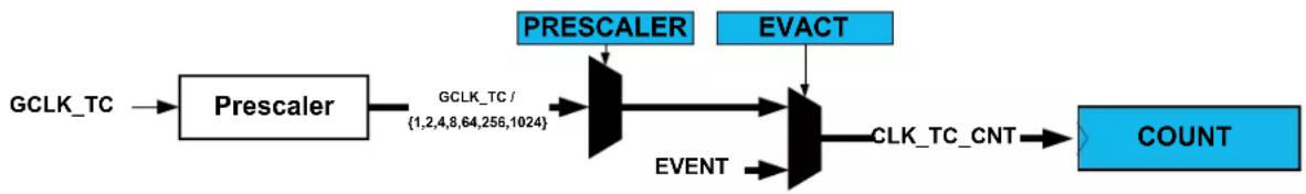
flowchart
graph LR
    A["GCLK_TC"] --> B["Prescaler"]
    B --> C["GCLK_TC / {1,2,4,8,64,256,1024}"]
    C --> D["PREScaler"]
    D --> E["EVACT"]
    D --> F["EVENT"]
    F --> G["CLK_TC_CNT"]
    G --> H["COUNT"]
34.6.2.4 Counter Mode
The counter mode is selected by the Mode bit group in the Control A register (CTRLA.MODE). By default, the counter is enabled in the 16-bit counter resolution. Three counter resolutions are available:
- COUNT8: The 8-bit TC has its own Period Value and Period Buffer Value registers (PER and PERBUF).
- COUNT16: 16-bit is the default counter mode. There is no dedicated period register in this mode.
- COUNT32: This mode is achieved by pairing two 16-bit TC peripherals. TC0 is paired with TC1, and TC2 is paired with TC3. TC4 does not support 32-bit resolution.
When paired, the TC peripherals are configured using the registers of the even-numbered TC (TC0 or TC2 respectively). The odd-numbered partner (TC1 or TC3 respectively) will act as Client, and the Client bit in the Status register (STATUS.SLAVE) will be set. The register values of a Client will not reflect the registers of the 32-bit counter. Writing to any of the Client registers will not affect the 32-bit counter. Normal access to the Client COUNT and CCx registers is not allowed.
34.6.2.5 Counter Operations
Depending on the mode of operation, the counter is cleared, reloaded, incremented, or decremented at each TC clock input (CLK_TC_CNT). A counter clear or reload marks the end of the current counter cycle and the start of a new one.
The counting direction is set by the Direction bit in the Control B register (CTRLB.DIR). If this bit is zero the counter is counting up, and counting down if CTRLB.DIR=1. The counter will count up or down for each tick (clock or event) until it reaches TOP or ZERO. When it is counting up and TOP is reached, the counter will be set to zero at the next tick (overflow) and the Overflow Interrupt Flag in the Interrupt Flag Status and Clear register (INTFLAG.OVF) will be set. When it is counting down, the counter is reloaded with the TOP value when ZERO is reached (underflow), and INTFLAG.OVF is set.
INTFLAG.OVF can be used to trigger an interrupt, a DMA request, or an event. An overflow/underflow occurrence (i.e. a compare match with TOP/ZERO) will stop counting if the One-Shot bit in the Control B register is set (CTRLBSET.ONESHOT).
It is possible to change the counter value (by writing directly in the COUNT register) even when the counter is running. When starting the TC, the COUNT value will be either ZERO or TOP (depending on the counting direction set by CTRLBSET.DIR or CTRLBCLR.DIR), unless a different value has been written to it, or the TC has been stopped at a value other than ZERO. The write access has higher priority than count, clear, or reload. The direction of the counter can also be changed during normal operation. See also the figure below.
Figure 34-3. Counter Operation

flowchart
graph TD
    A["COUNT"] --> B["TOP"]
    B --> C["ZERO"]
    C --> D["DIR"]
    style A fill:#f9f,stroke:#333
    style B fill:#ccf,stroke:#333
    style C fill:#cfc,stroke:#333
    style D fill:#fcc,stroke:#333
    note1[""RELOAD" update"] --> B
    note2["CLEAR"] --> B
    note3["COUNT writtenDirection Change"] --> B
    note4["period (T)"] --> B
    note5["COUNT writtenDirection Change"] --> B
Due to asynchronous clock domains, the internal counter settings are written when the synchronization is complete. Normal operation must be used when using the counter as timer base for the capture channels.
34.6.2.5.1 Stop Command and Event Action
A Stop command can be issued from software by using Command bits in the Control B Set register (CTRLBSET.CMD = 0x2, STOP). When a Stop is detected while the counter is running, the counter will be loaded with the starting value (ZERO or TOP, depending on direction set by CTRLBSET.DIR or CTRLBCLR.DIR). All waveforms are cleared and the Stop bit in the Status register is set (STATUS.STOP).
34.6.2.5.2 Re-Trigger Command and Event Action
A re-trigger command can be issued from software by writing the Command bits in the Control B Set register (CTRLBSET.CMD = 0x1, RETRIGGER), or from event when a re-trigger event action is configured in the Event Control register (EVCTRL.EVACT = 0x1, RETRIGGER).
When the command is detected during counting operation, the counter will be reloaded or cleared, depending on the counting direction (CTRLBSET.DIR or CTRLBCLR.DIR). When the re-trigger command is detected while the counter is stopped, the counter will resume counting from the current value in the COUNT register.
Note: When a re-trigger event action is configured in the Event Action bits in the Event Control register (EVCTRL.EVACT=0x1, RETRIGGER), enabling the counter will not start the counter. The counter will start on the next incoming event and restart on corresponding following event.
34.6.2.5.3 Count Event Action
The TC can count events. When an event is received, the counter increases or decreases the value, depending on direction settings (CTRLBSET.DIR or CTRLBCLR.DIR). The count event action can be selected by the Event Action bit group in the Event Control register (EVCTRL.EVACT=0x2, COUNT).
34.6.2.5.4 Start Event Action
The TC can start counting operation on an event when previously stopped. In this configuration, the event has no effect if the counter is already counting. When the peripheral is enabled, the counter operation starts when the event is received or when a re-trigger software command is applied.
The Start TC on Event action can be selected by the Event Action bit group in the Event Control register (EVCTRL.EVACT=0x3, START).
34.6.2.6 Compare Operations
By default, the Compare/Capture channel is configured for compare operations.
When using the TC and the Compare/Capture Value registers (CCx) for compare operations, the counter value is continuously compared to the values in the CCx registers. This can be used for timer or for waveform operation.
The Channel x Compare Buffer (CCBUFx) registers provide double buffer capability. The double buffering synchronizes the update of the CCx register with the buffer value at the UPDATE condition or a forced update command (CTRLBSET.CMD=UPDATE). For further details, refer to 34.6.2.7. Double Buffering. The synchronization prevents the occurrence of odd-length, non-symmetrical pulses and ensures glitch-free output.
34.6.2.6.1 Waveform Output Operations
The compare channels can be used for waveform generation on output port pins. To make the waveform available on the connected pin, the following requirements must be fulfilled:
- Choose a waveform generation mode in the Waveform Generation Operation bit in Waveform register (WAVE.WAVEGEN).
-
Optionally invert the waveform output WO[x] by writing the corresponding Output Waveform x Invert Enable bit in the Driver Control register (DRVCTRL.INVENx).
-
Configure the pins with the I/O Pin Controller. Refer to 28. PORT - I/O Pin Controller for details.
The counter value is continuously compared with each CCx value. On a comparison match, the Match or Capture Channel x bit in the Interrupt Flag Status and Clear register (INTFLAG.MCx) will be set on the next zero-to-one transition of CLK_TC_CNT (see Normal Frequency Operation). An interrupt/and or event can be generated on comparison match if enabled. The same condition generates a DMA request.
There are four waveform configurations for the Waveform Generation Operation bit group in the Waveform register (WAVE.WAVEGEN). This will influence how the waveform is generated and impose restrictions on the top value. The configurations are:
• Normal frequency (NFRQ)
- Match frequency (MFRQ)
• Normal pulse-width modulation (NPWM)
- Match pulse-width modulation (MPWM)
When using NPWM or NFRQ configuration, the TOP will be determined by the counter resolution. In 8-bit counter mode, the Period register (PER) is used as TOP, and the TOP can be changed by writing to the PER register. In 16- and 32-bit counter mode, TOP is fixed to the maximum (MAX) value of the counter.
34.6.2.6.2 Normal Frequency Generation (NFRQ)
For Normal Frequency Generation, the period time (T) is controlled by the period register (PER) for 8-bit counter mode and MAX for 16- and 32-bit mode. The waveform generation output (WO[x]) is toggled on each compare match between COUNT and CCx, and the corresponding Match or Capture Channel x Interrupt Flag (INTFLAG.MCx) will be set.
Figure 34-4. Normal Frequency Operation
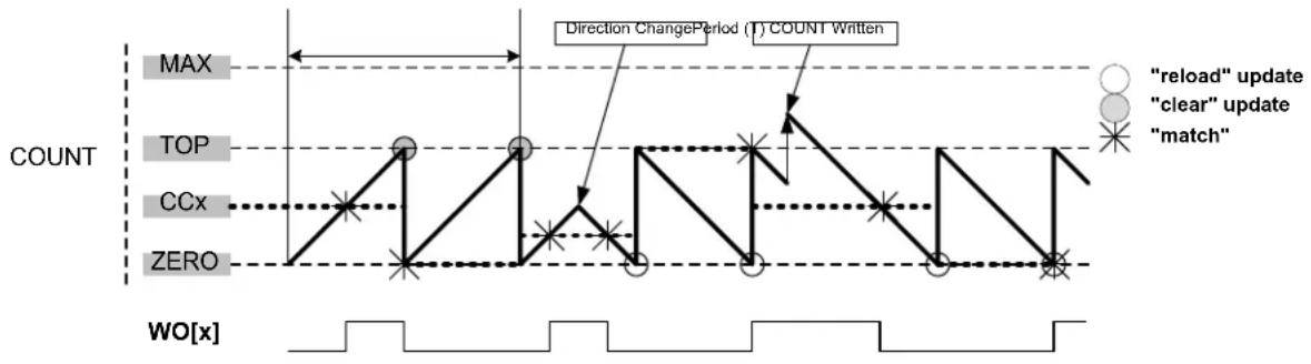
flowchart
graph TD
    A["Direction Change Period (T) COUNT Written"] --> B[""reload" update"]
    A --> C[""clear" update"]
    A --> D["match"]
    E["COUNT"] --> F["TOP"]
    F --> G["CCx"]
    G --> H["ZERO"]
    I[""WO[x"]" --> J["Waveform with horizontal lines"]
    style A fill:#f9f,stroke:#333
    style B fill:#ccf,stroke:#333
    style C fill:#ccf,stroke:#333
    style D fill:#ccf,stroke:#333
    style E fill:#fff,stroke:#333
    style F fill:#fff,stroke:#333
    style G fill:#fff,stroke:#333
    style H fill:#fff,stroke:#333
    style I fill:#fff,stroke:#333
34.6.2.6.3 Match Frequency Generation (MFRQ)
For Match Frequency Generation, the period time (T) is controlled by the CC0 register instead of PER or MAX. WO[0] toggles on each update condition.
Figure 34-5. Match Frequency Operation
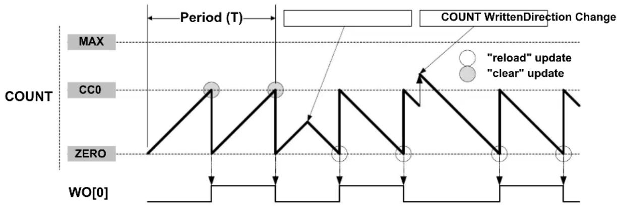
flowchart
graph TD
    A["Period (T)"] --> B["COUNT"]
    B --> C[""RELOAD" update"]
    B --> D[""CLEAR" update"]
    C --> E["Count WrittenDirection Change"]
    D --> E
    style A fill:#f9f,stroke:#333
    style B fill:#ccf,stroke:#333
    style C fill:#cfc,stroke:#333
    style D fill:#fcc,stroke:#333
    style E fill:#ffc,stroke:#333
34.6.2.6.4 Normal Pulse-Width Modulation Operation (NPWM)
NPWM uses single-slope PWM generation.
For single-slope PWM generation, the period time (T) is controlled by the TOP value, and CCx controls the duty cycle of the generated waveform output. When up-counting, the WO[x] is set at start or compare match between the COUNT and TOP values, and cleared on compare match between COUNT and CCx register values. When down-counting, the WO[x] is cleared at start or compare match between the COUNT and ZERO values, and set on compare match between COUNT and CCx register values.
The following equation calculates the exact resolution for a single-slope PWM ( R_PWM_SS ) waveform:
$$ R _ {\mathrm {PWM_ {S} S}} = \frac {\log (\mathrm{TOP} + 1)}{\log (2)} $$
The PWM frequency ( f_PWM_SS ) depends on TOP value and the peripheral clock frequency ( f_GCLK_TCC ), and can be calculated by the following equation:
$$ f _ {\text { PWM_SS }} = \frac {f _ {\text { GCLK_TC }}}{\mathrm{N} (\mathrm{TOP} + 1)} $$
Where N represents the prescaler divider used (1, 2, 4, 8, 16, 64, 256, 1024).
34.6.2.6.5 Match Pulse-Width Modulation Operation (MPWM)
In MPWM, the output of WO[1] is depending on CC1 as shown in the figure below. On on every overflow/underflow, a one-TC-clock-cycle negative pulse is put out on WO[0] (not shown in the figure).
Figure 34-6. Match PWM Operation
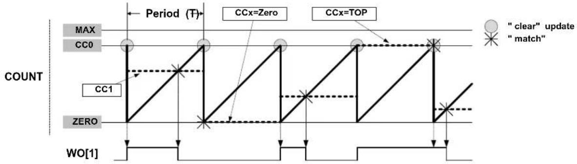
flowchart
graph TD
    A["Period (T)"] --> B["CCx=Zero"]
    A --> C["CCx=TOP"]
    D["COUNT"] --> E["CC0"]
    E --> F["CC1"]
    F --> G["ZERO"]
    G --> H["WO[1"]]
    I[""clear" update"] --> J["match"]
    style A fill:#f9f,stroke:#333
    style B fill:#ccf,stroke:#333
    style C fill:#ccf,stroke:#333
    style D fill:#fff,stroke:#333
    style E fill:#fff,stroke:#333
    style F fill:#fff,stroke:#333
    style G fill:#fff,stroke:#333
    style H fill:#fff,stroke:#333
The table below shows the update counter and overflow event/interrupt generation conditions in different operation modes.
Table 34-3. Counter Update and Overflow Event/interrupt Conditions in TC
| Name Operation TOP Update Output Waveform | OVFIF/Event | ||||||
| On Match On Update Up Down | |||||||
| NFRQ | Normal Frequency | PER | TOP/ ZERO | Toggle | Stable | TOP | ZERO |
| MFRQ | Match Frequency | CC0 | TOP/ ZERO | Toggle | Stable | TOP | ZERO |
| NPWM | Single-slope PWM | PER | TOP/ ZERO | See description above. | TOP | ZERO | |
| MPWM | Single-slope PWM | CC0 | TOP/ ZERO | Toggle | Toggle | TOP | ZERO |
34.6.2.7 Double Buffering
The Compare Channels (CCx) registers, and the Period (PER) register in 8-bit mode are double buffered. Each buffer register has a buffer valid bit (CCBUFVx or PERBUFV) in the STATUS register, which indicates that the buffer register contains a new valid value that can be copied into the corresponding register. As long as the respective buffer valid status flag (PERBUFV or CCBUFVx) are set to '1', related syncbusy bits are set (SYNCBUSY.PER or SYNCBUSY.CCx), a write to the respective PER/PERBUF or CCx/CCBUFx registers will generate a PAC error, and access to the respective PER or CCx register is invalid.
When the buffer valid flag bit in the STATUS register is '1' and the Lock Update bit in the CTRLB register is set to '0', (writing CTRLBCLR.LUPD to '1'), double buffering is enabled: the data from buffer registers will be copied into the corresponding register under hardware UPDATE conditions, then the buffer valid flags bit in the STATUS register are automatically cleared by hardware.
Note: The software update command (CTRLBSET.CMD=0x3) is acting independently of the LUPD value.
A compare register is double buffered as in the following figure.
Figure 34-7. Compare Channel Double Buffering
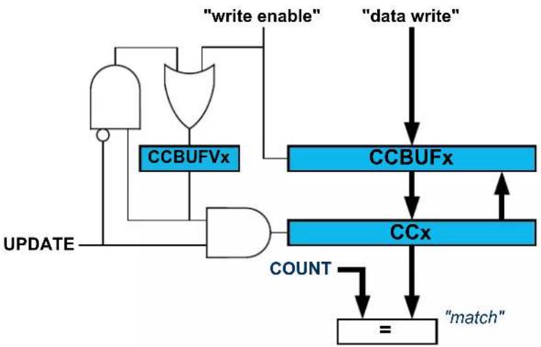
flowchart
graph TD
    A["CCBUFx"] -->|WRITE enable| B["CCBUFx"]
    C["CCx"] -->|COUNT| D["="]
    B -->|"match"| D
    style A fill:#f9f,stroke:#333
    style C fill:#f9f,stroke:#333
    style B fill:#bbf,stroke:#333
    style D fill:#dfd,stroke:#333
Both the registers (PER/CCx) and corresponding buffer registers (PERBUF/CCBUFx) are available in the I/O register map, and the double buffering feature is not mandatory. The double buffering is disabled by writing a '1' to CTRLBSET.LUPD.
Note: In NFRQ, MFRQ or PWM down-counting counter mode (CTRLBSET.DIR=1), when double buffering is enabled (CTRLBCLR.LUPD=1), PERBUF register is continuously copied into the PER independently of update conditions.
Changing the Period
The counter period can be changed by writing a new TOP value to the Period register (PER or CC0, depending on the waveform generation mode), any period update on registers (PER or CCx) is effective after the synchronization delay, whatever double buffering enabling is.
Figure 34-8. Unbuffered Single-Slope Up-Counting Operation
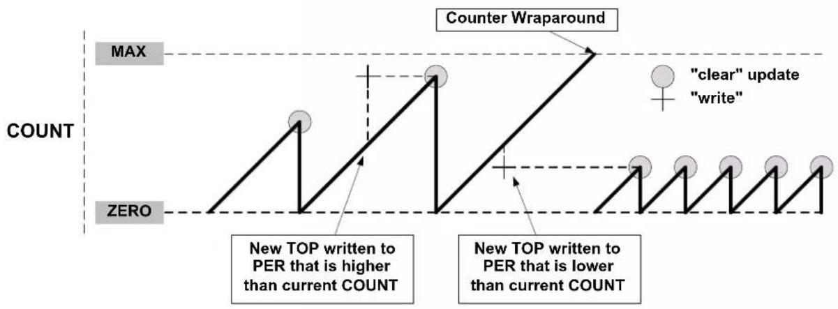
line
| Event Type | Description | Count | |------------|--------------------------------------------------|-------| | New TOP written to PER that is higher than current COUNT | "clear" update | 1 | | New TOP written to PER that is lower than current COUNT | "write" | 1 | | Counter Wraparound | (labeled as MAX) | 1 |A counter wraparound can occur in any operation mode when up-counting without buffering, see Figure 34-8.
COUNT and TOP are continuously compared, so when a new TOP value that is lower than current COUNT is written to TOP, COUNT will wrap before a compare match.
Figure 34-9. Unbuffered Single-Slope Down-Counting Operation
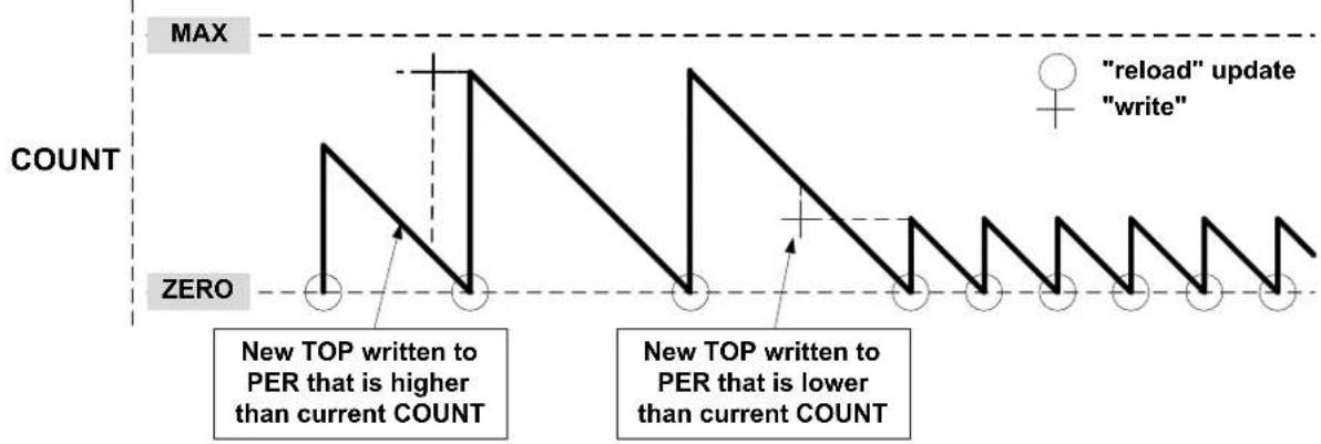
line
| Step | Count | |------|-------| | 1 | 0 | | 2 | 1 | | 3 | 0 | | 4 | 1 | | 5 | 0 | | 6 | 1 | | 7 | 0 | | 8 | 1 | | 9 | 0 | | 10 | 1 | | 11 | 0 | | 12 | 1 | | 13 | 0 | | 14 | 1 | | 15 | 0 | | 16 | 1 | | 17 | 0 | | 18 | 1 | | 19 | 0 | | 20 | 1 | | 21 | 0 | | 22 | 1 | | 23 | 0 | | 24 | 1 | | 25 | 0 | | 26 | 1 | | 27 | 0 | | 28 | 1 | | 29 | 0 | | 30 | 1 | | 31 | 0 | | 32 | 1 | | 33 | 0 | | 34 | 1 | | 35 | 0 | | 36 | 1 | | 37 | 0 | | 38 | 1 | | 39 | 0 | | 40 | 1 | | 41 | 0 | | 42 | 1 | | 43 | 0 | | 44 | 1 | | 45 | 0 | | 46 | 1 | | 47 | 0 | | 48 | 1 | | 49 | 0 | | 50 | 1 | | 51 | 0 | | 52 | 1 | | 53 | 0 | | 54 | 1 | | 55 | 0 | | 56 | 1 | | 57 | 0 | | 58 | 1 | | 59 | 0 | | 60 | 1 | | 61 | 0 | | 62 | 1 | | 63 | 0 | | 64 | 1 | | 65 | 0 | | 66 | 1 | | 67 | 0 | | 68 | 1 | | 69 | 0 | | 70 | 1 | | 71 | 0 | | 72 | 1 | | 73 | 0 | | 74 | 1 | | 75 | 0 | | 76 | 1 | | 77 | 0 | | 78 | 1 | | 79 | 0 | | 80 | 1 | | 81 | 0 | | 82 | 1 | | 83 | 0 | | 84 | 1 | | 85 | 0 | | 86 | 1 | | 87 | 0 | | 88 | 1 | | 89 | 0 | | 90 | 1 | | 91 | 0 | | 92 | 1 | | 93 | 0 | | 94 | 1 | | 95 | 0 | | 96 | 1 | | 97 | 0 | | 98 | 1 | | 99 | 0 | | Max (top) | MAX | | Zero (bottom) | ZERO (bottom) | | New TOP written to PER that is higher than current COUNT (top) | (top) | | New TOP written to PER that is lower than current COUNT (bottom) (top) | (bottom) | | "reload" update (top) / "write" (top) (top) (top) (top) (top) (top) (top) (top) (top) (top) (top) (top) (top) (top) (top) (top) (top) (top) (top) (top) (top) (top) (top) (top) (top) (top) (top) (top) (top) (top) (top) (top) (top) (top) / "reload" update (top) / "write" (top) (top) (top) (top) / "reload" update (top) / "write" (top) (top) (top) / "reload" update (top) / "write" (top) / "reload" update (top) / "write" (top) / "reload" update (top) / "write" (top) / "reload" update (top) / "write" (top) / "reload" update (top) / "write" (top) / "reload" update (top) / "write" (top) / "reload" update (top) / "write" (top) / "reload" update (up to top) / "write" (up to top) / "reload" update (up to top) / "write" (up to top) / "reload" update (up to top) / "write" (up to top) / "reload" update (up to top) / "write" (up to top) / "reload" update (up to top) / "write" (up to top) / "reload" update (up to top) / "write" (up to top) / "reload", up to bottom line; 'remove' update/ write/ write/ write/ write/ write/ write/ write/ write/ write/ write/ write/ write/ write/ write/ write/ write/ write/ write/ write/ write/ write/ write/ write/ write/ write/ write/ write/ write/ write/ write/ write/ write/ write/ write/ write/ write/ write/ write/ write/ write/ write/ write/ write/ write/ write/ write/ write/ write/ write/ write/ Write, up to bottom line; 'remove' update/ write/ write/ write/ write/ write/ write/ write/ write/ write/ write/ write/ write/ write/ write/ write/ write/ write/ write/ write/ write/ write/ write/ write/ write/ write/ write/ write/ write/ Write, up to bottom line; 'remove' update/ write/ write/ write/ write/ write/ write/ write/ write/ write/ write/ write/ write/ write/ write/ write/ Write, up to bottom line; 'remove' update/ write/ Write, Write, Write, Write, Write, Write, Write, Write, Write, Write, Write, Write, Write, Write, Write, Write, Write, Write, Write, Write, Write, Write, Write, Write, Write, Write, Write, Write, Write, Write, Write, Write, Write, Write, Write, Write, Write, Write, Write, Write, Write, Write, Write, Write, Write, Write, Write, Write, Write, Write, WriteWhen double buffering is used, the buffer can be written at any time and the counter will still maintain correct operation. The period register is always updated on the update condition, as shown in Figure 34-10. This prevents wraparound and the generation of odd waveforms.
Figure 34-10. Changing the Period Using Buffering

line
| Event Description | Count | | ----------------- | ----- | | New TOP written to PER that is higher than current COUNT | 100 | | New TOP written to PER that is lower than current COUNT | 50 |34.6.2.8 Capture Operations
To enable and use capture operations, the corresponding Capture Channel x Enable bit in the Control A register (CTRLA.CAPTENx) must be written to '1'.
A capture trigger can be provided by input event line TC_EV or by asynchronous IO pin WO[x] for each capture channel or by a TC event. To enable the capture from input event line, Event Input Enable bit in the Event Control register (EVCTRL.TCEI) must be written to '1'. To enable the capture from the IO pin, the Capture On Pin x Enable bit in CTRLA register (CTRLA.COPENx) must be written to '1'.
Notes:
- Capture on I/Os is only possible in "Event" and "Time-Stamp" capture action modes. Other modes can only use internal events (If I/Os toggling is needed in other modes, then the I/Os edge should be configured for generating internal events).
- Capture on an event from the Event System is possible in "Event", "PPW/PWP/PW" and "TimeStamp" capture modes. In this case, the event system channels must be configured to operate in asynchronous mode of operation.
- Depending on CTRLA.COPENx, channels can be configured for I/Os or internal event capture (both are mutually exclusive). One channel can be configured for I/Os capture while the other uses internal event capture.
By default, a capture operation is done when a rising edge is detected on the input signal. Capture on falling edge is available, its activation is depending on the input source:
- When the channel is used with a I/O pin, write a '1' to the corresponding Invert Enable bit in the Drive Control register (DRVCTRL.INVENx).
- When the channel is counting events from the Event System, write a '1' to the TC Event Input Invert Enable bit in Event Control register (EVCTRL.TCINV).
For input capture, the buffer register and the corresponding CCx act like a FIFO. When CCx is empty or read, any content in CCBUFx is transferred to CCx. The buffer valid flag is passed to set the CCx interrupt flag (IF) and generate the optional interrupt, event or DMA request. The CCBUFx register value can't be read, all captured data must be read from the CCx register.
Figure 34-11. Capture Double Buffering
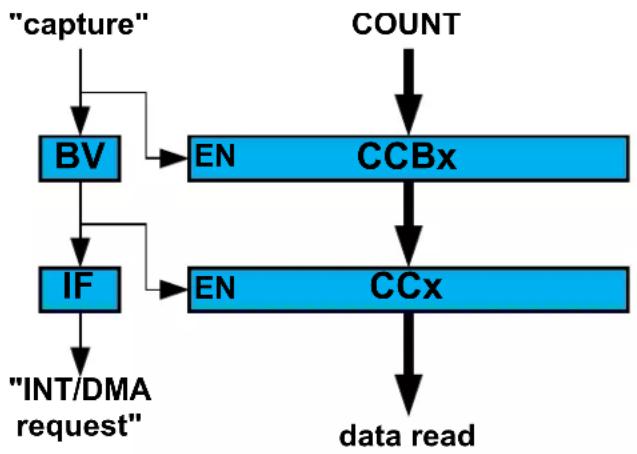
flowchart
graph TD
    A["capture"] --> B["BV"]
    B --> C["EN"]
    C --> D["CCBx"]
    D --> E["COUNT"]
    B --> F["IF"]
    F --> G["EN"]
    G --> H["CCx"]
    H --> I["data read"]
    F --> J["INT/DMA request"]
For input capture, the buffer register and the corresponding CCx act like a FIFO. When CCx is empty or read, any content in CCBUFx is transferred to CCx. The buffer valid flag is passed to set the CCx interrupt flag (IF) and generate the optional interrupt, event or DMA request. CCBUFx register value can't be read, all captured data must be read from CCx register.
34.6.2.8.1 Event Capture Action on Events or I/Os
The compare/capture channels can be used as input capture channels to capture events from the Event System or from the corresponding IO pin, and give them a timestamp. This mode is selected when EVCTRL.EVACT is configured either as OFF, RETRIGGER, COUNT or START. The following figure shows four capture events for one capture channel.
Figure 34-12. Input Capture Timing
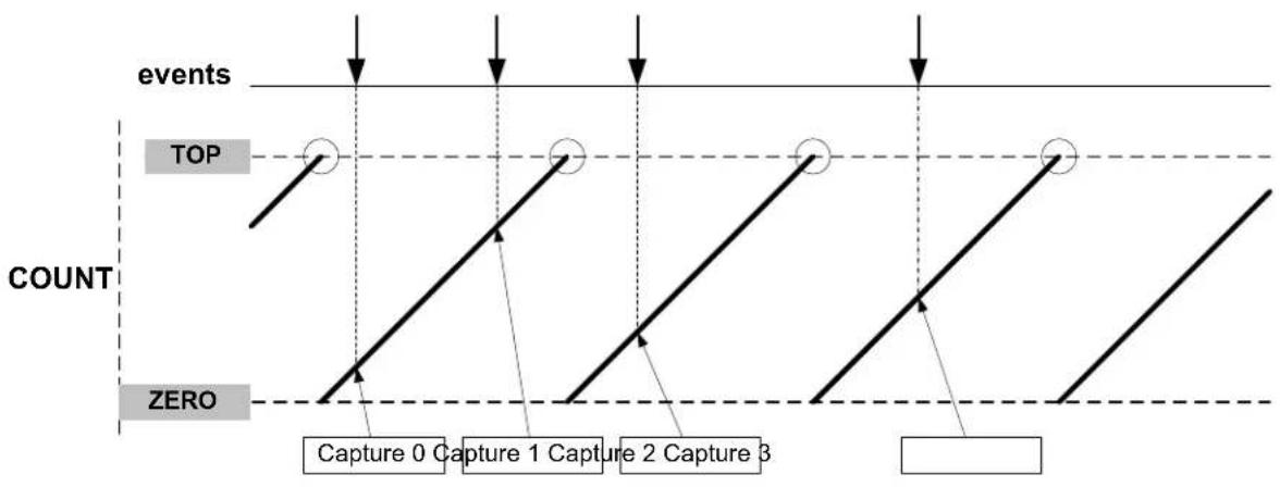
flowchart
graph TD
    A["events"] --> B["TOP"]
    B --> C["COUNT"]
    C --> D["ZERO"]
    D --> E["Capture 0 Capture 1 Capture 2 Capture 3"]
The TC can detect capture overflow of the input capture channels: When a new capture event is detected while the Capture Interrupt flag (INTFLAG.MCx) is still set, the new timestamp will not be stored and INTFLAG.ERR will be set.
34.6.2.8.2 Period and Pulse-Width (PPW/PWP) Capture Action on Events
The TC can perform two input captures and restart the counter on one of the edges. This enables the TC to measure the pulse width and period and to characterize the frequency f and duty cycle of an input signal:
$$ f = \frac {1}{T} $$
$$ \text { dutyCycle } = \frac {t _ {p}}{T} $$
Figure 34-13. PWP Capture

line
| Signal | Value | |-----------------|-------| | Period (T) | 10 | | Pulsewidth (tp) | 10 | | MAX | 10 | | COUNT | 10 | | ZERO | 0 | | CC0 CC0 CC1CC1 | 10 | | "capture" | 10 |Selecting PWP in the Event Action bit group in the Event Control register (EVCTRL.EVACT) enables the TC to perform one capture action on the rising edge and the other one on the falling edge. The period T will be captured into CC1 and the pulse width t_p in CC0. EVCTRL.EVACT=PPW (period and pulse-width) offers identical functionality, but will capture T into CC0 and t_p into CC1.
The TC Event Input Invert Enable bit in the Event Control register (EVCTRL.TCINV) is used to select whether the wraparound should occur on the rising edge or the falling edge. If EVCTRL.TCINV=1, the wraparound will happen on the falling edge.
The TC can detect capture overflow of the input capture channels: When a new capture event is detected while the Capture Interrupt flag (INTFLAG.MCx) is still set, the new timestamp will not be stored and INTFLAG.ERR will be set.
Note: The corresponding capture is working only if the channel is enabled in capture mode (CTRLA.CAPTENx=1). Consequently, both channels must be enabled in order to fully characterize the input.
34.6.2.8.3 Pulse-Width (PW) Capture Action on Events
The TC performs the input capture on the falling edge of the input signal. When the edge is detected, the counter value is cleared and the TC stops counting. When a rising edge is detected on the input signal, the counter restarts the counting operation. To enable the operation on opposite edges, the input signal to capture must be inverted (refer to DRVCTRL.INVENx or EVCTRL.TCINV).
Figure 34-14. Pulse-Width Capture on Channel 0
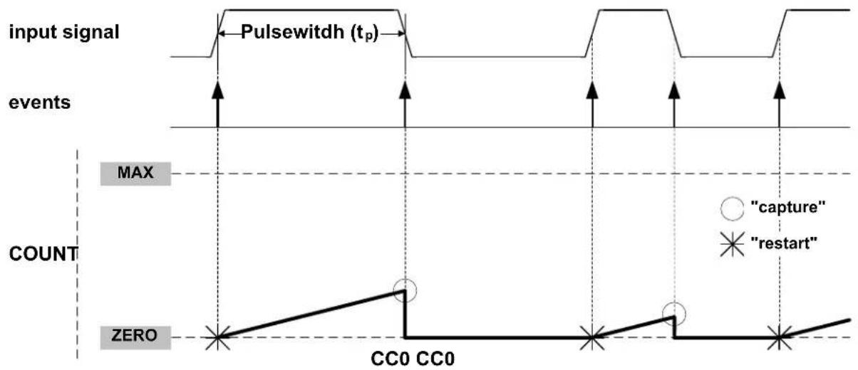
other
| Event Type | Time Segment | Event Description | |------------|--------------|--------------------------| | Input Signal | t_p | Pulsewidth (t_p) | | Events | Max | Peaks at t_p | | COUNT | Zero | Zero event | | CC0 | CC00 | CC00 capture | | CC0 | CC00 restart | Restart |The TC can detect capture overflow of the input capture channels: When a new capture event is detected while the Capture Interrupt flag (INTFLAG.MCx) is still set, the new timestamp will not be stored and INTFLAG.ERR will be set.
34.6.3 Additional Features
34.6.3.1 One-Shot Operation
When one-shot is enabled, the counter automatically stops on the next counter overflow or underflow condition. When the counter is stopped, the Stop bit in the Status register (STATUS.STOP) is automatically set and the waveform outputs are set to zero.
One-shot operation is enabled by writing a '1' to the One-Shot bit in the Control B Set register (CTRLBSET.ONESHOT), and disabled by writing a '1' to CTRLBCLR.ONESHOT. When enabled, the TC will count until an overflow or underflow occurs and stops counting operation. The one-shot
operation can be restarted by a re-trigger software command, a re-trigger event, or a start event. When the counter restarts its operation, STATUS.STOP is automatically cleared.
34.6.3.2 Time-Stamp Capture on Events or I/Os
This feature is enabled when the Capture Time Stamp (STAMP) Event Action in Event Control register (EVCTRL.EVACT) is selected. The counter TOP value must be smaller than MAX.
When a capture event is detected, the COUNT value is copied into the corresponding Channel x Compare/Capture Value (CCx) register. In case of an overflow, the MAX value is copied into the corresponding CCx register.
When a valid captured value is present in the capture channel register, the corresponding Capture Channel x Interrupt Flag (INTFLAG.MCx) is set.
The timer/counter can detect capture overflow of the input capture channels: When a new capture event is detected while the Capture Channel interrupt flag (INTFLAG.MCx) is still set, the new timestamp will not be stored and INTFLAG.ERR will be set.
Figure 34-15. Time-Stamp
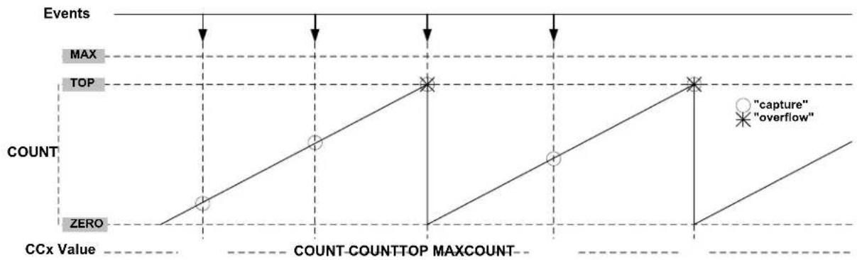
flowchart
graph TD
    A["CCx Value"] --> B["COUNT"]
    B --> C["TOP"]
    C --> D["CALL"]
    D --> E["TIME"]
    E --> F["TIME"]
    style A fill:#f9f,stroke:#333
    style B fill:#ccf,stroke:#333
    style C fill:#cfc,stroke:#333
    style D fill:#fcc,stroke:#333
    style E fill:#cff,stroke:#333
    style F fill:#ffc,stroke:#333
34.6.4 DMA Operation
The TC can generate the following DMA requests:
• Overflow (OVF): the request is set when an update condition (overflow, underflow or re-trigger) is detected, the request is cleared by hardware on DMA acknowledge.
- Match or Capture Channel x (MCx): for a compare channel, the request is set on each compare match detection, the request is cleared by hardware on DMA acknowledge. For a capture channel, the request is set when valid data is present in the CCx register, and cleared when CCx register is read.
34.6.5 Interrupts
The TC has the following interrupt sources:
• Overflow/Underflow (OVF)
- Match or Capture Channel x (MCx)
• Capture Overflow Error (ERR)
Each interrupt source has an interrupt flag associated with it. The interrupt flag in the Interrupt Flag Status and Clear register (INTFLAG) is set when the interrupt condition occurs.
Each interrupt can be individually enabled by writing a '1' to the corresponding bit in the Interrupt Enable Set register (INTENSET), and disabled by writing a '1' to the corresponding bit in the Interrupt Enable Clear register (INTENCLR).
An interrupt request is generated when the interrupt flag is set and the corresponding interrupt is enabled. The interrupt request remains active until either the interrupt flag is cleared, the interrupt is disabled, or the TC is reset. See INTFLAG for details on how to clear interrupt flags.
The TC has one common interrupt request line for all the interrupt sources. The user must read the INTFLAG register to determine which interrupt condition is present.
Note that interrupts must be globally enabled for interrupt requests to be generated. Refer to the Nested Vector Interrupt Controller for details.
34.6.6 Events
The TC can generate the following output events:
• Overflow/Underflow (OVF)
- Match or Capture Channel x (MCx)
Writing a '1' to an Event Output bit in the Event Control register (EVCTRL.MCEOx) enables the corresponding output event. The output event is disabled by writing EVCTRL.MCEOx=0.
One of the following event actions can be selected by the Event Action bit group in the Event Control register (EVCTRL.EVACT):
- Disable event action (OFF)
- Start TC (START)
• Re-trigger TC (RETRIGGER)
• Count on event (COUNT)
• Capture time stamp (STAMP)
• Capture Period (PPW and PWP)
• Capture Pulse Width (PW)
Writing a '1' to the TC Event Input bit in the Event Control register (EVCTRL.TCEI) enables input events to the TC. Writing a '0' to this bit disables input events to the TC. The TC requires only asynchronous event inputs. For further details on how configuring the asynchronous events, refer to 29. EVSYS - Event System.
34.6.7 Sleep Mode Operation
The TC can be configured to operate in any sleep mode. To be able to run in standby, the RUNSTDBY bit in the Control A register (CTRLA.RUNSTDBY) must be '1'. This peripheral can wake up the device from any sleep mode using interrupts or perform actions through the Event System.
If the On Demand bit in the Control A register (CTRLA.ONDEMAND) is written to '1', the module stops requesting its peripheral clock when the STOP bit in STATUS register (STATUS.STOP) is set to '1'. When a re-trigger or start condition is detected, the TC requests the clock before the operation starts.
34.6.8 Synchronization
Due to asynchronicity between the main clock domain and the peripheral clock domains, some registers need to be synchronized when written or read.
The following bits are synchronized when written:
- Software Reset and Enable bits in Control A register (CTRLA.SWRST and CTRLA.ENABLE)
- Capture Channel Buffer Valid bit in STATUS register (STATUS.CCBUFVx)
The following registers are synchronized when written:
• Control B Clear and Control B Set registers (CTRLBCLR and CTRLBSET)
• Count Value register (COUNT)
- Period Value and Period Buffer Value registers (PER and PERBUF)
- Channel x Compare/Capture Value and Channel x Compare/Capture Buffer Value registers (CCx and CCBUFx)
The following registers are synchronized when read:
- Count Value register (COUNT): synchronization is done on demand through READSYNC command (CTRLBSET.CMD).
Required write-synchronization is denoted by the "Write-Synchronized" property in the register description.
Required read-synchronization is denoted by the "Read-Synchronized" property in the register description.
34.7 Register Description
Registers can be 8, 16, or 32 bits wide. Atomic 8-, 16- and 32-bit accesses are supported. In addition, the 8-bit quarters and 16-bit halves of a 32-bit register, and the 8-bit halves of a 16-bit register can be accessed directly.
Some registers are optionally write-protected by the Peripheral Access Controller (PAC). Optional PAC write-protection is denoted by the "PAC Write-Protection" property in each individual register description. For details, refer to Register Access Protection.
Some registers are synchronized when read and/or written. Synchronization is denoted by the "Write-Synchronized" or the "Read-Synchronized" property in each individual register description. For details, refer to Synchronization.
Some registers are enable-protected, meaning they can only be written when the peripheral is disabled. Enable-protection is denoted by the "Enable-Protected" property in each individual register description.
34.8 Register Summary - 8-bit Mode
| Offset | Name Bit Pos. 7 | 6 | 5 | 4 | 3 | 2 | 1 | 0 | ||||||||
| 0x00 | CTRLA | 7:0 | ONDEMAND RUNSTDBY PRESCSYNC[1:0] MODE[1:0] ENABLE SWRST | |||||||||||||
| 15:8 | ALOCK PRESCALER[2:0] | |||||||||||||||
| 23:16 | COPEN1 | COPEN0 | CAPTEN1 | CAPTENO | ||||||||||||
| 31:24 | ||||||||||||||||
| 0x04 | CTRLBCLR | 7:0 | CMD[2:0] | ONESHOT | LUPD | DIR | ||||||||||
| 0x05 | CTRLBSET | 7:0 | CMD[2:0] | ONESHOT | LUPD | DIR | ||||||||||
| 0x06 | EVCTRL | 7:0 | TCEI | TCINV | EVACT[2:0] | |||||||||||
| 15:8 | MCEO1 MCEO0 | OVFEO | ||||||||||||||
| 0x08 | INTENCLR | 7:0 | MC1 | MC0 | ERR | OVF | ||||||||||
| 0x09 | INTENSET | 7:0 | MC1 | MC0 | ERR | OVF | ||||||||||
| 0x0A | INTFLAG | 7:0 | MC1 | MC0 | ERR | OVF | ||||||||||
| 0x0B | STATUS | 7:0 | CCBUFV1 | CCBUFV0 | PERBUFV | SLAVE | STOP | |||||||||
| 0x0C | WAVE | 7:0 | WAVEGEN[1:0] | |||||||||||||
| 0x0D | DRVCTRL | 7:0 | INVEN1 | INVEN0 | ||||||||||||
| 0x0E | Reserved | |||||||||||||||
| 0x0F | DBGCTRL | 7:0 | DBGRUN | |||||||||||||
| 0x10 | SYNCBUSY | 7:0 | CC1 | CC0 | PER | COUNT | STATUS | CTRLB | ENABLE | SWRST | ||||||
| 15:8 | ||||||||||||||||
| 23:16 | ||||||||||||||||
| 31:24 | ||||||||||||||||
| 0x14 | COUNT 7:0 | COUNT[7:0] | ||||||||||||||
| 0x15...0x1A | Reserved | |||||||||||||||
| 0x1B | PER | 7:0 | PER[7:0] | |||||||||||||
| 0x1C | CC0 | 7:0 | CC[7:0] | |||||||||||||
| 0x1D | CC1 | 7:0 | CC[7:0] | |||||||||||||
| 0x1E...0x2E | Reserved | |||||||||||||||
| 0x2F | PERBUF | 7:0 | PERBUF[7:0] | |||||||||||||
| 0x30 | CCBUF0 7:0 | CCBUF[7:0] | ||||||||||||||
| 0x31 | CCBUF1 7:0 | CCBUF[7:0] | ||||||||||||||
34.8.1 Control A
Name: CTRLA
Offset: 0x00
Reset: 0x00000000
Property: PAC Write-Protection, Write-Synchronized bits, Enable-Protected bits
| Bit 31 30 29 28 27 26 25 24 | |||||||
| Access Reset | |||||||
| Bit 23 22 21 20 19 18 17 16 | |||||||
| COPEN1 COPEN0 | CAPTEN1 CAPTENO | ||||||
| Access Reset | R/W | R/W | R/W | ||||
| 0 | 0 | 0 | |||||
| Bit 15 14 13 12 11 10 | 9 | 8 | |||||
| ALOCK | PRESCALER[2:0] | ||||||
| Access Reset | R/W | R/W | R/W | ||||
| 0 | 0 | 0 | |||||
| Bit | 7 | 6 | 5 | 4 | 3 | 2 | 1 |
| ONDEMAND | RUNSTDBY | PRESCSYNC[1:0] | MODE[1:0] | ENABLE | |||
| Access Reset | R/W | R/W | R/W | R/W | R/W | R/W | R/W |
| 0 | 0 | 0 | 0 | 0 | 0 | 0 | |
Bits 20, 21 - COPENx Capture On Pin x Enable
Bit x of COPEN[13:0] selects the trigger source for capture operation, either events or I/O pin input.
Note: This bit field is enable-protected. This bit field is not write-synchronized.
| Value | Description |
| 0 | Event from Event System is selected as trigger source for capture operation on channel x. |
| 1 | I/O pin is selected as trigger source for capture operation on channel x. |
Bits 16, 17 - CAPTENx Capture Channel x Enable
Bit x of CAPTEN[31:0] selects whether channel x is a capture or a compare channel.
Note: This bit field is enable-protected. This bit field is not write-synchronized.
| Value | Description |
| 0 | CAPTEN disables capture on channel x. |
| 1 | CAPTEN enables capture on channel x. |
Bit 11 - ALOCK Auto Lock
When this bit is set, Lock bit update (LUPD) is set to '1' on each overflow/underflow or re-trigger event.
Note: This bit is enable-protected. This bit is not write-synchronized.
| Value | Description |
| 0 | The LUPD bit is not affected on overflow/underflow, and re-trigger event. |
| 1 | The LUPD bit is set on each overflow/underflow or re-trigger event. |
Bits 10:8 - PRESCALER[2:0] Prescaler
These bits select the counter prescaler factor.
Note: This bit field is enable-protected. This bit field is not write-synchronized.
| Value Name | Description | |
| 0x0 | DIV1 Prescaler: GCLK_TC | |
| 0x1 | DIV2 Prescaler: GCLK_TC/2 | |
| 0x2 | DIV4 Prescaler: GCLK_TC/4 | |
| 0x3 | DIV8 Prescaler: GCLK_TC/8 | |
| 0x4 | DIV16 Prescaler: GCLK_TC/16 | |
| 0x5 | DIV64 Prescaler: GCLK_TC/64 | |
| 0x6 | DIV256 Prescaler: GCLK_TC/256 | |
| 0x7 | DIV1024 Prescaler: GCLK_TC/1024 | |
Bit 7 - ONDEMAND Clock On Demand
This bit selects the clock requirements when the TC is stopped.
In standby mode, if the Run in Standby bit (CTRLA.RUNSTDBY) is '0', ONDEMAND is forced to '0'.
Note: This bit is enable-protected. This bit is not write-synchronized.
| Value Description | |
| 0 | The On Demand is disabled. If On Demand is disabled, the TC will continue to request the clock when its operation is stopped (STATUS.STOP=1). |
| 1 | The On Demand is enabled. When On Demand is enabled, the stopped TC will not request the clock. The clock is requested when a software re-trigger command is applied or when an event with start/re-trigger action is detected. |
Bit 6 - RUNSTDBY Run in Standby
This bit is used to keep the TC running in standby mode.
Note: This bit is enable-protected. This bit is not write-synchronized.
| Value Description | |
| 0 | The TC is halted in standby. |
| 1 | The TC continues to run in standby. |
Bits 5:4 - PRESCSYNC[1:0] Prescaler and Counter Synchronization
These bits select whether the counter should wrap around on the next GCLK_TCx clock or the next prescaled GCLK_TCx clock. It also makes it possible to reset the prescaler.
Note: This bit field is enable-protected. This bit field is not write-synchronized.
| Value Name | Description |
| 0x0 | GCLK Reload or reset the counter on next generic clock |
| 0x1 | PRESC Reload or reset the counter on next prescaler clock |
| 0x2 | RESYNC Reload or reset the counter on next generic clock. Reset the prescaler counter |
| 0x3 | - Reserved |
Bits 3:2 - MODE[1:0] Timer Counter Mode
These bits select the counter mode.
Note: This bit field is enable-protected. This bit field is not write-synchronized.
| Value Name | Description | |
| 0x0 | COUNT16 Counter in 16-bit mode | |
| 0x1 | COUNT8 Counter in 8-bit mode | |
| 0x2 | COUNT32 Counter in 32-bit mode | |
| 0x3 | - | Reserved |
Bit 1 - ENABLE Enable
Due to synchronization, there is delay from writing CTRLA. ENABLE until the peripheral is enabled/disabled. The value written to CTRLA. ENABLE will read back immediately, and the ENABLE Synchronization Busy bit in the SYNCBUSY register (SYNCBUSY. ENABLE) will be set. SYNCBUSY. ENABLE will be cleared when the operation is complete.
Notes:
- This bit is not enable-protected.
- This bit is write-synchronized: SYNCBUSY. ENABLE bit must be checked to ensure the CTRLA. ENABLE synchronization is complete.
Value Description
| 0 | The peripheral is disabled. |
| 1 | The peripheral is enabled. |
Bit 0 - SWRST Software Reset
Writing a '0' to this bit has no effect.
Writing a '1' to this bit resets all registers in the TC, except DBGCTRL, to their initial state, and the TC will be disabled.
Writing a '1' to CTRLA.SWRST will always take precedence; all other writes in the same write-operation will be discarded.
Due to synchronization there is a delay from writing CTRLA.SWRST until the reset is complete. CTRLA.SWRST and SYNCBUSY.SWRST will both be cleared when the reset is complete.
Notes:
- This bit is not enable-protected.
- This bit is write-synchronized: SYNCBUSY.SWRST bit must be checked to ensure the CTRLA.SWRST synchronization is complete.
Value Description
| 0 | There is no reset operation ongoing. |
| 1 | The reset operation is ongoing. |
34.8.2 Control B Clear
Name: CTRLBCLR
Offset: 0x04
Reset: 0x00
Property: PAC Write-Protection, Read-Synchronized, Write-Synchronized
This register allows the user to clear bits in the CTRLB register without doing a read-modify-write operation. Changes in this register will also be reflected in the Control B Set register (CTRLBSET).
Bit 76543210
| CMD[2:0] | ONESHOT LUPD DIR | |||||
| Access | R/W R/W R/W | R/W R/W R/W | ||||
| Reset | 0 0 0 | 0 0 0 | ||||
Bits 7:5 - CMD[2:0] Command
These bits are used for software control of the TC. The commands are executed on the next prescaled GCLK_TC clock cycle. When a command has been executed, the CMD bit group will be read back as zero.
Writing 0x0 to these bits has no effect.
Writing a '1' to any of these bits will clear the pending command.
Bit 2 - ONESHOT One-Shot on Counter
This bit controls one-shot operation of the TC.
Writing a '0' to this bit has no effect
Writing a '1' to this bit will disable one-shot operation.
| Value | Description |
| 0 | The TC will wrap around and continue counting on an overflow/underflow condition. |
| 1 | The TC will wrap around and stop on the next underflow/overflow condition. |
Bit 1 - LUPD Lock Update
This bit controls the update operation of the TC buffered registers.
When CTRLB.LUPD is set, no any update of the registers with value of its buffered register is performed on hardware UPDATE condition. Locking the update ensures that all buffer registers are valid before an hardware update is performed. After all the buffer registers are loaded correctly, the buffered registers can be unlocked.
This bit has no effect when input capture operation is enabled.
Writing a '0' to this bit has no effect.
Writing a '1' to this bit will clear the LUPD bit.
| Value | Description |
| 0 | The CCBUFx and PERBUF buffer registers value are copied into CCx and PER registers on hardware update condition. |
| 1 | The CCBUFx and PERBUF buffer registers value are not copied into CCx and PER registers on hardware update condition. |
Bit 0 - DIR Counter Direction
This bit is used to change the direction of the counter.
Writing a '0' to this bit has no effect.
Writing a '1' to this bit will clear the bit and make the counter count up.
| Value | Description |
| 0 | The timer/counter is counting up (incrementing). |
| 1 | The timer/counter is counting down (decrementing). |
34.8.3 Control B Set
Name: CTRLBSET
Offset: 0x05
Reset: 0x00
Property: PAC Write-Protection, Read-synchronized, Write-Synchronized
This register allows the user to set bits in the CTRLB register without doing a read-modify-write operation. Changes in this register will also be reflected in the Control B Clear register (CTRLBCLR).
Bit 76543210
| CMD[2:0] | ONESHOT LUPD DIR | |||||
| Access | R/W R/W R/W | R/W R/W R/W | ||||
| Reset | 0 0 0 | 0 0 0 | ||||
Bits 7:5 - CMD[2:0] Command
These bits are used for software control of the TC. The commands are executed on the next prescaled GCLK_TC clock cycle. When a command has been executed, the CMD bit group will be read back as zero.
Writing 0x0 to these bits has no effect.
Writing a value different from 0x0 to these bits will issue a command for execution.
| Value | Name | Description |
| 0x0 | NONE | No action |
| 0x1 | RETRIGGER | Force a start, restart or retrigger |
| 0x2 | STOP | Force a stop |
| 0x3 | UPDATE | Force update of double buffered registers |
| 0x4 | READSYNC | Force a read synchronization of COUNT |
Bit 2 - ONESHOT One-Shot on Counter
This bit controls one-shot operation of the TC.
Writing a '0' to this bit has no effect.
Writing a '1' to this bit will enable one-shot operation.
| Value | Description |
| 0 | The TC will wrap around and continue counting on an overflow/underflow condition. |
| 1 | The TC will wrap around and stop on the next underflow/overflow condition. |
Bit 1 - LUPD Lock Update
This bit controls the update operation of the TC buffered registers.
When CTRLB.LUPD is set, no any update of the registers with value of its buffered register is performed on hardware UPDATE condition. Locking the update ensures that all buffer registers are valid before an hardware update is performed. After all the buffer registers are loaded correctly, the buffered registers can be unlocked.
Writing a '0' to this bit has no effect.
Writing a '1' to this bit will set the LUPD bit.
This bit has no effect when input capture operation is enabled.
| Value | Description |
| 0 | The CCBUFx and PERBUF buffer registers value are copied into CCx and PER registers on hardware update condition. |
| 1 | The CCBUFx and PERBUF buffer registers value are not copied into CCx and PER registers on hardware update condition. |
Bit 0 - DIR Counter Direction
This bit is used to change the direction of the counter.
Writing a '0' to this bit has no effect
Writing a '1' to this bit will clear the bit and make the counter count up.
Value Description
| 0 | The timer/counter is counting up (incrementing). |
| 1 | The timer/counter is counting down (decrementing). |
34.8.4 Event Control
Name: EVCTRL
Offset: 0x06
Reset: 0x0000
Property: PAC Write-Protection, Enable-Protected
Bit 15 14 13 12 11 10 9 8
| MCEΦ1 MCEO0 | OVFEO | ||||||
| Access Reset | R/W 0 0 | R/W | R/W 0 |
Bit 76543210
| TCEI | TCINV | EVACT[2:0] | ||||||
| Access Reset | R/W | R/W | R/W | R/W | R/W | |||
| 0 0 | 0 0 0 | |||||||
Bits 12, 13 - MCEOx Match or Capture Channel x Event Output Enable [x = 1..0]
These bits enable the generation of an event for every match or capture on channel x.
| Value | Description |
| 0 | Match/Capture event on channel x is disabled and will not be generated. |
| 1 | Match/Capture event on channel x is enabled and will be generated for every compare/capture. |
Bit 8 - OVFEO Overflow/Underflow Event Output Enable
This bit enables the Overflow/Underflow event. When enabled, an event will be generated when the counter overflows/underflows.
| Value | Description |
| 0 | Overflow/Underflow event is disabled and will not be generated. |
| 1 | Overflow/Underflow event is enabled and will be generated for every counter overflow/underflow. |
Bit 5 - TCEI TC Event Enable
This bit is used to enable asynchronous input events to the TC.
| Value | Description |
| 0 | Incoming events are disabled. |
| 1 | Incoming events are enabled. |
Bit 4 - TCINV TC Inverted Event Input Polarity
This bit inverts the asynchronous input event source.
| Value | Description |
| 0 | Input event source is not inverted. |
| 1 | Input event source is inverted. |
Bits 2:0 - EVACT[2:0] Event Action
These bits define the event action the TC will perform on an event.
| Value | Name | Description |
| 0x0 | OFF | Event action disabled |
| 0x1 | RETRIGGER Start, restart or retrigger TC on event | |
| 0x2 | COUNT | Count on event |
| 0x3 | START | Start TC on event |
| 0x4 | STAMP | Time stamp capture |
| 0x5 | PPW | Period captured in CC0, pulse width in CC1 |
| 0x6 | PWP | Period captured in CC1, pulse width in CC0 |
| 0x7 | PW | Pulse width capture |
34.8.5 Interrupt Enable Clear
Name: INTENCLR
Offset: 0x08
Reset: 0x00
Property: PAC Write-Protection
This register allows the user to disable an interrupt without doing a read-modify-write operation. Changes in this register will also be reflected in the Interrupt Enable Set register (INTENSET).
Bit 76543210
| MC1 | MC0 | ERR OVF | ||||||
| Access Reset | R/W R/W 0 0 | R/W R/W 0 0 |
Bits 4, 5 - MCx Match or Capture Channel x Interrupt Enable
Writing a '0' to these bits has no effect.
Writing a '1' to MCx will clear the corresponding Match or Capture Channel x Interrupt Enable bit, which disables the Match or Capture Channel x interrupt.
| Value | Description |
| 0 | The Match or Capture Channel x interrupt is disabled. |
| 1 | The Match or Capture Channel x interrupt is enabled. |
Bit 1 - ERR Error Interrupt Disable
Writing a '0' to this bit has no effect.
Writing a '1' to this bit will clear the Error Interrupt Enable bit, which disables the Error interrupt.
| Value | Description |
| 0 | The Error interrupt is disabled. |
| 1 | The Error interrupt is enabled. |
Bit 0 - OVF Overflow Interrupt Disable
Writing a '0' to this bit has no effect.
Writing a '1' to this bit will clear the Overflow Interrupt Enable bit, which disables the Overflow interrupt request.
| Value | Description |
| 0 | The Overflow interrupt is disabled. |
| 1 | The Overflow interrupt is enabled. |
34.8.6 Interrupt Enable Set
Name: INTENSET
Offset: 0x09
Reset: 0x00
Property: PAC Write-Protection
This register allows the user to enable an interrupt without doing a read-modify-write operation. Changes in this register will also be reflected in the Interrupt Enable Clear register (INTENCLR).
Bit 76543210
| MC1 | MC0 | ERR OVF | ||||||
| Access Reset | R/W R/W 0 0 | R/W R/W 0 0 |
Bits 4, 5 - MCx Match or Capture Channel x Interrupt Enable
Writing a '0' to these bits has no effect.
Writing a '1' to MCx will set the corresponding Match or Capture Channel x Interrupt Enable bit, which enables the Match or Capture Channel x interrupt.
| Value | Description |
| 0 | The Match or Capture Channel x interrupt is disabled. |
| 1 | The Match or Capture Channel x interrupt is enabled. |
Bit 1 - ERR Error Interrupt Enable
Writing a '0' to this bit has no effect.
Writing a '1' to this bit will set the Error Interrupt Enable bit, which enables the Error interrupt.
| Value | Description |
| 0 | The Error interrupt is disabled. |
| 1 | The Error interrupt is enabled. |
Bit 0 - OVF Overflow Interrupt Enable
Writing a '0' to this bit has no effect.
Writing a '1' to this bit will set the Overflow Interrupt Enable bit, which enables the Overflow interrupt request.
| Value | Description |
| 0 | The Overflow interrupt is disabled. |
| 1 | The Overflow interrupt is enabled. |
34.8.7 Interrupt Flag Status and Clear
Name: INTFLAG
Offset: 0x0A
Reset: 0x00
Property: -
Bit 76543210
| MC1 | MC0 | ERR OVF | ||||||
| Access Reset | R/W R/W 0 0 | R/W R/W 0 0 |
Bits 4, 5 - MCx Match or Capture Channel x
This flag is set on a comparison match, or when the corresponding CCx register contains a valid capture value. This flag is set on the next CLK_TC_CNT cycle, and will generate an interrupt request if the corresponding Match or Capture Channel x Interrupt Enable bit in the Interrupt Enable Set register (INTENSET.MCx) is '1'.
Writing a '0' to one of these bits has no effect.
Writing a '1' to one of these bits will clear the corresponding Match or Capture Channel x interrupt flag
In capture operation, this flag is automatically cleared when CCx register is read.
Bit 1 - ERR Error Interrupt Flag
This flag is set when a new capture occurs on a channel while the corresponding Match or Capture Channel x interrupt flag is set, in which case there is nowhere to store the new capture.
Writing a '0' to this bit has no effect.
Writing a '1' to this bit clears the Error interrupt flag.
Bit 0 - OVF Overflow Interrupt Flag
This flag is set on the next CLK_TC_CNT cycle after an overflow condition occurs, and will generate an interrupt request if INTENCLR.OVF or INTENSET.OVF is '1'.
Writing a '0' to this bit has no effect.
Writing a '1' to this bit clears the Overflow interrupt flag.
34.8.8 Status
Name: STATUS
Offset: 0x0B
Reset: 0x01
For a compare channel x, the bit x is set when a new value is written to the corresponding CCBUFx register.
The bit x is cleared by writing a '1' to it when CTRLB.LUPD is set, or it is cleared automatically by hardware on UPDATE condition.
For a capture channel x, the bit x is set when a valid capture value is stored in the CCBUFx register.
The bit x is cleared automatically when the CCx register is read.
Bit 3 - PERBUFV Period Buffer Valid
This bit is set when a new value is written to the PERBUF register. The bit is cleared by writing '1' to the corresponding location when CTRLB.LUPD is set, or automatically cleared by hardware on UPDATE condition. This bit is available only in 8-bit mode and will always read zero in 16- and 32-bit modes.
Bit 1 - SLAVE Client Status Flag
This bit is only available in 32-bit mode on the Client TC (i.e., TC1 and/or TC3). The bit is set when the associated Host TC (TC0 and TC2, respectively) is set to run in 32-bit mode.
Bit 0 - STOP Stop Status Flag
This bit is set when the TC is disabled, on a Stop command, or on an overflow/underflow condition when the One-Shot bit in the Control B Set register (CTRLBSET.ONESHOT) is '1'.
| Value | Description |
| 0 | Counter is running. |
| 1 | Counter is stopped. |
34.8.9 Waveform Generation Control
Name: WAVE
Offset: 0x0C
Reset: 0x00
Property: PAC Write-Protection, Enable-Protected
Bit 76543210
| WAVEGEN[1:0] | ||||||
| Access Reset 0 0 | R/W R/W | |||||
Bits 1:0 - WAVEGEN[1:0] Waveform Generation Mode
These bits select the waveform generation operation. They affect the top value, as shown in Waveform Output Operations. They also control whether frequency or PWM waveform generation should be used. The waveform generation operations are explained in Waveform Output Operations.
These bits are not synchronized.
| Value Name Operation Top Value | Output Waveform | on Match | Output Waveform on Wraparound | ||
| 0x0 | NFRQ Normal frequency | PER | ^1 / Max | Toggle | No action |
| 0x1 | MFRQ | Match frequency | CCO | Toggle | No action |
| 0x2 | NPWM | Normal PWM | PER ^1 / Max | Set | Clear |
| 0x3 | MPWM | Match PWM | CCO | Set | Clear |
Note:
- This depends on the TC mode: In 8-bit mode, the top value is the Period Value register (PER). In 16- and 32-bit mode it is the respective MAX value.
34.8.10 Driver Control
Name: DRVCTRL
Offset: 0x0D
Reset: 0x00
Property: PAC Write-Protection, Enable-Protected
Bit 76543210
| INVEN1 INVEND | ||||||
| Access Reset 0 0 | R/W R/W | |||||
Bits 0, 1 - INVENx Output Waveform x Invert Enable
INVENx bit selects inversion of the output or capture trigger input of channel x.
| Value Description | |
| 0 | Disable inversion of the WO[x] output and IO input pin. |
| 1 | Enable inversion of the WO[x] output and IO input pin. |
34.8.11 Debug Control
Name: DBGCTRL
Offset: 0x0F
Reset: 0x00
Property: PAC Write-Protection
Bit 76543210
| DBGRUN | |||||||
| Access Reset 0 | R/W | ||||||
Bit 0 - DBGRUN Run in Debug Mode
This bit is not affected by a software Reset, and should not be changed by software while the TC is enabled.
| Value Description | |
| 0 | The TC is halted when the device is halted in debug mode. |
| 1 | The TC continues normal operation when the device is halted in debug mode. |
34.8.12 Synchronization Busy
Name: SYNCBUSY
Offset: 0x10
Reset: 0x00000000
Property: -
text_image
Bit 31 30 29 28 27 26 25 24 Access Reset Bit 23 22 21 20 19 18 17 16 Access Reset Bit 15 14 13 12 11 10 9 8 Access Reset Bit 7 6 5 4 3 2 1 0 CC1 CC0 PER COUNT STATUS CTRLB ENABLE SWRST Access R R R R R R R Reset 0 0 0 0 0 0 0Bits 6, 7 - CCx Compare/Capture Channel x Synchronization Busy
For details on CC channels number, refer to each TC feature list.
This bit is set when the synchronization of CCx between clock domains is started.
This bit is also set when the CCBUFx is written, and cleared on update condition. The bit is automatically cleared when the STATUS.CCBUFx bit is cleared.
Bit 5 – PER PER Synchronization Busy
This bit is cleared when the synchronization of PER between the clock domains is complete.
This bit is set when the synchronization of PER between clock domains is started.
This bit is also set when the PER is written, and cleared on update condition. The bit is automatically cleared when the STATUS.PERBUF bit is cleared.
Bit 4 - COUNT COUNT Synchronization Busy
This bit is cleared when the synchronization of COUNT between the clock domains is complete.
This bit is set when the synchronization of COUNT between clock domains is started.
Bit 3 - STATUS STATUS Synchronization Busy
This bit is cleared when the synchronization of STATUS between the clock domains is complete.
This bit is set when a '1' is written to the Capture Channel Buffer Valid status flags (STATUS.CCBUFVx) and the synchronization of STATUS between clock domains is started.
Bit 2 - CTRLB CTRLB Synchronization Busy
This bit is cleared when the synchronization of CTRLB between the clock domains is complete.
This bit is set when the synchronization of CTRLB between clock domains is started.
Bit 1 - ENABLE ENABLE Synchronization Busy
This bit is cleared when the synchronization of ENABLE bit between the clock domains is complete.
This bit is set when the synchronization of ENABLE bit between clock domains is started.
Bit 0 - SWRST SWRST Synchronization Busy
This bit is cleared when the synchronization of SWRST bit between the clock domains is complete. This bit is set when the synchronization of SWRST bit between clock domains is started.
34.8.13 Counter Value, 8-bit Mode
Name: COUNT
Offset: 0x14
Reset: 0x00
Property: PAC Write-Protection, Write-Synchronized
Note: Prior to any read access, this register must be synchronized by writing the according TC Command value to the Control B Set register (CTRLBSET.CMD = READSYNC).
Bit 76543210
COUNT[7:0]
Access R/W R/W R/W R/W R/W R/W R/W R/W
Reset 00000000
Bits 7:0 - COUNT[7:0] Counter Value
These bits contain the current counter value.
34.8.14 Period Value, 8-bit Mode
Name: PER
Offset: 0x1B
Reset: 0xFF
Property: Write-Synchronized
Bit 76543210
PER[7:0]
Access R/W R/W R/W R/W R/W R/W R/W R/W
Reset 00000001
Bits 7:0 - PER[7:0] Period Value
These bits hold the value of the Period Buffer register PERBUF. The value is copied to PER register on UPDATE condition.
34.8.15 Channel x Compare/Capture Value, 8-bit Mode
Name: CCx
Offset: 0x1C + x*0x01 [x=0..1]
Reset: 0x00
Property: Write-Synchronized
Bit 76543210
CC[7:0]
Access R/W R/W R/W R/W R/W R/W R/W R/W
Reset 00000000
Bits 7:0 - CC[7:0] Channel x Compare/Capture Value
These bits contain the compare/capture value in 8-bit TC mode. In Match frequency (MFRQ) or Match PWM (MPWM) waveform operation (WAVE.WAVEGEN), the CC0 register is used as a period register.
34.8.16 Period Buffer Value, 8-bit Mode
Name: PERBUF
Offset: 0x2F
Reset: 0xFF
Property: Write-Synchronized
Bit 76543210
PERBUF[7:0]
Access R/W R/W R/W R/W R/W R/W R/W R/W
Reset 00000001
Bits 7:0 - PERBUF[7:0] Period Buffer Value
These bits hold the value of the period buffer register. The value is copied to PER register on UPDATE condition.
34.8.17 Channel x Compare Buffer Value, 8-bit Mode
Name: CCBUFx
Offset: 0x30 + x*0x01 [x=0..1]
Reset: 0x00
Property: Write-Synchronized
Bit 76543210
CCBUF[7:0]
Access R/W R/W R/W R/W R/W R/W R/W R/W
Reset 00000000
Bits 7:0 - CCBUF[7:0] Channel x Compare Buffer Value
These bits hold the value of the Channel x Compare Buffer Value. When the buffer valid flag is '1' and double buffering is enabled (CTRLBCLR.LUPD=1), the data from buffer registers will be copied into the corresponding CCx register under UPDATE condition (CTRLBSET.CMD=0x3), including the software update command.
34.9 Register Summary - 16-bit Mode
| Offset | Name Bit Pos. 76543210 | |||||||||
| 0x00 CTRLA | 7:0 ONDEMAND RUNSTDBY PRESCSYNC[1:0] MODE[1:0] ENABLE SWRST | |||||||||
| 15:8 | ALOCK PRESCALER[2:0] | |||||||||
| 23:16 | COPEN1 | COPEN0 | CAPTEN1 | CAPTENO | ||||||
| 31:24 | ||||||||||
| 0x04 | CTRLBCLR | 7:0 | CMD[2:0] | ONESHOT | LUPD | DIR | ||||
| 0x05 | CTRLBSET | 7:0 | CMD[2:0] | ONESHOT | LUPD | DIR | ||||
| 0x06 | EVCTRL | 7:0 | TCEI | TCINV | EVACT[2:0] | |||||
| 15:8 | MCEO1 MCEO0 | OVFEO | ||||||||
| 0x08 | INTENCLR | 7:0 | MC1 | MC0 | ERR | OVF | ||||
| 0x09 | INTENSET | 7:0 | MC1 | MC0 | ERR | OVF | ||||
| 0x0A | INTFLAG | 7:0 | MC1 | MC0 | ERR | OVF | ||||
| 0x0B | STATUS | 7:0 | CCBUFV1 | CCBUFV0 | PERBUFV | SLAVE | STOP | |||
| 0x0C | WAVE | 7:0 | WAVEGEN[1:0] | |||||||
| 0x0D | DRVCTRL | 7:0 | INVEN1 | INVEN0 | ||||||
| 0x0E | Reserved | |||||||||
| 0x0F | DBGCTRL | 7:0 | DBGRUN | |||||||
| 0x10 | SYNCBUSY | 7:0 | CC1 | CC0 | PER | COUNT | STATUS | CTRLB | ENABLE | SWRST |
| 15:8 | ||||||||||
| 23:16 | ||||||||||
| 31:24 | ||||||||||
| 0x14 | COUNT | 7:0 | COUNT[7:0] | |||||||
| 15:8 | COUNT[15:8] | |||||||||
| 0x16 ... 0x1B | Reserved | |||||||||
| 0x1C | CC0 | 7:0 | CC[7:0] | |||||||
| 15:8 | CC[15:8] | |||||||||
| 0x1E | CC1 | 7:0 | CC[7:0] | |||||||
| 15:8 | CC[15:8] | |||||||||
| 0x20 ... 0x2F | Reserved | |||||||||
| 0x30 | CCBUF0 | 7:0 | CCBUF[7:0] | |||||||
| 15:8 | CCBUF[15:8] | |||||||||
| 0x32 | CCBUF1 | 7:0 | CCBUF[7:0] | |||||||
| 15:8 | CCBUF[15:8] | |||||||||
34.9.1 Control A
Name: CTRLA
Offset: 0x00
Reset: 0x00000000
Property: PAC Write-Protection, Write-Synchronized bits, Enable-Protected bits
| Bit 31 30 29 28 27 26 25 24 | |||||||
| Access Reset | |||||||
| Bit 23 22 21 20 19 18 17 16 | |||||||
| COPEN1 COPEN0 | CAPTEN1 CAPTENO | ||||||
| Access Reset | R/W | R/W | R/W | ||||
| 0 | 0 | 0 | |||||
| Bit 15 14 13 12 11 10 | 9 | 8 | |||||
| ALOCK | PRESCALER[2:0] | ||||||
| Access Reset | R/W | R/W | R/W | ||||
| 0 | 0 | 0 | |||||
| Bit | 7 | 6 | 5 | 4 | 3 | 2 | 1 |
| ONDEMAND | RUNSTDBY | PRESCSYNC[1:0] | MODE[1:0] | ENABLE | |||
| Access Reset | R/W | R/W | R/W | R/W | R/W | R/W | R/W |
| 0 | 0 | 0 | 0 | 0 | 0 | 0 | |
Bits 20, 21 - COPENx Capture On Pin x Enable
Bit x of COPEN[13:0] selects the trigger source for capture operation, either events or I/O pin input.
Note: This bit field is enable-protected. This bit field is not write-synchronized.
| Value | Description |
| 0 | Event from Event System is selected as trigger source for capture operation on channel x. |
| 1 | I/O pin is selected as trigger source for capture operation on channel x. |
Bits 16, 17 - CAPTENx Capture Channel x Enable
Bit x of CAPTEN[31:0] selects whether channel x is a capture or a compare channel.
Note: This bit field is enable-protected. This bit field is not write-synchronized.
| Value | Description |
| 0 | CAPTEN disables capture on channel x. |
| 1 | CAPTEN enables capture on channel x. |
Bit 11 - ALOCK Auto Lock
When this bit is set, Lock bit update (LUPD) is set to '1' on each overflow/underflow or re-trigger event.
Note: This bit is enable-protected. This bit is not write-synchronized.
| Value | Description |
| 0 | The LUPD bit is not affected on overflow/underflow, and re-trigger event. |
| 1 | The LUPD bit is set on each overflow/underflow or re-trigger event. |
Bits 10:8 - PRESCALER[2:0] Prescaler
These bits select the counter prescaler factor.
Note: This bit field is enable-protected. This bit field is not write-synchronized.
| Value Name | Description | |
| 0x0 | DIV1 Prescaler: GCLK_TC | |
| 0x1 | DIV2 Prescaler: GCLK_TC/2 | |
| 0x2 | DIV4 Prescaler: GCLK_TC/4 | |
| 0x3 | DIV8 Prescaler: GCLK_TC/8 | |
| 0x4 | DIV16 Prescaler: GCLK_TC/16 | |
| 0x5 | DIV64 Prescaler: GCLK_TC/64 | |
| 0x6 | DIV256 Prescaler: GCLK_TC/256 | |
| 0x7 | DIV1024 Prescaler: GCLK_TC/1024 | |
Bit 7 - ONDEMAND Clock On Demand
This bit selects the clock requirements when the TC is stopped.
In standby mode, if the Run in Standby bit (CTRLA.RUNSTDBY) is '0', ONDEMAND is forced to '0'.
Note: This bit is enable-protected. This bit is not write-synchronized.
| Value Description | |
| 0 | The On Demand is disabled. If On Demand is disabled, the TC will continue to request the clock when its operation is stopped (STATUS.STOP=1). |
| 1 | The On Demand is enabled. When On Demand is enabled, the stopped TC will not request the clock. The clock is requested when a software re-trigger command is applied or when an event with start/re-trigger action is detected. |
Bit 6 - RUNSTDBY Run in Standby
This bit is used to keep the TC running in standby mode.
Note: This bit is enable-protected. This bit is not write-synchronized.
| Value Description | |
| 0 | The TC is halted in standby. |
| 1 | The TC continues to run in standby. |
Bits 5:4 - PRESCSYNC[1:0] Prescaler and Counter Synchronization
These bits select whether the counter should wrap around on the next GCLK_TCx clock or the next prescaled GCLK_TCx clock. It also makes it possible to reset the prescaler.
Note: This bit field is enable-protected. This bit field is not write-synchronized.
| Value Name | Description |
| 0x0 | GCLK Reload or reset the counter on next generic clock |
| 0x1 | PRESC Reload or reset the counter on next prescaler clock |
| 0x2 | RESYNC Reload or reset the counter on next generic clock. Reset the prescaler counter |
| 0x3 | - Reserved |
Bits 3:2 - MODE[1:0] Timer Counter Mode
These bits select the counter mode.
Note: This bit field is enable-protected. This bit field is not write-synchronized.
| Value Name | Description | |
| 0x0 | COUNT16 Counter in 16-bit mode | |
| 0x1 | COUNT8 Counter in 8-bit mode | |
| 0x2 | COUNT32 Counter in 32-bit mode | |
| 0x3 | - | Reserved |
Bit 1 - ENABLE Enable
Due to synchronization, there is delay from writing CTRLA. ENABLE until the peripheral is enabled/disabled. The value written to CTRLA. ENABLE will read back immediately, and the ENABLE Synchronization Busy bit in the SYNCBUSY register (SYNCBUSY. ENABLE) will be set. SYNCBUSY. ENABLE will be cleared when the operation is complete.
Notes:
- This bit is not enable-protected.
- This bit is write-synchronized: SYNCBUSY. ENABLE bit must be checked to ensure the CTRLA. ENABLE synchronization is complete.
Value Description
| 0 | The peripheral is disabled. |
| 1 | The peripheral is enabled. |
Bit 0 - SWRST Software Reset
Writing a '0' to this bit has no effect.
Writing a '1' to this bit resets all registers in the TC, except DBGCTRL, to their initial state, and the TC will be disabled.
Writing a '1' to CTRLA.SWRST will always take precedence; all other writes in the same write-operation will be discarded.
Due to synchronization there is a delay from writing CTRLA.SWRST until the reset is complete. CTRLA.SWRST and SYNCBUSY.SWRST will both be cleared when the reset is complete.
Notes:
- This bit is not enable-protected.
- This bit is write-synchronized: SYNCBUSY.SWRST bit must be checked to ensure the CTRLA.SWRST synchronization is complete.
Value Description
| 0 | There is no reset operation ongoing. |
| 1 | The reset operation is ongoing. |
34.9.2 Control B Clear
Name: CTRLBCLR
Offset: 0x04
Reset: 0x00
Property: PAC Write-Protection, Read-Synchronized, Write-Synchronized
This register allows the user to clear bits in the CTRLB register without doing a read-modify-write operation. Changes in this register will also be reflected in the Control B Set register (CTRLBSET).
Bit 76543210
| CMD[2:0] | ONESHOT LUPD DIR | |||||
| Access | R/W R/W R/W | R/W R/W R/W | ||||
| Reset | 0 0 0 | 0 0 0 | ||||
Bits 7:5 - CMD[2:0] Command
These bits are used for software control of the TC. The commands are executed on the next prescaled GCLK_TC clock cycle. When a command has been executed, the CMD bit group will be read back as zero.
Writing 0x0 to these bits has no effect.
Writing a '1' to any of these bits will clear the pending command.
Bit 2 - ONESHOT One-Shot on Counter
This bit controls one-shot operation of the TC.
Writing a '0' to this bit has no effect
Writing a '1' to this bit will disable one-shot operation.
| Value | Description |
| 0 | The TC will wrap around and continue counting on an overflow/underflow condition. |
| 1 | The TC will wrap around and stop on the next underflow/overflow condition. |
Bit 1 - LUPD Lock Update
This bit controls the update operation of the TC buffered registers.
When CTRLB.LUPD is set, no any update of the registers with value of its buffered register is performed on hardware UPDATE condition. Locking the update ensures that all buffer registers are valid before an hardware update is performed. After all the buffer registers are loaded correctly, the buffered registers can be unlocked.
This bit has no effect when input capture operation is enabled.
Writing a '0' to this bit has no effect.
Writing a '1' to this bit will clear the LUPD bit.
| Value | Description |
| 0 | The CCBUFx and PERBUF buffer registers value are copied into CCx and PER registers on hardware update condition. |
| 1 | The CCBUFx and PERBUF buffer registers value are not copied into CCx and PER registers on hardware update condition. |
Bit 0 - DIR Counter Direction
This bit is used to change the direction of the counter.
Writing a '0' to this bit has no effect.
Writing a '1' to this bit will clear the bit and make the counter count up.
| Value | Description |
| 0 | The timer/counter is counting up (incrementing). |
| 1 | The timer/counter is counting down (decrementing). |
34.9.3 Control B Set
Name: CTRLBSET
Offset: 0x05
Reset: 0x00
Property: PAC Write-Protection, Read-synchronized, Write-Synchronized
This register allows the user to set bits in the CTRLB register without doing a read-modify-write operation. Changes in this register will also be reflected in the Control B Clear register (CTRLBCLR).
Bit 76543210
| CMD[2:0] | ONESHOT LUPD DIR | |||||
| Access | R/W R/W R/W | R/W R/W R/W | ||||
| Reset | 0 0 0 | 0 0 0 | ||||
Bits 7:5 - CMD[2:0] Command
These bits are used for software control of the TC. The commands are executed on the next prescaled GCLK_TC clock cycle. When a command has been executed, the CMD bit group will be read back as zero.
Writing 0x0 to these bits has no effect.
Writing a value different from 0x0 to these bits will issue a command for execution.
| Value | Name | Description |
| 0x0 | NONE | No action |
| 0x1 | RETRIGGER | Force a start, restart or retrigger |
| 0x2 | STOP | Force a stop |
| 0x3 | UPDATE | Force update of double buffered registers |
| 0x4 | READSYNC | Force a read synchronization of COUNT |
Bit 2 - ONESHOT One-Shot on Counter
This bit controls one-shot operation of the TC.
Writing a '0' to this bit has no effect.
Writing a '1' to this bit will enable one-shot operation.
| Value | Description |
| 0 | The TC will wrap around and continue counting on an overflow/underflow condition. |
| 1 | The TC will wrap around and stop on the next underflow/overflow condition. |
Bit 1 - LUPD Lock Update
This bit controls the update operation of the TC buffered registers.
When CTRLB.LUPD is set, no any update of the registers with value of its buffered register is performed on hardware UPDATE condition. Locking the update ensures that all buffer registers are valid before an hardware update is performed. After all the buffer registers are loaded correctly, the buffered registers can be unlocked.
Writing a '0' to this bit has no effect.
Writing a '1' to this bit will set the LUPD bit.
This bit has no effect when input capture operation is enabled.
| Value | Description |
| 0 | The CCBUFx and PERBUF buffer registers value are copied into CCx and PER registers on hardware update condition. |
| 1 | The CCBUFx and PERBUF buffer registers value are not copied into CCx and PER registers on hardware update condition. |
Bit 0 - DIR Counter Direction
This bit is used to change the direction of the counter.
Writing a '0' to this bit has no effect
Writing a '1' to this bit will clear the bit and make the counter count up.
Value Description
| 0 | The timer/counter is counting up (incrementing). |
| 1 | The timer/counter is counting down (decrementing). |
34.9.4 Event Control
Name: EVCTRL
Offset: 0x06
Reset: 0x0000
Property: PAC Write-Protection, Enable-Protected
Bit 15 14 13 12 11 10 9 8
| MCEΦ1 MCEO0 | OVFEO | ||||||
| Access Reset | R/W 0 0 | R/W | R/W 0 |
Bit 76543210
| TCEI | TCINV | EVACT[2:0] | ||||||
| Access Reset | R/W | R/W | R/W | R/W | R/W | |||
| 0 0 | 0 0 0 | |||||||
Bits 12, 13 - MCEOx Match or Capture Channel x Event Output Enable [x = 1..0]
These bits enable the generation of an event for every match or capture on channel x.
| Value | Description |
| 0 | Match/Capture event on channel x is disabled and will not be generated. |
| 1 | Match/Capture event on channel x is enabled and will be generated for every compare/capture. |
Bit 8 - OVFEO Overflow/Underflow Event Output Enable
This bit enables the Overflow/Underflow event. When enabled, an event will be generated when the counter overflows/underflows.
| Value | Description |
| 0 | Overflow/Underflow event is disabled and will not be generated. |
| 1 | Overflow/Underflow event is enabled and will be generated for every counter overflow/underflow. |
Bit 5 - TCEI TC Event Enable
This bit is used to enable asynchronous input events to the TC.
| Value | Description |
| 0 | Incoming events are disabled. |
| 1 | Incoming events are enabled. |
Bit 4 - TCINV TC Inverted Event Input Polarity
This bit inverts the asynchronous input event source.
| Value | Description |
| 0 | Input event source is not inverted. |
| 1 | Input event source is inverted. |
Bits 2:0 - EVACT[2:0] Event Action
These bits define the event action the TC will perform on an event.
| Value | Name | Description |
| 0x0 | OFF | Event action disabled |
| 0x1 | RETRIGGER Start, restart or retrigger TC on event | |
| 0x2 | COUNT | Count on event |
| 0x3 | START | Start TC on event |
| 0x4 | STAMP | Time stamp capture |
| 0x5 | PPW | Period captured in CC0, pulse width in CC1 |
| 0x6 | PWP | Period captured in CC1, pulse width in CC0 |
| 0x7 | PW | Pulse width capture |
34.9.5 Interrupt Enable Clear
Name: INTENCLR
Offset: 0x08
Reset: 0x00
Property: PAC Write-Protection
This register allows the user to disable an interrupt without doing a read-modify-write operation. Changes in this register will also be reflected in the Interrupt Enable Set register (INTENSET).
Bit 76543210
| MC1 | MC0 | ERR OVF | ||||||
| Access Reset | R/W R/W 0 0 | R/W R/W 0 0 |
Bits 4, 5 - MCx Match or Capture Channel x Interrupt Enable
Writing a '0' to these bits has no effect.
Writing a '1' to MCx will clear the corresponding Match or Capture Channel x Interrupt Enable bit, which disables the Match or Capture Channel x interrupt.
| Value | Description |
| 0 | The Match or Capture Channel x interrupt is disabled. |
| 1 | The Match or Capture Channel x interrupt is enabled. |
Bit 1 - ERR Error Interrupt Disable
Writing a '0' to this bit has no effect.
Writing a '1' to this bit will clear the Error Interrupt Enable bit, which disables the Error interrupt.
| Value | Description |
| 0 | The Error interrupt is disabled. |
| 1 | The Error interrupt is enabled. |
Bit 0 - OVF Overflow Interrupt Disable
Writing a '0' to this bit has no effect.
Writing a '1' to this bit will clear the Overflow Interrupt Enable bit, which disables the Overflow interrupt request.
| Value | Description |
| 0 | The Overflow interrupt is disabled. |
| 1 | The Overflow interrupt is enabled. |
34.9.6 Interrupt Enable Set
Name: INTENSET
Offset: 0x09
Reset: 0x00
Property: PAC Write-Protection
This register allows the user to enable an interrupt without doing a read-modify-write operation. Changes in this register will also be reflected in the Interrupt Enable Clear register (INTENCLR).
Bit 76543210
| MC1 | MC0 | ERR OVF | ||||||
| Access Reset | R/W R/W 0 0 | R/W R/W 0 0 |
Bits 4, 5 - MCx Match or Capture Channel x Interrupt Enable
Writing a '0' to these bits has no effect.
Writing a '1' to MCx will set the corresponding Match or Capture Channel x Interrupt Enable bit, which enables the Match or Capture Channel x interrupt.
| Value | Description |
| 0 | The Match or Capture Channel x interrupt is disabled. |
| 1 | The Match or Capture Channel x interrupt is enabled. |
Bit 1 - ERR Error Interrupt Enable
Writing a '0' to this bit has no effect.
Writing a '1' to this bit will set the Error Interrupt Enable bit, which enables the Error interrupt.
| Value | Description |
| 0 | The Error interrupt is disabled. |
| 1 | The Error interrupt is enabled. |
Bit 0 - OVF Overflow Interrupt Enable
Writing a '0' to this bit has no effect.
Writing a '1' to this bit will set the Overflow Interrupt Enable bit, which enables the Overflow interrupt request.
| Value | Description |
| 0 | The Overflow interrupt is disabled. |
| 1 | The Overflow interrupt is enabled. |
34.9.7 Interrupt Flag Status and Clear
Name: INTFLAG
Offset: 0x0A
Reset: 0x00
Property: -
Bit 76543210
| MC1 | MC0 | ERR OVF | ||||||
| Access Reset | R/W R/W 0 0 | R/W R/W 0 0 |
Bits 4, 5 - MCx Match or Capture Channel x
This flag is set on a comparison match, or when the corresponding CCx register contains a valid capture value. This flag is set on the next CLK_TC_CNT cycle, and will generate an interrupt request if the corresponding Match or Capture Channel x Interrupt Enable bit in the Interrupt Enable Set register (INTENSET.MCx) is '1'.
Writing a '0' to one of these bits has no effect.
Writing a '1' to one of these bits will clear the corresponding Match or Capture Channel x interrupt flag
In capture operation, this flag is automatically cleared when CCx register is read.
Bit 1 - ERR Error Interrupt Flag
This flag is set when a new capture occurs on a channel while the corresponding Match or Capture Channel x interrupt flag is set, in which case there is nowhere to store the new capture.
Writing a '0' to this bit has no effect.
Writing a '1' to this bit clears the Error interrupt flag.
Bit 0 - OVF Overflow Interrupt Flag
This flag is set on the next CLK_TC_CNT cycle after an overflow condition occurs, and will generate an interrupt request if INTENCLR.OVF or INTENSET.OVF is '1'.
Writing a '0' to this bit has no effect.
Writing a '1' to this bit clears the Overflow interrupt flag.
34.9.8 Status
Name: STATUS
Offset: 0x0B
Reset: 0x01
For a compare channel x, the bit x is set when a new value is written to the corresponding CCBUFx register.
The bit x is cleared by writing a '1' to it when CTRLB.LUPD is set, or it is cleared automatically by hardware on UPDATE condition.
For a capture channel x, the bit x is set when a valid capture value is stored in the CCBUFx register.
The bit x is cleared automatically when the CCx register is read.
Bit 3 - PERBUFV Period Buffer Valid
This bit is set when a new value is written to the PERBUF register. The bit is cleared by writing '1' to the corresponding location when CTRLB.LUPD is set, or automatically cleared by hardware on UPDATE condition. This bit is available only in 8-bit mode and will always read zero in 16- and 32-bit modes.
Bit 1 - SLAVE Client Status Flag
This bit is only available in 32-bit mode on the Client TC (i.e., TC1 and/or TC3). The bit is set when the associated Host TC (TC0 and TC2, respectively) is set to run in 32-bit mode.
Bit 0 - STOP Stop Status Flag
This bit is set when the TC is disabled, on a Stop command, or on an overflow/underflow condition when the One-Shot bit in the Control B Set register (CTRLBSET.ONESHOT) is '1'.
| Value | Description |
| 0 | Counter is running. |
| 1 | Counter is stopped. |
34.9.9 Waveform Generation Control
Name: WAVE
Offset: 0x0C
Reset: 0x00
Property: PAC Write-Protection, Enable-Protected
Bit 76543210
| WAVEGEN[1:0] | ||||||
| Access Reset 0 0 | R/W R/W | |||||
Bits 1:0 - WAVEGEN[1:0] Waveform Generation Mode
These bits select the waveform generation operation. They affect the top value, as shown in Waveform Output Operations. They also control whether frequency or PWM waveform generation should be used. The waveform generation operations are explained in Waveform Output Operations.
These bits are not synchronized.
| Value Name Operation Top Value | Output Waveform | on Match | Output Waveform on Wraparound | ||
| 0x0 | NFRQ Normal frequency | PER | ^1 / Max | Toggle | No action |
| 0x1 | MFRQ | Match frequency | CCO | Toggle | No action |
| 0x2 | NPWM | Normal PWM | PER ^1 / Max | Set | Clear |
| 0x3 | MPWM | Match PWM | CCO | Set | Clear |
Note:
- This depends on the TC mode: In 8-bit mode, the top value is the Period Value register (PER). In 16- and 32-bit mode it is the respective MAX value.
34.9.10 Driver Control
Name: DRVCTRL
Offset: 0x0D
Reset: 0x00
Property: PAC Write-Protection, Enable-Protected
Bit 76543210
| INVEN1 INVEND | ||||||
| Access Reset 0 0 | R/W R/W | |||||
Bits 0, 1 - INVENx Output Waveform x Invert Enable
INVENx bit selects inversion of the output or capture trigger input of channel x.
| Value Description | |
| 0 | Disable inversion of the WO[x] output and IO input pin. |
| 1 | Enable inversion of the WO[x] output and IO input pin. |
34.9.11 Debug Control
Name: DBGCTRL
Offset: 0x0F
Reset: 0x00
Property: PAC Write-Protection
Bit 76543210
| DBGRUN | |||||||
| Access Reset 0 | R/W | ||||||
Bit 0 - DBGRUN Run in Debug Mode
This bit is not affected by a software Reset, and should not be changed by software while the TC is enabled.
| Value Description | |
| 0 | The TC is halted when the device is halted in debug mode. |
| 1 | The TC continues normal operation when the device is halted in debug mode. |
34.9.12 Synchronization Busy
Name: SYNCBUSY
Offset: 0x10
Reset: 0x00000000
Property: -

text_image
Bit 31 30 29 28 27 26 25 24 Access Reset Bit 23 22 21 20 19 18 17 16 Access Reset Bit 15 14 13 12 11 10 9 8 Access Reset Bit 7 6 5 4 3 2 1 0 CC1 CC0 PER COUNT STATUS CTRLB ENABLE SWRST Access R R R R R R R Reset 0 0 0 0 0 0 0Bits 6, 7 - CCx Compare/Capture Channel x Synchronization Busy
For details on CC channels number, refer to each TC feature list.
This bit is set when the synchronization of CCx between clock domains is started.
This bit is also set when the CCBUFx is written, and cleared on update condition. The bit is automatically cleared when the STATUS.CCBUFx bit is cleared.
Bit 5 – PER PER Synchronization Busy
This bit is cleared when the synchronization of PER between the clock domains is complete.
This bit is set when the synchronization of PER between clock domains is started.
This bit is also set when the PER is written, and cleared on update condition. The bit is automatically cleared when the STATUS.PERBUF bit is cleared.
Bit 4 - COUNT COUNT Synchronization Busy
This bit is cleared when the synchronization of COUNT between the clock domains is complete.
This bit is set when the synchronization of COUNT between clock domains is started.
Bit 3 - STATUS STATUS Synchronization Busy
This bit is cleared when the synchronization of STATUS between the clock domains is complete.
This bit is set when a '1' is written to the Capture Channel Buffer Valid status flags (STATUS.CCBUFVx) and the synchronization of STATUS between clock domains is started.
Bit 2 - CTRLB CTRLB Synchronization Busy
This bit is cleared when the synchronization of CTRLB between the clock domains is complete.
This bit is set when the synchronization of CTRLB between clock domains is started.
Bit 1 - ENABLE ENABLE Synchronization Busy
This bit is cleared when the synchronization of ENABLE bit between the clock domains is complete.
This bit is set when the synchronization of ENABLE bit between clock domains is started.
Bit 0 - SWRST SWRST Synchronization Busy
This bit is cleared when the synchronization of SWRST bit between the clock domains is complete. This bit is set when the synchronization of SWRST bit between clock domains is started.
34.9.13 Counter Value, 16-bit Mode
Name: COUNT
Offset: 0x14
Reset: 0x00
Property: PAC Write-Protection, Write-Synchronized
Note: Prior to any read access, this register must be synchronized by writing the according TC Command value to the Control B Set register (CTRLBSET.CMD = READSYNC).
Bit 15 14 13 12 11 10 9 8
COUNT[15:8]
Access R/W R/W R/W R/W R/W R/W R/W R/W
Reset 00000000
Bit 76543210
COUNT[7:0]
Access R/W R/W R/W R/W R/W R/W R/W R/W
Reset 00000000
Bits 15:0 - COUNT[15:0] Counter Value
These bits contain the current counter value.
34.9.14 Channel x Compare/Capture Value, 16-bit Mode
Name: CCx
Offset: 0x1C + x*0x02 [x=0..1]
Reset: 0x0000
Property: Write-Synchronized
Bit 15 14 13 12 11 10 9 8
CC[15:8]
Access R/W R/W R/W R/W R/W R/W R/W R/W
Reset 00000000
Bit 76543210
CC[7:0]
Access R/W R/W R/W R/W R/W R/W R/W R/W
Reset 00000000
Bits 15:0 - CC[15:0] Channel x Compare/Capture Value
These bits contain the compare/capture value in 16-bit TC mode. In Match frequency (MFRQ) or Match PWM (MPWM) waveform operation (WAVE.WAVEGEN), the CC0 register is used as a period register.
34.9.15 Channel x Compare Buffer Value, 16-bit Mode
Name: CCBUFx
Offset: 0x30 + x*0x02 [x=0..1]
Reset: 0x0000
Property: Write-Synchronized
Bit 15 14 13 12 11 10 9 8
CCBUF[15:8]
Access R/W R/W R/W R/W R/W R/W R/W R/W
Reset 00000000
Bit 76543210
CCBUF[7:0]
Access R/W R/W R/W R/W R/W R/W R/W R/W
Reset 00000000
Bits 15:0 - CCBUF[15:0] Channel x Compare Buffer Value
These bits hold the value of the Channel x Compare Buffer Value. When the buffer valid flag is '1' and double buffering is enabled (CTRLBCLR.LUPD=1), the data from buffer registers will be copied into the corresponding CCx register under UPDATE condition (CTRLBSET.CMD=0x3), including the software update command.
34.10 Register Summary - 32-bit Mode
| Offset | Name Bit Pos. 76 | 543210 | ||||||||
| 0x00 CTRLA | 7:0 ONDEMAND RUNSTDBY PRESCSYNC[1:0] MODE[1:0] ENABLE SWRST | |||||||||
| 15:8 | ALOCK PRESCALER[2:0] | |||||||||
| 23:16 | COPEN1 | COPEN0 | CAPTEN1 | CAPTENO | ||||||
| 31:24 | ||||||||||
| 0x04 | CTRLBCLR | 7:0 | CMD[2:0] | ONESHOT | LUPD | DIR | ||||
| 0x05 | CTRLBSET | 7:0 | CMD[2:0] | ONESHOT | LUPD | DIR | ||||
| 0x06 | EVCTRL | 7:0 | TCEI | TCINV | EVACT[2:0] | |||||
| 15:8 | MCEO1 MCEO0 | OVFEO | ||||||||
| 0x08 | INTENCLR | 7:0 | MC1 | MC0 | ERR | OVF | ||||
| 0x09 | INTENSET | 7:0 | MC1 | MC0 | ERR | OVF | ||||
| 0x0A | INTFLAG | 7:0 | MC1 | MC0 | ERR | OVF | ||||
| 0x0B | STATUS | 7:0 | CCBUFV1 | CCBUFV0 | PERBUFV | SLAVE | STOP | |||
| 0x0C | WAVE | 7:0 | WAVEGEN[1:0] | |||||||
| 0x0D | DRVCTRL | 7:0 | INVEN1 | INVEN0 | ||||||
| 0x0E | Reserved | |||||||||
| 0x0F | DBGCTRL | 7:0 | DBGRUN | |||||||
| 0x10 | SYNCBUSY | 7:0 | CC1 | CC0 | PER | COUNT | STATUS | CTRLB | ENABLE | SWRST |
| 15:8 | ||||||||||
| 23:16 | ||||||||||
| 31:24 | ||||||||||
| 0x14 | COUNT | 7:0 | COUNT[7:0] | |||||||
| 15:8 | COUNT[15:8] | |||||||||
| 23:16 | COUNT[23:16] | |||||||||
| 31:24 | COUNT[31:24] | |||||||||
| 0x18 ... 0x1B | Reserved | |||||||||
| 0x1C | CC0 | 7:0 | CC[7:0] | |||||||
| 15:8 | CC[15:8] | |||||||||
| 23:16 | CC[23:16] | |||||||||
| 31:24 | CC[31:24] | |||||||||
| 0x20 | CC1 | 7:0 | CC[7:0] | |||||||
| 15:8 | CC[15:8] | |||||||||
| 23:16 | CC[23:16] | |||||||||
| 31:24 | CC[31:24] | |||||||||
| 0x30 | CCBUF0 | 7:0 | CCBUF[7:0] | |||||||
| 15:8 | CCBUF[15:8] | |||||||||
| 23:16 | CCBUF[23:16] | |||||||||
| 31:24 | CCBUF[31:24] | |||||||||
| 0x34 | CCBUF1 | 7:0 | CCBUF[7:0] | |||||||
| 15:8 | CCBUF[15:8] | |||||||||
| 23:16 | CCBUF[23:16] | |||||||||
| 31:24 | CCBUF[31:24] | |||||||||
34.10.1 Control A
Name: CTRLA
Offset: 0x00
Reset: 0x00000000
Property: PAC Write-Protection, Write-Synchronized bits, Enable-Protected bits
| Bit 31 30 29 28 27 26 25 24 | |||||||
| Access Reset | |||||||
| Bit 23 22 21 20 19 18 17 16 | |||||||
| COPEN1 COPEN0 | CAPTEN1 CAPTENO | ||||||
| Access Reset | R/W | R/W | R/W | ||||
| 0 | 0 | 0 | |||||
| Bit 15 14 13 12 11 10 | 9 | 8 | |||||
| ALOCK | PRESCALER[2:0] | ||||||
| Access Reset | R/W | R/W | R/W | ||||
| 0 | 0 | 0 | |||||
| Bit | 7 | 6 | 5 | 4 | 3 | 2 | 1 |
| ONDEMAND | RUNSTDBY | PRESCSYNC[1:0] | MODE[1:0] | ENABLE | |||
| Access Reset | R/W | R/W | R/W | R/W | R/W | R/W | R/W |
| 0 | 0 | 0 | 0 | 0 | 0 | 0 | |
Bits 20, 21 - COPENx Capture On Pin x Enable
Bit x of COPEN[13:0] selects the trigger source for capture operation, either events or I/O pin input.
Note: This bit field is enable-protected. This bit field is not write-synchronized.
| Value | Description |
| 0 | Event from Event System is selected as trigger source for capture operation on channel x. |
| 1 | I/O pin is selected as trigger source for capture operation on channel x. |
Bits 16, 17 - CAPTENx Capture Channel x Enable
Bit x of CAPTEN[31:0] selects whether channel x is a capture or a compare channel.
Note: This bit field is enable-protected. This bit field is not write-synchronized.
| Value | Description |
| 0 | CAPTEN disables capture on channel x. |
| 1 | CAPTEN enables capture on channel x. |
Bit 11 - ALOCK Auto Lock
When this bit is set, Lock bit update (LUPD) is set to '1' on each overflow/underflow or re-trigger event.
Note: This bit is enable-protected. This bit is not write-synchronized.
| Value | Description |
| 0 | The LUPD bit is not affected on overflow/underflow, and re-trigger event. |
| 1 | The LUPD bit is set on each overflow/underflow or re-trigger event. |
Bits 10:8 - PRESCALER[2:0] Prescaler
These bits select the counter prescaler factor.
Note: This bit field is enable-protected. This bit field is not write-synchronized.
| Value Name Description | ||
| 0x0 | DIV1 Prescaler: GCLK_TC | |
| 0x1 | DIV2 Prescaler: GCLK_TC/2 | |
| 0x2 | DIV4 Prescaler: GCLK_TC/4 | |
| 0x3 | DIV8 Prescaler: GCLK_TC/8 | |
| 0x4 | DIV16 Prescaler: GCLK_TC/16 | |
| 0x5 | DIV64 Prescaler: GCLK_TC/64 | |
| 0x6 | DIV256 Prescaler: GCLK_TC/256 | |
| 0x7 | DIV1024 Prescaler: GCLK_TC/1024 | |
Bit 7 - ONDEMAND Clock On Demand
This bit selects the clock requirements when the TC is stopped.
In standby mode, if the Run in Standby bit (CTRLA.RUNSTDBY) is '0', ONDEMAND is forced to '0'.
Note: This bit is enable-protected. This bit is not write-synchronized.
| Value Description | |
| 0 | The On Demand is disabled. If On Demand is disabled, the TC will continue to request the clock when its operation is stopped (STATUS.STOP=1). |
| 1 | The On Demand is enabled. When On Demand is enabled, the stopped TC will not request the clock. The clock is requested when a software re-trigger command is applied or when an event with start/re-trigger action is detected. |
Bit 6 - RUNSTDBY Run in Standby
This bit is used to keep the TC running in standby mode.
Note: This bit is enable-protected. This bit is not write-synchronized.
| Value Description | |
| 0 | The TC is halted in standby. |
| 1 | The TC continues to run in standby. |
Bits 5:4 - PRESCSYNC[1:0] Prescaler and Counter Synchronization
These bits select whether the counter should wrap around on the next GCLK_TCx clock or the next prescaled GCLK_TCx clock. It also makes it possible to reset the prescaler.
Note: This bit field is enable-protected. This bit field is not write-synchronized.
| Value Name | Description |
| 0x0 | GCLK Reload or reset the counter on next generic clock |
| 0x1 | PRESC Reload or reset the counter on next prescaler clock |
| 0x2 | RESYNC Reload or reset the counter on next generic clock. Reset the prescaler counter |
| 0x3 | - Reserved |
Bits 3:2 - MODE[1:0] Timer Counter Mode
These bits select the counter mode.
Note: This bit field is enable-protected. This bit field is not write-synchronized.
| Value Name | Description | |
| 0x0 | COUNT16 Counter in 16-bit mode | |
| 0x1 | COUNT8 Counter in 8-bit mode | |
| 0x2 | COUNT32 Counter in 32-bit mode | |
| 0x3 | - | Reserved |
Bit 1 - ENABLE Enable
Due to synchronization, there is delay from writing CTRLA. ENABLE until the peripheral is enabled/disabled. The value written to CTRLA. ENABLE will read back immediately, and the ENABLE Synchronization Busy bit in the SYNCBUSY register (SYNCBUSY. ENABLE) will be set. SYNCBUSY. ENABLE will be cleared when the operation is complete.
Notes:
- This bit is not enable-protected.
- This bit is write-synchronized: SYNCBUSY. ENABLE bit must be checked to ensure the CTRLA. ENABLE synchronization is complete.
Value Description
| 0 | The peripheral is disabled. |
| 1 | The peripheral is enabled. |
Bit 0 - SWRST Software Reset
Writing a '0' to this bit has no effect.
Writing a '1' to this bit resets all registers in the TC, except DBGCTRL, to their initial state, and the TC will be disabled.
Writing a '1' to CTRLA.SWRST will always take precedence; all other writes in the same write-operation will be discarded.
Due to synchronization there is a delay from writing CTRLA.SWRST until the reset is complete. CTRLA.SWRST and SYNCBUSY.SWRST will both be cleared when the reset is complete.
Notes:
- This bit is not enable-protected.
- This bit is write-synchronized: SYNCBUSY.SWRST bit must be checked to ensure the CTRLA.SWRST synchronization is complete.
Value Description
| 0 | There is no reset operation ongoing. |
| 1 | The reset operation is ongoing. |
This register allows the user to clear bits in the CTRLB register without doing a read-modify-write operation. Changes in this register will also be reflected in the Control B Set register (CTRLBSET).
Bit 76543210
| CMD[2:0] | ONESHOT LUPD DIR | |||||
| Access | R/W R/W R/W | R/W R/W R/W | ||||
| Reset | 0 0 0 | 0 0 0 | ||||
Bits 7:5 - CMD[2:0] Command
These bits are used for software control of the TC. The commands are executed on the next prescaled GCLK_TC clock cycle. When a command has been executed, the CMD bit group will be read back as zero.
Writing 0x0 to these bits has no effect.
Writing a '1' to any of these bits will clear the pending command.
Bit 2 - ONESHOT One-Shot on Counter
This bit controls one-shot operation of the TC.
Writing a '0' to this bit has no effect
Writing a '1' to this bit will disable one-shot operation.
| Value | Description |
| 0 | The TC will wrap around and continue counting on an overflow/underflow condition. |
| 1 | The TC will wrap around and stop on the next underflow/overflow condition. |
Bit 1 - LUPD Lock Update
This bit controls the update operation of the TC buffered registers.
When CTRLB.LUPD is set, no any update of the registers with value of its buffered register is performed on hardware UPDATE condition. Locking the update ensures that all buffer registers are valid before an hardware update is performed. After all the buffer registers are loaded correctly, the buffered registers can be unlocked.
This bit has no effect when input capture operation is enabled.
Writing a '0' to this bit has no effect.
Writing a '1' to this bit will clear the LUPD bit.
| Value | Description |
| 0 | The CCBUFx and PERBUF buffer registers value are copied into CCx and PER registers on hardware update condition. |
| 1 | The CCBUFx and PERBUF buffer registers value are not copied into CCx and PER registers on hardware update condition. |
Bit 0 - DIR Counter Direction
This bit is used to change the direction of the counter.
Writing a '0' to this bit has no effect.
Writing a '1' to this bit will clear the bit and make the counter count up.
| Value | Description |
| 0 | The timer/counter is counting up (incrementing). |
| 1 | The timer/counter is counting down (decrementing). |
This register allows the user to set bits in the CTRLB register without doing a read-modify-write operation. Changes in this register will also be reflected in the Control B Clear register (CTRLBCLR).
Bit 76543210
| CMD[2:0] | ONESHOT LUPD DIR | |||||
| Access | R/W R/W R/W | R/W R/W R/W | ||||
| Reset | 0 0 0 | 0 0 0 | ||||
Bits 7:5 - CMD[2:0] Command
These bits are used for software control of the TC. The commands are executed on the next prescaled GCLK_TC clock cycle. When a command has been executed, the CMD bit group will be read back as zero.
Writing 0x0 to these bits has no effect.
Writing a value different from 0x0 to these bits will issue a command for execution.
| Value | Name | Description |
| 0x0 | NONE | No action |
| 0x1 | RETRIGGER | Force a start, restart or retrigger |
| 0x2 | STOP | Force a stop |
| 0x3 | UPDATE | Force update of double buffered registers |
| 0x4 | READSYNC | Force a read synchronization of COUNT |
Bit 2 - ONESHOT One-Shot on Counter
This bit controls one-shot operation of the TC.
Writing a '0' to this bit has no effect.
Writing a '1' to this bit will enable one-shot operation.
| Value | Description |
| 0 | The TC will wrap around and continue counting on an overflow/underflow condition. |
| 1 | The TC will wrap around and stop on the next underflow/overflow condition. |
Bit 1 - LUPD Lock Update
This bit controls the update operation of the TC buffered registers.
When CTRLB.LUPD is set, no any update of the registers with value of its buffered register is performed on hardware UPDATE condition. Locking the update ensures that all buffer registers are valid before an hardware update is performed. After all the buffer registers are loaded correctly, the buffered registers can be unlocked.
Writing a '0' to this bit has no effect.
Writing a '1' to this bit will set the LUPD bit.
This bit has no effect when input capture operation is enabled.
| Value | Description |
| 0 | The CCBUFx and PERBUF buffer registers value are copied into CCx and PER registers on hardware update condition. |
| 1 | The CCBUFx and PERBUF buffer registers value are not copied into CCx and PER registers on hardware update condition. |
Bit 0 - DIR Counter Direction
This bit is used to change the direction of the counter.
Writing a '0' to this bit has no effect
Writing a '1' to this bit will clear the bit and make the counter count up.
Value Description
| 0 | The timer/counter is counting up (incrementing). |
| 1 | The timer/counter is counting down (decrementing). |
34.10.4 Event Control
Name: EVCTRL
Offset: 0x06
Reset: 0x0000
Property: PAC Write-Protection, Enable-Protected
Bit 15 14 13 12 11 10 9 8
| MCEΦ1 MCEO0 | OVFEO | ||||||
| Access Reset | R/W 0 0 | R/W | R/W 0 |
Bit 76543210
| TCEI | TCINV | EVACT[2:0] | ||||||
| Access Reset | R/W | R/W | R/W | R/W | R/W | |||
| 0 0 | 0 0 0 | |||||||
Bits 12, 13 - MCEOx Match or Capture Channel x Event Output Enable [x = 1..0]
These bits enable the generation of an event for every match or capture on channel x.
| Value | Description |
| 0 | Match/Capture event on channel x is disabled and will not be generated. |
| 1 | Match/Capture event on channel x is enabled and will be generated for every compare/capture. |
Bit 8 - OVFEO Overflow/Underflow Event Output Enable
This bit enables the Overflow/Underflow event. When enabled, an event will be generated when the counter overflows/underflows.
| Value | Description |
| 0 | Overflow/Underflow event is disabled and will not be generated. |
| 1 | Overflow/Underflow event is enabled and will be generated for every counter overflow/underflow. |
Bit 5 - TCEI TC Event Enable
This bit is used to enable asynchronous input events to the TC.
| Value | Description |
| 0 | Incoming events are disabled. |
| 1 | Incoming events are enabled. |
Bit 4 - TCINV TC Inverted Event Input Polarity
This bit inverts the asynchronous input event source.
| Value | Description |
| 0 | Input event source is not inverted. |
| 1 | Input event source is inverted. |
Bits 2:0 - EVACT[2:0] Event Action
These bits define the event action the TC will perform on an event.
| Value | Name | Description |
| 0x0 | OFF | Event action disabled |
| 0x1 | RETRIGGER Start, restart or retrigger TC on event | |
| 0x2 | COUNT | Count on event |
| 0x3 | START | Start TC on event |
| 0x4 | STAMP | Time stamp capture |
| 0x5 | PPW | Period captured in CC0, pulse width in CC1 |
| 0x6 | PWP | Period captured in CC1, pulse width in CC0 |
| 0x7 | PW | Pulse width capture |
34.10.5 Interrupt Enable Clear
Name: INTENCLR
Offset: 0x08
Reset: 0x00
Property: PAC Write-Protection
This register allows the user to disable an interrupt without doing a read-modify-write operation. Changes in this register will also be reflected in the Interrupt Enable Set register (INTENSET).
Bit 76543210
| MC1 | MC0 | ERR OVF | ||||||
| Access Reset | R/W R/W 0 0 | R/W R/W 0 0 |
Bits 4, 5 - MCx Match or Capture Channel x Interrupt Enable
Writing a '0' to these bits has no effect.
Writing a '1' to MCx will clear the corresponding Match or Capture Channel x Interrupt Enable bit, which disables the Match or Capture Channel x interrupt.
| Value | Description |
| 0 | The Match or Capture Channel x interrupt is disabled. |
| 1 | The Match or Capture Channel x interrupt is enabled. |
Bit 1 - ERR Error Interrupt Disable
Writing a '0' to this bit has no effect.
Writing a '1' to this bit will clear the Error Interrupt Enable bit, which disables the Error interrupt.
| Value | Description |
| 0 | The Error interrupt is disabled. |
| 1 | The Error interrupt is enabled. |
Bit 0 - OVF Overflow Interrupt Disable
Writing a '0' to this bit has no effect.
Writing a '1' to this bit will clear the Overflow Interrupt Enable bit, which disables the Overflow interrupt request.
| Value | Description |
| 0 | The Overflow interrupt is disabled. |
| 1 | The Overflow interrupt is enabled. |
34.10.6 Interrupt Enable Set
Name: INTENSET
Offset: 0x09
Reset: 0x00
Property: PAC Write-Protection
This register allows the user to enable an interrupt without doing a read-modify-write operation. Changes in this register will also be reflected in the Interrupt Enable Clear register (INTENCLR).
Bit 76543210
| MC1 | MC0 | ERR OVF | ||||||
| Access Reset | R/W R/W | R/W R/W | ||||||
| 0 0 | 0 0 | |||||||
Bits 4, 5 - MCx Match or Capture Channel x Interrupt Enable
Writing a '0' to these bits has no effect.
Writing a '1' to MCx will set the corresponding Match or Capture Channel x Interrupt Enable bit, which enables the Match or Capture Channel x interrupt.
| Value | Description |
| 0 | The Match or Capture Channel x interrupt is disabled. |
| 1 | The Match or Capture Channel x interrupt is enabled. |
Bit 1 - ERR Error Interrupt Enable
Writing a '0' to this bit has no effect.
Writing a '1' to this bit will set the Error Interrupt Enable bit, which enables the Error interrupt.
| Value | Description |
| 0 | The Error interrupt is disabled. |
| 1 | The Error interrupt is enabled. |
Bit 0 - OVF Overflow Interrupt Enable
Writing a '0' to this bit has no effect.
Writing a '1' to this bit will set the Overflow Interrupt Enable bit, which enables the Overflow interrupt request.
| Value | Description |
| 0 | The Overflow interrupt is disabled. |
| 1 | The Overflow interrupt is enabled. |
34.10.7 Interrupt Flag Status and Clear
Name: INTFLAG
Offset: 0x0A
Reset: 0x00
Property: -
Bit 76543210
| MC1 | MC0 | ERR OVF | ||||||
| Access Reset | R/W R/W 0 0 | R/W R/W 0 0 |
Bits 4, 5 - MCx Match or Capture Channel x
This flag is set on a comparison match, or when the corresponding CCx register contains a valid capture value. This flag is set on the next CLK_TC_CNT cycle, and will generate an interrupt request if the corresponding Match or Capture Channel x Interrupt Enable bit in the Interrupt Enable Set register (INTENSET.MCx) is '1'.
Writing a '0' to one of these bits has no effect.
Writing a '1' to one of these bits will clear the corresponding Match or Capture Channel x interrupt flag
In capture operation, this flag is automatically cleared when CCx register is read.
Bit 1 - ERR Error Interrupt Flag
This flag is set when a new capture occurs on a channel while the corresponding Match or Capture Channel x interrupt flag is set, in which case there is nowhere to store the new capture.
Writing a '0' to this bit has no effect.
Writing a '1' to this bit clears the Error interrupt flag.
Bit 0 - OVF Overflow Interrupt Flag
This flag is set on the next CLK_TC_CNT cycle after an overflow condition occurs, and will generate an interrupt request if INTENCLR.OVF or INTENSET.OVF is '1'.
Writing a '0' to this bit has no effect.
Writing a '1' to this bit clears the Overflow interrupt flag.
34.10.8 Status
Name: STATUS
Offset: 0x0B
Reset: 0x01
For a compare channel x, the bit x is set when a new value is written to the corresponding CCBUFx register.
The bit x is cleared by writing a '1' to it when CTRLB.LUPD is set, or it is cleared automatically by hardware on UPDATE condition.
For a capture channel x, the bit x is set when a valid capture value is stored in the CCBUFx register.
The bit x is cleared automatically when the CCx register is read.
Bit 3 - PERBUFV Period Buffer Valid
This bit is set when a new value is written to the PERBUF register. The bit is cleared by writing '1' to the corresponding location when CTRLB.LUPD is set, or automatically cleared by hardware on UPDATE condition. This bit is available only in 8-bit mode and will always read zero in 16- and 32-bit modes.
Bit 1 - SLAVE Client Status Flag
This bit is only available in 32-bit mode on the Client TC (i.e., TC1 and/or TC3). The bit is set when the associated Host TC (TC0 and TC2, respectively) is set to run in 32-bit mode.
Bit 0 - STOP Stop Status Flag
This bit is set when the TC is disabled, on a Stop command, or on an overflow/underflow condition when the One-Shot bit in the Control B Set register (CTRLBSET.ONESHOT) is '1'.
| Value | Description |
| 0 | Counter is running. |
| 1 | Counter is stopped. |
34.10.9 Waveform Generation Control
Name: WAVE
Offset: 0x0C
Reset: 0x00
Property: PAC Write-Protection, Enable-Protected
Bit 76543210
| WAVEGEN[1:0] | ||||||
| Access Reset 0 0 | R/W R/W | |||||
Bits 1:0 - WAVEGEN[1:0] Waveform Generation Mode
These bits select the waveform generation operation. They affect the top value, as shown in Waveform Output Operations. They also control whether frequency or PWM waveform generation should be used. The waveform generation operations are explained in Waveform Output Operations.
These bits are not synchronized.
| Value Name Operation Top Value | Output Waveform | on Match | Output Waveform on Wraparound | ||
| 0x0 | NFRQ Normal frequency | PER | ^1 / Max | Toggle | No action |
| 0x1 | MFRQ | Match frequency | CCO | Toggle | No action |
| 0x2 | NPWM | Normal PWM | PER ^1 / Max | Set | Clear |
| 0x3 | MPWM | Match PWM | CCO | Set | Clear |
Note:
- This depends on the TC mode: In 8-bit mode, the top value is the Period Value register (PER). In 16- and 32-bit mode it is the respective MAX value.
34.10.10 Driver Control
Name: DRVCTRL
Offset: 0x0D
Reset: 0x00
Property: PAC Write-Protection, Enable-Protected
Bit 76543210
| INVEN1 INVEND | ||||||
| Access Reset 0 0 | R/W R/W | |||||
Bits 0, 1 - INVENx Output Waveform x Invert Enable
INVENx bit selects inversion of the output or capture trigger input of channel x.
| Value Description | |
| 0 | Disable inversion of the WO[x] output and IO input pin. |
| 1 | Enable inversion of the WO[x] output and IO input pin. |
34.10.11 Debug Control
Name: DBGCTRL
Offset: 0x0F
Reset: 0x00
Property: PAC Write-Protection
Bit 76543210
| DBGRUN | |||||||
| Access Reset 0 | R/W | ||||||
Bit 0 - DBGRUN Run in Debug Mode
This bit is not affected by a software Reset, and should not be changed by software while the TC is enabled.
| Value Description | |
| 0 | The TC is halted when the device is halted in debug mode. |
| 1 | The TC continues normal operation when the device is halted in debug mode. |
34.10.12 Synchronization Busy
Name: SYNCBUSY
Offset: 0x10
Reset: 0x00000000
Property: -

text_image
Bit 31 30 29 28 27 26 25 24 Access Reset Bit 23 22 21 20 19 18 17 16 Access Reset Bit 15 14 13 12 11 10 9 8 Access Reset Bit 7 6 5 4 3 2 1 0 CC1 CC0 PER COUNT STATUS CTRLB ENABLE SWRST Access R R R R R R R Reset 0 0 0 0 0 0 0Bits 6, 7 - CCx Compare/Capture Channel x Synchronization Busy
For details on CC channels number, refer to each TC feature list.
This bit is set when the synchronization of CCx between clock domains is started.
This bit is also set when the CCBUFx is written, and cleared on update condition. The bit is automatically cleared when the STATUS.CCBUFx bit is cleared.
Bit 5 – PER PER Synchronization Busy
This bit is cleared when the synchronization of PER between the clock domains is complete.
This bit is set when the synchronization of PER between clock domains is started.
This bit is also set when the PER is written, and cleared on update condition. The bit is automatically cleared when the STATUS.PERBUF bit is cleared.
Bit 4 - COUNT COUNT Synchronization Busy
This bit is cleared when the synchronization of COUNT between the clock domains is complete.
This bit is set when the synchronization of COUNT between clock domains is started.
Bit 3 - STATUS STATUS Synchronization Busy
This bit is cleared when the synchronization of STATUS between the clock domains is complete.
This bit is set when a '1' is written to the Capture Channel Buffer Valid status flags (STATUS.CCBUFVx) and the synchronization of STATUS between clock domains is started.
Bit 2 - CTRLB CTRLB Synchronization Busy
This bit is cleared when the synchronization of CTRLB between the clock domains is complete. This bit is set when the synchronization of CTRLB between clock domains is started.
Bit 1 - ENABLE ENABLE Synchronization Busy
This bit is cleared when the synchronization of ENABLE bit between the clock domains is complete.
This bit is set when the synchronization of ENABLE bit between clock domains is started.
Bit 0 - SWRST SWRST Synchronization Busy
This bit is cleared when the synchronization of SWRST bit between the clock domains is complete. This bit is set when the synchronization of SWRST bit between clock domains is started.
34.10.13 Counter Value, 32-bit Mode
Name: COUNT
Offset: 0x14
Reset: 0x00
Property: PAC Write-Protection, Write-Synchronized
Note: Prior to any read access, this register must be synchronized by writing the according TC Command value to the Control B Set register (CTRLBSET.CMD = READSYNC).
Bit 31 30 29 28 27 26 25 24
COUNT[31:24]
Access R/W R/W R/W R/W R/W R/W R/W R/W
Reset 00000000
Bit 23 22 21 20 19 18 17 16
COUNT[23:16]
Access R/W R/W R/W R/W R/W R/W R/W R/W
Reset 00000000
Bit 15 14 13 12 11 10 9 8
COUNT[15:8]
Access R/W R/W R/W R/W R/W R/W R/W R/W
Reset 00000000
Bit 76543210
COUNT[7:0]
Access R/W R/W R/W R/W R/W R/W R/W R/W
Reset 00000000
Bits 31:0 - COUNT[31:0] Counter Value
These bits contain the current counter value.
34.10.14 Channel x Compare/Capture Value, 32-bit Mode
Name: CCx
Offset: 0x1C + x*0x04 [x=0..1]
Reset: 0x00000000
Property: Write-Synchronized
| Bit 31 30 29 28 27 26 25 24 | |
| CC[31:24] | |
| Access R/W R/W R/W R/W R/W R/W R/W R/W Reset 0 0 0 0 0 0 0 0 | |
| Bit 23 22 21 20 19 18 17 16 | |
| CC[23:16] | |
| Access R/W R/W R/W R/W R/W R/W R/W R/W Reset 0 0 0 0 0 0 0 0 | |
| Bit 15 14 13 12 11 10 9 8 | |
| CC[15:8] | |
| Access R/W R/W R/W R/W R/W R/W R/W R/W Reset 0 0 0 0 0 0 0 0 | |
| Bit 7 6 5 4 3 2 1 0 | |
| CC[7:0] | |
| Access R/W R/W R/W R/W R/W R/W R/W R/W Reset 0 0 0 0 0 0 0 0 | |
Bits 31:0 - CC[31:0] Channel x Compare/Capture Value
These bits contain the compare/capture value in 32-bit TC mode. In Match frequency (MFRQ) or Match PWM (MPWM) waveform operation (WAVE.WAVEGEN), the CC0 register is used as a period register.
34.10.15 Channel x Compare Buffer Value, 32-bit Mode
Name: CCBUFx
Offset: 0x30 + x*0x04 [x=0..1]
Reset: 0x00000000
Property: Write-Synchronized
| Bit 31 30 29 28 27 26 25 24 | |
| CCBUF[31:24] | |
| Access R/W R/W R/W R/W R/W R/W R/W R/W Reset 0 0 0 0 0 0 0 0 | |
| Bit 23 22 21 20 19 18 17 16 | |
| CCBUF[23:16] | |
| Access R/W R/W R/W R/W R/W R/W R/W R/W Reset 0 0 0 0 0 0 0 0 | |
| Bit 15 14 13 12 11 10 9 8 | |
| CCBUF[15:8] | |
| Access R/W R/W R/W R/W R/W R/W R/W R/W Reset 0 0 0 0 0 0 0 0 | |
| Bit 7 6 5 4 3 2 1 0 | |
| CCBUF[7:0] | |
| Access R/W R/W R/W R/W R/W R/W R/W R/W Reset 0 0 0 0 0 0 0 0 | |
Bits 31:0 - CCBUF[31:0] Channel x Compare Buffer Value
These bits hold the value of the Channel x Compare Buffer Value. When the buffer valid flag is '1' and double buffering is enabled (CTRLBCLR.LUPD=1), the data from buffer registers will be copied into the corresponding CCx register under UPDATE condition (CTRLBSET.CMD=0x3), including the software update command.
35. TCC – Timer/Counter for Control Applications
35.1 Overview
The device provides one instance of the Timer/Counter for Control applications (TCC) peripheral.
Each TCC instance consists of a counter, a prescaler, compare/capture channels and control logic. The counter can be set to count events or clock pulses. The counter together with the compare/capture channels can be configured to time stamp input events, allowing capture of frequency and pulse-width. It can also perform waveform generation such as frequency generation and pulse-width modulation.
Waveform extensions are intended for motor control, ballast, LED, H-bridge, power converters, and other types of power control applications. They allow for low- and high-side output with optional dead-time insertion. Waveform extensions can also generate a synchronized bit pattern across the waveform output pins. The fault options enable fault protection for safe and deterministic handling, disabling and/or shut down of external drivers.
35.2 Features
- Up to four compare/capture channels (CC) with:
- Double buffered period setting
- Double buffered compare or capture channel
– Circular buffer on period and compare channel registers
- Waveform generation:
- Frequency generation
- Single-slope pulse-width modulation (PWM)
– Dual-slope pulse-width modulation with half-cycle reload capability
- Input capture:
- Event capture
- Frequency capture
- Pulse-width capture
- Waveform extensions:
- Configurable distribution of compare channels outputs across port pins
- Low- and high-side output with programmable dead-time insertion
- Waveform swap option with double buffer support
- Pattern generation with double buffer support
- Dithering support
- Fault protection for safe disabling of drivers:
- Two recoverable fault sources
- Two non-recoverable fault sources
- Debugger can be source of non-recoverable fault
- Input events:
- Two input events for counter
- One input event for each channel
- Output events:
- Three output events (Count, Re-Trigger and Overflow) available for counter
- One Compare Match/Input Capture event output for each channel
- Interrupts:
- Overflow and Re-Trigger interrupt
- Compare Match/Input Capture interrupt
- Interrupt on fault detection
35.3 Block Diagram
Figure 35-1. Timer/Counter for Control Applications - Block Diagram
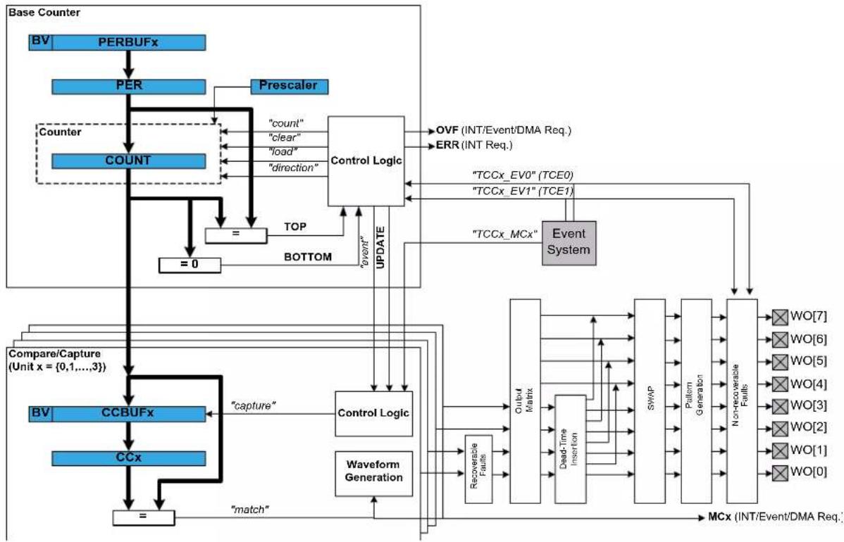
flowchart
graph TD
    A["Base Counter"] --> B["BV"]
    B --> C["PERBUFx"]
    C --> D["PER"]
    D --> E["Counter"]
    E --> F["COUNT"]
    F --> G["="]
    G --> H["=0"]
    H --> I["Comparison/Capture (Unit x = {0,1,...,3})"]
    I --> J["BV"]
    J --> K["CCBUFx"]
    K --> L["CCx"]
    L --> M["="]
    M --> N["match"]
    N --> O["capture"]
    O --> P["Control Logic"]
    P --> Q["Event System"]
    Q --> R["MCx (INT/Event/DMA Req.)"]
    R --> S["Recoverable Faults"]
    S --> T["Dead-Time Insertion"]
    T --> U["SWAP"]
    U --> V["Pattern Generation"]
    V --> W["Non-recoverable Faults"]
    W --> X["WO[7"]]
    W --> Y["WO[6"]]
    W --> Z["WO[5"]]
    W --> AA["WO[4"]]
    W --> AB["WO[3"]]
    W --> AC["WO[2"]]
    W --> AD["WO[1"]]
    W --> AE["WO[0"]]
    P --> AF["count"]
    AF --> AG["clear"]
    AF --> AH["load"]
    AF --> AI["direction"]
    AF --> AJ["TOP"]
    AJ --> AK["EVENT"]
    AK --> AL[""TCCx_EV0" (TCE0)"]
    AK --> AM[""TCCx_EV1" (TCE1)"]
    AK --> AN["TCCx_MCx"]
    AN --> AO["OVF (INT/Event/DMA Req.)"]
    AN --> AP["ERR (INT Req.)"]
    P --> AQ["TOP"]
    AQ --> AR["BOTTOM"]
    AQ --> AS["UPDATE"]
    AS --> AT["Event System"]
35.4 Signal Description
| Pin Name Type Description | |
| TCC/WO[0] Digital output Compare channel 0 waveform output | |
| TCC/WO[1] Digital output Compare channel 1 waveform output | |
| ... ... ... | |
| TCC/WO[7] Digital output Compare channel 7 waveform output | |
Refer to I/O Multiplexing and Considerations for details on the pin mapping for this peripheral. One signal can be mapped on several pins.
35.5 Product Dependencies
In order to use this peripheral, other parts of the system must be configured correctly, as described below.
35.5.1 I/O Lines
In order to use the I/O lines of this peripheral, the I/O pins must be configured using the I/O Pin Controller (PORT).
35.5.2 Power Management
This peripheral can continue to operate in any sleep mode where its source clock is running. The interrupts can wake up the device from sleep modes. Events connected to the event system can trigger other operations in the system without exiting sleep modes.
35.5.3 Clocks
The TCC bus clock (CLK_TCC0_APB) is enabled by default, and can be enabled and disabled in the Main Clock.
A generic clock (GCLK_TCC0) is required to clock the TCC. This clock must be configured and enabled in the generic clock controller before using the TCC.
The generic clocks (GCLK_TCC0) are asynchronous to the bus clock (CLK_TCC0_APB). Due to this asynchronicity, writing certain registers will require synchronization between the clock domains. Refer to 35.6.6. Synchronization for further details.
35.5.4 DMA
The DMA request lines are connected to the DMA Controller (DMAC). In order to use DMA requests with this peripheral the DMAC must be configured first. Refer to DMAC – Direct Memory Access Controller for details.
35.5.5 Interrupts
The interrupt request line is connected to the Interrupt Controller. In order to use interrupt requests of this peripheral, the Interrupt Controller (NVIC) must be configured first. Refer to Nested Vector Interrupt Controller for details.
35.5.6 Events
The events of this peripheral are connected to the Event System.
35.5.7 Debug Operation
When the CPU is halted in debug mode, this peripheral will halt normal operation. This peripheral can be forced to continue operation during debugging - refer to the Debug Control (DBGCTRL) register for details.
Refer to 35.8.8. DBGCTRL register for details.
35.5.8 Register Access Protection
Registers with write-access can be optionally write-protected by the Peripheral Access Controller (PAC), except for the following:
- Interrupt Flag register (INTFLAG)
- Status register (STATUS)
- Period and Period Buffer registers (PER, PERBUF)
- Compare/Capture and Compare/Capture Buffer registers (CCx, CCBUFx)
• Control Waveform register (WAVE) - Pattern Generation Value and Pattern Generation Value Buffer registers (PATT, PATTBUF)
Note: Optional write-protection is indicated by the "PAC Write-Protection" property in the register description.
When the CPU is halted in debug mode, all write-protection is automatically disabled. Write-protection does not apply for accesses through an external debugger.
35.5.9 Analog Connections
Not applicable.
35.6 Functional Description
35.6.1 Principle of Operation
The following definitions are used throughout the documentation:
Table 35-1. Timer/Counter for Control Applications - Definitions
| Name Description | |
| TOP The counter reaches TOP when it becomes equal to the highest value in the count sequence. The TOP value can be the same as Period (PER) or the Compare Channel 0 (CC0) register value depending on the waveform generator mode in 35.6.2.6. Waveform Output Generation Operations . | |
| ZERO The counter reaches ZERO when it contains all zeroes. | |
| MAX The counter reaches maximum when it contains all ones. | |
| UPDATE The timer/counter signals an update when it reaches ZERO or TOP, depending on the direction settings. | |
| Timer The timer/counter clock control is handled by an internal source. | |
| Counter The clock control is handled externally (e.g. counting external events). | |
| CC For compare operations, the CC are referred to as "compare channels." | |
Each TCC instance has up to four compare/capture channels (CCx).
The counter register (COUNT), period registers with buffer (PER and PERBUF), and compare and capture registers with buffers (CCx and CCBUFx) are 16- or 24-bit registers, depending on each TCC instance. Each buffer register has a buffer valid (BUFV) flag that indicates when the buffer contains a new value.
Under normal operation, the counter value is continuously compared to the TOP or ZERO value to determine whether the counter has reached TOP or ZERO. In either case, the TCC can generate interrupt requests, request DMA transactions, or generate events for the Event System. In waveform generator mode, these comparisons are used to set the waveform period or pulse width.
A prescaled generic clock (GCLK_TCC0) and events from the event system can be used to control the counter. The event system is also used as a source to the input capture.
The Recoverable Fault Unit enables event controlled waveforms by acting directly on the generated waveforms of the TCC compare channels output. These events can restart, halt the timer/counter period, shorten the output pulse active time, or disable waveform output as long as the fault condition is present. This can typically be used for current sensing regulation, and zero-crossing and demagnetization re-triggering.
The MCE0 and MCE1 event sources are shared with the Recoverable Fault Unit. Only asynchronous events are used internally when fault unit extension is enabled. For further details on how to configure asynchronous events routing, refer to EVSYS - Event System.
Recoverable fault sources can be filtered and/or windowed to avoid false triggering, for example from I/O pin glitches, by using digital filtering, input blanking, and qualification options. See also 35.6.3.5. Recoverable Faults.
In addition, six optional independent and successive units primarily intended for use with different types of motor control, ballast, LED, H-bridge, power converter, and other types of power switching applications, are implemented in some of TCC instances. See also Figure 35-1.
The output matrix (OTMX) can distribute and route out the TCC waveform outputs across the port pins in different configurations, each optimized for different application types. The Dead-Time Insertion (DTI) unit splits the four lower OTMX outputs into two non-overlapping signals: the non-inverted low side (LS) and inverted high side (HS) of the waveform output with optional dead-time
insertion between LS and HS switching. The SWAP unit can swap the LS and HS pin outputs, and can be used for fast decay motor control.
The pattern generation unit can be used to generate synchronized waveforms with constant logic level on TCC UPDATE conditions. This is useful for easy stepper motor and full bridge control.
The non-recoverable fault module enables event controlled fault protection by acting directly on the generated waveforms of the timer/counter compare channel outputs. When a non-recoverable fault condition is detected, the output waveforms are forced to a safe and pre-configured value that is safe for the application. This is typically used for instant and predictable shut down and disabling high current or voltage drives.
The count event sources (TCE0 and TCE1) are shared with the non-recoverable fault extension. The events can be optionally filtered. If the filter options are not used, the non-recoverable faults provide an immediate asynchronous action on waveform output, even for cases where the clock is not present. For further details on how to configure asynchronous events routing, refer to the EVSYS - Event System.
35.6.2 Basic Operation
35.6.2.1 Initialization
The following registers are enable-protected, meaning that they can only be written when the TCC is disabled(CTRLA.ENABLE=0):
- Control A (CTRLA) register, except Run Standby (RUNSTDBY), Enable (ENABLE) and Software Reset (SWRST) bits
- Recoverable Fault n Control registers (FCTRLA and FCTRLB)
- Waveform Extension Control register (WEXCTRL)
- Drive Control register (DRVCTRL)
• Event Control register (EVCTRL)
Enable-protected bits in the CTRLA register can be written at the same time as CTRLA. ENABLE is written to '1', but not at the same time as CTRLA. ENABLE is written to '0'. Enable-protection is denoted by the "Enable-Protected" property in the register description.
Before the TCC is enabled, it must be configured as outlined by the following steps:
- Enable the TCC bus clock (CLK_TCC0_APB).
- If Capture mode is required, enable the channel in capture mode by writing a '1' to the Capture Enable bit in the Control A register (CTRLA.CPTEN).
Optionally, the following configurations can be set before enabling TCC:
- Select PRESCALER setting in the Control A register (CTRLA.PRESCALER).
- Select Prescaler Synchronization setting in Control A register (CTRLA.PRESCSYNC).
- If down-counting operation is desired, write the Counter Direction bit in the Control B Set register (CTRLBSET.DIR) to '1'.
- Select the Waveform Generation operation in the WAVE register (WAVE.WAVEGEN).
- Select the Waveform Output Polarity in the WAVE register (WAVE.POL).
- The waveform output can be inverted for the individual channels using the Waveform Output Invert Enable bit group in the Driver register (DRVCTRL.INVENx).
35.6.2.2 Enabling, Disabling, and Resetting
The TCC is enabled by writing a '1' to the Enable bit in the Control A register (CTRLA.ENABLE). The TCC is disabled by writing a zero to CTRLA.ENABLE.
The TCC is reset by writing '1' to the Software Reset bit in the Control A register (CTRLA.SWRST). All registers in the TCC, except DBGCTRL, will be reset to their initial state, and the TCC will be disabled. Refer to Control A (35.8.1. CTRLA) register for details.
The TCC should be disabled before the TCC is reset to avoid undefined behavior.
35.6.2.3 Prescaler Selection
The GCLK_TCC0 clock is fed into the internal prescaler.
The prescaler consists of a counter that counts up to the selected prescaler value, whereupon the output of the prescaler toggles.
If the prescaler value is higher than one, the counter update condition can be optionally executed on the next GCLK_TCC clock pulse or the next prescaled clock pulse. For further details, refer to the Prescaler (CTRLA.PRESCALER) and Counter Synchronization (CTRLA.PRESYNC) descriptions.
Prescaler outputs from 1 to 1/1024 are available. For a complete list of available prescaler outputs, see the register description for the Prescaler bit group in the Control A register (CTRLA.PRESCALER).
Note: When counting events, the prescaler is bypassed.
The joint stream of prescaler ticks and event action ticks is called CLK_TCC_COUNT.
Figure 35-2. Prescaler
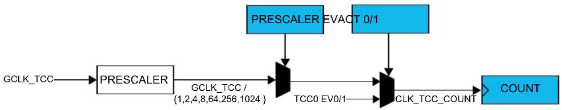
flowchart
graph LR
    A["GCLK_TCC"] --> B["PREScaler"]
    B --> C["GCLK_TCC / {1,2,4,8,64,256,1024}"]
    C --> D["TCC0 EV0/1"]
    D --> E["COUNT"]
    F["PREScaler"] --> G["EVACT 0/1"]
    H["Count"] --> E
35.6.2.4 Counter Operation
Depending on the mode of operation, the counter is cleared, reloaded, incremented, or decremented at each TCC clock input (CLK_TCC_COUNT). A counter clear or reload mark the end of current counter cycle and the start of a new one.
The counting direction is set by the Direction bit in the Control B register (CTRLB.DIR). If the bit is zero, it's counting up and one if counting down.
The counter will count up or down for each tick (clock or event) until it reaches TOP or ZERO. When it's counting up and TOP is reached, the counter will be set to zero at the next tick (overflow) and the Overflow Interrupt Flag in the Interrupt Flag Status and Clear register (INTFLAG.OVF) will be set. When down-counting, the counter is reloaded with the TOP value when ZERO is reached (underflow), and INTFLAG.OVF is set.
INTFLAG.OVF can be used to trigger an interrupt, a DMA request, or an event. An overflow/underflow occurrence (i.e. a compare match with TOP/ZERO) will stop counting if the One-Shot bit in the Control B register is set (CTRLBSET.ONESHOT).
Figure 35-3. Counter Operation
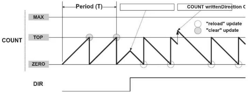
flowchart
graph TD
    A["Period (T)"] --> B["COUNT writtenDirection C"]
    B --> C[""reload" update"]
    B --> D[""clear" update"]
    C --> E["TOP"]
    D --> F["TOP"]
    E --> G["ZERO"]
    F --> H["ZERO"]
    G --> I["DIR"]
    H --> I
    style A fill:#f9f,stroke:#333
    style B fill:#ccf,stroke:#333
    style C fill:#cfc,stroke:#333
    style D fill:#fcc,stroke:#333
    style E fill:#ffc,stroke:#333
    style F fill:#cfc,stroke:#333
    style G fill:#fcc,stroke:#333
    style H fill:#cfc,stroke:#333
    style I fill:#fcc,stroke:#333
It is possible to change the counter value (by writing directly in the COUNT register) even when the counter is running. The COUNT value will always be ZERO or TOP, depending on direction set by CTRLBSET.DIR or CTRLBCLR.DIR, when starting the TCC, unless a different value has been written to it, or the TCC has been stopped at a value other than ZERO. The write access has higher priority than count, clear, or reload. The direction of the counter can also be changed during normal operation. See the Counter Operation figure above.
35.6.2.4.1 Stop Command
A stop command can be issued from software by using TCC Command bits in Control B Set register (CTRLBSET.CMD=0x2, STOP).
When a stop is detected while the counter is running, the counter will maintain its current value. If the waveform generation (WG) is used, all waveforms are set to a state defined in Non-Recoverable State x Output Enable bit and Non- Recoverable State x Output Value bit in the Driver Control register (DRVCTRL.NREx and DRVCTRL.NRVx), and the Stop bit in the Status register is set (STATUS.STOP).
35.6.2.4.2 Pause Event Action
A pause command can be issued when the stop event action is configured in the Input Event Action 1 bits in Event Control register (EVCTRL.EVACT1=0x3, STOP).
When a pause is detected, the counter will maintain its current value and all waveforms keep their current state, as long as a start event action is detected: Input Event Action 0 bits in Event Control register (EVCTRL.EVACT0=0x3, START).
35.6.2.4.3 Re-Trigger Command and Event Action
A re-trigger command can be issued from software by using TCC Command bits in Control B Set register (CTRLBSET.CMD=0x1, RETRIGGER), or from event when the re-trigger event action is configured in the Input Event 0/1 Action bits in Event Control register (EVCTRL.EVACTn=0x1, RETRIGGER).
When the command is detected during counting operation, the counter will be reloaded or cleared, depending on the counting direction (CTRLBSET.DIR or CTRLBCLR.DIR). The Re-Trigger bit in the Interrupt Flag Status and Clear register will be set (INTFLAG.TRG). It is also possible to generate an event by writing a '1' to the Re-Trigger Event Output Enable bit in the Event Control register (EVCTRL.TRGEO). If the re-trigger command is detected when the counter is stopped, the counter will resume counting operation from the value in COUNT.
Note: When a re-trigger event action is configured in the Event Action bits in the Event Control register (EVCTRL.EVACTn=0x1, RETRIGGER), enabling the counter will not start the counter. The counter will start on the next incoming event and restart on corresponding following event.
35.6.2.4.4 Start Event Action
The start action can be selected in the Event Control register (EVCTRL.EVACT0=0x3, START) and can start the counting operation when previously stopped. The event has no effect if the counter is
already counting. When the module is enabled, the counter operation starts when the event is received or when a re-trigger software command is applied.
Note: When a start event action is configured in the Event Action bits in the Event Control register (EVCTRL.EVACT0=0x3, START), enabling the counter will not start the counter. The counter will start on the next incoming event, but it will not restart on subsequent events.
35.6.2.4.5 Count Event Action
The TCC can count events. When an event is received, the counter increases or decreases the value, depending on direction settings (CTRLBSET.DIR or CTRLBCLR.DIR).
The count event action is selected by the Event Action 0 bit group in the Event Control register (EVCTRL.EVACT0=0x5, COUNT).
35.6.2.4.6 Direction Event Action
The direction event action can be selected in the Event Control register (EVCTRL.EVACT1=0x2, DIR). When this event is used, the asynchronous event path specified in the event system must be configured or selected. The direction event action can be used to control the direction of the counter operation, depending on external events level. When received, the event level overrides the Direction settings (CTRLBSET.DIR or CTRLBCLR.DIR) and the direction bit value is updated accordingly.
35.6.2.4.7 Increment Event Action
The increment event action can be selected in the Event Control register (EVCTRL.EVACT0=0x4, INC) and can change the counter state when an event is received. When the TCE0 event (TCC0_EV0) is received, the counter increments, whatever the direction setting (CTRLBSET.DIR or CTRLBCLR.DIR) is.
35.6.2.4.8 Decrement Event Action
The decrement event action can be selected in the Event Control register (EVCTRL.EVACT1=0x4, DEC) and can change the counter state when an event is received. When the TCE1 (TCC0_EV1) event is received, the counter decrements, whatever the direction setting (CTRLBSET.DIR or CTRLBCLR.DIR) is.
35.6.2.4.9 Non-recoverable Fault Event Action
Non-recoverable fault actions can be selected in the Event Control register (EVCTRL.EVACTn=0x7, FAULT). When received, the counter will be stopped and the output of the compare channels is overridden according to the Driver Control register settings (DRVCTRL.NREx and DRVCTRL.NRVx). TCE0 and TCE1 must be configured as asynchronous events.
35.6.2.4.10 Event Action Off
If the event action is disabled (EVCTRL.EVACTn=0x0, OFF), enabling the counter will also start the counter.
35.6.2.5 Compare Operations
By default, the Compare/Capture channel is configured for compare operations. To perform capture operations, it must be re-configured.
When using the TCC with the Compare/Capture Value registers (CCx) for compare operations, the counter value is continuously compared to the values in the CCx registers. This can be used for timer or for waveform operation.
The Channel x Compare/Capture Buffer Value (CCBUFx) registers provide double buffer capability. The double buffering synchronizes the update of the CCx register with the buffer value at the UPDATE condition or a force update command (CTRLBSET.CMD=0x3, UPDATE). For further details, refer to 35.6.2.14. Double Buffering. The synchronization prevents the occurrence of odd-length, non-symmetrical pulses and ensures glitch-free output.
35.6.2.6 Waveform Output Generation Operations
The compare channels can be used for waveform generation on output port pins. To make the waveform available on the connected pin, the following requirements must be fulfilled:
- Choose a waveform generation mode in the Waveform Generation Operation bit in Waveform register (WAVE.WAVEGEN).
- Optionally invert the waveform output WO[x] by writing the corresponding Waveform Output x Inversion bit in the Driver Control register (DRVCTRL.INVENx).
- Configure the pins with the I/O Pin Controller. Refer to PORT - I/O Pin Controller for details.
The counter value is continuously compared with each CCx value. On a comparison match, the Match or Capture Channel x bit in the Interrupt Flag Status and Clear register (INTFLAG.MCx) will be set on the next zero-to-one transition of CLK_TCC_COUNT (see Normal Frequency Operation). An interrupt and/or event can be generated on the same condition if Match/Capture occurs, i.e. INTENSET.MCx and/or EVCTRL.MCEOx is '1'. Both interrupt and event can be generated simultaneously. The same condition generates a DMA request.
There are seven waveform configurations for the Waveform Generation Operation bit group in the Waveform register (WAVE.WAVEGEN). This will influence how the waveform is generated and impose restrictions on the top value. The configurations are:
• Normal Frequency (NFRQ)
- Match Frequency (MFRQ)
• Normal Pulse-Width Modulation (NPWM)
- Dual-slope, interrupt/event at TOP (DSTOP)
- Dual-slope, interrupt/event at ZERO (DSBOTTOM)
- Dual-slope, interrupt/event at Top and ZERO (DSBOTH)
- Dual-slope, critical interrupt/event at ZERO (DSCRITICAL)
When using MFRQ configuration, the TOP value is defined by the CC0 register value. For the other waveform operations, the TOP value is defined by the Period (PER) register value.
For dual-slope waveform operations, the update time occurs when the counter reaches ZERO. For the other waveforms generation modes, the update time occurs on counter wraparound, on overflow, underflow, or re-trigger.
The table below shows the update counter and overflow event/interrupt generation conditions in different operation modes.
Table 35-2. Counter Update and Overflow Event/interrupt Conditions
| Name Operation | TOP Update Output Waveform | OVFIF/Event | |||||
| On Match On Up | Update Up Down | ||||||
| NFRQ Normal | Frequency | PER TOP/ ZERO Toggle | Stable TOP | ZERO | |||
| MFRQ | Match Frequency | CCO | TOP/ ZERO Toggle | Stable TOP | ZERO | ||
| NPWM | Single-slope PWM | PER TOP/ ZERO See section 'Output Polarity' below | TOP | ZERO | |||
| DSCRITICAL | Dual-slope PWM | PER ZERO | - | ZERO | |||
| DSBOTTOM | Dual-slope PWM | PER ZERO | - | ZERO | |||
| DSBOTH | Dual-slope PWM | PER TOP (1) & ZERO | TOP | ZERO | |||
| DSTOP | Dual-slope PWM | PER ZERO | TOP | - | |||
- The UPDATE condition on TOP only will occur when circular buffer is enabled for the channel.
35.6.2.7 Normal Frequency (NFRQ)
For Normal Frequency generation, the period time (T) is controlled by the period register (PER). The waveform generation output (WO[x]) is toggled on each compare match between COUNT and CCx, and the corresponding Match or Capture Channel x Interrupt Flag (EVCTRL.MCEOx) will be set.
Figure 35-4. Normal Frequency Operation
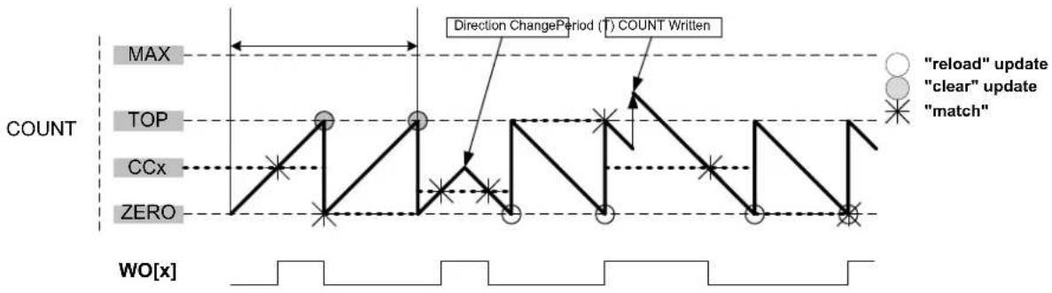
flowchart
graph TD
    A["Direction Change Period (T) COUNT Written"] --> B[""reload" update"]
    A --> C[""clear" update"]
    A --> D["match"]
    E["COUNT"] --> F["TOP"]
    F --> G["CCx"]
    G --> H["ZERO"]
    H --> I["WO[x"]]
    style A fill:#f9f,stroke:#333
    style B fill:#ccf,stroke:#333
    style C fill:#ccf,stroke:#333
    style D fill:#ccf,stroke:#333
    style E fill:#fff,stroke:#333
    style F fill:#fff,stroke:#333
    style G fill:#fff,stroke:#333
    style H fill:#fff,stroke:#333
    style I fill:#fff,stroke:#333
35.6.2.8 Match Frequency (MFRQ)
For Match Frequency generation, the period time (T) is controlled by CC0 register instead of PER. WO[0] toggles on each update condition.
Figure 35-5. Match Frequency Operation
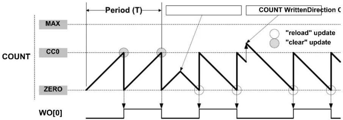
flowchart
graph TD
    A["Period (T)"] --> B["COUNT"]
    B --> C[""RELOAD" update"]
    B --> D[""CLEAR" update"]
    C --> E["CC0"]
    D --> F["CC0"]
    E --> G["zero"]
    F --> H["zero"]
    G --> I["zero"]
    H --> J["zero"]
    I --> K["zero"]
    J --> L["zero"]
    K --> M["zero"]
    L --> N["zero"]
    M --> O["zero"]
    N --> P["zero"]
    O --> Q["zero"]
    P --> R["zero"]
    Q --> S["zero"]
    R --> T["zero"]
    S --> U["zero"]
    T --> V["zero"]
    U --> W["zero"]
    V --> X["zero"]
    W --> Y["zero"]
    X --> Z["zero"]
    Y --> AA["zero"]
    Z --> AB["zero"]
    AA --> AC["zero"]
    AB --> AD["zero"]
    AC --> AE["zero"]
    AD --> AF["zero"]
    AE --> AG["zero"]
    AF --> AH["zero"]
    AG --> AI["zero"]
    AH --> AJ["zero"]
    AI --> AK["zero"]
    AJ --> AL["zero"]
    AK --> AM["zero"]
    AL --> AN["zero"]
    AM --> AO["zero"]
    AN --> AP["zero"]
    AO --> AQ["zero"]
    AP --> AR["zero"]
    AQ --> AS["zero"]
35.6.2.9 Normal Pulse-Width Modulation (NPWM)
NPWM uses single-slope PWM generation.
35.6.2.10 Single-Slope PWM Operation
For single-slope PWM generation, the period time (T) is controlled by Top value, and CCx controls the duty cycle of the generated waveform output. When up-counting, the WO[x] is set at start or compare match between the COUNT and TOP values, and cleared on compare match between COUNT and CCx register values. When down-counting, the WO[x] is cleared at start or compare match between the COUNT and ZERO values, and set on compare match between COUNT and CCx register values.
Figure 35-6. Single-Slope PWM Operation
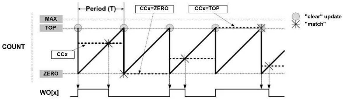
flowchart
graph TD
    A["Period (T)"] --> B["CCx=ZERO"]
    A --> C["CCx=TOP"]
    D["COUNT"] --> E["CCx"]
    D --> F["ZERO"]
    G["WO[x"]] --> H["Zero"]
    I[""clear" update"] --> J["match"]
    style A fill:#f9f,stroke:#333
    style B fill:#ccf,stroke:#333
    style C fill:#ccf,stroke:#333
    style D fill:#fff,stroke:#333
    style E fill:#fff,stroke:#333
    style F fill:#fff,stroke:#333
    style G fill:#fff,stroke:#333
    style H fill:#fff,stroke:#333
    style I fill:#fff,stroke:#333
    style J fill:#fff,stroke:#333
The following equation calculates the exact resolution for a single-slope PWM ( R_PWM_SS ) waveform:
$$ R _ {\mathrm {PWM_SS}} = \frac {\log (\mathrm{TOP} + 1)}{\log (2)} $$
The PWM frequency depends on the Period register value (PER) and the peripheral clock frequency ( f_GCLK_TCC ), and can be calculated by the following equation:
$$ f _ {\mathrm {PWM_SS}} = \frac {f _ {\mathrm {GCLK_TCC}}}{\mathrm{N(TOP+1)}} $$
Where N represents the prescaler divider used (1, 2, 4, 8, 16, 64, 256, 1024).
35.6.2.11 Dual-Slope PWM Generation
For dual-slope PWM generation, the period setting (TOP) is controlled by PER, while CCx control the duty cycle of the generated waveform output. The figure below shows how the counter repeatedly counts from ZERO to PER and then from PER to ZERO. The waveform generator output is set on compare match when up-counting, and cleared on compare match when down-counting. An interrupt/event is generated on TOP and/or ZERO, depend on Dual slope.
In DSBOTH operation, a second update time occurs on TOP when circular buffer is enabled.
Figure 35-7. Dual-Slope Pulse Width Modulation
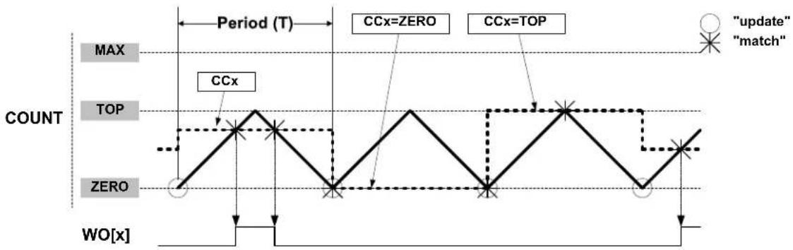
flowchart
graph TD
    A["CCx"] --> B["CCx=ZERO"]
    A --> C["CCx=TOP"]
    D["zero"] --> E["zero"]
    F["TOPOUT"] --> G["TOPOUT"]
    H["TIME Period T"] --> I["Period (T)"]
    J["update"] --> K["match"]
    style A fill:#f9f,stroke:#333
    style B fill:#ccf,stroke:#333
    style C fill:#ccf,stroke:#333
    style D fill:#fff,stroke:#333
    style E fill:#fff,stroke:#333
    style F fill:#fff,stroke:#333
    style G fill:#fff,stroke:#333
    style H fill:#fff,stroke:#333
    style I fill:#fff,stroke:#333
    style J fill:#fff,stroke:#333
    style K fill:#fff,stroke:#333
    style_L["COUNT"] --> M[""WO[x"]" --> N["zero"]
    style M --> O["TOPOUT"]
    style N --> P["TIME Period T"]
    style_Q["TIM Period T"] --> R["period (T)"]
    style_S["TIM Period T"] --> T["MAX"]
    style_U["TIM Period T"] --> V["CCx"]
    style_W["TIM Period T"] --> X["CCx=ZERO"]
    W --> Y["CCx=TOP"]
    Z["TIME Period T"] --> AA["MTX"]
    AB["TIM Period T"] --> AC["MTX"]
    AD["TIM Period T"] --> AE["MTX"]
    AF["TIM Period T"] --> AG["MTX"]
    AH["TIM Period T"] --> AI["MTX"]
    AJ["TIM Period T"] --> AK["MTX"]
    AL["TIM Period T"] --> AM["MTX"]
    AN["TIM Period T"] --> AO["MTX"]
    AP["TIM Period T"] --> AQ["MTX"]
    AR["TIM Period T"] --> AS["MTX"]
    AT["TIM Period T"] --> AU["MTX"]
    AV["TIM Period T"] --> AW["MTX"]
    AX["TIM Period T"] --> AY["MTX"]
    AZ["TIM Period T"] --> BA["MTX"]
    BB["TIM Period T"] --> BC["MTX"]
    BD["TIM Period T"] --> BE["MTX"]
    BF["TIM Period T"] --> BG["MTX"]
    BH["TIM Period T"] --> BI["MTX"]
    BJ["TIM Period T"] --> BK["MTX"]
    BL["TIM Period T"] --> BM["MTX"]
    BN["TIM Period T"] --> BO["MTX"]
    BP["TIM Period T"] --> BQ["MTX"]
    BR["TIM Period T"] --> BS["MTX"]
    BT["TIM Period T"] --> BU["MTX"]
    BV["TIM Period T"] --> BW["MTX"]
    BX["TIM Period T"] --> BY["MTX"]
    CA["TIM Period T"] --> AZ
    CB["TIM Period T"] --> DA
    DB["TIM Period T"] --> DB
    BE --> DC["MTX"]
    BE --> DD["MTX"]
    BE --> DE["MTX"]
    BE --> DF["MTX"]
    BE --> DG["MTX"]
    BE --> DH["MTX"]
    BE --> DI["MTX"]
    BE --> DJ["MTX"]
    BE --> DK["MTX"]
    BE --> DL["MTX"]
    BE --> DW["MTX"]
    BE --> DX["MTX"]
    BE --> DWG["MTX"]
    BE --> DWV["MTX"]
    BE --> DWVG["MTX"]
    BE --> DWVH["MTX"]
    BE --> DWVJ["MTX"]
    BE --> DWVK["MTX"]
    BE --> DWVL["MTX"]
    BE --> DWVM["MTX"]
    BE --> DWVN["MTX"]
    BE --> DWVN0["MTX"]
    BE --> DWVN1["MTX"]
    BE --> DWVN2["MTX"]
    BE --> DWVN20["MTX"]
    BE --> DWVN200["MTX"]
    BE --> DWVN2000["MTX"]
    BE --> DWVN20000000000000000000000000000000000000000000000000000000000000000000000000000000000000000000000000000
Using dual-slope PWM results in a lower maximum operation frequency compared to single-slope PWM generation. The period (TOP) defines the PWM resolution. The minimum resolution is 1 bit (TOP=0x00000001).
The following equation calculates the exact resolution for dual-slope PWM ( R_PWM_DS ):
$$ R _ {\mathrm {PWM_DS}} = \frac {\log (\mathrm{PER} + 1)}{\log (2)}. $$
The PWM frequency f_PWM_DS depends on the period setting (TOP) and the peripheral clock frequency f_GCLK_TCG , and can be calculated by the following equation:
$$ f _ {\mathrm {PWM_ {D} S}} = \frac {f _ {\mathrm {GCLK_ {T} CC}}}{2 N \cdot \mathrm{PER}} $$
N represents the prescaler divider used. The waveform generated will have a maximum frequency of half of the TCC clock frequency ( f_GCLK_TCC ) when TOP is set to 0x00000001 and no prescaling is used.
The pulse width ( P_PWM_DS ) depends on the compare channel (CCx) register value and the peripheral clock frequency ( f_GCLK_TCC ), and can be calculated by the following equation:
$$ P _ {\mathrm{PWM} _ \mathrm{DS}} = \frac {2 N \cdot \mathrm{TOP-CCx}}{f _ {\mathrm{GCLK} _ \mathrm{TCC}}} $$
N represents the prescaler divider used.
Note: In DSTOP, DSBOTTOM and DSBOTH operation, when TOP is lower than MAX/2, the CCx MSB bit defines the ramp on which the CCx Match interrupt or event is generated. (Rising if CCx[MSB]=0, falling if CCx[MSB]=1.)
35.6.2.12 Dual-Slope Critical PWM Generation
Dual-Slope Critical PWM Generation
Critical mode generation allows generation of non-aligned centered pulses. In this mode, the period time is controlled by PER while CCx control the generated waveform output edge during up-counting and CC(x+CC_NUM/2) control the generated waveform output edge during down-counting.
Figure 35-8. Dual-Slope Critical Pulse Width Modulation (N=CC_NUM)

flowchart
graph TD
    A["Period (T)"] --> B["MAX"]
    B --> C["TOP"]
    C --> D["ZERO"]
    D --> E["WO[x"]]
    F[""reload" update"] --> G["match"]
    style A fill:#f9f,stroke:#333
    style B fill:#ccf,stroke:#333
    style C fill:#cfc,stroke:#333
    style D fill:#fcc,stroke:#333
    style E fill:#ffc,stroke:#333
    style F fill:#fff,stroke:#333
    style G fill:#fff,stroke:#333
    style_H["CCx CC(x+N/2) CCx CC(x+N/2) CCx CC(x+N/2)"] --> I["+"]
    style I --> J["-"]
    style J --> K["-"]
    style_L["+"] --> M["+"]
    style_N["-"] --> O["-"]
    style_P["+"] --> Q["-"]
    style_R["-"] --> S["-"]
    style_T["+"] --> U["+"]
    style_V["-"] --> W["-"]
    style_X["+"] --> Y["-"]
    style_Z["-"] --> AA["-"]
    style_AB["+"] --> AC["+"]
    style_AD["-"] --> AE["-"]
    style_AF["+"] --> AG["-"]
    style_AH["-"] --> AI["-"]
    style_AJ["+"] --> AK["+"]
    style_AL["-"] --> AM["-"]
    style_AN["+"] --> AO["-"]
    style_AP["-"] --> AQ["-"]
    style_AR["+"] --> AS["+"]
    style_AT["-"] --> AU["-"]
    style_AV["+"] --> AW["-"]
    style_AX["-"] --> AY["-"]
    style_AZ["+"] --> BA["+"]
    style_BB["-"] --> BC["-"]
    style_BD["+"] --> BE["-"]
    style_BF["-"] --> BG["-"]
    style_BH["+"] --> BI["+"]
    style_BJ["-"] --> BK["-"]
    style_BL["+"] --> BM["-"]
    style_BN["-"] --> BO["-"]
    style_BP["+"] --> BQ["+"]
    style BQ --> BR["-"]
    style_BS["+"] --> BT["-"]
    style_BU["-"] --> BV["-"]
    style_BW["+"] --> BX["+"]
    style_BY["-"] --> BZ["-"]
    style_CA["+"] --> CB["+"]
    style CB --> CC["-"]
    style_CD["+"] --> CE["-"]
    style_CF["-"] --> CG["-"]
    style_CH["+"] --> CI["+"]
    style_CJ["-"] --> CK["-"]
    style_CL["+"] --> CM["-"]
    style CD --> CN["+"]
    CD --> CO["-"]
    CD --> CP["-"]
    CD --> CS["+"]
    CD --> CT["-"]
    CD --> CU["+"]
    CD --> CV["-"]
    CD --> CW["+"]
    CD --> CX["-"]
    CD --> CY["+"]
    CD --> CZ["-"]
    CD --> DA["+"]
    CD --> DB["-"]

    subgraph COUNT
        C
        D
        E
        F
        G
        H
        I
        J
        K
        L
        M
        N
        O
        P
        Q
        R
        S
        T
        U
        V
        W
        X
        Y
        Z
        AA
        AB
        AC
        AD
        AE
        AF
        AG
        AH
        AI
        AJ
        AK
        AL
        AM
        AN
        AO
        AP
        AQ
        AR
        AS
        AT
        AU
        AV
        AW
        AX
        AY
        AZ
        BA
        BB
        BC
        BD
        BE
        BF
        BG
        BH
        BI
        BJ
        BK
        BL
        BM
        BN
        BO
        BP
        BPB
        BPX
        BPX
        BPY
        BPZ
        BPZX
        BPZX
        BPZXN
        BPXCXN
        BPXCXNN1
        BPXCXN1N1
        BPXCXXN1N2
        BPXCXXN2N2
        BPXCXXN2N1N2
        BPXCXXN2N1N1N2
        BPXCXXN2N1N1N1N2
        BPXCXXN2N1N1N1N2N1N2N1N2N1N2N1N2N1N2N1N2N1N2N1N2N1N2N1N2N1N2N1N2N1N2N1N2N1N2N1N2N1N2N1N2N1N2N1N2N1N2N1N2N1N2N1N2N1N1N2N1N2N1N2N1N2N1N2N1N2N1N2N1N2N1N2N1N2N1N2N1N2N1N2N1N2N1N2N1N2N1N2N1N2N1N2N1N2N1N2N1N2N1N2N1N2N0
35.6.2.13 Output Polarity
The polarity (WAVE.POLx) is available in all waveform output generation. In single-slope and dual-slope PWM operation, it is possible to invert the pulse edge alignment individually on start or end of a PWM cycle for each compare channels. The table below shows the waveform output set/clear conditions, depending on the settings of timer/counter, direction, and polarity.
Table 35-3. Waveform Generation Set/Clear Conditions
| Waveform Generation operation | DIR | POLx | Waveform Generation Output Update | |
| Set Clear | ||||
| Single-Slope PWM 0 0 Timer/counter matches TOP Timer/counter matches CCx | ||||
| 1 Timer/counter matches CC Timer/counter matches TOP | ||||
| 1 0 Timer/counter matches CC Timer/counter matches ZERO | ||||
| 1 Timer/counter matches ZERO Timer/counter matches CC | ||||
| ......continued | ||||
| Waveform Generation operation | DIR | POLx | Waveform Generation Output Update | |
| Set Clear | ||||
| Dual-Slope PWM x 0 Timer/counter matches CC when counting up | Timer/counter matches CC when counting down | |||
| 1 Timer/counter matches CC when counting down | ||||
In Normal and Match Frequency, the WAVE.POLx value represents the initial state of the waveform output.
35.6.2.14 Double Buffering
The Pattern (PATT), Period (PER) and Compare Channels (CCx) registers are all double buffered. Each buffer register has a buffer valid (PATTBUFV, PERBUFV or CCBUFVx) bit in the STATUS register, which indicates that the buffer register contains a valid value that can be copied into the corresponding register.
When the buffer valid flag bit in the STATUS register is '1' and the Lock Update bit in the CTRLB register is set to '0', (writing CTRLBCLR.LUPD to '1'), double buffering is enabled: the data from buffer registers will be copied into the corresponding register under hardware UPDATE conditions, then the buffer valid flags bit in the STATUS register are automatically cleared by hardware.
Note: Software update command (CTRLBSET.CMD = 0x3) act independently of LUPD value.
A compare register is double buffered as in the following figure.
Figure 35-9. Compare Channel Double Buffering
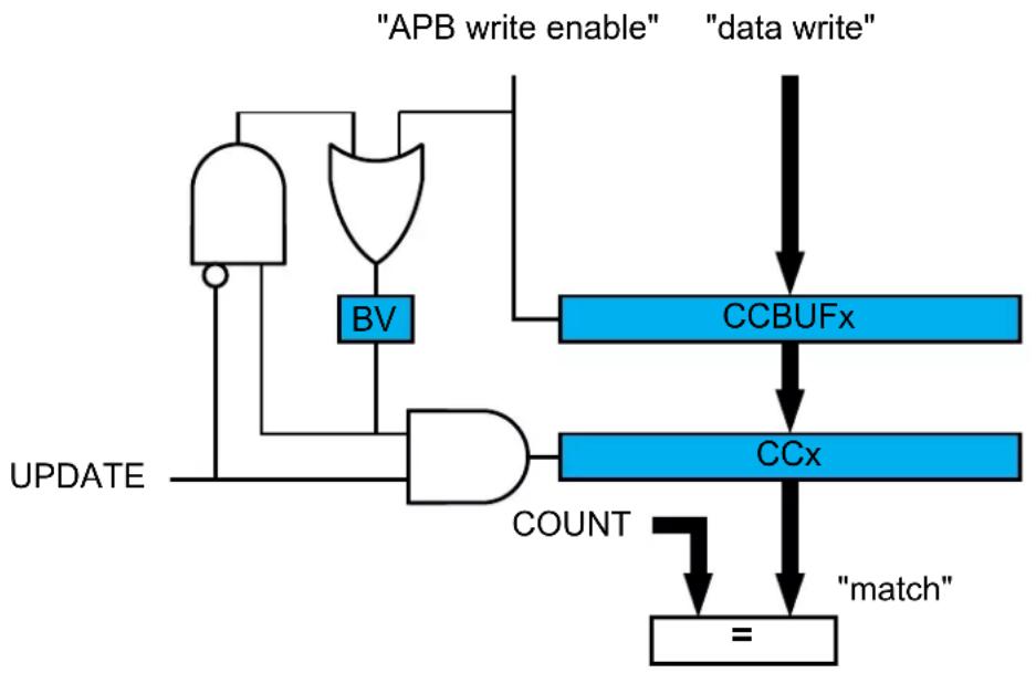
flowchart
graph TD
    A["APB write enable"] --> B["BB"]
    C["data write"] --> D["CCBUFx"]
    D --> E["CCx"]
    E --> F["match"]
    G["COUNT"] --> H["="]
    I["UPDATE"] --> J["AND Gate"]
    J --> K["AND Gate"]
    K --> L["AND Gate"]
    M["APB write enable"] --> N["AND Gate"]
    O["data write"] --> P["AND Gate"]
    Q["COUNT"] --> R["="]
    S["match"] --> T["="]
Both the registers (PATT/PER/CCx) and corresponding buffer registers (PATTBUF/PERBUF/CCBUFx) are available in the I/O register map, and the double buffering feature is not mandatory. The double buffering is disabled by writing a '1' to CTRLSET.LUPD.
Note: In NFRQ, MFRQ or PWM down-counting counter mode (CTRLBSET.DIR = 1), when double buffering is enabled (CTRLBCLR.LUPD = 1), PERBUF register is continuously copied into the PER independently of update conditions.
35.6.2.14.1 Changing the Period
The counter period can be changed by writing a new Top value to the Period register (PER or CC0, depending on the waveform generation mode), any period update on registers (PER or CCx) is effective after the synchronization delay, whatever double buffering enabling is.
Figure 35-10. Unbuffered Single-Slope Up-Counting Operation
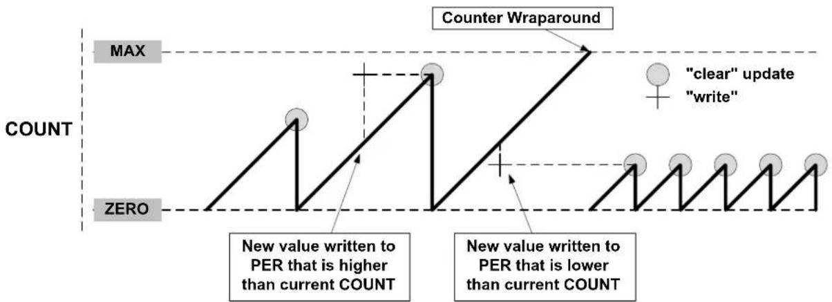
line
| COUNT | COUNT Value | Label | |-------|-------------|---------------------------| | 0 | 0 | "clear" update | | 1 | 1 | "write" | | 2 | 2 | "clear" update | | 3 | 3 | "write" | | 4 | 4 | "clear" update | | 5 | 5 | "write" | | 6 | 6 | "clear" update | | 7 | 7 | "write" | | 8 | 8 | "clear" update | | 9 | 9 | "write" | | 10 | 10 | "clear" update | | 11 | 11 | "write" | | 12 | 12 | "clear" update | | 13 | 13 | "write" | | 14 | 14 | "clear" update | | 15 | 15 | "write" | | 16 | 16 | "clear" update | | 17 | 17 | "write" | | 18 | 18 | "clear" update | | 19 | 19 | "write" | | 20 | 20 | "clear" update | | 21 | 21 | "write" | | 22 | 22 | "clear" update | | 23 | 23 | "write" | | 24 | 24 | "clear" update | | 25 | 25 | "write" | | 26 | 26 | "clear" update | | 27 | 27 | "write" | | 28 | 28 | "clear" update | | 29 | 29 | "write" | | 30 | 30 | "clear" update | | 31 | 31 | "write" | | 32 | 32 | "clear" update | | 33 | 33 | "write" | | 34 | 34 | "clear" update | | 35 | 35 | "write" | | 36 | 36 | "clear" update | | 37 | 37 | "write" | | 38 | 38 | "clear" update | | 39 | 39 | "write" | | 40 | 40 | "clear" update | | 41 | 41 | "write" | | 42 | 42 | "clear" update | | 43 | 43 | "write" | | 44 | 44 | "clear" update | | 45 | 45 | "write" | | 46 | 46 | "clear" update | | 47 | 47 | "write" | | 48 | 48 | "clear" update | | 49 | 49 | "write" | | 50 | 50 | "clear" update | | 51 | 51 | "write" | | 52 | 52 | "clear" update | | 53 | 53 | "write" | | 54 | 54 | "clear" update | | 55 | 55 | "write" | | 56 | 56 | "clear" update | | 57 | 57 | "write" | | 58 | 58 | "clear" update | | 59 | 59 | "write" | | 60 | 60 | "clear" update | | 61 | 61 | "write" | | 62 | 62 | "clear" update | | 63 | 63 | "write" | | 64 | 64 | "clear" update | | 65 | 65 | "write" | | 66 | 66 | "clear" update | | 67 | 67 | "write" | | 68 | 68 | "clear" update | | 69 | 69 | "write" | | 70 | 70 | "clear" update | | 71 | 71 | "write" | | 72 | 72 | "clear" update | | 73 | 73 | "write" | | 74 | 74 | "clear" update | | 75 | 75 | "write" | | 76 | 76 | "clear" update | | 77 | 77 | "write" | | 78 | 78 | "clear" update | | 79 | 79 | "write" | | 80 | 80 | "clear" update | | 81 | 81 | "write" | | 82 | 82 | "clear" update | | 83 | 83 | "write" | | 84 | 84 | "clear" update | | 85 | 85 | "write" | | 86 | 86 | "clear" update | | 87 | 87 | "write" | | 88 | 88 | "clear" update | | 89 | 89 | "write" | | 90 | 90 | "clear" update | | 91 | 91 | "write" | | 92 | 92 | "clear" update | | 93 | 93 | "write" | | 94 | 94 | "clear" update | | 95 | 95 | "write" | | 96 | 96 | "clear" update | | 97 | 97 | "write" | | 98 | 98 | "clear" update | | 99 | 99 | "write" | | Max | MAX | MAX | | Zero | ZERO | ZERO | The chart is a line graph with 'MAX' at the top and 'ZERO' at the bottom. The labels for the lines are 'PER' and 'Counter Wraparound'.Figure 35-11. Unbuffered Single-Slope Down-Counting Operation

line
| COUNT | COUNT | Event Type | |-------|-------|------------------| | 0 | 0 | "reload" update | | 1 | 1 | "write" | | 2 | 2 | "reload" update | | 3 | 3 | "write" | | 4 | 4 | "reload" update | | 5 | 5 | "write" | | 6 | 6 | "reload" update | | 7 | 7 | "write" | | 8 | 8 | "reload" update | | 9 | 9 | "write" | | 10 | 10 | "reload" update | | 11 | 11 | "write" | | 12 | 12 | "reload" update | | 13 | 13 | "write" | | 14 | 14 | "reload" update | | 15 | 15 | "write" | | 16 | 16 | "reload" update | | 17 | 17 | "write" | | 18 | 18 | "reload" update | | 19 | 19 | "write" | | 20 | 20 | "reload" update | | 21 | 21 | "write" | | 22 | 22 | "reload" update | | 23 | 23 | "write" | | 24 | 24 | "reload" update | | 25 | 25 | "write" | | 26 | 26 | "reload" update | | 27 | 27 | "write" | | 28 | 28 | "reload" update | | 29 | 29 | "write" | | 30 | 30 | "reload" update | | 31 | 31 | "write" | | 32 | 32 | "reload" update | | 33 | 33 | "write" | | 34 | 34 | "reload" update | | 35 | 35 | "write" | | 36 | 36 | "reload" update | | 37 | 37 | "write" | | 38 | 38 | "reload" update | | 39 | 39 | "write" | | 40 | 40 | "reload" update | | 41 | 41 | "write" | | 42 | 42 | "reload" update | | 43 | 43 | "write" | | 44 | 44 | "reload" update | | 45 | 45 | "write" | | 46 | 46 | "reload" update | | 47 | 47 | "write" | | 48 | 48 | "reload" update | | 49 | 49 | "write" | | 50 | 50 | "reload" update | | 51 | 51 | "write" | | 52 | 52 | "reload" update | | 53 | 53 | "write" | | 54 | 54 | "reload" update | | 55 | 55 | "write" | | 56 | 56 | "reload" update | | 57 | 57 | "write" | | 58 | 58 | "reload" update | | 59 | 59 | "write" | | 60 | 60 | "reload" update | | 61 | 61 | "write" | | 62 | 62 | "reload" update | | 63 | 63 | "write" | | 64 | 64 | "reload" update | | 65 | 65 | "write" | | 66 | 66 | "reload" update | | 67 | 67 | "write" | | 68 | 68 | "reload" update | | 69 | 69 | "write" | | 70 | 70 | "reload" update | | 71 | 71 | "write" | | 72 | 72 | "reload" update | | 73 | 73 | "write" | | 74 | 74 | "reload" update | | 75 | 75 | "write" | | 76 | 76 | "reload" update | | 77 | 77 | "write" | | 78 | 78 | "reload" update | | 79 | 79 | "write" | | 80 | 80 | "reload" update | | 81 | 81 | "write" | | 82 | 82 | "reload" update | | 83 | 83 | "write" | | 84 | 84 | "reload" update | | 85 | 85 | "write" | | 86 | 86 | "reload" update | | 87 | 87 | "write" | | 88 | 88 | "reload" update | | 89 | 89 | "write" | | 90 | 90 | "reload" update | | 91 | 91 | "write" | | 92 | 92 | "reload" update | | 93 | 93 | "write" | | 94 | 94 | "reload" update | | 95 | 95 | "write" | | 96 | 96 | "reload" update | | 97 | 97 | "write" | | 98 | 98 | "reload" update | | 99 | 99 | "write" | | <100 | MAX | MAX | ZERO = Zero ZERO ZERO ZERO ZERO ZERO ZERO ZERO ZERO ZERO ZERO ZERO ZERO ZERO ZERO ZERO ZERO ZERO ZERO ZERO ZERO ZERO ZERO ZERO ZERO ZERO ZERO ZERO ZERO ZERO ZERO ZERO ZERO ZERO ZERO ZERO ZERO ZERO ZERO ZERO ZERO ZERO ZERO ZERO ZERO ZERO ZERO ZERO ZERO ZERO ZERO ZERO ZERO ZERO ZERO ZERO ZERO ZERO ZERO ZERO ZERO ZERO ZERO ZERO ZERO ZERO ZERO ZERO BRL The chart displays a single series of counts for each category. The values are estimated based on the original data from the code.A counter wraparound can occur in any operation mode when up-counting without buffering, see the following figure. COUNT and TOP are continuously compared, so when a new value that is lower than the current COUNT is written to TOP, COUNT will wrap before a compare match.
Figure 35-12. Unbuffered Dual-Slope Operation

line
| Time/Event | Count | | ---------- | ----- | | "reload" update | 0 | | "write" | 0 | | Counter Wraparound | MAX | | Zero | 0 |When double buffering is used, the buffer can be written at any time and the counter will still maintain correct operation. The period register is always updated on the update condition, as shown in the following figure. This prevents wraparound and the generation of odd waveforms.
Figure 35-13. Changing the Period Using Buffering
line
| Metric | Value Type | Description | |--------|------------|-------------| | COUNT | NEW VALUE WRITTEN TO PERBUF THAT IS HIGHER THAN CURRENT COUNT | - | | COUNT | NEW VALUE WRITTEN TO PERBUF THAT IS LOWER THAN CURRENT COUNT | - | | COUNT | PER IS UPDATED WITH PERBUF VALUE | - | | COUNT | "reload" update | ○ (reload) update | | COUNT | "write" | ✕ (write) | | COUNT | ZERO | - | | MAX | - | - | | ZERO | - | - |35.6.2.15 Capture Operations
To enable and use capture operations, the Match or Capture Channel x Event Input Enable bit in the Event Control register (EVCTRL.MCEIx) must be written to '1'. The capture channels to be used must also be enabled in the Capture Channel x Enable bit in the Control A register (CTRLA.CPTENx) before capturing can be performed.
Note:
- Capture of the period and duty cycle on I/Os using PPW/PWP mode is possible using EIC and Event System.
35.6.2.15.1 Event Capture Action
The compare or capture channels can be used as input capture channels to capture events from the Event System, and give them a timestamp. The following figure shows four capture events for one capture channel.
Figure 35-14. Input Capture Timing

flowchart
graph TD
    A["events"] --> B["MAX"]
    B --> C["COUNT"]
    C --> D["ZERO"]
    D --> E["Capture 0"]
    D --> F["Capture 1"]
    D --> G["Capture 2"]
    D --> H["Capture 3"]
For input capture, the buffer register and the corresponding CCx act like a FIFO. When CCx is empty or read, any content in CCBUFx is transferred to CCx. The buffer valid flag is passed to set the CCx interrupt flag (IF) and generate the optional interrupt, event or DMA request. The CCBUFx register value can't be read, all captured data must be read from the CCx register.
Figure 35-15. Capture Double Buffering
flowchart
graph TD
    A["capture"] --> B["BUFV"]
    B --> C["EN"]
    C --> D["CCBUFx"]
    D --> E["CCx"]
    E --> F["data read"]
    G["INT/DMA request"] --> H["IF"]
    H --> I["EN"]
    I --> J["CCBUFx"]
    J --> K["COUNT"]
The TCC can detect capture overflow of the input capture channels: When a new capture event is detected while the Capture Buffer Valid flag (STATUS.CCBUFVx) is still set, the new timestamp will not be stored and INTFLAG.ERR will be set.
35.6.2.15.2 Period and Pulse-Width (PPW) Capture Action
The TCC can perform two input captures and restart the counter on one of the edges. This enables the TCC to measure the pulse-width and period and to characterize the frequency f' and dutyCycle of an input signal:
$$ f = \frac {1}{T}, d u t y C y c l e = \frac {t _ {p}}{T} $$
Figure 35-16. PWP Capture

line
| Signal Type | Value | | ----------------- | ----- | | external signal / event | 100 | | Pulsewidthh (tp) | 100 | | capture times | 100 | | COUNT | 100 | | MAX | 100 | | ZERO | 100 | | CC0 | 100 | | CC1CC1 | 100 |Selecting PWP or PPW in the Timer/Counter Event Input 1 Action bit group in the Event Control register (EVCTRL.EVACT1) enables the TCC to perform one capture action on the rising edge and the other one on the falling edge. When using PPW (period and pulse-width) event action, period T will be captured into CC0 and the pulse-width t_p into CC1. The PWP (Pulse-width and Period) event action offers the same functionality, but T will be captured into CC1 and t_p into CC0.
The Timer/Counter Event x Invert Enable bit in the Event Control register (EVCTRL.TCINVx) is used for event source x to select whether the wraparound should occur on the rising edge or the falling edge. If EVCTRL.TCINVx = 1, the wraparound will happen on the falling edge.
The corresponding capture is done only if the channel is enabled in capture mode (CTRLA.CPTENx = 1). If not, the capture action will be ignored and the channel will be enabled in compare mode of operation. When only one of these channels is required, the other channel can be used for other purposes.
The TCC can detect capture overflow of the input capture channels: When a new capture event is detected while the INTFLAG.MCx is still set, the new timestamp will not be stored and INTFLAG.ERR will be set.
Note: When up-counting (CTRLBSET.DIR = 0), counter values lower than 1 cannot be captured in Capture Minimum mode (FCTRLn.CAPTURE = CAPTMIN). To capture the full range including value 0, the TCC must be configured in down-counting mode (CTRLBSET.DIR = 0).
Note: In dual-slope PWM operation, and when TOP is lower than MAX/2, the CCx MSB captures the CTRLB.DIR state to identify the ramp on which the capture has been done. For rising ramps CCx[MSB] is zero, for falling ramps CCx[MSB] = 1.
35.6.3 Additional Features
35.6.3.1 One-Shot Operation
When one-shot is enabled, the counter automatically stops on the next counter overflow or underflow condition. When the counter is stopped, the Stop bit in the Status register (STATUS.STOP) is set and the waveform outputs are set to the value defined by DRVCTRL.NREx and DRVCTRL.NRVx.
One-shot operation can be enabled by writing a '1' to the One-Shot bit in the Control B Set register (CTRLBSET.ONESHOT) and disabled by writing a '1' to CTRLBCLR.ONESHOT. When enabled, the TCC will count until an overflow or underflow occurs and stop counting. The one-shot operation can be restarted by a re-trigger software command, a re-trigger event or a start event. When the counter restarts its operation, STATUS.STOP is automatically cleared.
35.6.3.2 Circular Buffer
The Period register (PER) and the compare channels register (CC0 to CC3) support circular buffer operation. When circular buffer operation is enabled, the PER or CCx values are copied into the corresponding buffer registers at each update condition. Circular buffering is dedicated to RAMP2, RAMP2A, and DSBOTH operations.
Figure 35-17. Circular Buffer on Channel 0

flowchart
graph TD
    A["BUFV"] --> B["AND"]
    B --> C["AND"]
    C --> D["CCBUF0"]
    D --> E["CC0"]
    E --> F["="]
    F --> G["m" atch"]
    H["write enable"] --> A
    I["data write"] --> D
    J["COUNT"] --> F
    K["UPDATE CIRCC0EN"] --> L["UPDATE"]
35.6.3.3 Dithering Operation
The TCC supports dithering on Pulse-width or Period on a 16, 32 or 64 PWM cycles frame.
Dithering consists in adding some extra clocks cycles in a frame of several PWM cycles, and can improve the accuracy of the average output pulse width and period. The extra clock cycles are added on some of the compare match signals, one at a time, through a "blue noise" process that minimizes the flickering on the resulting dither patterns.
Dithering is enabled by writing the corresponding configuration in the Enhanced Resolution bits in CTRLA register (CTRLA.RESOLUTION):
• DITH4 enable dithering every 16 PWM frames
• DITH5 enable dithering every 32 PWM frames
• DITH6 enable dithering every 64 PWM frames
The DITHERCY bits of COUNT, PER and CCx define the number of extra cycles to add into the frame (DITHERCY bits from the respective COUNT, PER or CCx registers). The remaining bits of COUNT, PER, CCx define the compare value itself.
The pseudo code, giving the extra cycles insertion regarding the cycle is:
int extra_cycle(resolution, dithercy, cycle){
    int MASK;
    int value
    switch (resolution){
    DITH4: MASK = 0x0f;
    DITH5: MASK = 0x1f;
    DITH6: MASK = 0x3f;
    }
    value = cycle * dithercy;
    if (((MASK & value) + dithercy) > MASK)
    return 1;
    return 0;
}
Dithering on Period
Writing DITHERCY in PER will lead to an average PWM period configured by the following formulas.
DITH4 mode:
$$ P w m P e r i o d = \left(\frac {\text { DITHERCY }}{1 6} + \text { PER }\right) \left(\frac {1}{f _ {\mathrm {GCLK_TCC}}}\right) $$
Note: If DITH4 mode is enabled, the last 4 significant bits from PER/CCx or COUNT register correspond to the DITHERCY value, rest of the bits corresponds to PER/CCx or COUNT value.
DITH5 mode:
$$ P w m P e r i o d = \left(\frac {\text { DITHERCY }}{3 2} + \text { PER }\right) \left(\frac {1}{f _ {\mathrm {GCLK_TCC}}}\right) $$
DITH6 mode:
$$ P w m P e r i o d = \left(\frac {\text { DITHERCY }}{6 4} + \text { PER }\right) \left(\frac {1}{f _ {\mathrm {GCLK_TCC}}}\right) $$
Dithering on Pulse Width
Writing DITHERCY in CCx will lead to an average PWM pulse width configured by the following formula.
DITH4 mode:
$$ P w m P u l s e W i d t h = \left(\frac {\text { DITHERCY }}{1 6} + \mathrm{CCx}\right) \left(\frac {1}{f _ {\mathrm {GCLK_TCC}}}\right) $$
DITH5 mode:
$$ P w m P u l s e W i d t h = \left(\frac {\text { DITHERCY }}{3 2} + \mathrm{CCx}\right) \left(\frac {1}{f _ {\mathrm {GCLK_TCC}}}\right) $$
DITH6 mode:
$$ P w m P u l s e W i d t h = \left(\frac {\text { DITHERCY }}{6 4} + \mathrm{CCx}\right) \left(\frac {1}{f _ {\mathrm {GCLK_TCC}}}\right) $$
Note: The PWM period will remain static in this case.
35.6.3.4 Ramp Operations
Three ramp operation modes are supported. All of them require the timer/counter running in single-slope PWM generation. The ramp mode is selected by writing to the Ramp Mode bits in the Waveform Control register (WAVE.RAMP).
RAMP1 Operation
This is the default PWM operation, described in Single-Slope PWM Generation.
RAMP2 Operation
These operation modes are dedicated for power factor correction (PFC), Half-Bridge and Push-Pull SMPS topologies, where two consecutive timer/counter cycles are interleaved, see the following figure. In cycle A, odd channel output is disabled, and in cycle B, even channel output is disabled. The ramp index changes after each update, but can be software modified using the Ramp index command bits in Control B Set register (CTRLBSET.IDXCMD).
Standard RAMP2 (RAMP2) Operation
Ramp A and B periods are controlled by the PER register value. The PER value can be different on each ramp by the Circular Period buffer option in the Wave register (WAVE.CIPEREN=1). This mode uses a two-channel TCC to generate two output signals, or one output signal with another CC channel enabled in capture mode.
Figure 35-18. RAMP2 Standard Operation
flowchart
graph TD
    A["TOPO(A)"] -->|CC0| B["TOPO(B)"]
    B -->|CC1| C["TOPO(B)"]
    C -->|CC0| D["Retrigger on FaultA"]
    D -->|CC1| E["TOPO(B)"]
    style A fill:#f9f,stroke:#333
    style B fill:#f9f,stroke:#333
    style C fill:#f9f,stroke:#333
    style D fill:#f9f,stroke:#333
    style E fill:#f9f,stroke:#333
    note right of A "A B A B Ramp"
    note right of B "CIPEREN = 1"
    note right of C "POLT0 = 1"
    note right of D "Keep on FaultB"
    note right of E "POL1 = 1"
    note_left_of_F["ZERO"]
    note_right_of_G["FaultA input"]
    note_right_of_H["FaultB input"]
    note_right_of_I[""clear" update"]
    note_right_of_J["match"]
    style A fill:#ccf,stroke:#333
    style B fill:#ccf,stroke:#333
    style C fill:#ccf,stroke:#333
    style D fill:#ccf,stroke:#333
    style E fill:#ccf,stroke:#333
    style F fill:#cfc,stroke:#333
    style G fill:#cfc,stroke:#333
    style H fill:#cfc,stroke:#333
    style I fill:#cfc,stroke:#333
Alternate RAMP2 (RAMP2A) Operation
Alternate RAMP2 operation is similar to RAMP2, but CC0 controls both WO[0] and WO[1] waveforms when the corresponding circular buffer option is enabled (CIPEREN=1). The waveform polarity is the same on both outputs. Channel 1 can be used in capture mode.
Figure 35-19. RAMP2 Alternate Operation

Critical RAMP2 (RAMP2C) Operation
Critical RAMP2 operation provides a way to cover RAMP2 operation requirements without the update constraint associated to the use of circular buffers. In this mode, CC0 is controlling the period of ramp A and PER is controlling the period of ramp B. When using more than two channels, WO[0] output is controlled by CC2 (HIGH) and CC0 (LOW). On TCC with 2 channels, a pulse on WO[0] will last the entire period of ramp A, if WAVE.POL0=0.
Figure 35-20. RAMP2 Critical Operation With More Than 2 Channels

flowchart
graph TD
    A["Ramp"] --> B["A"]
    B --> C["A B A B"]
    C --> D["STOP"]
    D --> E["CC0"]
    D --> F["CC1"]
    D --> G["CC2"]
    D --> H["CC1"]
    I["REtrigger on FaultA"] --> J["TOP"]
    K["CC0"] --> L["CC2"]
    M["CC1"] --> N["CC2"]
    O["CC1"] --> P["CC2"]
    Q["STOP"] --> R["CC1"]
    S["CC0"] --> T["CC2"]
    U["CC1"] --> V["CC2"]
    W["CC2"] --> X["CC2"]
    Y["CC1"] --> Z["CC2"]
    AA["zero"] --> AB["WO[0"]]
    AC["WO[1"]] --> AD["Kop on FaultB"]
    AE["FaultA input"] --> AF["FaultB input"]
    AG["POL2 = 1"] --> AH
    AI["POL1 = 1"] --> AJ
    AK["Count"] --> AL["COUNT"]
Figure 35-21. RAMP2 Critical Operation With 2 Channels

flowchart
graph TD
    A["Ramp"] --> B["A"]
    B --> C["A B A B"]
    C --> D["CC0"]
    D --> E["CC1"]
    E --> F["TOP"]
    F --> G["Retrigger on FaultA"]
    G --> H["CC1"]
    H --> I["TOP"]
    I --> J["CC0"]
    style A fill:#f9f,stroke:#333
    style J fill:#ccf,stroke:#333
    note right of A "clear" update
    note right of J "match"
    subgraph COUNT
        K["ZERO"]
        L["WO[0"]]
        M["WO[1"]]
        N["FaultA input"]
        O["FaultB input"]
    end
    subgraph Legend
        P["POL0 = 0"]
        Q["POL1 = 1"]
    end
35.6.3.5 Recoverable Faults
Recoverable faults can restart or halt the timer/counter. Two faults, called Fault A and Fault B, can trigger recoverable fault actions on the compare channels CC0 and CC1 of the TCC. The compare channels' outputs can be clamped to inactive state either as long as the fault condition is present, or from the first valid fault condition detection on until the end of the timer/counter cycle.
Fault Inputs
The first two channel input events (TCC0MC0 and TCC0MC1) can be used as Fault A and Fault B inputs, respectively. Event system channels connected to these fault inputs must be configured as asynchronous. The TCC must work in a PWM mode.
Fault Filtering
There are three filters available for each input Fault A and Fault B. They are configured by the corresponding Recoverable Fault n Configuration registers (FCTRLA and FCTRLB). The three filters can either be used independently or in any combination.
Input By default, the event detection is asynchronous. When the event occurs, the fault system will immediately and asynchronously perform the selected fault action on the compare channel output, also in device power modes where the clock is not available. To avoid false fault detection on external events (e.g. due to a glitch on an I/O port) a digital filter can be enabled and configured by the Fault B Filter Value bits in the Fault n Configuration registers (FCTRLn.FILTERVAL). If the event width is less than FILTERVAL (in clock cycles), the event will be discarded. A valid event will be delayed by FILTERVAL clock cycles.
Fault Blanking This ignores any fault input for a certain time just after a selected waveform output edge. This can be used to prevent false fault triggering due to signal bouncing, as shown in the figure below. Blanking can be enabled by writing an edge triggering configuration to the Fault n Blanking Mode bits in the Recoverable Fault n Configuration register (FCTRLn.BLANK). The desired duration of the blanking must be written to the Fault n Blanking Time bits (FCTRLn.BLANKVAL). The blanking time t_b is calculated by
$$ t _ {b} = \frac {1 + \text { BLANKVAL }}{f _ {\mathrm {GCLK_TCCO_PRESC}}} $$
Here, f_GCLK_TCC0_PRESC is the frequency of the prescaled peripheral clock frequency f_GCLK_TCC0 .
The prescaler is enabled by writing '1' to the Fault n Blanking Prescaler bit (FCTRLn.BLANKPRESC). When disabled, f_GCLK_TCC0_PRESC=f_GCLK_TCC0 . When enabled, f_GCLK_TCC0_PRESC=f_GCLK_TCC0/64 .
The maximum blanking time (FCTRLn.BLANKVAL=255) at f_GCLK_TCC0=96MHz is 2.67μs (no prescaler) or 170μs (prescaling). For f_GCLK_TCC0=1MHz , the maximum blanking time is either 170μs (no prescaling) or 10.9ms (prescaling enabled).
Figure 35-22. Fault Blanking in RAMP1 Operation with Inverted Polarity

flowchart
graph TD
    A["TOP"] --> B["CC0"]
    B --> C["ZERO"]
    C --> D["CMP0"]
    D --> E[""clear" update"]
    E --> F["match"]
    F --> G["Fault input enabled"]
    F --> H["Fault input disabled"]
    F --> I["Fault discarded"]
    J["FCTRLA BLANKVAL = 0"] --> K[" FaultA Input "]
    L["FCTRLA BLANKVAL > 0"] --> M[" FaultA Blanking "]
    N["WO[0"]] --> O[" FaultA Input "]
    P["FCTRILA BLANKVAL > 0"] --> Q[" FaultA Blanking "]
    R["FCTRILA BLANKVAL > 0"] --> S[" FaultA Blanking "]
    T["FCTRILA BLANKVAL > 0"] --> U[" FaultA Blanking "]
    V["FCTRILA BLANKVAL > 0"] --> W[" FaultA Blanking "]
    X["FCTRILA BLANKVAL > 0"] --> Y[" FaultA Blanking "]
    Z["FCTRILA BLANKVAL > 0"] --> AA[" FaultA Blanking "]
    AB["FCTRILA BLANKVAL > 0"] --> AC[" FaultA Blanking "]
    AD["FCTRILA BLANKVAL > 0"] --> AE[" FaultA Blanking "]
    AF["FCTRILA BLANKVAL > 0"] --> AG[" FaultA Blanking "]
    AH["FCTRILA BLANKVAL > 0"] --> AI[" FaultA Blanking "]
    AJ["FCTRILA BLANKVAL > 0"] --> AK[" FaultA Blanking "]
    AL["FCTRILA BLANKVAL > 0"] --> AM[" FaultA Blanking "]
    AN["FCTRILA BLANKVAL > 0"] --> AO[" FaultA Blanking "]
    AP["FCTRILA BLANKVAL > 0"] --> AQ[" FaultA Blanking "]
    AR["FCTRILA BLANKVAL > 0"] --> AS[" FaultA Blanking "]
    AT["FCTRILA BLANKVAL > 0"] --> AU[" FaultA Blanking "]
    AV["FCTRILA BLANKVAL > 0"] --> AW[" FaultA Blanking "]
    AX["FCTRILA BLANKVAL > 0"] --> AY[" FaultA Blanking "]
    AZ["FCTRILA BLANKVAL > 0"] --> BA[" FaultA Blanking "]
    BB["FCTRILA BLANKVAL > 0"] --> BC[" FaultA Blanking "]
    BD["FCTRILA BLANKVAL > 0"] --> BE[" FaultA Blanking "]
    BF["FCTRILA BLANKVAL > 0"] --> BG[" FaultA Blanking "]
    BH["FCTRILA BLANKVAL > 0"] --> BI[" FaultA Blanking "]
    BJ["FCTRILA BLANKVAL > 0"] --> BK[" FaultA Blanking "]
    BL["FCTRILA BLANKVAL > 0"] --> BLA[" FaultA Blanking "]
    BM["FCTRILA BLANKVAL > 0"] --> BN[" FaultA Blanking "]
    BO["FCTRILA BLANKVAL > 0"] --> BP[" FaultA Blanking "]
    BQ["FCTRILA BLANKVAL > 0"] --> BR[" FaultA Blanking "]
    BS["FCTRILA BLANKVAL > 0"] --> BT[" FaultA Blanking "]
    BU["FCTRILA BLANKVAL > 0"] --> BV[" FaultA Blanking "]
    BW["FCTRILA BLANKVAL > 0"] --> BX[" FaultA Blanking "]
    BY["FCTRILA BLANKVAL > 0"] --> BYA[" FaultA Blanking "]
    AZF["FCTRILA BLANKVAL > 0"] --> AZG[" FaultA Blanking "]
    BAFL["FCTRILA BLANKVAL > 0"] --> BBAY[" FaultA Blanking "]
    BBW["FCTRILA BLANKVAL > 0"] --> BCX[" FaultA Blanking "]
    BTX["FCTRILA BLANKVAL > 0"] --> BTXAY[" FaultA Blanking "]
    BZF["FCTRILA BLANKVAL > 0"] --> BZX[" FaultA Blanking "]
    CAX["FCTRILA BLANKVAL > 0"] --> CAXAY[" FaultA Blanking "]
    CBX["FCTRILA BLANKVAL > 0"] --> CBXAY[" FaultA Blanking "]
    CCX["FCTRILA BLANKVAL > 0"] --> CCXAY[" FaultA Blanking "]
    CE["XFCTRL A BLANKVAL = 0"] --> CF["XFCTRL A BLANKVAL > 0"]
    CG["XFCTRL A BLANKVAL > 0"] --> CH["XFCTRL A BLANKVAL > 0"]
    CI["XFCTRL A BLANKVAL > 0"] --> CJ["XFCTRL A BLANKVAL > 0"]
    CK["XFCTRL A BLANKVAL > 0"] --> CL["XFCTRL A BLANKVAL > 0"]
    CM["XFCTRL A BLANKVAL > 0"] --> CN["XFCTRL A BLANKVAL > 0"]
    CO["XFCTRL A BLANKVAL > 0"] --> CP["XFCTRL A BLANKVAL > 0"]
    COX["XFCTRL A BLANKVAL > 0"] --> CPX["XFCTRL A BLANKVAL > 0"]
    COY["XFCTRL A BLANKVAL > 0"] --> CYP["XFCTRL A BLANKVAL > 0"]
    CS["XFCTRL A BLANKVAL > 0"] --> CY["XFCTRL A BLANKVAL > 0"]
    CEX["XFCTRL A BLANKVAL > 0"] --> CEXAY["XFCTRL A BLANKVAL > 0"]
    CEYX["XFCTRL A BLANKVAL > 0"] --> CEYAY["XFCTRL A BLANKVAL > 0"]
    CEZX["XFCTRL A BLANKVAL > 0"] --> CEZXAY["XFCTRL A BLANKVAL > 0"]
    CEYZX["XFCTRL A BLANKVAL > 0"] --> CEYZAY["XFCTRL A BLANKVAL > 0"]
    CEZW["XFCTRL A BLANKVAL > 0"] --> CEZWAY["XFCTRL A BLANKVAL > 0"]
    CEAXX["XFCTRL A BLANKVAL > 0"] --> CEAXAY["XFCTRL A BLANKVAL > 0"]
    CEAXZ["XFCTRL A BLANKVAL > 0"] --> CEAXAYX["XFCTRL A BLANKVAL > 0"]
    CEAXYX["XFCTRL A BLANKVAL > 0"] --> CEAXAYY["XFCTRL A BLANKVAL > 0"]
    CEAXZY["XFCTRL A BLANKVAL > 0"] --> CEAXAYZ["XFCTRL A BLANKVAL > 0"]
    CEAXYZ["XFCTRL A BLANKVAL > 0"] --> CEAXAYC["XFCTRL A BLANKVAL > 0"]
    CEAXZC["XFCTRL A BLANKVAL > 0"] --> CEAXAYC1["XFCTRL A BLANKVAL > 0"]
    CEAXZC1["XFCTRL A BLANKVAL > 0"] --> CEAXAYC2["XFCTRL A BLANKVAL > 0"]
    CEAXYC1["XFCTRL A BLANKVAL > 0"] --> CEAXAYC3["XFCTRL A BLANKVAL > 0"]
    CEAXYC2["XFCTRL A BLANKVAL > 0"] --> CEAXAYC4["XFCTRL A BLANKVAL > 0"]
    CEAXYC3["XFCTRL A BLANKVAL > 0"] --> CEAXAYC5["XFCTRL A BLANKVAL > 0"]
    CEAXYC4["XFCTRL A BLANKVAL > 0"] --> CEAXAYC6["XFCTRL A BLANKVAL > 0"]
    CEAXYC5["XFCTRL A BLANKVAL > 0"] --> CEAXAYC7["XFCTRL A BLANKVAL > 0"]
    CEAXYC6["XFCTRL A BLANKVAL > 0"] --> CEAXAYC8["XFCTRL A BLANKVAL > 0"]
    CEAXYC7["XFCTRL A BLANKVAL > 0"] --> CEAXAYC9["XFCTRL A BLANKVAL > 0"]
    CEAXYC8["XFCTRL A BLANKVAL > 0"] --> CEAXAYC10["XFCTRL A BLANKVAL > 0"]
    CEAXYC9["XFCTRL A BLANKVAL > 0"] --> CEAXAYC11["XFCTRL A BLANKVAL > 0"]
    CEAXYC10["XFCTRL A BLANKVAL > 0"] --> CEAXAYC12["XFCTRL A BLANKVAL > 0"]
    CEAXYC11["XFCTRL A BLANKVAL > 0"] --> CEAXAYC13["XFCTRL A BLANKVAL > 0"]
    CEAXYC12["XFCTRL A BLANKVAL > 0"] --> CEAXAYC14["XFCTRL A BLANKVAL > 0"]
    CEAXYC13["XFCTRL A BLANKVAL > 0"] --> CEAXAYC15["XFCTRL A BLANKVAL > 0"]
    CEAXYC14["XFCTRL A BLANKVAL > 0"] --> CEAXAYC16["XFCTRL A BLANKVAL > 0"]
    CEAXYC15["XFCTRL A BLANKVAL > 0"] --> CEAXAYC17["XFCTRL A BLANKVAL > 0"]
    CEAXYC16["XFCTRL A BLANKVAL > 0"] --> CEAXAYC18["XFCTRL A BLANKVAL > 0"]
    CEAXYC17["XFCTRL A BLANKVAL > 0"] --> CEAXAYC19["XFCTRL A BLANKVAL > 0"]
    CEAXYC18["XFCTRL A BLANKVAL > 0"] --> CEAXAYC20["XFCTRL A BLANKVAL > 0"]
    CEAXYC19["XFCTRL A BLANKVAL > 0"] --> CEAXAYC21["XFCTRL A BLANKVAL > 0"]
    CEAXYC20["XFCTRL A BLANKVAL > 0"] --> CEAXAYC22["XFCTRL A BLANKVAL > 0"]
    CEAXYC21["XFCTRL A BLANKVAL > 0"] --> CEAXAYC23["XFCTRL A BLANKVAL > 0"]
Fault Qualification This is enabled by writing a '1' to the Fault n Qualification bit in the Recoverable Fault n Configuration register (FCTRLn.QUAL). When the recoverable fault qualification is enabled (FCTRLn.QUAL=1), the fault input is disabled all the time the corresponding channel output has an inactive level, as shown in the figures below.
Figure 35-23. Fault Qualification in RAMP1 Operation
flowchart
graph TD
    A["CC0"] --> B["match"]
    C["CC1"] --> D["match"]
    E["CC0"] --> F["Fault input enabled"]
    G["CC1"] --> H["Fault input disabled"]
    I["CC0"] --> J["Fault input B Input Qual"]
    K["CC1"] --> L[""Fault input B Input Qual"]
    M["CC0"] --> N["Fault input A Input Qual"]
    O["CC1"] --> P[""Fault input A Input Qual"]
    Q["CC0"] --> R[""Fault input B Input Qual"]
    S["CC1"] --> T[""Fault input B Input Qual"]
    U["CC0"] --> V["Fault input A Input Qual"]
    W["CC1"] --> X["Fault input A Input Qual"]
    Y["CC0"] --> Z["Fault input B Input Qual"]
    AA["CC1"] --> AB["Fault input B Input Qual"]
    AC["CC0"] --> AD["Fault input A Input Qual"]
    AE["CC1"] --> AF["Fault input A Input Qual"]
    AG["CC0"] --> AH["Fault input B Input Qual"]
    AI["CC1"] --> AJ["Fault input B Input Qual"]
    AK["CC0"] --> AL["Fault input A Input Qual"]
    AM["CC1"] --> AN["Fault input A Input Qual"]
    AO["CC0"] --> AP["Fault input B Input Qual"]
    AQ["CC1"] --> AR["Fault input B Input Qual"]
    AS["CC0"] --> AT["Fault input A Input Qual"]
    AU["CC1"] --> AV["Fault input A Input Qual"]
    AW["CC0"] --> AX["Fault input B Input Qual"]
    AY["CC1"] --> AZ["Fault input B Input Qual"]
    BA["CC0"] --> BB["Fault input A Input Qual"]
    BC["CC1"] --> BD["Fault input A Input Qual"]
    BE["CC0"] --> BF["Fault input B Input Qual"]
    BG["CC1"] --> BH["Fault input B Input Qual"]
    BI["CC0"] --> BJ["Fault input A Input Qual"]
    BK["CC1"] --> BL["Fault input A Input Qual"]
    BM["CC0"] --> BN["Fault input B Input Qual"]
    BO["CC1"] --> BP["Fault input B Input Qual"]
    BQ["CC0"] --> BR["Fault input A Input Qual"]
    BS["CC1"] --> BT["Fault input A Input Qual"]
    BU["CC0"] --> BV["Fault input B Input Qual"]
    BW["CC1"] --> BX["Fault input B Input Qual"]
    BY["CC0"] --> BZ["Fault input A Input Qual"]
    CA["CC1"] --> CB["Fault input A Input Qual"]
    CT["CC0"] --> DU["Fault input B Input Qual"]
    DV["CC1"] --> DW["Fault input B Input Qual"]
    BX<fcel>CA
DA
BD
BE
BF
BG
BA
BB
BC
BB
BB
BB
BB
BB
BB
BB
BB
BB
BB
BB
BB
BB
BB
BB
BB
BB
BB
BB
BB
BB
BB
BB
BB
BB
BB
BB
BB
BB
BB
BB
BB
BB
BB
BB
BB
BB
BB
BB
BB
BB
BB
BB
BB
BB
BB
BB
BB
BB
BB
AA
Figure 35-24. Fault Qualification in RAMP2 Operation with Inverted Polarity

flowchart
graph TD
    A["Cycle"] --> B["A"]
    B --> C["B"]
    C --> D["A"]
    D --> E["B"]
    F["COUNT"] --> G["CC0"]
    F --> H["CC1"]
    F --> I["ZERO"]
    J["Fault Input A"] --> K["Fault B Input Qual"]
    L["Fault Input B"] --> M["Fault Input A"]
    N["Fault Input A"] --> O["Fault Input B"]
    P["Fault Input B"] --> Q["Fault Input A"]
    R["Fault Input B"] --> S["Fault Input B"]
    T["Fault Input A"] --> U["Fault Input B"]
    V["Fault Input B"] --> W["Fault Input A"]
    X["Fault Input B"] --> Y["Fault Input B"]
    Z["Fault Input A"] --> AA["Fault Input B"]
    AB["Fault Input B"] --> AC["Fault Input A"]
    AD["Fault Input B"] --> AE["Fault Input B"]
    AF["Fault Input A"] --> AG["Fault Input B"]
    AH["Fault Input B"] --> AI["Fault Input A"]
    AJ["Fault Input B"] --> AK["Fault Input B"]
    AL["Fault Input A"] --> AM["Fault Input B"]
    AN["Fault Input B"] --> AO["Fault Input A"]
    AP["Fault Input A"] --> AQ["Fault Input B"]
    AR["Fault Input B"] --> AS["Fault Input A"]
    AT["Fault Input B"] --> AU["Fault Input B"]
Fault Actions
Different fault actions can be configured individually for Fault A and Fault B. Most fault actions are not mutually exclusive; hence two or more actions can be enabled at the same time to achieve a result that is a combination of fault actions.
Keep Action This is enabled by writing the Fault n Keeper bit in the Recoverable Fault n Configuration register (FCTRLn.KEEP) to '1'. When enabled, the corresponding channel output will be clamped to zero as long as the fault condition is present. The clamp will be released on the start of the first cycle after the fault condition is no longer present, see next Figure.
Figure 35-25. Waveform Generation with Fault Qualification and Keep Action
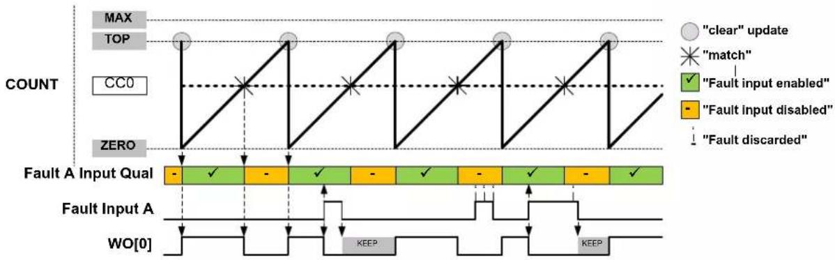
flowchart
graph TD
    A["CC0"] --> B[""clear" update"]
    B --> C["match"]
    C --> D["Fault input enabled"]
    D --> E["Fault input disabled"]
    E --> F["Fault discarded"]
    G["Fault Input Qual"] --> H["✓"]
    H --> I["-"]
    I --> J["✓"]
    J --> K["-"]
    K --> L["✓"]
    L --> M["-"]
    M --> N["✓"]
    N --> O["-"]
    O --> P["✓"]
    P --> Q["-"]
    Q --> R["✓"]
    R --> S["-"]
    S --> T["✓"]
    T --> U["-"]
    U --> V["✓"]
    V --> W["-"]
    W --> X["✓"]
    X --> Y["-"]
    Y --> Z["✓"]
    Z --> AA["-"]
    AA --> AB["✓"]
    AB --> AC["-"]
    AC --> AD["✓"]
    AD --> AE["-"]
    AE --> AF["✓"]
    AF --> AG["-"]
    AG --> AH["✓"]
    AH --> AI["-"]
    AI --> AJ["✓"]
    AJ --> AK["-"]
    AK --> AL["✓"]
    AL --> AM["-"]
    AM --> AN["✓"]
    AN --> AO["-"]
    AO --> AP["✓"]
    AP --> AQ["-"]
    AQ --> AR["✓"]
    AR --> AS["-"]
    AS --> AT["✓"]
    AT --> AU["-"]
    AU --> AV["✓"]
    AV --> AW["-"]
    AW --> AX["✓"]
    AX --> AY["-"]
    AY --> AZ["✓"]
    AZ --> BA["-"]
    BA --> BB["✓"]
    BB --> BC["-"]
    BC --> BD["✓"]
    BD --> BE["-"]
    BE --> BF["✓"]
    BF --> BG["-"]
    BG --> BH["✓"]
    BH --> BI["-"]
    BI --> BJ["✓"]
    BJ --> BK["-"]
    BK --> BL["✓"]
    BL --> BM["-"]
    BM --> BN["✓"]
    BN --> BO["-"]
    BO --> BP["✓"]
    BP --> BQ["-"]
    BQ --> BR["✓"]
    BR --> BS["-"]
    BS --> BT["✓"]
    BT --> BU["-"]
    BU --> BV["✓"]
    BV --> BW["-"]
    BW --> BX["✓"]
    BX --> BY["-"]
    BY --> BZ["✓"]
    BZ --> CA["-"]
    CA --> CB["✓"]
    CB --> CC["-"]
    CC --> CD["✓"]
    CD --> CE["-"]
    CE --> CF["✓"]
    CF --> CG["-"]
    CG --> CH["✓"]
    CH --> CI["-"]
    CI --> CJ["✓"]
    CJ --> CK["-"]
    CK --> CL["✓"]
    CL --> CM["-"]
    CM --> CN["✓"]
    CN --> CO["-"]
    CO --> CP["✓"]
    CP --> CQ["-"]
    CQ --> CR["✓"]
    CR --> CS["-"]
    CS --> CT["✓"]
    CT --> CU["-"]
    CU --> CV["✓"]
    CV --> CW["-"]
    CW --> CX["✓"]
    CX --> CY["-"]
    CY --> CZ["✓"]
Restart This is enabled by writing the Fault n Restart bit in Recoverable Fault n Configuration register (FCTRLn.RESTART) to '1'. When enabled, the timer/counter will be restarted as soon as the corresponding fault condition is present. The ongoing cycle is stopped and the timer/counter starts a new cycle, see the following figure. In Ramp 1 mode, when the new cycle starts, the compare outputs will be clamped to inactive level as long as the fault condition is present.
Note: For RAMP2 operation, when a new timer/counter cycle starts the cycle index will change automatically, as shown in the second following figure. Fault A and Fault B are qualified only during the cycle A and cycle B respectively: Fault A is disabled during cycle B, and Fault B is disabled during cycle A.
Figure 35-26. Waveform Generation in RAMP1 mode with Restart Action

flowchart
graph TD
    A["MAX"] --> B["TOP"]
    B --> C["CC0"]
    C --> D["CC1"]
    D --> E["ZERO"]
    E --> F["Restart"]
    F --> G["Fault Input A"]
    G --> H["WO[0"]]
    H --> I["WO[1"]]
    I --> J["End"]
    style A fill:#f9f,stroke:#333
    style B fill:#ccf,stroke:#333
    style C fill:#cfc,stroke:#333
    style D fill:#fcc,stroke:#333
    style E fill:#ffc,stroke:#333
    style F fill:#cff,stroke:#333
    style G fill:#ffc,stroke:#333
    style H fill:#cfc,stroke:#333
    style I fill:#cfc,stroke:#333
    style J fill:#ffc,stroke:#333
Figure 35-27. Waveform Generation in RAMP2 mode with Restart Action

flowchart
graph TD
    A["Start"] --> B["CC0/CC1"]
    B --> C["Period (T)"]
    C --> D["CCx=ZERO"]
    D --> E["CCx=TOP"]
    E --> F["Restart"]
    F --> G["Fault Input A"]
    G --> H["WO[0"]]
    G --> I["WO[1"]]
    style A fill:#f9f,stroke:#333
    style H fill:#ccf,stroke:#333
    style I fill:#ccf,stroke:#333
    style D fill:#fff,stroke:#333
    style E fill:#fff,stroke:#333
    style F fill:#fff,stroke:#333
    style G fill:#fff,stroke:#333
    style I fill:#fff,stroke:#333
    style H fill:#fff,stroke:#333
    style I fill:#fff,stroke:#333
    style_J[""clear" update"] --> K["match"]
    style_L["No fault A action in cycle B"] --> M["CC0/CC1"]
    M --> N["ZERO"]
    N --> O["CCx=ZERO"]
    O --> P["CCx=TOP"]
    P --> Q[""Restart"]
Capture Action Several capture actions can be selected by writing the Fault n Capture Action bits in the Fault n Control register (FCTRLn.CAPTURE). When one of the capture operations is selected, the counter value is captured when the fault occurs. These capture operations are available:
• CAPT - the equivalent to a standard capture operation, for further details refer to Capture Operations
- CAPTMIN - gets the minimum time stamped value: on each new local minimum captured value, an event or interrupt is issued.
- CAPTMAX - gets the maximum time stamped value: on each new local maximum captured value, an event or interrupt (IT) is issued, see Capture Action "CAPTMAX".
- LOCMIN - notifies by event or interrupt when a local minimum captured value is detected.
- LOCMAX - notifies by event or interrupt when a local maximum captured value is detected.
- DERIVO - notifies by event or interrupt when a local extreme captured value is detected, see Capture Action "DERIVO".
CCx Content:
In CAPTMIN and CAPTMAX operations, CCx keeps the respective extremum captured values, see Capture Action "CAPTMAX". In LOCMIN, LOCMAX or DERIV0 operation, CCx follows the counter value at fault time, see Capture Action "DERIV0".
Before enabling CAPTMIN or CAPTMAX mode of capture, the user must initialize the corresponding CCx register value to a value different from zero (for CAPTMIN) top (for CAPTMAX). If the CCx register initial value is zero (for CAPTMIN) top (for CAPTMAX), no captures will be performed using the corresponding channel.
MCx Behaviour:
In LOCMIN and LOCMAX operation, capture is performed on each capture event. The MCx interrupt flag is set only when the captured value is upper or equal (for LOCMIN) or lower or equal (for LOCMAX) to the previous captured value. So interrupt flag is set when a new relative local Minimum (for CAPTMIN) or Maximum (for CAPTMAX) value has been detected. DERIVO is equivalent to an OR function of (LOCMIN, LOCMAX).
In CAPT operation, capture is performed on each capture event. The MCx interrupt flag is set on each new capture.
In CAPTMIN and CAPTMAX operation, capture is performed only when on capture event time, the counter value is lower (for CAPTMIN) or upper (for CAPMAX) than the last captured value. The MCx interrupt flag is set only when on capture event time, the counter value is upper or equal (for CAPTMIN) or lower or equal (for CAPTMAX) to the value captured on the previous event. So interrupt flag is set when a new absolute local Minimum (for CAPTMIN) or Maximum (for CAPTMAX) value has been detected.
Interrupt Generation
In CAPT mode, an interrupt is generated on each filtered Fault n and each dedicated CCx channel capture counter value. In other modes, an interrupt is only generated on an extreme captured value.
Figure 35-28. Capture Action "CAPTMAX"
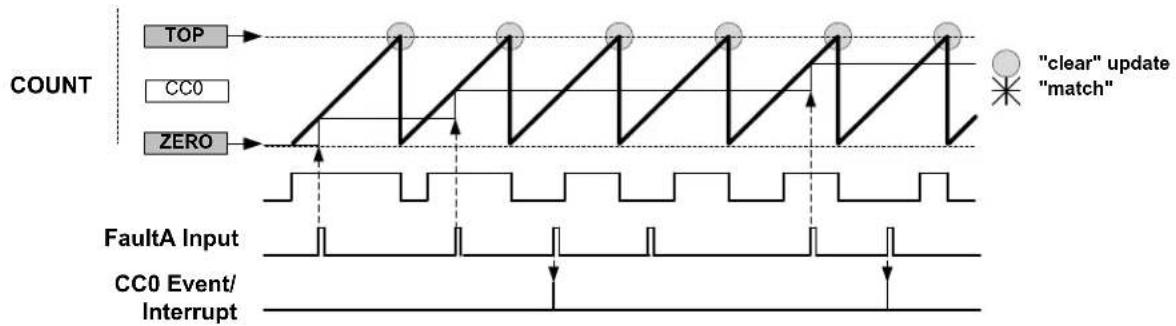
flowchart
graph TD
    A["TOP"] --> B["CC0"]
    B --> C["ZERO"]
    D[""clear" update"] --> E["match"]
    F["FaultA Input"] --> G["CC0 Event/Interrupt"]
    style A fill:#f9f,stroke:#333
    style B fill:#ccf,stroke:#333
    style C fill:#cfc,stroke:#333
    style D fill:#fcc,stroke:#333
    style E fill:#ffc,stroke:#333
    style F fill:#fcc,stroke:#333
    style G fill:#ffc,stroke:#333
Figure 35-29. Capture Action "DERIVO"
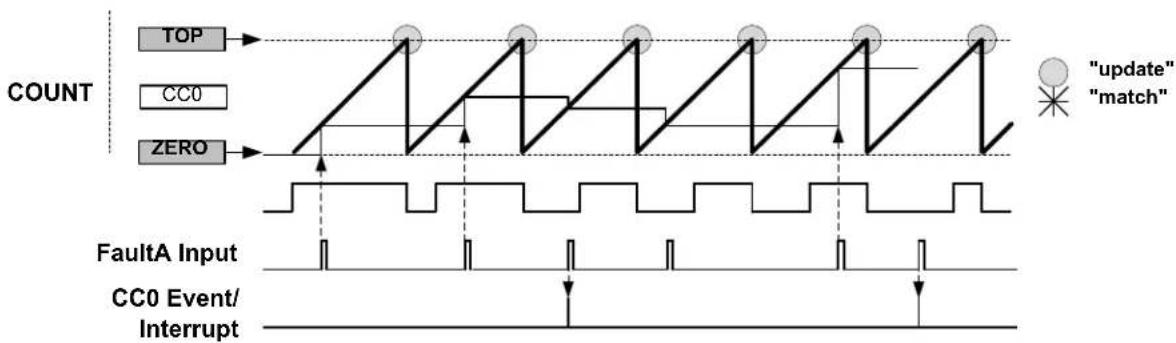
flowchart
graph TD
    A["TOP"] --> B["CC0"]
    B --> C["ZERO"]
    D["update"] --> E["match"]
    F[""Causes Input"] --> G["CC0 Event/Interrupt"]
    H["Failure A Input"] --> I["Clock Pulse Signal"]
    J["Count"] --> K["Waveform of TT Peaks"]
    style A fill:#f9f,stroke:#333
    style B fill:#ccf,stroke:#333
    style C fill:#cfc,stroke:#333
    style D fill:#fcc,stroke:#333
    style E fill:#ffc,stroke:#333
    style F fill:#fcc,stroke:#333
    style G fill:#ffc,stroke:#333
    style H fill:#fcc,stroke:#333
    style I fill:#ffc,stroke:#333
    style J fill:#fcc,stroke:#333
    style K fill:#cff,stroke:#333
Hardware This is configured by writing 0x1 to the Fault n Halt mode bits in the Recoverable Fault n Configuration Halt Action register (FCTRLn.HALT). When enabled, the timer/counter is halted and the cycle is extended as long as the corresponding fault is present.
The next figure ('Waveform Generation with Halt and Restart Actions') shows an example where both restart action and hardware halt action are enabled for Fault A. The compare channel 0 output is clamped to inactive level as long as the timer/counter is halted. The timer/counter resumes the counting operation as soon as the fault condition is no longer present. As the restart action is enabled in this example, the timer/counter is restarted after the fault condition is no longer present.
The figure after that ('Waveform Generation with Fault Qualification, Halt, and Restart Actions') shows a similar example, but with additionally enabled fault qualification. Here, counting is resumed after the fault condition is no longer present.
Note that in RAMP2 and RAMP2A operations, when a new timer/counter cycle starts, the cycle index will automatically change.
Figure 35-30. Waveform Generation with Halt and Restart Actions

flowchart
graph TD
    A["MAX"] --> B["TOP"]
    B --> C["CC0"]
    C --> D["ZERO"]
    D --> E["Fault Input A"]
    E --> F["WO[0"]]
    G["HALT"] --> H["RestartRestart"]
    I["""clear" update"] --> J["match"]
    style G fill:#f9f,stroke:#333
    style H fill:#ccf,stroke:#333
    style I fill:#cfc,stroke:#333
Figure 35-31. Waveform Generation with Fault Qualification, Halt, and Restart Actions
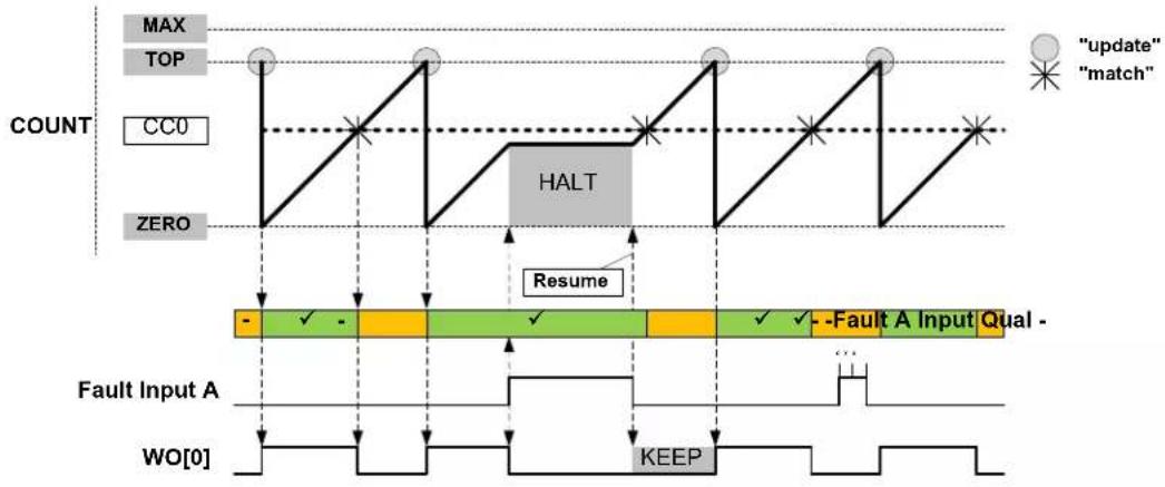
flowchart
graph TD
    A["MAX"] --> B["TOP"]
    B --> C["CC0"]
    C --> D["ZERO"]
    D --> E["HALT"]
    E --> F["Resume"]
    F --> G["- ✓ - ✓ ✓ ✓ ✓ -Fault A Input Qual -"]
    G --> H["Fault Input A"]
    H --> I["WO[0"]]
    I --> J["KEEP"]
    J --> K["update"]
    J --> L["match"]
    style A fill:#f9f,stroke:#333
    style B fill:#f9f,stroke:#333
    style C fill:#f9f,stroke:#333
    style D fill:#f9f,stroke:#333
    style E fill:#ccf,stroke:#333
    style F fill:#ccf,stroke:#333
    style G fill:#cfc,stroke:#333
    style H fill:#fcc,stroke:#333
    style I fill:#fcc,stroke:#333
    style J fill:#fcc,stroke:#333
    style K fill:#fcc,stroke:#333
Software Halt This is configured by writing 0x2 to the Fault n Halt mode bits in the Recoverable Fault n configuration Action register (FCTRLn.HALT). Software halt action is similar to hardware halt action, but in order to restart the timer/counter, the corresponding fault condition must not be present anymore, and the corresponding FAULT n bit in the STATUS register must be cleared by software.
Figure 35-32. Waveform Generation with Software Halt, Fault Qualification, Keep and Restart Actions

flowchart
graph TD
    A["COUNT"] --> B["CCO"]
    B --> C["ZERO"]
    C --> D["HAALT"]
    D --> E["Restart Restart"]
    E --> F["update" match"]
    G["Fault Input A"] --> H["Software Clear"]
    I["WO[0"]] --> J["KEEP"]
    J --> K["NO KEEP"]
    K --> L["+/-Fault A Input Qual -"]
    style A fill:#f9f,stroke:#333
    style B fill:#ccf,stroke:#333
    style C fill:#cfc,stroke:#333
    style D fill:#fcc,stroke:#333
    style E fill:#ffc,stroke:#333
    style F fill:#cff,stroke:#333
    style G fill:#ffc,stroke:#333
    style H fill:#fff,stroke:#333
    style I fill:#fff,stroke:#333
    style J fill:#fff,stroke:#333
    style K fill:#fff,stroke:#333
    style L fill:#fff,stroke:#333
35.6.3.6 Non-Recoverable Faults
The non-recoverable fault action will force all the compare outputs to a pre-defined level programmed into the Driver Control register (DRVCTRL.NRE and DRVCTRL.NRV). The non-recoverable fault input (EV0 and EV1) actions are enabled in Event Control register (EVCTRL.EVACT0 and EVCTRL.EVACT1).
To avoid false fault detection on external events (e.g. a glitch on an I/O port) a digital filter can be enabled using Non-Recoverable Fault Input x Filter Value bits in the Driver Control register (DRVCTRL.FILTERVALn). Therefore, the event detection is synchronous, and event action is delayed by the selected digital filter value clock cycles.
When the Fault Detection on Debug Break Detection bit in Debug Control register (DGBCTRL.FDDBD) is written to '1', a non-recoverable Debug Faults State and an interrupt (DFS) is generated when the system goes in debug operation.
In RAMP2, RAMP2A, or DSBOTH operation, when the Lock Update bit in the Control B register is set by writing CTRLBSET.LUPD=1 and the ramp index or counter direction changes, a non-recoverable Update Fault State and the respective interrupt (UFS) are generated.
35.6.3.7 Time-Stamp Capture on Events or I/Os
This feature is enabled when the Capture Time Stamp (STAMP) Event Action in Event Control register (EVCTRL.EVACT) is selected. The counter TOP value must be smaller than MAX.
When a capture event is detected, the COUNT value is copied into the corresponding Channel x Compare/Capture Value (CCx) register. In case of an overflow, the MAX value is copied into the corresponding CCx register.
When a valid captured value is present in the capture channel register, the corresponding Capture Channel x Interrupt Flag (INTFLAG.MCx) is set.
The timer/counter can detect capture overflow of the input capture channels: When a new capture event is detected while the Capture Channel interrupt flag (INTFLAG.MCx) is still set, the new timestamp will not be stored and INTFLAG.ERR will be set.
Figure 35-33. Time-Stamp

flowchart
graph LR
    A["CCx Value"] --> B["COUNT"]
    B --> C["POST"]
    C --> D["POSTTOP MAXCOUNT"]
    D --> E["POST"]
    E --> F["POSTTOP MAXCOUNT"]
    F --> G["POST"]
    G --> H["POSTTOP MAXCOUNT"]
    H --> I["POST"]
    I --> J["POSTTOP MAXCOUNT"]
    J --> K["POST"]
    K --> L["POSTTOP MAXCOUNT"]
    L --> M["POST"]
    M --> N["POSTTOP MAXCOUNT"]
    N --> O["POST"]
    O --> P["POSTTOP MAXCOUNT"]
    P --> Q["POST"]
    Q --> R["POSTTOP MAXCOUNT"]
    R --> S["POST"]
    S --> T["POSTTOP MAXCOUNT"]
    T --> U["POST"]
    U --> V["POSTTOP MAXCOUNT"]
    V --> W["POST"]
    W --> X["POSTTOP MAXCOUNT"]
    X --> Y["POST"]
    Y --> Z["POSTTOP MAXCOUNT"]
    Z --> AA["POST"]
    AA --> AB["POSTTOP MAXCOUNT"]
    AB --> AC["POST"]
    AC --> AD["POSTTOP MAXCOUNT"]
    AD --> AE["POST"]
    AE --> AF["POSTTOP MAXCOUNT"]
    AF --> AG["POST"]
    AG --> AH["POSTTOP MAXCOUNT"]
    AH --> AI["POST"]
    AI --> AJ["POSTTOP MAXCOUNT"]
    AJ --> AK["POST"]
    AK --> AL["POSTTOP MAXCOUNT"]
    AL --> AM["POST"]
    AM --> AN["POSTTOP MAXCOUNT"]
    AN --> AO["POST"]
    AO --> AP["POSTTOP MAXCOUNT"]
    AP --> AQ["POST"]
    AQ --> AR["POSTTOP MAXCOUNT"]
    AR --> AS["POST"]
    AS --> AT["POSTTOP MAXCOUNT"]
    AT --> AU["POST"]
    AU --> AV["POSTTOP MAXCOUNT"]
    AV --> AW["POST"]
    AW --> AX["POSTTOP MAXCOUNT"]
    AX --> AY["POST"]
    AY --> AZ["POSTTOP MAXCOUNT"]
    AZ --> BA["POST"]
    BA --> BB["POSTTOP MAXCOUNT"]
    BB --> BC["POST"]
    BC --> BD["POSTTOP MAXCOUNT"]
    BD --> BE["POST"]
    BE --> BF["POSTTOP MAXCOUNT"]
    BF --> BG["POST"]
    BG --> BH["POSTTOP MAXCOUNT"]
    BH --> BI["POST"]
    BI --> BJ["POSTTOP MAXCOUNT"]
    BJ --> BK["POST"]
    BK --> BL["POSTTOP MAXCOUNT"]
35.6.3.8 Waveform Extension
Figure 35-34 shows a schematic diagram of actions of the four optional units that follow the recoverable fault stage on a port pin pair: Output Matrix (OTMX), Dead-Time Insertion (DTI), SWAP and Pattern Generation. The DTI and SWAP units can be seen as a four port pair slices:
- Slice 0 DT10 / SWAP0 acting on port pins (WO[0], WO[WO_NUM/2 +0])
- Slice 1 DTI1 / SWAP1 acting on port pins (WO[1], WO[WO_NUM/2 +1])
And more generally:
- Slice n DTIx / SWAPx acting on port pins (WO[x], WO[WO_NUM/2 +x])
Figure 35-34. Waveform Extension Stage Details

flowchart
graph LR
    A["OTMX"] --> B["OTMX[x+WO_NUM/2"]]
    A --> C["OTMX[x"]]
    B --> D["LS"]
    B --> E["DTIx"]
    B --> F["HS"]
    C --> G["DTIx"]
    C --> H["DTIxEN SWAPx"]
    D --> I["PGV[x+WO_NUM/2"]]
    E --> J["PGO[x+WO_NUM/2"]]
    F --> K["PGO[x"]]
    G --> L["PGV[x"]]
    H --> M["PGV[x"]]
    I --> N["P[X+WO_NUM/2"]]
    J --> O["P[X+WO_NUM/2"]]
    K --> P["P[X+WO_NUM/2"]]
    L --> Q["P[X+WO_NUM/2"]]
    M --> R["P[X+WO_NUM/2"]]
    N --> S["INV[x+WO_NUM/2"]]
    O --> T["INV[x+WO_NUM/2"]]
    P --> U["INV[x+WO_NUM/2"]]
    Q --> V["INV[x+WO_NUM/2"]]
    R --> W["P[X"]]
    S --> X["P[X"]]
    T --> Y["P[X"]]
    U --> Z["P[X"]]
    V --> AA["P[X"]]
    W --> AB["P[X"]]
    X --> AC["P[X"]]
    Y --> AD["P[X"]]
    Z --> AE["P[X"]]
The output matrix (OTMX) unit distributes compare channels, according to the selectable configurations in Table 35-4.
Table 35-4. Output Matrix Channel Pin Routing Configuration
| Value OTMX[x] | |||||||
| 0x0 CC3 CC2 CC1 | CC0 CC3 CC2 | CC1 CC0 | |||||
| 0x1 CC1 CC0 CC1 | CC0 CC1 CC0 | CC1 CC0 | |||||
| 0x2 CC0 CC0 CC0 | CC0 CC0 CC0 | CC0 CC0 | |||||
| 0x3 CC1 CC1 CC1 | CC1 CC1 CC1 | CC1 CC0 | |||||
Notes on Table 35-4:
- Configuration 0x0 is the default configuration. The channel location is the default one, and channels are distributed on outputs modulo the number of channels. Channel 0 is routed to the Output matrix output OTMX[0], and Channel 1 to OTMX[1]. If there are more outputs than
channels, then channel 0 is duplicated to the Output matrix output OTMX[CC_NUM], channel 1 to OTMX[CC_NUM+1] and so on.
- Configuration 0x1 distributes the channels on output modulo half the number of channels. This assigns twice the number of output locations to the lower channels than the default configuration. This can be used, for example, to control the four transistors of a full bridge using only two compare channels. Using pattern generation, some of these four outputs can be overwritten by a constant level, enabling flexible drive of a full bridge in all quadrant configurations.
- Configuration 0x2 distributes compare channel 0 (CC0) to all port pins. With pattern generation, this configuration can control a stepper motor.
- Configuration 0x3 distributes the compare channel CC0 to the first output, and the channel CC1 to all other outputs. Together with pattern generation and the fault extension, this configuration can control up to seven LED strings, with a boost stage.
•Table 35-5. Example: four compare channels on four outputs
| Value OTMX[3] | OTMX[2] | OTMX[1] | OTMX[0] | ||
| 0x0 CC3 CC2 CC1 | CC0 | ||||
| 0x1 CC1 CC0 CC1 | CC0 | ||||
| 0x2 CC0 CC0 CC0 | CC0 | ||||
| 0x3 CC1 CC1 CC1 | CC0 |
The dead-time insertion (DTI) unit generates OFF time with the non-inverted low side (LS) and inverted high side (HS) of the wave generator output forced at low level. This OFF time is called dead time. Dead-time insertion ensures that the LS and HS will never switch simultaneously.
The DTI stage consists of four equal dead-time insertion generators; one for each of the first four compare channels. Figure 35-35 shows the block diagram of one DTI generator. The four channels have a common register which controls the dead time, which is independent of high side and low side setting.
Figure 35-35. Dead-Time Generator Block Diagram

flowchart
graph TD
    A["OTMX output"] --> B["D Q Edge Detect"]
    B --> C{AND Gate}
    C --> D["OR Gate"]
    D --> E["Counter"]
    E --> F["= 0"]
    F --> G[""DTLS" (To PORT)"]
    F --> H[""DTHS" (To PORT)"]
    I["Dead Time Generator"] --> J["DTLS"]
    I --> K["DTHS"]
    J --> L["AND Gate"]
    K --> M["AND Gate"]
    L --> N["Output"]
    M --> O["Output"]
As shown in Figure 35-36, the 8-bit dead-time counter is decremented by one for each peripheral clock cycle until it reaches zero. A non-zero counter value will force both the low side and high side
outputs into their OFF state. When the output matrix (OTMX) output changes, the dead-time counter is reloaded according to the edge of the input. When the output changes from low to high (positive edge) it initiates a counter reload of the DTLS register. When the output changes from high to low (negative edge) it reloads the DTHS register.
Figure 35-36. Dead-Time Generator Timing Diagram

text_image
"dti_cnt" "OTMX output" "DTLS" "DTHS" t_P t_DTLS t_DTHSThe pattern generator unit produces a synchronized bit pattern across the port pins it is connected to. The pattern generation features are primarily intended for handling the commutation sequence in brushless DC motors (BLDC), stepper motors, and full bridge control. See also Figure 35-37.
Figure 35-37. Pattern Generator Block Diagram

flowchart
graph TD
    A["COUNT UPDATE"] --> B["BV BVPGEB[7:0"]]
    B --> C["EN PGE[7:0"]]
    D["PGVB[7:0"]] --> E["EN PGV[7:0"]]
    E --> F["WOx[7:0"]]
    F --> G["SWAP OUTPUT"]
    G --> H["Output"]
    I["AND Gate"] --> B
    J["AND Gate"] --> E
As with other double-buffered timer/counter registers, the register update is synchronized to the UPDATE condition set by the timer/counter waveform generation operation. If synchronization is not required by the application, the software can simply access directly the PATT.PGE, PATT.PGV bits registers.
35.6.4 DMA, Interrupts, and Events
Table 35-6. Module Requests for TCC
| Condition Interrupt request Event | output | Event input | DMA request | DMA request is cleared | |
| Overflow / Underflow Yes Yes Yes | (1) | On DMA acknowledge | |||
| Channel Compare Match or Capture | Yes Yes Yes | (2) | Yes^(3) | For circular buffering: on DMA acknowledgeFor capture channel: when CCx register is read | |
| Retrigger Yes Yes | |||||
| Count Yes Yes | |||||
| Capture Overflow Error Yes | |||||
| Debug Fault State Yes | |||||
| Recoverable Faults Yes | |||||
| Non-Recoverable Faults Yes | |||||
| TCC0 Event 0 input Yes | (4) | ||||
| TCC0 Event 1 input Yes | (5) | ||||
Notes:
- DMA request set on overflow, underflow or re-trigger conditions.
- Can perform capture or generate recoverable fault on an event input.
- In capture or circular modes.
-
On event input, either action can be executed:
-
re-trigger counter
- control counter direction
- stop the counter
- decrement the counter
- perform period and pulse width capture
-
generate non-recoverable fault
-
On event input, either action can be executed:
-
re-trigger counter
- increment or decrement counter depending on direction
- start the counter
- increment or decrement counter based on direction
- increment counter regardless of direction
- generate non-recoverable fault
35.6.4.1 DMA Operation
The TCC can generate the following DMA requests:
| Counter overflow (OVF) | If the Ones-shot Trigger mode in the control A register (CTRLA.DMAOS) is written to '0', the TCC generates a DMA request on each cycle when an update condition (overflow, underflow or re-trigger) is detected.When an update condition (overflow, underflow or re-trigger) is detected while CTRLA.DMAOS=1, the TCC generates a DMA trigger on the cycle following the DMA One-Shot Command written to the Control B register (CTRLBSET.CMD=DMAOS).In both cases, the request is cleared by hardware on DMA acknowledge. |
| Channel Match (MCx) | A DMA request is set only on a compare match if CTRLA.DMAOS=0. The request is cleared by hardware on DMA acknowledge. |
When CTRLA.DMAOS=1, the DMA requests are not generated.
| Channel | For a capture channel, the request is set when valid data is present in the CCx register, and cleared once the CCx register is read. |
| Capture (MCx) | In this operation mode, the CTRLA.DMAOS bit value is ignored. |
DMA Operation with Circular Buffer
When circular buffer operation is enabled, the buffer registers must be written in a correct order and synchronized to the update times of the timer. The DMA triggers of the TCC provide a way to ensure a safe and correct update of circular buffers.
Note: Circular buffer are intended to be used with RAMP2, RAMP2A and DSBOTH operation only.
DMA Operation with Circular Buffer in RAMP and RAMP2A Mode
When a CCx channel is selected as a circular buffer, the related DMA request is not set on a compare match detection, but on start of ramp B.
If at least one circular buffer is enabled, the DMA overflow request is conditioned to the start of ramp A with an effective DMA transfer on previous ramp B (DMA acknowledge).
The update of all circular buffer values for ramp A can be done through a DMA channel triggered on a MC trigger. The update of all circular buffer values for ramp B, can be done through a second DMA channel triggered by the overflow DMA request.
Figure 35-38. DMA Triggers in RAMP and RAMP2 Operation Mode and Circular Buffer Enabled

flowchart
graph TD
    A["Ramp"] --> B["A"]
    B --> C["B"]
    C --> D["A"]
    D --> E["B"]
    E --> F["A"]
    F --> G["B"]
    G --> H["New Parameter Set"]
    I["Cycle"] --> J["N-2"]
    J --> K["N-1 N"]
    K --> L["Old Parameter Set"]
    M["COUNT"] --> N["ZERO"]
    N --> O["STATUS.IDX"]
    O --> P["DMA_CCx_req"]
    P --> Q["DMA_CChannel i"]
    Q --> R["Update ramp A"]
    S["DATA"] --> T["DMA_OVF_req"]
    T --> U["DMA_Channel j"]
    U --> V["Update ramp B"]
    W["update"] --> X["Update"]
DMA Operation with Circular Buffer in DSBOTH Mode
When a CC channel is selected as a circular buffer, the related DMA request is not set on a compare match detection, but on start of down-counting phase.
If at least one circular buffer is enabled, the DMA overflow request is conditioned to the start of up-counting phase with an effective DMA transfer on previous down-counting phase (DMA acknowledge).
When up-counting, all circular buffer values can be updated through a DMA channel triggered by MC trigger. When down-counting, all circular buffer values can be updated through a second DMA channel, triggered by the OVF DMA request.
Figure 35-39. DMA Triggers in DSBOTH Operation Mode and Circular Buffer Enabled

flowchart
graph TD
    A["Cycle"] --> B["N-2"]
    B --> C["N-1"]
    C --> D["N"]
    D --> E["Old Parameter Set"]
    E --> F["New Parameter Set"]
    F --> G["Update"]
    H["COUNT"] --> I["ZERO"]
    I --> J["CTRLB.DIR"]
    J --> K["DMA_CCx_req"]
    K --> L["DMA_OVF_req"]
    L --> M["Update Rising"]
    N["DMA Channel i"] --> O["Update Rising"]
    P["DMA Channel j"] --> Q["Update Rising"]
35.6.4.2 Interrupts
The TCC has the following interrupt sources:
• Overflow/Underflow (OVF)
- Retrigger (TRG)
- Count (CNT) - refer also to description of EVCTRL.CNTSEL.
• Capture Overflow Error (ERR)
• Non-Recoverable Update Fault (UFS)
- Debug Fault State (DFS)
• Recoverable Faults (FAULTn)
• Non-recoverable Faults (FAULTx)
• Compare Match or Capture Channels (MCx)
These interrupts are asynchronous wake-up sources. See the Sleep Mode Entry and Exit Table in the Sleep Mode Controller section for details.
Each interrupt source has an interrupt flag associated with it. The interrupt flag in the Interrupt Flag Status and Clear (INTFLAG) register is set when the interrupt condition occurs. Each interrupt can be individually enabled by writing a '1' to the corresponding bit in the Interrupt Enable Set (INTENSET) register, and disabled by writing a '1' to the corresponding bit in the Interrupt Enable Clear (INTENCLR) register. An interrupt request is generated when the interrupt flag is set and the corresponding interrupt is enabled. The interrupt request remains active until the interrupt flag is cleared, the interrupt is disabled, or the TCC is reset. See 35.8.12. INTFLAG for details on how to clear interrupt flags. The TCC has one common interrupt request line for all the interrupt sources. The user must read the INTFLAG register to determine which interrupt condition is present.
Note: Interrupts must be globally enabled for interrupt requests to be generated. Refer to Nested Vector Interrupt Controller for details.
35.6.4.3 Events
The TCC can generate the following output events:
• Overflow/Underflow (OVF)
- Trigger (TRG)
- Counter (CNT) For further details, refer to EVCTRL.CNTSEL description.
- Compare Match or Capture on compare/capture channels: MCx
Writing a '1' ('0') to an Event Output bit in the Event Control Register (EVCTRL.xxEO) enables (disables) the corresponding output event. Refer also to EVSYS - Event System.
The TCC can take the following actions on a channel input event (MCx):
- Capture event
- Generate a recoverable or non-recoverable fault
The TCC can take the following actions on counter Event 1 (TCC0 EV1):
- Counter re-trigger
- Counter direction control
- Stop the counter
- Decrement the counter on event
• Period and pulse width capture
• Non-recoverable fault
The TCC can take the following actions on counter Event 0 (TCC0 EV0):
- Counter re-trigger
- Count on event (increment or decrement, depending on counter direction)
- Counter start - start counting on the event rising edge. Further events will not restart the counter; the counter will keep on counting using prescaled GCLK_TCC0, until it reaches TOP or ZERO, depending on the direction.
- Counter increment on event. This will increment the counter, irrespective of the counter direction.
- Count during active state of an asynchronous event (increment or decrement, depending on counter direction). In this case, the counter will be incremented or decremented on each cycle of the prescaled clock, as long as the event is active.
• Non-recoverable fault
The counter Event Actions are available in the Event Control registers (EVCTRL.EVACT0 and EVCTRL.EVACT1). For further details, refer to EVCTRL.
Writing a '1' ('0') to an Event Input bit in the Event Control register (EVCTRL.MCEIx or EVCTRL.TCEIx) enables (disables) the corresponding action on input event.
Note: When several events are connected to the TCC, the enabled action will apply for each of the incoming events. Refer to EVSYS – Event System for details on how to configure the event system.
35.6.5 Sleep Mode Operation
The TCC can be configured to operate in any sleep mode. To be able to run in standby the RUNSTDBY bit in the Control A register (CTRLA.RUNSTDBY) must be '1'. The MODULE can in any sleep mode wake up the device using interrupts or perform actions through the Event System.
35.6.6 Synchronization
Due to asynchronicity between the main clock domain and the peripheral clock domains, some registers need to be synchronized when written or read.
The following bits are synchronized when written:
- Software Reset and Enable bits in Control A register (CTRLA.SWRST and CTRLA.ENABLE)
The following registers are synchronized when written:
• Control B Clear and Control B Set registers (CTRLBCLR and CTRLBSET)
- Status register (STATUS)
- Pattern and Pattern Buffer registers (PATT and PATTBUF)
• Waveform register (WAVE) - Count Value register (COUNT)
- Period Value and Period Buffer Value registers (PER and PERBUF)
- Compare/Capture Channel x and Channel x Compare/Capture Buffer Value registers (CCx and CCBUFx)
The following registers are synchronized when read:
- Control B Clear and Control B Set registers (CTRLBCLR and CTRLBSET)
- Count Value register (COUNT): synchronization is done on demand through READSYNC command (CTRLBSET.CMD)
Required write-synchronization is denoted by the "Write-Synchronized" property in the register description.
Required read-synchronization is denoted by the "Read-Synchronized" property in the register description.
For more information, refer to Register Synchronization.
35.7 Register Summary
| Offset | Name Bit Pos. 7 6 | 5 4 3 2 1 | 0 | ||||||||
| 0x00 | CTRLA | 7:0 RESOLUTION[1:0] ENABLE SWRST | |||||||||
| 15:8 MSYNC ALOCK PRESCYNC[1:0] RUNSTDBY PRESCALER[2:0] | |||||||||||
| 23:16 | DMAOS | ||||||||||
| 31:24 | CPTEN3 | CPTEN2 | CPTEN1 | CPTENO | |||||||
| 0x04 | CTRLBCLR | 7:0 | CMD[2:0] | IDXCMD[1:0] | ONESHOT | LUPD | DIR | ||||
| 0x05 | CTRLBSET | 7:0 | CMD[2:0] | IDXCMD[1:0] | ONESHOT | LUPD | DIR | ||||
| 0x06 ... 0x07 | Reserved | ||||||||||
| 0x08 | SYNCBUSY | 7:0 | PER | WAVE | PATT | COUNT | STATUS | CTRLB | ENABLE | SWRST | |
| 15:8 | CC3 | CC2 | CC1 | CCO | |||||||
| 23:16 | |||||||||||
| 31:24 | |||||||||||
| 0x0C | FCTRLA | 7:0 | RESTART | BLANK[1:0] | QUAL | KEEP | SRC[1:0] | ||||
| 15:8 | BLANKPRESC | CAPTURE[2:0] | CHSEL[1:0] | HALT[1:0] | |||||||
| 23:16 | BLANKVAL[7:0] | ||||||||||
| 31:24 | FILTERVAL[3:0] | ||||||||||
| 0x10 | FCTRLB | 7:0 | RESTART | BLANK[1:0] | QUAL | KEEP | SRC[1:0] | ||||
| 15:8 | BLANKPRESC | CAPTURE[2:0] | CHSEL[1:0] | HALT[1:0] | |||||||
| 23:16 | BLANKVAL[7:0] | ||||||||||
| 31:24 | FILTERVAL[3:0] | ||||||||||
| 0x14 | WEXCTRL | 7:0 | OTMX[1:0] | ||||||||
| 15:8 | DTIEN3 DTIEN2 DTIEN1 DTIEN0 | ||||||||||
| 23:16 | DTLS[7:0] | ||||||||||
| 31:24 | DTHS[7:0] | ||||||||||
| 0x18 | DRVCTRL | 7:0 | NRE7 | NRE6 | NRE5 | NRE4 | NRE3 | NRE2 | NRE1 | NRE0 | |
| 15:8 | NRV7 | NRV6 | NRV5 | NRV4 | NRV3 | NRV2 | NRV1 | NRV0 | |||
| 23:16 | INVEN7 | INVEN6 | INVEN5 | INVEN4 | INVEN3 | INVEN2 | INVEN1 | INVEN0 | |||
| 31:24 | FILTERVAL[1:3:0] | FILTERVAL[0:3:0] | |||||||||
| 0x1C ... 0x1D | Reserved | ||||||||||
| 0x1E | DBGCTRL | 7:0 | FDDBD | DBGRUN | |||||||
| 0x1F | Reserved | ||||||||||
| 0x20 | EVCTRL | 7:0 CNTSEL[1:0] | EVACT[1:2:0] | EVACT[0:2:0] | |||||||
| 15:8 | TCEI1 | TCEI0 | TCINV1 | TCINV0 | CNTEO | TRGEO | OVFEO | ||||
| 23:16 | MCEI3 | MCEI2 | MCEI1 | MCEI0 | |||||||
| 31:24 | MCEO3 MCEO2 MCEO1 MCEO0 | ||||||||||
| 0x24 | INTENCLR | 7:0 | ERR CNT TRG | OVF | |||||||
| 15:8 | FAULT1 | FAULT0 | FAULTB | FAULTA | DFS | UFS | |||||
| 23:16 | MC3 | MC2 | MC1 | MC0 | |||||||
| 31:24 | |||||||||||
| 0x28 INTENSET | 7:0 | ERR CNT TRG | OVF | ||||||||
| 15:8 | FAULT1 | FAULT0 | FAULTB | FAULTA | DFS | UFS | |||||
| 23:16 | MC3 | MC2 | MC1 | MC0 | |||||||
| 31:24 | |||||||||||
| 0x2C | INTFLAG | 7:0 | ERR CNT TRG | OVF | |||||||
| 15:8 | FAULT1 | FAULT0 | FAULTB | FAULTA | DFS | UFS | |||||
| 23:16 | MC3 | MC2 | MC1 | MC0 | |||||||
| 31:24 | |||||||||||
| 0X30 | STATUS | 7:0 | PERBUFV | PATTBUFV | DFS | UFS | IDX | STOP | |||
| 15:8 | FAULT1 | FAULT0 | FAULTB | FAULTA | FAULT1IN | FAULT0IN | FAULTBIN | FAULTAIN | |||
| 23:16 | CCBUFV3 | CCBUFV2 | CCBUFV1 | CCBUFV0 | |||||||
| 31:24 | CMP3 CMP2 CMP1 CMP0 | ||||||||||
| 0x34 | COUNT | 7:0 | COUNT[7:0] | ||||||||
| 15:8 | COUNT[15:8] | ||||||||||
| 23:16 | COUNT[23:16] | ||||||||||
| 31:24 | COUNT[31:24] | ||||||||||
......continued
| Offset | Name Bit Pos. 7 | 6 | 5 | 4 | 3 | 2 | 1 | 0 | |||||||||||||||||
| 0x38 | PATT | 7:0 | PGE7 | PGE6 | PGE5 | PGE4 | PGE3 | PGE2 | PGE1 | PGE0 | |||||||||||||||
| 15:8 | PGV7 | PGV6 | PGV5 | PGV4 | PGV3 | PGV2 | PGV1 | PGV0 | |||||||||||||||||
| 0x3A...0x3B | Reserved | ||||||||||||||||||||||||
| 0x3C | WAVE | 7:0 | CIPEREN | RAMP[1:0] | WAVEGEN[2:0] | ||||||||||||||||||||
| 15:8 | CICCEN3 | CICCEN2 | CICCEN1 | CICCEN0 | |||||||||||||||||||||
| 23:16 | POL3 | POL2 | POL1 | POL0 | |||||||||||||||||||||
| 31:24 | SWAP3 | SWAP2 | SWAP1 | SWAP0 | |||||||||||||||||||||
| 0x40 | PER | 7:0 | PER[1:0] | DITHER[5:0] | |||||||||||||||||||||
| 15:8 | PER[9:2] | ||||||||||||||||||||||||
| 23:16 | PER[17:10] | ||||||||||||||||||||||||
| 31:24 | PER[25:18] | ||||||||||||||||||||||||
| 0x44 | CC0 | 7:0 | CC1 | CC0 | DITHER[5:0] | ||||||||||||||||||||
| 15:8 | CC9 | CC8 | CC7 | CC6 | CC5 | CC4 | CC3 | CC2 | |||||||||||||||||
| 23:16 | CC17 | CC16 | CC15 | CC14 | CC13 | CC12 | CC11 | CC10 | |||||||||||||||||
| 31:24 | CC25 | CC24 | CC23 | CC22 | CC21 | CC20 | CC19 | CC18 | |||||||||||||||||
| 0x48 | CC1 | 7:0 | CC1 | CC0 | DITHER[5:0] | ||||||||||||||||||||
| 15:8 | CC9 | CC8 | CC7 | CC6 | CC5 | CC4 | CC3 | CC2 | |||||||||||||||||
| 23:16 | CC17 | CC16 | CC15 | CC14 | CC13 | CC12 | CC11 | CC10 | |||||||||||||||||
| 31:24 | CC25 | CC24 | CC23 | CC22 | CC21 | CC20 | CC19 | CC18 | |||||||||||||||||
| 0x4C | CC2 | 7:0 | CC1 | CC0 | DITHER[5:0] | ||||||||||||||||||||
| 15:8 | CC9 | CC8 | CC7 | CC6 | CC5 | CC4 | CC3 | CC2 | |||||||||||||||||
| 22:16 | CC17 | CC16 | CC15 | CC14 | CC13 | CC12 | CC11 | CC10 | |||||||||||||||||
| 31:24 | CC25 | CC24 | CC23 | CC22 | CC21 | CC20 | CC19 | CC18 | |||||||||||||||||
| 0x50 | CC3 | 7:0 | CC1 | CC0 | DITHER[5:0] | ||||||||||||||||||||
| 15:8 | CC9 | CC8 | CC7 | CC6 | CC5 | CC4 | CC3 | CC2 | |||||||||||||||||
| 25:16 | CC17 | CC16 | CC15 | CC14 | CC13 | CC12 | CC11 | CC10 | |||||||||||||||||
| 31:24 | CC25 | CC24 | CC23 | CC22 | CC21 | CC20 | CC19 | CC18 | |||||||||||||||||
| 0x54...0x63 | Reserved | ||||||||||||||||||||||||
| 0x64 | PATTBUF | 7:0 | PGEB7 | PGEB6 | PGEB5 | PGEB4 | PGEB3 | PGEB2 | PGEB1 | PGEB0 | |||||||||||||||
| 15:8 | PGVB7 | PGVB6 | PGVB5 | PGVB4 | PGVB3 | PGVB2 | PGVB1 | PGVB0 | |||||||||||||||||
| 0x66...0x6B | Reserved | ||||||||||||||||||||||||
| 0x6C | PERBUF | 7:0 PERBUF[1:0] | DITHERBUF[5:0] | ||||||||||||||||||||||
| 15:8 | PERBUF[9:2] | ||||||||||||||||||||||||
| 23:16 | PERBUF[17:10] | ||||||||||||||||||||||||
| 31:24 | PERBUF[25:18] | ||||||||||||||||||||||||
| 0x70 | CCBUF0 | 7:0 CCBUF[1:0] | DITHERBUF[5:0] | ||||||||||||||||||||||
| 15:8 | CCBUF[9:2] | ||||||||||||||||||||||||
| 23:16 | CCBUF[17:10] | ||||||||||||||||||||||||
| 31:24 | CCBUF[25:18] | ||||||||||||||||||||||||
| 0x74 | CCBUF1 | 7:0 CCBUF[1:0] | DITHERBUF[5:0] | ||||||||||||||||||||||
| 15:8 | CCBUF[9:2] | ||||||||||||||||||||||||
| 23:16 | CCBUF[17:10] | ||||||||||||||||||||||||
| 31:24 | CCBUF[25:18] | ||||||||||||||||||||||||
| 0x78 | CCBUF2 | 7:0 CCBUF[1:0] | DITHERBUF[5:0] | ||||||||||||||||||||||
| 15:8 | CCBUF[9:2] | ||||||||||||||||||||||||
| 23:16 | CCBUF[17:10] | ||||||||||||||||||||||||
| 31:24 | CCBUF[25:18] | ||||||||||||||||||||||||
| Ox7C | CCBUF3 | 7:0 CCBUF[1:0] | DITHERBUF[5:0] | ||||||||||||||||||||||
| 15:8 | CCBUF[9:2] | ||||||||||||||||||||||||
| 23:16 | CCBUF[17:10] | ||||||||||||||||||||||||
| 31:24 | CCBUF[25:18] | ||||||||||||||||||||||||
35.8 Register Description
Registers can be 8, 16, or 32 bits wide. Atomic 8-, 16-, and 32-bit accesses are supported. In addition, the 8-bit quarters and 16-bit halves of a 32-bit register, and the 8-bit halves of a 16-bit register can be accessed directly.
Some registers require synchronization when read and/or written. Synchronization is denoted by the "Read-Synchronized" and/or "Write-Synchronized" property in each individual register description.
Optional write-protection by the Peripheral Access Controller (PAC) is denoted by the "PAC Write-Protection" property in each individual register description.
Some registers are enable-protected, meaning they can only be written when the module is disabled. Enable-protection is denoted by the "Enable-Protected" property in each individual register description
35.8.1 Control A
Name: CTRLA
Offset: 0x00
Reset: 0x00000000
Property: PAC Write-Protection, Enable-Protected bits, Write-Synchronized bits
Bit 31 30 29 28 27 26 25 24
| CPTEN3 CPTEN2 | CPTEN1 CPTEN0 | |||||
| Access Reset 0 0 0 0 | R/W R/W R/W R/W | |||||
Bit 23 22 21 20 19 18 17 16
| DMAOS | ||||||||
| Access | R/W | |||||||
| Reset | 0 |
Bit 15 14 13 12 11 10 98
| MSYNC | ALOCK | PRESCYNC[1:0] | RUNSTDBY | PRESCALER[2:0] | |
| Access | R/W | R/W | R/W | R/W | R/W |
| Reset | 0 | 0 | 0 | 0 | 0 |
Bit 76543210
| RESOLUTION[1:0] | ENABLE | SWRST | |||
| Access | R/W R/W | R/W R/W | |||
| Reset | 0 0 | 0 0 | |||
Bits 24, 25, 26, 27 - CPTENx Capture Channel x Enable
These bits are used to select the capture or compare operation on channel x.
Writing a '1' to CPTENx enables capture on channel x.
Writing a '0' to CPTENx disables capture on channel x.
Note: This bit field is enable-protected. This bit field is not write-synchronized.
Bit 23 - DMAOS DMA One-Shot Trigger Mode
This bit enables the DMA One-shot Trigger Mode.
Writing a '1' to this bit will generate a DMA trigger on TCC cycle following a
TCC_CTRLBSET_CMD_DMAOS command.
Writing a '0' to this bit will generate DMA triggers on each TCC cycle.
Note: This bit is enable-protected. This bit is not write-synchronized.
Bit 15 -MSYNC Host Synchronization (only for TCC Client instance)
This bit must be set if the TCC counting operation must be synchronized on its Host TCC.
Note: This bit is enable-protected. This bit is not write-synchronized.
| Value | Description |
| 0 | The TCC controls its own counter. |
| 1 | The counter is controlled by its Host TCC. |
Bit 14 - ALOCK Auto Lock
Note: This bit is enable-protected. This bit is not write-synchronized.
| Value | Description |
| 0 | The Lock Update bit in the Control B register (CTRLB.LUPD) is not affected by overflow/underflow, and re-trigger events |
| 1 | CTRLB.LUPD is set to '1' on each overflow/underflow or re-trigger event. |
Bits 13:12 - PRESCYNC[1:0] Prescaler and Counter Synchronization
These bits select if on re-trigger event, the Counter is cleared or reloaded on either the next GCLK_TCC0 clock, or on the next prescaled GCLK_TCC0 clock. It is also possible to reset the prescaler on re-trigger event.
Note: This bit field is enable-protected. This bit field is not write-synchronized.
| Value Name Description | |||
| Counter Reloaded Prescaler | |||
| 0x0 GCLK Reload or reset | Counter on next GCLK - | ||
| 0x1 PRESC Reload or reset | Counter on next prescaler clock | - | |
| 0x2 RESYNC Reload or reset | Counter on next GCLK Reset prescaler counter | ||
| 0x3 Reserved | |||
Bit 11 - RUNSTDBY Run in Standby
This bit is used to keep the TCC running in Standby mode.
Note: This bit is enable-protected. This bit is not write-synchronized.
| Value Description | |
| 0 | The TCC is halted in standby. |
| 1 | The TCC continues to run in standby. |
Bits 10:8 - PRESCALER[2:0] Prescaler
These bits select the Counter prescaler factor.
Note: This bit field is enable-protected. This bit field is not write-synchronized.
| Value Name | Description | |
| 0x0 | DIV1 Prescaler: GCLK_TCC | |
| 0x1 | DIV2 Prescaler: GCLK_TCC/2 | |
| 0x2 | DIV4 Prescaler: GCLK_TCC/4 | |
| 0x3 | DIV8 Prescaler: GCLK_TCC/8 | |
| 0x4 | DIV16 Prescaler: GCLK_TCC/16 | |
| 0x5 | DIV64 Prescaler: GCLK_TCC/64 | |
| 0x6 | DIV256 Prescaler: GCLK_TCC/256 | |
| 0x7 | DIV1024 Prescaler: GCLK_TCC/1024 | |
Bits 6:5 - RESOLUTION[1:0] Dithering Resolution
These bits increase the TCC resolution by enabling the dithering options.
Note: This bit field is enable-protected. This bit field is not write-synchronized.
Table 35-7. Dithering
| Value | Name Description | |
| 0x0 | NONE | The dithering is disabled. |
| 0x1 | DITH4 Dithering is done every 16 PWM frames. PER[3:0] and CCx[3:0] contain dithering pattern selection. | |
| 0x2 | DITH5 Dithering is done every 32 PWM frames. PER[4:0] and CCx[4:0] contain dithering pattern selection. | |
| 0x3 | DITH6 Dithering is done every 64 PWM frames. PER[5:0] and CCx[5:0] contain dithering pattern selection. | |
Bit 1 - ENABLE Enable
Due to synchronization there is delay from writing CTRLA. ENABLE until the peripheral is enabled/disabled. The value written to CTRLA. ENABLE will read back immediately and the ENABLE bit in the SYNCBUSY register (SYNCBUSY. ENABLE) will be set. SYNCBUSY. ENABLE will be cleared when the operation is complete.
Notes:
- This bit is not enable protected.
- This bit is write-synchronized: SYNCBUSY. ENABLE must be checked to ensure the CTRLA. ENABLE synchronization is complete.
Value Description
| 0 | The peripheral is disabled. |
| 1 | The peripheral is enabled. |
Bit 0 - SWRST Software Reset
Writing a '0' to this bit has no effect.
Writing a '1' to this bit resets all registers in the TCC (except DBGCTRL) to their initial state, and the TCC will be disabled.
Writing a '1' to CTRLA.SWRST will always take precedence; all other writes in the same write-operation will be discarded.
Notes:
- This bit is not enable protected.
- This bit is write-synchronized: SYNCBUSY. ENABLE must be checked to ensure the CTRLA. ENABLE synchronization is complete.
Due to synchronization there is a delay from writing CTRLA.SWRST until the reset is complete. CTRLA.SWRST and SYNCBUSY.SWRST will both be cleared when the reset is complete.
Value Description
| 0 | There is no Reset operation ongoing. |
| 1 | The Reset operation is ongoing. |
35.8.2 Control B Clear
Name: CTRLBCLR
Offset: 0x04
Reset: 0x00
Property: PAC Write-Protection, Write-Synchronized, Read-Synchronized
This register allows the user to change this register without doing a read-modify-write operation.
Changes in this register will also be reflected in the Control B Set (CTRLBSET) register.
Bit 76543210
| CMD[2:0] IDXCMD[1:0] ONESHOT LUPD DIR | ||||
| Access | R/W R/W R/W R/W R/W R/W R/W R/W | |||
| Reset | 0 0 0 0 0 0 0 | |||
Bits 7:5 - CMD[2:0] TCC Command
These bits can be used for software control of re-triggering and stop commands of the TCC. When a command has been executed, the CMD bit field will read back zero. The commands are executed on the next prescaled GCLK_TCC clock cycle.
Writing zero to this bit group has no effect.
Writing a '1' to any of these bits will clear the pending command.
| Value Name | Description | |
| 0x0 | NONE | No action |
| 0x1 | RETRIGGER | Clear start, restart or retrigger |
| 0x2 | STOP | Force stop |
| 0x3 | UPDATE | Force update of double buffered registers |
| 0x4 | READSYNC | Force COUNT read synchronization |
Bits 4:3 - IDXCMD[1:0] Ramp Index Command
These bits can be used to force cycle A and cycle B changes in RAMP2 and RAMP2A operation. On timer/counter update condition, the command is executed, the IDX flag in STATUS register is updated and the IDXCMD command is cleared.
Writing zero to these bits has no effect.
Writing a '1' to any of these bits will clear the pending command.
| Value Name | Description | |
| 0x0 | DISABLE | DISABLE Command disabled: IDX toggles between cycles A and B |
| 0x1 | SET Set IDX: cycle B will be forced in the next cycle | |
| 0x2 | CLEAR | Clear IDX: cycle A will be forced in next cycle |
| 0x3 | HOLD | Hold IDX: the next cycle will be the same as the current cycle. |
Bit 2 - ONESHOT One-Shot
This bit controls one-shot operation of the TCC. When one-shot operation is enabled, the TCC will stop counting on the next overflow/underflow condition or on a stop command.
Writing a '0' to this bit has no effect
Writing a '1' to this bit will disable the one-shot operation.
| Value Description | |
| 0 | The TCC will update the counter value on overflow/underflow condition and continue operation. |
| 1 | The TCC will stop counting on the next underflow/overflow condition. |
Bit 1 - LUPD Lock Update
This bit controls the update operation of the TCC buffered registers.
When CTRLB.LUPD is set, no any update of the registers with value of its buffered register is performed on hardware UPDATE condition. Locking the update ensures that all buffer registers are valid before an hardware update is performed. After all the buffer registers are loaded correctly, the buffered registers can be unlocked.
This bit has no effect when input capture operation is enabled.
Writing a '0' to this bit has no effect.
Writing a '1' to this bit will enable updating.
| Value Description | |
| 0 | The CCBx, PERB, PGVB, PGOB, and SWAPBx buffer registers values are copied into the corresponding CCx, PER, PGV, PGO and SWAPx registers on hardware update condition. |
| 1 | The CCBx, PERB, PGVB, PGOB, and SWAPBx buffer registers values are not copied into the corresponding CCx, PER, PGV, PGO and SWAPx registers on hardware update condition. |
Bit 0 - DIR Counter Direction
This bit is used to change the direction of the counter.
Writing a '0' to this bit has no effect
Writing a '1' to this bit will clear the bit and make the counter count up.
| Value Description | |
| 0 | The timer/counter is counting up (incrementing). |
| 1 | The timer/counter is counting down (decrementing). |
35.8.3 Control B Set
Name: CTRLBSET
Offset: 0x05
Reset: 0x00
Property: PAC Write-Protection, Write-Synchronized, Read-Synchronized
This register allows the user to change this register without doing a read-modify-write operation. Changes in this register will also be reflected in the Control B Set (CTRLBCLR) register.
Bit 76543210
| CMD[2:0] IDXCMD[1:0] ONESHOT LUPD DIR | ||||
| Access | R/W R/W R/W R/W R/W R/W R/W R/W | |||
| Reset | 0 0 0 0 0 0 0 | |||
Bits 7:5 - CMD[2:0] TCC Command
These bits can be used for software control of re-triggering and stop commands of the TCC. When a command has been executed, the CMD bit field will be read back as zero. The commands are executed on the next prescaled GCLK_TCC clock cycle.
Writing zero to this bit group has no effect
Writing a valid value to this bit group will set the associated command.
| Value Name | Description | |
| 0x0 | NONE | No action |
| 0x1 | RETRIGGER | Force start, restart or retrigger |
| 0x2 | STOP | Force stop |
| 0x3 | UPDATE | Force update of double buffered registers |
| 0x4 | READSYNC | Force a read synchronization of COUNT |
Bits 4:3 - IDXCMD[1:0] Ramp Index Command
These bits can be used to force cycle A and cycle B changes in RAMP2 and RAMP2A operation. On timer/counter update condition, the command is executed, the IDX flag in STATUS register is updated and the IDXCMD command is cleared.
Writing a zero to these bits has no effect.
Writing a valid value to these bits will set a command.
| Value Name | Description | |
| 0x0 | DISABLE | Command disabled: IDX toggles between cycles A and B |
| 0x1 | SET | Set IDX: cycle B will be forced in the next cycle |
| 0x2 | CLEAR | Clear IDX: cycle A will be forced in next cycle |
| 0x3 | HOLD | Hold IDX: the next cycle will be the same as the current cycle. |
Bit 2 - ONESHOT One-Shot
This bit controls one-shot operation of the TCC. When in one-shot operation, the TCC will stop counting on the next overflow/underflow condition or a stop command.
Writing a '0' to this bit has no effect.
Writing a '1' to this bit will enable the one-shot operation.
| Value Description | |
| 0 | The TCC will count continuously. |
| 1 | The TCC will stop counting on the next underflow/overflow condition. |
Bit 1 - LUPD Lock Update
This bit controls the update operation of the TCC buffered registers.
When CTRLB.LUPD is set, no any update of the registers with value of its buffered register is performed on hardware UPDATE condition. Locking the update ensures that all buffer registers are valid before an hardware update is performed. After all the buffer registers are loaded correctly, the buffered registers can be unlocked.
This bit has no effect when input capture operation is enabled.
Writing a '0' to this bit has no effect.
Writing a '1' to this bit will lock updating.
| Value Description | |
| 0 | The CCBx, PERB, PGVB, PGOB, and SWAPBx buffer registers values are copied into the corresponding CCx, PER, PGV, PGO and SWAPx registers on hardware update condition. |
| 1 | The CCBx, PERB, PGVB, PGOB, and SWAPBx buffer registers values are not copied into CCx, PER, PGV, PGO and SWAPx registers on hardware update condition. |
Bit 0 - DIR Counter Direction
This bit is used to change the direction of the counter.
Writing a '0' to this bit has no effect
Writing a '1' to this bit will clear the bit and make the counter count up.
| Value Description | |
| 0 | The timer/counter is counting up (incrementing). |
| 1 | The timer/counter is counting down (decrementing). |
35.8.4 Synchronization Busy
Name: SYNCBUSY
Offset: 0x08
Reset: 0x00000000
Property: -
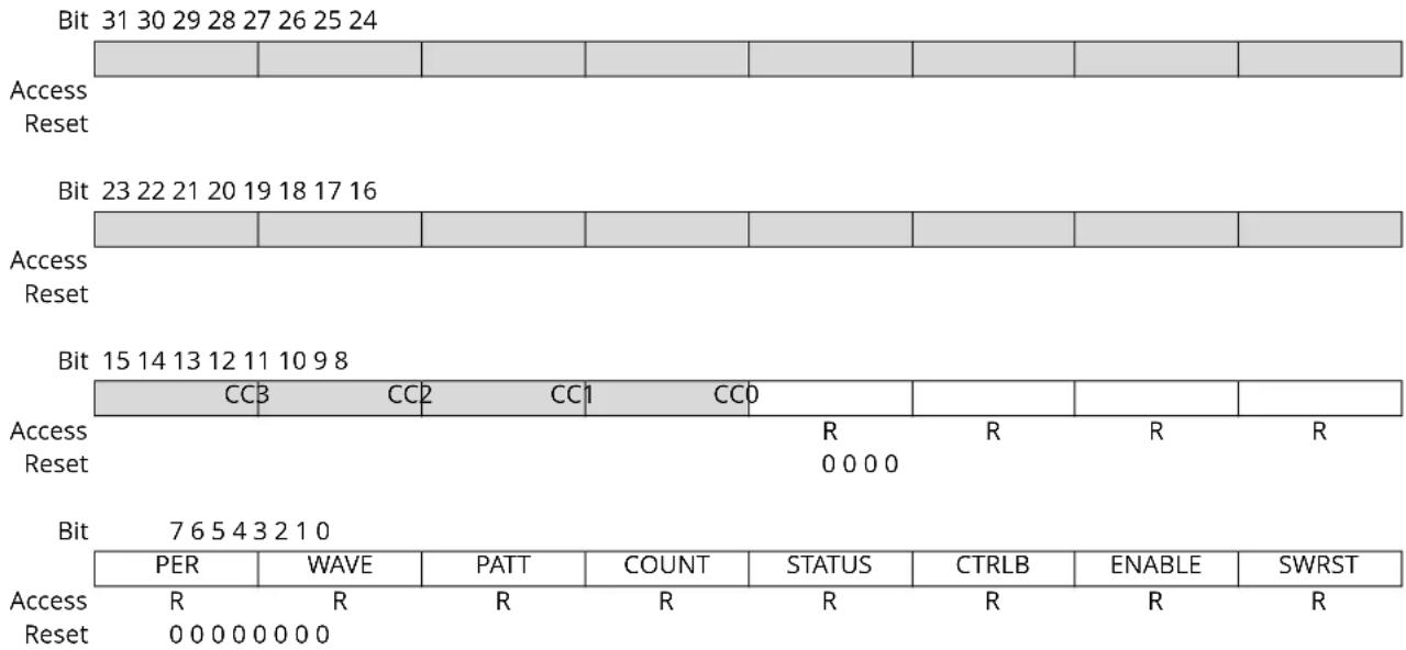
text_image
Bit 31 30 29 28 27 26 25 24 Access Reset Bit 23 22 21 20 19 18 17 16 Access Reset Bit 15 14 13 12 11 10 9 8 CCB CC2 CC1 CCO Access Reset R R R 0 0 0 0 Bit 7 6 5 4 3 2 1 0 PER WAVE PATT COUNT STATUS CTRLB ENABLE SWRST Access R R R R R R Reset 0 0 0 0 0 0 0Bits 8, 9, 10, 11 - CC Compare/Capture Channel x Synchronization Busy
This bit is cleared when the synchronization of Compare/Capture Channel x register between the clock domains is complete.
This bit is set when the synchronization of Compare/Capture Channel x register between clock domains is started.
CCx bit is available only for existing Compare/Capture Channels. For details on CC channels number, refer to each TCC feature list.
This bit is set when the synchronization of CCx register between clock domains is started.
Bit 7 - PER PER Synchronization Busy
This bit is cleared when the synchronization of PER register between the clock domains is complete.
This bit is set when the synchronization of PER register between clock domains is started.
Bit 6 - WAVE WAVE Synchronization Busy
This bit is cleared when the synchronization of WAVE register between the clock domains is complete.
This bit is set when the synchronization of WAVE register between clock domains is started.
Bit 5 - PATT PATT Synchronization Busy
This bit is cleared when the synchronization of PATTERN register between the clock domains is complete.
This bit is set when the synchronization of PATTERN register between clock domains is started.
Bit 4 - COUNT COUNT Synchronization Busy
This bit is cleared when the synchronization of COUNT register between the clock domains is complete.
This bit is set when the synchronization of COUNT register between clock domains is started.
Bit 3 - STATUS STATUS Synchronization Busy
This bit is cleared when the synchronization of STATUS register between the clock domains is complete.
This bit is set when the synchronization of STATUS register between clock domains is started.
Bit 2 - CTRLB CTRLB Synchronization Busy
This bit is cleared when the synchronization of CTRLB register between the clock domains is complete.
This bit is set when the synchronization of CTRLB register between clock domains is started.
Bit 1 - ENABLE ENABLE Synchronization Busy
This bit is cleared when the synchronization of ENABLE bit between the clock domains is complete.
This bit is set when the synchronization of ENABLE bit between clock domains is started.
Bit 0 - SWRST SWRST Synchronization Busy
This bit is cleared when the synchronization of SWRST bit between the clock domains is complete.
This bit is set when the synchronization of SWRST bit between clock domains is started.
35.8.5 Fault Control A and B
Name: FCTRLx
Offset: 0x0C + x*0x04 [x=0..1]
Reset: 0x00000000
Property: PAC Write-Protection, Enable-Protected
Bit 31 30 29 28 27 26 25 24
| FILTERVAL[3:0] | ||||
| Access Reset 0 0 0 0 | R/W R/W R/W R/W | |||
Bit 23 22 21 20 19 18 17 16
| BLANKVAL[7:0] | |
| Access | R/W R/W R/W R/W R/W R/W R/W R/W |
| Reset | 0 0 0 0 0 0 0 |
Bit 15 14 13 12 11 10 98
| BLANKPRESC | CAPTURE[2:0] | CHSEL[1:0] | HALT[1:0] | |
| Access | R/W R/W R/W R/W R/W R/W R/W | |||
| Reset | 0 0 0 0 0 0 0 0 | |||
Bit 76543210
| RESTART | BLANK[1:0] | QUAL | KEEP | SRC[1:0] | ||
| Access | R/W | R/W | R/W | R/W | ||
| Reset | 0 | 0 | 0 | 0 |
Bits 27:24 - FILTERVAL[3:0] Recoverable Fault n Filter Value
These bits define the filter value applied on MCEx (x=0,1) event input line. The value must be set to zero when MCEx event is used as synchronous event.
Bits 23:16 - BLANKVAL[7:0] Recoverable Fault n Blanking Value
These bits determine the duration of the blanking of the fault input source. Activation and edge selection of the blank filtering are done by the BLANK bits (FCTRLn.BLANK).
When enabled, the fault input source is internally disabled for BLANKVAL* prescaled GCLK_TCC periods after the detection of the waveform edge.
Bit 15 - BLANKPRESC Recoverable Fault n Blanking Value Prescaler
This bit enables a factor 64 prescaler factor on used as base frequency of the BLANKVAL value.
| Value | Description |
| 0 | Blank time is BLANKVAL* prescaled GCLK_TCC. |
| 1 | Blank time is BLANKVAL* 64 * prescaled GCLK_TCC. |
Bits 14:12 - CAPTURE[2:0] Recoverable Fault n Capture Action
These bits select the capture and Fault n interrupt/event conditions.
Table 35-8. Fault n Capture Action
| Value | Name | Description |
| 0x0 | DISABLE | Capture on valid recoverable Fault n is disabled |
| 0x1 | CAPT | On rising edge of a valid recoverable Fault n, capture counter value on channel selected by CHSEL[1:0]. INTFLAG.FAULTn flag rises on each new captured value. |
| 0x2 | CAPTMIN | On rising edge of a valid recoverable Fault n, capture counter value on channel selected by CHSEL[1:0], if COUNT value is lower than the last stored capture value (CC). INTFLAG.FAULTn flag rises on each local minimum detection. |
......continued
| Value | Name Description |
| 0x3 | CAPTMAX On rising edge of a valid recoverable Fault n, capture counter value on channel selected by CHSEL[1:0], if COUNT value is higher than the last stored capture value (CC). INTFLAG.FAULTn flag rises on each local maximum detection. |
| 0x4 | LOCMIN On rising edge of a valid recoverable Fault n, capture counter value on channel selected by CHSEL[1:0]. INTFLAG.FAULTn flag rises on each local minimum value detection. |
| 0x5 | LOCMAX On rising edge of a valid recoverable Fault n, capture counter value on channel selected by CHSEL[1:0]. INTFLAG.FAULTn flag rises on each local maximum detection. |
| 0x6 | DERIVO On rising edge of a valid recoverable Fault n, capture counter value on channel selected by CHSEL[1:0]. INTFLAG.FAULTn flag rises on each local maximum or minimum detection. |
| 0x7 | CAPTMARK Capture with ramp index as MSB value |
Bits 11:10 - CHSEL[1:0] Recoverable Fault n Capture Channel
These bits select the channel for capture operation triggered by recoverable Fault n.
Value Name Description
| 0x0 | CC0 Capture value stored into CC0 |
| 0x1 | CC1 Capture value stored into CC1 |
| 0x2 | CC2 Capture value stored into CC2 |
| 0x3 | CC3 Capture value stored into CC3 |
Bits 9:8 - HALT[1:0] Recoverable Fault n Halt Operation
These bits select the halt action for recoverable Fault n.
| Value Name | Description | |
| 0x0 | DISABLE | Halt action disabled |
| 0x1 | HW | Hardware halt action |
| 0x2 | SW | Software halt action |
| 0x3 | NR | Non-recoverable fault |
Bit 7 - RESTART Recoverable Fault n Restart
Setting this bit enables restart action for Fault n.
Value Description
| 0 | Fault n restart action is disabled. |
| 1 | Fault n restart action is enabled. |
Bits 6:5 - BLANK[1:0] Recoverable Fault n Blanking Operation
These bits, select the blanking start point for recoverable Fault n.
Value Name Description
| 0x0 | START | Blanking applied from start of the Ramp period |
| 0x1 | RISE | Blanking applied from rising edge of the waveform output |
| 0x2 | FALL Blanking applied from falling edge of the waveform output | |
| 0x3 | BOTH | Blanking applied from each toggle of the waveform output |
Bit 4 - QUAL Recoverable Fault n Qualification
Setting this bit enables the recoverable Fault n input qualification.
Value Description
| 0 | The recoverable Fault n input is not disabled on CMPx value condition. |
| 1 | The recoverable Fault n input is disabled when output signal is at inactive level (CMPx == 0). |
Bit 3 - KEEP Recoverable Fault n Keep
Setting this bit enables the Fault n keep action.
Value Description
| 0 | The Fault n state is released as soon as the recoverable Fault n is released. |
| 1 | The Fault n state is released at the end of TCC cycle. |
Bits 1:0 - SRC[1:0] Recoverable Fault n Source
These bits select the TCC event input for recoverable Fault n.
Event system channel connected to MCEx event input, must be configured to route the event asynchronously, when used as a recoverable Fault n input.
| Value Name | Description |
| 0x0 | DISABLE Fault input disabled |
| 0x1 | ENABLE MCEx (x=0,1) event input |
| 0x2 | INVERT Inverted MCEx (x=0,1) event input |
| 0x3 | ALTFAULT Alternate fault (A or B) state at the end of the previous period. |
35.8.6 Waveform Extension Control
Name: WEXCTRL
Offset: 0x14
Reset: 0x00000000
Property: PAC Write-Protection, Enable-Protected

text_image
Bit 31 30 29 28 27 26 25 24 DTHS[7:0] Access R/W R/W R/W R/W R/W R/W R/W Reset 0 0 0 0 0 0 0 0 Bit 23 22 21 20 19 18 17 16 DTLS[7:0] Access R/W R/W R/W R/W R/W R/W R/W Reset 0 0 0 0 0 0 0 0 Bit 15 14 13 12 11 10 9 8 DTIEN3 DTIEN2 DTIEN1 DTIENO Access R/W R/W R/W R/W Reset 0 0 0 0 Bit 7 6 5 4 3 2 1 0 OTMX[1:0] R/W R/W Reset 0 0Bits 31:24 - DTHS[7:0] Dead-Time High Side Outputs Value
This register holds the number of GCLK_TCC clock cycles for the dead-time high side.
Bits 23:16 - DTLS[7:0] Dead-time Low Side Outputs Value
This register holds the number of GCLK_TCC clock cycles for the dead-time low side.
Bits 8, 9, 10, 11 - DTIENx Dead-time Insertion Generator x Enable
Setting any of these bits enables the dead-time insertion generator for the corresponding output matrix. This will override the output matrix [x] and [x+WO_NUM/2], with the low side and high side waveform respectively.
| Value | Description |
| 0 | No dead-time insertion override. |
| 1 | Dead time insertion override on signal outputs[x] and [x+WO_NUM/2], from matrix outputs[x] signal. |
Bits 1:0 - OTMX[1:0] Output Matrix
These bits define the matrix routing of the TCC waveform generation outputs to the port pins, according to 35.6.3.8. Waveform Extension.
35.8.7 Driver Control
Name: DRVCTRL
Offset: 0x18
Reset: 0x00000000
Property: PAC Write-Protection, Enable-Protected
Bit 31 30 29 28 27 26 25 24
| FILTERVAL1[3:0] FILTERVAL0[3:0] |
Access R/W R/W R/W R/W R/W R/W R/W R/W
Reset 00000000
Bit 23 22 21 20 19 18 17 16
| INVEN7 INVEN6 INVEN5 | NVEN4 INVEN3 | INVEN2 INVEN1 | INVENO |
Access R/W R/W R/W R/W R/W R/W R/W R/W
Reset 00000000
Bit 15 14 13 12 11 10 98
| NRV7 | NRV6 | NRV5 | NRV4 | NRV3 | NRV2 | NRV1 | NRV0 |
Access R/W R/W R/W R/W R/W R/W R/W R/W
Reset 00000000
Bit 76543210
| NRE7 | NRE6 | NRE5 | NRE4 | NRE3 | NRE2 | NRE1 | NRE0 |
Access R/W R/W R/W R/W R/W R/W R/W R/W
Reset 00000000
Bits 31:28 - FILTERVAL1[3:0] Non-Recoverable Fault Input 1 Filter Value
These bits define the filter value applied on TCE1 event input line. When the TCE1 event input line is configured as a synchronous event, this value must be 0x0.
Bits 27:24 - FILTERVAL0[3:0] Non-Recoverable Fault Input 0 Filter Value
These bits define the filter value applied on TCE0 event input line. When the TCE0 event input line is configured as a synchronous event, this value must be 0x0.
Bits 16, 17, 18, 19, 20, 21, 22, 23 - INVENx Waveform Output x Inversion
These bits are used to select inversion on the output of channel x.
Writing a '1' to INVENx inverts output from WO[x].
Writing a '0' to INVENx disables inversion of output from WO[x].
Bits 8, 9, 10, 11, 12, 13, 14, 15 - NRVx NRVx Non-Recoverable State x Output Value
These bits define the value of the enabled override outputs, under non-recoverable fault condition.
Bits 0, 1, 2, 3, 4, 5, 6, 7 - NREx Non-Recoverable State x Output Enable
These bits enable the override of individual outputs by NRVx value, under non-recoverable fault condition.
| Value | Description |
| 0 | Non-recoverable fault tri-state the output. |
| 1 | Non-recoverable faults set the output to NRVx level. |
35.8.8 Debug control
Name: DBGCTRL
Offset: 0x1E
Reset: 0x00
Property: PAC Write-Protection
Bit 76543210
| FDBD DBGRUN | ||||||
| Access Reset 0 0 | R/W R/W | |||||
Bit 2 - FDDBD Fault Detection on Debug Break Detection
This bit is not affected by software reset and should not be changed by software while the TCC is enabled.
By default this bit is zero, and the on-chip debug (OCD) fault protection is enabled. OCD break request from the OCD system will trigger non-recoverable fault. When this bit is set, OCD fault protection is disabled and OCD break request will not trigger a fault.
| Value | Description |
| 0 | No faults are generated when TCC is halted in debug mode. |
| 1 | A non recoverable fault is generated and FAULTD flag is set when TCC is halted in debug mode. |
Bit 0 - DBGRUN Debug Running State
This bit is not affected by software reset and should not be changed by software while the TCC is enabled.
| Value | Description |
| 0 | The TCC is halted when the device is halted in debug mode. |
| 1 | The TCC continues normal operation when the device is halted in debug mode. |
35.8.9 Event Control
Name: EVCTRL
Offset: 0x20
Reset: 0x00000000
Property: PAC Write-Protection, Enable-Protected
Bit 31 30 29 28 27 26 25 24
| MCEO3 MCEO2 MCEO1 MCEO0 | |||||
| Access Reset 0 0 0 0 | R/W R/W R/W R/W | ||||
Bit 23 22 21 20 19 18 17 16
| MCEI3 | MCEI2 | MCEI1 | MCEI0 | ||||
| Access Reset 0 0 0 0 | R/W R/W R/W R/W | ||||||
Bit 15 14 13 12 11 10 98
| TCEI1 | TCEI0 | TCINV1 | TCINV0 | CNTEO | TRGEO | OVFEO | ||
| Access | R/W | R/W | R/W | R/W | R/W | R/W | ||
| Reset | 0 | 0 | 0 | 0 | 0 | 0 |
Bit 76543210
| CNTSEL[1:0] | EVACT1[2:0] | EVACT0[2:0] | |
| Access | R/W R/W R/W R/W R/W R/W R/W R/W | ||
| Reset | 0 0 0 0 0 0 0 0 | ||
Bits 24, 25, 26, 27 - MCEOx Match or Capture Channel x Event Output Enable
These bits control if the match/capture event on channel x is enabled and will be generated for every match or capture.
| Value | Description |
| 0 | Match/capture x event is disabled and will not be generated. |
| 1 | Match/capture x event is enabled and will be generated for every compare/capture on channel x. |
Bits 16, 17, 18, 19 - MCEIx Match or Capture Channel x Event Input Enable
These bits indicate if the match/capture x incoming event is enabled
These bits are used to enable match or capture input events to the CCx channel of TCC.
| Value | Description |
| 0 | Incoming events are disabled. |
| 1 | Incoming events are enabled. |
Bits 14, 15 - TCEIx Timer/Counter Event Input x Enable
This bit is used to enable input event x to the TCC.
| Value | Description |
| 0 | Incoming event x is disabled. |
| 1 | Incoming event x is enabled. |
Bits 12, 13 - TCINVx Timer/Counter Event x Invert Enable
This bit inverts the event x input.
| Value | Description |
| 0 | Input event source x is not inverted. |
| 1 | Input event source x is inverted. |
Bit 10 - CNTEO Timer/Counter Event Output Enable
This bit is used to enable the counter cycle event. When enabled, an event will be generated on begin or end of counter cycle depending of CNTSEL[1:0] settings.
| Value Description | |
| 0 | Counter cycle output event is disabled and will not be generated. |
| 1 | Counter cycle output event is enabled and will be generated depend of CNTSEL[1:0] value. |
Bit 9 - TRGEO Retrigger Event Output Enable
This bit is used to enable the counter retrigger event. When enabled, an event will be generated when the counter retriggers operation.
| Value Description | |
| 0 | Counter retrigger event is disabled and will not be generated. |
| 1 | Counter retrigger event is enabled and will be generated for every counter retrigger. |
Bit 8 - OVFEO Overflow/Underflow Event Output Enable
This bit is used to enable the overflow/underflow event. When enabled an event will be generated when the counter reaches the TOP or the ZERO value.
| Value Description | |
| 0 | Overflow/underflow counter event is disabled and will not be generated. |
| 1 | Overflow/underflow counter event is enabled and will be generated for every counter overflow/underflow. |
Bits 7:6 - CNTSEL[1:0] Timer/Counter Interrupt and Event Output Selection
These bits define on which part of the counter cycle the counter event output is generated.
| Value Name | Description |
| 0x0 | START An interrupt/event is generated at begin of each counter cycle |
| 0x1 | END An interrupt/event is generated at end of each counter cycle |
| 0x2 | BETWEEN An interrupt/event is generated between each counter cycle. |
| 0x3 | BOUNDARY An interrupt/event is generated at begin of first counter cycle, and end of last counter cycle. |
Bits 5:3 - EVACT1[2:0] Timer/Counter Event Input 1 Action
These bits define the action the TCC will perform on TCE1 event input.
| Value Name | Description |
| 0x0 | OFF Event action disabled. |
| 0x1 | RETRIGGER Start, restart or re-trigger TC on event |
| 0x2 | DIR (asynch) Direction control |
| 0x3 | STOP Stop TC on event |
| 0x4 | DEC Decrement TC on event |
| 0x5 | PPW Period captured into CC0 Pulse Width on CC1 |
| 0x6 | PWP Period captured into CC1 Pulse Width on CC0 |
| 0x7 | FAULT Non-recoverable Fault |
Bits 2:0 - EVACT0[2:0] Timer/Counter Event Input 0 Action
These bits define the action the TCC will perform on TCE0 event input 0.
| Value Name | Description | |
| 0x0 | OFF | Event action disabled. |
| 0x1 | RETRIGGER | Start, restart or re-trigger TC on event |
| 0x2 | COUNTEV | Count on event. |
| 0x3 | START | Start TC on event |
| 0x4 | INC | Increment TC on EVENT |
| 0x5 | COUNT (async) | Count on active state of asynchronous event |
| 0x6 | STAMP | Capture overflow times (Max value) |
| 0x7 | FAULT Non-recoverable Fault | |
35.8.10 Interrupt Enable Clear
Name: INTENCLR
Offset: 0x24
Reset: 0x00000000
Property: PAC Write-Protection
This register allows the user to enable an interrupt without doing a read-modify-write operation. Changes in this register will also be reflected in the Interrupt Enable Set (INTENSET) register.
| Bit 31 30 29 28 27 26 25 24 | |||||||
| Access Reset | |||||||
| Bit 23 22 21 20 19 18 17 16 | |||||||
| MC3 MC2 MC1 MC0 | |||||||
| Access Reset | R/W R/W R/W R/W | ||||||
| 0 | 0 | 0 | 0 | ||||
| Bit 15 14 13 12 11 10 | 9 | 8 | |||||
| FAULT1 | FAULT0 | FAULTB | FAULTA | DFS | UFS | ||
| Access Reset | R/W R/W R/W R/W R/W | ||||||
| 0 | 0 | 0 | 0 | 0 | 0 | ||
| Bit | 7 | 6 | 5 | 4 | 3 | 2 | 1 |
| ERR | CNT TRG OVF | ||||||
| Access Reset | R/W R/W R/W R/W | ||||||
| 0 | 0 | 0 | |||||
Bits 16, 17, 18, 19 - MCx Match or Capture Channel x Interrupt Enable
Writing a '0' to this bit has no effect.
Writing a '1' to this bit will clear the corresponding Match or Capture Channel x Interrupt Disable/Enable bit, which disables the Match or Capture Channel x interrupt.
| Value | Description |
| 0 | The Match or Capture Channel x interrupt is disabled. |
| 1 | The Match or Capture Channel x interrupt is enabled. |
Bit 15 - FAULT1 Non-Recoverable Fault x Interrupt Enable
Writing a '0' to this bit has no effect.
Writing a '1' to this bit will clear the Non-Recoverable Fault x Interrupt Disable/Enable bit, which disables the Non-Recoverable Fault x interrupt.
| Value | Description |
| 0 | The Non-Recoverable Fault x interrupt is disabled. |
| 1 | The Non-Recoverable Fault x interrupt is enabled. |
Bit 14 - FAULT0 Non-Recoverable Fault x Interrupt Enable
Writing a '0' to this bit has no effect.
Writing a '1' to this bit will clear the Non-Recoverable Fault x Interrupt Disable/Enable bit, which disables the Non-Recoverable Fault x interrupt.
| Value | Description |
| 0 | The Non-Recoverable Fault x interrupt is disabled. |
| 1 | The Non-Recoverable Fault x interrupt is enabled. |
Bit 13 - FAULTB Recoverable Fault B Interrupt Enable
Writing a '0' to this bit has no effect.
Writing a '1' to this bit will clear the Recoverable Fault B Interrupt Disable/Enable bit, which disables the Recoverable Fault B interrupt.
| Value Description | |
| 0 | The Recoverable Fault B interrupt is disabled. |
| 1 | The Recoverable Fault B interrupt is enabled. |
Bit 12 - FAULTA Recoverable Fault A Interrupt Enable
Writing a '0' to this bit has no effect.
Writing a '1' to this bit will clear the Recoverable Fault A Interrupt Disable/Enable bit, which disables the Recoverable Fault A interrupt.
| Value Description | |
| 0 | The Recoverable Fault A interrupt is disabled. |
| 1 | The Recoverable Fault A interrupt is enabled. |
Bit 11 - DFS Non-Recoverable Debug Fault Interrupt Enable
Writing a '0' to this bit has no effect.
Writing a '1' to this bit will clear the Debug Fault State Interrupt Disable/Enable bit, which disables the Debug Fault State interrupt.
| Value Description | |
| 0 | The Debug Fault State interrupt is disabled. |
| 1 | The Debug Fault State interrupt is enabled. |
Bit 10 - UFS Non-Recoverable Update Fault Interrupt Enable
Writing a zero to this bit has no effect.
Writing a one to this bit will clear the Non-Recoverable Update Fault Interrupt Disable/Enable bit, which disables the Non-Recoverable Update Fault interrupt.
| Value Description | |
| 0 | The Non-Recoverable Update Fault interrupt is disabled. |
| 1 | The Non-Recoverable Update Fault interrupt is enabled. |
Bit 3 - ERR Error Interrupt Enable
Writing a '0' to this bit has no effect.
Writing a '1' to this bit will clear the Error Interrupt Disable/Enable bit, which disables the Compare interrupt.
| Value Description | |
| 0 | The Error interrupt is disabled. |
| 1 | The Error interrupt is enabled. |
Bit 2 - CNT Counter Interrupt Enable
Writing a '0' to this bit has no effect.
Writing a '1' to this bit will clear the Counter Interrupt Disable/Enable bit, which disables the Counter interrupt.
| Value Description | |
| 0 | The Counter interrupt is disabled. |
| 1 | The Counter interrupt is enabled. |
Bit 1 - TRG Retrigger Interrupt Enable
Writing a '0' to this bit has no effect.
Writing a '1' to this bit will clear the Retrigger Interrupt Disable/Enable bit, which disables the Retrigger interrupt.
| Value Description | |
| 0 | The Retrigger interrupt is disabled. |
| 1 | The Retrigger interrupt is enabled. |
Bit 0 - OVF Overflow Interrupt Enable
Writing a '0' to this bit has no effect.
Writing a '1' to this bit will clear the Overflow Interrupt Disable/Enable bit, which disables the Overflow interrupt request.
| Value Description | |
| 0 | The Overflow interrupt is disabled. |
| 1 | The Overflow interrupt is enabled. |
35.8.11 Interrupt Enable Set
Name: INTENSET
Offset: 0x28
Reset: 0x00000000
Property: PAC Write-Protection
This register allows the user to enable an interrupt without doing a read-modify-write operation. Changes in this register will also be reflected in the Interrupt Enable Clear (INTENCLR) register.
| Bit 31 30 29 28 27 26 25 24 | |||||||
| Access Reset | |||||||
| Bit 23 22 21 20 19 18 17 16 | |||||||
| MC3 MC2 MC1 MC0 | |||||||
| Access Reset | R/W R/W R/W R/W | ||||||
| 0 | 0 | 0 | 0 | ||||
| Bit 15 14 13 12 11 10 | 9 | 8 | |||||
| FAULT1 | FAULT0 | FAULTB | FAULTA | DFS | UFS | ||
| Access Reset | R/W R/W R/W R/W R/W | ||||||
| 0 | 0 | 0 | 0 | 0 | 0 | ||
| Bit | 7 | 6 | 5 | 4 | 3 | 2 | 1 |
| ERR | CNT TRG OVF | ||||||
| Access Reset | R/W R/W R/W R/W | ||||||
| 0 | 0 | 0 | |||||
Bits 16, 17, 18, 19 - MCx Match or Capture Channel x Interrupt Enable
Writing a '0' to this bit has no effect.
Writing a '1' to this bit will set the corresponding Match or Capture Channel x Interrupt Disable/Enable bit, which enables the Match or Capture Channel x interrupt.
| Value | Description |
| 0 | The Match or Capture Channel x interrupt is disabled. |
| 1 | The Match or Capture Channel x interrupt is enabled. |
Bit 15 - FAULT1 Non-Recoverable Fault x Interrupt Enable
Writing a '0' to this bit has no effect.
Writing a '1' to this bit will set the Non-Recoverable Fault x Interrupt Disable/Enable bit, which enables the Non-Recoverable Fault x interrupt.
| Value | Description |
| 0 | The Non-Recoverable Fault x interrupt is disabled. |
| 1 | The Non-Recoverable Fault x interrupt is enabled. |
Bit 14 - FAULT0 Non-Recoverable Fault x Interrupt Enable
Writing a '0' to this bit has no effect.
Writing a '1' to this bit will clear the Non-Recoverable Fault x Interrupt Disable/Enable bit, which disables the Non-Recoverable Fault x interrupt.
| Value | Description |
| 0 | The Non-Recoverable Fault x interrupt is disabled. |
| 1 | The Non-Recoverable Fault x interrupt is enabled. |
Bit 13 - FAULTB Recoverable Fault B Interrupt Enable
Writing a '0' to this bit has no effect.
Writing a '1' to this bit will set the Recoverable Fault B Interrupt Disable/Enable bit, which enables the Recoverable Fault B interrupt.
| Value Description | |
| 0 | The Recoverable Fault B interrupt is disabled. |
| 1 | The Recoverable Fault B interrupt is enabled. |
Bit 12 - FAULTA Recoverable Fault A Interrupt Enable
Writing a '0' to this bit has no effect.
Writing a '1' to this bit will set the Recoverable Fault A Interrupt Disable/Enable bit, which enables the Recoverable Fault A interrupt.
| Value Description | |
| 0 | The Recoverable Fault A interrupt is disabled. |
| 1 | The Recoverable Fault A interrupt is enabled. |
Bit 11 - DFS Non-Recoverable Debug Fault Interrupt Enable
Writing a '0' to this bit has no effect.
Writing a '1' to this bit will set the Debug Fault State Interrupt Disable/Enable bit, which enables the Debug Fault State interrupt.
| Value Description | |
| 0 | The Debug Fault State interrupt is disabled. |
| 1 | The Debug Fault State interrupt is enabled. |
Bit 10 - UFS Non-Recoverable Update Fault Interrupt Enable
Writing a zero to this bit has no effect.
Writing a one to this bit will set the Non-Recoverable Update Fault Interrupt Disable/Enable bit, which enables the Non-Recoverable Update Fault interrupt.
| Value Description | |
| 0 | The Non-Recoverable Update Fault interrupt is disabled. |
| 1 | The Non-Recoverable Update Fault interrupt is enabled. |
Bit 3 - ERR Error Interrupt Enable
Writing a '0' to this bit has no effect.
Writing a '1' to this bit will set the Error Interrupt Disable/Enable bit, which enables the Compare interrupt.
| Value Description | |
| 0 | The Error interrupt is disabled. |
| 1 | The Error interrupt is enabled. |
Bit 2 - CNT Counter Interrupt Enable
Writing a '0' to this bit has no effect.
Writing a '1' to this bit will set the Retrigger Interrupt Disable/Enable bit, which enables the Counter interrupt.
| Value Description | |
| 0 | The Counter interrupt is disabled. |
| 1 | The Counter interrupt is enabled. |
Bit 1 - TRG Retrigger Interrupt Enable
Writing a '0' to this bit has no effect.
Writing a '1' to this bit will set the Retrigger Interrupt Disable/Enable bit, which enables the Retrigger interrupt.
| Value Description | |
| 0 | The Retrigger interrupt is disabled. |
| 1 | The Retrigger interrupt is enabled. |
Bit 0 - OVF Overflow Interrupt Enable
Writing a '0' to this bit has no effect.
Writing a '1' to this bit will set the Overflow Interrupt Disable/Enable bit, which enables the Overflow interrupt request.
| Value Description | |
| 0 | The Overflow interrupt is disabled. |
| 1 | The Overflow interrupt is enabled. |
35.8.12 Interrupt Flag Status and Clear
Name: INTFLAG
Offset: 0x2C
Reset: 0x00000000
Property: -
| Bit 31 30 29 28 27 26 25 24 | |||||||
| Access Reset | |||||||
| Bit 23 22 21 20 19 18 17 16 | |||||||
| MC3 MC2 MC1 MC0 | |||||||
| Access Reset | R/W R/W R/W R/W | ||||||
| 0 | 0 | 0 | 0 | ||||
| Bit 15 14 13 12 11 10 | 9 | 8 | |||||
| FAULT1 | FAULT0 | FAULTB | FAULTA | DFS | UFS | ||
| Access Reset | R/W R/W R/W R/W R/W | ||||||
| 0 | 0 | 0 | 0 | 0 | |||
| Bit | 7 | 6 | 5 | 4 | 3 | 2 | 1 |
| ERR | CNT TRG OVF | ||||||
| Access Reset | R/W R/W R/W R/W | ||||||
| 0 | 0 | 0 | 0 | ||||
Bits 16, 17, 18, 19 - MCx Match or Capture Channel x Interrupt Flag
This flag is set on the next CLK_TCC_COUNT cycle after a match with the compare condition or once CCx register contain a valid capture value.
Writing a '0' to one of these bits has no effect.
Writing a '1' to one of these bits will clear the corresponding Match or Capture Channel x interrupt flag
In Capture operation, this flag is automatically cleared when CCx register is read.
Bit 15 - FAULT1 Non-Recoverable Fault x Interrupt Flag
This flag is set on the next CLK_TCC_COUNT cycle after a Non-Recoverable Fault x occurs.
Writing a '0' to this bit has no effect.
Writing a '1' to this bit clears the Non-Recoverable Fault x interrupt flag.
Bit 14 - FAULT0 Non-Recoverable Fault x Interrupt Enable
Writing a '0' to this bit has no effect.
Writing a '1' to this bit will clear the Non-Recoverable Fault x Interrupt flag.
Bit 13 - FAULTB Recoverable Fault B Interrupt Flag
This flag is set on the next CLK_TCC_COUNT cycle after a Recoverable Fault B occurs.
Writing a '0' to this bit has no effect.
Writing a '1' to this bit clears the Recoverable Fault B interrupt flag.
Bit 12 - FAULTA Recoverable Fault A Interrupt Flag
This flag is set on the next CLK_TCC_COUNT cycle after a Recoverable Fault B occurs.
Writing a '0' to this bit has no effect.
Writing a '1' to this bit clears the Recoverable Fault B interrupt flag.
Bit 11 - DFS Non-Recoverable Debug Fault State Interrupt Flag
This flag is set on the next CLK_TCC_COUNT cycle after an Debug Fault State occurs.
Writing a '0' to this bit has no effect.
Writing a '1' to this bit clears the Debug Fault State interrupt flag.
Bit 10 - UFS Non-Recoverable Update Fault
This flag is set when the RAMP index changes and the Lock Update bit is set (CTRLBSET.LUPD).
Writing a zero to this bit has no effect.
Writing a one to this bit clears the Non-Recoverable Update Fault interrupt flag.
Bit 3 - ERR Error Interrupt Flag
This flag is set if a new capture occurs on a channel when the corresponding Match or Capture
Channel x interrupt flag is one. In which case there is nowhere to store the new capture.
Writing a '0' to this bit has no effect.
Writing a '1' to this bit clears the error interrupt flag.
Bit 2 - CNT Counter Interrupt Flag
This flag is set on the next CLK_TCC_COUNT cycle after a counter event occurs.
Writing a '0' to this bit has no effect.
Writing a '1' to this bit clears the CNT interrupt flag.
Bit 1 - TRG Retrigger Interrupt Flag
This flag is set on the next CLK_TCC_COUNT cycle after a counter retrigger occurs.
Writing a '0' to this bit has no effect.
Writing a '1' to this bit clears the re-trigger interrupt flag.
Bit 0 - OVF Overflow Interrupt Flag
This flag is set on the next CLK_TCC_COUNT cycle after an overflow condition occurs.
Writing a '0' to this bit has no effect.
Writing a '1' to this bit clears the Overflow interrupt flag.
35.8.13 Status
Name: STATUS
Offset: 0x30
Reset: 0x00000001
Bits 24, 25, 26, 27 - CMPx Channel x Compare Value
This bit reflects the channel x output compare value.
| Value | Description |
| 0 | Channel compare output value is 0. |
| 1 | Channel compare output value is 1. |
Bits 16, 17, 18, 19 - CCBUFVx Channel x Compare or Capture Buffer Valid
For a compare channel, this bit is set when a new value is written to the corresponding CCBUFx register. The bit is cleared either by writing a '1' to the corresponding location when CTRLB.LUPD is set, or automatically on an UPDATE condition.
For a capture channel, the bit is set when a valid capture value is stored in the CCBUFx register. The bit is automatically cleared when the CCx register is read.
Bits 14, 15 - FAULTx Non-recoverable Fault x State
This bit is set by hardware as soon as non-recoverable Fault x condition occurs.
This bit is cleared by writing a one to this bit and when the corresponding FAULTxIN status bit is low. Once this bit is clear, the timer/counter will restart from the last COUNT value. To restart the timer/counter from BOTTOM, the timer/counter restart command must be executed before clearing the corresponding STATEx bit. For further details on timer/counter commands, refer to available commands description (35.8.3. CTRLBSET.CMD).
Bit 13 - FAULTB Recoverable Fault B State
This bit is set by hardware as soon as recoverable Fault B condition occurs.
This bit can be clear by hardware when Fault B action is resumed, or by writing a '1' to this bit when the corresponding FAULTBIN bit is low. If software halt command is enabled (FAULTB.HALT=SW), clearing this bit will release the timer/counter.
Bit 12 - FAULTA Recoverable Fault A State
This bit is set by hardware as soon as recoverable Fault A condition occurs.
This bit can be clear by hardware when Fault A action is resumed, or by writing a '1' to this bit when the corresponding FAULTAIN bit is low. If software halt command is enabled (FAULTA.HALT=SW), clearing this bit will release the timer/counter.
Bit 11 - FAULT1IN Non-Recoverable Fault 1 Input
This bit is set while an active Non-Recoverable Fault 1 input is present.
Bit 10 - FAULT0IN Non-Recoverable Fault 0 Input
This bit is set while an active Non-Recoverable Fault 0 input is present.
Bit 9 - FAULTBIN Recoverable Fault B Input
This bit is set while an active Recoverable Fault B input is present.
Bit 8 - FAULTAIN Recoverable Fault A Input
This bit is set while an active Recoverable Fault A input is present.
Bit 7 - PERBUFV Period Buffer Valid
This bit is set when a new value is written to the PERBUF register. This bit is automatically cleared by hardware on UPDATE condition when CTRLB.LUPD is set, or by writing a '1' to this bit.
Bit 5 - PATTBUFV Pattern Generator Value Buffer Valid
This bit is set when a new value is written to the PATTBUF register. This bit is automatically cleared by hardware on UPDATE condition when CTRLB.LUPD is set, or by writing a '1' to this bit.
Bit 3 - DFS Debug Fault State
This bit is set by hardware in Debug mode when DDBGCTRL.FDDBD bit is set. The bit is cleared by writing a '1' to this bit and when the TCC is not in Debug mode.
When the bit is set, the counter is halted and the Waveforms state depend on DRVCTRL.NRE and DRVCTRL.NRV registers.
Bit 2 - UFS Non-recoverable Update Fault State
This bit is set by hardware when the RAMP index changes and the Lock Update bit is set (CTRLBSET.LUPD). The bit is cleared by writing a one to this bit.
When the bit is set, the waveforms state depend on DRVCTRL.NRE and DRVCTRL.NRV registers.
Bit 1 - IDX Ramp Index
In RAMP2 and RAMP2A operation, the bit is cleared during the cycle A and set during the cycle B. In RAMP1 operation, the bit always reads zero. For details on ramp operations, refer to 35.6.3.4. Ramp Operations.
Bit 0 - STOP Stop
This bit is set when the TCC is disabled either on a STOP command or on an UPDATE condition when One-Shot operation mode is enabled (CTRLBSET.ONESHOT=1).
This bit is clear on the next incoming counter increment or decrement.
| Value Description | |
| 0 | Counter is running. |
| 1 | Counter is stopped. |
35.8.14 Counter Value
Name: COUNT
Offset: 0x34
Reset: 0x00000000
Property: PAC Write-Protection, Write-Synchronized
Note: Prior to any read access, this register must be synchronized by user by writing the according TCC Command value to the Control B Set register (CTRLBSET.CMD=READSYNC).
| Bit 31 30 29 28 27 26 25 24 | |
| COUNT[31:24] | |
| Access R/W R/W R/W R/W R/W R/W R/W R/W Reset 0 0 0 0 0 0 0 0 | |
| Bit 23 22 21 20 19 18 17 16 | |
| COUNT[23:16] | |
| Access R/W R/W R/W R/W R/W R/W R/W R/W Reset 0 0 0 0 0 0 0 0 | |
| Bit 15 14 13 12 11 10 9 8 | |
| COUNT[15:8] | |
| Access R/W R/W R/W R/W R/W R/W R/W R/W Reset 0 0 0 0 0 0 0 0 | |
| Bit 7 6 5 4 3 2 1 0 | |
| COUNT[7:0] | |
| Access R/W R/W R/W R/W R/W R/W R/W R/W Reset 0 0 0 0 0 0 0 0 | |
Bits 31:0 - COUNT[31:0] Counter Value
These bits hold the value of the counter register.
Note: When the TCC is configured as 24- or 16-bit timer/counter, the excess bits are read zero.
Note: This bit field occupies the MSB of the register, [31:m]. m is dependent on the Resolution bit in the Control A register (CTRLA.RESOLUTION):
| CTRLA.RESOLUTION Bits [31:m] | |
| 0x0 - NONE | 31:0 (depicted) |
| 0x1 - DITH4 | 31:4 |
| 0x2 - DITH5 | 31:5 |
| 0x3 - DITH6 | 31:6 |
35.8.15 Pattern
Name: PATT
Offset: 0x38
Reset: 0x0000
Property: Write-Synchronized
Bit 15 14 13 12 11 10 9 8
| PGV7 PGV6 PGV5 PGV4 | PGV3 PGV2 PGV1 PGV0 |
Access R/W R/W R/W R/W R/W R/W R/W R/W
Reset 00000000
Bit 76543210
| PGE7 | PGE6 | PGE5 | PGE4 | PGE3 | PGE2 | PGE1 | PGE0 |
Access R/W R/W R/W R/W R/W R/W R/W R/W
Reset 00000000
Bits 8, 9, 10, 11, 12, 13, 14, 15 – PGV Pattern Generation Output Value
This register holds the values of pattern for each waveform output.
Bits 0, 1, 2, 3, 4, 5, 6, 7 – PGE Pattern Generation Output Enable
This register holds the enable status of pattern generation for each waveform output. A bit written to '1' will override the corresponding SWAP output with the corresponding PGVn value.
35.8.16 Waveform
Name: WAVE
Offset: 0x3C
Reset: 0x00000000
Property: Write-Synchronized
Bit 31 30 29 28 27 26 25 24
| SWAP3 SWAP2 SWAP1 SWAP0 | ||||||
| Access Reset 0 0 0 0 | R/W R/W R/W R/W | |||||
Bit 23 22 21 20 19 18 17 16
| POL3 | POL2 | POL1 | POL0 | ||||
| Access Reset 0 0 0 0 | R/W R/W R/W R/W | ||||||
Bit 15 14 13 12 11 10 98
| CICCEN3 | CICCEN2 | CICCEN1 | CICCEN0 | ||||
| Access Reset 0 0 0 0 | R/W R/W R/W R/W | ||||||
Bit 76543210
| CIPEREN | RAMP[1:0] | WAVEGEN[2:0] | ||||
| Access | R/W | R/W R/W | R/W R/W R/W | |||
| Reset | 0 | 0 | 0 | 0 | 0 | |
Bits 24, 25, 26, 27 - SWAP Swap DTI Output Pair x
Setting these bits enables output swap of DTI outputs [x] and [x+WO_NUM/2]. Note the DTIxEN settings will not affect the swap operation.
Bits 16, 17, 18, 19 - POL Channel Polarity x
Setting these bits enables the output polarity in single-slope and dual-slope PWM operations.
| Value | Name | Description |
| 0 | (single-slope PWM waveform generation) | Compare output is initialized to ~DIR and set to DIR when TCC counter matches CCx value |
| 1 | (single-slope PWM waveform generation) | Compare output is initialized to DIR and set to ~DIR when TCC counter matches CCx value. |
| 0 | (dual-slope PWM waveform generation) | Compare output is set to ~DIR when TCC counter matches CCx value |
| 1 | (dual-slope PWM waveform generation) | Compare output is set to DIR when TCC counter matches CCx value. |
Bits 8, 9, 10, 11 - CICCEN Circular CC Enable x
Setting this bits enables the compare circular buffer option on channel. When the bit is set, CCx register value is copied-back into the CCx register on UPDATE condition.
Bit 7 - CIPEREN Circular Period Enable
Setting this bits enable the period circular buffer option. When the bit is set, the PER register value is copied-back into the PERB register on UPDATE condition.
Bits 5:4 - RAMP[1:0] Ramp Operation
These bits select Ramp operation (RAMP).
| Value Name | Description | |
| 0x0 | RAMP1 RAMP1 operation | |
| 0x1 | RAMP2A Alternative RAMP2 operation | |
| 0x2 | RAMP2 RAMP2 operation | |
| 0x3 | RAMP2C Critical RAMP2 operation | |
Bits 2:0 - WAVEGEN[2:0] Waveform Generation Operation
These bits select the waveform generation operation. The settings impact the top value and control if frequency or PWM waveform generation should be used.
| Value | Name Description | ||||||||
| Operation Top Update | Waveform Output | On Match | Waveform Output On Update | OVFIF/Event Up Down | |||||
| 0x0 | NFRQ Normal Frequency | PER TOP/Zero | Toggle | Stable | TOP | Zero | |||
| 0x1 | MFRQ | Match Frequency | CCO | TOP/Zero | Toggle | Stable | TOP | Zero | |
| 0x2 | NPWM | Normal PWM | PER | TOP/Zero | Set | Clear | TOP | Zero | |
| 0x3 | Reserved | - | - | - | - | - | - | - | |
| 0x4 | DSCRITICAL | Dual-slope PWM | PER | Zero | ~DIR | Stable | - | Zero | |
| 0x5 | DSBOTTOM | Dual-slope PWM | PER | Zero | ~DIR | Stable | - | Zero | |
| 0x6 | DSBOTH | Dual-slope PWM | PER | TOP & Zero | ~DIR | Stable | TOP | Zero | |
| 0x7 | DSTOP | Dual-slope PWM | PER | Zero | ~DIR | Stable | TOP | - | |
35.8.17 Period Value
Name: PER
Offset: 0x40
Reset: 0xFFFFFFF
Property: Write-Synchronized
Bit 31 30 29 28 27 26 25 24
PER[25:18]
Access R/W R/W R/W R/W R/W R/W R/W R/W
Reset 1 1 1 1 1 1 1 1
Bit 23 22 21 20 19 18 17 16
PER[17:10]
Access R/W R/W R/W R/W R/W R/W R/W R/W
Reset 1 1 1 1 1 1 1 1
Bit 15 14 13 12 11 10 9 8
PER[9:2]
Access R/W R/W R/W R/W R/W R/W R/W R/W
Reset 1 1 1 1 1 1 1 1
Bit 76543210
PER[1:0] DITHER[5:0]
Access R/W R/W R/W R/W R/W R/W R/W R/W
Reset 1 1 1 1 1 1 1 1
Bits 31:6 - PER[25:0] Period Value
These bits hold the value of the period register.
Note: When the TCC is configured as 16- or 24-bit timer/counter, the excess bits are read zero.
Note: This bit field occupies the MSB of the register. m is dependent on the Resolution bit in the Control A register (CTRLA.RESOLUTION):
| CTRLA.RESOLUTION | Bits [31:m] |
| 0x0 - NONE | 31:0 |
| 0x1 - DITH4 | 31:4 |
| 0x2 - DITH5 | 31:5 |
| 0x3 - DITH6 | 31:6 (depicted) |
Bits 5:0 - DITHER[5:0] Dithering Cycle Number
These bits hold the number of extra cycles that are added on the PWM pulse period every 64 PWM frames.
Note: This bit field consists of the n LSB of the register. n is dependent on the value of the Resolution bits in the Control A register (CTRLA.RESOLUTION):
| CTRLA.RESOLUTION | Bits [n:0] |
| 0x0 - NONE | - |
| 0x1 - DITH4 | 3:0 |
| 0x2 - DITH5 | 4:0 |
| 0x3 - DITH6 | 5:0 (depicted) |
35.8.18 Compare/Capture Channel x
Name: CCx
Offset: 0x44 + x*0x04 [x=0..3]
Reset: 0x00000000
Property: Write-Synchronized
The CCx register represents the 16-, 24- or 32-bit value, CCx. The register has two functions, depending of the mode of operation.
For capture operation, this register represents the second buffer level and access point for the CPU and DMA.
For compare operation, this register is continuously compared to the counter value. Normally, the output form the comparator is then used for generating waveforms.
CCx register is updated with the buffer value from their corresponding CCBUFx register when an UPDATE condition occurs.
In addition, in match frequency operation, the CC0 register controls the counter period.
Bit 31 30 29 28 27 26 25 24
| CC25 CC24 CC23 CC22 CC21 CC20 CC19 CC18 | |||||
| Access | R/W R/W R/W R/W R/W R/W R/W R/W | ||||
| Reset | 0 0 0 0 0 0 0 | ||||
Bit 23 22 21 20 19 18 17 16
| CC17 CC16 CC15 CC14 CC13 CC12 CC11 CC10 | |||||
| Access | R/W R/W R/W R/W R/W R/W R/W R/W | ||||
| Reset | 0 0 0 0 0 0 0 | ||||
Bit 15 14 13 12 11 10 9 8
| CC9 | CC8 | CC7 | CC6 | CC5 | CC4 | CC3 | CC2 | |
| Access | R/W | R/W | R/W | R/W | R/W | R/W | R/W | R/W |
| Reset | 0 | 0 | 0 | 0 | 0 | 0 | 0 | 0 |
Bit 76543210
| CC1 | CC0 | DITHER[5:0] | |||||
| Access | R/W | R/W | R/W R/W R/W R/W R/W R/W | ||||
| Reset | 0 | 0 | 0 | 0 | 0 | 0 | 0 |
Bits 6, 7, 8, 9, 10, 11, 12, 13, 14, 15, 16, 17, 18, 19, 20, 21, 22, 23, 24, 25, 26, 27, 28, 29, 30, 31 – CCx Channel x Compare/Capture Value
These bits hold the value of the Channel x compare/capture register.
Note: When the TCC is configured as 16- or 24-bit timer/counter, the excess bits are read zero.
Note: This bit field occupies the MSB of the register, [31:m]. m is dependent on the Resolution bit in the Control A register (CTRLA.RESOLUTION):
| CTRLA.RESOLUTION | Bits [31:m] |
| 0x0 - NONE | 31:0 |
| 0x1 - DITH4 | 31:4 |
| 0x2 - DITH5 | 31:5 |
| 0x3 - DITH6 | 31:6 (depicted) |
Bits 5:0 - DITHER[5:0] Dithering Cycle Number
These bits hold the number of extra cycles that are added on the PWM pulse width every 64 PWM frames.
Note: This bit field consists of the n LSB of the register. n is dependent on the value of the Resolution bits in the Control A register (CTRLA.RESOLUTION):
| CTRLA.RESOLUTION Bits [n:0] | |
| 0x0 - NONE - | |
| 0x1 - DITH4 3:0 | |
| 0x2 - DITH5 4:0 | |
| 0x3 - DITH6 5:0 (depicted) |
35.8.19 Pattern Buffer
Name: PATTBUF
Offset: 0x64
Reset: 0x0000
Property: Write-Synchronized
Bit 15 14 13 12 11 10 9 8
| PGVB7 PG | VB6 PGVB5 PG | VB4 PGVB3 PG | VB2 PGVB1 PG | VB0 |
Access R/W R/W R/W R/W R/W R/W R/W R/W
Reset 00000000
Bit 76543210
| PGEB7 | PGEB6 | PGEB5 | PGEB4 | PGEB3 | PGEB2 | PGEB1 | PGEB0 |
Access R/W R/W R/W R/W R/W R/W R/W R/W
Reset 00000000
Bits 8, 9, 10, 11, 12, 13, 14, 15 – PGVB Pattern Generation Output Value Buffer
This register is the buffer for the PGV register. If double buffering is used, valid content in this register is copied to the PGV register on an UPDATE condition.
Bits 0, 1, 2, 3, 4, 5, 6, 7 – PGEB Pattern Generation Output Enable Buffer
This register is the buffer of the PGE register. If double buffering is used, valid content in this register is copied into the PGE register at an UPDATE condition.
35.8.20 Period Buffer Value
Name: PERBUF
Offset: 0x6C
Reset: 0xFFFFFFF
Property: Write-Synchronized
Bit 31 30 29 28 27 26 25 24
PERBUF[25:18]
Access R/W R/W R/W R/W R/W R/W R/W R/W
Reset 1 1 1 1 1 1 1 1
Bit 23 22 21 20 19 18 17 16
PERBUF[17:10]
Access R/W R/W R/W R/W R/W R/W R/W R/W
Reset 1 1 1 1 1 1 1 1
Bit 15 14 13 12 11 10 9 8
PERBUF[9:2]
Access R/W R/W R/W R/W R/W R/W R/W R/W
Reset 1 1 1 1 1 1 1 1
Bit 76543210
PERBUF[1:0] DITHERBUF[5:0]
Access R/W R/W R/W R/W R/W R/W R/W R/W
Reset 1 1 1 1 1 1 1 1
Bits 31:6 - PERBUF[25:0] Period Buffer Value
These bits hold the value of the period buffer register. The value is copied to PER register on UPDATE condition.
Note: When the TCC is configured as 16- or 24-bit timer/counter, the excess bits are read zero.
Note: This bit field occupies the MSB of the register, [31:m]. m is dependent on the Resolution bit in the Control A register (CTRLA.RESOLUTION):
| CTRLA.RESOLUTION | Bits [31:m] |
| 0x0 - NONE | 31:0 |
| 0x1 - DITH4 | 31:4 |
| 0x2 - DITH5 | 31:5 |
| 0x3 - DITH6 | 31:6 (depicted) |
Bits 5:0 - DITHERBUF[5:0] Dithering Buffer Cycle Number
These bits represent the PER.DITHER bits buffer. When the double buffering is enabled, the value of this bit field is copied to the PER.DITHER bits on an UPDATE condition.
Note: This bit field consists of the n LSB of the register. n is dependent on the value of the
Resolution bits in the Control A register (CTRLA.RESOLUTION):
| CTRLA.RESOLUTION | Bits [n:0] |
| 0x0 - NONE | - |
| 0x1 - DITH4 | 3:0 |
| 0x2 - DITH5 | 4:0 |
| 0x3 - DITH6 | 5:0 (depicted) |
35.8.21 Channel n Compare/Capture Buffer Value
Name: CCBUFn
Offset: 0x70 + n*0x04 [n=0..3]
Reset: 0x00000000
Property: Write-Synchronized
CCBUFx is copied into CCx at TCC update time
Bit 31 30 29 28 27 26 25 24
CCBUF[25:18]
Access R/W R/W R/W R/W R/W R/W R/W R/W
Reset 00000000
Bit 23 22 21 20 19 18 17 16
CCBUF[17:10]
Access R/W R/W R/W R/W R/W R/W R/W R/W
Reset 00000000
Bit 15 14 13 12 11 10 9 8
CCBUF[9:2]
Access R/W R/W R/W R/W R/W R/W R/W R/W
Reset 00000000
Bit 76543210
CCBUF[1:0] DITHERBUF[5:0]
Access R/W R/W R/W R/W R/W R/W R/W R/W
Reset 00000000
Bits 31:6 - CCBUF[25:0] Channel x Compare/Capture Buffer Value
These bits hold the value of the Channel x Compare/Capture Buffer Value register. The register serves as the buffer for the associated compare or capture registers (CCx). Accessing this register using the CPU or DMA will affect the corresponding CCBUFVx status bit.
Note: When the TCC is configured as 16-bit or 24-bit timer/counter, the excess bits are read zero.
Note: This bit field occupies the MSB of the register, [31:m]. m is dependent on the Resolution bit in the Control A register (CTRLA.RESOLUTION):
| CTRLA.RESOLUTION | Bits [31:m] |
| 0x0 - NONE | 31:0 |
| 0x1 - DITH4 | 31:4 |
| 0x2 - DITH5 | 31:5 |
| 0x3 - DITH6 | 31:6 (depicted) |
Bits 5:0 - DITHERBUF[5:0] Dithering Buffer Cycle Number
These bits represent the CCx.DITHER bits buffer. When the double buffering is enable, the DITHERBUF bits value is copied to the CCx.DITHER bits on an UPDATE condition.
Note: This bit field consists of the 'n' LSB of the register. 'n' is dependent on the value of the Resolution bits in the Control A register (CTRLA.RESOLUTION):
| CTRLA.RESOLUTION | Bits [n:0] |
| 0x0 - NONE | - |
| 0x1 - DITH4 | 3:0 |
| 0x2 - DITH5 | 4:0 |
| 0x3 - DITH6 | 5:0 (depicted) |
36. TRNG – True Random Number Generator
36.1 Overview
The True Random Number Generator (TRNG) generates unpredictable random numbers that are not generated by an algorithm. It passes the American NIST Special Publication 800-22 and Diehard Random Tests Suites.
The TRNG may be used as an entropy source for seeding an NIST approved DRNG (Deterministic RNG) as required by FIPS PUB 140-2 and 140-3.
36.2 Features
• Passed NIST Special Publication 800-22 Tests Suite
• Passed Diehard Random Tests Suite
- May be used as Entropy Source for seeding an NIST approved DRNG (Deterministic RNG) as required by FIPS PUB 140-2 and 140-3
- Provides a 32-bit random number every 84 clock cycles
36.3 Block Diagram
Figure 36-1. TRNG Block Diagram.

flowchart
graph TD
    A["MCLK"] --> B["User Interface"]
    B <--> C["TRNG"]
    C --> D["Control Logic"]
    D --> E["Interrupt Controller"]
    D --> F["Event Controller"]
    B <--> G["Entropy Source"]
    G <--> D
    B <--> H["APB"]
36.4 Signal Description
Not applicable.
36.5 Product Dependencies
In order to use this peripheral, other parts of the system must be configured correctly, as described below.
36.5.1 I/O Lines
Not applicable.
36.5.2 Power Management
The TRNG will continue to operate in any sleep mode, as long as its source clock is running. The TRNG interrupts can be used to wake up the device from sleep modes. Events connected to the event system can trigger other operations in the system without exiting sleep modes.
36.5.3 Clocks
The TRNG bus clock (CLK_TRNG_APB) can be enabled and disabled in the MCLK - Main Clock, and the default state of CLK_TRNG_APB can be found in 16.6.2.6. Peripheral Clock Masking.
36.5.4 DMA
Not applicable.
36.5.5 Interrupts
The interrupt request line is connected to the interrupt controller. Using the TRNG interrupt(s) requires the interrupt controller to be configured first. Refer to the Nested Vector Interrupt Controller for details.
36.5.6 Events
The events are connected to the Event System. Refer to EVSYS – Event System for details on how to configure the Event System.
36.5.7 Debug Operation
When the CPU is halted in debug mode the TRNG continues normal operation. If the TRNG is configured in a way that requires it to be periodically serviced by the CPU through interrupts or similar, improper operation or data loss may result during debugging.
36.5.8 Register Access Protection
All registers with write-access are optionally write-protected by the Peripheral Access Controller (PAC), except the following register:
Interrupt Flag Status and Clear (INTFLAG) register
Optional write-protection by the Peripheral Access Controller (PAC) is denoted by the "PAC Write-Protection" property in each individual register description.
36.5.9 Analog Connections
Not applicable.
36.6 Functional Description
36.6.1 Principle of Operation
As soon as the TRNG is enabled, the module automatically provides a new 32-bit random number every 84 CLK_TRNG_APB clock cycles. When new data is available, an optional interrupt or event can be generated.
Figure 36-2. TRNG Data Generation Sequence
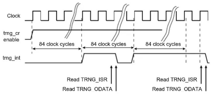
text_image
Clock trng_cre enable 84 clock cycles 84 clock cycles 84 clock cycles trng_int Read TRNG_ISR Read TRNG_ODATA Read TRNG_ISR Read TRNG_ODATA36.6.2 Basic Operation
36.6.2.1 Initialization
The following register is enable-protected, meaning that it can only be written when the TRNG is disabled (CTRLA.ENABLE is zero):
Event Control register (EVCTRL)
Enable-protection is denoted by the Enable-Protected property in the register description.
36.6.2.2 Enabling, Disabling and Resetting
The TRNG is enabled by writing '1' to the Enable bit in the Control A register (CTRLA.ENABLE). The TRNG is disabled by writing a zero to CTRLA.ENABLE.
36.6.3 Interrupts
The TRNG has the following interrupt source:
- Data Ready (DATARDY): Indicates that a new random data is available in DATA register and ready to be read.
This interrupt is a synchronous wake-up source. See Sleep Mode Controller for details.
Each interrupt source has an interrupt flag associated with it. The interrupt flag in the Interrupt Flag Status and Clear (INTFLAG) register is set when the interrupt condition occurs. Each interrupt can be individually enabled by writing a '1' to the corresponding bit in the Interrupt Enable Set (INTENSET) register, and disabled by writing a '1' to the corresponding bit in the Interrupt Enable Clear (INTENCLR) register.
An interrupt request is generated when the interrupt flag is set and the corresponding interrupt is enabled. The interrupt request remains active until the interrupt flag is cleared, or the interrupt is disabled. See 36.8.5. INTFLAG or details on how to clear interrupt flags. All interrupt requests from the peripheral are ORed together on system level to generate one combined interrupt request to the NVIC. Refer to the Nested Vector Interrupt Controller for details. The user must read the INTFLAG register to determine which interrupt condition is present.
Note that interrupts must be globally enabled for interrupt requests to be generated. Refer to the Nested Vector Interrupt Controller for details.
36.6.4 Events
The TRNG can generate the following output event:
- Data Ready (DATARDY): Generated when a new random number is available in the DATA register.
Writing '1' to an Event Output bit in the Event Control Register (EVCTRL.xxEO) enables the corresponding output event. Writing a '0' to this bit disables the corresponding output event. Refer to EVSYS – Event System for details on configuring the Event System.
36.6.5 Sleep Mode Operation
The Run in Standby bit in Control A register (CTRLA.RUNSTDBY) controls the behavior of the TRNG during standby sleep mode:
When this bit is '0', the TRNG is disabled during sleep, but maintains its current configuration.
When this bit is '1', the TRNG continues to operate during sleep and any enabled TRNG interrupt source can wake up the CPU.
36.6.6 Synchronization
Not applicable.
36.7 Register Summary
| Offset | Name Bit Pos. 76543210 | |||||||||
| 0x00 | CTRLA 7:0 RUNSTDBY ENABLE | |||||||||
| 0x01 | ||||||||||
| ... | Reserved | |||||||||
| 0x03 | ||||||||||
| 0x04 | EVCTRL 7:0 DATARDYEO | |||||||||
| 0x05 | ||||||||||
| ... | Reserved | |||||||||
| 0x07 | ||||||||||
| 0x08 | INTENCLR 7:0 | DATARDY | ||||||||
| 0x09 | INTENSET | 7:0 | DATARDY | |||||||
| 0x0A | INTFLAG | 7:0 | DATARDY | |||||||
| 0x0B | ||||||||||
| ... | Reserved | |||||||||
| 0x1F | ||||||||||
| 7:0 | DATA[7:0] | |||||||||
| 15:8 | DATA[15:8] | |||||||||
| 23:16 | DATA[23:16] | |||||||||
| 31:24 | DATA[31:24] | |||||||||
36.8 Register Description
Registers can be 8, 16, or 32 bits wide. Atomic 8-, 16-, and 32-bit accesses are supported. In addition, the 8-bit quarters and 16-bit halves of a 32-bit register, and the 8-bit halves of a 16-bit register can be accessed directly.
Some registers require synchronization when read and/or written. Synchronization is denoted by the "Read-Synchronized" and/or "Write-Synchronized" property in each individual register description.
Optional write-protection by the PAC - Peripheral Access Controller is denoted by the "PAC Write-Protection" property in each individual register description.
Some registers are enable-protected, meaning they can only be written when the module is disabled. Enable-protection is denoted by the "Enable-Protected" property in each individual register description
36.8.1 Control A
Name: CTRLA
Offset: 0x00
Reset: 0x00
Property: PAC Write-Protection
Bit 76543210
| RUNSTDBY ENABLE | ||||||
| Access Reset 0 0 | R/W R/W | |||||
Bit 6 - RUNSTDBY Run in Standby
This bit controls how the ADC behaves during standby sleep mode:
| Value | Description |
| 0 | The TRNG is halted during standby sleep mode. |
| 1 | The TRNG is not stopped in standby sleep mode. |
Bit 1 - ENABLE Enable
| Value | Description |
| 0 | The TRNG is disabled. |
| 1 | The TRNG is enabled. |
36.8.2 Event Control
Name: EVCTRL
Offset: 0x04
Reset: 0x00
Property: PAC Write-Protection
Bit 76543210
| DATARDYEO | |||||||
| Access Reset 0 | R/W | ||||||
Bit 0 - DATARDYEO Data Ready Event Output
This bit indicates whether the Data Ready event output is enabled or not and an output event will be generated when a new random value is completed.
| Value Description | |
| 0 | Data Ready event output is disabled and an event will not be generated. |
| 1 | Data Ready event output is enabled and an event will be generated. |
36.8.3 Interrupt Enable Clear
Name: INTENCLR
Offset: 0x08
Reset: 0x00
Property: PAC Write-Protection
This register allows the user to disable an interrupt without doing a read-modify-write operation. Changes in this register will also be reflected in the Interrupt Enable Set (INTENSET) register.
Bit 76543210
| DATARDY | |||||||
| Access Reset 0 | R/W | ||||||
Bit 0 - DATARDY Data Ready Interrupt Enable
Writing a '1' to this bit will clear the Data Ready Interrupt Enable bit, which disables the corresponding interrupt request.
| Value Description | |
| 0 | The DATARDY interrupt is disabled. |
| 1 | The DATARDY interrupt is enabled. |
36.8.4 Interrupt Enable Set
Name: INTENSET
Offset: 0x09
Reset: 0x00
Property: PAC Write-Protection
This register allows the user to enable an interrupt without doing a read-modify-write operation. Changes in this register will also be reflected in the Interrupt Enable Clear (INTENCLR) register.
Bit 76543210
| DATARDY | |||||||
| Access Reset 0 | R/W | ||||||
Bit 0 - DATARDY Data Ready Interrupt Enable
Writing a '1' to this bit will set the Data Ready Interrupt Enable bit, which enables the corresponding interrupt request.
| Value Description | |
| 0 | The DATARDY interrupt is disabled. |
| 1 | The DATARDY interrupt is enabled. |
36.8.5 Interrupt Flag Status and Clear
Name: INTFLAG
Offset: 0x0A
Reset: 0x00
Property: -
Bit 76543210
| DATARDY | |||||||
| Access Reset 0 | R/W | ||||||
Bit 0 - DATARDY Data Ready
This flag is set when a new random value is generated, and an interrupt will be generated if INTENCLR/SET.DATARDY=1.
This flag is cleared by writing a '1' to the flag or by reading the DATA register.
Writing a '0' to this bit has no effect.
36.8.6 Output Data
Name: DATA
Offset: 0x20
Reset: 0x00000000
Property: -
| Bit 31 30 29 28 27 26 25 24 | |
| DATA[31:24] | |
| Access R R R R R R R R Reset 0 0 0 0 0 0 0 0 | |
| Bit 23 22 21 20 19 18 17 16 | |
| DATA[23:16] | |
| Access R R R R R R R R Reset 0 0 0 0 0 0 0 0 | |
| Bit 15 14 13 12 11 10 9 8 | |
| DATA[15:8] | |
| Access R R R R R R R R Reset 0 0 0 0 0 0 0 0 | |
| Bit 7 6 5 4 3 2 1 0 | |
| DATA[7:0] | |
| Access R R R R R R R R Reset 0 0 0 0 0 0 0 0 | |
Bits 31:0 - DATA[31:0] Output Data
These bits hold the 32-bit randomly generated output data.
37. AES – Advanced Encryption Standard
37.1 Overview
The Advanced Encryption Standard peripheral (AES) provides a means for symmetric-key encryption of 128-bit blocks, in compliance to NIST specifications.
A symmetric-key algorithm requires the same key for both encryption and decryption.
Different key sizes are supported. The key size determines the number of repetitions of transformation rounds that convert the input (called the "plaintext") into the final output ("ciphertext"). The number of rounds of repetition is as follows:
• 10 rounds of repetition for 128-bit keys
• 12 rounds of repetition for 192-bit keys
• 14 rounds of repetition for 256-bit keys
37.2 Features
- Compliant with FIPS Publication 197, Advanced Encryption Standard (AES)
• 128/192/256 bit cryptographic key supported - Encryption time of 57/67/77 cycles with 128-bit/192-bit/256-bit cryptographic key
- Five confidentiality modes of operation as recommended in NIST Special Publication 800-38A
• Electronic Code Book (ECB)
• Cipher Block Chaining (CBC)
• Cipher Feedback (CFB)
• Output Feedback (OFB) - Counter (CTR)
- Supports Counter with CBC-MAC (CCM/CCM*) mode for authenticated encryption
• 8, 16, 32, 64, 128-bit data sizes possible in CFB mode - Optional (parameter) Galois Counter mode (GCM) encryption and authentication
37.3 Block Diagram
Figure 37-1. AES Block Diagram
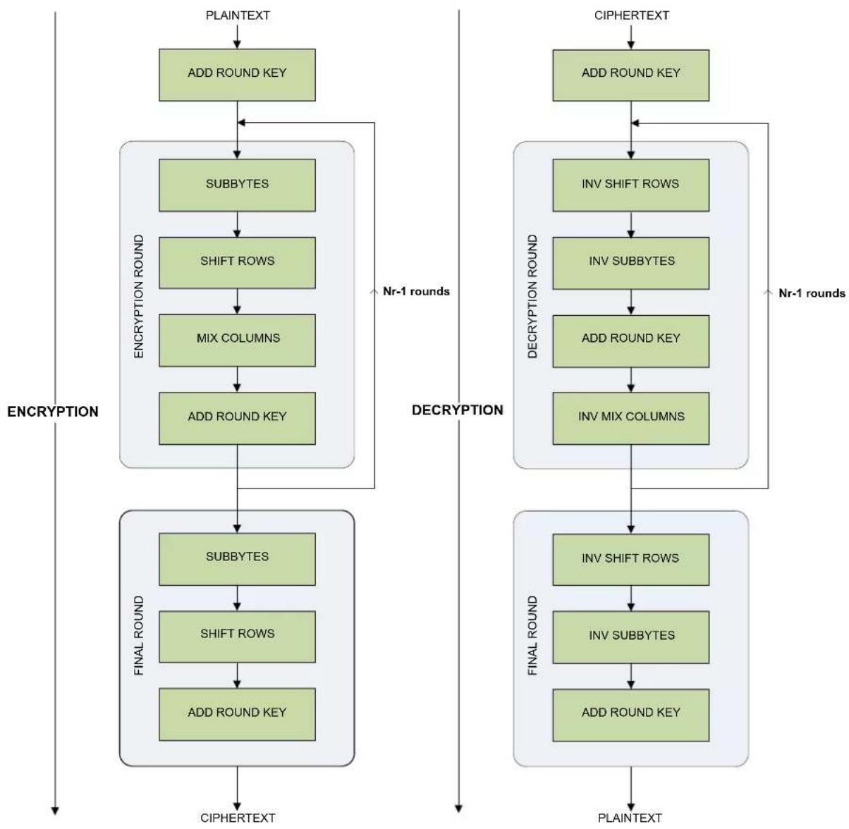
flowchart
graph TD
    A["PLAINTEXT"] --> B["ADD ROUND KEY"]
    B --> C["SUBBYTES"]
    C --> D["SHIFT ROWS"]
    D --> E["MIX COLUMNS"]
    E --> F["ADD ROUND KEY"]
    F --> G["SUBBYTES"]
    G --> H["SHIFT ROWS"]
    H --> I["ADD ROUND KEY"]
    I --> J["CIPHERTEXT"]

    K["CIPHERTEXT"] --> L["ADD ROUND KEY"]
    L --> M["INV SHIFT ROWS"]
    M --> N["INV SUBBYTES"]
    N --> O["ADD ROUND KEY"]
    O --> P["INV MIX COLUMNS"]
    P --> Q["INV SHIFT ROWS"]
    Q --> R["INV SUBBYTES"]
    R --> S["ADD ROUND KEY"]

    T["CIPHERTEXT"] --> U["ADD ROUND KEY"]
    U --> V["INV SHIFT ROWS"]
    V --> W["INV SUBBYTES"]
    W --> X["ADD ROUND KEY"]
    X --> Y["INV MIX COLUMNS"]
    Y --> Z["INV SHIFT ROWS"]
    Z --> AA["INV SUBBYTES"]
    AA --> AB["ADD ROUND KEY"]

    AC["Nr-1 rounds"] --> B
    AD["Nr-1 rounds"] --> L
    AE["NR-1 rounds"] --> M
    AF["NR-1 rounds"] --> N
    AG["NR-1 rounds"] --> O
    AH["NR-1 rounds"] --> P
    AI["NR-1 rounds"] --> Q
    AJ["NR-1 rounds"] --> R
    AK["NR-1 rounds"] --> S
    AL["NR-1 rounds"] --> Y
    AM["NR-1 rounds"] --> Z
    AN["NR-1 rounds"] --> AA
    AO["NR-1 rounds"] --> Y
37.4 Signal Description
Not applicable.
37.5 Product Dependencies
In order to use this AES module, other parts of the system must be configured correctly, as described below.
37.5.1 I/O Lines
Not applicable.
37.5.2 Power Management
The AES will continue to operate in any sleep mode, if it's source clock is running. The AES interrupts can be used to wake up the device from sleep modes. Refer to the Power Manager chapter for details on the different sleep modes.
AES is clocked only on the following conditions:
- Whenever there is an APB access for any read and write operation to the AES registers.
- When the AES is enabled & encryption/decryption is on.
37.5.3 Clocks
The AES bus clock (CLK_AES_APB) can be enabled and disabled in the MCLK - Main Clock, and the default state of CLK_AES_APB can be found in 16.6.2.6. Peripheral Clock Masking. The module is fully clocked by CLK_AES_APB.
37.5.4 DMA
The AES has two DMA request lines; one for input data, and one for output data. They are both connected to the DMA Controller (DMAC). These DMA request triggers will be acknowledged by the DMAC ACK signals. Using the AES DMA requests requires the DMA Controller to be configured first. Refer to the device DMA documentation.
37.5.5 Interrupts
The interrupt request line is connected to the interrupt controller. Using the AES interrupt requires the interrupt controller to be configured first. Refer to the Processor and Architecture chapter for details.
All the AES interrupts are synchronous wake-up sources. See 19.6.3.3. Sleep Mode Controller for details.
37.5.6 Events
Not applicable.
37.5.7 Debug Operation
When the CPU is halted in debug mode, the AES module continues normal operation. If the AES module is configured in a way that requires it to be periodically serviced by the CPU through interrupts or similar, improper operation or data loss may result during debugging. The AES module can be forced to halt operation during debugging.
37.5.8 Register Access Protection
All registers with write-access are optionally write-protected by the PAC - Peripheral Access Controller, except the
following register:
- Interrupt Flag Register (INTFLAG)
Write-protection is denoted by the Write-Protected property in the register description.
Write-protection does not apply to accesses through an external debugger. Refer to the PAC Peripheral Access Controller chapter for details.
37.5.9 Analog Connections
Not applicable.
37.6 Functional Description
37.6.1 Principle of Operation
The following is a high level description of the algorithm. These are the steps:
• KeyExpansion: Round keys are derived from the cipher key using Rijndael's key schedule.
- InitialRound:
- AddRoundKey: Each byte of the state is combined with the round key using bitwise XOR.
- Rounds:
- SubBytes: A non-linear substitution step where each byte is replaced with another according to a lookup table.
- ShiftRows: A transposition step where each row of the state is shifted cyclically a certain number of steps.
- MixColumns: A mixing operation which operates on the columns of the state, combining the four bytes in each column.
- AddRoundKey
• Final Round (no MixColumns):
- SubBytes
- ShiftRows
- AddRoundKey
The relationship between the module's clock frequency and throughput (in bytes per second) is given by:
Clock Frequency = (Throughput/2) x (Nr+1) for 2 byte parallel processing
Clock Frequency = (Throughput/4) x (Nr+1) for 4 byte parallel processing
where Nr is the number of rounds, depending on the key length.
37.6.2 Basic Operation
37.6.2.1 Initialization
The following register is enable-protected:
- Control A (CTRLA)
Enable-protection is denoted by the Enable-Protected property in the register description.
37.6.2.2 Enabling, Disabling, and Resetting
The AES module is enabled by writing a one to the Enable bit in the Control A register (CTRLA.ENABLE). The module is disabled by writing a zero to CTRLA.ENABLE. The module is reset by writing a one to the Software Reset bit in the Control A register (CTRLA.SWRST).
37.6.2.3 Basic Programming
The CIPHER bit in the Control A Register (CTRLA.CIPHER) allows selection between the encryption and the decryption processes. The AES is capable of using cryptographic keys of 128/192/256 bits to encrypt and decrypt data in blocks of 128 bits. The Key Size (128/192/256) can be programmed in the KEYSIZE field in the Control A Register (CTRLA.KEYSIZE). This 128-bit/192-bit/256-bit key is defined in the Key Word Registers (KEYWORD). By setting the XORKEY bit of CTRLA register, keyword can be updated with the resulting XOR value of user keyword and previous keyword content.
The input data for processing is written to a data buffer consisting of four 32-bit registers through the Data register address. The data buffer register (note that input and output data shares the same data buffer register) that is written to when the next write is performed is indicated by the Data Pointer in the Data Buffer Pointer (DATABUFPTR) register. This field is incremented by one or
wrapped by hardware when a write to the DATA register address is performed. This field can also be programmed, allowing the user direct control over which input buffer register to write to. Note that when AES module is in the CFB operation mode with the data segment size less than 128 bits, the input data must be written to the first (DATABUFPTR = 0) and/or second (DATABUFPTR = 1) input buffer registers (see Table 37-1).
The input to the encryption processes of the CBC, CFB and OFB modes includes, in addition to the plaintext, a 128-bit data block called the Initialization Vector (IV), which must be set in the Initialization Vector Registers (INTVECT). Additionally, the GCM mode 128-bit authentication data needs to be programmed. The Initialization Vector is used in the initial step in the encryption of a message and in the corresponding decryption of the message. The Initialization Vector Registers are also used by the Counter mode to set the counter value.
It is necessary to notify AES module whenever the next data block it is going to process is the beginning of a new message. This is done by writing a one to the New Message bit in the Control B register (CTRLB.NEWMSG).
The AES modes of operation are selected by setting the AESMODE field in the Control A Register (CTRLA.AESMODE). In Cipher Feedback Mode (CFB), five data sizes are possible (8, 16, 32, 64 or 128 bits), configurable by means of the CFBS field in the Control A Register (CTRLA.CFBS). In Counter mode, the size of the block counter embedded in the module is 16 bits. Therefore, there is a rollover after processing 1 megabyte of data. The data pre-processing, post-processing and data chaining for the concerned modes are automatically performed by the module.
When data processing has completed, the Encryption Complete bit in the Interrupt Flag register (INTFLAG.ENCCMP) is set by hardware (which triggers an interrupt request if the corresponding interrupt is enabled). The processed output data is read out through the Output Data register (DATA) address from the data buffer consisting of four 32-bit registers. The data buffer register that is read from when the next read is performed is indicated by the Data Pointer field in the Data Buffer Pointer register (DATABUFPTR). This field is incremented by one or wrapped by hardware when a read from the DATA register address is performed. This field can also be programmed, giving the user direct control over which output buffer register to read from. Note that when AES module is in the CFB operation mode with the data segment size less than 128 bits, the output data must be read from the first (DATABUFPTR = 0) and/or second (DATABUFPTR = 1) output buffer registers (see Table 37-1). The Encryption Complete bit (INTFLAG.ENCCMP) is cleared by hardware after the processed data has been read from the relevant output buffer registers.
Table 37-1. Relevant Input/Output Data Registers for Different Confidentiality Modes
| Confidentiality Mode Relevant Input / Output Data Registers | |
| ECB All | |
| CBC All | |
| OFB All | |
| 128-bit CFB All | |
| 64-bit CFB First and Second | |
| 32-bit CFB First | |
| 16-bit CFB First | |
| 8-bit CFB First | |
| CTR All | |
37.6.2.4 Start Modes
The Start mode field in the Control A Register (CTRLA.STARTMODE) allows the selection of encryption start mode.
1. Manual Start Mode
In the Manual Start Mode the sequence is as follows:
a. Write the 128/192/256 bit key in the Key Register (KEYWORD)
b. Write the initialization vector or counter in the Initialization Vector Register (INTVECT). The initialization vector concerns all modes except ECB
c. Enable interrupts in Interrupt Enable Set Register (INTENSET), depending on whether an interrupt is required or not at the end of processing.
d. Write the data to be encrypted or decrypted in the Data Registers (DATA).
e. Set the START bit in Control B Register (CTRLB.START) to begin the encryption or the decryption process.
f. When the processing completes, the Encryption Complete bit in the Interrupt Flag Register (INTFLAG.ENCCMP) raises. If Encryption Complete interrupt has been enabled, the interrupt line of the AES is activated.
g. When the software reads one of the Output Data Registers (DATA), INTFLAG.ENCCMP bit is automatically cleared.
2. Auto start Mode
The Auto Start Mode is similar to the manual one, except in this mode, as soon as the correct number of input data registers is written, processing is automatically started without setting the START bit in the Control B Register. DMA operation uses this mode.
3. Last Output Data Mode (LOD)
This mode is used to generate message authentication code (MAC) on data in CCM mode of operation. The CCM mode combines counter mode for encryption and CBC-MAC generation for authentication.
When LOD is disabled in CCM mode then counter mode of encryption is performed on the input data block.
When LOD is enabled in CCM mode then CBC-MAC generation is performed. Zero block is used as the initialization vector by the hardware. Also software read from the Output Data Register (DATA) is not required to clear the ENCCMP flag. The ENCCMP flag is automatically cleared by writing into the Input Data Register (DATA). This allows retrieval of only the last data in several encryption/decryption processes. No output data register reads are necessary between each block of encryption/decryption process.
Note that assembling message depending on the security level identifier in CCM* has to be done in software.
37.6.2.5 Computation of last Nk words of expanded key
The AES algorithm takes the cryptographic key provided by the user and performs a Key Expansion routine to generate an expanded key. The expanded key contains a total of 4(Nr + 1) 32-bit words, where the first Nk (4/6/8 for a 128-/192-/256-bit key) words are the user-provided key. For data encryption, the expanded key is used in the forward direction, i.e., the first four words are used in the initial round of data processing, the second four words in the first round, the third four words in the second round, and so on. On the other hand, for data decryption, the expanded key is used in the reverse direction, i.e., the last four words are used in the initial round of data processing, the last second four words in the first round, the last third four words in the second round, and so on.
To reduce gate count, the AES module does not generate and store the entire expanded key prior to data processing. Instead, it computes on-the-fly the round key (four 32-bit words) required for the current round of data processing. In general, the round key for the current round of data processing can be computed from the Nk words of the expanded key generated in the previous rounds. When AES module is operating in the encryption mode, the round key for the initial round of data processing is simply the user-provided key written to the KEY registers. On the other hand, when AES module is operating in the decryption mode, the round key for the initial round of data processing is the last four words of the expanded key, which is not available unless AES module has performed at least one encryption process prior to operating in the decryption mode.
In general, the last Nk words of the expanded key must be available before decryption can start. If desired, AES module can be instructed to compute the last Nk words of the expanded key in advance by writing a one to the Key Generate (KEYGEN) bit in the CTRLA register (CTRLA.KEYGEN). The computation takes Nr clock cycles. Alternatively, the last Nk words of the expanded key can be automatically computed by AES module when a decryption process is initiated if they have not been computed in advance or have become invalid. Note that this will introduce a latency of Nr clock cycles to the first decryption process.
37.6.2.6 Hardware Countermeasures against Differential Power Analysis Attacks
The AES module features four types of hardware countermeasures that are useful for protecting data against differential power analysis attacks:
- Type 1: Randomly add one cycle to data processing
- Type 2: Randomly add one cycle to data processing (other version)
- Type 3: Add a random number of clock cycles to data processing, subject to a maximum of 11/13/15 clock cycles for key sizes of 128/192/256 bits
- Type 4: Add random spurious power consumption during data processing
By default, all countermeasures are enabled. One or more of the countermeasures can be disabled by programming the Countermeasure Type field in the Control A (CTRLA.CTYPE) register. The countermeasures use random numbers generated by a deterministic random number generator embedded in AES module. The seed for the random number generator is written to the RANDSEED register. Note also that a new seed must be written after a change in the keysize. Note that enabling countermeasures reduces AES module's throughput. In short, the throughput is highest with all the countermeasures disabled. On the other hand, with all of the countermeasures enabled, the best protection is achieved but the throughput is worst.
37.6.3 Galois Counter Mode (GCM)
GCM is comprised of the AES engine in CTR mode along with a universal hash function (GHASH engine) that is defined over a binary Galois field to produce a message authentication tag. The GHASH engine processes data packets after the AES operation. GCM provides assurance of the confidentiality of data through the AES Counter mode of operation for encryption. Authenticity of the confidential data is assured through the GHASH engine. Refer to the NIST Special Publication 800-38D Recommendation for more complete information.

flowchart
graph TD
    A["Counter 0 Counter 1 Counter 2 Incr33 Incr32"] --> B["CIPH(K) CIPH(K) CIPH(K)"]
    B --> C["Plaintext 1 Plaintext 2+"]
    C --> D["Ciphertext 1 Ciphertext 2"]
    D --> E["Auth Data 1"]
    F["Auth Tag"] --> G["GF128Mult(H)GF128Mult(H)"]
    G --> H["+Len (A) || Len (C)"]
    H --> I["GF128Mult(H)"]
    I --> J["+"]
    J --> K["Auth Text"]
    style A fill:#f9f,stroke:#333
    style F fill:#f9f,stroke:#333
    style J fill:#f9f,stroke:#333
37.6.3.1 GCM Operation
Hashkey Generation
- Configure CTRLA register as follows:
a. CTRLA.STARTMODE as Manual (Auto for DMAC).
b. CTRLA.CIPHER as Encryption.
c. CTRLA.KEYSIZE as per the key used.
d. CTRLA.AESMODE as ECB.
e. CTRLA.CTYPE as per the countermeasures required.
- Set CTRLA.ENABLE
- Write zero to CIPLEN register
- Write the key in KEYWORDx register
- Write the zeros to DATA register
- Set CTRLB.START
- Wait for INTFLAG.ENCCMP to be set
- AES Hardware generates Hash Subkey in HASHKEYx register
Authentication Header Processing
-
Configure CTRLA register as follows:
a. CTRLA.STARTMODE as Manual.
b. CTRLA.CIPHER as Encryption.
c. CTRLA.KEYSIZE as per the key used.
d. CTRLA.AESMODE as GCM.
e. CTRLA.CTYPE as per the countermeasures required. -
Set CTRLA.ENABLE
- Write the key in KEYWORDx register
- Set CTRLB.GFMUL
- Write the Authdata to DATA register
- Set CTRLB.START as 1
- Wait for INTFLAG.GFMCMP to be set
- AES Hardware generates output in GHASHx register
- Continue steps 4 to 7 for remaining Authentication Header
Note: If the Authorization data is less than 128 bits, it has to be padded with zero to make it 128 bit aligned.
flowchart
graph TD
    A["GHASH"] --> C(( ))
    B["AUTHDAT +"] --> C
    C --> D["GF128Mult(H)"]
    D --> E["GHASH"]
Plain Text Processing
- Set CTRLB.NEWMSG for the new set of plain text processing
- Load CIPLEN register
- Load (J0+1) in INTVECTx register
- As described in NIST documentation J 0 = IV || 0 31 || 1 when len(IV)=96 and J0 = GHASH_H(IV || 0 s+64 || [len(IV)] 64) (s is the minimum number of zeroes that should be padded with the Initialization Vector to make it a multiple of 128) if len(IV) != 96
- Load plain text in DATA register
- Set CTRLB.START as 1
- Wait for INTFLAG.ENCCMP to be set
• AES Hardware generates output in DATA register - Intermediate GHASH is stored in GHASHx register and Cipher Text available in DATA register
- Continue 3 to 6 till the input of plain text to get the cipher text and the Hash keys
- At the last input, set CTRLB.EOM
• Write last in-data to DATA register - Set CTRLB.START as 1
- Wait for INTFLAG.ENCCMP to be set
• AES Hardware generates output in DATA register and final Hash key in GHASH register - Load [LEN(A)]64 || [LEN(C)]64 in DATA register and set CTRLB.GFMUL and CTRLB.START as 1
- Wait for INTFLAG.GFMCMP to be set
- AES Hardware generates final GHASH value in GHASHx register
Plain text processing with DMAC
- Set CTRLB.NEWMSG for the new set of plain text processing
- Load CIPLEN register
- Load (J0+1) in INTVECTx register
- Load plain text in DATA register
-
Wait for INTFLAG.ENCCMP to be set
-
AES Hardware generates output in DATA register
- Intermediate GHASH is stored in GHASHx register and Cipher Text available in DATA register
- Continue 3 to 5 till the input of plain text to get the cipher text and the Hash keys
- At the last input, set CTRLB.EOM
- Write last in-data to DATA register
- Wait for INTFLAG.ENCCMP to be set
- AES Hardware generates output in DATA register and final Hash key in GHASHx register
- Load [LEN(A)]64 || [LEN(C)]64 in DATA register and set CTRLB.GFMUL and CTRLB.START as 1
- Wait for INTFLAG.GFMCMP to be set
- AES Hardware generates final GHASH value in GHASHx register
Tag Generation
- Configure CTRLA
a. Set CTRLA. ENABLE to 0. b. Set CTRLA.AESMODE as CTR. c. Set CTRLA. ENABLE to 1.
- Load J0 value to INTVECTVx reg
- Load GHASH value to DATA reg
- Set CTRLB.NEWMSG and CTRLB.START to start the Counter mode operation
- Wait for INTFLAG.ENCCMP to be set
- AES Hardware generates the GCM Tag output in DATA register
37.6.4 Synchronization
Not applicable.
37.7 Register Summary
| Offset | Name Bit Pos. 7 | 6 | 5 | 4 | 3 | 2 | 1 | 0 | |||||||
| 0x00 | CTRLA | 7:0 | CFBS[2:0] AESMODE[2:0] ENABLE SWRST | ||||||||||||
| 15:8 | XORKEY KEYGEN LOD STARTMODE CIPHER | KEYSIZE[1:0] | |||||||||||||
| 23:16 | CTYPE[3:0] | ||||||||||||||
| 31:24 | |||||||||||||||
| 0x04 | CTRLB | 7:0 | GFMUL | EOM | NEWMSG | START | |||||||||
| 0x05 | INTENCLR | 7:0 | GFMCMP | ENCCMP | |||||||||||
| 0x06 | INTENSET | 7:0 | GFMCMP | ENCCMP | |||||||||||
| 0x07 | INTFLAG | 7:0 | GFMCMP | ENCCMP | |||||||||||
| 0x08 | DATABUFPTR | 7:0 | INDATAPTR[1:0] | ||||||||||||
| 0x09 | DBGCTRL | 7:0 | DBGRUN | ||||||||||||
| 0x0A...0x0B | Reserved | ||||||||||||||
| 0C | KEYWORD0 | 7:0 | KEYWORD[7:0] | ||||||||||||
| 15:8 | KEYWORD[15:8] | ||||||||||||||
| 23:16 | KEYWORD[23:16] | ||||||||||||||
| 31:24 | KEYWORD[31:24] | ||||||||||||||
| 10 | KEYWORD1 | 7:0 | KEYWORD[7:0] | ||||||||||||
| 15:8 | KEYWORD[15:8] | ||||||||||||||
| 23:16 | KEYWORD[23:16] | ||||||||||||||
| 31:24 | KEYWORD[31:24] | ||||||||||||||
| 14 | KEYWORD2 | 7:0 | KEYWORD[7:0] | ||||||||||||
| 15:8 | KEYWORD[15:8] | ||||||||||||||
| 23:16 | KEYWORD[23:16] | ||||||||||||||
| 31:24 | KEYWORD[31:24] | ||||||||||||||
| 18 | KEYWORD3 | 7:0 | KEYWORD[7:0] | ||||||||||||
| 15:8 | KEYWORD[15:8] | ||||||||||||||
| 23:16 | KEYWORD[23:16] | ||||||||||||||
| 31:24 | KEYWORD[31:24] | ||||||||||||||
| 1C | KEYWORD4 | 7:0 | KEYWORD[7:0] | ||||||||||||
| 15:8 | KEYWORD[15:8] | ||||||||||||||
| 23:16 | KEYWORD[23:16] | ||||||||||||||
| 31:24 | KEYWORD[31:24] | ||||||||||||||
| 20 | KEYWORD5 | 7:0 | KEYWORD[7:0] | ||||||||||||
| 15:8 | KEYWORD[15:8] | ||||||||||||||
| 23:16 | KEYWORD[23:16] | ||||||||||||||
| 31:24 | |||||||||||||||
| 24 | KEYWORD6 | 7:0 | KEYWORD[7:0] | ||||||||||||
| 15:8 | KEYWORD[15:8] | ||||||||||||||
| 23:16 | KEYWORD[23:16] | ||||||||||||||
| 31:24 | |||||||||||||||
......continued
| Offset | Name Bit Pos. 7 6 5 4 3 2 1 0 | ||||||||
| 40 INTVECTV1 | 7:0 INTVECTV[7:0] | ||||||||
| 15:8 INTVECTV[15:8] | |||||||||
| 23:16 INTVECTV[23:16] | |||||||||
| 31:24 INTVECTV[31:24] | |||||||||
| 44 INTVECTV2 | 7:0 INTVECTV[7:0] | ||||||||
| 15:8 INTVECTV[15:8] | |||||||||
| 23:16 INTVECTV[23:16] | |||||||||
| 31:24 INTVECTV[31:24] | |||||||||
| 48 INTVECTV3 | 7:0 INTVECTV[7:0] | ||||||||
| 15:8 INTVECTV[15:8] | |||||||||
| 23:16 INTVECTV[23:16] | |||||||||
| 31:24 INTVECTV[31:24] | |||||||||
| 0x4C ... 0x5B | Reserved | ||||||||
| 0x5C HASHKEY0 | 7:0 HASHKEY[7:0] | ||||||||
| 15:8 HASHKEY[15:8] | |||||||||
| 23:16 HASHKEY[23:16] | |||||||||
| 31:24 HASHKEY[31:24] | |||||||||
| 0x60 HASHKEY1 | 7:0 HASHKEY[7:0] | ||||||||
| 15:8 HASHKEY[15:8] | |||||||||
| 23:16 HASHKEY[23:16] | |||||||||
| 31:24 HASHKEY[31:24] | |||||||||
| 0×64 HASHKEY2 | 7:0 HASHKEY[7:0] | ||||||||
| 15:8 HASHKEY[15:8] | |||||||||
| 23:16 HASHKEY[23:16] | |||||||||
| 31:24 HASHKEY[31:24] | |||||||||
| 0X68 HASHKEY3 | 7:0 HASHKEY[7:0] | ||||||||
| 15:8 HASHKEY[15:8] | |||||||||
| 23:16 HASHKEY[23:16] | |||||||||
| 31:24 HASHKEY[31:24] | |||||||||
| 0 x6C GHASH0 | 7:0 GHASH[7:0] | ||||||||
| 15:8 GHASH[15:8] | |||||||||
| 23:16 GHASH[23:16] | |||||||||
| 31:24 GHASH[31:24] | |||||||||
| 0x70 GHASH1 | 7:0 GHASH[7:0] | ||||||||
| 15:8 GHASH[15:8] | |||||||||
| 23:16 GHASH[23:16] | |||||||||
| 31:24 GHASH[31:24] | |||||||||
| 0×74 GHASH2 | 7:0 GHASH[7:0] | ||||||||
| 15:8 GHASH[15:8] | |||||||||
| 23:16 GHASH[23:16] | |||||||||
| 31:24 GHASH[31:24] | |||||||||
| 0 x78 GHASH3 | 7:0 GHASH[7:0] | ||||||||
| 15:8 GHASH[15:8] | |||||||||
| 23:16 GHASH[23:16] | |||||||||
| 31:24 GHASH[31:24] | |||||||||
| 0X7C ... 0x7F | Reserved | ||||||||
| 0x80 | CIPLEN | 7:0 CIPLEN[7:0] | |||||||
| 15:8 CIPLEN[15:8] | |||||||||
| 23:16 CIPLEN[23:16] | |||||||||
| 31:24 CIPLEN[31:24] | |||||||||
| 0x84 RANDSEED | 7:0 RANDSEED[7:0] | ||||||||
| 15:8 RANDSEED[15:8] | |||||||||
| 23:16 RANDSEED[23:16] | |||||||||
| 31:24 RANDSEED[31:24] | |||||||||
37.8 Register Description
Registers can be 8, 16, or 32 bits wide. Atomic 8-, 16-, and 32-bit accesses are supported. In addition, the 8-bit quarters and 16-bit halves of a 32-bit register, and the 8-bit halves of a 16-bit register can be accessed directly.
Some registers require synchronization when read and/or written. Synchronization is denoted by the "Read-Synchronized" and/or "Write-Synchronized" property in each individual register description.
Optional write-protection by the Peripheral Access Controller (PAC) is denoted by the "PAC Write-Protection" property in each individual register description.
Some registers are enable-protected, meaning they can only be written when the module is disabled. Enable-protection is denoted by the "Enable-Protected" property in each individual register description
Refer to PAC - Peripheral Access Controller and 36.6.6. Synchronization for details.
37.8.1 Control A
Name: CTRLA
Offset: 0x00
Reset: 0x00000000
Property: PAC Write-Protection, Enable-protected
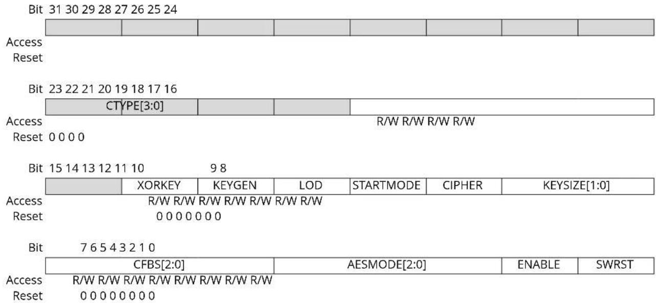
text_image
Bit 31 30 29 28 27 26 25 24 Access Reset Bit 23 22 21 20 19 18 17 16 CTYPE[3:0] Access R/W R/W R/W R/W Reset 0 0 0 0 Bit 15 14 13 12 11 10 9 8 XORKEY KEYGEN LOD STARTMODE CIPHER KEYSIZE[1:0] Access R/W R/W R/W R/W R/W R/W R/W Reset 0 0 0 0 0 0 0 Bit 7 6 5 4 3 2 1 0 CFBS[2:0] AESMODE[2:0] ENABLE SWRST Access R/W R/W R/W R/W R/W R/W R/W Reset 0 0 0 0 0 0 0Bits 19:16 - CTYPE[3:0] Countermeasure type
| Value | Name | Description |
| XXX0 | CTYPE1 disabled | Countermeasure1 disabled |
| XXX1 | CTYPE1 enabled | Countermeasure1 enabled |
| XX0X | CTYPE2 disabled | Countermeasure2 disabled |
| XX1X | CTYPE2 enabled | Countermeasure2 enabled |
| X0XX | CTYPE3 disabled | Countermeasure3 disabled |
| X1XX | CTYPE3 enabled | Countermeasure3 enabled |
| 0XXX | CTYPE4 disabled | Countermeasure4 disabled |
| 1XXX | CTYPE4 enabled | Countermeasure4 enabled |
Bit 14 - XORKEY XOR Key
| Value | Description |
| 0 | No effect |
| 1 | The user keyword gets XORed with the previous keyword register content. |
Bit 13 - KEYGEN Key Generation
| Value | Description |
| 0 | No effect |
| 1 | Start Computation of the last NK words of the expanded key |
Bit 12 - LOD Last Output Data Mode
| Value | Description |
| 0 | No effect |
| 1 | Start encryption in Last Output Data mode |
Bit 11 - STARTMODE Start Mode Select
| Value Name | Description |
| 0 | Manual Mode Start Encryption / Decryption in Manual mode |
| 1 | Auto Mode Start Encryption / Decryption in Auto mode |
Bit 10 - CIPHER Encryption/ Decryption
| Value Description | |
| 0 | Decryption |
| 1 | Encryption |
Bits 9:8 - KEYSIZE[1:0] Encryption Key Size
| Value Name | Description | |
| 0 | 128-bit Key 128-bit Key for Encryption / Decryption | |
| 1 | 192-bit Key 192-bit Key for Encryption / Decryption | |
| 2 | 256-bit Key 256-bit Key for Encryption / Decryption | |
| 3 | Reserved Reserved | |
Bits 7:5 - CFBS[2:0] Cipher Feedback Block Size
| Value Name | Description | |
| 0 | 128-bit data block 128-bit Input data block for Encryption/Decryption in Cipher Feedback mode | |
| 1 | 64-bit data block 64-bit Input data block for Encryption/Decryption in Cipher Feedback mode | |
| 2 | 32-bit data block 32-bit Input data block for Encryption/Decryption in Cipher Feedback mode | |
| 3 | 16-bit data block 16-bit Input data block for Encryption/Decryption in Cipher Feedback mode | |
| 4 | 8-bit data block 8-bit Input data block for Encryption/Decryption in Cipher Feedback mode | |
| 5-7 | Reserved Reserved | |
Bits 4:2 - AESMODE[2:0] AES Modes of Operation
| Value Name | Description | |
| 0 | ECB Electronic code book mode | |
| 1 | CBC | Cipher block chaining mode |
| 2 | OFB | Output feedback mode |
| 3 | CFB | Cipher feedback mode |
| 4 | Counter | Counter mode |
| 5 | CCM | CCM mode |
| 6 | GCM | Galois counter mode |
| 7 | Reserved | Reserved |
Bit 1 - ENABLE Enable
| Value Description | |
| 0 | The peripheral is disabled |
| 1 | The peripheral is enabled |
Bit 0 - SWRST Software Reset
Writing a '0' to this bit has no effect.
Writing a '1' to this bit resets all registers in the AES module to their initial state, and the module will be disabled.
Writing a '1' to SWRST will always take precedence, meaning that all other writes in the same write operation will be discarded.
| Value Description | |
| 0 | There is no reset operation ongoing |
| 1 | The reset operation is ongoing |
37.8.2 Control B
Name: CTRLB
Offset: 0x04
Reset: 0x00
Property: PAC Write-Protection
Bit 76543210
| GFMUL EOM NEWMSG START | ||||||
| Access Reset | R/W R/W R/W R/W0 0 0 0 | |||||
Bit 3 - GFMUL GF Multiplication
This bit is applicable only to GCM mode.
| Value | Description |
| 0 | No action |
| 1 | Setting this bit calculates GF multiplication with data buffer content and hashkey register content. |
Bit 2 - EOM End of Message
This bit is applicable only to GCM mode.
| Value | Description |
| 0 | No action |
| 1 | Setting this bit generates final GHASH value for the message. |
Bit 1 - NEWMSG New Message
This bit is used in cipher block chaining (CBC), cipher feedback (CFB) and output feedback (OFB), counter (CTR) modes to indicate the hardware to use Initialization vector for encrypting the first block of message.
| Value | Description |
| 0 | No action |
| 1 | Setting this bit indicates start of new message to the module. |
Bit 0 - START Start Encryption/Decryption
| Value | Description |
| 0 | No action |
| 1 | Start encryption / decryption in manual mode. |
37.8.3 Interrupt Enable Clear
Name: INTENCLR
Offset: 0x05
Reset: 0x00
Property: PAC Write-Protection
This register allows the user to disable an interrupt without doing a read-modify-write operation. Changes in this register will also be reflected in the Interrupt Enable Set (INTENSET) register.
Bit 76543210
| GFMCMP ENCCMP | ||||||
| Access Reset 0 0 | R/W R/W | |||||
Bit 1 - GFMCMP GF Multiplication Complete Interrupt Enable
Writing a '0' to this bit has no effect.
Writing a '1' to this bit will clear the GF Multiplication Complete Interrupt Enable bit, which disables the GF Multiplication Complete interrupt.
| Value Description | |
| 0 | The GF Multiplication Complete interrupt is disabled. |
| 1 | The GF Multiplication Complete interrupt is enabled. |
Bit 0 - ENCCMP Encryption Complete Interrupt Enable
Writing a '0' to this bit has no effect.
Writing a '1' to this bit will clear the Encryption Complete Interrupt Enable bit, which disables the Encryption Complete interrupt.
| Value Description | |
| 0 | The Encryption Complete interrupt is disabled. |
| 1 | The Encryption Complete interrupt is enabled. |
37.8.4 Interrupt Enable Set
Name: INTENSET
Offset: 0x06
Reset: 0x00
Property: PAC Write-Protection
This register allows the user to enable an interrupt without doing a read-modify-write operation. Changes in this register will also be reflected in the Interrupt Enable Clear (INTENCLR) register.
Bit 76543210
| GFMCMP ENCCMP | ||||||
| Access Reset 0 0 | R/W R/W | |||||
Bit 1 - GFMCMP GF Multiplication Complete Interrupt Enable
Writing a '0' to this bit has no effect. Writing a '1' to this bit will clear the GF Multiplication Complete Interrupt Enable bit, which enables the GF Multiplication Complete interrupt.
| Value Description | |
| 0 | The GF Multiplication Complete interrupt is disabled. |
| 1 | The GF Multiplication Complete interrupt is enabled. |
Bit 0 - ENCCMP Encryption Complete Interrupt Enable
Writing a '0' to this bit has no effect. Writing a '1' to this bit will clear the Encryption Complete Interrupt Enable bit, which enables the Encryption Complete interrupt.
| Value Description | |
| 0 | The Encryption Complete interrupt is disabled. |
| 1 | The Encryption Complete interrupt is enabled. |
37.8.5 Interrupt Flag Status and Clear
Name: INTFLAG
Offset: 0x07
Reset: 0x00
Bit 76543210
| GFMCMP ENCCMP | ||||||
| Access Reset 0 0 | R/W R/W | |||||
Bit 1 - GFMCMP GF Multiplication Complete
This flag is cleared by writing a '1' to it.
This flag is set when GHASH value is available on the Galois Hash Registers (GHASHx) in GCM mode.
Writing a '0' to this bit has no effect.
This flag is also automatically cleared in the following cases.
-
Manual encryption/decryption occurs (START in CTRLB register).
-
Reading from the GHASHx register.
Bit 0 - ENCCMP Encryption Complete
This flag is cleared by writing a '1' to it.
This flag is set when encryption/decryption is complete and valid data is available on the Data Register.
Writing a '0' to this bit has no effect.
This flag is also automatically cleared in the following cases:
-
Manual encryption/decryption occurs (START in CTRLA register). (This feature is needed only if we do not support double buffering of DATA registers).
-
Reading from the data register (DATAx) when LOD = 0.
-
Writing into the data register (DATAx) when LOD = 1.
-
Reading from the Hash Key register (HASHKEYx).
37.8.6 Data Buffer Pointer
Name: DATABUFPTR
Offset: 0x08
Reset: 0x00
Property: PAC Write-Protection
Bit 76543210
| INDATAPTR[1:Φ] | |||||
| Access Reset 0 0 | R/W R/W | ||||
Bits 1:0 - INDATAPTR[1:0] Input Data Pointer
Writing to this field changes the value of the input data pointer, which determines which of the four data registers is written to/read from when the next write/read to the DATA register address is performed.
37.8.7 Debug Control
Name: DBGCTRL
Offset: 0x09
Reset: 0x00
Property: PAC Write-Protection
Bit 76543210
| DBGRUN | |||||||
| Access Reset 0 | W | ||||||
Bit 0 - DBGRUN Debug Run
Writing a '0' to this bit causes the AES to halt during debug mode.
Writing a '1' to this bit allows the AES to continue normal operation during debug mode. This bit can only be changed while the AES is disabled.
37.8.8 Keyword n
Name: KEYWORDn
Offset: 0x0C + n*0x04 [n=0..7]
Reset: 0x00000000
Property: PAC Write-Protection
| Bit 31 30 29 28 27 26 25 24 | |
| KEYWORD[31:24] | |
| AccessWWWWWWWWW | |
| Reset 0 0 0 0 0 0 0 0 | |
| Bit 23 22 21 20 19 18 17 16 | |
| KEYWORD[23:16] | |
| AccessWWWWWWWWW | |
| Reset 0 0 0 0 0 0 0 0 | |
| Bit 15 14 13 12 11 10 9 8 | |
| KEYWORD[15:8] | |
| AccessWWWWWWWWW | |
| Reset 0 0 0 0 0 0 0 0 | |
| Bit 7 6 5 4 3 2 1 0 | |
| KEYWORD[7:0] | |
| AccessWWWWWWWWW | |
| Reset 0 0 0 0 0 0 0 0 | |
Bits 31:0 - KEYWORD[31:0] Key Word Value
The four/six/eight 32-bit Key Word registers set the 128-bit/192-bit/256-bit cryptographic key used for encryption/decryption. KEYWORD0. KEYWORD corresponds to the first word of the key and KEYWORD3/KEYWORD5/KEYWORD7. KEYWORD to the last one.
Note: By setting the XORKEY bit of the CTRLA register, keyword will update with the resulting XOR value of user keyword and previous keyword content.
37.8.9 Data
Name: INDATA
Offset: 0x38
Reset: 0x00000000
Property: -
Bit 31 30 29 28 27 26 25 24
INDATA[31:24]
Access R/W R/W R/W R/W R/W R/W R/W R/W
Reset 00000000
Bit 23 22 21 20 19 18 17 16
INDATA[23:16]
Access R/W R/W R/W R/W R/W R/W R/W R/W
Reset 00000000
Bit 15 14 13 12 11 10 9 8
INDATA[15:8]
Access R/W R/W R/W R/W R/W R/W R/W R/W
Reset 00000000
Bit 76543210
INDATA[7:0]
Access R/W R/W R/W R/W R/W R/W R/W R/W
Reset 00000000
Bits 31:0 - INDATA[31:0] Data Value
A write to or read from this register corresponds to a write to or read from one of the four data registers. The four 32-bit Data registers set the 128-bit data block used for encryption/decryption. The data register that is written to or read from is given by the DATABUFPTR.DATPTR field.
Note: Both input and output shares the same data buffer. Reading DATA register will return 0's when AES is performing encryption or decryption operation.
37.8.10 Initialization Vector Value Register
Name: INTVECTVn
Offset: 0x3C + n*0x04 [n=0..3]
Reset: 0x00000000
Property: PAC Write-Protection
| Bit 31 30 29 28 27 26 25 24 | |
| INTVECTV[31:24] | |
| AccessWWWWWWWWW | |
| Reset 0 0 0 0 0 0 0 0 | |
| Bit 23 22 21 20 19 18 17 16 | |
| INTVECTV[23:16] | |
| AccessWWWWWWWWW | |
| Reset 0 0 0 0 0 0 0 0 | |
| Bit 15 14 13 12 11 10 9 8 | |
| INTVECTV[15:8] | |
| AccessWWWWWWWWW | |
| Reset 0 0 0 0 0 0 0 0 | |
| Bit 7 6 5 4 3 2 1 0 | |
| INTVECTV[7:0] | |
| AccessWWWWWWWWW | |
| Reset 0 0 0 0 0 0 0 0 | |
Bits 31:0 - INTVECTV[31:0] Initialization Vector Value
The four 32-bit Initialization Vector Value registers INTVECTVx set the 128-bit Initialization Vector Value data block that is used by some modes of operation as an additional initial input. INTVECTV0.INTVECTV corresponds to the first word of the Initialization Vector Value, INTVECTV3.INTVECTV to the last one. These registers are write-only to prevent the Initialization Vector Value from being read by another application. For CBC, OFB and CFB modes, the Initialization Vector Value corresponds to the initialization vector value. or CTR mode, it corresponds to the counter value.
37.8.11 Hash Key n (GCM mode only)
Name: HASHKEYn
Offset: 0x5C + n*0x04 [n=0..3]
Reset: 0x00000000
Property: PAC Write-protection
Bit 31 30 29 28 27 26 25 24
| HASHKEY[31:24] |
Access R/W R/W R/W R/W R/W R/W R/W R/W
Reset 00000000
Bit 23 22 21 20 19 18 17 16
| HASHKEY[23:16] |
Access R/W R/W R/W R/W R/W R/W R/W R/W
Reset 00000000
Bit 15 14 13 12 11 10 9 8
| HASHKEY[15:8] |
Access R/W R/W R/W R/W R/W R/W R/W R/W
Reset 00000000
Bit 76543210
| HASHKEY[7:0] |
Access R/W R/W R/W R/W R/W R/W R/W R/W
Reset 00000000
Bits 31:0 - HASHKEY[31:0] Hash Key Value
The four 32-bit HASHKEYx registers contain the 128-bit Hash Key value computed from the AES KEY. The Hash Key value can also be programmed offering single GF128 multiplication possibilities.
37.8.12 Galois Hash n (GCM mode only)
Name: GHASHn
Offset: 0x6C + n*0x04 [n=0..3]
Reset: 0x00000000
Property: PAC Write-Protection
Bit 31 30 29 28 27 26 25 24
GHASH[31:24]
Access R/W R/W R/W R/W R/W R/W R/W R/W
Reset 00000000
Bit 23 22 21 20 19 18 17 16
GHASH[23:16]
Access R/W R/W R/W R/W R/W R/W R/W R/W
Reset 00000000
Bit 15 14 13 12 11 10 9 8
GHASH[15:8]
Access R/W R/W R/W R/W R/W R/W R/W R/W
Reset 00000000
Bit 76543210
GHASH[7:0]
Access R/W R/W R/W R/W R/W R/W R/W R/W
Reset 00000000
Bits 31:0 - GHASH[31:0] Galois Hash Value
The four 32-bit Hash Word registers GHASHx contain the GHASH value after GF128 multiplication in GCM mode. Writing a new key to KEYWORDx registers causes GHASH to be initialized with zeroes. These registers can also be programmed.
37.8.13 Cipher Length
Name: CIPLEN
Offset: 0x80
Reset: 0x00000000
Property: PAC Write-Protection
Bit 31 30 29 28 27 26 25 24
CIPLEN[31:24]
Access R/W R/W R/W R/W R/W R/W R/W R/W
Reset 00000000
Bit 23 22 21 20 19 18 17 16
CIPLEN[23:16]
Access R/W R/W R/W R/W R/W R/W R/W R/W
Reset 00000000
Bit 15 14 13 12 11 10 9 8
CIPLEN[15:8]
Access R/W R/W R/W R/W R/W R/W R/W R/W
Reset 00000000
Bit 76543210
CIPLEN[7:0]
Access R/W R/W R/W R/W R/W R/W R/W R/W
Reset 00000000
Bits 31:0 - CIPLEN[31:0] Cipher Length
This register contains the length in bytes of the Cipher text that is to be processed. This is programmed by the user in GCM mode for Tag generation.
37.8.14 Random Seed
Name: RANDSEED
Offset: 0x84
Reset: 0x00000000
Property: PAC Write-Protection
Bit 31 30 29 28 27 26 25 24
| RANDSEED[31:24] |
Access R/W R/W R/W R/W R/W R/W R/W R/W
Reset 00000000
Bit 23 22 21 20 19 18 17 16
| RANDSEED[23:16] |
Access R/W R/W R/W R/W R/W R/W R/W R/W
Reset 00000000
Bit 15 14 13 12 11 10 9 8
| RANDSEED[15:8] |
Access R/W R/W R/W R/W R/W R/W R/W R/W
Reset 00000000
Bit 76543210
| RANDSEED[7:0] |
Access R/W R/W R/W R/W R/W R/W R/W R/W
Reset 00000000
Bits 31:0 - RANDSEED[31:0] Random Seed
A write to this register corresponds to loading a new seed into the Random number generator.
38. USB – Universal Serial Bus
38.1 Overview
The Universal Serial Bus interface (USB) module complies with the Universal Serial Bus (USB) 2.1 specification supporting device modes.
The USB device mode supports 8 endpoint addresses. All endpoint addresses have one input and one output endpoint, for a total of 16 endpoints. Each endpoint is fully configurable in any of the four transfer types: control, interrupt, bulk or isochronous. The maximum data payload size is selectable up to 1023 bytes.
Internal SRAM is used to keep the configuration and data buffer for each endpoint. The memory locations used for the endpoint configurations and data buffers is fully configurable. The amount of memory allocated is dynamic according to the number of endpoints in use, and the configuration of these. The USB module has a built-in Direct Memory Access (DMA) and will read/write data from/to the system RAM when a USB transaction takes place. No CPU or DMA Controller resources are required.
To maximize throughput, an endpoint can be configured for ping-pong operation. When this is done the input and output endpoint with the same address are used in the same direction. The CPU or DMA Controller can then read/write one data buffer while the USB module writes/reads from the other buffer. This gives double buffered communication.
Multi-packet transfer enables a data payload exceeding the maximum packet size of an endpoint to be transferred as multiple packets without any software intervention. This reduces the number of interrupts and software intervention needed for USB transfers.
For low power operation the USB module can put the microcontroller in any sleep mode when the USB bus is idle and a suspend condition is given. Upon bus resume, the USB module can wake the microcontroller from any sleep mode.
38.2 Features
- Compatible with the USB 2.1 specification
- USB Device mode
- Supports full (12Mbit/s) and low (1.5Mbit/s) speed communication
• Supports Link Power Management (LPM-L1) protocol - On-chip transceivers with built-in pull-ups and pull-downs
- On-Chip USB serial resistors
• 1kHz SOF clock available on external pin -
Device mode
-
Supports 8 IN endpoints and 8 OUT endpoints
- No endpoint size limitations
- Built-in DMA with multi-packet and dual bank for all endpoints
– Supports feedback endpoint - Supports crystal less clock
38.3 USB Block Diagram
38.4 Signal Description
Pin Name Pin Description Type
DM Data -: Differential Data Line - Port Input/Output
......continued
Pin Name Pin Description Type
DP Data +: Differential Data Line + Port Input/Output
SOF 1kHz SOF Output Output
Refer to I/O Multiplexing and Considerations for details on the pin mapping for this peripheral. One signal can be mapped on several pins.
38.5 Product Dependencies
In order to use this peripheral module, other parts of the system must be configured correctly, as described below.
38.5.1 I/O Lines
The USB pins may be multiplexed with the I/O lines Controller. The user must first configure the I/O Controller to assign the USB pins to their peripheral functions.
A 1kHz SOF clock is available on an external pin. The user must first configure the I/O Controller to assign the 1kHz SOF clock to the peripheral function.
38.5.2 Power Management
This peripheral can continue to operate in any Sleep mode where its source clock is running. The interrupts can wake up the device from Sleep modes. Events connected to the event system can trigger other operations in the system without exiting Sleep modes.
38.5.3 Clocks
The USB bus clock (CLK_USB_AHB) can be enabled and disabled in the Main Clock module, MCLK, and the default state of CLK_USB_AHB can be found in the Peripheral Clock Masking.
A generic clock (GCLK_USB) is required to clock the USB. This clock must be configured and enabled in the Generic Clock Controller before using the USB.
This generic clock is asynchronous to the bus clock (CLK_USB_AHB). Due to this asynchronicity, writes to certain registers will require synchronization between the clock domains.
The USB module requires a GCLK_USB of 48 MHz ± 0.25% clock for low speed and full speed operation. To follow the USB data rate at 12 Mbit/s in full-speed mode, the CLK_USB_AHB clock should be at minimum 8 MHz. The GCLK_USB clock is generated by the DFLL48 using a reference clock. When the USB is disabled, the GCLK used as DFLL reference should be disabled.
Clock recovery is achieved by a digital phase-locked loop in the USB module, which complies with the USB jitter specifications. If crystal-less operation is used in USB device mode, refer to USB Clock Recovery Mode.
38.5.4 DMA
The USB has a built-in Direct Memory Access (DMA) and will read/write data to/from the system RAM when a USB transaction takes place. No CPU or DMA Controller resources are required.
38.5.5 Interrupts
The interrupt request line is connected to the Interrupt Controller. In order to use interrupt requests of this peripheral, the Interrupt Controller (NVIC) must be configured first. Refer to Nested Vector Interrupt Controller for details
38.5.6 Events
Not applicable.
38.5.7 Debug Operation
When the CPU is halted in debug mode the USB peripheral continues normal operation. If the USB peripheral is configured in a way that requires it to be periodically serviced by the CPU through interrupts or similar, improper operation or data loss may result during debugging.
38.5.8 Register Access Protection
Registers with write access can be optionally write-protected by the Peripheral Access Controller (PAC), except for the following:
• Device Interrupt Flag (INTFLAG) register
- Endpoint Interrupt Flag (EPINTFLAG) register
Note: Optional write protection is indicated by the "PAC Write Protection" property in the register description.
When the CPU is halted in debug mode, all write protection is automatically disabled. Write protection does not apply for accesses through an external debugger.
38.5.9 Analog Connections
Not applicable.
38.5.10 Calibration
The output drivers for the DP/DM USB line interface can be fine tuned with calibration values from production tests. The calibration values must be loaded from the NVM Software Calibration Area into the USB Pad Calibration register (PADCAL) by software, before enabling the USB, to achieve the specified accuracy. Refer to NVM Software Calibration Area Mapping for further details.
For additional information on Pad Calibration, refer to the Pad Calibration (PADCAL) register.
38.6 Functional Description
38.6.1 USB General Operation
38.6.1.1 Initialization
After a hardware reset, the USB is in the idle state. In this state:
- The module is disabled. The USB Enable bit in the Control A register (CTRLA.ENABLE) is reset.
- The module clock is stopped in order to minimize power consumption.
• The is in suspend mode. - The internal states and registers of the device are reset.
Before using the USB, the Pad Calibration register (PADCAL) must be loaded with production calibration values from the NVM Software Calibration Area.
The USB is enabled by writing a '1' to CTRLA. ENABLE. The USB is disabled by writing a '0' to CTRLA. ENABLE.
The USB is reset by writing a '1' to the Software Reset bit in CTRLA (CTRLA.SWRST). All registers in the USB will be reset to their initial state, and the USB will be disabled. Refer to the CTRLA register for details.
The user can configure pads and speed before enabling the USB by writing to the Speed Configuration field in the Control B register (CTRLB.SPDCONF). These values are taken into account once the USB has been enabled by writing a '1' to CTRLA.ENABLE.
After writing a '1' to CTRLA. ENABLE, the USB enters device mode.
The USB can be disabled at any time by writing a '0' to CTRLA. ENABLE.
Refer to 38.6.2. USB Device Operations for the basic operation of the device mode.
38.6.2 USB Device Operations
This section gives an overview of the USB module device operation during normal transactions. For more details on general USB and USB protocol, refer to the Universal Serial Bus specification revision 2.1.
38.6.2.1 Initialization
To attach the USB device to start the USB communications from the USB host, a zero should be written to the Detach bit in the Device Control B register (CTRLB.DETACH). To detach the device from the USB host, a one must be written to the CTRLB.DETACH.
After the device is attached, the host will request the USB device descriptor using the default device address zero. On successful transmission, it will send a USB reset. After that, it sends an address to be configured for the device. All further transactions will be directed to this device address. This address should be configured in the Device Address field in the Device Address register (DADD.DADD) and the Address Enable bit in DADD (DADD.ADDEN) should be written to one to accept communications directed to this address. DADD.ADDEN is automatically cleared on receiving a USB reset.
38.6.2.2 Endpoint Configuration
Endpoint data can be placed anywhere in the device RAM. The USB controller accesses these endpoints directly through the AHB host (built-in DMA) with the help of the endpoint descriptors. The base address of the endpoint descriptors needs to be written in the Descriptor Address register (DESCADD) by the user. For additional information, refer to Endpoint Description Structure.
Before using an endpoint, the user should configure the direction and type of the endpoint in Type of Endpoint field in the Device Endpoint Configuration register (EPCFG.EPTYPE0/1). The endpoint descriptor registers should be initialized to known values before using the endpoint, so that the USB controller does not read random values from the RAM.
The Endpoint Size field in the Packet Size register (PCKSIZE.SIZE) should be configured as per the size reported to the host for that endpoint. The Address of Data Buffer register (ADDR) should be set to the data buffer used for endpoint transfers.
The RAM Access Interrupt bit in Device Interrupt Flag register (INTFLAG.RAMACER) is set when a RAM access underflow error occurs during IN data stage.
When an endpoint is disabled, the following registers are cleared for that endpoint:
- Device Endpoint Interrupt Enable Clear/Set (EPINTENCLR/SET) register
• Device Endpoint Interrupt Flag (EPINTFLAG) register - Transmit Stall 0 bit in the Endpoint Status register (EPSTATUS.STALLRQ0)
- Transmit Stall 1 bit in the Endpoint Status register (EPSTATUS.STALLRQ1)
38.6.2.3 Multi-Packet Transfers
Multi-packet transfer enables a data payload exceeding the endpoint maximum transfer size to be transferred as multiple packets without software intervention. This reduces the number of interrupts and software intervention required to manage higher level USB transfers. Multi-packet transfer is identical to the IN and OUT transactions described below unless otherwise noted in this section.
The application software provides the size and address of the RAM buffer to be proceeded by the USB module for a specific endpoint, and the USB module will split the buffer in the required USB data transfers without any software intervention.
38.6.2.4 USB Reset
The USB bus reset is initiated by a connected host and managed by hardware.
During USB reset the following registers are cleared:
• Device Endpoint Configuration (EPCFG) register - except for Endpoint 0
• Device Frame Number (FNUM) register
• Device Address (DADD) register
- Device Endpoint Interrupt Enable Clear/Set (EPINTENCLR/SET) register
• Device Endpoint Interrupt Flag (EPINTFLAG) register
- Transmit Stall 0 bit in the Endpoint Status register (EPSTATUS.STALLRQ0)
- Transmit Stall 1 bit in the Endpoint Status register (EPSTATUS.STALLRQ1)
- Endpoint Interrupt Summary (EPINTSMRY) register
- Upstream resume bit in the Control B register (CTRLB.UPRSM)
At the end of the reset process, the End of Reset bit is set in the Interrupt Flag register (INTFLAG.EORST).
38.6.2.5 Start-of-Frame
When a Start-of-Frame (SOF) token is detected, the frame number from the token is stored in the Frame Number field in the Device Frame Number register (FNUM.FNUM), and the Start-of-Frame interrupt bit in the Device Interrupt Flag register (INTFLAG.SOF) is set. If there is a CRC or bit-stuff error, the Frame Number Error status flag (FNUM.FNCERR) in the FNUM register is set.
38.6.2.6 Management of SETUP Transactions
When a SETUP token is detected and the device address of the token packet does not match DADD.DADD, the packet is discarded and the USB module returns to idle and waits for the next token packet.
When the address matches, the USB module checks if the endpoint is enabled in EPCFG. If the addressed endpoint is disabled, the packet is discarded and the USB module returns to idle and waits for the next token packet.
When the endpoint is enabled, the USB module then checks on the EPCFG of the addressed endpoint. If the EPCFG.EPTYPE0 is not set to control, the USB module returns to idle and waits for the next token packet.
When the EPCFG.EPTYPE0 matches, the USB module then fetches the Data Buffer Address (ADDR) from the addressed endpoint's descriptor and waits for a DATA0 packet. If a PID error or any other PID than DATA0 is detected, the USB module returns to idle and waits for the next token packet.
When the data PID matches and if the Received Setup Complete interrupt bit in the Device Endpoint Interrupt Flag register (EPINTFLAG.RXSTP) is equal to zero, ignoring the Bank 0 Ready bit in the Device Endpoint Status register (EPSTATUS.BK0RDY), the incoming data is written to the data buffer pointed to by the Data Buffer Address (ADDR). If the number of received data bytes exceeds the endpoint's maximum data payload size as specified by the PCKSIZE.SIZE, the remainders of the received data bytes are discarded. The packet will still be checked for bit-stuff and CRC errors. Software must never report a endpoint size to the host that is greater than the value configured in PCKSIZE.SIZE. If a bit-stuff or CRC error is detected in the packet, the USB module returns to idle and waits for the next token packet.
If data is successfully received, an ACK handshake is returned to the host, and the number of received data bytes, excluding the CRC, is written to the Byte Count (PCKSIZE.BYTE_COUNT). If the number of received data bytes is the maximum data payload specified by PCKSIZE.SIZE, no CRC data is written to the data buffer. If the number of received data bytes is the maximum data payload specified by PCKSIZE.SIZE minus one, only the first CRC data is written to the data buffer. If the number of received data is equal or less than the data payload specified by PCKSIZE.SIZE minus two, both CRC data bytes are written to the data buffer.
Finally the EPSTATUS is updated. Data Toggle OUT bit (EPSTATUS.DTGLOUT), the Data Toggle IN bit (EPSTATUS.DTGLIN), the current bank bit (EPSTATUS.CURRBK) and the Bank Ready 0 bit (EPSTATUS.BK0RDY) are set. Bank Ready 1 bit (EPSTATUS.BK1RDY) and the Stall Bank 0/1 bit (EPSTATUS.STALLQR0/1) are cleared on receiving the SETUP request. The RXSTP bit is set and triggers an interrupt if the Received Setup Interrupt Enable bit is set in Endpoint Interrupt Enable Set/Clear register (EPINTENSET/CLR.RXSTP).
38.6.2.7 Management of OUT Transactions
When an OUT token is detected, and the device address of the token packet does not match DADD.DADD, the packet is discarded and the USB module returns to idle and waits for the next token packet.
If the address matches, the USB module checks if the endpoint number received is enabled in the EPCFG of the addressed endpoint. If the addressed endpoint is disabled, the packet is discarded and the USB module returns to idle and waits for the next token packet.
When the endpoint is enabled, the USB module then checks the Endpoint Configuration register (EPCFG) of the addressed output endpoint. If the type of the endpoint (EPCFG.EPTYPE0) is not set to OUT, the USB module returns to idle and waits for the next token packet.
The USB module then fetches the Data Buffer Address (ADDR) from the addressed endpoint's descriptor, and waits for a DATA0 or DATA1 packet. If a PID error or any other PID than DATA0 or DATA1 is detected, the USB module returns to idle and waits for the next token packet.
If EPSTATUS.STALLRQ0 in EPSTATUS is set, the incoming data is discarded. If the endpoint is not isochronous, a STALL handshake is returned to the host and the Transmit Stall Bank 0 interrupt bit in EPINTFLAG (EPINTFLAG.STALL0) is set.
For isochronous endpoints, data from both a DATA0 and DATA1 packet will be accepted. For other endpoint types the PID is checked against EPSTATUS.DTGLOUT. If a PID mismatch occurs, the incoming data is discarded, and an ACK handshake is returned to the host.
If EPSTATUS.BK0RDY is set, the incoming data is discarded, the bit Transmit Fail 0 interrupt bit in EPINTFLAG (EPINTFLAG.TRFAIL0) and the status bit STATUS_BK.ERRORFLOW are set. If the endpoint is not isochronous, a NAK handshake is returned to the host.
The incoming data is written to the data buffer pointed to by the Data Buffer Address (ADDR). If the number of received data bytes exceeds the maximum data payload specified as PCKSIZE.SIZE, the remainders of the received data bytes are discarded. The packet will still be checked for bit-stuff and CRC errors. If a bit-stuff or CRC error is detected in the packet, the USB module returns to idle and waits for the next token packet.
If the endpoint is isochronous and a bit-stuff or CRC error in the incoming data, the number of received data bytes, excluding CRC, is written to PCKSIZE.BYTE_COUNT. Finally the EPINTFLAG.TRFAIL0 and CRC Error bit in the Device Bank Status register (STATUS_BK.CRCERR) is set for the addressed endpoint.
If data was successfully received, an ACK handshake is returned to the host if the endpoint is not isochronous, and the number of received data bytes, excluding CRC, is written to PCKSIZE.BYTE_COUNT. If the number of received data bytes is the maximum data payload specified by PCKSIZE.SIZE no CRC data bytes are written to the data buffer. If the number of received data bytes is the maximum data payload specified by PCKSIZE.SIZE minus one, only the first CRC data byte is written to the data buffer. If the number of received data is equal or less than the data payload specified by PCKSIZE.SIZE minus two, both CRC data bytes are written to the data buffer.
Finally in EPSTATUS for the addressed output endpoint, EPSTATUS.BK0RDY is set and EPSTATUS.DTGLOUT is toggled if the endpoint is not isochronous. The flag Transmit Complete 0 interrupt bit in EPINTFLAG (EPINTFLAG.TRCPT0) is set for the addressed endpoint.
38.6.2.8 Multi-Packet Transfers for OUT Endpoint
The number of data bytes received is stored in endpoint PCKSIZE.BYTE_COUNT as for normal operation. Since PCKSIZE.BYTE_COUNT is updated after each transaction, it must be set to zero when setting up a new transfer. The total number of bytes to be received must be written to PCKSIZE.MULTI_PACKET_SIZE. This value must be a multiple of PCKSIZE.SIZE, otherwise excess data may be written to SRAM locations used by other parts of the application.
EPSTATUS.DTGLOUT management for non-isochronous packets and EPINTFLAG.BK1RDY/BK0RDY management are as for normal operation.
If a maximum payload size packet is received, PCKSIZE.BYTE_COUNT will be incremented by PCKSIZE.SIZE after the transaction has completed, and EPSTATUS.DTGLOUT will be toggled if the endpoint is not isochronous. If the updated PCKSIZE.BYTE_COUNT is equal to PCKSIZE.MULTI_PACKET_SIZE (i.e. the last transaction), EPSTATUS.BK1RDY/BK0RDY, and EPINTFLAG.TRCPT0/TRCPT1 will be set.
38.6.2.9 Management of IN Transactions
When an IN token is detected, and if the device address of the token packet does not match DADD.DADD, the packet is discarded and the USB module returns to idle and waits for the next token packet.
When the address matches, the USB module checks if the endpoint received is enabled in the EPCFG of the addressed endpoint and if not, the packet is discarded and the USB module returns to idle and waits for the next token packet.
When the endpoint is enabled, the USB module then checks on the EPCFG of the addressed input endpoint. If the EPCFG.EPTYPE1 is not set to IN, the USB module returns to idle and waits for the next token packet.
If EPSTATUS.STALLRQ1 in EPSTATUS is set, and the endpoint is not isochronous, a STALL handshake is returned to the host and EPINTFLAG.STALL1 is set.
If EPSTATUS.BK1RDY is cleared, the flag EPINTFLAG.TRFAIL1 is set. If the endpoint is not isochronous, a NAK handshake is returned to the host.
The USB module then fetches the Data Buffer Address (ADDR) from the addressed endpoint's descriptor. The data pointed to by the Data Buffer Address (ADDR) is sent to the host in a DATA0 packet if the endpoint is isochronous. For non-isochronous endpoints a DATA0 or DATA1 packet is sent depending on the state of EPSTATUS.DTGLIN. When the number of data bytes specified in endpoint PCKSIZE.BYTE_COUNT is sent, the CRC is appended and sent to the host.
For isochronous endpoints, EPSTATUS.BK1RDY is cleared and EPINTFLAG.TRCPT1 is set.
For all non-isochronous endpoints the USB module waits for an ACK handshake from the host. If an ACK handshake is not received within 16 bit times, the USB module returns to idle and waits for the next token packet. If an ACK handshake is successfully received EPSTATUS.BK1RDY is cleared, EPINTFLAG.TRCPT1 is set and EPSTATUS.DTGLIN is toggled.
38.6.2.10 Multi-Packet Transfers for IN Endpoint
The total number of data bytes to be sent is written to PCKSIZE.BYTE_COUNT as for normal operation. The Multi-packet size register (PCKSIZE.MULTI_PACKET_SIZE) is used to store the number of bytes that are sent, and must be written to zero when setting up a new transfer.
When an IN token is received, PCKSIZE.BYTE_COUNT and PCKSIZE.MULTI_PACKET_SIZE are fetched. If PCKSIZE.BYTE_COUNT minus PCKSIZE.MULTI_PACKET_SIZE is less than the endpoint PCKSIZE.SIZE, endpoint BYTE_COUNT minus endpoint PCKSIZE.MULTI_PACKET_SIZE bytes are transmitted, otherwise PCKSIZE.SIZE number of bytes are transmitted. If endpoint PCKSIZE.BYTE_COUNT is a multiple of PCKSIZE.SIZE, the last packet sent will be zero-length if the AUTOZLP bit is set.
If a maximum payload size packet was sent (i.e. not the last transaction), MULTI_PACKET_SIZE will be incremented by the PCKSIZE.SIZE. If the endpoint is not isochronous the EPSTATUS.DTLGIN bit will
be toggled when the transaction has completed. If a short packet was sent (i.e. the last transaction), MULTI_PACKET_SIZE is incremented by the data payload. EPSTATUS.BK0/1RDY will be cleared and EPINTFLAG.TRCPT0/1 will be set.
38.6.2.11 Ping-Pong Operation
When an endpoint is configured for ping-pong operation, it uses both the input and output data buffers (banks) for a given endpoint in a single direction. The direction is selected by enabling one of the IN or OUT direction in EPCFG.EPTYPE0/1 and configuring the opposite direction in EPCFG.EPTYPE1/0 as Dual Bank.
When ping-pong operation is enabled for an endpoint, the endpoint in the opposite direction must be configured as dual bank. The data buffer, data address pointer and byte counter from the enabled endpoint are used as Bank 0, while the matching registers from the disabled endpoint are used as Bank 1.
The Bank Select flag in EPSTATUS.CURBK indicates which bank data will be used in the next transaction, and is updated after each transaction. According to EPSTATUS.CURBK, EPINTFLAG.TRCPT0 or EPINTFLAG.TRFAIL0 or EPINTFLAG.TRCPT1 or EPINTFLAG.TRFAIL1 in EPINTFLAG and Data Buffer 0/1 ready (EPSTATUS.BK0RDY and EPSTATUS.BK1RDY) are set. The EPSTATUS.DTGLOUT and EPSTATUS.DTGLIN are updated for the enabled endpoint direction only.
38.6.2.12 Feedback Operation
Feedback endpoints are endpoints with same the address but in different directions. This is usually used in explicit feedback mechanism in USB Audio, where a feedback endpoint is associated to one or more isochronous data endpoints to which it provides feedback service. The feedback endpoint always has the opposite direction from the data endpoint.
The feedback endpoint always has the opposite direction from the data endpoint(s). The feedback endpoint has the same endpoint number as the first (lower) data endpoint. A feedback endpoint can be created by configuring an endpoint with different endpoint size (PCKSIZE.SIZE) and different endpoint type (EPCFG.EPTYPE0/1) for the IN and OUT direction.
Example Configuration for Feedback Operation:
- Endpoint n / IN: EPCFG.EPTYPE1 = Interrupt IN, PCKSIZE.SIZE = 64.
- Endpoint n / OUT: EPCFG.EPTYPE0= Isochronous OUT, PCKSIZE.SIZE = 512.
38.6.2.13 Suspend State and Pad Behavior
The following figure, Pad Behavior, illustrates the behavior of the USB pad in Device mode.
In Idle state, the pad is in Low Power Consumption mode.
In Active state, the pad is active.
The following figure, Pad Events, illustrates the pad events leading to a PAD state change.
The Suspend Interrupt bit in the Device Interrupt Flag register (INTFLAG.SUSPEND) is set when a USB Suspend state has been detected on the USB bus. The USB pad is then automatically put in the Idle state. The detection of a non-idle state sets the Wake Up Interrupt bit (INTFLAG.WAKEUP) and wakes the USB pad.
The pad goes to the Idle state if the USB module is disabled or if CTRLB.DETACH is written to one. It returns to the Active state when CTRLA.ENABLE is written to one and CTRLB.DETACH is written to zero.
38.6.2.14 Remote Wakeup
The remote wakeup request (also known as upstream resume) is the only request the device may send on its own initiative. This should be preceded by a DEVICE_REMOTE_WAKEUP request from the host.
First, the USB must have detected a "Suspend" state on the bus, i.e. the remote wakeup request can only be sent after INTFLAG.SUSPEND has been set.
The user may then write a one to the Remote Wakeup bit (CTRLB.UPRSM) to send an Upstream Resume to the host initiating the wakeup. This will automatically be done by the controller after 5 ms of inactivity on the USB bus.
When the controller sends the Upstream Resume INTFLAG.WAKEUP is set and INTFLAG.SUSPEND is cleared.
The CTRLB.UPRSM is cleared at the end of the transmitting Upstream Resume.
In case of a rebroadcast resume initiated by the host, the End of Resume bit (INTFLAG.EORSM) flag is set when the rebroadcast resume is completed.
In the case where the CTRLB.UPRSM bit is set while a host initiated downstream resume is already started, the CTRLB.UPRSM is cleared and the upstream resume request is ignored.
38.6.2.15 Link Power Management L1 (LPM-L1) Suspend State Entry and Exit as Device
The LPM Handshake bit in CTRLB.LPMHDSK should be configured to accept the LPM transaction.
When a LPM transaction is received on any enabled endpoint n and a handshake has been sent in response by the controller according to CTRLB.LPMHDSK, the Device Link Power Manager (EXTREG) register is updated in the bank 0 of the addressed endpoint's descriptor. It contains information such as the Best Effort Service Latency (BESL), the Remote Wake bit (bRemoteWake), and the Link State parameter (bLinkState). Usually, the LPM transaction uses only the endpoint number 0.
If the LPM transaction was positively acknowledged (ACK handshake), USB sets the Link Power Management Interrupt bit (INTFLAG.LPMSUSP) bit which indicates that the USB transceiver is suspended, reducing power consumption. This suspend occurs 9 microseconds after the LPM transaction according to the specification.
To further reduce consumption, it is recommended to stop the USB clock while the device is suspended.
The MCU can also enter in one of the available sleep modes if the wakeup time latency of the selected sleep mode complies with the host latency constraint, refer to the BESL parameter in EXTREG register.
Recovering from this LPM-L1 suspend state is exactly the same as the Suspend state (see Section 38.6.2.13. Suspend State and Pad Behavior) except that the remote wakeup duration initiated by USB is shorter to comply with the Link Power Management specification.
If the LPM transaction is responded with a NYET, the Link Power Management Not Yet Interrupt Flag (INTFLAG.LPMNYET) is set. This generates an interrupt if the Link Power Management Not Yet Interrupt Enable bit (INTENCLR/SET.LPMNYET) is set.
If the LPM transaction is responded with a STALL or no handshake, no flag is set, and the transaction is ignored.
38.6.2.16 USB Device Interrupt
Figure 38-1. Device Interrupt

flowchart
graph TD
    subgraph EPINTSMRY
        EPINT7 --> EPINT6
    end
    subgraph USB Endpoint Interrupt
        EPINT0 --> EPINT1
    end
    subgraph USB Device Interrupt
        INTFLAG --> INTENSET.LPMSUSP
        INTFLAG --> INTENSET.DDISC
        INTFLAG --> INTENSET.RAMACER
        INTFLAG --> INTENSET.UPRSM
        INTFLAG --> INTENSET.EORSM
        INTFLAG --> INTENSET.WAKEUP
        INTFLAG --> INTENSET.EORST
        INTFLAG --> INTENSET.SOF
        INTFLAG --> INTENSET.SUSPEND
    end
    subgraph INTFLAG
        INTFLAG.LPMSUSP --> INTENSET.LPMSUSP
        INTFLAG.LPMNYET --> INTENSET.DDISC
        INTFLAG.RAMACER --> INTENSET.RAMACER
        INTFLAG.UPRSM --> INTENSET.UPRSM
        INTFLAG.EORSM --> INTENSET.EORSM
        INTFLAG.WAKEUP* --> INTENSET.WAKEUP
        INTFLAG.EORST --> INTENSET.EORST
        INTFLAG.SOF --> INTENSET.SOF
        INTFLAG.SUSPEND --> INTENSET.SUSPEND
    end
    subgraph ASynchronous Interrupt
        INTFLAG.SUSPEND --> INTENSET.SUSPEND
    end
The WAKEUP is an asynchronous interrupt and can be used to wake-up the device from any sleep mode.
38.7 Communication Device Host Register Summary
| Offset | Name Bit Pos. 76543210 | ||||||||
| 0x00 | CTRLA 7:0 | RUNSTDBY ENABLE SWRST | |||||||
| 0x01 | Reserved | ||||||||
| 0x02 | SYNCBUSY | 7:0 | ENABLE SWRST | ||||||
| 0x03 | QOSCTRL | 7:0 | DQOS[1:0] | CQOS[1:0] | |||||
| 0x04 | |||||||||
| ... | Reserved | ||||||||
| 0x0C | |||||||||
| 0x0D | FSMSTATUS | 7:0 | FSMSTATE[6:0] | ||||||
| 0x0E | |||||||||
| ... | Reserved | ||||||||
| 0x23 | |||||||||
| DESCADD | 7:0 | DESCADD[7:0] | |||||||
| 15:8 | DESCADD[15:8] | ||||||||
| 23:16 | DESCADD[23:16] | ||||||||
| 31:24 | DESCADD[31:24] | ||||||||
| 0x28 | PADCAL | 7:0 | TRANSN[1:0] | TRANSP[4:0] | |||||
| 15:8 | TRIM[2:0] | TRANSN[4:2] | |||||||
38.8 Communication Device Host Register Description
Registers can be 8, 16, or 32 bits wide. Atomic 8-, 16-, and 32-bit accesses are supported. In addition, the 8-bit quarters and 16-bit halves of a 32-bit register, and the 8-bit halves of a 16-bit register can be accessed directly.
Some registers require synchronization when read and/or written. Synchronization is denoted by the "Read-Synchronized" and/or "Write-Synchronized" property in each individual register description.
Optional write-protection by the PAC - Peripheral Access Controller is denoted by the "PAC Write-Protection" property in each individual register description.
Some registers are enable-protected, meaning they can only be written when the module is disabled. Enable-protection is denoted by the "Enable-Protected" property in each individual register description
Refer to PAC - Peripheral Access Controller and 36.6.6. Synchronization for details.
38.8.1 Control A
Name: CTRLA
Offset: 0x00
Reset: 0x00
Property: PAC Write-Protection, Write-Synchronised
Bit 76543210
| RUNSTDBY ENABLE SWRST | ||||||
| Access Reset 0 0 0 | R/W R/W R/W | |||||
Bit 2 - RUNSTDBY Run in Standby Mode
This bit is Enable-Protected.
| Value | Description |
| 0 | USB clock is stopped in standby mode. |
| 1 | USB clock is running in standby mode |
Bit 1 - ENABLE Enable
Due to synchronization there is delay from writing CTRLA. ENABLE until the peripheral is enabled/disabled. The value written to CTRLA. ENABLE will read back immediately and the Synchronization status enable bit in the Synchronization Busy register (SYNCBUSY. ENABLE) will be set. SYNCBUSY. ENABLE will be cleared when the operation is complete.
This bit is Write-Synchronized.
| Value | Description |
| 0 | The peripheral is disabled or being disabled. |
| 1 | The peripheral is enabled or being enabled. |
Bit 0 - SWRST Software Reset
Writing a zero to this bit has no effect.
Writing a '1' to this bit resets all registers in the USB, to their initial state, and the USB will be disabled.
Writing a '1' to CTRLA.SWRST will always take precedence, meaning that all other writes in the same write-operation will be discarded.
Due to synchronization there is a delay from writing CTRLA.SWRST until the reset is complete.
CTRLA.SWRST and SYNCBUSY.SWRST will both be cleared when the reset is complete.
This bit is Write-Synchronized.
| Value | Description |
| 0 | There is no reset operation ongoing. |
| 1 | The reset operation is ongoing. |
38.8.2 Synchronization Busy
Name: SYNCBUSY
Offset: 0x02
Reset: 0x00
Property: -
Bit 76543210
| ENABLE SWRST | ||||||
| Access Reset 0 0 | R | R | ||||
Bit 1 - ENABLE Synchronization Enable status bit
This bit is cleared when the synchronization of ENABLE register between the clock domains is complete.
This bit is set when the synchronization of ENABLE register between clock domains is started.
Bit 0 - SWRST Synchronization Software Reset status bit
This bit is cleared when the synchronization of SWRST register between the clock domains is complete.
This bit is set when the synchronization of SWRST register between clock domains is started.
38.8.3 QOS Control
Name: QOSCTRL
Offset: 0x03
Reset: 0x0F
Property: PAC Write-Protection
Bit 76543210
| DQOS[1:0] CQOS[1:0] | ||||
| Access Reset 1 1 1 1 | R/W R/W R/W R/W | |||
These bits define the memory priority access during the endpoint or pipe read/write data operation. Refer to SRAM Quality of Service.
Bits 1:0 - CQOS[1:0] Configuration Quality of Service
These bits define the memory priority access during the endpoint or pipe read/write configuration operation. Refer to SRAM Quality of Service.
38.8.4 Finite State Machine Status
Name: FSMSTATUS
Offset: 0x0D
Reset: 0xXXXX
Property: Read only
Bit 76543210
Access
Reset 0000001
ts 6:0 - FSMSTATE[6:0] Fine State Machine Status
These bits indicate the state of the finite state machine of the USB controller.
| Value Name Description | ||
| 0x01 | OFF (L3) | Corresponds to the powered-off, disconnected, and disabled state. |
| 0x02 | ON (L0) | Corresponds to the Idle and Active states. |
| 0x04 | SUSPEND (L2) | - |
| 0x08 | SLEEP (L1) | - |
| 0x10 | DNRESUME | Down Stream Resume. |
| 0x20 | UPRESUME | Up Stream Resume. |
| 0x40 | RESET USB lines Reset. | |
| Others | - | Reserved |
38.8.5 Descriptor Address
Name: DESCADD
Offset: 0x24
Reset: 0x00000000
Property: PAC Write-Protection
| Bit 31 30 29 28 27 26 25 24 | |
| DESCADD[31:24] | |
| Access R/W R/W R/W R/W R/W R/W R/W R/W Reset 0 0 0 0 0 0 0 0 | |
| Bit 23 22 21 20 19 18 17 16 | |
| DESCADD[23:16] | |
| Access R/W R/W R/W R/W R/W R/W R/W R/W Reset 0 0 0 0 0 0 0 0 | |
| Bit 15 14 13 12 11 10 9 8 | |
| DESCADD[15:8] | |
| Access R/W R/W R/W R/W R/W R/W R/W R/W Reset 0 0 0 0 0 0 0 0 | |
| Bit 7 6 5 4 3 2 1 0 | |
| DESCADD[7:0] | |
| Access R/W R/W R/W R/W R/W R/W R/W R/W Reset 0 0 0 0 0 0 0 0 | |
Bits 31:0 - DESCADD[31:0] Descriptor Address Value
These bits define the base address of the main USB descriptor in RAM. The two least significant bits must be written to zero.
38.8.6 Pad Calibration
Name: PADCAL
Offset: 0x28
Reset: 0x0000
Property: PAC Write-Protection
The Pad Calibration values must be loaded from the NVM Software Calibration Area into the USB Pad Calibration register by software, before enabling the USB, to achieve the specified accuracy. Refer to NVM Software Calibration Area Mapping for further details.
Refer to for further details.
Bit 15 14 13 12 11 10 9 8
| TRIM[2:0] | TRANSN[4:2] | |||
| Access | R/W | R/W | R/W | R/W |
| Reset | 0 0 0 | 0 0 0 | ||
| Bit | 7 6 5 4 3 2 1 0 | |||
| TRANSN[1:0] | TRANSP[4:0] | |||
| Access | R/W | R/W | R/W | R/W |
| Reset | 0 0 | 0 0 0 0 0 | ||
Bits 14:12 - TRIM[2:0] Trim bits for DP/DM
These bits calibrate the matching of rise/fall of DP/DM.
Bits 10:6 - TRANSN[4:0] Trimmable Output Driver Impedance N
These bits calibrate the NMOS output impedance of DP/DM drivers.
Bits 4:0 - TRANSP[4:0] Trimmable Output Driver Impedance P
These bits calibrate the PMOS output impedance of DP/DM drivers.
38.9 Device Registers - Common -Register Summary
| Offset | Name Bit Pos. 7 | 6 | 5 | 4 | 3 | 2 | 1 | 0 | |||||||||||
| 0x00...0x07 | Reserved | ||||||||||||||||||
| 0x08 CTRLB | 7:0 | NREPLY SPDCONF[1:0] UPRSM DETACH | |||||||||||||||||
| 15:8 | LPMHDSK[1:0] GNAK | ||||||||||||||||||
| 0x0A | DADD 7:0 ADDEN | DADD[6:0] | |||||||||||||||||
| 0x0B | Reserved | ||||||||||||||||||
| 0x0C | STATUS | 7:0 | LINESTATE[1:0] | SPEED[1:0] | |||||||||||||||
| 0x0D...0x0F | Reserved | ||||||||||||||||||
| 0x10 FNUM | 7:0 | FNUM[4:0] | |||||||||||||||||
| 15:8 | FNCERR | FNUM[10:5] | |||||||||||||||||
| 0x12...0x13 | Reserved | ||||||||||||||||||
| 0x14 | INTENCLR | 7:0 | RAMACER | UPRSM | EORSM | WAKEUP | EORST | SOF | SUSPEND | ||||||||||
| 15:8 | LPMSUSP | LPMNYET | |||||||||||||||||
| 0x16...0x17 | Reserved | ||||||||||||||||||
| 0x18 | INTENSET | 7:0 | RAMACER | UPRSM | EORSM | WAKEUP | EORST | SOF | SUSPEND | ||||||||||
| 15:8 | LPMSUSP | LPMNYET | |||||||||||||||||
| 0x1A...0x1B | Reserved | ||||||||||||||||||
| 0x1C | INTFLAG | 7:0 | RAMACER | UPRSM | EORSM | WAKEUP | EORST | SOF | SUSPEND | ||||||||||
| 15:8 | LPMSUSP | LPMNYET | |||||||||||||||||
| 0x1E...0x1F | Reserved | ||||||||||||||||||
| 0x20 | EPINTSMRY | 7:0 | EPINT[7:0] | ||||||||||||||||
| 15:8 | EPINT[15:8] | ||||||||||||||||||
38.10 Device Registers - Common
Registers can be 8, 16, or 32 bits wide. Atomic 8-, 16-, and 32-bit accesses are supported. In addition, the 8-bit quarters and 16-bit halves of a 32-bit register, and the 8-bit halves of a 16-bit register can be accessed directly.
Some registers require synchronization when read and/or written. Synchronization is denoted by the "Read-Synchronized" and/or "Write-Synchronized" property in each individual register description.
Optional write-protection by the PAC - Peripheral Access Controller is denoted by the "PAC Write-Protection" property in each individual register description.
Some registers are enable-protected, meaning they can only be written when the module is disabled. Enable-protection is denoted by the "Enable-Protected" property in each individual register description
Refer to PAC - Peripheral Access Controller and 36.6.6. Synchronization for details.
38.10.1 Control B
Name: CTRLB
Offset: 0x08
Reset: 0x0000
Property: PAC Write-Protection
Bit 15 14 13 12 11 10 9 8
| LPMHDSK[1:0] GNAK | |||||
| Access Reset | R/W R/W R/W0 0 0 |
Bit 76543210
| NREPLY | SPDCONF[1:0] | UPRSM | DETACH | |||
| Access Reset | R | R/W R/W R/W R/W | ||||
| 0 0 0 0 0 |
Bits 11:10 - LPMHDSK[1:0] Link Power Management Handshake
These bits select the Link Power Management Handshake configuration.
| Value | Description |
| 0x0 | No handshake. LPM is not supported. |
| 0x1 | ACK |
| 0x2 | NYET |
| 0x3 | Reserved |
Bit 9 - GNAK Global NAK
This bit configures the operating mode of the NAK.
This bit is not synchronized.
| Value | Description |
| 0 | The handshake packet reports the status of the USB transaction |
| 1 | A NAK handshake is answered for each USB transaction regardless of the current endpoint memory bank status |
Bit 4 - NREPLY No reply excepted SETUP Token
This bit is cleared by hardware when receiving a SETUP packet.
This bit has no effect for any other endpoint but endpoint 0.
| Value | Description |
| 0 | Disable the “NO_REPLY” feature: Any transaction to endpoint 0 will be handled according to the USB2.0 standard. |
| 1 | Enable the “NO_REPLY” feature: Any transaction to endpoint 0 will be ignored except SETUP. |
Bits 3:2 - SPDCONF[1:0] Speed Configuration
These bits select the speed configuration.
| Value | Description |
| 0x0 | FS: Full-speed |
| 0x1 | LS: Low-speed |
| 0x2 | - |
| 0x3 | - |
Bit 1 - UPRSM Upstream Resume
This bit is cleared when the USB receives a USB reset or once the upstream resume has been sent.
| Value | Description |
| 0 | Writing a zero to this bit has no effect. |
| 1 | Writing a one to this bit will generate an upstream resume to the host for a remote wakeup. |
Bit 0 - DETACH Detach
| Value Description | |
| 0 | The device is attached to the USB bus so that communications may occur. |
| 1 | It is the default value at reset. The internal device pull-ups are disabled, removing the device from the USB bus. |
38.10.2 Device Address
Name: DADD
Offset: 0x0A
Reset: 0x00
Property: PAC Write-Protection
Bit 76543210
ADDEN DADD[6:0]
Access R/W R/W R/W R/W R/W R/W R/W R/W
Reset 00000000
Bit 7 - ADDEN Device Address Enable
This bit is cleared when a USB reset is received.
| Value Description | |
| 0 | Writing a zero will deactivate the DADD field (USB device address) and return the device to default address 0. |
| 1 | Writing a one will activate the DADD field (USB device address). |
Bits 6:0 - DADD[6:0] Device Address
These bits define the device address. The DADD register is reset when a USB reset is received.
38.10.3 Status
Name: STATUS
Offset: 0x0C
Reset: 0x40
Property: -
Bit 76543210
| LINESTATE[1:0] | SPEED[1:0] | |||||
| Access | R R R/W R/W | |||||
| Reset 0 1 | 0 1 | |||||
Bits 7:6 - LINESTATE[1:0] USB Line State Status
These bits define the current line state DP/DM.
| LINESTATE[1:0] | USB Line Status |
| 0x0 | SEO/RESET |
| 0x1 | FS-J or LS-K State |
| 0x2 | FS-K or LS-J State |
Bits 3:2 - SPEED[1:0] Speed Status
These bits define the current speed used of the device
| SPEED[1:0] | SPEED STATUS |
| 0x0 | Full-speed mode |
| 0x1 | Low-speed mode |
| 0x2 | |
| 0x3 | Reserved |
38.10.4 Device Frame Number
Name: FNUM
Offset: 0x10
Reset: 0x0000
Property: Read only
Bit 15 14 13 12 11 10 9 8
| FNCERR FNUM[10:5] | ||||
| Access | R/W R/W R/W R/W R/W R/W R/W | |||
| Reset | 0 | 0 0 0 0 0 0 | ||
| Bit | 7 6 5 4 3 2 1 0 | |||
| FNUM[4:0] | ||||
| Access | R/W R/W R/W R/W R/W | |||
| Reset | 0 0 0 0 0 | |||
Bit 15 - FNCERR Frame Number CRC Error
This bit is cleared upon receiving a USB reset.
This bit is set when a corrupted frame number is received.
This bit and the SOF interrupt bit are updated at the same time.
Bits 13:3 - FNUM[10:0] Frame Number
These bits are cleared upon receiving a USB reset.
These bits are updated with the frame number information as provided from the last SOF packet even if a corrupted SOF is received.
38.10.5 Device Interrupt Enable Clear
Name: INTENCLR
Offset: 0x14
Reset: 0x0000
Property: PAC Write-Protection
This register allows the user to disable an interrupt without doing a read-modify-write operation. Changes in this register will also be reflected in the Interrupt Enable Set (INTENSET) register.
Bit 15 14 13 12 11 10 9 8
| LPMSUSP LPM | NYET | |||||||
| Access Reset 0 0 | R/W R/W | |||||||
| Bit | 7 6 5 4 3 2 1 0 | |||||||
| RAMACER | UPRSM | EORSM | WAKEUP | EORST | SOF | SUSPEND | ||
| Access Reset | R/W R/W | R/W R/W | R/W | R/W | ||||
| 0 0 0 0 0 0 | 0 | |||||||
Bit 9 - LPMSUSP Link Power Management Suspend Interrupt Enable
Writing a zero to this bit has no effect.
Writing a one to this bit will clear the Link Power Management Suspend Interrupt Enable bit and disable the corresponding interrupt request.
| Value | Description |
| 0 | The Link Power Management Suspend interrupt is disabled. |
| 1 | The Link Power Management Suspend interrupt is enabled and an interrupt request will be generated when the Link Power Management Suspend interrupt Flag is set. |
Bit 8 - LPMNYET Link Power Management Not Yet Interrupt Enable
Writing a zero to this bit has no effect.
Writing a one to this bit will clear the Link Power Management Not Yet interrupt Enable bit and disable the corresponding interrupt request.
| Value | Description |
| 0 | The Link Power Management Not Yet interrupt is disabled. |
| 1 | The Link Power Management Not Yet interrupt is enabled and an interrupt request will be generated when the Link Power Management Not Yet interrupt Flag is set. |
Bit 7 - RAMACER RAM Access Interrupt Enable
Writing a zero to this bit has no effect.
Writing a one to this bit will clear the RAM Access interrupt Enable bit and disable the corresponding interrupt request.
| Value | Description |
| 0 | The RAM Access interrupt is disabled. |
| 1 | The RAM Access interrupt is enabled and an interrupt request will be generated when the RAM Access interrupt Flag is set. |
Bit 6 - UPRSM Upstream Resume Interrupt Enable
Writing a zero to this bit has no effect.
Writing a one to this bit will clear the Upstream Resume interrupt Enable bit and disable the corresponding interrupt request.
| Value | Description |
| 0 | The Upstream Resume interrupt is disabled. |
| 1 | The Upstream Resume interrupt is enabled and an interrupt request will be generated when the Upstream Resume interrupt Flag is set. |
Bit 5 - EORSM End Of Resume Interrupt Enable
Writing a zero to this bit has no effect.
Writing a one to this bit will clear the End Of Resume interrupt Enable bit and disable the corresponding interrupt request.
| Value Description | |
| 0 | The End Of Resume interrupt is disabled. |
| 1 | The End Of Resume interrupt is enabled and an interrupt request will be generated when the End Of Resume interrupt Flag is set. |
Bit 4 - WAKEUP Wake-Up Interrupt Enable
Writing a zero to this bit has no effect.
Writing a one to this bit will clear the Wake Up interrupt Enable bit and disable the corresponding interrupt request.
| Value Description | |
| 0 | The Wake Up interrupt is disabled. |
| 1 | The Wake Up interrupt is enabled and an interrupt request will be generated when the Wake Up interrupt Flag is set. |
Bit 3 - EORST End of Reset Interrupt Enable
Writing a zero to this bit has no effect.
Writing a one to this bit will clear the End of Reset interrupt Enable bit and disable the corresponding interrupt request.
| Value Description | |
| 0 | The End of Reset interrupt is disabled. |
| 1 | The End of Reset interrupt is enabled and an interrupt request will be generated when the End of Reset interrupt Flag is set. |
Bit 2 - SOF Start-of-Frame Interrupt Enable
Writing a zero to this bit has no effect.
Writing a one to this bit will clear the Start-of-Frame interrupt Enable bit and disable the corresponding interrupt request.
| Value Description | |
| 0 | The Start-of-Frame interrupt is disabled. |
| 1 | The Start-of-Frame interrupt is enabled and an interrupt request will be generated when the Start-of-Frame interrupt Flag is set. |
Bit 0 - SUSPEND Suspend Interrupt Enable
Writing a zero to this bit has no effect.
Writing a one to this bit will clear the Suspend Interrupt Enable bit and disable the corresponding interrupt request.
| Value Description | |
| 0 | The Suspend interrupt is disabled. |
| 1 | The Suspend interrupt is enabled and an interrupt request will be generated when the Suspend interrupt Flag is set. |
38.10.6 Device Interrupt Enable Set
Name: INTENSET
Offset: 0x18
Reset: 0x0000
Property: PAC Write-Protection
This register allows the user to enable an interrupt without doing a read-modify-write operation. Changes in this register will also be reflected in the Interrupt Enable Clear (INTENCLR) register.
Bit 15 14 13 12 11 10 9 8
| LPMSUSP LPMNYET | ||||||
| Access Reset 0 0 | R/W R/W | |||||
Bit 76543210
| RAMACER | UPRSM | EORSM | WAKEUP | EORST | SOF | SUSPEND | ||
| Access | R/W | R/W | R/W | R/W | R/W | |||
| Reset | 0 | 0 | 0 | 0 | 0 |
Bit 9 - LPMSUSP Link Power Management Suspend Interrupt Enable
Writing a zero to this bit has no effect.
Writing a one to this bit will set the Link Power Management Suspend Enable bit and enable the corresponding interrupt request.
| Value | Description |
| 0 | The Link Power Management Suspend interrupt is disabled. |
| 1 | The Link Power Management Suspend interrupt is enabled. |
Bit 8 - LPMNYET Link Power Management Not Yet Interrupt Enable
Writing a zero to this bit has no effect.
Writing a one to this bit will set the Link Power Management Not Yet interrupt bit and enable the corresponding interrupt request.
| Value | Description |
| 0 | The Link Power Management Not Yet interrupt is disabled. |
| 1 | The Link Power Management Not Yet interrupt is enabled. |
Bit 7 - RAMACER RAM Access Interrupt Enable
Writing a zero to this bit has no effect.
Writing a one to this bit will set the RAM Access Enable bit and enable the corresponding interrupt request.
| Value | Description |
| 0 | The RAM Access interrupt is disabled. |
| 1 | The RAM Access interrupt is enabled. |
Bit 6 - UPRSM Upstream Resume Interrupt Enable
Writing a zero to this bit has no effect.
Writing a one to this bit will set the Upstream Resume Enable bit and enable the corresponding interrupt request.
| Value | Description |
| 0 | The Upstream Resume interrupt is disabled. |
| 1 | The Upstream Resume interrupt is enabled. |
Bit 5 - EORSM End Of Resume Interrupt Enable
Writing a zero to this bit has no effect.
Writing a one to this bit will set the End Of Resume interrupt Enable bit and enable the corresponding interrupt request.
| Value Description | |
| 0 | The End Of Resume interrupt is disabled. |
| 1 | The End Of Resume interrupt is enabled. |
Bit 4 - WAKEUP Wake-Up Interrupt Enable
Writing a zero to this bit has no effect.
Writing a one to this bit will set the Wake Up interrupt Enable bit and enable the corresponding interrupt request.
| Value Description | |
| 0 | The Wake Up interrupt is disabled. |
| 1 | The Wake Up interrupt is enabled. |
Bit 3 - EORST End of Reset Interrupt Enable
Writing a zero to this bit has no effect.
Writing a one to this bit will set the End of Reset interrupt Enable bit and enable the corresponding interrupt request.
| Value Description | |
| 0 | The End of Reset interrupt is disabled. |
| 1 | The End of Reset interrupt is enabled. |
Bit 2 - SOF Start-of-Frame Interrupt Enable
Writing a zero to this bit has no effect.
Writing a one to this bit will set the Start-of-Frame interrupt Enable bit and enable the corresponding interrupt request.
| Value Description | |
| 0 | The Start-of-Frame interrupt is disabled. |
| 1 | The Start-of-Frame interrupt is enabled. |
Bit 0 - SUSPEND Suspend Interrupt Enable
Writing a zero to this bit has no effect.
Writing a one to this bit will set the Suspend interrupt Enable bit and enable the corresponding interrupt request.
| Value Description | |
| 0 | The Suspend interrupt is disabled. |
| 1 | The Suspend interrupt is enabled. |
38.10.7 Device Interrupt Flag Status and Clear
Name: INTFLAG
Offset: 0x01C
Reset: 0x0000
Property: -
Bit 15 14 13 12 11 10 9 8
| LPMSUSP LPMNYET | ||||||
| Access Reset 0 0 | R/W R/W | |||||
Bit 76543210
| RAMACER | UPRSM | EORSM | WAKEUP | EORST | SOF | SUSPEND | ||
| Access | R/W | R/W | R/W | R/W | R/W | |||
| Reset | 0 | 0 | 0 | 0 | 0 |
Bit 9 - LPMSUSP Link Power Management Suspend Interrupt Flag
This flag is cleared by writing a one to the flag.
This flag is set when the USB module acknowledge a Link Power Management Transaction (ACK handshake) and has entered the Suspended state and will generate an interrupt if INTENCLR/SET.LPMSUSP is one.
Writing a zero to this bit has no effect.
Writing a one to this bit clears the LPMSUSP Interrupt Flag.
Bit 8 - LPMNYET Link Power Management Not Yet Interrupt Flag
This flag is cleared by writing a one to the flag.
This flag is set when the USB module acknowledges a Link Power Management Transaction (handshake is NYET) and will generate an interrupt if INTENCLR/SET.LPMNYET is one.
Writing a zero to this bit has no effect.
Writing a one to this bit clears the LPMNYET Interrupt Flag.
Bit 7 - RAMACER RAM Access Interrupt Flag
This flag is cleared by writing a one to the flag.
This flag is set when a RAM access underflow error occurs during IN data stage. This bit will generate an interrupt if INTENCLR/SET.RAMACER is one.
Writing a zero to this bit has no effect.
Bit 6 - UPRSM Upstream Resume Interrupt Flag
This flag is cleared by writing a one to the flag.
This flag is set when the USB sends a resume signal called "Upstream Resume" and will generate an interrupt if INTENCLR/SET.UPRSM is one.
Writing a zero to this bit has no effect.
Bit 5 - EORSM End Of Resume Interrupt Flag
This flag is cleared by writing a one to the flag.
This flag is set when the USB detects a valid "End of Resume" signal initiated by the host and will generate an interrupt if INTENCLR/SET.EORSM is one.
Writing a zero to this bit has no effect.
Bit 4 - WAKEUP Wake Up Interrupt Flag
This flag is cleared by writing a one to the flag.
This flag is set when the USB is reactivated by a filtered non-idle signal from the lines and will generate an interrupt if INTENCLR/SET.WAKEUP is one.
Writing a zero to this bit has no effect.
Bit 3 - EORST End of Reset Interrupt Flag
This flag is cleared by writing a one to the flag. This flag is set when a USB "End of Reset" has been detected and will generate an interrupt if INTENCLR/SET.EORST is one. Writing a zero to this bit has no effect.
Bit 2 - SOF Start-of-Frame Interrupt Flag
This flag is cleared by writing a one to the flag. This flag is set when a USB "Start-of-Frame" has been detected (every 1 ms) and will generate an interrupt if INTENCLR/SET.SOF is one, the FNUM is updated. Writing a zero to this bit has no effect.
Bit 0 - SUSPEND Suspend Interrupt Flag
This flag is cleared by writing a one to the flag. This flag is set when a USB "Suspend" idle state has been detected for 3 frame periods (J state for 3 ms) and will generate an interrupt if INTENCLR/SET.SUSPEND is one. Writing a zero to this bit has no effect.
38.10.8 Endpoint Interrupt Summary
Name: EPINTSMRY
Offset: 0x20
Reset: 0x0000
Property: -
| Bit 15 14 13 12 11 10 9 8 | |
| EPINT[15:8] | |
| Access R R R R R R R R | |
| Reset 0 0 0 0 0 0 0 0 | |
| Bit 7 6 5 4 3 2 1 0 | |
| EPINT[7:0] | |
| Access R R R R R R R R | |
| Reset 0 0 0 0 0 0 0 0 | |
Bits 15:0 - EPINT[15:0] EndPoint Interrupt
The flag EPINT[n] is set when an interrupt is triggered by the EndPoint n. See the EPINTFLAGn register in the device EndPoint section.
This bit will be cleared when no interrupts are pending for EndPoint n.
38.11 Device Endpoint Register Summary
| Offset | Name Bit Pos. 7 | 6 | 5 | 4 | 3 | 2 | 1 | 0 | ||||||||
| 0x00 ... 0xFF | Reserved | |||||||||||||||
| 0x0100 | EPCFG0 | 7:0 | EPTYPE1[2:0] | EPTYPE0[2:0] | ||||||||||||
| ... | ||||||||||||||||
| 0x0104 | EPSTATUSCLR0 | 7:0 | BK1RDY | BK0RDY | STALLRQ1 | STALLRQ0 | CURBK | DTGLIN | DTGLOUT | |||||||
| ... | ||||||||||||||||
| 0x0105 | EPSTATUSSET0 | 7:0 | BK1RDY | BK0RDY | STALLRQ1 | STALLRQ0 | CURBK | DTGLIN | DTGLOUT | |||||||
| ... | ||||||||||||||||
| 0x0106 | EPSTATUS0 | 7:0 | BK1RDY | BK0RDY | STALLRQ | CURBK | DTGLIN | DTGLOUT | ||||||||
| ... | ||||||||||||||||
| 0x0107 | EPINTFLAG0 | 7:0 | STALL | RXSTP | TRFAIL | TRCPT | ||||||||||
| ... | ||||||||||||||||
| 0x0108 | EPINTENCLR0 | 7:0 | STALL | RXSTP | TRFAIL | TRCPT | ||||||||||
| ... | ||||||||||||||||
| 0x0109 | EPINTENSET0 | 7:0 | STALL | RXSTP | TRFAIL | TRCPT | ||||||||||
| ... | ||||||||||||||||
| 0x0114 | EPCFG20 | 7:0 | EPTYPE1[2:0] | EPTYPE0[2:0] | ||||||||||||
| 0x0118 | EPSTATUSCLR20 | 7:0 | BK1RDY | BK0RDY | STALLRQ1 | STALLRQ0 | CURBK | DTGLIN | DTGLOUT | |||||||
| 0x0119 | EPSTATUSSET20 | 7:0 | BK1RDY | BK0RDY | STALLRQ1 | STALLRQ0 | CURBK | DTGLIN | DTGLOUT | |||||||
| 0x011A | EPSTATUS20 | 7:0 | BK1RDY | BK0RDY | STALLRQ | CURBK | DTGLIN | DTGLOUT | ||||||||
| 0x011B | EPINTFLAG20 | 7:0 | STALL | RXSTP | TRFAIL | TRCPT | ||||||||||
| 0x011C | EPINTENCLR20 | 7:0 | STALL | RXSTP | TRFAIL | TRCPT | ||||||||||
| 0x011D | EPINTENSET20 | 7:0 | STALL | RXSTP | TRFAIL | TRCPT | ||||||||||
38.12 Device Endpoint Register Description
Registers can be 8, 16, or 32 bits wide. Atomic 8-, 16-, and 32-bit accesses are supported. In addition, the 8-bit quarters and 16-bit halves of a 32-bit register, and the 8-bit halves of a 16-bit register can be accessed directly.
Some registers require synchronization when read and/or written. Synchronization is denoted by the "Read-Synchronized" and/or "Write-Synchronized" property in each individual register description.
Optional write-protection by the PAC - Peripheral Access Controller is denoted by the "PAC Write-Protection" property in each individual register description.
Some registers are enable-protected, meaning they can only be written when the module is disabled. Enable-protection is denoted by the "Enable-Protected" property in each individual register description
Refer to PAC - Peripheral Access Controller and 36.6.6. Synchronization for details.
38.12.1 Device Endpoint Configuration register n
Name: EPCFGn
Offset: 0x0100 + n*0x01 [n=0..20]
Reset: 0x00
Property: PAC Write-Protection
Bit 76543210
| EPTYPE1[2:0] EPTYPE0[2:0] | |||
| Access | R/W R/W R/W R/W R/W R/W | ||
| Reset 0 0 0 0 0 0 | |||
Bits 6:4 - EPTYPE1[2:0] Endpoint Type for IN direction
These bits contains the endpoint type for IN direction.
Upon receiving a USB reset EPCFGn.EPTYPE1 is cleared except for endpoint 0 which is unchanged.
| Value | Description |
| 0x0 | Bank1 is disabled. |
| 0x1 | Bank1 is enabled and configured as Control IN. |
| 0x2 | Bank1 is enabled and configured as Isochronous IN. |
| 0x3 | Bank1 is enabled and configured as Bulk IN. |
| 0x4 | Bank1 is enabled and configured as Interrupt IN. |
| 0x5 | Bank1 is enabled and configured as Dual-Bank OUT(Endpoint type is the same as the one defined in EPTYPE0) |
| 0x6-0x7 | Reserved |
Bits 2:0 - EPTYPE0[2:0] Endpoint Type for OUT direction
These bits contains the endpoint type for OUT direction.
Upon receiving a USB reset EPCFGn.EPTYPE0 is cleared except for endpoint 0 which is unchanged.
| Value | Description |
| 0x0 | Bank0 is disabled. |
| 0x1 | Bank0 is enabled and configured as Control SETUP / Control OUT. |
| 0x2 | Bank0 is enabled and configured as Isochronous OUT. |
| 0x3 | Bank0 is enabled and configured as Bulk OUT. |
| 0x4 | Bank0 is enabled and configured as Interrupt OUT. |
| 0x5 | Bank0 is enabled and configured as Dual Bank IN(Endpoint type is the same as the one defined in EPTYPE1) |
| 0x6-0x7 | Reserved |
38.12.2 EndPoint Status Clear n
Name: EPSTATUSCLRn
Offset: 0x0104 + n*0x01 [n=0..20]
Reset: 0x00
Property: PAC Write-Protection
Bit 76543210
| BK1RDY | BK0RDY | STALLRQ1 | STALLRQ0 | CURBK | DTGL | N | DTGLOUT | ||||
| Access | W | W | W | W | W | W | W | ||||
| Reset | 0 | 0 | 0 | 0 | 0 | 0 | |||||
Bit 7 - BK1RDY Bank 1 Ready Clear
Writing a zero to this bit has no effect.
Writing a one to this bit will clear EPSTATUS.BK1RDY bit.
Bit 6 - BKORDY Bank 0 Ready Clear
Writing a zero to this bit has no effect.
Writing a one to this bit will clear EPSTATUS.BK0RDY bit.
Bit 5 - STALLRQ1 STALL bank 1 Request Clear
Writing a zero to this bit has no effect.
Writing a one to this bit will clear EPSTATUS.STALLRQ1 bit.
Bit 4 - STALLRQ0 STALL bank 0 Request Clear
Writing a zero to this bit has no effect.
Writing a one to this bit will clear EPSTATUS.STALLRQ0 bit.
Bit 2 - CURBK Current Bank Clear
Writing a zero to this bit has no effect.
Writing a one to this bit will clear EPSTATUS.CURBK bit.
Bit 1 - DTGLIN Data Toggle IN Clear
Writing a zero to this bit has no effect.
Writing a one to this bit will clear EPSTATUS.DTGLIN bit.
Bit 0 - DTGLOUT Data Toggle OUT Clear
Writing a zero to this bit has no effect.
Writing a one to this bit will clear the EPSTATUS.DTGLOUT bit.
38.12.3 EndPoint Status Set n
Name: EPSTATUSSETn
Offset: 0x0105 + n*0x01 [n=0..20]
Reset: 0x00
Property: PAC Write-Protection
Bit 76543210
| BK1RDY | BK0RDY | STALLRQ1 | STALLRQ0 | CURBK | DTGL | N | DTGLOUT | ||||
| Access | W | W | W | W | W | W | W | ||||
| Reset | 0 | 0 | 0 | 0 | 0 | 0 | |||||
Bit 7 - BK1RDY Bank 1 Ready Set
Writing a zero to this bit has no effect.
Writing a one to this bit will set EPSTATUS.BK1RDY bit.
Bit 6 - BKORDY Bank 0 Ready Set
Writing a zero to this bit has no effect.
Writing a one to this bit will set EPSTATUS.BK0RDY bit.
Bit 5 - STALLRQ1 STALL Request bank 1 Set
Writing a zero to this bit has no effect.
Writing a one to this bit will set EPSTATUS.STALLRQ1 bit.
Bit 4 - STALLRQ0 STALL Request bank 0 Set
Writing a zero to this bit has no effect.
Writing a one to this bit will set EPSTATUS.STALLRQ0 bit.
Bit 2 - CURBK Current Bank Set
Writing a zero to this bit has no effect.
Writing a one to this bit will set EPSTATUS.CURBK bit.
Bit 1 - DTGLIN Data Toggle IN Set
Writing a zero to this bit has no effect.
Writing a one to this bit will set EPSTATUS.DTGLIN bit.
Bit 0 - DTGLOUT Data Toggle OUT Set
Writing a zero to this bit has no effect.
Writing a one to this bit will set the EPSTATUS.DTGLOUT bit.
38.12.4 EndPoint Status n
Name: EPSTATUSn
Offset: 0x0106 + n*0x01 [n=0..20]
Reset: 0x00
Property: PAC Write-Protection
Bit 76543210
| BK1RDY | BK0RDY | STALLRQ | CURBK | DTGLIN | DTGLOUT | ||||
| Access | R | R | R | R | R | R | |||
| Reset | 0 | 0 | 2 | 0 | 0 | 0 | |||
Bit 7 - BK1RDY Bank 1 is ready
For Control/OUT direction Endpoints, the bank is empty.
Writing a one to the bit EPSTATUSCLR.BK1RDY will clear this bit.
Writing a one to the bit EPSTATUSSET.BK1RDY will set this bit.
Value Description
| 0 | The bank number 1 is not ready: For IN direction Endpoints, the bank is not yet filled in. For Control/OUT direction Endpoints, the bank is empty. |
| 1 | The bank number 1 is ready: For IN direction Endpoints, the bank is filled in. For Control/OUT direction Endpoints, the bank is full. |
Bit 6 - BK0RDY Bank 0 is ready
Writing a one to the bit EPSTATUSCLR.BK0RDY will clear this bit.
Writing a one to the bit EPSTATUSSET.BKORDY will set this bit.
Value Description
| 0 | The bank number 0 is not ready : For IN direction Endpoints, the bank is not yet filled in. For Control/OUT direction Endpoints, the bank is empty. |
| 1 | The bank number 0 is ready: For IN direction Endpoints, the bank is filled in. For Control/OUT direction Endpoints, the bank is full. |
Bit 4 - STALLRQ STALL bank x request
Writing a zero to the bit EPSTATUSCLR.STALLRQ will clear this bit.
Writing a one to the bit EPSTATUSSET.STALLRQ will set this bit.
This bit is cleared by hardware when receiving a SETUP packet.
Value Description
| 0 | Disable STALLRQx feature. |
| 1 | Enable STALLRQx feature: a STALL handshake will be sent to the host in regards to bank x. |
Bit 2 - CURBK Current Bank
Writing a zero to the bit EPSTATUSCLR.CURBK will clear this bit.
Writing a one to the bit EPSTATUSSET.CURBK will set this bit.
Value Description
| 0 | The bank0 is the bank that will be used in the next single/multi USB packet. |
| 1 | The bank1 is the bank that will be used in the next single/multi USB packet. |
Bit 1 - DTGLIN Data Toggle IN Sequence
Writing a zero to the bit EPSTATUSCLR.DTGLINCLR will clear this bit.
Writing a one to the bit EPSTATUSSET.DTGLINSET will set this bit.
Value Description
| 0 | The PID of the next expected IN transaction will be zero: data 0. |
| 1 | The PID of the next expected IN transaction will be one: data 1. |
Bit 0 - DTGLOUT Data Toggle OUT Sequence
Writing a zero to the bit EPSTATUSCLR.DTGLOUTCLR will clear this bit.
Writing a one to the bit EPSTATUSSET.DTGLOUTSET will set this bit.
| Value Description | |
| 0 | The PID of the next expected OUT transaction will be zero: data 0. |
| 1 | The PID of the next expected OUR transaction will be one: data 1. |
38.12.5 Device EndPoint Interrupt Flag n
Name: EPINTFLAGn
Offset: 0x0107 + n*0x01 [n=0..20]
Reset: 0x00
Property: -
Bit 76543210
| STALL RXSTP TRFAIL TRCPT | ||||||
| Access Reset | R/W0 0 | R/W0 | R/W0 | R/W0 | R/W0 |
Bit 5 - STALL Transmit Stall x Interrupt Flag
This flag is cleared by writing a one to the flag.
This flag is set when a Transmit Stall occurs and will generate an interrupt if EPINTENCLR/SET.STALL is one.
EPINTFLAG.STALL is set for a single bank OUT endpoint or double bank IN/OUT endpoint when current bank is "0".
Writing a zero to this bit has no effect.
Writing a one to this bit clears the STALL Interrupt Flag.
Bit 4 - RXSTP Received Setup Interrupt Flag
This flag is cleared by writing a one to the flag.
This flag is set when a Received Setup occurs and will generate an interrupt if EPINTENCLR/SET.RXSTP is one.
Writing a zero to this bit has no effect.
Writing a one to this bit clears the RXSTP Interrupt Flag.
Bit 2 - TRFAIL Transfer Fail x Interrupt Flag
This flag is cleared by writing a one to the flag.
This flag is set when a transfer fail occurs and will generate an interrupt if EPINTENCLR/SET.TRFAIL is one.
EPINTFLAG.TRFAIL is set for a single bank OUT endpoint or double bank IN/OUT endpoint when current bank is "0".
Writing a zero to this bit has no effect.
Writing a one to this bit clears the TRFAIL Interrupt Flag.
Bit 0 - TRCPT Transfer Complete x interrupt Flag
This flag is cleared by writing a one to the flag.
This flag is set when a Transfer complete occurs and will generate an interrupt if EPINTENCLR/SET.TRCPT is one. EPINTFLAG.TRCPT is set for a single bank OUT endpoint or double bank IN/OUT endpoint when current bank is "0".
Writing a zero to this bit has no effect.
Writing a one to this bit clears the TRCPT0 Interrupt Flag.
38.12.6 Device EndPoint Interrupt Enable n
Name: EPINTENCLRn
Offset: 0x0108 + n*0x01 [n=0..20]
Reset: 0x00
Property: PAC Write-Protection
This register allows the user to enable an interrupt without doing a read-modify-write operation. Changes in this register will also be reflected in the Endpoint Interrupt Enable Set (EPINTENSET) register.
Bit 76543210
| STALL RXSTP TRFAIL TRCPT | ||||||
| Access Reset | R/W0 0 | R/W0 | R/W0 | R/W0 | R/W0 |
Bit 5 - STALL Transmit STALL x Interrupt Enable
Writing a zero to this bit has no effect.
Writing a one to this bit will clear the Transmit Stall x Interrupt Enable bit and disable the corresponding interrupt request.
| Value | Description |
| 0 | The Transmit Stall x interrupt is disabled. |
| 1 | The Transmit Stall x interrupt is enabled and an interrupt request will be generated when the Transmit Stall x Interrupt Flag is set. |
Bit 4 - RXSTP Received Setup Interrupt Enable
Writing a zero to this bit has no effect.
Writing a one to this bit will clear the Received Setup Interrupt Enable bit and disable the corresponding interrupt request.
| Value | Description |
| 0 | The Received Setup interrupt is disabled. |
| 1 | The Received Setup interrupt is enabled and an interrupt request will be generated when the Received Setup Interrupt Flag is set. |
Bit 2 - TRFAIL Transfer Fail x Interrupt Enable
The user should look into the descriptor table status located in ram to be informed about the error condition : ERRORFLOW, CRC.
Writing a zero to this bit has no effect.
Writing a one to this bit will clear the Transfer Fail x Interrupt Enable bit and disable the corresponding interrupt request.
| Value | Description |
| 0 | The Transfer Fail bank x interrupt is disabled. |
| 1 | The Transfer Fail bank x interrupt is enabled and an interrupt request will be generated when the Transfer Fail x Interrupt Flag is set. |
Bit 0 - TRCPT Transfer Complete x interrupt Enable
Writing a zero to this bit has no effect.
Writing a one to this bit will clear the Transfer Complete x interrupt Enable bit and disable the corresponding interrupt request.
| Value | Description |
| 0 | The Transfer Complete bank x interrupt is disabled. |
| 1 | The Transfer Complete bank x interrupt is enabled and an interrupt request will be generated when the Transfer Complete x Interrupt Flag is set. |
38.12.7 Device Interrupt EndPoint Set n
Name: EPINTENSETn
Offset: 0x0109 + n*0x01 [n=0..20]
Reset: 0x0000
Property: PAC Write-Protection
This register allows the user to enable an interrupt without doing a read-modify-write operation. Changes in this register will also be reflected in the Endpoint Interrupt Enable Clear (EPINTENCLR) register. This register is cleared by USB reset.
Bit 76543210
| STALL RXSTP TRFAIL TRCPT | ||||||
| Access Reset | R/W0 0 | R/W0 | R/W0 | R/W0 | R/W0 |
Bit 5 - STALL Transmit Stall x Interrupt Enable
Writing a zero to this bit has no effect.
Writing a one to this bit will enable the Transmit bank Stall x interrupt.
| Value | Description |
| 0 | The Transmit Stall x interrupt is disabled. |
| 1 | The Transmit Stall x interrupt is enabled. |
Bit 4 - RXSTP Received Setup Interrupt Enable
Writing a zero to this bit has no effect.
Writing a one to this bit will enable the Received Setup interrupt.
| Value | Description |
| 0 | The Received Setup interrupt is disabled. |
| 1 | The Received Setup interrupt is enabled. |
Bit 2 - TRFAIL Transfer Fail bank x Interrupt Enable
Writing a zero to this bit has no effect.
Writing a one to this bit will enable the Transfer Fail interrupt.
| Value | Description |
| 0 | The Transfer Fail interrupt is disabled. |
| 1 | The Transfer Fail interrupt is enabled. |
Bit 0 - TRCPT Transfer Complete bank x interrupt Enable
Writing a zero to this bit has no effect.
Writing a one to this bit will enable the Transfer Complete bank x interrupt.
0.2.4 Device Registers - Endpoint RAM
| Value | Description |
| 0 | The Transfer Complete bank x interrupt is disabled. |
| 1 | The Transfer Complete bank x interrupt is enabled. |
38.13 Endpoint Descriptor Structure
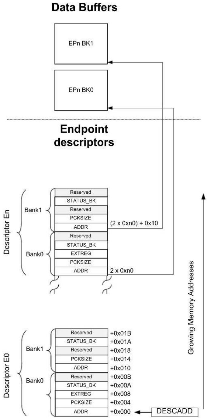
flowchart
graph TD
    subgraph Data Buffers
        EPnBank1["EPn BK1"] <--> EPnBK0["EPn BK0"]
        EPnBank1 <--> EndpointDescriptors["Endpoint descriptors"]
        EPnBK0 <--> EndpointDescriptors
    end

    subgraph Endpoint Descriptors
        Bank1["Bank1"] --> Reserved1["Reserved"]
        Bank1 --> STATUS_BK["STATUS_BK"]
        Bank1 --> Reserved2["Reserved"]
        Bank1 --> PCKSIZE["PCKSIZE"]
        Bank1 --> ADDR["ADDR"]
        Bank0["Bank0"] --> Reserved3["Reserved"]
        Bank0 --> STATUS_BKb["STATUS_BK"]
        Bank0 --> EXTREG["EXTREG"]
        Bank0 --> PCKSIZE["PCKSIZE"]
        Bank0 --> ADDR2["ADDR"]
        Bank0 --> Address2["2 x 0xn0"]
    end

    subgraph Growing Memory Addresses
        Address2 --> ADDDD["GEDNES"]
    end

    subgraph Descartor E0
        Bank1["Bank1"] --> Reserved4["Reserved"]
        Bank1 --> STATUS_BKb["STATUS_BK"]
        Bank1 --> Reserved5["Reserved"]
        Bank1 --> PCKSIZEb["PCKSIZE"]
        Bank1 --> ADDRc["ADDR"]
        Bank0["Bank0"] --> Reserved6["Reserved"]
        Bank0 --> STATUS_BKb2["STATUS_BK"]
        Bank0 --> EXTREGb["EXTREG"]
        Bank0 --> PCKSIZEb["PCKSIZE"]
        Bank0 --> ADDRd["ADDR"]
        Bank0 --> Addressd["DESCADD"]
    end

    Legend
38.14 Device Endpoint RAM Register Summary
| Offset | Name Bit Pos. 76543210 | ||||||||
| 0x00...0x07 | Reserved | ||||||||
| 0x08 EXTREG | 7:0 VARIABLE[3:0] SUBPID[3:0] | ||||||||
| 15:8 VARIABLE[10:4] | |||||||||
| 0x0A...0x0F | Reserved | ||||||||
| 0x10 ADDR | 7:0 ADDR[7:0] | ||||||||
| 15:8 ADDR[15:8] | |||||||||
| 23:16 | ADDR[23:16] | ||||||||
| 31:24 | ADDR[31:24] | ||||||||
| 0x14...0x400013 | Reserved | ||||||||
| 0x400014 | PCKSIZE | 7:0 | BYTE_COUNT[7:0] | ||||||
| 15:8 | MULTI_PACKET_SIZE[1:0] | BYTE_COUNT[13:8] | |||||||
| 23:16 | MULTI_PACKET_SIZE[9:2] | ||||||||
| 31:24 | AUTO_ZLP | SIZE[2:0] | MULTI_PACKET_SIZE[13:10] | ||||||
| 0x400018...0xA00019 | Reserved | ||||||||
| 0xA0001A | STATUS_BK | 7:0 | ERRORFLOW | CRCERR | |||||
38.15 Device Endpoint RAM Register Description
Registers can be 8, 16, or 32 bits wide. Atomic 8-, 16-, and 32-bit accesses are supported. In addition, the 8-bit quarters and 16-bit halves of a 32-bit register, and the 8-bit halves of a 16-bit register can be accessed directly.
Some registers require synchronization when read and/or written. Synchronization is denoted by the "Read-Synchronized" and/or "Write-Synchronized" property in each individual register description.
Optional write-protection by the PAC - Peripheral Access Controller is denoted by the "PAC Write-Protection" property in each individual register description.
Some registers are enable-protected, meaning they can only be written when the module is disabled. Enable-protection is denoted by the "Enable-Protected" property in each individual register description
Refer to PAC - Peripheral Access Controller and 36.6.6. Synchronization for details.
38.15.1 Address of Data Buffer
Name: ADDR
O[set: 0x00 & 0x10
Reset: 0xxxxxxxxx
Property: NA
| Bit 31 30 29 28 27 26 25 24 | |
| ADDR[31:24] | |
| Access R/W R/W R/W R/W R/W R/W R/W R/W Reset x x x x x x x x | |
| Bit 23 22 21 20 19 18 17 16 | |
| ADDR[23:16] | |
| Access R/W R/W R/W R/W R/W R/W R/W R/W Reset x x x x x x x x | |
| Bit 15 14 13 12 11 10 9 8 | |
| ADDR[15:8] | |
| Access R/W R/W R/W R/W R/W R/W R/W R/W Reset x x x x x x x x | |
| Bit 7 6 5 4 3 2 1 0 | |
| ADDR[7:0] | |
| Access R/W R/W R/W R/W R/W R/W R/W R/W Reset x x x x x x x x | |
Bits 31:0 - ADDR[31:0] Data Pointer Address Value
These bits define the data pointer address as an absolute word address in RAM. The two least significant bits must be zero to ensure the start address is 32-bit aligned.
38.15.2 Packet Size
Name: PCKSIZE
Offset: 0x04 & 0x14
Reset: 0xxxxxxxxx
Property: NA
| Bit 31 30 29 28 27 26 25 24 | ||
| AUTO_ZLP SIZE[2:0] MULTI_PACKET_SIZE[13:10] | ||
| Access Reset | R/W R/W R/W R/W R/W R/W R/W R/W | |
| x 0 0 x 0 0 0 0 | ||
| Bit 23 22 21 20 19 18 17 16 | ||
| MULTI_PACKET_SIZE[9:2] | ||
| Access Reset | R/W R/W R/W R/W R/W R/W R/W R/W | |
| 0 0 0 0 0 0 0 0 | ||
| Bit 15 14 13 12 11 10 | 9 8 | |
| MULTI_PACKET_SIZE[1:0] | BYTE_COUNT[13:8] | |
| Access Reset | R/W R/W R/W R/W R/W R/W R/W R/W | |
| 0 x 0 0 0 0 0 0 | ||
| Bit 7 6 5 4 3 2 1 0 | ||
| BYTE_COUNT[7:0] | ||
| Access Reset | R/W R/W R/W R/W R/W R/W R/W R/W | |
| 0 0 0 0 0 0 0 x | ||
Bit 31 - AUTO\_ZLP Automatic Zero Length Packet
This bit defines the automatic Zero Length Packet mode of the endpoint.
When enabled, the USB module will manage the ZLP handshake by hardware. This bit is for IN endpoints only. When disabled the handshake should be managed by firmware.
| Value | Description |
| 0 | Automatic Zero Length Packet is disabled. |
| 1 | Automatic Zero Length Packet is enabled. |
Bits 30:28 - SIZE[2:0] Endpoint size
These bits contains the maximum packet size of the endpoint.
| Value | Description |
| 0x0 | 8 Byte |
| 0x1 | 16 Byte |
| 0x2 | 32 Byte |
| 0x3 | 64 Byte |
| 0x4 | 128 Byte^(1) |
| 0x5 | 256 Byte^(1) |
| 0x6 | 512 Byte^(1) |
| 0x7 | 1023 Byte^(1) |
| (1) for Isochronous endpoints only. | |
Bits 27:14 - MULTI\_PACKET\_SIZE[13:0] Multiple Packet Size
These bits define the 14-bit value that is used for multi-packet transfers.
For IN endpoints, MULTI_PACKET_SIZE holds the total number of bytes sent. MULTI_PACKET_SIZE should be written to zero when setting up a new transfer.
For OUT endpoints, MULTI_PACKET_SIZE holds the total data size for the complete transfer. This value must be a multiple of the maximum packet size.
Bits 13:0 - BYTE\_COUNT[13:0] Byte Count
These bits define the 14-bit value that is used for the byte count.
For IN endpoints, BYTE_COUNT holds the number of bytes to be sent in the next IN transaction.
For OUT endpoint or SETUP endpoints, BYTE_COUNT holds the number of bytes received upon the last OUT or SETUP transaction.
38.15.3 Extended Register
Name: EXTREG
Offset: 0x08
Reset: 0xxxxxxxxx
Property: NA
Bit 15 14 13 12 11 10 9 8
| VARIABLE[10:4] |
Access
R/W R/W R/W R/W R/W R/W R/W
Reset 0000000
Bit 76543210
| VARIABLE[3:0] | SUBPID[3:0] |
Access
R/W R/W R/W R/W R/W R/W R/W R/W
Reset 000x
000x
Bits 14:4 - VARIABLE[10:0] Variable field send with extended token
These bits define the VARIABLE field of a received extended token. These bits are updated when the USB has answered by an handshake token ACK to a LPM transaction. See Section 2.1.1 Protocol Extension Token in the reference document "ENGINEERING CHANGE NOTICE, USB 2.0 Link Power Management Addendum".
To support the USB2.0 Link Power Management addition the VARIABLE field should be read as described below.
| VARIABLES | Description |
| VARIABLE[3:0] | bLinkState (1) |
| VARIABLE[7:4] | BESL (2) |
| VARIABLE[8] | bRemoteWake (1) |
| VARIABLE[10:9] | Reserved |
- For a definition of LPM Token bRemoteWake and bLinkState fields, refer to "Table 2-3 in the reference document ENGINEERING CHANGE NOTICE, USB 2.0 Link Power Management Addendum".
- For a definition of LPM Token BESL field, refer to "Table 2-3 in the reference document ENGINEERING CHANGE NOTICE, USB 2.0 Link Power Management Addendum" and "Table X-X1 in Errata for ECN USB 2.0 Link Power Management.
Bits 3:0 - SUBPID[3:0] SUBPID field send with extended token
These bits define the SUBPID field of a received extended token. These bits are updated when the USB has answered by an handshake token ACK to a LPM transaction. See Section 2.1.1 Protocol Extension Token in the reference document "ENGINEERING CHANGE NOTICE, USB 2.0 Link Power Management Addendum".
38.15.4 Device Status Bank
Name: STATUS_BK
Offset: 0x0A & 0x1A
Reset: 0xxxxxxxxx
Property: NA
Bit 76543210
| ERRORFLOW CRCERR | ||||||
| Access Reset x x | R/W R/W | |||||
Bit 1 - ERRORFLOW Error Flow Status
This bit defines the Error Flow Status.
This bit is set when a Error Flow has been detected during transfer from/towards this bank.
For OUT transfer, a NAK handshake has been sent.
For Isochronous OUT transfer, an overrun condition has occurred.
For IN transfer, this bit is not valid. EPSTATUS.TRFAIL0 and EPSTATUS.TRFAIL1 should reflect the flow errors.
| Value | Description |
| 0 | No Error Flow detected. |
| 1 | A Error Flow has been detected. |
Bit 0 - CRCERR CRC Error
This bit defines the CRC Error Status.
This bit is set when a CRC error has been detected in an isochronous OUT endpoint bank.
0.2.5 Host Registers - Common
| Value | Description |
| 0 | No CRC Error. |
| 1 | CRC Error detected. |
39. CCL – Configurable Custom Logic
39.1 Overview
The Configurable Custom Logic (CCL) is a programmable logic peripheral which can be connected to the device pins, to events, or to other internal peripherals. This allows the user to eliminate logic gates for simple glue logic functions on the PCB.
Each LookUp Table (LUT) consists of three inputs, a truth table, and as options synchronizer, filter and edge detector. Each LUT can generate an output as a user programmable logic expression with three inputs. Inputs can be individually masked.
The output can be combinatorially generated from the inputs, and can be filtered to remove spikes. Optional sequential logic can be used. The inputs of the sequential module are individually controlled by two independent, adjacent LUT (LUTO/LUT1, LUT2/LUT3 etc.) outputs, enabling complex waveform generation.
39.2 Features
- Glue logic for general purpose PCB design
• 4 programmable LookUp Tables (LUTs) - Combinatorial logic functions: AND, NAND, OR, NOR, XOR, XNOR, NOT
- Sequential logic functions: Gated D Flip-Flop, JK Flip-Flop, gated D Latch, RS Latch
-
Flexible LUT inputs selection:
-
I/Os
- Events
- Internal peripherals
-
Subsequent LUT output
-
Output can be connected to the I/O pins or the Event System
- Optional synchronizer, filter, or edge detector available on each LUT output
39.3 Block Diagram
Figure 39-1. Configurable Custom Logic

flowchart
graph TD
    subgraph LUT0
        A["LUTCTRL (INSEL)"] --> B["Truth Table"]
        C["Internal"] --> B
        D["Events"] --> B
        E["I/O"] --> B
        F["Peripherals"] --> B
        G["CLK_CCL_APB"] --> H["D Q"]
        I["GCLK_CCL"] --> H
        B --> J["OK/CS"]
        J --> K["Edge Detector Filter TS"]
        K --> L["Sequential CLR"]
        L --> M["SECTR (SEGSELO)"]
        M --> N["CTR (ENABLE)"]
        N --> O["OUT0"]
        P["Event System"] --> Q["IO"]
    end
    subgraph LUT1
        R["LUTCTRL1 (INSEL)"] --> S["Truth Table"]
        T["Internal"] --> S
        U["Events"] --> S
        V["I/O"] --> S
        W["Peripherals"] --> S
        X["CLK_CCL_APB"] --> Y["D Q"]
        Z["GCLK_CCL"] --> Y
        S --> AA["cur SUS"]
        AA --> AB["Edge Detector Filter TS"]
        AB --> AC["Sequential CLR"]
        AC --> AD["CTR (ENABLE)"]
        AD --> AE["OUT1"]
        AF["Event System"] --> AG["IO"]
    end
    LUT1 --> AH["Unit 0"]
    LUT0 --> AI["Unit 1"]
39.4 Signal Description
| Pin Name Type Description | |
| OUT[3:0] Digital output Output from lookup table | |
| IN[11:0] Digital input Input to lookup table |
Refer to I/O Multiplexing and Considerations for details on the pin mapping for this peripheral. One signal can be mapped on several pins.
39.5 Product Dependencies
In order to use this peripheral, other parts of the system must be configured correctly, as described below.
39.5.1 I/O Lines
Using the CCL I/O lines requires the I/O pins to be configured. Refer to PORT - I/O Pin Controller for details.
39.5.2 Power Management
This peripheral can continue to operate in any sleep mode where its source clock is running. Events connected to the event system can trigger other operations in the system without exiting sleep modes.
39.5.3 Clocks
The CCL bus clock (CLK_CCL_APB) can be enabled and disabled in the power manager, and the default state of CLK_CCL_APB can be found in the 16.6.2.6. Peripheral Clock Masking.
A generic clock (GCLK_CCL) is optionally required to clock the CCL. This clock must be configured and enabled in the Generic Clock Controller (GCLK) before using input events, filter, edge detection or sequential logic. GCLK_CCL is required when input events, a filter, an edge detector, or a sequential sub-module is enabled. Refer to 15. GCLK - Generic Clock Controller for details.
This generic clock is asynchronous to the user interface clock (CLK_CCL_APB).
39.5.4 DMA
Not applicable.
39.5.5 Interrupts
Not applicable.
39.5.6 Events
The events are connected to the Event System. Refer to EVSYS – Event System for details on how to configure the Event System.
39.5.7 Debug Operation
When the CPU is halted in debug mode the CCL continues normal operation. If the CCL is configured in a way that requires it to be periodically serviced by the CPU, improper operation or data loss may result during debugging.
39.5.8 Register Access Protection
All registers with write-access can be write-protected optionally by the PAC - Peripheral Access Controller.
Optional write-protection by the PAC - Peripheral Access Controller is denoted by the "PAC Write-Protection" property in each individual register description.
PAC write-protection does not apply to accesses through an external debugger.
39.5.9 Analog Connections
Not applicable.
39.6 Functional Description
39.6.1 Principle of Operation
Configurable Custom Logic (CCL) is a programmable logic block that can use the device port pins, internal peripherals, and the internal Event System as both input and output channels. The CCL can serve as glue logic between the device and external devices. The CCL can eliminate the need for external logic component and can also help the designer overcome challenging real-time constraints by combining core independent peripherals in clever ways to handle the most time critical parts of the application independent of the CPU.
39.6.2 Operation
39.6.2.1 Initialization
The following bits are enable-protected, meaning that they can only be written when the corresponding even LUT is disabled (LUTCTRLx.ENABLE=0):
- Sequential Selection bits in the Sequential Control x (SEQCTRLx.SEQSEL) register
The following registers are enable-protected, meaning that they can only be written when the corresponding LUT is disabled (LUTCTRLx.ENABLE=0):
- LUT Control x (LUTCTRLx) register, except the ENABLE bit
Enable-protected bits in the LUTCTRLx registers can be written at the same time as LUTCTRLx. ENABLE is written to '1', but not at the same time as LUTCTRLx. ENABLE is written to '0'.
Enable-protection is denoted by the Enable-Protected property in the register description.
39.6.2.2 Enabling, Disabling, and Resetting
The CCL is enabled by writing a '1' to the Enable bit in the Control register (CTRL.ENABLE). The CCL is disabled by writing a '0' to CTRL.ENABLE.
Each LUT is enabled by writing a '1' to the Enable bit in the LUT Control x register (LUTCTRLx.ENABLE). Each LUT is disabled by writing a '0' to LUTCTRLx.ENABLE.
The CCL is reset by writing a '1' to the Software Reset bit in the Control register (CTRL.SWRST). All registers in the CCL will be reset to their initial state, and the CCL will be disabled. Refer to 39.8.1. CTRL for details.
39.6.2.3 Lookup Table Logic
The lookup table in each LUT unit can generate any logic expression OUT as a function of three inputs (IN[2:0]), as shown in Figure 39-2. One or more inputs can be masked. The truth table for the expression is defined by TRUTH bits in LUT Control x register (LUTCTRLx.TRUTH).
Figure 39-2. Truth Table Output Value Selection
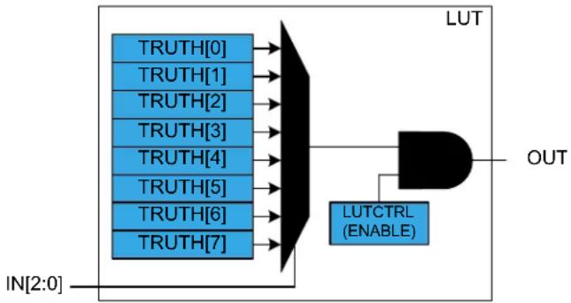
flowchart
graph LR
    subgraph Inputs
        A["TRUTH[0"] --> B["AND"]
        C["TRUTH[1"] --> B
        TRUTH["2"] --> B
        TRUTH["3"] --> B
        TRUTH["4"] --> B
        TRUTH["5"] --> B
        TRUTH["6"] --> B
        TRUTH["7"] --> B
    end
    B --> C
    B --> D["LUTCTRL (ENABLE)"]
    D --> E["OUT"]
    F["IN[2:0"]] --> A
Table 39-1. Truth Table of LUT
| IN[2] IN[1] IN[0] OUT | |||
| 0 0 0 TRUTH[0] | |||
| 0 0 1 TRUTH[1] | |||
| 0 1 0 TRUTH[2] | |||
| 0 1 1 TRUTH[3] | |||
| 1 0 0 TRUTH[4] | |||
| 1 0 1 TRUTH[5] | |||
| 1 1 0 TRUTH[6] | |||
| 1 1 1 TRUTH[7] |
39.6.2.4 Truth Table Inputs Selection
Input Overview
The inputs can be individually:
- Masked
- Driven by peripherals:
- Analog comparator output (AC)
- Timer/Counters waveform outputs (TC)
- Serial Communication output transmit interface (SERCOM)
- Driven by internal events from Event System
- Driven by other CCL sub-modules
The Input Selection for each input y of LUT x is configured by writing the Input y Source Selection bit in the LUT x Control register (LUTCTRLx.INSELy).
Masked Inputs (MASK)
When a LUT input is masked (LUTCTRLx.INSELy=MASK), the corresponding TRUTH input (IN) is internally tied to zero, as shown in this figure:
Figure 39-3. Masked Input Selection
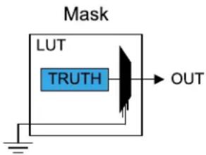
text_image
Mask LUT TRUTH OUTInternal Feedback Inputs (FEEDBACK)
When selected (LUTCTRLx.INSELy=FEEDBACK), the Sequential (SEQ) output is used as input for the corresponding LUT.
The output from an internal sequential sub-module can be used as input source for the LUT, see figure below for an example for LUTO and LUT1. The sequential selection for each LUT follows the formula:
IN2Ni[SEQN [ ]
IN2N+1i[S]EQN [ ]
With N representing the sequencer number and i=0,1,2 representing the LUT input index.
For details, refer to 39.6.2.7. Sequential Logic.
Figure 39-4. Feedback Input Selection
flowchart
graph TD
    A["LUTO"] --> B["TRUTH"]
    C["LUT1"] --> D["TRUTH"]
    B --> E["SEQ0"]
    D --> E
    E --> F["Feedback"]
Linked LUT (LINK)
When selected (LUTCTRLx.INSELy=LINK), the subsequent LUT output is used as the LUT input (e.g., LUT2 is the input for LUT1), as shown in this figure:
Figure 39-5. Linked LUT Input Selection
flowchart
graph TD
    A["LUT0SEQ 0"] --> B["AND"]
    C["LUT1"] --> D["AND"]
    E["LUT2SEQ 1"] --> F["AND"]
    G["LUT3"] --> H["AND"]
    I["CTRL (ENABLE)"] --> J["AND"]
    K["CTRL (ENABLE)"] --> L["AND"]
    M["AND"] --> N["Output"]
    O["Input"] --> A
    P["Input"] --> C
    Q["Input"] --> E
    R["Input"] --> G
Internal Events Inputs Selection (EVENT)
Asynchronous events from the Event System can be used as input selection, as shown in the following figure. For each LUT, one event input line is available and can be selected on each LUT input. Before enabling the event selection by writing LUTCTRLx.INSELy=EVENT, the Event System must be configured first.
The CCL includes an edge detector. When the event is received, an internal strobe is generated when a rising edge is detected. The pulse duration is one GCLK_CCL clock cycle. The following steps ensure proper operation:
- Enable the GCLK_CCL clock.
- Configure the Event System to route the event asynchronously.
- Select the event input type (LUTCTRLx.INSEL).
- If a strobe must be generated on the event input falling edge, write a '1' to the Inverted Event Input Enable bit in LUT Control register (LUTCTRLx.INVEI).
- Enable the event input by writing the Event Input Enable bit in LUT Control register (LUTCTRLx.LUTEI) to '1'.
Figure 39-6. Event Input Selection

flowchart
graph LR
    A["Event Input"] --> B["INVEI"]
    A --> C["LUTEI"]
    B --> D["AND Gate"]
    C --> D
    D --> E["Detector"]
    E --> F["LUT"]
    F --> G["TRUTH"]
    G --> H["OUT"]
    I["GCLK_CCL"] --> E
I/O Pin Inputs (I/O)
When the I/O pin is selected as LUT input (LUTCTRLx.INSELy=IO), the corresponding LUT input will be connected to the pin, as shown in the figure below.
Figure 39-7. I/O Pin Input Selection
flowchart
graph TD
    A["INx"] --> B["LUT"]
    B --> C["TRUTH"]
    C --> D["OUT"]
    E["IO"] --> B
Analog Comparator Inputs (AC)
The AC outputs can be used as input source for the LUT (LUTCTRLx.INSELy=AC).
The analog comparator outputs are distributed following the formula:
IN[N][i]=AC[N % ComparatorOutput Number]
With N representing the LUT number and i=[0,1,2] representing the LUT input index.
Before selecting the comparator output, the AC must be configured first.
The output of comparator 0 is available on even LUTs ("LUT(2x)": LUT0, LUT2) and the comparator 1 output is available on odd LUTs ("LUT(2x+1)": LUT1, LUT3), as shown in the figure below.
Figure 39-8. AC Input Selection
flowchart
graph LR
    A["COMP0"] --> B["LUT(2x)"]
    B --> C["OUT2x"]
    D["COMP1"] --> E["LUT(2x+1)"]
    E --> F["OUT2x+1"]
    B --> G["TRUTH"]
    E --> H["TRUTH"]
    G --> I["CMP0"]
    H --> J["CMP1"]
Timer/Counter Inputs (TC)
The TC waveform output WO[0] can be used as input source for the LUT (LUTCTRLx.INSELy=TC). Only consecutive instances of the TC, i.e. TCx and the subsequent TC(x+1), are available as default and alternative TC selections (e.g., TC0 and TC1 are sources for LUT0, TC1 and TC2 are sources for LUT1, etc). See the figure below for an example for LUT0. More general, the Timer/Counter selection for each LUT follows the formula:
IN[Ni#D]defaultTCN%T[C_Instance_Number]
IN[Ni][AlternativeTCN+1%TC_Instance_Number]
Where N represents the LUT number and i represents the LUT input index (i=0,1,2).
Before selecting the waveform outputs, the TC must be configured first.
Figure 39-9. TC Input Selection
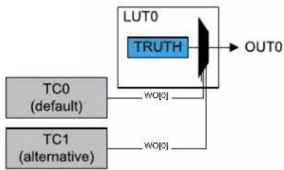
flowchart
graph TD
    A["TC0 (default)"] -->|WO["O"]| B["LUT0"]
    C["TC1 (alternative)"] -->|WO["O"]| B
    B --> D["OUT0"]
Timer/Counter for Control Application Inputs (TCC)
The TCC waveform outputs can be used as input source for the LUT. Only WO[2:0] outputs can be selected and routed to the respective LUT input (i.e., IN0 is connected to WO0, IN1 to WO1, and IN2 to WO2), as shown in the figure below.
Before selecting the waveform outputs, the TCC must be configured first.
Figure 39-10. TCC Input Selection

flowchart
graph TD
    A["TCCx"] --> B["WO[2:0"]]
    B --> C["LUTx"]
    C --> D["TRUTH"]
    D --> E["OUT"]
Serial Communication Output Transmit Inputs (SERCOM)
The serial engine transmitter output from Serial Communication Interface (SERCOM TX, TXd for USART, MOSI for SPI) can be used as input source for the LUT. The figure below shows an example for LUTO and LUT1. The SERCOM selection for each LUT follows the formula:
IN[Ni]HSERCOM[N%SERCOM_Instance_Number]
With N representing the LUT number and i=0,1,2 representing the LUT input index.
Before selecting the SERCOM as input source, the SERCOM must be configured first: the SERCOM TX signal must be output on SERCOMn/pad[0], which serves as input pad to the CCL.
Figure 39-11. SERCOM Input Selection
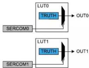
flowchart
graph TD
    A["SERCOM0"] --> B["LUT0"]
    B --> C["TRUTH"]
    C --> D["OUT0"]
    E["SERCOM1"] --> F["LUT1"]
    F --> G["TRUTH"]
    G --> H["OUT1"]
39.6.2.5 Filter
By default, the LUT output is a combinatorial function of the LUT inputs. This may cause some short glitches when the inputs change value. These glitches can be removed by clocking through filters, if demanded by application needs.
The Filter Selection bits in LUT Control register (LUTCTRLx.FILTSEL) define the synchronizer or digital filter options. When a filter is enabled, the OUT output will be delayed by two to five GCLK cycles. One APB clock after the corresponding LUT is disabled, all internal filter logic is cleared.
Note: Events used as LUT input will also be filtered, if the filter is enabled.
Figure 39-12. Filter

flowchart
graph TD
    A["Input"] --> B["D Q R"]
    B --> C["D Q R"]
    C --> D["D Q R"]
    D --> E["D G Q R"]
    E --> F["FILTSEL"]
    F --> G["OUT"]
    H["GCLK_CCL"] --> B
    I["CLR"] --> B
    J["OR Gate"] --> E
    style J fill:#f9f,stroke:#333
The edge detector can be used to generate a pulse when detecting a rising edge on its input. To detect a falling edge, the TRUTH table should be programmed to provide the opposite levels.
The edge detector is enabled by writing '1' to the Edge Selection bit in LUT Control register (LUTCTRLx.EDGESEL). In order to avoid unpredictable behavior, a valid filter option must be enabled as well.
Edge detection is disabled by writing a '0' to LUTCTRLx.EDGESEL. After disabling a LUT, the corresponding internal Edge Detector logic is cleared one APB clock cycle later.
Figure 39-13. Edge Detector

flowchart
graph TD
    A["Input"] --> B["D"]
    C["GCLK_CCL"] --> D["R"]
    E["CLR"] --> F["QN"]
    B --> G["AND Gate"]
    D --> G
    F --> G
    G --> H["EDGESEL"]
    H --> I["OUT"]
39.6.2.7 Sequential Logic
Each LUT pair can be connected to internal sequential logic: D flip flop, JK flip flop, gated D-latch or RS-latch can be selected by writing the corresponding Sequential Selection bits in Sequential Control x register (SEQCTRLx.SEQSEL). Before using sequential logic, the GCLK clock and optionally each LUT filter or edge detector, must be enabled.
Gated D Flip-Flop (DFF)
When the DFF is selected, the D-input is driven by the even LUT output (LUT0 and LUT2), and the G-input is driven by the odd LUT output (LUT1 and LUT3), as shown in the following figure.
Figure 39-14. D Flip Flop
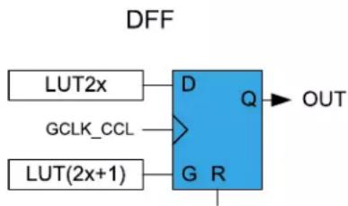
flowchart
graph LR
    A["LUT2x"] --> B["D Flip-Flop"]
    C["GCLK_CCL"] --> B
    D["LUT(2x+1)"] --> B
    B --> E["Q"]
    B --> F["R"]
    B --> G["OUT"]
When the even LUT is disabled (LUTCTRL0. ENABLE=0 / LUTCTRL2. ENABLE=0), the flip-flop is asynchronously cleared. The reset command (R) is kept enabled for one APB clock cycle. In all other cases, the flip-flop output (OUT) is refreshed on rising edge of the GCLK_CCL, as shown in the following table.
Table 39-2. DFF Characteristics
| R G D OUT | ||
| 1 X X Clear | ||
| 0 1 1 Set | ||
| 0 Clear | ||
| 0 X Hold state (no change) | ||
JK Flip-Flop (JK)
When this configuration is selected, the J-input is driven by the even LUT output (LUTO and LUT2), and the K-input is driven by the odd LUT output (LUT1 and LUT3), as shown in the following figure.
Figure 39-15. JK Flip Flop
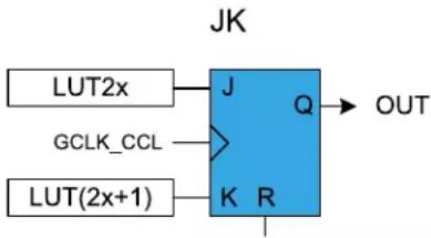
flowchart
graph LR
    A["LUT2x"] --> B["J"]
    C["GCLK_CCL"] --> D["JK Flip-Flop"]
    E["LUT(2x+1)"] --> F["K"]
    B --> G["Q"]
    D --> H["R"]
    F --> I["OUT"]
When the even LUT is disabled (LUTCTRL0. ENABLE=0 / LUTCTRL2. ENABLE=0), the flip-flop is asynchronously cleared. The reset command (R) is kept enabled for one APB clock cycle. In all other cases, the flip-flop output (OUT) is refreshed on rising edge of the GCLK_CCL, as shown in the following table.
Table 39-3. JK Characteristics
| R J K OUT | ||
| 1 X X Clear | ||
| 0 0 0 Hold state (no change) | ||
| 0 0 1 Clear | ||
| 0 1 0 Set | ||
| 0 1 1 Toggle |
Gated D-Latch (DLATCH)
When the DLATCH is selected, the D-input is driven by the even LUT output (LUTO and LUT2), and the G-input is driven by the odd LUT output (LUT1 and LUT3), as shown in the following figure.
Figure 39-16. D-Latch
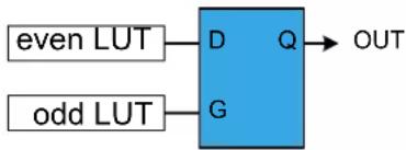
flowchart
graph LR
    A["even LUT"] --> B["D"]
    C["odd LUT"] --> D["G"]
    B --> E["OUT"]
    D --> E
When the even LUT is disabled (LUTCTRL0. ENABLE=0 / LUTCTRL2. ENABLE=0), the latch output will be cleared. The G-input is forced enabled for one more APB clock cycle, and the D-input to zero. In all other cases, the latch output (OUT) is refreshed as shown in the following table.
Table 39-4. D-Latch Characteristics
| G D OUT | ||
| 0 X Hold state (no change) | ||
| 1 0 Clear | ||
| 1 1 Set | ||
RS Latch (RS)
When this configuration is selected, the S-input is driven by the even LUT output (LUT0 and LUT2), and the R-input is driven by the odd LUT output (LUT1 and LUT3), as shown in the following figure.
Figure 39-17. RS-Latch

flowchart
graph LR
    A["even LUT"] --> B["S"]
    C["odd LUT"] --> D["R"]
    B --> E["Q"]
    D --> E
    E --> F["OUT"]
When the even LUT is disabled (LUTCTRL0.ENABLE=0 / LUTCTRL2.ENABLE=0), the latch output will be cleared. The R-input is forced enabled for one more APB clock cycle and S-input to zero. In all other cases, the latch output (OUT) is refreshed as shown in the following table.
Table 39-5. RS-latch Characteristics
| S R OUT | ||
| 0 0 Hold state (no change) | ||
| 0 1 Clear | ||
| 1 0 Set | ||
| 1 1 Forbidden state | ||
39.6.3 Events
The CCL can generate the following output events:
• LUTOUTx: Lookup Table Output Value
Writing a '1' to the LUT Control Event Output Enable bit (LUTCTRL.LUTEO) enables the corresponding output event. Writing a '0' to this bit disables the corresponding output event. Refer to EVSYS – Event System for details on configuration.
The CCL can take the following actions on an input event:
• INx: The event is used as input for the TRUTH table. For further details refer to 39.5.6. Events.
Writing a '1' to the LUT Control Event Input Enable bit (LUTCTRL.LUTEI) enables the corresponding action on input event. Writing a '0' to this bit disables the corresponding action on input event. Refer to EVSYS - Event System for details on configuration.
39.6.4 Sleep Mode Operation
When using the GCLK_CCL internal clocking, writing the Run In Standby bit in the Control register (CTRL.RUNSTDBY) to '1' will allow GCLK_CCL to be enabled in all sleep modes.
If CTRL.RUNSTDBY=0, the GCLK_CCL will be disabled. If the Filter, Edge Detector or Sequential logic are enabled, the LUT output will be forced to zero in STANDBY mode. In all other cases, the TRUTH table decoder will continue operation and the LUT output will be refreshed accordingly.
39.7 Register Summary
| Offset | Name Bit Pos. 76 | 543210 | |||||||
| 0x00 CTRL 7:0 RUNSTDBY | ENABLE SWRST | ||||||||
| 0x01 ... 0x03 | Reserved | ||||||||
| 0x04 SEQCTRL0 7:0 | SEQSEL[3:0] | ||||||||
| 0x05 SEQCTRL1 7:0 | SEQSEL[3:0] | ||||||||
| 0x06 ... 0x07 | Reserved | ||||||||
| 0x08 | LUTCTRL0 | 7:0 EDGESEL | FILTSEL[1:0] | ENABLE | |||||
| 15:8 | INSEL1[3:0] | INSEL0[3:0] | |||||||
| 23:16 | LUTEO | LUTEI | INVEI | INSEL2[3:0] | |||||
| 31:24 | TRUTH[7:0] | ||||||||
| 0x0C LUTCTRL1 | 7:0 EDGESEL | FILTSEL[1:0] | ENABLE | ||||||
| 15:8 | INSEL1[3:0] | INSEL0[3:0] | |||||||
| 23:16 | LUTEO | LUTEI | INVEI | INSEL2[3:0] | |||||
| 31:24 | TRUTH[7:0] | ||||||||
| 0x10 | LUTCTRL2 | 7:0 EDGESEL | FILTSEL[1:0] | ENABLE | |||||
| 15:8 | INSEL1[3:0] | INSEL0[3:0] | |||||||
| 23:16 | LUTEO | LUTEI | INVEI | INSEL2[3:0] | |||||
| 31:24 | TrUTH[7:0] | ||||||||
| 0x14 | LUTCTRL3 | 7:0 EDGESEL | FILTSEL[1:0] | ENABLE | |||||
| 15:8 | INSEL1[3:0] | INSEL0[3:0] | |||||||
| 23:16 | LUTEO | LUTEI | INVEI | INSEL2[3:0] | |||||
| 31:24 | trUTH[7:0] | ||||||||
39.8 Register Description
Registers can be 8, 16, or 32 bits wide. Atomic 8-, 16-, and 32-bit accesses are supported. In addition, the 8-bit quarters and 16-bit halves of a 32-bit register, and the 8-bit halves of a 16-bit register can be accessed directly.
Some registers require synchronization when read and/or written. Synchronization is denoted by the "Read-Synchronized" and/or "Write-Synchronized" property in each individual register description.
Optional write-protection by the Peripheral Access Controller (PAC) is denoted by the "PAC Write-Protection" property in each individual register description.
Some registers are enable-protected, meaning they can only be written when the CCL.LUTCTRLx .ENABLE bit is set to '0'. Enable-protection is denoted by the "Enable-Protected" property in each individual register description.
39.8.1 Control
Name: CTRL
Offset: 0x00
Reset: 0x00
Property: PAC Write-Protection
Bit 76543210
| RUNSTDBY ENABLE SWRST | ||||||
| Access | R/W R/W W | |||||
| Reset | 0 | 0 0 | ||||
Bit 6 - RUNSTDBY Run in Standby
This bit indicates if the GCLK_CCL clock must be kept running in standby mode. The setting is ignored for configurations where the generic clock is not required. For details refer to 39.6.4. Sleep Mode Operation.

Important: This bit must be written before enabling the CCL.
| Value | Description |
| 0 | Generic clock is not required in standby sleep mode. |
| 1 | Generic clock is required in standby sleep mode. |
Bit 1 - ENABLE Enable
| Value | Description |
| 0 | The peripheral is disabled. |
| 1 | The peripheral is enabled. |
Bit 0 - SWRST Software Reset
Writing a '0' to this bit has no effect.
Writing a '1' to this bit resets all registers in the CCL to their initial state.
| Value | Description |
| 0 | There is no reset operation ongoing. |
| 1 | The reset operation is ongoing. |
39.8.2 Sequential Control n
Name: SEQCTRLn
Offset: 0x04 + n*0x01 [n=0..1]
Reset: 0x00
Property: PAC Write-Protection, Enable-Protected
Note: SEQCTRL0 (SEQCTRL1) register is Enable-protected when CCL.LUTCTRL0.ENABLE = 1 (CCL.LUTCTRL2.ENABLE = 1).
Bit 76543210
| SEQSEL[3:0] | ||||
| Access Reset 0 0 0 0 | R/W R/W R/W R/W | |||
Bits 3:0 - SEQSEL[3:0] Sequential Selection
These bits select the sequential configuration:
Sequential Selection
| Value Name Description | ||
| 0x0 | DISABLE | Sequential logic is disabled |
| 0x1 | DFF | D flip flop |
| 0x2 | JK | JK flip flop |
| 0x3 | LATCH | D latch |
| 0x4 | RS | RS latch |
| 0x5 - 0xF | Reserved | |
39.8.3 LUT Control n
Name: LUTCTRLn
Offset: 0x08 + n*0x04 [n=0..3]
Reset: 0x00000000
Property: PAC Write-Protection, Enable-Protected
Note: The LUTCTRLn register is enable-protected when CCL.LUTCTRLn.ENABLE = 1.
Bit 31 30 29 28 27 26 25 24
| TRUTH[7:0] | |
| Access | R/W R/W R/W R/W R/W R/W R/W R/W |
| Reset | 0 0 0 0 0 0 0 |
Bit 23 22 21 20 19 18 17 16
| LUTEO LUTEI | INVEI | INSEL2[3:0] | |||
| Access | R/W R/W R/W R/W R/W R/W R/W | ||||
| Reset | 0 0 0 0 0 0 0 | ||||
Bit 15 14 13 12 11 10 98
| INSEL1[3:0] | INSEL0[3:0] | |
| Access | R/W R/W R/W R/W R/W R/W R/W R/W | |
| Reset | 0 0 0 0 0 0 0 | |
Bit 76543210
| EDGESEL | FILTSEL[1:0] | ENABLE | |||||
| Access | R/W | R/W R/W | R/W | ||||
| Reset | 0 | 0 0 | 0 |
Bits 31:24 - TRUTH[7:0] Truth Table
These bits define the value of truth logic as a function of inputs IN[2:0].
Bit 22 - LUTEO LUT Event Output Enable
| Value | Description |
| 0 | LUT event output is disabled. |
| 1 | LUT event output is enabled. |
Bit 21 - LUTEI LUT Event Input Enable
| Value | Description |
| 0 | LUT incoming event is disabled. |
| 1 | LUT incoming event is enabled. |
Bit 20 - INVEI Inverted Event Input Enable
| Value | Description |
| 0 | Incoming event is not inverted. |
| 1 | Incoming event is inverted. |
Bits 8:11, 12:15, 16:19 - INSELx LUT Input x Source Selection
These bits select the LUT input x source:
| Value | Name | Description |
| 0x0 | MASK | Masked input |
| 0x1 | FEEDBACK | Feedback input source |
| 0x2 | LINK | Linked LUT input source |
| 0x3 | EVENT | Event input source |
| 0x4 | IO | I/O pin input source |
| Value Name | Description |
| 0x5 | AC AC input source: CMP[0] (LUT0) / CMP[1] (LUT1) |
| 0x6 | TC TC input source: TC0 (LUT0) / TC1 (LUT1) |
| 0x7 | ALTTC Alternative TC input source: TC1 (LUT0) / TC2 (LUT1) |
| 0x8 | TCC TCC Input Source |
| 0x9 | SERCOM SERCOM input source: SERCOM0 (LUT0) / SERCOM1 (LUT1) |
| 0xA - 0xF | - Reserved |
These bits select the LUT output filter options:
Filter Selection
| Value Name | Description | |
| 0x0 | DISABLE Filter disabled | |
| 0x1 | SYNCH Synchronizer enabled | |
| 0x2 | FILTER Filter enabled | |
| 0x3 | - Reserved | |
Bit 1 - ENABLE LUT Enable
This bit is not Enable-Protected.
| Value Description | |
| 0 | The LUT is disabled. |
| 1 | The LUT is enabled. |
40. ADC - Analog-to-Digital Converter
40.1 Overview
The Analog-to-Digital Converter (ADC) converts analog signals to digital values. The ADC has up to 12-bit resolution, and is capable of a sampling rate of up to 1 MSPS. The input selection is flexible, and both differential and single-ended measurements can be performed. In addition, several internal signal inputs are available. The ADC can provide both signed and unsigned results.
ADC measurements can be started by either application software or an incoming event from another peripheral in the device. ADC measurements can be started with predictable timing and without software intervention.
Both internal and external reference voltages can be used.
The bandgap voltage, as well as the scaled I/O and core voltages, can also be measured by the ADC.
The ADC has a compare function for accurate monitoring of user-defined thresholds, with minimum software intervention required.
The ADC can be configured for 8-bit, 10-bit or 12-bit results. ADC conversion results are provided left-adjusted or right-adjusted, which eases calculation when the result is represented as a signed value. It is possible to use DMA to move ADC results directly to memory or peripherals when conversions are done.
40.2 Features
• 8-bit, 10-bit or 12-bit resolution
- Up to 1,000,000 samples per second (1MSPS)
• Differential and single-ended inputs
- Up to 20 analog inputs
26 positive and 9 negative, including internal and external
- Internal inputs:
- Internal temperature sensor
- Bandgap voltage
- Scaled core supply
- Scaled I/O supply
- Scaled VBAT supply
- Single, continuous, and sequencing options
- Windowing monitor with selectable channel
- Conversion range: V_ref = [1.0V to VDDANA]
• Built-in internal reference and external reference options
• Event-triggered conversion for accurate timing (one event input)
- Optional DMA transfer of conversion settings or result
- Hardware gain and offset compensation
- Averaging and oversampling with decimation to support up to 16-bit result
- Selectable sampling time
- Flexible Power or Throughput rate management
40.3 Block Diagram
Figure 40-1. ADC Block Diagram
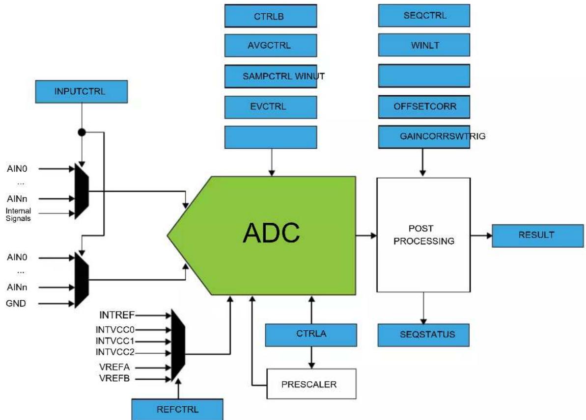
flowchart
graph TD
    A["INPUTCTRL"] --> B["AND"]
    C["AIN0"] --> B
    D["..."] --> B
    E["AINn"] --> B
    F["Internal Signals"] --> B
    G["AIN0"] --> H["AND"]
    I["..."] --> H
    J["GND"] --> H
    K["INTREF"] --> H
    L["INTVCC0"] --> H
    M["INTVCC1"] --> H
    N["INTVCC2"] --> H
    O["VREFA"] --> H
    P["VREFB"] --> H
    Q["REFCTRL"] --> H
    R["CTRLB"] --> S["ADC"]
    T["AVGCTRL"] --> S
    U["SAMPCTRL WINUT"] --> S
    V["EVCTRL"] --> S
    W["SEQCTRL"] --> X["POST PROCESSING"]
    Y["WINLT"] --> X
    Z["OFFSETCORR"] --> X
    AA["GAINCORRSWTRIG"] --> X
    AB["RESULT"] --> AC["SEQSTATUS"]
    AD["CTRLA"] --> AE["PREScaler"]
    AF["INTREF"] --> AE
    AG["INTVCC0"] --> AE
    AH["INTVCC1"] --> AE
    AI["VREFA"] --> AE
    AJ["VREFB"] --> AE
40.4 Signal Description
| Signal Description Type | ||
| VREF[A, B] Analog input External reference voltage | ||
| AIN[19..0] Analog input Analog input channels | ||
Note: One signal can be mapped on several pins.
40.5 Product Dependencies
In order to use this peripheral, other parts of the system must be configured correctly, as described below.
40.5.1 I/O Lines
Using the ADC's I/O lines requires the I/O pins to be configured using the port configuration (PORT).
40.5.2 Power Management
The ADC will continue to operate in any Sleep mode where the selected source clock is running. The ADC's RESRDY and WINMON interrupts, can be used to wake up the device from Sleep modes. Events connected to the event system can trigger other operations in the system without exiting Sleep modes.
40.5.3 Clocks
The ADC bus clock (CLK_ADC_APB) can be enabled in the Main Clock, which also defines the default state.
The ADC requires a generic clock (GCLK_ADC). This clock must be configured and enabled in the Generic Clock Controller (GCLK) before using the ADC.
A generic clock is asynchronous to the bus clock. Due to this asynchronicity, writes to certain registers will require synchronization between the clock domains. Refer to the section "Synchronization" for additional information.
40.5.4 DMA
The DMA request line is connected to the DMA Controller (DMAC). Using the ADC DMA requests requires the DMA Controller to be configured first.
40.5.5 Interrupts
The interrupt request line is connected to the interrupt controller. Using the ADC interrupt requires the interrupt controller to be configured first.
40.5.6 Events
The events are connected to the Event System.
40.5.7 Debug Operation
When the CPU is halted in debug mode the ADC will halt normal operation. The ADC can be forced to continue operation during debugging. Refer to DBGCTRL register for details.
40.5.8 Register Access Protection
All registers with write-access are optionally write-protected by the Peripheral Access Controller (PAC), except the following register:
- Interrupt Flag Status and Clear (INTFLAG) register
Optional write protection by the Peripheral Access Controller (PAC) is denoted by the "PAC Write Protection" property in each individual register description.
PAC write protection does not apply to accesses through an external debugger.
40.5.9 Analog Connections
I/O-pins (AlNx) and VREFA/VREFB reference voltage pins are analog inputs to the ADC. Any internal reference source, such as INTREF, supplied by the bandgap, must be configured and enabled prior to its use with the ADC.
40.5.10 Calibration
The ADC BIASCOMP and BIASREFBUF calibration values from the production test must be loaded from the NVM Software Calibration Area into the ADC Calibration register (CALIB) by software to achieve specified accuracy.
40.6 Functional Description
40.6.1 Principle of Operation
By default, the ADC provides results with 12-bit resolution. 8-bit or 10-bit results can be selected in order to reduce the conversion time, see 40.6.2.8. Conversion Timing and Sampling Rate.
The ADC has an oversampling with decimation option that can extend its resolution to 16 bits. The input values can be either internal or external (connected I/O pins). The user can also configure whether the conversion should be single-ended or differential.
40.6.2 Basic Operation
40.6.2.1 Initialization
The following registers are enable-protected, meaning that they can only be written when the ADC is disabled (CTRLA.ENABLE = 0):
• The Control B (CTRLB) register
• The Reference Control (REFCTRL) register
• The Event Control (EVCTRL) register
• The Calibration (CALIB) register
Enable-protection is denoted by the "Enable-Protected" property in the register description.
40.6.2.2 Enabling, Disabling, and Resetting
The ADC is enabled by writing a '1' to the Enable bit in the Control A register (CTRLA.ENABLE). The ADC is disabled by writing CTRLA.ENABLE = 0.
The ADC is reset by writing a '1' to the Software Reset bit in the Control A register (CTRLA.SWRST). All registers in the ADC, except DBGCTRL, will be reset to their initial state, and the ADC will be disabled. Refer to 40.8.1. CTRLA for details.
40.6.2.3 Operation
In the most basic configuration, the ADC samples values from the configured internal or external sources (INPUTCTRL register). The rate of the conversion depends on the combination of the GCLK_ADC frequency and the clock prescaler.
To convert analog values to digital values, the ADC needs to be initialized first, as described in the Initialization section. Data conversion can be started either manually by setting the Start bit in the Software Trigger register (SWTRIG.START=1), or automatically by configuring an automatic trigger to initiate the conversions. The ADC starts sampling the input only after the start of conversion is triggered. This means that even after the MUX selection is made, sample and hold (S&H) operation starts only on the conversion trigger. A free-running mode can be used to continuously convert an input channel. When using free-running mode the first conversion must be started, while subsequent conversions will start automatically at the end of the previous conversion.
The ADC starts sampling the input only after the start of a conversion is triggered. This means that even after the MUX selection is made, sample and hold operation starts only on the conversion trigger.
The result of the conversion is stored in the Result register (RESULT) overwriting the result from the previous conversion.
To avoid data loss, if more than one channel is enabled, the conversion result must be read as soon as it is available (INTFLAG.RESRDY). Failing to do so will result in an overrun error condition, indicated by the OVERRUN bit in the Interrupt Flag Status and Clear register (INTFLAG.OVERRUN).
To enable one of the available interrupts sources, the corresponding bit in the Interrupt Enable Set register (INTENSET) must be written to '1'.
40.6.2.4 Prescaler Selection
The ADC is clocked by GCLK_ADC. There is also a prescaler in the ADC to enable conversion at lower clock rates. Refer to CTRLB for details on prescaler settings. Refer to 40.6.2.8. Conversion Timing and Sampling Rate for details on timing and sampling rate.
Figure 40-2. ADC Prescaler
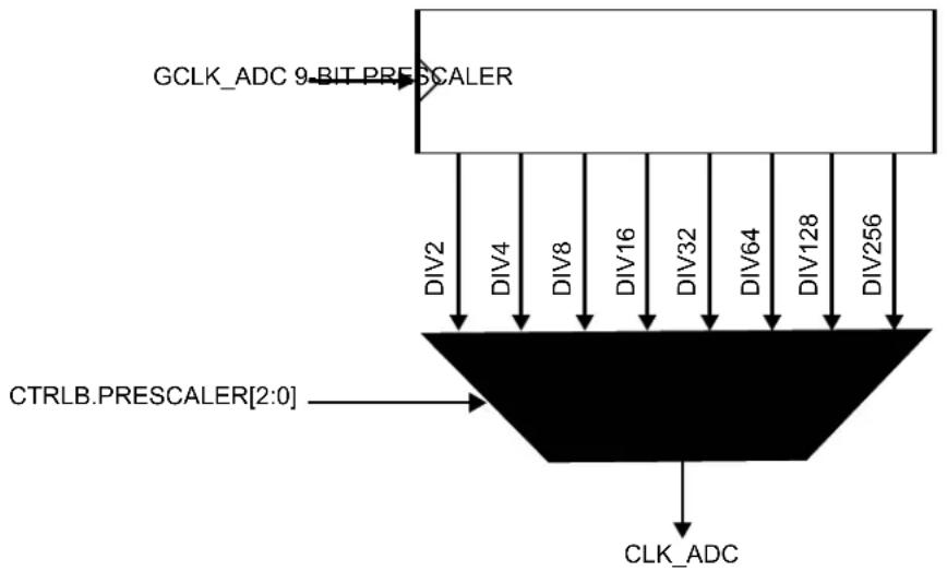
flowchart
graph TD
    A["GCLK_ADC 9-BIT PRESCALER"] --> B["DIV2"]
    A --> C["DIV4"]
    A --> D["DIV8"]
    A --> E["DIV16"]
    A --> F["DIV32"]
    A --> G["DIV64"]
    A --> H["DIV128"]
    A --> I["DIV256"]
    J["CTRLB.PRESCALER[2:0"]] --> K
    L["CLK_ADC"] --> M
Note: The minimum prescaling factor is DIV2.
40.6.2.5 Reference Configuration
The ADC has various sources for its reference voltage V_REF . The Reference Voltage Selection bit field in the Reference Control register (REFCTRL.REFSEL) determines which reference is selected. By default, the internal voltage reference INTREF, supplied by the bandgap, is selected. Based on customer application requirements, the external or internal reference can be selected. Refer to REFCTRL.REFSEL for further details on available selections.
40.6.2.6 ADC Resolution
The ADC supports 8-bit, 10-bit or 12-bit resolution. Resolution can be changed by writing the Resolution bit group in the Control C register (CTRLC.RESSEL). The RESSEL bit group has a specific configuration mode used to support Accumulation or Oversampling and Decimation features. Refer to these specific sections for more details.
By default, the ADC resolution is set to 12 bits. The resolution affects the propagation delay, see also 40.6.2.8. Conversion Timing and Sampling Rate.
40.6.2.7 Differential and Single-Ended Conversions
The ADC has two conversion options: differential and single-ended:
If the positive input is always positive, the single-ended conversion should be used in order to have full 12-bit resolution in the conversion.
If the positive input may go below the negative input, the differential mode should be used in order to get correct results.
The differential mode is enabled by setting DIFFMODE bit in the Control C register (CTRLC.DIFFMODE). Both conversion types could be run in single mode or in free-running mode. When the free-running mode is selected, an ADC input will continuously sample the input and perform a new conversion. The INTFLAG.RESRDY bit will be set at the end of each conversion.
40.6.2.8 Conversion Timing and Sampling Rate
The following figure shows the ADC timing for a single conversion. A conversion starts after the software or event start are synchronized with the GCLK_ADC clock. The input channel is sampled in the first half CLK_ADC period.
Figure 40-3. ADC Timing for One Conversion in 12-bit Resolution
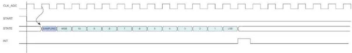
text_image
CLK_ADC START STATE INT SAMPLING MUSE 10 9 8 7 6 5 4 3 2 1 LSSThe sampling time can be increased by using the Sampling Time Length bit group in the Sampling Time Control register (SAMPCTRL.SAMPLEN). As example, the next figure is showing the timing conversion with sampling time increased to six CLK_ADC cycles.
Figure 40-4. ADC Timing for One Conversion with Increased Sampling Time, 12-bit
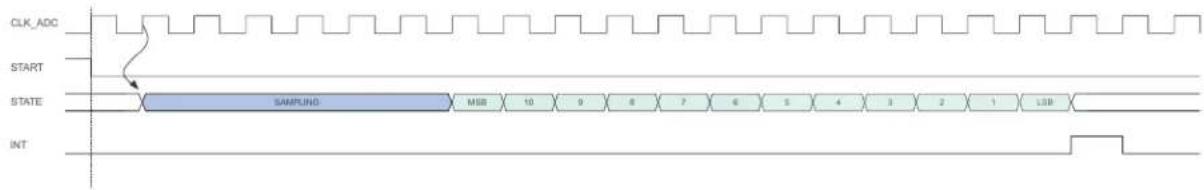
text_image
CLK_ADC START STATE SAMPLIN INTThe ADC can also provide offset compensation, as shown in the following figure. The offset compensation is enabled by the Offset Compensation bit in the Sampling Control register (SAMPCTRL.OFFCOMP).
Note: ADC sampling time is fixed to 4 ADC Clock cycles when offset compensation (OFFCOMP=1) is used.
In free running mode, the sampling rate R_S is calculated by
$$ R _ {S} = f _ {\text { CLK_ADC }} / \left(n _ {\text { SAMPLING }} + n _ {\text { OFFCOMP }} + n _ {\text { DATA }}\right) $$
Here, n_SAMPLING is the sampling duration in CLK_ADC cycles, n_OFFCOMP is the offset compensation duration in clock cycles, and n_DATA is the bit resolution. f_CLK_ADC is the ADC clock frequency from the internal prescaler: f_CLK_ADC = f_GCLK_ADC / 2^(1 + CTRLB.PRESCALER)
Figure 40-5. ADC Timing for One Conversion with Offset Compensation, 12-bit
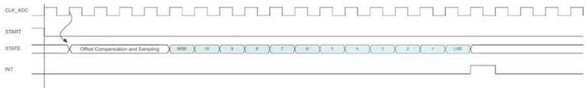
text_image
CLK_ADC START STATE INT Offset Compensation and Sampling MSS 10 B 8 T 6 S 4 3 2 1 LIBThe impact of resolution on the sampling rate is seen in the next two figures, where free-running sampling in 12-bit and 8-bit resolution are compared.
Figure 40-6. ADC Timing for Free Running in 12-bit Resolution
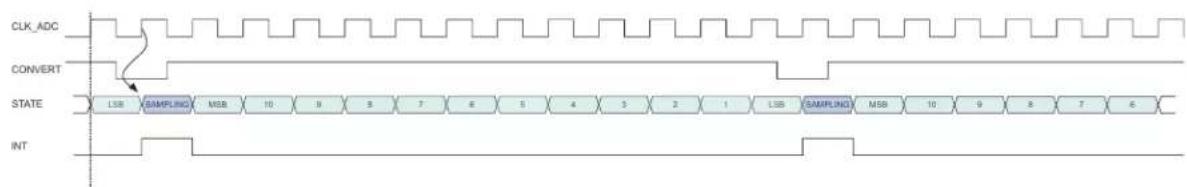
text_image
CLK_ADC CONVERT STATE LSB SAMPLING MSB 10 9 8 7 6 5 4 3 2 1 LSB (SAMPLING) MSB 10 9 8 7 6 INTFigure 40-7. ADC Timing for Free Running in 8-bit Resolution
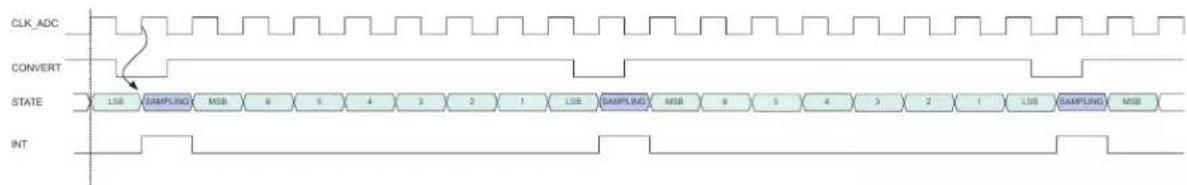
text_image
CLK_ADC CONVERT STATE INT LSB | SAMPLING | MSB | 6 | 5 | 4 | 3 | 2 | 1 | LSB | SAMPLING | MSB | 8 | 5 | 4 | 3 | 2 | 1 | LSB | (SAMPLING) | MSBThe propagation delay of an ADC measurement is given by:
$$ \text { PropagationDelay } = \frac {1 + \text { Resolution }}{f _ {\mathrm{ADC}}} $$
Example. In order to obtain 1 MSPS in 12-bit resolution with a sampling time length of four CLK_ADC cycles, f_CLK_ADC must be 1 MSPS * (4 + 12) = 16MHz. As the minimal division factor of the prescaler is 2, GCLK_ADC must be 32MHz.
40.6.2.9 Accumulation
The result from multiple consecutive conversions can be accumulated. The number of samples to be accumulated is specified by the Sample Number field in the Average Control register (AVGCTRL.SAMPLENUM). When accumulating more than 16 samples, the result will be too large to match the 16-bit RESULT register size. To avoid overflow, the result is right shifted automatically to fit within the available register size. The number of automatic right shifts is specified in the table below.
Note: To perform the accumulation of two or more samples, the Conversion Result Resolution field in the Control C register (CTRLC.RESSEL) must be set depending on the final result precision. For resolutions strictly higher than 12 bits, RESSEL must be set to 16 bits.
Table 40-1. Accumulation
| Number of Accumulated Samples | AVGCTRL. SAMPLENUM | Number of Automatic Right Shifts | Final Result Precision | Automatic Division Factor |
| 1 0x0 0 12 bits 0 | ||||
| 2 0x1 0 13 bits 0 | ||||
| 4 0x2 0 14 bits 0 | ||||
| 8 0x3 0 15 bits 0 | ||||
| 16 0x4 0 16 bits 0 | ||||
| 32 0x5 1 16 bits 2 | ||||
| 64 0x6 2 16 bits 4 | ||||
| 128 0x7 3 16 bits 8 | ||||
| 256 0x8 4 16 bits 16 | ||||
| 512 0x9 5 16 bits 32 | ||||
| 1024 0xA 6 16 bits 64 | ||||
| Reserved | 0xB -0xF | 12 bits 0 |
40.6.2.10 Averaging
Averaging is a feature that increases the sample accuracy, at the cost of a reduced sampling rate. This feature is suitable when operating in noisy conditions.
Averaging is done by accumulating m samples, as described in 40.6.2.9. Accumulation, then dividing the result by m. The averaged result is available in the RESULT register. The number of samples to be accumulated is specified by writing to AVGCTRL.SAMPLENUM as shown in Table 40-2.
The division is obtained by a combination of the automatic right shift described above, and an additional right shift that must be specified by writing to the Adjusting Result/Division Coefficient field in AVGCTRL (AVGCTRL.ADJRES), as described in Table 40-2.
Note: To perform the averaging of two or more samples, the Conversion Result Resolution field in the Control C register (CTRLC.RESSEL) must be set.
Averaging AVGCTRL.SAMPLENUM samples will reduce the un-averaged sampling rate by a factor 1
AVGCTRL.SAMPLENUM
When the averaged result is available, the INTFLAG.RESRDY bit will be set.
Table 40-2. Averaging
| Number of Accumulated Samples | AVGCTRL.SAMPLENUM | Intermediate Result Precision | Number of Automatic Right Shifts | Division Factor | AVGCTRL.ADJRES | Total Number of Right Shifts | Final Result Precision | Automatic Division Factor |
| 1 0x0 12 bits 0 | 1 0x0 12 bits 0 | |||||||
| 2 0x1 13 0 2 0x1 | 1 12 bits 0 | |||||||
| 4 0x2 14 0 4 0x2 | 2 12 bits 0 | |||||||
| 8 0x3 15 0 8 0x3 | 3 12 bits 0 | |||||||
| 16 0x4 16 0 16 | 0x4 4 12 bits 0 | |||||||
| 32 0x5 17 1 16 | 0x4 5 12 bits 2 | |||||||
| 64 0x6 18 2 16 | 0x4 6 12 bits 4 | |||||||
| 128 0x7 19 3 16 | 0x4 7 12 bits 8 | |||||||
| 256 0x8 20 4 16 | 0x4 8 12 bits 16 | |||||||
| 512 0x9 21 5 16 | 0x4 9 12 bits 32 | |||||||
| 1024 0xA 22 6 | 16 0x4 10 | 12 bits 64 | ||||||
| Reserved | 0xB -0xF | 0x0 12 bits 0 |
40.6.2.11 Oversampling and Decimation
By using oversampling and decimation, the ADC resolution can be increased from 12 bits up to 16 bits, for the cost of reduced effective sampling rate.
Note: To perform oversampling and decimation, the Conversion Result Resolution field in the Control C register (CTRLC.RESSEL) must be set to 16-bit mode.
To increase the resolution by 'n' bits, 4^n samples must be accumulated. The result must then be right shifted by 'n' bits. This right shift is a combination of the automatic right shift and the value written to AVGCTRL.ADJRES. To obtain the correct resolution, the ADJRES must be configured as described in the table below. This method will result in 'n' bit extra LSB resolution.
Table 40-3. Configuration Required for Oversampling and Decimation
| Result Resolution | Number of Samples to Average | AVGCTRL.SAMPLENUM[3:0] | Number of Automatic Right Shifts | AVGCTRL.ADJRES[2:0] |
| 13 bits | 4^1 = 4 | 0x2 | 0 | 0x1 |
| 14 bits | 4^2 = 16 | 0x4 | 0 | 0x2 |
| 15 bits | 4^3 = 64 | 0x6 | 2 | 0x1 |
| 16 bits | 4^4 = 256 | 0x8 | 4 | 0x0 |
40.6.2.12 Automatic Sequences
The ADC has the ability to automatically sequence a series of conversions. This means that each time the ADC receives a start-of-conversion request, it can perform multiple conversions automatically. All of the positive inputs can be included in a sequence by writing to corresponding
bits in the Sequence Control register (SEQCTRL). The order of the conversion in a sequence is the lower positive MUX selection to upper positive MUX (AIN0, AIN1, AIN2 ...). In differential mode, the negative inputs selected by MUXNEG field, will be used for the entire sequence.
When a sequence starts, the Sequence Busy status bit in Sequence Status register (SEQSTATUS.SEQBUSY) will be set. When the sequence is complete, the Sequence Busy status bit will be cleared.
Each time a conversion is completed, the Sequence State bit in Sequence Status register (SEQSTATUS.SEQSTATE) will store the input number from which the conversion is done. The result will be stored in the RESULT register, and the Result Ready Interrupt Flag (INTFLAG.RESRDY) is set.
If additional inputs must be scanned, the ADC will automatically start a new conversion on the next input present in the sequence list.
Note that if SEQCTRL register has no bits set to '1', the conversion is done with the selected MUXPOS input.
40.6.2.13 Window Monitor
The window monitor feature allows the conversion result in the RESULT register to be compared to predefined threshold values. The window mode is selected by setting the Window Monitor Mode bits in the Control C register (CTRLC.WINMODE). Threshold values must be written in the Window Monitor Lower Threshold register (WINLT) and Window Monitor Upper Threshold register (WINUT).
If differential input is selected, the WINLT and WINUT are evaluated as signed values. Otherwise they are evaluated as unsigned values. The significant WINLT and WINUT bits are given by the precision selected in the Conversion Result Resolution bit group in the Control C register (CTRLC.RESSEL). As an example in 8-bit mode, only the eight lower bits will be considered. In addition, in differential mode, the eighth bit will be considered as the sign bit, even if the ninth bit is zero.
The INTFLAG.WINMON interrupt flag will be set if the conversion result matches the window monitor condition.
40.6.2.14 Offset and Gain Correction
Inherent gain and offset errors affect the absolute accuracy of the ADC.
The offset error is defined as the deviation of the actual ADC transfer function from an ideal straight line at zero input voltage. The offset error cancellation is handled by the Offset Correction register (OFFSETCORR). The offset correction value is subtracted from the converted data before writing the Result register (RESULT).
The gain error is defined as the deviation of the last output step's midpoint from the ideal straight line, after compensating for offset error. The gain error cancellation is handled by the Gain Correction register (GAINCORR).
To correct these two errors, the Digital Correction Logic Enabled bit in the Control C register (CTRLC.CORREN) must be set.
Offset and gain error compensation results are both calculated according to:
Result = Conversion value + -OFFSETCORR · GAINCORR
The correction will introduce a latency of 13 CLK_ADC clock cycles. In free running mode this latency is introduced on the first conversion only, since its duration is always less than the propagation delay. In single conversion mode this latency is introduced for each conversion.
Figure 40-8. ADC Timing Correction Enabled

flowchart
graph TD
    A["START"] --> B["CONV0"]
    B --> C["CONV1"]
    C --> D["CONV2"]
    D --> E["CONV3"]
    E --> F["..."]
    F --> G["..."]
    G --> H["CORR0"]
    H --> I["CORR1"]
    I --> J["CORR2"]
    J --> K["CORR3"]
    K --> L["..."]
40.6.3 DMA Operation
The ADC generates the following DMA request:
- Result Conversion Ready (RESRDY): the request is set when a conversion result is available and cleared when the RESULT register is read. When the averaging operation is enabled, the DMA request is set when the averaging is completed and result is available.
40.6.4 Interrupts
The ADC has the following interrupt sources:
• Result Conversion Ready: RESRDY
• Window Monitor: WINMON
• Overrun: OVERRUN
The RESRDY and WINMON are asynchronous wake-up sources. See the Sleep Mode Controller for details.
Each interrupt source has an interrupt flag associated with it. The interrupt flag in the Interrupt Flag Status and Clear (INTFLAG) register is set when the interrupt condition occurs. Each interrupt can be individually enabled by writing a one to the corresponding bit in the Interrupt Enable Set (INTENSET) register, and disabled by writing a one to the corresponding bit in the Interrupt Enable Clear (INTENCLR) register. The status of enabled interrupts can be read from either INTENSET or INTENCLR.
An interrupt request is generated when the interrupt flag is set and the corresponding interrupt is enabled. The interrupt request remains active until the interrupt flag is cleared, the interrupt is disabled, or the ADC is reset. See INTFLAG register for details on how to clear interrupt flags. All interrupt requests from the peripheral are ORed together on system level to generate one combined interrupt request to the NVIC. Refer to Nested Vector Interrupt Controller for details. The user must read the INTFLAG register to determine which interrupt condition is present.
Note that interrupts must be globally enabled for interrupt requests to be generated. Refer to Nested Vector Interrupt Controller for details.
40.6.5 Events
The ADC can generate the following output events:
- Result Ready (RESRDY): Generated when the conversion is complete and the result is available. Refer to 40.8.4. EVCTRL for details.
- Window Monitor (WINMON): Generated when the window monitor condition match. Refer to 40.8.10. CTRL C for details.
Setting an Event Output bit in the Event Control Register (EVCTRL.xxEO=1) enables the corresponding output event. Clearing this bit disables the corresponding output event. Refer to the Event System chapter for details on configuring the event system.
The ADC can take the following actions on an input event:
- Start conversion (START): Start a conversion. Refer to 40.8.17. SWTRIG for details.
- Conversion flush (FLUSH): Flush the conversion. Refer to 40.8.17. SWTRIG for details.
Setting an Event Input bit in the Event Control register (EVCTRL.xxEI=1) enables the corresponding action on input event. Clearing this bit disables the corresponding action on input event.
By default, the ADC will detect a rising edge on the incoming event. If the ADC action must be performed on the falling edge of the incoming event, the event line must be inverted first. This is done by setting the corresponding Event Invert Enable bit in Event Control register (EVCTRL.xINV=1).
Note: If several events are connected to the ADC, the enabled action will be taken on any of the incoming events. If FLUSH and START events are available at the same time, the FLUSH event has priority.
40.6.6 Sleep Mode Operation
The ONDEMAND and RUNSTDBY bits in the Control A register (CTRLA) control the behavior of the ADC during standby sleep mode, in cases where the ADC is enabled (CTRLA.ENABLE = 1). For further details on available options, refer to Table 40-4.
Note: When CTRLA.ONDEMAND=1, the analog block is powered-off when the conversion is complete. When a start request is detected, the system returns from sleep and starts a new conversion after the start-up time delay.
Table 40-4. ADC Sleep Behavior
| CTRLA.RUNSTDBY CTRLA.ONDEMAND CTRLA.ENABLE Description | |||
| x x 0 Disabled | |||
| 0 0 1 Run in all sleep modes except STANDBY. | |||
| 0 1 1 Run in all sleep modes on request, except STANDBY. | |||
| 1 0 1 Run in all sleep modes. | |||
| 1 1 1 Run in all sleep modes on request. | |||
40.6.7 Synchronization
Due to asynchronicity between the main clock domain and the peripheral clock domains, some registers need to be synchronized when written or read.
The following bits are synchronized when written:
- Software Reset bit in Control A register (CTRLA.SWRST)
- Enable bit in Control A register (CTRLA.ENABLE)
The following registers are synchronized when written:
- Input Control register (INPUTCTRL)
• Control C register (CTRLC)
• Average control register (AVGCTRL) - Sampling time control register (SAMPCTRL)
• Window Monitor Lower Threshold register (WINLT)
• Window Monitor Upper Threshold register (WINUT) -
Gain correction register (GAINCORR)
-
Offset Correction register (OFFSETCORR)
- Software Trigger register (SWTRIG)
Required write synchronization is denoted by the "Write-Synchronized" property in the register description.
40.7 Register Summary
| Offset | Name Bit Pos. 76543210 | |||||||||
| 0x00 | CTRLA 7:0 ONDEMAND RUNSTDBY ENABLE SWRST | |||||||||
| 0x01 | CTRLB 7:0 PRESCALER[2:0] | |||||||||
| 0x02 | REFCTRL | 7:0 | REFCOMP | REFSEL[3:0] | ||||||
| 0x03 | EVCTRL | 7:0 | WINMONEO | RESRDYEO | STARTINV | FLUSHINV | STARTEI | FLUSHEI | ||
| 0x04 | INTENCLR | 7:0 | WINMON | OVERRUN | RESRDY | |||||
| 0x05 | INTENSET | 7:0 | WINMON | OVERRUN | RESRDY | |||||
| 0x06 | INTFLAG | 7:0 | WINMON | OVERRUN | RESRDY | |||||
| 0x07 | SEQSTATUS | 7:0 | SEQBUSY | SEQSTATE[4:0] | ||||||
| 0x08 | INPUTCTRL | 7:0 | MUXPOS[4:0] | |||||||
| 15:8 | MUXNEG[4:0] | |||||||||
| 0x0A | CTRLC | 7:0 | RESSEL[1:0] | CORREN | FREERUN | LEFTADJ | DIFFMODE | |||
| 15:8 | WINMODE[2:0] | |||||||||
| 0x0C | AVGCTRL | 7:0 | ADJRES[2:0] | SAMPLENUM[3:0] | ||||||
| 0x0D | SAMPCTRL | 7:0 | OFFCOMP | SAMPLEN[5:0] | ||||||
| 0x0E | WINLT | 7:0 | WINLT[7:0] | |||||||
| 15:8 | WINLT[15:8] | |||||||||
| 0x10 | WINUT | 7:0 | WINUT[7:0] | |||||||
| 15:8 | WINUT[15:8] | |||||||||
| 0x12 | GAINCORR | 7:0 | GAINCORR[7:0] | |||||||
| 15:8 | GAINCORR[11:8] | |||||||||
| 0x14 | OFFSETCORR | 7:0 | OFFSETCORR[7:0] | |||||||
| 15:8 | OFFSETCORR[11:8] | |||||||||
| 0x16 ... 0x17 | Reserved | |||||||||
| 0x18 | SWTRIG | 7:0 | START | FLUSH | ||||||
| 0x19 ... 0x1B | Reserved | |||||||||
| 0x1C | DBGCTRL | 7:0 | DBGRUN | |||||||
| 0x1D ... 0x1F | Reserved | |||||||||
| 0x20 | SYNCBUSY | 7:0 | WINUT | WINLT | SAMPCTRL | AVGCTRL | CTRLC | INPUTCTRL | ENABLE | SWRST |
| 15:8 | SWTRIG | OFFSETCORR | GAINCORR | |||||||
| 0x22 ... 0x23 | Reserved | |||||||||
| 0x24 | RESULT | 7:0 | RESULT[7:0] | |||||||
| 15:8 | RESULT[15:8] | |||||||||
| 0x26 ... 0x27 | Reserved | |||||||||
| 0x28 | SEQCTRL | 7:0 | SEQEN[7:0] | |||||||
| 15:8 | SEQEN[15:8] | |||||||||
| 23:16 | SEQEN[23:16] | |||||||||
| 31:24 | SEQEN[31:24] | |||||||||
| 0x2C | CALIB | 7:0 | BIASCOMP[2:0] | |||||||
| 15:8 | BIASREFBUF[2:0] | |||||||||
40.8 Register Description
Registers can be 8, 16, or 32 bits wide. Atomic 8-, 16- and 32-bit accesses are supported. In addition, the 8-bit quarters and 16-bit halves of a 32-bit register, and the 8-bit halves of a 16-bit register can be accessed directly.
Some registers are optionally write-protected by the Peripheral Access Controller (PAC). Optional PAC write protection is denoted by the "PAC Write-Protection" property in each individual register description. For details, refer to the section on Synchronization.
Some registers are synchronized when read and/or written. Synchronization is denoted by the "Write-Synchronized" or the "Read-Synchronized" property in each individual register description. For details, refer to Synchronization section.
Some registers are enable-protected, meaning they can only be written when the peripheral is disabled. Enable-protection is denoted by the "Enable-Protected" property in each individual register description.
40.8.1 Control A
Name: CTRLA
Offset: 0x00
Reset: 0x00
Property: PAC Write-Protection, Write-Synchronized
Bit 76543210
| ONDEMAND RUNSTDBY | ENABLE SWRST | |||||
| Access | R/W R/W R/W R/W | |||||
| Reset | 0 0 | 0 0 | ||||
Bit 7 - ONDEMAND On Demand Control
The On Demand operation mode allows the ADC to be enabled or disabled, depending on other peripheral requests.
In On Demand operation mode, i.e., if the ONDEMAND bit has been previously set, the ADC will only be running when requested by a peripheral. If there is no peripheral requesting the ADC will be in a disabled state.
If On Demand is disabled the ADC will always be running when enabled.
In standby sleep mode, the On Demand operation is still active if the CTRLA.RUNSTDBY bit is '1'. If CTRLA.RUNSTDBY is '0', the ADC is disabled.
This bit is not synchronized.
| Value | Description |
| 0 | The ADC is always on, if enabled. |
| 1 | The ADC is enabled, when a peripheral is requesting the ADC conversion. The ADC is disabled if no peripheral is requesting it. |
Bit 6 - RUNSTDBY Run in Standby
This bit controls how the ADC behaves during standby sleep mode.
This bit is not synchronized.
| Value | Description |
| 0 | The ADC is halted during standby sleep mode. |
| 1 | The ADC is not stopped in standby sleep mode. If CTRLA.ONDEMAND=1, the ADC will be running when a peripheral is requesting it. If CTRLA.ONDEMAND=0, the ADC will always be running in standby sleep mode. |
Bit 1 - ENABLE Enable
Due to synchronization there is delay from writing CTRLA. ENABLE until the peripheral is enabled/ disabled. The value written to CTRL. ENABLE will read back immediately and the ENABLE bit in the SYNCBUSY register (SYNCBUSY. ENABLE) will be set. SYNCBUSY. ENABLE will be cleared when the operation is complete.
| Value | Description |
| 0 | The ADC is disabled. |
| 1 | The ADC is enabled. |
Bit 0 - SWRST Software Reset
Writing a '0' to this bit has no effect.
Writing a '1' to this bit resets all registers in the ADC, except DBGCTRL, to their initial state, and the ADC will be disabled.
Writing a '1' to CTRL.SWRST will always take precedence, meaning that all other writes in the same write-operation will be discarded.
Due to synchronization there is a delay from writing CTRLA.SWRST until the reset is complete. CTRLA.SWRST and SYNCBUSY.SWRST will both be cleared when the reset is complete.
| Value | Description |
| 0 | There is no reset operation ongoing. |
| 1 | The reset operation is ongoing. |
40.8.2 Control B
Name: CTRLB
Offset: 0x01
Reset: 0x00
Property: PAC Write-Protection, Enable-Protected
Bit 76543210
| PRESCALER[2:0] | |||||
| Access Reset 0 0 0 | R/W R/W R/W | ||||
Bits 2:0 - PRESCALER[2:0] Prescaler Configuration
This field defines the ADC clock relative to the peripheral clock.
| Value Name | Description | |
| 0x0 | DIV2 | Peripheral clock divided by 2 |
| 0x1 | DIV4 | Peripheral clock divided by 4 |
| 0x2 | DIV8 | Peripheral clock divided by 8 |
| 0x3 | DIV16 | Peripheral clock divided by 16 |
| 0x4 | DIV32 | Peripheral clock divided by 32 |
| 0x5 | DIV64 | Peripheral clock divided by 64 |
| 0x6 | DIV128 | Peripheral clock divided by 128 |
| 0x7 | DIV256 | Peripheral clock divided by 256 |
40.8.3 Reference Control
Name: REFCTRL
Offset: 0x02
Reset: 0x00
Property: PAC Write-Protection, Enable-Protected
Bit 76543210
| REFCOMP | REFSEL[3:0] | ||||
| Access | R/W | R/W | R/W | R/W | R/W |
| Reset | 0 | 0 | 0 | 0 | 0 |
Bit 7 - REFCOMP Reference Buffer Offset Compensation Enable
The gain error can be reduced by enabling the reference buffer offset compensation. This will increase the start-up time of the reference.
| Value | Description |
| 0 | Reference buffer offset compensation is disabled. |
| 1 | Reference buffer offset compensation is enabled. |
Bits 3:0 - REFSEL[3:0] Reference Selection
These bits select the reference for the ADC.
| Value | Name Description | |
| 0x0 | INTREF | Internal variable reference voltage, refer to SUPC.VREF.SEL for voltage level information |
| 0x1 | INTVCC0 | 1/1.6 VDDANA |
| 0x2 | INTVCC1 | 1/2 VDDANA (only for VDDANA > 2.0V) |
| 0x3 | VREFA External reference | |
| 0x4 | VREFB External reference | |
| 0x5 | INTVCC2 | VDDANA |
| 0x6 - 0xF | Reserved | |
40.8.4 Event Control
Name: EVCTRL
Offset: 0x03
Reset: 0x00
Property: PAC Write-Protection, Enable-Protected
Bit 76543210
| WINMONEO RESRD | YEO STARTINY | FLUSHINV | STARTEI FLUSHEI | ||||
| Access | R/W | R/W | R/W | R/W | R/W | R/W | |
| Reset | 0 0 0 0 0 0 | ||||||
Bit 5 - WINMONEO Window Monitor Event Out
This bit indicates whether the Window Monitor event output is enabled or not and an output event will be generated when the window monitor detects something.
| Value | Description |
| 0 | Window Monitor event output is disabled and an event will not be generated. |
| 1 | Window Monitor event output is enabled and an event will be generated. |
Bit 4 - RESRDYEO Result Ready Event Out
This bit indicates whether the Result Ready event output is enabled or not and an output event will be generated when the conversion result is available.
| Value | Description |
| 0 | Result Ready event output is disabled and an event will not be generated. |
| 1 | Result Ready event output is enabled and an event will be generated. |
Bit 3 - STARTINV Start Conversion Event Invert Enable
| Value | Description |
| 0 | Start event input source is not inverted. |
| 1 | Start event input source is inverted. |
Bit 2 - FLUSHINV Flush Event Invert Enable
| Value | Description |
| 0 | Flush event input source is not inverted. |
| 1 | Flush event input source is inverted. |
Bit 1 - STARTEI Start Conversion Event Input Enable
| Value | Description |
| 0 | A new conversion will not be triggered on any incoming event. |
| 1 | A new conversion will be triggered on any incoming event. |
Bit 0 - FLUSHEI Flush Event Input Enable
| Value | Description |
| 0 | A flush and new conversion will not be triggered on any incoming event. |
| 1 | A flush and new conversion will be triggered on any incoming event. |
40.8.5 Interrupt Enable Clear
Name: INTENCLR
Offset: 0x04
Reset: 0x00
Property: PAC Write-Protection
This register allows the user to disable an interrupt without doing a read-modify-write operation. Changes in this register will also be reflected in the Interrupt Enable Set (INTENSET) register.
Bit 76543210
| WINMON OVERRUN RESRDY | ||||||
| Access Reset 0 0 0 | R/W R/W R/W | |||||
Bit 2 - WINMON Window Monitor Interrupt Enable
Writing a '0' to this bit has no effect.
Writing a '1' to this bit will clear the Window Monitor Interrupt Enable bit, which disables the corresponding interrupt request.
| Value | Description |
| 0 | The window monitor interrupt is disabled. |
| 1 | The window monitor interrupt is enabled, and an interrupt request will be generated when the Window Monitor interrupt flag is set. |
Bit 1 - OVERRUN Overrun Interrupt Enable
Writing a '0' to this bit has no effect.
Writing a '1' to this bit will clear the Overrun Interrupt Enable bit, which disables the corresponding interrupt request.
| Value | Description |
| 0 | The Overrun interrupt is disabled. |
| 1 | The Overrun interrupt is enabled, and an interrupt request will be generated when the Overrun interrupt flag is set. |
Bit 0 - RESRDY Result Ready Interrupt Enable
Writing a '0' to this bit has no effect.
Writing a '1' to this bit will clear the Result Ready Interrupt Enable bit, which disables the corresponding interrupt request.
| Value | Description |
| 0 | The Result Ready interrupt is disabled. |
| 1 | The Result Ready interrupt is enabled, and an interrupt request will be generated when the Result Ready interrupt flag is set. |
40.8.6 Interrupt Enable Set
Name: INTENSET
Offset: 0x05
Reset: 0x00
Property: PAC Write-Protection
This register allows the user to enable an interrupt without doing a read-modify-write operation. Changes in this register will also be reflected in the Interrupt Enable Clear (INTENCLR) register.
Bit 76543210
| WINMON OVERRUN RESRDY | ||||||
| Access Reset 0 0 0 | R/W R/W R/W | |||||
Bit 2 - WINMON Window Monitor Interrupt Enable
Writing a '0' to this bit has no effect.
Writing a '1' to this bit will set the Window Monitor Interrupt bit, which enables the Window Monitor interrupt.
| Value | Description |
| 0 | The Window Monitor interrupt is disabled. |
| 1 | The Window Monitor interrupt is enabled. |
Bit 1 - OVERRUN Overrun Interrupt Enable
Writing a '0' to this bit has no effect.
Writing a '1' to this bit will set the Overrun Interrupt bit, which enables the Overrun interrupt.
| Value | Description |
| 0 | The Overrun interrupt is disabled. |
| 1 | The Overrun interrupt is enabled. |
Bit 0 - RESRDY Result Ready Interrupt Enable
Writing a '0' to this bit has no effect.
Writing a '1' to this bit will set the Result Ready Interrupt bit, which enables the Result Ready interrupt.
| Value | Description |
| 0 | The Result Ready interrupt is disabled. |
| 1 | The Result Ready interrupt is enabled. |
40.8.7 Interrupt Flag Status and Clear
Name: INTFLAG
Offset: 0x06
Reset: 0x00
Property: -
Bit 76543210
| WINMON OVERRUN RESRDY | ||||||
| Access Reset 0 0 0 | R/W R/W R/W | |||||
Bit 2 - WINMON Window Monitor
This flag is cleared by writing a '1' to the flag or by reading the RESULT register.
This flag is set on the next GCLK_ADC cycle after a match with the window monitor condition, and an interrupt request will be generated if INTENCLR/SET.WINMON is '1'.
Writing a '0' to this bit has no effect.
Writing a '1' to this bit clears the Window Monitor interrupt flag.
Bit 1 - OVERRUN Overrun
This flag is cleared by writing a '1' to the flag.
This flag is set if RESULT is written before the previous value has been read by CPU, and an interrupt request will be generated if INTENCLR/SET.OVERRUN=1.
Writing a '0' to this bit has no effect.
Writing a '1' to this bit clears the Overrun interrupt flag.
Bit 0 - RESRDY Result Ready
This flag is cleared by writing a '1' to the flag or by reading the RESULT register.
This flag is set when the conversion result is available, and an interrupt will be generated if INTENCLR/SET.RESRDY=1.
Writing a '0' to this bit has no effect.
Writing a '1' to this bit clears the Result Ready interrupt flag.
40.8.8 Sequence Status
Name: SEQSTATUS
Offset: 0x07
Reset: 0x00
Property: -
Bit 76543210
SEQBUSY SEQSTATE[4:0]
Access RRRRRR
Reset 000000
Bit 7 - SEQBUSY Sequence busy
This bit is set when the sequence start.
This bit is clear when the last conversion in a sequence is done.
Bits 4:0 - SEQSTATE[4:0] Sequence State
These bit fields are the pointer of sequence. This value identifies the last conversion done in the sequence.
40.8.9 Input Control
Name: INPUTCTRL
Offset: 0x08
Reset: 0x0000
Property: PAC Write-Protection, Write-Synchronized
| Bit 15 14 13 12 11 10 9 8 | |||
| MUXNEG[4:0] | |||
| Access Reset 0 0 0 0 0 | R/W R/W R/W R/W R/W | ||
| Bit 7 6 5 4 3 2 1 0 | |||
| MUXPOS[4:0] | |||
| Access Reset 0 0 0 0 0 | R/W R/W R/W R/W R/W | ||
Bits 12:8 - MUXNEG[4:0] Negative MUX Input Selection
These bits define the MUX selection for the negative ADC input.
| Value | Name | Description |
| 0x00 | AIN0 | ADC AIN0 pin |
| 0x01 | AIN1 | ADC AIN1 pin |
| 0x02 | AIN2 | ADC AIN2 pin |
| 0x03 | AIN3 | ADC AIN3 pin |
| 0x04 | AIN4 | ADC AIN4 pin |
| 0x05 | AIN5 | ADC AIN5 pin |
| 0x06 | AIN6 | ADC AIN6 pin |
| 0x07 | AIN7 | ADC AIN7 pin |
| 0x08 - 0x17 | - | Reserved |
| 0x18 | GND | Internal ground |
| 0x19 - 0x1F | - | Reserved |
Bits 4:0 - MUXPOS[4:0] Positive MUX Input Selection
These bits define the MUX selection for the positive ADC input. If the internal INTREF voltage input channel is selected, then the Sampling Time Length bit group in the Sampling Control register must be written with a corresponding value.
| Value | Name | Description |
| 0x00 | AIN0 | ADC AIN0 pin |
| 0x01 | AIN1 | ADC AIN1 pin |
| 0x02 | AIN2 | ADC AIN2 pin |
| 0x03 | AIN3 | ADC AIN3 pin |
| 0x04 | AIN4 | ADC AIN4 pin |
| 0x05 | AIN5 | ADC AIN5 pin |
| 0x06 | AIN6 | ADC AIN6 pin |
| 0x07 | AIN7 | ADC AIN7 pin |
| 0x08 | AIN8 | ADC AIN8 pin |
| 0x09 | AIN9 | ADC AIN9 pin |
| 0x0A | AIN10 | ADC AIN10 pin |
| 0x0B | AIN11 | ADC AIN11 pin |
| 0x0C | AIN12 | ADC AIN12 pin |
| 0x0D | AIN13 | ADC AIN13 pin |
| 0x0E | AIN14 | ADC AIN14 pin |
| Value Name Description | ||
| 0x0F | AIN15 ADC AIN15 pin | |
| 0x10 | AIN16 ADC AIN16 pin | |
| 0x11 | AIN17 ADC AIN17 pin | |
| 0x12 | AIN18 ADC AIN18 pin | |
| 0x13 | AIN19 ADC AIN19 pin | |
| 0x14 - 0x18 | - Reserved | |
| 0x19 | BANDGAP Bandgap Voltage | |
| 0x1A | SCALECOREVCC 1⁄4 Scaled Core Supply | |
| 0x1B | SCALED IOVCC 1⁄4 Scaled I/O Supply | |
| 0x1C | - Reserved | |
| 0x1D | SCALEDVBAT 1/4 Scaled VBAT Supply | |
| 0x1E | - Reserved | |
| 0x1F | - Reserved | |
40.8.10 Control C
Name: CTRLC
Offset: 0x0A
Reset: 0x0000
Property: PAC Write-Protection, Write-Synchronized
Bit 15 14 13 12 11 10 9 8
| WINMODE[2:0] | |||||
| Access Reset 0 0 0 | R/W R/W R/W | ||||
Bit 76543210
| RESSEL[1:0] | CORREN | FREERUN | LEFTADJ | DIFFMODE | ||
| Access Reset | R/W R/W R/W R/W R/W R/W | |||||
| 0 0 0 0 0 0 | ||||||
Bits 10:8 - WINMODE[2:0] Window Monitor Mode
These bits enable and define the window monitor mode.
| Value | Name Description | |
| 0x0 | DISABLE | No window mode (default) |
| 0x1 | MODE1 | RESULT > WINLT |
| 0x2 | MODE2 | RESULT < WINUT |
| 0x3 | MODE3 | WINLT < RESULT < WINUT |
| 0x4 | MODE4 | WINUT < RESULT < WINLT |
| 0x5 - 0x7 | Reserved |
Bits 5:4 - RESSEL[1:0] Conversion Result Resolution
These bits define whether the ADC completes the conversion 12-, 10- or 8-bit result resolution.
| Value | Name | Description |
| 0x0 | 12BIT | 12-bit result |
| 0x1 | 16BIT | Accumulation or Oversampling and Decimation modes |
| 0x2 | 10BIT | 10-bit result |
| 0x3 | 8BIT | 8-bit result |
Bit 3 - CORREN Digital Correction Logic Enabled
| Value | Description |
| 0 | Disable the digital result correction. |
| 1 | Enable the digital result correction. The ADC conversion result in the RESULT register is then corrected for gain and offset based on the values in the GAINCORR and OFFSETCORR registers. Conversion time will be increased by 13 cycles according to the value in the Offset Correction Value bit group in the Offset Correction register. |
Bit 2 - FREERUN Free Running Mode
| Value | Description |
| 0 | The ADC run in single conversion mode. |
| 1 | The ADC is in free running mode and a new conversion will be initiated when a previous conversion completes. |
Bit 1 - LEFTADJ Left-Adjusted Result
| Value | Description |
| 0 | The ADC conversion result is right-adjusted in the RESULT register. |
| 1 | The ADC conversion result is left-adjusted in the RESULT register. The high byte of the 12-bit result will be present in the upper part of the result register. Writing this bit to zero (default) will right-adjust the value in the RESULT register. |
Bit 0 - DIFFMODE Differential Mode
Value Description
| 0 | The ADC is running in singled-ended mode. |
| 1 | The ADC is running in differential mode. In this mode, the voltage difference between the MUXPOS and MUXNEG inputs will be converted by the ADC. |
40.8.11 Average Control
Name: AVGCTRL
Offset: 0x0C
Reset: 0x00
Property: PAC Write-Protection, Write-Synchronized
Bit 76543210
| ADJRES[2:0] SAMPLENUM[3:0] |
Access
R/W R/W R/W R/W R/W R/W R/W
Reset 0000000
Bits 6:4 - ADJRES[2:0] Adjusting Result / Division Coefficient
These bits define the division coefficient in 2n steps.
Bits 3:0 - SAMPLENUM[3:0] Number of Samples to be Collected
These bits define how many samples are added together. The result will be available in the Result register (RESULT). Note: if the result width increases, CTRLC.RESSEL must be changed.
| Value Name | Description | |
| 0x0 | 1 | 1 sample |
| 0x1 | 2 | 2 samples |
| 0x2 | 4 | 4 samples |
| 0x3 | 8 | 8 samples |
| 0x4 | 16 | 16 samples |
| 0x5 | 32 | 32 samples |
| 0x6 | 64 | 64 samples |
| 0x7 | 128 | 128 samples |
| 0x8 | 256 | 256 samples |
| 0x9 | 512 | 512 samples |
| 0xA | 1024 | 1024 samples |
| 0xB - 0xF | - | Reserved |
40.8.12 Sampling Time Control
Name: SAMPCTRL
Offset: 0x0D
Reset: 0x00
Property: PAC Write-Protection, Write-Synchronized
Bit 76543210
OFFCOMP SAMPLEN[5:0]
Access R/W R/W R/W R/W R/W R/W R/W
Reset 0000000
Bit 7 - OFFCOMP Comparator Offset Compensation Enable
Setting this bit enables the offset compensation for each sampling period to ensure low offset and immunity to temperature or voltage drift. ADC sampling time is fixed to 4 ADC Clock cycles when OFFCOMP = 1.
Bits 5:0 - SAMPLEN[5:0] Sampling Time Length
These bits control the ADC sample time (Ts) in number of ADC Clock Period (CLK_ADC), depending on the prescaler value, thus controlling the ADC input impedance. Sampling time is set according to the equation:
$$ T _ {S} = (\text { SAMPLEN } + 1) \cdot (\text { CLK } _ {\text { ADC }}) $$
SAMPLEN is only available when OFFCOMP=0.
Note: Refer to the ADC Electrical Characteristics for T_S computation.
40.8.13 Window Monitor Lower Threshold
Name: WINLT
Offset: 0x0E
Reset: 0x0000
Property: PAC Write-Protection, Write-Synchronized
Bit 15 14 13 12 11 10 9 8
WINLT[15:8]
Access R/W R/W R/W R/W R/W R/W R/W R/W
Reset 00000000
Bit 76543210
WINLT[7:0]
Access R/W R/W R/W R/W R/W R/W R/W R/W
Reset 00000000
Bits 15:0 - WINLT[15:0] Window Lower Threshold
If the window monitor is enabled (CTRLC.WINMODE != 0), these bits define the lower threshold value.
40.8.14 Window Monitor Upper Threshold
Name: WINUT
Offset: 0x10
Reset: 0x0000
Property: PAV Write-Protection, Write-Synchronized
Bit 15 14 13 12 11 10 9 8
WINUT[15:8]
Access R/W R/W R/W R/W R/W R/W R/W R/W
Reset 00000000
Bit 76543210
WINUT[7:0]
Access R/W R/W R/W R/W R/W R/W R/W R/W
Reset 00000000
Bits 15:0 - WINUT[15:0] Window Upper Threshold
If the window monitor is enabled (CTRLC.WINMODE != 0), these bits define the upper threshold value.
40.8.15 Gain Correction
Name: GAINCORR
Offset: 0x12
Reset: 0x0000
Property: PAC Write-Protection, Write-Synchronized
Bit 15 14 13 12 11 10 9 8
| GA|NCORR[11:8] |
Access
Reset 0000
Bit 76543210
| GAINCORR[7:0] |
Access R/W R/W R/W R/W R/W R/W R/W R/W
Reset 00000000
Bits 11:0 - GAINCORR[11:0] Gain Correction Value
If CTRLC.CORREN=1, these bits define how the ADC conversion result is compensated for gain error before being written to the result register. The gain correction is a fractional value, a 1-bit integer plus an 11-bit fraction, and therefore 12 ≤ GAINCORR < 2 . GAINCORR values range from 0.10000000000 to 1.1111111111.
40.8.16 Offset Correction
Name: OFFSETCORR
Offset: 0x14
Reset: 0x0000
Property: PAC Write-Protection, Write-Synchronized
Bit 15 14 13 12 11 10 9 8
| OFFSETCORR[11:8] | |||
| Access Reset 0 0 0 0 | R/W R/W R/W R/W | ||
Bit 76543210
| OFFSETCORR[7:0] | |
| Access | R/W R/W R/W R/W R/W R/W R/W R/W |
| Reset | 0 0 0 0 0 0 0 |
Bits 11:0 - OFFSETCORR[11:0] Offset Correction Value
If CTRL.CORREN=1, these bits define how the ADC conversion result is compensated for offset error before being written to the Result register. This OFFSETCORR value is in two's complement format.
40.8.17 Software Trigger
Name: SWTRIG
Offset: 0x18
Reset: 0x00
Property: PAC Write-Protection, Write-Synchronized
Bit 76543210
| $TART FLUSH | |||||||
| Access Reset 0 0 | W | W |
Bit 1 - START ADC Start Conversion
Writing a '1' to this bit will start a conversion or sequence. The bit is cleared by hardware when the conversion has started. Writing a '1' to this bit when it is already set has no effect.
Writing a '0' to this bit will have no effect.
Bit 0 - FLUSH ADC Conversion Flush
Writing a '1' to this bit will flush the ADC pipeline. A flush will restart the ADC clock on the next peripheral clock edge, and all conversions in progress will be aborted and lost. This bit is cleared until the ADC has been flushed.
After the flush, the ADC will resume where it left off; i.e., if a conversion was pending, the ADC will start a new conversion.
Writing this bit to '0' will have no effect.
40.8.18 Debug Control
Name: DBGCTRL
Offset: 0x1C
Reset: 0x00
Property: PAC Write-Protection
Bit 76543210
| DBGRUN | |||||||
| Access Reset 0 | R/W | ||||||
Bit 0 - DBGRUN Debug Run
This bit is not reset by a software reset.
This bit controls the functionality when the CPU is halted by an external debugger.
This bit should be written only while a conversion is not ongoing.
| Value Description | |
| 0 | The ADC is halted when the CPU is halted by an external debugger. |
| 1 | The ADC continues normal operation when the CPU is halted by an external debugger. |
40.8.19 Synchronization Busy
Name: SYNCBUSY
Offset: 0x20
Reset: 0x0000
Property: Read-Only
Bit 15 14 13 12 11 10 9 8
| SWTRIG OFFSET | CORR GAINCORR | |||||
| Access Reset | R | R | R | |||
| 0 0 0 |
Bit 76543210
| WINUT | WINLT | SAMPCTRL | AVGCTRL | CTRLC | INPUTCTRL | ENABLE | SWRST | |
| Access | R | R | R | R | R | R | R | R |
| Reset | 0 0 0 0 0 0 0 0 | |||||||
Bit 10 - SWTRIG Software Trigger Synchronization Busy
This bit is cleared when the synchronization of SWTRIG register between the clock domains is complete.
This bit is set when the synchronization of SWTRIG register between clock domains is started.
Bit 9 - OFFSETCORR Offset Correction Synchronization Busy
This bit is cleared when the synchronization of OFFSETCORR register between the clock domains is complete.
This bit is set when the synchronization of OFFSETCORR register between clock domains is started.
Bit 8 - GAINCORR Gain Correction Synchronization Busy
This bit is cleared when the synchronization of GAINCORR register between the clock domains is complete.
This bit is set when the synchronization of GAINCORR register between clock domains is started.
Bit 7 - WINUT Window Monitor Lower Threshold Synchronization Busy
This bit is cleared when the synchronization of WINUT register between the clock domains is complete.
This bit is set when the synchronization of WINUT register between clock domains is started.
Bit 6 - WINLT Window Monitor Upper Threshold Synchronization Busy
This bit is cleared when the synchronization of WINLT register between the clock domains is complete.
This bit is set when the synchronization of WINLT register between clock domains is started.
Bit 5 - SAMPCTRL Sampling Time Control Synchronization Busy
This bit is cleared when the synchronization of SAMPCTRL register between the clock domains is complete.
This bit is set when the synchronization of SAMPCTRL register between clock domains is started.
Bit 4 - AVGCTRL Average Control Synchronization Busy
This bit is cleared when the synchronization of AVGCTRL register between the clock domains is complete.
This bit is set when the synchronization of AVGCTRL register between clock domains is started.
Bit 3 - CTRL C Control C Synchronization Busy
This bit is cleared when the synchronization of CTRLC register between the clock domains is complete.
This bit is set when the synchronization of CTRLC register between clock domains is started.
Bit 2 - INPUTCTRL Input Control Synchronization Busy
This bit is cleared when the synchronization of INPUTCTRL register between the clock domains is complete.
This bit is set when the synchronization of INPUTCTRL register between clock domains is started.
Bit 1 - ENABLE ENABLE Synchronization Busy
This bit is cleared when the synchronization of ENABLE register between the clock domains is complete.
This bit is set when the synchronization of ENABLE register between clock domains is started.
Bit 0 - SWRST SWRST Synchronization Busy
This bit is cleared when the synchronization of SWRST register between the clock domains is complete.
This bit is set when the synchronization of SWRST register between clock domains is started
40.8.20 Result
Name: RESULT
Offset: 0x24
Reset: 0x0000
Property: -
| Bit 15 14 13 12 11 10 9 8 | |
| RESULT[15:8] | |
| Access R R R R R R R R Reset 0 0 0 0 0 0 0 0 | |
| Bit 7 6 5 4 3 2 1 0 | |
| RESULT[7:0] | |
| Access R R R R R R R R Reset 0 0 0 0 0 0 0 0 | |
Bits 15:0 - RESULT[15:0] Result Conversion Value
These bits will hold up to a 16-bit ADC conversion result, depending on the configuration. In single conversion mode without averaging, the ADC conversion will produce a 12-bit result, which can be left- or right-shifted, depending on the setting of CTRLC.LEFTADJ. If the result is left-adjusted (CTRLC.LEFTADJ = 1), the high byte of the result will be in bit position [15:8], while the remaining 4 bits of the result will be placed in bit locations [7:4]. This can be used only if an 8-bit result is needed; i.e., one can read only the high byte of the entire 16-bit register. If the result is not left-adjusted (CTRLC.LEFTADJ = 0) and no oversampling is used, the result will be available in bit locations [11:0], and the result is then 12 bits long. If oversampling is used, the result will be located in bit locations [15:0], depending on the settings of the Average Control register.
40.8.21 Sequence Control
Name: SEQCTRL
Offset: 0x28
Reset: 0x00000000
Property: PAC Write-Protection
Bit 31 30 29 28 27 26 25 24
SEQEN[31:24]
Access R/W R/W R/W R/W R/W R/W R/W R/W
Reset 00000000
Bit 23 22 21 20 19 18 17 16
SEQEN[23:16]
Access R/W R/W R/W R/W R/W R/W R/W R/W
Reset 00000000
Bit 15 14 13 12 11 10 9 8
SEQEN[15:8]
Access R/W R/W R/W R/W R/W R/W R/W R/W
Reset 00000000
Bit 76543210
SEQEN[7:0]
Access R/W R/W R/W R/W R/W R/W R/W R/W
Reset 00000000
Bits 31:0 - SEQEN[31:0] Enable Positive Input in the Sequence
For details on available positive mux selection, refer to INPUTCTRL.MUXPOS.
The sequence starts from the lowest input, and goes to the next enabled input automatically when the conversion is done. If no bits are set the sequence is disabled.
| Value Description | |
| 0 | Disable the positive input mux selection from the sequence. |
| 1 | Enable the positive input mux selection to the sequence. |
40.8.22 Calibration
Name: CALIB
Offset: 0x2C
Reset: 0x0000
Property: PAC Write-Protection, Enable-Protected
Bit 15 14 13 12 11 10 9 8
| BIASREFBUF[2:0] | |||||
| Access Reset 0 0 0 | R/W R/W R/W | ||||
| Bit | 7 6 5 4 3 2 1 0 | ||||
| BIASCOMP[2:0] | |||||
| Access Reset 0 0 0 | R/W R/W R/W | ||||
Bits 10:8 - BIASREFBUF[2:0] Bias Reference Buffer Scaling
This value from the production test must be loaded from the NVM software calibration row into the CALIB register by the software to allow the conversion, and achieve the specified accuracy. The value must be copied only, and must not be changed.
Bits 2:0 - BIASCOMP[2:0] Bias Comparator Scaling
This value from the production test must be loaded from the NVM software calibration row into the CALIB register by the software to allow the conversion, and achieve the specified accuracy. The value must be copied only, and must not be changed
41. AC – Analog Comparators
41.1 Overview
The Analog Comparator (AC) supports two individual comparators. Each comparator (COMP) compares the voltage levels on two inputs, and provides a digital output based on this comparison. Each comparator may be configured to generate interrupt requests and/or peripheral events upon several different combinations of input change.
Hysteresis and propagation delay can be adjusted to achieve the optimal operation for each application.
The input selection includes four shared analog port pins and several internal signals. Each comparator output state can also be output on a pin for use by external devices.
The comparators are always grouped in pairs on each port. The AC peripheral implements one pair of comparators. These are called Comparator 0 (COMP0) and Comparator 1 (COMP1). They have identical behaviors, but separate control registers. The pair can be set in window mode to compare a signal to a voltage range instead of a single voltage level.
41.2 Features
- Two individual comparators
- Selectable propagation delay versus current consumption
- Selectable hysteresis: 4-level On, or Off
- Analog comparator outputs available on pins
-
Asynchronous or synchronous
-
Flexible input selection:
- Four pins selectable for positive or negative inputs
- Ground (for zero crossing)
- Bandgap voltage reference
-
64-level programmable VDD scaler per comparator
-
Interrupt generation on:
- Rising or falling edge
- Toggle
- End of comparison
- Window function interrupt generation on:
- Signal above window
- Signal inside window
- Signal below window
- Signal outside window
• Event generation on:
- Comparator output
- Window function inside/outside window
- Optional digital filter on comparator output
41.3 Block Diagram
Figure 41-1. Analog Comparator Block Diagram

flowchart
graph TD
    A["AIN0"] --> B["COMP0"]
    C["AIN1"] --> B
    D["VDD SCALER"] --> E["COMP0"]
    F["BANDGAP"] --> G["COMP0"]
    H["AIN2"] --> I["COMP0"]
    J["AIN3"] --> K["COMP0"]
    B --> L["COMPCTRLn WINCTRL"]
    I --> L
    K --> L
    L --> M["INTERRUPT SENSITIVITY CONTROL & WINDOW FUNCTION"]
    M --> N["Interrupts"]
    M --> O["EVENTS"]
    M --> P["GCLK_AC"]
    Q["EMP0"] --> R["+"]
    S["COMP1"] --> T["+"]
    U["Enable"] --> L
    V["Enable"] --> T
    W["HYSTERESIS"] --> L
    X["HYSTERESIS"] --> T
    Y["INTERRUPT MODE"] --> L
    Z["INTERRUPT MODE"] --> M
41.4 Signal Description
| Signal Description Type | ||
| AIN[3..0] Analog input Comparator inputs | ||
| CMP[1..0] Digital output Comparator outputs | ||
Refer to I/O Multiplexing and Considerations for details on the pin mapping for this peripheral. One signal can be mapped on several pins.
41.5 Product Dependencies
In order to use this peripheral, other parts of the system must be configured correctly, as described below.
41.5.1 I/O Lines
Using the AC's I/O lines requires the I/O pins to be configured. Refer to PORT - I/O Pin Controller for details.
41.5.2 Power Management
The AC will continue to operate in any sleep mode where the selected source clock is running. The AC's interrupts can be used to wake up the device from sleep modes. Events connected to the event system can trigger other operations in the system without exiting sleep modes.
41.5.3 Clocks
The AC bus clock (CLK_AC_APB) can be enabled and disabled in the Power Manager, and the default state of CLK_AC_APB can be found in the Peripheral Clock Masking section in the Power Manager description.
A generic clock (GCLK_AC) is required to clock the AC. This clock must be configured and enabled in the generic clock controller before using the AC. Refer to the Generic Clock Controller chapter for details.
This generic clock is asynchronous to the bus clock (CLK_AC_APB). Due to this asynchronicity, writes to certain registers will require synchronization between the clock domains. Refer to Synchronization for further details.
41.5.4 DMA
Not applicable.
41.5.5 Interrupts
The interrupt request lines are connected to the interrupt controller. Using the AC interrupts requires the interrupt controller to be configured first. Refer to the Nested Vector Interrupt Controller for details.
41.5.6 Events
The events are connected to the Event System. Refer to EVSYS - Event System for details on how to configure the Event System.
41.5.7 Debug Operation
When the CPU is halted in debug mode, the AC will halt normal operation after any on-going comparison is completed. The AC can be forced to continue normal operation during debugging. Refer to DBGCTRL for details. If the AC is configured in a way that requires it to be periodically serviced by the CPU through interrupts or similar, improper operation or data loss may result during debugging.
41.5.8 Register Access Protection
All registers with write-access can be write-protected optionally by the Peripheral Access Controller (PAC), except for the following registers:
• Control B register (CTRLB)
- Interrupt Flag register (INTFLAG)
Optional write-protection by the Peripheral Access Controller (PAC) is denoted by the "PAC Write-Protection" property in each individual register description.
PAC write-protection does not apply to accesses through an external debugger.
41.5.9 Analog Connections
Each comparator has up to four I/O pins that can be used as analog inputs. Each pair of comparators shares the same four pins. These pins must be configured for analog operation before using them as comparator inputs.
Any internal reference source, such as a bandgap voltage reference must be configured and enabled prior to its use as a comparator input.
41.6 Functional Description
41.6.1 Principle of Operation
Each comparator has one positive input and one negative input. Each positive input may be chosen from a selection of analog input pins. Each negative input may be chosen from a selection of both analog input pins and internal inputs, such as a bandgap voltage reference.
The digital output from the comparator is '1' when the difference between the positive and the negative input voltage is positive, and '0' otherwise.
The individual comparators can be used independently (normal mode) or paired to form a window comparison (window mode).
41.6.2 Basic Operation
41.6.2.1 Initialization
Some registers are enable-protected, meaning they can only be written when the module is disabled.
The following register is enable-protected:
• Event Control register (EVCTRL)
Enable-protection is denoted by the "Enable-Protected" property in each individual register description.
41.6.2.2 Enabling, Disabling and Resetting
The AC is enabled by writing a '1' to the Enable bit in the Control A register (CTRLA.ENABLE). The AC is disabled writing a '0' to CTRLA.ENABLE.
The AC is reset by writing a '1' to the Software Reset bit in the Control A register (CTRLA.SWRST). All registers in the AC will be reset to their initial state, and the AC will be disabled. Refer to CTRLA for details.
41.6.2.3 Comparator Configuration
Each individual comparator must be configured by its respective Comparator Control register (COMPCTRLx) before that comparator is enabled. These settings cannot be changed while the comparator is enabled.
- Select the desired measurement mode with COMPCTRLx.SINGLE. See Starting a Comparison for more details.
- Select the desired hysteresis with COMPCTRLx.HYSTEN and COMPCTRLx.HYST. See Input Hysteresis for more details.
- Select the comparator speed versus power with COMPCTRLx.SPEED. See Propagation Delay vs. Power Consumption for more details.
- Select the interrupt source with COMPCTRLx.INTSEL.
- Select the positive and negative input sources with the COMPCTRLx.MUXPOS and COMPCTRLx.MUXNEG bits. See Selecting Comparator Inputs for more details.
- Select the filtering option with COMPCTRLx.FLEN.
- Select standby operation with Run in Standby bit (COMPCTRLx.RUNSTDBY).
The individual comparators are enabled by writing a '1' to the Enable bit in the Comparator x Control registers (COMPCTRLx.ENABLE). The individual comparators are disabled by writing a '0' to COMPCTRLx.ENABLE. Writing a '0' to CTRLA.ENABLE will also disable all the comparators, but will not clear their COMPCTRLx.ENABLE bits.
41.6.2.4 Starting a Comparison
Each comparator channel can be in one of two different measurement modes, determined by the Single bit in the Comparator x Control register (COMPCTRLx.SINGLE):
• Continuous measurement
- Single-shot
After being enabled, a start-up delay is required before the result of the comparison is ready. This start-up time is measured automatically to account for environmental changes, such as temperature or voltage supply level, and is specified in Electrical Characteristics. During the start-up time, the COMP output is not available.
The comparator can be configured to generate interrupts when the output toggles, when the output changes from '0' to '1' (rising edge), when the output changes from '1' to '0' (falling edge) or at the end of the comparison. An end-of-comparison interrupt can be used with the single-shot mode to chain further events in the system, regardless of the state of the comparator outputs. The interrupt mode is set by the Interrupt Selection bit group in the Comparator Control register (COMPCTRLx.INTSEL). Events are generated using the comparator output state, regardless of whether the interrupt is enabled or not.
41.6.2.4.1 Continuous Measurement
Continuous measurement is selected by writing COMPCTRLx.SINGLE to zero. In continuous mode, the comparator is continuously enabled and performing comparisons. This ensures that the result of the latest comparison is always available in the Current State bit in the Status A register (STATUSA.STATEx).
After the start-up time has passed, a comparison is done and STATUSA is updated. The Comparator x Ready bit in the Status B register (STATUSB.READYx) is set, and the appropriate peripheral events and interrupts are also generated. New comparisons are performed continuously until the COMPCTRLx.ENABLE bit is written to zero. The start-up time applies only to the first comparison.
In continuous operation, edge detection of the comparator output for interrupts is done by comparing the current and previous sample. The sampling rate is the GCLK_AC frequency. An example of continuous measurement is shown in the Figure 41-2.
Figure 41-2. Continuous Measurement Example
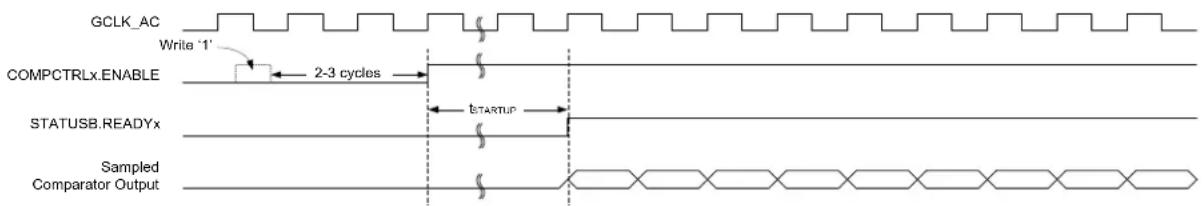
text_image
GCLK_AC Write '1' COMPCTRLx.ENABLE 2-3 cycles STATUSB.READYx Sampled Comparator OutputFor low-power operation, comparisons can be performed during sleep modes without a clock. The comparator is enabled continuously, and changes of the comparator state are detected asynchronously. When a toggle occurs, the Power Manager will start GCLK_AC to register the appropriate peripheral events and interrupts. The GCLK_AC clock is then disabled again automatically, unless configured to wake up the system from sleep.
41.6.2.4.2 Single-Shot
Single-shot operation is selected by writing COMPCTRLx.SINGLE to '1'. During single-shot operation, the comparator is normally idle. The user starts a single comparison by writing '1' to the respective Start Comparison bit in the write-only Control B register (CTRLB.STARTx). The comparator is enabled, and after the start-up time has passed, a single comparison is done and STATUSA is updated. Appropriate peripheral events and interrupts are also generated. No new comparisons will be performed.
Writing '1' to CTRLB.STARTx also clears the Comparator x Ready bit in the Status B register (STATUSB.READYx). STATUSB.READYx is set automatically by hardware when the single comparison has completed.
A single-shot measurement can also be triggered by the Event System. Setting the Comparator x Event Input bit in the Event Control Register (EVCTRL.COMPEIx) enables triggering on incoming peripheral events. Each comparator can be triggered independently by separate events. Event-triggered operation is similar to user-triggered operation; the difference is that a peripheral event from another hardware module causes the hardware to automatically start the comparison and clear STATUSB.READYx.
To detect an edge of the comparator output in single-shot operation for the purpose of interrupts, the result of the current measurement is compared with the result of the previous measurement (one sampling period earlier). An example of single-shot operation is shown in Figure 41-3.
Figure 41-3. Single-Shot Example

text_image
GCLK_AC Write '1' CTRLB.STARTx 2-3 cycles 2-3 cycles t_STARTUP Write '1' STATUSB.READYx t_STARTUP Sampled Comparator OutputFor low-power operation, event-triggered measurements can be performed during sleep modes. When the event occurs, the Power Manager will start GCLK_AC. The comparator is enabled, and after the startup time has passed, a comparison is done and appropriate peripheral events and interrupts are also generated. The comparator and GCLK_AC are then disabled again automatically, unless configured to wake up the system from sleep.
41.6.3 Selecting Comparator Inputs
Each comparator has one positive and one negative input. The positive input is one of the external input pins (AlNx). The negative input can be fed either from an external input pin (AlNx) or from one of the several internal reference voltage sources common to all comparators. The user selects the input source as follows:
- The positive input is selected by the Positive Input MUX Select bit group in the Comparator Control register (COMPCTRLx.MUXPOS)
- The negative input is selected by the Negative Input MUX Select bit group in the Comparator Control register (COMPCTRLx.MUXNEG)
In the case of using an external I/O pin, the selected pin must be configured for analog use in the PORT Controller by disabling the digital input and output. The switching of the analog input multiplexers is controlled to minimize crosstalk between the channels. The input selection must be changed only while the individual comparator is disabled.
Note: For internal use of the comparison results by the CCL, this bit must be 0x1 or 0x2.
41.6.4 Window Operation
Each comparator pair can be configured to work together in window mode. In this mode, a voltage range is defined, and the comparators give information about whether an input signal is within this range or not. Window mode is enabled by the Window Enable x bit in the Window Control register (WINCTRL.WENx). Both comparators in a pair must have the same measurement mode setting in their respective Comparator Control Registers (COMPCTRLx.SINGLE).
To physically configure the pair of comparators for window mode, the same I/O pin must be chosen as positive input for each comparator, providing a shared input signal. The negative inputs define the range for the window. In Figure 41-4, COMP0 defines the upper limit and COMP1 defines the lower limit of the window, as shown but the window will also work in the opposite configuration with COMP0 lower and COMP1 higher. The current state of the window function is available in the Window x State bit group of the Status register (STATUS.WSTATEx).
Window mode can be configured to generate interrupts when the input voltage changes to below the window, when the input voltage changes to above the window, when the input voltage changes into the window or when the input voltage changes outside the window. The interrupt selections are set by the Window Interrupt Selection bit field in the Window Control register (WINCTRL.WINTSEL). Events are generated using the inside/outside state of the window, regardless of whether the
interrupt is enabled or not. Note that the individual comparator outputs, interrupts and events continue to function normally during window mode.
When the comparators are configured for window mode and single-shot mode, measurements are performed simultaneously on both comparators. Writing '1' to either Start Comparison bit in the Control B register (CTRLB.STARTx) will start a measurement. Likewise either peripheral event can start a measurement.
Figure 41-4. Comparators in Window Mode
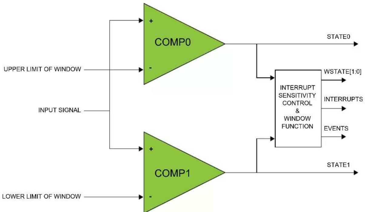
flowchart
graph TD
    A["UPPER LIMIT OF WINDOW"] --> B["COMP0"]
    C["INPUT SIGNAL"] --> D["COMP1"]
    E["LOWER LIMIT OF WINDOW"] --> F["COMP1"]
    B --> G["STATE0"]
    D --> H["INTERRUPT SENSITIVITY CONTROL & WINDOW FUNCTION"]
    F --> I["STATE1"]
    G --> J["WSTATE[1:0"]]
    H --> K["INTERRUPTS"]
    H --> L["EVENTS"]
41.6.5 VDD Scaler
The VDD scaler generates a reference voltage, that is a fraction of the device's supply voltage with 64 levels. One independent voltage channel is dedicated for each comparator. The scaler of a comparator is enabled when the Negative Input Mux bit field or the Positive Input Mux in the respective Comparator Control register (COMPCTRLx.MUXNEG or COMPCTRLx.MUXPOS) is set to 0x5 for Negative Input or 0x4 for Positive Input and the comparator is enabled. The voltage of each channel is selected by the Value bit field in the Scaler x registers (SCALERx.VALUE).
Figure 41-5. VDD Scaler

text_image
COMPCTRLx.MUXNEG==5 or COMPCTRLx.MUXPOS==4 SCALERx. VALUE 6 To COMPx41.6.6 Input Hysteresis
Application software can selectively enable/disable hysteresis for the comparison. Applying hysteresis will help prevent constant toggling of the output, which can be caused by noise when the input signals are close to each other.
Hysteresis is enabled for each comparator individually by the Hysteresis Enable bit in the Comparator x Control register (COMPCTRLx.HYSTEN). Furthermore, when enabled, the level of hysteresis is programmable through the Hysteresis Level bits also in the Comparator x Control register (COMPCTRLx.HYST). Hysteresis is available only in continuous mode (COMPCTRLx.SINGLE=0).
41.6.7 Propagation Delay vs. Power Consumption
It is possible to trade off comparison speed for power efficiency to get the shortest possible propagation delay or the lowest power consumption. The speed setting is configured for each comparator individually by the Speed bit group in the Comparator x Control register (COMPCTRLx.SPEED). The Speed bits select the amount of bias current provided to the comparator, and as such will also affect the start-up time.
41.6.8 Filtering
The output of the comparators can be filtered digitally to reduce noise. The filtering is determined by the Filter Length bits in the Comparator Control x register (COMPCTRLx.FLEN), and is independent for each comparator. Filtering is selectable from none, 3-bit majority (N=3) or 5-bit majority (N=5) functions. Any change in the comparator output is considered valid only if N/2+1 out of the last N samples agree. The filter sampling rate is the GCLK_AC frequency.
Note that filtering creates an additional delay of N-1 sampling cycles from when a comparison is started until the comparator output is validated. For continuous mode, the first valid output will occur when the required number of filter samples is taken. Subsequent outputs will be generated every cycle based on the current sample plus the previous N-1 samples, as shown in Figure 41-6. For single-shot mode, the comparison completes after the Nth filter sample, as shown in Figure 41-7.
Figure 41-6. Continuous Mode Filtering
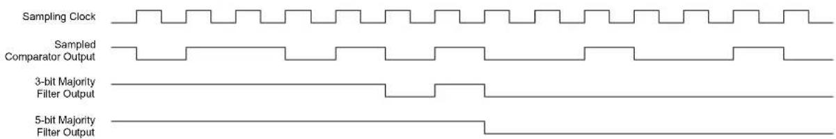
text_image
Sampling Clock Sampled Comparator Output 3-bit Majority Filter Output 5-bit Majority Filter OutputFigure 41-7. Single-Shot Filtering
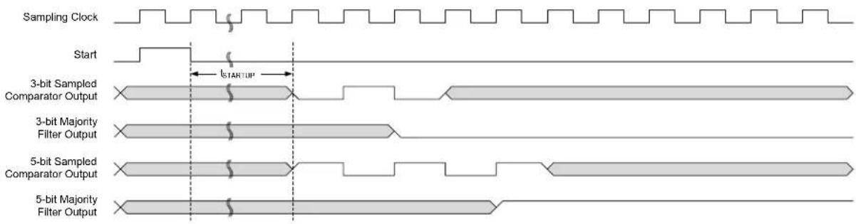
text_image
Sampling Clock Start 3-bit Sampled Comparator Output 3-bit Majority Filter Output 5-bit Sampled Comparator Output 5-bit Majority Filter OutputDuring sleep modes, filtering is supported only for single-shot measurements. Filtering must be disabled if continuous measurements will be done during sleep modes, or the resulting interrupt/event may be generated incorrectly.
41.6.9 Comparator Output
The output of each comparator can be routed to an I/O pin by setting the Output bit group in the Comparator Control x register (COMPCTRLx.OUT). This allows the comparator to be used by external circuitry. Either the raw, non-synchronized output of the comparator or the CLK_AC-synchronized version, including filtering, can be used as the I/O signal source. The output appears on the corresponding CMP[x] pin.
41.6.10 Offset Compensation
The Swap bit in the Comparator Control registers (COMPCTRLx.SWAP) controls switching of the input signals to a comparator's positive and negative terminals. When the comparator terminals are swapped, the output signal from the comparator is also inverted, as shown in Figure 41-8. This allows the user to measure or compensate for the comparator input offset voltage. As part of the input selection, COMPCTRLx.SWAP can be changed only while the comparator is disabled.
Figure 41-8. Input Swapping for Offset Compensation

flowchart
graph TD
    A["Input"] --> B["MUXPOS"]
    C["Input"] --> D["MUXNEG"]
    B --> E["Switch"]
    D --> F["Switch"]
    E --> G["COMPx"]
    F --> G
    G --> H["HYSTERESIS"]
    H --> I["Output"]
    J["COMPCTRLx"] --> K["SWAP"]
    K --> L["SWAP"]
    L --> G
    G --> M["Enable"]
    M --> N["SWAP"]
41.6.11 DMA Operation
Not applicable.
41.6.12 Interrupts
The AC has the following interrupt sources:
- Comparator (COMP0, COMP1): Indicates a change in comparator status.
- Window (WIN0): Indicates a change in the window status.
Comparator interrupts are generated based on the conditions selected by the Interrupt Selection bit group in the Comparator Control registers (COMPCTRL.INTSEL). Window interrupts are generated based on the conditions selected by the Window Interrupt Selection bit group in the Window Control register (WINCTRL.WINTSEL0).
Each interrupt source has an interrupt flag associated with it. The interrupt flag in the Interrupt Flag Status and Clear (INTFLAG) register is set when the interrupt condition occurs. Each interrupt can be individually enabled by writing a one to the corresponding bit in the Interrupt Enable Set (INTENSET) register, and disabled by writing a one to the corresponding bit in the Interrupt Enable Clear (INTENCLR) register. An interrupt request is generated when the interrupt flag is set and the corresponding interrupt is enabled. The interrupt request remains active until the interrupt flag is cleared, the interrupt is disabled, or the AC is reset. See INFLAG register for details on how to clear interrupt flags. All interrupt requests from the peripheral are ORed together on system level to generate one combined interrupt request to the NVIC. The user must read the INTFLAG register to determine which interrupt condition is present.
Note that interrupts must be globally enabled for interrupt requests to be generated.
41.6.13 Events
The AC can generate the following output events:
- Comparator (COMP0, COMP1): Generated as a copy of the comparator status
- Window (WIN0): Generated as a copy of the window inside/outside status
Writing a one to an Event Output bit in the Event Control Register (EVCTRL.xxEO) enables the corresponding output event. Writing a zero to this bit disables the corresponding output event. Refer to the Event System chapter for details on configuring the event system.
The AC can take the following action on an input event:
- Start comparison (START0, START1): Start a comparison.
Writing a one to an Event Input bit into the Event Control register (EVCTRL.COMPEIx) enables the corresponding action on input event. Writing a zero to this bit disables the corresponding action on input event. Note that if several events are connected to the AC, the enabled action will be taken on any of the incoming events. Refer to the Event System chapter for details on configuring the event system.
When EVCTRL.COMPEIx is one, the event will start a comparison on COMPx after the start-up time delay. In normal mode, each comparator responds to its corresponding input event independently. For a pair of comparators in window mode, either comparator event will trigger a comparison on both comparators simultaneously.
41.6.14 Sleep Mode Operation
The Run in Standby bits in the Comparator x Control registers (COMPCTRLx.RUNSTDBY) control the behavior of the AC during standby sleep mode. Each RUNSTDBY bit controls one comparator. When the bit is zero, the comparator is disabled during sleep, but maintains its current configuration. When the bit is one, the comparator continues to operate during sleep. Note that when RUNSTDBY is zero, the analog blocks are powered off for the lowest power consumption. This necessitates a start-up time delay when the system returns from sleep.
For Window Mode operation, both comparators in a pair must have the same RUNSTDBY configuration.
When RUNSTDBY is one, any enabled AC interrupt source can wake up the CPU. The AC can also be used during sleep modes where the clock used by the AC is disabled, provided that the AC is still powered (not in shutdown). In this case, the behavior is slightly different and depends on the measurement mode, as listed in Table 41-1.
Table 41-1. Sleep Mode Operation
| COMPCTRLx.MODE RUNSTDBY=0 RUNSTDBY=1 |
| 0 (Continuous) COMPx disabled GCLK_AC stopped, COMPx enabled |
| 1 (Single-shot) COMPx disabled GCLK_AC stopped, COMPx enabled only when triggered by an input event |
41.6.14.1 Continuous Measurement during Sleep
When a comparator is enabled in continuous measurement mode and GCLK_AC is disabled during sleep, the comparator will remain continuously enabled and will function asynchronously. The current state of the comparator is asynchronously monitored for changes. If an edge matching the interrupt condition is found, GCLK_AC is started to register the interrupt condition and generate events. If the interrupt is enabled in the Interrupt Enable registers (INTENCLR/SET), the AC can wake up the device; otherwise GCLK_AC is disabled until the next edge detection. Filtering is not possible with this configuration.
Figure 41-9. Continuous Mode SleepWalking

text_image
GCLK_AC Write '1' COMPCTRLX.ENABLE 2-3 cycles STATUSB.READYx t_STARTUP Sampled Comparator Output41.6.14.2 Single-Shot Measurement during Sleep
For low-power operation, event-triggered measurements can be performed during sleep modes. When the event occurs, the Power Manager will start GCLK_AC. The comparator is enabled, and after the start-up time has passed, a comparison is done, with filtering if desired, and the appropriate peripheral events and interrupts are also generated, as shown in Figure 41-10. The comparator and GCLK_AC are then disabled again automatically, unless configured to wake the system from sleep. Filtering is allowed with this configuration.
Figure 41-10. Single-Shot SleepWalking

text_image
GCLK_AC Input Event Comparator Output or Event41.6.15 Synchronization
Due to asynchronicity between the main clock domain and the peripheral clock domains, some registers need to be synchronized when written or read.
The following bits are synchronized when written:
- Software Reset bit in control register (CTRLA.SWRST)
- Enable bit in control register (CTRLA.ENABLE)
- Enable bit in Comparator Control register (COMPCTRLn.ENABLE)
The following registers are synchronized when written: - Window Control register (WINCTRL)
Required write-synchronization is denoted by the "Write-Synchronized" property in the register description.
41.7 Register Summary
| Offset | Name Bit Pos. 76543210 | ||||||||||
| 0x00 | CTRLA 7:0 | ENABLE SWRST | |||||||||
| 0x01 | CTRLB 7:0 | START1 START0 | |||||||||
| 0x02 | EVCTRL | 7:0 | WINEO0 | COMPEO1 | COMPEO0 | ||||||
| 15:8 | INVEI1 | INVEIO | COMPEI1 | COMPEIO | |||||||
| 0x04 | INTENCLR | 7:0 | WINO | COMP1 | COMP0 | ||||||
| 0x05 | INTENSET | 7:0 | WINO | COMP1 | COMP0 | ||||||
| 0x06 | INTFLAG | 7:0 | WINO | COMP1 | COMP0 | ||||||
| 0x07 | STATUS | 7:0 | WSTATEO[1:0] | STATE1 | STATE0 | ||||||
| 0x08 | STATUS | 7:0 | READY1 | READY0 | |||||||
| 0x09 | DBGCTRL | 7:0 | DBGRUN | ||||||||
| 0x0A | WINCTRL | 7:0 | WINTSEL0[1:0] | WENO | |||||||
| 0x0B | Reserved | ||||||||||
| 0x0C | SCALER0 7:0 | VALUE[5:0] | |||||||||
| 0x0D | SCALER1 | 7:0 | VALUE[5:0] | ||||||||
| 0x0E ... 0x0F | Reserved | ||||||||||
| 0x10 | COMPCTRL0 | 7:0 | RUNSTDBY | INTSEL[1:0] | SINGLE | ENABLE | |||||
| 15:8 | SWAP | MUXPOS[2:0] | MUXNEG[2:0] | ||||||||
| 23:16 | HYST[1:0] | HYSTEN | SPEED[1:0] | ||||||||
| 31:24 | OUT[1:0] | FLEN[2:0] | |||||||||
| 0x14 | COMPCTRL1 | 7:0 | RUNSTDBY | INTSEL[1:0] | SINGLE | ENABLE | |||||
| 15:8 | SWAP | MUXPOS[2:0] | MUXNEG[2:0] | ||||||||
| 23:16 | HYST[1:0] | HYSTEN | SPEED[1:0] | ||||||||
| 0x18 ... 0x1F | Reserved | ||||||||||
| 0x20 | SYNCBUSY | 7:0 | COMPCTRL1 | COMPCTRL0 | WINCTRL | ENABLE | SWRST | ||||
| 15:8 | |||||||||||
| 23:16 | |||||||||||
| 31:24 | |||||||||||
41.8 Register Description
Registers can be 8, 16, or 32 bits wide. Atomic 8-, 16-, and 32-bit accesses are supported. In addition, the 8-bit quarters and 16-bit halves of a 32-bit register, and the 8-bit halves of a 16-bit register can be accessed directly.
Some registers require synchronization when read and/or written. Synchronization is denoted by the "Read-Synchronized" and/or "Write-Synchronized" property in each individual register description.
Optional write-protection by the Peripheral Access Controller (PAC) is denoted by the "PAC Write-Protection" property in each individual register description.
Some registers are enable-protected, meaning they can only be written when the module is disabled. Enable-protection is denoted by the "Enable-Protected" property in each individual register description
Refer to PAC - Peripheral Access Controller and 36.6.6. Synchronization for details.
41.8.1 Control A
Name: CTRLA
Offset: 0x00
Reset: 0x00
Property: PAC Write-Protection, Write-Synchronized
Bit 76543210
| ENABLE SWRST | ||||||
| Access Reset 0 0 | R/W W | |||||
Bit 1 - ENABLE Enable
Due to synchronization, there is delay from updating the register until the peripheral is enabled/ disabled. The value written to CTRL. ENABLE will read back immediately and the corresponding bit in the Synchronization Busy register (SYNCBUSY. ENABLE) will be set. SYNCBUSY. ENABLE is cleared when the peripheral is enabled/disabled.
| Value Description | |
| 0 | The AC is disabled. |
| 1 | The AC is enabled. Each comparator must also be enabled individually by the Enable bit in the Comparator Control register (COMPCTRLn.ENABLE). |
Bit 0 - SWRST Software Reset
Writing a '0' to this bit has no effect.
Writing a '1' to this bit resets all registers in the AC to their initial state, and the AC will be disabled. Writing a '1' to CTRLA.SWRST will always take precedence, meaning that all other writes in the same write-operation will be discarded.
Due to synchronization, there is a delay from writing CTRLA.SWRST until the reset is complete. CTRLA.SWRST and SYNCBUSY.SWRST will both be cleared when the reset is complete.
| Value Description | |
| 0 | There is no reset operation ongoing. |
| 1 | The reset operation is ongoing. |
41.8.2 Control B
Name: CTRLB
Offset: 0x01
Reset: 0x00
Property: PAC Write-Protection, Write-Synchronized
Bit 76543210
| $START1 START0 | ||||||
| Access Reset 0 0 | R/W R/W | |||||
Bits 0, 1 - STARTx Comparator x Start Comparison
Writing a '0' to this field has no effect.
Writing a '1' to STARTx starts a single-shot comparison on COMPx if both the Single-Shot and Enable bits in the Comparator x Control Register are '1' (COMPCTRLx.SINGLE and COMPCTRLx.ENABLE). If comparator x is not implemented, or if it is not enabled in single-shot mode, Writing a '1' has no effect.
This bit always reads as zero.
41.8.3 Event Control
Name: EVCTRL
Offset: 0x02
Reset: 0x0000
Property: PAC Write-Protection, Enable-Protected
Bit 15 14 13 12 11 10 9 8
| INVE1 | INVE0 | COMPE1 | COMPE0 | |||||
| Access Reset | R/W0 0 | R/W | R/W0 0 |
Bit 76543210
| WINEO0 | COMPEO1 | COMPEO0 | |||||
| Access | R/W | R/W | R/W | ||||
| Reset | 0 | 0 0 |
Bits 12, 13 - INVEIx Inverted Event Input Enable x
| Value | Description |
| 0 | Incoming event is not inverted for comparator x. |
| 1 | Incoming event is inverted for comparator x. |
Bits 8, 9 - COMPEIX Comparator x Event Input
Note that several actions can be enabled for incoming events. If several events are connected to the peripheral, the enabled action will be taken for any of the incoming events. There is no way to tell which of the incoming events caused the action.
These bits indicate whether a comparison will start or not on any incoming event.
| Value | Description |
| 0 | Comparison will not start on any incoming event. |
| 1 | Comparison will start on any incoming event. |
Bit 4 - WINEO0 Window 0 Event Output Enable
These bits indicate whether the window 0 function can generate a peripheral event or not.
| Value | Description |
| 0 | Window 0 Event is disabled. |
| 1 | Window 0 Event is enabled. |
Bits 0, 1 - COMPEOx Comparator x Event Output Enable
These bits indicate whether the comparator x output can generate a peripheral event or not.
| Value | Description |
| 0 | COMPx event generation is disabled. |
| 1 | COMPx event generation is enabled. |
41.8.4 Interrupt Enable Clear
Name: INTENCLR
Offset: 0x04
Reset: 0x00
Property: PAC Write-Protection
This register allows the user to disable an interrupt without doing a read-modify-write operation. Changes in this register will also be reflected in the Interrupt Enable Set register (INTENSET).
Bit 76543210
| WIN0 | COMP1 | COMPO | ||||||
| Access Reset | R/W | R/W | R/W | |||||
| 0 | 0 0 |
Bit 4 - WIN0 Window 0 Interrupt Enable
Reading this bit returns the state of the Window 0 interrupt enable.
Writing a '0' to this bit has no effect.
Writing a '1' to this bit disables the Window 0 interrupt.
| Value | Description |
| 0 | The Window 0 interrupt is disabled. |
| 1 | The Window 0 interrupt is enabled. |
Bits 0, 1 - COMPx Comparator x Interrupt Enable
Reading this bit returns the state of the Comparator x interrupt enable.
Writing a '0' to this bit has no effect.
Writing a '1' to this bit disables the Comparator x interrupt.
| Value | Description |
| 0 | The Comparator x interrupt is disabled. |
| 1 | The Comparator x interrupt is enabled. |
41.8.5 Interrupt Enable Set
Name: INTENSET
Offset: 0x05
Reset: 0x00
Property: PAC Write-Protection
This register allows the user to enable an interrupt without doing a read-modify-write operation. Changes in this register will also be reflected in the Interrupt Enable Clear register (INTENCLR).
Bit 76543210
| WIN0 | COMP1 | COMPO | ||||||
| Access Reset | R/W | R/W | R/W | |||||
| 0 | 0 0 |
Bit 4 - WIN0 Window 0 Interrupt Enable
Reading this bit returns the state of the Window 0 interrupt enable.
Writing a '0' to this bit has no effect.
Writing a '1' to this bit enables the Window 0 interrupt.
| Value | Description |
| 0 | The Window 0 interrupt is disabled. |
| 1 | The Window 0 interrupt is enabled. |
Bits 0, 1 - COMPx Comparator x Interrupt Enable
Reading this bit returns the state of the Comparator x interrupt enable.
Writing a '0' to this bit has no effect.
Writing a '1' to this bit will set the Ready interrupt bit and enable the Ready interrupt.
| Value | Description |
| 0 | The Comparator x interrupt is disabled. |
| 1 | The Comparator x interrupt is enabled. |
41.8.6 Interrupt Flag Status and Clear
Name: INTFLAG
Offset: 0x06
Reset: 0x00
Property: -
Bit 76543210
| WIN0 | COMP1 | COMP0 | ||||||
| Access Reset | R/W | R/W | R/W | |||||
| 0 | 0 0 |
Bit 4 - WIN0 Window 0
This flag is set according to the Window 0 Interrupt Selection bit group in the WINCTRL register (WINCTRL.WINTSELx) and will generate an interrupt if INTENCLR/SET.WINx is also one.
Writing a '0' to this bit has no effect.
Writing a '1' to this bit clears the Window 0 interrupt flag.
Bits 0, 1 - COMPx Comparator x
Reading this bit returns the status of the Comparator x interrupt flag. If comparator x is not implemented, COMPx always reads as zero.
This flag is set according to the Interrupt Selection bit group in the Comparator x Control register (COMPCTRLx.INTSEL) and will generate an interrupt if INTENCLR/SET.COMPx is also one.
Writing a '0' to this bit has no effect.
Writing a '1' to this bit clears the Comparator x interrupt flag.
41.8.7 Status A
Name: STATUSA
Offset: 0x07
Reset: 0x00
Property: Read-Only
Bit 76543210
| WSTATE0[1:0] | STATE1 | STATE0 | |||||
| Access Reset | RRRR | ||||||
| 00 | 00 |
Bits 5:4 - WSTATE0[1:0] Window 0 Current State
These bits show the current state of the signal if the window 0 mode is enabled.
| Value | Name | Description |
| 0x0 | ABOVE | Signal is above window |
| 0x1 | INSIDE | Signal is inside window |
| 0x2 | BELOW | Signal is below window |
| 0x3 | Reserved |
Bits 0, 1 - STATEx Comparator x Current State
This bit shows the current state of the output signal from COMPx. STATEx is valid only when STATUSB.READYx is one.
41.8.8 Status B
Name: STATUSB
Offset: 0x08
Reset: 0x00
Property: Read-Only
Bit 76543210
| READY1 READY0 | ||||||
| Access Reset 0 0 | R | R | ||||
Bits 0, 1 - READYx Comparator x Ready
This bit is cleared when the comparator x output is not ready.
This bit is set when the comparator x output is ready.
41.8.9 Debug Control
Name: DBGCTRL
Offset: 0x09
Reset: 0x00
Property: PAC Write-Protection
Bit 76543210
| DBGRUN | |||||||
| Access Reset 0 | R/W | ||||||
Bit 0 - DBGRUN Debug Run
This bit is not reset by a software reset.
This bits controls the functionality when the CPU is halted by an external debugger.
| Value Description | |
| 0 | The AC is halted when the CPU is halted by an external debugger. Any on-going comparison will complete. |
| 1 | The AC continues normal operation when the CPU is halted by an external debugger. |
41.8.10 Window Control
Name: WINCTRL
Offset: 0x0A
Reset: 0x00
Property: PAC Write-Protection, Write-Synchronized
Bit 76543210
| WINTSELO[1:0] WENO | |||||
| Access Reset 0 0 0 | R/W R/W R/W | ||||
Bits 2:1 - WINTSEL0[1:0] Window 0 Interrupt Selection
These bits configure the interrupt mode for the comparator window 0 mode.
| Value Name | Description | |
| 0x0 | ABOVE | Interrupt on signal above window |
| 0x1 | INSIDE | Interrupt on signal inside window |
| 0x2 | BELOW | Interrupt on signal below window |
| 0x3 | OUTSIDE | Interrupt on signal outside window |
Bit 0 - WENO Window 0 Mode Enable
| Value Description | |
| 0 | Window mode is disabled for comparators 0 and 1. |
| 1 | Window mode is enabled for comparators 0 and 1. |
41.8.11 Scaler n
Name: SCALERn
Offset: 0x0C + n*0x01 [n=0..1]
Reset: 0x00
Property: PAC Write-Protection
Bit 76543210
| VALUE[5:0] | |
| Access Reset 0 0 0 0 0 0 | R/W R/W R/W R/W R/W R/W |
Bits 5:0 - VALUE[5:0] Scaler Value
These bits define the scaling factor for channel n of the V_DD voltage scaler. The output voltage, V_SCALE , is:
$$ V _ {\mathrm{SCALE}} = \frac {V _ {\mathrm{DD}} \cdot (\text { VALUE } + 1)}{6 4} $$
41.8.12 Comparator Control n
Name: COMPCTRLn
Offset: 0x10 + n*0x04 [n=0..1]
Reset: 0x00000000
Property: PAC Write-Protection, Write-Synchronized
Bit 31 30 29 28 27 26 25 24
| OUT[1:0] FLEN[2:0] | |||||
| Access Reset | R/W 0 | R/W 0 | R/W 0 | R/W 0 | R/W 0 |
Bit 23 22 21 20 19 18 17 16
| HYST[1:0] | HYSTEN | SPEED[1:0] | |||||
| Access Reset | R/W | R/W | R/W | R/W | |||
| 0 | 0 | 0 | 0 | 0 | |||
Bit 15 14 13 12 11 10 9 8
| SWAP | MUXPOS[2:0] | MUXNEG[2:0] | ||||||
| Access Reset | R/W R/W | R/W | R/W | R/W R/W | ||||
| 0 | 0 | 0 | 0 | 0 | 0 | 0 | ||
| Bit | 7 | 6 | 5 | 4 | 3 | 2 | 1 | 0 |
| RUNSTDBY | INTSEL[1:0] | SINGLE | ENABLE | |||||
| Access Reset | R/W R/W | R/W R/W R/W | ||||||
| 0 | 0 | 0 | 0 | 0 | ||||
Bits 29:28 - OUT[1:0] Output
These bits configure the output selection for comparator n. COMPCTRLn.OUT can be written only while COMPCTRLn.ENABLE is zero.
Note: For internal use of the comparison results by the CCL, this bit must be 0x1 or 0x2.
These bits are not synchronized.
| Value | Name | Description |
| 0x0 | OFF | The output of COMPn is not routed to the COMPn I/O port |
| 0x1 | ASYNC | The asynchronous output of COMPn is routed to the COMPn I/O port |
| 0x2 | SYNC | The synchronous output (including filtering) of COMPn is routed to the COMPn I/O port |
| 0x3 | N/A Reserved | |
Bits 26:24 - FLEN[2:0] Filter Length
These bits configure the filtering for comparator n. COMPCTRLn.FLEN can only be written while COMPCTRLn.ENABLE is zero.
These bits are not synchronized.
| Value | Name | Description |
| 0x0 | OFF | No filtering |
| 0x1 | MAJ3 | 3-bit majority function (2 of 3) |
| 0x2 | MAJ5 | 5-bit majority function (3 of 5) |
| 0x3-0x7 | N/A | Reserved |
Bits 21:20 - HYST[1:0] Hysteresis Level
These bits indicate the hysteresis level of comparator n when hysteresis is enabled (COMPCTRLn.HYSTEN=1). Hysteresis is available only for continuous mode (COMPCTRLn.SINGLE=0). COMPCTRLn.HYST can be written only while COMPCTRLn.ENABLE is zero.
These bits are not synchronized.
| Value Name | Description | |
| 0x0 | HYST50 50mV | |
| 0x1 | HYST70 70mV | |
| 0x2 | HYST90 90mV | |
| 0x3 | HYST110 110mV |
Bit 19 - HYSTEN Hysteresis Enable
This bit indicates the hysteresis mode of comparator n. Hysteresis is available only for continuous mode (COMPCTRLn.SINGLE=0). COMPCTRLn.HYST can be written only while COMPCTRLn.ENABLE is zero.
This bit is not synchronized.
| Value Description | |
| 0 | Hysteresis is disabled. |
| 1 | Hysteresis is enabled. |
Bits 17:16 - SPEED[1:0] Speed Selection
This bit indicates the speed/propagation delay mode of comparator n. COMPCTRLn.SPEED can be written only while COMPCTRLn. ENABLE is zero.
These bits are not synchronized.
| Value Name Description | ||
| 0x0 LOW Low speed | ||
| 0x1 MEDLOW Medium low speed | ||
| 0x2 MEDHIGH Medium high speed | ||
| 0x3 HIGH High speed |
Bit 15 - SWAP Swap Inputs and Invert
This bit swaps the positive and negative inputs to COMPn and inverts the output. This function can be used for offset cancellation. COMPCTRLn.SWAP can be written only while COMPCTRLn.ENABLE is zero.
These bits are not synchronized.
| Value Description | |
| 0 | The output of MUXPOS connects to the positive input, and the output of MUXNEG connects to the negative input. |
| 1 | The output of MUXNEG connects to the positive input, and the output of MUXPOS connects to the negative input. |
Bits 14:12 - MUXPOS[2:0] Positive Input Mux Selection
These bits select which input will be connected to the positive input of comparator n.
COMPCTRLn.MUXPOS can be written only while COMPCTRLn.ENABLE is zero.
These bits are not synchronized.
| Value Name | Description | |
| 0x0 | PIN0 I/O pin 0 | |
| 0x1 | PIN1 I/O pin 1 | |
| 0x2 | PIN2 I/O pin 2 | |
| 0x3 | PIN3 I/O pin 3 | |
| 0x4 | VSCALE VDD scaler | |
| 0x5-0x7 | - | Reserved |
Bits 10:8 - MUXNEG[2:0] Negative Input Mux Selection
These bits select which input will be connected to the negative input of comparator n.
COMPCTRLn.MUXNEG can only be written while COMPCTRLn.ENABLE is zero.
These bits are not synchronized.
| Value Name | Description | |
| 0x0 | PIN0 | I/O pin 0 |
| 0x1 | PIN1 | I/O pin 1 |
| Value Name | Description | |
| 0x2 | PIN2 I/O pin 2 | |
| 0x3 | PIN3 I/O pin 3 | |
| 0x4 | GND Ground | |
| 0x5 | VSCALE VDD scaler | |
| 0x6 | BANDGAP Internal bandgap voltage | |
| 0x7 | - Reserved | |
Bit 6 - RUNSTDBY Run in Standby
This bit controls the behavior of the comparator during standby sleep mode.
This bit is not synchronized
| Value Description | |
| 0 | The comparator is disabled during sleep. |
| 1 | The comparator continues to operate during sleep. |
Bits 4:3 - INTSEL[1:0] Interrupt Selection
These bits select the condition for comparator n to generate an interrupt or event.
COMPCTRLn.INTSEL can be written only while COMPCTRLn.ENABLE is zero.
These bits are not synchronized.
| Value | Name | Description |
| 0x0 | TOGGLE Interrupt on comparator output toggle | |
| 0x1 | RISING Interrupt on comparator output rising | |
| 0x2 | FALLING Interrupt on comparator output falling | |
| 0x3 | EOC Interrupt on end of comparison (single-shot mode only) | |
Bit 2 - SINGLE Single-Shot Mode
This bit determines the operation of comparator n. COMPCTRLn.SINGLE can be written only while COMPCTRLn.ENABLE is zero.
These bits are not synchronized.
| Value Description | |
| 0 | Comparator n operates in continuous measurement mode. |
| 1 | Comparator n operates in single-shot mode. |
Bit 1 - ENABLE Enable
Writing a zero to this bit disables comparator n.
Writing a one to this bit enables comparator n.
Due to synchronization, there is delay from updating the register until the comparator is enabled/ disabled. The value written to COMPCTRLn. ENABLE will read back immediately after being written. SYNCBUSY.COMPCTRLn is set. SYNCBUSY.COMPCTRLn is cleared when the peripheral is enabled/ disabled.
Writing a one to COMPCTRLn. ENABLE will prevent further changes to the other bits in COMPCTRLn. These bits remain protected until COMPCTRLn. ENABLE is written to zero and the write is synchronized.
41.8.13 Synchronization Busy
Name: SYNCBUSY
Offset: 0x20
Reset: 0x00000000
Property: Read-Only

text_image
Bit 31 30 29 28 27 26 25 24 Access Reset Bit 23 22 21 20 19 18 17 16 Access Reset Bit 15 14 13 12 11 10 9 8 Access Reset Bit 7 6 5 4 3 2 1 0 Access Reset COMPCTRL1 COMPCTRL0 WINCTRL ENABLE SWRST R R R R 0 0 0 0 0Bits 3, 4 - COMPCTRLx COMPCTRLx Synchronization Busy
This bit is cleared when the synchronization of the COMPCTRLx register between the clock domains is complete.
This bit is set when the synchronization of the COMPCTRLx register between clock domains is started.
Bit 2 - WINCTRL WINCTRL Synchronization Busy
This bit is cleared when the synchronization of the WINCTRL register between the clock domains is complete.
This bit is set when the synchronization of the WINCTRL register between clock domains is started.
Bit 1 - ENABLE Enable Synchronization Busy
This bit is cleared when the synchronization of the CTRLA. ENABLE bit between the clock domains is complete.
This bit is set when the synchronization of the CTRLA. ENABLE bit between clock domains is started.
Bit 0 - SWRST Software Reset Synchronization Busy
This bit is cleared when the synchronization of the CTRLA.SWRST bit between the clock domains is complete.
This bit is set when the synchronization of the CTRLA.SWRST bit between clock domains is started.
42. SLCD - Segment Liquid Crystal Display Controller
42.1 Overview
An LCD display is made of several segments (pixels or complete symbols) which can be visible or invisible. A segment has two electrodes with liquid crystal between them. These electrodes are the common terminal (COM pin) and the segment terminal (SEG pin). When a voltage above a threshold voltage is applied across the liquid crystal, the segment becomes visible.
The LCD controller is intended for monochrome passive liquid crystal display (LCD) with up to 8 common terminals and up to 44 segment terminals. A charge pump provides LCD display supply which can be higher than supply voltage of the device. Each LCD pin, segment or common terminals, can be configured as general purpose I/O pins if not driven by LCD controller.
Several features such as character mapping, automated characters string display, autonomous animation are implemented to reduce CPU load and power consumption.
Figure 42-1. LCD Panel - Segment/Common Terminals Connections
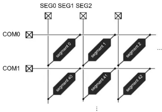
flowchart
graph TD
    A["COM0"] --> B["segment 0"]
    C["COM1"] --> D["segment 40"]
    B --> E["segment 1"]
    D --> F["segment 41"]
    E --> G["segment 2"]
    F --> H["..."]
    G --> I["segment 42"]
    H --> J["..."]
    I --> K["..."]
    L["SEG0 SEG1 SEG2"] --> M["×"]
    L --> N["×"]
    L --> O["×"]
Note: In order to avoid degradation due to electrophoresis in the liquid crystal, the waveform of the voltage across a segment must not have a DC component.
42.2 Features
- Display capacity up to 44 segments lines and up to 8 common lines (up to 320 segments)
- Selection of maximum 48 segment/common lines from 52 LCD pins
• Support from static up to 1/8 duty
• Support static, 1/2, 1/3 and 1/4 bias - Shadow display memory for full freedom in segment update
- LCD pins as segment terminal, common terminal or general purpose I/O
- Blink mode and frequency configuration (up to 16 segments)
- Regular and low power waveform
- Software contrast adjustment control
- On-chip LCD power supply
- Character mapping
- Automated characters string scrolling
- Automated characters string display
- Automated segments display
• Autonomous animation (up to 16 segments)
• Three frame counters for timing schedule
- Interrupt request and event output for display update
- DMA Support
- SleepWalking Support
42.3 Block Diagram
Figure 42-2. SLCD Block Diagram
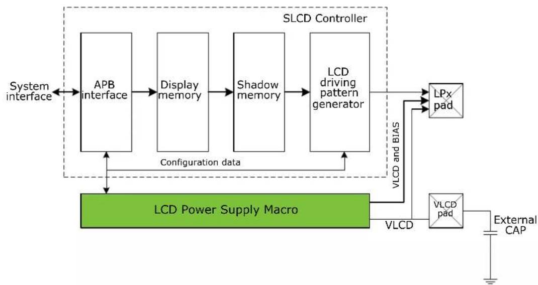
flowchart
graph TD
    A["System interface"] --> B["APB interface"]
    B --> C["Display memory"]
    C --> D["Shadow memory"]
    D --> E["LCD driving pattern generator"]
    E --> F["LPx pad"]
    F --> G["VLCD pad"]
    G --> H["External CAP"]
    I["Configuration data"] --> J["LCD Power Supply Macro"]
    J --> K["VLCD"]
    K --> G
    style I fill:#99ccff,stroke-dasharray: 5 5
    style J fill:#99ccff,stroke-dasharray: 5 5
    style K fill:#99ccff,stroke-dasharray: 5 5
42.4 Signal Description
| Signal Description Type | ||
| LPx LCD Pin x (COM or SEG terminal) Analog output | ||
| VLCD LCD Voltage Analog input or output |
One signal can be mapped to one of several pins.
Related Links
- I/O Multiplexing and Considerations
42.5 Product Dependencies
In order to use this peripheral, other parts of the system must be configured correctly, as described below.
42.5.1 I/O Lines
Using the SLCD I/O lines requires the I/O pins to be configured.
42.5.2 Power Management
The SLCD will continue to operate in any sleep mode where the selected source clock is running. The SLCD interrupts can be used to wake up the device from sleep modes. Events connected to the event system can trigger other operations in the system without exiting sleep modes.
Related Links
- PM - Power Manager
42.5.3 Clocks
The SLCD bus clock (CLK_SLCD_APB) can be enabled and disabled in the Main Clock module MCLK, and the default state of CLK_SLCD_APB can be found in Peripheral Clock Masking section.
A 32.768kHz oscillator clock (CLK_SLCD_OSC) is required to clock the SLCD. This clock must be configured and enabled in the 32KHz oscillator controller (OSC32KCTRL) before using the SLCD.
This oscillator clock is asynchronous to the bus clock (CLK_SLCD_APB). Due to this asynchronicity, writes to certain registers will require synchronization between the clock domains.
Related Links
16.6.2.6. Peripheral Clock Masking
21. OSC32KCTRL - 32.768 kHz Oscillators Controller
21.6.7. SLCD Clock Selection
14.2. Synchronous and Asynchronous Clocks
42.5.4 DMA
The DMA request lines are connected to the DMA Controller (DMAC). Using the SLCD DMA requests requires the DMA Controller to be configured first.
Related Links
- DMAC - Direct Memory Access Controller
42.5.5 Interrupts
The interrupt request line is connected to the interrupt controller. Using the SLCD interrupt(s) requires the interrupt controller to be configured first.
42.5.6 Events
The events are connected to the Event System.
42.5.7 Debug Operation
When the CPU is halted in debug mode the SLCD continues normal operation. If the SLCD is configured in a way that requires it to be periodically serviced by the CPU through interrupts or similar, improper operation or data loss may result during debugging.
42.5.8 Register Access Protection
All registers with write access can be write-protected optionally by the Peripheral Access Controller (PAC), except the following registers:
- Interrupt Flag Status and Clear register (INTFLAG)
- Segments Data Low and High for COMx Line (SDATAL/Hx)
- Indirect Segments Data Access (ISDATA)
• Character Mapping Data (CMDATA)
Optional write protection by the Peripheral Access Controller (PAC) is denoted by the "PAC Write Protection" property in each individual register description.
Write-protection does not apply to accesses through an external debugger.
42.5.9 Analog Connections
The LCD Power Supply Macro provides voltages (VDDLCD, BIAS1, BIAS2, BIAS3) for the LCD pads. Before enabling the peripheral, it must be configured correctly.
Figure 42-3. LCD Power Supply Macro Functional Block Diagram

flowchart
graph TD
    A["VLCD Generator"] -->|Power refresh signal| B["Controller"]
    A -->|Reference refresh signal| C["Resistor String"]
    C --> D["Bias1"]
    C --> E["Bias2"]
    C --> F["Bias3"]
    D --> G["Buffer Array"]
    E --> G
    F --> G
    G --> H["VLCD"]
    style A fill:#f9f,stroke:#333
    style B fill:#ccf,stroke:#333
    style C fill:#cfc,stroke:#333
    style D fill:#fcc,stroke:#333
    style E fill:#fcc,stroke:#333
    style F fill:#fcc,stroke:#333
    style G fill:#cff,stroke:#333
    style H fill:#ffc,stroke:#333
42.6 Functional Description
42.6.1 Basic Operation
42.6.1.1 Initialization
The following bits are enable-protected, meaning that they can only be written when the SLCD is disabled (CTRLA.ENABLE is zero):
- All bits in CTRLA register except SWRST and ENABLE
The following registers are enable-protected:
• Event Control register (EVCTRL)
• LCD Pins Enable registers (LPENL and LPENH) - Blink Configuration register (BCFG)
• Circular Shift Register Configuration register (CSRCFG) - Automated Character Mapping Configuration register (ACMCFG)
- Automated Bit Mapping Configuration register (ABMCFG)
The following registers are also enable-protected according their corresponding enable bit:
- Frame Counter 0 register (FC0) enabled-protected by Frame Counter 0 Enable (CTRLD.FC0EN)
• Frame Counter 1 register (FC1) enabled-protected by Frame Counter 1 Enable (CTRLD.FC1EN)
• Frame Counter 2 register (FC2) enabled-protected by Frame Counter 2 Enable (CTRLD.FC2EN)
Enable-protected bits in the CTRLA register can be written at the same time as CTRLA. ENABLE is written to '1', but not at the same time as CTRLA. ENABLE is written to '0'.
Enable-protection is denoted by the Enable-Protected property in the register description.
42.6.1.2 Enabling, Disabling, and Resetting
The SLCD is enabled by writing a '1' to the Enable bit in the Control A register (CTRLA.ENABLE). The SLCD is disabled by writing a '0' to CTRLA.ENABLE. To stop driving the LCD panel properly, SLCD will be disabled after the current frame is completed. The Enable bit in the Synchronization Busy register (SYNCBUSY.ENABLE) will thus be cleared at the end of the frame.
The SLCD is reset by writing a '1' to the Software Reset bit in the Control A register (CTRLA.SWRST). All registers in the SLCD will be reset to their initial state, and the SLCD will be disabled.
Software reset will stop waveforms generation of the current frame. For this reason it is recommended to disable SLCD first.
42.6.1.3 LCD Display
The display memory stores the values of all segments to display. The display memory is accessible through APB, and should be filled before the next frame starts. A start of a new frame triggers copying the display memory into the shadow display memory. A display memory refresh is thus possible without affecting data already sent to the panel.
Note: The display memory is not initialized at startup.
When a bit in the display memory is written to '1', the corresponding segment will be energized (ON / opaque), and de-energized (OFF / transparent) when this bit is written to '0'.
Each COM signal has identical waveforms but different phases. The maximum amplitude (VLCD) occurs during the corresponding phase of the frame (phase 0 for COM0, phase 1 for COM1 etc.). Otherwise, the signal amplitude is one of the bias voltages (depending on the bias setting).
The SEG lines are controlled according to the corresponding value in shadow display memory. For each phase of the frame, SEG lines are driven to VLCD and GND when the pixel is ON, or to one of the bias voltages when the pixel is OFF.
42.6.1.4 Operating Modes
SLCD supports up to eight COM and up to three bias voltages. The multiplexing and bias configurations are set independently by writing to the Duty Ratio bits and to the Bias Setting bits in Control A register (CTRLA.DUTY and CTRLA.BIAS, respectively). CTRLA.DUTY defines the number of COM lines used (NB_COM), as shown in the table below, and thus the number of phases.
Table 42-1. Duty Selection (CTRLA.DUTY)
| DUTY[2:0] Duty (NB_COM) Recommended Bias COM Pins | |||
| 0x0 1 Static COM0 | |||
| 0x1 2 1/2 COM0..1 | |||
| 0x2 3 1/3 COM0..2 | |||
| 0x3 4 1/3 COM0..3 | |||
| 0x4 6 1/3 COM0..5 | |||
| 0x5 8 1/4 COM0..7 | |||
The CTRLA.BIAS[1:0] bit field defines the number of bias voltage:
Table 42-2. Bias Selection (CTRLA.BIAS)
| BIAS[1:0] Description | |
| 00 Static | |
| 01 1/2 | |
| 10 1/3 | |
| 11 1/4 |
The LCD controller will drive different waveforms according to the different bias configurations. The LCD controller supports two types of driving waveform, bit-inversion (type A, standard) or frame-inversion (type B, low-power). The frame-inversion mode has a lower switching frequency than the bit-inversion mode, and thus reduced power consumption comparing to standard waveform. Both waveform modes have the same period, and their DC-component is null.
By default the low-power waveforms mode is enabled. To select frame-inversion mode, write a zero in the Waveform Mode bit in Control A register (CTRLA.WMOD). To select bit-inversion mode, write a '1' to CTRLA.WMOD.
The following section illustrates how the SLCD controller drives different LCD panels.
For static bias, standard and low-power waveform are identical. However, for 1/2, 1/3 and 1/4 bias, low-power waveform provides a lower toggle rate comparing to the standard waveform.
Figure 42-4. Static Bias Waveform template

text_image
Voltage Level Definition V1 : VLCD V0 : 0 SEG Waveform Template COM Waveform Template COM Pixel V1 —— Select Waveform V0 —— Pixel SEG Pixel V1 —— On Waveform V0 —— Pixel On V1 —— V0 —— -V1 —— SEG Pixel Off V1 —— Off Waveform V0 —— Pixel Off V1 —— V0 —— -V1 ——Figure 42-5. Static Bias and Duty Waveform

text_image
Frame SEG0 V1 V0 SEG1 V1 V0 COM0 V3 V0 On V1 V0 -V1 V1 V0 -V1 FrameFigure 42-6. 1/2 Bias Waveform Template

other
Voltage Level Definition V2: VLCD V1: VLCD * (1/2) V0: 0 SEG Waveform Template COM Waveform Template Select Waveform V2 V1 V0 Pixel V2 V1 V0 PixelOff V2 V1 V0 -V1 -V2 PixelOff V2 V1 V0 -V1 -V2Figure 42-7. 1/2 bias, 1/2 Duty Standard Waveform
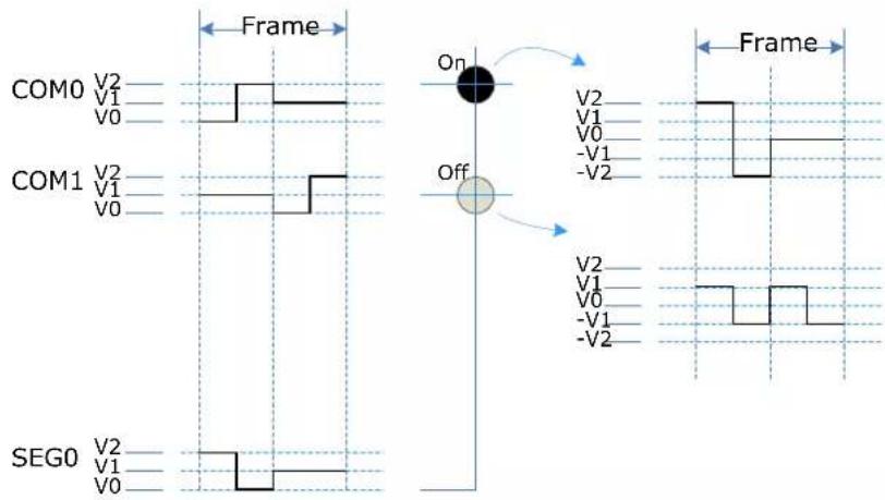
text_image
Frame COM0 V2 V1 V0 COM1 V2 V1 V0 SEG0 V2 V1 V0 On Off Frame V2 V1 V0 -V1 -V2 V2 V1 V0 -V1 -V2The low-power waveform template can be derived from the standard one by separating the standard waveform template into two subframe templates, as shown in the following figure:
Figure 42-8. Derive Low-Power Waveform Template from Standard Waveform Template
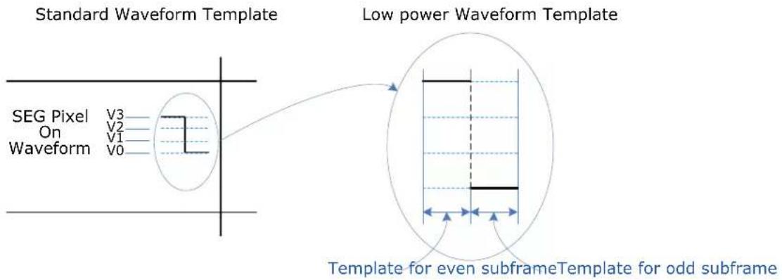
text_image
Standard Waveform Template SEG Pixel V3 On V2 Waveform V1 V0 Low power Waveform Template Template for even subframeTemplate for odd subframeFigure 42-9. 1/2 Bias, 1/2 Duty Low-Power Waveform
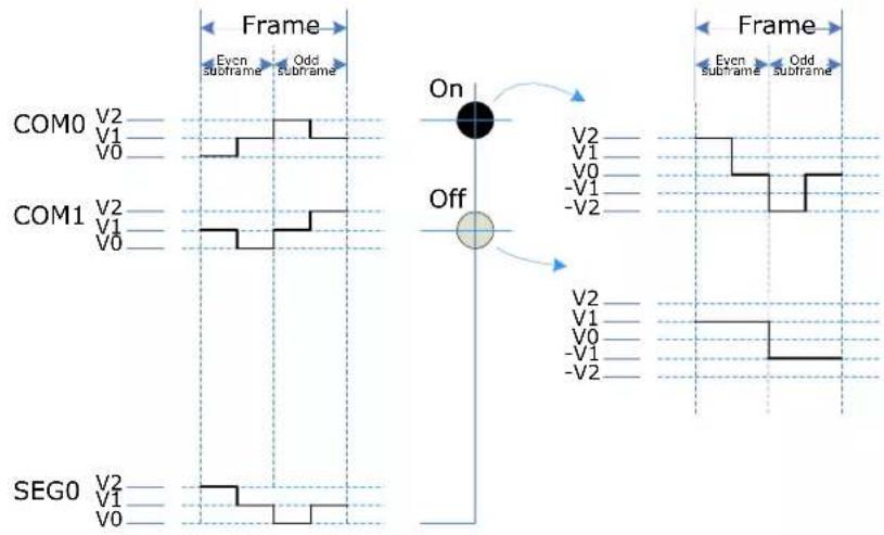
flowchart
graph TD
    subgraph Frame
        A["Frame"] --> B["On"]
        B --> C["Off"]
    end
    subgraph Off
        D["Frame"] --> E["On"]
        E --> F["Off"]
    end
    subgraph SEG0
        G["Frame"] --> H["Off"]
    end
    subgraph SEG0
        I["Frame"] --> J["Off"]
    end
Figure 42-10. 1/3 Bias Standard Driving Waveform Template and Combination
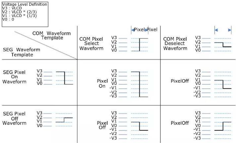
other
| Signal Type | Description | Voltage Level Definition | Selection | Waveform | |---|---|---|---|---| | COM Waveform Template | COM Pixel Select Waveform | V3 ———— | ———— | ———— | | COM Waveform Template | Pixel Off | ———— | ———— | ———— | | Pixel Off | Pixel Off | ———— | ———— | ———— | | Pixel Off | Pixel Off | ———— | ———— | ———— | | Pixel Off | Pixel Off | ———— | ———— | ———— | | Pixel Off | Pixel Off | ———— | ———— | ———— | | Pixel Off | Pixel Off | ———— | ———— | ———— | | Pixel Off | Pixel Off | -V1 ———— | ———— | ———— | | Pixel Off | Pixel Off | -V2 ———— | ———— | ———— | | Pixel Off | Pixel Off | -V3 ———— | ———— | ———— | | Pixel Off | Pixel Off | -V1 ———— | ———— | ———— | | Pixel Off | Pixel Off | -V2 ———— | ———— | ———— | | Pixel Off | Pixel Off | -V3 ———— | ———— | ———— | | Pixel Off | Pixel Off | -V1 ———— | ———— | ———— |Figure 42-11. 1/3 Bias, 1/4 Duty, Standard Waveform

text_image
Frame V3 V2 V1 V0 COM0 V3 V2 V1 V0 COM1 V3 V2 V1 V0 COM2 V3 V2 V1 V0 COM3 V3 V2 V1 V0 SEG0 V3 V2 V1 V0 On V3 V2 V1 V0 -V1 -V2 -V3 Off V3 V2 V1 V0 -V1 -V2 -V3 FrameFigure 42-12. 1/3 Bias, 1/4 Duty, Low-Power Waveform
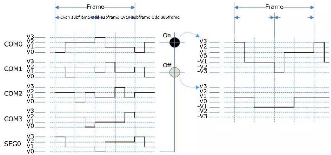
text_image
Frame Even subframe Odd subframe Even subframe Odd subframe COM0 V3 V2 V1 V0 COM1 V3 V2 V1 V0 COM2 V3 V2 V1 V0 COM3 V3 V2 V1 V0 SEG0 V3 V2 V1 V0 On Off V3 V2 V1 V0 -V1 -V2 -V3 V3 V2 V1 V0 -V1 -V2 -V3Figure 42-13. 1/4 Bias Standard Driving Waveform Template and Combination
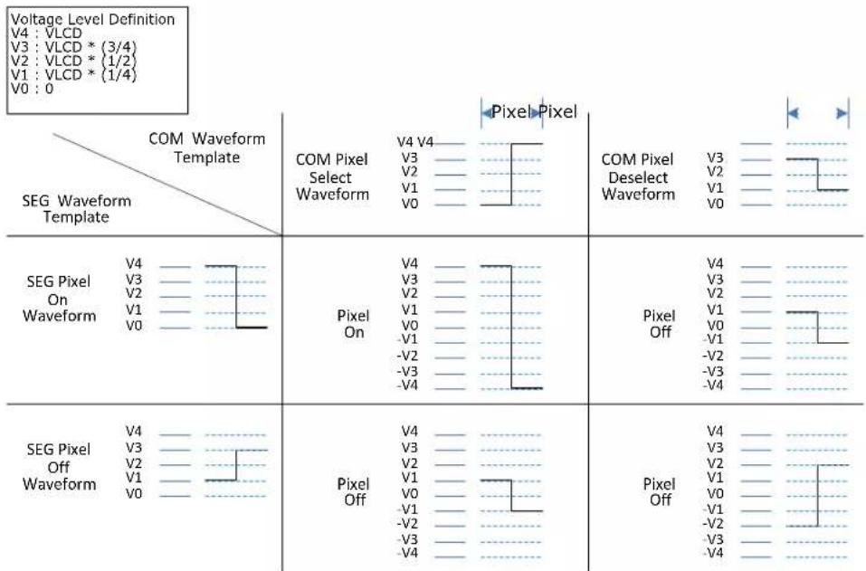
other
| Segment | Waveform Description | Value | |---------|-------------------------------|-------| | Top Segment | COM Waveform Template | V4 | | Top Segment | COM Waveform Template | V3 | | Top Segment | COM Waveform Template | V2 | | Top Segment | COM Waveform Template | V1 | | Top Segment | COM Waveform Template | V0 | | Bottom Segment | Pixel On | V4 | | Bottom Segment | Pixel On | V3 | | Bottom Segment | Pixel On | V2 | | Bottom Segment | Pixel On | V1 | | Bottom Segment | Pixel On | V0 | | Bottom Segment | Pixel Off | V4 | | Bottom Segment | Pixel Off | V3 | | Bottom Segment | Pixel Off | V2 | | Bottom Segment | Pixel Off | V1 | | Bottom Segment | Pixel Off | V0 | | Bottom Segment | Pixel Off | V1 | | Bottom Segment | Pixel Off | V2 | | Bottom Segment | Pixel Off | V3 | | Bottom Segment | Pixel Off | V4 |Figure 42-14. 1/4 Bias, 1/8 Duty, Standard Waveform
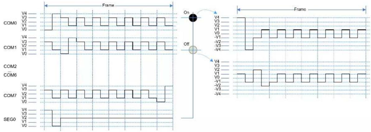
text_image
Frame V4 V3 V2 V1 V0 COM0 V4 V3 V2 V1 V0 COM1 V4 V3 V2 V1 V0 COM2 V4 V3 V2 V1 V0 COM6 V4 V3 V2 V1 V0 COM7 V4 V3 V2 V1 V0 SEG0 V4 V3 V2 V1 V0 On Off V4 V3 V2 V1 V0 -V1 -V2 -V3 -V4 FrameFigure 42-15. 1/4 Bias, 1/8 Duty, Low-Power Waveform
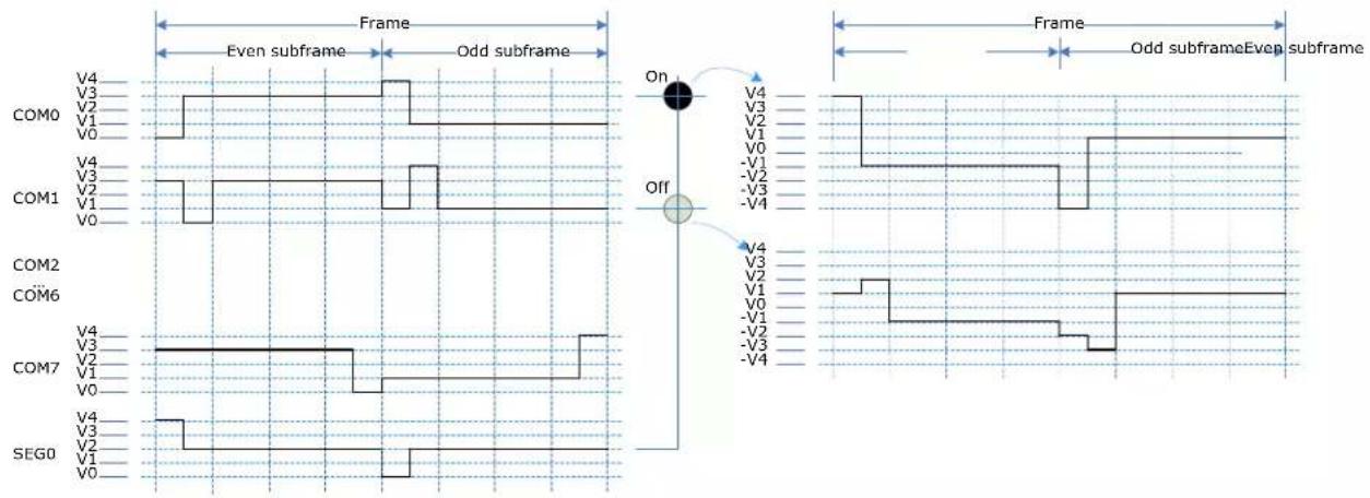
text_image
Frame Even subframe Odd subframe V4 V3 V2 V1 V0 COM0 V4 V3 V2 V1 V0 COM1 V4 V3 V2 V1 V0 COM2 V4 V3 V2 V1 V0 COM6 V4 V3 V2 V1 V0 COM7 V4 V3 V2 V1 V0 SEG0 V4 V3 V2 V1 V0 On Off V4 V3 V2 V1 V0 -V1 -V2 -V3 -V4 Frame Odd subframeEven subframe42.6.1.5 LCD Frame Frequency
The LCD frame frequency is defined as the number of times the segments are energized per second. The optimal frame frequency should be in range from 30Hz up to 100Hz to avoid flickering and ghosting effect.
The 32KHz oscillator clock (CLK_SLCD_OSC) is the base clock to define the LCD frame frequency (or frame rate) which in turn depends on the Duty Ratio bits in the Control A register (CTRLA.DUTY[2:0]). CLK_SLCD_OSC is used to generate the LCD waveform data for the enabled phases.
CLK_SLCD_OSC is first divided by a prescaler PVAL=16..128, then divided by DIV=1..8: The prescaler value PVAL is selected by writing the Prescaler bits in the Control A register (CTRLA.PRESC[1:0]), see table below.
Table 42-3. Prescaler Selection
| PRESC[1:0] Prescaler Value (PVAL) | |
| 0x0 16 | |
| 0x1 32 | |
| 0x2 64 | |
| 0x3 128 |
The clock division factor DIV is selected by the Clock Divider bits CTRLA.CKDIV[2:0]. The division factor is DIV = CKDIV[2:0] + 1 . The duty ratio NB_COM is selected by writing to the Duty Ratio bits in the Control A register (CTRLA.DUTY).
The resulting frame rate is calculated according to this formula:
$$ \text { FrameRate } = \frac {f (\mathrm{CLK} _ {\text { SLCD_OSC }})}{\mathrm{PVAL} \times \mathrm{DIV} \times \mathrm{NB} _ {\text { COM }}} $$
Table 42-4. Examples of Frame Rates for f(CLK_SLCD_OSC) = 32768Hz
| Prescaler Value (PVAL) | CKDIV[2:0] | DIV NB_COM | Frame Rate | ||
| 128 0x7 8 1 32 Hz | |||||
| 128 0x2 3 1 85.3 Hz | |||||
| 64 0x7 8 2 32 Hz | |||||
| 64 0x2 3 2 85.3 Hz | |||||
| 64 0x4 5 3 34.1 Hz | |||||
| 32 0x3 4 3 85.3 Hz | |||||
| 32 0x7 8 4 32 Hz | |||||
| 32 0x2 3 4 85.3 Hz | |||||
| 32 0x4 5 6 34.1 Hz | |||||
| 16 0x3 4 6 85.3 Hz | |||||
| 16 0x7 8 8 32 Hz | |||||
| 16 0x2 3 8 85.3 Hz |
42.6.1.6 LCD Pins Selection
Selection of maximum 48 segment/common lines from 52 LCD pins
There are 52 LCD pins (LPx), of which up to 48 LCD pins can be enabled or disabled individually according to the LCD glass. Each LCD pin can be configured as frontplane (SEG) or backplane (COM), offering various configurations. The maximum number of SEG lines and COM lines are defined in the table below.
Table 42-5. Maximum Number of COM and SEG Lines
| Duty #COM Lines Max #SEG Lines | ||
| Static 1 44 | ||
| 1/2 | 2 44 | |
| 1/3 | 3 44 | |
| 1/4 | 4 44 | |
| 1/6 | 6 42 | |
| 1/8 | 8 40 | |
In order to enable an LCD pin, Write a '1' to the corresponding bit in the corresponding register:
- For LP[31:0], write to LCD Pin Enable Low register bits LPENL[31:0]
• For LP[51:32], writ to LCD Pin Enable High register bits LPENH[18:0]
Writing a '0' to a bit in LPENL or LPENH will disable the corresponding LCD pin. The number of LCD pins enabled should not be higher than the maximum of COM and SEG lines supported (see the table above). Any LCD pin can be enabled individually, LCD pins do not have to be enabled in contiguous manner.
A disabled LCD pin can thus be used as GPIO or alternate function.
According to their duty configuration, COM lines are assigned first to LCD pins enabled. The number of SEG lines enabled is thus the number of LCD pins enabled minus the number of COM lines
assigned (limited to the maximum SEG lines supported according duty selection). COM and SEG lines are always assigned in ascending order, as shown in the figure here.
Figure 42-16. LCD Pins Configuration Example

text_image
7 6 5 4 3 2 1 0 .... 1 0 1 1 1 0 1 0 LPENL| LP0 = | |
| LP1 = 0 duty = 1/2 | |
| LP2 = | |
| LP3 = 1 | |
| LP4 = SEG0 | |
| LP5 = SEG1 | |
| LP6 = | |
| LP7 = 2 | |
| ... | |
42.6.1.7 Display Memory Mapping
The display memory size depends on the configured duty ratio. For duty ratios above 1/4, the display memory is 44 bits wide per COM line. For 1/6 duty, the display memory is 42 bits wide per COM line, and for 1/8 duty, the display memory is 40 bits wide per COM line.
Figure 42-17. Display Memory Mapping

bar_stacked
| Group | Segment | Value | |---|---|---| | COM0 | SEG[43:0] | 18 | | COM0 | SEG[43:0] | 12 | | COM0 | SEG[43:0] | 6 | | COM1 | SEG[39:0] | 30 | | COM1 | SEG[39:0] | 24 | | COM1 | SEG[39:0] | 18 | | COM2 | SEG[39:0] | 30 | | COM2 | SEG[39:0] | 24 | | COM2 | SEG[39:0] | 18 | | COM3 | SEG[39:0] | 30 | | COM3 | SEG[39:0] | 24 | | COM3 | SEG[39:0] | 18 | | COM4 | SEG[39:0] | 30 | | COM4 | SEG[39:0] | 24 | | COM4 | SEG[39:0] | 18 | | COM5 | SEG[39:0] | 30 | | COM5 | SEG[39:0] | 24 | | COM5 | SEG[39:0] | 18 | | COM6 | SEG[39:0] | 36 | | COM6 | SEG[39:0] | 24 | | COM6 | SEG[39:0] | 18 | | COM7 | SEG[39:0] | 42 | | COM7 | SEG[39:0] | 36 | | COM7 | SEG[39:0] | 24 | | Total Offset | SEG[41:0] | 18 | | Total Offset | SEG[41:0] | 12 | | Total Offset | SEG[41:0] | 6 | | Total Offset | SEG[41:0] | 5 | | Total Offset | SEG[41:0] | 4 | | Total Offset | SEG[41:0] | 3 | | Total Offset | SEG[41:0] | 2 | | Total Offset | SEG[41:0] | 1 | | Total Offset | SEG[41:0] | 0 | The chart displays the offset values for each segment in two groups (COM0 and COM7). The total Offset is labeled as '18'. The bars are segmented by segment, with the bottom segment labeled '0' and the top segment labeled '5'. The x-axis represents the offset values from 0 to 123456. The y-axis represents the offset value. The legend indicates that each segment's label corresponds to its corresponding segment.Duty = 1/4 Duty = 1/6 Duty = 1/8
Direct Access
CPU can access display memory in direct access by writing to the corresponding Segments Data Low/High for COMx Line register (SDATAL/Hx). For each bit y of the SDATAL/Hx register there is a corresponding segment connected to SEG y line and COMx line. For example, to update the segment connected to SEG4/COM2, write to bit 4 of the SDATAL2 register.
Indirect Access
The CPU can also update the display memory in indirect access mode, i.e. by writing to the Indirect Segments Data Access register (ISDATA). This register allows to write up to 8 contiguous bits in a single write operation to the display memory:
- SDATA[7:0], segments data value (see the figure above)
- SDMASK[7:0], mask for SDATA. When SDMASK[y]=1, SDATA[y] is not written to display memory
• OFF[5:0], byte offset in display memory (see the figure above)
Locking Shadow Display Memory
Shadow display memory can be locked so that it is not updated when new frames start.
Writing a '1' to the Lock bit in the Control B register (CTRLB.LOCK) will lock the shadow display memory. If the display memory is modified, the display remains unchanged.
Writing a '0' to CTRLB. LOCK will to unlock the shadow display memory. The shadow display memory will be updated when a new frame starts.
42.6.1.8 LCD Power Supply
The LCD voltage levels are generated either from the VLCD pin or by the internal power supply block, through an internal resistor divider network. The internal power supply is selected by writing a '0' to the External VLCD bit in the Control A register (CTRLA.XVLCD); the external power supply is selected by writing a '1' to CTRLA.XVLCD.
The LCD power supply block generates up to three intermediate voltage levels (in internal or external supply mode), depending on the bias configuration bits in the CTRLA register (CTRLA.BIAS[1:0]).
Table 42-6. VLCD Voltages
| CTRLA.BIAS[1:0] Configuration Voltages | |
| 00 Static VLCD | |
| 01 1/2 VLCD, 1/2 VLCD | |
| 10 1/3 VLCD, 2/3 VLCD, 1/3 VLCD | |
| 11 1/4 VLCD, 3/4 VLCD, 1/2 VLCD, 1/4 VLCD | |
The VLCD Status bit in the STATUS register (STATUS.VLCDS) indicates the current relation of VLCD and VDD. When VDD33 > Target VLCD, STATUS.VLCDS is set to '1'. Otherwise, STATUS.VLCDS is cleared to '0'.
The voltage status of VLCD itself is indicated by STATUS.VLCDR: when the VLCD voltage is not well regulated to the target voltage, indicated by STATUS.VLCDR=0, the display quality may be impaired during the ongoing settling period. If the display quality is critical for the application, transient phenomena can be avoided by first disabling the COM/SEG output by writing CTRLD.DISPEN=0, then enable COM/SEG output again once the STATUS.VLCDR bit is set.
42.6.1.9 Contrast Adjustment
The contrast of the LCD is determined by the value of VLCD voltage. The higher the VLCD voltage, the higher is the contrast. The software contrast adjustment is only possible in internal supply mode.
In internal supply mode, VLCD is in the range of 2.5V to 3.5V. VLCD can be adjusted in 16 steps of 60mV by writing a value to the Contrast bits in the Control B register (CTRLB.CTST), see also the according Electrical Characteristics section.
The contrast value can be written at any time, even if SLCD is enabled and running.
Related Links
42.6.1.8. LCD Power Supply
44.14. SLCD Characteristics
42.6.1.10 Saving Power with LowR and Buffer
The bias generation block generates the bias voltage that the LCD waveform needs. For intermediate bias levels between ground and VLCD, they are generated by an on-chip resistive voltage divider.
The voltage divider is made of two strings, one high resistance string and one low resistance string. The high resistance string is always on when the LCD is enabled. The low resistance string can be turned on for a configurable amount of time (defined in the SLCD controller) to increase the drive capability of the bias, at the price of increased power consumption. The on-time is aligned at waveform transition so that the best trade off can be found between power and waveform quality by tuning the ratio of the LowR on-time versus the waveform period to find the best trade-off. The LowR on-time is selected by writing the Low Resistance Enable Duration bits in the Control B register (CTRLB.LRD).
A buffer is also provided for each of the intermediate bias levels. The buffers have a fixed current consumption, but provide dynamic current drive capability. Similar to the LowR driver, the buffer can be turned on for only a portion of the waveform period after transition. This is tuned by writing to the Bias Buffer Enable bits in the Control B register (CTRLB.BBD).
Compared to LowR, buffers offer a higher drive capability with relatively fixed operating current, which achieve a better performance (waveform quality versus power consumption) when the panel represents a big capacitive load (i.e. 10nF).
Figure 42-18. LowR and Buffer Illustration

flowchart
graph TD
    A["LowR_en"] --> B["Buffer_en"]
    B --> C["Buffer"]
    C --> D["Bias1"]
    C --> E["Bias2"]
    C --> F["Bias3"]
42.6.1.11 Reference Refresh and Power Refresh
There are two refresh signals for SLCD:
- Reference refresh, which is used to periodically sample the bias current and target VLCD voltage.
- Power refresh, which is used to charge the external VLCD capacitor to the target VLCD level. This is usually due to the fact that the LCD panel driving waveform will need to charge the panel segment capacitors.
The reference refreshment rate is defined by the leakage of the circuit. The bias current and reference voltage start to drift slowly due to parasitic effects. A high frequency refresh rate can tolerate higher leakage at cost of higher power consumption. User can configure the reference refresh rate by writing the Reference Refresh Frequency bits in the Control A register (CTRLA.RRF).
The power refreshment rate is defined by the leakage of the circuit. High frequency could result in bit higher power but can tolerate higher load current on VLCD, which means driving a bigger panel at higher frequency. User can configure the power refresh rate by writing the Power Refresh Frequency bits in the Control A register (CTRLA.PRF)
Figure 42-19. Reference and Power Refresh System Behavior

text_image
32k clock Reference refresh period defined by CTRL.A.RRF CTRLA.ENABLE Reference refresh signal Power refresh signal STATUS.LCDR LCD bias status, just for software42.6.2 Additional Features
42.6.2.1 Frame Counters
For several functions (e.g., blinking, or automated modes) a frame counter is required as time base. There are three independent frame counters FC0, FC1 and FC2, which can be associated with any function.
Each frame counter x is enabled by writing a '1' to the Frame Counter x Enable bit in the Control D register (CTRLD.FCxEN), and disabled by writing a '0' to it. When disabling a frame counter, it will be disabled once the CTRLD register is synchronized.
The frame counter is synchronized to the LCD frame start and generates an internal event each time the counter overflows. The overflow value is selected by writing the Write Overflow bits in the Frame Counter x register (FCx.OVF). The FCx register can only be written when the frame counter x is disabled (CTRLD.FCxEN=0).
The frequency of the internal event is defined by the following formula:
$$ \mathrm{f} _ {\mathrm{FCx}} = \frac {\text {FrameRate}}{(\mathrm{FCx.OVF} \times 8 +) 1} $$
The prescaler of 8 can be bypassed by writing a '1' to the Prescaler Bypass bit in the FCx register (FCx.PB):
$$ \mathrm{f} _ {\mathrm{FCx}} = \frac {\text {FrameRate}}{(\mathrm{FCx.OVF}) - 1} $$
42.6.2.2 Blank
To blank the LCD panel, write a '1' to the Blank bit in the Control D register (CTRLD.BLANK). All LCD segments will be OFF at the beginning of next frame. The content of the display memory is not modified.
To output segment data normally, write a '0' to CTRLD.BLANK.
42.6.2.3 Blink
SLCD can be configured to blink all or selected LCD segments. Segments will alternate between on and off state at the frequency given by the selected frame counter.
The blinking feature is configured in the Blink Configuration register (BCFG):
- To blink all segments, write a '0' to the Mode bit in the BCFG register (BCFG.MODE). To blink only selected segments, write a '1' to BCFG.MODE. Then, up to sixteen segments can be enabled individually to blink, they are connected to SEG0, SEG1, and COM[0..7]:
- To enable blinking for the segment connected to SEG0 and COMx, write a '1' to bit x of the Blink Segment Selection 0 bit field in the BCFG register (BCFG.BSS0). Write a '0' to this bit to disable blinking.
- To enable blinking for the segment connected to SEG1 and COMy, write a '1' to bit y of the Blink Segment Selection 1 bit field in the BCFG register (BCFG.BSS1). Write a '0' to this bit to disable blinking.
A segment will blink only if it is already on - otherwise it will remain off.
- The blink frequency is defined by the number of frames between each on/off state, as given by a frame counter. Which frame counter is associated to the blink feature is selected by writing the corresponding frame counter x index to the Frame Counter Selection bits in the BCFG register (BCFG.FCS).
Once the desired blink configuration is written to the BCFG register, blinking is enabled by writing a '1' the to Blink bit in Control C register (CTRLC.BLINK). Blinking is disabled by writing a '0' to CTRLC.BLINK.
The BCFG register cannot be written when blink is enabled. The blink frequency can be modified, provided the selected frame counter has been disabled first.
Table 42-7. Blink Modes
| CTRLC.BLANK CTRLC.BLINK BSS1[7:0] BSS0[7:0] Mode | |||
| 1 x - All segments are off | |||
| 0 0 - All segments are driven according | display memory | ||
| 0 1 00000000 00000000 All segments are blinking | |||
| xxxxxxxx xxxxxxxx Selected segments (x=1) are blinking | |||
42.6.2.4 Autonomous Segment Animation
Up to sixteen segments can be animated by an internal circular shift register. Up to sixteen states are then defined, e.g. to make a running wheel. The size of the animation can be configured by writing the number of segments to use to the Size bits in the Circular Shift Register Configuration register (CSRCFG.SIZE).
The circular shift register bits are associated to segments connected to SEG2, SEG3 and COM[0..7] lines, refer to the table below.
Table 42-8. Circular Shift Register Bit Mapping
| Circular Shift Register Bit COM SEG | ||
| 0 0 2 | ||
| 1 0 3 | ||
| 2 1 2 | ||
| 3 1 3 | ||
| 4 2 2 | ||
| 5 2 3 | ||
| 6 3 2 | ||
| 7 3 3 | ||
| 8 4 2 | ||
| 9 4 3 | ||
| 10 5 2 | ||
| 11 5 3 | ||
| 12 6 2 | ||
| 13 6 3 | ||
| 14 7 2 | ||
| 15 7 3 |
The shifting frequency is configured in a frame counter as a number of frames. A frame counter is associated to this feature by writing the corresponding index to the Frame Counter Selection bits in the CSRCFG register (CSRCFG.FCS).
The shift direction is selected by writing to the Direction bit in CSRCFG register (CSRCFG.DIR): DIR=0 is shifting to the left; DIR=1 will shift to the right.
The initial value of the circular shift register must be written to the Data bits in the CSRCFG register (CSRCFG.DATA).
Once the circular shift register is configured, autonomous segment animation is enabled by writing a '1' to the Circular Shift Register Enable bit in the Control C register (CTRLC.CSREN). Animation is disabled by writing a '0' to CTRLC.CSREN. The initial value is shifted each time the selected frame counter overflows.
The CSRCFG register cannot be written when circular shift register is enabled. The shifting frequency can be modified, provided selected frame counter has been disabled first.
Figure 42-20. LCD Wheel Animation Example (8 Segments)
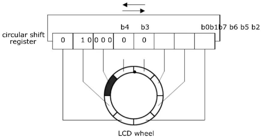
flowchart
graph TD
    A["circular shift register"] --> B["0"]
    B --> C["1 0"]
    C --> D["0 0 0"]
    D --> E["0"]
    E --> F["0"]
    F --> G[" "]
    G --> H[" "]
    H --> I["b0b1 b7 b6 b5 b2"]
    J["LCD wheel"] --> K["Data bits b4 b3"]
    style J fill:#f9f,stroke:#333
    style K fill:#ccf,stroke:#333
42.6.2.5 Character Mapping
Multiple segments of the LCD panel can be gathered to digits in order to display characters. Digits can be of various type (e.g., 7-segment, 16-segment) and mapped in the display memory differently, refer to the figure below for examples. The SLCD supports displaying up to 24-segment characters on any existing LCD panel.
Figure 42-21. Examples of Digit Mapped in Display Memory
Display Memory 7-segment digit
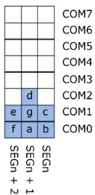
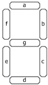
flowchart
graph TD
    A["a"] --> B["f"]
    A --> C["b"]
    B --> D["g"]
    C --> D
    D --> E["e"]
    D --> F["c"]
    E --> G["d"]
Display Memory
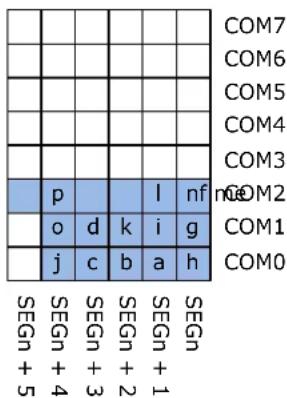
16-segment digit

flowchart
graph TD
    a --> h
    b --> c
    h --> l
    i --> g
    j --> m
    k --> m
    l --> n
    m --> p
    n --> f
    p --> e
    d --> e
Several digits can be mapped in display memory to form a digits chain, which is used to display a characters string. Once configured, the user updates a digit by providing up to 24 bits with a single write access. ASCII tables provide standard symbols which should be handled by software before being displayed.
Each character is a continuous display area with its SEG axis defined by the Character Mapping Configuration register (CMCFG.NSEG). The maximum size is 24. Refer also to the example figure below.
Figure 42-22. Character Mapping Example
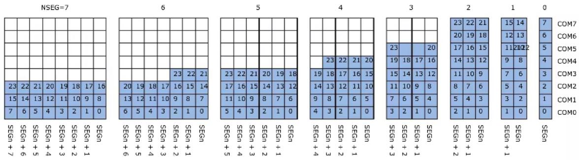
The 24 segments value is updated by a write access to the Character Mapping Segments Data register (CMDATA).
Since the CMDATA register can be up to 24 bits whereas a digit can consist of less than 24 segments, a mask can be configured to write only selected bits: Writing a '1' to a bit in the Character Mapping Data Mask register (CMDMASK) will mask the corresponding bit in the CMDATA register. This bit will not be written in display memory when CMDATA register is written. Write a '0' to a bit of CMDMASK to disable the mask for that bit. The corresponding bit in CMDATA will be written to display memory.
CMDATA is not written to the display memory in one shot, but in a serial way. Serialization takes 24 APB cycles. The user can check the status of the serial writing by reading the Character Mapping Write Busy bit in the Status register (STATUS.CMWRBUSY). Any write access to the display memory through CMDATA/SDATA/ISDATA will be ignored when STATUS.CMWRBUSY is high. Therefore, user must not write to CMDATA while STATUS.CMWRBUSY is asserted.
The coordinate of a character is defined by Character Mapping Index (CMINDEX) register.
The expected usage model for character mapping is shown below:
Figure 42-23. Usage Model for Character Mapping Function

flowchart
graph TD
    A["Manual CM Entry"] --> B["Configure character coordinate by writing CMINDEX"]
    B --> C{CMDMASK configured?}
    C -->|Y| D["Write CMDATA"]
    C -->|N| E["Configure CMDMASK"]
    D --> F["Manual CM Exit"]
    E --> F
By this character mapping feature, user could update any particular rectangular window defined by CMCFG and CMINDEX in the display memory just by a single APB write access.
The Decrement SEG Index bit in Character Mapping Configuration (CMCFG.DEC) defines the mapping order. And CMINDEX.SINDEX also have different coordinate under different DEC configuration. Refer to figure below for illustration.
Figure 42-24. Character Mapping Order
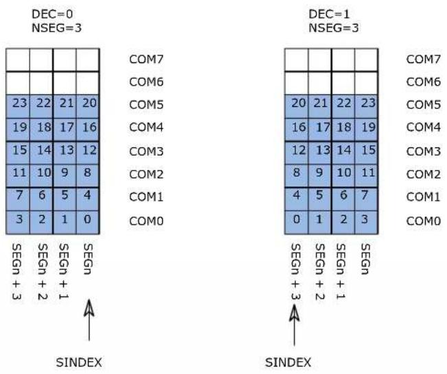
Note: The user must make sure all character bits could be mapped to some bit in display memory, not somewhere out side display memory.
42.6.2.6 Automated Character Mapping
Displaying predefined character strings can be automated by using the Direct Memory Access (DMA). This is the Automated Character Mapping (ACM) feature. Compared to manual character mapping, there is one restriction for ACM: the first character is always mapped to the COM0 line.
The size of a character is defined by the CMCFG register; the mask of a character is defined by the CMDMASK register.
Several digits can be mapped on different rows and form a string (chain), which could be configured by the Auto Character Mapping Configuration (ACMCFG) register:
- ACMCFG.NDROW defines number of digit per row.
• ACMCFG.STSEG defines the index of the first SEG line of the first digit. - ACMCFG.NDIG defines the number character in the whole string.
If the three fields are configured correctly, ACM logic can infer each character in the string automatically. Each row should contain NDROW digits except the last row. Digits of next row should be aligned with the digits of the previous row (same SEG lines). The figure below gives an example for how to configure a string in ACM mode.
Figure 42-25. Examples of Digits Chains Mapped in Display Memory
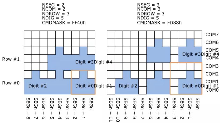
heatmap
| Row | Digit #0 | Digit #3Digit | | --- | --- | --- | | Row #1 | - | - | | Row #0 | - | - | | NSEG | 2 | 3 | | NCOM | 2 | 3 | | NDROW | 3 | 3 | | NDIG | 5 | 5 | | CMDMASK | - | - | | COM7 | - | - | | COM6 | - | - | | COM5 | - | - | | COM4 | - | - | | COM3 | - | - | | COM2 | - | - | | COM1 | - | - | | COM0 | - | - | | SEGN + 8 | - | - | | SEGN + 7 | - | - | | SEGN + 6 | - | - | | SEGN + 5 | - | - | | SEGN + 4 | - | - | | SEGN + 3 | - | - | | SEGN + 2 | - | - | | SEGN + 1 | - | - | | SEGN + 11 | - | - | | SEGN + 10 | - | - | | SEGN + 9 | - | - | | SEGN + 8 | - | - | | SEGN + 7 | - | - | | SEGN + 6 | - | - | | SEGN + 5 | - | - | | SEGN + 4 | - | - | | SEGN + 3 | - | - | | SEGN + 2 | - | - | | SEGN + 1 | - | - | | SEGN + 10 | - | - | | SEGN + 9 | - | - | | SEGN + 8 | - | - | | SEGN + 7 | - | - | | SEGN + 6 | - | - | | SEGN + 5 | - | - | | SEGN + 4 | - | - | | SEGN + 3 | - | - | | SEGN +2 | - | - | | SEGN +1 | - | - | | SEGN + 11 | - | - | The heatmap displays the distribution of Digit #0 and Digit #3 digits across the row and column of the row index. The legend indicates that each row corresponds to a specific integer value for both Digit #0 and Digit #3 digits. The chart includes a formula for the color coding of the cells.After the user has enabled ACM by writing a '1' to the ACM Enable bit in the Control C register (CTRLC.ACMEN), the ACM logic (state machine) will start according to the configuration by user. Whenever the user writes a '0' to CTRLC.ACMEN, the ACM logic will return to its initial state.
The mapping method can be altered: The line index direction is selected by writing to the Decrement SEG Line Index bit in the Character Mapping Configuration register (CMCFG.DEC). Either the segment is starting from the bottom right (DEC=0) or from the bottom left (DEC=1).
Note: The Start SEG bits in the ACM Configuration register (ACMCFG.STSEG) have different coordinates under different CMCFG.DEC configurations.
Refer to the figure below for illustration.
Figure 42-26. DEC and Auto Character Mapping Order

There are two usage models available under ACM, defined by the Mode bit in the Automated Character Mapping Configuration register (ACMCFG.MODE): when MODE=0, the Sequential Characters String Display mode is selected. When MODE=1, the Scrolling of Characters String Display mode is selected.
Both modes use the character mapping configuration (see 42.6.2.5. Character Mapping) and require the digit to be mapped with contiguous SEG/COM lines in order to increment the index for the next digit automatically. For example when the first digit is mapped on SEG2 and SEG3 lines, the second digit must be mapped on SEG4 and SEG5 lines.
Sequential Characters String Display
This mode displays characters of a string on a digits chain on the LCD panel. The characters string is split in several sub strings, which are to be displayed sequentially at a selected frequency (frame counter basis). It requires an internal frame counter (time base) and the DMA controller to transfer the sub strings.
To use this mode, character mapping must be configured first (see 42.6.2.5. Character Mapping), then additional configuration must be done to specify the sequential display. In the Automated Character Mapping Configuration register (ACMCFG):
- Write the size of the digits chain on LCD panel to the Number of Digit bits (ACMCFG.NDIG).
- Write a '0' to the Mode bit in order to select the sequential mode (ACMCFG.MODE).
- Configure a frame counter to set the display period (period between two sub strings display, see 42.6.2.1. Frame Counters), and write the frame counter index to the Frame Counter Selection bits (ACMCFG.FCS).
The DMA controller should be configured to transfer several blocks corresponding to the sub strings. Each block size is equal to the number of digit on the LCD panel (sub strings may require some blank characters in order to be displayed correctly). The number of blocks is the number of sub strings required to display the complete characters string. To repeat the complete character string display, the DMA controller should repeat the total blocks transfer. The DMA must write the blocks to the Character Mapping Segments Data register (CMDATA).
To enable the sequential characters string display, write a '1' to the Automated Character Mapping Enable bit in the Control B register (CTRLB.ACMEN); write a '0' to CTRLB.ACMEN to disable it.
The selected frame counter defines the number of frames before the SLCD triggers a new DMA block transfer. For example, if frame rate is 50Hz (20ms) in standard waveform mode, the characters string can be displayed with a period from 160ms up to 5.1s.
Figure 42-27. Sequential Character String Example (NDIG=5, frame rate=50Hz, FC0.OVF=31)
String = 'HELLOWORLDTHIS IS AUTOMATED'
other
| Time (s) | HEL | L O | WOR | L D | THI | S | | :--- | :--- | :--- | :--- | :--- | :--- | :--- | | 0 | □ | □ | □ | □ | □ | □ | | 5.1 | □ | □ | □ | □ | □ | □ | | 10.2 | □ | □ | □ | □ | □ | □ | | 15.3 | □ | □ | □ | □ | □ | □ | | 20.4 | □ | □ | □ | □ | □ | □ | | 25.5 | □ | □ | □ | □ | □ | □ | t (s)Scrolling of Characters String
This mode displays characters of a string on a digits chain on the LCD panel with a scrolling effect. For each step, a part of the characters string is displayed by shifting the string by one character in left direction. The period between each step can be configured on frame counter basis. This mode requires an internal frame counter (time base) and the DMA controller to transfer the character string.
To use this mode, character mapping must be configured first (see 42.6.2.5. Character Mapping), then additional configuration must be done to specify the scrolling display. In the Automated Character Mapping Configuration register (ACMCFG):
- Write the size of the digits chain on the LCD panel to the Number of Digit bits (ACMCFG.NDIG).
- Write the number of scrolling steps to the Steps bits (ACMCFG.STEPS).
The number of steps is equal to string length - NDIG + 1.
- Write a '1' to the Mode bit in order to to select the scrolling mode (ACMCFG.MODE).
- Configure a frame counter to set the display period (period between two steps, see 42.6.2.1. Frame Counters) and write the frame counter index to the Frame Counter Selection bits (ACMCFG.FCS).
The DMA controller should be configured to transfer several times the same block corresponding to the complete characters string (the string may require some blank characters at the end in order to be displayed correctly). For a complete scrolling of the string, the number of DMA block transfers should be at least the number of steps. To repeat the complete character string scrolling, the DMA controller should repeat the blocks transfer. The DMA must write the blocks to the Character Mapping Segments Data register (CMDATA).
To enable the scrolling of characters string, write a '1' to the Automated Character Mapping Enable bit in the Control B register (CTRLB.ACMEN); write a '0' to CTRLB.ACMEN and to disable it.
The selected frame counter defines the number of frames before the SLCD triggers a new DMA block transfer, after each scrolling steps.
Figure 42-28. Characters String Scrolling Examples (NDIG=3)

text_image
String='HELLO' (string length=5, STEPS=3) 1 2 3 4 5 6 1 Step String='HELLO' (string length=8, STEPS=6)42.6.2.6.1 Limitations of Auto Character Mapping Mode
If ACM is enabled and the Auto Character Mapping Busy bit in the Status register (STATUS.ACMBUSY) is asserted, any write access to the Character Mapping Data register (CMDATA) will be considered as coming from the DMA controller, and therefore handled by the ACM state machine. So if the user