COM20020i - Electronic component Microchip - Free user manual and instructions
Find the device manual for free COM20020i Microchip in PDF.

User questions about COM20020i Microchip
0 question about this device. Answer the ones you know or ask your own.
Ask a new question about this device
Download the instructions for your Electronic component in PDF format for free! Find your manual COM20020i - Microchip and take your electronic device back in hand. On this page are published all the documents necessary for the use of your device. COM20020i by Microchip.
USER MANUAL COM20020i Microchip
EIA RS-485 is a specification for the support of a multi-drop differential serial digital data network. RS-485 came about as microprocessors and the use of distributed intelligence became popular in the design of industrial systems. The implementation of such concepts created a demand for a standard method of communicating serially in such environments. The actual RS-485 specification came about as a result of the shortfalls of the RS-422 standard. RS-485 is virtually identical to RS-422 except in two respects, increased receiver sensitivity and support of longer line lengths.
The basic RS-485 specification standardizes the electrical characteristics of each transceiver and provides some basic guidelines for establishing a network. By definition, a basic transceiver shall have a minimum input resistance of 12 Kohms and handle a +/-7V common mode voltage regardless of whether power is applied or not. When the transceiver is powered it must present the minimum input resistance and present less than 50pf of capacitance at its input terminals. In addition, each driver must be capable of providing a minimum level of 1.5V in the presence of 32 transceivers and two 120 ohm terminating resistors. The 120 ohm termination results from the use of twisted pair cable, the preferred media in many industrial applications because of its wide availability and low cost. Another critical requirement of RS-485 is that the receiver must be capable of detecting levels down to 200mV which is of great advantage when long line lengths are needed. RS-485 does not specify a modulation method or a maximum data rate. This gives the system designer great flexibility in creating a low-cost high-performance network.
The combination of long line length, high node count (32 nodes), and support of low-cost media has made the RS-485 specification the primary choice as a data communication standard in industrial applications.
CABLING GUIDELINES FOR RS-485 INTERFACE WITH THE COM20020
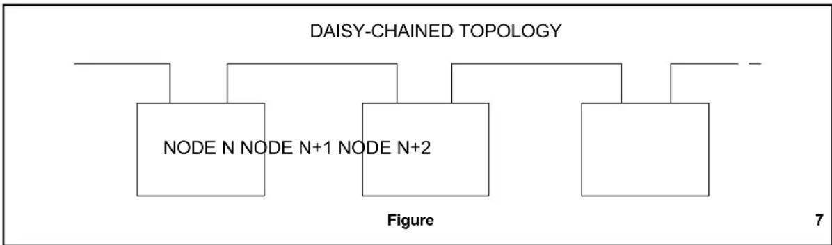
The following cabling guidelines provide a basis for establishing a low cost Local Area Network (LAN) based on the ARCNET protocol for use with the COM20020 Universal ARCNET Controller with a differential RS-485 driver. The guidelines presented are for unshielded twisted pair cable modulated with the COM20020's backplane encoding scheme. All testing and experiments were performed using a 24AWG copper twisted unshielded 2 pair cable with a characteristic impedance (Z_0) of 120 Ohms. The topology used in all experiments was a daisy-chained configuration with no stubs (i.e. no drops).
TRANSMISSION LINE EFFECTS IN LOCAL AREA NETWORKS
Transmission line effects often present an obstacle in obtaining high performance in data communication networks. Among the problems that plague high data rate LAN's are reflections, signal attenuation, and D.C. loading. Taking into account all three parameters when designing a network can result in a faster and more reliable network.
A) REFLECTIONS IN TRANSMISSION LINE
A reflection in a transmission line is the result of an impedance discontinuity that a travelling wave sees as it propagates down the line. To eliminate the presence of reflections from the end of the cable you must terminate the line at its characteristic impedance by placing a resistor across the line as shown in Figure 1.

text_image
TERMINATION OF A NETWORK - Reflections are caused by a discontinuity in the line SOURCE Z = 120 OHM DIRECTION OF PROPAGATION Z = 120 ohm REFLECTED WAVE R = 50 OHM DISCONTINUITY PROPERLY TERMINATED NETWORK DIRECTION OF PROPAGATION R = 120 OHM INCIDENT WAVE Z = 120 ohm DRIVER R = 120 OHM Z = 120 ohm Figure 1It is important that the line be terminated at both ends since the direction of propagation is bidirectional. In the case of unshielded twisted pair this termination is 120 ohms. Note that all reflection measurements were made with no stubs on the network (i.e. no drops).
Theoretically, a properly terminated transmission line would produce no reflections at all. However in a real network, small reflections are produced since the characteristic impedance of the cable cannot be met exactly due to variance in the manufacturing process of the cable. Another primary source of reflections is the impedance mismatch between a data transceiver and the line, which can cause problems on a data network by creating perturbations on the line during an otherwise idle state. Reflections affect the network by triggering false transitions (bits) on the line receiver's input translating into possible framing errors and CRC errors.
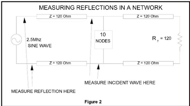
A measure of the relative strength of the reflection generated by discontinuities along the line is called the Reflection Attenuation Factor (RAF). This is a measure of the strength of the reflected wave to its incident wave. The RAF can be obtained by comparing a reflected wave to its incident wave. The magnitude of the reflected wave can be measured by sending a burst of sine waves down a transmission line and observing at the sending end the magnitude of the wave after the burst has ended (see Figure 2). The reflection measured at the sending end is the reflection generated by a discontinuity at the receiving end of the line. The magnitude of the incident wave can be measured at the receiving end of the cable, since this is the wave from which the reflection is generated. It is important to compensate for line loss when measuring the reflected wave because the reflected wave, measured at the sending end of the cable, has lost some amplitude due to line loss.
flowchart
graph TD
    A["~"] --> B["2.5Mhz SINE WAVE"]
    B --> C["Z = 120 Ohm"]
    C --> D["10 NODES"]
    D --> E["Z = 120 Ohm"]
    E --> F["R_T = 120"]
    F --> G["Z = 120 Ohm"]
    G --> H["MEASURE REFLECTION HERE"]
    H --> I["MEASURE INCIDENT WAVE HERE"]
Measurements were made for twisted pair cable and are summarized in Table 1. The following relationship was used in calculating the Reflection attenuation.
Reflection attenuation = 20 log (V ref/Vinc)
where V_ref = reflected voltage (compensated for loss) V_inc = incident voltage measured at receiving end of line
Table
| REQUENCY | 312.5 KHz | 625 MHz | 1.25 MHz | 2.5 MHz | 5.0 MHz | |
| Reflection Attenuation | -35.12 dB | -33.19 dB | -28.89 dB | -24.52 dB | -17.83 dB | |
1
These above numbers can be interpreted as follows:
Assume a +5v_p-p incident wave at 2.5MHz, a reflected wave will be generated that travels to the incident source at an amplitude of:
$$ - 2 4. 5 2 \mathrm{dB} = 0. 0 5 9 $$
therefore the reflected wave is 0.059 × 5V = 0.297V .
In practice, the amplitude of the reflected wave might be smaller because discontinuities are generated throughout the line and are not in phase with each other, thus providing a canceling effect and decreasing the magnitude of the reflection.
There are several methods for minimizing the effects of reflections such as squelch circuits and D.C. biasing. For the small reflection levels observed during experimentation, the recommended choice is D.C. biasing for its simplicity and minimum parts count (2 resistors). Biasing the network may cause some duty cycle distortion but the ARCNET protocol is insensitive to duty cycle or jitter. The biasing network will be discussed later in this guide.
B) SIGNAL ATTENUATION IN TRANSMISSION LINES
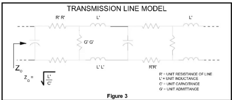
A second transmission line effect that has a bearing on the performance of LAN's is signal attenuation. A transmission line can be modeled as a combination of the distributed capacitance of the line, the distributed inductance, and resistance (see Figure 3).
C' C'
text_image
TRANSMISSION LINE MODEL R' R' L' L' G' G' L' L' R'R' Z₀ Z₀ = √(L'/C') Figure 3 R' = UNIT RESISTANCE OF LINE L' = UNIT INDUCTANCE C' = UNIT CAPACITANCE G' = UNIT ADMITTANCEThe capacitance of the line is formed by the parallel conductor pair. At the distances used in LAN's (100's feet), the resistance of the cable is negligible and contributes very little to line loss. The majority of line loss comes from the LC combination that acts like a low pass filter and tends to attenuate the signal as frequency and distance go up. For twisted pair cable, the attenuation rate is given in Table 2. These are measured values.
Table 2 - Signal Attenuation
| FREQUENCY | 312.5 KHz | 625 KHz | 1.25 MHz | 2.5 MHz | 5.0 MHz |
| Attenuation per 100ft. | -0.4 dB | -0.6 dB | -1.0 dB | -1.3 dB | -2.0 dB |
C) D.C. LOADING IN RS-485 NETWORKS
The third parameter that affects network performance is D.C. loading. The D.C. load presented to a line driver is a combination of three parameters:
1) loading effect of termination resistors
2) loading effect of biasing resistors
3) loading effect of RS-485 transceivers
EIA RS-485 specifies that a line driver must be capable of presenting a 1.5V signal differentially at its outputs under the loading of 32 receivers and two 120 ohm termination resistors. Each receiver or passive transceiver is to provide a minimum input impedance of 12K ohms. The total parallel combination load impedance is 51 ohms, which includes the receiver load, termination resistors, and biasing resistors. Since the worst-case specification is restrictive, it may not be practical to design to this worst-case because, quite often the typical RS-485 transceiver can drive substantially more than the worst-case load. Typically, many RS-485 drivers can drive quite a bit more than the 51 ohms, sometimes as low as 20 ohms. If typical characteristics are used, a network can be composed of many more nodes than the 32 specified by EIA RS-485. From laboratory experience, SMC recommends using typical transceiver characteristics when determining the D.C. load. In very high reliability applications (i.e. medical electronics, avionics), SMC recommends the use of the worst case RS-485 parameters.
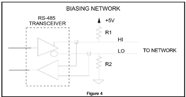
The D.C. biasing of the network is essential to providing reliable operation at high data rates. The D.C. bias offsets the NULL voltage of the network when all RS-485 transceivers are in their TRI-STATE mode. A small offset is needed because small reflections will occur that will cause spurious transitions on the RS-485 receivers input. This would cause the COM20020 to receive an undesired extra bit, thus causing framing or CRC errors and corrupting the data. It is only the negative half of the reflected wave that is of concern, so the effective reflection is .15V. The largest reflections seen on the network are approximately 0.3V_p-p differentially. This is more than enough voltage to trigger a transition on the receiver's input since the receiver has a hysteresis of 50mV and is thus quite sensitive (200mV differential sensitivity). By installing the biasing network of Figure 4 at each node, the network will be offset enough to keep the network in an inactive state. The +0.35V differential offset provided, will keep the line in an inactive state even in the presence of a 0.3V_p-p reflection (see Figure 5) which could cause a false bit to be recognized by the 20020 and cause data rejection by the receiving node. SMC recommends a pull-up and pull-down resistor (see Table 3 for correct value) in the circuit diagram shown in Figure 4.
text_image
BIASING NETWORK RS-485 TRANSCEIVER +5V R1 HI LO TO NETWORK R2 Figure 4If a larger offset is desired, the offset voltage can be calculated as follows:
To calculate the correct biasing voltage, the maximum reflection should be known:
From laboratory measurements maximum V ref = 0.3Vp-p . We are only concerned with the negative portion of V_ref = 0.15V
$$ \begin{array}{l} \text {so} \ \quad \mid_ {\text {ref}} < = 2. 5 \mathrm{ma} \end{array} $$
$$ \begin{array}{l l} \text { where } & _ {\mathrm{t1}} = \mathbb {R} _ {\mathrm{t2}} = 1 2 0 \text { ohms } = \text { termination resistance } \ \text { and } & _ {\mathrm{t}} = \mathbb {R} _ {\mathrm{t1}} | \mathbb {R} _ {\mathrm{t2}} \end{array} $$
$$ \text { We } \quad \text { bias walnt) } R _ {\mathrm{t}} > = 5 0 \mathrm{mV} \text { minimum } $$
The 50mV level is the hysteresis value for many RS-485 transceivers
therefore bias >= 3.33ma
To get the proper bias resistor values the following relationship can be used:
$$ + 5 \mathrm{V} = 1 \quad \text { bias } (R _ {\text { pull - up }} + R _ {\text { pull - down }} + (R _ {t 1} | R _ {t 2})) $$
This yields a bias resistor value of 720 ohms for the entire network which gives a bias voltage of 0.35V.
EFFECTS OF BIAS ON REFLECTIONS

line
| Time (V) | Signal Value | | -------- | ------------ | | 0 | +V | | 0 | -V | | 3 | +V | | 3 | -V | | 6 | +V | | 6 | -V | | 9 | +V | | 9 | -V | | 12 | +V | | 12 | -V | | 15 | +V | | 15 | -V | | 18 | +V | | 18 | -V | | 21 | +V | | 21 | -V | | 24 | +V | | 24 | -V | | 27 | +V | | 27 | -V | | 30 | +V | | 30 | -V | | 33 | +V | | 33 | -V | | 36 | +V | | 36 | -V | | 39 | +V | | 39 | -V | | 42 | +V | | 42 | -V | | 45 | +V | | 45 | -V | | 48 | +V | | 48 | -V | | 51 | +V | | 51 | -V | | 54 | +V | | 54 | -V | | 57 | +V | | 57 | -V | | 60 | +V | | 60 | -V | | 63 | +V | | 63 | -V | | 66 | +V | | 66 | -V | | 69 | +V | | 69 | -V | | 72 | +V | | 72 | -V | | 75 | +V | | 75 | -V | | 78 | +V | | 78 | -V | | 81 | +V | | 81 | -V | | 84 | +V | | 84 | -V | | 87 | +V | | 87 | -V | | 90 | +V | | 90 | -V | | 93 | +V | | 93 | -V | | 96 | +V | | 96 | -V | | 99 | +V | | 99 | -V | | 102 | +V | | 102 | -V | | 105 | +V | | 105 | -V | | 108 | +V | | 108 | -V | | 111 | +V | | 111 | -V | | 114 | +V | | 114 | -V | | 117 | +V | | 117 | -V | | 120 | +V | | 120 | -V | | 123 | +V | | 123 | -V | | 126 | +V | | 126 | -V | | 129 | +V | | 129 | -V | | 132 | +V | | 132 | -V | | 135 | +V | | 135 | -V | | 138 | +V | | 138 | -V | | 141 | +V | | 141 | -V | | 144 | +V | | 144 | -V | | 147 | +V | | 147 | -V | | 150 | +V | | 150 | -V | | 153 | +V | | 153 | -V | | 156 | +V | | 156 | -V | | 159 | +V | | 159 | -V | | 162 | +V | | 162 | -V | | 165 | +V | | 165 | -V | | 168 | +V | | 168 | -V | | 171 | +V | | 171 | -V | | 174 | +V | | 174 | -V | | 177 | +V | | 177 | -V | | 180 | +V | | 180 | -V | | 183 | +V | | 183 | -V | | 186 | +V | | 186 | -V | | 189 | +V | | 189 | -V | | 192 | +V | | 192 | -V | | 195 | +V | | 195 | -V | | 198 | +V | | 198 | -V | | 201 | +V | | 201 | -V | | 204 | +V | | 204 | -V | | 207 | +V | | 207 | -V | | 210 | +V | | 210 | -V | | 213 | +V | | 213 | -V | | 216 | +V | | 216 | -V | | 219 | +V | | 219 | -V | | 222 | +V | | 222 | -V | | 225 | +V | | 225 | -V | | 228 | +V | | 228 | -V | | 231 | +V | | 231 | -V | | 234 | +V | | 234 | -V | | 237 | +V | | 237 | -V | | 240 | +V | | 240 | -V | | 243 | +V | | 243 | -V | | 246 | +V | | 246 | -V | | 249 | +V | | 249 | -V | | 252 | +V | | 252 | -V | | 255 | +V | | 255 | -V | | 258 | +V | | 258 | -V | | 261 | +V | | 261 | -V | | 264 | +V | | 264 | -V | | 267 | +V | | 267 | -V | | 270 | +V | | 270 | -V | | Note: The V values are approximate based on the equation of differential signal and signal current. The diagram is divided into two sections based on the equation of differential signal. The diagram is divided into two sections based on the equation of differential signal. The diagram is divided into two sections based on the equation of differential signal. The diagram is divided into two sections based on the equation of differential signal. The diagram is divided into two sections based on the equation of differential signal. The diagram is divided into two sections based on the equation of differential signal. The diagram is divided into two sections based on the equation of differential signal. The diagram is divided into two sections based in series. The diagram is divided into two sections based in series. The diagram is divided into two sections based in series. The diagram is divided into two sections based in series. The diagram is divided into two sections based in series. The diagram is divided into two sections based in series. The diagram is divided into two sections based in series. The diagram is divided into two sections based in series. The diagram is divided into two sections based in series. The diagram is divided into two sections based in series.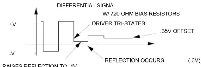
line
| Parameter | Value | | --------------------- | --------- | | DIFERENTIAL SIGNAL | +V | | W/ 720 OHM BIAS RESISTORS | -V | | DRIVER TRI-STATES | .35V OFFSET| | REFLECTION OCCURS | (.3V) |Figure 5
In practice, it is better to provide a larger bias resistor at each node so that the parallel combination of all nodes can provide a proper offset voltage. A lower resistor value than the suggested may be used if a large amount of noise is present in the system or if larger reflections are encountered. It should be noted, that the biasing arrangement adds to the total D.C. loading of the network, and yields a total load of
$$ R _ {\text { total }} = R _ {t 1} \left| R _ {t 2} \right| \left(R _ {\mathrm{rcvr}} / N\right) | \left(R _ {\text { bias }} / N\right) $$
where t_1 = R_12 = termination resistance
$$ R _ {r c v r} = \text { receiver impedance } $$
$$ R _ {\text { bias }} = \text { bias resistance } $$
N = Number of Nodes
CALCULATING THE NUMBER OF NODES AND LENGTH OF CABLE
Three parameters must be taken into account when deciding upon the configuration of the network (i.e. line length and number of nodes). These parameters are:
1) D.C. load
2) Cable attenuation
3) Noise margin
The first two parameters have been previously discussed and the third parameter, noise margin, will be addressed now. The noise margin is the minimum voltage above the 200mV receiver sensitivity limit prescribed by EIA RS-485. All further calculations will assume a 0V noise margin. Your individual application may require a greater noise margin then that prescribed by the EIA RS-485 specification. The following relationship may provide
$$ V _ {\text { end }} = . 8 \left(V _ {\text { driver }} - V _ {\text { loss }} - V _ {\text { noise }} - V _ {\text { bias }}\right) $$
where _end =Voltage at end of line
$$ V _ {\text { driver }} = \text { driver output voltage } $$
$$ V _ {\text { loss }} = \text { voltage loss due to cable } $$
$$ V _ {\text { noise }} = \text { noise margin } $$
$$ V _ {\text { bias }} = D. C. \text { bias voltage applied to network at each node (typically .4V) } $$
.8 = Derating for cable tolerances (± 20%)
The driver output voltage is a function of the D.C. load presented to the driver by the network and can be calculated as described above. For convenience, Table 4 contains the number of nodes vs. D.C. load using the typical transceiver characteristics for the 75176B RS-485 transceiver.
V_loss can be found by determining the driver output voltage for a given load and using Table 2 to calculate the line loss for a given distance and frequency.
Usually, either the number of nodes required or the maximum cable distance are known prior to designing a network. By using the above relationship all the remaining variables (i.e. number of nodes or maximum cable length) can be determined and combined to implement a working network.
BIASING THE NETWORK
From experimental results, a good value for biasing resistors is 810 ohms. This value can be implemented in two ways. One way is to provide one set of resistors for the entire network with a separate power supply for the bias. The second option is to provide separate bias resistors at each node, thus providing greater flexibility in adding nodes and increased reliability. This has the effect of increasing bias as nodes are added, automatically compensating for the additional reflections generated, but decreasing the dynamic range due to loading. Table 3 shows the recommended values for different numbers of nodes. Note that no one value is optimal because as the node numbers change the loading of the network will increase due to biasing.
Table 3 - Bias Resistance vs. Number of Nodes for 2.5 Mbs
| NUMBER OF NODES BIAS RESISTANCE | |
| 1 - 10 2.7K | |
| 11 - 20 12.0K | |
| 21 - 30 18.0K | |
| 31 - 40 27.0K | |
Table 4 contains the estimated load and corresponding driver output voltage based on the typical characteristics of the 75176B transceiver and the bias resistance from Table 5. Note that these are typical characteristics and your driver may vary significantly from these numbers.
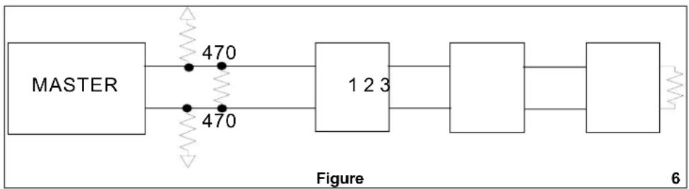
Note: SMC recommends locating the bias resistors at a single location if possible as shown in Figure 6.
flowchart
graph LR
    A["MASTER"] --> B["123"]
    B --> C["Figure"]
    C --> D["6"]
Table 4 - D.C. Load Table
| NUMBER OF NODES | TOTAL LOAD (Ohms) | ESTIMATED V_OUT (Volts) |
| 1 | 57.41 | |
| 5 | 48.97 | |
| 10 | 48.70 | |
| 15 | 52.17 | |
| 20 | 50.00 | |
| 25 | 49.65 | |
| 30 | 48.00 | |
| 35 | 47.89 | |
| 40 | 46.55 |
Table 5 takes into account line loss and shows Table 4 with the maximum distance that the network can be driven using the various data rates supported by the COM20020 (i.e. 312.5Kbs, 625Kbs, 1.25Mbs, 2.5Mbs). A 0.1 volt noise margin was used and a 0.200V receiving end voltage were used in establishing the criteria for cable length. The maximum distance driven is relatively independent of load for the node numbers of interest (<100). This is evidenced by examining Table 4 and noticing that the output voltage does not vary significantly as the number of nodes increases. Therefore, Table 5 shows the maximum distance using a driver output of 2.4V.
Table 5 - Line Length vs. Maximum Number of Nodes
| MAXIMUM NUMBER OF NODES | MAXIMUM DISTANCE @312.5 KHz | MAXIMUM DISTANCE @625 KHz | MAXIMUM DISTANCE @1.25 MHz | MAXIMUM DISTANCE @2.5 MBs |
| 21 | 2900(880 m) | 1940 ft.(590 m) | 1160 ft.(350 m) | 900 ft.(270 m) |
It should be noted that these figures are for the typical characteristics and represents a nominal case. The worst case output voltage for a RS-485 transceiver is 1.5V minimum. Typically, this worst case driver output is only encountered under heavy load conditions. If your system exhibits this parameter, measurements should be taken to correct for the lower driver output. A lower V_driver will result in shorter line lengths, however, if longer line length is needed less nodes can be accommodated.
CAPACITIVE EFFECTS
Line capacitance can have a significant effect on the performance of the network. The loading effect of the capacitance will affect both line length and the number of nodes.
Line capacitance is a combination of two sources. The first source is the effective capacitance of the two twisted wires. This is the dominant source and is directly proportional to line length (i.e as length increases so does C_line ). The second source is attributed to the capacitor formed from one wire to the insulation. This secondary capacitance is often substantially smaller but cannot be ignored. In twisted shielded cables, there is additional capacitance from conductor to the shield which can be quite appreciable in some cable types.
Network performance is often degraded by line capacitance and depends on the numbers of logical one's and zero's in a particular byte. Additionally, significant duty cycle distortion can occur due to how much the line capacitance can charge before it is discharged. For example, if a data byte of value 01h is transmitted across a cable in an RS-485 network, a significant amount of time is spent with the line voltage at +5V differentially. This amount of time is enough for the line to fully charge. When the logical one is driven (0V), the line must be completely discharged in order for the voltage to fully reach is lowest level. Quite often in high data rate networks, the bit time is much less than the time constant of the line. This will cause the duty cycle of the bits to vary depending on the bit rate, line length, and data pattern. The more logical one's in a given byte the better the duty cycle, because the line never gets to fully charge due to the many one's that are being transmitted. A secondary effect of line capacitance is bit jitter and is related to duty cycle distortion. Bit jitter results in varying pulse widths being received at the RX input of the COM20020 device. If the pulse width falls below 10ns then the bit is not detected by the COM20020 resulting in framing and CRC errors.
If capacitive effects are significantly degrading a network two approaches can be taken to resolve the problem. Solution one is to decrease the data rate of the network so as to reduce the duty cycle distortion and bit jitter, and the second is to use a special low capacitance cable specially designed for data communications. This type of cable often has increased costs as compared to telephone grade cable and may not be suitable for your every application.
CABLING TOPOLOGY AND CONNECTORS
SMC recommends a daisy-chained wiring scheme to reduce the reflections caused by long stubs used in a trunk-drop topology. RJ-11 connectors should be used through the network with a 1:1 wiring scheme (no reverse wiring). TEE connectors such as MOD-TAP p/n S09-300-444 can be used for wiring convenience but the stub should be kept as short as possible. If connectors other than RJ-11 are used measurements should be taken to insure that there is no insertion loss due to the connector. If insertion loss exists, the following equation can be used to calculate line length:
$$ V _ {r c v r} = V _ {\text { driver }} - V _ {\text { loss }} - V _ {\text { noise }} - V _ {\text { margin }} - V _ {\text { bias }} - \left(V _ {\text { insertion }} * N\right) $$
where _rcvr= Voltage received at the end of the cable
$$ V _ {\text { loss }} = \text { voltage loss from cable attenuation } $$
$$ V _ {\text { driver }} = \text { driver output under D.C. load of network } $$
$$ V _ {\text { noise }} = \text { noise margin } $$
$$ V _ {\text { margin }} = \text { tolerance of cable } (+ / - 20 \%) $$
$$ V _ {\text { bias }} = \text { Bias voltage applied to the network (typically } . 4 v) $$
$$ V _ {\text { insertion }} = \text { insertion loss } $$
N = number of nodes
There are several manufacturers of unshielded twisted pair cable. Here are a few vendors of this type of cable:
| VENDOR | CABLE | NUMBER |
| BELDEN | 9562 | |
| ALPHA | 55262 | |
| MOD-TAP | S39-102 |
For lengths greater than those listed in the above tables, SMC recommends inserting RS-485 repeaters in-line or using a hub in a Star topology. Note that, when using a hub or repeater, the device will act as one node. Be sure to take this into account when designing the network.
flowchart
graph TD
    A["NODE N"] --> C["Figure"]
    B["NODE N+1"] --> C["Figure"]
    D["NODE N+2"] --> C["Figure"]
    E["Figure"] --> F["7"]
ADDENDUM I
EXPERIMENTAL VERIFICATION OF RS-485 CABLING GUIDELINES FOR THE COM20020
OBJECTIVE:
To establish a correlation between Distance and Number of Nodes (based on the theory presented in the Cabling Guidelines) by observing network operation when distance is varied and when the number of nodes is varied. The data rate is held constant at 2.5 Mbps. Robust network operation is based on the following criteria:
a. Reflections should never cause the idle level to drop below -0.050 V, measured differentially.
b. All negative active levels should be more negative than -0.200 V, measured differentially.
c. Pulse widths of RXIN signals on various nodes should be greater than 100 nsec.
d. A thorough transmit/receive test (denoted here as Ping Pong) should operate successfully between the farthest nodes on the network and all nodes in between.
The media used is 24 AWG solid copper unshielded 2-pair twisted pair with characteristic impedance of 120 W. The network is configured in a stand-alone bus topology containing no repeaters. The cable is terminated using 120 W resistors on either end of the bus. The drops used to attach the nodes to the bus are MOD-TAP part# S09-300-444, which have a drop length of 3 in. and negligible insertion loss. The RS-485 transceivers used are National's 75176B. If a different physical media is to be evaluated, the criteria and methodology of this document may be followed. If the usage of repeaters are to be evaluated, bit jitter could be aggravated, and it is recommended to tighten the requirements on RXIN pulse width to approximately 180 nsec in order to protect against bit jitter error.
PROCEDURE:
- Configure the network to contain the maximum distance of cable specified in the Cabling Guidelines (900 feet). Connect the maximum number of nodes to the network which allows the criteria described above to be met. Attaching the appropriate bias resistors to the nodes fights reflections but hinders the minimum negative active level. Begin with 2.7 KΩ bias resistors on each node.
To determine whether the measurements fall within the criteria, take measurements as follows:
a. To differentially measure reflections, connect Channels 1 and 2 of the oscilloscope to the cable interface pins of the RS485 transceiver (pins 6 and 7 on the 75LS176). Observe the signals differentially by setting the oscilloscope to ADD and INVERT Channel 2. Connect the ground lines of the scope probes together; do not connect to system ground. Observe the tokens sent by each node to ensure that the idle level never drops below -0.050V, measured differentially. Pay special attention to the area just following the second DID of the token.
b. To differentially measure the minimum negative active levels, maintain the same setup as in (a). Observe the tokens sent by each node to ensure that negative active levels are always more negative than -0.200V, measured differentially. Pay special attention to the token sent by the furthest physical node from the one being observed. This token should appear to have the most attenuation.
c. To measure the RXIN pulse width, place Channel 1 on the RXIN signal of the COM20020 (pin 17 of the DIP package, pin 20 of the PLCC). View Channel 1; this is not a differential measurement. It may help to see each desired transmitted token by triggering externally off of the TXEN of the transmitting node. Ensure that all RXIN pulses are present and that they are all greater than 100 nsec wide. Due to the biasing of the network, the capacitance of the cable, and the RS-485 transceivers, the pulses most likely to disappear are the negative transitions (logic "1"s to the COM20020) immediately following a long duration of a high level (many logic "0"s to the COM20020). Pay special attention, for instance, to the negative transition in the 04H pattern (End Of Transmission pattern) and the negative transition immediately following this pattern. Again, the token sent by the furthest node is most likely to have problems as viewed by the observed node. Although the COM20020 data sheet specifies a minimum RXIN width of 10 nsec., it is important that the RXIN signals be greater than 100 nsec. This is because bit jitter, which is affected by duty cycle distortion due to the capacitance of the network, must be taken into account. As long as the RXIN width is greater than 100 nsec, it is guaranteed that bit jitter will not cause the receive circuitry of the COM20020 to lose synchronization.
-
Record the results obtained in Step 1, including the worst reflections on the network, minimum negative active level of the worst transition from the furthest node, RXIN width of the worst transition from the furthest node, and whether the Ping Pong test works between all nodes on network.
-
Detach 100 feet of cable, keep two nodes attached to network, and make the same measurements as in Step 1 and record.
- Add nodes to the network, remeasuring the parameters, until the measurements are similar to those obtained previously (worst reflection amplitude, minimum negative active level, RXIN width, and behavior of Ping Pong).
- Repeat steps (3) and (4) until Distance vs. Number of Nodes curve is complete.
SETUP:
See Figure 1 for the setup of the experiment. The media used is 24 AWG solid copper unshielded 2-pair twisted pair with characteristic impedance of 120 W. The network is configured in a stand-alone bus topology. The cable is terminated using 120 W resistors on either end of the bus. The drops used to attach the nodes to the bus are MOD-TAP part# S09-300-444, which have a drop length of 3 in. and negligible insertion loss. The RS-485 transceivers used are National's 75176B.

flowchart
graph TD
    A["P.C. Node NID=FD"] --> B["120 Ohm"]
    C["20020 NODE"] --> D["120 Ohm"]
    E["20020 20020 NODE"] --> F["120 Ohm"]
    G["20020 20020 NODE"] --> H["120 Ohm"]
    I["20020 20020 NODE"] --> J["120 Ohm"]
    K["20020"] --> L["120 Ohm"]
    M["20020 NODE"] --> N["120 Ohm"]
    O["20020 20020 NODE"] --> P["120 Ohm"]
    Q["20020"] --> R["120 Ohm"]
    S["20020"] --> T["120 Ohm"]
    U["20020"] --> V["NID=FA"]
    W["20020"] --> X["SCOPE"]
    Y["20020"] --> Z["CH 1 + CH 2 CH 3"]
    AA["Total Distance = 900 feet, 800 feet, 700 feet, 600 feet, 500 feet"] --> AB
    AC["Scope views Minimum Negative Active Level of Token passed by NID FD by adding and inverting Channel 2. RXIN width is viewed on Channel 3."] --> AD
RESULTS:
Table 1 - Results
(Each node containing 2.7 KW bias resistors)
| Configuration(#Nodes:Feet) | Minimum Idle Level(including reflections)(Volts) | Minimum Negative ActiveLevel(Volts) | RXINWidth(nsec) | PingPong? | No. of Additional Nodes toBring to Minimum NegativeActive Levels PreviouslyObtained at:600/700/800/900 Feet |
| 2:900 | +0.050 | -0.300 | 100 | Yes | -/-/-/- |
| 2:800 | +0.050 | -0.500 | 120 | Yes | -/-/-4 |
| 2:700 | +0.100 | -0.600 | 140 | Yes | -/-4/10 |
| 2:600 | +0.100 | -0.700 | 160 | Yes | -/5/10/14 |
| 2:500 | +0.100 | -0.800 | 180 | Yes | 5/10/14/* |
- The Cabling Guidelines specify that 900 feet is the maximum distance for a network. Experimentally, it was found that only 2 nodes may exist at 900 feet to safely meet the criteria listed above.
-
100 feet of cable was detached. At 800 feet, the addition of 4 more nodes was required to bring the Minimum Negative Active Level to those obtained for 2 Nodes at 900 feet.
-
Another 100 feet of cable was detached. At 700 feet, the addition of 4 more nodes was required to bring the Minimum Negative Active Level to those obtained for 2 Nodes at 800 feet, and the addition of 10 for those obtained at 900 feet.
- Another 100 feet of cable was detached. At 600 feet, the addition of 5 more nodes was required to bring the Minimum Negative Active Level to those obtained for 2 Nodes at 700 feet, the addition of 10 for those obtained at 800 feet, and the addition of 14 for those obtained at 900 feet.
- A final 100 feet of cable was detached. At 500 feet, the addition of 5 more nodes was required to bring the Minimum Negative Active Level to those obtained for 2 Nodes at 600 feet, the addition of 10 for those obtained at 700 feet, and the addition of 14 for those obtained at 800. * When 18 additional nodes were added, the minimum negative active level was similar to that obtained for 800 feet, which means that as cable distance decreases, the number of nodes begins to increase more rapidly.

line
| Distance (feet) | Total No. Nodes | |---|---| | 0-900 | 0 | | 900-1800 | 16 | | 1800-2700 | 19 | | 2700-3600 | 15 | | 3600-4500 | 6 | | 4500-5400 | 2 | | 5400-6300 | 2 | Figure 2Note that the previous values were all obtained using bias resistors of 2.7 KΩ. Once the node count exceeds 10, it is suggested to place higher value bias resistors on each node. This brings the bias level down to a reasonable level, allowing the minimum negative active level to become higher, but keeping the level of reflections still within specification.
The Distance vs. Number of Nodes curve, obtained from the previous results (using 2.7 KΩ bias resistors), is presented in Figure 2. Also in Figure 2 is a portion of the curve which results in placing 12 KΩ bias resistors on each node.
The following are additional results obtained, which may be helpful to the user, including the Edge Rate (around 0V differential) of the worst pulse seen from 20 unique tokens and the rise and fall time of a typical pulse. They are presented here:
Rising Transition Edge Rate = 22.2 Volts/μsec worst case.
Falling Transition Edge Rate = 7.27 Volts/μsec worst case.
Rise Time = 280 nsec typical.
Fall Time = 130 nsec typical.
CONCLUSION:
It was seen that the curve was relatively linear when one bias resistor value is placed on each node. Since the slope of the curve is approximately 4 nodes for every 100 feet (in terms of Minimum Negative Active Level), we can see that the addition of a 100 foot segment of cable has four times the impact versus the addition of one node. Therefore, the addition of two more nodes at 600 feet does not significantly hinder the network performance. In fact, connecting a total of 18 nodes at 600 feet with 2.7K bias resistors still showed perfect Ping Pong operation between all nodes. In addition, 10 Nodes at 1000 feet was observed, with the following results: Reflections of -0.100V , a minimum negative active level of -0.200V , and an RXIN width of 40 nsec. Ping Pong operation was adequate, but measurements such as these should be considered marginal because pushing the limits of the curve can represent marginal behavior. At any time, a tradeoff exists between reflections and the minimum negative active level. Adding many nodes to the network increases the probability of significant reflections. To overcome this, one might be inclined to raise the bias of the network. At some point, however, the minimum negative active level will no longer fall within the specified limits of the RS-485 Receiver.
Alternatively, increasing the number of nodes increases the total bias of the network. Therefore, to keep the minimum negative active level within specification, the bias resistor of each node may be increased thus decreasing the overall bias of the network. Increasing the bias resistors on each node to 12 KΩ allowed a large number of nodes to operate over a longer distance. However, please note that reflections are more likely to cross the specified threshold. The results of this experiment indicate that 14 nodes at 900 feet, or 19 nodes at 800 feet exhibited successful results. No additional testing was performed above 19 nodes.
ADDENDUM II
5 Mbs DC COUPLED RS-485 ANALYSIS
As a result of future customer requirements, an analytical and experimental analysis was performed with ARCNET running at a 5Mbs data rate using an RS-485 compatible physical layer. This analysis will present line loss, reflection values, biasing concerns, and a distance vs. load chart.
LINE LOSS
Using a symmetrical 5Mhz sine wave burst, the average line loss for UTP with 120 ohm terminations was found to be -2.0dB per 100 feet.
REFLECTIONS AND RAF
From experimental results, the maximum reflection measured was 50V_p-p . The average RAF was approximately -15.0dB of the incident wave.
DC BIASING
As discussed in TN 7-5, DC biasing of the network is necessary to avoid unwanted transitions as a result of reflections generated along the line. Although the maximum reflection is .5 volts, we are only concerned with the negative portion of the wave, so for calculation of the bias resistors a value of .25V will be used. Due to the larger reflections generated at 5Mbs, the following chart should be used:
| NUMBER OF NODES RESISTOR VALUE | |
| 2 - 5 1.8K | |
| 6 - 10 2.7K | |
| 11 - 20 6.8K | |
| 21 - 32 12.0K | |
Note: One set of bias resistors can be used for the entire network. In this case, a value of 470 ohms should be used.
ANALYTICAL PERFORMANCE
Analytical performance is based on several measured parameters including line loss and maximum reflections given a 5V_p_ep input. The bias resistors calculated above were determined based on the maximum reflection. If a smaller incident is to be used, the maximum reflection can be calculated using the RAF. Three cases are considered in the analysis: a nominal case in which the 485 transceiver outputs a +5V signal; a typical case where the driver outputs 2.4V; and a worst case where the driver outputs 1.5V.
| NUMBER OF NODES NOMINAL (5V) TYPICAL (2.4V) WORST CASE (1.5V) | |||
| 1 - 5 1.1Kft 800ft 600ft | |||
| 6 - 10 1.1Kft 800ft 550ft | |||
| 11 - 20 | 1.1Kft 800ft 550ft | ||
| 21 - 32 | 1.1Kft 775ft 525ft | ||
Note: The above numbers are calculated and do not take into account bit jitter or duty cycle distortion effects.
MEASURED PERFORMANCE
The procedure and criteria used for determining acceptable performance are identical to those outlined in Addendum I (Experimental Verification of RS-485 Cabling Guidelines for the COM20020). The only parameter that was changed was the bit jitter budget, which was decreased from 100ns to 50ns due to the change in clock speed. The following results were obtained:
Maximum distance - 600ft
Maximum number of nodes - 17
The maximum distance achieved was found with a +5v driver output. The primary reason for the decreased performance is attributed to duty cycle distortion as a result of the biasing network.

SMSC™
80 Arkay Drive
Hauppauge, NY 11788
(631)
435-6000
FAX (631) 273-3123
Copyright © SMSC 2004. All rights reserved.
Circuit diagrams and other information relating to SMSC products are included as a means of illustrating typical applications. Consequently, complete information sufficient for construction purposes is not necessarily given. Although the information has been checked and is believed to be accurate, no responsibility is assumed for inaccuracies. SMSC reserves the right to make changes to specifications and product descriptions at any time without notice. Contact your local SMSC sales office to obtain the latest specifications before placing your product order. The provision of this information does not convey to the purchaser of the described semiconductor devices any licenses under any patent rights or other intellectual property rights of SMSC or others. All sales are expressly conditional on your agreement to the terms and conditions of the most recently dated version of SMSC's standard Terms of Sale Agreement dated before the date of your order (the "Terms of Sale Agreement"). The product may contain design defects or errors known as anomalies which may cause the product's functions to deviate from published specifications. Anomaly sheets are available upon request. SMSC products are not designed, intended, authorized or warranted for use in any life support or other application where product failure could cause or contribute to personal injury or severe property damage. Any and all such uses without prior written approval of an Officer of SMSC and further testing and/or modification will be fully at the risk of the customer. Copies of this document or other SMSC literature, as well as the Terms of Sale Agreement, may be obtained by visiting SMSC's website at http://www.smsc.com. SMSC is a registered trademark of Standard Microsystems Corporation ("SMSC"). Product names and company names are the trademarks of their respective holders.
SMSC DISCLAIMS AND EXCLUDES ANY AND ALL WARRANTIES, INCLUDING WITHOUT LIMITATION ANY AND ALL IMPLIED WARRANTIES OF MERCHANTABILITY, FITNESS FOR A PARTICULAR PURPOSE, TITLE, AND AGAINST INFRINGEMENT AND THE LIKE, AND ANY AND ALL WARRANTIES ARISING FROM ANY COURSE OF DEALING OR USAGE OF TRADE.
IN NO EVENT SHALL SMSC BE LIABLE FOR ANY DIRECT, INCIDENTAL, INDIRECT, SPECIAL, PUNITIVE, OR CONSEQUENTIAL DAMAGES; OR FOR LOST DATA, PROFITS, SAVINGS OR REVENUES OF ANY KIND; REGARDLESS OF THE FORM OF ACTION, WHETHER BASED ON CONTRACT; TORT; NEGLIGENCE OF SMSC OR OTHERS; STRICT LIABILITY; BREACH OF WARRANTY; OR OTHERWISE; WHETHER OR NOT ANY REMEDY OF BUYER IS HELD TO HAVE FAILED OF ITS ESSENTIAL PURPOSE, AND WHETHER OR NOT SMSC HAS BEEN ADVISED OF THE POSSIBILITY OF SUCH DAMAGES.