ATSAMA5D23 - Electronic component Microchip - Free user manual and instructions
Find the device manual for free ATSAMA5D23 Microchip in PDF.

User questions about ATSAMA5D23 Microchip
0 question about this device. Answer the ones you know or ask your own.
Ask a new question about this device
Download the instructions for your Electronic component in PDF format for free! Find your manual ATSAMA5D23 - Microchip and take your electronic device back in hand. On this page are published all the documents necessary for the use of your device. ATSAMA5D23 by Microchip.
USER MANUAL ATSAMA5D23 Microchip
SAMA5D2C XULT User's Guide
Introduction
natural_image
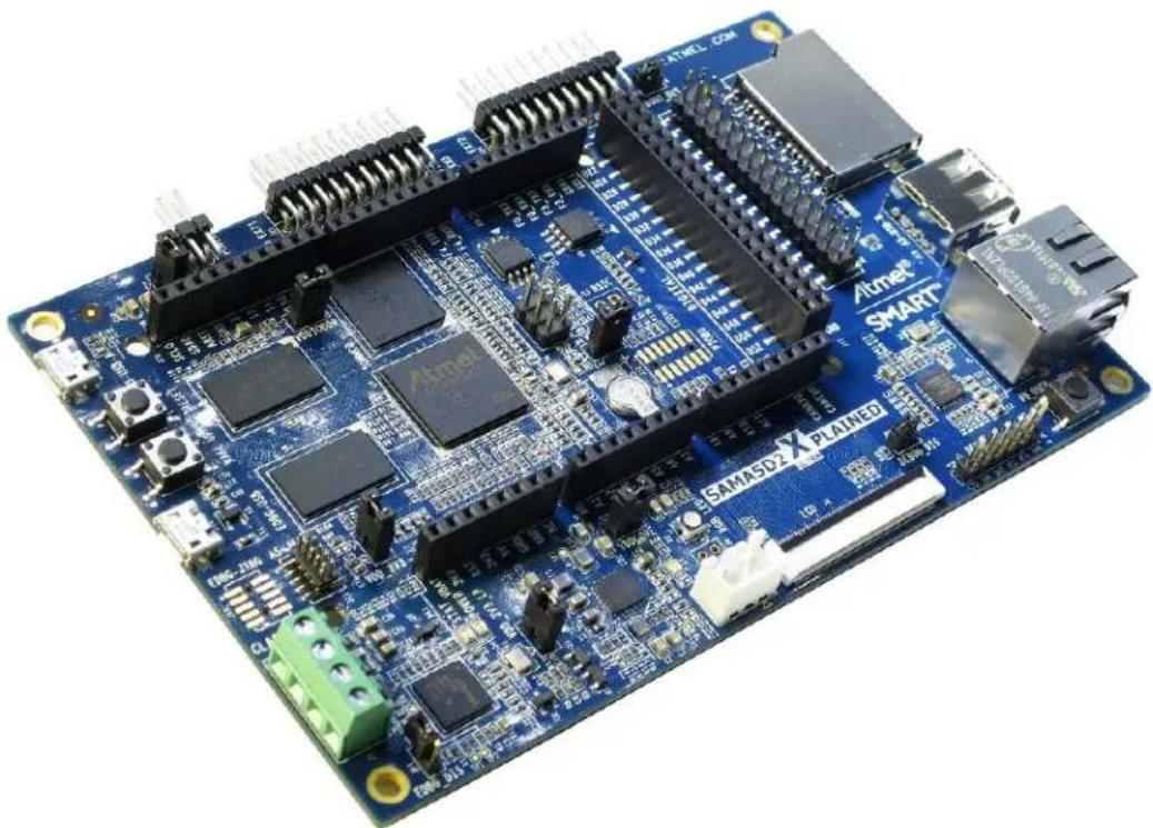
Blue printed circuit board with multiple ATMEs and Smart components (no readable text or symbols)This user's guide introduces the Microchip SAMA5D2C Xplained Ultra evaluation kit (SAMA5D2C-XULT kit) and describes the development and debugging capabilities for applications running on the SAMA5D2 Arm® Cortex®-A5-based microprocessor unit (MPU). The SAMA5D2C-XULT kit supports the following part numbers:
- ATSAMA5D21C
- ATSAMA5D22C
- ATSAMA5D23C
- ATSAMA5D24C
- ATSAMA5D26C
- ATSAMA5D27C
- ATSAMA5D28C
Table of Contents
Introduction....1
- Kit Contents....3
- Evaluation Kit Specifications....4
2.1. Electrostatic Warning....4
2.2. Power Supply Warning....4
- Board Power-Up....5
- Sample Code and Technical Support....6
- Hardware Overview....7
5.1. Introduction....7
5.2. Equipment List....7
5.3. Board Features....7
- Board Components....9
6.1. Board Overview....9
6.2. Connectors On Board....10
6.3. Function Blocks....10
6.4. PIO Usage and Interface Connectors.... 21
6.5. PIO Usage on Expansion Connectors....41
- Board Schematics....55
- Errata....70
8.1. NRST....70
8.2. nLBO....70
8.3. R63....70
8.4. R100/R105....70
- Revision History....71
The Microchip Website....72
Product Change Notification Service....72
Customer Support....72
Microchip Devices Code Protection Feature....72
Legal Notice....73
Trademarks....73
Quality Management System....74
Worldwide Sales and Service....75
1. Kit Contents
The SAMA5D2C Xplained Ultra evaluation kit includes:
• One SAMA5D2C-XULT board
• One Micro-AB type USB cable
2. Evaluation Kit Specifications
Table 2-1. Evaluation Kit Specifications
| Characteristic Specifications | ||
| Board SAMA5D2C-XULT | ||
| Part Number ATSAMA5D2C-XULT | ||
| Board Supply Voltage USB and/or Battery powered | ||
| Temperature Operating | 0°C to +70°C | |
| Storage -40°C to +85°C | ||
| Relative Humidity 0 to 90% (non-condensing) | ||
| Main Board Dimensions (L x W x H) 135 × 88 × 20 mm | ||
| Board Identification SAMA5D2 XPLAINED ULTRA | ||
2.1 Electrostatic Warning

ESD-Sensitive Electronic Equipment!
The evaluation kit is shipped in a protective anti-static package. The board system must not be subject to high electrostatic potentials.
We recommend using a grounding strap or similar ESD protective device when handling the board in hostile ESD environments (offices with synthetic carpet, for example). Avoid touching the component pins or any other metallic element on the board.
2.2 Power Supply Warning

Hardware Power Supply Limitation
Powering the board with voltages higher than 5 VCC (e.g., the 12 VCC power adapters from other kits such as Arduino kits) may damage the board.

Hardware Power Budget
Using the USB as the main power source (max. 500 mA) is acceptable only with the use of the on-board peripherals and low-power LCD extension.
When external peripheral or add-on boards need to be powered, we recommend the use of an external power adapter connected to the USB Micro-AB connectors (can provide up to 1.2A on the 3.3V node).
3. Board Power-Up
Three sources are available to power-up the SAMA5D2C-XULT board:
- USB-powered through the USB Micro-AB connector (J23 - default configuration)
- Powered through the USB Micro-AB connector on the Embedded Debugger (EDBG) interface (J14)
- Powered through a rechargeable battery Li-polymer 3.7V connected to J3 or J4

Unlike Arduino Uno boards, the SAMA5D2C-XULT board runs at 3.3V. The maximum voltage that the I/O pins can tolerate is 3.3V. Providing higher voltages (e.g., 5V) to an I/O pin could damage the board.
The sequence for the initial power-up of the board is the following:
- Unpack the board, taking care to avoid electrostatic discharge.
- Connect the USB Micro-AB cable to the connector J23 (or J14).
- Connect the other end of the cable to a free USB port of your PC.
Table 3-1. Electrical Characteristics
| Parameter Value | |
| Input voltage 5 VCC | |
| Maximum input voltage (limits) 6 VCC | |
| Maximum DC 3.3V current available 1.2A | |
| I/O voltage 3.3V only |
4. Sample Code and Technical Support
After boot up, you can run sample code or your own application on the evaluation kit. Sample code and technical support is available on www.microchip.com. In particular, the software package (example source code and drivers) can be found on the "SAMA5D2 Software Package" page of our website.
Linux® software and demos can be found on www.at91.com/linux4sam/bin/view/Linux4SAM/.

Make sure that the latest software version is downloaded before starting your evaluation. For more information, go to www.at91.com/linux4sam/bin/view/Linux4SAM/.
5. Hardware Overview
5.1 Introduction
The SAMA5D2C-XULT kit is a full-featured evaluation platform for the SAMA5D2 series ARM-based microprocessor units (MPU). It allows users to extensively evaluate, prototype and create application-specific designs.
5.2 Equipment List
The SAMA5D2C-XULT board is based on the integration of an ARM Cortex-A5-based microprocessor with external memory, one Ethernet physical layer transceiver, one SD/MMC interface, one host USB port and one device USB port, one 24-bit RGB LCD and debug interfaces.
Seven headers, compatible with Arduino R3 (Uno, Due) and two Xplained headers are available for various shield connections.
5.3 Board Features
Table 5-1. Board Specifications
| Characteristics Specifications | |
| Dimensions (L x W x H) | 135 x 88 x 20 mm |
| Processor SAMA5D27C (289-ball BGA package), 14x14 mm body, 0.8 mm ball pitch | |
| Oscillators MPU, EDBG: 12 MHz crystalRTC: 32.768 kHzPHY: 25 MHz | |
| Main memory 2 x DDR3L SDRAM 2 Gbit - 16 Mbit x 16 x 8 banks (total 4 Gbit = 512 Mbyte)1 x eMMC NAND Flash 4 Gbit | |
| Accessory memories One Serial EEPROM SPIOne QSPI Serial FlashOne EEPROM with MAC Address and Serial Number | |
| SD/MMC One 4-bit SD card connector | |
| USB One USB Host with power switchOne Micro-AB USB device | |
| Display One LCD interface connector, LCD TFT Controller with overlay, alpha-blending, rotation, scaling and color space conversion | |
| Image sensor One ISC interface and connector | |
| Ethernet One Ethernet PHY (RMII 10/100 MHz) | |
| Debug port One JTAG interface connectorOne EDBG interface with CDCOne serial debug console interface (3.3V level) | |
| Expansion connector Arduino R3 compatible set of connectorsXPRO set of connectors | |
| ......continued | |
| Characteristics Specifications | |
| Board supply voltage 5V from USBOn-board power regulation by PMICExternal battery-powered capability | |
| Battery On-board PowerCap | |
| User interface Reset, wake-up and user configurable push buttonsOne tri-color user LED (red, green, blue) | |
6. Board Components
6.1 Board Overview
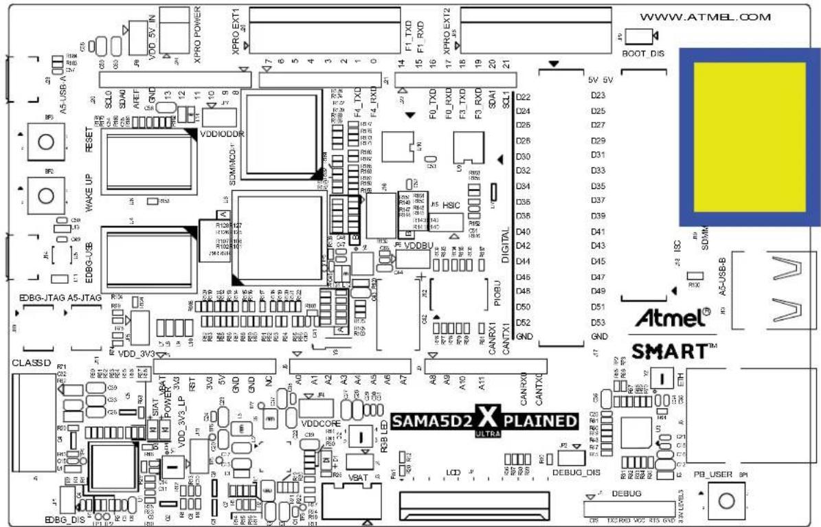
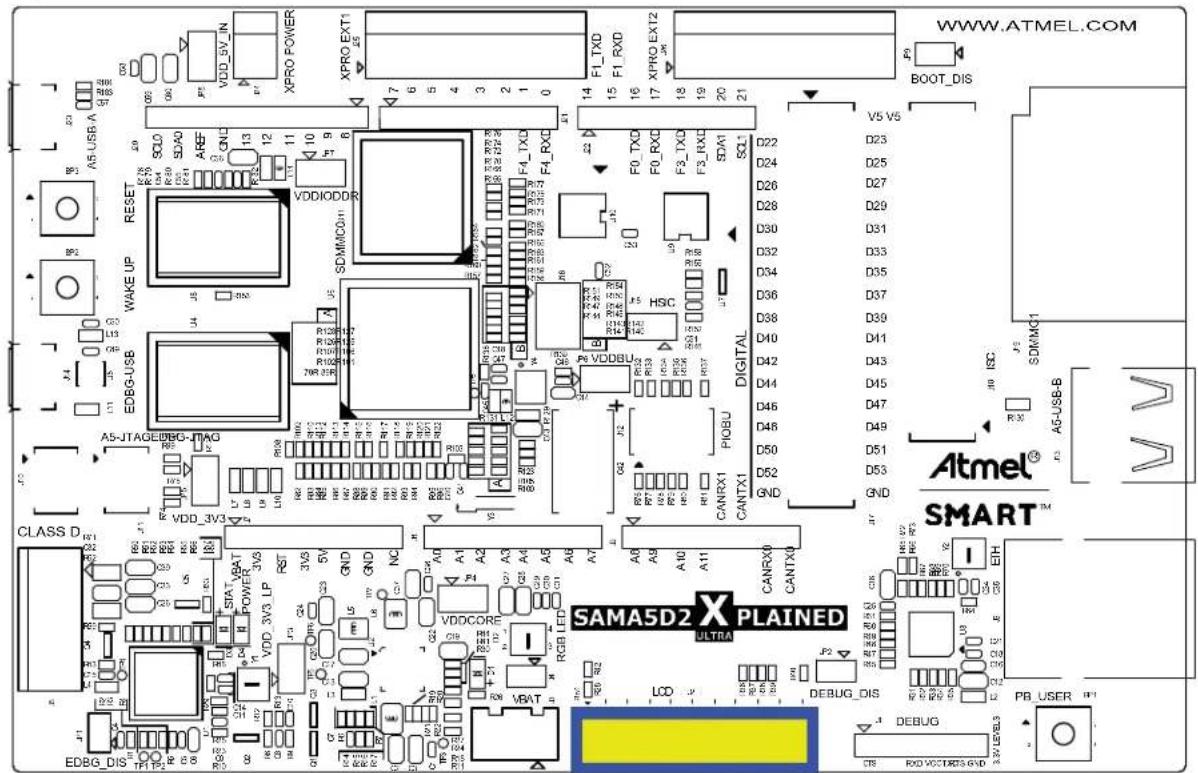
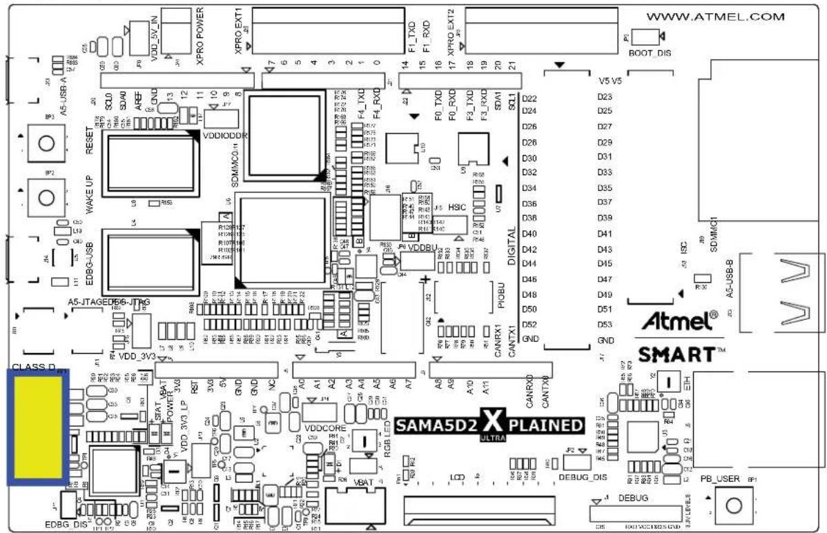
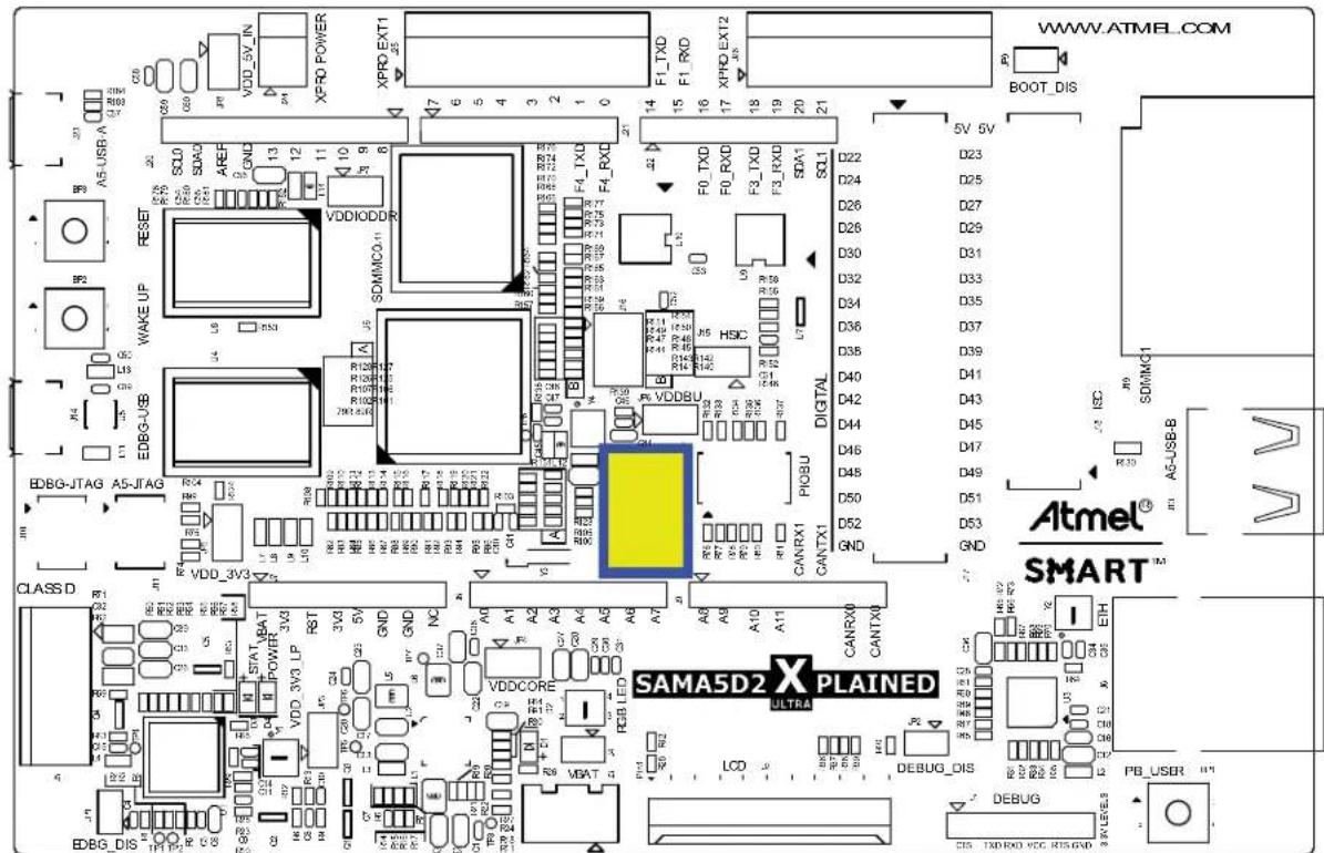
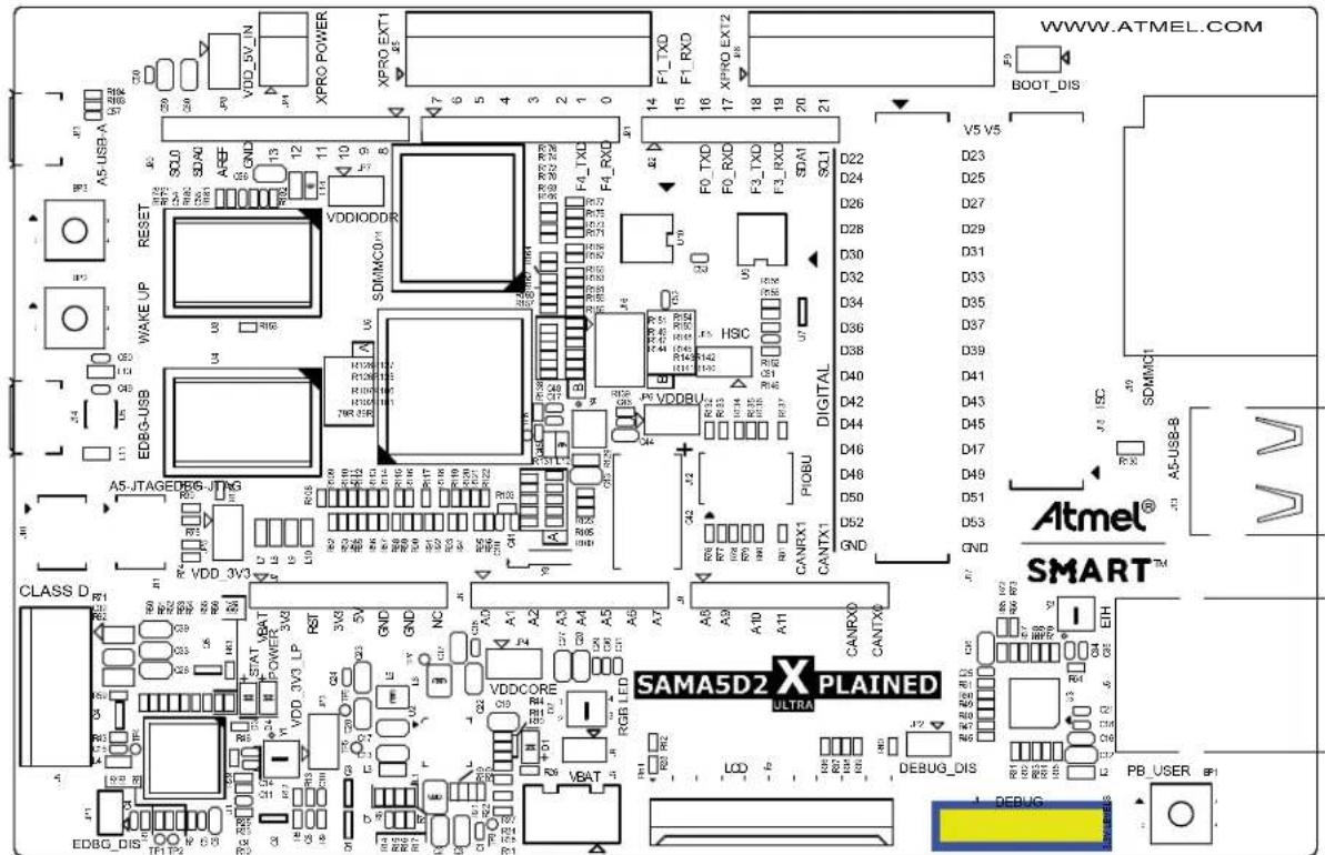
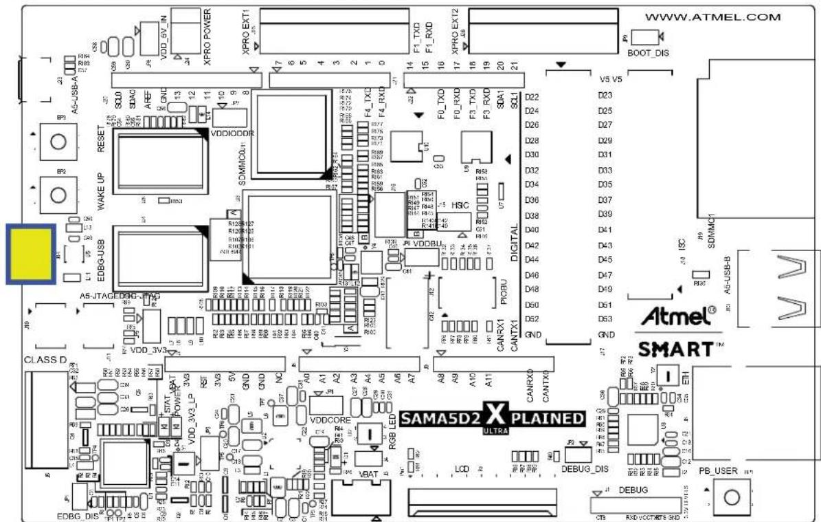
The fully-featured SAMA5D2C-XULT board integrates multiple peripherals and interface connectors as shown in the figure below.
Figure 6-1. SAMA5D2C-XULT Board Overview

text_image
WWW.ATMEL.COM BOOT_DIS V5 V5 D23 D25 D27 D29 D30 D31 D33 D35 D37 D38 D40 D41 D43 D45 D47 D49 D51 D53 GND DIGITAL P/IOBU CANRX1 CANTX1 C42 A12 R163 R164 R165 R166 R167 R168 R169 R170 R171 R172 R173 R174 R175 R176 R177 R178 R179 R180 R181 R182 R183 R184 R185 R186 R187 R188 R189 R190 R191 R192 R193 R194 R195 R196 R197 R198 R199 R200 R201 R202 R203 R204 R205 R206 R207 R208 R209 R210 R211 R212 R213 R214 R215 R216 R217 R218 R219 R220 R221 SAMA5D2 X_PLAINED CLASS D R71 STAT_VBAT POWER 3V3 RST 3V3 5V GND NC A0 A1 A2 A3 A4 A5 A6 A7 A8 A9 A10 A11 CANRXI CANTXI VDDCORE VDCB LED RGB LED RGB LED RGB LED RGB LED RGB LED RGB LED RGB LED RGB LED RGB LED RGB LED RGB LED RGB LED RGB LED RGB LED RGB LED RGB LED RGB LED RGB LED RGB LED RGB LED RGB LED RGB LED RGB LED RGB LED RGB LED RGB LED RGB LED RGB LED RGB LED RGB LED RGB LED RGB LED RGB LED RGB LED RGB LED RGB LED RGB LED RGB LED RGB LED RGB LED RGB LED RGB LED RGB LED RGB LED RGB LED RGB LED RGB LED RGB LED RGB LED RGB LED PCB 3V3 LP RST 3V3 5V GND NC A0 A1 A2 A3 A4 A5 A6 A7 A8 A9 A10 A11 CANRXI CANTXI VDDCORE VDCB LED RGB LED RGB LED RGB LED RGB LED RGB LED RGB LED RGB LED RGB LED RGB LED RGB LED RGB LED RGB LED RGB LED RGB LED RGB LED RGB LED RGB LED RGB LED RGB LED RGB LED RGB LED RGB LED RGB LED RGB LED PCB 3V3 LP RST 3V3 5V GND NC A0 A1 A2 A3 A4 A5 A6 A7 A8 A9 A10 A11 CANRXI CANTXI GND CNTX I/O ETH SAMA5D2 X_PLAINED LCD P B DEBUG_DIS CNTX I/O ETH SAMA5D2 X_PLAINED LCD P B DEBUG_DIS CNTX I/O ETH SAMA5D2 X_PLAINED LCD P B DEBUG_DIS CNTX I/O ETH SAMA5D2 X_PLAINED LCD P B DEBUG_DIS CNTX I/O ETH SAMA5D2 X_PLAINED LCD P B DEBUG_DIS CNTX I/O ETH SAMA5D4 X_PLAINED LCD P B DEBUG_DIS CNTX I/O ETH SAMA5D4 X_PLAINED LCD P B DEBUG_DIS CNTX I/O ETH SAMA5D4 X_PLAINED LCD P B DEBUG_DIS CNTX I/O ETH SAMA5D4 X_PLAINED LCD P B DEBUG_DIS CNTX I/O ETH SAMA5D4 X_PLAINED LCD P B DEBUG_DIS CMTX I/O ETH SAMA5D4 X_PLAINED LCD P B DEBUG_DIS CMTX I/O ETH SAMA5D4 X_PLAINED LCD P B DEBUG_DIS CMTX I/O ETH SAMA5D4 X_PLAINED LCD P B DEBUG_DIS CMTX I/O ETH SAMA5D4 X_PLAINED LCD P B DEBUG_DIS CMTX I/O ETH SAMA5D4 X PLAINED LCD P B DEBUG_DIS CMTX I/O ETH SAMA5D4 X PLAINED LCD P B DEBUG_DIS CMTX I/O ETH SAMA5D4 X PLAINED LCD P B DEBUG_DIS CMTX I/O ETH SAMA5D4 X PLAINED LCD P B DEBUG_DIS CMTX I/O ETH SAMA5D4 X PLAINED LCD P B DEBUG_DIS CMTX I/II ETH SAMA5D4 X PLAINED LCD P B DEBUG_DIS CMTX I/II ETH SAMA5D4 X PLAINED LCD P B DEBUG_DIS CMTX I/II ETH SAMA5D4 X PLAINED LCD P B DEBUG_DIS CMTX I/II ETH SAMA5D4 X PLAINED LCD P B DEBUG_DIS CMTX I/II ETH SAMA5D4X PLAINED LCD P B DEBUG_DIS CMTX I/II ETH SAMA5D4X PLAINED LCD P B DEBUG_DIS CMTX I/II ETH SAMA5D4X PLAINED LCD P B DEBUG_DIS CMTX I/II ETH SAMA5D4X PLAINED LCD P B DEBUG_DIS CMTX I/II ETH SAMA5D4X PLAINED LCD P B DEUG_DIS CMTX I/O ETH SAMA5D4X PLAINED LCD P B DEUG_DIS CMTX I/O ETH SAMA5D4X PLAINED LCD P B DEUG_DIS CMTX I/O ETH SAMA5D4X PLAINED LCD P B DEUG_DIS CMTX I/O ETH SAMA5D4X PLAINED LCD P B DEUG_DIS CMTX I/O ETH SAMA5D4X PLAINED LCO D P B DEUG_DIS CMTX I/O ETH SAMA5D4X PLAINED LCO D P B DEUG_DIS CMTX I/O ETH SAMA5D4X PLAINED LCO D P B DEUG_DIS CMTX I/O ETH SAMA5D4X PLAINED LCO D P B DEUG_DIS CMTX I/O ETH SAMA5D4X PLAINED LCO D P B DEUG_DIS CMTx I/O ETH SAMA5D4X PLAINED LCO D P B DEUG_DIS CMTx I/O ETH SAMA5D4X PLAINED LCO D P B DEUG_DIS CMTx I/O ETH SAMA5D4X PLAINED LCO D P B DEUG_DIS CMTx I/O ETH SAMA5D4X PLAINED LCO D P B DEUG_DIS CMTx I/O ETH SAMA5DO X PLAINED LCO D P B DEUG_DIS CMTx I/O ETH SAMA5D4X PLAINED LCO D P B DEUG_DIS CMTx I/O ETH SAMA5D4X PLAINED LCO D P B DEUG_DIS CMTx I/O ETH SAMA5D4X PLAINED LCO D P B DEUG_DIS CMTx I/O ETH SAMA5D4X PLAINED LCO D P BDEUG_DIS CMTx I/O ETH SAMA5D4X PLAINED LCO D P B DEUG_DIS CMTx I/O ETH SAMA5D4X PLAINED LCO D P B DEUG_DIS CMTx I/O ETH SAMA5D4X PLAINED LCO D P B DEUG_DIS CMTx I/O ETH SAMA5D4X PLAINED LCO D P B DEUG_DIS CMTx I/OE TH SAMA5D4X PLAINED LCO D P B DEUG_DIS CMTx I/OE TH SAMA5D4X PLAINED LCO D P B DEUG_DIS CMTx I/OE TH SAMA5D4X PLAINED LCO D P B DEUG_DIS CMTx I/OE TH SAMA5D4X PLAINED LCO D P B DEUG_DIS CMTx I/OE TH SAMA5D4X PLAINEED LCO D P B DEUG_DIS CMTx I/OE TH SAMA5D4X PLAINED LCO D P B DEUG_DIS CMTx I/OE TH SAMA5D4X PLAINED LCO D P B DEUG_DIS CMTx I/OE TH SAMA5D4X PLAINED LCO D P B DEUG_DIS CMTx I/OE TH SAMA5D4X PLAINEED LCO D P B DEUIG_DIS CMTx I/OE TH SAMA5D4X PLAINED LCO D P B DEUIG_DIS CMTx I/OE TH SAMA5D4X PLAINEED LCO D P B DEUIG_DIS CMTx I/OE TH SAMA5D4X PLAINEED LCO D P B DEUIG_DIS CMTx I/OE TH SAMA5D4X PLAINEED LCO D P B DEUIG_DIS CMTx I/OE TH SAMA5D4X PLAINEED LCO D P B DEUIG_DIS CMTx I/OE TH SAMA5D4X PLAINEES LCO D P B DEUIG_DIS CMTx I/OE TH SAMA5D4X PLAINEED LCO D P B DEUIG_DIS CMTx I/OE TH SAMA5D4X PLAINEED LCO D P B DEUIG_DIS CMTx I/OE TH SAMA5D4X PLAINEED LCO D P B DEUIG_DIS CMTx I/OE TH SAMA5D4X PLAINEE LCO D P B DEUIG_DIS CMTx I/OE TH SAMA5D4X PLAINEED LCO D P B DEUIG_DIS CMTx I/OE TH SAMA5D4X PLAINEED LCO D P B DEUIG_DIS CMTx I/OE TH SAMA5D4X PLAINEED LCO D P B DEUIG_DIS CMTx I/OE TH SAMA5D4X PLAINEEN LCO D P B DEUIG_DIS CMTx I/OE TH SAMA5D4X PLAINEED LCO D P B DEUIG_DIS CMTx I/OE TH SAMA5D4X PLAINEED LCO D P B DEUIG_DIS CMTx I/OE TH SAMA5D4X PLAINEED LCO D P B DEUIG_DIS CMTx I/OE TH SAMA5D4X PLAINEEM LCO D P B DEUIG_DIS CMTx I/OE TH SAMA5D4X PLAINEED LCO D P B DEUIG_DIS CMTx I/OE TH SAMA5D4X PLAINEED LCO D P B DEUIG_DIS CMTx I/OE TH SAMA5D4X PLAINEED LCO D P B DEUIG_DIS CMTx I/OE TH SAMA5D4X PLAINEEDI LCO D P B DEUIG_DIS CMTx I/OE TH SAMA5D4X PLAINEEDI LCO D P B DEUIG_DIS CMTx I/OE TH SAMA5D4X PLAINEEDI LCO D P B DEUIG_DIS CMTx I/OE TH SAMA5D4X PLAINEEDI LCO D P B DEUIG_DIS CMTx I/OE TH SAMA5D4X PLAINEEDL CO D P B DEUIG_DIS CMTx I/OE TH SAMA5D4X PLAINEEDL CO D P B DEUIG_DIS CMTx I/OE TH SAMA5D4X PLAINEEDL CO D P B DEUIG_DIS CMTx I/OE TH SAMA5D4X PLAINEEDL CO D P B DEUIG_DIS CMTx I/OE TH SAMA5D4X PLAINEEDL IL CO D P B DEUIG_DIS CMTx I/OE TH SAMA5D4X PLAINEEDL IL CO D P B DEUIG_DIS CMTx I/OE TH SAMA5D4X PLAINEEDL IL CO D P B DEUIG_DIS CMTx I/OE TH SAMA5D4X PLAINEEDL IL CO D P B DEUIG_DIS CMTx I/OE TH SAMA5D4X PLANEEDL IL CO D P B DEUIG_DIS CMTx I/OE TH SAMA5D4X PLAINEEDL IL CO D P B DEUIG_DIS CMTx I/OE TH SAMA5D4X PLAINEEDL IL CO D P B DEUIG_DIS CMTx I/OE TH SAMA5D4X PLAINEEDL IL CO D P B DEUIG_DIS CMTx I/OE TH SAMA5DO X PLAINEEDL IL CO D P B DEUIG_DIS CMTx I/OE TH SAMA5D4X PLAINEEDL IL CO D P B DEUIG_DIS CMTx I/OE TH SAMA5DO X PLAINEEDL IL CO D P B DEUIG_DIS CMTx I/OE TH SAMA5DO X PLAINEEDL IL CO D P B DEUIG_DIS CMTx I/OE TH SAMA5DO X PLAINEEDL IL CO D P B DEUIG_DIS CMTx I/OE TH SAMA5DO X PLAINEEDL IL CO D P B DEUIG_DIS CMTx I/OE TH SAMA5DO x PLAINEEDL IL CO D P B DEUIG_DIS CMTx I/OE TH SAMA5DO x PLAINEEDL IL CO D P B DEUIG_DIS CMTx I/OE TH SAMA5DO x PLAINEEDL IL CO D P B DEUIG_DIS CMTx I/OE TH SAMA5DO x PLAINEEDL IL CO D P B DEUIG_DIS CMTx I/OE TH SAMA5DO X PLAINEEDL IL CO D P B DEUIG_DIS CMTx I/OE TH SAMA5DO x PLAINEEDL IL CO D P B DEUIG_DIS CMTx I/OE TH SAMA5DO x PLAINEEDL IL CO D P B DEUIG_DIS CMTx I/OE TH SAMA5DO X PLAINEEDL IL CO D P B DEUIG_DIS CMTx I/OE TH SAMA5DO X PLAINEEDL IL CO D P B DEUIG_DIS CMTx II OIE TIN TIN TIN TIN TIN TIN TIN TIN TIN TIN TIN TIN TIN TIN TIN TIN TIN TIN TIN TIN TIN TIN TIN TIN TIN TIN TIN TIN TIN TIN TIN TIN TIN TIN TIN TIN TIN TIN TIN TIN TIN TIN TIN TIN TIN TIN TIN TIN TIN TIN TAIN6.1.1 Default Jumper Settings
The board overview shows the default jumper settings. Blue jumpers are configuration items. Red jumpers are current measurement points. The table below describes the functionality of the jumpers.
Table 6-1. SAMA5D2C-XULT Jumper Settings
| Jumper | Default | Function |
| JP1 | OPEN | Disable EDBG |
| JP2 | OPEN | Disable Debug |
| JP3 | CLOSE | VDD_3V3_LP current measurement |
| JP4 | CLOSE | VDDCORE current measurement |
| JP5 | CLOSE | VDDISC + VDDIOP0/1/2 current measurement |
| JP6 | CLOSE | VDDBU current measurement |
| JP7 | CLOSE | VDDIODDR_MPU current measurement |
| JP8 | CLOSE | VDD_5V_IN current measurement |
| ......continued | ||
| Jumper Default Function | ||
| JP9 OPEN Disable | CS of SPI, QSPI and eMMC memories | |
6.2 Connectors On Board
The table below describes the interface connectors on the SAMA5D2C-XULT board.
Table 6-2. SAMA5D2C-XULT Board Interface Connectors
| Connector Interfaces to | |
| J23 USB-A Device. Supports USB device using a type Micro-AB connector | |
| J13 USB Host B. Supports USB host using a type A connector | |
| J1 Serial DBGU (3.3V level) | |
| J11 JTAG, 10-pin IDC connector | |
| J14 EDBG USB connector | |
| J15 USB-C | TM (not populated) |
| J6 Ethernet | |
| J2 Expansion connector with all LCD controller signals for display module connection (QTouch®, TFT LCD display with touchscreen and backlight) | |
| J19 SDHCI SD/MMC connector | |
| J3, J4 Battery connectors | |
| J12 Tamper connector (not populated) | |
| J7, J8, J9,J16, J17, J20,J21, J22 | Expansion connectors with Arduino R3 compatible PIO signals |
| J24, J25, J26 Xplained Pro Expansion connectors | |
| J10 EDBG JTAG (not populated) | |
| J18 ISC interface | |
| J5 Class-D amplifier output | |
6.3 Function Blocks
6.3.1 Processor
The SAMA5D2 Series is a high-performance, power-efficient MPU based on the ARM Cortex-A5 processor. Refer to the SAMA5D2 Series data sheet for more information.
6.3.2 Power Supply Topology and Power Distribution
6.3.2.1 Power Supplies
Detailed information on the device power supplies is provided in the tables "SAMA5D2 Power Supplies" and "Power Supply Connections" in the SAMA5D2 Series data sheet.
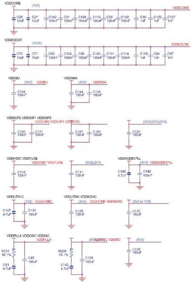
Figure 6-2. Processor Power Lines Supplies
text_image
VDDCORE (1V2) C28 C27 C143 C31 C108 C119 C29 C132 C30 C122 C137 10uF 10uF 100nF 100nF 100nF 100nF 100nF 100nF VDDIODR (1V35) C70 C71 C60 C104 C66 C102 C101 C114 C105 C84 C97 10uF 10uF 100nF 100nF 100nF 100nF 100nF VDDBU (3V3) VDDBU C134 100nF VDDANA (3V3) VDDANA C144 100nF C136 100nF VDDIOP0 VDDIOP1 VDDIOP2 C135 C131 C107 C103 100nF 100nF 100nF VDDHSC VDDFUSE C118 VDDHSIC VDDFUSE C116 100nF [6V2](2V1) C111 100nF VDDAUDIOPLL (3V3) VDDAUDIOPLL C148 4.7uF C140 100nF VDDUTMIC (1V2) VDDUTMIC C147 C133 4.7uF 100nF VDDUTMII VDDSDHC (3V3) VDDUTMII VDDSDHC C125 100nF C110 100nF VDDPLLA VDDOSC VDDISC R131 R269 1R 1% C45 C128 4.7uF 4.7uF VDDPLLA VDDPLLA R269 C128 4.7uF 4.7uF J3VQIDOSC VDDISC (3V3) C138 100nF
text_image
VDDCORE (1V2) D7 D9 F3 K13 N5 N9 VDDCORE 1 VDDCORE 2 VDDCORE 3 VDDCORE 4 VDDCORE 5 VDDCORE 6 VDDDDR_1 VDDDDR 2 VDDDDR 3 VDDDDR 4 VDDDDR 5 VDDDDR 6 VDDDDR 7 VDDBU VDDANA (3V3) K3 L5 VDDIOPC (3V3) E6 F7 VDDIOP1 (3V3) N13 R14 VDDIOP2 (3V3) F10 VDDHSIC (1V2) R9 VDDFUSE (2V5) M12 VDDAUDIOP-1 (3V3) T3 VDDUTMIC (1V2) P7 VDDUTMII (3V3) P8 VDDSDHC (3V3 or 1V8) P11 VDDPLLA (1V2) U4 VDDOSC (3V3) T7 VDDISC (3V3) F4 VDDCORE 1 GNDCORE 1 GNDCORE 2 GNDCORE 3 GNDCORE 4 GNDCORE 5 GNDCORE 6 GNDDDR_1 GNDDDR 2 GNDDDR 3 GNDDDR 4 GNDDDR 5 GNDDDR 6 GNDDDR 7 GNDBU GNDBANA 1 GNDBANA 2 GNDIOP0 1 GNDIOP0 2 GNDIOP1 1 GNDIOP1 2 GNDIOP2 GNDOPLL GNDAUDIOPLL GNDAUDIOPLL GNDUTMIC GNDUTMIC GNDUTMII GNDUSMMC GNDUSMMC GNDPLLA GNDPLLA GNDOSC GNDOSC GNDISC SAMA5027-CU E7 E9 F4 K12 M5 M9 D14 E11 E12 E14 H14 J14 L14 N6 L3 K5 F6 Q7 M13 P14 F9 T5 T4 R7 P9 R11 U5 T6 G4 GNDUTMII R261/29 GNDUTMII6.3.2.2 Power-Up and Power-Down Considerations
Power-up and power-down considerations are described in section "Power Considerations" of the SAMA5D2 Series data sheet.

The power-up sequence provided in the SAMA5D2 Series data sheet must be respected for reliable operation.
6.3.2.3 ACT8945A Power Management IC
The ACT8945A is a complete, cost-effective and highly-efficient ActivePMU ^™ power management solution, optimized to provide a single-chip power solution and voltage sequencing for SAMA5D2/SAMA5D3/SAMA5D4 and SAM9 series MPUs. It also meets the control requirements of these devices.
The ACT8945A features three step-down DC-DC converters and four low-noise, low-dropout linear regulators along with a complete battery charging solution featuring the advanced ActivePath™ system-power selection function.

Refer to the ACT8945A data sheet at www.active-semi.com/ for more details.
The three DC-DC converters utilize a high efficiency, fixed-frequency (2 MHz), current-mode PWM control architecture that requires a minimum number of external components. Two DC-DC converters are capable of
supplying up to 1100 mA of output current, while the third supports up to 1200 mA. All four low-dropout linear regulators are high performance, low-noise regulators that supply up to 320 mA of output current.
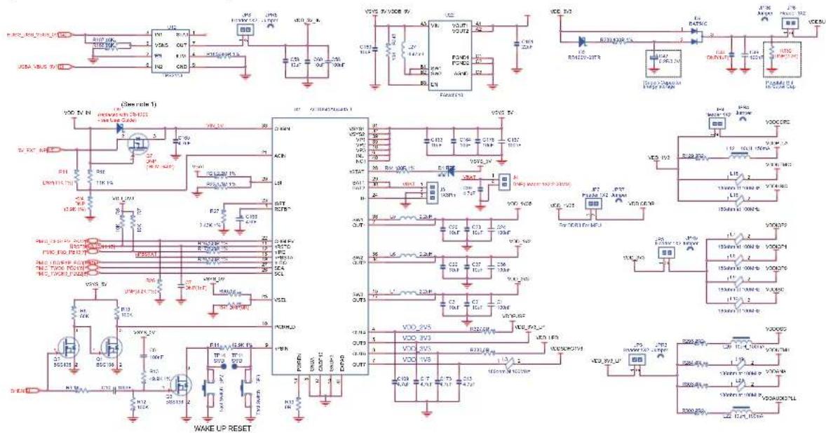
Figure 6-3. Board Power Management
text_image
Electrical schematic diagram of a wake-up circuit with multiple components and labeled pins and connectionsNote: Occasional board start-up problems occurred when powered from a USB source with a weak VBUS level below 4.8V. To avoid the voltage drop and resulting start-up problems, production boards were assembled with a 0 Ω resistor in place of the Schottky diode D9 shown here.
6.3.2.3.1 Supply Group Configuration
The ACT8945A provides:
• All power supplies required by the SAMA5D2 device:
- 1.2V VDDCORE, VDDPLLA, VDDUTMIC, VDDHSIC
-1.35V VDDIODDR
-2.0V VDDBU
- 3.3V VDDIOP, VDDISC
- 1.8V or 3.3V VDDSDHC (= VDDSDMMC)
-2.5V VDDFUSE
- 3.3V VDDOSC, VDDUTMII, VDDANA, VDDAUDIOPLL
• Power supplies to external chips on the main board:
-2.5V VDDLED
-4.8V VSYS_5V
6.3.2.4 Power Boost 5V
To generate a true 5V voltage from the PMIC output (4.8V typical), a FAN48610 low-power boost regulator is integrated into the design. This feeds the 5V USB host and the 5V LCD.
Figure 6-4. Power Boost 5V

text_image
VSYS_5V VDDB_5V U22 VIN VOUT1 A1 A2 L27 0.47uH PGND1 C1 C2 SW1 PGND2 AGND SW2 C3 B1 B2 B3 EN FAN48610 R34510K C180 10uF C181 22uF6.3.2.5 Input Power Options
There are several power options for the SAMA5D2C-XULT board.
USB-powered operation is the default configuration, where the USB device port is connected to a PC or a 5V DC supply. The USB supply is sufficient to power the board in most applications. It is important to note that when the USB supply is used, the USB-B Host port has limited power. If USB Host port is required for the application, it is recommended that an external DC supply be used.
The figure below provides the schematics of power options.
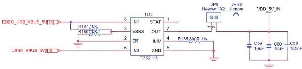
Figure 6-5. Input Powering Scheme
text_image
EDBG_USB_VBUS_5V[14] R187 10K R186 10K USBA_VBUS_5V[10] 8 IN1 STAT VSNS OUT EN ILIM IN2 GND TPS2113 1 7 4 5 JP8 Header 1X2 JPR8 Jumper VDD_5V_IN 1 2 R185 390R 1% C59 C60 C58 10uF 10uF 100nFNote: USB-powered operation eliminates additional wires and batteries. It is the preferred mode of operation for any project that requires only a 5V source at up to 500 mA.
6.3.2.6 Battery Supply Source
The ACT8945A features an advanced battery charger that incorporates the ActivePath architecture for system power selection. This combination of circuits provides a complete, advanced battery-management system that automatically selects the best available input supply, manages charge current to ensure system power availability, and provides a complete, high accuracy ( ±0.5% ), thermally regulated, full-featured single-cell linear Li+ charger.
The ActivePath circuitry monitors the state of the input supply, the battery, and the system, and automatically reconfigures itself to optimize the power system. If a valid input supply is present, ActivePath powers the system from the input while charging the battery in parallel. This allows the battery to charge as quickly as possible, while supplying the system. If a valid input supply is not present, ActivePath powers the system from the battery. Finally, if the input is present and the system current requirement exceeds the capability of the input supply, ActivePath allows system power to be drawn from both the battery and the input supply.
Figure 6-6. Battery Powering Scheme
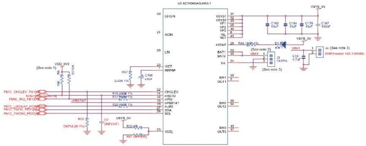
text_image
LM2 ACT8846AQJ405-T 33 CHGIN 21 ACIN 20 LSI 23 ISET REFBP 22 CHOLEV nRS10 nIRQ nPBSTAT 27 R27 2 R16 100k 1% R17 100k 1% R29 100k 1% R30 0.5V R41 DN4(0K) VSEL 25 VSEL 31 VSYS1 32 VSYS2 33 VP1 34 VP2 35 VP3 36 INL 6 NC1 40 C163 10uF C164 10uF C178 10uF C167 100uF VSYS_DW 28 R44 100F 15 D1 FDP BAT1 29 (See note 2) BAT2 30 VBAT 1 TH 24 (See note 3) SW1 39 OUT11 SW2 36 OUT2 SW3 15 OUT3Notes:
- Refer to errata NRST.
- If the battery does not have a pack embedded thermistor (i.e., battery temperature monitoring), the TH pin should be connected to ground => short J3 pins 2 and 3.
- If no battery is connected on connector J3 or J4, it is recommended that the charging function be disabled in the ACT8945 chip. To do so, write the SUSCHG bit to '1' in APCH register (REG 0x71, SUSCHG = 1).
6.3.2.6.1 Charger Input Interrupts
To facilitate input supply detection and eliminate the size and cost of external detection circuitry, the charger has the ability to generate interrupts based upon the status of the input supply. This function is capable of generating an interrupt when the input is connected, disconnected, or both, when the charger state machine transitions.
6.3.2.6.2 Charge Status Indicator
The charger provides a charge-status indicator output, nSTAT. nSTAT is an open-drain output which sinks current when the charger is in an active-charging state, and is high-Z otherwise. nSTAT features an internal 8 mA current limit, and is capable of directly driving an LED (D1).
6.3.2.6.3 Precision Voltage Detector
The low battery input (LBI) connects to one input of a precision voltage comparator, which can be used to monitor a system voltage such as the battery voltage. An external resistive-divider network can be used to set voltage monitoring thresholds. The output of the comparator is present at the open-drain low battery indicator output (nLBO) and connected to the red LED D1.
Table 6-3. PIOs Used to Control the Battery Charger
| PIO Function | |
| PA12 CHGLEV: Charge Current Selection Input | |
| PB13 nIRQ: Open-Drain Interrupt Output. nIRQ is asserted any time an unmasked fault condition exists or a charger interrupt occurs. | |
| PC8 | nLBO: Low Battery Indicator Output. nLBO is asserted low whenever the voltage at LBI is lower than1.2V; it is high-Z otherwise. |
Figure 6-7. Battery Connector J3 and Optional J4

text_image
WWW.ATMEL.COM VXPRO EXT1 F1_TXO F1_RXO XPRO POWER BOOT_DIS RESET WAKE UP EDBG-USB A5-JTAGED66-JTNG CLASS D SAMA5D2 X PLAINED ULTRA Atmel® SMART™ VBAT DEBUG_DIS PB_USER BP1 LED8G_DIS R07 R08 R09 R10 R11 R12 R13 R14 R15 R16 R17 R18 R19 R20 R21 R22 R23 R24 R25 R26 R27 R28 R29 R30 R31 R32 R33 R34 R35 R36 R37 R38 R39 R40 R41 R42 R43 R44 R45 R46 R47 R48 R49 R50 R51 R52 R53 R54 R55 R56 R57 R58 R59 R60 R61 R62 R63 R64 R65 R66 R67 R68 R69 R70 R71 R72 R73 R74 R75 R76 R77 R78 R79 R80 R81 R82 R83 R84 R85 R86 R87 R88 R89 R90 R91 R92 R93 R94 R95 R96 R97 R98 R99 R100Table 6-4. Battery J3 Signal Descriptions
| Pin Mnemonic Signal Description | ||
| 1 | VBAT | Battery I/O (exploitation and charging). Connect this pin directly to the battery anode (+ terminal) |
| 2 | GND | Common ground |
| 3 | TH | Temperature Sensing Input. Connect to battery thermistor. TH is pulled up with a 102 μA (typical) current internally. |
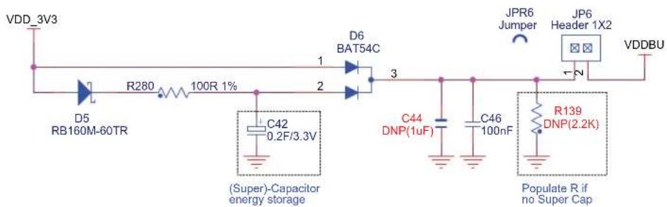
6.3.2.7 Backup Power Supply
The SAMA5D2C-XULT board requires a power source to permanently power the backup part of the SAMA5D2 device (refer to the SAMA5D2 Series data sheet). A super capacitor sustains such permanent power to VDDBU when all system power sources are off.
Figure 6-8. VDDBU Powering Scheme Option
text_image
VDD_3V3 D5 RB160M-60TR R280 100R 1% 1 2 D6 BAT54C 3 JPR6 Jumper JP6 Header 1X2 VDDBU C42 0.2F/3.3V C44 DNP(1uF) C46 100nF R139 DNP(2.2K) (Super)-Capacitor energy storage Populate R if no Super Cap6.3.2.8 Power Supply Control
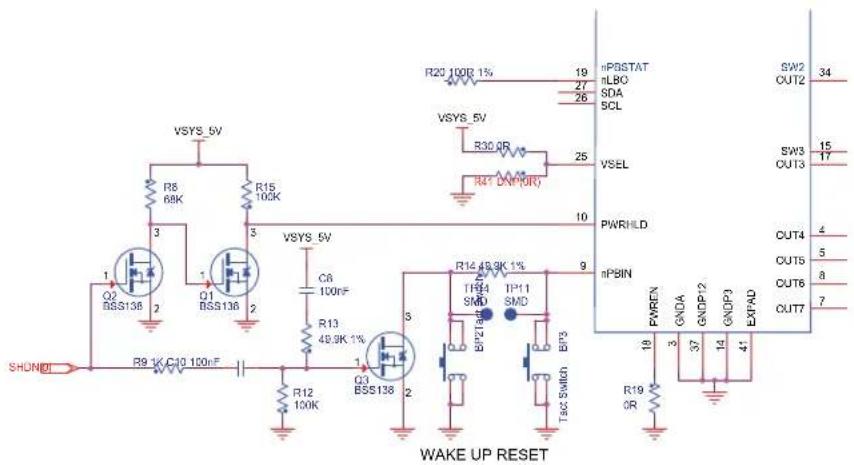
In the ACT8945A, three DC-DC converters (1.8V, 1.2V, 3.3V) and two LDO outputs are available.
All ACT8945A outputs can be controlled by the TWI interface through software.
The three DC-DC outputs can be enabled or disabled by the SAMA5D2 SHDN output:
- SHDN = 0: The DC-DC output is disabled.
- SHDN = 1: The DC-DC output is enabled.
Two push buttons are also available:
- Wake-up push button: When pressed, the ACT8945A power outputs are restarted if the ACT8945A is in Shutdown mode.
- Reset push button: When pressed, the ACT8945A transfers the reset signal to the MPU.
6.3.3 Reset Circuitry
The reset sources for the SAMA5D2C-XULT board are:
• Power-on Reset from the Power Management Unit (PMIC)
- Push button reset BP3
- External reset from Arduino connectors
• JTAG or EDBG reset from an in-circuit emulator
Figure 6-9. Reset/Wake-up and Shutdown Control
text_image
VSY5_5V R8 68K R15 10CK VSYS_5V R23 100R 1% 19 nPGSTAT nLBO SDA SCL 27 26 SW2 34 R30.0R 25 VSEL 15 OUT3 17 Q2 BSS138 Q1 BSS138 R13 48.9K 1% 10 PWRHLD Q3 BSS138 R14 48.9K 1% 9 nPBIN FPREN GNDIA GNDIP/2 GNDIPJ EXPAD 19 37 14 47 R19 OR Tsc Switch R12 100K SHONDT R9 1K C10 100nF WAKE UP RESET6.3.4 Clock Circuitry
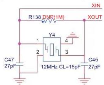
The SAMA5D2C-XULT board includes four clock sources:
- Two clocks are alternatives for the SAMA5D2 processor (12 MHz, 32 kHz)
• One crystal oscillator used for the Ethernet RMII chip (25 MHz)
• One crystal oscillator used for the EDBG (12 MHz)
Figure 6-10. Clock Circuitry
text_image
R138 DNR(1M) XIN XOUT Y4 1 2 3 4 C47 27pF 12MHz CL=15pF C45 27pF
text_image
R103 DNP(1M) XOUT32 32.768KHz CL=12.5pF XIN32 C41 22pF Y3 4 1 3 2 C40 22pF
text_image
C34 22pF 2 1 Y2 3 4 C35 22pF 25MHz CL=20pF ETH_XI R64 DNP(1M) ETH_XO6.3.5 Memory
6.3.5.1 Memory Organization
The SAMA5D2 features a DDR/SDR memory interface and an External Bus Interface (EBI) to allow interfacing to a wide range of external memories and to almost any kind of parallel peripheral.
This section describes the memory devices that equip the SAMA5D2C-XULT board.
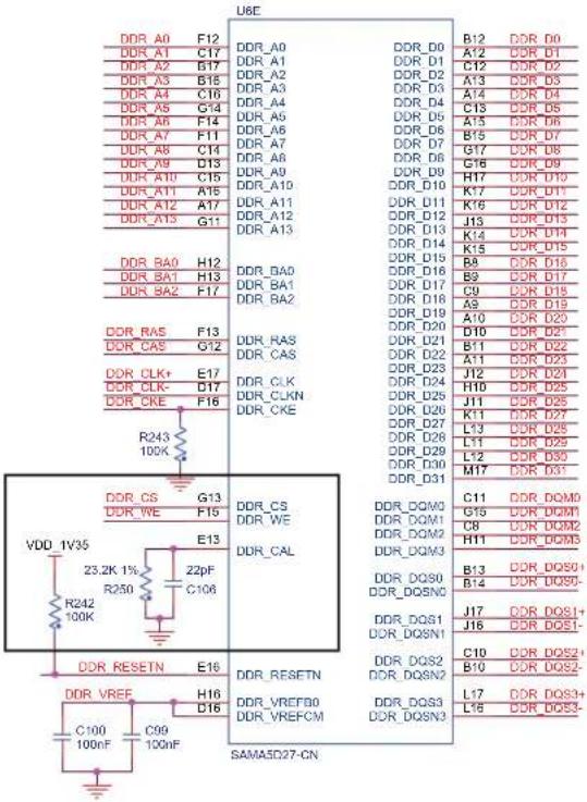
6.3.5.2 DDR3/SDRAM
Two DDR3L/SDRAM (MT41H128M16JT-125-K - 2 Gbit = 16 Mbit x 16 x 8 banks) are used as main system memory and total 4 Gbit of SDRAM on the board. The memory bus is 32 bits wide and operates with a frequency of up to 166 MHz.
Figure 6-11. DDR3L

One specific analog input, DDR_CAL, is used to calibrate all DDR I/Os.
Figure 6-12. DDR Signals and CAL Analog Input
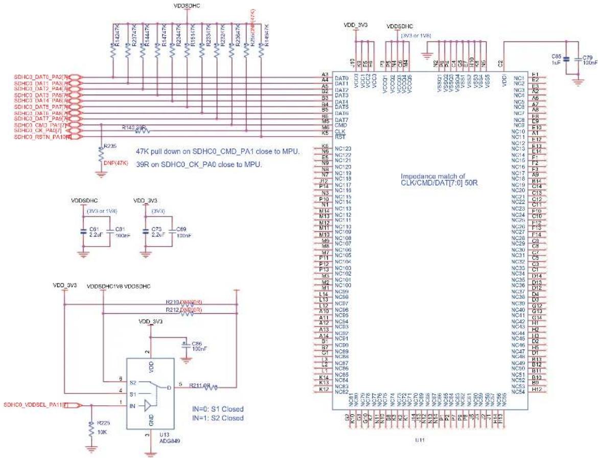
The Secure Digital Multimedia Card (SDMMC) Controller supports the Embedded MultiMedia Card (e.MMC) Specification V4.41, the SD Memory Card Specification V3.0, and the SDIO V3.0 specification. It is compliant with the SD Host Controller Standard V3.0 specification
One MTFC4GACAJCN-4M 4 Gb eMMC is connected to the processor through the SDMMC0 port.
Table 6-5. SDMMC Reference Documents
| Name Link | |
| SD Host Controller Simplified Specification V3.00 www.sdcard.org | |
| SDIO Simplified Specification V3.00 www.sdcard.org | |
| Physical Layer Simplified Specification V3.01 www.sdcard.org | |
| Embedded MultiMedia Card (e.MMC) Electrical Standard 4.51 www.jedec.org |
Figure 6-13. eMMC
text_image
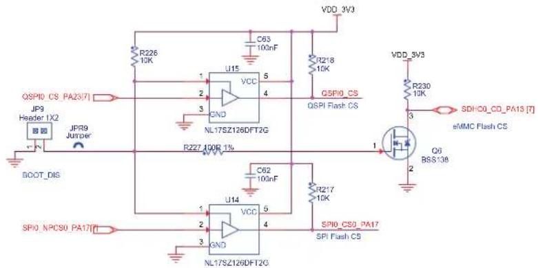
VDOSDHC R1427K R2372K R1447K R1477K R2347K R1517K R2357K R2397K R2967K R2567M (47K) R1807K VDD_3V3 VDDSDHC [3V3 or 1V8] NC1 F1 A3 DAT0 VCC01 VCC1 VCC2 VCC3 VCC01 VCC02 VCC03 VCC04 VCC05 VSS01 VSS02 VSS03 VSS04 VSS05 VSS06 VSS07 VSS08 VSS09 VSS10 VSS11 VSS12 VSS13 VSS14 VSS15 VSS16 VSS17 VSS18 VSS19 VSS20 VSS21 VSS22 VSS23 VSS24 VSS25 VSS26 VSS27 VSS28 VSS29 VSS30 VSS31 VSS32 VSS33 VSS34 VSS35 C2 C65 1uF C79 10nF SDHCO_DAT0_PA27K SDHCO_DAT1_PA37K SDHCO_DAT2_PA47K SDHCO_DAT3_PA57K SDHCO_DAT4_PA67K SDHCO_DAT5_PA77K SDHCO_DAT6_PA87K SDHCO_DAT7_PA97K SDHCO_CMO_PA107K SDHCO_CK_PA117K SDHCO_RSTN_PA139K R225 DNF(47K) R140.39R M6 CLK RST NC120 NC122 NC121 NC120 NC119 NC118 NC117 NC116 NC115 NC114 NC113 NC112 NC111 NC110 NC109 NC108 NC107 NC106 NC105 NC104 NC103 NC102 NC101 NC99 NC98 NC97 NC96 NC95 NC94 NC93 NC92 NC91 NC90 NC89 NC88 NC87 NC86 NC85 NC84 NC83 NC82 NC81 NC80 NC79 NC78 NC77 NC76 NC75 NC74 NC73 NC72 NC71 NC70 NC69 NC68 NC67 NC66 NC65 NC64 NC63 NC626.3.5.5 CS Disable
The SAMA5D2 device boots according to the following sequence:
- SD CARD connected on SDHC1
- eMMC connected on SDHC0
- Serial Flash connected on SPI0_IOSET1 (Chip Select 0: NPCS0)
- Optional QSPI Flash connected on QSPI0_IOSET3 (Chip Select 0: CS0)
In this sequence, the first device found with bootable contents is selected as the boot source. The others are disregarded. (see Note below)
An on-board jumper (JP9) controls the selection (CS#) of the on-board bootable memory components (eMMC and Serial Flash) using a non-inverting 3-state buffer.
Figure 6-14. CS Disable
text_image
QSPI0_CS_PA23(7) JPR9 Header 1X2 JPR9 Jumper BOOT_DIS SP0_NPC50_PA17(7) R226 10K U15 VCC 5 4 C63 100nF R218 10K QSPI0_CS QSPI Flash CS VDD_3V3 R230 10K SDHC0_CD_PA13 [T] eMMC Flash CS Q6 BSS138 R227_100R_1% U14 VCC 5 4 C62 100nF R217 10K SP10_CS0_PA17 SPI Flash CSThe rule of operation is:
- JP9 = OFF (default) → enable normal boot from serial Flash memories mounted on board
- JP9 = ON → booting from optional serial Flash memories is disabled
Refer to the SAMA5D2 Series data sheet for more information on standard boot strategies and sequencing.
Note: The errata in the SAMA5D2 data sheet state that booting from SD/MMC devices is nondeterministic. In order to have a known behavior regardless of SD/MMC data contents, we recommend SDMMC0/SDMMC1 boot bits be disabled in the Boot Configuration Word fuse.
6.3.6 Additional Memories
6.3.6.1 Serial Flash
The SAMA5D2 provides two high-speed Serial Peripheral Interface (SPI) controllers. One port is used to interface with the on-board serial serial Flash.
The four main signals used in the SPI are Clock, Data In, Data Out, and Chip Select. The SPI is a serial interface similar to the bus interface but with three main differences:
- It operates at a higher speed.
- Transmit and receive data lines are separate.
- Device access is chip select-based instead of address-based.
Figure 6-15. Serial Flash

text_image
SPI0_MOSI_PA15 SPI0_MISO_PA16 SPI0_SPCK_PA14 SPI0_CS0_PA17 5 2 6 1 SI SQ SCK CS U9 VCC WP HOLD GND AT25DF321A 8 3 7 4 VDD_3V3 C53 100nF6.3.6.2 QSPI Serial Flash
The SAMA5D2 provides two Quad Serial Peripheral Interfaces (QSPI). One port is used to interface with the optional on-board QSPI serial Flash.
The Quad SPI Interface (QSPI) is a synchronous serial data link that provides communication with external devices in Master mode.
The QSPI can be used in SPI mode to interface to serial peripherals (such as ADCs, DACs, LCD controllers, CAN controllers and sensors), or in Serial Memory mode to interface to serial Flash memories.
The QSPI allows the system to execute code directly from a serial Flash memory (XIP) without code shadowing to RAM. The serial Flash memory mapping is seen in the system as other memories (ROM, SRAM, DRAM, embedded Flash memory, etc.).
With the support of the Quad SPI protocol, the QSPI allows the system to use high-performance serial Flash memories which are small and inexpensive, in place of larger and more expensive parallel Flash memories.
Figure 6-16. QSPI Serial Flash
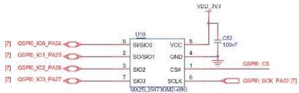
text_image
VDD_3V3 [7] QSPI0_IC0_PA24 5 S/SIO0 VCC 8 [7] QSPI0_IC1_PA25 2 SO/SIO1 GND 4 [7] QSPI0_IC2_PA26 3 SIO2 CSW 1 QSPI0_CS [7] QSPI0_IC3_PA27 7 SIO3 5CLK 6 QSPI0_SCK_PA22 [7] U10 MIX25L2587JGME-09G6.3.6.3 Serial EEPROM with Unique MAC Address
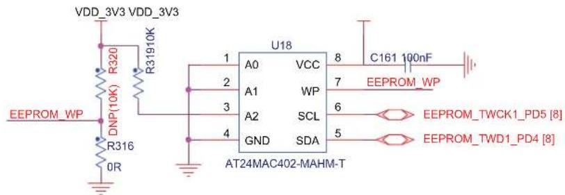
The SAMA5D2C-XULT board embeds one Microchip AT24MAC402/602 EEPROM using a TWI1 interface.
The AT24MAC402/602 provides 2048 bits of Serial Electrically-Erasable Programmable Read-Only Memory (EEPROM) organized as 256 words of eight bits each and is accessed via an I²C-compatible (2-wire) serial interface. In addition, the AT24MAC402/602 incorporates an easy and inexpensive method to obtain a globally unique MAC or EUI address (EUI-48 or EUI-64).
The EUI-48/64 addresses can be assigned as the actual physical address of a system hardware device or node, or it can be assigned to a software instance. These addresses are factory-programmed by Microchip and guaranteed unique. They are permanently write-protected in an extended memory block located outside of the standard 2-Kbit memory array.
In addition, the AT24MAC402/602 provides the value-added feature of a factory-programmed, also guaranteed unique 128-bit serial number located in the extended memory block (same area as the EUI address values).

The EEPROM device is also used as a “software label” to store board information such as chip type, manufacturer name and production date, using the last two 16-byte blocks in memory. To preserve the ease of board identification by software, the information contained in these blocks should not be modified.
Figure 6-17. EEPROM
text_image
VDD_3V3 VDD_3V3 R320 R31910K EEMROM_WP DNP(10K) R316 OR U18 A0 VCC 8 C161 100nF 2 A1 WP 7 EEPROM_WP 3 A2 SCL 6 EEPROM_TWCK1_PD5 [8] 4 GND SDA 5 EEPROM_TWD1_PD4 [8] AT24MAC402-MAHM-T6.4 PIO Usage and Interface Connectors
6.4.1 Secure Digital Multimedia Card Interface
6.4.1.1 Secure Digital Multimedia Card Controller (SDMMC)
The SAMA5D2C-XULT board has two SDMMC interfaces that support the MultiMedia Card (e.MMC) Specification V4.41, the SD Memory Card Specification V3.0, and the SDIO V3.0 specification. It is compliant with the SD Host Controller Standard V3.0 specification.
- SDMMC0 interface is connected to the eMMC.
- SDMMC1 Interface based on a 7-pin interface (clock, command, 4-bit data, power lines).
6.4.1.2 SDMMC1 Card Connector
A standard MMC/SD card connector, connected to SDMMC1, is mounted on the top side of the board. It includes a card detection switch.
Figure 6-18. SDMMC1

text_image
VDD_3V3 R214 8R C64 10uF C75 100nF VDD_3V3 R22H10K R245 R241 R209 R192B8K R189B8K R2910K 68K 68K 10K (MCI CD) (MCI DA1) (MCI DA0) (MCI CK) (MCI CDA) (MCI DA3) (MCI DA2) (SDHC1_WP) J19 16 15 14 13 12 11 10 SD Card ConnectorNote: Refer to details on SDcard boot in CS Disable.
Standard SD Socket J19
text_image
WWW.ATMEL.COM BOOT_DIS XPRO EXT1 XPRO EXT2 A5-USB-A SCL0 SDA0 AREF GND VDDIODDR F1_TXD F4_RXD F0_TXD F0_RXD F3_TXD F3_RXD SDA1 SQL1 D22 D23 D24 D25 D26 D27 D29 D31 D32 D35 D36 D37 D38 D39 D40 D41 D42 D43 D44 D45 D46 D47 D48 D49 D50 D51 D52 GND DIGITAL P10BU CANRX1 CANTX1 PI0BU QOL OSC1 OSC2 OSC3 OSC4 OSC5 OSC6 OSC7 OSC8 OSC9 OSC10 OSC11 OSC12 OSC13 OSC14 OSC15 OSC16 OSC17 OSC18 OSC19 OSC20 OSC21 OSC22 OSC23 OSC24 OSC25 OSC26 OSC27 OSC28 OSC29 OSC30 OSC31 OSC32 OSC33 OSC34 OSC35 OSC36 OSC37 OSC38 OSC39 OSC40 OSC41 OSC42 OSC43 OSC44 OSC45 OSC46 OSC47 OSC48 OSC49 OSC50 OSC51 OSC52 OSC53 OSC54 OSC55 OSC56 OSC57 OSC58 OSC59 OSC60 ESC10000000000000000000000000000000000000000000000000000000000000000000000000000000000000000000000000000Table 6-6. Standard SD Socket J19 Signal Descriptions
| Pin | Mnemonic | PIO | Signal Description |
| 1 | DAT3 | PA21 | Data Bit 3 |
| 2 | CDA | PA28 | Command Line |
| 3 | GND | - | Common ground |
| 4 | VCC | - | Supply Voltage 3.3V |
| ......continued | ||
| Pin Mnemonic PIO Signal Description | ||
| 5 CLK PA22 Clock / Command Line | ||
| 6 CD PA30 Card Detect | ||
| 7 DAT0 PA18 Data Bit 0 | ||
| 8 DAT1 PA19 Data Bit 1 | ||
| 9 DAT2 PA20 Data Bit 2 | ||
| 10 GND – Common ground | ||
6.4.2 Communication Interfaces
The SAMA5D2C-XULT board is equipped with GMAC and USB Host/Device communication interfaces.
6.4.2.1 Ethernet 10/100 (GMAC) Port
The SAMA5D2C-XULT board contains a MICREL PHY device (KSZ8081) operating at 10/100 Mb/s. The board supports RMII interface modes. The Ethernet interface consists of two pairs of low-voltage differential pair signals designated from GRX± and GTX± plus control signals for link activity indicators. These signals can be used to connect to a 10/100 Base-T RJ45 connector integrated on the SAMA5D2C-XULT board.
Additionally, for monitoring and control purposes, LED functionality is carried on the RJ45 connectors to indicate activity, link, and speed status information.
For more information about the Ethernet controller device, refer to the MICREL KSZ8081RN controller data sheet.
Figure 6-19. Ethernet (GMAC)
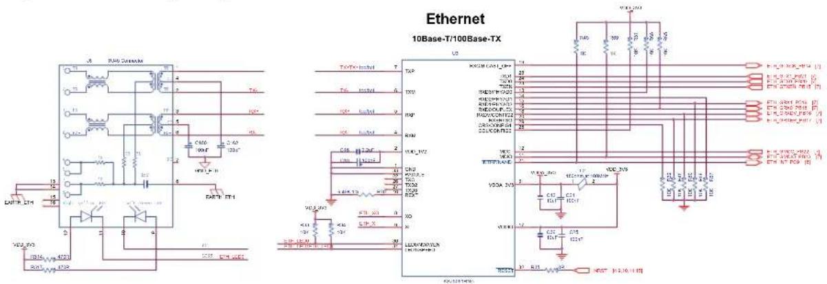
text_image
Ethernet 10Base-T/100Base-TX U3 VDDA 205 VDDA 206 VDDA 207 VDDA 208 VDDA 209 VDDA 210 VDDA 211 VDDA 212 VDDA 213 VDDA 214 VDDA 215 VDDA 216 VDDA 217 VDDA 218 VDDA 219 VDDA 220 VDDA 221 VDDA 222 VDDA 223 VDDA 224 VDDA 225 VDDA 226 VDDA 227 VDDA 228 VDDA 229 VDDA 230 VDDA 231 VDDA 232 VDDA 233 VDDA 234 VDDA 235 VDDA 236 VDDA 237 VDDA 238 VDDA 239 VDDA 240 VDDA 241 VDDA 242 VDDA 243 VDDA 244 VDDA 245 VDDA 246 VDDA 247 VDDA 248 VDDA 249 VDDA 250 VDDA 251 VDDA 252 VDDA 253 VDDA 254 VDDA 255 VDDA 256 VDDA 257 VDDA 258 VDDA 259 VDDA 260 VDDA 261 VDDA 262 VDDA 263 VDDA 264 VDDA 265 VDDA 266 VDDA 267 VDDA 268 VDDA 269 VDDA 270 VDDA 271 VDDA 272 VDDA 273 VDDA 274 VDDA 275 VDDA 276 VDDA 277 VDDA 278 VDDA 279 VDDA 280 VDDA 281 VDDA 282 VDDA 283 VDDA 284 VDDA 285 VDDA 286 VDDA 287 VDDA 288 VDDA 289 VDDA 290 VDDA 291 VDDA 292 VDDA 293 VDDA 294 VDDA 295 VDDA 296 VDDA 297 VDDA 298 VDDA 299 VDDA 300Figure 6-20. ETH RJ45 Connector J6

text_image
WWW.ATMEL.COM VDD 5V IN XPRO POWER XPRO EXT1 F1 RXD F1 TXD F1 RXD XPRO EXT2 BOOT_DIS SALU SDA0 REF R3 R4 R5 R6 R7 R8 R9 R10 R11 R12 R13 R14 R15 R16 R17 R18 R19 R20 R21 VDDIODDR RESET WAKE UP EDBG-USB A5 JTAGED BCG-JTAGS CLASS D R1 R2 R3 R4 R5 R6 R7 R8 R9 R10 R11 R12 R13 R14 R15 R16 R17 R18 R19 R20 R21 VDD 3V0 VDD 3V2 LP VDD 3V3 LP VDD 3V4 LP VDD 3V5 LP VDD 3V6 LP VDD 3V7 LP VDD 3V8 LP VDD 3V9 LP VDD 3V10 LP VDD 3V11 LP VDD 3V12 LP VDD 3V13 LP VDD 3V14 LP VDD 3V15 LP VDD 3V16 LP VDD 3V17 LP VDD 3V18 LP VDD 3V19 LP VDD 3V20 LP VDD 3V21 LP VDD 3V22 LP VDD 3V23 LP VDD 3V24 LP VDD 3V25 LP VDD 3V26 LP VDD 3V27 LP VDD 3V28 LP VDD 3V29 LP VDD 3V30 LP VDD 3V31 LP VDD 3V32 LP VDD 3V33 LP VDD 3V34 LP VDD 3V35 LP VDD 3V36 LP VDD 3V37 LP VDD 3V38 LP VDD 3V39 LP VDD 3V40 LP VDD 3V41 LP VDD 3V42 LP VDD 3V43 LP VDD 3V44 LP VDD 3V45 LP VDD 3V46 LP VDD 3V47 LP VDD 3V48 LP VDD 3V49 LP VDD 3V50 LP SAMS/CM/MI/IR/IO/IC/IC/IC/IC/IC/IC/IC/IC/IC/IC/IC/IC/IC/IC/IC/IC/IC/IC/IC/IC/IC/IC/IC/IC/IC/IC/IC/IC/IC/IC/IC/IC/IC/IC/IC/IC/IC/IC/IC/IC/IC/IC/IC/IC/IC/IC/IC/IC/IC/IC/AC/AC/AC/AC/AC/AC/AC/AC/AC/AC/AC/AC/AC/AC/AC/AC/AC/AC/AC/AC/AC/AC/AC/AC/AC/AC/AC/AC/AC/AC/AC/AC/AC/AC/AC/AC/AC/AC/CANTX1/CANTX2/CANTX3/CANTX4/CANTX5/CANTX6/CANTX7/CANTX8/CANTX9/CANTX10/CANTX11/CANTX12/CANTX13/CANTX14/CANTX15/CANTX16/CANTX17/CANTX18/CANTX19/CANTX20/CANTX21/CANTX22/CANTX23/CANTX24/CANTX25/CANTX26/CANTX27/CANTX28/CANTX29/CANTX30/CANTX31/CANTX32/CANTX33/CANTX34/CANTX35/CANTX36/CANTX37/CANTX38/CANTX39/CANTX40/CANTX41/CANTX42/CANTX43/CANTX44/CANTX45/CANTX46/CANTX47/CANTX48/CANTX49/CANTX50/CANTX51/CANTX52/CANTX53/CANTX54/CANTX55/CANTX56/CANTX57/CANTX58/CANTX59/CANTX60/CANTX61/CANTX62/CANTX63/CANTX64/CANTX65/CANTX66/CANTX67/CANTX68/CANTX69/CANTX70/CANTX71/CANTX72/CANTX73/CANTX74/CANTX75/CANTX76/CANTX77/CANTX78/CANTX79/CANTX80/CANTX81/CANTX82/CANTX83/CANTX84/CANTX85/CANTX86/CANTX87/CANTX88/CANTX89/CANTX90/CANTX91/CANTX92/CANTX93/CANTX94/CANTX95/CANTX96/CANTX97/CANTX98/CANTX99/CANTX100/ SAMS/D2 X PLAINEDTable 6-7. ETH RJ45 Connector Signal Descriptions
| Pin | Mnemonic | Signal Description |
| 1 | TX+ | Transmit |
| 2 | TX- | Transmit |
| 3 | RX+ | Receive |
| 4 | Decoupling capacitor | - |
| 5 | Decoupling capacitor | - |
| 6 | RX- | Receive |
| 7 | NC | - |
| 8 | EARTH / GND | Common ground |
| 9 | ACT LED | LED activity |
| 10 | ACT LED | LED activity |
| 11 | LINK LED | LED link connection |
| 12 | LINK LED | LED link connection |
| 13 | EARTH / GND | Common ground |
| 14 | EARTH / GND | Common ground |
| 15 | NC | - |
| 16 | NC | - |
6.4.2.2 USB Host/Device A, B
The SAMA5D2C-XULT board features three USB communication ports:
• USB-B Host High- and Full-speed Interface
- One USB host type A connector
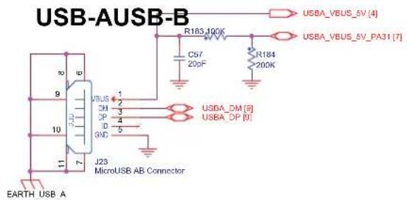
• USB-A Device Interface
- One USB device standard Micro-AB connector. This port has a VBUS detection function made through the resistor ladder R183 and R184.
• UBC-C High-speed Host Port
- One USB high-speed host port with a High-Speed Inter-Chip (HSIC) interface. This port is connected to a single 2-pin jumper.
Figure 6-21. USB-B Host & USB-A Device Interface
text_image
USB-AUSB-B R183,100K C57 20pF R184 200K USBA_VBUS_5V [4] USBA_VBUS_5V_PA31 [7] USBA_DM [8] USBA_DP [9] J23 MicroUSB AB Connector EARTH USB A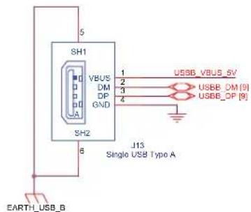
text_image
5 SH1 VBUS DM DP GND A SH2 6 J13 Single USB Type A 1 2 3 4 USB6_VBUS_5V USB8_DM[9] USB8_DP[9] EARTH_USB_BThe USB-B Host port is equipped with 500 mA high-side power switch for self-powered and bus-powered applications.
Figure 6-22. USB Power Switch
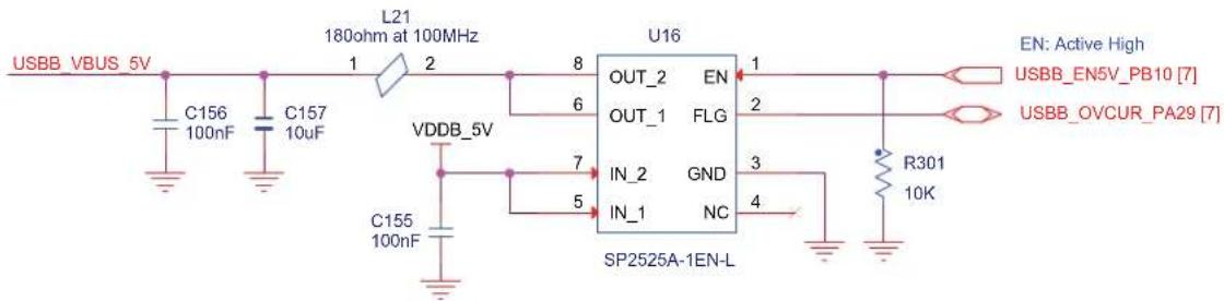
text_image
USBB_VBUS_5V C156 100nF C157 10uF L21 180ohm at 100MHz 2 8 U16 OUT_2 EN OUT_1 FLG IN_2 GND IN_1 NC VDDB_5V C155 100nF SP2525A-1EN-L EN: Active High USBB_EN5V_PB10 [7] USBB_OVCUR_PA29 [7] R301 10K6.4.3 USB-A Micro-AB Connector J23
Figure 6-23. USB-A Connector J23
text_image
WWW.ATMEL.COM XPRO EXT1 F1_TXD F1_RXD XPRO EXT2 J46 BOOT_DIS VDDIODDR SDMMOCLn VDDI R30 R31 R32 R33 R34 R35 R36 R37 R38 R39 R40 R41 R42 R43 R44 R45 R46 R47 R48 R49 R50 R51 R52 R53 R54 R55 R56 R57 R58 R59 R60 R61 R62 R63 R64 R65 R66 R67 R68 R69 R70 R71 R72 R73 R74 R75 R76 R77 R78 R79 R80 R81 R82 R83 R84 R85 R86 R87 R88 R89 R90 R91 R92 R93 R94 R95 R96 R97 R98 R99 R100 VDDI_XV3_PL_PN_PN_PN_PN_PN_PN_PN_PN_PN_PN_PN_PN_PN_PN_PN_PN_PN_PN_PN_PN_PN_PN_PN_PN_PN_PN_PN_PN_PN_PN_PN_PN_PN_PN_PN_PN_PN_PN_PN_PN_PN_PN_PN_PN_PN_PN_PN_PN_PN_PN_PNP_PLAINED_SAMA5D2 X_PLAINED_VDDI_XV3_PL_PN_PN_PN_PN_PN_PN_PN_PN_PN_PN_PN_PN_PN_PN_PN_PN_PN_PN_PN_PN_PN_PN_PN_PN_PN_PN_PN_PN_PN_PN_PN_PN_PN_PN_PN_PN_PN_PN_PN_PN_PN_PN_PN_PN_PNP_PLAINED_SAMA5D2 X PLAINED_VDDI_XV3_PL_PNP_PLAINED_SAMA5D2 X PLAINED_VDDI_XV3_PL_PNP_PLAINED_SAMA5D2 X PLAINED_VDDI_XV3_PL_PNP_PLAINED_SAMA5D2 X PLAINED_VDDI_XV3_PL_PNP_PLAINED_SAMA5D2 X PLAINED_VDDI_XV3_PL_PNP_PLAINED_SAMA5D2 X PLAINED_VDD1_XV3_PL_PNP_PLAINED_SAMA5D2 X PLAINEED_VDDI_XV3_PL_PNP_PLAINED_SAMA5D2 X PLAINEED_VDDI_XV3_PL_PNP_PLAINED_SAMA5D2 X PLAINEED_VDDI_XV3_PL_PNP_PLAINED_SAMA5D2 X PLAINEED_VDDI_XV3_PL_PNP_PLAINED_SAMA5D2 X PLAINEED_VDDI_XV3_PL_PNP_PLAINED_SAMATM_SMART™6.4.4 USB-B Type B Connector J13
The USB-B host port A (J13) features a VBUS insert detection function through the ladder-type resistors R26 and R27.
Figure 6-24. USB B Connector J13

text_image
XPRO EXT1 F1_TXD F1_RXD XPRO EXT2 WWW.ATMEL.COM BOOT_DIS V5 V5 D23 D25 D27 D29 D31 D33 D35 D36 D37 D38 D40 D42 D43 D45 D47 D49 D51 D52 GND DIGITAL Atmel® SMART™ SAMA5D2 X PLAINED ULTRA CLASS D VDD_3VS STAT VBAT POWER VDD_3VS LP RST 3VS GND NC A1 A2 A3 A4 A5 A6 A7 VDDCORE - VBAT - RGB LED - LCD & DEBUG DIS PB_USER DEBUG LEDG_DIS AD-USB-A A5-USB-A RESET WAKE UP EDBG-USB VDDIODDR SDMMC0n1 RIG RIO RIO RIO RIO RIO RIO RIO RIO RIO RIO RIO RIO RIO RIO RIO RIO RIO RIO RIO RIO RIO RIO RIO RIO RIO RIO RIO RIO RIO RIO RIO RIO RIO RIOTable 6-8. USB-A & USB-B Connector Signal Descriptions
| Pin | Mnemonic | Signal Description |
| 1 | VBUS | 5V power |
| 2 | DM | Data minus |
| 3 | DP | Data plus |
| 4 | ID | On-the-go identification |
| 5 | GND | Common ground |
6.4.5 LCD TFT Interface
6.4.5.1 LCD
The SAMA5D2C-XULT board provides 18 bits of data and control signals to the LCD interface. Other signals are used to control the LCD and are available on connector J2: TWI, SPI, two GPIOs for interrupt, 1-Wire and power supply lines.
6.4.5.2 LCD Expansion Header
J2 is a 1.27mm pitch 50-pin header. It gives access to the LCD signals.
Figure 6-25. LCD Expansion Header Interface Schematic
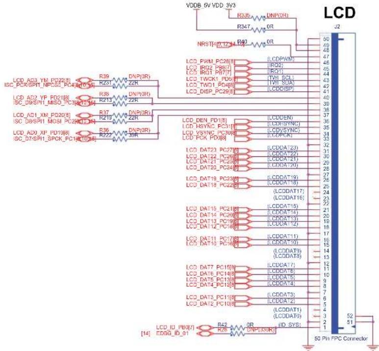
text_image
VDDB_GV VDD_3V3 R36 R347 NRSTI401234 R40 OR OR LCD_PWN_PC26[8] LCD_IRQ_P68[7] LCD_IRQ1_P87[7] LCD_TWCK1_PD5[7] LCD_TWD1_PD4[8] LCD_DISP_PC29[8] LCD_AO3_YM_PD22[8] ISC_PCK/SPN_NPCSC_PC4A[10]51 R39 R231 R36 R213 R37 R219 R36 R222 RNP(0R) 22R RNP(0R) 22R RNP(0R) 30R LCD DEN_PD1[8] LCD HSYNC_PC31[8] LCD VSYNC_PC30[8] LCD PCK_PD0[8] LCD_DAT23_PC27[8] LCD_DAT22_PC29[8] LCD_DAT21_PC23[8] LCD_DAT20_PC24[8] LCD_DAT18_PC23[8] LCD_DAT18_PC22[8] LCD_DAT15_PC21[8] LCD_DAT14_PC20[8] LCD_DAT13_PC19[8] LCD_DAT12_PC18[8] LCD_DAT11_PC17[8] LCD_DAT10_PC16[8] LCD_DAT7_PC15[9] LCD_DAT6_PC14[9] LCD_DAT5_PC13[9] LCD_DAT4_PC12[9] LCD_DAT3_PC11[9] LCD_DAT2_PC10[9] R42 R26 OR DNP(KNK) ID_SYS; 50 Ph FPC Connector 50 49 48 47 46 45 44 43 42 41 40 39 38 37 36 35 34 33 32 31 30 29 28 27 26 25 24 23 22 21 20 19 18 17 16 15 14 13 12 11 10 9 8 7 6 5 4 3 2 1 LCD6.4.5.3 LCD Power
In order to operate correctly out of the processor with various LCD modules, two voltage lines are available: 3.3V and 5 VCC (default), both selected by 0R resistors R335 and R347.
Figure 6-26. LCD Power

text_image
VDDB_5V VDD_3V3 R336 DNP(0R) R347 0R NRST-19.12-14-7 R40 0R LCD J2 50 49 48 47 46 456.4.5.4 LCD Connector J2
Figure 6-27. LCD Connector J2
text_image
WWW.ATMEL.COM BOOT_DIS V5 V5 D23 D25 D27 D29 D31 D33 D35 D37 D39 D41 D43 D45 D47 D49 D51 D53 GND J5 R-X R-X SDMMC1 Atmel® SMART™ SAMA5D2 X PLAINED ULTRA DEBUG_DIS DEBUG DBVCC1806-6VD PBJUSER PB_USER LCD LCC VDD_3V3 LP VDD_3V3 LP VDD_3V3 LP VDD_3V3 LP VDD_3V3 LP VDD_3V3 LP VDD_3V3 LP VDD_3V3 LP VDD_3V3 LP VDD_3V3 LP VDD_3V3 LP VDD_3V3 LP VDD_3V3 LP VDD 3V3 LP VDD 3V3 LP VDD 3V3 LP VDD 3V3 LP VDD 3V3 LP VDD 3V3 LP VDD 3V3 LP VDD 3V3 LP VDD 3V3 LP VDD 3V3 LP VDD 3V3 LP VDD 3V3 LP VDD 3V3 LPI VDD 3V3 LPI VDD 3V3 LPI VDD 3V3 LPI VDD 3V3 LPI VDD 3V3 LPI VDD 3V3 LPI VDD 3V3 LPI VDD 3V3 LPI VDD 3V3 LPI VDD 3V3 LPI VDD 3V3 LPITable 6-9. LCD Connector J2 Signal Descriptions
| Pin | Signal | PIO | Signal | RGB Interface Function | Alternate |
| 1 | ID_SYS | PB0/ ID00 | ID | Extension module identification | EDBG_ID_01 |
| 2 | - | GND | GND | GND | - |
| 3 | - | - | - | - | - |
| 4 | - | - | - | - | - |
| 5 | LCDDAT2 | PC10 | D2 | Data line | - |
| 6 | LCDDAT3 | PC11 | D3 | Data line | - |
| 7 | - | GND | GND | GND | - |
| 8 | LCDDAT4 | PC12 | D4 | Data line | - |
| 9 | LCDDAT5 | PC13 | D5 | Data line | - |
| 10 | LCDDAT6 | PC14 | D6 | Data line | - |
| 11 | LCDDAT7 | PC15 | D7 | Data line | - |
| 12 | - | GND | GND | GND | - |
| 13 | - | - | - | - | - |
| 14 | - | - | - | - | - |
| 15 | LCDDAT10 | PC16 | D10 | Data line | - |
| Pin Signal PIO Signal RGB Interface Function Alternate | |||||
| 16 LCDDAT11 PC17 D11 Data line - | |||||
| 17 - GND GND GND - | |||||
| 18 LCDDAT12 PC18 D12 | Data line - | ||||
| 19 LCDDAT13 PC19 D13 | Data line - | ||||
| 20 LCDDAT14 PC20 D14 | Data line - | ||||
| 21 LCDDAT15 PC21 D15 | Data line - | ||||
| 22 - GND GND GND - | |||||
| 23 - - - | - | - | |||
| 24 - - - | - | - | |||
| 25 LCDDAT18 PC22 D18 | Data line - | ||||
| 26 LCDDAT19 PC23 D19 | Data line - | ||||
| 27 - GND GND GND - | |||||
| 28 LCDDAT20 PC24 D20 | Data line - | ||||
| 29 LCDDAT21 PC25 D21 | Data line - | ||||
| 30 LCDDAT22 PE26 | D22 | Data line - | |||
| 31 LCDDAT23 PE27 | D23 | Data line - | |||
| 32 - GND GND GND - | |||||
| 33 | LCDPCK | PD0 | PCLK | Pixel clock | - |
| 34 | LCDVSYNC | PC30 | VSYNC/CS | Vertical synchronization | - |
| 35 | LCDHSYNC | PC31 | HSYNC/WE | Horizontal synchronization | - |
| 36 | LCDDEN | PD1 | DATA_ENABLE/RE | Data enable | - |
| 37 | SPI1_SPCK | PC1 | SPI_SCK | - | AD3/YM PD22 |
| 38 | SPI1_MOSI | PC2 | SPI_MOSI | - | AD2/YP PD21 |
| 39 | SPI1_MISO | PC3 | SPI_MISO | - | AD1/XM PD20 |
| 40 | SPI1_NPCS0 | PC4 | SPI_CS | - | AD0/XP PD19 |
| 41 | LCDDISP | PA29 | ENABLE | Display enable signal | - |
| 42 | TWD1 | PD4 | TWI_SDA | I2C data line (maXTouch®) | - |
| 43 | TWCK1 | PD5 | TWI_SCL | I2C clock line (maXTouch) | - |
| 44 | GPIO | PB7 | IRQ1 | maXTouch interrupt line | - |
| 45 | GPIO | PB8 | IRQ2 | Interrupt line for other I2C devices | - |
| 46 LCDPWM PC28 PWM Backlight control - | |||||
| 47 | RESET | - | RESET | Reset for both display and maXTouch | - |
| 48 | Main_5V/3V3 | VCC | VCC | 3.3V or 5V supply (0R) | - |
| 49 | Main_5V/3V3 | VCC | VCC | 3.3V or 5V supply (0R) | - |
| 50 GND GND GND GND - | |||||
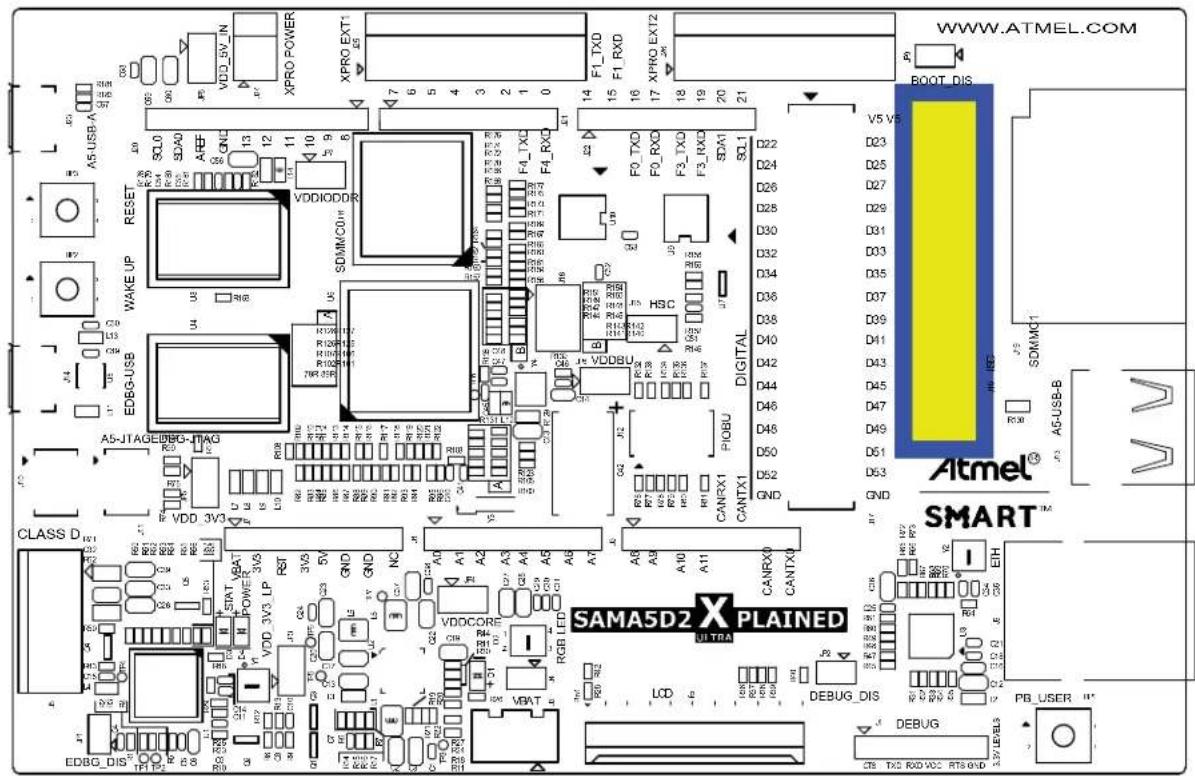
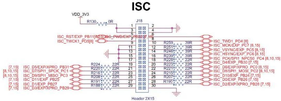
6.4.6 ISC
The Image Sensor Controller (ISC) system manages incoming data from a parallel or serial csi-2 based CMOS/CCD sensor. It supports a single active interface. It supports the ITU-R BT 656/1120 422 protocol with a data width of 8 bits or 10 bits and raw Bayer format. The internal image processor includes adjustable white balance, color filter array interpolation, color correction, gamma correction, 12-bit to 10-bit compression, programmable color space conversion, horizontal and vertical chrominance subsampling module.
Figure 6-28. ISC J18
text_image
WWW.ATMEL.COM BOOT_DIS V5 V5 D23 D25 D27 D29 D31 D33 D35 D07 D38 D40 D42 D44 D46 D48 D50 D52 GND DIGITAL Atmel® SMART™ SAMA5D2 X PLAINED SAMS-DIS® LEDG_DIS® EVB_GND RESET WAKE UP A5-JTAGEDBO-ITAG R00 R01 R02 R03 R04 R05 R06 R07 R08 R09 R10 R11 R12 R13 R14 R15 R16 R17 R18 R19 R20 R21 R22 R23 R24 R25 R26 R27 R28 R29 R30 R31 R32 R33 R34 R35 R36 R37 R38 R39 R40 R41 R42 R43 R44 R45 R46 R47 R48 R49 R50 R51 R52 R53 R54 R55 R56 R57 R58 R59 R60 R61 R62 R63 R64 R65 R66 R67 R68 R69 R70 R71 R72 R73 R74 R75 R76 R77 R78 R79 R80 R81 R82 R83 R84 R85 R86 R87 R88 R89 R90 R91 R92 R93 R94 R95 R96 R97 R98 R99 R100Table 6-10. ISC J18 Signal Descriptions
| Pin | Mnemonic | PIO | Signal Description |
| 1 | 3V3 | - | ISC Power Supply |
| 2 | GND | - | Ground |
| 3 | 3V3 | - | ISC Power Supply |
| 4 | GND | - | Ground |
| 5 | ISC_RST | PB11 | Reset ISC module |
| 6 | ISC_PWD | PB12 | Power Down module |
| 7 | TWCK1 | PD5 | TWI Clock |
| 8 | TWD1 | PD4 | TWI Data |
| 9 | GND | - | Ground |
| 10 | ISC_MCK | PC7 | ISC Master Clock |
| 11 | GND | - | Ground |
| 12 | ISC_VSYNC | PC5 | ISC Vertical Synchronization |
| Pin Mnemonic PIO Signal Description | |||
| 13 GND – Ground | |||
| 14 ISC_HSYNC PC6 ISC Horizontal Synchronization | |||
| 15 GND – Ground | |||
| 16 ISC_PCK PC4 Clock | |||
| 17 GND – Ground | |||
| 18 ISC_D4 PB30 Image data D0 | |||
| 19 ISC_D5 PB31 Data D1 | |||
| 20 ISC_D6 PC0 Data D2 | |||
| 21 ISC_D7 PC1 Data D3 | |||
| 22 ISC_D8 PC2 Data D4 | |||
| 23 ISC_D9 PC3 Data D5 | |||
| 24 ISC_D10 PB24 Data D6 | |||
| 25 ISC_D11 PB25 Data D7 | |||
| 26 ISC_D0 PB26 RFU | |||
| 27 ISC_D1 PB27 RFU | |||
| 28 ISC_D2 PB28 RFU | |||
| 29 ISC_D3 PB29 RFU | |||
| 30 GND – Ground | |||

The connector ISC J18 has been laid out to be compatible with previous evaluation kits and existing extensions in 8-bit modes. Hence, the 8-bit image data [7:0] are aligned with ISC_D[11:4] in the table above. Refer to the SAMA5D2 Series data sheet for an in-depth description of the ISC bussing scheme. A summary is also provided below.
The table below shows how ISC_DATA[11:0] is routed to image data D[11:0] in relation to the bit mode.
Table 6-11. ISC Interface - ISC_DATA to Image Data
| Interface 12-bit 11-bit | 10-bit 9-bit | 8-bit | |||
| isc_data[11](MSB) | D[11] | D[10] | D[9] | D[8] | D[7] |
| isc_data[10] | D[10] | D[9] | D[8] | D[7] | D[6] |
| isc_data[9] | D[9] | D[8] | D[7] | D[6] | D[5] |
| isc_data[8] | D[8] | D[7] | D[6] | D[5] | D[4] |
| isc_data[7] | D[7] | D[6] | D[5] | D[4] | D[3] |
| isc_data[6] | D[6] | D[5] | D[4] | D[3] | D[2] |
| isc_data[5] | D[5] | D[4] | D[3] | D[2] | D[1] |
| isc_data[4] | D[4] | D[3] | D[2] | D[1] | D[0] |
| isc_data[3] | D[3] | D[2] | D[1] | D[0] | Not Used |
| ......continued | ||||
| Interface 12-bit 11-bit 10-bit 9-bit 8-bit | ||||
| isc_data[2] D[2] D[1] D[0] Not Used Not Used | ||||
| isc_data[1] D[1] D[0] Not Used Not Used Not Used | ||||
| isc_data[0] D[0] Not Used Not Used Not Used Not Used | ||||
Figure 6-29. ISC J18 Header
text_image
ISC VDD_3V3 R130 0R J18 1 3 5 7 9 11 13 15 17 2 4 6 8 10 R259 39R 12 R251 39R 14 R246 39R 16 R239 39R 18 R228 22R 20 R223 22R 22 R221 22R 24 R215 22R 26 R207 22R 28 R190 22R 30 ISC_TWD1_PD4 [8] ISC_MCK/EXP_PC7 [8,15] ISC_VSYNC/EXP_PC5 [8,15] ISC_HSYNC/EXP_PC6 [8,15] ISC_PCK/SPI1_NPCS0_PC4 [8,10,15] ISC_D4/EXP_PB30 [7,15] ISC_D6/EXP/XPRO_PC0 [8,15] ISC_D8/SPI1_MOSI_PC2 [8,10,15] ISC_D10/EXP_PB24 [7,15] ISC_D0/EXP_PB26 [7,15] ISC_D2/EXP/XPRO_PB20 [7,15] ISC_D3/EXP/XPRO_PB29 [7,15] ISC D5/EXP/XPRO_PB31 [8,10,15] ISC_D7/SPI1_SPCK_PC1 [8,10,15] ISC_D9/SPI1_MISO_PC3 [7,15] ISC_D11/EXP_PB25 [7,15] ISC_D1/EXP_PB27 [7,15] ISC_D3/EXP/XPRO_PB29 Header 2X156.4.7 Audio Class D Amplifier
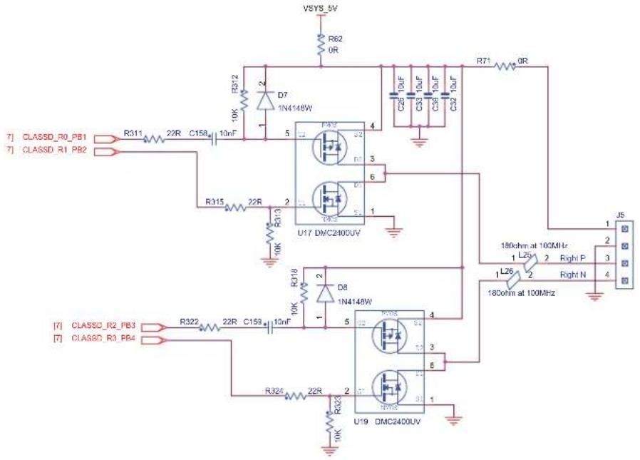
The Audio Class D Amplifier (CLASSD) is a digital input, Pulse Width Modulated (PWM) output stereo Class D amplifier. It features a high-quality interpolation filter embedding a digitally controlled gain, an equalizer and a de-emphasis filter.
On its input side, the CLASSD is compatible with most common audio data rates. On the output side, its PWM output can drive either:
- high-impedance single-ended or differential output loads (Audio DAC application) or,
• external MOSFETs through an integrated non-overlapping circuit (Class D power amplifier application).
Figure 6-30. Audio PWM Class D MOSFET Mono Amplifier
text_image
VSY5 5W R62 UR R312 D7 1N4148W C29 10uF C33 10uF C38 10uF C32 10uF R71 0R 7] CLASSD_R0_PB1 7] CLASSD_R1_PB2 R311 22R C158 10nF R315 22R R313 U17 DMC2400UV R318 D8 1N4148W 5 10k 10k 10k 10k 10k 10k 10k 10k 10k 10k 10k 10k 10k 10k 10k 10k 10k 10k 10k 10k 10k 10k 10k 10k 10k 10K [7] CLASSD_R2_PB3 [7] CLASSD_R3_PB4 R322 22R C159 10nF R324 22R R323 U19 DMC2400UV R325 22R R324 R326 22R R325 J5 1 L2G 2 Right P 1 L26 2 Right N 180ohm at 100MHz 4 3 8 1 2 3 4CLASSD Output Connector J5
text_image
WWW.ATMEL.COM XPRO EXT1 F1_TXD F1_RXD P2 BOOT_DIS V5 V5 D23 D25 D27 D29 D31 D33 D35 D37 D39 D41 D43 D45 D47 D49 D51 D53 GND Atmel® SMART™ SAMA5D2 X PLAINED ULTRA DEBUG_DIS P2 R0 R1 R2 R3 R4 R5 R6 R7 R8 R9 R10 R11 R12 R13 R14 R15 R16 R17 R18 R19 R20 R21 RESET WAKE UP EDBG-USB A5-JTAGED66-JTAG3 CLASS D EDBG_DIS 10 11 12 13 14 15 16 17 18 19 20 21 SOMMO.CI11 SDMMCO.II 13 14 15 16 17 18 19 20 21 VDDIODDR HSC HSC P0 VDDBU CANRX1 CANTX1 P/O BU DIGITAL DIGITAL VDDIODDR SDMMCO.II 13 14 15 16 17 18 19 20 21 VDDIODDR SDMMCO.II 13 14 15 16 17 18 19 20 21Table 6-12. CLASSD Output Connector J5 Signal Descriptions
| Pin Mnemonic | Signal Description | |
| 1 | VSYS_5V | Power |
| 2 | GND | GND |
| 3 | OUTPUT RIGHT P | Positive Level |
| 4 | OUTPUT RIGHT N | Negative Level |
6.4.8 Tamper Interface
The SAMA5D2C-XULT board features eight tamper pins for static or dynamic intrusion detections, UART reception, and two analog pins for comparison.
For information on intrusion detection for SAMA5D23 and SAMA5D28, refer to the document "SAMA5D2 Security Module", document no. 44036. This document is available under Non-Disclosure Agreement (NDA).
Contact a Microchip sales representative for further details.
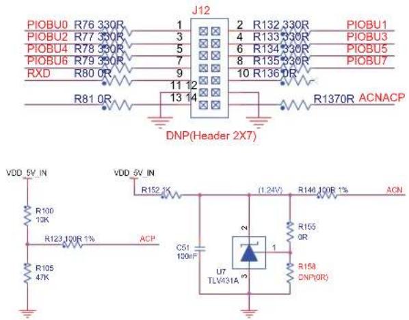
Figure 6-31. Tamper Pin Connector J12
text_image
PIOBU0 R76 330R PIOBU2 R77 330R PIOBU4 R78 330R PIOBU6 R79 330R RXD R80 0R J12 2 R132 330R 4 R133 330R 6 R134 330R 8 R135 330R 10 R136 0R R81 0R 11 12 13 14 R1370R ACNACP DNP(Header 2X7) VDD 5V IN R100 10K R123 100R 1% ACP R105 47K VDD 5V IN R152 1K (1.24V) R146 100R 1% ACN C51 130nF U7 TLV431A 2 1 R155 0R R158 DNP(0R)6.4.9 Tamper Connector
Figure 6-32. Tamper Connector J12
text_image
WWW.ATMEL.COM BOOT_DIS XPRO Power XPRO EXT1 25 F1_TXD F1_RXD XPRO EXT2 45 P0 VDDIODDR 6 SMM/MCO11 R120H17 R120H13 R107H18 R102H11 700 2.5V RESET WAKE UP L13 EDBG-JUB EDBG-JTAG A5-JTAG CLASS D R21 R22 R23 R24 R25 R26 R27 R28 R29 R30 R31 R32 R33 R34 R35 R36 R37 R38 R39 R40 R41 R42 R43 R44 R45 R46 R47 R48 R49 R50 R51 R52 R53 R54 R55 R56 R57 R58 R59 R60 R61 R62 R63 R64 R65 R66 R67 R68 R69 R70 R71 R72 R73 R74 R75 R76 R77 R78 R79 R80 R81 R82 R83 R84 R85 R86 R87 R88 R89 R90 R91 R92 R93 R94 R95 R96 R97 R98 R99 R100 VDD_3V3 LP VDD_3V3 LP RST 3V3 5V GND GND NC A0 A1 A2 A3 A4 A5 A6 A7 A8 A9 A10 A11 CANRX0 CANTX0 VDDCORE REB LED LCD P2 DEBUG_DIS DEBUG SAMA5D2 X PLAINED LATMEL® SMART™Table 6-13. Tamper Connector J12 Signal Descriptions
| Signal | Pin No. | Signal | |
| PIOBU0 | 1 | 2 | PIOBU1 |
| PIOBU2 | 3 | 4 | PIOBU3 |
| PIOBU4 | 5 | 6 | PIOBU5 |
| ......continued | |||
| Signal Pin No. Signal | |||
| PIOBU6 7 8 PIOBU7 | |||
| RXD 9 10 NC | |||
| GND 11 12 GND | |||
| ACP 13 14 ACN | |||
6.4.10 RGB LED
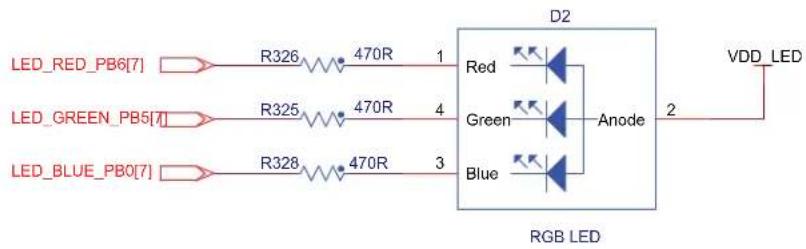
There is one RGB LED on the SAMA5D2C-XULT board; it can be controlled by the user. The three LED cathodes are controlled via GPIO PWM pins.
Figure 6-33. RGB LED Indicators
text_image
LED_RED_PB6[7] R326 470R 1 LED_GREEN_PB5[7] R325 470R 4 LED_BLUE_PB0[7] R328 470R 3 D2 Red Anode 2 VDD LED RGB LED6.4.11 Push Button Switches
The SAMA5D2C-XULT board features three push buttons:
- One board Reset button (BP3) connected to the PMIC ACT8945A. When pressed and released, it causes a Power-on Reset of the board.
- One wake-up push button connected to the PMIC ACT8945A, used to exit the processor from Low-power mode (BP2).
• One User momentary push button (BP1).
Figure 6-34. User Push Buttons (BP1)

text_image
[7] USER_PB_PB9 BP1 Tact Switch6.4.12 Debug Interfaces
The SAMA5D2C-XULT board includes a JTAG, a Debug serial COM port and an EDBG interface port, to provide debug level access to the SAMA5D2.
6.4.12.1 Debug JTAG
A 10-pin JTAG header is provided on the SAMA5D2C-XULT board to facilitate the software development and debugging by using various JTAG emulators. The interface signals have a voltage level of 3.3V.
Figure 6-35. JTAG Interface

text_image
VDD_3V3 R104 100K R75 100K R74 100K JTAG_TCK_PD14 R99 DNP(0R) JTAG_TCK_PD14 [8] JTAG_TDO_PD16 [8] JTAG_TDI_PD15 [8] NRST [4,9,10,12,14,15] JTAG_TMS_PD17 [8] JTAG_TCK_PD14 [8] JTAG_TDO_PD16 [8] Header 2X5Figure 6-36. JTAG J11

text_image
WWW.ATMEL.COM BOOT_DIS XPRO EXT1 F1_TXD F1_RXD XPRO EXT2 J95 P3 RESET VDDIODDR SDMMC011 R128 R124 R100 R105 R71 R62 R63 R64 R65 R66 R67 R68 R69 R70 R71 R72 R73 R74 R75 R76 R77 R78 R79 R80 R81 R82 R83 R84 R85 R86 R87 R88 R89 R90 R91 R92 R93 R94 R95 R96 R97 R98 R99 R100 R101 R102 R103 R104 R105 R106 R107 R108 R109 R110 R111 R112 R113 R114 R115 R116 R117 R118 R119 R120 R121 R122 R123 R124 R125 R126 R127 R128 R129 R130 R131 R132 R133 R134 R135 R136 R137 R138 R139 R140 R141 R142 R143 R144 R145 R146 R147 R148 R149 R150 R151 R152 GNDTable 6-14. JTAG/ICE Connector J11 Signal Descriptions
| Pin | Mnemonic | Signal Description |
| 1 | VTref. 3.3V power | This is the target reference voltage (main 3.3V). |
| 2 | TMS TEST MODE SELECT | JTAG mode set input into target CPU |
| 3 | GND | Common ground |
| 4 | TCK TEST CLOCK – Output timing signal, for synchronizing test logic and control register access | JTAG clock signal into target CPU |
| 5 | GND | Common ground |
| 6 | TDO JTAG TEST DATA OUTPUT – Serial data input from the target | JTAG data output from target CPU |
| ......continued | ||
| Pin | Mnemonic Signal Description | |
| 7 | RTCK – Input Return test clock signal from the target | Some targets having too slow of a system clock must synchronize the JTAG inputs to internal clocks. In present case such synchronization is unneeded and TCK merely looped back into RTCK. |
| 8 | TDI TEST DATA INPUT – Serial data output line, sampled on the rising edge of the TCK signal | JTAG data input into target CPU |
| 9 | GND Common ground | |
| 10 | nSRST RESET Active-low reset signal. Target CPU reset signal. | |
6.4.12.2 Serial Console Port
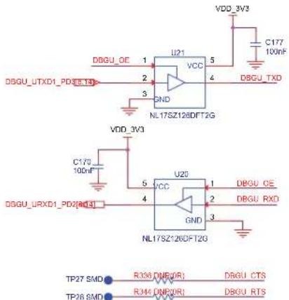
The SAMA5D2C-XULT board has a dedicated serial port for debugging, which is accessible through the 6-pin male header J1. Various interfaces can be used as USB/Serial DBGU port bridge, such as FTDI TTL-232R USB to TTL serial cable or basic breakout board for the RS232/USB converter.
Figure 6-37. Debug Com Port for Console
text_image
VDD_3V3 DBGU_OE 1 U21 5 VCC 4 DBGU_TXD 2 3 GND NL17SZ128DFT2G VDD_3V3 C177 100nF DBGU_LTXD1_PD(5.10) DBGU_URXD1_PD2(RDS) U20 1 DBGU_CE 5 VCC 2 DBGU_RXD 4 GND 3 NL17SZ128DFT2G TP27 SMD R336 DNEORI DGBU_CTS TP28 SMD R344 DNEORI DGBU_RTS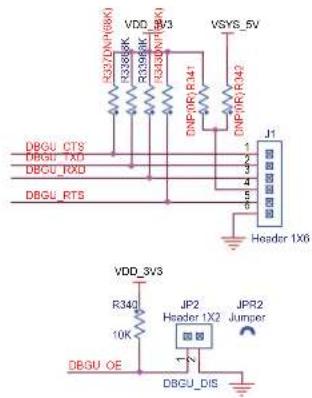
text_image
VDD_3V3 R527(DN168K) R33888K R29488K (UL4040)V(168K) DNP105(R441) DNP106(R342) VSYS_5V DBGU_CTS DBGU_XO DBGU_RXO DBGU_RTS J1 1 2 3 4 5 6 Header 1X6 VDD_3V3 R340 10K DBGU_OE JPN Header 1X2 JPR2 Jumper DBGU_DISA jumper (JP2) is available to disable the Debug communication interface.
R341 and R342 are optional (not implemented) resistors that can be used for power selection. Power can be delivered either by the SAMA5D2C-XULT board or by the debug interface tool. To avoid malfunction between the debug interface (e.g., FTDI) and the on-board power system, ensure that the selected voltage level corresponds to application requirements. The console baud rate is set to 115200 by default.
Figure 6-38. DEBUG Connector J1
text_image
WWW.ATMEL.COM V5 V5 D23 D25 D27 D29 D31 D33 D35 D37 D38 D40 D42 D44 D46 D48 D50 D52 GND DIGITAL Atmel® SMART™ SAMA5D2 X PLAINED DEBUG_DIS PB_USER SP1 DEBUG VDDIODDR SDMMC011 RESET A5-JTAGED66-JTG EDBG-USB CLASS D RST VDD_3V3 RST VDD_3V3_LP VDD_3V3_P VDD_3V3_LP VDD_3V3_LP VDD_3V3_LP VDD_3V3_LP VDD_3V3_LP VDD_3V3_LP VDD_3V3_LP VDD_3V3_LP VDD_3V3_LP VDD_3V3_LP VDD_3V3_LP VDD_3V3_LPTable 6-15. DEBUG Connector J1 Signal Descriptions
| Pin Mnemonic | PIO | Signal Description | |
| 1 | CTS | RFU | Handshake input |
| 2 | TXD1 (Transmitted Data) | PD3 | RS232 serial data output signal |
| 3 | RXD1 (Received Data) | PD2 | RS232 serial data input signal |
| 4 | Power | - | 5V/3.3V (selected by resistors) |
| 5 | RTS | RFU | Handshake output |
| 6 | GND | - | Common ground |

When using a console connected to the DEBUG interface J1, the jumper JP2 DEBUG_DIS should be OFF.
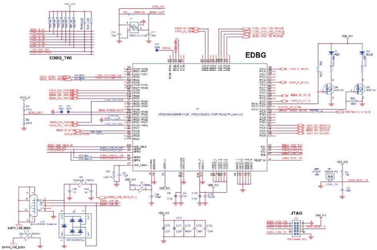
6.4.13 Embedded Debugger (EDBG) Interface
The Embedded Debugger (EDBG) ^(1) is an intuitive plug-and-play solution which adds full programming and debugging support to embedded hardware kits containing Microchip microcontrollers and microprocessors. It enables seamless integration between the target hardware and the Atmel Studio front end.
In addition to the Virtual COM port which provides a UART bridge to the target device, the EDBG provides a Data Gateway Interface, through which the target device and host PC can communicate, facilitating high-level application debugging, monitoring, graphing and logging of system information in real-time.
The EDBG is based on the AT32UC3A4256J high-performance low-power 32-bit AVR microcontroller running at up to 60 MHz. The device includes an on-chip USB 2.0 high-speed hardware module with dedicated DMA channels, making it ideal for data communications.
By default, the EDBG is in Reset state and not usable. To use the EDBG interface, remove the jumper JP1. To avoid any conflicts with the debug signals, do not use the JTAG and EDBG at the same time.
Figure 6-39. EDBG Interface
text_image
Circuit schematic diagram of an EDBG-based power supply with labeled components and connections6.4.14 CDC Debug Interface
This feature is enabled only if pin J9 (RESET_N) of the microcontroller is not tied to ground. The pin is normally pulled high and controlled by jumper JP1.
- Jumper JP1 not installed: The CDC device is enabled.
- Jumper JP1 installed: The CDC device is disabled.

The default baud rate CDC is 57600 (57600/N/8/1).

When using a console with the EDBG-CDC, the jumper JP2 DEBUG_DIS should be ON.
6.4.15 EDBG USB Type Micro-AB
Figure 6-40. EDBG USB Type Micro-AB Connector J14
text_image
SAMA5D2 X PLAINED WWW.ATMEL.COM BOOT_DIS VDD-3V3 RESET WAKE UP EDBG-USB A5-JTAGEDBG-JTAG CLASS D EDBG_DIS RGB LED VDD-3V3 RSTI STAT POWER VDD 3V3_LP RSI GND NC A1 A2 A3 A4 A5 A6 A7 A8 A9 A10 A11 CANRX1 CANTX1 CANRX2 CANTX3 VDDCORE RGB LED VBAT LCD DEBUG_DIS DEBUG CTB RGB VCCNTRTS SHD VDD-3V3_LP RSI GND NC A1 A2 A3 A4 A5 A6 A7 A8 A9 A10 A11 CANRX2 CANTX3 R120K107 R120K108 R100K109 R010K110 R020K111 R030K112 R040K113 R050K114 R060K115 R070K116 R080K117 R090K118 R100K119 R110K120 R120K121 R130K122 R140K123 R150K124 R160K125 R170K126 R180K127 R190K128 R200K129 R210K130 R220K131 R230K132 R240K133 R250K134 R260K135 R270K136 R280K137 R290K138 R300K139 R310K140 R320K141 R330K142 R340K143 R350K144 R360K145 R370K146 R380K147 R390K148 R400K149 R410K150 R420K151 R430K152 R440K153 R450K154 R460K155 R470K156 R480K157 R490K158 R500K159 R510K160 R520K161 R530K162 R540K163 R550K164 R560K165 R570K166 R580K167 R590K168 R600K169 R610K170 R620K171 R630K172 R640K173 R650K174 R660K175 R670K176 R680K177 R690K178 R700K179 R710K180Table 6-16. USB Connector J14 Signal Descriptions
| Pin | Mnemonic | Signal Description |
| 1 | VBUS | 5V power |
| 2 | DM | Data minus |
| 3 | DP | Data plus |
| 4 | ID | On-the-go identification (not connected) |
| 5 | GND | Common ground |
6.5 PIO Usage on Expansion Connectors
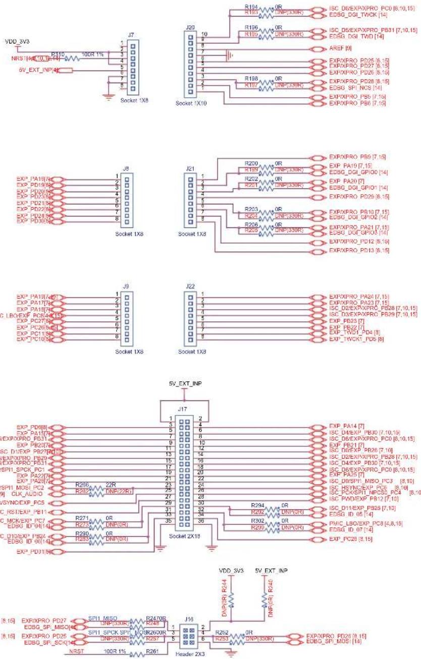
6.5.1 Arduino Connectors
Five 8-pin, one 6-pin, one 10-pin and one 36-pin headers (J7, J8, J9, J16, J17, J20, J21, J22) are provided on the SAMA5D2C-XULT board to enable the PIO connection of various expansion cards. These headers' physical and electrical implementation match the Arduino R3 extension ("shields") system.
Due to I/O multiplexing, different signals can be provided on each pin.
Figure 6-41. Expansion Boards Connectors

text_image
5V_EXT_INP J17 1 2 3 4 5 6 7 8 9 10 11 12 13 14 15 16 17 18 19 20 21 22 23 24 25 26 27 28 29 30 31 32 33 34 35 36 R206 22R R207 DNP(22R) R208 OR R209 OR R210 OR R211 OR R212 OR R213 OR R214 OR R215 OR R216 OR R217 RNP(0R) R218 RNP(0R) R219 RNP(0R) R220 RNP(0R) R221 RNP(0R) R222 RNP(0R) R223 RNP(0R) R224 RNP(0R) R225 RNP(0R) R226 RNP(0R) R227 RNP(0R) R228 RNP(0R) R229 RNP(0R) R230 RNP(0R) R231 RNP(0R) R232 RNP(0R) R233 RNP(0R) R234 RNP(0R) R235 RNP(0R) R236 RNP(0R) R237 RNP(0R) R238 RNP(0R) R239 RNP(0R) R240 RNP(0R) R241 RNP(0R) R242 RNP(0R) R243 RNP(0R) R244 RNP(0R) R245 RNP(0R) R246 RNP(0R) R247 RNP(0R) R248 RNP(0R) R249 RNP(0R) R250 RNP(0R) R251 RNP(0R) NRSST 100Ω 1% R261 Socket 2X19 EXP_PA8[8] EXP_PA1[7] ISC_DS/EXP_XPRO_PB31 ISC_DS/EXP_XPRO_PB37 ISC_DS/EXP_XPRO_PB39 ISC_DS/EXP_XPRO_PB31 ISC_DS/SPX_SPCK_PC1 EXP_PAZ[7] ISC_DS/EXP_XPRO_PB38 ISC_DS/EXP_XPRO_PB39 ISC_DS/EXP_XPRO_PC1 EXP_PAZ[7] ISC_DS/EXP_MISO_PC3 [8,10] ISC_DS/EXP_MISO_PC3 [8,10] ISC_DS/EXP_MISO_PC3 [8,10] ISC_DS/EXP_MISO_PC3 [8,10] ISC_DS/EXP_MISO_PC3 [8,10] ISC_DS/EXP_MISO_PC3 [8,10] ISC_DS/EXP_MISO_PC3 [8,10] ISC_DS/EXP_MISO_PC3 [8,10] OSC_PD3[9] ISC_DS/EXP_PB5 [7,10] ISC_DS/EXP_PB5 [7,10] ISC_DS/EXP_PB5 [7,10] ISC_DS/EXP_PB5 [7,10] ISC_DS/EXP_PB5 [7,10] ISC_DS/EXP_PB5 [7,10] ISC_DS/EXP_PB5 [7,10] ISC_DS/EXP_PB5 [7,10] ISC_DS/EXP_PB5 (8,10) ISC_DS/EXP_PB5 (8,10) ISC_DS/EXP_PB5 (8,10) ISC_DS/EXP_PB5 (8,10) ISC_DS/EXP_PB5 (8,10) ISC_DS/EXP_PB5 (8,10) ISC_DS/EXP_PB5 (8,10) ISC_DS/EXP_PB5 (8,10) ISC_DS/EXP_PB5 (7,10) ISC_DS/EXP_PB5 (7,10) ISC_DS/EXP_PB5 (7,10) ISC_DS/EXP_PB5 (7,10) ISC_DS/EXP_PB5 (7,10) ISC_DS/EXP_PB5 (7,10) ISC_DS/EXP_PB5 (7,10) ISC_DS/EXP_PB5 (7,10) ISC_DS/EXP_MISO_PC3 [8,10] ISC_DS/EXP_MISO_PC3 [8,10] ISC_DS/EXP_MISO_PC3 [8,10] ISC_DS/EXP_MISO_PC3 [8,10] ISC_DS/EXP_MISO_PC3 [8,10] ISC_DS/EXP_MISO_PC3 [8,10] ISC_DS/EXP_MISO_PC3 [8,10] ISC_DVI/EXP_PB5 [7,10] EDSG_ID_05 [7,4] PMIC_LSO/EXP_PC3 [6,8,15] EDSG_ID_07 [7,4] EXP_PC2[8,15] VDD_3V3 5V_EXT_INP DNP(DN)OR R244 DNP(DN)OR R246 DNP(DN)OR J16 4 R262 OR 6 R253 DNP(350R) EXP/XPRO_PD26 [9,15] EDSG_SPI_MOSI [14]6.5.1.1 Functions Available Through the Arduino Headers
The multiplexing of the SAMA5D27 I/Os (standard parallel I/O and up to three peripheral functions per pin) makes it possible to route alternate signals via Arduino extension headers. To enable these signals, SAMA5D27 PIO multiplexing must be properly configured. For more details, refer to Board Schematics and the section PIO Controller (PIO) in the SAMA5D2 Series data sheet.
The tables below, together with the connector schematics, provide the alternate signals available for use with Arduino connectors.
Figure 6-42. J7 Connector

text_image
WWW.ATMEL.COM VDDIODDR RESET WAKE UP EDBG-USB A5-JTAGED66-JTG CLASS D VDD 3V0 SAMA5D2 X PLAINED Atmel® SMART™ VBAT DEBUG_DIS PB_USER DBG_DIS LED8Q_DIS Ethy Levels 13V LEVELS CTB RXO VCCRDS GND CANTX1 CANRX1 P/CIBU DIGITAL HSC F0-TXD F0-RXD F3-TXD F3-RXD SDM SQ1 D22 D24 D26 D28 D30 D32 D34 D36 D38 D40 D42 D44 D46 D48 D50 D52 GND CANTX1 PINBU P2 VDDBU PS111 PS121 PS131 PS141 PS151 PS161 PS171 PS181 PS191 PS201 PS211 PS221 PS231 PS241 PS251 PS261 PS271 PS281 PS291 PS301 PS311 PS321 PS331 PS341 PS351 PS361 PS371 PS381 PS391 PS401 PS411 PS421 PS431 PS441 PS451 PS461 PS471 PS481 PS491 PS501 PS511 PS521 PHYTHAICOSISOLICOSISOLICOSISOLICOSISOLICOSISOLICOSISOLICOSISOLICOSISOLICOSISOLICOSISOLICOSISOLICOSISOLICOSISOLICOSISOLICOSISOLICOSISOLICOSISOLICOSISOLICOSISOLICOSISOLICOSISOLICOSISOLICOSISOLICOSISOLICOSISOLICOSISLPGKLEDTable 6-17. J7 Connector Signals
| Pin No. Signal | Function | |
| 1 | VBAT | NC |
| 2 | 3V3 | (IOREF) |
| 3 | RST | - |
| 4 | 3V3 | - |
| 5 | 5V | - |
| 6 | GND | - |
| 7 | GND | - |
| 8 | VIN | NC |
Figure 6-43. J8 Connector
text_image
WWW.ATMEL.COM XPRO-EXT1 F1_TXD F1_RXD XPRO-EXT2 BOOT_DIS A5-USB-A RESET WAKE UP EDBG-USB A5-JTAGEDBG-JTAG CLASS D SAMA5D2 X PLAINED ULTRA Atmel® SMART™ VBAT DEBUG_DIS PB_USER BP1 LEDG_DIS R02 R03 R04 R05 R06 R07 R08 R09 R10 R11 R12 R13 R14 R15 R16 R17 R18 R19 R20 R21 R22 VDD_3V3 LP VDD_3V3 LP VDD_CORE RGB_LED LED LED_GND LED_GND LED_GND LED_GND LED_GND LED_GND LED_GND LED_GND LED_GND LED_GND LED_GND LED_GND LED_GND LED_GND LED_GND LED_GND LED_GND LED_GND LED_GND LED_GND LED_GND LED_GND LED_GND LED_GND LED_GND LED_GN LED_GND LED_GND LED_GND LED_GND LED_GND LED_GND LED_GND LED_GND LED_GND LED_GND LED_GND LED_GND LED_GND LED_GND LED_GND LED_GND LED_GND LED_GND LED_GND LED_GND LED_GND LED_GND LED_GND LED_GND LED_GNG LED_GNG LED_GNG LED_GNG LED_GNG LED_GNG LED_GNG LED_GNG LED_GNG LED_GNG LED_GNG LED_GNG LED_GNG LED_GNG LED_GNG LED_GNG LED_GNG LED_GNG LED_GNG LED_GNG LED_GNG LED_GNG LED_GNG LED_GNG LED_GNG LED_GNSTable 6-18. J8 Connector Signals
| Pin | SAMA5D27 PIO Muxing Alternates | |||||||
| No. Type | ||||||||
| 1 | PA16 | SPI0_MISO | TD1 | QSPI0_IO0 | I2SWS1 | FLEXCOM3_IO4 | D11 | - |
| 2 | PD19 | PCK0 | TWD1 | URXD2 | - | I2SCK0 | ISC_D11 | AD0 |
| 3 | PD20 | TIOA2 | TWCK1 | UTXD2 | - | I2SMCK0 | ISC_PCK | AD1 |
| 4 | PD23 | URXD2 | - | FLEXCOM4_IO3 | - | I2SDO0 | ISC_FIELD | AD4 |
| 5 | PD21 | TIOB2 | TWD0 | FLEXCOM4_IO1 | - | I2SWS0 | ISC_VSYNC | AD2 |
| 6 | PD22 | TCLK2 | TWCK0 | FLEXCOM4_IO2 | - | I2SDI0 | ISC_HSYNC | AD3 |
| 7 | PD24 | UTXD2 | - | FLEXCOM4_IO4 | - | - | - | AD5 |
| 8 | PD30 | SPI1_NPCS2 | TMS | FLEXCOM2_O1 | TIOB3 | TWCK0 | - | AD11 |
Figure 6-44. J9 Connector
text_image
WWW.ATMEL.COM XPRO EXT1 F1_TXD F1_RXD XPRO EXT2 BOOT_DIS RESET SDMMC017 VDDIODDR WAKE UP EDBG-USB A5-JTAGEDBG-JTG CLASS D SAMA5D2 X PLAINED Atmel® SMART™ CAMR-X CANRX1 CANTX1 PINBU P311 P32 P33 P34 P35 P36 P37 P38 P39 P40 P41 P42 P43 P44 P45 P46 P47 P48 P49 P50 P51 P52 GND CANTX1 CANRX1 CANTX1 PINBU PINDBU PINDBU PINDBU PINDBU PINDBU PINDBU PINDBU PINDBU PINDBU PINDBU PINDBU PINDBU PINDBU PINDBU PINDBU PINDBU PINDBU PINDBU PINDBU PINDBU PINDBU PINDBU PINDBU PINDBU PINDBU PINDBUU PINDBUU PINDBUU PINDBUU PINDBUU PINDBUU PINDBUU PINDBUU PINDBUU PINDBUU PINDBUU PINDBUU PINDBUU PINDBUU PINDBUU PINDBUU PINDBUU PINDBUU PINDBUU PINDBUU PINDBUU PINDBUU PINDBUU PINDBUU PINDBUU PINDBU PINDBU PINDBU PINDBU PINDBU PINDBU PINDBU PINDBU PINDBU PINDBU PINDBU PINDBU PINDBU PINDBU PINDBU PINDBU PINDBU PINDBU PINDBU PINDBU PINDBU PINDBU PINDBU PINDBUTable 6-19. J9 Connector Signals
| Pin | SAMA5D27 PIO Muxing Alternates | ||||||
| No. Type | |||||||
| 1 | PA19 | SPI0_NPCS2 | RF1 | QSPI0_IO3 | TIOA0 | SDHC1_DAT1 | D14 |
| 2 | PA17 | SPI0_NPCS0 | RD1 | QSPI0_IO1 | I2SDI1 | FLEXCOM3_O1 | D12 |
| 3 | PA18 | SPI0_NPCS1 | RK1 | QSPI0_IO2 | I2SDO1 | SDHC1_DAT0 | D13 |
| 4 | PC8 | LCDDEN | NANDRDY | FIQ | PCK0 | UTXD1 | ISC_FIELD |
| 5 | PC27 | LCDDAT23 | GTX3 | PCK1 | CANRX1 | TWD0 | A16 |
| 6 | PC26 | LCDDAT22 | - | GTX2 | CANTX1 | - | A15 |
| 7 | PC11 | LCDDAT3 | GTXEN | ISC_D2 | TCLK4 | CANRX0 | A0/NBS0 |
| 8 | PC10 | LCDDAT2 | GTXCK | ISC_D1 | TIOB4 | CANTX0 | - |
Figure 6-45. J20 Connector

text_image
WWW.ATMEL.COM V5 V5 D23 D25 D27 D29 D31 D33 D35 D37 D39 D41 D43 D45 D47 D49 D51 D53 GND SDMMC1 A5-USB-8 R3 SAMS Atmel® SMART™ SAMA5D2 X PLAINED ULTRA DEBUG_DIS PB_USER BP1 DEBUG CT6 ROD VOLTRES GND VDDIODDR F0 TXD F0 RXD F3 TXD F3 RXD SDM SQ1 D22 D24 D26 D28 D30 D32 D34 D36 D38 DIGITAL HSC PVDDBU CANRX1 CANTX1 PQBU CANRX0 CANTX0 VDDIODDR SMMCO11 SDMMC10 VDDIODDR RESET WAKE UP EDBG-USB A5-JTAGEDBG-JTG CLASS D R1 R2 R3 R4 R5 R6 R7 R8 R9 R10 R11 R12 R13 R14 R15 R16 R17 R18 R19 R20 R21 R22 R23 R24 R25 R26 R27 R28 R29 R30 R31 R32 R33 R34 R35 R36 R37 R38 R39 R40 VDDIODDR SMMCO10 SMMCO11 SMMCO12 SMMCO13 SMMCO14 SMMCO15 SMMCO16 SMMCO17 SMMCO18 SMMCO19 SMMCO20 SMMCO21 SMMCO22 SMMCO23 SMMCO24 SMMCO25 SMMCO26 SMMCO27 SMMCO28 SMMCO29 SMMCO30 SMMCO31 SMMCO32 SMMCO33 SMMCO34 SMMCO35 SMMCO36 SMMCO37 SMMCO38 SMMCO39 SMMCO40 SMMCO41 SMMCO42 SMMCO43 SMMCO44 SMMCO45 SMMCO46 SMMCO47 SMMCO48 SMMCO49 SMMCO50 SMMCO51 SMMCO52 SMMCO53 SMMCO54 SMMCO55 SMMCO56 SMMCO57 SMMCO58 SMMCO59 SMMCO60 SMMCO61 SMMCO62 SMMCO63 SMMCO64 SMMCO65 SMMCO66 SMMCO67 SMMCO68 SMMCO69 SMMCO70 SMMCO71 SMMCO72 SMMCO73 SMMCO74 SMMCO75 SMMCO76 SMMCO77 SMMCO78 SMMCO79 SMMCO80 SMMCO81 SMMCO82 SMMCO83 SMMCO84 SMMCO85 SMMCO86 SMMCO87 SMMCO88 SMMCO89 SMMCO90 SMMCO91 SMMCO92 SMMCO93 SMMCO94 SMMCO95 SMMCO96 SMMCO97 SMMCO98 SMMCO99 SMMCO100 VDDIODDR VDDIODDR VDDIODDR VDDIODDR VDDIODDR VDDIODDR VDDIODDR VDDIODDR VDDIODDR VDDIODDR VDDIODDR VDDIODDR VDDIODDR VDDIODDR VDDIODDR VDDIODDR VDDIODDR VDD I VDDIODDR VDDIODDR VDDIODDR VDDIODDR VDDIODDR VDDIODDR VDDIODDR VDDIODDR VDDIODDR VDDIODDR VDDIODDR VDDIODDR VDDIODDR VDDIODDR VDDIODDR VDDIODDR VDDINOSCKSCKSCKSCKSCKSCKSCKSCKSCKSCKSCKSCKSCKSCKSCKSCKSCKSCKSCKSCKSCKSCKSCKSCKSCKSCKSCKSCKSCKSCKSCKSCKSCKSCKSCKSCKSCKSCKSCKSCKSCKSCKSCKSCKSCKSCKSCKSCKSCKSCKSCKsTable 6-20. J20 Connector Signals
| Pin | SAMA5D27 PIO Muxing Alternates | ||||||
| No. Type | |||||||
| 10 | PC0 | LCDDAT21 | A23 | FLEXCOM0_O1 | TWCK0 | - | ISC_D6 |
| 9 | PB31 | LCDDAT20 | A20 | FLEXCOM0_IO4 | TWD0 | - | ISC_D5 |
| 8 | AREF | - | - | - | - | - | - |
| 7 | GND | - | - | - | - | - | - |
| 6 | PD25 | SPI1_SPCK | FLEXCOM4_O1 | - | - | AD6 | |
| 5 | PD27 | SPI1_MISO | TCK | FLEXCOM2_IO2 | - | - | AD8 |
| 4 | PD26 | SPI1_MOSI | - | FLEXCOM2_IO1 | - | - | AD7 |
| 3 | PD28 | SPI1_NPCS0 | TDI | FLEXCOM2_IO3 | - | - | AD9 |
| 2 | PB5 | TCLK2 | D10 | PWMH2 | QSPI1_SCK | PTCPORT5 | GTSUCOMP |
| 1 | PB6 | TIOA2 | D11 | PWML2 | QSPI1_CS | PTCPORT6 | GTXER |
Figure 6-46. J21 Connector

text_image
WWW.ATMEL.COM XPRO EXT1 F1_TXD F1_RXD XPRO EXT2 BOOT_DIS A5 USB-A RESET WAKE UP EDBG-USB A5-JTAGEDBG-JTAG CLASS D SAMS-DIS SAMAS-D2 X PLAINED ULTRA DEBUG DBG_DIS R01 R02 R03 R04 R05 R06 R07 R08 R09 R10 R11 R12 R13 R14 R15 R16 R17 R18 R19 R20 R21 R22 V5 V5 D23 D25 D27 D29 D31 D33 D35 D37 D39 D41 D43 D45 D47 D49 D51 D53 GND DIGITAL H3C P0_VDDBU PIQBU CANRX1 CANTX1 CANTX2 CANRX0 CANTX0 VDDIODDR SDMMC011 SDMXCM11 VDDIODDR VDDIODDR VDDIODDR VDDIODDR VDDIODDR VDDIODDR VDDIODDR VDDIODDR VDDIODDR VDDIODDR VDDIODDR VDDIODDR VDDIODDR VDDIODDR VDDIODDR VDDIODDR VDDIODDR VDDIDRD VDDIDRD VDDIDRD VDDIDRD VDDIDRD VDDIDRD VDDIDRD VDDIDRD VDDIDRD VDDIDRD VDDIDRD VDDIDRD VDDIDRD VDDIDRD VDDIDRD VDDIDRD VDDIDRD VDDIDRD VDDIDRD VDDIDRD VDDIDR VDDIDRD VDDIDRD VDDIDRD VDDIDRD VDDIDRD VDDIDRD VDDIDRD VDDIDRD VDDIDRD VDDIDRD VDDIDRD VDDIDRD VDDIDRD VDDIDRD VDDIDRD VDDIDRD VDDIDRDTable 6-21. J21 Connector Signals
| Pin | SAMA5D27 PIO Muxing Alternates | ||||||
| No. Type | |||||||
| 1 | PB9 | TIOA3 | D14 | PWMFI1 | QSPI1_IO2 | - | GCOL |
| 2 | PA19 | SPI0_NPCS2 | RF1 | QSPI0_IO3 | TIOA0 | SDHC1_DAT1 | D14 |
| 3 | PA20 | SPI0_NPCS3 | - | - | TIOB0 | SDHC1_DAT2 | D15 |
| 4 | PD29 | SPI1_NPCS1 | TDO | FLEXCOM2_IO4 | TIOA3 | TWD0 | AD10 |
| 5 | PB10 | TIOB3 | D15 | PWMEXTRG1 | QSPI1_IO3 | - | GRX2 |
| 6 | PA21 | IRQ | PCK2 | TCLK0 | SDHC1_DAT3 | NANDRDY | |
| 7 | PD12 | TIOB1 | FLEXCOM4_IO0 | UTMI_LS1 | GRXER | ISC_D5 | ISC_D0 |
| 8 | PD13 | TCLK1 | FLEXCOM4_IO1 | UTMI_CRDCPSEL0 | GRX0 | ISC_D6 | ISC_D1 |
Figure 6-47. J22 Connector
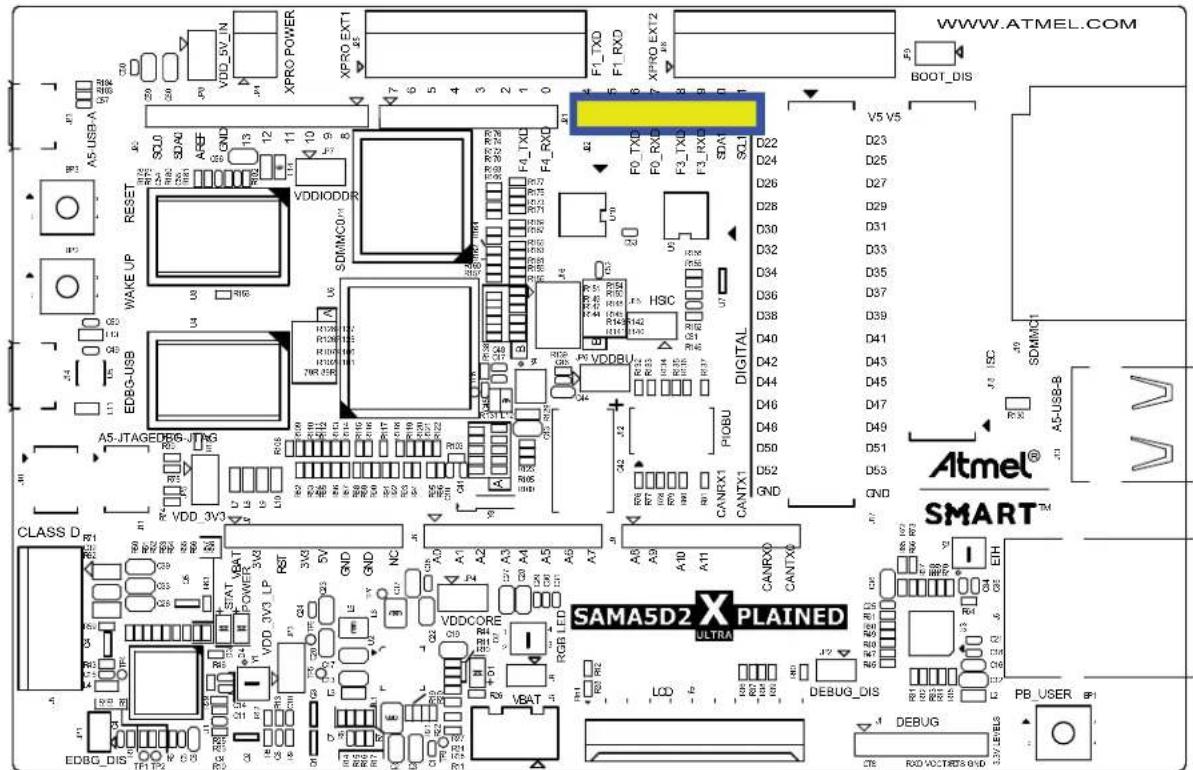
text_image
WWW.ATMEL.COM V5 V5 D23 D25 D27 D29 D31 D33 D35 D37 D38 D40 D41 D43 D45 D46 D48 D50 D51 D53 GND Atmel® SMART™ SAMA5D2 X PLAINED ULTRA DEBUG_DIS PB_USER BP1 DEBUG CTB RXO VOUTRDS GND 13V LEVELSTable 6-22. J22 Connector Signals
| Pin | SAMA5D27 PIO Muxing Alternates | ||||||
| No. Type | |||||||
| 1 | PA24 | FLEXCOM1_IO0 | D2 | TDO | SPI1_MISO | - | QSPI0_IO0 |
| 2 | PA23 | FLEXCOM1_IO1 | D1 | TDI | SPI1_MOSI | - | QSPI0_CS |
| 3 | PB28 | LCDDAT17 | A17 | FLEXCOM0_IO0 | TIOA5 | - | ISC_D2 |
| 4 | PB29 | LCDDAT18 | A18 | FLEXCOM0_IO1 | TIOB5 | - | ISC_D3 |
| 5 | PB23 | LCDDAT12 | A12 | RD0 | TIOB2 | FLEXCOM3_IO1 | GMDIO |
| 6 | PB22 | LCDDAT11 | A11 | TD0 | TIOA2 | FLEXCOM3_IO2 | GMDC |
| 7 | PD4 | TWD1 | URXD2 | - | GCOL | ISC_D10 | NCS0 |
| 8 | PD5 | TWCK1 | UTXD2 | - | GRX2 | ISC_D9 | NCS1 |
Figure 6-48. J17 Connector
text_image
WWW.ATMEL.COM BOOT_DIS XPRO-EXT1 F1_TXD F1_RXD XPRO-EXT2 VDDIODDR SDMMC017 RESET WAKE UP EDBG-USB A5-JTAGEDBG-JTAG CLASS D SAMA5D2 X PLAINED ALTMEL® SMART™ VBAT DEBUG_DIS PB_USER BP1 LEDG_DIS R3 R4 R5 R6 R7 R8 R9 R10 R11 R12 R13 R14 R15 R16 R17 R18 R19 R20 R21 R22 R23 R24 R25 R26 R27 R28 R29 R30 R31 R32 R33 R34 R35 R36 R37 R38 R39 R40 R41 R42 R43 R44 R45 R46 R47 R48 R49 R50 R51 RNCKX1 CANTX1 CANRXX CANTX1 P/OBU CANRXX CANTX1 DIGITAL V V5 V V6 V V7 V V8 V V9 V V10 V V11 V V12 V V13 V V14 V V15 V V16 V V17 V V18 V V19 V V20 V V21 V V22 V V23 V V24 V V25 V V26 V V27 V V28 V V29 V V30 V V31 V V32 V V33 V V34 V V35 V V36 V V37 V V38 V V39 V V40 V V41 V V42 V V43 V V44 V V45 V V46 V V47 V V48 V V49 V V50Table 6-23. J17 Connector Signals
| Pin | SAMA5D27 PIO Muxing Alternates | ||||||
| No. Type | |||||||
| 1 | 5V | - | - | - | - | - | - |
| 2 | 5V | - | - | - | - | - | - |
| 3 | PD6 | TCK | PCK1 | - | GRX3 | ISC_D8 | NCS2 |
| 4 | PA14 | SPI0_SPCK | TK1 | QSPI0_SCK | I2SMCK1 | FLEXCOM3_IO3 | D9 |
| 5 | PA15 | SPI0_MOSI | TF1 | QSPI0_CS | I2SCK1 | FLEXCOM3_IO1 | D10 |
| 6 | PB30 | LCDDAT19 | A19 | FLEXCOM0_IO3 | TCLK5 | - | ISC_D4 |
| 7 | PB31 | LCDDAT20 | A20 | FLEXCOM0_IO4 | TWD0 | - | ISC_D5 |
| 8 | PC0 | LCDDAT21 | A23 | FLEXCOM0_O1 | TWCK0 | - | ISC_D6 |
| 9 | PB20 | LCDDAT9 | A9 | TK0 | TIOB3 | PCK1 | GTX0 |
| 10 | PB21 | LCDDAT10 | A10 | TF0 | TCLK3 | FLEXCOM3_IO3 | GTX1 |
| 11 | PB27 | LCDDAT16 | A16 | UTXD0 | PDMCLK0 | - | ISC_D1 |
| 12 | PB26 | LCDDAT15 | A15 | URXD0 | PDMDAT0 | - | ISC_D0 |
| 13 | PB29 | LCDDAT18 | A18 | FLEXCOM0_IO1 | TIOB5 | - | ISC_D3 |
| 14 | PB28 | LCDDAT17 | A17 | FLEXCOM0_IO0 | TIOA5 | - | ISC_D2 |
| 15 | PB31 | LCDDAT20 | A20 | FLEXCOM0_IO4 | TWD0 | - | ISC_D5 |
| 16 | PB30 | LCDDAT19 | A19 | FLEXCOM0_IO3 | TCLK5 | - | ISC_D4 |
| Pin SAMA5D27 PIO Muxing Alternates | |||||||
| No. Type | |||||||
| 17 PC1 LCDDAT22 A24 CANTX0 SPI1_SPCK I2SCK0 ISC_D7 | |||||||
| 18 PC0 LCDDAT21 A23 FLEXCOM0_O1 TWCK0 - ISC_D6 | |||||||
| 19 PA22 FLEXCOM1_IO3 D0 TCK | SPI1_SPCK SDHC1_CK QSPI0_SCK | ||||||
| 20 PA25 FLEXCOM1_IO4 D3 TMS | SPI1_NPCS0 - QSPI0_IO1 | ||||||
| 21 PA26 FLEXCOM1_O1 D4 NTRST | SPI1_NPCS1 - QSPI0_IO2 | ||||||
| 22 | PC3 | LCDPWM | NWAIT | TIOA1 | SPI1_MISO | I2SWS0 | ISC_D9 |
| 23 | PC2 | LCDDAT23 | A25 | CANRX0 | SPI1_MOSI | I2SMCK0 | ISC_D8 |
| 24 | PC6 | LCDHSYNC | NCS1 | TWD1 | SPI1_NPCS2 | ISC_HSYNC | |
| 25 | PC5 | LCDVSYNC | NCS0 | TCLK1 | SPI1_NPCS1 | I2SDO0 | ISC_VSYNC |
| 26 | PC4 | LCDDISP | NWR1/NBS1 | TIOB1 | SPI1_NPCS0 | I2SDI0 | ISC_PCK |
| 27 | PB11 | LCDDAT0 | A0/NBS0 | URXD3 | PDMDAT0 | - | GRX3 |
| 28 | PB12 | LCDDAT1 | A1 | UTXD3 | PDMCLK0 | - | GTX2 |
| 29 | PC7 | LCDPCK | NCS2 | TWCK1 | SPI1_NPCS3 | URXD1 | ISC_MCK |
| 30 PB25 | LCDDAT14 A14 RF0 | - FLEXCOM3_IO1 ISC_D11 | |||||
| 31 | PB24 | LCDDAT13 | A13 | RK0 | TCLK2 | FLEXCOM3_IO4 | ISC_D10 |
| 32 | PC8 | LCDDEN | NANDRDY | FIQ | PCK0 | UTXD1 | ISC_FIELD |
| 33 | PD31 | ADTRG | NTRST | IRQ | TCLK3 | PCK0 | - |
| 34 PC26 | LCDDAT22 - GTX2 | CANTX1 | A15 | ||||
| 35 GND | ---- | ||||||
| 36 GND | ---- | ||||||
Figure 6-49. J16 Connector

Note: 5V/3.3V selected by resistors
6.5.2 XPRO
The SAMA5D2C-XULT board features three connectors to interface with standard Xplained PRO extensions.
Figure 6-50. XPRO Connectors Schematics

text_image
XPRO Power 5V_EXT_INP J24 1 2 3 4 VDD_3V3VSYS_5V DNP(Header 2X2) XPRO EXT1 EDBG_ID_02[14] XPRO_PD1[8] EXPXPRO_PD136[10] FXPXXPRO_FB57[11] EXPXPRO_PD139[15] ISC_D6/EXPXPRO_FB316[16] EXPXPRO_PA23[15] EXPXPRO_TD23[16] EXPXPRO_FD276[18] J25 ID ADC(-) GPIO PWM(-) IROGPIO TWI_SDA UART_RX SPI_SS_A SPI_MISO 13 15 17 19 20 4 ADC(-) GPIO PWM(-) IROSSO TWI_SDA UART_RX SPI_SS_A SPI_MISO 13 15 17 19 4 ADC(-) GPIO PWM(-) IROSSO TWI_SDA UART_RX SPI_SS_A SPI_MISO 13 15 17 19 4 ADC(-) GPIO PWM(-) IROSSO TWI_SDA UART_RX SPI_SS_A SPI_MISO 13 15 17 19 4 ADC(-) GPIO PWM(-) IROSSO TXI_SDA UART_RX SPI_SS_A SPI_MISO 13 15 17 19 4 ADC(-) GPIO PWM(-) IROSSO TXI_SDA UART_RX SPI_SS_A SPI_MISO 13 15 17 19 4 ADC(-) GPIO PWM(-) IROSSO TXI_SDA UART_RX SPI_SS_A SPI_MISO 20 20 20 VDD_3V3 EXPXPRO_PD12[8.16] EXPXPRO_PD18[8] EXPXPRO_P910[7.15] EXPXPRO_P229[8.16] EXPXPRO_P00[8.10,15] EXPXPRO_PA24[7.15] EXPXPRO_P026[8.15] EXPXPRO_P025[8.15] XPRO EXT2 EDBG_ID_53[14] XPRO_PD7[8] XPRO_PD8[8] EXPXPRO_FB57[10] EXPXPRO_PD216[16] ISC_D2/EXPXPRO_FB286[10,15] ISC_D2/EXPXPRO_FB296[10,15] EXPXPRO_FD276[18] EXPXPRO_FD276[18] J26 ID ADC(-) GPIO PWM(-) IROGPIO TWI_SDA UART_RX SPI_SS_A SPI_MISO 13 15 17 19 4 ADC(-) GPIO PWM(-) IROSSO TXI_SDA UART_RX SPI_SS_A SPI_MISO 13 15 17 19 4 ADC(-) GPIO PWM(-) IROSSO TXI_SDA UART_RX SPI_SS_A SPI_M ISOThe standard extension headers include common signals.
Figure 6-51. XPRO Connectors
text_image
XPRO POWER XPRO EXT1 7 6 5 4 3 2 1 0 14 F1 TXD 15 F1 RXD 16 F1 RXD EXT2 17 20 21 WWW.ATMEL.COM BOOT_DIS RESET SCL0 SDA0 GND VDDIODDR R10 R11 R12 R13 R14 R15 R16 R17 R18 R19 R20 R21 R22 D23 D24 D25 D26 D27 D28 D29 D30 D31 D32 D33 D34 D35 D36 D37 D38 D39 D40 D41 D42 D43 D44 D45 D46 D47 D48 D49 D50 D51 D52 D53 GND DIGITAL HSC VDDBU CANEX1 CANTX1 CLASS D R10 VDD_3V3 R11 R12 R13 R14 R15 R16 R17 R18 R19 R20 R21 R22 R23 R24 R25 R26 R27 R28 R29 R30 R31 R32 R33 R34 R35 R36 R37 R38 R39 R40 R41 R42 R43 R44 R45 R46 R47 R48 R49 R50 R51 R52 R53 GND Atmel® SMART™ ETH F8_USER BP1 SAMA5D2 X PLAINED ULTRA DEBUG_DIS LCD 40000000000000000000000000000000000000000000000000000000000000000000000000000000000000000000000000000Table 6-25. XPRO Power Connector J24 Signal Descriptions
| Signal | Pin No. | Signal | |
| EXP_5V | 1 | 2 | GND |
| ......continued | |||
| Signal Pin No. Signal | |||
| VDD_5V 3 4 VSYS_3V3 | |||
Table 6-26. XPRO EXT1 Connector J25 Signal Descriptions
| Pin XPRO Signal SAMA5D27 PIO Muxing Alternates | |||||||||
| No. Type | |||||||||
| 1 - EDBG_ID_02 ---- | |||||||||
| 2 GND --- | ---- | ||||||||
| 3 | PD11 | ADC(+) | TIOA1 | PCK2 | UTMI_LS0 | GRXDV | ISI_D4 | ISI_MCK | PTCCOL0 |
| 4 | PD12 | ADC(-) | TIOB1 | FLEXCOM4_IO0 | UTMI_LS1 | GRXER | ISI_D5 | ISI_D4 | PTCCOL1 |
| 5 | PD13 | GPIO | TCLK1 | FLEXCOM4_IO1 | UTMI_CDRCPSEL0 | GRX0 | ISI_D6 | ISI_D5 | PTCCOL2 |
| 6 | PD18 | GPIO | NTRST | - | - | GMDIO | ISI_FIELD | ISI_D10 | PTCCOL7 |
| 7 | PB9 | PWM(+) | TIOA3 | D14 | PWMFI1 | QSPI1_IO2 | - | GCOL | - |
| 8 | PB10 | PWM(-) | TIOB3 | D15 | PWMEXTRG1 | QSPI1_IO3 | - | GRX2 | - |
| 9 | PD13 | IRQ/GPIO | TCLK1 | FLEXCOM4_IO2 | UTMI_CDRCPSEL0 | GRX0 | ISI_D6 | ISI_D5 | PTCCOL2 |
| 10 | PD29 | SPI_SS_B/GPIO | SPI1_NPCS1 | TDO | FLEXCOM2_IO4 | TIOA3 | TWD0 | - | AD10 |
| 11 | PB31 | TWI_SDA | LCDDAT20 | A20 | FLEXCOM0_IO4 | TWD0 | - | ISI_D5 | - |
| 12 | PC0 | TWI_SCL | LCDDAT21 | A23 | FLEXCOM0_O1 | TWCK0 | - | ISI_D6 | - |
| 13 | PA23 | UART_RX | FLEXCOM1_IO2 | D1 | TDI | SPI1_MOSI | - | QSPI0_CS | - |
| 14 | PA24 | UART_TX | FLEXCOM1_IO1 | D2 | TDO | SPI1_MISO | - | QSPI0_IO0 | - |
| 15 | PD28 | SPI_SS_A | SPI1_NPCS0 | TDI | FLEXCOM2_IO3 | - | - | - | AD9 |
| 16 | PD26 | SPI_MOSI | SPI1_MOSI | - | FLEXCOM2_IO1 | - | - | - | AD7 |
| 17 | PD27 | SPI_MISO | SPI1_MISO | TCK | FLEXCOM2_IO2 | - | - | - | AD8 |
| 18 | PD25 | SPI_SCK | SPI1_SPCK | - | FLEXCOM4_O1 | - | - | - | AD6 |
| 19 | GND --- | - | ---- | ||||||
| 20 | 3V3 | -- | ---- | ||||||
Table 6-27. XPRO EXT2 Connector J26 Signal Descriptions
| Pin | XPRO Signal | SAMA5D27 PIO Muxing Alternates | |||||||
| No. | Type | ||||||||
| 1 | - | EDBG_ID_03 | - | - | - | - | - | - | - |
| 2 | GND | - | - | - | - | - | - | - | - |
| 3 | PD7 | ADC(+) | TDI | - | UTMI_RXVAL | GTX2 | ISI_D0 | NWR1/NBS1 | PTCROW4 |
| 4 | PD8 | ADC(-) | TDO | - | UTMI_RXERR | GTX3 | ISI_D1 | NANDRDY | PTCROW5 |
| 5 | PD9 | GPIO | TMS | - | UTMI_RXACT | GTXCK | ISI_D2 | - | PTCROW6 |
| 6 | PD10 | GPIO | NTRST | - | UTMI_HDIS | GTXEN | ISI_D3 | - | PTCROW7 |
| 7 | PB5 | PWM(+) | TCLK2 | D10 | PWMH2 | QSPI1_SCK | PTCPORT5 | GTSUCOMP | - |
| 8 | PB6 | PWM(-) | TIOA2 | D11 | PWML2 | QSPI1_CS | PTCPORT6 | GTXER | - |
| Pin XPRO Signal SAMA5D27 PIO Muxing Alternates | |||||||||
| No. Type | |||||||||
| 9 PA21 IRQ/GPIO IRQ PCK2 - TCLK0 SDHC1_DAT3 NANDRDY - | |||||||||
| 10 | PD28 | SPI_SS_B/GPIO | SPI1_NPCS0 | TDI | FLEXCOM2_IO3 | - | - | - | AD9 |
| 11 | PB28 | TWI_SDA | LCDDAT17 | A17 | FLEXCOM0_IO1 | TIOA5 | - | ISI_D2 | - |
| 12 | PB29 | TWI_SCL | LCDDAT18 | A18 | FLEXCOM0_IO2 | TIOB5 | - | ISI_D3 | - |
| 13 | PB29 | UART_RX | LCDDAT18 | A18 | FLEXCOM0_IO2 | TIOB5 | - | ISI_D3 | - |
| 14 | PB28 | UART_TX | LCDDAT17 | A17 | FLEXCOM0_IO1 | TIOA5 | - | ISI_D2 | - |
| 15 | PD29 | SPI_SS_A | SPI1_NPCS1 | TDO | FLEXCOM2_IO4 | TIOA3 | TWD0 | - | AD10 |
| 16 | PD26 | SPI_MOSI | SPI1_MOSI | - | FLEXCOM2_IO1 | - | - | - | AD7 |
| 17 | PD27 | SPI_MISO | SPI1_MISO | TCK | FLEXCOM2_IO2 | - | - | - | AD8 |
| 18 | PD25 | SPI_SCK | SPI1_SPCK | - | FLEXCOM4_O1 | - | - | - | AD6 |
| 19 | GND | - | - | - | - | - | - | - | - |
| 20 | 3V3 | - | - | - | - | - | - | - | - |
7. Board Schematics
This section contains the following schematics:
- Block Diagram
- PIO Muxing Table
- Power Supply
- SAMA5D27 – Power
- SAMA5D27 - DDR3
• SAMA5D27 – PIOA and PIOB
• SAMA5D27 – PIOC and PIOD - SAMA5D27 – SYS, Tamper, and Debug
- USB, ISC, and LCD
- Serial Flash, LEDS, Push Button and ClassD
- Ethernet
- SD and eMMC
• EDBG - Expansion and XPRO Connectors

Important: Design Reuse Recommendation
In case the memory or PIO busses go to multiple destinations, series resistors must be added. These resistors must be located at the beginning of each branch, as close as possible to the MPU.
In case these connections are point-to-point, the branch resistors found in the following schematics can be removed.
In all cases, it is recommended to always perform routing simulation to check signal integrity prior to PCB manufacturing.
Figure 7-1. Block Diagram
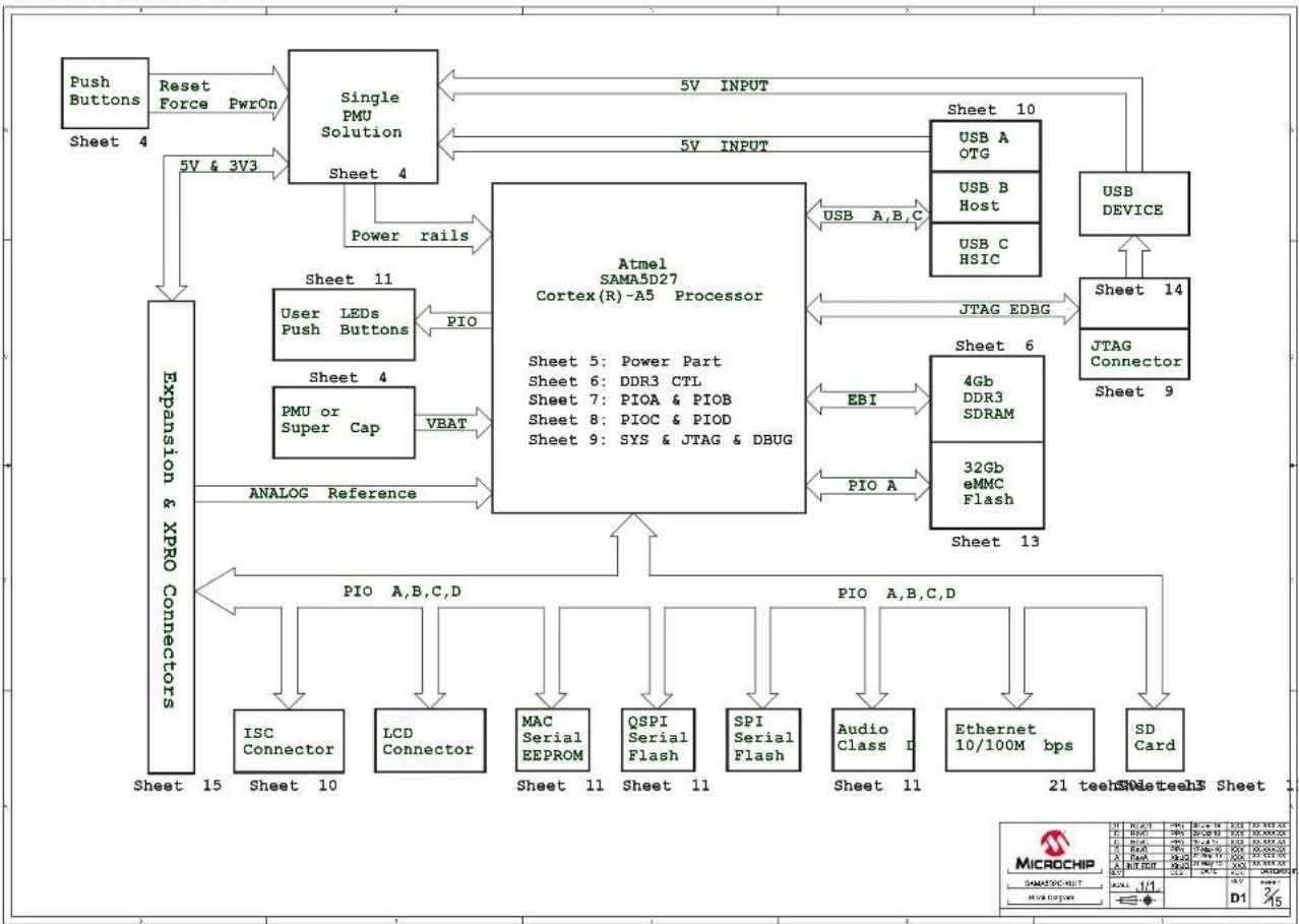
flowchart
graph TD
    A["Microchip"] -->|10/11 21 teeth| B["32Gb eMMC Flash"]
    A -->|21 teeth| C["4Gb DDR3 SDRAM"]
    A -->|21 teeth| D["32Gb eMMC Flash"]
    A -->|21 teeth| E["4Gb DDR3 SDRAM"]
    A -->|21 teeth| F["32Gb eMMC Flash"]
    A -->|21 teeth| G["4Gb DDR3 SDRAM"]
    A -->|21 teeth| H["32Gb eMMC Flash"]
    A -->|21 teeth| I["4Gb DDR3 SDRAM"]
    A -->|21 teeth| J["32Gb eMMC Flash"]
    A -->|21 teeth| K["4Gb DDR3 SDRAM"]
    A -->|21 teeth| L["32Gb eMMC Flash"]
    A -->|21 teeth| M["4Gb DDR3 SDRAM"]
    A -->|21 teeth| N["32Gb eMMC Flash"]
    A -->|21 teeth| O["4Gb DDR3 SDRAM"]
    A -->|21 teeth| P["32Gb eMMC Flash"]
    A -->|21 teeth| Q["4Gb DDR3 SDRAM"]
    A -->|21 teeth| R["32Gb eMMC Flash"]
    A -->|21 teeth| S["4Gb DDR3 SDRAM"]
    A -->|21 teeth| T["32Gb eMMC Flash"]
    A -->|21 teeth| U["4Gb DDR3 SDRAM"]
    A -->|21 teeth| V["32Gb eMMC Flash"]
    A -->|21 teeth| W["4Gb DDR3 SDRAM"]
    A -->|21 teeth| X["32Gb eMMC Flash"]
    A -->|21 teeth| Y["4Gb DDR3 SDRAM"]
    A -->|21 teeth| Z["32Gb eMMC Flash"]
    A -->|21 teeth| AA["4Gb DDR3 SDRAM"]
    A -->|21 teeth| AB["32Gb eMMC Flash"]
    A -->|21 teeth| AC["4Gb DDR3 SDRAM"]
    A -->|21 teeth| AD["32Gb eMMC Flash"]
    A -->|21 teeth| AE["4Gb DDR3 SDRAM"]
    A -->|21 teeth| AF["32Gb eMMC Flash"]
    A -->|21 teeth| AG["4Gb DDR3 SDRAM"]
    A -->|21 teeth| AH["32Gb eMMC Flash"]
    A -->|21 teeth| AI["4Gb DDR3 SDRAM"]
    A -->|21 teeth| AJ["32Gb eMMC Flash"]
    A -->|21 teeth| AK["4Gb DDR3 SDRAM"]
    A -->|21 teeth| AL["32Gb eMMC Flash"]
    A -->|21 teeth| AM["4Gb DDR3 SDRAM"]
    A -->|21 teeth| AN["32Gb eMMC Flash"]
    A -->|21 teeth| AO["4Gb DDR3 SDRAM"]
    A -->|21 teeth| AP["32Gb eMMC Flash"]
    A -->|21 teeth| AQ["4Gb DDR3 SDRAM"]
    A -->|21 teeth| AR["32Gb eMMC Flash"]
    A -->|21 teeth| AS["4Gb DDR3 SDRAM"]
    A -->|21 teeth| AT["32Gb eMMC Flash"]
    A -->|21 teeth| AU["4Gb DDR3 SDRAM"]
    A -->|21 teeth| AV["32Gb eMMC Flash"]
    A -->|21 teeth| AW["4Gb DDR3 SDRAM"]
    A -->|21 teeth| AX["32Gb eMMC Flash"]
    A -->|21 teeth| AY["4Gb DDR3 SDRAM"]
    A -->|21 teeth| AZ["32Gb eMMC Flash"]
    A -->|21 teeth| BA["4Gb DDR3 SDRAM"]
    A -->|21 teeth| BB["32Gb eMMC Flash"]
    A -->|21 teeth| BC["4Gb DDR3 SDRAM"]
    A -->|21 teeth| BD["32Gb eMMC Flash"]
    A -->|21 teeth| BE["4Gb DDR3 SDRAM"]
    A -->|21 teeth| BF["32Gb eMMC Flash"]
    A -->|21 teeth| BG["4Gb DDR3 SDRAM"]
    A -->|21 teeth| BH["32Gb eMMC Flash"]
    A -->|21 teeth| BI["4Gb DDR3 SDRAM"]
    A -->|21 teeth| BJ["32Gb eMMC Flash"]
    A -->|21 teeth| BK["4Gb DDR3 SDRAM"]
    A -->|21 teeth| BL["32Gb eMMC Flash"]
    A -->|21 teeth| BM["4Gb DDR3 SDRAM"]
    A -->|21 teeth| BN["32Gb eMMC Flash"]
    A -->|21 teeth| BO["4Gb DDR3 SDRAM"]
    A -->|21 teeth| BP["32Gb eMMC Flash"]
    A -->|21 teeth| BQ["4Gb DDR3 SDRAM"]
    A -->|21 teeth| BR["32Gb eMMC Flash"]
    A -->|21 teeth| BS["4Gb DDR3 SDRAM"]
    A -->|21 teeth| BT["32Gb eMMC Flash"]
    A -->|21 teeth| BU["4Gb DDR3 SDRAM"]
    A -->|21 teeth| BV["32Gb eMMC Flash"]
    A -->|21 teeth| BW["4Gb DDR3 SDRAM"]
    A -->|21 teeth| BX["32Gb eMMC Flash"]
    A -->|21 teeth| BY["4Gb DDR3 SDRAM"]
    A -->|21 teeth| BZ["32Gb eMMC Flash"]
    A -->|21 teeth| CA["4Gb DDR3 SDRAM"]
    A -->|21 teeth| CB["32Gb eMMC Flash"]
    A -->|21 teeth| CC["4Gb DDR3 SDRAM"]
    A -->|21 teeth| CD["32Gb eMMC Flash"]
    A -->|21 teeth| CE["4Gb DDR3 SDRAM"]
    A -->|21 teeth| CF["32Gb eMMC Flash"]
    A -->|21 teeth| CG["4Gb DDR3 SDRAM"]
    A -->|21 teeth| CH["32Gb eMMC Flash"]
    A -->|21 teeth| CI["4Gb DDR3 SDRAM"]
    A -->|21 teeth| CJ["32Gb eMMC Flash"]
    A -->|21 teeth| CK["4Gb DDR3 SDRAM"]
    A -->|21 teeth| CL["32Gb eMMC Flash"]
    A -->|21 teeth| CM["4Gb DDR3 SDRAM"]
    A -->|21 teeth| CN["32Gb eMMC Flash"]
    A -->|21 teeth| CO["4Gb DDR3 SDRAM"]
    A -->|21 teeth| CP["32Gb eMMC Flash"]
    A -->|21 teeth| COB["4Gb DDR3 SDRAM"]
    A -->|21 teeth| CPB["32Gb eMMC Flash"]
    A -->|21 teeth| CPC["32Gb eMMC Flash"]
    A -->|21 teeth| CPD["4Gb DDR3 SDRAM"]
    A -->|21 teeth| CPE["32Gb eMMC Flash"]
    A -->|21 teeth| CPF["4Gb DDR3 SDRAM"]
    A -->|21 teeth| CPG["32Gb eMMC Flash"]
    A -->|21 teeth| CPH["4Gb DDR3 SDRAM"]
    A -->|21 teeth| CPI["32Gb eMMC Flash"]
    A -->|21 teeth| CPJ["4Gb DDR3 SDRAM"]
Board Schematics
SAMAD2C XULT
Figure 7-2. PIO Muxing Table
PIO Muxing & Jumper setting
| LCD | |
| ID_SYS | 1 |
| GND | 2 |
| KC | 3 |
| KC | 4 |
| LCDDAT2 | 5 |
| LCDDAT3 | 6 |
| GND | 7 |
| LCDDAT4 | 9 |
| LCDDAT5 | 9 |
| LCDDAT6 | 10 |
| LCDDAT7 | 11 |
| GND | 12 |
| KC | 13 |
| KC | 14 |
| LCDDAT10 | 15 |
| LCDDAT11 | 16 |
| GND | 17 |
| LCDDAT12 | 18 |
| LCDDAT13 | 19 |
| LCDDAT14 | 20 |
| LCDDAT15 | 21 |
| GND | 22 |
| KC | 23 |
| KC | 24 |
| LCDDAT16 | 25 |
| LCDDAT19 | 26 |
| GND | 27 |
| LCDDAT20 | 28 |
| LCDDAT21 | 29 |
| LCDDAT22 | 30 |
| LCDDAT23 | 31 |
| GND | 32 |
| LCDPPCK | 33 |
| LCDSVSYNC | 34 |
| LCDSVSYNC | 35 |
| LCDDEN | 36 |
| SPTI_SPCK/ADJ_XP | 37 |
| SPTI_MOSFAD1_XM | 38 |
| SPTI_MISOFAD2_TP | 39 |
| SPTI_NPCSDAD3_YM | 40 |
| LCDDISP | 41 |
| TWDT | 42 |
| TWCKT | 43 |
| IRQ1 | 44 |
| IRQ2 | 45 |
| TCIPPWM | 46 |
| MRST | 47 |
| VCC | 48 |
| VCC | 49 |
| GND | 50 |
| PIOA | PIQA | PIOB | PIOR | PIOC | EASURGASUEGASURGASURGASU | ||||
| PA0 | SDHC0_CX | PA18 | SPID_MISOEXP | P00 | LED_BLUE/CO_ID | P016 | ETH_GRXIV | PC4 | ISC_DMS/EXP/PRO |
| PA1 | SDHC0_CMD | PA17 | SPID_CS/DEXP | P61 | CLASSD_R3 | PB17 | ETH_GRER | PC1 | ISC_DTS/INT_SPCK/EXP |
| PA2 | SDHC0_DAT0 | PA18 | SDHCT_DAT/DEXP | P62 | CLASSD_R1 | PB18 | ETH_GRX0 | PC2 | ISC_DSS/P1_MOS/EXP |
| PA3 | SDHC0_DAT1 | PA19 | SDHCT_DAT/DEXP | P63 | CLASSD_R2 | PB19 | ETH_GRX1 | PC3 | ISC_DSS/P1_MISO/EXP |
| PA4 | SDHC0_DAT2 | PA20 | SDHC1_DAT/DEXP | P64 | CLASSD_R3 | PB20 | ETH GTX/EXP | PC4 | ISC_PCK/SPIN_NPC/S/EXP |
| PA5 | SDHC0_DAT3 | PA21 | SDHC1_DAT/EEXP/PRO | P65 | LED_GREEN/EXP/PRO | P621 | ETH GTX/EXP | PC5 | ISC_VSYNC/EXP |
| PA6 | SDHC0_DAT4 | PA22 | SDHC1_OK/GSPII_SCK/EXP | P66 | LED_RE/EXP/PRO | P622 | ETH_GM/EXP | PC6 | ISC_LSYNC/EXP |
| PA7 | SDHC0_DAT5 | PA23 | QSPII_CS/EXP/PRO | P67 | LCD_IRQ1 | PB23 | ETH_CAND/EXP | PC7 | ISC_MCK/EXP |
| PA8 | SDHC0_DAT6 | PA24 | QSPII_ON/DEXP/PRO | P68 | LCD_IRQ2 | PB24 | ISC_DTX/EXP | PC8 | PMIC_LO/EXP |
| PA9 | SDHC0_DAT7 | PA25 | QSPII_OT/EXP | P69 | USER_FB/EXP/PRO | PB25 | ISC_OTI/EXP | PC9 | ETH_INT |
| PA10 | SDHC0_RSTN | PA26 | QSPII_TO/EXP | PB10 | USBG_EN/S/EXP/PRO | PB26 | ISC_DXE/EXP | PC10 | LCD_DAT/DEXP |
| SDHC0_MOUSEH | PA27 | QSPII_IO3 | PB11 | ISC_RST/EXP | PB27 | AMC_DTEX/EXP | PC11 | LCD_DAT/DEXP | |
| PA12 | PMIC_CHGEFV | PA28 | SDHCT_CMD | PB12 | ISC_PWD/EXP | PB28 | ISC_C2/EXP/PRO | PC12 | LCD_DAT4 |
| PA13 | SDHC0_CD | PA29 | USBB_DVCUR | PB13 | PMIC_IRQ | PB29 | ISC_C3/EXP/PRO | PC13 | LCD_DAT5 |
| PA14 | SPID_SPCK/EXP | PA30 | SDHC1_CD | PB14 | ETH_CTX/CK | PB30 | ISC_C4/EXP | PC14 | LCD_DAT6 |
| PA15 | SPID_MOS/EXP | PA31 | USBA_VBUS_Detection | PB15 | LTH_IST/EN | PB31 | ISC_C6/EXP/PRO | PC15 | LCD_DAT7 |
| PIOC | PIOD | PIOD | EGASUEGASUEGASO | ||
| PC16 | LCO_DAT10 | PD0 | LCD_FCK | PD16 | JTAG_TDO |
| PC17 | LCO_DAT11 | PD1 | LCD_DLN | PD17 | JTAG_INS |
| PC18 | LCO_DAT12 | PD2 | DEGU_CRXDI | PD18 | XPRO |
| PC19 | LCO_DAT13 | PD3 | DEGU_UTXD1 | PD19 | LCD_XPIEXP |
| PC20 | LCO_DAT14 | PD4 | LCODEPMSCEXP TWD1 | PD20 | LCD_XMEXP |
| PC21 | LCO_DAT15 | PD5 | LCODEPMSCEXP TWCK1 | PD21 | LCD_YMPPROC_TWCKEXP |
| PC22 | LCO_DAT16 | PD6 | EXP | PD22 | LCD_YMPPROC_TWCKEXP |
| PC23 | LCO_DAT19 | PD7 | XPRO | PD23 | EXP |
| PC24 | LCO_DAT20 | PD8 | XPRO | PD24 | EXP |
| PC25 | LCO_DAT21 | PD9 | XPRO | PD25 | EXPXPRO |
| PC26 | LCO_DAT22/DX2 | PD10 | XPRO | PD26 | EXPXPRO |
| PC27 | LCO_DAT23/DX2 | PD11 | XPRO | PD27 | EXPXPRO |
| PC28 | LCO_PWM | PD12 | EXPXPRO | PD28 | EXPXPRO |
| PC29 | LCO_DISP | PD13 | EXPXPRO | PD29 | EXPXPRO |
| PC30 | LCO_VSYNC | PD14 | JTAG_TCK | PD30 | EXP |
| PC31 | LCO_HSYNC | PD15 | JTAG_TDI | PD31 | EXP |
| JUMPER DESCRIPTION | ||
| PART | DEFAULT | FUNCTION |
| JP1 | OPEN | Disable LDGS |
| JP2 | OPEN | Disable Debug |
| JP3 | CLOSE | IVDD_SV_LP Measurement |
| JP4 | CLOSE | IVDDCORE Measurement |
| JP5 | CLOSE | IVDDISC-VDDIOPVIZ Measurement |
| JP6 | CLOSE | IVDDBU Measurement |
| JP7 | CLOSE | IVDDIOUR_MPU Measurement |
| JP8 | CLOSE | IVDD_BV_IN Measurement |
| JP9 | OPEN | Disable CS of SP/SDSP/SMMHC Memory |
| MICROCHIP | ||||
| SALMATIC X-IIIT | ||||
| PRO MIMO |
Board Schematics
Figure 7-3. Power Supply

text_image
VDD2_0.5 VDD2_0.5 VDD2_0.5 VDD2_0.5 VDD2_0.5 VDD2_0.5 VDD2_0.5 VDD2_0.5 VDD2_0.5 VDD2_0.5 VDD2_0.5 VDD2_0.5 VDD2_0.5 VDD2-0.5 VDD2-0.5 VDD2-0.5 VDD2-0.5 VDD2-0.5 VDD2-0.5 VDD2-0.5 VDD2-0.5 VDD2-0.5 VDD2-0.5 VDD2-0.5 VDD2-0.5 VDD2-0.5Board Schematics
SAMAD2C XULT
Figure 7-4. SAMA5D27 - Power
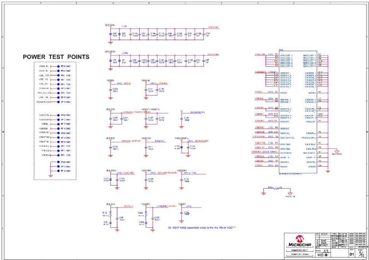
text_image
POWER TEST POINTS VOCER 10kΩ VOCER 10kΩ VOCER 10kΩ VOCER 10kΩ VOCER 10kΩ VOCER 10kΩ VOCER 10kΩ VOCER 10kΩ VOCER 10kΩ VOCER 10kΩ VOCER 10kΩ VOCER 10kΩ, VOCER 10kΩ, VOCER 10kΩ, VOCER 10kΩ, VOCER 10kΩ, VOCER 10kΩ, VOCER 10kΩ, VOCER 10kΩ, VOCER 10kΩ, VOCER 10kΩ, VOCER 10kΩ, VOCER 10kΩ, VAC/DC/DC/DC/DC/DC/DC/DC/DC/DC/DC/DC/DC/DC/DC/DC/DC/DC/DC/DC/DC/DC/DC/DC/DC/DC/DC/DC/DC/DC/DC/DC/DC/DC/DC/DC/DC/DC/DC/DC/DC/DC/DC/DC/DC/DC/DC/DC/DC/DC/DC/NC VOCER 10kΩ VOCER 10kΩ VOCER 10kΩ VOCER 10kΩ VOCER 10kΩ VOCER 10kΩ VOCER 10kΩ VOCER 10kΩ VOCER 10kΩ VOCER 10kΩ VOCER 10kΩ (5.2) VOCER 10kΩ (5.2) VOCER 10kΩ (5.2) VOCER 10kΩ (5.2) VOCER 10kΩ (5.2) VOCER 10kΩ (5.2) VOCER 10kΩ (5.2) VOCER 10kΩ (5.2) VOCER 10kΩ VOCER 10kΩ (5.2) VOCER 10kΩ (5.2) VOCER 10kΩ (5.2) VOCER 10kΩ (5.2) VOCER 10kΩ (5.2) VOCER 10kΩ (5.2) VOCER 10kΩ (5.2) (5.2) VOCER 10kΩ (5.2) (5.2) VOCER 10kΩ (5.2) (5.2) VOCER 10kΩ (5.2) (5.2) VOCER 10kΩ (5.2) (5.2) VOCER 10kΩ (5.2) (5.2) VOCER 48kΩ VOCER 48kΩ VOCER 48kΩ VOCER 48kΩ VOCER 48kΩ VOCER 48kΩ VOCER 48kΩ VOCER 48kΩ VOCER 48kΩ VOCER 48kΩ VOCER 48kΩ VOCER 48kΩ A: VODEN-6492 capacitors close to the Pin of VODEN- All VODEN-6492 capacitors close to the Pin of VODEN- MICROCHIP SINAMATROC-NEUT SINAMATROC-POWEY D1 PANT 6/ D7 PANT 6/ MINT MINT MINT MINT MINT MINT MINT MINT MINT MINT MINT MINT MINT MINT MINT MINT MINT MINT MINT MINT MINT MINT MINT MINT MINT MINT MINTBoard Schematics
SAMAD2C XULT
Figure 7-5. SAMA5D27 - DDR3
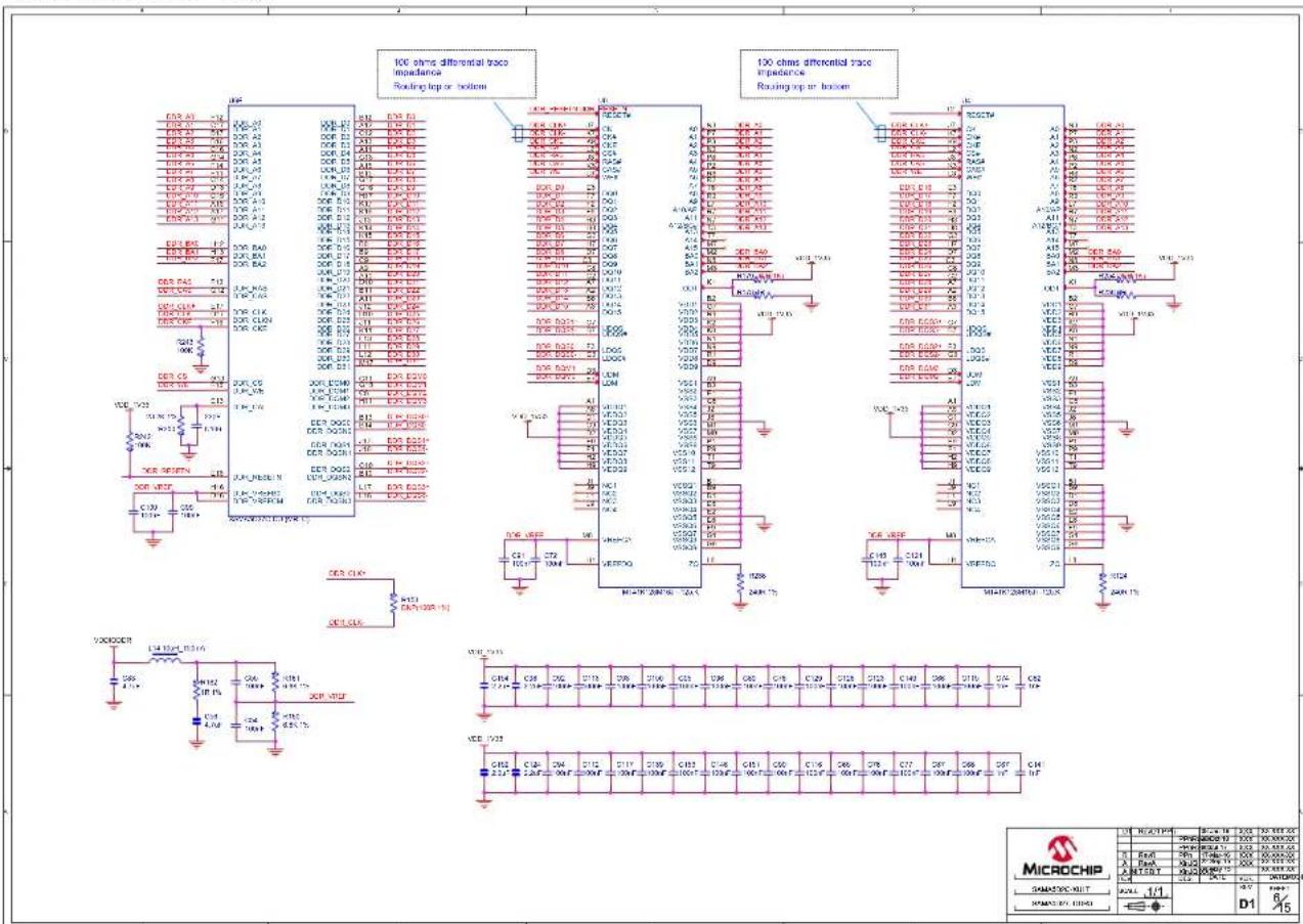
text_image
100 ohms differential race impedance Routing top or bottom 120 ohms differential race impedance Routing up or bottom 100 ohms differential base Impedance Routing top or bottom 120 ohms differential base Impedance Routing up or bottom 100 ohms differential base Impedance Routing top or bottom 120 ohms differential base Impedance Routing up or bottom 100 ohms differential base Impedance Routing top or bottom 120 ohms differential base Impedance Routing top or bottom 100 ohms differential base Impedance Routing top or bottom 120 ohms differential base Impedance Routing top or bottom 100 ohms differential base Impedance Routing top or bottom 120 ohms differential base Impedance Routing top or bottom 100 ohms differential base Impedance Routing top or bottom 120 ohms differential base ImpedanceBoard Schematics
SAMAD2C XULT
Figure 7-6. SAMA5D27 - PIOA and PIOB
text_image
S202 S203 S204 S205 S206 S207 S208 S209 S210 S211 S212 S213 S214 S215 S216 S217 S218 S219 S220 S221 S222 S223 S224 S225 S226 S227 S228 S229 S230 S231 S232 S233 S234 S235 S236 S237 S238 S239 S240 S241 S242 S243 S244 S245 S246 S247 S248 S249 S250 S251 S252 S253 S254 S255 S256 S257 S258 S259 S260 S261 S262 S263 S264 S265 S266 S267 S268 S269 S270 S271 S272 S273 S274 S275 S276 S277 S278 S279 S280 S281 S282 S283 S284 S285 S286 S287 S288 S289 S290 S291 S292 S293 S294 S295 S296 S297 S298 S299 S300
text_image
R172 R172 R172 R173 R173 R173 R174 R174 R174 R175 R175 R175 R176 R176 R176 R177 R177 R177 R178 R178 R178 R179 R179 R179 R180 R180 R180 R181 R181 R181 R182 R182 R182 R183 R183 R183 R184 R184 R184 R185 R185 R185 R186 R186 R186 R187 R187 R187 R188 R188 R188 R189 R189 R189 R190 R190 R190 R191 R191 R191 R192 R192 R192 R193 R193 R193 R194 R194 R194 R195 R195 R195 R196 R196 R196 R197 R197 R197 R198 R198 R198 R199 R199 R199 R200 R200 R200 R201 R201 R201 R202 R202 R202 R203 R203 R203 R204 R204 R204 R205 R205 R205 R206 R206 R206 R207 R207 R207 R208 R208 R208 R209 R209 R209 R210 R210 R210 R211 R211 R211 R212 R212 R212 R213 R213 R213 R214 R214 R214 R215 R215 R215 R216 R216 R216 R217 R217 R217 R218 R218 R218 R219 R219 R219 R220 R220 R220 R221 R221 R221 R222 R222 R222 R223 R223 R223 R224 R224 R224 R225 R225 R225 R226 R226 R226 R227 R227 R227 R228 R228 R228 R229 R229 R229 R230 R230 R230 R231 R231 R231 R232 R232 R232 R233 R233 R233 R234 R234 R234 R235 R235 R235 R236 R236 R236 R237 R237 R237 R238 R238 R238 R239 R239 R239 R240 R240 R240 R241 R241 R241 R242 R243 R243 R243 R244 R244 R244 R245 R245 R245 R246 R246 R246 R247 R247 R247 R248 R248 R248 R249 R249 R249 R250 R250 R250 DPTGATGATGATGATGATGATGATGATGATGATGATGATGATGATGATGATGATGATGATGATGATGATGATGATGATGATGATGATGATGATGATGATGATGATGATGATGATGATGATGATGATGATGATGATGATGATGATGATGATGATG38R on PAZZ close to MPU.

text_image
15 20 21 22 23 24 25 26 27 28 29 30 31 32 33 34 35 36 37 38 39 40 41 42 43 44 45 46 47 48 49 50 51 52 53 54 55 56 57 58 59 60 61 62 63 64 65 66 67 68 69 70 71 72 73 74 75 76 77 78 79 80 81 82 83 84 85 86 87 88 89 90 91 92 93 94 95 96 97 98 99 100
text_image
B01 B12 B23 B02 B12 B24 B03 B12 B25 B04 B12 B26 B05 B12 B27 B06 B12 B28 B07 B12 B29 B08 B12 B30 B09 B12 B31 B10 B12 B32 B11 B12 B33 B12 B12 B34 B13 B12 B35 B14 B12 B36 B15 B12 B37 B16 B12 B38 B17 B12 B39 B18 B12 B40 B19 B12 B41 B20 B12 B42 B21 B12 B43 B22 B12 B44 B23 B12 B45 B24 B12 B46 B25 B12 B47 B26 B12 B48 B27 B12 B49 B28 B12 B50 B29 B12 B51 B30 B12 B52 B31 B12 B53 B32 B12 B54 B33 B12 B55 B34 B12 B56 B35 B12 B57 B36 B12 B58 B37 B12 B59 B38 B12 B60 B39 B12 B61 B40 B12 B62 B41 B12 B63 B42 B12 B64 B43 B12 B65 B44 B12 B66 B45 B12 B67 B46 B12 B68 B47 B12 B69 B48 B12 B70 B49 B12 B71 B50 B12 B72 B51 B12 B73 B52 B12 B74 B53 B12 B75 B54 B12 B76 B55 B12 B77 B56 B12 B78 B57 B12 B79 B58 B12 B80 B59 B12 B81 B60 B12 B82 B61 B12 B83 B62 B12 B84 B63 B12 B85 B64 B12 B86 B65 B12 B87 B66 B12 B88 B67 B12 B89 B68 B12 B90 B69 B12 B91 B70 B12 B92 B71 B12 B93 B72 B12 B94 B73 B12 B95 B74 B12 B96 B75 B12 B97 B76 B12 B98 B77 B12 B99 B78 A07A F08 D09 E0D| MICROCHIP | 31 | NO. (2) | PWR | 8000 10 | 300 | 3000000 |
| 2000 | 8000 10 | 300 | 3000000 | |||
| 4000 | 8000 10 | 300 | 3000000 | |||
| A | R### | 200 | 7000 10 | 300 | 3000000 | |
| A | R### | 300 | 7000 10 | 300 | 3000000 | |
| A | R### | 400 | 6000 10 | 300 | 3000000 | |
| BVI | 500 | 300 | DATOMY | |||
| R### | 191 | D1 | 7/5 |
Board Schematics
SAMAD2C XULT
Figure 7-7. SAMA5D27 - PIOC and PIOD

text_image
PC22 71 PC23 72 PC24 73 PC25 74 PC26 75 PC27 76 PC28 77 PC29 78 PC30 79 PC31 80 PC32 81 PC33 82 PC34 83 PC35 84 PC36 85 PC37 86 PC38 87 PC39 88 PC40 89 PC41 90 PC42 91 PC43 92 PC44 93 PC45 94 PC46 95 PC47 96 PC48 97 PC49 98 PC50 99 PC51 100 PC52 101 PC53 102 PC54 103 PC55 104 PC56 105 PC57 106 PC58 107 PC59 108 PC60 109 PC61 110 PC62 111 PC63 112 PC64 113 PC65 114 PC66 115 PC67 116 PC68 117 PC69 118 PC70 119 PC71 120 PC72 121 PC73 122 PC74 123 PC75 124 PC76 125 PC77 126 PC78 127 PC79 128 PC80 129 PC81 130 PC82 131 PC83 132 PC84 133 PC85 134 PC86 135 PC87 136 PC88 137 PC89 138 PC90 139 PC91 140 PC92 141 PC93 142 PC94 143 PC95 144 PC96 145 PC97 146 PC98 147 PC99 148 PC100 149
text_image
PC1 PC2 PC3 PC4 PC5 PC6 PC7 PC8 PC9 PC10 PC11 PC12 PC13 PC14 PC15 PC16 PC17 PC18 PC19 PC20 PC21 PC22 PC23 PC24 PC25 PC26 PC27 PC28 PC29 PC30 PC31 PC32 PC33 PC34 PC35 PC36 PC37 PC38 PC39 PC40 PC41 PC42 PC43 PC44 PC45 PC46 PC47 PC48 PC49 PC50 PC51 PC52 PC53 PC54 PC55 PC56 PC57 PC58 PC59 PC60 PC61 PC62 PC63 PC64 PC65 PC66 PC67 PC68 PC69 PC70 PC71 PC72 PC73 PC74 PC75 PC76 PC77 PC78 PC79 PC80 PC81 PC82 PC83 PC84 PC85 PC86 PC87 PC88 PC89 PC90 PC91 PC92 PC93 PC94 PC95 PC96 PC97 PC98 PC99 PC100
Figure 7-8. SAMA5D27 - SYS, Tamper, and Debug
text_image
SYS Routing USB Max trace length min/mech between USB signal output SNDs be Rs. sensor than 3.5mm 80 ohms differentials trace Impedance Routing HSC Routing HSC Rinks to Sout JTAG DEBUG MICROCHIP SMAPTOR/OFF D1 PWR 1/4 15Board Schematics
SAMAD2C XULT
Figure 7-9. USB, ISC, and LCD

text_image
ISC LCD USB A USB C USB B Through Holes MICROCHIP SAMSUNG KINT 1.14 D1 10/15Board Schematics
SAMAD2C XULT
Figure 7-10. Serial Flash, LEDS, Push Button and ClassD

 |
Board Schematics
Figure 7-11. Ethernet

text_image
100 ohms differential trace impedance Routing top or bottom Ethernet 10Base-T/100Base-TX U5 DCBCAST_21T TX4 RCC VDD_102 VDDA_203 VDDA_204 VDDA_205 VDDA_206 VDDA_207 VDDA_208 VDDA_209 VDDA_210 VDDA_211 VDDA_212 VDDA_213 VDDA_214 VDDA_215 VDDA_216 VDDA_217 VDDA_218 VDDA_219 VDDA_220 VDDA_221 VDDA_222 VDDA_223 VDDA_224 VDDA_225 VDDA_226 VDDA_227 VDDA_228 VDDA_229 VDDA_230 VDDA_231 VDDA_232 VDDA_233 VDDA_234 VDDA_235 VDDA_236 VDDA_237 VDDA_238 VDDA_239 VDDA_240 VDDA_241 VDDA_242 VDDA_243 VDDA_244 VDDA_245 VDDA_246 VDDA_247 VDDA_248 VDDA_249 VDDA_250 VDDA_251 VDDA_252 VDDA_253 VDDA_254 VDDA_255 VDDA_256 VDDA_257 VDDA_258 VDDA_259 VDDA_260 VDDA_261 VDDA_262 VDDA_263 VDDA_264 VDDA_265 VDDA_266 VDDA_267 VDDA_268 VDDA_269 VDDA_270 VDDA_271 VDDA_272 VDDA_273 VDDA_274 VDDA_275 VDDA_276 VDDA_277 VDDA_278 VDDA_279 VDDA_280 VDDA_281 VDDA_282 VDDA_283 VDDA_284 VDDA_285 VDDA_286 VDDA_287 VDDA_288 VDDA_289 VDDA_290 VDDA_291 VDDA_292 VDDA_293 VDDA_294 VDDA_295 VDDA_296 VDDA_297 VDDA_298 VDDA_299 VDDA_300 ECCOS-TP-B CYP-30F YZ VND-CL-CPK PRC-30F VND-CL-CPK PRC-30F VND-CL-CPK PRC-30F VND-CL-CPK PRC-30F VND-CL-CPK PRC-30F VND-CL-CPK PRC-30F VND-CL-CPK PRC-30F VND-CL-CPK PRC-30F VND-CL-CPK PPC-30F VND-CL-CPK PRC-30F VND-CL-CPK PRC-30F VND-CL-CPK PRC-30F VND-CL-CPK PRC-30F VND-CL-CPK PRC-30F VND-CL-CPK PRC-30F VND-CL-CPK PRC-30F VND-CL 1/1 1/4 1/10 1/4 1/10 1/4 1/10 1/4 1/10 1/4 1/10 1/4 1/10 1/4 1/10 1/4 1/10 1/4 1/10 1/4 1/10 1/4 1/10 1/4 1/10Board Schematics
SAMAD2C XULT
Figure 7-12. SD and eMMC

text_image
SD/MMCPlus CARD INTERFACE - SDHC1 47K pull down on SDHC0 OVD PA1 close to MPU. 3RR on SDHC0 CK PA3 close to MPU. Incremental match of CLVC/CMD (DAI[7:30] 30R) eMMC - SDHC0 MicroCHIP SINAMATOSC-251T D1 13 15 VCCB 262 VCCB 263 VCCB 264 VCCB 265 VCCB 266 VCCB 267 VCCB 268 VCCB 269 VCCB 270 VCCB 271 VCCB 272 VCCB 273 VCCB 274 VCCB 275 VCCB 276 VCCB 277 VCCB 278 VCCB 279 VCCB 280 VCCB 281 VCCB 282 VCCB 283 VCCB 284 VCCB 285 VCCB 286 VCCB 287 VCCB 288 VCCB 289 VCCB 290 VCCB 291 VCCB 292 VCCB 293 VCCB 294 VCCB 295 VCCB 296 VCCB 297 VCCB 298 VCCB 299 VCCB 300 VCCB 301 VCCB 302 VCCB 303 VCCB 304 VCCB 305 VCCB 306 VCCB 307 VCCB 308 VCCB 309 VCCB 310 VCCB 311 VCCB 312 VCCB 313 VCCB 314 VCCB 315 VCCB 316 VCCB 317 VCCB 318 VCCB 319 VCCB 320 VCCB 321 VCCB 322 VCCB 323 VCCB 324 VCCB 325 VCCB 326 VCCB 327 VCCB 328 VCCB 329 VCCB 330 VCCB 331 VCCB 332 VCCB 333 VCCB 334 VCCB 335 VCCB 336 VCCB 337 VCCB 338 VCCB 339 VCCB 340 VCCB 341 VCCB 342 VCCB 343 VCCB 344 VCCB 345 VCCB 346 VCCB 347 VCCB 348 VCCB 349 VCCB 350 VCCB 351 VCCB 352 VCCB 353 VCCB 354 VCCB 355 VCCB 356 VCCB 357 VCCB 358 VCCB 359 VCCB 360 VCCB 361 VCCB 362 VCCB 363 VCCB 364 VCCB 365 VCCB 366 VCCB 367 VCCB 368 VCCB 369 VCCB 370 VCCB 371 VCCB 372 VCCB 373 VCCB 374 VCCB 375 VCCB 376 VCCB 377 VCCB 378 VCCB 379 VCCB 380 VCCB 381 VCCB 382 VCCB 383 VCCB 384 VCCB 385 VCCB 386 VCCB 387 VCCB 388 VCCB 389 VCCB 390 VCCB 391 VCCB 392 VCCB 393 VCCB 394 VCCB 395 VCCB 396 VCCB 397 VCCB 398 VCCB 399 VCCB 400Board Schematics
SAMAD2C XULT
Figure 7-13. EDBG
text_image
EDBG_TWI EDBG JTAG MICROCHIP SAMSUNG-KILT D1 14/15Board Schematics
SAMAD2C XULT
Figure 7-14. Expansion and XPRO Connectors

text_image
Expansion Boards Connectors XPRO Power XPRO EXT1 XPRO EXT2 Sv Ext 8.0 Sv Ext 7.5 Sv Ext 6.5 Sv Ext 5.5 Sv Ext 4.5 Sv Ext 3.5 Sv Ext 2.5 Sv Ext 1.5 Sv Ext 0.5 Sv Ext 0.1 Sv Ext 0.05 Sv Ext 0.01 Sv Ext 0.005 Sv Ext 0.001 Sv Ext 0.0005 Sv Ext 0.0001 Sv Ext 0.00005 Sv Ext 0.00001 Sv Ext 0.000005 Sv Ext 0.000001 Sv Ext 0.0000005 Sv Ext 0.0000001 Sv Ext 0.00000005 Sv Ext 0.00000001 Sv Ext 0.000000005 Sv Ext 0.000000001 Sv Ext 0.0000000005 Sv Ext 0.0000000001 Sv Ext 0.00000000005 Sv Ext 9.5 Sv Ext 8.5 Sv Ext 7.5 Sv Ext 6.5 Sv Ext 5.5 Sv Ext 4.5 Sv Ext 3.5 Sv Ext 2.5 Sv Ext 1.5 Sv Ext 0.5 Sv Ext 0.1 Sv Ext 0.05 Sv Ext 0.01 Sv Ext 9.5 Sv Ext 8.5 Sv Ext 7.5 Sv Ext 6.5 Sv Ext 5.5 Sv Ext 4.5 Sv Ext 3.5 Sv Ext 2.5 Sv Ext 1.5 Sv Ext 0.5 Sv Ext 9.5 Sv Ext 8.5 Sv Ext 7.5 Sv Ext 6.5 Sv Ext 5.5 Sv Ext 4.5 Sv Ext 3.5 Sv Ext 2.5 Sv Ext 1.5 Sv Ext 9.5 Sv Ext 8.5 Sv Ext 7.5 Sv Ext 6.5 Sv Ext 5.5 Sv Ext 4.5 Sv Ext 3.5 Sv Ext 2.5 Sv Ext 1.5 Sv Ext 9.5 Sv Ext 8.5 Sv Ext 7.5
Board Schematics
SAMAD2C XULT
8. Errata
8.1 NRST
Issue: Pullup R6 is connected to VDD_3V3
Workaround: Connect pullup R6 to VDDBU.
8.2 nLBO
Issue: No pullup on nLBO
Workaround: Add pullup 10K to nLBO output.
8.3 R63
Issue: Incorrect R63 resistance in schematic "EDBG"
Workaround: Correct the resistance to 47R.
8.4 R100/R105
Issue: The values of resistors R100/R105 (mounted as a resistive divider on VDD_5V_IN) are swapped. This results in:
- a leakage current path is created from VDD_5V_IN to VDDDU through the ACP pin, and
- the ACP pin is biased around 4V instead of 0.88V, therefore the voltage detection between ACP and CAN does not work
Workaround: Swap R100 and R105.
9. Revision History
Table 9-1. Rev. E - 08/2020
| Changes |
| Updated PD12 and PD13 in XPRO EXT1 Connector J25 Signal Descriptions and J21 Connector Signals. |
Table 9-2. Rev. D - 05/2019
| Changes |
| Updated 7. Board Schematics: all schematics regenerated. |
Table 9-3. Rev. C - 10/2018
| Changes |
| Document title modified to SAMA5D2C XULT User's Guide (was SAMA5D2 (Rev. C) Xplained Ultra Evaluation Kit User's Guide) |
| Updated Figure 6-10. |
| Changed eMMC reference in section eMMC. |
| All schematics regenerated. |
| Added R100/R105 in section Errata. |
Table 9-4. Rev. B - 12/2017
| Changes |
| Updated SAMA5D27 – PIOA and PIOB. |
| Removed Declaration of Conformity. |
Table 9-5. Rev. A - 10/2017
| Changes |
| First issue. |
The Microchip Website
Microchip provides online support via our website at www.microchip.com/. This website is used to make files and information easily available to customers. Some of the content available includes:
- Product Support – Data sheets and errata, application notes and sample programs, design resources, user's guides and hardware support documents, latest software releases and archived software
- General Technical Support – Frequently Asked Questions (FAQs), technical support requests, online discussion groups, Microchip design partner program member listing
- Business of Microchip – Product selector and ordering guides, latest Microchip press releases, listing of seminars and events, listings of Microchip sales offices, distributors and factory representatives
Product Change Notification Service
Microchip's product change notification service helps keep customers current on Microchip products. Subscribers will receive email notification whenever there are changes, updates, revisions or errata related to a specified product family or development tool of interest.
To register, go to www.microchip.com/pcn and follow the registration instructions.
Customer Support
Users of Microchip products can receive assistance through several channels:
• Distributor or Representative
- Local Sales Office
- Embedded Solutions Engineer (ESE)
- Technical Support
Customers should contact their distributor, representative or ESE for support. Local sales offices are also available to help customers. A listing of sales offices and locations is included in this document.
Technical support is available through the website at: www.microchip.com/support
Microchip Devices Code Protection Feature
Note the following details of the code protection feature on Microchip devices:
- Microchip products meet the specifications contained in their particular Microchip Data Sheet.
- Microchip believes that its family of products is secure when used in the intended manner and under normal conditions.
- There are dishonest and possibly illegal methods being used in attempts to breach the code protection features of the Microchip devices. We believe that these methods require using the Microchip products in a manner outside the operating specifications contained in Microchip's Data Sheets. Attempts to breach these code protection features, most likely, cannot be accomplished without violating Microchip's intellectual property rights.
- Microchip is willing to work with any customer who is concerned about the integrity of its code.
- Neither Microchip nor any other semiconductor manufacturer can guarantee the security of its code. Code protection does not mean that we are guaranteeing the product is “unbreakable.” Code protection is constantly evolving. We at Microchip are committed to continuously improving the code protection features of our products. Attempts to break Microchip’s code protection feature may be a violation of the Digital Millennium Copyright Act. If such acts allow unauthorized access to your software or other copyrighted work, you may have a right to sue for relief under that Act.
Legal Notice
Information contained in this publication is provided for the sole purpose of designing with and using Microchip products. Information regarding device applications and the like is provided only for your convenience and may be superseded by updates. It is your responsibility to ensure that your application meets with your specifications.
THIS INFORMATION IS PROVIDED BY MICROCHIP "AS IS". MICROCHIP MAKES NO REPRESENTATIONS OR WARRANTIES OF ANY KIND WHETHER EXPRESS OR IMPLIED, WRITTEN OR ORAL, STATUTORY OR OTHERWISE, RELATED TO THE INFORMATION INCLUDING BUT NOT LIMITED TO ANY IMPLIED WARRANTIES OF NON-INFRINGEMENT, MERCHANTABILITY, AND FITNESS FOR A PARTICULAR PURPOSE OR WARRANTIES RELATED TO ITS CONDITION, QUALITY, OR PERFORMANCE.
IN NO EVENT WILL MICROCHIP BE LIABLE FOR ANY INDIRECT, SPECIAL, PUNITIVE, INCIDENTAL OR CONSEQUENTIAL LOSS, DAMAGE, COST OR EXPENSE OF ANY KIND WHATSOEVER RELATED TO THE INFORMATION OR ITS USE, HOWEVER CAUSED, EVEN IF MICROCHIP HAS BEEN ADVISED OF THE POSSIBILITY OR THE DAMAGES ARE FORESEEABLE. TO THE FULLEST EXTENT ALLOWED BY LAW, MICROCHIP'S TOTAL LIABILITY ON ALL CLAIMS IN ANY WAY RELATED TO THE INFORMATION OR ITS USE WILL NOT EXCEED THE AMOUNT OF FEES, IF ANY, THAT YOU HAVE PAID DIRECTLY TO MICROCHIP FOR THE INFORMATION. Use of Microchip devices in life support and/or safety applications is entirely at the buyer's risk, and the buyer agrees to defend, indemnify and hold harmless Microchip from any and all damages, claims, suits, or expenses resulting from such use. No licenses are conveyed, implicitly or otherwise, under any Microchip intellectual property rights unless otherwise stated.
Trademarks
The Microchip name and logo, the Microchip logo, Adaptec, AnyRate, AVR, AVR logo, AVR Freaks, BesTime, BitCloud, chipKIT, chipKIT logo, CryptoMemory, CryptoRF, dsPIC, FlashFlex, flexPWR, HELDO, IGLOO, JukeBlox, KeeLoq, Kleer, LANCheck, LinkMD, maXStylus, maXTouch, MediaLB, megaAVR, Microsemi, Microsemi logo, MOST, MOST logo, MPLAB, OptoLyzer, PackeTime, PIC, picoPower, PICSTART, PIC32 logo, PolarFire, Prochip Designer, QTouch, SAM-BA, SenGenuity, SpyNIC, SST, SST Logo, SuperFlash, Symmetricom, SyncServer, Tachyon, TempTrackr, TimeSource, tinyAVR, UNI/O, Vectron, and XMEGA are registered trademarks of Microchip Technology Incorporated in the U.S.A. and other countries.
APT, ClockWorks, The Embedded Control Solutions Company, EtherSynch, FlashTec, Hyper Speed Control, HyperLight Load, IntelliMOS, Libero, motorBench, mTouch, Powermite 3, Precision Edge, ProASIC, ProASIC Plus, ProASIC Plus logo, Quiet-Wire, SmartFusion, SyncWorld, Temux, TimeCesium, TimeHub, TimePictra, TimeProvider, Vite, WinPath, and ZL are registered trademarks of Microchip Technology Incorporated in the U.S.A.
Adjacent Key Suppression, AKS, Analog-for-the-Digital Age, Any Capacitor, AnyIn, AnyOut, BlueSky, BodyCom, CodeGuard, CryptoAuthentication, CryptoAutomotive, CryptoCompanion, CryptoController, dsPICDEM, dsPICDEM.net, Dynamic Average Matching, DAM, ECAN, EtherGREEN, In-Circuit Serial Programming, ICSP, INICnet, Inter-Chip Connectivity, JitterBlocker, KleerNet, KleerNet logo, memBrain, Mindi, MiWi, MPASM, MPF, MPLAB Certified logo, MPLIB, MPLINK, MultiTRAK, NetDetach, Omniscient Code Generation, PICDEM, PICDEM.net, PICkit, PICtail, PowerSmart, PureSilicon, QMatrix, REAL ICE, Ripple Blocker, SAM-ICE, Serial Quad I/O, SMART-I.S., SQI, SuperSwitcher, SuperSwitcher II, Total Endurance, TSHARC, USBCheck, VariSense, ViewSpan, WiperLock, Wireless DNA, and ZENA are trademarks of Microchip Technology Incorporated in the U.S.A. and other countries.
SQTP is a service mark of Microchip Technology Incorporated in the U.S.A.
The Adaptec logo, Frequency on Demand, Silicon Storage Technology, and Symmcom are registered trademarks of Microchip Technology Inc. in other countries.
GestIC is a registered trademark of Microchip Technology Germany II GmbH & Co. KG, a subsidiary of Microchip Technology Inc., in other countries.
All other trademarks mentioned herein are property of their respective companies.
© 2020, Microchip Technology Incorporated, Printed in the U.S.A., All Rights Reserved.
ISBN: 978-1-5224-6567-6
AMBA, Arm, Arm7, Arm7TDMI, Arm9, Arm11, Artisan, big.LITTLE, Cordio, CoreLink, CoreSight, Cortex, DesignStart, DynamIQ, Jazelle, Keil, Mali, Mbed, Mbed Enabled, NEON, POP, RealView, SecurCore, Socrates, Thumb,
TrustZone, ULINK, ULINK2, ULINK-ME, ULINK-PLUS, ULINKpro, μVision, Versatile are trademarks or registered trademarks of Arm Limited (or its subsidiaries) in the US and/or elsewhere.
Quality Management System
For information regarding Microchip's Quality Management Systems, please visit www.microchip.com/quality.
Worldwide Sales and Service
AMERICAS ASIA/PACIFIC ASIA/PACIFIC EUROPE
| Corporate Office | Australia - Sydney | India - Bangalore | Austria - Wels |
| 2355 West Chandler Blvd. | Tel: 61-2-9868-6733 | Tel: 91-80-3090-4444 | Tel: 43-7242-2244-39 |
| Chandler, AZ 85224-6199 | China - Beijing | India - New Delhi | Fax: 43-7242-2244-393 |
| Tel: 480-792-7200 | Tel: 86-10-8569-7000 | Tel: 91-11-4160-8631 | Denmark - Copenhagen |
| Fax: 480-792-7277 | China - Chengdu | India - Pune | Tel: 45-4485-5910 |
| Technical Support: | Tel: 86-28-8665-5511 | Tel: 91-20-4121-0141 | Fax: 45-4485-2829 |
| www.microchip.com/support | China - Chongqing | Japan - Osaka | Finland - Espoo |
| Web Address: | Tel: 86-23-8980-9588 | Tel: 81-6-6152-7160 | Tel: 358-9-4520-820 |
| www.microchip.com | China - Dongguan | Japan - Tokyo | France - Paris |
| Atlanta | Tel: 86-769-8702-9880 | Tel: 81-3-6880-3770 | Tel: 33-1-69-53-63-20 |
| Duluth, GA | China - Guangzhou | Korea - Daegu | Fax: 33-1-69-30-90-79 |
| Tel: 678-957-9614 | Tel: 86-20-8755-8029 | Tel: 82-53-744-4301 | Germany - Garching |
| Fax: 678-957-1455 | China - Hangzhou | Korea - Seoul | Tel: 49-8931-9700 |
| Austin, TX | Tel: 86-571-8792-8115 | Tel: 82-2-554-7200 | Germany - Haan |
| Tel: 512-257-3370 | China - Hong Kong SAR | Malaysia - Kuala Lumpur | Tel: 49-2129-3766400 |
| Boston | Tel: 852-2943-5100 | Tel: 60-3-7651-7906 | Germany - Heilbronn |
| Westborough, MA | China - Nanjing | Malaysia - Penang | Tel: 49-7131-72400 |
| Tel: 774-760-0087 | Tel: 86-25-8473-2460 | Tel: 60-4-227-8870 | Germany - Karlsruhe |
| Fax: 774-760-0088 | China - Qingdao | Philippines - Manila | Tel: 49-721-625370 |
| Chicago | Tel: 86-532-8502-7355 | Tel: 63-2-634-9065 | Germany - Munich |
| Itasca, IL | China - Shanghai | Singapore | Tel: 49-89-627-144-0 |
| Tel: 630-285-0071 | Tel: 86-21-3326-8000 | Tel: 65-6334-8870 | Fax: 49-89-627-144-44 |
| Fax: 630-285-0075 | China - Shenyang | Taiwan - Hsin Chu | Germany - Rosenheim |
| Dallas | Tel: 86-24-2334-2829 | Tel: 886-3-577-8366 | Tel: 49-8031-354-560 |
| Addison, TX | China - Shenzhen | Taiwan - Kaohsiung | Israel - Ra'anana |
| Tel: 972-818-7423 | Tel: 86-755-8864-2200 | Tel: 886-7-213-7830 | Tel: 972-9-744-7705 |
| Fax: 972-818-2924 | China - Suzhou | Taiwan - Taipei | Italy - Milan |
| Detroit | Tel: 86-186-6233-1526 | Tel: 886-2-2508-8600 | Tel: 39-0331-742611 |
| Novi, MI | China - Wuhan | Thailand - Bangkok | Fax: 39-0331-466781 |
| Tel: 248-848-4000 | Tel: 86-27-5980-5300 | Tel: 66-2-694-1351 | Italy - Padova |
| Houston, TX | China - Xian | Vietnam - Ho Chi Minh | Tel: 39-049-7625286 |
| Tel: 281-894-5983 | Tel: 86-29-8833-7252 | Tel: 84-28-5448-2100 | Netherlands - Drunen |
| Indianapolis | China - Xiamen | Tel: 31-416-690399 | |
| Noblesville, IN | Tel: 86-592-2388138 | Fax: 31-416-690340 | |
| Tel: 317-773-8323 | China - Zhuhai | Norway - Trondheim | |
| Fax: 317-773-5453 | Tel: 86-756-3210040 | Tel: 47-72884388 | |
| Tel: 317-536-2380 | Poland - Warsaw | ||
| Los Angeles | Tel: 48-22-3325737 | ||
| Mission Viejo, CA | Romania - Bucharest | ||
| Tel: 949-462-9523 | Tel: 40-21-407-87-50 | ||
| Fax: 949-462-9608 | Spain - Madrid | ||
| Tel: 951-273-7800 | Tel: 34-91-708-08-90 | ||
| Raleigh, NC | Fax: 34-91-708-08-91 | ||
| Tel: 919-844-7510 | Sweden - Gothenberg | ||
| New York, NY | Tel: 46-31-704-60-40 | ||
| Tel: 631-435-6000 | Sweden - Stockholm | ||
| San Jose, CA | Tel: 46-8-5090-4654 | ||
| Tel: 408-735-9110 | UK - Wokingham | ||
| Tel: 408-436-4270 | Tel: 44-118-921-5800 | ||
| Canada - Toronto | Fax: 44-118-921-5820 | ||
| Tel: 905-695-1980 | |||
| Fax: 905-695-2078 |