LX7220 - Unspecified Microchip - Free user manual and instructions
Find the device manual for free LX7220 Microchip in PDF.

User questions about LX7220 Microchip
0 question about this device. Answer the ones you know or ask your own.
Ask a new question about this device
Download the instructions for your Unspecified in PDF format for free! Find your manual LX7220 - Microchip and take your electronic device back in hand. On this page are published all the documents necessary for the use of your device. LX7220 by Microchip.
USER MANUAL LX7220 Microchip
Note the following details of the code protection feature on Microchip products:
• Microchip products meet the specifications contained in their particular Microchip Data Sheet.
- Microchip believes that its family of products is secure when used in the intended manner, within operating specifications, and under normal conditions.
- Microchip values and aggressively protects its intellectual property rights. Attempts to breach the code protection features of Microchip product is strictly prohibited and may violate the Digital Millennium Copyright Act.
- Neither Microchip nor any other semiconductor manufacturer can guarantee the security of its code. Code protection does not mean that we are guaranteeing the product is "unbreakable" Code protection is constantly evolving. Microchip is committed to continuously improving the code protection features of our products.
This publication and the information herein may be used only with Microchip products, including to design, test, and integrate Microchip products with your application. Use of this information in any other manner violates these terms. Information regarding device applications is provided only for your convenience and may be superseded by updates. It is your responsibility to ensure that your application meets with your specifications. Contact your local Microchip sales office for additional support or, obtain additional support at https://www.microchip.com/en-us/support/design-help/client-support-services.
THIS INFORMATION IS PROVIDED BY MICROCHIP "AS IS". MICROCHIP MAKES NO REPRESENTATIONS OR WARRANTIES OF ANY KIND WHETHER EXPRESS OR IMPLIED, WRITTEN OR ORAL, STATUTORY OR OTHERWISE, RELATED TO THE INFORMATION INCLUDING BUT NOT LIMITED TO ANY IMPLIED WARRANTIES OF NON-INFRINGEMENT, MERCHANTABILITY, AND FITNESS FOR A PARTICULAR PURPOSE, OR WARRANTIES RELATED TO ITS CONDITION, QUALITY, OR PERFORMANCE.
IN NO EVENT WILL MICROCHIP BE LIABLE FOR ANY INDIRECT, SPECIAL, PUNITIVE, INCIDENTAL, OR CONSEQUENTIAL LOSS, DAMAGE, COST, OR EXPENSE OF ANY KIND WHATSOEVER RELATED TO THE INFORMATION OR ITS USE, HOWEVER CAUSED, EVEN IF MICROCHIP HAS BEEN ADVISED OF THE POSSIBILITY OR THE DAMAGES ARE FORESEEABLE. TO THE FULLEST EXTENT ALLOWED BY LAW, MICROCHIP'S TOTAL LIABILITY ON ALL CLAIMS IN ANY WAY RELATED TO THE INFORMATION OR ITS USE WILL NOT EXCEED THE AMOUNT OF FEES, IF ANY, THAT YOU HAVE PAID DIRECTLY TO MICROCHIP FOR THE INFORMATION.
Use of Microchip devices in life support and/or safety applications is entirely at the buyer's risk, and the buyer agrees to defend, indemnify and hold harmless Microchip from any and all damages, claims, suits, or expenses resulting from such use. No licenses are conveyed, implicitly or otherwise, under any Microchip intellectual property rights unless otherwise stated.
Trademarks
The Microchip name and logo, the Microchip logo, Adaptec, AVR, AVR logo, AVR Freaks, BesTime, BitCloud, CryptoMemory, CryptoRF, dsPIC, flexPWR, HELDO, IGLOO, JukeBlox, KeeLoq, Kleer, LANCheck, LinkMD, maXStylus, maXTouch, MediaLB, megaAVR, Microsemi, Microsemi logo, MOST, MOST logo, MPLAB, OptoLyzer, PIC, picoPower, PICSTART, PIC32 logo, PolarFire, Prochip Designer, QTouch, SAM-BA, SenGenuity, SpyNIC, SST, SST Logo, SuperFlash, Symmetricom, SyncServer, Tachyon, TimeSource, tinyAVR, UNI/O, Vectron, and XMEGA are registered trademarks of Microchip Technology Incorporated in the U.S.A. and other countries.
AgileSwitch, ClockWorks, The Embedded Control Solutions Company, EtherSynch, Flashtec, Hyper Speed Control, HyperLight Load, Libero, motorBench, mTouch, Powermite 3, Precision Edge, ProASIC, ProASIC Plus, ProASIC Plus logo, Quiet-Wire, SmartFusion, SyncWorld, TimeCesium, TimeHub, TimePictra, TimeProvider, and ZL are registered trademarks of Microchip Technology Incorporated in the U.S.A.
Adjacent Key Suppression, AKS, Analog-for-the-Digital Age, Any Capacitor, AnyIn, AnyOut, Augmented Switching, BlueSky, BodyCom, Clockstudio, CodeGuard, CryptoAuthentication, CryptoAutomotive, CryptoCompanion, CryptoController, dsPICDEM, dsPICDEM.net, Dynamic Average Matching, DAM, ECAN, Espresso T1S, EtherGREEN, EyeOpen, GridTime, IdealBridge, IGAT, In-Circuit Serial Programming, ICSP, INICnet, Intelligent Paralleling, IntelliMOS, Inter-Chip Connectivity, JitterBlocker, Knob-on-Display, MarginLink, maxCrypto, maxView, memBrain, Mindi, MiWi, MPASM, MPF, MPLAB Certified logo, MPLIB, MPLINK, mSiC, MultiTRAK, NetDetach, Omniscient Code Generation, PICDEM, PICDEM.net, PICkit, PICtail, Power MOS IV, Power MOS 7, PowerSmart, PureSilicon, QMatrix, REAL ICE, Ripple Blocker, RTAX, RTG4, SAM-ICE, Serial Quad I/O, simpleMAP, SimpliPHY, SmartBuffer, SmartHLS, SMART-I.S., storClad, SQI, SuperSwitcher, SuperSwitcher II, Switchtec, SynchroPHY, Total Endurance, Trusted Time, TSHARC, Turing, USBCheck, VariSense, VectorBlox, VeriPHY, ViewSpan, WiperLock, XpressConnect, and ZENA are trademarks of Microchip Technology Incorporated in the U.S.A. and other countries.
SQTP is a service mark of Microchip Technology Incorporated in the U.S.A.
The Adaptec logo, Frequency on Demand, Silicon Storage Technology, and Symmcom are registered trademarks of Microchip Technology Inc. in other countries.
GestIC is a registered trademark of Microchip Technology Germany II GmbH & Co. KG, a subsidiary of Microchip Technology Inc., in other countries.
All other trademarks mentioned herein are property of their respective companies.
© 2024, Microchip Technology Incorporated and its subsidiaries.
All Rights Reserved.
ISBN: 978-1-6683-4207-7
For information regarding Microchip's Quality Management Systems, please visit www.microchip.com/quality.
Table of Contents
Preface 5
Chapter 1. Product Overview
1.1 Introduction ...... 9
1.2 LX7219/20 Short Overview 9
1.3 What is the LX7219/20 Evaluation Board? 10
1.4 Contents of the LX7219/20 Evaluation Board Kit 10
Chapter 2. Installation and Operation
2.1 Introduction ...... 11
2.2 Features 12
2.3 Getting Started 12
2.3.1 Power Input and Output Connection 12
Chapter 3. GUI Installation and Operation
3.1 Getting Started 17
3.1.1 Required Software 17
3.1.2 Required Hardware 17
3.2 Graphical User Interface (GUI) Installation 17
Chapter 4. GUI Description
4.1 Introduction ...... 21
4.2 The Graphical User Interface (GUI) 22
4.2.1 Device Menu 22
4.2.2 File Menu 22
4.2.3 Settings Menu 22
4.2.4 I²C Monitor Status and Control Bar 22
4.2.5 I²C Generic Register View 23
4.2.6 LX7219-01 I²C Programmable Features 24
4.2.7 LX7219-01 I²C Diagnostic 27
Appendix A. Schematic and Layouts
A.1 Introduction 29
A.2 Board – Schematic 30
A.3 Board – Top Copper and Silk 31
A.4 Board – Signal Layer 1 ...... 31
A.5 Board – Signal Layer 2 ...... 32
A.6 Board – Bottom Copper and Silk 32
Appendix B. Bill of Materials
Table B-1: Bill of Materials (BOM) 33
Table B-2: Bill of Materials (BOM) – Microchip Parts 34
Table B-3: Bill of Materials (BOM) – Mechanical Parts 34
Table B-4: Bill of Materials (BOM) – Do Not Populate Parts 34
Appendix C. LX7219-01 Control Register Bit Definition
Table C-1: LX7219-01 Control Register Bit Definition 35
Worldwide Sales and Service 37
Preface
NOTICE TO CUSTOMERS
All documentation becomes dated, and this manual is no exception. Microchip tools and documentation are constantly evolving to meet customer needs, so some actual dialogs and/or tool descriptions may differ from those in this document. Please refer to our website (www.microchip.com) to obtain the latest documentation available.
Documents are identified with a "DS" number. This number is located on the bottom of each page, in front of the page number. The numbering convention for the DS number is "DSXXXXXA", where "XXXXX" is the document number and "A" is the revision level of the document.
For the most up-to-date information on development tools, see the MPLAB ^® IDE online help. Select the Help menu, and then Topics to open a list of available online help files.
INTRODUCTION
This chapter contains general information that will be useful to know before using the LX7219/20 Evaluation Board. Items discussed in this chapter include:
- Document Layout
- Conventions Used in this Guide
- Recommended Reading
• The Microchip Website - Customer Support
• Document Revision History
DOCUMENT LAYOUT
This document describes how to use the LX7219/20 Evaluation Board as a development tool. The manual layout is as follows:
- Chapter 1. “Product Overview” – Important information about the LX7219/20 Evaluation Board.
- Chapter 2. “Installation and Operation” – Includes instructions on how to get started with the LX7219/20 Evaluation Board and a description of each function.
- Chapter 3. “GUI Installation and Operation” – Includes instructions on how to install the Graphical User Interface (GUI).
- Chapter 4. "GUI Description" – Describes the items in the GUI.
- Appendix A. “Schematic and Layouts” – Shows the schematic and PCB layout for the LX7219/20 Evaluation Board.
- Appendix B. "Bill of Materials" – Lists the parts used to build the LX7219/20 Evaluation Board.
- Appendix C. "LX7219-01 Control Register Bit Definition" – Describes the internal registers.
CONVENTIONS USED IN THIS GUIDE
This manual uses the following documentation conventions:
DOCUMENTATION CONVENTIONS
| Description Represents Examples | ||
| Arial font: | ||
| Italic characters Referenced books | MPLAB | ^ IDE User's Guide |
| Emphasized text ...is the only compiler... | ||
| Initial caps A window the Output | window | |
| A dialog the Settings dialog | ||
| A menu selection select Enable Programmer | ||
| Quotes A field name in a window | ordialog | "Save project before build" |
| Underlined, italic text with right angle bracket | A menu path File>Save | —— |
| Bold characters A dialog button | Click OK | |
| A tab | Click the Power tab | |
| N'Rnnnn | A number in verilog format, where N is the total number of digits, R is the radix and n is a digit. | 4'b0010, 2'hF1 |
| Text in angle brackets <> | A key on the keyboard | Press,, |
| Courier New font: | ||
| Plain Courier New | Sample source code | #define START |
| Filenames | autoexec.bat | |
| File paths | c:\mccl8\h | |
| Keywords | _asm, _endasm, static | |
| Command-line options | -0pa+, -0pa- | |
| Bit values | 0, 1 | |
| Constants | 0xFF, 'A' | |
| Italic Courier New | A variable argument | file.o, where file can be any valid filename |
| Square brackets [] | Optional arguments | mccl8 [options] file [options] |
| Curly brackets and pipe character: { | } | Choice of mutually exclusive arguments; an OR selection | errorlevel {0|1} |
| Ellipses... | Replaces repeated text | var_name [, var_name...] |
| Represents code supplied by user | void main (void) { ... } | |
RECOMMENDED READING
This user's guide describes how to use the LX7219/20 Evaluation Board. Other useful documents include the following Microchip documents listed below, which are available and recommended as supplemental reference resources:
- LX7219 Data Sheet – “6A Hysteretic Synchronous Buck Regulator with I^2C Production”
- LX7220 Data Sheet – “2.7V to 5.5V, 6A Constant Frequency Hysteretic Synchronous Buck Regulator with I²C” (DS2006704A)
THE MICROCHIP WEBSITE
Microchip provides online support via our website at www.microchip.com. This website is used as a means to make files and information easily available to customers.
Accessible by using your favorite Internet browser, the website contains the following information:
- Product Support – Data sheets and errata, application notes and sample programs, design resources, user's guides and hardware support documents, latest software releases and archived software
- General Technical Support – Frequently Asked Questions (FAQs), technical support requests, online discussion groups, Microchip consultant program member listing
- Business of Microchip – Product selector and ordering guides, latest Microchip press releases, listing of seminars and events, listings of Microchip sales offices, distributors and factory representatives
CUSTOMER SUPPORT
Users of Microchip products can receive assistance through several channels:
• Distributor or Representative
- Local Sales Office
• Field Application Engineer (FAE)
- Technical Support
Customers should contact their distributor, representative or field application engineer (FAE) for support. Local sales offices are also available to help customers. A listing of sales offices and locations is included in the back of this document.
Technical support is available through the website at:
https://www.microchip.com/support
DOCUMENT REVISION HISTORY
Revision A (May 2024)
- Initial release of this document.
NOTES:
Chapter 1. Product Overview
1.1 INTRODUCTION
This chapter provides an overview of the LX7219/20 Evaluation Board and covers the following topics:
• LX7219/20 Short Overview
• What is the LX7219/20 Evaluation Board?
- Contents of the LX7219/20 Evaluation Board Kit
1.2 LX7219/20 SHORT OVERVIEW
The LX7219/20 are 6A step-down regulators with integrated MOSFETs, packaged in a space-saving 14-lead, 2 mm x 3 mm VQFN, for today's mobile devices. They use an ultra-fast, constant frequency hysteretic control method to minimize external filter components while maintaining excellent regulation. The LX7219/20 reference voltage is programmable from 0.6V to 1.195V through a high-speed (up to 3.4 MHz), bidirectional I ^2 C bus.
The LX7219/20 operate from 2.7V to 5.5V and outputs 0.6V to 3.3V.
Cycle-by-cycle current limiting protects against overcurrent conditions. Hiccup mode provides protection against heavy overload or short-circuit faults. Thermal protection shuts down the regulator under overtemperature conditions. Overvoltage conditions will immediately shut off the output to protect against permanent damage. The LX7219/20 automatically restart when all faults disappear.
This LX7219/20 Evaluation Board is compatible with LX7219-01, LX7219-02 and LX7220. The evaluation board is the same for all devices, but there are small differences between their operation. The default output voltage is 0.8V for LX7219-01, 0.9V for LX7219-02 and 0.95V for LX7220.
The purpose of this evaluation board is to demonstrate the features of the LX7219/20 devices.
text_image
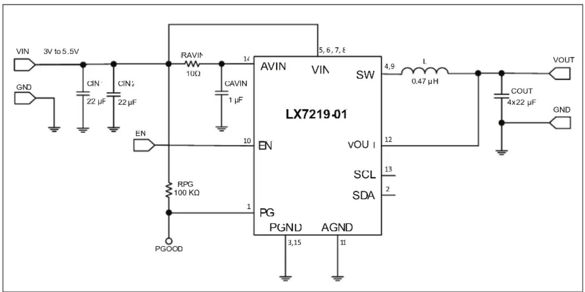
VIN 3V to 5.5V GND CIN 22 μF CIN2 22 μF RAVIN 10Ω CAVIN 1 μF EN RPG 100 KΩ PGOOD AVIN VIN SW LX7219-01 4,9 L 0.47 μH VOU I 12 13 2 SCL PG PGND AGND 3,15 11 VOUT COUT 4x22 μF GNDFIGURE 1-1: Typical LX7219-01 Buck Converter Application @ 0.8V Output.
1.3 WHAT IS THE LX7219/20 EVALUATION BOARD?
The LX7219/20 Evaluation Board is used to evaluate Microchip's Technology LX7219/20 devices. The input voltage range for a typical output voltage of 0.8V for the LX7219-01 is 3-5.5V. The load current can go up to 6A.
1.4 CONTENTS OF THE LX7219/20 EVALUATION BOARD KIT
The LX7219/20 Evaluation Board kit includes:
• LX7219/20 Evaluation Board (EV97L85A)
- Important Information Sheet
Chapter 2. Installation and Operation
2.1 INTRODUCTION
The LX7219/20 Evaluation Board is offered with the LX7219-01 installed. The LX7219-01 operates using a 2.7V to 5.5V input rail, outputs 0.6V to 3.3V and can deliver an output current of up to 6A. Using the I²C interface, VOUT can be adjusted between 0.6V and 1.195V. The reference voltage is programmed via the I²C bus, using the VSEL register value. In case a higher output voltage is needed, it must be programmed through an external resistive divider; the regulated voltage (VOUT) should be lower than the input voltage (VIN).
text_image
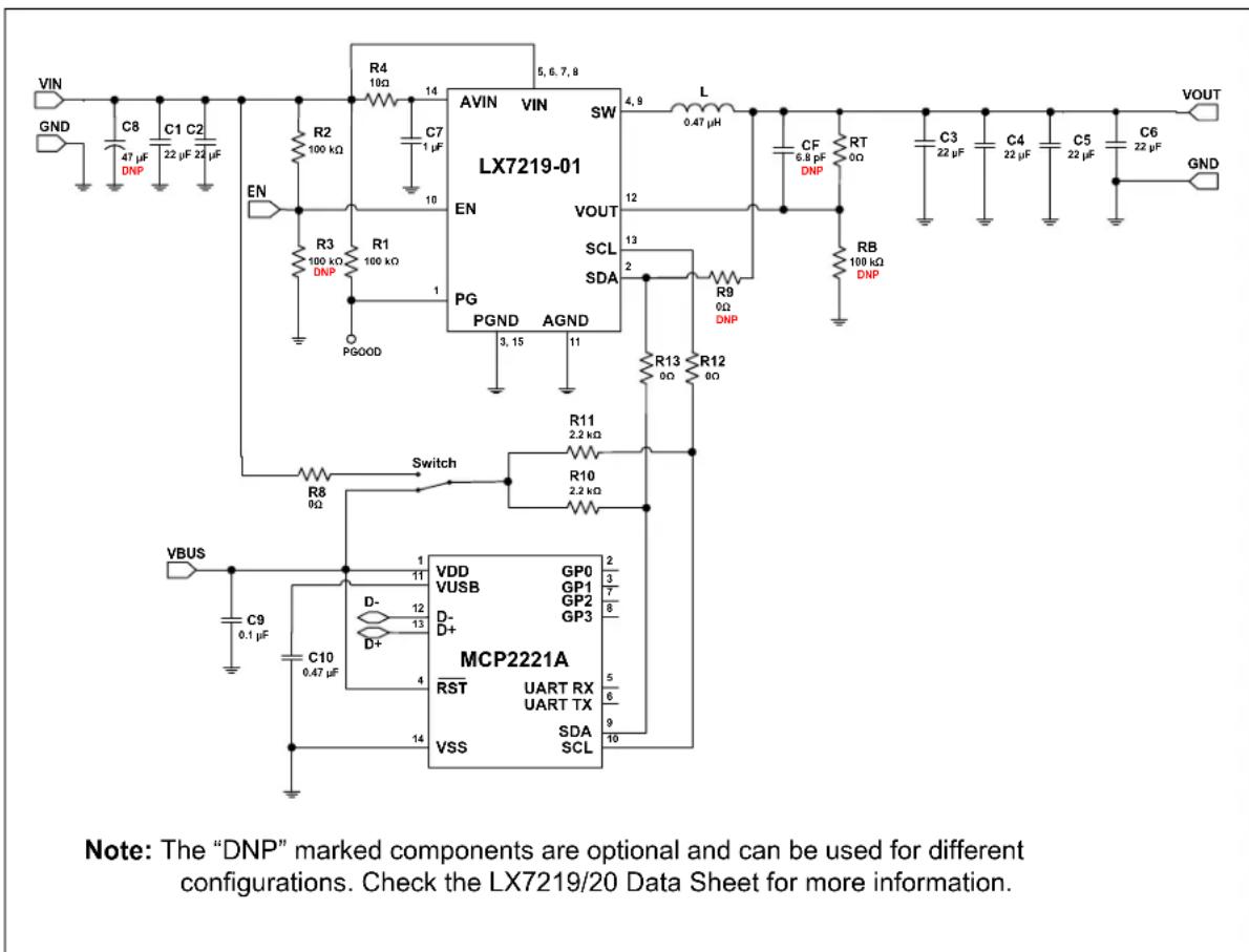
VIN GND C8 47 μF DNP C1 C2 22 μF 24 μF EN R2 100 kΩ R3 100 kΩ DNP R1 100 kΩ PGOOD V_BUS C9 0.1 μF C10 0.47 μF R4 10Ω C7 1 μF AVIN VIN SW LX7219-01 EN PG PGND AGND Switch R8 0Ω R11 2.2 kΩ R10 2.2 kΩ MCP2221A VSS UART RX UART TX SDA SCL GP0 GP1 GP2 GP3 D- D+ D- 11 12 13 14 5, 6, 7, 8 4, 9 L 0.47 μH CF 6.8 pF DNP RT 0Ω RB 100 kΩ DNP R9 0Ω DNP R13 0Ω R12 0Ω VOUT VOUT SCL SDA VOUT GNDFIGURE 2-1: Typical LX7219-01 Step-Down Converter Application: @ 0.8V Output and MCP2221A for I²C Communication.
2.2 FEATURES
The LX7219/20 Evaluation Board has the following features:
- Input Voltage Range (V _IN ): 2.7V - 5.5V
• Output Voltage: 0.6V to 3.3V - Output Current: typically, 6A @ 0.8V Output, 5V Input
- Power Save Mode (PSM) can be selected to improve light load efficiency
- PWM Switching Frequency: 1.2 MHz
• Hysteretic Control offers optimized transient response - Input Undervoltage and Overvoltage Protection
- Enable and Power Good Functions
• I ^2 C Serial Interface at 3.4 Mbps - Internal Soft Start
• Cycle-by-Cycle Overcurrent Protection - Hiccup mode protects against short circuit Faults
- Seven Bit Adjustable Reference Voltage via I ^2 C Bus
• Available in a 14L VQFN Package, 2 mm x 3 mm - Overtemperature Protection (if the die temperature exceeds 150^ , with 20^ hysteresis)
- RoHS Compliant
2.3 GETTING STARTED
The LX7219/20 Evaluation Board is fully assembled and tested to evaluate and demonstrate the features of the LX7219 and LX7220 devices and comes with the LX7219-01 installed. This board requires the use of an external laboratory power supply and load. For I²C operation, the I²C Monitor GUI can be used (for more details, see Chapter 3. "GUI Installation and Operation" and Chapter 4. "GUI Description"). The differences among the various devices are described in the LX7219 and LX7220 Data Sheets.
This document describes the setup and operation of the board when the LX7219-01 is installed. The default output voltage is 0.8V. The LX7219-02, with a default output voltage of 0.9V, and LX7220, with a default output voltage of 0.95V, can also be installed. All device options may be fitted on the board as is.
2.3.1 Power Input and Output Connection
2.3.1.1 POWERING THE LX7219/20 EVALUATION BOARD
The LX7219/20 Evaluation Board provides a typical circuit application for a 0.8V output, used to evaluate the LX7219-01 product.
The switch peak current limit will provide a safe maximum current value. The maximum output current for the converter will vary with input and output voltage. Refer to the LX7219 Data Sheet for more information on the maximum output current.
2.3.1.2 BOARD POWER-UP PROCEDURE
For the power-up procedure, follow the steps below:
- Connect the power supply to the input terminals of the evaluation board. The input voltage should be higher than V_OUT , but it should not exceed the Absolute Maximum Ratings specified in the data sheet. Connect the load to VOUT and GND terminals; maximum load varies with input and output voltage (see the LX7219 and LX7220 Data Sheets for more information on the maximum load). Connect the (+) side of the load to VOUT terminal
and the (-) side of the load to GND terminal of the board, see Figure 2-2.
-
Connect the board to a PC, using a USB to Micro-USB Cable.
-
To modify the mode of operation, to enable/disable the Input Overvoltage Protection and other features of the part, use the I²C Monitor GUI (for more details, see Chapter 3. "GUI Installation and Operation" and Chapter 4. "GUI Description"). By default, the EN pin is pulled high through a resistor. In addition to the EN pin, the regulator can be enabled and disabled through the I²C bus by programming the control register. While disabled, the regulator and most of the support circuitry is turned off. However, the I²C bus circuitry is still active and may be programmed.
-
After the power supply is turned on, a voltmeter can be used to monitor V OUT. The measured output voltage should be 0.8V, 0.9V or 0.95V, depending on the installed device. Adjusting the input voltage and load should not cause the output to vary more than a few mV over the operating range of the converter.
text_image
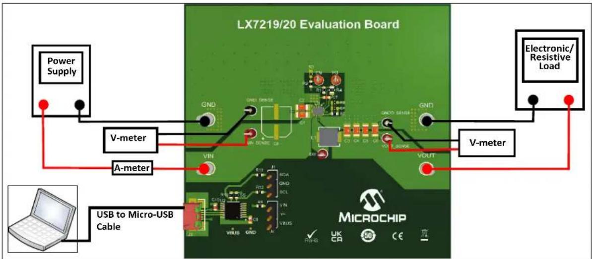
LX7219/20 Evaluation Board Power Supply V-meter A-meter USB to Micro-USB Cable Electronic/Resistive Load GND GND TINRSE VIN VOUT V-METER MicroCHIP ✓ UK CA SO CEFIGURE 2-2: LX7219/20 Evaluation Board Test Setup.
2.3.1.3 ADJUSTABLE V OUT SETTING
Using the I ^2 C interface, the output voltage can be adjusted from 0.6V to 1.195V. The reference voltage is programmed using the I ^2 C bus VSEL register value.
EQUATION 2-1: V REF PROGRAMMING WITH THE I²C BUS VSEL REGISTER
$$ V _ {R E F} = 0. 6 V V + \quad_ {S E L} \times 0. 0 0 4 7 V $$
Where:
V_SEL = the decimal value of the 7 VSEL bits.
In case a higher output voltage is needed, it must be programmed through an external resistive divider. The following formula calculates the value of V_OUT based on the resistive divider components R_TOP and R_BOT .
EQUATION 2-2: OUTPUT VOLTAGE CALCULATION
$$ V _ {O U T} \quad V _ {R E F} \times = \left(1 + \frac {R _ {T O P}}{R _ {B O T}}\right) $$
Where:
V_REF default is determined by the chip (0.8V, 0.9V and 0.95V options are available).
2.3.1.4 PERFORMANCE EVALUATION
The following plots show efficiency in PSM/PWM mode vs. load current and load transient response for the LX7219-01.

line
| Load current [A] | PSM | PWM | | ---------------- | ---- | ---- | | 0.001 | 30 | 0 | | 0.01 | 45 | 5 | | 0.1 | 60 | 10 | | 1 | 70 | 20 | | 10 | 80 | 40 | | 100 | 85 | 80 | | 1000 | 85 | 85 | | 10000 | 85 | 80 |FIGURE 2-3: LX7219-01, Efficiency PSM/PWM Mode @ V V_IN = 5.0V, L = 0.47 H, C_IN = 2 × 22 F, C_OUT = 4 × 22 F. _OUT = 0.8V,

line
| Time (μs) | VOUT (V) | Offset (V) | 20 mV/div | |-----------|----------|------------|-----------| | 0 | 0.8 | 0.8 | - | | 10 | ~0.8 | 0.8 | - | | 20 | ~0.8 | 0.8 | - | | 30 | ~0.8 | 0.8 | - | | 40 | ~0.8 | 0.8 | - | | 50 | ~0.8 | 0.8 | - | | 60 | ~0.8 | 0.8 | - | | 70 | ~0.8 | 0.8 | - | | 80 | ~0.8 | 0.8 | - | | 90 | ~0.8 | 0.8 | - | | 100 | ~0.8 | 0.8 | - | | 110 | ~0.8 | 0.8 | - | | 120 | ~0.8 | 0.8 | - | | 130 | ~0.8 | 0.8 | - | | 140 | ~0.8 | 0.8 | - | | 150 | ~0.8 | 0.8 | - | | 160 | ~0.8 | 0.8 | - | | 170 | ~0.8 | 0.8 | - | | 180 | ~0.8 | 0.8 | - | | 190 | ~0.8 | 0.8 | - | | 200 | ~0.8 | 0.8 | - | | 210 | ~0.8 | 0.8 | - | | 220 | ~0.8 | 0.8 | - | | 230 | ~0.8 | 0.8 | - | | 240 | ~0.8 | 0.8 | - | | 250 | ~0.8 | 0.8 | - | | 260 | ~0.8 | 0.8 | - | | 270 | ~0.8 | 0.8 | - | | 280 | ~0.8 | 0.8 | - | | 290 | ~0.8 | 0.8 | - | | 300 | ~0.8 | 0.8 | - | | 310 | ~0.8 | 0.8 | - | | 320 | ~0.8 | 0.8 | - | | 330 | ~0.8 | 0.8 | - | | 340 | ~0.8 | 0.8 | - | | 350 | ~0.8 | 0.8 | - | | 360 | ~0.8 | 0.8 | - | | 370 | ~0.8 | 0.8 | - | | 380 | ~0.8 | 0.8 | - | | 390 | ~0.8 | 0.8 | - | | 400 | ~0.8 | 0.8 | - | | 410 | ~0.8 | 0.8 | - | | 420 | ~0.8 | 0.8 | - | | 430 | ~0.8 | 0.8 | - | | 440 | ~0.8 | 0.8 | - | | 450 | ~0.8 | 0.8 | - | | 460 | ~0.8 | 0.8 | - | | 470 | ~0.8 | 0.8 | - | | 480 | ~0.8 | 0.8 | - | | 490 | ~0.8 | 0.8 | - | | 500 | ~0.8 | 0.8 | - | | 510 | ~0.8 | 0.8 | - | | 520 | ~0.8 | 0.8 | - | | 530 | ~0.8 | 0.8 | - | | 540 | ~0.8 | 0.8 | - | | 550 | ~0.8 | 0.8 | - | | 560 | ~0.8 | 0.8 | - | | 570 | ~0.8 | 0.8 | - | | 580 | ~0.8 | 0.8 | - | | 590 | ~0.8 | 0.8 | - | | 600 | ~0.8 | 0.8 | - | | 610 | ~0.8 | 0.8 | - | | 620 | ~0.8 | 0.8 | - | | 630 | ~0.8 | 0.8 | - | | 640 | ~0.8 | 0.8 | - | | 650 | ~0.8 | 0.8 | - | | 660 | ~0.8 | 0.8 | - | | 670 | ~0.8 | 0.8 | - | | 680 | ~0.8 | 0.8 | - | | 690 | ~0.8 | 0.8 | - | | 700 | ~0.8 | 0.8 | - | | 710 | ~0.8 | 0.8 | - | | 720 | ~0.8 | 0.8 | - | | 730 | ~0.8 | 0.8 | - | | 740 | ~0.8 | 0.8 | - | | 750 | ~0.8 | 0.8 | - | | 760 | ~0.8 | 0.8 | - | | 770 | ~0.8 | 0.8 | - | | 780 | ~0.8 | 0.8 | - | | 790 | ~0.8 | 0.8 | - | | 800 | ~0.8 | 0.8 | - | | 2 | - | - | + | | (top) IOUT = IOUT / SW node / SW div: Label: Top label indicates 'SW node' and 'SW div' values for each node.FIGURE 2-4: LX7219-01, Load Step Response, I_OUT = 1A to 4A , L = 0.47 H , C_IN = 2× 22 F , C_OUT = 4× 22 F , V_IN = 5.0V , V_OUT = 0.8V .

line
| Time (μs) | VOUT (V) | Offset (V) | 20 mV/div | IOUT (2A/div) | |-----------|----------|------------|-----------|---------------| | 0 | 0.8 | 0.8 | - | - | | 1 | 0.8 | 0.8 | - | - | | 2 | 0.8 | 0.8 | - | - | | 3 | 0.8 | 0.8 | - | - | | 4 | 0.8 | 0.8 | - | - | | 5 | 0.8 | 0.8 | - | - | | 6 | 0.8 | 0.8 | - | - | | 7 | 0.8 | 0.8 | - | - | | 8 | 0.8 | 0.8 | - | - | | 9 | 0.8 | 0.8 | - | - | | 10 | 0.8 | 0.8 | - | - | | 11 | 0.8 | 0.8 | - | - | | 12 | 0.8 | 0.8 | - | - | | 13 | 0.8 | 0.8 | - | - | | 14 | 0.8 | 0.8 | - | - | | 15 | 0.8 | 0.8 | - | - | | 16 | 0.8 | 0.8 | - | - | | 17 | 0.8 | 0.8 | - | - | | 18 | 0.8 | 0.8 | - | - | | 19 | 0.8 | 0.8 | - | - | | 20 | 0.8 | 0.8 | - | - | | 21 | 0.8 | 0.8 | - | - | | 22 | 0.8 | 0.8 | - | - | | 23 | 0.8 | 0.8 | - | - | | 24 | 0.8 | 0.8 | - | - | | 25 | 0.8 | 0.8 | - | - | | 26 | 0.8 | 0.8 | - | - | | 27 | 0.8 | 0.8 | - | - | | 28 | 0.8 | 0.8 | - | - | | 29 | 0.8 | 0.8 | - | - | | 30 | 0.8 | 0.8 | - | - | | 31 | 0.8 | 0.8 | - | - | | 32 | 0.8 | 0.8 | - | - | | 33 | 0.8 | 0.8 | - | - | | 34 | 0.8 | 0.8 | - | - | | 35 | 0.8 | 0.8 | - | - | | 36 | 0.8 | 0.8 | - | - | | 37 | 0.8 | 0.8 | - | - | | 38 | 0.8 | 0.8 | - | - | | 39 | 0.8 | 0.8 | - | - | | 40 | 0.8 | 0.8 | - | - | | 41 | 0.8 | 0.8 | - | - | | 42 | 0.8 | 0.8 | - | - | | 43 | 0.8 | 0.8 | - | - | | 44 | 0.8 | 0.8 | - | - | | 45 | 0.8 | 0.8 | - | - | | 46 | 0.8 | 0.8 | - | - | | 47 | 0.8 | 0.8 | - | - | | 48 | 0.8 | 0.8 | - | - | | 49 | 0.8 | 0.8 | - | - | | 50 | 0.8 | 0.8 | - | - | | 51 | 0.8 | 0.8 | - | - | | 52 | 0.8 | 0.8 | - | - | | 53 | 0.8 | 0.8 | - | - | | 54 | 0.8 | 0.8 | - | - | | 55 | 0.8 | 0.8 | - | - | | 56 | 0.8 | 0.8 | - | - | | 57 | 0.8 | 0.8 | - | - | | 58 | 0.8 | 0.8 | - | - | | 59 | 0.8 | 0.8 | - | - | | 60 | 0.8 | 0.8 | - | - | | 61 | 0.8 | 0.8 | - | - | | 62 | 0.8 | 0.8 | - | - | | 63 | 0.8 | 0.8 | - | - | | 64 | 0.8 | 0.8 | - | - | | 65 | 0.8 | 0.8 | - | - | | 66 | 0.8 | 0.8 | - | - | | 67 | 0.8 | 0.8 | - | - | | 68 | 0.8 | 0.8 | - | - | | 69 | 0.8 | 0.8 | - | - | | 70 | 0.8 | 0.8 | - | - | | 71 | 0.8 | 0.8 | - | - | | 72 | 0.8 | 0.8 | - | - | | 73 | 0.8 | 0.8 | - | - | | 74 | 0.8 | 0.8 | - | - | | 75 | 0.8 | 0.8 | - | - | | 76 | 0.8 | 0.8 | - | - | | 77 | 0.8 | 0.8 | - | - | | 78 | 0.8 | 0.8 | - | - | | 79 | 0.8 | 0.8 | - | - | | 80 | 0.8 | 0.8 | - | - | | Note: The data is presented in the code as it is a simplified representation of the original visual output (VOUT). The original visual output is labeled as 'SW node' with '5V/div'. The other visual output is labeled as 'SW node' with '4 μs/div'.FIGURE 2-5: LX7219-01, Load Step Response, I OUT = 1A to 4A, L = 0.47 μH, C IN =2 × 22 μF, C OUT =4 × 22 μF, Rising Edge, V IN =5.0V, V _OUT =0.8V.

line
| Time (μs) | Voltage (V) | Current (IOUT) | SW node (5V) | |-----------|-------------|----------------|--------------| | 0 | 0.8 | 2A | 5V | | 4 | 0.8 | 2A | 5V | | 10 | 0.8 | 2A | 5V | | 15 | 0.8 | 2A | 5V | | 20 | 0.8 | 2A | 5V | | 25 | 0.8 | 2A | 5V | | 30 | 0.8 | 2A | 5V | | 35 | 0.8 | 2A | 5V | | 40 | 0.8 | 2A | 5V | | 45 | 0.8 | 2A | 5V | | 50 | 0.8 | 2A | 5V | | 55 | 0.8 | 2A | 5V | | 60 | 0.8 | 2A | 5V | | 65 | 0.8 | 2A | 5V | | 70 | 0.8 | 2A | 5V | | 75 | 0.8 | 2A | 5V | | 80 | 0.8 | 2A | 5V | | 85 | 0.8 | 2A | 5V | | 90 | 0.8 | 2A | 5V | | 95 | 0.8 | 2A | 5V | | 100 | 0.8 | 2A | 5V | | 105 | 0.8 | 2A | 5V | | 110 | 0.8 | 2A | 5V | | 115 | 0.8 | 2A | 5V | | 120 | 0.8 | 2A | 5V | | 125 | 0.8 | 2A | 5V | | 130 | 0.8 | 2A | 5V | | 135 | 0.8 | 2A | 5V | | 140 | 0.8 | 2A | 5V | | 145 | 0.8 | 2A | 5V | | 150 | 0.8 | 2A | 5V | | 155 | 0.8 | 2A | 5V | | 160 | 0.8 | 2A | 5V | | 165 | 0.8 | 2A | 5V | | 170 | 0.8 | 2A | 5V | | 175 | 0.8 | 2A | 5V | | 180 | 0.8 | 2A | 5V | | 185 | 0.8 | 2A | 5V | | 190 | 0.8 | 2A | 5V | | 195 | 0.8 | 2A | 5V | | 200 | 0.8 | 2A | 5V | | 205 | 0.8 | 2A | 5V | | | | | | | | | | | | | | | | | | | | | | | | | | | | | | | | | | | | | | | | | | | | | | | | | | | | | | | | | | | | | | = SW node (SW node) | | | | | | | | | | | | | | | | | | | | | | | | | | | | | | | | | | | | | | | | | | | | | | | | | | | | | | | | | | | | | | | | | | | | | | | | | | | | | | | | | | | | | | | | | | | | | | | | | | | | | |FIGURE 2-6: LX7219-01, Load Step Response, I_OUT = 1A to 4A , L = 0.47 H , C_IN = 2× 22 F , C_OUT = 4× 22 F , Falling Edge, V_IN = 5.0V , V_OUT = 0.8V .
2.3.1.5 | ^2 C PULL-UP VOLTAGE SELECTION
The LX7219/20 Evaluation Board is equipped with a jumper (JP2) for selecting the I ^2 C pull-up supply voltage. The J2 header can be used to select the I ^2 C pull-up voltage to either VBUS or VIN. If a different pull-up voltage is desired, it can be injected into the v+ pin of J2. In this case, please make sure that no jumper is inserted in header J2, to prevent shorting the externally injected pull-up voltage to either VBUS or VIN.
NOTES:
Chapter 3. GUI Installation and Operation
3.1 GETTING STARTED
In order to install, use, and evaluate the product, several software and hardware tools are required.
3.1.1 Required Software
- I ^2 C Monitor GUI (minimum v8.0)
- Micr®.NEF Framework 4.5 or higher
3.1.2 Required Hardware
• LX7219/20 Evaluation Board
- USB to micro-USB Cable
3.2 GRAPHICAL USER INTERFACE (GUI) INSTALLATION
The following steps describe how to install the I ^2 C Monitor GUI:
- If Microsoft.NET Framework is already installed, go to Step 2. If not, download Microsoft.NET Framework from www.microsoft.com and follow the installation instructions.
- Download the I ^2 C Monitor GUI (v8.0) archive from www.microchip.com/LX7219 under “Embedded Software”.
- Unzip the I ^2 C Monitor GUI archive, which contains the setup.exe file.
-
Double click the setup.exe file to open the Setup Wizard window and wait for the extraction to complete. If required, the installation can be stopped by pressing the Cancel button.
-
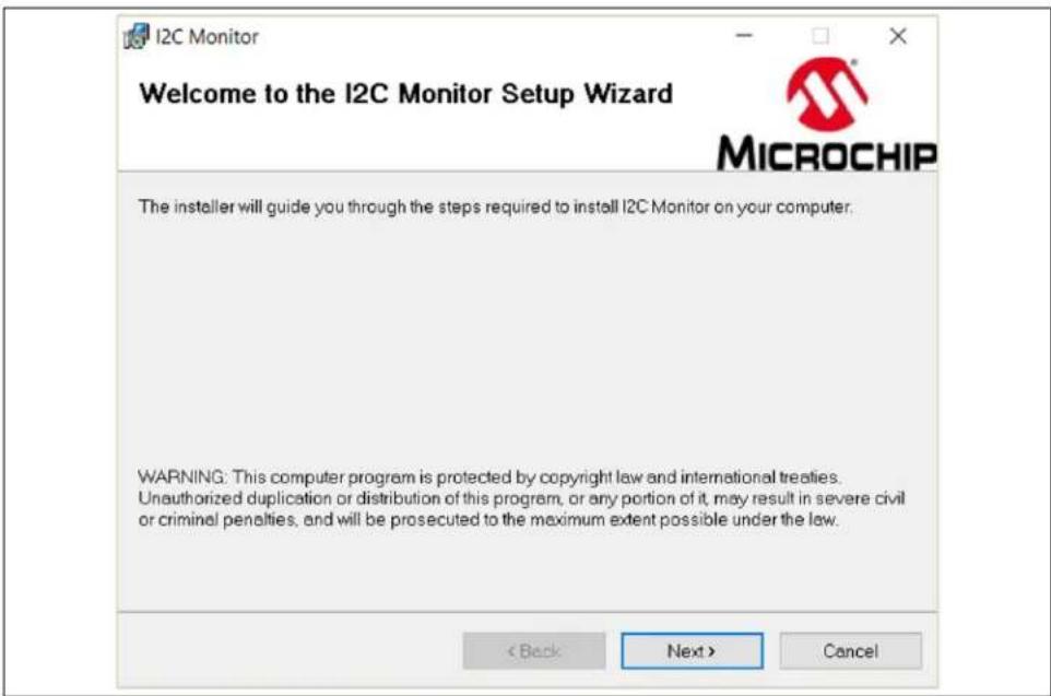
In the Welcome to the I ^2 C Monitor Setup Wizard window, click the Next button to start the installation.
text_image
I2C Monitor Welcome to the I2C Monitor Setup Wizard MICROCHIP The insteller will guide you through the steps required to install I2C Monitor on your computer. WARNING: This computer program is protected by copyright law and international treaties. Unauthorized duplication or distribution of this program, or any portion of it, may result in severe civil or criminal penalties, and will be prosecuted to the maximum extent possible under the law. < Back Next > CancelFIGURE 3-1: Starting the I ^2 C Monitor GUI Installation.
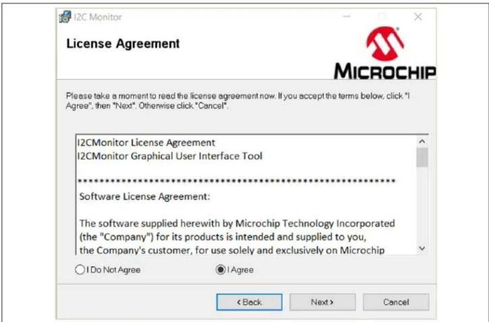
- Read the Software License Agreement, check the agreement box, then click the Next button.
text_image
I2C Monitor License Agreement Please take a moment to read the license agreement now. If you accept the terms below, click "I Agree", then "Next". Otherwise click "Cancel". I2CMonitor License Agreement I2CMonitor Graphical User Interface Tool ********************************************************************** Software License Agreement: The software supplied herewith by Microchip Technology Incorporated (the "Company") for its products is intended and supplied to you, the Company's customer, for use solely and exclusively on Microchip ○ I Do Not Agree ● I Agree < Back Next > CancelFIGURE 3-2: License Agreement.
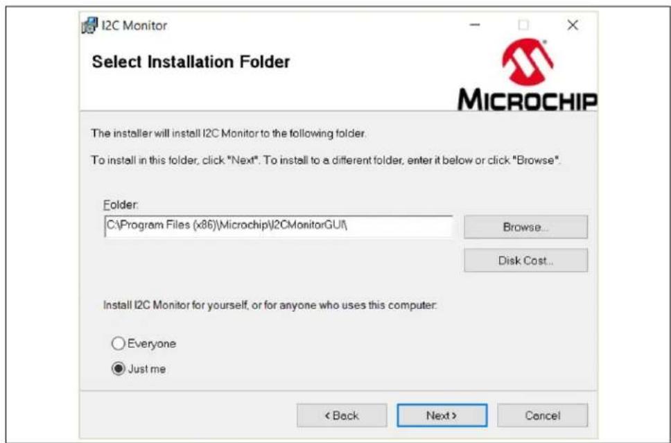
- The installation path can be changed, although it is recommended to keep the default path. Click Next to continue.
text_image
I2C Monitor Select Installation Folder The installer will install I2C Monitor to the following folder. To install in this folder, click "Next". To install to a different folder, enter it below or click "Browse". Folder: C:\Program Files (x86)\Microchip\2CMonitorGUI\ Browse... Disk Cost... Install I2C Monitor for yourself, or for anyone who uses this computer: Everyone Just me < Back Next > CancelFIGURE 3-3: Selecting the Destination Folder.
- Click the Next button to start the installation.

text_image
I2C Monitor Confirm Installation The installer is ready to install I2C Monitor on your computer. Click "Next" to start the installation. < Back Next > CancelFIGURE 3-4: Confirm Installation.
- The installation progress can be observed in the Installing I ^2 C Monitor window.

text_image
I2C Monitor Installing I2C Monitor I2C Monitor is being installed. Please wait... < Back Next > Cancel MICROCHIPFIGURE 3-5: Installing the I ^2 C Monitor GUI.
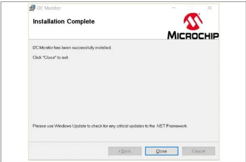
- Once the installation is complete, click Close to end the installation. To start the GUI, either double-click the desktop icon or browse for "PC Monitor" in the Windows Search bar.
text_image
I2C Monitor Installation Complete I2C Monitor has been successfully installed. Click "Close" to exit. Please use Windows Update to check for any critical updates to the .NET Framework. < Back Close CancelFIGURE 3-6: The Installation Complete Window.
Chapter 4. GUI Description
4.1 INTRODUCTION
This chapter describes how to use the I ^2 C Monitor GUI when connected to the LX7219/20 Evaluation Board included in the kit.
NOTICE
This chapter provides information regarding the use of the GUI that applies only to the LX7219/20 devices. For other devices using the I²C Monitor GUI, please refer to their specific Data Sheets and User's Guides.

text_image
Device Menu PC Monitor Status and Control Bar I²C Generic and Register View Reset to Default Register Settings Options ✓ Regulator Enabled ✓ Power Save Mode ✓ Output Discharge ✓ 45 ms Power Good Delay ✓ Reduced Switch Node Rate (LX7219 only) Output Voltage 0.8016 V Slew Rate 0.8 mV/μs ✓ Relative Divider Supply Resistor 1 Sew Rate 1 Vppr Voltage 0.8016 V Read Write Target Voltage 0.8016 V Slew Rate 0.8 mV/μs ✓ Target Vppr Voltage 0.8016 V Allowed range for Target Output Voltage: 0.6000V - 1.16MW ✓ Reverse (Target to Output) Status Bar LX7219 or LX7220 I²C Diagnostic Progress Bar Status Connected! Read WriteFIGURE 4-1: I ^2 C Monitor GUI Main Window - LX7219-01 View.
4.2 THE GRAPHICAL USER INTERFACE (GUI)
The following sections describe the items depicted in the GUI.
4.2.1 Device Menu
The Device drop-down menu allows the user to select the device to be evaluated. If an evaluation (or added custom) board is used, the profile will automatically change to the preselected profile.
4.2.2 File Menu
The File menu allows the user to save (Save registers to file) the registers of the currently selected device to a file that can then be loaded into the GUI by using the Load registers from file button. The saved file can also be edited (open it with a text editor).

text_image
File Settings About Load registers from file Save registers to fileFIGURE 4-2: File Menu.
4.2.3 Settings Menu
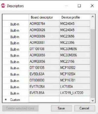
From the Settings menu, add a new custom board to be automatically detected and switch to its profile. To do this, go to Settings > Device descriptors and in the Descriptors window, add the desired "Board" descriptor and select the desired "Device" profile.
text_image
Descriptors Board descriptor Device profile Built-in ADM00764 MIC24045 Built-in ADM00826 MIC24045 Built-in ADM00886 MIC23656 Built-in ADM00881 MIC23356 Built-in DT100108 MIC33M656 Built-in ADM00855 MIC33M356 Built-in ADM00856 MIC23156 Built-in DT100105 MCP16502 Built-in EV90L63A MCP16504 Built-in DT00000 MCP16701 Built-in EV17U26A LX7180A Built-in EV57L85A LX7219_LX7220 Custom Delete selected rows Save CancelFIGURE 4-3: Custom Board Menu.
4.2.4 I ^2 C Monitor Status and Control Bar
The "Status and Control" bar contains the items listed in Table 4-1.

text_image
Addr 0x70 - Connector MCP22ZX-1-EV97LB5A - ScanAddr Connect Disconnect Voltage - V Rate 400 kHz Pullups -FIGURE 4-4: I ^2 C Monitor Status and Control Bar.
TABLE 4-1: MONITOR STATUS AND CONTROL BAR
| Item Description | |
| Addr This drop-down menu shows the address of the available devices. | |
| Connector This drop-down menu shows the type of connector used to connect the board. | |
| ScanAddr This button is used to scan for a valid address. | |
| Connect/Disconnect | These buttons are used to connect/disconnect the currently selected device. |
| Voltage | Not applicable. |
| Rate | This drop-down menu is used to select the corresponding communication rate for the device. |
| Pull Ups | Not applicable. |
In the “Status and Control” bar, the user can choose the hardware tool used to communicate with the device and the settings it should allow.
In order to connect to a device, the user must follow the steps described in
Section 3.1 "Getting Started". After connecting the Micro-USB cable, the user must scan for a valid address. Once a valid address is detected, clicking the Connect button will initialize the connection with the device and the registers will be available for read and write operations.
4.2.5 I ^2 C Generic Register View
The “I ^2 C Generic Register View” area contains the items listed in Table 4-2. This section of the I ^2 C Monitor GUI is common for all evaluated devices.
text_image
OPERATION Register 0x00 Read | Write | Read All | Write All | Read Modified | Write Modified | Number of Registers: 5 Address Size: 9bit Update Address (Hex) 00 01 02 03 04 Data (Hex) 00 AB 2F 21 08FIGURE 4-5: Generic Register View Area.
TABLE 4-2: I²C GENERIC REGISTER VIEW ITEMS
| Panel | Item | Description |
| Operation | Register | This section shows the registers available for read/write operations. |
| Read/Write | These buttons are used for single read/write operations. | |
| Read All/Write All | These buttons are used for reading/writing all the available registers. | |
| Read Modified/Write Modified | These buttons are used for reading/writing the content of the modified registers. | |
| Number of Registers | In this section, the user can set the number of the available registers for read/write operations. | |
| Address Size | In this section, the Address Size is specified. | |
| Update | This button sets/updates the number of available registers for read/write operations in the register area. | |
| Register Area | This section shows the current status of the register addresses and their content. | |
The specific registers for LX7219-01 are described in the device data sheet, in section 6.8 "Control Register Bit Definitions".
4.2.6 LX7219-01 I ^2 C Programmable Features
The LX7219-01 I²C "Programmable Features" area contains the items listed in Table4-3.

text_image
Reset to Default Register Settings Options ✓ Regulator Enabled ✓ Power Save Mode ☐ Output Discharge ☐ 45 ms Power Good Delay ✓ Reduced Switch Node Rise Rate (LX7219 only) Output Voltage Output Voltage 0.8016 V Slew Rate 0.8 mV/µs ☐ Resistive Divider Top Resistor 1 kΩ Bottom Resistor 1 kΩ VREF Voltage 0.8016 V Read Write Target Voltage Target Output Voltage 0.8016 V Slew Rate 0.8 mV/µs Target VREF Voltage 0.8016 V Allowed range for Target Output Voltage: 0.6000V - 1.1969V ☐ Reverse (Target to Output) Start Status Non-latched Power Good OK Enabled Latched Over Current Over Temperature Feedback Under Voltage Lockout Clear Faults Read WriteFIGURE 4-6: LX7219-01 I ^2 C Programmable Features, Resistive Divider Disabled.

text_image
Reset to Default Register Settings Options ✓ Regulator Enabled ✓ Power Save Mode □ Output Discharge □ 45 ms Power Good Delay ✓ Reduced Switch Node Rise Rate (LX7219 only) Output Voltage Output Voltage 3.3048 V Slew Rate 0.8 mV/µs ✓ Resistive Divider Top Resistor 240 kΩ Bottom Resistor 120 kΩ VREF Voltage 1.1016 V Read Write Target Voltage Target Output Voltage 3.3048 V Slew Rate 0.8 mV/µs Target VREF Voltage 1.1016 V Allowed range for Target Output Voltage: 1.8000V - 3.5907V □ Reverse (Target to Output) Start Status Non-latched Power Good OK Enabled Latched Over Current Over Temperature Feedback Under Voltage Lockout Clear Faults Read WriteFIGURE 4-7: LX7219-01 I ^2 C Programmable Features, Resistive Divider Enabled.
TABLE 4-3: LX7219-01 I ^2 C PROGRAMMABLE FEATURES
| Panel/Button Items Description | ||
| Options Regulator | Enabled | This check box allows the user to enable/disable the regulator via the I^2C bus. Uncheck the box to disable the regulator. During disable, the regulator and most of the support circuitry is turned off; however, the I^2C bus circuitry is still active and may be programmed. |
| Power Save Mode This check box allows the switch between auto PSM mode and PWM only mode. Check the box to enable the Power Save mode, uncheck the box for PWM only mode. | ||
| Output Discharge This check box allows the user to configure the Output Discharge option. If the box is checked, when the regulator is disabled, the output voltage is discharged through the SW pin. | ||
| 45 ms Power Good Delay This check box controls the Power Good Delay. If checked, it will introduce a 45 ms delay on PGOOD. | ||
| Reduced Switch Node Rise Rate | This check box allows the user to select between Reduced and Normal Switch Node Rise Rate. If the box is checked, then the Reduced Switch Node Rise Rate is enabled. This feature is available only for LX7219-01 and LX7219-02. The LX7220 does not have this feature. | |
| Read/Write | These buttons are used to read/write the registers that contain the information described above. | |
| Output Voltage | Output Voltage | This box allows the setting of the output voltage. If the Resistive Divider box is unchecked, then the allowed V_OUT range is 0.6V-1.195V. If the Resistive Divider option is enabled, the V_OUT range can be extended to 3.3V. |
| Slew Rate This box contains a drop-down list with all possible slew rate settings. | ||
| Resistive Divider | This check box enables/disables the resistive divider configuration. If the box is checked, the Top Resistor and Bottom Resistor fields become active and it is requested to fill in the configured values on the hardware. | |
| V_REF Voltage | This spin box displays the resulting V_REF Voltage. | |
| Error Message | An error message is displayed in this area if the entered V_OUT value is not valid. | |
| Read/Write | These buttons are used to read/write the registers that contain the information described above. | |
| Target Voltage | Target Output Voltage | This box allows setting the target output voltage for V_OUT transitions. If the Resistive Divider is unchecked, then the allowed target V_OUT range is 0.6V-1.195V. If the Resistive Divider option is checked, then the target V_OUT range can be extended to 3.3V. Depending on the hardware-configured resistive divider, information about the permitted target V_OUT range is provided in the message area. |
| Slew Rate This box contains a drop-down list with all possible slew rate settings. | ||
| Target V_REF Voltage This spin box displays the resulting Target V REF Voltage. | ||
| Info/Error Message This area p provides information about the allowed target V OUT range. If a value that is not valid is set, then an Out of range! message is displayed. | ||
| Reverse (Target to Output) If V OUT is already set to the Target Output Voltage value and the box is checked, when the Start button is pressed, V_OUT will return to the Output Voltage value.If V_OUT is set to the Output Voltage value and the box is checked, when the Start button is pressed, V_OUT will transition to the Target Output Voltage value and, after approximately 80 ms, will return to the Output Voltage value, see Figure 4-8 (case C). | ||
| Start | When this button is pressed, a transition from the Output Voltage to the Target Output Voltage starts; see Figure 4-8 (case A). If the Reverse (Target to Output) is checked, then a transition from the Target Output Voltage to the Output Voltage occurs; see Figure 4-8 (case B). | |
| Reset to Default Register Settings | When this button is pressed, the registers are (re)set to their default values. The default values can be found in section 6.8 “Control Register Bit Definitions” of the device data sheet. | |
This area of the GUI allows the user to modify the device features. For additional information about the part, please refer to its data sheet.

line
| Panel | Wave Description | Annotation | |-------|-------------------------------------|-------------------------------| | A | Output Voltage | Target Output Voltage | | A | Slew Rate | Reverse (Target to Output)" box unchecked | | B | Target Output Voltage | Slew Rate | | B | Slew Rate | "Reverse (Target to Output)" box checked | | C | Output Voltage | Target Output Voltage | | C | Slew Rate | "Reverse (Target to Output)" box checked | | C | VOUT (200 mV/div) | 20 ms/div |FIGURE 4-8: Output Voltage Transitions.
4.2.7 LX7219-01 I ^2 C Diagnostic
The LX7219-01 Diagnostic area contains the items listed in Table 4-4.
text_image
Status Non-latched Power Good OK Enabled Latched Over Current Over Temperature Feedback Under Voltage Lockout Clear FaultsFIGURE 4-9: LX7219-01 I ^2 C Diagnostic Area.
TABLE 4-4: LX7219-01 I ^2 C DIAGNOSTIC AREA
| Panel Items Description | ||
| Status | Power Good OK | This box indicates green if the output voltage has reached 90% of its set value. It indicates red when the output voltage is in transition or the regulator is disabled. |
| Enabled This box indicates green if the regulator is enabled. When the Regulator Enabled box is unchecked, the Enabled box indicates red. | ||
| Over Current | This box indicates red if the overcurrent limit is reached and it is latched to '1'. Press Clear Faults button to reset the status flag. | |
| Over Temperature | This box indicates red if an overtemperature event occurs and it is latched to '1'. Press Clear Faults button to reset the status flag. | |
| Feedback Under Voltage Lockout | This box indicates red if a feedback undervoltage event occurs and it is latched to '1'. Press Clear Faults button to reset the status flag. | |
The LX7219-01 I²C Diagnostic area summarizes the information contained in the "Status" section. The "Status" section contains latched (Flag) or non-latched (Status) bits. Flag bits are set when the corresponding Fault condition occurs and do not return to zero once the Fault condition ceases. If such a Fault occurs, the user can clear the Faults by clicking on the Clear Faults button or by power cycling the device. Status bits are set when the corresponding Fault condition has occurred and return to '0' automatically once the Fault condition has ceased. This information is refreshed once every two seconds.
TABLE 4-5: STATUS BAR ITEMS
| Item | Description |
| Status Label | The status label shows if there is any device connected to the board. Refer to Table 4-6 for a list of possible labels. |
| Progress Bar | This bar shows the progress for a given command. |
TABLE 4-6: STATUS LABELS
| Item | Description |
| STATUS: Connected! | This message is shown when the GUI is connected to a device. |
| STATUS: Disconnected! | This message is shown when the GUI is not connected to a device. |
NOTES:
Appendix A. Schematic and Layouts
A.1 INTRODUCTION
This appendix contains the following schematic and layouts for the LX7219/20 Evaluation Board:
- Board – Schematic
• Board – Top Copper and Silk - Board – Signal Layer 1
- Board – Signal Layer 2
- Board – Bottom Copper and Silk
A.2 BOARD - SCHEMATIC
text_image
Electrical schematic diagram with labeled components including ICs, resistors, capacitors, and inductorsA.3 BOARD - TOP COPPER AND SILK

text_image
LX7219/20 Evaluation Board GND GNDI SENSE VIN_SENSE C0 R3 EN PG R2 R4 C7 RB R5 C1 L1 C3 C4 C5 C6 VOUT SENSE VOUT SW R13 J1 SDA GND SCL R12 R8 VIN V+ VBUS C9 V_BUS GND J2 R10 SS C10 U2 R3 MICROCHIP UK CA 50 CEA.4 BOARD – SIGNAL LAYER 1

natural_image
Abstract pattern with scattered blue circles and white dots on a brown background, no text or symbols present.A.5 BOARD - SIGNAL LAYER 2

natural_image
Pure electrical circuit lines without any symbolsA.6 BOARD – BOTTOM COPPER AND SILK

text_image
Blue grid map with scattered white dots and small circular icons, possibly representing locations or data pointsAppendix B. Bill of Materials
TABLE B-1: BILL OF MATERIALS (BOM)
| Qty | Reference Description | Description Manufacturer Part Number | ||
| 6 C | 1, C2, C3, C4,C5, C6 | Capacitor, Ceramic, 22 μF, 16V,20%, X7R, SMD, 1206 | Murata Manufacturing Co.,Ltd. | GRM31CZ71C226ME15L |
| 1 C | 7 Capacitor, Ceramic, 1 μF, 16V,10%, X7R, SMD, 0603 | Yageo Corporation CC0603K | RX7R7BB105 | |
| 1 C | 9 Capacitor, Ceramic, 0.1 μF, 16V,10%, X7R, SMD, 0603 | Kyocera AVX® | 0603YC104KAT2A | |
| 1 C | 10 Capacitor, Ceramic, 0.47 μF, 16V,10%, X7R, SMD, 0603 | Murata Manufacturing Co.,Ltd. | GRM188R71C474KA88D | |
| 2 EN, PG Test Point, | LOOP, Orange, TH Keystone | ® Electronics Corp. | 5003 | |
| 4 G | NDI, GNDO,VIN, VOUT | Test Point, PIN Tin, TH | Harwin Plc. | H2121-01 |
| 2 G | NDI_SENSE,GNDO_SENSE | Test Point, Multi Purpose, Mini Black | Keystone Electronics Corp. | 5001 |
| 2 | J1, J2 | Connector, Header, 2.54 mm, Male,1x3 Tin, 5.84 MH, TH, VERT | Samtec, Inc. | TSW-103-07-T-S |
| 1 J3 | Connector, USB 2.0, Micro-B,Female, SMD | FCI | 10118192-0001LF | |
| 1 L1 | Inductor, 470 nH, 12.2A, 20%, SMD Vishay® Dale | IHLP2020CZERR47M01 | ||
| 4 PAD1, PAD2,PAD3, PAD4 | Mechanical HW Rubber Pad,BumponTM Hemisphere,0.44" x 0.20", Black | 3M | SJ-5003 (BLACK) | |
| 2 | R1, R2 | Resistor, Thick Film, 100 kΩ, 1%,1/10W, SMD, 0603 | Vishay® Beyschlag | MCT06030C1003FP500 |
| 1 R4 | Resistor, Thick Film, 10R, 1%,1/8W, SMD, 0805 | Bourns®, Inc. | CR0805-FX-10R0ELF | |
| 4 R8, R12, R13,RT | Resistor, Thick Film, 0Ω, 1/10W,SMD, 0603 | Panasonic® - ECG | ERJ-3GEY0R00V | |
| 2 | R10, R11 | Resistor, Thin Film, 2.2 kΩ, 1%,1/8W, SMD, 0603 | Vishay Beyschlag | MCT06030C2201FP500 |
| 3 | SW,VIN_SENSE,VOUT_SENSE | Test Point, Multi Purpose, Mini, Red | Keystone Electronics Corp. | 5000 |
| 1 PCB | LX72XX Evaluation Board Printed Circuit Board | — | 04-12011 | |
Note 1: The components listed in this Bill of Materials are representative of the PCB assembly. The released BOM used in manufacturing uses all RoHS-compliant components.
TABLE B-2: BILL OF MATERIALS (BOM) – MICROCHIP PARTS
| Qty | Reference Description | Manufacturer Part Number | ||
| 1 U | 1 Analog Hysteresic | Synchronous Buck Regulator, 6A, VQFN-14 | Microchip Technology Inc. LX7 | 219-01-02ILQTR |
| 1 U | 2 Interface USB | I2C UART, TSSOP-14 Microchip Technology Inc. MCP2221A-I/ST |
Note 1: The components listed in this Bill of Materials are representative of the PCB assembly. The released BOM used in manufacturing uses all RoHS-compliant components.
TABLE B-3: BILL OF MATERIALS (BOM) – MECHANICAL PARTS
| Qty | Reference Description | Manufacturer Part Number | ||
| 1 | JP2 Mechanical | HW Jumper, 2.54 mm, 1 x 2 | Amphenol Corporation 63429-202LF | |
| 1 | LABEL1 Label, | ASSY, W/REV Level (Small Modules), PER, MTS-0002 | Raynen 10010276 | |
| 4 | P AD1, PAD2, PAD3, PAD4 | Mechanical HW Rubber Pad, Bumpon Hemisphere, 0.44" x 0.20", Black | 3M | SJ-5003 (BLACK) |
Note 1: The components listed in this Bill of Materials are representative of the PCB assembly. The released BOM used in manufacturing uses all RoHS-compliant components.
TABLE B-4: BILL OF MATERIALS (BOM) – DO NOT POPULATE PARTS
| Qty | Reference Description | Manufacturer Part Number | ||
| 0 | C8 | Capacitor, Aluminum, 47 μF, 50V, 20%, SMD F | KEMET EDT476M050S9MAA | |
| 0 | CF | Capacitor, Ceramic, 6.8 pF, 100V, 5%, C0G, SMD, 0603 | Kyocera AVX | 06031A6R8JAT2A |
| 0 | R3, RB | Resistor, Thin Film, 100 kΩ,1%, 1/8W, SMD, 0603 | Vishay Beyschlag | MCT06030C1003FP500 |
Note 1: The components listed in this Bill of Materials are representative of the PCB assembly. The released BOM used in manufacturing uses all RoHS-compliant components.
Appendix C. LX7219-01 Control Register Bit Definition
TABLE C-1: LX7219-01 CONTROL REGISTER BIT DEFINITION
| Bit Name Value Description | |||
| Status, Address 00h | |||
| 7:3 Reserved | |||
| 2 | OCP | 0-d | Latched to 1 if the overcurrent limit is reached. Write a ‘1’ to reset the status flag. |
| 1 | OTP | 0-d | Latched to 1 if an overtemperature event occurs. Write a ‘1’ to reset the status flag. |
| 0 | FB_UVLO | 0-d | Latched to 1 if a FB_UVLO event occurs. Write a ‘1’ to reset the status flag. |
| VSEL, Address 01h, (aka dac) | |||
| 7 | EN | 1-d Device enabled. | |
| 0 | Device disabled. | ||
| 6:0 | VSEL[6:0] | 7-bit DAC value to set V_REF . The default value is determined by the REF ordering code of the part. | |
| Ctrl1, Address 02h, (aka reg2) | |||
| 7:6 Reserved 00-d | |||
| 5 | ctrl1 | 1-d Not used. | |
| 4 | DLY_DIS | 1 | 45 ms delay on PGOOD is enabled when this bit is high. |
| 0-d Disable 45 ms delay on PGOOD. | |||
| 3 | SW_RATE(LX7219-01 only) | 1-d Reduced switch node rise rate. | |
| 0 | High switch node rise rate. | ||
| 2 | Reserved | 1-d | |
| 0 | |||
| 1 | Reserved | 1-d | |
| 0 | |||
| 0 | MODE | 1-d P SM - Power Save mode allows the converter to run in Discontinuous Conduction mode. | |
| 0 | PWM - Always run in Continuous Conduction mode. | ||
| Vendor ID, Address 03h (Read Only) | |||
| 7:4 | VID[3:0] | 0010 | Microchip Vendor ID. |
| 3:2 | A1A0 | 00 | Designates the client address version. These bits will correspond to the two LSB. |
| 1:0 | VOUT | 01 | Designates the default output voltage version. The default value is determined by the REF ordering code of the part. |
| Ctrl2, Address 04h, (reg4) | |||
| 7:6 Reserved 00-d | |||
| 5 | GO | 1 | Write ‘1’ to start a V_REF transition. |
| 0-d The V OUT is ramped to the default VSEL value. | |||
| 4 Discharge | 1 | When the regulator is disabled, the output voltage is discharged through the SW pin. | |
| 0-d When the regulator is disabled, the output voltage is not discharged. | |||
| 3 | PGOK | 1 | Is high when output is in regulation; read-only dynamic signal. |
| 0 | Is low during an output voltage transition; read-only dynamic signal. | ||
| 2:1 SLEW | 00 Do not select. | ||
| 01-d V | REF slews at 0.8 mV/μs. | ||
| 10 | V_REF slews at 2.2 mV/μs. | ||
| 11 | V_REF slews at 8.4 mV/μs. | ||
| 0 | R e s | e r | v e d 1 - d |
Worldwide Sales and Service
AMERICAS
Corporate Office
2355 West Chandler Blvd.
Chandler, AZ 85224-6199
Tel: 480-792-7200
Fax: 480-792-7277
Technical Support:
http://www.microchip.com/
support
Web Address:
www.microchip.com
Atlanta
Duluth, GA
Tel: 678-957-9614
Fax: 678-957-1455
Austin, TX
Tel: 512-257-3370
Boston
Westborough, MA
Tel: 774-760-0087
Fax: 774-760-0088
Chicago
Itasca, IL
Tel: 630-285-0071
Fax: 630-285-0075
Dallas
Addison, TX
Tel: 972-818-7423
Fax: 972-818-2924
Detroit
Novi, MI
Tel: 248-848-4000
Houston, TX
Tel: 281-894-5983
Indianapolis
Noblesville, IN
Tel: 317-773-8323
Fax: 317-773-5453
Tel: 317-536-2380
Los Angeles
Mission Viejo, CA
Tel: 949-462-9523
Fax: 949-462-9608
Tel: 951-273-7800
Raleigh, NC
Tel: 919-844-7510
New York, NY
Tel: 631-435-6000
San Jose, CA
Tel: 408-735-9110
Tel: 408-436-4270
Canada - Toron
Tel: 905-695-1980
Fax: 905-695-2078
ASIA/PACIFIC
Australia - Sydney
Tel: 61-2-9868-6733
China - Beijing
Tel: 86-10-8569-7000
China - Chengdu
Tel: 86-28-8665-5511
China - Chongqing
Tel: 86-23-8980-9588
China - Dongguan
Tel: 86-769-8702-9880
China - Guangzhou
Tel: 86-20-8755-8029
China - Hangzhou
Tel: 86-571-8792-8115
China - Hong Kong SAR
Tel: 852-2943-5100
China - Nanjing
Tel: 86-25-8473-2460
China - Qingdao
Tel: 86-532-8502-7355
China - Shanghai
Tel: 86-21-3326-8000
China - Shenyang
Tel: 86-24-2334-2829
China - Shenzhen
Tel: 86-755-8864-2200
China - Suzhou
Tel: 86-186-6233-1526
China - Wuhan
Tel: 86-27-5980-5300
China - Xian
Tel: 86-29-8833-7252
China - Xiamen
Tel: 86-592-2388138
China - Zhuhai
Tel: 86-756-3210040
ASIA/PACIFIC
India - Bangalore
Tel: 91-80-3090-4444
India - New Delhi
Tel: 91-11-4160-8631
India - Pune
Tel: 91-20-4121-0141
Japan - Osaka
Tel: 81-6-6152-7160
Japan - Tokyo
Tel: 81-3-6880-3770
Korea - Daegu
Tel: 82-53-744-4301
Korea - Seoul
Tel: 82-2-554-7200
Malaysia - Kuala Lumpur
Tel: 60-3-7651-7906
Malaysia - Penang
Tel: 60-4-227-8870
Philippines - Manila
Tel: 63-2-634-9065
Singapore
Tel: 65-6334-8870
Taiwan - Hsin Chu
Tel: 886-3-577-8366
Taiwan - Kaohsiung
Tel: 886-7-213-7830
Taiwan - Taipei
Tel: 886-2-2508-8600
Thailand - Bangkok
Tel: 66-2-694-1351
Tel: 43-7242-2244-39
Fax: 43-7242-2244-393
Denmark - Copenhagen
Tel: 45-4485-5910
Fax: 45-4485-2829
Finland - Espoo
Tel: 358-9-4520-820
France - Paris
Tel: 33-1-69-53-63-20
Fax: 33-1-69-30-90-79
Germany - Garching
Tel: 49-8931-9700
Germany - Haan
Tel: 49-2129-3766400
Germany - Heilbronn
Tel: 49-7131-72400
Germany - Karlsruhe
Tel: 49-721-625370
Germany - Munich
Tel: 49-89-627-144-0
Fax: 49-89-627-144-44
Germany - Rosenheim
Tel: 49-8031-354-560
Israel - Hod Hasharon
Tel: 972-9-775-5100
Italy - Milan
Tel: 39-0331-742611
Fax: 39-0331-466781
Italy - Padova
Tel: 39-049-7625286
Netherlands - Drunen
Tel: 31-416-690399
Fax: 31-416-690340
Norway - Trondheim
Tel: 47-7288-4388
Poland - Warsaw
Tel: 48-22-3325737
Romania - Bucharest
Tel: 40-21-407-87-50
Spain - Madrid
Tel: 34-91-708-08-90
Fax: 34-91-708-08-91
Sweden - Gothenberg
Tel: 46-31-704-60-40
Sweden - Stockholm
Tel: 46-8-5090-4654
UK - Wokingham
Tel: 44-118-921-5800
Fax: 44-118-921-5820