MIC2126 - Electronic component Microchip - Free user manual and instructions
Find the device manual for free MIC2126 Microchip in PDF.

User questions about MIC2126 Microchip
0 question about this device. Answer the ones you know or ask your own.
Ask a new question about this device
Download the instructions for your Electronic component in PDF format for free! Find your manual MIC2126 - Microchip and take your electronic device back in hand. On this page are published all the documents necessary for the use of your device. MIC2126 by Microchip.
USER MANUAL MIC2126 Microchip
28V Synchronous Buck Controllers Featuring Adaptive ON-Time Control
Features
• Hyper Speed Control Architecture Enables:
- High delta V operation ( V_IN = 28V and V_OUT = 0.6V )
- Any Capacitor™ stable
• 4.5V to 28V Input Voltage
- Adjustable Output Voltage from 0.6V to 24V
• 200 kHz to 750 kHz Programmable Switching Frequency
• HyperLight Load ^® (MIC2125)
• Hyper Speed Control ^® (MIC2126)
- Enable Input and Power Good Output
• Built-in 5V Regulator for Single-Supply Operation
- Programmable current limit and "hiccup" mode short-circuit protection
- 7 ms internal soft-start, internal compensation, and thermal shutdown
• Supports Safe Start-Up into a Prebiased Output
- - 40^ C to + 125^ C Junction Temperature Range
• Available in 16-pin, 3 mm × 3 mm QFN Package
Applications
• Networking/Telecom Equipment
- Base Stations, Servers
• Distributed Power Systems
- Industrial Power Supplies
General Description
The MIC2125 and MIC2126 are constant-frequency synchronous buck controllers featuring a unique adaptive ON-time control architecture. The MIC2125/6 operate over an input voltage range from 4.5V to 28V and can be used to supply load current up to 25A. The output voltage is adjustable down to 0.6V with a guaranteed accuracy of ±1%. The device operates with programmable switching frequency from 200 kHz to 750 kHz.
HyperLight Load ^® architecture provides the same high efficiency and ultra-fast transient response as the Hyper Speed Control ^® architecture under medium to heavy loads. It also maintains high efficiency under light load conditions by transitioning to variable frequency, discontinuous conduction mode operation.
The MIC2125/6 offer a full suite of features to ensure protection of the IC during fault conditions. These include undervoltage lockout to ensure proper operation under power-sag conditions, internal soft-start to reduce inrush current, "hiccup" mode short-circuit protection, and thermal shutdown.
Package Type
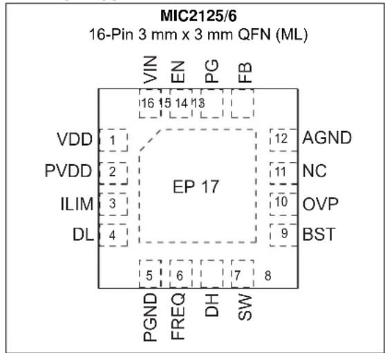
text_image
MIC2125/6 16-Pin 3 mm x 3 mm QFN (ML) VIN EN PG FB 16 15 14 13 VDD 1 PVDD 2 ILIM 3 DL 4 EP 17 12 AGND 11 NC 10 OVP 9 BST 5 6 7 8 PGND FREQ DH SWTypical Application Circuit
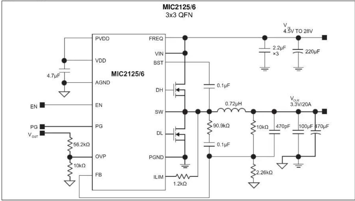
text_image
MIC2125/6 3x3 QFN PVDD VDD AGND EN PG VOUT 56.2kΩ 10kΩ OVP FB FREQ VIN BST DH SW DL PGND ILIM 1.2kΩ 0.1μF 0.72μH 90.9kΩ 0.1μF 2.26kΩ 4.7μF 2.2μF ×3 470pF 10kΩ 470μF VOUT TO 28V VOUT 3.3V/20AFunctional Block Diagram

text_image
MIC2125/26 PVDD VDD LDO VDD LVLO MODIFIED TOUT FIXED TON ESTIMATE VIN FREQ BST HSD DH Q1 0.1μF SW PVDD LSD DL Q3 POND CL DETECTION ILIM OVP Vpp 0.6V THERMAL SHUTDOWN COMP COMPENSATION g,EA 8% Vpp 0.6V AGND VDD 49.9kΩ PG EN EN 4.7μF R19 R20 2.2μF x2 220μF 0.72μH R1 10kΩ 470pF 100μF 470μF 3.3V/20A1.0 ELECTRICAL CHARACTERISTICS
Absolute Maximum Ratings †
V_IN -0.3V to +30V
V_DD, P_VDD -0.3V to +6V
V_SW , V_FREQ , V_ILIM , V_EN -0.3V to ( V_IN + 0.3V )
V_BST to V_SW ...... -0.3V to 6V
V_BST -0.3V to 36V
V_PG -0.3V to (V_DD + 0.3V)
V_FB -0.3V to (V_DD + 0.3V)
P_GND to A_GND -0.3V to +0.3V
ESD Rating ^(1) 2 kV
Operating Ratings ‡
Supply Voltage ( V_IN ) 4.5V to 28V
V_SW , V_FREQ , V_ILIM , V_EN ....0V to V_IN
† Notice: Stresses above those listed under “Absolute Maximum Ratings” may cause permanent damage to the device. This is a stress rating only and functional operation of the device at those or any other conditions above those indicated in the operational sections of this specification is not intended. Exposure to maximum rating conditions for extended periods may affect device reliability.
‡ Notice: The device is not guaranteed to function outside its operating ratings.
Note 1: Devices are ESD sensitive. Handling precautions are recommended. Human body model, 1.5 kΩ in series with 100 pF.
TABLE 1-1: ELECTRICAL CHARACTERISTICS
| Electrical Characteristics: V_IN = 12V, V_OUT = 1.2V, V_BST - V_SW = 5V; T_A = 25°C , unless noted. Bold values indicate -40°C ≤ T_J ≤ +125°C. (Note 1). | |||||
| Parameters Min. Typ. | Max. Units | Conditions | |||
| Power Supply Input | |||||
| Input Voltage Range ( V_IN ) (Note 2) | 4.5 — 5 | 5 V | V | _DD = V_IN | |
| 4.5 — 28 | — | ||||
| Quiescent Supply Current (MIC2125) | — | 3 | 4 | 0 | 750 FB = 1.5μA V |
| Quiescent Supply Current (MIC2126) | — | 1.1 | 3 | mA | V_FB = 1.5V |
| Shutdown Supply Current | — | 0.1 | 5 | μA | SW unconnected, V_EN = 0V |
| V_DD Supply | |||||
| V_DD Output Voltage | 4.8 | 5.2 | 5.4 | V | V_IN = 7V to 28V, I_DD = 10mA |
| V_DD UVLO Threshold | 3.7 | 4.2 | 4.5 | V_DD rising | |
| V_DD UVLO Hysteresis | — | 400 | — | mV | — |
| Load Regulation | 0.6 | 2 | 3.6 | % | I_DD = 0 to 40 mA |
| Reference | |||||
| Feedback Reference Voltage | 0.597 | 0.6 | 0.603 | V | T_J = 25°C (±0.5%) |
| 0.594 | 0.6 | 0.606 | -40°C ≤ T_J ≤ +125°C (±1%) | ||
| FB Bias Current | — | 0.01 | 0.5 | μA | V_FB = 0.6V |
| Enable Control | |||||
| EN Logic Level High | 1.6 | — | — | V | — |
| EN Logic Level Low | — | — | 0.6 | — | |
| EN Hysteresis | — | 120 | — | mV | — |
| EN Bias Current | — | 6 | 30 | μA | V_EN = 12V |
| Oscillator | |||||
| Switching Frequency | — | 750 | — | kHz | V_FREQ = V_IN |
| — | 3 | 7 | 5 | — | |
| Maximum Duty Cycle | — | 85 | — | % | — |
| Minimum Duty Cycle | —0 | — | V | _FREQ = 50% × V_IN | |
| Minimum On-Time | — | 100 | — | ns | — |
| Minimum Off-Time | 150 | 220 | 300 | — | |
| Soft-Start | |||||
| Soft-Start Time | — | 7 | — | ms | — |
| Short-Circuit Protection and OVP | |||||
| Current-Limit Comparator Offset | -15 | -47 | mV | V | _FB = 0.6V |
| Current-Limit Source Current | 32 | 36 | 40 | μA | V_FB = 0.6V |
Note 1: Specification for packaged product only.
2: The application is fully functional at low V_DD (supply of the control section) if the external MOSFETs have low voltage V_TH .
TABLE 1-1: ELECTRICAL CHARACTERISTICS (CONTINUED)
| Electrical Characteristics: V_IN = 12V, V_OUT = 1.2V, V_BST - V_SW = 5V; T_A = 25°C , unless noted. Bold values indicate -40°C ≤ T_J ≤ +125°C. (Note 1). | |||||
| Parameters | Min. | Typ. | Max. | Units | Conditions |
| Overvoltage Protection Threshold | — 0.62 | — V — | |||
| FET Drivers | |||||
| DH, DL Output Low Voltage — | — 0.1 V | I | _SINK = 10 mA | ||
| DH, DL Output High Voltage V | _PVDD-0.1 or V_BST-0.1 | — | — | I_SOURCE = 10 mA | |
| DH On-Resistance, High State | — 2.5 — Ω | — | |||
| DH On-Resistance, Low State | — 1.6 — — | ||||
| DL On-Resistance, High State | — 1.9 — — | ||||
| DL On-Resistance, Low State | — | 0.55 — | — | ||
| SW, BST Leakage Current — | — 50 | μA — | |||
| Power Good (PG) | |||||
| PG Threshold Voltage | 85 | 89 | 95 | % V_OUT | Sweep V_FB from low to high |
| PG Hysteresis | — | 6 | — Sweep V | _FB from high to low | |
| PG Delay Time | — | 80 | — | μs | Sweep V_FB from low to high |
| PG Low Voltage | — | 60 | 200 | mV | V_FB < 90% × V_NOM, I_PG = 1 mA |
| Thermal Protection | |||||
| Overtemperature Shutdown | — | 150 | — | °C | T_J Rising |
| Overtemperature Shutdown Hysteresis | — | 15 | — | °C | — |
Note 1: Specification for packaged product only.
2: The application is fully functional at low V_DD (supply of the control section) if the external MOSFETs have low voltage V_TH .
TEMPERATURE SPECIFICATIONS
| Parameters Sym. Min. Typ. Max. Units Conditions | ||||||
| Temperature Ranges | ||||||
| Junction Operating Temperature T | J | -40 — | +125 °C | Note 1 | ||
| Storage Temperature Range T | S | -65 — | +150 °C — | |||
| Junction Temperature | TJ | — | — +150 °C — | |||
| Lead Temperature | — | — | — | +260 | °C | Soldering, 10s |
| Package Thermal Resistances | ||||||
| Thermal Resistance 3 mm x 3 mm QFN-16LD | _JA | — | 50.8 | — | °C/W | — |
| _JC | — | 25.3 | — | °C/W | — | |
Note 1: The maximum allowable power dissipation is a function of ambient temperature, the maximum allowable junction temperature and the thermal resistance from junction to air (i.e., T_A , T_J , _JA ). Exceeding the maximum allowable power dissipation will cause the device operating junction temperature to exceed the maximum +125°C rating. Sustained junction temperatures above +125°C can impact the device reliability.
2.0 TYPICAL PERFORMANCE CURVES
Note: The graphs and tables provided following this note are a statistical summary based on a limited number of samples and are provided for informational purposes only. The performance characteristics listed herein are not tested or guaranteed. In some graphs or tables, the data presented may be outside the specified operating range (e.g., outside specified power supply range) and therefore outside the warranted range.
Note: Unless otherwise noted, V_IN = 12V , FREQ = 350 kHz.
line
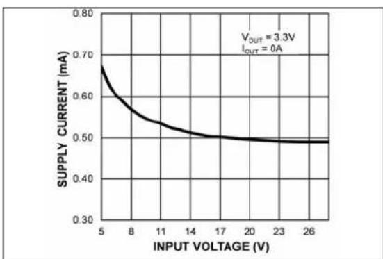
| INPUT VOLTAGE (V) | SUPPLY CURRENT (mA) | | ----------------- | ------------------- | | 5 | 0.68 | | 8 | 0.58 | | 11 | 0.54 | | 14 | 0.52 | | 17 | 0.51 | | 20 | 0.50 | | 23 | 0.50 | | 26 | 0.50 |FIGURE 2-1: V IN Operating Supply Current vs. Input Voltage (MIC2125).
line
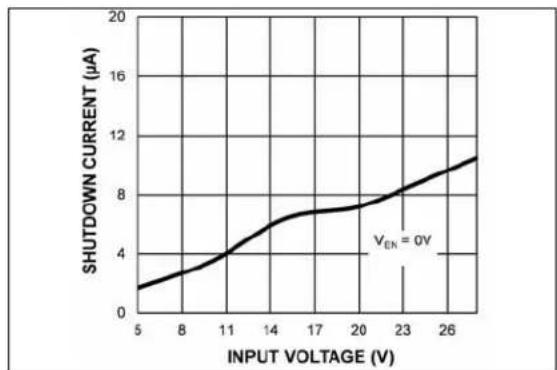
| INPUT VOLTAGE (V) | SHUTDOWN CURRENT (μA) | | ----------------- | ---------------------- | | 5 | 2 | | 8 | 3 | | 11 | 4 | | 14 | 6 | | 17 | 7 | | 20 | 8 | | 23 | 9 | | 26 | 11 |FIGURE 2-4: V IN Shutdown Current vs. Input Voltage (MIC2125).

line
| INPUT VOLTAGE (V) | FEEDBACK VOLTAGE (V) | | ----------------- | -------------------- | | 5 | 0.600 | | 8 | 0.601 | | 11 | 0.601 | | 14 | 0.601 | | 17 | 0.601 | | 20 | 0.601 | | 23 | 0.601 | | 26 | 0.602 |FIGURE 2-2: Feedback Voltage vs. Input Voltage (MIC2125).
line
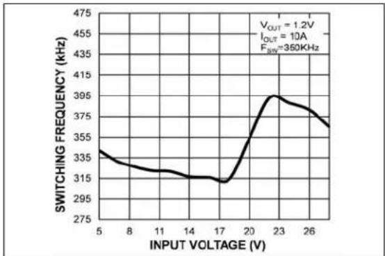
| INPUT VOLTAGE (V) | SWITCHING FREQUENCY (kHz) | | ----------------- | -------------------------- | | 5 | 335 | | 8 | 325 | | 11 | 320 | | 14 | 315 | | 17 | 310 | | 20 | 395 | | 23 | 400 | | 26 | 375 |FIGURE 2-5: Switching Frequency vs. Input Voltage.

line
| INPUT VOLTAGE (V) | OUTPUT VOLTAGE (V) | | ----------------- | ------------------ | | 5 | 3.320 | | 8 | 3.320 | | 11 | 3.320 | | 14 | 3.320 | | 17 | 3.320 | | 20 | 3.320 | | 23 | 3.320 | | 26 | 3.320 |FIGURE 2-3: Output Voltage vs. Input Voltage (MIC2125).

line
| TEMPERATURE (°C) | SWITCHING FREQUENCY (kHz) | | ---------------- | ------------------------- | | -50 | 340 | | 0 | 350 | | 25 | 345 | | 50 | 320 | | 75 | 280 | | 100 | 220 | | 125 | 200 |FIGURE 2-6: Switching Frequency vs. Temperature (MIC2126).
Note: Unless otherwise noted, V_IN = 12V , FREQ = 350 kHz.

line
| INPUT VOLTAGE (V) | VDD VOLTAGE (V) | | ----------------- | --------------- | | 5 | 3.3 | | 8 | 5.0 | | 11 | 5.0 | | 14 | 5.0 | | 17 | 5.0 | | 20 | 5.0 | | 23 | 5.0 | | 26 | 5.0 |FIGURE 2-7: V _DD Voltage vs. Input Voltage (MIC2125).

line
| TEMPERATURE (°C) | SUPPLY CURRENT (mA) | | ---------------- | ------------------- | | -50 | 0.6 | | 0 | 0.7 | | 25 | 0.8 | | 50 | 0.9 | | 75 | 0.95 | | 100 | 1.0 | | 125 | 1.05 |FIGURE 2-10: V IN Operating Supply Current vs. Temperature (MIC2125).
line
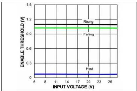
| INPUT VOLTAGE (V) | ENABLE THRESHOLD (V) | | ----------------- | -------------------- | | 5 | 0 | | 8 | 0 | | 11 | 0 | | 14 | 0 | | 17 | 0 | | 20 | 0 | | 23 | 0 | | 26 | 0 |FIGURE 2-8: Enable Threshold vs. Input Voltage (MIC2125).

line
| TEMPERATURE (°C) | FEEBACK VOLTAGE (V) | | ---------------- | ------------------- | | -50 | 0.600 | | 0 | 0.600 | | 25 | 0.600 | | 50 | 0.600 | | 75 | 0.600 | | 100 | 0.601 | | 125 | 0.601 |FIGURE 2-11: Feedback Voltage vs. Temperature (MIC2125).
line
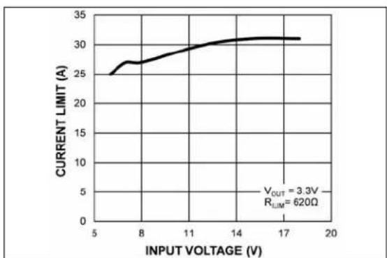
| INPUT VOLTAGE (V) | CURRENT LIMIT (A) | | ----------------- | ----------------- | | 5 | 25 | | 8 | 27 | | 11 | 29 | | 14 | 30 | | 17 | 31 | | 20 | 31 |FIGURE 2-9: Output Peak Current Limit vs. Input Voltage (MIC2125).
line
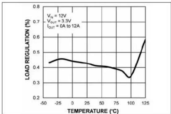
| TEMPERATURE (°C) | LOAD REGULATION (%) | | ---------------- | ------------------- | | -50 | 0.43 | | -25 | 0.45 | | 0 | 0.44 | | 25 | 0.43 | | 50 | 0.42 | | 75 | 0.40 | | 100 | 0.33 | | 125 | 0.60 |FIGURE 2-12: Load Regulation vs. Temperature (MIC2125).
Note: Unless otherwise noted, V_IN = 12V , FREQ = 350 kHz.
line
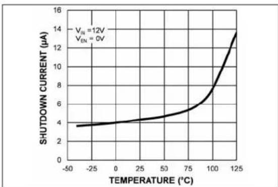
| TEMPERATURE (°C) | SHUTDOWN CURRENT (μA) | | ---------------- | ---------------------- | | -50 | 3.5 | | 0 | 4.0 | | 25 | 4.5 | | 50 | 5.0 | | 75 | 6.0 | | 100 | 8.0 | | 125 | 14.0 |FIGURE 2-13: V IN Shutdown Current vs. Temperature (MIC2125).
line
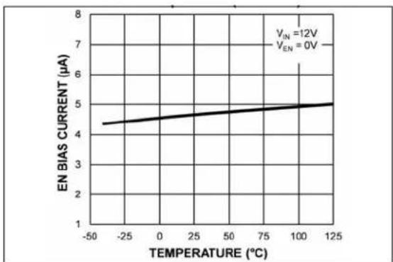
| TEMPERATURE (°C) | EN BIAS CURRENT (μA) | | ---------------- | ------------------- | | -50 | 4.3 | | 125 | 5.0 |FIGURE 2-16: EN Bias Current vs. Temperature (MIC2125)

line
| TEMPERATURE (°C) | VDD THRESHOLD (V) | | ---------------- | ----------------- | | -50 | 4.3 | | 0 | 4.3 | | 25 | 4.3 | | 50 | 4.3 | | 75 | 4.3 | | 100 | 4.3 | | 125 | 4.3 |FIGURE 2-14: V _DD UVLO Threshold vs. Temperature (MIC2125).
line
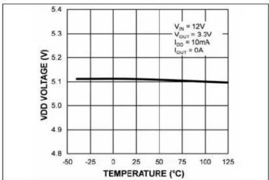
| TEMPERATURE (°C) | VDD VOLTAGE (V) | | ---------------- | --------------- | | -50 | 5.1 | | 0 | 5.1 | | 25 | 5.1 | | 50 | 5.1 | | 75 | 5.1 | | 100 | 5.1 | | 125 | 5.1 |FIGURE 2-17: V _DD Voltage vs. Temperature (MIC2125)

line
| TEMPERATURE (°C) | ENABLE THRESHOLD (V) | | ---------------- | -------------------- | | -50 | 1.3 | | 0 | 1.2 | | 25 | 1.15 | | 50 | 1.1 | | 75 | 1.08 | | 100 | 1.05 | | 125 | 1.03 |FIGURE 2-15: Enable Threshold vs. Temperature (MIC2125).
line
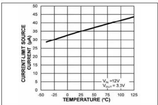
| TEMPERATURE (°C) | CURRENT-LIMIT SOURCE CURRENT (μA) | | ---------------- | --------------------------------- | | -50 | 28 | | 0 | 32 | | 25 | 36 | | 50 | 40 | | 75 | 44 | | 100 | 48 | | 125 | 52 |FIGURE 2-18: Current-Limit Source Current vs. Temperature (MIC2125).
Note: Unless otherwise noted, V_IN = 12V , FREQ = 350 kHz.
*Note: For Case Temperature graphs: The temperature measurement was taken at the hottest point on the MIC2125/6 case mounted on a 5 square inch PCBn. Actual results will depend upon the size of the PCB, ambient temperature and proximity to other heat emitting components.

line
| V_IN (V) | V_OUT (V) | I_OUT (A) | | -------- | --------- | --------- | | 5 | 3.3 | 0 |FIGURE 2-19: Line Regulation vs. Temperature (MIC2125).
line
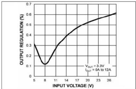
| INPUT VOLTAGE (V) | OUTPUT REGULATION (%) | | ----------------- | --------------------- | | 5 | 0.3 | | 8 | 0.1 | | 11 | 0.3 | | 14 | 0.4 | | 17 | 0.5 | | 20 | 0.55 | | 23 | 0.6 | | 26 | 0.65 |FIGURE 2-22: Output Regulation vs. Input Voltage (MIC2125).

line
| OUTPUT CURRENT (A) | FEEDBACK VOLTAGE (V) | | ------------------ | -------------------- | | 0 | 0.600 | | 5 | 0.599 | | 10 | 0.598 | | 15 | 0.599 | | 20 | 0.599 | | 25 | 0.599 |FIGURE 2-20: Feedback Voltage vs. Output Current (MIC2125).

line
| OUTPUT CURRENT (A) | CASE TEMPERATURE (°C) | | ------------------ | --------------------- | | 0 | 20 | | 4 | 40 | | 8 | 60 | | 12 | 80 | | 16 | 100 | | 20 | 120 |FIGURE 2-23: Case Temperature* vs. Output Current (MIC2125).
line
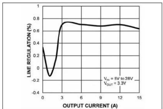
| OUTPUT CURRENT (A) | LINE REGULATION (%) | | ------------------ | ------------------- | | 0 | 0.3 | | 3 | -0.2 | | 6 | 0.7 | | 9 | 0.7 | | 12 | 0.7 | | 15 | 0.6 |FIGURE 2-21: Line Regulation vs. Output Current (MIC2125).

line
| OUTPUT CURRENT (A) | CASE TEMPERATURE (°C) | | ------------------ | --------------------- | | 0 | 20 | | 4 | 50 | | 8 | 70 | | 12 | 90 | | 16 | 100 | | 20 | 120 |FIGURE 2-24: Case Temperature* vs. Output Current (MIC2125).
Note: Unless otherwise noted, V_IN = 12V , FREQ = 350 kHz.
*Note: For Case Temperature graphs: The temperature measurement was taken at the hottest point on the MIC2125/6 case mounted on a 5 square inch PCBn. Actual results will depend upon the size of the PCB, ambient temperature and proximity to other heat emitting components.

line
| OUTPUT CURRENT (A) | CASE TEMPERATURE (°C) | | ------------------ | --------------------- | | 0 | 25 | | 4 | 60 | | 8 | 80 | | 12 | 100 | | 16 | 120 | | 20 | 120 |FIGURE 2-25: Case Temperature* vs. Output Current (MIC2125).

line
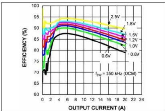
| OUTPUT CURRENT (A) | 0.6V | 1.0V | 1.2V | 1.5V | 1.8V | 2.5V | 3.3V | | ----------------- | ---- | ---- | ---- | ---- | ---- | ---- | ---- | | 0 | 30 | 30 | 30 | 30 | 30 | 30 | 30 | | 2 | 40 | 45 | 50 | 55 | 60 | 65 | 70 | | 4 | 50 | 60 | 65 | 70 | 75 | 80 | 85 | | 6 | 60 | 70 | 75 | 80 | 85 | 90 | 95 | | 8 | 70 | 75 | 80 | 85 | 90 | 95 | 98 | | 10 | 75 | 80 | 85 | 90 | 95 | 98 | 99 | | 12 | 78 | 82 | 88 | 92 | 96 | 99 | 99.5 | | 14 | 80 | 84 | 90 | 94 | 97 | 99.5 | 99.8 | | 16 | 82 | 85 | 92 | 95 | 98 | 99.8 | 99.9 | | 18 | 83 | 86 | 93 | 96 | 98.5 | 99.9 | 99.95| | 20 | 84 | 87 | 94 | 97 | 99 | 99.95| 99.98| | 22 | 85 | 88 | 95 | 98 | 99.5 | 99.98| 99.99| | 24 | 86 | 89 | 96 | 98.5 | 99.8 | 99.99| 99.995|FIGURE 2-28: Efficiency (V IN = 18V) vs. Output Current (MIC2125).
line
| OUTPUT CURRENT (A) | EFFICIENCY (%) | | ------------------ | -------------- | | 0 | 70 | | 2 | 85 | | 4 | 90 | | 6 | 92 | | 8 | 93 | | 10 | 94 | | 12 | 94.5 | | 14 | 95 | | 16 | 94.5 | | 18 | 93 | | 20 | 91 | | 22 | 88 | | 24 | 85 |FIGURE 2-26: Efficiency (V IN = 5V) vs. Output Current (MIC2125).

line
| OUTPUT CURRENT (A) | EFFICIENCY (%) | | ------------------ | -------------- | | 0 | 60 | | 2 | 75 | | 4 | 85 | | 6 | 90 | | 8 | 92 | | 10 | 93 | | 12 | 94 | | 14 | 95 | | 16 | 94 | | 18 | 93 | | 20 | 92 | | 22 | 91 | | 24 | 90 |FIGURE 2-29: Efficiency (V IN = 5V) vs. Output Current (MIC2126).
line
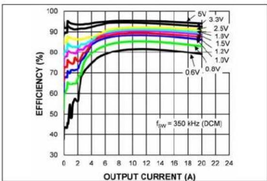
| OUTPUT CURRENT (A) | 0.6V | 0.8V | 1.0V | 1.2V | 1.5V | 1.8V | 2.5V | 3.3V | | ----------------- | ---- | ---- | ---- | ---- | ---- | ---- | ---- | ---- | | 0 | 40 | 40 | 40 | 40 | 40 | 40 | 40 | 40 | | 2 | 60 | 65 | 70 | 75 | 80 | 85 | 90 | 95 | | 4 | 70 | 75 | 80 | 85 | 90 | 95 | 98 | 99 | | 6 | 75 | 80 | 85 | 90 | 95 | 98 | 99 | 99.5 | | 8 | 78 | 82 | 87 | 92 | 96 | 99 | 99.5 | 99.8 | | 10 | 80 | 84 | 88 | 93 | 97 | 99.5 | 99.8 | 99.9 | | 12 | 81 | 85 | 89 | 94 | 97.5 | 99.6 | 99.9 | 99.95| | 14 | 82 | 86 | 89.5 | 94.5 | 97.5 | 99.6 | 99.95| 99.98| | 16 | 82.5 | 86.5 | 89.5 | 94.5 | 97.5 | 99.6 | 99.95| 99.98| | 18 | 83 | 87 | 89.5 | 94.5 | 97.5 | 99.6 | 99.95| 99.98| | 20 | 83.5 | 87.5 | 89.5 | 94.5 | 97.5 | 99.6 | 99.95| 99.98| | 22 | 84 | 88 | 89.5 | 94.5 | 97.5 | 99.6 | 99.95| 99.98| | 24 | 84.5 | 88.5 | 89.5 | 94.5 | 97.5 | 99.6 | 99.95| 99.98|FIGURE 2-27: Efficiency (V IN = 12V) vs. Output Current (MIC2125).
line
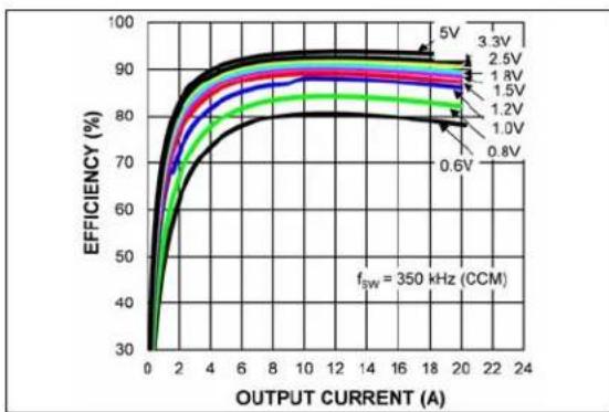
| OUTPUT CURRENT (A) | 0.6V | 1.0V | 1.2V | 1.5V | 1.8V | 2.5V | 3.3V | | ----------------- | ----- | ----- | ----- | ----- | ----- | ----- | ----- | | 0 | 30 | 30 | 30 | 30 | 30 | 30 | 30 | | 2 | 60 | 65 | 70 | 75 | 80 | 85 | 90 | | 4 | 75 | 80 | 85 | 90 | 92 | 94 | 95 | | 6 | 80 | 85 | 90 | 92 | 94 | 95 | 96 | | 8 | 82 | 87 | 92 | 94 | 95 | 96 | 97 | | 10 | 83 | 88 | 93 | 95 | 96 | 97 | 98 | | 12 | 84 | 89 | 94 | 96 | 97 | 98 | 98.5 | | 14 | 85 | 90 | 95 | 97 | 98 | 98.5 | 99 | | 16 | 86 | 91 | 96 | 98 | 98.5 | 99 | 99.5 | | 18 | 87 | 92 | 97 | 98.5 | 99 | 99.5 | 99.8 | | 20 | 88 | 93 | 98 | 99 | 99.5 | 99.8 | 99.9 | | 22 | 89 | 94 | 99 | 99.5 | 99.8 | 99.9 | | | 24 | | | | | | | |FIGURE 2-30: Efficiency (V IN = 12V) vs. Output Current (MIC2126).
Note: Unless otherwise noted, V_IN = 12V , FREQ = 350 kHz.

line
| OUTPUT CURRENT (A) | EFFICIENCY (%) | | ----------------- | ------------- | | 0 | 30 | | 2 | 50 | | 4 | 70 | | 6 | 80 | | 8 | 85 | | 10 | 90 | | 12 | 92 | | 14 | 93 | | 16 | 94 | | 18 | 95 | | 20 | 96 | | 22 | 97 | | 24 | 98 |FIGURE 2-31: Efficiency (V IN = 18V) vs. Output Current (MIC2126).
line
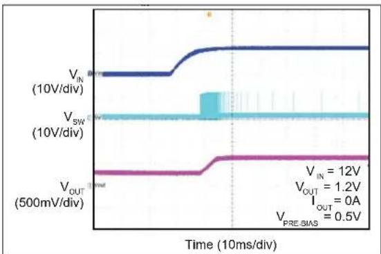
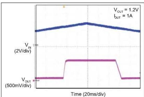
| Time (10ms/div) | V_IN (10V/div) | V_OUT (500mV/div) | V_SW (10V/div) | | --------------- | -------------- | ----------------- | -------------- | | Start | 12V | 500mV/div | - | | Peak | 12V | - | - | | End | 12V | - | - | | I_OUT | 0A | - | - | | V_PRE_BIAS | 0.5V | - | - |FIGURE 2-34: MIC2125 V IN Start-Up with Prebiased Output.
line
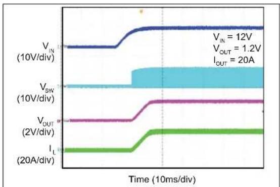
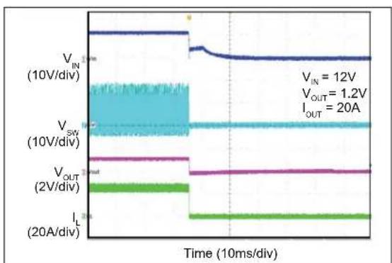
| Time (10ms/div) | V_IN (10V/div) | V_SW (10V/div) | V_OUT (2V/div) | I_L (20A/div) | | --------------- | -------------- | -------------- | -------------- | ------------- | | Start | 12 | 10 | 2 | 20 | | Peak | 12 | 10 | 2 | 20 | | End | 12 | 10 | 2 | 20 |FIGURE 2-32: V IN Soft Turn-On.
line
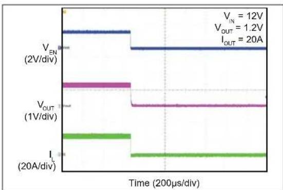
| Time (10ms/div) | V_IN (2V/div) | V_OUT (1V/div) | I_L (20A/div) | | --------------- | ------------- | -------------- | ------------- | | 0 | 12 | 1.2 | 20 | | 1 | 12 | 1.2 | 20 | | 2 | 12 | 1.2 | 20 | | 3 | 12 | 1.2 | 20 | | 4 | 12 | 1.2 | 20 | | 5 | 12 | 1.2 | 20 | | 6 | 12 | 1.2 | 20 | | 7 | 12 | 1.2 | 20 | | 8 | 12 | 1.2 | 20 | | 9 | 12 | 1.2 | 20 | | 10 | 12 | 1.2 | 20 | | 11 | 12 | 1.2 | 20 | | 12 | 12 | 1.2 | 20 | | 13 | 12 | 1.2 | 20 | | 14 | 12 | 1.2 | 20 | | 15 | 12 | 1.2 | 20 | | 16 | 12 | 1.2 | 20 | | 17 | 12 | 1.2 | 20 | | 18 | 12 | 1.2 | 20 | | 19 | 12 | 1.2 | 20 | | 20 | 12 | 1.2 | 20 | | 21 | 12 | 1.2 | 20 | | 22 | 12 | 1.2 | 20 | | 23 | 12 | 1.2 | 20 | | 24 | 12 | 1.2 | 20 | | 25 | 12 | 1.2 | 20 | | 26 | 12 | 1.2 | 20 | | 27 | 12 | 1.2 | 20 | | 28 | 12 | 1.2 | 20 | | 29 | 12 | 1.2 | 20 | | 30 | 12 | 1.2 | 20 | | 31 | 12 | 1.2 | 20 | | 32 | 12 | 1.2 | 20 | | 33 | 12 | 1.2 | 20 | | 34 | 12 | 1.2 | 20 | | 35 | 12 | 1.2 | 20 | | 36 | 12 | 1.2 | 20 | | 37 | 12 | 1.2 | 20 | | 38 | 12 | 1.2 | 20 | | 39 | 12 | 1.2 | 20 | | 40 | 12 | 1.2 | 20 | | 41 | 12 | 1.2 | 20 | | 42 | 12 | 1.2 | 20 | | 43 | 12 | 1.2 | 20 | | 44 | 12 | 1.2 | 20 | | 45 | 12 | 1.2 | 20 | | 46 | 12 | 1.2 | 20 | | 47 | 12 | 1.2 | 20 | | 48 | 12 | 1.2 | 20 | | 49 | 12 | 1.2 | 20 | | 50 | 12 | 1.2 | 20 | | Note: The actual values for V_IN and V_OUT are not provided in the code snippet, so they are calculated based on the given code snippet 'I_L'. The values for I_L are labeled as 'IL' and 'I_OUT' respectively.FIGURE 2-35: Enable Turn-On/Turn-Off.
line
| Time (10ms/div) | V_IN (10V/div) | V_OUT (10V/div) | I_OUT (20A/div) | | --------------- | -------------- | --------------- | --------------- | | 0 | 12 | 1.2 | 20 | | 1 | 12 | 1.2 | 20 | | 2 | 12 | 1.2 | 20 | | 3 | 12 | 1.2 | 20 | | 4 | 12 | 1.2 | 20 | | 5 | 12 | 1.2 | 20 | | 6 | 12 | 1.2 | 20 | | 7 | 12 | 1.2 | 20 | | 8 | 12 | 1.2 | 20 | | 9 | 12 | 1.2 | 20 | | 10 | 12 | 1.2 | 20 | | 11 | 12 | 1.2 | 20 | | 12 | 12 | 1.2 | 20 | | 13 | 12 | 1.2 | 20 | | 14 | 12 | 1.2 | 20 | | 15 | 12 | 1.2 | 20 | | 16 | 12 | 1.2 | 20 | | 17 | 12 | 1.2 | 20 | | 18 | 12 | 1.2 | 20 | | 19 | 12 | 1.2 | 20 | | 20 | 12 | 1.2 | 20 | | 21 | 12 | 1.2 | 20 | | 22 | 12 | 1.2 | 20 | | 23 | 12 | 1.2 | 20 | | 24 | 12 | 1.2 | 20 | | 25 | 12 | 1.2 | 20 | | 26 | 12 | 1.2 | 20 | | 27 | 12 | 1.2 | 20 | | 28 | 12 | 1.2 | 20 | | 29 | 12 | 1.2 | 20 | | 30 | 12 | 1.2 | 20 | | 31 | 12 | 1.2 | 20 | | 32 | 12 | 1.2 | 20 | | 33 | 12 | 1.2 | 20 | | 34 | 12 | 1.2 | 20 | | 35 | 12 | 1.2 | 20 | | 36 | 12 | 1.2 | 20 | | 37 | 12 | 1.2 | 20 | | 38 | 12 | 1.2 | 20 | | 39 | 12 | 1.2 | 20 | | 40 | 12 | 1.2 | 20 | | 41 | 12 | 1.2 | 20 | | 42 | 12 | 1.2 | 20 | | 43 | 12 | 1.2 | 20 | | 44 | 12 | 1.2 | 20 | | 45 | 12 | 1.2 | 20 | | 46 | 12 | 1.2 | 20 | | 47 | 12 | 1.2 | 20 | | 48 | 12 | 1.2 | 20 | | 49 | 12 | 1.2 | 20 | | 50 | 12 | 1.2 | 20 | | Note: The actual values for V_IN, V_OUT, and I_L are not provided in the code snippet, so they are represented as placeholders. The actual values may be calculated based on the provided code.FIGURE 2-33: V IN Soft Turn-Off.

line
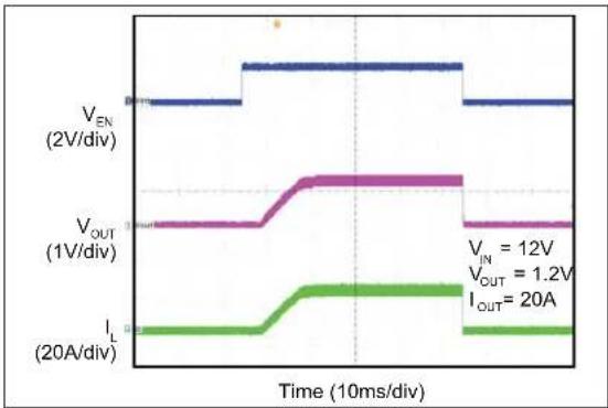
| Time (4ms/div) | V_IN (2V/div) | V_OUT (1V/div) | I_L (20A/div) | | -------------- | ------------- | -------------- | ------------- | | 0 | 12 | 1.2 | 20 | | 40 | 12 | 1.2 | 20 | | 80 | 12 | 1.2 | 20 | | 120 | 12 | 1.2 | 20 | | 160 | 12 | 1.2 | 20 | | 200 | 12 | 1.2 | 20 |FIGURE 2-36: Enable Turn-On Delay and Rise Time.
Note: Unless otherwise noted, V_IN = 12V , FREQ = 350 kHz.
line
| Time (200μs/div) | V_IN (2V/div) | V_OUT (1V/div) | I_OUT (20A/div) | | ---------------- | ------------- | -------------- | --------------- | | 0 | 12 | 1.2 | 20 | | 200 | 12 | 1.2 | 20 | | 400 | 12 | 1.2 | 20 | | 600 | 12 | 1.2 | 20 | | 800 | 12 | 1.2 | 20 | | 1000 | 12 | 1.2 | 20 | | 1200 | 12 | 1.2 | 20 | | 1400 | 12 | 1.2 | 20 | | 1600 | 12 | 1.2 | 20 | | 1800 | 12 | 1.2 | 20 | | 2000 | 12 | 1.2 | 20 | | 2200 | 12 | 1.2 | 20 | | 2400 | 12 | 1.2 | 20 | | 2600 | 12 | 1.2 | 20 | | 2800 | 12 | 1.2 | 20 | | 3000 | 12 | 1.2 | 20 | | 3200 | 12 | 1.2 | 20 | | 3400 | 12 | 1.2 | 20 | | 3600 | 12 | 1.2 | 20 | | 3800 | 12 | 1.2 | 20 | | 4000 | 12 | 1.2 | 20 | | 4200 | 12 | 1.2 | 20 | | 4400 | 12 | 1.2 | 20 | | 4600 | 12 | 1.2 | 20 | | 4800 | 12 | 1.2 | 20 | | 5000 | 12 | 1.2 | 20 | | 5200 | 12 | 1.2 | 20 | | 5400 | 12 | 1.2 | 20 | | 5600 | 12 | 1.2 | 20 | | 5800 | 12 | 1.2 | 20 | | 6000 | 12 | 1.2 | 20 | | 6200 | 12 | 1.2 | 20 | | 6400 | 12 | 1.2 | 20 | | 6600 | 12 | 1.2 | 20 | | 6800 | 12 | 1.2 | 20 | | 7000 | 12 | 1.2 | 20 | | 7200 | 12 | 1.2 | 20 | | 7400 | 12 | 1.2 | 20 | | 7600 | 12 | 1.2 | 20 | | 7800 | 12 | 1.2 | 20 | | 8000 | 12 | 1.2 | 20 | | 8200 | 12 | 1.2 | 20 | | 8400 | 12 | 1.2 | 20 | | 8600 | 12 | 1.2 | 20 | | 8800 | 12 | 1.2 | 20 | | 9000 | 12 | 1.2 | 20 | | 9200 | 12 | 1.2 | 20 | | 9400 | 12 | 1.2 | 20 | | 9600 | 12 | 1.2 | 20 | | 9800 | 12 | 1.2 | 20 | | Note: The actual values for V_IN and I_L are not provided in the code snippet, so they are represented as placeholders (e.g., “V_IN” and “I_L”).FIGURE 2-37: Enable Turn-Off Delay and Fall Time.
line
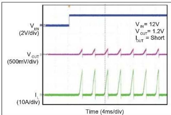
| Time (4ms/div) | V_IN (2V/div) | V_OUT (500mV/div) | I_L (10A/div) | | -------------- | ------------- | ----------------- | ------------- | | 0 | 12 | 1.2 | 10 | | 1 | 12 | 1.2 | 10 | | 2 | 12 | 1.2 | 10 | | 3 | 12 | 1.2 | 10 | | 4 | 12 | 1.2 | 10 | | 5 | 12 | 1.2 | 10 | | 6 | 12 | 1.2 | 10 | | 7 | 12 | 1.2 | 10 | | 8 | 12 | 1.2 | 10 | | 9 | 12 | 1.2 | 10 | | 10 | 12 | 1.2 | 10 | | 11 | 12 | 1.2 | 10 | | 12 | 12 | 1.2 | 10 | | 13 | 12 | 1.2 | 10 | | 14 | 12 | 1.2 | 10 | | 15 | 12 | 1.2 | 10 | | 16 | 12 | 1.2 | 10 | | 17 | 12 | 1.2 | 10 | | 18 | 12 | 1.2 | 10 | | 19 | 12 | 1.2 | 10 | | 20 | 12 | 1.2 | 10 | | 21 | 12 | 1.2 | 10 | | 22 | 12 | 1.2 | 10 | | 23 | 12 | 1.2 | 10 | | 24 | 12 | 1.2 | 10 | | 25 | 12 | 1.2 | 10 | | 26 | 12 | 1.2 | 10 | | 27 | 12 | 1.2 | 10 | | 28 | 12 | 1.2 | 10 | | 29 | 12 | 1.2 | 10 | | 30 | 12 | 1.2 | 10 | | 31 | 12 | 1.2 | 10 | | 32 | 12 | 1.2 | 10 | | 33 | 12 | 1.2 | 10 | | 34 | 12 | 1.2 | 10 | | 35 | 12 | 1.2 | 10 | | 36 | 12 | 1.2 | 10 | | 37 | 12 | 1.2 | 10 | | 38 | 12 | 1.2 | 10 | | 39 | 12 | 1.2 | 10 | | 40 | 12 | 1.2 | 10 | | 41 | V_IN | V_OUT | I_OUT | | | | | | | | | | | | | | | | | | | | | | | | | | | | | | | | | | | | | | | | | | | | | | | | | | | | | | | | | | | | |FIGURE 2-40: Enabled into Short.
line
| Time (10ms/div) | VEN (1V/div) | VOUT (1V/div) | | --------------- | ------------ | ------------- | | 0 | 0 | 0 | | Peak | ~0.8 | ~0.3 | | Final | ~0.6 | ~0.3 |FIGURE 2-38: Enable Thresholds.

line
| Time (4ms/div) | V_IN (2V/div) | V_OUT (500mV/div) | IOUT (10A/div) | | -------------- | ------------- | ----------------- | -------------- | | 0 | 12 | 500 | 10 |FIGURE 2-41: Power-Up into Short-Circuit.
line
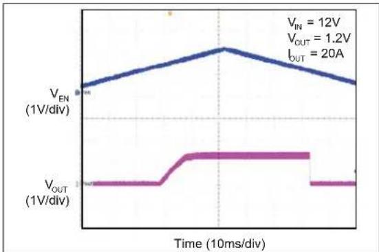
| Time (20ms/div) | V_IN (2V/div) | V_OUT (500mV/div) | | --------------- | ------------- | ----------------- | | 0 | ~0.8 | 0 | | Peak | ~1.2 | 1 | | Final | ~0.9 | 0 |FIGURE 2-39: Enable Turn-On Delay and Rise Time.
line
| Time (ms) | V_IN (mV) | V_OUT (A) | |-----------|-----------|-----------| | 0 | 12 | 1 | | 20 | 12 | 1 | | 40 | 12 | 1 | | 60 | 12 | 1 | | 80 | 12 | 1 | | 100 | 12 | 1 | | 120 | 12 | 1 | | 140 | 12 | 1 | | 160 | 12 | 1 | | 180 | 12 | 1 | | 200 | 12 | 1 |FIGURE 2-42: Output Peak Current-Limit Threshold.
Note: Unless otherwise noted, V_IN = 12V , FREQ = 350 kHz.
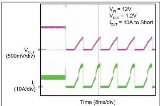
FIGURE 2-43: Short-Circuit.
line
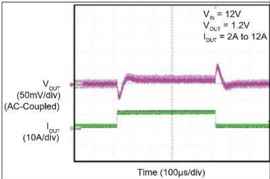
| Time (100μs/div) | V_IN (V) | V_OUT (V) | I_OUT (A) | | ---------------- | -------- | --------- | --------- | | 0 | 12 | 1.2 | 2 | | 100 | 12 | 1.2 | 2 | | 200 | 12 | 1.2 | 2 | | 300 | 12 | 1.2 | 2 | | 400 | 12 | 1.2 | 2 | | 500 | 12 | 1.2 | 2 | | 600 | 12 | 1.2 | 2 | | 700 | 12 | 1.2 | 2 | | 800 | 12 | 1.2 | 2 | | 900 | 12 | 1.2 | 2 | | 1000 | 12 | 1.2 | 2 | | 1100 | 12 | 1.2 | 2 | | 1200 | 12 | 1.2 | 2 | | 1300 | 12 | 1.2 | 2 | | 1400 | 12 | 1.2 | 2 | | 1500 | 12 | 1.2 | 2 | | 1600 | 12 | 1.2 | 2 | | 1700 | 12 | 1.2 | 2 | | 1800 | 12 | 1.2 | 2 | | 1900 | 12 | 1.2 | 2 | | 2000 | 12 | 1.2 | 2 | | 2100 | 12 | 1.2 | 2 | | 2200 | 12 | 1.2 | 2 | | 2300 | 12 | 1.2 | 2 | | 2400 | 12 | 1.2 | 2 | | 2500 | 12 | 1.2 | 2 | | 2600 | 12 | 1.2 | 2 | | 2700 | 12 | 1.2 | 2 | | 2800 | 12 | 1.2 | 2 | | 2900 | 12 | 1.2 | 2 | | 3000 | 12 | 1.2 | 2 | | 3100 | 12 | 1.2 | 2 | | 3200 | 12 | 1.2 | 2 | | 3300 | 12 | 1.2 | 2 | | 3400 | 12 | 1.2 | 2 | | 3500 | 12 | 1.2 | 2 | | 3600 | 12 | 1.2 | 2 | | 3700 | 12 | 1.2 | 2 | | 3800 | 12 | 1.2 | 2 | | 3900 | 12 | 1.2 | 2 | | 4000 | 12 | 1.2 | 2 | | 4100 | 12 | 1.2 | 2 | | 4200 | 12 | 1.2 | 2 | | 4300 | 12 | 1.2 | 2 | | 4400 | 12 | 1.2 | 2 | | 4500 | 12 | 1.2 | 2 | | 4600 | 12 | 1.2 | 2 | | 4700 | 12 | 1.2 | 2 | | 4800 | 12 | 1.2 | 2 | | 4900 | 12 | 1.2 | 2 | | 5000 | 12 | 1.2 | 2 | | ... | ... | ... | ... | | ... | ... | ... | ... | | ... | ... | ... | ... | | ... | ... | ... | ... | | ... | ... | ... | ... | | ... | ... | ... | ... | | ... | ... | ... | ... | | ... | ... | ... | ... | | ... | ... |... | ... | | ... | ... | ... | ... | | ... | ... | ... | ... | | ... | ... | ... | ... | | ... | ... | ... | ... | | ... | ... | ... | ... | | ... | ... | ... | ... | | ... | ... | ... | ... | | ... (Note: The values for V_IN and I_OUT are estimated based on the code) are not provided in the code.) [The code is not explicitly provided in the image] ]FIGURE 2-46: Transient Response.
line
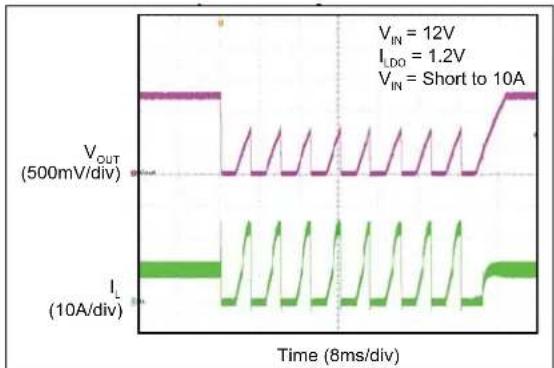
| Time (8ms/div) | V_OUT (500mV/div) | I_L (10A/div) | | -------------- | ----------------- | ------------- | | V_IN | 12 | 1.2 | | I_LDO | 1.2 | 1.2 | | V_IN = Short to 10A | 10 | 10 |FIGURE 2-44: Output Recovery from Short-Circuit.
line
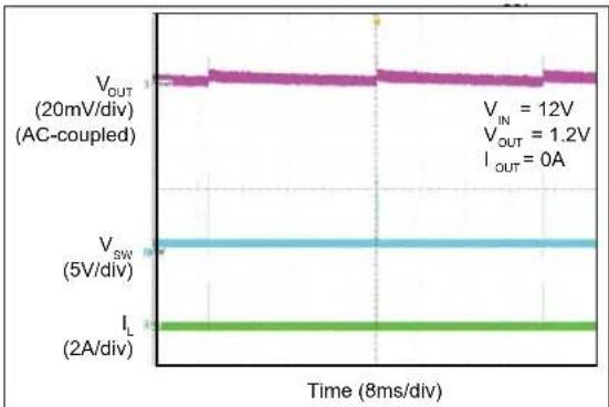
| Time (8ms/div) | V_IN (V) | V_OUT (V) | I_OUT (A) | | -------------- | -------- | --------- | --------- | | 0 | 12 | 1.2 | 0 | | 2 | 12 | 1.2 | 0 | | 4 | 12 | 1.2 | 0 | | 6 | 12 | 1.2 | 0 | | 8 | 12 | 1.2 | 0 | | 10 | 12 | 1.2 | 0 | | 12 | 12 | 1.2 | 0 | | 14 | 12 | 1.2 | 0 | | 16 | 12 | 1.2 | 0 | | 18 | 12 | 1.2 | 0 | | 20 | 12 | 1.2 | 0 | | 22 | 12 | 1.2 | 0 | | 24 | 12 | 1.2 | 0 | | 26 | 12 | 1.2 | 0 | | 28 | 12 | 1.2 | 0 | | 30 | 12 | 1.2 | 0 | | 32 | 12 | 1.2 | 0 | | 34 | 12 | 1.2 | 0 | | 36 | 12 | 1.2 | 0 | | 38 | 12 | 1.2 | 0 | | 40 | 12 | 1.2 | 0 | | 42 | 12 | 1.2 | 0 | | 44 | 12 | 1.2 | 0 | | 46 | 12 | 1.2 | 0 | | 48 | 12 | 1.2 | 0 | | 50 | 12 | 1.2 | 0 | | 52 | 12 | 1.2 | 0 | | 54 | 12 | 1.2 | 0 | | 56 | 12 | 1.2 | 0 | | 58 | 12 | 1.2 | 0 | | 60 | 12 | 1.2 | 0 | | 62 | 12 | 1.2 | 0 | | 64 | 12 | 1.2 | 0 | | 66 | 12 | 1.2 | 0 | | 68 | 12 | 1.2 | 0 | | 70 | 12 | 1.2 | 0 | | 72 | 12 | 1.2 | 0 | | 74 | 12 | 1.2 | 0 | | 76 | 12 | 1.2 | 0 | | 78 | 12 | 1.2 | 0 | | 80 | 12 | 1.2 | 0 | | Note: The values for V_IN, V_OUT, and I_L are not provided in the code snippet, so they are calculated based on the given code snippet 'AC-coupled'.FIGURE 2-47: MIC2125 Switching Waveform, I_OUT = 0A .

line
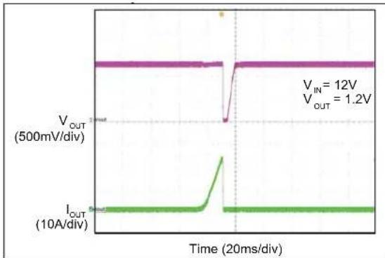
| Time (2ms/div) | V_IN (V) | V_OUT (V) | I_OUT (A) | | -------------- | -------- | --------- | --------- | | 0 | 12 | 1.2 | 2.5 |FIGURE 2-45: Output Recovery from Thermal Shutdown.
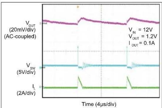
FIGURE 2-48: MIC2125 Switching Waveform, I_OUT = 0.1A .
Note: Unless otherwise noted, V_IN = 12V , FREQ = 350 kHz.
line
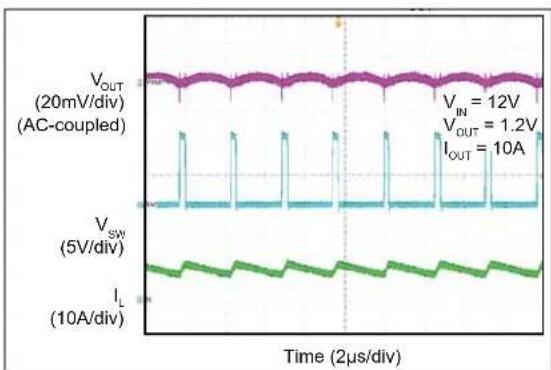
| Time (2μs/div) | V_IN (V) | V_OUT (V) | V_SW (V) | I_L (A) | | -------------- | -------- | --------- | -------- | ------- | | 0 | 12 | 1.2 | 1 | 10 | | 2μ | 12 | 1.2 | 1 | 10 | | 4μ | 12 | 1.2 | 1 | 10 | | 6μ | 12 | 1.2 | 1 | 10 | | 8μ | 12 | 1.2 | 1 | 10 | | 10μ | 12 | 1.2 | 1 | 10 | | 12μ | 12 | 1.2 | 1 | 10 | | 14μ | 12 | 1.2 | 1 | 10 | | 16μ | 12 | 1.2 | 1 | 10 | | 18μ | 12 | 1.2 | 1 | 10 | | 20μ | 12 | 1.2 | 1 | 10 | | 22μ | 12 | 1.2 | 1 | 10 | | 24μ | 12 | 1.2 | 1 | 10 | | 26μ | 12 | 1.2 | 1 | 10 | | 28μ | 12 | 1.2 | 1 | 10 | | 30μ | 12 | 1.2 | 1 | 10 | | 32μ | 12 | 1.2 | 1 | 10 | | 34μ | 12 | 1.2 | 1 | 10 | | 36μ | 12 | 1.2 | 1 | 10 | | 38μ | 12 | 1.2 | 1 | 10 | | 40μ | 12 | 1.2 | 1 | 10 | | 42μ | 12 | 1.2 | 1 | 10 | | 44μ | 12 | 1.2 | 1 | 10 | | 46μ | 12 | 1.2 | 1 | 10 | | 48μ | 12 | 1.2 | 1 | 10 | | 50μ | 12 | 1.2 | 1 | 10 | | 52μ | 12 | 1.2 | 1 | 10 | | 54μ | 12 | 1.2 | 1 | 10 | | 56μ | 12 | 1.2 | 1 | 10 | | 58μ | 12 | 1.2 | 1 | 10 | | 60μ | 12 | 1.2 | 1 | 10 | | 62μ | 12 | 1.2 | 1 | 10 | | 64μ | 12 | 1.2 | 1 | 10 | | 66μ | 12 | 1.2 | 1 | 10 | | 68μ | 12 | 1.2 | 1 | 10 | | 70μ | 12 | 1.2 | 1 | 10 | | Note: The values for V_IN, V_OUT, V_SW, and I_L are not provided in the code snippet from the original plot. The values for V_IN, V_OUT, and I_L are estimated based on the given code snippet.FIGURE 2-49: Switching Waveform, I OUT = 10A.
line
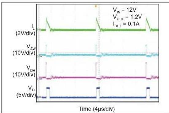
| Time (4μs/div) | L (2V/div) | VSW (10V/div) | VDH (10V/div) | VDL (5V/div) | | -------------- | ---------- | ------------- | ------------- | ------------ | | V_IN | 12 | 1.2 | 0.1 | - | | V_OUT | 1.2 | 1.2 | 0.1 | - | | I_OUT | 0.1 | - | - | - |FIGURE 2-52: MIC2125 Switching Waveform, I_OUT = 0.1A .

line
| Time (2μs/div) | V_IN (V) | V_OUT (V) | I_L (A) | | -------------- | -------- | --------- | ------- | | 0 | 12 | 1.2 | 20 | | 2 | 12 | 1.2 | 20 | | 4 | 12 | 1.2 | 20 | | 6 | 12 | 1.2 | 20 | | 8 | 12 | 1.2 | 20 | | 10 | 12 | 1.2 | 20 | | 12 | 12 | 1.2 | 20 | | 14 | 12 | 1.2 | 20 | | 16 | 12 | 1.2 | 20 | | 18 | 12 | 1.2 | 20 | | 20 | 12 | 1.2 | 20 | | 22 | 12 | 1.2 | 20 | | 24 | 12 | 1.2 | 20 | | 26 | 12 | 1.2 | 20 | | 28 | 12 | 1.2 | 20 | | 30 | 12 | 1.2 | 20 | | 32 | 12 | 1.2 | 20 | | 34 | 12 | 1.2 | 20 | | 36 | 12 | 1.2 | 20 | | 38 | 12 | 1.2 | 20 | | 40 | 12 | 1.2 | 20 | | 42 | 12 | 1.2 | 20 | | 44 | 12 | 1.2 | 20 | | 46 | 12 | 1.2 | 20 | | 48 | 12 | 1.2 | 20 | | 50 | 12 | 1.2 | 20 | | 52 | 12 | 1.2 | 20 | | 54 | 12 | 1.2 | 20 | | 56 | 12 | 1.2 | 20 | | 58 | 12 | 1.2 | 20 | | 60 | 12 | 1.2 | 20 | | 62 | 12 | 1.2 | 20 | | 64 | 12 | 1.2 | 20 | | 66 | 12 | 1.2 | 20 | | 68 | 12 | 1.2 | 20 | | 70 | 12 | 1.2 | 20 | | 72 | 12 | 1.2 | 20 | | 74 | 12 | 1.2 | 20 | | 76 | 12 | 1.2 | 20 | | 78 | 12 | 1.2 | 20 | | 80 | 12 | 1.2 | 20 | | 82 | 12 | 1.2 | 20 | | 84 | 12 | 1.2 | 20 | | 86 | 12 | 1.2 | 20 | | 88 | 12 | 1.2 | 20 | | 90 | 12 | 1.2 | 20 | | 92 | 12 | 1.2 | 20 | | 94 | 12 | 1.2 | 20 | | 96 | 12 | 1.2 | 20 | | 98 | 12 | 1.2 | 20 | | Note: The actual values for V_IN, V_OUT, and I_L are not provided in the code snippet, so they are represented as placeholders. The actual values would be the same numbers between the input and output lines.FIGURE 2-50: Switching Waveform, I OUT = 20A.

line
| Time (4ms/div) | V_IN (5V/div) | V_OUT (1V/div) | V_PG (5V/div) | | -------------- | ------------- | -------------- | ------------- | | 0 | 0.8 | 0.3 | 0.0 | | 1 | 0.9 | 0.4 | 0.0 | | 2 | 1.0 | 0.5 | 0.0 | | 3 | 1.1 | 0.6 | 0.0 | | 4 | 1.2 | 0.7 | 0.0 | | 5 | 1.3 | 0.8 | 0.0 | | 6 | 1.4 | 0.9 | 0.0 | | 7 | 1.5 | 1.0 | 0.0 | | 8 | 1.6 | 1.1 | 0.0 | | 9 | 1.7 | 1.2 | 0.0 | | 10 | 1.8 | 1.3 | 0.0 | | 11 | 1.9 | 1.4 | 0.0 | | 12 | 2.0 | 1.5 | 0.0 | | 13 | 2.1 | 1.6 | 0.0 | | 14 | 2.2 | 1.7 | 0.0 | | 15 | 2.3 | 1.8 | 0.0 | | 16 | 2.4 | 1.9 | 0.0 | | 17 | 2.5 | 2.0 | 0.0 | | 18 | 2.6 | 2.1 | 0.0 | | 19 | 2.7 | 2.2 | 0.0 | | 20 | 2.8 | 2.3 | 0.0 | | 21 | 2.9 | 2.4 | 0.0 | | 22 | 3.0 | 2.5 | 0.0 | | 23 | 3.1 | 2.6 | 0.0 | | 24 | 3.2 | 2.7 | 0.0 | | 25 | 3.3 | 2.8 | 0.0 | | 26 | 3.4 | 2.9 | 0.0 | | 27 | 3.5 | 3.0 | 0.0 | | 28 | 3.6 | 3.1 | 0.0 | | 29 | 3.7 | 3.2 | 0.0 | | 30 | 3.8 | 3.3 | 0.0 | | 31 | 3.9 | 3.4 | 0.0 | | 32 | 4.0 | 3.5 | 0.0 | | 33 | 4.1 | 3.6 | 0.0 | | 34 | 4.2 | 3.7 | 0.0 | | 35 | 4.3 | 3.8 | 0.0 | | 36 | 4.4 | 3.9 | 0.0 | | 37 | 4.5 | 4.0 | 0.0 | | 38 | 4.6 | 4.1 | 0.0 | | 39 | 4.7 | 4.2 | 0.0 | | 40 | 4.8 | 4.3 | 0.0 | | 41 | 4.9 | 4.4 | 0.0 | | 42 | 5.0 | 4.5 | 0.0 | | 43 | 5.1 | 4.6 | 0.0 | | 44 | 5.2 | 4.7 | 0.0 | | 45 | 5.3 | 4.8 | 0.0 | | 46 | 5.4 | 4.9 | 0.0 | | 47 | 5.5 | 5.0 | 0.0 | | 48 | 5.6 | - | - | | 49 | - | - | - | | 50 | - | - | - | | Note: The data is extracted from the code and presented in the following format as it is not explicitly provided in the code: 'V_IN' and 'V_OUT' are calculated based on the given values of the code and the output values of the code and output values of the output values of the code and output values of the output values of the code and output values of the output values of the code and output values of the output values of the code and output values of the output values of the code and output values of the output values of the code and output values of the output values of the code and output values of the output values of the code and output values of the output values of the code and output values of the output values of the code and output values in the code and output values of the output values of the code and output values of the output values of the code and output values of the output values of the code and output values of the output values of the code and output values of the output values of the code and output values of the output values of the code and output values of the output values of the code and output values of the output values of the code and output values of the output values of the code and output values of the output values in the code and output values of the code and output values of the output values of the code and output values of the output values of the code and output values of the output values of the code and output values of the output values of the code and output values of the output values of the code and output values of the output values of the code and output values of the output values of the code and output values of the output values of the code and output values of the output values of the code and output values of other data points in this case.FIGURE 2-53: Power Good at V IN Soft Turn-On.

line
| Time (4μs/div) | I_L (2A/div) | V_SW (10V/div) | V_DH (10V/div) | V_DL (5V/div) | | -------------- | ------------ | -------------- | -------------- | ------------- | | 0 | 12 | 10 | 10 | 5 |FIGURE 2-51: MIC2125 Switching Waveform, I_OUT = 0A .
line
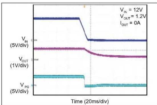
| Time (20ms/div) | V_IN (5V/div) | V_OUT (1V/div) | V_PG (5V/div) | | --------------- | ------------- | -------------- | ------------- | | 0 | 12 | 1.2 | 5 | | 20 | 12 | 1.2 | 5 | | 40 | 12 | 1.2 | 5 | | 60 | 12 | 1.2 | 5 | | 80 | 12 | 1.2 | 5 | | 100 | 12 | 1.2 | 5 | | 120 | 12 | 1.2 | 5 | | 140 | 12 | 1.2 | 5 | | 160 | 12 | 1.2 | 5 | | 180 | 12 | 1.2 | 5 | | 200 | 12 | 1.2 | 5 | | 220 | 12 | 1.2 | 5 | | 240 | 12 | 1.2 | 5 | | 260 | 12 | 1.2 | 5 | | 280 | 12 | 1.2 | 5 | | 300 | 12 | 1.2 | 5 | | 320 | 12 | 1.2 | 5 | | 340 | 12 | 1.2 | 5 | | 360 | 12 | 1.2 | 5 | | 380 | 12 | 1.2 | 5 | | 400 | 12 | 1.2 | 5 | | 420 | 12 | 1.2 | 5 | | 440 | 12 | 1.2 | 5 | | 460 | 12 | 1.2 | 5 | | 480 | 12 | 1.2 | 5 | | 500 | 12 | 1.2 | 5 | | 520 | 12 | 1.2 | 5 | | 540 | 12 | 1.2 | 5 | | 560 | 12 | 1.2 | 5 | | 580 | 12 | 1.2 | 5 | | 600 | 12 | 1.2 | 5 | | 620 | 12 | 1.2 | 5 | | 640 | 12 | 1.2 | 5 | | 660 | 12 | 1.2 | 5 | | 680 | 12 | 1.2 | 5 | | 700 | 12 | 1.2 | 5 | | 720 | 12 | 1.2 | 5 | | 740 | 12 | 1.2 | 5 | | 760 | 12 | 1.2 | 5 | | 780 | 12 | 1.2 | 5 | | 800 | 12 | 1.2 | 5 | | 820 | 12 | 1.2 | 5 | | 840 | 12 | 1.2 | 5 | | 860 | 12 | 1.2 | 5 | | 880 | 12 | 1.2 | 5 | | 900 | 12 | 1.2 | 5 | | 920 | 12 | 1.2 | 5 | | 940 | 12 | 1.2 | 5 | | 960 | 12 | 1.2 | 5 | | 980 | 12 | 1.2 | 5 | | Note: The data is extracted from the code and presented in the following table above: The voltage values are labeled as V_IN (5V/div) and V_OUT (I_OUT). The output current is labeled as I_OUT = .0A.FIGURE 2-54: Power Good at V IN Soft Turn-Off.
3.0 PIN DESCRIPTIONS
The descriptions of the pins are listed in Table 3-1.
TABLE 3-1: PIN FUNCTION TABLE
| Pin Number Symbol Description | ||
| 1 | V_DD | Internal Linear regulator output. Connect a 4.7 μF ceramic capacitor from V_DD to A_GND for decoupling. In the applications where V_IN < +5.5V , V_DD should be tied to V_IN to by-pass the linear regulator. |
| 2 | P_VDD | 5V supply input for the low-side N-channel MOSFET driver, which can be tied to V_DD externally. A 4.7 μF ceramic capacitor from P_VDD to P_GND is recommended for decoupling. |
| 3 | I_LIM | Current limit setting input. Connect a resistor from SW to I_LIM to set the overcurrent threshold for the converter. |
| 4 DL Low-side gate driver output. The DL driving voltage swings from ground to V DD | ||
| 5 | P_GND | Power ground. P_GND is the return path for the low side gate driver. Connect P_GND pin to the source of low-side N-Channel external MOSFET. |
| 6 FREQ Switching frequency adjust input. Connect FREQ to the mid-point of an external resistor divider from V_IN to GND to program the switching frequency. Tie to V_IN to operate at 750 kHz frequency. | ||
| 7 DH High-side gate driver output. The DH driving voltage is floating on the switch node voltage ( V_SW ). | ||
| 8 | SW | Switch node and current-sense input. Connect the SW pin to the switch node of the buck converter. The SW pin also senses the current by monitoring the voltage across the low-side MOSFET during OFF time. In order to sense the current accurately, connect the low-side MOSFET drain to the SW pin using a Kelvin connection. |
| 9 | BST | Bootstrap Capacitor Input. Connect a ceramic capacitor with a minimum value of 0.1 μF from BST to SW. |
| 10 | OVP Output Overvoltage Protection Input. Connect to the mid-point of an external resistive divider from the V_OUT to GND to program overvoltage limit. Connect to A_GND if the output overvoltage protection is not required. | |
| 11 | NC No connect. | |
| 12 | A_GND | Analog Ground. Connect A_GND to the exposed pad. |
| 13 | FB Feedback input. Input to the transconductance amplifier of the control loop. The FB pin is regulated to 0.6V. A resistor divider connecting the feedback to the output is used to set the desired output voltage. | |
| 14 | PG | Open-drain Power good output. Pull-up with an external pull-up resistor to V_DD or to an external power rail. |
| 15 | EN Enable input. A logic signal to enable or disable the buck converter operation. Logic-high enables the device; logic-low shuts down the regulator. In disable mode, the V_DD supply current for the device is minimized to 0.1 μA typically. Do not pull-up EN pin to V_DD/P_VDD . | |
| 16 | V_IN | Supply voltage input. The V_IN operating voltage range is from 4.5V to 28V. A 1 μF ceramic capacitor from V_IN to A_GND is required for decoupling. |
| 17 | EP Exposed Pad. Connect the exposed pad to the A GND copper plane to improve the thermal performance. | |
4.0 FUNCTIONAL DESCRIPTION
The MIC2125 and MIC2126 are adaptive on-time synchronous buck controllers built for high input voltage to low output voltage applications. They are designed to operate over a wide input voltage range from 4.5V to 28V and their output is adjustable with an external resistive divider. An adaptive ON-time control scheme is employed to obtain a constant switching frequency and to simplify the control compensation. Overcurrent protection is implemented when sensing low-side MOSFET's R_DS(ON) . The device features internal soft-start, enable, UVLO, and thermal shutdown.
4.1 Theory of Operation
The MIC2125/6 Functional Block Diagram appears on page two. The output voltage is sensed by the MIC2125/6 feedback pin (FB), and is compared to a 0.6V reference voltage ( V_REF ) at the low gain transconductance error amplifier ( g_m ). Figure 4-1 shows the MIC2125/6 control loop timing during steady-state operation. When the feedback voltage decreases and the amplifier output is below 0.6V, the comparator triggers and generates an ON-time period. The ON-time period is predetermined by the fixed t_ON estimator circuitry value from Equation 4-1:
EQUATION 4-1:
$$ t _ {O N E S T I M A T E D (} = \frac {V _ {O U T}}{V _ {I N} \times f _ {S W}} $$
Where:
$$ V _ {\text { OUT }} $$
$$ V _ {I N} $$
$$ f _ {S W} $$
Output Voltage
Power Stage Input Voltage
Switching Frequency
At the end of the ON-time, the internal high-side driver turns off the high-side MOSFET and the low-side driver turns on the low-side MOSFET. The OFF-time depends upon the feedback voltage. When the feedback voltage decreases and the output of the g_m amplifier is below 0.6V, the ON-time period is triggered and the OFF-time period ends. If the OFF-time period determined by the feedback voltage is less than the minimum OFF-time t_OFF(min) , which is about 220 ns, the MIC2125/6 control logic applies the t_OFF(min) instead. t_OFF(min) is required to maintain enough energy in the boost capacitor ( C_BST ) to drive the high-side MOSFET.
The maximum duty cycle is obtained from the 220 ns t_OFF(MIN) :
EQUATION 4-2:
$$ D _ {M A X} \quad \frac {t _ {S} - t _ {O F F M I N (}}{t _ {S}} \quad 1 - \frac {2 2 0 n s}{t _ {S}} $$
Where:
$$ t _ {S} \quad 1 / f _ {S W} $$
It is not recommended to use MIC2125/6 with an OFF-time close to t_OFF(MIN) during steady-state operation.
The adaptive ON-time control scheme results in a constant switching frequency in the MIC2125/6. The actual ON-time and resulting switching frequency varies with the different rising and falling times of the external MOSFETs. Also, the minimum t_ON results in a lower switching frequency in high V_IN to V_OUT applications.

line
| Time Segment | Value | |----------------------|--------------------| | I_OUT | ΔI_L(PP) | | V_OUT | ΔV_OUT(PP) | | V_FB | ΔV_FB(PP) | | V_REF | ΔV_FB(PP) | | DR | TRIGGER ON-TIME | | V_FB | IS BELOW V_REF | | ESTIMATED ON-TIME | ESTIMATED ON-TIME |FIGURE 4-1: MIC2125/6 Control Loop Timing
Figure 4-2 shows the operation of the MIC2125/6 during load transient. The output voltage drops due to a sudden increase in load, which results in the V_FB falling below V_REF . This causes the comparator to trigger an ON-time period. At the end of the ON-time, a minimum OFF-time t_OFF(min) is generated to charge C_BST if the feedback voltage is still below V_REP . The next ON-time is triggered immediately after the t_OFF(min) due to the low feedback voltage. This operation results in higher switching frequency during load transients. The switching frequency returns to the nominal set frequency once the output stabilizes at new load current level. The output recovery time is fast and the output voltage deviation is small in MIC2125/6 converter due to the varying duty cycle and switching frequency.
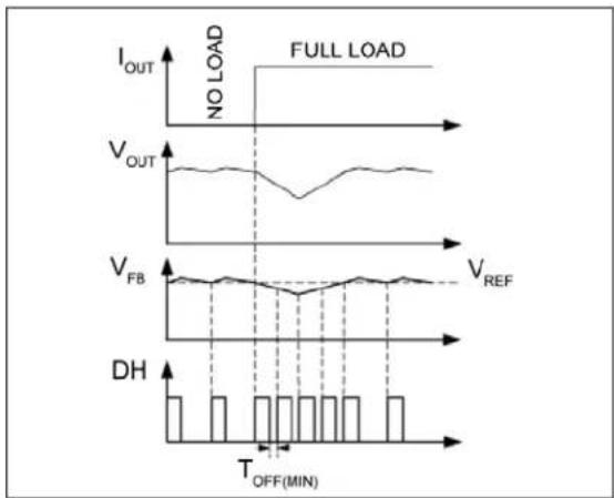
FIGURE 4-2: MIC2125/6 Load Transient Response
Unlike true current-mode control, the MIC2125/6 uses the output voltage ripple to trigger an ON-time period. In order to meet the stability requirements, the MIC2125/6 feedback voltage ripple should be in phase with the inductor current ripple and large enough to be sensed by the g_m amplifier. The recommended feedback voltage ripple is 20 mV \~ 100 mV over the full input voltage range. If a low-ESR output capacitor is selected, then the feedback voltage ripple may be too small to be sensed by the g_m amplifier. Also, the output voltage ripple and the feedback voltage ripple are not necessarily in phase with the inductor current ripple if the ESR of the output capacitor is very low. For these applications, ripple injection is required to ensure proper operation. Refer to the Ripple Injection section under Application Information for details about the ripple injection technique.
4.2 Discontinuous Conduction Mode (MIC2125 Only)
The MIC2125 operates in discontinuous conduction mode at light load. The MIC2125 has a zero crossing comparator (ZC detection) that monitors the inductor current by sensing the voltage drop across the low-side MOSFET during its ON-time. If the V_FB > 0.6V and the inductor current goes slightly negative, the MIC2125 turns off both the high-side and low-side MOSFETs. During this period, the efficiency is optimized by shutting down all the non-essential circuits and the load current is supplied by the output capacitor. The control circuitry wakes up when the feedback voltage falls below V_REF and triggers a t_ON pulse. Figure 4-3 shows the control loop timing in discontinuous conduction mode.

FIGURE 4-3: MIC2125 Control Loop Timing (Discontinuous Conduction Mode)
The typical no load supply current during discontinuous conduction mode is only about 340 A, allowing the MIC2125 to achieve high efficiency at light load operation.
4.3 Soft-Start
Soft-start reduces the power supply inrush current at startup by controlling the output voltage rise time. The MIC2125/6 implements an internal digital soft-start by ramping up the reference voltage V_REF from 0 to 100% in about 7 ms. Once the soft-start is completed, the related circuitry is disabled to reduce the current consumption.
4.4 Current Limit
The MIC2125/6 uses the low-side MOSFET R_DS(ON) to sense the inductor current.
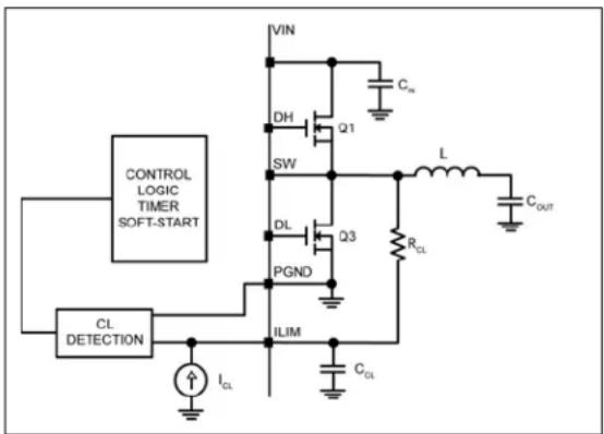
text_image
CONTROL LOGIC TIMER SOFT-START CL DETECTION VIN DH Q1 SW DL Q3 PGND ILIM ICL CCL L RCL COUTFIGURE 4-4: MIC2125/6 Current-Limiting Circuit
In each switching cycle of the MIC2125/6 converter, the inductor current is sensed by monitoring the voltage across the low-side MOSFET during the OFF period. An internal current source of 36 A generates a voltage across the external resistor R_CL . The I_LIM pin voltage V_(ILIM) is the sum of the voltage across the low side MOSFET and the voltage across the resistor ( V_CL ). The sensed voltage V_(ILIM) is compared with the power ground ( P_GND ) after a blanking time of 150 ns.
If the absolute value of the voltage drop across the low side MOSFET is greater than V_CL , the current limit event is triggered. Eight consecutive current limit events triggers hiccup mode. The hiccup sequence, including the soft-start, reduces the stress on the switching FETs and protects the load and supply from severe short conditions.
The current limit can be programmed by using Equation 4-3.
EQUATION 4-3:
| R_CL = (I_CLIM + _PP × 0.5) R_DSON(-) × V_OFFSETI_CL | |
| Where: | |
| I_CLIM | Desired Current Limit |
| _PP | Inductor Current Peak-to-Peak |
| R_DS(ON) | On-Resistance of Low-Side Power MOSFET |
| V_OFFSET | Current-Limit Comparator Offset (Typical Value is -4 mV per Table 1-1) |
| I_CL | Current-Limit Source Current (Typical Value is 36 μA, per Table 1-1) |
Because MOSFET R_DS(ON) varies from 30% to 40% with temperature, it is recommended to add a 50% margin to I_CL in the previous equation to avoid false current limiting due to increased MOSFET junction temperature rise. It is also recommended to connect the SW pin directly to the drain of the low-side MOSFET to accurately sense the MOSFET's R_DS(ON) .
4.5 Negative Current Limit (MIC2126 Only)
The MIC2126 implements negative current limit by sensing the SW voltage when the low-side FET is off. If the SW node voltage exceeds 12 mV typical, the device turns off the low-side FET until the next ON-time event is triggered. The negative current limit value is given by Equation 4-4.
EQUATION 4-4:
$$ I _ {N L I M} = \frac {1 2 m V}{R _ {D S O N (\quad)}} $$
Where:
$$ \begin{array}{c c} I _ {N L I M} & \text { Negative Current Limit } \ R _ {D S (O N)} & \text { On - Resistance of Low - Side Power } \ & \text { MOSFET } \end{array} $$
4.6 MOSFET Gate Drive
The MIC2125/6 high-side drive circuit is designed to switch an N-Channel MOSFET. Figure 4-1 shows a bootstrap circuit, consisting of a PMOS switch and C_BST . This circuit supplies energy to the high-side drive circuit. Capacitor C_BST is charged while the low-side MOSFET is on and the voltage on the SW pin is approximately 0V. When the high-side MOSFET driver is turned on, energy from C_BST is used to turn the MOSFET on. If the bias current of the high-side driver is less than 10 mA, a 0.1 μF capacitor is sufficient to hold the gate voltage within minimal droop, (i.e., _BST = 10 mA × 3.33 μs/0.1 μF = 333 mV ). A small resistor, RG in series with C_BST , can be used to slow down the turn-on time of the high-side N-channel MOSFET.
4.7 Overvoltage Protection
The MIC2125/6 includes the OVP feature to protect the load from overshoots due to input transients and output short to a high voltage. When the overvoltage condition is triggered, the converter turns off immediately to allow the output voltage to discharge. The MIC2125/6 power should be recycled to enable it again.
5.0 APPLICATION INFORMATION
5.1 Setting the Switching Frequency
The MIC2125/6 are adjustable-frequency, synchronous buck controllers featuring a unique adaptive ON-time control architecture. The switching frequency can be adjusted between 200 kHz and 750 kHz by changing the resistor divider network consisting of R19 and R20.

text_image
MIC2125/26 VDD/PVDD AGND VDD 5V 4.7µF VIN 2.2µF x3 R19 R20 VIN FREQ PGNDFIGURE 5-1: Switching Frequency Adjustment.
Equation 5-1 gives the estimated switching frequency.
EQUATION 5-1:

text_image
fSW(ADJ) fO×R20/R19R20+ Where: fO Switching Frequency when R19 is 100 kΩ and R20 is open. fO is typically 750 kHz.For more precise setting, it is recommended to use Figure 5-2.
line
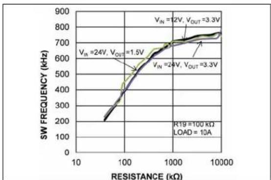
| RESISTANCE (kΩ) | SW FREQUENCY (kHz) | | --------------- | ------------------ | | 10 | 200 | | 100 | 500 | | 1000 | 700 | | 10000 | 800 |FIGURE 5-2: Switching Frequency vs. R20
5.2 MOSFET Selection
Voltage rating, on-resistance, and total gate charge are important parameters for MOSFET selection.
The voltage rating for the high-side and low-side MOSFETs are essentially equal to the power stage input voltage V_IN . A safety factor of 30% should be added to the V_IN(MAX) while selecting the voltage rating of the MOSFETs to account for voltage spikes due to circuit parasitic elements.
The power dissipated in the MOSFETs is the sum of conduction losses ( P_CONDUCTION ) and switching losses ( P_AC ).
EQUATION 5-2:
$$ P _ {S W} = P _ {C O N D U C T I O N} + P _ {A C} $$
EQUATION 5-3:
$$ P _ {C O N D U C T I O N} = I _ {S W (R M S)} ^ {2} \times R _ {D S (O N)} $$
Where:
$$ \begin{array}{l} R _ {D S (O N)} \quad \text { On - Resistance of the MOSFET } \ I _ {S W (R M S)} \quad R M S \text { current of the MOSFET } \ \end{array} $$
The total high-side MOSFET switching loss is:
EQUATION 5-4:
$$ P _ {A C} = 0. 5 \times V _ {I N} \times I _ {L O A D} \times (t _ {R} + t _ {F}) \times f _ {S W} $$
Where:
$$ \begin{array}{l} t _ {R} / t _ {F} \quad \text { Switching Transition Times } \ I _ {\text {LOAD}} \quad \text {Load Current} \ f _ {S W} \quad \text { Switching Frequency } \ \end{array} $$
Turn-on and turn-off transition times can be approximated by:
EQUATION 5-5:
$$ t _ {R} = \frac {Q _ {S W (H S)} \times \left(R _ {I I S D (P U L L - U P)} + R _ {H S (G A T E)}\right)}{V _ {D D} - V _ {T H}} $$
EQUATION 5-6:
$$ t _ {F} = \frac {Q _ {S W H S (\quad)} R _ {H S D P U L L U P - (\quad + (R _ {H S G A T E (\quad)})}}{V _ {T H}} $$
Where:
$$ R _ {H S D (P U L L - U P)} $$
High-Side Gate Driver Pull-Up Resistance
$$ R _ {H S D (P U L L - D O W N)} $$
High-Side Gate Driver Pull-Down Resistance
$$ R _ {H S (G A T E)} $$
High-Side MOSFET Gate Resistance
$$ Q _ {S W (H S)} $$
Switching Gate Charge of the High-Side MOSFET
$$ V _ {T H} $$
Gate Threshold Voltage
The high-side MOSFET switching losses increase with the switching frequency and the input voltage. The low-side MOSFET switching losses are negligible and can be ignored for these calculations.
5.3 Inductor Selection
Inductance value, saturation, and RMS currents are required to select the output inductor. The input and output voltages and the inductance value determine the peak-to-peak inductor ripple current. Larger peak-to-peak ripple current increases the power dissipation in the inductor and MOSFETs. Larger output ripple current also requires more output capacitance to smooth out the larger ripple current. Smaller peak-to-peak ripple current requires a larger inductance value and therefore a larger and more expensive inductor.
A good compromise between size, loss, and cost is to set the inductor ripple current to be equal to 40% of the maximum output current.
The inductance value is calculated by Equation 5-7.
EQUATION 5-7:
$$ L = \frac {V _ {O U T} V _ {I N M A X (} \times (V _ {O U T})}{V _ {I N M A X (} \times f _ {S W} \times 0 . 4 \times I _ {O U T M A X (}} \quad) $$
Where:
f_SW
Switching Frequency
0.4
Ratio of AC Ripple Current to DC Output Current
$$ V _ {\text { IN(MAX) }} $$
Maximum Power Stage Input Voltage
The peak-to-peak inductor current ripple is:
EQUATION 5-8:
$$ \Delta I _ {L (P P)} = \frac {V _ {O U T} - V _ {I N M A X (\times (V _ {O U T})}}{V _ {I N M A X (\times f _ {S W} \times L}} $$
The peak inductor current is equal to the average output current plus one half of the peak-to-peak inductor current ripple.
EQUATION 5-9:
$$ I _ {L P K (\quad)} I _ {\overline {{{O}}} U T M A X (\quad)} 0, \Delta k _ {L (P P)} $$
The saturation current rating is given by:
EQUATION 5-10:
$$ I _ {L (S A T)} = \frac {(R _ {C L} \times I _ {C L}) - V _ {O F F S E T}}{R _ {D S (O N)}} $$
Where:
$$ R _ {C L} $$
Current-Limit Resistor
$$ I _ {C L} $$
Current-Limit Source Current
$$ V _ {\text { OFFSET }} $$
Current-Limit Comparator Offset
$$ R _ {D S (O N)} $$
On-Resistance of Low-Side Power MOSFET
The RMS inductor current is used to calculate the I^2R losses in the inductor.
EQUATION 5-11:
$$ I _ {L (R M S)} = \sqrt {I _ {O U T M A X (\quad^ {2} + \frac {\Delta I _ {L (P P)} ^ {2}}{1 2})}} $$
Maximizing efficiency requires the proper selection of core material and minimizing the winding resistance. The high-frequency operation of the MIC2125/6 requires the use of ferrite materials. Lower cost iron powder cores may be used, but the increase in core loss reduces the efficiency of the power supply. This is especially noticeable at low output power. The winding resistance decreases efficiency at the higher output current levels. The winding resistance must be minimized, although this usually comes at the expense of a larger inductor. The power dissipated in the inductor is equal to the sum of the core and copper losses. At higher output loads, the core losses are usually insignificant and can be ignored. At lower output currents, the core losses can be significant. Core loss information is usually available from the magnetics vendor.
The amount of copper loss in the inductor is calculated by Equation 5-12:
EQUATION 5-12:
$$ P _ {I N D U C T O R (C U)} = I _ {L (R M S)} ^ {2} \times R _ {W I N D I N G} $$
5.4 Output Capacitor Selection
The type of the output capacitor is usually determined by its equivalent series resistance (ESR). Voltage and RMS current capability are two other important factors for selecting the output capacitor. Recommended capacitor types are ceramic, tantalum, low-ESR aluminum electrolytic, OS-CON, and POSCAP. The output capacitor's ESR is usually the main cause of the output ripple. The output capacitor ESR also affects the control loop from a stability point of view. The maximum value of ESR is calculated by Equation 5-13.
EQUATION 5-13:
$$ E S R _ {C _ {O U T}} \leq \frac {\Delta V _ {O U T P P (})}{\Delta J _ {L P P (})} $$
Where:
$$ \begin{array}{l l} \Delta V _ {\text { OUT(PP) }} & \text { Peak - to - Peak Output Voltage Ripple } \ \Delta I _ {\text { L(PP) }} & \text { Peak - to - Peak Inductor Current Ripple } \end{array} $$
The required output capacitance is calculated in Equation 5-14.
EQUATION 5-14:
$$ C _ {O U T} = \frac {\Delta I _ {L P P (\quad)}}{\Delta V _ {\mathcal {G} U T P P (\quad)} ^ {f} \times_ {S W} 8 \times} $$
Where:
$$ \begin{array}{l l} \mathrm{C} _ {\text {OUT}} & \text {Output Capacitance Value} \ \mathrm{f} _ {\text {SW}} & \text {Switching Frequency} \end{array} $$
As described in the Theory of Operation subsection of the Functional Description, the MIC2125/26 requires at least 20 mV peak-to-peak ripple at the FB pin to ensure that the g_m amplifier and the comparator behave properly. Also, the output voltage ripple should be in phase with the inductor current. Therefore, the output voltage ripple caused by the output capacitors value should be much smaller than the ripple caused by the output capacitor ESR. If low-ESR capacitors, such as ceramic capacitors, are selected as the output capacitors, a ripple injection method should be applied to provide the enough feedback voltage ripple. Refer to the Ripple Injection subsection for details.
The voltage rating of the capacitor should be twice the output voltage for a tantalum and 20% greater for aluminum electrolytic or OS-CON. The output capacitor RMS current is calculated in Equation 5-15.
EQUATION 5-15:
$$ I _ {C _ {O U T R M S (}} = \frac {\Delta I _ {L P P}}{\sqrt {1 2}} (\quad) $$
The power dissipated in the output capacitor is:
EQUATION 5-16:
$$ P _ {D I S S C O U T} = I _ {\text { GOUT(RMS) }} ^ {2} \times E S R _ {C O U T} $$
5.5 Input Capacitor Selection
The input capacitor reduces peak current drawn from the power supply and reduces noise and voltage ripple on the input. The input voltage ripple depends on the input capacitance and ESR. The input capacitance and ESR values are calculated by using Equation 5-17 and Equation 5-18.
EQUATION 5-17:
$$ C _ {I N} = \frac {I _ {O U T} \times D \times (1 - D)}{\eta \times \Delta V _ {I N (C)} \times f _ {S W}} $$
Where:
$$ \begin{array}{c c} I _ {O U T} & \text { Load Current } \ \eta & \text { Power Conversion Efficiency } \ \Delta V _ {I N (C)} & \text { Input Ripple Due to Capacitance Value } \end{array} $$
EQUATION 5-18:
$$ E S R _ {C I N} = \frac {\Delta V _ {I N (E S R)}}{I _ {L (P K)}} $$
Where:
$$ \begin{array}{l l} \Delta V _ {I N (E S R)} & \text {Input Ripple Due to Capacitor ESR} \ & \text {Value} \ L _ {(P K)} & \text {Peak Inductor Current} \end{array} $$
The input capacitor should be qualified for ripple current rating and voltage rating. The RMS value of the input capacitor current is determined at the maximum output current. Assuming the peak-to-peak inductor current ripple is low:
EQUATION 5-19:
$$ I _ {C I N (R M S)} \approx I _ {O U T (M A X)} \times \sqrt {D \times (1 - D)} $$
The power dissipated in the input capacitor is:
EQUATION 5-20:
$$ P _ {D I S S (C I N)} = I _ {C I N (R M S)} ^ {2} \times E S R _ {C I N} $$
5.6 Output Voltage Setting
The MIC2125/26 requires two resistors to set the output voltage, as shown in Figure 5-3.

text_image
gm AMP - + VREF - FB R1 R2FIGURE 5-3: Voltage-Divider Configuration.
The output voltage is determined by Equation 5-21:
EQUATION 5-21:
| V_OUT | V_FB × = (1 + 1R2) | |
| Where: | ||
| V_FB | 0.6V | |
A typical value of R1 can be in the range of 3 kΩ and 15 kΩ. If R1 is too large, it may allow noise to be introduced into the voltage feedback loop. If R1 is too small in value, it will decrease the efficiency of the power supply, especially at light loads. Once R1 is selected, R2 can be calculated using Equation 5-22.
EQUATION 5-22:
$$ R 2 = \frac {V _ {F B} R 1 \times}{V _ {O U T} - V _ {F B}} $$
5.7 Output Overvoltage Limit Setting
The output overvoltage limit should be typically 20% higher than the nominal output voltage. Set the OVP limit by connecting a resistor divider from the output to ground as shown in Figure 5-4.

text_image
+ - VREF OVP R1 R2FIGURE 5-4: OVP Voltage-Divider Configuration.
Choose R2 in the range of 10 kΩ to 49.9 kΩ and calculate R1 using Equation 5-23.
EQUATION 5-23:
$$ R 1 R \geqslant \left[ \frac {V _ {O V P}}{0 . 6} - 1 \right] $$
5.8 Ripple Injection
The V_FB ripple required for proper operation of the MIC2125/6 g_m amplifier and comparator is 20 mV to 100 mV. However, the output voltage ripple is generally designed as 1% to 2% of the output voltage. For low output voltages, such as a 1V, the output voltage ripple is only 10 mV to 20 mV, and the feedback voltage ripple is less than 20 mV. If the feedback voltage ripple is so small that the g_m amplifier and comparator cannot sense it, then the MIC2125/6 loses control and the output voltage is not regulated. In order to have sufficient V_FB ripple, a ripple injection method should be applied for low output voltage ripple applications.
The applications are divided into three situations according to the amount of the feedback voltage ripple:
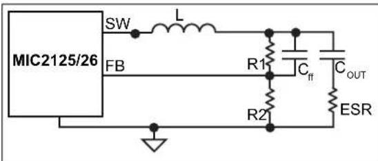
- Enough ripple at the feedback voltage due to the large ESR of the output capacitors (Figure 5-5). The converter is stable without any ripple injection.

text_image
MIC2125/26 SW L FB R1 COUT ESR R2FIGURE 5-5: Enough Ripple at FB.
The feedback voltage ripple is:
EQUATION 5-24:
$$ \Delta V _ {F B P P (\quad)} \frac {R 2}{\bar {R} 1 R 2 +} \times E \delta R _ {C _ {O U T}} \quad \Delta \times_ {L P P (\quad)} $$
Where:
I_L(PP) Peak-to-Peak Value of the Inductor Current Ripple
- Inadequate ripple at the feedback voltage due to the small ESR of the output capacitors.
The output voltage ripple is fed into the FB pin through a feed-forward capacitor, C_ff in this situation, as shown in Figure 5-7. The typical C_ff value is between 1 nF and 100 nF.
text_image
MIC2125/26 SW L FB R1 Cff COUT R2 ESRFIGURE 5-6: Inadequate Ripple at FB.
With the feed-forward capacitor, the feedback voltage ripple is very close to the output voltage ripple.
EQUATION 5-25:
$$ \Delta V _ {F B P P (\quad)} E \mathbf {S} R \quad \Delta k _ {L P P (\quad)} $$
- Virtually no ripple at the FB pin voltage due to the very low ESR of the output capacitors.
Therefore, additional ripple is injected into the FB pin from the switching node SW via a resistor R_INJ and a capacitor C_INJ , as shown in Figure 5-7.
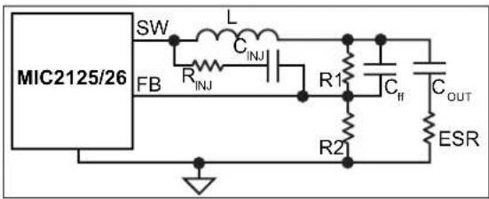
text_image
MIC2125/26 SW L C_INJ FB R_INJ R1 C_fH C_OUT ESRFIGURE 5-7: Invisible Ripple at FB.
The process of sizing the ripple injection resistor and capacitors is as follows.
- S e I e_IN as 100 nF, which can be considered as short for a wide range of the frequencies.
- S e I e_ff to feeC all output ripples into the feedback pin. Typical choice of C_ff is 0.47 nF to 47 nF, if R1 and R2 are in the kΩ range. The C_ff value can be calculated using Equation 5-26:
EQUATION 5-26:
$$ C _ {f f} \gg \frac {1}{R _ {P}} \times \left(\frac {t _ {S} \times V _ {I N} \times D \times (1 - D)}{\left(V _ {I N} \times D \times (1 - D)\right) - \Delta V _ {F B P P (}}\right) $$
Where:
V_IN Power Stage Input Voltage
D Duty Cycle t_S 1/ f_SW R_P (R1//R2// R_IN ) F_B(PP) Feedback Rip
- S e l eINS according to Equation 5-27.
EQUATION 5-27:
$$ R _ {I N J} = \frac {1}{C _ {f f}} \times \left(\frac {V _ {I N} \times D \times (1 - D)}{\Delta V _ {F B P P} (\times f _ {S W})}\right) $$
6.0 PCB LAYOUT GUIDELINES
PCB layout is critical to achieve reliable, stable and efficient performance. The following guidelines should be followed to ensure proper operation of the MIC2125/26 converter.
6.1 IC
- The ceramic bypass capacitors which are connected to the V_DD and P_VDD pins must be located right at the IC. Use wide traces to connect to the V_DD , P_VDD and A_GND , P_GND pins respectively.
- The signal ground pin (A_GND) must be connected directly to the ground planes.
- Place the IC close to the point-of-load (POL).
- Signal and power grounds should be kept separate and connected at only one location.
6.2 Input Capacitor
- Place the input ceramic capacitors as close as possible to the MOSFETs.
- Place several vias to the ground plane close to the input capacitor ground terminal.
6.3 Inductor
- Keep the inductor connection to the switch node (SW) short.
- Do not route any digital lines underneath or close to the inductor.
- Keep the switch node (SW) away from the feedback (FB) pin.
- The SW pin should be connected directly to the drain of the low-side MOSFET to accurately sense the voltage across the low-side MOSFET.
6.4 Output Capacitor
- Use a copper plane to connect the output capacitor ground terminal to the input capacitor ground terminal.
- The feedback trace should be separate from the power trace and connected as close as possible to the output capacitor. Sensing a long high-current load trace can degrade the DC load regulation.
6.5 MOSFETs
- MOSFET gate drive traces must be short. The ground plane should be the connection between the MOSFET source and P_GND .
- Choose a low-side MOSFET with a high C_GS/C_GD ratio and a low internal gate resistance to minimize the effect of d_v/d_t inducted turn-on.
- Use a 4.5V V _GS rated MOSFET. Its higher gate threshold voltage is more immune to glitches than a 2.5V or 3.3V rated MOSFET.
For more information about the Evaluation board layout, please contact Microchip sales.
7.0 PACKAGING INFORMATION
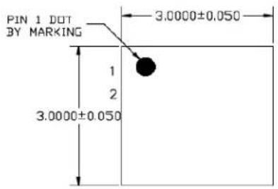
16-Lead QFN 3 mm x 3 mm Package Outline and Recommended Land Pattern
Note: For the most current package drawings, please see the Microchip Packaging Specification located at http://www.microchip.com/packaging
TITLE
16 LEAD QFN 3x3mm PACKAGE OUTLINE & RECOMMENDED LAND PATTERN
DRAWING # QFN33-16LD-PL-1 UNIT MM
text_image
PIN 1 DOT BY MARKING 3.0000±0.050 1 2 3.0000±0.050TOP VIEW NOTE 1, 2, 3
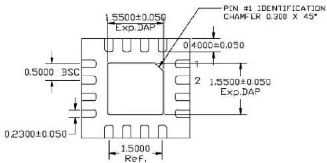
text_image
1.5500±0.050 Exp.DAP PIN #1 IDENTIFICATION CHAMFER 0.300 X 45° 0.5000 BSC 0.2300±0.050 1.5500±0.050 Exp.DAP 1.5000 Ref.BOTTOM VIEW NOTE 1, 2, 3
text_image
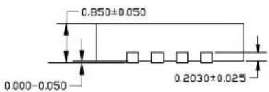
0.850±0.050 0.000-0.050 0.2030±0.025SIDE VIEW NOTE: 1, 2, 3
NOTE:
- MAX PACKAGE WARPAGE IS 0.05 MM
- MAX ALLOWABLE BURR [S 0.076 MM IN ALL DIRECTIONS
- PIN #1 IS ON TOP WILL BE LASER MARKED
- RED CIRCLE IN LAND PATTERN INDICATE THERMAL VIA. SIZE SHOULD BE 0.30-0.35 MM
IN DIAMETER AND SHOULD BE CONNECTED TO GND FOR MAX THERMAL PERFORMANCE - GREEN RECTANGLES (SHADED AREA) indicate SOLDER STENCIL OPENING ON EXPOSED
PAD AREA. SIZE SHOULD BE 0.60×0.60 MM IN SIZE, 0.20 MM SPACING.
Note: For the most current package drawings, please see the Microchip Packaging Specification located at http://www.microchip.com/packaging
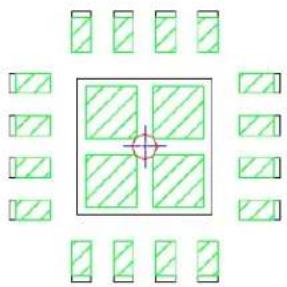
POD-Land Pattern drawing # QFN33-16LD-PL-1
RECOMMENDED LAND PATTERN
NOTE: 4, 5
natural_image
Geometric diagram with green hatched squares arranged around a central square, no text or symbols presentSTACKED-UP
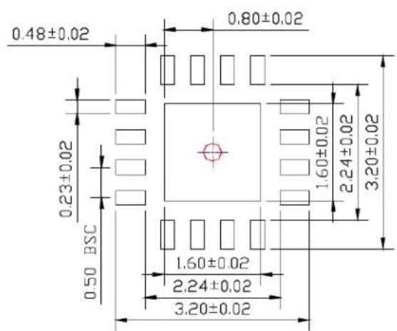
text_image
0.48±0.02 0.80±0.02 0.23±0.02 1.60±0.02 2.24±0.02 3.20±0.02 0.50 BSC 1.60±0.02 2.24±0.02 3.20±0.02EXPOSED METAL TRACE

text_image
0.70±0.02 0.40±0.02 0.10±0.02 0.23±0.02 1.40±0.02 2.24±0.02 3.04±0.02 2.24±0.02 3.04±0.02Revision A (November 2015)
• Original Conversion of this Document.
Revision B (December 2015)
- Corrected the erroneous listing of the MIC2126 example with a 64LD package. Replaced with correct 16LD package information.
NOTES:
PRODUCT IDENTIFICATION SYSTEM
To order or obtain information, e.g., on pricing or delivery, contact your local Microchip representative or sales office.

Device: MIC2125: 28V, Synchronous Buck Controller featuring Adaptive On-Time Control with HyperLight Load MIC2126: 28V, Synchronous Buck Controller featuring Adaptive On-Time Control with HyperSpeed Control
Temperature: Y = -40^ to +125^
Package: ML = 16-Pin 3 mm x 3 mm QFN
Examples:
a) MIC2125YML: 28V, Synchronous Buck
Controller featuring Adaptive On-Time Control with HyperLight Load, -40°C to +125°C junction temperature range, 16LD QFN
b) MIC2126YML: 28V, Synchronous Buck Controller featuring Adaptive On-Time Control with Hyper Speed Control, -40°C to +125°C junction temperature range, 16LD QFN
NOTES:
Note the following details of the code protection feature on Microchip devices:
• Microchip products meet the specification contained in their particular Microchip Data Sheet.
- Microchip believes that its family of products is one of the most secure families of its kind on the market today, when used in the intended manner and under normal conditions.
- There are dishonest and possibly illegal methods used to breach the code protection feature. All of these methods, to our knowledge, require using the Microchip products in a manner outside the operating specifications contained in Microchip's Data Sheets. Most likely, the person doing so is engaged in theft of intellectual property.
• Microchip is willing to work with the customer who is concerned about the integrity of their code.
- Neither Microchip nor any other semiconductor manufacturer can guarantee the security of their code. Code protection does not mean that we are guaranteeing the product as "unbreakable."
Code protection is constantly evolving. We at Microchip are committed to continuously improving the code protection features of our products. Attempts to break Microchip's code protection feature may be a violation of the Digital Millennium Copyright Act. If such acts allow unauthorized access to your software or other copyrighted work, you may have a right to sue for relief under that Act.
Information contained in this publication regarding device applications and the like is provided only for your convenience and may be superseded by updates. It is your responsibility to ensure that your application meets with your specifications. MICROCHIP MAKES NO REPRESENTATIONS OR WARRANTIES OF ANY KIND WHETHER EXPRESS OR IMPLIED, WRITTEN OR ORAL, STATUTORY OR OTHERWISE, RELATED TO THE INFORMATION, INCLUDING BUT NOT LIMITED TO ITS CONDITION, QUALITY, PERFORMANCE, MERCHANTABILITY OR FITNESS FOR PURPOSE. Microchip disclaims all liability arising from this information and its use. Use of Microchip devices in life support and/or safety applications is entirely at the buyer's risk, and the buyer agrees to defend, indemnify and hold harmless Microchip from any and all damages, claims, suits, or expenses resulting from such use. No licenses are conveyed, implicitly or otherwise, under any Microchip intellectual property rights unless otherwise stated.
QUALITY MANAGEMENT SYSTEM CERTIFIED BY DNV = ISO/TS 16949=
Trademarks
The Microchip name and logo, the Microchip logo, dsPIC, FlashFlex, flexPWR, JukeBlox, KEELOQ, KEELOQ logo, Kleer, LANCheck, MediaLB, MOST, MOST logo, MPLAB, OptoLyzer, PIC, PICSTART, PIC ^32 logo, RightTouch, SpyNIC, SST, SST Logo, SuperFlash and UNI/O are registered trademarks of Microchip Technology Incorporated in the U.S.A. and other countries.
The Embedded Control Solutions Company and mTouch are registered trademarks of Microchip Technology Incorporated in the U.S.A.
Analog-for-the-Digital Age, BodyCom, chipKIT, chipKIT logo, CodeGuard, dsPICDEM, dsPICDEM.net, ECAN, In-Circuit Serial Programming, ICSP, Inter-Chip Connectivity, KleerNet, KleerNet logo, MiWi, motorBench, MPASM, MPF, MPLAB Certified logo, MPLIB, MPLINK, MultiTRAK, NetDetach, Omniscient Code Generation, PICDEM, PICDEM.net, PICkit, PICtail, RightTouch logo, REAL ICE, SQI, Serial Quad I/O, Total Endurance, TSHARC, USBCheck, VariSense, ViewSpan, WiperLock, Wireless DNA, and ZENA are trademarks of Microchip Technology Incorporated in the U.S.A. and other countries.
SQTP is a service mark of Microchip Technology Incorporated in the U.S.A.
Silicon Storage Technology is a registered trademark of Microchip Technology Inc. in other countries.
GestIC is a registered trademark of Microchip Technology Germany II GmbH & Co. KG, a subsidiary of Microchip Technology Inc., in other countries.
All other trademarks mentioned herein are property of their respective companies.
© 2015, Microchip Technology Incorporated, Printed in the U.S.A., All Rights Reserved.
ISBN: 978-1-5224-0039-4
Microchip received ISO/TS-16949:2009 certification for its worldwide headquarters, design and wafer fabrication facilities in Chandler and Tempe, Arizona; Gresham, Oregon and design centers in California and India. The Company's quality system processes and procedures are for its PIC® MCUs and dsPIC® DSCs, KEELoo® code hopping devices, Serial EEPROMs, microperipherals, nonvolatile memory and analog products. In addition, Microchip's quality system for the design and manufacture of development systems is ISO 9001:2000 certified.
Worldwide Sales and Service
AMERICAS
Corporate Office
2355 West Chandler Blvd.
Chandler, AZ 85224-6199
Tel: 480-792-7200
Fax: 480-792-7277
Technical Support:
http://www.microchip.com/
support
Web Address:
www.microchip.com
Atlanta
Duluth, GA
Tel: 678-957-9614
Fax: 678-957-1455
Austin, TX
Tel: 512-257-3370
Boston
Westborough, MA
Tel: 774-760-0087
Fax: 774-760-0088
Chicago
Itasca, IL
Tel: 630-285-0071
Fax: 630-285-0075
Cleveland
Independence, OH
Tel: 216-447-0464
Fax: 216-447-0643
Dallas
Addison, TX
Tel: 972-818-7423
Fax: 972-818-2924
Detroit
Novi, MI
Tel: 248-848-4000
Houston, TX
Tel: 281-894-5983
Indianapolis
Noblesville, IN
Tel: 317-773-8323
Fax: 317-773-5453
Los Angeles
Mission Viejo, CA
Tel: 949-462-9523
Fax: 949-462-9608
New York, NY
Tel: 631-435-6000
San Jose, CA
Tel: 408-735-9110
Canada - Toronto
Tel: 905-673-0699
Fax: 905-673-6509
ASIA/PACIFIC
Asia Pacific Office
Suites 3707-14, 37th Floor
Tower 6, The Gateway
Harbour City, Kowloon
Hong Kong
Tel: 852-2943-5100
Fax: 852-2401-3431
Australia - Sydney
Tel: 61-2-9868-6733
Fax: 61-2-9868-6755
China - Beijing
Tel: 86-10-8569-7000
Fax: 86-10-8528-2104
China - Chengdu
Tel: 86-28-8665-5511
Fax: 86-28-8665-7889
China - Chongqing
Tel: 86-23-8980-9588
Fax: 86-23-8980-9500
China - Dongguan
Tel: 86-769-8702-9880
China - Hangzhou
Tel: 86-571-8792-8115
Fax: 86-571-8792-8116
China - Hong Kong SAR
Tel: 852-2943-5100
Fax: 852-2401-3431
China - Nanjing
Tel: 86-25-8473-2460
Fax: 86-25-8473-2470
China - Qingdao
Tel: 86-532-8502-7355
Fax: 86-532-8502-7205
China - Shanghai
Tel: 86-21-5407-5533
Fax: 86-21-5407-5066
China - Shenyang
Tel: 86-24-2334-2829
Fax: 86-24-2334-2393
China - Shenzhen
Tel: 86-755-8864-2200
Fax: 86-755-8203-1760
China - Wuhan
Tel: 86-27-5980-5300
Fax: 86-27-5980-5118
China - Xian
Tel: 86-29-8833-7252
Fax: 86-29-8833-7256
ASIA/PACIFIC
China - Xiamen
Tel: 86-592-2388138
Fax: 86-592-2388130
China - Zhuhai
Tel: 86-756-3210040
Fax: 86-756-3210049
India - Bangalore
Tel: 91-80-3090-4444
Fax: 91-80-3090-4123
India - New Delhi
Tel: 91-11-4160-8631
Fax: 91-11-4160-8632
India - Pune
Tel: 91-20-3019-1500
Japan - Osaka
Tel: 81-6-6152-7160
Fax: 81-6-6152-9310
Japan - Tokyo
Tel: 81-3-6880-3770
Fax: 81-3-6880-3771
Korea - Daegu
Tel: 82-53-744-4301
Fax: 82-53-744-4302
Korea - Seoul
Tel: 82-2-554-7200
Fax: 82-2-558-5932 or
82-2-558-5934
Malaysia - Kuala Lumpur
Tel: 60-3-6201-9857
Fax: 60-3-6201-9859
Malaysia - Penang
Tel: 60-4-227-8870
Fax: 60-4-227-4068
Philippines - Manila
Tel: 63-2-634-9065
Fax: 63-2-634-9069
Singapore
Tel: 65-6334-8870
Fax: 65-6334-8850
Taiwan - Hsin Chu
Tel: 886-3-5778-366
Fax: 886-3-5770-955
Taiwan - Kaohsiung
Tel: 886-7-213-7828
Taiwan - Taipei
Tel: 886-2-2508-8600
Fax: 886-2-2508-0102
Thailand - Bangkok
Tel: 66-2-694-1351
Fax: 66-2-694-1350
EUROPE
Austria - Wels
Tel: 43-7242-2244-39
Fax: 43-7242-2244-393
Denmark - Copenhagen
Tel: 45-4450-2828
Fax: 45-4485-2829
France - Paris
Tel: 33-1-69-53-63-20
Fax: 33-1-69-30-90-79
Germany - Dusseldorf
Tel: 49-2129-3766400
Germany - Karlsruhe
Tel: 49-721-625370
Germany - Munich
Tel: 49-89-627-144-0
Fax: 49-89-627-144-44
Italy - Milan
Tel: 39-0331-742611
Fax: 39-0331-466781
Italy - Venice
Tel: 39-049-7625286
Netherlands - Drunen
Tel: 31-416-690399
Fax: 31-416-690340
Poland - Warsaw
Tel: 48-22-3325737
Spain - Madrid
Tel: 34-91-708-08-90
Fax: 34-91-708-08-91
Sweden - Stockholm
Tel: 46-8-5090-4654
UK - Wokingham
Tel: 44-118-921-5800
Fax: 44-118-921-5820