ATSAM4C8 - Microcontroller Microchip - Free user manual and instructions
Find the device manual for free ATSAM4C8 Microchip in PDF.

User questions about ATSAM4C8 Microchip
0 question about this device. Answer the ones you know or ask your own.
Ask a new question about this device
Download the instructions for your Microcontroller in PDF format for free! Find your manual ATSAM4C8 - Microchip and take your electronic device back in hand. On this page are published all the documents necessary for the use of your device. ATSAM4C8 by Microchip.
USER MANUAL ATSAM4C8 Microchip
natural_image
Blue printed circuit board with various electronic components and connectors (no visible text or symbols)Introduction
The ATSAM4C-EK is an evaluation kit for the 32-bit ARM® Cortex®-M4 SAM4C microcontroller from Atmel® Corporation.
The ATSAM4C-EK can be used with the following SAM4C series microcontrollers:
SAM4C16C
SAM4C8C
This document describes the kit contents and architecture, and provides guidelines on how to use the kit.
Contents
- Board
• One SAM4C Evaluation Kit Board (EK)
Power Supply
- One universal input AC/DC power supply with US, Europe and UK plug adapters
• One 3V Lithium Battery type CR1225
Cables
• One serial RS232 cable
• One micro A/B-type USB cable
- Welcome letter
Reference documents
• Atmel SAM4C Series Datasheet
(http://www.atmel.com/images/atmel_11102_smartenergy_sam4c16-c8_datasheet.pdf)
Table of Contents
Introduction....1
Contents 2
Reference documents....2
Table of Contents 3
1. Evaluation Kit Specifications .... 4
1.1 Electrostatic Warning 4
1.2 Battery....4
1.3 Recovery Procedure 4
2. Power Up 5
2.1 Power up the Board 5
2.2 Sample Code and Technical Support 5
3. Evaluation Kit Hardware 6
3.1 Overview....6
3.2 Equipment List 7
3.3 Function Blocks....9
3.4 Embedded Memories 12
3.5 Communication Interfaces 14
3.6 Debug Interfaces....15
3.7 Extend Interfaces 16
3.8 LCD Display 18
3.9 Analog I/O....21
3.10 CryptoAuthentication (optional).... 22
3.11 LEDs and Buttons....23
3.12 Miscellaneous I/O 24
3.13 Metrology Core Serial Interface 24
3.14 PIO Usage 25
3.15 Connectors 28
4. Evaluation Kit Firmware Demonstration 35
4.1 ATSAM4C-EK Default Application 35
4.2 Measuring the Backup mode current consumption on VDDBU ..... 35
5. ATSAM4C-EK Design Files 37
5.1 ATSAM4C-EK Schematics 37
5.2 ATSAM4C-EK Layout 45
6. Revision History 53
1. Evaluation Kit Specifications
Table 1-1. Evaluation Kit Specifications
| Characteristic Specifications | |
| PCB 6 layers, 140 mm x 100 mm | |
| PCB Material Standard FR4 in 1.6 mm thickness | |
| Clock Speed | Crystal 8 MHzPiezoelectric Ceramic Resonator 8.192 MHz32.768 kHz external clock |
| Ports | RS232RS485USB |
| Memory | TWI EEPROMSerial Data Flash |
| Board Supply Voltage | 5V DC from main connector power supply5V DC from USB3V Battery for Backup and RTC |
| ROHS Compliant | |
| CE and FCC Part 15 status Compliant |
1.1 Electrostatic Warning
Warning: ESD-Sensitive Electronic Equipment!

The evaluation kit is shipped in a protective anti-static package. The board system must not be subjected to high electrostatic discharge.
We strongly recommend using a grounding strap or similar ESD protective device when handling the board in hostile ESD environments (offices with synthetic carpet, for example). Avoid touching the component pins or any other metallic element on the board.
1.2 Battery
The ATSAM4C-EK ships with a 3V coin battery. This battery is not required for the board to start up as long as Jumper JP8 is closed.
The coin battery is provided for user convenience in case the user would like to exercise the date and time backup function of the SAM4C devices when the board is switched off.
1.3 Recovery Procedure
The demo software is stored in internal Flash memory. If the content of the internal Flash has been erased, it can be reprogrammed recovered to the state as it was when shipped by Atmel using Atmel SAM-BA ^® In-system Programmer available on the Atmel website (www.atmel.com/tools/atmelsam-bain-systemprogrammer.aspx). The binary file of the demo software is available on the Atmel website in the ATSAM4C-EK Evaluation Kit Section (http://www.atmel.com/tools/SAM4C-EK.aspx).
2. Power Up
2.1 Power up the Board
Unpack the board taking care to avoid electrostatic discharge. Unpack the power supply, select the right power plug adapter corresponding to that of your country, and insert it in the power supply.
Connect the power supply DC connector to the board and plug the power supply to an AC power plug. The board LCD should light up and display a graphic demo program.
2.2 Sample Code and Technical Support
After boot up, designers can run sample code or their own application, on the development kit. Users can download sample code and get technical support from the Atmel website. The ATSAM4C-EK is supported by the Atmel Software Framework (ASF) (http://www.atmel.com/tools/AVRSOFTWAREFRAMEWORK.aspx).
3. Evaluation Kit Hardware
3.1 Overview
This section introduces the Atmel SAM4C Evaluation Kit design. It introduces system-level concepts, such as power distribution, memory, and interface assignments.
The Atmel SAM4C16C and SAM4C8C microcontrollers are system-on-chip solutions for smart energy applications, built around two high-performance 32-bit ARM Cortex-M4 RISC processors. These devices operate at a maximum speed of 120MHz and feature up to 1 Mbyte of embedded Flash, 152 Kbytes of SRAM and on-chip cache for each core.
The dual ARM Cortex-M4 architecture allows for integration of application layer, communications layers and security functions in a single device, with the ability to extend program and data memory via a 16-bit external bus interface. The peripheral set includes an advanced cryptographic engine, two anti-tamper pins with time-stamping function, floating point unit (FPU), five USARTs, two UARTs, two TWIs, up to seven SPIs, as well as a PWM timer, two 3-channel general-purpose 16-bit timers, temperature compensable low-power RTC running on backup area down to 0.5 A , and a 50× 6 segmented LCD controller.
The SAM4C series is a scalable platform providing, alongside Atmel's industry leading SAM4 standard microcontrollers, unprecedented cost structure, performance and flexibility to smart meter designers worldwide.
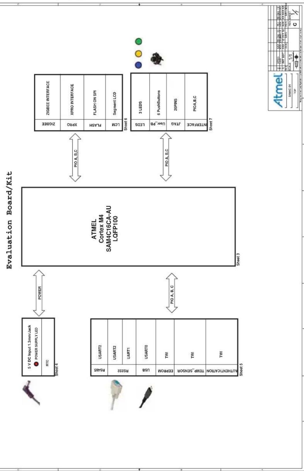
Figure 3-1. ATSAM4C-EK Board Architecture
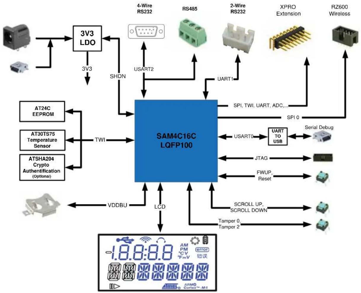
flowchart
graph TD
    A["3V3 LDO"] -->|3V3| B["SAM4C16C LQFP100"]
    C["4-Wire RS232"] -->|SHDN| B
    D["RS485"] -->|USART2| B
    E["2-Wire RS232"] -->|UART1| B
    F["XPRO Extension"] -->|SPI, TWI, UART, ADC...| B
    G["RZ600 Wireless"] -->|SPI 0| B
    H["AT24C EEPROM"] --> I["TWI"]
    J["AT30TS75 Temperature Sensor"] --> I
    K["ATSHA204 Crypto Authentication (Optional)"] --> I
    I --> L["VDDBU"]
    M["ATD"] --> N["LCD"]
    O["SCROLL UP, SCROLL DOWN"] --> P["Tamper 0, Tamper 2"]
    Q["Serial Debug"] --> R["UART TO USB"]
    S["JTAG"] --> T["FFWUP, Reset"]
    U["1.8:8:8 AM PM CV error"] --> V["ARM Cortex™-M4"]
3.2 Equipment List
3.2.1 Features List
The CM board components are listed as follows:
• CPU SAM4C with its embedded resources
- 8 MHz and 32.768 kHz Quartz Crystal, SMB connector for external source
- Main regulator 5V/3.3V with red LED indicator
• 1 Lithium Coin Cell Battery
- Main board with:
• 1 custom segmented LCD
• 1 shared interface RS232 / RS485
• 1 Serial data Flash SPI
• 1 Two-Wire Serial EEPROM
• 1 Two-Wire Temperature Sensor
• 1 Two-Wire CryptoAuthentication™ Memory (optional)
- Debug solution:
• 2 peripheral Input/Output extension connectors HE10 (PIO A, B)
• 1 peripheral Input/Output extension connector HE10 (PIO Sense)
• 1 JTAG/ICE interface
• 1 UART/USB bridge Device Communication interface
Analog
• 1 Analog 3V reference
• 1 Potentiometer connected on ADC input
- Buttons
- 4 system push buttons: Reset, Force Wake-Up, Tamper 0, Tamper 2
- 2 user push buttons: Scroll Up and Scroll Down
• LEDs
- 1 amber LED
- 1 blue LED
- 1 green LED
3.2.2 Interface Connection
The ATSAM4C-EK board includes hardware interfaces such as:
1 RS232/RS485 (USART0 RX, TX, RTS, CTS) connected to:
• 9-way male D-type RS232 connector
- 3-pin connector
• 1 JTAG/SWD 20-pin IDC connector
• 1 USB 5-pin type Micro AB connector (bridge UART)
3 PIOs connected to HE10 connectors
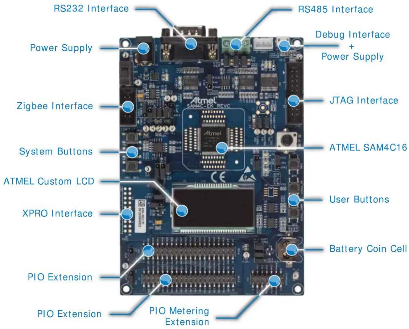
Figure 3-2. Annotated ATSAM4C-EK Board Layout
text_image
RS232 Interface Power Supply Zigbee Interface System Buttons ATMEL Custom LCD XPRO Interface PIO Extension PIO Extension RS485 Interface Debug Interface + Power Supply JTAG Interface ATMEL SAM4C16 User Buttons Battery Coin Cell PIO Metering Extension3.3 Function Blocks
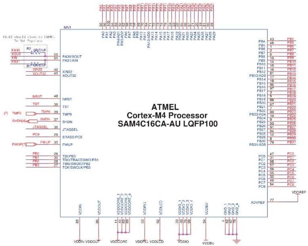
3.3.1 Processor
The ATSAM4C-EK board is equipped with a SAM4C16 device in an LQFP100 package.
Figure 3-3. SAM4C Processor
other
ATMEL Cortex-M4 Processor SAM4C16CA-AU LQFP100 Pin 1: VDDIN Pin 2: VDDOUT Pin 3: VDDCORE Pin 4: VDDPLL Pin 5: VDDIO Pin 6: VDDBU Pin 7: GND_1 Pin 8: GND_2 Pin 9: GND_3 Pin 10: GND_4 Pin 11: GND_5 Pin 12: GND_6 Pin 13: GND_7 Pin 14: GND_8 Pin 15: GND_9 Pin 16: GND_10 Pin 17: GND_11 Pin 18: GND_12 Pin 19: GND_13 Pin 20: GND_14 Pin 21: GND_15 Pin 22: GND_16 Pin 23: GND_17 Pin 24: GND_18 Pin 25: GND_19 Pin 26: GND_20 Pin 27: GND_21 Pin 28: GND_22 Pin 29: GND_23 Pin 30: GND_24 Pin 31: GND_25 Pin 32: GND_26 Pin 33: GND_27 Pin 34: GND_28 Pin 35: GND_29 Pin 36: GND_30 Pin 37: GND_31 Pin 38: GND_32 Pin 39: GND_33 Pin 40: GND_34 Pin 41: GND_35 Pin 42: GND_36 Pin 43: GND_37 Pin 44: GND_38 Pin 45: GND_39 Pin 46: GND_40 Pin 47: GND_41 Pin 48: GND_42 Pin 49: GND_43 Pin 50: GND_44 Pin 51: GND_45 Pin 52: GND_46 Pin 53: GND_47 Pin 54: GND_48 Pin 55: GND_49 Pin 56: GND_50 Pin 57: GND_51 Pin 58: GND_52 Pin 59: GND_53 Pin 60: GND_54 Pin 61: GND_55 Pin 62: GND_56 Pin 63: GND_57 Pin 64: GND_58 Pin 65: GND_59 Pin 66: GND_60 Pin 67: GND_61 Pin 68: GND_62 Pin 69: GND_63 Pin 70: GND_64 Pin 71: GND_65 Pin 72: GND_66 Pin 73: GND_67 Pin 74: GND_68 Pin 75: GND_69 Pin 76: GND_70 Pin 77: GND_71 Pin 78: GND_72 Pin 79: GND_73 Pin 80: GND_74 Pin 81: GND_75 Pin 82: GND_76 Pin 83: GND_77 Pin 84: GND_78 Pin 85: VDDOUT Pin 86: VDDOUT Pin 87: VDDOUT Pin 88: VDDOUT Pin 89: VDDOUT Pin 90: VDDOUT Pin 91: VDDOUT Pin 92: VDDOUT Pin 93: VDDOUT Pin 94: VDDOUT Pin 95: VDDOUT Pin 96: VDDOUT Pin 97: VDDOUT Pin 98: VDDOUT Pin 99: VDDOUT Pin 100: VDDOUT3.3.2 Clock Distribution
The ATSAM4C-EK board includes two clock systems (see Table 3-1 and Figure 3-4).
Table 3-1. Components Clock System
| Qty Description Component Assignment | |
| 1 Crystal for Internal Clock 8 MHz Y2 | |
| 1 Crystal for RTC Clock 32.768 kHz Y1 |
Figure 3-4. Clock System

text_image
(4) RTC_32 Do Not Populate R3 0R_DNP C1 18pF Y1 32.768 kHz C19 18pF R4 0R XIN32 R5 0R XOUT32
text_image
C20 18pF R6 0R XOUT Y2 8MHz C24 18pF 4 3 R9 0R XIN3.3.3 Reset and Wake-Up Circuitry
The reset sources for the EK board are:
Power on reset
- Push button reset (refer to Section 3.11.2 "Push Buttons")
- JTAG reset from an in-circuit emulator
3.3.4 Power Supplies
The ATSAM4C-EK board evaluation and development platform embeds all the necessary power rails required for the SAM4C processor and peripherals.
The ATSAM4C-EK board can be supplied by either a 5V DC block through input J2 (see Figure 3-5) or a USB connection via J6 (refer to "DBGU/USB Bridge Schematic" on page 16).
A manual power supply selection switch (SW1) is provided to power on/off the main power line.
Figure 3-5. Power Supply Schematic
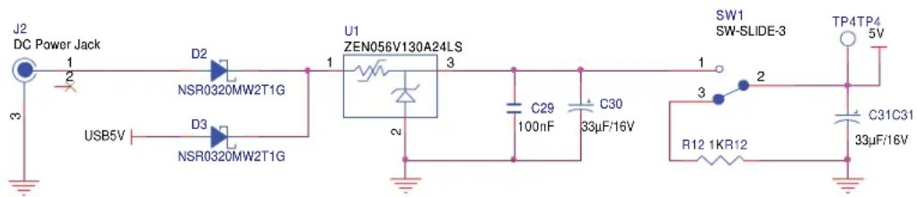
text_image
J2 DC Power Jack 1 2 USB5V D2 NSR0320MW2T1G D3 NSR0320MW2T1G U1 ZEN056V130A24LS 3 2 C29 100nF C30 33μF/16V SW1 SW-SLIDE-3 1 2 3 R12 1KR12 TP4TP4 5V C31C31 33μF/16V3.3.5 Power Rails
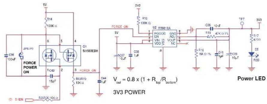
The SAM4C supports 1.6V–3.6V single supply mode (VDDIN). An internal regulator input is connected to the source and its output feeds VDDCORE (VDDOUT connected to VDDCORE).
When the 3.3V supply is present, the Power LED D5 is lit. Test points TP2 to TP5 are used to perform testing.
Table 3-2. Power Supply Voltage Ranges
| Power Supply Ranges Comments | ||
| VDDIO 1.6V–3.6V | Flash Memory Charge Pumps Supply for Erase and Program Operations, and Read operationInput Output buffers Supply | |
| VDDBU 1.6V–3.6V | Backup Area power supply. VDDBU is automatically disconnected when VDDIO is present (>1.9V) | |
| VDDIN 1.6V–3.6V 1.6V min. | if LCD and ADC not used, 2.5V otherwise | |
| VDDLCD 2.5V–3.6V | LCD Voltage Regulator OutputExternal LCD power supply input (LCD regulator not used)VDDIO/VDDIN need to be supplied when the LCD Controller is used | |
| VDDOUT 1.2V Output 120 mA Output Current | ||
| VDDPLL | 1.08V–1.32V | - |
| VDDCORE | 1.08V–1.32V | - |
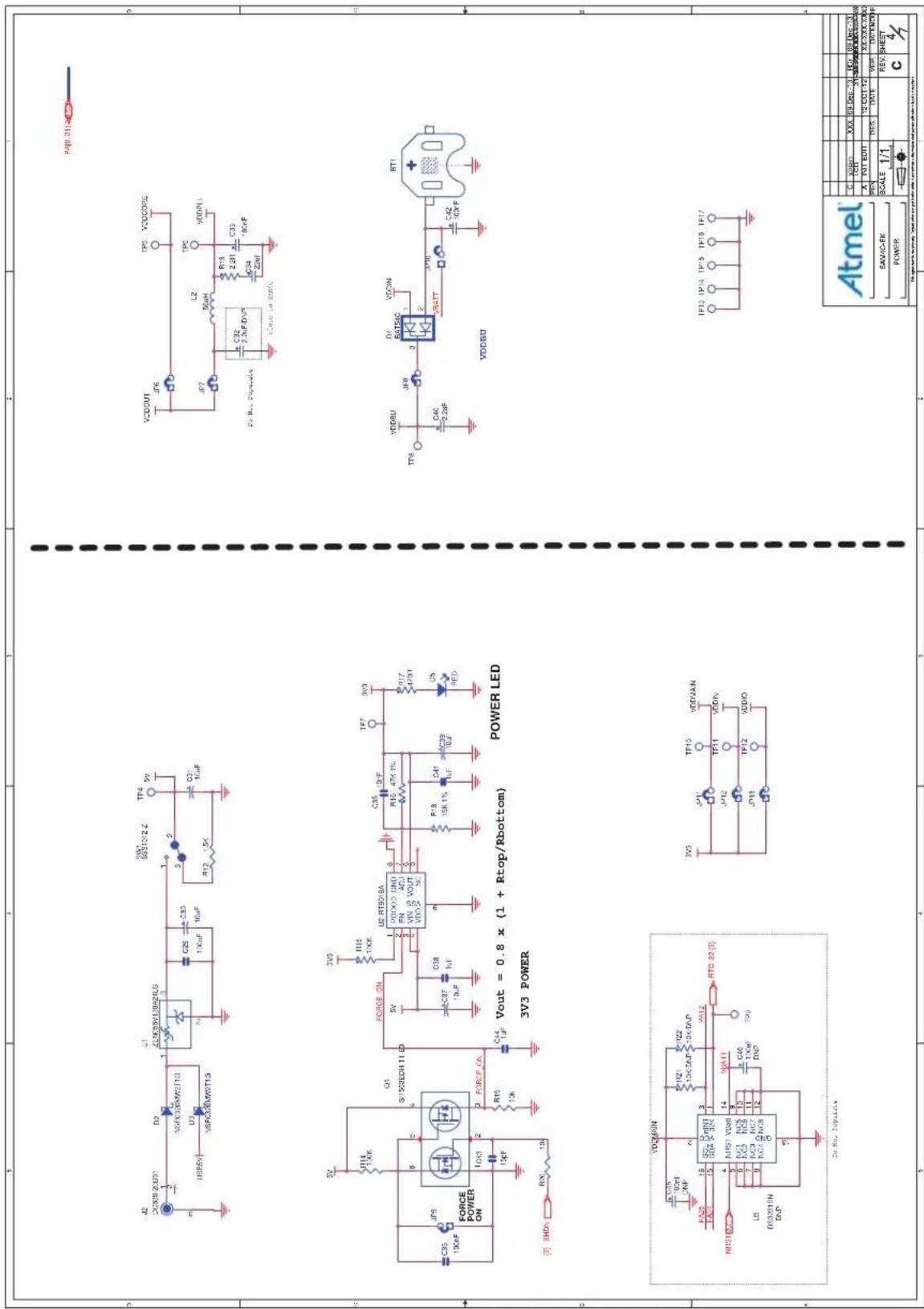
Figure 3-6. Power Rails Schematic
text_image
FORCE ON U2 ST8015A PGOOD GND EN ADJ VIN VOUT VD0 NC C36 10F R18 47X 0.1% C37 10F C38 1μF R19R19 13KΩ C44 1μF 5V 5V 5V 5V 5V 5V 5V 5V 5V 5V 5V 5V 5V 5V 5V 5V 5V 5V 5V 5V 5V 5V 5V 5V 5V 5V 5V 5V 5V 5V 5V 5V 5V 5V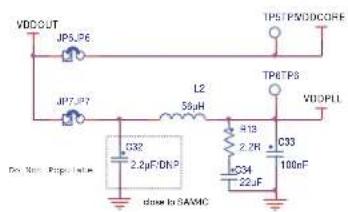
text_image
VDDOUT JPSJP6 JP7JP7 L2 50μH TPETPS VDDPLL C32 2.2μF/ONP C33 2.2Hz 100nF C34 22uF down to SAMIC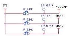
Note: Test points and jumpers are provided for easy access to each of the regulated power lines and measure the current on each line.
3.3.6 Battery Backup
The VDDBU pin is powered from the 3.3V rail or from a backup battery BT1 via a dual Schottky diode D4. Test points TP8 and jumper JP8/JP10 are used to perform voltage and current measurements.
Figure 3-7. Backup Battery Schematic
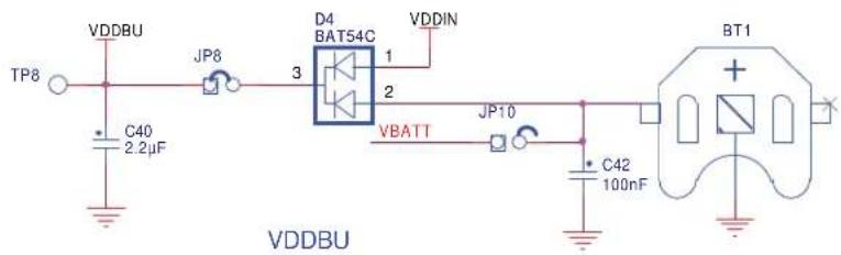
text_image
VDDBU TP8 C40 2.2µF JP8 3 D4 BAT54C VDDIN 1 2 VBATT JP10 C42 100nF BT1 VDDBU3.4 Embedded Memories
I2C for data storage in EEPROM (Atmel AT24C1024B)
• SPI Serial Flash AT45 or AT25F
3.4.1 TWI EEPROM
The AT24C1024B provides 1,048,576 bits of serial electrically erasable and programmable read-only memory (EEPROM) organized as 131,072 words of 8 bits each.
Device slave address byte: 0x50.
Figure 3-8. TWI EEPROM Schematic
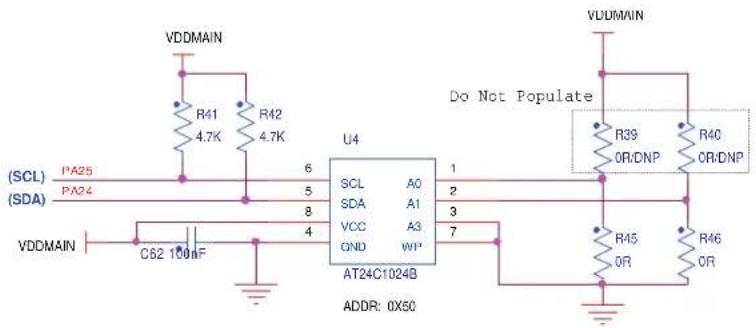
text_image
VDDMAIN R41 4.7K R42 4.7K SCL A0 SDA A1 VCC A3 GND WIP AT24C1024B 6 5 8 4 U4 Do Not Populate VDDMAIN R39 OR/DNP R40 OR/DNP R45 OR R46 OR SCL SDA VCC GND C62 100nF ADDR: 0X503.4.2 SPI Serial Flash
The ATSAM4C-EK embeds one serial Flash device AT25DFxx or AT45DBxx connected through the SPI. (The AT25DF321A is mounted by default.)
Figure 3-9. SPI Serial Flash Schematic
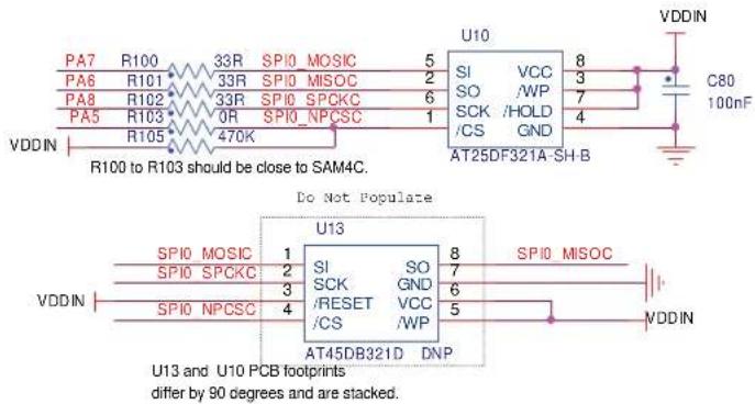
text_image
PA7 R100 33R SPI0 MOSIC 5 PA6 R101 33R SPI0 MISOC 2 PA8 R102 33R SPI0 SPCKC 6 PA5 R103 470K SPI0 NPCSC 1 VDDIN R100 to R103 should be close to SAM4C. U10 VCC 8 SI SO SCK //HOLD /CS GND AT25DF321A-SH-B C80 100nF Do Not Populate SPI0 MOSIC 1 SI SO 8 SPI0 SPCKC 2 SCK GND 7 SP10 NPCSC 3 /RESET VCC 6 /CS /WP 5 VDDIN AT45DB321D DNP SPI0 MISOC VDDIN U13 and U10 PCB footprints differ by 90 degrees and are stacked.3.4.3 Compatible Devices
Table 3-3. Compatible Devices
| Adesto AT45DB Series Devices Adesto AT25DF | Series Devices |
| AT45DB64D2-CNU AT25DF641A-SH | |
| AT45DB321D-MWU AT25DF321A-SH | |
| AT45DB131D-SS AT25DF161-SH | |
| AT45DB081D-SS AT25DF081-SSH | |
| AT45DB041D-SS AT25DF021-SH | |
| AT45DB021D-SS – | |
| AT45DB011D-SS – |
3.5 Communication Interfaces
3.5.1 Serial Port USART2 RS232
The USART2 is buffered with one RS-232 Transceiver ADM3312E (Analog Devices) and is connected to a DB9 connector. A classic implementation RS232 transceiver selection should include double source capability. The USART2 connector with RTS/CTS handshake signal support is connected to the RS232 transceiver.
Features:
• One RS232 transceiver connected to RXD2, TXD2, RTS2, and CTS2
• One DB9 male connector
• Required resistors and capacitors
Figure 3-10. USART2 RS232 Schematic

text_image
USART2 MN3 ADM3312EARU VCC C1+ 6 C50 100nF C47 4.7μF C48 100nF C49 100nF 1 21 V- V- C1- C2+ 20 2 C51 100nF GND C2- C3+ 4 24 SD EN C3- 22 CS3 100nF VDDMAIN R25 47K/DNP R26 0Ω TXD2 RXD2 RTS2 CTS2 PA10 PA8 232 PA14 PA15 VDDMAIN Do Not Populate 7 10 8 11 12 T1IN R1OUT T2IN R2OUT T3IN R3OUT T3OUT R3IN T1OUT R1IN T2OUT R2IN T3OUT R3IN T3OUT 0Ω/34.47K J3 Male Straight Angle 1 6 2 7 3 8 4 9 5 10 11 FGND3.5.2 Serial Port USART2 RS485
The USART2 is buffered with an Analog Devices ADM3485 RS-485/RS-422 transceiver and is connected to a 3-point jumper.
Features:
• One RS485 transceiver connected to RXD2, TXD2 and RTS2, CTS2
One 3-point connector
• Required resistors and capacitors
Figure 3-11. USART2 RS485 Schematic
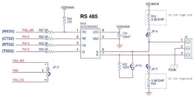
text_image
RS 485 MN4 ADM3485ARZ VDDMAIN R23 10K R27 OR 1 PO VCC 8 FE GND 5 DE 6 DI A B 7 VDDMAIN C54 100nF JP14 JP16 R37 120R JP17 3.3K/DNP R39 VGDMAIN R24 3.3K/DNP Do Not Populate J4 1 2 3 FGND Do Not Populate PA9_485 PA9_232 JP153.5.3 Serial Port UART1 RS232
The UART1 is buffered with an Analog Devices ADM3312E RS-232 transceiver and is connected to the HE10 PIO port C. A classic implementation RS232 transceiver selection should include double source capability.
Features:
• One RS232 transceiver connected to RXD (PC1) and TXD (PC0) only
• One HE10 male connector (PIO port C)
• Required resistors and capacitors
Figure 3-12. Serial Port Schematic
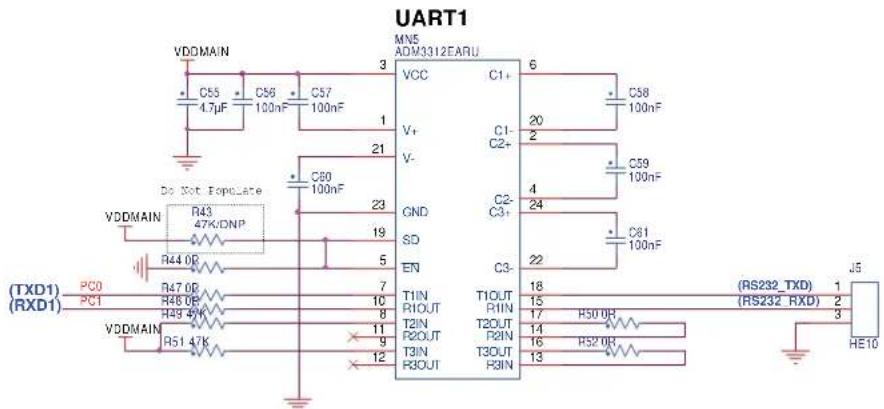
text_image
UART1 VDDMAIN C55 4.7µF C56 100nF C57 100nF MN5 ADM3312EARU VCC C1+ 6 C58 100nF V+ 20 2 C1- C2+ C59 100nF V- C2- C3+ 4 24 C61 100nF Do Not Populate VDDMAIN R43 47K/DNP R44 0P TXD1 PC0 R47 0P TXD1 RXD1 PC1 R46 0P TXD1 RXD1 R49 47K VDDMAIN R51 47K T1IN T1OUT 18 R1OUT R1IN 15 T2IN T2OUT 17 R2OUT R2IN 14 T3IN T3OUT 16 R3OUT R3IN 13 T1IN T1OUT 18 R1OUT R1IN 15 T2IN T2OUT 17 R2OUT R2IN 14 T3IN T3OUT 16 R3OUT R3IN 13 J5 (RS232_TXD) 1 (RS232_RXD) 2 HE103.6 Debug Interfaces
3.6.1 JTAG/ICE
The ATSAM4C-EK includes a JTAG interface port to provide debug level access to the system-on-chip. The JTAG port is a 20-pin, dual-row, 0.1-inch male connector. This port provides the required interface for in-circuit emulators such as the ARM Multi-ICE® and Atmel SAM-ICE™.
Features:
• One HE10 20-pin male connector
- Required resistors
Figure 3-13. JTAG/ICE Interface Schematic
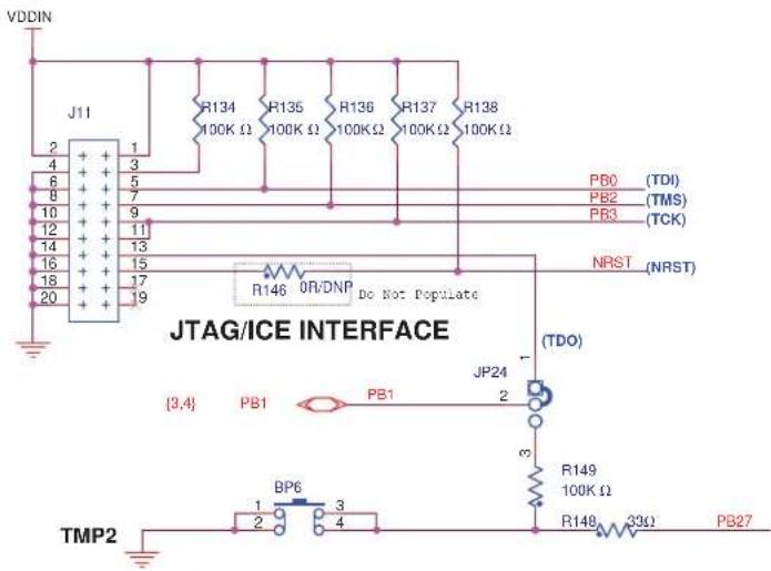
text_image
VDDIN J11 2 4 6 8 10 12 14 16 18 20 1 3 5 7 9 11 13 15 17 19 R134 100K Ω R135 100K Ω R136 100KΩ R137 100KΩ R138 100KΩ PB0 (TDI) PB2 (TMS) PB3 (TCK) NRST (NRST) R146 OR/DNP Do Not Populate JP24 (TDO) {3,4} PB1 PB1 JP24 2 3 R149 100K Ω R148 33Ω PB27 TMP2 BP6 3 1 2 3 43.6.2 UART/USB Bridge Interface
The UART is connected to an interface USB through an FTDI FT232R (TTL to USB converter) device. RX and TX DBGU only are connected to the USB connector Micro AB.
Figure 3-14. DBGU/USB Bridge Schematic
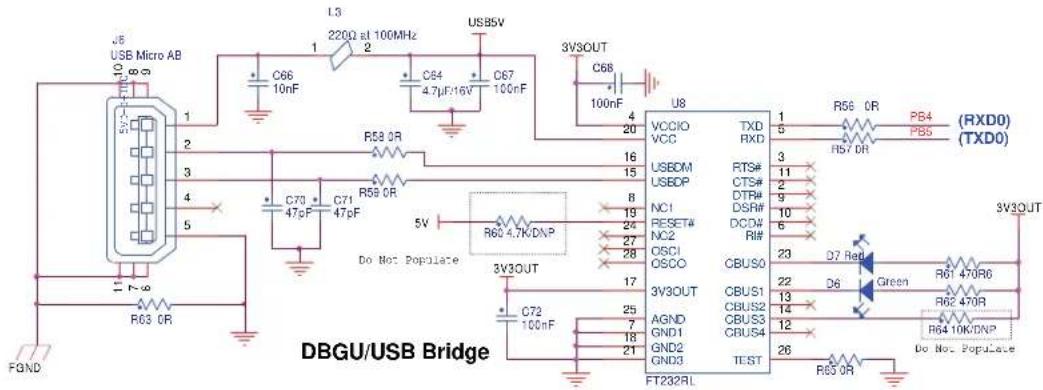
text_image
USB Micro AB 1 2 3 4 5 6 7 8 9 10 11 FOND R03 OR C70 47pF C71 47pF C66 10nF L3 220Ω at 100MHz C64 4.7μF/16V C67 100nF USB5V 3V3OUT C68 100nF U8 VCCIO VCC 16 USEDM USEDP 8 NC1 RESET# NC2 27 OSCJ OSCO 17 3V3OUT C72 100nF AGND GND1 GND2 GND3 3V3OUT FT232RL TXD RXD FTS# CTS# DTR# DSRW# DCW# RI# CBUSO CBUS1 CBUS2 CBUS3 CBUS4 TEST D7 Red D6 Green R61 470R6 R62 470R R64 10K/DNP Do Not Populate 3V3OUT (RXD0) (TXD0) 1 5 3 11 2 9 10 6 23 22 D6 Green 13 14 12 26 R65 OR3.7 Extend Interfaces
The SAMAC-EK embeds two connectors to interface Atmel IEEE 802.15.4-compliant wireless transceivers for ZigBee®-based applications.
Features:
- Atmel RZ600 module
• Atmel REB233-XPRO module
3.7.1 RZ600 Interface
- The RZ600 interface connects with Atmel modules used for ZigBee communication platforms that are equipped with a 10-pin HE10 male connector.
Figure 3-15. RZ600 Interface Schematic

text_image
(ZB_RSTN) PA17 R66 0R 1 J7 2 R67 0R PA11 (ZB_IRQ0) (ZB_IRQ1) PA12 R68 0R 3 4 R69 0R PA18 (ZB_SLPTR) (SPI0_NPCS0) PA5 R70 0R 5 6 R71 33R PA7 (SPI0_MOSI) (SPI0_MISO) PA6 R72 33R 7 8 R73 33R PA8 (SPI0_SPCK) 9 10 L4 220Ω at 100MHz JP18 VDDMAIN R70 to R73 should be close to SAM4C.ZigBee
Table 3-4. RZ600 HE10 Pin Functions
| Function | Pin | Pin | Function | |
| Reset | 1 | 2 | IRQ0 | |
| Interrupt Request | 3 | 4 | SLP_TR | |
| SPI Chip Select | 5 | 6 | SPI MOSI | |
| SPI MISO | 7 | 8 | SPI CLK | |
| Power Ground | 9 | 10 | Power Supply |
3.7.2 REB233-XPRO Interface
The XPRO interface connects with new Atmel modules used for XPRO platforms that are equipped with a 20-pin HE14 male connector.
Figure 3-16. XPRO Interface Schematic
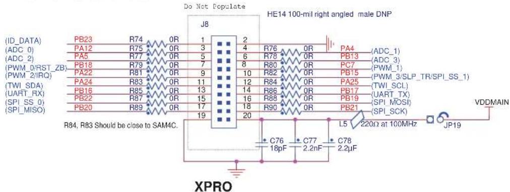
text_image
(ID_DATA) (ADC_0) (ADC_2) (PWM_0/RST_ZB) (PWM_2/IRQ) (TWI_SDA) (UART_RX) (SPI_SS_0) (SPI_MISO) PB23 R74 0R 1 J8 PA12 R75 0R 3 2 PA5 R77 0R 5 4 R76 0R PA4 (ADC_1) PB18 R79 0R 7 6 R78 0R PB13 (ADC_3) PA22 R81 0R 9 8 R80 0R PC7 (PWM_3) PA24 R83 0R 11 10 R82 0R PB15 (PWM_3/SLP_TR/SPI_SS_1) PB16 R85 0R 13 12 R84 0R PA25 (TWI_SCL) PB22 R87 0R 15 14 R86 0R PB17 (UART_TX) PB20 R89 0R 17 16 R88 0R PB19 (SPI_MOSI) 19 18 R90 0R PB21 (SPI_SCK) R84, R83 Should be close to SAM4C. XPRO Do Not Populate HE14 100-mil right angled male DNP VDDMAIN JP19 L5 220Ω at 100MHz C76 C77 C78 18pF 2.2nF 2.2μF XPROTable 3-5. XPRO HE10 Pin Functions
| Function Pin Pin Function | ||||
| Module Identity 1 2 Ground | ||||
| ADC Input 3 4 ADC Input | ||||
| ADC Input 5 6 ADC Input | ||||
| ZigBit^TM Reset 7 8 PWM Output | ||||
| IRQ Interrupt from ZigBit to Host Processor | 9 | 10 | SLP_TR wake-up signal to ZigBit | |
| Two-Wire Data Line | 11 | 12 | Two-Wire Clock Line | |
| UART RX Line | 13 | 14 | UART TX Line | |
| SPI Chip Select | 15 | 16 | SPI MOSI | |
| SPI MISO | 17 | 18 | SPI Clock | |
| Power Ground | 19 | 20 | Power Supply |
3.8 LCD Display
The ATSAM4C-EK board is equipped with one LCD segment interfaced with the SAM4C device through the LCD controller. Note that only certain segments (highlighted in blue in Figure 3-17 on page 18) are usable without using U11 and U12 analog switches or unpopulated 0 ohm resistors.
Features:
LCD segment YMCC42364AAANDCL (Anshan Yes Optoelectronics Display Co., Ltd.)
Figure 3-17. LCD Display Schematic

text_image
VDDMAIN C81 10µF C82 100µF R104 4.7K JP20 C2 R03 40R9 R106R106 PA13 100R U9 COM1 COM2 COM3 COM4 COM5 COM6 COM7 COM8 COM9 COM10 COM11 COM12 COM13 COM14 COM15 COM16 COM17 COM18 COM19 COM20 COM21 COM22 COM23 COM24 COM25 COM26 COM27 COM28 COM29 COM30 COM31 COM32 COM33 COM34 COM35 COM36 COM37 COM38 COM39 COM40 COM41 COM42 COM43 COM44 COM45 COM46 COM47 COM48 COM49 COM50 COM51 COM52 COM53 COM54 COM55 COM56 COM57 COM58 COM59 COM60 COM61 COM62 COM63 COM64 COM65 COM66 COM67 COM68 COM69 COM70 COM71 COM72 COM73 COM74 COM75 COM76 COM77 COM78 COM79 COM80 COM81 COM82 COM83 COM84 COM85 COM86 COM87 COM88 COM89 COM90 COM91 COM92 COM93 COM94 COM95 COM96 COM97 COM98 COM99 COM100 SEG 11 SEG 10 SEG 9 SEG 8 SEG 7 SEG 6 SEG 5 SEG 4 SEG 3 SEG 2 SEG 1 SEG 0 SEG -1 SEG -2 SEG -3 SEG -4 SEG -5 SEG -6 SEG -7 SEG -8 SEG -9 SEG -10 SEG -11 SEG -12 SEG -13 SEG -14 SEG -15 SEG -16 SEG -17 SEG -18 SEG -19 SEG -20 SEG -21 SEG -22 SEG -23 SEG -24 SEG -25 SEG -26 SEG -27 SEG -28 SEG -29 SEG -30 SEG -31 SEG -32 SEG -33 SEG -34 SEG -35 SEG -36 SEG -37 SEG -38 SEG -39 SEG -40 R107 R108 R109 R110 R111 R112 R113 R114 R115 R116 R117 R118 R119 R120 R121 R122 R123 R124 R125 R126 R127 R128 R129 R130 R131 R132 R133 R134 R135 R136 R137 R138 R139 R140 R141 R142 R143 R144 R145 R146 R147 R148 R149 R150 R151 R152 R153 R154 R155 R156 R157 R158 R159 R160 R161 R162 R163 R164 R165 R166 R167 R168 R169 R170 R171 R172 R173 R174 R175 R176 R177 R178 R179 R180 R181 R182 R183 R184 R185 R186 R187 R188 R189 R190 R191 R192 R193 R194 R195 R196 R197 R198 R199 R200 R201 R202 R203 R204 R205 R206 R207 R208 R209 R210 R211 R212 R213 R214 R215 R216 R217 R218 R219 R220 R221 R222 R223 R224 R225 R226 R227 R228 R229 R230 PDAIIN (AM PM CNTX错误) AM PM CNTX错误 (AM PM CNTX错误) AM PM CNTX错误 (AM PM CNTX错误) AM PM CNTX错误 (AM PM CNTX错误) AM PM CNTX错误 (AM PM CNTX错误) AM PM CNTX错误 (AM PM CNTX错误) AM PM CNTX错误 (AM PM CNTX错误) AM PM CNTX错误 (AM PM CNTX错误) AM PM CNTX错误 (AIREM Cortex-MA) AM PM CNTX错误 (AIREM Cortex-MA) AM PM CNTX错误 (AIREM Cortex-MA) AM PM CNTX错误 (AIREM Cortex-MA) AM PM CNTX错误 (AIREM Cortex-MA) AM PM CNTX错误 (AIREM Cortex-MA) AM PM CNTX错误 (AIREM Cortex-MA) AM PM CNTX错误 (AIREM Cortex-MA) AVDC/AVDC/AVDC/AVDC/AVDC/AVDC/AVDC/AVDC/AVDC/AVDC/AVDC/AVDC/AVDC/AVDC/AVDC/AVDC/AVDC/AVDC/AVDC/AVDC/AVDC/AVDC/AVDC/AVDC/AVDC/AVDC/AVDC/AVDC/AVDC/AVDC/AVDC/AVDC/AVDC/AVDC/ AVDC/AVDC/AVDC/AVDC/AVDC/AVDC/AVDC/AVDC/AVDC/AVDC/AVDC/AVDC/AVDC/AVDC/AVDC/AVDC/AVDC/AVDC/AVDC/AVDC/AVDC/AVDC/AVDC/AVDC/AVDC/AVDC/AVDC/AVDC/AVDC/AVDC/AVDC/AVDC/AVDC/AVD / AVD / AVD / AVD / AVD / AVD / AVD / AVD / AVD / AVD / AVD / AVD / AVD / AVD / AVD / AVD / AVD / AVD / AVD / AVD / AVD / AVD / AVD / AVD / AVD / AVD / AVD / AVD / AVD / AVD / AVD / AVD / AVD / AVD / AV D / AV D / AV D / AV D / AV D / AV D / AV D / AV D / AV D / AV D / AV D / AV D / AV D / AV D / AV D / AV D / AV D / AV D / AV D / AV D / AV D / AV D / AV D / AV D / AV D / AV D / AV D / AV D / AV D / AV D / AV D / AV D / AV D / AV D A VDD MAIN (C79) 100nF PAI6 (U) 6 6 6 6 6 6 6 6 6 6 6 6 6 6 6 6 6 6 6 6 6 6 6 6 6 6 6 6 6 6 6 6 6 6 VDD MAIN (C83) 8 PB02 PB03 PB04 PB05 PB06 PB07 PB08 PB09 PB0B PB0B PB0B PB0B PB0B PB0B PB0B PB0B PB0B PB0B PB0B PB0B PB0B PB0B PB0B PB0B PB0B PB0B PB0B PB0B PB0B PB0B PB0B PB0B PB0B PB0B PB0B PB0B PB0B PB0B PB0B PB0B PB0B PB0B WBCCWV WCCWV WCCWV WCCWV WCCWV WCCWV WCCWV WCCWV WCCWV WCCWV WCCWV WCCWV WCCWV WCCWV WCCWV WCCWV WCCWV WCCWV WCCWV WCCWV WCCWV WCCWV WCCWV WCCWV WCCWV WCCWV VDD MAIN (C) UDD MAIN (C) UDD MAIN (C) UDD MAIN (C) UDD MAIN (C) UDD MAIN (C) UDD MAIN (C) UDD MAIN (C) UDD MAIN (C) UDD MAIN (C) UDD MAIN (C) UDD MAIN (C) UDD MAIN (C) UDD MAIN (C) UDD MAIN (C) UDD Main (C) UDD Main (C) UDD Main (C) UDD Main (C) UDD Main (C) UDD Main (C) UDD Main (C) UDD Main (C) UDD Main (C) UDD Main (C) UDD Main (C) UDD Main (C) UDD Main (C) UDD Main (C) UDD Main (C) UDD Main (C) UDD Main (C) UDD Main (C) UDD Main (C) UDD Main (C) UDD Main (C) UDD Main (C) UDD Main (C) UDD Main (C) UDD Main(AB) VDD MAIN(AC) VDD MAIN(AC) VDD MAIN(AC) VDD MAIN(AC) VDD MAIN(AC) VDD MAIN(AC) VDD MAIN(AC) VDD MAIN(AC) VDD MAIN(AC) VDD MAIN(AC) VDD MAIN(AC) VDD MAIN(AC) VDD MAIN(AC) VDD MAIN(AC) VDD MAIN(AC) VDD MAIN(AC) VDD MAIN(AC) VDD Main(BC) VDD Main(BC) VDD Main(BC) VDD Main(BC) VDD Main(BC) VDD Main(BC) VDD Main(BC) VDD Main(BC) VDD Main(BC) VDD Main(BC) VDD Main(BC) VDD Main(BC) VDD Main(BC) VDD Main(BC) VDD Main(BC) VDD Main(BC) VDD Main(BC) VDDMain(BC) VDD Main(BC) VDD Main(BC) VDD Main(BC) VDD Main(BC) VDD Main(BC) VDD Main(BC) VDD Main(BC) VDD Main(BC) VDD Main(BC) VDD Main(BC) VDD Main(BC) VDD Main(BC) VDD Main(BC) VDD Main(BC) VDD Main(BC) VDD Main(BC) B: P: P: P: P: P: P: P: P: P: P: P: P: P: P: P: P: P: P: P: P: P: P: P: P: P: P: P: P: P: P: P: P: P: P: P: P: P: P: P: P: P: P: P: P: P: P: P: P: P: P:P: P: P: P: P: P: P: P: P: P: P: P: P: P: P: P: P: P: P: P: P: P: P: P: P: P: P: P: P: P: P: P: P: P: P: P: P: P: P: P: P: P: P: P: P: P: P: P: P: P: M : : : : : : : : : : : : : : : : : : : : : : : : : : : : : : : : : : : : : : : : : : : : : : : : : : : : : : : : : : : : : : : : : : : : : : : : : : : : : : : : : : : : : : : : : : : : : : : : : : : : : - LED+ LED- LED- AM PM CV CMOSL @TOM AM TM @TOM AM TM @TOM AM TM @TOM AM TM @TOM AM TM @TOM AM TM @TOM AM TM @TOM AM TM @TOM AM TM @TOM AM TM @TOM AM TM @TOM AM TM @TOM AM TM @TOM AM TM @TOM AM TM @TOM AM TM @TOM AM TM @TOM AM TM @TOM AM TM @TOM AM TM @TOM AM TCM @TOM AM TCM @TOM AM TCM @TOM AM TCM @TOM AM TCM @TOM AM TCM @TOM AM TCM @TOM AM TCM @TOM AM TCM @TOM AM TCM @TOM AM TCM @TOM AM TCM @TOM AM TCM @TOM AM TCM @TOM AM TCM @TOM AM TCM @TOM AM TCM @TOM AICETEORCEM Cortex-MATFigure 3-18. LCD Layout

text_image
COM3 COM2 COM1 SEMO SEC0 16 G0 G2 G3 G4 B4 B1 B0 D0 D1 D2 D3 B9 AM PM C V B13 B0 B2 B3 B4 B5 B6 ERROR G5 错误 G6 A0 A1 A2 A3 A4 A5 A6 B7 B8 G7 ARM Cortex™ -M4 SEC39 SEC12 a f g h i b j k e L m n c d 44 17Table 3-6. LCD pinout vs Segment
| Pin COM0 COM1 COM2 COM3 Pin COM0 COM1 COM2 COM3 | |||||||||
| 1 | - | - | - | C | O | M | 3 | 2 | |
| 2--COM2-24 | A5-g | A5-j | A5-L A5-m | ||||||
| 3 | - | COM1 | - | - | 25 | A4-h | A4-i | A4-k | A4-n |
| 4 | COM0 | - | - | - | 26 | B6 | A4-f | A5-e | A5-d |
| 5 | G1 | G0 | G2 | G3 | 27 | A4-a | A4-b | A4-c | B11 |
| 6 | G4 | G5 | G6 | G7 | 28 | A4-g | A4-j | A4-L | A4-m |
| 7 | E0 | E2 | E4 | E6 | 29 | A3-h | A3-i | A3-k | A3-n |
| 8 | E1 | E3 | E5 | E7 | 30 | B4 | A3-f | A3-e | A3-d |
| 9 | D3-a | D3-b | D3-c | B9 | 31 | A3-a | A3-b | A3-c | B10 |
| 10 | D3-f | D3-g | D3-e | D3-d | 32 | A3-g | A3-j | A3-L | A3-m |
| 11 | D2-a | D2-b | D2-c | D2-p | 33 | A2-h | A2-i | A2-k | A2-n |
| 12 | D2-f | D2-g | D2-e | D2-d | 34 | B3 | A2-f | A2-e | A2-d |
| 13 | D1-a | D1-b | D1-c | D1-p | 35 | A2-a | A2-b | A2-c | B1 |
| 14 | D1-f | D1-g | D1-e | D1-d | 36 | A2-g | A2-j | A2-L | A2-m |
| 15 | D0-a | D0-b | D0-c | D0-p | 37 | A1-h | A1-i | A1-k | A1-n |
| 16 | D0-f | D0-g | D0-e | D0-d | 38 | B2 | A1-f | A1-e | A1-d |
| 17 | A6-h | A6-i | A6-k | A6-n | 39 | A1-a | A1-b | A1-c | B8 |
| 18 | B14 | A6-f | A6-e | A6-d | 40 | A1-g | A1-j | A1-L | A1-m |
| 19 | A6-a | A6-b | A6-c | B13 | 41 | A0-h | A0-i | A0-k | A0-n |
| 20 | A6-g | A6-j | A6-L | A6-m | 42 | B0 | A0-f | A0-e | A0-d |
| 21 | A5-h | A5-i | A5-k | A5-n | 43 | A0-a | A0-b | A0-c | B7 |
| 22 | B5 | A5-f | A5-e | A5-d | 44 | A0-g | A0-j | A0-L | A0-m |
The SAM4C features a LM4040 precision micropower curvature-corrected bandgap shunt voltage reference with a several fixed reverse breakdown voltages. The device voltage reference on the board is 3.0V.
Figure 3-19. Analog Reference Schematic
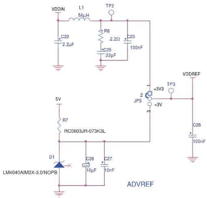
text_image
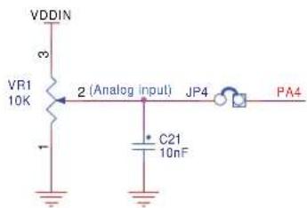
VDDIN L1 56μH TP2 C22 2.2μF R8 2.2Ω C23 100nF C25 22μF 5V R7 RC0603JR-073K3L D1 LM4040AIM3X-3.0/NOPB C26 10μF C27 10nF +3V3 JP5 +3V VDDREF TP3 C28 100nF ADVREF3.9.2 Analog Input
One potentiometer VR1 multi-turn 10K Ω is connected to the jumper JP4. If JP4 is closed, this analog reference is available on analog input PA4.
Figure 3-20. Analog Input Schematic
text_image
VDDIN 3 VR1 10K 2 (Analog input) JP4 PA4 C21 10nF3.9.3 Temperature Sensor
The Atmel AT30TS75 temperature sensor converts temperatures from -40^ to +125^ to a digital word and provides a typical accuracy of ±0.5^ over the operating temperature range of 0^ to +85^ . The device is factory calibrated and requires no external components to help provide a cost effective solution. To reduce current consumption and save power, the AT30TS75 features a shutdown mode that turns off all internal circuitry except for the internal power-on reset and serial interface circuits. In addition, the device features a power saving one-shot mode that allows the device to make a temperature measurement and update the temperature register and then return to shutdown mode.
Device slave address byte: 0x48.
Figure 3-21. Temperature Sensor Schematic
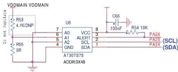
text_image
VDDMAIN VDDMAIN R53 4.7K/DNP Do Not Popolare R55 0R U6 7 6 5 4 A0 VCC A1 ALERT A2 SCL GND SDA AT30TS75 ADDR:0X48 8 3 2 1 C65 100nF R54 10K PA26 PA25 (SCL) PA24 (SDA)3.10 CryptoAuthentication (optional)
The Atmel ATSHA204 is a member of the Atmel CryptoAuthentication family of high-security hardware authentication devices.
It has a flexible command set that allows use for many applications, such as Anti-counterfeiting, Protection for Firmware or Media, Session Key Exchange, Secure Data Storage or User Password Checking.
Device slave address byte: 0xC9.
Figure 3-22. CryptoAuthentication Schematic
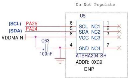
text_image
Do Not Populate (SCL) PA25 (SDA) PA24 VDDMAIN C63 100nF U5 6 5 8 4 SCL NC1 1 SDA NC2 2 VCC NC3 3 GND NC4 7 ATSHA204-SH ADDR: 0XC9 DNP3.11 LEDs and Buttons
The ATSAM4C-EK is equipped with two user push buttons and three LEDs.
3.11.1 Discrete LEDs
Indicators on the main board include three discrete LEDs:
• 1 blue LED connected to a PIO
• 1 amber LED connected to a PWM output
• 1 green LED connected to a PWM output
Figure 3-23. Debug Discrete LED Schematic

text_image
VDDIN D8 D9 Q10 BLUE AMBER GREEN R125 R126 R127 4700 4700 4700 LED PWM PD8 PWM PD7 PC83.11.2 Push Buttons
The EK board is equipped with four system push buttons and two user push buttons. The push buttons consist of momentary push button switches mounted directly to the board. When any switch is depressed it will cause a low (zero) to appear at the associated input pin.
• System push buttons:
• NRST (Reset, perform system reset)
• FWPU (Force Wake-Up)
- TMP0 (Tamper)
- TMP2 (Tamper)
- User push buttons:
It is possible to select the pull-up level for Tamper TMP0 pin. By selecting PB1 instead of VDDBU, it allows to end user a dynamic tampering synchronized with RTCOUT pin. It allows a diminution of the power consumption when the button is pressed (divided by the Duty Cycle applied on RTCOUT Output signal).
It is possible to use the TMP2 Push Button as another Tamper input. By using this feature, the end user must use JTAG in 2-wire mode (SWIO and SWD) due to the loss of the TDO pin. In this case TMP2 is pull-up at RTCOUT Level (PB1 pin) and can be managed dynamically synchronized with the RTCOUT pin.
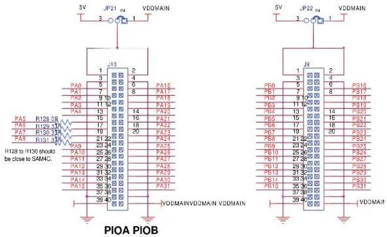
3.12 Miscellaneous I/O
This board is equipped with additional I/O connectors which allow the measurements of specific points are allow the connection of an additional extension board.
Figure 3-25. PIO A and PIO B Extension I/O Connectors Schematic
text_image
5V JP21 VDDMAIN 3 1 J10 1 2 4 PA0 5 6 PA16 PA1 7 8 PA17 PA18 PA19 PA20 PA21 PA22 PA23 PA24 PA25 PA26 PA27 PA28 PA29 PA30 PA31 PA32 PA33 PA34 PA35 PA36 PA37 PA38 PA39 PA40 PA41 PA42 PA43 PA44 PA45 PA46 PA47 PA48 PA49 PA50 PA51 PA52 PA53 PA54 PA55 PA56 PA57 PA58 PA59 PA60 P100 P101 P102 P103 P104 P105 P106 P107 P108 P109 P110 P111 P112 P113 P114 P115 P116 P117 P118 P119 P120 P121 P122 P123 P124 P125 P126 P127 P128 P129 P130 P131 P132 P133 P134 P135 P136 P137 P138 P139 P140 VDDMAIN VDDMAIN VDDMAIN H128 to H130 should be close to SAM4C. 5V JP22 VDDMAIN3.13 Metrology Core Serial Interface
This board includes an additional connector which allows connecting to an external board through the SPI 1 port.
Figure 3-26. Connector Schematic
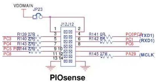
text_image
VDDMAIN JP23 J12J12 1 2 3 4 R141 QR PC0PC0 PC3 R139 27R R140 27R PC1 (RXD1) 5 6 R142 QR PC6 (RXD1) 7 8 9 10 11 12 R145 27B PA29 (MCLK) 13 14 PIOsense3.14 PIO Usage
3.14.1 PIO Port A Pin Assignments
Table 3-8. PIO Port A Pin Assignments
| I/O Line | Peripheral | Extra Function | System Function Reset State UsingA | B | ||
| PA0 RTS3 | PCK2 A10 COM0 | WKUP5 | LCD Com | |||
| PA1 CTS3 | NCS1 A9 COM1 | -LCD Com | ||||
| PA2 SCK3 | NCS2 A8 COM2 | -LCD Com | ||||
| PA3 RXD3 | NCS3 A7 COM3 | WKUP6 | LCD Com | |||
| PA4 TXD3 | - | A6 COM4/AD1 | -Analog input | |||
| PA5 SPI0 | NPCS0 | -A5 COM5/AD2 | -SerFlash / NPCS | |||
| PA6 SPI0 | MISO | -A4 SEG0 | -ZigBee | |||
| PA7 SPI0 | MOSI | -A3 SEG1 | -ZigBee | |||
| PA8 SPI0 | SPCK | -A2 SEG2 | -ZigBee | |||
| PA9 RXD2 | - | A1 SEG3 | WKUP2 | RS232/485 | ||
| PA10 | TXD2 | - | A0/NBS0 | SEG4 | - | RS232/485 |
| PA11 | RXD1 | - | A23 | SEG5 | WKUP9 | ZigBee / IRQ0 |
| PA12 | TXD1 | - | A22-NCLE | SEG6/AD0 | - | ZigBee/IRQ1/IRTC |
| PA13 | SCK2 | TIOA0 | A21-NALE | SEG7 | - | Backlight On/off |
| PA14 | RTS2 | TIOB0 | A20 | SEG8 | WKUP3 | RS232/485 |
| PA15 | CTS2 TIOA4 | A19 SEG9 | -RS232/485 | |||
| PA16 | SCK1 TIOB4 | A18 SEG10 | -MuxLCD | |||
| PA17 | RTS1 | TCLK4 | A17 | SEG11 | WKUP7 | ZigBee / RST |
| PA18 | CTS1 | TIOA5 | A16 | SEG12 | - | ZigBee / SLPTR |
| PA19 | RTS0 | TCLK5 | A15 | SEG13 | WKUP4 | PB ScrUp |
| PA20 | CTS0 TIOB5 | A14 SEG14 | -PB ScrDwn | |||
| PA21 | SPI0_NPCS1 | - | A13 | SEG15 | - | ZigBee / NPCS |
| PA22 | SPI0_NPCS2 | - | A12 | SEG16 | - | ZigBit / IRQ |
| PA23 | SPI0_NPCS3 | - | A11 | SEG17 | - | - |
| PA24 | TWD0 | - | A10 | SEG18 | WKUP1 | TWI / ZigBit |
| PA25 | TWCK0 | - | A9 | SEG19 | - | TWI / ZigBit |
| PA26 | CTS4 - | A8 SEG20 | -- | |||
| PA27 | - | - | NCS0 | SEG21 | - | - |
| PA28 | - | - | NRD | SEG22 | - | - |
| PA29 | PCK1 | - | NWAIT | SEG23 | - | MCLK (ATSense) |
| PA30 | PCK1 | - | A15 | - | XOUT | XOUT |
| PA31 | PCK0 | - | A14 | - | XIN | XIN |
3.14.2 PIO Port B Pin Assignments
Table 3-9. PIO Port B Pin Assignments
| I/O Line | Peripheral | Extra Function | System Function Reset State UsingA | B | ||
| PB0 TWD1 -- - TDI | - | |||||
| PB1 TWCK1 -- - RTCOUT0 TDO/TRACESWO - | ||||||
| PB2 | - | - | - | - | TMS/SWDIO | - |
| PB3 | - | - | - | - | TCK/SWCLK | - |
| PB4 URXD0 TCLK0 A17 - WKUP8 | PIO, I, PU, ST | DBGU | ||||
| PB5 UTXD0 - A16 -- | DBGU | |||||
| PB6 -- D0 SEG24 - | - | |||||
| PB7 | TIOA1 | - | D1 | SEG25 | - | - |
| PB8 | TIOB1 | - | D2 | SEG26 | - | - |
| PB9 | TCLK1 | - | D3 | SEG27 | - | - |
| PB10 | TIOA2 | - | D4 | SEG28 | - | - |
| PB11 | TIOB2 | - | D5 | SEG29 | - | - |
| PB12 | TCLK2 | - | D6 | SEG30 | - | - |
| PB13 | PCK0 | - | D7 | SEG31/AD3 | - | - |
| PB14 | - | - | NWR0-NWE | SEG32 | - | - |
| PB15 | - | - | NWR1-NBS1 | SEG33 | - | ZigBit / SLPTR |
| PB16 | RXD0 | - | D8 | SEG34 | WKUP10 | ZigBit / RXD |
| PB17 | TXD0 | - | D9 | SEG35 | - | ZigBit / TXD |
| PB18 | SCK0 | PCK2 | D10 | SEG36 | - | ZigBit / RST |
| PB19 | RXD4 | - | D11 | SEG37 | - | ZigBit / MOSI |
| PB20 | TXD4 | - | D12 | SEG38 | - | ZigBit / MISO |
| PB21 | SCK4 | NANDOE | D13 | SEG39 | WKUP11 | ZigBit / SPCK |
| PB22 | RTS4 | NANDWE | D14 | SEG40 | - | ZigBit / NPCS |
| PB23 | ADTRG | - | D15 | SEG41/AD4 | - | - |
| PB24 | TIOA3 | - | A7 | SEG42 | - | - |
| PB25 | TIOB3 | - | A6 | SEG43 | - | - |
| PB26 | TCLK3 | - | A5 | SEG44 | WKUP13 | - |
| PB27 | - | - | A4 | SEG45 | WKUP14 | - |
| PB28 | - | - | A3 | SEG46 | WKUP15 | - |
| PB29 | - | - | A2 | SEG47 | - | - |
| PB30 | - | - | A1 | SEG48 | - | - |
| PB31 | - | - | A0-NBS0 | SEG49/AD5 | - | - |
3.14.3 PIO Port C Pin Assignments
Table 3-10. PIO Port C Pin Assignments
| I/O Line | Peripheral | Extra Function | System Function Reset | Set State UsingA | B | ||
| PC0 UTXD1 | PWM0 - - - - - | ||||||
| PC1 URXD1 | PWM1 WKUP12 - - - - | ||||||
| PC2 SPI1_ | NPCS0 PWM2 - - - - - | ||||||
| PC3 SPI1_ | MISO PWM3 - - - - - | ||||||
| PC4 SPI1_ | MOSI - - - - - | ||||||
| PC5 SPI1_ | SPCK - - - - - | ||||||
| PC6 PWM0 | SPI1_NPCS1 | - - - - LED Green | |||||
| PC7 PWM1 | SPI1_NPCS2 | - - - - LED Amber | |||||
| PC8 PWM2 | SPI1_NPCS3 | - - - - LED Blue | |||||
| PC9 PWM3 | - - - - ERASE | - Jumper Erase | |||||
3.15 Connectors
3.15.1 Power Supply Connector
The ATSAM4C-EK is equipped with an ACDC wall adapter that can be connected to a J2 connector (described below). The maximum input voltage that can be applied on this connector must be lower than 6V.
Figure 3-27. Power Supply Connector

natural_image
Close-up of a black electronic component with three labeled parts (1, 2, 3), no visible text or symbols beyond labels.Table 3-11. Power Supply Connector Pinout
| Pin Signal Name Description | |
| 1 +5V Wall Adapter Main Voltage | |
| 2 NC Floating Point | |
| 3 GND Ground |
3.15.2 JTAG/ICE Connector
Figure 3-28. JTAG/ICE Connector
text_image
2 4 6 8 10 12 14 16 18 20 ● ● ● ● ● ● ● ● ● ● ● ● ● ● ● ● ● ● ● ● ● ● ● 1 3 5 7 9 11 13 15 17 19Table 3-12. JTAG/ICE Connector Pinout
| Pin Signal | Name Description | |
| 4, 6, 8, 10, 12, 14, 16, 18, 20 | GND Common ground | |
| 1 VTref 3 | 3V power | This is the target reference voltage. It is used to check if the target has power, to create the logic-level reference for the input comparators, and to control the output logic levels to the target. It is normally fed from VDD on the target board and must not have a series resistor. |
| 2 Vsupply | 3.3V power | This pin is not connected in SAM-ICE. It is reserved for compatibility with other equipment. Connect to VDD or leave open in target system. |
| 3 nTRST | TARGET RESET | JTAG Reset (active-low output signal that resets the target). Output from SAM-ICE to the Reset signal on the target JTAG port. Typically connected to nTRST on the target CPU. This pin is normally pulled HIGH on the target to avoid unintentional resets when there is no connection. |
| 5 TDI TEST DATA INPUT | JTAG data input of target CPU (serial data output line, sampled on the rising edge of the TCK signal). It is recommended that this pin is pulled to a defined state on the target board. Typically connected to TDI on target CPU. | |
| 7 TMS TEST MODE SELECT | JTAG mode set input of target CPU. This pin should be pulled up on the target. Typically connected to TMS on target CPU. Output signal that sequences the target's JTAG state machine, sampled on the rising edge of the TCK signal. | |
| 9 TCK TEST CLOCK | JTAG clock signal to target CPU (output timing signal, for synchronizing test logic and control register access). It is recommended that this pin is pulled to a defined state on the target board. Typically connected to TCK on target CPU. | |
| 11 RTCK | Input Return test clock signal from the target.Some targets must synchronize the JTAG inputs to internal clocks. To assist in meeting this requirement, a returned and retimed TCK can be used to dynamically control the TCK rate. SAM-ICE supports adaptive clocking which waits for TCK changes to be echoed correctly before making further changes. Connect to RTCK if available, otherwise to GND | |
| 13 | TDO JTAG TEST DATA OUTPUT | JTAG data output from target CPU (serial data input from the target). Typically connected to TDO on target CPU. |
| 15 | nSRST RESET | Active-low reset signal. Target CPU reset signal |
| 17 | RFU | This pin is not connected in SAM-ICE |
| 19 | RFU | This pin is not connected in SAM-ICE |
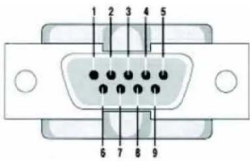
3.15.3 RS232 Connector
Figure 3-29. RS232 Connector
text_image
1 2 3 4 5 6 7 8 9Table 3-13. RS232 Connector Pinout
| Pin Signal Name Description | ||
| 1, 4, 6, 9 NC | Not Connected | |
| 2 RXD RS232 Serial Data Output Signal | ||
| 3 TXD RS232 Serial Data Input Signal | ||
| 5 GND Common Ground | ||
| 7 RTS Request To Send - Not Used | ||
| 8 CTS Clear To Send - Not Used | ||
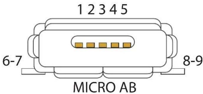
3.15.4 UART/USB Micro AB
Figure 3-30. Micro AB USB Connector
text_image
1 2 3 4 5 6-7 8-9 MICRO ABTable 3-14. Micro AB USB Connector Pinout
| Pin Signal Name Description | ||
| 1 VBUS | 5V Power | |
| 2 DM Data Minus | ||
| 3 DP Data Plus | ||
| 4 ID On | The Go Identification | |
| 5 GND | Common Ground | |
| 6, 7, 8, 9 Shield Mechanical Pins | ||
3.15.5 RZ600 IEEE 802.15.4 Wireless Transceiver Socket J12
Figure 3-31. Socket J12
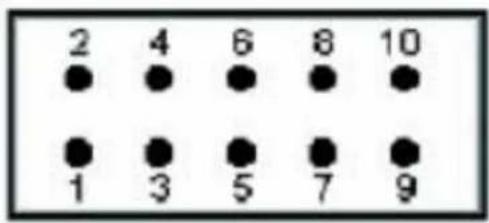
text_image
2 4 6 8 10 ● ● ● ● ● ● ● ● ● ● 1 3 5 7 9Table 3-15. Socket Pinout
| Function Signal | Name Pin | Pin Signal Name Function | ||||
| Reset /RST 1 2 | IRQ0 Interrupt Request | |||||
| Interrupt Request IRQ1 3 4 SLP_TR | SLP_TR | |||||
| SPI Chip Select | /CS | 5 | 6 | MOSI | SPI MOSI | |
| SPI MISO | MISO | 7 | 8 | SCLK | SPI CLK | |
| Power Supply | GND | 9 | 10 | VCC | VCC | |
3.15.6 I/O Expansion Port
Figure 3-32. Expansion Port J9 & J10
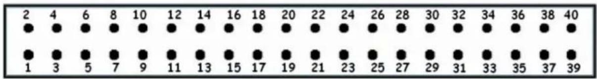
text_image
2 4 6 8 10 12 14 16 18 20 22 24 26 28 30 32 34 36 38 40 ● ● ● ● ● ● ● ● ● ● ● ● ● ● ● ● ● ● ● ● ● ● ● ● ● ● ● ● ● ● ● ● ● ● ● ● ● ● ● ● ● ● ● ● ● ● ● ● ● ● 1 3 5 7 9 11 13 15 17 19 21 23 25 27 29 31 33 35 37 39Table 3-16. Expansion Port J9 Pinout
| Function Signal | Name Pin | Pin Signal Name Function | ||||
| 3.3V or 5V – 1 2 – | 3.3V or 5V | |||||
| Ground GND 3 4 | GND | Ground | ||||
| - | PB0 | 5 | 6 | PB16 | - | |
| - | PB1 | 7 | 8 | PB17 | - | |
| - | PB2 | 9 | 10 | PB18 | - | |
| - | PB3 | 11 | 12 | PB19 | - | |
| - | PB4 | 13 | 14 | PB20 | - | |
| - | PB5 | 15 | 16 | PB21 | - | |
| - | PB6 | 17 | 18 | PB22 | - | |
| - | PB7 | 19 | 20 | PB23 | - | |
| - | PB8 | 21 | 22 | PB24 | - | |
| - | PB9 | 23 | 24 | PB25 | - | |
| - | PB10 | 25 | 26 | PB26 | - | |
| - | PB11 | 27 | 28 | PB27 | - | |
| - | PB12 | 29 | 30 | PB28 | - | |
| - | PB13 | 31 | 32 | PB29 | - | |
| - | PB14 | 33 | 34 | PB30 | - | |
| - | PB15 | 35 | 36 | PB31 | - | |
| Ground | GND | 37 | 38 | GND | Ground | |
| Power Supply | VDDMAIN | 39 | 40 | VDDMAIN | Power Supply |
Table 3-17. Expansion Port J10 Pinout
| Function | Signal Name | Pin | Pin | Signal Name | Function | |
| 3.3V or 5V – 1 2 – | 3.3V or 5V | |||||
| Ground GND 3 4 | GND | Ground | ||||
| - | PA0 | 5 | 6 | PA16 | - | |
| - | PA1 | 7 | 8 | PA17 | - | |
| - PA2 9 10 PA18 - | ||||||
| - | P | A | 3 | 1 | ||
| - PA4 13 | 14 PA20 - | |||||
| - PA5 15 | 16 PA21 - | |||||
| - PA6 17 | 18 PA22 - | |||||
| - PA7 19 | 20 PA23 - | |||||
| - PA8 21 | 22 PA24 - | |||||
| - PA9 23 | 24 PA25 - | |||||
| - | PA10 | 25 | 26 PA26 - | |||
| - | PA11 | 27 | 28 PA27 - | |||
| - | PA12 | 29 | 30 PA28 - | |||
| - | PA13 | 31 | 32 PA29 - | |||
| - | PA14 | 33 | 34 PA30 - | |||
| - | PA15 | 35 | 36 PA31 - | |||
| Ground | GND | 37 | 38 | GND | Ground | |
| Power Supply | VDDMAIN | 39 | 40 | VDDMAIN | Power Supply | |
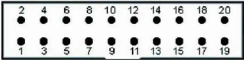
Figure 3-33. Expansion Port J12
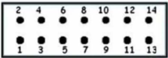
text_image
2 4 6 8 10 12 14 ● ● ● ● ● ● ● ● ● ● ● ● ● ● 1 3 5 7 9 11 13Table 3-18. Expansion Port J12 Pinout
| PIO | Power | Pin | Pin | Power | PIO | |
| - | 3.3V | 1 | 2 | 3.3V | - | |
| PC2 | - | 3 | 4 | - | PC0 | |
| PC3 | - | 5 | 6 | - | PC1 | |
| PC4 | - | 7 | 8 | - | PC6 | |
| PC5 | - | 9 | 10 | - | PC7 | |
| PC8 | - | 11 | 12 | - | PA29 | |
| - | GND | 13 | 14 | GND | - |
4. Evaluation Kit Firmware Demonstration
4.1 ATSAM4C-EK Default Application
The ATSAM4C-EK is delivered with a preprogrammed default application in SAM4C Flash memory. This application implements SAM4C embedded peripherals and external (on-board) peripherals as detailed in the table below.
Table 4-1.
| SAM4C Embedded Peripheral Connected to External (on-board) Peripheral | |
| Real-Time Clock (RTC) — | |
| Anti-Tamper BP3 Push Button | |
| Two-wire Interface Temperature Sensor AT30TS75 | |
| Segmented LCD Custom Atmel Display | |
| SAM4C Core 1 — | |
| 10-bit ADC Internal ADC channel connected to Battery Backup Power Rail (VDDBU) | |
After the first power-up without the backup battery, the time (hour and minute) of the RTC can be configured. The Hour and Minute settings are entered using the following push buttons:
BP4 (SCROLL-UP)—sets the Hour (24H mode entries must be made)
BP5 (SCROLL-DOWN)—sets the Minute
BP6 (TMP2)—saves the Hour and Minute settings
Once the time settings have been saved, BP4 (SCROLL-UP) can be used to toggle the Hour display between 12H or 24H mode.
Note: RTC time configuration can be skipped by pressing BP6.
Once the Hour and Minute have been configured, the main application on core 0 runs in an infinite loop, repeating the following steps:
• Every second, the time is displayed with colon (:) icon blinking
• Every fifteen (15) seconds, the VDDBU pin voltage is measured and displayed ^(1)
• Every thirty (30) seconds, the temperature (using the AT30TS75) is measured and displayed in °C and in °F.
Note: 1. On the ATSAM4C-EK, the voltage measured is the VDDIO voltage minus the forward voltage of the diode in the BAT54C (D4).
At startup, the main application configures the core 1 subsystem to run a CoreMark algorithm from the core 1 SRAM memories (SRAM1 and SRAM2). Once the CoreMark is finished, the result of the CoreMark (number of CoreMark/MHz) is passed to the main application using the inter-processor communication embedded in the SAM4C. Once the result is retrieved by the main application, the result of the CoreMark is displayed and the CoreMark algorithm running on core 1 is restarted. An ammeter connected either on JP12 (VDDIN) or on JP6 (VDDCORE) can measure the active current consumption of both cores.
4.2 Measuring the Backup mode current consumption on VDDBU
The SAM4C has an ultra-low-power mode RTC and Supply controller allowing less than 1 A (typical) on VDDBU, with the following functions/peripherals configuration:
• 32.768 kHz Crystal Oscillator enabled
• POR backup on VDDBU disabled
- RTC running
• RTT enabled on 1 Hz mode
• Force wake-up (FWUP) enabled
• Anti-tamper Input (TMP0) enabled
To measure the current consumption on VDDBU when in backup mode, JP9 (Shutdown control) must be opened and an ammeter connected on JP8 (VDDBU) as described in the following procedure:
- Power off the board using SW1
- Insert the 3V lithium battery provided in the battery holder
- Place an ammeter (with sufficient capacity to measure current lower than 1μA) on JP8
- Power on the board using SW1
- (optional) Set the RTC as described above
- Press the push button BP5 (SCROLL-DOWN) to place the board in low-power mode
Before shutdown, the following messages are displayed on the LCD:
"ENTERING BACKUP MODE"
"PRESS FWUP BP1 TO WAKE UP"
"USE BP3 TO GENERATE TAMPER EVENTS"
Blinking "BYE"
At this point, the current consumption on the ammeter should be less than 1 A @ 25^ @ 3V.
Once in backup mode, the Anti-tamper pin 0 (TMP0) is enabled. BP3 (TMP0) push button can be used to generate tamper events before waking up the board. Tamper events are registered without waking up the board. Up to 15 tamper events can be registered. To wake up the board, press BP1 (FWUP). Upon start-up, the number of tamper events and time-stamping of the tamper events are displayed on the LCD.
5. ATSAM4C-EK Design Files
5.1 ATSAM4C-EK Schematics
This section contains the schematics for the SAM4C Evaluation Kit (Rev. C).
• Main page with Block Diagram
• Information regarding the design
SAM4C Microcontroller and its crystals, decoupling capacitors and analog inputs
• Power Supplies Distribution
• RS232, RS485 and DBGU Interfaces, TWI Memories, and Temperature Sensor
- Custom Glass LCD and ZigBee, XPRO interfaces
- User Buttons, I/O expansion headers and JTAG Interfaces
Figure 5-1. ATSAM4C-EK Schematic (Page 1 of 7)
flowchart
graph TD
    subgraph_Sheet_4["5 V DC Input 1.3mm/Jack"]
        A["POWER SUPPLY LED"] --> B["ATMEL Cortex M4 SAM4C16CA-AU LQFP100"]
        C["RTC"] --> B
    end

    subgraph_Sheet_5["RS485"]
        D["USART2"] --> B
        E["USART1"] --> B
        F["USART0"] --> B
        G["TWI"] --> B
        H["TWI"] --> B
        I["TWI"] --> B
    end

    subgraph_Sheet_3["Sheet 3"]
        J["PIO A, B, C"] --> K["ZIGBEE INTERFACE"]
        L["XPRO"] --> M["XPRO INTERFACE"]
        N["FLASH"] --> O["FLASH ON SPI"]
        P["LCM"] --> Q["Segment LCD"]
    end

    subgraph_Sheet_7["Sheet 7"]
        R["LEDS"] --> S["3 LEDS"]
        T["User_PB"] --> U["6 PushButtons"]
        V["JTAG"] --> W["20PINS"]
        X["INTERFACE"] --> Y["PIOA,B,C"]
    end

    A <-->|POWER| B
    C <-->|PIO A, B, C| B
    D <-->|PIO A, B, C| B
    E <-->|PIO A, B, C| B
    F <-->|PIO A, B, C| B
    G <-->|PIO A, B, C| B
    H <-->|PIO A, B, C| B
    I <-->|PIO A, B, C| B
    J <-->|PIO A, B, C| B
    K <-->|PIO A, B, C| B
    L <-->|PIO A, B, C| B
    M <-->|PIO A, B, C| B
    N <-->|PIO A, B, C| B
    O <-->|PIO A, B, C| B
    P <-->|PIO A, B, C| B
    Q <-->|PIO A, B, C| B
    R <-->|PIO A, B, C| B
    S <-->|PIO A, B, C| B
    T <-->|PIO A, B, C| B
    U <-->|PIO A, B, C| B
    V <-->|PIO A, B, C| B
    W <-->|PIO A, B, C| B
    X <-->|PIO A, B, C| B
    Y <-->|PIO A, B, C| B
    Z["Atmel"] --> AA["SCALE 1/1"]
    AA --> AB["C"]
    AB --> AC["REV: SHEET C"]
Figure 5-2. ATSAM4C-EK Schematic (Page 2 of 7)
JUMPER AND SOLDERDROP
| PAGE | REFERENCE | DEFAULT | FUNCTION |
| 3 | JP1JP2JP3JP4 CLOSE Connect AD input from potentiometer.JP5 | OPENOPEN Close for JTAG boundary scan manufacturing test or Fast flash programming mode.Close to select JTAG.OPEN1-2 | Close to reinitialize the Flash contents and some of its NVM bits. |
| JP6,JP7,JP8 | CLOSE Respective Power connection.JP9 CLOSE Close to unable Power supply with SHDN command.JP10 | OPEN Use Back-up Balter to supply RTC Power.JP11,JP12 | |
PIO MUXING
DEFAULT NO POPULATE PARTS
| PAGE | REFERENCE | FUNCTION |
| 3 | R1,R2 | Expansion IO Interface. |
| R10 | External clock resource input. | |
| 4 | R24,R38 | RS485 Pull-up and Pull-down Resistor. |
| 5 | R39,R40 | Change EEPROM I2C Address. |
| R53 | Change Temperature Sensor I2C Address. | |
| R60 | PowerUp to Reset FT232RL. | |
| R64 | When USB suspend is HIGH level |
LIST OF CHANGES
| REVB => REVC | 1 | Update XPRO interface (Change J8 ZigBit HE14 right angled male DNP) |
| 2 | R3 DNP | |
| 3 | Add TMP2 | |
| 4 Push button TMP0, add pull up VDDBU | ||
SCHEMATICS CONVENTIONS
| (1)Resistance Unit:"K"Is"Kohm","R"Is"Ohm". |
| (2)"DNP"means the component is not populated by default. |
TEST POINT
| PAGE | REFERENCE | FUNCTION |
| 3 | TP1 | VDDLCD |
| TP2 | VDDREF_P | |
| TP3 | VDDREF | |
| 4 | TP4 | 5V |
| TP5 | VDDCORE | |
| TP6 | VDDPLL | |
| TP7 | 3V3 | |
| TP8 | VDDBU | |
| TP9 | RTC_32 | |
| TP10 | VDDMAIN | |
| TP11 | VDDIN | |
| TP12 | VDDIO | |
| TP13 to TP17 | GND |
REVISION HISTORY
| REV | DATA | NOTE |
| A 2012.10 Original released | ||
| B 2013.1 | Modify LCD circuit | |
| C | 2013.4 | Update XPRO Interface/Add TMP2 |
TABLE OF CONTENTS
| PAGE | DESCRIPTION |
| 1 Block Diagram | |
| Reference guide2 | |
| Microcontroller,AD3 | |
| 4 | Power,RTC |
| RS232,RS485,USB,EEPROM, | |
| 5 | Temperature Sensor,Crypto Authentication |
| 6 | LCD,FLASH,ZIGBEE,ZIGBIT |
| LED,Button,IO Expansion,JTAG7 | |
Figure 5-3. ATSAM4C-EK Schematic (Page 3 of 7)

text_image
ATMEL Cortex-M4 Processor SAM4C16CA-AU LQFP100 LQFP100 SOCKET Do Not Populate VDDN VDDOUT VDDOPEL VDDPLL VDDLCD VDDCD VDDCU VDDN VDDOUT VDDOPEL VDDPLL VDDLCD VDDCD VDDCU VDDN VDDOUT VDDOPEL VDDPLL VDDLCD VDDCD VDDCU VDDN VDDOUT VDDOPEL VDDPLL VDDLCD VDDCD VDDCU VDDN VDDOUT VDDOPEL VDDPLL VDDLCD VDDCD VDDCU VDDO VDDIN VDDIN VDDIN VDDIN VDDIN VDDIN VDDIN VDDIN VDDIN VDDIN VDDIN VDDIN VDDIN VDDIN VDDIN VDDIN VDDIN VDDIN VDDIN VDDIN VDDIN VDDIN VDDIN VDDIN VDDIN VDDN VDDIN VDDIN VDDIN VDDIN VDDIN VDDIN VDDIN VDDIN VDDIN VDDIN VDDIN VDDIN VDDIN VDDIN VDDIN VDDIN VDDIN VDDIN VDDIN VDDIN VDDIN VDDIN VDDIN VDDIN VDDI VDDIN VDDIN VDDIN VDDIN VDDIN VDDIN VDDIN VDDIN VDDIN VDDIN VDDIN VDDIN VDDIN VDDIN VDDIN VDDIN VDDIN VDDIN VDDIN VDDIN VDDIN VDDIN VDDIN VDDIN VDDINO VDOLOELE VDOLOELE VDOLOELE VDOLOELE VDOLOELE VDOLOELE VDOLOELE VDOLOELE VDOLOELE VDOLOELE VDOLOELE VDOLOELE VDOLOELE VDOLOELE VDOLOELE VDOLOELE VDOLOELE VDOLOELE VDOLOELE VDOLOELE VDOLOELEFigure 5-4. ATSAM4C-EK Schematic (Page 4 of 7)
text_image
VOUT = 0.8 x (1 + Rtop/Rbottom) POWER LED 3V3 POWER VDDOUT TP5 VDDORE C22 2.0kF/DVP R13 2.2Ω C33 10Ω/F C34 2.0Ω C35 10Ω R16 10Ω R17 4Ω/1 R18 10Ω R19 10Ω R20 10Ω R21 10Ω R22 10Ω R23 10Ω R24 10Ω R25 10Ω R26 10Ω R27 10Ω R28 10Ω R29 10Ω R30 10Ω R31 10Ω R32 10Ω R33 10Ω R34 10Ω R35 10Ω R36 10Ω R37 10Ω R38 10Ω R39 10Ω R40 10Ω R41 10Ω R42 10Ω R43 10Ω R44 10Ω R45 10Ω R46 10Ω R47 10Ω R48 10Ω R49 10Ω R50 10Ω R51 10Ω R52 10Ω R53 10Ω R54 10Ω R55 10Ω R56 10Ω R57 10Ω R58 10Ω R59 10Ω R60 10Ω R61 10Ω R62 10Ω R63 10Ω R64 10Ω R65 10Ω R66 10Ω R67 10Ω R68 10Ω R69 10Ω R70 10Ω R71 10Ω R72 10Ω R73 10Ω R74 10Ω R75 10Ω R76 10Ω R77 10Ω R78 10Ω R79 10Ω R80 10Ω R81 10Ω R82 10Ω R83 10Ω R84 10Ω R85 10Ω R86 10Ω R87 10Ω R88 10Ω R89 10Ω R90 10ΩFigure 5-5. ATSAM4C-EK Schematic (Page 5 of 7)
text_image
USART2 MS3 ADM5036EARU VDDVAIN C17 7.7kF C28 10kF C35 10kF C45 10kF C55 10kF C65 10kF C75 10kF C85 10kF C95 10kF C105 10kF C115 10kF C125 10kF C135 10kF C145 10kF C155 10kF C165 10kF C175 10kF C185 10kF C195 10kF C205 10kF C215 10kF C225 10kF C235 10kF C245 10kF C255 10kF C265 10kF C275 10kF C285 10kF C295 10kF C305 10kF C315 10kF C325 10kF C335 10kF C345 10kF C355 10kF C365 10kF C375 10kF C385 10kF C395 10kF C405 10kF C415 10kF C425 10kF C435 10kF C445 10kF C455 10kF C465 10kF C475 10kF C485 10kF C495 10kF C505 10kF C515 10kF C525 10kF C535 10kF C545 10kF C555 10kF C565 10kF C575 10kF C585 10kF C595 10kF C605 10kF C615 10kF C625 10kF C635 10kF C645 10kF C655 10kF C665 10kF C675 10kF C685 10kF C695 10kF C705 10kF C715 10kF C725 10kF C735 10kF C745 10kF C755 10kF C765 10kF C775 10kF C785 10kF C795 10kF C805 10kF C815 10kF C825 10kF C835 10kF C845 10kF C855 10kF C865 10kF C875 10kF C885 10kF C895 10kF C905 10kF C915 10kF C925 10kF C935 10kF C945 10kF C955 10kF C965 10kF C975 10kF C985 10kF C995 10kF RS485 MR4 AC2M4MCMXZ RIO VCCB GND DE A PSS RCP RCP RCP RCP RCP RCP RCP RCP RCP RCP RCP RCP RCP RCP RCP RCP RCP RCP RCP RCP RCP RCP RCP RCP RCP RCP RCP RCP RCP RCP RCP RCP RCP RCP RCP RCP RCP RCP RCP RCP RCP RCP RCP RCP RCP RCP RCP RCP RCP RCP RCF RCF RCF RCF RCF RCF RCF RCF RCF RCF RCF RCF RCF RCF RCF RCF RCF RCF RCF RCF RCF RCF RCF RCF RCF RCF RCF RCF RCF RCF RCF RCF RCF RCF RCF RCF RCF RCF RCF RCF RCF RCF RCF RCF RCF RCF RCF RCF RCF RCF RCP RCP RCP RCP RCP RCP RCP RCP RCP RCP RCP RCP RCP RCP RCP RCP RCP RCP RCP RCP RCP RCP RCP RCP RCP RCP RCP RCP RCP RCP RCP RCP RCP RCP RCP SCL SCL SCL SCL SCL SCL SCL SCL SCL SCL SCL SCL SCL SCL SCL SCL SCL SCL SCL SCL SCL SCL SCL SCL SCL SCL SCL SCL SCL SCL SCL SCL SCL SCL SCL SCL SCL SCL SCL SCL SCL SCL SCL SCL SCL SCL SCL SCL SCL SCL SCS LSC LSC LSC LSC LSC LSC LSC LSC LSC LSC LSC LSC LSC LSC LSC LSC LSC LSC LSC LSC LSC LSC LSC LSC LSC LSC LSC LSC LSC LSC LSC LSC LSC LSC LSC LSC LSC LSC LSC LSC LSC LSC LSC LSC LSC LSC LSC LSC LSC LSC LSP LSP LSP LSP LSP LSP LSP LSP LSP LSP LSP LSP LSP LSP LSP LSP LSP LSP LSP LSP LSP LSP LSP LSP LSP LSP LSP LSP LSP LSP LSP LSP LSP LSP LSP LSP LSP LSP LSP LSP LSP LSP LSP LSP LSP LSP LSP LSP LSP LSP LFP A B C D E F F G H I J K M N N O P P Q P Q P Q P Q P Q P Q P Q P Q P Q P Q P Q P Q P Q P Q P Q P Q P Q P Q P Q P Q P Q P Q P Q P Q P Q P Q P Q P Q P Q P Q P Q P Q P Q P Q P Q P Q P Q P Q P Q P Q P Q P Q P Q P Q P Q P Q P Q P Q P Q P Q PQ P A B C D E F F G H I J K M N N O P P P Q P Q P Q P Q P Q P Q P Q P Q P Q P Q P Q P Q P Q P Q P Q P Q P Q P Q P Q P Q P Q P Q P Q P Q P Q P Q P Q P Q P Q P Q P Q P Q P Q P Q P Q P Q P QP A B C D E F F G H I J K M N N O P P P P Q F G H I J K M N N O P P P P Q F G H I J K M N N O P P P P Q F G H I J K M N N O P P P P Q F G H I J K M N N O P P P P Q F G H I J K M N N O P P P P Q F G H I J K M N N O P P P P Q F G H I J K M N N N O P P P P Q F G H I J K M N N O O U U U U U U U U U U U U U U U U U U U U U U U U U U U U U U U U U U U U U U U U U U U U U U U U U U U U U U U U U U U U U U U U U U U U U U U U U U U U U U U U U U U U U U U U U U U U U U U U U U U U USLUSUSUSUSUSUSUSUSUSUSUSUSUSUSUSUSUSUSUSUSUSUSUSUSUSUSUSUSUSUSUSUSUSUSUSUSUSUSUSUSUSUSUSUSUSUSUSUSUSUSUSUSUSUSUSUSUSUSUSUSUSUSUSUSUSUSUSUSUSUSUSUSUSUSUSUSUSUSUSUSUSUSUSUSUSUS US US US US US US US US US US US US US US US US US US US US US US US US US US US US US US US US US US US US US US US US US US US US US US US US US US US US US US US US US US US US US US US US US US US US US US US US US US US US US US US US US US US US US US US US US US US US US US US US US US US US USA USA USA USA USA USA USA USA USA USA USA USA USA USA USA USA USA USA USA USA USA USA USA USA USA USA USA USA USA USA USA USA USA USA USA USA USA USA USA USA USA USA USA USA USA USA USA USA USA USA USA USA USA USA USA USA USA USA USA USA USA USA USA USA USA USA USA USA USA USA USA USA USA USA USA USA USA USA USA USA USA USA USA USA USA USA USA USA USA USA USA USA USA USA USA USA USA USA USA USA SAVAC-FK COMATWINER USART2 USART2 USART2 USART2 USART2 USART2 USART2 USART2 USART2 USART2 USART2 USART2 USART2 USART2 USART2 USART2 USART2 USART2 USART2 USART2 USART2 USART2 USART2 USART2 USART2 USART2 USART2 USART2 USART2 USART2 USART2 USART2 USART2 USART2Figure 5-6. ATSAM4C-EK Schematic (Page 6 of 7)

text_image
ZIGBEE COM1 COM2 COM3 COM4 COM5 COM6 COM7 COM8 COM9 COM10 COM11 COM12 COM13 COM14 COM15 COM16 COM17 COM18 COM19 COM20 COM21 COM22 COM23 COM24 COM25 COM26 COM27 COM28 COM29 COM30 COM31 COM32 COM33 COM34 COM35 COM36 COM37 COM38 COM39 COM40 COM41 COM42 COM43 COM44 COM45 COM46 COM47 COM48 COM49 COM50 COM51 COM52 COM53 COM54 COM55 COM56 COM57 COM58 COM59 COM60 COM61 COM62 COM63 COM64 COM65 COM66 COM67 COM68 COM69 COM70 COM71 COM72 COM73 COM74 COM75 COM76 COM77 COM78 COM79 COM80 COM81 COM82 COM83 COM84 COM85 COM86 COM87 COM88 COM89 COM90 COM91 COM92 COM93 COM94 COM95 COM96 COM97 COM98 COM99 COM100 COM101 COM102 COM103 COM104 COM105 COM106 COM107 COM108 COM109 COM110 COM111 COM112 COM113 COM114 COM115 COM116 COM117 COM118 COM119 COM120 COM121 COM122 COM123 COM124 COM125 COM126 COM127 COM128 COM129 COM130 COM131 COM132 COM133 COM134 COM135 COM136 COM137 COM138 COM139 COM140 COM141 COM142 COM143 COM144 COM145 COM146 COM147 COM148 COM149 COM150 COM151 COM152 COM153 COM154 COM155 COM156 COM157 COM158 COM159 COM160 COM161 COM162 COM163 COM164 COM165 COM166 COM167 COM168 COM169 COM170 COM171 COM172 COM173 COM174 COM175 COM176 COM177 COM178 COM179 COM180 COM181 COM182 COM183 COM184 COM185 COM186 COM187 COM188 COM189 COM190 COM191 COM192 COM193 COM194 COM195 COM196 COM197 COM198 COM199 COM200Figure 5-7. ATSAM4C-EK Schematic (Page 7 of 7)
text_image
USER INTERFACE FWUP NRST TMP0 Scroll up Scroll down JTAG/ICE INTERFACE TMP2 VDDU JP56 VCCBU R123 R124 R125 R126 R127 R128 R129 R130 R131 R132 R133 R134 R135 R136 R137 R138 R139 R140 R141 R142 R143 R144 R145 R146 R147 R148 R149 R150 R151 R152 R153 R154 R155 R156 R157 R158 R159 R160 R161 R162 R163 R164 R165 R166 R167 R168 R169 R170 R171 R172 R173 R174 R175 R176 R177 R178 R179 R180 R181 R182 R183 R184 R185 R186 R187 R188 R189 R190 R191 R192 R193 R194 R195 R196 R197 R198 R199 R200 VDDMAIN VDDMAIN VDDMAIN/TO/MIN VDDMAIN BOIPAOIP LED VDDN D8 D9 D10 BLUE Blue 7.0Hz 3.0Hz 3.0Hz 3.0Hz 3.0Hz 3.0Hz 3.0Hz 3.0Hz 3.0Hz 3.0Hz 3.0Hz 3.0Hz 3.0Hz 3.0Hz 3.0Hz 3.0Hz 3.0Hz 3.0Hz 3.0Hz 3.0Hz 3.0Hz 5V JP21 VDDMAIN 5V JP22 VDDMAIN 5V JP23 VDDMAIN 5V JP24 VDDMAIN 5V JP25 VDDMAIN 5V JP26 VDDMAIN 5V JP27 VDDMAIN 5V JP28 VDDMAIN 5V JP29 VDDMAIN 5V JP30 VDDMAIN 5V JP31 VDDMAIN 5V JP32 VDDMAIN 5V JP33 VDDMAIN 5V JP34 VDDMAIN 5V JP35 VDDMAIN 5V JP36 VDDMAIN 5V JP37 VDDMAIN 5V JP38 VDDMAIN 5V JP39 VDDMAIN 5V JP40 VDDMAIN 5V JP41 VDDMAIN 5V JP42 VDDMAIN 5V JP43 VDDMAIN 5V JP44 VDDMAIN 5V JP45 VDDMAIN 5V JP46 VDDMAIN 5V JP47 VDDMAIN 5V JP48 VDDMAIN 5V JP49 VDDMAIN 5V JP50 VDDMAIN 5V JP51 VDDMAIN 5V JP52 VDDMAIN 5V JP53 VDDMAIN 5V JP54 VDDMAIN 5V JP55 VDDMAIN 5V JP56 VDDMAIN 5V JP57 VDDMAIN 5V JP58 VDDMAIN 5V JP59 VDDMAIN 5V JP60 VDDMAIN 5V JP61 VDDMAIN 5V JP62 VDDMAIN 5V JP63 VDDMAIN 5V JP64 VDDMAIN 5V JP65 VDDMAIN 5V JP66 VDDMAIN 5V JP67 VDDMAIN 5V JP68 VDDMAIN 5V JP69 VDDMAIN 5V JP70 VDDMAIN 5V JP71 VDDMAIN 5V JP72 VDDMAIN 5V JP73 VDDMAIN 5V JP74 VDDMAIN 5V JP75 VDDMAIN 5V JP76 VDDMAIN 5V JP77 VDDMAIN 5V JP78 VDDMAIN 5V JP79 VDDMAIN 5V JP80 VDDMAIN 5V JP81 VDDMAIN 5V JP82 VDDMAIN 5V JP83 VDDMAIN 5V JP84 VDDMAIN 5V JP85 VDDMAIN 5V JP86 VDDMAIN 5V JP87 VDDMAIN 5V JP88 VDDMAIN 5V JP89 VDDMAIN 5V JP90 VDDMAIN 5V JP91 VDDMAIN 5V JP92 VDDMAIN 5V JP93 VDDMAIN 5V JP94 VDDMAIN 5V JP95 VDDMAIN 5V JP96 VDDMAIN 5V JP97 VDDMAIN 5V JP98 VDDMAIN 5V JP99 VDDMAIN 5V JND PND PND PND PND PND PND PND PND PND PND PND PND PND PND PND PND PND PND PND PND PND PND PND PND PND PND PND PND PND PND PND PND PND PND PND PND PND PND PND PND PND PND PND PND PND PND PND PND PND PND TON TON TON TON TON TON TON TON TON TON TON TON TON TON TON TON TON TON TON TON TON TON TON TON TON TON TON TON TON TON TON TON TON TON TON TON TON TON TON TON TON TON TON TON TON TON TON TON TON TON TCON TCON TCON TCON TCON TCON TCON TCON TCON TCON TCON TCON TCON TCON TCON TCON TCON TCON TCON TCON TCON TCON TCON TCON TCON TCON TCON TCON TCON TCON TCON TCON TCON TCON TCON TCON TCON TCON TCON TCON TCON TCON TCON TCON TCON TCON TCON TCON TCON TCON TCO U U U U U U U U U U U U U U U U U U U U U U U U U U U U U U U U U U U U U U U U U U U U U U U U U U U U U U U U U U U U U U U U U U U U U U U U U U U U U U U U U U U U U U U U U U U U U U U U U U U U A B B C D E F G H I J K L M N O X R O S S A X X X X X X X X X X X X X X X X X X X X X X X X X X X X X X X X X X X X X X X X X X X X X X X X X X X X X X X X X X X X X X X X X X X X X X X X X X X X X X X X X X X X X X X X X X X X X X X X X X X XXXXXXXXXXXXXXXXXXXXXXXXXXXXXXXXXXXXXXXXXXXXXXXXXXXXXXXXXXXXXXXXXXXXXXXXXXXx x x x x x x x x x x x x x x x x x x x x x x x x x x x x x x x x x x x x x x x x x x x x x x x x x x x x x x x x x x x x x x x x x x x x x x x x x x x x x x x x x x x x x x x x x x x x x x x x x x x x u A B B C D E F G H I J K L M N O X R O S S A X X X X X X X X X X X X X X X X X X X X X X X X X X X X X X X X X X X X X X X X X X X X X X X X X X I N I N I N I N I N I N I N I N I N I N I N I N I N I N I N I N I N I N I N I N I N I N I N I N I N I N I N I N I N I N I N I N I N I N I N I N I N I N I N I N I N I N I N I N I N I N I N I N I N I N IN I N I N I N I N I N I N I N I N I N I N I N I N I N I N I N I N I N I N I N I N I N I N I N I N I N I N I N I N I N I N I N I N I N I N I N I N I N I N I N I N I N I N I N I N I N I N I N I N I N I Inn t n n t n t n t n t n t n t n t n t n t n t n t n t n t n t n t n t n t n t n t n t n t n t n t n t n t n t n t n t n t n t n t n t n t n t n t n t n t n t n t n t n t n t n t n t n t n t n t n t n t n t n s c d d e d f e r e l o f i o f o r o f o r o f o r o f o r o f o r o f o r o f o r o f o r o f o r o f o r o f o r o f o r o f o r o f o r o f o r o f o r o f o r o f o r o f o r o f o r o f o r o f o r o f o r o f o r o f o r o f o f o r o f o r o f o r o f o r o f o r o f o r o f o r o f o r o f o r o f o r o f o r o f o r o f o r o f o r o f o r o f o r o f o r o f o r o f o r o f o r o f o r o f o r o f o r o f o r o f o w a b a b b a b b a b b a b b a b b a b b a b b a b b a b b a b b a b b a b b a b b a b b a b b a b b a b b a b b a b b a b b a b b a b b a b b a b b a b b a b b a b b a b b a b b a b b a b b a b b a b b a b a b b a b b a b b a b b a b b a b b a b b a b b a b b a b b a b b a b b a b b a b b a b b a b b a b b a b b a b b a b b a b b a b b a b b a b b a b b a b b a b b a b b a b b a b b a b b a b b a c c c c c c c c c c c c c c c c c c c c c c c c c c c c c c c c c c c c c c c c c c c c c c c c c c c c c c c c c c c c c c c c c c c c c c c c c c c c c c c c c c c c c c c c c c c c c c c c c c c c &c&c&c&c&c&c&c&c&c&c&c&c&c&c&c&c&c&c&c&c&c&c&c&c&c&c&c&c&c&c&c&c&c&c&c&c&c&c&c&c&c&c&c&c&c&c&c&c&c&c&c(II)I#I#I#I#I#I#I#I#I#I#I#I#I#I#I#I#I#I#I#I#I#I#I#I#I#I#I#I#I#I#I#I#I#I#I#I#I#I#I#I#I#I#I#I#I#I#I#I#I#I#I##TOMP2< img src="">d>< img src="">d>< img src="">d>< img src="">d>< img src="">d>< img src="">d>< img src="">d>< img src="">d>< img src="">d>< img src="">d>< img src="">d>< img src="">d>< img src="">d>< img src="">d>< img src="">d>< img src="">d>< img src="">d>< img src="">d>< img src="">d>< img src="">d>< img src="">d>5.2 ATSAM4C-EK Layout
This section contains the layout graphics for the SAM4C Evaluation Kit (Rev. C).
• Layer 1: Top Layer (Figure 5-8 on page 45)
• Layer 2: Ground Layer (Figure 5-9 on page 46)
• Layer 3: Internal Signals 1 (Figure 5-10 on page 47)
• Layer 4: Internal Signals 2 (Figure 5-11 on page 48)
• Layer 5: Power Supplies (Figure 5-12 on page 49)
• Layer 6: Bottom Layer (Figure 5-13 on page 50)
• TOP Components Placement (Figure 5-14 on page 51)
• BOTTOM Components Placement (Figure 5-15 on page 52)
Figure 5-8. ATSAM4C-EK Layout: Top Layer
natural_image
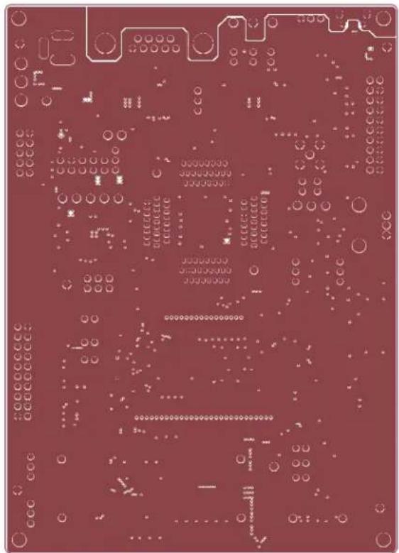
Green printed circuit board with integrated circuits and traces, no readable text or symbolsFigure 5-9. ATSAM4C-EK Layout: Ground Layer
natural_image
Close-up of a red printed circuit board with visible traces, pads, and electronic components (no readable text or symbols)Figure 5-10. ATSAM4C-EK Layout: Internal Signals 1 Layer

natural_image
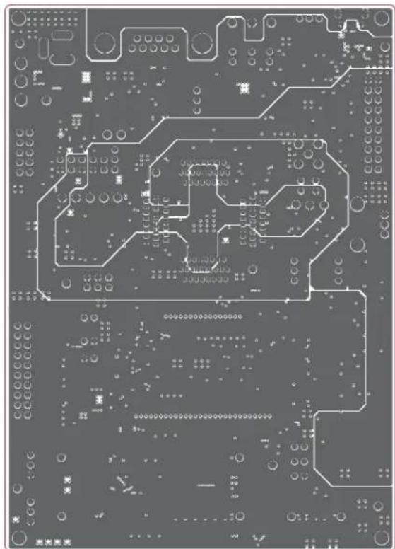
Close-up of a purple printed circuit board with visible traces and pads (no text or symbols)Figure 5-11. ATSAM4C-EK Layout: Internal Signals 2 Layer
natural_image
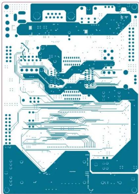
Blue printed circuit board pattern with various traces and pads (no text or symbols)Figure 5-12. ATSAM4C-EK Layout: Power Supplies Layer
natural_image
Close-up of a printed circuit board with traces and pads (no readable text or symbols)Figure 5-13. ATSAM4C-EK Layout: Bottom Layer

natural_image
Red printed circuit board with various traces and components, no visible text or symbolsFigure 5-14. ATSAM4C-EK Layout: TOP Components Placement
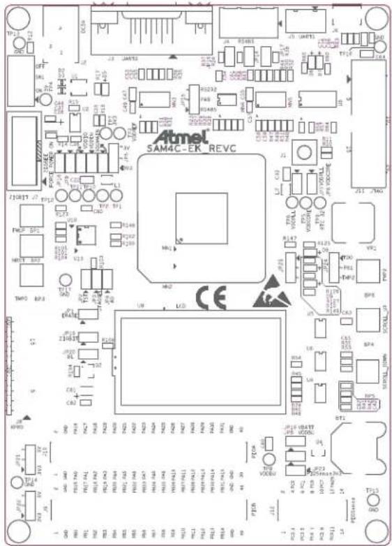
text_image
ATmel SAM4C-EK REVC CEFigure 5-15. ATSAM4C-EK Layout: BOTTOM Components Placement
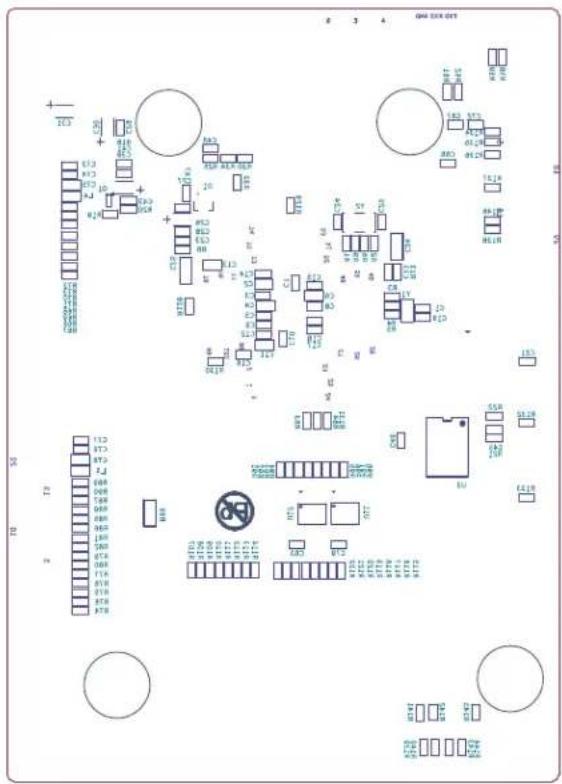
text_image
Circuit board layout diagram with component labels and pin connections6. Revision History
Table 6-1. Revision History
| Doc. Rev. Date Changes | |
| A 16-Dec-2013 First issue |
Atmel
Enabling Unlimited Possibilities®
Atmel Corporation
1600 Technology Drive
San Jose, CA 95110
USA
Tel: (+1) (408) 441-0311
Fax: (+1) (408) 487-2600
www.atmel.com
Atmel Asia Limited
Unit 01-5 & 16, 19F
BEA Tower, Millennium City 5
418 Kwun Tong Road
Kwun Tong, Kowloon
HONG KONG
Tel: (+852) 2245-6100
Fax: (+852) 2722-1369
Atmel Munich GmbH
Business Campus
Parkring 4
D-85748 Garching b. Munich
GERMANY
Tel: (+49) 89-31970-0
Fax: (+49) 89-3194621
Atmel Japan G.K.
16F Shin-Osaki Kangyo Bldg
1-6-4 Osaki, Shinagawa-ku
Tokyo 141-0032
JAPAN
Tel: (+81) (3) 6417-0300
Fax: (+81) (3) 6417-0370
© 2013 Atmel Corporation. All rights reserved. / Rev.: 11251A–ATARM–16-Dec-13
Atmel®, Atmel logo and combinations thereof, Enabling Unlimited Possibilities®, and others are registered trademarks or trademarks of Atmel Corporation or its subsidiaries. ARM®, Cortex®, and others are registered trademarks or trademarks of ARM Ltd. Other terms and product names may be trademarks of others.
Disclaimer: The information in this document is provided in connection with Atmel products. No license, express or implied, by estoppel or otherwise, to any intellectual property right is granted by this document or in connection with the sale of Atmel products. EXCEPT AS SET FORTH IN THE ATMEL TERMS AND CONDITIONS OF SALES LOCATED ON THE ATMEL WEBSITE, ATMEL ASSUMES NO LIABILITY WHATSOEVER AND DISCLAIMS ANY EXPRESS, IMPLIED OR STATUTORY WARRANTY RELATING TO ITS PRODUCTS INCLUDING, BUT NOT LIMITED TO, THE IMPLIED WARRANTY OF MERCHANTABILITY, FITNESS FOR A PARTICULAR PURPOSE, OR NON-INFRINGEMENT. IN NO EVENT SHALL ATMEL BE LIABLE FOR ANY DIRECT, INDIRECT, CONSEQUENTIAL, PUNITIVE, SPECIAL OR INCIDENTAL DAMAGES (INCLUDING WITHOUT LIMITATION, DAMAGES FOR LOSS AND PROFITS, BUSINESS INTERRUPTION, OR LOSS OF INFORMATION) ARISING OUT OF THE USE OR INABILITY TO USE THIS DOCUMENT, EVEN IF ATMEL HAS BEEN ADVISED OF THE POSSIBILITY OF SUCH DAMAGES. Atmel makes no representations or warranties with respect to the accuracy or completeness of the contents of this document and reserves the right to make changes to specifications and products descriptions at any time without notice. Atmel does not make any commitment to update the information contained herein. Unless specifically provided otherwise, Atmel products are not suitable for, and shall not be used in, automotive applications. Atmel products are not intended, authorized, or warranted for use as components in applications intended to support or sustain life.