HV9967B - Electronic component Microchip - Free user manual and instructions
Find the device manual for free HV9967B Microchip in PDF.

User questions about HV9967B Microchip
0 question about this device. Answer the ones you know or ask your own.
Ask a new question about this device
Download the instructions for your Electronic component in PDF format for free! Find your manual HV9967B - Microchip and take your electronic device back in hand. On this page are published all the documents necessary for the use of your device. HV9967B by Microchip.
USER MANUAL HV9967B Microchip
Integrated LED Driver with Average-Mode Current Control
Features
• 3% Accurate LED Current
• 60V, 0.8Ω Integrated MOSFET
- Low Sensitivity to External Component Variation
- Single-Resistor LED Current Setting
• Fixed Off-Time Control
- PWM Dimming Input
- Output Short-Circuit Protection with Skip Mode
• Overtemperature Protection
Applications
• DC/DC or AC/DC LED Drivers
- RGB Backlighting Drivers for Flat Panel Displays
- General Purpose Constant-Current Source
• Signage and Decorative LED Lighting
- Chargers
General Description
The HV9967B is an Average-mode current control LED driver IC operating in a Constant Off-time mode.
The IC features an integrated 60V, 0.8Ω MOSFET that can be used as a stand-alone buck converter switch or connected as a source driver for driving an external high-voltage Depletion-mode MOSFET. The HV9967B is powered through its switching output when the integrated switch is off. Therefore, the same external MOSFET can be used as a high-voltage linear regulator for powering the IC.
The LED current is programmed with one external resistor. The Average-mode current control method does not produce a peak-to-average error. This greatly improves the current accuracy as well as the line and load regulations of the LED current without any need for loop compensation or direct sensing of the LED current at a high-voltage potential. The auto-zero circuit cancels the effects of the input offset voltage and of the propagation delay of the current sense comparator.
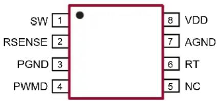
Package Types
8-lead MSOP
(Top view)
text_image
SW 1 RSENSE 2 PGND 3 PWMD 4 8 VDD 7 AGND 6 RT 5 NC8-lead WDFN
(Top view)
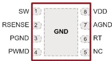
text_image
SW 1 GND 8 VDD RSENSE 2 7 AGND PGND 3 6 RT PWMD 4 5 NCSee Table 2-1 for pin information.
Functional Block Diagram
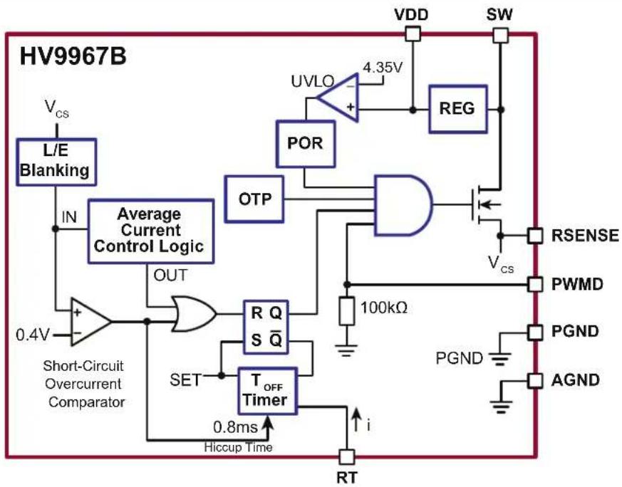
flowchart
graph TD
    A["L/E Blanking"] -->|IN| B["Average Current Control Logic"]
    B --> C["OUT"]
    C --> D["R Q S Q̅"]
    D --> E["T_OFF Timer"]
    E --> F["SET"]
    F --> G["0.4V Short-Circuit Overcurrent Comparator"]
    G --> H["Vcs"]
    H --> I["LV"]
    I --> J["AVLO"]
    J --> K["+"]
    K --> L["REG"]
    L --> M["VDD"]
    M --> N["SW"]
    O["100kΩ"] --> P["AND Gate"]
    Q["Vcs"] --> R["RSENSE"]
    S["PWMD"] --> T["PGND"]
    U["PGND"] --> V["AGND"]
    W["Hiccup Time"] --> X["0.8ms"]
    Y["i"] --> Z["RT"]
Typical Application Circuit

text_image
8 VDC to 60 VDC U1 4 PWMD HV9967B SW 1 L1 R_SENSE 2 R_SENSE PGND AGND RT 3 7 6 8 R_T C_DD + C_IN D1 C_o LED String1.0 ELECTRICAL CHARACTERISTICS
Absolute Maximum Ratings ^()
| SW to GND | -0.5V to +65V |
| V_DD to GND | -0.3V to 6V |
| Other I/O to GND | -0.3V to ( V_DD + 0.3V) |
| I_RT | 2 mA |
| Junction Temperature Range, T_J | -40°C to +150°C |
| Storage Temperature Range, T_S | -65°C to +150°C |
| Continuous Power Dissipation ( T_A = +25°C): | |
| 8-lead MSOP | 350 mW |
| 8-lead WDFN | 1.6W |
Notice: Stresses above those listed under “Absolute Maximum Ratings” may cause permanent damage to the device. This is a stress rating only, and functional operation of the device at those or any other conditions above those indicated in the operational sections of this specification is not intended. Exposure to maximum rating conditions for extended periods may affect device reliability.
ELECTRICAL CHARACTERISTICS
| Electrical Specifications: T_A=25°C, V_SW=10V/10 mA, V_DD=5V unless otherwise specified. | ||||||
| Parameter Sym. Min. Typ. Max. Unit Conditions | ||||||
| INPUT | ||||||
| Input DC Supply Voltage Range V | SWDC | 8 | — | 60 | V | DC input voltage (Note 1) |
| Shutdown Mode Supply Current | I_INSD | — | 0.5 | 1 | mA Pin PWMD connected to GND | |
| INTERNAL REGULATOR | ||||||
| Internally Regulated Voltage | V_DD | 4.7 | 5 | 5.2 | V | V_PWMD=V_DD, R_T=100 kΩ |
| V_DD Undervoltage Lockout Upper Threshold | V_UVLOR | 4.1 | 4.35 | 4.7 | V | V_DD rising, as needed to ensure I_C(MIN) (Note 1) |
| V_DD Undervoltage Lockout Hysteresis | V_UVLO | — | 150 | — | mV V | D_D falling |
| PMW DIMMING | ||||||
| PWMD Input Low Voltage | V_EN(LO) | — | — | 0.8 | V | Note 1 |
| PWMD Input High Voltage | V_EN(HI) | 2.2 | — | — | V | Note 1 |
| PWMD Pull-Down Resistance | R_EN | 50 | 100 | 150 | kΩ | V_PWMD=5V |
| CURRENT CONTROL | ||||||
| RSENSE Current Threshold Voltage | V_CS(TH) | 243 | 250 | 257 | mV | |
| Threshold Voltage Temperature Coefficient | dV_CS/dT | — | 0.1 — | mV/°C | ||
| Current Sense Blanking Interval | T_BLANK | 140 | — | 290 | ns | Note 1 |
| Minimum On-Time | T_ON(MIN) | — | — | 950 | ns | V_RSENSE=V_CS(TH)+50 mV (Note 1) |
| Maximum Steady-State Duty Cycle | D_MAX | 80 | — | — | % | Reduction in output LED current may occur beyond this duty cycle. (Note 1) |
| SHORT-CIRCUIT PROTECTION | ||||||
| Hiccup Threshold Voltage at RSENSE | V_CS(SHORT) | 355 | 400 | 440 | mV | Note 1 |
| Current Limit Delay RSENSE to SW-OFF | T_DELAY | — | — | 150 | ns | V_RSENSE=V_CS(SHORT)+50 mV |
Note 1: Denotes specifications which apply over the full operating ambient temperature range of
-40^ < T_A < +125^
2: For design guidance only
ELECTRICAL CHARACTERISTICS (CONTINUED)
| Electrical Specifications: TA=25°C, VSW=10V/10 mA, VDD=5V unless otherwise specified. | ||||||
| Parameter | Sym. | Min. | Typ. | Max. | Unit | Conditions |
| Short-Circuit Hiccup Time T | HICCUP | —80 | 0—μs | |||
| Minimum On-Time (Short-Circuit) T | ON(MIN),SC | — — | 400 ns | VRSENSE=VCS(SHORT)+50 mV | ||
| TOFF TIMER | ||||||
| Off Time T | OFF | 28 40 | 48 | μs | RT=100 kΩ (Note 1) | |
| 7 10 | 12 R | T=100 kΩ (Note 1) | ||||
| 0.7 1 | 1.2 R | T=10 kΩ (Note 1) | ||||
| SW OUTPUT | ||||||
| On Resistance | RON | — | 0.8 | — | Ω | VDD=5V |
| Continuous Current | IC | 0.75 | — | — | A | VDD=4.75V, VRSENSE=370 mV, VSW=10V (Note 1) |
| OVERTEMPERATURE PROTECTION | ||||||
| Thermal Shutdown Temperature | TSD | 125 | 145 | — | °C | Note 2 |
| Thermal Shutdown Hysteresis | ΔTSD | —20 | —°C | Note 2 | ||
Note 1: Denotes specifications which apply over the full operating ambient temperature range of -40^ < T_A < +125^
2: For design guidance only
TEMPERATURE SPECIFICATIONS
| Parameter | Sym. | Min. | Typ. | Max. | Unit | Conditions |
| TEMPERATURE RANGE | ||||||
| Operating Ambient Temperature | T_A | -40 — | +125 °C | |||
| Maximum Junction Temperature | T_J(ABSMAX) | — — | +150 °C | |||
| Storage Temperature | Ts | -65 | — | +150 | °C | |
| PACKAGE THERMAL RESISTANCE | ||||||
| 8-lead MSOP | _JA | — 216 | — | °C/W | ||
| 8-lead WDFN | _JA | — 60 | — | °C/W | ||
2.0 PIN DESCRIPTION
Table 2-1 shows the pin description details of HV9967B. Refer to Package Types for the location of pins.
TABLE 2-1: PIN FUNCTION TABLE
| Pin Number | Pin Name Description | |
| 1 SW | Drain of 60V 0.8Ω | NDMOS switch and input of H/V regulator |
| 2 RSENSE | Source of NDMOS switch and current sense input. Connect a resistor between RSENSE and GND to program the output current and short-circuit protection tripping current. | |
| 3 PGND | Power ground. | Must be wired to AGND on PCB. |
| 4 PWMD | PWM dimming input. | This TTL input enables switching of SW when in High state. |
| 5 | NC | No connection |
| 6 | RT | Resistor connected between RT and VDD. This programs the off time of SW. |
| 7 AGND | Analog ground (0V) | |
| 8 | VDD | Power supply for all internal circuits. Bypass with a low-ESR capacitor to PGND (>0.5 μF). Connect gate of external Depletion-mode NFET for high-voltage operation. |
3.0 APPLICATION INFORMATION
3.1 General Description
The HV9967B employs a control scheme that achieves fast and extremely accurate control of the average current in the buck inductor by sensing only the switch current. No compensation of the current control loop is required. The LED current response to PWMD input is similar to that of the peak-current control ICs, such as the HV9910B. The inductor current ripple amplitude does not affect this control scheme significantly. Therefore, the LED current is independent of the variation in inductance, switching frequency, and output voltage. Constant off-time control of the buck converter is used for stability and to reduce input voltage regulation of the LED current.
3.2 Off Timer
The timing resistor connected to RT pindetermines the off time of the gate driver and SW. The timing resistor must be wired across RT pin and VDD pin. Refer to Equation 3-1 for the computation of the SW off time.
EQUATION 3-1:
$$ \begin{array}{r l} & T _ {O F F} = R _ {T} \times 1 0 0 p F \ & \text { Within the range of } 1 0 \mathrm{k} \Omega \leq R _ {\mathrm{T}} \leq 4 0 0 \mathrm{k} \Omega \end{array} $$
3.3 Average Current Control Feedback and Output Short-Circuit Protection
The constant-current control feedback derives the average-current signal from the source current of the switching MOSFET. This current is detected with a sense resistor at the RSENSE pin. The feedback operates in a fast Open-loop mode. No compensation is required. Output current is programmed as seen in Equation 3-2:
EQUATION 3-2:
$$ I _ {L E D} = \frac {0 . 2 5 V}{R _ {C S}} $$
The above equation is only valid for continuous conduction of the output inductor. It is a good practice to design the inductor such that the peak-to-peak switching inductor ripple current in it is 30% to 40% of its average full DC current load. Hence, the recommended inductance can be computed as specified in Equation 3-3:
EQUATION 3-3:
$$ L _ {O} = \frac {V _ {Q M A X)} \times T _ {O F F}}{0 . 4 \times I _ {O}} $$
The duty cycle range of the current control feedback is limited to D ≤ 0.8 . A reduction in the LED current may occur when the LED string voltage V_O is greater than 80% of the input voltage V_IN of the HV9967B LED driver.
Reducing the output LED voltage V_O below V_O(MIN) = V_IN × D_MIN , where D_MIN = 0.8 s/(T_OFF + 8 s) , may also result in loss of LED current regulation. This condition, however, causes an increase in the LED current and can potentially trip the short-circuit protection comparator threshold.
The short-circuit protection comparator trips when the voltage at RSENSE exceeds 0.4V. When this occurs, the SW off time T_HICCUP = 800 s is generated to prevent the staircasing of the inductor current and, potentially, its saturation due to insufficient output voltage. The typical short-circuit inductor current is shown in the waveform in Figure 3-1.

line
| Time (μs) | Value | | --------- | --------- | | 0 | 0.44 | | 800 | 800 |FIGURE 3-1: Short-Circuit Inductor Current.
A leading-edge blanking delay is provided at RSENSE pin to prevent false triggering of the short-circuit hiccup threshold voltage and the short-circuit protection.
3.4 SW Input and Linear Regulator
The HV9967B includes an integrated 60V, 0.8Ω switching MOSFET at the SW input. The power for the IC is supplied from a built-in linear 5V regulator that is also derived from the SW input.
3.5 PWM Dimming
The HV9967B features a TTL-compatible dimming input PWMD. Applying a square-wave voltage to PWMD will modulate the duty ratio of the LED current accordingly. The rising and falling edges are limited by the current slew rate in the inductor. The first switching cycle is terminated upon reaching the 250 mV level at RSENSE pin. The circuit will reach the Steady state within three to four switching cycles regardless of the switching frequency.
3.6 Overtemperature Protection
The HV9967B includes overtemperature protection. Typically, when the junction temperature exceeds 145^ C, switching of the SW input is disabled. The switching resumes when the temperature falls by approximately 20^ C from the trip point.
4.0 PACKAGING INFORMATION
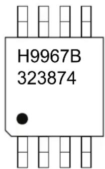
4.1 Package Marking Information
8-lead MSOP
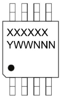
text_image
XXXXXX YWWNNN8-lead WDFN
Example
text_image
H9967B 323874Example
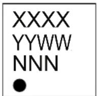
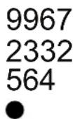
Legend: XX...X Product Code or Customer-specific information
Y Year code (last digit of calendar year)
YY Year code (last 2 digits of calendar year)
WW Week code (week of January 1 is week '01')
NNN Alphanumeric traceability code
epb-free JEDEC ^® designator for Matte Tin (Sn)
* This package is Pb-free. The Pb-free JEDEC designator ( ) e3
can be found on the outer packaging for this package.
Note: In the event the full Microchip part number cannot be marked on one line, it will be carried over to the next line, thus limiting the number of available characters for product code or customer-specific information. Package may or not include the corporate logo.
8-Lead Plastic Micro Small Outline Package (MS) - 3x3 mm Body [MSOP]
Note: For the most current package drawings, please see the Microchip Packaging Specification located at http://www.microchip.com/packaging
![Microchip HV9967B - 8-Lead Plastic Micro Small Outline Package (MS) - 3x3 mm Body [MSOP] - 1](/content/2026/06/1221674/images/ec4b4b994e0766b36b774f79e2abc844376ad74c6c4fe976c30cedb2a2cecd8e.jpg)
text_image
2X 0.20 H D D/2 A N E1/2 E1 2X 0.20 H NOTE 1 1 2 e B D/2 E E 2X 4 TIPS 0.25 CTOP VIEW
![Microchip HV9967B - 8-Lead Plastic Micro Small Outline Package (MS) - 3x3 mm Body [MSOP] - 2](/content/2026/06/1221674/images/01d7a989345e5bd56f7062cec05b3b7b898e08d8aa59aecee90143ff9ee776a7.jpg)
text_image
A A2 A1 8X 0.10 C SEATING PLANE C 8X b Ø 0.25 M A-B D ASIDE VIEW
![Microchip HV9967B - 8-Lead Plastic Micro Small Outline Package (MS) - 3x3 mm Body [MSOP] - 3](/content/2026/06/1221674/images/40ea49043f761e8cfa0605841a8899fdd11872d4bc9595a28bb0f0ff3283b8f4.jpg)
text_image
H SEE DETAIL BVIEW A-A
Microchip Technology Drawing C04-111-MS Rev F Sheet 1 of 2
© 2022 Microchip Technology Inc.
8-Lead Plastic Micro Small Outline Package (MS) - 3x3 mm Body [MSOP]
Note: For the most current package drawings, please see the Microchip Packaging Specification located at http://www.microchip.com/packaging
![Microchip HV9967B - 8-Lead Plastic Micro Small Outline Package (MS) - 3x3 mm Body [MSOP] - 1](/content/2026/06/1221674/images/c678c4b733f7c98034c528a5e4a8307fd9d76270098ae45be24e6062b403981d.jpg)
text_image
4X θ1 R1 H R SEATING PLANE C L (L1) 4X θ1 c θDETAIL B
![Microchip HV9967B - 8-Lead Plastic Micro Small Outline Package (MS) - 3x3 mm Body [MSOP] - 2](/content/2026/06/1221674/images/00d0db1e54c9794d42e2919a544eb63ecc5afd78b37c2f033fc2f5df4d7ed2ee.jpg)
natural_image
Isometric line drawing of an integrated circuit chip with multiple pins (no text or symbols)| Units | MILLIMETERS | |||
| Dimension Limits | MIN | NOM | MAX | |
| Number of Terminals | N | 8 | ||
| Pitch | e | 0.65 BSC | ||
| Overall Height | A | - | - | 1.10 |
| Standoff | A1 | 0.00 | - | 0.15 |
| Molded Package Thickness | A2 | 0.75 | 0.85 | 0.95 |
| Overall Length D 3.00 BSC | ||||
| Overall Width | E | 4.90 BSC | ||
| Molded Package Width | E1 | 3.00 BSC | ||
| Terminal Width | b | 0.22 | - | 0.40 |
| Terminal Thickness | c | 0 | . | 0 8 |
| Terminal Length | L | 0.40 | 0.60 | 0.80 |
| L1 0.95 REFFootprint | ||||
| R | -0.07 | -Lead Bend | ||
| R1 | -0.07 | -Lead Bend | ||
| θ | -0° 8° | Foot Angle | ||
| Draft Angle | θ1 | -5° 15° | ||
Radius Radius
Notes:
- Pin 1 visual index feature may vary, but must be located within the hatched area.
- Dimensions D and E1 do not include mold flash or protrusions. Mold flash or protrusions shall not exceed 0.15mm per side.
- Dimensioning and tolerancing per ASME Y14.5M BSC: Basic Dimension. Theoretically exact value shown without tolerances. REF: Reference Dimension, usually without tolerance, for information purposes only.
Microchip Technology Drawing C04-111-MS Rev F Sheet 2 of 2
8-Lead Plastic Micro Small Outline Package (MS) - 3x3 mm Body [MSOP]
Note: For the most current package drawings, please see the Microchip Packaging Specification located at http://www.microchip.com/packaging
![Microchip HV9967B - 8-Lead Plastic Micro Small Outline Package (MS) - 3x3 mm Body [MSOP] - 1](/content/2026/06/1221674/images/d26f686a211688625bd33c96c9dcb11a500bd1b38aed08b5d7d2afb23e877ac8.jpg)
text_image
GX C G1 SILK SCREEN Y X ERECOMMENDED LAND PATTERN
| Units | MILLIMETERS | |||
| Dimension Limits | MIN | NOM | MAX | |
| Contact Pitch | E | 0.65 BSC | ||
| CContact Pad Spacing 4.40 | ||||
| Contact Pad Width (X8) | X | 0.45 | ||
| Contact Pad Length (X8) | Y | 1.45 | ||
| Contact Pad to Contact Pad (X4) G1 | 2.95 | |||
| Contact Pad to Contact Pad (X6) GX | 0.20 | |||
Notes:
Dimensioning and tolerancing per ASME Y14.5M1.
BSC: Basic Dimension. Theoretically exact value shown without tolerances.
Microchip Technology Drawing C04-2111-MS Rev F
© 2022 Microchip Technology Inc.
8-Lead Very, Very Thin Plastic Dual Flat, No Lead Package (UQ) - 3x3 mm Body [WDFN]; Supertex Legacy Package
Note: For the most current package drawings, please see the Microchip Packaging Specification located at http://www.microchip.com/packaging
![Microchip HV9967B - 8-Lead Very, Very Thin Plastic Dual Flat, No Lead Package (UQ) - 3x3 mm Body [WDFN]; Supertex Legacy Package - 1](/content/2026/06/1221674/images/92abe7c735097bd87e390265edeebdb14bd45afd756efd5ee5a0075920ae1187.jpg)
text_image
(DATUM A) (DATUM B) NOTE 1 2X 0.15 C 2X 0.15 C TOP VIEW SEATING PLANE A θ // 0.10 C A1 SIDE VIEW 8X 0.08 C NOTE 1 D2 1 4 E2 K L N 5 8X b See Detail A for Pullback Leads alternative e 0.10 A B 0.05 B BOTTOM VIEWMicrochip Technology Drawing C04-291 Rev A Sheet 1 of 2
8-Lead Very, Very Thin Plastic Dual Flat, No Lead Package (UQ) - 3x3 mm Body [WDFN]; Supertex Legacy Package
Note: For the most current package drawings, please see the Microchip Packaging Specification located at http://www.microchip.com/packaging
![Microchip HV9967B - 8-Lead Very, Very Thin Plastic Dual Flat, No Lead Package (UQ) - 3x3 mm Body [WDFN]; Supertex Legacy Package - 2](/content/2026/06/1221674/images/03998070418511b320787ab99ce23e404b21775d93418df0ec86e66b126598d4.jpg)
text_image
L L1 DETAIL A| Units | MILLIMETERS | |||
| Dimension Limits | MIN | NOM | MAX | |
| Number of Terminals | N | 8 | ||
| Pitch | e | 0.65 BSC | ||
| Overall Height | A | 0.70 | 0.75 | 0.80 |
| Standoff | A1 | 0.00 | 0.02 | 0.05 |
| Terminal Thickness | A3 | 0.20 REF | ||
| Overall Length | D | 3.00 BSC | ||
| Exposed Pad Length | D2 1.60 | - | 2 | |
| Overall Width | E | 3.00 BSC | ||
| Exposed Pad Width | E2 | 1.35 - 1.75 | ||
| Terminal Width | b | 0.25 | 0.30 | 0.35 |
| Terminal Length | L | 0.30 | 0.40 | 0.50 |
| Pullback L1 -- 0.15 | ||||
| Mold Angle 0° 7° 14° | θ | |||
| K | -0.20 - | |||
. 5 0 0.20 -Terminal-to-Expos
Notes:
- Pin 1 visual index feature may vary, but must be located within the hatched area.
- Package is saw singulated
- Dimensioning and tolerancing per ASME Y14.5M
BSC: Basic Dimension. Theoretically exact value shown without tolerances.
REF: Reference Dimension, usually without tolerance, for information purposes only.
Microchip Technology Drawing C04-291A Sheet 2 of 2
8-Lead Very, Very Thin Plastic Dual Flat, No Lead Package (UQ) - 3x3 mm Body [WDFN]; Supertex Legacy Package
Note: For the most current package drawings, please see the Microchip Packaging Specification located at http://www.microchip.com/packaging
![Microchip HV9967B - 8-Lead Very, Very Thin Plastic Dual Flat, No Lead Package (UQ) - 3x3 mm Body [WDFN]; Supertex Legacy Package - 1](/content/2026/06/1221674/images/69561521bca2de899aded46769007a5c05a4532be840400f0acf12aa99b29f07.jpg)
text_image
X2 EV 8 C1 Y2 EV ØV G1 Y1 1 2 X1 E SILK SCREENRECOMMENDED LAND PATTERN
| Units | MILLIMETERS | |||
| Dimension Limits | MIN | NOM | MAX | |
| Contact Pitch | E | 0.65 BSC | ||
| Optional Center Pad Width | X2 | 2.50 | ||
| Optional Center Pad Length | Y2 | 1.75 | ||
| C1C | Contact Pad S | pacing 3.00 | ||
| Contact Pad Width (X8) | X1 | 0.35 | ||
| Contact Pad Length (X8) | Y1 | 0.85 | ||
| Contact Pad to Center Pad (X8) G1 | 0.20 | |||
| Thermal Via Diameter V | 0.33 | |||
| Thermal Via Pitch EV | 1.20 | |||
Notes:
- Dimensioning and tolerancing per ASME Y14.5M
BSC: Basic Dimension. Theoretically exact value shown without tolerances.
- For best soldering results, thermal vias, if used, should be filled or tented to avoid solder loss during reflow process
Microchip Technology Drawing C04-2291 Rev A
© 2021 Microchip Technology Inc.
APPENDIX A: REVISION HISTORY
Revision B (June 2023)
- Changed PWMD Input High Voltage from 2V to 2.2V
- Changed the package type "8-lead DFN K7" to "8-lead WDFN K7"
- Updated the 8-lead WDFN K7 package outline drawings
• Made minor text changes throughout the document
Revision A (February 2020)
- Converted Supertex Doc# DSFP-HV9967B to Microchip DS20005734A
- Updated the package marking format
- Updated the packaging quantity of the 8-lead DFN K7 package from 3000/Reel to 3300/Reel to align it with the actual BQM
• Made minor text changes throughout the document
PRODUCT IDENTIFICATION SYSTEM
To order or obtain information, e.g., on pricing or delivery, contact your local Microchip representative or sales office.
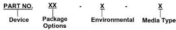
text_image
PART NO. Device XX Package Options X Environmental Media TypeDevice: HV9967B = Integrated LED Driver with Average-Mode Current Control
Packages: MG = 8-lead MSOP K7 = 8-lead WDFN
Environmental: G = Lead (Pb)-free/RoHS-compliant Package
Media Type: (blank) = 2500/Reel for an MG Package, 3300/Reel for a K7 Package
Examples:
a) HV9967BMG-G: Integrated LED Driver with Average-Mode Current Control, 8-lead MSOP, 2500/Reel
b) HV9967BK7-G: Integrated LED Driver with Average-Mode Current Control, 8-lead WDFN, 3300/Reel
Note the following details of the code protection feature on Microchip products:
• Microchip products meet the specifications contained in their particular Microchip Data Sheet.
- Microchip believes that its family of products is secure when used in the intended manner, within operating specifications, and under normal conditions.
- Microchip values and aggressively protects its intellectual property rights. Attempts to breach the code protection features of Microchip product is strictly prohibited and may violate the Digital Millennium Copyright Act.
- Neither Microchip nor any other semiconductor manufacturer can guarantee the security of its code. Code protection does not mean that we are guaranteeing the product is "unbreakable" Code protection is constantly evolving. Microchip is committed to continuously improving the code protection features of our products.
This publication and the information herein may be used only with Microchip products, including to design, test, and integrate Microchip products with your application. Use of this information in any other manner violates these terms. Information regarding device applications is provided only for your convenience and may be superseded by updates. It is your responsibility to ensure that your application meets with your specifications. Contact your local Microchip sales office for additional support or, obtain additional support at https://www.microchip.com/en-us/support/design-help/client-support-services.
THIS INFORMATION IS PROVIDED BY MICROCHIP "AS IS". MICROCHIP MAKES NO REPRESENTATIONS OR WARRANTIES OF ANY KIND WHETHER EXPRESS OR IMPLIED, WRITTEN OR ORAL, STATUTORY OR OTHERWISE, RELATED TO THE INFORMATION INCLUDING BUT NOT LIMITED TO ANY IMPLIED WARRANTIES OF NON-INFRINGEMENT, MERCHANTABILITY, AND FITNESS FOR A PARTICULAR PURPOSE, OR WARRANTIES RELATED TO ITS CONDITION, QUALITY, OR PERFORMANCE.
IN NO EVENT WILL MICROCHIP BE LIABLE FOR ANY INDIRECT, SPECIAL, PUNITIVE, INCIDENTAL, OR CONSEQUENTIAL LOSS, DAMAGE, COST, OR EXPENSE OF ANY KIND WHATSOEVER RELATED TO THE INFORMATION OR ITS USE, HOWEVER CAUSED, EVEN IF MICROCHIP HAS BEEN ADVISED OF THE POSSIBILITY OR THE DAMAGES ARE FORESEEABLE. TO THE FULLEST EXTENT ALLOWED BY LAW, MICROCHIP'S TOTAL LIABILITY ON ALL CLAIMS IN ANY WAY RELATED TO THE INFORMATION OR ITS USE WILL NOT EXCEED THE AMOUNT OF FEES, IF ANY, THAT YOU HAVE PAID DIRECTLY TO MICROCHIP FOR THE INFORMATION.
Use of Microchip devices in life support and/or safety applications is entirely at the buyer's risk, and the buyer agrees to defend, indemnify and hold harmless Microchip from any and all damages, claims, suits, or expenses resulting from such use. No licenses are conveyed, implicitly or otherwise, under any Microchip intellectual property rights unless otherwise stated.
Trademarks
The Microchip name and logo, the Microchip logo, Adaptec, AVR, AVR logo, AVR Freaks, BesTime, BitCloud, CryptoMemory, CryptoRF, dsPIC, flexPWR, HELDO, IGLOO, JukeBlox, KeeLoq, Kleer, LANCheck, LinkMD, maXStylus, maXTouch, MediaLB, megaAVR, Microsemi, Microsemi logo, MOST, MOST logo, MPLAB, OptoLyzer, PIC, picoPower, PICSTART, PIC32 logo, PolarFire, Prochip Designer, QTouch, SAM-BA, SenGenuity, SpyNIC, SST, SST Logo, SuperFlash, Symmetricom, SyncServer, Tachyon, TimeSource, tinyAVR, UNI/O, Vectron, and XMEGA are registered trademarks of Microchip Technology Incorporated in the U.S.A. and other countries.
AgileSwitch, APT, ClockWorks, The Embedded Control Solutions Company, EtherSynch, Flashtec, Hyper Speed Control, HyperLight Load, Libero, motorBench, mTouch, Powermite 3, Precision Edge, ProASIC, ProASIC Plus, ProASIC Plus logo, Quiet-Wire, SmartFusion, SyncWorld, Temux, TimeCesium, TimeHub, TimePictra, TimeProvider, TrueTime, and ZL are registered trademarks of Microchip Technology Incorporated in the U.S.A.
Adjacent Key Suppression, AKS, Analog-for-the-Digital Age, Any Capacitor, AnyIn, AnyOut, Augmented Switching, BlueSky, BodyCom, Clockstudio, CodeGuard, CryptoAuthentication, CryptoAutomotive, CryptoCompanion, CryptoController, dsPICDEM, dsPICDEM.net, Dynamic Average Matching, DAM, ECAN, Espresso T1S, EtherGREEN, GridTime, IdealBridge, In-Circuit Serial Programming, ICSP, INICnet, Intelligent Paralleling, IntelliMOS, Inter-Chip Connectivity, JitterBlocker, Knob-on-Display, KoD, maxCrypto, maxView, memBrain, Mindi, MiWi, MPASM, MPF, MPLAB Certified logo, MPLIB, MPLINK, MultiTRAK, NetDetach, Omniscient Code Generation, PICDEM, PICDEM.net, PICkit, PICtail, PowerSmart, PureSilicon, QMatrix, REAL ICE, Ripple Blocker, RTAX, RTG4, SAM-ICE, Serial Quad I/O, simpleMAP, SimpliPHY, SmartBuffer, SmartHLS, SMART-I.S., storClad, SQI, SuperSwitcher, SuperSwitcher II, Switchtec, SynchroPHY, Total Endurance, Trusted Time, TSHARC, USBCheck, VariSense, VectorBlox, VeriPHY, ViewSpan, WiperLock, XpressConnect, and ZENA are trademarks of Microchip Technology Incorporated in the U.S.A. and other countries.
SQTP is a service mark of Microchip Technology Incorporated in the U.S.A.
The Adaptec logo, Frequency on Demand, Silicon Storage Technology, and Symmcom are registered trademarks of Microchip Technology Inc. in other countries.
GestIC is a registered trademark of Microchip Technology Germany II GmbH & Co. KG, a subsidiary of Microchip Technology Inc., in other countries.
All other trademarks mentioned herein are property of their respective companies.
© 2023, Microchip Technology Incorporated and its subsidiaries.
All Rights Reserved.
ISBN: 978-1-6683-2706-7
For information regarding Microchip's Quality Management Systems, please visit www.microchip.com/quality.
Worldwide Sales and Service
AMERICAS
Corporate Office
2355 West Chandler Blvd.
Chandler, AZ 85224-6199
Tel: 480-792-7200
Fax: 480-792-7277
Technical Support:
http://www.microchip.com/
support
Web Address:
www.microchip.com
Atlanta
Duluth, GA
Tel: 678-957-9614
Fax: 678-957-1455
Austin, TX
Tel: 512-257-3370
Boston
Westborough, MA
Tel: 774-760-0087
Fax: 774-760-0088
Chicago
Itasca, IL
Tel: 630-285-0071
Fax: 630-285-0075
Dallas
Addison, TX
Tel: 972-818-7423
Fax: 972-818-2924
Detroit
Novi, MI
Tel: 248-848-4000
Houston, TX
Tel: 281-894-5983
Indianapolis
Noblesville, IN
Tel: 317-773-8323
Fax: 317-773-5453
Tel: 317-536-2380
Los Angeles
Mission Viejo, CA
Tel: 949-462-9523
Fax: 949-462-9608
Tel: 951-273-7800
Raleigh, NC
Tel: 919-844-7510
New York, NY
Tel: 631-435-6000
San Jose, CA
Tel: 408-735-9110
Tel: 408-436-4270
Canada - Toron
Tel: 905-695-1980
Fax: 905-695-2078
ASIA/PACIFIC
Australia - Sydney
Tel: 61-2-9868-6733
China - Beijing
Tel: 86-10-8569-7000
China - Chengdu
Tel: 86-28-8665-5511
China - Chongqing
Tel: 86-23-8980-9588
China - Dongguan
Tel: 86-769-8702-9880
China - Guangzhou
Tel: 86-20-8755-8029
China - Hangzhou
Tel: 86-571-8792-8115
China - Hong Kong SAR
Tel: 852-2943-5100
China - Nanjing
Tel: 86-25-8473-2460
China - Qingdao
Tel: 86-532-8502-7355
China - Shanghai
Tel: 86-21-3326-8000
China - Shenyang
Tel: 86-24-2334-2829
China - Shenzhen
Tel: 86-755-8864-2200
China - Suzhou
Tel: 86-186-6233-1526
China - Wuhan
Tel: 86-27-5980-5300
China - Xian
Tel: 86-29-8833-7252
China - Xiamen
Tel: 86-592-2388138
China - Zhuhai
Tel: 86-756-3210040
ASIA/PACIFIC
India - Bangalore
Tel: 91-80-3090-4444
India - New Delhi
Tel: 91-11-4160-8631
India - Pune
Tel: 91-20-4121-0141
Japan - Osaka
Tel: 81-6-6152-7160
Japan - Tokyo
Tel: 81-3-6880-3770
Korea - Daegu
Tel: 82-53-744-4301
Korea - Seoul
Tel: 82-2-554-7200
Malaysia - Kuala Lumpur
Tel: 60-3-7651-7906
Malaysia - Penang
Tel: 60-4-227-8870
Philippines - Manila
Tel: 63-2-634-9065
Singapore
Tel: 65-6334-8870
Taiwan - Hsin Chu
Tel: 886-3-577-8366
Taiwan - Kaohsiung
Tel: 886-7-213-7830
Taiwan - Taipei
Tel: 886-2-2508-8600
Thailand - Bangkok
Tel: 66-2-694-1351
Tel: 43-7242-2244-39
Fax: 43-7242-2244-393
Denmark - Copenhagen
Tel: 45-4485-5910
Fax: 45-4485-2829
Finland - Espoo
Tel: 358-9-4520-820
France - Paris
Tel: 33-1-69-53-63-20
Fax: 33-1-69-30-90-79
Germany - Garching
Tel: 49-8931-9700
Germany - Haan
Tel: 49-2129-3766400
Germany - Heilbronn
Tel: 49-7131-72400
Germany - Karlsruhe
Tel: 49-721-625370
Germany - Munich
Tel: 49-89-627-144-0
Fax: 49-89-627-144-44
Germany - Rosenheim
Tel: 49-8031-354-560
Israel - Ra'anana
Tel: 972-9-744-7705
Italy - Milan
Tel: 39-0331-742611
Fax: 39-0331-466781
Italy - Padova
Tel: 39-049-7625286
Netherlands - Drunen
Tel: 31-416-690399
Fax: 31-416-690340
Norway - Trondheim
Tel: 47-7288-4388
Poland - Warsaw
Tel: 48-22-3325737
Romania - Bucharest
Tel: 40-21-407-87-50
Spain - Madrid
Tel: 34-91-708-08-90
Fax: 34-91-708-08-91
Sweden - Gothenberg
Tel: 46-31-704-60-40
Sweden - Stockholm
Tel: 46-8-5090-4654
UK - Wokingham
Tel: 44-118-921-5800
Fax: 44-118-921-5820