MCP6548 - Electronic component Microchip - Free user manual and instructions
Find the device manual for free MCP6548 Microchip in PDF.

User questions about MCP6548 Microchip
0 question about this device. Answer the ones you know or ask your own.
Ask a new question about this device
Download the instructions for your Electronic component in PDF format for free! Find your manual MCP6548 - Microchip and take your electronic device back in hand. On this page are published all the documents necessary for the use of your device. MCP6548 by Microchip.
USER MANUAL MCP6548 Microchip
Open-Drain Output Sub-Microamp Comparators
Features
- Low Quiescent Current: 600 nA/Comparator (typical)
• Rail-to-Rail Input: V_SS - 0.3V to V_DD + 0.3V - Open-Drain Output: V_OUT ≤ 10V
- Propagation Delay: 4 μs (typical, 100 mV Overdrive)
- Wide Supply Voltage Range: 1.6V to 5.5V
- Single Available in SOT-23-5, SC-70-5* Packages
• Available in Single, Dual and Quad
• Chip Select (CS) with MCP6548 - Low Switching Current
• Internal Hysteresis: 3.3 mV (typical)
• Temperature Ranges: - Industrial: -40°C to +85°C
- Extended: -40°C to +125°C
Typical Applications
- Laptop Computers
- Mobile Phones
- Metering Systems
- Handheld Electronics
- RC Timers
• Alarm and Monitoring Circuits - Windowed Comparators
- Multivibrators
Related Devices
• CMOS/TTL-Compatible Output: MCP6541/2/3/4
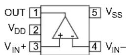
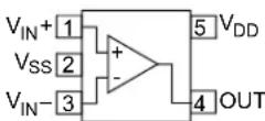
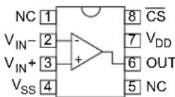
Package Types
MCP6546
PDIP, SOIC, MSOP
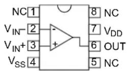
MCP6546R MCP6547
SOT-23-5
Description
The Microchip MCP6546/6R/6U/7/8/9 family of comparators, is offered in single (MCP6546, MCP6546R, MCP6546U), single with Chip Select (CS) (MCP6548), dual (MCP6547) and quad (MCP6549) configurations. The outputs are open-drain and are capable of driving heavy DC or capacitive loads.
These comparators are optimized for low-power, single-supply application with greater than rail-to-rail input operation. The output limits supply current surges and dynamic power consumption while switching. The open-drain output of the MCP6546/6R/6U/7/8/9 family can be used as a level-shifter for up to 10V using a pull-up resistor. It can also be used as a wired-OR logic. The internal input hysteresis eliminates output switching due to internal noise voltage, reducing current draw. These comparators operate with a single-supply voltage as low as 1.6V and draw a quiescent current of less than 1 A/comparator.
The related Microchip MCP6541/2/3/4 family of comparators has a push-pull output that supports rail-to-rail output swing and interfaces with CMOS/TTL logic.
Note that SC-70-5 E-Temp parts are not available at this release of the data sheet.
The MCP6546U SOT-23-5 is E-Temp only.
MCP6546
SC-70-5, SOT23-5

MCP6546U
SC-70-5, SOT-23-5
MCP6548
PDIP, SOIC, MSOP
V_DD - V_SS 7.0V
Open-Drain Output. V_SS + 10.5V
Analog Input (V IN +, V IN -)††...... V SS - 1.0V to V DD + 1.0V
All Other Inputs and Outputs .... V SS - 0.3V to V DD + 0.3V
Difference Input Voltage .... |V_DD - V_SS|
Output Short-Circuit Current ......Continuous
Current at Input Pins ....±2 mA
Current at Output and Supply Pins ....±30 mA
Storage Temperature ( T_S )....-65°C to +150°C
Maximum Junction Temperature (TJ) ....+150°C
ESD Protection on all Pins:
(HBM;MM) 2 kV;200V (MCP6546U)
(HBM;MM) 4 kV; 200V (all other parts)
† Notice: Stresses above those listed under “Absolute Maximum Ratings” may cause permanent damage to the device. This is a stress rating only and functional operation of the device at those or any other conditions above those indicated in the operational listings of this specification is not implied. Exposure to maximum rating conditions for extended periods may affect device reliability.
†† See Section 4.1.2 "Input Voltage and Current Limits".
DC CHARACTERISTICS
| Electrical Specifications: Unless otherwise indicated, V_DD = +1.6V to +5.5V , V_SS = GND , T_A = 25°C , V_IN + = V_DD/2 , V_IN - = V_SS , R_PU = 2.74 kΩ to V_PU = V_DD (Refer to Figure 1-3). | ||||||
| Parameters Sym Min | Typ Max Units | Conditions | ||||
| Power Supply | ||||||
| Supply Voltage | V_DD | 1.6 | — | 5.5 | V | V_PU ≥ V_DD |
| Quiescent Current per Comparator | I_Q | 0.3 | 0.6 | 1 | μA | I_OUT = 0 |
| Input | ||||||
| Input Voltage Range | V_CMR | V_SS-0.3 | — | V_DD+0.3 | V | |
| Common-mode Rejection Ratio | CMRR | 55 | 70 | — | dB | V_DD = 5V , V_CM = -0.3V to 5.3V |
| Common-mode Rejection Ratio | CMRR | 50 | 65 | — | dB | V_DD = 5V , V_CM = 2.5V to 5.3V |
| Common-mode Rejection Ratio | CMRR | 55 | 70 | — | dB | V_DD = 5V , V_CM = -0.3V to 2.5V |
| Power Supply Rejection Ratio | PSRR | 63 | 80 | — | dB | V_CM = V_SS |
| Input Offset Voltage | V_OS | -7.0 ± 1.5 | +7.0 mV | V | _CM = V_SS (Note 1) | |
| Drift with Temperature | V_OS/ T_A | — | ±3 | — μV/°C | T_A = -40°C to +125°C , V_CM = V_SS | |
| Input Hysteresis Voltage | V_HYST | 1.5 | 3.3 | 6.5 | mV | V_CM = V_SS (Note 1) |
| Linear Temp. Co. | TC_1 | — | 6.7 | — | μV/°C | T_A = -40°C to +125°C , V_CM = V_SS (Note 2) |
| Quadratic Temp. Co. TC | 2 | — | -0.035 | — μV/°C | ^2 | T_A = -40°C to +125°C , V_CM = V_SS (Note 2) |
| Input Bias Current | I_B | — | 1 | — pA | V | _CM = V_SS |
| At Temperature (I-Temp parts) | I_B | — | 25 | 100 | pA | T_A = +85°C , V_CM = V_SS (Note 3) |
| At Temperature (E-Temp parts) | I_B | — | 1200 | 5000 pA | T | _A = +125°C , V_CM = V_SS (Note 3) |
| Input Offset Current | I_OS | — | ±1 | — pA | V | _CM = V_SS |
Note 1: The input offset voltage is the center of the input-referred trip points. The input hysteresis is the difference between the input-referred trip points.
2: V_HYST at differential temperatures is estimated using:
V_HYST(T_A)=V_HYST+(T_A-25^)TC_1+(T_A-25^)^2TC_2.
3: Input bias current at temperature is not tested for the SC-70-5 package.
4: Do not short the output above V_SS + 10V . Limit the output current to Absolute Maximum Rating of 30 mA. The minimum V_PU test limit was V_DD before Dec. 2004 (week code 52).
DC CHARACTERISTICS (CONTINUED)
| Electrical Specifications: Unless otherwise indicated, V_DD = +1.6V to +5.5V , V_SS = GND , T_A = 25°C , V_IN+ = V_DD/2 , V_IN- = V_SS , R_PU = 2.74 k to V_PU = V_DD (Refer to Figure 1-3). | ||||||
| Parameters | Sym | Min | Typ | Max | Units | Conditions |
| Common-mode Input Impedance | Z_CM | — | 10^13||4 | — Ω||pF | ||
| Differential Input Impedance Z | DIFF | — | 10^13||2 | — Ω||pF | ||
| Open-Drain Output | ||||||
| Output Pull-Up Voltage V | PU | 1.6 — | 10 V (Note 4) | |||
| High-Level Output Current I | OH | -100 — | — nA V | _DD = 1.6V to 5.5V, V_PU = 10V (Note 4) | ||
| Low-Level Output Voltage | V_OL | V_SS | — | V_SS+0.2 | V I | _OUT = 2 mA , V_PU = V_DD = 5V |
| Short-Circuit Current | I_SC | — | ±1.5 | — | mA | V_PU = V_DD = 1.6V (Note 4) |
| I_SC | — | 30 — | mA | V | _PU = V_DD = 5.5V (Note 4) | |
| Output Pin Capacitance | C_OUT | — | 8 | — pF | ||
Note 1: The input offset voltage is the center of the input-referred trip points. The input hysteresis is the difference between the input-referred trip points.
2: V_HYST at differential temperatures is estimated using: V_HYST(T_A) = V_HYST + (T_A - 25^)TC_1 + (T_A - 25^)^2TC_2.
3: Input bias current at temperature is not tested for the SC-70-5 package.
4: Do not short the output above V_SS + 10V . Limit the output current to Absolute Maximum Rating of 30 mA. The minimum V_PU test limit was V_DD before Dec. 2004 (week code 52).
AC CHARACTERISTICS
| Electrical Specifications: Unless otherwise indicated, V_DD = +1.6V to +5.5V , V_SS = GND , T_A = 25°C , V_IN+ = V_DD/2 , Step = 200 mV, Overdrive = 100 mV, R_PU = 2.74 k to V_PU = V_DD , and C_L = 36 pF (Refer to Figure 1-2 and Figure 1-3). | ||||||
| Parameters | Sym | Min | Typ | Max | Units | Conditions |
| Fall Time | t_F | — | 0.7 | — | μs | (Note 1) |
| Propagation Delay (High-to-Low) | t_PHL | — | 4.0 8.0 μs | |||
| Propagation Delay (Low-to-High) | t_PLH | — | 3.0 | 8.0 | μs | (Note 1) |
| Propagation Delay Skew | t_PDS | — | -1.0 | — | μs | (Note 1 and Note 2) |
| Maximum Toggle Frequency | f_MAX | — 225 | — | kHz | V | _DD = 1.6V |
| f_MAX | — 165 | — | kHz | V | _DD = 5.5V | |
| Input Noise Voltage | E_ni | — 200 | — | μV | _P-P | 10 Hz to 100 kHz |
Note 1: t_R and t_PLH depend on the load ( R_L and C_L ); these specifications are valid for the indicated load only.
2: Propagation Delay Skew is defined as: t_PDS = t_PLH - t_PHL .
MCP6548 CHIP SELECT (CS) CHARACTERISTICS
| Electrical Specifications: Unless otherwise indicated, V_DD = +1.6V to +5.5V , V_SS = GND , T_A = 25°C , V_IN + = V_DD/2 , V_IN - = V_SS , R_PU = 2.74 k to V_PU = V_DD , and C_L = 36 pF (Refer to Figure 1-1 and Figure 1-3). | ||||||
| Parameters Sym Min | Typ Max | Units Conditions | ||||
| Low Specifications | ||||||
| Logic Threshold, Low | V_IL | V_SS | —0.2 | V_DD | V | |
| Input Current, Low | I_CSL | —5 — | pA | = V_SS | ||
| High Specifications | ||||||
| Logic Threshold, High | V_IH | 0.8 V_DD | — | V_DD | V | |
| Input Current, High | I_CSH | —1 — | pA | = V_DD | ||
| Input High, V_DD Current | I_DD | — | 18 | —pA | = V_DD | |
| Input High, GND Current | I_SS | — | -20 | — | pA | = V_DD |
| Comparator Output Leakage | I_O(LEAK) | —1 — | pA | V_OUT = V_SS+10V , = V_DD | ||
| Dynamic Specifications | ||||||
| Low to Comparator Output Low Turn-on Time | t_ON | —2 | 50 | ms | = 0.2V_DD to V_OUT = V_DD/2 , V_IN - = V_DD | |
| High to Comparator Output High Z Turn-off Time | t_OFF | — | 10 | — | μs | = 0.8V_DD to V_OUT = V_DD/2 , V_IN - = V_DD |
| Hysteresis | V_CS\_HYST | —0.6 | — | V | V_DD = 5V | |
text_image
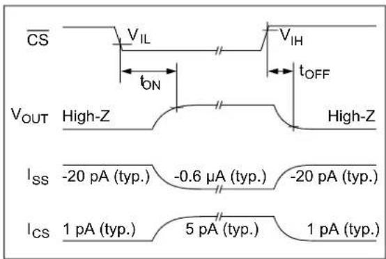
CS V_IL V_IH t_ON t_OFF V_OUT High-Z High-Z I_SS -20 pA (typ.) -0.6 μA (typ.) -20 pA (typ.) I_CS 1 pA (typ.) 5 pA (typ.) 1 pA (typ.)FIGURE 1-1: Timing Diagram for the CS pin on the MCP6548.
text_image
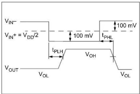
VIN- VIN+ = VDD/2 100 mV tPHL 100 mV tPLH VOH VOUT VOL VOLFIGURE 1-2: Propagation Delay Timing Diagram.
TEMPERATURE CHARACTERISTICS
| Electrical Specifications: Unless otherwise indicated, V_DD = +1.6V to +5.5V and V_SS = GND . | ||||||
| Parameters Sym Min Typ Max Units Conditions | ||||||
| Temperature Ranges | ||||||
| Specified Temperature Range T | _A | -40 — | +85 °C | |||
| Operating Temperature Range | T_A | -40 — | +125 °C | Note | ||
| Storage Temperature Range | T_A | -65 — | +150 °C | |||
| Thermal Package Resistances | ||||||
| Thermal Resistance, 5L-SC-70 | θ_JA | — 33 | 1 — | °C/W | ||
| Thermal Resistance, 5L-SOT-23 | θ_JA | — | 220.7 | — | °C/W | |
| Thermal Resistance, 8L-MSOP | θ_JA | — | 211 | — °C/W | ||
| Thermal Resistance, 8L-PDIP θ | JA | — 89 | 3 — | °C/W | ||
| Thermal Resistance, 8L-SOIC | θ_JA | — | 149.5 | — | °C/W | |
| Thermal Resistance, 14L-PDIP | θ_JA | — | 70 | — | °C/W | |
| Thermal Resistance, 14L-SOIC | θ_JA | — 95 | 3 — | °C/W | ||
| Thermal Resistance, 14L-TSSOP | θ_JA | — 100 | — | °C/W | ||
Note: The MCP6546/6R/6U/7/8/9 I-Temp family operates over this extended temperature range, but with reduced performance. In any case, the Junction Temperature ( T_J ) must not exceed the absolute maximum specification of +150°C.
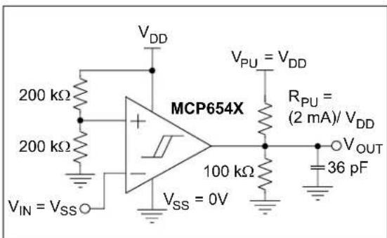
1.1 Test Circuit Configuration
This test circuit configuration is used to determine the AC and DC specifications.
text_image
VDD 200 kΩ 200 kΩ VIN = VSS MCP654X VSS = 0V 100 kΩ VPU = VDD RPU = (2 mA)/ VDD VOUT =36 pFFIGURE 1-3: AC and DC Test Circuit for the Open-Drain Output Comparators.
2.0 TYPICAL PERFORMANCE CURVES
Note: The graphs and tables provided following this note are a statistical summary based on a limited number of samples and are provided for informational purposes only. The performance characteristics listed herein are not tested or guaranteed. In some graphs or tables, the data presented may be outside the specified operating range (e.g., outside specified power supply range) and therefore outside the warranted range.
Note: Unless otherwise indicated, V_DD = +1.6V to +5.5V, V_SS = GND , T_A = +25^ , V_IN^+ = V_DD/2 , V_IN^- = GND , R_PU = 2.74 k to V_PU = V_DD , and C_L = 36 pF .
histogram
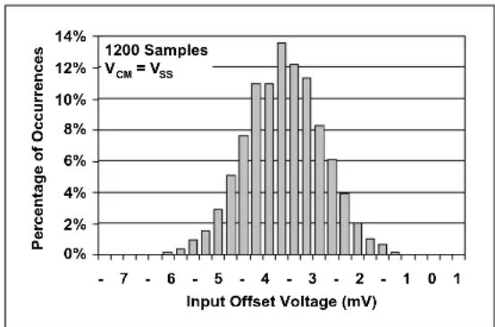
1200 Samples V_CM = V_SS | Input Offset Voltage (mV) | Percentage of Occurrences | | :--- | :--- | | -7 | 0 | | -6 | 0.5 | | -5 | 3.0 | | -4 | 7.5 | | -3 | 11.0 | | -2 | 13.5 | | -1 | 12.0 | | 0 | 8.0 | | 1 | 4.0 | | 2 | 2.0 | | 3 | 1.0 | | 4 | 0.5 | | 5 | 0.2 | | 6 | 0.1 | | 7 | 0.05 | | 8 | 0.02 | | 9 | 0.01 | | 10 | 0.01 | | 11 | 0.01 | | 12 | 0.01 | | 13 | 0.01 | | 14 | 0.01 | | 15 | 0.01 | | 16 | 0.01 | | 17 | 0.01 | | 18 | 0.01 | | 19 | 0.01 | | 20 | 0.01 | | 21 | 0.01 | | 22 | 0.01 | | 23 | 0.01 | | 24 | 0.01 | | 25 | 0.01 | | 26 | 0.01 | | 27 | 0.01 | | 28 | 0.01 | | 29 | 0.01 | | 30 | 0.01 | | 31 | 0.01 | | 32 | 0.01 | | 33 | 0.01 | | 34 | 0.01 | | 35 | 0.01 | | 36 | 0.01 | | 37 | 0.01 | | 38 | 0.01 | | 39 | 0.01 | | 40 | 0.01 | | 41 | 0.01 | | 42 | 0.01 | | 43 | 0.01 | | 44 | 0.01 | | 45 | 0.01 | | 46 | 0.01 | | 47 | 0.01 | | 48 | 0.01 | | 49 | 0.01 | | 50 | 0.01 | | 51 | 0.01 | | 52 | 0.01 | | 53 | 0.01 | | 54 | 0.01 | | 55 | 0.01 | | 56 | 0.01 | | 57 | 0.01 | | 58 | 0.01 | | 59 | 0.01 | | 60 | 0.01 | | 61 | 0.01 | | 62 | 0.01 | | 63 | 0.01 | | 64 | 0.01 | | 65 | 0.01 | | 66 | 0.01 | | 67 | 0.01 | | 68 | 0.01 | | 69 | 0.01 | | 70 | 0.01 | | 71 | 0.01 | | 72 | 0.01 | | 73 | 0.01 | | 74 | 0.01 | | 75 | 0.01 | | 76 | 0.01 | | 77 | 0.01 | | 78 | 0.01 | | 79 | 0.01 | | 80 | 0.01 | | 81 | 0.01 | | 82 | 0.01 | | 83 | 0.01 | | 84 | 0.01 | | 85 | 0.01 | | 86 | 0.01 | | 87 | 0.01 | | 88 | 0.01 | | 89 | 0.01 | | 90 | 0.01 | | 91 | 0.01 | | 92 | 0.01 | | 93 | 0.01 | | 94 | 0.01 | | 95 | 0.01 | | 96 | 0.01 | | 97 | 0.01 | | 98 | 0.01 | | 99 | 0.01 | | >25 | <2%FIGURE 2-1: Input Offset Voltage at V_CM = V_SS .
histogram
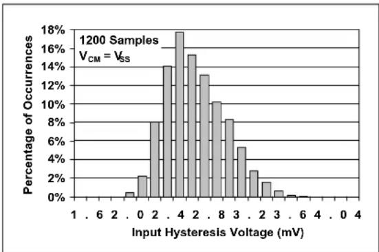
1200 Samples V_CM = V_SS | Input Hysteresis Voltage (mV) | Percentage of Occurrences | | :--- | :--- | | 1 - 6 | 0 | | 6 - 2 | 0 | | 2 - 0 | 2 | | 0 - 2 | 8 | | 2 - 4 | 14 | | 4 - 2 | 18 | | 2 - 8 | 15 | | 8 - 3 | 10 | | 3 - 2 | 8 | | 2 - 3 | 5 | | 3 - 6 | 2 | | 6 - 4 | 0 | | 0 - 4 | 0 |FIGURE 2-4: Input Hysteresis Voltage at V_CM = V_SS .
histogram
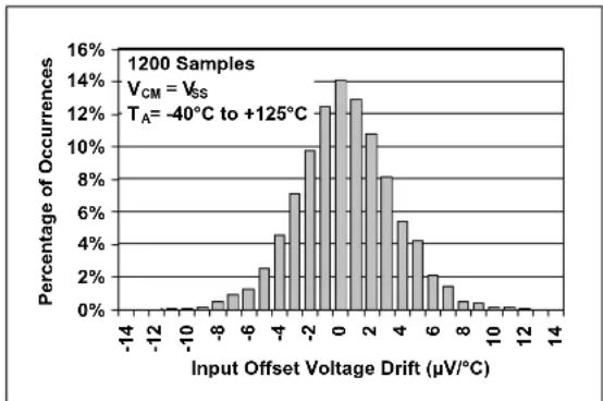
1200 Samples V_CM = V_SS T_A = -40°C to +125°C | Input Offset Voltage Drift (μV/°C) | Percentage of Occurrences | | :--- | :--- | | -14 | 0 | | -12 | 0 | | -10 | 0 | | -8 | 0.5 | | -6 | 1.5 | | -4 | 4.5 | | -2 | 7.5 | | 0 | 14 | | 2 | 13 | | 4 | 8 | | 6 | 4 | | 8 | 1.5 | | 10 | 0.5 | | 12 | 0.2 | | 14 | 0 |FIGURE 2-2: Input Offset Voltage Drift at V_CM = V_SS .
bar
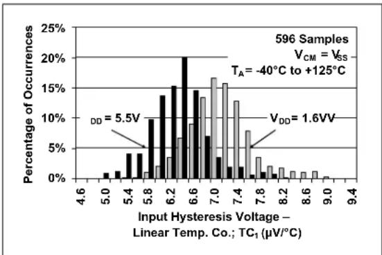
| Input Hysteresis Voltage – Linear Temp. Co.; TC₁ (μV/°C) | Percentage of Occurrences | |---|---| | 4.6 | 0.0 | | 5.0 | 1.0 | | 5.4 | 4.0 | | 5.8 | 10.0 | | 6.2 | 15.0 | | 6.6 | 20.0 | | 7.0 | 15.0 | | 7.4 | 16.0 | | 7.8 | 8.0 | | 8.2 | 2.0 | | 8.6 | 1.0 | | 9.0 | 0.5 | | 9.4 | 0.0 |FIGURE 2-5: Input Hysteresis Voltage Linear Temp. Co. (TC1) at VCM = VSS
line
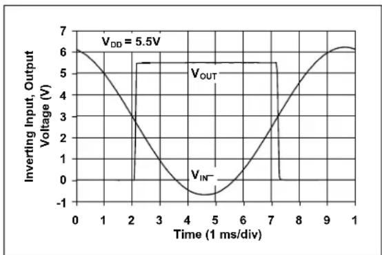
| Time (1 ms/div) | Inverting Input, Output Voltage (V) | | --------------- | ----------------------------------- | | 0 | 6 | | 2 | 3 | | 4 | 0 | | 5 | -1 | | 7 | 0 | | 9 | 6 | | 1 | 6 |FIGURE 2-3: The MCP6546/6R/6U/7/8/9 Comparators Show No Phase Reversal.
bar
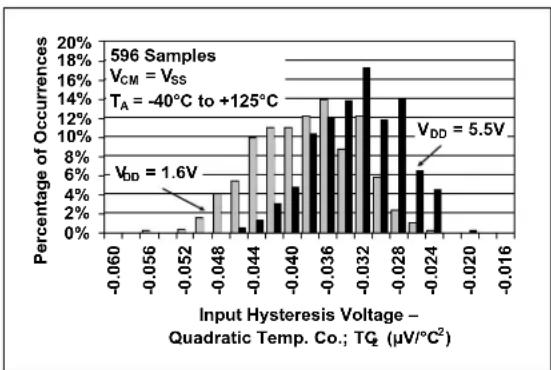
| Input Hysteresis Voltage – Quadratic Temp. Co.; TQ (μV/°C²) | Percentage of Occurrences | | -------------------------------------------------------- | ------------------------- | | -0.060 | 0% | | -0.056 | 0% | | -0.052 | 0% | | -0.048 | 0% | | -0.044 | 0% | | -0.040 | 0% | | -0.036 | 0% | | -0.032 | 0% | | -0.028 | 0% | | -0.024 | 0% | | -0.020 | 0% | | -0.016 | 0% |FIGURE 2-6: Input Hysteresis Voltage Quadratic Temp. Co. (TC 2 ) at V CM = V _SS .
Note: Unless otherwise indicated, V_DD = +1.6V to +5.5V, V_SS = GND , T_A = +25^ , V_IN^+ = V_DD/2 , V_IN^- = GND , R_PU = 2.74 k to V_PU = V_DD , and C_L = 36 pF .

line
| Ambient Temperature (°C) | Input Offset Voltage (mV) | | ------------------------ | ------------------------- | | -50 | 0.3 | | 0 | 0.4 | | 25 | 0.45 | | 50 | 0.5 | | 75 | 0.55 | | 100 | 0.6 | | 125 | 0.65 | | 150 | 0.7 | | 175 | 0.75 | | 200 | 0.8 |FIGURE 2-7: Input Offset Voltage vs. Ambient Temperature at V_CM = V_SS .
line
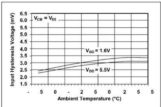
| Ambient Temperature (°C) | Input Hysteresis Voltage (mV) for V_DD = 1.6V | Input Hysteresis Voltage (mV) for V_DD = 5.5V | | ------------------------ | ------------------------------------------ | ------------------------------------------ | | -5 | 2.3 | 2.4 | | 0 | 2.8 | 2.9 | | 5 | 3.2 | 3.3 | | 10 | 3.4 | 3.5 | | 20 | 3.5 | 3.6 | | 50 | 3.6 | 3.7 |FIGURE 2-10: Input Hysteresis Voltage vs. Ambient Temperature at V_CM = V_SS
line
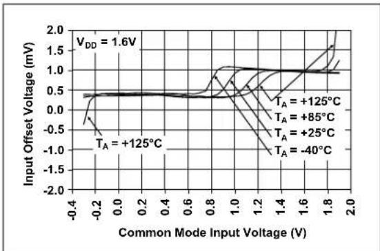
| Common Mode Input Voltage (V) | Input Offset Voltage (mV) for TA = +125°C | Input Offset Voltage (mV) for TA = +85°C | Input Offset Voltage (mV) for TA = +25°C | Input Offset Voltage (mV) for TA = -40°C | | ----------------------------- | ---------------------------------------- | --------------------------------------- | --------------------------------------- | --------------------------------------- | | -0.4 | -0.5 | 0.3 | 0.4 | 0.4 | | -0.2 | -0.8 | 0.3 | 0.4 | 0.4 | | 0.0 | -0.9 | 0.3 | 0.4 | 0.4 | | 0.2 | -0.9 | 0.3 | 0.4 | 0.4 | | 0.4 | -0.9 | 0.3 | 0.4 | 0.4 | | 0.6 | -0.9 | 0.3 | 0.4 | 0.4 | | 0.8 | -0.9 | 0.3 | 0.4 | 0.4 | | 1.0 | -0.9 | 0.3 | 0.4 | 0.4 | | 1.2 | -1.0 | 0.3 | 0.4 | 0.4 | | 1.4 | -1.1 | 0.3 | 0.4 | 0.4 | | 1.6 | -1.2 | 0.3 | 0.4 | 0.4 | | 1.8 | -1.3 | 0.3 | 0.4 | 0.4 | | 2.0 | -1.4 | 0.3 | 0.4 | 0.4 |FIGURE 2-8: Input Offset Voltage vs. Common-mode Input Voltage at V_DD = 1.6V .
line
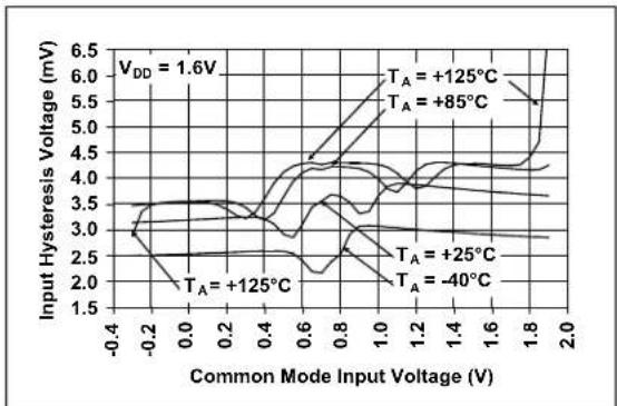
| Common Mode Input Voltage (V) | Input Hysteresis Voltage (mV) for T_A = -40°C | Input Hysteresis Voltage (mV) for T_A = +40°C | Input Hysteresis Voltage (mV) for T_A = +125°C | Input Hysteresis Voltage (mV) for T_A = +85°C | | ----------------------------- | ------------------------------------------- | ------------------------------------------- | -------------------------------------------- | -------------------------------------------- | | -0.4 | 3.0 | 3.0 | 3.0 | 3.0 | | 0.0 | 2.5 | 2.5 | 2.5 | 2.5 | | 0.4 | 3.0 | 3.0 | 3.0 | 3.0 | | 0.8 | 3.5 | 3.5 | 3.5 | 3.5 | | 1.2 | 4.0 | 4.0 | 4.0 | 4.0 | | 1.6 | 4.5 | 4.5 | 4.5 | 4.5 | | 2.0 | 5.0 | 5.0 | 5.0 | 5.0 |FIGURE 2-11: Input Hysteresis Voltage vs. Common-mode Input Voltage at V_DD = 1.6V .
line
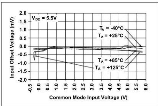
| Common Mode Input Voltage (V) | Input Offset Voltage (mV) for TA = -40°C | Input Offset Voltage (mV) for TA = +25°C | Input Offset Voltage (mV) for TA = +85°C | Input Offset Voltage (mV) for TA = +125°C | | ----------------------------- | ---------------------------------------- | ---------------------------------------- | ---------------------------------------- | ----------------------------------------- | | 0.0 | -0.5 | -0.5 | -0.5 | -0.5 | | 0.5 | -0.2 | -0.2 | -0.3 | -0.4 | | 1.0 | 0.0 | 0.0 | -0.1 | -0.2 | | 1.5 | 0.1 | 0.1 | 0.0 | -0.1 | | 2.0 | 0.2 | 0.2 | 0.1 | 0.0 | | 2.5 | 0.3 | 0.3 | 0.2 | 0.1 | | 3.0 | 0.4 | 0.4 | 0.3 | 0.2 | | 3.5 | 0.5 | 0.5 | 0.4 | 0.3 | | 4.0 | 0.6 | 0.6 | 0.5 | 0.4 | | 4.5 | 0.7 | 0.7 | 0.6 | 0.5 | | 5.0 | 0.8 | 0.8 | 0.7 | 0.6 | | 5.5 | 0.9 | 0.9 | 0.8 | 0.7 | | 6.0 | 1.0 | 1.0 | 0.9 | 0.8 |FIGURE 2-9: Input Offset Voltage vs. Common-mode Input Voltage at V_DD = 5.5V .

line
| Common Mode Input Voltage (V) | Input Hysteresis Voltage (mV) at T_A = +125°C | Input Hysteresis Voltage (mV) at T_A = +85°C | Input Hysteresis Voltage (mV) at T_A = +25°C | Input Hysteresis Voltage (mV) at T_A = -40°C | | ----------------------------- | ------------------------------------------ | ------------------------------------------ | ------------------------------------------ | ------------------------------------------ | | 0.0 | 4.5 | 3.0 | 2.5 | 2.0 | | 0.5 | 5.0 | 3.5 | 3.0 | 2.5 | | 1.0 | 5.5 | 4.0 | 3.5 | 3.0 | | 1.5 | 6.0 | 4.5 | 4.0 | 3.5 | | 2.0 | 6.0 | 4.5 | 4.0 | 3.5 | | 2.5 | 6.0 | 4.5 | 4.0 | 3.5 | | 3.0 | 6.0 | 4.5 | 4.0 | 3.5 | | 3.5 | 6.0 | 4.5 | 4.0 | 3.5 | | 4.0 | 6.0 | 4.5 | 4.0 | 3.5 | | 4.5 | 6.0 | 4.5 | 4.0 | 3.5 | | 5.0 | 6.0 | 4.5 | 4.0 | 3.5 | | 5.5 | 6.0 | 4.5 | 4.0 | 3.5 | | 6.0 | 6.0 | 4.5 | 4.0 | 3.5 |FIGURE 2-12: Input Hysteresis Voltage vs. Common-mode Input Voltage at V_DD = 5.5V .
Note: Unless otherwise indicated, V_DD = +1.6V to +5.5V, V_SS = GND , T_A = +25^ , V_IN^+ = V_DD/2 , V_IN^- = GND , R_PU = 2.74 k to V_PU = V_DD , and C_L = 36 pF .
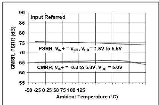
FIGURE 2-13: CMRR, PSRR vs. Ambient Temperature.

line
| Common Mode Input Voltage (V) | I_B, T_A = +125°C | I_B, T_A = +85°C | I_OS, T_A = +125°C | I_OS, T_A = +85°C | | ----------------------------- | ----------------- | ---------------- | ------------------ | ----------------- | | 0.0 | ~10n | ~10n | ~10p | ~10p | | 0.5 | ~10n | ~10n | ~10p | ~10p | | 1.0 | ~10n | ~10n | ~10p | ~10p | | 1.5 | ~10n | ~10n | ~10p | ~10p | | 2.0 | ~10n | ~10n | ~10p | ~10p | | 2.5 | ~10n | ~10n | ~10p | ~10p | | 3.0 | ~10n | ~10n | ~10p | ~10p | | 3.5 | ~10n | ~10n | ~10p | ~10p | | 4.0 | ~10n | ~10n | ~10p | ~10p | | 4.5 | ~10n | ~10n | ~10p | ~10p | | 5.0 | ~10n | ~10n | ~10p | ~10p | | 5.5 | ~10n | ~10n | ~10p | ~10p |FIGURE 2-16: Input Bias Current, Input Offset Current vs. Common-mode Input Voltage.

line
| Ambient Temperature (°C) | Input Bias, Offset Currents (pA) | | ------------------------ | --------------------------------- | | 55 | 1 | | 65 | 0.1 | | 75 | 0.1 | | 85 | 1 | | 95 | 10 | | 105 | 10 | | 115 | 1 | | 125 | 0.1 | | 135 | 1 | | 145 | 10 | | 155 | 100 | | 165 | 1000 |FIGURE 2-14: Input Bias Current, Input Offset Current vs. Ambient Temperature.
line
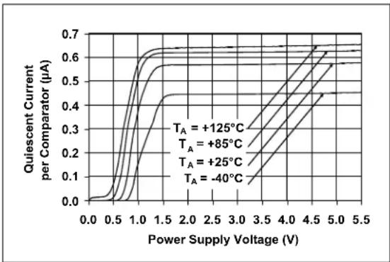
| Power Supply Voltage (V) | Quiescent Current per Comparator (μA) for T_A = +125°C | Quiescent Current per Comparator (μA) for T_A = +85°C | Quiescent Current per Comparator (μA) for T_A = +25°C | Quiescent Current per Comparator (μA) for T_A = -40°C | | ------------------------ | ------------------------------------------------------ | ---------------------------------------------------- | ---------------------------------------------------- | ---------------------------------------------------- | | 0.0 | 0.0 | 0.0 | 0.0 | 0.0 | | 0.5 | 0.1 | 0.1 | 0.1 | 0.1 | | 1.0 | 0.3 | 0.3 | 0.3 | 0.3 | | 1.5 | 0.5 | 0.5 | 0.5 | 0.5 | | 2.0 | 0.6 | 0.6 | 0.6 | 0.6 | | 2.5 | 0.65 | 0.65 | 0.65 | 0.65 | | 3.0 | 0.7 | 0.7 | 0.7 | 0.7 | | 3.5 | 0.7 | 0.7 | 0.7 | 0.7 | | 4.0 | 0.7 | 0.7 | 0.7 | 0.7 | | 4.5 | 0.7 | 0.7 | 0.7 | 0.7 | | 5.0 | 0.7 | 0.7 | 0.7 | 0.7 | | 5.5 | 0.7 | 0.7 | 0.7 | 0.7 |FIGURE 2-17: Quiescent Current vs. Power Supply Voltage.

line
| Common Mode Input Voltage (V) | Quiescent Current per Comparator (µA) | | ----------------------------- | ------------------------------------- | | 0.2 | 0.4 | | 0.4 | 0.2 | | 0.6 | 0.5 | | 0.8 | 0.4 | | 1.0 | 0.5 | | 1.2 | 0.1 | | 1.4 | 0.4 |FIGURE 2-15: Quiescent Current vs. Common-mode Input Voltage at V_DD = 1.6V .

line
| Common Mode Input Voltage (V) | Quiescent Current per Comparator (µA) | | ----------------------------- | ------------------------------------- | | 1.0 | 0.4 | | 1.5 | 0.3 | | 2.0 | 0.5 | | 2.5 | 0.4 | | 3.0 | 0.5 | | 3.5 | 0.4 | | 4.0 | 0.5 | | 4.5 | 0.1 | | 5.0 | 0.4 |FIGURE 2-18: Quiescent Current vs. Common-mode Input Voltage at V_DD = 5.5V .
Note: Unless otherwise indicated, V_DD = +1.6V to +5.5V, V_SS = GND , T_A = +25^ , V_IN^+ = V_DD/2 , V_IN^- = GND , R_PU = 2.74 k to V_PU = V_DD , and C_L = 36 pF .

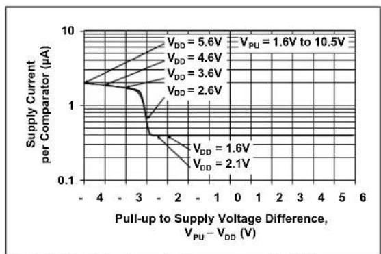
FIGURE 2-19: Supply Current vs. Pull-Up Voltage.
line
| Pull-up to Supply Voltage Difference, V_PU - V_DD (V) | Supply Current per Comparator (μA) for V_DD = 1.6V | Supply Current per Comparator (μA) for V_PU = 1.6V to 10.5V | Supply Current per Comparator (μA) for V_DD = 2.6V | Supply Current per Comparator (μA) for V_PU = 2.6V to 4.6V | Supply Current per Comparator (μA) for V_PU = 4.6V to 5.6V | | -------------------------------------------------- | ----------------------------------------------- | ------------------------------------------------------------- | ----------------------------------------------- | ------------------------------------------------------------- | ------------------------------------------------------------- | | -4 | ~10 | ~10 | ~10 | ~10 | ~10 | | -3 | ~1 | ~1 | ~1 | ~1 | ~1 | | -2 | ~0.1 | ~0.1 | ~0.1 | ~0.1 | ~0.1 | | -1 | ~0.1 | ~0.1 | ~0.1 | ~0.1 | ~0.1 | | 0 | ~0.1 | ~0.1 | ~0.1 | ~0.1 | ~0.1 | | 1 | ~0.1 | ~0.1 | ~0.1 | ~0.1 | ~0.1 | | 2 | ~0.1 | ~0.1 | ~0.1 | ~0.1 | ~0.1 | | 3 | ~0.1 | ~0.1 | ~0.1 | ~0.1 | ~0.1 | | 4 | ~0.1 | ~0.1 | ~0.1 | ~0.1 | ~0.1 | | 5 | ~0.1 | ~0.1 | ~0.1 | ~0.1 | ~0.1 | | 6 | ~0.1 | ~0.1 | ~0.1 | ~0.1 | ~0.1 |FIGURE 2-22: Supply Current vs. Pull-Up to Supply Voltage Difference.
line
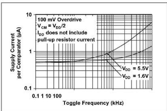
| Toggle Frequency (kHz) | Supply Current per Comparator (μA) | | ---------------------- | ---------------------------------- | | 0.1 | ~0.5 | | 1 | ~0.5 | | 10 | ~0.5 | | 100 | ~0.5 |FIGURE 2-20: Supply Current vs. Toggle Frequency.
line
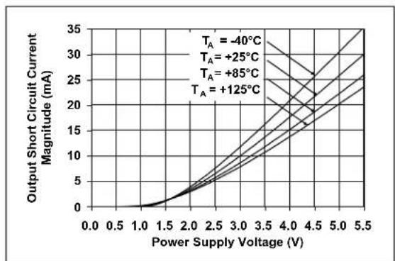
| Power Supply Voltage (V) | Output Short Circuit Current Magnitude (mA) for TA = -40°C | Output Short Circuit Current Magnitude (mA) for TA = +25°C | Output Short Circuit Current Magnitude (mA) for TA = +85°C | Output Short Circuit Current Magnitude (mA) for TA = +125°C | | ------------------------- | -------------------------------------------------------- | -------------------------------------------------------- | -------------------------------------------------------- | -------------------------------------------------------- | | 0.0 | 0.0 | 0.0 | 0.0 | 0.0 | | 0.5 | 0.0 | 0.0 | 0.0 | 0.0 | | 1.0 | 0.0 | 0.0 | 0.0 | 0.0 | | 1.5 | 0.0 | 0.0 | 0.0 | 0.0 | | 2.0 | 5.0 | 5.0 | 5.0 | 5.0 | | 2.5 | 10.0 | 10.0 | 10.0 | 10.0 | | 3.0 | 15.0 | 15.0 | 15.0 | 15.0 | | 3.5 | 20.0 | 20.0 | 20.0 | 20.0 | | 4.0 | 25.0 | 25.0 | 25.0 | 25.0 | | 4.5 | 30.0 | 30.0 | 30.0 | 30.0 | | 5.0 | 35.0 | 35.0 | 35.0 | 35.0 | | 5.5 | 40.0 | 40.0 | 40.0 | 40.0 |FIGURE 2-23: Output Short Circuit Current Magnitude vs. Power Supply Voltage.
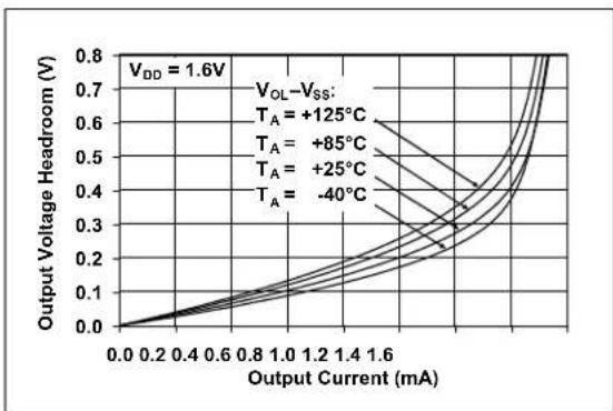
FIGURE 2-21: Output Voltage Headroom vs. Output Current at V_DD = 1.6V .

line
| Output Current (mA) | Output Voltage Headroom (V) | | ------------------- | --------------------------- | | 0 | 0.0 | | 5 | 0.3 | | 10 | 0.7 | | 15 | 0.9 | | 20 | 1.0 | | 25 | 1.0 |FIGURE 2-24: Output Voltage Headroom vs. Output Current at V_DD = 5.5V .
Note: Unless otherwise indicated, V_DD = +1.6V to +5.5V, V_SS = GND , T_A = +25^ , V_IN^+ = V_DD/2 , V_IN^- = GND , R_PU = 2.74 k to V_PU = V_DD , and C_L = 36 pF .

bar
| High-to-Low Propagation Delay (μs) | Percentage of Occurrences | | ---------------------------------- | -------------------------- | | 2.0 | 5% | | 2.5 | 50% | | 3.0 | 38% | | 3.5 | 10% | | 4.0 | 37% | | 4.5 | 15% | | 5.0 | 2% |FIGURE 2-25: High-to-Low Propagation Delay.
bar
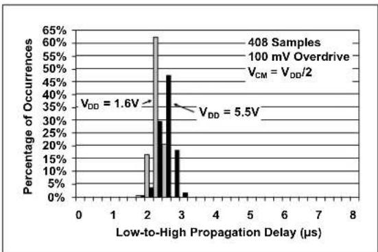
| Low-to-High Propagation Delay (μs) | Percentage of Occurrences | | ---------------------------------- | ------------------------- | | 2.0 | 60% | | 2.5 | 45% | | 3.0 | 20% |FIGURE 2-28: Low-to-High Propagation Delay.
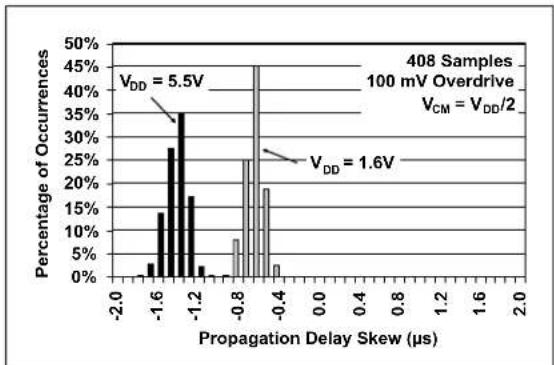
histogram
| Propagation Delay Skew (μs) | Percentage of Occurrences | | --------------------------- | ------------------------- | | -1.6 | 5.5% | | -0.8 | 25% | | -0.4 | 19% |FIGURE 2-26: Propagation Delay Skew.
line
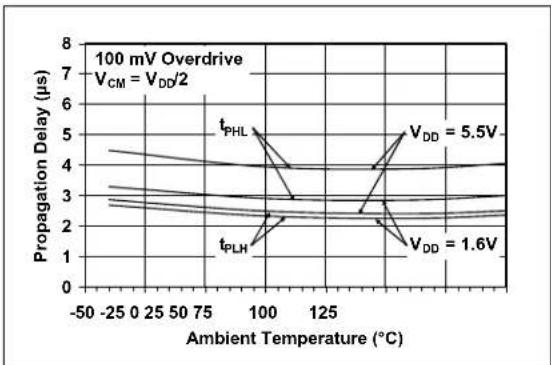
| Ambient Temperature (°C) | Propagation Delay (μs) | | ------------------------ | ---------------------- | | -50 | ~4.5 | | 0 | ~4.2 | | 25 | ~4.0 | | 50 | ~3.8 | | 75 | ~3.6 | | 100 | ~3.4 | | 125 | ~3.2 | | 150 | ~3.0 | | 175 | ~2.8 | | 200 | ~2.6 | | 225 | ~2.4 | | 250 | ~2.2 | | 275 | ~2.0 | | 300 | ~1.8 | | 325 | ~1.6 | | 350 | ~1.4 | | 375 | ~1.2 | | 400 | ~1.0 |FIGURE 2-29: Propagation Delay vs. Ambient Temperature.

line
| Power Supply Voltage (V) | Propagation Delay (μs) - 10 mV Overdrive | Propagation Delay (μs) - 100 mV Overdrive | | ------------------------ | ---------------------------------------- | ----------------------------------------- | | 0 | 3.0 | 1.0 | | 2 | 6.0 | 3.0 | | 4 | 9.0 | 7.0 | | 6 | 12.0 | 11.0 | | 8 | 14.0 | 13.0 | | 10 | 12.0 | 11.0 | | 12 | 10.0 | 9.0 | | 14 | 8.0 | 7.0 | | 16 | 6.0 | 5.0 | | 18 | 4.0 | 3.0 | | 20 | 2.0 | 1.0 | | 22 | 1.0 | 0.5 | | 24 | 0.5 | 0.2 | | 26 | 0.2 | 0.1 | | 28 | 0.1 | 0.05 | | 30 | 0.05 | 0.02 |FIGURE 2-27: Propagation Delay vs. Power Supply Voltage.

line
| Input Overdrive (mV) | Propagation Delay (μs) | | --------------------- | ---------------------- | | 1 | ~50 | | 10 | ~10 | | 100 | ~3 | | 1000 | ~1 |FIGURE 2-30: Propagation Delay vs. Input Overdrive.
Note: Unless otherwise indicated, V_DD = +1.6V to +5.5V, V_SS = GND , T_A = +25^ , V_IN^+ = V_DD/2 , V_IN^- = GND , R_PU = 2.74 k to V_PU = V_DD , and C_L = 36 pF .

line
| Common Mode Input Voltage (V) | Propagation Delay (μs) | | ----------------------------- | ---------------------- | | 0.0 | 4.0 | | 0.2 | 4.0 | | 0.4 | 4.0 | | 0.6 | 4.0 | | 0.8 | 3.5 | | 1.0 | 3.0 | | 1.2 | 2.5 | | 1.4 | 2.0 | | 1.6 | 2.0 |FIGURE 2-31: Propagation Delay vs. Common-mode Input Voltage at V_DD = 1.6V .

line
| Common Mode Input Voltage (V) | Propagation Delay (μs) | | ----------------------------- | ---------------------- | | 0 | ~5.5 | | 0 | ~3.5 | | 0 | ~2.5 | | 0 | ~2.0 | | 5 | ~4.0 | | 5 | ~4.0 | | 5 | ~4.0 | | 5 | ~4.0 | | 3 | ~4.0 | | 3 | ~2.0 | | 3 | ~2.0 | | 3 | ~2.0 | | 0 | ~4.0 |FIGURE 2-34: Propagation Delay vs. Common-mode Input Voltage at V_DD = 5.5V .
line
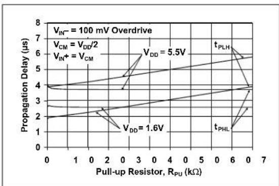
| Pull-up Resistor, RPU (kΩ) | Propagation Delay (μs) | | -------------------------- | ---------------------- | | 0 | 4.0 | | 2 | 4.5 | | 6 | 5.5 | | 6 | 3.5 |FIGURE 2-32: Propagation Delay vs. Pull-up Resistor.

line
| Load Capacitance (nF) | Propagation Delay (μs) | | ---------------------- | ---------------------- | | 20 | 5.5 | | 30 | 1.6 | | 70 | 1.6 | | 80 | 1.6 |FIGURE 2-35: Propagation Delay vs. Load Capacitance.
line
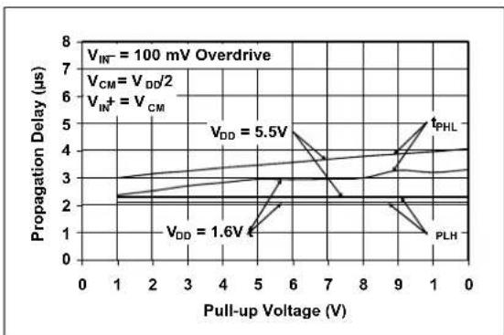
| Pull-up Voltage (V) | Propagation Delay (μs) | | ------------------- | ---------------------- | | 5 | 1.6 | | 6 | 5.5 | | 9 | 4.0 | | 1 | 4.0 |FIGURE 2-33: Propagation Delay vs. Pull-up Voltage.
line
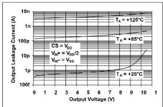
| Output Voltage (V) | Output Leakage Current (A) at T_A = +125°C | Output Leakage Current (A) at T_A = +85°C | Output Leakage Current (A) at T_A = +25°C | | ------------------ | ---------------------------------------- | ---------------------------------------- | ---------------------------------------- | | 0 | ~10^0 | ~10^0 | ~10^0 | | 1 | ~10^0 | ~10^0 | ~10^0 | | 2 | ~10^0 | ~10^0 | ~10^0 | | 3 | ~10^0 | ~10^0 | ~10^0 | | 4 | ~10^0 | ~10^0 | ~10^0 | | 5 | ~10^0 | ~10^0 | ~10^0 | | 6 | ~10^0 | ~10^0 | ~10^0 | | 7 | ~10^0 | ~10^0 | ~10^0 | | 8 | ~10^0 | ~10^0 | ~10^0 | | 9 | ~10^0 | ~10^0 | ~10^0 | | 10 | ~10^0 | ~10^0 | ~10^0 | | 1 | ~10^0 | ~10^0 | ~10^0 |FIGURE 2-36: Output Leakage Current (CS = VDD) vs. Output Voltage (MCP6548 only).
Note: Unless otherwise indicated, V_DD = +1.6V to +5.5V, V_SS = GND , T_A = +25^ , V_IN^+ = V_DD/2 , V_IN^- = GND , R_PU = 2.74 k to V_PU = V_DD , and C_L = 36 pF .
line
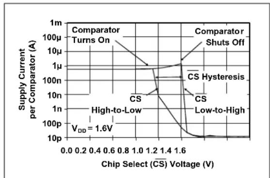
| Chip Select (CS) Voltage (V) | Supply Current per Comparator (A) | | ---------------------------- | --------------------------------- | | 0.0 | 100μ | | 0.2 | 100μ | | 0.4 | 100μ | | 0.6 | 100μ | | 0.8 | 100μ | | 1.0 | 1μ | | 1.2 | 1μ | | 1.4 | 1μ | | 1.6 | 1μ | | High-to-Low | 1n | | Low-to-High | 1n | | CS | 1n | | CS Hysteresis | 1n | | Compactor | 1m | | Shift Off | 1m | | Comparator | 1m | | Turns On | 1m | | Comparator | 1m |FIGURE 2-37: Supply Current (Shoot-through Current) vs. Chip Select (CS) Voltage at V_DD = 1.6V (MCP6548 only).
line
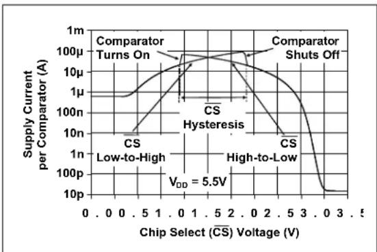
| Chip Select (CS) Voltage (V) | Supply Current per Comparator (A) | | ---------------------------- | --------------------------------- | | 0 | 1 | | 5 | 10 | | 1 | 100 | | 2 | 1000 | | 3 | 1 | | 5 | 1 |FIGURE 2-40: Supply Current (Shoot-through Current) vs. Chip Select (CS) Voltage at V_DD = 5.5V (MCP6548 only).

line
| Time (1 ms/div) | Supply Current (μA) | Output Voltage (V) | | --------------- | ------------------- | ------------------ | | 0 | 0 | 0.0 | | 1 | 0 | 0.0 | | 2 | 30 | 0.0 | | 3 | 30 | 0.0 | | 4 | 30 | 0.0 | | 5 | 30 | 0.0 | | 6 | 30 | 0.0 | | 7 | 30 | 0.0 | | 8 | 30 | 0.0 | | 9 | 20 | 1.6 | | 10 | 10 | 1.6 | | 11 | 5 | 1.6 | | 12 | 2 | 1.6 | | 13 | 1 | 1.6 | | 14 | 0 | 1.6 | | 15 | 0 | 1.6 | | 16 | 0 | 1.6 |FIGURE 2-38: Supply Current (Charging Current) vs. Chip Select (CS) Pulse at V_DD = 1.6V (MCP6548 only).
line
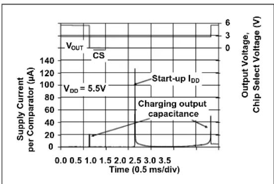
| Time (ms/div) | Supply Current per Comparator (μA) | Output Voltage (V) | | ------------- | ---------------------------------- | ------------------ | | 0.0 | 0 | 0 | | 0.5 | 140 | 3 | | 1.0 | 20 | 6 | | 1.5 | 140 | 3 | | 2.0 | 140 | 3 | | 2.5 | 140 | 3 | | 3.0 | 140 | 3 | | 3.5 | 140 | 3 | | 4.0 | 140 | 3 | | 4.5 | 140 | 3 | | 5.0 | 140 | 3 | | 5.5 | 140 | 3 | | 6.0 | 140 | 3 | | 6.5 | 140 | 3 | | 7.0 | 140 | 3 | | 7.5 | 140 | 3 | | 8.0 | 140 | 3 | | 8.5 | 140 | 3 | | 9.0 | 140 | 3 | | 9.5 | 140 | 3 | | 10.0 | 140 | 3 | | 10.5 | 140 | 3 | | 11.0 | 140 | 3 | | 11.5 | 140 | 3 | | 12.0 | 140 | 3 | | 12.5 | 140 | 3 | | 13.0 | 140 | 3 | | 13.5 | 140 | 3 | | 14.0 | 140 | 3 | | 14.5 | 140 | 3 | | 15.0 | 140 | 3 | | 15.5 | 140 | 3 | | 16.0 | 140 | 3 | | 16.5 | 140 | 3 | | 17.0 | 140 | 3 | | 17.5 | 140 | 3 | | 18.0 | 140 | 3 | | 18.5 | 140 | 3 | | 19.0 | 140 | 3 | | 19.5 | 140 | 3 | | 20.0 | 140 | 3 | | 20.5 | 140 | 3 | | 21.0 | 140 | 3 | | 21.5 | 140 | 3 | | 22.0 | 140 | 3 | | 22.5 | 140 | 3 | | 23.0 | 140 | 3 | | 23.5 | 140 | 3 | | 24.0 | 140 | 3 | | 24.5 | 140 | 3 | | 25.0 | 140 | 3 | | 25.5 | 140 | 3 | | 26.0 | 140 | 3 | | 26.5 | 140 | 3 | | 27.0 | 140 | 3 | | 27.5 | 140 | 3 | | 28.0 | 140 | 3 | | 28.5 | 140 | 3 | | 29.0 | 140 | 3 | | 29.5 | 140 | 3 | | 30.0 | 140 | 3 | | 30.5 | 140 | 3 | | 31.0 | 140 | 3 | | 31.5 | 140 | 3 | | 32.0 | 140 | 3 | | 32.5 | 140 | 3 | | 33.0 | 140 | 3 | | 33.5 | 140 | 3 | | 34.0 | 140 | 3 | | 34.5 | 140 | 3 | | 35.0 | 140 | 3 | | 35.5 | 140 | 3 | | 36.0 | 140 | 3 | | 36.5 | 140 | 3 | | 37.0 | 140 | 3 | | 37.5 | 140 | 3 | | 38.0 | 140 | 3 | | 38.5 | 140 | 3 | | 39.0 | 140 | 3 | | 39.5 | 140 | 3 | | 40.0 | 140 | 3 | | Note: The supply current per comparator (μA) and output voltage (V) are not provided in the code provided in the code above the code provided in the code below it. The code does not include the output voltage values for each capacitor type in the output current comparison.FIGURE 2-41: Supply Current (Charging Current) vs. Chip Select (CS) Pulse at V_DD = 5.5V (MCP6548 only).
line
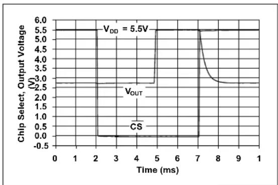
| Time (ms) | Chip Select, Output Voltage (V) | | --------- | ------------------------------- | | 0 | 2.5 | | 2 | 2.5 | | 4 | 2.5 | | 5 | 5.5 | | 7 | 5.5 | | 8 | 3.0 | | 1 | 2.5 |FIGURE 2-39: Chip Select (CS) Step Response (MCP6548 only).
line
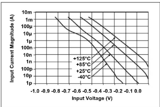
| Input Voltage (V) | +125°C | +85°C | +25°C | -40°C | | ----------------- | ------ | ----- | ----- | ----- | | -1.0 | 10m | 1m | 10μ | 1μ | | -0.9 | 1m | 1n | 10n | 1n | | -0.8 | 10n | 1n | 10p | 1p | | -0.7 | 10m | 1n | 10p | 1p | | -0.6 | 1m | 1n | 10p | 1p | | -0.5 | 1m | 1n | 10p | 1p | | -0.4 | 1m | 1n | 10p | 1p | | -0.3 | 1m | 1n | 10p | 1p | | -0.2 | 1m | 1n | 10p | 1p | | -0.1 | 1m | 1n | 10p | 1p | | 0.0 | 1m | 1n | 10p | 1p |FIGURE 2-42: Input Bias Current vs. Input Voltage.
3.0 PIN DESCRIPTIONS
Descriptions of the pins are listed in Table 3-1.
TABLE 3-1: PIN FUNCTION TABLE
| MCP6546 | MCP6546 | MCP6546R | MCP6546U | MCP6547 | MCP6548 | MCP6549 | Symbol Description |
| PDIP, SOIC, MSOP | SC-70, SOT-23 | SOT-23-5 | SC-70, SOT-23-5 | PDIP, SOIC, MSOP | PDIP, SOIC, MSOP | PDIP, SOIC, TSSOP | |
| 6 1 1 | 4 1 6 1 | OUT, OUTA | Digital Output (Comparator A) | ||||
| 2 4 4 | 3 2 2 2 | V | _IN^-, V_INA^- Inverting Input (Comparator A) | ||||
| 3 3 3 | 1 3 3 3 | V | _IN^+, V_INA^+ Noninverting Input (Comparator A) | ||||
| 7 5 2 | 5 8 7 4 | V | _DD Positive Power Supply | ||||
| — | — | — | — | 5 | — | 5 | V_INB^+ Noninverting Input (Comparator B) |
| — | — | — | — | 6 | — | 6 | V_INB^- Inverting Input (Comparator B) |
| — | — | — | — | 7 | — | 7 | OUTB Digital Output (Comparator B) |
| — | — | — | — | — | — | 8 | OUTC Digital Output (Comparator C) |
| — | — | — | — | — | — | 9 | V_INC^- Inverting Input (Comparator C) |
| — | — | — | — | — | — | 10 | V_INC^+ Noninverting Input (Comparator C) |
| 4 2 5 | 2 4 4 | 11 | V | _SS Negative Power Supply | |||
| — | — | — | — | — | — | 12 | V_IND^+ Noninverting Input (Comparator D) |
| — | — | — | — | — | — | 13 | V_IND^- Inverting Input (Comparator D) |
| — | — | — | — | — | — | 14 | OUTD Digital Output (Comparator D) |
| — | — | — | — | — | 8 | — | _CS Chip Select |
| 1, 5, 8 | — | — | — | — | 1, 5 | — | NCNo Internal Connection |
3.1 Analog Inputs
The comparator noninverting and inverting inputs are high-impedance CMOS inputs with low bias currents.
3.2 CS Digital Input
This is a CMOS, Schmitt-triggered input that places the part into a low-power mode of operation.
3.3 Digital Outputs
The comparator outputs are CMOS, open-drain digital outputs. They are designed to make level shifting and wired-OR easy to implement.
3.4 Power Supply (V SS and VDD)
The positive power supply pin ( V_DD ) is 1.6V to 5.5V higher than the negative power supply pin ( V_SS ). For normal operation, the other pins are at voltages between V_SS and V_DD , except the output pins which can be as high as 10V above V_SS .
Typically, these parts are used in a single (positive) supply configuration. In this case, V_SS is connected to ground and V_DD is connected to the supply. V_DD will need a local bypass capacitor (typically 0.01 F to 0.1 F) within 2 mm of the V_DD pin. These pins can share a bulk capacitor with nearby analog parts (within 100 mm), but it is not required.
4.0 APPLICATION INFORMATION
The MCP6546/6R/6U/7/8/9 family of push-pull output comparators are fabricated on Microchip's state-of-the-art CMOS process. They are suitable for a wide range of applications requiring very low-power consumption.
4.1 Comparator Inputs
4.1.1 PHASE REVERSAL
The MCP6546/6R/6U/7/8/9 comparator family uses CMOS transistors at the input. They are designed to prevent phase inversion when the input pins exceed the supply voltages. Figure 2-3 shows an input voltage exceeding both supplies with no resulting phase inversion.
4.1.2 INPUT VOLTAGE AND CURRENT LIMITS
The ESD protection on the inputs can be depicted as shown in Figure 4-1. This structure was chosen to protect the input transistors, and to minimize input bias current (IB). The input ESD diodes clamp the inputs when they try to go more than one diode drop below V_SS . They also clamp any voltages that go too far above V_DD ; their breakdown voltage is high enough to allow normal operation, and low enough to bypass ESD events within the specified limits.

flowchart
graph TD
    A["V_DD"] --> B["Bond Pad"]
    C["V_IN+"] --> D["Bond Pad"]
    E["V_SS"] --> F["Bond Pad"]
    B --> G["Input Stage"]
    D --> G
    F --> G
    G --> H["Bond Pad"]
    H --> I["V_IN-"]
FIGURE 4-1: Simplified Analog Input ESD Structures.
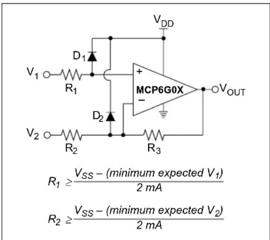
In order to prevent damage and/or improper operation of these amplifiers, the circuits they are in must limit the currents (and voltages) at the V_IN^+ and V_IN^- pins (see Absolute Maximum Ratings at the beginning of Section 1.0 “Electrical Characteristics”). Figure 4-3 shows the recommended approach to protecting these inputs. The internal ESD diodes prevent the input pins ( V_IN^+ and V_IN^- ) from going too far below ground, and the resistors R_1 and R_2 limit the possible current drawn out of the input pin. Diodes D_1 and D_2 prevent the input pin ( V_IN^+ and V_IN^- ) from going too far above V_DD . When implemented as shown, resistors R_1 and R_2 also limit the current through D_1 and D_2 .
text_image
VDD D1 + MCP6G0X - V1 R1 D2 R2 R3 V2 VOUT R1 ≥ VSS - (minimum expected V1) / 2 mA R2 ≥ VSS - (minimum expected V2) / 2 mAFIGURE 4-2: Protecting the Analog Inputs.
It is also possible to connect the diodes to the left of the resistors R_1 and R_2 . In this case, the currents through diodes D_1 and D_2 need to be limited by some other mechanism. The resistor then serves as in-rush current limiter; the DC current into the input pins ( V_IN^+ and V_IN^- ) should be very small.
A significant amount of current can flow out of the inputs when the Common-mode voltage ( V_CM ) is below ground ( V_SS ); see Figure 2-42. Applications that are high-impedance may need to limit the usable voltage range.
The input stage of this family of devices uses two differential input stages in parallel: one operates at low input voltages and the other at high input voltages. With this topology, the input voltage is 0.3V above V_DD and 0.3V below V_SS . The input offset voltage is measured at both V_SS - 0.3V and V_DD + 0.3V to ensure proper operation.
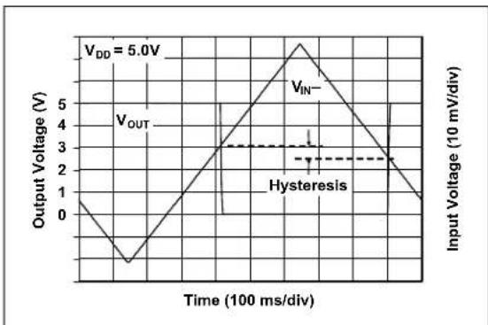
The MCP6546/6R/6U/7/8/9 family has internally set hysteresis that is small enough to maintain input offset accuracy (<7 mV), and large enough to eliminate output chattering caused by the comparator's own input noise voltage (200 V_p-P ). Figure 4-3 illustrates this capability.
line
| Time (100 ms/div) | Output Voltage (V) | Input Voltage (10 mV/div) | | ----------------- | ------------------ | ------------------------- | | 0 | 0.5 | 3.0 | | 1 | -1.0 | 3.0 | | 2 | 0.0 | 3.0 | | 3 | 2.0 | 3.0 | | 4 | 4.0 | 3.0 | | 5 | 5.0 | 3.0 | | 6 | 4.5 | 3.0 | | 7 | 3.5 | 3.0 | | 8 | 2.5 | 3.0 | | 9 | 1.5 | 3.0 | | 10 | 0.5 | 3.0 |FIGURE 4-3: The MCP6546/6R/6U/7/8/9 Comparators' Internal Hysteresis Eliminates Output Chatter Caused by Input Noise Voltage.
4.2 Open-Drain Output
The open-drain output is designed to make level-shifting and wired-OR logic easy to implement. The output can go as high as 10V for 9V battery-powered applications. The output stage minimizes switching current (shoot-through current from supply-to-supply) when the output changes state. See Figure 2-15, Figure 2-18 and Figure 2-37 through Figure 2-41 for more information.
4.3 MCP6548 Chip Select (CS)
The MCP6548 is a single comparator with a Chip Select (CS) pin. When CS is pulled high, the total current consumption drops to 20 pA (typical). 1 pA (typical) flows through the CS pin, 1 pA (typical) flows through the output pin and 18 pA (typical) flows through the V_DD pin, as shown in Figure 1-1. When this happens, the comparator output is put into a high-impedance state. By pulling CS low, the comparator is enabled. If the CS pin is left floating, the comparator will not operate properly. Figure 1-1 shows the output voltage and supply current response to a CS pulse.
The internal circuitry is designed to minimize glitches when cycling the pin. This helps conserve power, which is especially important in battery-powered applications.
4.4 Externally Set Hysteresis
Greater flexibility in selecting hysteresis, or input trip points, is achieved by using external resistors.
Input offset voltage ( V_OS ) is the center (average) of the (input-referred) low-high and high-low trip points. Input hysteresis voltage ( V_HYST ) is the difference between the same trip points. Hysteresis reduces output chattering when one input is slowly moving past the other, thus reducing dynamic supply current. It also helps in systems where it is best not to cycle between states too frequently (e.g., air conditioner thermostatic control).
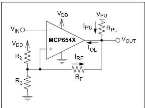
4.4.1 INVERTING CIRCUIT
Figure 4-4 shows an inverting circuit for a single-supply application using three resistors, besides the pull-up resistor. The resulting hysteresis diagram is shown in Figure 4-5.
text_image
VDD VPU IPU RPU MCP654X + - VIN VDD R2 R3 IOL IRF RF VOUTFIGURE 4-4: Inverting Circuit with Hysteresis.

FIGURE 4-5: Hysteresis Diagram for the Inverting Circuit.
In order to determine the trip voltages ( V_THL and V_TLH ) for the circuit shown in Figure 4-4, R_2 and R_3 can be simplified to the Thevenin equivalent circuit with respect to V_DD as shown in Figure 4-6.

text_image
MCP654X V23○—R23—●—R_F + V_PU R_PU V_OUTFIGURE 4-6: Thevenin Equivalent Circuit.
EQUATION 4-1:
$$ R _ {2 3} = \frac {R _ {2} R _ {3}}{R _ {2} + R _ {3}} $$
$$ V _ {2 3} = \frac {R _ {3}}{R _ {2} + R _ {3}} \times V _ {D D} $$
Using this simplified circuit, the trip voltage can be calculated using the following equation:
EQUATION 4-2:
$$ V _ {T H L} = V _ {P U} \left(\frac {R _ {2 3}}{R _ {2 3} + R _ {F} + R _ {P U}}\right) + V _ {2 3} \left(\frac {R _ {F} + R _ {P U}}{R _ {2 3} + R _ {F} + R _ {P U}}\right) $$
$$ V _ {T L H} = V _ {O L} \left(\frac {R _ {2 3}}{R _ {2 3} + R _ {F}}\right) + V _ {2 3} \left(\frac {R _ {F}}{R _ {2 3} + R _ {I ^ {\prime}}}\right) $$
V_TLH= trip voltage from low to high
V_THL = trip voltage from high to low
Figure 2-21 and Figure 2-24 can be used to determine typical values for V_OL . This voltage is dependent on the output current I_OL as shown in Figure 4-4. This current can be determined using the equation below:
EQUATION 4-3:
$$ I _ {O L} = I _ {P U} + I _ {R F} $$
$$ I _ {O L} = \left(\frac {V _ {P U} - V _ {O L}}{R _ {P U}}\right) + \left(\frac {V _ {2 3} - V _ {O L}}{R _ {2 3} + R _ {F}}\right) $$
V_OH can be calculated using the equation below:
EQUATION 4-4:
$$ V _ {O H} = (V _ {P U} - V _ {2 3}) \times \left(\frac {R _ {2 3} + R _ {F}}{R _ {2 3} + R _ {F} + R _ {P U}}\right) $$
As explained in Section 4.1 "Comparator Inputs", it is important to keep the noninverting input below V_DD + 0.3V when V_PU > V_DD .
4.5 Supply Bypass
With this family of comparators, the power supply pin ( V_DD for single supply) should have a local bypass capacitor (i.e., 0.01 F to 0.1 F) within 2 mm for good edge-rate performance.
4.6 Capacitive Loads
Reasonable capacitive loads (e.g., logic gates) have little impact on propagation delay (see Figure 2-27). The supply current increases with increasing toggle frequency (Figure 2-30), especially with higher capacitive loads.
4.7 Battery Life
In order to maximize battery life in portable applications, use large resistors and small capacitive loads. Avoid toggling the output more than necessary. Do not use Chip Select (CS) too frequently, in order to conserve power. Capacitive loads will draw additional power at start-up.
4.8 PCB Surface Leakage
In applications where low input bias current is critical, PCB (Printed Circuit Board) surface leakage effects need to be considered. Surface leakage is caused by humidity, dust or other contamination on the board. Under low humidity conditions, a typical resistance between nearby traces is 10^12 . A 5V difference would cause 5 pA of current to flow. This is greater than the MCP6546/6R/6U/7/8/9 family's bias current at 25^ (1 pA, typical).
The easiest way to reduce surface leakage is to use a guard ring around sensitive pins (or traces). The guard ring is biased at the same voltage as the sensitive pin. An example of this type of layout is shown in Figure 4-7.

text_image
V_{IN^-} V_{IN^+} V_{SS} Guard RingFIGURE 4-7: Example Guard Ring Layout for Inverting Circuit.
For the Inverting Configuration (Figure 4-4 and Figure 4-7):
a) Connect the guard ring to the noninverting input pin ( V_IN^+ ). This biases the guard ring to the same reference voltage as the comparator (e.g., V_DD/2 or ground).
b) Connect the inverting pin (V IN-) to the input pad, without touching the guard ring.
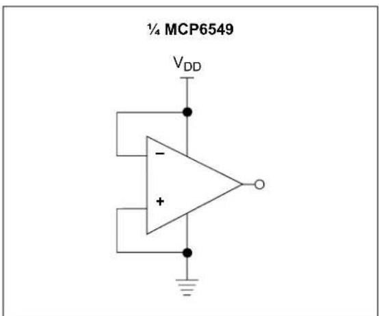
4.9 Unused Comparators
An unused amplifier in a quad package (MCP6549) should be configured as shown in Figure 4-8. This circuit prevents the output from toggling and causing crosstalk. It uses the minimum number of components and draws minimal current (see Figure 2-15 and Figure 2-18).
text_image
½ MCP6549 VDD - + +FIGURE 4-8: Unused Comparators.
4.10 Typical Applications
4.10.1 PRECISE COMPARATOR
Some applications require higher DC precision. An easy way to solve this problem is to use an amplifier (such as the MCP6041) to gain-up the input signal before it reaches the comparator. Figure 4-9 shows an example of this approach.

text_image
VDD VREF + MCP6041 - VIN R1 R2 VREF + VDD VPU RPU MCP6546 VOUTFIGURE 4-9: Precise Inverting Comparator.
4.10.2 WINDOWED COMPARATOR
Figure 4-10 shows one approach to designing a windowed comparator. The wired-OR connection produces a high output (logic 1) when the input voltage is between V_RB and V_RT (where V_RT > V_RB ).

FIGURE 4-10: Windowed Comparator.
5.0 PACKAGING INFORMATION
5.1 Package Marking Information
5-Lead SC-70 (MCP6546, MCP6546U)
Example: (I-temp)
Device
I-Temp
Code
E-Temp
Code
MCP6546 ACNN Note 2
MCP6546U BBNN Note 2
Note 1: I-Temp parts prior to March 2005 are marked "ACN"
2: SC-70-5 E-Temp parts not available at this release of the data sheet.
AC25
5-Lead SOT-23 (MCP6546, MCP6546R, MCP6546U)
Example: (I-temp)
Device
I-Temp
Code
E-Temp
Code
MCP6546 ACNN GWNN
MCP6546R AHNN
GXNN
MCP6546U
一
AWNN
Note: Applies to 5-Lead SOT-23
AC25
8-Lead PDIP (300 mil) (MCP6546, MCP6547, MCP6548, MCP6549)
Examples:
MCP6546
I/P256
1148
MCP6546
I/P ^R2 256
1148
8-Lead SOIC (150 mil) (MCP6546, MCP6547, MCP6548, MCP6549)
MCP6547
I/SN1148
256
OR
MCP6547
SNe31148
256
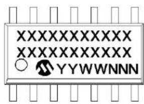
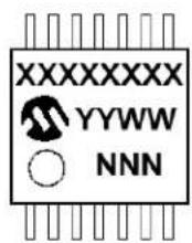
Legend: XX...X Customer-specific information
Y Year code (last digit of calendar year)
YY Year code (last 2 digits of calendar year)
WW Week code (week of January 1 is week '01')
NNN Alphanumeric traceability code
e3 Pb-free JEDEC designator for Matte Tin (Sn)
* This package is Pb-free. The Pb-free JEDEC designator ( )
e3
Note: In the event the full Microchip part number cannot be marked on one line, it will be carried over to the next line, thus limiting the number of available characters for customer-specific information.
Package Marking Information (Continued)
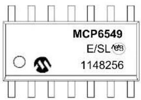
8-Lead MSOP (MCP6546, MCP6547, MCP6548) Example:


text_image
65461 14825614-Lead PDIP (300 mil) (MCP6549) Example:
text_image
XXXXXXXXXXXXXX XXXXXXXXXXXXXX YYWWNNN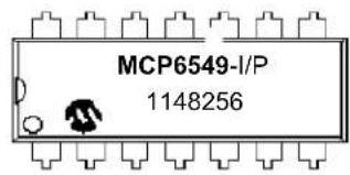
text_image
MCP6549-I/P 1148256OR

text_image
MCP6549-E/P e3 1148256OR

text_image
MCP6549 I/P83 1148256Legend: XX...X Customer-specific information
Y Year code (last digit of calendar year)
YY Year code (last 2 digits of calendar year)
WW Week code (week of January 1 is week '01')
NNN Alphanumeric traceability code
ePb-free JEDEC designator for Matte Tin (Sn)
* This package is Pb-free. The Pb-free JEDEC designator (e3)
Note: In the event the full Microchip part number cannot be marked on one line, it will be carried over to the next line, thus limiting the number of available characters for customer-specific information.
Package Marking Information (Continued)
Example:14-Lead SOIC (150 mil) (MCP6549)
text_image
XXXXXXXXXXXX XXXXXXXXXXXX ○ YYWWNNN
text_image
MCP6549ISL 1148256OR
text_image
MCP6549 E/SL® 114825614-Lead TSSOP (MCP6549) Example:

Legend: XX...X Customer-specific information Y Year code (last digit of calendar year) YY Year code (last 2 digits of calendar year) WW Week code (week of January 1 is week '01') NNN Alphanumeric traceability code ePb-free JEDEC designator for Matte Tin (Sn) * This package is Pb-free. The Pb-free JEDEC designator (e3)
Note: In the event the full Microchip part number cannot be marked on one line, it will be carried over to the next line, thus limiting the number of available characters for customer-specific information.
5-Lead Plastic Small Outline Transistor (LT) [SC70]
Note: For the most current package drawings, please see the Microchip Packaging Specification located at http://www.microchip.com/packaging
![Microchip MCP6548 - 5-Lead Plastic Small Outline Transistor (LT) [SC70] - 1](/content/2026/06/1221672/images/c8e630e089331b91257bc5eae591785416c52b1575630f3779dc6837ea549916.jpg)
text_image
D b 3 2 1 E1 E 4 e 5![Microchip MCP6548 - 5-Lead Plastic Small Outline Transistor (LT) [SC70] - 2](/content/2026/06/1221672/images/515963efa39204c5b1ed7252c649736fd337701e28b0606f70166395adfd704b.jpg)
natural_image
Isometric line drawing of an integrated circuit chip with three leads (no text or symbols)![Microchip MCP6548 - 5-Lead Plastic Small Outline Transistor (LT) [SC70] - 3](/content/2026/06/1221672/images/7c973afe922b101c84c6902e178372cee49dc68344bc8fdf8a52e9003fc52d3b.jpg)
text_image
A A2 A1![Microchip MCP6548 - 5-Lead Plastic Small Outline Transistor (LT) [SC70] - 4](/content/2026/06/1221672/images/e3c33765cb963f93cfb89d4d6618f877a602a24ee87e41f7e133cf12c34ddf89.jpg)
text_image
C L| Units | MILLIMETERS | |||
| Dimension Limitss | MINsNOMsMAX | |||
| Number of Pins | Ns | 5 | ||
| Pitchses0.65 BSC | ||||
| Overall HeightsAs0.80 - | 1.10 | |||
| Molded Package Thickness | A2 | 0.80 | - | 1.00 |
| Standoff | A1 | 0.00 | - | 0.10 |
| Overall Width | Es1.80 | 2.10 | 2.40 | |
| Molded Package Width | E1 | 1.15 | 1.25 | 1.35 |
| Overall Length | D | 1.80 | 2.00 | 2.25 |
| Foot Length | L | 0.10 | 0.20 | 0.46 |
| Lead Thickness | c | 0.08 | - | 0.26 |
| Lead Width | b | 0.15 | - | 0.40 |
Notes:
- Dimensions D and E1 do not include mold flash or protrusions. Mold flash or protrusions shall not exceed 0.127 mm per side.
2.sDimensioning and tolerancing per ASME Y14.5M.
BSC:sBasic Dimension. Theoretically exact value shown without tolerances.
Microchip Technology Drawing C04-061B
5-Lead Plastic Small Outline Transistor (LT) [SC70]
Note: For the most current package drawings, please see the Microchip Packaging Specification located at http://www.microchip.com/packaging

text_image
E Gx 3 2 1 C G 4 5 Y X SILK SCREENRECOMMENDED LAND PATTERN
| Units | MILLIMETERS | |||
| Dimension Limits | MIN | NOM | MAX | |
| Contact Pitch | E | 0.65 BSC | ||
| Contact Pad Spacing | C | 2.20 | ||
| Contact Pad Width | X | 0.45 | ||
| Contact Pad Length | Y | 0.95 | ||
| Distance Between Pads | G | 1.25 | ||
| Distance Between Pads | Gx | 0.20 | ||
Notes:
1. Dimensioning and tolerancing per ASME Y14.5M
BSC: Basic Dimension. Theoretically exact value shown without tolerances.
Microchip Technology Drawing No. C04-2061A
5-Lead Plastic Small Outline Transistor (OT) [SOT-23]
Note: For the most current package drawings, please see the Microchip Packaging Specification located at http://www.microchip.com/packaging
![Microchip MCP6548 - 5-Lead Plastic Small Outline Transistor (OT) [SOT-23] - 1](/content/2026/06/1221672/images/2ba4cf0d00096c36fe9775f138f4b2a488df6e0c16f6a51ed3ef8141f0d63e97.jpg)
| Units | MILLIMETERS | |||
| Dimension Limitss | MINsNOMsMAX | |||
| Number of Pins | Ns | 5 | ||
| Lead Pitchses0.95 BSC | ||||
| Outside Lead Pitchse1s1.90 BSC | ||||
| Overall HeightsA 0.90 - | 1.45 | |||
| Molded Package Thickness | A2 | 0.89 | - | 1.30 |
| Standoff | A1 | 0.00 | - | 0.15 |
| Overall Width | E | 2.20 | - | 3.20 |
| Molded Package Width | E1 | 1.30 | - | 1.80 |
| Overall Length | D | 2.70 | - | 3.10 |
| Foot Length | L | 0.10 | - | 0.60 |
| Footprint | L1 | 0.35 | - | 0.80 |
| Foot Angle | 0° | - | 30° | |
| Lead Thickness | c | 0.08 | - | 0.26 |
| Lead Width | b | 0.20 | - | 0.51 |
Notes:
- Dimensions D and E1 do not include mold flash or protrusions. Mold flash or protrusions shall not exceed 0.127 mm per side.
2.sDimensioning and tolerancing per ASME Y14.5M.
BSC:sBasic Dimension. Theoretically exact value shown without tolerances.
Microchip Technology Drawing C04-091B
5-Lead Plastic Small Outline Transistor (OT) [SOT-23]
Note: For the most current package drawings, please see the Microchip Packaging Specification located at http://www.microchip.com/packaging
![Microchip MCP6548 - 5-Lead Plastic Small Outline Transistor (OT) [SOT-23] - 1](/content/2026/06/1221672/images/c4609763368ed78cf98b2fec67e737b9eacec708db29c0d25df003a40a02396c.jpg)
text_image
X Y Z C G SILK SCREEN E GXRECOMMENDED LAND PATTERN
| Units | MILLIMETERS | |||
| Dimension Limits | MIN | NOM | MAX | |
| Contact Pitch | E | 0.95 BSC | ||
| Contact Pad Spacing | C | 2.80 | ||
| Contact Pad Width (X5) | X | 0.60 | ||
| Contact Pad Length (X5) | Y | 1.10 | ||
| Distance Between Pads | G | 1.70 | ||
| Distance Between Pads | GX | 0.35 | ||
| Overall Width | Z | 3.90 | ||
Notes:
1. Dimensioning and tolerancing per ASME Y14.5M
BSC: Basic Dimension. Theoretically exact value shown without tolerances.
Microchip Technology Drawing No. C04-2091A
8-Lead Plastic Dual In-Line (P) - 300 mil Body [PDIP]
Note: For the most current package drawings, please see the Microchip Packaging Specification located at http://www.microchip.com/packaging
![Microchip MCP6548 - 8-Lead Plastic Dual In-Line (P) - 300 mil Body [PDIP] - 1](/content/2026/06/1221672/images/0fdf9985a1fe3957bde4a6cc8825b97553755440428d893bd4cd2e2da1b2d1d6.jpg)
| Units | INCHES | |||
| Dimension Limitss | MINsNOMsMAX | |||
| Number of Pins | Ns | 8 | ||
| Pitchses.100 BSC | ||||
| Top to Seating PlanesAs-s-s.210 | ||||
| Molded Package Thickness | A2 | .115 | .130 | .195 |
| Base to Seating Plane | A1 | .015s-s- | ||
| Shoulder to Shoulder Width | E | .290 | .310 | .325 |
| Molded Package Width | E1 | .240 | .250 | .280 |
| Overall Length | D | .348 | .365 | .400 |
| Tip to Seating Plane | L | .115 | .130 | .150 |
| Lead Thickness | c | .008 | .010 | .015 |
| Upper Lead Width | b1 | .040 | .060 | .070 |
| Lower Lead Width | b | .014 | .018 | .022 |
| Overall Row Spacing § | eB | -s-s.430 | ||
Notes:
- sPin 1 visual index feature may vary, but must be located with the hatched area.
2.s§ Significant Characteristic. - Dimensions D and E1 do not include mold flash or protrusions. Mold flash or protrusions shall not exceed .010" per side.
4.sDimensioning and tolerancing per ASME Y14.5M.
BSC: Basic Dimension. Theoretically exact value shown without tolerances.
Microchip Technology Drawing C04-018B
8-Lead Plastic Small Outline (SN) - Narrow, 3.90 mm Body [SOIC]
Note: For the most current package drawings, please see the Microchip Packaging Specification located at http://www.microchip.com/packaging
![Microchip MCP6548 - 8-Lead Plastic Small Outline (SN) - Narrow, 3.90 mm Body [SOIC] - 1](/content/2026/06/1221672/images/87fd864f86042e7cf8abc67ba3b9a6f64b134d42da1de0bdb637736a59cfe446.jpg)
Microchip Technology Drawing No. C04-057C Sheet 1 of 2
8-Lead Plastic Small Outline (SN) - Narrow, 3.90 mm Body [SOIC]
Note: For the most current package drawings, please see the Microchip Packaging Specification located at http://www.microchip.com/packaging
![Microchip MCP6548 - 8-Lead Plastic Small Outline (SN) - Narrow, 3.90 mm Body [SOIC] - 1](/content/2026/06/1221672/images/be8987f17813be43ea2c9dcde4c3b9ef5c887810b5c3fd45fc1394fcac5e263c.jpg)
natural_image
Isometric line drawing of an integrated circuit chip with multiple pins (no text or symbols)| Units | MILLIMETERS | |||
| Dimension Limits | MIN | NOM | MAX | |
| Number of Pins | N | 8 | ||
| Pitch | e | 1.27 BSC | ||
| Overall Height | A | - | - | 1.75 |
| Molded Package Thickness | A2 | 1.25 | - | - |
| Standoff § | A1 | 0.10 | - | 0.25 |
| Overall Width | E | 6.00 BSC | ||
| Molded Package Width | E1 | 3.90 BSC | ||
| Overall Length | D | 4.90 BSC | ||
| Chamfer (Optional) | h | 0.25 | - | 0.50 |
| Foot Length | L | 0.40 | - | 1.27 |
| Footprint | L1 | 1.04 REF | ||
| Foot Angle | 0° | - | 8° | |
| Lead Thickness | c | 0.17 | - | 0.25 |
| Lead Width | b | 0.31 | - | 0.51 |
| Mold Draft Angle Top | 5° | - | 15° | |
| Mold Draft Angle Bottom | 5° | - | 15° | |
Notes:
- Pin 1 visual index feature may vary, but must be located within the hatched area.
- § Significant Characteristic
- Dimensions D and E1 do not include mold flash or protrusions. Mold flash or protrusions shall not exceed 0.15mm per side.
- Dimensioning and tolerancing per ASME Y14.5M BSC: Basic Dimension. Theoretically exact value shown without tolerances. REF: Reference Dimension, usually without tolerance, for information purposes only.
Microchip Technology Drawing No. C04-057C Sheet 2 of 2
8-Lead Plastic Small Outline (SN) – Narrow, 3.90 mm Body [SOIC]
Note: For the most current package drawings, please see the Microchip Packaging Specification located at http://www.microchip.com/packaging
![Microchip MCP6548 - 8-Lead Plastic Small Outline (SN) – Narrow, 3.90 mm Body [SOIC] - 1](/content/2026/06/1221672/images/01fb1fc5997035b7338639279e01f6c5bd200491eb883e13d089ff261a22106f.jpg)
text_image
E C SILK SCREEN Y1 X1RECOMMENDED LAND PATTERN
| Units | MILLIMETERS | |||
| Dimension Limits | MIN | NOM | MAX | |
| Contact Pitch | E | 1.27 BSC | ||
| Contact Pad Spacing | C | 5.40 | ||
| Contact Pad Width (X8) | X1 | 0.60 | ||
| Contact Pad Length (X8) | Y1 | 1.55 | ||
Notes:
- Dimensioning and tolerancing per ASME Y14.5M
BSC: Basic Dimension. Theoretically exact value shown without tolerances.
Microchip Technology Drawing No. C04-2057A
8-Lead Plastic Micro Small Outline Package (MS) [MSOP]
Note: For the most current package drawings, please see the Microchip Packaging Specification located at http://www.microchip.com/packaging
![Microchip MCP6548 - 8-Lead Plastic Micro Small Outline Package (MS) [MSOP] - 1](/content/2026/06/1221672/images/f559e6468b8bb8eb76cebdbe04d0d5f361d937a1a4a7fc70dbe74f7ef3bd8c86.jpg)
text_image
2X 0.20 H D/2 A E/2 D E1 E1/2 N E E NOTE 1 1 2 N/2 0.25 C e B NX b ⊕ 0.13 M C A-B D TOP VIEW A A2 A1 SIDE VIEW C 0.10 C SEE DETAIL C END VIEWMicrochip Technology Drawing C04-111C Sheet 1 of 2
8-Lead Plastic Micro Small Outline Package (MS) [MSOP]
Note: For the most current package drawings, please see the Microchip Packaging Specification located at http://www.microchip.com/packaging
![Microchip MCP6548 - 8-Lead Plastic Micro Small Outline Package (MS) [MSOP] - 1](/content/2026/06/1221672/images/6af9d846523940ba2679b9e5e5ed78a288a0b8f04c7123de8ec816652cc2c996.jpg)
text_image
SEATING PLANE C L (L1) GAUGE PLANE c φDETAIL C
| Units | MILLIMETERS | |||
| Dimension Limits | MIN | NOM | MAX | |
| Number of Pins | N | 8 | ||
| Pitch | e | 0.65 BSC | ||
| Overall Height | A | - | - | 1.10 |
| Molded Package Thickness | A2 | 0.75 | 0.85 | 0.95 |
| Standoff | A1 | 0.00 | - | 0.15 |
| Overall Width | E | 4.90 BSC | ||
| Molded Package Width | E1 | 3.00 BSC | ||
| Overall Length | D | 3.00 BSC | ||
| Foot Length | L | 0.40 | 0.60 | 0.80 |
| Footprint | L1 | 0.95 REF | ||
| Foot Angle | 0^ | - | 8^ | |
| Lead Thickness | c | 0.08 | - | 0.23 |
| Lead Width | b | 0.22 | - | 0.40 |
Notes:
- Pin 1 visual index feature may vary, but must be located within the hatched area.
- Dimensions D and E1 do not include mold flash or protrusions. Mold flash or protrusions shall not exceed 0.15mm per side.
- Dimensioning and tolerancing per ASME Y14.5M. BSC: Basic Dimension. Theoretically exact value shown without tolerances. REF: Reference Dimension, usually without tolerance, for information purposes only.
Microchip Technology Drawing C04-111C Sheet 2 of 2
14-Lead Plastic Small Outline (SL) - Narrow, 3.90 mm Body [SOIC]
Note: For the most current package drawings, please see the Microchip Packaging Specification located at http://www.microchip.com/packaging
![Microchip MCP6548 - 14-Lead Plastic Small Outline (SL) - Narrow, 3.90 mm Body [SOIC] - 1](/content/2026/06/1221672/images/b3db21251756dc5f4380eccc4b14c1c8aecbf7d41a304acb17feb2606c2beae9.jpg)
text_image
NOTE 1 2X 0.10 C D NOTE 5 N E1 1 2 3 e B NOTE 5 D A D E 0.10 C A-B 2X 0.20 C 2X N/2 TIPS NX b ⊕ 0.25① C A-B DTOP VIEW
![Microchip MCP6548 - 14-Lead Plastic Small Outline (SL) - Narrow, 3.90 mm Body [SOIC] - 2](/content/2026/06/1221672/images/1a94e97a1a2496745654f03b65abdfe8ff37f6c7da73abe33e135a0bc8330447.jpg)
text_image
// 0.10 C A A2 A1 SIDE VIEW 0.10 C NX SEATING PLANE C A![Microchip MCP6548 - 14-Lead Plastic Small Outline (SL) - Narrow, 3.90 mm Body [SOIC] - 3](/content/2026/06/1221672/images/c565fafd3042943985dfbb666d443b37cdb2926c4aab07aa68ecc759f0df7e44.jpg)
text_image
h H SEE VIEW C cVIEW A-A
Microchip Technology Drawing No. C04-065C Sheet 1 of 2
14-Lead Plastic Small Outline (SL) - Narrow, 3.90 mm Body [SOIC]
Note: For the most current package drawings, please see the Microchip Packaging Specification located at http://www.microchip.com/packaging
![Microchip MCP6548 - 14-Lead Plastic Small Outline (SL) - Narrow, 3.90 mm Body [SOIC] - 1](/content/2026/06/1221672/images/62a1d79bbff441b174b6ab525d58e41d2d3e1afb38e4461bf224d7e2c12f69e5.jpg)
text_image
α 4X Θ φ L (L1) 4X β![Microchip MCP6548 - 14-Lead Plastic Small Outline (SL) - Narrow, 3.90 mm Body [SOIC] - 2](/content/2026/06/1221672/images/b5d2aac8e5adb74000ca020795893af59062dbb8dc42edb1d859d61d1caac8b1.jpg)
natural_image
Isometric line drawing of an integrated circuit chip with multiple pins (no text or symbols)VIEW C
| Units | MILLIMETERS | |||
| Dimension Limits | MIN | NOM | MAX | |
| Number of Pins | N | 14 | ||
| Pitch | e | 1.27 BSC | ||
| Overall Height | A | - | - | 1.75 |
| Molded Package Thickness | A2 | 1.25 | - | - |
| Standoff § | A1 | 0.10 | - | 0.25 |
| Overall Width | E | 6.00 BSC | ||
| Molded Package Width | E1 | 3.90 BSC | ||
| Overall Length | D | 8.65 BSC | ||
| Chamfer (Optional) | h | 0.25 | - | 0.50 |
| Foot Length | L | 0.40 | - | 1.27 |
| Footprint | L1 | 1.04 REF | ||
| Lead Angle | 0° | - | - | |
| Foot Angle | 0° | - | 8° | |
| Lead Thickness | c | 0.10 | - | 0.25 |
| Lead Width | b | 0.31 | - | 0.51 |
| Mold Draft Angle Top | 5° | - | 15° | |
| Mold Draft Angle Bottom | 5° | - | 15° | |
Notes:
- Pin 1 visual index feature may vary, but must be located within the hatched area.
- § Significant Characteristic
- Dimension D does not include mold flash, protrusions or gate burrs, which shall not exceed 0.15 mm per end. Dimension E1 does not include interlead flash or protrusion, which shall not exceed 0.25 mm per side.
- Dimensioning and tolerancing per ASME Y14.5M BSC: Basic Dimension. Theoretically exact value shown without tolerances. REF: Reference Dimension, usually without tolerance, for information purposes only.
- Datums A & B to be determined at Datum H.
Microchip Technology Drawing No. C04-065C Sheet 2 of 2
14-Lead Plastic Small Outline (SL) - Narrow, 3.90 mm Body [SOIC]
Note: For the most current package drawings, please see the Microchip Packaging Specification located at http://www.microchip.com/packaging

text_image
Gx C G SILK SCREEN Y E XRECOMMENDED LAND PATTERN
| Units | MILLIMETERS | |||
| Dimension Limits | MIN | NOM | MAX | |
| Contact Pitch | E | 1.27 BSC | ||
| Contact Pad Spacing | C | 5.40 | ||
| Contact Pad Width | X | 0.60 | ||
| Contact Pad Length | Y | 1.50 | ||
| Distance Between Pads | Gx | 0.67 | ||
| Distance Between Pads | G | 3.90 | ||
Notes:
1. Dimensioning and tolerancing per ASME Y14.5M
BSC: Basic Dimension. Theoretically exact value shown without tolerances.
Microchip Technology Drawing No. C04-2065A
14-Lead Plastic Thin Shrink Small Outline (ST) - 4.4 mm Body [TSSOP]
Note: For the most current package drawings, please see the Microchip Packaging Specification located at http://www.microchip.com/packaging
![Microchip MCP6548 - 14-Lead Plastic Thin Shrink Small Outline (ST) - 4.4 mm Body [TSSOP] - 1](/content/2026/06/1221672/images/6daa8bb28862e6e58e42580bf89b08c34ec0cbb1195f945baf7b9b72dbbcc0fa.jpg)
Microchip Technology Drawing C04-087C Sheet 1 of 2
14-Lead Plastic Thin Shrink Small Outline (ST) - 4.4 mm Body [TSSOP]
Note: For the most current package drawings, please see the Microchip Packaging Specification located at http://www.microchip.com/packaging
![Microchip MCP6548 - 14-Lead Plastic Thin Shrink Small Outline (ST) - 4.4 mm Body [TSSOP] - 1](/content/2026/06/1221672/images/158e3e47155f30b52fc4b59bd3796d1a2b285af42984a4d007c36afa78460e0c.jpg)
natural_image
Isometric line drawing of an integrated circuit chip with multiple pins (no text or symbols)| Units | MILLIMETERS | |||
| Dimension Limits | MIN | NOM | MAX | |
| Number of Pins | N | 14 | ||
| Pitch | e | 0.65 BSC | ||
| Overall Height | A | - | - | 1.20 |
| Molded Package Thickness | A2 | 0.80 | 1.00 | 1.05 |
| Standoff | A1 | 0.05 | - | 0.15 |
| Overall Width | E | 6.40 BSC | ||
| Molded Package Width | E1 | 4.30 | 4.40 | 4.50 |
| Molded Package Length | D | 4.90 | 5.00 | 5.10 |
| Foot Length | L | 0.45 | 0.60 | 0.75 |
| Footprint | (L1) | 1.00 REF | ||
| Foot Angle | φ | 0° | - | 8° |
| Lead Thickness | c | 0.09 | - | 0.20 |
| Lead Width | b | 0.19 | - | 0.30 |
Notes:
- Pin 1 visual index feature may vary, but must be located within the hatched area.
- Dimensions D and E1 do not include mold flash or protrusions. Mold flash or protrusions shall not exceed 0.15mm per side.
- Dimensioning and tolerancing per ASME Y14.5M
BSC: Basic Dimension. Theoretically exact value shown without tolerances.
REF: Reference Dimension, usually without tolerance, for information purposes only.
Microchip Technology Drawing No. C04-087C Sheet 2 of 2
14-Lead Plastic Thin Shrink Small Outline (ST) - 4.4 mm Body [TSSOP]
Note: For the most current package drawings, please see the Microchip Packaging Specification located at http://www.microchip.com/packaging
![Microchip MCP6548 - 14-Lead Plastic Thin Shrink Small Outline (ST) - 4.4 mm Body [TSSOP] - 1](/content/2026/06/1221672/images/5d642effc5cf2fff7df751fc392a3bb06fbec96feca2c6ef086f01bbc9fa9ebc.jpg)
text_image
C1 E G X1 Y1 SILK SCREENRECOMMENDED LAND PATTERN
| Units | MILLIMETERS | |||
| Dimension Limits | MIN | NOM | MAX | |
| Contact Pitch | E | 0.65 BSC | ||
| Contact Pad Spacing | C1 | 5.90 | ||
| Contact Pad Width (X14) | X1 | 0.45 | ||
| Contact Pad Length (X14) | Y1 | 1.45 | ||
| Distance Between Pads | G | 0.20 | ||
Notes:
1. Dimensioning and tolerancing per ASME Y14.5M
BSC: Basic Dimension. Theoretically exact value shown without tolerances.
Microchip Technology Drawing No. C04-2087A
APPENDIX A: REVISION HISTORY
Revision H (November 2022)
The following is the list of modifications:
- Updated Section 5.1, Package Marking Information
- Made minor formatting changes throughout the document.
Revision G (February 2012)
The following is the list of modifications:
- Updated the Package Types drawing to correct the device representation of the SC-70 package.
- Updated package temperatures in the Temperature Characteristics table.
- Corrected the marking information table for the 5-Lead SC-70 package (MCP6546 and MCP6546U) in Section 5.1, Package Marking Information.
- Updated the package outline drawings in Section 5.1, Package Marking Information, to show all views for each package.
- Minor editorial changes.
Revision F (September 2007)
The following is the list of modifications:
- Corrected polarity of MCP6546U SOT-23-5 pin-out diagram on the first page.
- Updated package outline drawings in Section 5.1, Package Marking Information per Marcom.
Revision E (September 2006)
The following is the list of modifications:
- Added MCP6546U pinout for the SOT-23-5 package.
- Clarified Absolute Maximum Analog Input Voltage and Current Specifications.
- Added application information on unused comparators.
- Added disclaimer to package outline drawings.
Revision D (May 2006)
The following is the list of modifications:
- Added E-Temp parts.
- Changed minimum pull-up voltage specification (V_PU) to 1.6V for parts starting Dec. 2004 (week code 52); previous parts are specified at a minimum of V_DD .
- Changed V_HYST temperature specifications to linear and quadratic temperature coefficients.
- Changed specifications and plots to include E-Temp parts.
- Added Section 3.0, Pin Descriptions.
- Corrected package markings (Section 5.1, Package Marking Information).
- Added Appendix A: "Revision History".
Revision C (May 2003)
- Undocumented changes.
Revision B (December 2002)
- Undocumented changes.
Revision A (February 2002)
• Original Release of this Document.
NOTES:
PRODUCT IDENTIFICATION SYSTEM
To order or obtain information, e.g., on pricing or delivery, refer to the factory or the listed sales office.

Device

Temperature Range

Package
Device: MCP6546: Single Comparator
MCP6546T: Single Comparator (Tape and Reel) (SC-70, SOT-23, SOIC, MSOP)
MCP6546RT: Single Comparator (Rotated - Tape and Reel) (SOT-23 only)
MCP6546UT: Single Comparator (Tape and Reel) (SC-70, SOT-23)(SOT-23-5 is E-Temp only)
MCP6547: Dual Comparator
MCP6547T: Dual Comparator
(Tape and Reel for SOIC and MSOP)
MCP6548: Single Comparator with CS
MCP6548T: Single Comparator with CS
(Tape and Reel for SOIC and MSOP)
MCP6549: Quad Comparator
MCP6549T: Quad Comparator
(Tape and Reel for SOIC and TSSOP)
Temperature Range: I = -40^ to +85^
E^*=-40^ to +125^
* SC-70-5 E-Temp parts not available at this release of the data sheet.
Package: LT = Plastic Package (SC-70), 5-lead
OT = Plastic Small Outline Transistor (SOT-23), 5-lead
MS = Plastic MSOP, 8-lead
P = Plastic DIP (300 mil Body), 8-lead, 14-lead
SN = Plastic SOIC (150 mil Body), 8-lead
SL = Plastic SOIC (150 mil Body), 14-lead (MCP6549)
ST = Plastic TSSOP (4.4mm Body), 14-lead (MCP6549)
Examples:
a) MCP6546T-I/LT: Tape and Reel, Industrial Temperature, 5LD SC-70.
b) MCP6546T-I/OT: Tape and Reel, Industrial Temperature, 5LD SOT-23.
c) MCP6546-I/MS: Tape and Reel, Industrial Temperature, 8LD MSOP.
d) MCP6546-E/P: Extended Temperature, 8LD PDIP.
e) MCP6546-E/SN: Extended Temperature, 8LD SOIC.
a) MCP6546RT-I/OT: Tape and Reel, Industrial Temperature, 5LD SOT23.
a) MCP6546UT-E/LT: Tape and Reel, Industrial Temperature, 5LD SC-70
b) MCP6546UT-E/OT: Tape and Reel, Extended Temperature, 5LD SOT23.
a) MCP6547-I/MS: Industrial Temperature, 8LD MSOP.
b) MCP6547T-I/MS: Tape and Reel, Industrial Temperature, 8LD MSOP.
c) MCP6547-I/P: Industrial Temperature, 8LD PDIP.
d) MCP6547-E/SN: Extended Temperature, 8LD SOIC.
a) MCP6548-I/SN: Industrial Temperature, 8LD SOIC.
b) MCP6548T-I/SN: Tape and Reel, Industrial Temperature, 8LD SOIC.
c) MCP6548-I/P: Industrial Temperature, 8LD PDIP.
d) MCP6548-E/SN: Extended Temperature, 8LD SOIC.
a) MCP6549T-I/SL: Tape and Reel, Industrial Temperature, 14LD SOIC.
b) MCP6549T-E/SL: Tape and Reel, Extended Temperature, 14LD SOIC.
c) MCP6549-I/P: Industrial Temperature, 14LD PDIP.
d) MCP6549-E/ST: Extended Temperature, 14LD TSSOP.
NOTES:
Note the following details of the code protection feature on Microchip products:
• Microchip products meet the specifications contained in their particular Microchip Data Sheet.
- Microchip believes that its family of products is secure when used in the intended manner, within operating specifications, and under normal conditions.
- Microchip values and aggressively protects its intellectual property rights. Attempts to breach the code protection features of Microchip product is strictly prohibited and may violate the Digital Millennium Copyright Act.
- Neither Microchip nor any other semiconductor manufacturer can guarantee the security of its code. Code protection does not mean that we are guaranteeing the product is "unbreakable" Code protection is constantly evolving. Microchip is committed to continuously improving the code protection features of our products.
This publication and the information herein may be used only with Microchip products, including to design, test, and integrate Microchip products with your application. Use of this information in any other manner violates these terms. Information regarding device applications is provided only for your convenience and may be superseded by updates. It is your responsibility to ensure that your application meets with your specifications. Contact your local Microchip sales office for additional support or, obtain additional support at https://www.microchip.com/en-us/support/design-help/client-support-services.
THIS INFORMATION IS PROVIDED BY MICROCHIP "AS IS". MICROCHIP MAKES NO REPRESENTATIONS OR WARRANTIES OF ANY KIND WHETHER EXPRESS OR IMPLIED, WRITTEN OR ORAL, STATUTORY OR OTHERWISE, RELATED TO THE INFORMATION INCLUDING BUT NOT LIMITED TO ANY IMPLIED WARRANTIES OF NON-INFRINGEMENT, MERCHANTABILITY, AND FITNESS FOR A PARTICULAR PURPOSE, OR WARRANTIES RELATED TO ITS CONDITION, QUALITY, OR PERFORMANCE.
IN NO EVENT WILL MICROCHIP BE LIABLE FOR ANY INDIRECT, SPECIAL, PUNITIVE, INCIDENTAL, OR CONSEQUENTIAL LOSS, DAMAGE, COST, OR EXPENSE OF ANY KIND WHATSOEVER RELATED TO THE INFORMATION OR ITS USE, HOWEVER CAUSED, EVEN IF MICROCHIP HAS BEEN ADVISED OF THE POSSIBILITY OR THE DAMAGES ARE FORESEEABLE. TO THE FULLEST EXTENT ALLOWED BY LAW, MICROCHIP'S TOTAL LIABILITY ON ALL CLAIMS IN ANY WAY RELATED TO THE INFORMATION OR ITS USE WILL NOT EXCEED THE AMOUNT OF FEES, IF ANY, THAT YOU HAVE PAID DIRECTLY TO MICROCHIP FOR THE INFORMATION.
Use of Microchip devices in life support and/or safety applications is entirely at the buyer's risk, and the buyer agrees to defend, indemnify and hold harmless Microchip from any and all damages, claims, suits, or expenses resulting from such use. No licenses are conveyed, implicitly or otherwise, under any Microchip intellectual property rights unless otherwise stated.
Trademarks
The Microchip name and logo, the Microchip logo, Adaptec, AVR, AVR logo, AVR Freaks, BesTime, BitCloud, CryptoMemory, CryptoRF, dsPIC, flexPWR, HELDO, IGLOO, JukeBlox, KeeLoq, Kleer, LANCheck, LinkMD, maXStylus, maXTouch, MediaLB, megaAVR, Microsemi, Microsemi logo, MOST, MOST logo, MPLAB, OptoLyzer, PIC, picoPower, PICSTART, PIC32 logo, PolarFire, Prochip Designer, QTouch, SAM-BA, SenGenuity, SpyNIC, SST, SST Logo, SuperFlash, Symmetricom, SyncServer, Tachyon, TimeSource, tinyAVR, UNI/O, Vectron, and XMEGA are registered trademarks of Microchip Technology Incorporated in the U.S.A. and other countries.
AgileSwitch, APT, ClockWorks, The Embedded Control Solutions Company, EtherSynch, Flashtec, Hyper Speed Control, HyperLight Load, Libero, motorBench, mTouch, Powermite 3, Precision Edge, ProASIC, ProASIC Plus, ProASIC Plus logo, Quiet-Wire, SmartFusion, SyncWorld, Temux, TimeCesium, TimeHub, TimePictra, TimeProvider, TrueTime, and ZL are registered trademarks of Microchip Technology Incorporated in the U.S.A.
Adjacent Key Suppression, AKS, Analog-for-the-Digital Age, Any Capacitor, AnyIn, AnyOut, Augmented Switching, BlueSky, BodyCom, Clockstudio, CodeGuard, CryptoAuthentication, CryptoAutomotive, CryptoCompanion, CryptoController, dsPICDEM, dsPICDEM.net, Dynamic Average Matching, DAM, ECAN, Espresso T1S, EtherGREEN, GridTime, IdealBridge, In-Circuit Serial Programming, ICSP, INICnet, Intelligent Paralleling, IntelliMOS, Inter-Chip Connectivity, JitterBlocker, Knob-on-Display, KoD, maxCrypto, maxView, memBrain, Mindi, MiWi, MPASM, MPF, MPLAB Certified logo, MPLIB, MPLINK, MultiTRAK, NetDetach, Omniscient Code Generation, PICDEM, PICDEM.net, PICkit, PICtail, PowerSmart, PureSilicon, QMatrix, REAL ICE, Ripple Blocker, RTAX, RTG4, SAM-ICE, Serial Quad I/O, simpleMAP, SimpliPHY, SmartBuffer, SmartHLS, SMART-I.S., storClad, SQI, SuperSwitcher, SuperSwitcher II, Switchtec, SynchroPHY, Total Endurance, Trusted Time, TSHARC, USBCheck, VariSense, VectorBlox, VeriPHY, ViewSpan, WiperLock, XpressConnect, and ZENA are trademarks of Microchip Technology Incorporated in the U.S.A. and other countries.
SQTP is a service mark of Microchip Technology Incorporated in the U.S.A.
The Adaptec logo, Frequency on Demand, Silicon Storage Technology, and Symmcom are registered trademarks of Microchip Technology Inc. in other countries.
GestIC is a registered trademark of Microchip Technology Germany II GmbH & Co. KG, a subsidiary of Microchip Technology Inc., in other countries.
All other trademarks mentioned herein are property of their respective companies.
© 2002-2022, Microchip Technology Incorporated and its subsidiaries.
All Rights Reserved.
ISBN: 978-1-6683-1529-3
For information regarding Microchip's Quality Management Systems, please visit www.microchip.com/quality.
Worldwide Sales and Service
AMERICAS
Corporate Office
2355 West Chandler Blvd.
Chandler, AZ 85224-6199
Tel: 480-792-7200
Fax: 480-792-7277
Technical Support:
http://www.microchip.com/
support
Web Address:
www.microchip.com
Atlanta
Duluth, GA
Tel: 678-957-9614
Fax: 678-957-1455
Austin, TX
Tel: 512-257-3370
Boston
Westborough, MA
Tel: 774-760-0087
Fax: 774-760-0088
Chicago
Itasca, IL
Tel: 630-285-0071
Fax: 630-285-0075
Dallas
Addison, TX
Tel: 972-818-7423
Fax: 972-818-2924
Detroit
Novi, MI
Tel: 248-848-4000
Houston, TX
Tel: 281-894-5983
Indianapolis
Noblesville, IN
Tel: 317-773-8323
Fax: 317-773-5453
Tel: 317-536-2380
Los Angeles
Mission Viejo, CA
Tel: 949-462-9523
Fax: 949-462-9608
Tel: 951-273-7800
Raleigh, NC
Tel: 919-844-7510
New York, NY
Tel: 631-435-6000
San Jose, CA
Tel: 408-735-9110
Tel: 408-436-4270
Canada - Toron
Tel: 905-695-1980
Fax: 905-695-2078
ASIA/PACIFIC
Australia - Sydney
Tel: 61-2-9868-6733
China - Beijing
Tel: 86-10-8569-7000
China - Chengdu
Tel: 86-28-8665-5511
China - Chongqing
Tel: 86-23-8980-9588
China - Dongguan
Tel: 86-769-8702-9880
China - Guangzhou
Tel: 86-20-8755-8029
China - Hangzhou
Tel: 86-571-8792-8115
China - Hong Kong SAR
Tel: 852-2943-5100
China - Nanjing
Tel: 86-25-8473-2460
China - Qingdao
Tel: 86-532-8502-7355
China - Shanghai
Tel: 86-21-3326-8000
China - Shenyang
Tel: 86-24-2334-2829
China - Shenzhen
Tel: 86-755-8864-2200
China - Suzhou
Tel: 86-186-6233-1526
China - Wuhan
Tel: 86-27-5980-5300
China - Xian
Tel: 86-29-8833-7252
China - Xiamen
Tel: 86-592-2388138
China - Zhuhai
Tel: 86-756-3210040
ASIA/PACIFIC
India - Bangalore
Tel: 91-80-3090-4444
India - New Delhi
Tel: 91-11-4160-8631
India - Pune
Tel: 91-20-4121-0141
Japan - Osaka
Tel: 81-6-6152-7160
Japan - Tokyo
Tel: 81-3-6880-3770
Korea - Daegu
Tel: 82-53-744-4301
Korea - Seoul
Tel: 82-2-554-7200
Malaysia - Kuala Lumpur
Tel: 60-3-7651-7906
Malaysia - Penang
Tel: 60-4-227-8870
Philippines - Manila
Tel: 63-2-634-9065
Singapore
Tel: 65-6334-8870
Taiwan - Hsin Chu
Tel: 886-3-577-8366
Taiwan - Kaohsiung
Tel: 886-7-213-7830
Taiwan - Taipei
Tel: 886-2-2508-8600
Thailand - Bangkok
Tel: 66-2-694-1351
Tel: 43-7242-2244-39
Fax: 43-7242-2244-393
Denmark - Copenhagen
Tel: 45-4485-5910
Fax: 45-4485-2829
Finland - Espoo
Tel: 358-9-4520-820
France - Paris
Tel: 33-1-69-53-63-20
Fax: 33-1-69-30-90-79
Germany - Garching
Tel: 49-8931-9700
Germany - Haan
Tel: 49-2129-3766400
Germany - Heilbronn
Tel: 49-7131-72400
Germany - Karlsruhe
Tel: 49-721-625370
Germany - Munich
Tel: 49-89-627-144-0
Fax: 49-89-627-144-44
Germany - Rosenheim
Tel: 49-8031-354-560
Israel - Ra'anana
Tel: 972-9-744-7705
Italy - Milan
Tel: 39-0331-742611
Fax: 39-0331-466781
Italy - Padova
Tel: 39-049-7625286
Netherlands - Drunen
Tel: 31-416-690399
Fax: 31-416-690340
Norway - Trondheim
Tel: 47-7288-4388
Poland - Warsaw
Tel: 48-22-3325737
Romania - Bucharest
Tel: 40-21-407-87-50
Spain - Madrid
Tel: 34-91-708-08-90
Fax: 34-91-708-08-91
Sweden - Gothenberg
Tel: 46-31-704-60-40
Sweden - Stockholm
Tel: 46-8-5090-4654
UK - Wokingham
Tel: 44-118-921-5800
Fax: 44-118-921-5820